ECE 255, BJT Small Signal Analysis 22 February 201 In this lecture, we will introduce small-signal analysis, operation, and models from Section 7.2 of Sedra and Smith. Unlike the text book, we will follow the historical development and start with the BJT case. In the small-signal analysis, one assumes that the device is biased at a DC operating point, and then, a small signal is super-imposed on the DC biasing point. 1 The DC Bias Point and Linearization–The BJT Case Before one starts, it will be prudent to refresh our memory on the salient features of the BJT from Table 6.2 of Sedra and Smith. Printed on March 14, 2018 at 10 : 43: W.C. Chew and S.K. Gupta. 1

Welcome message from author
This document is posted to help you gain knowledge. Please leave a comment to let me know what you think about it! Share it to your friends and learn new things together.
Transcript
ECE 255, BJT Small Signal Analysis
22 February 201
In this lecture, we will introduce small-signal analysis, operation, and modelsfrom Section 7.2 of Sedra and Smith. Unlike the text book, we will follow thehistorical development and start with the BJT case.
In the small-signal analysis, one assumes that the device is biased at a DCoperating point, and then, a small signal is super-imposed on the DC biasingpoint.
1 The DC Bias Point and Linearization–The BJTCase
Before one starts, it will be prudent to refresh our memory on the salient featuresof the BJT from Table 6.2 of Sedra and Smith.
Printed on March 14, 2018 at 10 : 43: W.C. Chew and S.K. Gupta.
1
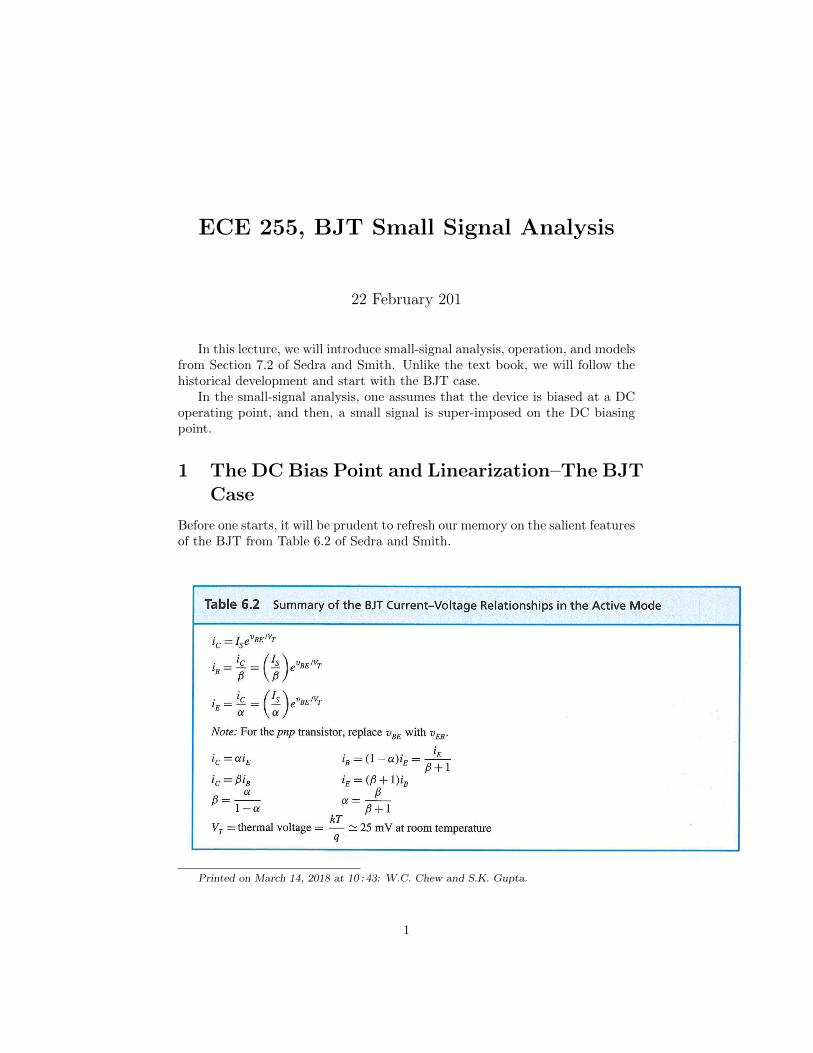
Figure 1 illustrates an npn BJT operating as an amplifier. It is being biasedwith a DC voltage, and a small signal is superimposed on top of the DC voltage.
Figure 1: Circuit diagram of a transistor amplifier (a) with a small time varyingsignal superimposed on top of a DC voltage bias source, (b) with the smallsignal turned off (Courtesy of Sedra and Smith).
Before proceeding further, one is also reminded of the i-v characteristics ofa BJT.
iC = ISevBE/VT (1.1)
iE = iC/α (1.2)
iB = iC/β (1.3)
vCE = vCC − iCRC (1.4)
In the above
iC = IC + ic, vBE = VBE + vbe, etc (1.5)
Furthermore, an uppercase variable implies a DC value, a lowercase variablewith uppercase subscript implies the total value. But a lowercase variable withlowercase subscript implies a small value which can be time varying.
Hence, the left-hand side of an equation in (1.5) above is the total value,while the first term on the right-hand side is the DC value, and the secondterm on the right-hand side is the small time varying signal or value. Similarnotations will be used for the rest of the analysis here.
2
As a consequence
iC = ISevBE/VT = ISe
(VBE+vbe)/VT = ISeVBE/VT evbe/VT (1.6)
By defining the DC quantity IC = ISeVBE/VT , the above can be rewritten as
iC = ICevbe/VT ≈ IC
(1 +
vbeVT
)= IC +
ICVT
vbe (1.7)
where it is assumed that vbe � VT . The above is the essence of Taylor seriesexpansion, as implicitly, it has been used in the aforementioned approximation.
From the above, one gathers that the small signal collector current is
ic ≈ICVT
vbe = gmvbe (1.8)
where gm = ICVT
is the transconductance. The above is the essence of lin-earization: A nonlinear relation between iC and vBE in (1.6) is now reduced toa linear relation between the small signals, ic and vbe.
Due to the exponential relation of the i-v characteristics for BJT, as opposeto the algebraic relation in MOSFET, the transconductance of a BJT is muchlarger than that of a MOSFET. It is noted that a high transconductance is good,as a small vbe gives rise to a larger ic. The transconductance can be increasedby increasing IC .
The transconductance, is related to the incremental conductance, and henceis also given by
gm =∂iC∂vBE
∣∣∣∣iC=IC
(1.9)
This relationship is also shown graphically in Figure 2. The small-signal analysisis similar performing a Taylor series approximation about the operating pointQ or the quiescent point.
3
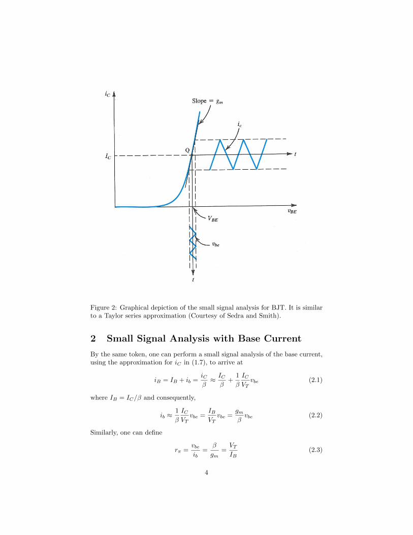
Figure 2: Graphical depiction of the small signal analysis for BJT. It is similarto a Taylor series approximation (Courtesy of Sedra and Smith).
2 Small Signal Analysis with Base Current
By the same token, one can perform a small signal analysis of the base current,using the approximation for iC in (1.7), to arrive at
iB = IB + ib =iCβ
≈ ICβ
+1
β
ICVT
vbe (2.1)
where IB = IC/β and consequently,
ib ≈1
β
ICVT
vbe =IBVT
vbe =gmβvbe (2.2)
Similarly, one can define
rπ =vbeib
=β
gm=VTIB
(2.3)
4
In the above, rπ is the incremental resistance seen by a small signal drivingthe small base current from the base to the emitter.
3 Small Signal Analysis of the Emitter Current
Applying small signal analysis to the emitter current, one gets
iE =iCα
=ICα
+icα
= IE + ie (3.1)
where
ie =icα
≈ ICαVT
vbe =IEVT
vbe (3.2)
One can define incremental emitter resistance from the above to be givenby
re =vbeie
=VTIE
=α
gm≈ 1
gm, for large β. (3.3)
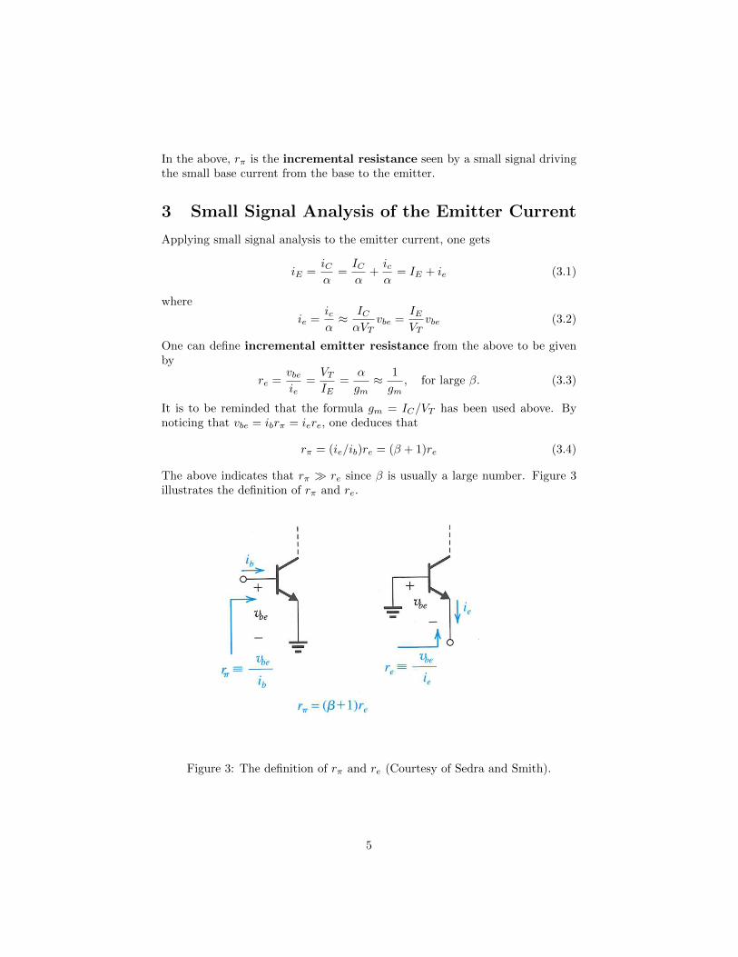
It is to be reminded that the formula gm = IC/VT has been used above. Bynoticing that vbe = ibrπ = iere, one deduces that
rπ = (ie/ib)re = (β + 1)re (3.4)
The above indicates that rπ � re since β is usually a large number. Figure 3illustrates the definition of rπ and re.
Figure 3: The definition of rπ and re (Courtesy of Sedra and Smith).
5

4 Voltage Gain
The total collector voltage vCE , by Kirchhoff voltage law (KVL), is
vCE = VCC−iCRC = VCC−(IC+ic)RC = (VCC−ICRC)−icRC = VCE−icRC(4.1)
Thus the small collector voltage is then
vce = −icRC ≈ −gmvbeRC = (−gmRC)vbe = Avvbe (4.2)
whereAv =
vcevbe
= −gmRC (4.3)
Finally, the voltage gain can be expressed as
Av = −ICRCVT
(4.4)
The negative sign comes about because if vBE increases, iC increases, and thevoltage drop across RC increases, giving rise to a decrease in the voltage dropvCE . Hence, the small signals are of opposite polarity.
Figure 4: The small signal circuit of the original amplifier circuit where the DCvoltage sources are replaced by short cirtuits (Courtesy of Sedra and Smith).
6

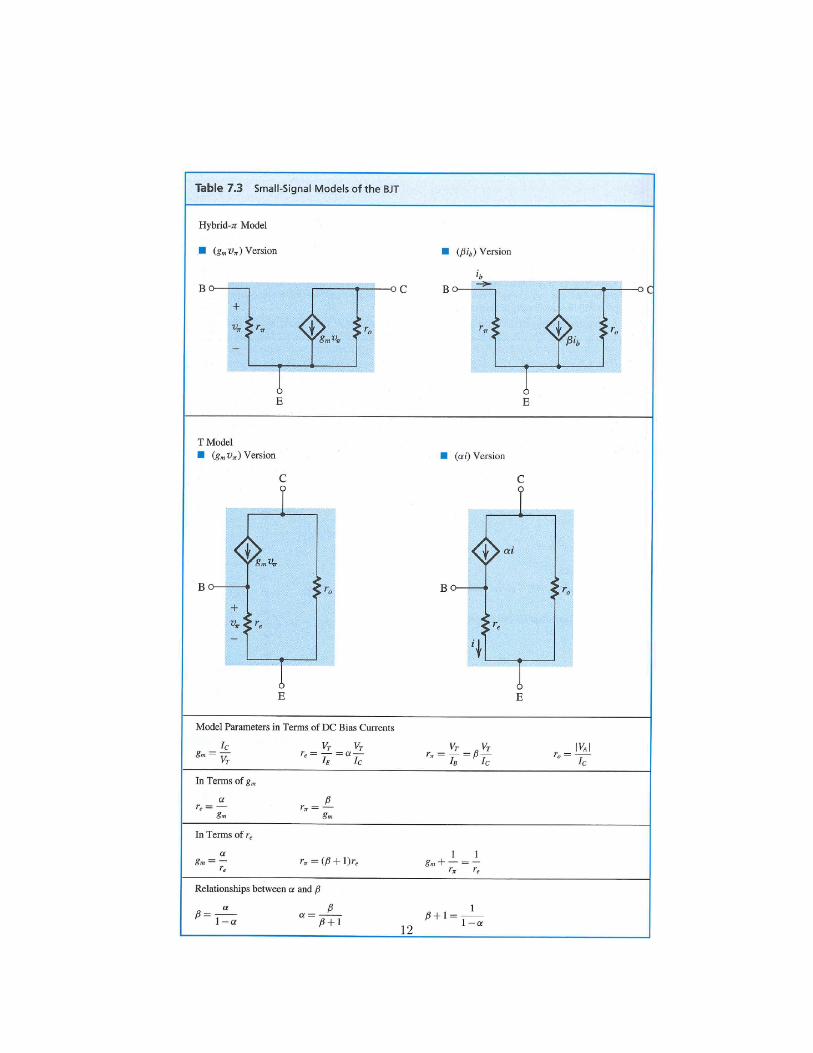
5 Hybrid-π Model
The name comes about because the circuit model looks like a π symbol (in-verted), and that both voltage and current are used in defining the model. Thehybrid-π model shown in Figure 5(a) does correctly predict the collector cur-rent ic = gmvbe and ib = vbe/rπ. Moreover, it also correctly predicts the correctvalue for ie, namely
ie =vberπ
+ gmvbe =vberπ
(1 + gmrπ) =vberπ
(1 + β) = vbe
/(rπ
1 + β
)= vbe/re
(5.1)where (2.3) and (3.4) have been used in the above.
Alternatively, one can relate the voltage vbe to the current ib, and use thecontrolled current source model shown in Figure 5(b) instead. To this end, onewrites
gmvbe = gm (ibrπ) = (gmrπ) ib = βib (5.2)
The Early effect can be accounted for by adding a resistor ro = VA/IC whereVA is the negative intercept of the Early effect, and IC is the collector currentif the Early effect is not there. These equivalent circuit model for small signalis shown in Figure 6.
It is seen that in the above model, the incremental current ic does not changewith respect to the incremental voltage vce, without the output resistor ro. Withthe output resistance ro, the incremental current ic now changes with respectto incremental voltage vce, due to base-width modulation or Early effect.
Figure 5: Two different versions of the hybrid-π model for small signals (a)voltage controlled current source (VCCS), and (b) current controlled currentsource (CCCS) (Courtesy of Sedra and Smith).
7
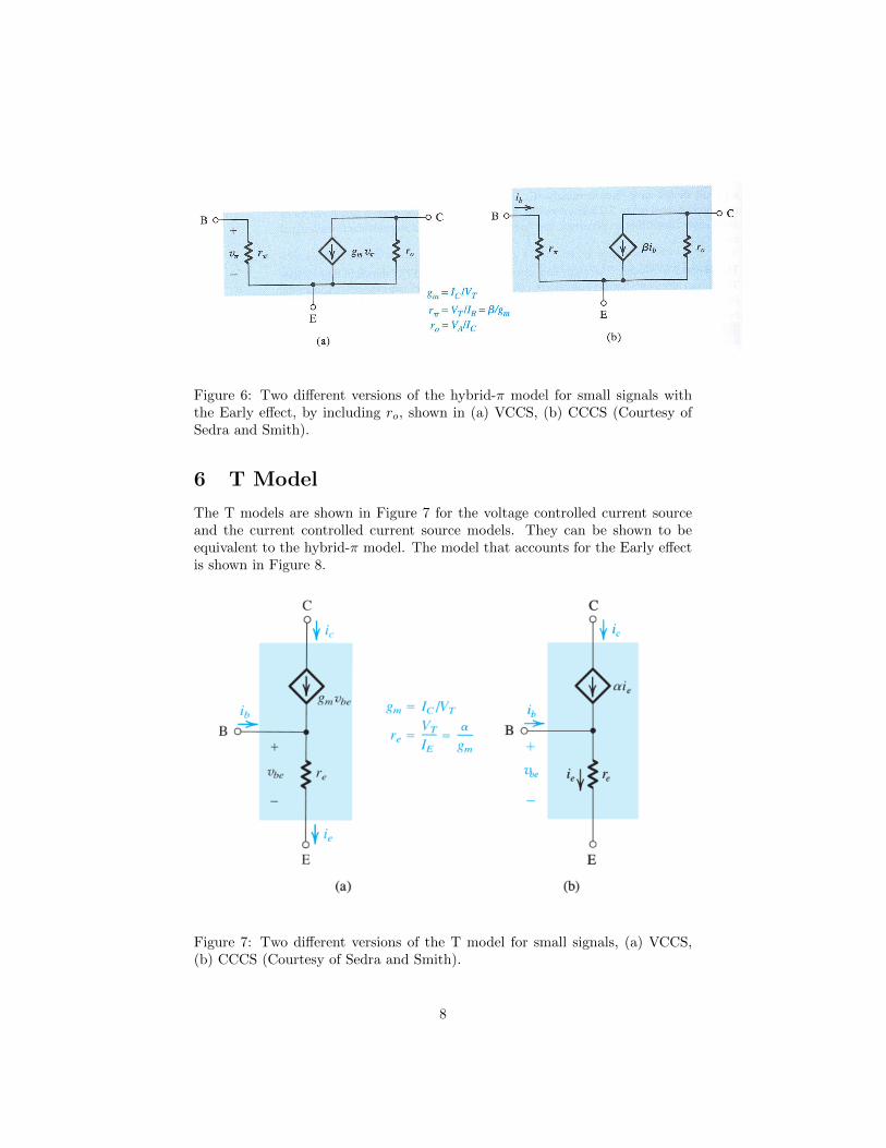
Figure 6: Two different versions of the hybrid-π model for small signals withthe Early effect, by including ro, shown in (a) VCCS, (b) CCCS (Courtesy ofSedra and Smith).
6 T Model
The T models are shown in Figure 7 for the voltage controlled current sourceand the current controlled current source models. They can be shown to beequivalent to the hybrid-π model. The model that accounts for the Early effectis shown in Figure 8.
Figure 7: Two different versions of the T model for small signals, (a) VCCS,(b) CCCS (Courtesy of Sedra and Smith).
8

Figure 8: Two different versions of the T model for small signals where theEarly effect is included (Courtesy of Sedra and Smith).
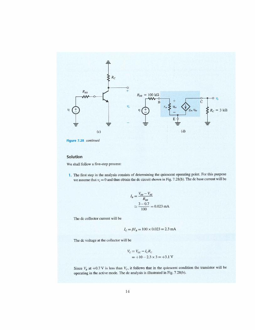
7 Small Signal Analysis on Circuit Diagram
The important point to notice about small signal analysis is that a small signalis riding on top of a larger DC signal. Then by linearization approximation, thesmall signals are actually linearly related to each other, even though the DCcomponents are nonlinearly related. The procedure outlined in Figure 9 showsthe way to derive these linear relationship.
9
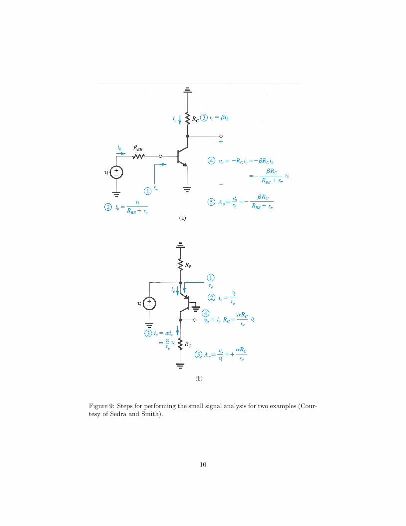
Figure 9: Steps for performing the small signal analysis for two examples (Cour-tesy of Sedra and Smith).
10

8 Summary Tables
The main points of this lecture can be summarized in summary tables.
11
12

13
14
15
Related Documents