1 ECE 20B, Winter 2003 Introduction to Electrical Engineering, II LECTURE NOTES #5 Instructor: Andrew B. Kahng (lecture) Email: [email protected] Telephone: 858-822-4884 office, 858-353-0550 cell Office: 3802 AP&M Office Hours: MW noon-1pm Class Website: http://vlsicad.ucsd.edu/courses/ece20b/wi03

Welcome message from author
This document is posted to help you gain knowledge. Please leave a comment to let me know what you think about it! Share it to your friends and learn new things together.
Transcript
1
ECE 20B, Winter 2003Introduction to Electrical Engineering, IILECTURE NOTES #5Instructor: Andrew B. Kahng (lecture)Email: [email protected]: 858-822-4884 office, 858-353-0550 cellOffice: 3802 AP&MOffice Hours: MW noon-1pm
Class Website: http://vlsicad.ucsd.edu/courses/ece20b/wi03

2
Goals for LectureXOR/XNOR Combinational Logic Blocks

3
Exclusive OR/ Exclusive NOR
The eXclusive OR (XOR) function is an important Boolean function used extensively in logic circuits. Uses for the XOR gate include:– Adders/subtractors– Parity generators/checkers– Signature analyzers– Pseudo-random sequence generators
Definitions– The XOR function is: – The eXclusive NOR (XNOR) function, otherwise
known as Equivalence is:
YXYXYX +=⊕
XYXYYX +=⊕
4
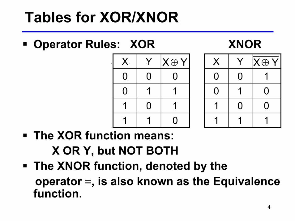
Tables for XOR/XNOR
Operator Rules: XOR XNOR
The XOR function means:X OR Y, but NOT BOTH
The XNOR function, denoted by theoperator ≡, is also known as the Equivalence function.
011101110000
YX YX⊕
111001010100
YX YX⊕

5
XOR/XNOR ExtensionThe XOR function can be extended to 3 or more variables. For more than 2 variables, it is called a modulo 2 sum (Mod 2 sum), instead of XOR:
The XOR definition, Boolean identities and Boolean theorems give:
X1XX0X =⊕=⊕1XX0XX =⊕=⊕
YXYXYXYX ⊕=⊕⊕=⊕XYYX ⊕=⊕
ZYX)ZY(XZ)YX( ⊕⊕=⊕⊕=⊕⊕
XYZZYXZYXZYXZYX +++=⊕⊕

6
XOR ImplementationsThe simple SOP implementation uses the following structure:
A NAND only implementation is:
X Y
X
Y
X Y
X
Y

7
XOR Implementations (Cont.)The AND-OR implementation is the SOP form for the XOR function:
The multiple-level NAND implementation can be derived by combining inversions as follows:
YXYXYX +=⊕
YXYXYX +=⊕
YXXYYXYX +=+=Y)(XXY +⋅=
YXYXXY ⋅+⋅=

8
Odd FunctionThe modulo 2 sum function for n variables– Contains an odd number of 1’s, and– Is therefore called the odd function.
The inverse of the modulo 2 sum function for n variables– Contains an even number of 1’s, and– Is therefore called the even function.
Implementation of even and odd functions for greater than 4 variables as a single gate is difficult, so “trees” of 2 to 4 input XOR or XNORs are used.

9
Example: Odd Function ImplementationThree-Input Odd Function:
Four Input Odd Function:
10
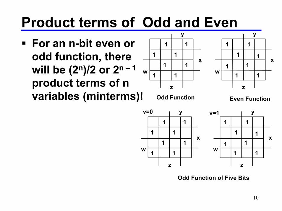
Product terms of Odd and EvenFor an n-bit even or odd function, there will be (2n)/2 or 2n – 1
product terms of n variables (minterms)!
x
y
z
w
x
y
z
w
1
1
1
1
1
1 1
1
1
1
1
1
1 1
1 1
Odd Function Even Function
x
y
z
w
x
y
z
w
1
1
1
1
1
1 1
1
1
1
1
1
1 1
1 1
Odd Function of Five Bits
v=0 v=1

11
Parity Generators/CheckersA parity tree for n data bits generates a parity bit that is appended to the data bits to form an n + 1-bit codewordExample: 3-bit even parity generator
A parity tree for n + 1 bits checks the codeword for correct parity:– C=0 if the codeword
parity is correct– C=1 if the codeword
parity is IncorrectExample: 4-bit even parity checker
XY
Z
P
XY
ZP
C
12
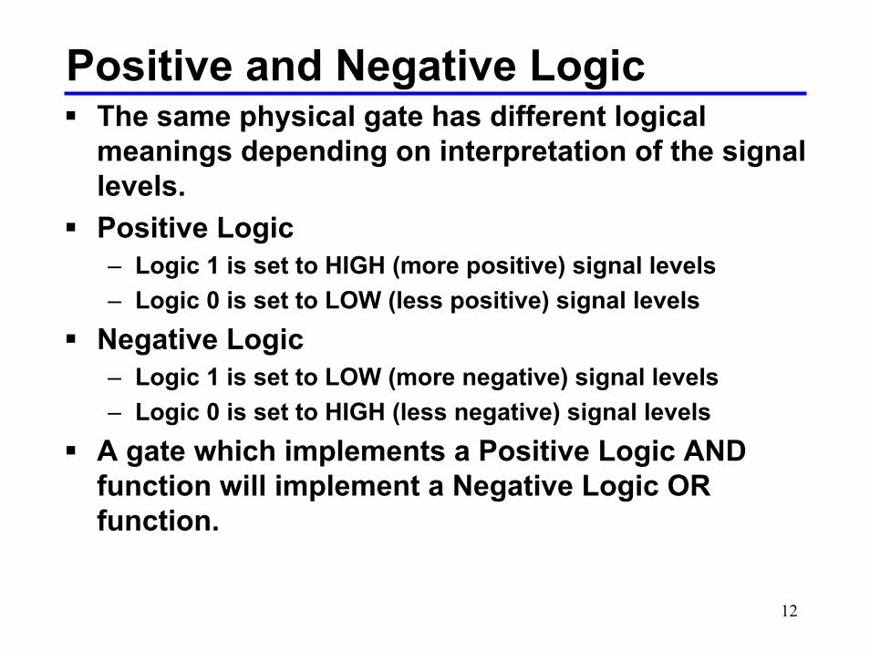
Positive and Negative LogicThe same physical gate has different logical meanings depending on interpretation of the signal levels.Positive Logic– Logic 1 is set to HIGH (more positive) signal levels– Logic 0 is set to LOW (less positive) signal levels
Negative Logic– Logic 1 is set to LOW (more negative) signal levels– Logic 0 is set to HIGH (less negative) signal levels
A gate which implements a Positive Logic AND function will implement a Negative Logic OR function.

13
Design Hierarchy (MK 3.1)Combinational CircuitsA combinational logic circuit has:– A set of m Boolean inputs,– A set of n Boolean outputs, and– n switching functions mapping the 2n input
combinations to a output such that the current output depends only on the current inputs.
A block diagram:
m Boolean Inputs n Boolean Outputs
CombinationalLogic Circuit

14
Hierarchical DesignThe function mapping inputs to outputs may be very complex– To control complexity, we decompose the function into
smaller pieces called blocks– The blocks are subdivided into finer blocks– The "leaves” in the hierarchy are called primitive blocks
Example: 16 input parity tree– Top Level: 16 inputs, one output– 2nd Level: Five 4-bit parity trees in two levels– 3rd Level: Three 2-bit exclusive-OR functions– Primitive level: Four 2-input NANDs– The design requires 5 X 3 X 4 = 60 two-input NAND
gates

15
Reusable Functions and DesignWhenever possible, we try to decompose a complex design into common, reusable function blocksThese blocks are tested and well documentedComputer-aided design (CAD) tools might include them in librariesComputer-aided manufacturing (CAM) tools might know how to manufacture and test themOther tools:– Schematic Capture– Logic Simulators– Timing Verifiers– Hardware Description Languages (HDL)

16
What is “Design (Technology)”?Design = specification, synthesis, analysis– What do I want?– Create– Check
Design Technology = Technology that enables design to occur in a timely, cost-effective way– (What happens if we can’t design new
products quickly?)LibrariesToolsMethods

17
Top-Down versus Bottom-UpA Top-Down design proceeds from an abstract, high level specification to a more and more detailed design by decomposition and successive refinementA Bottom-Up design starts with detailed primitive elements and combines them into larger and larger and more complex functionsDesigns usually proceed from both directions simultaneously– Top-Down design answers: What are we building? – Bottom-Up design answers: How do we build it?
Top-Down controls complexity while Bottom-Up controls the details

18
Analysis ProcedureSwitching Functions from Logic DiagramsGiven a logic diagram, the analysis process provides a set of Boolean equations, a truth table, or a verbal explanation of circuit behavior.Procedure:
1. Determine that the circuit is combinational (no feedback loops), then:
2. Identify and label all gate outputs that are a function of the input variables. Obtain the Boolean functions for these labeled gate outputs.
3. Identify and label all gate outputs that are a function of inputs or previously labeled gates. Obtain Boolean functions for them.
4. Repeat Step 2 until all outputs are completed. 5. Back substitute until all functions are specified in terms of
inputs only.

19
Analysis ExampleStep 2: Label all outputs of gates near inputs.
Write Boolean equations for them:
CB1T +=EB2T =
FA
C
B
B
D
E
FA
C
B
T1
T2
B
D
E

20
Analysis (Continued)
Step 3: Identify and label all gate outputs that are a function of inputs or previously labeled gates. Obtain Boolean functions for them.
Step 4: Repeat Step 3 until all doneT4 = T1 T3F = A + T4
FA
C
B
T1
T2
T4
T3
B
D
E
T2DT3 +=

21
Analysis (Continued)
Step 4: Back substitute until all functions are specified in terms of inputs only
Substituting:
FA
C
B
T1
T2
T4
T3
B
D
E
F = A + T4 T4 = T1 T3EBT2T2DT3 ⋅=+=
CBT1 +=
))EB(D()CB(AF))EB(D()CB(4T
)EB(D3T
+++=++=
⋅+=

22
Analysis Example: Code Converter
w x
y
z
AB C D
F1F2
F0
23
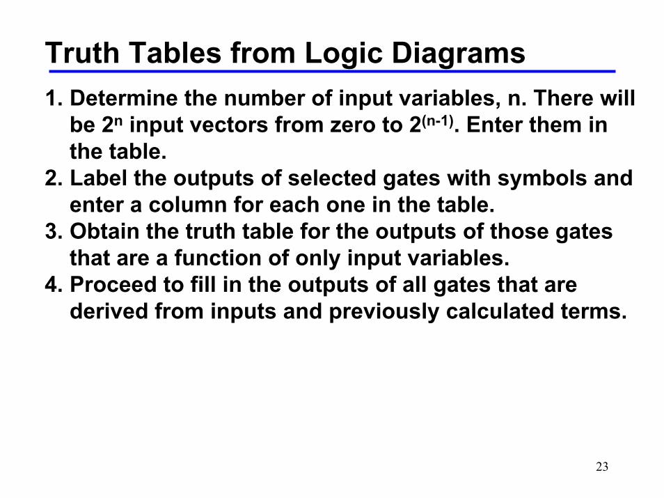
Truth Tables from Logic Diagrams1. Determine the number of input variables, n. There will
be 2n input vectors from zero to 2(n-1). Enter them in the table.
2. Label the outputs of selected gates with symbols and enter a column for each one in the table.
3. Obtain the truth table for the outputs of those gates that are a function of only input variables.
4. Proceed to fill in the outputs of all gates that are derived from inputs and previously calculated terms.

24
Truth Tables from Logic DiagramsProcedure:– Determine the number of input variables, n.
There will be 2n input vectors from zero to 2n – 1. Enter them in the table.
– Label the outputs of selected gates with symbols and enter a column for each one in the table.
– Obtain the truth table for the outputs of those gates that are a function of only input variables.
– Proceed to fill in the outputs of all gates that are derived from inputs and previously calculated terms.
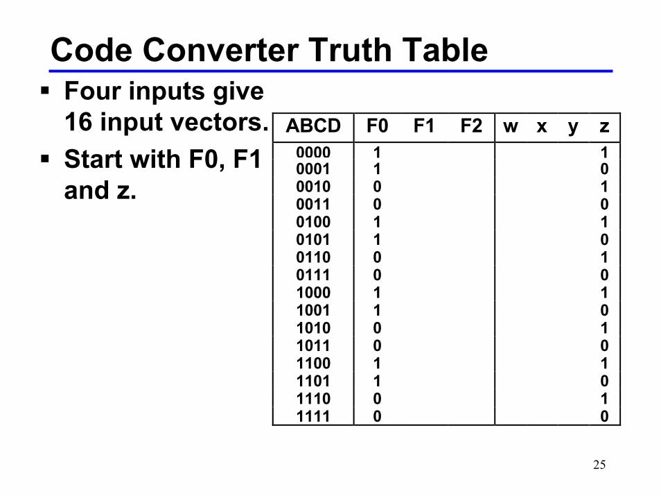
Example: Find the function table for the code converter.
25
Code Converter Truth TableFour inputs give 16 input vectors.Start with F0, F1 and z.
ABCD F0 F1 F2 w x y z
0000 1 10001 1 00010 0 10011 0 00100 1 10101 1 00110 0 10111 0 01000 1 11001 1 01010 0 11011 0 01100 1 11101 1 01110 0 11111 0 0
26
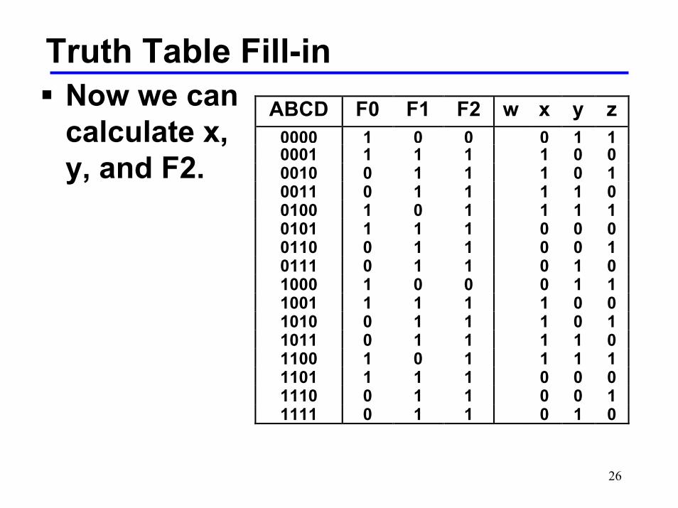
Truth Table Fill-inNow we can calculate x, y, and F2.
ABCD F0 F1 F2 w x y z0000 1 0 0 0 1 10001 1 1 1 1 0 00010 0 1 1 1 0 10011 0 1 1 1 1 00100 1 0 1 1 1 10101 1 1 1 0 0 00110 0 1 1 0 0 10111 0 1 1 0 1 01000 1 0 0 0 1 11001 1 1 1 1 0 01010 0 1 1 1 0 11011 0 1 1 1 1 01100 1 0 1 1 1 11101 1 1 1 0 0 01110 0 1 1 0 0 11111 0 1 1 0 1 0

27
Complete EntriesFinally we can fill in w to com-plete the table:
ABCD F0 F1 F2 w x y z0000 1 0 0 0 0 1 10001 1 1 1 0 1 0 00010 0 1 1 0 1 0 10011 0 1 1 0 1 1 00100 1 0 1 0 1 1 10101 1 1 1 1 0 0 00110 0 1 1 1 0 0 10111 0 1 1 1 0 1 01000 1 0 0 1 0 1 11001 1 1 1 1 1 0 01010 0 1 1 1 1 0 11011 0 1 1 1 1 1 01100 1 0 1 1 1 1 11101 1 1 1 0 0 0 01110 0 1 1 0 0 0 11111 0 1 1 0 0 1 0
28
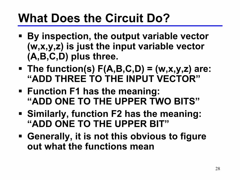
What Does the Circuit Do?By inspection, the output variable vector (w,x,y,z) is just the input variable vector (A,B,C,D) plus three.The function(s) F(A,B,C,D) = (w,x,y,z) are:“ADD THREE TO THE INPUT VECTOR”Function F1 has the meaning:“ADD ONE TO THE UPPER TWO BITS”Similarly, function F2 has the meaning:“ADD ONE TO THE UPPER BIT”Generally, it is not this obvious to figure out what the functions mean

29
Final Note (and warning)The use of "Don't Cares" in the original specification can cloud the analysis.– Note that the functions for the "w" bit differ
from the implementation in Ex. 3-2 of the book. – The book used "Don't Cares" to simplify the
logic. The example here did not. – This can be seen
by inspecting the two K-maps for the function w:
B
C
D
A
0 1 3 2
4 5 7 6
12 13 15 14
8 9 11 10
1 1
1
X X X
X X
X
1
1
w
B
C
D
A
0 1 3 2
4 5 7 6
12 13 15 14
8 9 11 10
1 1
1
1
1 11
1
w
Book Fig. 4-8 Notes Example

30
Logic Design: Functional BlocksAnalysis: From a design to a specificationof the behavior– Logic diagram to equations – Logic diagram to function table– "Word description" of circuit operation
Synthesis: From a specification to design implementation– Define the problem– Generate function table or equations– Minimize the Boolean function– Implement the circuit

31
Combinational Logic ImplementationA combinational logic circuit has:– A set of m Boolean inputs,– A set of n Boolean outputs, and– A function mapping inputs to outputs.
We think of the function as n separate Boolean functions of m inputsProcedure:– Treat each output as a separate function– Minimize the equations for each function– Implement each function independently– Sometimes an implementation can share product
or sum logic terms to arrive at a lower literal cost solution.

32
Design Procedure (MK 3.4)First, start with the specification of the circuit to be designed.– Note: this can sometimes require a lot of work
to complete the specification process, especially if it is poorly specified initially
Second, follow these steps: We will study the design of a code converter to see these steps.– Identify the inputs and outputs– Derive truth table– Obtain simplified Boolean equations– Draw the logic diagram– Check your work to verify correctness

33
Code Converter Design ExampleA code converter transforms one internal representation of data to anotherWe will start with a table of the desired conversion and minimize the resulting multiple output Boolean functionSometimes terms can be shared to minimize the implementation costThe Problem:– Design a BCD to Excess-3 code converter– Specification:
• BCD code -- 4-bit patterns "0000" to "1001" for digits 0 to 9 base 10
• Excess-3 -- BCD code plus binary "0011" for digits 0 to 9 base 10

34
Example: BCD to Excess 3Input BCD A B C D
Output Excess-3 w x y z
0 0 0 0 0 0 1 10 0 0 1 0 1 0 00 0 1 0 0 1 0 10 0 1 1 0 1 1 00 1 0 0 0 1 1 10 1 0 1 1 0 0 00 1 1 0 1 0 0 10 1 1 1 1 0 1 01 0 0 0 1 0 1 11 0 0 1 1 0 1 1
Function table:
Note:
All BCD codes greater than "9" can be assigned "Don't Cares" in the K-Map. Such BCD codes are never possible.

35
Example (Cont.): BCD to Excess 3Map functions and find minimum cost SOP equations for each
B
C
D
A
0 1 3 2
4 5 7 6
12 13 15 14
8 9 11 10
1
11
1
X X X
X X
X
1
B
C
D
A
0 1 3 2
4 5 7 6
12 13 15 14
8 9 11 10
1
11
1
X X X
X X
X
1
B
C
D
A
0 1 3 2
4 5 7 6
12 13 15 14
8 9 11 10
1 1
1
1
X X X
X X
X
1
B
C
D
A
0 1 3 2
4 5 7 6
12 13 15 14
8 9 11 10
1 1
1
X X X
X X
X
1
1
w
z y
x

36
Example (Cont.): BCD to Excess 3Next, we will manipulate the equations to expose some shared terms:
The term (C + D) can be used more than once to simplify the implementationSee Fig. 3-10 in Mano and Kime for the implementation

37
Functional Block: Decoders (MK 3.5)A Decoder converts n binary bits to a maximum of 2n
unique output lines.An m-to-n line decoder, where m < 2n, can be used to:
Generate 2n (or fewer) mintermsSelect one-of 2n items
Decoders are sometimes known as demultiplexers when enabled with a separate data-in line.

38
2-to-4 Line Decoder
B
A
BA
BA
BA
BA
This device takes: n=2 input lines and decodes minterms for:m=2n= 4 output lines.

39
2-to-4 Line Demultiplexer
B
A
BA
BA
BA
BA
XX
X
X
X
This device takes:n=2 input lines and decodes minterms for: m=22 =4 output lineswhere each output is:ANDed with an input, X.If X is viewed as an Enable, all outputs are 0 for X = 0 and one output is 1 for X = 1.If X is viewed as Data, then this data is sent to one or the outputs.
40
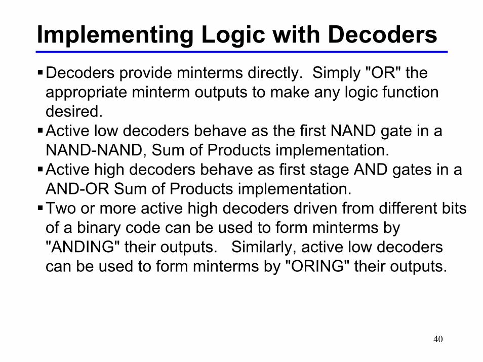
Implementing Logic with DecodersDecoders provide minterms directly. Simply "OR" the appropriate minterm outputs to make any logic function desired.Active low decoders behave as the first NAND gate in a NAND-NAND, Sum of Products implementation.Active high decoders behave as first stage AND gates in a AND-OR Sum of Products implementation.Two or more active high decoders driven from different bits of a binary code can be used to form minterms by "ANDING" their outputs. Similarly, active low decoders can be used to form minterms by "ORING" their outputs.

41
Example: F(A,B) = ∑m(0,3)
B
A
F
m0
m3For this we use a 2-to-4 line decoder and sum minterms0 and 3 with an OR gate:

42
Example: F(X,Y,Z) = ∑m(0,3,5,6)

43
Implementing Larger Minterms
This works best with widely scattered, sparse minterms.
S0
S1
D3D2
D1
D0
S0
S1
D3D2
D1
D0
AB
CD
m15
m0
m??
Minterm m15 is formedby "ANDING" the D3 outputs of each decoder. Similarly m0 is formed by "ANDING" the D0 outputs of each decoder.
What minterm is formed by "ANDING" D1 (upper) and D2 (lower) outputs?
44
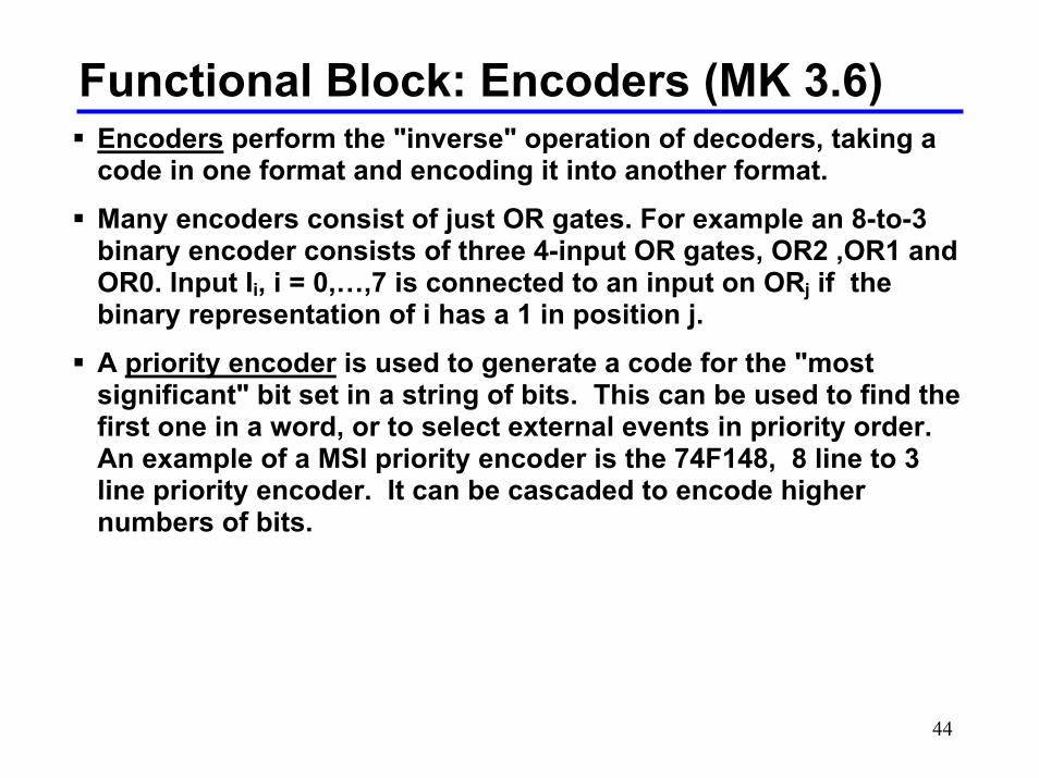
Functional Block: Encoders (MK 3.6) Encoders perform the "inverse" operation of decoders, taking a code in one format and encoding it into another format.
Many encoders consist of just OR gates. For example an 8-to-3 binary encoder consists of three 4-input OR gates, OR2 ,OR1 and OR0. Input Ii, i = 0,…,7 is connected to an input on ORj if the binary representation of i has a 1 in position j.
A priority encoder is used to generate a code for the "most significant" bit set in a string of bits. This can be used to find the first one in a word, or to select external events in priority order. An example of a MSI priority encoder is the 74F148, 8 line to 3 line priority encoder. It can be cascaded to encode higher numbers of bits.

45
Encoder ExampleEncode 4 lines 0, 1, 2, 3 into the corresponding binary codes.

46
Review: Decoders and EncodersA Decoder converts n binary bits to a maximum of 2n
unique output lines.Decoders are sometimes know as demultiplexers when enabled with a separate data-in line.Decoders implement minterms directly.Use a decoder and an OR gate to form Sum-of-Minterms directly.Encoders perform the "inverse" operation of decoders, taking a code in one format and encoding it into another format.

47
Multiplexers (MK 3.7) A Multiplexer (MUX) is another common functional block.
A Multiplexer uses n binary select bits to choose from a maximum of 2n unique input lines. Like a decoder, it decodes minterms internally. Unlike a decoder, it has only one output line. The decoded minterms are used to select data from one of up to 2n unique data input lines. The output of the multiplexer is the data input whose index is specified by the n bit code.

48
Example: A 4-to-1 multiplexer
S0
S1
I3
I2
I1
I0
X
The 4-to-1 line Multiplexer uses the same minterm decoder core.It is like a demultiplexerwith individual data inputlines (instead of just one) and an output OR gate.

49
Multiplexer Versus Decoder
S0
S1
I3
I2
I1
I0
X
B
A
BA
BA
BA
BA
XX
X
X
X
Note how similar the two are internally.
50
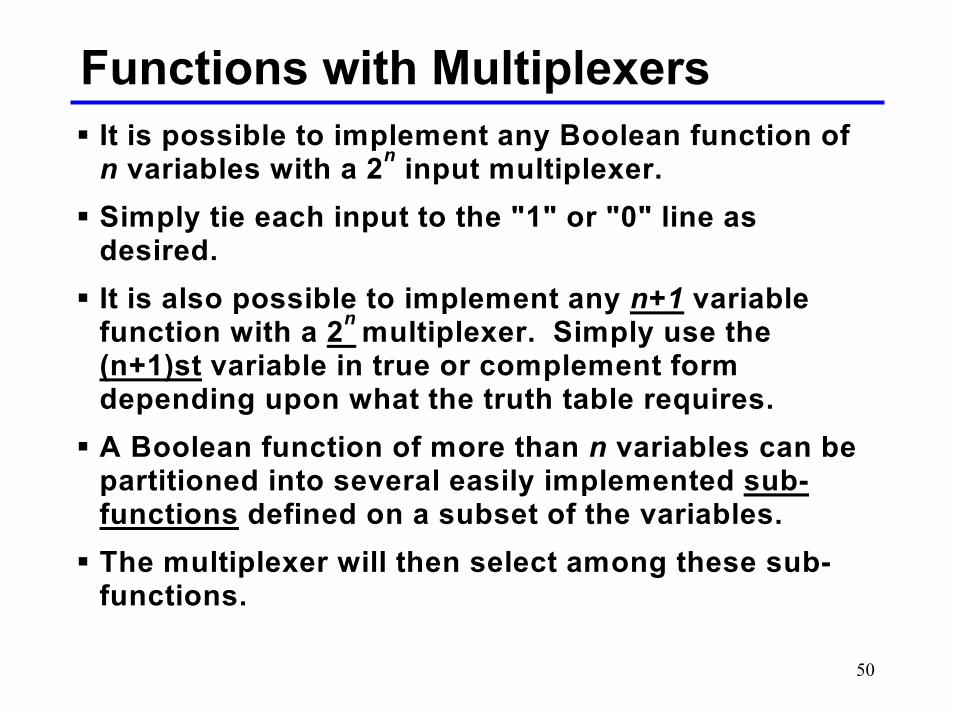
Functions with Multiplexers It is possible to implement any Boolean function of n variables with a 2n input multiplexer. Simply tie each input to the "1" or "0" line as desired. It is also possible to implement any n+1 variable function with a 2n multiplexer. Simply use the (n+1)st variable in true or complement form depending upon what the truth table requires. A Boolean function of more than n variables can be partitioned into several easily implemented sub-functions defined on a subset of the variables. The multiplexer will then select among these sub-functions.

51
Example: Gray to Binary Code Gray A B C
Binary x y z
0 0 0 0 0 0 1 0 0 0 0 1 1 1 0 0 1 0 0 1 0 0 1 1 0 1 1 1 0 0 1 1 1 1 0 1 1 0 1 1 1 0 0 0 1 1 1 1
The Gray code has adjacent elements separated by only one bit change. We wish to convert a 3-bit Gray code to a binary code. The function table on the right documents the required conversion. ⇒
The Gray to Binary Code Converter requires us to implement three separate, three-input Boolean functions.

52
Gray to Binary (Continued)
First step: Let's get the function table into a logical order by re-ordering the input Gray code values in binary sequence: ⇒
Gray A B C
Binary x y z
0 0 0 0 0 0 0 0 1 1 1 1 0 1 0 0 1 1 0 1 1 1 0 0 1 0 0 0 0 1 1 0 1 1 1 0 1 1 0 0 1 0 1 1 1 1 0 1
By inspection: x = F(A,B,C) = ∑m(1, 3, 5, 7) y = G(A,B,C) = ∑m(1, 2, 5, 6) z = H(A,B,C) = ∑m(1, 2, 4, 7)

53
Gray to Binary (Continued)The K-Maps
A
B
C
0 1 23
4 5 67 A
B
C
0 1 23
4 5 67
A
B
C
0 1 23
4 5 67
X Y
Z
1 1
1
11 1
1
1 1
1
11
Note: x(A,B,C) = C, is an easy function to
implement. (No logic gates needed!) Function y(A,B,C) = B'C + B'C is a bit
harder to implement. Function z(A,B,C) looks familiar.
What is it?

54
Gray to Binary (Continued)We know that 2n to 1 Multiplexers can be used to implement arbitrary functions of n bits. We simply connect the inputs to "0" or "1" as needed.
D3D2D1D0
S1S0
AB
S2
D4D5D6D7
Out
C
D3D2D1D0
S1S0
AB
S2
D4D5D6D7
Out
C
11
1
1
11
110
0
0
0
0
00
0
Z Y
8-to-1MUX
8-to-1MUX
Use two eight-input multiplexers to implement functions for y and z: ⇒
In this case, the MUX elements are acting like a "Read Only Memory" (ROM).

55
Other MUX ImplementationsWe can also use two 4-to-1 MUX blocks and implement y and z. Suppose we factor out A and use B and C as the select inputs to the multiplexers
1
1
1
1
00 01 11
D0 D1 D2D3
0
0
0
0
B 10
A
C
Y
0
1
0
1
00 01 11
D0 D1 D2D3
0
11
0
B 10Z
A
CA AA A
56
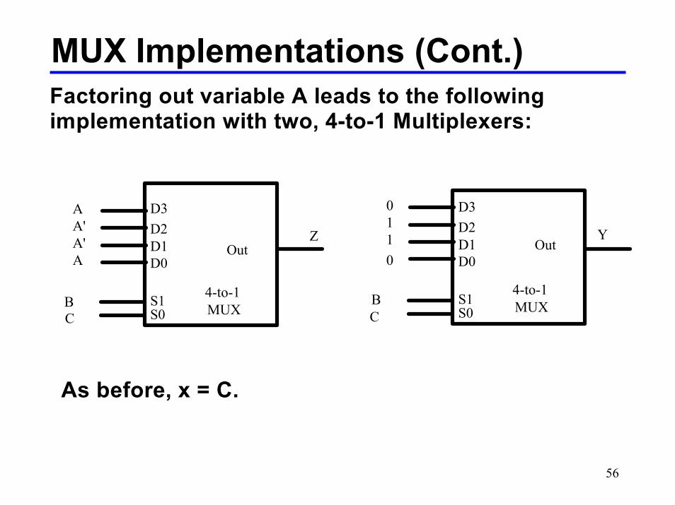
MUX Implementations (Cont.)Factoring out variable A leads to the following implementation with two, 4-to-1 Multiplexers:
D3D2D1D0
S1S0
B
Out
C
D3D2D1D0
S1S0
B
Out
C
A'A'
11
A
A
0
0
Z Y
4-to-1MUX
4-to-1MUX
As before, x = C.

57
MUX: (Cont.) Factoring Out CWe could have factored out other variables. As in the book, we will factor out C and apply AB to the select inputs:
Gray BinaryA B C x y z0 0 0 0 D0 = C 0 D0 = C 0 D0 = C0 0 1 1 1 10 1 0 0 D1 = C 1 D1 = C' 1 D1 = C'0 1 1 1 0 01 0 0 0 D2 = C 0 D2 = C 1 D2 = C'1 0 1 1 1 01 1 0 0 D3 = C 0 D3 = C' 0 D3 = C1 1 1 1 0 1
This is slightly larger than selecting A to factor out.
58
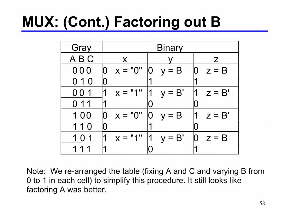
MUX: (Cont.) Factoring out BGray BinaryA B C x y z0 0 0 0 x = "0" 0 y = B 0 z = B0 1 0 0 1 10 0 1 1 x = "1" 1 y = B' 1 z = B'0 1 1 1 0 01 0 0 0 x = "0" 0 y = B 1 z = B'1 1 0 0 1 01 0 1 1 x = "1" 1 y = B' 0 z = B1 1 1 1 0 1
Note: We re-arranged the table (fixing A and C and varying B from 0 to 1 in each cell) to simplify this procedure. It still looks like factoring A was better.

59
MUX: (Cont.) Factoring out AGray BinaryA B C x y z0 0 0 0 D0 = 0 0 D0 = 0 0 D0 = A1 0 0 0 0 10 0 1 1 D1 = 1 1 D1 = 1 1 D1 = A'1 0 1 1 1 00 1 0 0 D2 = 0 1 D2 = 1 1 D2 = A'1 1 0 0 1 00 1 1 1 D3 = 1 0 D3 = 0 0 D3 = A1 1 1 1 0 1
Note: We re-arranged the table (fixing B and C and varying A from 0 to 1 in each cell) to simplify this procedure. Factoring A is best! Note also that x = C holds.

60
SummaryKnow the functions performed by the following functional blocks:– Decoders– Demultiplexers– Encoders– Multiplexers
Know how to implement Boolean functions using:– Multiplexers– Decoders
61
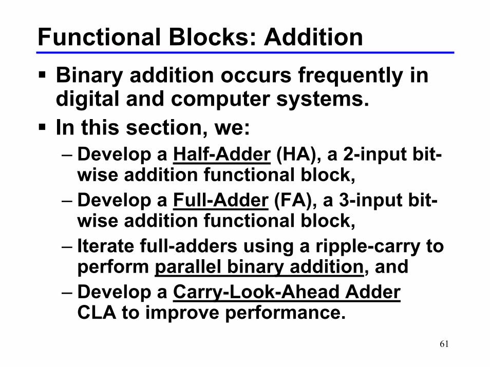
Functional Blocks: AdditionBinary addition occurs frequently in digital and computer systems.In this section, we:– Develop a Half-Adder (HA), a 2-input bit-
wise addition functional block,– Develop a Full-Adder (FA), a 3-input bit-
wise addition functional block,– Iterate full-adders using a ripple-carry to
perform parallel binary addition, and– Develop a Carry-Look-Ahead Adder
CLA to improve performance.

62
Functional Block: Half-AdderA 2-input, 1-bit width binary adder that produces the following values:
A half adder adds two bits to produce a two-bit sum.The sum is expressed as a sum bit , S and a carry bit, C.The half adder can be specified as a combined truth table for S and C: ⇒
X 0 0 1 1+ Y + 0 + 1 + 0 + 1C S 0 0 0 1 0 1 1 0
0111100110100000SCYX

63
Logic Simplification: Half-AdderThe K-Map for S, C is:This is a pretty trivial map! By inspection:
and
These equations lead to several implementations.
Y
X0 1
3211
S Y
X0 1
32 1
C
)YX()YX(SYXYXYXS
+⋅+=
⊕=⋅+⋅=
)(CYXC
)YX( ⋅=
⋅=

64
Five Implementations: Half-Adder
We can derive following sets of equations for a half-adder:
(a), (b), and (e) are SOP, POS, and XOR implementations for S. In (c), the C function is used as a term in the AND-NOR implementation of S, and in (d), the function is used in a POS term for S.
YXC)(S)c(
YXC)YX()YX(S)b(
YXCYXYXS)a(
YXC===
++==
+=
+YXCYXS)e(
)YX(C)YX(S)d(
==
+=+= C
⊕
C

65
Implementations: Half-AdderThe most common half adder implementation (e) is:
A NAND only implemen-tation (equivalent to equation d) is:
X
Y S
C
X
Y
S
C
C
YXCYXS
⋅=⊕=
)(CC)YX(S
)YX(=+=

66
Functional Block: Full-AdderA full adder is similar to a half adder, but includes a carry-in bit from lower stages. Like the half-adder, it computes a sum bit, S and a carry bit, C.– For a carry-in (Z) of
zero, it is the same as the half-adder: ⇒
– For a carry- in(Z) of one: ⇒
Z 0 0 0 0X 0 0 1 1
+ Y + 0 + 1 + 0 + 1C S 0 0 0 1 0 1 1 0
Z 1 1 1 1X 0 0 1 1
+ Y + 0 + 1 + 0 + 1C S 0 1 1 0 1 0 1 1

67
Design: Full-AdderFull-Adder Function Table: ⇒
Full-Adder K-Map:
X Y Z C S0 0 0 0 00 0 1 0 10 1 0 0 10 1 1 1 01 0 0 0 11 0 1 1 01 1 0 1 01 1 1 1 1
X
Y
Z
0 1 3 2
4 5 7 61
1
1
1S
X
Y
Z
0 1 3 2
4 5 7 61 11
1C
68
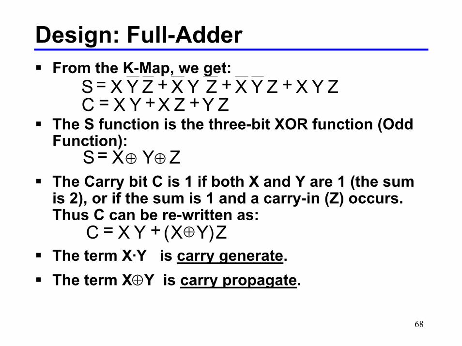
Design: Full-AdderFrom the K-Map, we get:
The S function is the three-bit XOR function (Odd Function):
The Carry bit C is 1 if both X and Y are 1 (the sum is 2), or if the sum is 1 and a carry-in (Z) occurs. Thus C can be re-written as:
The term X·Y is carry generate.The term X⊕Y is carry propagate.
ZYZXYXCZYXZYXZYXZYXS
++=+++=
ZYXS=
Z)YX(YXC +=
⊕ ⊕
⊕

69
Implementation: Full Adder
Full Adder Schematic ⇒
Here X, Y, and Z, and C (from the previous pages) are A, B, Ci and Co respectively. Also,
G = Generate and P = Propagate.
Note: This is really a combination of a 3-bit odd function (for S = sum) and Carry logic:
(G = Generate) OR (P =Propagate AND Ci = Carry In)Co = G + P · Ci
A
BP
G
S
Co
Ci

70
Parallel Binary AddersTo add more than one bit, we "bundle" sets of logical signals together and build devices that operate on the whole set in parallel.Example: 4-bit binary adder:Adds an input vector "A(3..0) " to "B(3..0)“ to get a sum S(3..0) thus: ⇒
Note: the carry out of Stage i becomes the carry in of Stage i+1.
Description Subscript3 2 1 0
Name
Input Carry 0 1 1 0 Ci
Augend 1 0 1 1 Ai
Addend 0 0 1 1 Bi
Sum 1 1 1 0 Si
Output Carry
0 0 1 1 Ci+1

71
4-bit Ripple-Carry Binary Adder
A four-bit Full Adder made from four 1-bit Full Adders: ⇒
Here FA is a Full-Adder from before: ⇒
AB
P
G
S
Co
Ci
Co Cix y
SFA
A(3)B(3)
S(3)
Co Cix y
SFA
B(2)
S(2)
Co Cix y
SFA
B(1)
S(1)
Co Cix y
SFA
S(0)
B(0)A(2) A(1) A(0)
C(4) C(3) C(2) C(1) C(0)

72
Carry Propagation & DelayOne problem with the addition of binary numbers is the length of time to propagate the ripple carry from the least significant bit to the most significant bit.The gate-level propagation path for a 4-bit ripple carry adder of the last example:
Note: The "long path" is from A(0) or B(0) though the network to either C(4) or S(3).
A(3)B(3)
S(3)
B(2)
S(2)
B(1)
S(1) S(0)
B(0)A(2) A(1) A(0)
C(4)
C(3) C(2) C(1) C(0)

73
Carry Look-AheadGiven Stage i from a Full Adder, we know that there will be a carry generated when Ai = Bi = "1", whether or not there is a carry-in.Alternately, there will be a carry propagated if the "Half-Sum" is "1" and a carry-in, Ci occurs. These two signal conditions are called Generate denoted as Gi, and Propagate denoted as Pi respectively and are shown here: ⇒
AiBi
Pi
Gi
SiCi+1
Ci
74
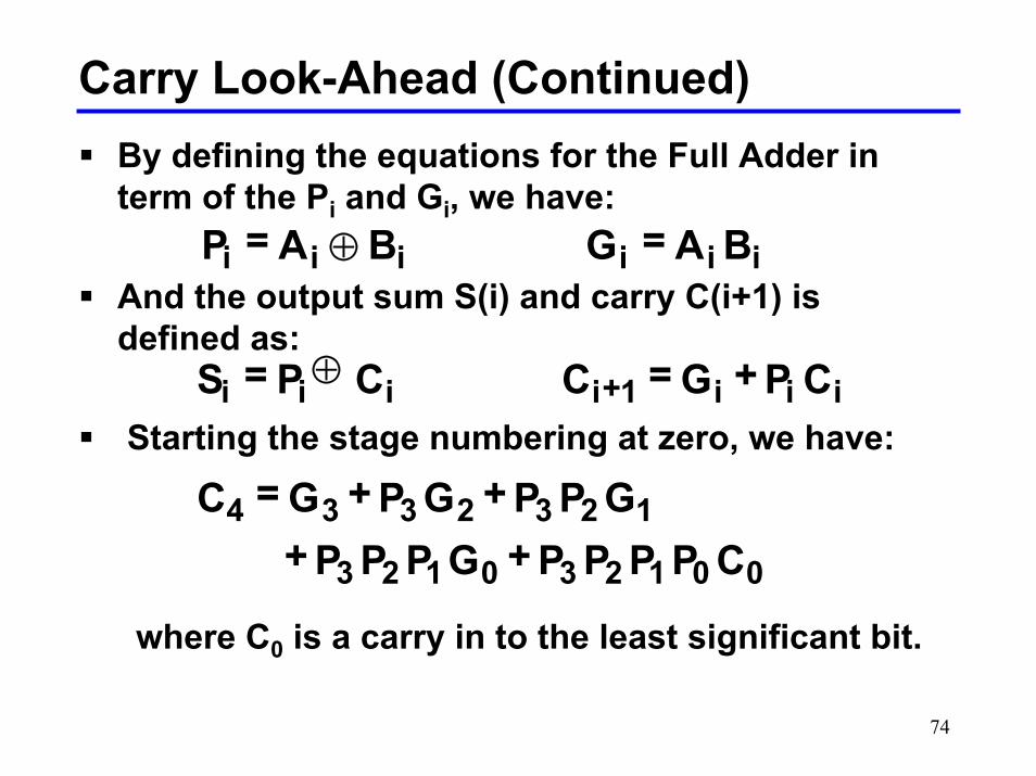
Carry Look-Ahead (Continued)By defining the equations for the Full Adder in term of the Pi and Gi, we have:
And the output sum S(i) and carry C(i+1) is defined as:
Starting the stage numbering at zero, we have:
where C0 is a carry in to the least significant bit.
iiiiii BAGBAP ==
001230123
1232334CPPPPGPPP
GPPGPGC++
++=
⊕
iii1iiii CPGCCPS +== +⊕

75
Carry Look-Ahead (Continued)Look at the following addition examples, all of which generate a carry of 1 out of the third stage:
Use a carry into Stage0 and propagate it through Stage0, Stage1, Stage2 and Stage3
1111+000010000
Generate a carry in Stage0 and propagate it through Stage1, Stage2 and Stage3
1111+00011000x
Generate a carry in Stage1 and propagate it through Stage2 and Stage3
111x+001x100xx
Generate a carry in Stage2 and propagate it through Stage3
11xx+01xx10xxx
Generate a carry in Stage31xxx+1xxx1xxxx

76
Group Carry Look-Ahead LogicFigure 3-28 in the text shows how to implement a carry look-ahead circuit for four bits. This could be extended to more than four bits. In practice, though, it becomes more difficult to implement this over more than a few bits. The concept can be extended another level by considering a Group Generate (G 0-3) and Group Propagate (P 0-3) logic condition:
Using these two equations:
Thus, it is possible to have four 4-bit adders use one of the same carry look-ahead circuits to add 16 bits!
012330
0012312323330
PPPPPGPPPPGPPGPGG
=+++=
-
-
030304 CPGC -- +=

77
ComplementsSubtraction of numbers requires a different algorithm from that for additionAdding the complement of a number is equivalent to subtractionWe will discuss two complements:– Diminished Radix Complement– Radix Complement
Subtraction will be done by adding the complement of the subtrahend

78
Diminished Radix ComplementGiven a number N in Base r having n digits, the (r – 1)’s-complement (called the Diminished Radix Complement) is defined as: (rn – 1) – NExample:– For r = 10, N = 123410, n = 4 (4 digits),we have:
(rn – 1) = 10,000 – 1 = 999910– The 9's complement of 123410 is then:
999910 - 123410 = 876510

79
Binary 1's ComplementFor r = 2, N = 011100112, n = 8 (8 digits):
(rn – 1) = 256 -1 = 25510 or 111111112The 1's complement of 011100112 is then:
11111111– 01110011
10001100Since the 2n – 1 factor consists of all 1's and since 1 – 0 = 1 and 1 – 1 = 0, the one's complement is obtained by complementing each individual bit(bitwise NOT).

80
Radix ComplementGiven a number N in Base r having n digits, the r's complement (called the radix complement) is defined as:
– rn – N for N ≠ 0 and– 0 for N = 0
The radix complement is obtained by adding 1 to the diminished radix complementExample:
–For r = 10, N = 123410, n = 4 (4 digits), we have:rn = 10,00010
–The 10's complement of 1234 is then10,000 - 1234 = 876610 or 8765 + 1 (9's
complement plus 1)

81
Binary 2's ComplementFor r = 2, N = 011100112, n = 8 (8 digits), we have:(rn ) = 25610 or 1000000002The 2's complement of 01110011 is then:
100000000– 01110011
10001101Note the result is the 1's complement plus 1

82
Alternate 2’s ComplementGiven: an n-bit binary number, beginning at the right and proceeding left: – Copy all least significant 0’s– Copy the first 1– Complement all bits thereafter.
2’s Complement Example:10010100
– Copy underlined bits:100
– and complement bits to the left:01101100

83
Subtraction with Radix ComplementsFor n-digit, unsigned numbers M and N, find M − N in base r:
– Add the r's complement of the subtrahend N to the minuend M:
M + (rn − N) = M − N + rn
– If M > N, the sum produces end carry rn which is discarded; from above, M − N remains.
– If M < N, the sum does not produce an end carry and, from above, is equal to rn − ( N − M ), the r's complement of ( N − M ).
– To obtain the result − (N – M) , take the r's complement of the sum and place a − in front.
84
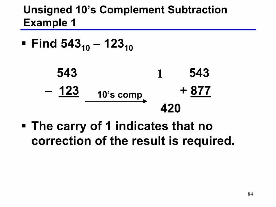
Unsigned 10’s Complement Subtraction Example 1
Find 54310 – 12310
543 543– 123 + 877
420The carry of 1 indicates that no correction of the result is required.
110’s comp

85
Unsigned 10’s Complement Subtraction Example 2
Find 12310 – 54310
123 123– 543 + 457
580 520The carry of 0 indicates that a correction of the result is required.Result = – (520)
010’s comp
10’s comp

86
Unsigned 2’s Complement Subtraction Example 1
Find 010101002 – 010000112
01010100 01010100– 01000011 + 10111101
00010001The carry of 1 indicates that no correction of the result is required.
12’s comp

87
Unsigned 2’s Complement Subtraction Example 2
Find 010000112 – 010101002
01000011 01000011– 01010100 + 10101100
1110111100010001
The carry of 0 indicates that a correction of the result is required.Result = – (00010001)
2’s comp 2’s comp
0

88
Subtraction with Diminished Radix Complement
For n-digit, unsigned numbers M and N, find M −N in base r:– Add the (r − 1)'s complement of the subtrahend N to the
minuend M:M + (rn − 1 − N) = M − N + rn − 1
– If M > N, the result is excess by rn − 1. The end carry rn
when discarded removes rn, leaving a result short by 1. To fix this shortage, whenever and end carry occurs we all 1 in the LSB position. This is called end-around carry.
– If M < N, the sum does not produce an end carry and, from above, is equal to rn − 1 − ( N − M ), the r − 1 's complement of ( N − M ).
– To obtain the result − (N – M) , take the r − 1 's complement of the sum and place a − in front.

89
Unsigned 1’s Complement Subtraction Example 1
Find 010101002 – 010000112
01010100 01010100– 01000011 + 10111100
00010000+1
00010001The end-around carry occurs.
11’s comp

90
Unsigned 1’s Complement Subtraction Example 2
Find 010000112 – 010101002
01000011 01000011– 01010100 + 10101011
1110111000010001
The carry of 0 indicates that a correction of the result is required.Result = – (00010001)
1’s comp
1’s comp
0

91
Signed IntegersPositive numbers and zero can be represented by unsigned n-digit, radix r numbers. We need a representation for negative numbers. To represent a sign (+ or –) we need exactly one more bit of information (1 binary digit gives 21 = 2 elements which is exactly what is needed).Since computers use binary numbers, by convention, (and, for convenience), the most significant bit is interpreted as a sign bit:
s an–2 … a2a1a0where:
s = 0 for Positive numbers s = 1 for Negative numbersand ai = 0 or 1 represent in some form the magnitude.

92
Signed Integer RepresentationsSigned-Magnitude – here the n – 1 digits are interpreted as a positive magnitude.Signed-Complement – here the digits are interpreted as the rest of the complement of the number. There are two possibilities here:Signed One's Complement –
– Uses 1's Complement ArithmeticSigned Two's Complement –
– Use 2's Complement Arithmetic

93
Signed Integer Representation Example
r =2, n=3Number Sign-Mag. 1's Comp. 2's Comp.
+3 011 011 011+2 010 010 010+1 001 001 001+0 000 000 000–0 100 111 —–1 101 110 111–2 110 101 110–3 111 100 101–4 — — 100
94
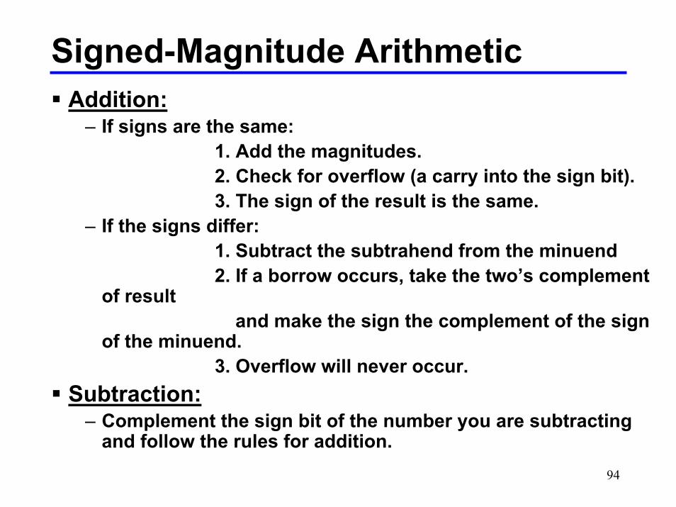
Signed-Magnitude ArithmeticAddition:
– If signs are the same:1. Add the magnitudes.2. Check for overflow (a carry into the sign bit).3. The sign of the result is the same.
– If the signs differ:1. Subtract the subtrahend from the minuend2. If a borrow occurs, take the two’s complement
of resultand make the sign the complement of the sign
of the minuend.3. Overflow will never occur.
Subtraction:– Complement the sign bit of the number you are subtracting
and follow the rules for addition.

95
Sign-Magnitude Examples
96
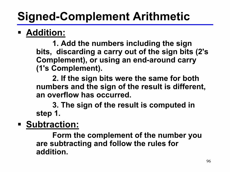
Signed-Complement ArithmeticAddition:
1. Add the numbers including the sign bits, discarding a carry out of the sign bits (2's Complement), or using an end-around carry (1's Complement).
2. If the sign bits were the same for both numbers and the sign of the result is different, an overflow has occurred.
3. The sign of the result is computed in step 1.
Subtraction:Form the complement of the number you
are subtracting and follow the rules for addition.

97
Signed 2’s Complement Examples

98
Signed 1’s Complement Examples

99
2’s Complement Adder/Subtractor
Subtraction can be accomplished by addition of the Two's Complement.
1. Complement each bit (One's Comp.)2. Add one to the result.
The following circuit computes A - B:When the Carry-In is 1, the 2’s comp of B is formed using XORs to form the 1’s comp and adding the 1 on C(0).
Co Cix y
SFA
A(3)B(3)
S(3)
Co Cix y
SFA
B(2)
S(2)
Co Cix y
SFA
B(1)
S(1)
Co Cix y
SFA
S(0)
B(0)A(2) A(1) A(0)
C(4) C(3) C(2) C(1)
C(0)

100
Overflow Detection

101
Binary MultiplicationThe binary digit multiplication table is trivial:
This is simply the Boolean AND function.Form larger products the same way we form larger products in base 10.
(a × b) b = 0 b =1a = 0 0 0a = 1 0 1

102
Review of Decimal MultiplicationPerform base 10 multiplication by:– Computing partial products, and– Justifying and summing the partial
products.To compute partial products:– Multiply the row of multiplicand digits
by each multiplier digit, one at a time.Partial product formation here require carries to be added – more complex than binary

103
Example: (237 x 149) Base 10Partial products are: 237 × 9, 237 ×4, and 237 × 1Note that the partial product summation for n digit, base 10 numbers requires adding up to n digits (with carries).Note also n x m digit multiply generates up to an m+n digit result.
2 3 7× 1 4 92 1 3 39 4 8 -
+ 2 3 7 - -3 5 3 1 3

104
Binary Multiplication AlgorithmWe compute base 2 multiplication by:– Computing partial products, and– Justifying and summing the partial products.
(same as decimal!)To compute partial products:– Multiply the row of multiplicand digits by each
multiplier digit, one at a time.– With binary numbers, partial products are very
simple! They are either:• all zero (if the multiplier digit is zero), or• the same as the multiplicand (if the multiplier digit is
one).
Note: No carries are added in partial product formation!

105
Example: (101 x 011) Base 2
Partial products are: 101 x 0, 101 x 1, and 101 x 1Note that the partial product summation for n digit, base 2 numbers requires adding up to n digits (with carries) in a column.Note also n x m digit multiply generates up to an m + ndigit result (same as decimal).
1 0 1× 0 1 1
1 0 11 0 1
0 0 0
0 0 1 1 1 1
Related Documents


![UCSD CSE 21, Spring 2014 [Section B00] Mathematics for ...vlsicad.ucsd.edu/courses/cse21-s14/slides/cse21-s14-Lecture17... · Mathematics for Algorithm and System Analysis ... •](https://static.cupdf.com/doc/110x72/5aa103ae7f8b9a67178f0db3/ucsd-cse-21-spring-2014-section-b00-mathematics-for-for-algorithm-and-system.jpg)