EC6401 Electronic Circuits II Department of ECE 2017-2018 3105-DSCET 1 EC6401-ELECTRONIC CIRCUITS II-QUESTION BANK UNIT I - FEEDBACK AMPLIFIERS PART - A (C210.1) 1. Define positive and negative feedback? Ans: Positive feedback: If the feedback voltage (or current) is so applied as to increase the input voltage (i.e. it is in phase with it), then it is called positive feedback. Negative feedback: If the feedback voltage (or current) is so applied as to reduce the input voltage (i.e. it is 180out of phase with it), then it is called negative feedback. 2. What are the advantages of negative feedback? Ans: The advantages of negative feedback are higher fidelity and stabilized gain, increased bandwidth, less distortion and reduced noise and input & output impedances can be modified as desired. 3. List four basic types of feedback? Ans: (1) Voltage series feedback (2) Voltage shunt feedback (3) Current series feedback and (4) Current shunt feedback. 4. Negative feedback is preferred to other methods of modifying Amplifier characteristics. Why? Ans: Negative feedback is preferred to other methods of modifying Amplifier Characteristics because it has the following advantages of reduction in distortion, stability in gain, increased bandwidth etc. 5. State the condition in (1+A) which a feedback amplifier must satisfy in order to be stable. Ans: The two important and necessary conditions are (1) The feedback must be positive, (2) Feedback factor must be unity i.e. A = 1 6. What is meant by phase and gain margin? Ans: Phase Margin: It is defined as 180 0 minus the magnitude of the Aat the frequency at which A is unity. If he phase margin is negative the system is stable otherwise unstable. Gain Margin: It is defined as the value of (A) in decibels at the frequency at which the phase angle of A is 180 0 . If the gain margin is negative the system is stable, otherwise the system is unstable 7. The open loop gain of an amplifier is 100.What will be the overall gain when the negative feedback of 0.5 is applied to the amplifier? Ans: The overall gain is 50 ) 01 . 0 100 ( 1 100 1 A A A f 8. List the five characteristics of an amplifier which are modified by negative feedback. (Dec-13 & May 2015) Ans: (1) Increased stability, (2) Reduction in non-linear distortion, (3) Increased bandwidth, (4) Desensitivity of transfer Amplification & (5) Sensitivity of transfer gain 9. State the three fundamental assumptions which are made in order that the expression Af = A/ (1+ A) be satisfied exactly? Ans: (1) The input signal should be transmitted to the output through the internal amplifier A and not through the feedback network. Thus if A is set to zero by reducing hfe or gm of the transistor to zero, the output must drop to zero. (2) The feedback signal travels from the output to the input through the network and not through the amplifier. (3) The reverse transmission factor of the feedback network is independent of the load and the source resistance RL and Rs 10. State Nyquist's stability criteria for feedback amplifiers. Ans: Nyquist's stability criterion states that in a complex S plane if A +1 represents a circle of unit radius with its centre at the point –1+ j0 and if A lies within the circle then 1+ A < 1, feedback is positive . Even with this positive feedback the system will not oscillate unless Nyquist criterion is satisfied. 11. What is the effect of complex loop gain and on input resistance in series voltage feedback? Ans: In series voltage amplifier the complex loop gain decreases and the input resistance increases. 12. Mention the equation relating the gains & feedback factor in a single loop feedback amplifier. Ans: A A A f 1 (For negative feedback Af < A) A A A f 1 (For positive feedback Af >A) 13. Define desensitivity. Ans: The reciprocal of sensitivity is called as de-sensitivity D = 1+A Where sensitivity is defined as the fractional change in amplification with feedback divided by the fractional change without feedback and is equal to 1/(1+A).

Welcome message from author
This document is posted to help you gain knowledge. Please leave a comment to let me know what you think about it! Share it to your friends and learn new things together.
Transcript
EC6401 Electronic Circuits II Department of ECE 2017-2018
3105-DSCET 1
EC6401-ELECTRONIC CIRCUITS II-QUESTION BANK UNIT I - FEEDBACK AMPLIFIERS
PART - A (C210.1)
1. Define positive and negative feedback?
Ans: Positive feedback: If the feedback voltage (or current) is so applied as to increase the input voltage
(i.e. it is in phase with it), then it is called positive feedback.
Negative feedback: If the feedback voltage (or current) is so applied as to reduce the input voltage (i.e. it is
180out of phase with it), then it is called negative feedback.
2. What are the advantages of negative feedback?
Ans: The advantages of negative feedback are higher fidelity and stabilized gain, increased bandwidth, less
distortion and reduced noise and input & output impedances can be modified as desired.
3. List four basic types of feedback?
Ans: (1) Voltage series feedback (2) Voltage shunt feedback (3) Current series feedback and (4) Current
shunt feedback.
4. Negative feedback is preferred to other methods of modifying Amplifier characteristics. Why? Ans: Negative feedback is preferred to other methods of modifying Amplifier Characteristics because it
has the following advantages of reduction in distortion, stability in gain, increased bandwidth etc.
5. State the condition in (1+A) which a feedback amplifier must satisfy in order to be stable.
Ans: The two important and necessary conditions are (1) The feedback must be positive, (2) Feedback
factor must be unity i.e. A = 1
6. What is meant by phase and gain margin?
Ans: Phase Margin: It is defined as 1800 minus the magnitude of the Aat the frequency at which A is
unity. If he phase margin is negative the system is stable otherwise unstable.
Gain Margin: It is defined as the value of (A) in decibels at the frequency at which the phase angle of A
is 1800. If the gain margin is negative the system is stable, otherwise the system is unstable
7. The open loop gain of an amplifier is 100.What will be the overall gain when the negative feedback
of 0.5 is applied to the amplifier?
Ans: The overall gain is 50)01.0100(1
100
1
A
AA f
8. List the five characteristics of an amplifier which are modified by negative feedback. (Dec-13 &
May 2015)
Ans: (1) Increased stability, (2) Reduction in non-linear distortion, (3) Increased bandwidth, (4)
Desensitivity of transfer Amplification & (5) Sensitivity of transfer gain
9. State the three fundamental assumptions which are made in order that the expression Af = A/ (1+
A) be satisfied exactly? Ans: (1) The input signal should be transmitted to the output through the internal amplifier A and not
through the feedback network. Thus if A is set to zero by reducing hfe or gm of the transistor to zero, the
output must drop to zero.
(2) The feedback signal travels from the output to the input through the network and not through
the amplifier.
(3) The reverse transmission factor of the feedback network is independent of the load and the
source resistance RL and Rs
10. State Nyquist's stability criteria for feedback amplifiers.
Ans: Nyquist's stability criterion states that in a complex S plane if A +1 represents a circle of unit radius
with its centre at the point –1+ j0 and if A lies within the circle then 1+ A < 1, feedback is positive .
Even with this positive feedback the system will not oscillate unless Nyquist criterion is satisfied.
11. What is the effect of complex loop gain and on input resistance in series voltage feedback?
Ans: In series voltage amplifier the complex loop gain decreases and the input resistance increases.
12. Mention the equation relating the gains & feedback factor in a single loop feedback amplifier.
Ans: A
AAf
1 (For negative feedback Af < A)
A
AA f
1 (For positive feedback Af >A)
13. Define desensitivity.
Ans: The reciprocal of sensitivity is called as de-sensitivity D = 1+A
Where sensitivity is defined as the fractional change in amplification with feedback divided by the
fractional change without feedback and is equal to 1/(1+A).
EC6401 Electronic Circuits II Department of ECE 2017-2018
3105-DSCET 2
14. What is the effect of voltage shunt feedback on input resistance and output resistance?
Ans: In voltage shunt feedback amplifier both the input & output resistance decrease.
15. Define trans resistance amplifier.
Ans: It is an amplifier; driven by a source represented by its Norton’s equivalent i.e. the current source Is
connected with the source resistance Rs in shunt. The amplifier output circuit has been represented by its
Thevenin’s equivalent. This amplifier behaves as a Trans-resistance amplifier if RI « Rs and Ro « RI.
16. Explain the ideal characteristics of voltage amplifier.
Ans: RI = , Ro = 0 and Vo = AVVs
17. What are the characteristics of trans-conductance amplifier?
Ans: The property of the transconductance amplifier is Ri » Rs , and Ro » RL and its ideal characteristics
are Ri = , Ro = and Io = GmVs
18. Explain the term sensitivity.
Ans: Sensitivity is defined as the fractional change in amplification with feedback divided by the fractional
change without feedback and is equal to 1/1+A.
19. If two stages of a multistage amplifier have gains of 20 dB and 10 dB respectively. What is the
total voltage gain?
Ans: Total voltage gain = 20 + 10 = 30dB
20. Define sampling and mixing.
Ans: Sampling is the process of taking a part of output voltage or current. The process of adding or
subtracting this sampled value to the input of the amplifier is called mixing.
21. Negative feedback stabilizes the gain. Justify the statement. (June-14)
Ans: The gain of the Amplifier with negative feedback is given by Af = A/(1+A). When it is assumed that
Aβ>>1, the above equation may be written as Af = A/A ie Af = 1/. Thus, the gain of the feedback
amplifier Af has been made independent of the internal gain A. It depends only on β which in turn depends
only on the passive elements such as resistors, capacitors and inductors whose values are maintained
constant. And hence the gain is stabilized.
22. In a negative feedback amplifier, A=100, β=0.04, and Vs=50mV, find a) Gain with feedback, (b)
Output Voltage, (c) Feedback factor (Dec13, May 16)
Ans: (a) Gain with feedback Af = A/(1+A)= 100/(1+100x0.04)=20
(b) Output Voltage Vo = Af x Vs =20x50x10-3=1000mV.
(c) Feedback factor (β) = 0.04
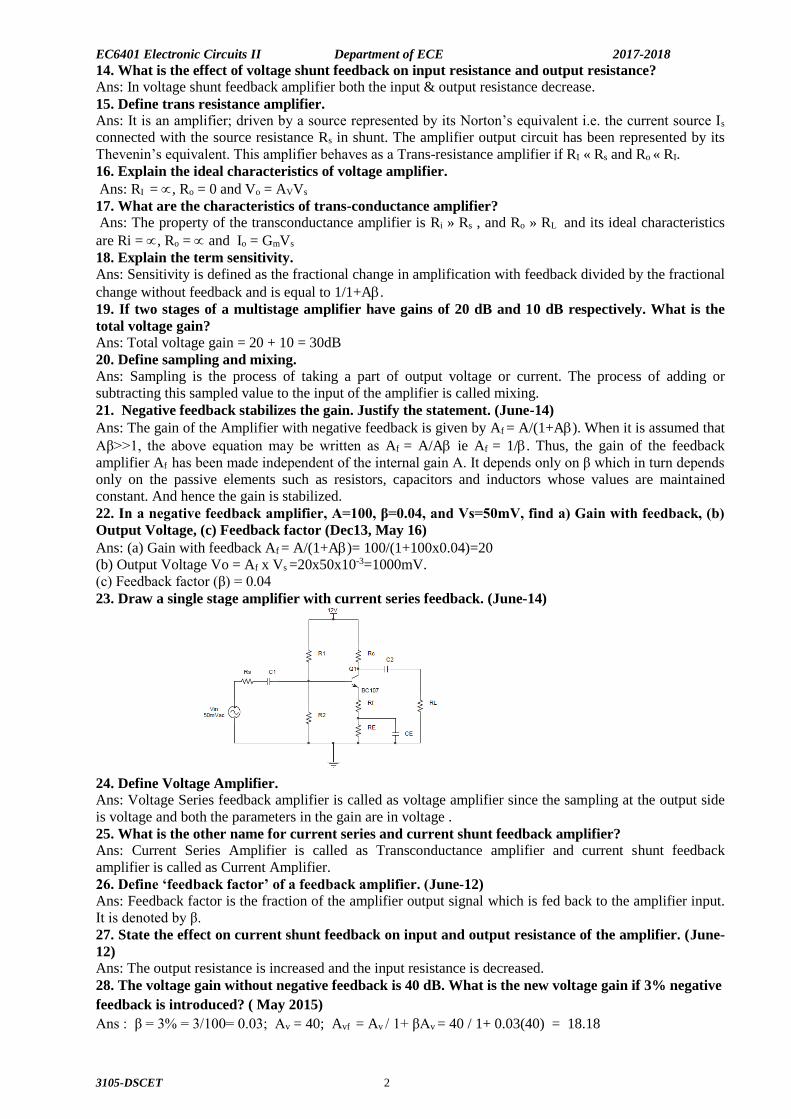
23. Draw a single stage amplifier with current series feedback. (June-14)
24. Define Voltage Amplifier.
Ans: Voltage Series feedback amplifier is called as voltage amplifier since the sampling at the output side
is voltage and both the parameters in the gain are in voltage .
25. What is the other name for current series and current shunt feedback amplifier?
Ans: Current Series Amplifier is called as Transconductance amplifier and current shunt feedback
amplifier is called as Current Amplifier.
26. Define ‘feedback factor’ of a feedback amplifier. (June-12)
Ans: Feedback factor is the fraction of the amplifier output signal which is fed back to the amplifier input.
It is denoted by β.
27. State the effect on current shunt feedback on input and output resistance of the amplifier. (June-
12)
Ans: The output resistance is increased and the input resistance is decreased.
28. The voltage gain without negative feedback is 40 dB. What is the new voltage gain if 3% negative
feedback is introduced? ( May 2015)
Ans : β = 3% = 3/100= 0.03; Av = 40; Avf = Av / 1+ βAv = 40 / 1+ 0.03(40) = 18.18
EC6401 Electronic Circuits II Department of ECE 2017-2018
3105-DSCET 3
29. List the effects of negative feedback on the noise and bandwidth of an amplifier (or) What will
happen for noise, if we introduce negative feedback at amolifier. (May 16/ Nov 16, May 17)
Reduction in noise
Nf = N/1+A β
Increase in bandwidth (B.W)f = B.W( 1+Aβ) = B.W X D
30. A Negative feedback amplifier has a bandwidth of 250Khz and de-sensitivity factor of 4.What is
the bandwidth of the basic amplifier without feedback. (Dec 15) D= 4 ; (B.W)f = 250 Khz
(B.W)f = B.W( 1+Aβ) = B.W X D
B.W = (B.W)f / D = 250 X 103 /4 = 62.5 Khz
31. Draw the magnitude and phase angle plot of three stage amplifier(Dec 15)
32. An amplifier has an open loop gain of 1000 and feedback ratio of 0.04.If the loop gain changes
by 10% due to temperature, find the % change in gain of the amplifier with the feedback.
(Nov 16)
β = 0.04; Av = 1000; dA/A = 10: dAvf /Avf = (dAv / A )(1/D) where D =1+ βAv
= 10 (1/(1+0.04*1000)) = 0.25%
33. Mention the three networks that are connected around the basic amplifier to implement
feedback concept. (May 17)
The three networks that are connected around the basic amplifier to implement the feedback concept are
i) Mixing Network ii) Sampling Network iii) Feedback Network PART – B ( C210.1)
1. Draw the block diagram of 4 types of feedback topologies and compare them wrt gain, input & output
resistance. Give one example for each. (Dec 14)
2. Draw the circuit of an emitter follower. Identify the type of negative feedback. Calculate the gain,
input & output resistance with & without feedback. (Dec14)
3. (i) Draw the block diagram of voltage series amplifier and derive for Avf, Rif & Rof. Draw a two stage
amplifier with voltage series feedback.(10) ( May-2015)
(ii) Derive for bandwidth with feedback BWf (6) (Jun14)
4. Explain about Current shunt and Current series feedback and derive the expression for input
impedance, output impedance and voltage gain. (Dec-13, May15, Nov 16)
5. With an example circuit, explain the method of identifying the feedback topology. Also determine the
feedback factor. (May 15)
6. (i) Sketch the block diagram of a feedback amplifier and derive the expressions for gain 1) With
positive feedback. 2) With negative feedback. State the advantages of negative feedback. (10)
(ii) An amplifier, with feedback, has voltage gain of 100. When the gain without feedback changes by
20% and the gain with feedback.
7. (i) What is the effect of a current series negative feedback on input resistance and output resistance of
a BJT amplifier? Explain the same, with necessary circuit, equivalent circuit and equations. (8) (June-
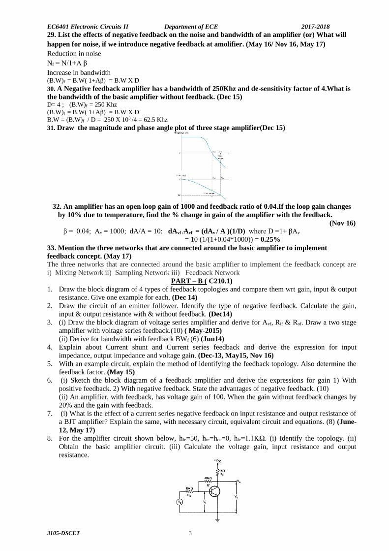
12, May 17) 8. For the amplifier circuit shown below, hfe=50, hre=hoe=0, hie=1.1KΩ. (i) Identify the topology. (ii)
Obtain the basic amplifier circuit. (iii) Calculate the voltage gain, input resistance and output
resistance.
EC6401 Electronic Circuits II Department of ECE 2017-2018
3105-DSCET 4
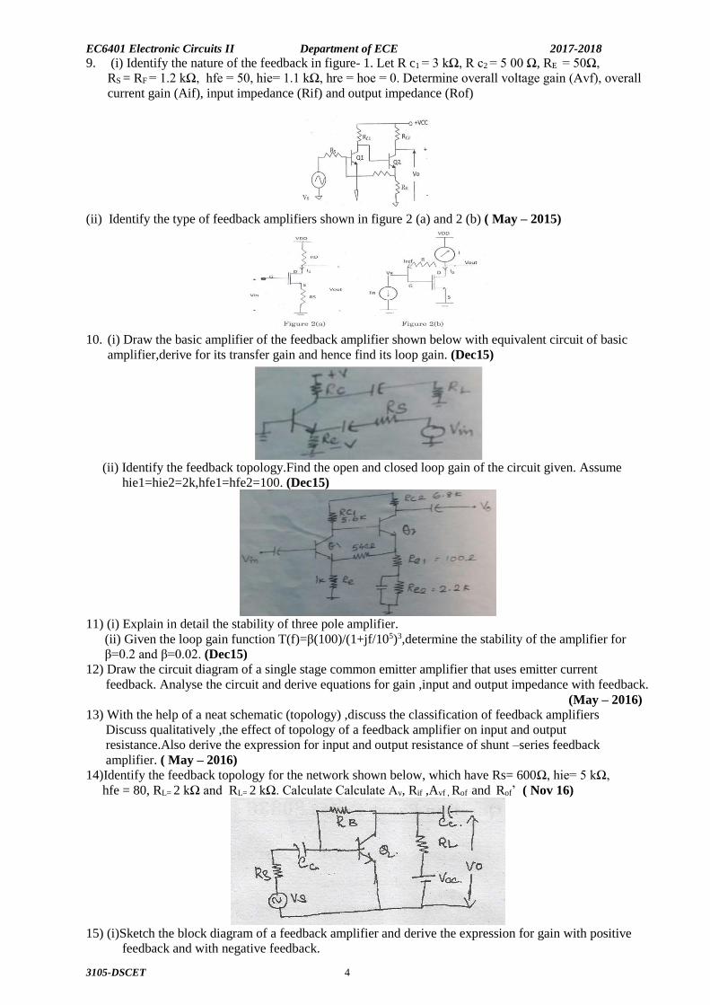
9. (i) Identify the nature of the feedback in figure- 1. Let R c1 = 3 kΩ, R c2 = 5 00 Ω, RE = 50Ω,
RS = RF = 1.2 kΩ, hfe = 50, hie= 1.1 kΩ, hre = hoe = 0. Determine overall voltage gain (Avf), overall
current gain (Aif), input impedance (Rif) and output impedance (Rof)
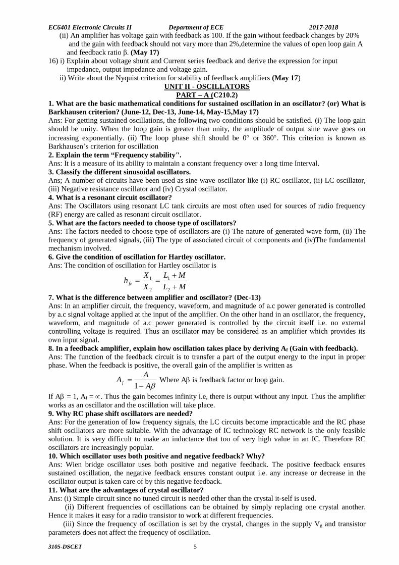
(ii) Identify the type of feedback amplifiers shown in figure 2 (a) and 2 (b) ( May – 2015)
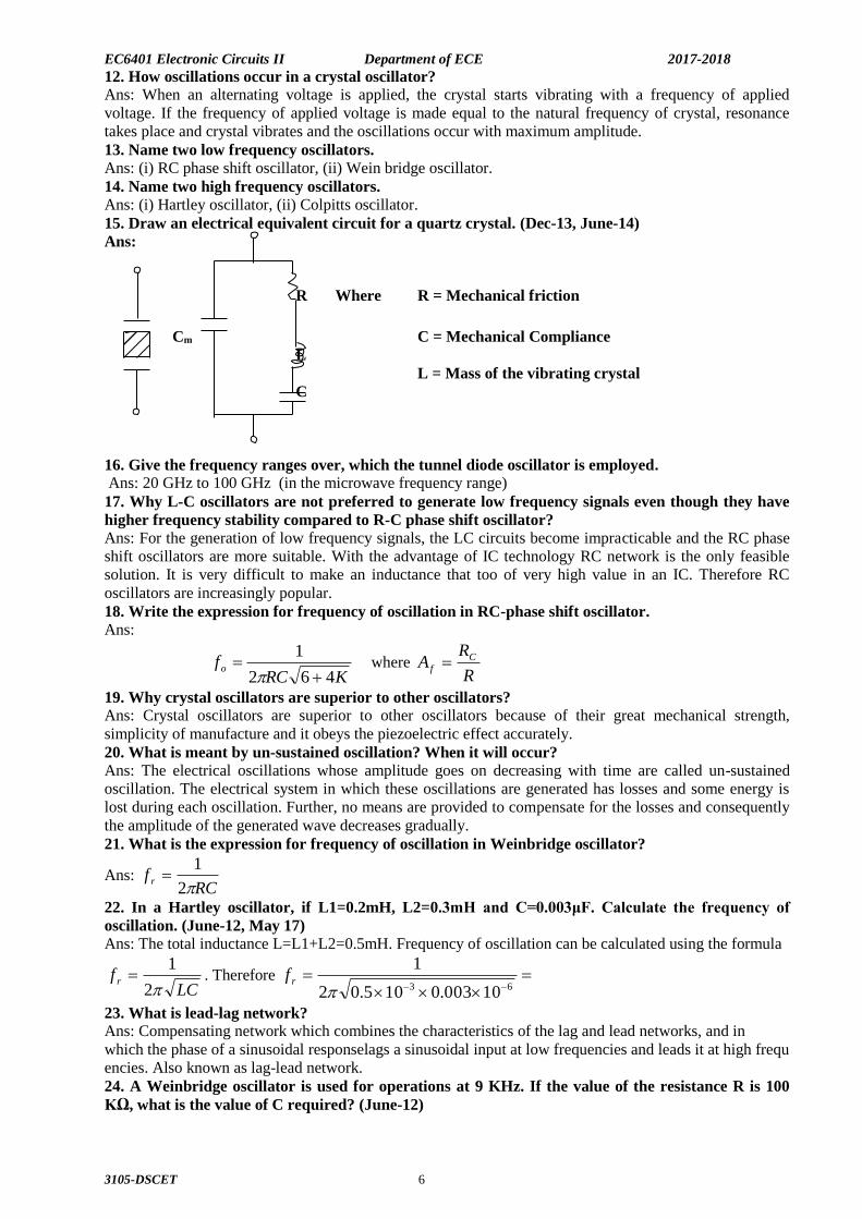
10. (i) Draw the basic amplifier of the feedback amplifier shown below with equivalent circuit of basic
amplifier,derive for its transfer gain and hence find its loop gain. (Dec15)
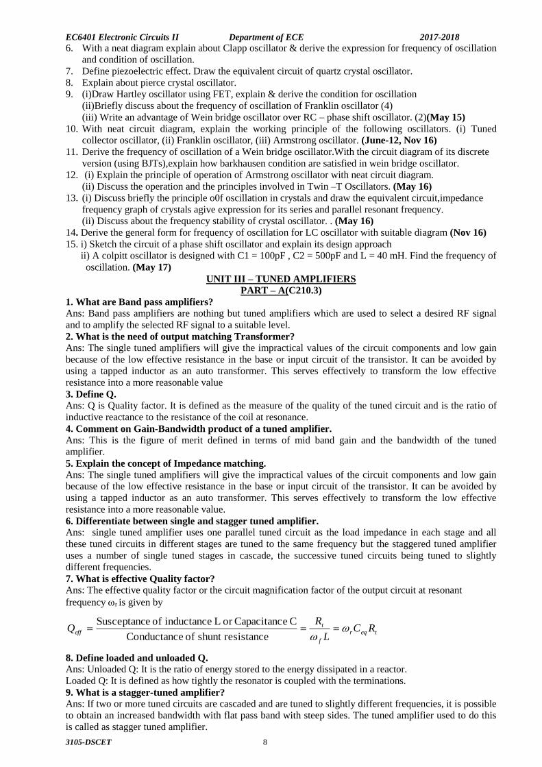
(ii) Identify the feedback topology.Find the open and closed loop gain of the circuit given. Assume
hie1=hie2=2k,hfe1=hfe2=100. (Dec15)
11) (i) Explain in detail the stability of three pole amplifier.
(ii) Given the loop gain function T(f)=β(100)/(1+jf/105)3,determine the stability of the amplifier for
β=0.2 and β=0.02. (Dec15)
12) Draw the circuit diagram of a single stage common emitter amplifier that uses emitter current
feedback. Analyse the circuit and derive equations for gain ,input and output impedance with feedback.
(May – 2016)
13) With the help of a neat schematic (topology) ,discuss the classification of feedback amplifiers
Discuss qualitatively ,the effect of topology of a feedback amplifier on input and output
resistance.Also derive the expression for input and output resistance of shunt –series feedback
amplifier. ( May – 2016)
14)Identify the feedback topology for the network shown below, which have Rs= 600Ω, hie= 5 kΩ,
hfe = 80, RL= 2 kΩ and RL= 2 kΩ. Calculate Calculate Av, Rif ,Avf , Rof and Rof’ ( Nov 16)
15) (i)Sketch the block diagram of a feedback amplifier and derive the expression for gain with positive
feedback and with negative feedback.
EC6401 Electronic Circuits II Department of ECE 2017-2018
3105-DSCET 5
(ii) An amplifier has voltage gain with feedback as 100. If the gain without feedback changes by 20%
and the gain with feedback should not vary more than 2%,determine the values of open loop gain A
and feedback ratio β. (May 17)
16) i) Explain about voltage shunt and Current series feedback and derive the expression for input
impedance, output impedance and voltage gain.
ii) Write about the Nyquist criterion for stability of feedback amplifiers (May 17)
UNIT II - OSCILLATORS
PART – A (C210.2)
1. What are the basic mathematical conditions for sustained oscillation in an oscillator? (or) What is
Barkhausen criterion? (June-12, Dec-13, June-14, May-15,May 17)
Ans: For getting sustained oscillations, the following two conditions should be satisfied. (i) The loop gain
should be unity. When the loop gain is greater than unity, the amplitude of output sine wave goes on
increasing exponentially. (ii) The loop phase shift should be 0 or 360. This criterion is known as
Barkhausen’s criterion for oscillation
2. Explain the term “Frequency stability".
Ans: It is a measure of its ability to maintain a constant frequency over a long time Interval.
3. Classify the different sinusoidal oscillators.
Ans; A number of circuits have been used as sine wave oscillator like (i) RC oscillator, (ii) LC oscillator,
(iii) Negative resistance oscillator and (iv) Crystal oscillator.
4. What is a resonant circuit oscillator?
Ans: The Oscillators using resonant LC tank circuits are most often used for sources of radio frequency
(RF) energy are called as resonant circuit oscillator.
5. What are the factors needed to choose type of oscillators?
Ans: The factors needed to choose type of oscillators are (i) The nature of generated wave form, (ii) The
frequency of generated signals, (iii) The type of associated circuit of components and (iv)The fundamental
mechanism involved.
6. Give the condition of oscillation for Hartley oscillator.
Ans: The condition of oscillation for Hartley oscillator is
ML
ML
X
Xh fe
2
1
2
1
7. What is the difference between amplifier and oscillator? (Dec-13)
Ans: In an amplifier circuit, the frequency, waveform, and magnitude of a.c power generated is controlled
by a.c signal voltage applied at the input of the amplifier. On the other hand in an oscillator, the frequency,
waveform, and magnitude of a.c power generated is controlled by the circuit itself i.e. no external
controlling voltage is required. Thus an oscillator may be considered as an amplifier which provides its
own input signal.
8. In a feedback amplifier, explain how oscillation takes place by deriving Af (Gain with feedback).
Ans: The function of the feedback circuit is to transfer a part of the output energy to the input in proper
phase. When the feedback is positive, the overall gain of the amplifier is written as
A
AA f
1 Where A is feedback factor or loop gain.
If A = 1, Af = . Thus the gain becomes infinity i.e, there is output without any input. Thus the amplifier
works as an oscillator and the oscillation will take place.
9. Why RC phase shift oscillators are needed?
Ans: For the generation of low frequency signals, the LC circuits become impracticable and the RC phase
shift oscillators are more suitable. With the advantage of IC technology RC network is the only feasible
solution. It is very difficult to make an inductance that too of very high value in an IC. Therefore RC
oscillators are increasingly popular.
10. Which oscillator uses both positive and negative feedback? Why?
Ans: Wien bridge oscillator uses both positive and negative feedback. The positive feedback ensures
sustained oscillation, the negative feedback ensures constant output i.e. any increase or decrease in the
oscillator output is taken care of by this negative feedback.
11. What are the advantages of crystal oscillator?
Ans: (i) Simple circuit since no tuned circuit is needed other than the crystal it-self is used.
(ii) Different frequencies of oscillations can be obtained by simply replacing one crystal another.
Hence it makes it easy for a radio transistor to work at different frequencies.
(iii) Since the frequency of oscillation is set by the crystal, changes in the supply Vg and transistor
parameters does not affect the frequency of oscillation.
EC6401 Electronic Circuits II Department of ECE 2017-2018
3105-DSCET 6
12. How oscillations occur in a crystal oscillator?
Ans: When an alternating voltage is applied, the crystal starts vibrating with a frequency of applied
voltage. If the frequency of applied voltage is made equal to the natural frequency of crystal, resonance
takes place and crystal vibrates and the oscillations occur with maximum amplitude.
13. Name two low frequency oscillators. Ans: (i) RC phase shift oscillator, (ii) Wein bridge oscillator.
14. Name two high frequency oscillators.
Ans: (i) Hartley oscillator, (ii) Colpitts oscillator.
15. Draw an electrical equivalent circuit for a quartz crystal. (Dec-13, June-14)
Ans:
R Where R = Mechanical friction
Cm C = Mechanical Compliance
L
L = Mass of the vibrating crystal
C
16. Give the frequency ranges over, which the tunnel diode oscillator is employed.
Ans: 20 GHz to 100 GHz (in the microwave frequency range)
17. Why L-C oscillators are not preferred to generate low frequency signals even though they have
higher frequency stability compared to R-C phase shift oscillator?
Ans: For the generation of low frequency signals, the LC circuits become impracticable and the RC phase
shift oscillators are more suitable. With the advantage of IC technology RC network is the only feasible
solution. It is very difficult to make an inductance that too of very high value in an IC. Therefore RC
oscillators are increasingly popular.
18. Write the expression for frequency of oscillation in RC-phase shift oscillator.
Ans:
KRC
fo462
1
where
R
RA C
f
19. Why crystal oscillators are superior to other oscillators?
Ans: Crystal oscillators are superior to other oscillators because of their great mechanical strength,
simplicity of manufacture and it obeys the piezoelectric effect accurately.
20. What is meant by un-sustained oscillation? When it will occur?
Ans: The electrical oscillations whose amplitude goes on decreasing with time are called un-sustained
oscillation. The electrical system in which these oscillations are generated has losses and some energy is
lost during each oscillation. Further, no means are provided to compensate for the losses and consequently
the amplitude of the generated wave decreases gradually.
21. What is the expression for frequency of oscillation in Weinbridge oscillator?
Ans: RC
f r2
1
22. In a Hartley oscillator, if L1=0.2mH, L2=0.3mH and C=0.003μF. Calculate the frequency of
oscillation. (June-12, May 17)
Ans: The total inductance L=L1+L2=0.5mH. Frequency of oscillation can be calculated using the formula
LCf r
2
1 . Therefore
63 10003.0105.02
1
rf
23. What is lead-lag network?
Ans: Compensating network which combines the characteristics of the lag and lead networks, and in
which the phase of a sinusoidal responselags a sinusoidal input at low frequencies and leads it at high frequ
encies. Also known as lag-lead network.
24. A Weinbridge oscillator is used for operations at 9 KHz. If the value of the resistance R is 100
KΩ, what is the value of C required? (June-12)

EC6401 Electronic Circuits II Department of ECE 2017-2018
3105-DSCET 7
Ans: The frequency of operation for Weinbridge oscillator is given by RC
f r2
1 . Therefore the value of
C can be obtained as follows.
1331 )101001092()2( RfC r 0.174nF.
25. A tuned collector oscillator in a radio receiver has a fixed inductance of 60μH and has to be
tunable over the frequency band of 400KHz to 1200KHz. Find the range of variable capacitor to be
used. (June-12)
Ans: Frequency of oscillation is given byLC
f2
1 . Therefore,
2/1)2
1(
fLC
. For f=400KHz,
C=7.16 mF and for f=1200KHz, C= 4.13 mF.
26. Write the feedback factor expression for BJT based Wein bridge oscillator.
Z1 / (Z1 + Z2) where Z1 = R1 / 1+jω R1C1 ; Z1= R2 + 1 / jω C2
27. Sketch the feedback circuit of a Colpitts Oscillator.Calculate the value of the equivalent series
capacitance required if it uses an inductance of 100mH and is to oscillate at 40Khz. . (May 16)
LCf
2
1 Where L is the inductance of the inductor in the tank circuit and C is
the effective capacitance of the capacitors in the tank circuit. If C1 and C2 are the
individual capacitance, then the effective capacitance of the serial combination C =
(C1* C2) / (C1+C2). Here substitute F = 40 x 103 Hz and L = 100 x10-3 H. Calculate
C. C = 0.01mF
28. Mention the advantages and disadvantages of RC phase shift oscillators.(May 16 / Nov 16) Ans: Advantage : For the generation of low frequency signals, the LC circuits become impracticable and
the RC phase shift oscillators are more suitable. With the advantage of IC technology RC network is the
only feasible solution. It is very difficult to make an inductance that too of very high value in an IC.
Disadvantage: The output is small and It is due to smaller feedback. The frequency stability is not as good
as that of the Wien bridge oscillator. It is difficult for the circuit to start oscillations as the feedback is
usually small
29.The quartz crystal has Cm=1pF,Ls=3H Cs=0.05pF and Rs=1k.Calculate the series and parallel
resonant frequencies. (Dec 15)
Ceq = Cm Cs/ Cm +Cs = 0.0476F
fs = 1 / 2π Ceq Ls
=0.06 Hz
fp = 1 / 2π Cm Ls
= 0.02754 µf
30.How Barkhausen conditions are satisfied in Twin-T Oscillator? (Dec 15)
The phase shift introduced in the feedback loop of two T – Network is 0, and the gain of the amplifier is 3.
31.What are the factors which affect the frequency stability of an oscillator? (Nov 16)
i) Operating point ii) Interelment capacitances iii) Stray capacitances iv) Temperature v) Circuit
components vi) Gain (β) vii) Supply voltages
PART–B (C210.2)
1. With a neat diagram explain about RC phase shift oscillator using BJT and derive the expression for
frequency of oscillation and condition of oscillation. Also discuss about frequency stability of an
oscillator (June-12, Dec-13, June-14, May-2015)
2. With a neat diagram explain about Wien Bridge oscillator and derive the expression for frequency of
oscillation and condition of oscillation.(May 15, Dec 15)
3. (i) With a neat diagram explain about Colpitt oscillator & derive the expression for frequency of
oscillation and condition of oscillation. (June-14, May 15, Dec 15, May 17)
(ii) Design a clap oscillation to generate 12Khz Sine wave using BJT amplifier with a gain of
110.Given gm=30mA/V, hfe=150.Draw the designed circuit Vec=20V. (Dec 15)
4. Explain the drawback of Colpitt oscillator and how it is overcome in Clapp oscillator (June-14).
5. (i)With a neat diagram explain about Hartley oscillator & derive the expression for frequency of
oscillation and condition of oscillation. (Dec-13)
(ii) In colpitt’s oscillator C1 = 1 µF and C2 = 0.2 µF. If the frequency of oscillation is 10 kHz, find the
value of inductor. Also find the required gain for sustained oscillation. ( May-2015)
EC6401 Electronic Circuits II Department of ECE 2017-2018
3105-DSCET 8
6. With a neat diagram explain about Clapp oscillator & derive the expression for frequency of oscillation
and condition of oscillation.
7. Define piezoelectric effect. Draw the equivalent circuit of quartz crystal oscillator.
8. Explain about pierce crystal oscillator.
9. (i)Draw Hartley oscillator using FET, explain & derive the condition for oscillation
(ii)Briefly discuss about the frequency of oscillation of Franklin oscillator (4)
(iii) Write an advantage of Wein bridge oscillator over RC – phase shift oscillator. (2)(May 15)
10. With neat circuit diagram, explain the working principle of the following oscillators. (i) Tuned
collector oscillator, (ii) Franklin oscillator, (iii) Armstrong oscillator. (June-12, Nov 16)
11. Derive the frequency of oscillation of a Wein bridge oscillator.With the circuit diagram of its discrete
version (using BJTs),explain how barkhausen condition are satisfied in wein bridge oscillator.
12. (i) Explain the principle of operation of Armstrong oscillator with neat circuit diagram.
(ii) Discuss the operation and the principles involved in Twin –T Oscillators. (May 16)
13. (i) Discuss briefly the principle o0f oscillation in crystals and draw the equivalent circuit,impedance
frequency graph of crystals agive expression for its series and parallel resonant frequency.
(ii) Discuss about the frequency stability of crystal oscillator. . (May 16)
14. Derive the general form for frequency of oscillation for LC oscillator with suitable diagram (Nov 16)
15. i) Sketch the circuit of a phase shift oscillator and explain its design approach
ii) A colpitt oscillator is designed with C1 = 100pF , C2 = 500pF and L = 40 mH. Find the frequency of
oscillation. (May 17)
UNIT III – TUNED AMPLIFIERS
PART – A(C210.3)
1. What are Band pass amplifiers?
Ans: Band pass amplifiers are nothing but tuned amplifiers which are used to select a desired RF signal
and to amplify the selected RF signal to a suitable level.
2. What is the need of output matching Transformer?
Ans: The single tuned amplifiers will give the impractical values of the circuit components and low gain
because of the low effective resistance in the base or input circuit of the transistor. It can be avoided by
using a tapped inductor as an auto transformer. This serves effectively to transform the low effective
resistance into a more reasonable value
3. Define Q.
Ans: Q is Quality factor. It is defined as the measure of the quality of the tuned circuit and is the ratio of
inductive reactance to the resistance of the coil at resonance.
4. Comment on Gain-Bandwidth product of a tuned amplifier. Ans: This is the figure of merit defined in terms of mid band gain and the bandwidth of the tuned
amplifier.
5. Explain the concept of Impedance matching.
Ans: The single tuned amplifiers will give the impractical values of the circuit components and low gain
because of the low effective resistance in the base or input circuit of the transistor. It can be avoided by
using a tapped inductor as an auto transformer. This serves effectively to transform the low effective
resistance into a more reasonable value.
6. Differentiate between single and stagger tuned amplifier.
Ans: single tuned amplifier uses one parallel tuned circuit as the load impedance in each stage and all
these tuned circuits in different stages are tuned to the same frequency but the staggered tuned amplifier
uses a number of single tuned stages in cascade, the successive tuned circuits being tuned to slightly
different frequencies.
7. What is effective Quality factor?
Ans: The effective quality factor or the circuit magnification factor of the output circuit at resonant
frequency r is given by
teqr
f
t
eff RCL
RQ
resistanceshunt of eConductanc
C eCapacitancor L inductance of eSusceptanc
8. Define loaded and unloaded Q.
Ans: Unloaded Q: It is the ratio of energy stored to the energy dissipated in a reactor.
Loaded Q: It is defined as how tightly the resonator is coupled with the terminations.
9. What is a stagger-tuned amplifier?
Ans: If two or more tuned circuits are cascaded and are tuned to slightly different frequencies, it is possible
to obtain an increased bandwidth with flat pass band with steep sides. The tuned amplifier used to do this
is called as stagger tuned amplifier.
EC6401 Electronic Circuits II Department of ECE 2017-2018
3105-DSCET 9
10. What is a synchronous tuned amplifier?
Ans: A number of amplifiers can be cascaded in order to achieve high gain. All stages are assumed to be
identical and to be tuned to the same frequency. This is termed as synchronously tuned amplifier which has
increased gain and band width which is narrower than the band width of each of the stages.
11. What is the effect of ‘Q’ on stability?
Ans: Higher the value of Q, provides better stability, but smaller bandwidth and larger gain. Hence it
provides less stability.
12. Define coil losses.
Copper loss, Eddy current loss and hysteresis loss are called coil losses.
13. What is the instability of tuned amplifiers?
Due to the internal capacitance between the input and output there will be feedback in the circuit. If the
feedback is positive then the circuit starts oscillating instead of amplifying.
14. What is the advantage of stagger tuning?
Ans: It increases the bandwidth with a flat pass-band with steep sides.
15. What are the techniques of stabilizing a band pass amplifier?
Ans: (i) Neutralization, (ii) Unilaterization, (iii) Mismatching technique.
16. What is Neutralization? (Dec-13, June-14, Dec15)
Ans: At high frequencies the various capacitances of the transistor circuits play an important role. If some
feedback signal manages to reach the input terminal as a positive feedback, the stability of the circuit is
affected. To avoid this, a capacitance is connected in the feedback circuit to neutralize the effect of other
capacitances. This is called Neutralization.
17. Write the disadvantages of tuned amplifier. (June-12)
Ans: (1) Since they use inductors & capacitors as tuning elements, the circuit is bulky and costly, (2) If the
band of frequency is increased, design becomes complex. (3) They are not suitable to amplify audio
frequency.
18. Write the advantages of tuned amplifier. (June-12)
Ans: 1. They amplify desired frequencies.
2. Signal to noise ratio at output is good.
3. They are well suited for radio Transmitters and receivers.
4. The band of frequencies over which amplification is required can be varied.
19. What are tuned amplifiers? What are the various types of Tuned simplifiers? (Dec-13)
Ans: Amplifiers which amplify a specific frequency or narrow band of frequencies are called tuned
amplifiers. The types are (i) Single tuned amplifiers, (ii) Double tuned amplifiers and (iii) Stagger tuned
amplifiers.
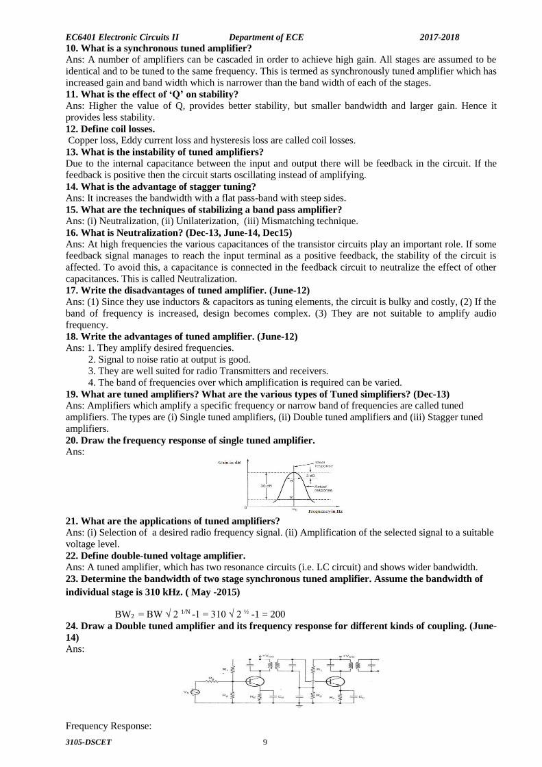
20. Draw the frequency response of single tuned amplifier.
Ans:
21. What are the applications of tuned amplifiers?
Ans: (i) Selection of a desired radio frequency signal. (ii) Amplification of the selected signal to a suitable
voltage level.
22. Define double-tuned voltage amplifier.
Ans: A tuned amplifier, which has two resonance circuits (i.e. LC circuit) and shows wider bandwidth.
23. Determine the bandwidth of two stage synchronous tuned amplifier. Assume the bandwidth of
individual stage is 310 kHz. ( May -2015)
BW2 = BW √ 2 1/N -1 = 310 √ 2 ½ -1 = 200
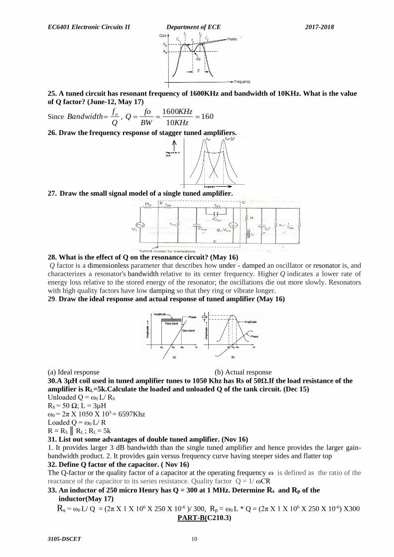
24. Draw a Double tuned amplifier and its frequency response for different kinds of coupling. (June-
14) Ans:
Frequency Response:
EC6401 Electronic Circuits II Department of ECE 2017-2018
3105-DSCET 10
25. A tuned circuit has resonant frequency of 1600KHz and bandwidth of 10KHz. What is the value
of Q factor? (June-12, May 17)
Since Q
fBandwidth o , 160
10
1600
KHz
KHz
BW
foQ
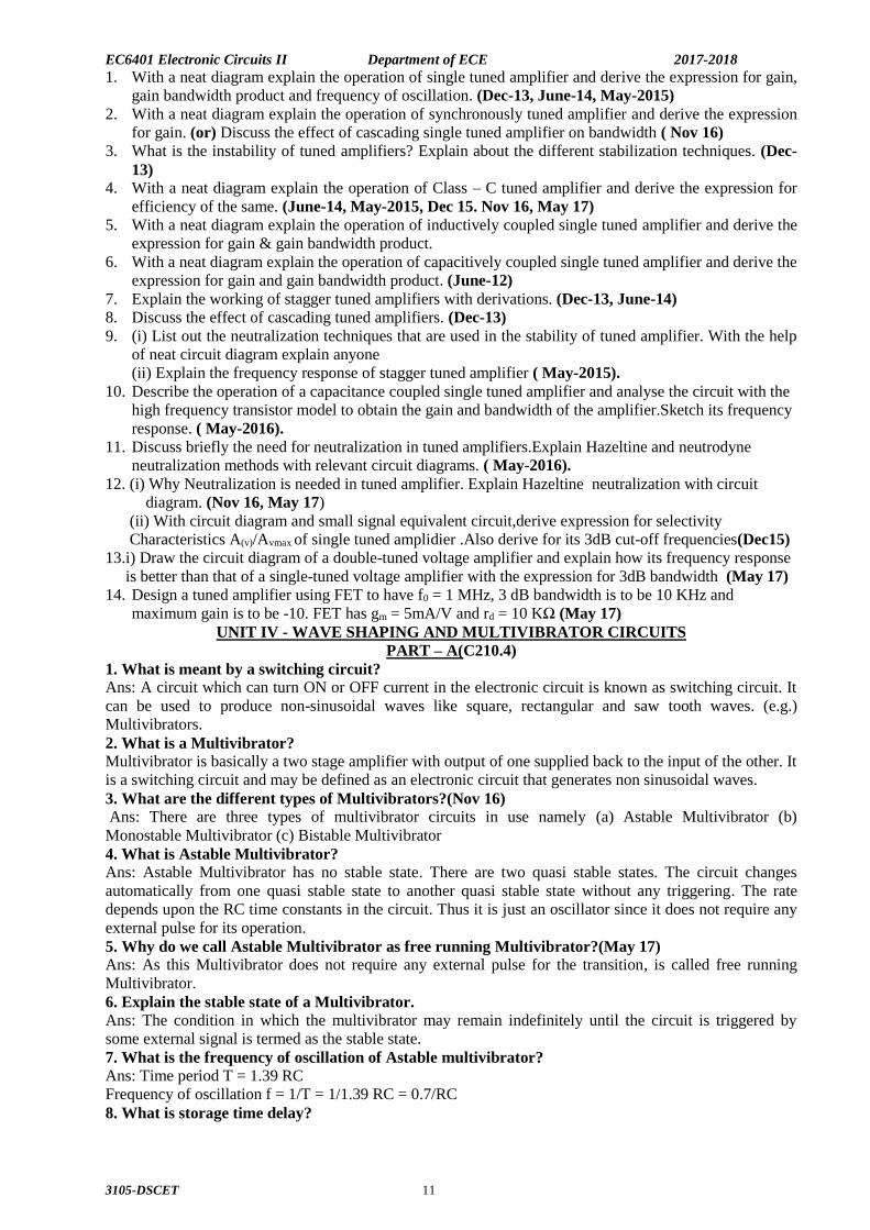
26. Draw the frequency response of stagger tuned amplifiers.
27. Draw the small signal model of a single tuned amplifier.
28. What is the effect of Q on the resonance circuit? (May 16) Q factor is a dimensionless parameter that describes how under - damped an oscillator or resonator is, and
characterizes a resonator's bandwidth relative to its center frequency. Higher Q indicates a lower rate of
energy loss relative to the stored energy of the resonator; the oscillations die out more slowly. Resonators
with high quality factors have low damping so that they ring or vibrate longer.
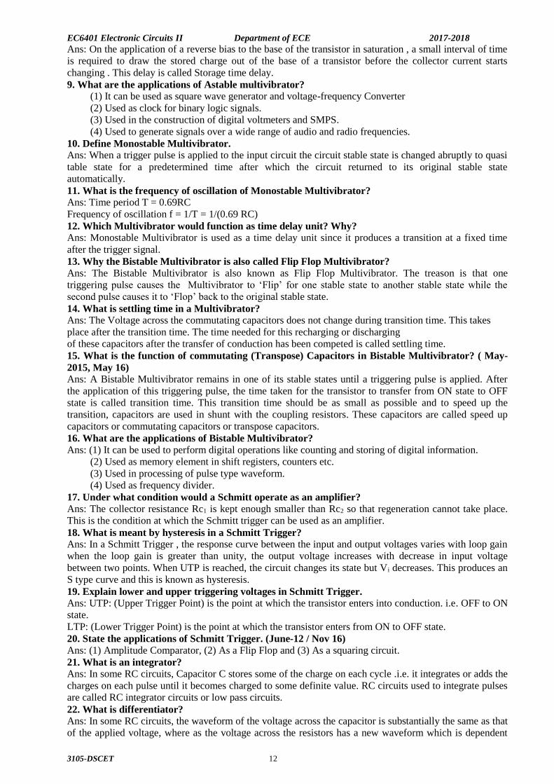
29. Draw the ideal response and actual response of tuned amplifier (May 16)
(a) Ideal response (b) Actual response
30.A 3µH coil used in tuned amplifier tunes to 1050 Khz has Rs of 50Ω.If the load resistance of the
amplifier is RL=5k.Calculate the loaded and unloaded Q of the tank circuit. (Dec 15)
Unloaded Q = ω0 L/ RS
RS = 50 Ω; L = 3µH
ω0 = 2π X 1050 X 103 = 6597Khz
Loaded Q = ω0 L/ R
R = RS RL ; RL = 5k
31. List out some advantages of double tuned amplifier. (Nov 16)
1. It provides larger 3 dB bandwidth than the single tuned amplifier and hence provides the larger gain-
bandwidth product. 2. It provides gain versus frequency curve having steeper sides and flatter top
32. Define Q factor of the capacitor. ( Nov 16)
The Q-factor or the quality factor of a capacitor at the operating frequency ω is defined as the ratio of the
reactance of the capacitor to its series resistance. Quality factor Q = 1/ ωCR
33. An inductor of 250 micro Henry has Q = 300 at 1 MHz. Determine Rs and Rp of the
inductor(May 17)
Rs = ω0 L/ Q = (2π X 1 X 106 X 250 X 10-6 )/ 300, Rp = ω0 L * Q = (2π X 1 X 106 X 250 X 10-6) X300
PART-B(C210.3)
EC6401 Electronic Circuits II Department of ECE 2017-2018
3105-DSCET 11
1. With a neat diagram explain the operation of single tuned amplifier and derive the expression for gain,
gain bandwidth product and frequency of oscillation. (Dec-13, June-14, May-2015)
2. With a neat diagram explain the operation of synchronously tuned amplifier and derive the expression
for gain. (or) Discuss the effect of cascading single tuned amplifier on bandwidth ( Nov 16)
3. What is the instability of tuned amplifiers? Explain about the different stabilization techniques. (Dec-
13) 4. With a neat diagram explain the operation of Class – C tuned amplifier and derive the expression for
efficiency of the same. (June-14, May-2015, Dec 15. Nov 16, May 17)
5. With a neat diagram explain the operation of inductively coupled single tuned amplifier and derive the
expression for gain & gain bandwidth product.
6. With a neat diagram explain the operation of capacitively coupled single tuned amplifier and derive the
expression for gain and gain bandwidth product. (June-12)
7. Explain the working of stagger tuned amplifiers with derivations. (Dec-13, June-14)
8. Discuss the effect of cascading tuned amplifiers. (Dec-13)
9. (i) List out the neutralization techniques that are used in the stability of tuned amplifier. With the help
of neat circuit diagram explain anyone
(ii) Explain the frequency response of stagger tuned amplifier ( May-2015).
10. Describe the operation of a capacitance coupled single tuned amplifier and analyse the circuit with the
high frequency transistor model to obtain the gain and bandwidth of the amplifier.Sketch its frequency
response. ( May-2016).
11. Discuss briefly the need for neutralization in tuned amplifiers.Explain Hazeltine and neutrodyne
neutralization methods with relevant circuit diagrams. ( May-2016).
12. (i) Why Neutralization is needed in tuned amplifier. Explain Hazeltine neutralization with circuit
diagram. (Nov 16, May 17)
(ii) With circuit diagram and small signal equivalent circuit,derive expression for selectivity
Characteristics A(v)/Avmax of single tuned amplidier .Also derive for its 3dB cut-off frequencies(Dec15)
13.i) Draw the circuit diagram of a double-tuned voltage amplifier and explain how its frequency response
is better than that of a single-tuned voltage amplifier with the expression for 3dB bandwidth (May 17)
14. Design a tuned amplifier using FET to have f0 = 1 MHz, 3 dB bandwidth is to be 10 KHz and
maximum gain is to be -10. FET has gm = 5mA/V and rd = 10 KΩ (May 17)
UNIT IV - WAVE SHAPING AND MULTIVIBRATOR CIRCUITS
PART – A(C210.4)
1. What is meant by a switching circuit?
Ans: A circuit which can turn ON or OFF current in the electronic circuit is known as switching circuit. It
can be used to produce non-sinusoidal waves like square, rectangular and saw tooth waves. (e.g.)
Multivibrators.
2. What is a Multivibrator?
Multivibrator is basically a two stage amplifier with output of one supplied back to the input of the other. It
is a switching circuit and may be defined as an electronic circuit that generates non sinusoidal waves.
3. What are the different types of Multivibrators?(Nov 16)
Ans: There are three types of multivibrator circuits in use namely (a) Astable Multivibrator (b)
Monostable Multivibrator (c) Bistable Multivibrator
4. What is Astable Multivibrator?
Ans: Astable Multivibrator has no stable state. There are two quasi stable states. The circuit changes
automatically from one quasi stable state to another quasi stable state without any triggering. The rate
depends upon the RC time constants in the circuit. Thus it is just an oscillator since it does not require any
external pulse for its operation.
5. Why do we call Astable Multivibrator as free running Multivibrator?(May 17)
Ans: As this Multivibrator does not require any external pulse for the transition, is called free running
Multivibrator.
6. Explain the stable state of a Multivibrator.
Ans: The condition in which the multivibrator may remain indefinitely until the circuit is triggered by
some external signal is termed as the stable state.
7. What is the frequency of oscillation of Astable multivibrator?
Ans: Time period T = 1.39 RC
Frequency of oscillation f = 1/T = 1/1.39 RC = 0.7/RC
8. What is storage time delay?
EC6401 Electronic Circuits II Department of ECE 2017-2018
3105-DSCET 12
Ans: On the application of a reverse bias to the base of the transistor in saturation , a small interval of time
is required to draw the stored charge out of the base of a transistor before the collector current starts
changing . This delay is called Storage time delay.
9. What are the applications of Astable multivibrator?
(1) It can be used as square wave generator and voltage-frequency Converter
(2) Used as clock for binary logic signals.
(3) Used in the construction of digital voltmeters and SMPS.
(4) Used to generate signals over a wide range of audio and radio frequencies.
10. Define Monostable Multivibrator.
Ans: When a trigger pulse is applied to the input circuit the circuit stable state is changed abruptly to quasi
table state for a predetermined time after which the circuit returned to its original stable state
automatically.
11. What is the frequency of oscillation of Monostable Multivibrator?
Ans: Time period T = 0.69RC
Frequency of oscillation f = 1/T = 1/(0.69 RC)
12. Which Multivibrator would function as time delay unit? Why?
Ans: Monostable Multivibrator is used as a time delay unit since it produces a transition at a fixed time
after the trigger signal.
13. Why the Bistable Multivibrator is also called Flip Flop Multivibrator?
Ans: The Bistable Multivibrator is also known as Flip Flop Multivibrator. The treason is that one
triggering pulse causes the Multivibrator to ‘Flip’ for one stable state to another stable state while the
second pulse causes it to ‘Flop’ back to the original stable state.
14. What is settling time in a Multivibrator?
Ans: The Voltage across the commutating capacitors does not change during transition time. This takes
place after the transition time. The time needed for this recharging or discharging
of these capacitors after the transfer of conduction has been competed is called settling time.
15. What is the function of commutating (Transpose) Capacitors in Bistable Multivibrator? ( May-
2015, May 16)
Ans: A Bistable Multivibrator remains in one of its stable states until a triggering pulse is applied. After
the application of this triggering pulse, the time taken for the transistor to transfer from ON state to OFF
state is called transition time. This transition time should be as small as possible and to speed up the
transition, capacitors are used in shunt with the coupling resistors. These capacitors are called speed up
capacitors or commutating capacitors or transpose capacitors.
16. What are the applications of Bistable Multivibrator?
Ans: (1) It can be used to perform digital operations like counting and storing of digital information.
(2) Used as memory element in shift registers, counters etc.
(3) Used in processing of pulse type waveform.
(4) Used as frequency divider.
17. Under what condition would a Schmitt operate as an amplifier?
Ans: The collector resistance Rc1 is kept enough smaller than Rc2 so that regeneration cannot take place.
This is the condition at which the Schmitt trigger can be used as an amplifier.
18. What is meant by hysteresis in a Schmitt Trigger?
Ans: In a Schmitt Trigger , the response curve between the input and output voltages varies with loop gain
when the loop gain is greater than unity, the output voltage increases with decrease in input voltage
between two points. When UTP is reached, the circuit changes its state but Vi decreases. This produces an
S type curve and this is known as hysteresis.
19. Explain lower and upper triggering voltages in Schmitt Trigger.
Ans: UTP: (Upper Trigger Point) is the point at which the transistor enters into conduction. i.e. OFF to ON
state.
LTP: (Lower Trigger Point) is the point at which the transistor enters from ON to OFF state.
20. State the applications of Schmitt Trigger. (June-12 / Nov 16)
Ans: (1) Amplitude Comparator, (2) As a Flip Flop and (3) As a squaring circuit.
21. What is an integrator?
Ans: In some RC circuits, Capacitor C stores some of the charge on each cycle .i.e. it integrates or adds the
charges on each pulse until it becomes charged to some definite value. RC circuits used to integrate pulses
are called RC integrator circuits or low pass circuits.
22. What is differentiator?
Ans: In some RC circuits, the waveform of the voltage across the capacitor is substantially the same as that
of the applied voltage, where as the voltage across the resistors has a new waveform which is dependent

EC6401 Electronic Circuits II Department of ECE 2017-2018
3105-DSCET 13
upon how fast the applied voltage changes. Because of their ability to differentiate between rates of change
of the applied voltage, these circuits are called differentiator circuits. Also they are called High pass filters.
23. Define the threshold points in a Schmitt Trigger circuit. (Dec-13)
Ans: The Schmitt Trigger is a type of comparator with two different threshold voltage levels. Whenever
the input voltage goes over the High Threshold Level, the output of the comparator is switched HIGH (if is
a standard ST) or LOW (if is an inverting ST). The output will remain in this state, as long as the input
voltage is above the second threshold level, the Low Threshold Level. When the input voltage goes below
this level, the output of the Schmitt Trigger will switch.
24. Determine the value of capacitors to be used in an astable multivibrator to provide a train of
pulse of 4µs wide at a reception rate of 80 KHz if R1=R2=10 KΩ. (Dec-13)
Ans: The period of oscillation is given by T = 1/f = (1/80x103) = 12.5 μs
T1 = 4 μs (Given), T2 = T-T1 = 12.5-4 = 8.5 μs
T1 = 0.693 R1 C1, therefore C1 = T1/(0.693 R1) = 577 pF
T2 = 0.693 R2 C2, therefore C2 = T2/(0.693 R2) = 1.226 nF
25. Briefly explain any one type of triggering for Bistable multivibrator (June-14)
Ans: Let us assume that initially transistor Q1 is ON and Q2 is OFF in the Bistable multivibrator. It is a
stable state of the circuit and it will remain in this state until a trigger pulse is applied from outside. A
positive triggering pulse applied to the reset input (base of Q2) increases its forward bias, thereby turning
transistor Q2 ON and an increase in collector current and a decrease in collector voltage. The fall in
collector voltage is coupled to the base of Q1, where it reverse biases the base-emitter circuit and Q1 is
thus turned OFF. The circuit is then in its second stable state and remains so till a positive trigger pulse is
applied to set input (base of Q1).
26. What is meant by clamper circuit? (June-12)
Ans: A clamping circuit is used to place either the positive or negative peak of a signal at a desired level.
The dc component is simply added or subtracted to/from the input signal.
27. Differentiate between Clipper and Clamper circuits ( May-2015)
Ans
CLIPPERS CLAMPERS
Clips a portion of a waveform depending upon
the applied reference voltage
Clamps or adds the required dc level to the
applied input AC signal
Also called as slicer or limiter Also called as DC inserter or restorer
28. Draw the input and output waveform of the circuit shown below (June-14)
Ans:
29. An RC low pass circuit has R=1.5kΩ and C=0.2µf.What is the rise time of the output when
excited by a step input. (May 16)
3 db cut – off frequency : fh = 1/2πRC = 530 .51 Hz
Rise time : t r = 0.35/ fh = 6.59 x 10⁻⁴ sec.
30.Define rise time of a switching transistor.(Dec 15) Ans: It is the time taken for the output to rise from 10% to 90 % of its steady state value. Rise time depends upon the
input capacitance. During rise time tr, Collector-emitter voltage falls from VCC to VCES
31.Draw the hysteresis characteristics of the Schmitt trigger circuit.(Dec15)

EC6401 Electronic Circuits II Department of ECE 2017-2018
3105-DSCET 14
32. How can a Schemitt trigger act as a zero crossing detector? (May 17)
A Schmitt trigger circuit is also called a regenerative comparator circuit. The circuit is designed with a
positive feedback and hence will have a regenerative action which will make the output switch levels.
Also, the use of positive voltage feedback instead of a negative feedback, aids the feedback voltage to the
input voltage, instead of opposing it. The use of a regenerative circuit is to remove the difficulties in
a zero-crossing detector circuit due to low frequency signals and input noise voltages.
PART-B(C210.4)
1. i) Draw the circuit of emitter coupled astable multivibrator for one of the quasi stable states and show
the direction of currents. Mention the terminal voltages in the circuit.
ii) With a neat diagram explain the working of monostable multivibrator. Derive it’s on time. Draw the
base and collector signals. (Nov 16)
2. Design a collector coupled astable multivibrator for the following specifications: output voltage =
10V, Ic= 1mA, hfe = 100, Icbo = 0, output to be a positive pulse, the duration of which is 20µsec, the
time between pulses to be 10µsec.
3. Sketch the response of RC high pass filter for the following inputs and explain (i) Ramp and (2) Pulse.
(Dec-13)
4. Explain the switching characteristics of transistor with neat sketch. (Dec-13, May 17)
5. Explain with a neat diagram the operation of types of clampers and draw the output waveform. (June-
14)
6. With a neat diagram explain the operation of collector coupled Astable multivibrator and derive the
expression for frequency. (June-14, Dec-15)
7. With a neat diagram explain the operation of collector coupled Bistable multivibrator (May 17)
8. With a neat diagram explain the triggering methods of Monostable mulivibrator.
9. Design a discrete monostable multivibrator with Vcc=20V and T=5 sec. Draw the designed circuit.
(June-14)
10. (i) Design a Schmitt trigger using BJT with UTP = 5 v and LTP = 2v. Assume Vcc = 15 v, Ic2= 5 mA
and hfe = 100 (May-2015)
(ii) Consider a fixed bias NPN bistable multivibrator shown in figure 3. Determine its stable currents
(IB1, Ic1 , IB2 , Ic2 ) and stable voltages (VB1 , VC1 ,VB2 , VC2 ) when Q1 is on ON and Q2 is on OFF
11. Explain the operation of a Schmitt Trigger with a neat circuit diagram showing revelant input and
output waveforms. (May-2016)
12. Explain the following:(i) Positive clamper(ii) Negative clamper and (iii) RC circuit differentiator
(May-2016)
13. (i)Explain a clamper and clipper circuit with input and output waveforms
(ii)With switching characteristics of BJT, explain the cause of storage, rise, delay, off times and how
they can be reduced to improve the switching time of BJT ( Dec-15)
14.Design a saturated collector coupled multivibrator for the following specification. Output voltage 12V
peak. Output to be positive pulse, the duration is 10 micro seconds. The time between pulses to be 20
micro seconds, for the BJT hfe= 100, ICBO = 0, IC(ON) =1mA, assume VCE(sat) = 0.2V (Nov 16)
15. Design a Astable multivibrator circuit to generate a pulse waveform at 40% duty cycle at 20 KHz
using Vcc= 10V, hfe=220,Ic(sat)=2 mA (May 17)
EC6401 Electronic Circuits II Department of ECE 2017-2018
3105-DSCET 15
UNIT V - BLOCKING OSCILLATORS AND TIMEBASE GENERATORS
PART – A (C210.5)
1. What are Blocking Oscillators?
Ans: The Blocking Oscillator is a special type of relaxation oscillator which produces a single pulse as
output or a train of pulses. This is achieved by a regenerative feedback amplifier using a transistor where
the feedback is through a pulse transformer.
2. What are the different modes of blocking oscillators?
Ans: There are two major modes of operation – the monostable or triggered mode which produces a single
pulse output and the astable mode which produces a pulse train.
3. What are the uses of a pulse transformer? (June-12)
Ans: A pulse transformer is used for satisfying any one of the following requirements (1) Isolation between
signals, (2) A floating source, (3) A coupling circuit between stages and (4) Stepping up or downing the
signals.
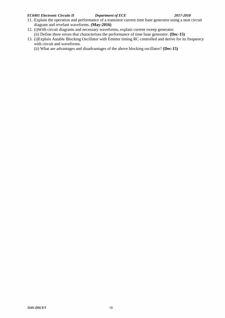
4. Classify the different types of Blocking oscillators.
Ans: 1. Monostable Blocking oscillators (Base time and Emitter time)
2. Astable Blocking Oscillators (Diode Controlled and RC Controlled)
5. How do we avoid distortion in the output of a pulse transformer?
Ans: The distortion can be avoided by making magnetising inductance (L) very high and Leakage
inductance () and Capacitance (C) very low during design.
6. What are the applications of Blocking oscillator? (May 16)
Ans: (i) used as frequency divider or counter.
(ii) used as low impedance switch
(iii) used as master oscillator to supply triggering signals for synchronizing
the system.
7. What is the equation for the coefficient of coupling in a pulse transformer?
Ans: The coefficient of coupling for this type of transformer is unity. The co efficient of coupling is given
by
sp LL
MK
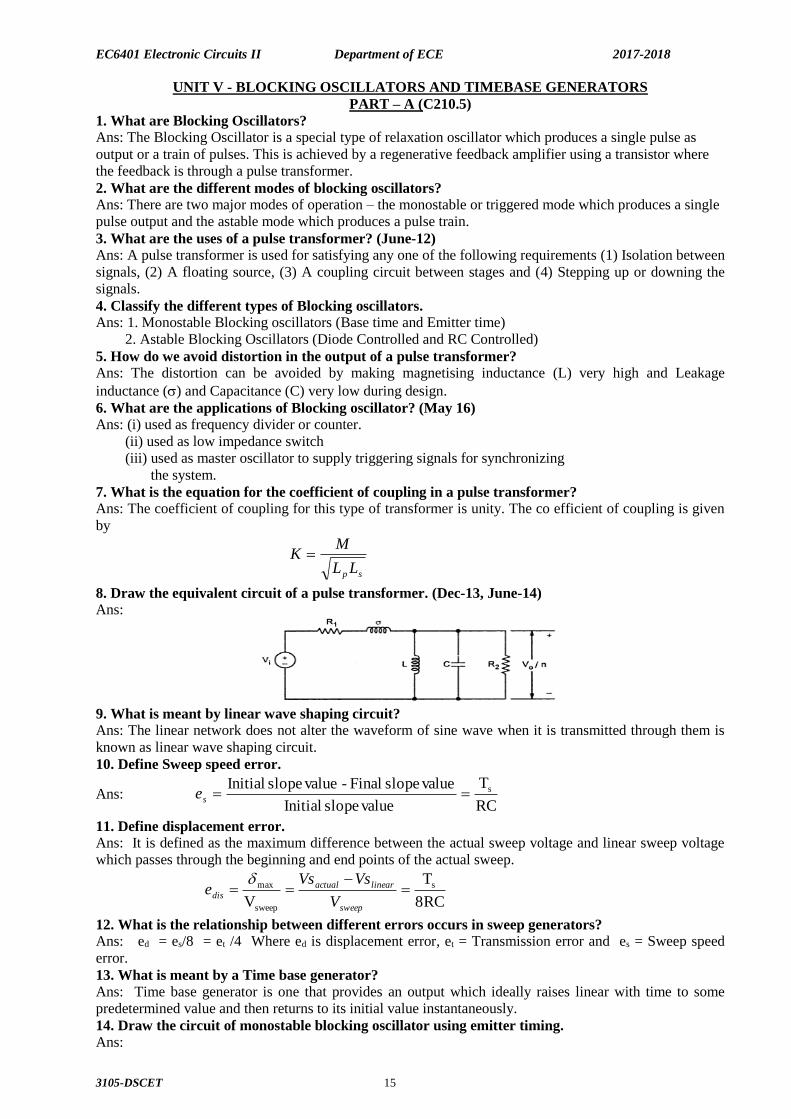
8. Draw the equivalent circuit of a pulse transformer. (Dec-13, June-14)
Ans:
9. What is meant by linear wave shaping circuit?
Ans: The linear network does not alter the waveform of sine wave when it is transmitted through them is
known as linear wave shaping circuit.
10. Define Sweep speed error.
Ans: RC
T
valueslope Initial
valueslope Final - valueslope Initial sse
11. Define displacement error.
Ans: It is defined as the maximum difference between the actual sweep voltage and linear sweep voltage
which passes through the beginning and end points of the actual sweep.
8RC
T
V
s
sweep
max
sweep
linearactual
disV
VsVse
12. What is the relationship between different errors occurs in sweep generators?
Ans: ed = es/8 = et /4 Where ed is displacement error, et = Transmission error and es = Sweep speed
error.
13. What is meant by a Time base generator?
Ans: Time base generator is one that provides an output which ideally raises linear with time to some
predetermined value and then returns to its initial value instantaneously.
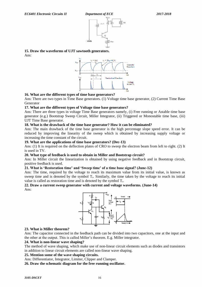
14. Draw the circuit of monostable blocking oscillator using emitter timing.
Ans:
EC6401 Electronic Circuits II Department of ECE 2017-2018
3105-DSCET 16
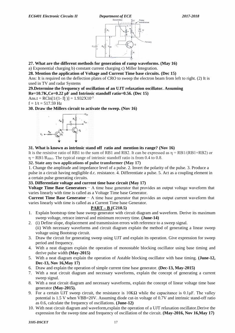
15. Draw the waveforms of UJT sawtooth generators.
Ans:
16. What are the different types of time base generators?
Ans: There are two types in Time Base generators. (1) Voltage time base generator, (2) Current Time Base
Generator
17. What are the different types of Voltage time base generators?
Ans: There are three types in voltage Time Base generators namely, (i) Free running or Astable time base
generator (e.g.) Bootstrap Sweep Circuit, Miller Integrator, (ii) Triggered or Monostable time base, (iii)
UJT Time Base generator.
18. What is the drawback of the time base generator? How it can be eliminated?
Ans: The main drawback of the time base generator is the high percentage slope speed error. It can be
reduced by improving the linearity of the sweep which is obtained by increasing supply voltage or
increasing the time constant of the circuit.
19. What are the applications of time base generators? (Dec-13)
Ans: (1) It is required on the deflection plates of CRO to sweep the electron beam from left to right. (2) It
is used in TV.
20. What type of feedback is used to obtain in Miller and Bootstrap circuit?
Ans: In Miller circuit the linearization is obtained by using negative feedback and in Bootstrap circuit,
positive feedback is used.
21. What is ‘Restoration time’ and ‘Sweep time’ of a time base signal? (June-12)
Ans: The time, required by the voltage to reach its maximum value from its initial value, is known as
sweep time and is denoted by the symbol Ts. Similarly, the time taken by the voltage to reach its initial
value is called as restoration time and is denoted by the symbol Tr.
22. Draw a current sweep generator with current and voltage waveforms. (June-14) Ans:
23. What is Miller theorem?
Ans: The capacitor connected in the feedback path can be divided into two capacitors, one at the input and
the other at the output. This is called Miller’s theorem. E.g. Miller integrator.
24. What is non-linear wave shaping?
The method of wave shaping, which make use of non-linear circuit elements such as diodes and transistors
in addition to linear circuit elements are called non-linear wave shaping.
25. Mention some of the wave shaping circuits.
Ans: Differentiator, Integrator, Limiter, Clipper and Clamper.
26. Draw the schematic diagram for the free running oscillator.
EC6401 Electronic Circuits II Department of ECE 2017-2018
3105-DSCET 17
27. What are the different methods for generation of ramp waveforms. (May 16)
a) Exponential charging b) constant current charging c) Miller Integration.
28. Mention the application of Voltage and Current Time base circuits. (Dec 15)
Ans: It is required on the deflection plates of CRO to sweep the electron beam from left to right. (2) It is
used in TV and radar Systems
29.Determine the frequency of oscillation of an UJT relaxation oscillator. Assuming
Re=10.7K,Ce=0.22 µF and Intrinsic standoff ratio=0.56. (Dec 15)
Ans.t = RCln[1/(1- Ƞ )] = 1.932X10⁻³
f = 1/t = 517.59 Hz
30. Draw the Millers circuit to activate the sweep. (Nov 16)
31. What is known as intrinsic stand off ratio and mention its range? (Nov 16)
It is the resistive ratio of RB1 to the sum of RB1 and RB2. It can be expressed as η = RB1/(RB1+RB2) or
η = RB1/RBBO. The typical range of intrinsic standoff ratio is from 0.4 to 0.8.
32. State any two applications of pulse transformer (May 17)
1. Change the amplitude and impedance level of a pulse. 2. Invert the polarity of the pulse. 3. Produce a
pulse in a circuit having negligible d.c. resistance. 4. Differentiate a pulse. 5. Act as a coupling element in
a certain pulse generating circuits.
33. Differentiate voltage and current time base circuit (May 17)
Voltage Time Base Generators − A time base generator that provides an output voltage waveform that
varies linearly with time is called as a Voltage Time base Generator.
Current Time Base Generator − A time base generator that provides an output current waveform that
varies linearly with time is called as a Current Time base Generator.
PART – B (C210.5)
1. Explain bootstrap time base sweep generator with circuit diagram and waveform. Derive its maximum
sweep voltage, retrace interval and minimum recovery time. (June-14)
2. (i) Define slope, displacement and transmission errors with reference to a sweep signal.
(ii) With necessary waveforms and circuit diagram explain the method of generating a linear sweep
voltage using Bootstrap circuit.
3. Draw the circuit for generating sweep using UJT and explain its operation. Give expression for sweep
period and frequency.
4. With a neat diagram explain the operation of monostable blocking oscillator using base timing and
derive pulse width (May-2015)
5. With a neat diagram explain the operation of Astable blocking oscillator with base timing. (June-12,
Dec-13, Nov 16,May 17) 6. Draw and explain the operation of simple current time base generator. (Dec-13, May-2015)
7. With a neat circuit diagram and necessary waveforms, explain the concept of generating a current
sweep signal.
8. With a neat circuit diagram and necessary waveforms, explain the concept of linear voltage time base
generator (May-2015).
9. For a certain UJT sweep circuit, the resistance is 10KΩ while the capacitance is 0.1μF. The valley
potential is 1.5 V when VBB=20V. Assuming diode cut-in voltage of 0.7V and intrinsic stand-off ratio
as 0.6, calculate the frequency of oscillations. (June-12)
10. With neat circuit diagram and waveform,explain the operation of a UJT relaxation oscillator.Derive the
expression for the sweep time and frequency of oscillation of the circuit. (May-2016, Nov 16,May 17)
EC6401 Electronic Circuits II Department of ECE 2017-2018
3105-DSCET 18
11. Explain the operation and performance of a transistor current time base generator using a neat circuit
diagram and revelant waveforms. (May-2016)
12. (i)With circuit diagrams and necessary waveforms, explain current sweep generator.
(ii) Define three errors that characterises the performance of time base generator. (Dec-15)
13. (i)Explain Astable Blocking Oscillator with Emitter timing RC controlled and derive for its frequency
with circuit and waveforms.
(ii) What are advantages and disadvantages of the above blocking oscillator? (Dec-15)
Related Documents