1 BAPATLA ENGINEERING COLLEGE ELECTRONIC CIRCUITS -1LAB (EC261) PREPARED BY M. BABY M.Tech LECTURER & S. ANUSHA B.Tech LECTURER Department of Electronics and Communications Engineering Bapatla Engineering College (Affiliated to Acharya Nagarjuna University) Bapatla-522101 2008-2009

Welcome message from author
This document is posted to help you gain knowledge. Please leave a comment to let me know what you think about it! Share it to your friends and learn new things together.
Transcript
1
BAPATLA ENGINEERING COLLEGE ELECTRONIC CIRCUITS -1LAB (EC261)
PREPARED BY
M. BABY M.Tech
LECTURER
&
S. ANUSHA B.Tech
LECTURER
Department of Electronics and Communications Engineering Bapatla Engineering College
(Affiliated to Acharya Nagarjuna University) Bapatla-522101
2008-2009
2
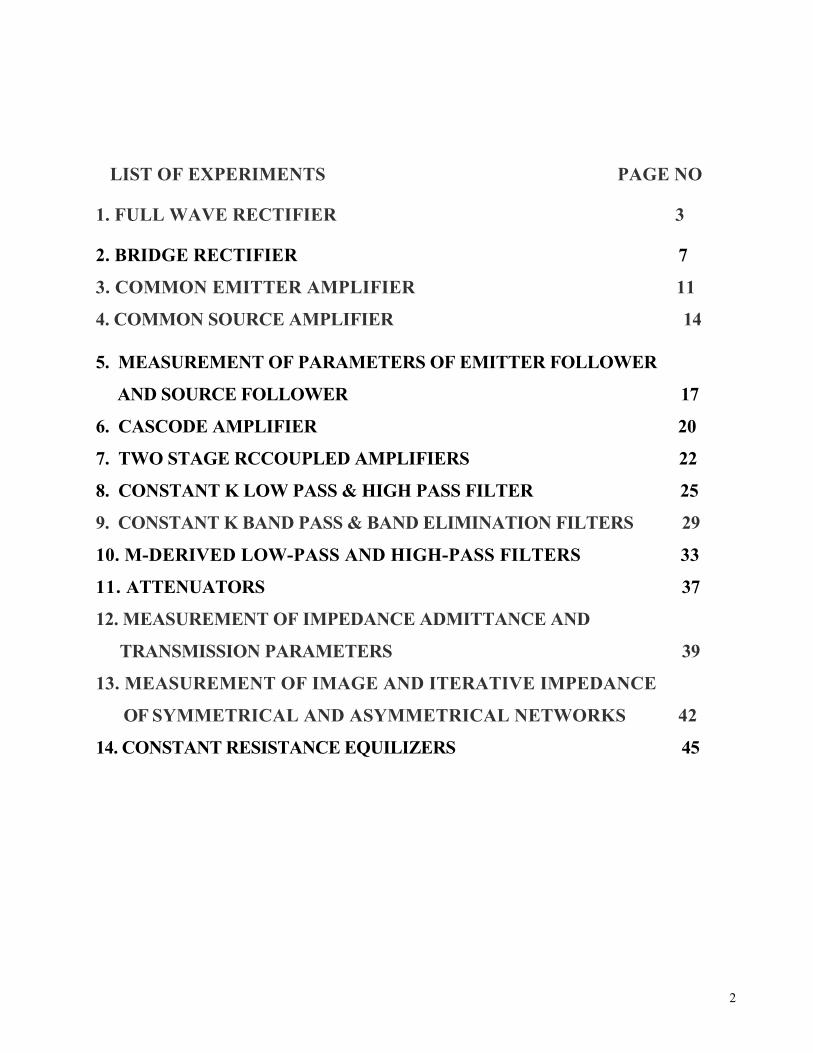
LIST OF EXPERIMENTS PAGE NO
1. FULL WAVE RECTIFIER 3
2. BRIDGE RECTIFIER 7
3. COMMON EMITTER AMPLIFIER 11
4. COMMON SOURCE AMPLIFIER 14 5. MEASUREMENT OF PARAMETERS OF EMITTER FOLLOWER
AND SOURCE FOLLOWER 17
6. CASCODE AMPLIFIER 20
7. TWO STAGE RCCOUPLED AMPLIFIERS 22
8. CONSTANT K LOW PASS & HIGH PASS FILTER 25
9. CONSTANT K BAND PASS & BAND ELIMINATION FILTERS 29
10. M-DERIVED LOW-PASS AND HIGH-PASS FILTERS 33
11. ATTENUATORS 37
12. MEASUREMENT OF IMPEDANCE ADMITTANCE AND
TRANSMISSION PARAMETERS 39
13. MEASUREMENT OF IMAGE AND ITERATIVE IMPEDANCE
OF SYMMETRICAL AND ASYMMETRICAL NETWORKS 42
14. CONSTANT RESISTANCE EQUILIZERS 45
3
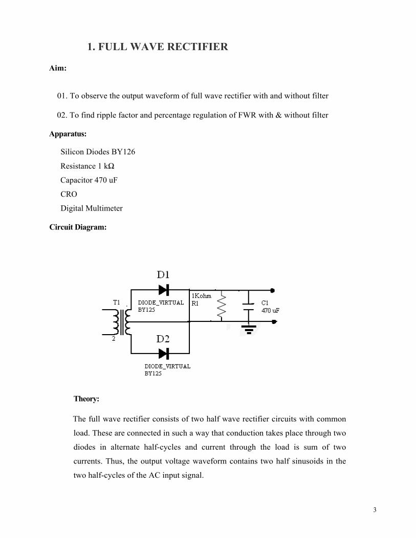
1. FULL WAVE RECTIFIER
Aim:
01. To observe the output waveform of full wave rectifier with and without filter
02. To find ripple factor and percentage regulation of FWR with & without filter
Apparatus:
Silicon Diodes BY126
Resistance 1 kΩ
Capacitor 470 uF
CRO
Digital Multimeter
Circuit Diagram:
Theory:
The full wave rectifier consists of two half wave rectifier circuits with common
load. These are connected in such a way that conduction takes place through two
diodes in alternate half-cycles and current through the load is sum of two
currents. Thus, the output voltage waveform contains two half sinusoids in the
two half-cycles of the AC input signal.
4
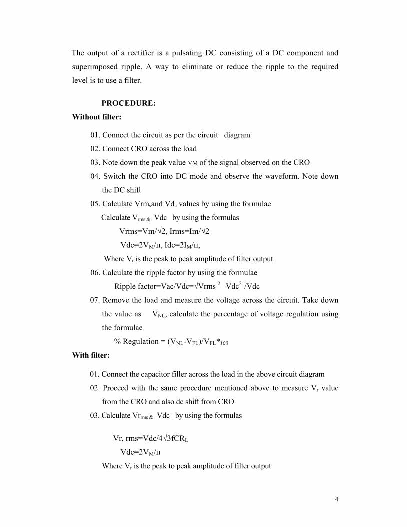
The output of a rectifier is a pulsating DC consisting of a DC component and
superimposed ripple. A way to eliminate or reduce the ripple to the required
level is to use a filter.
PROCEDURE:
Without filter:
01. Connect the circuit as per the circuit diagram
02. Connect CRO across the load
03. Note down the peak value VM of the signal observed on the CRO
04. Switch the CRO into DC mode and observe the waveform. Note down
the DC shift
05. Calculate Vrmsand Vdc values by using the formulae
Calculate Vrms & Vdc by using the formulas
Vrms=Vm/√2, Irms=Im/√2
Vdc=2VM/п, Idc=2IM/п,
Where Vr is the peak to peak amplitude of filter output
06. Calculate the ripple factor by using the formulae
Ripple factor=Vac/Vdc=√Vrms 2 –Vdc2 /Vdc
07. Remove the load and measure the voltage across the circuit. Take down
the value as VNL; calculate the percentage of voltage regulation using
the formulae
% Regulation = (VNL-VFL)/VFL*100
With filter:
01. Connect the capacitor filler across the load in the above circuit diagram
02. Proceed with the same procedure mentioned above to measure Vr value
from the CRO and also dc shift from CRO
03. Calculate Vrrms & Vdc by using the formulas
Vr, rms=Vdc/4√3fCRL
Vdc=2VM/п
Where Vr is the peak to peak amplitude of filter output
5
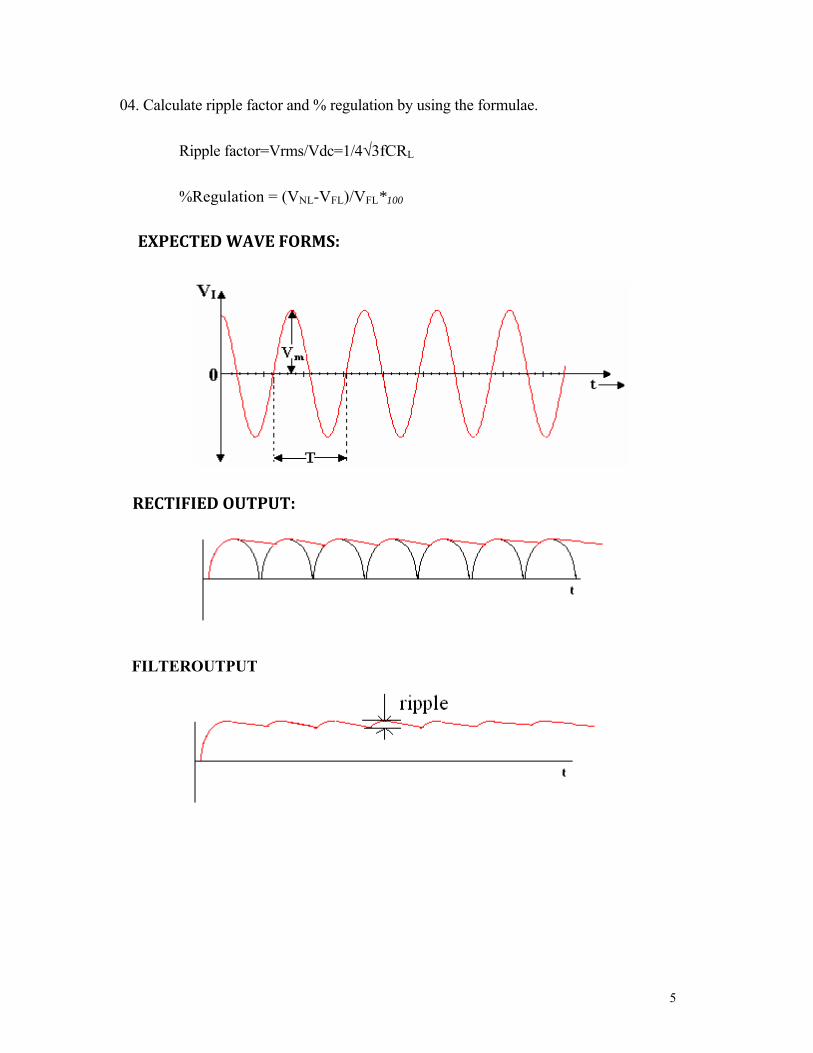
04. Calculate ripple factor and % regulation by using the formulae.
Ripple factor=Vrms/Vdc=1/4√3fCRL
%Regulation = (VNL-VFL)/VFL*100
EXPECTED WAVE FORMS:
RECTIFIED OUTPUT:
FILTEROUTPUT

6
Precautions:
1. Wires should be checked for good continuity.
2. Carefully note down the readings with out any errors.
Result:

7
2. BRIDGE RECTIFIER
Aim:
1. To observe the output waveform of bridge rectifier with and without filter
2. To find ripple factor and percentage of regulation of bridge rectifier with and
without filter
Apparatus:
Silicon Diodes BY126
Resistance 1 KΏ
Capacitor 470 µF
CRO Multimeter
Circuit Diagram:
Theory:
The bridge is seen to consist of four diodes connected with their arrowhead
symbols all pointing toward the positive output terminal of the circuit.

8
During the positive half cycle of input voltage. Thus load current flows from
the positive input terminal through D1 to RL and then through RL and D4 back to the
negative input terminal. During this time, the positive input terminal is applied to the
cathode of D2 so it is reversed biased and similarly D3 is also reverse biased. These
two diodes are forward biased during negative half cycle; D1 & D4 are reverse biased
during this cycle. And finally both half cycles are rectified.
Procedure:
Without filter:
01. Connect the circuit as per the circuit diagram.
02. Connect CRO across the load
03. Note down the peak value VM of the signal observed on the CRO
04. Switch the CRO into DC mode and observe the waveform. Note
down the DC shift.
05. Calculate Vmis and Vdc values by using the formulae
Vrms=Vm/√2, Irms=Im/√2,
Vdc=2VM/п , Idc=2IM/п
06. Calculate the ripple factor by using the formulae
R=√ (Vrms/Vdc)2 -1
07. Remove the load and measure the voltage across the circuit take
down the value as VNL. Calculate the percentage of voltage regulation
using the formula
Regulation = (VNL-VFL)/VFL*100
With Filter:
01. Connect the capacitor filter across the load in the above circuit
diagram.
02. Procedure mentioned above to measure Vr value and also dc shift
from CRO
03. Calculate Vrms by using the formula
Where Vr is the peak to peak amplitude of filter output
9
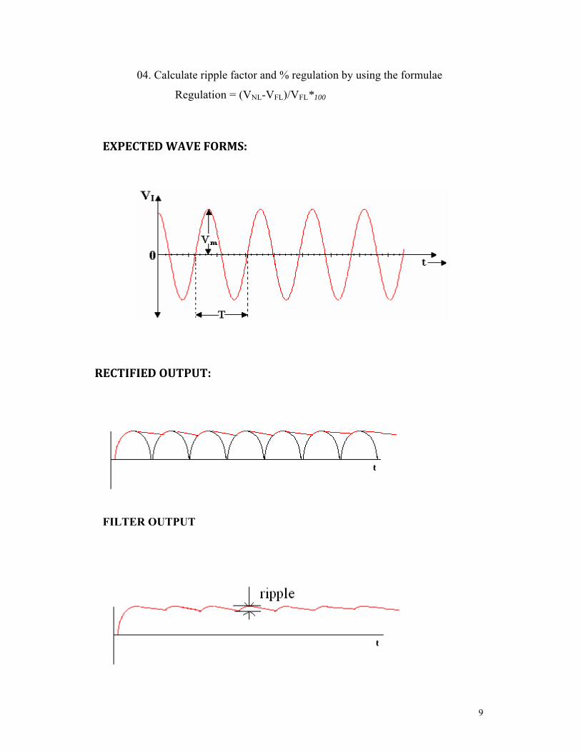
04. Calculate ripple factor and % regulation by using the formulae
Regulation = (VNL-VFL)/VFL*100
EXPECTED WAVE FORMS:
RECTIFIED OUTPUT:
FILTER OUTPUT

10
Precautions:
01. Wires should be checked for good continuity.
02. Carefully note down the readings with out any errors.
Result:
11
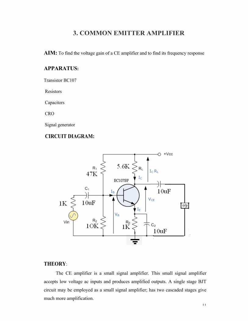
3. COMMON EMITTER AMPLIFIER
AIM: To find the voltage gain of a CE amplifier and to find its frequency response
APPARATUS:
Transistor BC107
Resistors
Capacitors
CRO
Signal generator
CIRCUIT DIAGRAM:
THEORY:
The CE amplifier is a small signal amplifier. This small signal amplifier
accepts low voltage ac inputs and produces amplified outputs. A single stage BJT
circuit may be employed as a small signal amplifier; has two cascaded stages give
much more amplification.

12
Designing for a particular voltage gain requires the use of a ac negative
feedback to stabilize the gain. For good bias stability, the emitter resistor voltage
drop should be much larger than the base -emitter voltage. And Re resistor will
provide the required negative feedback to the circuit. CE is provided to provide
necessary gain to the circuit. All bypass capacitors should be selected to have the
smallest possible capacitance value, both to minimize the physical size of the
circuit for economy. The coupling capacitors should have a negligible effect on the
frequency response of the circuit.
PROCEDURE:
1. Connect the circuit as per the circuit diagram.
2. Give l00Hz signal and 20mv p-p as Vs from the signal generator
3. Observe the output on CRO and note down the output voltage.
4. Keeping input voltage constant and by varying the frequency in steps
100Hz-1MHz, note down the corresponding output voltages.
5. Calculate gain in dB and plot the frequency response on semi log sheet.
TABULAR FORM
Input voltage (Vi)=
.NO FREQUENCY OUTPUT
VOLTAGE(Vo)
GAIN Av=Vo/Vi GAIN IN dB
20 log gain
13
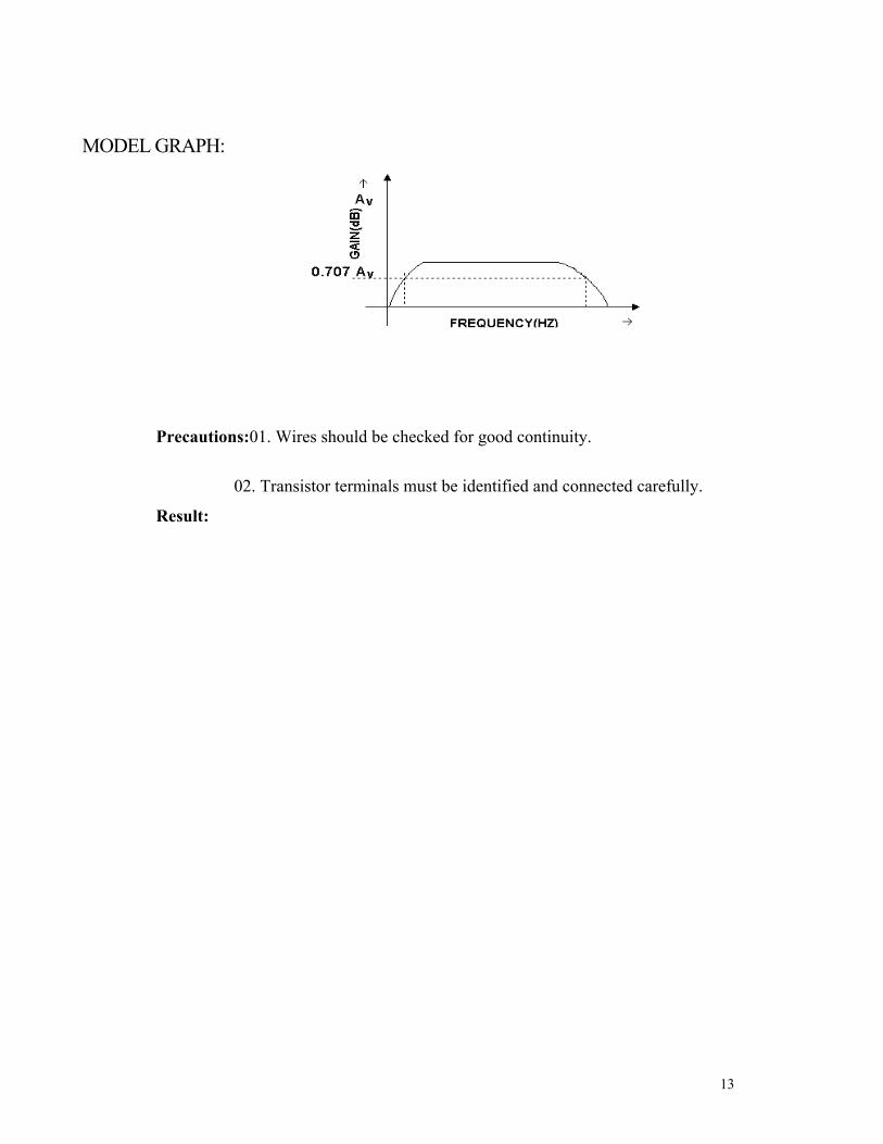
MODEL GRAPH:
Precautions:01. Wires should be checked for good continuity.
02. Transistor terminals must be identified and connected carefully.
Result:

14
4. COMMON SOURCE AMPLIFIER
AIM: To find the voltage gain of a CS amplifier and to find its frequency response
APPARATUS:
FETBFW10
RESISTORS
Capacitors
Signal generator &CRO
CIRCUIT DIAGRAM:
THEORY:
The CS amplifier is a small signal amplifier. For good bias stability, the
source resistor voltage drop should be as large as possible. Where the supply voltage
is small, Vs may be reduced to a minimum to allow for the minimum level of
Vds.R2 is usually selected as 1MΏ or less as for BJT capacitor coupled circuit,
15
coupling and bypass capacitors should be selected to have the smallest possible
capacitance values. The largest capacitor in the circuit sets the circuit low 3dB
frequency (capacitor C2). Generally to have high input impedance FET is used.
As in BJT circuit RL is usually much larger than Zo and Zi is often much larger than
Rs
PROCEDURE:
1. Connect the circuit as per the circuit diagram
2. Give 1 KHz signal and 25 mv (P-P) as Vs from signal generator.
3 Observe the output on CRO for proper working of the amplifier.
4 After ensuring the amplifier function, vary signal frequency from 50 Hz to
600 Hz in proper steps for 15-20 readings keeping Vs =25mv(P-P) at
every frequency ,note down the resulting output voltage and tabulate in a
table
5. Calculate gain in dB and plot on semi log graph paper for frequency Vs gain
in dB
TABULAR FORM:
Input voltage (Vi)=
S.NO FREQUENCY OUTPUT
VOLTAGE(Vo)
GAIN Av=Vo/Vi GAIN IN dB
20 log gain

16
MODEL GRAPH:
PRECAUTIONS: 1. Wires should be checked for good continuity
2 FET terminals must be identified and connected carefully.
RESULT:
17
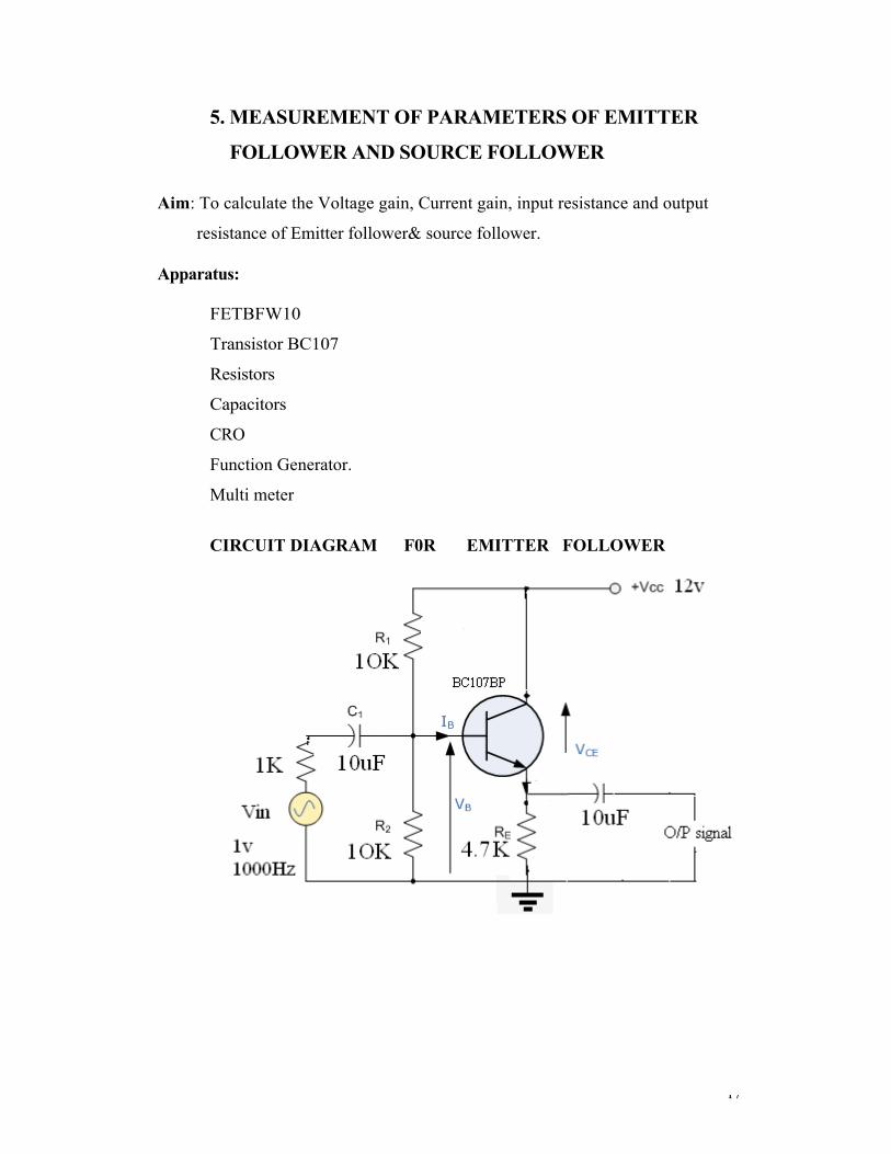
5. MEASUREMENT OF PARAMETERS OF EMITTER
FOLLOWER AND SOURCE FOLLOWER
Aim: To calculate the Voltage gain, Current gain, input resistance and output
resistance of Emitter follower& source follower.
Apparatus:
FETBFW10
Transistor BC107
Resistors
Capacitors
CRO
Function Generator.
Multi meter
CIRCUIT DIAGRAM F0R EMITTER FOLLOWER

18
CIRCUIT DIAGRAM F0R SOURCE FOLLOWER
THEORY: EMITTER FOLLOWER
The common collector circuit is also known as emitter follower. The ac
output voltage from a CC circuit is essentially the same as the input voltage; there is
no voltage gain or phase shift. Thus, the CC circuit can be said to have a voltage
gain of 1. The fact that the CC output voltage follows the changes in signal voltage
gives the circuit its other name emitter follower. The input impedance of a CC
amplifier is high. Output impedance is low and the Voltage gain is almost unity.
Because of these Characteristics the CC circuit is normally used as a buffer
amplifier, placed between a high impedance signal source and a low impedance load.
19
SOURCE FOLLOWER
The FET common drain circuit has the output voltage developed across the
source resistor Rs. Here the ac output voltage is closely equal to the ac input
voltage, and the circuit can be said to have unity gain. Because the output voltage at
the source terminal follows the signal voltage at the gate, the common drain circuit
is also known as a source follower.
A common drain circuit has a voltage gain approximately equal to 1, no phase shift
between input and output, very high input impedance and low output impedance.
Because of its high Zi, low Zo and unity gain the CD circuit is used as a buffer
amplifier between a high impedance signal source and a low impedance load.
PROCEDURE:
1. Connect the circuit as per the circuit diagram.
2. Apply Vslv 1 KHz signal from the signal generator.
3. Observe corresponding output from the CRO and then calculate voltage gain using
the formula Av=Vo/Vi.
4. Measure voltage across AB terminals and then calculate input current by using the
formula Iin=Vab/Rab.
5. Measure current flowing through resistor at Source (or Emitter) terminal and note
down it as Iout.
6. Calculate Current gain using the formula AI=Iin/Iout.
7. Calculate input resistance using the formula Rin=Vin/Iin.
8. To calculate the output resistance, connect the pot at the output and vary the
resistance of the pot up to half of the output with RL is equal to infinity. The
resistance of pot is the output resistance.
PRECAUTIONS:
1. Wires should be checked for good continuity
2. FET terminals must be identified and connected carefully.
RESULT:

20
6. CASCODE AMPLIFIER
AIM: To measure voltage gain, input resistance and output resistance of cascode
amplifier
APPARATUS:
Transistor BC107 Resistors
Signal generator
Capacitors
CIRCUIT DIAGRAM:
21
DESIGN:
IB1=VCE-VBE/RB1
IC1=IE2=IC2=ßIB1
VC1=VE2=VB2-VBE
VC2=VCC-IC2*RC2
VCE2=VC2-VE2
Rin=RB1ß1RE1
Av1=-RL1/RE1=-1
Ro=RC2
RL2=RC2RL
AV2=RL2/RE2
Av=AV1*AV2
THEORY: Cascode amplifier is a cascade connection of a common emitter and
common base amplifiers. It is used for amplifying the input signals. The common
application of cascade amplifier is for impedance matching. The low impedance of CE
age is matched with the medium of the CB sage.
PRECAUTIONS:
1. Wires should be checked for good continuity
2. Take the readings carefully
RESULT:
22
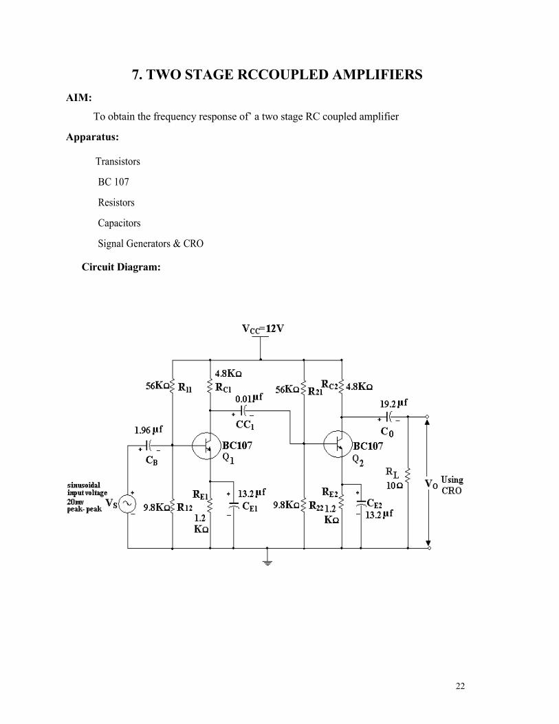
7. TWO STAGE RCCOUPLED AMPLIFIERS AIM:
To obtain the frequency response of’ a two stage RC coupled amplifier
Apparatus:
Transistors
BC 107
Resistors
Capacitors
Signal Generators & CRO
Circuit Diagram:
23
Theory:
A RC coupled two stage amplifier is shown in the figure each
stage is similar to the single stage circuit. Stage 1 is capacitor coupled to
the input of stage 2. The signal is applied to the input of stage 1 and the
load is coupled to the output of stage 2. The signal K amplified by stage 1
and the output of stage 1 is amplified by stage 2. So that the overall voltage
gain is much greater than the gain of a single stage. The signal voltage is
phase shifted through 180° by stage 1 and through a further 180° by stage 2.
Consequently the overall phase shift from input to output is zero or 360"
PROCEDURE
01. Connect the circuit as per the circuit diagram
02. Give 1 KHz signal, 25 mV (p-p) as Vs from signal generator
03. Observe the output on CRO for proper working of the amplifier
04. After ensuring the amplifier function, vary signal frequency
from 50 Hz to 600 Hz in proper steps for 15 to 20 readings.
Keeping Vs = 25 mV (p-p) at every frequency, note down the
resetting output voltage and tabulate in a table.
05. Calculate gain db and plot on semi log graph paper for frequency VS gain db.
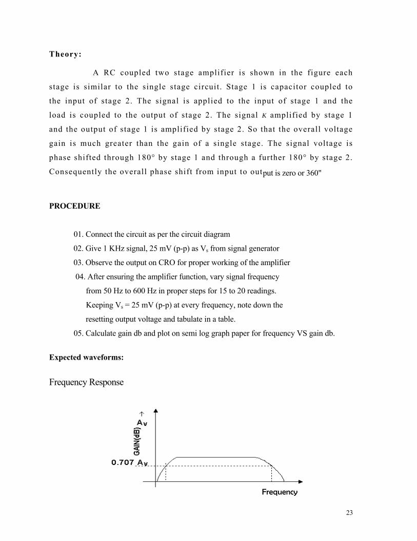
Expected waveforms:
Frequency Response
Frequency

24
Tabular Form:
S.NO FREQUENCY
(HZ)
OUTPUT
VOLTAGE(Vo)
GAIN
Av=Vo/Vi
GAIN IN
dB
20 log gain
PRECAUTIONS: 1. Wires should be checked for good continuity
2. FET terminals must be identified and connected carefully.
RESULT:
25
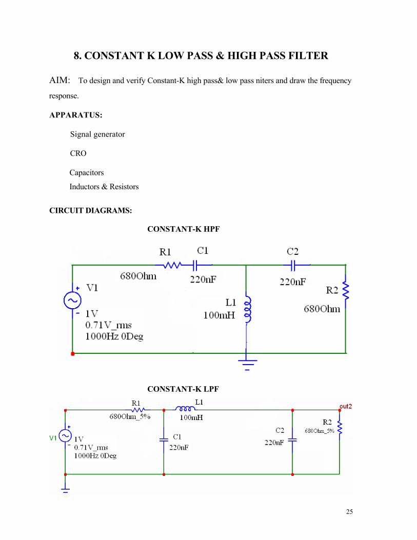
8. CONSTANT K LOW PASS & HIGH PASS FILTER
AIM: To design and verify Constant-K high pass& low pass niters and draw the frequency
response.
APPARATUS:
Signal generator
CRO
Capacitors
Inductors & Resistors
CIRCUIT DIAGRAMS:
CONSTANT-K HPF
CONSTANT-K LPF
26
DESIGN EQUATIONS:
ForLPF:
Given RL-680Ω, Fc=2 KHz, Rs=680 Ω. Rl=Rs=Rk
C=1/ (πfcRk), R=Rk/fc
For HPF:
Given RL=Rs=Rk
Given RL-680Ω, Fc=2 KHz, Rs=680 Ω. Rl=Rs=Rk
C=1/ (πfcRk), L=Rk/4пfc
THEORY:
The low pass filter is a filter that transmits all frequencies from zero unto some
designated frequency called the cut-oft frequency and offer great attenuation at all other
higher frequencies. A Constant-K filter is a T or TT network in which the series and shunt
impedances, Zl and Z2 are connected by the relationship Z.1Z2=Rk2. where Rk is a real
constant or it is termed as design impedance or nominal impedance of Constant-K filter. A
HPF is a filter that transmits all frequencies above a designated cut-off frequency but
attenuates frequencies below this.
PROCEDURE:
1. Design L and C values with the help of formulae and connect them in the circuit.
2. Set the input voltage Vi=5v using signal generator and vary the frequency from1Hz-lMHz
in regular intervals.
3. Note down the corresponding output voltage.
4. Calculate gain in dB.
5. Plot the frequency response of HPF & LPF.

27
TABULAR COLUMN
S.NO FREQUENCY
(HZ)
OUTPUT
VOLTAGE(Vo)
GAIN
Av=Vo/Vi
GAIN IN dB
20 log gain
MODEL GRAPHS: CONSTANT-KHPF

28
CONSTANT-KLPF
PRECAUTIONS: 1. Wires should be checked for good continuity
2. Vary the frequency carefully.
RESULT:
9. CONSTANT K BAND PASS AND BAND ELIMINATION

29
FILTERS
AIM: To design constant-k band pass and band elimination filters and measures their cut off
frequencies.
APPARATUS:
Signal generator (0-1) MHz
CRO
CIRCUIT DIAGRAM:
Band pass filter:
30
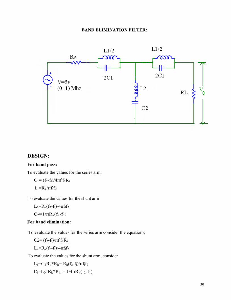
BAND ELIMINATION FILTER:
DESIGN: For band pass:
To evaluate the values for the series arm,
C1= (f2-fl)/4пflf2Rk
Ll=Rk/пflf2
To evaluate the values for the shunt arm
L2=Rk(f2-fl)/4пflf2
C2=1/пRk(f2-f1)
For band elimination:
To evaluate the values for the series arm consider the equations,
C2= (f2-fl)/пflf2Rk
L2=Rk(f2-fl)/4пflf2
To evaluate the values for the shunt arm, consider
L1=C2Rk*Rk= Rk(f2-fl)/пflf2
C1=L2/ Rk*Rk = 1/4пRk(f2-f1)

31
THEORY:
Band passes and band elimination filters are designed to allow a particular band of
frequencies or to eliminate a particular band of frequencies. A band pass filter is obtained by
using a low pass filter followed by a high pass filter in which the cut off frequency of the LP
Filter is above the cut off frequency of the HP hence allowing only a band of frequencies. A band
stop filter can be realized by connecting a low pass filter in parallel with a high pass filter. The
cutoff frequency of low pass is below the high pass.
PROCEDURE:
1. Connect the circuit as per the circuit diagram
2. Set i/p voltage Vi=5v using signal generator and vary
the frequency from (0-l) MHz in regular intervals
3. Note down the corresponding output voltage
4. Plot the graph between gain Vs frequencies
TABULAR COLOUMN:
S.No
frequency(Hz)
Output Voltage
(Volts)
Gain (Vo/Vin) Gain in dB

32
MODEL GRAPH:
BAND PASS FILTER:
BAND ELIMINATION FILTER
PRECAUTIONS: 1. Wires should be checked for good continuity
2. Vary the frequency carefully.
RESULT:
33
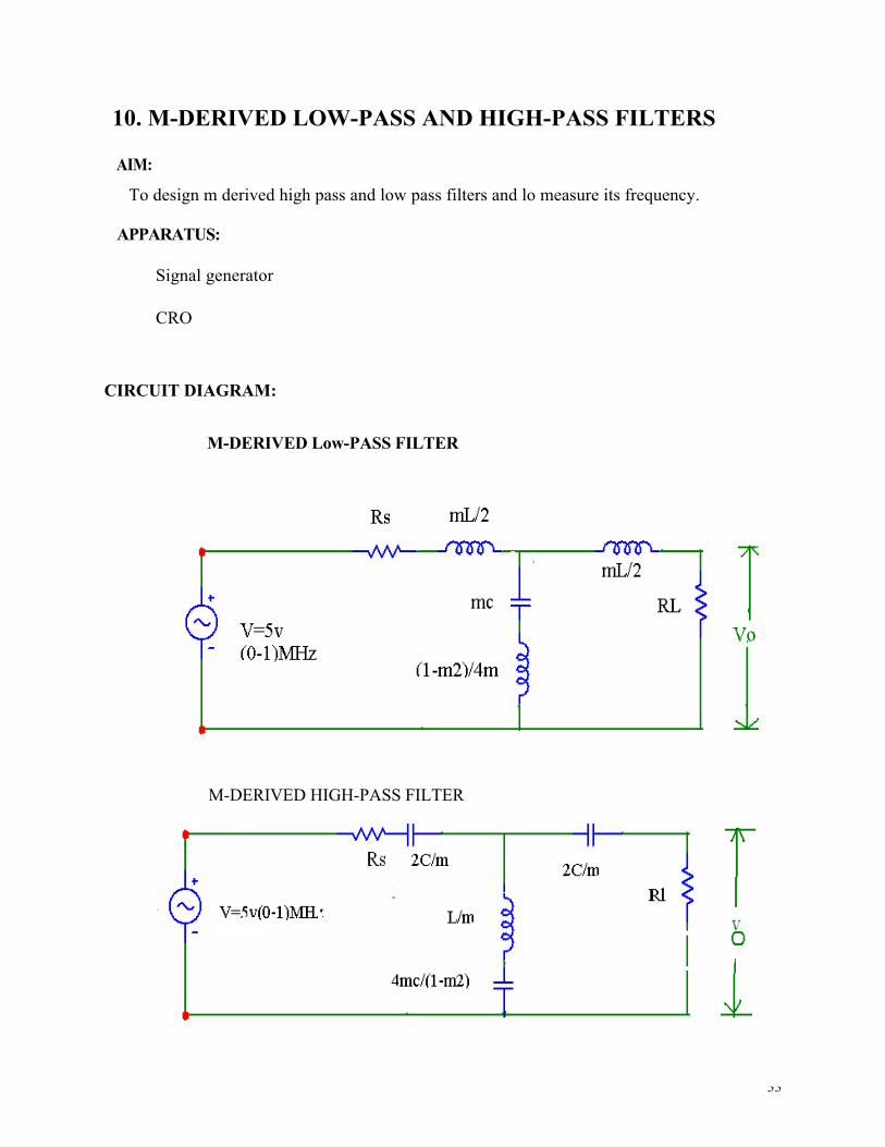
10. M-DERIVED LOW-PASS AND HIGH-PASS FILTERS
AIM:
To design m derived high pass and low pass filters and lo measure its frequency.
APPARATUS:
Signal generator
CRO
CIRCUIT DIAGRAM:
M-DERIVED Low-PASS FILTER
M-DERIVED HIGH-PASS FILTER
34
THEORY: For a constant k prototype filter section has two major disadvantages. The
attenuation does not rise very rapidly at cutoff frequency .so that a satisfactory impedance match
is not possible. So m derived filters used to raise the attenuation near cutoff. To have a sharp cut
off frequency, m derived filter is used. A HPF is one which attenuates the lower frequencies and
passes the higher frequencies above the cut off frequency. A LPF is one allows the frequencies
below the cut off frequency and attenuates the frequencies above cut off frequency.
DESIGN:
FOR HPF
0<m<1(m=0.5) f=2 kHz, C=0.01 fr=1/4п√LC L=?
FOR LPF:
0<m<1(m=0.5) f=2 kHz, C=0.01 uF
fr=1/п√LC (1-m2) L=?
PROCEDURE:
1. Connect the circuit as per the circuit diagram
2. Set i/p voltage Vi=5v using signal generator and vary
the frequency from (0-l) MHz in regular intervals
3. Note down the corresponding output voltage
4. Plot the graph between gain vs frequencies
TABULAR COLOUMN
M-DERIVED HIGH PASS FILTER
S.No
frequency(Hz)
Output Voltage
(Volts)
Gain (Vo/Vin) Gain in dB

35
TABULAR COLOUMN
M-DERIVED LOW PASS FILTER
S.No
frequency(Hz)
Output Voltage
(Volts)
Gain (Vo/Vin) Gain in dB
MODEL GRAPH: m-Derived High Pas Filter:
m-Derived Low Pass Filter:

36
PRECAUTIONS:
1. Connections are made tight.
2. Vary the voltage properly.
RESULT:

37
11. ATTENUATORS
AIM: To design a T- attenuator and ∏-attenuator which attenuate given signal to the desired
level
APPARATUS: Signal generator (0-1) MHz
CRO (0-20) MHz
CIRCUIT DIAGRAM: T-ATTENUATOR
П-ATTENUATOR
DESIGN: Given D=2dB, Rs=L680 Ω
Rl=Ro(N2-l/2N),R2=Ro(N+l/N-l)
N=Antilog(DdB/20)

38
PROCEDURE:
1. Connect the circuit as per the circuit diagram
2. Set input voltage, Vi=5v using signal generator and
vary the frequency from (0--1) MHz in regular steps
3. Note down the corresponding output voltage
4. Plot the graph output voltage Vs frequencies
TABULAR COLOUMN
INPUT VOLTAGE= (Vi)
S.No
frequency(Hz)
Output Voltage (Volts)
MODEL GRAPH:
PRECAUTIONS: 1. Check for loose connections in the circuit.
2. Vary the frequency carefully.
RESULT:
39
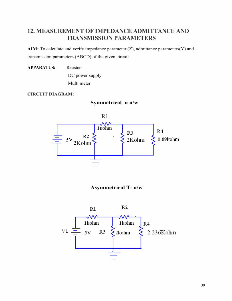
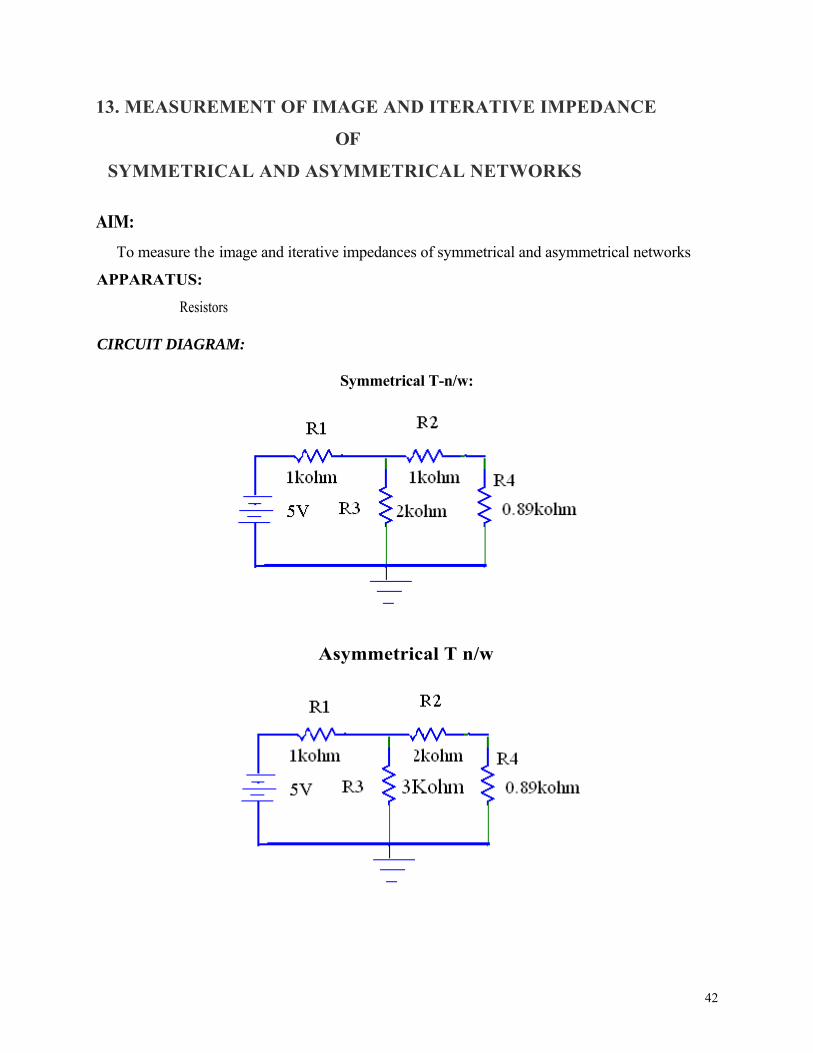
12. MEASUREMENT OF IMPEDANCE ADMITTANCE AND TRANSMISSION PARAMETERS
AIM: To calculate and verify impedance parameter (Z), admittance parameters(Y) and
transmission parameters (ABCD) of the given circuit.
APPARATUS: Resistors
DC power supply
Multi meter.
CIRCUIT DIAGRAM:
Symmetrical п n/w
Asymmetrical T- n/w
40
THEORY:
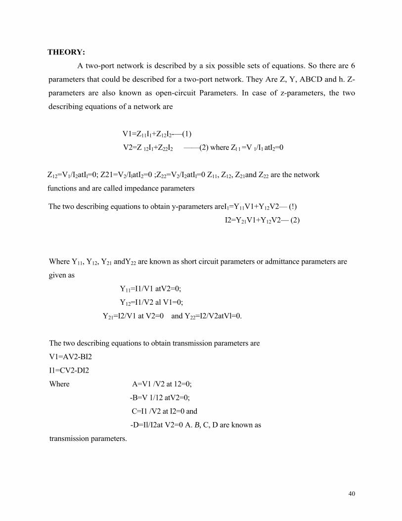
A two-port network is described by a six possible sets of equations. So there are 6
parameters that could be described for a two-port network. They Are Z, Y, ABCD and h. Z-
parameters are also known as open-circuit Parameters. In case of z-parameters, the two
describing equations of a network are
V1=Z11I1+Z12I2-—(1)
V2=Z 12I1+Z22I2 ——(2) where Zl 1 =V 1/I1 atI2=0
Z12=V1/I2atIl=0; Z21=V2/IlatI2=0 ;Z22=V2/I2atIl=0 Z11, Z12, Z21and Z22 are the network
functions and are called impedance parameters
The two describing equations to obtain y-parameters areI1=Y11V1+Y12V2— (!)
I2=Y21V1+Y12V2— (2)
Where Y11, Y12, Y21 andY22 are known as short circuit parameters or admittance parameters are
given as
Y11=I1/V1 atV2=0;
Y12=I1/V2 al V1=0;
Y21=I2/V1 at V2=0 and Y22=I2/V2atVl=0.
The two describing equations to obtain transmission parameters are
V1=AV2-BI2
I1=CV2-DI2
Where A=V1 /V2 at 12=0;
-B=V 1/12 atV2=0;
C=I1 /V2 at I2=0 and
-D=Il/I2at V2=0 A. B, C, D are known as
transmission parameters.

41
PROCEDURE:
1. Connect the circuit as per the circuit diagram.
2. Calculate Z11, Z12, Z21and Z22 & Y11, Y12, Y21 andY22 & A, B, C. D parameters theoretically.
3. Measure VI, V2, I1, I2 practically and finally obtain Z, Y and ABCD parameters practically.
4. Compare practical values with theoretical calculation.
TABULAR COLUMN
PRECAUTIONS:
1. Check for loose connections in the circuit.
RESULT:
Theoretical Practical
Z parameters
Y parameters
ABCD
Parameters
42
13. MEASUREMENT OF IMAGE AND ITERATIVE IMPEDANCE
OF
SYMMETRICAL AND ASYMMETRICAL NETWORKS
AIM: To measure the image and iterative impedances of symmetrical and asymmetrical networks
APPARATUS:
Resistors
CIRCUIT DIAGRAM:
Symmetrical T-n/w:
Asymmetrical T n/w
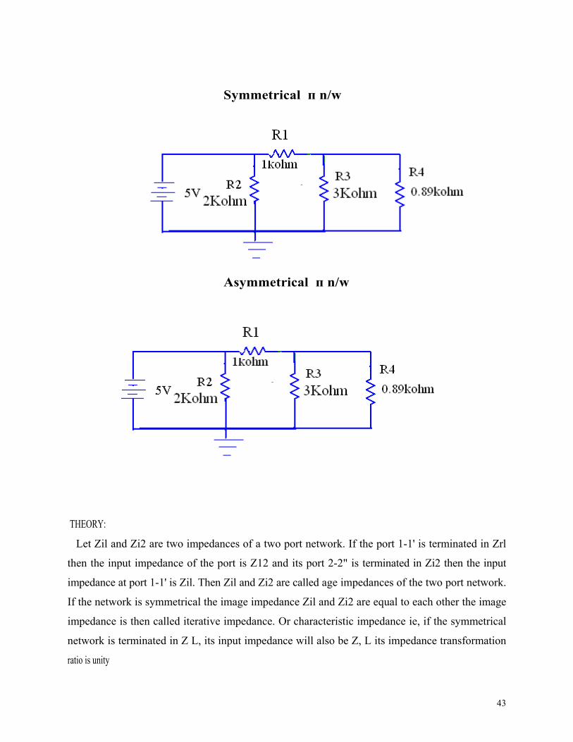
43
Symmetrical п n/w
Asymmetrical п n/w
THEORY:
Let Zil and Zi2 are two impedances of a two port network. If the port 1-1' is terminated in Zrl
then the input impedance of the port is Z12 and its port 2-2" is terminated in Zi2 then the input
impedance at port 1-1' is Zil. Then Zil and Zi2 are called age impedances of the two port network.
If the network is symmetrical the image impedance Zil and Zi2 are equal to each other the image
impedance is then called iterative impedance. Or characteristic impedance ie, if the symmetrical
network is terminated in Z L, its input impedance will also be Z, L its impedance transformation
ratio is unity
44
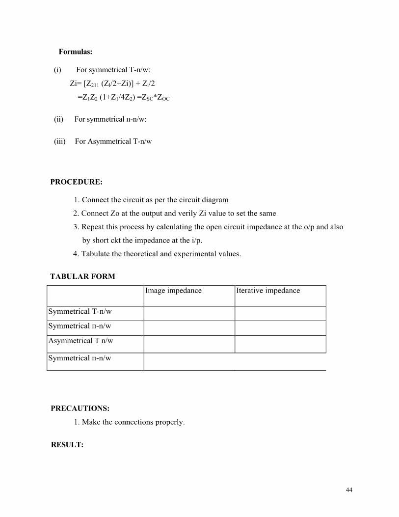
Formulas:
(i) For symmetrical T-n/w:
Zi= [Z211 (Zl/2+Zi)] + Zl/2
=Z1Z2 (1+Z1/4Z2) =ZSC*ZOC
(ii) For symmetrical п-n/w:
(iii) For Asymmetrical T-n/w
PROCEDURE:
1. Connect the circuit as per the circuit diagram
2. Connect Zo at the output and verily Zi value to set the same
3. Repeat this process by calculating the open circuit impedance at the o/p and also
by short ckt the impedance at the i/p.
4. Tabulate the theoretical and experimental values.
TABULAR FORM
PRECAUTIONS:
1. Make the connections properly.
RESULT:
Image impedance Iterative impedance
Symmetrical T-n/w
Symmetrical п-n/w
Asymmetrical T n/w
Symmetrical п-n/w
45
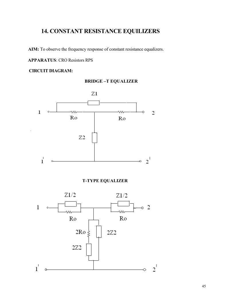
14. CONSTANT RESISTANCE EQUILIZERS
AIM: To observe the frequency response of constant resistance equalizers.
APPARATUS: CRO Resistors RPS
CIRCUIT DIAGRAM:
BRIDGE –T EQUALIZER
T-TYPE EQUALIZER

46
∏ -TYPE EQUALIZER
DESIGN EQUATIONS:
T- type Equalizer: Z1Z2=Ro2., M=16dB;
Ro, =600Ω, Z l=l/ωCl, Z2=ωL2;
L1=Ro√m-1/ω
C1=√m-1/ωRo
п type Equalizer: Z1Z2=Ro2.,
Z1= ωL1
Z2 = 1/ ωc1
C1= Ro√m-1/ω
L1=Ro√m-1/ω
BridgeT-Equalizer:
R1R2=L1/C1=Ro2.
L1=Ro√m-1/ω
C3=L1/ Ro2

47
PROCEDURE:
1. Connect the circuit as per the circuit diagram
2. Vary the frequency and observe the waveform on the CRO
3. Plot the attenuation Vs frequency graph.
TABULAR COLOUMN:
S NO FREQUENCY ATTENUATION
PRECAUTIONS:
1. Check for loose connections
2. Vary the frequency carefully.
RESULT:
Related Documents


![[ru]=> P145 20ec-mobile.ru/user_files/File/Teltonika/ALLCAN300_list.pdf[ru]=> P145_20 Легковые автомобили Замок зажиганияКлюч в замке зажиганияПаника](https://static.cupdf.com/doc/110x72/5e0147d5a3acb90bab5a3297/ru-p145-20ec-ru-p14520-.jpg)
