EBSD sample preparation: high energy Ar ion milling Zoltán Dankházi 1,a , Szilvia Kalácska 1,b , Adrienn Baris 1,c , Gábor Varga 1,d , Zsolt Radi 2,e , Károly Havancsák 3,f 1 Eötvös Loránd University, Department of Materials Physics Hungary, 1117 Budapest, Pázmány Péter sétány 1/a. 2 Technoorg Linda LTD. CO. Hungary, 1044 Budapest, Ipari Park utca 10. 3 Eötvös Loránd University, Faculty of Science Research and Instrument Core Facility Hungary, 1117 Budapest, Pázmány Péter sétány 1/a. a: [email protected]; b: [email protected]; c: [email protected] d: [email protected]; e: [email protected]; f: [email protected] Keywords: EBSD, sample preparation, ion milling, SEM. Abstract. Surface quality development on series of metal samples was investigated using a new Ar ion milling apparatus. The surface quality of samples was characterized by the image quality (IQ) parameter of the electron backscatter diffraction (EBSD) measurement. Ar ion polishing recipes have provided to prepare a surface appropriate for high quality EBSD mapping. The initial surfaces of samples were roughly grinded and polished. High quality surface smoothness could be achieved during the subsequent Ar ion polishing treatment. The optimal angles of Ar ion incidence and the polishing times were determined for several materials. Introduction EBSD is a versatile tool providing grain size determination, orientation mapping, phase identification and 3D mapping. Since the EBSD information comes from a few tens of nanometers of the specimen surface regions the most critical issue of the EBSD measurement is the surface quality. The surface should be perfectly clean, free of amorphous or deformed surface layer and moreover it should be flat because of the shadowing effect. Lack of these factors can result either no or faded diffraction pattern. As it is known, the usual mechanical grinding and polishing create an amorphous layer of (1- 100) nm thickness on the surface; the so called Beilby layer [1]. Furthermore, diamond polishing is not recommended, because it can deform the grains on the surface. Both induce the diffuseness of the diffraction patterns. The commonly suggested colloidal silica polishment continues for hours and can embed residual polishing material in the surface grains. Electro-polishing of the surface can also be tried, but this is a difficult and complex procedure, nevertheless in some cases it cannot lead to the desired result. In the last decades a new surface milling method is spreading. This is based on energetic ion beam milling; the underlying physical process is the sputtering. One direction of this method is the focused ion beam technique (FIB) with ion energies up to 30 keV. The other direction uses near parallel inert gas (usually Ar) ion beams with energy up to 10 keV. In this paper we present a newly developed Ar ion sample milling apparatus and show how advantageously it can be utilized to produce high quality sample surface. This new apparatus is the SC-1000 SEMPrep sample preparation device [2] designed by Technoorg Linda Ltd. Co., Hungary. The milling apparatus has two Ar ion guns, a high-energy (E max = 10 keV) one for rapid milling, as well as a low-energy (E max = 2 keV) ion gun for gentle surface polishing and cleaning (Fig. 1a.). Moreover, this device is capable for cross-sectional sample preparation by slope cutting for traditional SEM and EBSD measurements (Fig. 1b.). In this apparatus the sample can be rotated or oscillated using different tilting angles. In this paper first of

Welcome message from author
This document is posted to help you gain knowledge. Please leave a comment to let me know what you think about it! Share it to your friends and learn new things together.
Transcript
EBSD sample preparation: high energy Ar ion milling
Zoltán Dankházi1,a, Szilvia Kalácska1,b, Adrienn Baris1,c, Gábor Varga1,d, Zsolt Radi2,e, Károly Havancsák3,f
1 Eötvös Loránd University, Department of Materials Physics
Hungary, 1117 Budapest, Pázmány Péter sétány 1/a.
2 Technoorg Linda LTD. CO.
Hungary, 1044 Budapest, Ipari Park utca 10.
3 Eötvös Loránd University, Faculty of Science Research and Instrument Core Facility
Hungary, 1117 Budapest, Pázmány Péter sétány 1/a.
a: [email protected]; b: [email protected]; c: [email protected] d: [email protected]; e: [email protected]; f: [email protected]
Keywords: EBSD, sample preparation, ion milling, SEM.
Abstract. Surface quality development on series of metal samples was investigated using a new Ar
ion milling apparatus. The surface quality of samples was characterized by the image quality (IQ)
parameter of the electron backscatter diffraction (EBSD) measurement. Ar ion polishing recipes
have provided to prepare a surface appropriate for high quality EBSD mapping. The initial surfaces
of samples were roughly grinded and polished. High quality surface smoothness could be achieved
during the subsequent Ar ion polishing treatment. The optimal angles of Ar ion incidence and the
polishing times were determined for several materials.
Introduction
EBSD is a versatile tool providing grain size determination, orientation mapping, phase
identification and 3D mapping. Since the EBSD information comes from a few tens of nanometers
of the specimen surface regions the most critical issue of the EBSD measurement is the surface
quality. The surface should be perfectly clean, free of amorphous or deformed surface layer and
moreover it should be flat because of the shadowing effect. Lack of these factors can result either no
or faded diffraction pattern.
As it is known, the usual mechanical grinding and polishing create an amorphous layer of (1-
100) nm thickness on the surface; the so called Beilby layer [1]. Furthermore, diamond polishing is
not recommended, because it can deform the grains on the surface. Both induce the diffuseness of
the diffraction patterns. The commonly suggested colloidal silica polishment continues for hours
and can embed residual polishing material in the surface grains. Electro-polishing of the surface can
also be tried, but this is a difficult and complex procedure, nevertheless in some cases it cannot lead
to the desired result.
In the last decades a new surface milling method is spreading. This is based on energetic ion
beam milling; the underlying physical process is the sputtering. One direction of this method is the
focused ion beam technique (FIB) with ion energies up to 30 keV. The other direction uses near
parallel inert gas (usually Ar) ion beams with energy up to 10 keV. In this paper we present a newly
developed Ar ion sample milling apparatus and show how advantageously it can be utilized to
produce high quality sample surface.
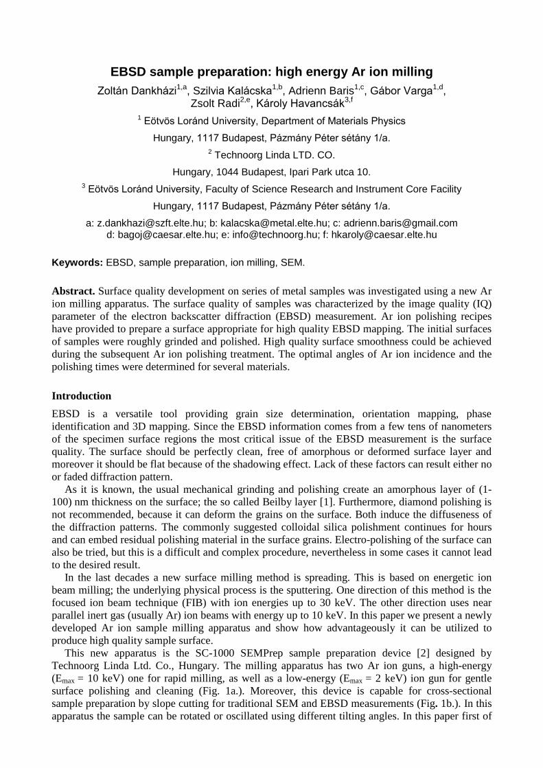
This new apparatus is the SC-1000 SEMPrep sample preparation device [2] designed by
Technoorg Linda Ltd. Co., Hungary. The milling apparatus has two Ar ion guns, a high-energy
(Emax = 10 keV) one for rapid milling, as well as a low-energy (Emax = 2 keV) ion gun for gentle
surface polishing and cleaning (Fig. 1a.). Moreover, this device is capable for cross-sectional
sample preparation by slope cutting for traditional SEM and EBSD measurements (Fig. 1b.). In this
apparatus the sample can be rotated or oscillated using different tilting angles. In this paper first of
all we concentrate on the surface cleaning capabilities of the device, but the advantage of the slope
cutting will be shown in one example. The details of the slope cutting capabilities of the SC-1000
SEMPrep apparatus will be discussed in another report.
a.
b.
Fig. 1. Scheme of the two operation modes in SEMPrep:
low angle surface polishing (a) and ion beam slope cut (b).
Experiment
In the framework of cooperation between Eötvös University and Technoorg Linda Co. Ltd. sample
preparation protocols are specified in the university SEM laboratory [3]. A FEI “Quanta 3D FEG”
SEM and its EDAX EBSD device was used to study the surface quality effects of ion milling.
EBSD provides information on surface microstructure. To optimize backscattered electron yield
the sample has to be tilted. Elastically backscattered electrons from a crystalline sample produce a
diffraction pattern (Kikuchi pattern) which is detected by a fluorescent screen, and the pattern is
recorded by the high speed CCD camera [4]. The Kikuchi pattern shows bands corresponding to
Bragg reflection directions according to a family of the grain lattice planes where the electron beam
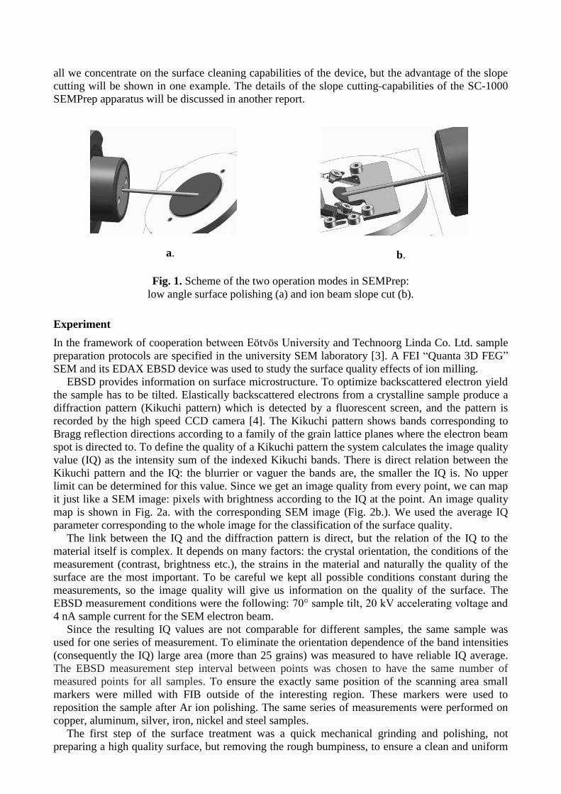
spot is directed to. To define the quality of a Kikuchi pattern the system calculates the image quality
value (IQ) as the intensity sum of the indexed Kikuchi bands. There is direct relation between the
Kikuchi pattern and the IQ: the blurrier or vaguer the bands are, the smaller the IQ is. No upper
limit can be determined for this value. Since we get an image quality from every point, we can map
it just like a SEM image: pixels with brightness according to the IQ at the point. An image quality
map is shown in Fig. 2a. with the corresponding SEM image (Fig. 2b.). We used the average IQ
parameter corresponding to the whole image for the classification of the surface quality.
The link between the IQ and the diffraction pattern is direct, but the relation of the IQ to the
material itself is complex. It depends on many factors: the crystal orientation, the conditions of the
measurement (contrast, brightness etc.), the strains in the material and naturally the quality of the
surface are the most important. To be careful we kept all possible conditions constant during the
measurements, so the image quality will give us information on the quality of the surface. The
EBSD measurement conditions were the following: 70° sample tilt, 20 kV accelerating voltage and
4 nA sample current for the SEM electron beam.
Since the resulting IQ values are not comparable for different samples, the same sample was
used for one series of measurement. To eliminate the orientation dependence of the band intensities
(consequently the IQ) large area (more than 25 grains) was measured to have reliable IQ average.
The EBSD measurement step interval between points was chosen to have the same number of
measured points for all samples. To ensure the exactly same position of the scanning area small
markers were milled with FIB outside of the interesting region. These markers were used to
reposition the sample after Ar ion polishing. The same series of measurements were performed on
copper, aluminum, silver, iron, nickel and steel samples.
The first step of the surface treatment was a quick mechanical grinding and polishing, not
preparing a high quality surface, but removing the rough bumpiness, to ensure a clean and uniform
surface to start Ar ion milling. The steps of the mechanical treatment were as follows: series of
grinding paper 600-, 1200-, 2500- and 4000-grit; and 1 µm average particle size alumina paste for
the finishing step.
The EBSD mapping was begun on the raw surfaces to determine the initial average IQ value.
The Ar ion milling system has four relevant adjustable parameters: accelerating voltage, time of ion
bombardment, angle of beam incidence and sample movement. Since ion polishing leaves marks on
the sample showing the direction of incidence the samples were rotated around the axis
perpendicular to the surface. In all cases the accelerating voltages was of 10 keV, while the time-
and incident angle dependence is the subject of this work.
a.
b.
Fig. 2. Image quality (IQ) map (a) and the corresponding SEM image (b) of a Ni sample.
Results and discussion
The aim of the present work was to elaborate protocols, how to obtain high quality surfaces by Ar
ion polishing using the SC-1000 SEMPrep apparatus. The primary issue is that in what angle and
how long we have to mill the sample to create an EBSD quality surface using the high-energy
(10 keV) Ar ion beam. As a first step Ar ion treatment was performed where the incident beam
angle was changed relatively to the sample surface. At each angle the polishing treatment was
followed by EBSD measurement. The EBSD program calculates the IQ parameter in each
measurement point. After each completed EBSD measurement the average IQ values were
calculated over the whole area. In Fig. 3. the average IQ value can be seen as a function of angle of
Ar ion beam incidence measured on a Cu sample. Since the points were measured on different
samples, to decrease the deviation due to distinct initial IQ, these initial values were subtracted from
the respective IQ calculated after polishing.
The time value of this isochronous curve was determined prior to the measurements so that the
polishing should not take too long, and at the same time not too short to prevent the accurate
measurement. The milling time of this curve in each point was 6 min. Fig. 3. shows the resulting
curve for Cu, but very similar curves were obtained for aluminum, silver, nickel and iron. The curve
following a nearly linear initial rise saturates and then it begins to decline. The rising part is related
to the reduction in the thickness of the deformed (amorphous) surface layer. The saturation
indicates that the deformed surface layer has been stripped due to the Ar ion polishing. Decrease
after saturation can be regarded as the consequence of the inhomogeneity of the Ar ion polishment,
which is partly due to the orientation dependence of the sputtering, and partly to the initial surface
Fig. 3. Effect of ion beam incidence angle on the background subtracted average IQ.
irregularities having different milling speeds. Consequently, after a relatively long processing time
surface coarsening can be observed and for some materials even cratering starts. The ideal Ar ion
polishing angle was determined from the curve in Fig. 3. and 6-8 degree was obtained. This value
proved to be suitable for other materials as well, as it listed in
Table 1a.
sample Al Cu Ni Fe steel
angle (deg) 7 8 8 6 8
a.
sample Al Cu Ni Fe steel
time (min) 6 7 6 7 26
b.
Table 1. Ideal angle (a) and time (b) values to prepare high quality
EBSD surface for various materials.
The second step was the determination of the ideal time of milling at the optimal angle found
previously. The time dependence of the average IQ values can be seen in Fig. 4. measured on a
similar Cu sample. In order to assure the accuracy each point were measured on the same sample
and even at the same area of that. As a result of the careful measuring procedure the uncertainty of
the measurement was not larger than 2%. As it can be seen in Fig. 4. after a relatively rapid growth
saturation occurs in IQ. The saturation is again the sign of the removal of the amorphous and/or
deformed layer. However, coarsening occurs in the saturation region due to the Ar bombardment,
although if the surface roughness is not too large, the EBSD measurements practically are not
sensitive to these surface irregularities. After a long time milling the IQ trend begins to decline but
this is not shown in the figure. Thus if we want to have a good quality surface smoothness then the
Ar ion milling should be completed at the beginning of the IQ saturation. In case of Cu the
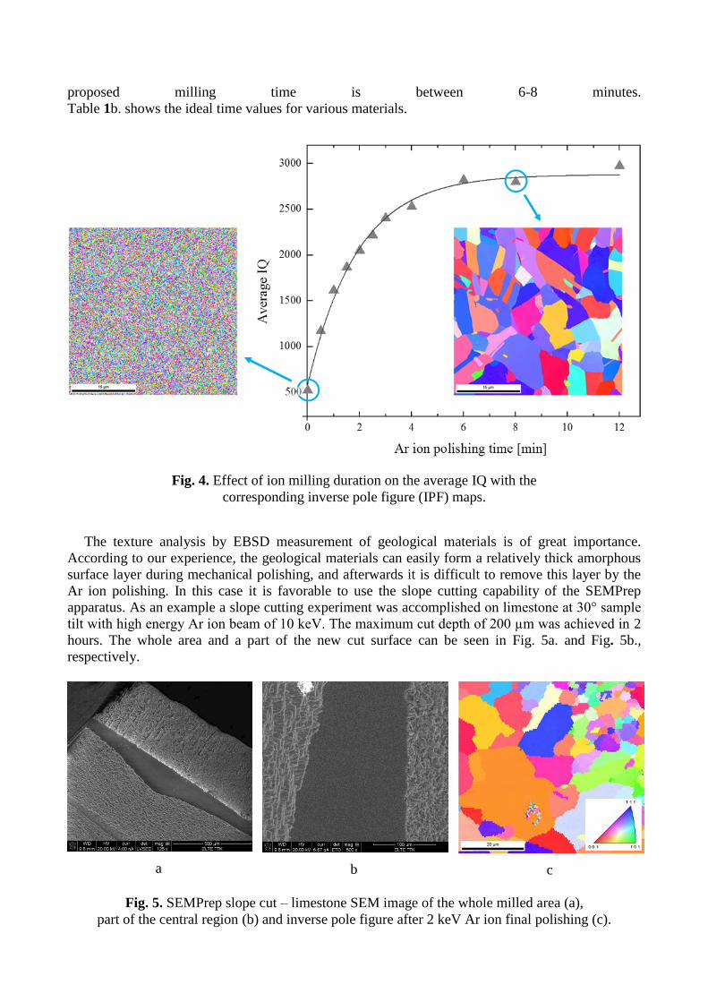
proposed milling time is between 6-8 minutes.
Table 1b. shows the ideal time values for various materials.
Fig. 4. Effect of ion milling duration on the average IQ with the
corresponding inverse pole figure (IPF) maps.
The texture analysis by EBSD measurement of geological materials is of great importance.
According to our experience, the geological materials can easily form a relatively thick amorphous
surface layer during mechanical polishing, and afterwards it is difficult to remove this layer by the
Ar ion polishing. In this case it is favorable to use the slope cutting capability of the SEMPrep
apparatus. As an example a slope cutting experiment was accomplished on limestone at 30° sample
tilt with high energy Ar ion beam of 10 keV. The maximum cut depth of 200 µm was achieved in 2
hours. The whole area and a part of the new cut surface can be seen in Fig. 5a. and Fig. 5b.,
respectively.
a
b
c
Fig. 5. SEMPrep slope cut – limestone SEM image of the whole milled area (a),
part of the central region (b) and inverse pole figure after 2 keV Ar ion final polishing (c).
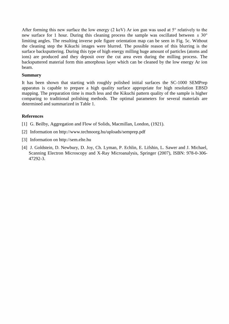
After forming this new surface the low energy (2 keV) Ar ion gun was used at 5° relatively to the
new surface for 1 hour. During this cleaning process the sample was oscillated between ± 30°
limiting angles. The resulting inverse pole figure orientation map can be seen in Fig. 5c. Without
the cleaning step the Kikuchi images were blurred. The possible reason of this blurring is the
surface backsputtering. During this type of high energy milling huge amount of particles (atoms and
ions) are produced and they deposit over the cut area even during the milling process. The
backsputtered material form thin amorphous layer which can be cleaned by the low energy Ar ion
beam.
Summary
It has been shown that starting with roughly polished initial surfaces the SC-1000 SEMPrep
apparatus is capable to prepare a high quality surface appropriate for high resolution EBSD
mapping. The preparation time is much less and the Kikuchi pattern quality of the sample is higher
comparing to traditional polishing methods. The optimal parameters for several materials are
determined and summarized in Table 1.
References
[1] G. Beilby, Aggregation and Flow of Solids, Macmillan, London, (1921).
[2] Information on http://www.technoorg.hu/uploads/semprep.pdf
[3] Information on http://sem.elte.hu
[4] J. Goldstein, D. Newbury, D. Joy, Ch. Lyman, P. Echlin, E. Lifshin, L. Sawer and J. Michael,
Scanning Electron Microscopy and X-Ray Microanalysis, Springer (2007), ISBN: 978-0-306-
47292-3.
Related Documents