Copyright ANPEC Electronics Corp. Rev. A.1 - Oct., 2009 APW7159A www.anpec.com.tw 1 ANPEC reserves the right to make changes to improve reliability or manufacturability without notice, and advise customers to obtain the latest version of relevant information to verify before placing orders. Dual Channel Synchronous Buck PWM Controller for SMPS Features • Single 12V Power Supply Required • Excellent Output Voltage Regulation - 1.0V±0.8% Internal Reference Over Line and Temperature • Simple Single Loop Control Design - Voltage Mode PWM Control • 0~100% Duty Ratio • Programmable Frequency Range from 50kHz to 400kHz (Constant 50kHz when Floating) • Integrated Soft-Start and Soft-Off (Patent Pending) • Support Pre-Biased Power-On • Both Channel with 180 o Phase Shift • Integrated Boot-Strap Diode • Over-Current Protection - Sense High Side MOSFET’s R DS(ON) • 120% Over-Voltage Protection • 50% Under-Voltage Protection • Over-Temperature Protection • Available in SOP-20 Package • Lead Free and Green Devices Available (RoHS Compliant) Applications General Description • SMPS Simplified Application Circuit S The APW7159A is a dual channel voltage mode and syn- chronous PWM controller which drives dual N-channel MOSFETs. The two channels are operated with 180 de- gree phase shift. The device integrates all of the control, monitoring, and protecting functions into a single package; provides two controlled power output with over-voltage, over- temperature, and over-current protections. The APW7159A provides excellent regulation for output load variation. The internal 1.0V temperature-compen- sated reference voltage provides high accuracy of 0.8% over line and temperature. The device includes a 50kHz free-running triangle-wave oscillator that is adjustable from 50kHz to 400kHz. PWM Controller 1 PWM Controller 2 APW7159A V OUT2 V IN V OUT1 Phase Shift The APW7159A has been equipped with excellent pro- tection functions: POR, OCP, UVP, and OVP protections. The Power-On-Reset (POR) circuit can monitor the VCC and OCSET voltage to make sure the supply voltage ex- ceeds their threshold voltage while the controller is running. The Over-Current Protection (OCP) monitors the output current by using the voltage drop across the high side MOSFET’s R DS(ON) . When the output current reaches the trip point, the controller will be latched. Under-Voltage Protection (UVP) and Over-Voltage Protection (OVP) moni- tor the FB voltage to protect APW7159A from burnout when output voltage is under 50% or over 120% of normal out- put voltage. The APW7159A is available in SOP-20 package.

Welcome message from author
This document is posted to help you gain knowledge. Please leave a comment to let me know what you think about it! Share it to your friends and learn new things together.
Transcript

Copyright ANPEC Electronics Corp.Rev. A.1 - Oct., 2009
APW7159A
www.anpec.com.tw1
ANPEC reserves the right to make changes to improve reliability or manufacturability without notice, andadvise customers to obtain the latest version of relevant information to verify before placing orders.
Dual Channel Synchronous Buck PWM Controller for SMPS
Features
• Single 12V Power Supply Required• Excellent Output Voltage Regulation
- 1.0V±0.8% Internal Reference Over Line and Temperature
• Simple Single Loop Control Design - Voltage Mode PWM Control
• 0~100% Duty Ratio• Programmable Frequency Range from 50kHz to
400kHz (Constant 50kHz when Floating)• Integrated Soft-Start and Soft-Off (Patent Pending)• Support Pre-Biased Power-On• Both Channel with 180o Phase Shift• Integrated Boot-Strap Diode• Over-Current Protection
- Sense High Side MOSFET’s RDS(ON)
• 120% Over-Voltage Protection• 50% Under-Voltage Protection• Over-Temperature Protection• Available in SOP-20 Package• Lead Free and Green Devices Available
(RoHS Compliant)
Applications
General Description
• SMPS
Simplified Application Circuit
S
The APW7159A is a dual channel voltage mode and syn-chronous PWM controller which drives dual N-channelMOSFETs. The two channels are operated with 180 de-gree phase shift.The device integrates all of the control, monitoring, andprotecting functions into a single package; provides twocontrolled power output with over-voltage, over-temperature, and over-current protections.The APW7159A provides excellent regulation for outputload variation. The internal 1.0V temperature-compen-sated reference voltage provides high accuracy of 0.8%over line and temperature. The device includes a 50kHzfree-running triangle-wave oscillator that is adjustablefrom 50kHz to 400kHz.
PWMController
1
PWMController
2
APW7159A
VOUT2
VIN
VOUT1
Phase Shift
The APW7159A has been equipped with excellent pro-tection functions: POR, OCP, UVP, and OVP protections.The Power-On-Reset (POR) circuit can monitor the VCCand OCSET voltage to make sure the supply voltage ex-ceeds their threshold voltage while the controller isrunning. The Over-Current Protection (OCP) monitors theoutput current by using the voltage drop across the highside MOSFET’s RDS(ON). When the output current reachesthe trip point, the controller will be latched. Under-VoltageProtection (UVP) and Over-Voltage Protection (OVP) moni-tor the FB voltage to protect APW7159A from burnout whenoutput voltage is under 50% or over 120% of normal out-put voltage. The APW7159A is available in SOP-20package.

Copyright ANPEC Electronics Corp.Rev. A.1 - Oct., 2009
APW7159A
www.anpec.com.tw2
Ordering and Marking Information
Note: ANPEC lead-free products contain molding compounds/die attach materials and 100% matte tin plate termination finish; whichare fully compliant with RoHS. ANPEC lead-free products meet or exceed the lead-free requirements of IPC/JEDEC J-STD-020D forMSL classification at lead-free peak reflow temperature. ANPEC defines “Green” to mean lead-free (RoHS compliant) and halogenfree (Br or Cl does not exceed 900ppm by weight in homogeneous material and total of Br and Cl does not exceed 1500ppm byweight).
Pin Configuration
SOP-20(Top View)
16
15
14
17
18
19
201
2
3
4
5
6
78
9
10 11
12
13
GND
UGATE1
VCC
COMP1
OCSET1
BOOT1
FB1
PHASE1
LGATE1
PGND
SS
FB2
UGATE2
COMP2
RT
OCSET2
BOOT2
NC
PHASE2LGATE2
APW7159A
Handling Code
Temperature Range
Package Code
Assembly Material
APW7159A K: XXXXX - Date Code
Package Code K : SOP-20Operating Ambient Temperature Range I : -40 to 85oCHandling Code TR : Tape & ReelAssembly Material G : Halogen and Lead Free Device
APW7159AXXXXX
Absolute Maximum Ratings (Note 1)
Symbol Parameter Rating Unit
VVCC Input Bias Supply Voltage (VCC to GND) -0.3 ~ 16 V
VBOOT1/2 BOOT1/ BOOT2 to PHASE1/PHASE2 Voltage -0.3 ~ 16 V
<400ns pulse width -5 ~ VBOOT1/2+5 V UGATE1/UGATE2 to PHASE1/PHASE2
>400ns pulse width -0.3 ~ VBOOT1/2+0.3 V
<400ns pulse width -5 ~ VVCC+0.3 V LGATE1/LGATE2 to PGND Voltage
>400ns pulse width -0.3 ~ VVCC+0.3 V
<400ns pulse width -10 ~ 30 V PHASE1/PHASE2 to PGND Voltage
>400ns pulse width -0.3 ~ 16 V
RT, SS, COMP1, COMP2, FB1, FB2 to GND Voltage -0.3 ~ 7 V
OCSET1, OCSET2 to GND -0.3 ~ VVCC+0.3 V

Copyright ANPEC Electronics Corp.Rev. A.1 - Oct., 2009
APW7159A
www.anpec.com.tw3
Absolute Maximum Ratings (Cont.) (Note 1)
Symbol Parameter Rating Unit
PGND to GND Voltage -0.3 ~ 0.3 V
PD Power Dissipation Internally Limited W
Maximum Junction Temperature 150 oC
TSTG Storage Temperature -65 ~ 150 oC
TSDR Maximum Lead Soldering Temperature, 10 Seconds 260 oC
Thermal CharacteristicsSymbol Parameter Typical Value Unit
θJA Junction-to-Ambient Thermal Resistance in Free Air (Note 2)
SOP-20 100 °C/W
Recommended Operating Conditions (Note 3)
Symbol Parameter Range Unit
VVCC Input Bias Supply Voltage (VCC to GND) 10 ~ 13.2 V
VIN1/VIN2 Converter Input Voltage 2 ~ 13.2 V
VOUT1/VOUT2 Converter Output Voltage 1 ~ VIN1/VIN2 V
IOUT1/IOUT2 Converter Output Current 0 ~ 30 A
TA Ambient Temperature -40 ~ 85 oC
TJ Junction Temperature -40 ~ 125 oC
Note 3 : Refer to the typical application circuit
Note 1: Absolute Maximum Ratings are those values beyond which the life of a device may be impaired. Exposure to absolutemaximum rating conditions for extended periods may affect device reliability.
Note 2: θJA is measured with the component mounted on a high effective thermal conductivity test board in free air.
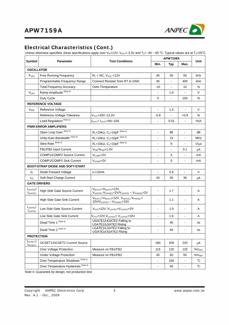
Unless otherwise specified, these specifications apply over VIN=12V, VOUT= 3.3V and TA= -40 ~ 85 oC. Typical values are at TA=25oC.
APW7159A Symbol Parameter Test Conditions
Min. Typ. Max. Unit
SUPPLY CURRENT
VCC Supply Current (Shutdown Mode) VVCC<5V, SS=GND - 0.5 1 mA
VCC Supply Current (Shutdown Mode) 5V< VVCC <9V, SS=GND - 0.8 1.6 mA
IVCC VCC Supply Current UGATE1/UGATE2 and LGATE1/LGATE2 open - 5 10 mA
POWER-ON-RESET (POR) AND LOCKOUT VOLTAGE THRESHOLDS
Rising VCC Threshold 9 9.5 10 V
Falling VCC Threshold 1 7.5 8 8.5 V
Falling VCC Threshold 2 - 4.6 - V
Rising VOCSET1/VOCSET2 Threshold - 1.6 - V
Falling VOCSET1/VOCSET2 Threshold - 1.0 - V
Electrical Characteristics
Copyright ANPEC Electronics Corp.Rev. A.1 - Oct., 2009
APW7159A
www.anpec.com.tw4
Unless otherwise specified, these specifications apply over VIN=12V, VOUT= 3.3V and TA= -40 ~ 85 oC. Typical values are at TA=25oC.
APW7159A Symbol Parameter Test Conditions
Min. Typ. Max. Unit
OSCILLATOR
FOSC Free Running Frequency RT = NC, VVCC =12V 45 50 55 kHz
Programmable Frequency Range Connect Resistor from RT to GND 45 - 400 kHz
Total Frequency Accuracy Over-Temperature -10 - 10 %
VOSC Ramp Amplitude (Note 4) - 1.9 - V
Duty Cycle 0 - 100 %
REFERENCE VOLTAGE
VREF Reference Voltage - 1.0 - V
Reference Voltage Tolerance VVCC=10V~13.2V -0.8 - +0.8 %
Load Regulation (Note 4) IOUT1= IOUT2=0A~10A - 0.01 - %/A
PWM ERROR AMPLIFIERS
Open Loop Gain (Note 4) RL=10kΩ, CL=10pF (Note 4) - 88 - dB
Unity-Gain Bandwidth (Note 4) RL=10kΩ, CL=10pF (Note 4) - 15 - MHz
Slew Rate (Note 4) RL=10kΩ, CL=10pF (Note 4) - 6 - V/µs
FB1/FB2 Input Current VFB1/VFB2=1.0V - - 0.1 µA
COMP1/COMP2 Source Current VCOMP=2V - 5 - mA
COMP1/COMP2 Sink Current VCOMP=2V - 5 - mA
BOOT-STRAP DIODE AND SOFT-START
VF Diode Forward Voltage IF=10mA - 0.8 - V
ISS Soft-Start Charge Current 24 30 36 µA
GATE DRIVERS
IUGATE1/ IUGATE2
High Side Gate Source Current VBOOT1=VBOOT2=12V, VUGATE1-VPHASE1=2V/VUGATE2 – VPHASE2=2V - 1.7 - A
High Side Gate Sink Current VBOOT1=VBOOT2=12V, VUGATE1-VPHASE1= 10V/VUGATE2 – VPHASE2=10V - 1.1 - A
ILGATE1/ ILGATE2
Low Side Gate Source Current VVCC=12V, VLGATE1=VLGATE2=2V - 1.9 - A
Low Side Gate Sink Current VVCC=12V,VLGATE1= VLGATE2=10V - 1.6 - A
Dead Time 1 (Note 4) UGATE1/UGATE2 Falling to LGATE1/LGATE2 Rising - 40 - ns
Dead Time 2 (Note 4) LGATE1/LGATE2 Falling to UGATE1/UGATE2 Rising - 40 - ns
PROTECTION
IOCSET1/ IOCSET2
OCSET1/OCSET2 Current Source 180 200 220 µA
Over Voltage Protection Measure on FB1/FB2 115 120 125 %VREF
Under Voltage Protection Measure on FB1/FB2 45 50 55 %VREF
Over-Temperature Shutdown (Note 4) - 150 - oC
Over-Temperature Hysteresis (Note 4) - 40 - oC
Note 4: Guarantee by design, not production test
Electrical Characteristics (Cont.)

Copyright ANPEC Electronics Corp.Rev. A.1 - Oct., 2009
APW7159A
www.anpec.com.tw5
Typical Operating Characteristics
Reference Voltage vs. JunctionTemperature
Switching Frequency vs. JunctionTemperature
Junction Temperature
Ref
eren
ce V
olta
ge (m
V)
996
997
998
999
1000
1001
1002
1003
-40 -20 0 20 40 60 80 100 120
Junction Temperature
Sw
itchi
ng F
requ
ency
(kH
z)45
46
47
48
49
50
51
52
53
54
55
-40 -20 0 20 40 60 80 100 120

Copyright ANPEC Electronics Corp.Rev. A.1 - Oct., 2009
APW7159A
www.anpec.com.tw6
Operating WaveformsRefer to the typical application circuit. The test condition is VIN=12V, TA= 25oC unless otherwise specified.
Power On Power Off
CH1: VIN1=VIN2=VVCC, 5V/DivCH2: VOUT1, 2V/Div
Time: 2ms/DivCH3: VOUT2, 2V/Div
1
3
2
VIN1= VIN2=Vvcc
VOUT1
VOUT2
1
2
3
VIN1= VIN2=VVCC, IOUT=0mA
VOUT1
VOUT2
CH1: VIN1=VIN2=VVCC, 5V/DivCH2: VOUT1, 2V/Div
Time: 5ms/DivCH3: VOUT2, 2V/Div
Enable Shutdown
CH1: VSS, 5V/DivCH2: VOUT1, 2V/DivCH3: VOUT2, 2V/DivTime: 2ms/Div
CH1: VSS, 5V/DivCH2: VOUT1, 2V/DivCH3: VOUT2, 2V/DivTime: 10ms/Div
1
3
2
VSS
VOUT1
VOUT2
1
3
2
VSS
VOUT1
VOUT2
RLOAD1=RLOAD2=10Ω

Copyright ANPEC Electronics Corp.Rev. A.1 - Oct., 2009
APW7159A
www.anpec.com.tw7
Operating Waveforms (Cont.)Refer to the typical application circuit. The test condition is VIN=12V, TA= 25oC unless otherwise specified.
Short-Circuit Protection Over-Current Protection
2
4
3
1
ROCSET=1kΩ, RDS(high-side)=10mΩ
VIN=VVCC
VOUT
VPHASE
IL
CH1: VIN=VVCC, 10V/DivCH2: VOUT, 2V/Div
Time: 50µA/Div
CH3: VPHASE, 10V/DivCH4: IL, 10A/Div
CH1: VIN=VVCC, 10V/DivCH2: VOUT, 2V/Div
Time: 10ms/Div
CH3: VPHASE, 10V/DivCH4: IL, 10A/Div
2
4
3
1
VIN=Vvcc
VOUT
VPHASE
IL
UGATE Falling UGATE Rising
1,2
3
IOUT=10A
VUGATE
VPHASE
VLGATE
CH1: VUGATE, 10V/DivCH2: VLGATE, 5V/DivCH3: VPHASE, 10V/DivTime: 20ns/Div
1,2
3
IOUT=10A
VLGATE
VPHASE
VUGATE
CH1: VUGATE, 10V/DivCH2: VLGATE, 5V/DivCH3: VPHASE, 10V/DivTime: 20ns/Div

Copyright ANPEC Electronics Corp.Rev. A.1 - Oct., 2009
APW7159A
www.anpec.com.tw8
Operating Waveforms (Cont.)Refer to the typical application circuit. The test condition is VIN=12V, TA= 25oC unless otherwise specified.
Load Transient Response Load Transient Response
PIN
NO. NAME FUNCTION
1 FB1 Feedback Input of Channel 1. The Buck converter senses feedback voltage via FB1 and regulates the FB1 voltage at 1.0V. Connecting FB1 with a resistor-divider from the output sets the output voltage of the Buck converter.
2 COMP1 Error Amplifier Output of Channel 1. It is used to compensate the regulation control loop. Refer to the section “Application Information” for details.
3 OCSET1 This pin is used to set the maximum inductor current of channel 1. Refer to the section in “Function Description” for detail.
4 GND Signal Ground.
5 VCC Power Supply Input. Connect a nominal 10V to 13.2V power supply voltage to this pin. A power-on-reset function monitors the input voltage at this pin. It is recommended that a decoupling capacitor (1 to 10µF) should be connected to the GND for noise decoupling.
6 BOOT1 This pin provides the bootstrap voltage to the high-side gate driver for driving the N-channel MOSFET. An external capacitor from PHASE1 to BOOT1, an internal diode, and the power supply voltage VCC, generate the bootstrap voltage for the high-side gate driver (UGATE1).
7 UGATE1 High-Side Gate Driver Output of Channel 1. This pin is the gate driver for high-side MOSFET.
8 PHASE1 This pin is the return path for the high-side gate driver 1. Connect this pin to the high-side MOSFET source and connect a capacitor to BOOT1 for the bootstrap voltage. This pin is also used to monitor the voltage drop across the MOSFET for over-current protection.
Pin Description
2
1
VIN2=VVCC=12V, VOUT2=3.3V
IOUT2 slew rate=10A/µs
VOUT2
IOUT2
CH1: VOUT2, 200mV/Div
Time: 100µs/DivCH2: IOUT2, 5A/Div
CH1: VOUT1, 200mV/Div
Time: 100µs/DivCH2: IOUT1, 5A/Div
VIN1=VVCC=12V, VOUT1=5V
IOUT1 slew rate=10A/µs
VOUT1
IOUT1
2
1

Copyright ANPEC Electronics Corp.Rev. A.1 - Oct., 2009
APW7159A
www.anpec.com.tw9
PIN
NO. NAME FUNCTION
9 LGATE1 Low-side Gate Driver Output of channel 1. This pin is connected to low-side MOSFET.
10 PGND Power Ground of the Low-Side Gate Drivers. Use a separate track to connect this pin to Source of the low-side MOSFET. The Source of the low-side MOSFET must be connected to system ground with very low impedance. Connecting this pin to the GND.
11 NC No Connection.
12 LGATE2 Low-side Gate Driver Output of channel 2. This pin is the gate driver for low-side MOSFET.
13 PHASE2 This pin is the return path for the high-side gate driver of channel 2. Connect this pin to the high-side MOSFET source and connect a capacitor to BOOT2 for the bootstrap voltage. This pin is also used to monitor the voltage drop across the MOSFET for over-current protection.
14 UGATE2 High-side Gate Driver Output of Channel 2. This pin is connected to high-side MOSFET.
15 BOOT2 This pin provides the bootstrap voltage to the high-side gate driver for driving the N-channel MOSFET. An external capacitor from PHASE2 to BOOT2, an internal diode, and the power supply voltage VCC, generate the bootstrap voltage for the high-side gate driver (UGATE2).
16 OCSET2 This pin is used to set the maximum inductor current of channel 2. Refer to the section in “Function Description” for detail.
17 COMP2 Error Amplifier Output of Channel 2. It is used to compensate the regulation control loop. Refer to the section “Application Information” for details.
18 FB2 Feedback Input of Channel 2. The converter senses feedback voltage via FB2 and regulates the FB2 voltage at 1.0V. Connecting FB2 with a resistor-divider from the output sets the output voltage of the Buck converter.
19 SS Connect a capacitor to the GND and a 30µA current source charges this capacitor to set the soft-start time. The pin also integrates EN/Shutdown function. Pulling SS below 0.7V shuts down the IC.
20 RT This pin allows adjusting the switching frequency. Connect a resistor from RT to the ground to increase the switching frequency.
- Exposed Pad Connect the pad to the system ground plane on PCBs. The PCB will be a heat sink of the IC.
Pin Description (Cont.)

Copyright ANPEC Electronics Corp.Rev. A.1 - Oct., 2009
APW7159A
www.anpec.com.tw10
Block Diagram
PHASE1
UGATE1
BOOT1
GND
LGATE1
VCC
PGND1
FB1
VREF
ErrorAmplifier
1
PWMComparator
1
COMP1
Oscillator
GateControl
OCSET1
PHASE2
UGATE2
BOOT2
LGATE2
VCC
PGND2
FB2
VREF
ErrorAmplifier
2
PWMComparator
2
COMP2
GateControl
OCSET2
RT
I OCSET1IOCSET2
VCC
Over-CurrentComparator
2
Over-CurrentComparator
1
ISS(30µA typ.)
SS
Over-VoltageComparator
2
Over-VoltageComparator
1
1.2
Soft-Startand
Fault Logic
VREF
(1.0V typ.)
Regulator Power-On-Reset
15k
15k15k
15k
1.2
0.5
Under-VoltageComparator
20.5
Under-VoltageComparator
1

Copyright ANPEC Electronics Corp.Rev. A.1 - Oct., 2009
APW7159A
www.anpec.com.tw11
Typical Application Circuit
VIN
VOUT23.3V/30A
BOOT2
UGATE2
PHASE2
LGATE2
PGND
COMP2
FB2
RT
SS
100nF
APM3109
APM3106 2200µFx2ESR=30mΩ
5.2k
12k
47nF
BOOT1
UGATE1
PHASE1
LGATE1
PGND
COMP1
FB1
VCC
GND
100nF
APM3109
APM3106
RT
1µF
APW7159
OCSET1 OCSET2
6.8nF33nF
12k6.8nF
33nF
12k
3k
12k
VVCC
VOUT1
5V/30AL1
7.2µH L2
1nF(option)
2k 2k
1.5nF
4R7
1.5nF
4R7
1k
15nF
1k
15nF
5R1
7.2µH
2200µFx2ESR=30mΩ
470µF1µF 10µF1µF10µF
1nF(option)
(option)(option)

Copyright ANPEC Electronics Corp.Rev. A.1 - Oct., 2009
APW7159A
www.anpec.com.tw12
Function Description
VCC Power-On-Reset (POR)
The Power-On-Reset (POR) function of APW7159A con-tinually monitors the voltage on VCC and OCSET1/OCSET2 pin. When the voltage on VCC and OCSET1/OCSET2 exceeds their rising POR threshold voltage re-spectively (9.5V and 1.6V typical), the POR function ini-tiates soft-start operation. Where the voltage at OCSET1/OCSET2 pin is equal to VIN1/VIN2 minus a fixed voltagedrop (VOCSET1/VOCSET2 = VIN1/VIN2 – VROCSET1/VROCSET2). For op-eration with a single +12V power source, VIN1/VIN2 andVCC are equivalent and the +12V power source mustexceed the rising VCC threshold. With all input suppliesabove their POR thresholds, the device initiates a soft-start interval.
Soft-Start
The SS pin controls the soft-start and enables/disablesthe controller. Connect a soft-start capacitor from SS pinto GND to set the soft-start interval. Figure1 shows thesoft-start interval. When VCC reaches its Power-On-Re-set threshold (9.5V typical), a soft-start current source, ISS
(30µA typical), starts to charge the capacitor. When theVSS reaches the threshold about 1V, the internal 1.0V ref-erence starts to rise and follows the VSS; the error ampli-fier output (VCOMP) suddenly rises to 1.1V, which is thevalley of the triangle wave of the oscillator, leads the VOUT1/VOUT2 to start up. VOUT1 and VOUT2 have power on sequenceissue, VOUT2 will start up after VSS rise up to 1.4V. The soft-start time can be calculated as below:
The APW7159A does not have EN pin, pull SS low (SS<0.7V) shut down the IC.
WhereCSS = external capacitor connected at SS pinISS = soft-start current, typical ISS current is 30µA
Soft-Off (5V<VCC<9V) (Note 5)
The APW7159A also integrates a soft-off circuitry. Whenthe voltage on VCC falls below the falling threshold1 (8Vtypical), an internal current source, ISS (30µA typical), startsto discharge from SS. When the VVCC falls below the fall-ing threshold2 (4.6V typical), the device is shutdown. TheAPW7159A will initiate a soft-start process until re-cyclepower supply (9.5V typical).Note 5: The mentioned soft-off function is patent pending by ANPEC
Over-Temperature Protection (OTP)
The over-temperature circuit limits the junction tempera-ture of the APW7159A. When the junction temperatureexceeds 150oC, a thermal sensor pulls UGTAE1/UGATE2and LGATE1/LGATE2 low, allowing the devices to cool.The thermal sensor allows the converters to start a soft-start process and to regulate the output voltage againafter the junction temperature cools by 40oC. The OTP isdesigned with a 40oC hysteresis to lower the averageJunction Temperature (TJ) during continuous thermaloverload conditions, increasing the lifetime of the device.
Over-Current Protection
The over-current function protects the switching converteragainst over-current or short-circuit conditions. The con-troller senses the inductor current by detecting the drain-to-source voltage, which the product of the inductor’s cur-rent and high side MOSFET on-resistance during it’s on-state. This method enhances the converter’s efficiencyand reduces cost by eliminating a current sensing resis-tor required.
1VIC
ttttTSS
SS2413STARTSOFT ⋅=−=−=−
Figure 1. Soft-start timing sequence
Voltage
1.4
Timet0
1
VSS
VFB
1
VFB2
t1 t2 t3 t4

Copyright ANPEC Electronics Corp.Rev. A.1 - Oct., 2009
APW7159A
www.anpec.com.tw13
Function Description (Cont.)
Over-Current Protection (Cont.)
A resistor (ROCSET1/ROCSET2) connected between OCSET1/OCSET2 pin and the drain of the upper MOSFET will de-termine the over-current limit. An internal current sourcewill flow through this resistor, creating a voltage drop,which will be compared with the voltage across the up-per MOSFET. When the voltage across the upper MOSFETexceeds the voltage drop across the ROCSET1/ROCSET2, theIC shuts off the entire gate drives. After a soft-start perioddelay, the APW7159A initiates a new soft-start process.After 3 times over-current events are counted continuously,all devices and gate drivers (UGATE1/UGATE2/LGATE1/LGATE2) were shutdown. Both outputs of the PWM con-verter are latched to be floating. The threshold of the over-current limit is therefore given by :
( )sidehighRRI
I)ON(DS
OCSETOCSETLIMIT −
⋅=
For the over-current is never occurred in the normal oper-ating load range; the variation of all parameters in theabove equation should be determined.
- The MOSFET’s RDS(ON) is varied by temperature andgate to source voltage, the user should determine themaximum RDS(ON) in manufacturer’s datasheet.
-The minimum IOCSET1/IOCSET2 (typical 200µA) and mini-mum ROCSET1/ROCSET2 should be used in the aboveequation.
-Note that the ILIMIT is the current flow through the up-per MOSFET; ILIMIT must be greater than maximum outputcurrent add the half of inductor ripple current.The over-current protection will shut down the device anddischarge the CSS with a 30µA sink current. If the ROCSET1/ROCSET2 is not connected or VOCSET1/VOCSET2 is below 1.6V,the APW7159A will not initiate soft-start process and forcedevice shutdown.
Over-Voltage Protection
The over-voltage protection monitors the FB voltage toprevent the output from over-voltage. When the outputvoltage rises to 120% of the nominal output voltage, theAPW7159A turns off all devices. The APW7159A will ini-tiate a soft-start process until re-cycle power supply.
Adaptive Shoot-Through Protection
The gate driver incorporates adaptive shoot-through pro-tection to high-side and low-side MOSFETs from con-ducting simultaneously and shorting the input supply.This is accomplished by ensuring the falling gate hasturned off one MOSFET before the other is allowed torise.During turn-off of the low-side MOSFET, the LGATE1/LGATE2 voltage is monitored until it reaches a 1.6Vthreshold, at which time the UGATE is released to riseafter a constant delay. During turn-off of the high-sideMOSFET, the UGATE1/UGATE2 to PHASE1/PHASE2 volt-age is also monitored until it reaches a 1.6V threshold, atwhich time the LGATE1/LGATE2 is released to rise aftera constant delay.
Pre-Bias Power-On
When the APW7159A initiates the soft-start, the outputvoltage will smoothly rising without discharged even thevoltage is not zero.
Switching Frequency
The APW7159A provides the oscillator switching fre-quency adjustment. The device includes a 50kHz free-running triangle wave oscillator. If operates in higher fre-quency than 50kHz, connect a resistor from RT pin to theground to increase the switching frequency. Equation 1and figure 2 shows the relationship between oscillationfrequency and RT resistance.
Under-Voltage Protection
The under-voltage function monitors the voltage on FB byUnder-Voltage comparator to protect the PWM converteragainst short-circuit conditions. When the VFB falls belowthe falling UVP threshold (50% VREF), a fault signal is in-ternally generated and the device turns off high-sideand low-side MOSFETs. The converter is shutdown andthe output is latched to be floating.
( ) ( )Ω+=
kR7550
50kHzFT
OSC

Copyright ANPEC Electronics Corp.Rev. A.1 - Oct., 2009
APW7159A
www.anpec.com.tw14
Function Description (Cont.)
Figure 2. Oscillator Frequency vs. RT Resistance
Switching Frequency (Cont.)
Oscillator Frequency vs. RT Resistance
Osc
illat
or F
requ
ency
(kH
z)
RT Resistance (k)
0 100 200 300 400 500 6000
100
200
300
400
500
600
700

Copyright ANPEC Electronics Corp.Rev. A.1 - Oct., 2009
APW7159A
www.anpec.com.tw15
Application Information
Output Voltage Selection
The output voltage can be programmed with a resistivedivider. Use 1% or better resistors for the resistive divideris recommended. The FB pin is the inverter input of theerror amplifier, and the reference voltage is 1V. The out-put voltage is determined by:
Where ROUT is the resistor connected from VOUT to FB andRGND is the resistor connected from FB to the GND.
Output Inductor Selection
The inductor value determines the inductor ripple currentand affects the load transient response. Higher inductorvalue reduces the inductor’s ripple current and induceslower output ripple voltage. The ripple current and ripplevoltage can be approximated by:
where Fs is the switching frequency of the regulator.
Although increase of the inductor value and frequencyreduces the ripple current and voltage, a tradeoff willexist between the inductor’s ripple current and theregulator load transient response time.
A smaller inductor will give the regulator a faster loadtransient response at the expense of higher ripple current.Increasing the switching frequency (FS) also reduces theripple current and voltage, but it will increase theswitching loss of the MOSFET and the power dissipationof the converter. The maximum ripple current occurs atthe maximum input voltage. A good starting point is tochoose the ripple current to be approximately 30% ofthe maximum output current. Once the inductance valuehas been chosen, select an inductor is capable of carry-ing the required peak current without going intosaturation. In some types of inductors, especially corethat is made of ferrite, the ripple current will increaseabruptly when it saturates. This will result in a larger out-put ripple voltage.
IN
OUT
S
OUTINRIPPLE V
VLF
VVI ×
×−
=
ESRIV RIPPLEOUT ×=∆
Output Capacitor Selection
Higher capacitor value and lower ESR reduce the outputripple and the load transient drop. Therefore, selecting highperformance low ESR capacitors is intended for switch-ing regulator applications. In some applications, mul-tiple capacitors have to be parallelled to achieve thedesired ESR value. A small decoupling capacitor inparallel for bypassing the noise is also recommended,and the voltage rating of the output capacitors also mustbe considered. If tantalum capacitors are used, makesure they are surge tested by the manufactures. If in doubt,consult the capacitors manufacturer.
Input Capacitor SelectionThe input capacitor is chosen based on the voltage ratingand the RMS current rating. For reliable operation, selectthe capacitor voltage rating to be at least 1.3 times higherthan the maximum input voltage. The RMS current of thebulk input capacitor is calculated as the following equation:
During power up, the input capacitors have to handlelarge amount of surge current. If tantalum capacitors areused, make sure they are surge tested by themanufactures. If in doubt, consult the capacitorsmanufacturer. For high frequency decoupling, a ceramiccapacitor 1µF can be connected between the drain ofupper MOSFET and the source of lower MOSFET.
MOSFET Selection
The selection of the N-channel power MOSFETs aredetermined by the RDS(ON), reverse transfer capacitance(CRSS) and maximum output current requirement. Thereare two components of loss in the MOSFETs: conductionloss and transition loss. For the upper and lowerMOSFET, the losses are approximately given by the fol-lowing equations:
PUPPER = IOUT 2 ( 1+ TC)(RDS(ON))D + (0.5)( IOUT)(VIN)( tSW)FS
PLOWER = IOUT 2 (1+ TC)(RDS(ON))(1-D)
Where IOUT is the load currentTC is the temperature dependency of RDS(ON)
FS is the switching frequencytSW is the switching intervalD is the duty cycle
( )D1DII OUTRMS −⋅⋅=
+×=
GND
OUTOUT R
R11V

Copyright ANPEC Electronics Corp.Rev. A.1 - Oct., 2009
APW7159A
www.anpec.com.tw16
Note that both MOSFETs have conduction loss while theupper MOSFET includes an additional transition loss.The switching internal, tSW, is the function of the reversetransfer capacitance CRSS. The (1+TC) term is to factorin the temperature dependency of the RDS(ON) and can beextracted from the “RDS(ON) vs Temperature” curve of thepower MOSFET.
PWM Compensation
The output LC filter of a step down converter introduces adouble pole, which contributes with -40dB/decade gainslope and 180 degrees phase shift in the control loop. Acompensation network among COMP, FB, and VOUT
should be added. The compensation network is shown inFigure 6. The output LC filter consists of the output induc-tor and output capacitors. The transfer function of the LCfilter is given by:
Application Information (Cont.)MOSFET Selection (Cont.)
The FLC is the double poles of the LC filter, and FESR is thezero introduced by the ESR of the output capacitor.
VPHASE L VOUT
COUT
ESR
Figure 3. The Output LC Filter
Figure 4. The LC Filter GAIN and Frequency
The PWM modulator is shown in Figure 5. The input isthe output of the error amplifier and the output is thePHASE node. The transfer function of the PWM modulatoris given by:
OUTESR CESR2
1F
××π×=
FLC
FESR
-40dB/dec
-20dB/dec
Frequency(Hz)
GA
IN (
dB)
OSC
INPWM V
VGAIN
∆=
Figure 5. The PWM Modulator
Output ofError Amplifier
ΔVOSCPWM
Comparator
Driver
Driver
PHASE
V IN
OSC
The compensation network is shown in Figure 6. Itprovides a close loop transfer function with the highestzero crossover frequency and sufficient phase margin.The transfer function of error amplifier is given by:
The poles and zeros of the transfer function are:
VREF
VOUT
VCOMPR1
R3 C3 R2 C2
C1
FB
Figure 6. Compensation Network
( )
C3R321
F
C2C1C2C1
R22
1F
C3R3R121
F
C2R221
F
P2
P1
Z2
Z1
××π×=
+×
××π×=
×+×π×=
××π×=
( )
×+×
××+
+
×+
+×
×+
×××
+=
+
+
==
C3R31
sC2C1R2
C2C1ss
C3R3R11
sC2R2
1s
C1R3R1R3R1
sC31
R3R1//
sC21
R2//sC1
1
VV
GAINOUT
COMPAMP

Copyright ANPEC Electronics Corp.Rev. A.1 - Oct., 2009
APW7159A
www.anpec.com.tw17
The poles and zero of this transfer functions are:
Application Information (Cont.)PWM Compensation (Cont.)The closed loop gain of the converter can be written as:
GAINLC X GAINPWM X GAINAMP
Figure 7. shows the asymptotic plot of the closed loopconverter gain, and the following guidelines will help todesign the compensation network. Using the belowguidelines should give a compensation similars to thecurve plotted. A stable closed loop has a -20dB/ decadeslope and a phase margin greater than 45 degree.
1. Choose a value for R1, usually between 1K and 5K.
2. Select the desired zero crossover frequency
FO: (1/5 ~ 1/10) X FS >FO>FESR
Use the following equation to calculate R2:
3. Place the first zero FZ1 before the output LC filter doublepole frequency FLC.
FZ1 = 0.75 X FLC
Calculate the C2 by the equation:
4. Set the pole at the ESR zero frequency FESR:
FP1 = FESR
Calculate the C1 by the equation:
5. Set the second pole FP2 at the half of the switchingfrequency and also set the second zero FZ2 at the output LCfilter double pole FLC. The compensation gain should notexceed the error amplifier open loop gain, check thecompensation gain at FP2 with the capabilities of the erroramplifier.
FP2 = 0.5 X FS
FZ2 = FLC
Combine the two equations will get the following componentcalculations:
R1FF
VV
R2LC
O
IN
OSC ××∆
=
0.75FR221
C2LC ×××π×
=
1FC2R22C2
C1ESR −×××π×
=
1CESRsCLsCESRs1
GAINOUTOUT
2OUT
LC +××+××××+
=
Figure 7. Converter Gain and Frequency
S
LC
S
OUTLC
FR31
C3
1F2
FR1
R3
CL2
1F
××π=
−×
=
××π×=
FLC
Frequency(Hz)
GA
IN (
dB)
20log(R2/R1) 20log
(VIN/ΔVOSC)
FZ1 FZ2 FP1 FP2
FESR
PWM & FilterGain
ConverterGain
CompensationGain
Layout Consideration
In any high switching frequency converter, a correct lay-out is important to ensure proper operation of theregulator. With power devices switching at 200kHz, theresulting current transient will cause voltage spike acrossthe interconnecting impedance and parasitic circuitelements. As an example, consider the turn-off transitionof the PWM MOSFET. Before turn-off, the MOSFET is car-rying the full load current. During turn-off, current stopsflowing in the MOSFET and is free-wheeling by the lowerMOSFET and parasitic diode. Any parasitic inductance ofthe circuit generates a large voltage spike during theswitching interval. In general, using short and wide printedcircuit traces should minimize interconnecting imped-ances and the magnitude of voltage spike. And signaland power grounds are to be kept separating till com-bined using the ground plane construction or single pointgrounding. Figure 8. illustrates the layout, with bold lines

Copyright ANPEC Electronics Corp.Rev. A.1 - Oct., 2009
APW7159A
www.anpec.com.tw18
Application Information (Cont.)
indicating high current paths; these traces must be shortand wide. Components along the bold lines should beplaced lose together. Below is a checklist for your layout:
Layout Consideration (Cont.)
- Keep the switching nodes (UGATE, LGATE, and PHASE)away from sensitive small signal nodes since thesenodes are fast moving signals. Therefore, keep tracesto these nodes as short as possible.
- The traces from the gate drivers to the MOSFETs (UGATEand LGATE) should be short and wide.
- Place the source of the high-side MOSFET and the drainof the low-side MOSFET as close as possible. Minimiz-ing the impedance with wide layout plane between thetwo pads reduces the voltage bounce of the node.
- Decoupling capacitor, compensation component, theresistor dividers, and boot capacitors should be closetheir pins. (For example, place the decoupling ceramiccapacitor near the drain of the high-side MOSFET asclose as possible. The bulk capacitors are also placednear the drain).
- The input capacitor should be near the drain of the up-per MOSFET; the output capacitor should be near theloads. The input capacitor GND should be close to thelower MOSFET GND.
- The drain of the MOSFETs (VIN and PHASE nodes)should be a large plane for heat sinking.
- The ROCSET resistance should be placed near the IC asclose as possible.
- The decoupling capacitor for VCC should be placednear the VCC and GND. CBOOT should be connected asclose to the BOOT and PHASE pins as possible.
Figure 8. Layout Consideration
VCC
BOOT
PHASE
UGATE
LGATE
VIN
VOUT
LOAD
APW7159A
ROCSET
Close to IC
OCSET
GND

Copyright ANPEC Electronics Corp.Rev. A.1 - Oct., 2009
APW7159A
www.anpec.com.tw19
Package Information
SOP-20
0L
VIEW A
0.25
SEATING PLANEGAUGE PLANE
Note : 1. Follow from JEDEC MS-013 AC. 2. Dimension "D" does not include mold flash, protrusions
or gate burrs. Mold flash, protrusion or gate burrs shall not exceed 6 mil per side. 3. Dimension "E" does not include inter-lead flash or protrusions. Inter-lead flash and protrusions shall not exceed 10 mil per side.
D
E1
E
e b
A
A1
A2
SYMBOL MIN. MAX.
2.65
0.10
0.20 0.33
0.30
A
A1
c
D
E
E1
e
h
L
MILLIMETERS
b 0.31 0.51
SOP-20
0.25 0.75
0.40 1.27
MIN. MAX.
INCHES
0.104
0.004
0.012 0.020
0.008 0.013
0.010 0.030
0.016 0.050
0 0o 8o 0o 8o
0.012
1.27 BSC 0.050 BSC
2.05 0.081A2
12.60 13.00 0.496 0.512
10.10 10.50 0.398 0.413
7.40 7.60 0.291 0.299
SEE VIEW A
ch
X 4
5o

Copyright ANPEC Electronics Corp.Rev. A.1 - Oct., 2009
APW7159A
www.anpec.com.tw20
Application A H T1 C d D W E1 F
330.0±2.00 50 MIN. 24.40+2.00 -0.00
13.0+0.50 -0.20
1.5 MIN. 20.2 MIN. 24.0±0.30 1.75±0.10 11.5±0.10
P0 P1 P2 D0 D1 T A0 B0 K0 SOP-20
4.0±0.10 12.0±0.10 2.0±0.10 1.5+0.10 -0.00 1.5 MIN. 0.6+0.00
-0.40 10.9±0.20 13.3±0.20 3.1±0.20
(mm)
Carrier Tape & Reel Dimensions
A
E1
AB
W
F
T
P0OD0
BA0
P2
K0
B0
SECTION B-B
SECTION A-A
OD1
P1
H
T1
A
d
Package Type Unit Quantity
SOP-20 Tape & Reel 1000
Devices Per Unit

Copyright ANPEC Electronics Corp.Rev. A.1 - Oct., 2009
APW7159A
www.anpec.com.tw21
Taping Direction InformationSOP-20
USER DIRECTION OF FEED
Classification Profile

Copyright ANPEC Electronics Corp.Rev. A.1 - Oct., 2009
APW7159A
www.anpec.com.tw22
Classification Reflow ProfilesProfile Feature Sn-Pb Eutectic Assembly Pb-Free Assembly
Preheat & Soak Temperature min (Tsmin) Temperature max (Tsmax) Time (Tsmin to Tsmax) (ts)
100 °C 150 °C
60-120 seconds
150 °C 200 °C
60-120 seconds
Average ramp-up rate (Tsmax to TP) 3 °C/second max. 3°C/second max.
Liquidous temperature (TL) Time at liquidous (tL)
183 °C 60-150 seconds
217 °C 60-150 seconds
Peak package body Temperature (Tp)*
See Classification Temp in table 1 See Classification Temp in table 2
Time (tP)** within 5°C of the specified classification temperature (Tc)
20** seconds 30** seconds
Average ramp-down rate (Tp to Tsmax) 6 °C/second max. 6 °C/second max.
Time 25°C to peak temperature 6 minutes max. 8 minutes max.
* Tolerance for peak profile Temperature (Tp) is defined as a supplier minimum and a user maximum. ** Tolerance for time at peak profile temperature (tp) is defined as a supplier minimum and a user maximum.
Table 2. Pb-free Process – Classification Temperatures (Tc)
Package Thickness
Volume mm3 <350
Volume mm3 350-2000
Volume mm3 >2000
<1.6 mm 260 °C 260 °C 260 °C 1.6 mm – 2.5 mm 260 °C 250 °C 245 °C
≥2.5 mm 250 °C 245 °C 245 °C
Table 1. SnPb Eutectic Process – Classification Temperatures (Tc)
Package Thickness
Volume mm3
<350 Volume mm3
≥350 <2.5 mm 235 °C 220 °C ≥2.5 mm 220 °C 220 °C
Reliability Test ProgramTest item Method Description
SOLDERABILITY JESD-22, B102 5 Sec, 245°C HOLT JESD-22, A108 1000 Hrs, Bias @ 125°C PCT JESD-22, A102 168 Hrs, 100%RH, 2atm, 121°C TCT JESD-22, A104 500 Cycles, -65°C~150°C HBM MIL-STD-883-3015.7 VHBM≧2KV MM JESD-22, A115 VMM≧200V Latch-Up JESD 78 10ms, 1tr≧100mA

Copyright ANPEC Electronics Corp.Rev. A.1 - Oct., 2009
APW7159A
www.anpec.com.tw23
Customer Service
Anpec Electronics Corp.Head Office :
No.6, Dusing 1st Road, SBIP,Hsin-Chu, Taiwan, R.O.C.Tel : 886-3-5642000Fax : 886-3-5642050
Taipei Branch :2F, No. 11, Lane 218, Sec 2 Jhongsing Rd.,Sindian City, Taipei County 23146, TaiwanTel : 886-2-2910-3838Fax : 886-2-2917-3838
Related Documents