© Panasonic Corporation 2012. All rights reserved. Unauthorized copying and distribution is a violation of law. PSG1204015CE DVD Home Theater Sound System Model No. SA-XH20PH Product Color: (K)...Black Type TABLE OF CONTENTS PAGE PAGE 1 Safety Precautions ----------------------------------------------- 3 1.1. General Guidelines---------------------------------------- 3 1.2. Before Repair and Adjustment ------------------------- 4 1.3. Protection Circuitry ---------------------------------------- 4 1.4. Caution For Fuse Replacement------------------------ 4 1.5. Safety Part Information----------------------------------- 5 2 Warning -------------------------------------------------------------- 6 2.1. Prevention of Electrostatic Discharge (ESD) to Electrostatic Sensitive (ES) Devices -------------- 6 2.2. Precaution of Laser Diode------------------------------- 7 2.3. Service caution based on Legal restrictions -------- 8 2.4. Handling Precautions for Traverse Unit-------------- 9 3 Service Navigation ---------------------------------------------- 11 3.1. Service Information --------------------------------------11 4 Specifications ---------------------------------------------------- 12 4.1. Others (Licences)-----------------------------------------13 5 General/Introduction ------------------------------------------- 14 5.1. Power-Saving Features -------------------------------- 14 5.2. Disc Information ------------------------------------------ 15 5.3. DivX Information------------------------------------------ 17 6 Location of Controls and Components------------------ 18 6.1. Remote Control Key Button Operations------------ 18 6.2. Main Unit Key Button Operations -------------------- 19 7 Installation Instructions -------------------------------------- 20 7.1. Speaker Connections ----------------------------------- 20 7.2. Radio Antenna Connection ---------------------------- 21 8 Operating Instructions ---------------------------------------- 22 8.1. Removing of disc during abnormality --------------- 22 9 Service Mode ----------------------------------------------------- 24 9.1. Cold-Start -------------------------------------------------- 24 9.2. Panel Code Setting Operation ------------------------ 24 9.3. Self Diagnostic-------------------------------------------- 27 Note: Please refer to the original service manual for: DVD Mechanism Unit (BRS1D), Order No. PSG1012001CE Speaker system SB-XH70GS-K, Order No. PSG1202009CE

Welcome message from author
This document is posted to help you gain knowledge. Please leave a comment to let me know what you think about it! Share it to your friends and learn new things together.
Transcript
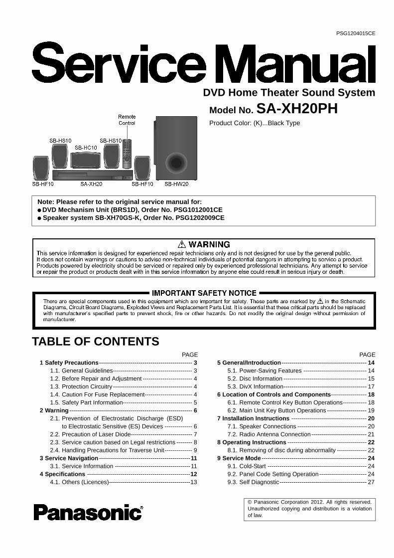
PSG1204015CE
DVD Home Theater Sound System
Model No. SA-XH20PHProduct Color: (K)...Black Type
TABLE OF CONTENTSPAGE PAGE
1 Safety Precautions----------------------------------------------- 31.1. General Guidelines---------------------------------------- 31.2. Before Repair and Adjustment ------------------------- 41.3. Protection Circuitry ---------------------------------------- 41.4. Caution For Fuse Replacement------------------------ 41.5. Safety Part Information----------------------------------- 5
2 Warning -------------------------------------------------------------- 62.1. Prevention of Electrostatic Discharge (ESD)
to Electrostatic Sensitive (ES) Devices -------------- 62.2. Precaution of Laser Diode------------------------------- 72.3. Service caution based on Legal restrictions -------- 82.4. Handling Precautions for Traverse Unit-------------- 9
3 Service Navigation ----------------------------------------------113.1. Service Information --------------------------------------11
4 Specifications ----------------------------------------------------124.1. Others (Licences)-----------------------------------------13
5 General/Introduction------------------------------------------- 145.1. Power-Saving Features -------------------------------- 145.2. Disc Information ------------------------------------------ 155.3. DivX Information------------------------------------------ 17
6 Location of Controls and Components------------------ 186.1. Remote Control Key Button Operations------------ 186.2. Main Unit Key Button Operations -------------------- 19
7 Installation Instructions -------------------------------------- 207.1. Speaker Connections ----------------------------------- 207.2. Radio Antenna Connection---------------------------- 21
8 Operating Instructions ---------------------------------------- 228.1. Removing of disc during abnormality --------------- 22
9 Service Mode ----------------------------------------------------- 249.1. Cold-Start -------------------------------------------------- 249.2. Panel Code Setting Operation------------------------ 249.3. Self Diagnostic-------------------------------------------- 27
Note: Please refer to the original service manual for: DVD Mechanism Unit (BRS1D), Order No. PSG1012001CE Speaker system SB-XH70GS-K, Order No. PSG1202009CE
© Panasonic Corporation 2012. All rights reserved.Unauthorized copying and distribution is a violationof law.
9.4. Error Code ------------------------------------------------- 329.5. Sales Demonstration Lock Function ---------------- 349.6. Firmware Version-Up Information-------------------- 35
10 Troubleshooting Guide---------------------------------------- 3710.1. Troubleshooting Guide for F61 and/or F76 -------- 3710.2. DVD/CD Laser Diode current measurement ------ 4010.3. Basic Troubleshooting Guide for Traverse
Unit (Backend P.C.B.) ----------------------------------- 4210.4. Basic Troubleshooting Guide for HDMI AV
output-------------------------------------------------------- 4311 Service Fixture & Tools --------------------------------------- 4412 Disassembly and Assembly Instructions --------------- 45
12.1. Screw Type ------------------------------------------------ 4512.2. Disassembly Flow Chart-------------------------------- 4612.3. Main Components and P.C.B. Locations ----------- 4712.4. Disassembly of Top Cabinet--------------------------- 4812.5. Replacement of Tray Ornament ---------------------- 4912.6. Disassembly of Front Panel Block Assembly ----- 5112.7. Disassembly of Panel P.C.B. -------------------------- 5212.8. Disassembly of Power Button P.C.B.---------------- 5412.9. Disassembly of Rear Panel---------------------------- 55
12.10. Disassembly of SMPS P.C.B. ------------------------- 5512.11. Replacement of Current Limiting Switch
(Q5701)----------------------------------------------------- 5612.12. Replacement of Diode (D5706) ---------------------- 5712.13. Disassembly of Main P.C.B. --------------------------- 5812.14. Replacement of Digital Amplifier IC (IC403/
IC404/IC405) ---------------------------------------------- 6012.15. Disassembly of Backend P.C.B. ---------------------- 6212.16. Disassembly of Component Video P.C.B.---------- 6312.17. Disassembly of DVD Mechanism Unit
(BRS1D)---------------------------------------------------- 6412.18. Replacement of Traverse unit------------------------- 65
13 Service Position ------------------------------------------------- 7013.1. Checking & Repairing of Panel P.C.B. -------------- 7013.2. Checking & Repairing of SMPS P.C.B. ------------- 7013.3. Checking & Repairing Main P.C.B. ------------------ 7113.4. Checking & Repairing of Backend P.C.B. ---------- 73
14 Overall Simplified Block Diagram ------------------------- 7515 Block Diagram --------------------------------------------------- 76
15.1. Backend ---------------------------------------------------- 7615.2. IC Terminal Chart----------------------------------------- 7715.3. System Control ------------------------------------------- 7815.4. Audio & Video --------------------------------------------- 7915.5. Power Supply --------------------------------------------- 80
16 Wiring Connection Diagram --------------------------------- 8217 Schematic Diagram--------------------------------------------- 83
17.1. Schematic Diagram Notes ----------------------------- 8317.2. Backend Circuit ------------------------------------------- 8517.3. Main Circuit ------------------------------------------------ 9017.4. Panel and Power Button Circuit ---------------------- 9817.5. SMPS Circuit ---------------------------------------------- 9917.6. Component Video Circuit----------------------------- 101
18 Printed Circuit Board ---------------------------------------- 10218.1. Backend P.C.B. ----------------------------------------- 10218.2. Main P.C.B. ---------------------------------------------- 10318.3. Panel, Power Button and Component Video
P.C.B.------------------------------------------------------ 10518.4. SMPS P.C.B. -------------------------------------------- 106
19 Appendix Information of Schematic Diagram ------- 10719.1. Voltage & Waveform Chart -------------------------- 107
19.2. Illustration of ICs, Transistor and Diode----------- 11519.3. Terminal Function of ICs ------------------------------ 116
20 Exploded View and Replacement Parts List---------- 11920.1. Exploded View and Mechanical Replacement
Parts List -------------------------------------------------- 11920.2. Electrical Replacement Parts List ------------------122
2
1 Safety Precautions1.1. General Guidelines
1. When servicing, observe the original lead dress. If a short circuit is found, replace all parts which have been overheated ordamaged by the short circuit.
2. After servicing, see to it that all the protective devices such as insulation barriers, insulation papers shields are properlyinstalled.
3. After servicing, carry out the following leakage current checks to prevent the customer from being exposed to shock hazards.
1.1.1. Leakage Current Cold Check1. Unplug the AC cord and connect a jumper between the two prongs on the plug.2. Measure the resistance value, with an ohmmeter, between the jumpered AC plug and each exposed metallic cabinet part on
the equipment such as screwheads, connectors, control shafts, etc. When the exposed metallic part has a return path to thechassis, the reading should be between 1MΩ and 5.2MΩ.
When the exposed metal does not have a return path to the chassis, the reading must be
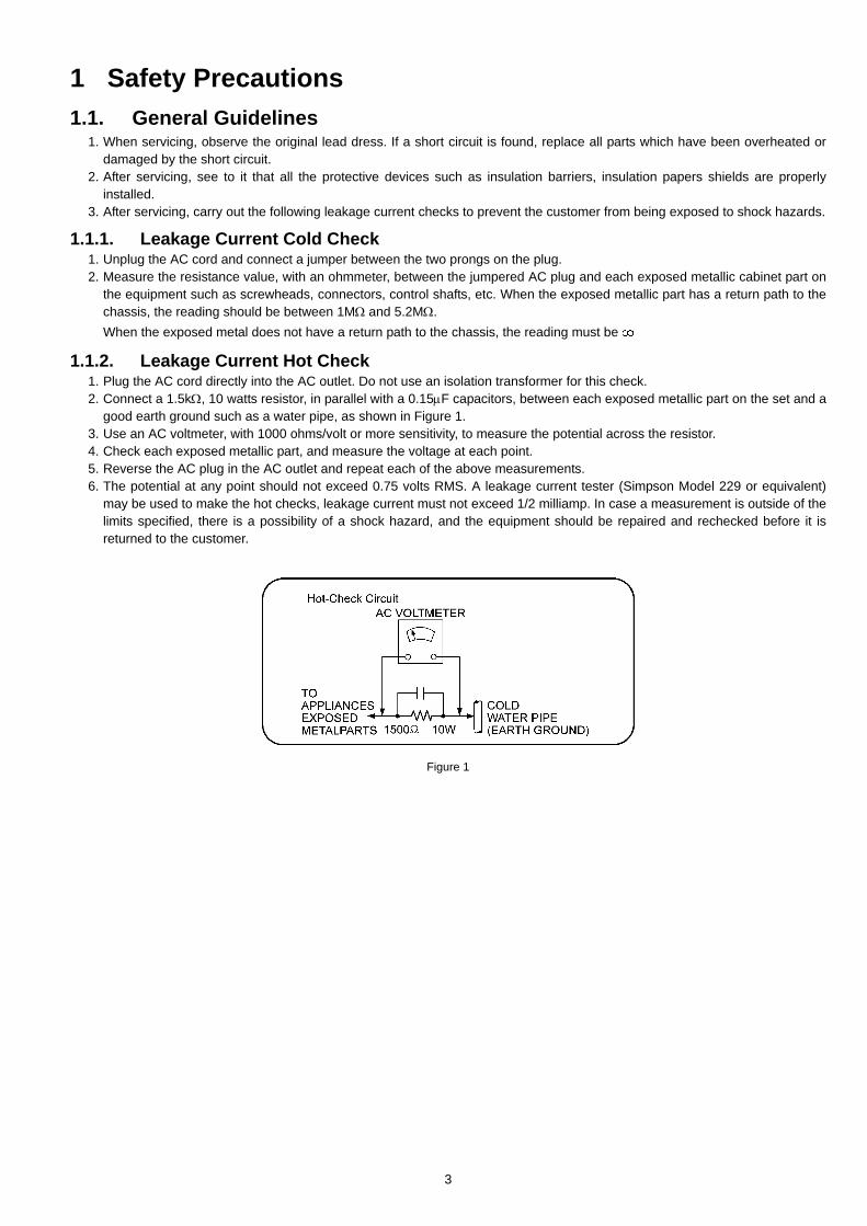
1.1.2. Leakage Current Hot Check1. Plug the AC cord directly into the AC outlet. Do not use an isolation transformer for this check.2. Connect a 1.5kΩ, 10 watts resistor, in parallel with a 0.15µF capacitors, between each exposed metallic part on the set and a
good earth ground such as a water pipe, as shown in Figure 1.3. Use an AC voltmeter, with 1000 ohms/volt or more sensitivity, to measure the potential across the resistor.4. Check each exposed metallic part, and measure the voltage at each point.5. Reverse the AC plug in the AC outlet and repeat each of the above measurements.6. The potential at any point should not exceed 0.75 volts RMS. A leakage current tester (Simpson Model 229 or equivalent)
may be used to make the hot checks, leakage current must not exceed 1/2 milliamp. In case a measurement is outside of thelimits specified, there is a possibility of a shock hazard, and the equipment should be repaired and rechecked before it isreturned to the customer.
Figure 1
3
1.2. Before Repair and AdjustmentDisconnect AC power to discharge unit AC Capacitors as such (C5702, C5703, C5704, C5705, C5706) through a 10 Ω, 10 W resis-tor to ground.Caution:
DO NOT SHORT-CIRCUIT DIRECTLY (with a screwdriver blade, for instance), as this may destroy solid state devices.After repairs are completed, restore power gradually using a variac, to avoid overcurrent.Current consumption at AC 110/127V, 50/60 Hz in NO SIGNAL mode at volume minimal should be ~ 500 mA.Current consumption at AC 240V, 50 Hz in NO SIGNAL mode at volume minimal should be ~ 500 mA.
1.3. Protection CircuitryThe protection circuitry may have operated if either of the following conditions are noticed:
• No sound is heard when the power is turned on.• Sound stops during a performance.
The function of this circuitry is to prevent circuitry damage if, for example, the positive and negative speaker connection wires are“shorted”, or if speaker systems with an impedance less than the indicated rated impedance of the amplifier are used.If this occurs, follow the procedure outlines below:
1. Turn off the power.2. Determine the cause of the problem and correct it.3. Turn on the power once again after one minute.
Note:When the protection circuitry functions, the unit will not operate unless the power is first turned off and then on again.
1.4. Caution For Fuse Replacement
4
1.5. Safety Part InformationSafety Parts List:
There are special components used in this equipment which are important for safety.These parts are marked by in the Schematic Diagrams, Exploded View & Replacement Parts List. It is essential that thesecritical parts should be replaced with manufacturer’s specified parts to prevent shock, fire or other hazards. Do not modify theoriginal design without permission of manufacturer.
Safety Ref No. Part No. Part Name & Description Remarks
8 RGRX1004E-D1 REAR PANEL
16 RKMX1009-K TOP CABINET
21 RMNX1050 BOTTOM PC SHEET
27 RMN1017 TOP PC SHEET
301 RAY1101-V TRAVERSE ASS'Y
A2 K2CQ2CA00006 AC CORD
A3 RQT9570-M O/I BOOK (Sp)
PCB5 REP4764C SMPS P.C.B. (RTL)
DZ5701 ERZVA5Z471 ZNR
L5701 G0B722G00002 LINE FILTER
L5702 G0B453G00003 LINE FILTER
F1 K5G312Y00007 FUSE
T2900 G4D1A0000142 SWITCHING TRANSFORMER
T5701 ETS35BL146AC SWITCHING TRANSFORMER
PC701 B3PBA0000579 PHOTO COUPLER
TH5701 D4CC11040013 THERMISTOR
TH5702 D4CAA5R10001 THERMISTOR
P5701 K2AA2B000011 AC INLET
R5701 D0GB824JA008 820K 1/10W
R5702 D0GB824JA008 820K 1/10W
R5703 D0GB824JA008 820K 1/10W
R5704 D0GB824JA008 820K 1/10W
C5702 F0CAF104A105 0.1uF
C5703 F0CAF104A105 0.1uF
C5704 F1BAF1020020 1000pF
C5705 F1BAF1020020 1000pF
C5706 F1BAF1020020 1000pF
5
2 Warning2.1. Prevention of Electrostatic Discharge (ESD) to Electrostatic Sensitive
(ES) DevicesSome semiconductor (solid state) devices can be damaged easily by static electricity. Such components commonly are called Elec-trostatically Sensitive (ES) Devices. Examples of typical ES devices are integrated circuits and some field-effect transistors andsemiconductor “chip” components. The following techniques should be used to help reduce the incidence of component damagecaused by electrostatic discharge (ESD).
1. Immediately before handling any semiconductor component or semiconductor-equipped assembly, drain off any ESD on yourbody by touching a known earth ground. Alternatively, obtain and wear a commercially available discharging ESD wrist strap,which should be removed for potential shock reasons prior to applying power to the unit under test.
2. After removing an electrical assembly equipped with ES devices, place the assembly on a conductive surface such as alumi-num foil, to prevent electrostatic charge build up or exposure of the assembly.
3. Use only a grounded-tip soldering iron to solder or unsolder ES devices.4. Use only an anti-static solder removal device. Some solder removal devices not classified as “anti-static (ESD protected)” can
generate electrical charge sufficient to damage ES devices.5. Do not use freon-propelled chemicals. These can generate electrical charges sufficient to damage ES devices.6. Do not remove a replacement ES device from its protective package until immediately before you are ready to install it. (Most
replacement ES devices are packaged with leads electrically shorted together by conductive foam, aluminum foil or compara-ble conductive material).
7. Immediately before removing the protective material from the leads of a replacement ES device, touch the protective materialto the chassis or circuit assembly into which the device will be installed.Caution:
Be sure no power is applied to the chassis or circuit, and observe all other safety precautions.8. Minimize bodily motions when handling unpackaged replacement ES devices. (Otherwise harmless motion such as the
brushing together of your clothes fabric or the lifting of your foot from a carpeted floor can generate static electricity (ESD) suf-ficient to damage an ES device).
6

2.2. Precaution of Laser Diode
Caution:This product utilizes a laser diode with the unit turned “on”, invisible laser radiation is emitted from the pickup lens.Wavelength: 655 nm (DVD)/790 nm (CD)Maximum output radiation power from pickup: 100 µW/VDELaser radiation from the pickup unit is safety level, but be sure the followings: 1. Do not disassemble the pickup unit, since radiation from exposed laser diode is dangerous. 2. Do not adjust the variable resistor on the pickup unit. It was already adjusted.3. Do not look at the focus lens using optical instruments.4. Recommend not to look at pickup lens for a long time.
7
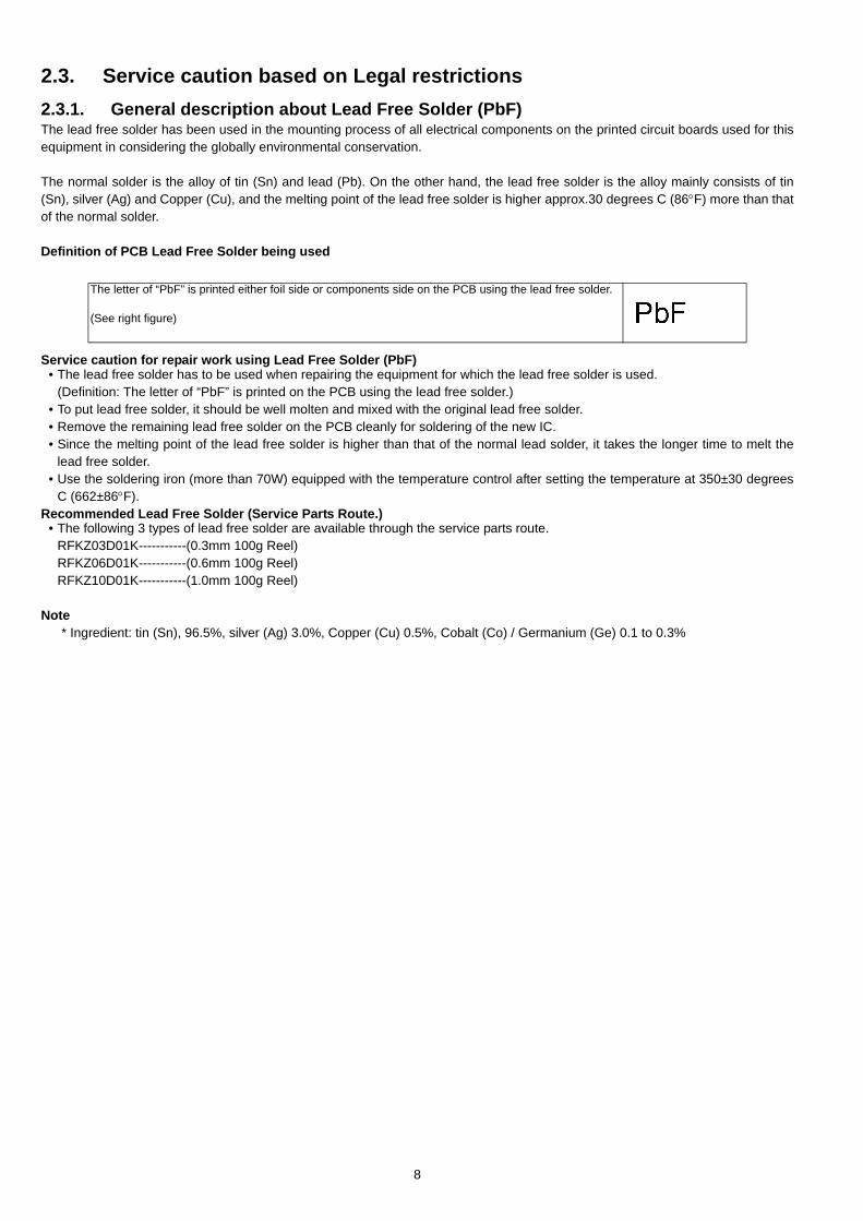
2.3. Service caution based on Legal restrictions
2.3.1. General description about Lead Free Solder (PbF)The lead free solder has been used in the mounting process of all electrical components on the printed circuit boards used for thisequipment in considering the globally environmental conservation.
The normal solder is the alloy of tin (Sn) and lead (Pb). On the other hand, the lead free solder is the alloy mainly consists of tin(Sn), silver (Ag) and Copper (Cu), and the melting point of the lead free solder is higher approx.30 degrees C (86°F) more than thatof the normal solder.
Definition of PCB Lead Free Solder being used
Service caution for repair work using Lead Free Solder (PbF)• The lead free solder has to be used when repairing the equipment for which the lead free solder is used.
(Definition: The letter of “PbF” is printed on the PCB using the lead free solder.)• To put lead free solder, it should be well molten and mixed with the original lead free solder.• Remove the remaining lead free solder on the PCB cleanly for soldering of the new IC.• Since the melting point of the lead free solder is higher than that of the normal lead solder, it takes the longer time to melt the
lead free solder.• Use the soldering iron (more than 70W) equipped with the temperature control after setting the temperature at 350±30 degrees
C (662±86°F).Recommended Lead Free Solder (Service Parts Route.)
• The following 3 types of lead free solder are available through the service parts route.RFKZ03D01K-----------(0.3mm 100g Reel)RFKZ06D01K-----------(0.6mm 100g Reel)RFKZ10D01K-----------(1.0mm 100g Reel)
Note* Ingredient: tin (Sn), 96.5%, silver (Ag) 3.0%, Copper (Cu) 0.5%, Cobalt (Co) / Germanium (Ge) 0.1 to 0.3%
The letter of “PbF” is printed either foil side or components side on the PCB using the lead free solder. (See right figure)
8
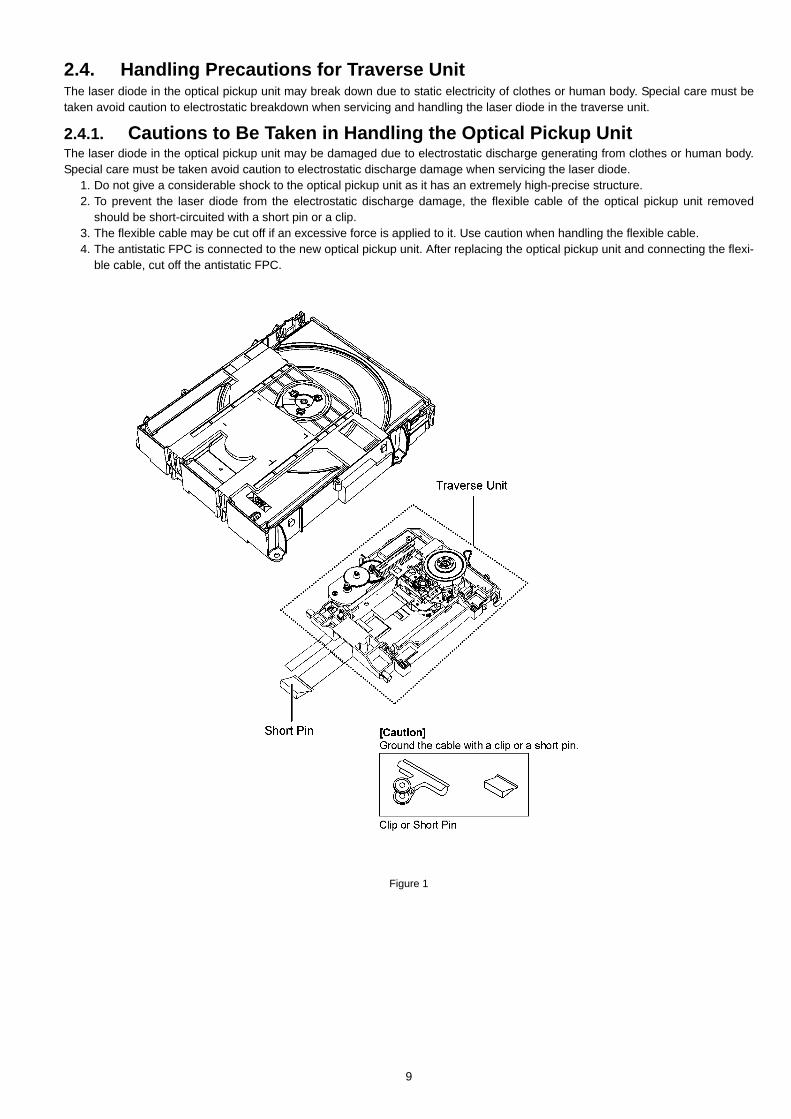
2.4. Handling Precautions for Traverse UnitThe laser diode in the optical pickup unit may break down due to static electricity of clothes or human body. Special care must betaken avoid caution to electrostatic breakdown when servicing and handling the laser diode in the traverse unit.
2.4.1. Cautions to Be Taken in Handling the Optical Pickup UnitThe laser diode in the optical pickup unit may be damaged due to electrostatic discharge generating from clothes or human body.Special care must be taken avoid caution to electrostatic discharge damage when servicing the laser diode.
1. Do not give a considerable shock to the optical pickup unit as it has an extremely high-precise structure.2. To prevent the laser diode from the electrostatic discharge damage, the flexible cable of the optical pickup unit removed
should be short-circuited with a short pin or a clip.3. The flexible cable may be cut off if an excessive force is applied to it. Use caution when handling the flexible cable.4. The antistatic FPC is connected to the new optical pickup unit. After replacing the optical pickup unit and connecting the flexi-
ble cable, cut off the antistatic FPC.
Figure 1
9
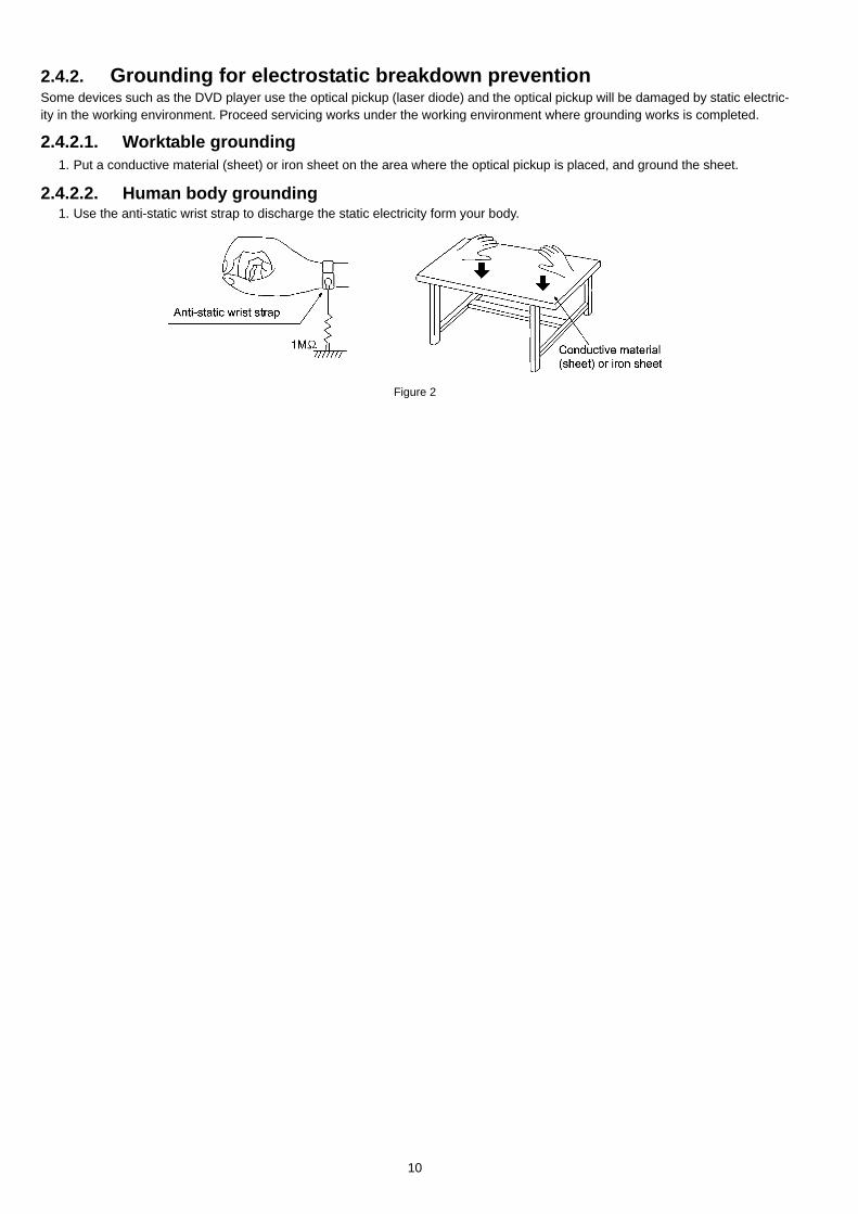
2.4.2. Grounding for electrostatic breakdown preventionSome devices such as the DVD player use the optical pickup (laser diode) and the optical pickup will be damaged by static electric-ity in the working environment. Proceed servicing works under the working environment where grounding works is completed.
2.4.2.1. Worktable grounding1. Put a conductive material (sheet) or iron sheet on the area where the optical pickup is placed, and ground the sheet.
2.4.2.2. Human body grounding1. Use the anti-static wrist strap to discharge the static electricity form your body.
Figure 2
10
3 Service Navigation3.1. Service InformationThis service manual contains technical information which will allow service personnel’s to understand and service this model.Please place orders using the parts list and not the drawing reference numbers.
If the circuit is changed or modified, this information will be followed by supplement service manual to be filed with original servicemanual.
• DVD Mechanism Unit (BRS1D):
1) This model uses DVD Mechanism Unit (BRS1D).
• Micro-processor:
1) The following components are supplied as an assembled part. • Micro-processor IC, IC200 (RFKWMXH70EB)
11

4 Specifications
Main unitAMPLIFIER SECTION
RMS Output Power: Dolby Digital ModeFront Ch
55 W per channel (5 Ω), 1 kHz, 10% THDSurround Ch
55 W per channel (5 Ω), 1 kHz, 10% THDCenter Ch
55 W per channel (5 Ω), 1 kHz, 10% THDSubwoofer Ch
80 W per channel (3 Ω), 100 Hz, 10% THDTotal RMS Dolby Digital mode power 355 W
Front Ch67 W per channel (5 Ω), 1 kHz, 30% THD
Surround Ch67 W per channel (5 Ω), 1 kHz, 30% THD
Center Ch67 W per channel (5 Ω), 1 kHz, 30% THD
Subwoofer Ch100 W per channel (3 Ω), 100 Hz, 30% THD
Total RMS Dolby Digital mode power 435 W
FM TUNER, TERMINALS SECTIONPreset Memory FM 30 stationsFrequency Modulation (FM)Frequency range
87.50 MHz to 108.00 MHz (50-kHz step)Antenna terminals 75 Ω (unbalanced)Digital audio inputOptical digital input Optical terminalSampling frequency 32 kHz, 44.1 kHz, 48 kHzUSB PortUSB standard USB 2.0 Full SpeedMedia file format support MP3 (*.mp3)
JPEG (*.jpg, *.jpeg)DivX (*.divx, *.avi)
USB device file system FAT12, FAT16, FAT32USB Port power Max. 500 mABit rate Up to 4 Mbps (DivX)
DISC SECTIONDiscs played (8 cm or 12 cm)
(1) DVD (DVD-Video, DivX*4, 5)
(2) DVD-R (DVD-Video, MP3*2, 4, JPEG*3, 4, DivX*4, 5)
(3) DVD-R DL (DVD-Video, DivX*4, 5)
(4) DVD-RW (DVD-Video, MP3*2, 4, JPEG*3, 4, DivX*4, 5)(5) +R/+RW (Video)(6) +R DL (Video)
(7) CD, CD-R/RW (CD-DA, Video CD, SVCD*1, MP3*2, 4, JPEG*3, 4,
DivX*4, 5)*1 Conforming to IEC62107*2 MPEG-1 Layer 3, MPEG-2 Layer 3, MPEG-2.5 Layer 3*3 Exif Ver 2.1 JPEG Baseline filesPicture resolution:16:9 min. size 4 x 4, max. size (720 x 8) x (405 x 8);4:3 min. size 4 x 4, max. size (720 x 8) x (540 x 8)*4 The total combined maximum number of recognizable audio, pic-ture and video contents and groups: 2600 audio, picture and videocontents and 259 groups. (Excluding Root folder)*5 Plays DivX® videoPick upWavelength (DVD/CD) 655/790 nm
Laser power CLASS 1Audio output (Disc)Number of channels 5.1 ch (FL, FR, C, SL, SR, SW)
VIDEO SECTIONVideo system NTSCComposite video outputOutput level 1 Vp-p (75 Ω)Terminal Pin jack (1 system)Component video outputY output level 1 Vp-p (75 Ω)PB output level 0.7 Vp-p (75 Ω)
PR output level 0.7 Vp-p (75 Ω)
TerminalPin jack (Y: green, PB: blue, PR: red) (1 system)
GENERALPower supply AC 110 V to 240 V, 50/60 HzPower consumption Main Unit 50 WDimensions (W×H×D) 360 mm × 48 mm × 273 mmMass Main unit 2.0 kgOperating temperature range 0 °C to +40 °COperating humidity range:
35 % to 80 % RH (no condensation)Power Consumption in standby mode:
approx. 0.45 W
Note:1. Specifications are subject to change without notice.Mass and dimensions are approximate.2. Total harmonic distortion is measured by the digital spectrum ana-lyzer.Solder:This model uses lead free solder (PbF).
Refer to their respective original service manuals for *1.
12

4.1. Others (Licences)
13
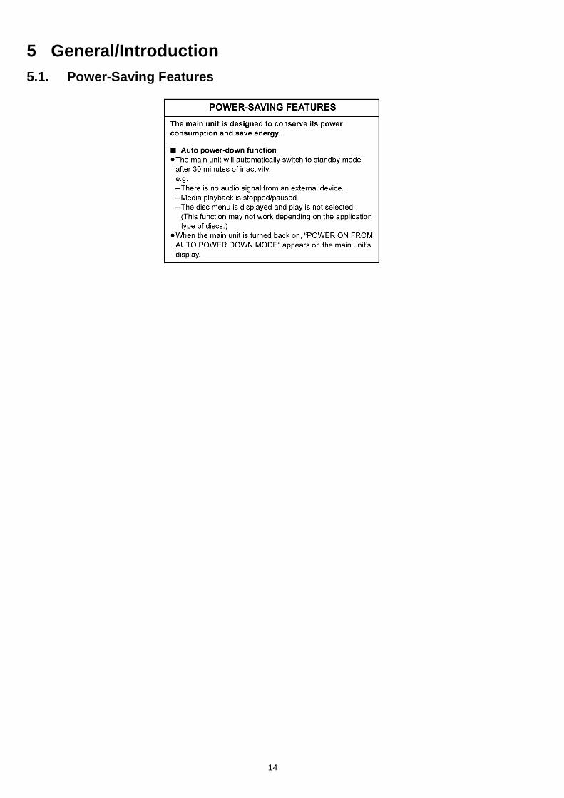
5 General/Introduction5.1. Power-Saving Features
14

5.2. Disc Information
5.2.1. Media that can be played
15
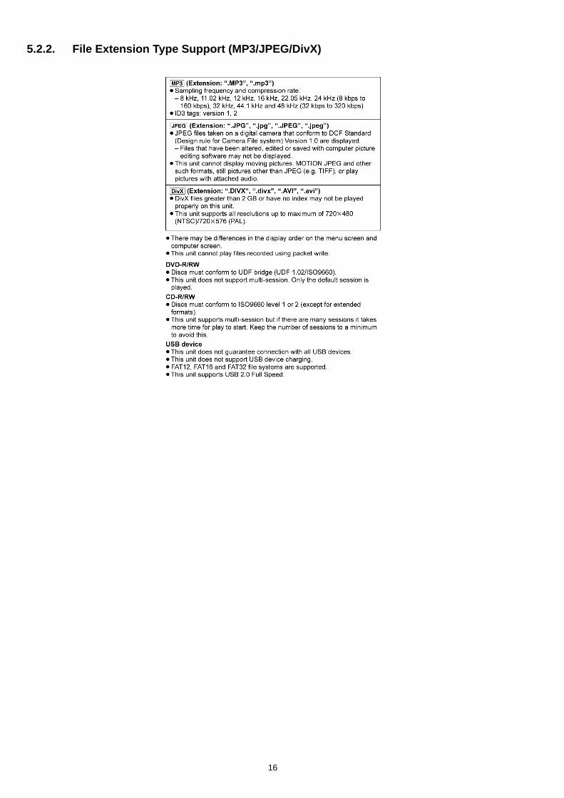
5.2.2. File Extension Type Support (MP3/JPEG/DivX)
16

5.3. DivX Information
17

6 Location of Controls and Components6.1. Remote Control Key Button Operations
18
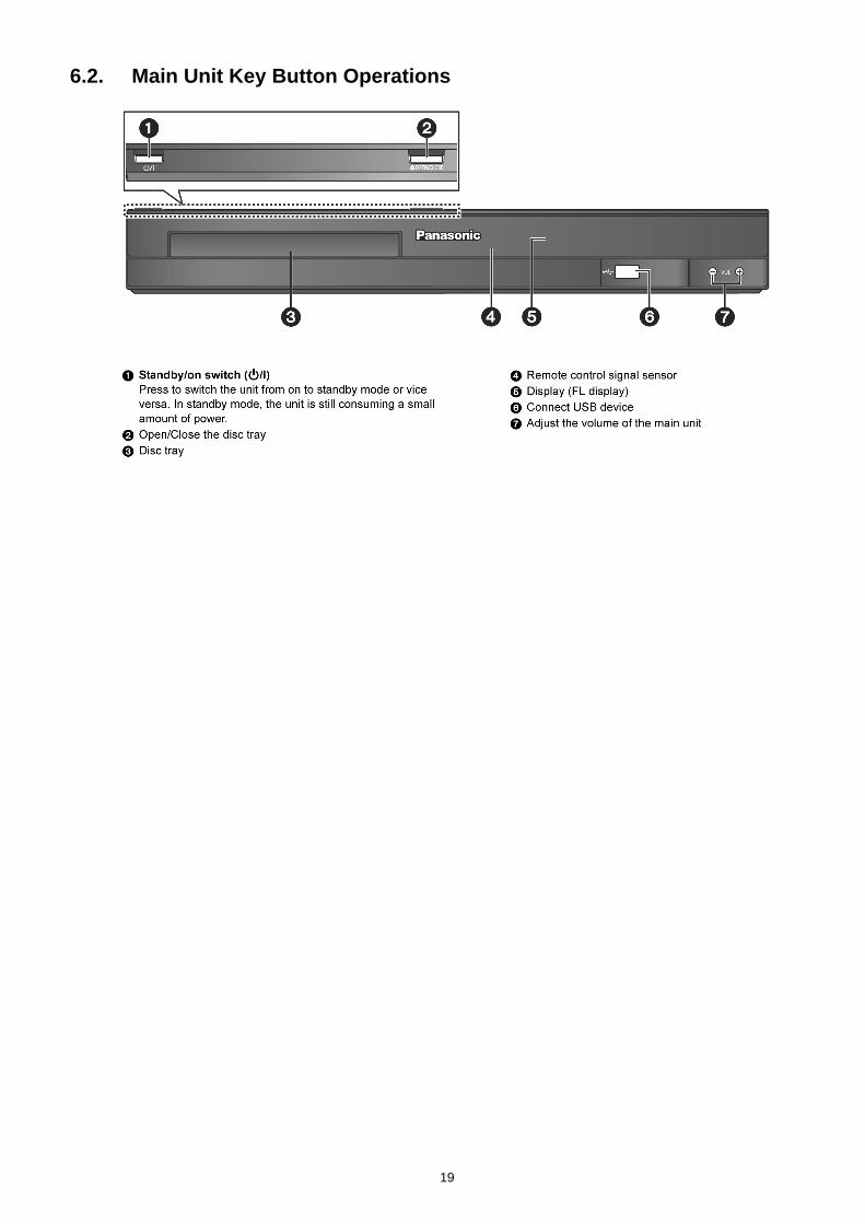
6.2. Main Unit Key Button Operations
19
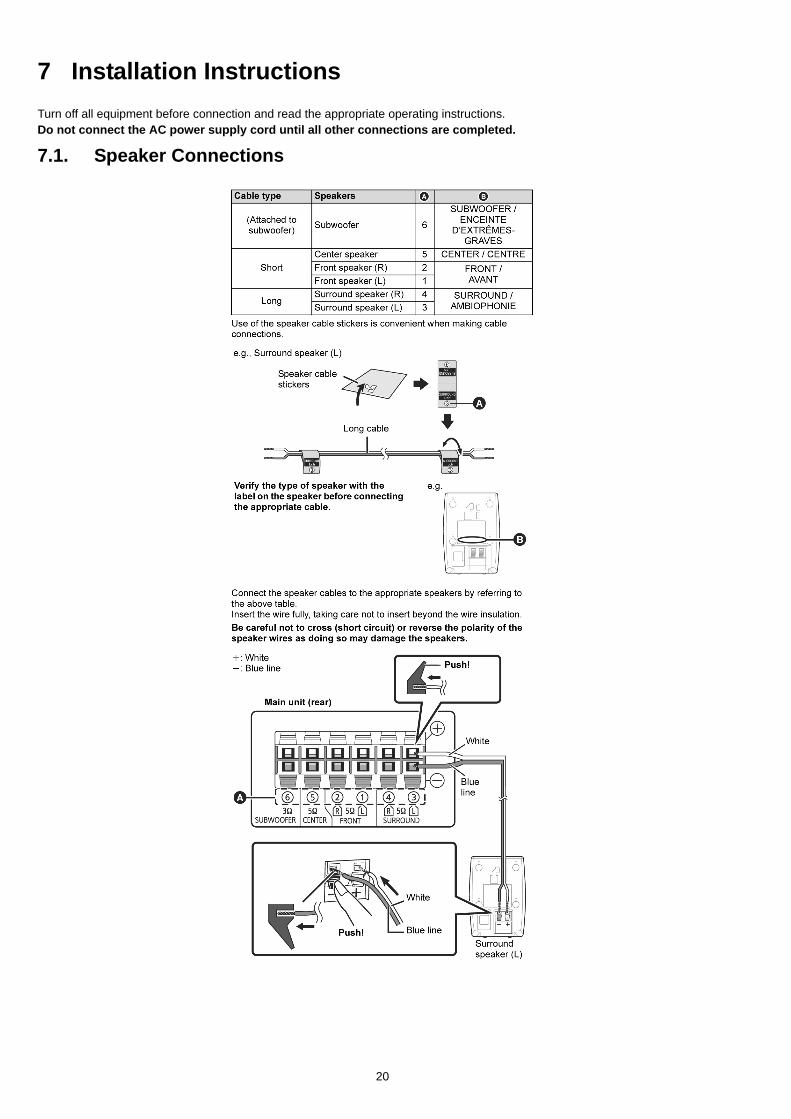
7 Installation Instructions
Turn off all equipment before connection and read the appropriate operating instructions. Do not connect the AC power supply cord until all other connections are completed.
7.1. Speaker Connections
20
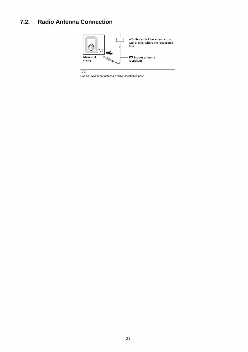
7.2. Radio Antenna Connection
21
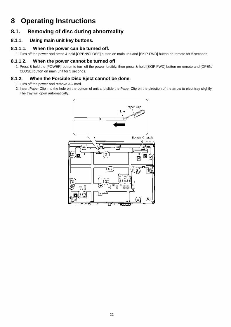
8 Operating Instructions8.1. Removing of disc during abnormality
8.1.1. Using main unit key buttons.
8.1.1.1. When the power can be turned off.1. Turn off the power and press & hold [OPEN/CLOSE] button on main unit and [SKIP FWD] button on remote for 5 seconds
8.1.1.2. When the power cannot be turned off1. Press & hold the [POWER] button to turn off the power forcibly, then press & hold [SKIP FWD] button on remote and [OPEN/
CLOSE] button on main unit for 5 seconds.
8.1.2. When the Forcible Disc Eject cannot be done.1. Turn off the power and remove AC cord.2. Insert Paper Clip into the hole on the bottom of unit and slide the Paper Clip on the direction of the arrow to eject tray slightly.
The tray will open automatically.
22

3. Gently pull out the tray.4. Remove the disc
23
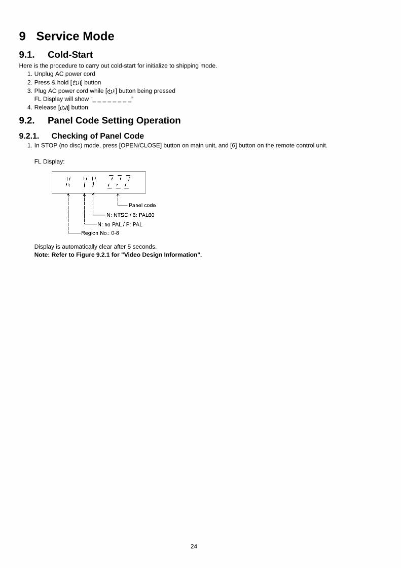
9 Service Mode9.1. Cold-StartHere is the procedure to carry out cold-start for initialize to shipping mode.
1. Unplug AC power cord2. Press & hold [ ] button3. Plug AC power cord while [ ] button being pressed
FL Display will show “_ _ _ _ _ _ _ _”4. Release [ ] button
9.2. Panel Code Setting Operation
9.2.1. Checking of Panel Code1. In STOP (no disc) mode, press [OPEN/CLOSE] button on main unit, and [6] button on the remote control unit.
FL Display:
Display is automatically clear after 5 seconds.Note: Refer to Figure 9.2.1 for "Video Design Information".
24
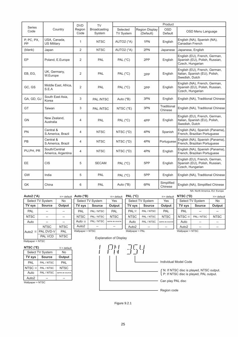
Figure 9.2.1
English (NA), Spanish (NA),
Canadian French
Japanese, English
English (EU), French, German,
Spanish (EU), Polish, Russian,
Czech, Hungarian
English (EU), French, German,
Italian, Spanish (EU), Polish,
Swedish, Dutch
English (NA), French, German,
Spanish (EU), Polish, Russian,
Czech, Hungarian
GA, GD, GJ English (NA), Traditional Chinese
English (EU), French, German,
Italian, Spanish (EU), Polish,
Swedish, Dutch
English (NA), Spanish (Panama),
French, Brazilian Portuguese
English (EU), French, German,
Spanish (EU), Polish, Russian,
Czech, Hungarian
GN
EE
PU,PH, PR
EP
P, PC, PX,
PP
GC, GS
EB, EG,
2
5
4
4
2
2
1
2
3
DVD
Region
Code
PAL /NTSC
SECAM
NTSC
NTSC
PAL
PAL
PAL
PAL
PAL
PAL
TV
Broadcasting
System
NTSC (*D)
NTSC (*D)
NTSC (*D)
Auto (*B)
Auto (*B)
PAL (*C)
PAL (*C)
PAL (*C)
PAL (*C)
PAL (*C)
PAL (*C)
Selected
TV System
2PN
4PN
4PN
5PP
3PN
1PN
2PP
2PP
2PP
4PP
Region Display
(Default)
ProductSeries
Code
Japan
South East Asia,
Korea
New Zealand,
Australia
South/Centrial
America, Argentina
CIS
Poland, E.Europe
USA, Canada,
US Military
UK, Germany,
W.Europe
Middle East, Africa,
S.E.A
CountryOSD Menu Language
OSD
Default
English
English
English
English
English (NA), Traditional ChineseGW 5 5PPIndia English
English
GT English (NA), Traditional Chinese3 PAL /NTSC NTSC (*E) 3PNTaiwanTraditional
Chinese
English
English
English
GK English (NA), Simplified Chinese6 6PNChinaSimplified
Chinese
Japanese
English (NA), Spanish (Panama),
French, Brazilian PortuguesePN 4 NTSC
Central &
S.America, BrazilSpanish
4PNEnglish (NA), Spanish (Panama),
French, Brazilian PortuguesePB 4 NTSC
NTSC
Central &
S.America, BrazilPortuguese
AUTO2 (*A)
AUTO2 (*A)(blank)
NA: North America, EU: Europe
NTSC (*E)
Auto2
TV sys Source Output
Select TV System
PAL PAL
-- --
same as source
PAL / NTSC
PAL / NTSC
PAL / NTSC
Auto
NTSC
= default
Wallpaper = NTSC
NTSC
No
Auto2 (*A)
TV sys Source Output
Select TV System
PAL -- --
-- --
-- --
NTSC
NTSC
PAL DVD-V
PAL VCD
PAL
NTSC
NTSC
Auto
No
Auto2
= default
Wallpaper = NTSC
Auto (*B)
Auto2
TV sys Source Output
Select TV System
PAL PAL
-- --
NTSC
PAL / NTSC
PAL / NTSC
PAL / NTSC same as source
Yes
Auto
= default
NTSC
Wallpaper = NTSC
PAL (*C)
Auto2
TV sys Source Output
Select TV System
-- --
NTSC
PAL / NTSC
PAL / NTSC
PAL / NTSC
same as sourceAuto
Yes
PAL
= default
Wallpaper = PAL
PAL
NTSC
NTSC (*D)
Auto2
TV sys Source Output
Select TV System
PAL
-- --
-- --
-- --
PAL / NTSC
Auto
No
NTSC
= default
Wallpaper = NTSC
NTSC
Explanation of Display
Individual Model Code
Can play PAL disc
Region code
N: If NTSC disc is played, NTSC output.
P: If NTSC disc is played, PAL output.
25
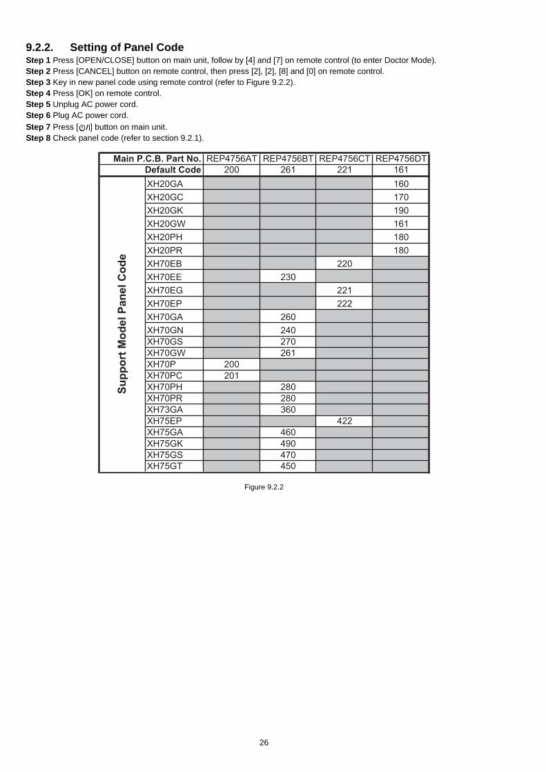
9.2.2. Setting of Panel Code Step 1 Press [OPEN/CLOSE] button on main unit, follow by [4] and [7] on remote control (to enter Doctor Mode).Step 2 Press [CANCEL] button on remote control, then press [2], [2], [8] and [0] on remote control.Step 3 Key in new panel code using remote control (refer to Figure 9.2.2).Step 4 Press [OK] on remote control.Step 5 Unplug AC power cord.Step 6 Plug AC power cord.Step 7 Press [ ] button on main unit.Step 8 Check panel code (refer to section 9.2.1).
Figure 9.2.2
REP4756AT REP4756BT REP4756CT REP4756DT
200 261 221 161
XH20GA 160
XH20GC 170
XH20GK 190
XH20GW 161
XH20PH 180
XH20PR 180
XH70EB 220
XH70EE 230
XH70EG 221
XH70EP 222
XH70GA 260
XH70GN 240
XH70GS 270
XH70GW 261
XH70P 200
XH70PC 201
XH70PH 280
XH70PR 280
XH73GA 360
XH75EP 422
XH75GA 460
XH75GK 490
XH75GS 470
XH75GT 450
Main P.C.B. Part No.
Default Code
Su
pp
ort
Mo
de
l P
an
el
Co
de
26
9.3. Self DiagnosticBy pressing various button combinations on the main unit and remote control unit, you can activate the various service modes forchecking.Special Note:
• Due to the limitations of the no. characters that can be shown on the FL Display, the “FL Display” button on the remote controlunit can be used to show the two display pages. (Display 1 / Display 2).
• Refer to Section 6.1 for the section on “Remote Control Key Buttons Operations”.
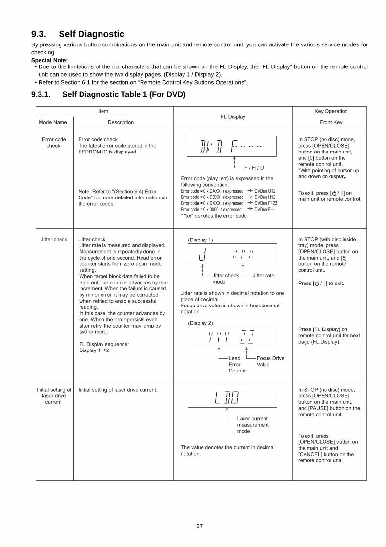
9.3.1. Self Diagnostic Table 1 (For DVD)
FL DisplayKey Operation
Front Key
Item
DescriptionMode Name
Initial setting of
laser drive
current
Jitter check Jitter check.
Jitter rate is measured and displayed.
Measurement is repeatedly done in
the cycle of one second. Read error
counter starts from zero upon mode
setting.
When target block data failed to be
read out, the counter advances by one
increment. When the failure is caused
by minor error, it may be corrected
when retried to enable successful
reading.
In this case, the counter advances by
one. When the error persists even
after retry, the counter may jump by
two or more.
FL Display sequence:
Display 1 2.
Jitter rate is shown in decimal notation to one
place of decimal.
Focus drive value is shown in hexadecimal
notation.
(Display 1)
Jitter rateJitter check
mode
(Display 2)
Lead
Error
Counter
Focus Drive
Value
Press [ / ] to exit.
In STOP (with disc inside
tray) mode, press
[OPEN/CLOSE] button on
the main unit, and [5]
button on the remote
control unit.
Press [FL Display] on
remote control unit for next
page (FL Display).
Error code
check
Error code check
The latest error code stored in the
EEPROM IC is displayed.
Note: Refer to "(Section 9.4) Error
Code" for more detailed information on
the error codes.
Error code (play_err) is expressed in the
following convention.
Error code = 0 x DAXX is expressed: DVDnn U12
Error code = 0 x DBXX is expressed: DVDnn H12
Error code = 0 x DXXX is expressed: DVDnn F123
Error code = 0 x 0000 is expressed: DVDnn F---
* "xx" denotes the error code
F / H / U
To exit, press [ / ] on
main unit or remote control.
In STOP (no disc) mode,
press [OPEN/CLOSE]
button on the main unit,
and [0] button on the
remote control unit.
*With pointing of cursor up
and down on display.
In STOP (no disc) mode,
press [OPEN/CLOSE]
button on the main unit,
and [PAUSE] button on the
remote control unit.
To exit, press
[OPEN/CLOSE] button on
the main unit and
[CANCEL] button on the
remote control unit.
Initial setting of laser drive current.
The value denotes the current in decimal
notation.
Laser current
measurement
mode
27

9.3.2. Self Diagnostic Table 2 (For DVD)
FL DisplayKey Operation
Front Key
Item
DescriptionMode Name
CD laser drive
current
measurement
In STOP (no disc) mode,
press [OPEN/CLOSE]
button on the main unit,
and [3] button on the
remote control unit.
DVD laser
drive current
measurement
CD laser current
measurement mode
(Display 1)
In STOP (no disc) mode,
press [OPEN/CLOSE]
button on the main unit,
and [FUNCTIONS] button
on the remote control unit.
To exit, press
[OPEN/CLOSE] button on
the main unit and
[CANCEL] button on the
remote control unit.
To exit, press
[OPEN/CLOSE] button on
the main unit and
[CANCEL] button on the
remote control unit.
The value denotes the current in decimal
notation.
DVD laser current
measurement mode
DVD laser drive current measurement.
For DVD laser drive current, refer to
Troubleshooting Guide (Section 10.2)
CD laser drive current measurement.
For CD laser drive current, refer to
Troubleshooting Guide (Section 10.2)
28
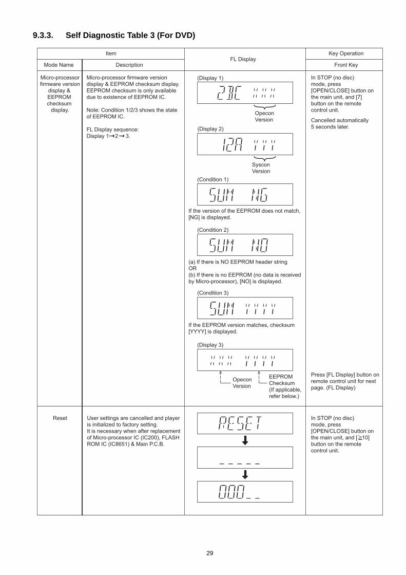
9.3.3. Self Diagnostic Table 3 (For DVD)
FL DisplayKey Operation
Front Key
Item
DescriptionMode Name
Reset
Micro-processor
firmware version
display &
EEPROM
checksum
display.
User settings are cancelled and player
is initialized to factory setting.
It is necessary when after replacement
of Micro-processor IC (IC200), FLASH
ROM IC (IC8651) & Main P.C.B.
Micro-processor firmware version
display & EEPROM checksum display.
EEPROM checksum is only available
due to existence of EEPROM IC.
Note: Condition 1/2/3 shows the state
of EEPROM IC.
FL Display sequence:
Display 1 2 3.
In STOP (no disc)
mode, press
[OPEN/CLOSE] button on
the main unit, and [ 10]
button on the remote
control unit.
Cancelled automatically
5 seconds later.
In STOP (no disc)
mode, press
[OPEN/CLOSE] button on
the main unit, and [7]
button on the remote
control unit.
Press [FL Display] button on
remote control unit for next
page. (FL Display)
(Display 2)
If the version of the EEPROM does not match,
[NG] is displayed.
(Condition 1)
(a) If there is NO EEPROM header string
OR
(b) If there is no EEPROM (no data is received
by Micro-processor), [NO] is displayed.
(Condition 2)
Opecon
Version
EEPROM
Checksum
(If applicable,
refer below.)
(Display 3)
(Display 1)
(Condition 3)
If the EEPROM version matches, checksum
[YYYY] is displayed.
Opecon
Version
Syscon
Version
29
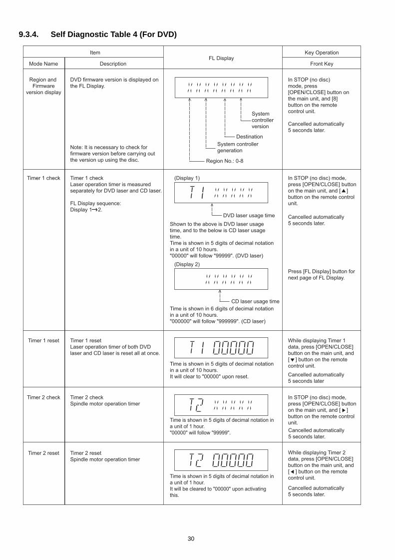
9.3.4. Self Diagnostic Table 4 (For DVD)
FL DisplayKey Operation
Front Key
Item
DescriptionMode Name
Region and
Firmware
version display
Cancelled automatically
5 seconds later.
In STOP (no disc)
mode, press
[OPEN/CLOSE] button on
the main unit, and [8]
button on the remote
control unit.
DVD firmware version is displayed on
the FL Display.
Note: It is necessary to check for
firmware version before carrying out
the version up using the disc.
Destination
System
controller
version
System controller
generation
Region No.: 0-8
Timer 1 check
DVD laser usage time
(Display 1)
Shown to the above is DVD laser usage
time, and to the below is CD laser usage
time.
Time is shown in 5 digits of decimal notation
in a unit of 10 hours.
"00000" will follow "99999". (DVD laser)
(Display 2)
CD laser usage time
Time is shown in 6 digits of decimal notation
in a unit of 10 hours.
"000000" will follow "999999". (CD laser)
Press [FL Display] button for
next page of FL Display.
Cancelled automatically
5 seconds later.
In STOP (no disc) mode,
press [OPEN/CLOSE] button
on the main unit, and [ ]
button on the remote control
unit.
Timer 1 reset
Timer 2 check
Timer 2 reset
Timer 1 check
Laser operation timer is measured
separately for DVD laser and CD laser.
FL Display sequence:
Display 1 2.
Timer 1 reset
Laser operation timer of both DVD
laser and CD laser is reset all at once.
Timer 2 check
Spindle motor operation timer
Timer 2 reset
Spindle motor operation timer
Time is shown in 5 digits of decimal notation
in a unit of 10 hours.
It will clear to "00000" upon reset.
Time is shown in 5 digits of decimal notation in
a unit of 1 hour.
"00000" will follow "99999".
Time is shown in 5 digits of decimal notation in
a unit of 1 hour.
It will be cleared to "00000" upon activating
this.
Cancelled automatically
5 seconds later
While displaying Timer 1
data, press [OPEN/CLOSE]
button on the main unit, and
[ ] button on the remote
control unit.
Cancelled automatically
5 seconds later.
In STOP (no disc) mode,
press [OPEN/CLOSE] button
on the main unit, and [ ]
button on the remote control
unit.
Cancelled automatically
5 seconds later.
While displaying Timer 2
data, press [OPEN/CLOSE]
button on the main unit, and
[ ] button on the remote
control unit.
30
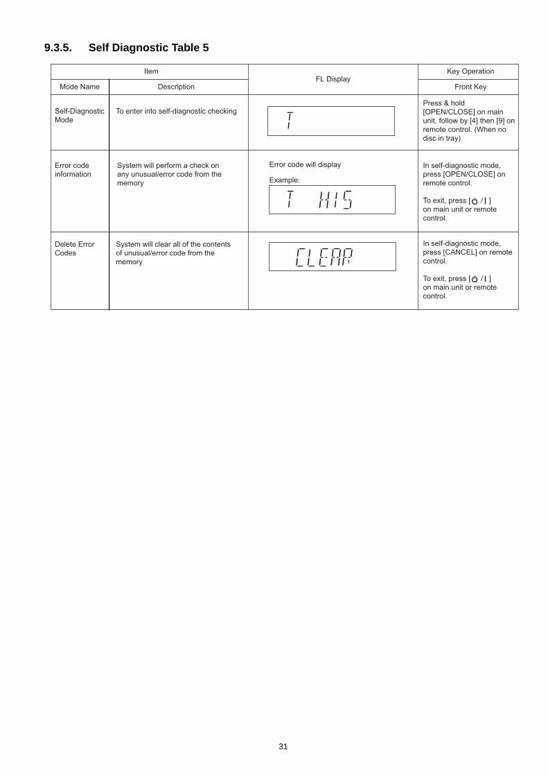
9.3.5. Self Diagnostic Table 5
FL DisplayKey Operation
Front Key
Item
DescriptionMode Name
Delete Error
Codes
Error code
information
System will perform a check on
any unusual/error code from the
memory
Error code will display
Example:
Self-Diagnostic
Mode
To enter into self-diagnostic checkingPress & hold
[OPEN/CLOSE] on main
unit, follow by [4] then [9] on
remote control. (When no
disc in tray)
System will clear all of the contents
of unusual/error code from the
memory
In self-diagnostic mode,
press [OPEN/CLOSE] on
remote control.
To exit, press [ / ]
on main unit or remote
control.
In self-diagnostic mode,
press [CANCEL] on remote
control.
To exit, press [ / ]
on main unit or remote
control.
31

9.4. Error Code
9.4.1. Error Code Table 1
Error
Code
F61 The abnormalities
in the Power Amp
output or power
supply
In normal operation, when DCDET2 goes to
L, immediately PCNT is set to L (not normal
POWER OFF sequence), and Error Code
F61 is displayed, without displaying
‘GOODBYE’ scroll on the FL. When happen
error, it memorizes the contents and
displays unusual contents in self-diagnostic
error detection mode.
Press [OPEN/CLOSE]
on main unit for next
error.
F76 Abnormality in the
output voltage of
stabilized power
supply
In normal operation when DCDET1 is
detected L(Low) for two consecutive times,
F76 is displayed on FL for 1 seconds and
after that PCONT will be turned to L (Low).
Press [OPEN/CLOSE]
on main unit for next
error.
Diagnosis
ContentsDescription of error Automatic FL Display Remarks
IPOD
OVER
CURRENT
Over current
occurs in Power
Supply for iPod
charging
Disc Region
In normal operation when IPOD_OC is
detected "L" (Low) for two consecutive
times, the message will display on FL once
and Power Supply to iPod shall be cut.
Power off the main unit
and power on again.
F0C1 DVD: Prohibited by the restricted region
code.
F0C3 DVD: Parental lock setting prohibits the
playback of the entire title.
32
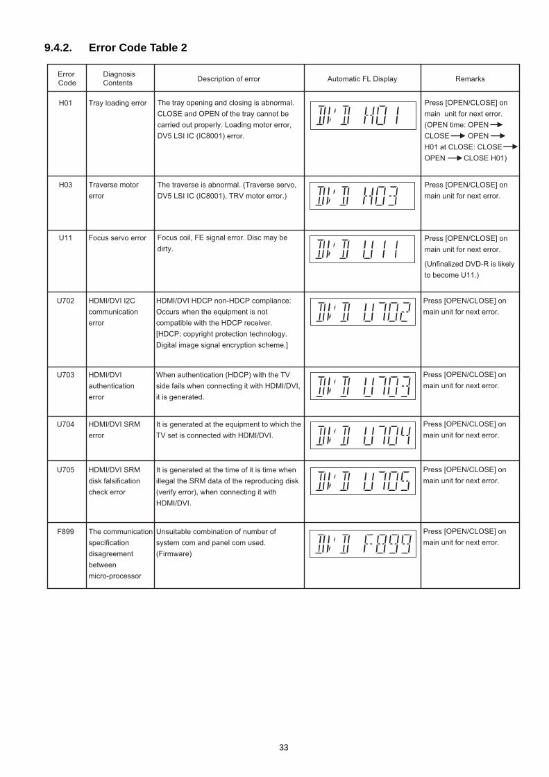
9.4.2. Error Code Table 2
H01 Tray loading error The tray opening and closing is abnormal.
CLOSE and OPEN of the tray cannot be
carried out properly. Loading motor error,
DV5 LSI IC (IC8001) error.
Press [OPEN/CLOSE] on
main unit for next error.
(OPEN time: OPEN
CLOSE OPEN
H01 at CLOSE: CLOSE
OPEN CLOSE H01)
Press [OPEN/CLOSE] on
main unit for next error.
Press [OPEN/CLOSE] on
main unit for next error.
H03 Traverse motor
error
The traverse is abnormal. (Traverse servo,
DV5 LSI IC (IC8001), TRV motor error.)
U11 Focus servo error Focus coil, FE signal error. Disc may be
dirty.
(Unfinalized DVD-R is likely
to become U11.)
U702 HDMI/DVI I2C
communication
error
HDMI/DVI HDCP non-HDCP compliance:
Occurs when the equipment is not
compatible with the HDCP receiver.
[HDCP: copyright protection technology.
Digital image signal encryption scheme.]
Press [OPEN/CLOSE] on
main unit for next error.
Press [OPEN/CLOSE] on
main unit for next error.
Press [OPEN/CLOSE] on
main unit for next error.
Press [OPEN/CLOSE] on
main unit for next error.
Press [OPEN/CLOSE] on
main unit for next error.
U703 HDMI/DVI
authentication
error
When authentication (HDCP) with the TV
side fails when connecting it with HDMI/DVI,
it is generated.
U704 HDMI/DVI SRM
error
It is generated at the equipment to which the
TV set is connected with HDMI/DVI.
U705 HDMI/DVI SRM
disk falsification
check error
It is generated at the time of it is time when
illegal the SRM data of the reproducing disk
(verify error), when connecting it with
HDMI/DVI.
F899 The communication
specification
disagreement
between
micro-processor
Unsuitable combination of number of
system com and panel com used.
(Firmware)
Error
Code
Diagnosis
ContentsDescription of error Automatic FL Display Remarks
33

9.5. Sales Demonstration Lock FunctionThis function prevents discs from being lost when the unit is used for sales demonstrations by disabling the disc eject function.“LOCKED” is displayed on the unit, and ordinary operation is disabled.
9.5.1. Setting• Prohibiting removal of disc
1. Select the DVD/CD function.2. At POWER ON condition, press and hold down the [ OPEN/CLOSE] button and the [- VOL] button on the main unit for at
least three seconds. (The message, “LOCKED” appears when the function is activated.)Note:
OPEN/CLOSE button is invalid and the main unit displays “LOCKED” while the lock function mode is entered.
• Prohibiting operation of selector and disc1. Select the DVD/CD function.2. At POWER ON condition, press and hold down the [ OPEN/CLOSE] button and the [VOL +] button on the main unit for at
least three seconds. (The message, “LOCKED” appears when the function is activated.)Note:
The following buttons are invalid and the main unit displays “LOCKED” while the lock function mode is entered.
9.5.2. CancellationThe lock can be cancelled by the same procedure as used in locking. (“UNLOCKED” is displayed on cancellation)At normal Power ON/OFF the LOCKED condition is not cleared. However, AC Power ON/OFF should clear LOCKED condition.
Main unit OPEN/CLOSE Remote con-
troller unitAV/INPUT, NUMERIC KEYS 0~9, , CANCEL, DVD, RADIO, EXT-IN, , , , , , , , FUNCTIONS,
EXIT, TOP MENU, , , , , OK, START, MENU, RETURN, PLAY MODE/-REPEAT, CH SELECT, FL DISPLAY
34
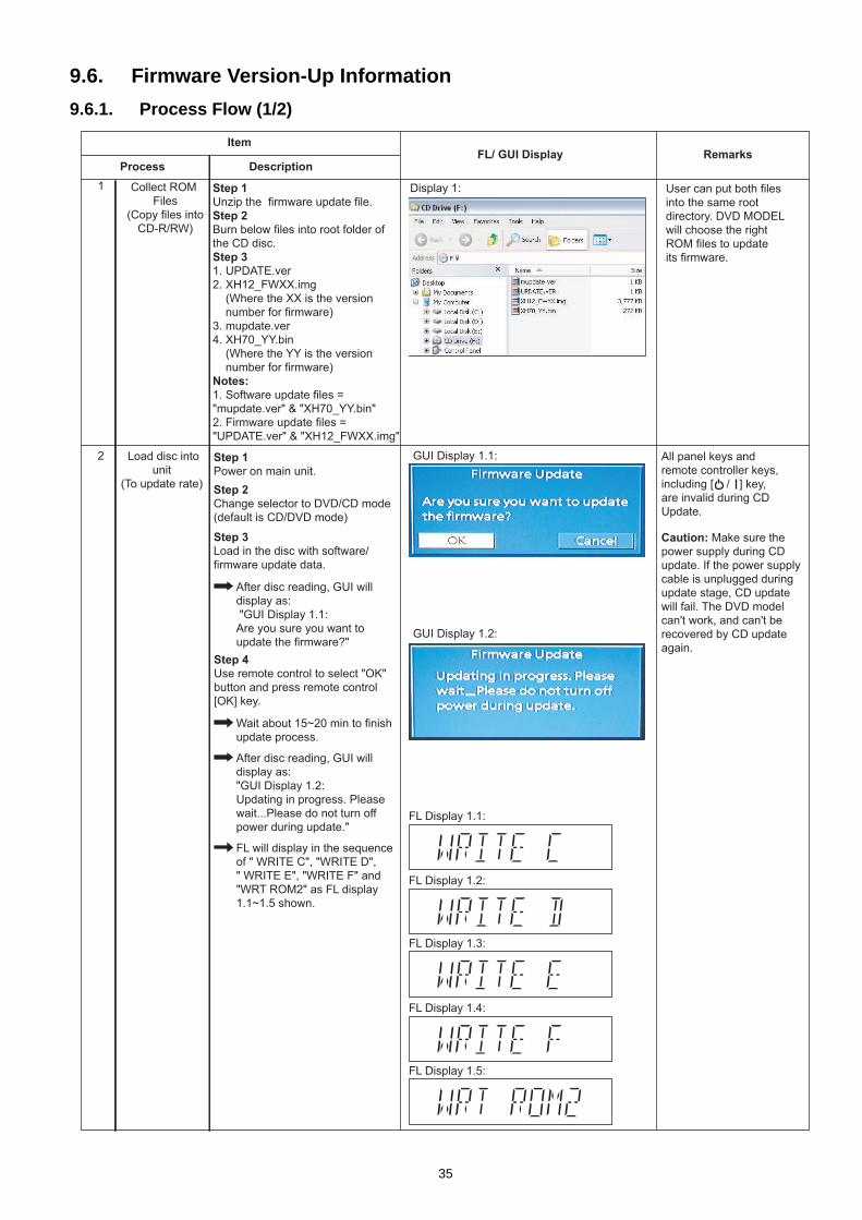
9.6. Firmware Version-Up Information
9.6.1. Process Flow (1/2)
Collect ROM
Files
(Copy files into
CD-R/RW)
Load disc into
unit
(To update rate)
Step 1
Unzip the firmware update file.
Step 2
Burn below files into root folder of
the CD disc.
Step 3
1. UPDATE.ver
2. XH12_FWXX.img
(Where the XX is the version
number for firmware)
3. mupdate.ver
4. XH70_YY.bin
(Where the YY is the version
number for firmware)
Notes:
1. Software update files =
"mupdate.ver" & "XH70_YY.bin"
2. Firmware update files =
"UPDATE.ver" & "XH12_FWXX.img"
All panel keys and
remote controller keys,
including [ / ] key,
are invalid during CD
Update.
Caution: Make sure the
power supply during CD
update. If the power supply
cable is unplugged during
update stage, CD update
will fail. The DVD model
can't work, and can't be
recovered by CD update
again.
User can put both files
into the same root
directory. DVD MODEL
will choose the right
ROM files to update
its firmware.
FL/ GUI Display RemarksItem
DescriptionProcess
1
2 GUI Display 1.1:Step 1
Power on main unit.
Step 2
Change selector to DVD/CD mode
(default is CD/DVD mode)
Step 3
Load in the disc with software/
firmware update data.
After disc reading, GUI will
display as:
"GUI Display 1.1:
Are you sure you want to
update the firmware?"
Wait about 15~20 min to finish
update process.
After disc reading, GUI will
display as:
"GUI Display 1.2:
Updating in progress. Please
wait...Please do not turn off
power during update."
FL will display in the sequence
of " WRITE C", "WRITE D",
" WRITE E", "WRITE F" and
"WRT ROM2" as FL display
1.1~1.5 shown.
Step 4
Use remote control to select "OK"
button and press remote control
[OK] key.
GUI Display 1.2:
FL Display 1.1:
FL Display 1.2:
FL Display 1.3:
FL Display 1.4:
FL Display 1.5:
Display 1:
35
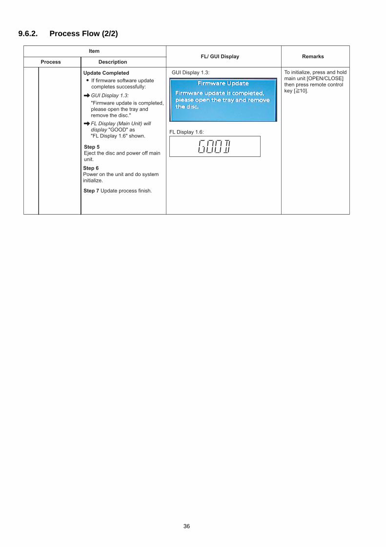
9.6.2. Process Flow (2/2)
FL/ GUI Display RemarksItem
DescriptionProcess
FL Display 1.6:
FL Display (Main Unit) will
display "GOOD" as
"FL Display 1.6" shown.
To initialize, press and hold
main unit [OPEN/CLOSE]
then press remote control
key [ 10].
Update Completed
If firmware software update
completes successfully:
GUI Display 1.3:
"Firmware update is completed,
please open the tray and
remove the disc."
GUI Display 1.3:
Step 5
Eject the disc and power off main
unit.
Step 6
Power on the unit and do system
initialize.
Step 7 Update process finish.
36
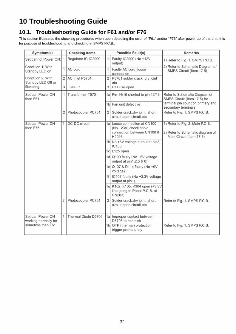
10 Troubleshooting Guide10.1. Troubleshooting Guide for F61 and/or F76This section illustrates the checking procedures when upon detecting the error of “F61” and/or “F76” after power up of the unit. It isfor purpose of troubleshooting and checking in SMPS P.C.B..
Symptom(s) Checking items Possible Fault(s) Remarks
Set cannot Power ON:
Condition 1: With
Standby LED on1
2
1
Solder crack,dry joint ,short
circuit,open circuit,etc
AC cord
AC Inlet P5701
1 Faulty AC cord, loose
connection
2
2
Solder crack,dry joint ,short
circuit,open circuit,etc
2
P5701 solder crack, dry joint
etc
Faulty IC2900 (No +12V
output)
Set can Power ON
then F61
Set can Power ON
then F76
Set can Power ON
working normally for
sometime then F61
Condition 2: With
Standby LED Off or
flickering 3
1
3 F1 Fuse openFuse F1
DC-DC circuit
1 Thermal Diode D5706
2 Photocoupler PC701
1 Transformer T5701
2 Photocoupler PC701
1a Pin 14/15 shorted to pin 12/13
1b Fan unit defective
1a Loose connection at CN100
(No +23V) check cable
connection between CN100 &
H2016
1b No +6V voltage output at pin3,
IC106
1d Q100 faulty (No +5V voltage
output at pin1,2,5 & 6)
1e Q107 & D114 faulty (No +9V
voltage)
1c L125 open
1a
1b
Improper contact between
D5706 to heatsink
OTP (thermal) protection
trigger prematurely
1f IC107 faulty (No +3.3V voltage
output at pin1)
1g K102, K105, K304 open (+3.3V
line going to Panel P.C.B. at
CN203)
1) Refer to Fig. 1. SMPS P.C.B.
Refer to Fig. 1. SMPS P.C.B.
Refer to Fig. 1. SMPS P.C.B.
Refer to Fig. 1. SMPS P.C.B.
Refer to Schematic Diagram of
SMPS Circuit (Item 17.5) for
terminal pin count on primary and
secondary terminals
SMPS Circuit (Item 17.5)2) Refer to Schematic Diagram of
1) Refer to Fig. 2. Main P.C.B.
Main Circuit (Item 17.3)2) Refer to Schematic diagram of
1 Regulator IC IC2900
37
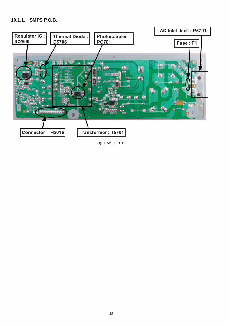
10.1.1. SMPS P.C.B.
Fig. 1. SMPS P.C.B.
AC Inlet Jack : P5701
Fuse : F1
Regulator IC :
IC2900Thermal Diode :
D5706
Photocoupler :
PC701
H2016Connector : H2016 Transformer : T5701
38
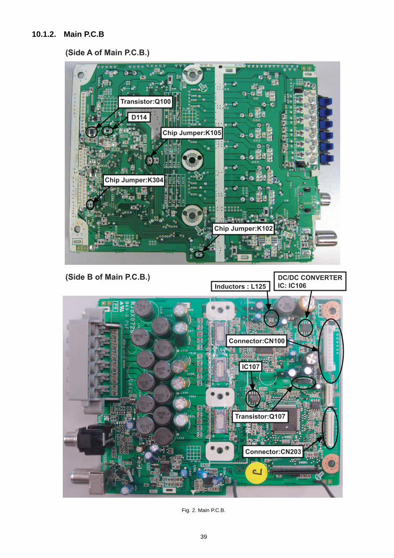
10.1.2. Main P.C.B
Fig. 2. Main P.C.B.
Transistor:Q100
D114
Chip Jumper:K102
Chip Jumper:K105
Chip Jumper:K304
(Side B of Main P.C.B.)
(Side A of Main P.C.B.)
Connector:CN100
Transistor:Q107
Connector:CN203
DC/DC CONVERTER
IC: IC106Inductors : L125
IC107
39

10.2. DVD/CD Laser Diode current measurementThis section will illustrate proceddures of measuring & deriving DVD/CD Laser Diode Current.
DVD Laser Diode Current Measurement
CD Laser Diode Current Measurement
Checking Item/Formula RemarksItem Description
1. Measurement the voltage (VCD) on the testpoints CL8530(+) & CL8531(-).
This is voltage across R8566 which has a resistance value of 4.7 ohm.
2. Calculate the CD Laser current by the following formula:
CD_LD=VCD/4.7
1. Measurement the voltage (VDVD) on the testpoints CL8530(+) & CL8532(-).
This is voltage across R8556 which has a resistance value of 4.7 ohm.
2. Calculate the DVD Laser current by the following formula:
DVD_LD=VCD/4.7
Refer to 10.2.1.
Backend P.C.B.
(Fig. 3. Backend
P.C.B.)
Refer to 10.2.1.
Backend P.C.B.
(Fig. 3. Backend
P.C.B.)
3. Specification for CD laser current is 58 mA
3. Specification for DVD laser current is 58 mA
40
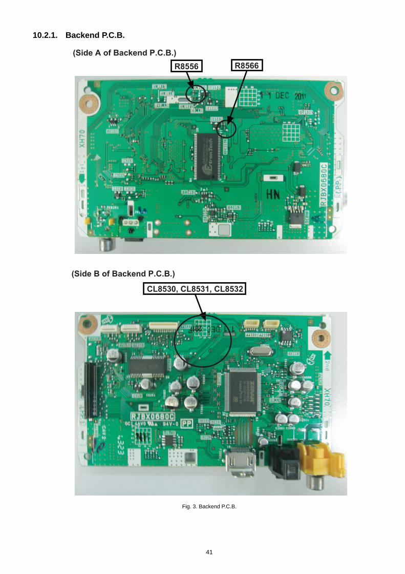
10.2.1. Backend P.C.B.
Fig. 3. Backend P.C.B.
CL8530, CL8531, CL8532
R8556 R8566
(Side A of Backend P.C.B.)
(Side B of Backend P.C.B.)
41

10.3. Basic Troubleshooting Guide for Traverse Unit (Backend P.C.B.)
Problems Checking Points Checking components
b) Check video signals (CVBS) LB8317, R8325 (IC8011 Pin 63)
a) Check SDRAM address, data
bus, CLK and other control signals
waveform
IC80511) Distorted picture or
abnormal sound is head
during the initialization
c) Check audio DAC circuitry
* Compare the above with OK
condition DVD Module P.C.B
LB8422 till LB8428
*Check for solder short and/or
component missing/damaged
b) Check laser drive circuitry
(Voltages & current)
Q8552, CL8532 (For DVD),
Q8562, CL8530 (For CD)
a) Check motor driver circuitry
(VCC PVCC)
IC8251 Pin 8, (+9V), 19 (+5V)2) No TOC/Long TOC
c) Check LSI IC connection to
motor drive circuitry
IC8001 Pin 90, 93, 94, 95
IC8251 Pin 11 to 18
* Check for solder short and/or
component missing/damaged
a) Check connection from Main to
Traverse unit
FP82513) Disc not spinning
4) Traverse not moving
5) Traverse and spindle
abnormal movementb) Check motor driver circuitry on
the voltages and control signals
IC8251
* Check for solder short and/or
component damaged
6) Cannot read the disc but
spindle motor is spinning
- Cannot read CD/DVD
a) Check laser drive circuitry
(voltages and current)
- Check CD Laser Drive
- Check DVD Laser Drive
* Check voltages and LD current
and compare with OK condition
Main P.C.B.
Q8552, LB8551
(For DVD Laser Drive current)
Q8562, LB8561
(For CD Laser Drive current)
7) Block Noise during play a) Check SDRAM address and
data bus signal
IC8051
8) Jitter out of specification a) Check LD current
b) Check OPU
(Change to other unit and
confirmed operating condition)
OPU Unit (Traverse unit), FPC
connection (FP8531 & FP8251)
42
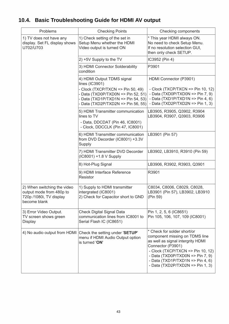
10.4. Basic Troubleshooting Guide for HDMI AV output
Problems Checking Points Checking components
1) Check setting of the set in
Setup Menu whether the HDMI
Video output is turned ON
* This year HDMI always ON.
No need to check Setup Menu.
If no resolution selection GUI,
then only check SETUP.
2) +5V Supply to the TV IC3952 (Pin 4)
3) HDMI Connector Solderability
condition
P3901
4) HDMI Output TDMS signal
lines (IC3901)
- Clock (TXCP/TXCN => Pin 50, 49)
- Data (TXD0P/TXD0N => Pin 52, 51)
- Data (TXD1P/TXD1N => Pin 54, 53)
- Data (TXD2P/TXD2N => Pin 56, 55)
HDMI Connector (P3901)
- Clock (TXCP/TXCN => Pin 10, 12)
- Data (TXD0P/TXD0N => Pin 7, 9)
- Data (TXD1P/TXD1N => Pin 4, 6)
- Data (TXD2P/TXD2N => Pin 1, 3)
- Data, DDCDAT (Pin 46, IC8001)
- Clock, DDCCLK (Pin 47, IC8001)
5) HDMI Transmitter communication
lines to TV
6) HDMI Transmitter communication
from DVD Decorder (IC8001) +3.3V
Supply
7) HDMI Transmitter DVD Decorder
(IC8001) +1.8 V Supply
8) Hot-Plug Signal
9) HDMI Interface Reference
Resistor
1) Supply to HDMI transmitter
intergrated (IC8001)
2) Check for Capacitor short to GND
Check Digital Signal Data
communication lines from IC8001 to
Serial Flash IC (IC8651)
Check the setting under 'SETUP'
menu if HDMI Audio Output option
is turned 'ON'
- Clock (TXCP/TXCN => Pin 10, 12)
- Data (TXD0P/TXD0N => Pin 7, 9)
- Data (TXD1P/TXD1N => Pin 4, 6)
- Data (TXD2P/TXD2N => Pin 1, 3)
* Check for solder short/or
component missing on TDMS line
as well as signal intergrity HDMI
Connector (P3901)
LB3905, R3905, Q3902, R3904
LB3904, R3907, Q3903, R3906
LB3901 (Pin 57)
LB3902, LB3910, R3910 (Pin 59)
LB3906, R3902, R3903, Q3901
C8034, C8006, C8029, C8028,
LB3901 (Pin 57), LB3902, LB3910
(Pin 59)
Pin 1, 2, 5, 6 (IC8651)
Pin 105, 106, 107, 109 (IC8001)
R3901
1) TV does not have any
display. Set FL display shows
U702/U703
2) When switching the video
output mode from 480p to
720p /1080i, TV display
become blank
3) Error Video Output.
TV screen shows green
Display
4) No audio output from HDMI
43

11 Service Fixture & ToolsPrepare service tools before process service position.
Ref. No Service Tools RemarksSFT1 Main P.C.B. (CN201) - Backend P.C.B. (FP8101) RFKZXH150PK2 (50P FFC)
44

12 Disassembly and Assembly InstructionsCaution Note:
• This section describes the disassembly and/or assembly procedures for all major printed circuit boards & main compo-nents for the unit. (You may refer to the section of “Main components and P.C.B Locations” as described in the servicemanual)
• Before carrying out the disassembly process, please ensure all the safety precautions & procedures are followed.• During the disassembly and/or assembly process, please handle with care as there may be chassis components with
sharp edges.• Avoid touching heatsinks due to its high temperature after prolong use. (See caution as described below)
• During disassembly and assembly, please ensure proper service tools, equipments or jigs is being used.• During replacement of component parts, please refer to the section of “Replacement Parts List” as described in the ser-
vice manual.• Select items from the following indexes when disassembly or replacement are required.• Disassembly of Top Cabinet• Replacement of Tray Ornament• Disassembly of Front Panel Block Assembly• Disassembly of Panel P.C.B.• Disassembly of Power Button P.C.B.• Disassembly of Rear Panel• Disassembly of SMPS P.C.B.• Replacement of Current Limiting Switch (Q5701)• Replacement of Diode (D5706)• Disassembly of Main P.C.B.• Replacement of Digital Amplifier IC (IC403/IC404/IC405)• Disassembly of Backend P.C.B.• Disassembly of Component Video P.C.B.• Disassembly of DVD Mechanism Unit (BRS1D)• Replacement of Traverse Unit.
12.1. Screw Type
45
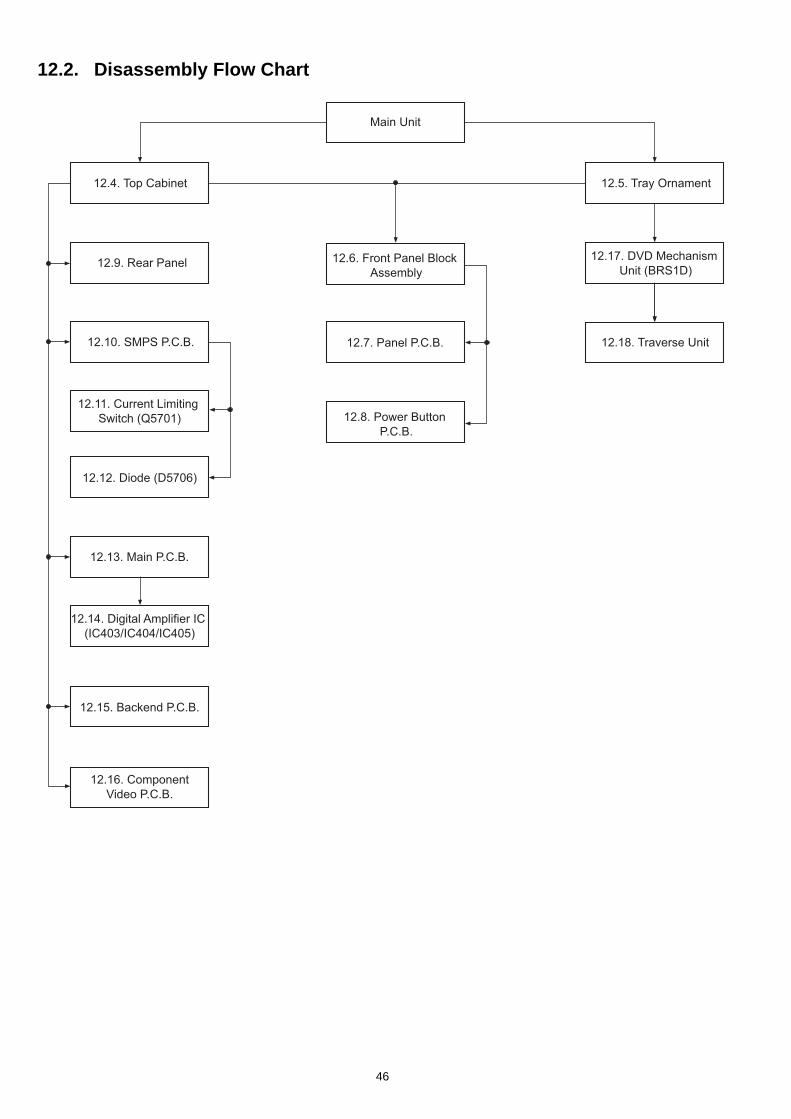
12.2. Disassembly Flow Chart
Main Unit
12.5. Tray Ornament
12.9. Rear Panel
12.13. Main P.C.B.
12.6. Front Panel Block
Assembly
12.4. Top Cabinet
12.7. Panel P.C.B.
12.8. Power Button
P.C.B.
12.17. DVD Mechanism
Unit (BRS1D)
12.18. Traverse Unit
12.14. Digital Amplifier IC
(IC403/IC404/IC405)
12.15. Backend P.C.B.
12.16. Component
Video P.C.B.
12.10. SMPS P.C.B.
12.11. Current Limiting
Switch (Q5701)
12.12. Diode (D5706)
46
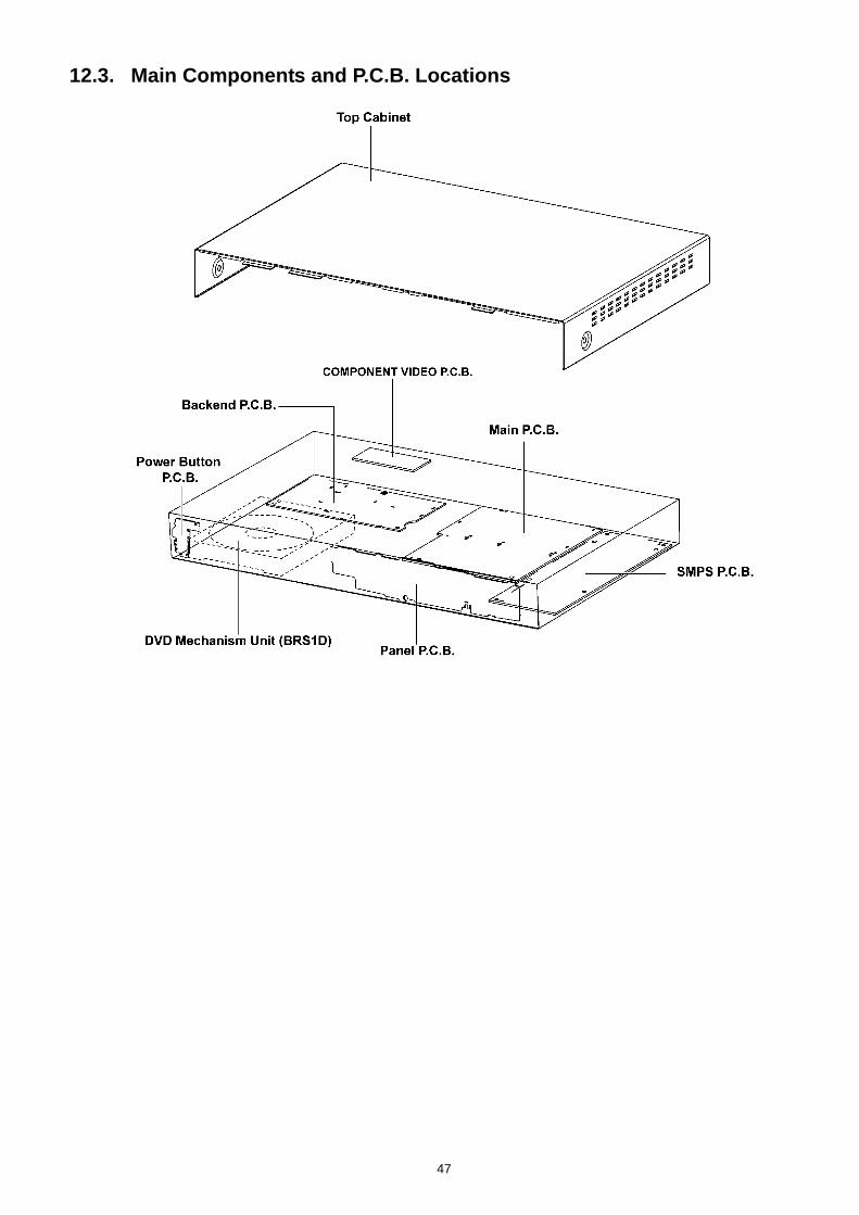
12.3. Main Components and P.C.B. Locations
47
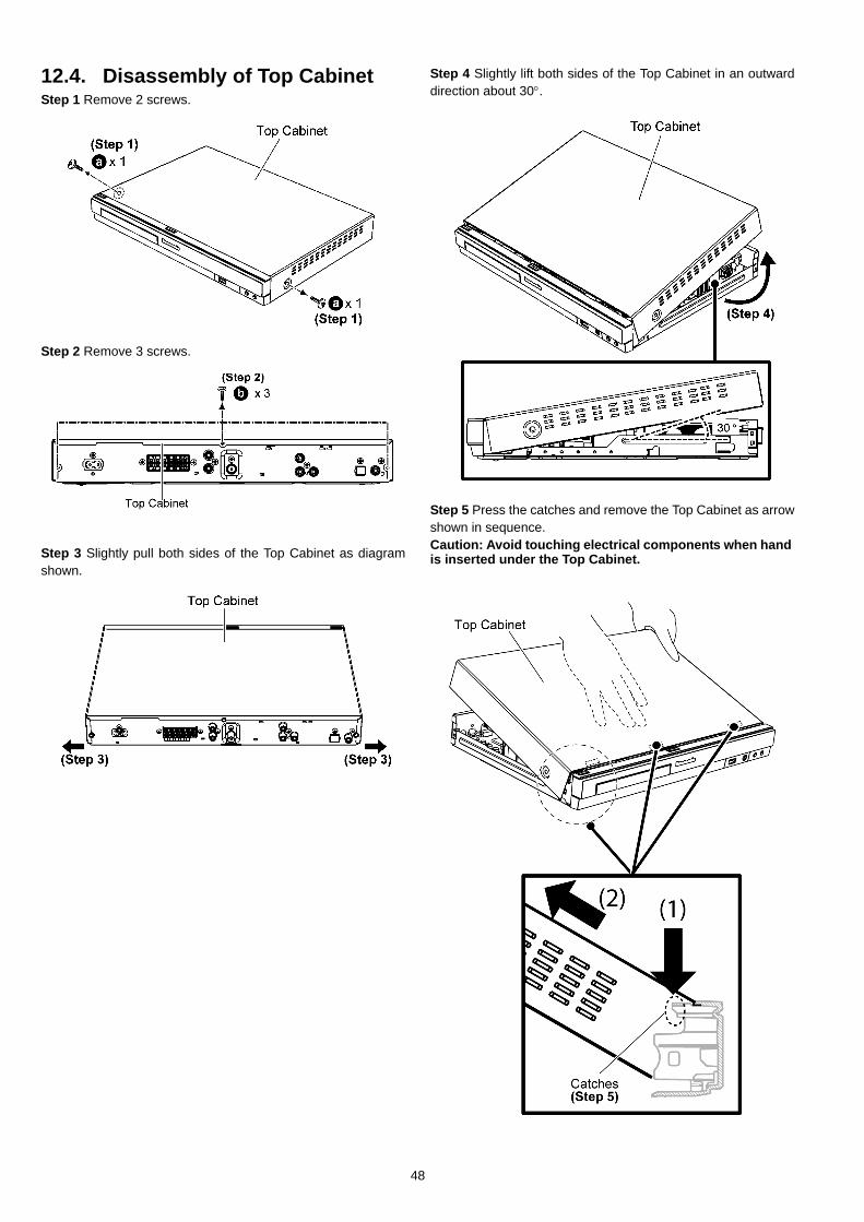
12.4. Disassembly of Top CabinetStep 1 Remove 2 screws.
Step 2 Remove 3 screws.
Step 3 Slightly pull both sides of the Top Cabinet as diagramshown.
Step 4 Slightly lift both sides of the Top Cabinet in an outwarddirection about 30°.
Step 5 Press the catches and remove the Top Cabinet as arrowshown in sequence.Caution: Avoid touching electrical components when hand is inserted under the Top Cabinet.
48
Caution: During assembling, ensure that the Top Cabinet is inserted into the Front Panel Block Assembly.
Caution: Replace the Top Cabinet Insulator sheet if broken. Ensure it is pasted properly on the Top Cabinet as diagram shown.
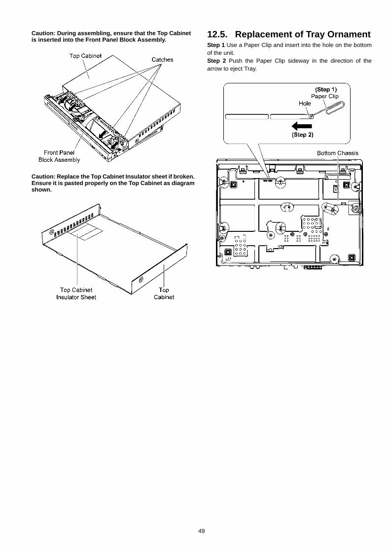
12.5. Replacement of Tray OrnamentStep 1 Use a Paper Clip and insert into the hole on the bottomof the unit.Step 2 Push the Paper Clip sideway in the direction of thearrow to eject Tray.
49

Step 3 Slide the Tray out as direction of arrow.
Step 4 Upset the Unit.Step 5 Release 2 catches. Caution: During assembling, ensure that the Tray Orna-ment is inserted and fully catched onto the Tray.
Step 6 Remove the Tray Ornament in the direction of arrow.
Caution: During assembling, ensure that the Tray Orna-ment’s guide rib is properly inserted onto the Tray.
50
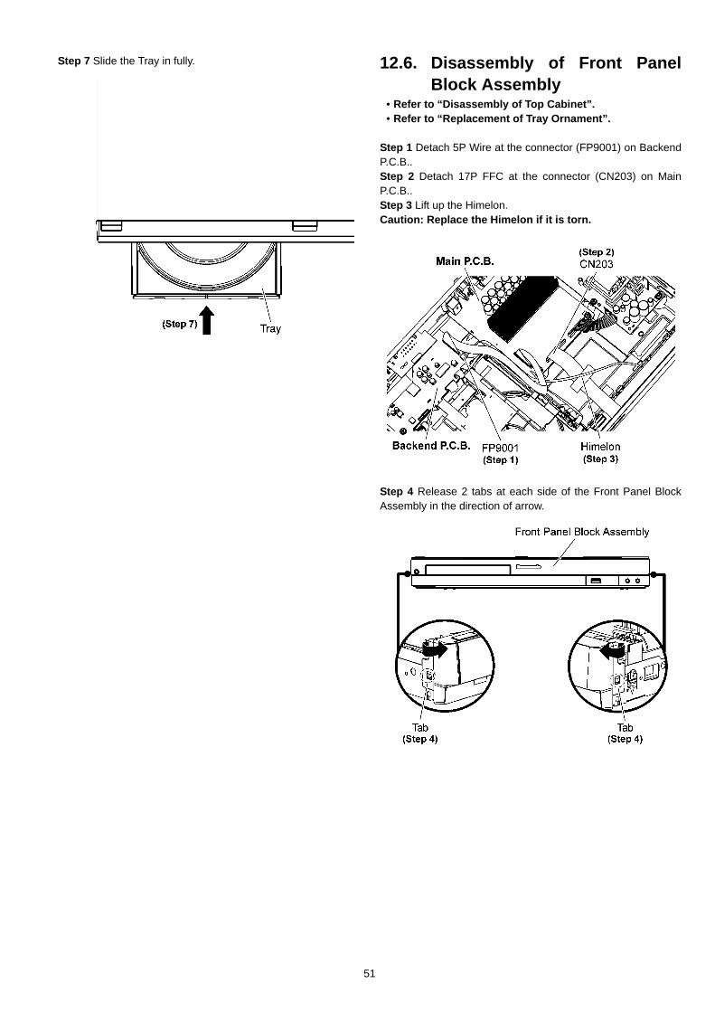
Step 7 Slide the Tray in fully. 12.6. Disassembly of Front PanelBlock Assembly
• Refer to “Disassembly of Top Cabinet”.• Refer to “Replacement of Tray Ornament”.
Step 1 Detach 5P Wire at the connector (FP9001) on BackendP.C.B..Step 2 Detach 17P FFC at the connector (CN203) on MainP.C.B..Step 3 Lift up the Himelon.Caution: Replace the Himelon if it is torn.
Step 4 Release 2 tabs at each side of the Front Panel BlockAssembly in the direction of arrow.
51

Step 5 Release 3 tabs at the Bottom Chassis.Caution: Do not exert strong force when releasing the tabs.
Caution: During assembling, ensure that the Front Panel Block Assembly is inserted properly and fully catched onto the Bottom Chassis.
Step 6 Remove the Front Panel Block Assembly.
12.7. Disassembly of Panel P.C.B.• Refer to “Disassembly of Top Cabinet”.• Refer to “Replacement of Tray Ornament”.• Refer to “Disassembly of Front Panel Block Assembly”.
Step 1 Remove 4 screws.Step 2 Remove 1 screw.
52
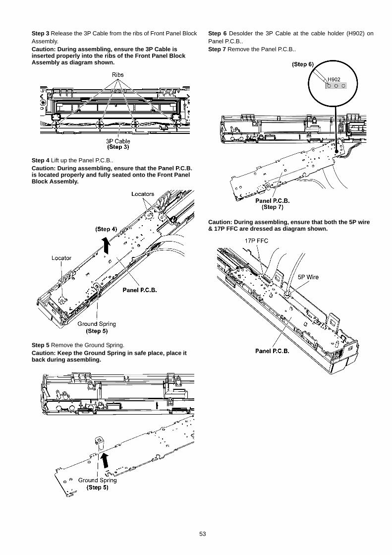
Step 3 Release the 3P Cable from the ribs of Front Panel BlockAssembly.Caution: During assembling, ensure the 3P Cable is inserted properly into the ribs of the Front Panel Block Assembly as diagram shown.
Step 4 Lift up the Panel P.C.B..Caution: During assembling, ensure that the Panel P.C.B. is located properly and fully seated onto the Front Panel Block Assembly.
Step 5 Remove the Ground Spring.Caution: Keep the Ground Spring in safe place, place it back during assembling.
Step 6 Desolder the 3P Cable at the cable holder (H902) onPanel P.C.B..Step 7 Remove the Panel P.C.B..
Caution: During assembling, ensure that both the 5P wire & 17P FFC are dressed as diagram shown.
53
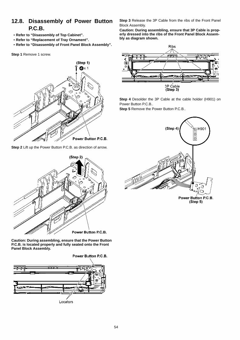
12.8. Disassembly of Power ButtonP.C.B.
• Refer to “Disassembly of Top Cabinet”.• Refer to “Replacement of Tray Ornament”.• Refer to “Disassembly of Front Panel Block Assembly”.
Step 1 Remove 1 screw.
Step 2 Lift up the Power Button P.C.B. as direction of arrow.
Caution: During assembling, ensure that the Power Button P.C.B. is located properly and fully seated onto the Front Panel Block Assembly.
Step 3 Release the 3P Cable from the ribs of the Front PanelBlock Assembly.Caution: During assembling, ensure that 3P Cable is prop-erly dressed into the ribs of the Front Panel Block Assem-bly as diagram shown.
Step 4 Desolder the 3P Cable at the cable holder (H901) onPower Button P.C.B..Step 5 Remove the Power Button P.C.B..
54
12.9. Disassembly of Rear Panel• Refer to “Disassembly of Top Cabinet”
Step 1 Remove 8 screws.
Step 2 Release tabs of each side of the Rear Panel in thedirection of arrow.
Step 3 Remove the Rear Panel.
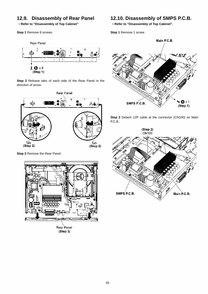
12.10. Disassembly of SMPS P.C.B.• Refer to “Disassembly of Top Cabinet”.
Step 1 Remove 1 screw.
Step 2 Detach 12P cable at the connector (CN100) on MainP.C.B..
55
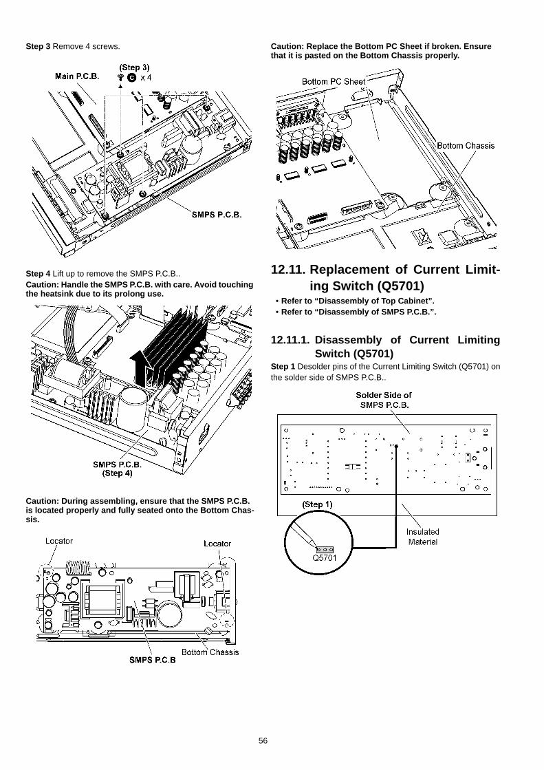
Step 3 Remove 4 screws.
Step 4 Lift up to remove the SMPS P.C.B..Caution: Handle the SMPS P.C.B. with care. Avoid touching the heatsink due to its prolong use.
Caution: During assembling, ensure that the SMPS P.C.B. is located properly and fully seated onto the Bottom Chas-sis.
Caution: Replace the Bottom PC Sheet if broken. Ensure that it is pasted on the Bottom Chassis properly.
12.11. Replacement of Current Limit-ing Switch (Q5701)
• Refer to “Disassembly of Top Cabinet”.• Refer to “Disassembly of SMPS P.C.B.”.
12.11.1. Disassembly of Current LimitingSwitch (Q5701)
Step 1 Desolder pins of the Current Limiting Switch (Q5701) onthe solder side of SMPS P.C.B..
56
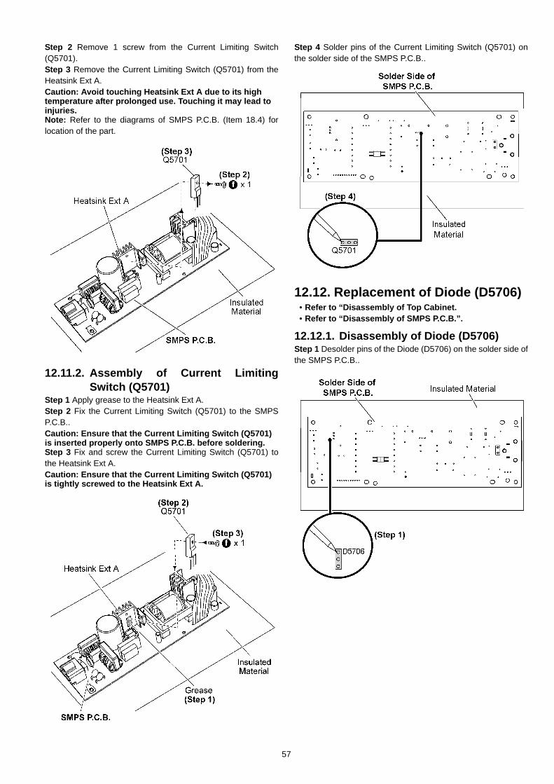
Step 2 Remove 1 screw from the Current Limiting Switch(Q5701).Step 3 Remove the Current Limiting Switch (Q5701) from theHeatsink Ext A.Caution: Avoid touching Heatsink Ext A due to its high temperature after prolonged use. Touching it may lead to injuries.Note: Refer to the diagrams of SMPS P.C.B. (Item 18.4) forlocation of the part.
12.11.2. Assembly of Current LimitingSwitch (Q5701)
Step 1 Apply grease to the Heatsink Ext A.Step 2 Fix the Current Limiting Switch (Q5701) to the SMPSP.C.B..Caution: Ensure that the Current Limiting Switch (Q5701) is inserted properly onto SMPS P.C.B. before soldering.Step 3 Fix and screw the Current Limiting Switch (Q5701) tothe Heatsink Ext A.Caution: Ensure that the Current Limiting Switch (Q5701) is tightly screwed to the Heatsink Ext A.
Step 4 Solder pins of the Current Limiting Switch (Q5701) onthe solder side of the SMPS P.C.B..
12.12. Replacement of Diode (D5706)• Refer to “Disassembly of Top Cabinet.• Refer to “Disassembly of SMPS P.C.B.”.
12.12.1. Disassembly of Diode (D5706)Step 1 Desolder pins of the Diode (D5706) on the solder side ofthe SMPS P.C.B..
57
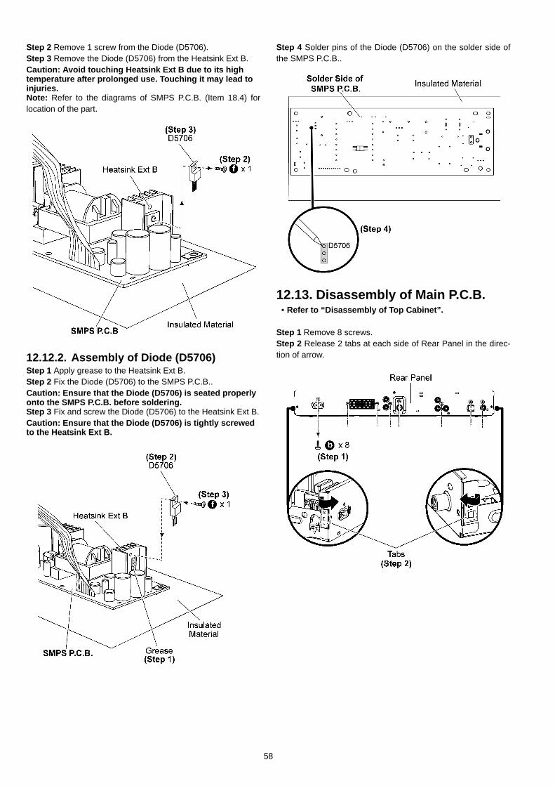
Step 2 Remove 1 screw from the Diode (D5706).Step 3 Remove the Diode (D5706) from the Heatsink Ext B.Caution: Avoid touching Heatsink Ext B due to its high temperature after prolonged use. Touching it may lead to injuries.Note: Refer to the diagrams of SMPS P.C.B. (Item 18.4) forlocation of the part.
12.12.2. Assembly of Diode (D5706)Step 1 Apply grease to the Heatsink Ext B.Step 2 Fix the Diode (D5706) to the SMPS P.C.B..Caution: Ensure that the Diode (D5706) is seated properly onto the SMPS P.C.B. before soldering.Step 3 Fix and screw the Diode (D5706) to the Heatsink Ext B.Caution: Ensure that the Diode (D5706) is tightly screwed to the Heatsink Ext B.
Step 4 Solder pins of the Diode (D5706) on the solder side ofthe SMPS P.C.B..
12.13. Disassembly of Main P.C.B.• Refer to “Disassembly of Top Cabinet”.
Step 1 Remove 8 screws.Step 2 Release 2 tabs at each side of Rear Panel in the direc-tion of arrow.
58
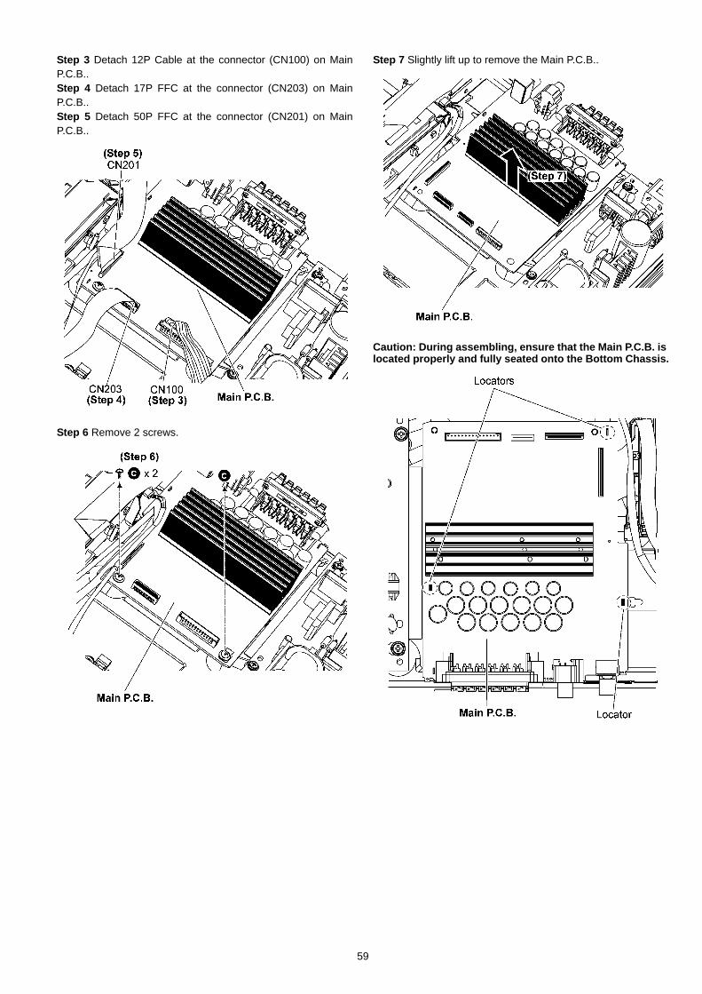
Step 3 Detach 12P Cable at the connector (CN100) on MainP.C.B..Step 4 Detach 17P FFC at the connector (CN203) on MainP.C.B..Step 5 Detach 50P FFC at the connector (CN201) on MainP.C.B..
Step 6 Remove 2 screws.
Step 7 Slightly lift up to remove the Main P.C.B..
Caution: During assembling, ensure that the Main P.C.B. is located properly and fully seated onto the Bottom Chassis.
59
12.14. Replacement of Digital Ampli-fier IC (IC403/IC404/IC405)
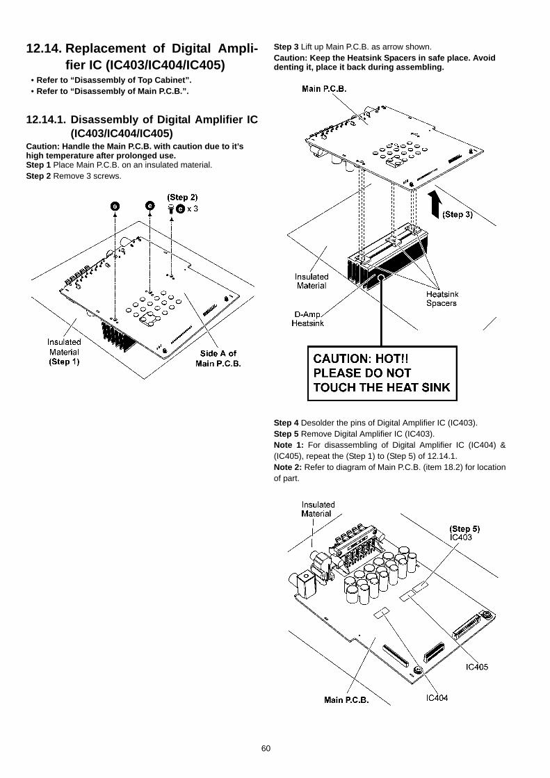
• Refer to “Disassembly of Top Cabinet”.• Refer to “Disassembly of Main P.C.B.”.
12.14.1. Disassembly of Digital Amplifier IC(IC403/IC404/IC405)
Caution: Handle the Main P.C.B. with caution due to it’s high temperature after prolonged use. Step 1 Place Main P.C.B. on an insulated material.Step 2 Remove 3 screws.
Step 3 Lift up Main P.C.B. as arrow shown.Caution: Keep the Heatsink Spacers in safe place. Avoid denting it, place it back during assembling.
Step 4 Desolder the pins of Digital Amplifier IC (IC403).Step 5 Remove Digital Amplifier IC (IC403).Note 1: For disassembling of Digital Amplifier IC (IC404) &(IC405), repeat the (Step 1) to (Step 5) of 12.14.1.Note 2: Refer to diagram of Main P.C.B. (item 18.2) for locationof part.
60

12.14.2. Assembly of Digital Amplifier IC(IC403/IC404/IC405)
Step 1 Fix the Digital Amplifier IC (IC403) onto the Main P.C.B..Step 2 Solder pins of Digital Amplifier IC (IC403).Caution: Ensure that the pins of Digital Amplifier IC (IC403) is positioned correctly on Main P.C.B. before soldering.Step 3 Apply grease on the top side of the Digital Amplifier IC(IC403).
Step 4 Fix Heatsink spacers onto D-Amp Heatsink.
Step 5 Upset the Main P.C.B..Step 6 Fix 3 screws.Note: For assembling of Digital Amplifier IC (IC404) & (IC405),repeat the (Step 1) to (Step 6) of 12.14.2.
61

12.15. Disassembly of Backend P.C.B.• Refer to “Disassembly of Top Cabinet”.• Refer to “Disassembly of Component Video P.C.B.”.
Step 1 Remove 8 screws.Step 2 Release 2 tabs at each side of the Rear Panel in thedirection of arrow.
Step 3 Detach 24P FFC at the connector (FP8531) on BackendP.C.B..Step 4 Detach 6P FFC at the connector (FP8251) on Backend P.C.B..Step 5 Detach 5P FFC at the connector (FP8252) on Backend P.C.B..Step 6 Detach 5P Cable at the connector (FP9001) on Back-end P.C.B..Step 7 Detach 50P FFC at the connector (FP8101) on Backend P.C.B..Step 8 Detach 11P FFC at the connector (FP8301) on BackendP.C.B..
Step 9 Remove 2 screws.
Step 10 Lift up the Backend P.C.B..
Caution: During assembling, ensure that the Backend P.C.B. is properly located & fully seated onto the Bottom Chassis.
62

12.16. Disassembly of ComponentVideo P.C.B.
• Refer to “Disassembly of Top Cabinet”.
Step 1 Remove 1 screw.
Step 2 Lift up the Component Video P.C.B..
Step 3 Detach 11P FFC at the connector (CN400) on Compo-nent Video P.C.B..
Caution: During assembling, ensure that the Component Video P.C.B. is inserted properly and fully catched onto the rear panel.
63
12.17. Disassembly of DVD Mecha-nism Unit (BRS1D)
• Refer to “Disassembly of Top Cabinet”• Refer to “Replacement of Tray Ornament”
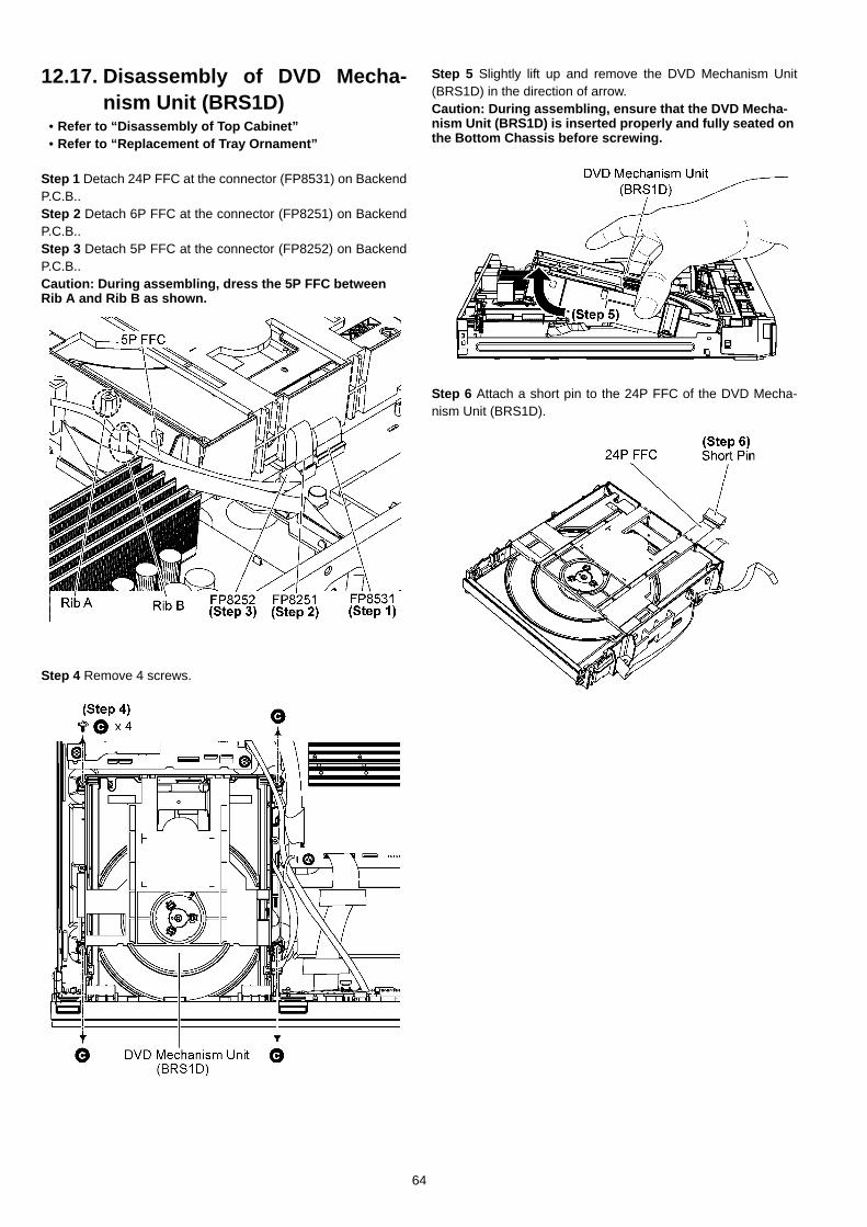
Step 1 Detach 24P FFC at the connector (FP8531) on BackendP.C.B..Step 2 Detach 6P FFC at the connector (FP8251) on BackendP.C.B..Step 3 Detach 5P FFC at the connector (FP8252) on BackendP.C.B..Caution: During assembling, dress the 5P FFC between Rib A and Rib B as shown.
Step 4 Remove 4 screws.
Step 5 Slightly lift up and remove the DVD Mechanism Unit(BRS1D) in the direction of arrow.Caution: During assembling, ensure that the DVD Mecha-nism Unit (BRS1D) is inserted properly and fully seated on the Bottom Chassis before screwing.
Step 6 Attach a short pin to the 24P FFC of the DVD Mecha-nism Unit (BRS1D).
64
12.18. Replacement of Traverse unit• Refer to “Disassembly of DVD Mechanism Unit
(BRS1D)”.Caution: Refer to 2.4 “Handling Precaution for Traverse Unit” to prevent static damage to the Optical Pickup unit.Note:
1. When the optical pickup unit is defective, the overalltraverse unit needs replacement.
2. Please note that appropriate actions need to be taken toprevent static damage.
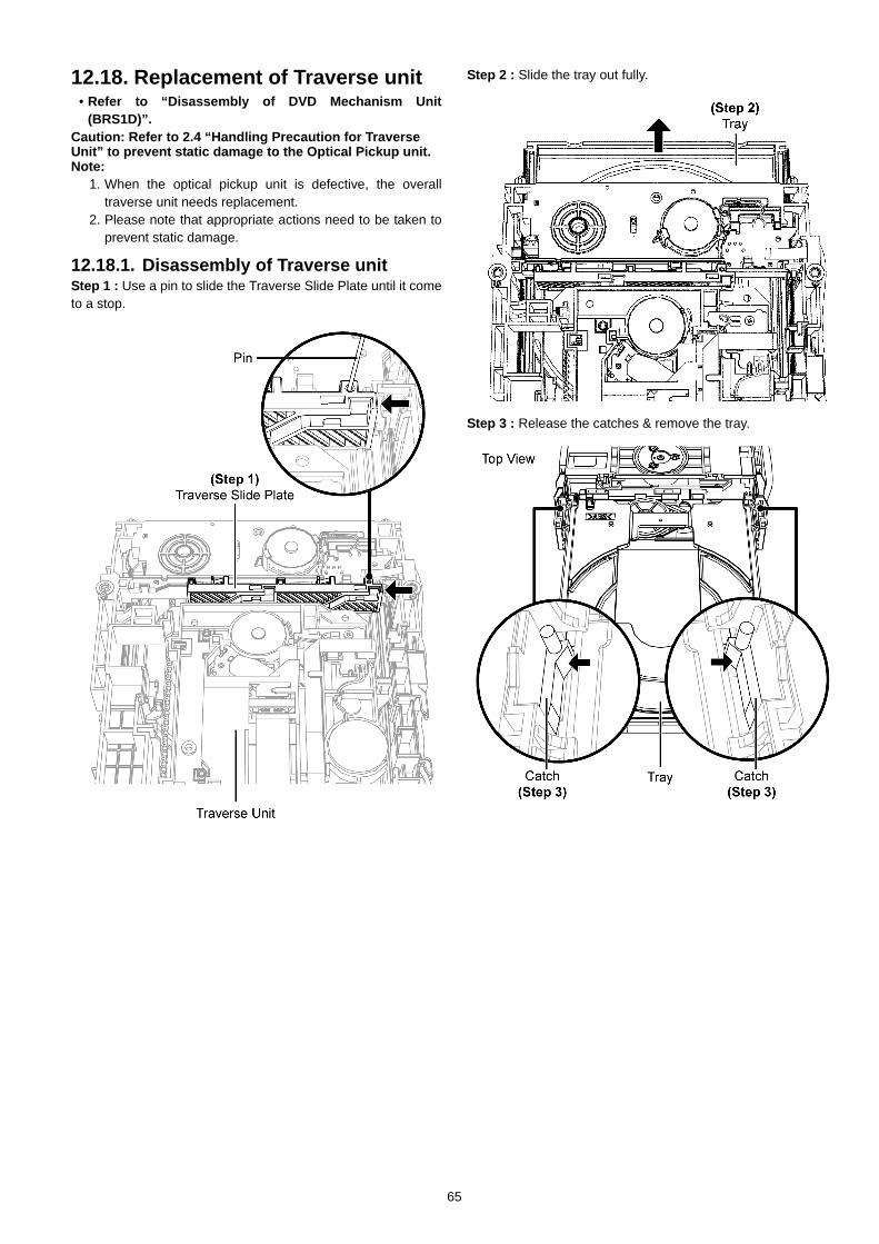
12.18.1. Disassembly of Traverse unitStep 1 : Use a pin to slide the Traverse Slide Plate until it cometo a stop.
Step 2 : Slide the tray out fully.
Step 3 : Release the catches & remove the tray.
65
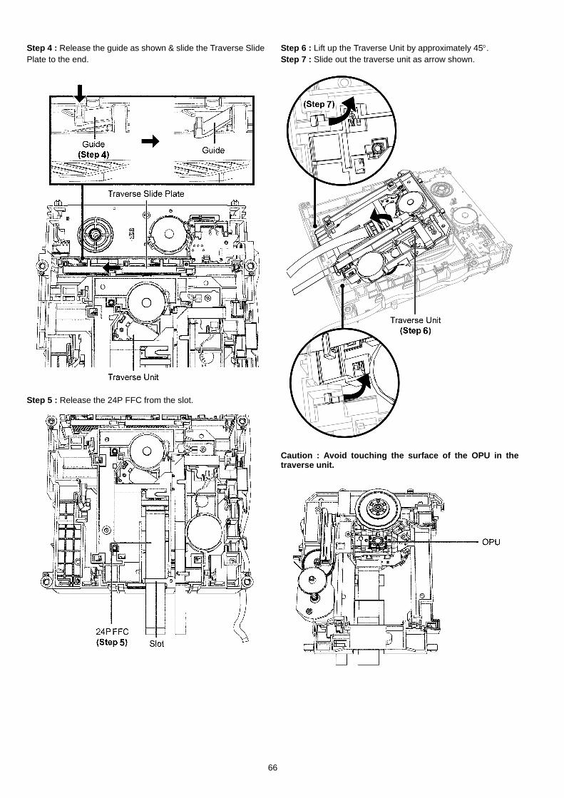
Step 4 : Release the guide as shown & slide the Traverse SlidePlate to the end.
Step 5 : Release the 24P FFC from the slot.
Step 6 : Lift up the Traverse Unit by approximately 45°.Step 7 : Slide out the traverse unit as arrow shown.
Caution : Avoid touching the surface of the OPU in thetraverse unit.
66
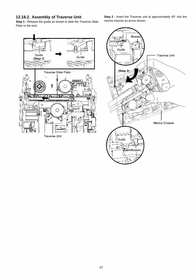
12.18.2. Assembly of Traverse UnitStep 1 : Release the guide as shown & slide the Traverse SlidePlate to the end.
Step 2 : Insert the Traverse unit at approximately 45° into themecha chassis as arrow shown.
67
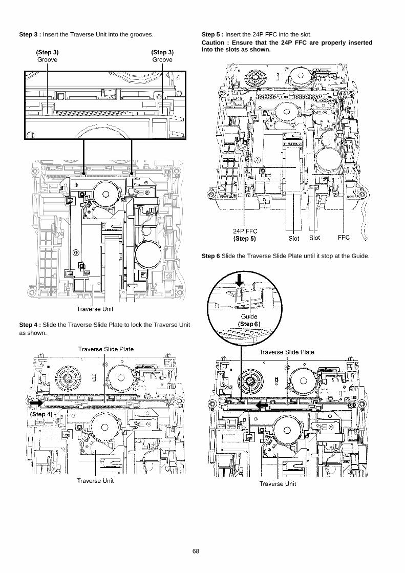
Step 3 : Insert the Traverse Unit into the grooves.
Step 4 : Slide the Traverse Slide Plate to lock the Traverse Unitas shown.
Step 5 : Insert the 24P FFC into the slot.Caution : Ensure that the 24P FFC are properly insertedinto the slots as shown.
Step 6 Slide the Traverse Slide Plate until it stop at the Guide.
68
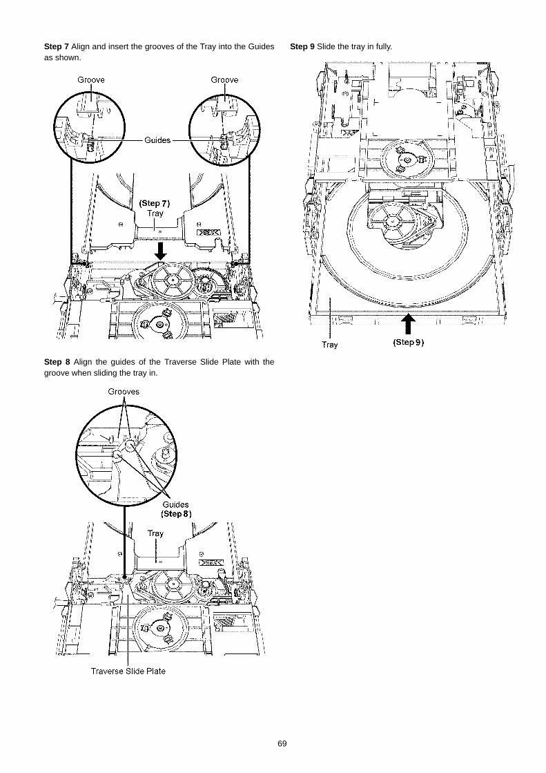
Step 7 Align and insert the grooves of the Tray into the Guidesas shown.
Step 8 Align the guides of the Traverse Slide Plate with thegroove when sliding the tray in.
Step 9 Slide the tray in fully.
69
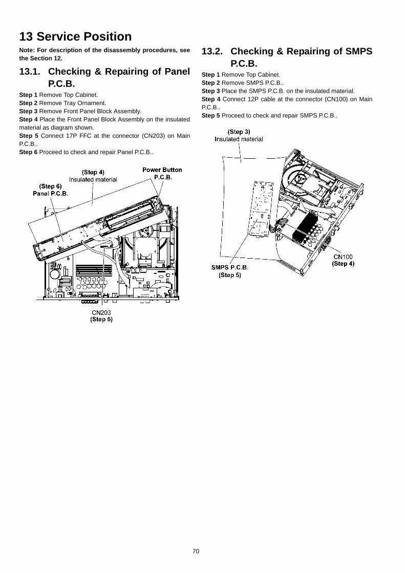
13 Service PositionNote: For description of the disassembly procedures, seethe Section 12.
13.1. Checking & Repairing of PanelP.C.B.
Step 1 Remove Top Cabinet.Step 2 Remove Tray Ornament.Step 3 Remove Front Panel Block Assembly.Step 4 Place the Front Panel Block Assembly on the insulatedmaterial as diagram shown.Step 5 Connect 17P FFC at the connector (CN203) on MainP.C.B..Step 6 Proceed to check and repair Panel P.C.B..
13.2. Checking & Repairing of SMPSP.C.B.
Step 1 Remove Top Cabinet.Step 2 Remove SMPS P.C.B..Step 3 Place the SMPS P.C.B. on the insulated material.Step 4 Connect 12P cable at the connector (CN100) on MainP.C.B..Step 5 Proceed to check and repair SMPS P.C.B..
70

13.3. Checking & Repairing MainP.C.B.
13.3.1. Checking & Repairing Main P.C.B.(Side A)
Step 1 Remove Top Cabinet.Step 2 Remove Main P.C.B..Step 3 Connect 12P Cable at the connector (CN100) on Main P.C.B..Step 4 Connect 17P FFC at the connector (CN203) on MainP.C.B..Step 5 Connect 50P Extension FFC (RFKZXH150PK2) from(CN201) to (FP8101).
Step 6 Upset the Main P.C.B. and place it onto the insulatedmaterial.Step 7 Proceed to check and repair side A of Main P.C.B..
13.3.2. Checking & Repairing Main P.C.B.(Side B)
Step 1 Remove Top Cabinet.Step 2 Remove Main P.C.B..Step 3 Remove 3 screws.
71

Step 4 Lift up the Main P.C.B. as arrow shown. Step 5 Place the Main P.C.B. back to original position.Step 6 Connect 12P Cable at the connector (CN100) on MainP.C.B..Step 7 Connect 17P FFC at the connector (CN203) on Main P.C.B..Step 8 Connect 50P FFC at the connector (CN201) on Main P.C.B..Step 9 Proceed to check & repair Side B of Main P.C.B..
72
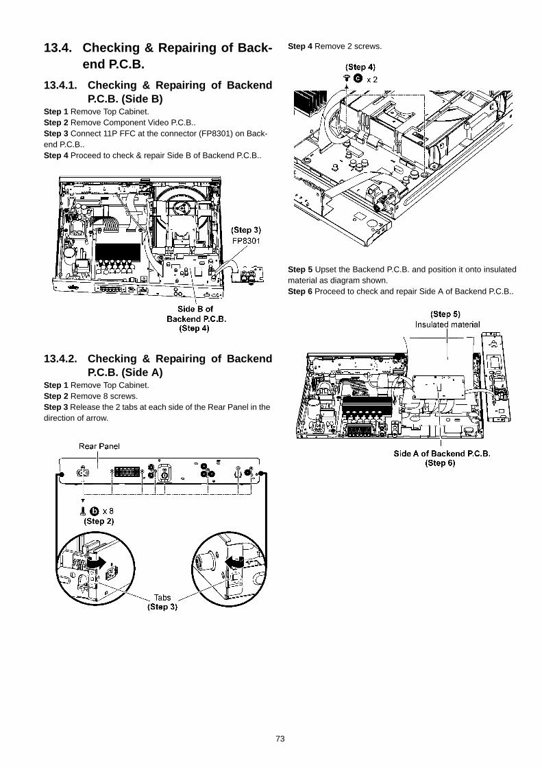
13.4. Checking & Repairing of Back-end P.C.B.
13.4.1. Checking & Repairing of BackendP.C.B. (Side B)
Step 1 Remove Top Cabinet.Step 2 Remove Component Video P.C.B..Step 3 Connect 11P FFC at the connector (FP8301) on Back-end P.C.B..Step 4 Proceed to check & repair Side B of Backend P.C.B..
13.4.2. Checking & Repairing of BackendP.C.B. (Side A)
Step 1 Remove Top Cabinet.Step 2 Remove 8 screws.Step 3 Release the 2 tabs at each side of the Rear Panel in the direction of arrow.
Step 4 Remove 2 screws.
Step 5 Upset the Backend P.C.B. and position it onto insulatedmaterial as diagram shown.Step 6 Proceed to check and repair Side A of Backend P.C.B..
73

74

75
14 Overall Simplified Block Diagram
Main
Transformer
SELECTOR
MICROPROCESSOR
SMPS BLOCK
AC INY
iver
MAIN BLOCK
PCONT,ECO CTL
DC-DET
DAP
SE
SE
BTL
BTL
FRONT L
FRONT R
SURR L
SURR R
CENTER
SUBWOOFER
TUNER AUX
I2C
LDOVref 3.3V
ADC
I2C
Zoran 976
HDMI
IC
ADC
Video
Buffer
I2S
MCLK,BCLK,SRCK
HDMI D-IN
MUX
+9V
UART
FLASH
SDRAM
I2C
I2C
+5.3V
+5.3V
FL Supply
Transformer
F+, F-
-VP
DC-DC
Converter
+12V +23V
PGND
+23V
PG
ND
DIGITAL AMP (TI Solution)
DC-DC
ConverterVOLT
REG
+23V
+5.3V
MOSFET
SY
S6V
PC
ON
T
Motor
Driver
PANEL BLOCK
FL DISPLAUSB
FL Dr
Power Button
Open/Close ButtonLED
DVD Mechanism (BRS1D)
IR
Sensor
US
B D
+,D
-
+9V
76
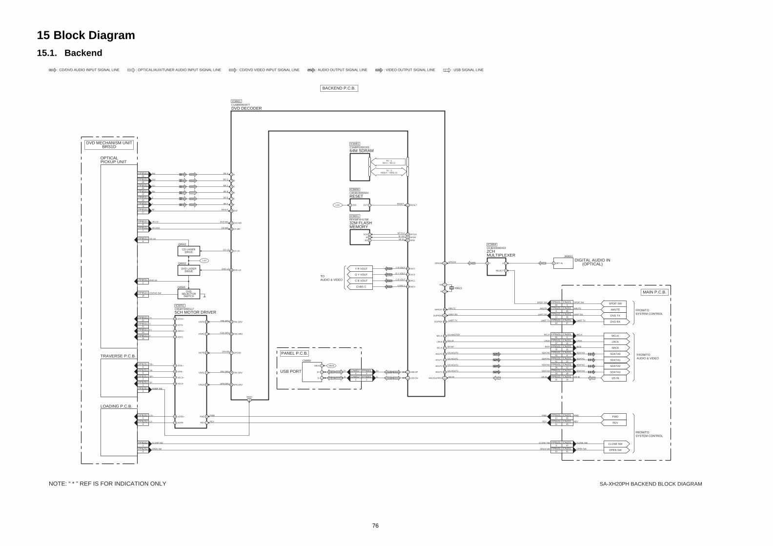
15 Block Diagram15.1. Backend
SA-XH20PH BACKEND BLOCK DIAGRAM
DVD DECODERC1AB00003477
IC8001
64M SDRAMC3ABPG000163
IC8051
MA 0 ~ MA 11TC - 1
MDQ 0 ~ MDQ 15TC - 2
6SCK
32M FLASHMEMORY
RFKWFXH170E
IC8651
RESETC0EBE0000504
IC8606
3.3V
I2S AOUT0
AIN2/DUPRD1 102I2S IN
AOUT0 42
I2S AOUT1AOUT1 41
I2S AOUT2AOUT2 40
AOUT3 36
MCLK 43
BCLK 37
LRCK 38
I2S AOUT3
I2S BIT
I2S LR
I2S MASTER
RFP68
CD LD87
F79
E77
B72
C74
D75
A71
OPTICALPICKUP UNIT
10
FP8531
FWD
REV
E RF E
16
FP8531 A/a RF A
15
FP8531 B/b RF B
20
FP8531 C/c RF C
19
FP8531 D/d RF D
17
FP8531 RF RFIN P
CD MD857
FP8531 VR-DVD CD MD
DVD MD868
FP8531 VR-CD DVD MD
CD LD
SF CLK
5SISF DO
2SOSF DI
14
FP8531 F RF F
6
FP8531 CD-LD
OPEN SW OPEN SW
10 41
FP8101 CN201OPEN SW
BICK
35 16
FP8101 CN201
37 14
FP8101 CN201
SRCK
LRCKLRCK
MCLK
45 6
FP8101 CN201MCLK
SDATA3
33 18
FP8101 CN201SDATA3
SDATA2
39 12
FP8101 CN201SDATA2
SDATA1
41 10
FP8101 CN201SDATA1
SDATA0
43 8
FP8101 CN201
14 37
FP8101 CN201
SDATA0
CLOSE SW
9 42
FP8101 CN201CLOSE SWCLOSE SW
CD LASER
VDD5
MAIN P.C.B.
BACKEND P.C.B.
DVD MECHANISM UNITBRS1D
FROM/TO
AUDIO & VIDEO
FROM/TO
SYSTEM CONTROL
FROM/TO
SYSTEM CONTROL
I2S IN
BICK
LRCK
MCLK
SDATA3
SDATA2
SDATA1
SDATA0
I2S IN
32 19
FP8101 CN201I2S IN
DUPRDO 100UART RX UART RX
13 38
FP8101 CN201DVD TX
98GPIO37AMUTE AMUTE
6 45
FP8101 CN201AMUTE
SPDIF SW
99DUPRDIUART TX UART TX
UART RX
AMUTE
UART TXDVD RX
FWD
12 39
FP8101 CN201FWD
REV
11 40
FP8101 CN201REV
109 SFCLK
106 SFDO
107 SFDI
117 USB DP
118 USB DN
4OUTRESET
110 RESET
Q8562
D+
D-
3
FP9001
2
FP9001
X8621
XO 111
XI 112
: CD/DVD VIDEO INPUT SIGNAL LINE : VIDEO OUTPUT SIGNAL LINE: CD/DVD AUDIO INPUT SIGNAL LINE : AUDIO OUTPUT SIGNAL LINE : USB SIGNAL LINE: OPTICAL/AUX/TUNER AUDIO INPUT SIGNAL LINE
DAC3S CCVBS C
DAC1
DAC2
DAC4
C B VOUT
Y R VOUT
G Y VOUT
OUT
OUT
OUT
63
66
65
61
SPDIF SW
48 3
FP8101 CN201
2CHMULTIPLEXER
C0JBAR000433
IC3954
JK8001
3 OPT-IN
SPDIF SW
DIGITAL AUDIO IN(OPTICAL)1Y
6SELECT
5GPIO34 104GPIO34
A
5CH MOTOR DRIVERC0GBY0000117
IC8251
3.3V
11 VOSL+
DVD LD88
TRAVERSE P.C.B.
LOADING P.C.B.
6
FP8251 TR+
12 VOSL-5
FP8251 TR-
FWD
REV
17 VOLD+2
FP8251 SP+
18 VOLD-1
FP8251 SP-
15 VOTK+22
FP8531 T+
DVD LD
3
FP8251 INNER SW
3
FP8252 OPEN SW
1
FP8252 CLOSE SW
VINSL 4 TRV DRV95TRV DRV
VINLD 23
FWD 6
REV 7
SPN DRV94SPN DRV
VINTK 26 TRK DRV93TRK DRV
VINFC 1 FOC DRV90FOC DRV
16 VOTK-21
FP8531 T-
14 VOFC+23
FP8531 F+
13 VOFC-24
FP8531 F-
DRIVE
2
FP8531 DVD-LD
18
FP8531 CD/DVD SW
DVD LASERDRIVE
10 VOTR+5
FP8252 LD+
9 VOTR-4
FP8252 LD-
106
SFDO
Q8565
DVDSELECTOR
SWITCH
Q8552
NOTE: “ * ” REF IS FOR INDICATION ONLY
CN950
USB PORT
VBUS
D+
D-
D+
D-
VBUS1
3
2
PANEL P.C.B.
3
CN951*
2
CN951*
MUTE 28 GPIO3997DRVSB
CVB
TO
AUDIO & VIDEO C B V
Y R V
G Y V
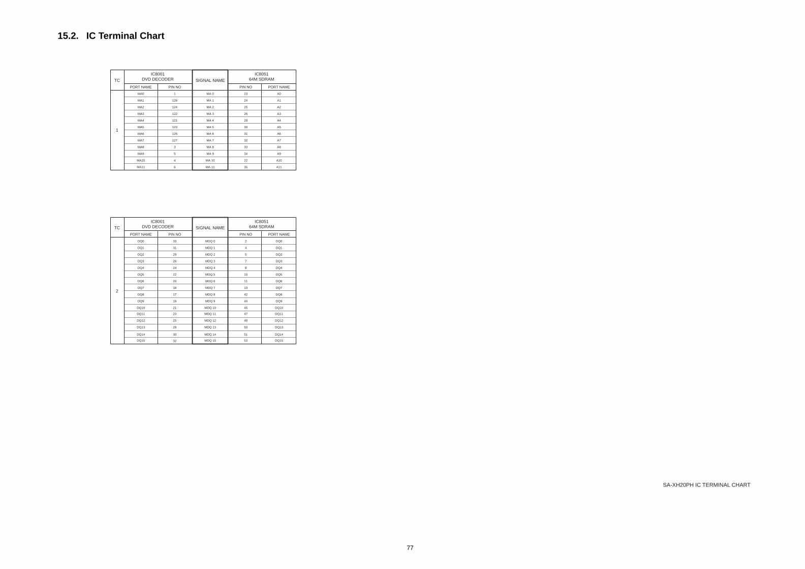
77
15.2. IC Terminal Chart
SA-XH20PH IC TERMINAL CHART
SIGNAL NAMETC
PIN NOPORT NAME PIN NO PORT NAME
33 MDQ 0 2
31 MDQ 1 4
29 MDQ 2 5
26 MDQ 3 7
DQ0
DQ1
DQ2
DQ3
DQ0
DQ1
DQ2
DQ3
IC8051
64M SDRAM
IC8001
DVD DECODER
SIGNAL NAMETC
1
PIN NOPORT NAME PIN NO PORT NAME
125
MA 0 23
123
MA 1 24126
MA 2 25
127
MA 3 26122
MA 4 29
124
MA 5 30
121
MA 6 31
1
MA 7 32
3 MA 8 33
5 MA 9 34
MA 10 224
A0
A1
A2
A3
A4
A5
A6
A7
A8
A9
A10
6 MA 11
MA0
MA1
MA2
MA3
MA4
MA5
MA6
MA7
MA8
MA9
MA10
MA11 35 A11
IC8051
64M SDRAM
IC8001
DVD DECODER
2
24 MDQ 4 8
22 MDQ 5 10
20 MDQ 6 11
18 MDQ 7 13
17 MDQ 8 42
19 MDQ 9 44
21 MDQ 10 45
23 MDQ 11 47
25 MDQ 12 48
28 MDQ 13 50
30 MDQ 14 51
32 MDQ 15
DQ4
DQ5
DQ6
DQ7
DQ8
DQ9
DQ10
DQ11
DQ12
DQ13
DQ14
DQ15
DQ4
DQ5
DQ6
DQ7
DQ8
DQ9
DQ10
DQ11
DQ12
DQ13
DQ14
DQ1553

78
15.3. System Control
SA-XH20PH SYSTEM CONTROL BLOCK DIAGRAM
5 SDA
6 SCL
MICROPROCESSORRFKWMXH70EB
IC200
EEPROMC3EBFY000030
IC201
91 SEL A
92 SEL B
ECK 34
X201
XIN 13
XOUT 11
EDA 33
DAP CLK76DAP CLK
DAP DAT75DAP SDA
TUN SCLK22TUN SCLK
TUN SCLK
TUN SDIO20TUN SDIO
TUN SDIO
SELECTOR LSB
SELECTOR MSB
DCDET256DC DET2
DC DET2
AUX DET88AUX DET
AUX DET
DAP RST79DAP RST
DAP MUTE32DAP MUTE
DAP RST
DAP MUTE
FWD36FWD
REV37REV
FWD
AMUTE38AMUTE
AMUTE
DVD TX28DVD TX
DVD TX
REV
SELECTOR LSB
DAP CLK
TUN RST21TUN REST
TUN REST
DAP SDA
TUN INT TUN INT16TUN INT
SELECTOR MSB
64 NRSTRSTBRSTB
FROM/TO
AUDIO & VIDEO
FROM/TO
BACKEND
MAIN P.C.B.
82SD
VALID
SDSD
81 VALIDVALID
80 DAP PDNDAP PDNDAP PDN
SPDIF SW99SPDIF SW
SPDIF SW
FL DISPLAYDRIVER
C0HBB0000057
IC901
POWER BUTTON P.C.B.
PANEL P.C.B.
99
CN901CN203FLD OUT 24 7 DIN
FL IC DAT
810
CN901CN203FLD CLK 25
FL IC CLK
711
CN901CN203FLD STB 26
FL IC STB
108
CN901CN203 RMT
89KEY2
8 CLK
9 STB
FL901
FL DISPLAY
31
32
F+
F+
FL+
1
2
F-
F-
FL-
3.3V
REMOTE CONTROL SENSOR
Z901
3
VOLUME+S906
VOLUME-S905
P1 ~ P16G1 ~ G9
14 4
CN203 CN901
90KEY1
FL IC DAT
FL IC CLK
FL IC STB
RMT
KEY2
KEY1
13 5
CN203 CN901 KEY1 KEY1
2 2
H902 H901
OPEN/CLOSES901
POWERS902
SYNC17SYNC
SYNC
DCDET155DC DET1
DC DET1
OPEN SWOPEN SW
CLOSE SW1CLOSE SW
CLOSE SW
DVD RX27DVD RX
DVD RX
PCONT48PCONT
PCONT
FROM/TO
POWER SUPPLY
OPEN SW100
52
51
USB OC USB OCUSB OC
VBUS ENVBUS ENVBUS EN
KEY2
RMT
KEY1

79
15.4. Audio and Video
SA-XH20PH AUDIO & VIDEO BLOCK DIAGRAM
TUN SDIO
FM ANT
JK600
FM RADIORECEIVER
VUEALLPT040
IC600
LOUT 14
ROUT 13
LCH 3SDTO 9
PDN 13
LRCK 10
MCLK 11
SCLK 12
RCH 132 FMI
17 DCLK
9 RCLK
DC DET2
I2S IN
DAP SDA
SDATA1
SDATA2
SRCK
LRCK
MCLK
SADAT3
SDATA0AUX/TV
JK300
2
1
3
X400
PWM SL+
TUN SCLK
DAP RST
DAP CLK
DAP DA
DAP CLK
DC DET2DC DET2
SDATA1
SDATA2
SDATA3
SDATA0
DAP MUTE
SPEAKERS
Q114,Q116,Q500,Q501
DC DETECTCIRCUIT
AUX LL
R AUX R
AUX L
AUX R
SCLK 7
SDIO 8
I2S IN
RSTB
PWM P 8 52
PWM SL-PWM M 8 51
PWM SR+PWM P 7 50
PWM SR-PWM M 7 49
PWM FL+PWM P 4 47
PWM FL-PWM M 4 46
PWM FR+PWM P 3 45
PWM FR-PWM M 3 44
PWM CENT+PWM P 2 43
PWM CENT-PWM M 2 42
PWM SUBW+PWM P 1 41
PWM SUBW-PWM M 1 40
VALIDVALID 39
DIGITAL AUDIOPWM PROCESSOR
C1AB00003610
IC401
SDIN131
XTL IN20
XTL OUT19
SDIN230
SDIN428
SDIN329
MCLK63
LRCLK26
SCLK27
SDA24
SCL25
/RESET11
/MUTE14DAP MUTE
DAP PDN /PDN13DAP PDN
DAP RST
DC DET2
SD
VALID
SD
VALID
+
-
5 SD
7 RST AB
17 RST CD
5 SD
7 RST AB
17 RST CD
5 SD
7 RST AB
17 RST CD
16 PWM C
18 PWM D
DIGITAL AMPLIFIERC1AB00003217
IC404
6 PWM A
8 PWM B SURROUND(LEFT)
OUT B
BST B
OUT A
BST A
11
JK401
12
JK401
36
34
39
43
+
-
SURROUND(RIGHT)OUT C
BST C
OUT D
BST D
9
JK401
10
JK40131
33
28
24
16 PWM C
18 PWM D
DIGITAL AMPLIFIERC1AB00003217
IC405
6 PWM A
8 PWM B OUT B
BST B
OUT A
BST A
36
34
39
43
OUT C
BST C
OUT D
BST D
31
33
28
24
16 PWM C
18 PWM D
DIGITAL AMPLIFIERC1AB00003217
IC403
6 PWM A
8 PWM B OUT B
BST B
OUT A
BST A
36
34
39
43
OUT C
BST C
OUT D
BST D
31
33
28
24
+
-
FRONT(LEFT)
7
JK401
8
JK401
+
-
FRONT(RIGHT)
5
JK401
6
JK401
+
-CENTER
3
JK401
4
JK401
+
-SUBWOOFER
1
JK401
2
JK401
L01
R012
L22
R215
AUDIOSELECTOR
C0JBAR000367
IC300
AINL2
AINR1
LRCK
MCLK
SRCK
DIGITAL AUDIO A/D CONVERTER
C0FBAK000026
IC700
TUN-LCH
TUN-RCH
TUN SCLK
TUN RESTRST 5
GCGPIO2 18
TUN REST
TUN SDIO
TUN INTTUN INT RSTB
MAIN P.C.B.
IC100
AUX DETAUX DET
DUAL OP-AMPC0ABBB000067
AUX DETECT CIRCUIT
Q122,Q123,Q124
X600
23.5V
FROM
POWER SUPPLY
FROM
SYSTEM CONTROL
TO BACKEND
FROM BACKEND
FROM/TO
SYSTEM CONTROL
FROM/TO
SYSTEM CONTROL
A (LSB)10
B (MSB)9
SELECTOR LSBSELECTOR LSB
Q301
SELECTOR
SWITCH
Q300
SELECTOR
SWITCH
SELECTOR MSBSELECTOR MSB
FROM
SYSTEM CONTROL
: AUX/TUNER AUDIO INPUT SIGNAL LINE : AUDIO OUTPUT SIGNAL LINE : FM SIGNAL LINE : VIDEO OUTPUT SIGNAL LINE
FROM BACKEND
CVBS CCVBS C
VIDEO OUT
JK8301
2
1
BACKEND P.C.B.
COMPONENT VIDEO P.C.B.
COMPONENTVIDEO OUT
PR
Y
JK4000
PB
2
1
3
4
R C VOUT
G Y VOUT
B C VOUT
R C VOUT
G Y VOUT
B C VOUTC B VOUT
Y R VOUT
G Y VOUT
9
FP8301
7
FP8301
6
FP8301
R C VOUT
G Y VOUT
B C VOUT
3
CN4000
5
CN4000
6
CN4000
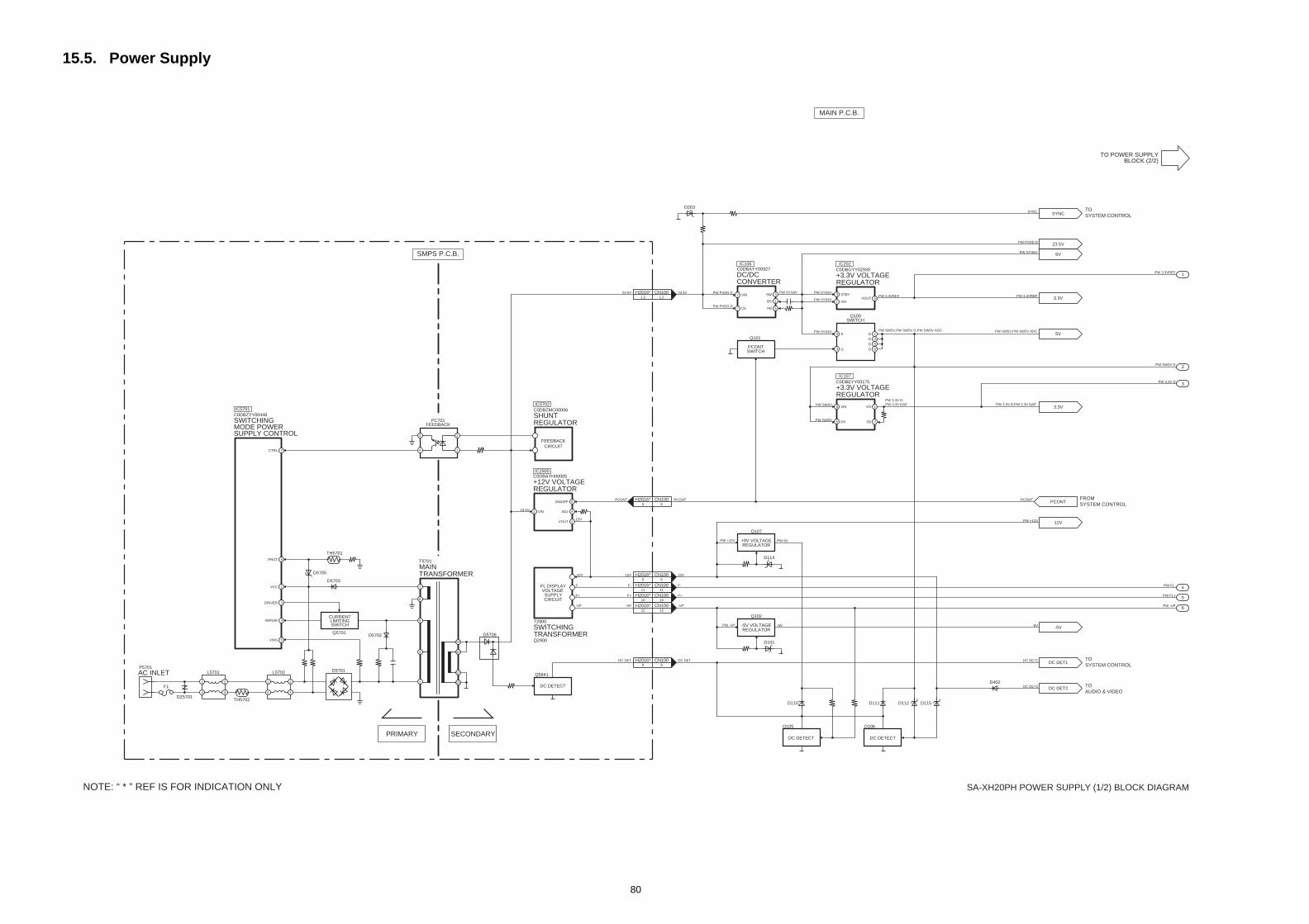
80
15.5. Power Supply
SA-XH20PH POWER SUPPLY (1/2) BLOCK DIAGRAM
3
2
5
4
6
TO POWER SUPPLYBLOCK (2/2)
1
PW SYS6V
PW SYS6V
PW SYS6V
PW SYS6VPW 3.3VREF
IC106
2 VIN
7 CE
DC/DCCONVERTER
C0DBAYY00927
SW 3
BS 1
FB 5
1,21,2
CN100H2016*23.5V 23.5V
1212
CN100H2016*-VP -VP
1010
CN100H2016*F+ F+
1111
CN100H2016*F- F-
88
CN100H2016*DC DET DC DET DC DET1
DC DET2
DC DET1
DC DET2
SWITCHINGC0DBZYY00448
IC5701
D111
PC701FEEDBACK
SHUNTREGULATOR
C0DBZMC00006
IC5702
-5V VOLTAGEREGULATOR
-5V
Q102
PW -VP
PCONTSWITCH
Q101
-5V-5V
PW +12V12V
PW PVDD D23.5V
+9V VOLTAGEREGULATOR
PW 9V
Q107
PW +12V
+3.3V VOLTAGEREGULATOR
C0DBGYY02930
IC202
PW 3.3VREF
VIN
STBYVOUT 3.3V
1
35
+3.3V VOLTAGEREGULATOR
C0DBEYY00175
IC107
PW 3.3V D,
PW 3.3V DAP PW 3.3V D,PW 3.3V DAP
EN
VIN VO
FB
3.3V
PW SW5V,PW SW5V ADC
PCONT
PW SW5V,PW SW5V D,PW SW5V ADC5V
5
8 1
2
MAIN P.C.B.
SMPS P.C.B.
FROM
SYSTEM CONTROL
TO
AUDIO & VIDEO
TO
SYSTEM CONTROL
DC DETECT
Q106
PW SW5V
D110 D112 D115
PW SW5V
DC DETECT
Q105
PCONT6
CN100 PCONT
6
H2016*PCONT
3 G
4 S D 1
D 2
D 5
D 6
SWITCHQ100
55
CN100H2016*12V 12V
PW 3.3V D
PW SW5V D
PW FL+
PW FL-
PW -VP
PW PVDD D
PW PVDD D
D402
D101
D114
D203SYNC
SYNCTO
SYSTEM CONTROL
PW 3.3VREF
PW SYS6V6V
12V
12V
IC2900
1 VIN
+12V VOLTAGEREGULATOR
C0DBAYH00005
2
ON/OFF
VOUT
ADJ
5
423.5V
F1
DZ5701
-VP
F+
F-
MODE POWER SUPPLY CONTROL
TH5701
TH5702
D5701P5701
L5702
1
4
2
3
L5701
1
4
2
3
1
5
8
7
3
MAINTRANSFORMER
T5701
14
15
12
13
CTRL 7
VCC 1
PROT 6
DRIVER 3
ISENSE 4
D5706
D5703
D5705
3
4
2
1
VINS 5
Q5701
CURRENTLIMITINGSWITCH
FEEDBACK
CIRCUIT
AC INLET
NOTE: “ * ” REF IS FOR INDICATION ONLY
Q5841
DC DETECT
SWITCHINGTRANSFORMER
T2900
Q2900
FL DISPLAYVOLTAGESUPPLYCIRCUIT
D5702
SECONDARYPRIMARY
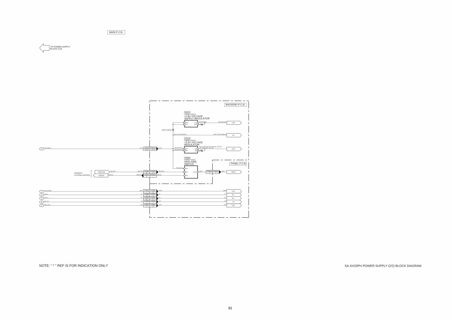
81
SA-XH20PH POWER SUPPLY (2/2) BLOCK DIAGRAM
TO POWER SUPPLYBLOCK (1/2)
-VP
FL-
FL+
-VP
3.3VVREF
3.3V3.3V
FL+
FL-
MAIN P.C.B.
+3.3V VOLTAGEREGULATOR
C0DBEYY00175
IC8112
+1.8V VOLTAGESUPPLY REGULATOR
C0DBEYY00215
IC8111
BACKEND P.C.B.
PANEL P.C.B.
D8101,D8102
3.3V
PW D+3R3V,PW VDD SDRAM, VDD AFE,
5VPW A +5V,PW USB 5VPW A +5V,PW USB 5V
1.8V2 VCC 1.8V
ADJ
4
5
PW VDD1R8V PW VDD1R8V
VBUS
1 CTL
VBUS
4
5
6
3
1
2
FL-
FL+
-VP
216
CN901CN203
315
CN901CN203
117
CN901CN203
FL-
FL+
-VP
VREF
117
CN901CN203 VREF
3.3V
126
CN901CN203 3.3V
FROM/TO
SYSTEM CONTROL
NOTE: “ * ” REF IS FOR INDICATION ONLY
HIGH SIDESWITCH
C0DBZYY00311
IC9006
25~3120~26
FP8101CN201D+5V D+5V8 VIN VO
FB
1
2
PW VDDP HDMI, PW DACPW DVD D+5V
PW DVD D+5V5 EN
USB OC
VBUS EN
USB OC
VBUS EN
843
FP8101CN201VBUS EN VBUS EN
11
CN951*FP9001
744
FP8101CN201USB OC USB OC
3 EN
4 /OC
VOUT 5VBUS
PW USB 5V1 VIN
PW FL-
PW FL+
PW -VP
PW 3.3V D
PW 3.3VREF
PW SW5V D

82
16 Wiring Connection Diagram
SA-XH20PH WIRING CONNECTION DIAGRAM
12
JK8301
VIDEO OUT
CN4000JK4000
1110 2
1
34 2
COMPONENT VIDEO OUT
1
PbF
FP8301
1210
11
COMPONENT VIDEO P.C.B.(SOLDER SIDE)
F
FP8001FOR FIRMWARE DOWNLOAD
FP8002FOR FIRMWARE DEBUG
1
5
1
5
FP90011 5
CN951*1 5
1
3DIGITAL AUDIO IN
(OPTICAL)
JK8001
P DOWNLOADER
CN202
12
910
FP8101
FP8531
TO OPTICALPICKUP UNIT
(DVD MECHANISMUNIT BRS1D)
FP8252TO LOADING PCB(DVD MECHANISM UNIT BRS1D)
FP8251TO TRAVERSE PCB(DVD MECHANISM UNIT BRS1D)
1
5
24
12
2423
1
52
6
501
FM ANT
AUX
SURROUND
FRONT
SPEAKERS
CENTER
SUBWOOFER
JK300
JK401
JK600
CN203
CN100
CN201
3
2
1
1
12
11
10
9
8
7
6
5
4
3
2
1
50
50
1
1
12
12 16
17
1617
12
1
Z901
CN901
SENSOR
USBPORT
CN950
H902
13
12
17164 1
56
1 3
H901
13
PANEL P.C.B.(SOLDER SIDE)
POWER BUTTON P.C.B.(SOLDER SIDE)
BACKEND P.C.B.(SIDE B)
MAIN P.C.B.(SIDE B)
PbF
PbF
PbF
PbF
C
B
D A
NOTE: " * " REF IS FOR INDICATION ONLY.
TO u
H2016*
T2900SWITCHING TRANSFORMER
P5701
T5701MAIN TRANSFORMER
110V-240V50/60Hz
AC IN
112
987 6 5
43
21
SMPS P.C.B.(SOLDER SIDE)
15
14
13
12
7
3
1
5
8
PbF
E
17 Schematic Diagram17.1. Schematic Diagram Notes
• This schematic diagram may be modified at any timewith the development of new technology.
Notes:
• Important safety notice:Components identified by mark have special characteris-tics important for safety.Furthermore, special parts which have purposes of fire-retar-dant (resistors), high quality sound (capacitors), low-noise(resistors), etc are used.When replacing any of components, be sure to use onlymanufacturer’s specified parts shown in the parts list.
• In case of AC rated voltage Capacitors, the part no. and val-ues will be indicated in the Schematic Diagram.AC rated voltage capacitors:C5702, C5703, C5704, C5705, C5706
• ResistorUnit of resistance is OHM [Ω] (K=1,000, M=1,000,000).
• CapacitorUnit of capacitance is µF, unless otherwise noted. F=Farads,pF=pico-Farad.
• CoilUnit of inductance is H, unless otherwise noted.
• *REF is for indication only.
• Voltage and signal line
S901: Open/Close switch ( ).S902: Power switch ( ).S905: Vol (-) switch.S906: Vol (+) switch.
: +B signal line: -B signal line: Audio output signal line
: Video output signal line: CD/DVD Audio input signal line : CD/DVD Video input signal line: AUX/Tuner/Optical Audio input signal line: FM signal line: USB signal line
83

84
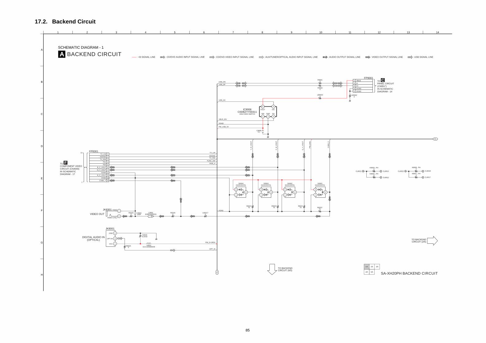
85
17.2. Backend Circuit
A
1 2 3 4 5 6 7 8 9 10 11 12 13 14
C
D
B
A BACKEND CIRCUIT
SCHEMATIC DIAGRAM - 1
SA-XH20PH BACKEND CIRCUIT
2/5 3/5
5/5
1/5
4/5
TO BACKENDCIRCUIT (2/5)
TO BACKENDCIRCUIT (4/5)
P1
: AUX/TUNER/OPTICAL AUDIO INPUT SIGNAL LINE : AUDIO OUTPUT SIGNAL LINE: CD/DVD AUDIO INPUT SIGNAL LINE : CD/DVD VIDEO INPUT SIGNAL LINE: +B SIGNAL LINE : USB SIGNAL LINE
CTOPANEL CIRCUIT
(CN951*)
IN SCHEMATIC
DIAGRAM - 14
: VIDEO OUTPUT SIGNAL LINE
11
R832275
3
1
2
D8301DA3X101F0L
CV
BS
_C
Y_R
_V
OU
T
C_B
_V
OU
T
G_Y
_V
OU
T
75R8321
PW
_D
AC
75R8323
75R8324
2
3
1
5
4
FP9001
D+
DGND
DGND
D-
VBUS
C90060.1
USB_OC
VBUS_EN
USB_DN
PW_USB_5V
USB_DP
31 2
45
IC9006C0DBZYY00311
HIGH SIDE SWITCH
/OC
EN
VOUT
VIN GND
DGND
R90020
R90010
0LB9002LB9003
0
K8003...PH0
K8008...PH0
CL8021 CL8013 CL8022 CL8018
FP8301
ADGND
TV_LIN
2
1ADGND
TV_LIN
3
1
2
D8304DA3X101F0L
3
1
2
D8303DA3X101F0L
3
1
2
D8302DA3X101F0L
K8007...PH0
CL8017
K8002...PH0
CL8012
EG
H
F
P1
FTOCOMPONENT VIDEO
CIRCUIT (CN4000)
IN SCHEMATIC
DIAGRAM - 17
1
LB83170
VGND
R83260
L2802
JK8301
VIDEO OUTC2823100P J0JBC00000150
R8325
VIDEO (YEL)
VGND
2
1
VGND
R_C_VOUT
B_C_VOUT
G_Y_VOUT
CVBS_Y
VGND
FS2
FS1
TV_RIN
6
8
9
7
4
5
3
10
11
TV_RIN
RGB_H
FUNC_SW
(OPTICAL)DIGITAL AUDIO IN
3
1
JK8001
VCC
GND
OPT-IN
2
PW_D+3R3V
OPT_IN
L8001G1C100M00049
R80250
C80306.3V33
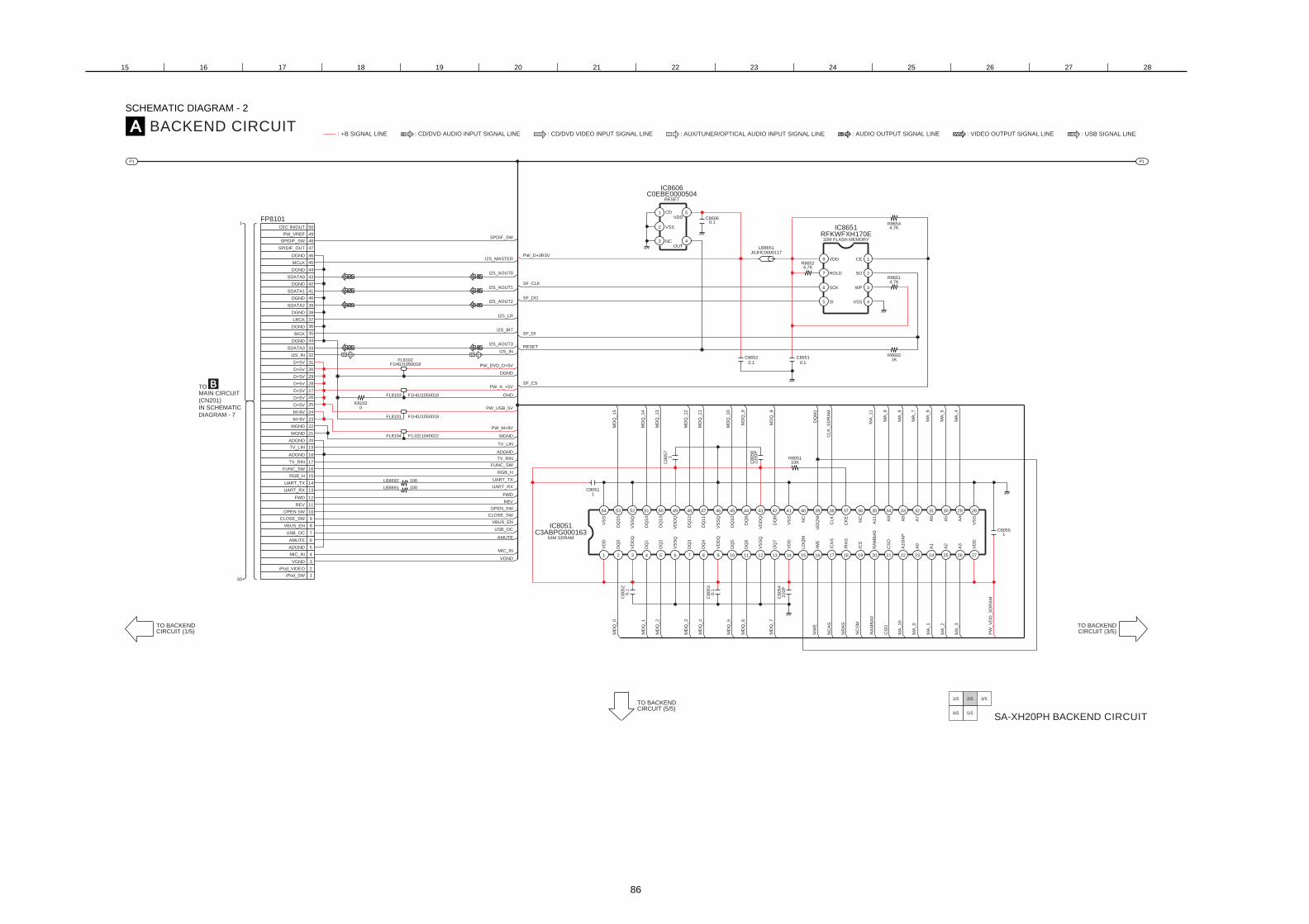
86
15 16 17 18 19 20 21 22 23 24 25 26 27 28
A BACKEND CIRCUIT
SCHEMATIC DIAGRAM - 2
SA-XH20PH BACKEND CIRCUIT
2/5 3/5
5/5
1/5
4/5
TO BACKENDCIRCUIT (3/5)
TO BACKENDCIRCUIT (5/5)
P1 P1
BTOMAIN CIRCUIT
(CN201)
IN SCHEMATIC
DIAGRAM - 7
: AUX/TUNER/OPTICAL AUDIO INPUT SIGNAL LINE : AUDIO OUTPUT SIGNAL LINE: CD/DVD AUDIO INPUT SIGNAL LINE : CD/DVD VIDEO INPUT SIGNAL LINE: +B SIGNAL LINE : USB SIGNAL LINE: VIDEO OUTPUT SIGNAL LINE
MD
Q_4
MD
Q_5
MD
Q_6
0.1
C8053
MD
Q_3
MD
Q_11
MD
Q_9
MD
Q_10
MD
Q_12
10KR8051
MD
Q_7
NW
E
NR
AS
MA
_10
MA
_1
MA
_2
MA
_0
NC
SM
CS
O
RA
MB
A0
NC
AS
220P
C8054
MD
Q_8
MA
_9
MA
_7
MA
_5
MA
_6
MA
_8
CLK
_S
DR
AM
MA
_11
DQ
M1
2200P
C8056
1C
8057
MD
Q_0
MD
Q_1
MD
Q_2
0.1
C8052
MD
Q_15
MD
Q_13
MD
Q_14
PW
_V
DD
_S
DR
AM
MA
_3
1C8055
MA
_4
29 283031
272624 2520 21191612 14 1513 18171076 8 9 112 43 5
3436394142 40 384952 5153 50 44 43454748 46 37 35
2322
3233
DQ
11
DQ
4
DQ
12
DQ
3
A7
A5
A6
NC
DQ
8
VS
S
DQ
9
CLK
CK
E
NC
A8
A9
A11
VS
S
A4
DQ
5D
Q10
UD
QM
A1
A2
/WE
LD
QM
/RA
S
/CA
S
VD
D
A0
CS
O
A10/A
P
/CS
RA
MB
A0
A3
VD
D
VD
DQ
DQ
6
DQ
7
VS
SQ
VS
SQ
VD
DQ
VS
SQ
VD
DQ
DQ
15
DQ
0
DQ
2D
Q13
VS
SQ
VD
DQ
DQ
14
DQ
1
C86060.1
3
1
2
4
5
C0EBE0000504RESET
IC8606
OUTNC
VSS
VDDCD
47
44
39
40
35
31
27
24
23
26
25
30
28
29
34
32
33
38
36
37
43
41
42
46
45
49
48
501
FP8101
GND
F1H0J1050018FL8102
0K8102
FL8101 F1H0J1050018
F1H0J1050018FL8103
I2S_AOUT0
I2S_AOUT1
I2S_MASTER
I2S_BIT
I2S_AOUT3
I2S_AOUT2
I2S_LR
PW_USB_5V
PW_DVD_D+5V
PW_A_+5V
I2S_IN
D+5V
D+5V
DGND
DGND
CEC IN/OUT
DGND
MCLK
DGND
DGND
BICK
DGND
DGND
LRCK
DGND
D+5V
D+5V
M+9V
M+9V
D+5V
D+5V
D+5V
SDATA1
SDATA0
PW_VREF
SPIDIF_SW
SPIDIF_OUT
I2S_IN
SDATA3
SDATA2
SF_DI
SF_CS
R86021K
R86514.7K
4.7KR8654
LB8651J0JHC0000117
SF_CLK
SF_DO
6
7
5
2
4
3
8 1
IC8651RFKWFXH170E32M FLASH MEMORY
C86520.1
RESET
R86524.7K
C86510.1
PW_D+3R3VVDD CE
WP
VSS
SO
SI
SCK
HOLD
SPDIF_SW
TO BACKENDCIRCUIT (1/5)
C80511
1
54
IC8051C3ABPG000163
64M SDRAM
VS
SV
DD6
7
5
9
21
20
22
16
15
18
17
11
13
12
10
14
19
8
150
3
4
2
FL8104 F1J1E1040022
LB8691 100
LB8692 100
FWD
PW_M+9V
UART_TX
UART_RX
MGND
CLOSE_SW
REV
MIC_IN
VGND
AMUTE
MGND
ADGND
MGND
ADGND
TV_RIN
TV_LIN
REV
FWD
VGND
ADGND
RGB_H
UART_TX
AMUTE
USB_OC
UART_RX
VBUS_EN
OPEN SWOPEN_SW
FUNC_SW
MIC_IN
iPod_SW
CLOSE_SW
iPod_VIDEO
VBUS_EN
USB_OC
ADGND
RGB_H
FUNC_SW
TV_RIN
TV_LIN

87
29 30 31 32 33 34 35 36 37 38 39 40 41 42
A
C
D
B
E
G
H
F
A BACKEND CIRCUIT
SCHEMATIC DIAGRAM - 3
SA-XH20PH BACKEND CIRCUIT
2/5 3/5
5/5
1/5
4/5
: AUX/TUNER/OPTICAL AUDIO INPUT SIGNAL LINE : AUDIO OUTPUT SIGNAL LINE: CD/DVD AUDIO INPUT SIGNAL LINE : CD/DVD VIDEO INPUT SIGNAL LINE: +B SIGNAL LINE : USB SIGNAL LINE: VIDEO OUTPUT SIGNAL LINE
L8401G1C100M00049
220R8622
R8621220K
C84016.3V220
C80330.1
1KR8601
I2S
_B
IT
I2S
_LR
C8009
0.1
0.1
C8023
VD
D_A
FE
C8010
0.1
R8653 22
SF_DO
SF_CLK
L8552G1C100M00049
C8566
0.1C8016
SF_DI
SF_CS
R8411 6.19K
C8018 0.1
C8032 0.1
C8017 0.1
DV
D_M
D
DV
D_LD
CD
_LD
CD
_M
D
DU
PR
DO
DU
PT
DO
10K
R8010
6.3
V100
6.3
V100
C8302
L8302G1C100M00049
C8528
1
DR
VS
B
R84024
21
3
D1H456020001RX8402
0
100
J0JCC0000308
LB8401
I2S_AOUT1
I2S_AOUT2
0.1C8014
I2S_MASTER
I2S_AOUT0
R8401
103
107
106
110
113
119
118
124
127
128
125
126
121
120
123
122
115
114
117
116
111
112
108
109
104
105
12 111415 131819 1617 9 57 6 3 124810262829 27 22 212425 23
45
47
46
42
43
40
39
41
44
3738 34 3335 31 303236
49
48
50
20
9594 10099 10210196 98978584 87863 91 93928988 90
01003477ODER
H0J270500131X8621
C862110P
C86228P
R85691K
1000PC8024
RESET
J0JHC0000045LB9001
TR
V_P
WM
SP
N_P
WM
TR
K_P
WM
FO
C_P
WM
8
6 5
7
4
2
2
1
3D1H88204A043
RX8012
8 6
57
4
13
D1H
88204A
043
RX
8019
8 6
57
4
13
D1H
88204A
043
RX
8018
8 6
57
4 2222222
13
D1H
88204A
043
RX
8013
8 6
57
4
13
D1H
88204A
043
RX
8015
8 6
57
4
13
D1H
88204A
043
RX
8011
22
R8011
8 6
57
4
13
D1H
88204A
043
RX
8016
8 6
57
4
13
RX
8014
D1H
88204A
043
MD
Q_12
MD
Q_3
MD
Q_6
MD
Q_11
MD
Q_5
MD
Q_4
MD
Q_10
MD
Q_14
MD
Q_13
MD
Q_2
MA_3
MA_4
CLK
_S
DR
AM
MD
Q_9
MD
Q_8
MD
Q_7
MA_0
MA
_10
RA
MB
A0
MA
_11
CS
O
NR
AS
NC
SM
MA
_9
MA
_8
MA_1
MA_2
MA_5
MA_6
MA_7
DQ
M1
NC
AS
NW
E
MD
Q_15
MD
Q_1
MD
Q_0
PW_VDD_SDRAM
LB8051J0JHC0000045
8
6 5
7
4
1
3D1H88204A043
RX8017
6.3V100C805842
1 3
RX8401D1H456020001
C80116.3V220
I2S
_A
OU
T3
100
R8404
0.1C8022 PW_D+3R3V
PW_VDD1R8V
LB8011J0JHC0000045
4V330C8001
LB8001J0JHC0000045
UA
RT
_T
X
UA
RT
_R
X
MIC
_IN
AM
UT
E
DGND
DO
WN
LO
AD
INNER_SW
DQ
13
DQ
3
DQ
6
DQ
5
DQ
8
RA
S
DQ
M
CA
S
WE
#
DQ
9
DQ
7
MA
8
MA
9
MA
0
DQ
4
DQ
12
VDDP
SFDI
SFCS
GPIO34
GNDC
GP
IO34
I2S
_IN
DU
PR
DI
DU
PT
DI
VD
DC
VD
D_P
WM
GP
IO39
GP
IO37
DU
PR
DI
DU
PR
DO
GP
IO55
TR
K_D
RV
TR
V_D
RV
SP
N_D
RV
SFDO
[102] AIN2/DUPRD1
CD
_M
D
VD
D_A
FE
DV
D_LD
AU
D_IN
FO
C_D
RV
CD
_LD
DV
D_M
D
RE
SLO
AD
MA
10
MA
11
CS
0#
RA
MB
A0
CS
#1
[127] MA7
XO
SFCLK
XI
MA2
VDDC
GNDA
MA3
MA5
MA4
USBREF
VDDPLL
MA1
MA6
[128] GNDC
USB_DN
USBVDDPLL
RESET#
USB_DP
USB_VDD
VD
DP
[101] GPIO6/DUPTD1
DQ
11
VD
DP
CLK
DQ
10
PC
LK
GN
DP
CLK
VD
DP
[39] GNDC
AO
UT
3
VD
DA
VDDP
TXCN
LR
CK
MCLK
DDCDAT
DDCCLK
SPIDIF_OUT
CP_IC RESET
BC
LK
AOUT1
[40] AOUT2
AOUT0
DQ
2
DQ
0
DQ
15
VD
DC
DQ
14
DQ
1
0.1C8027
0.1C8012
0.1C8002
0.1C8013
USB_DN
USB_DP
TO BACKENDCIRCUIT (2/5)
P1
C83016.3V100
J0JHC0000045LB8301
J0JHC0000045LB3901
0.1
C8021
R8050
15.4
K
VC
RF
_F
1000PK8301
J0JH
C0000045
LB
3910
C8007 0.1
C8034 0.1
C8006 100P
C8028 0.01
C8029 1000P
R391010
C8008 0.1
C8003 0.1
R3901 402
G_Y_VOUT
CVBS_C
LB3902J0JHC0000045
VGND
0.1
C8020
RF
IN_P
C8512
1000P
0.1
C8019
C8511
1000P
RF
_A
RF
_C
RF
_E
RF
_D
RF
_B
Y_R
_V
OU
T
C_B
_V
OU
T
R8311392
61
62
57
55
56
51
52
54
53
60
59
58
64
63
880 817668 6965 6766 73 757470 7271 7877 79 82
IC80C1AB00
DVD DEC
GN
D
D FKR
F_K
VR
EF
VC
GN
D_A
FE
JR
F_J
ERS
ET
RF
P
[64] GNDC
TXCP
TXD0P
TXD0N
[63] DAC3
VDDC
DAC4
DA
C1
DA
C2
VDDDAC
PW_DAC
TXD1P
TXD1N
TXD2P
TXD2N
VDDC1V8_HDMI
VDDP_HDMI
TXREXT
CRF
N
VD
DA
FE
BA VD
DA
FE
PW_VDDP_HDMI

88
I
8 9 10 11 12 13 14
K
L
J
A BACKEND CIRCUIT
SCHEMATIC DIAGRAM - 4
SA-XH20PH BACKEND CIRCUIT
2/5 3/5
5/5
1/5
4/5
TO BACKENDCIRCUIT (5/5)
TO BACKENDCIRCUIT (1/5)
P1
P1
: AUX/TUNER/OPTICAL AUDIO INPUT SIGNAL LINE : AUDIO OUTPUT SIGNAL LINE: CD/DVD AUDIO INPUT SIGNAL LINE : CD/DVD VIDEO INPUT SIGNAL LINE: +B SIGNAL LINE : USB SIGNAL LINE: VIDEO OUTPUT SIGNAL LINE
C81210.1
J0JHC0000045LB8121
2
3
1
5
4
FP8002
2
3
1
5
4
FP8001
UPTDO
UPRDO
DUPRDIUPRDI
DGND
DGND
DUPTDIUPTDI
DGND
DUPRDO
DUPTDO
VDD_3R3V
DOWNLOADOWNLOAD
VDD_3R3V
2
3
1
5
4
FP8252
LB8012 0
2
4
3
1
6
5
FP8251
TO TRAVERSE PCB
(DVD MECHANISM UNIT BRS1D)
TO LOADING PCB
(DVD MECHANISM UNIT BRS1D)
FOR FIRMWAREDOWNLOAD
FOR FIRMWARE DEBUG
R8267
1K
0.1C8264
R82661K
R826833K
FOC_DRV
GNDPW_D+3R3V
R82634.7K
2
1
27
5
4
24
25
22
17
19
18
30
20
21
7
11
10
12
8
29
9
236
3 26
28
C0GBY00001175CH MOTOR DRIVER
IC8251
R826210K
R826110K
TRV_DRV
10KR8259R8260
10K
TRK_DRV
SPN_DRV
DRVSB
L8251J0JHC0000117
FWD
J0JHC0000117L8252
1KR8264
PW_M+9V
PW_USB_5VLD+
LD-
OPEN_SW
CLOSE_SW
CLOSE_SW
REV
VINFC MUTE
FWD
REV
VOTR+
TRB_1
VINSL TRB_2
VOSL+
VOSL-
VCC
VOTR-
REGO1
VOLD+
VOLD-
NC
NC
GND
VINLD
VCTL
GND
PVCC
GND
BIAS
VINTKREGO2
T-F-
TR-TR-
TR-
TR+TR+
TR+
SP-
SP+
DGND
LD+
LD-LD+
LD-
DGND
CLOSE_SW
OPEN_SWOPEN_SW
INNER_SWINNER_SW
3
1
2
D8251DA3X103E0L
C82630.1
DD_AFE
R82562K
2KR8255
R82542.2
R82532.2
F_K
F_J
CL8262
CL8261
1 2 3 4 5 6 7
M
O
P
N D
D
D
D
D
R8101270K
C81134.7
6
7
T1
5
2
4
3
8
Therm
alP
ad
1
C0DBEYY00175+3.3V VOLTAGE REGULATOR
IC8112
C81014.7
R810347K
R810415K
421 3 5
C0DBEYY00215+1.8V VOLTAGE SUPPLY REGULATOR
IC8111
R8102130K
4.7
C8151
C811110
B0ECKP000062D8101
B0ECKP000062D8102
C81121
PW_VDD1R8V
PW_DVD_D+5V
DGND
1.8V
FB NC
NC
NC
EN
GND
ADJVINVO
VCCCTL GND
K82520
6.19KR8258
1KR8265
0.1C8256
15
1613
14
C825216V47
K82510
6.3V100C8251
MGND
VOFC-
VOFC+
VOTK-
VOTK+F+ T+
V
R
R
CL8101

89
22 23 24 25 26 27 28
A BACKEND CIRCUIT
SCHEMATIC DIAGRAM - 5
SA-XH20PH BACKEND CIRCUIT
2/5 3/5
5/5
1/5
4/5
TO BACKENDCIRCUIT (4/5)
TO BACKENDCIRCUIT (2/5)
: AUX/TUNER/OPTICAL AUDIO INPUT SIGNAL LINE : AUDIO OUTPUT SIGNAL LINE: CD/DVD AUDIO INPUT SIGNAL LINE : CD/DVD VIDEO INPUT SIGNAL LINE: +B SIGNAL LINE : USB SIGNAL LINE: VIDEO OUTPUT SIGNAL LINE
C8533 0.1
0R8542
0.1C8530
0R8532
R8531 0
6
7
5
9
13
15
14
11
10
12
21
22
18
16
17
20
19
8
1
3
4
2
24
23
FP8531
TO OPTICAL PICKUP UNIT(DVD MECHANISM UNIT BRS1D)
RF_A
RF_B
R85370
RF_F
LB8530J0JHC0000045
4
21
3
RX8531D1H456020001
4
2 1
3RX8532
D1H456020001
RF_D
RF_C
PW_A_+5V
B1ABDF000026Q8565
RFIN_P
RF_E
VC
LB8532J0JDC0000102
CD_MD
GND
R85380
LB8531 22
DVD_MD
LB8551J0JDC0000102
LB8561J0JDC0000102
T-T-
D/d
C/c
F+F+
F-F-
T+T+
NC
NC
MD
F
E
NC
B/b
VCC
CD-LD
RF
A/a
PD GND
CD/DVD SW
DVD-LD
GND-LD
VR-CD
VR-DVD
VC(REF)
L8550G1C100M00049
0.1C8561C8563
6.3V220R8566
4.7
220R8554
220R8564
6.3V220C8553
0.1C8551
R85564.7
Q8552DSA200200LDVD LASER DRIVE
Q8562DSA200200LCD LASER DRIVE
DVD_LD
CD_LD
PW_D+3R3V
51KR8227
TRK_DRV
R822951K FOC_DRV
C82301000P
C82281000P
TRV_PWM 51KR8225
SPN_PWM
C82260.027
R822122K
TRK_PWM
FOC_PWM
TRV_DRV
SPN_DRV
0.027C8222
CL8530
CL8531
CL8532
15 16 17 18 19 20 21
P1
R85363.3K
DVD SELECTOR SWITCH
R853410K
R853547K
GPIO34
PW_VDDP_HDMI
GNDY
B
/Y
A
/ST
VCC
SELECT
0.1C3958 R3908
10K
LB3907J0JCC0000308
SPDIF_SW
OPT_IN
5 4
R8016100
6
7 2
3
8 1
C0JBAR0004332CH MULTIPLEXER
IC3954
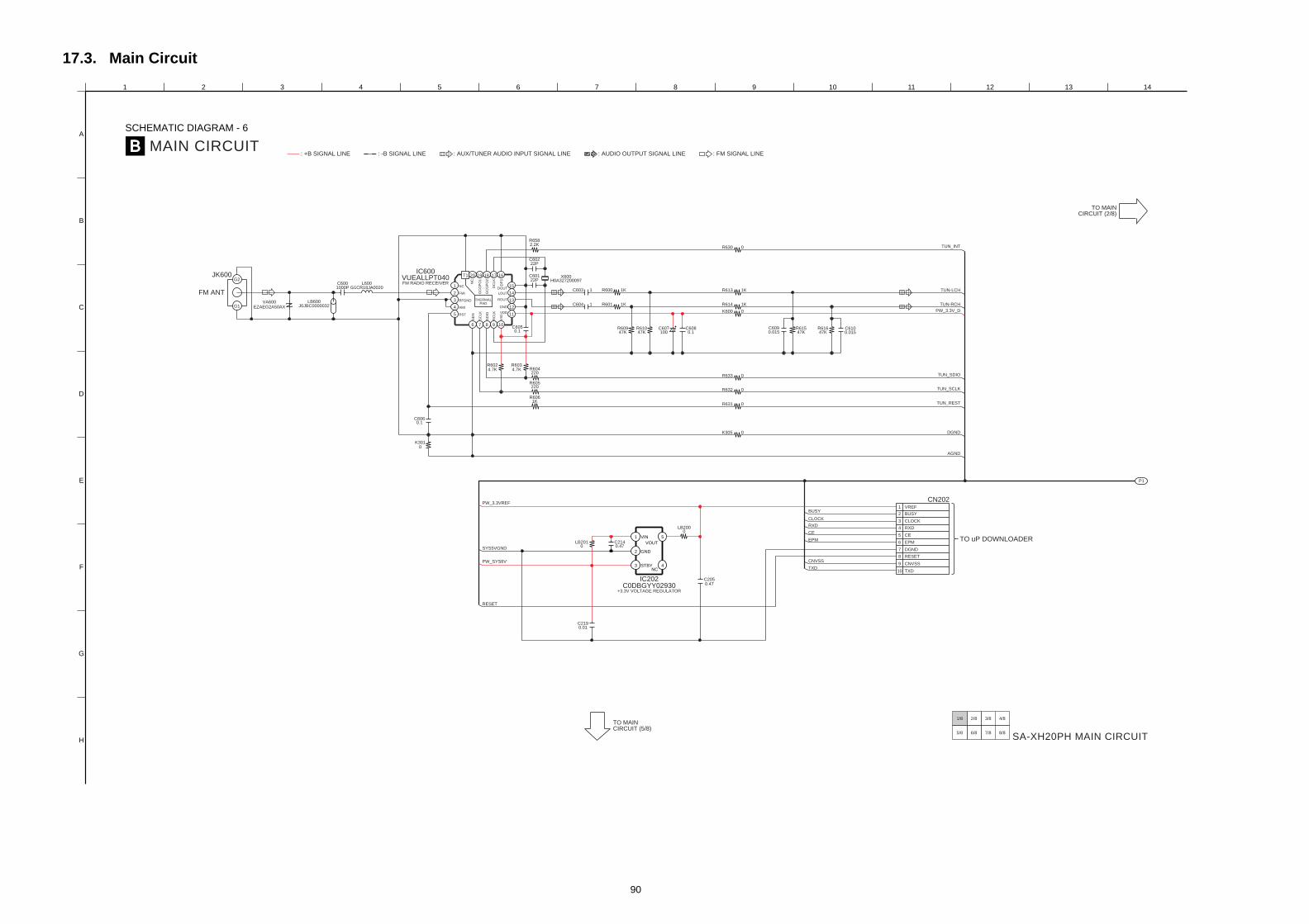
90
17.3. Main Circuit
A
1 2 3 4 5 6 7 8 9 10 11 12 13 14
C
D
B
B MAIN CIRCUIT
SCHEMATIC DIAGRAM - 6
SA-XH20PH MAIN CIRCUIT
3/8 4/8
7/8
2/8
6/8 8/8
1/8
5/8
TO MAINCIRCUIT (2/8)
TO MAINCIRCUIT (5/8)
P1
: AUX/TUNER AUDIO INPUT SIGNAL LINE: -B SIGNAL LINE: +B SIGNAL LINE : FM SIGNAL LINE: AUDIO OUTPUT SIGNAL LINE
DGND
AGND
R601 1K
R600 1K
0.1C605
R605220
R604220
R6061K
R6582.2K
22PC602
22PC601
G2
G1
JK600
FM ANT
VA600EZAEG2A50AX
LB600J0JBC0000032
C6001000P
0.1C606
R6024.7K
R6034.7K
L600G1CR18JA0020
4 12
1
2 14
T1 1719 18 16
15
20
3 13THERMALPAD
5 11
108 976
VUEALLPT040FM RADIO RECEIVER
IC600
C604 1
C603 1
X600H0A327200097
R613
R614
K600
1K
1K
0
C607100
C6080.1
0R631
0K305
R633 0
0R632
0R630 TUN_INT
R61547K
R61647K
TUN-RCH
TUN-LCH
TUN_SCLK
TUN_SDIO
TUN_REST
R60947K
R61047K
RST
SE
NN
C
RFGND
FMI
NC
AMI GND
ROUT
RC
LK
VIO
VDD
SC
LK
SD
IO
DF
S
DC
LK
GC
GP
O2
LOUT
DOUT
GC
GP
O1
0.015C609
0.015C610
6
8
9
7
2
1
4
5
3
10
CN202
TO uP DOWNLOADER
C2050.47
+3.3V VOLTAGE REGULATOR
CECE
DGND
EPMEPM
RESET
TXDTXD
CNVSSCNVSS
BUSYBUSY
CLOCKCLOCK
VREF
RXDRXD
PW_3.3V_D
C2140.47
LB2000
3
1
2
4
5
IC202C0DBGYY02930
NCSTBY
GND
VOUT
VIN
E
G
H
F
K3010
PW_3.3VREF
SYS5VGND
PW_SYS6V
0.01
RESET
C219
LB2010

91
15 16 17 18 19 20 21 22 23 24 25 26 27 28
B MAIN CIRCUIT
SCHEMATIC DIAGRAM - 7
SA-XH20PH MAIN CIRCUIT
3/8 4/8
7/8
2/8
6/8 8/8
1/8
5/8
TO MAINCIRCUIT (1/8)
TO MAINCIRCUIT (3/8)
TO MAINCIRCUIT (6/8)
P1
ATOBACKEND CIRCUIT
1
: AUX/TUNER AUDIO INPUT SIGNAL LINE: -B SIGNAL LINE: +B SIGNAL LINE : FM SIGNAL LINE: AUDIO OUTPUT SIGNAL LINE
0.1C400
16V10C406
0.1C407
C42016V10
PW
M_F
L+
0.1C421
PW
M_F
R+
PW
M_C
EN
T-
PW
M_C
EN
T+
PW
M_S
UB
W-
VA
LID
PW
M_S
UB
W+
PW
M_F
R-
PW
M_F
L-
0.1C417
DAP_CLK
SRCK
LRCK
C4120.1
C4110.1
DAP_SDA
SDATA0
SDATA2
DMIX
R414 10K
SDATA1
4748 4445 4041 36 3335 343839 3743 4246
1
62
63
58
57
60
61
59
64
53
50
49
52
51
55
56
54
87 94 65
23
24
21
18
19
17
20
22
1612 1310 11 15142 3
31
29
30
32
27
28
25
26IC401C1AB00003610
0.1C416
220
R401
0.1
C402
0.01C453
DA
P_R
ST
C408
16V
10
PW
_3.3
V_D
PW
_3.3
V_D
AP
DA
P_P
DN
1K
R436R435
100
J0JBC0000014L427
DA
P_M
UT
E
3.3
R402
C451 15P
C452 15P
0.1
C405
0.1
C404
0.1
C403
220
C4010.1
R400
16V
10
C410
C409
1000P
0.0
1C
414
PWM_SR-
PWM_SL-
PWM_SL+
PWM_SR+
MCLK
RESERVED
VR
_P
WM
[3] PLL_FLTM
VB
GA
P
/RE
SE
T
[17] VRD_DPLL
AV
SS
/PD
N
/MU
TE
DV
SS
DV
DD
AV
SS
AV
SS
_P
LL
/HP
_S
EL
VR
D_P
LL
AV
DD
_P
LL
PLL_F
LT
P
[1] VRA_PLL
XTL_IN
RESERVED
SCL
SDIN4
SCLK
LRCLK
[31] SDIN1[32] PSVC
SDIN3
SDIN2
SDA
DV
SS
VR
_D
IG
RESERVED
RESERVED
XTL_OUT
OSC_CAP
VA
LID
PW
M_M
_1
PW
M_M
_3
PW
M_M
_4
PW
M_P
_4
PW
M_P
_3
PW
M_P
_1
PW
M_P
_2
PW
M_M
_2
DIGITAL AUDIO PWM PROCESSOR
DV
DD
DV
SS
/BK
ND
_E
RR
DV
SS
[2] PLL_FLT_RET
[50] PWM_P_7
DVSS_PWM
PWM_HPML
PWM_HPMR
PWM_HPPR
PWM_HPPL
DVDD_PWM
PWM_P_8
PWM_P_5
PWM_P_6
PWM_M_6
PWM_M_5
PWM_M_8
[49] PWM_M_7
R4110
1MR404
10PC415
C4138P
2GND
3
1
4GND
X400H0J135500050
LRCK
0R283
0R284
0R285
0R282
SDATA2
CEC_IN_OUT
PW_3.3VREF
SDATA0
SDATA1
SRCK
DMIX
0R286
0R287
6
7
5
9
24
21
20
22
16
15
18
17
11
13
12
10
14
19
23
25
8
1
3
4
2
CN201
PW_SW5V_D0L290
I2S_IN0R296
0R295
PW_VREF
CEC IN/OUT
SPIDIF_SW
MCLK
DGND
DGND
DGND
DGND
LRCK
BICK
DGND
DGND
SDATA2
SDATA0
SDATA1
D+5V
D+5V
I2S_IN
D+5V
SDATA3
D+5V
D+5V
D+5V
SPIDIF_OUT
DGND
SPDIF SW
8
65
7
4
21
3
86
5 7
42
1 3
86
5 7
42
1 3
D1H84704A024RX401
8
65
7
4
21
3
8
65
7
4
21
3
D1H84704A024RX404
D1H84704A024RX405
D1H84704A024RX402
D1H84704A024RX403
P1
(FP8101)
IN SCHEMATIC
DIAGRAM - 2
50
R495100
MCLK
GND
REV
AMUTE
0K105
L291
L292
J0JBC0000015
J0JBC0000015
VBUS_EN
DVD_TX
DVD_RX
FWD
CLOSE_SW
OPEN_SW
USB_OC
AGND
K153
K155
K154
0K158
K156
0 00 0
47
44
39
40
35
31
27
26
30
28
29
34
32
33
38
36
37
43
41
42
46
45
49
48
50
0R272
VGND
MGND
M+9V
MGND
M+9V
MGND
RGB_H
ADGND
ADGND
PW_9V
TV_LIN
FUNC_SW
TV_RIN
D+5V
ADGND
AMUTE
VBUS_EN
USB_OC
MIC_IN
CLOSE_SW
FWD
REV
UART_TX
OPEN SW
UART_RX
iPod_VIDEO
VGND
iPod_SW
TV_R
TV_L

92
29 30 31 32 33 34 35 36 37 38 39 40 41 42
B MAIN CIRCUIT
SCHEMATIC DIAGRAM - 8
SA-XH20PH MAIN CIRCUIT
3/8 4/8
7/8
2/8
6/8 8/8
1/8
5/8
TO MAINCIRCUIT (4/8)
TO MAINCIRCUIT (7/8)
P1 P1
: AUX/TUNER AUDIO INPUT SIGNAL LINE: -B SIGNAL LINE: +B SIGNAL LINE : FM SIGNAL LINE: AUDIO OUTPUT SIGNAL LINE
US
B_O
C
C2010.1
RS
TB
DC
_D
ET
2
DC
_D
ET
1
R247220
R246220
R22910
R22810
PW_3.3VREF
R231 56K
VB
US
_E
N
R236 56K
PCONT
SDA
FWD
R217 1K
REV
AMUTE
R248 47K
220R250
R215 100
R214 100
DAP_MUTE
DVD_RX
FLD_STB
CK_FLD
FLD_OUT
PW_3.3V_D
LED_CTRL
TUN_REST
TUN_SCLK
TUN_SDIO
SYNC
CEC_IN_OUT
R20027K
LB202 0
R233 220 DVD_TX
TUN_INT
C2000.022
R208 10K
SD
VA
LID
DA
P_R
ST
DA
P_P
DN
1K
R210
R216
100
DA
P_S
DA
DA
P_C
LK
79
77
76
78
49
47
48
50
74 7172 6768 56 5558 57 52 5154 536566 6162 596064 6370 697375
81
82
80
84
83
85
45
43
41
42
44
46
6
7
5
2
4
3
8 1
C3EBFY000030EEPROM
IC201
10KR202
10KR203
4.7KR235
4.7KR234
C209 560P
NC
NC
NC
NC
DC
DE
T2
[48] PCONT
DC
DE
T1
US
B_O
C
VB
US
_E
N
[50] VMUTE[49] RGB_H
NC
NC
NC
NC
CE
NC
CE
EPM
TXD
BUSY
CLOCK
RXD
NC
WP
SCLSCL
SCL
VCC
SDASDA
A2
GND
A0
A1
SD
NC
NC
NC
NC
NC
VO
L 0
[77] NC[78] NC
NC
NR
ST
WID
E1
NC
VS
S
NC
[76] DAP_CLK
NC
DAP_PDN
OTW
NC
VALID
NC
DA
P_D
AT
[79] DAP_RST
NC
VC
C
NC
C4191
C4710.110K
R405
K4000
R43747K
R43815K
GND
PW_SW5V 0L426
PW_3.3V_DAP
C4181
R4250
6
7
5
2
4
3
8 1
IC107C0DBEYY00175
+3.3V VOLTAGE REGULATOR
EN
NC
NC
VIN
FB
CN
GND
VO
T1
TH
ER
MA
L P
AD
8
65
7
4
21
3
D1H81014A024RX201
8
65
7
4
21
3
8
65
7
4
21
3
8
65
7
4
21
3
D1H84734A024RX204
D1H81034A024RX203
D1H81034A024RX202
R243 220
R242 1K
TO MAINCIRCUIT (2/8)
3
1
2
X201H2D500400006
R29447K
C2020.1
R222150K
220R201
10KR239
10K
R241
0.1C207
1087 9 1211
99
100
95
94
96
97
90
91
89
93
92
98
4 6521 3
86
87
88
19171514 16 18 232120 22 24
39
37
33
35
34
29
30
27
26
28
32
31
36
38
25
40
13
IC200RFKWMXH70EB
MICROPROCESSOR
SELECTOR_LSB
SELECTOR_MSB
10KR207
10KR206
R205 10K
KEY2
KEY1
R232 220RMT
RESET
R209 10K
560PC210
R2231.2K
OPEN_SW
SYS5VGND
CLOSE_SW
CNVSS
ECO_CNTRL
TU
N_S
CLK
TU
N_R
ST
FLD
_O
UT
FLD
_C
LK
SCLK
NC
NC
REV
FWD
EPM
EDA
ECK
DAP_MUTE
DBG_RX
AMUTE
DBG_TX
LE
D_C
TR
L
NC
[28] DVD_TX[27] DVD_RX[26] FLD_STB
TU
N_S
DIO
CE
C_IN
/OU
T
NC
KEY2
KEY1
SEL_B
SEL_A
DES3
AUX_DET
RM
T
NC
DES2
VREF
[98] NC[97] AVCC
AVSS
EC
O_C
0N
TR
L
CLO
SE
_S
W
DES1
NC
XIN
VC
C
VS
S
NC
XO
UT
RE
SE
T
BY
TE
CN
VS
S
[99] SPDIF_SW
SPDIF SW
[100] OPEN_SW
NC
SY
NC
NC
TU
N_IN
T
8
65
7
4
21
3D1H81014A024
RX205
AUX_DET

93
43 44 45 46 47 48 49 50 51 52 53 54 55 56
A
C
D
B
E
G
H
F
B MAIN CIRCUIT
SCHEMATIC DIAGRAM - 9
SA-XH20PH MAIN CIRCUIT
3/8 4/8
7/8
2/8
6/8 8/8
1/8
5/8
TO MAINCIRCUIT (3/8)
AC
AD
: AUX/TUNER AUDIO INPUT SIGNAL LINE: -B SIGNAL LINE: +B SIGNAL LINE : FM SIGNAL LINE: AUDIO OUTPUT SIGNAL LINE
SP_SL-
C5671000P
R5063.3
0K157
SP_CENT+
C479 0.033 SP_SUB+
SP_SUB-
PWM_SUBW-
R444 10
C4250.1
SP_CENT-3.3
R466
C185 1000P
R524100K
C184 1000P
ABCF000231Q500
B1ABCF000231Q501
R523100K
R521100K
R520100K
33KR522
SP_PROTCT
3.3R467
C4450.01
50V10C548
C4440.01
C4900.1
SP_FL+
3.3R464
3.3R465
C186 1000P
SP_FL-
0.1C501
5.6KR502
C4430.01
C4420.01
0.1C502
SP_FR+
C183 1000P
R528
100K
C181 1000P
C182 1000P
100K
R525
R527
100K
R526
100K
R443 10
C4260.1
10R445
C42710
R446 10
R428 10
R427 10
C4230.1
C5661000P
0.033C464 SP_CENT-
C4600.1
C4770.1
SP_SUB-
3.3R468
R5015.6K
G0A100H00018L418
C4860.1
C4460.01
C4780.1
G0A100H00018L419
C4870.1C505
25V330
C4240.1
PWM_SUBW+
R442 100
C470 0.033R44122K
R440 100
R429 100
5.6KR500
SP_CENT+
L410
G0A100H00018
G0A100H00018L417
SP_SUB+
3.3R469
C4730.1
C4620.1
C4720.125V330
C467C4610.1
C476 0.033
43
11
9
10
34
36
35
12 33
6
7
5
39
38
41
40
8 37
2322
20
18
16
14
13
15
17
19
31
32
28
26
25
27
30
29
21 24
3
4
2
1
42
44
IC403
DIGITAL AMPLIFIERC1AB00003217
C4470.01
PWM_CENT-
PWM_CENT+
SP_FL+
SP_FR-
3.3R496
0.1C522
3.3R497
SP_FR+
C192 1000P
SP_FL- C191 1000P
C4490.01
R5035.6K
0.1C523
C4480.01
C4540.01
C190 1000P
0.01C450
SP_SR-
SP_SL+
3.3R499
C187 1000P
3.3R498
C189 1000P
C188 1000P
SP_SR+
SP_FR-
C4550.01
R5073.3
C4560.01
1
G1
8
9
11
10
12
5
6
2
4
3
7
G2
JK401
GND
CHASSIS
FR-
C-
FR+
SR+
SL-
SL+
SR-
FL+
FL-
SW-
NC
OUT_C
BST_C
OUT_D
GND_C
GND_D
NC
OUT_A
BST_A
BST_B
GND_A
OUT_B
GND_B
SW+
BST_D
PVDD_D
PVDD_D
PVDD_A
PVDD_B
GVDD_A
PVDD_A
PVDD_C
GVDD_D
C+
NC
M2
NC
NC
M3
M1
GND
NC
VDD
VREG
AGND
PWM_B
PWM_D
PWM_C
SD(L)
PWM_A
OC_ADJ
GVDD_B
OTW(L)
GVDD_C
RST_AB(L)
RST_CD(L)
TO SPEAKERSSPEAKER PROTECTION SWITCH
R PROTECTION SWITCH
C8060.47
C8070.47
C8050.47
C8040.47
TO MAINCIRCUIT (8/8)
P1
P1
AA
AB
OTW
SD
B1
C4290.1
C49625V330
G0A100H00018L406
C497
0.1
C4930.1
C492 0.033
0.1C481
PWM_FL+
PWM_FL-
R448 100
R449 100
R447 10
IC405
DIGITAL AMPLIFIERC1AB00003217
PWM_FR+
C508
0.1
G0A100H00018
L408C4300.1
0.033C510R452 10
R453 10
PWM_FR-
R451 100
C5090.1
G0A100H00018L409
C51925V330
VALID
C4310.1
C4320.1
10R454
C43310
C5140.1
R45022K
C498 0.033
C507 0.033
G0A100H00018L407
GND
43
11
9
10
34
36
35
12 33
6
7
5
39
38
41
40
8 37
2322
20
18
16
14
13
15
17
19
31
32
28
26
25
27
30
29
21 24
3
4
2
1
42
44
NC
OUT_C
BST_C
OUT_D
GND_C
GND_D
NC
OUT_A
BST_A
BST_B
GND_A
OUT_B
GND_B
BST_D
PVDD_D
PVDD_D
PVDD_A
PVDD_B
GVDD_A
PVDD_A
PVDD_C
GVDD_D
NC
M2
NC
NC
M3
M1
GND
NC
VDD
VREG
AGND
PWM_B
PWM_D
PWM_C
SD(L)
PWM_A
OC_ADJ
GVDD_B
OTW(L)
GVDD_C
RST_AB(L)
RST_CD(L)
SPEAKE

94
I
8 9 10 11 12 13 14
K
L
J
B MAIN CIRCUIT
SCHEMATIC DIAGRAM - 10
SA-XH20PH MAIN CIRCUIT
3/8 4/8
7/8
2/8
6/8 8/8
1/8
5/8
TO MAINCIRCUIT (6/8)
TO MAINCIRCUIT (1/8)
P1
: AUX/TUNER AUDIO INPUT SIGNAL LINE: -B SIGNAL LINE: +B SIGNAL LINE : FM SIGNAL LINE: AUDIO OUTPUT SIGNAL LINE
C316 47P
C315 47P
R10122
R1023.9K
25V47C102
C1010.1
SE
LE
CT
OR
_M
SB
RE
CO
UT
-L
PW
_-V
P
AG
ND
R31515K
1K
R314
B1GBCFJJ0041SELECTOR SWITCH
Q301
TUN-LCH
TUN-RCH R308 1K
R307 1K
PW
_S
W5V
10KR330
R300 0
R32710K
C329220P
R32910K
10KR328 C328
220P
1
2
3
JK300
AUX/TV R302 0
R30910K
10KR310
D101DZ2J056M0L
Q102DSA200100L
-5V VOLTAGE REGULATOR
C10010V100
R316 27K
RE
CO
UT
-R
R318 27K
C3170.1
10KR313
10KR312
SE
LE
CT
OR
_LS
B
R31715K
B1GBCFJJ0041SELECTOR SWITCH
Q300
1K
R326
1C313
C314 1
C304 1
C306 1
75 61 2 43
1012141516 13 11
8
9
C0JBAR000367AUDIO SELECTOR
IC300
R0
R2
R1
R C
H
VC
C
R CH
L CH
L1
L2
L0
L3
L C
H
INH
GN
D
VE
E
R3
B (
MS
B)
A (
LS
B)
AUX_R
AUX_LC312 1
C307 1
0R311
0R304
C309680P
C308680P
TV_L
TV_R
1 2 3 4 5 6 7
M
O
P
N

95
22 23 24 25 26 27 28
B MAIN CIRCUIT
SCHEMATIC DIAGRAM - 11
SA-XH20PH MAIN CIRCUIT
3/8 4/8
7/8
2/8
6/8 8/8
1/8
5/8
TO MAINCIRCUIT (5/8)
TO MAINCIRCUIT (7/8)
TO MAINCIRCUIT (2/8)
P1
CTOPANEL CIRCUIT
(CN901)
IN SCHEMATIC
DIAGRAM - 14
1
17
: AUX/TUNER AUDIO INPUT SIGNAL LINE: -B SIGNAL LINE: +B SIGNAL LINE : FM SIGNAL LINE: AUDIO OUTPUT SIGNAL LINE
0LB701
RECOUT-L J0JCC0000388LB700
J0JCC0000388LB702RECOUT-R
R703 1K
R7024.7
R701 0
PW_SW5V_ADC
MCLK
LB704G1C100M00049
I2S_IN
6.3V47C708
C707 10
R700 100
15
5 12
13
98
6 11
7 10
3
4
2
1
14
16
IC700C0FBAK000026
DIGITAL AUDIO A/D CONVERTER
LRCK
SRCK
RSTB
C705 10
C706 1000P
C703 10
C704 10
C702 16V10
LB703J0JCC0000388
RMT
PW_3.3V_D
AGND
K304 0
PGND R131 0
FLD_OUT
LED_CTRL
FLD_STB
KEY2
PW_FL+
PW_FL-
KEY1
CK_FLD R136 0
R137 0
R135 0
PW_-VP R142 0
R141 0
6
5
8
9
11
12
10
14
15
13
7
2
1
4
3
17
16
CN203
R139 0
AGND
PW_3.3VREF
FL_IC_CLK
FL+
KEY2
-VP
FL-
KEY1
DGND
AGND
VD
VA
SDT0
SCLK
LRCK
MCLK
AINR CKS0
PDNVCOM
AINL CKS2
CKS1 DIF
LED_CTRL
FL_IC_STB
VREF
3.3V
GND
DGND
AGND
AGND
RMT
MPORT_LCH
MPORT_RCH
FL_IC_DAT
K7000
R18647K
C1092.2
R1831K
R18510K
Q122B1ABCF000231
DETECT SWITCH
PW_SYS6V
AUX_DET
R144 0
R145 0
15 16 17 18 19 20 21
P1
10PC140
1C133
R1921.5M
R19112K
R18922K
1C124
1C122
C1101
C1211 12K
R188
1.5MR187
C19510P
R19022K
B1GBCFGN0018Q123
B1GBCFGN0018Q124
BUFFER SWITCH
BUFFER SWITCH
6 75
24 3
8
1
C0ABBB000067IC100
DUAL OP-AMP
-VCC
+VCC
AUX_L
AUX_R
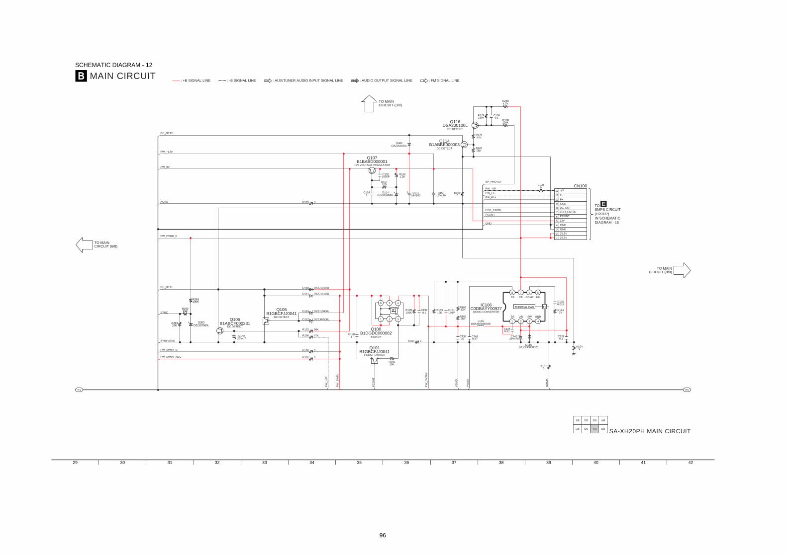
96
36 37 38 39 40 41 42
B MAIN CIRCUIT
SCHEMATIC DIAGRAM - 12
SA-XH20PH MAIN CIRCUIT
3/8 4/8
7/8
2/8
6/8 8/8
1/8
5/8
TO MAINCIRCUIT (6/8)
TO MAINCIRCUIT (8/8)
TO MAINCIRCUIT (3/8)
P1
ETOSMPS CIRCUIT
(H2016*)
IN SCHEMATIC
DIAGRAM - 15
: AUX/TUNER AUDIO INPUT SIGNAL LINE: -B SIGNAL LINE: +B SIGNAL LINE : FM SIGNAL LINE: AUDIO OUTPUT SIGNAL LINE
PW_PVDD_D
4.7KR249
220KR180
220KR179
0.1C158
1C139
L1000
1000PC132
16V100C151
16V470C150
1.2KR156
D114DZ2J100M0L
R157100
R58756K
B1ABBE000003Q114
PW_+12V
Q107B1BABD000001
+9V VOLTAGE REGULATOR
K109
DC DETECT
DSA200100LQ116
DC DETECT
0
7
9
10
8
4
5
1
3
2
6
12
11
CN100
K107 0
K103 0
K1040
K1010
PCONT
PW_FL+
ECO_CNTRL
PW_FL-
PW_-VP
R19610K
0.1C197
180PC131
100KR195
15KR165 R164
1K
C1300.015
67
T1
5
2 43
8
THERMAL PAD
1
C0DBAYY00927DC/DC CONVERTER
IC106
PC
ON
T
C1350.01
CFJJ0041ONT SWITCH
Q101
46 5
21 3
Q100GDC000002
SWITCH22
C1380.47C141
25V470C143
0.1C129
G0A330G00016L125
R16212K
R16356K
D116B0JCPG000028
PW
_S
YS
6V
VG
ND
PG
ND
MG
ND
DA2J10100LD402
R17847K
DC_DET2
GND
SP_PROTCT
AGND
PW_9V
F-
F+
PCONT
GND
GND
23.5V
23.5V
12V
GND
-VP
DC_DET
ECO_CNTRL
SW
COMP
GND
FBCE
VIN
SS
BS
29 30 31 32 33 34 35
P1
DC DETECT
DC DETECT
Q106B1GBCFJJ0041
DA2J10100LD111
DA2J10100LD110
SYNC
C14225V4.7
DC_DET1
B1ABCF000231Q105
PW_SW5V_D
PW_SW5V_ADC
PW
_S
W5V
R152 20K
K106 0
K102 0
R150 47K
DZ2J15000LD115
DZ2J07500LD112
1C198
SYS5VGND
B1GBPC
B1D
PW
_-V
P
100KR291
39KR292
D203DZ2J07500L27K
R293
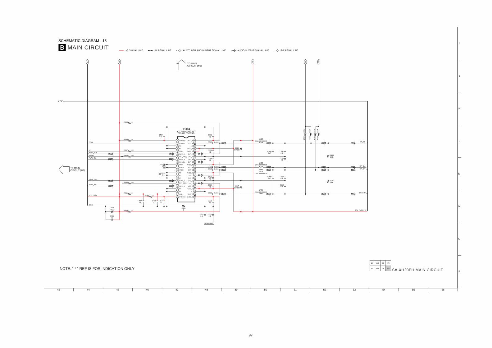
97
I
K
L
J
M
O
P
N
50 51 52 53 54 55 56
B MAIN CIRCUIT
SCHEMATIC DIAGRAM - 13
SA-XH20PH MAIN CIRCUIT
3/8 4/8
7/8
2/8
6/8 8/8
1/8
5/8
TO MAINCIRCUIT (4/8)
AA
AD
AC
AB
P1
P1
: AUX/TUNER AUDIO INPUT SIGNAL LINE: -B SIGNAL LINE: +B SIGNAL LINE : FM SIGNAL LINE: AUDIO OUTPUT SIGNAL LINE
SP_SR+G0A100H00018
L405
PW_PVDD_D
G0A100H00018
L404
C5590.1
SP_SR-
0
C5580.1
R5055.6K
OTW
SD
IC404
DIGITAL AMPLIFIERC1AB00003217
C4340.1
VALID
R455 10
PWM_SL+
R456 10
100K
R530
100K
R532
100K
R531
100K
R529
C5260.1
SP_SL-C527 0.033
0.1C540
G0A100H00018L403
G0A100H00018L402
25V330C533
5.6KR504
SP_SL+
C5370.1
R458 100
R457 100
PWM_SL-
C5280.1
C529
43
6
7
5
39
38
41
40
8 37
3
4
2
1
42
44
NC
OUT_A
BST_A
GND_A
GND_B
PVDD_A
GVDD_A
PVDD_ANC
NC
PWM_B
SD(L)
PWM_A
GVDD_B
OTW(L)
RST_AB(L)
C8090.47
C8080.47
43 44 45 46 47 48 49
TO MAINCIRCUIT (7/8)
NOTE: “ * ” REF IS FOR INDICATION ONLY
C5740.1
C55425V33
PWM_SR+
R460 100
PWM_SR-
PW_+12V
R461 10
R462 10
C550 0.033
C4360.1
C5460.1
C5510.1
0.1C802
0.1C803
R463 10
C4380.1
C4370.1
16V33
C441
C5120.1
C43910
C547 0.033
0.1
R45922K
C530 0.033
GND
0K303
HEATSINK*
11
9
10
34
36
35
12 33
2322
20
18
16
14
13
15
17
19
31
32
28
26
25
27
30
29
21 24
NC
OUT_C
BST_C
OUT_D
GND_C
GND_D
BST_B
OUT_B
BST_D
PVDD_D
PVDD_D
PVDD_B
PVDD_C
GVDD_D
NC
M2
M3
M1
GND
NC
VDD
VREG
AGND
PWM_D
PWM_C
OC_ADJ
GVDD_C
RST_CD(L)

98
17.4. Panel and Power Button Circuit
BBTOMAIN CIRCUIT
(CN203)
IN SCHEMATIC
DIAGRAM - 11
17
C PANEL CIRCUIT
SCHEMATIC DIAGRAM - 14
SA-XH20PH PANEL / POWER BUTTON CIRCUIT
: +B SIGNAL LINE : -B SIGNAL LINE : USB SIGNAL LINE
ATOBACKEND CIRCUIT
(FP9001)
IN SCHEMATIC
DIAGRAM - 1
A
B
C
D
1 2 3 4 5 6 7 8 9 10 11 12 13 14
8 9 10 11 12 13 14
A
B
D
E
F
H
G
CC91550V22
P13
P15
P14
P6
P5
P7
P2
P1
P4
P3
P10
P12
P11
P8
P9
C91350V22
22KR923
P8
P7
P9
G5
G3
G4
P6
G8
G7
G5
G4
G8
G6
G7
G1
P1
G2
G3
P4
P5
P2
P3
G9
C912 0.01
G9
G6
82KR905
21
5
6
3
1
2
4
19
9
7
8
16 17
11
10
12 151413 18 20
35374244 43 39 3841 40 36
33
22
31
29
27
24
23
26
25
28
30
32
34
IC901C0HBB0000057
G2
P16
G1
312 8 2621 232219 20 2524 28 292712 1310 14 16157 32
FL901A2BB00000175
68R901
68R904
R903 68
P14
P13
P16
P15
P11
P10
P12
6.3V100C905
0.1C909C903
0.1C908
1
1
3
2
H902
R92410
DZ2J02400LD901
C93110
6
5
8
9
11
12
10
14
13
7
2
1
4
3
CN901
F-
B3RAB0000081Z901
REMOTE CONTROL SENSOR
F-
P3
P1
P11
P12
P10
G2
G3
G1
F+
F+
G6
G7
G4
G5
NP
G8
G9
NC
P15
P16
P13
P14
P9
P5
P6
P4
P8
P7
NP
P2
[23] P9STB [11] K2
DIN
DOUT
CLK P6
P7
P4
P5
P12
P17
P16
K1
GN
D
VC
C
P18
P13
P15
P14
P10
P11
P8
P1
P2
G1G3
P3
-VP
NC
GN
D
G9
G8
G10
VC
C
NC
[1] USB RIP LED
G5
G4
[34] G2
G7
G6
NC
OSC
RMTRMT
VREFVREF
DGND
-VP
FL+FL+
FL+
VREF
FL-FL-
FL-
VREF_LED
KEY1
DGND
AGND
FL_IC_STBFL_IC_STB
FL_IC_STB
LED_CTRL
3.3V3.3V
FL_IC_CLK
FL_IC_DATFL_IC_DAT
FL_IC_DAT
RMT
KEY1
KEY2
1 4 5 6 9 11 17 18
RM
T
GN
D
VC
C
R92247
FL DISPLAY DRIVER
FL DISPLAY
0
R9131.2K
S905
S906
S901
R91418K
R9081.2K
VOLUME+
OPEN/CLOSE
VOLUME-
0K955
D-
D+
2
5G1
4
6G
3 D+
D-
DGND
VBUS
CN950
USB PORT
LB9510
LB9500
R9500
0R951
R9520
CHASSIS
CN951*
4
3
5
1
2
D+
D-
VBUS
DGND
DGND
D-
D+
G2
21 3
G1
K960...PH
1
D POWER BUTTON CIRCUIT: +B SIGNAL LINE
E
F
G
H
1 2 3 4 5 6 7
3.3V
15
17
16AGND
MPORT_RCH
MPORT_LCH
S9021
3
2
H901DGND POWER
KEY1
VREF_LED
NOTE: “ * ” REF IS FOR INDICATION ONLY

99
17.5. SMPS Circuit
A
1 2 3 4 5 6 7 8 9 10 11 12 13 14
8 9 10 11 12 13 14
C
D
B
E SMPS CIRCUIT
SCHEMATIC DIAGRAM - 15
SA-XH20PH SMPS CIRCUIT2/21/2
TO SMPSCIRCUIT (2/2)
1
2
3
4
: +B SIGNAL LINE : -B SIGNAL LINE
BTOMAIN CIRCUIT
(CN100)
IN SCHEMATIC
DIAGRAM - 12
D2908B0EAMM000057
DZ2J36000LD2901
Q2900B1BABK000001
4.7KR2900
C290016V33
5 3
4
8
7
6 2
1
9T2900
G4D1A0000142SWITCHING TRANSFORMER
47R2902
POWER SAVE CONTROL
C29025600P
47KR2914
DZ2J24000LD2909
7
9
10
8
4
5
1
3
2
6
12
11
H2016*
B0EAMM000057D2903C2903
35V33
B0EAMM000057D2906C2912
6.3V100
R290810K
C29080.1
D2907
B0JC
PG
000028
L2900G0A330G00016
25V100C2907
16V820C2906
R2907
3.9
K C57250.1
0R2901
3.3R2903
30KR2906R2905
4.7K
1KR2909
421 3 5
C0DBAYH00005+12V VOLTAGE REGULATOR
IC2900
15KR5729
C57260.33
1
4
2
3
C0DBZMC00006SHUNT REGULATOR
IC5702
R573139K
R57304.7K
R58170
C57271000P
R57351K
VIN ADJ
R C
NC A
ON/OFFVOUT GND
12V
-VP
GND
GND
PCONT
ECO_CNTRL
F-
DC_DET
F+
23.5V
23.5V
GND
1 2 3 4 5 6 7
E
G
H
F
NOTE: “ * ” REF IS FOR INDICATION ONLY
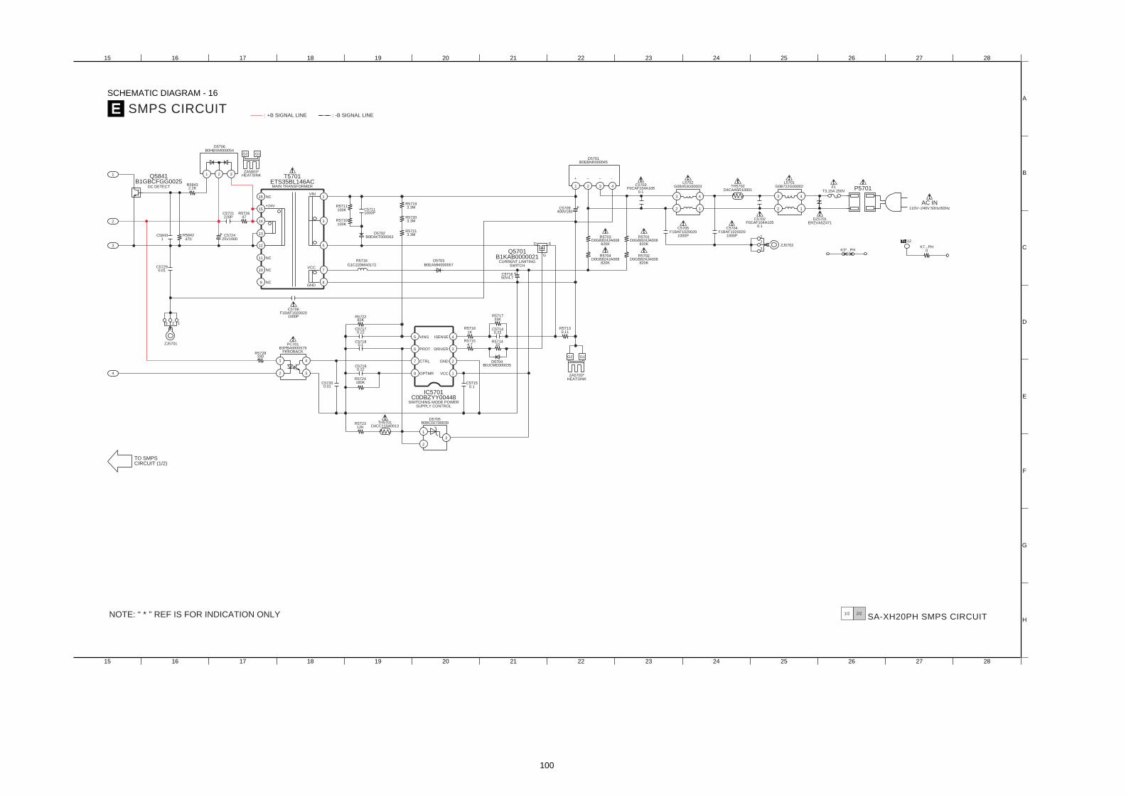
100
15 16 17 18 19 20 21 22 23 24 25 26 27 28
22 23 24 25 26 27 28
A
C
D
B
E
G
H
F
E SMPS CIRCUIT
SCHEMATIC DIAGRAM - 16
SA-XH20PH SMPS CIRCUIT2/21/2
1
2
3
: +B SIGNAL LINE : -B SIGNAL LINE
3
2
1
3 2 1
R5703D0GB824JA008
820K
0.1F0CAF104A105
C5703
R5704D0GB824JA008
820K
~ -~
32 4
+
1
B0EBNR000045D5701
C5709400V180
ZJ5702
R5702D0GB824JA008
820K
F1D4CAA5R10001
TH5702
F0CAF104A105C5702
0.1
3
2
4
1
G0B453G00003L5702
C5705F1BAF1020020
1000P
DZ5701ERZVA5Z471
R5701D0GB824JA008
820K
G2 G1
ZA5703*HEATSINK
G2 G1
ZA5803*HEATSINK
R5842470
C5721220P
C572425V1000
R58432.2K
31 2
B0HBSM000054D5706
Q5841B1GBCFGG0025
1C5843
G1C220MA0172R5716
R5711100K
R5710100K
C57111000P
F1BAF1020020C5706
1000P
B0EAKT000063D5702
47R5726
C57290.01
D5703B0EAMM000057
9 8
15
13
14
16
10
11
12
3
1
7
5
ETS35BL146ACMAIN TRANSFORMER
T5701
D S
GQ5701
B1KAB0000021
50V4.7C5716
CURRENT LIMITINGSWITCH
330R5728
3.3MR5721
1KR5718
4.7R5715
C57140.22
R571733K
R57193.3M
R57203.3M
6
7
5
2
4
3
R571410
D5704B0JCME000035
ZJ5701
0.22C5717
C57180.1
82KR5722
41
B3PBA0000579FEEDBACK
PC701
R57130.11
T3.15A 250V
NC
+24V
VIN
PROT
CTRL
VINS
NC
NC
NC
GND
VCC
GND
ISENSE
DRIVER
DC DETECT
C5704F1BAF1020020
1000P
12TL
110V~240V 50Hz/60Hz
AC IN
P5701
K7...PH0K3*...PH
G0B722G00002L5701
3
2
4
1
15 16 17 18 19 20 21
TO SMPSCIRCUIT (1/2)
4
3
2
1
C57150.1
B0BC02700039D5705
0.01C5720
8 1
IC5701C0DBZYY00448
SWITCHING MODE POWERSUPPLY CONTROL
C57190.22
32
TH5701D4CC11040013
R572312K
R5724180K
OPTMR VCC
NOTE: “ * ” REF IS FOR INDICATION ONLY
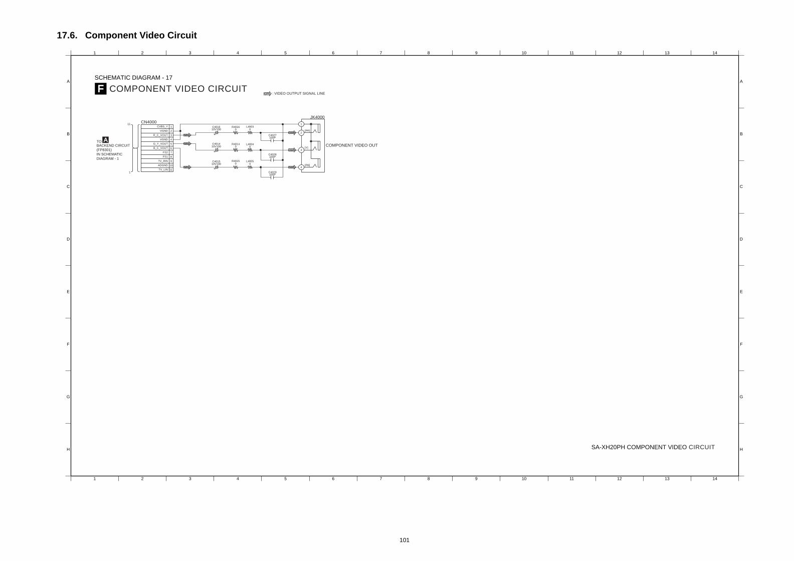
101
17.6. Component Video Circuit
A
1 2 3 4 5 6 7 8 9 10 11 12 13 14
8 9 10 11 12 13 14
C
D
B
A
C
D
B
E
G
H
F
SCHEMATIC DIAGRAM - 17
SA-XH20PH COMPONENT VIDEO CIRCUIT
F COMPONENT VIDEO CIRCUIT: VIDEO OUTPUT SIGNAL LINE
ATOBACKEND CIRCUIT
(FP8301)
IN SCHEMATIC
DIAGRAM - 1
1
11
C4027
C4029100P
3
2
1
4
JK4000
COMPONENT VIDEO OUT
C401610V100
C401410V100
R40160
0
0
L40040
L40030
R4014
0L4005R4015C4015
10V100
6
8
9
7
2
1
4
5
3
10
11
CN4000
C4028
[PB]
[PR]
[Y]
100P
100P
CVBS_Y
VGND
VGND
TV_LIN
FS2
FS1
TV_RIN
ADGND
R_C_VOUT
G_Y_VOUT
B_C_VOUT
1 2 3 4 5 6 7
E
G
H
F
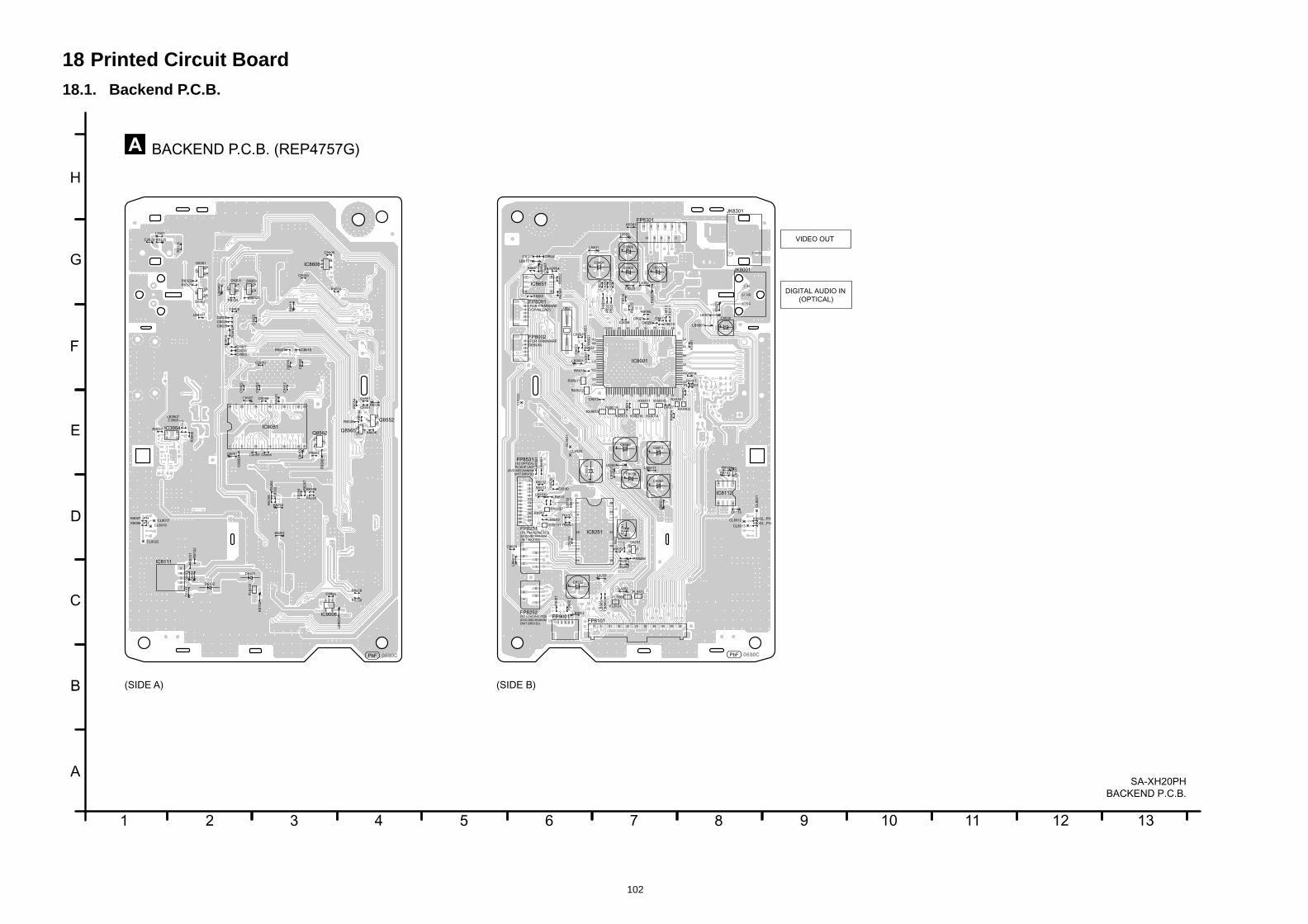
102
18 Printed Circuit Board18.1. Backend P.C.B.
17 8 9
F
G
H
10 1 12 13
A BACKEND P.C.B. (REP4757G)
SA-XH20PHBACKEND P.C.B.
0680C0680CPbF
BC
E
R80
25
C8003
C8006
C8007
C8008
R80
51
C8056C8057
C80
12D8304
R8324R8323
D8303
LB8317
D8301
R8322R8321
D8302
R8601
R80
10
C80
22
C80
02
C8016
C8010
C80
18
C80
23
C80
32
C8033
C8028C8029
R39
10
LB39
10
C8034
C8606
R85
34
R8556
R85
54
Q8552
C8561
C8551
IC8606
R8535
LB39
02
R8602
RX8012
IC8001
C8013
RX8013
RX8011
R80
11
RX8401
RX8016 RX8014
RX8015
RX8402
R8401
R84
02
LB8401
C8014
RX8017
LB8011
R86
21
R8622
C8302
L8302
C8528
C8301
C8566
L8552
C8563
LB8121C8121
C80
17
R86
52
C86
51LB
8651
C8652
R8651 R8654
R85
69
C8009
R82
29
C8021
R8050
C8020
C82
30
C82
28
C82
22
C82
26
R82
21R
8225
R82
27
R86
53
X8621
LB80
01
C8001
FL8103FL8101
L8104
R8411
C8401
L8401
C8019
R39
01
LB3901
C85
12
C8511
C8027
C8621
C86
22
R8253
R8254
R8255
R8256
D8251
C82
63
R84
04
L8252
C8011
C82
51
C8058
K8301
R83
11
LB9001
LB83
01
IC8651
50
RX8018
RX8019
R8263
R8103R8104
C81
01
LB80
51
IC8112
C8113
FP8301
C2823 R8325
L2802
R83
26
K8002...PH
1-GND2-V
JK8301
VIDEO OUT
FP8001(FOR FIRMWARE DOWNLOAD)
FP8002(FOR FIRMWARE DEBUG)
1
5432
1
5432
K8003...PH
LB3907
L8001
C3958
C8030
1-VCC
2-GND
3-IN
JK8001
DIGITAL AUDIO IN(OPTICAL)
CL8013
CL8012
CL8
021
CL8
532
5
4
123
283540455054 30
128
125
120
115
110
105103
102100 95 90 85 80 75 70 65
64
60
55
50
45
4039
3835302520151051
8
5
0
5
0
1
4 5
8
5045403530252015
14
5 8
BC
E
CAC
CA
CAC
CA
CAC
CA
CAC
CA
1579 3
246810
11
1 2 3 4 5 6
A
B
C
D
E
(SIDE A) (SIDE B)
0680C0680CPbF
C80
55
C80
52
C8053 C8054
Q8565
C8051
K81
02
FL8
102
K8251
K8252
LB90
03
R8260
R8259
R81
02
C81
12
C81
51
C81
11
IC8111
R8536
C82
64 R82
67
R8268
R8266
Q8562
R8564
R85
66
IC9006
C9006
R82
64R
8265
R82
58
D8101
D8102
R81
01
IC8051
LB86
91LB
8692
IC8251
C85
53
LB9002
R90
02R90
01
F
L8251
C8252
R8262
R8261
C82
56
L85
LB85
61
R85
38
C8530
RX8532R8542
LB8532
RX8531
R85
37
LB8531
C85
33
LB8530
R8531
R8532
LB85
51
FP8101FP9001
LB80
12
C8024
FP8531(TO OPTICALPICKUP UNIT
(DVD MECHANISMUNIT BRS1D))
FP8252(TO LOADING PCB(DVD MECHANISM UNIT BRS1D))
FP8251(TO TRAVERSE PCB(DVD MECHANISM UNIT BRS1D))
K8007...PHK8008...PH
R8016
R39
08
1
4 5
8IC3954
CL8018CL8017
CL8022
CL8
531
CL8530
3
2
4
1
5
54
123
1 5 10 15 20 2725
2
2
2
114
10
5
1
29 3
1
5
32
4
1
579
3
15171921
1113
2022
1012141618
2468
2423
1
5
32
6
4
10511 5432
BC
E
BC
E
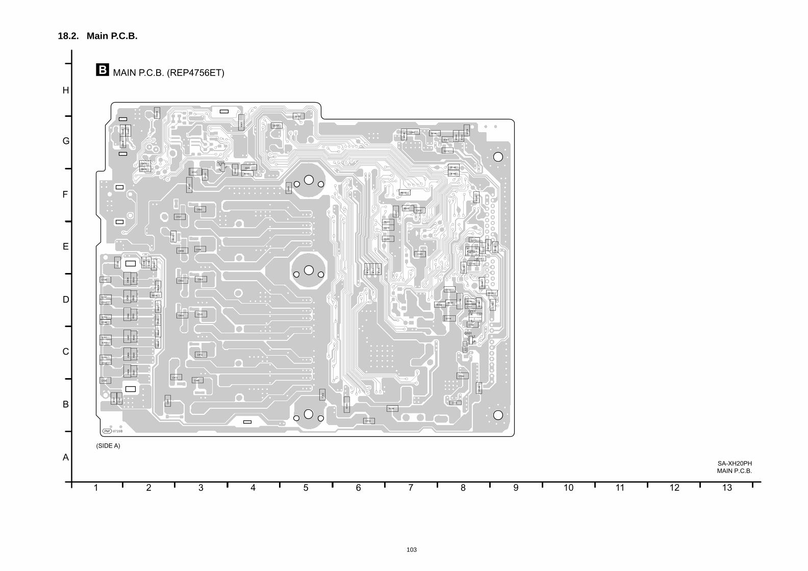
103
18.2. Main P.C.B.
17 8 9
E
F
G
H
10 1 12 13
B MAIN P.C.B. (REP4756ET)
SA-XH20PHMAIN P.C.B.
C80
3
C540
C558
R53
2
0 88
C537
C559
Q102
R10
2
C10
1D101R101
K30
1
66
LB701
K102
R600
C60
0
C603
L600
LB60
0
C60
8
K15
8
R272
L290
K15
4
K155
K156
K15
3
K10
6
C21
9
C135
R232
R29
4
K10
7
09
K30
4
R222
C13
9
C198
Q101
C197 R19
6R195
Q100
R13
9
R14
1
R142
C210
C209
R223
C201
C20
7 C202
LB20
0
C205
C214
LB201
K10
4
R157
D114
R156
C132
K600
C129
IC202
L100
K30
5
R144
R145
4
6 1
3
1234
5
CB
E
BC
E
1 2 3 4 5 6
A
B
C
D
(SIDE A)
0729B0729BPbF
R50
0R
501
R50
2R
503
R50
4R
505
C473
C472
C48
7
C486
C502 C501
C522C523
K15
7
C56
7
R52
8R
527
R52
5R
529
R530
R53
1
C80
2
C19
C182
C183
C184
C185
C186
C187
C1
C191
C192
C181
C189
R52
6
C80
8C
809
C5
C80
4C
805
C80
6C
807
K1
K10
5
K10
3
C512
K10
1
K30
3

104
17 8 9
E
F
G
H
10 1 12 13
B
SA-XH20PHMAIN P.C.B.
MAIN P.C.B. (REP4756ET)
0729B0729BPbF
FM ANT
AUX
SURROUND
FRONT
SPEAKERS
CENTER
SUBWOOFER
C530
C547
C550
C526
HEATSINK
C551
C57
4C
546
C52
9C
528
IC404
JK300
C533
C554
C15
8Q116
R17
8
R58
7
Q114
C54
8
Q500
R52
3
R520
R52
1
R52
4
Q501
R300
R302
R468
R466
R467
R464
R465
R497
R496
R499
R498
R506
R507
R463 C43
7C
438
R461
R462
R460
C436
R459
R458
R457
R455
R45
6
C43
4
D40
2
R30
7R
308
R30
9R
310
C31
3
IC300
C317
C315
C316
R326
R314
Q301
Q300
R312
R313
C100
C102
C61
0
C43
9
R630
R632
R633
R61
4
R61
6R
615
C60
9
R61
3
R610
R609
R601
C604
C44
6C
447
C30
6
C44
4C
445
C304
C44
8C
449
C45
0C
454
C45
5C
456
R631
R18
0
C44
3
R17
9
R522
C52
7
C44
2
L419
L417
L409
L407
L406
L405
L404
L403
L402
JK401
C32
8
R32
7
R328
R329
R330
C70
2
C705
C70
7
C70
8
C32
9
R24
9
C314
R315
R316
R317
R318
IC700
LB702
LB700
C704
C70
3
K70
0
R70
1
R70
0
C70
6
LB70
3
LB704
R702
R70
3
JK600
C601
IC600
R602
R60
3
R60
4
R60
5
R658
VA600
C60
5
C60
6R
606
C60
2X600
C607
31
R29
6
R29
5
R137
R136
R135
R131
L291
L292
R28
2
R28
3
R28
4
R28
5
R28
6
R28
7
R20
8
R207
R206
R20
5R
203
R202R
209
R210
R216
R235
R234
R228
R229
47
R246
R21
7
R215
R214
R24
8
R241
R239
R20
0
LB20
2
R20
1
X201
C200
IC201
CN203
IC200
R236
CN201
IC107
9
C418
471
405
R42
5
R437
R438
RX
205RX
201
RX
202
RX
203
RX204
R233
R25
0
R469
B
C
E
R185
C109
Q122 C12
4
R19
1
C133
C14
0
R19
2
R18
9
R19
0
C12
2
B
C
E
BC
E
Q124
Q123C121
R18
8
C195
R187
14
5 8
IC100
R183
C11
0
R186
C307
C30
8
C30
9
C31
2
R30
4
R31
1
R24
2
R24
3
(TO uP DOWNLOADER)CN202
6
8
9
7
10
44
40
35
30
25
2322
20
15
10
5
1
3-LCH
2-RCH
1-GND
1-SW+
12-SL-
11-SL+
10-SR-
9-SR+
8-FL-
7-FL+
6-FR-
5-FR+
4-C-
3-C+
2-SW-
1615 10 9
851
1615109
8 5 1
1
20171615
12
1110 6
5
1
50 45 40 35 30 25 20 15 10 5 1
1 4
58
1
3
5
7
9
2
4
6
8
16
14
12
10
17
15
13
11
14
1510152025
26
30
35
40
45
50
51 55 60 65 70 75
76
80
85
90
95
100
B
C
E
BC
E
B
C
E
BC
E
B
C
E
B
C
E
1 2 3 4 5 6
A
B
C
D
(SIDE B)
B C E
IC403
C46
1C
462
C47
7C
478
C460
C476
C470
C498
C507
C481
C514
C50
9C
508
C49
7C
493
IC405
C505
C467
C496
C519
C42
3
R42
8
R427
R429
R440
R441
C424
R442
R443
R444
C425
R445
C42
7
R454
C43
1C
432
R452
R453
R451
C430
R450
R449
R448
R446
R44
7
C42
9
C43
3
C49
0
C46
4C
510
C49
2
C479
L418
L410
L408
C42
6
L125C143
IC106
D11
6
R163R164
C13
0
C131
R16
5
C14
1
R16
2
C138
R2
R411
R15
2
D115
R2
C42
1
Q106
C150
D112
D111
D110
R150
Q105
C142
CN100
C45
1
C45
3
C410
C441
C151
L427
C411
C409
C405
X400
C452R435
R436
C412
C408
C404
R402
C40
3
C41
4
C40
2
C401C400
R495
C407
C40
6
C415
C413
R41
4
C41
6C
417
C420
IC401
R404
R40
0
R401
Q107
K400
L426
C41CR
RX
403
RX404
RX401
RX405
RX402
D20
3
R293
R29
1
R29
2
1
2
4
5
3
44
40
35
30
25
2322
20
15
10
5
1
44
40
35
30
25
2322
20
15
10
5
1
1 4
58
5 8
12
11
10
1
2
3
4
5
6
7
8
9
43
2 1
1
5
10
1516
17 20 25 30 32
33
35
40
45
48
4950556064
BC
E
BC
E
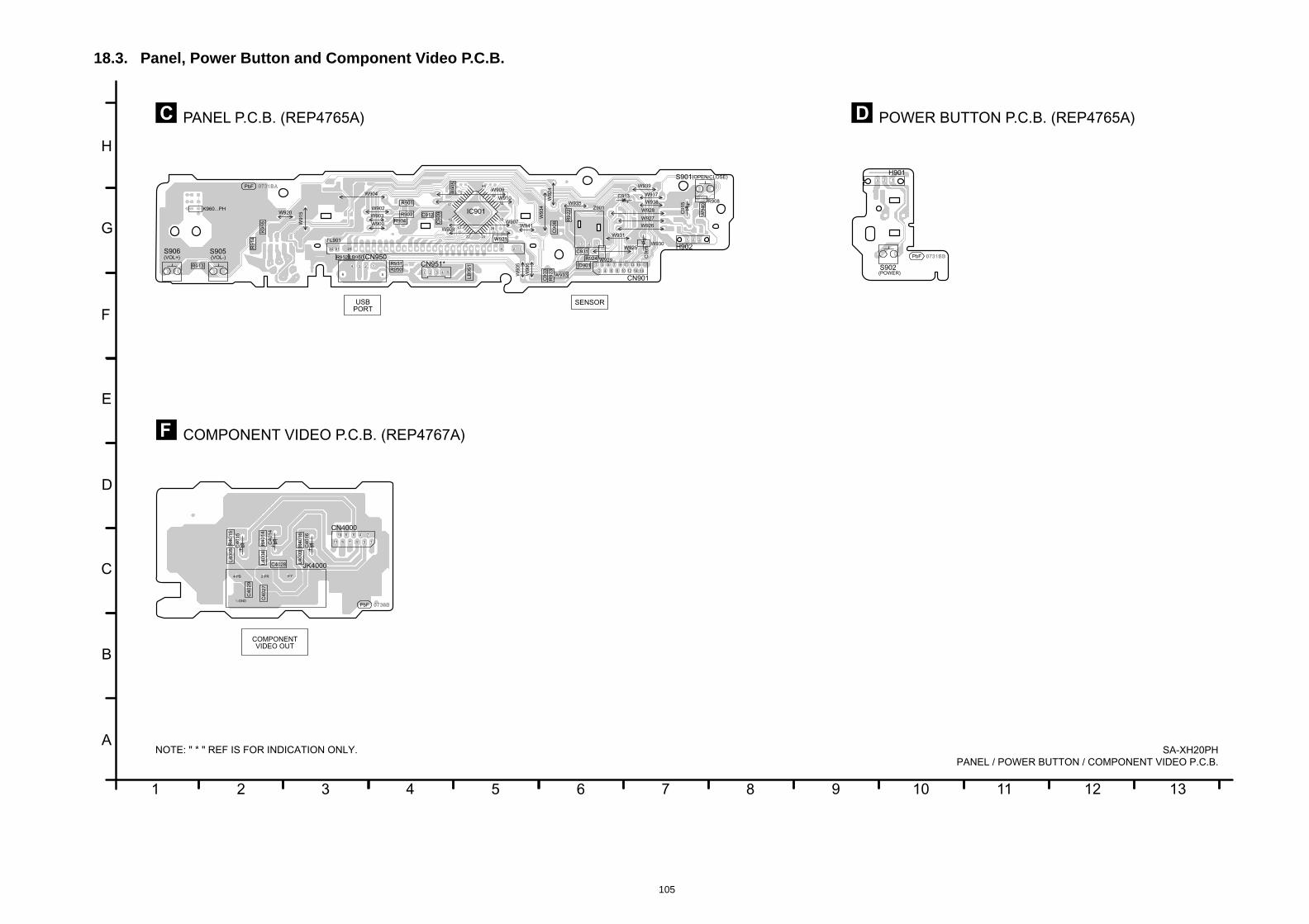
105
18.3. Panel, Power Button and Component Video P.C.B.
17 8 9
E
F
G
H
10 1 12 13
C PANEL P.C.B. (REP4765A) D POWER BUTTON P.C.B. (REP4765A)
SA-XH20PHPANEL / POWER BUTTON / COMPONENT VIDEO P.C.B.
0731BB0731BB
0731BA0731BA
W921
D901
IC901
C90
9
R913(POWER)
(VOL-)(VOL+)
R90
5
R904R903
R91
4
R950
LB950R952
C912
LB95
1
R92
2
C90
8R
923
C90
3
R924
R901
R951
C931
R908
(OPEN/CLOSE)
W929
W930
W933
W94
0
K95
5
K960...PHW920
W91
5
FL901
W90
6
W90
5
W902
W903
W900
W904W909
W910
W907
W908
S906 S905
C90
5
Z901
C913
C91
5
CN901
SENSORUSBPORT
S901
W92
4
W925
W926W927
W928
W937
W938
W931
W93
4
W935
W939
W941
CN950
H902
S902
H901
PbF
PbF
CN951*1 2 3 4 5
143132 229
123
1
2
3
4
5
6
7
8
9
10
11
12
13 15
14
17
164 3 2 1
56
1 2 3
1
5
11
12
17
22 23
28
33
34
39
44
123
1 2 3 4 5 6
A
B
C
D
NOTE: " * " REF IS FOR INDICATION ONLY.
F COMPONENT VIDEO P.C.B. (REP4767A)
COMPONENTVIDEO OUT
C40
14
C40
15
C40
16
R40
14
R40
15
R40
16
C40
27
C4028
C40
29
L400
3
L400
4
L400
5
JK4000
CN4000
11 9
10 2
1
4
3
6
5
8
7
3-Y4-PB 2-PR
1-GND0736B0736BPbF
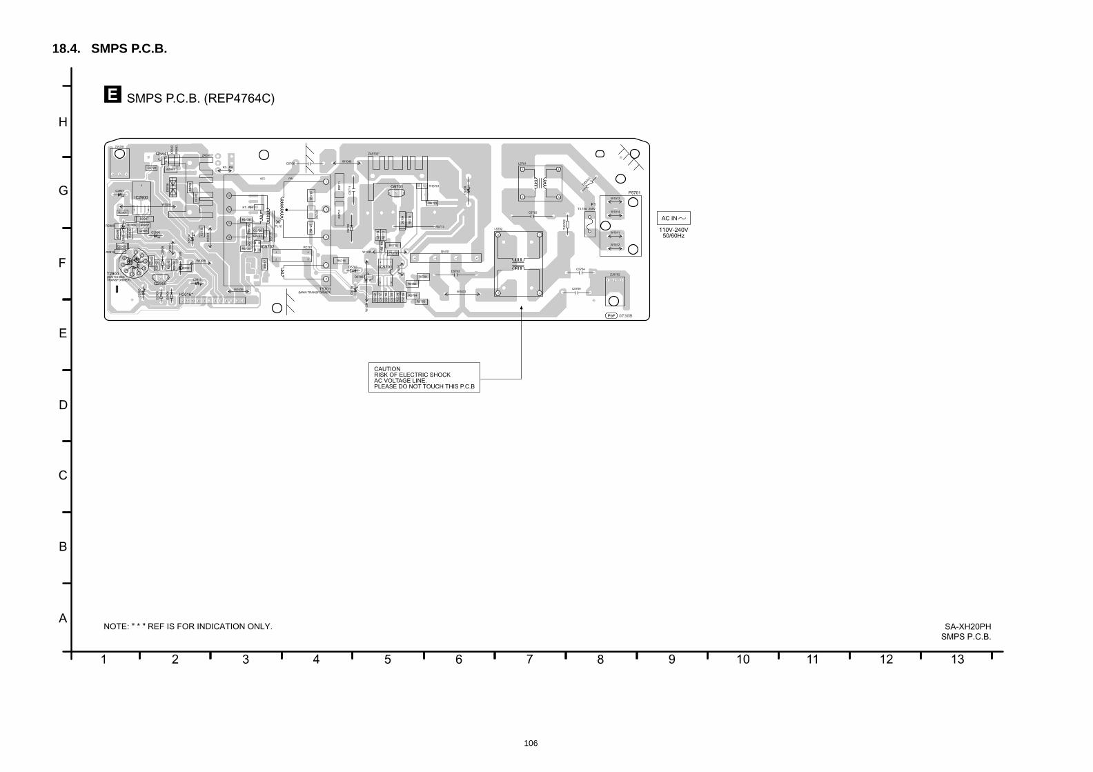
106
18.4. SMPS P.C.B.
17 8 9
E
F
G
H
10 1 12 13
E SMPS P.C.B. (REP4764C)
SA-XH20PHSMPS P.C.B.
0730B0730B
D5705
R29
05
R5703
R5702
R5701
R5704
D57
04
R58
17
D2907
C57
20
R5716
R29
03
C57
19
PC701
R57
11R
5710
TH5701
IC5701
C5729
C5727
C5726
C57
25
C57
21
C57
18
C57
17
C5715
C57
14R57
35R
5731
R5730
R57
29
R5728
R57
26
R57
24
R5723
R57
22
R57
21
R57
20
R57
19
R57
18R
5717
R5715
R57
14
C29
02
C2908
C58
43
D2901
D2909
IC2900
Q5841
R29
00R29
02
R2906 R2907
R2914
R58
42
R5843
R2908
R29
09
R2901
IC5702
W1039
W1038
W10
37
W10
36
W1035
W10
34
W1033
TH
5702
W1013
W10
31W1026
H2016*C5705
C5704
R5713
F1
D5703
D57
02
C2912
W1012
W1011
C57
09
ZA5703*
Q5701
C57
11
ZJ5701
Q2900
D57
06
C57
24
C57
16
C5706
SEC PRI
C2906
C29
03
C29
00
C2907
D29
03
D29
06
D29
08
L290
0
T2900(SWITCHING TRANSFORMER)
ZA5803*
ZJ5702
P5701
L5702
DZ5701
D5701
C5703
C5702
W1040
T5701(MAIN TRANSFORMER)
W1014T3.15A 250V
110V-240V50/60Hz
AC IN
K3...PHL5701
2
1 4
3
K7...PH
TL12
PbF
BCE
GDS
12345678912 11 10
3 2 1
9
8
76 5
4
3
21
321
12
3 4
+1-4 ~3 ~2
15
14
13
12
7
3
1
5
8
4
32
1
14
5 8
5
3
1
3
2
4
1
BC
E
B
C
E
1 2 3 4 5 6
A
B
C
D
NOTE: " * " REF IS FOR INDICATION ONLY.
CAUTIONRISK OF ELECTRIC SHOCKAC VOLTAGE LINE.PLEASE DO NOT TOUCH THIS P.C.B
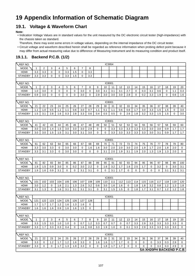
19 Appendix Information of Schematic Diagram19.1. Voltage & Waveform ChartNote:
• Indication Voltage Values are in standard values for the unit measured by the DC electronic circuit tester (high-impedance) withthe chassis taken as standard.Therefore, there may exist some errors in voltage values, depending on the internal impedance of the DC circuit tester.
• Circuit voltage and waveform described herein shall be regarded as reference information when probing defect point because itmay differ from actual measuring value due to difference of Measuring instrument and its measuring condition and product itself.
19.1.1. Backend P.C.B. (1/2)
REF NO.
MODE 1 2 3 4 5 6 7 8
HDMI 3.3 3.3 0 0 3.3 1.5 0 3.3
STANDBY 3.3 3.3 0 0 3.3 1.5 0 3.3
REF NO.
MODE 1 2 3 4 5 6 7 8 9 10 11 12 13 14 15 16 17 18 19 20
HDMI 1.0 3.0 0 0 0 0 3.0 0 3.0 3.1 3.1 3.1 2.7 0 0.3 3.1 0.6 0 1.1 0.4
STANDBY 0.9 3.0 0 0 0 0 3.0 0 2.9 3.0 3.0 3.0 2.8 0 0.2 3.3 1.9 0 0.6 1.6
REF NO.
MODE 21 22 23 24 25 26 27 28 29 30 31 32 33 34 35 36 37 38 39 40
HDMI 1.1 1.0 0.5 1.1 1.1 0.6 3.0 0.7 1.1 0.1 1.1 0.6 0.6 1.7 3.0 3.3 1.5 1.5 0 3.0
STANDBY 1.5 3.1 2.8 1.6 0.3 2.8 3.3 0.6 0.4 0.5 0.5 0 2.6 1.8 3.2 3.3 1.5 1.5 0 3.0
REF NO.
MODE 41 42 43 44 45 46 47 48 49 50 51 52 53 54 55 56 57 58 59 60
HDMI 3.0 3.0 1.4 1.5 3.0 3.0 3.0 2.9 0 0 3.3 3.3 3.3 3.3 3.3 3.0 3.0 0.9 1.7 1.7
STANDBY 3.0 3.0 1.5 1.5 3.1 3.0 3.1 3.0 0 0 3.3 3.3 3.3 3.3 3.3 3.0 3.1 0.9 1.7 1.7
REF NO.
MODE 61 62 63 64 65 66 67 68 69 70 71 72 73 74 75 76 77 78 79 80
HDMI 3.3 3.0 3.3 0 3.0 3.0 0 1.6 1.6 3.0 2.0 2.0 3.0 2.0 1.9 1.7 2.0 1.8 2.0 0
STANDBY 3.3 3.1 3.3 0 3.0 3.0 0 0 0 3.1 2.0 1.9 3.1 1.9 2.0 1.3 1.9 1.3 2.0 0
REF NO.
MODE 81 82 83 84 85 86 87 88 89 90 91 92 93 94 95 96 97 98 99 100
HDMI 1.9 1.5 0.9 3.0 0 0.2 3.0 2.2 0 1.6 3.2 1.7 1.6 2.5 1.7 0 3.2 0 3.0 3.1
STANDBY 1.9 1.6 0.9 3.1 0 0 3.1 3.1 0 0 3.1 1.7 0 0 0 0 0 3.1 3.1 3.1
REF NO.
MODE 101 102 103 104 105 106 107 108 109 110 111 112 113 114 115 116 117 118 119 120
HDMI 3.0 1.2 0 1.6 2.1 1.3 2.6 3.2 0.6 3.0 1.6 1.6 0 1.8 1.8 3.2 0.8 1.2 1.3 1.8
STANDBY 3.1 1.3 0 1.6 3.1 3.1 3.1 3.1 0 3.1 1.5 1.5 0 1.8 1.7 3.1 0.7 1.2 1.2 1.8
REF NO.
MODE 121 122 123 124 125 126 127 128
HDMI 1.7 1.7 1.7 1.2 1.6 1.3 1.6 0
STANDBY 1.6 1.6 1.6 0.9 1.6 1.6 1.5 0
REF NO.
MODE 1 2 3 4 5 6 7 8 9 10 11 12 13 14 15 16 17 18 19 20
HDMI 3.3 1.5 3.3 1.0 1.0 0 0.7 1.2 3.3 0.7 0.7 0 0.7 3.3 2.9 3.3 3.3 3.3 3.3 0
STANDBY 3.3 1.7 3.3 0.3 0.4 0 1.6 0.8 3.3 1.9 1.0 0 0.1 3.3 2.9 3.3 3.3 3.3 3.3 0
REF NO.
MODE 21 22 23 24 25 26 27 28 29 30 31 32 33 34 35 36 37 38 39 40
HDMI 3.3 0 1.2 1.7 1.2 1.6 3.3 0 1.6 1.6 1.7 1.7 0 0 0 0 3.3 0.3 2.9 0
STANDBY 3.3 0 0 1.7 1.3 1.9 3.3 0 0 1.8 1.7 1.7 0 0 0 0 3.3 0.3 2.9 0
IC8001
IC8001
IC8051
SA-XH20PH BACKEND P.C.B.
IC8051
IC8001
IC8001
IC3954
IC8001
IC8001
IC8001
107
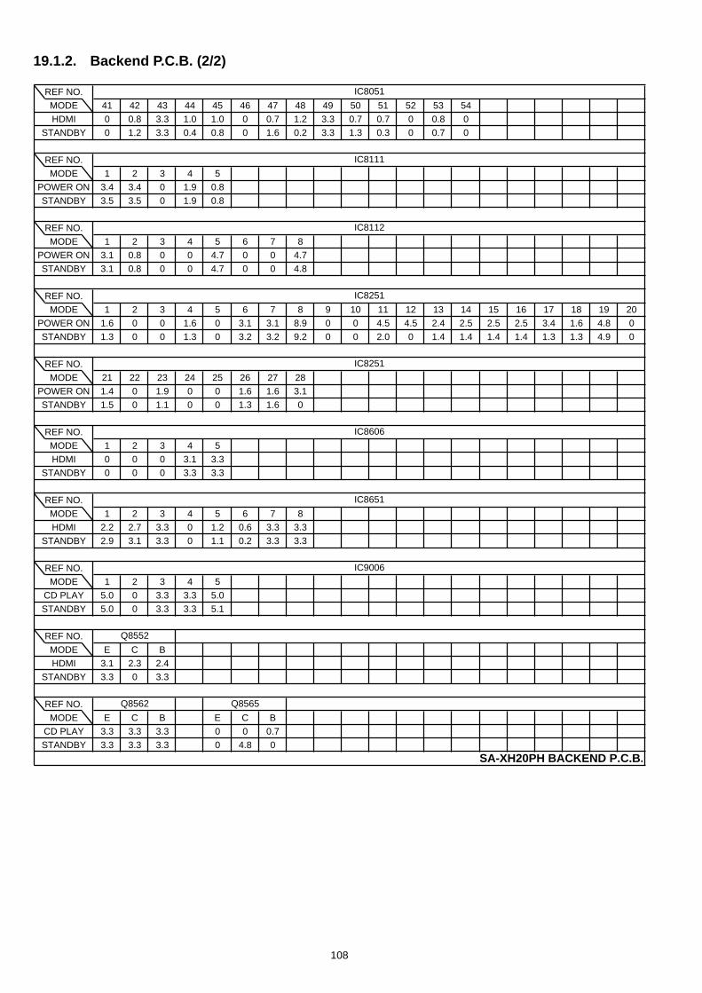
19.1.2. Backend P.C.B. (2/2)
REF NO.
MODE 41 42 43 44 45 46 47 48 49 50 51 52 53 54
HDMI 0 0.8 3.3 1.0 1.0 0 0.7 1.2 3.3 0.7 0.7 0 0.8 0
STANDBY 0 1.2 3.3 0.4 0.8 0 1.6 0.2 3.3 1.3 0.3 0 0.7 0
REF NO.
MODE 1 2 3 4 5
POWER ON 3.4 3.4 0 1.9 0.8
STANDBY 3.5 3.5 0 1.9 0.8
REF NO.
MODE 1 2 3 4 5 6 7 8
POWER ON 3.1 0.8 0 0 4.7 0 0 4.7
STANDBY 3.1 0.8 0 0 4.7 0 0 4.8
REF NO.
MODE 1 2 3 4 5 6 7 8 9 10 11 12 13 14 15 16 17 18 19 20
POWER ON 1.6 0 0 1.6 0 3.1 3.1 8.9 0 0 4.5 4.5 2.4 2.5 2.5 2.5 3.4 1.6 4.8 0
STANDBY 1.3 0 0 1.3 0 3.2 3.2 9.2 0 0 2.0 0 1.4 1.4 1.4 1.4 1.3 1.3 4.9 0
REF NO.
MODE 21 22 23 24 25 26 27 28
POWER ON 1.4 0 1.9 0 0 1.6 1.6 3.1
STANDBY 1.5 0 1.1 0 0 1.3 1.6 0
REF NO.
MODE 1 2 3 4 5
HDMI 0 0 0 3.1 3.3
STANDBY 0 0 0 3.3 3.3
REF NO.
MODE 1 2 3 4 5 6 7 8
HDMI 2.2 2.7 3.3 0 1.2 0.6 3.3 3.3
STANDBY 2.9 3.1 3.3 0 1.1 0.2 3.3 3.3
REF NO.
MODE 1 2 3 4 5
CD PLAY 5.0 0 3.3 3.3 5.0
STANDBY 5.0 0 3.3 3.3 5.1
REF NO.
MODE E C B
HDMI 3.1 2.3 2.4
STANDBY 3.3 0 3.3
REF NO.
MODE E C B E C B
CD PLAY 3.3 3.3 3.3 0 0 0.7
STANDBY 3.3 3.3 3.3 0 4.8 0
Q8562 Q8565
SA-XH20PH BACKEND P.C.B.
Q8552
IC8251
IC8606
IC8651
IC9006
IC8051
IC8111
IC8112
IC8251
108
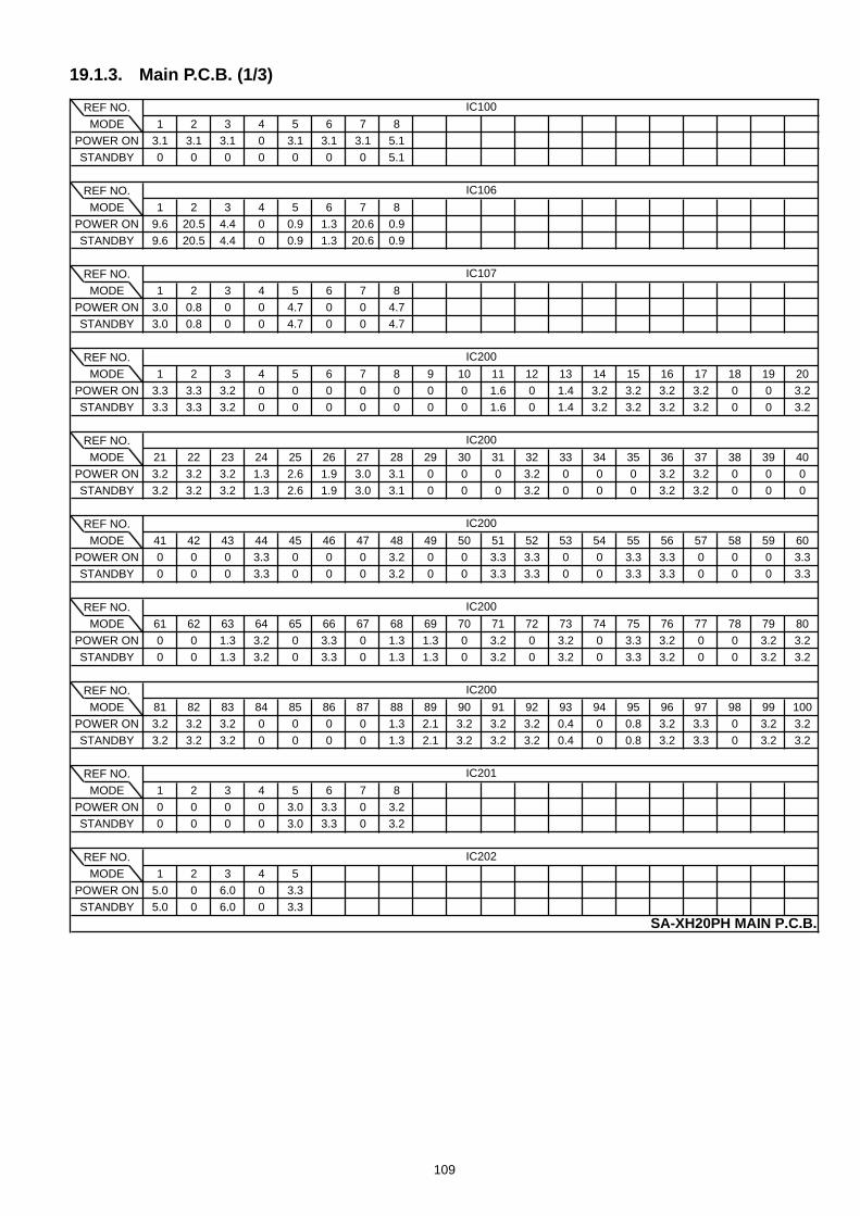
19.1.3. Main P.C.B. (1/3)
REF NO.
MODE 1 2 3 4 5 6 7 8
POWER ON 3.1 3.1 3.1 0 3.1 3.1 3.1 5.1
STANDBY 0 0 0 0 0 0 0 5.1
REF NO.
MODE 1 2 3 4 5 6 7 8
POWER ON 9.6 20.5 4.4 0 0.9 1.3 20.6 0.9
STANDBY 9.6 20.5 4.4 0 0.9 1.3 20.6 0.9
REF NO.
MODE 1 2 3 4 5 6 7 8
POWER ON 3.0 0.8 0 0 4.7 0 0 4.7
STANDBY 3.0 0.8 0 0 4.7 0 0 4.7
REF NO.
MODE 1 2 3 4 5 6 7 8 9 10 11 12 13 14 15 16 17 18 19 20
POWER ON 3.3 3.3 3.2 0 0 0 0 0 0 0 1.6 0 1.4 3.2 3.2 3.2 3.2 0 0 3.2
STANDBY 3.3 3.3 3.2 0 0 0 0 0 0 0 1.6 0 1.4 3.2 3.2 3.2 3.2 0 0 3.2
REF NO.
MODE 21 22 23 24 25 26 27 28 29 30 31 32 33 34 35 36 37 38 39 40
POWER ON 3.2 3.2 3.2 1.3 2.6 1.9 3.0 3.1 0 0 0 3.2 0 0 0 3.2 3.2 0 0 0
STANDBY 3.2 3.2 3.2 1.3 2.6 1.9 3.0 3.1 0 0 0 3.2 0 0 0 3.2 3.2 0 0 0
REF NO.
MODE 41 42 43 44 45 46 47 48 49 50 51 52 53 54 55 56 57 58 59 60
POWER ON 0 0 0 3.3 0 0 0 3.2 0 0 3.3 3.3 0 0 3.3 3.3 0 0 0 3.3
STANDBY 0 0 0 3.3 0 0 0 3.2 0 0 3.3 3.3 0 0 3.3 3.3 0 0 0 3.3
REF NO.
MODE 61 62 63 64 65 66 67 68 69 70 71 72 73 74 75 76 77 78 79 80
POWER ON 0 0 1.3 3.2 0 3.3 0 1.3 1.3 0 3.2 0 3.2 0 3.3 3.2 0 0 3.2 3.2
STANDBY 0 0 1.3 3.2 0 3.3 0 1.3 1.3 0 3.2 0 3.2 0 3.3 3.2 0 0 3.2 3.2
REF NO.
MODE 81 82 83 84 85 86 87 88 89 90 91 92 93 94 95 96 97 98 99 100
POWER ON 3.2 3.2 3.2 0 0 0 0 1.3 2.1 3.2 3.2 3.2 0.4 0 0.8 3.2 3.3 0 3.2 3.2
STANDBY 3.2 3.2 3.2 0 0 0 0 1.3 2.1 3.2 3.2 3.2 0.4 0 0.8 3.2 3.3 0 3.2 3.2
REF NO.
MODE 1 2 3 4 5 6 7 8
POWER ON 0 0 0 0 3.0 3.3 0 3.2
STANDBY 0 0 0 0 3.0 3.3 0 3.2
REF NO.
MODE 1 2 3 4 5
POWER ON 5.0 0 6.0 0 3.3
STANDBY 5.0 0 6.0 0 3.3
IC200
IC200
IC100
IC106
IC107
IC200
IC200
IC200
IC202
SA-XH20PH MAIN P.C.B.
IC201
109

19.1.4. Main P.C.B. (2/3)
REF NO.
MODE 1 2 3 4 5 6 7 8 9 10 11 12 13 14 15 16
SELECTOR 2.8 3.0 2.2 3.0 3.0 0 -5.0 0 3.0 3.0 3.0 2.8 2.2 3.0 3.0 5.0
STANDBY 2.8 3.0 0 3.0 3.0 0 -5.0 0 3.0 3.0 3.0 2.8 0 3.0 3.0 5.0
REF NO.
MODE 1 2 3 4 5 6 7 8 9 10 11 12 13 14 15 16 17 18 19 20
CD PLAY 1.8 0 0.8 0.9 0 0 2.0 0 3.3 1.3 3.3 0 3.3 3.3 3.3 0 1.9 0 0.5 0.8
STANDBY 1.8 0 0.8 0.9 0 0 1.9 0 3.3 1.3 3.3 0 3.3 3.3 3.3 0 1.9 0 0 0.9
REF NO.
MODE 21 22 23 24 25 26 27 28 29 30 31 32 33 34 35 36 37 38 39 40
CD PLAY 0 0 0 3.3 3.3 1.7 0 3.3 3.3 3.3 3.3 3.3 0 0 0 3.3 0 0 0 3.0
STANDBY 0 0 0 0 3.3 1.7 0 0 3.3 0 0 3.3 0 0 0 3.3 0 0 0 0
REF NO.
MODE 41 42 43 44 45 46 47 48 49 50 51 52 53 54 55 56 57 58 59 60
CD PLAY 1.4 1.3 1.3 1.2 1.2 1.2 1.2 0 1.1 1.1 1.4 1.4 0 3.3 0 0 0 0 0 0
STANDBY 0 0 0 0 0 0 0 0 0 0 0 0 0 3.3 0 0 0 0 0 0
REF NO.
MODE 61 62 63 64
CD PLAY 0 0 0 0
STANDBY 0 0 0 0
REF NO.
MODE 1 2 3 4 5 6 7 8 9 10 11 12 13 14 15 16 17 18 19 20
CD PLAY 12.0 3.3 0 0 3.2 1.6 3.3 1.4 0 0 0 0 0 0 0 1.4 3.9 1.4 0 0
STANDBY 12.0 3.3 0 0 0 0 3.3 0 0 0 0 0 0 0 0 0 0 0 0 0
REF NO.
MODE 21 22 23 24 25 26 27 28 29 30 31 32 33 34 35 36 37 38 39 40
CD PLAY 12.0 12.0 12.0 10.1 0 20.3 20.3 1.4 0 0 1.4 20.3 10.2 10.2 20.3 1.2 0 0 1.2 20.3
STANDBY 12.0 12.0 12.0 10.1 0 20.3 20.3 0 0 0 0 20.3 10.2 10.2 20.3 0 0 0 0 20.3
REF NO.
MODE 41 42 43 44
CD PLAY 20.3 0 10.2 12.0
STANDBY 20.3 0 10.2 12.0
REF NO.
MODE 1 2 3 4 5 6 7 8 9 10 11 12 13 14 15 16 17 18 19 20
CD PLAY 12.0 3.3 0 0 3.2 1.6 3.3 1.4 0 0 0 0 0 0 0 1.4 3.9 1.4 0 0
STANDBY 12.0 3.3 0 0 0 0 3.3 0 0 0 0 0 0 0 0 0 0 0 0 0
REF NO.
MODE 21 22 23 24 25 26 27 28 29 30 31 32 33 34 35 36 37 38 39 40
CD PLAY 12.0 12.0 12.0 10.1 0 20.3 20.3 1.4 0 0 1.4 20.3 10.2 10.2 20.3 1.2 0 0 1.2 20.3
STANDBY 12.0 12.0 12.0 10.1 0 20.3 20.3 0 0 0 0 20.3 10.2 10.2 20.3 0 0 0 0 20.3
IC403
IC403
IC404
SA-XH20PH MAIN P.C.B.
IC404
IC401
IC403
IC300
IC401
IC401
IC401
110

19.1.5. Main P.C.B. (3/3)
REF NO.
MODE 41 42 43 44
CD PLAY 20.3 0 10.2 12.0
STANDBY 20.3 0 10.2 12.0
REF NO.
MODE 1 2 3 4 5 6 7 8 9 10 11 12 13 14 15 16 17 18 19 20
CD PLAY 12.0 3.3 0 0 3.2 1.6 3.3 1.4 0 0 0 0 0 0 0 1.4 3.9 1.4 0 0
STANDBY 12.0 3.3 0 0 0 0 3.3 0 0 0 0 0 0 0 0 0 0 0 0 0
REF NO.
MODE 21 22 23 24 25 26 27 28 29 30 31 32 33 34 35 36 37 38 39 40
CD PLAY 12.0 12.0 12.0 10.1 0 20.3 20.3 1.4 0 0 1.4 20.3 10.2 10.2 20.3 1.2 0 0 1.2 20.3
STANDBY 12.0 12.0 12.0 10.1 0 20.3 20.3 0 0 0 0 20.3 10.2 10.2 20.3 0 0 0 0 20.3
REF NO.
MODE 41 42 43 44
CD PLAY 20.3 0 10.2 12.0
STANDBY 20.3 0 10.2 12.0
REF NO.
MODE 1 2 3 4 5 6 7 8 9 10 11 12 13 14 15 16 17 18 19 20
TUNER 0 2.8 0 0 2.8 0 3.3 2.8 2.8 3.3 3.3 0 2.8 2.8 2.8 0 2.8 0 0 0
STANDBY 0 2.8 0 0 2.8 0 3.3 2.8 2.8 3.3 3.3 0 2.8 2.8 2.8 0 2.8 0 0 0
REF NO.
MODE 1 2 3 4 5 6 7 8 9 10 11 12 13 14 15 16
CD PLAY 2.4 2.4 0 2.4 0 4.8 3.3 0 1.2 1.4 1.5 1.5 3.1 3.1 0 0
STANDBY 0 0 0 2.4 0 4.8 3.3 0 0 0 1.5 1.5 3.1 3.1 0 0
REF NO.
MODE 1 2 3 4 5 6 E C B E C B E C B
POWER ON 4.9 4.9 0 5.0 4.9 4.9 0 0 2.7 -5.0 -6.0 0 0 3.2 0
STANDBY 4.9 4.9 0 5.0 4.9 4.9 0 0 2.7 -5.0 -6.0 0 0 3.2 0
REF NO.
MODE E C B E C B E C B E C B E C B
POWER ON 0 3.1 0 9.3 12.1 10.0 0 3.1 0 20.6 0 0 0 3.1 3.1
STANDBY 0 3.1 0 9.3 12.1 10.0 0 3.1 0 20.6 0 0 0 0 0
REF NO.
MODE E C B E C B E C B E C B
POWER ON 0 3.1 3.1 0 3.1 3.1 1.4 0 10.3 10.3 0 1.4
STANDBY 0 0 0 0 0 0 1.4 0 10.3 10.3 0 1.4
REF NO.
MODE E C B E C B
SELECTOR 0 7.0 3.1 0 7.0 3.1
STANDBY 0 7.0 3.1 0 7.0 0
SA-XH20PH MAIN P.C.B.
Q300 Q301
IC600
IC404
IC405
IC405
IC405
Q122
Q123 Q124 Q500 Q501
Q106 Q107 Q114 Q116
IC700
Q100 Q101 Q102 Q105
111
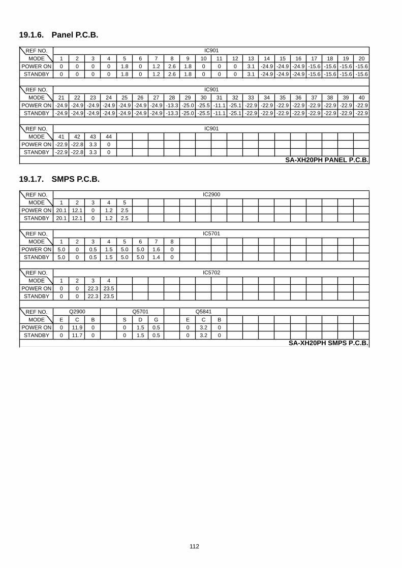
19.1.6. Panel P.C.B.
19.1.7. SMPS P.C.B.
REF NO.
MODE 1 2 3 4 5 6 7 8 9 10 11 12 13 14 15 16 17 18 19 20
POWER ON 0 0 0 0 1.8 0 1.2 2.6 1.8 0 0 0 3.1 -24.9 -24.9 -24.9 -15.6 -15.6 -15.6 -15.6
STANDBY 0 0 0 0 1.8 0 1.2 2.6 1.8 0 0 0 3.1 -24.9 -24.9 -24.9 -15.6 -15.6 -15.6 -15.6
REF NO.
MODE 21 22 23 24 25 26 27 28 29 30 31 32 33 34 35 36 37 38 39 40
POWER ON -24.9 -24.9 -24.9 -24.9 -24.9 -24.9 -24.9 -13.3 -25.0 -25.5 -11.1 -25.1 -22.9 -22.9 -22.9 -22.9 -22.9 -22.9 -22.9 -22.9
STANDBY -24.9 -24.9 -24.9 -24.9 -24.9 -24.9 -24.9 -13.3 -25.0 -25.5 -11.1 -25.1 -22.9 -22.9 -22.9 -22.9 -22.9 -22.9 -22.9 -22.9
REF NO.
MODE 41 42 43 44
POWER ON -22.9 -22.8 3.3 0
STANDBY -22.9 -22.8 3.3 0
IC901
IC901
IC901
SA-XH20PH PANEL P.C.B.
REF NO.
MODE 1 2 3 4 5
POWER ON 20.1 12.1 0 1.2 2.5
STANDBY 20.1 12.1 0 1.2 2.5
REF NO.
MODE 1 2 3 4 5 6 7 8
POWER ON 5.0 0 0.5 1.5 5.0 5.0 1.6 0
STANDBY 5.0 0 0.5 1.5 5.0 5.0 1.4 0
REF NO.
MODE 1 2 3 4
POWER ON 0 0 22.3 23.5
STANDBY 0 0 22.3 23.5
REF NO.
MODE E C B S D G E C B
POWER ON 0 11.9 0 0 1.5 0.5 0 3.2 0
STANDBY 0 11.7 0 0 1.5 0.5 0 3.2 0
SA-XH20PH SMPS P.C.B.
IC2900
IC5701
IC5702
Q2900 Q5701 Q5841
112
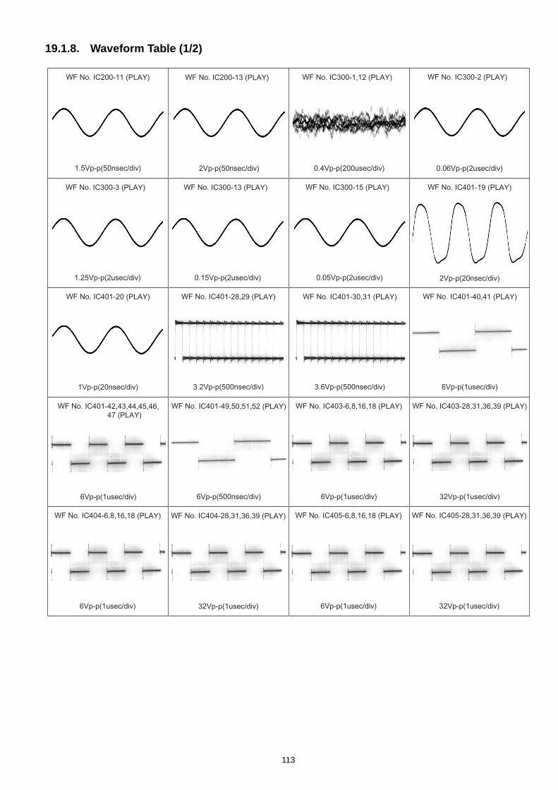
19.1.8. Waveform Table (1/2)
WF No. IC200-11 (PLAY)
1.5Vp-p(50nsec/div)
WF No. IC200-13 (PLAY)
2Vp-p(50nsec/div)
WF No. IC300-1,12 (PLAY)
0.4Vp-p(200usec/div)
WF No. IC300-2 (PLAY)
0.06Vp-p(2usec/div)
WF No. IC300-15 (PLAY)
0.05Vp-p(2usec/div)
WF No. IC300-3 (PLAY)
1.25Vp-p(2usec/div)
WF No. IC300-13 (PLAY)
0.15Vp-p(2usec/div)
WF No. IC401-19 (PLAY)
2Vp-p(20nsec/div)
WF No. IC401-20 (PLAY)
1Vp-p(20nsec/div)
WF No. IC401-42,43,44,45,46, 47 (PLAY)
6Vp-p(1usec/div)
WF No. IC401-28,29 (PLAY)
3.2Vp-p(500nsec/div)
WF No. IC401-49,50,51,52 (PLAY)
6Vp-p(500nsec/div)
WF No. IC401-30,31 (PLAY)
3.6Vp-p(500nsec/div)
WF No. IC401-40,41 (PLAY)
6Vp-p(1usec/div)
WF No. IC403-6,8,16,18 (PLAY)
6Vp-p(1usec/div)
WF No. IC404-6,8,16,18 (PLAY)
6Vp-p(1usec/div)
WF No. IC403-28,31,36,39 (PLAY)
32Vp-p(1usec/div)
WF No. IC405-6,8,16,18 (PLAY)
6Vp-p(1usec/div)
WF No. IC405-28,31,36,39 (PLAY)
32Vp-p(1usec/div)
WF No. IC404-28,31,36,39 (PLAY)
32Vp-p(1usec/div)
113

19.1.9. Waveform Table (2/2)
WF No. IC600-2,13,14 (PLAY)
0.4Vp-p(200usec/div)
WF No. IC8001-111,112 (PLAY)
2Vp-p(20nsec/div)
WF No. IC8001-36,42 (PLAY)
4.8Vp-p(2usec/div)
WF No. IC8001-63 (PLAY)
1.25Vp-p(50usec/div)
WF No. IC8001-102 (PLAY)
5Vp-p(1usec/div)
114
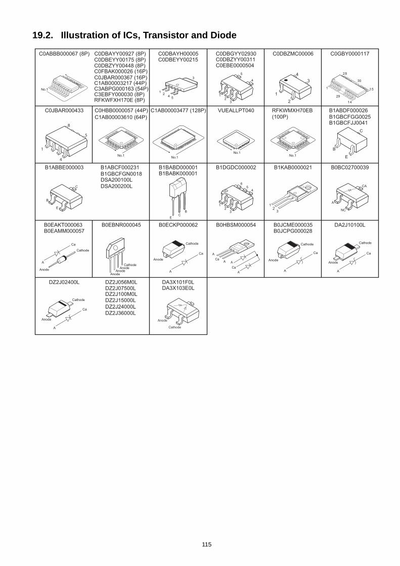
19.2. Illustration of ICs, Transistor and Diode
C0GBY0000117
DA3X101F0LDA3X103E0L
C0DBZMC00006
B0EBNR000045
B0BC02700039
B0EAMM000057B0EAKT000063 B0HBSM000054
C0DBEYY00215C0DBAYH00005
C1AB00003477 (128P)
B1BABK000001B1BABD000001B1ABBE000003
B0ECKP000062 B0JCME000035B0JCPG000028
B1DGDC000002
VUEALLPT040C0HBB0000057 (44P)
C1AB00003610 (64P)
DA2J10100L
DZ2J02400L DZ2J056M0LDZ2J07500L
DZ2J36000L
DZ2J24000L
DZ2J100M0LDZ2J15000L
B1ABDF000026
B1GBCFJJ0041B1GBCFGG0025
DSA200100L
DSA200200L
B1GBCFGN0018
B1ABCF000231 B1KAB0000021
C0EBE0000504C0DBZYY00311C0DBGYY02930C0ABBB000067 (8P) C0DBAYY00927 (8P)
C3ABPG000163 (54P)C1AB00003217 (44P)
C0FBAK000026 (16P)C0DBZYY00448 (8P)C0DBEYY00175 (8P)
C0JBAR000367 (16P)
RFKWFXH170E (8P)C3EBFY000030 (8P)
RFKWMXH70EB
(100P)
C0JBAR000433
A
Ca
Cathode
Anode
1
3
4
2
AnodeAnode
AnodeCathode
Ca
A
A
Ca
A
A
EC
BE
B
C
A
Ca
Cathode
AnodeA
Ca
Cathode
Anode
1
42
5
3
No.1
No.1
1
28
15
14
30
29
B
C
ENo.1
Cathode
Anode
A
Ca
No.1
NC
A
CA
Anode
CathodeA
Ca
Cathode
Anode
4
5
3
12
4
65
3
12
3
12
No.1
1
8
4
5
115
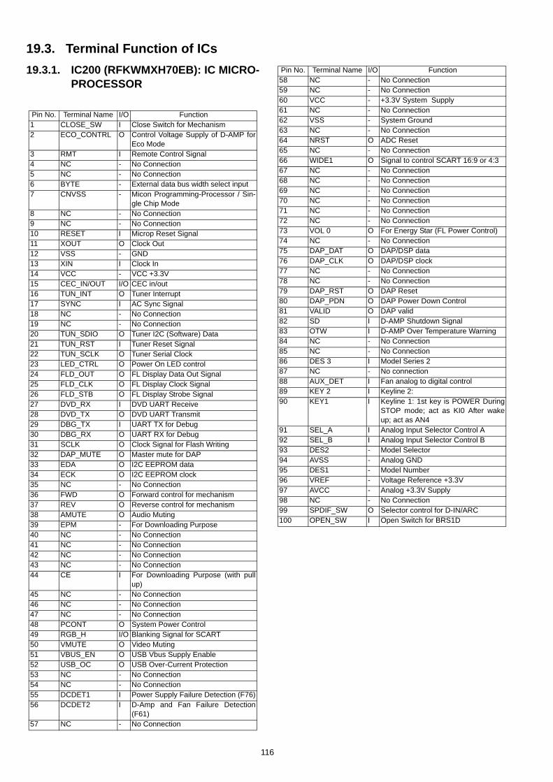
19.3. Terminal Function of ICs
19.3.1. IC200 (RFKWMXH70EB): IC MICRO-PROCESSOR
Pin No. Terminal Name I/O Function1 CLOSE_SW I Close Switch for Mechanism2 ECO_CONTRL O Control Voltage Supply of D-AMP for
Eco Mode3 RMT I Remote Control Signal4 NC - No Connection5 NC - No Connection6 BYTE - External data bus width select input7 CNVSS - Micon Programming-Processor / Sin-
gle Chip Mode8 NC - No Connection9 NC - No Connection10 RESET I Microp Reset Signal11 XOUT O Clock Out12 VSS - GND13 XIN I Clock In14 VCC - VCC +3.3V15 CEC_IN/OUT I/O CEC in/out 16 TUN_INT O Tuner Interrupt17 SYNC I AC Sync Signal18 NC - No Connection19 NC - No Connection20 TUN_SDIO O Tuner I2C (Software) Data21 TUN_RST I Tuner Reset Signal22 TUN_SCLK O Tuner Serial Clock23 LED_CTRL O Power On LED control24 FLD_OUT O FL Display Data Out Signal25 FLD_CLK O FL Display Clock Signal26 FLD_STB O FL Display Strobe Signal27 DVD_RX I DVD UART Receive28 DVD_TX O DVD UART Transmit29 DBG_TX I UART TX for Debug30 DBG_RX O UART RX for Debug31 SCLK O Clock Signal for Flash Writing32 DAP_MUTE O Master mute for DAP33 EDA O I2C EEPROM data34 ECK O I2C EEPROM clock35 NC - No Connection36 FWD O Forward control for mechanism37 REV O Reverse control for mechanism38 AMUTE O Audio Muting39 EPM - For Downloading Purpose40 NC - No Connection41 NC - No Connection42 NC - No Connection43 NC - No Connection44 CE I For Downloading Purpose (with pull
up)45 NC - No Connection46 NC - No Connection47 NC - No Connection48 PCONT O System Power Control49 RGB_H I/O Blanking Signal for SCART50 VMUTE O Video Muting51 VBUS_EN O USB Vbus Supply Enable52 USB_OC O USB Over-Current Protection53 NC - No Connection54 NC - No Connection55 DCDET1 I Power Supply Failure Detection (F76)56 DCDET2 I D-Amp and Fan Failure Detection
(F61)57 NC - No Connection
58 NC - No Connection59 NC - No Connection60 VCC - +3.3V System Supply 61 NC - No Connection62 VSS - System Ground 63 NC - No Connection64 NRST O ADC Reset65 NC - No Connection66 WIDE1 O Signal to control SCART 16:9 or 4:367 NC - No Connection68 NC - No Connection 69 NC - No Connection 70 NC - No Connection 71 NC - No Connection 72 NC - No Connection73 VOL 0 O For Energy Star (FL Power Control)74 NC - No Connection75 DAP_DAT O DAP/DSP data76 DAP_CLK O DAP/DSP clock77 NC - No Connection78 NC - No Connection79 DAP_RST O DAP Reset80 DAP_PDN O DAP Power Down Control81 VALID O DAP valid82 SD I D-AMP Shutdown Signal83 OTW I D-AMP Over Temperature Warning84 NC - No Connection85 NC - No Connection86 DES 3 I Model Series 287 NC - No connection88 AUX_DET I Fan analog to digital control89 KEY 2 I Keyline 2:90 KEY1 I Keyline 1: 1st key is POWER During
STOP mode; act as KI0 After wakeup; act as AN4
91 SEL_A I Analog Input Selector Control A92 SEL_B I Analog Input Selector Control B93 DES2 - Model Selector94 AVSS - Analog GND 95 DES1 - Model Number96 VREF - Voltage Reference +3.3V97 AVCC - Analog +3.3V Supply98 NC - No Connection 99 SPDIF_SW O Selector control for D-IN/ARC100 OPEN_SW I Open Switch for BRS1D
Pin No. Terminal Name I/O Function
116

19.4. IC901 (C0HBB0000057): IC FL Display Driver
Pin No.
Terminal Name I/O Function
1 USB RIP LED - No Connection2 NC - No Connection3 NC - No Connection4 NC - No Connection5 OSC I Oscillator Input6 DOUT - No Connection7 DIN I Data Input8 CLK I Clock Input9 STB I Serial Interface Strobe10 K1 - Key Data Input 1 (No Connec-
tion)11 K2 - Key Data Input 2 (No Connec-
tion)12 GND - GND13 VCC - Power Supply (+5V)14 P18 O No Connection15 P17 O No Connection16 P16 O Segment Output 1617 P15 O Segment Output 1518 P14 O Segment Output 1419 P13 O Segment Output 1320 P12 O Segment Output 1221 P11 O Segment Output 1122 P10 O Segment Output 1023 P9 O Segment Output 924 P8 O Segment Output 825 P7 O Segment Output 726 P6 O Segment Output 627 P5 O Segment Output 528 P4 O Segment Output 429 P3 O Segment Output 330 -VP - Voltage Supply31 P2 O Segment Output 232 P1 O Segment Output 133 G1 O Grid Segment Output 134 G2 O Grid Segment Output 235 G3 O Grid Segment Output 336 G4 O Grid Segment Output 437 G5 O Grid Segment Output538 G6 O Grid Segment Output 639 G7 O Grid Segment Output740 G8 O Grid Segment Output 841 G9 O Grid Segment Output 942 G10 O Grid Segment Output 1043 VCC - Voltage Supply (+5V)44 GND - GND
117

118
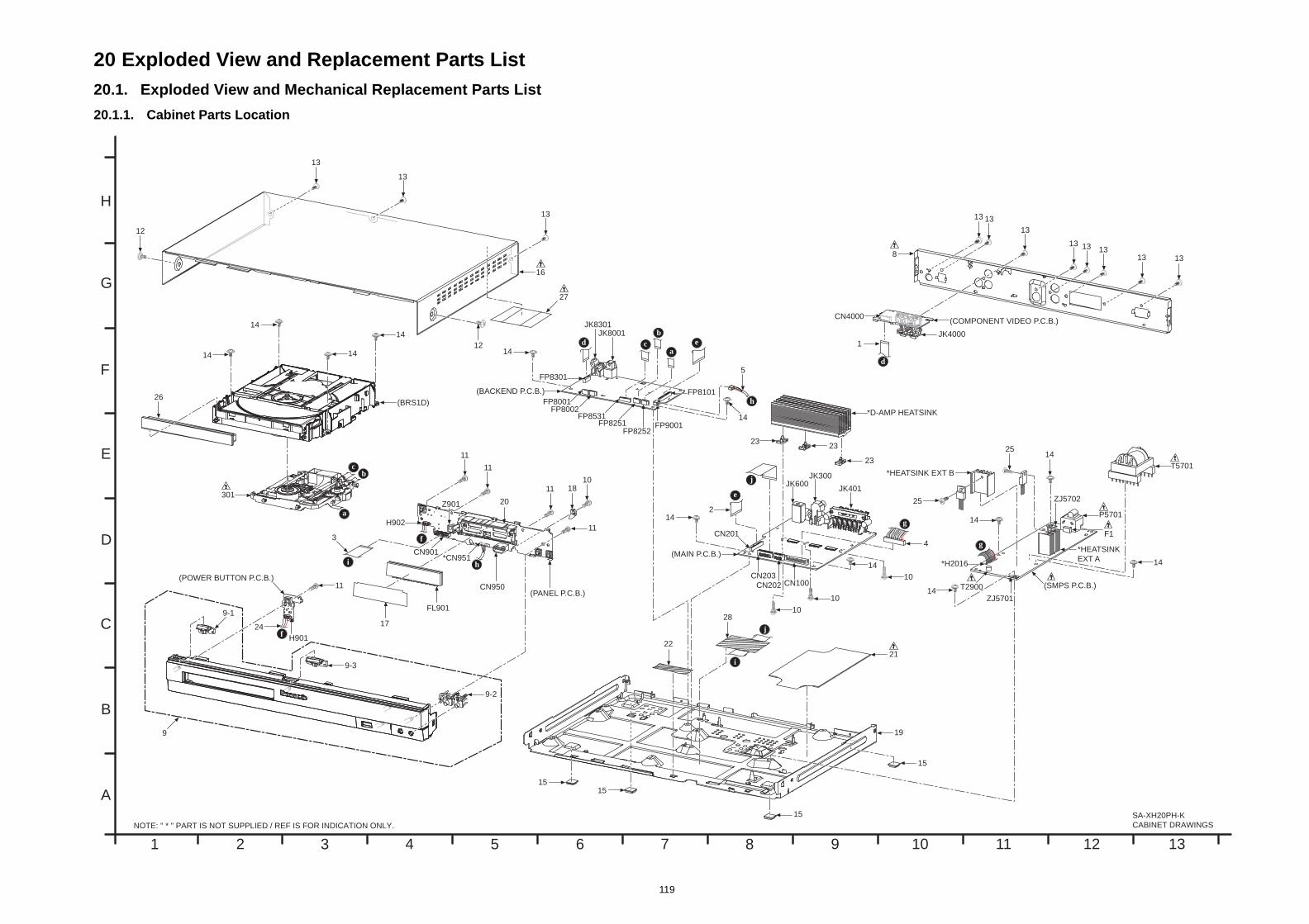
119
20 Exploded View and Replacement Parts List20.1. Exploded View and Mechanical Replacement Parts List
20.1.1. Cabinet Parts Location
(BRS1D)
(SMPS P.C.B.)
(MAIN P.C.B.)
(COMPONENT VIDEO P.C.B.)
(BACKEND P.C.B.)
ZJ5702
ZJ5701
T5701
T2900
P5701
JK8301JK8001 JK4000
JK600JK401
JK300 *HEATSINK EXT B
*HEATSINK
EXT A*H2016
FP9001FP8531
FP8301
8252FP8251
FP8101
FP8002FP8001
F1
*D-AMP HEATSINK
CN4000
CN203
CN202
CN201
CN100
28
27
26
25
25
23
2323
22
21
19
16
15
15
14
14
14
14
14
14
14
14
14
14
14
14
1313131313
13
13
1313
13
13
12
12
10
10
10
8
5
4
2
1a
b
cd
d
e
e
g
g
h
i
j
j
7 8 9
F
G
H
10 11 12 13
SA-XH20PH-K
CABINET DRAWINGS
(POWER BUTTON P.C.B.)
(PANEL P.C.B.)
Z901
H902
H901
FP
FL901
*CN951
CN950
CN901
301
24
20
18
17
1515
11
11
11
11
11
10
9-3
9-2
9-1
9
3
a
bc
f
f
hi
1 2 3 4 5 6
A
B
C
D
E
NOTE: " * " PART IS NOT SUPPLIED / REF IS FOR INDICATION ONLY.

120
20.1.2. Packaging
-XH70GS
SA-XH20PH
ACCESSORIES BAG
AC PLUG ADAPTORA8
VIDEO CABLEA6
FM INDOOR ANTENNAA4
A3 OI BOOK
AC CORDA2A1-1A1
P3
*P2*P2
7 8 9
E
F
G
H
10 11 12 13
SC-XH20PH-K
PACKAGING DRAWINGS
SB
FRONTP1
1 2 3 4 5 6
A
B
C
D
POLYFOAM (LEFT)
POLYFOAM (RIGHT)
*P2
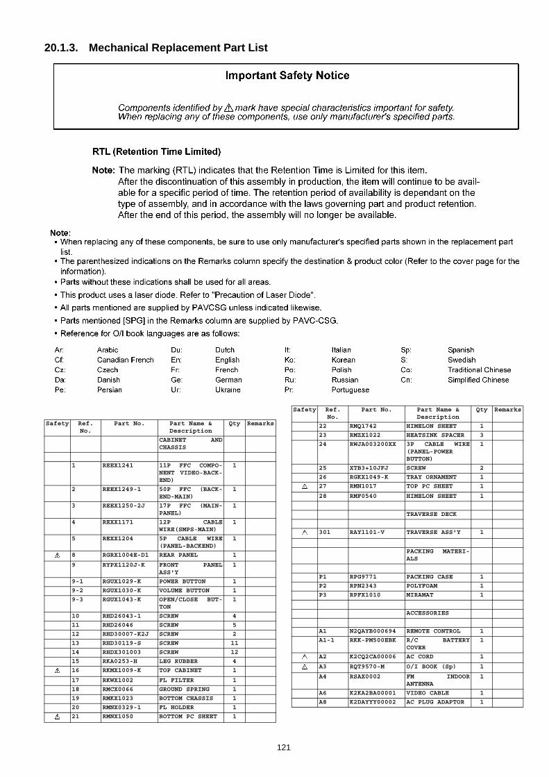
20.1.3. Mechanical Replacement Part List
Safety Ref. No.
Part No. Part Name & Description
Qty Remarks
CABINET ANDCHASSIS
1 REEX1241 11P FFC COMPO-NENT VIDEO-BACK-END)
1
2 REEX1249-1 50P FFC (BACK-END-MAIN)
1
3 REEX1250-2J 17P FFC (MAIN-PANEL)
1
4 REXX1171 12P CABLEWIRE(SMPS-MAIN)
1
5 REXX1204 5P CABLE WIRE(PANEL-BACKEND)
1
8 RGRX1004E-D1 REAR PANEL 1
9 RYPX1120J-K FRONT PANELASS'Y
1
9-1 RGUX1029-K POWER BUTTON 1
9-2 RGUX1030-K VOLUME BUTTON 1
9-3 RGUX1043-K OPEN/CLOSE BUT-TON
1
10 RHD26043-1 SCREW 4
11 RHD26046 SCREW 5
12 RHD30007-K2J SCREW 2
13 RHD30119-S SCREW 11
14 RHDX301003 SCREW 12
15 RKA0253-H LEG RUBBER 4
16 RKMX1009-K TOP CABINET 1
17 RKWX1002 FL FILTER 1
18 RMCX0066 GROUND SPRING 1
19 RMKX1023 BOTTOM CHASSIS 1
20 RMNX0329-1 FL HOLDER 1
21 RMNX1050 BOTTOM PC SHEET 1
22 RMQ1742 HIMELON SHEET 1
23 RMZX1022 HEATSINK SPACER 3
24 RWJA003200XX 3P CABLE WIRE(PANEL-POWERBUTTON)
1
25 XTB3+10JFJ SCREW 2
26 RGKX1049-K TRAY ORNAMENT 1
27 RMN1017 TOP PC SHEET 1
28 RMF0540 HIMELON SHEET 1
TRAVERSE DECK
301 RAY1101-V TRAVERSE ASS'Y 1
PACKING MATERI-ALS
P1 RPG9771 PACKING CASE 1
P2 RPN2343 POLYFOAM 1
P3 RPFX1010 MIRAMAT 1
ACCESSORIES
A1 N2QAYB000694 REMOTE CONTROL 1
A1-1 RKK-PM500EBK R/C BATTERYCOVER
1
A2 K2CQ2CA00006 AC CORD 1
A3 RQT9570-M O/I BOOK (Sp) 1
A4 RSAX0002 FM INDOORANTENNA
1
A6 K2KA2BA00001 VIDEO CABLE 1
A8 K2DAYYY00002 AC PLUG ADAPTOR 1
Safety Ref. No.
Part No. Part Name & Description
Qty Remarks
121
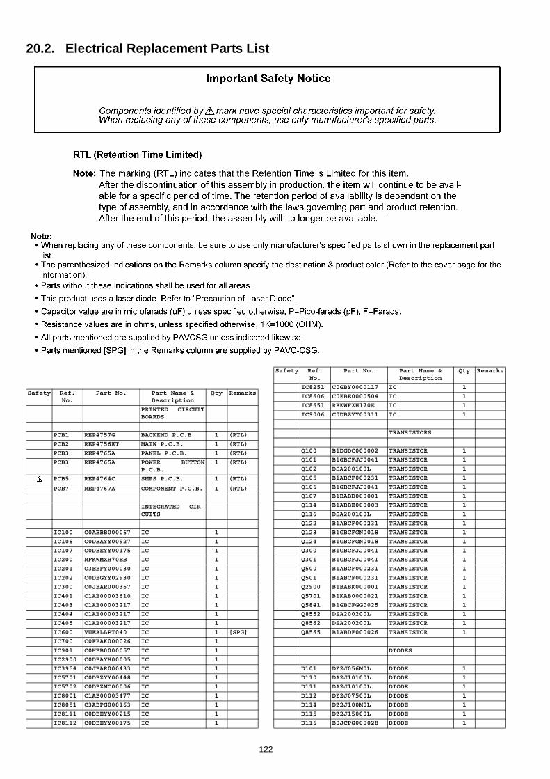
20.2. Electrical Replacement Parts List
Safety Ref. No.
Part No. Part Name & Description
Qty Remarks
PRINTED CIRCUITBOARDS
PCB1 REP4757G BACKEND P.C.B 1 (RTL)
PCB2 REP4756ET MAIN P.C.B. 1 (RTL)
PCB3 REP4765A PANEL P.C.B. 1 (RTL)
PCB3 REP4765A POWER BUTTONP.C.B.
1 (RTL)
PCB5 REP4764C SMPS P.C.B. 1 (RTL)
PCB7 REP4767A COMPONENT P.C.B. 1 (RTL)
INTEGRATED CIR-CUITS
IC100 C0ABBB000067 IC 1
IC106 C0DBAYY00927 IC 1
IC107 C0DBEYY00175 IC 1
IC200 RFKWMXH70EB IC 1
IC201 C3EBFY000030 IC 1
IC202 C0DBGYY02930 IC 1
IC300 C0JBAR000367 IC 1
IC401 C1AB00003610 IC 1
IC403 C1AB00003217 IC 1
IC404 C1AB00003217 IC 1
IC405 C1AB00003217 IC 1
IC600 VUEALLPT040 IC 1 [SPG]
IC700 C0FBAK000026 IC 1
IC901 C0HBB0000057 IC 1
IC2900 C0DBAYH00005 IC 1
IC3954 C0JBAR000433 IC 1
IC5701 C0DBZYY00448 IC 1
IC5702 C0DBZMC00006 IC 1
IC8001 C1AB00003477 IC 1
IC8051 C3ABPG000163 IC 1
IC8111 C0DBEYY00215 IC 1
IC8112 C0DBEYY00175 IC 1
IC8251 C0GBY0000117 IC 1
IC8606 C0EBE0000504 IC 1
IC8651 RFKWFXH170E IC 1
IC9006 C0DBZYY00311 IC 1
TRANSISTORS
Q100 B1DGDC000002 TRANSISTOR 1
Q101 B1GBCFJJ0041 TRANSISTOR 1
Q102 DSA200100L TRANSISTOR 1
Q105 B1ABCF000231 TRANSISTOR 1
Q106 B1GBCFJJ0041 TRANSISTOR 1
Q107 B1BABD000001 TRANSISTOR 1
Q114 B1ABBE000003 TRANSISTOR 1
Q116 DSA200100L TRANSISTOR 1
Q122 B1ABCF000231 TRANSISTOR 1
Q123 B1GBCFGN0018 TRANSISTOR 1
Q124 B1GBCFGN0018 TRANSISTOR 1
Q300 B1GBCFJJ0041 TRANSISTOR 1
Q301 B1GBCFJJ0041 TRANSISTOR 1
Q500 B1ABCF000231 TRANSISTOR 1
Q501 B1ABCF000231 TRANSISTOR 1
Q2900 B1BABK000001 TRANSISTOR 1
Q5701 B1KAB0000021 TRANSISTOR 1
Q5841 B1GBCFGG0025 TRANSISTOR 1
Q8552 DSA200200L TRANSISTOR 1
Q8562 DSA200200L TRANSISTOR 1
Q8565 B1ABDF000026 TRANSISTOR 1
DIODES
D101 DZ2J056M0L DIODE 1
D110 DA2J10100L DIODE 1
D111 DA2J10100L DIODE 1
D112 DZ2J07500L DIODE 1
D114 DZ2J100M0L DIODE 1
D115 DZ2J15000L DIODE 1
D116 B0JCPG000028 DIODE 1
Safety Ref. No.
Part No. Part Name & Description
Qty Remarks
122
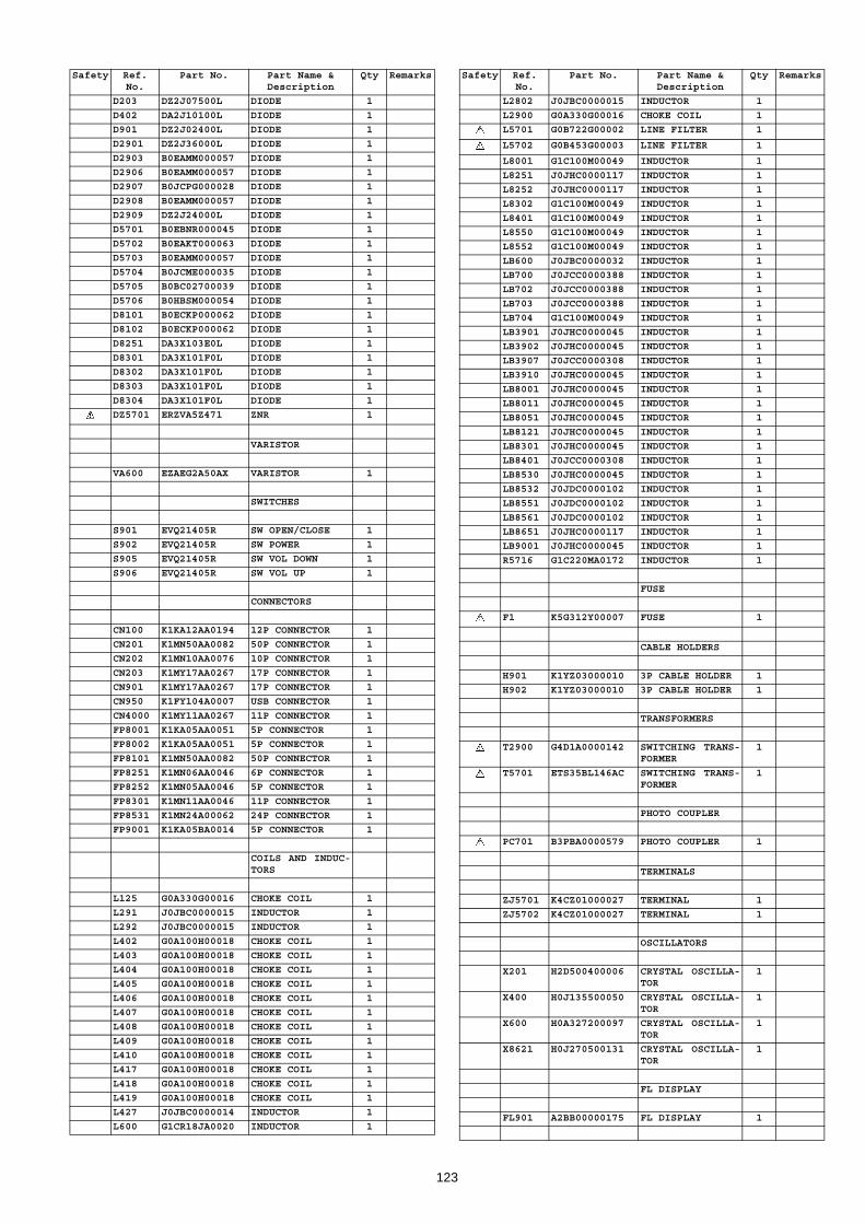
D203 DZ2J07500L DIODE 1
D402 DA2J10100L DIODE 1
D901 DZ2J02400L DIODE 1
D2901 DZ2J36000L DIODE 1
D2903 B0EAMM000057 DIODE 1
D2906 B0EAMM000057 DIODE 1
D2907 B0JCPG000028 DIODE 1
D2908 B0EAMM000057 DIODE 1
D2909 DZ2J24000L DIODE 1
D5701 B0EBNR000045 DIODE 1
D5702 B0EAKT000063 DIODE 1
D5703 B0EAMM000057 DIODE 1
D5704 B0JCME000035 DIODE 1
D5705 B0BC02700039 DIODE 1
D5706 B0HBSM000054 DIODE 1
D8101 B0ECKP000062 DIODE 1
D8102 B0ECKP000062 DIODE 1
D8251 DA3X103E0L DIODE 1
D8301 DA3X101F0L DIODE 1
D8302 DA3X101F0L DIODE 1
D8303 DA3X101F0L DIODE 1
D8304 DA3X101F0L DIODE 1
DZ5701 ERZVA5Z471 ZNR 1
VARISTOR
VA600 EZAEG2A50AX VARISTOR 1
SWITCHES
S901 EVQ21405R SW OPEN/CLOSE 1
S902 EVQ21405R SW POWER 1
S905 EVQ21405R SW VOL DOWN 1
S906 EVQ21405R SW VOL UP 1
CONNECTORS
CN100 K1KA12AA0194 12P CONNECTOR 1
CN201 K1MN50AA0082 50P CONNECTOR 1
CN202 K1MN10AA0076 10P CONNECTOR 1
CN203 K1MY17AA0267 17P CONNECTOR 1
CN901 K1MY17AA0267 17P CONNECTOR 1
CN950 K1FY104A0007 USB CONNECTOR 1
CN4000 K1MY11AA0267 11P CONNECTOR 1
FP8001 K1KA05AA0051 5P CONNECTOR 1
FP8002 K1KA05AA0051 5P CONNECTOR 1
FP8101 K1MN50AA0082 50P CONNECTOR 1
FP8251 K1MN06AA0046 6P CONNECTOR 1
FP8252 K1MN05AA0046 5P CONNECTOR 1
FP8301 K1MN11AA0046 11P CONNECTOR 1
FP8531 K1MN24A00062 24P CONNECTOR 1
FP9001 K1KA05BA0014 5P CONNECTOR 1
COILS AND INDUC-TORS
L125 G0A330G00016 CHOKE COIL 1
L291 J0JBC0000015 INDUCTOR 1
L292 J0JBC0000015 INDUCTOR 1
L402 G0A100H00018 CHOKE COIL 1
L403 G0A100H00018 CHOKE COIL 1
L404 G0A100H00018 CHOKE COIL 1
L405 G0A100H00018 CHOKE COIL 1
L406 G0A100H00018 CHOKE COIL 1
L407 G0A100H00018 CHOKE COIL 1
L408 G0A100H00018 CHOKE COIL 1
L409 G0A100H00018 CHOKE COIL 1
L410 G0A100H00018 CHOKE COIL 1
L417 G0A100H00018 CHOKE COIL 1
L418 G0A100H00018 CHOKE COIL 1
L419 G0A100H00018 CHOKE COIL 1
L427 J0JBC0000014 INDUCTOR 1
L600 G1CR18JA0020 INDUCTOR 1
Safety Ref. No.
Part No. Part Name & Description
Qty Remarks
L2802 J0JBC0000015 INDUCTOR 1
L2900 G0A330G00016 CHOKE COIL 1
L5701 G0B722G00002 LINE FILTER 1
L5702 G0B453G00003 LINE FILTER 1
L8001 G1C100M00049 INDUCTOR 1
L8251 J0JHC0000117 INDUCTOR 1
L8252 J0JHC0000117 INDUCTOR 1
L8302 G1C100M00049 INDUCTOR 1
L8401 G1C100M00049 INDUCTOR 1
L8550 G1C100M00049 INDUCTOR 1
L8552 G1C100M00049 INDUCTOR 1
LB600 J0JBC0000032 INDUCTOR 1
LB700 J0JCC0000388 INDUCTOR 1
LB702 J0JCC0000388 INDUCTOR 1
LB703 J0JCC0000388 INDUCTOR 1
LB704 G1C100M00049 INDUCTOR 1
LB3901 J0JHC0000045 INDUCTOR 1
LB3902 J0JHC0000045 INDUCTOR 1
LB3907 J0JCC0000308 INDUCTOR 1
LB3910 J0JHC0000045 INDUCTOR 1
LB8001 J0JHC0000045 INDUCTOR 1
LB8011 J0JHC0000045 INDUCTOR 1
LB8051 J0JHC0000045 INDUCTOR 1
LB8121 J0JHC0000045 INDUCTOR 1
LB8301 J0JHC0000045 INDUCTOR 1
LB8401 J0JCC0000308 INDUCTOR 1
LB8530 J0JHC0000045 INDUCTOR 1
LB8532 J0JDC0000102 INDUCTOR 1
LB8551 J0JDC0000102 INDUCTOR 1
LB8561 J0JDC0000102 INDUCTOR 1
LB8651 J0JHC0000117 INDUCTOR 1
LB9001 J0JHC0000045 INDUCTOR 1
R5716 G1C220MA0172 INDUCTOR 1
FUSE
F1 K5G312Y00007 FUSE 1
CABLE HOLDERS
H901 K1YZ03000010 3P CABLE HOLDER 1
H902 K1YZ03000010 3P CABLE HOLDER 1
TRANSFORMERS
T2900 G4D1A0000142 SWITCHING TRANS-FORMER
1
T5701 ETS35BL146AC SWITCHING TRANS-FORMER
1
PHOTO COUPLER
PC701 B3PBA0000579 PHOTO COUPLER 1
TERMINALS
ZJ5701 K4CZ01000027 TERMINAL 1
ZJ5702 K4CZ01000027 TERMINAL 1
OSCILLATORS
X201 H2D500400006 CRYSTAL OSCILLA-TOR
1
X400 H0J135500050 CRYSTAL OSCILLA-TOR
1
X600 H0A327200097 CRYSTAL OSCILLA-TOR
1
X8621 H0J270500131 CRYSTAL OSCILLA-TOR
1
FL DISPLAY
FL901 A2BB00000175 FL DISPLAY 1
Safety Ref. No.
Part No. Part Name & Description
Qty Remarks
123
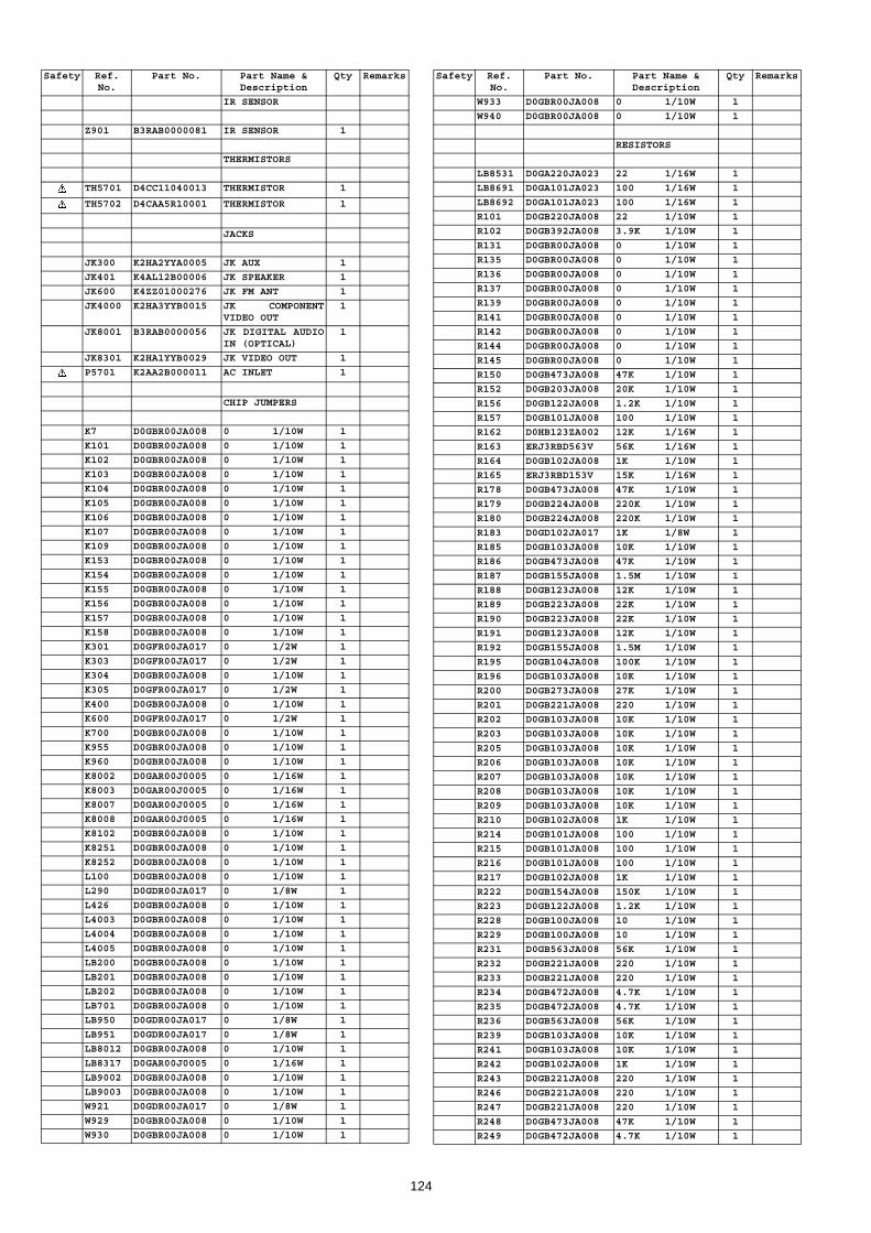
IR SENSOR
Z901 B3RAB0000081 IR SENSOR 1
THERMISTORS
TH5701 D4CC11040013 THERMISTOR 1
TH5702 D4CAA5R10001 THERMISTOR 1
JACKS
JK300 K2HA2YYA0005 JK AUX 1
JK401 K4AL12B00006 JK SPEAKER 1
JK600 K4ZZ01000276 JK FM ANT 1
JK4000 K2HA3YYB0015 JK COMPONENTVIDEO OUT
1
JK8001 B3RAB0000056 JK DIGITAL AUDIOIN (OPTICAL)
1
JK8301 K2HA1YYB0029 JK VIDEO OUT 1
P5701 K2AA2B000011 AC INLET 1
CHIP JUMPERS
K7 D0GBR00JA008 0 1/10W 1
K101 D0GBR00JA008 0 1/10W 1
K102 D0GBR00JA008 0 1/10W 1
K103 D0GBR00JA008 0 1/10W 1
K104 D0GBR00JA008 0 1/10W 1
K105 D0GBR00JA008 0 1/10W 1
K106 D0GBR00JA008 0 1/10W 1
K107 D0GBR00JA008 0 1/10W 1
K109 D0GBR00JA008 0 1/10W 1
K153 D0GBR00JA008 0 1/10W 1
K154 D0GBR00JA008 0 1/10W 1
K155 D0GBR00JA008 0 1/10W 1
K156 D0GBR00JA008 0 1/10W 1
K157 D0GBR00JA008 0 1/10W 1
K158 D0GBR00JA008 0 1/10W 1
K301 D0GFR00JA017 0 1/2W 1
K303 D0GFR00JA017 0 1/2W 1
K304 D0GBR00JA008 0 1/10W 1
K305 D0GFR00JA017 0 1/2W 1
K400 D0GBR00JA008 0 1/10W 1
K600 D0GFR00JA017 0 1/2W 1
K700 D0GBR00JA008 0 1/10W 1
K955 D0GBR00JA008 0 1/10W 1
K960 D0GBR00JA008 0 1/10W 1
K8002 D0GAR00J0005 0 1/16W 1
K8003 D0GAR00J0005 0 1/16W 1
K8007 D0GAR00J0005 0 1/16W 1
K8008 D0GAR00J0005 0 1/16W 1
K8102 D0GBR00JA008 0 1/10W 1
K8251 D0GBR00JA008 0 1/10W 1
K8252 D0GBR00JA008 0 1/10W 1
L100 D0GBR00JA008 0 1/10W 1
L290 D0GDR00JA017 0 1/8W 1
L426 D0GBR00JA008 0 1/10W 1
L4003 D0GBR00JA008 0 1/10W 1
L4004 D0GBR00JA008 0 1/10W 1
L4005 D0GBR00JA008 0 1/10W 1
LB200 D0GBR00JA008 0 1/10W 1
LB201 D0GBR00JA008 0 1/10W 1
LB202 D0GBR00JA008 0 1/10W 1
LB701 D0GBR00JA008 0 1/10W 1
LB950 D0GDR00JA017 0 1/8W 1
LB951 D0GDR00JA017 0 1/8W 1
LB8012 D0GBR00JA008 0 1/10W 1
LB8317 D0GAR00J0005 0 1/16W 1
LB9002 D0GBR00JA008 0 1/10W 1
LB9003 D0GBR00JA008 0 1/10W 1
W921 D0GDR00JA017 0 1/8W 1
W929 D0GBR00JA008 0 1/10W 1
W930 D0GBR00JA008 0 1/10W 1
Safety Ref. No.
Part No. Part Name & Description
Qty Remarks
W933 D0GBR00JA008 0 1/10W 1
W940 D0GBR00JA008 0 1/10W 1
RESISTORS
LB8531 D0GA220JA023 22 1/16W 1
LB8691 D0GA101JA023 100 1/16W 1
LB8692 D0GA101JA023 100 1/16W 1
R101 D0GB220JA008 22 1/10W 1
R102 D0GB392JA008 3.9K 1/10W 1
R131 D0GBR00JA008 0 1/10W 1
R135 D0GBR00JA008 0 1/10W 1
R136 D0GBR00JA008 0 1/10W 1
R137 D0GBR00JA008 0 1/10W 1
R139 D0GBR00JA008 0 1/10W 1
R141 D0GBR00JA008 0 1/10W 1
R142 D0GBR00JA008 0 1/10W 1
R144 D0GBR00JA008 0 1/10W 1
R145 D0GBR00JA008 0 1/10W 1
R150 D0GB473JA008 47K 1/10W 1
R152 D0GB203JA008 20K 1/10W 1
R156 D0GB122JA008 1.2K 1/10W 1
R157 D0GB101JA008 100 1/10W 1
R162 D0HB123ZA002 12K 1/16W 1
R163 ERJ3RBD563V 56K 1/16W 1
R164 D0GB102JA008 1K 1/10W 1
R165 ERJ3RBD153V 15K 1/16W 1
R178 D0GB473JA008 47K 1/10W 1
R179 D0GB224JA008 220K 1/10W 1
R180 D0GB224JA008 220K 1/10W 1
R183 D0GD102JA017 1K 1/8W 1
R185 D0GB103JA008 10K 1/10W 1
R186 D0GB473JA008 47K 1/10W 1
R187 D0GB155JA008 1.5M 1/10W 1
R188 D0GB123JA008 12K 1/10W 1
R189 D0GB223JA008 22K 1/10W 1
R190 D0GB223JA008 22K 1/10W 1
R191 D0GB123JA008 12K 1/10W 1
R192 D0GB155JA008 1.5M 1/10W 1
R195 D0GB104JA008 100K 1/10W 1
R196 D0GB103JA008 10K 1/10W 1
R200 D0GB273JA008 27K 1/10W 1
R201 D0GB221JA008 220 1/10W 1
R202 D0GB103JA008 10K 1/10W 1
R203 D0GB103JA008 10K 1/10W 1
R205 D0GB103JA008 10K 1/10W 1
R206 D0GB103JA008 10K 1/10W 1
R207 D0GB103JA008 10K 1/10W 1
R208 D0GB103JA008 10K 1/10W 1
R209 D0GB103JA008 10K 1/10W 1
R210 D0GB102JA008 1K 1/10W 1
R214 D0GB101JA008 100 1/10W 1
R215 D0GB101JA008 100 1/10W 1
R216 D0GB101JA008 100 1/10W 1
R217 D0GB102JA008 1K 1/10W 1
R222 D0GB154JA008 150K 1/10W 1
R223 D0GB122JA008 1.2K 1/10W 1
R228 D0GB100JA008 10 1/10W 1
R229 D0GB100JA008 10 1/10W 1
R231 D0GB563JA008 56K 1/10W 1
R232 D0GB221JA008 220 1/10W 1
R233 D0GB221JA008 220 1/10W 1
R234 D0GB472JA008 4.7K 1/10W 1
R235 D0GB472JA008 4.7K 1/10W 1
R236 D0GB563JA008 56K 1/10W 1
R239 D0GB103JA008 10K 1/10W 1
R241 D0GB103JA008 10K 1/10W 1
R242 D0GB102JA008 1K 1/10W 1
R243 D0GB221JA008 220 1/10W 1
R246 D0GB221JA008 220 1/10W 1
R247 D0GB221JA008 220 1/10W 1
R248 D0GB473JA008 47K 1/10W 1
R249 D0GB472JA008 4.7K 1/10W 1
Safety Ref. No.
Part No. Part Name & Description
Qty Remarks
124
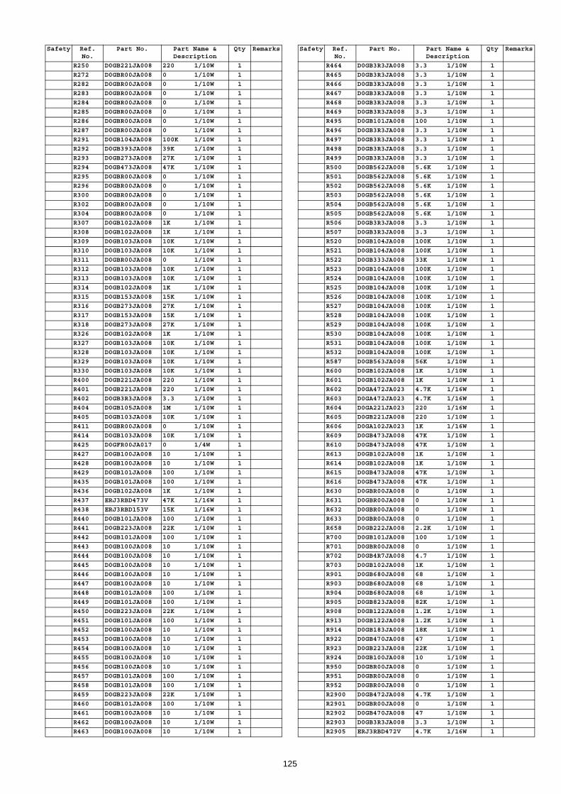
R250 D0GB221JA008 220 1/10W 1
R272 D0GBR00JA008 0 1/10W 1
R282 D0GBR00JA008 0 1/10W 1
R283 D0GBR00JA008 0 1/10W 1
R284 D0GBR00JA008 0 1/10W 1
R285 D0GBR00JA008 0 1/10W 1
R286 D0GBR00JA008 0 1/10W 1
R287 D0GBR00JA008 0 1/10W 1
R291 D0GB104JA008 100K 1/10W 1
R292 D0GB393JA008 39K 1/10W 1
R293 D0GB273JA008 27K 1/10W 1
R294 D0GB473JA008 47K 1/10W 1
R295 D0GBR00JA008 0 1/10W 1
R296 D0GBR00JA008 0 1/10W 1
R300 D0GBR00JA008 0 1/10W 1
R302 D0GBR00JA008 0 1/10W 1
R304 D0GBR00JA008 0 1/10W 1
R307 D0GB102JA008 1K 1/10W 1
R308 D0GB102JA008 1K 1/10W 1
R309 D0GB103JA008 10K 1/10W 1
R310 D0GB103JA008 10K 1/10W 1
R311 D0GBR00JA008 0 1/10W 1
R312 D0GB103JA008 10K 1/10W 1
R313 D0GB103JA008 10K 1/10W 1
R314 D0GB102JA008 1K 1/10W 1
R315 D0GB153JA008 15K 1/10W 1
R316 D0GB273JA008 27K 1/10W 1
R317 D0GB153JA008 15K 1/10W 1
R318 D0GB273JA008 27K 1/10W 1
R326 D0GB102JA008 1K 1/10W 1
R327 D0GB103JA008 10K 1/10W 1
R328 D0GB103JA008 10K 1/10W 1
R329 D0GB103JA008 10K 1/10W 1
R330 D0GB103JA008 10K 1/10W 1
R400 D0GB221JA008 220 1/10W 1
R401 D0GB221JA008 220 1/10W 1
R402 D0GB3R3JA008 3.3 1/10W 1
R404 D0GB105JA008 1M 1/10W 1
R405 D0GB103JA008 10K 1/10W 1
R411 D0GBR00JA008 0 1/10W 1
R414 D0GB103JA008 10K 1/10W 1
R425 D0GFR00JA017 0 1/4W 1
R427 D0GB100JA008 10 1/10W 1
R428 D0GB100JA008 10 1/10W 1
R429 D0GB101JA008 100 1/10W 1
R435 D0GB101JA008 100 1/10W 1
R436 D0GB102JA008 1K 1/10W 1
R437 ERJ3RBD473V 47K 1/16W 1
R438 ERJ3RBD153V 15K 1/16W 1
R440 D0GB101JA008 100 1/10W 1
R441 D0GB223JA008 22K 1/10W 1
R442 D0GB101JA008 100 1/10W 1
R443 D0GB100JA008 10 1/10W 1
R444 D0GB100JA008 10 1/10W 1
R445 D0GB100JA008 10 1/10W 1
R446 D0GB100JA008 10 1/10W 1
R447 D0GB100JA008 10 1/10W 1
R448 D0GB101JA008 100 1/10W 1
R449 D0GB101JA008 100 1/10W 1
R450 D0GB223JA008 22K 1/10W 1
R451 D0GB101JA008 100 1/10W 1
R452 D0GB100JA008 10 1/10W 1
R453 D0GB100JA008 10 1/10W 1
R454 D0GB100JA008 10 1/10W 1
R455 D0GB100JA008 10 1/10W 1
R456 D0GB100JA008 10 1/10W 1
R457 D0GB101JA008 100 1/10W 1
R458 D0GB101JA008 100 1/10W 1
R459 D0GB223JA008 22K 1/10W 1
R460 D0GB101JA008 100 1/10W 1
R461 D0GB100JA008 10 1/10W 1
R462 D0GB100JA008 10 1/10W 1
R463 D0GB100JA008 10 1/10W 1
Safety Ref. No.
Part No. Part Name & Description
Qty Remarks
R464 D0GB3R3JA008 3.3 1/10W 1
R465 D0GB3R3JA008 3.3 1/10W 1
R466 D0GB3R3JA008 3.3 1/10W 1
R467 D0GB3R3JA008 3.3 1/10W 1
R468 D0GB3R3JA008 3.3 1/10W 1
R469 D0GB3R3JA008 3.3 1/10W 1
R495 D0GB101JA008 100 1/10W 1
R496 D0GB3R3JA008 3.3 1/10W 1
R497 D0GB3R3JA008 3.3 1/10W 1
R498 D0GB3R3JA008 3.3 1/10W 1
R499 D0GB3R3JA008 3.3 1/10W 1
R500 D0GB562JA008 5.6K 1/10W 1
R501 D0GB562JA008 5.6K 1/10W 1
R502 D0GB562JA008 5.6K 1/10W 1
R503 D0GB562JA008 5.6K 1/10W 1
R504 D0GB562JA008 5.6K 1/10W 1
R505 D0GB562JA008 5.6K 1/10W 1
R506 D0GB3R3JA008 3.3 1/10W 1
R507 D0GB3R3JA008 3.3 1/10W 1
R520 D0GB104JA008 100K 1/10W 1
R521 D0GB104JA008 100K 1/10W 1
R522 D0GB333JA008 33K 1/10W 1
R523 D0GB104JA008 100K 1/10W 1
R524 D0GB104JA008 100K 1/10W 1
R525 D0GB104JA008 100K 1/10W 1
R526 D0GB104JA008 100K 1/10W 1
R527 D0GB104JA008 100K 1/10W 1
R528 D0GB104JA008 100K 1/10W 1
R529 D0GB104JA008 100K 1/10W 1
R530 D0GB104JA008 100K 1/10W 1
R531 D0GB104JA008 100K 1/10W 1
R532 D0GB104JA008 100K 1/10W 1
R587 D0GB563JA008 56K 1/10W 1
R600 D0GB102JA008 1K 1/10W 1
R601 D0GB102JA008 1K 1/10W 1
R602 D0GA472JA023 4.7K 1/16W 1
R603 D0GA472JA023 4.7K 1/16W 1
R604 D0GA221JA023 220 1/16W 1
R605 D0GB221JA008 220 1/10W 1
R606 D0GA102JA023 1K 1/16W 1
R609 D0GB473JA008 47K 1/10W 1
R610 D0GB473JA008 47K 1/10W 1
R613 D0GB102JA008 1K 1/10W 1
R614 D0GB102JA008 1K 1/10W 1
R615 D0GB473JA008 47K 1/10W 1
R616 D0GB473JA008 47K 1/10W 1
R630 D0GBR00JA008 0 1/10W 1
R631 D0GBR00JA008 0 1/10W 1
R632 D0GBR00JA008 0 1/10W 1
R633 D0GBR00JA008 0 1/10W 1
R658 D0GB222JA008 2.2K 1/10W 1
R700 D0GB101JA008 100 1/10W 1
R701 D0GBR00JA008 0 1/10W 1
R702 D0GB4R7JA008 4.7 1/10W 1
R703 D0GB102JA008 1K 1/10W 1
R901 D0GB680JA008 68 1/10W 1
R903 D0GB680JA008 68 1/10W 1
R904 D0GB680JA008 68 1/10W 1
R905 D0GB823JA008 82K 1/10W 1
R908 D0GB122JA008 1.2K 1/10W 1
R913 D0GB122JA008 1.2K 1/10W 1
R914 D0GB183JA008 18K 1/10W 1
R922 D0GB470JA008 47 1/10W 1
R923 D0GB223JA008 22K 1/10W 1
R924 D0GB100JA008 10 1/10W 1
R950 D0GBR00JA008 0 1/10W 1
R951 D0GBR00JA008 0 1/10W 1
R952 D0GBR00JA008 0 1/10W 1
R2900 D0GB472JA008 4.7K 1/10W 1
R2901 D0GBR00JA008 0 1/10W 1
R2902 D0GB470JA008 47 1/10W 1
R2903 D0GB3R3JA008 3.3 1/10W 1
R2905 ERJ3RBD472V 4.7K 1/16W 1
Safety Ref. No.
Part No. Part Name & Description
Qty Remarks
125
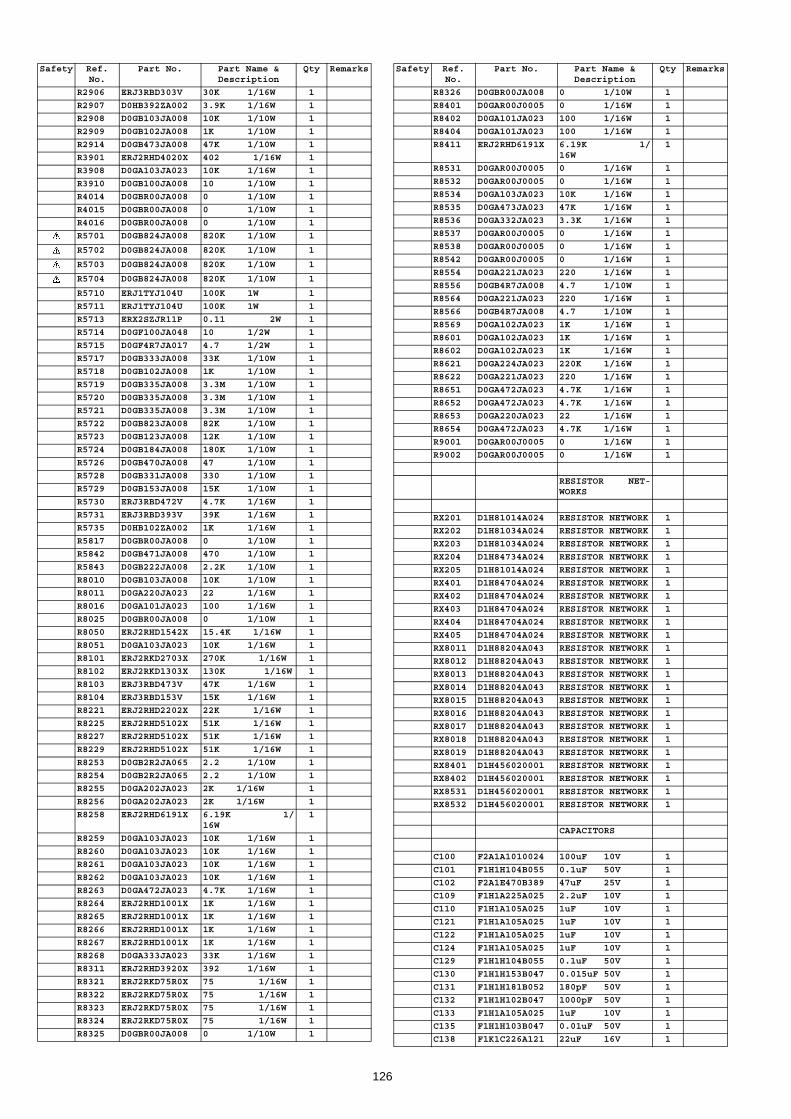
R2906 ERJ3RBD303V 30K 1/16W 1
R2907 D0HB392ZA002 3.9K 1/16W 1
R2908 D0GB103JA008 10K 1/10W 1
R2909 D0GB102JA008 1K 1/10W 1
R2914 D0GB473JA008 47K 1/10W 1
R3901 ERJ2RHD4020X 402 1/16W 1
R3908 D0GA103JA023 10K 1/16W 1
R3910 D0GB100JA008 10 1/10W 1
R4014 D0GBR00JA008 0 1/10W 1
R4015 D0GBR00JA008 0 1/10W 1
R4016 D0GBR00JA008 0 1/10W 1
R5701 D0GB824JA008 820K 1/10W 1
R5702 D0GB824JA008 820K 1/10W 1
R5703 D0GB824JA008 820K 1/10W 1
R5704 D0GB824JA008 820K 1/10W 1
R5710 ERJ1TYJ104U 100K 1W 1
R5711 ERJ1TYJ104U 100K 1W 1
R5713 ERX2SZJR11P 0.11 2W 1
R5714 D0GF100JA048 10 1/2W 1
R5715 D0GF4R7JA017 4.7 1/2W 1
R5717 D0GB333JA008 33K 1/10W 1
R5718 D0GB102JA008 1K 1/10W 1
R5719 D0GB335JA008 3.3M 1/10W 1
R5720 D0GB335JA008 3.3M 1/10W 1
R5721 D0GB335JA008 3.3M 1/10W 1
R5722 D0GB823JA008 82K 1/10W 1
R5723 D0GB123JA008 12K 1/10W 1
R5724 D0GB184JA008 180K 1/10W 1
R5726 D0GB470JA008 47 1/10W 1
R5728 D0GB331JA008 330 1/10W 1
R5729 D0GB153JA008 15K 1/10W 1
R5730 ERJ3RBD472V 4.7K 1/16W 1
R5731 ERJ3RBD393V 39K 1/16W 1
R5735 D0HB102ZA002 1K 1/16W 1
R5817 D0GBR00JA008 0 1/10W 1
R5842 D0GB471JA008 470 1/10W 1
R5843 D0GB222JA008 2.2K 1/10W 1
R8010 D0GB103JA008 10K 1/10W 1
R8011 D0GA220JA023 22 1/16W 1
R8016 D0GA101JA023 100 1/16W 1
R8025 D0GBR00JA008 0 1/10W 1
R8050 ERJ2RHD1542X 15.4K 1/16W 1
R8051 D0GA103JA023 10K 1/16W 1
R8101 ERJ2RKD2703X 270K 1/16W 1
R8102 ERJ2RKD1303X 130K 1/16W 1
R8103 ERJ3RBD473V 47K 1/16W 1
R8104 ERJ3RBD153V 15K 1/16W 1
R8221 ERJ2RHD2202X 22K 1/16W 1
R8225 ERJ2RHD5102X 51K 1/16W 1
R8227 ERJ2RHD5102X 51K 1/16W 1
R8229 ERJ2RHD5102X 51K 1/16W 1
R8253 D0GB2R2JA065 2.2 1/10W 1
R8254 D0GB2R2JA065 2.2 1/10W 1
R8255 D0GA202JA023 2K 1/16W 1
R8256 D0GA202JA023 2K 1/16W 1
R8258 ERJ2RHD6191X 6.19K 1/16W
1
R8259 D0GA103JA023 10K 1/16W 1
R8260 D0GA103JA023 10K 1/16W 1
R8261 D0GA103JA023 10K 1/16W 1
R8262 D0GA103JA023 10K 1/16W 1
R8263 D0GA472JA023 4.7K 1/16W 1
R8264 ERJ2RHD1001X 1K 1/16W 1
R8265 ERJ2RHD1001X 1K 1/16W 1
R8266 ERJ2RHD1001X 1K 1/16W 1
R8267 ERJ2RHD1001X 1K 1/16W 1
R8268 D0GA333JA023 33K 1/16W 1
R8311 ERJ2RHD3920X 392 1/16W 1
R8321 ERJ2RKD75R0X 75 1/16W 1
R8322 ERJ2RKD75R0X 75 1/16W 1
R8323 ERJ2RKD75R0X 75 1/16W 1
R8324 ERJ2RKD75R0X 75 1/16W 1
R8325 D0GBR00JA008 0 1/10W 1
Safety Ref. No.
Part No. Part Name & Description
Qty Remarks
R8326 D0GBR00JA008 0 1/10W 1
R8401 D0GAR00J0005 0 1/16W 1
R8402 D0GA101JA023 100 1/16W 1
R8404 D0GA101JA023 100 1/16W 1
R8411 ERJ2RHD6191X 6.19K 1/16W
1
R8531 D0GAR00J0005 0 1/16W 1
R8532 D0GAR00J0005 0 1/16W 1
R8534 D0GA103JA023 10K 1/16W 1
R8535 D0GA473JA023 47K 1/16W 1
R8536 D0GA332JA023 3.3K 1/16W 1
R8537 D0GAR00J0005 0 1/16W 1
R8538 D0GAR00J0005 0 1/16W 1
R8542 D0GAR00J0005 0 1/16W 1
R8554 D0GA221JA023 220 1/16W 1
R8556 D0GB4R7JA008 4.7 1/10W 1
R8564 D0GA221JA023 220 1/16W 1
R8566 D0GB4R7JA008 4.7 1/10W 1
R8569 D0GA102JA023 1K 1/16W 1
R8601 D0GA102JA023 1K 1/16W 1
R8602 D0GA102JA023 1K 1/16W 1
R8621 D0GA224JA023 220K 1/16W 1
R8622 D0GA221JA023 220 1/16W 1
R8651 D0GA472JA023 4.7K 1/16W 1
R8652 D0GA472JA023 4.7K 1/16W 1
R8653 D0GA220JA023 22 1/16W 1
R8654 D0GA472JA023 4.7K 1/16W 1
R9001 D0GAR00J0005 0 1/16W 1
R9002 D0GAR00J0005 0 1/16W 1
RESISTOR NET-WORKS
RX201 D1H81014A024 RESISTOR NETWORK 1
RX202 D1H81034A024 RESISTOR NETWORK 1
RX203 D1H81034A024 RESISTOR NETWORK 1
RX204 D1H84734A024 RESISTOR NETWORK 1
RX205 D1H81014A024 RESISTOR NETWORK 1
RX401 D1H84704A024 RESISTOR NETWORK 1
RX402 D1H84704A024 RESISTOR NETWORK 1
RX403 D1H84704A024 RESISTOR NETWORK 1
RX404 D1H84704A024 RESISTOR NETWORK 1
RX405 D1H84704A024 RESISTOR NETWORK 1
RX8011 D1H88204A043 RESISTOR NETWORK 1
RX8012 D1H88204A043 RESISTOR NETWORK 1
RX8013 D1H88204A043 RESISTOR NETWORK 1
RX8014 D1H88204A043 RESISTOR NETWORK 1
RX8015 D1H88204A043 RESISTOR NETWORK 1
RX8016 D1H88204A043 RESISTOR NETWORK 1
RX8017 D1H88204A043 RESISTOR NETWORK 1
RX8018 D1H88204A043 RESISTOR NETWORK 1
RX8019 D1H88204A043 RESISTOR NETWORK 1
RX8401 D1H456020001 RESISTOR NETWORK 1
RX8402 D1H456020001 RESISTOR NETWORK 1
RX8531 D1H456020001 RESISTOR NETWORK 1
RX8532 D1H456020001 RESISTOR NETWORK 1
CAPACITORS
C100 F2A1A1010024 100uF 10V 1
C101 F1H1H104B055 0.1uF 50V 1
C102 F2A1E470B389 47uF 25V 1
C109 F1H1A225A025 2.2uF 10V 1
C110 F1H1A105A025 1uF 10V 1
C121 F1H1A105A025 1uF 10V 1
C122 F1H1A105A025 1uF 10V 1
C124 F1H1A105A025 1uF 10V 1
C129 F1H1H104B055 0.1uF 50V 1
C130 F1H1H153B047 0.015uF 50V 1
C131 F1H1H181B052 180pF 50V 1
C132 F1H1H102B047 1000pF 50V 1
C133 F1H1A105A025 1uF 10V 1
C135 F1H1H103B047 0.01uF 50V 1
C138 F1K1C226A121 22uF 16V 1
Safety Ref. No.
Part No. Part Name & Description
Qty Remarks
126
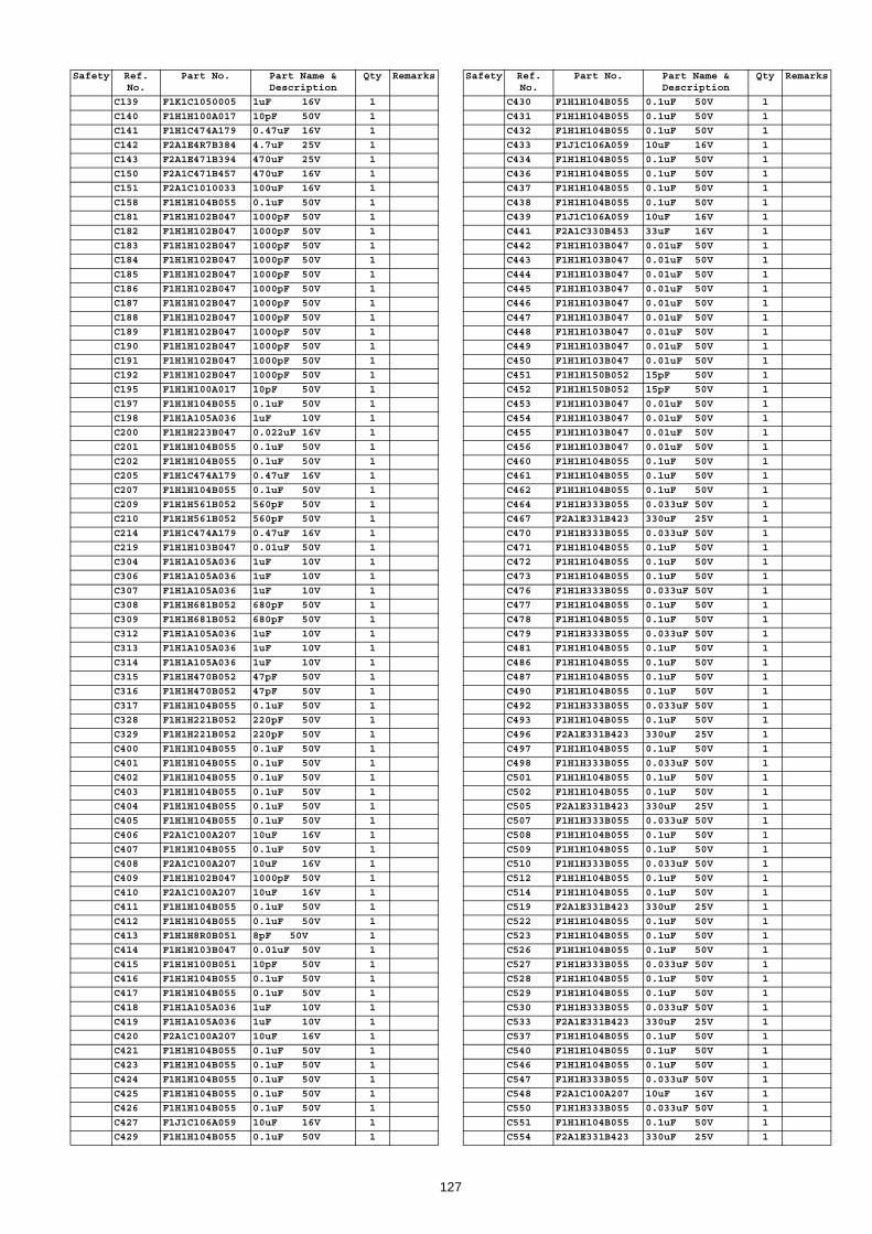
C139 F1K1C1050005 1uF 16V 1
C140 F1H1H100A017 10pF 50V 1
C141 F1H1C474A179 0.47uF 16V 1
C142 F2A1E4R7B384 4.7uF 25V 1
C143 F2A1E471B394 470uF 25V 1
C150 F2A1C471B457 470uF 16V 1
C151 F2A1C1010033 100uF 16V 1
C158 F1H1H104B055 0.1uF 50V 1
C181 F1H1H102B047 1000pF 50V 1
C182 F1H1H102B047 1000pF 50V 1
C183 F1H1H102B047 1000pF 50V 1
C184 F1H1H102B047 1000pF 50V 1
C185 F1H1H102B047 1000pF 50V 1
C186 F1H1H102B047 1000pF 50V 1
C187 F1H1H102B047 1000pF 50V 1
C188 F1H1H102B047 1000pF 50V 1
C189 F1H1H102B047 1000pF 50V 1
C190 F1H1H102B047 1000pF 50V 1
C191 F1H1H102B047 1000pF 50V 1
C192 F1H1H102B047 1000pF 50V 1
C195 F1H1H100A017 10pF 50V 1
C197 F1H1H104B055 0.1uF 50V 1
C198 F1H1A105A036 1uF 10V 1
C200 F1H1H223B047 0.022uF 16V 1
C201 F1H1H104B055 0.1uF 50V 1
C202 F1H1H104B055 0.1uF 50V 1
C205 F1H1C474A179 0.47uF 16V 1
C207 F1H1H104B055 0.1uF 50V 1
C209 F1H1H561B052 560pF 50V 1
C210 F1H1H561B052 560pF 50V 1
C214 F1H1C474A179 0.47uF 16V 1
C219 F1H1H103B047 0.01uF 50V 1
C304 F1H1A105A036 1uF 10V 1
C306 F1H1A105A036 1uF 10V 1
C307 F1H1A105A036 1uF 10V 1
C308 F1H1H681B052 680pF 50V 1
C309 F1H1H681B052 680pF 50V 1
C312 F1H1A105A036 1uF 10V 1
C313 F1H1A105A036 1uF 10V 1
C314 F1H1A105A036 1uF 10V 1
C315 F1H1H470B052 47pF 50V 1
C316 F1H1H470B052 47pF 50V 1
C317 F1H1H104B055 0.1uF 50V 1
C328 F1H1H221B052 220pF 50V 1
C329 F1H1H221B052 220pF 50V 1
C400 F1H1H104B055 0.1uF 50V 1
C401 F1H1H104B055 0.1uF 50V 1
C402 F1H1H104B055 0.1uF 50V 1
C403 F1H1H104B055 0.1uF 50V 1
C404 F1H1H104B055 0.1uF 50V 1
C405 F1H1H104B055 0.1uF 50V 1
C406 F2A1C100A207 10uF 16V 1
C407 F1H1H104B055 0.1uF 50V 1
C408 F2A1C100A207 10uF 16V 1
C409 F1H1H102B047 1000pF 50V 1
C410 F2A1C100A207 10uF 16V 1
C411 F1H1H104B055 0.1uF 50V 1
C412 F1H1H104B055 0.1uF 50V 1
C413 F1H1H8R0B051 8pF 50V 1
C414 F1H1H103B047 0.01uF 50V 1
C415 F1H1H100B051 10pF 50V 1
C416 F1H1H104B055 0.1uF 50V 1
C417 F1H1H104B055 0.1uF 50V 1
C418 F1H1A105A036 1uF 10V 1
C419 F1H1A105A036 1uF 10V 1
C420 F2A1C100A207 10uF 16V 1
C421 F1H1H104B055 0.1uF 50V 1
C423 F1H1H104B055 0.1uF 50V 1
C424 F1H1H104B055 0.1uF 50V 1
C425 F1H1H104B055 0.1uF 50V 1
C426 F1H1H104B055 0.1uF 50V 1
C427 F1J1C106A059 10uF 16V 1
C429 F1H1H104B055 0.1uF 50V 1
Safety Ref. No.
Part No. Part Name & Description
Qty Remarks
C430 F1H1H104B055 0.1uF 50V 1
C431 F1H1H104B055 0.1uF 50V 1
C432 F1H1H104B055 0.1uF 50V 1
C433 F1J1C106A059 10uF 16V 1
C434 F1H1H104B055 0.1uF 50V 1
C436 F1H1H104B055 0.1uF 50V 1
C437 F1H1H104B055 0.1uF 50V 1
C438 F1H1H104B055 0.1uF 50V 1
C439 F1J1C106A059 10uF 16V 1
C441 F2A1C330B453 33uF 16V 1
C442 F1H1H103B047 0.01uF 50V 1
C443 F1H1H103B047 0.01uF 50V 1
C444 F1H1H103B047 0.01uF 50V 1
C445 F1H1H103B047 0.01uF 50V 1
C446 F1H1H103B047 0.01uF 50V 1
C447 F1H1H103B047 0.01uF 50V 1
C448 F1H1H103B047 0.01uF 50V 1
C449 F1H1H103B047 0.01uF 50V 1
C450 F1H1H103B047 0.01uF 50V 1
C451 F1H1H150B052 15pF 50V 1
C452 F1H1H150B052 15pF 50V 1
C453 F1H1H103B047 0.01uF 50V 1
C454 F1H1H103B047 0.01uF 50V 1
C455 F1H1H103B047 0.01uF 50V 1
C456 F1H1H103B047 0.01uF 50V 1
C460 F1H1H104B055 0.1uF 50V 1
C461 F1H1H104B055 0.1uF 50V 1
C462 F1H1H104B055 0.1uF 50V 1
C464 F1H1H333B055 0.033uF 50V 1
C467 F2A1E331B423 330uF 25V 1
C470 F1H1H333B055 0.033uF 50V 1
C471 F1H1H104B055 0.1uF 50V 1
C472 F1H1H104B055 0.1uF 50V 1
C473 F1H1H104B055 0.1uF 50V 1
C476 F1H1H333B055 0.033uF 50V 1
C477 F1H1H104B055 0.1uF 50V 1
C478 F1H1H104B055 0.1uF 50V 1
C479 F1H1H333B055 0.033uF 50V 1
C481 F1H1H104B055 0.1uF 50V 1
C486 F1H1H104B055 0.1uF 50V 1
C487 F1H1H104B055 0.1uF 50V 1
C490 F1H1H104B055 0.1uF 50V 1
C492 F1H1H333B055 0.033uF 50V 1
C493 F1H1H104B055 0.1uF 50V 1
C496 F2A1E331B423 330uF 25V 1
C497 F1H1H104B055 0.1uF 50V 1
C498 F1H1H333B055 0.033uF 50V 1
C501 F1H1H104B055 0.1uF 50V 1
C502 F1H1H104B055 0.1uF 50V 1
C505 F2A1E331B423 330uF 25V 1
C507 F1H1H333B055 0.033uF 50V 1
C508 F1H1H104B055 0.1uF 50V 1
C509 F1H1H104B055 0.1uF 50V 1
C510 F1H1H333B055 0.033uF 50V 1
C512 F1H1H104B055 0.1uF 50V 1
C514 F1H1H104B055 0.1uF 50V 1
C519 F2A1E331B423 330uF 25V 1
C522 F1H1H104B055 0.1uF 50V 1
C523 F1H1H104B055 0.1uF 50V 1
C526 F1H1H104B055 0.1uF 50V 1
C527 F1H1H333B055 0.033uF 50V 1
C528 F1H1H104B055 0.1uF 50V 1
C529 F1H1H104B055 0.1uF 50V 1
C530 F1H1H333B055 0.033uF 50V 1
C533 F2A1E331B423 330uF 25V 1
C537 F1H1H104B055 0.1uF 50V 1
C540 F1H1H104B055 0.1uF 50V 1
C546 F1H1H104B055 0.1uF 50V 1
C547 F1H1H333B055 0.033uF 50V 1
C548 F2A1C100A207 10uF 16V 1
C550 F1H1H333B055 0.033uF 50V 1
C551 F1H1H104B055 0.1uF 50V 1
C554 F2A1E331B423 330uF 25V 1
Safety Ref. No.
Part No. Part Name & Description
Qty Remarks
127

C558 F1H1H104B055 0.1uF 50V 1
C559 F1H1H104B055 0.1uF 50V 1
C566 F1H1H102B047 1000pF 50V 1
C567 F1H1H102B047 1000pF 50V 1
C574 F1H1H104B055 0.1uF 50V 1
C600 F1H1H102B047 1000pF 50V 1
C601 F1H1H220A889 22pF 50V 1
C602 F1H1H220A889 22pF 50V 1
C603 F1H1A105A036 1uF 10V 1
C604 F1H1A105A036 1uF 10V 1
C605 F1G1C104A146 0.1uF 16V 1
C606 F1G1C104A146 0.1uF 16V 1
C607 F2A1C1010033 100uF 16V 1
C608 F1H1H104B055 0.1uF 50V 1
C609 F1H1H153A885 0.015uF 50V 1
C610 F1H1H153A885 0.015uF 50V 1
C702 F2A1C100A207 10uF 16V 1
C703 F1J1A106A043 10uF 10V 1
C704 F1J1A106A043 10uF 10V 1
C705 F1J1A106A043 10uF 10V 1
C706 F1H1H102B047 1000pF 50V 1
C707 F1J1A106A043 10uF 10V 1
C708 F2A0J470A013 47uF 6.3V 1
C802 F1H1H104B055 0.1uF 50V 1
C803 F1H1H104B055 0.1uF 50V 1
C804 F1J1H4740002 0.47uF 50V 1
C805 F1J1H4740002 0.47uF 50V 1
C806 F1J1H4740002 0.47uF 50V 1
C807 F1J1H4740002 0.47uF 50V 1
C808 F1J1H4740002 0.47uF 50V 1
C809 F1J1H4740002 0.47uF 50V 1
C903 F1H1H104B055 0.1uF 50V 1
C905 F2A0J101A208 100uF 6.3V 1
C908 F1J1V1050001 1uF 35V 1
C909 F1H1H104B055 0.1uF 50V 1
C912 F1H1H103B047 0.01uF 50V 1
C913 F2A1H220A216 22uF 50V 1
C915 F2A1H220A216 22uF 50V 1
C931 F1J1A106A043 10uF 10V 1
C2823 F1H1H101B052 100pF 50V 1
C2900 F2A1C330B453 33uF 16V 1
C2902 F1H1H562B047 5600pF 50V 1
C2903 F2A1V3300058 33uF 35V 1
C2906 F2A1C821B459 820uF 16V 1
C2907 F2A1E101B416 100uF 25V 1
C2908 F1H1H104B055 0.1uF 50V 1
C2912 F2A0J101B034 100uF 6.3V 1
C3958 F1G1A1040006 0.1uF 10V 1
C4014 F2A1A1010024 100uF 10V 1
C4015 F2A1A1010024 100uF 10V 1
C4016 F2A1A1010024 100uF 10V 1
C4027 F1H1H101A889 100pF 50V 1
C4028 F1H1H101A889 100pF 50V 1
C4029 F1H1H101A889 100pF 50V 1
C5702 F0CAF104A105 0.1uF 1
C5703 F0CAF104A105 0.1uF 1
C5704 F1BAF1020020 1000pF 1
C5705 F1BAF1020020 1000pF 1
C5706 F1BAF1020020 1000pF 1
C5709 F2B2G1810020 180uF 400V 1
C5711 F0C2J1020001 1000pF 630V 1
C5714 F1H1E224A068 0.22uF 25V 1
C5715 F1H1H104B055 0.1uF 50V 1
C5716 F2A1H4R70070 4.7uF 50V 1
C5717 F1H1E224A068 0.22uF 25V 1
C5718 F1H1C104A179 0.1uF 16V 1
C5719 F1H1C224A178 0.22uF 16V 1
C5720 F1H1E103A161 0.01uF 25V 1
C5721 F1H1H221B047 220pF 50V 1
C5724 F2A1E1020114 1000uF 25V 1
C5725 F1H1H104B055 0.1uF 50V 1
C5726 F1H1E334A068 0.33uF 25V 1
C5727 F1H1H102B047 1000pF 50V 1
Safety Ref. No.
Part No. Part Name & Description
Qty Remarks
C5729 F1H1H103B047 0.01uF 50V 1
C5843 F1H1C105A095 1uF 50V 1
C8001 EEE0GA331WP 330uF 4V 1
C8002 F1G1A1040006 0.1uF 10V 1
C8003 F1G1A1040006 0.1uF 10V 1
C8006 F1G1H101A834 100pF 50V 1
C8007 F1G1A1040006 0.1uF 10V 1
C8008 F1G1A1040006 0.1uF 10V 1
C8009 F1G1A1040006 0.1uF 10V 1
C8010 F1G1A1040006 0.1uF 10V 1
C8011 F2G0J2210020 220uF 6.3V 1
C8012 F1G1A1040006 0.1uF 10V 1
C8013 F1G1A1040006 0.1uF 10V 1
C8014 F1G1A1040006 0.1uF 10V 1
C8016 F1G1A1040006 0.1uF 10V 1
C8017 F1G1A1040006 0.1uF 10V 1
C8018 F1G1A1040006 0.1uF 10V 1
C8019 F1G1A1040006 0.1uF 10V 1
C8020 F1G1A1040006 0.1uF 10V 1
C8021 F1G1A1040006 0.1uF 10V 1
C8022 F1G1A1040006 0.1uF 10V 1
C8023 F1G1A1040006 0.1uF 10V 1
C8024 F1G1H1020008 1000pF 50V 1
C8027 F1G1A1040006 0.1uF 10V 1
C8028 F1G1C103A146 0.01uF 16V 1
C8029 F1G1H1020008 1000pF 50V 1
C8030 F2G0J330A031 33uF 6.3V 1
C8032 F1G1A1040006 0.1uF 10V 1
C8033 F1G1A1040006 0.1uF 10V 1
C8034 F1G1A1040006 0.1uF 10V 1
C8051 F1H0J105A051 1uF 6.3V 1
C8052 F1G1A1040006 0.1uF 10V 1
C8053 F1G1A1040006 0.1uF 10V 1
C8054 F1G1H221A834 220pF 50V 1
C8055 F1H0J105A051 1uF 6.3V 1
C8056 F1G1H222A830 2200pF 50V 1
C8057 F1H0J105A051 1uF 6.3V 1
C8058 F2G0J101A031 100uF 6.3V 1
C8101 F1H0J4750005 4.7uF 6.3V 1
C8111 F1J1A106A043 10uF 10V 1
C8112 F1H0J105A051 1uF 6.3V 1
C8113 F1H0J4750005 4.7uF 6.3V 1
C8121 F1G1A1040006 0.1uF 10V 1
C8151 F1H0J4750005 4.7uF 6.3V 1
C8222 F1G1C273A146 0.027uF 16V 1
C8226 F1G1C273A146 0.027uF 16V 1
C8228 F1G1H1020008 1000pF 50V 1
C8230 F1G1H1020008 1000pF 50V 1
C8251 F2G0J101A031 100uF 6.3V 1
C8252 F2G1C4700061 47uF 16V 1
C8256 F1G1A1040006 0.1uF 10V 1
C8263 F1G1A1040006 0.1uF 10V 1
C8264 F1G1A1040006 0.1uF 10V 1
C8301 F2G0J101A031 100uF 6.3V 1
C8302 F2G0J101A031 100uF 6.3V 1
C8401 F2G0J2210020 220uF 6.3V 1
C8511 F1G1H1020008 1000pF 50V 1
C8512 F1G1H1020008 1000pF 50V 1
C8528 F1H0J105A051 1uF 6.3V 1
C8530 F1G1A1040006 0.1uF 10V 1
C8533 F1G1A1040006 0.1uF 10V 1
C8551 F1G1A1040006 0.1uF 10V 1
C8553 F2G0J2210020 220uF 6.3V 1
C8561 F1G1A1040006 0.1uF 10V 1
C8563 F2G0J2210020 220uF 6.3V 1
C8566 F2G0J101A031 100uF 6.3V 1
C8606 F1G1A1040006 0.1uF 10V 1
C8621 F1G1H100A834 10pF 50V 1
C8622 F1G1H8R0A833 8pF 50V 1
C8651 F1G1A1040006 0.1uF 10V 1
C8652 F1G1A1040006 0.1uF 10V 1
C9006 F1G1A1040006 0.1uF 10V 1
K8301 F1H1H102B047 1000pF 50V 1
Safety Ref. No.
Part No. Part Name & Description
Qty Remarks
128
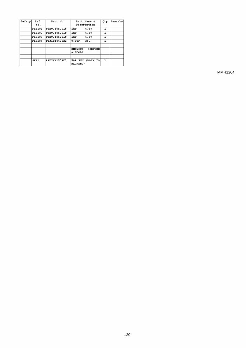
MMH1204
FL8101 F1H0J1050018 1uF 6.3V 1
FL8102 F1H0J1050018 1uF 6.3V 1
FL8103 F1H0J1050018 1uF 6.3V 1
FL8104 F1J1E1040022 0.1uF 25V 1
SERVICE FIXTURE& TOOLS
SFT1 RFKZXH150PK2 50P FFC (MAIN TOBACKEND)
1
Safety Ref. No.
Part No. Part Name & Description
Qty Remarks
129
Related Documents