www.ti.com FEATURES KEY SPECIFICATIONS TRF1112 / TRF1212 PIN OUT DESCRIPTION LPCC-48 PACKAGE (TOP VIEW) 1 2 3 4 5 6 7 8 9 10 11 12 CP2O LD1 LF1 EN FRBP VCCD1 FR VCCD2 CLK DATA LF2 LD2 13 14 15 16 17 18 19 20 21 22 23 24 CP2O LO2TUN LO2BPB VDET AGCI LO2BPA VCCLO2 BBON BBOP VBGR IF2BON IF2BOP 36 35 34 33 32 31 30 29 28 27 26 25 AGCO IFBPB IF1IP IF1IN VCCA VCCB VERR VREF VFB VCCC IF2AOP IF2AON 48 47 46 45 44 43 42 41 40 39 38 37 EXTLO1N EXTLO1P VCCLO1 LO1OP LO1ON LO1BPA LO1TUN LO1BPB IF2BIN IF2BIP IF2AIN IF2AIP BLOCK DIAGRAM TRF1112 TRF1212 SLWS175A – APRIL 2005 – REVISED DECEMBER 2005 Dual VCO/PLL Synthesizer With IF Down-Conversion The TRF1112 / TRF1212 are designed to function as part of Texas Instruments 2.5-GHz and 3.5-GHz • Low Phase Noise complete radio chipsets, respectively. In the chipset, • High Dynamic Range Image-Reject two chips function together to double-down convert Downconverter RF frequencies to an IF frequency that is suitable for most baseband modem ADCs. The TRF1112 / • Selectable IF Filters TRF1212 performs the second down conversion from • Internal or External AGC Control With Peak the first IF frequency (480 MHz typical) to a final IF Detector and Voltage Reference frequency (20-50 MHz). The radio chipset features • Analog Gain Control Range sufficient linearity, phase noise and dynamic range to work in single carrier or multi-carrier, line-of-sight or • Direct Interface to A/D non-line-of-sight, IEEE standard 802.16, BWIF, or • Dual VCO/PLL With On-Chip Resonator For proprietary systems. Due to the modular nature of the Double Down-Conversion Architecture chipset, it is ideal for use in systems that employ transmit or receive diversity. • S-Band LO Frequency Range: – TRF1112: 1700 to 2400 MHz – TRF1212: 2400 MHz to 3550 MHz • UHF LO Frequency Range: 325 MHz to 460 MHz • Phase Noise is 0.5 RMS Typ 100 Hz to 1 MHz • Rx Noise Figure of 5 dB, Typ • UHF LO Tuning Step Size of 125 kHz With 18 MHz Reference • Typical Gain of 90 dB, Including 15-dB Loss IF2 SAW Filter • Input Third Order Intercept Point > 0 dBm • Input 1-dB Compression Point > –10 dBm • Gain Control Range of 90 dB Typ The TRF1112 / TRF1212 are UHF-VHF down converters with integrated UHF and S-band frequency synthesizers for radio applications in the 2GHz to 4GHz range. The device integrates an image reject mixer, IF gain blocks, automatic gain control (AGC), and two complete phase locked loop (PLL) circuits including: VCOs, resonator circuit, varactors, dividers, and phase detectors. The detailed block diagram and the pin-out of the ASIC are shown in Figure 1 and the Terminal Functions table. Please be aware that an important notice concerning availability, standard warranty, and use in critical applications of Texas Instruments semiconductor products and disclaimers thereto appears at the end of this data sheet. PRODUCTION DATA information is current as of publication date. Copyright © 2005, Texas Instruments Incorporated Products conform to specifications per the terms of the Texas Instruments standard warranty. Production processing does not necessarily include testing of all parameters.

Welcome message from author
This document is posted to help you gain knowledge. Please leave a comment to let me know what you think about it! Share it to your friends and learn new things together.
Transcript
www.ti.com
FEATURES
KEY SPECIFICATIONSTRF1112 / TRF1212 PIN OUT
DESCRIPTION
LPCC−48 PACKAGE(TOP VIEW)
123
456789
101112
CP2OLD1LF1
ENFRBP
VCCD1FR
VCCD2CLK
DATALF2LD2
13 14 15 16 17 18 19 20 21 22 23 24
CP
2OLO
2TU
NLO
2BP
B
VD
ET
AG
CI
LO2B
PAV
CC
LO2
BB
ON
BB
OP
VB
GR
IF2B
ON
IF2B
OP
363534
333231302928
272625
AGCOIFBPBIF1IP
IF1INVCCAVCCBVERRVREFVFB
VCCCIF2AOPIF2AON
48 47 46 45 44 43 42 41 40 39 38 37
EX
TLO
1NE
XT
LO1P
VC
CLO
1
LO1O
PLO
1ON
LO1B
PALO
1TU
NLO
1BP
BIF
2BIN
IF2B
IPIF
2AIN
IF2A
IP
BLOCK DIAGRAM
TRF1112TRF1212
SLWS175A–APRIL 2005–REVISED DECEMBER 2005
Dual VCO/PLL Synthesizer With IF Down-Conversion
The TRF1112 / TRF1212 are designed to function aspart of Texas Instruments 2.5-GHz and 3.5-GHz• Low Phase Noisecomplete radio chipsets, respectively. In the chipset,
• High Dynamic Range Image-Reject two chips function together to double-down convertDownconverter RF frequencies to an IF frequency that is suitable for
most baseband modem ADCs. The TRF1112 /• Selectable IF FiltersTRF1212 performs the second down conversion from• Internal or External AGC Control With Peakthe first IF frequency (480 MHz typical) to a final IFDetector and Voltage Reference frequency (20-50 MHz). The radio chipset features
• Analog Gain Control Range sufficient linearity, phase noise and dynamic range towork in single carrier or multi-carrier, line-of-sight or• Direct Interface to A/Dnon-line-of-sight, IEEE standard 802.16, BWIF, or• Dual VCO/PLL With On-Chip Resonator Forproprietary systems. Due to the modular nature of theDouble Down-Conversion Architecture chipset, it is ideal for use in systems that employtransmit or receive diversity.
• S-Band LO Frequency Range:– TRF1112: 1700 to 2400 MHz– TRF1212: 2400 MHz to 3550 MHz
• UHF LO Frequency Range: 325 MHz to 460MHz
• Phase Noise is 0.5 RMS Typ 100 Hz to 1 MHz• Rx Noise Figure of 5 dB, Typ• UHF LO Tuning Step Size of 125 kHz With 18
MHz Reference• Typical Gain of 90 dB, Including 15-dB Loss
IF2 SAW Filter• Input Third Order Intercept Point > 0 dBm• Input 1-dB Compression Point > –10 dBm• Gain Control Range of 90 dB Typ
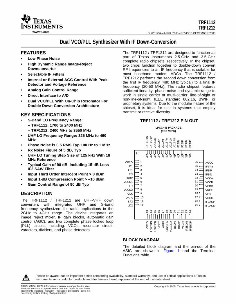
The TRF1112 / TRF1212 are UHF-VHF downconverters with integrated UHF and S-bandfrequency synthesizers for radio applications in the2GHz to 4GHz range. The device integrates animage reject mixer, IF gain blocks, automatic gaincontrol (AGC), and two complete phase locked loop(PLL) circuits including: VCOs, resonator circuit,varactors, dividers, and phase detectors.
The detailed block diagram and the pin-out of theASIC are shown in Figure 1 and the TerminalFunctions table.
Please be aware that an important notice concerning availability, standard warranty, and use in critical applications of TexasInstruments semiconductor products and disclaimers thereto appears at the end of this data sheet.
PRODUCTION DATA information is current as of publication date. Copyright © 2005, Texas Instruments IncorporatedProducts conform to specifications per the terms of the TexasInstruments standard warranty. Production processing does notnecessarily include testing of all parameters.
www.ti.com
LPF
LPF
BPF
BPF
DETECTOR
90 º
90 º
ChrgPump
N N
Automatic GainController
Power Supply
VC
CC
IF1IP
IF1IN
LO1OP
LO1ON
DATA
EN
CLK SynthesizerData Decoder& Controller
EX
TLO
IN
CP
1O
LO1T
UN
CP
20
LO2T
UN
LD1
FR
LO2B
PB
IF2AOP
IF2BON
IF2AIP
IF2BIN
BBOPBBON
VDET
VCCD2
VC
CA
AGCI
AGCO
ChrgPump
R
VERR
VREF
VFB
VBGR
EX
TLO
IP
VC
CLO
1
LFI
LO1B
PB
LO1B
PA
FR
BP
VC
CLO
2
LO2B
PA
LD2
LF2
IFBPBIF2AIN
IF2BIPIF2BOP
IF2AON
Synthesizer #2Synthesizer #1
VCO2
Down−converter
IF VGA
IF2IF1
IF2
VC
CB
VC
CD
1
VCO1
TRF1112TRF1212SLWS175A–APRIL 2005–REVISED DECEMBER 2005
Figure 1. Detailed Block Diagram of TRF1112 / TRF1212
TERMINAL FUNCTIONS
TERMINALI/O TYPE DESCRIPTION
NO. NAME
1 CP1O O Analog Analog Synthesizer 1 Charge Pump Output
2 LD1 O Digital Synthesizer 1 Lock Detect Output, High is locked
3 LF1 O Analog Lock Detector Filter Capacitor for LO1, 0.01 µF Typ. 100 kΩ pull-up (1)
4 EN I Digital 3-wire bus Enable; Active High
5 FRBP O Analog Reference Frequency Bypass, Internally biased to 2.5 V.
6 VCCD1 I Power Digital Power Supply Voltage
7 FR I Analog Reference Frequency Source Input, HCMOS input. (DC level = 2.5 V)
8 VCCD2 I Power Digital Power Supply Voltage
9 CLK I Digital 3-wire bus Clock
10 DATA I Digital 3-wire bus Data
11 LF2 O Analog Lock Detector Filter Capacitor for LO2, 0.01 µF typ 100 kΩ pull-up (1)
12 LD2 O Analog Synthesizer 2 Lock Detect Output, High is locked
13 CP2O O Analog Synthesizer 2 Charge Pump Output
14 LO2TUN I Analog Synthesizer 2 VCO Input tune port
15 LO2BPB O Analog Bypass cap for LO2, 0.1 µF (min) DCV = 1 V
16 VDET O Analog Peak Detector Output
(1) Current leakage on the order of 10 µA through the capacitor or by any other means from either LF pin can cause false loss of locksignals. The two pull up resistors (R23 and R24) in Figure 20 reduce this sensitivity.
2
www.ti.com
TRF1112TRF1212
SLWS175A–APRIL 2005–REVISED DECEMBER 2005
TERMINAL FUNCTIONS (continued)
TERMINALI/O TYPE DESCRIPTION
NO. NAME
17 AGCI I Analog AGC Voltage Input, 0-3 V
18 LO2BPA O Not connected for normal operation. DC bias nominal 1.8 V. Do not ground or connect to any otherAnalog pin.
19 VCCLO2 I Power VCC for LO2, Low Noise Supply
20 BBON O Analog IF output (differential) negative, DC coupled, internally biased to 3 V typical
21 BBOP O Analog IF output (differential) positive, DC coupled, internally biased to 3 V typical
22 VBGR O Analog Band-Gap Reference Voltage, 1.17 V
23 IF2BON O Analog IF2B output (differential) negative, DC coupled, internally biased to 4 V typical
24 IF2BOP O Analog IF2B output (differential) positive , DC coupled, internally biased to 4 V typical
25 IF2AON O Analog IF2A output (differential) negative, DC coupled, internally biased to 4 V typical
26 IF2AOP O Analog IF2A output (differential) positive, DC coupled, internally biased to 4 V typical
27 VCCC I Power Analog Power Supply Voltage
28 VFB I Analog Error Amplifier Feedback Input
29 VREF I Analog Reference Frequency Input
30 VERR O Analog Error Amplifier Output, internal op amp output
31 VCCB I Power Analog Power Supply Voltage
32 VCCA I Power Analog Power Supply Voltage
33 IF1IN I Analog IF1 input (differential) negative, DC coupled, Internally biased to 1.4 V typical
34 IF1IP I Analog IF1 input (differential) positive, DC coupled, Internally biased to 1.4 V typical
35 IFBPB O Analog Bypass cap for IF amp, 0.1 µF (min), DCV = 1 V
36 AGCO O Analog AGC Voltage Output Used to control Front end gain for extended dynamic range
37 IF2AIP I Analog IF2A input (differential) positive, DC coupled, Internally biased to 3.0 V typical
38 IF2AIN I Analog IF2A input (differential) negative, DC coupled, Internally biased to 3.0 V typical
39 IF2BIP I Analog IF2B input (differential) positive, DC coupled, Internally biased to 3.0 V typical
40 IF2BIN I Analog IF2B input (differential) negative, DC coupled, Internally biased to 3.0 V typical
41 LO1BPB O Analog Bypass cap for LO1 0.1 µF (min), DCV = 1 V
42 LO1TUN I Analog Synthesizer1 VCO Tune port Input
43 LO1BPA O Not connected for normal operation. DC bias nominal 1.8 V. Do not ground or connect to any otherAnalog pin.
44 LO1ON O Analog LO1 output (differential) neg. Negative and positive VCC bias (+5 V) for LO buffer amp.
45 LO1OP O Analog LO1 output (differential) pos. Negative and positive VCC bias (+5 V) for LO buffer amp.
46 VCCLO1 I Power VCC for LO1, Low Noise Supply
47 EXTLO1P I Analog External VCO input (differential) positive and logic level for VCO select.
48 EXTLO1N I Analog External VCO input (differential) negative and logic level for VCO select.
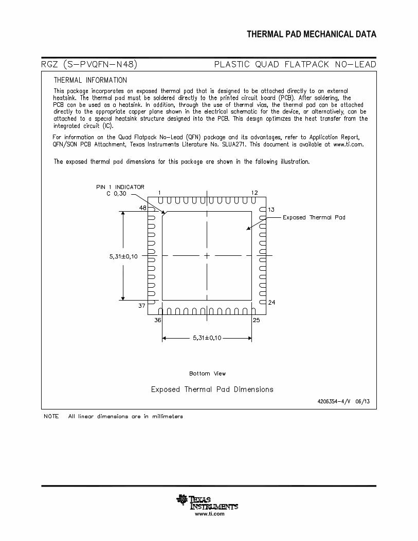
– BACK – – Back side of package has metal base that must be grounded for thermal and RF performance.
3
www.ti.com
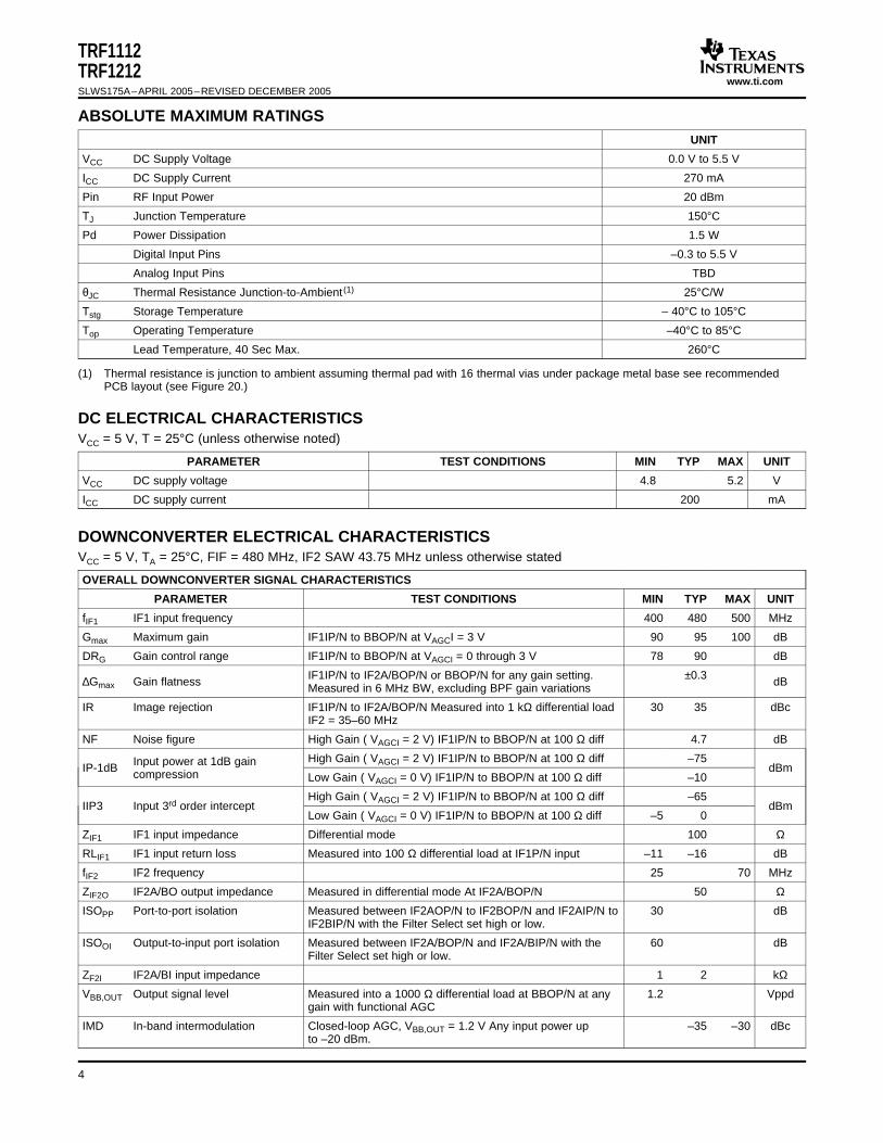
ABSOLUTE MAXIMUM RATINGS
DC ELECTRICAL CHARACTERISTICS
DOWNCONVERTER ELECTRICAL CHARACTERISTICS
TRF1112TRF1212SLWS175A–APRIL 2005–REVISED DECEMBER 2005
UNIT
VCC DC Supply Voltage 0.0 V to 5.5 V
ICC DC Supply Current 270 mA
Pin RF Input Power 20 dBm
TJ Junction Temperature 150°C
Pd Power Dissipation 1.5 W
Digital Input Pins –0.3 to 5.5 V
Analog Input Pins TBD
θJC Thermal Resistance Junction-to-Ambient (1) 25°C/W
Tstg Storage Temperature – 40°C to 105°C
Top Operating Temperature –40°C to 85°C
Lead Temperature, 40 Sec Max. 260°C
(1) Thermal resistance is junction to ambient assuming thermal pad with 16 thermal vias under package metal base see recommendedPCB layout (see Figure 20.)
VCC = 5 V, T = 25°C (unless otherwise noted)
PARAMETER TEST CONDITIONS MIN TYP MAX UNIT
VCC DC supply voltage 4.8 5.2 V
ICC DC supply current 200 mA
VCC = 5 V, TA = 25°C, FIF = 480 MHz, IF2 SAW 43.75 MHz unless otherwise stated
OVERALL DOWNCONVERTER SIGNAL CHARACTERISTICS
PARAMETER TEST CONDITIONS MIN TYP MAX UNIT
fIF1 IF1 input frequency 400 480 500 MHz
Gmax Maximum gain IF1IP/N to BBOP/N at VAGCI = 3 V 90 95 100 dB
DRG Gain control range IF1IP/N to BBOP/N at VAGCI = 0 through 3 V 78 90 dB
IF1IP/N to IF2A/BOP/N or BBOP/N for any gain setting. ±0.3∆Gmax Gain flatness dBMeasured in 6 MHz BW, excluding BPF gain variations
IR Image rejection IF1IP/N to IF2A/BOP/N Measured into 1 kΩ differential load 30 35 dBcIF2 = 35–60 MHz
NF Noise figure High Gain ( VAGCI = 2 V) IF1IP/N to BBOP/N at 100 Ω diff 4.7 dB
High Gain ( VAGCI = 2 V) IF1IP/N to BBOP/N at 100 Ω diff –75Input power at 1dB gainIP-1dB dBmcompression Low Gain ( VAGCI = 0 V) IF1IP/N to BBOP/N at 100 Ω diff –10
High Gain ( VAGCI = 2 V) IF1IP/N to BBOP/N at 100 Ω diff –65IIP3 Input 3rd order intercept dBm
Low Gain ( VAGCI = 0 V) IF1IP/N to BBOP/N at 100 Ω diff –5 0
ZIF1 IF1 input impedance Differential mode 100 Ω
RLIF1 IF1 input return loss Measured into 100 Ω differential load at IF1P/N input –11 –16 dB
fIF2 IF2 frequency 25 70 MHz
ZIF2O IF2A/BO output impedance Measured in differential mode At IF2A/BOP/N 50 Ω
ISOPP Port-to-port isolation Measured between IF2AOP/N to IF2BOP/N and IF2AIP/N to 30 dBIF2BIP/N with the Filter Select set high or low.
ISOOI Output-to-input port isolation Measured between IF2A/BOP/N and IF2A/BIP/N with the 60 dBFilter Select set high or low.
ZF2I IF2A/BI input impedance 1 2 kΩ
VBB,OUT Output signal level Measured into a 1000 Ω differential load at BBOP/N at any 1.2 Vppdgain with functional AGC
IMD In-band intermodulation Closed-loop AGC, VBB,OUT = 1.2 V Any input power up –35 –30 dBcto –20 dBm.
4
www.ti.com
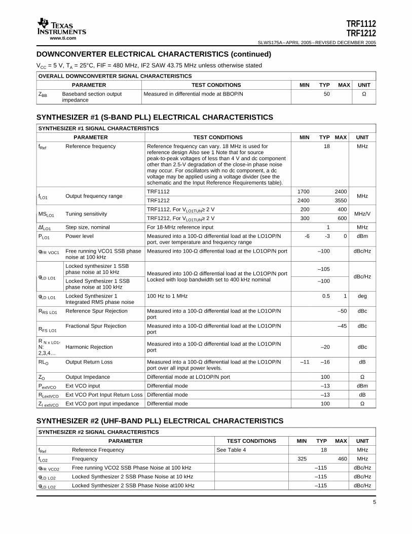
SYNTHESIZER #1 (S-BAND PLL) ELECTRICAL CHARACTERISTICS
SYNTHESIZER #2 (UHF-BAND PLL) ELECTRICAL CHARACTERISTICS
TRF1112TRF1212
SLWS175A–APRIL 2005–REVISED DECEMBER 2005
DOWNCONVERTER ELECTRICAL CHARACTERISTICS (continued)VCC = 5 V, TA = 25°C, FIF = 480 MHz, IF2 SAW 43.75 MHz unless otherwise stated
OVERALL DOWNCONVERTER SIGNAL CHARACTERISTICS
PARAMETER TEST CONDITIONS MIN TYP MAX UNIT
ZBB Baseband section output Measured in differential mode at BBOP/N 50 Ωimpedance
SYNTHESIZER #1 SIGNAL CHARACTERISTICS
PARAMETER TEST CONDITIONS MIN TYP MAX UNIT
fRef Reference frequency Reference frequency can vary. 18 MHz is used for 18 MHzreference design Also see 1 Note that for sourcepeak-to-peak voltages of less than 4 V and dc componentother than 2.5-V degradation of the close-in phase noisemay occur. For oscillators with no dc component, a dcvoltage may be applied using a voltage divider (see theschematic and the Input Reference Requirements table).
TRF1112 1700 2400fLO1 Output frequency range MHz
TRF1212 2400 3550
TRF1112, For VLO1TUN≥ 2 V 200 400MSLO1 Tuning sensitivity MHz/V
TRF1212, For VLO1TUN≥ 2 V 300 600
∆fLO1 Step size, nominal For 18-MHz reference input 1 MHz
PLO1 Power level Measured into a 100-Ω differential load at the LO1OP/N -6 -3 0 dBmport, over temperature and frequency range
φFR VOC1 Free running VCO1 SSB phase Measured into 100-Ω differential load at the LO1OP/N port –100 dBc/Hznoise at 100 kHz
Locked synthesizer 1 SSB –105phase noise at 10 kHz Measured into 100-Ω differential load at the LO1OP/N portφLD LO1 dBc/HzLocked with loop bandwidth set to 400 kHz nominalLocked Synthesizer 1 SSB –100phase noise at 100 kHz
φLD LO1 Locked Synthesizer 1 100 Hz to 1 MHz 0.5 1 degIntegrated RMS phase noise
RRS LO1 Reference Spur Rejection Measured into a 100-Ω differential load at the LO1OP/N –50 dBcport
Fractional Spur Rejection Measured into a 100-Ω differential load at the LO1OP/N –45 dBcRFS LO1 port
R N x LO1, Measured into a 100-Ω differential load at the LO1OP/NN: Harmonic Rejection –20 dBcport2,3,4…
RLO Output Return Loss Measured into a 100-Ω differential load at the LO1OP/N –11 –16 dBport over all input power levels.
ZO Output Impedance Differential mode at LO1OP/N port 100 Ω
PextVCO Ext VCO input Differential mode –13 dBm
RLextVCO Ext VCO Port Input Return Loss Differential mode –13 dB
ZI extVCO Ext VCO port input impedance Differential mode 100 Ω
SYNTHESIZER #2 SIGNAL CHARACTERISTICS
PARAMETER TEST CONDITIONS MIN TYP MAX UNIT
fRef Reference Frequency See Table 4 18 MHz
fLO2 Frequency 325 460 MHz
φFR VCO2 Free running VCO2 SSB Phase Noise at 100 kHz –115 dBc/Hz
φLD LO2 Locked Synthesizer 2 SSB Phase Noise at 10 kHz –115 dBc/Hz
φLD LO2 Locked Synthesizer 2 SSB Phase Noise at100 kHz –115 dBc/Hz
5
www.ti.com
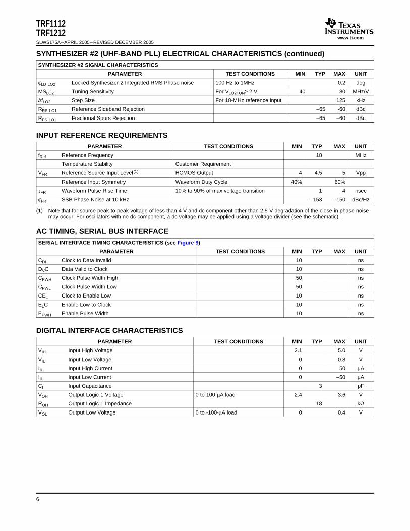
INPUT REFERENCE REQUIREMENTS
AC TIMING, SERIAL BUS INTERFACE
DIGITAL INTERFACE CHARACTERISTICS
TRF1112TRF1212SLWS175A–APRIL 2005–REVISED DECEMBER 2005
SYNTHESIZER #2 (UHF-BAND PLL) ELECTRICAL CHARACTERISTICS (continued)SYNTHESIZER #2 SIGNAL CHARACTERISTICS
PARAMETER TEST CONDITIONS MIN TYP MAX UNIT
φLD LO2 Locked Synthesizer 2 Integrated RMS Phase noise 100 Hz to 1MHz 0.2 deg
MSLO2 Tuning Sensitivity For VLO2TUN≥ 2 V 40 80 MHz/V
∆fLO2 Step Size For 18-MHz reference input 125 kHz
RRS LO1 Reference Sideband Rejection –65 -60 dBc
RFS LO1 Fractional Spurs Rejection –65 –60 dBc
PARAMETER TEST CONDITIONS MIN TYP MAX UNIT
fRef Reference Frequency 18 MHz
Temperature Stability Customer Requirement
VFR Reference Source Input Level (1) HCMOS Output 4 4.5 5 Vpp
Reference Input Symmetry Waveform Duty Cycle 40% 60%
τFR Waveform Pulse Rise Time 10% to 90% of max voltage transition 1 4 nsec
φFR SSB Phase Noise at 10 kHz –153 –150 dBc/Hz
(1) Note that for source peak-to-peak voltage of less than 4 V and dc component other than 2.5-V degradation of the close-in phase noisemay occur. For oscillators with no dc component, a dc voltage may be applied using a voltage divider (see the schematic).
SERIAL INTERFACE TIMING CHARACTERISTICS (see Figure 9)
PARAMETER TEST CONDITIONS MIN TYP MAX UNIT
CDI Clock to Data Invalid 10 ns
DVC Data Valid to Clock 10 ns
CPWH Clock Pulse Width High 50 ns
CPWL Clock Pulse Width Low 50 ns
CEL Clock to Enable Low 10 ns
ELC Enable Low to Clock 10 ns
EPWH Enable Pulse Width 10 ns
PARAMETER TEST CONDITIONS MIN TYP MAX UNIT
VIH Input High Voltage 2.1 5.0 V
VIL Input Low Voltage 0 0.8 V
IIH Input High Current 0 50 µA
IIL Input Low Current 0 –50 µA
CI Input Capacitance 3 pF
VOH Output Logic 1 Voltage 0 to 100-µA load 2.4 3.6 V
ROH Output Logic 1 Impedance 18 kΩ
VOL Output Low Voltage 0 to -100-µA load 0 0.4 V
6
www.ti.com
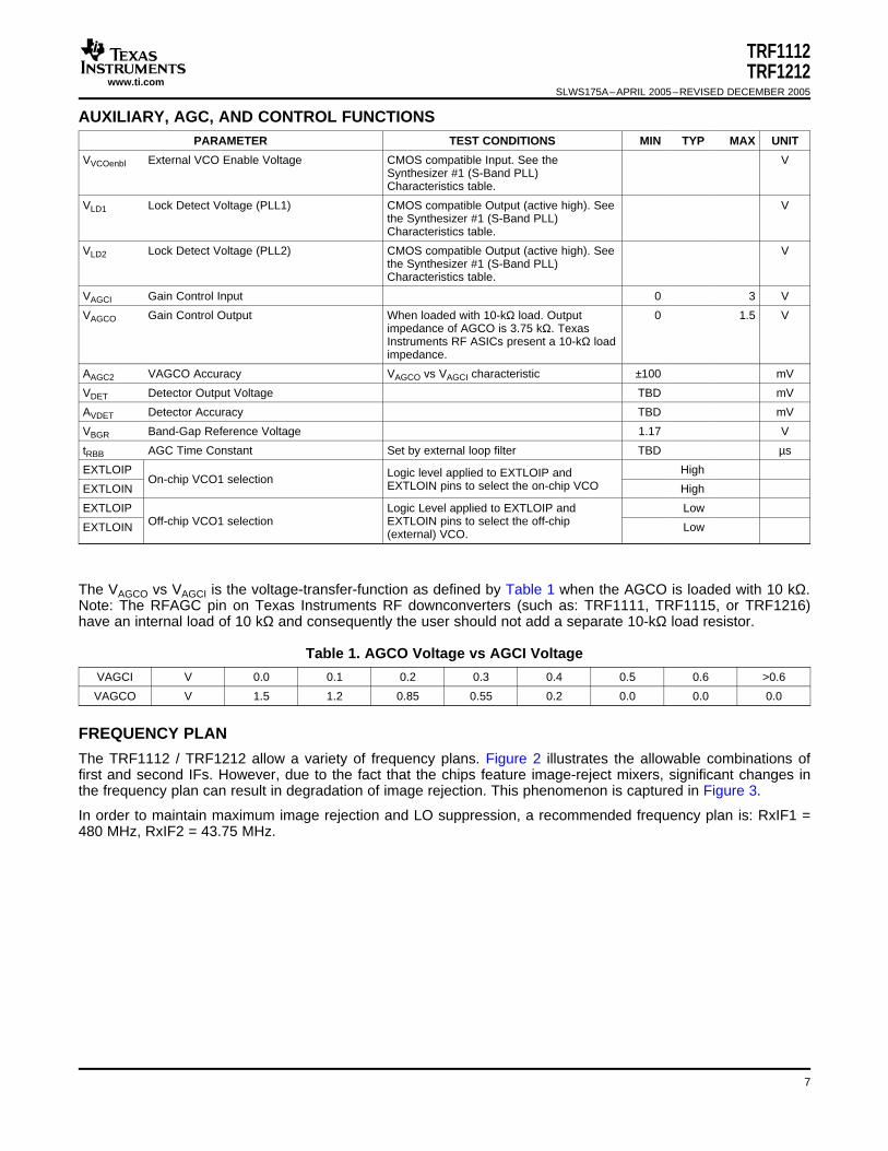
AUXILIARY, AGC, AND CONTROL FUNCTIONS
FREQUENCY PLAN
TRF1112TRF1212
SLWS175A–APRIL 2005–REVISED DECEMBER 2005
PARAMETER TEST CONDITIONS MIN TYP MAX UNIT
VVCOenbl External VCO Enable Voltage CMOS compatible Input. See the VSynthesizer #1 (S-Band PLL)Characteristics table.
VLD1 Lock Detect Voltage (PLL1) CMOS compatible Output (active high). See Vthe Synthesizer #1 (S-Band PLL)Characteristics table.
VLD2 Lock Detect Voltage (PLL2) CMOS compatible Output (active high). See Vthe Synthesizer #1 (S-Band PLL)Characteristics table.
VAGCI Gain Control Input 0 3 V
VAGCO Gain Control Output When loaded with 10-kΩ load. Output 0 1.5 Vimpedance of AGCO is 3.75 kΩ. TexasInstruments RF ASICs present a 10-kΩ loadimpedance.
AAGC2 VAGCO Accuracy VAGCO vs VAGCI characteristic ±100 mV
VDET Detector Output Voltage TBD mV
AVDET Detector Accuracy TBD mV
VBGR Band-Gap Reference Voltage 1.17 V
tRBB AGC Time Constant Set by external loop filter TBD µs
EXTLOIP HighLogic level applied to EXTLOIP andOn-chip VCO1 selection EXTLOIN pins to select the on-chip VCOEXTLOIN High
EXTLOIP Logic Level applied to EXTLOIP and LowOff-chip VCO1 selection EXTLOIN pins to select the off-chipEXTLOIN Low
(external) VCO.
The VAGCO vs VAGCI is the voltage-transfer-function as defined by Table 1 when the AGCO is loaded with 10 kΩ.Note: The RFAGC pin on Texas Instruments RF downconverters (such as: TRF1111, TRF1115, or TRF1216)have an internal load of 10 kΩ and consequently the user should not add a separate 10-kΩ load resistor.
Table 1. AGCO Voltage vs AGCI Voltage
VAGCI V 0.0 0.1 0.2 0.3 0.4 0.5 0.6 >0.6
VAGCO V 1.5 1.2 0.85 0.55 0.2 0.0 0.0 0.0
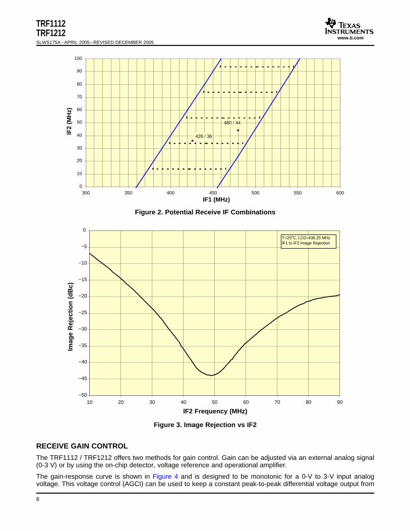
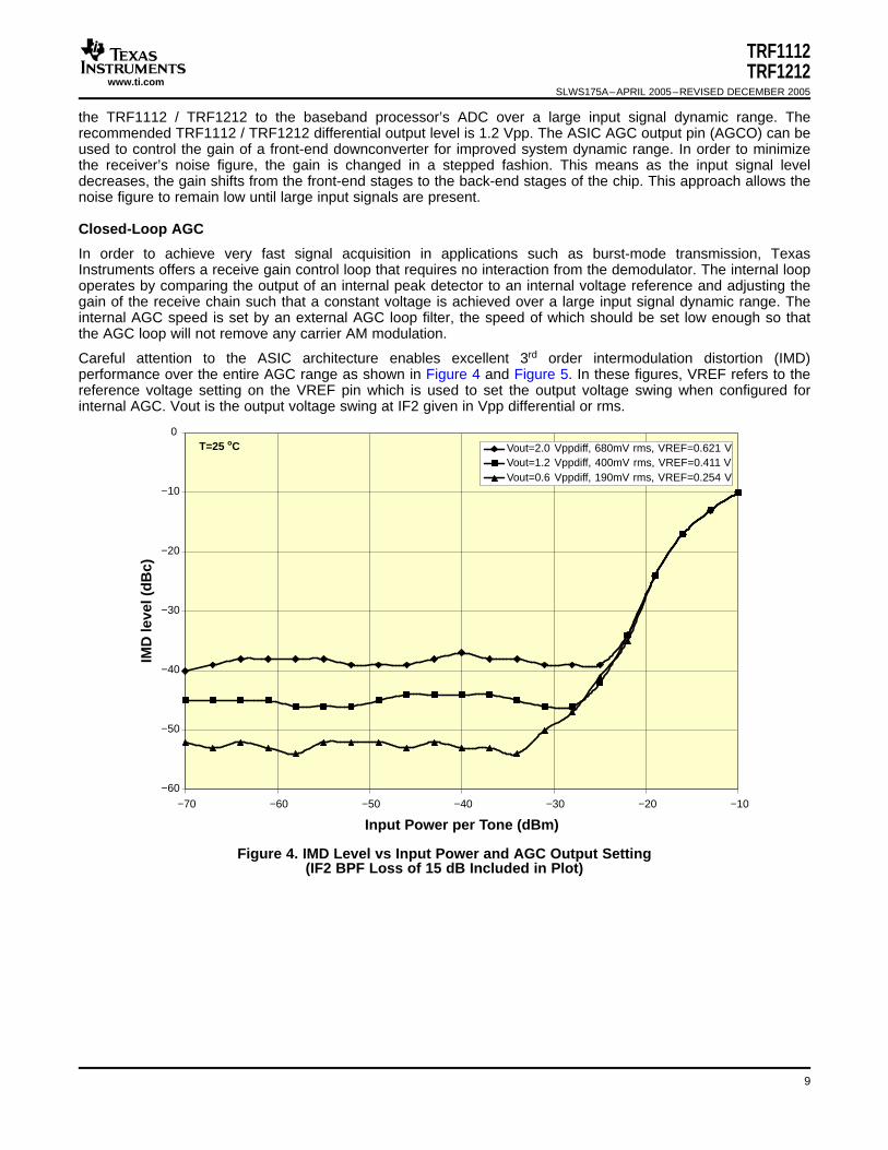
The TRF1112 / TRF1212 allow a variety of frequency plans. Figure 2 illustrates the allowable combinations offirst and second IFs. However, due to the fact that the chips feature image-reject mixers, significant changes inthe frequency plan can result in degradation of image rejection. This phenomenon is captured in Figure 3.
In order to maintain maximum image rejection and LO suppression, a recommended frequency plan is: RxIF1 =480 MHz, RxIF2 = 43.75 MHz.
7
www.ti.com
480 / 44
426 / 36
0
10
20
30
40
50
60
70
80
90
100
300 350 400 450 500 550 600
IF1 (MHz)
IF2
(MH
z)
−50
−45
−40
−35
−30
−25
−20
−15
−10
−5
0
10 20 30 40 50 60 70 80 90
IF2 Frequency (MHz)
Imag
e R
ejec
tio
n (
dB
c)
T=25oC, LO2=436.25 MHzIF1 to IF2 Image Rejection
RECEIVE GAIN CONTROL
TRF1112TRF1212SLWS175A–APRIL 2005–REVISED DECEMBER 2005
Figure 2. Potential Receive IF Combinations
Figure 3. Image Rejection vs IF2
The TRF1112 / TRF1212 offers two methods for gain control. Gain can be adjusted via an external analog signal(0-3 V) or by using the on-chip detector, voltage reference and operational amplifier.
The gain-response curve is shown in Figure 4 and is designed to be monotonic for a 0-V to 3-V input analogvoltage. This voltage control (AGCI) can be used to keep a constant peak-to-peak differential voltage output from
8
www.ti.com
Closed-Loop AGC
−60
−50
−40
−30
−20
−10
0
−70 −60 −50 −40 −30 −20 −10
Input Power per Tone (dBm)
IMD
leve
l (d
Bc)
Vout=2.0 Vppdiff, 680mV rms, VREF=0.621 VVout=1.2 Vppdiff, 400mV rms, VREF=0.411 VVout=0.6 Vppdiff, 190mV rms, VREF=0.254 V
T=25 oC
TRF1112TRF1212
SLWS175A–APRIL 2005–REVISED DECEMBER 2005
the TRF1112 / TRF1212 to the baseband processor’s ADC over a large input signal dynamic range. Therecommended TRF1112 / TRF1212 differential output level is 1.2 Vpp. The ASIC AGC output pin (AGCO) can beused to control the gain of a front-end downconverter for improved system dynamic range. In order to minimizethe receiver’s noise figure, the gain is changed in a stepped fashion. This means as the input signal leveldecreases, the gain shifts from the front-end stages to the back-end stages of the chip. This approach allows thenoise figure to remain low until large input signals are present.
In order to achieve very fast signal acquisition in applications such as burst-mode transmission, TexasInstruments offers a receive gain control loop that requires no interaction from the demodulator. The internal loopoperates by comparing the output of an internal peak detector to an internal voltage reference and adjusting thegain of the receive chain such that a constant voltage is achieved over a large input signal dynamic range. Theinternal AGC speed is set by an external AGC loop filter, the speed of which should be set low enough so thatthe AGC loop will not remove any carrier AM modulation.
Careful attention to the ASIC architecture enables excellent 3rd order intermodulation distortion (IMD)performance over the entire AGC range as shown in Figure 4 and Figure 5. In these figures, VREF refers to thereference voltage setting on the VREF pin which is used to set the output voltage swing when configured forinternal AGC. Vout is the output voltage swing at IF2 given in Vpp differential or rms.
Figure 4. IMD Level vs Input Power and AGC Output Setting(IF2 BPF Loss of 15 dB Included in Plot)
9

www.ti.com
−60
−50
−40
−30
−20
−10
0
−70 −60 −50 −40 −30 −20 −10
Input Power per Tone (dBm)
IMD
lev
el (
dB
c)
−40 ºC+25 ºC+85 ºC
External Analog Control
TRF1112TRF1212SLWS175A–APRIL 2005–REVISED DECEMBER 2005
Figure 5. IMD Level vs Temperature at Output AGC Setting of 1.2-Vpp Differential(IF2 Filter Loss of 15 dB Included)
Receive signal gain control can also be accomplished through direct interaction with the modem. For example,the modem can look at several metrics on the incoming signal including voltage swing, SNR, and AGC error,then feedback an analog (0 V to 3 V) gain control signal to the Texas Instruments ASIC. Note that forapplications requiring large channel bandwidths (e.g., 6 MHz) the maximum usable VAGCI should be limited toapproximately 2 V to 2.5 V, otherwise the resulting gain produces excessive amounts of noise at the output.
10
www.ti.com
0
10
20
30
40
50
60
70
80
90
100
0 0.5 1 1.5 2 2.5
AGC (V)
GA
IN (
dB
)
0
5
10
15
20
25
30
35
40
50
Noise Figure
No
ise
Fig
ure
(d
B)
−40 ºC+25 ºC+85 ºC
Gain
−80.0
−70.0
−60.0
−50.0
−40.0
−30.0
−20.0
−10.0
0.0
0.0 0.5 1.0 1.5 2.0 2.5AGCI (V)
IIP3
(dB
m)
−40 ºC+25 ºC+85 ºC
TRF1112TRF1212
SLWS175A–APRIL 2005–REVISED DECEMBER 2005
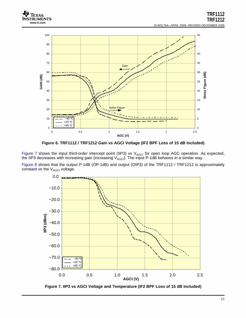
Figure 6. TRF1112 / TRF1212 Gain vs AGCI Voltage (IF2 BPF Loss of 15 dB Included)
Figure 7 shows the input third-order intercept point (IIP3) vs VAGCI for open loop AGC operation. As expected,the IIP3 decreases with increasing gain (increasing VAGCI). The input P-1dB behaves in a similar way.
Figure 8 shows that the output P-1dB (OP-1dB) and output (OIP3) of the TRF1112 / TRF1212 is approximatelyconstant vs the VAGCI voltage.
Figure 7. IIP3 vs AGCI Voltage and Temperature (IF2 BPF Loss of 15 dB Included)
11
www.ti.com
−10.0
−5.0
0.0
5.0
10.0
15.0
20.0
25.0
30.0
0.0 0.5 1.0 1.5 2.0 2.5AGCI (V)
OIP
3 o
r O
P−1
dB
(d
Bm
)
OIP3
OP1dB
−40 ºC+25 ºC+85 ºC
INTEGRATED SYNTHESIZERS
PLL Programming
A[7]=MSB A[6] A[5] D[1]Data
Clock
EN
EPWHCPWLCPWH
D[0] LSBA[4]
CDI DVC CEL
ELC
TRF1112TRF1212SLWS175A–APRIL 2005–REVISED DECEMBER 2005
Figure 8. OP-1dB and OIP3 vs AGCI Voltage and Temperature (IF2 BPF Loss of 15 dB Included)
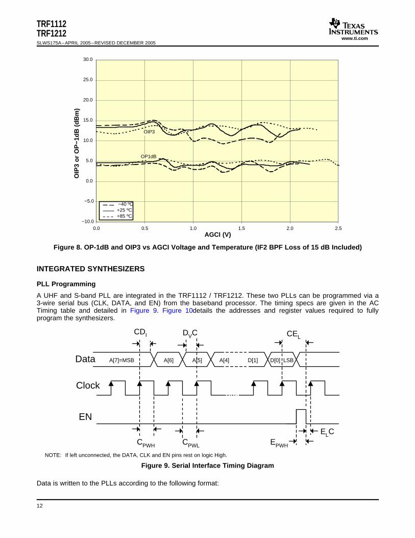
A UHF and S-band PLL are integrated in the TRF1112 / TRF1212. These two PLLs can be programmed via a3-wire serial bus (CLK, DATA, and EN) from the baseband processor. The timing specs are given in the ACTiming table and detailed in Figure 9. Figure 10details the addresses and register values required to fullyprogram the synthesizers.
NOTE: If left unconnected, the DATA, CLK and EN pins rest on logic High.
Figure 9. Serial Interface Timing Diagram
Data is written to the PLLs according to the following format:
12
www.ti.com
Fout REFIN 8 (N 3) S F188
(1)
Fout REFIN 8 (N 3) S F18
(2)
TRF1112TRF1212
SLWS175A–APRIL 2005–REVISED DECEMBER 2005
MSB Byte 1 LSB MSB Byte 2 LSB MSB Byte 3 LSB
Address Data
A[7] A[6] A[5] A[4] A[3] A[2] A[1] A[0] D[15] D[14] D[13] D[12] D[11] D[10] D[9] D[8] D[7] D[6] D[5] D[4] D[3] D[2] D[1] D[0]
0 0 0 0 0 0 0 0 0 0 Synth #1 N divider Synth #1 S counter Synth #1 F divider
0 0 0 0 0 0 0 1 0 0 Synth #2 N divider Synth #2 S counter Synth #2 F divider
0 0 0 0 0 1 0 0 0 0 0 0 0 0 FS PS 0 0 0 0 0 0 0 0
all other addresses reserved for future expansion
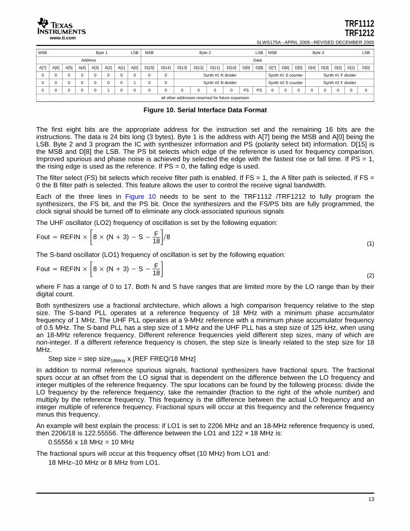
Figure 10. Serial Interface Data Format
The first eight bits are the appropriate address for the instruction set and the remaining 16 bits are theinstructions. The data is 24 bits long (3 bytes). Byte 1 is the address with A[7] being the MSB and A[0] being theLSB. Byte 2 and 3 program the IC with synthesizer information and PS (polarity select bit) information. D[15] isthe MSB and D[8] the LSB. The PS bit selects which edge of the reference is used for frequency comparison.Improved spurious and phase noise is achieved by selected the edge with the fastest rise or fall time. If PS = 1,the rising edge is used as the reference. If PS = 0, the falling edge is used.
The filter select (FS) bit selects which receive filter path is enabled. If FS = 1, the A filter path is selected, if FS =0 the B filter path is selected. This feature allows the user to control the receive signal bandwidth.
Each of the three lines in Figure 10 needs to be sent to the TRF1112 /TRF1212 to fully program thesynthesizers, the FS bit, and the PS bit. Once the synthesizers and the FS/PS bits are fully programmed, theclock signal should be turned off to eliminate any clock-associated spurious signals
The UHF oscillator (LO2) frequency of oscillation is set by the following equation:
The S-band oscillator (LO1) frequency of oscillation is set by the following equation:
where F has a range of 0 to 17. Both N and S have ranges that are limited more by the LO range than by theirdigital count.
Both synthesizers use a fractional architecture, which allows a high comparison frequency relative to the stepsize. The S-band PLL operates at a reference frequency of 18 MHz with a minimum phase accumulatorfrequency of 1 MHz. The UHF PLL operates at a 9-MHz reference with a minimum phase accumulator frequencyof 0.5 MHz. The S-band PLL has a step size of 1 MHz and the UHF PLL has a step size of 125 kHz, when usingan 18-MHz reference frequency. Different reference frequencies yield different step sizes, many of which arenon-integer. If a different reference frequency is chosen, the step size is linearly related to the step size for 18MHz.
Step size = step size18MHz x [REF FREQ/18 MHz]
In addition to normal reference spurious signals, fractional synthesizers have fractional spurs. The fractionalspurs occur at an offset from the LO signal that is dependent on the difference between the LO frequency andinteger multiples of the reference frequency. The spur locations can be found by the following process: divide theLO frequency by the reference frequency, take the remainder (fraction to the right of the whole number) andmultiply by the reference frequency. This frequency is the difference between the actual LO frequency and aninteger multiple of reference frequency. Fractional spurs will occur at this frequency and the reference frequencyminus this frequency.
An example will best explain the process: if LO1 is set to 2206 MHz and an 18-MHz reference frequency is used,then 2206/18 is 122.55556. The difference between the LO1 and 122 × 18 MHz is:
0.55556 x 18 MHz = 10 MHz
The fractional spurs will occur at this frequency offset (10 MHz) from LO1 and:18 MHz–10 MHz or 8 MHz from LO1.
13
www.ti.com
VCO Tuning Characteristics
1000
1250
1500
1750
2000
2250
2500
1 1.5 2 2.5 3 3.5 4 4.5 5
Tuning Voltage (V)
Fre
qu
ency
(M
Hz)
100
200
300
400
500
600
700
Mo
d S
ense
(M
Hz/
V)
Mod Sense
Frequency
−40 ºC+25 ºC+85 ºC
TRF1112TRF1212SLWS175A–APRIL 2005–REVISED DECEMBER 2005
The fractional spurious level varies with the offset from the LO since these spurious signals are attenuated by theloop filter response. The larger the offset from the LO, the lower the spur level. In general, spurs at offsetsgreater than 3 or 4 MHz are below –75 dBc and are not a concern. The worst fractional spurs levels occur whenthey are located at 1 MHz offset from the LO1 frequency. (Note: the fractional spur is offset from the LO1frequency by 1 MHz when the difference between the LO1 and an integer multiple of the reference frequency is 1or 17 MHz.)
Although both synthesizers have fractional spurs, for most applications the spurious signals from the UHF (LO2)synthesizer can be ignored because these spurs are attenuated by frequency dividers that are placed after theLO2 generation. In some frequency plans it is possible to offset LO1 and LO2, in a complementary manner, toavoid worst-case fractional spurs (i.e., 1-MHz offsets) on LO1 synthesizer.
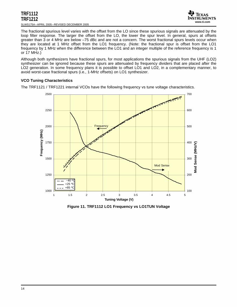
The TRF1121 / TRF1221 internal VCOs have the following frequency vs tune voltage characteristics.
Figure 11. TRF1112 LO1 Frequency vs LO1TUN Voltage
14
www.ti.com
200.0
250.0
300.0
350.0
400.0
450.0
500.0
1 1.5 2 2.5 3 3.5 4 4.5 5
Tuning Voltage (V)
Fre
qu
ency
(M
Hz)
20
40
60
80
100
120
140
Mo
d S
ense
(M
Hz/
V)
Mod Sense
Frequency
−40 ºC+25 ºC+85 ºC
1750
2000
2250
2500
2750
3000
3250
3500
3750
1 1.5 2 2.5 3 3.5 4 4.5 5
Tuning Voltage (V)
Fre
qu
ency
(M
Hz)
100
200
300
400
500
600
700
800
900
Mo
d S
ense
(M
Hz/
V)
Mod Sense
Frequency
−40 ºC+25 ºC+85 ºC
TRF1112TRF1212
SLWS175A–APRIL 2005–REVISED DECEMBER 2005
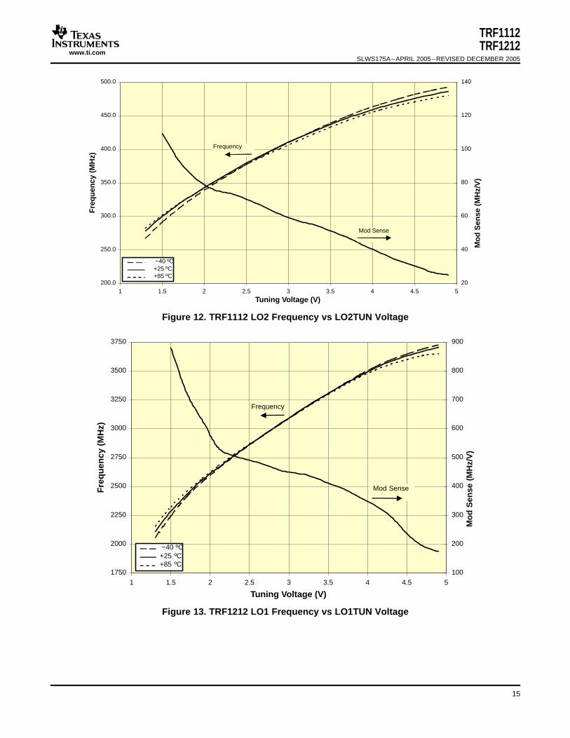
Figure 12. TRF1112 LO2 Frequency vs LO2TUN Voltage
Figure 13. TRF1212 LO1 Frequency vs LO1TUN Voltage
15

www.ti.com
200.0
250.0
300.0
350.0
400.0
450.0
500.0
1 1.5 2 2.5 3 3.5 4 4.5 5
Tuning Voltage (V)
Fre
qu
ency
(M
Hz)
20
40
60
80
100
120
140
Mo
d S
ense
(M
Hz/
V)
Mod Sense
Frequency
−40 ºC+25 ºC+85 ºC
Phase Noise
TRF1112TRF1212SLWS175A–APRIL 2005–REVISED DECEMBER 2005
Figure 14. TRF1212 LO2 Frequency vs LO2TUN Voltage
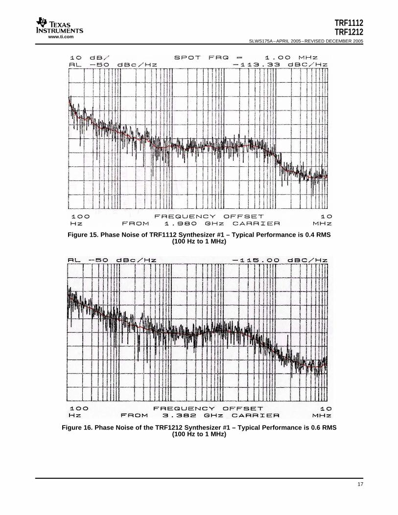
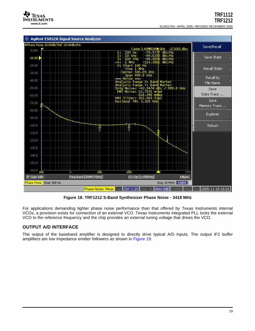
The TRF1112 / TRF1212 achieve superior phase noise performance with on-chip resonators and varactors. Theyare designed to meet the phase noise requirements of both single carrier and multi-carrier systems. Due to chiparchitecture, the phase noise and spurious performance of the LO2 (UHF) PLL is about 15 dB better than theLO1 (S-band) PLL. The typical phase noise of the TRF1112 and TRF1212 S-Band PLL (LO1) with the PLLlocked is shown in Figure 15 and Figure 16, respectively. The phase noise of the TRF1212 S-Band PLL at themin and max range are shown in Figure 17 and Figure 18 respectively. These plots were taken at roomtemperature and typical voltage conditions.
16
www.ti.com
TRF1112TRF1212
SLWS175A–APRIL 2005–REVISED DECEMBER 2005
Figure 15. Phase Noise of TRF1112 Synthesizer #1 – Typical Performance is 0.4 RMS(100 Hz to 1 MHz)
Figure 16. Phase Noise of the TRF1212 Synthesizer #1 – Typical Performance is 0.6 RMS(100 Hz to 1 MHz)
17
www.ti.com
TRF1112TRF1212SLWS175A–APRIL 2005–REVISED DECEMBER 2005
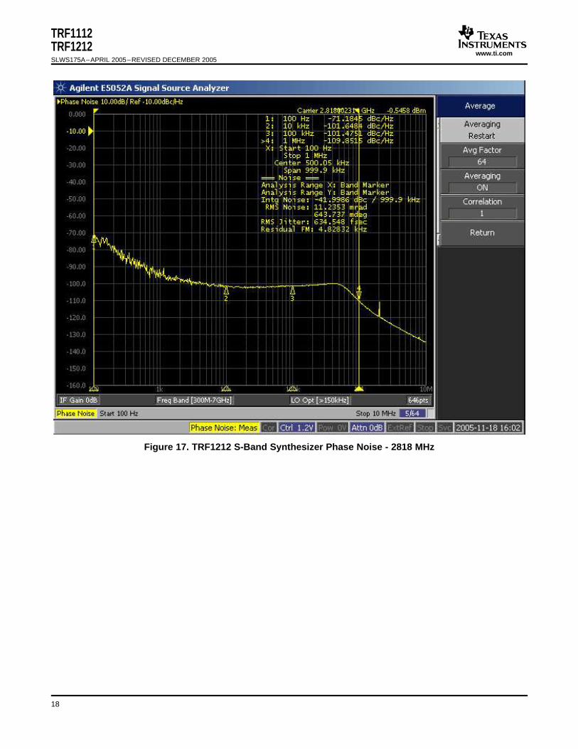
Figure 17. TRF1212 S-Band Synthesizer Phase Noise - 2818 MHz
18
www.ti.com
OUTPUT A/D INTERFACE
TRF1112TRF1212
SLWS175A–APRIL 2005–REVISED DECEMBER 2005
Figure 18. TRF1212 S-Band Synthesizer Phase Noise - 3418 MHz
For applications demanding tighter phase noise performance than that offered by Texas Instruments internalVCOs, a provision exists for connection of an external VCO. Texas Instruments integrated PLL locks the externalVCO to the reference frequency and the chip provides an external tuning voltage that drives the VCO.
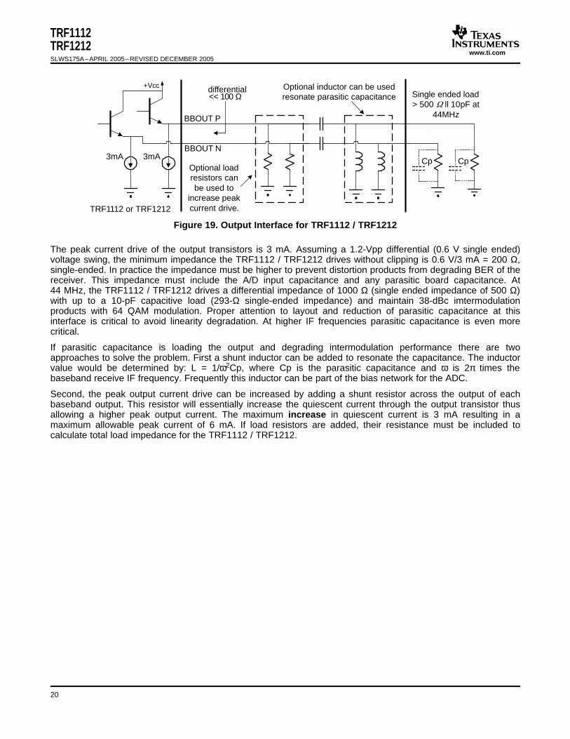
The output of the baseband amplifier is designed to directly drive typical A/D inputs. The output IF2 bufferamplifiers are low impedance emitter followers as shown in Figure 19.
19
www.ti.com
<< 100 Ωdifferential
BBOUT N
BBOUT P
3mA3mA
+VccSingle ended load> 500 ll 10pF at
44MHz
Cp Cp
Optional inductor can be usedresonate parasitic capacitance
Optional loadresistors canbe used to
increase peakcurrent drive.TRF1112 or TRF1212
TRF1112TRF1212SLWS175A–APRIL 2005–REVISED DECEMBER 2005
Figure 19. Output Interface for TRF1112 / TRF1212
The peak current drive of the output transistors is 3 mA. Assuming a 1.2-Vpp differential (0.6 V single ended)voltage swing, the minimum impedance the TRF1112 / TRF1212 drives without clipping is 0.6 V/3 mA = 200 Ω,single-ended. In practice the impedance must be higher to prevent distortion products from degrading BER of thereceiver. This impedance must include the A/D input capacitance and any parasitic board capacitance. At44 MHz, the TRF1112 / TRF1212 drives a differential impedance of 1000 Ω (single ended impedance of 500 Ω)with up to a 10-pF capacitive load (293-Ω single-ended impedance) and maintain 38-dBc imtermodulationproducts with 64 QAM modulation. Proper attention to layout and reduction of parasitic capacitance at thisinterface is critical to avoid linearity degradation. At higher IF frequencies parasitic capacitance is even morecritical.
If parasitic capacitance is loading the output and degrading intermodulation performance there are twoapproaches to solve the problem. First a shunt inductor can be added to resonate the capacitance. The inductorvalue would be determined by: L = 1/ω2Cp, where Cp is the parasitic capacitance and ω is 2π times thebaseband receive IF frequency. Frequently this inductor can be part of the bias network for the ADC.
Second, the peak output current drive can be increased by adding a shunt resistor across the output of eachbaseband output. This resistor will essentially increase the quiescent current through the output transistor thusallowing a higher peak output current. The maximum increase in quiescent current is 3 mA resulting in amaximum allowable peak current of 6 mA. If load resistors are added, their resistance must be included tocalculate total load impedance for the TRF1112 / TRF1212.
20
www.ti.com
APPLICATION INFORMATION
TR
F11
12/T
RF
1212
TRF1112TRF1212
SLWS175A–APRIL 2005–REVISED DECEMBER 2005
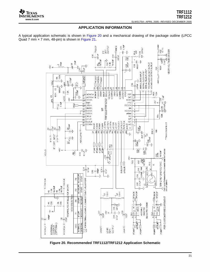
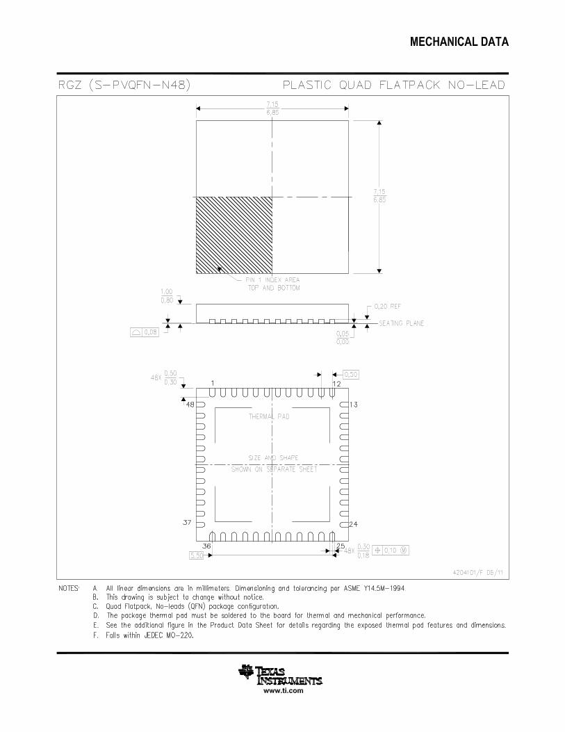
A typical application schematic is shown in Figure 20 and a mechanical drawing of the package outline (LPCCQuad 7 mm × 7 mm, 48-pin) is shown in Figure 21.
Figure 20. Recommended TRF1112/TRF1212 Application Schematic
21

www.ti.com
TRF1112TRF1212SLWS175A–APRIL 2005–REVISED DECEMBER 2005
APPLICATION INFORMATION (continued)
Figure 21. Package Drawing
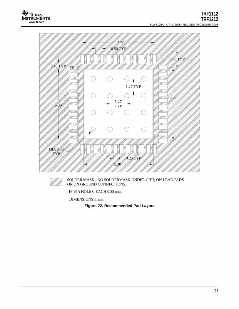
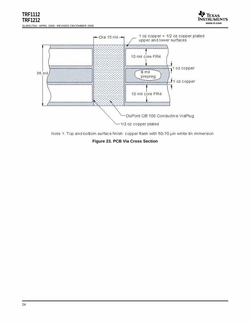
The recommended PCB Layout mask is shown in Figure 22, along with recommendations on the board material(see Table 2) and construction (see Figure 23).
Table 2. PCB Recommendations
Board Material FR4
Board Material Core Thickness 10 mil
Copper Thickness (starting) 1 oz
Prepreg Thickness 8 mil
Recommended Number of Layers 4
Via Plating Thickness ½ oz
Final Plate White immersion tin
Final Board Thickness 33–37 mil
22
www.ti.com
DIMENSIONS in mm
16 VIA HOLES, EACH 0.38 mm.
SOLDER MASK: NO SOLDERMASK UNDER CHIP, ON LEAD PADSOR ON GROUND CONNECTIONS.
1.27 TYP
1.27TYP
0.60 TYP
5.50
0.50 TYP
0.45 TYP
5.30
5.30
5.50
DIA 0.38TYP
0.25 TYP
PIN 1
TRF1112TRF1212
SLWS175A–APRIL 2005–REVISED DECEMBER 2005
Figure 22. Recommended Pad Layout
23
www.ti.com
TRF1112TRF1212SLWS175A–APRIL 2005–REVISED DECEMBER 2005
Figure 23. PCB Via Cross Section
24

PACKAGE OPTION ADDENDUM
www.ti.com 9-Aug-2013
Addendum-Page 1
PACKAGING INFORMATION
Orderable Device Status(1)
Package Type PackageDrawing
Pins PackageQty
Eco Plan(2)
Lead/Ball Finish MSL Peak Temp(3)
Op Temp (°C) Device Marking(4/5)
Samples
PTRF1212IRGZR NRND VQFN RGZ 48 Green (RoHS& no Sb/Br)
CU SN Level-3-260C-168 HR -40 to 85 TRF1212
TRF1112IRGZR NRND VQFN RGZ 48 TBD Call TI Call TI -40 to 85 TRF1112
TRF1112IRGZRG3 NRND VQFN RGZ 48 TBD Call TI Call TI -40 to 85 TRF1112
TRF1112IRGZT NRND VQFN RGZ 48 250 Green (RoHS& no Sb/Br)
CU SN Level-3-260C-168 HR -40 to 85 TRF1112
TRF1112IRGZTG3 NRND VQFN RGZ 48 250 Green (RoHS& no Sb/Br)
CU SN Level-3-260C-168 HR -40 to 85 TRF1112
TRF1212IRGZR NRND VQFN RGZ 48 2500 Green (RoHS& no Sb/Br)
CU SN Level-3-260C-168 HR -40 to 85 TRF1212
TRF1212IRGZRG3 NRND VQFN RGZ 48 2500 Green (RoHS& no Sb/Br)
CU SN Level-3-260C-168 HR -40 to 85 TRF1212
TRF1212IRGZT NRND VQFN RGZ 48 250 Green (RoHS& no Sb/Br)
CU SN Level-3-260C-168 HR -40 to 85 TRF1212
TRF1212IRGZTG3 NRND VQFN RGZ 48 250 Green (RoHS& no Sb/Br)
CU SN Level-3-260C-168 HR -40 to 85 TRF1212
(1) The marketing status values are defined as follows:ACTIVE: Product device recommended for new designs.LIFEBUY: TI has announced that the device will be discontinued, and a lifetime-buy period is in effect.NRND: Not recommended for new designs. Device is in production to support existing customers, but TI does not recommend using this part in a new design.PREVIEW: Device has been announced but is not in production. Samples may or may not be available.OBSOLETE: TI has discontinued the production of the device.
(2) Eco Plan - The planned eco-friendly classification: Pb-Free (RoHS), Pb-Free (RoHS Exempt), or Green (RoHS & no Sb/Br) - please check http://www.ti.com/productcontent for the latest availabilityinformation and additional product content details.TBD: The Pb-Free/Green conversion plan has not been defined.Pb-Free (RoHS): TI's terms "Lead-Free" or "Pb-Free" mean semiconductor products that are compatible with the current RoHS requirements for all 6 substances, including the requirement thatlead not exceed 0.1% by weight in homogeneous materials. Where designed to be soldered at high temperatures, TI Pb-Free products are suitable for use in specified lead-free processes.Pb-Free (RoHS Exempt): This component has a RoHS exemption for either 1) lead-based flip-chip solder bumps used between the die and package, or 2) lead-based die adhesive used betweenthe die and leadframe. The component is otherwise considered Pb-Free (RoHS compatible) as defined above.Green (RoHS & no Sb/Br): TI defines "Green" to mean Pb-Free (RoHS compatible), and free of Bromine (Br) and Antimony (Sb) based flame retardants (Br or Sb do not exceed 0.1% by weightin homogeneous material)
PACKAGE OPTION ADDENDUM
www.ti.com 9-Aug-2013
Addendum-Page 2
(3) MSL, Peak Temp. -- The Moisture Sensitivity Level rating according to the JEDEC industry standard classifications, and peak solder temperature.
(4) There may be additional marking, which relates to the logo, the lot trace code information, or the environmental category on the device.
(5) Multiple Device Markings will be inside parentheses. Only one Device Marking contained in parentheses and separated by a "~" will appear on a device. If a line is indented then it is a continuationof the previous line and the two combined represent the entire Device Marking for that device.
Important Information and Disclaimer:The information provided on this page represents TI's knowledge and belief as of the date that it is provided. TI bases its knowledge and belief on informationprovided by third parties, and makes no representation or warranty as to the accuracy of such information. Efforts are underway to better integrate information from third parties. TI has taken andcontinues to take reasonable steps to provide representative and accurate information but may not have conducted destructive testing or chemical analysis on incoming materials and chemicals.TI and TI suppliers consider certain information to be proprietary, and thus CAS numbers and other limited information may not be available for release.
In no event shall TI's liability arising out of such information exceed the total purchase price of the TI part(s) at issue in this document sold by TI to Customer on an annual basis.
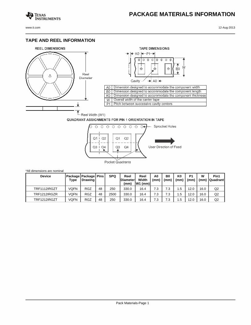
TAPE AND REEL INFORMATION
*All dimensions are nominal
Device PackageType
PackageDrawing
Pins SPQ ReelDiameter
(mm)
ReelWidth
W1 (mm)
A0(mm)
B0(mm)
K0(mm)
P1(mm)
W(mm)
Pin1Quadrant
TRF1112IRGZT VQFN RGZ 48 250 330.0 16.4 7.3 7.3 1.5 12.0 16.0 Q2
TRF1212IRGZR VQFN RGZ 48 2500 330.0 16.4 7.3 7.3 1.5 12.0 16.0 Q2
TRF1212IRGZT VQFN RGZ 48 250 330.0 16.4 7.3 7.3 1.5 12.0 16.0 Q2
PACKAGE MATERIALS INFORMATION
www.ti.com 12-Aug-2013
Pack Materials-Page 1
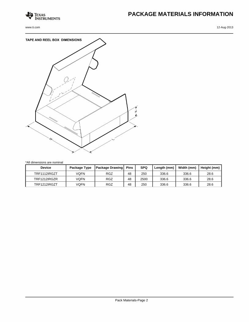
*All dimensions are nominal
Device Package Type Package Drawing Pins SPQ Length (mm) Width (mm) Height (mm)
TRF1112IRGZT VQFN RGZ 48 250 336.6 336.6 28.6
TRF1212IRGZR VQFN RGZ 48 2500 336.6 336.6 28.6
TRF1212IRGZT VQFN RGZ 48 250 336.6 336.6 28.6
PACKAGE MATERIALS INFORMATION
www.ti.com 12-Aug-2013
Pack Materials-Page 2
IMPORTANT NOTICE
Texas Instruments Incorporated and its subsidiaries (TI) reserve the right to make corrections, enhancements, improvements and otherchanges to its semiconductor products and services per JESD46, latest issue, and to discontinue any product or service per JESD48, latestissue. Buyers should obtain the latest relevant information before placing orders and should verify that such information is current andcomplete. All semiconductor products (also referred to herein as “components”) are sold subject to TI’s terms and conditions of salesupplied at the time of order acknowledgment.
TI warrants performance of its components to the specifications applicable at the time of sale, in accordance with the warranty in TI’s termsand conditions of sale of semiconductor products. Testing and other quality control techniques are used to the extent TI deems necessaryto support this warranty. Except where mandated by applicable law, testing of all parameters of each component is not necessarilyperformed.
TI assumes no liability for applications assistance or the design of Buyers’ products. Buyers are responsible for their products andapplications using TI components. To minimize the risks associated with Buyers’ products and applications, Buyers should provideadequate design and operating safeguards.
TI does not warrant or represent that any license, either express or implied, is granted under any patent right, copyright, mask work right, orother intellectual property right relating to any combination, machine, or process in which TI components or services are used. Informationpublished by TI regarding third-party products or services does not constitute a license to use such products or services or a warranty orendorsement thereof. Use of such information may require a license from a third party under the patents or other intellectual property of thethird party, or a license from TI under the patents or other intellectual property of TI.
Reproduction of significant portions of TI information in TI data books or data sheets is permissible only if reproduction is without alterationand is accompanied by all associated warranties, conditions, limitations, and notices. TI is not responsible or liable for such altereddocumentation. Information of third parties may be subject to additional restrictions.
Resale of TI components or services with statements different from or beyond the parameters stated by TI for that component or servicevoids all express and any implied warranties for the associated TI component or service and is an unfair and deceptive business practice.TI is not responsible or liable for any such statements.
Buyer acknowledges and agrees that it is solely responsible for compliance with all legal, regulatory and safety-related requirementsconcerning its products, and any use of TI components in its applications, notwithstanding any applications-related information or supportthat may be provided by TI. Buyer represents and agrees that it has all the necessary expertise to create and implement safeguards whichanticipate dangerous consequences of failures, monitor failures and their consequences, lessen the likelihood of failures that might causeharm and take appropriate remedial actions. Buyer will fully indemnify TI and its representatives against any damages arising out of the useof any TI components in safety-critical applications.
In some cases, TI components may be promoted specifically to facilitate safety-related applications. With such components, TI’s goal is tohelp enable customers to design and create their own end-product solutions that meet applicable functional safety standards andrequirements. Nonetheless, such components are subject to these terms.
No TI components are authorized for use in FDA Class III (or similar life-critical medical equipment) unless authorized officers of the partieshave executed a special agreement specifically governing such use.
Only those TI components which TI has specifically designated as military grade or “enhanced plastic” are designed and intended for use inmilitary/aerospace applications or environments. Buyer acknowledges and agrees that any military or aerospace use of TI componentswhich have not been so designated is solely at the Buyer's risk, and that Buyer is solely responsible for compliance with all legal andregulatory requirements in connection with such use.
TI has specifically designated certain components as meeting ISO/TS16949 requirements, mainly for automotive use. In any case of use ofnon-designated products, TI will not be responsible for any failure to meet ISO/TS16949.
Products Applications
Audio www.ti.com/audio Automotive and Transportation www.ti.com/automotive
Amplifiers amplifier.ti.com Communications and Telecom www.ti.com/communications
Data Converters dataconverter.ti.com Computers and Peripherals www.ti.com/computers
DLP® Products www.dlp.com Consumer Electronics www.ti.com/consumer-apps
DSP dsp.ti.com Energy and Lighting www.ti.com/energy
Clocks and Timers www.ti.com/clocks Industrial www.ti.com/industrial
Interface interface.ti.com Medical www.ti.com/medical
Logic logic.ti.com Security www.ti.com/security
Power Mgmt power.ti.com Space, Avionics and Defense www.ti.com/space-avionics-defense
Microcontrollers microcontroller.ti.com Video and Imaging www.ti.com/video
RFID www.ti-rfid.com
OMAP Applications Processors www.ti.com/omap TI E2E Community e2e.ti.com
Wireless Connectivity www.ti.com/wirelessconnectivity
Mailing Address: Texas Instruments, Post Office Box 655303, Dallas, Texas 75265Copyright © 2013, Texas Instruments Incorporated
Related Documents