© 2007 Microchip Technology Inc. DS70150C dsPIC30F6010A/6015 Data Sheet High-Performance, 16-Bit Digital Signal Controllers

Welcome message from author
This document is posted to help you gain knowledge. Please leave a comment to let me know what you think about it! Share it to your friends and learn new things together.
Transcript

Note the following details of the code protection feature on Microchip devices:
• Microchip products meet the specification contained in their particular Microchip Data Sheet.
• Microchip believes that its family of products is one of the most secure families of its kind on the market today, when used in the intended manner and under normal conditions.
• There are dishonest and possibly illegal methods used to breach the code protection feature. All of these methods, to our knowledge, require using the Microchip products in a manner outside the operating specifications contained in Microchip’s Data Sheets. Most likely, the person doing so is engaged in theft of intellectual property.
• Microchip is willing to work with the customer who is concerned about the integrity of their code.
• Neither Microchip nor any other semiconductor manufacturer can guarantee the security of their code. Code protection does not mean that we are guaranteeing the product as “unbreakable.”
Code protection is constantly evolving. We at Microchip are committed to continuously improving the code protection features of ourproducts. Attempts to break Microchip’s code protection feature may be a violation of the Digital Millennium Copyright Act. If such actsallow unauthorized access to your software or other copyrighted work, you may have a right to sue for relief under that Act.
Information contained in this publication regarding deviceapplications and the like is provided only for your convenienceand may be superseded by updates. It is your responsibility toensure that your application meets with your specifications.MICROCHIP MAKES NO REPRESENTATIONS ORWARRANTIES OF ANY KIND WHETHER EXPRESS ORIMPLIED, WRITTEN OR ORAL, STATUTORY OROTHERWISE, RELATED TO THE INFORMATION,INCLUDING BUT NOT LIMITED TO ITS CONDITION,QUALITY, PERFORMANCE, MERCHANTABILITY ORFITNESS FOR PURPOSE. Microchip disclaims all liabilityarising from this information and its use. Use of Microchipdevices in life support and/or safety applications is entirely atthe buyer’s risk, and the buyer agrees to defend, indemnify andhold harmless Microchip from any and all damages, claims,suits, or expenses resulting from such use. No licenses areconveyed, implicitly or otherwise, under any Microchipintellectual property rights.
DS70150C-page ii
Trademarks
The Microchip name and logo, the Microchip logo, Accuron, dsPIC, KEELOQ, microID, MPLAB, PIC, PICmicro, PICSTART, PRO MATE, PowerSmart, rfPIC and SmartShunt are registered trademarks of Microchip Technology Incorporated in the U.S.A. and other countries.
AmpLab, FilterLab, Migratable Memory, MXDEV, MXLAB, SEEVAL, SmartSensor and The Embedded Control Solutions Company are registered trademarks of Microchip Technology Incorporated in the U.S.A.
Analog-for-the-Digital Age, Application Maestro, CodeGuard, dsPICDEM, dsPICDEM.net, dsPICworks, ECAN, ECONOMONITOR, FanSense, FlexROM, fuzzyLAB, In-Circuit Serial Programming, ICSP, ICEPIC, Linear Active Thermistor, Mindi, MiWi, MPASM, MPLIB, MPLINK, PICkit, PICDEM, PICDEM.net, PICLAB, PICtail, PowerCal, PowerInfo, PowerMate, PowerTool, REAL ICE, rfLAB, rfPICDEM, Select Mode, Smart Serial, SmartTel, Total Endurance, UNI/O, WiperLock and ZENA are trademarks of Microchip Technology Incorporated in the U.S.A. and other countries.
SQTP is a service mark of Microchip Technology Incorporated in the U.S.A.
All other trademarks mentioned herein are property of their respective companies.
© 2007, Microchip Technology Incorporated, Printed in the U.S.A., All Rights Reserved.
Printed on recycled paper.
© 2007 Microchip Technology Inc.
Microchip received ISO/TS-16949:2002 certification for its worldwide headquarters, design and wafer fabrication facilities in Chandler and Tempe, Arizona, Gresham, Oregon and Mountain View, California. The Company’s quality system processes and procedures are for its PIC®
MCUs and dsPIC DSCs, KEELOQ® code hopping devices, Serial EEPROMs, microperipherals, nonvolatile memory and analog products. In addition, Microchip’s quality system for the design and manufacture of development systems is ISO 9001:2000 certified.
dsPIC30F6010A/6015
dsPIC30F6010A/6015 Enhanced Flash16-bit Digital Signal Controller (DSC)
High-Performance Modified RISC CPU:
• Modified Harvard architecture• C compiler optimized instruction set architecture
with flexible Addressing modes• 83 base instructions• 24-bit wide instructions, 16-bit wide data path
• 144 Kbytes on-chip Flash program space (Instruction words)
• 8 Kbytes of on-chip data RAM• 4 Kbytes of nonvolatile data EEPROM• Up to 30 MIPS operation:
- DC to 40 MHz external clock input- 4 MHz-10 MHz oscillator input with
PLL active (4x, 8x, 16x)- 7.37 MHz internal RC with PLL active
(4x, 8x, 16x)• 44 interrupt sources:
- 5 external interrupt sources
- 8 user selectable priority levels for each interrupt source
- 4 processor trap sources• 16 x 16-bit working register array
DSP Engine Features:
• Dual data fetch• Accumulator write-back for DSP operations
• Modulo and Bit-Reversed Addressing modes• Two, 40-bit wide accumulators with optional
saturation logic• 17-bit x 17-bit single-cycle hardware fractional/
integer multiplier• All DSP instructions single cycle• ±16-bit single-cycle shift
Peripheral Features:
• High-current sink/source I/O pins: 25 mA/25 mA
• Timer module with programmable prescaler: - Five 16-bit timers/counters; optionally pair
16-bit timers into 32-bit timer modules• 16-bit Capture input functions• 16-bit Compare/PWM output functions
• 3-wire SPI modules (supports 4 Frame modes)• I2CTM module supports Multi-Master/Slave mode
and 7-bit/10-bit addressing• 2 UART modules with FIFO Buffers• 2 CAN modules, 2.0B compliant (dsPIC306010A)
• 1 CAN module, 2.0B compliant (dsPIC306015)
Motor Control PWM Module Features:
• 8 PWM output channels:- Complementary or Independent Output
modes- Edge and Center-Aligned modes
• 4 duty cycle generators
• Dedicated time base• Programmable output polarity• Dead-Time control for Complementary mode
• Manual output control• Trigger for A/D conversions
Quadrature Encoder Interface Module Features:
• Phase A, Phase B and Index Pulse input
• 16-bit up/down position counter • Count direction status• Position Measurement (x2 and x4) mode
• Programmable digital noise filters on inputs• Alternate 16-bit Timer/Counter mode• Interrupt on position counter rollover/underflow
Note: This data sheet summarizes features of thisgroup of dsPIC30F devices and is not intended to bea complete reference source. For more informationon the CPU, peripherals, register descriptions andgeneral device functionality, refer to the “dsPIC30FFamily Reference Manual” (DS70046). For moreinformation on the device instruction set and pro-gramming, refer to the “dsPIC30F/33F ProgrammersReference Manual” (DS70157).
© 2007 Microchip Technology Inc. DS70150C-page 1
dsPIC30F6010A/6015
Analog Features:
• 10-bit Analog-to-Digital Converter (ADC) with4 S/H Inputs:- 1 Msps conversion rate
- 16 input channels- Conversion available during Sleep and Idle
• Programmable Brown-out Reset
Special Microcontroller Features:
• Enhanced Flash program memory:
- 10,000 erase/write cycle (min.) for industrial temperature range, 100K (typical)
• Data EEPROM memory:- 100,000 erase/write cycle (min.) for
industrial temperature range, 1M (typical)• Self-reprogrammable under software control
• Power-on Reset (POR), Power-up Timer (PWRT) and Oscillator Start-up Timer (OST)
• Flexible Watchdog Timer (WDT) with on-chip, low-power RC oscillator for reliable operation
• Fail-Safe Clock Monitor operation detects clock failure and switches to on-chip, low-power RC oscillator
• Programmable code protection• In-Circuit Serial Programming™ (ICSP™)• Selectable Power Management modes
- Sleep, Idle and Alternate Clock modes
CMOS Technology:
• Low-power, high-speed Flash technology• Wide operating voltage range (2.5V to 5.5V)• Industrial and Extended temperature ranges
• Low-power consumption
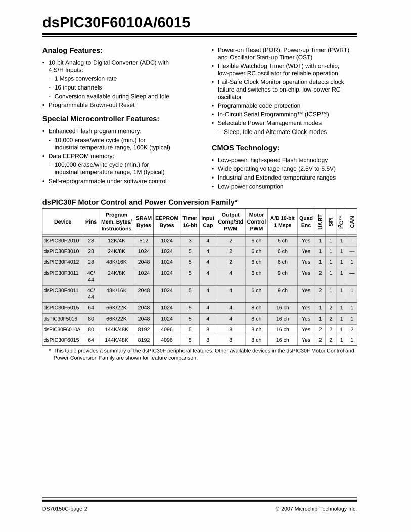
dsPIC30F Motor Control and Power Conversion Family*
Device PinsProgram
Mem. Bytes/Instructions
SRAMBytes
EEPROMBytes
Timer 16-bit
InputCap
OutputComp/Std
PWM
MotorControl
PWM
A/D 10-bit 1 Msps
Quad Enc U
AR
T
SP
I
I2 C™
CA
N
dsPIC30F2010 28 12K/4K 512 1024 3 4 2 6 ch 6 ch Yes 1 1 1 —
dsPIC30F3010 28 24K/8K 1024 1024 5 4 2 6 ch 6 ch Yes 1 1 1 —
dsPIC30F4012 28 48K/16K 2048 1024 5 4 2 6 ch 6 ch Yes 1 1 1 1
dsPIC30F3011 40/44
24K/8K 1024 1024 5 4 4 6 ch 9 ch Yes 2 1 1 —
dsPIC30F4011 40/44
48K/16K 2048 1024 5 4 4 6 ch 9 ch Yes 2 1 1 1
dsPIC30F5015 64 66K/22K 2048 1024 5 4 4 8 ch 16 ch Yes 1 2 1 1
dsPIC30F5016 80 66K/22K 2048 1024 5 4 4 8 ch 16 ch Yes 1 2 1 1
dsPIC30F6010A 80 144K/48K 8192 4096 5 8 8 8 ch 16 ch Yes 2 2 1 2
dsPIC30F6015 64 144K/48K 8192 4096 5 8 8 8 ch 16 ch Yes 2 2 1 1
* This table provides a summary of the dsPIC30F peripheral features. Other available devices in the dsPIC30F Motor Control and Power Conversion Family are shown for feature comparison.
DS70150C-page 2 © 2007 Microchip Technology Inc.

dsPIC30F6010A/6015
Pin Diagram
72
74
73
71
70
69
68
67
66
65
64
63
62
61
20
2
3
4
5
6
7
8
9
10
11
12
13
14
15
16
50
49
48
47
46
45
44
21
41
4039383736353423 24 25 26 27 28 29 30 31 32 33dsPIC30F6010A
17
18
19
75
1
57
56
55
54
53
52
51
60
59
58
43
42
76
78
77
79
2280
IC5/
RD
12O
C4/
RD
3
OC
3/R
D2
EM
UD
2/O
C2/
RD
1
PW
M2L
/RE
2P
WM
1H/R
E1
PW
M1L
/RE
0
C2R
X/R
G0
C2T
X/R
G1
C1T
X/R
F1
C1R
X/R
F0
PW
M3L
/RE
4
PW
M2H
/RE
3
OC
8/U
PD
N/C
N16
/RD
7
OC
6/C
N14
/RD
5
EMUC2/OC1/RD0
IC4/RD11
IC2/RD9
IC1/RD8
INT4/RA15
IC3/RD10
INT3/RA14VSS
OSC1/CLKI
VDD
SCL/RG2
U1RX/RF2
U1TX/RF3
EMUC1/SOSCO/T1CK/CN0/RC14
EMUD1/SOSCI/CN1/RC13V
RE
F+
/RA
10
VR
EF-/
RA
9
AV
DD
AV
SS
AN
8/R
B8
AN
9/R
B9
AN
10/R
B10
AN
11/R
B11
VD
D
U2R
X/C
N17
/RF
4
IC8/
CN
21/R
D15
U2T
X/C
N18
/RF
5
AN
6/O
CFA
/RB
6
AN
7/R
B7
PWM4H/RE7
T2CK/RC1
T4CK/RC3
SCK2/CN8/RG6
SDI2/CN9/RG7
SDO2/CN10/RG8
MCLR
SS2/CN11/RG9
AN4/QEA/CN6/RB4AN3/INDX/CN5/RB3
AN2/SS1/CN4/RB2
PGC/EMUC/AN1/CN3/RB1
PGD/EMUD/AN0/CN2/RB0
VSS
VDD
PWM3H/RE5
PWM4L/RE6
FLTB/INT2/RE9
FLTA/INT1/RE8
AN
12/R
B12
AN
13/R
B13
AN
14/R
B14
AN
15/O
CF
B/C
N12
/RB
15
VD
D
VS
S
OC
5/C
N13
/RD
4
IC6/
CN
19/R
D13
SDA/RG3
SDI1/RF7
EMUD3/SDO1/RF8
AN5/QEB/CN7/RB5
VS
S
OSC2/CLKO/RC15O
C7/
CN
15/R
D6
EMUC3/SCK1/INT0/RF6
IC7/
CN
20/R
D14
80-Pin TQFP
Note: Pinout subject to change.
© 2007 Microchip Technology Inc. DS70150C-page 3

dsPIC30F6010A/6015
Pin Diagram
dsPIC30F6015
64-Pin TQFP
Note: Pinout subject to change.
12345678910111213 36
353433
32313029282726
64 63 62 61 60 59 58 57 56
141516
17 18 19 20 21 22 23 24 25
EMUC1/SOSCO/T1CK/CN0/RC14EMUD1/SOSCI/T4CK/CN1/RC13EMUC2/OC1/RD0IC4/INT4/RD11
IC2/FLTB/INT2/RD9IC1/FLTA/INT1/RD8VSS
OSC2/CLKO/RC15OSC1/CLKIVDD
SCL/RG2
EMUC3/SCK1/INT0/RF6U1RX/SDI1/RF2EMUD3/U1TX/SDO1/RF3
PWM3H/RE5PWM4L/RE6PWM4H/RE7
SCK2/CN8/RG6SDI2/CN9/RG7
SDO2/CN10/RG8MCLR
VSS
VDD
AN3/INDX/CN5/RB3AN2/SS1/CN4/RB2
AN1/VREF-/CN3/RB1AN0/VREF+/CN2/RB0
OC
8/U
PD
N/C
N16
/RD
7
PW
M3L
/RE
4P
WM
2H/R
E3
PW
M2L
/RE
2
VS
S
PW
M1L
/RE
0C
1TX
/RF
1
PW
M1H
/RE
1
EM
UD
2/O
C2/
RD
1O
C3/
RD
2
PG
C/E
MU
C/A
N6/
OC
FA/R
B6
PG
D/E
MU
D/A
N7/
RB
7A
VD
D
AV
SS
AN
8/R
B8
AN
9/R
B9
AN
10/R
B10
AN
11/R
B11
VS
S
VD
D
AN
12/R
B12
AN
13/R
B13
AN
14/R
B14
AN
15/O
CF
B/C
N12
/RB
15
U2T
X/C
N18
/RF
5U
2RX
/CN
17/R
F4
SDA/RG3
43424140393837
44
484746
50 495154 53 5255
45
SS2/CN11/RG9
AN5/QEB/IC8/CN7/RB5AN4/QEA/IC7/CN6/RB4
IC3/INT3/RD10
VD
D
C1R
X/R
F0
OC
4/R
D3
OC
7/C
N15
/RD
6O
C6/
IC6/
CN
14/R
D5
OC
5/IC
5/C
N13
/RD
4
DS70150C-page 4 © 2007 Microchip Technology Inc.
dsPIC30F6010A/6015
Table of Contents1.0 Device Overview ......................................................................................................................................................................... 72.0 CPU Architecture Overview ....................................................................................................................................................... 133.0 Memory Organization ................................................................................................................................................................ 214.0 Address Generator Units ........................................................................................................................................................... 335.0 Interrupts .................................................................................................................................................................................. 396.0 Flash Program Memory ............................................................................................................................................................. 477.0 Data EEPROM Memory ............................................................................................................................................................ 538.0 I/O Ports .................................................................................................................................................................................... 579.0 Timer1 Module .......................................................................................................................................................................... 6310.0 Timer2/3 Module ....................................................................................................................................................................... 6711.0 Timer4/5 Module ...................................................................................................................................................................... 7512.0 Input Capture Module ............................................................................................................................................................... 7913.0 Output Compare Module ........................................................................................................................................................... 8314.0 Quadrature Encoder Interface (QEI) Module ............................................................................................................................ 8715/0 Motor Control PWM Module ...................................................................................................................................................... 9316.0 SPI Module .............................................................................................................................................................................. 10317.0 I2C™ Module .......................................................................................................................................................................... 10718.0 Universal Asynchronous Receiver Transmitter (UART) Module ............................................................................................. 11519.0 CAN Module ............................................................................................................................................................................ 12320.0 10-bit High-Speed Analog-to-Digital Converter (ADC) Module ............................................................................................... 13521.0 System Integration .................................................................................................................................................................. 14722.0 Instruction Set Summary ......................................................................................................................................................... 16323.0 Development Support .............................................................................................................................................................. 17124.0 Electrical Characteristics ......................................................................................................................................................... 17525.0 Packaging Information ............................................................................................................................................................. 215Appendix A: Revision History ............................................................................................................................................................ 219Appendix B: Device Comparisons .................................................................................................................................................... 221Appendix C: Migration From dsPIC30F6010 to dsPIC30F6010A ..................................................................................................... 223Index ................................................................................................................................................................................................. 225The Microchip Web Site .................................................................................................................................................................... 231Customer Change Notification Service ............................................................................................................................................. 231Customer Support ............................................................................................................................................................................. 231Reader Response ............................................................................................................................................................................. 232Product Identification System ............................................................................................................................................................. 23
TO OUR VALUED CUSTOMERSIt is our intention to provide our valued customers with the best documentation possible to ensure successful use of your Micro-chip products. To this end, we will continue to improve our publications to better suit your needs. Our publications will be refinedand enhanced as new volumes and updates are introduced.
If you have any questions or comments regarding this publication, please contact the Marketing Communications Department viaE-mail at [email protected] or fax the Reader Response Form in the back of this data sheet to (480) 792-4150. Wewelcome your feedback.
Most Current Data SheetTo obtain the most up-to-date version of this data sheet, please register at our Worldwide Web site at:
http://www.microchip.com
You can determine the version of a data sheet by examining its literature number found on the bottom outside corner of any page.The last character of the literature number is the version number, (e.g., DS30000A is version A of document DS30000).
ErrataAn errata sheet, describing minor operational differences from the data sheet and recommended workarounds, may exist for cur-rent devices. As device/documentation issues become known to us, we will publish an errata sheet. The errata will specify the revi-sion of silicon and revision of document to which it applies.
To determine if an errata sheet exists for a particular device, please check with one of the following:
• Microchip’s Worldwide Web site; http://www.microchip.com• Your local Microchip sales office (see last page)When contacting a sales office, please specify which device, revision of silicon and data sheet (include literature number) you areusing.
Customer Notification SystemRegister on our web site at www.microchip.com to receive the most current information on all of our products.
© 2007 Microchip Technology Inc. DS70150C-page 5

dsPIC30F6010A/6015
NOTES:
DS70150C-page 6 © 2007 Microchip Technology Inc.
dsPIC30F6010A/6015
1.0 DEVICE OVERVIEW This document contains device-specific information forthe dsPIC30F6010A and dsPIC30F6015 devices. ThedsPIC30F devices contain extensive Digital SignalProcessor (DSP) functionality within a high-performance16-bit microcontroller (MCU) architecture. Figure 1-1shows a device block diagram for the dsPIC30F6010Adevice. Figure 1-2 shows a device block diagram for thedsPIC30F6015 device.
Note: This data sheet summarizes features of thisgroup of dsPIC30F devices and is not intended to bea complete reference source. For more informationon the CPU, peripherals, register descriptions andgeneral device functionality, refer to the “dsPIC30FFamily Reference Manual” (DS70046). For moreinformation on the device instruction set and pro-gramming, refer to the “dsPIC30F/33F ProgrammersReference Manual” (DS70157).
© 2007 Microchip Technology Inc. DS70150C-page 7

dsPIC30F6010A/6015
FIGURE 1-1: dsPIC30F6010A BLOCK DIAGRAM
AN8/RB8AN9/RB9AN10/RB10AN11/RB11
Power-upTimer
OscillatorStart-up Timer
POR/BORReset
WatchdogTimer
InstructionDecode &Control
OSC1/CLKI
MCLR
VDD, VSS
AN4/QEA/CN6/RB4
AN12/RB12AN13/RB13AN14/RB14AN15/OCFB/CN12/RB15
Low-VoltageDetect
UART1,SPI1, Motor Control
PWM
INT4/RA15INT3/RA14VREF+/RA10VREF-/RA9
CAN2
TimingGeneration
CAN1,
AN5/QEB/CN7/RB5
16
PCH PCLProgram Counter
ALU<16>
16
Address Latch
Program Memory(144 Kbytes)
Data Latch
24
24
24
24
X Data Bus
IR
I2C™
QEI
AN6/OCFA/RB6AN7/RB7
PCU
PWM1L/RE0PWM1H/RE1PWM2L/RE2PWM2H/RE3PWM3L/RE4
10-bit ADC
Timers
PWM3H/RE5PWM4L/RE6PWM4H/RE7FLTA/INT1/RE8FLTB/INT2/RE9
SCK2/CN8/RG6SDI2/CN9/RG7
SDO2/CN10/RG8SS2/CN11/RG9
U2TX/CN18/RF5EMUC3/SCK1/INT0/RF6SDI1/RF7EMUD3/SDO1/RF8
InputCaptureModule
Output Compare
Module
EMUC1/SOSCO/T1CK/CN0/RC14EMUD1/SOSCI/CN1/RC13T4CK/RC3T2CK/RC1
PORTB
C1RX/RF0C1TX/RF1U1RX/RF2U1TX/RF3
C2RX/RG0C2TX/RG1
SCL/RG2SDA/RG3
PORTG PORTF
PORTD
16
16 16
16 x 16W Reg Array
Divide Unit Engine
DSP
Decode
ROM Latch
16
Y Data Bus
Effective Address
X RAGUX WAGU Y AGU
PGD/EMUD/AN0/CN2/RB0PGC/EMUC/AN1/CN3/RB1AN2/SS1/CN4/RB2AN3/INDX/CN5/RB3
OSC2/CLKO/RC15
U2RX/CN17/RF4
AVDD, AVSS
UART2SPI2
16
16
16
16
16
PORTA
PORTC
PORTE
16
16
16
16
8
InterruptController PSV & Table
Data AccessControl Block
StackControl Logic
LoopControlLogic
Data LatchData LatchY Data
(4 Kbytes)RAM
X Data
(4 Kbytes)RAM
AddressLatch
AddressLatch
Control Signals to Various Blocks
EMUC2/OC1/RD0EMUD2/OC2/RD1OC3/RD2OC4/RD3OC5/CN13/RD4OC6/CN14/RD5OC7/CN15/RD6OC8/UPDN/CN16/RD7IC1/RD8IC2/RD9IC3/RD10IC4/RD11IC5/RD12IC6/CN19/RD13IC7/CN20/RD14IC8/CN21/RD15
16
Data EEPROM(4 Kbytes)
16
DS70150C-page 8 © 2007 Microchip Technology Inc.

dsPIC30F6010A/6015
FIGURE 1-2: dsPIC30F6015 BLOCK DIAGRAM
AN8/RB8AN9/RB9AN10/RB10AN11/RB11
Power-upTimer
OscillatorStart-up Timer
POR/BORReset
WatchdogTimer
InstructionDecode &Control
OSC1/CLKI
MCLR
VDD, VSS
AN4/QEA/IC7/CN6/RB4
AN12/RB12AN13/RB13AN14/RB14AN15/OCFB/CN12/RB15
Low-VoltageDetect
UART1,SPI1, Motor Control
PWM
TimingGeneration
CAN1
AN5/QEB/IC8/CN7/RB5
16
PCH PCLProgram Counter
ALU<16>
16
Address Latch
Program Memory(144 Kbytes)
Data Latch
24
24
24
24
X Data Bus
IR
I2C™
QEI
PGC/EMUC/AN6/OCFA/RB6PGD/EMUD/AN7/RB7
PCU
PWM1L/RE0PWM1H/RE1PWM2L/RE2PWM2H/RE3PWM3L/RE4
10-bit ADC
Timers
PWM3H/RE5PWM4L/RE6PWM4H/RE7
SCK2/CN8/RG6SDI2/CN9/RG7
SDO2/CN10/RG8SS2/CN11/RG9 U2TX/CN18/RF5
EMUC3/SCK1/INT0/RF6
InputCaptureModule
Output Compare
Module
EMUC1/SOSCO/T1CK/CN0/RC14EMUD1/SOSCI/T4CK/CN1/RC13
PORTB
C1RX/RF0C1TX/RF1U1RX/SDI1/RF2EMUD3/U1TX/SDO1/RF3
SCL/RG2SDA/RG3
PORTG PORTF
PORTD
16
16 16
16 x 16W Reg Array
Divide Unit Engine
DSP
Decode
ROM Latch
16
Y Data Bus
Effective Address
X RAGUX WAGU Y AGU
AN0/VREF+/CN2/RB0AN1/VREF-/CN3/RB1AN2/SS1/CN4/RB2AN3/INDX/CN5/RB3
OSC2/CLKO/RC15
U2RX/CN17/RF4
AVDD, AVSS
UART2SPI2
16
16
16
16
16
PORTC
PORTE
16
16
16
16
8
InterruptController PSV & Table
Data AccessControl Block
StackControl Logic
LoopControlLogic
Data LatchData LatchY Data
(4 Kbytes)RAM
X Data
(4 Kbytes)RAM
AddressLatch
AddressLatch
Control Signals to Various Blocks
EMUC2/OC1/RD0EMUD2/OC2/RD1OC3/RD2OC4/RD3OC5/IC5/CN13/RD4
OC7/CN15/RD6OC8/UPDN/CN16/RD7IC1/FLTA/INT1/RD8IC2/FLTB/INT2/RD9IC3/INT3/RD10IC4/INT4/RD11
16
Data EEPROM(4 Kbytes)
16
OC6/IC6/CN14/RD5
© 2007 Microchip Technology Inc. DS70150C-page 9
dsPIC30F6010A/6015
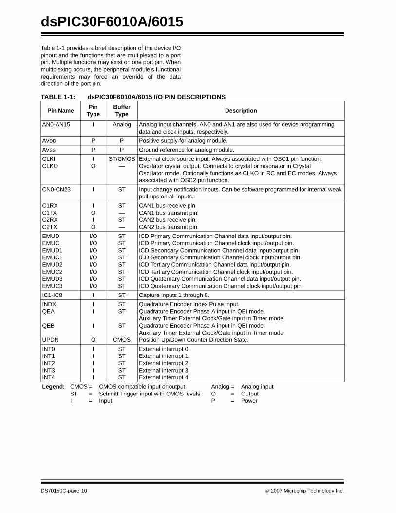
Table 1-1 provides a brief description of the device I/Opinout and the functions that are multiplexed to a portpin. Multiple functions may exist on one port pin. Whenmultiplexing occurs, the peripheral module’s functionalrequirements may force an override of the datadirection of the port pin.
TABLE 1-1: dsPIC30F6010A/6015 I/O PIN DESCRIPTIONS
Pin NamePin
TypeBuffer Type
Description
AN0-AN15 I Analog Analog input channels. AN0 and AN1 are also used for device programming data and clock inputs, respectively.
AVDD P P Positive supply for analog module.
AVSS P P Ground reference for analog module.
CLKICLKO
IO
ST/CMOS—
External clock source input. Always associated with OSC1 pin function.Oscillator crystal output. Connects to crystal or resonator in Crystal Oscillator mode. Optionally functions as CLKO in RC and EC modes. Always associated with OSC2 pin function.
CN0-CN23 I ST Input change notification inputs. Can be software programmed for internal weak pull-ups on all inputs.
C1RXC1TXC2RXC2TX
IOIO
ST—ST—
CAN1 bus receive pin.CAN1 bus transmit pin.CAN2 bus receive pin.CAN2 bus transmit pin.
EMUDEMUCEMUD1EMUC1EMUD2EMUC2EMUD3EMUC3
I/OI/OI/OI/OI/OI/OI/OI/O
STSTSTSTSTSTSTST
ICD Primary Communication Channel data input/output pin.ICD Primary Communication Channel clock input/output pin.ICD Secondary Communication Channel data input/output pin.ICD Secondary Communication Channel clock input/output pin.ICD Tertiary Communication Channel data input/output pin.ICD Tertiary Communication Channel clock input/output pin.ICD Quaternary Communication Channel data input/output pin.ICD Quaternary Communication Channel clock input/output pin.
IC1-IC8 I ST Capture inputs 1 through 8.
INDXQEA
QEB
UPDN
II
I
O
STST
ST
CMOS
Quadrature Encoder Index Pulse input.Quadrature Encoder Phase A input in QEI mode. Auxiliary Timer External Clock/Gate input in Timer mode.Quadrature Encoder Phase A input in QEI mode. Auxiliary Timer External Clock/Gate input in Timer mode.Position Up/Down Counter Direction State.
INT0INT1INT2INT3INT4
IIIII
STSTSTSTST
External interrupt 0.External interrupt 1.External interrupt 2.External interrupt 3.External interrupt 4.
Legend: CMOS = CMOS compatible input or output Analog = Analog inputST = Schmitt Trigger input with CMOS levels O = Output I = Input P = Power
DS70150C-page 10 © 2007 Microchip Technology Inc.
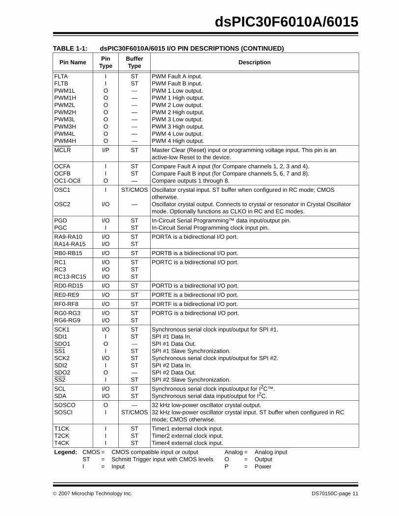
dsPIC30F6010A/6015
FLTAFLTBPWM1LPWM1HPWM2LPWM2HPWM3LPWM3HPWM4LPWM4H
IIOOOOOOOO
STST————————
PWM Fault A input.PWM Fault B input.PWM 1 Low output. PWM 1 High output.PWM 2 Low output.PWM 2 High output.PWM 3 Low output.PWM 3 High output.PWM 4 Low output.PWM 4 High output.
MCLR I/P ST Master Clear (Reset) input or programming voltage input. This pin is an active-low Reset to the device.
OCFAOCFBOC1-OC8
IIO
STST—
Compare Fault A input (for Compare channels 1, 2, 3 and 4).Compare Fault B input (for Compare channels 5, 6, 7 and 8).Compare outputs 1 through 8.
OSC1
OSC2
I
I/O
ST/CMOS
—
Oscillator crystal input. ST buffer when configured in RC mode; CMOS otherwise.Oscillator crystal output. Connects to crystal or resonator in Crystal Oscillator mode. Optionally functions as CLKO in RC and EC modes.
PGDPGC
I/OI
STST
In-Circuit Serial Programming™ data input/output pin.In-Circuit Serial Programming clock input pin.
RA9-RA10RA14-RA15
I/OI/O
STST
PORTA is a bidirectional I/O port.
RB0-RB15 I/O ST PORTB is a bidirectional I/O port.
RC1 RC3RC13-RC15
I/OI/OI/O
STSTST
PORTC is a bidirectional I/O port.
RD0-RD15 I/O ST PORTD is a bidirectional I/O port.
RE0-RE9 I/O ST PORTE is a bidirectional I/O port.
RF0-RF8 I/O ST PORTF is a bidirectional I/O port.
RG0-RG3RG6-RG9
I/OI/O
STST
PORTG is a bidirectional I/O port.
SCK1SDI1SDO1SS1SCK2SDI2SDO2SS2
I/OIOI
I/OIOI
STST—STSTST—ST
Synchronous serial clock input/output for SPI #1.SPI #1 Data In.SPI #1 Data Out.SPI #1 Slave Synchronization.Synchronous serial clock input/output for SPI #2.SPI #2 Data In.SPI #2 Data Out.SPI #2 Slave Synchronization.
SCLSDA
I/OI/O
STST
Synchronous serial clock input/output for I2C™.Synchronous serial data input/output for I2C.
SOSCOSOSCI
OI
—ST/CMOS
32 kHz low-power oscillator crystal output. 32 kHz low-power oscillator crystal input. ST buffer when configured in RC mode; CMOS otherwise.
T1CKT2CKT4CK
III
STSTST
Timer1 external clock input.Timer2 external clock input.Timer4 external clock input.
TABLE 1-1: dsPIC30F6010A/6015 I/O PIN DESCRIPTIONS (CONTINUED)
Pin NamePin
TypeBuffer Type
Description
Legend: CMOS = CMOS compatible input or output Analog = Analog inputST = Schmitt Trigger input with CMOS levels O = Output I = Input P = Power
© 2007 Microchip Technology Inc. DS70150C-page 11
dsPIC30F6010A/6015
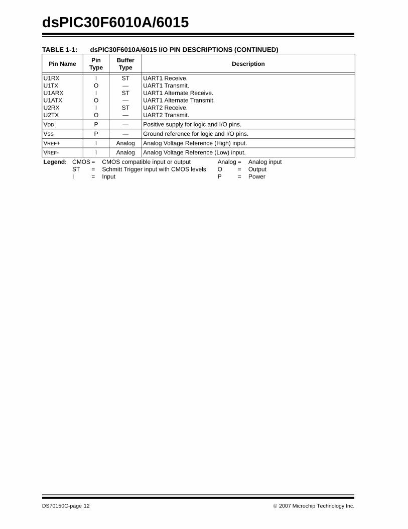
U1RXU1TXU1ARXU1ATXU2RXU2TX
IOIOIO
ST—ST—ST—
UART1 Receive.UART1 Transmit.UART1 Alternate Receive.UART1 Alternate Transmit.UART2 Receive.UART2 Transmit.
VDD P — Positive supply for logic and I/O pins.
VSS P — Ground reference for logic and I/O pins.
VREF+ I Analog Analog Voltage Reference (High) input.
VREF- I Analog Analog Voltage Reference (Low) input.
TABLE 1-1: dsPIC30F6010A/6015 I/O PIN DESCRIPTIONS (CONTINUED)
Pin NamePin
TypeBuffer Type
Description
Legend: CMOS = CMOS compatible input or output Analog = Analog inputST = Schmitt Trigger input with CMOS levels O = Output I = Input P = Power
DS70150C-page 12 © 2007 Microchip Technology Inc.
dsPIC30F6010A/6015
2.0 CPU ARCHITECTUREOVERVIEW
This document summarizes the CPU and peripheralfunctions of the dsPIC30F6010A/6015. For a completedescription of this functionality, please refer tothe “dsPIC30F Family Reference Manual” (DS70046).
2.1 Core Overview
The core has a 24-bit instruction word. The ProgramCounter (PC) is 23 bits wide with the Least Significantbit (LSb) always clear (see Section 3.1 “ProgramAddress Space”), and the Most Significant bit (MSb)is ignored during normal program execution, except forcertain specialized instructions. Thus, the PC canaddress up to 4M instruction words of user programspace. An instruction prefetch mechanism is used tohelp maintain throughput. Program loop constructs,free from loop count management overhead, are sup-ported using the DO and REPEAT instructions, both ofwhich are interruptible at any point.
The working register array consists of 16x16-bit regis-ters, each of which can act as data, address or offsetregisters. One working register (W15) operates as aSoftware Stack Pointer for interrupts and calls.
The data space is 64 Kbytes (32K words) and is split intotwo blocks, referred to as X and Y data memory. Eachblock has its own independent Address Generation Unit(AGU). Most instructions operate solely through the Xmemory AGU, which provides the appearance of a sin-gle unified data space. The Multiply-Accumulate (MAC)class of dual source DSP instructions operate throughboth the X and Y AGUs, splitting the data address spaceinto two parts (see Section 3.2 “Data AddressSpace”). The X and Y data space boundary is device-specific and cannot be altered by the user. Each dataword consists of 2 bytes, and most instructions canaddress data either as words or bytes.
There are two methods of accessing data stored inprogram memory:
• The upper 32 Kbytes of data space memory can be mapped into the lower half (user space) of program space at any 16K program word boundary, defined by the 8-bit Program Space Visibility Page (PSVPAG) register. This lets any instruction access program space as if it were data space, with a limita-tion that the access requires an additional cycle. Moreover, only the lower 16 bits of each instruction word can be accessed using this method.
• Linear indirect access of 32K word pages within program space is also possible using any working register, via table read and write instructions. Table read and write instructions can be used to access all 24 bits of an instruction word.
Overhead-free circular buffers (Modulo Addressing)are supported in both X and Y address spaces. This isprimarily intended to remove the loop overhead forDSP algorithms.
The X AGU also supports Bit-Reversed Addressing ondestination Effective Addresses, to greatly simplifyinput or output data reordering for radix-2 FFT algo-rithms. Refer to Section 4.0 “Address GeneratorUnits” for details on Modulo and Bit-ReversedAddressing.
The core supports Inherent (no operand), Relative, Lit-eral, Memory Direct, Register Direct, Register Indirect,Register Offset and Literal Offset Addressing modes.Instructions are associated with predefined addressingmodes, depending upon their functional requirements.
For most instructions, the core is capable of executinga data (or program data) memory read, a working reg-ister (data) read, a data memory write and a program(instruction) memory read per instruction cycle. As aresult, 3-operand instructions are supported, allowingC = A + B operations to be executed in a single cycle.
A DSP engine has been included to significantlyenhance the core arithmetic capability and throughput.It features a high-speed 17-bit by 17-bit multiplier, a40-bit ALU, two 40-bit saturating accumulators and a40-bit bidirectional barrel shifter. Data in the accumula-tor or any working register can be shifted up to 16 bitsright or 16 bits left in a single cycle. The DSP instruc-tions operate seamlessly with all other instructions andhave been designed for optimal real-time performance.The MAC class of instructions can concurrently fetchtwo data operands from memory, while multiplying twoW registers. To enable this concurrent fetching of dataoperands, the data space has been split for theseinstructions and linear for all others. This has beenachieved in a transparent and flexible manner, by ded-icating certain working registers to each address spacefor the MAC class of instructions.
The core does not support a multi-stage instructionpipeline. However, a single stage instruction prefetchmechanism is used, which accesses and partiallydecodes instructions a cycle ahead of execution, inorder to maximize available execution time. Mostinstructions execute in a single cycle, with certainexceptions.
The core features a vectored exception processingstructure for traps and interrupts, with 62 independentvectors. The exceptions consist of up to 8 traps (ofwhich 4 are reserved) and 54 interrupts. Each interruptis prioritized based on a user-assigned priority between1 and 7 (1 being the lowest priority and 7 being thehighest) in conjunction with a predetermined ‘naturalorder’. Traps have fixed priorities, ranging from 8 to 15.
Note: This data sheet summarizes features of thisgroup of dsPIC30F devices and is not intended to bea complete reference source. For more informationon the CPU, peripherals, register descriptions andgeneral device functionality, refer to the “dsPIC30FFamily Reference Manual” (DS70046). For moreinformation on the device instruction set and pro-gramming, refer to the “dsPIC30F/33F ProgrammersReference Manual” (DS70157).
© 2007 Microchip Technology Inc. DS70150C-page 13
dsPIC30F6010A/6015
2.2 Programmer’s Model
The programmer’s model is shown in Figure 2-1 andconsists of 16x16-bit working registers (W0 throughW15), 2x40-bit accumulators (AccA and AccB),STATUS register (SR), Data Table Page register(TBLPAG), Program Space Visibility Page register(PSVPAG), DO and REPEAT registers (DOSTART,DOEND, DCOUNT and RCOUNT), and ProgramCounter (PC). The working registers can act as data,address or offset registers. All registers are memorymapped. W0 acts as the W register for file registeraddressing.
Some of these registers have a shadow register asso-ciated with each of them, as shown in Figure 2-1. Theshadow register is used as a temporary holding registerand can transfer its contents to or from its host registerupon the occurrence of an event. None of the shadowregisters are accessible directly. The following rulesapply for transfer of registers into and out of shadows.
• PUSH.S and POP.S W0, W1, W2, W3, SR (DC, N, OV, Z and C bits only) are transferred.
• DO instruction DOSTART, DOEND, DCOUNT shadows are pushed on loop start and popped on loop end.
When a byte operation is performed on a workingregister, only the Least Significant Byte of the targetregister is affected. However, a benefit of memorymapped working registers is that both the Least andMost Significant Bytes can be manipulated throughbyte-wide data memory space accesses.
2.2.1 SOFTWARE STACK POINTER/ FRAME POINTER
The dsPIC® DSC devices contain a software stack.W15 is the dedicated Software Stack Pointer (SP), andwill be automatically modified by exception processingand subroutine calls and returns. However, W15 can bereferenced by any instruction in the same manner as allother W registers. This simplifies the reading, writingand manipulation of the Stack Pointer (e.g., creatingstack frames).
W15 is initialized to 0x0800 during a Reset. The usermay reprogram the SP during initialization to anylocation within data space.
W14 has been dedicated as a Stack Frame Pointer asdefined by the LNK and ULNK instructions. However,W14 can be referenced by any instruction in the samemanner as all other W registers.
2.2.2 STATUS REGISTER
The dsPIC DSC core has a 16-bit STATUS register(SR), the LSB of which is referred to as the SR LowByte (SRL) and the MSB as the SR High Byte (SRH).See Figure 2-1 for SR layout.
SRL contains all the MCU ALU operation status flags(including the Z bit), as well as the CPU Interrupt Prior-ity Level Status bits, IPL<2:0>, and the Repeat ActiveStatus bit, RA. During exception processing, SRL isconcatenated with the MSB of the PC to form acomplete word value which is then stacked.
The upper byte of the SR register contains the DSPadder/subtractor Status bits, the DO Loop Active bit(DA) and the Digit Carry (DC) Status bit.
2.2.3 PROGRAM COUNTER
The Program Counter is 23 bits wide. Bit 0 is alwaysclear. Therefore, the PC can address up to 4Minstruction words.
Note: In order to protect against misalignedstack accesses, W15<0> is always clear.
DS70150C-page 14 © 2007 Microchip Technology Inc.
dsPIC30F6010A/6015
FIGURE 2-1: dsPIC30F6010A/6015 PROGRAMMER’S MODEL
TABPAG
PC22 PC0
7 0
D0D15
Program Counter
Data Table Page Address
STATUS Register
Working Registers
DSP OperandRegisters
W1
W2
W3
W4
W5
W6
W7
W8
W9
W10
W11
W12/DSP Offset
W13/DSP Write-Back
W14/Frame Pointer
W15/Stack Pointer
DSP AddressRegisters
AD39 AD0AD31
DSPAccumulators
AccA
AccB
PSVPAG7 0
Program Space Visibility Page Address
Z
0
OA OB SA SB
RCOUNT15 0
REPEAT Loop Counter
DCOUNT15 0
DO Loop Counter
DOSTART
22 0DO Loop Start Address
IPL2 IPL1
SPLIM Stack Pointer Limit Register
AD15
SRL
PUSH.S Shadow
DO Shadow
OAB SAB
15 0 Core Configuration Register
Legend
CORCON
DA DC RA N
TBLPAG
PSVPAG
IPL0 OV
W0/WREG
SRH
DO Loop End AddressDOEND
22
C
© 2007 Microchip Technology Inc. DS70150C-page 15
dsPIC30F6010A/6015
2.3 Divide Support
The dsPIC DSC devices feature a 16/16-bit signedfractional divide operation, as well as 32/16-bit and16/16-bit signed and unsigned integer divide opera-tions, in the form of single instruction iterative divides.The following instructions and data sizes aresupported:
1. DIVF – 16/16 signed fractional divide2. DIV.sd – 32/16 signed divide3. DIV.ud – 32/16 unsigned divide
4. DIV.s – 16/16 signed divide5. DIV.u – 16/16 unsigned divide
The divide instructions must be executed within aREPEAT loop. Any other form of execution (e.g., aseries of discrete divide instructions) will not functioncorrectly because the instruction flow depends onRCOUNT. The divide instruction does not automaticallyset up the RCOUNT value, and it must, therefore, beexplicitly and correctly specified in the REPEAT instruc-tion, as shown in Table 2-1 (REPEAT will execute the tar-get instruction {operand value + 1} times). The REPEATloop count must be set up for 18 iterations of the DIV/DIVF instruction. Thus, a complete divide operationrequires 19 cycles.
TABLE 2-1: DIVIDE INSTRUCTIONS
2.4 DSP Engine
The DSP engine consists of a high-speed 17-bit x17-bit multiplier, a barrel shifter, and a 40-bit adder/sub-tractor (with two target accumulators, round andsaturation logic).
The dsPIC30F devices have a single instruction flowwhich can execute either DSP or MCU instructions.Many of the hardware resources are shared betweenthe DSP and MCU instructions. For example, theinstruction set has both DSP and MCU multiplyinstructions which use the same hardware multiplier.
The DSP engine also has the capability to perform inher-ent accumulator-to-accumulator operations, whichrequire no additional data. These instructions are ADD,SUB and NEG.
The DSP engine has various options selected throughvarious bits in the CPU Core Configuration register(CORCON), as listed below:
1. Fractional or Integer DSP Multiply (IF).2. Signed or Unsigned DSP Multiply (US).3. Conventional or Convergent Rounding (RND).
4. Automatic Saturation On/Off for AccA (SATA).5. Automatic Saturation On/Off for AccB (SATB).6. Automatic Saturation On/Off for Writes to Data
Memory (SATDW).7. Accumulator Saturation mode Selection
(ACCSAT).
A block diagram of the DSP engine is shown inFigure 2-2.
Note: The divide flow is interruptible. However,the user needs to save the context asappropriate.
Instruction Function
DIVF Signed fractional divide: Wm/Wn → W0; Rem → W1
DIV.sd Signed divide: (Wm+1:Wm)/Wn → W0; Rem → W1
DIV.s Signed divide: Wm/Wn → W0; Rem → W1
DIV.ud Unsigned divide: (Wm+1:Wm)/Wn → W0; Rem → W1
DIV.u Unsigned divide: Wm/Wn → W0; Rem → W1
Note: For CORCON layout, see Table 3-3.
TABLE 2-2: DSP INSTRUCTION SUMMARY
Instruction Algebraic Operation
CLR A = 0
ED A = (x – y)2
EDAC A = A + (x – y)2
MAC A = A + (x * y)
MOVSAC No change in A
MPY A = x * y
MPY.N A = – x * y
MSC A = A – x * y
DS70150C-page 16 © 2007 Microchip Technology Inc.

dsPIC30F6010A/6015
FIGURE 2-2: DSP ENGINE BLOCK DIAGRAM
Zero Backfill
Sign-Extend
BarrelShifter
40-bit Accumulator A40-bit Accumulator B
RoundLogic
X D
ata
Bus
To/From W Array
Adder
Saturate
Negate
32
3233
16
16 16
16
4040
40 40
Saturate
Y D
ata
Bus
40
Carry/Borrow Out
Carry/Borrow In
16
40
Multiplier/Scaler17-bit
© 2007 Microchip Technology Inc. DS70150C-page 17
dsPIC30F6010A/6015
2.4.1 MULTIPLIER
The 17x17-bit multiplier is capable of signed orunsigned operations and can multiplex its output usinga scaler to support either 1.31 fractional (Q31) or 32-bitinteger results. Unsigned operands are zero-extendedinto the 17th bit of the multiplier input value. Signedoperands are sign-extended into the 17th bit of the mul-tiplier input value. The output of the 17x17-bit multiplier/scaler is a 33-bit value, which is sign-extended to40 bits. Integer data is inherently represented as asigned two’s complement value, where the MSB isdefined as a sign bit. Generally speaking, the range ofan N-bit two’s complement integer is -2N-1 to 2N-1 – 1.For a 16-bit integer, the data range is -32768 (0x8000)to 32767 (0x7FFF), including 0. For a 32-bit integer, thedata range is -2,147,483,648 (0x8000 0000) to2,147,483,645 (0x7FFF FFFF).
When the multiplier is configured for fractional multipli-cation, the data is represented as a two’s complementfraction, where the MSB is defined as a sign bit and theradix point is implied to lie just after the sign bit(QX format). The range of an N-bit two’s complementfraction with this implied radix point is -1.0 to (1-21-N).For a 16-bit fraction, the Q15 data range is -1.0(0x8000) to 0.999969482 (0x7FFF), including 0 andhas a precision of 3.01518x10⁻⁵. In Fractional mode, a16x16 multiply operation generates a 1.31 product,which has a precision of 4.65661x10⁻¹⁰.
The same multiplier is used to support the MCU multi-ply instructions, which include integer 16-bit signed,unsigned and mixed sign multiplies.
The MUL instruction may be directed to use byte orword-sized operands. Byte operands will direct a 16-bitresult, and word operands will direct a 32-bit result tothe specified register(s) in the W array.
2.4.2 DATA ACCUMULATORS AND ADDER/SUBTRACTOR
The data accumulator consists of a 40-bit adder/sub-tractor with automatic sign extension logic. It can selectone of two accumulators (A or B) as its pre-accumulation source and post-accumulation destina-tion. For the ADD and LAC instructions, the data to beaccumulated or loaded can be optionally scaled via thebarrel shifter, prior to accumulation.
2.4.2.1 Adder/Subtractor, Overflow and Saturation
The adder/subtractor is a 40-bit adder with an optionalzero input into one side and either true or complementdata into the other input. In the case of addition, thecarry/borrow input is active-high and the other input istrue data (not complemented), whereas in the case ofsubtraction, the carry/borrow input is active-low and theother input is complemented. The adder/subtractorgenerates Overflow Status bits, SA/SB and OA/OB,which are latched and reflected in the STATUS register.
• Overflow from bit 39: this is a catastrophic overflow in which the sign of the accumulator is destroyed.
• Overflow into guard bits 32 through 39: this is a recoverable overflow. This bit is set whenever all the guard bits are not identical to each other.
The adder has an additional saturation block whichcontrols accumulator data saturation, if selected. Ituses the result of the adder, the Overflow Status bitsdescribed above, and the SATA/B (CORCON<7:6>)and ACCSAT (CORCON<4>) mode control bits todetermine when and to what value to saturate.
Six STATUS register bits have been provided tosupport saturation and overflow. They are:
1. OA:AccA overflowed into guard bits
2. OB: AccB overflowed into guard bits
3. SA:AccA saturated (bit 31 overflow and saturation)orAccA overflowed into guard bits and saturated(bit 39 overflow and saturation)
4. SB:AccB saturated (bit 31 overflow and saturation)orAccB overflowed into guard bits and saturated(bit 39 overflow and saturation)
5. OAB:Logical OR of OA and OB
6. SAB:Logical OR of SA and SB
The OA and OB bits are modified each time data passesthrough the adder/subtractor. When set, they indicatethat the most recent operation has overflowed into theaccumulator guard bits (bits 32 through 39). The OA andOB bits can also optionally generate an arithmetic warn-ing trap when set and the corresponding overflow trapflag enable bit (OVATE, OVBTE) in the INTCON1 regis-ter (refer to Section 5.0 “Interrupts”) is set. This allowsthe user to take immediate action, for example, to correctsystem gain.
DS70150C-page 18 © 2007 Microchip Technology Inc.
dsPIC30F6010A/6015
The SA and SB bits are modified each time data passesthrough the adder/subtractor, but can only be cleared bythe user. When set, they indicate that the accumulatorhas overflowed its maximum range (bit 31 for 32-bitsaturation, or bit 39 for 40-bit saturation) and will besaturated if saturation is enabled. When saturation is notenabled, SA and SB default to bit 39 overflow and thusindicate that a catastrophic overflow has occurred. If theCOVTE bit in the INTCON1 register is set, SA and SBbits will generate an arithmetic warning trap whensaturation is disabled.
The Overflow and Saturation Status bits can optionallybe viewed in the STATUS register (SR) as the logicalOR of OA and OB (in bit OAB) and the logical OR of SAand SB (in bit SAB). This allows programmers to checkone bit in the STATUS register to determine if eitheraccumulator has overflowed, or one bit to determine ifeither accumulator has saturated. This would be usefulfor complex number arithmetic which typically usesboth the accumulators.
The device supports three Saturation and Overflowmodes.
1. Bit 39 Overflow and Saturation:When bit 39 overflow and saturation occurs, thesaturation logic loads the maximally positive 9.31(0x7FFFFFFFFF) or maximally negative 9.31value (0x8000000000) into the target accumula-tor. The SA or SB bit is set and remains set untilcleared by the user. This is referred to as ‘supersaturation’ and provides protection against erro-neous data or unexpected algorithm problems(e.g., gain calculations).
2. Bit 31 Overflow and Saturation:When bit 31 overflow and saturation occurs, thesaturation logic then loads the maximally posi-tive 1.31 value (0x007FFFFFFF) or maximallynegative 1.31 value (0x0080000000) into thetarget accumulator. The SA or SB bit is set andremains set until cleared by the user. When thisSaturation mode is in effect, the guard bits are notused so the OA, OB or OAB bits are never set.
3. Bit 39 Catastrophic OverflowThe bit 39 Overflow Status bit from the adder isused to set the SA or SB bit, which remain setuntil cleared by the user. No saturation operationis performed and the accumulator is allowed tooverflow (destroying its sign). If the COVTE bit inthe INTCON1 register is set, a catastrophicoverflow can initiate a trap exception.
2.4.2.2 Accumulator ‘Write-Back’
The MAC class of instructions (with the exception ofMPY, MPY.N, ED and EDAC) can optionally write arounded version of the high word (bits 31 through 16)of the accumulator that is not targeted by the instructioninto data space memory. The write is performed acrossthe X bus into combined X and Y address space. Thefollowing addressing modes are supported:
1. W13, Register Direct:The rounded contents of the non-targetaccumulator are written into W13 as a 1.15fraction.
2. [W13]+ = 2, Register Indirect with Post-Increment:The rounded contents of the non-target accumu-lator are written into the address pointed to byW13 as a 1.15 fraction. W13 is thenincremented by 2 (for a word write).
2.4.2.3 Round Logic
The round logic is a combinational block, which per-forms a conventional (biased) or convergent (unbiased)round function during an accumulator write (store). TheRound mode is determined by the state of the RND bitin the CORCON register. It generates a 16-bit, 1.15 datavalue which is passed to the data space write saturationlogic. If rounding is not indicated by the instruction, atruncated 1.15 data value is stored and the leastsignificant word is simply discarded.
Conventional rounding takes bit 15 of the accumulator,zero-extends it and adds it to the ACCxH word (bits 16through 31 of the accumulator). If the ACCxL word (bits0 through 15 of the accumulator) is between 0x8000and 0xFFFF (0x8000 included), ACCxH is incre-mented. If ACCxL is between 0x0000 and 0x7FFF,ACCxH is left unchanged. A consequence of this algo-rithm is that over a succession of random roundingoperations, the value will tend to be biased slightlypositive.
Convergent (or unbiased) rounding operates in thesame manner as conventional rounding, except whenACCxL equals 0x8000. If this is the case, the LSb(bit 16 of the accumulator) of ACCxH is examined. If itis ‘1’, ACCxH is incremented. If it is ‘0’, ACCxH is notmodified. Assuming that bit 16 is effectively random innature, this scheme will remove any rounding bias thatmay accumulate.
The SAC and SAC.R instructions store either a trun-cated (SAC) or rounded (SAC.R) version of the contentsof the target accumulator to data memory, via the X bus(subject to data saturation, see Section 2.4.2.4 “DataSpace Write Saturation”). Note that for the MAC classof instructions, the accumulator write-back operationwill function in the same manner, addressing combinedMCU (X and Y) data space though the X bus. For thisclass of instructions, the data is always subject torounding.
© 2007 Microchip Technology Inc. DS70150C-page 19

dsPIC30F6010A/6015
2.4.2.4 Data Space Write Saturation
In addition to adder/subtractor saturation, writes to dataspace may also be saturated, but without affecting thecontents of the source accumulator. The data spacewrite saturation logic block accepts a 16-bit, 1.15fractional value from the round logic block as its input,together with overflow status from the original source(accumulator) and the 16-bit round adder. These arecombined and used to select the appropriate 1.15fractional value as output to write to data spacememory.
If the SATDW bit in the CORCON register is set, data(after rounding or truncation) is tested for overflow andadjusted accordingly. For input data greater than0x007FFF, data written to memory is forced to the max-imum positive 1.15 value, 0x7FFF. For input data lessthan 0xFF8000, data written to memory is forced to themaximum negative 1.15 value, 0x8000. The MSb of thesource (bit 39) is used to determine the sign of theoperand being tested.
If the SATDW bit in the CORCON register is not set, theinput data is always passed through unmodified underall conditions.
2.4.3 BARREL SHIFTER
The barrel shifter is capable of performing up to 16-bitarithmetic or logic right shifts, or up to 16-bit left shiftsin a single cycle. The source can be either of the twoDSP accumulators or the X bus (to support multi-bitshifts of register or memory data).
The shifter requires a signed binary value to determineboth the magnitude (number of bits) and direction of theshift operation. A positive value will shift the operandright. A negative value will shift the operand left. Avalue of ‘0’ will not modify the operand.
The barrel shifter is 40 bits wide, thereby obtaining a40-bit result for DSP shift operations and a 16-bit resultfor MCU shift operations. Data from the X bus is pre-sented to the barrel shifter between bit positions 16 to31 for right shifts, and bit positions 0 to 15 for left shifts.
DS70150C-page 20 © 2007 Microchip Technology Inc.


dsPIC30F6010A/6015
TABLE 3-1: PROGRAM SPACE ADDRESS CONSTRUCTION
FIGURE 3-2: DATA ACCESS FROM PROGRAM SPACE ADDRESS GENERATION
Access TypeAccessSpace
Program Space Address<23> <22:16> <15> <14:1> <0>
Instruction Access User 0 PC<22:1> 0
TBLRD/TBLWT User (TBLPAG<7> = 0)
TBLPAG<7:0> Data EA <15:0>
TBLRD/TBLWT Configuration (TBLPAG<7> = 1)
TBLPAG<7:0> Data EA <15:0>
Program Space Visibility User 0 PSVPAG<7:0> Data EA <14:0>
0Program Counter
23 bits
1
PSVPAG Reg
8 bits
EA
15 bits
Program
Using
Select
TBLPAG Reg
8 bits
EA
16 bits
Using
Byte24-bit EA
0
0
1/0
Select
User/Configuration
TableInstruction
ProgramSpace
Counter
Using
Space Select
Note: Program Space Visibility cannot be used to access bits <23:16> of a word in program memory.
Visibility
DS70150C-page 22 © 2007 Microchip Technology Inc.
dsPIC30F6010A/6015
3.1.1 DATA ACCESS FROM PROGRAM MEMORY USING TABLE INSTRUCTIONS
This architecture fetches 24-bit wide program memory.Consequently, instructions are always aligned. How-ever, as the architecture is modified Harvard, data canalso be present in program space.
There are two methods by which program space canbe accessed; via special table instructions, or throughthe remapping of a 16K word program space page intothe upper half of data space (see Section 3.1.2 “DataAccess From Program Memory Using ProgramSpace Visibility”). The TBLRDL and TBLWTL instruc-tions offer a direct method of reading or writing the leastsignificant word of any address within program space,without going through data space. The TBLRDH andTBLWTH instructions are the only method whereby theupper 8 bits of a program space word can be accessedas data.
The PC is incremented by two for each successive24-bit program word. This allows program memoryaddresses to directly map to data space addresses.Program memory can thus be regarded as two 16-bitword-wide address spaces, residing side by side, eachwith the same address range. TBLRDL and TBLWTLaccess the space which contains the lsw, and TBLRDHand TBLWTH access the space which contains theMSB.
Figure 3-2 shows how the EA is created for table oper-ations and data space accesses (PSV = 1). Here,P<23:0> refers to a program space word, whereasD<15:0> refers to a data space word.
A set of table instructions are provided to move byte orword-sized data to and from program space.
1. TBLRDL: Table Read LowWord: Read the least significant word of theprogram address;P<15:0> maps to D<15:0>.Byte: Read one of the Least Significant Bytes ofthe program address;P<7:0> maps to the destination byte when byteselect = 0;P<15:8> maps to the destination byte when byteselect = 1.
2. TBLWTL: Table Write Low (refer to Section 6.0“Flash Program Memory” for details on FlashProgramming).
3. TBLRDH: Table Read HighWord: Read the most significant word of theprogram address;P<23:16> maps to D<7:0>; D<15:8> always be = 0.Byte: Read one of the Most Significant Bytes ofthe program address;P<23:16> maps to the destination byte whenbyte select = 0;The destination byte will always be = 0 whenbyte select = 1.
4. TBLWTH: Table Write High (refer to Section 6.0“Flash Program Memory” for details on FlashProgramming).
FIGURE 3-3: PROGRAM DATA TABLE ACCESS (LEAST SIGNIFICANT WORD)
0816PC Address
0x0000000x000002
0x0000040x000006
2300000000
00000000
00000000
00000000
Program Memory‘Phantom’ Byte(Read as ‘0’).
TBLRDL.W
TBLRDL.B (Wn<0> = 1)
TBLRDL.B (Wn<0> = 0)
© 2007 Microchip Technology Inc. DS70150C-page 23
dsPIC30F6010A/6015
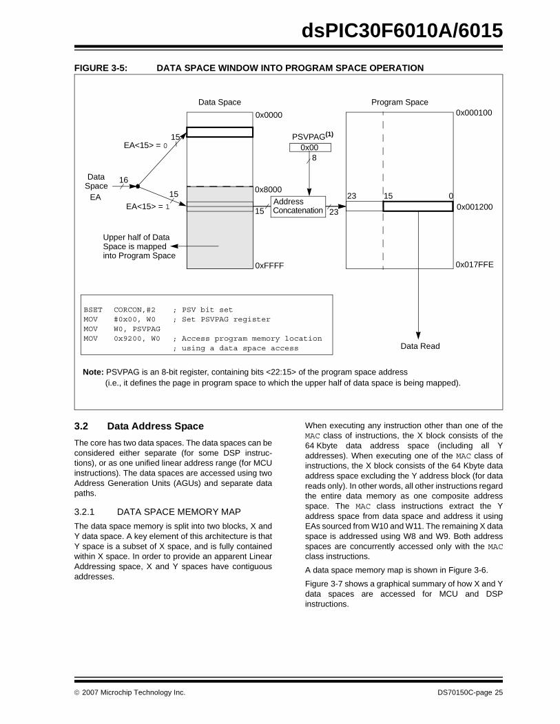
FIGURE 3-5: DATA SPACE WINDOW INTO PROGRAM SPACE OPERATION
3.2 Data Address Space
The core has two data spaces. The data spaces can beconsidered either separate (for some DSP instruc-tions), or as one unified linear address range (for MCUinstructions). The data spaces are accessed using twoAddress Generation Units (AGUs) and separate datapaths.
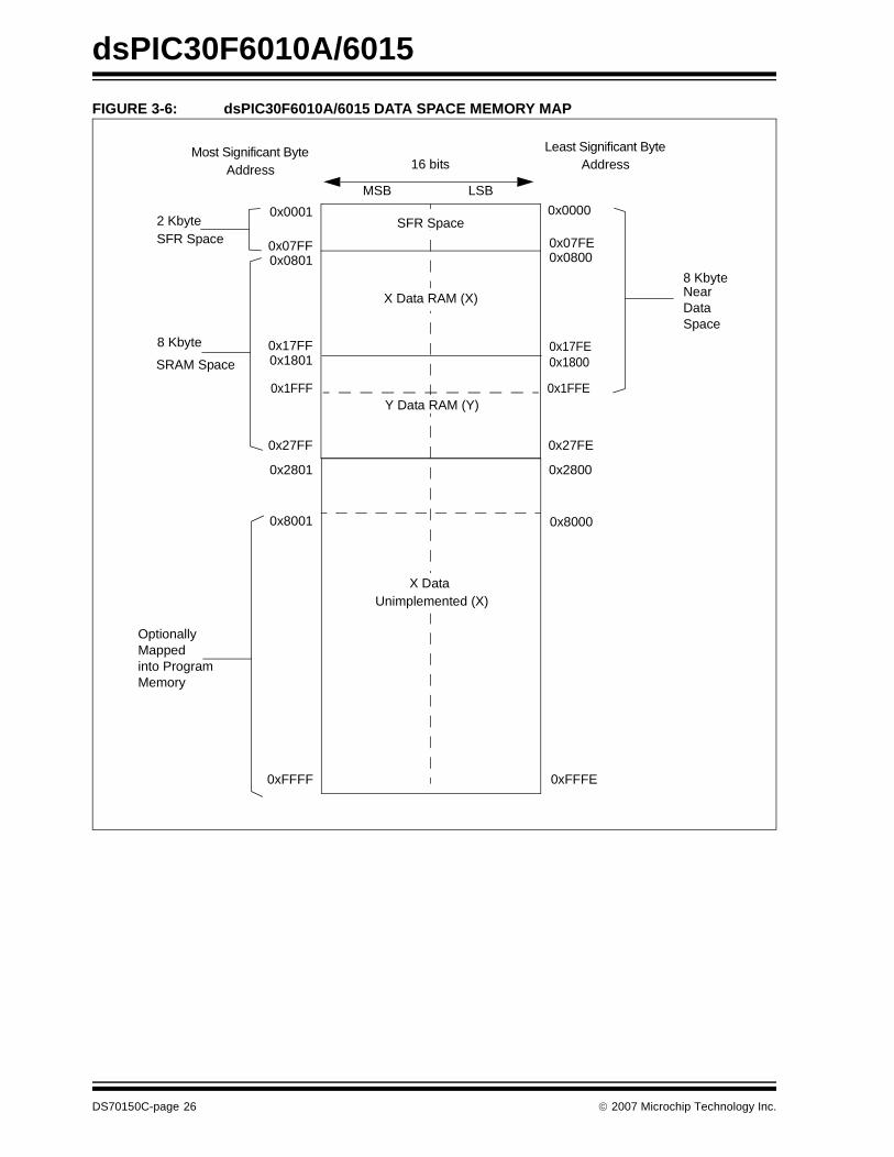
3.2.1 DATA SPACE MEMORY MAP
The data space memory is split into two blocks, X andY data space. A key element of this architecture is thatY space is a subset of X space, and is fully containedwithin X space. In order to provide an apparent LinearAddressing space, X and Y spaces have contiguousaddresses.
When executing any instruction other than one of theMAC class of instructions, the X block consists of the64 Kbyte data address space (including all Yaddresses). When executing one of the MAC class ofinstructions, the X block consists of the 64 Kbyte dataaddress space excluding the Y address block (for datareads only). In other words, all other instructions regardthe entire data memory as one composite addressspace. The MAC class instructions extract the Yaddress space from data space and address it usingEAs sourced from W10 and W11. The remaining X dataspace is addressed using W8 and W9. Both addressspaces are concurrently accessed only with the MACclass instructions.
A data space memory map is shown in Figure 3-6.
Figure 3-7 shows a graphical summary of how X and Ydata spaces are accessed for MCU and DSPinstructions.
23 15 0
PSVPAG(1)15
15
EA<15> = 0
EA<15> = 1
16DataSpace
EA
Data Space Program Space
8
15 23
0x0000
0x8000
0xFFFF
0x00
0x017FFE
Data Read
Upper half of Data Space is mapped into Program Space
Note: PSVPAG is an 8-bit register, containing bits <22:15> of the program space address (i.e., it defines the page in program space to which the upper half of data space is being mapped).
0x001200AddressConcatenation
BSET CORCON,#2 ; PSV bit setMOV #0x00, W0 ; Set PSVPAG registerMOV W0, PSVPAGMOV 0x9200, W0 ; Access program memory location
; using a data space access
0x000100
© 2007 Microchip Technology Inc. DS70150C-page 25
dsPIC30F6010A/6015
FIGURE 3-6: dsPIC30F6010A/6015 DATA SPACE MEMORY MAP
0x0000
0x07FE
0x17FE
0xFFFE
Least Significant ByteAddress16 bits
LSBMSB
Most Significant ByteAddress
0x0001
0x07FF
0x17FF
0xFFFF
0x8001 0x8000
OptionallyMappedinto ProgramMemory
0x27FF 0x27FE
0x28000x2801
0x0801 0x0800
0x1801 0x1800
NearData
0x1FFE0x1FFF
2 KbyteSFR Space
8 Kbyte
SRAM Space
8 Kbyte
Space
Unimplemented (X)X Data
SFR Space
X Data RAM (X)
Y Data RAM (Y)
DS70150C-page 26 © 2007 Microchip Technology Inc.

dsPIC30F6010A/6015
FIGURE 3-7: DATA SPACE FOR MCU AND DSP (MAC CLASS) INSTRUCTIONS EXAMPLE
SFR SPACE
(Y SPACE)
X S
PA
CE
SFR SPACE
UNUSED
X S
PA
CE
X S
PA
CE
Y SPACE
UNUSED
UNUSED
Non-MAC Class Ops (Read/Write) MAC Class Ops Read-Only
Indirect EA using any W Indirect EA using W10, W11 Indirect EA using W8, W9
MAC Class Ops (Write)
© 2007 Microchip Technology Inc. DS70150C-page 27

dsPIC30F6010A/6015
3.2.2 DATA SPACES
The X data space is used by all instructions and sup-ports all addressing modes. There are separate readand write data buses. The X read data bus is the returndata path for all instructions that view data space ascombined X and Y address space. It is also the Xaddress space data path for the dual operand readinstructions (MAC class). The X write data bus is theonly write path to data space for all instructions.
The X data space also supports Modulo Addressing forall instructions, subject to addressing mode restric-tions. Bit-Reversed Addressing is only supported forwrites to X data space.
The Y data space is used in concert with the X dataspace by the MAC class of instructions (CLR, ED,EDAC, MAC, MOVSAC, MPY, MPY.N and MSC) to pro-vide two concurrent data read paths. No writes occuracross the Y bus. This class of instructions dedicatestwo W register pointers, W10 and W11, to alwaysaddress Y data space, independent of X data space,whereas W8 and W9 always address X data space.Note that during accumulator write-back, the dataaddress space is considered a combination of X and Ydata spaces, so the write occurs across the X bus.Consequently, the write can be to any address in theentire data space.
The Y data space can only be used for the dataprefetch operation associated with the MAC class ofinstructions. It also supports Modulo Addressing forautomated circular buffers. Of course, all other instruc-tions can access the Y data address space through theX data path, as part of the composite linear space.
The boundary between the X and Y data spaces isdefined as shown in Figure 3-6 and is not user pro-grammable. Should an EA point to data outside its ownassigned address space, or to a location outside phys-ical memory, an all-zero word/byte will be returned. Forexample, although Y address space is visible by allnon-MAC instructions using any addressing mode, anattempt by a MAC instruction to fetch data from thatspace, using W8 or W9 (X space pointers), will return0x0000.
All Effective Addresses are 16 bits wide and point tobytes within the data space. Therefore, the data spaceaddress range is 64 Kbytes or 32K words.
3.2.3 DATA SPACE WIDTH
The core data width is 16 bits. All internal registers areorganized as 16-bit wide words. Data space memory isorganized in byte addressable, 16-bit wide blocks.
3.2.4 DATA ALIGNMENT
To help maintain backward compatibility with PIC®
devices and improve data space memory usage effi-ciency, the dsPIC30F instruction set supports bothword and byte operations. Data is aligned in data mem-ory and registers as words, but all data space EAsresolve to bytes. Data byte reads will read the completeword, which contains the byte, using the LSb of any EAto determine which byte to select. The selected byte isplaced onto the LSB of the X data path (no byteaccesses are possible from the Y data path as the MACclass of instruction can only fetch words). That is, datamemory and registers are organized as two parallelbyte wide entities with shared (word) address decode,but separate write lines. Data byte writes only write tothe corresponding side of the array or register whichmatches the byte address.
As a consequence of this byte accessibility, all EffectiveAddress calculations (including those generated by theDSP operations, which are restricted to word-sizeddata) are internally scaled to step through word-alignedmemory. For example, the core would recognize thatPost-Modified Register Indirect Addressing mode,[Ws++], will result in a value of Ws + 1 for byteoperations and Ws + 2 for word operations.
All word accesses must be aligned to an even address.Misaligned word data fetches are not supported, socare must be taken when mixing byte and word opera-tions, or translating from 8-bit MCU code. Should amisaligned read or write be attempted, an addresserror trap will be generated. If the error occurred on aread, the instruction underway is completed, whereas ifit occurred on a write, the instruction will be executedbut the write will not occur. In either case, a trap willthen be executed, allowing the system and/or user toexamine the machine state prior to execution of theaddress Fault.
FIGURE 3-8: DATA ALIGNMENTTABLE 3-2: EFFECT OF INVALID MEMORY ACCESSES
Attempted Operation Data Returned
EA = an unimplemented address 0x0000
W8 or W9 used to access Y data space in a MAC instruction
0x0000
W10 or W11 used to access X data space in a MAC instruction
0x0000
15 8 7 0
0001
0003
0005
0000
0002
0004
Byte 1 Byte 0
Byte 3 Byte 2
Byte 5 Byte 4
LSBMSB
DS70150C-page 28 © 2007 Microchip Technology Inc.
dsPIC30F6010A/6015
All byte loads into any W register are loaded into theLSB. The MSB is not modified.
A sign-extend (SE) instruction is provided to allowusers to translate 8-bit signed data to 16-bit signedvalues. Alternatively, for 16-bit unsigned data, userscan clear the MSB of any W register by executing azero-extend (ZE) instruction on the appropriateaddress.
Although most instructions are capable of operating onword or byte data sizes, it should be noted that someinstructions, including the DSP instructions, operateonly on words.
3.2.5 NEAR DATA SPACE
An 8 Kbyte ‘near’ data space is reserved in X addressmemory space between 0x0000 and 0x1FFF, which isdirectly addressable via a 13-bit absolute address fieldwithin all memory direct instructions. The remaining Xaddress space and all of the Y address space isaddressable indirectly. Additionally, the whole of X dataspace is addressable using MOV instructions, whichsupport memory direct addressing with a 16-bitaddress field.
3.2.6 SOFTWARE STACK
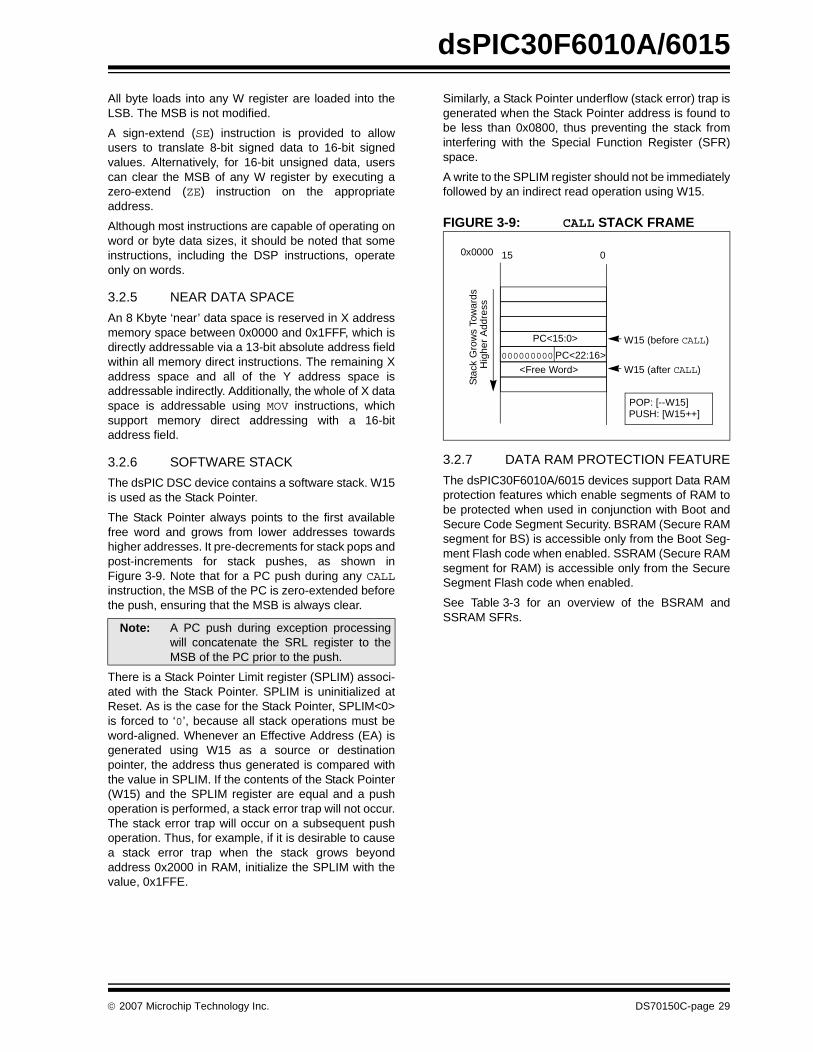
The dsPIC DSC device contains a software stack. W15is used as the Stack Pointer.
The Stack Pointer always points to the first availablefree word and grows from lower addresses towardshigher addresses. It pre-decrements for stack pops andpost-increments for stack pushes, as shown inFigure 3-9. Note that for a PC push during any CALLinstruction, the MSB of the PC is zero-extended beforethe push, ensuring that the MSB is always clear.
There is a Stack Pointer Limit register (SPLIM) associ-ated with the Stack Pointer. SPLIM is uninitialized atReset. As is the case for the Stack Pointer, SPLIM<0>is forced to ‘0’, because all stack operations must beword-aligned. Whenever an Effective Address (EA) isgenerated using W15 as a source or destinationpointer, the address thus generated is compared withthe value in SPLIM. If the contents of the Stack Pointer(W15) and the SPLIM register are equal and a pushoperation is performed, a stack error trap will not occur.The stack error trap will occur on a subsequent pushoperation. Thus, for example, if it is desirable to causea stack error trap when the stack grows beyondaddress 0x2000 in RAM, initialize the SPLIM with thevalue, 0x1FFE.
Similarly, a Stack Pointer underflow (stack error) trap isgenerated when the Stack Pointer address is found tobe less than 0x0800, thus preventing the stack frominterfering with the Special Function Register (SFR)space.
A write to the SPLIM register should not be immediatelyfollowed by an indirect read operation using W15.
FIGURE 3-9: CALL STACK FRAME
3.2.7 DATA RAM PROTECTION FEATURE
The dsPIC30F6010A/6015 devices support Data RAMprotection features which enable segments of RAM tobe protected when used in conjunction with Boot andSecure Code Segment Security. BSRAM (Secure RAMsegment for BS) is accessible only from the Boot Seg-ment Flash code when enabled. SSRAM (Secure RAMsegment for RAM) is accessible only from the SecureSegment Flash code when enabled.
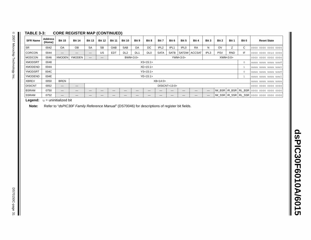
See Table 3-3 for an overview of the BSRAM andSSRAM SFRs.
Note: A PC push during exception processingwill concatenate the SRL register to theMSB of the PC prior to the push.
<Free Word>
PC<15:0>
000000000
015
W15 (before CALL)
W15 (after CALL)
Sta
ck G
row
s To
war
dsH
ighe
r A
ddre
ss
PUSH: [W15++]POP: [--W15]
0x0000
PC<22:16>
© 2007 Microchip Technology Inc. DS70150C-page 29
dsP
IC30F
6010A/6015
DS
70150C-page 30
© 2007 M
icrochip Technology Inc.
Bit 2 Bit 1 Bit 0 Reset State
0000 0000 0000 0000
0000 0000 0000 0000
0000 0000 0000 0000
0000 0000 0000 0000
0000 0000 0000 0000
0000 0000 0000 0000
0000 0000 0000 0000
0000 0000 0000 0000
0000 0000 0000 0000
0000 0000 0000 0000
0000 0000 0000 0000
0000 0000 0000 0000
0000 0000 0000 0000
0000 0000 0000 0000
0000 0000 0000 0000
0000 1000 0000 0000
0000 0000 0000 0000
0000 0000 0000 0000
0000 0000 0000 0000
0000 0000 0000 0000
0000 0000 0000 0000
0000 0000 0000 0000
0000 0000 0000 0000
0000 0000 0000 0000
0000 0000 0000 0000
0000 0000 0000 0000
0000 0000 0000 0000
uuuu uuuu uuuu uuuu
uuuu uuuu uuuu uuuu
0 uuuu uuuu uuuu uuu0
TH 0000 0000 0uuu uuuu
0 uuuu uuuu uuuu uuu0
H 0000 0000 0uuu uuuu
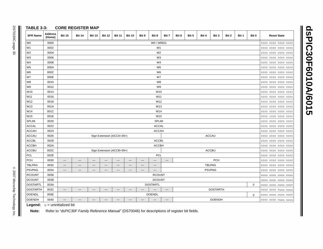
TABLE 3-3: CORE REGISTER MAP
SFR Name Address(Home) Bit 15 Bit 14 Bit 13 Bit 12 Bit 11 Bit 10 Bit 9 Bit 8 Bit 7 Bit 6 Bit 5 Bit 4 Bit 3
W0 0000 W0 / WREG
W1 0002 W1
W2 0004 W2
W3 0006 W3
W4 0008 W4
W5 000A W5
W6 000C W6
W7 000E W7
W8 0010 W8
W9 0012 W9
W10 0014 W10
W11 0016 W11
W12 0018 W12
W13 001A W13
W14 001C W14
W15 001E W15
SPLIM 0020 SPLIM
ACCAL 0022 ACCAL
ACCAH 0024 ACCAH
ACCAU 0026 Sign Extension (ACCA<39>) ACCAU
ACCBL 0028 ACCBL
ACCBH 002A ACCBH
ACCBU 002C Sign Extension (ACCB<39>) ACCBU
PCL 002E PCL
PCH 0030 — — — — — — — — — PCH
TBLPAG 0032 — — — — — — — — TBLPAG
PSVPAG 0034 — — — — — — — — PSVPAG
RCOUNT 0036 RCOUNT
DCOUNT 0038 DCOUNT
DOSTARTL 003A DOSTARTL
DOSTARTH 003C — — — — — — — — — DOSTAR
DOENDL 003E DOENDL
DOENDH 0040 — — — — — — — — — DOEND
Legend: u = uninitialized bit
Note: Refer to “dsPIC30F Family Reference Manual” (DS70046) for descriptions of register bit fields.
© 2007 M
icrochip Technology Inc.
DS
70150C-page 31
dsP
IC30F
6010A/6015
SR V Z C 0000 0000 0000 0000
CO V RND IF 0000 0000 0010 0000
MO XWM<3:0> 0000 0000 0000 0000
XM 0 uuuu uuuu uuuu uuu0
XM 1 uuuu uuuu uuuu uuu1
YM 0 uuuu uuuu uuuu uuu0
YM 1 uuuu uuuu uuuu uuu1
XB uuuu uuuu uuuu uuuu
DI 0000 0000 0000 0000
BS BSR IR_BSR RL_BSR 0000 0000 0000 0000
SS SSR IR_SSR RL_SSR 0000 0000 0000 0000
TA
SF t 2 Bit 1 Bit 0 Reset State
Le
0042 OA OB SA SB OAB SAB DA DC IPL2 IPL1 IPL0 RA N O
RCON 0044 — — — US EDT DL2 DL1 DL0 SATA SATB SATDW ACCSAT IPL3 PS
DCON 0046 XMODEN YMODEN — — BWM<3:0> YWM<3:0>
ODSRT 0048 XS<15:1>
ODEND 004A XE<15:1>
ODSRT 004C YS<15:1>
ODEND 004E YE<15:1>
REV 0050 BREN XB<14:0>
SICNT 0052 — — DISICNT<13:0>
RAM 0750 — — — — — — — — — — — — — IW_
RAM 0752 — — — — — — — — — — — — — IW_
BLE 3-3: CORE REGISTER MAP (CONTINUED)
R Name Address(Home) Bit 15 Bit 14 Bit 13 Bit 12 Bit 11 Bit 10 Bit 9 Bit 8 Bit 7 Bit 6 Bit 5 Bit 4 Bit 3 Bi
gend: u = uninitialized bit
Note: Refer to “dsPIC30F Family Reference Manual” (DS70046) for descriptions of register bit fields.

dsPIC30F6010A/6015
NOTES:
DS70150C-page 32 © 2007 Microchip Technology Inc.
dsPIC30F6010A/6015
4.0 ADDRESS GENERATOR UNITS
The dsPIC DSC core contains two independentAddress Generator Units (AGU): the X AGU and YAGU. The Y AGU supports word-sized data reads forthe DSP MAC class of instructions only. The dsPIC DSCAGUs support three types of data addressing:
• Linear Addressing
• Modulo (Circular) Addressing• Bit-Reversed Addressing
Linear and Modulo Data Addressing modes can beapplied to data space or program space. Bit-ReversedAddressing mode is only applicable to data spaceaddresses.
4.1 Instruction Addressing Modes
The addressing modes in Table 4-1 form the basis ofthe addressing modes optimized to support the specificfeatures of individual instructions. The addressingmodes provided in the MAC class of instructions aresomewhat different from those in the other instructiontypes.
4.1.1 FILE REGISTER INSTRUCTIONS
Most file register instructions use a 13-bit address field(f) to directly address data present in the first8192 bytes of data memory (near data space). Most fileregister instructions employ a working register W0,which is denoted as WREG in these instructions. Thedestination is typically either the same file register, orWREG (with the exception of the MUL instruction),which writes the result to a register or register pair. TheMOV instruction allows additional flexibility and canaccess the entire data space during file registeroperation.
4.1.2 MCU INSTRUCTIONS
The three-operand MCU instructions are of the form:
Operand 3 = Operand 1 <function> Operand 2
where Operand 1 is always a working register (i.e., theaddressing mode can only be Register Direct), which isreferred to as Wb. Operand 2 can be a W register,fetched from data memory, or a 5-bit literal. The resultlocation can be either a W register or an addresslocation. The following addressing modes aresupported by MCU instructions:
• Register Direct• Register Indirect
• Register Indirect Post-Modified• Register Indirect Pre-Modified• 5-bit or 10-bit Literal
TABLE 4-1: FUNDAMENTAL ADDRESSING MODES SUPPORTED
Note: This data sheet summarizes features of thisgroup of dsPIC30F devices and is not intended to bea complete reference source. For more informationon the CPU, peripherals, register descriptions andgeneral device functionality, refer to the “dsPIC30FFamily Reference Manual” (DS70046). For moreinformation on the device instruction set and pro-gramming, refer to the “dsPIC30F/33F ProgrammersReference Manual” (DS70157).
Note: Not all instructions support all the address-ing modes given above. Individualinstructions may support different subsetsof these addressing modes.
Addressing Mode Description
File Register Direct The address of the file register is specified explicitly.
Register Direct The contents of a register are accessed directly.
Register Indirect The contents of Wn forms the EA.
Register Indirect Post-Modified The contents of Wn forms the EA. Wn is post-modified (incremented or decremented) by a constant value.
Register Indirect Pre-Modified Wn is pre-modified (incremented or decremented) by a signed constant value to form the EA.
Register Indirect with Register Offset The sum of Wn and Wb forms the EA.
Register Indirect with Literal Offset The sum of Wn and a literal forms the EA.
© 2007 Microchip Technology Inc. DS70150C-page 33

dsPIC30F6010A/6015
4.1.3 MOVE AND ACCUMULATOR INSTRUCTIONS
Move instructions and the DSP Accumulator class ofinstructions provide a greater degree of addressingflexibility than other instructions. In addition to theaddressing modes supported by most MCU instruc-tions, Move and Accumulator instructions also supportRegister Indirect with Register Offset Addressingmode, also referred to as Register Indexed mode.
In summary, the following addressing modes aresupported by Move and Accumulator instructions:
• Register Direct• Register Indirect• Register Indirect Post-Modified
• Register Indirect Pre-Modified• Register Indirect with Register Offset (Indexed)• Register Indirect with Literal Offset
• 8-bit Literal• 16-bit Literal
4.1.4 MAC INSTRUCTIONS
The dual source operand DSP instructions (CLR, ED,EDAC, MAC, MPY, MPY.N, MOVSAC and MSC), alsoreferred to as MAC instructions, utilize a simplified set ofaddressing modes to allow the user to effectivelymanipulate the data pointers through Register Indirecttables.
The two source operand prefetch registers must be amember of the set {W8, W9, W10, W11}. For data reads,W8 and W9 will always be directed to the X RAGU andW10 and W11 will always be directed to the Y AGU. TheEffective Addresses generated (before and after modifi-cation) must, therefore, be valid addresses within X dataspace for W8 and W9 and Y data space for W10 andW11.
In summary, the following addressing modes aresupported by the MAC class of instructions:
• Register Indirect• Register Indirect Post-Modified by 2• Register Indirect Post-Modified by 4
• Register Indirect Post-Modified by 6• Register Indirect with Register Offset (Indexed)
4.1.5 OTHER INSTRUCTIONS
Besides the various addressing modes outlined above,some instructions use literal constants of various sizes.For example, BRA (branch) instructions use 16-bitsigned literals to specify the branch destination directly,whereas the DISI instruction uses a 14-bit unsignedliteral field. In some instructions, such as ADD Acc, thesource of an operand or result is implied by the opcodeitself. Certain operations, such as NOP, do not have anyoperands.
4.2 Modulo Addressing
Modulo Addressing is a method of providing anautomated means to support circular data buffers usinghardware. The objective is to remove the need forsoftware to perform data address boundary checkswhen executing tightly looped code, as is typical inmany DSP algorithms.
Modulo Addressing can operate in either data orprogram space (since the data pointer mechanism isessentially the same for both). One circular buffer can besupported in each of the X (which also provides thepointers into program space) and Y data spaces. ModuloAddressing can operate on any W register pointer.However, it is not advisable to use W14 or W15 forModulo Addressing, since these two registers are usedas the Stack Frame Pointer and Stack Pointer,respectively.
In general, any particular circular buffer can only beconfigured to operate in one direction, as there arecertain restrictions on the buffer start address (forincrementing buffers) or end address (for decrementingbuffers) based upon the direction of the buffer.
The only exception to the usage restrictions is forbuffers which have a power-of-2 length. As thesebuffers satisfy the start and end address criteria, theymay operate in a Bidirectional mode, (i.e., addressboundary checks will be performed on both the lowerand upper address boundaries).
Note: For the MOV instructions, the addressingmode specified in the instruction can differfor the source and destination EA. How-ever, the 4-bit Wb (Register Offset) field isshared between both source anddestination (but typically only used byone).
Note: Not all instructions support all the address-ing modes given above. Individualinstructions may support different subsetsof these addressing modes.
Note: Register Indirect with Register OffsetAddressing is only available for W9 (in Xspace) and W11 (in Y space).
DS70150C-page 34 © 2007 Microchip Technology Inc.
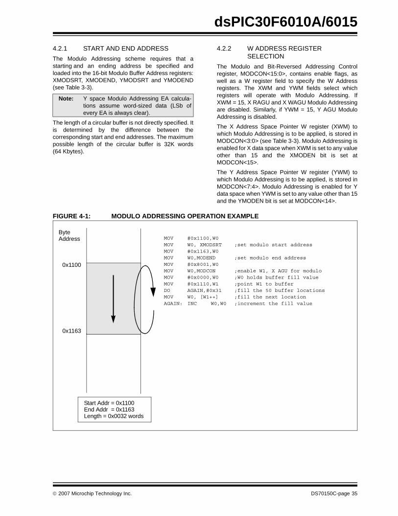
dsPIC30F6010A/6015
4.2.1 START AND END ADDRESS
The Modulo Addressing scheme requires that astarting and an ending address be specified andloaded into the 16-bit Modulo Buffer Address registers:XMODSRT, XMODEND, YMODSRT and YMODEND(see Table 3-3).
The length of a circular buffer is not directly specified. Itis determined by the difference between thecorresponding start and end addresses. The maximumpossible length of the circular buffer is 32K words(64 Kbytes).
4.2.2 W ADDRESS REGISTER SELECTION
The Modulo and Bit-Reversed Addressing Controlregister, MODCON<15:0>, contains enable flags, aswell as a W register field to specify the W Addressregisters. The XWM and YWM fields select whichregisters will operate with Modulo Addressing. IfXWM = 15, X RAGU and X WAGU Modulo Addressingare disabled. Similarly, if YWM = 15, Y AGU ModuloAddressing is disabled.
The X Address Space Pointer W register (XWM) towhich Modulo Addressing is to be applied, is stored inMODCON<3:0> (see Table 3-3). Modulo Addressing isenabled for X data space when XWM is set to any valueother than 15 and the XMODEN bit is set atMODCON<15>.
The Y Address Space Pointer W register (YWM) towhich Modulo Addressing is to be applied, is stored inMODCON<7:4>. Modulo Addressing is enabled for Ydata space when YWM is set to any value other than 15and the YMODEN bit is set at MODCON<14>.
FIGURE 4-1: MODULO ADDRESSING OPERATION EXAMPLE
Note: Y space Modulo Addressing EA calcula-tions assume word-sized data (LSb ofevery EA is always clear).
0x1100
0x1163
Start Addr = 0x1100End Addr = 0x1163Length = 0x0032 words
ByteAddress MOV #0x1100,W0
MOV W0, XMODSRT ;set modulo start addressMOV #0x1163,W0MOV W0,MODEND ;set modulo end addressMOV #0x8001,W0MOV W0,MODCON ;enable W1, X AGU for moduloMOV #0x0000,W0 ;W0 holds buffer fill valueMOV #0x1110,W1 ;point W1 to bufferDO AGAIN,#0x31 ;fill the 50 buffer locationsMOV W0, [W1++] ;fill the next locationAGAIN: INC W0,W0 ;increment the fill value
© 2007 Microchip Technology Inc. DS70150C-page 35

dsPIC30F6010A/6015
4.2.3 MODULO ADDRESSING APPLICABILITY
Modulo Addressing can be applied to the EffectiveAddress (EA) calculation associated with any Wregister. It is important to realize that the addressboundaries check for addresses less than or greaterthan the upper (for incrementing buffers) and lower (fordecrementing buffers) boundary addresses (not justequal to). Address changes may, therefore, jumpbeyond boundaries and still be adjusted correctly.
4.3 Bit-Reversed Addressing
Bit-Reversed Addressing is intended to simplify datare-ordering for radix-2 FFT algorithms. It is supportedby the X AGU for data writes only.
The modifier, which may be a constant value or registercontents, is regarded as having its bit order reversed.The address source and destination are kept in normalorder. Thus, the only operand requiring reversal is themodifier.
4.3.1 BIT-REVERSED ADDRESSING IMPLEMENTATION
Bit-Reversed Addressing is enabled when:
1. BWM (W register selection) in the MODCON reg-ister is any value other than 15 (the stack can notbe accessed using Bit-Reversed Addressing)and
2. the BREN bit is set in the XBREV register and3. the addressing mode used is Register Indirect
with Pre-Increment or Post-Increment.
If the length of a Bit-Reversed buffer is M = 2N bytes,then the last ‘N’ bits of the data buffer start addressmust be zeros.
XB<14:0> is the Bit-Reversed Address modifier or‘pivot point’ which is typically a constant. In the case ofan FFT computation, its value is equal to half of the FFTdata buffer size.
When enabled, Bit-Reversed Addressing will only beexecuted for Register Indirect with Pre-Increment orPost-Increment Addressing and word-sized data writes.It will not function for any other addressing mode or forbyte-sized data, and normal addresses will be generatedinstead. When Bit-Reversed Addressing is active, the WAddress Pointer will always be added to the addressmodifier (XB) and the offset associated with the RegisterIndirect Addressing mode will be ignored. In addition, asword-sized data is a requirement, the LSb of the EA isignored (and always clear).
If Bit-Reversed Addressing has already been enabledby setting the BREN (XBREV<15>) bit, then a write tothe XBREV register should not be immediately followedby an indirect read operation using the W register thathas been designated as the Bit-Reversed Pointer.
FIGURE 4-2: BIT-REVERSED ADDRESS EXAMPLE
Note: The modulo corrected Effective Address iswritten back to the register only when Pre-Modify or Post-Modify Addressing mode isused to compute the Effective Address.When an address offset (e.g., [W7+W2]) isused, Modulo Address correction is per-formed, but the contents of the registerremains unchanged.
Note: All Bit-Reversed EA calculations assumeword-sized data (LSb of every EA isalways clear). The XB value is scaledaccordingly to generate compatible (byte)addresses.
Note: Modulo Addressing and Bit-ReversedAddressing should not be enabledtogether. In the event that the userattempts to do this, Bit-Reversed Address-ing will assume priority when active for theX WAGU, and X WAGU Modulo Address-ing will be disabled. However, ModuloAddressing will continue to function in theX RAGU.
b3 b2 b1 0
b2 b3 b4 0
Bit Locations Swapped Left-to-RightAround Center of Binary Value
Bit-Reversed Address
XB = 0x0008 for a 16-word Bit-Reversed Buffer
b7 b6 b5 b1
b7 b6 b5 b4b11 b10 b9 b8
b11 b10 b9 b8
b15 b14 b13 b12
b15 b14 b13 b12
Sequential Address
Pivot Point
DS70150C-page 36 © 2007 Microchip Technology Inc.

dsPIC30F6010A/6015
TABLE 4-2: BIT-REVERSED ADDRESS SEQUENCE (16-ENTRY)
TABLE 4-3: BIT-REVERSED ADDRESS MODIFIER VALUES FOR XBREV REGISTER
Normal Address Bit-Reversed Address
A3 A2 A1 A0 Decimal A3 A2 A1 A0 Decimal
0 0 0 0 0 0 0 0 0 0
0 0 0 1 1 1 0 0 0 8
0 0 1 0 2 0 1 0 0 4
0 0 1 1 3 1 1 0 0 12
0 1 0 0 4 0 0 1 0 2
0 1 0 1 5 1 0 1 0 10
0 1 1 0 6 0 1 1 0 6
0 1 1 1 7 1 1 1 0 14
1 0 0 0 8 0 0 0 1 1
1 0 0 1 9 1 0 0 1 9
1 0 1 0 10 0 1 0 1 5
1 0 1 1 11 1 1 0 1 13
1 1 0 0 12 0 0 1 1 3
1 1 0 1 13 1 0 1 1 11
1 1 1 0 14 0 1 1 1 7
1 1 1 1 15 1 1 1 1 15
Buffer Size (Words) XB<14:0> Bit-Reversed Address Modifier Value
4096 0x0800
2048 0x0400
1024 0x0200
512 0x0100
256 0x0080
128 0x0040
64 0x0020
32 0x0010
16 0x0008
8 0x0004
4 0x0002
2 0x0001
© 2007 Microchip Technology Inc. DS70150C-page 37

dsPIC30F6010A/6015
NOTES:
DS70150C-page 38 © 2007 Microchip Technology Inc.
dsPIC30F6010A/6015
5.0 INTERRUPTS
The dsPIC30F6010A/6015 has 44 interrupt sourcesand four processor exceptions (traps), which must bearbitrated based on a priority scheme.
The CPU is responsible for reading the InterruptVector Table (IVT) and transferring the address con-tained in the interrupt vector to the program counter.The interrupt vector is transferred from the programdata bus into the program counter, via a 24-bit widemultiplexer on the input of the program counter.
The Interrupt Vector Table (IVT) and Alternate Inter-rupt Vector Table (AIVT) are placed near the beginningof program memory (0x000004). The IVT and AIVTare shown in Figure 5-1.
The interrupt controller is responsible for pre-processing the interrupts and processor exceptions,prior to their being presented to the processor core.The peripheral interrupts and traps are enabled,prioritized and controlled using centralized SpecialFunction Registers:
• IFS0<15:0>, IFS1<15:0>, IFS2<15:0>All Interrupt Request Flags are maintained in these three registers. The flags are set by their respective peripherals or external signals, and they are cleared via software.
• IEC0<15:0>, IEC1<15:0>, IEC2<15:0>All Interrupt Enable Control bits are maintained in these three registers. These control bits are used to individually enable interrupts from the peripherals or external signals.
• IPC0<15:0>... IPC11<7:0>The user assignable priority level associated with each of these 44 interrupts is held centrally in these twelve registers.
• IPL<3:0> The current CPU priority level is explicitly stored in the IPL bits. IPL<3> is present in the CORCON register, whereas IPL<2:0> are present in the STATUS register (SR) in the processor core.
• INTCON1<15:0>, INTCON2<15:0>Global interrupt control functions are derived from these two registers. INTCON1 contains the con-trol and status flags for the processor exceptions. The INTCON2 register controls the external interrupt request signal behavior and the use of the alternate vector table.
• INTTREG<15:0>The associated interrupt vector number and the new CPU interrupt priority level are latched into Vector number (VECNUM<5:0>) and Interrupt level ILR<3:0> bit fields in the INTTREG register. The new interrupt priority level is the priority of the pending interrupt.
All interrupt sources can be user assigned to one ofseven priority levels, 1 through 7, via the IPCxregisters. Each interrupt source is associated with aninterrupt vector, as shown in Table 5-1. Levels 7 and 1represent the highest and lowest maskable priorities,respectively.
If the NSTDIS bit (INTCON1<15>) is set, nesting ofinterrupts is prevented. Thus, if an interrupt is currentlybeing serviced, processing of a new interrupt is pre-vented, even if the new interrupt is of higher prioritythan the one currently being serviced.
Certain interrupts have specialized control bits forfeatures like edge or level triggered interrupts, inter-rupt-on-change, etc. Control of these features remainswithin the peripheral module which generates theinterrupt.
The DISI instruction can be used to disable theprocessing of interrupts of priorities 6 and lower for acertain number of instructions, during which the DISI bit(INTCON2<14>) remains set.
When an interrupt is serviced, the PC is loaded with theaddress stored in the vector location in programmemory that corresponds to the interrupt. There are 63different vectors within the IVT (refer to Figure 5-2).These vectors are contained in locations 0x000004through 0x0000FE of program memory (refer toFigure 5-2). These locations contain 24-bit addresses,and in order to preserve robustness, an address errortrap will take place should the PC attempt to fetch anyof these words during normal execution. This preventsexecution of random data as a result of accidentallydecrementing a PC into vector space, accidentallymapping a data space address into vector space, or thePC rolling over to 0x000000 after reaching the end ofimplemented program memory space. Execution of aGOTO instruction to this vector space will also generatean address error trap.
Note: This data sheet summarizes features of thisgroup of dsPIC30F devices and is not intended to bea complete reference source. For more informationon the CPU, peripherals, register descriptions andgeneral device functionality, refer to the “dsPIC30FFamily Reference Manual” (DS70046). For moreinformation on the device instruction set and pro-gramming, refer to the “dsPIC30F/33F ProgrammersReference Manual” (DS70157).
Note: Interrupt flag bits get set when an interruptcondition occurs, regardless of the state ofits corresponding enable bit. User soft-ware should ensure the appropriate inter-rupt flag bits are clear prior to enabling aninterrupt.
Note: Assigning a priority level of 0 to an inter-rupt source is equivalent to disabling thatinterrupt.
Note: The IPL bits become read-only wheneverthe NSTDIS bit has been set to ‘1’.
© 2007 Microchip Technology Inc. DS70150C-page 39
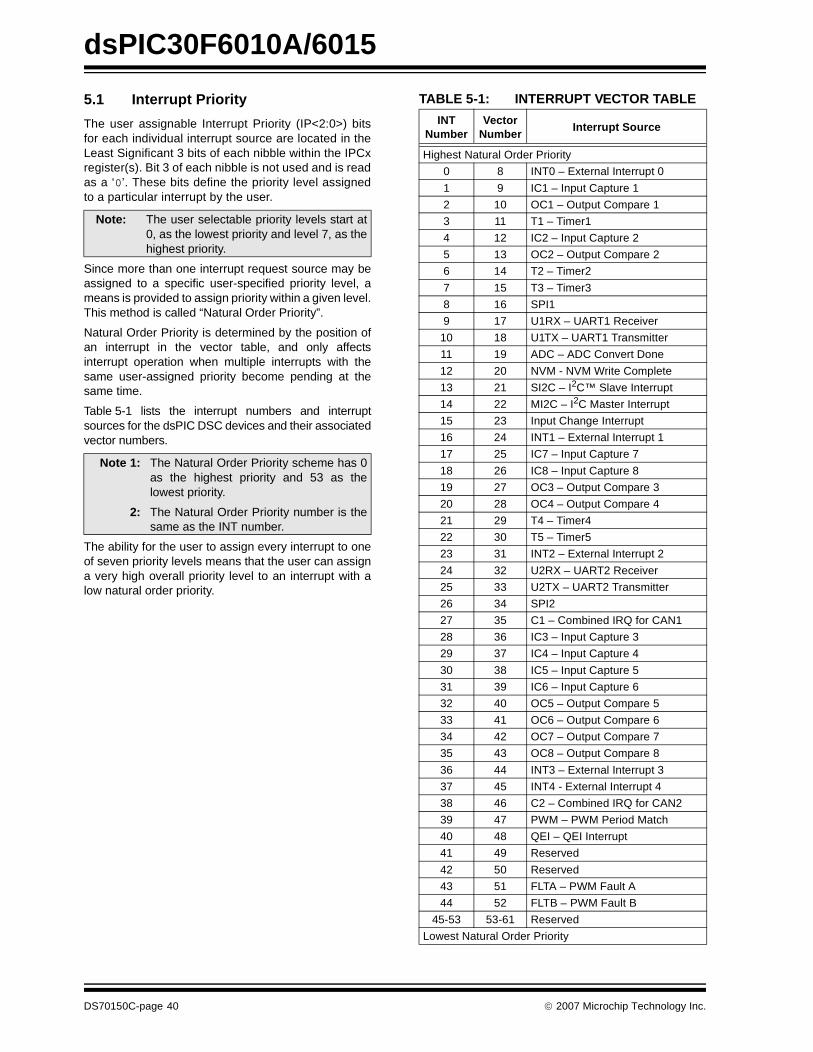
dsPIC30F6010A/6015
5.1 Interrupt Priority
The user assignable Interrupt Priority (IP<2:0>) bitsfor each individual interrupt source are located in theLeast Significant 3 bits of each nibble within the IPCxregister(s). Bit 3 of each nibble is not used and is readas a ‘0’. These bits define the priority level assignedto a particular interrupt by the user.
Since more than one interrupt request source may beassigned to a specific user-specified priority level, ameans is provided to assign priority within a given level.This method is called “Natural Order Priority”.
Natural Order Priority is determined by the position ofan interrupt in the vector table, and only affectsinterrupt operation when multiple interrupts with thesame user-assigned priority become pending at thesame time.
Table 5-1 lists the interrupt numbers and interruptsources for the dsPIC DSC devices and their associatedvector numbers.
The ability for the user to assign every interrupt to oneof seven priority levels means that the user can assigna very high overall priority level to an interrupt with alow natural order priority.
TABLE 5-1: INTERRUPT VECTOR TABLE
Note: The user selectable priority levels start at0, as the lowest priority and level 7, as thehighest priority.
Note 1: The Natural Order Priority scheme has 0as the highest priority and 53 as thelowest priority.
2: The Natural Order Priority number is thesame as the INT number.
INT Number
Vector Number
Interrupt Source
Highest Natural Order Priority
0 8 INT0 – External Interrupt 0
1 9 IC1 – Input Capture 1
2 10 OC1 – Output Compare 1
3 11 T1 – Timer1
4 12 IC2 – Input Capture 2
5 13 OC2 – Output Compare 2
6 14 T2 – Timer2
7 15 T3 – Timer3
8 16 SPI1
9 17 U1RX – UART1 Receiver
10 18 U1TX – UART1 Transmitter
11 19 ADC – ADC Convert Done
12 20 NVM - NVM Write Complete
13 21 SI2C – I2C™ Slave Interrupt
14 22 MI2C – I2C Master Interrupt
15 23 Input Change Interrupt
16 24 INT1 – External Interrupt 1
17 25 IC7 – Input Capture 7
18 26 IC8 – Input Capture 8
19 27 OC3 – Output Compare 3
20 28 OC4 – Output Compare 4
21 29 T4 – Timer4
22 30 T5 – Timer5
23 31 INT2 – External Interrupt 2
24 32 U2RX – UART2 Receiver
25 33 U2TX – UART2 Transmitter
26 34 SPI2
27 35 C1 – Combined IRQ for CAN1
28 36 IC3 – Input Capture 3
29 37 IC4 – Input Capture 4
30 38 IC5 – Input Capture 5
31 39 IC6 – Input Capture 6
32 40 OC5 – Output Compare 5
33 41 OC6 – Output Compare 6
34 42 OC7 – Output Compare 7
35 43 OC8 – Output Compare 8
36 44 INT3 – External Interrupt 3
37 45 INT4 - External Interrupt 4
38 46 C2 – Combined IRQ for CAN2
39 47 PWM – PWM Period Match
40 48 QEI – QEI Interrupt
41 49 Reserved
42 50 Reserved
43 51 FLTA – PWM Fault A
44 52 FLTB – PWM Fault B
45-53 53-61 Reserved
Lowest Natural Order Priority
DS70150C-page 40 © 2007 Microchip Technology Inc.

dsPIC30F6010A/6015
5.2 Reset Sequence
A Reset is not a true exception because the interruptcontroller is not involved in the Reset process. The pro-cessor initializes its registers in response to a Resetwhich forces the PC to zero. The processor then beginsprogram execution at location 0x000000. A GOTOinstruction is stored in the first program memory loca-tion, immediately followed by the address target for theGOTO instruction. The processor executes the GOTO tothe specified address and then begins operation at thespecified target (start) address.
5.2.1 RESET SOURCES
There are 6 sources of error which will cause a deviceReset.
• Watchdog Time-out:The watchdog has timed out, indicating that the processor is no longer executing the correct flow of code.
• Uninitialized W Register Trap:An attempt to use an uninitialized W register as an Address Pointer will cause a Reset.
• Illegal Instruction Trap:Attempted execution of any unused opcodes will result in an illegal instruction trap. Note that a fetch of an illegal instruction does not result in an illegal instruction trap if that instruction is flushed prior to execution due to a flow change.
• Brown-out Reset (BOR):A momentary dip in the power supply to the device has been detected which may result in malfunction.
• Trap Lockout:Occurrence of multiple trap conditions simultaneously will cause a Reset.
5.3 Traps
Traps can be considered as non-maskable interruptsindicating a software or hardware error, which adhereto a predefined priority, as shown in Figure 5-1. Theyare intended to provide the user a means to correcterroneous operation during debug and when operatingwithin the application.
Note that many of these trap conditions can only bedetected when they occur. Consequently, the question-able instruction is allowed to complete prior to trapexception processing. If the user chooses to recoverfrom the error, the result of the erroneous action thatcaused the trap may have to be corrected.
There are 8 fixed priority levels for traps: Level 8through Level 15, which means that IPL3 is always setduring processing of a trap.
If the user is not currently executing a trap, and he setsthe IPL<3:0> bits to a value of ‘0111’ (Level 7), then allinterrupts are disabled, but traps can still be processed.
5.3.1 TRAP SOURCES
The following traps are provided with increasing prior-ity. However, since all traps can be nested, priority haslittle effect.
Math Error Trap:
The math error trap executes under the following threecircumstances:
1. Should an attempt be made to divide by zero,the divide operation will be aborted on a cycleboundary and the trap taken.
2. If enabled, a math error trap will be taken whenan arithmetic operation on either Accumulator Aor B causes an overflow from bit 31 and theAccumulator Guard bits are not utilized.
3. If enabled, a math error trap will be taken whenan arithmetic operation on either Accumulator Aor B causes a catastrophic overflow from bit 39and all saturation is disabled.
4. If the shift amount specified in a shift instructionis greater than the maximum allowed shiftamount, a trap will occur.
Note: If the user does not intend to take correc-tive action in the event of a trap errorcondition, these vectors must be loadedwith the address of a default handler thatsimply contains the RESET instruction. If,on the other hand, one of the vectorscontaining an invalid address is called, anaddress error trap is generated.
© 2007 Microchip Technology Inc. DS70150C-page 41

dsPIC30F6010A/6015
Address Error Trap:
This trap is initiated when any of the followingcircumstances occurs:
1. A misaligned data word access is attempted.2. A data fetch from our unimplemented data
memory location is attempted.3. A data access of an unimplemented program
memory location is attempted.4. An instruction fetch from vector space is
attempted.
5. Execution of a “BRA #literal” instruction or a“GOTO #literal” instruction, where literalis an unimplemented program memory address.
6. Executing instructions after modifying the PC topoint to unimplemented program memoryaddresses. The PC may be modified by loadinga value into the stack and executing a RETURNinstruction.
Stack Error Trap:
This trap is initiated under the following conditions:
1. The Stack Pointer is loaded with a value whichis greater than the (user programmable) limitvalue written into the SPLIM register (stackoverflow).
2. The Stack Pointer is loaded with a value whichis less than 0x0800 (simple stack underflow).
Oscillator Fail Trap:
This trap is initiated if the external oscillator fails andoperation becomes reliant on an internal RC backup.
5.3.2 HARD AND SOFT TRAPS
It is possible that multiple traps can become activewithin the same cycle (e.g., a misaligned word stackwrite to an overflowed address). In such a case, thefixed priority shown in Figure 5-2 is implemented,which may require the user to check if other traps arepending in order to completely correct the Fault.
‘Soft’ traps include exceptions of priority level 8 throughlevel 11, inclusive. The arithmetic error trap (level 11)falls into this category of traps.
‘Hard’ traps include exceptions of priority level 12through level 15, inclusive. The address error (level12), stack error (level 13) and oscillator error (level 14)traps fall into this category.
Each hard trap that occurs must be Acknowledgedbefore code execution of any type may continue. If alower priority hard trap occurs while a higher prioritytrap is pending, Acknowledged, or is being processed,a hard trap conflict will occur.
The device is automatically reset in a hard trap conflictcondition. The TRAPR Status bit (RCON<15>) is setwhen the Reset occurs, so that the condition may bedetected in software.
FIGURE 5-1: TRAP VECTORS
Note: In the MAC class of instructions, whereinthe data space is split into X and Y dataspace, unimplemented X space includesall of Y space, and unimplemented Yspace includes all of X space.
Oscillator Fail Trap VectorStack Error Trap Vector
Reserved VectorMath Error Trap Vector
Reserved
Oscillator Fail Trap VectorAddress Error Trap Vector
Reserved VectorReserved VectorInterrupt 0 VectorInterrupt 1 Vector
Interrupt 52 VectorInterrupt 53 Vector
Math Error Trap Vector
Dec
reas
ing
Prio
rity
0x000000
0x000014
Reserved
Stack Error Trap Vector
Reserved VectorIVT
AIVT
0x0000800x00007E
0x0000FE
Reserved
0x000094
Reset – GOTO InstructionReset – GOTO Address 0x000002
Reserved0x0000820x000084
0x000004
Reserved Vector
Reserved VectorInterrupt 0 VectorInterrupt 1 Vector
Interrupt 52 VectorInterrupt 53 Vector
Address Error Trap Vector
DS70150C-page 42 © 2007 Microchip Technology Inc.
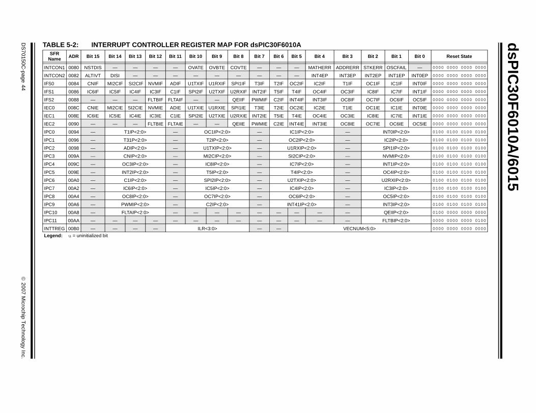
dsP
IC30F
6010A/6015
DS
70150C-page 44
© 2007 M
icrochip Technology Inc.
Bit 2 Bit 1 Bit 0 Reset State
TKERR OSCFAIL — 0000 0000 0000 0000
NT2EP INT1EP INT0EP 0000 0000 0000 0000
OC1IF IC1IF INT0IF 0000 0000 0000 0000
IC8IF IC7IF INT1IF 0000 0000 0000 0000
OC7IF OC6IF OC5IF 0000 0000 0000 0000
OC1IE IC1IE INT0IE 0000 0000 0000 0000
IC8IE IC7IE INT1IE 0000 0000 0000 0000
OC7IE OC6IE OC5IE 0000 0000 0000 0000
INT0IP<2:0> 0100 0100 0100 0100
IC2IP<2:0> 0100 0100 0100 0100
SPI1IP<2:0> 0100 0100 0100 0100
NVMIP<2:0> 0100 0100 0100 0100
INT1IP<2:0> 0100 0100 0100 0100
OC4IP<2:0> 0100 0100 0100 0100
U2RXIP<2:0> 0100 0100 0100 0100
IC3IP<2:0> 0100 0100 0100 0100
OC5IP<2:0> 0100 0100 0100 0100
INT3IP<2:0> 0100 0100 0100 0100
QEIIP<2:0> 0100 0000 0000 0000
FLTBIP<2:0> 0000 0000 0000 0100
5:0> 0000 0000 0000 0000
TABLE 5-2: INTERRUPT CONTROLLER REGISTER MAP FOR dsPIC30F6010A SFR
Name ADR Bit 15 Bit 14 Bit 13 Bit 12 Bit 11 Bit 10 Bit 9 Bit 8 Bit 7 Bit 6 Bit 5 Bit 4 Bit 3
INTCON1 0080 NSTDIS — — — — OVATE OVBTE COVTE — — — MATHERR ADDRERR S
INTCON2 0082 ALTIVT DISI — — — — — — — — — INT4EP INT3EP I
IFS0 0084 CNIF MI2CIF SI2CIF NVMIF ADIF U1TXIF U1RXIF SPI1IF T3IF T2IF OC2IF IC2IF T1IF
IFS1 0086 IC6IF IC5IF IC4IF IC3IF C1IF SPI2IF U2TXIF U2RXIF INT2IF T5IF T4IF OC4IF OC3IF
IFS2 0088 — — — FLTBIF FLTAIF — — QEIIF PWMIF C2IF INT4IF INT3IF OC8IF
IEC0 008C CNIE MI2CIE SI2CIE NVMIE ADIE U1TXIE U1RXIE SPI1IE T3IE T2IE OC2IE IC2IE T1IE
IEC1 008E IC6IE IC5IE IC4IE IC3IE C1IE SPI2IE U2TXIE U2RXIE INT2IE T5IE T4IE OC4IE OC3IE
IEC2 0090 — — — FLTBIE FLTAIE — — QEIIE PWMIE C2IE INT4IE INT3IE OC8IE
IPC0 0094 — T1IP<2:0> — OC1IP<2:0> — IC1IP<2:0> —
IPC1 0096 — T31P<2:0> — T2IP<2:0> — OC2IP<2:0> —
IPC2 0098 — ADIP<2:0> — U1TXIP<2:0> — U1RXIP<2:0> —
IPC3 009A — CNIP<2:0> — MI2CIP<2:0> — SI2CIP<2:0> —
IPC4 009C — OC3IP<2:0> — IC8IP<2:0> — IC7IP<2:0> —
IPC5 009E — INT2IP<2:0> — T5IP<2:0> — T4IP<2:0> —
IPC6 00A0 — C1IP<2:0> — SPI2IP<2:0> — U2TXIP<2:0> —
IPC7 00A2 — IC6IP<2:0> — IC5IP<2:0> — IC4IP<2:0> —
IPC8 00A4 — OC8IP<2:0> — OC7IP<2:0> — OC6IP<2:0> —
IPC9 00A6 — PWMIP<2:0> — C2IP<2:0> — INT41IP<2:0> —
IPC10 00A8 — FLTAIP<2:0> — — — — — — — — —
IPC11 00AA — — — — — — — — — — — — —
INTTREG 00B0 — — — — ILR<3:0> — — VECNUM<
Legend: u = uninitialized bit
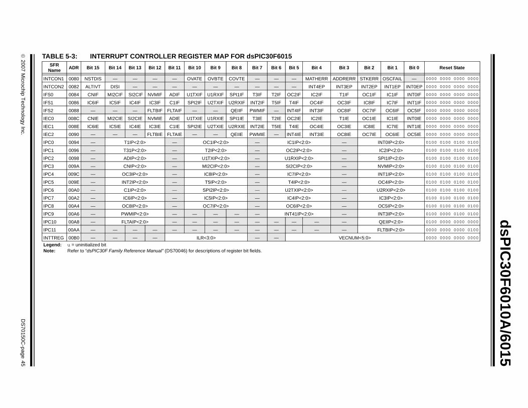
© 2007 M
icrochip Technology Inc.
DS
70150C-page 45
dsP
IC30F
6010A/6015
TA
Bit 1 Bit 0 Reset State
IN R OSCFAIL — 0000 0000 0000 0000
IN P INT1EP INT0EP 0000 0000 0000 0000
IFS F IC1IF INT0IF 0000 0000 0000 0000
IFS F IC7IF INT1IF 0000 0000 0000 0000
IFS F OC6IF OC5IF 0000 0000 0000 0000
IEC E IC1IE INT0IE 0000 0000 0000 0000
IEC IC7IE INT1IE 0000 0000 0000 0000
IEC E OC6IE OC5IE 0000 0000 0000 0000
IPC INT0IP<2:0> 0100 0100 0100 0100
IPC IC2IP<2:0> 0100 0100 0100 0100
IPC SPI1IP<2:0> 0100 0100 0100 0100
IPC NVMIP<2:0> 0100 0100 0100 0100
IPC INT1IP<2:0> 0100 0100 0100 0100
IPC OC4IP<2:0> 0100 0100 0100 0100
IPC U2RXIP<2:0> 0100 0100 0100 0100
IPC IC3IP<2:0> 0100 0100 0100 0100
IPC OC5IP<2:0> 0100 0100 0100 0100
IPC INT3IP<2:0> 0100 0000 0100 0100
IPC QEIIP<2:0> 0100 0000 0000 0000
IPC FLTBIP<2:0> 0000 0000 0000 0100
IN 0000 0000 0000 0000
LeNo
BLE 5-3: INTERRUPT CONTROLLER REGISTER MAP FOR dsPIC30F6015 SFR
Name ADR Bit 15 Bit 14 Bit 13 Bit 12 Bit 11 Bit 10 Bit 9 Bit 8 Bit 7 Bit 6 Bit 5 Bit 4 Bit 3 Bit 2
TCON1 0080 NSTDIS — — — — OVATE OVBTE COVTE — — — MATHERR ADDRERR STKER
TCON2 0082 ALTIVT DISI — — — — — — — — — INT4EP INT3EP INT2E
0 0084 CNIF MI2CIF SI2CIF NVMIF ADIF U1TXIF U1RXIF SPI1IF T3IF T2IF OC2IF IC2IF T1IF OC1I
1 0086 IC6IF IC5IF IC4IF IC3IF C1IF SPI2IF U2TXIF U2RXIF INT2IF T5IF T4IF OC4IF OC3IF IC8I
2 0088 — — — FLTBIF FLTAIF — — QEIIF PWMIF — INT4IF INT3IF OC8IF OC7I
0 008C CNIE MI2CIE SI2CIE NVMIE ADIE U1TXIE U1RXIE SPI1IE T3IE T2IE OC2IE IC2IE T1IE OC1I
1 008E IC6IE IC5IE IC4IE IC3IE C1IE SPI2IE U2TXIE U2RXIE INT2IE T5IE T4IE OC4IE OC3IE IC8IE
2 0090 — — — FLTBIE FLTAIE — — QEIIE PWMIE — INT4IE INT3IE OC8IE OC7I
0 0094 — T1IP<2:0> — OC1IP<2:0> — IC1IP<2:0> —
1 0096 — T31P<2:0> — T2IP<2:0> — OC2IP<2:0> —
2 0098 — ADIP<2:0> — U1TXIP<2:0> — U1RXIP<2:0> —
3 009A — CNIP<2:0> — MI2CIP<2:0> — SI2CIP<2:0> —
4 009C — OC3IP<2:0> — IC8IP<2:0> — IC7IP<2:0> —
5 009E — INT2IP<2:0> — T5IP<2:0> — T4IP<2:0> —
6 00A0 — C1IP<2:0> — SPI2IP<2:0> — U2TXIP<2:0> —
7 00A2 — IC6IP<2:0> — IC5IP<2:0> — IC4IP<2:0> —
8 00A4 — OC8IP<2:0> — OC7IP<2:0> — OC6IP<2:0> —
9 00A6 — PWMIP<2:0> — — — — — INT41IP<2:0> —
10 00A8 — FLTAIP<2:0> — — — — — — — — —
11 00AA — — — — — — — — — — — — —
TTREG 00B0 — — — — ILR<3:0> — — VECNUM<5:0>
gend: u = uninitialized bitte: Refer to “dsPIC30F Family Reference Manual” (DS70046) for descriptions of register bit fields.

dsPIC30F6010A/6015
NOTES:
DS70150C-page 46 © 2007 Microchip Technology Inc.
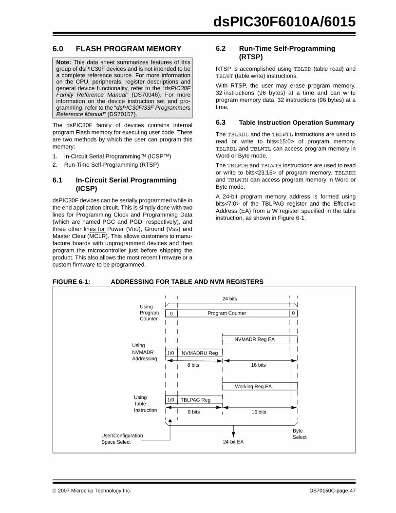
dsPIC30F6010A/6015
6.0 FLASH PROGRAM MEMORY
The dsPIC30F family of devices contains internalprogram Flash memory for executing user code. Thereare two methods by which the user can program thismemory:
1. In-Circuit Serial Programming™ (ICSP™)2. Run-Time Self-Programming (RTSP)
6.1 In-Circuit Serial Programming (ICSP)
dsPIC30F devices can be serially programmed while inthe end application circuit. This is simply done with twolines for Programming Clock and Programming Data(which are named PGC and PGD, respectively), andthree other lines for Power (VDD), Ground (VSS) andMaster Clear (MCLR). This allows customers to manu-facture boards with unprogrammed devices and thenprogram the microcontroller just before shipping theproduct. This also allows the most recent firmware or acustom firmware to be programmed.
6.2 Run-Time Self-Programming (RTSP)
RTSP is accomplished using TBLRD (table read) andTBLWT (table write) instructions.
With RTSP, the user may erase program memory,32 instructions (96 bytes) at a time and can writeprogram memory data, 32 instructions (96 bytes) at atime.
6.3 Table Instruction Operation Summary
The TBLRDL and the TBLWTL instructions are used toread or write to bits<15:0> of program memory.TBLRDL and TBLWTL can access program memory inWord or Byte mode.
The TBLRDH and TBLWTH instructions are used to reador write to bits<23:16> of program memory. TBLRDHand TBLWTH can access program memory in Word orByte mode.
A 24-bit program memory address is formed usingbits<7:0> of the TBLPAG register and the EffectiveAddress (EA) from a W register specified in the tableinstruction, as shown in Figure 6-1.
FIGURE 6-1: ADDRESSING FOR TABLE AND NVM REGISTERS
Note: This data sheet summarizes features of thisgroup of dsPIC30F devices and is not intended to bea complete reference source. For more informationon the CPU, peripherals, register descriptions andgeneral device functionality, refer to the “dsPIC30FFamily Reference Manual” (DS70046). For moreinformation on the device instruction set and pro-gramming, refer to the “dsPIC30F/33F ProgrammersReference Manual” (DS70157).
0Program Counter
24 bits
NVMADRU Reg
8 bits 16 bits
Program
Using
TBLPAG Reg
8 bits
Working Reg EA
16 bits
Using
Byte
24-bit EA
1/0
0
1/0
Select
TableInstruction
NVMADRAddressing
Counter
Using
NVMADR Reg EA
User/ConfigurationSpace Select
© 2007 Microchip Technology Inc. DS70150C-page 47
dsPIC30F6010A/6015
6.4 RTSP Operation
The dsPIC30F Flash program memory is organizedinto rows and panels. Each row consists of 32 instruc-tions, or 96 bytes. Each panel consists of 128 rows, or4K x 24 instructions. RTSP allows the user to erase onerow (32 instructions) at a time and to program32 instructions at one time.
Each panel of program memory contains write latchesthat hold 32 instructions of programming data. Prior tothe actual programming operation, the write data mustbe loaded into the panel write latches. The data to beprogrammed into the panel is loaded in sequentialorder into the write latches; instruction 0, instruction 1,etc. The addresses loaded must always be from a 32address boundary.
The basic sequence for RTSP programming is to set upa Table Pointer, then do a series of TBLWT instructionsto load the write latches. Programming is performed bysetting the special bits in the NVMCON register. 32TBLWTL and 32 TBLWTH instructions are required toload the 32 instructions.
All of the table write operations are single-word writes(2 instruction cycles), because only the table latchesare written.
After the latches are written, a programming operationneeds to be initiated to program the data.
The Flash program memory is readable, writable anderasable during normal operation over the entire VDD
range.
6.5 RTSP Control Registers
The four SFRs used to read and write the programFlash memory are:
• NVMCON• NVMADR
• NVMADRU• NVMKEY
6.5.1 NVMCON REGISTER
The NVMCON register controls which blocks are to beerased, which memory type is to be programmed andstart of the programming cycle.
6.5.2 NVMADR REGISTER
The NVMADR register is used to hold the lower twobytes of the Effective Address. The NVMADR registercaptures the EA<15:0> of the last table instruction thathas been executed and selects the row to write.
6.5.3 NVMADRU REGISTER
The NVMADRU register is used to hold the upper byteof the Effective Address. The NVMADRU register cap-tures the EA<23:16> of the last table instruction thathas been executed.
6.5.4 NVMKEY REGISTER
NVMKEY is a write-only register that is used for writeprotection. To start a programming or an erasesequence, the user must consecutively write 0x55 and0xAA to the NVMKEY register. Refer to Section 6.6“Programming Operations” for further details.
Note: The user can also directly write to theNVMADR and NVMADRU registers tospecify a program memory address forerasing or programming.
DS70150C-page 48 © 2007 Microchip Technology Inc.
dsPIC30F6010A/6015
6.6 Programming Operations
A complete programming sequence is necessary forprogramming or erasing the internal Flash in RTSPmode. A programming operation is nominally 2 msec induration and the processor stalls (waits) until the oper-ation is finished. Setting the WR bit (NVMCON<15>)starts the operation, and the WR bit is automaticallycleared when the operation is finished.
6.6.1 PROGRAMMING ALGORITHM FOR PROGRAM FLASH
The user can erase or program one row of programFlash memory at a time. The general process is:
1. Read one row of program Flash (32 instructionwords) and store into data RAM as a data“image”.
2. Update the data image with the desired newdata.
3. Erase program Flash row.a) Set up NVMCON register for multi-word,
program Flash, erase, and set WREN bit.b) Write address of row to be erased into
NVMADRU/NVMDR.c) Write ‘55’ to NVMKEY.d) Write ‘AA’ to NVMKEY.
e) Set the WR bit. This will begin erase cycle.f) CPU will stall for the duration of the erase
cycle.g) The WR bit is cleared when erase cycle
ends.
4. Write 32 instruction words of data from dataRAM “image” into the program Flash writelatches.
5. Program 32 instruction words into programFlash.
a) Set up NVMCON register for multi-word,program Flash, program, and set WRENbit.
b) Write ‘55’ to NVMKEY.
c) Write ‘AA’ to NVMKEY.d) Set the WR bit. This will begin program
cycle.e) CPU will stall for duration of the program
cycle.f) The WR bit is cleared by the hardware
when program cycle ends.6. Repeat steps 1 through 5 as needed to program
desired amount of program Flash memory.
6.6.2 ERASING A ROW OF PROGRAM MEMORY
Example 6-1 shows a code sequence that can be usedto erase a row (32 instructions) of program memory.
EXAMPLE 6-1: ERASING A ROW OF PROGRAM MEMORY
; Setup NVMCON for erase operation, multi word write; program memory selected, and writes enabled
MOV #0x4041,W0 ;MOV W0,NVMCON ; Init NVMCON SFR
; Init pointer to row to be ERASEDMOV #tblpage(PROG_ADDR),W0 ; MOV W0,NVMADRU ; Initialize PM Page Boundary SFRMOV #tbloffset(PROG_ADDR),W0 ; Intialize in-page EA[15:0] pointerMOV W0, NVMADR ; Intialize NVMADR SFRDISI #5 ; Block all interrupts with priority <7
; for next 5 instructionsMOV #0x55,W0 MOV W0,NVMKEY ; Write the 0x55 key MOV #0xAA,W1 ;MOV W1,NVMKEY ; Write the 0xAA keyBSET NVMCON,#WR ; Start the erase sequence NOP ; Insert two NOPs after the eraseNOP ; command is asserted
© 2007 Microchip Technology Inc. DS70150C-page 49
dsPIC30F6010A/6015
6.6.3 LOADING WRITE LATCHES
Example 6-2 shows a sequence of instructions thatcan be used to load the 96 bytes of write latches.32 TBLWTL and 32 TBLWTH instructions are needed toload the write latches selected by the Table Pointer.
EXAMPLE 6-2: LOADING WRITE LATCHES
6.6.4 INITIATING THE PROGRAMMING SEQUENCE
For protection, the write initiate sequence for NVMKEYmust be used to allow any erase or program operationto proceed. After the programming command has beenexecuted, the user must wait for the programming timeuntil programming is complete. The two instructionsfollowing the start of the programming sequenceshould be NOPs.
EXAMPLE 6-3: INITIATING A PROGRAMMING SEQUENCE
; Set up a pointer to the first program memory location to be written; program memory selected, and writes enabled
MOV #0x0000,W0 ; MOV W0,TBLPAG ; Initialize PM Page Boundary SFRMOV #0x6000,W0 ; An example program memory address
; Perform the TBLWT instructions to write the latches; 0th_program_word
MOV #LOW_WORD_0,W2 ; MOV #HIGH_BYTE_0,W3 ; TBLWTL W2,[W0] ; Write PM low word into program latchTBLWTH W3,[W0++] ; Write PM high byte into program latch
; 1st_program_wordMOV #LOW_WORD_1,W2 ; MOV #HIGH_BYTE_1,W3 ; TBLWTL W2,[W0] ; Write PM low word into program latchTBLWTH W3,[W0++] ; Write PM high byte into program latch
; 2nd_program_wordMOV #LOW_WORD_2,W2 ; MOV #HIGH_BYTE_2,W3 ; TBLWTL W2, [W0] ; Write PM low word into program latchTBLWTH W3, [W0++] ; Write PM high byte into program latch•••
; 31st_program_wordMOV #LOW_WORD_31,W2 ; MOV #HIGH_BYTE_31,W3 ; TBLWTL W2, [W0] ; Write PM low word into program latchTBLWTH W3, [W0++] ; Write PM high byte into program latch
Note: In Example 6-2, the contents of the upper byte of W3 has no effect.
DISI #5 ; Block all interrupts with priority <7; for next 5 instructions
MOV #0x55,W0MOV W0,NVMKEY ; Write the 0x55 key MOV #0xAA,W1 ;MOV W1,NVMKEY ; Write the 0xAA keyBSET NVMCON,#WR ; Start the erase sequence NOP ; Insert two NOPs after the eraseNOP ; command is asserted
DS70150C-page 50 © 2007 Microchip Technology Inc.

© 2007 M
icrochip Technology Inc.
DS
70150C-page 51
dsP
IC30F
6010A/6015
TAF 1 Bit 0 All Resets
NV 0000 0000 0000 0000
NV uuuu uuuu uuuu uuuu
NV 0000 0000 uuuu uuuu
NV 0000 0000 0000 0000
Le
No
BLE 6-1: NVM REGISTER MAPile Name Addr. Bit 15 Bit 14 Bit 13 Bit 12 Bit 11 Bit 10 Bit 9 Bit 8 Bit 7 Bit 6 Bit 5 Bit 4 Bit 3 Bit 2 Bit
MCON 0760 WR WREN WRERR — — — — TWRI — PROGOP<6:0>
MADR 0762 NVMADR<15:0>
MADRU 0764 — — — — — — — — NVMADR<23:16>
MKEY 0766 — — — — — — — — KEY<7:0>
gend: u = uninitialized bit
te: Refer to “dsPIC30F Family Reference Manual” (DS70046) for descriptions of register bit fields.

dsPIC30F6010A/6015
NOTES:
DS70150C-page 52 © 2007 Microchip Technology Inc.
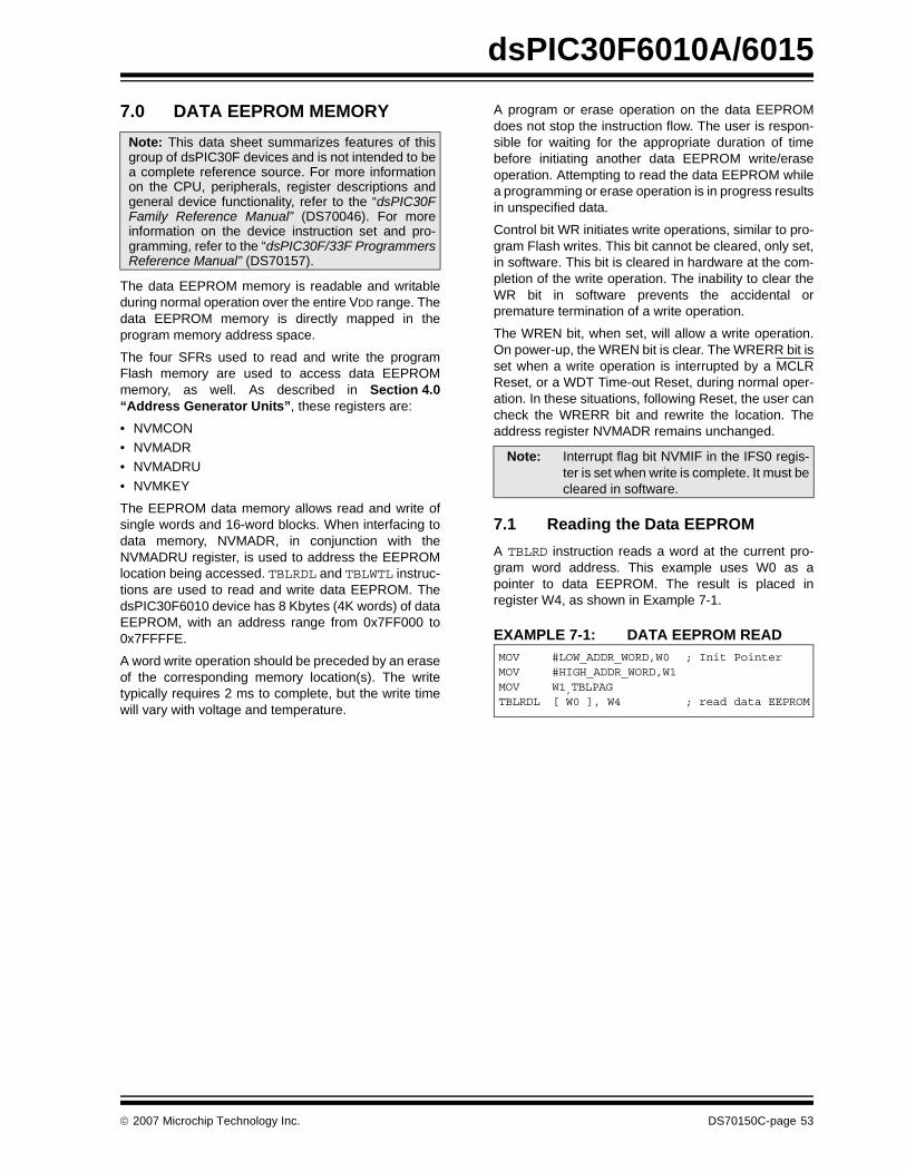
dsPIC30F6010A/6015
7.0 DATA EEPROM MEMORY
The data EEPROM memory is readable and writableduring normal operation over the entire VDD range. Thedata EEPROM memory is directly mapped in theprogram memory address space.
The four SFRs used to read and write the programFlash memory are used to access data EEPROMmemory, as well. As described in Section 4.0“Address Generator Units”, these registers are:
• NVMCON• NVMADR• NVMADRU
• NVMKEY
The EEPROM data memory allows read and write ofsingle words and 16-word blocks. When interfacing todata memory, NVMADR, in conjunction with theNVMADRU register, is used to address the EEPROMlocation being accessed. TBLRDL and TBLWTL instruc-tions are used to read and write data EEPROM. ThedsPIC30F6010 device has 8 Kbytes (4K words) of dataEEPROM, with an address range from 0x7FF000 to0x7FFFFE.
A word write operation should be preceded by an eraseof the corresponding memory location(s). The writetypically requires 2 ms to complete, but the write timewill vary with voltage and temperature.
A program or erase operation on the data EEPROMdoes not stop the instruction flow. The user is respon-sible for waiting for the appropriate duration of timebefore initiating another data EEPROM write/eraseoperation. Attempting to read the data EEPROM whilea programming or erase operation is in progress resultsin unspecified data.
Control bit WR initiates write operations, similar to pro-gram Flash writes. This bit cannot be cleared, only set,in software. This bit is cleared in hardware at the com-pletion of the write operation. The inability to clear theWR bit in software prevents the accidental orpremature termination of a write operation.
The WREN bit, when set, will allow a write operation.On power-up, the WREN bit is clear. The WRERR bit isset when a write operation is interrupted by a MCLRReset, or a WDT Time-out Reset, during normal oper-ation. In these situations, following Reset, the user cancheck the WRERR bit and rewrite the location. Theaddress register NVMADR remains unchanged.
7.1 Reading the Data EEPROM
A TBLRD instruction reads a word at the current pro-gram word address. This example uses W0 as apointer to data EEPROM. The result is placed inregister W4, as shown in Example 7-1.
EXAMPLE 7-1: DATA EEPROM READ
Note: This data sheet summarizes features of thisgroup of dsPIC30F devices and is not intended to bea complete reference source. For more informationon the CPU, peripherals, register descriptions andgeneral device functionality, refer to the “dsPIC30FFamily Reference Manual” (DS70046). For moreinformation on the device instruction set and pro-gramming, refer to the “dsPIC30F/33F ProgrammersReference Manual” (DS70157).
Note: Interrupt flag bit NVMIF in the IFS0 regis-ter is set when write is complete. It must becleared in software.
MOV #LOW_ADDR_WORD,W0 ; Init PointerMOV #HIGH_ADDR_WORD,W1MOV W1,TBLPAG TBLRDL [ W0 ], W4 ; read data EEPROM
© 2007 Microchip Technology Inc. DS70150C-page 53
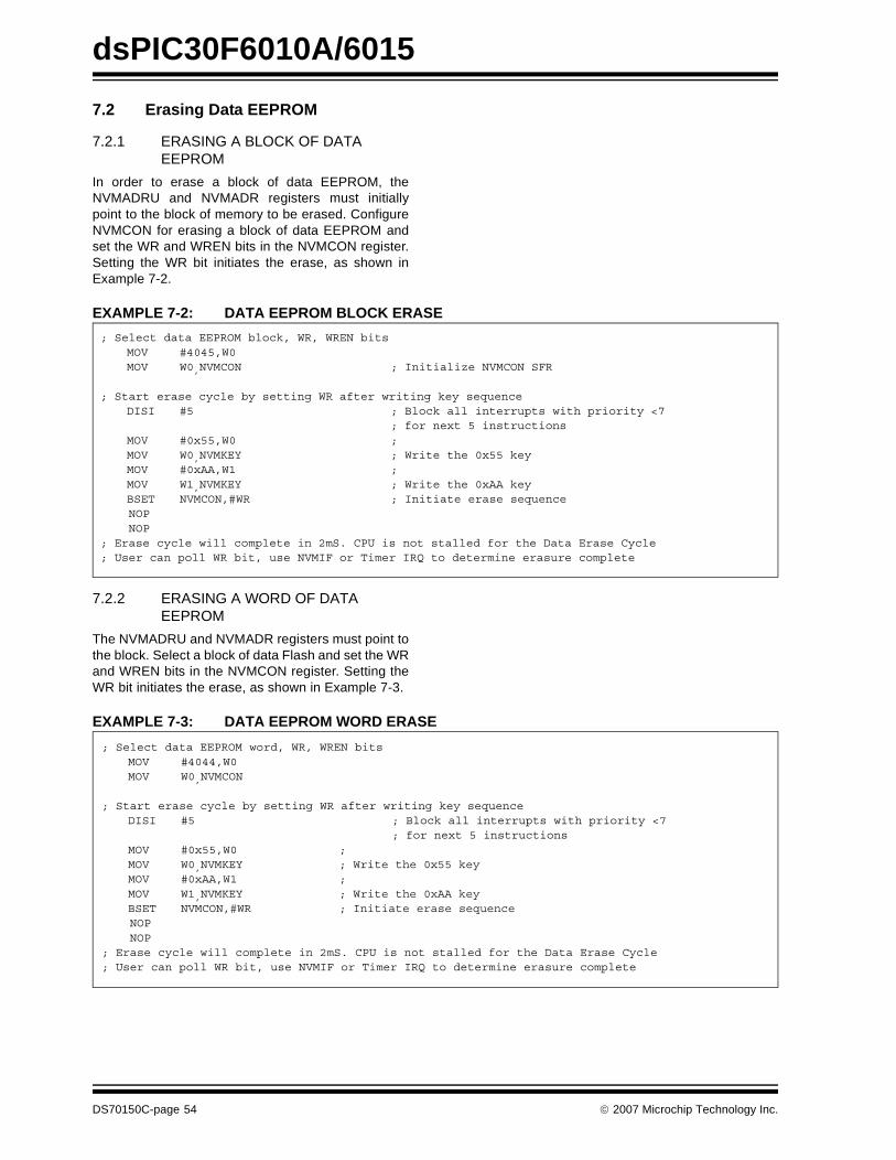
dsPIC30F6010A/6015
7.2 Erasing Data EEPROM
7.2.1 ERASING A BLOCK OF DATA EEPROM
In order to erase a block of data EEPROM, theNVMADRU and NVMADR registers must initiallypoint to the block of memory to be erased. ConfigureNVMCON for erasing a block of data EEPROM andset the WR and WREN bits in the NVMCON register.Setting the WR bit initiates the erase, as shown inExample 7-2.
EXAMPLE 7-2: DATA EEPROM BLOCK ERASE
7.2.2 ERASING A WORD OF DATA EEPROM
The NVMADRU and NVMADR registers must point tothe block. Select a block of data Flash and set the WRand WREN bits in the NVMCON register. Setting theWR bit initiates the erase, as shown in Example 7-3.
EXAMPLE 7-3: DATA EEPROM WORD ERASE
; Select data EEPROM block, WR, WREN bitsMOV #4045,W0MOV W0,NVMCON ; Initialize NVMCON SFR
; Start erase cycle by setting WR after writing key sequence
DISI #5 ; Block all interrupts with priority <7; for next 5 instructions
MOV #0x55,W0 ; MOV W0,NVMKEY ; Write the 0x55 key
MOV #0xAA,W1 ;MOV W1,NVMKEY ; Write the 0xAA keyBSET NVMCON,#WR ; Initiate erase sequence
NOP NOP; Erase cycle will complete in 2mS. CPU is not stalled for the Data Erase Cycle; User can poll WR bit, use NVMIF or Timer IRQ to determine erasure complete
; Select data EEPROM word, WR, WREN bitsMOV #4044,W0MOV W0,NVMCON
; Start erase cycle by setting WR after writing key sequence
DISI #5 ; Block all interrupts with priority <7; for next 5 instructions
MOV #0x55,W0 ; MOV W0,NVMKEY ; Write the 0x55 keyMOV #0xAA,W1 ;MOV W1,NVMKEY ; Write the 0xAA keyBSET NVMCON,#WR ; Initiate erase sequence
NOP NOP ; Erase cycle will complete in 2mS. CPU is not stalled for the Data Erase Cycle; User can poll WR bit, use NVMIF or Timer IRQ to determine erasure complete
DS70150C-page 54 © 2007 Microchip Technology Inc.

dsPIC30F6010A/6015
7.3 Writing to the Data EEPROM
To write an EEPROM data location, the followingsequence must be followed:
1. Erase data EEPROM word.a) Select word, data EEPROM, erase and set
WREN bit in NVMCON register.b) Write address of word to be erased into
NVMADRU/NVMADR.c) Enable NVM interrupt (optional).
d) Write ‘55’ to NVMKEY.e) Write ‘AA’ to NVMKEY.f) Set the WR bit. This will begin erase cycle.
g) Either poll NVMIF bit or wait for NVMIFinterrupt.
h) The WR bit is cleared when the erase cycleends.
2. Write data word into data EEPROM writelatches.
3. Program 1 data word into data EEPROM.a) Select word, data EEPROM, program and
set WREN bit in NVMCON register.b) Enable NVM write done interrupt (optional).c) Write ‘55’ to NVMKEY.
d) Write ‘AA’ to NVMKEY.e) Set the WR bit. This will begin program
cycle.f) Either poll NVMIF bit or wait for NVM
interrupt.g) The WR bit is cleared when the write cycle
ends.
The write will not initiate if the above sequence is notexactly followed (write 0x55 to NVMKEY, write 0xAA toNVMCON, then set WR bit) for each word. It is stronglyrecommended that interrupts be disabled during thiscode segment.
Additionally, the WREN bit in NVMCON must be set toenable writes. This mechanism prevents accidentalwrites to data EEPROM, due to unexpected code exe-cution. The WREN bit should be kept clear at all times,except when updating the EEPROM. The WREN bit isnot cleared by hardware.
After a write sequence has been initiated, clearing theWREN bit will not affect the current write cycle. The WRbit will be inhibited from being set unless the WREN bitis set. The WREN bit must be set on a previous instruc-tion. Both WR and WREN cannot be set with the sameinstruction.
At the completion of the write cycle, the WR bit iscleared in hardware and the Nonvolatile Memory WriteComplete Interrupt Flag bit (NVMIF) is set. The usermay either enable this interrupt, or poll this bit. NVMIFmust be cleared by software.
7.3.1 WRITING A WORD OF DATA EEPROM
Once the user has erased the word to be programmed,then a table write instruction is used to write one writelatch, as shown in Example 7-4.
EXAMPLE 7-4: DATA EEPROM WORD WRITE
; Point to data memoryMOV #LOW_ADDR_WORD,W0 ; Init pointerMOV #HIGH_ADDR_WORD,W1MOV W1,TBLPAGMOV #LOW(WORD),W2 ; Get dataTBLWTL W2,[ W0] ; Write data
; The NVMADR captures last table access address; Select data EEPROM for 1 word op
MOV #0x4004,W0MOV W0,NVMCON
; Operate key to allow write operation
DISI #5 ; Block all interrupts with priority <7; for next 5 instructions
MOV #0x55,W0MOV W0,NVMKEY ; Write the 0x55 keyMOV #0xAA,W1MOV W1,NVMKEY ; Write the 0xAA keyBSET NVMCON,#WR ; Initiate program sequence
NOP NOP ; Write cycle will complete in 2mS. CPU is not stalled for the Data Write Cycle; User can poll WR bit, use NVMIF or Timer IRQ to determine write complete
© 2007 Microchip Technology Inc. DS70150C-page 55
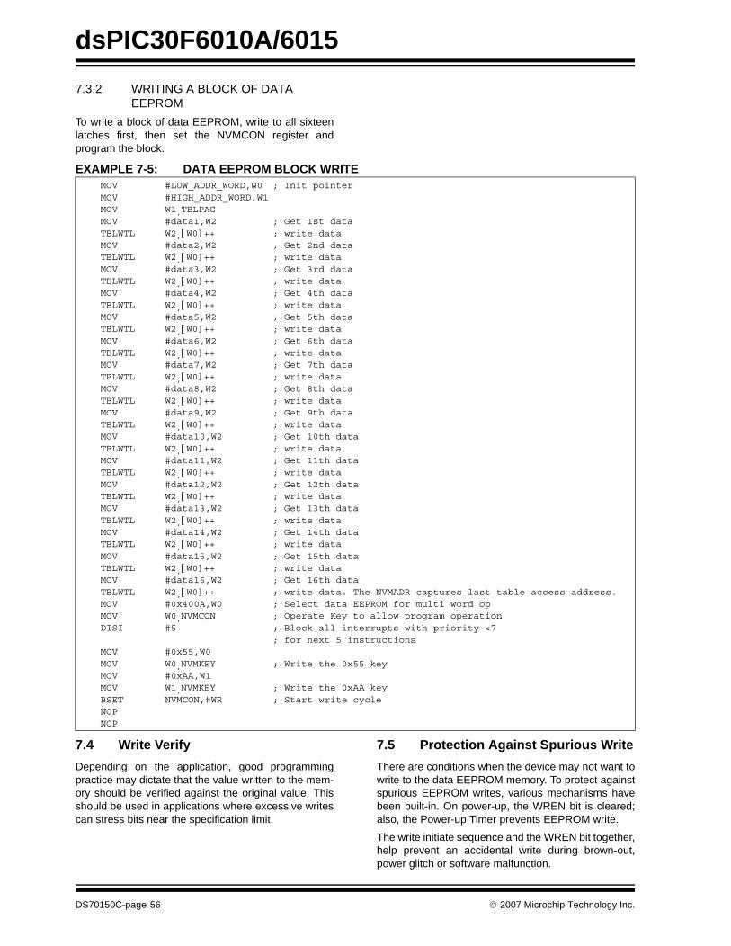
dsPIC30F6010A/6015
7.3.2 WRITING A BLOCK OF DATA EEPROM
To write a block of data EEPROM, write to all sixteenlatches first, then set the NVMCON register andprogram the block.
EXAMPLE 7-5: DATA EEPROM BLOCK WRITE
7.4 Write Verify
Depending on the application, good programmingpractice may dictate that the value written to the mem-ory should be verified against the original value. Thisshould be used in applications where excessive writescan stress bits near the specification limit.
7.5 Protection Against Spurious Write
There are conditions when the device may not want towrite to the data EEPROM memory. To protect againstspurious EEPROM writes, various mechanisms havebeen built-in. On power-up, the WREN bit is cleared;also, the Power-up Timer prevents EEPROM write.
The write initiate sequence and the WREN bit together,help prevent an accidental write during brown-out,power glitch or software malfunction.
MOV #LOW_ADDR_WORD,W0 ; Init pointer MOV #HIGH_ADDR_WORD,W1 MOV W1,TBLPAG MOV #data1,W2 ; Get 1st data TBLWTL W2,[ W0]++ ; write data MOV #data2,W2 ; Get 2nd data TBLWTL W2,[ W0]++ ; write data MOV #data3,W2 ; Get 3rd data TBLWTL W2,[ W0]++ ; write data MOV #data4,W2 ; Get 4th data TBLWTL W2,[ W0]++ ; write data MOV #data5,W2 ; Get 5th data TBLWTL W2,[ W0]++ ; write data MOV #data6,W2 ; Get 6th data TBLWTL W2,[ W0]++ ; write data MOV #data7,W2 ; Get 7th data TBLWTL W2,[ W0]++ ; write data MOV #data8,W2 ; Get 8th data TBLWTL W2,[ W0]++ ; write data MOV #data9,W2 ; Get 9th data TBLWTL W2,[ W0]++ ; write data MOV #data10,W2 ; Get 10th data TBLWTL W2,[ W0]++ ; write data MOV #data11,W2 ; Get 11th data TBLWTL W2,[ W0]++ ; write data MOV #data12,W2 ; Get 12th data TBLWTL W2,[ W0]++ ; write data MOV #data13,W2 ; Get 13th data TBLWTL W2,[ W0]++ ; write data MOV #data14,W2 ; Get 14th data TBLWTL W2,[ W0]++ ; write data MOV #data15,W2 ; Get 15th data TBLWTL W2,[ W0]++ ; write data MOV #data16,W2 ; Get 16th data TBLWTL W2,[ W0]++ ; write data. The NVMADR captures last table access address. MOV #0x400A,W0 ; Select data EEPROM for multi word op
MOV W0,NVMCON ; Operate Key to allow program operationDISI #5 ; Block all interrupts with priority <7
; for next 5 instructions MOV #0x55,W0 MOV W0,NVMKEY ; Write the 0x55 key MOV #0xAA,W1 MOV W1,NVMKEY ; Write the 0xAA key BSET NVMCON,#WR ; Start write cycle NOP NOP
DS70150C-page 56 © 2007 Microchip Technology Inc.

dsPIC30F6010A/6015
8.0 I/O PORTS
All of the device pins (except VDD, VSS, MCLR andOSC1/CLKI) are shared between the peripherals andthe parallel I/O ports.
All I/O input ports feature Schmitt Trigger inputs forimproved noise immunity.
8.1 Parallel I/O (PIO) Ports
When a peripheral is enabled and the peripheral isactively driving an associated pin, the use of the pin asa general purpose output pin is disabled. The I/O pinmay be read, but the output driver for the parallel portbit will be disabled. If a peripheral is enabled, but theperipheral is not actively driving a pin, that pin may bedriven by a port.
All port pins have three registers directly associatedwith the operation of the port pin. The data directionregister (TRISx) determines whether the pin is an inputor an output. If the data direction bit is a ‘1’, then the pinis an input. All port pins are defined as inputs after aReset. Reads from the latch (LATx), read the latch.Writes to the latch, write the latch (LATx). Reads fromthe port (PORTx), read the port pins and writes to theport pins, write the latch (LATx).
Any bit and its associated data and control registersthat are not valid for a particular device will bedisabled. That means the corresponding LATx andTRISx registers and the port pin will read as zeros.
When a pin is shared with another peripheral or func-tion that is defined as an input only, it is neverthelessregarded as a dedicated port because there is noother competing source of outputs. An example is theINT4 pin. Figure 8-1 shows the structure for adedicated port.
The format of the registers for PORTA are shown inTable 8-1.
The TRISA (Data Direction Control) register controlsthe direction of the RA<7:0> pins, as well as the INTxpins and the VREF pins. The LATA register suppliesdata to the outputs and is readable/writable. Readingthe PORTA register yields the state of the input pins,while writing the PORTA register modifies the contentsof the LATA register.
A parallel I/O (PIO) port that shares a pin with a periph-eral is, in general, subservient to the peripheral. Theperipheral’s output buffer data and control signals areprovided to a pair of multiplexers. The multiplexersselect whether the peripheral or the associated porthas ownership of the output data and control signals ofthe I/O pad cell. Figure 8-2 shows how ports are sharedwith other peripherals, and the associated I/O cell (pad)to which they are connected. Table 8-1 shows theformats of the registers for the shared ports, PORTBthrough PORTG.
FIGURE 8-1: BLOCK DIAGRAM OF A DEDICATED PORT STRUCTURE
Note: This data sheet summarizes features of thisgroup of dsPIC30F devices and is not intended to bea complete reference source. For more informationon the CPU, peripherals, register descriptions andgeneral device functionality, refer to the dsPIC30FFamily Reference Manual (DS70046).
QD
CK
WR LAT+
TRIS Latch
I/O Pad
WR Port
Data Bus
QD
CK
Data Latch
Read LAT
Read Port
Read TRIS
WR TRIS
I/O Cell
Dedicated Port Module
© 2007 Microchip Technology Inc. DS70150C-page 57

dsPIC30F6010A/6015
FIGURE 8-2: BLOCK DIAGRAM OF A SHARED PORT STRUCTURE
8.2 Configuring Analog Port Pins
The use of the ADPCFG and TRIS registers control theoperation of the A/D port pins. The port pins that aredesired as analog inputs must have their correspond-ing TRIS bit set (input). If the TRIS bit is cleared(output), the digital output level (VOH or VOL) will beconverted.
When reading the PORT register, all pins configured asanalog input channels will read as cleared (a low level).
Pins configured as digital inputs will not convert an ana-log input. Analog levels on any pin that is defined as adigital input (including the ANx pins) may cause theinput buffer to consume current that exceeds thedevice specifications.
8.2.1 I/O PORT WRITE/READ TIMING
One instruction cycle is required between a portdirection change or port write operation and a readoperation of the same port. Typically this instructionwould be a NOP.
EXAMPLE 8-1: PORT WRITE/READ EXAMPLE
QD
CK
WR LAT +
TRIS Latch
I/O Pad
WR Port
Data Bus
QD
CK
Data Latch
Read LAT
Read Port
Read TRIS
1
0
1
0
WR TRIS
Peripheral Output Data
Peripheral Input Data
I/O Cell
Peripheral Module
Peripheral Output Enable
PIO Module
Output Multiplexers
Input Data
Peripheral Module Enable
Output Enable
Output Data
MOV 0xFF00, W0 ; Configure PORTB<15:8>; as inputs
MOV W0, TRISBB ; and PORTB<7:0> as outputsNOP ; Delay 1 cycleBTSS PORTB, #13 ; Next Instruction
DS70150C-page 58 © 2007 Microchip Technology Inc.
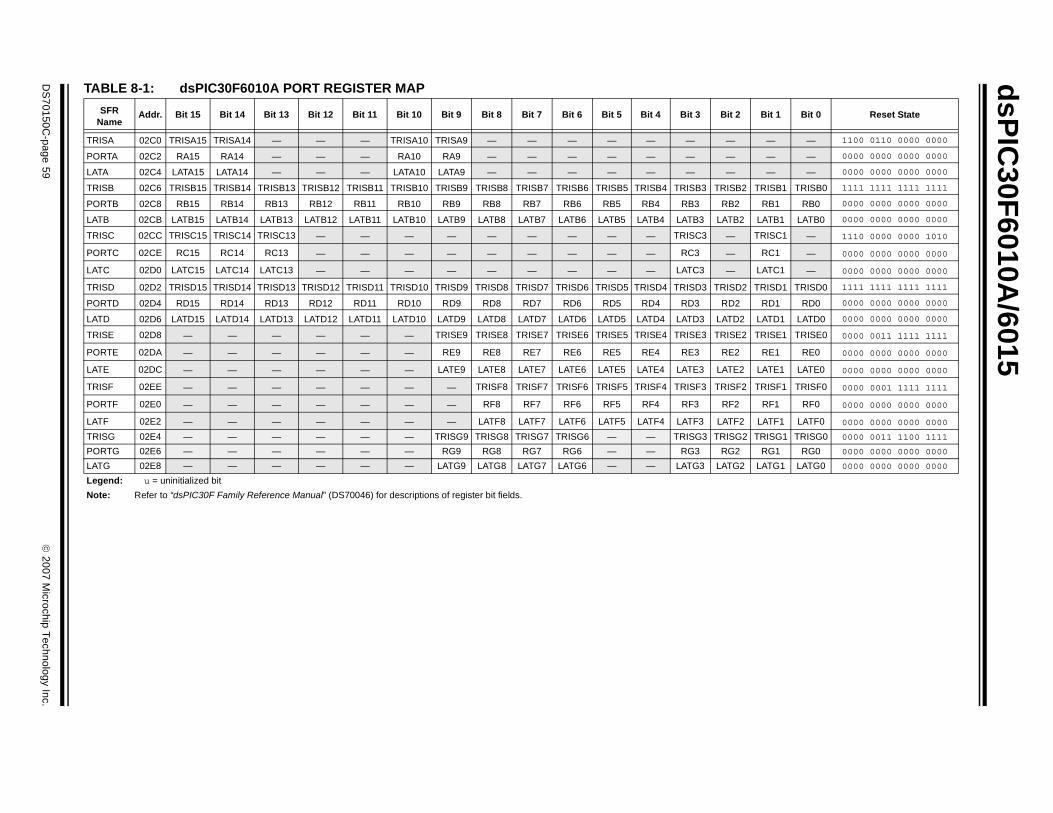
dsP
IC30F
6010A/6015
DS
70150C-page 59
© 2007 M
icrochip Technology Inc.
Bit 2 Bit 1 Bit 0 Reset State
— — — 1100 0110 0000 0000
— — — 0000 0000 0000 0000
— — — 0000 0000 0000 0000
RISB2 TRISB1 TRISB0 1111 1111 1111 1111
RB2 RB1 RB0 0000 0000 0000 0000
ATB2 LATB1 LATB0 0000 0000 0000 0000
— TRISC1 — 1110 0000 0000 1010
— RC1 — 0000 0000 0000 0000
— LATC1 — 0000 0000 0000 0000
RISD2 TRISD1 TRISD0 1111 1111 1111 1111
RD2 RD1 RD0 0000 0000 0000 0000
ATD2 LATD1 LATD0 0000 0000 0000 0000
RISE2 TRISE1 TRISE0 0000 0011 1111 1111
RE2 RE1 RE0 0000 0000 0000 0000
ATE2 LATE1 LATE0 0000 0000 0000 0000
RISF2 TRISF1 TRISF0 0000 0001 1111 1111
RF2 RF1 RF0 0000 0000 0000 0000
ATF2 LATF1 LATF0 0000 0000 0000 0000
RISG2 TRISG1 TRISG0 0000 0011 1100 1111
RG2 RG1 RG0 0000 0000 0000 0000
ATG2 LATG1 LATG0 0000 0000 0000 0000
TABLE 8-1: dsPIC30F6010A PORT REGISTER MAP
SFR Name
Addr. Bit 15 Bit 14 Bit 13 Bit 12 Bit 11 Bit 10 Bit 9 Bit 8 Bit 7 Bit 6 Bit 5 Bit 4 Bit 3
TRISA 02C0 TRISA15 TRISA14 — — — TRISA10 TRISA9 — — — — — —
PORTA 02C2 RA15 RA14 — — — RA10 RA9 — — — — — —
LATA 02C4 LATA15 LATA14 — — — LATA10 LATA9 — — — — — —
TRISB 02C6 TRISB15 TRISB14 TRISB13 TRISB12 TRISB11 TRISB10 TRISB9 TRISB8 TRISB7 TRISB6 TRISB5 TRISB4 TRISB3 T
PORTB 02C8 RB15 RB14 RB13 RB12 RB11 RB10 RB9 RB8 RB7 RB6 RB5 RB4 RB3
LATB 02CB LATB15 LATB14 LATB13 LATB12 LATB11 LATB10 LATB9 LATB8 LATB7 LATB6 LATB5 LATB4 LATB3 L
TRISC 02CC TRISC15 TRISC14 TRISC13 — — — — — — — — — TRISC3
PORTC 02CE RC15 RC14 RC13 — — — — — — — — — RC3
LATC 02D0 LATC15 LATC14 LATC13 — — — — — — — — — LATC3
TRISD 02D2 TRISD15 TRISD14 TRISD13 TRISD12 TRISD11 TRISD10 TRISD9 TRISD8 TRISD7 TRISD6 TRISD5 TRISD4 TRISD3 T
PORTD 02D4 RD15 RD14 RD13 RD12 RD11 RD10 RD9 RD8 RD7 RD6 RD5 RD4 RD3
LATD 02D6 LATD15 LATD14 LATD13 LATD12 LATD11 LATD10 LATD9 LATD8 LATD7 LATD6 LATD5 LATD4 LATD3 L
TRISE 02D8 — — — — — — TRISE9 TRISE8 TRISE7 TRISE6 TRISE5 TRISE4 TRISE3 T
PORTE 02DA — — — — — — RE9 RE8 RE7 RE6 RE5 RE4 RE3
LATE 02DC — — — — — — LATE9 LATE8 LATE7 LATE6 LATE5 LATE4 LATE3 L
TRISF 02EE — — — — — — — TRISF8 TRISF7 TRISF6 TRISF5 TRISF4 TRISF3 T
PORTF 02E0 — — — — — — — RF8 RF7 RF6 RF5 RF4 RF3
LATF 02E2 — — — — — — — LATF8 LATF7 LATF6 LATF5 LATF4 LATF3 L
TRISG 02E4 — — — — — — TRISG9 TRISG8 TRISG7 TRISG6 — — TRISG3 T
PORTG 02E6 — — — — — — RG9 RG8 RG7 RG6 — — RG3
LATG 02E8 — — — — — — LATG9 LATG8 LATG7 LATG6 — — LATG3 L
Legend: u = uninitialized bit
Note: Refer to “dsPIC30F Family Reference Manual” (DS70046) for descriptions of register bit fields.

© 2007 M
icrochip Technology Inc.
DS
70150C-page 60
dsP
IC30F
6010A/6015
TA
Bit 1 Bit 0 Reset State
TR — — 0000 0000 0000 0000
PO — — 0000 0000 0000 0000
LA — — 0000 0000 0000 0000
TR TRISB1 TRISB0 1111 1111 1111 1111
PO RB1 RB0 0000 0000 0000 0000
LA LATB1 LATB0 0000 0000 0000 0000
TR — — 1110 0000 0000 0000
PO — — 0000 0000 0000 0000
LA — — 0000 0000 0000 0000
TR TRISD1 TRISD0 0000 1111 1111 1111
PO RD1 RD0 0000 0000 0000 0000
LA LATD1 LATD0 0000 0000 0000 0000
TR TRISE1 TRISE0 0000 0000 1111 1111
PO RE1 RE0 0000 0000 0000 0000
LA LATE1 LATE0 0000 0000 0000 0000
TR TRISF1 TRISF0 0000 0000 0111 1111
PO RF1 RF0 0000 0000 0000 0000
LA LATF1 LATF0 0000 0000 0000 0000
TR 2 — — 0000 0011 1100 1100
PO — — 0000 0000 0000 0000
LA — — 0000 0000 0000 0000
Le
No
BLE 8-2: dsPIC30F6015 PORT REGISTER MAP
SFR Name
Addr. Bit 15 Bit 14 Bit 13 Bit 12 Bit 11 Bit 10 Bit 9 Bit 8 Bit 7 Bit 6 Bit 5 Bit 4 Bit 3 Bit 2
ISA 02C0 — — — — — — — — — — — — — —
RTA 02C2 — — — — — — — — — — — — — —
TA 02C4 — — — — — — — — — — — — — —
ISB 02C6 TRISB15 TRISB14 TRISB13 TRISB12 TRISB11 TRISB10 TRISB9 TRISB8 TRISB7 TRISB6 TRISB5 TRISB4 TRISB3 TRISB2
RTB 02C8 RB15 RB14 RB13 RB12 RB11 RB10 RB9 RB8 RB7 RB6 RB5 RB4 RB3 RB2
TB 02CB LATB15 LATB14 LATB13 LATB12 LATB11 LATB10 LATB9 LATB8 LATB7 LATB6 LATB5 LATB4 LATB3 LATB2
ISC 02CC TRISC15 TRISC14 TRISC13 — — — — — — — — — — —
RTC 02CE RC15 RC14 RC13 — — — — — — — — — — —
TC 02D0 LATC15 LATC14 LATC13 — — — — — — — — — — —
ISD 02D2 — — — — TRISD11 TRISD10 TRISD9 TRISD8 TRISD7 TRISD6 TRISD5 TRISD4 TRISD3 TRISD2
RTD 02D4 — — — — RD11 RD10 RD9 RD8 RD7 RD6 RD5 RD4 RD3 RD2
TD 02D6 — — — — LATD11 LATD10 LATD9 LATD8 LATD7 LATD6 LATD5 LATD4 LATD3 LATD2
ISE 02D8 — — — — — — — — TRISE7 TRISE6 TRISE5 TRISE4 TRISE3 TRISE2
RTE 02DA — — — — — — — — RE7 RE6 RE5 RE4 RE3 RE2
TE 02DC — — — — — — — — LATE7 LATE6 LATE5 LATE4 LATE3 LATE2
ISF 02EE — — — — — — — — — TRISF6 TRISF5 TRISF4 TRISF3 TRISF2
RTF 02E0 — — — — — — — — — RF6 RF5 RF4 RF3 RF2
TF 02E2 — — — — — — — — — LATF6 LATF5 LATF4 LATF3 LATF2
ISG 02E4 — — — — — — TRISG9 TRISG8 TRISG7 TRISG6 — — TRISG3 TRISG
RTG 02E6 — — — — — — RG9 RG8 RG7 RG6 — — RG3 RG2
TG 02E8 — — — — — — LATG9 LATG8 LATG7 LATG6 — — LATG3 LATG2
gend: u = uninitialized bit
te: Refer to “dsPIC30F Family Reference Manual” (DS70046) for descriptions of register bit fields.
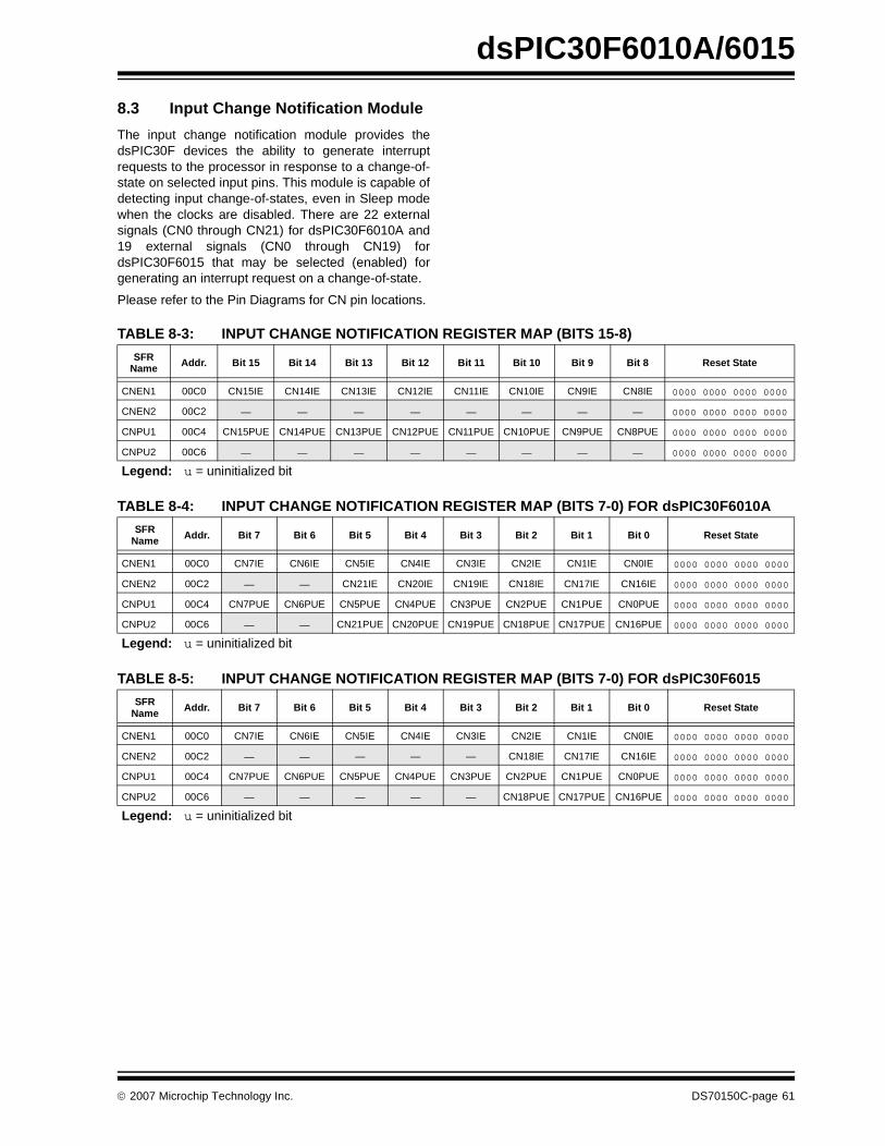
dsPIC30F6010A/6015
8.3 Input Change Notification Module
The input change notification module provides thedsPIC30F devices the ability to generate interruptrequests to the processor in response to a change-of-state on selected input pins. This module is capable ofdetecting input change-of-states, even in Sleep modewhen the clocks are disabled. There are 22 externalsignals (CN0 through CN21) for dsPIC30F6010A and19 external signals (CN0 through CN19) fordsPIC30F6015 that may be selected (enabled) forgenerating an interrupt request on a change-of-state.
Please refer to the Pin Diagrams for CN pin locations.
TABLE 8-3: INPUT CHANGE NOTIFICATION REGISTER MAP (BITS 15-8)
TABLE 8-4: INPUT CHANGE NOTIFICATION REGISTER MAP (BITS 7-0) FOR dsPIC30F6010A
TABLE 8-5: INPUT CHANGE NOTIFICATION REGISTER MAP (BITS 7-0) FOR dsPIC30F6015
SFR Name Addr. Bit 15 Bit 14 Bit 13 Bit 12 Bit 11 Bit 10 Bit 9 Bit 8 Reset State
CNEN1 00C0 CN15IE CN14IE CN13IE CN12IE CN11IE CN10IE CN9IE CN8IE 0000 0000 0000 0000
CNEN2 00C2 — — — — — — — — 0000 0000 0000 0000
CNPU1 00C4 CN15PUE CN14PUE CN13PUE CN12PUE CN11PUE CN10PUE CN9PUE CN8PUE 0000 0000 0000 0000
CNPU2 00C6 — — — — — — — — 0000 0000 0000 0000
Legend: u = uninitialized bit
SFR Name Addr. Bit 7 Bit 6 Bit 5 Bit 4 Bit 3 Bit 2 Bit 1 Bit 0 Reset State
CNEN1 00C0 CN7IE CN6IE CN5IE CN4IE CN3IE CN2IE CN1IE CN0IE 0000 0000 0000 0000
CNEN2 00C2 — — CN21IE CN20IE CN19IE CN18IE CN17IE CN16IE 0000 0000 0000 0000
CNPU1 00C4 CN7PUE CN6PUE CN5PUE CN4PUE CN3PUE CN2PUE CN1PUE CN0PUE 0000 0000 0000 0000
CNPU2 00C6 — — CN21PUE CN20PUE CN19PUE CN18PUE CN17PUE CN16PUE 0000 0000 0000 0000
Legend: u = uninitialized bit
SFR Name Addr. Bit 7 Bit 6 Bit 5 Bit 4 Bit 3 Bit 2 Bit 1 Bit 0 Reset State
CNEN1 00C0 CN7IE CN6IE CN5IE CN4IE CN3IE CN2IE CN1IE CN0IE 0000 0000 0000 0000
CNEN2 00C2 — — — — — CN18IE CN17IE CN16IE 0000 0000 0000 0000
CNPU1 00C4 CN7PUE CN6PUE CN5PUE CN4PUE CN3PUE CN2PUE CN1PUE CN0PUE 0000 0000 0000 0000
CNPU2 00C6 — — — — — CN18PUE CN17PUE CN16PUE 0000 0000 0000 0000
Legend: u = uninitialized bit
© 2007 Microchip Technology Inc. DS70150C-page 61
dsPIC30F6010A/6015
NOTES:
DS70150C-page 62 © 2007 Microchip Technology Inc.
dsPIC30F6010A/6015
9.0 TIMER1 MODULE
This section describes the 16-bit General Purpose(GP) Timer1 module and associated operationalmodes.
The following sections provide a detailed description,including setup and control registers along with associ-ated block diagrams for the operational modes of thetimers.
The Timer1 module is a 16-bit timer which can serve asthe time counter for the Real-Time Clock, or operate asa free running interval timer/counter. The 16-bit timerhas the following modes:
• 16-bit Timer• 16-bit Synchronous Counter• 16-bit Asynchronous Counter
Further, the following operational characteristics aresupported:
• Timer gate operation• Selectable prescaler settings
• Timer operation during CPU Idle and Sleep modes
• Interrupt on 16-bit Period register match or falling edge of external gate signal
These operating modes are determined by setting theappropriate bit(s) in the 16-bit SFR, T1CON. Figure 9-1presents a block diagram of the 16-bit timer module.
16-bit Timer Mode: In the 16-bit Timer mode, the timerincrements on every instruction cycle up to a matchvalue, preloaded into the period register, PR1, thenresets to ‘0’ and continues to count.
When the CPU goes into the Idle mode, the timer willstop incrementing, unless the TSIDL (T1CON<13>)bit = 0. If TSIDL = 1, the timer module logic will resumethe incrementing sequence upon termination of theCPU Idle mode.
16-bit Synchronous Counter Mode: In the 16-bitSynchronous Counter mode, the timer increments onthe rising edge of the applied external clock signal,which is synchronized with the internal phase clocks.The timer counts up to a match value preloaded in PR1,then resets to 0 and continues.
When the CPU goes into the Idle mode, the timer willstop incrementing, unless the respective TSIDL bit = 0.If TSIDL = 1, the timer module logic will resume theincrementing sequence upon termination of the CPUIdle mode.
16-bit Asynchronous Counter Mode: In the 16-bitAsynchronous Counter mode, the timer increments onevery rising edge of the applied external clock signal.The timer counts up to a match value preloaded in PR1,then resets to ‘0’ and continues.
When the timer is configured for the Asynchronous modeof operation and the CPU goes into the Idle mode, thetimer will stop incrementing if TSIDL = 1.
Note: This data sheet summarizes features of thisgroup of dsPIC30F devices and is not intended to bea complete reference source. For more informationon the CPU, peripherals, register descriptions andgeneral device functionality, refer to the “dsPIC30FFamily Reference Manual” (DS70046).
Note: Timer1 is a Type A timer. Please refer to thespecifications for a Type A timer inSection 24.0 "Electrical Characteristics"of this document.
© 2007 Microchip Technology Inc. DS70150C-page 63

dsPIC30F6010A/6015
FIGURE 9-1: 16-BIT TIMER1 MODULE BLOCK DIAGRAM (TYPE A TIMER)
9.1 Timer Gate Operation
The 16-bit timer can be placed in the Gated TimeAccumulation mode. This mode allows the internal TCY
to increment the respective timer when the gate inputsignal (T1CK pin) is asserted high. Control bit TGATE(T1CON<6>) must be set to enable this mode. Thetimer must be enabled (TON = 1) and the timer clocksource set to internal (TCS = 0).
When the CPU goes into the Idle mode, the timer willstop incrementing, unless TSIDL = 0. If TSIDL = 1, thetimer will resume the incrementing sequence upontermination of the CPU Idle mode.
9.2 Timer Prescaler
The input clock (FOSC/4 or external clock) to the 16-bitTimer has a prescale option of 1:1, 1:8, 1:64 and 1:256selected by control bits, TCKPS<1:0> (T1CON<5:4>).The prescaler counter is cleared when any of thefollowing occurs:
• a write to the TMR1 register• clearing of the TON bit (T1CON<15>)
• device Reset such as POR and BOR
However, if the timer is disabled (TON = 0), then thetimer prescaler cannot be reset since the prescalerclock is halted.
TMR1 is not cleared when T1CON is written. It iscleared by writing to the TMR1 register.
9.3 Timer Operation During Sleep Mode
During CPU Sleep mode, the timer will operate if:
• The timer module is enabled (TON = 1) and
• The timer clock source is selected as external (TCS = 1) and
• The TSYNC bit (T1CON<2>) is asserted to a logic ‘0’, which defines the external clock source as asynchronous
When all three conditions are true, the timer will con-tinue to count up to the period register and be reset to0x0000.
When a match between the timer and the period regis-ter occurs, an interrupt can be generated, if therespective timer interrupt enable bit is asserted.
TON
Sync
SOSCI
SOSCO/
PR1
T1IF
EqualComparator x 16
TMR1Reset
LPOSCEN
Event Flag
1
0
TSYNC
Q
Q D
CK
TGATE
TCKPS<1:0>
Prescaler 1, 8, 64, 256
2
TGATE
TCY
1
0
T1CK
TC
S
1 X
0 1
TG
AT
E
0 0
(3)
GateSync
DS70150C-page 64 © 2007 Microchip Technology Inc.
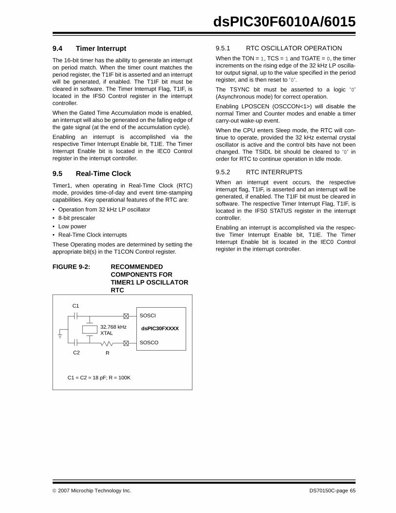
dsPIC30F6010A/6015
9.4 Timer Interrupt
The 16-bit timer has the ability to generate an interrupton period match. When the timer count matches theperiod register, the T1IF bit is asserted and an interruptwill be generated, if enabled. The T1IF bit must becleared in software. The Timer Interrupt Flag, T1IF, islocated in the IFS0 Control register in the interruptcontroller.
When the Gated Time Accumulation mode is enabled,an interrupt will also be generated on the falling edge ofthe gate signal (at the end of the accumulation cycle).
Enabling an interrupt is accomplished via therespective Timer Interrupt Enable bit, T1IE. The TimerInterrupt Enable bit is located in the IEC0 Controlregister in the interrupt controller.
9.5 Real-Time Clock
Timer1, when operating in Real-Time Clock (RTC)mode, provides time-of-day and event time-stampingcapabilities. Key operational features of the RTC are:
• Operation from 32 kHz LP oscillator• 8-bit prescaler
• Low power • Real-Time Clock interrupts
These Operating modes are determined by setting theappropriate bit(s) in the T1CON Control register.
FIGURE 9-2: RECOMMENDED COMPONENTS FOR TIMER1 LP OSCILLATOR RTC
9.5.1 RTC OSCILLATOR OPERATION
When the TON = 1, TCS = 1 and TGATE = 0, the timerincrements on the rising edge of the 32 kHz LP oscilla-tor output signal, up to the value specified in the periodregister, and is then reset to ‘0’.
The TSYNC bit must be asserted to a logic ‘0’(Asynchronous mode) for correct operation.
Enabling LPOSCEN (OSCCON<1>) will disable thenormal Timer and Counter modes and enable a timercarry-out wake-up event.
When the CPU enters Sleep mode, the RTC will con-tinue to operate, provided the 32 kHz external crystaloscillator is active and the control bits have not beenchanged. The TSIDL bit should be cleared to ‘0’ inorder for RTC to continue operation in Idle mode.
9.5.2 RTC INTERRUPTS
When an interrupt event occurs, the respectiveinterrupt flag, T1IF, is asserted and an interrupt will begenerated, if enabled. The T1IF bit must be cleared insoftware. The respective Timer Interrupt Flag, T1IF, islocated in the IFS0 STATUS register in the interruptcontroller.
Enabling an interrupt is accomplished via the respec-tive Timer Interrupt Enable bit, T1IE. The TimerInterrupt Enable bit is located in the IEC0 Controlregister in the interrupt controller.
SOSCI
SOSCO
R
C1
C2
dsPIC30FXXXX32.768 kHzXTAL
C1 = C2 = 18 pF; R = 100K
© 2007 Microchip Technology Inc. DS70150C-page 65
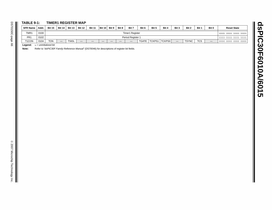
dsP
IC30F
6010A/6015
DS
70150C-page 66
© 2007 M
icrochip Technology Inc.
Bit 2 Bit 1 Bit 0 Reset State
uuuu uuuu uuuu uuuu
1111 1111 1111 1111
SYNC TCS — 0000 0000 0000 0000
TABLE 9-1: TIMER1 REGISTER MAPSFR Name Addr. Bit 15 Bit 14 Bit 13 Bit 12 Bit 11 Bit 10 Bit 9 Bit 8 Bit 7 Bit 6 Bit 5 Bit 4 Bit 3
TMR1 0100 Timer1 Register
PR1 0102 Period Register 1
T1CON 0104 TON — TSIDL — — — — — — TGATE TCKPS1 TCKPS0 — T
Legend: u = uninitialized bit
Note: Refer to “dsPIC30F Family Reference Manual” (DS70046) for descriptions of register bit fields.

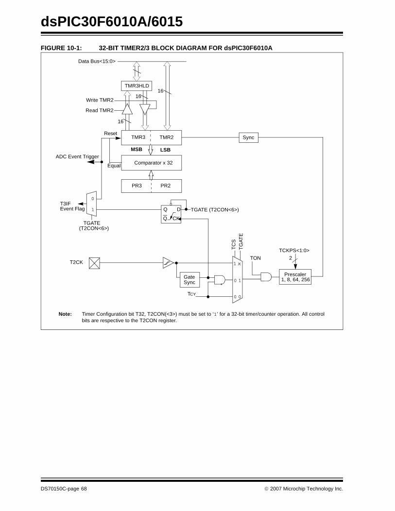
dsPIC30F6010A/6015
FIGURE 10-1: 32-BIT TIMER2/3 BLOCK DIAGRAM FOR dsPIC30F6010A
TMR3 TMR2
T3IF
Equal Comparator x 32
PR3 PR2
Reset
LSB MSB
Event Flag
Note: Timer Configuration bit T32, T2CON(<3>) must be set to ‘1’ for a 32-bit timer/counter operation. All controlbits are respective to the T2CON register.
Data Bus<15:0>
TMR3HLD
Read TMR2
Write TMR216
16
16
Q
Q D
CK
TGATE (T2CON<6>)
(T2CON<6>)TGATE
0
1
TON
TCKPS<1:0>
Prescaler1, 8, 64, 256
2
TCY
TC
S
1 x
0 1
TG
AT
E
0 0
Gate
T2CK
Sync
ADC Event Trigger
Sync
DS70150C-page 68 © 2007 Microchip Technology Inc.

dsPIC30F6010A/6015
FIGURE 10-2: 32-BIT TIMER2/3 BLOCK DIAGRAM FOR dsPIC30F6015
TMR3 TMR2
T3IF
Equal Comparator x 32
PR3 PR2
Reset
LSB MSB
Event Flag
Note: Timer Configuration bit T32, T2CON(<3>) must be set to ‘1’ for a 32-bit timer/counter operation. All controlbits are respective to the T2CON register.
Data Bus<15:0>
TMR3HLD
Read TMR2
Write TMR216
16
16
Q
Q D
CK
TGATE(T2CON<6>)
(T2CON<6>)TGATE
0
1
TON
TCKPS<1:0>
Prescaler1, 8, 64, 256
2
TCY
TC
S
1 x
0 1
TG
AT
E
0 0
Gate
Sync
ADC Event Trigger
Sync
© 2007 Microchip Technology Inc. DS70150C-page 69
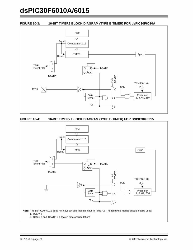
dsPIC30F6010A/6015
FIGURE 10-3: 16-BIT TIMER2 BLOCK DIAGRAM (TYPE B TIMER) FOR dsPIC30F6010A
FIGURE 10-4: 16-BIT TIMER2 BLOCK DIAGRAM (TYPE B TIMER) FOR DSPIC30F6015
TON
Sync
PR2
T2IF
EqualComparator x 16
TMR2Reset
Event Flag
Q
Q D
CK
TGATE
TCKPS<1:0>
Prescaler1, 8, 64, 256
2
TGATE
TCY
1
0
TC
S
1 x
0 1
TG
AT
E
0 0
Gate
T2CK
Sync
TON
Sync
PR2
T2IF
EqualComparator x 16
TMR2Reset
Event Flag
Q
Q D
CK
TGATE
TCKPS<1:0>
Prescaler1, 8, 64, 256
2
TGATE
TCY
1
0
TC
S
1 x
0 1
TG
AT
E
0 0
GateSync
Note: The dsPIC30F6015 does not have an external pin input to TIMER2. The following modes should not be used:1. TCS = 12. TCS = 0 and TGATE = 1 (gated time accumulation)
DS70150C-page 70 © 2007 Microchip Technology Inc.
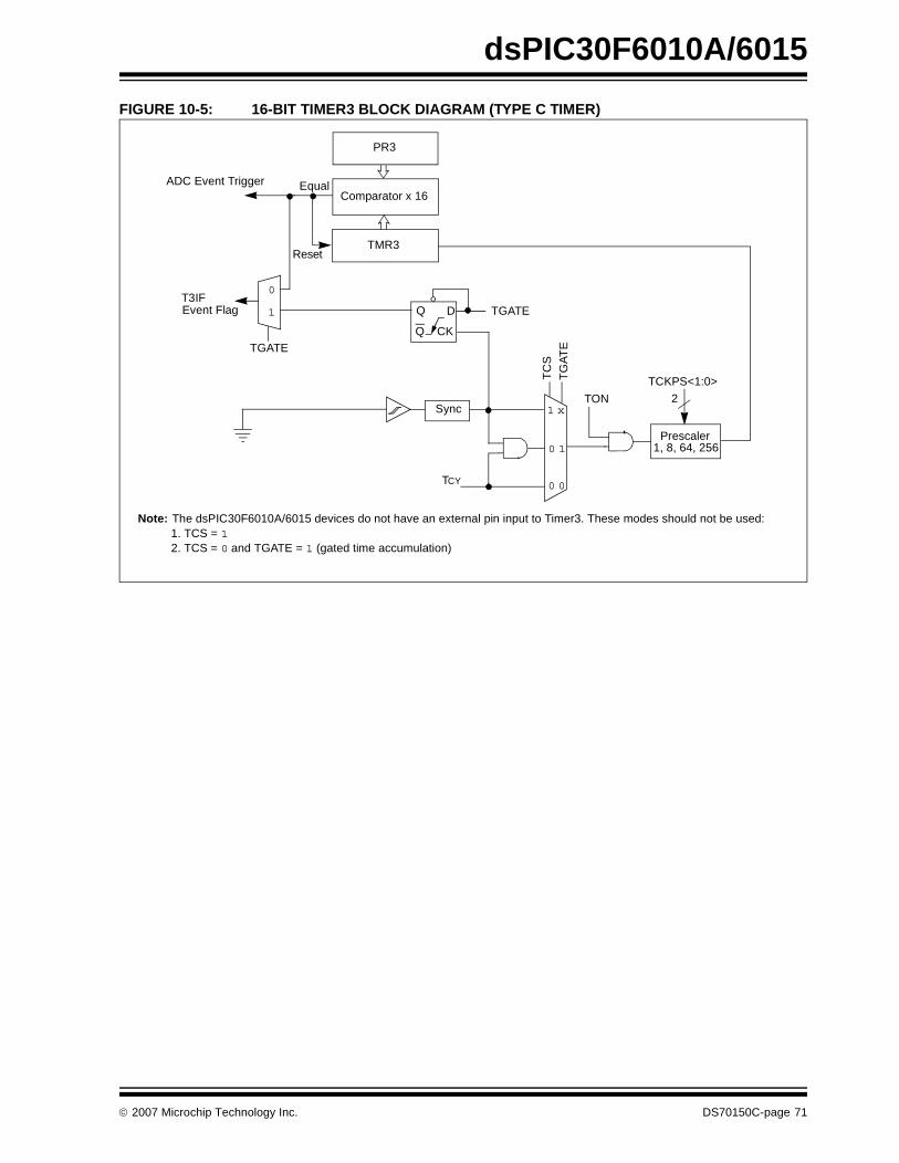
dsPIC30F6010A/6015
FIGURE 10-5: 16-BIT TIMER3 BLOCK DIAGRAM (TYPE C TIMER)
TON
PR3
T3IF
EqualComparator x 16
TMR3Reset
Event Flag
Q
Q D
CK
TGATE
TCKPS<1:0>
Prescaler 1, 8, 64, 256
2
TGATE
TCY
1
0
TC
S
1 x
0 1
TG
AT
E
0 0
ADC Event Trigger
Sync
Note: The dsPIC30F6010A/6015 devices do not have an external pin input to Timer3. These modes should not be used:1. TCS = 12. TCS = 0 and TGATE = 1 (gated time accumulation)
© 2007 Microchip Technology Inc. DS70150C-page 71

dsPIC30F6010A/6015
10.1 Timer Gate Operation
The 32-bit timer can be placed in the Gated TimeAccumulation mode. This mode allows the internal TCY
to increment the respective timer when the gate inputsignal (T2CK pin) is asserted high. Control bit TGATE(T2CON<6>) must be set to enable this mode. When inthis mode, Timer2 is the originating clock source. TheTGATE setting is ignored for Timer3. The timer must beenabled (TON = 1) and the timer clock source set tointernal (TCS = 0).
The falling edge of the external signal terminates thecount operation, but does not reset the timer. The usermust reset the timer in order to start counting from zero.
10.2 ADC Event Trigger
When a match occurs between the 32-bit timer (TMR3/TMR2) and the 32-bit combined period register (PR3/PR2), a special ADC trigger event signal is generatedby Timer3.
10.3 Timer Prescaler
The input clock (FOSC/4 or external clock) to the timerhas a prescale option of 1:1, 1:8, 1:64, and 1:256selected by control bits TCKPS<1:0> (T2CON<5:4>and T3CON<5:4>). For the 32-bit timer operation, theoriginating clock source is Timer2. The prescaler oper-ation for Timer3 is not applicable in this mode. Theprescaler counter is cleared when any of the followingoccurs:
• a write to the TMR2/TMR3 register• clearing either of the TON (T2CON<15> or
T3CON<15>) bits to ‘0’• device Reset such as POR and BOR
However, if the timer is disabled (TON = 0), then theTimer2 prescaler cannot be reset, since the prescalerclock is halted.
TMR2/TMR3 is not cleared when T2CON/T3CON iswritten.
10.4 Timer Operation During Sleep Mode
During CPU Sleep mode, the timer will not operate,because the internal clocks are disabled.
10.5 Timer Interrupt
The 32-bit timer module can generate an interrupt onperiod match, or on the falling edge of the external gatesignal. When the 32-bit timer count matches therespective 32-bit period register, or the falling edge ofthe external “gate” signal is detected, the T3IF bit(IFS0<7>) is asserted and an interrupt will be gener-ated if enabled. In this mode, the T3IF interrupt flag isused as the source of the interrupt. The T3IF bit mustbe cleared in software.
Enabling an interrupt is accomplished via therespective Timer Interrupt Enable bit, T3IE (IEC0<7>).
DS70150C-page 72 © 2007 Microchip Technology Inc.
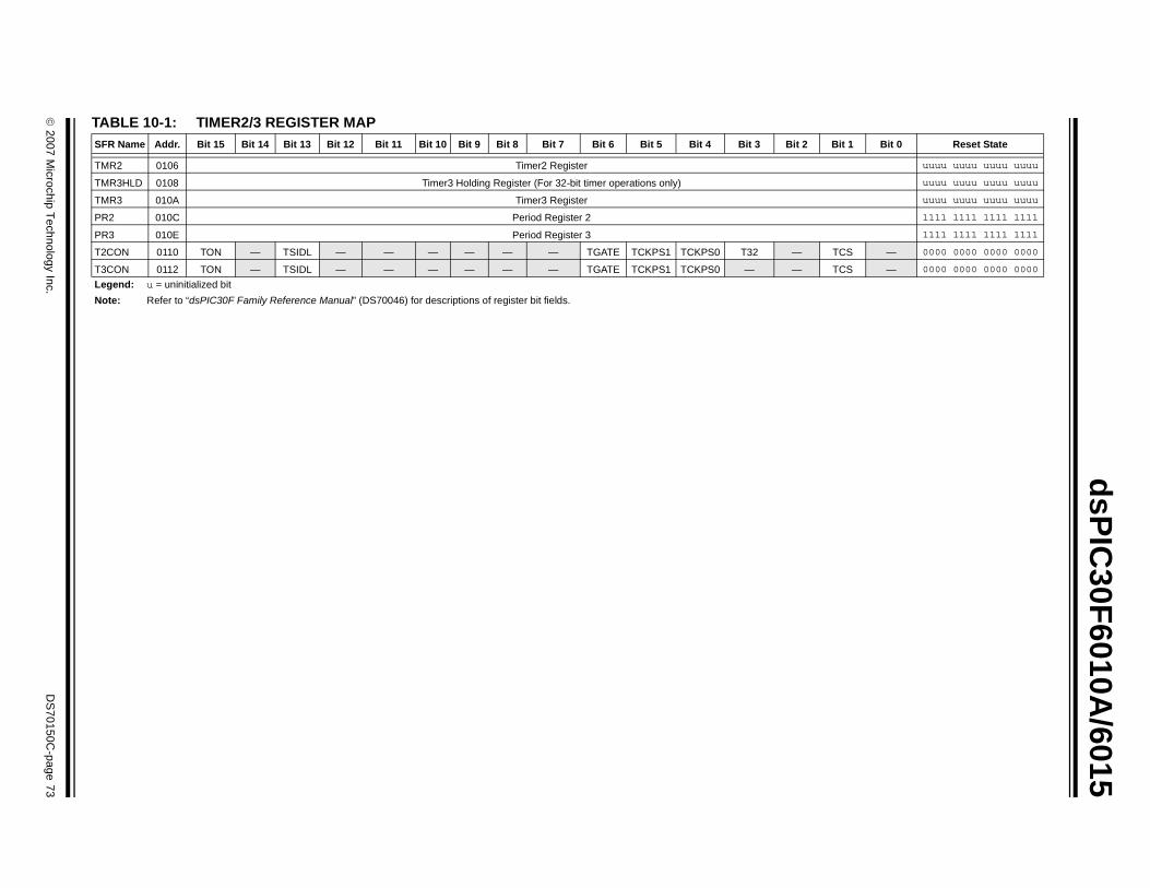
© 2007 M
icrochip Technology Inc.
DS
70150C-page 73
dsP
IC30F
6010A/6015
TASF Bit 1 Bit 0 Reset State
TM uuuu uuuu uuuu uuuu
TM uuuu uuuu uuuu uuuu
TM uuuu uuuu uuuu uuuu
PR 1111 1111 1111 1111
PR 1111 1111 1111 1111
T2 TCS — 0000 0000 0000 0000
T3 TCS — 0000 0000 0000 0000
Le
No
BLE 10-1: TIMER2/3 REGISTER MAPR Name Addr. Bit 15 Bit 14 Bit 13 Bit 12 Bit 11 Bit 10 Bit 9 Bit 8 Bit 7 Bit 6 Bit 5 Bit 4 Bit 3 Bit 2
R2 0106 Timer2 Register
R3HLD 0108 Timer3 Holding Register (For 32-bit timer operations only)
R3 010A Timer3 Register
2 010C Period Register 2
3 010E Period Register 3
CON 0110 TON — TSIDL — — — — — — TGATE TCKPS1 TCKPS0 T32 —
CON 0112 TON — TSIDL — — — — — — TGATE TCKPS1 TCKPS0 — —
gend: u = uninitialized bit
te: Refer to “dsPIC30F Family Reference Manual” (DS70046) for descriptions of register bit fields.

dsPIC30F6010A/6015
NOTES:
DS70150C-page 74 © 2007 Microchip Technology Inc.

dsPIC30F6010A/6015
11.0 TIMER4/5 MODULE
This section describes the second 32-bit GeneralPurpose (GP) Timer module (Timer4/5) and associatedoperational modes. Figure 11-1 depicts the simplifiedblock diagram of the 32-bit Timer4/5 Module.Figure 11-2 and Figure 11-3 show Timer4/5 configuredas two independent 16-bit timers, Timer4 and Timer5,respectively.
The Timer4/5 module is similar in operation to theTimer2/3 module. However, there are somedifferences, which are listed below:
• The Timer4/5 module does not support the ADC Event Trigger feature
• Timer4/5 can not be utilized by other peripheral modules such as Input Capture and Output Compare
The operating modes of the Timer4/5 module aredetermined by setting the appropriate bit(s) in the 16-bitT4CON and T5CON SFRs.
For 32-bit timer/counter operation, Timer4 is the lswand Timer5 is the msw of the 32-bit timer.
FIGURE 11-1: 32-BIT TIMER4/5 BLOCK DIAGRAM
Note: This data sheet summarizes features of thisgroup of dsPIC30F devices and is not intended to bea complete reference source. For more informationon the CPU, peripherals, register descriptions andgeneral device functionality, refer to the “dsPIC30FFamily Reference Manual” (DS70046).
Note: Timer4 is a Type B timer and Timer5 is aType C timer. Please refer to the appropri-ate timer type in Section 24.0 "ElectricalCharacteristics" of this document.
Note: For 32-bit timer operation, T5CON controlbits are ignored. Only T4CON control bitsare used for setup and control. Timer4clock and gate inputs are utilized for the32-bit timer module, but an interrupt isgenerated with the Timer5 Interrupt Flag(T5IF) and the interrupt is enabled with theTimer5 Interrupt Enable bit (T5IE).
© 2007 Microchip Technology Inc. DS70150C-page 75
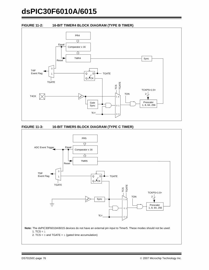
dsPIC30F6010A/6015
FIGURE 11-2: 16-BIT TIMER4 BLOCK DIAGRAM (TYPE B TIMER)
FIGURE 11-3: 16-BIT TIMER5 BLOCK DIAGRAM (TYPE C TIMER)
TON
Sync
PR4
T4IF
EqualComparator x 16
TMR4Reset
Event Flag
Q
Q D
CK
TGATE
TCKPS<1:0>
Prescaler 1, 8, 64, 256
2
TGATE
TCY
1
0
TC
S
1 x
0 1
TG
AT
E
0 0
Gate
T4CK
Sync
TON
PR5
T5IF
EqualComparator x 16
TMR5Reset
Event Flag
Q
Q D
CK
TGATE
TCKPS<1:0>
Prescaler 1, 8, 64, 256
2
TGATE
TCY
1
0
TC
S
1 x
0 1
TG
AT
E
0 0
ADC Event Trigger
Sync
Note: The dsPIC30F6010A/6015 devices do not have an external pin input to Timer5. These modes should not be used:1. TCS = 12. TCS = 0 and TGATE = 1 (gated time accumulation)
DS70150C-page 76 © 2007 Microchip Technology Inc.
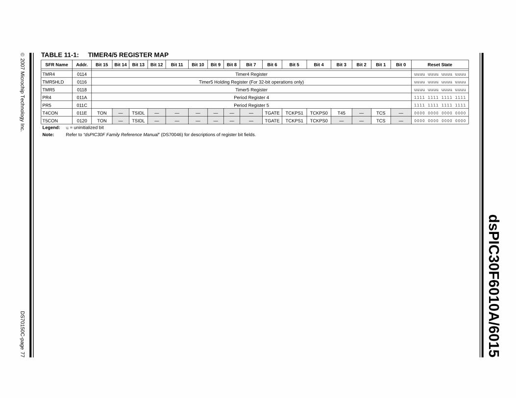
© 2007 M
icrochip Technology Inc.
DS
70150C-page 77
dsP
IC30F
6010A/6015
TAS 2 Bit 1 Bit 0 Reset State
TM uuuu uuuu uuuu uuuu
TM uuuu uuuu uuuu uuuu
TM uuuu uuuu uuuu uuuu
PR 1111 1111 1111 1111
PR 1111 1111 1111 1111
T4 TCS — 0000 0000 0000 0000
T5 TCS — 0000 0000 0000 0000
Le
No
BLE 11-1: TIMER4/5 REGISTER MAPFR Name Addr. Bit 15 Bit 14 Bit 13 Bit 12 Bit 11 Bit 10 Bit 9 Bit 8 Bit 7 Bit 6 Bit 5 Bit 4 Bit 3 Bit
R4 0114 Timer4 Register
R5HLD 0116 Timer5 Holding Register (For 32-bit operations only)
R5 0118 Timer5 Register
4 011A Period Register 4
5 011C Period Register 5
CON 011E TON — TSIDL — — — — — — TGATE TCKPS1 TCKPS0 T45 —
CON 0120 TON — TSIDL — — — — — — TGATE TCKPS1 TCKPS0 — —
gend: u = uninitialized bit
te: Refer to “dsPIC30F Family Reference Manual” (DS70046) for descriptions of register bit fields.

dsPIC30F6010A/6015
NOTES:
DS70150C-page 78 © 2007 Microchip Technology Inc.
dsPIC30F6010A/6015
12.0 INPUT CAPTURE MODULE
This section describes the input capture module andassociated operational modes. The features provided bythis module are useful in applications requiringfrequency (period) and pulse measurement. Figure 12-1depicts a block diagram of the input capture module.Input capture is useful for such modes as:
• Frequency/Period/Pulse Measurements• Additional sources of External Interrupts
The key operational features of the input capturemodule are:
• Simple Capture Event mode• Timer2 and Timer3 mode selection
• Interrupt on input capture event
These operating modes are determined by setting theappropriate bits in the ICxCON register (wherex = 1,2,...,N). The dsPIC30F6010A and dsPIC30F6015devices have eight capture channels.
12.1 Simple Capture Event Mode
The simple capture events in the dsPIC30F productfamily are:
• Capture every falling edge• Capture every rising edge
• Capture every 4th rising edge• Capture every 16th rising edge• Capture every rising and falling edge
These simple Input Capture modes are configured bysetting the appropriate bits ICM<2:0> (ICxCON<2:0>).
12.1.1 CAPTURE PRESCALER
There are four input capture prescaler settings, speci-fied by bits ICM<2:0> (ICxCON<2:0>). Whenever thecapture channel is turned off, the prescaler counter willbe cleared. In addition, any Reset will clear theprescaler counter.
FIGURE 12-1: INPUT CAPTURE MODE BLOCK DIAGRAM
Note: This data sheet summarizes features of thisgroup of dsPIC30F devices and is not intended to bea complete reference source. For more informationon the CPU, peripherals, register descriptions andgeneral device functionality, refer to the “dsPIC30FFamily Reference Manual” (DS70046).
ICxBUF
Prescaler
ICx
ICM<2:0> Mode Select
3
Note: Where ‘x’ is shown, reference is made to the registers or bits associated to the respective inputcapture channels 1 through N.
1 0
Set Flag
Pin
ICxIF
ICTMR
T2_CNT T3_CNT
EdgeDetection
Logic
ClockSynchronizer1, 4, 16
From GP Timer Module
16 16
FIFOR/WLogic
ICI<1:0>
ICBNE, ICOV
ICxCONInterrupt
Logic
Set Flag ICxIF
Data Bus
© 2007 Microchip Technology Inc. DS70150C-page 79
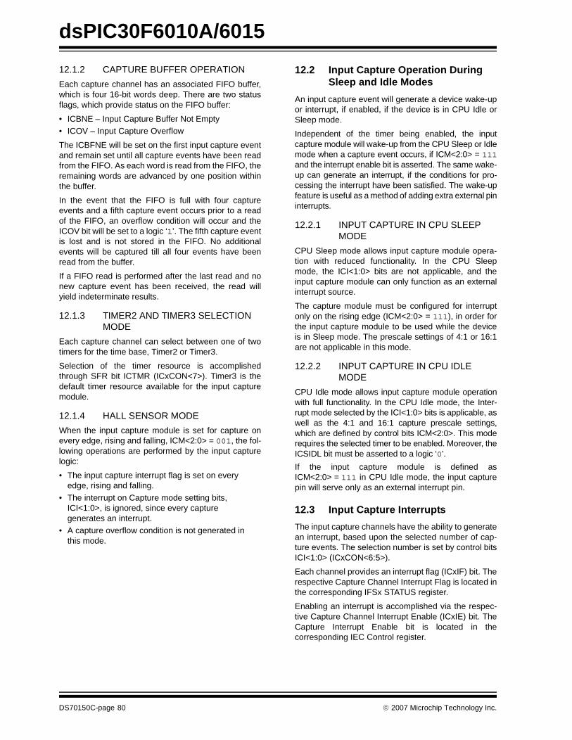
dsPIC30F6010A/6015
12.1.2 CAPTURE BUFFER OPERATION
Each capture channel has an associated FIFO buffer,which is four 16-bit words deep. There are two statusflags, which provide status on the FIFO buffer:
• ICBNE – Input Capture Buffer Not Empty• ICOV – Input Capture Overflow
The ICBFNE will be set on the first input capture eventand remain set until all capture events have been readfrom the FIFO. As each word is read from the FIFO, theremaining words are advanced by one position withinthe buffer.
In the event that the FIFO is full with four captureevents and a fifth capture event occurs prior to a readof the FIFO, an overflow condition will occur and theICOV bit will be set to a logic ‘1’. The fifth capture eventis lost and is not stored in the FIFO. No additionalevents will be captured till all four events have beenread from the buffer.
If a FIFO read is performed after the last read and nonew capture event has been received, the read willyield indeterminate results.
12.1.3 TIMER2 AND TIMER3 SELECTION MODE
Each capture channel can select between one of twotimers for the time base, Timer2 or Timer3.
Selection of the timer resource is accomplishedthrough SFR bit ICTMR (ICxCON<7>). Timer3 is thedefault timer resource available for the input capturemodule.
12.1.4 HALL SENSOR MODE
When the input capture module is set for capture onevery edge, rising and falling, ICM<2:0> = 001, the fol-lowing operations are performed by the input capturelogic:
• The input capture interrupt flag is set on every edge, rising and falling.
• The interrupt on Capture mode setting bits, ICI<1:0>, is ignored, since every capture generates an interrupt.
• A capture overflow condition is not generated in this mode.
12.2 Input Capture Operation During Sleep and Idle Modes
An input capture event will generate a device wake-upor interrupt, if enabled, if the device is in CPU Idle orSleep mode.
Independent of the timer being enabled, the inputcapture module will wake-up from the CPU Sleep or Idlemode when a capture event occurs, if ICM<2:0> = 111and the interrupt enable bit is asserted. The same wake-up can generate an interrupt, if the conditions for pro-cessing the interrupt have been satisfied. The wake-upfeature is useful as a method of adding extra external pininterrupts.
12.2.1 INPUT CAPTURE IN CPU SLEEP MODE
CPU Sleep mode allows input capture module opera-tion with reduced functionality. In the CPU Sleepmode, the ICI<1:0> bits are not applicable, and theinput capture module can only function as an externalinterrupt source.
The capture module must be configured for interruptonly on the rising edge (ICM<2:0> = 111), in order forthe input capture module to be used while the deviceis in Sleep mode. The prescale settings of 4:1 or 16:1are not applicable in this mode.
12.2.2 INPUT CAPTURE IN CPU IDLE MODE
CPU Idle mode allows input capture module operationwith full functionality. In the CPU Idle mode, the Inter-rupt mode selected by the ICI<1:0> bits is applicable, aswell as the 4:1 and 16:1 capture prescale settings,which are defined by control bits ICM<2:0>. This moderequires the selected timer to be enabled. Moreover, theICSIDL bit must be asserted to a logic ‘0’.
If the input capture module is defined asICM<2:0> = 111 in CPU Idle mode, the input capturepin will serve only as an external interrupt pin.
12.3 Input Capture Interrupts
The input capture channels have the ability to generatean interrupt, based upon the selected number of cap-ture events. The selection number is set by control bitsICI<1:0> (ICxCON<6:5>).
Each channel provides an interrupt flag (ICxIF) bit. Therespective Capture Channel Interrupt Flag is located inthe corresponding IFSx STATUS register.
Enabling an interrupt is accomplished via the respec-tive Capture Channel Interrupt Enable (ICxIE) bit. TheCapture Interrupt Enable bit is located in thecorresponding IEC Control register.
DS70150C-page 80 © 2007 Microchip Technology Inc.
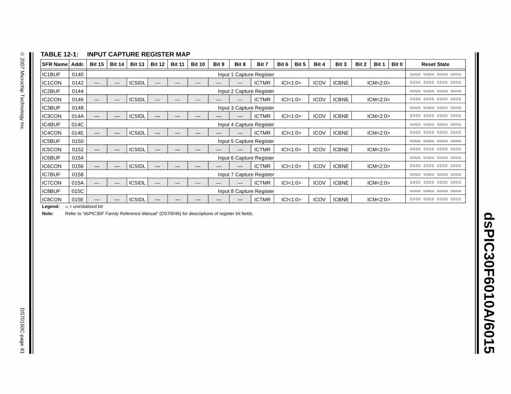
© 2007 M
icrochip Technology Inc.
DS
70150C-page 81
dsP
IC30F
6010A/6015
TASF t 2 Bit 1 Bit 0 Reset State
IC uuuu uuuu uuuu uuuu
IC ICM<2:0> 0000 0000 0000 0000
IC uuuu uuuu uuuu uuuu
IC ICM<2:0> 0000 0000 0000 0000
IC uuuu uuuu uuuu uuuu
IC ICM<2:0> 0000 0000 0000 0000
IC uuuu uuuu uuuu uuuu
IC ICM<2:0> 0000 0000 0000 0000
IC uuuu uuuu uuuu uuuu
IC ICM<2:0> 0000 0000 0000 0000
IC uuuu uuuu uuuu uuuu
IC ICM<2:0> 0000 0000 0000 0000
IC uuuu uuuu uuuu uuuu
IC ICM<2:0> 0000 0000 0000 0000
IC uuuu uuuu uuuu uuuu
IC ICM<2:0> 0000 0000 0000 0000
Le
No
BLE 12-1: INPUT CAPTURE REGISTER MAPR Name Addr. Bit 15 Bit 14 Bit 13 Bit 12 Bit 11 Bit 10 Bit 9 Bit 8 Bit 7 Bit 6 Bit 5 Bit 4 Bit 3 Bi
1BUF 0140 Input 1 Capture Register
1CON 0142 — — ICSIDL — — — — — ICTMR ICI<1:0> ICOV ICBNE
2BUF 0144 Input 2 Capture Register
2CON 0146 — — ICSIDL — — — — — ICTMR ICI<1:0> ICOV ICBNE
3BUF 0148 Input 3 Capture Register
3CON 014A — — ICSIDL — — — — — ICTMR ICI<1:0> ICOV ICBNE
4BUF 014C Input 4 Capture Register
4CON 014E — — ICSIDL — — — — — ICTMR ICI<1:0> ICOV ICBNE
5BUF 0150 Input 5 Capture Register
5CON 0152 — — ICSIDL — — — — — ICTMR ICI<1:0> ICOV ICBNE
6BUF 0154 Input 6 Capture Register
6CON 0156 — — ICSIDL — — — — — ICTMR ICI<1:0> ICOV ICBNE
7BUF 0158 Input 7 Capture Register
7CON 015A — — ICSIDL — — — — — ICTMR ICI<1:0> ICOV ICBNE
8BUF 015C Input 8 Capture Register
8CON 015E — — ICSIDL — — — — — ICTMR ICI<1:0> ICOV ICBNEgend: u = uninitialized bit
te: Refer to “dsPIC30F Family Reference Manual” (DS70046) for descriptions of register bit fields.

dsPIC30F6010A/6015
NOTES:
DS70150C-page 82 © 2007 Microchip Technology Inc.
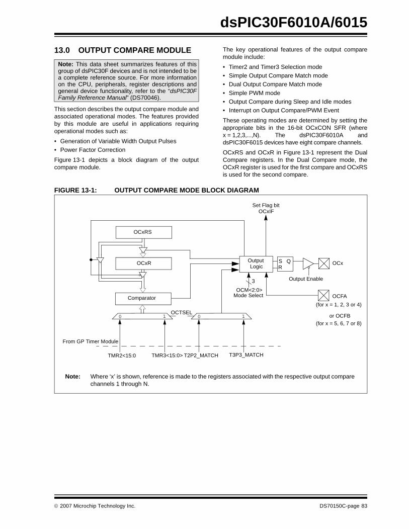
dsPIC30F6010A/6015
13.0 OUTPUT COMPARE MODULE
This section describes the output compare module andassociated operational modes. The features providedby this module are useful in applications requiringoperational modes such as:
• Generation of Variable Width Output Pulses• Power Factor Correction
Figure 13-1 depicts a block diagram of the outputcompare module.
The key operational features of the output comparemodule include:
• Timer2 and Timer3 Selection mode• Simple Output Compare Match mode• Dual Output Compare Match mode
• Simple PWM mode• Output Compare during Sleep and Idle modes• Interrupt on Output Compare/PWM Event
These operating modes are determined by setting theappropriate bits in the 16-bit OCxCON SFR (wherex = 1,2,3,...,N). The dsPIC30F6010A anddsPIC30F6015 devices have eight compare channels.
OCxRS and OCxR in Figure 13-1 represent the DualCompare registers. In the Dual Compare mode, theOCxR register is used for the first compare and OCxRSis used for the second compare.
FIGURE 13-1: OUTPUT COMPARE MODE BLOCK DIAGRAM
Note: This data sheet summarizes features of thisgroup of dsPIC30F devices and is not intended to bea complete reference source. For more informationon the CPU, peripherals, register descriptions andgeneral device functionality, refer to the “dsPIC30FFamily Reference Manual” (DS70046).
OCxR
Comparator
OutputLogic
QSR
OCM<2:0>
Output Enable
OCx
Set Flag bitOCxIF
OCxRS
Mode Select
3
Note: Where ‘x’ is shown, reference is made to the registers associated with the respective output comparechannels 1 through N.
OCFA
OCTSEL0 1
T2P2_MATCHTMR2<15:0 TMR3<15:0> T3P3_MATCH
From GP Timer Module
(for x = 1, 2, 3 or 4)
or OCFB(for x = 5, 6, 7 or 8)
0 1
© 2007 Microchip Technology Inc. DS70150C-page 83

dsPIC30F6010A/6015
13.1 Timer2 and Timer3 Selection Mode
Each output compare channel can select between oneof two 16-bit timers; Timer2 or Timer3.
The selection of the timers is controlled by the OCTSELbit (OCxCON<3>). Timer2 is the default timer resourcefor the Output Compare module.
13.2 Simple Output Compare Match Mode
When control bits OCM<2:0> (OCxCON<2:0>) = 001,010 or 011, the selected output compare channel isconfigured for one of three simple output comparematch modes:
• Compare forces I/O pin low• Compare forces I/O pin high• Compare toggles I/O pin
The OCxR register is used in these modes. The OCxRregister is loaded with a value and is compared to theselected incrementing timer count. When a compareoccurs, one of these compare match modes occurs. Ifthe counter resets to zero before reaching the value inOCxR, the state of the OCx pin remains unchanged.
13.3 Dual Output Compare Match Mode
When control bits OCM<2:0> (OCxCON<2:0>) = 100or 101, the selected output compare channel is config-ured for one of two Dual Output Compare modes,which are:
• Single Output Pulse mode• Continuous Output Pulse mode
13.3.1 SINGLE PULSE MODE
For the user to configure the module for the generationof a single output pulse, the following steps arerequired (assuming timer is off):
• Determine instruction cycle time TCY.
• Calculate desired pulse-width value based on TCY.
• Calculate time to start pulse from timer start value of 0x0000.
• Write pulse-width start and stop times into OCxR and OCxRS Compare registers (x denotes channel 1, 2, ...,N).
• Set Timer Period register to value equal to, or greater than, value in OCxRS Compare register.
• Set OCM<2:0> = 100.
• Enable timer, TON (TxCON<15>) = 1.
To initiate another single pulse, issue another write toset OCM<2:0> = 100.
13.3.2 CONTINUOUS PULSE MODE
For the user to configure the module for the generationof a continuous stream of output pulses, the followingsteps are required:
• Determine instruction cycle time TCY.• Calculate desired pulse value based on TCY.• Calculate timer to start pulse width from timer start
value of 0x0000.• Write pulse-width start and stop times into OCxR
and OCxRS (x denotes channel 1, 2, ...,N) Compare registers, respectively.
• Set Timer Period register to value equal to, or greater than, value in OCxRS Compare register.
• Set OCM<2:0> = 101.• Enable timer, TON (TxCON<15>) = 1.
13.4 Simple PWM Mode
When control bits OCM<2:0> (OCxCON<2:0>) = 110or 111, the selected output compare channel is config-ured for the PWM mode of operation. When configuredfor the PWM mode of operation, OCxR is the main latch(read-only) and OCxRS is the secondary latch. Thisenables glitchless PWM transitions.
The user must perform the following steps in order toconfigure the output compare module for PWMoperation:
1. Set the PWM period by writing to the appropriateperiod register.
2. Set the PWM duty cycle by writing to the OCxRSregister.
3. Configure the output compare module for PWMoperation.
4. Set the TMRx prescale value and enable theTimer, TON (TxCON<15>) = 1.
13.4.1 INPUT PIN FAULT PROTECTION FOR PWM
When control bits OCM<2:0> (OCxCON<2:0>) = 111,the selected output compare channel is againconfigured for the PWM mode of operation, with theadditional feature of input Fault protection. While in thismode, if a logic ‘0’ is detected on the OCFA/B pin, therespective PWM output pin is placed in the high-impedance input state. The OCFLT bit (OCxCON<4>)indicates whether a Fault condition has occurred. Thisstate will be maintained until both of the followingevents have occurred:
• The external Fault condition has been removed. • The PWM mode has been re-enabled by writing
to the appropriate control bits.
DS70150C-page 84 © 2007 Microchip Technology Inc.

dsPIC30F6010A/6015
13.4.2 PWM PERIOD
The PWM period is specified by writing to the PRxregister. The PWM period can be calculated usingEquation 13-1.
EQUATION 13-1: PWM PERIOD
PWM frequency is defined as 1/[PWM period].
When the selected TMRx is equal to its respectiveperiod register, PRx, the following four events occur onthe next increment cycle:
• TMRx is cleared.
• The OCx pin is set.- Exception 1: If PWM duty cycle is 0x0000,
the OCx pin will remain low.- Exception 2: If duty cycle is greater than PRx,
the pin will remain high.• The PWM duty cycle is latched from OCxRS into
OCxR.• The corresponding timer interrupt flag is set.
See Figure 13-2 for key PWM period comparisons.Timer3 is referred to in the figure for clarity.
FIGURE 13-2: PWM OUTPUT TIMING
13.5 Output Compare Operation During CPU Sleep Mode
When the CPU enters the Sleep mode, all internalclocks are stopped. Therefore, when the CPU entersthe Sleep state, the output compare channel will drivethe pin to the active state that was observed prior toentering the CPU Sleep state.
For example, if the pin was high when the CPUentered the Sleep state, the pin will remain high. Like-wise, if the pin was low when the CPU entered theSleep state, the pin will remain low. In either case, theoutput compare module will resume operation whenthe device wakes up.
13.6 Output Compare Operation During CPU Idle Mode
When the CPU enters the Idle mode, the outputcompare module can operate with full functionality.
The output compare channel will operate during theCPU Idle mode if the OCSIDL bit (OCxCON<13>) is atlogic 0 and the selected time base (Timer2 or Timer3)is enabled and the TSIDL bit of the selected timer isset to logic 0.
13.7 Output Compare Interrupts
The output compare channels have the ability to gener-ate an interrupt on a compare match, for whichevermatch mode has been selected.
For all modes except the PWM mode, when a compareevent occurs, the respective interrupt flag (OCxIF) isasserted and an interrupt will be generated, if enabled.The OCxIF bit is located in the corresponding IFS STA-TUS register and must be cleared in software. Theinterrupt is enabled via the respective Compare Inter-rupt Enable (OCxIE) bit, located in the correspondingIEC Control register.
For the PWM mode, when an event occurs, the respec-tive Timer Interrupt Flag (T2IF or T3IF) is asserted andan interrupt will be generated, if enabled. The IF bit islocated in the IFS0 STATUS register, and must becleared in software. The interrupt is enabled via therespective Timer Interrupt Enable bit (T2IE or T3IE),located in the IEC0 Control register. The outputcompare interrupt flag is never set during the PWMmode of operation.
PWM Period = [(PRx) + 1] • 4 • TOSC •(TMRx Prescale Value)
Period
Duty Cycle
TMR3 = Duty Cycle (OCxR) TMR3 = Duty Cycle (OCxR)
TMR3 = PR3
T3IF = 1(Interrupt Flag)
OCxR = OCxRS
TMR3 = PR3
(Interrupt Flag) OCxR = OCxRS
T3IF = 1
© 2007 Microchip Technology Inc. DS70150C-page 85

dsP
IC30F
6010A/6015
DS
70150C-page 86
© 2007 M
icrochip Technology Inc.
it 2 Bit 1 Bit 0 Reset State
0000 0000 0000 0000
0000 0000 0000 0000
OCM<2:0> 0000 0000 0000 0000
0000 0000 0000 0000
0000 0000 0000 0000
OCM<2:0> 0000 0000 0000 0000
0000 0000 0000 0000
0000 0000 0000 0000
OCM<2:0> 0000 0000 0000 0000
0000 0000 0000 0000
0000 0000 0000 0000
OCM<2:0> 0000 0000 0000 0000
0000 0000 0000 0000
0000 0000 0000 0000
OCM<2:0> 0000 0000 0000 0000
0000 0000 0000 0000
0000 0000 0000 0000
OCM<2:0> 0000 0000 0000 0000
0000 0000 0000 0000
0000 0000 0000 0000
OCM<2:0> 0000 0000 0000 0000
0000 0000 0000 0000
0000 0000 0000 0000
OCM<2:0> 0000 0000 0000 0000
TABLE 13-1: OUTPUT COMPARE REGISTER MAP
SFR Name Addr. Bit 15 Bit 14 Bit 13 Bit 12 Bit 11 Bit 10 Bit 9 Bit 8 Bit 7 Bit 6 Bit 5 Bit 4 Bit 3 B
OC1RS 0180 Output Compare 1 Secondary Register
OC1R 0182 Output Compare 1 Main Register
OC1CON 0184 — — OCSIDL — — — — — — — — OCFLT OCTSEL
OC2RS 0186 Output Compare 2 Secondary Register
OC2R 0188 Output Compare 2 Main Register
OC2CON 018A — — OCSIDL — — — — — — — — OCFLT OCTSE
OC3RS 018C Output Compare 3 Secondary Register
OC3R 018E Output Compare 3 Main Register
OC3CON 0190 — — OCSIDL — — — — — — — — OCFLT OCTSEL
OC4RS 0192 Output Compare 4 Secondary Register
OC4R 0194 Output Compare 4 Main Register
OC4CON 0196 — — OCSIDL — — — — — — — — OCFLT OCTSEL
OC5RS 0198 Output Compare 5 Secondary Register
OC5R 019A Output Compare 5 Main Register
OC5CON 019C — — OCSIDL — — — — — — — — OCFLT OCTSEL
OC6RS 019E Output Compare 6 Secondary Register
OC6R 01A0 Output Compare 6 Main Register
OC6CON 01A2 — — OCSIDL — — — — — — — — OCFLT OCTSEL
OC7RS 01A4 Output Compare 7 Secondary Register
OC7R 01A6 Output Compare 7 Main Register
OC7CON 01A8 — — OCSIDL — — — — — — — — OCFLT OCTSEL
OC8RS 01AA Output Compare 8 Secondary Register
OC8R 01AC Output Compare 8 Main Register
OC8CON 01AE — — OCSIDL — — — — — — — — OCFLT OCTSEL
Legend: u = uninitialized bit
Note: Refer to “dsPIC30F Family Reference Manual” (DS70046) for descriptions of register bit fields.
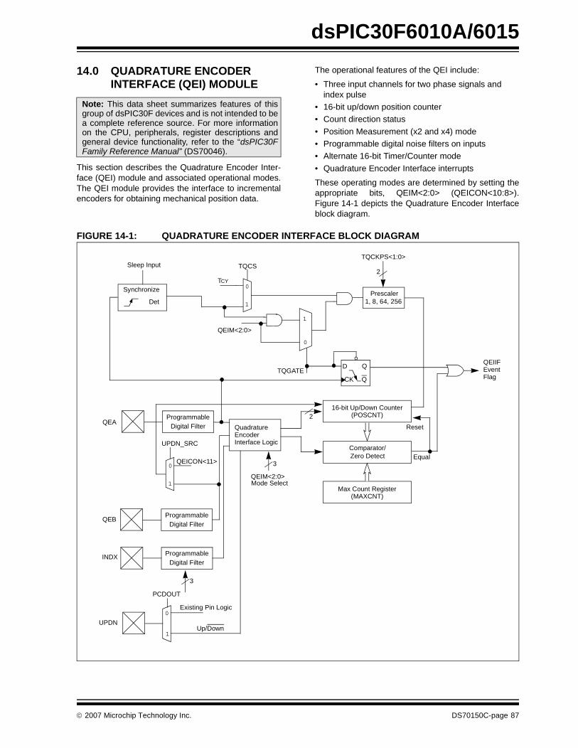
dsPIC30F6010A/6015
14.0 QUADRATURE ENCODER INTERFACE (QEI) MODULE
This section describes the Quadrature Encoder Inter-face (QEI) module and associated operational modes.The QEI module provides the interface to incrementalencoders for obtaining mechanical position data.
The operational features of the QEI include:
• Three input channels for two phase signals and index pulse
• 16-bit up/down position counter• Count direction status
• Position Measurement (x2 and x4) mode• Programmable digital noise filters on inputs• Alternate 16-bit Timer/Counter mode
• Quadrature Encoder Interface interrupts
These operating modes are determined by setting theappropriate bits, QEIM<2:0> (QEICON<10:8>).Figure 14-1 depicts the Quadrature Encoder Interfaceblock diagram.
FIGURE 14-1: QUADRATURE ENCODER INTERFACE BLOCK DIAGRAM
Note: This data sheet summarizes features of thisgroup of dsPIC30F devices and is not intended to bea complete reference source. For more informationon the CPU, peripherals, register descriptions andgeneral device functionality, refer to the “dsPIC30FFamily Reference Manual” (DS70046).
16-bit Up/Down Counter
Comparator/
Max Count Register
Quadrature
ProgrammableDigital Filter
QEA
ProgrammableDigital Filter
INDX
0
1Up/Down
Existing Pin Logic
UPDN
3
Encoder
ProgrammableDigital Filter
QEB
Interface Logic
QEIM<2:0> Mode Select
3
(POSCNT)
(MAXCNT)
PCDOUT
QEIIFEvent Flag
Reset
Equal
2
TCY
1
0
TQCS TQCKPS<1:0>
2
1, 8, 64, 256 Prescaler
Q
QD
CKTQGATE
QEIM<2:0>
Synchronize
Det
1
0
Sleep Input
0
1
UPDN_SRC
QEICON<11>Zero Detect
© 2007 Microchip Technology Inc. DS70150C-page 87

dsPIC30F6010A/6015
14.1 Quadrature Encoder Interface Logic
A typical incremental (a.k.a. optical) encoder has threeoutputs: Phase A, Phase B, and an index pulse. Thesesignals are useful and often required in position andspeed control of ACIM and SR motors.
The two channels, Phase A (QEA) and Phase B (QEB),have a unique relationship. If Phase A leads Phase B,then the direction (of the motor) is deemed positive orforward. If Phase A lags Phase B, then the direction (ofthe motor) is deemed negative or reverse.
A third channel, termed index pulse, occurs once perrevolution and is used as a reference to establish anabsolute position. The index pulse coincides withPhase A and Phase B, both low.
14.2 16-bit Up/Down Position Counter Mode
The 16-bit up/down counter counts up or down onevery count pulse, which is generated by the differenceof the Phase A and Phase B input signals. The counteracts as an integrator, whose count value is proportionalto position. The direction of the count is determined bythe UPDN signal, which is generated by theQuadrature Encoder Interface logic.
14.2.1 POSITION COUNTER ERROR CHECKING
Position count error checking in the QEI is provided forand indicated by the CNTERR bit (QEICON<15>). Theerror checking only applies when the position counteris configured for Reset on the Index Pulse modes(QEIM<2:0> = ‘110’ or ‘100’). In these modes, thecontents of the POSCNT register are compared withthe values (0xFFFF or MAXCNT + 1, depending ondirection). If these values are detected, an error condi-tion is generated by setting the CNTERR bit and a QEIcount error interrupt is generated. The QEI count errorinterrupt can be disabled by setting the CEID bit(DFLTCON<8>). The position counter continues tocount encoder edges after an error has been detected.The POSCNT register continues to count up/down untila natural rollover/underflow. No interrupt is generatedfor the natural rollover/underflow event. The CNTERRbit is a read/write bit and reset in software by the user.
14.2.2 POSITION COUNTER RESET
The Position Counter Reset Enable bit, POSRES(QEI<2>), controls whether the position counter is resetwhen the index pulse is detected. This bit is onlyapplicable when QEIM<2:0> = 100 or 110.
If the POSRES bit is set to ‘1’, then the position counteris reset when the index pulse is detected. If thePOSRES bit is set to ‘0’, then the position counter is notreset when the index pulse is detected. The positioncounter will continue counting up or down, and will bereset on the rollover or underflow condition.
The interrupt is still generated on the detection of theindex pulse and not on the position counter overflow/underflow.
14.2.3 COUNT DIRECTION STATUS
As mentioned in the previous section, the QEI logicgenerates an UPDN signal, based upon the relation-ship between Phase A and Phase B. In addition to theoutput pin, the state of this internal UPDN signal issupplied to a SFR bit, UPDN (QEICON<11>) as a read-only bit. To place the state of this signal on an I/O pin,the SFR bit, PCDOUT (QEICON<6>), must be 1.
14.3 Position Measurement Mode
There are two measurement modes which aresupported and are termed x2 and x4. These modes areselected by the QEIM<2:0> mode select bits located inSFR QEICON<10:8>.
When control bits QEIM<2:0> = 100 or 101, the x2Measurement mode is selected and the QEI logic onlylooks at the Phase A input for the position counterincrement rate. Every rising and falling edge of thePhase A signal causes the position counter to be incre-mented or decremented. The Phase B signal is stillutilized for the determination of the counter direction,just as in the x4 mode.
Within the x2 Measurement mode, there are twovariations of how the position counter is reset:
1. Position counter reset by detection of indexpulse, QEIM<2:0> = 100.
2. Position counter reset by match with MAXCNT,QEIM<2:0> = 101.
When control bits QEIM<2:0> = 110 or 111, the x4Measurement mode is selected and the QEI logic looksat both edges of the Phase A and Phase B input sig-nals. Every edge of both signals causes the positioncounter to increment or decrement.
Within the x4 Measurement mode, there are twovariations of how the position counter is reset:
1. Position counter reset by detection of indexpulse, QEIM<2:0> = 110.
2. Position counter reset by match with MAXCNT,QEIM<2:0> = 111.
The x4 Measurement mode provides for finer resolu-tion data (more position counts) for determining motorposition.
DS70150C-page 88 © 2007 Microchip Technology Inc.
dsPIC30F6010A/6015
14.4 Programmable Digital Noise Filters
The digital noise filter section is responsible forrejecting noise on the incoming capture or quadraturesignals. Schmitt Trigger inputs and a three-clock cycledelay filter combine to reject low level noise and large,short duration noise spikes that typically occur in noiseprone applications, such as a motor system.
The filter ensures that the filtered output signal is notpermitted to change until a stable value has beenregistered for three consecutive clock cycles.
For the QEA, QEB and INDX pins, the clock dividefrequency for the digital filter is programmed by bitsQECK<2:0> (DFLTCON<6:4>) and are derived fromthe base instruction cycle TCY.
To enable the filter output for channels QEA, QEB andINDX, the QEOUT bit must be ‘1’. The filter network forall channels is disabled on POR and BOR.
14.5 Alternate 16-bit Timer/Counter
When the QEI module is not configured for the QEImode QEIM<2:0> = 001, the module can be configuredas a simple 16-bit timer/counter. The setup and controlof the auxiliary timer is accomplished through theQEICON SFR register. This timer functions identicallyto Timer1. The QEA pin is used as the timer clock input.
When configured as a timer, the POSCNT registerserves as the Timer Count register and the MAXCNTregister serves as the Period register. When a Timer/Period register match occur, the QEI interrupt flag willbe asserted.
The only exception between the general purposetimers and this timer is the added feature of externalup/down input select. When the UPDN pin is assertedhigh, the timer will increment up. When the UPDN pinis asserted low, the timer will be decremented.
The UPDN control/Status bit (QEICON<11>) can beused to select the count direction state of the Timerregister. When UPDN = 1, the timer will count up. WhenUPDN = 0, the timer will count down.
In addition, control bit, UDSRC (QEICON<0>), deter-mines whether the timer count direction state is basedon the logic state, written into the UPDN control/Statusbit (QEICON<11>), or the QEB pin state. WhenUDSRC = 1, the timer count direction is controlled fromthe QEB pin. Likewise, when UDSRC = 0, the timercount direction is controlled by the UPDN bit.
14.6 QEI Module Operation During CPU Sleep Mode
14.6.1 QEI OPERATION DURING CPU SLEEP MODE
The QEI module will be halted during the CPU Sleepmode.
14.6.2 TIMER OPERATION DURING CPU SLEEP MODE
During CPU Sleep mode, the timer will not operate,because the internal clocks are disabled.
14.7 QEI Module Operation During CPU Idle Mode
Since the QEI module can function as a QuadratureEncoder Interface, or as a 16-bit timer, the followingsection describes operation of the module in bothmodes.
14.7.1 QEI OPERATION DURING CPU IDLE MODE
When the CPU is placed in the Idle mode, the QEImodule will operate if the QEISIDL bit (QEICON<13>)= 0. This bit defaults to a logic ‘0’ upon executing PORand BOR. For halting the QEI module during the CPUIdle mode, QEISIDL should be set to ‘1’.
Note: Changing the operational mode (i.e., fromQEI to Timer or vice versa), will not affectthe Timer/Position Count register contents.
Note: This Timer does not support the ExternalAsynchronous Counter mode of operation.If using an external clock source, the clockwill automatically be synchronized to theinternal instruction cycle.
© 2007 Microchip Technology Inc. DS70150C-page 89

dsPIC30F6010A/6015
14.7.2 TIMER OPERATION DURING CPU IDLE MODE
When the CPU is placed in the Idle mode and the QEImodule is configured in the 16-bit Timer mode, the16-bit timer will operate if the QEISIDL bit(QEICON<13>) = 0. This bit defaults to a logic ‘0’ uponexecuting POR and BOR. For halting the timer moduleduring the CPU Idle mode, QEISIDL should be setto ‘1’.
If the QEISIDL bit is cleared, the timer will functionnormally, as if the CPU Idle mode had not beenentered.
14.8 Quadrature Encoder Interface Interrupts
The Quadrature Encoder Interface has the ability togenerate an interrupt on occurrence of the followingevents:
• Interrupt on 16-bit up/down position counter rollover/underflow
• Detection of qualified index pulse, or if CNTERR bit is set
• Timer period match event (overflow/underflow)• Gate accumulation event
The QEI Interrupt Flag bit, QEIIF, is asserted uponoccurrence of any of the above events. The QEIIF bitmust be cleared in software. QEIIF is located in theIFS2 STATUS register.
Enabling an interrupt is accomplished via the respec-tive enable bit, QEIIE. The QEIIE bit is located in theIEC2 Control register.
DS70150C-page 90 © 2007 Microchip Technology Inc.
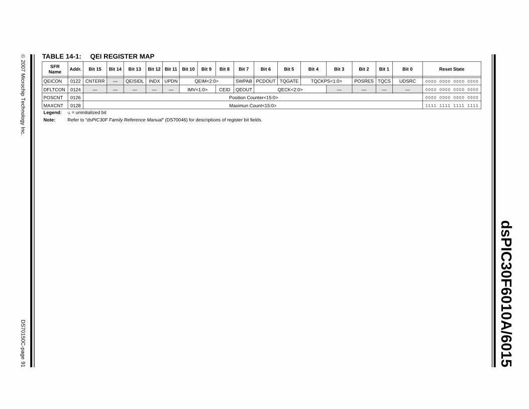
© 2007 M
icrochip Technology Inc.
DS
70150C-page 91
dsP
IC30F
6010A/6015
TA
Bit 1 Bit 0 Reset State
QE TQCS UDSRC 0000 0000 0000 0000
DF — — 0000 0000 0000 0000
PO 0000 0000 0000 0000
MA 1111 1111 1111 1111
Le
No
BLE 14-1: QEI REGISTER MAPSFR
Name Addr. Bit 15 Bit 14 Bit 13 Bit 12 Bit 11 Bit 10 Bit 9 Bit 8 Bit 7 Bit 6 Bit 5 Bit 4 Bit 3 Bit 2
ICON 0122 CNTERR — QEISIDL INDX UPDN QEIM<2:0> SWPAB PCDOUT TQGATE TQCKPS<1:0> POSRES
LTCON 0124 — — — — — IMV<1:0> CEID QEOUT QECK<2:0> — —
SCNT 0126 Position Counter<15:0>
XCNT 0128 Maximun Count<15:0>
gend: u = uninitialized bit
te: Refer to “dsPIC30F Family Reference Manual” (DS70046) for descriptions of register bit fields.

dsPIC30F6010A/6015
NOTES:
DS70150C-page 92 © 2007 Microchip Technology Inc.
dsPIC30F6010A/6015
15.0 MOTOR CONTROL PWM MODULE
This module simplifies the task of generating multiple,synchronized Pulse-Width Modulated (PWM) outputs.In particular, the following power and motion controlapplications are supported by the PWM module:
• Three Phase AC Induction Motor
• Switched Reluctance (SR) Motor• Brushless DC (BLDC) Motor• Uninterruptible Power Supply (UPS)
The PWM module has the following features:
• 8 PWM I/O pins with 4 duty cycle generators• Up to 16-bit resolution
• ‘On-the-Fly’ PWM frequency changes• Edge and Center-Aligned Output modes• Single Pulse Generation mode
• Interrupt support for asymmetrical updates in Center-Aligned mode
• Output override control for Electrically Commutative Motor (ECM) operation
• ‘Special Event’ comparator for scheduling other peripheral events
• Fault pins to optionally drive each of the PWM output pins to a defined state
• Duty cycle updates are configurable to be immediate or synchronized to the PWM time base
This module contains 4 duty cycle generators, num-bered 1 through 4. The module has 8 PWM output pins,numbered PWM1H/PWM1L through PWM4H/PWM4L.The eight I/O pins are grouped into high/low numberedpairs, denoted by the suffix H or L, respectively. Forcomplementary loads, the low PWM pins are alwaysthe complement of the corresponding high I/O pin.
The PWM module allows several modes of operationwhich are beneficial for specific power controlapplications.
Note: This data sheet summarizes features of thisgroup of dsPIC30F devices and is not intended to bea complete reference source. For more informationon the CPU, peripherals, register descriptions andgeneral device functionality, refer to the “dsPIC30FFamily Reference Manual” (DS70046).
© 2007 Microchip Technology Inc. DS70150C-page 93

dsPIC30F6010A/6015
FIGURE 15-1: PWM MODULE BLOCK DIAGRAM
PDC4
PDC4 Buffer
PWMCON1
PTPER Buffer
PWMCON2
PTPER
PTMR
Comparator
Comparator
Channel 4 Dead-TimeGenerator and
PTCON
SEVTCMP
ComparatorSpecial Event Trigger
FLTBCON
OVDCON
PWM Enable and Mode SFRs
PWM ManualControl SFR
Channel 3 Dead-TimeGenerator and
Channel 2 Dead-TimeGenerator and
PWM Generator#3
PWM Generator#2
PWM Generator #4
SEVTDIR
PTDIR
DTCON1 Dead-Time Control SFRs
Special EventPostscaler
PWM1L
PWM1H
PWM2L
PWM2H
PWM3L
PWM3H
PWM Generator#1 Channel 1 Dead-Time
Generator and
Note: Details of PWM Generator #1, #2 and #3 not shown for clarity.
16-b
it D
ata
Bus
PWM4L
PWM4H
DTCON2
FLTACON Fault Pin Control SFRs
PWM Time Base
Output
Driver
Block
FLTB
FLTA
Override Logic
Override Logic
Override Logic
Override Logic
DS70150C-page 94 © 2007 Microchip Technology Inc.

dsPIC30F6010A/6015
15.1 PWM Time Base
The PWM time base is provided by a 15-bit timer witha prescaler and postscaler. The time base is accessiblevia the PTMR SFR. PTMR<15> is a read-only Statusbit, PTDIR, that indicates the present count direction ofthe PWM time base. If PTDIR is cleared, PTMR iscounting upwards. If PTDIR is set, PTMR is countingdownwards. The PWM time base is configured via thePTCON SFR. The time base is enabled/disabled bysetting/clearing the PTEN bit in the PTCON SFR.PTMR is not cleared when the PTEN bit is cleared insoftware.
The PTPER SFR sets the counting period for PTMR.The user must write a 15-bit value to PTPER<14:0>.When the value in PTMR<14:0> matches the value inPTPER<14:0>, the time base will either reset to ‘0’, orreverse the count direction on the next occurring clockcycle. The action taken depends on the operatingmode of the time base.
The PWM time base can be configured for four differentmodes of operation:
• Free-Running mode• Single-Shot mode• Continuous Up/Down Count mode
• Continuous Up/Down Count mode with interrupts for double updates
These four modes are selected by the PTMOD<1:0>bits in the PTCON SFR. The Up/Down Counting modessupport center-aligned PWM generation. The Single-Shot mode allows the PWM module to support pulsecontrol of certain Electronically Commutative Motors(ECMs).
The interrupt signals generated by the PWM time basedepend on the mode selection bits (PTMOD<1:0>) andthe postscaler bits (PTOPS<3:0>) in the PTCON SFR.
15.1.1 FREE-RUNNING MODE
In the Free-Running mode, the PWM time base countsupwards until the value in the Time Base Period regis-ter (PTPER) is matched. The PTMR register is reset onthe following input clock edge and the time base willcontinue to count upwards as long as the PTEN bitremains set.
When the PWM time base is in the Free-Running mode(PTMOD<1:0> = 00), an interrupt event is generatedeach time a match with the PTPER register occurs andthe PTMR register is reset to zero. The postscalerselection bits may be used in this mode of the timer toreduce the frequency of the interrupt events.
15.1.2 SINGLE-SHOT MODE
In the Single-Shot Counting mode, the PWM time basebegins counting upwards when the PTEN bit is set.When the value in the PTMR register matches thePTPER register, the PTMR register will be reset on thefollowing input clock edge and the PTEN bit will becleared by the hardware to halt the time base.
When the PWM time base is in the Single-Shot mode(PTMOD<1:0> = 01), an interrupt event is generatedwhen a match with the PTPER register occurs, thePTMR register is reset to zero on the following inputclock edge, and the PTEN bit is cleared. The postscalerselection bits have no effect in this mode of the timer.
15.1.3 CONTINUOUS UP/DOWN COUNTING MODES
In the Continuous Up/Down Counting modes, the PWMtime base counts upwards until the value in the PTPERregister is matched. The timer will begin countingdownwards on the following input clock edge. ThePTDIR bit in the PTMR SFR is read-only and indicatesthe counting direction The PTDIR bit is set when thetimer counts downwards.
In the Up/Down Counting mode (PTMOD<1:0> = 10),an interrupt event is generated each time the value ofthe PTMR register becomes zero and the PWM timebase begins to count upwards. The postscaler selec-tion bits may be used in this mode of the timer to reducethe frequency of the interrupt events.
Note: If the Period register is set to 0x0000, thetimer will stop counting, and the interruptand the special event trigger will not begenerated, even if the special event valueis also 0x0000. The module will not updatethe Period register, if it is already at0x0000; therefore, the user must disablethe module in order to update the Periodregister.
© 2007 Microchip Technology Inc. DS70150C-page 95
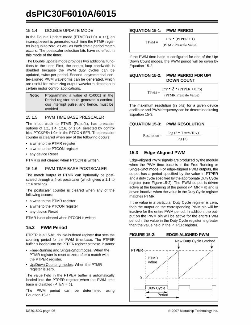
dsPIC30F6010A/6015
15.1.4 DOUBLE UPDATE MODE
In the Double Update mode (PTMOD<1:0> = 11), aninterrupt event is generated each time the PTMR regis-ter is equal to zero, as well as each time a period matchoccurs. The postscaler selection bits have no effect inthis mode of the timer.
The Double Update mode provides two additional func-tions to the user. First, the control loop bandwidth isdoubled because the PWM duty cycles can beupdated, twice per period. Second, asymmetrical cen-ter-aligned PWM waveforms can be generated, whichare useful for minimizing output waveform distortion incertain motor control applications.
15.1.5 PWM TIME BASE PRESCALER
The input clock to PTMR (FOSC/4), has prescaleroptions of 1:1, 1:4, 1:16, or 1:64, selected by controlbits, PTCKPS<1:0>, in the PTCON SFR. The prescalercounter is cleared when any of the following occurs:
• a write to the PTMR register• a write to the PTCON register• any device Reset
PTMR is not cleared when PTCON is written.
15.1.6 PWM TIME BASE POSTSCALER
The match output of PTMR can optionally be post-scaled through a 4-bit postscaler (which gives a 1:1 to1:16 scaling).
The postscaler counter is cleared when any of thefollowing occurs:
• a write to the PTMR register
• a write to the PTCON register• any device Reset
PTMR is not cleared when PTCON is written.
15.2 PWM Period
PTPER is a 15-bit, double-buffered register that sets thecounting period for the PWM time base. The PTPERbuffer is loaded into the PTPER register at these instants:
• Free-Running and Single-Shot modes: When the PTMR register is reset to zero after a match with the PTPER register.
• Up/Down Counting modes: When the PTMR register is zero.
The value held in the PTPER buffer is automaticallyloaded into the PTPER register when the PWM timebase is disabled (PTEN = 0).
The PWM period can be determined usingEquation 15-1:
EQUATION 15-1: PWM PERIOD
If the PWM time base is configured for one of the Up/Down Count modes, the PWM period will be given byEquation 15-2.
EQUATION 15-2: PWM PERIOD FOR UP/DOWN COUNT
The maximum resolution (in bits) for a given deviceoscillator and PWM frequency can be determined usingEquation 15-3:
EQUATION 15-3: PWM RESOLUTION
15.3 Edge-Aligned PWM
Edge-aligned PWM signals are produced by the modulewhen the PWM time base is in the Free-Running orSingle-Shot mode. For edge-aligned PWM outputs, theoutput has a period specified by the value in PTPERand a duty cycle specified by the appropriate Duty Cycleregister (see Figure 15-2). The PWM output is drivenactive at the beginning of the period (PTMR = 0) and isdriven inactive when the value in the Duty Cycle registermatches PTMR.
If the value in a particular Duty Cycle register is zero,then the output on the corresponding PWM pin will beinactive for the entire PWM period. In addition, the out-put on the PWM pin will be active for the entire PWMperiod if the value in the Duty Cycle register is greaterthan the value held in the PTPER register.
FIGURE 15-2: EDGE-ALIGNED PWM
Note: Programming a value of 0x0001 in thePeriod register could generate a continu-ous interrupt pulse, and hence, must beavoided.
TPWM =TCY • (PTPER + 1)
(PTMR Prescale Value)
TPWM =TCY • 2 • (PTPER + 0.75)
(PTMR Prescale Value)
Resolution =log (2 • TPWM/TCY)
log (2)
Period
Duty Cycle
0
PTPER
PTMRValue
New Duty Cycle Latched
DS70150C-page 96 © 2007 Microchip Technology Inc.

dsPIC30F6010A/6015
15.4 Center-Aligned PWM
Center-aligned PWM signals are produced by the mod-ule when the PWM time base is configured in an Up/Down Counting mode (see Figure 15-3).
The PWM compare output is driven to the active statewhen the value of the Duty Cycle register matches thevalue of PTMR and the PWM time base is countingdownwards (PTDIR = 1). The PWM compare output isdriven to the inactive state when the PWM time base iscounting upwards (PTDIR = 0) and the value in thePTMR register matches the duty cycle value.
If the value in a particular Duty Cycle register is zero,then the output on the corresponding PWM pin will beinactive for the entire PWM period. In addition, the out-put on the PWM pin will be active for the entire PWMperiod if the value in the Duty Cycle register is equal tothe value held in the PTPER register.
FIGURE 15-3: CENTER-ALIGNED PWM
15.5 PWM Duty Cycle Comparison Units
There are four 16-bit Special Function Registers(PDC1, PDC2, PDC3 and PDC4) used to specify dutycycle values for the PWM module.
The value in each Duty Cycle register determines theamount of time that the PWM output is in the activestate. The Duty Cycle registers are 16-bits wide. TheLSb of a Duty Cycle register determines whether thePWM edge occurs in the beginning. Thus, the PWMresolution is effectively doubled.
15.5.1 DUTY CYCLE REGISTER BUFFERS
The four PWM Duty Cycle registers are double-buffered to allow glitchless updates of the PWMoutputs. For each duty cycle, there is a Duty Cycle reg-ister that is accessible by the user and a second DutyCycle register that holds the actual compare valueused in the present PWM period.
For edge-aligned PWM output, a new duty cycle valuewill be updated whenever a match with the PTPER reg-ister occurs and PTMR is reset. The contents of theduty cycle buffers are automatically loaded into theDuty Cycle registers when the PWM time base is dis-abled (PTEN = 0) and the UDIS bit is cleared inPWMCON2.
When the PWM time base is in the Up/Down Countingmode, new duty cycle values are updated when thevalue of the PTMR register is zero and the PWM timebase begins to count upwards. The contents of the dutycycle buffers are automatically loaded into the DutyCycle registers when the PWM time base is disabled(PTEN = 0).
When the PWM time base is in the Up/Down Countingmode with double updates, new duty cycle values areupdated when the value of the PTMR register is zero,and when the value of the PTMR register matches thevalue in the PTPER register. The contents of the dutycycle buffers are automatically loaded into the DutyCycle registers when the PWM time base is disabled(PTEN = 0).
15.5.2 DUTY CYCLE IMMEDIATE UPDATES
When the Immediate Update Enable bit is set (IUE = 1),any write to the Duty Cycle registers will update thenew duty cycle value immediately. This feature givesthe option to the user to allow immediate updates of theactive PWM Duty Cycle registers instead of waiting forthe end of the current time base period. System stabil-ity is improved in closed loop servo applications byreducing the delay between system observation andthe issuance of system corrective commands whenimmediate updates are enabled (IUE = 1).
If the PWM output is active at the time the new dutycycle is written and the new duty cycle is less than thecurrent time base value, the PWM pulse width will beshortened. If the PWM output is active at the time thenew duty cycle is written and the new duty cycle isgreater than the current time base value, the PWMpulse width will be lengthened.
If the PWM output is inactive at the time the new dutycycle is written and the new duty cycle is greater thanthe current time base value, the PWM output willbecome active immediately and will remain active forthe new written duty cycle value.
0
PTPERPTMRValue
Period
Period/2
DutyCycle
© 2007 Microchip Technology Inc. DS70150C-page 97
dsPIC30F6010A/6015
15.6 Complementary PWM Operation
In the Complementary mode of operation, each pair ofPWM outputs is obtained by a complementary PWMsignal. A dead time may be optionally inserted duringdevice switching, when both outputs are inactive for ashort period (Refer to Section 15.7 “Dead-TimeGenerators”).
In Complementary mode, the duty cycle comparisonunits are assigned to the PWM outputs as follows:
• PDC1 register controls PWM1H/PWM1L outputs
• PDC2 register controls PWM2H/PWM2L outputs• PDC3 register controls PWM3H/PWM3L outputs• PDC4 register controls PWM4H/PWM4L outputs
The Complementary mode is selected for each PWMI/O pin pair by clearing the appropriate PMODx bit in thePWMCON1 SFR. The PWM I/O pins are set toComplementary mode by default upon a device Reset.
15.7 Dead-Time Generators
Dead-time generation may be provided when any ofthe PWM I/O pin pairs are operating in theComplementary Output mode. The PWM outputs usePush-Pull drive circuits. Due to the inability of thepower output devices to switch instantaneously, someamount of time must be provided between the turn offevent of one PWM output in a complementary pair andthe turn on event of the other transistor.
The PWM module allows two different dead times to beprogrammed. These two dead times may be used inone of two methods described below to increase userflexibility:
• The PWM output signals can be optimized for different turn off times in the high side and low side transistors in a complementary pair of tran-sistors. The first dead time is inserted between the turn off event of the lower transistor of the complementary pair and the turn on event of the upper transistor. The second dead time is inserted between the turn off event of the upper transistor and the turn on event of the lower transistor.
• The two dead times can be assigned to individual PWM I/O pin pairs. This Operating mode allows the PWM module to drive different transistor/load combinations with each complementary PWM I/O pin pair.
15.7.1 DEAD-TIME GENERATORS
Each complementary output pair for the PWM modulehas a 6-bit down counter that is used to produce thedead-time insertion. As shown in Figure 15-4, eachdead-time unit has a rising and falling edge detectorconnected to the duty cycle comparison output.
15.7.2 DEAD-TIME ASSIGNMENT
The DTCON2 SFR contains control bits that allow thedead times to be assigned to each of the complemen-tary outputs. Table 15-1 summarizes the function ofeach dead-time selection control bit.
TABLE 15-1: DEAD-TIME SELECTION BITS
15.7.3 DEAD-TIME RANGES
The amount of dead time provided by each dead-timeunit is selected by specifying the input clock prescalervalue and a 6-bit unsigned value. The amount of deadtime provided by each unit may be set independently.
Four input clock prescaler selections have been pro-vided to allow a suitable range of dead times, based onthe device operating frequency. The clock prescaleroption may be selected independently for each of thetwo dead-time values. The dead-time clock prescalervalues are selected using the DTAPS<1:0> andDTBPS<1:0> control bits in the DTCON1 SFR. One offour clock prescaler options (TCY, 2 TCY, 4 TCY or 8 TCY)may be selected for each of the dead-time values.
After the prescaler values are selected, the dead timefor each unit is adjusted by loading two 6-bit unsignedvalues into the DTCON1 SFR.
The dead-time unit prescalers are cleared on thefollowing events:
• On a load of the down timer due to a duty cycle comparison edge event.
• On a write to the DTCON1 or DTCON2 registers.• On any device Reset.
Bit Function
DTS1A Selects PWM1L/PWM1H active edge dead time.
DTS1I Selects PWM1L/PWM1H inactive edge dead time.
DTS2A Selects PWM2L/PWM2H active edge dead time.
DTS2I Selects PWM2L/PWM2H inactive edge dead time.
DTS3A Selects PWM3L/PWM3H active edge dead time.
DTS3I Selects PWM3L/PWM3H inactive edge dead time.
DTS4A Selects PWM4L/PWM4H active edge dead time.
DTS4I Selects PWM4L/PWM4H inactive edge dead time.
Note: The user should not modify the DTCON1or DTCON2 values while the PWM mod-ule is operating (PTEN = 1). Unexpectedresults may occur.
DS70150C-page 98 © 2007 Microchip Technology Inc.
dsPIC30F6010A/6015
FIGURE 15-4: DEAD-TIME TIMING DIAGRAM
15.8 Independent PWM Output
An independent PWM Output mode is required for driv-ing certain types of loads. A particular PWM output pairis in the Independent Output mode when the corre-sponding PMOD bit in the PWMCON1 register is set.No dead-time control is implemented between adjacentPWM I/O pins when the module is operating in theIndependent mode and both I/O pins are allowed to beactive simultaneously.
In the Independent mode, each duty cycle generator isconnected to both of the PWM I/O pins in an outputpair. By using the associated Duty Cycle register andthe appropriate bits in the OVDCON register, the usermay select the following signal output options for eachPWM I/O pin operating in the Independent mode:
• I/O pin outputs PWM signal• I/O pin inactive
• I/O pin active
15.9 Single-Pulse PWM Operation
The PWM module produces single pulse outputs whenthe PTCON control bits PTMOD<1:0> = 10. Only edge-aligned outputs may be produced in the Single-Pulsemode. In Single-Pulse mode, the PWM I/O pin(s) aredriven to the active state when the PTEN bit is set.When a match with a Duty Cycle register occurs, thePWM I/O pin is driven to the inactive state. When amatch with the PTPER register occurs, the PTMRregister is cleared, all active PWM I/O pins are drivento the inactive state, the PTEN bit is cleared, and aninterrupt is generated.
15.10 PWM Output Override
The PWM output override bits allow the user to manu-ally drive the PWM I/O pins to specified logic states,independent of the duty cycle comparison units.
All control bits associated with the PWM output over-ride function are contained in the OVDCON register.The upper half of the OVDCON register contains eightbits, POVDxH<4:1> and POVDxL<4:1>, that determinewhich PWM I/O pins will be overridden. The lower halfof the OVDCON register contains eight bits,POUTxH<4:1> and POUTxL<4:1>, that determine thestate of the PWM I/O pins when a particular output isoverridden via the POVD bits.
15.10.1 COMPLEMENTARY OUTPUT MODE
When a PWMxL pin is driven active via the OVDCONregister, the output signal is forced to be the comple-ment of the corresponding PWMxH pin in the pair.Dead-time insertion is still performed when PWMchannels are overridden manually.
15.10.2 OVERRIDE SYNCHRONIZATION
If the OSYNC bit in the PWMCON2 register is set, alloutput overrides performed via the OVDCON registerare synchronized to the PWM time base. Synchronousoutput overrides occur at the following times:
• Edge-Aligned mode, when PTMR is zero.
• Center-Aligned modes, when PTMR is zero and when the value of PTMR matches PTPER.
Duty Cycle Generator
PWMxH
PWMxL
Time selected by DTSxA bit (A or B) Time selected by DTSxI bit (A or B)
© 2007 Microchip Technology Inc. DS70150C-page 99

dsPIC30F6010A/6015
15.11 PWM Output and Polarity Control
There are three device Configuration bits associatedwith the PWM module that provide PWM output pincontrol:
• HPOL Configuration bit• LPOL Configuration bit• PWMPIN Configuration bit
These three bits in the FPORBOR Configuration regis-ter (see Section 21.0 “System Integration”) work inconjunction with the four PWM Enable bits (PENxH andPENxL) located in the PWMCON1 SFR. The Configu-ration bits and PWM Enable bits ensure that the PWMpins are in the correct states after a device Resetoccurs. The PWMPIN configuration fuse allows thePWM module outputs to be optionally enabled on adevice Reset. If PWMPIN = 0, the PWM outputs will bedriven to their inactive states at Reset. If PWMPIN = 1(default), the PWM outputs will be tri-stated. The HPOLbit specifies the polarity for the PWMxH outputs,whereas the LPOL bit specifies the polarity for thePWMxL outputs.
15.11.1 OUTPUT PIN CONTROL
The PEN<4:1>H and PEN<4:1>L control bits in thePWMCON1 SFR enable each high PWM output pinand each low PWM output pin, respectively. If a partic-ular PWM output pin is not enabled, it is treated as ageneral purpose I/O pin.
15.12 PWM Fault Pins
There are two Fault pins (FLTA and FLTB) associatedwith the PWM module. When asserted, these pins canoptionally drive each of the PWM I/O pins to a definedstate.
15.12.1 FAULT PIN ENABLE BITS
The FLTACON and FLTBCON SFRs each have 4 con-trol bits that determine whether a particular pair ofPWM I/O pins is to be controlled by the Fault input pin.To enable a specific PWM I/O pin pair for Faultoverrides, the corresponding bit should be set in theFLTACON or FLTBCON register.
If all enable bits are cleared in the FLTACON orFLTBCON registers, then the corresponding Fault inputpin has no effect on the PWM module and the pin maybe used as a general purpose interrupt or I/O pin.
15.12.2 FAULT STATES
The FLTACON and FLTBCON Special Function Regis-ters have 8 bits each that determine the state of eachPWM I/O pin when it is overridden by a Fault input.When these bits are cleared, the PWM I/O pin is drivento the inactive state. If the bit is set, the PWM I/O pinwill be driven to the active state. The active and inactivestates are referenced to the polarity defined for eachPWM I/O pin (HPOL and LPOL polarity control bits).
A special case exists when a PWM module I/O pair isin the Complementary mode and both pins are pro-grammed to be active on a Fault condition. ThePWMxH pin always has priority in the Complementarymode, so that both I/O pins cannot be driven activesimultaneously.
15.12.3 FAULT PIN PRIORITY
If both Fault input pins have been assigned to control aparticular PWM I/O pin, the Fault state programmed forthe Fault A input pin will take priority over the Fault Binput pin.
15.12.4 FAULT INPUT MODES
Each of the Fault input pins has two modes ofoperation:
• Latched Mode: When the Fault pin is driven low, the PWM outputs will go to the states defined in the FLTACON/FLTBCON register. The PWM out-puts will remain in this state until the Fault pin is driven high and the corresponding interrupt flag has been cleared in software. When both of these actions have occurred, the PWM outputs will return to normal operation at the beginning of the next PWM cycle or half-cycle boundary. If the interrupt flag is cleared before the Fault condition ends, the PWM module will wait until the Fault pin is no longer asserted, to restore the outputs.
• Cycle-by-Cycle Mode: When the Fault input pin is driven low, the PWM outputs remain in the defined Fault states for as long as the Fault pin is held low. After the Fault pin is driven high, the PWM outputs return to normal operation at the beginning of the following PWM cycle or half-cycle boundary.
The Operating mode for each Fault input pin is selectedusing the FLTAM and FLTBM control bits in theFLTACON and FLTBCON Special Function Registers.
Each of the Fault pins can be controlled manually insoftware.
Note: The Fault pin logic can operate indepen-dent of the PWM logic. If all the enable bitsin the FLTACON/FLTBCON register arecleared, then the Fault pin(s) could beused as general purpose interrupt pin(s).Each Fault pin has an interrupt vector,Interrupt Flag bit and Interrupt Priority bitsassociated with it.
DS70150C-page 100 © 2007 Microchip Technology Inc.
dsPIC30F6010A/6015
15.13 PWM Update Lockout
For a complex PWM application, the user may need towrite up to four Duty Cycle registers and the Time BasePeriod register, PTPER, at a given time. In some appli-cations, it is important that all buffer registers be writtenbefore the new duty cycle and period values are loadedfor use by the module.
The PWM update lockout feature is enabled by settingthe UDIS control bit in the PWMCON2 SFR. The UDISbit affects all Duty Cycle Buffer registers and the PWMtime base period buffer, PTPER. No duty cyclechanges or period value changes will have effect whileUDIS = 1.
If the IUE bit is set, any change to the Duty Cycle reg-isters will be immediately updated regardless of theUDIS bit state. The PWM Period register updates(PTPER) are not affected by the IUE control bit.
15.14 PWM Special Event Trigger
The PWM module has a special event trigger thatallows A/D conversions to be synchronized to the PWMtime base. The A/D sampling and conversion time maybe programmed to occur at any point within the PWMperiod. The special event trigger allows the user to min-imize the delay between the time when A/D conversionresults are acquired and the time when the duty cyclevalue is updated.
The PWM special event trigger has an SFR namedSEVTCMP, and five control bits to control its operation.The PTMR value for which a special event triggershould occur is loaded into the SEVTCMP register.When the PWM time base is in an Up/Down Countingmode, an additional control bit is required to specify thecounting phase for the special event trigger. The countphase is selected using the SEVTDIR control bit in theSEVTCMP SFR. If the SEVTDIR bit is cleared, the spe-cial event trigger will occur on the upward countingcycle of the PWM time base. If the SEVTDIR bit is set,the special event trigger will occur on the downwardcount cycle of the PWM time base. The SEVTDIRcontrol bit has no effect unless the PWM time base isconfigured for an Up/Down Counting mode.
15.14.1 SPECIAL EVENT TRIGGER POSTSCALER
The PWM special event trigger has a postscaler thatallows a 1:1 to 1:16 postscale ratio. The postscaler isconfigured by writing the SEVOPS<3:0> control bits inthe PWMCON2 SFR.
The special event output postscaler is cleared on thefollowing events:
• Any write to the SEVTCMP register• Any device Reset
15.15 PWM Operation During CPU Sleep Mode
The Fault A and Fault B input pins have the ability towake the CPU from Sleep mode. The PWM modulegenerates an interrupt if either of the Fault pins isdriven low while in Sleep.
15.16 PWM Operation During CPU Idle Mode
The PTCON SFR contains a PTSIDL control bit. Thisbit determines if the PWM module will continue tooperate or stop when the device enters Idle mode. IfPTSIDL = 0, the module will continue to operate. IfPTSIDL = 1, the module will stop operation as long asthe CPU remains in Idle mode.
© 2007 Microchip Technology Inc. DS70150C-page 101

dsP
IC30F
6010A/6015
DS
70150C-page 102
© 2007 M
icrochip Technology Inc.
Bit 2 Bit 1 Bit 0 Reset State
S<1:0> PTMOD<1:0> 0000 0000 0000 0000
0000 0000 0000 0000
0111 1111 1111 1111
0000 0000 0000 0000
PEN3L PEN2L PEN1L 0000 0000 1111 1111
IUE OSYNC UDIS 0000 0000 0000 0000
e A Value 0000 0000 0000 0000
DTS2I DTS1A DTS1I 0000 0000 0000 0000
FAEN3 FAEN2 FAEN1 0000 0000 0000 0000
FBEN3 FBEN2 FBEN1 0000 0000 0000 0000
POUT2L POUT1H POUT1L 1111 1111 0000 0000
0000 0000 0000 0000
0000 0000 0000 0000
0000 0000 0000 0000
0000 0000 0000 0000
TABLE 15-2: 8-OUTPUT PWM REGISTER MAP
SFR Name Addr. Bit 15 Bit 14 Bit 13 Bit 12 Bit 11 Bit 10 Bit 9 Bit 8 Bit 7 Bit 6 Bit 5 Bit 4 Bit 3
PTCON 01C0 PTEN — PTSIDL — — — — — PTOPS<3:0> PTCKP
PTMR 01C2 PTDIR PWM Timer Count Value
PTPER 01C4 — PWM Time Base Period Register
SEVTCMP 01C6 SEVTDIR PWM Special Event Compare Register
PWMCON1 01C8 — — — — PTMOD4 PTMOD3 PTMOD2 PTMOD1 PEN4H PEN3H PEN2H PEN1H PEN4L
PWMCON2 01CA — — — — SEVOPS<3:0> — — — — —
DTCON1 01CC DTBPS<1:0> Dead-Time B Value DTAPS<1:0> Dead-Tim
DTCON2 01CE — — — — — — — — DTS4A DTS4I DTS3A DTS3I DTS2A
FLTACON 01D0 FAOV4H FAOV4L FAOV3H FAOV3L FAOV2H FAOV2L FAOV1H FAOV1L FLTAM — — — FAEN4
FLTBCON 01D2 FBOV4H FBOV4L FBOV3H FBOV3L FBOV2H FBOV2L FBOV1H FBOV1L FLTBM — — — FBEN4
OVDCON 01D4 POVD4H POVD4L POVD3H POVD3L POVD2H POVD2L POVD1H POVD1L POUT4H POUT4L POUT3H POUT3L POUT2H
PDC1 01D6 PWM Duty Cycle #1 Register
PDC2 01D8 PWM Duty Cycle #2 Register
PDC3 01DA PWM Duty Cycle #3 Register
PDC4 01DC PWM Duty Cycle #4 Register
Legend: u = uninitialized bit
Note: Refer to “dsPIC30F Family Reference Manual” (DS70046) for descriptions of register bit fields.

dsPIC30F6010A/6015
16.0 SPI MODULE
The Serial Peripheral Interface (SPI) module is asynchronous serial interface. It is useful for communi-cating with other peripheral devices such asEEPROMs, shift registers, display drivers and A/Dconverters, or other microcontrollers. It is compatiblewith Motorola’s SPI and SIOP interfaces.
16.1 Operating Function Description
Each SPI module consists of a 16-bit shift register,SPIxSR (where x = 1 or 2), used for shifting data inand out, and a buffer register, SPIxBUF. A control reg-ister, SPIxCON, configures the module. Additionally, aSTATUS register, SPIxSTAT, indicates various statusconditions.
The serial interface consists of 4 pins: SDIx (SerialData Input), SDOx (Serial Data Output), SCKx (ShiftClock Input or Output) and SSx (active-low SlaveSelect).
In Master mode operation, SCK is a clock output, butin Slave mode, it is a clock input.
A series of eight (8) or sixteen (16) clock pulses shiftsout bits from the SPIxSR to SDOx pin and simulta-neously shifts in data from SDIx pin. An interrupt isgenerated when the transfer is complete and the cor-responding interrupt flag bit (SPI1IF or SPI2IF) is set.This interrupt can be disabled through an interruptenable bit (SPI1IE or SPI2IE).
The receive operation is double-buffered. When acomplete byte is received, it is transferred fromSPIxSR to SPIxBUF.
If the receive buffer is full when new data is beingtransferred from SPIxSR to SPIxBUF, the module willset the SPIROV bit, indicating an overflow condition.The transfer of the data from SPIxSR to SPIxBUF willnot be completed and the new data will be lost. Themodule will not respond to SCL transitions whileSPIROV is ‘1’, effectively disabling the module untilSPIxBUF is read by user software.
Transmit writes are also double-buffered. The userwrites to SPIxBUF. When the master or slave transferis completed, the contents of the shift register(SPIxSR) is moved to the receive buffer. If any trans-mit data has been written to the buffer register, thecontents of the transmit buffer are moved to SPIxSR.The received data is thus placed in SPIxBUF and thetransmit data in SPIxSR is ready for the next transfer.
In Master mode, the clock is generated by prescalingthe system clock. Data is transmitted as soon as avalue is written to SPIxBUF. The interrupt is generatedat the middle of the transfer of the last bit.
In Slave mode, data is transmitted and received asexternal clock pulses appear on SCK. Again, the inter-rupt is generated when the last bit is latched. If SSxcontrol is enabled, then transmission and receptionare enabled only when SSx = low. The SDOx outputwill be disabled in SSx mode with SSx high.
The clock provided to the module is (FOSC/4). Thisclock is then prescaled by the primary (PPRE<1:0>)and the secondary (SPRE<2:0>) prescale factors. TheCKE bit determines whether transmit occurs on transi-tion from active clock state to Idle clock state, or viceversa. The CKP bit selects the Idle state (high or low)for the clock.
16.1.1 WORD AND BYTE COMMUNICATION
A control bit, MODE16 (SPIxCON<10>), allows themodule to communicate in either 16-bit or 8-bit mode.16-bit operation is identical to 8-bit operation, exceptthat the number of bits transmitted is 16 instead of 8.
The user software must disable the module prior tochanging the MODE16 bit. The SPI module is resetwhen the MODE16 bit is changed by the user.
A basic difference between 8-bit and 16-bit operation isthat the data is transmitted out of bit 7 of the SPIxSR for8-bit operation, and data is transmitted out of bit 15 ofthe SPIxSR for 16-bit operation. In both modes, data isshifted into bit 0 of the SPIxSR.
16.1.2 SDOx DISABLE
A control bit, DISSDO, is provided to the SPIxCON reg-ister to allow the SDOx output to be disabled. This willallow the SPI module to be connected in an input onlyconfiguration. SDO can also be used for generalpurpose I/O.
Note: This data sheet summarizes features of this groupof dsPIC30F devices and is not intended to be a completereference source. For more information on the CPU,peripherals, register descriptions and general devicefunctionality, refer to the “dsPIC30F Family ReferenceManual” (DS70046).
Note: The user must perform reads of SPIxBUFif the module is used in a transmit onlyconfiguration to avoid a receive overflowcondition. (SPIROV = 1)
Note: Both the transmit buffer (SPIxTXB) andthe receive buffer (SPIxRXB) are mappedto the same register address, SPIxBUF.
© 2007 Microchip Technology Inc. DS70150C-page 103
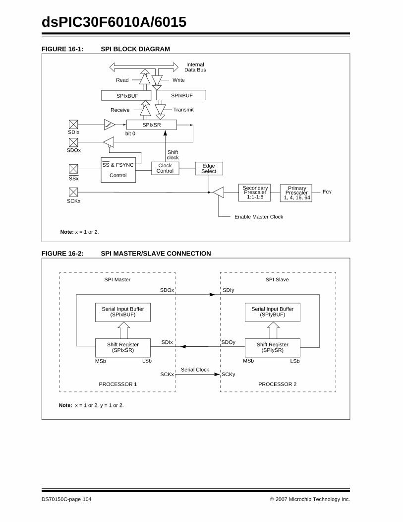
dsPIC30F6010A/6015
FIGURE 16-1: SPI BLOCK DIAGRAM
FIGURE 16-2: SPI MASTER/SLAVE CONNECTION
Note: x = 1 or 2.
Read Write
InternalData Bus
SDIx
SDOx
SSx
SCKx
SPIxSR
SPIxBUF
bit 0
Shiftclock
EdgeSelect
FCYPrimary
1, 4, 16, 64
Enable Master Clock
PrescalerSecondaryPrescaler
1:1-1:8
SS & FSYNC
Control
ClockControl
Transmit
SPIxBUF
Receive
Serial Input Buffer(SPIxBUF)
Shift Register(SPIxSR)
MSb LSb
SDOx
SDIx
PROCESSOR 1
SCKx
SPI Master
Serial Input Buffer(SPIyBUF)
Shift Register(SPIySR)
LSbMSb
SDIy
SDOy
PROCESSOR 2
SCKy
SPI Slave
Serial Clock
Note: x = 1 or 2, y = 1 or 2.
DS70150C-page 104 © 2007 Microchip Technology Inc.

dsPIC30F6010A/6015
16.2 Framed SPI Support
The module supports a basic framed SPI protocol inMaster or Slave mode. The control bit, FRMEN,enables framed SPI support and causes the SSx pin toperform the Frame Synchronization pulse (FSYNC)function. The control bit SPIFSD determines whetherthe SSx pin is an input or an output (i.e., whether themodule receives or generates the Frame Synchroniza-tion pulse). The frame pulse is an active-high pulse fora single SPI clock cycle. When Frame Synchronizationis enabled, the data transmission starts only on thesubsequent transmit edge of the SPI clock.
16.3 Slave Select Synchronization
The SSx pin allows a Synchronous Slave mode. TheSPI must be configured in SPI Slave mode, with SSxpin control enabled (SSEN = 1). When the SSx pin islow, transmission and reception are enabled, and theSDOx pin is driven. When SSx pin goes high, the SDOxpin is no longer driven. Also, the SPI module is re-synchronized, and all counters/control circuitry arereset. Therefore, when the SSx pin is asserted lowagain, transmission/reception will begin at the MSb,even if SSx had been de-asserted in the middle of atransmit/receive.
16.4 SPI Operation During CPU Sleep Mode
During Sleep mode, the SPI module is shut down. Ifthe CPU enters Sleep mode while an SPI transactionis in progress, then the transmission and reception isaborted.
The transmitter and receiver will stop in Sleep mode.However, register contents are not affected byentering or exiting Sleep mode.
16.5 SPI Operation During CPU Idle Mode
When the device enters Idle mode, all clock sourcesremain functional. The SPISIDL bit (SPIxSTAT<13>)selects if the SPI module will stop or continue on Idle.If SPISIDL = 0, the module will continue to operatewhen the CPU enters Idle mode. If SPISIDL = 1, themodule will stop when the CPU enters Idle mode.
© 2007 Microchip Technology Inc. DS70150C-page 105
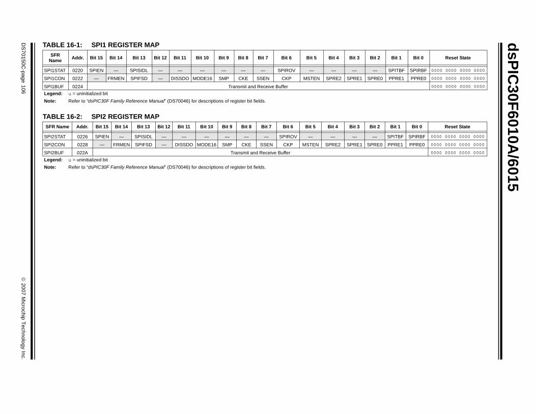
dsP
IC30F
6010A/6015
DS
70150C-page 106
© 2007 M
icrochip Technology Inc.
Bit 2 Bit 1 Bit 0 Reset State
— SPITBF SPIRBF 0000 0000 0000 0000
SPRE0 PPRE1 PPRE0 0000 0000 0000 0000
0000 0000 0000 0000
Bit 2 Bit 1 Bit 0 Reset State
— SPITBF SPIRBF 0000 0000 0000 0000
SPRE0 PPRE1 PPRE0 0000 0000 0000 0000
0000 0000 0000 0000
TABLE 16-1: SPI1 REGISTER MAP
TABLE 16-2: SPI2 REGISTER MAP
SFR Name Addr. Bit 15 Bit 14 Bit 13 Bit 12 Bit 11 Bit 10 Bit 9 Bit 8 Bit 7 Bit 6 Bit 5 Bit 4 Bit 3
SPI1STAT 0220 SPIEN — SPISIDL — — — — — — SPIROV — — —
SPI1CON 0222 — FRMEN SPIFSD — DISSDO MODE16 SMP CKE SSEN CKP MSTEN SPRE2 SPRE1
SPI1BUF 0224 Transmit and Receive Buffer
Legend: u = uninitialized bit
Note: Refer to “dsPIC30F Family Reference Manual” (DS70046) for descriptions of register bit fields.
SFR Name Addr. Bit 15 Bit 14 Bit 13 Bit 12 Bit 11 Bit 10 Bit 9 Bit 8 Bit 7 Bit 6 Bit 5 Bit 4 Bit 3
SPI2STAT 0226 SPIEN — SPISIDL — — — — — — SPIROV — — —
SPI2CON 0228 — FRMEN SPIFSD — DISSDO MODE16 SMP CKE SSEN CKP MSTEN SPRE2 SPRE1
SPI2BUF 022A Transmit and Receive Buffer
Legend: u = uninitialized bit
Note: Refer to “dsPIC30F Family Reference Manual” (DS70046) for descriptions of register bit fields.
dsPIC30F6010A/6015
17.0 I2C™ MODULE
The Inter-Integrated Circuit™ (I2C™) module providescomplete hardware support for both Slave and Multi-Master modes of the I2C serial communicationstandard, with a 16-bit interface.
This module offers the following key features:
• I2C interface supporting both Master and Slave operation.
• I2C Slave mode supports 7 and 10-bit address.• I2C Master mode supports 7 and 10-bit address.• I2C port allows bidirectional transfers between
master and slaves.• Serial clock synchronization for I2C port can be
used as a handshake mechanism to suspend and resume serial transfer (SCLREL control).
• I2C supports multi-master operation; detects bus collision and will arbitrate accordingly.
17.1 Operating Function Description
The hardware fully implements all the master andslave functions of the I2C Standard and Fast modespecifications, as well as 7 and 10-bit addressing.
Thus, the I2C module can operate either as a slave ora master on an I2C bus.
17.1.1 VARIOUS I2C MODES
The following types of I2C operation are supported:
• I2C Slave operation with 7-bit address
• I2C Slave operation with 10-bit address• I2C Master operation with 7 or 10-bit address
See the I2C programmer’s model in Figure 17-1.
17.1.2 PIN CONFIGURATION IN I2C MODE
I2C has a 2-pin interface; pin SCL is clock and pin SDAis data.
FIGURE 17-1: PROGRAMMER’S MODEL
17.1.3 I2C REGISTERS
I2CCON and I2CSTAT are control and STATUS regis-ters, respectively. The I2CCON register is readable andwritable. The lower 6 bits of I2CSTAT are read-only.The remaining bits of the I2CSTAT are read/write.
I2CRSR is the shift register used for shifting data,whereas I2CRCV is the buffer register to which databytes are written, or from which data bytes are read.I2CRCV is the receive buffer, as shown in Figure 16-1.I2CTRN is the transmit register to which bytes are writtenduring a transmit operation, as shown in Figure 16-2.
The I2CADD register holds the slave address. A Statusbit, ADD10, indicates 10-bit Address mode. TheI2CBRG acts as the Baud Rate Generator reload value.
In receive operations, I2CRSR and I2CRCV togetherform a double-buffered receiver. When I2CRSR receivesa complete byte, it is transferred to I2CRCV and an inter-rupt pulse is generated. During transmission, theI2CTRN is not double-buffered.
Note: This data sheet summarizes features of thisgroup of dsPIC30F devices and is not intended to bea complete reference source. For more informationon the CPU, peripherals, register descriptions andgeneral device functionality, refer to the “dsPIC30FFamily Reference Manual” (DS70046).
bit 7 bit 0I2CRCV (8 bits)
bit 7 bit 0I2CTRN (8 bits)
bit 8 bit 0I2CBRG (9 bits)
bit 15 bit 0I2CCON (16 bits)
bit 15 bit 0I2CSTAT (16 bits)
bit 9 bit 0I2CADD (10 bits)
Note: Following a Restart condition in 10-bitmode, the user only needs to match thefirst 7-bit address.
© 2007 Microchip Technology Inc. DS70150C-page 107

dsPIC30F6010A/6015
FIGURE 17-2: I2C™ BLOCK DIAGRAM
I2CRSR
I2CRCV
InternalData Bus
SCL
SDA
Shift
Match Detect
I2CADD
Start andStop bit Detect
Clock
Addr_Match
ClockStretching
I2CTRN
LSBShiftClock
Write
Read
BRG Down I2CBRG
ReloadControl
FCY
Start, Restart,Stop bit Generate
Write
Read
AcknowledgeGeneration
CollisionDetect
DS70150C-page 108 © 2007 Microchip Technology Inc.
dsPIC30F6010A/6015
17.2 I2C Module Addresses
The I2CADD register contains the Slave modeaddresses. The register is a 10-bit register.
If the A10M bit (I2CCON<10>) is ‘0’, the address isinterpreted by the module as a 7-bit address. When anaddress is received, it is compared to the 7 LeastSignificant bits of the I2CADD register.
If the A10M bit is ‘1’, the address is assumed to be a10-bit address. When an address is received, it will becompared with the binary value ‘1 1 1 1 0 A9 A8’(where A9, A8 are two Most Significant bits ofI2CADD). If that value matches, the next address willbe compared with the Least Significant 8 bits ofI2CADD, as specified in the 10-bit addressing protocol.
TABLE 17-1: 7-BIT I2C™ SLAVE ADDRESSES SUPPORTED BY dsPIC30F
17.3 I2C 7-bit Slave Mode Operation
Once enabled (I2CEN = 1), the slave module will waitfor a Start bit to occur (i.e., the I2C module is ‘Idle’).Following the detection of a Start bit, 8 bits are shiftedinto I2CRSR and the address is compared againstI2CADD. In 7-bit mode (A10M = 0), bits I2CADD<6:0>are compared against I2CRSR<7:1> and I2CRSR<0>is the R_W bit. All incoming bits are sampled on therising edge of SCL.
If an address match occurs, an Acknowledgement willbe sent, and the Slave Event Interrupt Flag (SI2CIF) isset on the falling edge of the ninth (ACK) bit. Theaddress match does not affect the contents of theI2CRCV buffer or the RBF bit.
17.3.1 SLAVE TRANSMISSION
If the R_W bit received is a ‘1’, then the serial port willgo into Transmit mode. It will send ACK on the ninth bitand then hold SCL to ‘0’ until the CPU responds by writ-ing to I2CTRN. SCL is released by setting the SCLRELbit, and 8 bits of data are shifted out. Data bits areshifted out on the falling edge of SCL, such that SDA isvalid during SCL high (see timing diagram). The inter-rupt pulse is sent on the falling edge of the ninth clockpulse, regardless of the status of the ACK receivedfrom the master.
17.3.2 SLAVE RECEPTION
If the R_W bit received is a ‘0’ during an addressmatch, then Receive mode is initiated. Incoming bitsare sampled on the rising edge of SCL. After 8 bits arereceived, if I2CRCV is not full or I2COV is not set,I2CRSR is transferred to I2CRCV. ACK is sent on theninth clock.
If the RBF flag is set, indicating that I2CRCV is stillholding data from a previous operation (RBF = 1), thenACK is not sent; however, the interrupt pulse is gener-ated. In the case of an overflow, the contents of theI2CRSR are not loaded into the I2CRCV.
17.4 I2C 10-bit Slave Mode Operation
In 10-bit mode, the basic receive and transmit opera-tions are the same as in the 7-bit mode. However, thecriteria for address match is more complex.
The I2C specification dictates that a slave must beaddressed for a write operation, with two address bytesfollowing a Start bit.
The A10M bit is a control bit that signifies that theaddress in I2CADD is a 10-bit address rather than a7-bit address. The address detection protocol for thefirst byte of a message address is identical for 7-bitand 10-bit messages, but the bits being compared aredifferent.
I2CADD holds the entire 10-bit address. Upon receiv-ing an address following a Start bit, I2CRSR <7:3> iscompared against a literal ‘11110’ (the default 10-bitaddress) and I2CRSR<2:1> are compared againstI2CADD<9:8>. If a match occurs and if R_W = 0, theinterrupt pulse is sent. The ADD10 bit will be cleared toindicate a partial address match. If a match fails orR_W = 1, the ADD10 bit is cleared and the modulereturns to the Idle state.
The low byte of the address is then received and com-pared with I2CADD<7:0>. If an address match occurs,the interrupt pulse is generated and the ADD10 bit isset, indicating a complete 10-bit address match. If anaddress match did not occur, the ADD10 bit is clearedand the module returns to the Idle state.
0x00 General call address or start byte
0x01-0x03 Reserved
0x04-0x07 Hs-mode Master codes
0x04-0x77 Valid 7-bit addresses
0x78-0x7b Valid 10-bit addresses (lower 7 bits)
0x7c-0x7f Reserved
Note: The I2CRCV will be loaded if the I2COVbit = 1 and the RBF flag = 0. In this case,a read of the I2CRCV was performed, butthe user did not clear the state of theI2COV bit before the next receiveoccurred. The Acknowledgement is notsent (ACK = 1) and the I2CRCV isupdated.
© 2007 Microchip Technology Inc. DS70150C-page 109
dsPIC30F6010A/6015
17.4.1 10-BIT MODE SLAVE TRANSMISSION
Once a slave is addressed in this fashion, with the full10-bit address (we will refer to this state as“PRIOR_ADDR_MATCH”), the master can beginsending data bytes for a slave reception operation.
17.4.2 10-BIT MODE SLAVE RECEPTION
Once addressed, the master can generate a RepeatedStart, reset the high byte of the address and set theR_W bit without generating a Stop bit, thus initiating aslave transmit operation.
17.5 Automatic Clock Stretch
In the slave modes, the module can synchronize bufferreads and write to the master device by clockstretching.
17.5.1 TRANSMIT CLOCK STRETCHING
Both 10-bit and 7-bit Transmit modes implement clockstretching by asserting the SCLREL bit after the fallingedge of the ninth clock if the TBF bit is cleared,indicating the buffer is empty.
In Slave Transmit modes, clock stretching is alwaysperformed, irrespective of the STREN bit.
Clock synchronization takes place following the ninthclock of the transmit sequence. If the device samplesan ACK on the falling edge of the ninth clock, and if theTBF bit is still clear, then the SCLREL bit is auto-matically cleared. The SCLREL being cleared to ‘0’will assert the SCL line low. The user’s ISR must setthe SCLREL bit before transmission is allowed to con-tinue. By holding the SCL line low, the user has time toservice the ISR and load the contents of the I2CTRNbefore the master device can initiate another transmitsequence.
17.5.2 RECEIVE CLOCK STRETCHING
The STREN bit in the I2CCON register can be used toenable clock stretching in Slave Receive mode. Whenthe STREN bit is set, the SCL pin will be held low atthe end of each data receive sequence.
17.5.3 CLOCK STRETCHING DURING 7-BIT ADDRESSING (STREN = 1)
When the STREN bit is set in Slave Receive mode,the SCL line is held low when the buffer register is full.The method for stretching the SCL output is the samefor both 7 and 10-bit addressing modes.
Clock stretching takes place following the ninth clock ofthe receive sequence. On the falling edge of the ninthclock at the end of the ACK sequence, if the RBF bit isset, the SCLREL bit is automatically cleared, forcing theSCL output to be held low. The user’s ISR must set theSCLREL bit before reception is allowed to continue. Byholding the SCL line low, the user has time to servicethe ISR and read the contents of the I2CRCV before themaster device can initiate another receive sequence.This will prevent buffer overruns from occurring.
17.5.4 CLOCK STRETCHING DURING 10-BIT ADDRESSING (STREN = 1)
Clock stretching takes place automatically during theaddressing sequence. Because this module has aregister for the entire address, it is not necessary forthe protocol to wait for the address to be updated.
After the address phase is complete, clock stretchingwill occur on each data receive or transmit sequenceas was described earlier.
17.6 Software Controlled Clock Stretching (STREN = 1)
When the STREN bit is ‘1’, the SCLREL bit may becleared by software to allow software to control theclock stretching. The logic will synchronize writes tothe SCLREL bit with the SCL clock. Clearing theSCLREL bit will not assert the SCL output until themodule detects a falling edge on the SCL output andSCL is sampled low. If the SCLREL bit is cleared bythe user while the SCL line has been sampled low, theSCL output will be asserted (held low). The SCL out-put will remain low until the SCLREL bit is set, and allother devices on the I2C bus have de-asserted SCL.This ensures that a write to the SCLREL bit will notviolate the minimum high time requirement for SCL.
If the STREN bit is ‘0’, a software write to the SCLRELbit will be disregarded and have no effect on theSCLREL bit.
Note 1: If the user loads the contents of I2CTRN,setting the TBF bit before the falling edgeof the ninth clock, the SCLREL bit will notbe cleared and clock stretching will notoccur.
2: The SCLREL bit can be set in software,regardless of the state of the TBF bit.
Note 1: If the user reads the contents of theI2CRCV, clearing the RBF bit before thefalling edge of the ninth clock, theSCLREL bit will not be cleared and clockstretching will not occur.
2: The SCLREL bit can be set in software,regardless of the state of the RBF bit. Theuser should be careful to clear the RBF bitin the ISR before the next receivesequence in order to prevent an overflowcondition.
DS70150C-page 110 © 2007 Microchip Technology Inc.

dsPIC30F6010A/6015
17.7 Interrupts
The I2C module generates two interrupt flags, MI2CIF(I2C Master Interrupt Flag) and SI2CIF (I2C Slave Inter-rupt Flag). The MI2CIF interrupt flag is activated oncompletion of a master message event. The SI2CIFinterrupt flag is activated on detection of a messagedirected to the slave.
17.8 Slope Control
The I2C standard requires slope control on the SDAand SCL signals for Fast Mode (400 kHz). The controlbit, DISSLW, enables the user to disable slew rate con-trol, if desired. It is necessary to disable the slew ratecontrol for 1 MHz mode.
17.9 IPMI Support
The control bit, IPMIEN, enables the module to supportIntelligent Peripheral Management Interface (IPMI).When this bit is set, the module accepts and acts uponall addresses.
17.10 General Call Address Support
The general call address can address all devices. Whenthis address is used, all devices should, in theory,respond with an acknowledgement.
The general call address is one of eight addressesreserved for specific purposes by the I2C protocol. Itconsists of all ‘0’s with R_W = 0.
The general call address is recognized when the Gen-eral Call Enable (GCEN) bit is set (I2CCON<7> = 1).Following a Start bit detection, 8 bits are shifted intoI2CRSR and the address is compared with I2CADD,and is also compared with the general call addresswhich is fixed in hardware.
If a general call address match occurs, the I2CRSR istransferred to the I2CRCV after the eighth clock, theRBF flag is set, and on the falling edge of the ninth bit(ACK bit), the Master Event Interrupt Flag (MI2CIF) isset.
When the interrupt is serviced, the source for theinterrupt can be checked by reading the contents of theI2CRCV to determine if the address was device-spe-cific, or a general call address.
17.11 I2C Master Support
As a Master device, six operations are supported.
• Assert a Start condition on SDA and SCL.
• Assert a Restart condition on SDA and SCL.• Write to the I2CTRN register initiating
transmission of data/address.• Generate a Stop condition on SDA and SCL.• Configure the I2C port to receive data.
• Generate an ACK condition at the end of a received byte of data.
17.12 I2C Master Operation
The master device generates all of the serial clockpulses and the Start and Stop conditions. A transfer isended with a Stop condition or with a Repeated Startcondition. Since the Repeated Start condition is alsothe beginning of the next serial transfer, the I2C bus willnot be released.
In Master Transmitter mode, serial data is outputthrough SDA, while SCL outputs the serial clock. Thefirst byte transmitted contains the slave address of thereceiving device (7 bits) and the data direction bit. Inthis case, the data direction bit (R_W) is logic ‘0’. Serialdata is transmitted 8 bits at a time. After each byte istransmitted, an ACK bit is received. Start and Stop con-ditions are output to indicate the beginning and the endof a serial transfer.
In Master Receive mode, the first byte transmitted con-tains the slave address of the transmitting device(7 bits) and the data direction bit. In this case, the datadirection bit (R_W) is logic ‘1’. Thus, the first bytetransmitted is a 7-bit slave address, followed by a ‘1’ toindicate receive bit. Serial data is received via SDA,while SCL outputs the serial clock. Serial data isreceived 8 bits at a time. After each byte is received, anACK bit is transmitted. Start and Stop conditionsindicate the beginning and end of transmission.
17.12.1 I2C MASTER TRANSMISSION
Transmission of a data byte, a 7-bit address, or thesecond half of a 10-bit address is accomplished by sim-ply writing a value to I2CTRN register. The user shouldonly write to I2CTRN when the module is in a WAITstate. This action will set the buffer full flag (TBF) andallow the Baud Rate Generator to begin counting andstart the next transmission. Each bit of address/datawill be shifted out onto the SDA pin after the fallingedge of SCL is asserted. The Transmit Status Flag,TRSTAT (I2CSTAT<14>), indicates that a mastertransmit is in progress.
17.12.2 I2C MASTER RECEPTION
Master mode reception is enabled by programming theReceive Enable (RCEN) bit (I2CCON<3>). The I2Cmodule must be idle before the RCEN bit is set, other-wise the RCEN bit will be disregarded. The Baud RateGenerator begins counting, and on each rollover, thestate of the SCL pin toggles, and data is shifted in to theI2CRSR on the rising edge of each clock.
17.12.3 BAUD RATE GENERATOR
In I2C Master mode, the reload value for the BRG islocated in the I2CBRG register. When the BRG isloaded with this value, the BRG counts down to ‘0’ andstops until another reload has taken place. If clock arbi-tration is taking place, for instance, the BRG isreloaded when the SCL pin is sampled high.
© 2007 Microchip Technology Inc. DS70150C-page 111

dsPIC30F6010A/6015
As per the I2C standard, FSCL may be 100 kHz or400 kHz. However, the user can specify any baud rateup to 1 MHz. I2CBRG values of ‘0’ or ‘1’ are illegal.
EQUATION 17-1: SERIAL CLOCK RATE
17.12.4 CLOCK ARBITRATION
Clock arbitration occurs when the master de-assertsthe SCL pin (SCL allowed to float high) during anyreceive, transmit, or Restart/Stop condition. When theSCL pin is allowed to float high, the Baud Rate Gener-ator (BRG) is suspended from counting until the SCLpin is actually sampled high. When the SCL pin is sam-pled high, the Baud Rate Generator is reloaded withthe contents of I2CBRG and begins counting. Thisensures that the SCL high time will always be at leastone BRG rollover count in the event that the clock isheld low by an external device.
17.12.5 MULTI-MASTER COMMUNICATION, BUS COLLISION AND BUS ARBITRATION
Multi-Master operation support is achieved by busarbitration. When the master outputs address/data bitsonto the SDA pin, arbitration takes place when themaster outputs a ‘1’ on SDA, by letting SDA float highwhile another master asserts a ‘0’. When the SCL pinfloats high, data should be stable. If the expected dataon SDA is a ‘1’ and the data sampled on the SDApin = 0, then a bus collision has taken place. Themaster will set the MI2CIF pulse and reset the masterportion of the I2C port to its Idle state.
If a transmit was in progress when the bus collisionoccurred, the transmission is halted, the TBF flag iscleared, the SDA and SCL lines are de-asserted, and avalue can now be written to I2CTRN. When the userservices the I2C master event Interrupt ServiceRoutine, if the I2C bus is free (i.e., the P bit is set), theuser can resume communication by asserting a Startcondition.
If a Start, Restart, Stop or Acknowledge condition wasin progress when the bus collision occurred, thecondition is aborted, the SDA and SCL lines are de-asserted, and the respective control bits in the I2CCONregister are cleared to 0. When the user services thebus collision Interrupt Service Routine, and if the I2Cbus is free, the user can resume communication byasserting a Start condition.
The Master will continue to monitor the SDA and SCLpins, and if a Stop condition occurs, the MI2CIF bit willbe set.
A write to the I2CTRN will start the transmission of dataat the first data bit, regardless of where the transmitterleft off when bus collision occurred.
In a Multi-Master environment, the interrupt generationon the detection of Start and Stop conditions allows thedetermination of when the bus is free. Control of the I2Cbus can be taken when the P bit is set in the I2CSTATregister, or the bus is Idle and the S and P bits arecleared.
17.13 I2C Module Operation During CPU Sleep and Idle Modes
17.13.1 I2C OPERATION DURING CPU SLEEP MODE
When the device enters Sleep mode, all clock sourcesto the module are shutdown and stay at logic ‘0’. IfSleep occurs in the middle of a transmission, and thestate machine is partially into a transmission as theclocks stop, then the transmission is aborted. Similarly,if Sleep occurs in the middle of a reception, then thereception is aborted.
17.13.2 I2C OPERATION DURING CPU IDLE MODE
For the I2C, the I2CSIDL bit selects if the module willstop on Idle or continue on Idle. If I2CSIDL = 0, themodule will continue operation on assertion of the Idlemode. If I2CSIDL = 1, the module will stop on Idle.
I2CBRGFCY
FSCL------------- FCY
1 111 111, ,---------------------------–⎝ ⎠
⎛ ⎞ 1–=
DS70150C-page 112 © 2007 Microchip Technology Inc.
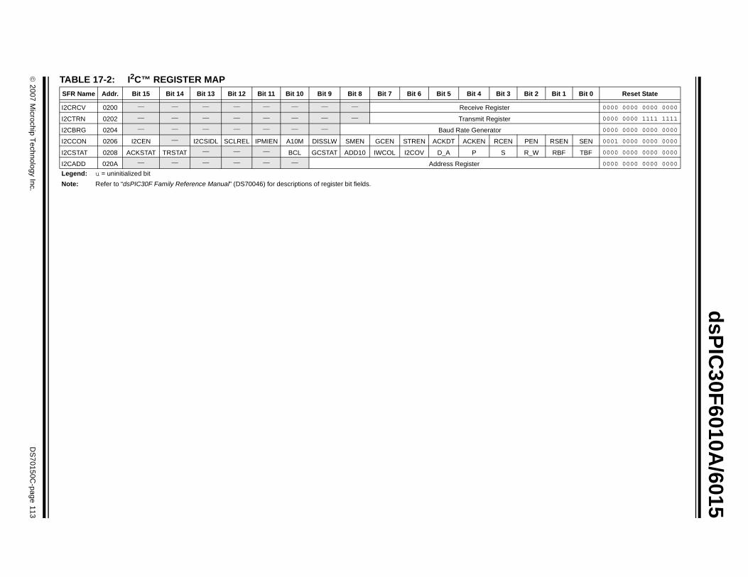
© 2007 M
icrochip Technology Inc.
DS
70150C-page 113
dsP
IC30F
6010A/6015
TASF it 2 Bit 1 Bit 0 Reset State
I2C 0000 0000 0000 0000
I2C 0000 0000 1111 1111
I2C 0000 0000 0000 0000
I2C EN RSEN SEN 0001 0000 0000 0000
I2C _W RBF TBF 0000 0000 0000 0000
I2C 0000 0000 0000 0000
Le
No
BLE 17-2: I2C™ REGISTER MAPR Name Addr. Bit 15 Bit 14 Bit 13 Bit 12 Bit 11 Bit 10 Bit 9 Bit 8 Bit 7 Bit 6 Bit 5 Bit 4 Bit 3 B
RCV 0200 — — — — — — — — Receive Register
TRN 0202 — — — — — — — — Transmit Register
BRG 0204 — — — — — — — Baud Rate Generator
CON 0206 I2CEN — I2CSIDL SCLREL IPMIEN A10M DISSLW SMEN GCEN STREN ACKDT ACKEN RCEN P
STAT 0208 ACKSTAT TRSTAT — — — BCL GCSTAT ADD10 IWCOL I2COV D_A P S R
ADD 020A — — — — — — Address Register
gend: u = uninitialized bit
te: Refer to “dsPIC30F Family Reference Manual” (DS70046) for descriptions of register bit fields.

dsPIC30F6010A/6015
NOTES:
DS70150C-page 114 © 2007 Microchip Technology Inc.

dsPIC30F6010A/6015
18.0 UNIVERSAL ASYNCHRONOUS RECEIVER TRANSMITTER (UART) MODULE
This section describes the Universal AsynchronousReceiver/Transmitter Communications module.
18.1 UART Module Overview
The key features of the UART module are:
• Full-duplex, 8 or 9-bit data communication
• Even, Odd or No Parity options (for 8-bit data)• One or two Stop bits• Fully integrated Baud Rate Generator with 16-bit
prescaler• Baud rates range from 38 bps to 1.875 Mbps at a
30 MHz instruction rate• 4-word deep transmit data buffer
• 4-word deep receive data buffer• Parity, Framing and Buffer Overrun error detection• Support for Interrupt only on Address Detect
(9th bit = 1)• Separate Transmit and Receive Interrupts
• Loopback mode for diagnostic support
FIGURE 18-1: UART TRANSMITTER BLOCK DIAGRAM
Note: This data sheet summarizes features of thisgroup of dsPIC30F devices and is not intended to bea complete reference source. For more informationon the CPU, peripherals, register descriptions andgeneral device functionality, refer to the “dsPIC30FFamily Reference Manual” (DS70046).
Write Write
UTX8 UxTXREG Low Byte
Load TSR
Transmit Control
– Control TSR– Control Buffer– Generate Flags– Generate Interrupt
Control and Status bits
UxTXIF
Data
‘0’ (Start)
‘1’ (Stop)
Parity ParityGenerator
Transmit Shift Register (UxTSR)
16 Divider
ControlSignals
16X Baud Clockfrom Baud Rate
Generator
Internal Data Bus
UTXBRK
Note: x = 1 or 2.
UxTX
© 2007 Microchip Technology Inc. DS70150C-page 115

dsPIC30F6010A/6015
FIGURE 18-2: UART RECEIVER BLOCK DIAGRAM
Read
URX8 UxRXREG Low Byte
DS70150C-page 116 © 2007 Microchip Technology Inc.
dsPIC30F6010A/6015
18.2 Enabling and Setting Up UART
18.2.1 ENABLING THE UART
The UART module is enabled by setting the UARTENbit in the UxMODE register (where x = 1 or 2). Onceenabled, the UxTX and UxRX pins are configured as anoutput and an input respectively, overriding the TRISand LAT register bit settings for the corresponding I/Oport pins. The UxTX pin is at logic ‘1’ when notransmission is taking place.
18.2.2 DISABLING THE UART
The UART module is disabled by clearing theUARTEN bit in the UxMODE register. This is thedefault state after any Reset. If the UART is disabled,all I/O pins operate as port pins under the control ofthe LAT and TRIS bits of the corresponding port pins.
Disabling the UART module resets the buffers toempty states. Any data characters in the buffers arelost, and the baud rate counter is reset.
All error and status flags associated with the UARTmodule are reset when the module is disabled. TheURXDA, OERR, FERR, PERR, UTXEN, UTXBRK andUTXBF bits are cleared, whereas RIDLE and TRMTare set. Other control bits, including ADDEN,URXISEL<1:0>, UTXISEL, as well as the UxMODEand UxBRG registers, are not affected.
Clearing the UARTEN bit while the UART is active willabort all pending transmissions and receptions andreset the module as defined above. Re-enabling theUART will restart the UART in the same configuration.
18.2.3 SETTING UP DATA, PARITY AND STOP BIT SELECTIONS
Control bits PDSEL<1:0> in the UxMODE register areused to select the data length and parity used in thetransmission. The data length may either be 8-bits witheven, odd or no parity, or 9-bits with no parity.
The STSEL bit determines whether one or two Stop bitswill be used during data transmission.
The default (power-on) setting of the UART is 8 bits, noparity, 1 Stop bit (typically represented as 8, N, 1).
18.3 Transmitting Data
18.3.1 TRANSMITTING IN 8-BIT DATA MODE
The following steps must be performed in order totransmit 8-bit data:
1. Set up the UART:First, the data length, parity and number of Stopbits must be selected. Then, the Transmit andReceive Interrupt Enable and Priority bits aresetup in the UxMODE and UxSTA registers.Also, the appropriate baud rate value must bewritten to the UxBRG register.
2. Enable the UART by setting the UARTEN bit(UxMODE<15>).
3. Set the UTXEN bit (UxSTA<10>), therebyenabling a transmission.
4. Write the byte to be transmitted to the lower byteof UxTXREG. The value will be transferred to theTransmit Shift Register (UxTSR) immediatelyand the serial bit stream will start shifting outduring the next rising edge of the baud clock.Alternatively, the data byte may be written whileUTXEN = 0, following which, the user may setUTXEN. This will cause the serial bit stream tobegin immediately because the baud clock willstart from a cleared state.
5. A transmit interrupt will be generated dependingon the value of the interrupt control bit UTXISEL(UxSTA<15>).
18.3.2 TRANSMITTING IN 9-BIT DATA MODE
The sequence of steps involved in the transmission of9-bit data is similar to 8-bit transmission, except that a16-bit data word (of which the upper 7 bits are alwaysclear) must be written to the UxTXREG register.
18.3.3 TRANSMIT BUFFER (UXTXB)
The transmit buffer is 9-bits wide and 4 charactersdeep. Including the Transmit Shift Register (UxTSR),the user effectively has a 5-deep FIFO (First-In, First-Out) buffer. The UTXBF Status bit (UxSTA<9>)indicates whether the transmit buffer is full.
If a user attempts to write to a full buffer, the new datawill not be accepted into the FIFO, and no data shiftwill occur within the buffer. This enables recovery froma buffer overrun condition.
The FIFO is reset during any device Reset, but is notaffected when the device enters or wakes up from aPower-Saving mode.
Note: The UTXEN bit must be set after theUARTEN bit is set to enable UARTtransmissions.
© 2007 Microchip Technology Inc. DS70150C-page 117
dsPIC30F6010A/6015
18.3.4 TRANSMIT INTERRUPT
The Transmit Interrupt Flag (U1TXIF or U2TXIF) islocated in the corresponding interrupt flag register.
The transmitter generates an edge to set the UxTXIFbit. The condition for generating the interrupt dependson UTXISEL control bit:
a) If UTXISEL = 0, an interrupt is generated whena word is transferred from the transmit buffer tothe Transmit Shift Register (UxTSR). Thismeans that the transmit buffer has at least oneempty word.
b) If UTXISEL = 1, an interrupt is generated whena word is transferred from the transmit buffer tothe Transmit Shift Register (UxTSR) and thetransmit buffer is empty.
Switching between the two interrupt modes duringoperation is possible and sometimes offers moreflexibility.
18.3.5 TRANSMIT BREAK
Setting the UTXBRK bit (UxSTA<11>) will cause theUxTX line to be driven to logic ‘0’. The UTXBRK bitoverrides all transmission activity. Therefore, the usershould generally wait for the transmitter to be Idlebefore setting UTXBRK.
To send a Break character, the UTXBRK bit must beset by software and must remain set for a minimum of13 baud clock cycles. The UTXBRK bit is then clearedby software to generate Stop bits. The user must waitfor a duration of at least one or two baud clock cyclesin order to ensure a valid Stop bit(s) before reloadingthe UxTXB or starting other transmitter activity. Trans-mission of a Break character does not generate atransmit interrupt.
18.4 Receiving Data
18.4.1 RECEIVING IN 8-BIT OR 9-BIT DATA MODE
The following steps must be performed while receiving8-bit or 9-bit data:
1. Set up and enable the UART (see Section 18.3"Transmitting Data").
2. A receive interrupt will be generated when oneor more data words have been received,depending on the receive interrupt settingsspecified by the URXISEL bits (UxSTA<7:6>).
3. Read the OERR bit to determine if an overrunerror has occurred. The OERR bit must be resetin software.
4. Read the received data from UxRXREG. The actof reading UxRXREG will move the next word tothe top of the receive FIFO, and the PERR andFERR values will be updated.
18.4.2 RECEIVE BUFFER (UXRXB)
The receive buffer is 4 words deep. Including theReceive Shift Register (UxRSR), the user effectivelyhas a 5-word deep FIFO buffer.
URXDA (UxSTA<0>) = 1 indicates that the receivebuffer has data available. URXDA = 0 means that thebuffer is empty. If a user attempts to read an emptybuffer, the old values in the buffer will be read and nodata shift will occur within the FIFO.
The FIFO is reset during any device Reset. It is notaffected when the device enters or wakes up from aPower-Saving mode.
18.4.3 RECEIVE INTERRUPT
The Receive Interrupt Flag (U1RXIF or U2RXIF) canbe read from the corresponding interrupt flag register.The interrupt flag is set by an edge generated by thereceiver. The condition for setting the receive interruptflag depends on the settings specified by theURXISEL<1:0> (UxSTA<7:6>) control bits.
a) If URXISEL<1:0> = 00 or 01, an interrupt isgenerated every time a data word is transferredfrom the Receive Shift Register (UxRSR) to thereceive buffer. There may be one or morecharacters in the receive buffer.
b) If URXISEL<1:0> = 10, an interrupt is generatedwhen a word is transferred from the ReceiveShift Register (UxRSR) to the receive buffer,which, as a result of the transfer, contains3 characters.
c) If URXISEL<1:0> = 11, an interrupt is set whena word is transferred from the Receive ShiftRegister (UxRSR) to the receive buffer, which,as a result of the transfer, contains 4 characters(i.e., becomes full).
Switching between the interrupt modes during opera-tion is possible, though generally not advisable duringnormal operation.
18.5 Reception Error Handling
18.5.1 RECEIVE BUFFER OVERRUN ERROR (OERR BIT)
The OERR bit (UxSTA<1>) is set if all of the followingconditions occur:
a) The receive buffer is full.b) The Receive Shift Register is full, but unable to
transfer the character to the receive buffer.c) The Stop bit of the character in the UxRSR is
detected, indicating that the UxRSR needs totransfer the character to the buffer.
Once OERR is set, no further data is shifted in UxRSR(until the OERR bit is cleared in software or a Resetoccurs). The data held in UxRSR and UxRXREGremains valid.
DS70150C-page 118 © 2007 Microchip Technology Inc.

dsPIC30F6010A/6015
18.9 Auto-Baud Support
To allow the system to determine baud rates ofreceived characters, the input can be optionally linkedto a selected capture input. To enable this mode, theuser must program the input capture module to detectthe falling and rising edges of the Start bit.
18.10 UART Operation During CPU Sleep and Idle Modes
18.10.1 UART OPERATION DURING CPU SLEEP MODE
When the device enters Sleep mode, all clock sourcesto the module are shut down and stay at logic ‘0’. If
DS70150C-page 120 © 2007 Microchip Technology Inc.
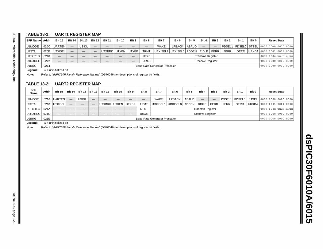
© 2007 M
icrochip Technology Inc.
DS
70150C-page 121
dsP
IC30F
6010A/6015
TA
TA
SF 2 Bit 1 Bit 0 Reset State
U1 EL1 PDSEL0 STSEL 0000 0000 0000 0000
U1 R OERR URXDA 0000 0001 0001 0000
U1 0000 000u uuuu uuuu
U1 0000 0000 0000 0000
U1 0000 0000 0000 0000
Le
No
2 Bit 1 Bit 0 Reset State
U2 L1 PDSEL0 STSEL 0000 0000 0000 0000
U2 R OERR URXDA 0000 0001 0001 0000
U2 0000 000u uuuu uuuu
U2 0000 0000 0000 0000
U2 0000 0000 0000 0000
Le
No
BLE 18-1: UART1 REGISTER MAP
BLE 18-2: UART2 REGISTER MAP
R Name Addr. Bit 15 Bit 14 Bit 13 Bit 12 Bit 11 Bit 10 Bit 9 Bit 8 Bit 7 Bit 6 Bit 5 Bit 4 Bit 3 Bit
MODE 020C UARTEN — USIDL — — — — — WAKE LPBACK ABAUD — — PDS
STA 020E UTXISEL — — — UTXBRK UTXEN UTXBF TRMT URXISEL1 URXISEL0 ADDEN RIDLE PERR FER
TXREG 0210 — — — — — — — UTX8 Transmit Register
RXREG 0212 — — — — — — — URX8 Receive Register
BRG 0214 Baud Rate Generator Prescaler
gend: u = uninitialized bit
te: Refer to “dsPIC30F Family Reference Manual” (DS70046) for descriptions of register bit fields.
SFR Name Addr. Bit 15 Bit 14 Bit 13 Bit 12 Bit 11 Bit 10 Bit 9 Bit 8 Bit 7 Bit 6 Bit 5 Bit 4 Bit 3 Bit
MODE 0216 UARTEN — USIDL — — — — — WAKE LPBACK ABAUD — — PDSE
STA 0218 UTXISEL — — — UTXBRK UTXEN UTXBF TRMT URXISEL1 URXISEL0 ADDEN RIDLE PERR FER
TXREG 021A — — — — — — — UTX8 Transmit Register
RXREG 021C — — — — — — — URX8 Receive Register
BRG 021E Baud Rate Generator Prescaler
gend: u = uninitialized bit
te: Refer to “dsPIC30F Family Reference Manual” (DS70046) for descriptions of register bit fields.

dsPIC30F6010A/6015
NOTES:
DS70150C-page 122 © 2007 Microchip Technology Inc.

dsPIC30F6010A/6015
19.0 CAN MODULE
19.1 Overview
The Controller Area Network (CAN) module is a serialinterface, useful for communicating with other CANmodules or microcontroller devices. This interface/protocol was designed to allow communications withinnoisy environments. The dsPIC30F6010A has twoCAN modules. The dsPIC30F6015 has only one.
The CAN module is a communication controller imple-menting the CAN 2.0 A/B protocol, as defined in theBOSCH specification. The module will supportCAN 1.2, CAN 2.0A, CAN2.0B Passive and CAN 2.0BActive versions of the protocol. The module implemen-tation is a full CAN system. The CAN specification isnot covered within this data sheet. The reader mayrefer to the BOSCH CAN specification for furtherdetails.
The module features are as follows:
• Implementation of the CAN protocol CAN 1.2, CAN 2.0A and CAN 2.0B
• Standard and extended data frames• 0-8 bytes data length• Programmable bit rate up to 1 Mbit/sec
• Support for remote frames• Double-buffered receiver with two prioritized
received message storage buffers (each buffer may contain up to 8 bytes of data)
• 6 full (standard/extended identifier) acceptance filters, 2 associated with the high priority receive buffer, and 4 associated with the low priority receive buffer
• 2 full acceptance filter masks, one each associ-ated with the high and low priority receive buffers
• Three transmit buffers with application specified prioritization and abort capability (each buffer may contain up to 8 bytes of data)
• Programmable wake-up functionality with integrated low-pass filter
• Programmable Loopback mode supports self-test operation
• Signaling via interrupt capabilities for all CAN receiver and transmitter error states
• Programmable clock source• Programmable link to timer module for
time-stamping and network synchronization• Low-Power Sleep and Idle mode
The CAN bus module consists of a protocol engine,and message buffering/control. The CAN protocolengine handles all functions for receiving and trans-mitting messages on the CAN bus. Messages aretransmitted by first loading the appropriate data regis-ters. Status and errors can be checked by reading theappropriate registers. Any message detected on theCAN bus is checked for errors and then matchedagainst filters to see if it should be received and storedin one of the receive registers.
19.2 Frame Types
The CAN module transmits various types of frames,which include data messages or remote transmissionrequests initiated by the user as other frames that areautomatically generated for control purposes. Thefollowing frame types are supported:
• Standard Data Frame
A Standard Data Frame is generated by a node whenthe node wishes to transmit data. It includes a 11-bitStandard Identifier (SID), but not an 18-bit ExtendedIdentifier (EID).
• Extended Data Frame
An Extended Data Frame is similar to a Standard DataFrame, but includes an Extended Identifier as well.
• Remote Frame
It is possible for a destination node to request the datafrom the source. For this purpose, the destination nodesends a Remote Frame with an identifier that matchesthe identifier of the required Data Frame. The appropri-ate data source node will then send a Data Frame as aresponse to this remote request.
• Error Frame
An Error Frame is generated by any node that detectsa bus error. An error frame consists of 2 fields: an ErrorFlag field and an Error Delimiter field.
• Overload Frame
An Overload Frame can be generated by a node as aresult of 2 conditions. First, the node detects a domi-nant bit during lnterframe Space, which is an illegalcondition. Second, due to internal conditions, the nodeis not yet able to start reception of the next message. Anode may generate a maximum of 2 sequentialOverload Frames to delay the start of the nextmessage.
• Interframe Space
Interframe Space separates a proceeding frame (ofwhatever type) from a following Data or RemoteFrame.
Note: This data sheet summarizes features of thisgroup of dsPIC30F devices and is not intended to bea complete reference source. For more informationon the CPU, peripherals, register descriptions andgeneral device functionality, refer to the “dsPIC30FFamily Reference Manual” (DS70046).
© 2007 Microchip Technology Inc. DS70150C-page 123
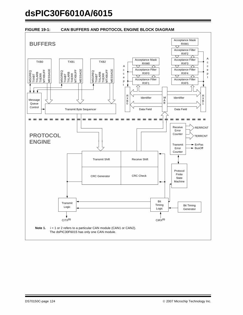
dsPIC30F6010A/6015
FIGURE 19-1: CAN BUFFERS AND PROTOCOL ENGINE BLOCK DIAGRAM
Acceptance FilterRXF2
RXB1
Accept
Accept
Identifier
Data Field Data Field
Identifier
Acceptance MaskRXM1
Acceptance FilterRXF3
Acceptance FilterRXF4
Acceptance FilterRXF5
MAB
Acceptance MaskRXM0
Acceptance FilterRXF0
Acceptance FilterRXF1
RXB0
MS
GR
EQ
TXB2
TX
AB
TT
XLA
RB
TX
ER
RM
TX
BU
FF
ME
SS
AG
E
MessageQueueControl
Transmit Byte Sequencer
MS
GR
EQ
TXB1T
XA
BT
TX
LAR
BT
XE
RR
MT
XB
UF
F
ME
SS
AG
E
MS
GR
EQ
TXB0
TX
AB
TT
XLA
RB
TX
ER
RM
TX
BU
FF
ME
SS
AG
E
Receive ShiftTransmit Shift
ReceiveError
TransmitError
Protocol
RERRCNT
TERRCNT
ErrPasBusOff
FiniteState
Machine
Counter
Counter
TransmitLogic
BitTimingLogic
CiTX(1) CiRX(1)
Bit TimingGenerator
PROTOCOLENGINE
BUFFERS
CRC CheckCRC Generator
Note 1. i = 1 or 2 refers to a particular CAN module (CAN1 or CAN2). The dsPIC30F6015 has only one CAN module.
DS70150C-page 124 © 2007 Microchip Technology Inc.
dsPIC30F6010A/6015
19.3 Modes of Operation
The CAN module can operate in one of several operationmodes selected by the user. These modes include:
• Initialization mode• Disable mode
• Normal Operation mode• Listen-Only mode• Loopback mode
• Error Recognition mode
Modes are requested by setting the REQOP<2:0>bits (CiCTRL<10:8>). Entry into a mode isacknowledged by monitoring the OPMODE<2:0> bits(CiCTRL<7:5>). The module will not change the modeand the OPMODE bits until a change in mode isacceptable, generally during bus idle time which isdefined as at least 11 consecutive recessive bits.
19.3.1 INITIALIZATION MODE
In the Initialization mode, the module will not transmit orreceive. The error counters are cleared and the inter-rupt flags remain unchanged. The programmer willhave access to Configuration registers that are accessrestricted in other modes. The module will protect theuser from accidentally violating the CAN protocolthrough programming errors. All registers which controlthe configuration of the module can not be modifiedwhile the module is on-line. The CAN module will notbe allowed to enter the Configuration mode while atransmission is taking place. The Configuration modeserves as a lock to protect the following registers:
• All Module Control Registers• Baud Rate and Interrupt Configuration Registers
• Bus Timing Registers • Identifier Acceptance Filter Registers • Identifier Acceptance Mask Registers
19.3.2 DISABLE MODE
In Disable mode, the module will not transmit orreceive. The module has the ability to set the WAKIF bitdue to bus activity, however any pending interrupts willremain and the error counters will retain their value.
If the REQOP<2:0> bits (CiCTRL<10:8>) = 001, themodule will enter the Module Disable mode. If themodule is active, the module will wait for 11 recessivebits on the CAN bus, detect that condition as an idlebus, then accept the module disable command. Whenthe OPMODE<2:0> bits (CiCTRL<7:5>) = 001, thatindicates whether the module successfully went intoModule Disable mode. The I/O pins will revert to normalI/O function when the module is in the Module Disablemode.
The module can be programmed to apply a low-passfilter function to the CiRX input line while the module orthe CPU is in Sleep mode. The WAKFIL bit(CiCFG2<14>) enables or disables the filter.
19.3.3 NORMAL OPERATION MODE
Normal Operating mode is selected whenREQOP<2:0> = 000. In this mode, the module isactivated, the I/O pins will assume the CAN busfunctions. The module will transmit and receive CANbus messages via the CiTX and CiRX pins.
19.3.4 LISTEN-ONLY MODE
If the Listen-Only mode is activated, the module on theCAN bus is passive. The transmitter buffers revert tothe Port I/O function. The receive pins remain inputs.For the receiver, no error flags or acknowledge signalsare sent. The error counters are deactivated in thisstate. The Listen-Only mode can be used for detectingthe baud rate on the CAN bus. To use this, it is neces-sary that there are at least two further nodes thatcommunicate with each other.
19.3.5 ERROR RECOGNITION MODE
The module can be set to ignore all errors and receiveany message. The Error Recognition mode is activatedby setting the RXM<1:0> bits (CiRXnCON<6:5>) to‘11’. In this mode, the data which is in the messageassembly buffer until the time an error occurred, is cop-ied in the receive buffer and can be read via the CPUinterface.
19.3.6 LOOPBACK MODE
If the Loopback mode is activated, the module will con-nect the internal transmit signal to the internal receivesignal at the module boundary. The transmit andreceive pins revert to their Port I/O function.
Note: Typically, if the CAN module is allowed totransmit in a particular mode of operationand a transmission is requested immedi-ately after the CAN module has beenplaced in that mode of operation, the mod-ule waits for 11 consecutive recessive bitson the bus before starting transmission. Ifthe user switches to Disable mode withinthis 11-bit period, then this transmission isaborted and the corresponding TXABT bitis set and TXREQ bit is cleared.
© 2007 Microchip Technology Inc. DS70150C-page 125
dsPIC30F6010A/6015
19.4 Message Reception
19.4.1 RECEIVE BUFFERS
The CAN bus module has 3 receive buffers. However,one of the receive buffers is always committed to mon-itoring the bus for incoming messages. This buffer iscalled the Message Assembly Buffer (MAB). So thereare 2 receive buffers visible, RXB0 and RXB1, that canessentially instantaneously receive a completemessage from the protocol engine.
All messages are assembled by the MAB, and are trans-ferred to the RXBn buffers only if the acceptance filtercriterion is met. When a message is received, the RXnIFflag (CiINTF<0> or CiINTF<1>) will be set. This bit canonly be set by the module when a message is received.The bit is cleared by the CPU when it has completedprocessing the message in the buffer. If the RXnIE bit(CiINTE<0> or CiINTE<1>) is set, an interrupt will begenerated when a message is received.
RXF0 and RXF1 filters with RXM0 mask are associatedwith RXB0. The filters RXF2, RXF3, RXF4, and RXF5and the mask RXM1 are associated with RXB1.
19.4.2 MESSAGE ACCEPTANCE FILTERS
The message acceptance filters and masks are used todetermine if a message in the message assemblybuffer should be loaded into either of the receive buff-ers. Once a valid message has been received into themessage assembly buffer, the identifier fields of themessage are compared to the filter values. If there is amatch, that message will be loaded into the appropriatereceive buffer.
The acceptance filter looks at incoming messages forthe RXIDE bit (CiRXnSID<0>) to determine how tocompare the identifiers. If the RXIDE bit is clear, themessage is a standard frame, and only filters with theEXIDE bit (CiRXFnSID<0>) clear are compared. If theRXIDE bit is set, the message is an extended frame,and only filters with the EXIDE bit set are compared.Configuring the RXM<1:0> bits to ‘01’ or ‘10’ canoverride the EXIDE bit.
19.4.3 MESSAGE ACCEPTANCE FILTER MASKS
The mask bits essentially determine which bits to applythe filter to. If any mask bit is set to a zero, then that bitwill automatically be accepted regardless of the filterbit. There are 2 programmable acceptance filter masksassociated with the receive buffers, one for each buffer.
19.4.4 RECEIVE OVERRUN
An overrun condition occurs when the messageassembly buffer has assembled a valid receivedmessage and the message is accepted through theacceptance filters, but the receive buffer associatedwith the filter still contains unread data.
The overrun error flag, RXnOVR (CiINTF<15> orCiINTF<14>) and the ERRIF bit (CiINTF<5>) will be setand the message in the MAB will be discarded.
If the DBEN bit is clear, RXB1 and RXB0 operate inde-pendently. When this is the case, a message intendedfor RXB0 will not be diverted into RXB1 if RXB0contains an unread message and the RX0OVR bit willbe set.
If the DBEN bit is set, the overrun for RXB0 is handleddifferently. If a valid message is received for RXB0 andRXFUL = 1 indicates that RXB0 is full and RXFUL = 0indicates that RXB1 is empty, the message for RXB0will be loaded into RXB1. An overrun error will not begenerated for RXB0. If a valid message is received forRXB0 and RXFUL = 1, and RXFUL = 1 indicating thatboth RXB0 and RXB1 are full, the message will be lostand an overrun will be indicated for RXB1.
19.4.5 RECEIVE ERRORS
The CAN module will detect the following receiveerrors:
• Cyclic Redundancy Check (CRC) error• Bit Stuffing error
• Invalid message receive error
These receive errors do not generate an interrupt.However, the receive error counter is incremented byone in case one of these errors occur. The RXWAR bit(CiINTF<9>) indicates that the Receive Error Counterhas reached the CPU warning limit of 96 and aninterrupt is generated.
19.4.6 RECEIVE INTERRUPTS
Receive interrupts can be divided into 3 major groups,each including various conditions that generateinterrupts:
• Receive Interrupt
A message has been successfully received and loadedinto one of the receive buffers. This interrupt is acti-vated immediately after receiving the End-of-Frame(EOF) field. Reading the RXnIF flag will indicate whichreceive buffer caused the interrupt.
• Wake-up Interrupt
The CAN module has woken up from Disable mode orthe device has woken up from Sleep mode.
DS70150C-page 126 © 2007 Microchip Technology Inc.

dsPIC30F6010A/6015
• Receive Error Interrupts
A receive error interrupt will be indicated by the ERRIFbit. This bit shows that an error condition occurred. Thesource of the error can be determined by checking thebits in the CAN Interrupt STATUS register, CiINTF.
• Invalid message received
If any type of error occurred during reception of the lastmessage, an error will be indicated by the IVRIF bit.
• Receiver overrun
The RXnOVR bit indicates that an overrun conditionoccurred.
• Receiver warning
The RXWAR bit indicates that the Receive ErrorCounter (RERRCNT<7:0>) has reached the Warninglimit of 96.
• Receiver error passive
The RXEP bit indicates that the Receive Error Counterhas exceeded the Error Passive limit of 127 and themodule has gone into Error Passive state.
19.5 Message Transmission
19.5.1 TRANSMIT BUFFERS
The CAN module has three transmit buffers. Each ofthe three buffers occupies 14 bytes of data. Eight of thebytes are the maximum 8 bytes of the transmitted mes-sage. Five bytes hold the standard and extendedidentifiers and other message arbitration information.
19.5.2 TRANSMIT MESSAGE PRIORITY
Transmit priority is a prioritization within each node of thepending transmittable messages. There are 4 levels oftransmit priority. If TXPRI<1:0> (CiTXnCON<1:0>, wheren = 0, 1 or 2 represents a particular transmit buffer) for aparticular message buffer is set to ‘11’, that buffer has thehighest priority. If TXPRI<1:0> for a particular messagebuffer is set to ‘10’ or ‘01’, that buffer has an intermediatepriority. If TXPRI<1:0> for a particular message buffer is‘00’, that buffer has the lowest priority.
19.5.3 TRANSMISSION SEQUENCE
To initiate transmission of the message, the TXREQ bit(CiTXnCON<3>) must be set. The CAN bus moduleresolves any timing conflicts between setting of theTXREQ bit and the Start-of-Frame (SOF), ensuringthat if the priority was changed, it is resolved correctlybefore the SOF occurs. When TXREQ is set, theTXABT (CiTXnCON<6>), TXLARB (CiTXnCON<5>)and TXERR (CiTXnCON<4>) flag bits areautomatically cleared.
Setting TXREQ bit simply flags a message buffer asenqueued for transmission. When the module detectsan available bus, it begins transmitting the messagewhich has been determined to have the highest priority.
If the transmission completes successfully on the firstattempt, the TXREQ bit is cleared automatically and aninterrupt is generated if TXIE was set.
If the message transmission fails, one of the errorcondition flags will be set and the TXREQ bit willremain set indicating that the message is still pendingfor transmission. If the message encountered an errorcondition during the transmission attempt, the TXERRbit will be set and the error condition may cause aninterrupt. If the message loses arbitration during thetransmission attempt, the TXLARB bit is set. Nointerrupt is generated to signal the loss of arbitration.
19.5.4 ABORTING MESSAGE TRANSMISSION
The system can also abort a message by clearing theTXREQ bit associated with each message buffer.Setting the ABAT bit (CiCTRL<12>) will request anabort of all pending messages. If the message has notyet started transmission, or if the message started butis interrupted by loss of arbitration or an error, the abortwill be processed. The abort is indicated when themodule sets the TXABT bit, and the TXnIF flag is notautomatically set.
19.5.5 TRANSMISSION ERRORS
The CAN module will detect the following transmissionerrors:
• Acknowledge error• Form error• Bit Eerror
These transmission errors will not necessarily generatean interrupt, but are indicated by the transmission errorcounter. However, each of these errors will cause thetransmission error counter to be incremented by one.Once the value of the error counter exceeds the valueof 96, the ERRIF (CiINTF<5>) and the TXWAR bit(CiINTF<10>) are set. Once the value of the errorcounter exceeds the value of 96, an interrupt isgenerated and the TXWAR bit in the Error Flag registeris set.
© 2007 Microchip Technology Inc. DS70150C-page 127

dsPIC30F6010A/6015
19.5.6 TRANSMIT INTERRUPTS
Transmit interrupts can be divided into 2 major groups,each including various conditions that generateinterrupts:
• Transmit Interrupt
At least one of the three transmit buffers is empty (notscheduled) and can be loaded to schedule a messagefor transmission. Reading the TXnIF flags will indicatewhich transmit buffer is available and caused theinterrupt.
• Transmit Error Interrupts
A transmission error interrupt will be indicated by theERRIF flag. This flag shows that an error conditionoccurred. The source of the error can be determined bychecking the error flags in the CAN Interrupt STATUSregister, CiINTF. The flags in this register are related toreceive and transmit errors.
• Transmitter Warning Interrupt
The TXWAR bit indicates that the Transmit ErrorCounter has reached the CPU warning limit of 96.
• Transmitter Error Passive
The TXEP bit (CiINTF<12>) indicates that the TransmitError Counter has exceeded the Error Passive limit of127 and the module has gone to Error Passive state.
• Bus Off
The TXBO bit (CiINTF<13>) indicates that the TransmitError Counter has exceeded 255 and the module hasgone to Bus Off state.
19.6 Baud Rate Setting
All nodes on any particular CAN bus must have thesame nominal bit rate. In order to set the baud rate, thefollowing parameters have to be initialized:
• Synchronization jump width• Baud rate prescaler • Phase segments
• Length determination of Phase2 Seg • Sample point • Propagation segment bits
19.6.1 BIT TIMING
All controllers on the CAN bus must have the same baudrate and bit length. However, different controllers are notrequired to have the same master oscillator clock. At dif-ferent clock frequencies of the individual controllers, thebaud rate has to be adjusted by adjusting the number oftime quanta in each segment.
The Nominal Bit Time can be thought of as beingdivided into separate non-overlapping time segments.These segments are shown in Figure 19-2.
• Synchronization segment (Sync Seg)• Propagation time segment (Prop Seg)• Phase segment 1 (Phase1 Seg)
• Phase segment 2 (Phase2 Seg)
The time segments and also the nominal bit time aremade up of integer units of time called time quanta orTQ. By definition, the nominal bit time has a minimumof 8 TQ and a maximum of 25 TQ. Also, by definition,the minimum nominal bit time is 1 μsec, correspondingto a maximum bit rate of 1 MHz.
FIGURE 19-2: CAN BIT TIMING
Input Signal
SyncProp
SegmentPhase
Segment 1Phase
Segment 2 Sync
Sample Point
TQ
DS70150C-page 128 © 2007 Microchip Technology Inc.

dsPIC30F6010A/6015
19.6.2 PRESCALER SETTING
There is a programmable prescaler, with integralvalues ranging from 1 to 64, in addition to a fixed divide-by-2 for clock generation. The Time Quantum (TQ) is afixed unit of time derived from the oscillator period, andis given by Equation 19-1, where FCAN is FCY (if theCANCKS bit is set or 4 FCY (if CANCKS is cleared).
EQUATION 19-1: TIME QUANTUM FOR CLOCK GENERATION
19.6.3 PROPAGATION SEGMENT
This part of the bit time is used to compensate physicaldelay times within the network. These delay times con-sist of the signal propagation time on the bus line andthe internal delay time of the nodes. The PropagationSegment can be programmed from 1 TQ to 8 TQ bysetting the PRSEG<2:0> bits (CiCFG2<2:0>).
19.6.4 PHASE SEGMENTS
The phase segments are used to optimally locate thesampling of the received bit within the transmitted bittime. The sampling point is between Phase1 Seg andPhase2 Seg. These segments are lengthened or short-ened by re-synchronization. The end of the Phase1Seg determines the sampling point within a bit period.The segment is programmable from 1 TQ to 8 TQ.Phase2 Seg provides delay to the next transmitted datatransition. The segment is programmable from 1 TQ to8 TQ, or it may be defined to be equal to the greater ofPhase1 Seg or the Information Processing Time(2 TQ). The Phase1 Seg is initialized by setting bitsSEG1PH<2:0> (CiCFG2<5:3>), and Phase2 Seg isinitialized by setting SEG2PH<2:0> (CiCFG2<10:8>).
The following requirement must be fulfilled while settingthe lengths of the Phase Segments:
• Propagation Segment + Phase1 Seg > = Phase2 Seg
19.6.5 SAMPLE POINT
The sample point is the point of time at which the buslevel is read and interpreted as the value of that respec-tive bit. The location is at the end of Phase1 Seg. If thebit timing is slow and contains many TQ, it is possible tospecify multiple sampling of the bus line at the samplepoint. The level determined by the CAN bus then corre-sponds to the result from the majority decision of threevalues. The majority samples are taken at the samplepoint and twice before with a distance of TQ/2. TheCAN module allows the user to chose between sam-pling three times at the same point or once at the samepoint, by setting or clearing the SAM bit (CiCFG2<6>).
Typically, the sampling of the bit should take place atabout 60-70% through the bit time, depending on thesystem parameters.
19.6.6 SYNCHRONIZATION
To compensate for phase shifts between the oscillatorfrequencies of the different bus stations, each CANcontroller must be able to synchronize to the relevantsignal edge of the incoming signal. When an edge inthe transmitted data is detected, the logic will comparethe location of the edge to the expected time (Synchro-nous Segment). The circuit will then adjust the valuesof Phase1 Seg and Phase2 Seg. There are 2mechanisms used to synchronize.
19.6.6.1 Hard Synchronization
Hard synchronization is only done whenever there is arecessive to dominant edge during bus Idle, indicatingthe start of a message. After hard synchronization, thebit time counters are restarted with the SynchronousSegment. Hard synchronization forces the edge whichhas caused the hard synchronization to lie within thesynchronization segment of the restarted bit time. If ahard synchronization is done, there will not be are-synchronization within that bit time.
19.6.6.2 Re-synchronization
As a result of re-synchronization, Phase1 Seg may belengthened or Phase2 Seg may be shortened. Theamount of lengthening or shortening of the phasebuffer segment has an upper bound known as thesynchronization jump width, and is specified by theSJW<1:0> bits (CiCFG1<7:6>). The value of thesynchronization jump width will be added to Phase1Seg or subtracted from Phase2 Seg. The re-synchronization jump width is programmable between1 TQ and 4 TQ.
The following requirement must be fulfilled while settingthe SJW<1:0> bits:
• Phase2 Seg > Synchronization Jump Width
Note: FCAN must not exceed 30 MHz. IfCANCKS = 0, then FCY must not exceed7.5 MHz.
TQ = 2 ( BRP<5:0> + 1 )/FCAN
© 2007 Microchip Technology Inc. DS70150C-page 129
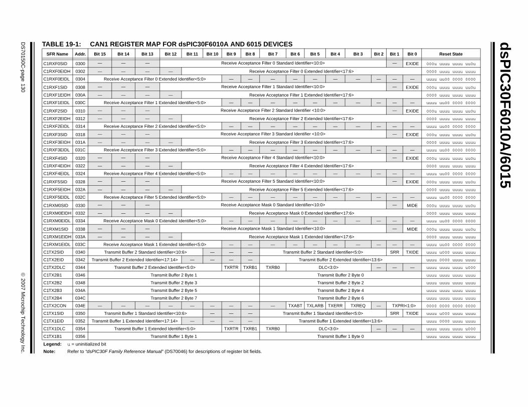
dsP
IC30F
6010A/6015
DS
70150C-page 130
© 2007 M
icrochip Technology Inc.
Bit 2 Bit 1 Bit 0 Reset State
— EXIDE 000u uuuu uuuu uu0u
0000 uuuu uuuu uuuu
— — — uuuu uu00 0000 0000
— EXIDE 000u uuuu uuuu uu0u
0000 uuuu uuuu uuuu
— — — uuuu uu00 0000 0000
— EXIDE 000u uuuu uuuu uu0u
0000 uuuu uuuu uuuu
— — — uuuu uu00 0000 0000
— EXIDE 000u uuuu uuuu uu0u
0000 uuuu uuuu uuuu
— — — uuuu uu00 0000 0000
— EXIDE 000u uuuu uuuu uu0u
0000 uuuu uuuu uuuu
— — — uuuu uu00 0000 0000
— EXIDE 000u uuuu uuuu uu0u
0000 uuuu uuuu uuuu
— — — uuuu uu00 0000 0000
— MIDE 000u uuuu uuuu uu0u
0000 uuuu uuuu uuuu
— — — uuuu uu00 0000 0000
— MIDE 000u uuuu uuuu uu0u
0000 uuuu uuuu uuuu
— — — uuuu uu00 0000 0000
SRR TXIDE uuuu u000 uuuu uuuu
fier<13:6> uuuu 0000 uuuu uuuu
— — — uuuu uuuu uuuu u000
uuuu uuuu uuuu uuuu
uuuu uuuu uuuu uuuu
uuuu uuuu uuuu uuuu
uuuu uuuu uuuu uuuu
— TXPRI<1:0> 0000 0000 0000 0000
SRR TXIDE uuuu u000 uuuu uuuu
fier<13:6> uuuu 0000 uuuu uuuu
— — — uuuu uuuu uuuu u000
uuuu uuuu uuuu uuuu
TABLE 19-1: CAN1 REGISTER MAP FOR dsPIC30F6010A AND 6015 DEVICESSFR Name Addr. Bit 15 Bit 14 Bit 13 Bit 12 Bit 11 Bit 10 Bit 9 Bit 8 Bit 7 Bit 6 Bit 5 Bit 4 Bit 3
C1RXF0SID 0300 — — — Receive Acceptance Filter 0 Standard Identifier<10:0>
C1RXF0EIDH 0302 — — — — Receive Acceptance Filter 0 Extended Identifier<17:6>
C1RXF0EIDL 0304 Receive Acceptance Filter 0 Extended Identifier<5:0> — — — — — — —
C1RXF1SID 0308 — — — Receive Acceptance Filter 1 Standard Identifier<10:0>
C1RXF1EIDH 030A — — — — Receive Acceptance Filter 1 Extended Identifier<17:6>
C1RXF1EIDL 030C Receive Acceptance Filter 1 Extended Identifier<5:0> — — — — — — —
C1RXF2SID 0310 — — — Receive Acceptance Filter 2 Standard Identifier <10:0>
C1RXF2EIDH 0312 — — — — Receive Acceptance Filter 2 Extended Identifier<17:6>
C1RXF2EIDL 0314 Receive Acceptance Filter 2 Extended Identifier<5:0> — — — — — — —
C1RXF3SID 0318 — — — Receive Acceptance Filter 3 Standard Identifier <10:0>
C1RXF3EIDH 031A — — — — Receive Acceptance Filter 3 Extended Identifier<17:6>
C1RXF3EIDL 031C Receive Acceptance Filter 3 Extended Identifier<5:0> — — — — — — —
C1RXF4SID 0320 — — — Receive Acceptance Filter 4 Standard Identifier<10:0>
C1RXF4EIDH 0322 — — — — Receive Acceptance Filter 4 Extended Identifier<17:6>
C1RXF4EIDL 0324 Receive Acceptance Filter 4 Extended Identifier<5:0> — — — — — — —
C1RXF5SID 0328 — — — Receive Acceptance Filter 5 Standard Identifier<10:0>
C1RXF5EIDH 032A — — — — Receive Acceptance Filter 5 Extended Identifier<17:6>
C1RXF5EIDL 032C Receive Acceptance Filter 5 Extended Identifier<5:0> — — — — — — —
C1RXM0SID 0330 — — — Receive Acceptance Mask 0 Standard Identifier<10:0>
C1RXM0EIDH 0332 — — — — Receive Acceptance Mask 0 Extended Identifier<17:6>
C1RXM0EIDL 0334 Receive Acceptance Mask 0 Extended Identifier<5:0> — — — — — — —
C1RXM1SID 0338 — — — Receive Acceptance Mask 1 Standard Identifier<10:0>
C1RXM1EIDH 033A — — — — Receive Acceptance Mask 1 Extended Identifier<17:6>
C1RXM1EIDL 033C Receive Acceptance Mask 1 Extended Identifier<5:0> — — — — — — —
C1TX2SID 0340 Transmit Buffer 2 Standard Identifier<10:6> — — — Transmit Buffer 2 Standard Identifier<5:0>
C1TX2EID 0342 Transmit Buffer 2 Extended Identifier<17:14> — — — — Transmit Buffer 2 Extended Identi
C1TX2DLC 0344 Transmit Buffer 2 Extended Identifier<5:0> TXRTR TXRB1 TXRB0 DLC<3:0>
C1TX2B1 0346 Transmit Buffer 2 Byte 1 Transmit Buffer 2 Byte 0
C1TX2B2 0348 Transmit Buffer 2 Byte 3 Transmit Buffer 2 Byte 2
C1TX2B3 034A Transmit Buffer 2 Byte 5 Transmit Buffer 2 Byte 4
C1TX2B4 034C Transmit Buffer 2 Byte 7 Transmit Buffer 2 Byte 6
C1TX2CON 034E — — — — — — — — — TXABT TXLARB TXERR TXREQ
C1TX1SID 0350 Transmit Buffer 1 Standard Identifier<10:6> — — — Transmit Buffer 1 Standard Identifier<5:0>
C1TX1EID 0352 Transmit Buffer 1 Extended Identifier<17:14> — — — — Transmit Buffer 1 Extended Identi
C1TX1DLC 0354 Transmit Buffer 1 Extended Identifier<5:0> TXRTR TXRB1 TXRB0 DLC<3:0>
C1TX1B1 0356 Transmit Buffer 1 Byte 1 Transmit Buffer 1 Byte 0
Legend: u = uninitialized bit
Note: Refer to “dsPIC30F Family Reference Manual” (DS70046) for descriptions of register bit fields.

© 2007 M
icrochip Technology Inc.
DS
70150C-page 131
dsP
IC30F
6010A/6015
C1 uuuu uuuu uuuu uuuu
C1 uuuu uuuu uuuu uuuu
C1 uuuu uuuu uuuu uuuu
C1 — TXPRI<1:0> 0000 0000 0000 0000
C1 SRR TXIDE uuuu u000 uuuu uuuu
C1 3:6> uuuu 0000 uuuu uuuu
C1 — — — uuuu uuuu uuuu u000
C1 uuuu uuuu uuuu uuuu
C1 uuuu uuuu uuuu uuuu
C1 uuuu uuuu uuuu uuuu
C1 uuuu uuuu uuuu uuuu
C1 — TXPRI<1:0> 0000 0000 0000 0000
C1 SRR RXIDE 000u uuuu uuuu uuuu
C1 0000 uuuu uuuu uuuu
C1 DLC<3:0> uuuu uuuu 000u uuuu
C1 uuuu uuuu uuuu uuuu
C1 uuuu uuuu uuuu uuuu
C1 uuuu uuuu uuuu uuuu
C1 uuuu uuuu uuuu uuuu
C1 FILHIT<2:0> 0000 0000 0000 0000
C1 SRR RXIDE 000u uuuu uuuu uuuu
C1 0000 uuuu uuuu uuuu
C1 DLC<3:0> uuuu uuuu 000u uuuu
C1 uuuu uuuu uuuu uuuu
C1 uuuu uuuu uuuu uuuu
C1 uuuu uuuu uuuu uuuu
C1 uuuu uuuu uuuu uuuu
C1 DBEN JTOFF FILHIT0 0000 0000 0000 0000
C1 E<2:0> — 0000 0100 1000 0000
C1 0000 0000 0000 0000
C1 PRSEG<2:0> 0u00 0uuu uuuu uuuu
C1 TX0IF RX1IF RX0IF 0000 0000 0000 0000
C1 TX0IE RX1E RX0IE 0000 0000 0000 0000
C1 0000 0000 0000 0000
TAS Bit 2 Bit 1 Bit 0 Reset State
Le
No
TX1B2 0358 Transmit Buffer 1 Byte 3 Transmit Buffer 1 Byte 2
TX1B3 035A Transmit Buffer 1 Byte 5 Transmit Buffer 1 Byte 4
TX1B4 035C Transmit Buffer 1 Byte 7 Transmit Buffer 1 Byte 6
TX1CON 035E — — — — — — — — — TXABT TXLARB TXERR TXREQ
TX0SID 0360 Transmit Buffer 0 Standard Identifier<10:6> — — — Transmit Buffer 0 Standard Identifier<5:0>
TX0EID 0362 Transmit Buffer 0 Extended Identifier<17:14> — — — — Transmit Buffer 0 Extended Identifier<1
TX0DLC 0364 Transmit Buffer 0 Extended Identifier<5:0> TXRTR TXRB1 TXRB0 DLC<3:0>
TX0B1 0366 Transmit Buffer 0 Byte 1 Transmit Buffer 0 Byte 0
TX0B2 0368 Transmit Buffer 0 Byte 3 Transmit Buffer 0 Byte 2
TX0B3 036A Transmit Buffer 0 Byte 5 Transmit Buffer 0 Byte 4
TX0B4 036C Transmit Buffer 0 Byte 7 Transmit Buffer 0 Byte 6
TX0CON 036E — — — — — — — — — TXABT TXLARB TXERR TXREQ
RX1SID 0370 — — — Receive Buffer 1 Standard Identifier<10:0>
RX1EID 0372 — — — — Receive Buffer 1 Extended Identifier<17:6>
RX1DLC 0374 Receive Buffer 1 Extended Identifier<5:0> RXRTR RXRB1 — — — RXRB0
RX1B1 0376 Receive Buffer 1 Byte 1 Receive Buffer 1 Byte 0
RX1B2 0378 Receive Buffer 1 Byte 3 Receive Buffer 1 Byte 2
RX1B3 037A Receive Buffer 1 Byte 5 Receive Buffer 1 Byte 4
RX1B4 037C Receive Buffer 1 Byte 7 Receive Buffer 1 Byte 6
RX1CON 037E — — — — — — — — RXFUL — — — RXRTRRO
RX0SID 0380 — — — Receive Buffer 0 Standard Identifier<10:0>
RX0EID 0382 — — — — Receive Buffer 0 Extended Identifier<17:6>
RX0DLC 0384 Receive Buffer 0 Extended Identifier<5:0> RXRTR RXRB1 — — — RXRB0
RX0B1 0386 Receive Buffer 0 Byte 1 Receive Buffer 0 Byte 0
RX0B2 0388 Receive Buffer 0 Byte 3 Receive Buffer 0 Byte 2
RX0B3 038A Receive Buffer 0 Byte 5 Receive Buffer 0 Byte 4
RX0B4 038C Receive Buffer 0 Byte 7 Receive Buffer 0 Byte 6
RX0CON 038E — — — — — — — — RXFUL — — — RXRTRRO
CTRL 0390 CANCAP — CSIDLE ABAT CANCKS REQOP<2:0> OPMODE<2:0> — ICOD
CFG1 0392 — — — — — — — — SJW<1:0> BRP<5:0>
CFG2 0394 — WAKFIL — — — SEG2PH<2:0> SEG2PHTS SAM SEG1PH<2:0>
INTF 0396 RX0OVR RX1OVR TXBO TXEP RXEP TXWAR RXWAR EWARN IVRIF WAKIF ERRIF TX2IF TX1IF
INTE 0398 — — — — — — — — IVRIE WAKIE ERRIE TX2IE TX1IE
EC 039A Transmit Error Count Register Receive Error Count Register
BLE 19-1: CAN1 REGISTER MAP FOR dsPIC30F6010A AND 6015 DEVICES (CONTINUED)FR Name Addr. Bit 15 Bit 14 Bit 13 Bit 12 Bit 11 Bit 10 Bit 9 Bit 8 Bit 7 Bit 6 Bit 5 Bit 4 Bit 3
gend: u = uninitialized bit
te: Refer to “dsPIC30F Family Reference Manual” (DS70046) for descriptions of register bit fields.
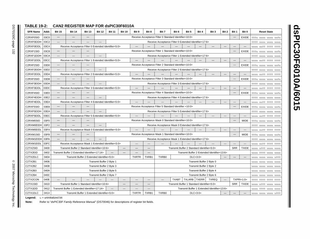
dsP
IC30F
6010A/6015
DS
70150C-page 132
© 2007 M
icrochip Technology Inc.
it 3 Bit 2 Bit 1 Bit 0 Reset State
— EXIDE 000u uuuu uuuu uu0u
0000 uuuu uuuu uuuu
— — — — uuuu uu00 0000 0000
— EXIDE 000u uuuu uuuu uu0u
0000 uuuu uuuu uuuu
— — — — uuuu uu00 0000 0000
— EXIDE 000u uuuu uuuu uu0u
0000 uuuu uuuu uuuu
— — — — uuuu uu00 0000 0000
— EXIDE 000u uuuu uuuu uu0u
0000 uuuu uuuu uuuu
— — — — uuuu uu00 0000 0000
— EXIDE 000u uuuu uuuu uu0u
0000 uuuu uuuu uuuu
— — — — uuuu uu00 0000 0000
— EXIDE 000u uuuu uuuu uu0u
0000 uuuu uuuu uuuu
— — — — uuuu uu00 0000 0000
— MIDE 000u uuuu uuuu uu0u
0000 uuuu uuuu uuuu
— — — — uuuu uu00 0000 0000
— MIDE 000u uuuu uuuu uu0u
0000 uuuu uuuu uuuu
— — — — uuuu uu00 0000 0000
:0> SRR TXIDE uuuu u000 uuuu uuuu
entifier<13:6> uuuu 0000 uuuu uuuu
— — — uuuu uuuu uuuu u000
te 0 uuuu uuuu uuuu uuuu
te 2 uuuu uuuu uuuu uuuu
te 4 uuuu uuuu uuuu uuuu
te 6 uuuu uuuu uuuu uuuu
REQ — TXPRI<1:0> 0000 0000 0000 0000
:0> SRR TXIDE uuuu u000 uuuu uuuu
entifier<13:6> uuuu 0000 uuuu uuuu
— — — uuuu uuuu uuuu u000
TABLE 19-2: CAN2 REGISTER MAP FOR dsPIC30F6010ASFR Name Addr. Bit 15 Bit 14 Bit 13 Bit 12 Bit 11 Bit 10 Bit 9 Bit 8 Bit 7 Bit 6 Bit 5 Bit 4 B
C2RXF0SID 03C0 — — — Receive Acceptance Filter 0 Standard Identifier<10:0>
C2RXF0EIDH 03C2 — — — — Receive Acceptance Filter 0 Extended Identifier<17:6>
C2RXF0EIDL 03C4 Receive Acceptance Filter 0 Extended Identifier<5:0> — — — — — —
C2RXF1SID 03C8 — — — Receive Acceptance Filter 1 Standard Identifier<10:0>
C2RXF1EIDH 03CA — — — — Receive Acceptance Filter 1 Extended Identifier<17:6>
C2RXF1EIDL 03CC Receive Acceptance Filter 1 Extended Identifier<5:0> — — — — — —
C2RXF2SID 03D0 — — — Receive Acceptance Filter 2 Standard Identifier<10:0>
C2RXF2EIDH 03D2 — — — — Receive Acceptance Filter 2 Extended Identifier<17:6>
C2RXF2EIDL 03D4 Receive Acceptance Filter 2 Extended Identifier<5:0> — — — — — —
C2RXF3SID 03D8 — — — Receive Acceptance Filter 3 Standard Identifier<10:0>
C2RXF3EIDH 03DA — — — — Receive Acceptance Filter 3 Extended Identifier<17:6>
C2RXF3EIDL 03DC Receive Acceptance Filter 3 Extended Identifier<5:0> — — — — — —
C2RXF4SID 03E0 — — — Receive Acceptance Filter 4 Standard Identifier<10:0>
C2RXF4EIDH 03E2 — — — — Receive Acceptance Filter 4 Extended Identifier<17:6>
C2RXF4EIDL 03E4 Receive Acceptance Filter 4 Extended Identifier<5:0> — — — — — —
C2RXF5SID 03E8 — — — Receive Acceptance Filter 5 Standard Identifier <10:0>
C2RXF5EIDH 03EA — — — — Receive Acceptance Filter 5 Extended Identifier<17:6>
C2RXF5EIDL 03EC Receive Acceptance Filter 5 Extended Identifier<5:0> — — — — — —
C2RXM0SID 03F0 — — — Receive Acceptance Mask 0 Standard Identifier<10:0>
C2RXM0EIDH 03F2 — — — — Receive Acceptance Mask 0 Extended Identifier<17:6>
C2RXM0EIDL 03F4 Receive Acceptance Mask 0 Extended Identifier<5:0> — — — — — —
C2RXM1SID 03F8 — — — Receive Acceptance Mask 1 Standard Identifier<10:0>
C2RXM1EIDH 03FA — — — — Receive Acceptance Mask 1 Extended Identifier<17:6>
C2RXM1EIDL 03FC Receive Acceptance Mask 1 Extended Identifier<5:0> — — — — — —
C2TX2SID 0400 Transmit Buffer 2 Standard Identifier<10:6> — — — Transmit Buffer 2 Standard Identifier<5
C2TX2EID 0402 Transmit Buffer 2 Extended Identifier<17:14> — — — — Transmit Buffer 2 Extended Id
C2TX2DLC 0404 Transmit Buffer 2 Extended Identifier<5:0> TXRTR TXRB1 TXRB0 DLC<3:0>
C2TX2B1 0406 Transmit Buffer 2 Byte 1 Transmit Buffer 2 By
C2TX2B2 0408 Transmit Buffer 2 Byte 3 Transmit Buffer 2 By
C2TX2B3 040A Transmit Buffer 2 Byte 5 Transmit Buffer 2 By
C2TX2B4 040C Transmit Buffer 2 Byte 7 Transmit Buffer 2 By
C2TX2CON 040E — — — — — — — — — TXABT TXLARB TXERR TX
C2TX1SID 0410 Transmit Buffer 1 Standard Identifier<10:6> — — — Transmit Buffer 1 Standard Identifier<5
C2TX1EID 0412 Transmit Buffer 1 Extended Identifier<17:14> — — — — Transmit Buffer 1 Extended Id
C2TX1DLC 0414 Transmit Buffer 1 Extended Identifier<5:0> TXRTR TXRB1 TXRB0 DLC<3:0>
Legend: u = uninitialized bit
Note: Refer to “dsPIC30F Family Reference Manual” (DS70046) for descriptions of register bit fields.

© 2007 M
icrochip Technology Inc.
DS
70150C-page 133
dsP
IC30F
6010A/6015
C2 uuuu uuuu uuuu uuuu
C2 uuuu uuuu uuuu uuuu
C2 uuuu uuuu uuuu uuuu
C2 uuuu uuuu uuuu uuuu
C2 — TXPRI<1:0> 0000 0000 0000 0000
C2 SRR TXIDE uuuu u000 uuuu uuuu
C2 <13:6> uuuu 0000 uuuu uuuu
C2 — — — uuuu uuuu uuuu u000
C2 uuuu uuuu uuuu uuuu
C2 uuuu uuuu uuuu uuuu
C2 uuuu uuuu uuuu uuuu
C2 uuuu uuuu uuuu uuuu
C2 — TXPRI<1:0> 0000 0000 0000 0000
C2 SRR RXIDE 000u uuuu uuuu uuuu
C2 0000 uuuu uuuu uuuu
C2 DLC<3:0> uuuu uuuu 000u uuuu
C2 uuuu uuuu uuuu uuuu
C2 uuuu uuuu uuuu uuuu
C2 uuuu uuuu uuuu uuuu
C2 uuuu uuuu uuuu uuuu
C2 FILHIT<2:0> 0000 0000 0000 0000
C2 SRR RXIDE 000u uuuu uuuu uuuu
C2 0000 uuuu uuuu uuuu
C2 DLC<3:0> uuuu uuuu 000u uuuu
C2 uuuu uuuu uuuu uuuu
C2 uuuu uuuu uuuu uuuu
C2 uuuu uuuu uuuu uuuu
C2 uuuu uuuu uuuu uuuu
C2 DBEN JTOFF FILHIT0 0000 0000 0000 0000
C2 DE<2:0> — 0000 0100 1000 0000
C2 :0> 0000 0000 0000 0000
C2 PRSEG<2:0> 0u00 0uuu uuuu uuuu
C2 TX0IF RX1IF RX0IF 0000 0000 0000 0000
C2 TX0IE RX1E RX0IE 0000 0000 0000 0000
C2 r 0000 0000 0000 0000
TAS Bit 2 Bit 1 Bit 0 Reset State
Le
No
TX1B1 0416 Transmit Buffer 1 Byte 1 Transmit Buffer 1 Byte 0
TX1B2 0418 Transmit Buffer 1 Byte 3 Transmit Buffer 1 Byte 2
TX1B3 041A Transmit Buffer 1 Byte 5 Transmit Buffer 1 Byte 4
TX1B4 041C Transmit Buffer 1 Byte 7 Transmit Buffer 1 Byte 6
TX1CON 041E — — — — — — — — — TXABT TXLARB TXERR TXREQ
TX0SID 0420 Transmit Buffer 0 Standard Identifier<10:6> — — — Transmit Buffer 0 Standard Identifier<5:0>
TX0EID 0422 Transmit Buffer 0 Extended Identifier<17:14> — — — — Transmit Buffer 0 Extended Identifier
TX0DLC 0424 Transmit Buffer 0 Extended Identifier<5:0> TXRTR TXRB1 TXRB0 DLC<3:0>
TX0B1 0426 Transmit Buffer 0 Byte 1 Transmit Buffer 0 Byte 0
TX0B2 0428 Transmit Buffer 0 Byte 3 Transmit Buffer 0 Byte 2
TX0B3 042A Transmit Buffer 0 Byte 5 Transmit Buffer 0 Byte 4
TX0B4 042C Transmit Buffer 0 Byte 7 Transmit Buffer 0 Byte 6
TX0CON 042E — — — — — — — — — TXABT TXLARB TXERR TXREQ
RX1SID 0430 — — — Receive Buffer 1 Standard Identifier<10:0>
RX1EID 0432 — — — — Receive Buffer 1 Extended Identifier <17:6>
RX1DLC 0434 Receive Buffer 1 Extended Identifier<5:0> RXRTR RXRB1 — — — RXRB0
RX1B1 0436 Receive Buffer 1 Byte 1 Receive Buffer 1 Byte 0
RX1B2 0438 Receive Buffer 1 Byte 3 Receive Buffer 1 Byte 2
RX1B3 043A Receive Buffer 1 Byte 5 Receive Buffer 1 Byte 4
RX1B4 043C Receive Buffer 1 Byte 7 Receive Buffer 1 Byte 6
RX1CON 043E — — — — — — — — RXFUL — — — RXRTRRO
RX0SID 0440 — — — Receive Buffer 0 Standard Identifier<10:0>
RX0EID 0442 — — — — Receive Buffer 0 Extended Identifier<17:6>
RX0DLC 0444 Receive Buffer 0 Extended Identifier<5:0> RXRTR RXRB1 — — — RXRB0
RX0B1 0446 Receive Buffer 0 Byte 1 Receive Buffer 0 Byte 0
RX0B2 0448 Receive Buffer 0 Byte 3 Receive Buffer 0 Byte 2
RX0B3 044A Receive Buffer 0 Byte 5 Receive Buffer 0 Byte 4
RX0B4 044C Receive Buffer 0 Byte 7 Receive Buffer 0 Byte 6
RX0CON 044E — — — — — — — — RXFUL — — — RXRTRRO
CTRL 0450 CANCAP — CSIDLE ABAT CANCKS REQOP<2:0> OPMODE<2:0> — ICO
CFG1 0452 — — — — — — — — SJW<1:0> BRP<5
CFG2 0454 WAKFIL — — — SEG2PH<2:0> SEG2PHTS SAM SEG1PH<2:0>
INTF 0456 RX0OVR RX1OVR TXBO TXEP RXEP TXWAR RXWAR EWARN IVRIF WAKIF ERRIF TX2IF TX1IF
INTE 0458 — — — — — — — — IVRIE WAKIE ERRIE TX2IE TX1IE
EC 045A Transmit Error Count Register Receive Error Count Registe
BLE 19-2: CAN2 REGISTER MAP FOR dsPIC30F6010A (CONTINUED)FR Name Addr. Bit 15 Bit 14 Bit 13 Bit 12 Bit 11 Bit 10 Bit 9 Bit 8 Bit 7 Bit 6 Bit 5 Bit 4 Bit 3
gend: u = uninitialized bit
te: Refer to “dsPIC30F Family Reference Manual” (DS70046) for descriptions of register bit fields.
dsPIC30F6010A/6015
NOTES:
DS70150C-page 134 © 2007 Microchip Technology Inc.

dsPIC30F6010A/6015
20.0 10-BIT HIGH-SPEED ANALOG-TO-DIGITAL CONVERTER (ADC) MODULE
The10-bit high-speed Analog-to-Digital Converter(ADC) allows conversion of an analog input signal to a10-bit digital number. This module is based on a Suc-cessive Approximation Register (SAR) architecture,and provides a maximum sampling rate of 1 Msps. TheA/D module has 16 analog inputs which are multi-plexed into four sample and hold amplifiers. The outputof the sample and hold is the input into the converter,which generates the result. The analog reference volt-ages are software selectable to either the device sup-ply voltage (AVDD/AVSS) or the voltage level on the(VREF+/VREF-) pin. The A/D converter has a uniquefeature of being able to operate while the device is inSleep mode.
The A/D module has six 16-bit registers:
• A/D Control Register 1 (ADCON1)• A/D Control Register 2 (ADCON2)
• A/D Control Register 3 (ADCON3)• A/D Input Select Register (ADCHS)• A/D Port Configuration Register (ADPCFG)
• A/D Input Scan Selection Register (ADCSSL)
The ADCON1, ADCON2 and ADCON3 registerscontrol the operation of the A/D module. The ADCHSregister selects the input channels to be converted. TheADPCFG register configures the port pins as analoginputs or as digital I/O. The ADCSSL register selectsinputs for scanning.
The block diagram of the A/D module is shown inFigure 20-1.
Note: This data sheet summarizes features of thisgroup of dsPIC30F devices and is not intended to bea complete reference source. For more informationon the CPU, peripherals, register descriptions andgeneral device functionality, refer to the “dsPIC30FFamily Reference Manual” (DS70046).
Note: The SSRC<2:0>, ASAM, SIMSAM,SMPI<3:0>, BUFM and ALTS bits, as wellas the ADCON3 and ADCSSL registers,must not be written to while ADON = 1.This would lead to indeterminate results.
© 2007 Microchip Technology Inc. DS70150C-page 135

dsPIC30F6010A/6015
A5
FIGURE 20-1: 10-BIT HIGH-SPEED A/D FUNCTIONAL BLOCK DIAGRAM
S/H
+
-
10-bit Result Conversion Logic
VREF+ (Note 1)
AVSSAVDD
ADC
Dat
a
16-word, 10-bitDual Port
Buffer
Bus
Inte
rfac
e
AN12
AN0
AN5
N
DS70150C-page 136 © 2007 Microchip Technology Inc.

dsPIC30F6010A/6015
20.1 A/D Result Buffer
The module contains a 16-word dual port, read-onlybuffer, called ADCBUF0...ADCBUFF, to buffer the A/Dresults. The RAM is 10-bits wide, but is read into differentformat 16-bit words. The contents of the sixteen A/DConversion Result Buffer registers, ADCBUF0 throughADCBUFF, cannot be written by user software.
20.2 Conversion Operation
After the A/D module has been configured, the sampleacquisition is started by setting the SAMP bit. Varioussources, such as a programmable bit, timer time-outs andexternal events, will terminate acquisition and start a con-version. When the A/D conversion is complete, the resultis loaded into ADCBUF0...ADCBUFF, and the A/DInterrupt Flag ADIF and the DONE bit are set after thenumber of samples specified by the SMPI bit.
The following steps should be followed for doing anA/D conversion:
1. Configure the A/D module:-Configure analog pins, voltage reference
and digital I/O-Select A/D input channels
-Select A/D conversion clock-Select A/D conversion trigger-Turn on A/D module
2. Configure A/D interrupt (if required):-Clear ADIF bit -Select A/D interrupt priority
3. Start sampling.4. Wait the required acquisition time.5. Trigger acquisition end, start conversion
6. Wait for A/D conversion to complete, by either:-Waiting for the A/D interrupt
7. Read A/D result buffer, clear ADIF if required.
20.3 Selecting the Conversion Sequence
Several groups of control bits select the sequence inwhich the A/D connects inputs to the sample/holdchannels, converts channels, writes the buffer memory,and generates interrupts. The sequence is controlledby the sampling clocks.
The SIMSAM bit controls the acquire/convertsequence for multiple channels. If the SIMSAM bit is‘0’, the two or four selected channels are acquired andconverted sequentially, with two or four sample clocks.If the SIMSAM bit is ‘1’, two or four selected channelsare acquired simultaneously, with one sample clock.The channels are then converted sequentially. Obvi-ously, if there is only 1 channel selected, the SIMSAMbit is not applicable.
The CHPS bits selects how many channels are sam-pled. This can vary from 1, 2 or 4 channels. If CHPSselects 1 channel, the CH0 channel will be sampled atthe sample clock and converted. The result is stored inthe buffer. If CHPS selects 2 channels, the CH0 andCH1 channels will be sampled and converted. If CHPSselects 4 channels, the CH0, CH1, CH2 and CH3channels will be sampled and converted.
The SMPI bits select the number of acquisition/conver-sion sequences that would be performed before aninterrupt occurs. This can vary from 1 sample perinterrupt to 16 samples per interrupt.
The user cannot program a combination of CHPS andSMPI bits that specifies more than 16 conversions perinterrupt, or 8 conversions per interrupt, depending onthe BUFM bit. The BUFM bit, when set, will split the16-word results buffer (ADCBUF0...ADCBUFF) intotwo 8-word groups. Writing to the 8-word buffers will bealternated on each interrupt event. Use of the BUFM bitwill depend on how much time is available for movingdata out of the buffers after the interrupt, as determinedby the application.
If the processor can quickly unload a full buffer withinthe time it takes to acquire and convert one channel,the BUFM bit can be ‘0’ and up to 16 conversions maybe done per interrupt. The processor will have onesample and conversion time to move the sixteenconversions.
If the processor cannot unload the buffer within the acqui-sition and conversion time, the BUFM bit should be ‘1’.For example, if SMPI<3:0> (ADCON2<5:2> = 0111),then eight conversions will be loaded into 1/2 of thebuffer, following which an interrupt occurs. The next eightconversions will be loaded into the other 1/2 of the buffer.The processor will have the entire time betweeninterrupts to move the eight conversions.
The ALTS bit can be used to alternate the inputsselected during the sampling sequence. The inputmultiplexer has two sets of sample inputs: MUX A andMUX B. If the ALTS bit is ‘0’, only the MUX A inputs areselected for sampling. If the ALTS bit is ‘1’ andSMPI<3:0> = 0000, on the first sample/convertsequence, the MUX A inputs are selected, and on thenext acquire/convert sequence, the MUX B inputs areselected.
The CSCNA bit (ADCON2<10>) will allow the CH0channel inputs to be alternately scanned across aselected number of analog inputs for the MUX A group.The inputs are selected by the ADCSSL register. If aparticular bit in the ADCSSL register is ‘1’, the corre-sponding input is selected. The inputs are alwaysscanned from lower to higher numbered inputs, startingafter each interrupt. If the number of inputs selected isgreater than the number of samples taken per interrupt,the higher numbered inputs are unused.
© 2007 Microchip Technology Inc. DS70150C-page 137
dsPIC30F6010A/6015
20.4 Programming the Start of Conversion Trigger
The conversion trigger will terminate acquisition andstart the requested conversions.
The SSRC<2:0> bits select the source of theconversion trigger.
The SSRC bits provide for up to 5 alternate sources ofconversion trigger.
When SSRC<2:0> = 000, the conversion trigger isunder software control. Clearing the SAMP bit willcause the conversion trigger.
When SSRC<2:0> = 111 (Auto-Start mode), the con-version trigger is under A/D clock control. The SAMCbits select the number of A/D clocks between the startof acquisition and the start of conversion. This providesthe fastest conversion rates on multiple channels.SAMC must always be at least 1 clock cycle.
Other trigger sources can come from timer modules,motor control PWM module, or external interrupts.
20.5 Aborting a Conversion
Clearing the ADON bit during a conversion will abortthe current conversion and stop the sampling sequenc-ing. The ADCBUF will not be updated with the partiallycompleted A/D conversion sample. That is, theADCBUF will continue to contain the value of the lastcompleted conversion (or the last value written to theADCBUF register).
If the clearing of the ADON bit coincides with anauto-start, the clearing has a higher priority.
After the A/D conversion is aborted, a 2 TAD wait isrequired before the next sampling may be started bysetting the SAMP bit.
If sequential sampling is specified, the A/D will continueat the next sample pulse which corresponds with thenext channel converted. If simultaneous sampling isspecified, the A/D will continue with the nextmultichannel group conversion sequence.
20.6 Selecting the A/D Conversion Clock
The A/D conversion requires 12 TAD. The source of theA/D conversion clock is software selected using a six-bit counter. There are 64 possible options for TAD.
EQUATION 20-1: A/D CONVERSION CLOCK
The internal RC oscillator is selected by setting theADRC bit.
For correct A/D conversions, the A/D conversion clock(TAD) must be selected to ensure a minimum TAD timeof 83.33 nsec (for VDD = 5V). Refer to the Section 24.0"Electrical Characteristics" for minimum TAD underother operating conditions.
Example 20-1 shows a sample calculation for theADCS<5:0> bits, assuming a device operating speedof 30 MIPS.
EXAMPLE 20-1: A/D CONVERSION CLOCK CALCULATION
Note: To operate the A/D at the maximum speci-fied conversion speed, the Auto-ConvertTrigger option should be selected(SSRC = 111) and the Auto-Sample Timebits should be set to 1 TAD
(SAMC = 00001). This configuration willgive a total conversion period (sample +convert) of 13 TAD.
The use of any other conversion triggerwill result in additional TAD cycles tosynchronize the external event to the A/D.
TAD = TCY * (0.5 * (ADCS<5:0> + 1))
ADCS<5:0> = 2 – 1TAD
TCY
TAD = 84 nsec
ADCS<5:0> = 2 – 1TAD
TCY
TCY = 33 nsec (30 MIPS)
= 2 • – 184 nsec33 nsec
= 4.09
Therefore,Set ADCS<5:0> = 9
Actual TAD = (ADCS<5:0> + 1)TCY
2
= (9 + 1)33 nsec
2
= 99 nsec
DS70150C-page 138 © 2007 Microchip Technology Inc.
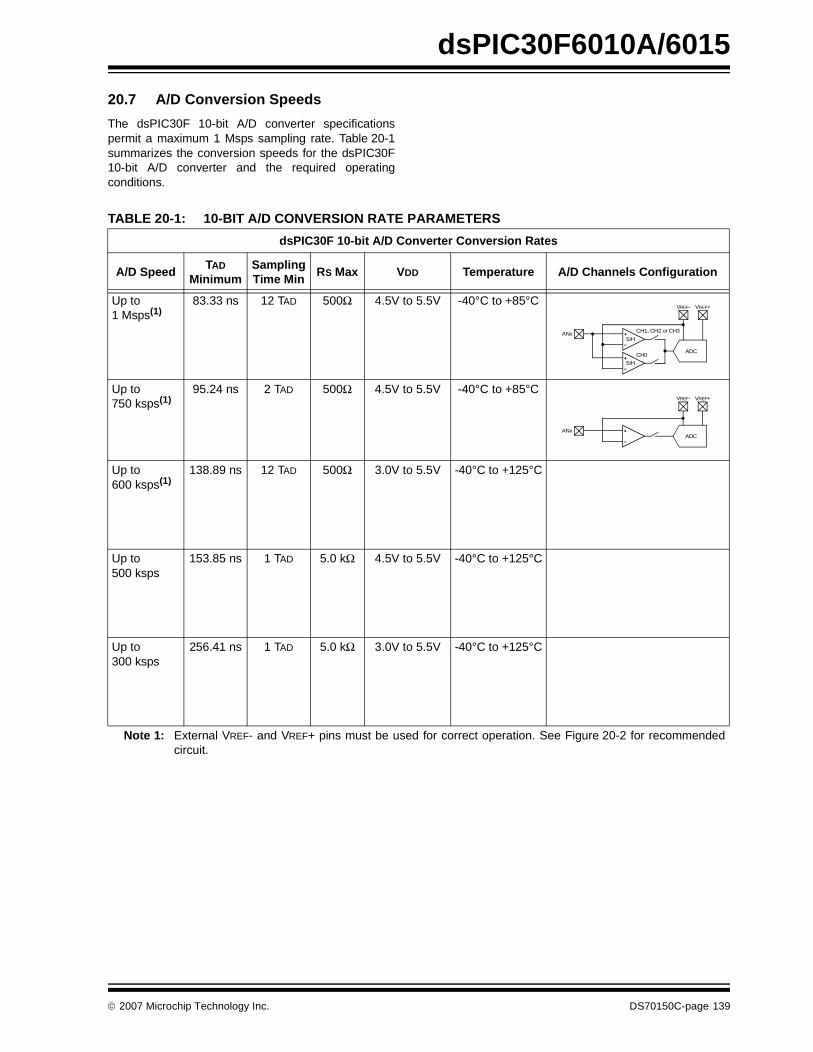
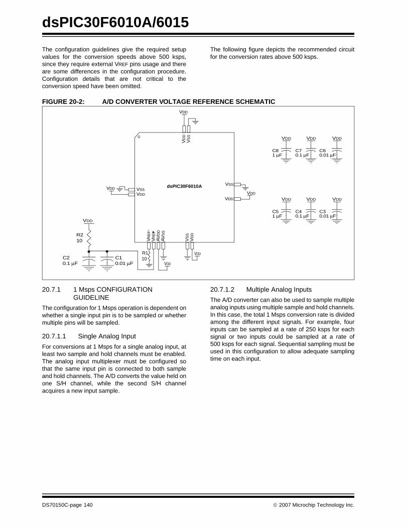
dsPIC30F6010A/6015
The configuration guidelines give the required setupvalues for the conversion speeds above 500 ksps,since they require external VREF pins usage and thereare some differences in the configuration procedure.Configuration details that are not critical to theconversion speed have been omitted.
The following figure depicts the recommended circuitfor the conversion rates above 500 ksps.
FIGURE 20-2: A/D CONVERTER VOLTAGE REFERENCE SCHEMATIC
20.7.1 1 Msps CONFIGURATION GUIDELINE
The configuration for 1 Msps operation is dependent onwhether a single input pin is to be sampled or whethermultiple pins will be sampled.
20.7.1.1 Single Analog Input
For conversions at 1 Msps for a single analog input, atleast two sample and hold channels must be enabled.The analog input multiplexer must be configured sothat the same input pin is connected to both sampleand hold channels. The A/D converts the value held onone S/H channel, while the second S/H channelacquires a new input sample.
20.7.1.2 Multiple Analog Inputs
The A/D converter can also be used to sample multipleanalog inputs using multiple sample and hold channels.In this case, the total 1 Msps conversion rate is dividedamong the different input signals. For example, fourinputs can be sampled at a rate of 250 ksps for eachsignal or two inputs could be sampled at a rate of500 ksps for each signal. Sequential sampling must beused in this configuration to allow adequate samplingtime on each input.
VD
DV
SS
VSSVDD
VDD
VR
EF-
VR
EF+
AV
DD
AV
SS
VS
SV
DD
VSSdsPIC30F6010A
VDD
VDD
VDD
VDD
VDD
VDD
VDD
R210
C20.1 μF
C10.01 μF
R110
C81 μF
VDD
C70.1 μF
VDD
C60.01 μF
VDD
C51 μF
VDD
C40.1 μF
VDD
C30.01 μF
DS70150C-page 140 © 2007 Microchip Technology Inc.
dsPIC30F6010A/6015
20.7.1.3 1 Msps Configuration Items
The following configuration items are required toachieve a 1 Msps conversion rate.
• Comply with conditions provided in Table 20-2• Connect external VREF+ and VREF- pins following
the recommended circuit shown in Figure 20-2• Set SSRC<2:0> = 111 in the ADCON1 register to
enable the auto-convert option• Enable automatic sampling by setting the ASAM
control bit in the ADCON1 register• Enable sequential sampling by clearing the
SIMSAM bit in the ADCON1 register• Enable at least two sample and hold channels by
writing the CHPS<1:0> control bits in the ADCON2 register
• Write the SMPI<3:0> control bits in the ADCON2 register for the desired number of conversions between interrupts. At a minimum, set SMPI<3:0> = 0001 since at least two sample and hold channels should be enabled
• Configure the A/D clock period to be:
by writing to the ADCS<5:0> control bits in the ADCON3 register
• Configure the sampling time to be 2 TAD by writing: SAMC<4:0> = 00010
• Select at least two channels per analog input pin by writing to the ADCHS register
20.7.2 750 ksps CONFIGURATION GUIDELINE
The following configuration items are required toachieve a 750 ksps conversion rate. This configurationassumes that a single analog input is to be sampled.
• Comply with conditions provided in Table 20-2
• Connect external VREF+ and VREF- pins following the recommended circuit shown in Figure 20-2
• Set SSRC<2:0> = 111 in the ADCON1 register to enable the auto-convert option
• Enable automatic sampling by setting the ASAM control bit in the ADCON1 register
• Enable one sample and hold channel by setting CHPS<1:0> = 00 in the ADCON2 register
• Write the SMPI<3:0> control bits in the ADCON2 register for the desired number of conversions between interrupts
• Configure the A/D clock period to be:
by writing to the ADCS<5:0> control bits in the ADCON3 register
• Configure the sampling time to be 2 TAD by writing: SAMC<4:0> = 00010
20.7.3 600 ksps CONFIGURATION GUIDELINE
The configuration for 600 ksps operation is dependenton whether a single input pin is to be sampled orwhether multiple pins will be sampled.
20.7.3.1 Single Analog Input
When performing conversions at 600 ksps for a singleanalog input, at least two sample and hold channelsmust be enabled. The analog input multiplexer must beconfigured so that the same input pin is connected toboth sample and hold channels. The A/D converts thevalue held on one S/H channel, while the second S/Hchannel acquires a new input sample.
20.7.3.2 Multiple Analog Input
The A/D converter can also be used to sample multipleanalog inputs using multiple sample and hold channels.In this case, the total 600 ksps conversion rate isdivided among the different input signals. For example,four inputs can be sampled at a rate of 150 ksps foreach signal or two inputs can be sampled at a rate of300 ksps for each signal. Sequential sampling must beused in this configuration to allow adequate samplingtime on each input.
20.7.3.3 600 ksps Configuration Items
The following configuration items are required toachieve a 600 ksps conversion rate.
• Comply with conditions provided in Table 20-2
• Connect external VREF+ and VREF- pins following the recommended circuit shown in Figure 20-2
• Set SSRC<2:0> = 111 in the ADCON1 register to enable the auto-convert option
• Enable automatic sampling by setting the ASAM control bit in the ADCON1 register
• Enable sequential sampling by clearing the SIMSAM bit in the ADCON1 register
• Enable at least two sample and hold channels by writing the CHPS<1:0> control bits in the ADCON2 register
• Write the SMPI<3:0> control bits in the ADCON2 register for the desired number of conversions between interrupts. At a minimum, set SMPI<3:0> = 0001 since at least two sample and hold channels should be enabled
• Configure the A/D clock period to be:
by writing to the ADCS<5:0> control bits in the ADCON3 register
• Configure the sampling time to be 2 TAD by writing: SAMC<4:0> = 00010
• Select at least two channels per analog input pin by writing to the ADCHS register
1
12 x 1,000,000= 83.33 ns
1
(12 + 2) X 750,000= 95.24 ns
1
12 x 600,000= 138.89 ns
© 2007 Microchip Technology Inc. DS70150C-page 141
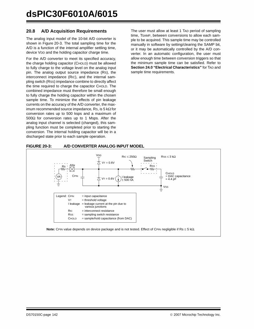
dsPIC30F6010A/6015
20.8 A/D Acquisition Requirements
The analog input model of the 10-bit A/D converter isshown in Figure 20-3. The total sampling time for theA/D is a function of the internal amplifier settling time,device VDD and the holding capacitor charge time.
For the A/D converter to meet its specified accuracy,the charge holding capacitor (CHOLD) must be allowedto fully charge to the voltage level on the analog inputpin. The analog output source impedance (RS), theinterconnect impedance (RIC), and the internal sam-pling switch (RSS) impedance combine to directly affectthe time required to charge the capacitor CHOLD. Thecombined impedance must therefore be small enoughto fully charge the holding capacitor within the chosensample time. To minimize the effects of pin leakagecurrents on the accuracy of the A/D converter, the max-imum recommended source impedance, RS, is 5 kΩ forconversion rates up to 500 ksps and a maximum of500Ω for conversion rates up to 1 Msps. After theanalog input channel is selected (changed), this sam-pling function must be completed prior to starting theconversion. The internal holding capacitor will be in adischarged state prior to each sample operation.
The user must allow at least 1 TAD period of samplingtime, TSAMP, between conversions to allow each sam-ple to be acquired. This sample time may be controlledmanually in software by setting/clearing the SAMP bit,or it may be automatically controlled by the A/D con-verter. In an automatic configuration, the user mustallow enough time between conversion triggers so thatthe minimum sample time can be satisfied. Refer toSection 24.0 “Electrical Characteristics” for TAD andsample time requirements.
FIGURE 20-3: A/D CONVERTER ANALOG INPUT MODEL
CPINVA
Rs ANxVT = 0.6V
VT = 0.6V I leakage
RIC ≤ 250Ω SamplingSwitch
RSS
CHOLD= DAC capacitance
VSS
VDD
= 4.4 pF± 500 nA
Legend: CPIN
VT
I leakage
RIC
RSS
CHOLD
= input capacitance= threshold voltage= leakage current at the pin due to
= interconnect resistance= sampling switch resistance= sample/hold capacitance (from DAC)
various junctions
Note: CPIN value depends on device package and is not tested. Effect of CPIN negligible if Rs ≤ 5 kΩ.
RSS ≤ 3 kΩ
DS70150C-page 142 © 2007 Microchip Technology Inc.
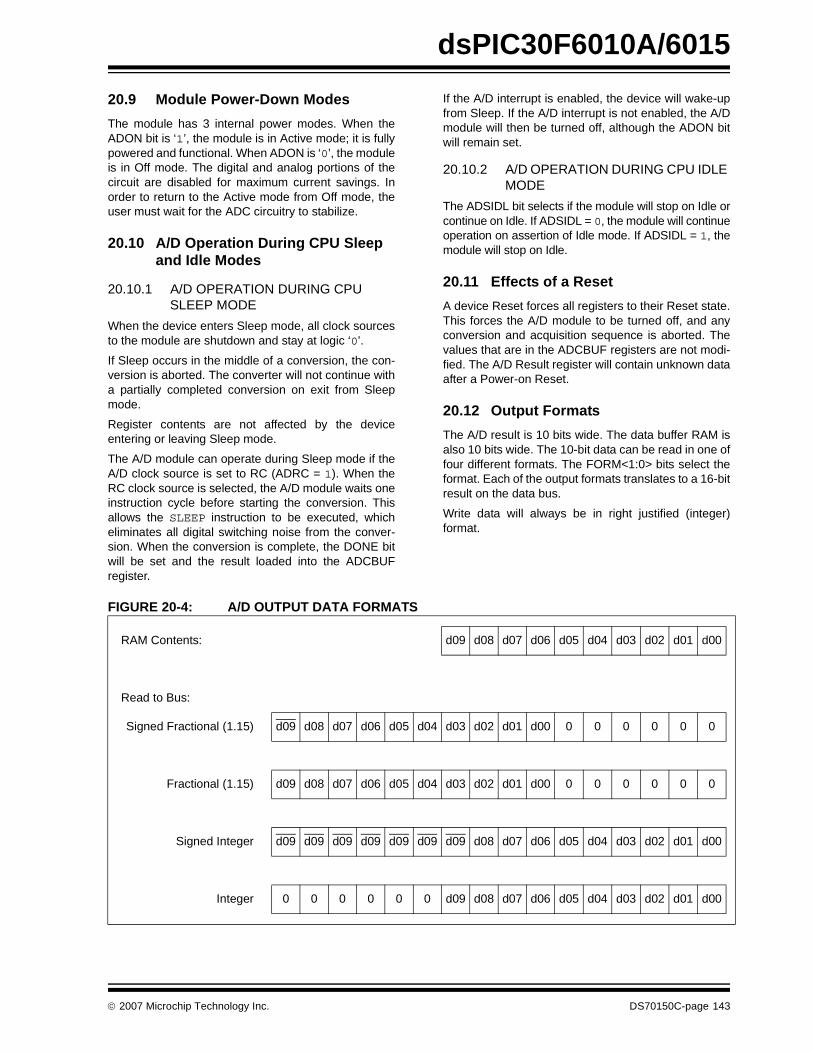
dsPIC30F6010A/6015
20.9 Module Power-Down Modes
The module has 3 internal power modes. When theADON bit is ‘1’, the module is in Active mode; it is fullypowered and functional. When ADON is ‘0’, the moduleis in Off mode. The digital and analog portions of thecircuit are disabled for maximum current savings. Inorder to return to the Active mode from Off mode, theuser must wait for the ADC circuitry to stabilize.
20.10 A/D Operation During CPU Sleep and Idle Modes
20.10.1 A/D OPERATION DURING CPU SLEEP MODE
When the device enters Sleep mode, all clock sourcesto the module are shutdown and stay at logic ‘0’.
If Sleep occurs in the middle of a conversion, the con-version is aborted. The converter will not continue witha partially completed conversion on exit from Sleepmode.
Register contents are not affected by the deviceentering or leaving Sleep mode.
The A/D module can operate during Sleep mode if theA/D clock source is set to RC (ADRC = 1). When theRC clock source is selected, the A/D module waits oneinstruction cycle before starting the conversion. Thisallows the SLEEP instruction to be executed, whicheliminates all digital switching noise from the conver-sion. When the conversion is complete, the DONE bitwill be set and the result loaded into the ADCBUFregister.
If the A/D interrupt is enabled, the device will wake-upfrom Sleep. If the A/D interrupt is not enabled, the A/Dmodule will then be turned off, although the ADON bitwill remain set.
20.10.2 A/D OPERATION DURING CPU IDLE MODE
The ADSIDL bit selects if the module will stop on Idle orcontinue on Idle. If ADSIDL = 0, the module will continueoperation on assertion of Idle mode. If ADSIDL = 1, themodule will stop on Idle.
20.11 Effects of a Reset
A device Reset forces all registers to their Reset state.This forces the A/D module to be turned off, and anyconversion and acquisition sequence is aborted. Thevalues that are in the ADCBUF registers are not modi-fied. The A/D Result register will contain unknown dataafter a Power-on Reset.
20.12 Output Formats
The A/D result is 10 bits wide. The data buffer RAM isalso 10 bits wide. The 10-bit data can be read in one offour different formats. The FORM<1:0> bits select theformat. Each of the output formats translates to a 16-bitresult on the data bus.
Write data will always be in right justified (integer)format.
FIGURE 20-4: A/D OUTPUT DATA FORMATS
RAM Contents: d09 d08 d07 d06 d05 d04 d03 d02 d01 d00
Read to Bus:
Signed Fractional (1.15) d09 d08 d07 d06 d05 d04 d03 d02 d01 d00 0 0 0 0 0 0
Fractional (1.15) d09 d08 d07 d06 d05 d04 d03 d02 d01 d00 0 0 0 0 0 0
Signed Integer d09 d09 d09 d09 d09 d09 d09 d08 d07 d06 d05 d04 d03 d02 d01 d00
Integer 0 0 0 0 0 0 d09 d08 d07 d06 d05 d04 d03 d02 d01 d00
© 2007 Microchip Technology Inc. DS70150C-page 143
dsPIC30F6010A/6015
20.13 Configuring Analog Port Pins
The use of the ADPCFG and TRIS registers control theoperation of the A/D port pins. The port pins that aredesired as analog inputs must have their correspond-ing TRIS bit set (input). If the TRIS bit is cleared (out-put), the digital output level (VOH or VOL) will beconverted.
The A/D operation is independent of the state of theCH0SA<3:0>/CH0SB<3:0> bits and the TRIS bits.
When reading the PORT register, all pins configured asanalog input channels will read as cleared.
Pins configured as digital inputs will not convert ananalog input. Analog levels on any pin that is defined asa digital input (including the ANx pins) may cause theinput buffer to consume current that exceeds thedevice specifications.
20.14 Connection Considerations
The analog inputs have diodes to VDD and VSS as ESDprotection. This requires that the analog input bebetween VDD and VSS. If the input voltage exceeds thisrange by greater than 0.3V (either direction), one of thediodes becomes forward biased and it may damage thedevice if the input current specification is exceeded.
An external RC filter is sometimes added for anti-aliasing of the input signal. The R component should beselected to ensure that the sampling time requirementsare satisfied. Any external components connected (viahigh-impedance) to an analog input pin (capacitor,Zener diode, etc.) should have very little leakagecurrent at the pin.
DS70150C-page 144 © 2007 Microchip Technology Inc.
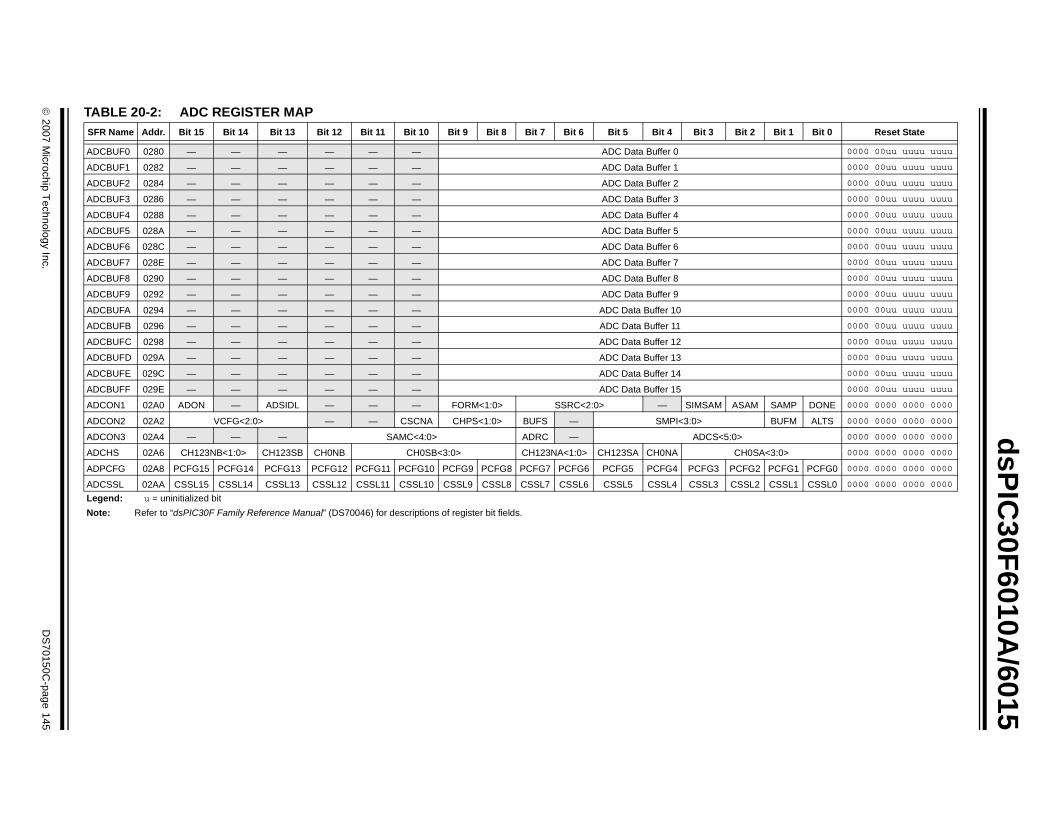
© 2007 M
icrochip Technology Inc.
DS
70150C-page 145
dsP
IC30F
6010A/6015
TASF t 2 Bit 1 Bit 0 Reset State
AD 0000 00uu uuuu uuuu
AD 0000 00uu uuuu uuuu
AD 0000 00uu uuuu uuuu
AD 0000 00uu uuuu uuuu
AD 0000 00uu uuuu uuuu
AD 0000 00uu uuuu uuuu
AD 0000 00uu uuuu uuuu
AD 0000 00uu uuuu uuuu
AD 0000 00uu uuuu uuuu
AD 0000 00uu uuuu uuuu
AD 0000 00uu uuuu uuuu
AD 0000 00uu uuuu uuuu
AD 0000 00uu uuuu uuuu
AD 0000 00uu uuuu uuuu
AD 0000 00uu uuuu uuuu
AD 0000 00uu uuuu uuuu
AD AM SAMP DONE 0000 0000 0000 0000
AD BUFM ALTS 0000 0000 0000 0000
AD 0000 0000 0000 0000
AD 0SA<3:0> 0000 0000 0000 0000
AD FG2 PCFG1 PCFG0 0000 0000 0000 0000
AD SL2 CSSL1 CSSL0 0000 0000 0000 0000
Le
No
BLE 20-2: ADC REGISTER MAPR Name Addr. Bit 15 Bit 14 Bit 13 Bit 12 Bit 11 Bit 10 Bit 9 Bit 8 Bit 7 Bit 6 Bit 5 Bit 4 Bit 3 Bi
CBUF0 0280 — — — — — — ADC Data Buffer 0
CBUF1 0282 — — — — — — ADC Data Buffer 1
CBUF2 0284 — — — — — — ADC Data Buffer 2
CBUF3 0286 — — — — — — ADC Data Buffer 3
CBUF4 0288 — — — — — — ADC Data Buffer 4
CBUF5 028A — — — — — — ADC Data Buffer 5
CBUF6 028C — — — — — — ADC Data Buffer 6
CBUF7 028E — — — — — — ADC Data Buffer 7
CBUF8 0290 — — — — — — ADC Data Buffer 8
CBUF9 0292 — — — — — — ADC Data Buffer 9
CBUFA 0294 — — — — — — ADC Data Buffer 10
CBUFB 0296 — — — — — — ADC Data Buffer 11
CBUFC 0298 — — — — — — ADC Data Buffer 12
CBUFD 029A — — — — — — ADC Data Buffer 13
CBUFE 029C — — — — — — ADC Data Buffer 14
CBUFF 029E — — — — — — ADC Data Buffer 15
CON1 02A0 ADON — ADSIDL — — — FORM<1:0> SSRC<2:0> — SIMSAM AS
CON2 02A2 VCFG<2:0> — — CSCNA CHPS<1:0> BUFS — SMPI<3:0>
CON3 02A4 — — — SAMC<4:0> ADRC — ADCS<5:0>
CHS 02A6 CH123NB<1:0> CH123SB CH0NB CH0SB<3:0> CH123NA<1:0> CH123SA CH0NA CH
PCFG 02A8 PCFG15 PCFG14 PCFG13 PCFG12 PCFG11 PCFG10 PCFG9 PCFG8 PCFG7 PCFG6 PCFG5 PCFG4 PCFG3 PC
CSSL 02AA CSSL15 CSSL14 CSSL13 CSSL12 CSSL11 CSSL10 CSSL9 CSSL8 CSSL7 CSSL6 CSSL5 CSSL4 CSSL3 CS
gend: u = uninitialized bit
te: Refer to “dsPIC30F Family Reference Manual” (DS70046) for descriptions of register bit fields.

dsPIC30F6010A/6015
NOTES:
DS70150C-page 146 © 2007 Microchip Technology Inc.
dsPIC30F6010A/6015
21.0 SYSTEM INTEGRATION
There are several features intended to maximizesystem reliability, minimize cost through elimination ofexternal components, provide power-saving operatingmodes and offer code protection:
• Oscillator Selection• Reset
- Power-on Reset (POR)
- Power-up Timer (PWRT)- Oscillator Start-up Timer (OST)- Programmable Brown-out Reset (BOR)
• Watchdog Timer (WDT)• Power-Saving modes (Sleep and Idle)• Code Protection
• Unit ID Locations• In-Circuit Serial Programming (ICSP)
dsPIC30F devices have a Watchdog Timer, which ispermanently enabled via the Configuration bits or canbe software controlled. It runs off its own RC oscillatorfor added reliability. There are two timers that offernecessary delays on power-up. One is the OscillatorStart-up Timer (OST), intended to keep the chip inReset until the crystal oscillator is stable. The other isthe Power-up Timer (PWRT), which provides a delayon power-up only, designed to keep the part in Resetwhile the power supply stabilizes. With these two tim-ers on-chip, most applications need no external Resetcircuitry.
Sleep mode is designed to offer a very low-currentPower-Down mode. The user can wake-up from Sleepthrough external Reset, Watchdog Timer Wake-up orthrough an interrupt. Several oscillator options are alsomade available to allow the part to fit a wide variety ofapplications. In the Idle mode, the clock sources arestill active, but the CPU is shut-off. The RC oscillatoroption saves system cost, while the LP crystal optionsaves power.
21.1 Oscillator System Overview
The dsPIC30F oscillator system has the followingmodules and features:
• Various external and internal oscillator options as clock sources
• An on-chip PLL to boost internal operating frequency
• A clock switching mechanism between various clock sources
• Programmable clock postscaler for system power savings
• A Fail-Safe Clock Monitor (FSCM) that detects clock failure and takes fail-safe measures
• Clock Control register (OSCCON)• Configuration bits for main oscillator selection
Configuration bits determine the clock source uponPower-on Reset (POR) and Brown-out Reset (BOR).Thereafter, the clock source can be changed betweenpermissible clock sources. The OSCCON register con-trols the clock switching and reflects system clockrelated Status bits.
Table 21-1 provides a summary of the dsPIC30Foscillator operating modes. A simplified diagram of theoscillator system is shown in Figure 21-1.
Note: This data sheet summarizes features of thisgroup of dsPIC30F devices and is not intended to bea complete reference source. For more informationon the CPU, peripherals, register descriptions andgeneral device functionality, refer to the “dsPIC30FFamily Reference Manual” (DS70046). For moreinformation on the device instruction set and pro-gramming, refer to the “dsPIC30F/33F ProgrammersReference Manual” (DS70157).
© 2007 Microchip Technology Inc. DS70150C-page 147
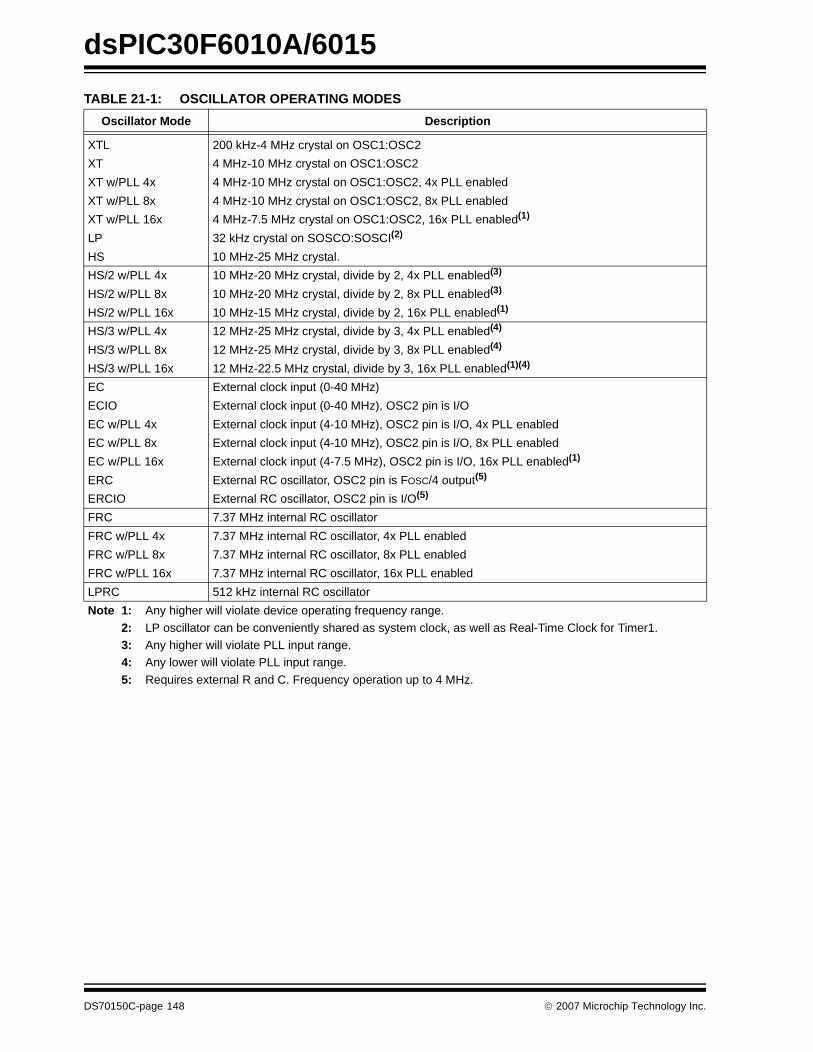
dsPIC30F6010A/6015
TABLE 21-1: OSCILLATOR OPERATING MODES
Oscillator Mode Description
XTL 200 kHz-4 MHz crystal on OSC1:OSC2
XT 4 MHz-10 MHz crystal on OSC1:OSC2
XT w/PLL 4x 4 MHz-10 MHz crystal on OSC1:OSC2, 4x PLL enabled
XT w/PLL 8x 4 MHz-10 MHz crystal on OSC1:OSC2, 8x PLL enabled
XT w/PLL 16x 4 MHz-7.5 MHz crystal on OSC1:OSC2, 16x PLL enabled(1)
LP 32 kHz crystal on SOSCO:SOSCI(2)
HS 10 MHz-25 MHz crystal.
HS/2 w/PLL 4x 10 MHz-20 MHz crystal, divide by 2, 4x PLL enabled(3)
HS/2 w/PLL 8x 10 MHz-20 MHz crystal, divide by 2, 8x PLL enabled(3)
HS/2 w/PLL 16x 10 MHz-15 MHz crystal, divide by 2, 16x PLL enabled(1)
HS/3 w/PLL 4x 12 MHz-25 MHz crystal, divide by 3, 4x PLL enabled(4)
HS/3 w/PLL 8x 12 MHz-25 MHz crystal, divide by 3, 8x PLL enabled(4)
HS/3 w/PLL 16x 12 MHz-22.5 MHz crystal, divide by 3, 16x PLL enabled(1)(4)
EC External clock input (0-40 MHz)
ECIO External clock input (0-40 MHz), OSC2 pin is I/O
EC w/PLL 4x External clock input (4-10 MHz), OSC2 pin is I/O, 4x PLL enabled
EC w/PLL 8x External clock input (4-10 MHz), OSC2 pin is I/O, 8x PLL enabled
EC w/PLL 16x External clock input (4-7.5 MHz), OSC2 pin is I/O, 16x PLL enabled(1)
ERC External RC oscillator, OSC2 pin is FOSC/4 output(5)
ERCIO External RC oscillator, OSC2 pin is I/O(5)
FRC 7.37 MHz internal RC oscillator
FRC w/PLL 4x 7.37 MHz internal RC oscillator, 4x PLL enabled
FRC w/PLL 8x 7.37 MHz internal RC oscillator, 8x PLL enabled
FRC w/PLL 16x 7.37 MHz internal RC oscillator, 16x PLL enabled
LPRC 512 kHz internal RC oscillator
Note 1: Any higher will violate device operating frequency range.
2: LP oscillator can be conveniently shared as system clock, as well as Real-Time Clock for Timer1.3: Any higher will violate PLL input range.4: Any lower will violate PLL input range.
5: Requires external R and C. Frequency operation up to 4 MHz.
DS70150C-page 148 © 2007 Microchip Technology Inc.
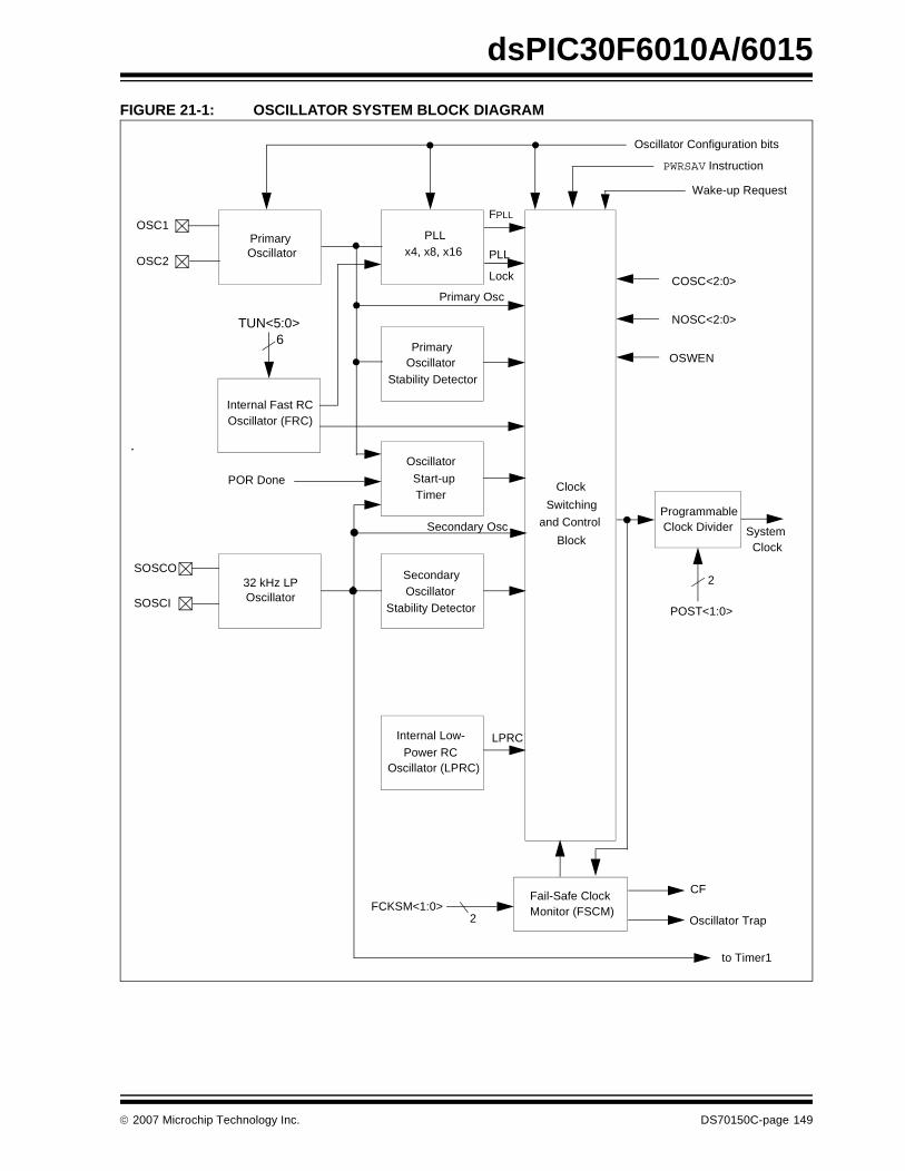
dsPIC30F6010A/6015
FIGURE 21-1: OSCILLATOR SYSTEM BLOCK DIAGRAM
Primary OSC1
OSC2
SOSCO
SOSCI
Oscillator
32 kHz LP
Clock
and Control
Block
Switching
Oscillator
x4, x8, x16 PLL
Primary Oscillator
Stability Detector
Stability Detector
SecondaryOscillator
ProgrammableClock Divider
Oscillator
Start-upTimer
Fail-Safe ClockMonitor (FSCM)
Internal Fast RCOscillator (FRC)
Internal Low-
Power RCOscillator (LPRC)
PWRSAV Instruction
Wake-up Request
Oscillator Configuration bits
SystemClock
Oscillator Trap
to Timer1
LPRC
Secondary Osc
POR Done
Primary Osc
FPLL
POST<1:0>
2
FCKSM<1:0>2
PLL
Lock COSC<2:0>
NOSC<2:0>
OSWEN
CF
TUN<5:0>6
© 2007 Microchip Technology Inc. DS70150C-page 149
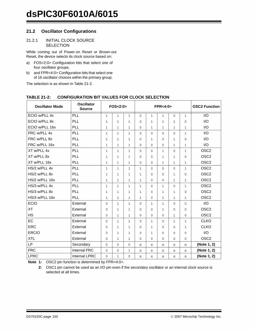
dsPIC30F6010A/6015
21.2 Oscillator Configurations
21.2.1 INITIAL CLOCK SOURCE SELECTION
While coming out of Power-on Reset or Brown-outReset, the device selects its clock source based on:
a) FOS<2:0> Configuration bits that select one offour oscillator groups,
b) and FPR<4:0> Configuration bits that select oneof 16 oscillator choices within the primary group.
The selection is as shown in Table 21-2.
TABLE 21-2: .CONFIGURATION BIT VALUES FOR CLOCK SELECTION
Oscillator ModeOscillator
SourceFOS<2:0> FPR<4:0> OSC2 Function
ECIO w/PLL 4x PLL 1 1 1 0 1 1 0 1 I/O
ECIO w/PLL 8x PLL 1 1 1 0 1 1 1 0 I/O
ECIO w/PLL 16x PLL 1 1 1 0 1 1 1 1 I/O
FRC w/PLL 4x PLL 1 1 1 0 0 0 0 1 I/O
FRC w/PLL 8x PLL 1 1 1 0 1 0 1 0 I/O
FRC w/PLL 16x PLL 1 1 1 0 0 0 1 1 I/O
XT w/PLL 4x PLL 1 1 1 0 0 1 0 1 OSC2
XT w/PLL 8x PLL 1 1 1 0 0 1 1 0 OSC2
XT w/PLL 16x PLL 1 1 1 0 0 1 1 1 OSC2
HS/2 w/PLL 4x PLL 1 1 1 1 0 0 0 1 OSC2
HS/2 w/PLL 8x PLL 1 1 1 1 0 0 1 0 OSC2
HS/2 w/PLL 16x PLL 1 1 1 1 0 0 1 1 OSC2
HS/3 w/PLL 4x PLL 1 1 1 1 0 1 0 1 OSC2
HS/3 w/PLL 8x PLL 1 1 1 1 0 1 1 0 OSC2
HS/3 w/PLL 16x PLL 1 1 1 1 0 1 1 1 OSC2
ECIO External 0 1 1 0 1 1 0 0 I/O
XT External 0 1 1 0 0 1 0 0 OSC2
HS External 0 1 1 0 0 0 1 0 OSC2
EC External 0 1 1 0 1 0 1 1 CLKO
ERC External 0 1 1 0 1 0 0 1 CLKO
ERCIO External 0 1 1 0 1 0 0 0 I/O
XTL External 0 1 1 0 0 0 0 0 OSC2
LP Secondary 0 0 0 x x x x x (Note 1, 2)
FRC Internal FRC 0 0 1 x x x x x (Note 1, 2)
LPRC Internal LPRC 0 1 0 x x x x x (Note 1, 2)
Note 1: OSC2 pin function is determined by FPR<4:0>.2: OSC1 pin cannot be used as an I/O pin even if the secondary oscillator or an internal clock source is
selected at all times.
DS70150C-page 150 © 2007 Microchip Technology Inc.
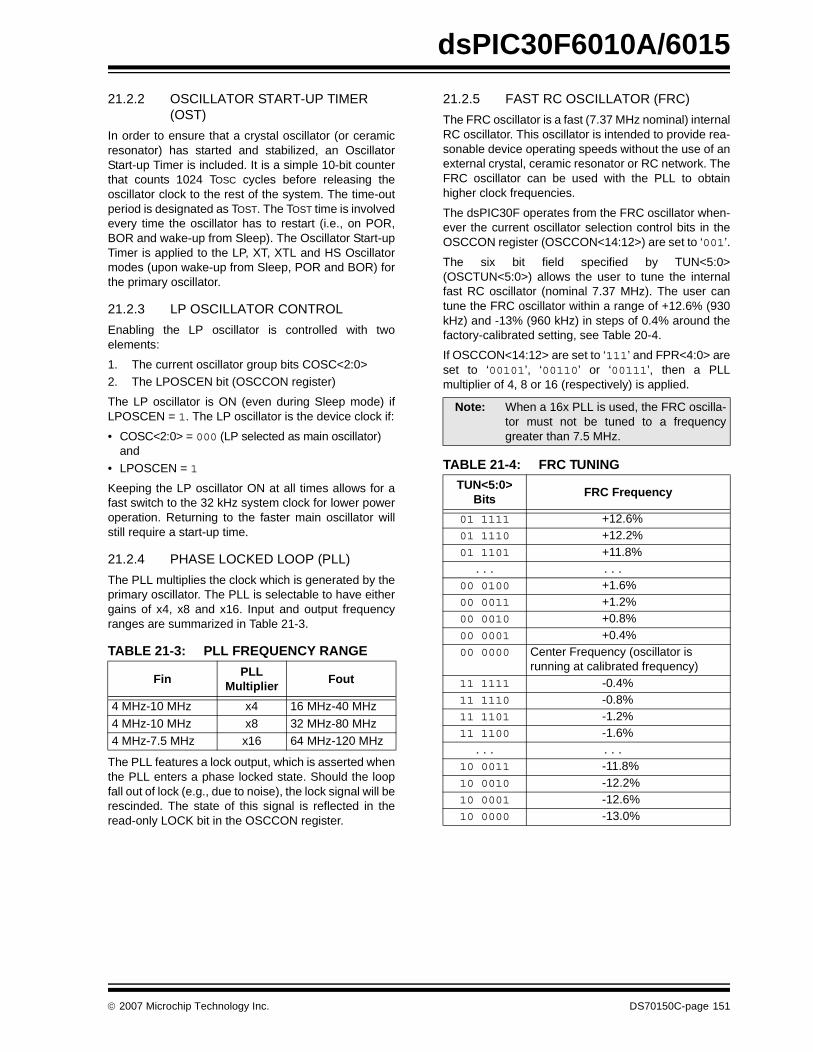
dsPIC30F6010A/6015
21.2.2 OSCILLATOR START-UP TIMER (OST)
In order to ensure that a crystal oscillator (or ceramicresonator) has started and stabilized, an OscillatorStart-up Timer is included. It is a simple 10-bit counterthat counts 1024 TOSC cycles before releasing theoscillator clock to the rest of the system. The time-outperiod is designated as TOST. The TOST time is involvedevery time the oscillator has to restart (i.e., on POR,BOR and wake-up from Sleep). The Oscillator Start-upTimer is applied to the LP, XT, XTL and HS Oscillatormodes (upon wake-up from Sleep, POR and BOR) forthe primary oscillator.
21.2.3 LP OSCILLATOR CONTROL
Enabling the LP oscillator is controlled with twoelements:
1. The current oscillator group bits COSC<2:0>2. The LPOSCEN bit (OSCCON register)
The LP oscillator is ON (even during Sleep mode) ifLPOSCEN = 1. The LP oscillator is the device clock if:
• COSC<2:0> = 000 (LP selected as main oscillator)and
• LPOSCEN = 1
Keeping the LP oscillator ON at all times allows for afast switch to the 32 kHz system clock for lower poweroperation. Returning to the faster main oscillator willstill require a start-up time.
21.2.4 PHASE LOCKED LOOP (PLL)
The PLL multiplies the clock which is generated by theprimary oscillator. The PLL is selectable to have eithergains of x4, x8 and x16. Input and output frequencyranges are summarized in Table 21-3.
TABLE 21-3: PLL FREQUENCY RANGE
The PLL features a lock output, which is asserted whenthe PLL enters a phase locked state. Should the loopfall out of lock (e.g., due to noise), the lock signal will berescinded. The state of this signal is reflected in theread-only LOCK bit in the OSCCON register.
21.2.5 FAST RC OSCILLATOR (FRC)
The FRC oscillator is a fast (7.37 MHz nominal) internalRC oscillator. This oscillator is intended to provide rea-sonable device operating speeds without the use of anexternal crystal, ceramic resonator or RC network. TheFRC oscillator can be used with the PLL to obtainhigher clock frequencies.
The dsPIC30F operates from the FRC oscillator when-ever the current oscillator selection control bits in theOSCCON register (OSCCON<14:12>) are set to ‘001’.
The six bit field specified by TUN<5:0>(OSCTUN<5:0>) allows the user to tune the internalfast RC oscillator (nominal 7.37 MHz). The user cantune the FRC oscillator within a range of +12.6% (930kHz) and -13% (960 kHz) in steps of 0.4% around thefactory-calibrated setting, see Table 20-4.
If OSCCON<14:12> are set to ‘111’ and FPR<4:0> areset to ‘00101’, ‘00110’ or ‘00111’, then a PLLmultiplier of 4, 8 or 16 (respectively) is applied.
TABLE 21-4: FRC TUNING
FinPLL
MultiplierFout
4 MHz-10 MHz x4 16 MHz-40 MHz
4 MHz-10 MHz x8 32 MHz-80 MHz4 MHz-7.5 MHz x16 64 MHz-120 MHz
Note: When a 16x PLL is used, the FRC oscilla-tor must not be tuned to a frequencygreater than 7.5 MHz.
TUN<5:0>Bits
FRC Frequency
01 1111 +12.6%01 1110 +12.2%01 1101 +11.8%... ...
00 0100 +1.6%00 0011 +1.2%00 0010 +0.8%00 0001 +0.4%00 0000 Center Frequency (oscillator is
running at calibrated frequency)11 1111 -0.4%11 1110 -0.8%11 1101 -1.2%11 1100 -1.6%... ...
10 0011 -11.8%10 0010 -12.2%10 0001 -12.6%10 0000 -13.0%
© 2007 Microchip Technology Inc. DS70150C-page 151
dsPIC30F6010A/6015
21.2.6 LOW-POWER RC OSCILLATOR (LPRC)
The LPRC oscillator is a component of the WatchdogTimer (WDT) and oscillates at a nominal frequency of512 kHz. The LPRC oscillator is the clock source forthe Power-up Timer (PWRT) circuit, WDT and clockmonitor circuits. It may also be used to provide a lowfrequency clock source option for applications wherepower consumption is critical, and timing accuracy isnot required.
The LPRC oscillator is always enabled at a Power-onReset, because it is the clock source for the PWRT.After the PWRT expires, the LPRC oscillator willremain ON if one of the following is TRUE:
• The Fail-Safe Clock Monitor is enabled• The WDT is enabled
• The LPRC oscillator is selected as the system clock via the COSC<2:0> control bits in the OSCCON register
If one of the above conditions is not true, the LPRC willshut-off after the PWRT expires.
21.2.7 FAIL-SAFE CLOCK MONITOR
The Fail-Safe Clock Monitor (FSCM) allows the deviceto continue to operate even in the event of an oscillatorfailure. The FSCM function is enabled by appropriatelyprogramming the FCKSM Configuration bits (ClockSwitch and Monitor Selection bits) in the FOSC deviceConfiguration register. If the FSCM function isenabled, the LPRC internal oscillator will run at alltimes (except during Sleep mode) and will not besubject to control by the SWDTEN bit.
In the event of an oscillator failure, the FSCM willgenerate a clock failure trap event and will switch the sys-tem clock over to the FRC oscillator. The user will thenhave the option to either attempt to restart the oscillatoror execute a controlled shutdown. The user may decideto treat the trap as a warm Reset by simply loading theReset address into the oscillator fail trap vector. In thisevent, the CF (Clock Fail) Status bit (OSCCON<3>) isalso set whenever a clock failure is recognized.
In the event of a clock failure, the WDT is unaffectedand continues to run on the LPRC clock.
If the oscillator has a very slow start-up time comingout of POR, BOR or Sleep, it is possible that thePWRT timer will expire before the oscillator hasstarted. In such cases, the FSCM will be activated andthe FSCM will initiate a clock failure trap, and the
COSC<2:0> bits are loaded with FRC oscillator selec-tion. This will effectively shut-off the original oscillatorthat was trying to start.
The user may detect this situation and restart theoscillator in the clock fail trap ISR.
Upon a clock failure detection, the FSCM module willinitiate a clock switch to the FRC oscillator as follows:
1. The COSC bits (OSCCON<14:12>) are loadedwith the FRC oscillator selection value.
2. CF bit is set (OSCCON<3>).3. OSWEN control bit (OSCCON<0>) is cleared.
For the purpose of clock switching, the clock sourcesare sectioned into four groups:
1. Primary2. Secondary3. Internal FRC
4. Internal LPRC
The user can switch between these functional groups,but cannot switch between options within a group. If theprimary group is selected, then the choice within thegroup is always determined by the FPR<4:0>Configuration bits.
The OSCCON register holds the control and Status bitsrelated to clock switching.
• COSC<2:0>: Read-only Status bits always reflect the current oscillator group in effect.
• NOSC<2:0>: Control bits which are written to indicate the new oscillator group of choice.- On POR and BOR, COSC<2:0> and
NOSC<2:0> are both loaded with the Configuration bit values FOS<2:0>.
• LOCK: The LOCK Status bit indicates a PLL lock.• CF: Read-only Status bit indicating if a clock fail
detect has occurred.• OSWEN: Control bit changes from a ‘0’ to a ‘1’
when a clock transition sequence is initiated. Clearing the OSWEN control bit will abort a clock transition in progress (used for hang-up situations).
If Configuration bits FCKSM<1:0> = 1x, then the clockswitching and Fail-Safe Clock Monitor functions aredisabled. This is the default Configuration bit setting.
If clock switching is disabled, then the FOS<2:0> andFPR<4:0> bits directly control the oscillator selectionand the COSC<2:0> bits do not control the clockselection. However, these bits will reflect the clocksource selection.
Note 1: OSC2 pin function is determined by thePrimary Oscillator mode selection(FPR<4:0>).
2: Note that OSC1 pin cannot be used as anI/O pin, even if the secondary oscillator oran internal clock source is selected at alltimes.
Note: The application should not attempt toswitch to a clock of frequency lower than100 kHz when the Fail-Safe Clock Monitoris enabled. If clock switching is performed,the device may generate an oscillator failtrap and switch to the fast RC oscillator.
DS70150C-page 152 © 2007 Microchip Technology Inc.
dsPIC30F6010A/6015
21.2.8 PROTECTION AGAINST ACCIDENTAL WRITES TO OSCCON
A write to the OSCCON register is intentionally madedifficult because it controls clock switching and clockscaling.
To write to the OSCCON low byte, the following codesequence must be executed without any otherinstructions in between:
Byte write is allowed for one instruction cycle. Write thedesired value or use bit manipulation instruction.
To write to the OSCCON high byte, the followinginstructions must be executed without any otherinstructions in between:
Byte write is allowed for one instruction cycle. Write thedesired value or use bit manipulation instruction.
21.3 Reset
The dsPIC30F differentiates between various kinds ofReset:
a) Power-on Reset (POR) b) MCLR Reset during normal operation
c) MCLR Reset during Sleep d) Watchdog Timer (WDT) Reset (during normal
operation)e) Programmable Brown-out Reset (BOR) f) RESET Instruction
g) Reset caused by trap lockup (TRAPR)h) Reset caused by illegal opcode, or by using an
uninitialized W register as an Address Pointer(IOPUWR)
Different registers are affected in different ways byvarious Reset conditions. Most registers are notaffected by a WDT wake-up, since this is viewed as theresumption of normal operation. Status bits from theRCON register are set or cleared differently in differentReset situations, as indicated in Table 21-5. These bitsare used in software to determine the nature of theReset.
A block diagram of the on-chip Reset circuit is shown inFigure 21-2.
A MCLR noise filter is provided in the MCLR Resetpath. The filter detects and ignores small pulses.
Internally generated Resets do not drive MCLR pin low.
FIGURE 21-2: RESET SYSTEM BLOCK DIAGRAM
Byte Write “0x46” to OSCCON lowByte Write “0x57” to OSCCON low
Byte Write “0x78” to OSCCON highByte Write “0x9A” to OSCCON high
S
R Q
MCLR
VDD
VDD RiseDetect
POR
SYSRST
Sleep or Idle
Brown-outReset
BOREN
RESETInstruction
WDTModule
DigitalGlitch Filter
BOR
Trap Conflict
Illegal Opcode/Uninitialized W Register
© 2007 Microchip Technology Inc. DS70150C-page 153

dsPIC30F6010A/6015
21.3.1 POR: POWER-ON RESET
A power-on event will generate an internal POR pulsewhen a VDD rise is detected. The Reset pulse will occurat the POR circuit threshold voltage (VPOR), which isnominally 1.85V. The device supply voltage character-istics must meet specified starting voltage and rise raterequirements. The POR pulse will reset a POR timerand place the device in the Reset state. The POR alsoselects the device clock source identified by theoscillator configuration fuses.
The POR circuit inserts a small delay, TPOR, which isnominally 10 μs and ensures that the device biascircuits are stable. Furthermore, a user selected power-up time-out (TPWRT) is applied. The TPWRT parameteris based on device Configuration bits and can be 0 ms(no delay), 4 ms, 16 ms or 64 ms. The total delay is atdevice power-up TPOR + TPWRT. When these delayshave expired, SYSRST will be negated on the nextleading edge of the Q1 clock, and the PC will jump tothe Reset vector.
The timing for the SYSRST signal is shown inFigure 21-3 through Figure 21-5.
FIGURE 21-3: TIME-OUT SEQUENCE ON POWER-UP (MCLR TIED TO VDD)
FIGURE 21-4: TIME-OUT SEQUENCE ON POWER-UP (MCLR NOT TIED TO VDD): CASE 1
TPWRT
TOST
VDD
Internal POR
PWRT Time-out
OST Time-out
Internal Reset
MCLR
TPWRT
TOST
VDD
Internal POR
PWRT Time-out
OST Time-out
Internal Reset
MCLR
DS70150C-page 154 © 2007 Microchip Technology Inc.
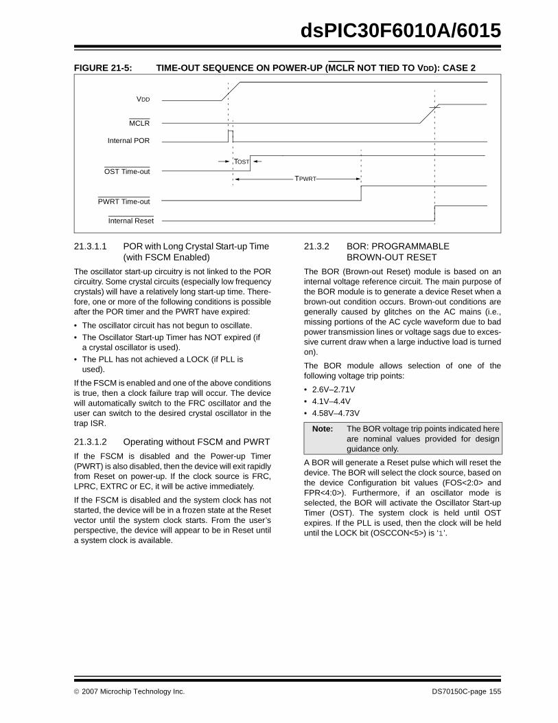
dsPIC30F6010A/6015
FIGURE 21-5: TIME-OUT SEQUENCE ON POWER-UP (MCLR NOT TIED TO VDD): CASE 2
21.3.1.1 POR with Long Crystal Start-up Time (with FSCM Enabled)
The oscillator start-up circuitry is not linked to the PORcircuitry. Some crystal circuits (especially low frequencycrystals) will have a relatively long start-up time. There-fore, one or more of the following conditions is possibleafter the POR timer and the PWRT have expired:
• The oscillator circuit has not begun to oscillate.
• The Oscillator Start-up Timer has NOT expired (if a crystal oscillator is used).
• The PLL has not achieved a LOCK (if PLL is used).
If the FSCM is enabled and one of the above conditionsis true, then a clock failure trap will occur. The devicewill automatically switch to the FRC oscillator and theuser can switch to the desired crystal oscillator in thetrap ISR.
21.3.1.2 Operating without FSCM and PWRT
If the FSCM is disabled and the Power-up Timer(PWRT) is also disabled, then the device will exit rapidlyfrom Reset on power-up. If the clock source is FRC,LPRC, EXTRC or EC, it will be active immediately.
If the FSCM is disabled and the system clock has notstarted, the device will be in a frozen state at the Resetvector until the system clock starts. From the user’sperspective, the device will appear to be in Reset untila system clock is available.
21.3.2 BOR: PROGRAMMABLE BROWN-OUT RESET
The BOR (Brown-out Reset) module is based on aninternal voltage reference circuit. The main purpose ofthe BOR module is to generate a device Reset when abrown-out condition occurs. Brown-out conditions aregenerally caused by glitches on the AC mains (i.e.,missing portions of the AC cycle waveform due to badpower transmission lines or voltage sags due to exces-sive current draw when a large inductive load is turnedon).
The BOR module allows selection of one of thefollowing voltage trip points:
• 2.6V–2.71V• 4.1V–4.4V• 4.58V–4.73V
A BOR will generate a Reset pulse which will reset thedevice. The BOR will select the clock source, based onthe device Configuration bit values (FOS<2:0> andFPR<4:0>). Furthermore, if an oscillator mode isselected, the BOR will activate the Oscillator Start-upTimer (OST). The system clock is held until OSTexpires. If the PLL is used, then the clock will be helduntil the LOCK bit (OSCCON<5>) is ‘1’.
VDD
MCLR
Internal POR
PWRT Time-out
OST Time-out
Internal Reset
TPWRT
TOST
Note: The BOR voltage trip points indicated hereare nominal values provided for designguidance only.
© 2007 Microchip Technology Inc. DS70150C-page 155

dsPIC30F6010A/6015
Concurrently, the POR time-out (TPOR) and the PWRTtime-out (TPWRT) will be applied before the internalReset is released. If TPWRT = 0 and a crystal oscillatoris being used, then a nominal delay of TFSCM = 100 μsis applied. The total delay in this case is(TPOR + TFSCM).
The BOR Status bit (RCON<1>) will be set to indicatethat a BOR has occurred. The BOR circuit, if enabled,will continue to operate while in Sleep or Idle modesand will reset the device should VDD fall below the BORthreshold voltage.
FIGURE 21-6: EXTERNAL POWER-ON RESET CIRCUIT (FOR SLOW VDD POWER-UP)
Note: Dedicated supervisory devices, such asthe MCP1XX and MCP8XX, may also beused as an external Power-on Resetcircuit.
Note 1: External Power-on Reset circuit isrequired only if the VDD power-up slopeis too slow. The diode D helps dischargethe capacitor quickly when VDD powersdown.
2: R should be suitably chosen so as tomake sure that the voltage drop acrossR does not violate the device’s electricalspecification.
3: R1 should be suitably chosen so as tolimit any current flowing into MCLR fromexternal capacitor C, in the event ofMCLR/VPP pin breakdown due to Elec-trostatic Discharge (ESD) or ElectricalOverstress (EOS).
C
R1RD
VDD
dsPIC30F
MCLR
DS70150C-page 156 © 2007 Microchip Technology Inc.
dsPIC30F6010A/6015
Table 21-5 shows the Reset conditions for the RCONregister. Since the control bits within the RCON registerare R/W, the information in the table means that all thebits are negated prior to the action specified in thecondition column.
TABLE 21-5: INITIALIZATION CONDITION FOR RCON REGISTER CASE 1
Table 21-6 shows a second example of the bitconditions for the RCON register. In this case, it is notassumed the user has set/cleared specific bits prior toaction specified in the condition column.
TABLE 21-6: INITIALIZATION CONDITION FOR RCON REGISTER CASE 2
ConditionProgram Counter
TRAPR IOPUWR EXTR SWR WDTO IDLE SLEEP POR BOR
Power-on Reset 0x000000 0 0 0 0 0 0 0 1 1
Brown-out Reset 0x000000 0 0 0 0 0 0 0 0 1
MCLR Reset during normal operation
0x000000 0 0 1 0 0 0 0 0 0
Software Reset during normal operation
0x000000 0 0 0 1 0 0 0 0 0
MCLR Reset during Sleep 0x000000 0 0 1 0 0 0 1 0 0
MCLR Reset during Idle 0x000000 0 0 1 0 0 1 0 0 0
WDT Time-out Reset 0x000000 0 0 0 0 1 0 0 0 0
WDT Wake-up PC + 2 0 0 0 0 1 0 1 0 0
Interrupt Wake-up from Sleep
PC + 2(1) 0 0 0 0 0 0 1 0 0
Clock Failure Trap 0x000004 0 0 0 0 0 0 0 0 0
Trap Reset 0x000000 1 0 0 0 0 0 0 0 0
Illegal Operation Trap 0x000000 0 1 0 0 0 0 0 0 0
Legend: u = unchanged, x = unknown, - = unimplemented bit, read as ‘0’
Note 1: When the wake-up is due to an enabled interrupt, the PC is loaded with the corresponding interrupt vector.
ConditionProgram Counter
TRAPR IOPUWR EXTR SWR WDTO IDLE SLEEP POR BOR
Power-on Reset 0x000000 0 0 0 0 0 0 0 1 1
Brown-out Reset 0x000000 u u u u u u u 0 1
MCLR Reset during normal operation
0x000000 u u 1 0 0 0 0 u u
Software Reset during normal operation
0x000000 u u 0 1 0 0 0 u u
MCLR Reset during Sleep 0x000000 u u 1 u 0 0 1 u u
MCLR Reset during Idle 0x000000 u u 1 u 0 1 0 u u
WDT Time-out Reset 0x000000 u u 0 0 1 0 0 u u
WDT Wake-up PC + 2 u u u u 1 u 1 u u
Interrupt Wake-up from Sleep
PC + 2(1) u u u u u u 1 u u
Clock Failure Trap 0x000004 u u u u u u u u u
Trap Reset 0x000000 1 u u u u u u u u
Illegal Operation Reset 0x000000 u 1 u u u u u u u
Legend: u = unchanged, x = unknown, - = unimplemented bit, read as ‘0’Note 1: When the wake-up is due to an enabled interrupt, the PC is loaded with the corresponding interrupt vector.
© 2007 Microchip Technology Inc. DS70150C-page 157

dsPIC30F6010A/6015
If Watchdog Timer is enabled, then the processor willwake-up from Sleep mode upon WDT time-out. TheSleep and WDTO Status bits are both set.
21.5.2 IDLE MODE
In Idle mode, the clock to the CPU is shutdown whileperipherals keep running. Unlike Sleep mode, the clocksource remains active.
Several peripherals have a control bit in each module,that allows them to operate during Idle.
LPRC fail-safe clock remains active if clock failuredetect is enabled.
The processor wakes up from Idle if at least one of thefollowing conditions is true:
• on any interrupt that is individually enabled (IE bit is ‘1’) and meets the required priority level
• on any Reset (POR, BOR, MCLR)• on WDT time-out
Upon wake-up from Idle mode, the clock is re-appliedto the CPU and instruction execution begins immedi-ately, starting with the instruction following the PWRSAVinstruction.
Any interrupt that is individually enabled (using IE bit)and meets the prevailing priority level will be able towake-up the processor. The processor will process theinterrupt and branch to the ISR. The Idle Status bit inRCON register is set upon wake-up.
Any Reset, other than POR, will set the Idle Status bit.On a POR, the Idle bit is cleared.
If Watchdog Timer is enabled, then the processor willwake-up from Idle mode upon WDT time-out. The Idleand WDTO Status bits are both set.
Unlike wake-up from Sleep, there are no time delaysinvolved in wake-up from Idle.
21.6 Device Configuration Registers
The Configuration bits in each device Configurationregister specify some of the device modes and areprogrammed by a device programmer, or by using theIn-Circuit Serial Programming™ (ICSP™) feature of thedevice. Each device Configuration register is a 24-bitregister, but only the lower 16 bits of each register areused to hold configuration data. There are six deviceConfiguration registers available to the user:
1. FOSC (0xF80000): Oscillator Configuration register
2. FWDT (0xF80002): Watchdog Timer Configuration register
3. FBORPOR (0xF80004): BOR and POR Configuration register
4. FBS (0xF80006): Boot Code Segment Configuration register
5. FSS (0xF80008): Secure Code Segment Configuration register
6. FGS (0xF8000A): General Code Segment Configuration register
The placement of the Configuration bits is automaticallyhandled when you select the device in your device pro-grammer. The desired state of the Configuration bits maybe specified in the source code (dependent on the lan-guage tool used), or through the programming interface.After the device has been programmed, the applicationsoftware may read the Configuration bit values throughthe table read instructions. For additional information,please refer to the “dsPIC30F/33F Programmers Refer-ence Manual” (DS70157) and the “dsPIC30F FamilyReference Manual” (DS70046).
Note 1: If the code protection Configuration Fusebits (FBS(BSS<2:0>), FSS(SSS<2:0>),FGS<GCP> and FGS<GWRP>) havebeen programmed, an erase of the entirecode-protected device is only possible atvoltages VDD ≥ 4.5V.
2: This device supports an Advanced imple-mentation of CodeGuard™ Security.Please refer to the “CodeGuard Security”chapter (DS70180) for information onhow CodeGuard Security may be used inyour application.
© 2007 Microchip Technology Inc. DS70150C-page 159
dsPIC30F6010A/6015
21.7 Peripheral Module Disable (PMD) Registers
The Peripheral Module Disable (PMD) registers pro-vide a method to disable a peripheral module by stop-ping all clock sources supplied to that module. When aperipheral is disabled via the appropriate PMD controlbit, the peripheral is in a minimum power consumptionstate. The control and STATUS registers associatedwith the peripheral will also be disabled so writes tothose registers will have no effect and read values willbe invalid.
A peripheral module will only be enabled if both theassociated bit in the PMD register is cleared and theperipheral is supported by the specific dsPIC DSC vari-ant. If the peripheral is present in the device, it isenabled in the PMD register by default.
21.8 In-Circuit Debugger
When MPLAB® ICD 2 is selected as a debugger, theIn-Circuit Debugging functionality is enabled. Thisfunction allows simple debugging functions when usedwith MPLAB IDE. When the device has this featureenabled, some of the resources are not available forgeneral use. These resources include the first 80 bytesof data RAM and two I/O pins.
One of four pairs of debug I/O pins may be selected bythe user using configuration options in MPLAB IDE.These pin pairs are named EMUD/EMUC, EMUD1/EMUC1, EMUD2/EMUC2 and MUD3/EMUC3.
In each case, the selected EMUD pin is the Emulation/Debug Data line, and the EMUC pin is the Emulation/Debug Clock line. These pins will interface to theMPLAB ICD 2 module available from Microchip. Theselected pair of debug I/O pins is used by MPLABICD 2 to send commands and receive responses, aswell as to send and receive data. To use the In-CircuitDebugger function of the device, the design mustimplement ICSP connections to MCLR, VDD, VSS,PGC, PGD and the selected EMUDx/EMUCx pin pair.
This gives rise to two possibilities:
1. If EMUD/EMUC is selected as the debug I/O pinpair, then only a 5-pin interface is required, asthe EMUD and EMUC pin functions are multi-plexed with the PGD and PGC pin functions inall dsPIC30F devices.
2. If EMUD1/EMUC1, EMUD2/EMUC2 or EMUD3/EMUC3 is selected as the debug I/O pin pair,then a 7-pin interface is required, as theEMUDx/EMUCx pin functions (x = 1, 2 or 3) arenot multiplexed with the PGD and PGC pinfunctions.
Note: If a PMD bit is set, the corresponding mod-ule is disabled after a delay of 1 instructioncycle. Similarly, if a PMD bit is cleared, thecorresponding module is enabled after adelay of 1 instruction cycle (assuming themodule control registers are alreadyconfigured to enable module operation).
DS70150C-page 160 © 2007 Microchip Technology Inc.

© 2007 M
icrochip Technology Inc.
DS
70150C-page 161
dsP
IC30F
6010A/6015
TA
TA
TA
N Bit 1 Bit 0 Reset State
RC BOR POR Depends on type of Reset.
OS SCEN OSWEN Depends on Configuration bits.
OS 0000 0000 0000 0000
PM 1MD ADCMD 0000 0000 0000 0000
PM C2MD OC1MD 0000 0000 0000 0000
Le
No
N Bit 1 Bit 0 Reset State
RC BOR POR Depends on type of Reset.
OS SCEN OSWEN Depends on Configuration bits.
OS 0000 0000 0000 0000
PM 1MD ADCMD 0000 0000 0000 0000
PM C2MD OC1MD 0000 0000 0000 0000
Le
No
F Bit 4 Bit 3 Bit 2 Bit 1 Bit 0
FO FPR<4:0>
FW PSA<1:0> FWPSB<3:0>
FB RV<1:0> — — FPWRT<1:0>
FB BSS<2:0> BWRP
FS SSS<2:0> SWRP
FG — — GSS<1:0> GWRP
Le
No
BLE 21-7: SYSTEM INTEGRATION REGISTER MAP FOR dsPIC30F6010A
BLE 21-8: SYSTEM INTEGRATION REGISTER MAP FOR dsPIC30F6015
BLE 21-9: DEVICE CONFIGURATION REGISTER MAP
SFR ame Addr. Bit 15 Bit 14 Bit 13 Bit 12 Bit 11 Bit 10 Bit 9 Bit 8 Bit 7 Bit 6 Bit 5 Bit 4 Bit 3 Bit 2
ON 0740 TRAPR IOPUWR BGST — — — — — EXTR SWR SWDTEN WDTO SLEEP IDLE
CCON 0742 — COSC<2:0> — NOSC<2:0> POST<1:0> LOCK — CF — LPO
CTUN 0744 — — — — — — — — — — TUN<5:0>
D1 0770 T5MD T4MD T3MD T2MD T1MD QEIMD PWMMD — I2CMD U2MD U1MD SPI2MD SPI1MD C2MD C
D2 0772 IC8MD IC7MD IC6MD IC5MD IC4MD IC3MD IC2MD IC1MD OC8MD OC7MD OC6MD OC5MD OC4MD OC3MD O
gend: u = uninitialized bit
te: Refer to “dsPIC30F Family Reference Manual” (DS70046) for descriptions of register bit fields.
SFR ame Addr. Bit 15 Bit 14 Bit 13 Bit 12 Bit 11 Bit 10 Bit 9 Bit 8 Bit 7 Bit 6 Bit 5 Bit 4 Bit 3 Bit 2
ON 0740 TRAPR IOPUWR BGST — — — — — EXTR SWR SWDTEN WDTO SLEEP IDLE
CCON 0742 — COSC<2:0> — NOSC<2:0> POST<1:0> LOCK — CF — LPO
CTUN 0744 — — — — — — — — — — TUN<5:0>
D1 0770 T5MD T4MD T3MD T2MD T1MD QEIMD PWMMD — I2CMD U2MD U1MD SPI2MD SPI1MD — C
D2 0772 IC8MD IC7MD IC6MD IC5MD IC4MD IC3MD IC2MD IC1MD OC8MD OC7MD OC6MD OC5MD OC4MD OC3MD O
gend: u = uninitialized bit
te: Refer to “dsPIC30F Family Reference Manual” (DS70046) for descriptions of register bit fields.
ile Name Addr. Bits 23-16 Bit 15 Bit 14 Bit 13 Bit 12 Bit 11 Bit 10 Bit 9 Bit 8 Bit 7 Bit 6 Bit 5
SC F80000 — FCKSM<1:0> — — — FOS<2:0> — — —
DT F80002 — FWDTEN — — — — — — — — — FW
ORPOR F80004 — MCLREN — — — — PWMPIN HPOL LPOL BOREN — BO
S F80006 RBS1 RBS0 EBS
S F80008 RSS1 RSS0 ESS1 ESS0
S F8000A — — — — — — — — — — — —
gend: u = uninitialized bit
te: Refer to “dsPIC30F Family Reference Manual” (DS70046) for descriptions of register bit fields.

dsPIC30F6010A/6015
NOTES:
DS70150C-page 162 © 2007 Microchip Technology Inc.
dsPIC30F6010A/6015
22.0 INSTRUCTION SET SUMMARY
The dsPIC30F instruction set adds many enhance-ments to the previous PIC® Microcontroller (MCU)instruction sets, while maintaining an easy migrationfrom PIC MCU instruction sets.
Most instructions are a single program memory word(24-bits). Only three instructions require two programmemory locations.
Each single-word instruction is a 24-bit word dividedinto an 8-bit opcode which specifies the instructiontype, and one or more operands which further specifythe operation of the instruction.
The instruction set is highly orthogonal and is groupedinto five basic categories:
• Word or byte-oriented operations• Bit-oriented operations
• Literal operations• DSP operations• Control operations
Table 22-1 shows the general symbols used indescribing the instructions.
The dsPIC30F instruction set summary in Table 22-2lists all the instructions along with the Status flagsaffected by each instruction.
Most word or byte-oriented W register instructions(including barrel shift instructions) have threeoperands:
• The first source operand, which is typically a register ‘Wb’ without any address modifier
• The second source operand, which is typically a register ‘Ws’ with or without an address modifier
• The destination of the result, which is typically a register ‘Wd’ with or without an address modifier
However, word or byte-oriented file register instructionshave two operands:
• The file register specified by the value ‘f’• The destination, which could either be the file
register ‘f’ or the W0 register, which is denoted as ‘WREG’
Most bit oriented instructions (including simple rotate/shift instructions) have two operands:
• The W register (with or without an address modi-fier) or file register (specified by the value of ‘Ws’ or ‘f’)
• The bit in the W register or file register (specified by a literal value, or indirectly by the contents of register ‘Wb’)
The literal instructions that involve data movement mayuse some of the following operands:
• A literal value to be loaded into a W register or file register (specified by the value of ‘k’)
• The W register or file register where the literal value is to be loaded (specified by ‘Wb’ or ‘f’)
However, literal instructions that involve arithmetic orlogical operations use some of the following operands:
• The first source operand, which is a register ‘Wb’ without any address modifier
• The second source operand, which is a literal value
• The destination of the result (only if not the same as the first source operand), which is typically a register ‘Wd’ with or without an address modifier
The MAC class of DSP instructions may use some of thefollowing operands:
• The accumulator (A or B) to be used (required operand)
• The W registers to be used as the two operands• The X and Y address space prefetch operations• The X and Y address space prefetch destinations
• The accumulator write-back destination
The other DSP instructions do not involve anymultiplication, and may include:
• The accumulator to be used (required)
• The source or destination operand (designated as Wso or Wdo, respectively) with or without an address modifier
• The amount of shift, specified by a W register ‘Wn’ or a literal value
The control instructions may use some of the followingoperands:
• A program memory address • The mode of the table read and table write
instructions
All instructions are a single word, except for certaindouble word instructions, which were made doubleword instructions so that all the required information isavailable in these 48 bits. In the second word, the8 MSbs are ‘0’s. If this second word is executed as aninstruction (by itself), it will execute as a NOP.
Note: This data sheet summarizes features of thisgroup of dsPIC30F devices and is not intended to bea complete reference source. For more informationon the CPU, peripherals, register descriptions andgeneral device functionality, refer to the “dsPIC30FFamily Reference Manual” (DS70046). For moreinformation on the device instruction set and pro-gramming, refer to the “dsPIC30F/33F ProgrammersReference Manual” (DS70157).
© 2007 Microchip Technology Inc. DS70150C-page 163
dsPIC30F6010A/6015
Most single-word instructions are executed in a singleinstruction cycle, unless a conditional test is true or theprogram counter is changed as a result of the instruc-tion. In these cases, the execution takes two instructioncycles with the additional instruction cycle(s) executedas a NOP. Notable exceptions are the BRA (uncondi-tional/computed branch), indirect CALL/GOTO, all tablereads and writes and RETURN/RETFIE instructions,which are single-word instructions, but take two orthree cycles. Certain instructions that involve skippingover the subsequent instruction, require either two or
three cycles if the skip is performed, depending onwhether the instruction being skipped is a single-wordor two-word instruction. Moreover, double word movesrequire two cycles. The double word instructionsexecute in two instruction cycles.
Note: For more details on the instruction set,refer to the “dsPIC30F/33F ProgrammersReference Manual“ (DS70157).
TABLE 22-1: SYMBOLS USED IN OPCODE DESCRIPTIONSField Description
#text Means literal defined by “text”(text) Means “content of “text”[text] Means “the location addressed by text”{ } Optional field or operation<n:m> Register bit field.b Byte mode selection.d Double Word mode selection.S Shadow register select.w Word mode selection (default)Acc One of two accumulators {A, B}AWB Accumulator Write-Back Destination Address register ∈ {W13, [W13]+ = 2}bit4 4-bit bit selection field (used in word addressed instructions) ∈ {0...15}C, DC, N, OV, Z MCU Status bits: Carry, Digit Carry, Negative, Overflow, ZeroExpr Absolute address, label or expression (resolved by the linker)f File register address ∈ {0x0000...0x1FFF}lit1 1-bit unsigned literal ∈ {0,1}lit4 4-bit unsigned literal ∈ {0...15}lit5 5-bit unsigned literal ∈ {0...31}lit8 8-bit unsigned literal ∈ {0...255}lit10 10-bit unsigned literal ∈ {0...255} for Byte mode, {0:1023} for Word modelit14 14-bit unsigned literal ∈ {0...16384}lit16 16-bit unsigned literal ∈ {0...65535}lit23 23-bit unsigned literal ∈ {0...8388608}; LSB must be ‘0’None Field does not require an entry, may be blankOA, OB, SA, SB DSP Status bits: AccA Overflow, AccB Overflow, AccA Saturate, AccB SaturatePC Program CounterSlit10 10-bit signed literal ∈ {-512...511}Slit16 16-bit signed literal ∈ {-32768...32767}Slit6 6-bit signed literal ∈ {-16...16}
DS70150C-page 164 © 2007 Microchip Technology Inc.
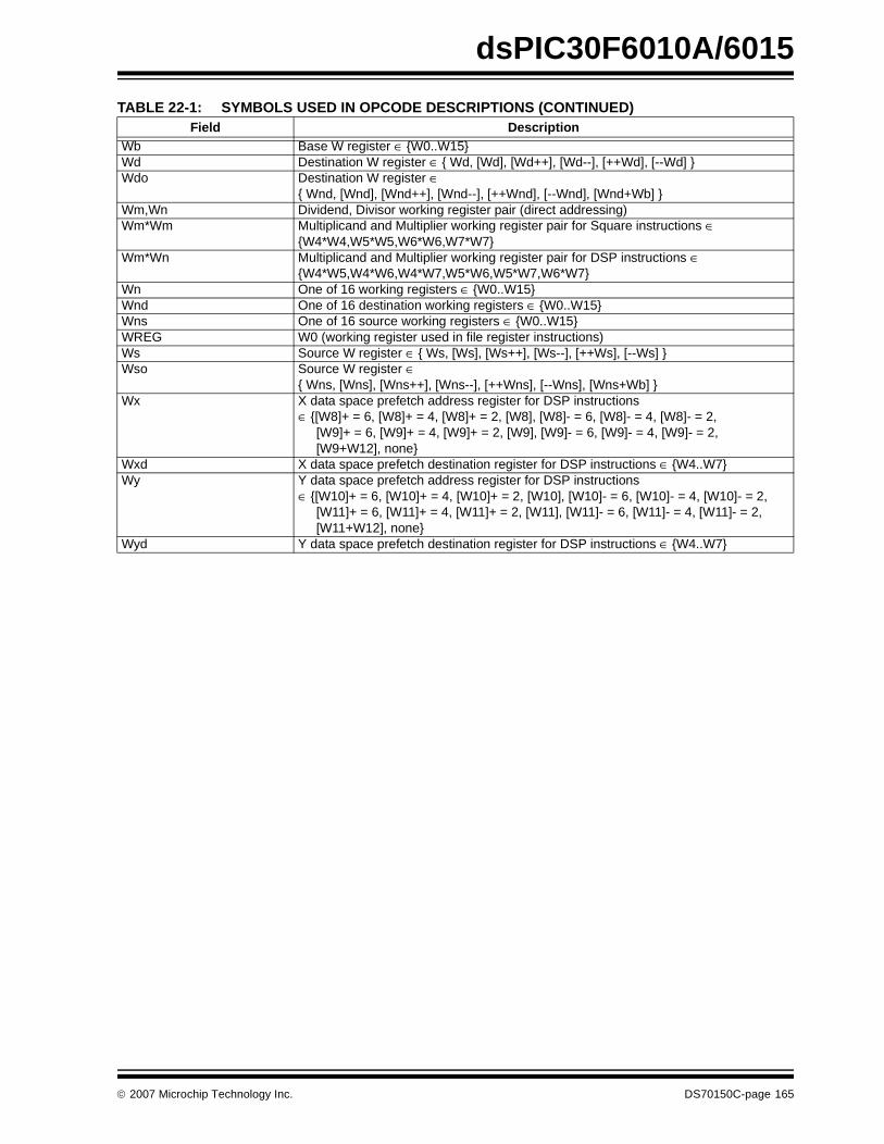
dsPIC30F6010A/6015
Wb Base W register ∈ {W0..W15}Wd Destination W register ∈ { Wd, [Wd], [Wd++], [Wd--], [++Wd], [--Wd] }Wdo Destination W register ∈
{ Wnd, [Wnd], [Wnd++], [Wnd--], [++Wnd], [--Wnd], [Wnd+Wb] } Wm,Wn Dividend, Divisor working register pair (direct addressing)Wm*Wm Multiplicand and Multiplier working register pair for Square instructions ∈
{W4*W4,W5*W5,W6*W6,W7*W7} Wm*Wn Multiplicand and Multiplier working register pair for DSP instructions ∈
{W4*W5,W4*W6,W4*W7,W5*W6,W5*W7,W6*W7}Wn One of 16 working registers ∈ {W0..W15}Wnd One of 16 destination working registers ∈ {W0..W15}Wns One of 16 source working registers ∈ {W0..W15}WREG W0 (working register used in file register instructions)Ws Source W register ∈ { Ws, [Ws], [Ws++], [Ws--], [++Ws], [--Ws] }Wso Source W register ∈
{ Wns, [Wns], [Wns++], [Wns--], [++Wns], [--Wns], [Wns+Wb] } Wx X data space prefetch address register for DSP instructions
∈ {[W8]+ = 6, [W8]+ = 4, [W8]+ = 2, [W8], [W8]- = 6, [W8]- = 4, [W8]- = 2, [W9]+ = 6, [W9]+ = 4, [W9]+ = 2, [W9], [W9]- = 6, [W9]- = 4, [W9]- = 2, [W9+W12], none}
Wxd X data space prefetch destination register for DSP instructions ∈ {W4..W7}Wy Y data space prefetch address register for DSP instructions
∈ {[W10]+ = 6, [W10]+ = 4, [W10]+ = 2, [W10], [W10]- = 6, [W10]- = 4, [W10]- = 2, [W11]+ = 6, [W11]+ = 4, [W11]+ = 2, [W11], [W11]- = 6, [W11]- = 4, [W11]- = 2, [W11+W12], none}
Wyd Y data space prefetch destination register for DSP instructions ∈ {W4..W7}
TABLE 22-1: SYMBOLS USED IN OPCODE DESCRIPTIONS (CONTINUED)Field Description
© 2007 Microchip Technology Inc. DS70150C-page 165

dsPIC30F6010A/6015
TABLE 22-2: INSTRUCTION SET OVERVIEWBaseInstr
#
AssemblyMnemonic Assembly Syntax Description # of
words# of
cyclesStatus Flags
Affected
1 ADD ADD Acc Add Accumulators 1 1 OA,OB,SA,SB
ADD f f = f + WREG 1 1 C,DC,N,OV,Z
ADD f,WREG WREG = f + WREG 1 1 C,DC,N,OV,Z
ADD #lit10,Wn Wd = lit10 + Wd 1 1 C,DC,N,OV,Z
ADD Wb,Ws,Wd Wd = Wb + Ws 1 1 C,DC,N,OV,Z
ADD Wb,#lit5,Wd Wd = Wb + lit5 1 1 C,DC,N,OV,Z
ADD Wso,#Slit4,Acc 16-bit Signed Add to Accumulator 1 1 OA,OB,SA,SB
2 ADDC ADDC f f = f + WREG + (C) 1 1 C,DC,N,OV,Z
ADDC f,WREG WREG = f + WREG + (C) 1 1 C,DC,N,OV,Z
ADDC #lit10,Wn Wd = lit10 + Wd + (C) 1 1 C,DC,N,OV,Z
ADDC Wb,Ws,Wd Wd = Wb + Ws + (C) 1 1 C,DC,N,OV,Z
ADDC Wb,#lit5,Wd Wd = Wb + lit5 + (C) 1 1 C,DC,N,OV,Z
3 AND AND f f = f .AND. WREG 1 1 N,Z
AND f,WREG WREG = f .AND. WREG 1 1 N,Z
AND #lit10,Wn Wd = lit10 .AND. Wd 1 1 N,Z
AND Wb,Ws,Wd Wd = Wb .AND. Ws 1 1 N,Z
AND Wb,#lit5,Wd Wd = Wb .AND. lit5 1 1 N,Z
4 ASR ASR f f = Arithmetic Right Shift f 1 1 C,N,OV,Z
ASR f,WREG WREG = Arithmetic Right Shift f 1 1 C,N,OV,Z
ASR Ws,Wd Wd = Arithmetic Right Shift Ws 1 1 C,N,OV,Z
ASR Wb,Wns,Wnd Wnd = Arithmetic Right Shift Wb by Wns 1 1 N,Z
ASR Wb,#lit5,Wnd Wnd = Arithmetic Right Shift Wb by lit5 1 1 N,Z
5 BCLR BCLR f,#bit4 Bit Clear f 1 1 None
BCLR Ws,#bit4 Bit Clear Ws 1 1 None
6 BRA BRA C,Expr Branch if Carry 1 1 (2) None
BRA GE,Expr Branch if greater than or equal 1 1 (2) None
BRA GEU,Expr Branch if unsigned greater than or equal 1 1 (2) None
BRA GT,Expr Branch if greater than 1 1 (2) None
BRA GTU,Expr Branch if unsigned greater than 1 1 (2) None
BRA LE,Expr Branch if less than or equal 1 1 (2) None
BRA LEU,Expr Branch if unsigned less than or equal 1 1 (2) None
BRA LT,Expr Branch if less than 1 1 (2) None
BRA LTU,Expr Branch if unsigned less than 1 1 (2) None
BRA N,Expr Branch if Negative 1 1 (2) None
BRA NC,Expr Branch if Not Carry 1 1 (2) None
BRA NN,Expr Branch if Not Negative 1 1 (2) None
BRA NOV,Expr Branch if Not Overflow 1 1 (2) None
BRA NZ,Expr Branch if Not Zero 1 1 (2) None
BRA OA,Expr Branch if Accumulator A overflow 1 1 (2) None
BRA OB,Expr Branch if Accumulator B overflow 1 1 (2) None
BRA OV,Expr Branch if Overflow 1 1 (2) None
BRA SA,Expr Branch if Accumulator A saturated 1 1 (2) None
BRA SB,Expr Branch if Accumulator B saturated 1 1 (2) None
BRA Expr Branch Unconditionally 1 2 None
BRA Z,Expr Branch if Zero 1 1 (2) None
BRA Wn Computed Branch 1 2 None
7 BSET BSET f,#bit4 Bit Set f 1 1 None
BSET Ws,#bit4 Bit Set Ws 1 1 None
8 BSW BSW.C Ws,Wb Write C bit to Ws<Wb> 1 1 None
BSW.Z Ws,Wb Write Z bit to Ws<Wb> 1 1 None
9 BTG BTG f,#bit4 Bit Toggle f 1 1 None
BTG Ws,#bit4 Bit Toggle Ws 1 1 None
10 BTSC BTSC f,#bit4 Bit Test f, Skip if Clear 1 1 (2 or 3)
None
BTSC Ws,#bit4 Bit Test Ws, Skip if Clear 1 1 (2 or 3)
None
DS70150C-page 166 © 2007 Microchip Technology Inc.

dsPIC30F6010A/6015
11 BTSS BTSS f,#bit4 Bit Test f, Skip if Set 1 1 (2 or 3)
None
BTSS Ws,#bit4 Bit Test Ws, Skip if Set 1 1 (2 or 3)
None
12 BTST BTST f,#bit4 Bit Test f 1 1 Z
BTST.C Ws,#bit4 Bit Test Ws to C 1 1 C
BTST.Z Ws,#bit4 Bit Test Ws to Z 1 1 Z
BTST.C Ws,Wb Bit Test Ws<Wb> to C 1 1 C
BTST.Z Ws,Wb Bit Test Ws<Wb> to Z 1 1 Z
13 BTSTS BTSTS f,#bit4 Bit Test then Set f 1 1 Z
BTSTS.C Ws,#bit4 Bit Test Ws to C, then Set 1 1 C
BTSTS.Z Ws,#bit4 Bit Test Ws to Z, then Set 1 1 Z
14 CALL CALL lit23 Call Subroutine 2 2 None
CALL Wn Call indirect Subroutine 1 2 None
15 CLR CLR f f = 0x0000 1 1 None
CLR WREG WREG = 0x0000 1 1 None
CLR Ws Ws = 0x0000 1 1 None
CLR Acc,Wx,Wxd,Wy,Wyd,AWB Clear Accumulator 1 1 OA,OB,SA,SB
16 CLRWDT CLRWDT Clear Watchdog Timer 1 1 WDTO,Sleep
17 COM COM f f = f 1 1 N,Z
COM f,WREG WREG = f 1 1 N,Z
COM Ws,Wd Wd = Ws 1 1 N,Z
18 CP CP f Compare f with WREG 1 1 C,DC,N,OV,Z
CP Wb,#lit5 Compare Wb with lit5 1 1 C,DC,N,OV,Z
CP Wb,Ws Compare Wb with Ws (Wb – Ws) 1 1 C,DC,N,OV,Z
19 CP0 CP0 f Compare f with 0x0000 1 1 C,DC,N,OV,Z
CP0 Ws Compare Ws with 0x0000 1 1 C,DC,N,OV,Z
20 CPB CPB f Compare f with WREG, with Borrow 1 1 C,DC,N,OV,Z
CPB Wb,#lit5 Compare Wb with lit5, with Borrow 1 1 C,DC,N,OV,Z
CPB Wb,Ws Compare Wb with Ws, with Borrow (Wb – Ws – C)
1 1 C,DC,N,OV,Z
21 CPSEQ CPSEQ Wb, Wn Compare Wb with Wn, skip if = 1 1 (2 or 3)
None
22 CPSGT CPSGT Wb, Wn Compare Wb with Wn, skip if > 1 1 (2 or 3)
None
23 CPSLT CPSLT Wb, Wn Compare Wb with Wn, skip if < 1 1 (2 or 3)
None
24 CPSNE CPSNE Wb, Wn Compare Wb with Wn, skip if ≠ 1 1 (2 or 3)
None
25 DAW DAW Wn Wn = decimal adjust Wn 1 1 C
26 DEC DEC f f = f –1 1 1 C,DC,N,OV,Z
DEC f,WREG WREG = f –1 1 1 C,DC,N,OV,Z
DEC Ws,Wd Wd = Ws – 1 1 1 C,DC,N,OV,Z
27 DEC2 DEC2 f f = f – 2 1 1 C,DC,N,OV,Z
DEC2 f,WREG WREG = f – 2 1 1 C,DC,N,OV,Z
DEC2 Ws,Wd Wd = Ws – 2 1 1 C,DC,N,OV,Z
28 DISI DISI #lit14 Disable Interrupts for k instruction cycles 1 1 None
29 DIV DIV.S Wm,Wn Signed 16/16-bit Integer Divide 1 18 N,Z,C, OV
DIV.SD Wm,Wn Signed 32/16-bit Integer Divide 1 18 N,Z,C, OV
DIV.U Wm,Wn Unsigned 16/16-bit Integer Divide 1 18 N,Z,C, OV
DIV.UD Wm,Wn Unsigned 32/16-bit Integer Divide 1 18 N,Z,C, OV
30 DIVF DIVF Wm,Wn Signed 16/16-bit Fractional Divide 1 18 N,Z,C, OV
31 DO DO #lit14,Expr Do code to PC + Expr, lit14 + 1 times 2 2 None
DO Wn,Expr Do code to PC + Expr, (Wn) + 1 times 2 2 None
32 ED ED Wm*Wm,Acc,Wx,Wy,Wxd Euclidean Distance (no accumulate) 1 1 OA,OB,OAB,SA,SB,SAB
33 EDAC EDAC Wm*Wm,Acc,Wx,Wy,Wxd Euclidean Distance 1 1 OA,OB,OAB,SA,SB,SAB
34 EXCH EXCH Wns,Wnd Swap Wns with Wnd 1 1 None
TABLE 22-2: INSTRUCTION SET OVERVIEW (CONTINUED)BaseInstr
#
AssemblyMnemonic Assembly Syntax Description # of
words# of
cyclesStatus Flags
Affected
© 2007 Microchip Technology Inc. DS70150C-page 167

dsPIC30F6010A/6015
35 FBCL FBCL Ws,Wnd Find Bit Change from Left (MSb) Side 1 1 C
36 FF1L FF1L Ws,Wnd Find First One from Left (MSb) Side 1 1 C
37 FF1R FF1R Ws,Wnd Find First One from Right (LSb) Side 1 1 C
38 GOTO GOTO Expr Go to address 2 2 None
GOTO Wn Go to indirect 1 2 None
39 INC INC f f = f + 1 1 1 C,DC,N,OV,Z
INC f,WREG WREG = f + 1 1 1 C,DC,N,OV,Z
INC Ws,Wd Wd = Ws + 1 1 1 C,DC,N,OV,Z
40 INC2 INC2 f f = f + 2 1 1 C,DC,N,OV,Z
INC2 f,WREG WREG = f + 2 1 1 C,DC,N,OV,Z
INC2 Ws,Wd Wd = Ws + 2 1 1 C,DC,N,OV,Z
41 IOR IOR f f = f .IOR. WREG 1 1 N,Z
IOR f,WREG WREG = f .IOR. WREG 1 1 N,Z
IOR #lit10,Wn Wd = lit10 .IOR. Wd 1 1 N,Z
IOR Wb,Ws,Wd Wd = Wb .IOR. Ws 1 1 N,Z
IOR Wb,#lit5,Wd Wd = Wb .IOR. lit5 1 1 N,Z
42 LAC LAC Wso,#Slit4,Acc Load Accumulator 1 1 OA,OB,OAB,SA,SB,SAB
43 LNK LNK #lit14 Link Frame Pointer 1 1 None
44 LSR LSR f f = Logical Right Shift f 1 1 C,N,OV,Z
LSR f,WREG WREG = Logical Right Shift f 1 1 C,N,OV,Z
LSR Ws,Wd Wd = Logical Right Shift Ws 1 1 C,N,OV,Z
LSR Wb,Wns,Wnd Wnd = Logical Right Shift Wb by Wns 1 1 N,Z
LSR Wb,#lit5,Wnd Wnd = Logical Right Shift Wb by lit5 1 1 N,Z
45 MAC MAC Wm*Wn,Acc,Wx,Wxd,Wy,Wyd,AWB
Multiply and Accumulate 1 1 OA,OB,OAB,SA,SB,SAB
MAC Wm*Wm,Acc,Wx,Wxd,Wy,Wyd Square and Accumulate 1 1 OA,OB,OAB,SA,SB,SAB
46 MOV MOV f,Wn Move f to Wn 1 1 None
MOV f Move f to f 1 1 N,Z
MOV f,WREG Move f to WREG 1 1 N,Z
MOV #lit16,Wn Move 16-bit literal to Wn 1 1 None
MOV.b #lit8,Wn Move 8-bit literal to Wn 1 1 None
MOV Wn,f Move Wn to f 1 1 None
MOV Wso,Wdo Move Ws to Wd 1 1 None
MOV WREG,f Move WREG to f 1 1 N,Z
MOV.D Wns,Wd Move Double from W(ns):W(ns + 1) to Wd 1 2 None
MOV.D Ws,Wnd Move Double from Ws to W(nd + 1):W(nd) 1 2 None
MOV.D Ws,Wnd Move Double from Ws to W(nd + 1):W(nd) 1 2 None
47 MOVSAC MOVSAC Acc,Wx,Wxd,Wy,Wyd,AWB Prefetch and store Accumulator 1 1 None
48 MPY MPY Wm*Wn,Acc,Wx,Wxd,Wy,Wyd Multiply Wm by Wn to Accumulator 1 1 OA,OB,OAB,SA,SB,SAB
MPY Wm*Wm,Acc,Wx,Wxd,Wy,Wyd Square Wm to Accumulator 1 1 OA,OB,OAB,SA,SB,SAB
49 MPY.N MPY.N Wm*Wn,Acc,Wx,Wxd,Wy,Wyd -(Multiply Wm by Wn) to Accumulator 1 1 None
50 MSC MSC Wm*Wm,Acc,Wx,Wxd,Wy,Wyd,AWB
Multiply and Subtract from Accumulator 1 1 OA,OB,OAB,SA,SB,SAB
51 MUL MUL.SS Wb,Ws,Wnd {Wnd + 1, Wnd} = signed(Wb) * signed(Ws) 1 1 NoneMUL.SU Wb,Ws,Wnd {Wnd + 1, Wnd} = signed(Wb) * unsigned(Ws) 1 1 None
MUL.US Wb,Ws,Wnd {Wnd + 1, Wnd} = unsigned(Wb) * signed(Ws) 1 1 None
MUL.UU Wb,Ws,Wnd {Wnd + 1, Wnd} = unsigned(Wb) * unsigned(Ws) 1 1 None
MUL.SU Wb,#lit5,Wnd {Wnd + 1, Wnd} = signed(Wb) * unsigned(lit5) 1 1 None
MUL.UU Wb,#lit5,Wnd {Wnd + 1, Wnd} = unsigned(Wb) * unsigned(lit5) 1 1 None
MUL f W3:W2 = f * WREG 1 1 None
TABLE 22-2: INSTRUCTION SET OVERVIEW (CONTINUED)BaseInstr
#
AssemblyMnemonic Assembly Syntax Description # of
words# of
cyclesStatus Flags
Affected
DS70150C-page 168 © 2007 Microchip Technology Inc.

dsPIC30F6010A/6015
52 NEG NEG Acc Negate Accumulator 1 1 OA,OB,OAB,SA,SB,SAB
NEG f f = f + 1 1 1 C,DC,N,OV,Z
NEG f,WREG WREG = f + 1 1 1 C,DC,N,OV,Z
NEG Ws,Wd Wd = Ws + 1 1 1 C,DC,N,OV,Z53 NOP NOP No Operation 1 1 None
NOPR No Operation 1 1 None
54 POP POP f Pop f from Top-of-Stack (TOS) 1 1 None
POP Wdo Pop from Top-of-Stack (TOS) to Wdo 1 1 None
POP.D Wnd Pop from Top-of-Stack (TOS) to W(nd):W(nd+1)
1 2 None
POP.S Pop Shadow Registers 1 1 All55 PUSH PUSH f Push f to Top-of-Stack (TOS) 1 1 None
PUSH Wso Push Wso to Top-of-Stack (TOS) 1 1 None
PUSH.D Wns Push W(ns):W(ns +1) to Top-of-Stack (TOS) 1 2 None
PUSH.S Push Shadow Registers 1 1 None56 PWRSAV PWRSAV #lit1 Go into Sleep or Idle mode 1 1 WDTO,Sleep57 RCALL RCALL Expr Relative Call 1 2 None
RCALL Wn Computed Call 1 2 None
58 REPEAT REPEAT #lit14 Repeat Next Instruction lit14 + 1 times 1 1 None
REPEAT Wn Repeat Next Instruction (Wn) + 1 times 1 1 None
59 RESET RESET Software device Reset 1 1 None
60 RETFIE RETFIE Return from interrupt 1 3 (2) None
61 RETLW RETLW #lit10,Wn Return with literal in Wn 1 3 (2) None
62 RETURN RETURN Return from Subroutine 1 3 (2) None
63 RLC RLC f f = Rotate Left through Carry f 1 1 C,N,Z
RLC f,WREG WREG = Rotate Left through Carry f 1 1 C,N,Z
RLC Ws,Wd Wd = Rotate Left through Carry Ws 1 1 C,N,Z
64 RLNC RLNC f f = Rotate Left (No Carry) f 1 1 N,Z
RLNC f,WREG WREG = Rotate Left (No Carry) f 1 1 N,Z
RLNC Ws,Wd Wd = Rotate Left (No Carry) Ws 1 1 N,Z
65 RRC RRC f f = Rotate Right through Carry f 1 1 C,N,Z
RRC f,WREG WREG = Rotate Right through Carry f 1 1 C,N,Z
RRC Ws,Wd Wd = Rotate Right through Carry Ws 1 1 C,N,Z
66 RRNC RRNC f f = Rotate Right (No Carry) f 1 1 N,Z
RRNC f,WREG WREG = Rotate Right (No Carry) f 1 1 N,Z
RRNC Ws,Wd Wd = Rotate Right (No Carry) Ws 1 1 N,Z
67 SAC SAC Acc,#Slit4,Wdo Store Accumulator 1 1 None
SAC.R Acc,#Slit4,Wdo Store Rounded Accumulator 1 1 None
68 SE SE Ws,Wnd Wnd = sign extended Ws 1 1 C,N,Z
69 SETM SETM f f = 0xFFFF 1 1 None
SETM WREG WREG = 0xFFFF 1 1 None
SETM Ws Ws = 0xFFFF 1 1 None
70 SFTAC SFTAC Acc,Wn Arithmetic Shift Accumulator by (Wn) 1 1 OA,OB,OAB,SA,SB,SAB
SFTAC Acc,#Slit6 Arithmetic Shift Accumulator by Slit6 1 1 OA,OB,OAB,SA,SB,SAB
71 SL SL f f = Left Shift f 1 1 C,N,OV,ZSL f,WREG WREG = Left Shift f 1 1 C,N,OV,Z
SL Ws,Wd Wd = Left Shift Ws 1 1 C,N,OV,Z
SL Wb,Wns,Wnd Wnd = Left Shift Wb by Wns 1 1 N,Z
SL Wb,#lit5,Wnd Wnd = Left Shift Wb by lit5 1 1 N,Z
TABLE 22-2: INSTRUCTION SET OVERVIEW (CONTINUED)BaseInstr
#
AssemblyMnemonic Assembly Syntax Description # of
words# of
cyclesStatus Flags
Affected
© 2007 Microchip Technology Inc. DS70150C-page 169

dsPIC30F6010A/6015
72 SUB SUB Acc Subtract Accumulators 1 1 OA,OB,OAB,SA,SB,SAB
SUB f f = f – WREG 1 1 C,DC,N,OV,Z
SUB f,WREG WREG = f – WREG 1 1 C,DC,N,OV,Z
SUB #lit10,Wn Wn = Wn – lit10 1 1 C,DC,N,OV,Z
SUB Wb,Ws,Wd Wd = Wb – Ws 1 1 C,DC,N,OV,Z
SUB Wb,#lit5,Wd Wd = Wb – lit5 1 1 C,DC,N,OV,Z
73 SUBB SUBB f f = f – WREG – (C) 1 1 C,DC,N,OV,Z
SUBB f,WREG WREG = f – WREG – (C) 1 1 C,DC,N,OV,Z
SUBB #lit10,Wn Wn = Wn – lit10 - (C) 1 1 C,DC,N,OV,Z
SUBB Wb,Ws,Wd Wd = Wb – Ws – (C) 1 1 C,DC,N,OV,Z
SUBB Wb,#lit5,Wd Wd = Wb – lit5 – (C) 1 1 C,DC,N,OV,Z74 SUBR SUBR f f = WREG – f 1 1 C,DC,N,OV,Z
SUBR f,WREG WREG = WREG – f 1 1 C,DC,N,OV,Z
SUBR Wb,Ws,Wd Wd = Ws – Wb 1 1 C,DC,N,OV,Z
SUBR Wb,#lit5,Wd Wd = lit5 - Wb 1 1 C,DC,N,OV,Z
75 SUBBR SUBBR f f = WREG – f - (C) 1 1 C,DC,N,OV,Z
SUBBR f,WREG WREG = WREG – f – (C) 1 1 C,DC,N,OV,Z
SUBBR Wb,Ws,Wd Wd = Ws – Wb – (C) 1 1 C,DC,N,OV,Z
SUBBR Wb,#lit5,Wd Wd = lit5 – Wb – (C) 1 1 C,DC,N,OV,Z
76 SWAP SWAP.b Wn Wn = nibble swap Wn 1 1 None
SWAP Wn Wn = byte swap Wn 1 1 None
77 TBLRDH TBLRDH Ws,Wd Read Prog<23:16> to Wd<7:0> 1 2 None
78 TBLRDL TBLRDL Ws,Wd Read Prog<15:0> to Wd 1 2 None
79 TBLWTH TBLWTH Ws,Wd Write Ws<7:0> to Prog<23:16> 1 2 None
80 TBLWTL TBLWTL Ws,Wd Write Ws to Prog<15:0> 1 2 None
81 ULNK ULNK Unlink Frame Pointer 1 1 None
82 XOR XOR f f = f .XOR. WREG 1 1 N,Z
XOR f,WREG WREG = f .XOR. WREG 1 1 N,Z
XOR #lit10,Wn Wd = lit10 .XOR. Wd 1 1 N,Z
XOR Wb,Ws,Wd Wd = Wb .XOR. Ws 1 1 N,Z
XOR Wb,#lit5,Wd Wd = Wb .XOR. lit5 1 1 N,Z
83 ZE ZE Ws,Wnd Wnd = Zero-Extend Ws 1 1 C,Z,N
TABLE 22-2: INSTRUCTION SET OVERVIEW (CONTINUED)BaseInstr
#
AssemblyMnemonic Assembly Syntax Description # of
words# of
cyclesStatus Flags
Affected
DS70150C-page 170 © 2007 Microchip Technology Inc.
dsPIC30F6010A/6015
23.0 DEVELOPMENT SUPPORT
The PIC® microcontrollers are supported with a fullrange of hardware and software development tools:
• Integrated Development Environment
- MPLAB® IDE Software• Assemblers/Compilers/Linkers
- MPASMTM Assembler
- MPLAB C18 and MPLAB C30 C Compilers- MPLINKTM Object Linker/
MPLIBTM Object Librarian- MPLAB ASM30 Assembler/Linker/Library
• Simulators
- MPLAB SIM Software Simulator• Emulators
- MPLAB ICE 2000 In-Circuit Emulator
- MPLAB ICE 4000 In-Circuit Emulator• In-Circuit Debugger
- MPLAB ICD 2
• Device Programmers- PICSTART® Plus Development Programmer- MPLAB PM3 Device Programmer
- PICkit™ 2 Development Programmer• Low-Cost Demonstration and Development
Boards and Evaluation Kits
23.1 MPLAB Integrated Development Environment Software
The MPLAB IDE software brings an ease of softwaredevelopment previously unseen in the 8/16-bit micro-controller market. The MPLAB IDE is a Windows®
operating system-based application that contains:
• A single graphical interface to all debugging tools- Simulator- Programmer (sold separately)
- Emulator (sold separately)- In-Circuit Debugger (sold separately)
• A full-featured editor with color-coded context
• A multiple project manager• Customizable data windows with direct edit of
contents• High-level source code debugging• Visual device initializer for easy register
initialization• Mouse over variable inspection
• Drag and drop variables from source to watch windows
• Extensive on-line help• Integration of select third party tools, such as
HI-TECH Software C Compilers and IAR C Compilers
The MPLAB IDE allows you to:
• Edit your source files (either assembly or C)
• One touch assemble (or compile) and download to PIC MCU emulator and simulator tools (automatically updates all project information)
• Debug using:
- Source files (assembly or C)- Mixed assembly and C- Machine code
MPLAB IDE supports multiple debugging tools in asingle development paradigm, from the cost-effectivesimulators, through low-cost in-circuit debuggers, tofull-featured emulators. This eliminates the learningcurve when upgrading to tools with increased flexibilityand power.
© 2007 Microchip Technology Inc. DS70150C-page 171
dsPIC30F6010A/6015
23.2 MPASM Assembler
The MPASM Assembler is a full-featured, universalmacro assembler for all PIC MCUs.
The MPASM Assembler generates relocatable objectfiles for the MPLINK Object Linker, Intel® standard HEXfiles, MAP files to detail memory usage and symbolreference, absolute LST files that contain source linesand generated machine code and COFF files fordebugging.
The MPASM Assembler features include:
• Integration into MPLAB IDE projects
• User-defined macros to streamline assembly code
• Conditional assembly for multi-purpose source files
• Directives that allow complete control over the assembly process
23.3 MPLAB C18 and MPLAB C30 C Compilers
The MPLAB C18 and MPLAB C30 Code DevelopmentSystems are complete ANSI C compilers forMicrochip’s PIC18 family of microcontrollers and thedsPIC30, dsPIC33 and PIC24 family of digital signalcontrollers. These compilers provide powerful integra-tion capabilities, superior code optimization and easeof use not found with other compilers.
For easy source level debugging, the compilers providesymbol information that is optimized to the MPLAB IDEdebugger.
23.4 MPLINK Object Linker/MPLIB Object Librarian
The MPLINK Object Linker combines relocatableobjects created by the MPASM Assembler and theMPLAB C18 C Compiler. It can link relocatable objectsfrom precompiled libraries, using directives from alinker script.
The MPLIB Object Librarian manages the creation andmodification of library files of precompiled code. Whena routine from a library is called from a source file, onlythe modules that contain that routine will be linked inwith the application. This allows large libraries to beused efficiently in many different applications.
The object linker/library features include:
• Efficient linking of single libraries instead of many smaller files
• Enhanced code maintainability by grouping related modules together
• Flexible creation of libraries with easy module listing, replacement, deletion and extraction
23.5 MPLAB ASM30 Assembler, Linker and Librarian
MPLAB ASM30 Assembler produces relocatablemachine code from symbolic assembly language fordsPIC30F devices. MPLAB C30 C Compiler uses theassembler to produce its object file. The assemblergenerates relocatable object files that can then bearchived or linked with other relocatable object files andarchives to create an executable file. Notable featuresof the assembler include:
• Support for the entire dsPIC30F instruction set
• Support for fixed-point and floating-point data• Command line interface• Rich directive set
• Flexible macro language• MPLAB IDE compatibility
23.6 MPLAB SIM Software Simulator
The MPLAB SIM Software Simulator allows codedevelopment in a PC-hosted environment by simulat-ing the PIC MCUs and dsPIC® DSCs on an instructionlevel. On any given instruction, the data areas can beexamined or modified and stimuli can be applied froma comprehensive stimulus controller. Registers can belogged to files for further run-time analysis. The tracebuffer and logic analyzer display extend the power ofthe simulator to record and track program execution,actions on I/O, most peripherals and internal registers.
The MPLAB SIM Software Simulator fully supportssymbolic debugging using the MPLAB C18 andMPLAB C30 C Compilers, and the MPASM andMPLAB ASM30 Assemblers. The software simulatoroffers the flexibility to develop and debug code outsideof the hardware laboratory environment, making it anexcellent, economical software development tool.
DS70150C-page 172 © 2007 Microchip Technology Inc.

dsPIC30F6010A/6015
23.7 MPLAB ICE 2000 High-Performance In-Circuit Emulator
The MPLAB ICE 2000 In-Circuit Emulator is intendedto provide the product development engineer with acomplete microcontroller design tool set for PIC micro-controllers. Software control of the MPLAB ICE 2000In-Circuit Emulator is advanced by the MPLAB Inte-grated Development Environment, which allows edit-ing, building, downloading and source debugging froma single environment.
The MPLAB ICE 2000 is a full-featured emulatorsystem with enhanced trace, trigger and data monitor-ing features. Interchangeable processor modules allowthe system to be easily reconfigured for emulation ofdifferent processors. The architecture of the MPLABICE 2000 In-Circuit Emulator allows expansion tosupport new PIC microcontrollers.
The MPLAB ICE 2000 In-Circuit Emulator system hasbeen designed as a real-time emulation system withadvanced features that are typically found on moreexpensive development tools. The PC platform andMicrosoft® Windows® 32-bit operating system werechosen to best make these features available in asimple, unified application.
23.8 MPLAB ICE 4000 High-Performance In-Circuit Emulator
The MPLAB ICE 4000 In-Circuit Emulator is intended toprovide the product development engineer with acomplete microcontroller design tool set for high-endPIC MCUs and dsPIC DSCs. Software control of theMPLAB ICE 4000 In-Circuit Emulator is provided by theMPLAB Integrated Development Environment, whichallows editing, building, downloading and sourcedebugging from a single environment.
The MPLAB ICE 4000 is a premium emulator system,providing the features of MPLAB ICE 2000, but withincreased emulation memory and high-speed perfor-mance for dsPIC30F and PIC18XXXX devices. Itsadvanced emulator features include complex triggeringand timing, and up to 2 Mb of emulation memory.
The MPLAB ICE 4000 In-Circuit Emulator system hasbeen designed as a real-time emulation system withadvanced features that are typically found on moreexpensive development tools. The PC platform andMicrosoft Windows 32-bit operating system werechosen to best make these features available in asimple, unified application.
23.9 MPLAB ICD 2 In-Circuit Debugger
Microchip’s In-Circuit Debugger, MPLAB ICD 2, is apowerful, low-cost, run-time development tool,connecting to the host PC via an RS-232 or high-speedUSB interface. This tool is based on the Flash PICMCUs and can be used to develop for these and otherPIC MCUs and dsPIC DSCs. The MPLAB ICD 2 utilizesthe in-circuit debugging capability built into the Flashdevices. This feature, along with Microchip’s In-CircuitSerial ProgrammingTM (ICSPTM) protocol, offers cost-effective, in-circuit Flash debugging from the graphicaluser interface of the MPLAB Integrated DevelopmentEnvironment. This enables a designer to develop anddebug source code by setting breakpoints, single step-ping and watching variables, and CPU status andperipheral registers. Running at full speed enablestesting hardware and applications in real time. MPLABICD 2 also serves as a development programmer forselected PIC devices.
23.10 MPLAB PM3 Device Programmer
The MPLAB PM3 Device Programmer is a universal,CE compliant device programmer with programmablevoltage verification at VDDMIN and VDDMAX formaximum reliability. It features a large LCD display(128 x 64) for menus and error messages and a modu-lar, detachable socket assembly to support variouspackage types. The ICSP™ cable assembly is includedas a standard item. In Stand-Alone mode, the MPLABPM3 Device Programmer can read, verify and programPIC devices without a PC connection. It can also setcode protection in this mode. The MPLAB PM3connects to the host PC via an RS-232 or USB cable.The MPLAB PM3 has high-speed communications andoptimized algorithms for quick programming of largememory devices and incorporates an SD/MMC card forfile storage and secure data applications.
© 2007 Microchip Technology Inc. DS70150C-page 173
dsPIC30F6010A/6015
23.11 PICSTART Plus Development Programmer
The PICSTART Plus Development Programmer is aneasy-to-use, low-cost, prototype programmer. Itconnects to the PC via a COM (RS-232) port. MPLABIntegrated Development Environment software makesusing the programmer simple and efficient. ThePICSTART Plus Development Programmer supportsmost PIC devices in DIP packages up to 40 pins.Larger pin count devices, such as the PIC16C92X andPIC17C76X, may be supported with an adapter socket.The PICSTART Plus Development Programmer is CEcompliant.
23.12 PICkit 2 Development Programmer
The PICkit™ 2 Development Programmer is a low-costprogrammer with an easy-to-use interface for pro-gramming many of Microchip’s baseline, mid-rangeand PIC18F families of Flash memory microcontrollers.The PICkit 2 Starter Kit includes a prototyping develop-ment board, twelve sequential lessons, software andHI-TECH’s PICC™ Lite C compiler, and is designed tohelp get up to speed quickly using PIC® micro-controllers. The kit provides everything needed toprogram, evaluate and develop applications usingMicrochip’s powerful, mid-range Flash memory familyof microcontrollers.
23.13 Demonstration, Development and Evaluation Boards
A wide variety of demonstration, development andevaluation boards for various PIC MCUs and dsPICDSCs allows quick application development on fully func-tional systems. Most boards include prototyping areas foradding custom circuitry and provide application firmwareand source code for examination and modification.
The boards support a variety of features, including LEDs,temperature sensors, switches, speakers, RS-232interfaces, LCD displays, potentiometers and additionalEEPROM memory.
The demonstration and development boards can beused in teaching environments, for prototyping customcircuits and for learning about various microcontrollerapplications.
In addition to the PICDEM™ and dsPICDEM™ demon-stration/development board series of circuits, Microchiphas a line of evaluation kits and demonstration softwarefor analog filter design, KEELOQ® security ICs, CAN,IrDA®, PowerSmart® battery management, SEEVAL®
evaluation system, Sigma-Delta ADC, flow ratesensing, plus many more.
Check the Microchip web page (www.microchip.com)and the latest “Product Selector Guide” (DS00148) forthe complete list of demonstration, development andevaluation kits.
DS70150C-page 174 © 2007 Microchip Technology Inc.

dsPIC30F6010A/6015
24.0 ELECTRICAL CHARACTERISTICS
This section provides an overview of dsPIC30F electrical characteristics. Additional information will be provided in futurerevisions of this document as it becomes available.
For detailed information about the dsPIC30F architecture and core, refer to the “dsPIC30F Family Reference Manual”(DS70046).
Absolute maximum ratings for the dsPIC30F family are listed below. Exposure to these maximum rating conditions forextended periods may affect device reliability. Functional operation of the device at these or any other conditions abovethe parameters indicated in the operation listings of this specification is not implied.
Absolute Maximum Ratings(†)
Ambient temperature under bias............................................................................................................ .-40°C to +125°C
Storage temperature .............................................................................................................................. -65°C to +150°CVoltage on any pin with respect to VSS (except VDD and MCLR) (Note 1) ..................................... -0.3V to (VDD + 0.3V)Voltage on VDD with respect to VSS ......................................................................................................... -0.3V to +5.5V
Voltage on MCLR with respect to VSS........................................................................................................ 0V to +13.25VMaximum current out of VSS pin ...........................................................................................................................300 mAMaximum current into VDD pin (Note 2)................................................................................................................250 mA
Input clamp current, IIK (VI < 0 or VI > VDD) ..........................................................................................................±20 mAOutput clamp current, IOK (VO < 0 or VO > VDD) ...................................................................................................±20 mAMaximum output current sunk by any I/O pin..........................................................................................................25 mA
Maximum output current sourced by any I/O pin ....................................................................................................25 mAMaximum current sunk by all ports .......................................................................................................................200 mAMaximum current sourced by all ports (Note 2)....................................................................................................200 mA
Note 1: Voltage spikes below VSS at the MCLR/VPP pin, inducing currents greater than 80 mA, may cause latch-up.Thus, a series resistor of 50-100Ω should be used when applying a “low” level to the MCLR/VPP pin, ratherthan pulling this pin directly to VSS.
2: Maximum allowable current is a function of device maximum power dissipation. See Table 24-6.
†NOTICE: Stresses above those listed under “Absolute Maximum Ratings” may cause permanent damage to thedevice. This is a stress rating only and functional operation of the device at those or any other conditions above thoseindicated in the operation listings of this specification is not implied. Exposure to maximum rating conditions forextended periods may affect device reliability.
© 2007 Microchip Technology Inc. DS70150C-page 175
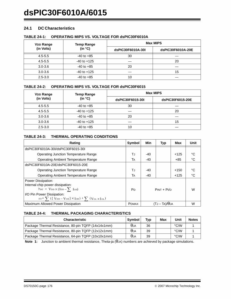
dsPIC30F6010A/6015
24.1 DC Characteristics
TABLE 24-1: OPERATING MIPS VS. VOLTAGE FOR dsPIC30F6010A
VDD Range(in Volts)
Temp Range(in °C)
Max MIPS
dsPIC30F6010A-30I dsPIC30F6010A-20E
4.5-5.5 -40 to +85 30 —
4.5-5.5 -40 to +125 — 20
3.0-3.6 -40 to +85 20 —
3.0-3.6 -40 to +125 — 15
2.5-3.0 -40 to +85 10 —
TABLE 24-2: OPERATING MIPS VS. VOLTAGE FOR dsPIC30F6015
VDD Range(in Volts)
Temp Range(in °C)
Max MIPS
dsPIC30F6015-30I dsPIC30F6015-20E
4.5-5.5 -40 to +85 30 —
4.5-5.5 -40 to +125 — 20
3.0-3.6 -40 to +85 20 —
3.0-3.6 -40 to +125 — 15
2.5-3.0 -40 to +85 10 —
TABLE 24-3: THERMAL OPERATING CONDITIONS
Rating Symbol Min Typ Max Unit
dsPIC30F6010A-30I/dsPIC30F6015-30I
Operating Junction Temperature Range TJ -40 +125 °C
Operating Ambient Temperature Range TA -40 +85 °C
dsPIC30F6010A-20E/dsPIC30F6015-20E
Operating Junction Temperature Range TJ -40 +150 °C
Operating Ambient Temperature Range TA -40 +125 °C
Power Dissipation:Internal chip power dissipation:
PD PINT + PI/O WI/O Pin Power Dissipation:
Maximum Allowed Power Dissipation PDMAX (TJ – TA)/θJA W
PINT VDD IDD IOH∑–( )×=
PI/O VDD VOH–{ } IOH×( )∑ VOL I OL×( )∑+=
TABLE 24-4: THERMAL PACKAGING CHARACTERISTICS
Characteristic Symbol Typ Max Unit Notes
Package Thermal Resistance, 80-pin TQFP (14x14x1mm) θJA 36 °C/W 1
Package Thermal Resistance, 80-pin TQFP (12x12x1mm) θJA 39 °C/W 1
Package Thermal Resistance, 64-pin TQFP (10x10x1mm) θJA 39 °C/W 1
Note 1: Junction to ambient thermal resistance, Theta-ja (θJA) numbers are achieved by package simulations.
DS70150C-page 176 © 2007 Microchip Technology Inc.

dsPIC30F6010A/6015
TABLE 24-5: DC TEMPERATURE AND VOLTAGE SPECIFICATIONS
DC CHARACTERISTICS
Standard Operating Conditions: 2.5V to 5.5V(unless otherwise stated)Operating temperature -40°C ≤ TA ≤ +85°C for Industrial
-40°C ≤ TA ≤ +125°C for Extended
Param No.
Symbol Characteristic Min Typ(1) Max Units Conditions
Operating Voltage(2)
DC10 VDD Supply Voltage 2.5 — 5.5 V Industrial temperature
DC11 VDD Supply Voltage 3.0 — 5.5 V Extended temperature
DC12 VDR RAM Data Retention Voltage(3) 1.5 — — V
DC16 VPOR VDD Start Voltageto ensure internalPower-on Reset signal
— VSS — V
DC17 SVDD VDD Rise Rateto ensure internalPower-on Reset signal
0.05 — — V/ms 0-5V in 0.1 sec0-3V in 60 ms
Note 1: Data in “Typ” column is at 5V, 25°C unless otherwise stated. Parameters are for design guidance only and are not tested.
2: These parameters are characterized but not tested in manufacturing.
3: This is the limit to which VDD can be lowered without losing RAM data.
© 2007 Microchip Technology Inc. DS70150C-page 177
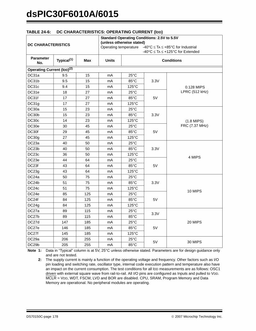
dsPIC30F6010A/6015
TABLE 24-6: DC CHARACTERISTICS: OPERATING CURRENT (IDD)
DC CHARACTERISTICS
Standard Operating Conditions: 2.5V to 5.5V(unless otherwise stated)Operating temperature -40°C ≤ TA ≤ +85°C for Industrial
-40°C ≤ TA ≤ +125°C for Extended
Parameter No.
Typical(1) Max Units Conditions
Operating Current (IDD)(2)
DC31a 9.5 15 mA 25°C
3.3V
0.128 MIPSLPRC (512 kHz)
DC31b 9.5 15 mA 85°C
DC31c 9.4 15 mA 125°C
DC31e 18 27 mA 25°C
5VDC31f 17 27 mA 85°C
DC31g 17 27 mA 125°C
DC30a 15 23 mA 25°C
3.3V
(1.8 MIPS)FRC (7.37 MHz)
DC30b 15 23 mA 85°C
DC30c 14 23 mA 125°C
DC30e 30 45 mA 25°C
5VDC30f 29 45 mA 85°C
DC30g 27 45 mA 125°C
DC23a 40 50 mA 25°C
3.3V
4 MIPS
DC23b 40 50 mA 85°C
DC23c 36 50 mA 125°C
DC23e 44 64 mA 25°C
5VDC23f 43 64 mA 85°C
DC23g 43 64 mA 125°C
DC24a 50 75 mA 25°C
3.3V
10 MIPS
DC24b 51 75 mA 85°C
DC24c 51 75 mA 125°C
DC24e 85 125 mA 25°C
5VDC24f 84 125 mA 85°C
DC24g 84 125 mA 125°C
DC27a 89 115 mA 25°C3.3V
20 MIPS
DC27b 89 115 mA 85°C
DC27d 147 185 mA 25°C
5VDC27e 146 185 mA 85°C
DC27f 145 185 mA 125°C
DC29a 206 255 mA 25°C5V 30 MIPS
DC29b 205 255 mA 85°C
Note 1: Data in “Typical” column is at 5V, 25°C unless otherwise stated. Parameters are for design guidance only and are not tested.
2: The supply current is mainly a function of the operating voltage and frequency. Other factors such as I/O pin loading and switching rate, oscillator type, internal code execution pattern and temperature also have an impact on the current consumption. The test conditions for all IDD measurements are as follows: OSC1 driven with external square wave from rail-to-rail. All I/O pins are configured as Inputs and pulled to VDD. MCLR = VDD, WDT, FSCM, LVD and BOR are disabled. CPU, SRAM, Program Memory and Data Memory are operational. No peripheral modules are operating.
DS70150C-page 178 © 2007 Microchip Technology Inc.
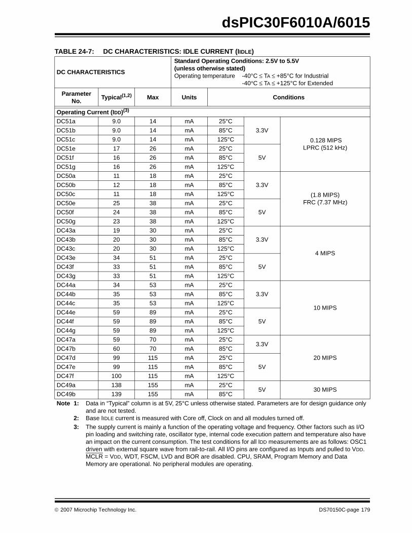
dsPIC30F6010A/6015
TABLE 24-7: DC CHARACTERISTICS: IDLE CURRENT (IIDLE)
DC CHARACTERISTICS
Standard Operating Conditions: 2.5V to 5.5V(unless otherwise stated)Operating temperature -40°C ≤ TA ≤ +85°C for Industrial
-40°C ≤ TA ≤ +125°C for Extended
Parameter No.
Typical(1,2) Max Units Conditions
Operating Current (IDD)(3)
DC51a 9.0 14 mA 25°C
3.3V
0.128 MIPSLPRC (512 kHz)
DC51b 9.0 14 mA 85°C
DC51c 9.0 14 mA 125°C
DC51e 17 26 mA 25°C
5VDC51f 16 26 mA 85°C
DC51g 16 26 mA 125°C
DC50a 11 18 mA 25°C
3.3V
(1.8 MIPS)FRC (7.37 MHz)
DC50b 12 18 mA 85°C
DC50c 11 18 mA 125°C
DC50e 25 38 mA 25°C
5VDC50f 24 38 mA 85°C
DC50g 23 38 mA 125°C
DC43a 19 30 mA 25°C
3.3V
4 MIPS
DC43b 20 30 mA 85°C
DC43c 20 30 mA 125°C
DC43e 34 51 mA 25°C
5VDC43f 33 51 mA 85°C
DC43g 33 51 mA 125°C
DC44a 34 53 mA 25°C
3.3V
10 MIPS
DC44b 35 53 mA 85°C
DC44c 35 53 mA 125°C
DC44e 59 89 mA 25°C
5VDC44f 59 89 mA 85°C
DC44g 59 89 mA 125°C
DC47a 59 70 mA 25°C3.3V
20 MIPS
DC47b 60 70 mA 85°C
DC47d 99 115 mA 25°C
5VDC47e 99 115 mA 85°C
DC47f 100 115 mA 125°C
DC49a 138 155 mA 25°C5V 30 MIPS
DC49b 139 155 mA 85°C
Note 1: Data in “Typical” column is at 5V, 25°C unless otherwise stated. Parameters are for design guidance only and are not tested.
2: Base IIDLE current is measured with Core off, Clock on and all modules turned off.
3: The supply current is mainly a function of the operating voltage and frequency. Other factors such as I/O pin loading and switching rate, oscillator type, internal code execution pattern and temperature also have an impact on the current consumption. The test conditions for all IDD measurements are as follows: OSC1 driven with external square wave from rail-to-rail. All I/O pins are configured as Inputs and pulled to VDD. MCLR = VDD, WDT, FSCM, LVD and BOR are disabled. CPU, SRAM, Program Memory and Data Memory are operational. No peripheral modules are operating.
© 2007 Microchip Technology Inc. DS70150C-page 179

dsPIC30F6010A/6015
TABLE 24-8: DC CHARACTERISTICS: POWER-DOWN CURRENT (IPD)
DC CHARACTERISTICS
Standard Operating Conditions: 2.5V to 5.5V(unless otherwise stated)Operating temperature -40°C ≤ TA ≤ +85°C for Industrial
-40°C ≤ TA ≤ +125°C for Extended
Parameter No.
Typical(1) Max Units Conditions
Power-Down Current (IPD)(2)
DC60a 0.2 — μA 25°C
3.3V
Base Power-Down Current(3)
DC60b 1.2 40 μA 85°C
DC60c 12 65 μA 125°C
DC60e 0.4 — μA 25°C
5VDC60f 1.7 55 μA 85°C
DC60g 15 90 μA 125°C
DC61a 9 15 μA 25°C
3.3V
Watchdog Timer Current: ΔIWDT(3)
DC61b 9 15 μA 85°C
DC61c 9 15 μA 125°C
DC61e 18 30 μA 25°C
5VDC61f 17 30 μA 85°C
DC61g 16 30 μA 125°C
DC62a 4 10 μA 25°C
3.3V
Timer1 w/32 kHz Crystal: ΔITI32(3)
DC62b 5 10 μA 85°C
DC62c 4 10 μA 125°C
DC62e 4 15 μA 25°C
5VDC62f 6 15 μA 85°C
DC62g 5 15 μA 125°C
DC63a 29 52 μA 25°C 3.3V
BOR On: ΔIBOR(3)
DC63b 32 52 μA 85°C
DC63c 33 52 μA 125°C
DC63e 34 60 μA 25°C
5VDC63f 39 60 μA 85°C
DC63g 38 60 μA 125°C
Note 1: Data in the “Typical” column is at 5V, 25°C unless otherwise stated. Parameters are for design guidance only and are not tested.
2: Base IPD is measured with all peripherals and clocks shut down. All I/Os are configured as inputs and pulled high. BOR, WDT, etc. are all switched off.
3: The Δ current is the additional current consumed when the module is enabled. This current should be added to the base IPD current.
DS70150C-page 180 © 2007 Microchip Technology Inc.
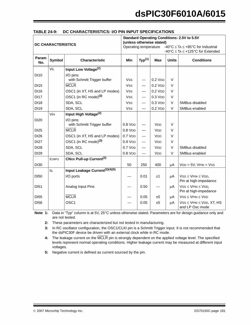
dsPIC30F6010A/6015
TABLE 24-9: DC CHARACTERISTICS: I/O PIN INPUT SPECIFICATIONS
DC CHARACTERISTICS
Standard Operating Conditions: 2.5V to 5.5V(unless otherwise stated)Operating temperature -40°C ≤ TA ≤ +85°C for Industrial
-40°C ≤ TA ≤ +125°C for Extended
Param No.
Symbol Characteristic Min Typ(1) Max Units Conditions
VIL Input Low Voltage(2)
DI10 I/O pins: with Schmitt Trigger buffer VSS — 0.2 VDD V
DI15 MCLR VSS — 0.2 VDD V
DI16 OSC1 (in XT, HS and LP modes) VSS — 0.2 VDD V
DI17 OSC1 (in RC mode)(3) VSS — 0.3 VDD V
DI18 SDA, SCL VSS — 0.3 VDD V SMBus disabled
DI19 SDA, SCL VSS — 0.2 VDD V SMBus enabled
VIH Input High Voltage(2)
DI20 I/O pins: with Schmitt Trigger buffer 0.8 VDD — VDD V
DI25 MCLR 0.8 VDD — VDD V
DI26 OSC1 (in XT, HS and LP modes) 0.7 VDD — VDD V
DI27 OSC1 (in RC mode)(3) 0.9 VDD — VDD V
DI28 SDA, SCL 0.7 VDD — VDD V SMBus disabled
DI29 SDA, SCL 0.8 VDD — VDD V SMBus enabled
ICNPU CNXX Pull-up Current(2)
DI30 50 250 400 μA VDD = 5V, VPIN = VSS
IIL Input Leakage Current(2)(4)(5)
DI50 I/O ports — 0.01 ±1 μA VSS ≤ VPIN ≤ VDD,Pin at high-impedance
DI51 Analog Input Pins — 0.50 — μA VSS ≤ VPIN ≤ VDD,Pin at high-impedance
DI55 MCLR — 0.05 ±5 μA VSS ≤ VPIN ≤ VDD
DI56 OSC1 — 0.05 ±5 μA VSS ≤ VPIN ≤ VDD, XT, HSand LP Osc mode
Note 1: Data in “Typ” column is at 5V, 25°C unless otherwise stated. Parameters are for design guidance only and are not tested.
2: These parameters are characterized but not tested in manufacturing.3: In RC oscillator configuration, the OSC1/CLKl pin is a Schmitt Trigger input. It is not recommended that
the dsPIC30F device be driven with an external clock while in RC mode.4: The leakage current on the MCLR pin is strongly dependent on the applied voltage level. The specified
levels represent normal operating conditions. Higher leakage current may be measured at different input voltages.
5: Negative current is defined as current sourced by the pin.
© 2007 Microchip Technology Inc. DS70150C-page 181
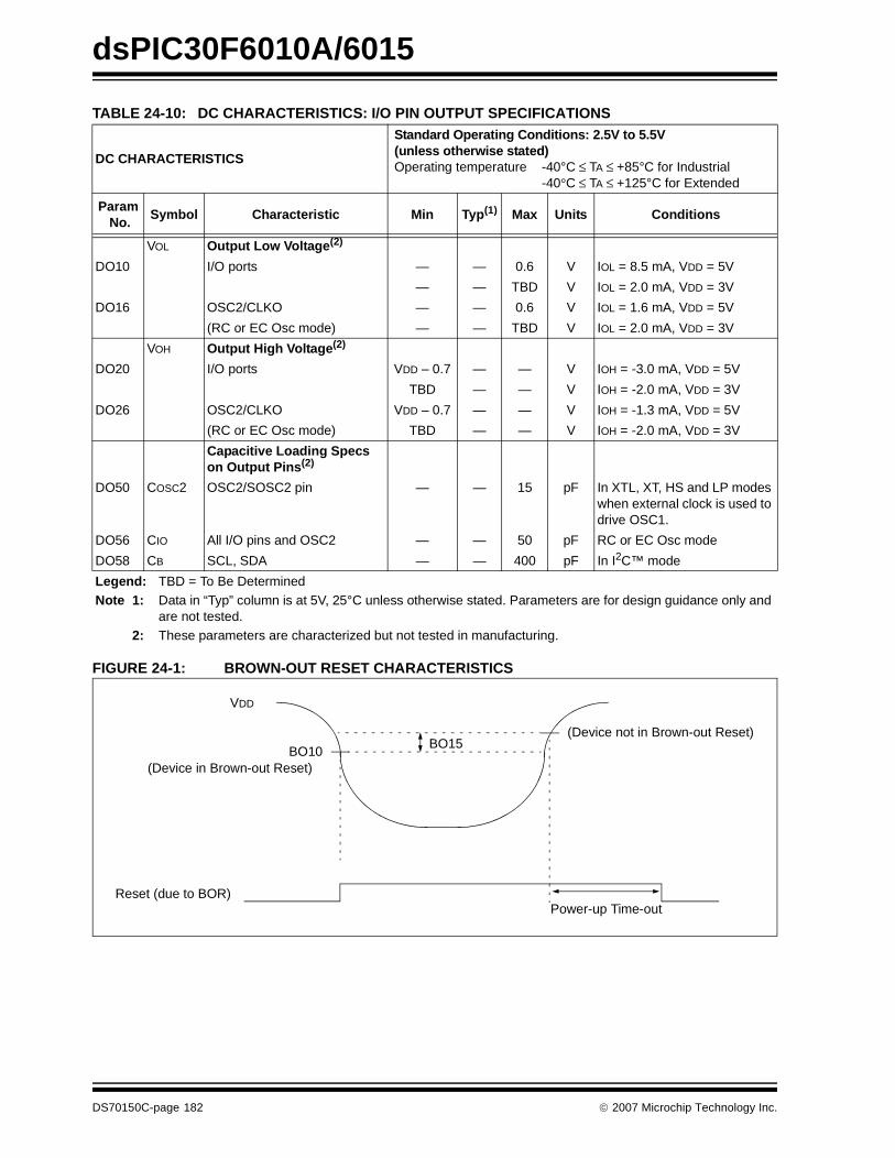
dsPIC30F6010A/6015
FIGURE 24-1: BROWN-OUT RESET CHARACTERISTICS
TABLE 24-10: DC CHARACTERISTICS: I/O PIN OUTPUT SPECIFICATIONS
DC CHARACTERISTICS
Standard Operating Conditions: 2.5V to 5.5V(unless otherwise stated)Operating temperature -40°C ≤ TA ≤ +85°C for Industrial
-40°C ≤ TA ≤ +125°C for Extended
Param No.
Symbol Characteristic Min Typ(1) Max Units Conditions
VOL Output Low Voltage(2)
DO10 I/O ports — — 0.6 V IOL = 8.5 mA, VDD = 5V
— — TBD V IOL = 2.0 mA, VDD = 3V
DO16 OSC2/CLKO — — 0.6 V IOL = 1.6 mA, VDD = 5V
(RC or EC Osc mode) — — TBD V IOL = 2.0 mA, VDD = 3V
VOH Output High Voltage(2)
DO20 I/O ports VDD – 0.7 — — V IOH = -3.0 mA, VDD = 5V
TBD — — V IOH = -2.0 mA, VDD = 3V
DO26 OSC2/CLKO VDD – 0.7 — — V IOH = -1.3 mA, VDD = 5V
(RC or EC Osc mode) TBD — — V IOH = -2.0 mA, VDD = 3V
Capacitive Loading Specs on Output Pins(2)
DO50 COSC2 OSC2/SOSC2 pin — — 15 pF In XTL, XT, HS and LP modes when external clock is used to drive OSC1.
DO56 CIO All I/O pins and OSC2 — — 50 pF RC or EC Osc mode
DO58 CB SCL, SDA — — 400 pF In I2C™ mode
Legend: TBD = To Be DeterminedNote 1: Data in “Typ” column is at 5V, 25°C unless otherwise stated. Parameters are for design guidance only and
are not tested.2: These parameters are characterized but not tested in manufacturing.
BO10
Reset (due to BOR)
VDD
(Device in Brown-out Reset)
(Device not in Brown-out Reset)
Power-up Time-out
BO15
DS70150C-page 182 © 2007 Microchip Technology Inc.

dsPIC30F6010A/6015
TABLE 24-11: ELECTRICAL CHARACTERISTICS: BOR
DC CHARACTERISTICS
Standard Operating Conditions: 2.5V to 5.5V(unless otherwise stated)Operating temperature -40°C ≤ TA ≤ +85°C for Industrial
-40°C ≤ TA ≤ +125°C for Extended
ParamNo.
Symbol Characteristic Min Typ(1) Max Units Conditions
BO10 VBOR BOR Voltage(2) on VDD transition high-to-low
BORV = 11(3) — — — V Not in operating range
BORV = 10 2.6 — 2.71 V
BORV = 01 4.1 — 4.4 V
BORV = 00 4.58 — 4.73 V
BO15 VBHYS — 5 — mV
Note 1: Data in “Typ” column is at 5V, 25°C unless otherwise stated. Parameters are for design guidance only and are not tested.
2: These parameters are characterized but not tested in manufacturing.3: ‘11’ values not in usable operating range.
TABLE 24-12: DC CHARACTERISTICS: PROGRAM AND EEPROM
DC CHARACTERISTICS
Standard Operating Conditions: 2.5V to 5.5V(unless otherwise stated)Operating temperature -40°C ≤ TA ≤ +85°C for Industrial
-40°C ≤ TA ≤ +125°C for Extended
ParamNo.
Symbol Characteristic Min Typ(1) Max Units Conditions
Data EEPROM Memory(2)
D120 ED Byte Endurance 100K 1M — E/W -40°C ≤ TA ≤ +85°C
D121 VDRW VDD for Read/Write VMIN — 5.5 V Using EECON to read/writeVMIN = Minimum operating voltage
D122 TDEW Erase/Write Cycle Time — 2 — ms
D123 TRETD Characteristic Retention 40 100 — Year Provided no other specifications are violated
D124 IDEW IDD During Programming — 10 30 mA Row Erase
Program FLASH Memory(2)
D130 EP Cell Endurance 10K 100K — E/W -40°C ≤ TA ≤ +85°C
D131 VPR VDD for Read VMIN — 5.5 V VMIN = Minimum operating voltage
D132 VEB VDD for Bulk Erase 4.5 — 5.5 V
D133 VPEW VDD for Erase/Write 3.0 — 5.5 V
D134 TPEW Erase/Write Cycle Time — 2 — ms
D135 TRETD Characteristic Retention 40 100 — Year Provided no other specifica-tions are violated
D136 TEB ICSP™ Block Erase Time — 4 — ms
D137 IPEW IDD During Programming — 10 30 mA Row Erase
D138 IEB IDD During Programming — 10 30 mA Bulk Erase
Note 1: Data in “Typ” column is at 5V, 25°C unless otherwise stated.2: These parameters are characterized but not tested in manufacturing.
© 2007 Microchip Technology Inc. DS70150C-page 183

dsPIC30F6010A/6015
24.2 AC Characteristics and Timing Parameters
The information contained in this section defines dsPIC30F AC characteristics and timing parameters.
TABLE 24-13: TEMPERATURE AND VOLTAGE SPECIFICATIONS – AC
FIGURE 24-2: LOAD CONDITIONS FOR DEVICE TIMING SPECIFICATIONS
FIGURE 24-3: EXTERNAL CLOCK TIMING
AC CHARACTERISTICS
Standard Operating Conditions: 2.5V to 5.5V(unless otherwise stated)Operating temperature -40°C ≤ TA ≤ +85°C for Industrial
-40°C ≤ TA ≤ +125°C for ExtendedOperating voltage VDD range as described in DC Spec Section 24.0.
VDD/2
CL
RL
Pin
Pin
VSS
VSS
CL
RL = 464 ΩCL = 50 pF for all pins except OSC2
5 pF for OSC2 output
Load Condition 1 – for all pins except OSC2 Load Condition 2 – for OSC2
Legend:
OSC1
CLKO
Q4 Q1 Q2 Q3 Q4 Q1
OS20
OS25OS30 OS30
OS40 OS41
OS31 OS31
DS70150C-page 184 © 2007 Microchip Technology Inc.
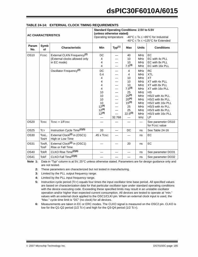
dsPIC30F6010A/6015
TABLE 24-14: EXTERNAL CLOCK TIMING REQUIREMENTS
AC CHARACTERISTICS
Standard Operating Conditions: 2.5V to 5.5V(unless otherwise stated)Operating temperature -40°C ≤ TA ≤ +85°C for Industrial
-40°C ≤ TA ≤ +125°C for Extended
ParamNo.
Symbol
Characteristic Min Typ(1) Max Units Conditions
OS10 FOSC External CLKN Frequency(2)
(External clocks allowed onlyin EC mode)
DC444
————
401010
7.5(3)
MHzMHzMHzMHz
ECEC with 4x PLLEC with 8x PLLEC with 16x PLL
Oscillator Frequency(2) DC0.44444
10101010
12(4)
12(4)
12(4)
—
—————————————
32.768
44
101010
7.5(3)
2520(4)
20(4)
15(3)
2525
22.5(3)
—
MHzMHzMHzMHzMHzMHzMHzMHzMHzMHzMHzMHzMHzkHz
RCXTLXTXT with 4x PLLXT with 8x PLLXT with 16x PLLHSHS/2 with 4x PLLHS/2 with 8x PLLHS/2 with 16x PLLHS/3 with 4x PLLHS/3 with 8x PLLHS/3 with 16x PLLLP
OS20 TOSC TOSC = 1/FOSC — — — — See parameter OS10for FOSC value
OS25 TCY Instruction Cycle Time(2)(5) 33 — DC ns See Table 24-16
OS30 TosL,TosH
External Clock(2) in (OSC1)High or Low Time
.45 x TOSC — — ns EC
OS31 TosR,TosF
External Clock(2) in (OSC1)Rise or Fall Time
— — 20 ns EC
OS40 TckR CLKO Rise Time(2)(6) — — — ns See parameter DO31
OS41 TckF CLKO Fall Time(2)(6) — — — ns See parameter DO32
Note 1: Data in “Typ” column is at 5V, 25°C unless otherwise stated. Parameters are for design guidance only and are not tested.
2: These parameters are characterized but not tested in manufacturing.3: Limited by the PLL output frequency range.
4: Limited by the PLL input frequency range.5: Instruction cycle period (TCY) equals four times the input oscillator time base period. All specified values
are based on characterization data for that particular oscillator type under standard operating conditions with the device executing code. Exceeding these specified limits may result in an unstable oscillator operation and/or higher than expected current consumption. All devices are tested to operate at “min.” values with an external clock applied to the OSC1/CLKI pin. When an external clock input is used, the “Max.” cycle time limit is “DC” (no clock) for all devices.
6: Measurements are taken in EC or ERC modes. The CLKO signal is measured on the OSC2 pin. CLKO is low for the Q1-Q2 period (1/2 TCY) and high for the Q3-Q4 period (1/2 TCY).
© 2007 Microchip Technology Inc. DS70150C-page 185
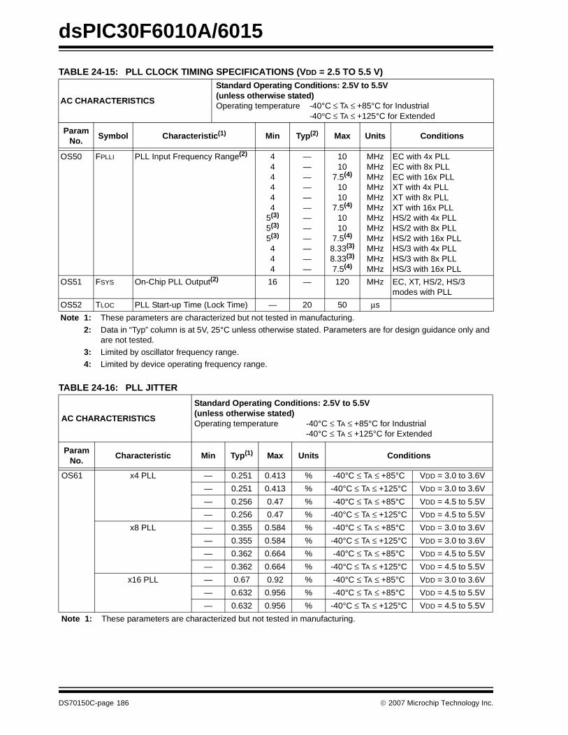
dsPIC30F6010A/6015
TABLE 24-15: PLL CLOCK TIMING SPECIFICATIONS (VDD = 2.5 TO 5.5 V)
AC CHARACTERISTICS
Standard Operating Conditions: 2.5V to 5.5V(unless otherwise stated)Operating temperature -40°C ≤ TA ≤ +85°C for Industrial
-40°C ≤ TA ≤ +125°C for Extended
ParamNo.
Symbol Characteristic(1) Min Typ(2) Max Units Conditions
OS50 FPLLI PLL Input Frequency Range(2) 444444
5(3)
5(3)
5(3)
444
————————————
1010
7.5(4)
1010
7.5(4)
1010
7.5(4)
8.33(3)
8.33(3)
7.5(4)
MHzMHzMHzMHzMHzMHzMHzMHzMHzMHzMHzMHz
EC with 4x PLL EC with 8x PLL EC with 16x PLL XT with 4x PLLXT with 8x PLLXT with 16x PLLHS/2 with 4x PLLHS/2 with 8x PLLHS/2 with 16x PLLHS/3 with 4x PLLHS/3 with 8x PLLHS/3 with 16x PLL
OS51 FSYS On-Chip PLL Output(2) 16 — 120 MHz EC, XT, HS/2, HS/3 modes with PLL
OS52 TLOC PLL Start-up Time (Lock Time) — 20 50 μs
Note 1: These parameters are characterized but not tested in manufacturing.
2: Data in “Typ” column is at 5V, 25°C unless otherwise stated. Parameters are for design guidance only and are not tested.
3: Limited by oscillator frequency range.4: Limited by device operating frequency range.
TABLE 24-16: PLL JITTER
AC CHARACTERISTICS
Standard Operating Conditions: 2.5V to 5.5V(unless otherwise stated)Operating temperature -40°C ≤ TA ≤ +85°C for Industrial
-40°C ≤ TA ≤ +125°C for Extended
Param No.
Characteristic Min Typ(1) Max Units Conditions
OS61 x4 PLL — 0.251 0.413 % -40°C ≤ TA ≤ +85°C VDD = 3.0 to 3.6V
— 0.251 0.413 % -40°C ≤ TA ≤ +125°C VDD = 3.0 to 3.6V
— 0.256 0.47 % -40°C ≤ TA ≤ +85°C VDD = 4.5 to 5.5V
— 0.256 0.47 % -40°C ≤ TA ≤ +125°C VDD = 4.5 to 5.5V
x8 PLL — 0.355 0.584 % -40°C ≤ TA ≤ +85°C VDD = 3.0 to 3.6V
— 0.355 0.584 % -40°C ≤ TA ≤ +125°C VDD = 3.0 to 3.6V
— 0.362 0.664 % -40°C ≤ TA ≤ +85°C VDD = 4.5 to 5.5V
— 0.362 0.664 % -40°C ≤ TA ≤ +125°C VDD = 4.5 to 5.5V
x16 PLL — 0.67 0.92 % -40°C ≤ TA ≤ +85°C VDD = 3.0 to 3.6V
— 0.632 0.956 % -40°C ≤ TA ≤ +85°C VDD = 4.5 to 5.5V
— 0.632 0.956 % -40°C ≤ TA ≤ +125°C VDD = 4.5 to 5.5V
Note 1: These parameters are characterized but not tested in manufacturing.
DS70150C-page 186 © 2007 Microchip Technology Inc.

dsPIC30F6010A/6015
TABLE 24-17: INTERNAL CLOCK TIMING EXAMPLES
Clock Oscillator
Mode
FOSC (MHz)(1) TCY (μsec)(2) MIPS(3)
w/o PLLMIPS(3)
w/PLL x4MIPS(3)
w/PLL x8MIPS(3)
w/PLL x16
EC 0.200 20.0 0.05 — — —
4 1.0 1.0 4.0 8.0 16.0
10 0.4 2.5 10.0 20.0 —
25 0.16 6.25 — — —
XT 4 1.0 1.0 4.0 8.0 16.0
10 0.4 2.5 10.0 20.0 —
Note 1: Assumption: Oscillator Postscaler is divide by 1.2: Instruction Execution Cycle Time: TCY = 1/MIPS.3: Instruction Execution Frequency: MIPS = (FOSC * PLLx)/4 [since there are 4 Q clocks per instruction
cycle].
© 2007 Microchip Technology Inc. DS70150C-page 187

dsPIC30F6010A/6015
TABLE 24-18: AC CHARACTERISTICS: INTERNAL FRC JITTER, ACCURACY AND DRIFT(2)
AC CHARACTERISTICS
Standard Operating Conditions: 2.5V to 5.5V(unless otherwise stated)Operating temperature -40°C ≤ TA ≤ +85°C for Industrial
-40°C ≤ TA ≤ +125°C for Extended
Param No.
Characteristic Min Typ Max Units Conditions
Internal FRC Jitter @ FRC Freq. = 7.37 MHz(1)
OS62 FRC — +0.04 +0.16 % -40°C ≤ TA ≤ +85°C VDD = 3.0-3.6V
— +0.07 +0.23 % -40°C ≤ TA ≤ +125°C VDD = 4.5-5.5V
FRC with 4x PLL — +0.31 +0.62 % -40°C ≤ TA ≤ +85°C VDD = 3.0-3.6V
— +0.34 +0.77 % -40°C ≤ TA ≤ +125°C VDD = 4.5-5.5V
FRC with 8x PLL — +0.44 +0.87 % -40°C ≤ TA ≤ +85°C VDD = 3.0-3.6V
— +0.48 +1.08 % -40°C ≤ TA ≤ +125°C VDD = 4.5-5.5V
FRC with 16x PLL — +0.71 +1.23 % -40°C ≤ TA ≤ +125°C VDD = 4.5-5.5V
Internal FRC Accuracy @ FRC Freq. = 7.37 MHz(1)
OS63 FRC — — +0.4 % -40°C ≤ TA ≤ +125°C VDD = 3.0-5.5V
Internal FRC Drift @ FRC Freq. = 7.37 MHz(1)
OS64 -0.7 — 0.5 % -40°C ≤ TA ≤ +85°C VDD = 3.0-3.6V
-0.7 — 0.7 % -40°C ≤ TA ≤ +125°C VDD = 3.0-3.6V
-0.7 — 0.5 % -40°C ≤ TA ≤ +85°C VDD = 4.5-5.5V
-0.7 — 0.7 % -40°C ≤ TA ≤ +125°C VDD = 4.5-5.5V
Note 1: Frequency calibrated at 25°C and 5V. TUN bits can be used to compensate for temperature drift.2: Overall FRC variation can be calculated by adding the absolute values of jitter, accuracy and drift
percentages.
TABLE 24-19: INTERNAL LPRC ACCURACY
AC CHARACTERISTICS
Standard Operating Conditions: 2.5V to 5.5V(unless otherwise stated)Operating temperature -40°C ≤ TA ≤ +85°C for Industrial
-40°C ≤ TA ≤ +125°C for Extended
ParamNo.
Characteristic Min Typ Max Units Conditions
LPRC @ Freq. = 512 kHz(1)
OS65 -35 — +35 % —
Note 1: Change of LPRC frequency as VDD changes.
DS70150C-page 188 © 2007 Microchip Technology Inc.
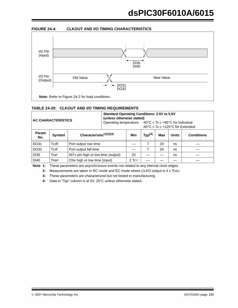
dsPIC30F6010A/6015
FIGURE 24-4: CLKOUT AND I/O TIMING CHARACTERISTICS
Note: Refer to Figure 24-2 for load conditions.
I/O Pin(Input)
I/O Pin(Output)
DI35
Old Value New Value
DI40
DO31DO32
TABLE 24-20: CLKOUT AND I/O TIMING REQUIREMENTS
AC CHARACTERISTICS
Standard Operating Conditions: 2.5V to 5.5V(unless otherwise stated)Operating temperature -40°C ≤ TA ≤ +85°C for Industrial
-40°C ≤ TA ≤ +125°C for Extended
ParamNo.
Symbol Characteristic(1)(2)(3) Min Typ(4) Max Units Conditions
DO31 TIOR Port output rise time — 7 20 ns —
DO32 TIOF Port output fall time — 7 20 ns —
DI35 TINP INTx pin high or low time (output) 20 — — ns —
DI40 TRBP CNx high or low time (input) 2 TCY — — — —
Note 1: These parameters are asynchronous events not related to any internal clock edges.
2: Measurements are taken in RC mode and EC mode where CLKO output is 4 x TOSC.3: These parameters are characterized but not tested in manufacturing.4: Data in “Typ” column is at 5V, 25°C unless otherwise stated.
© 2007 Microchip Technology Inc. DS70150C-page 189

dsPIC30F6010A/6015
FIGURE 24-5: RESET, WATCHDOG TIMER, OSCILLATOR START-UP TIMER AND POWER-UP TIMER TIMING CHARACTERISTICS
VDD
MCLR
InternalPOR
PWRTTime-out
OSCTime-out
InternalReset
WatchdogTimerReset
SY11
SY10
SY20SY13
I/O Pins
SY13
Note: Refer to Figure 24-2 for load conditions.
FSCM Delay
SY35
SY30
SY12
DS70150C-page 190 © 2007 Microchip Technology Inc.

dsPIC30F6010A/6015
FIGURE 24-6: BAND GAP START-UP TIME CHARACTERISTICS
TABLE 24-21: RESET, WATCHDOG TIMER, OSCILLATOR START-UP TIMER, POWER-UP TIMER AND BROWN-OUT RESET TIMING REQUIREMENTS
AC CHARACTERISTICS
Standard Operating Conditions: 2.5V to 5.5V(unless otherwise stated)Operating temperature -40°C ≤ TA ≤ +85°C for Industrial
-40°C ≤ TA ≤ +125°C for Extended
ParamNo.
Symbol Characteristic(1) Min Typ(2) Max Units Conditions
SY10 TmcL MCLR Pulse Width (low) 2 — — μs -40°C to +85°C
SY11 TPWRT Power-up Timer Period 31250
41664
62290
ms -40°C to +85°CUser programmable
SY12 TPOR Power-on Reset Delay(4) 3 10 30 μs -40°C to +85°C
SY13 TIOZ I/O High-impedance from MCLR Low or Watchdog Timer Reset
— 0.8 1.0 μs
SY20 TWDT1 Watchdog Timer Time-out Period (No Prescaler)
1.4 2.1 2.8 ms VDD = 5V, -40°C to +85°C
TWDT2 1.4 2.1 2.8 ms VDD = 3V, -40°C to +85°C
SY25 TBOR Brown-out Reset Pulse Width(3) 100 — — μs VDD ≤ VBOR (D034)
SY30 TOST Oscillator Start-up Timer Period — 1024 TOSC — — TOSC = OSC1 period
SY35 TFSCM Fail-Safe Clock Monitor Delay — 500 900 μs -40°C to +85°C
Note 1: These parameters are characterized but not tested in manufacturing.2: Data in “Typ” column is at 5V, 25°C unless otherwise stated.3: Refer to Figure 24-1 and Table for BOR4: Characterized by design but not tested.
VBGAP
Enable Band Gap
Band Gap
0V
(see Note)
Stable
Note: Set FBORPOR<7>.
SY40
TABLE 24-22: BAND GAP START-UP TIME REQUIREMENTS
AC CHARACTERISTICS
Standard Operating Conditions: 2.5V to 5.5V(unless otherwise stated)Operating temperature -40°C ≤ TA ≤ +85°C for Industrial
-40°C ≤ TA ≤ +125°C for Extended
ParamNo.
Symbol Characteristic(1) Min Typ Max Units Conditions
SY40 TBGAP Band Gap Start-up Time — 40 65 μs Defined as the time between the instant that the band gap is enabled and the moment that the band gap reference voltage is stable (RCON<13>Status bit).
Note 1: These parameters are characterized but not tested in manufacturing.
© 2007 Microchip Technology Inc. DS70150C-page 191
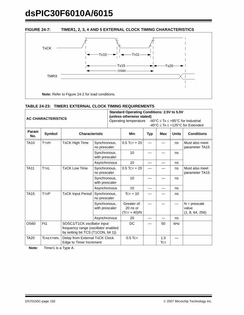
dsPIC30F6010A/6015
FIGURE 24-7: TIMER1, 2, 3, 4 AND 5 EXTERNAL CLOCK TIMING CHARACTERISTICS
Note: Refer to Figure 24-2 for load conditions.
Tx11
Tx15
Tx10
Tx20
TMRX
OS60
TxCK
TABLE 24-23: TIMER1 EXTERNAL CLOCK TIMING REQUIREMENTS
AC CHARACTERISTICS
Standard Operating Conditions: 2.5V to 5.5V(unless otherwise stated)Operating temperature -40°C ≤ TA ≤ +85°C for Industrial
-40°C ≤ TA ≤ +125°C for Extended
ParamNo.
Symbol Characteristic Min Typ Max Units Conditions
TA10 TTXH TxCK High Time Synchronous,no prescaler
0.5 TCY + 20 — — ns Must also meet parameter TA15
Synchronous,with prescaler
10 — — ns
Asynchronous 10 — — ns
TA11 TTXL TxCK Low Time Synchronous,no prescaler
0.5 TCY + 20 — — ns Must also meet parameter TA15
Synchronous,with prescaler
10 — — ns
Asynchronous 10 — — ns
TA15 TTXP TxCK Input Period Synchronous,no prescaler
TCY + 10 — — ns
Synchronous,with prescaler
Greater of:20 ns or
(TCY + 40)/N
— — — N = prescale value(1, 8, 64, 256)
Asynchronous 20 — — ns
OS60 Ft1 SOSC1/T1CK oscillator input frequency range (oscillator enabled by setting bit TCS (T1CON, bit 1))
DC — 50 kHz
TA20 TCKEXTMRL Delay from External TxCK Clock Edge to Timer Increment
0.5 TCY 1.5 TCY
—
Note: Timer1 is a Type A.
DS70150C-page 192 © 2007 Microchip Technology Inc.
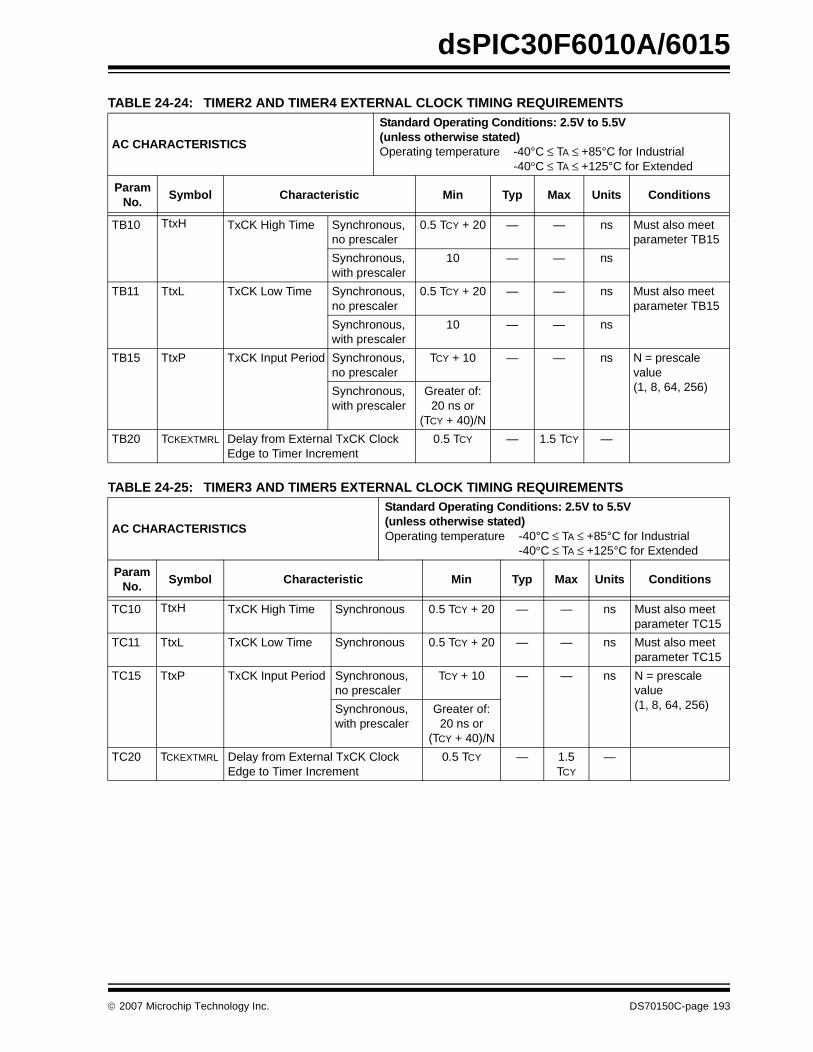
dsPIC30F6010A/6015
TABLE 24-24: TIMER2 AND TIMER4 EXTERNAL CLOCK TIMING REQUIREMENTS
AC CHARACTERISTICS
Standard Operating Conditions: 2.5V to 5.5V(unless otherwise stated)Operating temperature -40°C ≤ TA ≤ +85°C for Industrial
-40°C ≤ TA ≤ +125°C for Extended
ParamNo.
Symbol Characteristic Min Typ Max Units Conditions
TB10 TtxH TxCK High Time Synchronous,no prescaler
0.5 TCY + 20 — — ns Must also meet parameter TB15
Synchronous,with prescaler
10 — — ns
TB11 TtxL TxCK Low Time Synchronous,no prescaler
0.5 TCY + 20 — — ns Must also meet parameter TB15
Synchronous,with prescaler
10 — — ns
TB15 TtxP TxCK Input Period Synchronous,no prescaler
TCY + 10 — — ns N = prescale value(1, 8, 64, 256)Synchronous,
with prescalerGreater of:
20 ns or(TCY + 40)/N
TB20 TCKEXTMRL Delay from External TxCK Clock Edge to Timer Increment
0.5 TCY — 1.5 TCY —
TABLE 24-25: TIMER3 AND TIMER5 EXTERNAL CLOCK TIMING REQUIREMENTS
AC CHARACTERISTICS
Standard Operating Conditions: 2.5V to 5.5V(unless otherwise stated)Operating temperature -40°C ≤ TA ≤ +85°C for Industrial
-40°C ≤ TA ≤ +125°C for Extended
ParamNo.
Symbol Characteristic Min Typ Max Units Conditions
TC10 TtxH TxCK High Time Synchronous 0.5 TCY + 20 — — ns Must also meet parameter TC15
TC11 TtxL TxCK Low Time Synchronous 0.5 TCY + 20 — — ns Must also meet parameter TC15
TC15 TtxP TxCK Input Period Synchronous,no prescaler
TCY + 10 — — ns N = prescalevalue (1, 8, 64, 256)Synchronous,
with prescalerGreater of:
20 ns or (TCY + 40)/N
TC20 TCKEXTMRL Delay from External TxCK Clock Edge to Timer Increment
0.5 TCY — 1.5 TCY
—
© 2007 Microchip Technology Inc. DS70150C-page 193
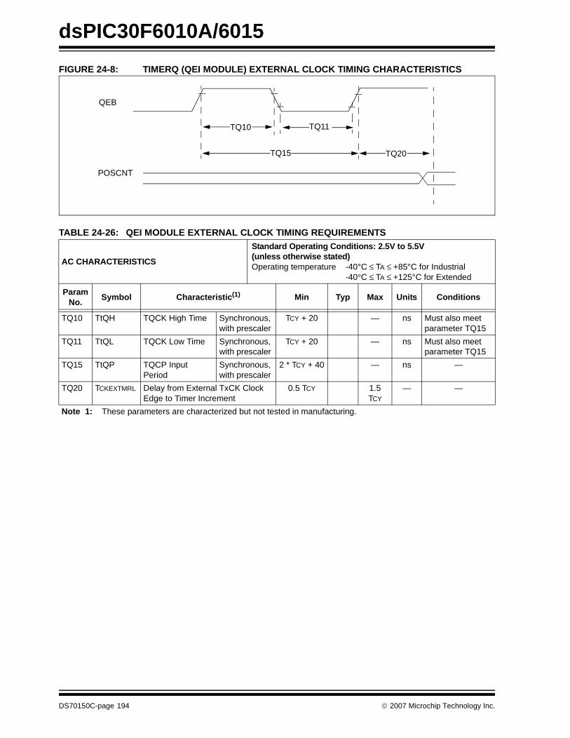
dsPIC30F6010A/6015
FIGURE 24-8: TIMERQ (QEI MODULE) EXTERNAL CLOCK TIMING CHARACTERISTICS
TQ11
TQ15
TQ10
TQ20
QEB
POSCNT
TABLE 24-26: QEI MODULE EXTERNAL CLOCK TIMING REQUIREMENTS
AC CHARACTERISTICS
Standard Operating Conditions: 2.5V to 5.5V(unless otherwise stated)Operating temperature -40°C ≤ TA ≤ +85°C for Industrial
-40°C ≤ TA ≤ +125°C for Extended
ParamNo.
Symbol Characteristic(1) Min Typ Max Units Conditions
TQ10 TtQH TQCK High Time Synchronous,with prescaler
TCY + 20 — ns Must also meet parameter TQ15
TQ11 TtQL TQCK Low Time Synchronous,with prescaler
TCY + 20 — ns Must also meet parameter TQ15
TQ15 TtQP TQCP Input Period
Synchronous,with prescaler
2 * TCY + 40 — ns —
TQ20 TCKEXTMRL Delay from External TxCK Clock Edge to Timer Increment
0.5 TCY 1.5 TCY
— —
Note 1: These parameters are characterized but not tested in manufacturing.
DS70150C-page 194 © 2007 Microchip Technology Inc.
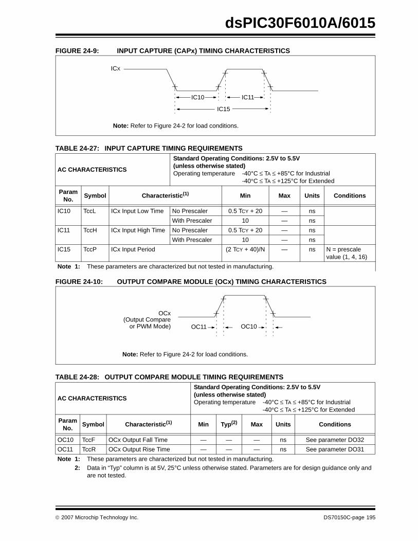
dsPIC30F6010A/6015
FIGURE 24-9: INPUT CAPTURE (CAPx) TIMING CHARACTERISTICS
FIGURE 24-10: OUTPUT COMPARE MODULE (OCx) TIMING CHARACTERISTICS
ICX
IC10 IC11
IC15
Note: Refer to Figure 24-2 for load conditions.
TABLE 24-27: INPUT CAPTURE TIMING REQUIREMENTS
AC CHARACTERISTICS
Standard Operating Conditions: 2.5V to 5.5V(unless otherwise stated)Operating temperature -40°C ≤ TA ≤ +85°C for Industrial
-40°C ≤ TA ≤ +125°C for Extended
ParamNo.
Symbol Characteristic(1) Min Max Units Conditions
IC10 TccL ICx Input Low Time No Prescaler 0.5 TCY + 20 — ns
With Prescaler 10 — ns
IC11 TccH ICx Input High Time No Prescaler 0.5 TCY + 20 — ns
With Prescaler 10 — ns
IC15 TccP ICx Input Period (2 TCY + 40)/N — ns N = prescale value (1, 4, 16)
Note 1: These parameters are characterized but not tested in manufacturing.
OCx
OC11 OC10(Output Compare
Note: Refer to Figure 24-2 for load conditions.
or PWM Mode)
TABLE 24-28: OUTPUT COMPARE MODULE TIMING REQUIREMENTS
AC CHARACTERISTICS
Standard Operating Conditions: 2.5V to 5.5V(unless otherwise stated)Operating temperature -40°C ≤ TA ≤ +85°C for Industrial
-40°C ≤ TA ≤ +125°C for Extended
Param No.
Symbol Characteristic(1) Min Typ(2) Max Units Conditions
OC10 TccF OCx Output Fall Time — — — ns See parameter DO32
OC11 TccR OCx Output Rise Time — — — ns See parameter DO31
Note 1: These parameters are characterized but not tested in manufacturing.2: Data in “Typ” column is at 5V, 25°C unless otherwise stated. Parameters are for design guidance only and
are not tested.
© 2007 Microchip Technology Inc. DS70150C-page 195

dsPIC30F6010A/6015
FIGURE 24-11: OC/PWM MODULE TIMING CHARACTERISTICS
OCFA/OCFB
OCx
OC20
OC15
TABLE 24-29: SIMPLE OC/PWM MODE TIMING REQUIREMENTS
AC CHARACTERISTICS
Standard Operating Conditions: 2.5V to 5.5V(unless otherwise stated)Operating temperature -40°C ≤ TA ≤ +85°C for Industrial
-40°C ≤ TA ≤ +125°C for Extended
Param No.
Symbol Characteristic(1) Min Typ(2) Max Units Conditions
OC15 TFD Fault Input to PWM I/O Change
— — 50 ns —
OC20 TFLT Fault Input Pulse Width 50 — — ns —
Note 1: These parameters are characterized but not tested in manufacturing.2: Data in “Typ” column is at 5V, 25°C unless otherwise stated. Parameters are for design guidance only and
are not tested.
DS70150C-page 196 © 2007 Microchip Technology Inc.
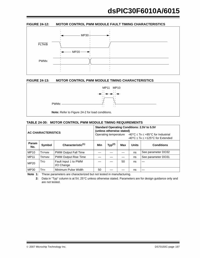
dsPIC30F6010A/6015
FIGURE 24-12: MOTOR CONTROL PWM MODULE FAULT TIMING CHARACTERISTICS
FIGURE 24-13: MOTOR CONTROL PWM MODULE TIMING CHARACTERISTICS
FLTA/B
PWMx
MP30
MP20
PWMx
MP11 MP10
Note: Refer to Figure 24-2 for load conditions.
TABLE 24-30: MOTOR CONTROL PWM MODULE TIMING REQUIREMENTS
AC CHARACTERISTICS
Standard Operating Conditions: 2.5V to 5.5V(unless otherwise stated)Operating temperature -40°C ≤ TA ≤ +85°C for Industrial
-40°C ≤ TA ≤ +125°C for Extended
ParamNo.
Symbol Characteristic(1) Min Typ(2) Max Units Conditions
MP10 TFPWM PWM Output Fall Time — — — ns See parameter DO32
MP11 TRPWM PWM Output Rise Time — — — ns See parameter DO31
MP20TFD Fault Input ↓ to PWM
I/O Change— — 50 ns —
MP30 TFH Minimum Pulse Width 50 — — ns —
Note 1: These parameters are characterized but not tested in manufacturing.
2: Data in “Typ” column is at 5V, 25°C unless otherwise stated. Parameters are for design guidance only and are not tested.
© 2007 Microchip Technology Inc. DS70150C-page 197
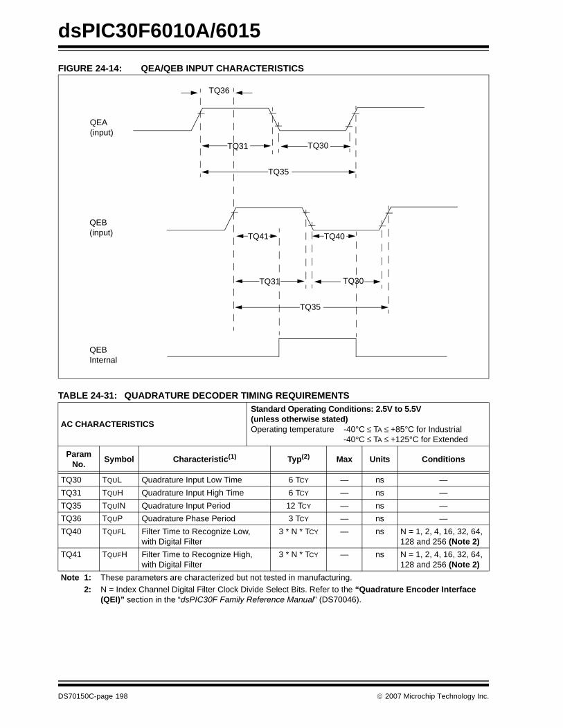
dsPIC30F6010A/6015
FIGURE 24-14: QEA/QEB INPUT CHARACTERISTICS
TQ30
TQ35
TQ31
QEA (input)
TQ30
TQ35
TQ31
QEB (input)
TQ36
QEB Internal
TQ40TQ41
TABLE 24-31: QUADRATURE DECODER TIMING REQUIREMENTS
AC CHARACTERISTICS
Standard Operating Conditions: 2.5V to 5.5V(unless otherwise stated)Operating temperature -40°C ≤ TA ≤ +85°C for Industrial
-40°C ≤ TA ≤ +125°C for Extended
ParamNo.
Symbol Characteristic(1) Typ(2) Max Units Conditions
TQ30 TQUL Quadrature Input Low Time 6 TCY — ns —
TQ31 TQUH Quadrature Input High Time 6 TCY — ns —
TQ35 TQUIN Quadrature Input Period 12 TCY — ns —
TQ36 TQUP Quadrature Phase Period 3 TCY — ns —
TQ40 TQUFL Filter Time to Recognize Low,with Digital Filter
3 * N * TCY — ns N = 1, 2, 4, 16, 32, 64, 128 and 256 (Note 2)
TQ41 TQUFH Filter Time to Recognize High,with Digital Filter
3 * N * TCY — ns N = 1, 2, 4, 16, 32, 64, 128 and 256 (Note 2)
Note 1: These parameters are characterized but not tested in manufacturing.2: N = Index Channel Digital Filter Clock Divide Select Bits. Refer to the “Quadrature Encoder Interface
(QEI)” section in the “dsPIC30F Family Reference Manual” (DS70046).
DS70150C-page 198 © 2007 Microchip Technology Inc.
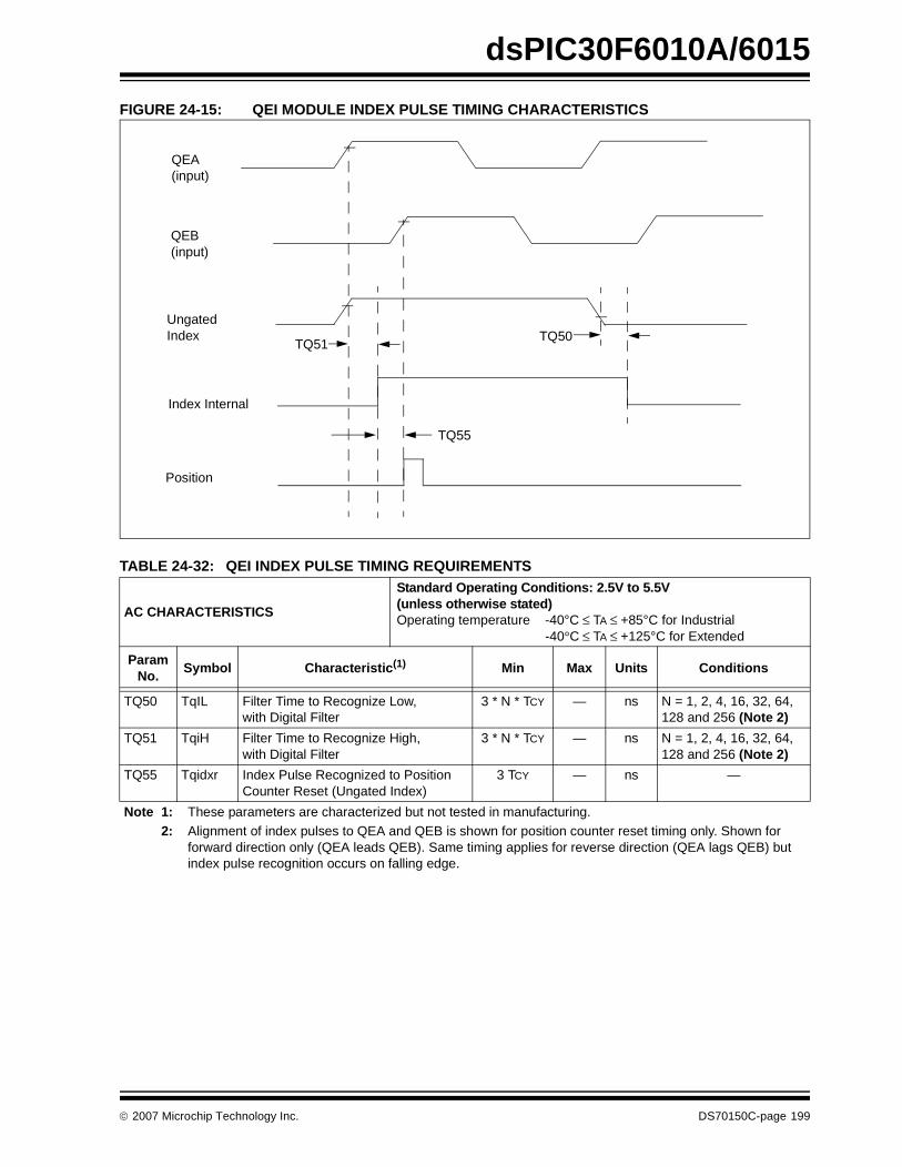
dsPIC30F6010A/6015
FIGURE 24-15: QEI MODULE INDEX PULSE TIMING CHARACTERISTICS
QEA(input)
UngatedIndex
QEB(input)
TQ55
Index Internal
Position
TQ50TQ51
TABLE 24-32: QEI INDEX PULSE TIMING REQUIREMENTS
AC CHARACTERISTICS
Standard Operating Conditions: 2.5V to 5.5V(unless otherwise stated)Operating temperature -40°C ≤ TA ≤ +85°C for Industrial
-40°C ≤ TA ≤ +125°C for Extended
ParamNo.
Symbol Characteristic(1) Min Max Units Conditions
TQ50 TqIL Filter Time to Recognize Low,with Digital Filter
3 * N * TCY — ns N = 1, 2, 4, 16, 32, 64,128 and 256 (Note 2)
TQ51 TqiH Filter Time to Recognize High,with Digital Filter
3 * N * TCY — ns N = 1, 2, 4, 16, 32, 64,128 and 256 (Note 2)
TQ55 Tqidxr Index Pulse Recognized to PositionCounter Reset (Ungated Index)
3 TCY — ns —
Note 1: These parameters are characterized but not tested in manufacturing.2: Alignment of index pulses to QEA and QEB is shown for position counter reset timing only. Shown for
forward direction only (QEA leads QEB). Same timing applies for reverse direction (QEA lags QEB) but index pulse recognition occurs on falling edge.
© 2007 Microchip Technology Inc. DS70150C-page 199

dsPIC30F6010A/6015
FIGURE 24-16: SPI MODULE MASTER MODE (CKE = 0) TIMING CHARACTERISTICS
SCKx(CKP = 0)
SCKx(CKP = 1)
SDOx
SDIx
SP11 SP10
SP40 SP41
SP21SP20SP35
SP20SP21
MSb LSbBIT14 - - - - - -1
MSb IN LSb INBIT14 - - - -1
SP30SP31
Note: Refer to Figure 24-2 for load conditions.
TABLE 24-33: SPI MASTER MODE (CKE = 0) TIMING REQUIREMENTS
AC CHARACTERISTICS
Standard Operating Conditions: 2.5V to 5.5V(unless otherwise stated)Operating temperature -40°C ≤ TA ≤ +85°C for Industrial
-40°C ≤ TA ≤ +125°C for Extended
ParamNo.
Symbol Characteristic(1) Min Typ(2) Max Units Conditions
SP10 TscL SCKX Output Low Time(3) TCY/2 — — ns —
SP11 TscH SCKX Output High Time(3) TCY/2 — — ns —
SP20 TscF SCKX Output Fall Time(4) — — — ns See parameter DO32
SP21 TscR SCKX Output Rise Time(4) — — — ns See parameter DO31
SP30 TdoF SDOX Data Output Fall Time(4) — — — ns See parameter DO32
SP31 TdoR SDOX Data Output Rise Time(4)
— — — ns See parameter DO31
SP35 TscH2doV,TscL2doV
SDOX Data Output Valid after SCKX Edge
— — 30 ns —
SP40 TdiV2scH,TdiV2scL
Setup Time of SDIX Data Inputto SCKX Edge
20 — — ns —
SP41 TscH2diL,TscL2diL
Hold Time of SDIX Data Inputto SCKX Edge
20 — — ns —
Note 1: These parameters are characterized but not tested in manufacturing.2: Data in “Typ” column is at 5V, 25°C unless otherwise stated. Parameters are for design guidance only and
are not tested.3: The minimum clock period for SCK is 100 ns. Therefore, the clock generated in Master mode must not
violate this specification.
4: Assumes 50 pF load on all SPI pins.
DS70150C-page 200 © 2007 Microchip Technology Inc.

dsPIC30F6010A/6015
FIGURE 24-17: SPI MODULE MASTER MODE (CKE =1) TIMING CHARACTERISTICS
SCKX
(CKP = 0)
SCKX
(CKP = 1)
SDOX
SDIX
SP36
SP30,SP31
SP35
MSb
MSb IN
BIT14 - - - - - -1
LSb INBIT14 - - - -1
LSb
Note: Refer to Figure 24-2 for load conditions.
SP11 SP10 SP20SP21
SP21SP20
SP40
SP41
TABLE 24-34: SPI MODULE MASTER MODE (CKE = 1) TIMING REQUIREMENTS
AC CHARACTERISTICS
Standard Operating Conditions: 2.5V to 5.5V(unless otherwise stated)Operating temperature -40°C ≤ TA ≤ +85°C for Industrial
-40°C ≤ TA ≤ +125°C for Extended
ParamNo.
Symbol Characteristic(1) Min Typ(2) Max Units Conditions
SP10 TscL SCKX output low time(3) TCY/2 — — ns —
SP11 TscH SCKX output high time(3) TCY/2 — — ns —
SP20 TscF SCKX output fall time(4) — — — ns See parameter DO32
SP21 TscR SCKX output rise time(4) — — — ns See parameter DO31
SP30 TdoF SDOX data output fall time(4) — — — ns See parameter DO32
SP31 TdoR SDOX data output rise time(4) — — — ns See parameter DO31
SP35 TscH2doV,TscL2doV
SDOX data output valid afterSCKX edge
— — — ns —
SP36 TdoV2sc, TdoV2scL
SDOX data output setup tofirst SCKX edge
30 — — ns —
SP40 TdiV2scH, TdiV2scL
Setup time of SDIX data inputto SCKX edge
20 — — ns —
SP41 TscH2diL, TscL2diL
Hold time of SDIX data inputto SCKX edge
20 — — ns —
Note 1: These parameters are characterized but not tested in manufacturing.2: Data in “Typ” column is at 5V, 25°C unless otherwise stated. Parameters are for design guidance only and
are not tested.3: The minimum clock period for SCK is 100 ns. Therefore, the clock generated in Master mode must not
violate this specification.4: Assumes 50 pF load on all SPI pins.
© 2007 Microchip Technology Inc. DS70150C-page 201
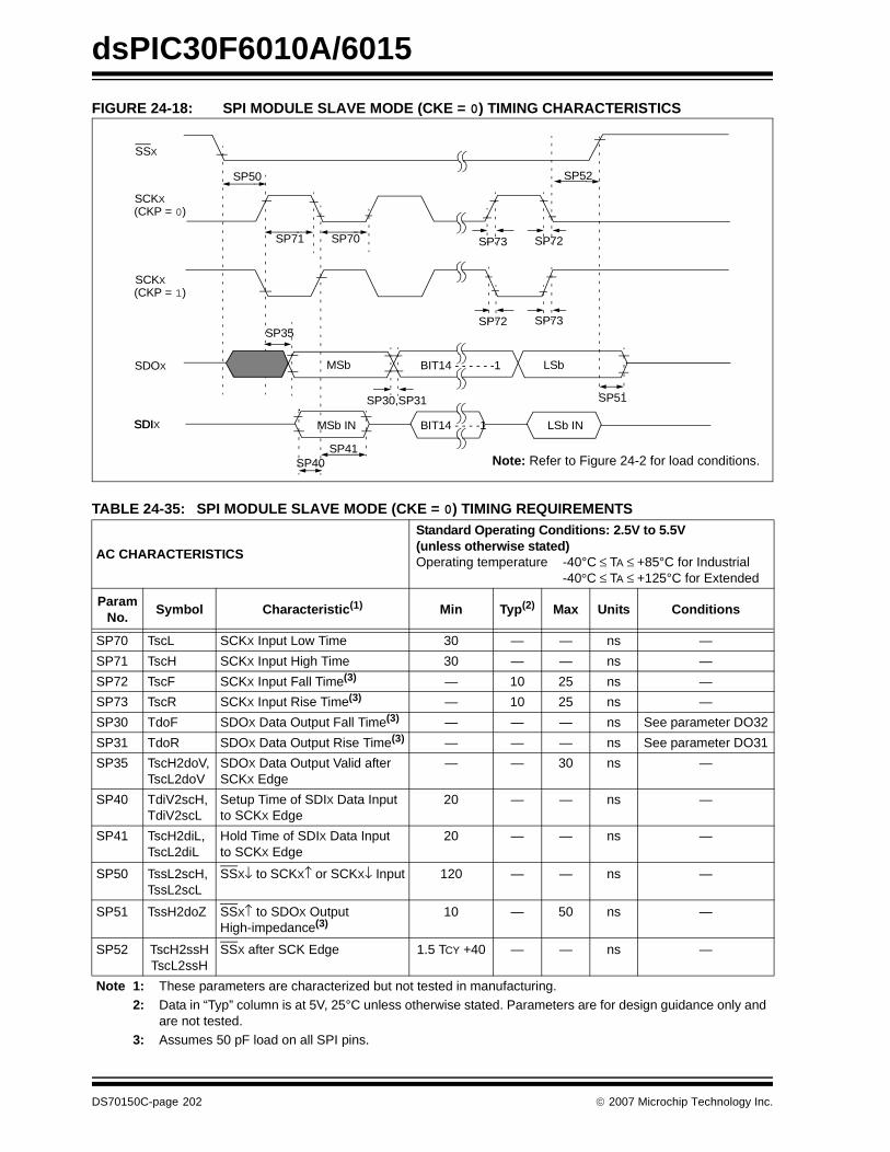
dsPIC30F6010A/6015
FIGURE 24-18: SPI MODULE SLAVE MODE (CKE = 0) TIMING CHARACTERISTICS
SSX
SCKX(CKP = 0)
SCKX(CKP = 1)
SDOX
SDI
SP50
SP40SP41
SP30,SP31 SP51
SP35
SDIX
MSb LSbBIT14 - - - - - -1
MSb IN BIT14 - - - -1 LSb IN
SP52
SP73SP72
SP72SP73SP71 SP70
Note: Refer to Figure 24-2 for load conditions.
TABLE 24-35: SPI MODULE SLAVE MODE (CKE = 0) TIMING REQUIREMENTS
AC CHARACTERISTICS
Standard Operating Conditions: 2.5V to 5.5V(unless otherwise stated)Operating temperature -40°C ≤ TA ≤ +85°C for Industrial
-40°C ≤ TA ≤ +125°C for Extended
ParamNo.
Symbol Characteristic(1) Min Typ(2) Max Units Conditions
SP70 TscL SCKX Input Low Time 30 — — ns —
SP71 TscH SCKX Input High Time 30 — — ns —
SP72 TscF SCKX Input Fall Time(3) — 10 25 ns —
SP73 TscR SCKX Input Rise Time(3) — 10 25 ns —
SP30 TdoF SDOX Data Output Fall Time(3) — — — ns See parameter DO32
SP31 TdoR SDOX Data Output Rise Time(3) — — — ns See parameter DO31
SP35 TscH2doV,TscL2doV
SDOX Data Output Valid afterSCKX Edge
— — 30 ns —
SP40 TdiV2scH, TdiV2scL
Setup Time of SDIX Data Inputto SCKX Edge
20 — — ns —
SP41 TscH2diL, TscL2diL
Hold Time of SDIX Data Inputto SCKX Edge
20 — — ns —
SP50 TssL2scH, TssL2scL
SSX↓ to SCKX↑ or SCKX↓ Input 120 — — ns —
SP51 TssH2doZ SSX↑ to SDOX OutputHigh-impedance(3)
10 — 50 ns —
SP52 TscH2ssHTscL2ssH
SSX after SCK Edge 1.5 TCY +40 — — ns —
Note 1: These parameters are characterized but not tested in manufacturing.2: Data in “Typ” column is at 5V, 25°C unless otherwise stated. Parameters are for design guidance only and
are not tested.3: Assumes 50 pF load on all SPI pins.
DS70150C-page 202 © 2007 Microchip Technology Inc.

dsPIC30F6010A/6015
FIGURE 24-19: SPI MODULE SLAVE MODE (CKE = 1) TIMING CHARACTERISTICS
SSX
SCKX
(CKP = 0)
SCKX
(CKP = 1)
SDOX
SDI
SP50
SP60
SDIX
SP30,SP31
MSb BIT14 - - - - - -1 LSb
SP51
MSb IN BIT14 - - - -1 LSb IN
SP35
SP52
SP52
SP73SP72
SP72SP73SP71 SP70
SP40SP41
Note: Refer to Figure 24-2 for load conditions.
TABLE 24-36: SPI MODULE SLAVE MODE (CKE = 1) TIMING REQUIREMENTS
AC CHARACTERISTICS
Standard Operating Conditions: 2.5V to 5.5V(unless otherwise stated)Operating temperature -40°C ≤ TA ≤ +85°C for Industrial
-40°C ≤ TA ≤ +125°C for Extended
ParamNo.
Symbol Characteristic(1) Min Typ(2) Max Units Conditions
SP70 TscL SCKX Input Low Time 30 — — ns —
SP71 TscH SCKX Input High Time 30 — — ns —
SP72 TscF SCKX Input Fall Time(3) — 10 25 ns —
SP73 TscR SCKX Input Rise Time(3) — 10 25 ns —
SP30 TdoF SDOX Data Output Fall Time(3) — — — ns See parameter DO32
SP31 TdoR SDOX Data Output Rise Time(3) — — — ns See parameter DO31
SP35 TscH2doV,TscL2doV
SDOX Data Output Valid afterSCKX Edge
— — 30 ns —
SP40 TdiV2scH, TdiV2scL
Setup Time of SDIX Data Inputto SCKX Edge
20 — — ns —
SP41 TscH2diL, TscL2diL
Hold Time of SDIX Data Inputto SCKX Edge
20 — — ns —
SP50 TssL2scH, TssL2scL
SSX↓ to SCKX↓ or SCKX↑ input 120 — — ns —
Note 1: These parameters are characterized but not tested in manufacturing.2: Data in “Typ” column is at 5V, 25°C unless otherwise stated. Parameters are for design guidance only and
are not tested.3: The minimum clock period for SCK is 100 ns. Therefore, the clock generated in Master mode must not
violate this specification.4: Assumes 50 pF load on all SPI pins.
© 2007 Microchip Technology Inc. DS70150C-page 203
dsPIC30F6010A/6015
SP51 TssH2doZ SS↑ to SDOX OutputHigh-impedance(4)
10 — 50 ns —
SP52 TscH2ssHTscL2ssH
SSX↑ after SCKX Edge 1.5 TCY + 40
— — ns —
SP60 TssL2doV SDOX Data Output Valid afterSSX Edge
— — 50 ns —
TABLE 24-36: SPI MODULE SLAVE MODE (CKE = 1) TIMING REQUIREMENTS (CONTINUED)
AC CHARACTERISTICS
Standard Operating Conditions: 2.5V to 5.5V(unless otherwise stated)Operating temperature -40°C ≤ TA ≤ +85°C for Industrial
-40°C ≤ TA ≤ +125°C for Extended
ParamNo.
Symbol Characteristic(1) Min Typ(2) Max Units Conditions
Note 1: These parameters are characterized but not tested in manufacturing.2: Data in “Typ” column is at 5V, 25°C unless otherwise stated. Parameters are for design guidance only and
are not tested.3: The minimum clock period for SCK is 100 ns. Therefore, the clock generated in Master mode must not
violate this specification.4: Assumes 50 pF load on all SPI pins.
DS70150C-page 204 © 2007 Microchip Technology Inc.

dsPIC30F6010A/6015
FIGURE 24-20: I2C™ BUS START/STOP BITS TIMING CHARACTERISTICS (MASTER MODE)
FIGURE 24-21: I2C™ BUS DATA TIMING CHARACTERISTICS (MASTER MODE)
IM31 IM34SCL
SDA
StartCondition
StopCondition
IM30 IM33
Note: Refer to Figure 24-2 for load conditions.
IM11IM10 IM33
IM11
IM10
IM20
IM26IM25
IM40 IM40 IM45
IM21
SCL
SDAIn
SDAOut
Note: Refer to Figure 24-2 for load conditions.
© 2007 Microchip Technology Inc. DS70150C-page 205
dsPIC30F6010A/6015
TABLE 24-37: I2C™ BUS DATA TIMING REQUIREMENTS (MASTER MODE)
AC CHARACTERISTICS
Standard Operating Conditions: 2.5V to 5.5V(unless otherwise stated)Operating temperature -40°C ≤ TA ≤ +85°C for Industrial
-40°C ≤ TA ≤ +125°C for Extended
ParamNo.
Symbol Characteristic Min(1) Max Units Conditions
IM10 TLO:SCL Clock Low Time 100 kHz mode TCY/2 (BRG + 1) — μs —
400 kHz mode TCY/2 (BRG + 1) — μs —
1 MHz mode(2) TCY/2 (BRG + 1) — μs —
IM11 THI:SCL Clock High Time 100 kHz mode TCY/2 (BRG + 1) — μs —
400 kHz mode TCY/2 (BRG + 1) — μs —
1 MHz mode(2) TCY/2 (BRG + 1) — μs —
IM20 TF:SCL SDA and SCLFall Time
100 kHz mode — 300 ns CB is specified to be from 10 to 400 pF400 kHz mode 20 + 0.1 CB 300 ns
1 MHz mode(2) — 100 ns
IM21 TR:SCL SDA and SCLRise Time
100 kHz mode — 1000 ns CB is specified to be from 10 to 400 pF400 kHz mode 20 + 0.1 CB 300 ns
1 MHz mode(2) — 300 ns
IM25 TSU:DAT Data InputSetup Time
100 kHz mode 250 — ns —
400 kHz mode 100 — ns
1 MHz mode(2) TBD — ns
IM26 THD:DAT Data InputHold Time
100 kHz mode 0 — ns —
400 kHz mode 0 0.9 μs
1 MHz mode(2) TBD — ns
IM30 TSU:STA Start ConditionSetup Time
100 kHz mode TCY/2 (BRG + 1) — μs Only relevant for Repeated Startcondition
400 kHz mode TCY/2 (BRG + 1) — μs
1 MHz mode(2) TCY/2 (BRG + 1) — μs
IM31 THD:STA Start Condition Hold Time
100 kHz mode TCY/2 (BRG + 1) — μs After this period thefirst clock pulse isgenerated
400 kHz mode TCY/2 (BRG + 1) — μs
1 MHz mode(2) TCY/2 (BRG + 1) — μs
IM33 TSU:STO Stop Condition Setup Time
100 kHz mode TCY/2 (BRG + 1) — μs —
400 kHz mode TCY/2 (BRG + 1) — μs
1 MHz mode(2) TCY/2 (BRG + 1) — μs
IM34 THD:STO Stop Condition 100 kHz mode TCY/2 (BRG + 1) — ns —
Hold Time 400 kHz mode TCY/2 (BRG + 1) — ns
1 MHz mode(2) TCY/2 (BRG + 1) — ns
IM40 TAA:SCL Output Valid From Clock
100 kHz mode — 3500 ns —
400 kHz mode — 1000 ns —
1 MHz mode(2) — — ns —
IM45 TBF:SDA Bus Free Time 100 kHz mode 4.7 — μs Time the bus must be free before a newtransmission can start
400 kHz mode 1.3 — μs
1 MHz mode(2) TBD — μs
IM50 CB Bus Capacitive Loading — 400 pF —
Legend: TBD = To Be DeterminedNote 1: BRG is the value of the I2C Baud Rate Generator. Refer to the “Inter-Integrated Circuit (I2C™)” section
in the “dsPIC30F Family Reference Manual” (DS70046).2: Maximum pin capacitance = 10 pF for all I2C pins (for 1 MHz mode only).
DS70150C-page 206 © 2007 Microchip Technology Inc.
dsPIC30F6010A/6015
FIGURE 24-22: I2C™ BUS START/STOP BITS TIMING CHARACTERISTICS (SLAVE MODE)
FIGURE 24-23: I2C™ BUS DATA TIMING CHARACTERISTICS (SLAVE MODE)
IS31 IS34SCL
SDA
StartCondition
StopCondition
IS30 IS33
IS30IS31 IS33
IS11
IS10
IS20
IS26IS25
IS40 IS40 IS45
IS21
SCL
SDAIn
SDAOut
© 2007 Microchip Technology Inc. DS70150C-page 207

dsPIC30F6010A/6015
TABLE 24-38: I2C™ BUS DATA TIMING REQUIREMENTS (SLAVE MODE
AC CHARACTERISTICS
Standard Operating Conditions: 2.5V to 5.5V(unless otherwise stated)Operating temperature -40°C ≤ TA ≤ +85°C for Industrial
-40°C ≤ TA ≤ +125°C for Extended
ParamNo.
Symbol Characteristic Min Max Units Conditions
IS10 TLO:SCL Clock Low Time 100 kHz mode 4.7 — μs Device must operate at a minimum of 1.5 MHz
400 kHz mode 1.3 — μs Device must operate at a minimum of 10 MHz
1 MHz mode(1) 0.5 — µs —IS11 THI:SCL Clock High Time 100 kHz mode 4.0 — µs Device must operate at a
minimum of 1.5 MHz400 kHz mode 0.6 — µs Device must operate at a
minimum of 10 MHz1 MHz mode(1) 0.5 — µs —
IS20 TF:SCL SDA and SCLFall Time
100 kHz mode — 300 ns CB is specified to be from10 to 400 pF400 kHz mode 20 + 0.1 CB 300 ns
1 MHz mode(1) — 100 nsIS21 TR:SCL SDA and SCL
Rise Time100 kHz mode — 1000 ns CB is specified to be from
10 to 400 pF400 kHz mode 20 + 0.1 CB 300 ns1 MHz mode(1) — 300 ns
IS25 TSU:DAT Data InputSetup Time
100 kHz mode 250 — ns —
400 kHz mode 100 — ns1 MHz mode(1) 100 — ns
IS26 THD:DAT Data InputHold Time
100 kHz mode 0 — ns —400 kHz mode 0 0.9 μs1 MHz mode(1) 0 0.3 μs
IS30 TSU:STA Start ConditionSetup Time
100 kHz mode 4.7 — μs Only relevant for Repeated Start condition400 kHz mode 0.6 — μs
1 MHz mode(1) 0.25 — μs
IS31 THD:STA Start Condition Hold Time
100 kHz mode 4.0 — μs After this period, the first clock pulse is generated400 kHz mode 0.6 — μs
1 MHz mode(1) 0.25 — μs
IS33 TSU:STO Stop Condition Setup Time
100 kHz mode 4.7 — μs —400 kHz mode 0.6 — μs1 MHz mode(1) 0.6 — μs
IS34 THD:STO Stop Condition 100 kHz mode 4000 — ns —Hold Time 400 kHz mode 600 — ns
1 MHz mode(1) 250 ns
IS40 TAA:SCL Output Valid From Clock
100 kHz mode 0 3500 ns —400 kHz mode 0 1000 ns1 MHz mode(1) 0 350 ns
IS45 TBF:SDA Bus Free Time 100 kHz mode 4.7 — μs Time the bus must be free before a new transmission can start
400 kHz mode 1.3 — μs1 MHz mode(1) 0.5 — μs
IS50 CB Bus Capacitive Loading
— 400 pF —
Note 1: Maximum pin capacitance = 10 pF for all I2C pins (for 1 MHz mode only).
DS70150C-page 208 © 2007 Microchip Technology Inc.
dsPIC30F6010A/6015
FIGURE 24-24: CAN MODULE I/O TIMING CHARACTERISTICS
CXTX Pin(output)
CA10 CA11
Old Value New Value
CA20
CXRX Pin(input)
TABLE 24-39: CAN MODULE I/O TIMING REQUIREMENTS
AC CHARACTERISTICS
Standard Operating Conditions: 2.5V to 5.5V(unless otherwise stated)Operating temperature -40°C ≤ TA ≤ +85°C for Industrial
-40°C ≤ TA ≤ +125°C for Extended
ParamNo.
Symbol Characteristic(1) Min Typ(2) Max Units Conditions
CA10 TioF Port Output Fall Time — — — ns See parameter DO32
CA11 TioR Port Output Rise Time — — — ns See parameter DO31
CA20 Tcwf Pulse Width to TriggerCAN Wake-up Filter
500 ns —
Note 1: These parameters are characterized but not tested in manufacturing.2: Data in “Typ” column is at 5V, 25°C unless otherwise stated. Parameters are for design guidance only and
are not tested.
© 2007 Microchip Technology Inc. DS70150C-page 209
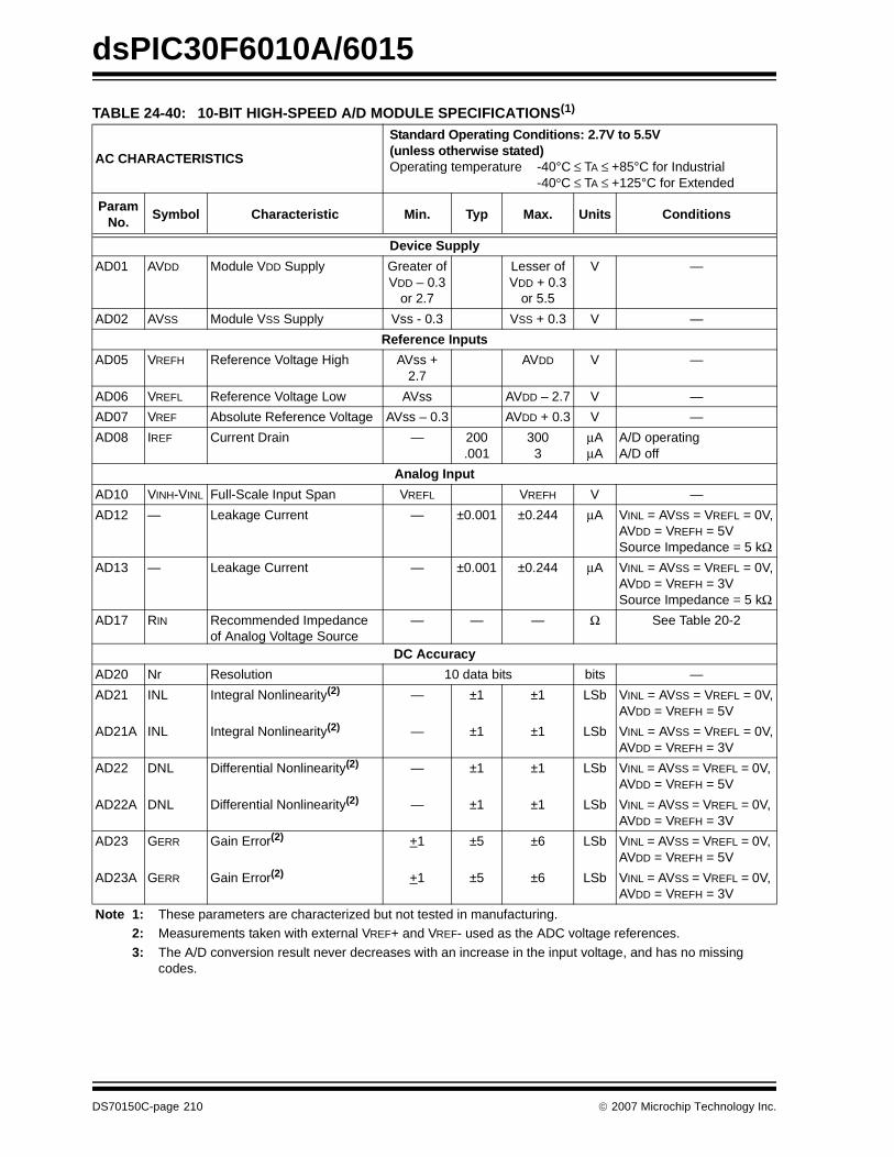
dsPIC30F6010A/6015
TABLE 24-40: 10-BIT HIGH-SPEED A/D MODULE SPECIFICATIONS(1)
AC CHARACTERISTICS
Standard Operating Conditions: 2.7V to 5.5V(unless otherwise stated)Operating temperature -40°C ≤ TA ≤ +85°C for Industrial
-40°C ≤ TA ≤ +125°C for Extended
Param No.
Symbol Characteristic Min. Typ Max. Units Conditions
Device Supply
AD01 AVDD Module VDD Supply Greater ofVDD – 0.3
or 2.7
Lesser ofVDD + 0.3
or 5.5
V —
AD02 AVSS Module VSS Supply Vss - 0.3 VSS + 0.3 V —
Reference Inputs
AD05 VREFH Reference Voltage High AVss + 2.7
AVDD V —
AD06 VREFL Reference Voltage Low AVss AVDD – 2.7 V —
AD07 VREF Absolute Reference Voltage AVss – 0.3 AVDD + 0.3 V —
AD08 IREF Current Drain — 200.001
3003
μAμA
A/D operatingA/D off
Analog Input
AD10 VINH-VINL Full-Scale Input Span VREFL VREFH V —
AD12 — Leakage Current — ±0.001 ±0.244 μA VINL = AVSS = VREFL = 0V,AVDD = VREFH = 5VSource Impedance = 5 kΩ
AD13 — Leakage Current — ±0.001 ±0.244 μA VINL = AVSS = VREFL = 0V,AVDD = VREFH = 3VSource Impedance = 5 kΩ
AD17 RIN Recommended Impedanceof Analog Voltage Source
— — — Ω See Table 20-2
DC Accuracy
AD20 Nr Resolution 10 data bits bits —
AD21 INL Integral Nonlinearity(2) — ±1 ±1 LSb VINL = AVSS = VREFL = 0V,AVDD = VREFH = 5V
AD21A INL Integral Nonlinearity(2) — ±1 ±1 LSb VINL = AVSS = VREFL = 0V,AVDD = VREFH = 3V
AD22 DNL Differential Nonlinearity(2) — ±1 ±1 LSb VINL = AVSS = VREFL = 0V, AVDD = VREFH = 5V
AD22A DNL Differential Nonlinearity(2) — ±1 ±1 LSb VINL = AVSS = VREFL = 0V, AVDD = VREFH = 3V
AD23 GERR Gain Error(2) +1 ±5 ±6 LSb VINL = AVSS = VREFL = 0V, AVDD = VREFH = 5V
AD23A GERR Gain Error(2) +1 ±5 ±6 LSb VINL = AVSS = VREFL = 0V, AVDD = VREFH = 3V
Note 1: These parameters are characterized but not tested in manufacturing.2: Measurements taken with external VREF+ and VREF- used as the ADC voltage references.
3: The A/D conversion result never decreases with an increase in the input voltage, and has no missing codes.
DS70150C-page 210 © 2007 Microchip Technology Inc.
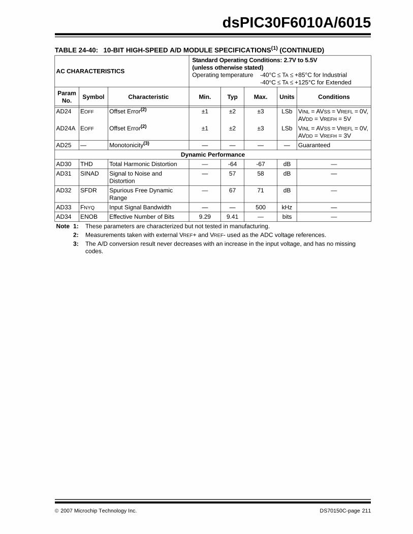
dsPIC30F6010A/6015
AD24 EOFF Offset Error(2) ±1 ±2 ±3 LSb VINL = AVSS = VREFL = 0V, AVDD = VREFH = 5V
AD24A EOFF Offset Error(2) ±1 ±2 ±3 LSb VINL = AVSS = VREFL = 0V, AVDD = VREFH = 3V
AD25 — Monotonicity(3) — — — — Guaranteed
Dynamic Performance
AD30 THD Total Harmonic Distortion — -64 -67 dB —
AD31 SINAD Signal to Noise andDistortion
— 57 58 dB —
AD32 SFDR Spurious Free Dynamic Range
— 67 71 dB —
AD33 FNYQ Input Signal Bandwidth — — 500 kHz —
AD34 ENOB Effective Number of Bits 9.29 9.41 — bits —
TABLE 24-40: 10-BIT HIGH-SPEED A/D MODULE SPECIFICATIONS(1) (CONTINUED)
AC CHARACTERISTICS
Standard Operating Conditions: 2.7V to 5.5V(unless otherwise stated)Operating temperature -40°C ≤ TA ≤ +85°C for Industrial
-40°C ≤ TA ≤ +125°C for Extended
Param No.
Symbol Characteristic Min. Typ Max. Units Conditions
Note 1: These parameters are characterized but not tested in manufacturing.2: Measurements taken with external VREF+ and VREF- used as the ADC voltage references.
3: The A/D conversion result never decreases with an increase in the input voltage, and has no missing codes.
© 2007 Microchip Technology Inc. DS70150C-page 211
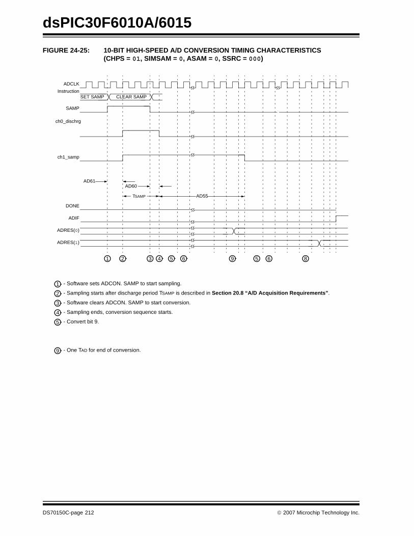
dsPIC30F6010A/6015
FIGURE 24-25: 10-BIT HIGH-SPEED A/D CONVERSION TIMING CHARACTERISTICS(CHPS = 01, SIMSAM = 0, ASAM = 0, SSRC = 000)
AD55TSAMP
CLEAR SAMPSET SAMP
AD61
ADCLK
Instruction
SAMP
ch0_dischrg
ch1_samp
AD60
DONE
ADIF
ADRES(0)
ADRES(1)
1 2 3 4 5 6 9 5 6 8
1 - Software sets ADCON. SAMP to start sampling.
2 - Sampling starts after discharge period TSAMP is described in Section 20.8 “A/D Acquisition Requirements”.
3 - Software clears ADCON. SAMP to start conversion.
4 - Sampling ends, conversion sequence starts.
5 - Convert bit 9.
9 - One TAD for end of conversion.
DS70150C-page 212 © 2007 Microchip Technology Inc.
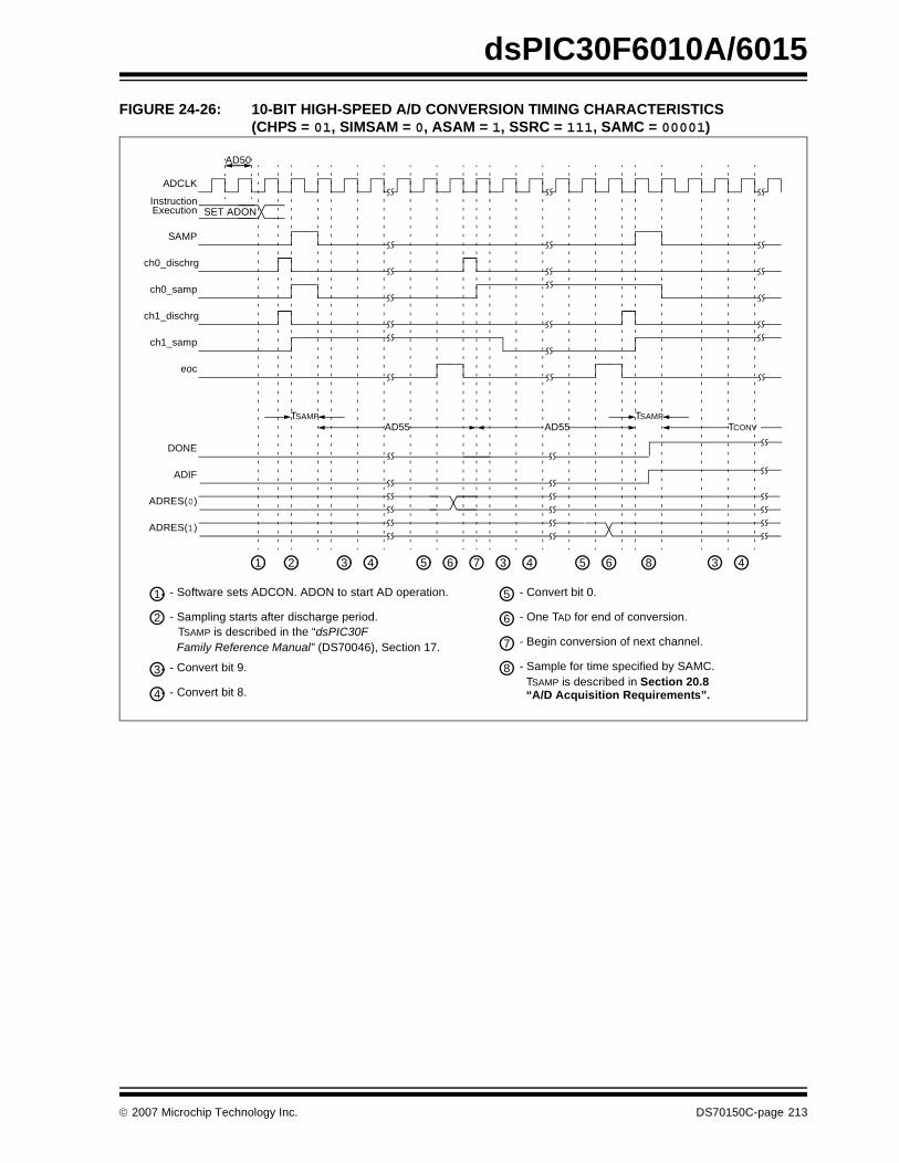
dsPIC30F6010A/6015
FIGURE 24-26: 10-BIT HIGH-SPEED A/D CONVERSION TIMING CHARACTERISTICS(CHPS = 01, SIMSAM = 0, ASAM = 1, SSRC = 111, SAMC = 00001)
AD55TSAMP
SET ADON
ADCLK
Instruction
SAMP
ch0_dischrg
ch1_samp
DONE
ADIF
ADRES(0)
ADRES(1)
1 2 3 4 5 6 4 5 6 8
1 - Software sets ADCON. ADON to start AD operation.
2 - Sampling starts after discharge period.
3 - Convert bit 9.
4 - Convert bit 8.
5 - Convert bit 0.
AD50
ch0_samp
ch1_dischrg
eoc
7 3
AD55
6 - One TAD for end of conversion.
7 - Begin conversion of next channel.
8 - Sample for time specified by SAMC.
TSAMPTCONV
3 4
Execution
TSAMP is described in the “dsPIC30F Family Reference Manual” (DS70046), Section 17.
TSAMP is described in Section 20.8“A/D Acquisition Requirements”.
© 2007 Microchip Technology Inc. DS70150C-page 213
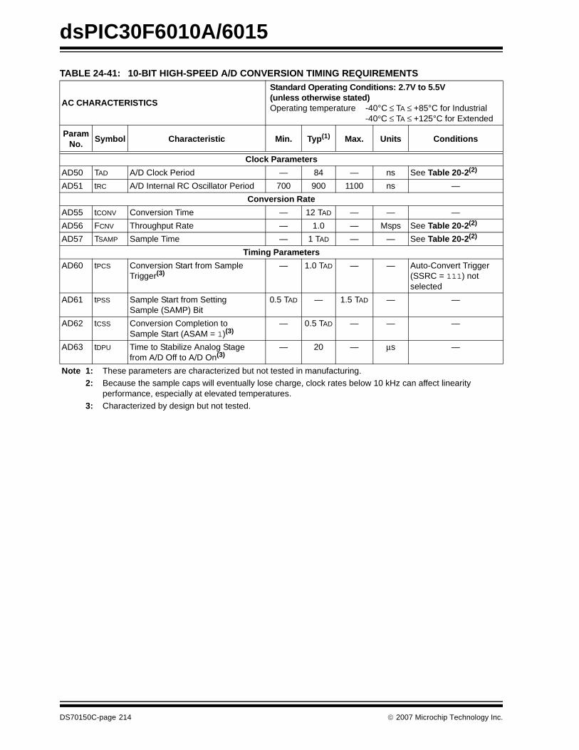
dsPIC30F6010A/6015
TABLE 24-41: 10-BIT HIGH-SPEED A/D CONVERSION TIMING REQUIREMENTS
AC CHARACTERISTICS
Standard Operating Conditions: 2.7V to 5.5V(unless otherwise stated)Operating temperature -40°C ≤ TA ≤ +85°C for Industrial
-40°C ≤ TA ≤ +125°C for Extended
Param No.
Symbol Characteristic Min. Typ(1) Max. Units Conditions
Clock Parameters
AD50 TAD A/D Clock Period — 84 — ns See Table 20-2(2)
AD51 tRC A/D Internal RC Oscillator Period 700 900 1100 ns —
Conversion Rate
AD55 tCONV Conversion Time — 12 TAD — — —
AD56 FCNV Throughput Rate — 1.0 — Msps See Table 20-2(2)
AD57 TSAMP Sample Time — 1 TAD — — See Table 20-2(2)
Timing Parameters
AD60 tPCS Conversion Start from SampleTrigger(3)
— 1.0 TAD — — Auto-Convert Trigger (SSRC = 111) not selected
AD61 tPSS Sample Start from SettingSample (SAMP) Bit
0.5 TAD — 1.5 TAD — —
AD62 tCSS Conversion Completion toSample Start (ASAM = 1)(3)
— 0.5 TAD — — —
AD63 tDPU Time to Stabilize Analog Stage from A/D Off to A/D On(3)
— 20 — μs —
Note 1: These parameters are characterized but not tested in manufacturing.2: Because the sample caps will eventually lose charge, clock rates below 10 kHz can affect linearity
performance, especially at elevated temperatures.3: Characterized by design but not tested.
DS70150C-page 214 © 2007 Microchip Technology Inc.
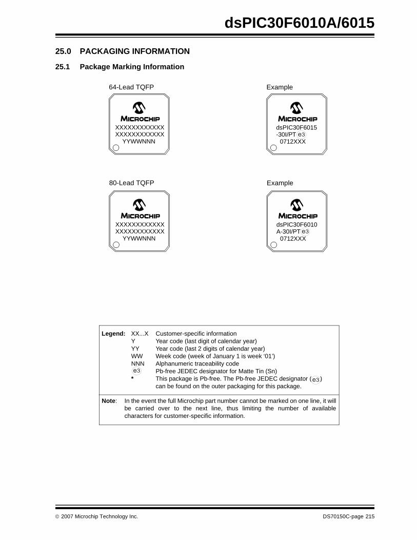
dsPIC30F6010A/6015
25.0 PACKAGING INFORMATION
25.1 Package Marking Information
XXXXXXXXXXXXXXXXXXXXXXXX
YYWWNNN
64-Lead TQFP
dsPIC30F6015-30I/PT
0712XXX
Example
XXXXXXXXXXXXXXXXXXXXXXXX
YYWWNNN
80-Lead TQFP
dsPIC30F6010A-30I/PT
0712XXX
Example
Legend: XX...X Customer-specific informationY Year code (last digit of calendar year)YY Year code (last 2 digits of calendar year)WW Week code (week of January 1 is week ‘01’)NNN Alphanumeric traceability code Pb-free JEDEC designator for Matte Tin (Sn)* This package is Pb-free. The Pb-free JEDEC designator ( )
can be found on the outer packaging for this package.
Note: In the event the full Microchip part number cannot be marked on one line, it willbe carried over to the next line, thus limiting the number of availablecharacters for customer-specific information.
3e
3e
3e
3e
© 2007 Microchip Technology Inc. DS70150C-page 215
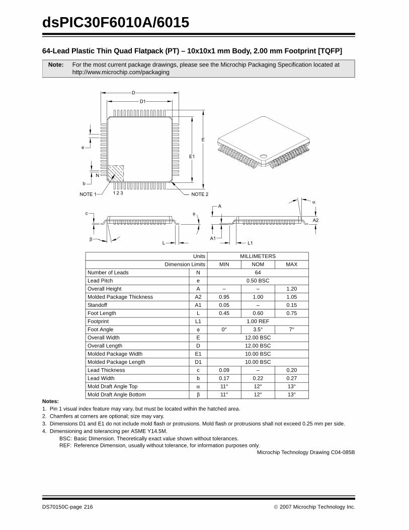
dsPIC30F6010A/6015
64-Lead Plastic Thin Quad Flatpack (PT) – 10x10x1 mm Body, 2.00 mm Footprint [TQFP]
Notes:1. Pin 1 visual index feature may vary, but must be located within the hatched area.2. Chamfers at corners are optional; size may vary.3. Dimensions D1 and E1 do not include mold flash or protrusions. Mold flash or protrusions shall not exceed 0.25 mm per side.4. Dimensioning and tolerancing per ASME Y14.5M.
BSC: Basic Dimension. Theoretically exact value shown without tolerances.REF: Reference Dimension, usually without tolerance, for information purposes only.
Note: For the most current package drawings, please see the Microchip Packaging Specification located at http://www.microchip.com/packaging
Units MILLIMETERS
Dimension Limits MIN NOM MAX
Number of Leads N 64
Lead Pitch e 0.50 BSC
Overall Height A – – 1.20
Molded Package Thickness A2 0.95 1.00 1.05
Standoff A1 0.05 – 0.15
Foot Length L 0.45 0.60 0.75
Footprint L1 1.00 REF
Foot Angle φ 0° 3.5° 7°
Overall Width E 12.00 BSC
Overall Length D 12.00 BSC
Molded Package Width E1 10.00 BSC
Molded Package Length D1 10.00 BSC
Lead Thickness c 0.09 – 0.20
Lead Width b 0.17 0.22 0.27
Mold Draft Angle Top α 11° 12° 13°
Mold Draft Angle Bottom β 11° 12° 13°
D
D1
E
E1
e
b
N
NOTE 1 1 2 3 NOTE 2
c
L
A1
L1
A2
A
φ
β
α
Microchip Technology Drawing C04-085B
DS70150C-page 216 © 2007 Microchip Technology Inc.
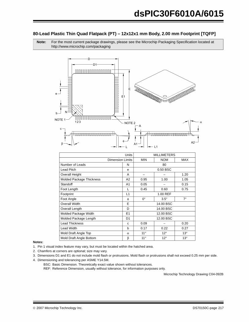
dsPIC30F6010A/6015
80-Lead Plastic Thin Quad Flatpack (PT) – 12x12x1 mm Body, 2.00 mm Footprint [TQFP]
Notes:1. Pin 1 visual index feature may vary, but must be located within the hatched area.2. Chamfers at corners are optional; size may vary.3. Dimensions D1 and E1 do not include mold flash or protrusions. Mold flash or protrusions shall not exceed 0.25 mm per side.4. Dimensioning and tolerancing per ASME Y14.5M.
BSC: Basic Dimension. Theoretically exact value shown without tolerances.REF: Reference Dimension, usually without tolerance, for information purposes only.
Note: For the most current package drawings, please see the Microchip Packaging Specification located at http://www.microchip.com/packaging
Units MILLIMETERS
Dimension Limits MIN NOM MAX
Number of Leads N 80
Lead Pitch e 0.50 BSC
Overall Height A – – 1.20
Molded Package Thickness A2 0.95 1.00 1.05
Standoff A1 0.05 – 0.15
Foot Length L 0.45 0.60 0.75
Footprint L1 1.00 REF
Foot Angle φ 0° 3.5° 7°
Overall Width E 14.00 BSC
Overall Length D 14.00 BSC
Molded Package Width E1 12.00 BSC
Molded Package Length D1 12.00 BSC
Lead Thickness c 0.09 – 0.20
Lead Width b 0.17 0.22 0.27
Mold Draft Angle Top α 11° 12° 13°
Mold Draft Angle Bottom β 11° 12° 13°
D
D1
E
E1
e
bN
NOTE 112 3
NOTE 2
A
A2
L1
A1
L
c
α
βφ
Microchip Technology Drawing C04-092B
© 2007 Microchip Technology Inc. DS70150C-page 217
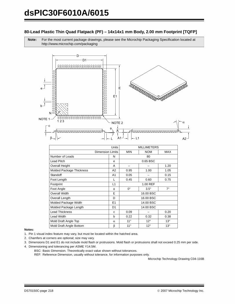
dsPIC30F6010A/6015
80-Lead Plastic Thin Quad Flatpack (PF) – 14x14x1 mm Body, 2.00 mm Footprint [TQFP]
Notes:1. Pin 1 visual index feature may vary, but must be located within the hatched area.2. Chamfers at corners are optional; size may vary.3. Dimensions D1 and E1 do not include mold flash or protrusions. Mold flash or protrusions shall not exceed 0.25 mm per side.4. Dimensioning and tolerancing per ASME Y14.5M.
BSC: Basic Dimension. Theoretically exact value shown without tolerances.REF: Reference Dimension, usually without tolerance, for information purposes only.
Note: For the most current package drawings, please see the Microchip Packaging Specification located at http://www.microchip.com/packaging
Units MILLIMETERS
Dimension Limits MIN NOM MAX
Number of Leads N 80
Lead Pitch e 0.65 BSC
Overall Height A – – 1.20
Molded Package Thickness A2 0.95 1.00 1.05
Standoff A1 0.05 – 0.15
Foot Length L 0.45 0.60 0.75
Footprint L1 1.00 REF
Foot Angle φ 0° 3.5° 7°
Overall Width E 16.00 BSC
Overall Length D 16.00 BSC
Molded Package Width E1 14.00 BSC
Molded Package Length D1 14.00 BSC
Lead Thickness c 0.09 – 0.20
Lead Width b 0.22 0.32 0.38
Mold Draft Angle Top α 11° 12° 13°
Mold Draft Angle Bottom β 11° 12° 13°
D
D1
E
E1
e
b
N
NOTE 1
c
1 2 3NOTE 2
A2L1A1
A
L
α
β
φ
Microchip Technology Drawing C04-116B
DS70150C-page 218 © 2007 Microchip Technology Inc.
dsPIC30F6010A/6015
APPENDIX A: REVISION HISTORY
Revision A (July 2005)
Original data sheet for dsPIC30F6010A anddsPIC30F6015 devices.
Revision B (September 2006)
This revision reflects updates in these areas:
• Data Ram protection feature enables segments of RAM to be protected when used in conjunction with Boot and Secure Code Segment Security (see Section 3.2.7 “Data Ram Protection Fea-ture”)
• BSRAM and SSRAM SFRs added to support Data Ram Protection (see Table 3-3)
• Base Instruction CP1 removed (see Table 22-2)
• Supported I2C Slave addresses (see Table 17-2)• Revised Electrical Characteristics:
- Operating current (IDD) specifications (see Table 24-6)
- Idle current (IIDLE) specifications (see Table 24-7)
- Power-down current (IPD) specifications (see Table 24-8)
- I/O Pin input specifications (see Table 24-9)
- BOR voltage limits (see Table 24-11)- Watchdog Timer time-out limits (see
Table 24-21)• Added note to package drawings.
Revision C (January 2007)
This revision includes updates to the packaging diagrams.
© 2007 Microchip Technology Inc. DS70150C-page 219


dsPIC30F6010A/6015
APPENDIX A: DEVICE COMPARISONS
This appendix outlines the differences between thedsPIC30F6010 and the dsPIC30F6010A. Differencesare highlighted in Table A-1.
TABLE A-1: dsPIC30F6010 AND dsPIC30F6010A COMPARISON
Features dsPIC30F6010 dsPIC30F6010A
Program Memory (Kbytes) 144 144
Data Memory (Bytes) 8192 8192
Data EEPROM (Bytes) 4096 4096
Timers (16-bits) 5 5
Input Capture Channels 8 8
Input Change Notification Channels 22 22
Output Compare/Standard PWM Channels 8 8
Motor Control PWM Channels 8 8
A/D 10-bit 500 ksps 16 16
Quadrature Encoder Yes Yes
UART 2 2
SPI 2 2
I2C™ 1 1
CAN 1 1
PGC (ICSP™ Clock Input) RB1/AN1 RB1/AN1
PGC (ICSP Data Input/Output) RB0/AN0 RB0/AN0
Packages 80-Pin TQFP (14x14x1 mm) 80-Pin TQFP (14x14x1 mm)80-Pin TQFP (12x12x1 mm)
I/O Pins (maximum) 68 68
© 2007 Microchip Technology Inc. DS70150C-page 221

dsPIC30F6010A/6015
NOTES:
DS70150C-page 222 © 2007 Microchip Technology Inc.

dsPIC30F6010A/6015
APPENDIX A: MIGRATION FROM dsPIC30F6010 TO dsPIC30F6010A
The dsPIC30F6010A supersedes the dsPIC30F6010device. The “A” version of the silicon is identical innearly all aspects compared to the dsPIC30F6010device. Review the latest dsPIC30F6010A/6015Silicon Errata documents posted on the Microchip website to see what is fixed from the dsPIC30F6010 Rev.B2 Silicon Errata (DS80195B) document.
This appendix describes the differences between thedsPIC30F6010 and dsPIC30F6010A devices.
A.1 Code Compatibility
For the most part, dsPIC30F code developed with theMPLAB C30 C Compiler and MPLAB ASM30 Assem-bler is directly portable between the dsPIC30F6010and dsPIC30F6010A devices. However, in some casessmall changes may be required depending on whichfeatures have been enhanced. To migrate source codeto the dsPIC30F6010A device, perform these twosteps:
1. Include the appropriate dsPIC30F6010A deviceheader (.h) and include (.inc) files in thesource code files.
2. Remove any workarounds implemented insource code or MPLAB C30 command-lineoptions for errata described in the“dsPIC30F6010 Rev. B2 Silicon Errata”(DS80195B) document.
Other changes are called out in this section. Read thelatest dsPIC30F6010A/6015 Silicon Errata documentsposted on the Microchip web site.
A.2 Oscillator Operation
Several oscillator modes have been added to thedsPIC30F6010A device:
• FRC with x4, x8 and x16 PLL mode• HS/2 with x4, x8 and x16 PLL mode• HS/3 with x4, x8 and x16 PLL mode
The new oscillator modes are presented inSection 21.0 “System Integration”. In support of theFRC, the OSCTUN Special Function Register (SFR)has been added. This register includes four FRC tuningbits (TUN<5:0>). There are no code or operationalcompatibility issues to address for this new feature.
Another important change deals with the OSCCONSFR. Bits have been added to both the COSC andNOSC functional definitions. Use the dsPIC30F6010Adevice header and include files to achieve codeportability with the OSCCON SFR.
A.3 Device Configuration Registers
In support of the new oscillator modes, the FOSCConfiguration register has been modified. ThedsPIC30F6010A device header and include filesprovide the updated bit field definitions and macros forthe device Configuration registers. Please refer tothese new macros when embedding specific deviceconfiguration information in the C and Assemblersource files.
A.4 Electrical Characteristics
The dsPIC30F6010A device is rated at 30 MIPS @4.5-5.5 VDC and 20 MIPS @ 3.0-3.6 VDC for the indus-trial temperature range. Even though compatibledevices are tested to the same electrical specifications,the device characteristics may have changed due tochanges in the manufacturing process. These differ-ences should not affect the systems that weredesigned well within the device specifications. For sys-tems that operate close to or outside the specificationlimits, manufacturing differences may cause the deviceto behave differently.
A.5 Device Packages
The dsPIC30F6010A device is offered in the followingTQFP pages:
• 80-Pin TQFP 12x12x1mm (new designs)
• 80-Pin TQFP 14x14x1mm (migration support)
Refer to Section 25.0 “Packaging Information” fordetails on these packages.
Note: Oscillator operation should be verified toensure that it starts and performs asexpected. You may need to adjust the loadcapacitor and/or the oscillator mode toachieve the proper values.
© 2007 Microchip Technology Inc. DS70150C-page 223

dsPIC30F6010A/6015
NOTES:
DS70150C-page 224 © 2007 Microchip Technology Inc.

dsPIC30F6010A/6015
INDEX
AA/D
Aborting a Conversion ............................................. 138Acquisition Requirements ........................................ 142ADCHS .................................................................... 135ADCON1 .................................................................. 135ADCON2 .................................................................. 135ADCON3 .................................................................. 135ADCSSL ................................................................... 135ADPCFG .................................................................. 135Configuring Analog Port Pins ................................... 144Connection Considerations ...................................... 144Conversion Operation .............................................. 137Conversion Rate Parameters ................................... 139Conversion Speeds .................................................. 139Effects of a Reset ..................................................... 143Operation During CPU Idle Mode ............................ 143Operation During CPU Sleep Mode ......................... 143Output Formats ........................................................ 143Power-Down Modes ................................................. 143Programming the Start of Conversion Trigger ......... 138Register Map ............................................................ 145Result Buffer ............................................................ 137Selecting the Conversion Clock ............................... 138Selecting the Conversion Sequence ........................ 137Voltage Reference Schematic ................................. 1401 Msps Configuration Guideline ............................... 14010-bit High-Speed Analog-to-Digital
Converter Module ............................................ 135600 ksps Configuration Guideline ............................ 141750 ksps Configuration Guideline ............................ 141
AC Characteristics ........................................................... 184Internal FRC Jitter, Accuracy and Drift .................... 188Internal LPRC Accuracy ........................................... 188Load Conditions ....................................................... 184Temperature and Voltage Specifications ................. 184
Address Generator Units ................................................... 33Alternate Vector Table ....................................................... 43Alternate 16-bit Timer/Counter ........................................... 89Assembler
MPASM Assembler .................................................. 172Automatic Clock Stretch ................................................... 110
During 10-bit Addressing (STREN = 1) .................... 110During 7-bit Addressing (STREN = 1) ...................... 110Receive Mode .......................................................... 110Transmit Mode ......................................................... 110
BBarrel Shifter ...................................................................... 20Bit-Reversed Addressing ................................................... 36
Example ..................................................................... 36Implementation .......................................................... 36Modifier Values (table) ............................................... 37Sequence Table (16-Entry) ........................................ 37
Block DiagramsCAN Buffers and Protocol Engine ............................ 124Dedicated Port Structure ............................................ 57DSP Engine ............................................................... 17dsPIC30F6010A ........................................................... 8dsPIC30F6015 ............................................................. 9External Power-on Reset Circuit .............................. 156Input Capture Mode ................................................... 79I2C ............................................................................ 108
Oscillator System ..................................................... 149Output Compare Mode .............................................. 83PWM Module ............................................................. 94Quadrature Encoder Interface ................................... 87Reset System .......................................................... 153Shared Port Structure ................................................ 58SPI ........................................................................... 104SPI Master/Slave Connection .................................. 104UART Receiver ........................................................ 116UART Transmitter .................................................... 11510-bit High-Speed A/D Functional ........................... 13616-bit Timer1 Module (Type A Timer) ........................ 6416-bit Timer2 (Type B Timer) for dsPIC30F6010A .... 7016-bit Timer2 (Type B Timer) for dsPIC30F6015 ...... 7016-bit Timer3 (Type C Timer) .................................... 7116-bit Timer4 (Type B Timer) .................................... 7616-bit Timer5 (Type C Timer) .................................... 7632-bit Timer2/3 for dsPIC30F6010A .......................... 6832-bit Timer2/3 for dsPIC30F6015 ............................ 6932-bit Timer4/5 .......................................................... 75
BOR. See Brown-out Reset.Brown-out Reset (BOR) ................................................... 147
CC Compilers
MPLAB C18 ............................................................. 172MPLAB C30 ............................................................. 172
CANBaud Rate Setting ................................................... 128
Bit Timing ......................................................... 128Phase Segments ............................................. 129Prescaler ......................................................... 129Propagation Segment ...................................... 129Sample Point ................................................... 129Synchronization ............................................... 129
CAN1 Register Map for dsPIC30F6010A/6015 ....... 130CAN2 Register Map for dsPIC30F6010A ................ 132Frame Types ........................................................... 123Message Reception ................................................. 126
Acceptance Filter Masks ................................. 126Acceptance Filters ........................................... 126Receive Buffers ............................................... 126Receive Errors ................................................. 126Receive Interrupts ........................................... 126Receive Overrun .............................................. 126
Message Transmission ............................................ 127Aborting ........................................................... 127Errors ............................................................... 127Priority ............................................................. 127Sequence ........................................................ 127Transmit Buffers .............................................. 127Transmit Interrupts .......................................... 128
Operation Modes ..................................................... 125Disable ............................................................ 125Error Recognition ............................................. 125Initialization ...................................................... 125Listen-Only ...................................................... 125Loopback ......................................................... 125Normal ............................................................. 125
Overview .................................................................. 123CAN Module .................................................................... 123Center-Aligned PWM ......................................................... 97
© 2007 Microchip Technology Inc. DS70150C-page 225
dsPIC30F6010A/6015
Code ExamplesData EEPROM Block Erase ....................................... 54Data EEPROM Block Write ........................................ 56Data EEPROM Read ................................................. 53Data EEPROM Word Erase ....................................... 54Data EEPROM Word Write ........................................ 55Erasing a Row of Program Memory ........................... 49Initiating a Programming Sequence ........................... 50Loading Write Latches ............................................... 50Port Write/Read Example .......................................... 58
Code Protection ............................................................... 147Complementary PWM Operation ....................................... 98Configuring Analog Port Pins ............................................. 58Core Overview ................................................................... 13CPU Architecture Overview ............................................... 13Customer Change Notification Service ............................ 231Customer Notification Service .......................................... 231Customer Support ............................................................ 231
DData Access from Program Memory Using
Program Space Visibility ............................................ 24Data Accumulators and Adder/Subtracter .......................... 18
Data Space Write Saturation ..................................... 20Write Back .................................................................. 19
Data Accumulators and Adder/SubtractorOverflow and Saturation ............................................ 18Round Logic ............................................................... 19
Data Address Space .......................................................... 25Alignment ................................................................... 28Alignment (Figure) ..................................................... 28Effect of Invalid Memory Accesses ............................ 28MCU and DSP (MAC Class) Instructions Example .... 27Memory Map ........................................................ 25, 26Near Data Space ....................................................... 29Software Stack ........................................................... 29Spaces ....................................................................... 28Width .......................................................................... 28
Data EEPROM Memory ..................................................... 53Erasing ....................................................................... 54Erasing, Block ............................................................ 54Erasing, Word ............................................................ 54Protection Against Spurious Write ............................. 56Reading ...................................................................... 53Write Verify ................................................................ 56Writing ........................................................................ 55Writing, Block ............................................................. 56Writing, Word ............................................................. 55
DC Characteristics ........................................................... 176Brown-out Reset ...................................................... 182I/O Pin Output Specifications ................................... 182Idle Current (IIDLE) ................................................... 179Operating Current (IDD) ............................................ 178Operating MIPS vs. Voltage for dsPIC30F6010A .... 176Operating MIPS vs. Voltage for dsPIC30F6015 ...... 176Power-Down Current (IPD) ....................................... 180Program and EEPROM ............................................ 183Thermal Operating Conditions for
dsPIC30F6010A/6015 ...................................... 176Thermal Packaging Characteristics ......................... 176
Dead-Time Generators ...................................................... 98Assignment ................................................................ 98Ranges ....................................................................... 98Selection Bits ............................................................. 98
Development Support ...................................................... 171Device Comparisons ........................................................ 221
Device ConfigurationRegister Map ........................................................... 161
Device Configuration Registers ....................................... 159FBORPOR ............................................................... 159FGS ......................................................................... 159FOSC ....................................................................... 159FWDT ...................................................................... 159
Device Overview .................................................................. 7Divide Support ................................................................... 16DSP Engine ....................................................................... 16
Multiplier .................................................................... 18dsPIC30F6010A Port Register Map .................................. 59dsPIC30F6015 Port Register Map ..................................... 60Dual Output Compare Match Mode ................................... 84
Continuous Pulse Mode ............................................. 84Single Pulse Mode ..................................................... 84
EEdge-Aligned PWM ........................................................... 96Electrical Characteristics ................................................. 175
Absolute Maximum Ratings ..................................... 175BOR ......................................................................... 183
EquationsA/D Conversion Clock .............................................. 138Baud Rate ................................................................ 119PWM Period ............................................................... 96PWM Resolution ........................................................ 96Serial Clock Rate ..................................................... 112Time Quantum for Clock Generation ....................... 129
Errata ................................................................................... 5External Interrupt Requests ............................................... 43
FFast Context Saving .......................................................... 43Flash Program Memory ..................................................... 47
In-Circuit Serial Programming (ICSP) ........................ 47Run-Time Self-Programming (RTSP) ........................ 47Table Instruction Operation Summary ....................... 47
II/O Ports ............................................................................. 57
Parallel I/O (PIO) ....................................................... 57Idle Current (IIDLE) ........................................................... 179In-Circuit Debugger (ICD 2) ............................................. 160In-Circuit Serial Programming (ICSP) .............................. 147Independent PWM Output ................................................. 99Initialization Condition for RCON Register Case 1 .......... 157Initialization Condition for RCON Register Case 2 .......... 157Input Capture Module ........................................................ 79
Interrupts ................................................................... 80Operation During Sleep and Idle Modes .................... 80Register Map ............................................................. 81Simple Capture Event Mode ...................................... 79
Input Change Notification Module ...................................... 61Register Map (bits 15-8) ............................................ 61Register Map (bits 7-0 for dsPIC30F6010A) .............. 61Register Map (bits 7-0 for dsPIC30F6015) ................ 61
Instruction Addressing Modes ........................................... 33File Register Instructions ........................................... 33Fundamental Modes Supported ................................ 33MAC Instructions ....................................................... 34MCU Instructions ....................................................... 33Move and Accumulator Instructions ........................... 34Other Instructions ...................................................... 34
DS70150C-page 226 © 2007 Microchip Technology Inc.
dsPIC30F6010A/6015
Instruction SetOverview .................................................................. 166Summary .................................................................. 163
Internet Address ............................................................... 231Interrupt Controller
Register Map (dsPIC30F6010A) ................................ 44Register Map (dsPIC30F6015) .................................. 45
Interrupt Priority ................................................................. 40Interrupt Sequence ............................................................ 43
Interrupt Stack Frame ................................................ 43Interrupts ............................................................................ 39I2C Master Operation
Baud Rate Generator ............................................... 111Clock Arbitration ....................................................... 112Multi-Master Communication, Bus Collision
and Bus Arbitration .......................................... 112Reception ................................................................. 111Transmission ............................................................ 111
I2C ModuleAddresses ................................................................ 109General Call Address Support ................................. 111Interrupts .................................................................. 111IPMI Support ............................................................ 111Master Operation ..................................................... 111Master Support ........................................................ 111Operating Function Description ............................... 107Operation During CPU Sleep and Idle Modes ......... 112Pin Configuration ..................................................... 107Programmer’s Model ................................................ 107Register Map ............................................................ 113Registers .................................................................. 107Slope Control ........................................................... 111Software Controlled Clock Stretching (STREN = 1) . 110Various Modes ......................................................... 107
I2C 10-bit Slave Mode Operation ..................................... 10910-bit Mode Slave Reception ................................... 11010-bit Mode Slave Transmission .............................. 110
I2C 7-bit Slave Mode Operation ....................................... 109Reception ................................................................. 109Transmission ............................................................ 109
I2C™ Module ................................................................... 107
MMemory Organization ......................................................... 21
Core Register Map ..................................................... 30Microchip Internet Web Site ............................................. 231Migration from dsPIC30F6010 to dsPIC30F6010A .......... 223Modulo Addressing ............................................................ 34
Applicability ................................................................ 36Operation Example .................................................... 35Start and End Address ............................................... 35W Address Register Selection ................................... 35
Motor Control PWM Module ............................................... 938-Output Register Map ............................................. 102
MPLAB ASM30 Assembler, Linker, Librarian .................. 172MPLAB ICD 2 In-Circuit Debugger .................................. 173MPLAB ICE 2000 High-Performance Universal
In-Circuit Emulator ................................................... 173MPLAB ICE 4000 High-Performance Universal
In-Circuit Emulator ................................................... 173MPLAB Integrated Development Environment Software . 171MPLAB PM3 Device Programmer ................................... 173MPLINK Object Linker/MPLIB Object Librarian ............... 172
OOperating Current (IDD) ................................................... 178Oscillator
Operating Modes (Table) ......................................... 148System Overview ..................................................... 147
Oscillator Configurations .................................................. 150Fail-Safe Clock Monitor ........................................... 152Fast RC (FRC) ......................................................... 151Initial Clock Source Selection .................................. 150Low-Power RC (LPRC) ........................................... 152LP Oscillator Control ................................................ 151Phase Locked Loop (PLL) ....................................... 151Start-up Timer (OST) ............................................... 151
Oscillator Selection .......................................................... 147Output Compare Module ................................................... 83
Interrupts ................................................................... 85Operation During CPU Idle Mode .............................. 85Operation During CPU Sleep Mode .......................... 85Register Map ............................................................. 86
PPackaging Information ..................................................... 215
Marking .................................................................... 215Peripheral Module Disable (PMD) Registers ................... 160PICSTART Plus Development Programmer .................... 174Pin Diagrams ................................................................... 3–4Pinout Descriptions ............................................................ 10POR. See Power-on Reset.Position Measurement Mode ............................................. 88Power Saving Modes
Idle ........................................................................... 159Sleep ....................................................................... 158
Power-on Reset (POR) .................................................... 147Oscillator Start-up Timer (OST) ............................... 147Power-up Timer (PWRT) ......................................... 147
Power-Saving Modes ....................................................... 158Power-Saving Modes (Sleep and Idle) ............................ 147Program Address Space .................................................... 21
Construction .............................................................. 22Data Access from Program Memory Using
Table Instructions .............................................. 23Data Access from, Address Generation .................... 22Memory Map .............................................................. 21Table Instructions
TBLRDH ............................................................ 23TBLRDL ............................................................. 23TBLWTH ............................................................ 23TBLWTL ............................................................ 23
Program Counter ............................................................... 14Program Data Table Access .............................................. 24Program Space Visibility
Window into Program Space Operation .................... 25Programmable ................................................................. 147Programmable Digital Noise Filters ................................... 89Programmer’s Model ......................................................... 14
Diagram ..................................................................... 15Programming Operations ................................................... 49
Algorithm for Program Flash ...................................... 49Erasing a Row of Program Memory .......................... 49Initiating the Programming Sequence ....................... 50Loading Write Latches ............................................... 50
Protection Against Accidental Writes to OSCCON .......... 153PWM Duty Cycle Comparison Units .................................. 97
Duty Cycle Immediate Updates ................................. 97Duty Cycle Register Buffers ...................................... 97
© 2007 Microchip Technology Inc. DS70150C-page 227
dsPIC30F6010A/6015
PWM Fault Pins ............................................................... 100Enable Bits ............................................................... 100Fault States .............................................................. 100Input Modes ............................................................. 100
Cycle-by-Cycle ................................................. 100Latched ............................................................ 100
Priority ...................................................................... 100PWM Operation During CPU Idle Mode ........................... 101PWM Operation During CPU Sleep Mode ....................... 101PWM Output and Polarity Control .................................... 100
Output Pin Control ................................................... 100PWM Output Override ........................................................ 99
Complementary Output Mode .................................... 99Synchronization ......................................................... 99
PWM Period ....................................................................... 96PWM Special Event Trigger ............................................. 101
Postscaler ................................................................ 101PWM Time Base ................................................................ 95
Continuous Up/Down Counting Modes ...................... 95Double Update Mode ................................................. 96Free-Running Mode ................................................... 95Postscaler .................................................................. 96Prescaler .................................................................... 96Single-Shot Mode ...................................................... 95
PWM Update Lockout ...................................................... 101
QQuadrature Encoder Interface (QEI) Module ..................... 87
Interrupts .................................................................... 90Logic .......................................................................... 88Operation During CPU Idle Mode .............................. 89Operation During CPU Sleep Mode ........................... 89Register Map .............................................................. 91Timer Operation During CPU Idle Mode .................... 90Timer Operation During CPU Sleep Mode ................. 89
RReader Response ............................................................ 232Reset ........................................................................ 147, 153Reset Sequence ................................................................. 41
Reset Sources ........................................................... 41Resets
Brown-out Rest (BOR), Programmable ................... 155POR with Long Crystal Start-up Time ...................... 155POR, Operating without FSCM and PWRT ............. 155Power-on Reset (POR) ............................................ 154
Revision History ............................................................... 219RTSP Control Registers ..................................................... 48
NVMADR ................................................................... 48NVMADRU ................................................................. 48NVMCON ................................................................... 48NVMKEY .................................................................... 48
SSimple Capture Event Mode
Capture Buffer Operation ........................................... 80Capture Prescaler ...................................................... 79Hall Sensor Mode ...................................................... 80Timer2 and Timer3 Selection Mode ........................... 80
Simple Output Compare Match Mode ................................ 84Simple PWM Mode ............................................................ 84
Input Pin Fault Protection ........................................... 84Period ......................................................................... 85
Single-Pulse PWM Operation ............................................ 99Software Controlled Clock Stretching (STREN = 1) ......... 110Software Simulator (MPLAB SIM) .................................... 172
Software Stack Pointer, Frame Pointer ............................. 14CALL Stack Frame .................................................... 29
SPI Module ...................................................................... 103Framed SPI Support ................................................ 105Operating Function Description ............................... 103Operation During CPU Idle Mode ............................ 105Operation During CPU Sleep Mode ......................... 105SDOx Disable .......................................................... 103Slave Select Synchronization .................................. 105SPI1 Register Map ................................................... 106SPI2 Register Map ................................................... 106Word and Byte Communication ............................... 103
STATUS Register .............................................................. 14Symbols Used in Opcode Descriptions ........................... 164System Integration ........................................................... 147
Register Map for dsPIC30F6010A ........................... 161Register Map for dsPIC30F6015 ............................. 161
TTimer1 Module ................................................................... 63
Gate Operation .......................................................... 64Interrupt ..................................................................... 65Operation During Sleep Mode ................................... 64Prescaler ................................................................... 64Real-Time Clock ........................................................ 65
Interrupts ........................................................... 65Oscillator Operation ........................................... 65
Register Map ............................................................. 6616-bit Asynchronous Counter Mode .......................... 6316-bit Synchronous Counter Mode ............................ 6316-bit Timer Mode ...................................................... 63
Timer2 and Timer3 Selection Mode ................................... 84Timer2/3 Module ................................................................ 67
ADC Event Trigger ..................................................... 72Gate Operation .......................................................... 72Interrupt ..................................................................... 72Operation During Sleep Mode ................................... 72Register Map ............................................................. 73Timer Prescaler ......................................................... 7232-bit Synchronous Counter Mode ............................ 6732-bit Timer Mode ...................................................... 67
Timer4/5 Module ................................................................ 75Register Map ............................................................. 77
Timing DiagramsBand Gap Start-up Time .......................................... 191CAN Bit .................................................................... 128CAN I/O ................................................................... 209Center-Aligned PWM ................................................. 97Dead-Time ................................................................. 99Edge-Aligned PWM ................................................... 96External Clock .......................................................... 184Input Capture (CAPx) .............................................. 195I2C Bus Data (Master Mode) ................................... 205I2C Bus Data (Slave Mode) ..................................... 207I2C Bus Start/Stop Bits (Master Mode) .................... 205I2C Bus Start/Stop Bits (Slave Mode) ...................... 207Motor Control PWM ................................................. 197Motor Control PWM Fault ........................................ 197OC/PWM .................................................................. 196Output Compare (OCx) ............................................ 195PWM Output .............................................................. 85QEA/QEB Input ....................................................... 198QEI Module Index Pulse .......................................... 199Reset, Watchdog Timer, Oscillator Start-up
Timer and Power-up Timer .............................. 190SPI Master Mode (CKE = 0) .................................... 200
DS70150C-page 228 © 2007 Microchip Technology Inc.

dsPIC30F6010A/6015
SPI Master Mode (CKE = 1) .................................... 201SPI Slave Mode (CKE = 0) ...................................... 202SPI Slave Mode (CKE = 1) ...................................... 203Time-out Sequence on Power-up (MCLR
Not Tied to VDD), Case 1 ................................. 154Time-out Sequence on Power-up (MCLR
Not Tied to VDD), Case 2 ................................. 155Time-out Sequence on Power-up (MCLR
Tied to VDD) ..................................................... 154TimerQ (QEI Module) External Clock ...................... 194Timer1, 2, 3, 4, 5 External Clock .............................. 19210-bit High-Speed A/D Conversion (CHPS = 01,
SIMSAM = 0, ASAM = 0, SSRC = 000) ........... 21210-bit High-Speed A/D Conversion (CHPS = 01,
SIMSAM = 0, ASAM = 1, SSRC = 111, SAMC = 00001) ............................................... 213
Timing RequirementsInput Capture ........................................................... 195
Timing SpecificationsBand Gap Start-up Time Requirements ................... 191CAN I/O Requirements ............................................ 209CLKOUT and I/O Characteristics ............................. 189CLKOUT and I/O Requirements .............................. 189External Clock Requirements .................................. 185Internal Clock Examples .......................................... 187I2C Bus Data Requirements (Master Mode) ............ 206I2C Bus Data Requirements (Slave Mode) .............. 208Motor Control PWM Requirements .......................... 197Output Compare Requirements ............................... 195PLL Clock ................................................................. 186PLL Jitter .................................................................. 186QEI External Clock Requirements ........................... 194QEI Index Pulse Requirements ................................ 199Quadrature Decoder Requirements ......................... 198Reset, Watchdog Timer, Oscillator Start-up
Timer, Power-up Timer and Brown-out Reset Requirements ........................................ 191
Simple OC/PWM Mode Requirements .................... 196SPI Master Mode (CKE = 0) Requirements ............. 200SPI Master Mode (CKE = 1) Requirements ............. 201SPI Slave Mode (CKE = 0) Requirements ............... 202SPI Slave Mode (CKE = 1) Requirements ............... 203Timer1 External Clock Requirements ...................... 192Timer2 and Timer4 External Clock Requirements ... 193Timer3 and Timer5 External Clock Requirements ... 19310-bit High-Speed A/D ............................................. 21010-bit High-Speed A/D Conversion Requirements .. 214
Traps .................................................................................. 41Hard and Soft ............................................................. 42Sources ...................................................................... 41Vectors ....................................................................... 42
UUART
Address Detect Mode .............................................. 119Auto-Baud Support .................................................. 120Baud Rate Generator (BRG) .................................... 119Disabling .................................................................. 117Enabling and Setup .................................................. 117Loopback Mode ....................................................... 119Module Overview ..................................................... 115Operation During CPU Sleep and Idle Modes ......... 120Receiving Data ......................................................... 118
In 8-bit or 9-bit Data Mode ............................... 118Interrupt ........................................................... 118Receive Buffer (UxRXB) .................................. 118
Reception Error Handling ........................................ 118Framing Error (FERR) ..................................... 119Idle Status ....................................................... 119Parity Error (PERR) ......................................... 119Receive Break ................................................. 119Receive Buffer Overrun Error (OERR Bit) ....... 118
Setting Up Data, Parity and Stop Bit Selections ...... 117Transmitting Data .................................................... 117
In 8-bit Data Mode ........................................... 117In 9-bit Data Mode ........................................... 117Interrupt ........................................................... 118Transmit Break ................................................ 118Transmit Buffer (UxTXB) ................................. 117
UART1 Register Map .............................................. 121UART2 Register Map .............................................. 121
Unit ID Locations ............................................................. 147Universal Asynchronous Receiver Transmitter
Module (UART) ........................................................ 115
WWake-up from Sleep ........................................................ 147Wake-up from Sleep and Idle ............................................ 43Watchdog Timer (WDT) ........................................... 147, 158
Enabling and Disabling ............................................ 158Operation ................................................................. 158
WWW Address ................................................................ 231WWW, On-Line Support ...................................................... 5
Z16-bit Up/Down Position Counter Mode ............................ 88
Count Direction Status ............................................... 88Error Checking ........................................................... 88
© 2007 Microchip Technology Inc. DS70150C-page 229

dsPIC30F6010A/6015
NOTES:
DS70150C-page 230 © 2007 Microchip Technology Inc.

dsPIC30F6010A/6015
THE MICROCHIP WEB SITE
Microchip provides online support via our WWW site atwww.microchip.com. This web site is used as a meansto make files and information easily available tocustomers. Accessible by using your favorite Internetbrowser, the web site contains the following informa-tion:
• Product Support – Data sheets and errata, appli-cation notes and sample programs, design resources, user’s guides and hardware support documents, latest software releases and archived software
• General Technical Support – Frequently Asked Questions (FAQ), technical support requests, online discussion groups, Microchip consultant program member listing
• Business of Microchip – Product selector and ordering guides, latest Microchip press releases, listing of seminars and events, listings of Micro-chip sales offices, distributors and factory repre-sentatives
CUSTOMER CHANGE NOTIFICATION SERVICE
Microchip’s customer notification service helps keepcustomers current on Microchip products. Subscriberswill receive e-mail notification whenever there arechanges, updates, revisions or errata related to a spec-ified product family or development tool of interest.
To register, access the Microchip web site atwww.microchip.com, click on Customer Change Notifi-cation and follow the registration instructions.
CUSTOMER SUPPORT
Users of Microchip products can receive assistancethrough several channels:
• Distributor or Representative
• Local Sales Office• Field Application Engineer (FAE)• Technical Support
• Development Systems Information Line
Customers should contact their distributor, representa-tive or field application engineer (FAE) for support.Local sales offices are also available to help custom-ers. A listing of sales offices and locations is included inthe back of this document.
Technical support is available through the web siteat: http://support.microchip.com
© 2007 Microchip Technology Inc. DS70150C-page 231

dsPIC30F6010A/6015
READER RESPONSE
It is our intention to provide you with the best documentation possible to ensure successful use of your Microchip prod-uct. If you wish to provide your comments on organization, clarity, subject matter, and ways in which our documentationcan better serve you, please FAX your comments to the Technical Publications Manager at (480) 792-4150.
Please list the following information, and use this outline to provide us with your comments about this document.
To: Technical Publications Manager
RE: Reader Response
Total Pages Sent ________
From: Name
Company
Address
City / State / ZIP / Country
Telephone: (_______) _________ - _________
Application (optional):
Would you like a reply? Y N
Device: Literature Number:
Questions:
FAX: (______) _________ - _________
DS70150CdsPIC30F6010A/6015
1. What are the best features of this document?
2. How does this document meet your hardware and software development needs?
3. Do you find the organization of this document easy to follow? If not, why?
4. What additions to the document do you think would enhance the structure and subject?
5. What deletions from the document could be made without affecting the overall usefulness?
6. Is there any incorrect or misleading information (what and where)?
7. How would you improve this document?
DS70150C-page 232 © 2007 Microchip Technology Inc.
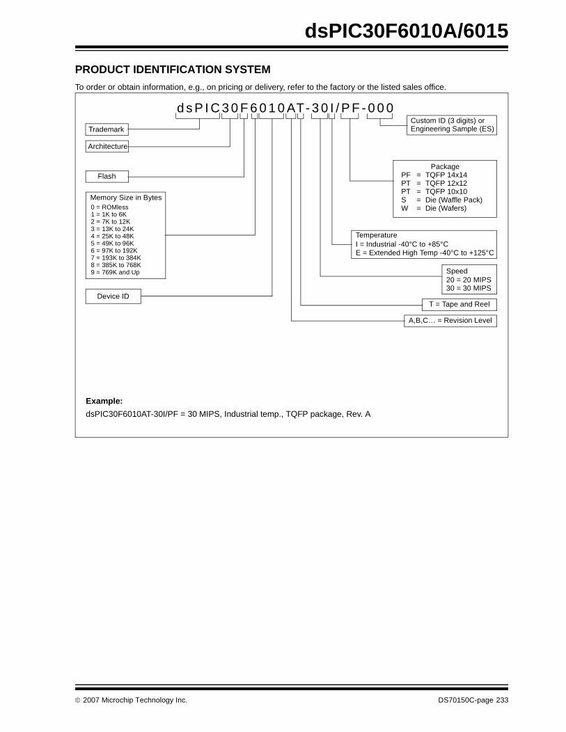
© 2007 Microchip Technology Inc. DS70150C-page 233
dsPIC30F6010A/6015
PRODUCT IDENTIFICATION SYSTEM
To order or obtain information, e.g., on pricing or delivery, refer to the factory or the listed sales office.
d s P I C 3 0 F 6 0 1 0 AT- 3 0 I / P F - 0 0 0
Example:
dsPIC30F6010AT-30I/PF = 30 MIPS, Industrial temp., TQFP package, Rev. A
Trademark
Architecture
Flash
E = Extended High Temp -40°C to +125°CI = Industrial -40°C to +85°CTemperature
Device ID
PackagePF = TQFP 14x14PT = TQFP 12x12PT = TQFP 10x10S = Die (Waffle Pack)W = Die (Wafers)
Memory Size in Bytes0 = ROMless1 = 1K to 6K2 = 7K to 12K3 = 13K to 24K4 = 25K to 48K5 = 49K to 96K6 = 97K to 192K7 = 193K to 384K8 = 385K to 768K9 = 769K and Up
Custom ID (3 digits) or
T = Tape and Reel
A,B,C… = Revision Level
Engineering Sample (ES)
Speed20 = 20 MIPS30 = 30 MIPS

DS70150C-page 234 © 2007 Microchip Technology Inc.
AMERICASCorporate Office2355 West Chandler Blvd.Chandler, AZ 85224-6199Tel: 480-792-7200 Fax: 480-792-7277Technical Support: http://support.microchip.comWeb Address: www.microchip.com
AtlantaDuluth, GA Tel: 678-957-9614 Fax: 678-957-1455
BostonWestborough, MA Tel: 774-760-0087 Fax: 774-760-0088
ChicagoItasca, IL Tel: 630-285-0071 Fax: 630-285-0075
DallasAddison, TX Tel: 972-818-7423 Fax: 972-818-2924
DetroitFarmington Hills, MI Tel: 248-538-2250Fax: 248-538-2260
KokomoKokomo, IN Tel: 765-864-8360Fax: 765-864-8387
Los AngelesMission Viejo, CA Tel: 949-462-9523 Fax: 949-462-9608
Santa ClaraSanta Clara, CA Tel: 408-961-6444Fax: 408-961-6445
TorontoMississauga, Ontario, CanadaTel: 905-673-0699 Fax: 905-673-6509
ASIA/PACIFICAsia Pacific OfficeSuites 3707-14, 37th FloorTower 6, The GatewayHabour City, KowloonHong KongTel: 852-2401-1200Fax: 852-2401-3431
Australia - SydneyTel: 61-2-9868-6733Fax: 61-2-9868-6755
China - BeijingTel: 86-10-8528-2100 Fax: 86-10-8528-2104
China - ChengduTel: 86-28-8665-5511Fax: 86-28-8665-7889
China - FuzhouTel: 86-591-8750-3506 Fax: 86-591-8750-3521
China - Hong Kong SARTel: 852-2401-1200 Fax: 852-2401-3431
China - QingdaoTel: 86-532-8502-7355Fax: 86-532-8502-7205
China - ShanghaiTel: 86-21-5407-5533 Fax: 86-21-5407-5066
China - ShenyangTel: 86-24-2334-2829Fax: 86-24-2334-2393
China - ShenzhenTel: 86-755-8203-2660 Fax: 86-755-8203-1760
China - ShundeTel: 86-757-2839-5507 Fax: 86-757-2839-5571
China - WuhanTel: 86-27-5980-5300Fax: 86-27-5980-5118
China - XianTel: 86-29-8833-7250Fax: 86-29-8833-7256
ASIA/PACIFICIndia - BangaloreTel: 91-80-4182-8400 Fax: 91-80-4182-8422
India - New DelhiTel: 91-11-4160-8631Fax: 91-11-4160-8632
India - PuneTel: 91-20-2566-1512Fax: 91-20-2566-1513
Japan - YokohamaTel: 81-45-471- 6166 Fax: 81-45-471-6122
Korea - GumiTel: 82-54-473-4301Fax: 82-54-473-4302
Korea - SeoulTel: 82-2-554-7200Fax: 82-2-558-5932 or 82-2-558-5934
Malaysia - PenangTel: 60-4-646-8870Fax: 60-4-646-5086
Philippines - ManilaTel: 63-2-634-9065Fax: 63-2-634-9069
SingaporeTel: 65-6334-8870Fax: 65-6334-8850
Taiwan - Hsin ChuTel: 886-3-572-9526Fax: 886-3-572-6459
Taiwan - KaohsiungTel: 886-7-536-4818Fax: 886-7-536-4803
Taiwan - TaipeiTel: 886-2-2500-6610 Fax: 886-2-2508-0102
Thailand - BangkokTel: 66-2-694-1351Fax: 66-2-694-1350
EUROPEAustria - WelsTel: 43-7242-2244-39Fax: 43-7242-2244-393Denmark - CopenhagenTel: 45-4450-2828 Fax: 45-4485-2829
France - ParisTel: 33-1-69-53-63-20 Fax: 33-1-69-30-90-79
Germany - MunichTel: 49-89-627-144-0 Fax: 49-89-627-144-44
Italy - Milan Tel: 39-0331-742611 Fax: 39-0331-466781
Netherlands - DrunenTel: 31-416-690399 Fax: 31-416-690340
Spain - MadridTel: 34-91-708-08-90Fax: 34-91-708-08-91
UK - WokinghamTel: 44-118-921-5869Fax: 44-118-921-5820
WORLDWIDE SALES AND SERVICE
12/08/06
Related Documents