© 2008 Microchip Technology Inc. DS70061D-page 14-1 Output Compare 14 Section 14. Output Compare HIGHLIGHTS This section of the manual contains the following major topics: 14.1 Introduction .................................................................................................................. 14-2 14.2 Output Compare Registers .......................................................................................... 14-3 14.3 Modes of Operation ..................................................................................................... 14-4 14.4 Output Compare Operation in Power Saving States.................................................. 14-23 14.5 I/O Pin Control ........................................................................................................... 14-23 14.6 Design Tips ................................................................................................................ 14-26 14.7 Related Application Notes.......................................................................................... 14-27 14.8 Revision History ......................................................................................................... 14-28

Welcome message from author
This document is posted to help you gain knowledge. Please leave a comment to let me know what you think about it! Share it to your friends and learn new things together.
Transcript

Section 14. Output Compare
Output
Com
pare
14
HIGHLIGHTSThis section of the manual contains the following major topics:
14.1 Introduction .................................................................................................................. 14-214.2 Output Compare Registers .......................................................................................... 14-314.3 Modes of Operation ..................................................................................................... 14-414.4 Output Compare Operation in Power Saving States.................................................. 14-2314.5 I/O Pin Control ........................................................................................................... 14-2314.6 Design Tips ................................................................................................................ 14-2614.7 Related Application Notes.......................................................................................... 14-2714.8 Revision History ......................................................................................................... 14-28
© 2008 Microchip Technology Inc. DS70061D-page 14-1
dsPIC30F Family Reference Manual
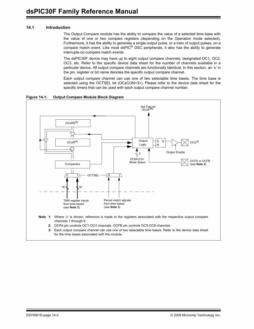
14.1 IntroductionThe Output Compare module has the ability to compare the value of a selected time base withthe value of one or two compare registers (depending on the Operation mode selected).Furthermore, it has the ability to generate a single output pulse, or a train of output pulses, on acompare match event. Like most dsPIC® DSC peripherals, it also has the ability to generateinterrupts-on-compare match events.
The dsPIC30F device may have up to eight output compare channels, designated OC1, OC2,OC3, etc. Refer to the specific device data sheet for the number of channels available in aparticular device. All output compare channels are functionally identical. In this section, an ‘x’ inthe pin, register or bit name denotes the specific output compare channel.
Each output compare channel can use one of two selectable time bases. The time base isselected using the OCTSEL bit (OCxCON<3>). Please refer to the device data sheet for thespecific timers that can be used with each output compare channel number.
Figure 14-1: Output Compare Module Block Diagram
OCxR(1)
Comparator
OutputLogic
QSR
OCM<2:0>
Output Enable
OCx(1)
Set Flag bitOCxIF(1)
OCxRS(1)
Mode Select
3
Note 1: Where ‘x’ is shown, reference is made to the registers associated with the respective output comparechannels 1 through 8.
2: OCFA pin controls OC1-OC4 channels. OCFB pin controls OC5-OC8 channels.3: Each output compare channel can use one of two selectable time bases. Refer to the device data sheet
for the time bases associated with the module.
0 1 OCTSEL 0 1
16 16
OCFA or OCFB(see Note 2)
TMR register inputsfrom time bases(see Note 3)
Period match signalsfrom time bases(see Note 3)
DS70061D-page 14-2 © 2008 Microchip Technology Inc.

Section 14. Output CompareO
utputC
ompare
14
14.2 Output Compare RegistersEach output compare channel has the following registers:
• OCxCON: the control register for the channel• OCxR: a data register for the output compare channel• OCxRS: a secondary data register for the output compare channel
The control registers for the 8 compare channels are named OC1CON through OC8CON. All 8control registers have identical bit definitions. They are represented by a common registerdefinition below. The ‘x’ in OCxCON represents the output compare channel number.
Register 14-1: OCxCON: Output Compare x Control Register Upper Byte:
U-0 U-0 R/W-0 U-0 U-0 U-0 U-0 U-0— — OCSIDL — — — — —
bit 15 bit 8
Lower Byte:U-0 U-0 U-0 R-0, HC R/W-0 R/W-0 R/W-0 R/W-0— — — OCFLT OCTSEL OCM<2:0>
bit 7 bit 0
bit 15-14 Unimplemented: Read as ‘0’bit 13 OCSIDL: Stop Output Compare in Idle Mode Control bit
1 = Output compare x will halt in CPU Idle mode0 = Output compare x will continue to operate in CPU Idle mode
bit 12-5 Unimplemented: Read as ‘0’bit 4 OCFLT: PWM Fault Condition Status bit
1 = PWM Fault condition has occurred (cleared in HW only)0 = No PWM Fault condition has occurred(This bit is only used when OCM<2:0> = 111.)
bit 3 OCTSEL: Output Compare Timer Select bit1 = Timer3 is the clock source for compare x0 = Timer2 is the clock source for compare x
Note: Refer to the device data sheet for specific time bases available to the output compare module.
bit 2-0 OCM<2:0>: Output Compare Mode Select bits111 = PWM mode on OCx, Fault pin enabled110 = PWM mode on OCx, Fault pin disabled101 = Initialize OCx pin low, generate continuous output pulses on OCx pin100 = Initialize OCx pin low, generate single output pulse on OCx pin011 = Compare event toggles OCx pin010 = Initialize OCx pin high, compare event forces OCx pin low001 = Initialize OCx pin low, compare event forces OCx pin high 000 = Output compare channel is disabled
Legend:HC = Cleared in Hardware R = Readable bit W = Writable bit U = Unimplemented bit, read as ‘0’-n = Value at POR ‘1’ = Bit is set ‘0’ = Bit is cleared x = Bit is unknown
© 2008 Microchip Technology Inc. DS70061D-page 14-3

dsPIC30F Family Reference Manual
14.3 Modes of OperationEach output compare module has the following modes of operation:
• Single Compare Match mode• Dual Compare Match mode generating
- Single Output Pulse- Continuous Output Pulses
• Simple Pulse-Width Modulation mode - with Fault Protection Input- without Fault Protection Input
14.3.1 Single Compare Match Mode
When control bits OCM<2:0> (OCxCON<2:0>) are set to ‘001’, ‘010’ or ‘011’, the selectedoutput compare channel is configured for one of three Single Output Compare Match modes.
In the Single Compare mode, the OCxR register is loaded with a value and is compared to theselected incrementing timer register, TMRy. On a compare match event, one of the followingevents will take place:
• Compare forces OCx pin high, initial state of pin is low. Interrupt is generated on the single compare match event.
• Compare forces OCx pin low, initial state of pin is high. Interrupt is generated on the single compare match event.
• Compare toggles OCx pin. Toggle event is continuous and an interrupt is generated for each toggle event.
Note 1: It is recommended that the user turn off the output compare module (i.e., clearOCM<2:0> (OCxCON<2:0>)) before switching to a new mode.
2: In this section, a reference to any SFRs associated with the selected timer sourceis indicated by a ‘y’ suffix. For example, PRy is the Period register for the selectedtimer source, while TyCON is the Timer Control register for the selected timersource.
DS70061D-page 14-4 © 2008 Microchip Technology Inc.
Section 14. Output CompareO
utputC
ompare
14
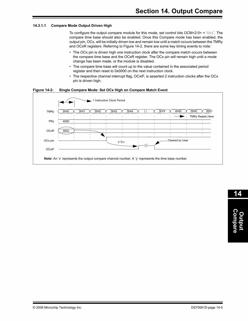
14.3.1.1 Compare Mode Output Driven High
To configure the output compare module for this mode, set control bits OCM<2:0> = ‘001’. Thecompare time base should also be enabled. Once this Compare mode has been enabled, theoutput pin, OCx, will be initially driven low and remain low until a match occurs between the TMRyand OCxR registers. Referring to Figure 14-2, there are some key timing events to note:
• The OCx pin is driven high one instruction clock after the compare match occurs between the compare time base and the OCxR register. The OCx pin will remain high until a mode change has been made, or the module is disabled.
• The compare time base will count up to the value contained in the associated period register and then reset to 0x0000 on the next instruction clock.
• The respective channel interrupt flag, OCxIF, is asserted 2 instruction clocks after the OCx pin is driven high.
Figure 14-2: Single Compare Mode: Set OCx High on Compare Match Event
OCxIF
4000 00013001 3002 3003 30043000TMRy 0000
Cleared by User
1 Instruction Clock Period
2 TCY
4000
3002
PRy
OCxR
3FFF
OCx pin
TMRy Resets Here
Note: An ‘x’ represents the output compare channel number. A ‘y’ represents the time base number.
© 2008 Microchip Technology Inc. DS70061D-page 14-5
dsPIC30F Family Reference Manual
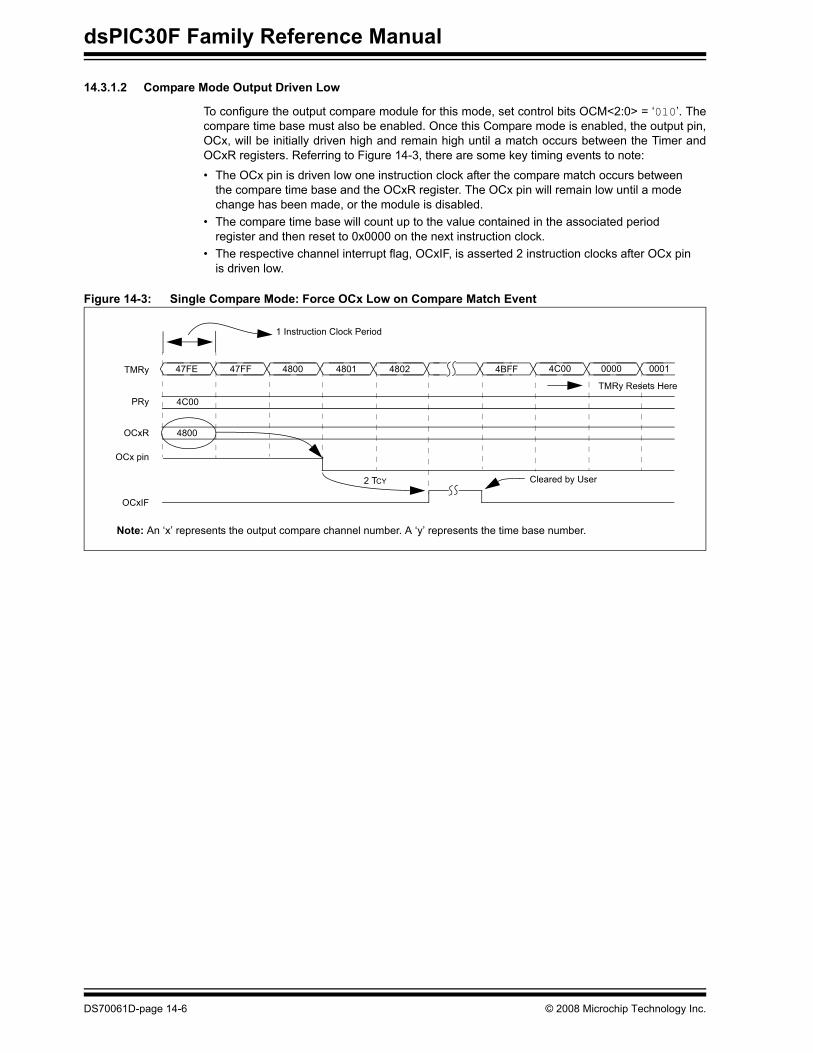
14.3.1.2 Compare Mode Output Driven Low
To configure the output compare module for this mode, set control bits OCM<2:0> = ‘010’. Thecompare time base must also be enabled. Once this Compare mode is enabled, the output pin,OCx, will be initially driven high and remain high until a match occurs between the Timer andOCxR registers. Referring to Figure 14-3, there are some key timing events to note:
• The OCx pin is driven low one instruction clock after the compare match occurs between the compare time base and the OCxR register. The OCx pin will remain low until a mode change has been made, or the module is disabled.
• The compare time base will count up to the value contained in the associated period register and then reset to 0x0000 on the next instruction clock.
• The respective channel interrupt flag, OCxIF, is asserted 2 instruction clocks after OCx pin is driven low.
Figure 14-3: Single Compare Mode: Force OCx Low on Compare Match Event
OCxIF
4C00 000147FF 4800 4801 480247FETMRy 0000
Cleared by User
1 Instruction Clock Period
2 TCY
4C00
4800
PRy
OCxR
4BFF
OCx pin
TMRy Resets Here
Note: An ‘x’ represents the output compare channel number. A ‘y’ represents the time base number.
DS70061D-page 14-6 © 2008 Microchip Technology Inc.
Section 14. Output CompareO
utputC
ompare
14
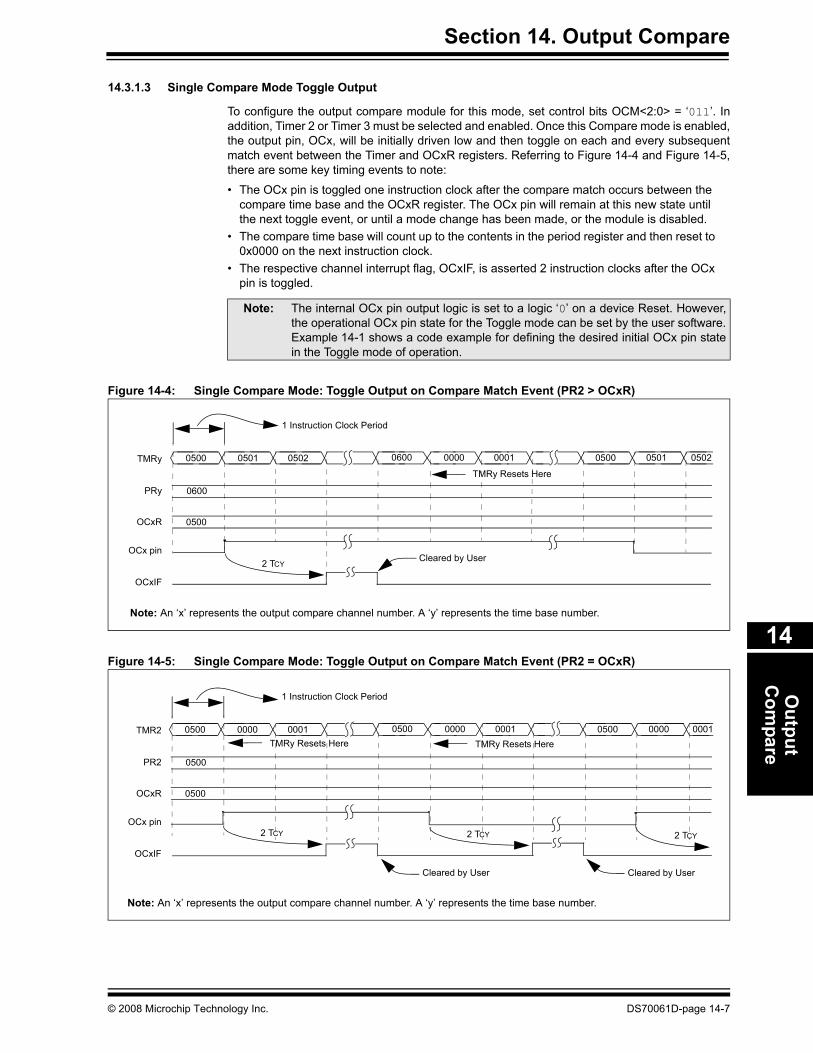
14.3.1.3 Single Compare Mode Toggle Output
To configure the output compare module for this mode, set control bits OCM<2:0> = ‘011’. Inaddition, Timer 2 or Timer 3 must be selected and enabled. Once this Compare mode is enabled,the output pin, OCx, will be initially driven low and then toggle on each and every subsequentmatch event between the Timer and OCxR registers. Referring to Figure 14-4 and Figure 14-5,there are some key timing events to note:
• The OCx pin is toggled one instruction clock after the compare match occurs between the compare time base and the OCxR register. The OCx pin will remain at this new state until the next toggle event, or until a mode change has been made, or the module is disabled.
• The compare time base will count up to the contents in the period register and then reset to 0x0000 on the next instruction clock.
• The respective channel interrupt flag, OCxIF, is asserted 2 instruction clocks after the OCx pin is toggled.
Figure 14-4: Single Compare Mode: Toggle Output on Compare Match Event (PR2 > OCxR)
Figure 14-5: Single Compare Mode: Toggle Output on Compare Match Event (PR2 = OCxR)
Note: The internal OCx pin output logic is set to a logic ‘0’ on a device Reset. However,the operational OCx pin state for the Toggle mode can be set by the user software.Example 14-1 shows a code example for defining the desired initial OCx pin statein the Toggle mode of operation.
OCxIF
05000501 0502 06000500TMRy
1 Instruction Clock Period
0600
0500
PRy
OCxR
0001
OCx pin
TMRy Resets Here
0000 0501 0502
Cleared by User2 TCY
Note: An ‘x’ represents the output compare channel number. A ‘y’ represents the time base number.
OCxIF
05000000 0001 05000500TMR2
Cleared by User
1 Instruction Clock Period
2 TCY
0500
0500
PR2
OCxR
0001
OCx pin
TMRy Resets Here0000 0000 0001
Cleared by User
2 TCY 2 TCY
TMRy Resets Here
Note: An ‘x’ represents the output compare channel number. A ‘y’ represents the time base number.
© 2008 Microchip Technology Inc. DS70061D-page 14-7

dsPIC30F Family Reference Manual
Example 14-1: Compare Mode Toggle Mode Pin State Setup
Example 14-2 shows example code for the configuration and interrupt service of the SingleCompare mode toggle event.
Example 14-2: Compare Mode Toggle Setup and Interrupt Servicing
; The following code example illustrates how to define the initial; OC1 pin state for the output compare toggle mode of operation.
; Toggle mode with initial OC1 pin state set low
MOV 0x0001, w0 ; load setup value into w0MOV w0, OC1CON ; enable module for OC1 pin low, toggle highBSET OC1CON, #1 ; set module to toggle mode with initial pin
; state low
; Toggle mode with initial OC1 pin state set high
MOV 0x0002, w0 ; load setup value into w0MOV w0, OC1CON ; enable module for OC1 pin high, toggle lowBSET OC1CON, #0 ; set module to toggle mode with initial pin
; state high
; The following code example will set the Output Compare 1 module ; for interrupts on the toggle event and select Timer 2 as the clock ; source for the compare time-base. It is assumed in that Timer 2 ; and Period Register 2 are properly configured. Timer 2 will ; be enabled here.
CLR OC1CON ; Turn off Output Compare 1 Module. MOV #0x0003, w0 ; Load the working register with the new MOV w0, OC1CON ; compare mode and write to OC1CON MOV #0x0500, w0 ; Initialize Compare Register 1 MOV w0, OC1R ; with 0x0500 BSET IPC0, #OC1IP0 ; Setup Output Compare 1 interrupt for BCLR IPC0, #OC1IP1 ; desired priority level BCLR IPC0, #OC1IP2 ; (this example assigns level 1 priority) BCLR IFS0, #OC1IF ; Clear Output Compare 1 interrupt flag BSET IEC0, #OC1IE ; Enable Output Compare 1 interrupts BSET T2CON, #TON ; Start Timer2 with assumed settings
; Example code for Output Compare 1 ISR:
__OC1Interrupt:BCLR IFS0, #OC1IF ; Reset respective interrupt flag
; Remaining user code hereRETFIE ; Return from ISR
DS70061D-page 14-8 © 2008 Microchip Technology Inc.

Section 14. Output CompareO
utputC
ompare
14
14.3.2 Dual Compare Match Mode
When control bits OCM<2:0> = ‘100’ or ‘101’ (OCxCON<2:0>), the selected output comparechannel is configured for one of two Dual Compare Match modes which are:
• Single Output Pulse mode• Continuous Output Pulse mode
In the Dual Compare mode, the module uses both the OCxR and OCxRS registers for thecompare match events. The OCxR register is compared against the incrementing timer count,TMRy, and the leading (rising) edge of the pulse is generated at the OCx pin, on a comparematch event. The OCxRS register is then compared to the same incrementing timer count,TMRy, and the trailing (falling) edge of the pulse is generated at the OCx pin, on a comparematch event.
14.3.2.1 Dual Compare Mode: Single Output Pulse
To configure the Output Compare module for the Single Output Pulse mode, set control bitsOCM<2:0> = ‘100’. In addition, the compare time base must be selected and enabled. Once thismode is enabled, the output pin, OCx, will be driven low and remain low until a match occursbetween the time base and OCxR registers. Referring to Figure 14-6 and Figure 14-7, there aresome key timing events to note:
• The OCx pin is driven high one instruction clock after the compare match occurs between the compare time base and OCxR register. The OCx pin will remain high until the next match event occurs between the time base and the OCxRS register. At this time, the pin will be driven low. The OCx pin will remain low until a mode change has been made, or the module is disabled.
• The compare time base will count up to the value contained in the associated period register and then reset to 0x0000 on the next instruction clock.
• If the time base period register contents are less than the OCxRS register contents, then no falling edge of the pulse is generated. The OCx pin will remain high until OCxRS <= PRy, or a mode change or Reset condition has occurred.
• The respective channel interrupt flag, OCxIF, is asserted 2 instruction clocks after the OCx pin is driven low (falling edge of single pulse).
Figure 14-6 depicts the General Dual Compare mode generating a single output pulse.Figure 14-7 depicts another timing example where OCxRS > PRy. In this example, no fallingedge of the pulse is generated since the compare time base resets before counting up to0x4100.
© 2008 Microchip Technology Inc. DS70061D-page 14-9

dsPIC30F Family Reference Manual
Figure 14-6: Dual Compare Mode
Figure 14-7: Dual Compare Mode: Single Output Pulse (OCxRS > PR2)
OCxIF
00003001 3002 3003 30043000TMRy 4000
Cleared by User
Note 1: An ‘x’ represents the output compare channel number. A ‘y’ represents the time base number.2: OCxR = Compare Register, OCxRS = Secondary Compare Register.
1 Instruction Clock Period
2 TCY
4000
3000
PRy
OCxR
3006
OCx pin
TMRy Resets Here
3003OCxRS
3005
OCxIF
00003001 3002 3003 30043000TMRy 4000
1 Instruction Clock Period
4000
3000
PRy
OCxR
3006
OCx pin
TMRy Resets Here
4100OCxRS
3005
Note 1: An ‘x’ represents the output compare channel number. A ‘y’ represents the time base number.2: OCxR = Compare Register, OCxRS = Secondary Compare Register.
Compare Interrupt does not occur
DS70061D-page 14-10 © 2008 Microchip Technology Inc.

Section 14. Output CompareO
utputC
ompare
14
14.3.2.2 Setup for Single Output Pulse Generation
When control bits OCM<2:0> (OCxCON<2:0>) are set to ‘100’, the selected output comparechannel initializes the OCx pin to the low state and generates a single output pulse.
To generate a single output pulse, the following steps are required (these steps assume timersource is initially turned off, but this is not a requirement for the module operation):
1. Determine the instruction clock cycle time. Take into account the frequency of the externalclock to the timer source (if one is used) and the timer prescaler settings.
2. Calculate time to the rising edge of the output pulse relative to the TMRy start value(0x0000).
3. Calculate the time to the falling edge of the pulse based on the desired pulse-width andthe time to the rising edge of the pulse.
4. Write the values computed in Step 2 and 3 above into the compare register, OCxR, andthe secondary compare register, OCxRS, respectively.
5. Set timer period register, PRy, to value equal to or greater than value in OCxRS, thesecondary compare register.
6. Set OCM<2:0> = ‘100’ and the OCTSEL (OCxCON<3>) bit to the desired timer source.The OCx pin state will now be driven low.
7. Set the TON (TyCON<15>) bit to ‘1’, which enables the compare time base to count. 8. Upon the first match between TMRy and OCxR, the OCx pin will be driven high.9. When the incrementing timer, TMRy, matches the secondary compare register, OCxRS,
the second and trailing edge (high-to-low) of the pulse is driven onto the OCx pin. Noadditional pulses are driven onto the OCx pin and it remains at low. As a result of thesecond compare match event, the OCxIF interrupt flag bit set, which will result in aninterrupt if it is enabled, by setting the OCxIE bit. For further information on peripheralinterrupts, refer to Section 6. “Reset Interrupts”.
10. To initiate another single pulse output, change the timer and compare register settings, ifneeded, and then issue a write to set OCM<2:0> (OCxCON<2:0>) bits to ‘100’. Disablingand re-enabling of the timer and clearing the TMRy register are not required, but may beadvantageous for defining a pulse from a known event time boundary.
The output compare module does not have to be disabled after the falling edge of the outputpulse. Another pulse can be initiated by rewriting the value of the OCxCON register.
© 2008 Microchip Technology Inc. DS70061D-page 14-11

dsPIC30F Family Reference Manual
Example 14-3 shows example code for configuration of the single output pulse event.
Example 14-3: Single Output Pulse Setup and Interrupt Servicing ; The following code example will set the Output Compare 1 module ; for interrupts on the single pulse event and select Timer 2 ; as the clock source for the compare time base. It is assumed ; that Timer 2 and Period Register 2 are properly initialized. ; Timer 2 will be enabled here.
CLR OC1CON ; Turn off Output Compare 1 Module. MOV #0x0004, w0 ; Load the working register with the new MOV W0, OC1CON ; compare mode and write to OC1CON MOV #0x3000, w0 ; Initialize Compare Register 1 MOV W0, OC1R ; with 0x3000 MOV #0x3003, w0 ; Initialize Secondary Compare Register 1 MOV W0, OC1RS ; with 0x3003 BSET IPC0, #OC1IP0 ; Setup Output Compare 1 interrupt for BCLR IPC0, #OC1IP1 ; desired priority level BCLR IPC0, #OC1IP2 ; (this example assigns level 1 priority) BCLR IFS0, #OC1IF ; Clear Output Compare 1 interrupt flag BSET IEC0, #OC1IE ; Enable Output Compare 1 interrupts
BSET T2CON, #TON ; Start Timer2 with assumed settings
; Example code for Output Compare 1 ISR:
__OC1Interrupt:BCLR IFS0, #OC1IF ; Reset respective interrupt flag
; Remaining user code hereRETFIE ; Return from ISR
DS70061D-page 14-12 © 2008 Microchip Technology Inc.
Section 14. Output CompareO
utputC
ompare
14
14.3.2.3 Special Cases for Dual Compare Mode Generating a Single Output Pulse
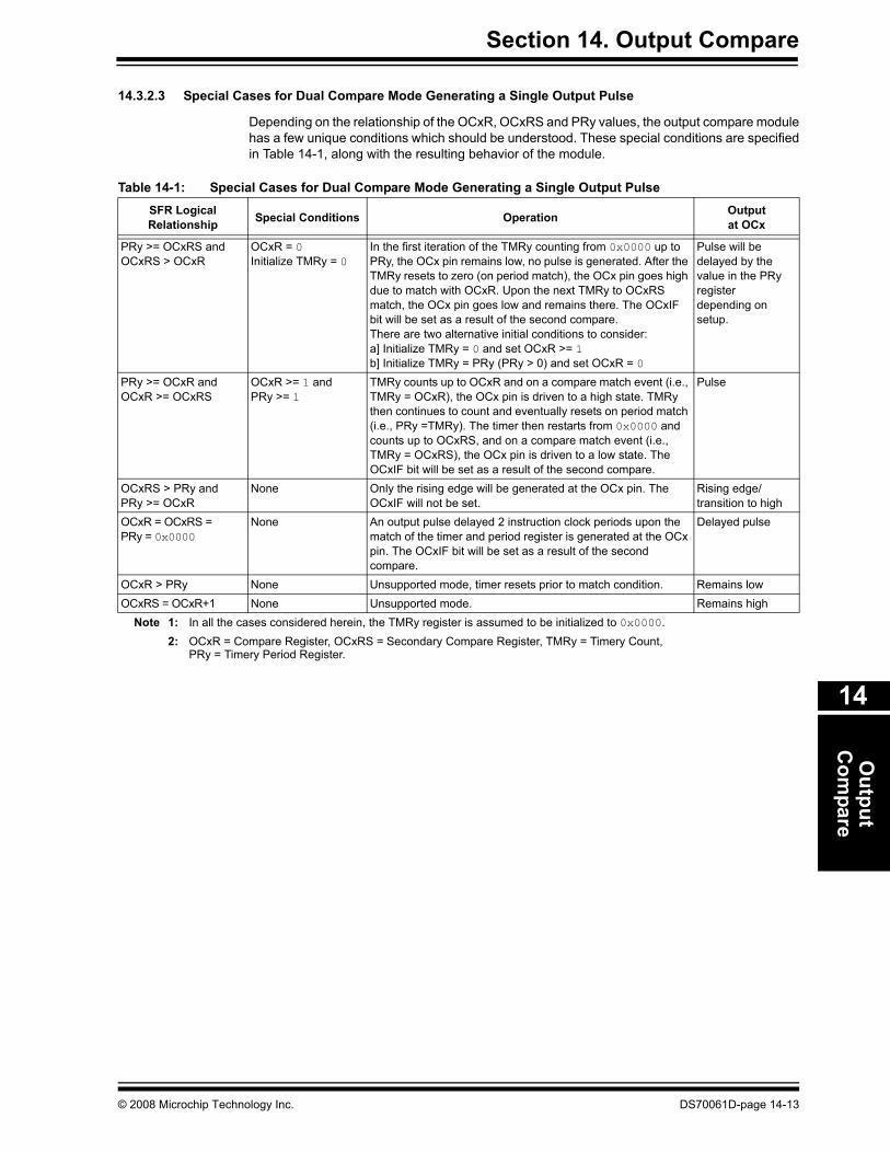
Depending on the relationship of the OCxR, OCxRS and PRy values, the output compare modulehas a few unique conditions which should be understood. These special conditions are specifiedin Table 14-1, along with the resulting behavior of the module.
Table 14-1: Special Cases for Dual Compare Mode Generating a Single Output Pulse
SFR LogicalRelationship Special Conditions Operation Output
at OCx
PRy >= OCxRS andOCxRS > OCxR
OCxR = 0Initialize TMRy = 0
In the first iteration of the TMRy counting from 0x0000 up to PRy, the OCx pin remains low, no pulse is generated. After the TMRy resets to zero (on period match), the OCx pin goes high due to match with OCxR. Upon the next TMRy to OCxRS match, the OCx pin goes low and remains there. The OCxIF bit will be set as a result of the second compare.There are two alternative initial conditions to consider:a] Initialize TMRy = 0 and set OCxR >= 1b] Initialize TMRy = PRy (PRy > 0) and set OCxR = 0
Pulse will be delayed by the value in the PRy register depending on setup.
PRy >= OCxR andOCxR >= OCxRS
OCxR >= 1 andPRy >= 1
TMRy counts up to OCxR and on a compare match event (i.e., TMRy = OCxR), the OCx pin is driven to a high state. TMRy then continues to count and eventually resets on period match (i.e., PRy =TMRy). The timer then restarts from 0x0000 and counts up to OCxRS, and on a compare match event (i.e., TMRy = OCxRS), the OCx pin is driven to a low state. The OCxIF bit will be set as a result of the second compare.
Pulse
OCxRS > PRy andPRy >= OCxR
None Only the rising edge will be generated at the OCx pin. The OCxIF will not be set.
Rising edge/transition to high
OCxR = OCxRS = PRy = 0x0000
None An output pulse delayed 2 instruction clock periods upon the match of the timer and period register is generated at the OCx pin. The OCxIF bit will be set as a result of the second compare.
Delayed pulse
OCxR > PRy None Unsupported mode, timer resets prior to match condition. Remains lowOCxRS = OCxR+1 None Unsupported mode. Remains high
Note 1: In all the cases considered herein, the TMRy register is assumed to be initialized to 0x0000.2: OCxR = Compare Register, OCxRS = Secondary Compare Register, TMRy = Timery Count,
PRy = Timery Period Register.
© 2008 Microchip Technology Inc. DS70061D-page 14-13
dsPIC30F Family Reference Manual
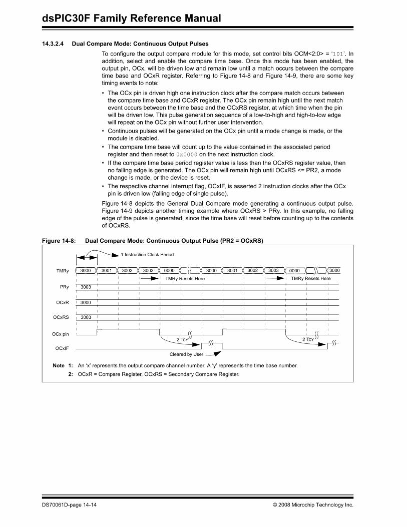
14.3.2.4 Dual Compare Mode: Continuous Output PulsesTo configure the output compare module for this mode, set control bits OCM<2:0> = ‘101’. Inaddition, select and enable the compare time base. Once this mode has been enabled, theoutput pin, OCx, will be driven low and remain low until a match occurs between the comparetime base and OCxR register. Referring to Figure 14-8 and Figure 14-9, there are some keytiming events to note:
• The OCx pin is driven high one instruction clock after the compare match occurs between the compare time base and OCxR register. The OCx pin remain high until the next match event occurs between the time base and the OCxRS register, at which time when the pin will be driven low. This pulse generation sequence of a low-to-high and high-to-low edge will repeat on the OCx pin without further user intervention.
• Continuous pulses will be generated on the OCx pin until a mode change is made, or the module is disabled.
• The compare time base will count up to the value contained in the associated period register and then reset to 0x0000 on the next instruction clock.
• If the compare time base period register value is less than the OCxRS register value, then no falling edge is generated. The OCx pin will remain high until OCxRS <= PR2, a mode change is made, or the device is reset.
• The respective channel interrupt flag, OCxIF, is asserted 2 instruction clocks after the OCx pin is driven low (falling edge of single pulse).
Figure 14-8 depicts the General Dual Compare mode generating a continuous output pulse.Figure 14-9 depicts another timing example where OCxRS > PRy. In this example, no fallingedge of the pulse is generated, since the time base will reset before counting up to the contentsof OCxRS.
Figure 14-8: Dual Compare Mode: Continuous Output Pulse (PR2 = OCxRS)
OCxIF
30033001 3002 3003 00003000TMRy 3002
Cleared by User
1 Instruction Clock Period
2 TCY
3003
3000
PRy
OCxR
3000
OCx pin
3003OCxRS
3001 30000000
2 TCY
TMRy Resets Here TMRy Resets Here
Note 1: An ‘x’ represents the output compare channel number. A ‘y’ represents the time base number.2: OCxR = Compare Register, OCxRS = Secondary Compare Register.
DS70061D-page 14-14 © 2008 Microchip Technology Inc.

Section 14. Output CompareO
utputC
ompare
14
Figure 14-9: Dual Compare Mode: Continuous Output Pulse (OCxRS > PR2)
14.3.2.5 Setup for Continuous Output Pulse Generation
When control bits OCxM<2:0> (OCxCON<2:0>) are set to ‘101’, the selected output comparechannel initializes the OCx pin to the low state and generates output pulses on each and everycompare match event.
For the user to configure the module for the generation of a continuous stream of output pulses,the following steps are required (these steps assume timer source is initially turned off, but thisis not a requirement for the module operation):
1. Determine the instruction clock cycle time. Take into account the frequency of the externalclock to the timer source (if one is used) and the timer prescaler settings.
2. Calculate time to the rising edge of the output pulse relative to the TMRy start value(0x0000).
3. Calculate the time to the falling edge of the pulse, based on the desired pulse-width andthe time to the rising edge of the pulse.
4. Write the values computed in Step 2 and 3 above into the compare register, OCxR, andthe secondary compare register, OCxRS, respectively.
5. Set timer period register, PRy, to value equal to or greater than value in OCxRS, thesecondary compare register.
6. Set OCM<2:0> = ‘101’ and the OCTSEL (OCxCON<3>) bit to the desired timer source.The OCx pin state will now be driven low.
7. Enable the compare time base by setting the TON (TyCON<15>) bit to ‘1’. 8. Upon the first match between TMRy and OCxR, the OCx pin will be driven high.9. When the compare time base, TMRy, matches the secondary compare register, OCxRS,
the second and trailing edge (high-to-low) of the pulse is driven onto the OCx pin.10. As a result of the second compare match event, the OCxIF interrupt flag bit set.11. When the compare time base and the value in its respective period register match, the
TMRy register resets to 0x0000 and resumes counting.12. Steps 8 through 11 are repeated and a continuous stream of pulses is generated,
indefinitely. The OCxIF flag is set on each OCxRS-TMRy compare match event.
OCxIF
30033001 3002 3003 00003000TMRy 3002
1 Instruction Clock Period
3003
3000
PRy
OCxR
3000
OCx pin
3004OCxRS
3001 30000000
TMRy Resets Here TMRy Resets Here
Note 1: An ‘x’ represents the output compare channel number. A ‘y’ represents the time base number.2: OCxR = Compare Register, OCxRS = Secondary Compare Register.
Compare Interrupt does not Occur
© 2008 Microchip Technology Inc. DS70061D-page 14-15

dsPIC30F Family Reference Manual
Example 14-4 shows example code for configuration of the continuous output pulse event.
Example 14-4: Continuous Output Pulse Setup and Interrupt Servicing ; The following code example will set the Output Compare 1 module ; for interrupts on the continuous pulse event and select Timer 2 ; as the clock source for the compare time-base. It is assumed ; that Timer 2 and Period Register 2 are properly configured. ; Timer 2 will be enabled here.
CLR OC1CON ; Turn off Output Compare 1 Module. MOV #0x0005, W0 ; Load the working register with the new MOV W0, OC1CON ; compare mode and write to OC1CON MOV #0x3000, W0 ; Initialize Compare Register 1 MOV W0, OC1R ; with 0x3000 MOV #0x3003, W0 ; Initialize Secondary Compare Register 1 MOV W0, OC1RS ; with 0x3003 BSET IPC0, #OC1IP0 ; Setup Output Compare 1 interrupt for BCLR IPC0, #OC1IP1 ; desired priority level BCLR IPC0, #OC1IP2 ; (this example assigns level 1 priority) BCLR IFS0, #OC1IF ; Clear Output Compare 1 interrupt flag BSET IEC0, #OC1IE ; Enable Output Compare 1 interrupts
BSET T2CON, #TON ; Start Timer2 with assumed settings
; Example code for Output Compare 1 ISR:
__OC1Interrupt:BCLR IFS0, #OC1IF ; Reset respective interrupt flag
; Remaining user code hereRETFIE ; Return from ISR
DS70061D-page 14-16 © 2008 Microchip Technology Inc.

Section 14. Output CompareO
utputC
ompare
14
14.3.2.6 Special Cases for Dual Compare Mode Generating Continuous Output Pulses
Depending on the relationship of the OCxR, OCxRS and PRy values, the output compare modulemay not provide the expected results. These special cases are specified in Table 14-2, along withthe resulting behavior of the module.
Table 14-2: Special Cases for Dual Compare Mode Generating Continuous Output Pulses
SFR LogicalRelationship Special Conditions Operation Output
at OCx
PRy >= OCxRS andOCxRS > OCxR
OCxR = 0Initialize TMRy = 0
In the first iteration of the TMRy counting from 0x0000 up to PRy, the OCx pin remains low, no pulse is generated. After the TMRy resets to zero (on period match), the OCx pin goes high. Upon the next TMRy to OCxRS match, the OCx pin goes low. If OCxR = 0 and PRy = OCxRS, the pin will remain low for one clock cycle, then be driven high until the next TMRy to OCxRS match. The OCxIF bit will be set as a result of the second compare.There are two alternative initial conditions to consider:a] Initialize TMRy = 0 and set OCxR >= 1b] Initialize TMRy = PRy (PRy > 0) and set OCxR = 0
Continuous pulses with the first pulse delayed by the value in the PRy register, depending on setup.
PRy >= OCxR andOCxR >= OCxRS
OCxR >= 1 andPRy >= 1
TMRy counts up to OCxR and on a compare match event (i.e., TMRy = OCxR), the OCx pin is driven to a high state. TMRy then continues to count and eventually resets on period match (i.e., PRy =TMRy). The timer then restarts from 0x0000 and counts up to OCxRS, and on a compare match event (i.e., TMRy = OCxR), the OCx pin is driven to a low state. The OCxIF bit will be set as a result of the second compare.
Continuous pulses
OCxRS > PRy andPRy >= OCxR
None Only one transition will be generated at the OCx pin until the OCxRS register contents have been changed to a value less than or equal to the period register contents (PRy). OCxIF is not set until then.
Rising edge/ transition to high
OCxR = OCxRS =PRy = 0x0000
None Continuous output pulses are generated at the OCx pin. The first pulse is delayed 2 instruction clock periods upon the match of the timer and period register. The OCxIF bit will be set as a result of the second compare.
First pulse is delayed. Continuous pulsesare generated.
OCxR > PRy None Unsupported mode, Timer resets prior to match condition. Remains lowOCxRS = OCxR+1 None Unsupported mode. Remains high
Note 1: In all the cases considered herein, the TMRy register is assumed to be initialized to 0x0000.2: OCxR = Compare Register, OCxRS = Secondary Compare Register, TMRy = Timery Count,
PRy = Timery Period Register.
© 2008 Microchip Technology Inc. DS70061D-page 14-17
dsPIC30F Family Reference Manual
14.3.3 Pulse-Width Modulation Mode
When control bits OCM<2:0> (OCxCON<2:0>) are set to ‘110’ or ‘111’, the selected outputcompare channel is configured for the PWM (Pulse-Width Modulation) mode of operation.
The following two PWM modes are available:
• PWM without Fault Protection Input• PWM with Fault Protection Input
The OCFA or OCFB Fault input pin is utilized for the second PWM mode. In this mode, anasynchronous logic level ‘0’ on the OCFx pin will cause the selected PWM channel to beshutdown. (Described in Section 14.3.3.1, “PWM with Fault Protection Input Pin”.)
In PWM mode, the OCxR register is a read only slave duty cycle register and OCxRS is a bufferregister that is written by the user to update the PWM duty cycle. On every timer to period registermatch event (end of PWM period), the duty cycle register, OCxR, is loaded with the contents ofOCxRS. The TyIF interrupt flag is asserted at each PWM period boundary.
The following steps should be taken when configuring the output compare module for PWMoperation:
1. Set the PWM period by writing to the selected timer period register (PRy).2. Set the PWM duty cycle by writing to the OCxRS register.3. Write the OxCR register with the initial duty cycle.4. Enable interrupts, if required, for the timer and output compare modules. The output
compare interrupt is required for PWM Fault pin utilization.5. Configure the output compare module for one of two PWM Operation modes by writing to
the Output Compare mode bits OCM<2:0> (OCxCON<2:0>).6. Set the TMRy prescale value and enable the time base by setting TON (TxCON<15>) = 1.
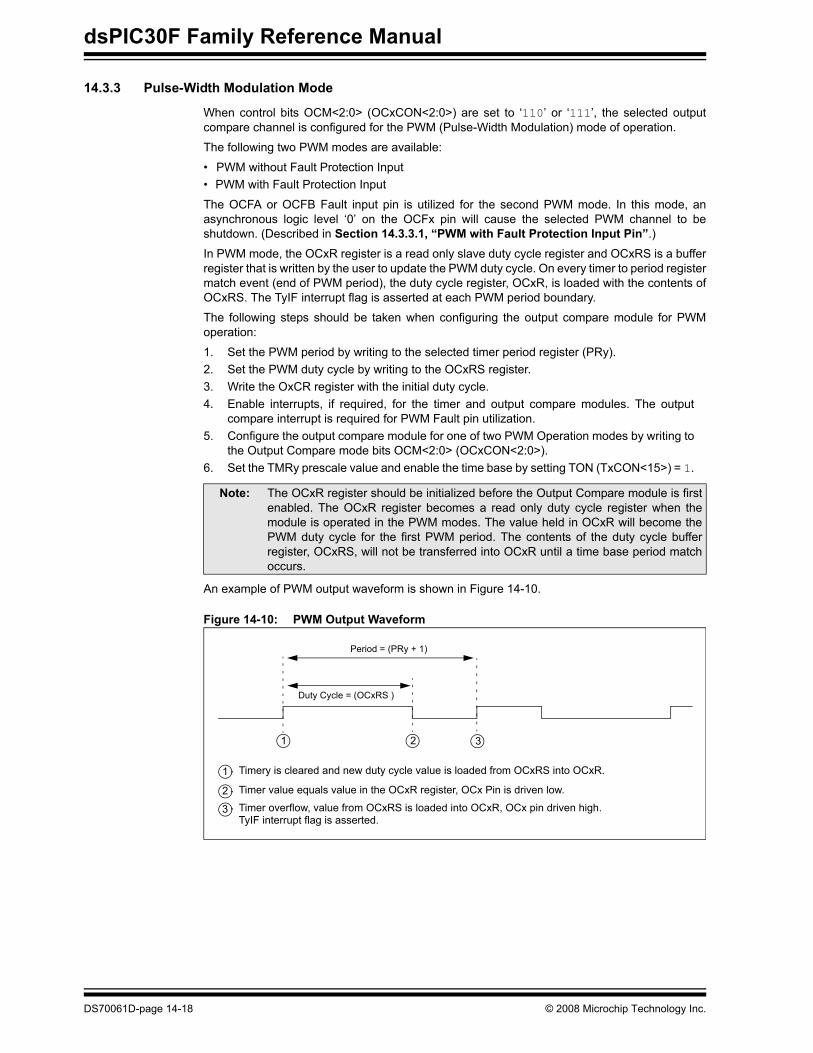
An example of PWM output waveform is shown in Figure 14-10.
Figure 14-10: PWM Output Waveform
Note: The OCxR register should be initialized before the Output Compare module is firstenabled. The OCxR register becomes a read only duty cycle register when themodule is operated in the PWM modes. The value held in OCxR will become thePWM duty cycle for the first PWM period. The contents of the duty cycle bufferregister, OCxRS, will not be transferred into OCxR until a time base period matchoccurs.
Period = (PRy + 1)
Duty Cycle = (OCxRS )
Timery is cleared and new duty cycle value is loaded from OCxRS into OCxR.
Timer value equals value in the OCxR register, OCx Pin is driven low.
Timer overflow, value from OCxRS is loaded into OCxR, OCx pin driven high.
21 3
2
3
1
TyIF interrupt flag is asserted.
DS70061D-page 14-18 © 2008 Microchip Technology Inc.

Section 14. Output CompareO
utputC
ompare
14
14.3.3.1 PWM with Fault Protection Input Pin
When the Output Compare mode bits, OCM<2:0> (OCxCON<2:0>), are set to ‘111’, the selectedoutput compare channel is configured for the PWM mode of operation. All functions described inSection 14.3.3, “Pulse-Width Modulation Mode” apply, with the addition of input Faultprotection.
Fault protection is provided via the OCFA and OCFB pins. The OCFA pin is associated with theoutput compare channels 1 through 4, while the OCFB pin is associated with the output comparechannels 5 through 8.
If a logic ‘0’ is detected on the OCFA/OCFB pin, the selected PWM output pin(s) are placed inthe high impedance state. The user may elect to provide a pull-down or pull-up resistor on thePWM pin to provide for a desired state if a Fault condition occurs. The shutdown of the PWMoutput is immediate and is not tied to the device clock source. This state will remain until:
• The external Fault condition has been removed and• The PWM mode is re-enabled by writing to the appropriate mode bits, OCM<2:0>
(OCxCON<2:0>).
As a result of the Fault condition, the respective interrupt flag, OCxIF bit, is asserted and aninterrupt will be generated, if enabled. Upon detection of the Fault condition, the OCFLT bit(OCx-CON<4>) is asserted high (logic ‘1’). This bit is a read only bit and will only be cleared oncethe external Fault condition has been removed and the PWM mode is re-enabled, by writing tothe appropriate mode bits, OCM<2:0> (OCxCON<2:0>).
14.3.3.2 PWM Period
The PWM period is specified by writing to PRy, the Timery period register. The PWM period canbe calculated using the following formula:
Equation 14-1: Calculating the PWM Period
Note: The external Fault pins, if enabled for use, will continue to control the OCx outputpins, while the device is in Sleep or Idle mode.
PWM Period = [(PRy) + 1] • TCY • (TMRy Prescale Value)
PWM Frequency = 1/[PWM Period]
Note: A PRy value of N will produce a PWM period of N + 1 time base count cycles. Forexample: a value of 7 written into the PRy register will yield a period consisting of 8time base cycles.
© 2008 Microchip Technology Inc. DS70061D-page 14-19

dsPIC30F Family Reference Manual
14.3.3.3 PWM Duty Cycle
The PWM duty cycle is specified by writing to the OCxRS register. The OCxRS register can bewritten to at any time, but the duty cycle value is not latched into OCxR until a match betweenPRy and TMRy occurs (i.e., the period is complete). This provides a double buffer for the PWMduty cycle and is essential for glitchless PWM operation. In the PWM mode, OCxR is a read onlyregister.
Some important boundary parameters of the PWM duty cycle include:
• If the duty cycle register, OCxR, is loaded with 0x0000, the OCx pin will remain low(0% duty cycle).
• If OCxR is greater than PRy (timer period register), the pin will remain high (100% duty cycle).
• If OCxR is equal to PRy, the OCx pin will be low for one time base count value and high for all other count values.
See Figure 14-11 for PWM mode timing details. Table 14-3 and Table 14-4 illustrates an examplePWM frequencies and resolutions for a device operating at 10 and 30 MIPs, respectively.
Equation 14-2: Calculation for Maximum PWM Resolution
Example 14-5: PWM Period and Duty Cycle Calculation
( )Maximum PWM Resolution (bits) =
FOSCFPWM
log10
log10(2)bits
Desired PWM frequency is 52.08 kHz, FOSC = 10 MHz with x4 PLL (40 MHz device clock rate) (TCY = 4/FOSC)Timer 2 prescale setting: 1:1
1/52.08 kHz = (PR2+1) • TCY • (Timer 2 prescale value) 19.20 μs = (PR2+1) • 0.1 μs • (1) PR2 = 191
Find the maximum resolution of the duty cycle that can be used with a 48 kHz frequency and a 40 MHz device clock rate.
1/52.08 kHz = 2PWM RESOLUTION • 1/40 MHz • 1 19.20 μs = 2PWM RESOLUTION • 25 ns • 1 768 = 2PWM RESOLUTION
log10(768) = (PWM Resolution) • log10(2) PWM Resolution= 9.5 bits
DS70061D-page 14-20 © 2008 Microchip Technology Inc.

Section 14. Output CompareO
utputC
ompare
14
Figure 14-11: PWM Output Timing
Table 14-3: Example PWM Frequencies and Resolutions at 10 MIPs (FOSC = 40 MHz)
Table 14-4: Example PWM Frequencies and Resolutions at 30 MIPs (FOSC = 120 MHz)
PWM Frequency 19 Hz 153 Hz 305 Hz 2.44 kHz 9.77 kHz 78.1 kHz 313 kHz
Timer Prescaler Ratio 8 1 1 1 1 1 1Period Register Value 0xFFFF 0xFFFF 0x7FFF 0x0FFF 0x03FF 0x007F 0x001FResolution (bits) 16 16 15 12 10 7 5
PWM Frequency 57 Hz 458 Hz 916 Hz 7.32 kHz 29.3 kHz 234 kHz 938 kHz
Timer Prescaler Ratio 8 1 1 1 1 1 1Period Register Value 0xFFFF 0xFFFF 0x7FFF 0x0FFF 0x03FF 0x007F 0x001FResolution (bits) 16 16 15 12 10 7 5
00020000 0001 0002 00030005TMR3 0001
1 Instruction Clock Period
0005
0002
PR3
OCxR
0005
OCx pin
0002OCxRS
0000 000500030004 0004
0001
New Value Written to OCxRS
0001 New Duty Cycle Loaded Here
Note 1: An ‘x’ represents the output compare channel number. A ‘y’ represents the time base number.2: OCxR = Compare Register, OCxRS = Secondary Compare Register.
TyIF is SetOCxR = OCxRS TyIF is Set
OCxR = OCxRS
© 2008 Microchip Technology Inc. DS70061D-page 14-21

dsPIC30F Family Reference Manual
Example 14-6 shows configuration and interrupt service code for the PWM mode of operation.
Example 14-6: PWM Mode Pulse Setup and Interrupt Servicing ; The following code example will set the Output Compare 1 module ; for PWM mode w/o FAULT pin enabled, a 50% duty cycle and a ; PWM frequency of 52.08 kHz at Fosc = 40 MHz. Timer2 is selected as ; the clock for the PWM time base and Timer2 interrupts ; are enabled.
CLR OC1CON ; Turn off Output Compare 1 Module.
MOV #0x0060, w0 ; Initialize Duty Cycle to 0x0060MOV w0, OC1RS ; Write duty cycle buffer registerMOV w0, OC1R ; Write OC1R to initial duty cycle value
MOV #0x0006, w0 ; Load the working register with the new MOV w0, OC1CON ; compare mode and write to OC1CON MOV #0x00BF w0 ; Initialize PR2 with 0x00BF MOV w0, PR2 ;
BSET IPC0, #T2IP0 ; Setup Timer 2 interrupt for BCLR IPC0, #T2IP1 ; desired priority level BCLR IPC0, #T2IP2 ; (this example assigns level 1 priority) BCLR IFS0, #T21IF ; Clear Timer 2 interrupt flag BSET IEC0, #T21IE ; Enable Timer 2 interrupts BSET T2CON, #TON ; Start Timer2 with assumed settings
; Example code for Timer 2 ISR:
__T2Interrupt:BCLR IFS0, #T21IF ; Reset respective interrupt flag
; Remaining user code hereRETFIE ; Return from ISR
DS70061D-page 14-22 © 2008 Microchip Technology Inc.
Section 14. Output CompareO
utputC
ompare
14
14.4 Output Compare Operation in Power Saving States
14.4.1 Output Compare Operation in Sleep Mode
When the device enters Sleep mode, the system clock is disabled. During Sleep, the outputcompare channel will drive the pin to the same active state as driven prior to entering Sleep. Themodule will then halt at this state.
For example, if the pin was high and the CPU entered the Sleep state, the pin will stay high.Likewise, if the pin was low and the CPU entered the Sleep state, the pin will stay low. In bothcases when the part wakes up, the output compare module will resume operation.
14.4.2 Output Compare Operation in Idle Mode
When the device enters Idle mode, the system clock sources remain functional and the CPUstops executing code. The OCSIDL bit (OCxCON<13>) selects if the capture module will stop inIdle mode or continue operation in Idle mode.
• If OCSIDL = 1, the module will discontinue operation in Idle mode. The module will perform the same procedures when stopped in Idle mode (OCxSIDL = 1) as it does for Sleep mode.
• If OCSIDL = 0, the module will continue operation in Idle only if the selected time base is set to operate in Idle mode. The output compare channel(s) will operate during the CPU Idle mode if the OCSIDL bit is a logic ‘0’. Furthermore, the time base must be enabled with the respective TxSIDL bit set to a logic ‘0’.
14.5 I/O Pin ControlWhen the output compare module is enabled, the I/O pin direction is controlled by the comparemodule. The compare module returns the I/O pin control back to the appropriate pin LAT andTRIS control bits when it is disabled.
When the PWM with Fault Protection Input mode is enabled, the OCFx Fault pin must beconfigured for an input by setting the respective TRIS SFR bit. Enabling this special PWM modedoes not configure the OCFx Fault pin as an input.
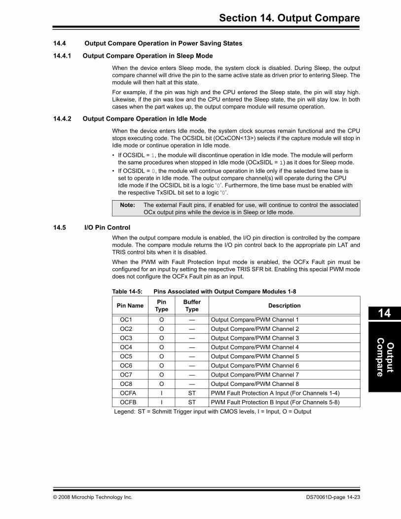
Table 14-5: Pins Associated with Output Compare Modules 1-8
Note: The external Fault pins, if enabled for use, will continue to control the associatedOCx output pins while the device is in Sleep or Idle mode.
Pin Name PinType
BufferType Description
OC1 O — Output Compare/PWM Channel 1OC2 O — Output Compare/PWM Channel 2OC3 O — Output Compare/PWM Channel 3OC4 O — Output Compare/PWM Channel 4OC5 O — Output Compare/PWM Channel 5OC6 O — Output Compare/PWM Channel 6OC7 O — Output Compare/PWM Channel 7OC8 O — Output Compare/PWM Channel 8OCFA I ST PWM Fault Protection A Input (For Channels 1-4)OCFB I ST PWM Fault Protection B Input (For Channels 5-8)
Legend: ST = Schmitt Trigger input with CMOS levels, I = Input, O = Output
© 2008 Microchip Technology Inc. DS70061D-page 14-23
dsPIC30F Fam
ily Reference M
anual
DS
70061D-page 14-24
© 2008 M
icrochip Technology Inc.
it 2 Bit 1 Bit 0 Reset State
0000 0000 0000 0000
0000 0000 0000 0000
1111 1111 1111 1111
1111 1111 1111 1111
— TCS — 0000 0000 0000 0000
— TCS — 0000 0000 0000 0000
uuuu uuuu uuuu uuuu
uuuu uuuu uuuu uuuu
OCM<2:0> 0000 0000 0000 0000
uuuu uuuu uuuu uuuu
uuuu uuuu uuuu uuuu
OCM<2:0> 0000 0000 0000 0000
uuuu uuuu uuuu uuuu
uuuu uuuu uuuu uuuu
OCM<2:0> 0000 0000 0000 0000
uuuu uuuu uuuu uuuu
uuuu uuuu uuuu uuuu
OCM<2:0> 0000 0000 0000 0000
uuuu uuuu uuuu uuuu
uuuu uuuu uuuu uuuu
OCM<2:0> 0000 0000 0000 0000
uuuu uuuu uuuu uuuu
uuuu uuuu uuuu uuuu
OCM<2:0> 0000 0000 0000 0000
uuuu uuuu uuuu uuuu
uuuu uuuu uuuu uuuu
OCM<2:0> 0000 0000 0000 0000
uuuu uuuu uuuu uuuu
uuuu uuuu uuuu uuuu
OCM<2:0> 0000 0000 0000 0000
C1IF IC1IF INT0 0000 0000 0000 0000
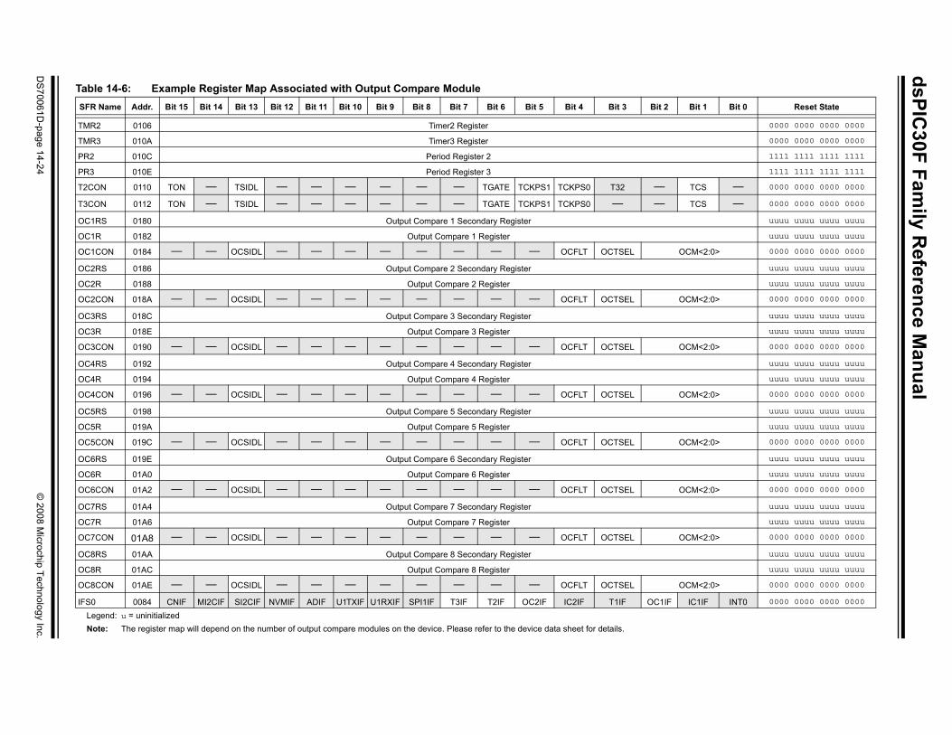
Table 14-6: Example Register Map Associated with Output Compare ModuleSFR Name Addr. Bit 15 Bit 14 Bit 13 Bit 12 Bit 11 Bit 10 Bit 9 Bit 8 Bit 7 Bit 6 Bit 5 Bit 4 Bit 3 B
TMR2 0106 Timer2 Register
TMR3 010A Timer3 Register
PR2 010C Period Register 2
PR3 010E Period Register 3
T2CON 0110 TON — TSIDL — — — — — — TGATE TCKPS1 TCKPS0 T32
T3CON 0112 TON — TSIDL — — — — — — TGATE TCKPS1 TCKPS0 —OC1RS 0180 Output Compare 1 Secondary Register
OC1R 0182 Output Compare 1 Register
OC1CON 0184 — — OCSIDL — — — — — — — — OCFLT OCTSEL
OC2RS 0186 Output Compare 2 Secondary Register
OC2R 0188 Output Compare 2 Register
OC2CON 018A — — OCSIDL — — — — — — — — OCFLT OCTSEL
OC3RS 018C Output Compare 3 Secondary Register
OC3R 018E Output Compare 3 Register
OC3CON 0190 — — OCSIDL — — — — — — — — OCFLT OCTSEL
OC4RS 0192 Output Compare 4 Secondary Register
OC4R 0194 Output Compare 4 Register
OC4CON 0196 — — OCSIDL — — — — — — — — OCFLT OCTSEL
OC5RS 0198 Output Compare 5 Secondary Register
OC5R 019A Output Compare 5 Register
OC5CON 019C — — OCSIDL — — — — — — — — OCFLT OCTSEL
OC6RS 019E Output Compare 6 Secondary Register
OC6R 01A0 Output Compare 6 Register
OC6CON 01A2 — — OCSIDL — — — — — — — — OCFLT OCTSEL
OC7RS 01A4 Output Compare 7 Secondary Register
OC7R 01A6 Output Compare 7 Register
OC7CON 01A8 — — OCSIDL — — — — — — — — OCFLT OCTSEL
OC8RS 01AA Output Compare 8 Secondary Register
OC8R 01AC Output Compare 8 Register
OC8CON 01AE — — OCSIDL — — — — — — — — OCFLT OCTSEL
IFS0 0084 CNIF MI2CIF SI2CIF NVMIF ADIF U1TXIF U1RXIF SPI1IF T3IF T2IF OC2IF IC2IF T1IF OLegend: u = uninitializedNote: The register map will depend on the number of output compare modules on the device. Please refer to the device data sheet for details.
Section 14. Output C
ompare
© 2008 M
icrochip Technology Inc.D
S70061D
-page 14-25
IFS IC7IF INT1IF 0000 0000 0000 0000
IFS OC6IF OC5IF 0000 0000 0000 0000
IEC IC1IE INT0IE 0000 0000 0000 0000
IEC IC7IE INT1IE 0000 0000 0000 0000
IEC OC6IE OC5IE 0000 0000 0000 0000
IPC INT0IP<2:0> 0100 0100 0100 0100
IPC IC2IP<2:0> 0100 0100 0100 0100
IPC INT1IP<2:0> 0100 0100 0100 0100
IPC OC4IP<2:0> 0100 0100 0100 0100
IPC OC5IP<2:0> 0100 0100 0100 0100
TaSF Bit 1 Bit 0 Reset State
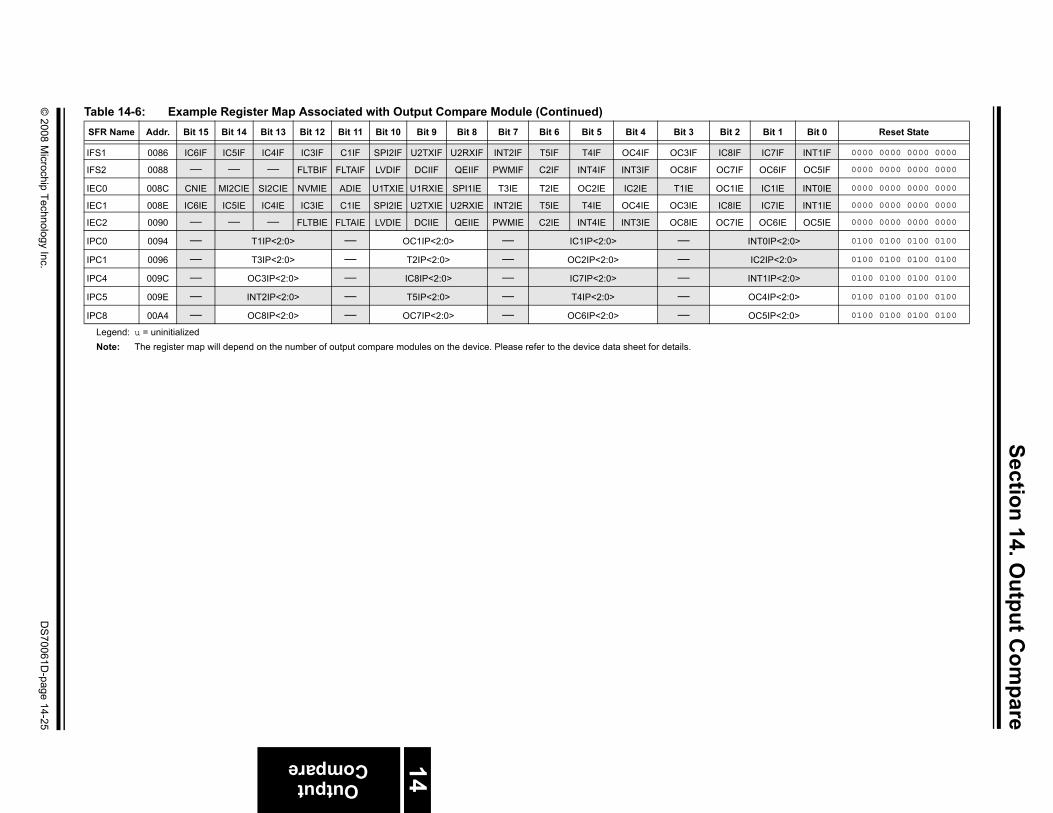
OutputCompare 14
1 0086 IC6IF IC5IF IC4IF IC3IF C1IF SPI2IF U2TXIF U2RXIF INT2IF T5IF T4IF OC4IF OC3IF IC8IF
2 0088 — — — FLTBIF FLTAIF LVDIF DCIIF QEIIF PWMIF C2IF INT4IF INT3IF OC8IF OC7IF
0 008C CNIE MI2CIE SI2CIE NVMIE ADIE U1TXIE U1RXIE SPI1IE T3IE T2IE OC2IE IC2IE T1IE OC1IE
1 008E IC6IE IC5IE IC4IE IC3IE C1IE SPI2IE U2TXIE U2RXIE INT2IE T5IE T4IE OC4IE OC3IE IC8IE
2 0090 — — — FLTBIE FLTAIE LVDIE DCIIE QEIIE PWMIE C2IE INT4IE INT3IE OC8IE OC7IE
0 0094 — T1IP<2:0> — OC1IP<2:0> — IC1IP<2:0> —1 0096 — T3IP<2:0> — T2IP<2:0> — OC2IP<2:0> —4 009C — OC3IP<2:0> — IC8IP<2:0> — IC7IP<2:0> —5 009E — INT2IP<2:0> — T5IP<2:0> — T4IP<2:0> —8 00A4 — OC8IP<2:0> — OC7IP<2:0> — OC6IP<2:0> —
ble 14-6: Example Register Map Associated with Output Compare Module (Continued)R Name Addr. Bit 15 Bit 14 Bit 13 Bit 12 Bit 11 Bit 10 Bit 9 Bit 8 Bit 7 Bit 6 Bit 5 Bit 4 Bit 3 Bit 2
Legend: u = uninitializedNote: The register map will depend on the number of output compare modules on the device. Please refer to the device data sheet for details.
dsPIC30F Family Reference Manual
14.6 Design Tips
Question 1: The Output Compare pin stops functioning even when the OCSIDL bit is notset. Why?
Answer: This is most likely to occur when the TSIDL bit (TxCON<13>) of the associated timersource is set. Therefore, it is the timer that actually goes into Idle mode when the PWRSAVinstruction is executed.
Question 2: Can I use the Output Compare modules with the selected time baseconfigured for 32-bit mode?
Answer: No. The T32 bit (TxCON<3>) should be cleared when the timer is used with an outputcompare module.
DS70061D-page 14-26 © 2008 Microchip Technology Inc.
Section 14. Output CompareO
utputC
ompare
14
14.7 Related Application NotesThis section lists application notes that are related to this section of the manual. Theseapplication notes may not be written specifically for the dsPIC30F Product Family, but theconcepts are pertinent and could be used with modification and possible limitations. The currentapplication notes related to the Output Compare module are:
Title Application Note #No related application notes at this time.
Note: Please visit the Microchip web site (www.microchip.com) for additional ApplicationNotes and code examples for the dsPIC30F Family of devices.
© 2008 Microchip Technology Inc. DS70061D-page 14-27
dsPIC30F Family Reference Manual
14.8 Revision HistoryRevision A This is the initial released revision of this document.
Revision BThere were no technical content or editorial revisions to this section of the manual, however, thissection was updated to reflect Revision B throughout the manual.
Revision CThere were no technical content revisions to this section of the manual, however, this section wasupdated to reflect Revision C throughout the manual.
Revision D (February 2008)Corrects timing example illustrated in Figure 14-9 to reflect proper compare condition(PR2 > OCxRS) and OCxRS compare value (3004).
DS70061D-page 14-28 © 2008 Microchip Technology Inc.
Related Documents