Welcome message from author
This document is posted to help you gain knowledge. Please leave a comment to let me know what you think about it! Share it to your friends and learn new things together.
Transcript


" • ~ .,~_~., .• ' _<__" ~ __ n •• _'.·' < ,.,_~" •. ,<" ••
I
l_-=--~
fLlEXIBLIEDIS~{
MEMORY SYSTEM
User's Guide
; "': .
. ' "" .. "-.: ...
." __ . , . ~q.'J"~.' "

)
{ )
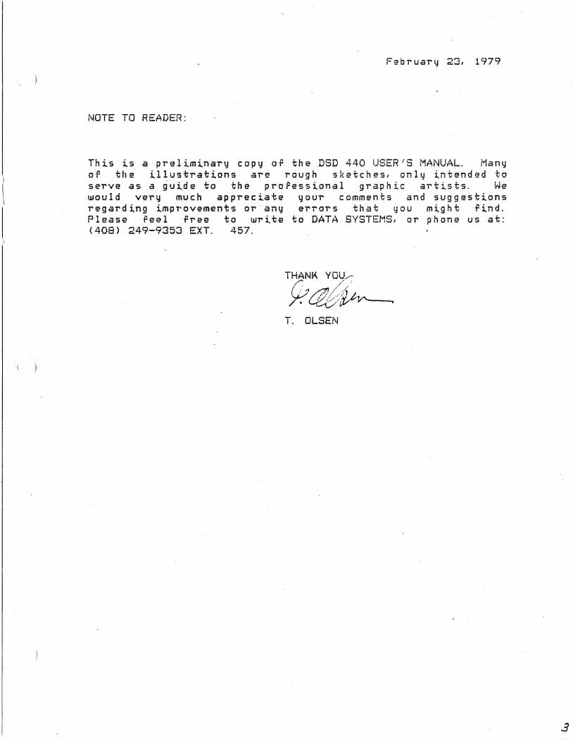
Febru~ry 23~ 1979
NOTE TO READER:
This is a preliminary copy or the DSO 440 US~R!S MANVAL Many or th e ill vstrat ions are rou9 h s k etc h es, on 1 y intend ed to serve as a guide to the proPessional graphic artists. We would very much appreciate your comments and suggestions regarding impT'ovements or' any errors that you mi.ght.rind. Please feel rree to write to ,DATA SYSTEMS, or phone us at: (408) 249-9353 EXT. 457.
T. OLSEN
14
NOTICE:
The infd~mation contained in this manu.l is subJect to change without notice. Data 5~.temsDesign makes no commitment to update nor to keep current the infoT'i1hltion contained in·· this manual. Data S~stem.s Des ign assumes no resp ons ib il i ty ror any errors that matj ap pear in th i.s manua 1. . -Data S~ stems Des ign makes no warranty ,or· any ki.nd with "l"egaT'd to this mate~ialJ inc Iud ing J hut not 1 imi ted. to, the impl ied waY""I".Hit ies of~e"chantabilit~ and fi~ness::f9~ . a particular purp ase.
\.,
,'" .
"~ .,.,- , ~
,::.\ .. .....!::.t .. :...;' ..• ' ~.~ ".'
'":; ."' .
., ..
\ /
l
DSD440 USERS MANUAL
CONTENTS --~--------"""------~,,,,---,,-!,"...:.~~--~ ...... ~-------~--.---- .... -..:. ......... ------.... ----._--_ ..... PREFACE
CHAPTER 1 1-1 1-2 1-3 1-4 1-5
CHAPTER 2 2-1 2-2 2 .... 2. 1 2-2.2 2-2.3 2-2. 4 2-2. 5 2-2.6 2-2. 7 2-2.8 2-2. 9
CHAPTER 3 3-1 3-2 3-3 3 ..... 4 3-5 3-6 3-7 3-8 3-9 .3-10 3-11 3-12
CHAPTER 4 4-1 4-2 4-3 4-4 4-5 4-6 4-7 4-8 4-9 4-10 4-11
GENERAL INFORMATION PRODUCT': INTRODUCTION PURPOSE OF EQUIPMENT DISKETTE SYSTEM DESCRIPTION F£AT\JRES ,
. SPECIFICATIONS
OPERATING MODES AND SYSTEM CONFIGURATION OPERATIONAL MODES OSD 440 SYSTEM CONFIGURATION
FLOPPY DISK DRIVES MASTER CONTROLLER PCB DC POWER SUPPLY POWER DISTRIBUTION PCB ASSEMBLY AC POWER SWITCH FAN CORCOM CONNECTOR AND FUSIN~ INiERFACE GABLE INTERF~CE MODULE
SYSTEM INSTALLATION AND ACCEPTANCE ENVIRONMENTAl- CONSIDERATIONS UNPACKING THE SYSTEM MOUNTING THE DSD 440 CHASSIS INSTALLING THE INTERFACE MODULE AND CABLE INPUT POWER CONSIDERATIONS CHANGING THE OPERATING MODE FINAL INSTALLATION POWERING UP INITIALIZATION RESPONSE CHE,Cl-\ SYSTEM BOOTSTRAP ACCEPTANCE TE.STING ON PDP-ll AND LSI-11 AC.CEPTANCE TESTING ON PDP-8
MAINTENANCE FEATURES OVERVIEW OF MAINTENANCE FEATURES 1'40RMAL vs. "HYPER-OIAGNOS1"!C" I"10DE INDICATORt..EDS, OHIVE LEOS,DIP-SWITCH LED MEANINGS DURING "NORM.AL" 1'100£ D.IP-SWliCH SETTINGS OUR1NG "NORMAL" MODE HARDWARE SELF-TEST ROUTINES "HYPER-DIAGNOSTIC" MODE DIP-SWITCH SETTINGS DURING "HYPER-DIAGNOSTIC" M,ppe: LEO MEANINGS DURING "HYPER-DIAGNOST!C n MODE D~SCRIPT!QN OF "HVPER-DIAGNOST!C"TESTS HOW TO READ THE INDICATOR LEDS

CHAPTER 5' ,5 .... 1
.;~I"" .. " ...... '. , ,~~L 1.
. 5 ... 1. 1. 1 " ~ 5-1. 1. 1. 1
-'5-1. 1. 1. 2 '5-1. 1. 1. 3 5-1. 1. 1. 4 5-1. 1. 1. 5 5-1. 1. 1. 6 5-1. 1. 2 5-1. 1. 2. 1 5--1. 1. 2. 2 5-1. 1. 2. 3 5-1. 1. 2. 4 5-1. 1. 2. 5;
5-1. 1. 2. 6 5-1. 1. 2.7 5-1. 1. 2. 8 5-1. 1. 2. 9 5-1. 1. 3 5.,..1. 1. 3. 1 5-1. 1. 3. 2 5-1. 1. 3. 3 5-1. 1.3.4 5-1. 1. 4 5-1.2 5-1. 2. 1 5-1.2. 1. 1 5-1.2. 1. 2 5-1.2. 1.3 .5-t. 2.1.4 5'-1. 2. 1. 5 5:-1. 2. 1. 6 5~L 2. 1. i 5-1. 2.2 5-1. 2. 2. 1 . 5-1.2.2.2 5-1.2.2.3 5-1.2.2.4 5-1.2.2.5 5-1. 2. 2.6 5-1. 2. 2. 7 5-1.2.2.8 5-1. 2.2. 9 5-1.~.2. 10 5""'1. 2. 3 5 .... 1. 2. 3. 1 5 ..... 1.2.3.2 5-1. 2. 3. 3 5 .... 1. 2. 3.4 5-1. 2. 4
'DSD 440 PROGRAMMING INFORMATION DEC 11 FAMILY PROGRAI'1MERS I INTERFACE
.MODE 1 OPERATION PERIPHERAL DEVICE REGISTERS
COMMAND AND STATUS REGISTER DATA REGISTER DATA BUFFER REGISTER FLOPPY DIS~ TRAC~ ADDRESS FLOPPY DISK SECTOR ADDRESS SYSTEM ERROR AND STATUS REGISTER
MODE 1 PROTOCOLS. FILL SECTOR BUFFER EMPTY Se:CTOR' BUFFER WRITE SECTOR READ SECTOR READ SiAIUS WRITE DELETED DATA SECTOR READ ERROR REGISTER POWER FAIL OR INIT COMMAND DISKETTE FORMATTING
TYPICAL SEQUENCES OF OPERATlONS READ/WRITEBUFFER READ/WR ITE/WRITE D. D. STATUS READ COMMON PROGRAMMING PITFALLS
INTERRUPTS MODE 2 OPERATION
'. PERIPHERAL DEVICE REGISTERS •. COMMAND AND STATUS REGISTER
DATA REGISTER FLOPPY DISK TRACK ADDRESS FI_OPPY DISK SECTOR ADDRESS WORD COUNT REGISTER aUSADDRESS RE:GISTER SYSTEM ERROR AND STATUS REGISTER
MODE 2 PROTOCOLS FILL SECTOR BUFF='ER EMPTY SECTOR BUFFER WRITE SECTOR READ SECTOR SEi MEDIA DENSITY READ STATUS WRITE DELETED DATA SECTOR READ E'XTENOED Sl'ATUS . POWER FAIL OISJi(.ETTE: FORMAT1'INQ tNMULTIPLE DENSITIES
TVPICALSEGUENCES OF OPERATIONS RE:AD/WRITE BUFFER READ/WR ITE/WRI TE D. 0, STATUS REAO COMMON PROGRAMMINGPITFALI...S
INTERRUPTS
)/
5-2 5-2. 1 5-2. 1 .. 2 5-2. 1.3
\ 5-2. 1.4 ! 5-2. 1.5
5-2. 1.6 5-2. 1.7 5-2.2 5-2.2.1 5-2.2.2 5-2.2.3 5-2.2.4 5-2. 2. 5 5-2 .. 2.6 5-2.3 5-2.3.1 5-2.3.2 5-2. 3. 3 5-2.3.4 5-2.3.5 5-2.3.6 5-2.3.7 5-2.3.8 5-2.3.9 5-2.3.10
CHAPTeR 6 6-1
\ 6-2 I 6-3
6-3. 1 6-3. 2 6-3. 3
·'i· "' .. " ~ 'j. ... ,<
, )
DEC PDP-8FAMILY PRQGRAt1ME:RS I INTERFt\CE·.·:-;~J;,.')" INSTRVCTION SET . '. "'i
. THE TRANSFER DATA REGISTER (XDRJ:· INSTRuctION . THE SKIP ON TRANSFER REGUEST.(StR) INSTRUCTION THE, SKIP ON ERROR (SER) INSTRUCTION THE SKIP ON DONE (SDN) INSTRUCTION THE INTERRUPT ENABLE/DISABLE (INTR) INSTRUCTION THE INITIALIZE (INIT) INSTRUtTION
REGISTER DESCRIPTIONS COMMAND REGISTER TRACK ADDRESS REGISTER SECTO.R ADDRESS REGISTER DATA BUFFER REGISTER ERROR AND STATUS REGISTER (MODE 1 OPERATION) ERROR AND STATUS REGISTER (MODE 2 OPERATION)
FUNCTION CODE DESCR IPTIONS I
FILL BUFFER EMPTY BUFFER WRITE SECTOR READ SECTOR SET MEDIA DENSITY READ S,TATUS WRITE DELETED DATA SECTOR READ ERRQR REGISTER POWER FAIL DISKETTE FORMATTING IN MULTIPLE DENSITIES
HIGH LEVEL SOFTWARE AND THE DSD 440 GE~tERATING AN RT11 SYSTEM DISKETTE
. GENERATING DOUBLE DENSITY DISKETTES FRD440 SYSTEM DIAGNOSTIC PROGRAM· .
PROGRAM LOADING AND MONITOR PROTOCOL FRD440 PROGRAM FUNCTIONAL MODES . PROGRAM STf\TUS AND ERROR PRINTOUTS
LIST OF ILLUSTRATIONS --. ........... ~...,"-'..., ___ ... II!IIIIioIiI ..... ____ ~ __ ~ ..... _.;..._""'!"_. __ ~ ___ .~ __ :-_ .... _______ ... _ .......... ___ .......... ____ .. __ . __ :-__
FIGURE 1-1 FlGURE 1.-.:2 FIGURE 1-3 FIGURE 1-4
FIGURE 2-1 FIGURE 2:"'2 FIGURE 2-3
FIGURE 3-1 FIGURE 3-2 FIGURE :3-3 FIGURE 3-4 FH~URE 3-5 FIGURE 3-0 FIGURE 3-7 FIGURE 3-8 FIGURE :3-9 FIGURE: 3-10
FIGURE 4-1 -PI~UR'E 4-2
FIGURE 4-3 FIGURE 4-4
FIGURE 5-1 FIGUR€, 5 ..... 2 FIGURE 5-3 FIGURE 5-4 FIGURE 5--5 FIGURE 5-6 FIGURE 5-7 FIGURE 5 .... 8 FIGURE 5-9 FIGURE 5-10 FIGURE 5-11 FIGURE 5-12 FIGURE 5-13 FIGURE '5-14 FIGURE 5-15 FIGURE 5-16 FIGURE 5-17 FIGURE 5-18 FIGVRE 5-19 FIGURE 5-20
SYSTEM BLOCK DIAGRAM SINGLE AND DOUBLE SIDED DISKETTE SINGLE DENSITY TRACK FORMAT DEC DOUBLE DENSITY TRACK FORMAT
DSD 440 SYSTEM MASTER CONTROLLER PCB DC POWER SUPPLY
CHASSIS SLIDES MOUNTING BULLET ENl'ERING HOLE IN REAR OF UNIT FRONT VIEW OF CHASSIS WITH FRONT PANEL REMOVED LSI-11 INTERFACE MODULE OPTION PRIORITY IN DEC BACKPLANES FOR LSI-ll PDP-l1 INT.ERFACE MODULE INTERRUPT PRIORITY LEVELS PDP-8 INTERFACE MODULE MASTER CONTROLLER BOARD DIP-SWITCH INSERTING A DISKETTE INTO A DRIVE
SWITCH AND LED ORIENTATION ON MASTER CONTROLLER CARD DIP-SWITCH SETTING WHEN PRODUCT IS SHIPPED EXAMPLE uHYPER-DIAGNOSTIC II DIP-SWITCH CONFIGURATION LED INTERPRETATION EXAMPLES
COMMAND AND STATUS REGISTER; MODE 1 (RXOl COMPATIBLE) REGISTER FORMATS. 11 FAMILYi MODE 1 (RXOl COl"1PATIBLE)
)
FILL / EMPTY BUFFER PROGRAM EXAMPLEiMODE 1 j! READ I WRITE SECTOR PROGRAM EXAMPLE; MODE 1 COMMAND AND STATUS REGISTER; MODE 2 (RX02 COMPATIBLE)
,REGISTER FORMATS;. 11 FAMILY; MODE 2 (RX02 COMPATIBLE) FILL /EMPTY BUFFER PROGRAM EXAl"1PLE; i10DE 2 READ / WRITE SECTOR PROGRAM EXAMPLE; MODE 2 COMr-1AND REGISTER FORMAT; PDP-8; MODE 1 COMMAND REGISTER FORMAT; PDP-8; MODE 2; 12 BIT WORD COMMAND REGISTER FORMAT; PDP-8; MODE 2; 8 BIT WORD TRACK ADDRESS REGISTER; PDP-S SECTOR ADDRESS REGISTER; PDP"'8 DATA BUFFER REGISTER; PDP-8 ERROR/STATUS REGISTER; PDP-8; MODE 1 ERROR/STATUS REGISTER; PDP-8; MODE 2 FILL BUFFER FLOW CHART; pop-a EMPl'Y BUFFER FLOW CHART; pOP-a WRITE/READ/WRITE DEL. DATA FLOW CHART; PDP-a
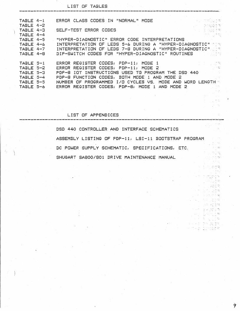
LIST OF TABLES ------------~------------~----~---------------~_~ __ ~ __ --~~-~~~_~~~~~~~w. TABLE 4-1 TABLE 4-2 TABLE 4:-3 TABLE 4 ... 4 TABLE 4-5 TABLE 4-6 TABLE 4-7 TABLE 4-8
TABLE 5-1 TABLE 5-2 TABLE 5-3 TABLE 5-4· TABLE 5-5 TABLE 5-6
ERROR CLASS CODES IN IINORMAL" MODE
SELF-TEST ERROR CODES
.. _ .. p- <I :~_.r .,
"' .. - . ,', ., .. ~ . .... J ~~.': . ....-.
'\.;"'.,:" :
"HYPER-DIAGNOSTIC" ERROR CODE INTERPRETATIONS INTERPRETATION OF LEDS 5-6 DURING A "HYPER-DIAGNOSTIcn INTERPRETATION OF LEDS 7-8 DURING A uHYPER-DIAGNOSTIC". DIP-SWITCH CODES FOR I1HYPER-DIAGNOSTIC II ROUTINES
ERROR REGISTER CODES; PDP-i1i MODE i ERROR REGISTER CODES; PDP-ll i 1'-10 DE 2 PDP-8 lOT INSTRUCTIONS USED TO PROGRAM THE DSD 440 PDP-8 FUNCTION CODES, BOTH MODE 1 AND MODE 2 NUMBER OF PROGRAMMED 1/0 CYCLES VS. MODE AND WORD LENGTH·" ERROR REGISTER CODESiPDP",Si MODE 1 AND MODE 2
LIST OF APPENDICES
DSD 440 CONTROLLER AND INTERFACE SCHEMATICS
ASSEMBLY LISTING OF PDp .... 11, LSI-!! BOOTSTRAP PROGRAi'1
DC POWER SUPPLY SCHEMATIC, SPECIFICATIONS, ETC.
SHUGART SASOO/SOl DRIVE MAINTENANCE: MANUAL
'"\ -~:'J .....
. ~ ", .~ ·i "" .
. ,'- -:, .. ':' ~.

PREFACE
The purpose df this manual is to provide the u.er with sufficient information to correctly set up and operate the DSD 440 Double DensitlJ Floppy Disk Memory System. Included is a detailed- description of what the product is, how to install it, how to program it, and how to maintain it. A l1amilia-rity with basic data processing terminology and the DEC PDP-ii, LSI-II, and PDP-8* is assumed in some sections.
* DEC, PDP, UNIBUS, and OMNIBUS are registered trademarks 011 Digital Equipment Corporation.
/1
IJ..
1-1 PRODUCT INTRODUCTION
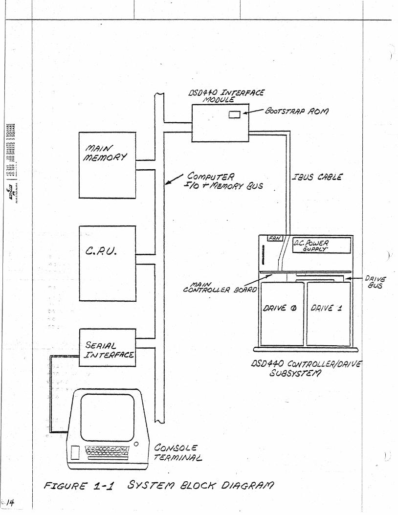
The DSD 440 F'loppy Disk Memory System i.s a random access data storage subsystem. Data is stored in fixed-length blocks on preformatted industry standard 8 inch diameter flexible disks. Each flexible disk, OT' "diskette"can store up to 512 kilobytes (8 bits per byte) of data. The average access time to this data is 296 milliseconds and the average sustainable data transll-er rate is 16 kilobytes per seco,nd. A complete data storage system consis"ts of a rack .... mountab Ie controller/d~ive subsyst.m. a computer interface module. and an interconnecting cable.
The nSD 440 can be used with the DIGI1;AL EGUIPMENT CORPORATION PDP-ll, PDP-9, or LSI-ll computers using interface modules supplied by DATA SYSTEMS DESIGN. When used with the ap propr iate interfac e mod u 1 e, th e DSO 440 is hardware, software, diagn-ostic, and media compatible with the DEC RX02 double density flexible di .• k system. In addition. the DSD 440 has many features nat found in the DEC RX02 s~st~m including:
* HARDWARE BOOTSTRAP * SEU:;'-CONTAINED DIAGNOSTICS AND UTILITY PROQRAMS * DISKETTE FORMATTING
The DSD 440 can be used with other types of computers if a user design~ an interface module th~t conforms to the PSO 440 V Inte~l"face Bus Specification.
f ' (
\ )
1-2 PURPOSE OF EGUIPtlENT
A Floppy Disk Memory System consists of a set oT mecha~ical and ele~tronic componants arrange~ Tor the purpose of passing data between a host computar and a flexible disk or, as IBM calls it, a "diskette ll • Due to their low cost and convenient packaging, -flexible disks have become a very popular transportable data storage media for man~ applications. This popularity will be further increased by flexible disk systems such as the DSD 440 which provide increased capacity and performance over first generation flexible disk systems at only a slight increase in cost.
The DSD 440 was designed to provide a highly reliable, low cost and co.mpact flexible disk system j:hat is totally com!1atible with the DEC RX02. While satis-fying these design goals, advances in L.SI circuitry and'microprocessors have made possible the incorporation of a number of "BONUS" features. Important amang 'these featur.s are:
* The ability to execute test and utility programs on the controller/drive subsy$te~ even when the controller and drives are not connected to a host computer.
* The ability to write-format diskettes in two industry standard formats.
Hi.gh reliability is attai.ned by using L.SI ci.rcuits. by burnl.ng-in and pretesting all components. and b'J using f iel d-proven Stl ugart Assoc iates fie x ib 1 e dis k drive s. L.ow cost is attained by a design which minimizes parts count and assemb lies. Compac tnes s is provid ed by pac.kag ing two dis k drive~ horizontally in a 5 1/4~ high rack-mountable chassis. Figure l-i 5 h oUJs th e Sy stem Blot k Diagram. .
/.3
~E§ ::::r.J: ~~'" 000 'I')~~ __ ""0- ..
:0:0== l"JMM::
~/'f - ---
c.p.u.
.,.\,\
\"
FIGURe 1..-1
c==::==:::::::::~~ I .oS/)#4-0 CO#TA'OLLER/OP.I;~
SuaSYSTE/? I
)
, }
)
- -•• ,.~ ~ -".q., .... ...... :-... --'" .......... -~~.~
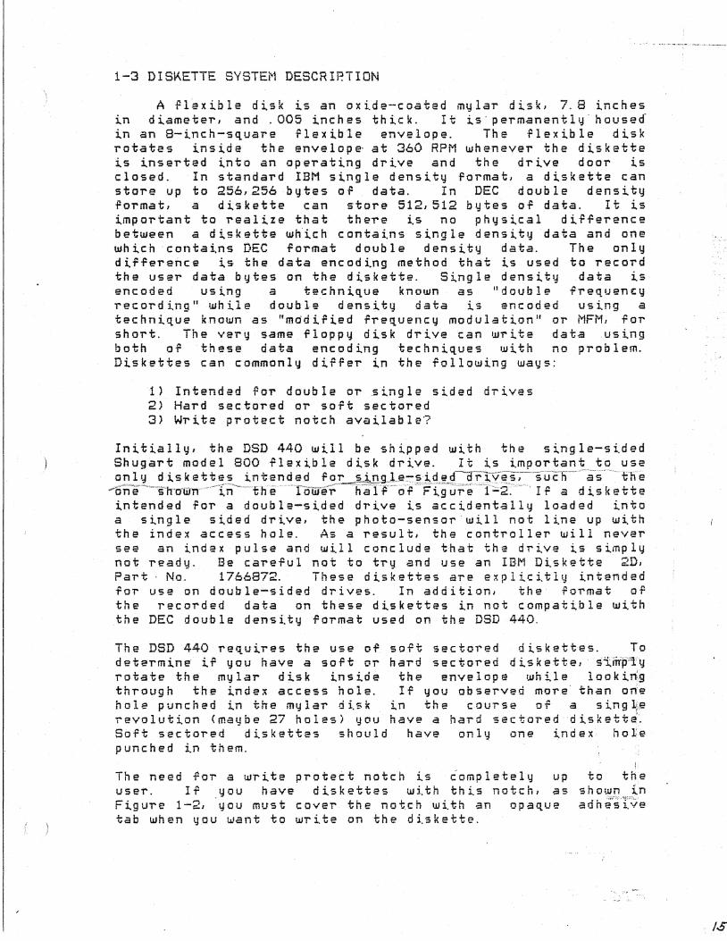
1-3 DISKETTE SYSTEi'1 DESCRIPTION
A flexible disk is an oxide-coated mylar disk, 7.8 inches in diameter, and .005 inches thick. It is'permanantly' house~ in an 8-inch-square flexible envelope. The flexible disk rotates inside the envelop~ at 360 RPM whenever the diskette is inserted into an operating drive and the drive door is closed. In standard IBM single density format, a diskette can store up to 256,256 bytes of data. In DEC double density format, a diskette can store 512,512 bytes of data. It is important to realize that there is no physical difference between a diskette which contains single density data and one which 'contains DEC format double densi.ty data. The only differerice is the data encoding method that is used t~ record the user data bytes on the diskette. Single density data is encoded using a technique known as "double frequency recording" while double density data is enc~ded using a technique known as "mddiPied frequency modulation" or MFM, for short. The very same floppy disk drive can write data ,using both of these data encoding techniques with no problem. Diskettes can commonly diffar in the following ways:
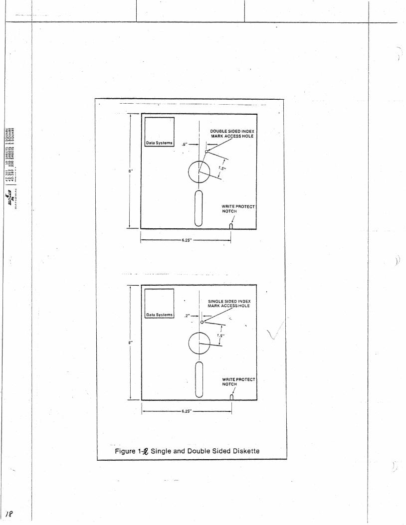
1) Intended for double or single sided drives 2) Hard sectored or soft sectored 3) Write protect notch available?
Initially, the DSD 440 will be shipped with the single-sided Shugart model 800 flexible disk drive. It is important to use on 1 y 1:1 is k ette? intended for s in...9-l .. e.:::§;.~LE!.nr-m~s,-suc-fl·---a·s---··lilie
""On e'---$-l'rtfurtl"'-'rn-'-"t'h'e"'-ToUl6-h::;J:~'~o":P'"F i9 ure""P';;2:"~~" I fad is k e tt e int2nded for a double-sided drive is accidentally loaded into a single sided drive, thephoto-sensor'will not li.ne up wi.th the index access hole. As a result, the controller will never see an index pulse and will conclude t~at the drive is simply not ready. Be careful not t~ tr~ and use an IBM Diskette 2D. Part' No. 1766872. These diskettes are explicitly intended for use on double-sided drives. In addition, the format of the recorded data on these diskettes in not compatible with the DEC double density format used on the DSD 440.
The DSD 440 reG-uires the use of soft sectored diskettes. To determine i-Pyou have a s-oft or hard sectored diskette, s'i,riijj:;t'y rotate the mt,llar disk inside the envelope l.I1oile laokin:g through the index access hole. If you observed mare' than ori~ hole punched in the mylar disk in the tourse of a sing~. revolution (maybe 27 holes> you have a hard sectored'diskett~~ Soft sectored diskettes should have only one ind.x hor. punched in them.
The need for a write protett notch is ~ompletely up to the user. If you have diskettes wi.th thi.s notch, as sholJJO in Figure 1-2, you must cover the not.en with an opaque adhe"'sr~e tab when you want to write on the diskette.
-. /..5

Ib
Flexible disk systems are ideal "for applications that require a low cost, medium speed, random access memory device. Flexible disk systems provide faster access times than magnetic t.:apes, and cost less than the bigger rigid disk systems. They can replace paper tape or punch card storage methods. Because the diskettes can be quickly removed, the amount of data that is immediately accessible with a flexible disk system is far greater than the capacity of a single
diskette. Diskettes can be exchanged in a drive within 'seeonds, the limiting factor being the dexte1'i.ty o-r the use1'.
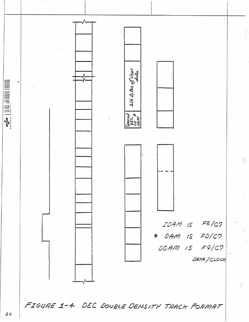
Unli.ke 1'i9id disks, indust1'Y standards have been ~stablishe~ -ror the physical format o-r the recorded data on diskettes. Each of the form.:atsPQssible on the DSD 440 record data on 77 concentric tracks, at a track density of 48 t1'acks per' inch. Each' t-rack is di.vided up into 26 sectors. Each sector contains 128 bytes of user data in single density format, and 256 bytes a-r user data i~ double density format. Associated with each sector is an 10 field and a data -rield. The 10 field contains a unique bit pattern, known as the 10 address mark, that enables the controller to rec~gnize the start of an In field. This ID field contains a track address • by te, ahead ad dress by te, and a sec tor addres s byte. Appended to these disk address bytes is a pair of CRC (cyclic redundancy check) bytes which al'e used to dete1'mine if a data e1'1'01' has occurred whil~ 1'eading the disk address data. The controll~r is able to rInd the secto1' it wants to 1'ead or lIJ1'ite by scanning the ID fields. Note that the ID fi.eld Just desc1'ibed is exactly the same fo1' diskettescontai.ning single density data and those containing dOUble density data. In both Cases, all the data bytes contained in the ID 'ield are encoded using the "double frequency" reco~ding technique associated with single density. Following the ID field of each sector is the data field. The be~inning of the data field is identified b~ anothe1' unique bit patte1'n ~alled the Data Address Mark. Following this mark are the 128 or 256 bytes of data and anothe-r pair of_CRC check bytes. Fi.gu1'e 1-3 is a schematic representation of the f01'mat of a single density track. Figu1'e 1-4 shows the format of a DEC compatible double density track. Note that only the 256 user data bytes and the 2 ORC bytes following the data are ~ncoded using the "m~dified frequency modulation" recor~ing technique. All the other fields (p1'sCimble. postamble. ID) are recorded the same as in the single density track format.
)
'\
}i

TECHNICAL COMPATIBILITY NOTE::
The "modified frequency modulation'l encoding algorithm which DEC chose to use when implementing the RX02 is not exactly 'he same as the MFM encoding algorithm one would find desc~ibed in a communications theory textbook. For this reason <and oi;hers j I both the RX02 and DSD 440 are not compatible with the IBM dOOble density recording technique which uses a "textbook" MFM encoding algorithm to record data. The' IBM format does not mix "double frequency" encoding and "modified frequency modulation" recording on the same track. The fact that the DEC double density -flormat DOES mix these two entoding algorithms is the basis -flor why a stand~rd MFM enco.dingalgorithm could not be used on the RX02 and DSD 440. These ~echnical details in no way relate to the reliability or performance o-fl the DSD 440 machine. They were included here to give the reader a better understanding of why what we call "DEC double density 'ormat~ is not compatible with IIIBM double density format".
/1
JR
8"
-I
8"
DOUBj;E SIDED INDEX MARX ACCESS HOLE .
Dala Systems .S'· __
WRITE PROTECT NOTCH
I
1-----------·6.25" -------1/
DataSyslems
I SINGLE SlDED INDEX I MARK ACCESS HOLE
.2"-1~ • 0· __
t 1.5"
J
WRITE PROTECT NOTCH
I
--------6.25·'------1
Figure 1-t Single and Double Sided Diskette
, .
)' 1./
\ . I

"'()
l-, ~ ~ ())
~ l
<JJ
~ ~ C"-O)
~ ~ " ,~
~ ~ ~
~ ~
~ '\
~!ia ~
NATIONAL
4·2·j/H 50 StUnS 5 SQUARE .. 2-382 100 SHEETS 5 SQUARE <2·389 200 StiEETS 5 SQUARE
r n-1L ______ _ _.""'CAl'Non -~."
.... VTU
~INAL ~
I DAU GA' " . FIELD I"AE,I'oO[X r "'CORa ,. l2Q 8.,.11:5
I
10 ADDRESS I '''ACK
~,U"FI" ADc;.J~iss
~ ~ ~ ~
&) ....... <n
~ ~ ~ Qj ~ ~""" C; f\ C')
n "\..1 ""\l :x-v.
~
G .... r 1
1'05T 11-40£)(
n BVTES
zffujis , 1
/
'0 G~p 1
10 RECORD G" , , .,
6YTi:S
I I
.'tTl:
Sf'CIOR ACDRESS
OA'A Fl{LO RECORO . ,
lEt\qfS
G£.' 1 OArAoGAP lJ 8VTfS
CAC 6YH
>0 RECORD
• 1 ct.,. 2
I
~cilC; ,8Y-liE 2
DATA FIELD RECORD . ,
I
t1 / ~
-__ .--------_1 GAr 2
\ I I I I
"-~
~ ~ ~
tHE. 0(1)0' HI tHE": Q(»
J
~ ____ 1111"1£5 ~+-'."£s_1 "",*'ITf (~A IE
ruA~ON fOR upo ... rE OF N£)I,T DATA flf;. .. O
I
'0 GA'l RECORO
• 1
I
OA'rIl.OA DELE TEO 04TA AODRfSS ... ARK
I~£k CIOQ' HI
GAP 2
I
I
DATA fiELD
+ RECORD .,
II
128 ByTES OF USER OATA
G ... f J
i>'"
IHue: 00 Of FfJ IHE" OCI
'0 A£(:O"O
.>6
l--.v'l£~ J-.. m'~ ~ WAITE ruAN~fF
• Wh.,jI "to. 00 Qf , f II QIlhQ,n ....
f F '1 • ...:;omlTlfi'f\o.d,
fOR UPDATE OF l-~fV.OUS DATA. fiELD
.. "" ,
CAC IVTE ~
'".
co.ATAft£LD
.. "". -< RECORD .,.
CAC lylE 2
Ii I·r I ~'
t f y-:---
':-1,
.f . I,
I . "
~ ~
,': ;...
_No-~
~~=~ :"1MM f
~:;;~{
I j.O
-r/'-r-
A
-R=
-'-J'-~
\..
~~ ~~ ~ ,.., ~ ~ ~ t'il
-.,. ~cJ ;-: ~Iu~~ *q~
.£<21111 /S F£/C?
~ Ot9/Yl IS ,cole?
OIJ~//l IS F9/C?
iJI'9T/1 /CLDC.
1-4 FEATURES
* HARDWARE COMPATIBLE The DSD 440 can be used on (UNIBUS)' LSI-11 (G-BUS), or computer when ordered with interface module.
* SOFTWARE Cm'1PATIBLE
any DEC PDP-11 PDP-8 (ONNIBUS)
the appropriate
All DEC software intended ror either t'he RXOl or the RX02 will run on the DSD 440 without mod i il icat ion. ~() __ .~~1_ .. JL~tY:.:b~.e hand I er or d~~~$ ar~ requ~~ea~ . '~
* MEDIA AND FORMAT COMPATIBLE The DSD 440 can read and write diskettes in the indust"ystandard ilol'mats. This means diskettes can be freely interchanged between the DSD 440, DEC RX01 ~ndRX02.
* INCREASED STORAGE CAPACITY A two drive configuration is capable of one megabyte of data storage.
* DISKETTE FORMATTING CAPABILITY The DSD 440 permits write-formatting of diskettes.
, The physical sector sequen~e writ~en on the diskette can be determined by the programmer so that hard sector interleaving is pO$sible. Dtskette$ ~ith "blown" headers can usually be recovered by reformatting.
* LOW PROFILE 5 1/411 HIGH'CHASSIS The DSn 440 takes up ~alf as much rack space as th e DIE:C RX02.

))
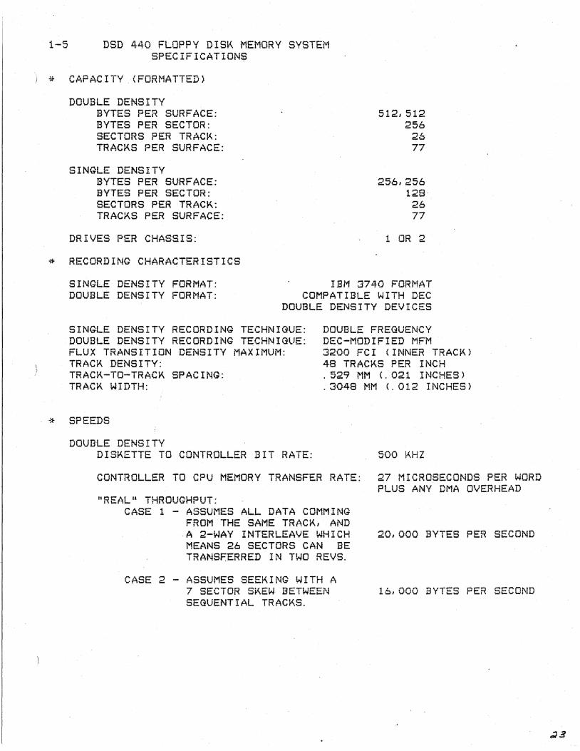
1-5 DSD 440 FLOPPY DISK MEMORY SYSTEM SPECIFICATIONS
i * CAPACITY. (FORMATTED)
DOUBLE DENSITY BYTES PER SURFACE: BYTES PER SECTOR: SECTORS PER TRACK: TRACKS PER SURFACE:
SINGLE DENSITY BYTES PER SURFACE: BYTES PER SECTOR: SECTORS PER TRACK: TRACKS PER SURFACE:
DRIVES PER CHASSIS:
* RECORDING CHARACTERISTICS
512, 512 256
26 77
256,256 128 26 77
1 OR 2
SINGLE DENSITY FORMAT: DOUBLE DENSITY FORNAT:
IBM 3740 FORI'"1AT COMPATIBLE WITH DEC
DOUBLE DENSITY DEVICES
SINGLE DENSITY RECORDING TECHNIGUE: DOUBLE DENSITY RECORDING TECHNIGUE:
DOUBLE FREGUENCY DEC-MODIFIED MFl'-1
FLUX TRANSITION DENSITY MAXIMUM: TRACK DENSITY:
3200 FCI (INNER TRACK) 48 TRACKS PER INCH
TRACK-TO-TRACK SPACING: TRACK WIDTH:
. 529 ~1M <. 021 INCHES)
.3048 MM (.012 INCHES)
* SPEEDS
DOUBLE DENSITY DISKETTE TO CONTROLLER BIT RATE: 500 KHZ
CONTROLLER TO CPU MEMORY TRANSFER RATE: 27 MICROSECONDS PER WORD PLUS ANY DMA OVERHEAD
"REALIl THROUGHPUT: CASE 1 - ASSUMES ALL DATA COMMING
FROM THE SAME TRACK, AND A 2-WAY INTERLEAVE WHICH 20,000 BYTES PER SECOND MEANS 26 SECTORS CAN BE TRANSFERRED IN TWO REVS.
CASE 2 - ASSUMES SEEKING WITH A 7 SECTOR SKEW BETWEEN SEGUENTIAL TRACKS.
16,000 BYTES PER SECOND
SINGLE DENSITY DISKETTE TO CONTROLI...ER BIT RATE: 250 KHz )
CONTROLLER TO CPU MEMORY TRANSFER RATE 27 t1ICROSECONDS PER WORD IN RX02 COMPATIBLE 1'-10DE: PLUS ANY DMA OVERHEAD
CONTROL.LER TO CPU TRANSFER RATE WHILE FUNCTION OF THE PROGRAM IN RXOl COMPATIBLE MODE: LOOP EXECUTION TIME
UREAL" THROUGHPUT: CASE t - SAI'-1E AS DESCRIBED ABOVE 10,000 BYTES PER SECOND
CASE 2 .... SAME AS DESCRIBED ABOVE • 8,000 BYTES PER SECOND
DISKETTE ROTATION: 360 RPM +/- 27-HEAD STEP RATE: HEAD LOAD T I i"lE :
8 MSEC TRACK .... TO-TRAC}' (SA800) 35 MSEC
AVERAGE ACCESS TIME: 296 MSEC MAXIMUM ACCESS TIME: 645 M$EC
* INTERFACE CHARACTERISTICS
INTERFACE MODUI.,.E BACKPLANE REQUIREMENTS
PDP-8 <OMNIBUS} 1 QUAD SI.,.OT '-...f"I.,.S:I-ll (G-BUS)
PDP-1t (UNIBUS) 1 HALF-QUAD SL.oT 1 QUAD SPC SLOT
INTERFACE MODUL.E POWER CONSUMPTION (+5 VOl... T9)
DSD 440-2131 (Pop-e) DSD 440-4432 (LSI .... 11) DSD 440-4430 (PDP-1l)
STANDARD DEVICE ADDRESSES DR CODES
DSD 440-2131 (PDP-e) VDSD 440-4432 ( I...S I -11 )
DSD440-4430 (PDP-1I)
NOMINAL 1..37 AMPS 1.44 AMPS 1. 44 AMPS
MAXIMUM 2.35 At1PS 2. 59 AMPS 2.17 AMPS
6750 - 6757 777170 - 777172 777170 - 777172

* CHASSIS POWER CONSU~1PTION
MASTER CONTROLLER NODULE, CURRENT FROM 5 VOLT SUPPLY: SINGLE DRIVE CHASSIS: DUAL DRIVE CHASSIS:
SELECTABLE INPUT VOLTAGES:
I NP UT FR EGUENC I ES:
FUSE RATINGS: SINGLE DRIVE; 115 VAC
DUAL DRIVE; 115 VAC SINGLE DRIVE; 220 VAC
DUAL DRIVE; 220 VAC
4 Al'1PS N01"lINAL, 150 WATTS IDLE, 248 WATTS IDLE,
5. 6 AMPS MAX IMU~1 232 WATTS BUSY 330 WATTS BUSY
100 VAC OR 120 VAC RNS +/- 10% 220 VAC OR 240 VAC RMS +/- 10%
50 HZ +/- 1 HZ 60 HZ +/- 1 HZ
2. 5 ANP SLOW-BLOW 3 AMP SLOW-BLOW 1.2S AMP -SLOW-BLOW 2 AMP SLOW-BLOW

(.
* HEAT DISSIPATION (IN BTU'S PER HOUR)
NOMINAL MAXIMUM 44 ALL DSD 440 INTERFACE CARDS;
MASTER CONTROLLER CARD: SINGLE DRIVE CHASSIS: . (IDLE)
(BUSY) DUAL DRIVE CHASSIS: (IDI.,..E)
(BUSY)
* ENV I RONl"lENT
24 85
290 503
. 468 681
95 512 791 846
1125
U. L. LISTING: EDP EGUIPMENT, UL 478 STANDARD
OPERATING TEMPERATURES INTERFACE MODULES: MASTER CONTROLLER CARD: CHASSIS: DISKETTES: DISKETTE MAXIMUM THERMAL GRADIENT:
NON-OPERATING TEMPERATURES I NTERF ACE i'10DULES: MASTER CONTROLLER CARD: CHASSIS: DISKETTES:
* HUMIDITY
INTERFACE MODULES, CHASSIS, AND 1'1ASTER CONTROLLER CARD:
DISKETTES:
* SIZES
CHASSIS: SHIPP I NG CARTON: MASTER CONTROLLER CARD: GUAD INTERFACE t10PULES: DUAL-HEIGHT INTERFACE 1'10DULE:
* WEIGHT
CHASSIS: SYSTEM, PACKAGED FOR SHIPPING:
* SHOCK AND VIBRATION
OPERATING SHOCK: NON-OPERATING SHOCP<.: VIBRATION:
0 C TO 50 C <32 F TO 122 F) 0 C TO 50 C (32 F TO 122 F) 0 C TO 40 C (32 F TO 104 F)
10 C TO 51 C ( 50 F TO 125 FI
15 F PER HOUR
-f'-O C TO 66 C (-40 F TO 150.8 F) -40 C TO 66 C (----40 F TO 150. 8 F) -40 C TO 66 C (-40 F TO 150.8 Fi -40 C TO 52 C (-40 F TO 125 F)
10% TO 95% (NON-CONDENSATING)
8% TO 80% \Ai I TH A i"IAX H1UM \.JET BULB TEi"-1P. OF 29.4 C (85 F)
5.25" H X 17.6" 30.0 n H X 24. 5" 17. 1" H X 9.0't H X 9.0" H X
50 POUNDS 74 POUNDS
4. 6" 10. 5"
5 ,,)11 • <:..
W X 21. 0" D W X 1" =11 <:.. • .., D W X 1. 0" D W X 0.5 11 D W X O. 5 1t D
10 FO~ 10-20 MILLISECONDS 15G FOR 10-20 MI~LISECONDS
5 - 25 HZ @ . 0014 INCHES 25 - 55 HZ @ .0007 INCHES 55 300 HZ @ .30
)
»)
)
CHAPTER 2 nSD .440 OPERAT~NG MODES AND SYSTEM CONFIGURATION
2-1 OPERATIONAL MODES
The nSD 440 has two difhrent operating modes. These two modes diffe~ f~om each other in the way data can be st~r~d on a diskette. and the way the programs access the disk system. Chapter 5 will first d~scribe the Mode 1 programmers' interface for PDP-il family comput~rs and then the Mode 2 programmers' interfac e. Th e programmers' interfac e for th e PDP-8 family will be described for both modes simultaneously since the number of differences is far fewer and no interface module changes are required when switching modes.
MODE 1:
Wh~n operated in Mode I, the DSD 440 emulates the DSD 210 and the DEC RXOI programmed lID single density flexible disk systems. This means that programs written for the nSD 210 or the DEC RX01 will run on the DSD 440 without modification. Mode 1 operation ~oes not permit double-density data to be read or written. The user should configure his system in Mode 1 if his operating system software has only a first generation floppy disk device handler and if double-density capability is not immediately needed. The DSD 440 is normally shipped configured to run in Mode 2. Complete instructions for changing the operating mode can be found in chapter 3.
MODE 2:
Mode 2 operation allows the DSD 440 to access double density diskettes and to transfer data across DEC 11 family processors' IIO bus via di.rect memory access (Di"1A). The DSD 440 has been designed to be program compatible with the DEC RX02. Data transfer is faster in 1'-10de 2 because dir'ect memory access is used to move data between main memory and the floppy disk system and becaus~ the bit transfer rate off the di.skette is twice that in single density recording. Th~ programmer can set the density of a given fu·nctiorl using a bit in the control and status register. This means that the programme'r is Tree to deci.de when to employ douqle density and single density while all the time remaining configured in Mode 2. A diskette should never contain data of mixed densities. The controlle~ determin~s the density of a diskette by sampling the Data Address Mark on an arbitrary track and sector. The controller then assumes that the entire diskett. has been recorded in that same density.
2-2 DSD 440 SYSTEM CONFIGURATION
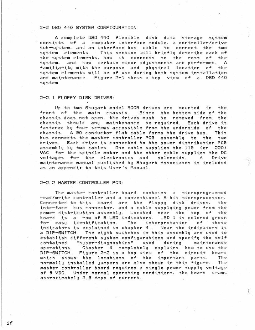
A complete DSD 440 'lexible disk data storage system consists of a ~omputer interface module, a controller/drive sub-system, and an interrace bus cable to connect the two system elements. This section will briefly describe each of the system elements, how it connects to the rest of the system, and how certai.n minor adjustments are performed. A familiarity with the purpos~ and physital location of the system elements will be of use during both system installation and maintenance. FiguT'e 2-1 shows a top view oT a· DSD 440 s.tjstem.
2-2. 1 FLOPPY DISK DRIVES:
Up to two Shugart model SOOR drives are mounted in the front of the main chassis. Since the bottom side of the chassis does not open, the driv~$o must be removed 'rom the chassis should any maintenance be required. Each drive i.s fasten~d by four screws accessible from the underside aT the chassis .. A 50 conductor flat cable forms the drive bus. This bus connects the master controller pca assembly to the two drives. Each d'rive is connected to the power distT'ibution PCB assembly by two cables. One cable supplies the 115 (OT' 2201 VAC for the spindle mota'!" anti the othercablesuppl.ies the DC voltages faT' the electronics and sblenoids. A Drive ma intenance manua 1 pub 1 i.$oo ed by Sh ugart As soc iates is inc 1 uded as an appendix to this User's Manual.
2-2.2 MASTER CONTROLLER PCB:
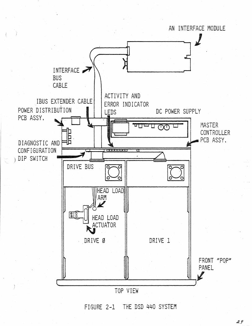
The maste'r controller board contains a miero~ro9rammed read/write controller and a conventional 8 bit microproces$o'r. Connecte~ to this board are the floppy disk drives, the interface bus connector, and a cable supplying power from the power distribution assembly. Located near the top of ~he boa'rd is a row or SLED ind icatoT's. LED 1 is colored green for easy identification. The interpretation of these i.ndicato'rs is explained in c.hapter 4. Neal" the i.ndicators is a DIP-SWITCH. The eight switches in this assembly are used to establi.sh different system configul"ati,ons and specify th~ aelf contained "h y per-d iagnost ie s" used dur ing ma intenanc e operations. Chapter 4 completely expiains how to use the DIP-SWITCH. Fig ure 2-2 is a top view of th e c ire ui t board which shows the locations of the impor~ant parts. The normally installed Jumpers are also shown in this Figul"e. The master controllel" board 'requires a single power supply voltage of 5 VDC. Under nOT:mal operating condi.tions, the board draws approximately 3.5 Amps of cur'!"ent.
)
)
INTERFACE ,;;r 1\ BUS CABLE
IBUS EXTENDER CABLE POWER DISTRIBUTION
AN INTERFACE MODULE
--~-J 1
J'-----_-.-.. -
ACTIVITY AND ERROR INDICATOR LEDS DC POWER SUPPLY
PCB ASSY. ~r~ ·10o-~~~·lJ T' ::~I ~O;;:6;;:t5~D~(!X!);:6~=jl1 MASTER = ~ - .~ CONTROLLER
D IAGNOSTI C AND 1= § ..Ii. i"'- PCB ASSY,
CONFIGURATION ~. 1 I .oJ. /\
) DIP SWITCH "';::::~--~-s=~===;r===~~;.---, DRIVE BUS
HEAD LOAD ARM
_~~CX I~l~ 0 HEAD LOAD
l'::: ~CTUA'rOR
. DRIVE 0 DRIVE 1
FRONT "POP" PANEL
~--------~~--------~)I l~ __________________________ _
TOP VIEW
FIGURE 2-1 THE DSD 440 SYSTEM
/9 JUhI,ctE";:($ ARc /N0TA~t.E.o FOR. NO/?:/l?~( \ i
! oPE/?l9r/dl'/~ rilEY Akc; Silo wNO/9/?l\eNe!)- IN 01'1) if!£" OI/fv.:/1~
iJ?/1$ rEA CaNrA'o Lt.€f /I/ORm ;91.-(./ rN:S TI7t.t.€J:, Jum;'::;E~5
)
2-2. 3 DC POWER SUPPLY:
The DC p~we~ supply is located in the rear 0; the chassis. It is a conventional open-frame supply using linear regulators. DC output voltages include: 5 volts, 24 volts, and unregulated -12 volts. Figure 2-3 shows points of interest on the power supply. Note the two trimme~
potentiometers which can be used to adjust the +5 and +24 volt outputs. A schematic, parts list, list of specifica.tions., and trouble sho~ting guide for the power supply are included as an appendix to this Users' Guide.
2-2.4 POWER DISTRIBUTION PCB ASSEMBLY:
The power distribution assembly is mount.d on the left side of the ch~ssis. This board is used to distribute both AC and DC voltages within the chassis. Any sub-system element can be rapidly removed from the chassis since all .lectrical connections are made using cables with a connector on at least one end.
2-2. 5 ACPOWER SWITCH:
An AC power switth is mo~nted Just below the CORCOM connector. When the DSD 440 is installed in a computer system with a central AC power cont-roller, this swi.tchwOLlld normally be left ON. When the "hyper-diagnostic" test and utility programs are being executed (see Chapter 4), the AC power switch is a convenient way to start and stop these pro~rams.
2-2.6 FAN:
The fan draws air in through the chassi.s vents and blows it out the small fan grill on the rear of the chassis. No filters are used in this coaling system, so no periodic fi.lter changes are needed.
..3/
I 3.:1..
2-2. 7 CORCOM CONNECTOR:
The CORCOM connecto~ is mounted through the rear panel of the chassis next to the fan. This connector assembly contains a line filter. fuse. and a small PC board which can be moved to rapidly modify the way transformer primaries are wired to the AC line. A molded line cord mates with the CORCON connector on the outside of the chassis. The following fuses should be installed in the CORCOM connector:
SINGLE DRIVE SYSTEM; DUAL DRIVE SYSTEM;
SINGLE DRIVE SYSTEM; DUAL DR IVE SYSTEi"li
100/120 VAC 100/120 VAC 220/240 VAC 220/240 VAC
2. 5 3 1. 25 2
AMP AMP Af1P AMP
SLOW-BLOW SLOW-BLOW SLOW .... BLOW SLOW-BLOW
The small PC board can be inserted into the CORCOM connector in anyone of four ways. When the PC board is fully inserted in the CORCON connector. tbe AC voltage currently selected can be read directly off the PC board. Note that the connector is constructed in such a way that only one of the four voltage labels etched on the PC board can be seen when the board is fully inserted in the connector. It is possible to make rapid conversions between the two low line voltages (100 VAC. 120 VAC) simply by pulling the PC board out. changing ~~S
orientation. and re-inserting it. Using a similar procedurel a rapid conversion between the two high line voltages (220 VAC, 240 VAC) can also be made.
CAUTION: The procedure required in ordsr to convert between a low line voltage (100-120 VAC) and a high line voltage (220-240 VAC) is far more complicated than Just changing the position of the PC board. This conversion requi.res changi.ng the fan. the two AC spindle motors in the floppy disk drives. the motor capacitors associated I..,si.th the spindle motors, and the -ruse value. For t h i. s rea son J NEVER c han get h epa 5 it ion 0 f the PC boa r d f r Q m the low line voltages to the high line voltages without c han 9 i. n g the AC mot 0 r s . I f you do. the rei sag 0 0 d c han c e the motors will burn up.
)
2-2.8 INTERFACE CABLE:
The interface cable is a 26 conductor 91~t cable with f e ma I e 3M" t 1,1 jJ e con n e c tor son e a c hen d . T his cab 1 e is keyed to help prevent backward installation. The hole in the con~ectors corresponding to pin 23 has been plugged" on both ends. Similarly, the pin th~t Ulould normally mate with these holes ~as been clipped on both the main chassis connector and the interface module connector. No AC or DC power is transmitted across the interface bus (IEUS) cable. Half of the conductors are signals and the other half serve as grounds. Data Systems ships a ten foot interface cable with DSD 440 systems. It is recom~ended th~t users requiring a longer cable build one from a 26 conductor ,twisted pair/flat cab Ie. Sp ec tra-str ip Corp orat ion is a sup pi ier of th is ty p e or cable.
2-2.9 INTERFACE MODULE:
The interface module is a printed circuit board that has been designed to meet the I/O bus interface specifications and the physical form factor of the host computer. Data Systems manufactures interface modules fo,.. the DEC POp ..... ! L PDP--8, and LSI-11 computers. In addition. Data Systems can supply a complete specification of the signals and protocols on the IBUS. Customers desiring to intei'face the DSD 440 to other computers can design their oUln interface mddules based on the information contained in this "IBUS H specification.
The DSD 440-11 and DSD 440-L11 interface modules contain a built in hqJ"dw~re bootstrap. The hardware bootstrap 'circuit ~ ~-------""."--,---consists of addr~ss d~coding circuits and a PROM with a PDP-il
program which can be executed by the host com~uter. Th~ program which resides in this PROM spee~s the loading of an operating system from di,.skette to the host CPU's memo'ry. Also in th1s PROM· are some simple CPU and memory diagnostic programs. More deta il s ab out th e b ootstr~p program c an be found in chap ter 3. An assemb 1 y I i5tin9 Or th e program is included as an appendix to th(s user~' m~nual.

D
CHAPTER 3 SYSTEM INSTALLATION AND ACCEPTANCE
3-1 ENVIRONMENTAL CONSIDERATIONS
All floppy disk systems manufactur~d by Data, Systems Design perform efficiently i,n a normal computer room environment. Temp eratur e$ humidity, andc lean 1 iness are three environmental parameters that can impair reliable usage of diskettes if not kept within specified limits.
Diskettes are specified to operate within an ambient temperature range of 10 *c to 51 *C (SO *F to 125 *Fi. The maximum thermal gradient should not exceed 15 *F pe~ hour. The DSD 440 chassis should be installed where the ambient t.mperature does not exceed these limits while the s~stem is in op e't'at ion,
Humidity control is necessary for the efficient operation of di.skette memory systems. At very 10lJJ humi.dity {dry air) static electTicity can be generated as a result of contact between the read/write head and the diskette. When the electrical potential becomes hi9h enough to ~ause a discharge. soft data errors may occur. At very high humi,ditlJ' mylar diskettes can start to swell as they absorb moisture from ~ne
air. This can hav~ the effect of moving the centerline of a previously recorded ~rac) away from the centerline of the read/write head. Again, the noti.ceable. eFfect will be an increase in the soft error rate. The operating relative humidity range is 8 to 80% with a maximum wet bulb temperature of 29.4 *C (85 *F).
Cleanliness is important wherever diskettes are going to be u5ed,· handled, and stored. Unlike most rigid disk cartridges, floppy disks are not sealed units. If the DSD 440 is operated in an environment which has a high concentration of abrasive airborne particles, the useable life of ;;ne diskettes is likely to be reduced and the soft error rate will incTeas~. Care must be taken, while handling diskettes, never to touch the magnetic media.
Chapter 1 of this manual includes specifications on heat dissipation associated IJJith of tiSD 440 sIJ',;tem. This data can be used to determine if the cooling capacity of your complete computer system will accommodate the DSD 440 system.
..3s

3"
3-2 UNPACKING THE SYSTEM
No special tools or equipment are required to install the DSD 44 on a p p y dis ks y s t em. It is recommended that all packing materials be saved in case the system requires shipment at some future date. Please adhere to th~ following list of steps:
1) Inspect the shipping carton for damage caused in shipment. Report any, damage to the shippeT' befoT'e opening the carton.
2) Open the top of the outer carton and then the top of the inner carton.
3) Remove the foam blocks from the doors of the disk drives. 4) Pull the system from the inner box by inserting fingeT's
inside the drive doors and pulling the chassis out of the box (2 person operation).
5) Inspect the unit faT any obvious damage. Immediately report any damage to Data Systems Desi~n.
6} Remove the other system parts fro~ the cartbn.
Except where noted, all DSD 440 systems will be shipped with the following materials. Be sure to inForm Data Systems Design immediately if any materials are missing aT' damaged.
LIST OF MATERIALS: 1) Chassis 2) Computer interface module 3) Documentation binder including:
a. System Users Manual b. DSD boo.table diagnostic di.skette
4) AC pOW2T' COT'd 5) Interf~ce bus connecting cable 6) Chassis mounts (if ordeT'ed) 7) Bag with spare shunts and Jumpers
)
3-3 MOUNTING THE DSD 440 CHASSIS
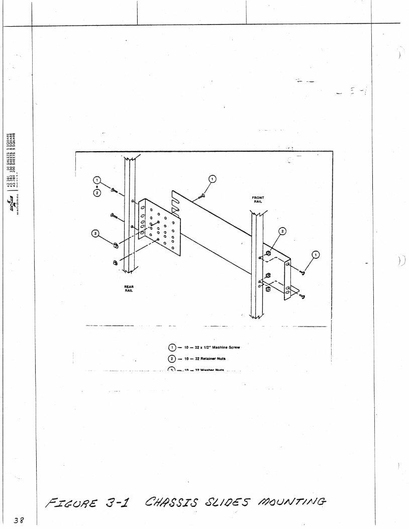
The DSD 440 chassis must be installe~ sufficiently close to the ultimate location of the interface module so that the 10 foot interconnecting cable will reach. An~ther
consideration concerns the Frequency of diskette changes. If the computer operator is likely to b.e changing diskettes often. it would be desirable to install the chassis as close to the console terminal as possible.
The following. discussion pertains to installing the DSD 440 chassis. in a 19" rack. Because of the width of the Shugart floppy disk dTives and th.ir horizontal mounting in the DSD 440. a wider than usual chassis is needed. The DSD 440 chassis can be mounted in a standard 19" RETi'1A rack if special slim-line chassis mounts are used. Figure 3~1 ill us t1' ate s h 0 1II to at t a chit he s 1 im-l i. nee has s i. s mo un t s toy 0 IJ 1"
rac k using the hardlJJare supp 1 ied with the mounts. Note that the left and righ~ rear extender bracket. are not interchattgeab 1 e. After th e mounts are sec ure 1 y fas taned to the rack, slide the DSD· 440 chassis on the mounts until the two bullets at the rear of the chassis mounts engage the corresponding holes in the rear of the chassis. (See Figure 3-2) Remove the molded Front pop pan~l from th. chassis by pulling the top of the panel out From the chassis. Secure the chassis in the rack by bolting the front fiange of the chassis to the f1'ont rails of the rack. (See Figure 3-3) Replace the pop panel by pushing ~~ stratght back on to the two Hhead 10cks H. Before actually bolting the chassis in the rack, it is advisable that the ~emainder of this chapte~ be r~ad first. This is because some system ~onfigurations will require ~odification of a DIP-SWITCH on the controller board inside the chassis. It is gene1'ally diFficult to modify the settings of this DIP-SWITCH once the chassis has been secured in the rae k.
The nBD 440 chassis should not that the air flow behind the temperature of the air ent~ring the 40 *C (104 *F).
be mounted in suc~ a way Fan is restrict~d. The chassis should not exceed
~=: ~~!::: :<:"'''' ""m" 000 ,.,~~
_("<10.1#1 =GIIGII~ MMM ~
~~~i
0- 10 .... 32 X 112" Machi ... 5<; ....
0- 10 - 32 "-tain.rNIiIs
)J

: ESE ::t;c """'" 000 <>00 -....
t UP
Figure 3·2. Bullet entering Hole in Rear of Unit
SECURING HOLES
Figure 3·3. Front View of Chassis with Front Panel Removed to Indicate Securing Holes

· ' 1/-IJ
3-4 INSTALLING THE INTERFACE MODULE AND CABLE
Ensul'e that all with this section separate proiedure~ systems.
syste~ power is off before proceeding of the DSD 440 inst~flla'!;ion. There are ror LSI-Ii, PDP-l1, and PDP-8 based
I J LSI-11 BASED SYSTEJ"1S:
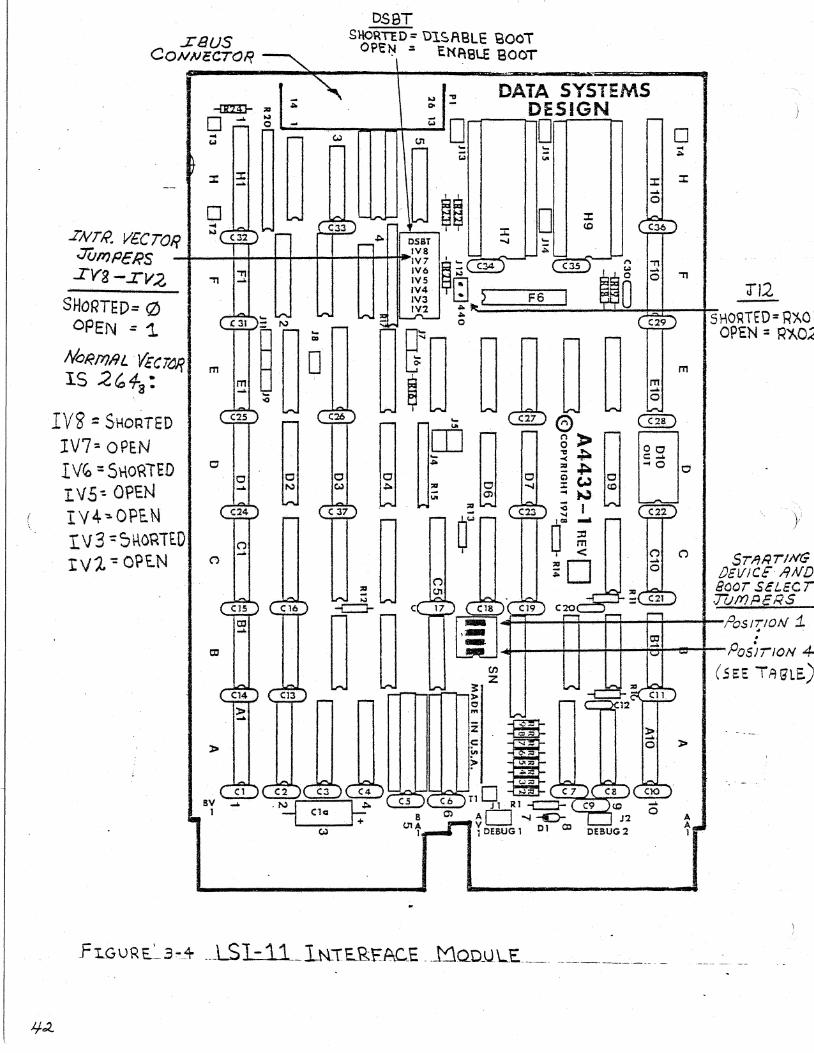
The DSO 440 intel'face ~odule for LSI-II based systems sh~uld be marked PIN 4432 on the component side of the board. The user can select from one of four device register addresses, one of four b60tstrap PROM st.rting addresses, and a 7-bit interrupt vector address. Therj is a separate Jumper which, Ulhen installed, disables the bootstrap PROM. (Se~ Figure 3-4)· Data Systems Design ships this module so that the device register address is at 177170, the bootstrap PROM is enabled at address 173000, and the interrupt vector ~s 264. The Mode 1 Jumper is removed when this module is shipped, therefore the mo~ule is initially configured for Mode 2 (RX02 compatible) operation. Note that when the interrupt vector Jumpers are in place, the associated bit of the vector address is a O. Thus, if all seven vector Jumpers l.iJere to be installed, the vector address would be 000. Please check your module against the tables and Figure 3-4 to insure that it has been configured consistent with your needs. Most system sOTtware assumes a device address oT 177170 and an i.nterrupt vector of 264. If you change either of 'tinese number~, corresponding changes will generally have to be made in the software. Also, be sure to read the explanation of' the bootstrap and diagnostic programs carefully if non-standard a~dT'e~ses are used.
STARTING REGISTER ADDRESS POSITION 1 POSITION 2 -~--"'-'!------~----------~--------- ...... ---...... ---~--~~----------..--
V 177170 (NORI'1AL) 177160 177140 177150
STARTING BOOT PROM ADDRESS
CLOSED OPEN
CLOSED OPEN
POSITION 3
Cl,.OSED CLOSED
OPEN OPEN
POSITION 4 ---~--""-----"'-'!""'" ---~ -----..... ~- ---~-~--- .. .,..-----....... - ...... """"'---,-----...... ----
173000 (NORMAIr-> 071000
175000 166000
CLOSED OPEN
CLOSED OPEN
CLOSED CLOSED
OPEN OPEN
, '. )
J'

1
When you are sure that the~ Jumpers on the interface module are configured correctly, plug one end of the ten foot interface cable into the interface module such that pin 1 (the stri.ped side) is closest to the edge of the board. Also confirm that the pin position of the clipped pin on the module connector matches the position of the plugged up hole on the cable connector. After verifying that power is off, plug the module into the lowest numbered available Q-bus slot.
CAUTION: There must be no open Q-bus slots in between the processor and the DSD 440-Ll1 interface module. Since this module uses both interrupts and direct m~mory access, a break in either of the grant propagation chains would prevent the interface module from obtaining control of the Q-bus. Figure 3-5 shows how Q-bus slots are numbered in $ome of th~ more common backplanes available from DEC.
Installation information for continues in section 3-5.
LSI-i1 based systems
.Iaus CONNeCTOR
DSBT SHORT"fD= U1.Sf\BlE BooT OPE~ = ENAB~BOCT
.... ~ DATA SYSTEMS
--li!!l- ;a 0-
0 ..... .... c 0 .. '" 0'1
U ::x: ::x: ....
0 ... INTI;>. V£CTO/f OSBT ~ Iva
....
D ... '"
~~ ::x: ~
'-
DESIGN
~
o .... ....
o ::x: <0
o ::x: ::x: ..... o
I-vU/I'} P€ 1(S --1---I-t-~f-+-+--+H-ItJ!"· IV 7 ij'.... "'" IYo IV6 ;::; <5 "
o - ..rV2 :~~ [;] TI2 SHORTED= n. :~; ~ ~>::::==F6:::::;;:=-_.D~-b,~_+
@D C9D
'U ~ 5 l-\OiHED = Rj\O\
OPEN :: '1 ~ D~!:::. :::; u· U OPEN = 1=<'1-.02 NORJYJflL V!Ci~J? m 0 G m
IS 2"4g: ~ ~
IVS ;: SHORTED :: CSD
IV?· OPEN ~;:;;I I l;a ~g. IV~ =SHo~IED 0 0 0 0 0 _
rV5-=- OPEN .... N W ~
IV4~OPEN ~~ Iv3 ,:SI-\O~IE.D n ~
..... IV1-= OPEN
}
STI7~TING v£V)CE" /lND BCCT SeLECT Tt.) jY} fJ c R S
...... 4--+-4-+-if--+-r---t-PoS IT/oN ::1. 4 .
.... -l--H-H---iSt--e,.-...;r-PosjrloN 4-
» ..... o
A A 1
(SEE TAG'LE.)

_."'100'" -:::.a:n:e :::; :-'1:0")""0
~~~ i
)-I927CJ
119273-~
ODVII-8
VIEW FROM MaCULE $IOE OF aACXP\.ANE
PROCESSORIHIGHEST PRIORITY LOCATIONi
OPTION 3
OPTION"
OPTION 7
P~OCiSSOR OR OPTION 1
OPTION 2
OPTION 5
OPTION 6· / ILOWEST PRIORITY LOCATIONI ~~~~--~----~
... -:....---- PREFERRED LOCATION FOR MMV"·" CORE MEMORY
CONNECTOR 1 .- CONNECTORZ
r~------------'""'----------~, I~--------~"'------------~ SLOT A . SLOT 8 SLOT C SLOT a <
~ ~ ~ W1 W2 W3
ROW! Pro~ esSOY" (PrOc.e~ SQY)
.• OW2 C;p '70/\/ I I .OW3 OP; "JON 2 ROW" C;PI ~/" AI 3
OP1 "'ION 4 ROW .. OPT ICJN S ROW 7' O;Q, 'r-1(jA) ~
ROWe ()P7 IaN 7 ROWS oJ'r liON '?
VIEW IS FROM MOOUU SIDE OF CONNECTORS.
-------
,- PROCESSOR PROCESSOR OR OPTION'
2- FOSITION3 OPTION POSlTlON 2
3- POSiTION" 4 1- .osmON 5
4- POSITlON 1 POSITIONS
POWER 5- 1 POsmONS POSITION 9
nRMIN.I\t. BLOCK .- POSITION 1 1 ?OSmON 10
7- POSiTlON 12 POSITION 13 -I 8- ?OSITION 15 F'OSIT10N 1Ao
9- POSITION 16 POSITION 17
ROW--. " c 1 - 0 t ~" I MOCULe INSERTION slOe ,'----:c-:--;---;.,;,.;.I;.
USER oeFINED SLOTS
c ;
- ~ " '
3- .6 ()~TI6N Pl1bJ(IT/ IN OEC. E#CkPi/l,/J£5 FOP.. t...:5I .. 1/
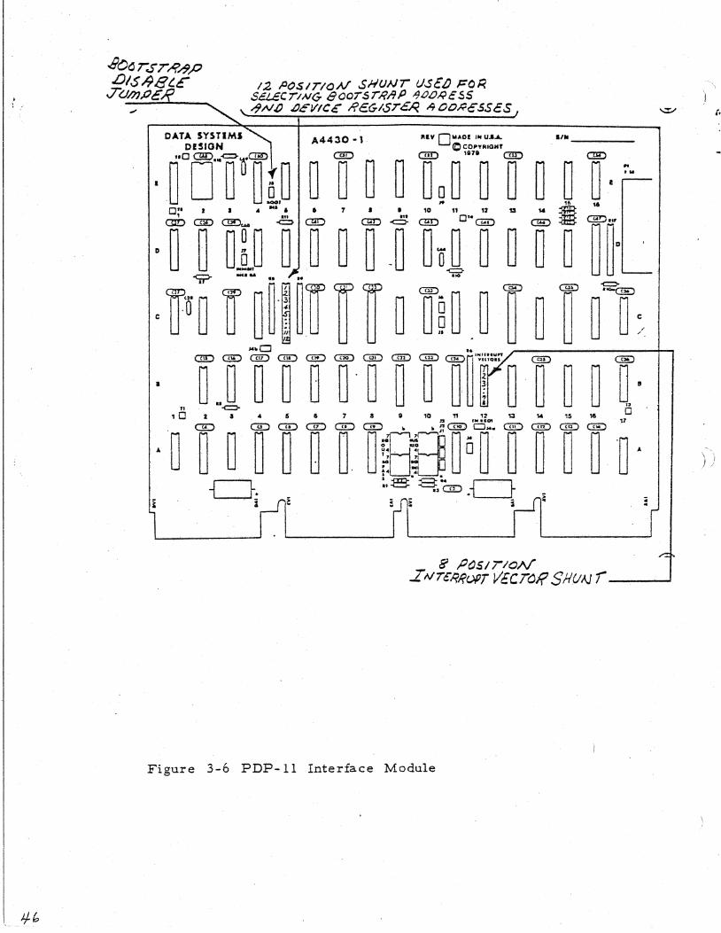
PDP-11 BASED SYSTEI"1S:
The DSD 440 interface for PDP-Ii based systems is a quad module marked 4430 on the component si.de. Data Systems Design ships this interface module configured as follows:
REGISTER ADDRESS: 777170 BOOTSTRAP PROM: ENABLED AT 771000 INTERRUPT VECTOR: 264 INTERRUPT PRIORITY: BR5 OPERATING i"1ODE: MODE 2 (RX02 COMPATIBLE)
C-5 on reg is ter
Fi.gur€.'
The twelve position shunt located at coordinates the 4430 interface module is used to configure device addresses and the bootstrap program starting address. 3-6 shows how the twelve shunt positions are numbered. positions 1 and 2 are used to configu~. the bootstrap starting address as follows:
STARTING BOOT PROM ADDRESS POSITION 1
Shunt program
POSITION 2 -------~-.. -----.-------~~---.;;.....--~---- .. -~--- ...... --------------..... -~
773000 771000 (NORMAL) 775000 766000
OPEN OPEN
CLOSED CLOSED
OPEN CLOSED
OPEN CLOSED
The bootst?a~ program contained on the interface ~odule will occupy 256 words of memory space, starting at one of the four selectable addresses shown above. If the user does not want the bootstrap program to respond to any addresses, ~ne
bootstrap disable Jumper (shown ~n Figure 3-6) should be installed.
Shunt positions 3 thru 12 correspond to aaaress bits A3 ~Aru A12 respectively when configuring the device register address. A closed shunt position corr,esponds to a bi.nary 0 and an open shunt position correspOnds to a binary 1. When this interface module is shipped, it i.s confi.gured to respond to a base register address of 777170 (octal). This UlorKs out to havi.ng shunt positions 7 and B left c.losed, and positions 3~4,5,6,9, 10, 11, and 12 punched open.
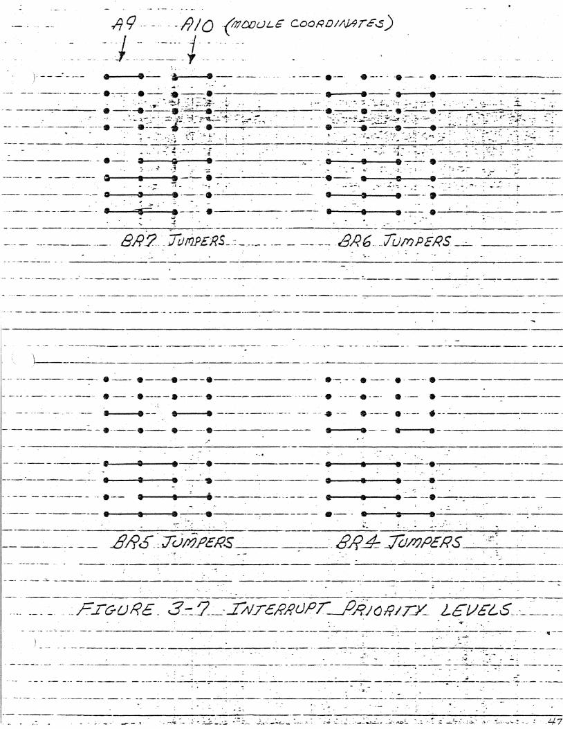
There is an eight position shunt located at coordinates 6-12 whi.ch is used to configure the interrupt vector address. Figure 3-6 shous how the B shunt pos~~~ons are numbered. Position 1 i~ not used. Positions 2 thru B corr.spond to interrupt vector address bits IV2 thru Iva respectively. A closed shunt position corresponds to a binary 0 and an open shunt position corresponds to a binary 1. When this interface module is shipped, it is configured to have an interrupt vector address of 264 <octal). This IJJOrKS out to havi.ng shunt positions 3,6, and 8 left closed, anq posi.ti.ons 2,4 .. 5 .. and 7 punched open.
In the rare cases where the interrupt prior~~y level must be changed. you will have to cut and Jumper the circuit board so that it looks like the diagram co~responding to the desired
.interrupt priority level. (see Figure 3-7). If the priority levels arS going to be changed often, it is suggested that the six permanent traces be cut, and four 8-pin IC sockets be installed in the positions outlined on the board. Either four-position shunts or dip-switches can then be placed in the sockets to facilitate rapid Jumper changes. The interrupt priority Jumpers are located at coordinates A-9 and A-I0 on the interface module circuit board. Interrupt priority level 4 is the lowest and level 7 is the highest.
If the system compati.ble
be operated RXOl JumpeT'
coordinates A-12 must be installed. Th~s Jumper for RX02 compatible operation.
mode, is going then the
to Er·..j
in th e located near
When you aTe sure the Jumpers on the interface module are configured correctly, plug one end of the ten foot interface cable into the interface module such that pin 1 (striped side) is closest to the module handle. Also confirm that the pin position of the clipped pin on the module connector matches the position of the plugged up hole on the cable connector. After verifying that power is off, plug ~ne module into a con v e n i e n t s Ina 11 per i p her a 1 con t r 0 lIe r ( S PC) s lot. t·1 a k e sur e that there is grant continuity between the processor and the interface module. If there are any open SPC slots between the pT'ocessor and the inteT'face module, there should be a grant continuity card placed in slot D.
Il'"1P OR T ANT ~ ~ !
Since the DSD 440-11 module uses direct memory access (DMA) you must ensure that there is no backplane Jumper OT' foil trace between backplane pins CAl and CBl of the SPC s!O~
you select. These two pins normally connect NPG IN to NPG OUT. Usually the pins are left connected since most small peripheT'al controllers do not use DMA. lr ~n~s Jumper is not removed and an interface module configured for RX02 compatible operation is installed, the whole system wi.ll hang. Remember to replace the Jumper any time the 4430 module is T'emoved. If you forget, DMA devices further out on the UNIBUS will never receive NPG and the UNIBUS will hang each time a DMA cycle is attempted by one of these devices.
.1 ~ ,"
(.
)
Figure 3-6 PDP-II Interface Module
A9 '.j" . -
--1i/O(IJJt){)UL£ COORD//JATE.s)
--t • ' •. -'-".---' .-_. e---' ... - .--_. --_._._------
0---- a=-----og-· ----•• ----------..,.. ~~ --
-- --- . - - - -- ---- Q,..----IIl---_.-~. -e -- •• I"'----;01----tII8 -..;...-~--....;;..---"'~ ~-
-- -----.. ---.- 00---11~~-""~ ._-- -~ - •• --....-GI.I--.....--tt. -- - • ---------'---
•• ----'1F~~-•• -.~.- e------. ----- ---- .......... --11.,---__ • --:-- 0----. ..,.
8J<6-.--TumPERS __ .
._---------- -- ------
• --- e------e---o---------.--.--, e·-: • --- e- ----e---- _.-. - --- - .. - - -_. . 0-----.-----·. ---------- • 0--- • e----------::-----
.. :,...--...... -- • 81----811 --- - ---------- .. e---- .. .--..:.....------ ------- - 8----e--- 0---0---·------- IQl----,. - ~--------,'--------
- ------------- .• ---.... ---.• ·-0----------·- •• __ - ...... r----.. -0-----------.-------- •• --_e_e---oo -. --'5 • • ---e--..:...---. - --.- - --.---- - .. e-- •• ---4I---i ---.-----.....:-.-- - - .e--.... --..... - --e --------- •• ----a----a. -. -' ---G------:-c--- --- c... • --- • ------.----.---'-------........;.........;.---~-
.,8/?S_;.JUmPERS __ _ _ -------
- _._----_._---------.------~-----------.--------
.. FIGuRE_ -.---------- --..,.-- -.--- - -' ---- --.-----------~-------- "'._-
---:---~.-----. -------_. --_._--_._._._.-. --.--' ---------._.-:..,
. " .. . -- ---- ----.:.-....'-----. ---.Ii
-----.------~------ ---_._----.. -. --------
--- -----------~---..,...,.;------~.- -------:-:-.... --"-:-: ... -...,. 47
, ! \
PDP-8 BASED SYSTEMS:
THE DSD 440 interface module for PDP-8 based systems should be marked DSD 2131 on the component side opp~site the interrace cable connector. Data Systems Design ships this module Jumpered to respond to device code 75 (octa15. All device code Jumpers except Jumper 7 should be in place if this is the device code actually desired. There are no additional Jumpers or adjustments on the 2131 interface module.
Locate the ten fo~t interface cable. Plug one end of the cable into the 2131 module such that the pin position of the cli,pped pin on the module connector matches the position of the plugged up hole on the cable connector. Plug the opposite end of the interface cable into the connector motinted on the rear panel o'r the chassis. Again, observe that there is only one correct way to insert the cable. After verif~ing that power is off, plug the module into an available Omnibus'slot.
Note thai; th·e PDP-8 interface module does not contain' a bootstrap. This module is not capable of direct memory access (DMA> e1 th er.
)

3-5 INPUT PO!'JEH CONSIDERATIONS
The DSD 440 can be ordered so as to be initially configured with any combination of 50 or 60 HZ and 120 or 240 VAC. Optional conversion kits allow users to change the system between 50 and 60 HZ operation. The system cannot be easily changed between 120 and 240 VAC in the field.
In geographic locations where the line voltage deviates more than lOX from 120 VAC or 240 VAC, an easy adjustment can be made to modify the way the power transformer primaries are wired to the AC line. The CORCON filter which is mounted through the rear panel of the chassis contains a small PC board which c~n be removed from its slot and reinserted in different orientations. The different orientations correspond to various line voltages. Although this PC card allows for both + and - variations on both 120 VAC and 240 VAG systems, one should NEVER attempt to use this card to change a 120 VAG systeM into a 240 VAG system or visa-versa. It simply does not work that w~y! Section 2-2.7 discusses the CORCOM connector in more detail.
3-6 CHANGING THE OPERATI.NG MODE
As mentioned in ch~pter 2, the DSD 440. can be configured to operate in either RX01 compatible mode or RX02 c6mpa~~Dle mode. There is a switch that· selects the operating mode located on the large circuit board assembly inside the chassis. Data Systems ships systems configured in RX02 compatible mode (MODE 2). IF this is how you plan to use your DSD 440, then there is no need to open up the chassis at this time. If I,lOU' desire the RXOl compati.ble mode (i"10DE 1.), then the state of this switch and possibly a Jumper on th9 int~rfacB module will have to be changed. Figure 3-9 shows the location of the switch and which position is which. If you are going to operate in RXOl mode, I,IOU must i.nstall a Jump er on th e DSD 440-11 or DSD 440-Ll1 i.n;; er-Fac e mOG U.L e s. Figur~~ 3-4 and 3-6 show the location of that Jumper On each oft h e t 1.!.1 0 mo d u 1 e s . On vi. 0 I_I sly I the J u m per s h 0 IJ 1 d b ere m 0 v e d when converting back to Mode 2 operation. No changes ale required on the PDP-8 interface module IJJhen changing operating mode.

~.:~ ~~~ :::c::: "''''''' 000 <I"I:!:~
_NO." =~a):l t'"IMM;
~~~~
-+
crfP OPaN ---
SCJIrcJ.l Sf{O(;tIA./ /1'1 rile l'MOI)€ 2. "
!?X02 Com.Pl9r.r$LE POSITION
§ - ........... -oP£tV --......
$1..1.)/ rCH S/loaJ/V IN rfl£ "/J?aI)E.J. JJ
I?xo.t Com,o;;TI8I..e J'OSITION
) ...

3-7 FINAL INSTALLATION:
Locate the power co~d.and plug the female end into the connector on the back of the chassis and the other end into a suitable AC receptacle. Route the Pree end of the interface bus cable over to the rear of the chassis and plug it into the 26 pin connector such that the striped side of the cable is tOUlard the middle aT the chassi.s. Also conrirm that the pin position of the clipped pin on the connector on the r~ar o'P the chassis matches the position of the plugged up hole in the cable connector. .
3-9 POWERING UP
The DSD 440 chassis gets power from its own internal power supply. The interrace module uses onl l" +5 VDC, and 1." receives this 'rom the computer backplane. lne eSD 440 chassis and the interface module can be powered up in either order without the risk of any adverse aFfects. lnere is no danger of writing on diskettes loaded in the drives during power up or power dOUln cycles.
rJe,''f No () . .'
(t- /;1 ,uo,i,
V--0V( tv \!t£t'd
3-9 INITIALIZATION RESPONSE CHECK
An initialization response should occur when the DSD 440 is powered up. !'the system has been connected to the host com~uter cor~ectlVI an initialization response can be forced as a result of some of the Following operator console actions:
LSI-l1 BASED SYSTEMS: , (1) Flip t~e IN!T switch <if there is one). (2) Using DDT,
use the "G" command at any arbitrary starting address. (3) Using ODT, write the numbe,- 40000 into the DSD 440 RXCS ,-egiste,-, no,-mally at add,-ess 171170.
PDP-i1 BASeD SYSTEMS: (1) Generate a UNIBUS IN IT by depressing 'the START switch or button. (,2) Using the console, deposit the numbe,- 40000 into the DSD 440 RXCS register, no,-mally at address 717170.
PDP-8 BASED SYSTEMS: (1) Depress the system clear switch. "clea,- all 'lags" 110 1nst,-uction.
(2) Load and execute the
An initialization response will only be observed on floppy disk d,..ives· if the doo,.. i,s clOsed. Each ti.me you
)
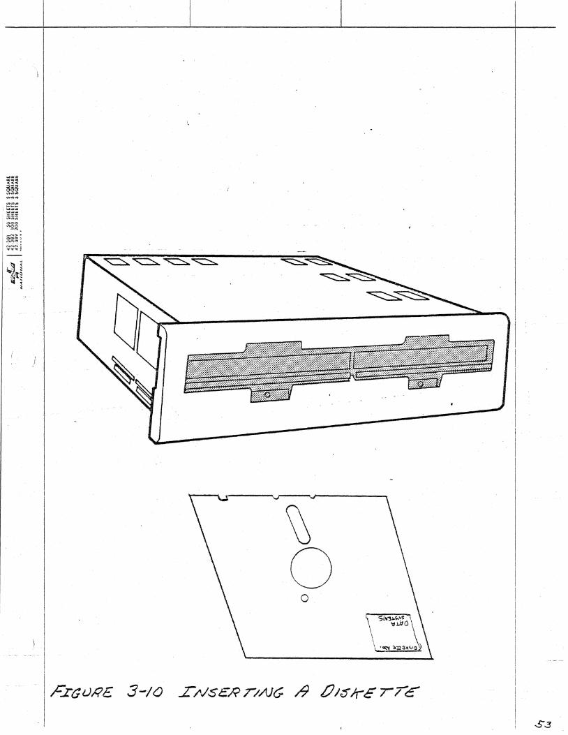
gene,..ate an IN!T. you should hear a b,-ief noise came from the ); flexible disk d,-ives as the control Ie,.. homes the head positione,-s. The activity LEDs on the f,-on1:; of the drives , should come on b,..ierly. If a diskette i,s loaded into drive 0-11'V~1 (normally the left hand drive) you should also hear the head load. The d,-ive 0 activity LED will remain on slightly longer as the cont~olle,.. reads t,-sck 1/se~tor 1 of the diskette into the secto,- buffer, Be sure that you inSErt diskettes into the d,-ives ~s shown in Figu,-e 3-10, Neve,- use hard sectored dis k e t t. e sin t his s y s t em. i f \LO u did not: Db s e,- ve 'I; her e s u 1 t s described he,-e, please confi.rmth"e Fonowing: 1) You have applied pawe,- to both the computer mainframe and
the DSD 440 chassis. 2) You have connected both ends of t:he DSD 440 interface bus
cable in the proper orientation as directed. 3) You are being successful at gene,..atin9 a system initialize
0'- device 'initialize signal by one of the above methods, and that th~ signal is ,..eaching the DSD 440 interface.
4} The d,-ive doors are not open.
If you a'-e unable to force ~n in it i. ali. z a t ion response b IJ anlJ of the above m£>ntioned methods, see ,j.' 'In e rna j, n ten a nee section of this manual or call the Data SIJsterns Design Custome,- Service Department for assistance.
"''''''' ~~~
I ~~~ =:!:x "'''''''
1
000 ,..,~~ ~
_C"tOolJ
I ~~~~ NC'lC"I1 "Of"""";;:
\j o
o
3-10 SYSTEt'1 BOOTSTRAPPING
Bootstrapping is a term which generally refers to the act of reading in a block of code from some mass storage media, and then having th~ processor Jump to that code. Executing that code, the C. P. U. continues to read the system monitor into memo~y so that the user can interact with the system through tte console keyboard.
BOOTSTRAP PROGRAM ON LSI-11 AND PDP-ll INTERFACE MODULES
In addition to bootstrapping the DSn 440, this program executes a number of system diagnostics. Among these are:
(1) A limited C.P.V. inst~uction set test (2) A test for stuck address and data bits throughQut all availab Ie memorlJ (3) A bit-latch test of the DSD 440 interface registers (4) A DSD'440 fill/empty buffer test
Should a malfunction be detected during the execution of any of these tests, the processo~ will either HALT or hang. You
'can assume that the processor is "hung" during execution of the bootstrap if the floppy drives are quiet and nothing has been output to the console terminal. In this case, you will have to manually halt the processor to determine th. address at which the program was hung. Once the "hang" or "halt" address is known, ref~a--t.b.jL_!LQot2:ju~ap program 1 ist ing in the a p pen d i x to fin d 0 u t wh i c h t est- fail e ci--:----.. ----·---·-·-.·----------'--·
After successful completi.on OT -ene system diagnostics, the bootstrap program will read track l!sector 1 of drive 0 into the controller sector buffer. Should ~nLS Doera~~on
induce a d.ns~ty error. the density bit is changed and the command is issued again. If any other error results. the processor will halt leavinQ the drive numbeTinRO, the memory addT'ess of the extended st~tus ~im~-ti-~~"':Cn'--R4, .. nd 'Cne definitive err~r code in Rb. If the READ SECTOR operation is successful. the bootstrap program determines ~ne pT'esent operational mode of the DSD 440. If the system is configured Tor RX02 compatible operation, a D!"iA empty inl·Ffer cycle- takes place. A progra~med I/O cycle takes place if the system is in RX01 compatible mode. At this point, the fi.rst IJJord of data transferred to memory (at address 000000) is examined. If that word is a NOP instruc;tion (000240 octal>. the bootstrap program c;onc;IUdes-··fhat; the diskette is boatable. In this case the program counteT' is cleared and the s9conosry bootstrap progT'am pT'oceeds to load in the operating system. If the bootstrap program does not find a NOP instruction in address 0, it will switch to the other drive and try to bootstrap the diskette it contains.
One normally starts execution of the bootstrap program by loading the program counter with the floppy disk bootstrap program base address. This address is determined by the
pos~~~on of switches or Jumpers on section 3-4). After loading the start th e CPU.
the interface modules (see starting address. simply
BOOTSTRAPPING SYSTEMS WITH NON-STANDARD DEVICE ADDRESSES
Most DSD 440 systems will be configured such that the command and status register will respond to address 177170. Thi.s address is typi.cally regarded as -cne "standard" devi.ce addre~s for the first floppy disk storage peripheral installed on PDP-11 or'LSI-11 based computer systems. Under certain circumstances. a user may want to configure his DSD 440 system to respond to a non-standard device address. If this is done. the bootstrap proceedu~e is slightly modified.
Let us consider a few specific cases to illustrate the different bootstrap star"C~ng proceedur2s. Assume that the shunts on the interface module have been set up so that the bootstrap program base address is 173000 and the RXCS = 177170 <standard add·ressJ. Under these ci.rcumstances the system is bootstrapped by starting the computer at the bootstrap program base address, which would be 173000 in this case. If now ';;he interface module is modified so that the R~CS = 177150, the system could be bootstrapped by starting the computer at ~ne
bootstrap program base address plus 10 (oct'al), which tuoule be 173010 in this case. If now the interface module is modiflea so that the device address is any legal address other than 177150 or 177170. the following steps are required to bootstrap the system: Fi.rst, write the device address (assume" 177160 i.n this case) into mem~;:~y-addr-ess-OOOoOO'~-- Sec;;J,Q, write the number 000002 i.nto CPU regi.ster Rl. Finall'J' start the !=omputer at the bootstrap program base address plus 2t, . ...-" (octa!). which would be 173026 in this case.
In order to successfully bootstrap any opera~~ng system. the system device handler software (on the operating system diskette) must have been specially adapted to accommodate the non-standard device address for whic~ the floppy disk system hardware has been configured.

3-11 ACCEPTANCE TESTING ON PDP-11 AND LSI-i1
The ACCEPTANCE test should be performed when the DSD 440 sgs~em is first installed or when a fault condition is susp ec ted. To run th e test p,..og ram, 1 oc ate th e d iagnos t ic diskette that was shipped with your system. The diskette should be labeled:
DSD 440-11 DIAGNOSTIC DISKETTE VERSION 6 (OR GREATER),
Insert the diskette in drive Q and pe,..fo,..m the bootst,..ap procedu,..e described in the p,..evious section. If the system is able to load the diagnostic p,..ogram "into memory, a short paragraph will be tgped on the console terminal. Included will be a s~stem memory map for your information. The diagnostic program indicates that it is waiting for a command by typing the prompt:
MODE:
When this word appears on the terminal, remove the diagnostic diskette and insert two scratch diskett~s into the drives. These diskettes should not be write protected, as the ACCEPTANCE program will be writing on them. The stratch diskettes can have eithe,.. single or double density data recorded on them. To start the acceptance test, ~im,ly type the character "AU.
MODE: ACCEPTANCE
The proper operation of the DSD 440 is tested by running five passes· of the acceptance test. . Each time a pass is completed, an asterisk will be printed on the console terminal. If there a,..e any er,..0,..5, they l.uil1 also be p,..inted on the console te,..minal. If any er,..ors occur, contact the Data Systems Design Customer Service Department at (40S) 249-9353.
More detailed information about the diagnostic program FRD440 on the diagnostic diskette can be found in chapter 6.
3-12 ACCEPTANCE TESTING ON PDp .... S
(
CHAPTER 4 MAINTENANCE FEATURES AND ERROR ANALYSIS
4-1 OVERVIEW OF MAINTENANCE FEATURES
The DSD 440 has many built-in maintenance related features. These featur~s were incorporated into the product so that the need for a specially trained field service force would be substantially reduced. If the product should fail in the Tield, Data Systems expects that service can be rapidly restored using a combination of the diagnostics which run on the host C.P.U. and the hyper-diagnostics which have been built directly into the DSD 440. Data Systems also maintains a telephone "HOT-LINE" to help customers solve problems r~lated to.OSD equipment.
An a-bit microprocessor is the "brains" of the DSD 440 master controller. In addition to performing all of the standard floppy ~isk functions described in the programmers' interface chapter1 this microprocessor executes a great deal of code designed to simpli'y the Job of maintenance. Following every power-up or initialization cycle, a series 0' hardware II se lf-test lf routines are executed. Also, by changing the position of the switches on the controller, a user can instruct the microprocessor to execute one of seveial system hyper-diagnostics. These hyper-d1ag~ostics are unique in that they permit the user to thoroughly verify the integrity of a large part 0' his system without requiring any connection to a haste.p. U. The r~mainder 0' this chapter will explain in detail the maintenance features and how they are used.
6"7

4-2 NORMAL VS.· HYPER-DIAGNOSTIC MODE
The DSD 440 system is said to be in II NORMAL I! mode when it is connected to a host C.P.U. and is being used to read and write data on diskettes. Most of the exposure a user· has to the DSD 440 system will be through the application software running on the host central processor.
The system is said to be in IIHYPER-DIAGNOSTIC" mode when the user has removed the DSD 440 chassis cover and has initiated a particular hyper-diagnostic through the 8 position DIP-SWITCH on the master controll~r circuit b~ard assembly. The interface bus cable should be disconnected from the rear of the DSD 440 chassis. The user interface to the DSD 440 system is through 9 LED i.ndicators and the DIP~pWITCH on the master controller. Hyper-diagnosti.c mode is very useful for demonstrating the DSD 440 in the field, mass formatting of diskettes, and verifying the proper operation of parts of the DSD 440 memory system whi.ch DO NOT i.nvolve the host C.P.V. interface. The individual .hyper-diagnostic tests are started and stopped by cycling the main AC power switch located on the rear of the chassis.
y
4-3 INDICATOR LEDS, DRIVE ACTIVITY LEDS, AND DIP-SWITCH
Figure 4-1 shows the relative location of the 9 indicator LEDs and the DIP-SWITCH on the master controller eire·uit board assembly. Note that two of the LEOs are green and the remaining seven are red. LED 1 i.5 green, and is located nearest the DIP-SWITCH. LEDs 2-8 are all red, and are .located adjacent to LED 1. The meanings of LEDs 1-8 will vary accord ing to whether the system is i.n II NORI'-1AL " or lIHYPER-DIAGNOSTIC" mode; and whether the mi.croprocessor is running or halted. LED 9, which also is green, is ON when the microprocessor 1.S running. Conversely, it is OFF 1.!Jhen the microprocessor is halted. LED 9 will sometimes be referred to as th e IIRUN II LED.
Note: Ir there is ever doubt Q~ to whether a particular LED indicator is ON or OFF, this disc~epancy can usually be eliminated by viewing the indicator from directly above. This is especially true of the green indicators, Slnce they are not quite as bright as the red ones.
The drive activity LEDs are mounted in the diskette eject button on the front of each disk drive. These LED~ are mostly used to indicate when the head is loaded against the media and the drive door should nat be opened. When the system is operating i.n "NORi'"lAL" made, these LEDs may be flashed on and off at about a 1 Hz. rate to indicate an error condition. This flashing will continue until an INIT occurs or two minutes have elapsed.
The 8 position DIP-SWITCH ~s the principal mechanism by which the u~er communicates with the microproc2s50~ when ~ne
normal programmers' interface is not available. Figure 4-1 shows exactly how the sw~~ches are numbered, and which p h Y sic alp 0 sit ion 0 Pas wit c h COT' res p 0 n d s to a b i.n a T' IJ !I 1 " and lJ.! h i. c h pas it ion cor res p 0 n d s t 0 a "0 It • I t i. S ve r IJ e a S IJ t G
become confused about the switch position conven~~ons defined by this illustration, so it would be worth your while to spend some time studying Figure 4-1.
S'J

I !
I ~o ;="10U.'<£ -f-/
SWITC)! ? IS CLOSEI);: 0
SWlrcll g /S OPlN:: ..1.
~ ... iDJ. .1 .. ; ... G ... ~. 'EEj./ L.EJ)S 2-8 J ;reD A. r .. -.. -. --------,
SwiTCH /IN'{) LE£)·OJ;JIENT;I?TloN
4 .... 4 LED MEANINGS DURING "NORMAL!! i10DE
This section gives the meanings of LED 1·- LED 8 when the DSD 440 system i.s under control of! the host computer (UNORt'1/\L ll
modeL Naturally, the chassis cover will have to beremov€!o in order to see these LEDs.
LED 1, when on. indicates that the DSD 440 system is currently operating in uNORMAL" mode. LED 1 is green. See section 4-2 Tor a review or what is meant by "NORMA.L" mode.
LED 2. when on. indicates that the controller microprocessor is currently waiting ror the host C. P.U. to issue a new command, write a parameter to the data buffer register) or read/write a data bgte from/to the data bufferlregister.
LED 3, when on, indicates that the controller is currently in the process of writing on a diskette.
L.ED 4, when on. indicates that th'e controller is currently i.n the process of reading from a diskette.
L.ED 5 - LED 8 are use d to dis pia 14 an" err 0 rei ass 11 cod e. W hen a L.ED is on, this corresponds to a binary Land when it is o~i,.",~~..E.Pl'.~s. !.~,~J~.na~~,O. The code bits read from left to right where LED 5 is the most significant bit and LED 8 is the least significant bit. Each error class code represents a grouping of one or more definitive error codes that are passed to the main C. P. U. on command. The errors were grouped into 16 "classes" so that all possible errors could be visually coded using only four LED indicators. See Table 5-1 for a more detailed explanation of th~ ERRSG codes referen~ed in Table 4-1.
I ( 0 ~
~I

BINARY 5678
0000
0001
0010
0011
\; 0100
0101
0110
i"lEANING
NO ERRORS HAVE OCCURRED SINCE POWER ON
PROGRAMMING ERROR-WRITE PROTECT (ERREG = 100)
PROGRf\MMING ERROR-DENSITY/KEY (ERREG ::: 240 OR 250)
PROGRAMMING ERROR-DR IVE/TRACK f~DDRESS (ERREG = 040)
PROGRAt1MING ERROR-WORD COUNT INXN (ERREG ::: 230 OR 350)
INDETERMINATE DENSITY (ERREG ::: 260)
SEEX ERROR (ERREG :::: 150)
0111 HEADER CRC ERROR (ERREG ::: 140)
1000 DATA CRC ERROR (ERREG ::: 200)
1001 SECTOR UNRECOVERABLE (ERREG ::: 070,120,130,160, OR 170)
1010 DRIVE READ SIGNAL LOST (ERREG :::: 110)
1011 READ/WRITE CONTR. FAILURE (ERREG :::: 220,320, OR 330)
1100 MASTER CONTROLLER FAILURE (ERREG :::: 340)
DRIVE FAILURE (ERREG::: 010,020,030,050,300 OR 310)
1110 INTERFACE PARITY ERROR (ERREG :::: 21.0)
1111 AC POl-lER LOW ABORT m= WR ITE OR FORi"lAT (ERREG :::: 370)
TABLE 4-1 ERROR CLASS CODES IN "NORI'lALH MODE (BOTH GREEr·.! LEDS ON)
The error class code will be displayed in the LEDs as soon as the error is detected. The code will be reset to zero if the power is cycled or an INIT is generated over the IBU8 cable. The drive activity LEOs are also used to indicate the occurrence of errors. Whenever bit 15 of the contr~l and status register indicates the occurrence of an error (other than den s i. t Y error), t h ec 0 n t r 0 1 leT' m i c r C,l pro c e s SOT' :..u i. lIs 1:; art flashing the drive activity LED of the dri,ve associated wi.th the error at roughly a 1 HZ rate. This flashing wi.ll step when either a system initialize i.s forced by the host C. P. U. , or roughly two minutes passes.
) )
j
4-5 Dlp ..... SWITCH SETTINGS DURING IJNORMAL li ,-mDE
The 8 rocker follo~ing meanings II NORMAL " mod e.
switches in the when the system
"DIP-SWITCH II have, the is being operated in
Switch 1, switch 2, and switch 3 must all be O. When these th~ee switches are configured this way, the micToprocessor knows that the system is to operate in "NORI"1AL" mode.
Switch 4 tells the microp~ocessor which operational 'mode is to be used when communicating with the inte'rrClce module-:--Ghapter 2 explains operational mode and section 3-6 discusses changing it. When switch 4 is a 0, the system is configured in i10de 2 (RX02 compati.ble). When switch 4 is a 1, the system is configured in Mode 1 (RXOl compati.ble).
Switch 5 is called the drive mapping switch. When switch 5 is a 0, the left hand disk drive is drive 0 and th~ right hand disk drive is drive 1. When switch 5 is a L the left hand disk drive i~ drive 1 and the right hand disk drive is drive O. This switch permits an easy re-mapping of the right hand floppy disk drive to drive 0 in the event that the normal drive 0 fails.
Switches 6 and 7 are not currently used to indicate anything in IINORMAL" mod e.
Switch 8 is used to encode the numbsr of floppy O~SK that are connected to the controller. When switch 8 this indicates ona drive. When switch 8 is a indicates 2 drives.
drives is a 0,
L this
Data Systems ships switches in the 0 NORMAL mode, Mode 2 floppy disk drives.
the standard esc 440 system with i -a ... J.
p os i. t ion EXCEPT (RX02 compatible),
(See Figu're 4-2)
switch 8. Thi.s means: normal drive mappi.ng .. c:
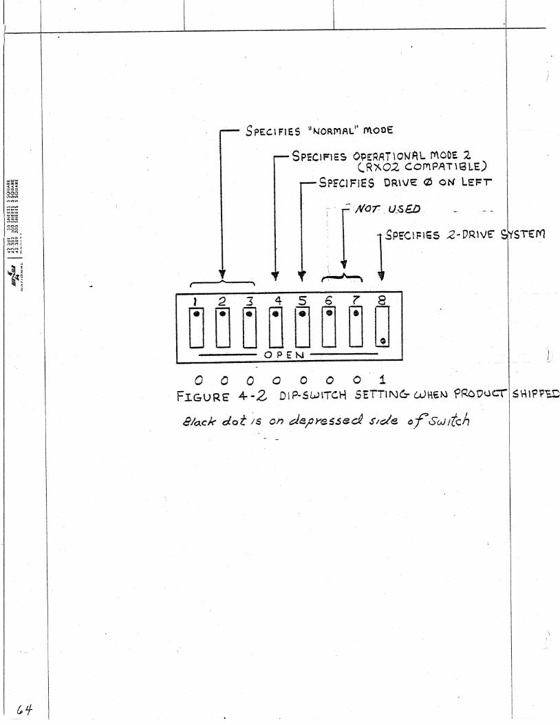
_t'lf(>01 ~I;QCO"
,:~~ ; ~~~!
- SPEC.1FIES II NORfI'lAt;." m.oDE
- SPECIFIES OPE~AT'O\IJAL J"t\OOE 2. (R)'..02 C.Ort\PAT\9LE)
-SPfC1FIES OR\VE ~ ON LEFr
;. ~:Nar.V~eD
rpE'<: I FIGS 2- DR IV€" SYSTEM
. 'I' ~ .. , ~, ~" ~
DD~[j~D~a ---- OPEN----
o Q 0 0 0 0 0 1 F~GURE' +-2 DIP-SWiTCH SE'T"TlN& Wt\E~ f'~OOucrS~l~\'~
BJa.ck clot ~s on d~l'ye.s$ed sIde (J.-r SWItch
4-6 HARDWARE SELF-TEST ROUTINES
The microprocessor always executes a number of system hardware tests following power-up or an initialization. This is true even when the system is being used in "HYPER-DIAGNOSTIC" mode. These tests are called IIPASSIVE" tests because there is no way that the user can inhibit them from executing. and there is no way that the user can operate the system should one of these tests detect a malfunction. Just before each hardware test routine is executed, the microprocessor writes the error code associated with the failure of that particular test in LEDs 5-8. In the event the test detects a malfunction. the microprocessor does a hard ~HALT leavi.ng the error code displayed. The codes and their interpretation are shown in Table 4-3. The user knows that the code being displayed in the LEDs is from Table 4-3 if the green RUN LED is OFF and LED 2 ~~ ON. Also. LEDs 1. 3. and 4 s h 0 u 1 d a 11 b e OFF.

BINARY 5678
0000
0001
0010
0011
0100
0101
0110
0111
1000
1001
* 1010
* 1011
* 1100
1101
1110
1111
t1EANING
UNASSIGNED
THIS ERROR CODE NOT CURRENTLY ASSIGNED
THIS ERROR CODE NOT CURRENTLY ASSIGNED
MICROPROCESSOR (P}ROM CHECKSUM ERROR
THIS ERROR CODE NOT CURRENTLY ASSIGNED
ERROR DURING TEST OF THE INTERFACE SHIFT REGISTER
PROGRAMMABLE I/O PORT FAILURE IN 8155 Ci·-1IP
PARITY LOGIC/LATCHED IN!T LOGIC TEST FAILURE
RAM TEST FAILED IN THE 2111 CHIP(S)
RAI"1 TEST FAILED IN THE 8155 CHIP
PHASE-LOCKED-LOOP TEST FAILURE
RE:AD/WRITE CONTROLL.ER iEST FAILURE
CRC/SERIAL DATA PATH TEST FAILURE
COUNTER/TIMER FAILURE IN 8155 CHIP
INVALID SWITCH SETTING (POSSIBLY BAD HYPER-DIAGNOSTIC CODE)
8085 CPU TEST FAILURE
TABLE 4-3 SELF-TEST ERROR CODES
* These three error codes can only occur following an INIT if the system is configured for HNORi1AL" operati.on. u- c:ne s~stem is configured for running hyper-diagnostics, these codes Can only appear if the corresponding hyper-diagnostic test has· been selected. The hardware selF-test loOp hyper-diagnostic te.t will never test these functions and thus cannot produce these error codes. (See section 4-10)
Should a passive test error occur, and the problem not be obvious, try cycling the times. .If the error is consistent and the evident, call the Data Systems Design Department ~or assistance.
the solution to main power several
solution is not Customer Service
, \'
.I
4-7 HYPER-DIAGNOSTIC MODE
As mentioned earlier, hyper-diagnostic mode is used when '1: n e use r wa n t s to ad JUS t I a x ere is e ,or t est his con t r a 1 1. e r and/or drives independent of a host computer system associated software. The DSD 440 chassis need connected to the AC power in the wall to hyper-dia~nostics. The user selects particular
and only
run tests
the be
the and
particular floppy disk drives usina the DIP-SWITCH on the controller board. Test results are observed through a combination of the 9 indicator LEDs on the controller board and perhaps an oscilloscope. After the switch and LED conventions are explained, the details of each of the hyper-diagnostic routines will be discussed.
NOTE: With the exception of the cabla orientation test, all of ~ne
hyper-diagnostic tests are to be executed with the interface bus (IBUS) cable disconnected from the DSD 440 chassis.
4-8 Dlp .... SWITCH SETTINGS DURING "HYPER-DIAGNOSTIC" t-l0DE
Switch 1 through switch 5 are used to encc~e the desired test. Since 5 individual switches constitutes 5 bits, one would assume that 32 individual tests could be encoded in these switches. This is not true however because any time switches L 2, and 3 are all zeros, the microp'rocessor assumes "NORi"lAL" mode operation, as previously explai.ned in secti.on 4-5. Switch 1 is the MSB and switch 5 is the LSB.
LED Switches 6 and 7 are not used to indicate anything during
hyper-diagnostic mods, except during the DIP-SWITCH! test.
Switch 8 is used to encode the particular floppy disk drive that is to be used for a given test. When ~ne sWl~ch is a 0, drive 0 is selected, when it is a L drive 1 is selected. Note that not all of the tests involve a drive. so in some cases the position of switch 8 will be irrelevant. The general exerciser tests are capable of exercising more ~nan
one drive. These two tests <switch codes 11110 and 11111) interpret switch 8 as the number of drives to be exercised. In other words, if switch 8 i.s a 0, only drive 0 will oe exercised. If switch 8 is a L both drive 0 and drive 1 will be exercised.
Note that there is no drive mapping function available in hyper-diagnostic mode. This function is only available when the systEm is being operated in "NORMAL" mode.

To run.·a particular hyper-diagnostic, one first powers down the controller/d~ive subsystem possibly using the AC switch conveniently mounted on the re~r of the chassis. Next, set the 8 switches to reflect the desired test, and in some cases, the desired drive. To start the test, si.mply turn the power back on. One should not play with the DIP-SWITCH settings while power is on EXCEPT where explici.tly, directed to do so in the explanation of a particular test. An example hyper .... diagnostic DIP-SWITCH configuration is shown in FiguT'e 4-3.
After extended use, the reliability of ' the DIP-SWITCH may become questionable. A swit.ch that "appears" to be in the shoT'ted state may in fatt be in the open state. If you ever have reason to believe that the microprocessor is mis-interpreting the byte encoded in the DIP-SWITCH, always use a pointed obJect (such a~ a ball point pen) to depress the rocker s~itches. Another technique that can be used to confirm your switch set~ings is the DIP-SWITCH/LED hypeT'-diagnostic. The code for thi.stest is (10000). Onc.e the microprocessor recognizes this test code, all it does is read the DIP-SWITCH and echo the setting in the LEOs. Once this test is running, change the DIP-SWITCH to the desired questionable setting and verify the setttng in the LEDs. If the LEDsreflect .the corT'~ct switch ~etting, the specific hyper-diagnostic test indicated Di.J the swi.tches can be executed by simply powering the unit oown, and then up agai.n.
4-9 LED MEANINGS DURING "HYPER-DIAGNOSTIC" MODE
Except in the tests where noted otherwise .. the LEDs IJ.d .. 11 work as follows. LED 1 and LED 2 will be off to indicate that the microprocessor is in hyper-diagnostic mode and is not curT'ently executing any of the hardware self-test routines described in section 4-6. LEDs 3 and 4 work the same way they did in "NORNAL" mode. When LED 3 is on, the system is cUT'rently writing on a diskette. When LED 4 is on, the sl~stem
is currently reading from a diskette. These two LEOs can be veT'y useful when trying to decide when to stop a particular hyper-diagnostic by turntng of-P the AC power. In gen.eral. i.t is not a good idea to tUrn 0" the power while the WRITE LED is sti lIon.
Just as in the hardware self-tests, the microprocessor will halt whenever it detects an error. The user knows when the microprocessor is halted by observing the green "RUN Il LED shown in Figure 4-1. An error code is di.splayed in LEDs 5-8 when the mic~oprocessor detects an error and halts. The error codes are similar to the error class codes discussed in section 4-4. Errors that involve a host computer interface .. such as non-existent memory and parity errors, could never occur during execution of any of the hyper-diagnostics. Table 4-5 shows the code interpretations. The activity LED of the drive selected when the failure was detected :J!ill be left on.
) .
)
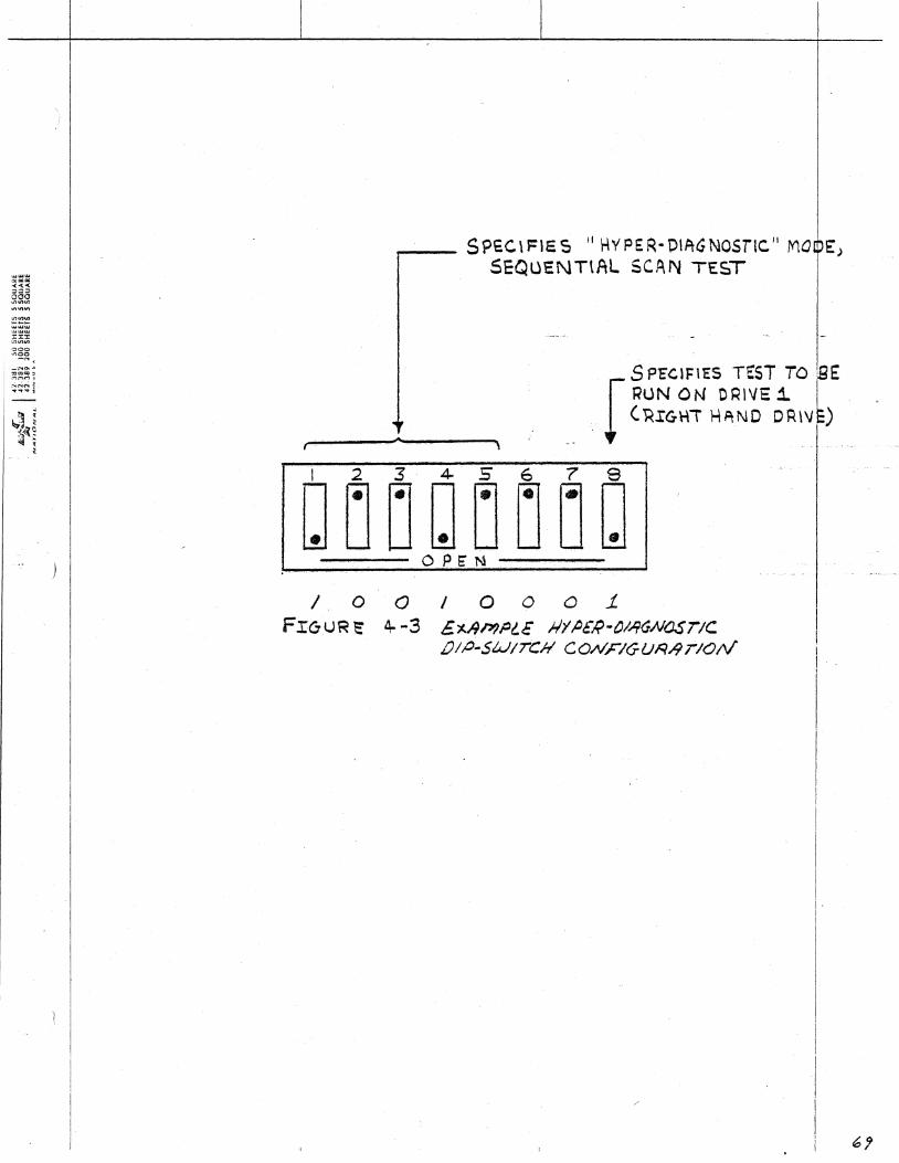
~~~
lJoI.uw Cl,/~W
.r::t: ~~~
000 ...,~~
~~~~ I
:"<("jN1 "'I'~"" li
r---. S PE.e. \ FIE S II HY PE R- DIA~ NOSTle /I ~Q 1 E) SEQUENTtAL SCAN TEST
f S PE'CIFIES TEST TO iBE RUN ON DRIVE j,. 1-('~IGH" H PtND DR\V~) ,
/00 I 0 0 0 1 Frc:;uR E' 4e -3 £xAP'JPI..€ HYPI;~R-O/.-9GNOSTIC
j)1"o-$wITC;"; CON'F/(;UR~ TIOtV'

BINARY 5678
0000
0001
0010
0011
0100
0101
0110
0111
1000
1001
1010
1011
1100
ME.ANING
NO- ERRORS HAVE OCCURRED SINCE POWER ON OR LAST INrT
OPERATOR ERROR - WRITE PROTECT VIOLATION (ERREG = 100}
THIS ERROR CODE NOT CURRENTLY ASSIGNED
IBUS Cf\BLE BAC~,WARDS OR INTERFACE f10DULE WITHOUT POWER
DRIVE BUS CABLE IS INSTALLED BACKWARDS
INDETERMINATE DENSITY (ERREG = 260>
SEE~" ERROR. (ERREG == 150)
THIS ERROR CODE NOT CURRENTLY ASSIGNED
DATA CRe ERROR (ERREG =:: 200)
SECTOR UNRECOVERABLE (ERREG =:: 070,120,1:30,160. OR 170)
DRIVE READ SIGNAL LOST (ERREG =:: 110)
READ/WRITE CONTR. FAILURE (ERREG == 220,320, OR 330)
MASTER CONTROLLER FAILURE (ERREG == 340)
1101 DRIVE FAILURE (ERREG:::: 010,020,030,050,300 OR 310)
1110 DATA PATTERN READ NOT THE SAME AS PATT£RN ("JRITTEN
1.111 AC POWER LOW ABORT OF WR ITE OR FORI'IAT (ERREG := 370)
TABLE 4-5 HYPER--:DIAGNOSTIC ERROR CODE INTERPRETATIONS
The follo~ing note of caution should be heeded here: The hardware self-tests and the hyper-diagnostics report errors by writing an error code in LEDs 5...,,8 and then halting. The microprocessor will execute the hardware self-tests before it
.gets to the ~~per-diagnostic routine encoded in the switches. The only way to tell if the error code displayed in LEDs 5-8 is from Table 4-5 or Table 4-3 is by looking at LED 2. LED 2 will be ON Following an erroT caused by the hardware self-test routines. LED 2 is OFFrolloUJing an error caused by most of the Hyper-diagnostic routines. The exceptions are noted in the test explanations.
LEDs 5-8 have a different meaning when the microprocessor is executing a hyper-diagnostic routine but has not yet detected anlJ error. One knows that this is .the condition by obsa-rving that the "RUN" LED is still ON. At thi.s ti.me, LEDs 5 and· Q en cod e den 5 it Y I and LED 5 I a Tl d 8 en cod e s e 1 e c ted drive. Coding is as follows:
LED ;, LED 6 DENSITY ""'!'l"-----...... ___ ..,... ___________ ~-~,~-.------__________ ._ OFF OFF ON
OFF ON OFF
DENSITY UN~-<'NOWN <DRIVE PROBABLY NOT READY) IBM 3740 SINGLE DENSITY DEC DOUBLE DENSITY
TABLE 4-6 INTERPRETATION OF LEDS 5 AND 6 DURING EXECUTION OF HYPER-DIAGNOSTIC ROUTINES (EXCEPT WHERE OTHERWISE NOTED)
LED 7 LED 8 SELECTED DRIVE ---0;00----____ ..... ___ - ____ . ________________ _ OFF OFF
OFF ON
o 1
TABLE 4-7 INTERPRETATION OF LEDS 7 AND 8 DURING EXECUTION OF HYPER-DIAGNOSTIC ROUTINES (EXCEPT WHERE OTHERWISE NOTED)
71
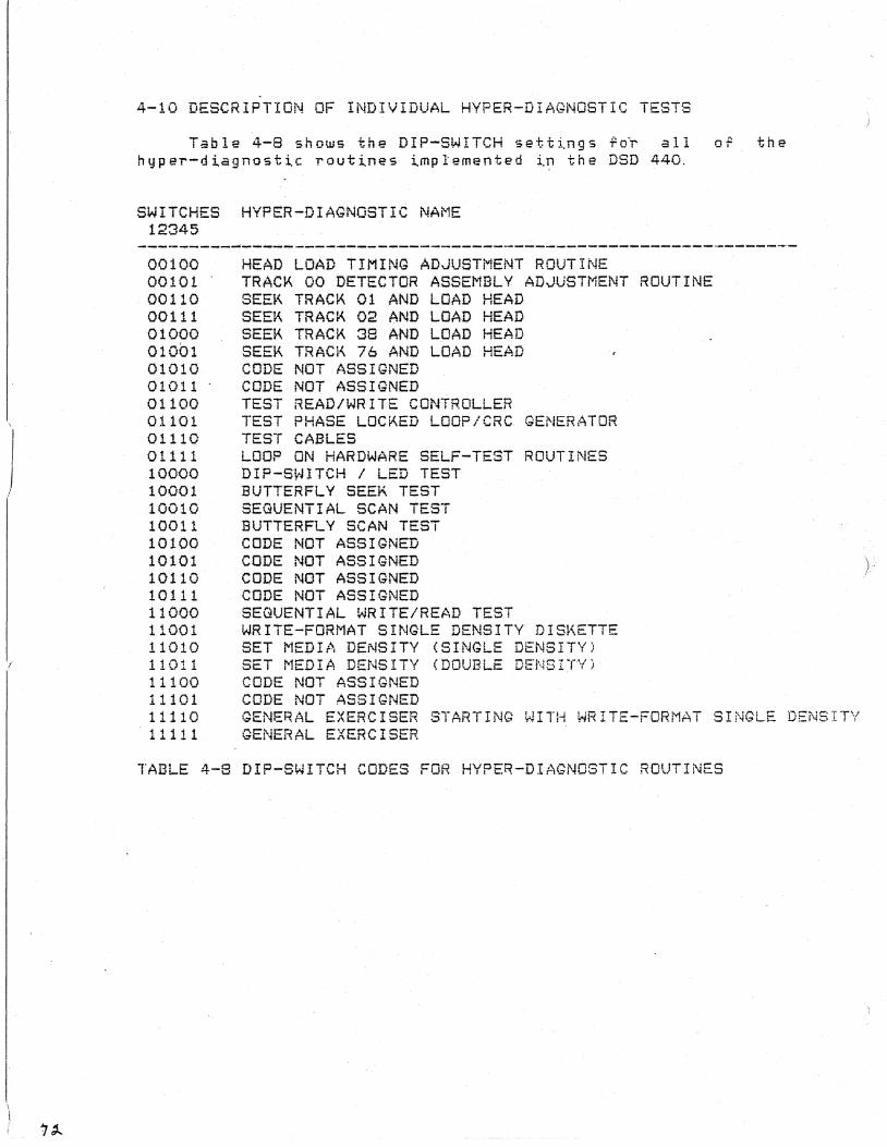
\
j
I
4-10 DESCRIPTION OF INDIVIDUAL HYPER-DIAGNOSTIC TESTS
Table 4-8 shows the DIP-SWITCH settings fo~ all of the hyper-diagnostic routines implemented in the DSD 440.
SWITCHES HYPER-DIAGNOSTIC NAME 12345
----~----,;.,....- ..... ..,."--"'!'--------..,. ...... --------------...;.----...... ~~-------_._---'-----00100 00101 00110 00111 01000 01001 01010 01011 01100 01101 01110 01111 10000 10001 10010 10011 10100 10101 10110 10111 11000 11001 11010 11011 11100 11101 11110
·11111
HEAD LOAD TIMING ADJUSTMENT ROUTINE TRACK 00 DETECTOR ASSEMBLY ADJUSTMENT ROUTINE SEEK TRACK 01 AND LOAD HEAD SEEK TRACK 02 AND LOAD HEAD SEEK TRACK 38 AND LOAD HEAD SEEK TRACK 76 AND LOAD HEAD CODE NOT ASSIGNED CODE NOT ASSIGNED TEST READ/WRITE CONTROLLER TEST PHASE LOCKED LOOP/CRC GENERATOR TEST CABLES LOOP ON HARDWARE SELF-TEST ROUTINES DIP-SWITCH / LED TEST BUTTERFLY SEEK TEST SEQUENTIAL SCAN TEST BUTTERFLY SCAN TEST CODE NOT ASSIGNED CODE NOT ASS I GNED ). CODE NOT ASSIGNED CODE NOT ASSIGNED SEGUENTIAL WRITE/READ TEST WRITE-FORMAT SINGLE DENSITY DISl,ETTE SET MEDI .. \ DENSITY (SINGLE DENSITY) SET MEDIA DENSITY (DOUBLE DENSITY) CODE NOT ASSIGNED CODE NOT ASSIGNED GENERAL EXERCISER STARTING WITH WRITE-FORMAT SINGLE DENSITY GENERAL EXERCISER
TABLE 4-8 DIP-SWITCH CODES FOR HYPER-DIAGNOSTIC ROUTINES

FLOPPY DISK DRIVE ALIGNMENT ROUTINES (00100-01001)
The first six test routines about to be described are intended for use with a special alignment diskette (PART NUMBER SA120-1) av~ilable from Shugart Associates. To perform some of the alignment procedures. it will be necessary to remove sev.ral screws in the bottom of the DSD 440 chassis so that the drives can be propped up on their side. Many of the ~dJustment screws and oscilloscope test points a~e located on the underside of the drives. This section will only describe what the six floppy disk alignment routines bUl1~ into the DSD 440 do. The actual alignment procedures can be found in a document published by Shugart Associates. which was included in your DSD 440 documentation binder. The document is called the SASOO/80i DISKETTE STORAGE DRIVE MAINTENANCE MANUAL.
HEAD LOAD ACTUATOR ADJUSTMENT ROUTINE (00100)
Inl.s routine starts by "homing" the selected dri.ve to track 00. Once there, the head is loaded and unloaded at roughly a 5 Hz. rate. The head 1.5 loaded ror 100 milliseconds, and then unloaded for 100 milliseconds before the cycle is repeated. As mentioned earlier, the routine l.S
terminated by a1.sconneC~1.ng AC power from the chassis. Paragraph 4.6.3 in the Shugart manual calls for a routine su~h as tl1 i sane.
TRACK 00 DETECTOR ASSEMBLY AD.JUSTMENT ROUTINE (00101)
This rOU~l.ne starts by "homing" the selected dri.ve to track 00. The head is then alternately moved between track 01 and track 02 about once every 70 ffisec.· The head is loaded during this test. The routine is terminated by disconnecting AC power. Paragraph 4.11. 8 in the Shugart marwal callsPor a routine such as this one.
SEEK TRACK 01 AND LOAD HEAD (00110)
This routine starts by "homing" the selected ori.ve to track 00. Next, the head is positioned at track 01 and loaded against the media. The head remains loaded until power lS removed. Paragraph 4.11.8 in tl'd? Shugart manual calls for a routine such as this one.
SEEK TRACK 02 AND LOAD HEAD (00111)
T h i. s r 0 uti. ne s tar t s by" hom in 9 !! -::.: n e s e 1 e c ted d r i. vet 0
track 00. Next. the head is positioned at track 02 and loaded against the medi.a. The head ,.-emai.ns loaded unti.l pOLJ':!- 1.S
removed .. Paragraph ~1-. 11. 8 in the Shugart manual calls for .:; routine such as this one.
73
74
SEEK TRACK 38 AND LOAD HEAD (01000)
This routine starts blJ "homing" the selected drive to track 00. Next, the head is positi.oned at track· 38 and loaded against the media. The head remains loaded until power ~s
removed. This routine is used during the HEAD RADIAL AD0USTI"1ENT described in p<aragraph 4.11. 3 of the Shugart manua 1.
SEEK TRACK 76 AND LOAD HEAD (01001)
This routine starts.by "homing" the selected drive to track 00. Next, the head is positi.oned at tracK 76 and loaded against the media. The head remains loaded until power is removed. This routine is used during the READ/WRITE HEAD AZIMUTH ALIGNMENT described in paragraph 4.11.9 of the Shugart manua 1.
TEST READ/WRITE CONTROLLER (01100)
This routine causes the read/write controller st~ate machine to be conti.nuously cycled through its internal selP~test microcode. This test should be run if there is reason to believe that the read/w~ite controller state machine is not performi.ng reliably. Should this test generate an error, the code is shown in Table 4-3 as a 1011. Note that LED 2 will also be on if this error is reported.
TEST PLL/CRC GENERATOR (OIIOI)
This routine checks the operation of the phase locked loop circuitry by counting the number of PLL VCO cycles that occur duri.ng a 50 milli.second inter"·lal. Thi.s te~t should be run to determine circuitry. If it 4-3 as a 1010.
if a READ problem is being caused by the PLL is, the error code will be sholi.ln in Table Note that LED 2 will be on if this error is
reported. The second half of this test verifies that the eRG generator/chacker and serial oa~a path is functioning properly. IF this test detects a malfUnction, the error code is shown in Table 4-3 as a 1100. LED 2 will also be on.
TEST CABLE ORIENTATION
This test is used to veriFy that both the interface bus cable (connecting the controller to the interFace module) and the drive bus cable (connecting the controller to the drives) are not installed backwards. Note that the interface bus cable must be connected on both ends and the interface module must have power in order to run this test. The interface bus cable must be disconnected at one or both ends when running all hyper-diagnostic tests EXCEPT this error, Table 4-5 indicates which cable is
one. If there is an causi.ng the pTobl-em.
HARDWARE SELF-TEST LOOP (01111)
The DSD 440 microprocessor executes the hardwa~e self-test once after powe~ing up. When this hyper~diagnostic routine is selected, the microprocessor will keep executing the hardware self-test over and over again indefinitely until either power is removed or an error i.s detected. LEDs 5, 7, and 8 should be flashing on and off when this routine is executing (error-free').
DIP-SWITCH / LED TEST ROUTINE (10000)
This routine is used to determine if the microprocessor can correctly read all S switches in the DIP-SWITCH, and correctly illl,.lminate LED's 1-8. The routine will simply read the DIP-SWITCH and wT'ite that byte to the LED bank. As an example, if swi.tch 2 were in the 1 pOsiti.onl then LE:D 2 should b eon. I f s wit c h 2 we rei nth e 0 p 0 sit i. 0 i'i , the n LED 2 5 h 0 u 1 d be off. Since the mic~oprocessor is execu~~ng this loop continuously, the state of a LED should appear to change very shortly following a switch position change. The test is terminated by removing power.
BUTTERFL Y SEEK TEST (10001)
This routine starts by "homing" <;ne selected dri.v2 to tT'ack 00. The head positioner is then moved back and forth in what has been called a "butterfly" pattern. This pattern consists of the following series of tracks: 76,01,75,02,74,03 .. ,.-.. After one complete cI,Jcle, the microprocessor tT'ies to seek the positioner to track 00. If the track 00 signal is rtot asserted. the errQr code is reported in the :LEDs ~nd the microprocessor halts. If the_ tT'ack 00 5i.gnal is asserted, the test i.s repeated. The head is not loaded at any time during this test so no reading or writi.ng is done.
SEGUENTIAL SCAN TEST, (10010)
This routine starts by IIhoming" the selected dri.ye to track 00. The head is then loaded and the media density is determined and di_splayed in the LEDs (see Table 4-6), The controller then sequentially reads every sector of every trac\L If no errors occur, this scan routi.ne wi.ll (Ijcle over and over until power is removed. l-r an error does occur, the processor will halt and the error code will be displayed in LEDs 5-8. The meanings associated wi.th the 16 possible error codes are shOUJn in Table-4-5. Remember, the code displal~,ed in LEDs 5-8 is not an error code UNLESS the green CPU run LED is out and the head positioner is not movin~. The meaning o~ LEDs 5-8 are shoUJn in Tables 4-6 and 4-7 when the test is stUI executing.

BUTTERFLY SCAN TEST ( 10011)
This routine is similar to the sequential scan test, except that the sequence of tracks read is 76,01,75,02,74 ..... This test wi.ll take much longer than the sequential scan test to read the same total number of sectors because of the added positioner st~p and head load time. This test will detect problems associated with seeking andlor reading.
SEGUENTIAL WRITE/READ TEST (11000)
This routine starts by "homingll the .selected drive to track 00. Next. the density of the di.skette inserted in the drive is determined. The routine then sequentially writes. pseudo-random data dn every track and sector of the diskette, in the appropriate density. After wri.ting, every track and sector on the diskette is sequentially read. Any error encountered will b~ reflected in the LEDs when it occurs and the machine will halt. The write cycle only happens once. The read cycle is repeated indefinitely until power is disconnected or an error is detected. LEDs 3 and 4 can be used to determine if the routine has completed the write cy c Ie.
WRITE-FORMAT DISKETTE IN 3740 S.D. FORMAT (11001)
This routine starts by Uhoming ll the selected drive to track 00.· Next, the entire diskette is formatted accord1.n9 -to the IBM 3740 single density standard. The sector addresses are written s~quentiallyon each tracK. After all tracks have been written, control is transferred directly to the sequential scan test, whil:;h then k'eeps readi.ng the diskette in~eFinately until error or power disconnect. LEDs 3 and 4 can be used to determine when the write cycle has been completed.
SET MEDIA DENSITY (TO SINGLE DENSITY) (11010)
This routine starts by IIhoming" the selected dri.ve to ~track 00. Next, every secto;' on the di.skette is wri.tten wi.th a single density data addr~-ss mark, 126 bytes of O'SI and 2 eRC bytes. Unlike .the previous write-format routine, this routine does not modify the sector headers. Control is transferred to the sequential scan test as soon as all sectors have been written. LEDs 3 and 4 can be used to determine when the writing has stopped and the reading has begun.
)) .Y
·--i

----~
SET MEDIA DENSITY (TO DOUBLE DENSITY) (11011)
This routine starts by "homing" the selected drive to track 00. Next, every sector on the di.skette is written wi.th a double density data address mark, 256 bytes of DEC MMFM 0'5, and 2 eRC bytes. This routine does not modify the sector headers. Control is transferred to the sequential scan test as soon as all sectors have been written. LEDs 3 and 4 can be used to determine when the writing has stopped and the reading has begun.
GENERAL EXERCISER STARTING WITH WRITE-FORMAT S. D. (11110)
This test is designed to exercise all parts of a DSD 440 system as thoro~ghly as possible. Unlike the other hyp~r-d(agnostic routines. this rou~~ne and the following rou~~ne can operate on multiple drives. Switch 8 is used to specify the drives to be exercised. As an example, if switch 8 were set to a I, the general exerciser would first exercise drive L then drive 0, then drive'l, etc. if slJJitch 8 l..LIers set to a 0, only drive 0 would be exercisEd. It i.s important that all drives that are to be exercised be loaded with write-enabled diskettes. The sequence of operations is listed below: ( i' ... J Execute hardwa~e self-tests (no drives involved) (2) Write-format selected drive according to 3740 S. D. standard (3) Do sequential read of all sectors on selected drive (4) Do sequential write/read of all sectors on selected drive (5) Do butterfly read of all sectors on selected drive (6) Do a double density set media density on selected drive (7) Do a sequential read of all sectors on selected drive (8) Do sequential write/read of all sectors on selected drive (9) Do butt~rPly read of all sectors on selected drive (10) Do a single density set media density on selected drive (11) Dete~mine next logical drive unit, and if that unit has not already been turi.te-formatted once, go to step (2);
otherwise go to step (3)
GENERAL EXERCISER (11111)
This test is the same as the previous one (11110), but minus the single density write-format routine indicated in step {2L
77
4-11 HOW TO READ THE INDICATOR LEDS
The nine indicator LEDs on the master controller circuit board assembly encode different information at different times. Although all of the encoding algorithms have been explained in previous sections of this chapter) they will be reviewed in this section usi.ng a "flow-chart" technique. By following the steps of this flow-chart, a minimum amount of time is required to determine the information encoded in the LEDs at anlJ given time. Four examp les are given in Figure 4-4. To test your understanding of the Plow-chart, t,..y covering up the right side of Figure 4-4 and interpreting each of the four LED patterns. When you are donea verify that your interpretation ag~ees with the ones listed on the right side of Fig ure 4-4.
Ii /'
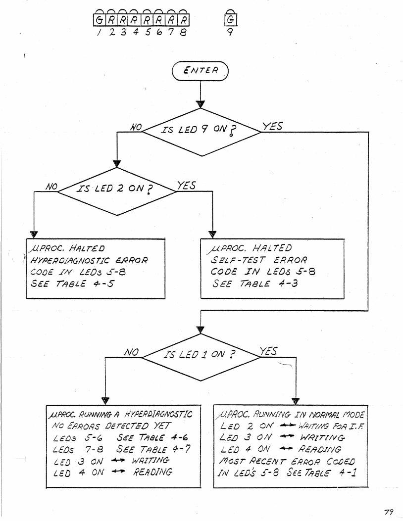
0000 00 00 I'(?G"" I 161RIRIR[RIRIRIRI J234Sb78 9
ENTER
NO YES
NO YES
flPROC. H,iJI..T&D '~
, !i IIYPcROiAGNOsrJC MRaR ?PROC. 1-1111. rED SEL.F-TEST ERROR CO!)c IN LEO,s S-8 SEE V78L£ 4-3
---j
COOE IN LEO~ S-8 SeE 1/78LE 4--5
NO
,)J.P/(()('. j(UNNINIJ 11 HYP£~f;lRuNosr/c /Vo EARORS iJ€TE'CTEO YET -LcO.s S';", SeE ~8t.£ -4-6
LEOs 7- 8 SEE 1;:;8Lf f-? L (1)..3 ON .... W,Q.lT1N(5-
L€D 4 ON ..... j(£.~O/NG
YES
flPf(OC. RUNNiNG IN I'IORI'?!:;L f'10D[ LED 2" QIY .......... ~/T//VG rO;:(.r. F. I...e.l) .3 ON ... Jr/;t:{[TI'NG:-
L£.D 4- ON ~ HcI70f/'/G /'los r /(€CEN r t£ifRQf( C~€.o
IN L€/)$ s- 8 S€E. "!'hSle ~-1
79

"'1.1:1"" ~~~ ~ww
www :r:::::r <r.IV)'"
OQO ",~~
_-N00" Qc)=~ ~~..., ::
~~~~
FIGURE 4 - 4-
I/vO)(/i?...9l II /?OOE:; !VQT WhlIT//V'G'./N'h'I77NG; '" .-'(t!'/i/))N~; L..-9sr EJ'?;:(ol? N..-9S v~TA C.-'i'C EI(.tr'()1? 0°8);
CONT.,qOI..L€I<~PI?OC • ..sr/I..L.. /?t..JNNINC:-
I£]l?tlN 65i.r.rE57;:;.pII..U,«t!'; 8-"1£) 2/// h'~".?J Cl-lliJ LJE7t5'C/ED ; ~"o/(()C. )I/JI../ef)
''HYPEN-i///Jt;N'OSTIC JI /Yl()£)€; 1¥~/iING; l)EC 2D Ft.1/f/I'J.lfT; ORIVe,J. S£I..GCrElJ .J·.r,.D"fJoc. Srll.L ~UNNIAJ

SECTION 5 DSD 440 PROGRAMMING INFORMATION
The programmers' interface to the eSD 440 varies depending on which host computer family (such as the DEC 8's and 11's) and in which operational mode the system is configured. The characteristics or each programmers' interface are determined by the controller. The controller can utilize five separate IBUS protocols to communicate with the interface module and in turn the host computer program. This section will be organized by computer family and operational mode. MODES 1 and 2 of the PDP-11 and LSI-ii will be dlscussed separately. Since the PDP-8 is not capable Qf DMAt even in MODE 2, the programmers' interface does not differ substantially between MODE 1 operation and MODE 2 operation. For this reason, both operational modes of the PDP-8 interface will be discussed together, with the differences being emphasized.
5-1 DEC 11 FAMILY PROGRAMMERS' INTERFACE
For a person primarily interested in programming, there is little difference between the PDP-l1 and the LSI-ii. The programmers' interface to the DSD 440 fleXible disk system is the same for both computers. This section will present an overview of th~t programmer interface.
Data is transferred to and from the flexible disk or "diskette" in fixed length blocks called !Isectol~sll. A sector contains 64 sixtee~ bit words when the system is being used in single density mode and 128 words in double density mode.
The programmer can direct the DSD 440 controller to perform several "operations" or "tasks". Each of these tasks is used to facilitate the storage and retreival of information on a di.skette. As an example, two operations are needed to move a sector of data from main memory to a particular sector on a di.skette. The first operati.on is called "FILL BUFFER". This is used to move the data from computer memory to a RAM buffer ~hich is an internal part of the di.sk controller. The second operation is called "WRITE SECTOR". Thi.s operation positions the read/write head of a flexible disk drive over the specified portion of the di.skette, and then writes the data stored in the controller's sector buffer on the diskette.
~/
The programmer communicates his task reG.uirements to the DSD 440 . controller through two physical registers which are addressed as though they were memory. The CONTROL and STATUS REGISTER is normally located at address 777170. The DATA BUFFER REGISTER is normally located at address 777172. There are a total of seven "logical registers" that will be referred tn throughout this chapter. These registers represent such information as data, controller status, track address and sector address. The programm~T always reads and writes logical registers through the data b~ffer register, which is a physical register.
A task is initiatad by writing a specific bit pattern to the control and status registe~. Associated with each task is a specifi.c IIprotocol tl • A protocol is derined as a set of rules which determine the parameters OT data the computer should be passing th~ough the data burrel" register at ~ny time during the execution of! a task. As an example, operations which cause ~he read/write head in the f!lexible disk drive to move will require a track and sector address. The protocol ror these runctions is as rollows: (1) The cnmmand is written to the control and status regi.ster. (2) The sector address is written to the .data buffer register when the controller requests it. (3) The track address is written to the data buffer register when the controller requests it.
The operational modes which were discussed in chapter 2 l.nfluence the protocol that is a·.;sociated with· the val"ious )J flexible disk tasks. The main differences in these modes center i.n two areas. First, in Mode 1 programmed I/O i.s used exclusively for the' transfer of both data and parameters between computer and controller. In Mode 2, programmed liD is used to transfer parameters, but DMA is used to transfer data between controlle~ and main me.mory. Second, in M~de 1 data is recorded on di~kette in single density only. In Mode 2. data can be recorded on diskette in either sintle or double density. This chapter on programming has been divided up by ope rat i ona 1 mod e. I t is s u 9 9 est edt hat· the p r og r amm e r determine the operational mode he is going to be using and then read the corresponding section o~ this chapt~r.
----'l

):
-t
5-1. 1 MODE 1 OPERATION
The system assumes MODE 1 ope~ation when the "RX01" switch <located on the main controller board) is placed in the 11111 p os it ion. (see sect ion 2.,.1,4-5) Any program that runs successfully with the DEC RX-l1 (or RXV-l1) will run equally well on a D5D440 system configured to operated in this mode.
5-1. 1. 1 PERIPHERAL DEVICE REGISTERS
Programs communicate with the DSD 440 peripheral device registers. They are:
COMMAND AND STATUS REGISTER DATA BUFFER REGISTER
(RXCS = 777170) (RXDB = 777172i
through two
Peripheral device registers reside in the top 4K words of the II-family computer's memory address space. They are addressed as memory and anJ.,l instruction that can operate on a mem.ory location can operate on a peTiph-eTal device. register in the same way. For infoTmation exp laining how to assign these reg isters non-standard bus addresses, see section 3-4.
5-1. 1. 1. 1 COMMAND AND STATUS REGISTER
Writing the bits of this register controls the DSD.440. The fOTmat for this register is shoUln in figure 5-1. The RXCS registeT also provides important status information and errol' indications when read by the program.
INSERT FIGURE 5-1 ON THIS PAGE
•
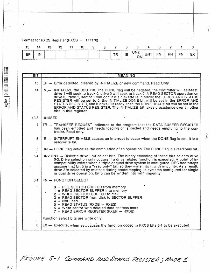
'" ... w """ .. «< ~~~.
_No.n
-=GlI=~ MM,", ~
~~~1
+ -- ."_ ••• _ •• - - - •
Format for RXeS Register (RXCS = 177170)
15
ER
14 13 12 11 10 9 8 7 6 5 4 3 2 1 0
I· IN I I I I TR I IE IUN~N) UN1 I FN FN I FN I EX I BIT MEANING
15 ER - Error detected, cleared by INITlALLZE or new command. Read Only
14 IN.- INITIALIZE the DSD 110. The DONE flag will be negated, the controller will self·test, drive 1 wit! seek to track 0, drive 0 will seek to track O. A READ SECTOR operation on drive 0, track 1, sector 1 will occur if a diskette is in place; the ERROR AND STATUS REGISTER will be set to 0, the INITIALIZE DONE bit wiJl be set in the ERROR AND STATUS REGISTER, and if drive 0 is rea<:fy, then the DRIVE READY bit will be set in the ERROR AND STATUS REGISTER.The lN1T1ALlZE bit takes precedence over all other bits in this register.
13-8 UNUSED
7 TR - TFiANSFER REQUEST indicates to the program that the DATA BUFFER REGISTER has been emptied and needs loading or is loaded and needs emptying to the control/er. Read only_
6 IE- INTERRUPT ENABLE causes an interrupt to occur when the DONE flag is set. It is a ' read/write bit. .
5· ON - DONE flag indicates the completion of an operation. The DONE flag is a readonfy bit.
5-4 UN2 UN1 - Diskette drive unit select bits. The binary encoding of these bits selects drive 0-3~ Drive selection only occurs if a drive related function is executed.A point of incompatibility exists when a triple or quad drive system is configured. DEC bootstraps assume that bit 5 is a "read only" bit, so they write into it with impuriity. As a result, drive 2 is selected by mistake during bootstrapping. In systems configured for single or dual drive operation, bit 5 can be written into with impunity.
3·1 FN - FUNCTION SELECT
o = FILL SECTOR SUFFER from memory 1 = READ SECTOR BUFFER into memory 2 = WRITE SECTOR BUFFER to disk 3 = READ SECTOR from disk to SECTOR BUFFER 4 = Not used 5 = READ STATUS (RXDS -RXES) 6 = Write sector with deleted data address mark 7 = READ ERROR REGISTER (RXER - RXDB)
Function select bits are wri.te only.
o EX - Execute, when ~et, causes the function coded in RXeS bits 3·1 to be executed.
)
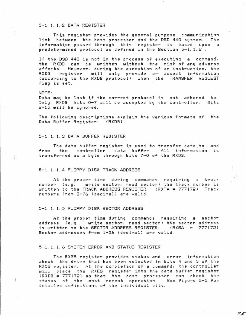
\
!
--)
5-1. 1. 1.. 2 DATA REGISTER
This register provides the general purpose communication link between the host processor and the DSD 440 system. The information passed through this register is based upon a p red e t ermine d pro t 0 col a s d e f i. ned i. nth e Sec t ion 5-1. 1. 2 .
If the DSD 440 is not in the process o~ executing a command, the RXDB can be written without the rigk of any adverse affects. HOUlever, during the execution or an instl"uction, the RXDB register Ulill only provide 01" accept infol"mation (according to the RXDB protocol) Ulhen the TRANSFER REGUEST flag is set.
NOTE: Data may be lost if the correct protocol is not adhered Only RXDB bits 0-7 will be accepted by the controller. S-i5 will be ignored.
The following descriptions explain the vaTious ro~mats or Data Buffer Register. (RXDB)
5-1.1.1.3 DATA BUFFER REGISTER
to. Bits
the
The data buffeT register is used to transfer data .to and from the controller data buffer. All information is tl"ansfel"red as a ~yte through bits 7-0 of the RXDB.
5-1.1.1.4 FLOPPY DISK TRACK ADDRESS
At the proper time during commands re~uiring atTack number (e. g. write sector, read sector) the track number is written to the TRACK ADDRESS REGISTER. (RXTA = 777172) Track numbers from 0-76 (decimal) are valid.
5-1. 1. 1. 5 FLOPPY DISK SECTOR ADDRESS
At the propel" time during commands requiring a address (e. g. write sector, read sectOT) the sector is wri tten to the SECTOR ADDRESS REGISTER. CRXSA = Sector addresses from 1-26 (decimal) are valid.
5-1.1.1.6 SYSTEM ERROR AND STATUS REGISTER
sector address 777172)
The RXES register provides status and errol" information about the drive that has been selected in bits 4 and 5 of the RXCS regi.ster. At the completi.on of a command, the controller will place the RXES register into the data buffer regi.ster (RXDB·= 777172) so that the host processor· can check the status of the most recent operation. See figure 5-2 ror detailed definitions of the individual bits.

_NO. /l :CQ~:l ~MM"
~~~~
l------.v---·-.. )\.----v-----) /1/br (./$£1). iVI?J7ET#G'SIr .BlrS Q/\}t.Y
15 14 IJ 1.2. // 10 . q 8 '7. ~ . .5" 4- .J 2 / 0
I11II II 10 10011 I III l----V----) \. V·)
NOT U$£O /-.3:28
15 . /4- I.J /2 II /0 9 8 ?.6 S- + :; . .z 1 0
I I , I III I 0 II I I II I I l _____ ---)
V
;Vor USED
l ______ --) V
0-11+8
- /5 14- 13 12 II 10 ,;; 6' ? ~ ..; 4-.2 .2 / 0
l ________ -----) v
Alor U:SEO ITT r
DD DEN TD eRG ERR
DRV DRV WP PAR RDr DEN S;T
/?x£s
5-1. 1.2 MODE 1 PROTOCOLS
Protocols are required in the DSD 440 because the computer interface module and the DSD 440 controller communicate mostly through a single liD register. Because of this constraint, the controller must identify parameters being passed to it by the order in which they are transmitted through the register link. The following sections describe the proper protocol for ea~h of the possible commands that can be sent to the controller. Failure to adhere to the correct protocol may result in lost or incorrect data.
5-1.1.2.1 FILL SECTOR BUFFER (000)
The FILL SECTOR BUFFER command is used to fill a storage buffer inside the DSD 440 with 128 8-bit bytes of data from the host processor .. Other functions can later be used to either write that data to diskette, or transfer it back to the processor.
When the FILL SECTOR BUFFER command is given, the DSD 440 responds by clearing the DONE flag, RXCS bit 5. The controller then requests the first byte of data by setting the TRANSFER REQUEST flag, RXCS bi.t 7. At this time, one byte of data should be written into the lower 8 bits of the RXDB register by the host processor. When the processor writes a byte i.nto the RXDB register, the TRANSFER REGUEST flag will be cleared. Whe~ the TRANSFER REGUEST flag is again set by the controller, another byte of data should be transferred to the RXDE register. This process is repeated un~il a total of 128 bytes have been transferred. When the controller has the 128 bytes needed to fill the buffer, TRANSFER REQUEST is left c 1 ear I and t Ii e DOr"\~E f- 1 a 9 J R xes bit 5 IJJ i.l 1 be set. 1Ft h e INTERRUPT ENABLE bit, RXCS bit 6, is set, an interrupt request wi.ll occur when the DONE flag is set.
NOTES: 1) Data will not be accepted unless the TRANSFER REQUEST flag
is set. 2) If the ERROR flag, RXCS bit 15, l.s set, the speciFic error
must be obtained from the RXER (see Section 5-1. 1. 2. 7 READ ERROR REGISTER).
3) The controller will ign~re all data sent after the 128th by teo
4) Since the FILL BUFFER command is not associated with any one drive, RXCS bits 4 and 5 do not affect this function.
S) Interrupts are generated by the logical AND of DONE and interrupt enable. If the DONE bit is already set the first time the pr6grammer sets the interrupt enable bit, a spurious interrupt should be expected.
!?7
5-1.1.2.2 EMPTY SECTOR BUFFER (OOI)
The EMPTY SECTOR BUFFER function is used to transfer the contents of the sector buffer to the computer. The sector buffer is loaded from a previous FILL SECTOR BUFFER or READ SECTOR command.
When the- EI'-1PTY BUFFER command i.s given, the controller responds by clearing the DONE rlag, RXCS bit 5. The controller then sets the TRANSFERREGUEST 'f!lag,RXCS bit 7, to indicate that a byte of data is available for reading. The data byte appears in the lower 8 bits Or the RXDB. When the host computer reads the byte, the TRANSFER REQUEST flag is cleared. The TRANSFER REQUEST flag will again be set when the cont?oller has placed another byte of data in the RXDB register. This proc~ss is continued until all 128 bytes have been transfe?red to the host computer. After the 128 bytes of data have been transfer?ed, the TRANSFER REGUEST rlag will remain cleared and the DONE Ilag will be set. An interrupt request will be generated ir the INTERRUPT ENABLE bit was set when DONE became true.
The notes that apply to the FILL BUFFER command apply equally to the EMPTY SECTOR BUFFER command. In addition, it should be noted that the EMPTY BUFFER function does not modify the contents of the sector buffer.
.--~

\
l
5-1. 1. 2. 3 WRITE SECTOR (010) ,
The WRITE SECTOR function is used to transfer the contents of the sector buffer to a specified track and sector or the diskette. When the WRITE SECTOR command is given. the controller clears the RXES register and the DONE flag. Next, the controller sets the TRANSFER REQUEST flag, RXCS bit 7, to re~uest a sector address. The program should respond by writing the desired sector address (RXSA) into the data buffer register (RXDB=777172L Thi.s clears the TRANSFER REQUEST flag. As soon as the controller shifts the sector address over the interface cable, it asserts TRANSFER REGUEST again. This time the program should yespond by writing the desired track address (RXTA) into the data burfer register. This clears the TRANSFER REQUEST flag. After the track address is received, the controller will cause the selected drive to seek to the desired track and locate the desired sector. TRANSFER REQUEST will stay unassertted for the remainder of the function. If the correct track and sector are found, the controller will write the 128 bytes of data from the sector buffer, plus two bytes of CRC onto the di.skette. When this is finished, the controller completes the function by writing the RXES to the data buffer register and setting the DONE flag. As in all functions, an interrupt request will be generated if the interrupt enable bit, RXCS bit 6, was set when DONE became true.
-I-f-t h e c-o-n-tr 0 I 1 ei"------i;-s u n-a-Jj-I-e t o------l-o-c a t e-t-h-e s p-ee-i-r-i e d diskette track, the RXER is set to a 150(8). If the specified sector cannot b. found within two diskette revolutions, the RXES is set to a 70(8). Both of these error conditions cause the function to be terminated. The ERROR flag! RXCS bit 15. and the DONE flag, oRXeS bit 5 are asserted. As IJJith the error-free termination, an interrupt request will be generated if the interrupt enable bit was set when the DONE flag became true.
NOTES: 1) The contents of the sector bufFer are not modified by the
WRITE SECTOR function. 2) The contents of the sector buffer ARE mqdified as a result
of a power failure and an initialize commando Programmers must be sure that valid . data is written back into the sector buffer following either of these conditions. This is especially true' before executing the WRITE SECTOR command.
3) If the sector number written into the RXSA is 152 (octal) the WRITE SECTOR function becomes a WRITE FORMAT TRACK function. Track formatting is explained in section 5~1. 1. 2. 9

90
5-1.1.2.4 READ SECTOR (011)
The READ SECTOR function is used to locate a specified track and sector of a diskette and then tTansfer the c~ntents of the da~a field into the controller's sector buffer. When the READ SECTOR command is given, the controller clears the RXES register and the DONE flag. Next, the controller sets the TRANSFER REGUEST flag, RXCS bit 7, to re~uest a sector address. The program should respond by writing the desired sector add~ess (RXSA) into the data bufFer register (RXDB=777172L This clears the TRANSFER REGUEST ftlag. As soon as the controller shifts the sector address ove~ the interface cable, it asserts TRANSFER REGUEST a second time. The program should respond by writing the desired t~ac' address (RXTA) into the data buffer register. This clears the TRANSFER REGUEST flag. After receiving the track address, the controller will cause the selected drive to seek to the desired track and locate the desired sector. TRANSFER REQUEST will be left reset for the remainder of this functiGn. If the correct trMck and sector are located. the controller will start looking for a data address m~rk (DAM) or a deleted data address mark (DDAM). When a valid mark is found. this marks the beginning of the 128 b~te data Pield on the diskette. At that point, the following 128 bytes are read from the diskette and stored in the controller data buffer. The two CRe bytes are read immed iate I y after th e data fie 1 d. An erTor-free read i.s indicated if the address mark. 128 bytes of data, and two bytes of CRC produce a zero residue when passed sequentially)) through the CRC checker hardware circuits. As soon as the data is available in the buffer. the controller will terminate the function by writing the RXES to the data buffer register and set the DONE flag. An interrupt request will be generated if the interrupt enable bit, RXCS bit 6, ~as set when DONE was asserted.
Ir the delet.ed data address mark (see Section 5-1. 1. 2.6) was detected, the controller will set the deleted data flag. This flag appears in the ERROR/STATUS register (RXES bit 6). If a CRC error is detected, the controller will set RXES bit 0 and the ERROR flag (RXCS bit 15) to indicate that fact. Seek errors and missing sector arrors are reported Just as in the WRITE SECTOR function.
. _-j
5-1. 1. 2. 5 READ STATUS (101)
The READ STATUS command is used to determine the current status of the drive selected by RXCS bits 4 and 5. The status information passed ~ack is: 1) Is the drive ready? 2) Is the diskette write-protected? *
When the command is issued, the DONE flag is cleared. The. controller then checks to see that the door of the selected drive is closed, a diskette is inserted, and that the diskette is up to speed. Diskette speed is determined by measuring the amount of time between successive index pulses. Since this measurement takes an average of 250 milliseconds, excessive use of the READ' STATUS function will cause reduced throughp.ut. If the dr'ive is ready, the controller sets bit 7 (DRIVE READY) of the RXES. IF the drive detects an uncovered write protect notch on the diskette, the controller senses' this and sets bit 3 (WRITE PROTECT) of' the RXES. The remaining bits of the RXES will reflect the re~ult of the last command before READ STATUS. The controller terminates the function by shifting the RXES over to the RXDE and setting the DONE flag. An interrupt request will be generated if the interrupt enable bit, RXCS bit 6, was.et when done became true.
* If the interface module ;bei.ng used is ei.ther the 4430 or 4432, bit 3 of the RXES, when asserted, ~eans that AC power is low in the c~ntroller/drive subsystem. On the other LSI-il (2132. 2133} . and PDP-l1 (2130) in:terface modules. bit 3 correspancis to the drlve write protect status as stated above.
5-1.1.2.6 WRITE DELETED DATA SECTOR (011)
This function performs the same t~5k as WRITE SECTOR. The difference between the commands is that this command writes a deleted data address mark Just before the data field. The standard J,.IRITE SECTOR function writes a regular data address mark. When a sector which was written with a deleted data addre~s mark is read, bit 6 oT the RXES will be set .
9/
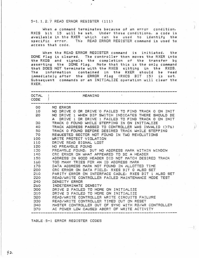
...
5-1.1.2.7 READ ERROR REGISTER (111)
Wh.n a command terminates because of an error condition, RXCS bit 15 will be set. Under these conditions, a code is available in the RXER . which can be used to identify the specific error. Th~ READ ERROR REGISTER cnmmand is used to access that code.
When the READ ERROR REGISTER command is initiated, the DONE 'flag is cleared. The controller then moves the RXER into the RXDB and signals the completion of the transfer bg asserting the DONE flag. Note that this is the only command that DOES NOT terminate with the RXES sitting in the RXDB. The information contained in the RXER should be read i.mmedi.atelyafter the ERROR -Flag (RXCS BIT 15) is set. Subsequent commands or an INITIALIZE operation will clear the RXER.
_____ ~ ... __ ---___ ~--~----------------.------~----.---- ... ...ot---________ _ OCTAL CODE
rlEANING
-~--.-----~- ................. --------~-----... ------~-.... ---.--..,.----..... ------~ ..... -~ ..... ----00 10 20
30 40 50 70
100 110 120 130 140 150 160 170 200 210 220 240 260 300 310 320 330 340 370
NO ERROR NO DRIVE 0 OR DRIVE-O FAILED TO FIND TRACK 0 ON INIT NO D.RIVE 1 WHEN DIP SWITCH INDICATES THERE SHOULD BE A DRIVE 1 OR DRIVE 1 FA'ILED TO FIND TRACK 0 ON INIT TRACK 0 FOUNDWHIL.E STEPPING IN ON INITIALIZE TRACK ADDRESS PASSED TO CONTROLU!R WAS INVALID <)-76) TRACK 0 FOUNO BEFORE DESIRED TRACK WHIL.E STEPPING Rt;(lUESTEDSECTOR NOT FOUND IN TWO REVOLUTIONS WRITE PROTECT VIOLATION DRIVE READ SIGNAL LOST NO PREAi"1BLE FOUND PREAMBLE FOUND, BUT NO AQDRESS MARK WITHIN WINDOW CRC ERROR ON WHAT APPEARED TO BE A HEADER ADDRESS' IN GOOD HEADER DID NOT MATCH DESIRED TRACK TOO MANY TRIES FOR AN ID ADDRESS MARK DATA ADDRESS MARK NOT FOUND IN ALLOTTED TIME C.RC ERROR ON DATA FIELD; RXES BIT 0 ALSO SET PARITY ERROR ON INTERFACE CABL.E; RXES-BIT 1 ALSO SET READ/WRITE CONTROL.LER FAIL.ED MAINTENANCE MODE TEST DENSITY ERROR INDETERMINATE DENSITY DRIVE 2 FAIL.ED TO HOME ON INITIALIZE DRIVE 3 FAIL.ED TO HOME ON INITIALIZE READ/WRITE CONTROLL.ER WRITE CIRCUITS FAILURE READ/WRITE CONTROLLER TIMED OUT ON RESET MASTER CONTROLLER OUT OF SYNC WITH RD/WR CONTROLLER AC POWER LOW CAUSED ABORT OF WRITE ACTIVITY
-----------~-----~~~---------------------------~------~-------
TABLE·5-1 ERROR REGISTER CODES
)
5-1.1.2.8 POWER FAIL OR INIT COMMAND (40000 -) RXCS)
When a power failure occurs or DC power to the DSD 440 is interrupted, the controller gradually drains the filter capacitors and dies. Just prior to any diskette writing activity, the controller checks the power. This insures that the sector being written will be written entirely before power is lost. .
When power is returned, the DSD 440 controller will initiate the following sequence of events: 1) DONE is cleared. 2) Controller executes the hardware self-tests. 3) All drives homed to track 00. 4) RXES is cleared of all active error bits: 5) The controller reads sector 1, track 1 of unit 0 into
buffer. 6) Bit 2 of RXES (INITIALIZE DONE) is set. 7) Bits 7 <DRIVE READY) and 3 (WRITE PROTECT) of RXES are
updated ac.cording to the status of drive o. * 8) RXCS bit :5 (DONE) is set.
* Bit 3 of RXES configured with Bit 3 corresponds drive when any PDP-l1 and LSI-11
corresponds to AC LO if the system is either the 4430 or 4432 interrace modules. to the write protect status of the selected Or the other interface modules available ror are being used.
..
9..3

5-1. 1. 2. 9 DISKETTE FORMATTING
The DSD 440 floppy disk system can be used to write-format diskettes. This involves re-writing all of the hea~er and data fields ori a specified track. The entire track is alwags written. Figure 1-3 shows a detailed diagram of the s in9 led ens i ty trac k format. Th e pro toe ° I nec essary to write-format a track is as follows:
The user program is~ues the WRITE SECTOR function cod. (010) to the controller. When the controller ~equests a sector address by setting the TRANSFER REQUEST flag, the number 152(8) is written into the data buffer register. When the controller sees this sp~cial number, it branches to a special section ofmic~ocode which handles track formatting. The next time the controller sets the TRANSFER REQUEST fllag, the program specifies the track to be 'ormatted by writing a valid t~ack address (RXTA) into the data buffer register. At this point, the controller will raise the TRANSFER REGUEST 'lag 26 more times. Each time the user program sees the TRANSFER REQUESTfllag, another valid and unique sector address s h au I d b e wr itt en tot h e d a tab u T T err e 9 is t e ~ . Not e t hat the controller does NOT check these sector addresses flor uni~ueness or flor being in the range 1-26. After receiving the 26th sector address, the controller will seek the heads to the speciTied track and await the index pulse. Starting at the index mark, the controller will write the entire track. The sector addre'se~ written in the sector headers will be in the same order that the\j were passed to the controller. This enables all typesoT hard sector interleaving 'techniilues to be easily implemented by the programmer. When the track has been full y wr itt en, the DONE fll a 9 wi 11 b e set and an in tel' ~ u p t wi 11 be generated if the interrupt enable bit was set .
. '
)
5-1. 1.3 TYPICAL SEQUENCES OF OPERATIONS
The programming examples shown in figures 5-4 thru 5-5 are intended to illustrate how to write routines which will successfully manipulate the DSD 440 data storage system.
5-1. 1. 3. 1 READ/WRITE BUFFER
5-1. 1. 3. 2 READ/WRITE/WRITE D. D.
5-1.1.3.3 STATUS READ
Status information is usually needed to determine what the status of a drive is, or what the cause of an error was. To determine drive related status (DRIVE READY~ WRITE PROTECT) the READ STATUS command (Section 5-1. 1. 2.5) should be used. When the ERROR' flag, RXCS bit 15. is set following a function. the RXES should be read first. Remember that the RXES is left in the RXDB following all functions EXCEPT the READ ERROR REGISTER 'Punction. As shown in figure 5-2, the RXES has error bits for: CRC ERROR. PARITY ERROR, and DENSITY ERROR. If no error bits are set in the RXES. the definitive error code can be obtained using the READ ERROR REGISTER command. The code interpretations are shown in table 5-1.
5-1.1.3.4 COMMON PROGRAMMING PITFALLS AND SUGGESTIONS
This chapter will point out programming mistakes that can indications.
some of the more common cause data loss andlor error
1) Illegal track or sector address sent to controller A. Valid sectors are 1-26 (decimal)
(There is no sector 0) B. Valid tracks are 0-76 (decimal)
2) The READ STATUS command requires up to two revolutions of the disk to complete. To avoid excessive dela'Js, use this command only when necessary.
3) After reading or writi.ng, the INITIALIZE DONE bit, RXES bit 2. may be checked for an indicati.on of power fai.lure. A short power outage will cause DONE to set without any error indication even though invalid data may have been read or written.
4) The drive select bit, RXCS bit 4 is not by the controller during FILL BUFFER functions.
looked at and ENPTY BUFFER
5) It is recommended that a two-sector interleave be used.
6) Typically a FILL BUFFER command will precede a WRITE SECTOR command. Similarly, a READ SECTOR command will precede an EMPTY BUFFER command.

5-1.1.4 INTERRUPTS
An interrupt is requested by the inter9ace module whenever the INTERRUPT ENABLE and DONE bits or the RXCS both become set. Only a single interrupt can occur per request. The standard interrupt vector address is location 264.

)
5-1.2 MODE 2 OPERATION
The system assumes MODE 2 operation when the "RX01" switch is placed in the 0 position (see sections 2-1. 3-6, 4...,5>' The system will only operate accordi.ng to !-iDDE 2 pro toe 0 I wh en con nee ted t 0 an in tel' f-ace mod u lew h i c h· is capable or DHA. The programmers' i.ntel'face for MODE 2 is identical to that of the DEC RX02 based systems. Any program that runs successfully with the DEC RX211 (01" RXV211) will run e~ually well on a DSD 440 system configured to opel'ated in MODE 2.
5-1. 2. 1 PERIPHERAL DEVICE REGISTERS·
Programs communicate with the DSD 440 peripheral device registers. They are:
COMMAND AND STATUS REGISTER DATA BUFFER REGISTER
(RX2CS = 777170) (RX2DB = 777172)
through two
Peripheral device registers reside in the top 4K words of the II-family computer's memory address space. They are addressed asmemol'Y and any instl'uction that can operate on a memory location can opel'ate on apel'ipheral device register in the same way. For infol'mation explaining how· to assign these registel's non-standal'd bus addresses, see section 3-4 .
97

5-1.2.1.1 COMMAND AND STATUS REGISTER
Writing the bits of this register controls the DSD 440. The format for this register is shown in figure 5-6. The RX2CS register also provides important status information and error indications when read by the program.
BIT 15- ER - Error detected" cleared by INITIALIZE or the issuance of a new' command. Read Only bit.
BIT 14 - IN INITIALIZE the DSD 440. The DONE flag will be negated, the controller will reset some internal flags and variables, and then execute the self-test microcode. All of the floppy disk drives will be homed to track O. If the
'controller is configured in "NORI"1AL" mode (as o'pposed to "HYPER-DIAGNOSTIC" mode), the controller will now attempt to read track 1 sector 1 of the diskette in drive O. When the READ SECTOR function has been attempted, the INITIALIZE DONE bit in the error/status regi.ster is set. Assuming there actually was a readable diskette in drive 0, the DRIVE READY bit will also be set. If the diskette happened to have been double densitlJ' then the dri.ve density bit will beset. The DONE flag is set when the controller has completed the Initialization sequence. The INITIALIZE bit takes precedence over all other bits in this registe~.
BIT 13 - Ai7 Extended address bit 17. This write only bit will be asserted on UNIBUS or Q-BUS elddress line 17 when the DSD 440 is ti-ansferring data via direct memory access. This bit is cleared by an INITIALIZE. A17 will toggle if A01-A16 are all ones and the bus address register is incremented by the logic.
BIT 12 - A16 Extended address bit 16 .. This write only bit will be asserted on UNIBUS Dr G-BUS address line 16 when the DSD 440 is transferring data via direct memory access. This bit is cleared by a~ INITIALIZE. A16 will toggle if A01-A15 are all ones and the bus address'register is incremented by the logic.
BIT 11 - RX02 RX02 system identification bit. This r~ad only bit provides an easy way for software to differentiate RXOl slJstems from RX02 systems.
BITS 10, 9 - RESERVED FOR POSSIBLE FUTURE USE
BIT 8 - DEN Density of function. This read/write bit is used to specify the density or the function encoded in bits 1-3. High density is specified when this bit i.s set. NOTE: Even though the FILL BUFFER and EMPTY BUFFER functions do not involve any magnetic medi.a, a valid density bit is important so that the controller can evaluate the validity of the word count parameter.
)
\
)' ,
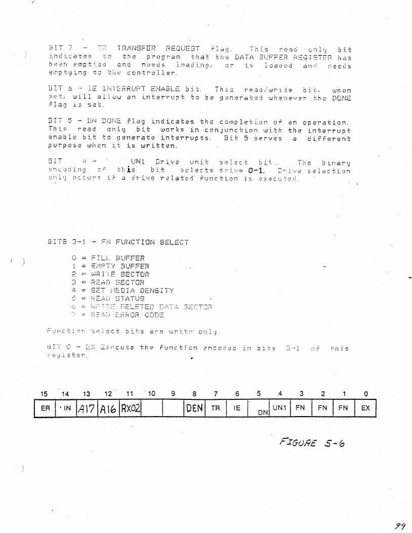
/
1(-'. TRANSFER REQUEST In 1.,S rf?.-3G ! • ;
n 1,'(:
I,riG 1 .. :,:01=2S ~ne program that th~ DATA BUFFER REGISTER nas , , . .l oaQ ::,ng} loadod ann needs
nIT 6 - IE IN1[RRUPT ENABLE bit. , . ;] :;. c- .. UH1 en
set, ~ill allow an interrupt to be generated whenever the DONE -Flag i.s se1;_
131-,5 - l.;r~ DfJ;~·i2. flag indicates the completi,on of an Qperati.c:n. Th~s read only bit works in conJunc~~on w~~n enable bit to generate interrupts. Bit 5 serves purpose when it is written.
BIT UNl url.ve
BITS 3-1 - FN FUNCTION SELECT
C; = F I LL_ H lJFFER J. = Ei'''lp~r\r' Bl}FFER c: -.. WR 1"1 E SECTOR :~ -.. REAr) ~~ECTOR
4 = S~:::T i'lf:. D If:) DEi"··iS 1 T'f
U!li.-t : . I
'-'.!... ':
., ~
1.il"Gerrup"t d i.f feren't
The
F.IGUI9E 5- b
79

I
/00
BIT 7 TR TRANSFER REQUEST flag. Th is read on l.y bit indicates to the program that the DATA BUFFER REGISTER has been emptied and needs loading, or is loaded and needs emptying to the controller.
\
BIT 6 - IE INTERRUPT ENABLE bit. This read/write bit, when set, will allow an interT'upt to be geneT'ated whenever the DONE flag is set.
BIT 5·- DN DONE fllag indicates the completion of This read only bit works in conjunction with enable bit to geneT'ate interrupts. Bit 5 serves purpose when it is written.
an operation. the interrupt a· d irrerent
BITS 5-4 - UN2 UN1 Drive unit select bits. The binary encoding Or these bits selects drive 0-3. Drive selection only occurs if a drive related 'uncti~n is executed. A po~n~ Or incompatibilit~ exists when a tT'iple o~ ~uad drive system is configured. DEC bootstT'aps aSsume that bit 5 is a "read onl y ll bit, so they write into it with impunity. As a result, drive 2 is selected by mistake during bootstrapping. In systems conrigured for single or dual drive operation, bit 5 can be written into with impunity.
BITS 3-1 ... FN FUNCTION SELECT
0 = FILL BUFFER 1 = EMPjy BUFFER 2 = WRITE SECTOR 3 = REA·D SECTOR 4 = SET i"IEDIA DENSITY 5 -. READ STATUS 6 = WRITE DELETED DATA SECTOR 7 = READ ERROR CODE
Function select bits are write only.
BIT 0 ~ EX Execute the function encoded in bits 3-1 of this reg i.ster.
5-1.2.1.2 DATA REGISTER
This register provides the general purpose communication' link between the host processor and the DSD 440 system. The information passed through this register is based upon a predetermined protocol as defined in the Section 5-1.2.2 .
If the DSD 440 is not in the process of executing a command, the RX2DB can be written without the risk of any adverse aFfects. However, during the execution of an instruction, the RX2DB register will only provide or accept information (according to the RX2DB protocol) when the TRANSFER REQUEST flag is set.
NOTE: Data may be lost if the correct protocol is not adhered to.
~
The following descriptions explain the various formats of the Data Register. (RX2DB)
5-1. 2. 1. 3 FLOPPY DISK TRACK ADDRESS
At the proper time during commands requiring a track number (e. g. write sector, read sector) the track number is written to the TRACK ADDRESS REGISTER.' (RX2TA = 777172) Track numbers fr~m 0-76 (decimal) are valid.
5-1.2.1.4 FLOPPY DISK SECTOR ADDRESS
At the proper time during commands requiring a sector address (e. g. write sector, read sector) the sector address is written to th~ SECTOR ADDRESS REGISTER. (RX2SA - 777172) Sector addresses from 1-26 (decimal) are valid.
5-1. 2. 1. 5 WORD COUNT REGISTER
The WORD COUNT REGISTER is used to specify the number of words to be transferred between the controller sector buffer and main memory via direct memory access.. For a double density sector, the maximum word count is 128 decimal words (256 bytes>. The maximum word count in single densi.ty i.s one half this amount (128 bytes). The programmer loads the actual count i.nto this regi.ster, NOT the 2's complement of the count.
I '
)0/
5-1. 2. 1. 6 BUS p.DDRESS REG! STER
This register speciFies the bus address to which data lS to be transferred during any DMA operation. It is in fact a 16 bit counter that increments by two following each data transfer. The bus address register cannot be read. It should always be loaded with the starting address of a data buffer in memory at the appropriate tim~ during the FILL BUFFER, EMPTY BUFFER, or READ EXTENDED STATUS functions. Do not try to load bit 00 with a 1 (it is ignored).
5-1. 2. 1. 7 SYSTEM ERROR AND STATUS REGISTER
The RX2ES register provides status and error information about the'drive that is selected by bits 4 and 5 of the RX2CS register. At'the completi.on of a command, the controller will place the RX2ES register into the data buffer register (RX2DB = 777172) so that the host pro~essor can check the most recent operation. Se~ figure 5-7 for detailed definitions of the individual bits.
-~ J.

I "
)
- j
5-1.2.2 MODE 2 PROTOCOLS
Protocols are required in the DSD 440 because the Cdmputer interfa~e module and the intelligent portion of the DSD.440 are connected by a single serial data link. Because of this, the controller must identify parameters based on the ord ar in wh ic h th ey are transmi ttad across th e data I in k. Th e following sections describe the proper protticol for each of the possible commands that can be sent to the controller. FailuT~ to adhere to the correct protocol may result in lost or incorrect data.
5-1. 2. 2. 1 FILL SECTOR BUFFER (000)
The FILL SECTOR BUFFER command is used to'fill a storage buffer inside the DSD 440 with up to'128 or 256 8-bit bytes of data from computer memory. Other functions can later be used to either write that data to diskette, or transfer it back to memory.
Whe"n the F,ILL SECTOR BUFFER command is given, the DSD 440 responds by clearing the DONE 'Plag, RXCS bi.t 5. The controller then requests a word count by setting the TRANSFER REGUEST flal. The program should respond by writing a valid RX2WC into the RX2DB. When TRANSFER REGUEST is again asserted by the ~ontroller, the program should respond by writing a va I id start ing memory ad dress (RX2BA) into th e RX2DB. As soon as the RX2BA has been loaded, TRANSFER REQUEST is cleared and remains cleared for the duration of this function. The data bytes are now transferred directly from memory to the controller sector buffer. When the word count is decremented to zero and the controller has zero-filled the remainder of tlie sector buffer (if necessary). DONE is asserted thus end i.ng the operation. An interrupt request will be generated if the interrupt enable bit. RX2CS bit 6. was set when DONE became true. The RX2ES register usiil be found in the RX2DB at the completion o~ the function.
NOTES: Bits 4 and 5 of the RX2CS do not affect this function since no floppy disk drives need be selected. The DENSITY bit, RX2CS bit 8. must be correctly set since this bit is used by the controller in evaluating the validity of the word count.
5-1.2.2.2 EMPTY SECTOR BUFFER (001)
The EMPTY SECTOR BUFFER function is used to t,.ans-re,. the contents or the secto,. bufre,. to ma~n memo,.y. The sec to,. burre,. ~s loaded r,.om a p,.evious FILL SECTOR BUFFER 0,. READ SECTOR command.
When the EMPTY BUFFER command ~s g~ven. the cont,.olle,. ,.esponds by clea,.ing the DONE flag, RX2CS bit 5. The cont~olle,. then sets the' TRANSFER REQUEST flag, RX2CS b~t 7, to ,.equest the' w(J,.d count ,.eg~ste,.. The p,.og,.am should ,.espond by loading a valid wo,.d count into the d~ta bUrrel' ,.egiste,.. When TRANSFER REQUEST is again asse,.ted, the p,.ogram should ,.espond by loading the sta,.ting memo,.y address into the data buffer ,.egister. When this is done, the cont,.011er will clea,. the TRANSFER REQUEST flag and it will remain clear f~,. the rest of the operation. The data in the sector burfe,. will be transfer,.ed to memo,.y one word at a time until the wo,.d count is dec,.emented to ze,.O. When the data has been t,.ansfer,.ed. the cont,.olle,. will place the R'X2ES into the data buffer ,.egister and set the DONE flag. If t~e inter,.upt enable bit is set, an inteT'T'upt request will be initiated when DONE becomes tT'ue.
The notes that apply to the FILL BUFFER command apply equally to the EMPTY SECTOR BUFFER command. In addition, it should be noted that the Ei-1PTY BUFFER functi.on does not modify the contents of the sectoT' buffer.
)
))
---j

5-1.2.2.3 WRITE" SECTOR (010)
The WRITE SECTOR function is used to trans Per the contents of the sector buffer to a specified track and sector of the diskette. When the WRITE SECTOR command is given, the controller clears the RX2ES register and the DONE flag. Next, the controller sets the TRANSFER REGUEST flag. RX2CS bit 7, to request a sector address. The program should respond by writing the desired sector address (RX2SA) into the data buffer register. This clears the TRANSFER REQUEST flag. As soon as the controller shifts the sector address over the interface cable, it asserts TRANSFER REQUEST again. This time the program should respond by writing the desired track address (RX2TA) into the data buffer register. This clears the TRANSFER REQUEST fiag. Af~er the track address is received, the controller will cause the selected drive to seek the desired track. TRANSFER REQUEST will be left reset for the remainder of tha function. At this time. the heads of the selected drive are positioned over the specified track and are loaded against the media. If the controller does not already know the density and format of the me~ia, this information will be determined by reading a random sector on the diskette. If the density of the media does not agree with the command den sit Y ( R X 2C S bit 8) the 0 per at ion is t e r min ate d . B i. t 4 0 f the RX2ES register is set to indicate a density error. If the densities agree, the controller checks the track address and starts looking for the specified sector address. IF the correct track and sector are found, the controller will write either 128 bytes of single density data or 256 bytes of double density data from the sector buffer to the diskette. Two CRe bytes are written immediately after the data.
If the controller is unable to locate the specified diskette track. the RX2ER is set to a 150(8). If the specified sector tannot be found within two diskette revolutions, the RX2ES will be set to a 70(8). These error conditions, and the den~·it'J error, cause the function to be terminated. The ERROR flag, RX2CS bit 15, and the DONE Flag, RX2CS bit 5 are asserted when the function completes in this way. As with the error-free te'rmination, an interrupt request will be generated if the interrupt enable bit was set when the bONE flag became true.
NOTES: 1) The contents of the sector buffer are not modifi&d by the
WRITE SECTOR function. 2) The contents of the sector buffer ARE modified as a result
of a power failure or the initialize command. Programmers must be sure that vali~ data is written back into the sector buffer following either of these conditions. This is especially true before executing the WRITE SECTOR command.
/()~
3} If a secto~ number of 152 or 153 (octal) is w~itten to
/
the RXSA, th'e WRITE SECTOR -Punction turns into a WRITE FORMAT TRAC~<' functi.on.' The protocol -Por formatting is explained in section 5-1. 2. 2.10 .
5-1.2.2.4 READ SECTOR (011)
The READ SECTOR -Punction is used to locate a specified track and sector of a diskette and then transfer the contents of the data field into the controller's secto~ buffer. When the READ SECTOR command is given, the cont~oller clears the RX2ES register and the DONE flag. Next, the cont~oller sets the TRANSFER REQUES~ flag, RX2CS bit 7, to request a sector address. The program should respond by writing the desired sec tor addres s (RX2SA) i.nto th e da ta b uf-Per reg ister (RX2DB=777172). This clears the TRANSFER REQUEST flag. As s 0 on as the c on t~ 0 11 e r s h i .p t s the s e.c t or add ~ as s over the inte~-Pace cable, it asserts TRANSFER REQUEST a second time. The prog~am should ~es~ond by writing the desired track address (RX2TA) into the data buf-Pe~ register. This clears the TRANSFEB REQUEST flag. After receiving the track address, the controlle~ will cause the selected drive to seek the desired track. TRANSFER REQUEST will be le-Pt reset for the remainder of this function. The controll~r loads the heads against the media and trie~ to dete~mine the density of the media (if it is not al~eadyknown). If the density of the diskette does not agree with the command density CRX2CS bit 8), a density e~~or is reported 'and the function is termi.nated. If the densities agree, the cont~oller starts looking for the specifi.d sector. When the right sector is located, the controller starts looking for the appropriate data, or deleted data address mark. When the mark is found, the controller transfers the following 128 (or 256) bytes into the sector buffer. The two CRe bytes are read immediately after the data -Pield. An er~or-free read is indicated if the address mark, data bytes, and two byt~s of CRe check bytes produce a zero residue when pa~sed seq~entially through the CRG checker hardware circuits. As .. soon as the data is available in the buffer, the controlle~ will terminate the -Puncilon by writing the RX2ES to the data buffer register and setting the DONE flag. An interrupt request will be generated if the interrupt enable bit was set when DONE became true.
If the deleted data address marl( (see Section 5-1. 2. 2. 7'> was detected, the controller will set the deleted data flag. This flag appears in the ERROR/STATUS register (RX2ES bit 6). If a CRG error is detected, the controller will s,t RX2ES bit () and the ERROR flag (RX2GS bi.t 15) to indicate that fact. Seek errors and missing sector errors are reported Just as in the I.4RITESECTOR function.
)
. --j.
'f
\ !'
)
.... 1
5-1.2.2.5 SET MEDIA DENSITY (100)
This command -Function is used to initi.:alize an entire diskette to some specified density. When the SET MEDIA DENSITY command is executed, the controller attempts to write zeros in every data rield on the diskette. Bit 8 of the RX2CS determines the recording density and the type of Data Address Mark to be written in each data -Field. No sector headers are written when the SET MEDIA DENSITY command is executed.
FUNCTION PROTOCOL;
When the command is received, the controller clears the DONE flag and the RX2ES register. Next, the controller sets the TRANSFER REGUEST flag. The program should respond by wri.ting a "key byte h into the RX2DB. If the key byte i.s an ASCII III" (111)8, the SET MEDIA DENSITY function will be executed. If the byte written into the RX2DB at thi~ time is not an III", the DONE and ERROR rlags will be, set and the op eration will termi.nate. Th e error reg ister I/.d.ll bel oad ad with a (250)8 ~a indicate an invalid key. The purpose of the k e 1J i. s to ma k e it d i.p fie u 1 t .p a l' apr 0 9 l' a mme l' to ace ide n tall y erase all of the data on a diskette. As soon as the safety character "I" is received, the cont1"oller moves the heads to track O. When sector 1 is found, the controller starts writing~ If bit 8 of the RX2CS was a 0, a single density Data Address Mark and 128 FM zeros are written. If bit 8 of the RX2CS was a 1. a double density Data Address Mark and 256 DEC MFM zeros are written. After wri.ting all 26 sectors on track 0, the controller seeks to track L 2, . '" writing all 26 sectors on each t1"ack. This process con~~nues until either every secto1" has been written through track 76 sector 26 or a bad header is found. "£:he ERROR and DONE flags UJill be set if the Operation terminates due to a bad header. The SET MEDIA DENSITY function requires about 15 'seconds to complete and should never be interrupted before it is done. If the function does not terminate normally, an illegal diskette ~hich has Data Address Marks of both densities may have been created. IP this happens, the diskette should be completely re-written again. If the SET MEDIA DENSITY function will not complete because of an unreadable header, the TRACK FORNAT procedure can be used to re-write the bloUJn header. (See Sec t i on 5-1. 2. 2. 10 )
5-1.2.2.6 READ STATUS (101)
The READ STATUS command is used to determine the cu~rent
status 0' the drive sel~cted by RX2CS bits 4 and 5. The status information passed back is: 1) Is the drive ready? and 2) What is the density of tbe diskette currently in the drive?
When the command is issued, the DONE flag is cleared. The ·controller then checks to see that the door of the selected drive is closed, a dis.kette is inserted, and that diskette is up to speed~ Diskette speed is determined by measuring the amount of time between successive index· pulses. Since this measurement takes an av~rage of 250 milliseconds, excessive use of the READ STATUS function will cause reduced throughput. If the drive is ready, the controller sets bit 7 (DRIVE READY) of the RX2ES. Next, the controller loads the heads and reads the first sector l~ finds. If a double density address mark is detected, bit 5 (DRV DEN) of the RX2ES is set. If a single density mark i.s found, bit 5 is cleared. The remaining bi.ts of the RX2ES will reflect the result of the 1ast command before READ STATUS. The controller te~minates the function by shifting the RX2ES over to the RX2DB and setting the DONE flag. An i.nterrupt request will be generated if the interrupt enable bit, RX2CS bit 6, was set when done became true.
--~\
5-1. 2.2.7 WRITE DELETED DATA SECTOR (011)
This function performs the same task as WRITE SECTOR. The difference between the commands is that this command writes a deleted data address mark Just before the data field. The standard WRITE SECTOR function w'rites a regular data address mark. When a sector which was written Wl~n a deleted data address. mark is read. bit 6 of the RX2ES will be set. The density bit associated with this function (RX2CS bit 8) determines whetheT a single or double density deleted data address mark will be written.
5-1.2.2.8 REAO EXTENDED STATUS (111)
The READ EXTENDED STATUS command is used to retrieve a number of internal controller regi.sters. i.ncludi.ng the error register. These registers are transferred to memory using direct memory access. As soon as the command is loaded into the RX2CS, the DONE flag will go false. ihe controller wi.ll then assert the TRANSFER REQUEST flag. The program should then load a starting memory address into the RX2DE. The controller will then transfer 4 worosdirectly to memory. When the words are in memor1,J. the controller will assert DONE and this will· generate an interrupt request if interrupt enable had been previously ·set.
The words transferred to memory are as follows:
WORD 1 -LO BYTE DEFINITIVE ERROR CODE WORD 1 - HI EYTE WORD COUNT REGISTER WORD 2 - La BYTE CURRENT TRACK ADDRESS OF DRIVE 0 WORD 2 HI BYTE CURRENT TRACK ADDRESS OF DRIVE 1 WORD 3 - La BYTE TARGET TRACK OF CURRENT DISK ACCESS J...JORD 3 - HI EyrE iARGET SECTOR OF CURRENT DISK ACCESS (,.,jORD 4 BIT 0 DENSITY OF READ ERROR REGISTER COMt1AND WORD 4 - BIT 4 DRIVE DENSITY OF DRIVE 0 WORD 4 - BIT 5 HEAD LOAD BIT. WORD 4 -BIT 6 DRIVE DENSITY OF DRIVE 1 WORD 4 - BIT 7 UNIT SELECT BIT WORD L't - HI BYTE TRACK ADDRESS OF SELECTED DRIVE

//0
-------------~---~--------------------------------------------, OCTAL CODE
MEANING
------------.-----------..... -----------~--.-------- ..... ---.-------------00 10 20
30 40 50 70
100 110 120 130 140 150 160 170 ' 200 210 220
v 230 240 250 260 300 310 320 330 340
V 350 360
. 370
NO ERROR NO DRIVE 0 OR DRIVE 0 FAILED TO FIND TRACK 0 ON INIT NO DRIVE 1 WHEN DIP SWITCH INDICATES THERE SHOULD BE A DRIVE 1 OR DRIVE 1 FAILED TO FIND TRACK 0 ON INIT TRACK 0 FOUND WHILE STEPPING IN ON INITIALIZE TRACK ADDRESS PASSED TO CONTROLLER WAS INVALID (~76) TRACK 0 FOUND BEFORE DESIRED TRACK WHILE STEPPING REGUESTED SECTOR NOT FOUND IN TWO REVOLUTIONS WRITE PROTECT VIOLATION DRIVE READ SIGNAL LOST NO PREAi"lBLE FOUND PREAI'-18LE FOUND. BUT NO ADDRESS MARK WITHIN WINDOW CRC ERROR ON WHAT APPEARED TO BE A HEADER ADDRESS IN. GOOD HEADER DID NOT MATCH DESIRED TRACK TOO MANY TRJES FOR AN ID ADDRESS MARK DATA ADDRESS MARik NOT FOUND IN ALLOTTED TIME CRe ERROR ON DATA FIELDi RXES BIT 0 ALSO SET PARITy ERROR ON INTERFACE CABLE; RXES BIT 1 AI-SO SET READ/WRITE CONTROLLER FAILED MAINTENANCE MODE TEST INVALID WORD COUNT SPECIFIED DENSITY ERROR WRONG KEY FOR SET MEDIA DENSITY OR FORMAT COMMAND INDETERMINATE DENSITY DRIVE 2 FAILED TO Hot1E ON INITIALIZE DRIVE 3 FAILED TO HOME ON INITIALIZE READ/WRITE CONTROLLER DETECTED WRITE CIRCUIT FAILURE READ/WRITE CONTROLLER TIME OUT ON RESET i1ASTER CONTROLLER OUT OF SYNC t.JITH RD/WR CONTROLLER NON-EX TSTANT ~lEMORY .ERROR OUR ING Dt1A DRIVE NOT READY DURING FORMAT COi"1MAND AC POWER LOW CAUSED ABORT OF WRITE ACTIVITY
____ ._""'!"" _________ --.;. _______________ ......... ~-....i---_~_--_________________ _ TABLE 5-2 ERROR REGISTER CODES
,
)
.----J

)
\ ;"
5-1.2.2.9 POWER FAIL
When a power fallure occurs or DC power t~ the DSD 440 is lnterrupted the controller gradually dralns the filter capacitors and dies. Just prior to any dlskette wr~~~ng
activity. the controller checks the power. This lnsures that the s~ctor being written will be valid.
When power is returned, and the controller dlp switch is configured for II NORMAL II mode, the DSD 440 controller will initiate the following sequence of events: 1) DONE is cleared. 2) Controller executes the hardware self-tests. 3) All drives homed to track 00. 4) RX2ESis claared of all active error bits. 5) The controller reads sec~or 1, track 1 of unit 0 into
bur·Per. 6) Bit 2 oi! RX2ES (INITIALI ZE DONE) is set. 7) Bits 7 (DRIVE READY) and 5 (DRIVE DENSITY) oi! RX2ES are
updated according to the status oi! drive O. 8) RX2ES bit 5 (DONE) is set.
III
/1 :J-,
5-1.2.2.10 DISKETTE FORMATTING IN MULTIPLE DENSITIES
When ~onfigu~ed in operational Mode 2. the DSn 440 floppy disk system ~an be made to w~ite-fo~mat diskettes in th~ee unique formats. The DEC RX02 will not support the command protocol about to be described. In this sense. the DSD 440's commands are a super-set of those of the RX02.
Each time the write-fo~mat command protocol is executed, one entire track is re-written. The protocol starts when the user program sends the WRITE SECTOR funtion code (010) to the cont~oller. The state of the density bit, RX2CS bit 8, will be unimpo~tant during the execution of this particula~, command. After receivin~ the command. the cont~oller clears the RX2ES register and the DONE flag. Next, the controller sets the TRANSFER REGUEST flag, RX2CS bit 7, to request a secto~ address. If the track format desired is IEM 3740 single density, the user program writes the numb~r 152(8) into the data buffer registe~. If the t~ack format desired is DEC double density. the user program writes the number 153(8) into the data buffer register. When the controller sees these "strange" sector addresses. it Jumps out of the WRITE SECTOR microcode and into special microcode designed to format tracks. The protocol continues as follows: The controller sets the TRANSFER REGUEST flag to request a track address. The user program should respond by writing a valid t~ack address into the data buffer register. Next. the controller enters a lQ.Op where 26 sector addresses are requested. Each time the user program sees the TRANSFER ~EQUEST flag. another valid and unique sector add~eS5 is written into the data buffer register. Note that the controller does NOT verify either the uniqueness or the validity <in the range 1-26) of ~he sector addresses being passed at this time. Aft.r the 26th sector address is received. the TRANSFER REQUEST flag will remain false. The controller will seek the heads to the specifi.ed track and await an index pulse. Starting at the index mark. the control1e~ will write the entire track acco~ding to the specified -format-. (See Figures 1-3. 1 .... 4) The sector addresses that were passed to the controller will be writt.n in the secto~ headers in the same order that they were passed to the controller. This enables all types of hard sector interleaving techniques to be easily implemented by the programmer to i.mprove the effective throughput of the disk system.
)
- --1
5-1.2.3 TYPICAL SEGUENCESOF OPERATIONS
The programming examples shown in ~igures 5-8 and 5-9 are intended to illustrate how to write routines which will successfully manipulate the DSD 440 data storage system.
5-1.2.3.1 READ/WRITE BUFFER
5-1.2.3.2 READ/WRITE/WRITE D.O.
5~1.2.3.3 STATUS READ
Status information is usually needed to determine what the status of a drive is, or what the cause of an error was. To determine drive related status (DRIVE READY, DRIVE DENSITY) the READ STATUS command (Section 5-1. 2. 2. 6) should be used. When the ERROR flag, RX2CS bit 15, is set following a function, the RX2ES should be read first. Remember that the RX2ES is left in the RX2DB following all functions. As shown in figure 5-7, the RX2ES ha~ error bits for: eRe ERROR and DENSITY ERROR. If no error bits are set in the RX2ES, th~
defini.tive error code can be obtained using the READ EXTENDED STATUS command. The code interpretations are shown in table 5-2.
//...J

. ~I ...!.
iPfo10GRAMf1INO EXAMPLE ; FlU. I El1PTY RX02 SECTOR BUFFER
. ;
177170 RXCS-177170 ; CONTROL AND STATUS ReGISTER .... , l 177172 RXDB-177172 ; DATA BUFFeR RE~ISTER : I ~ ~------------------------------~----------------------~----------------~----------------~ -•
.ll
• .:.l
1 2.
• 2.
f
-t
;:.
• (
~ ..;.!
• 2-
t ~
4 ..:..!.
.. ~ , -
\ 1!.
• ..::.
;EMPTY RX02 SECTOR BUFFER 000000 012700 000003 El'IPBUF: MOV #3,RO;BUILD EMPBUF COMMAND IN RO -000004 OOyO~4~Q~_·"· ______________ ~~ ______ B~R~~ENC~~S~N~T~ __________________________ --______________ ~
; 1 FlU. RX02 SECTOR BUFF'ER ROUTINE
-4).O.Q.QQOQQOQ· .bb ........ OiJ.. ;..;12""7p,O~O;;l.;-..QJ;~jQ.I __ --___ --<~~~:""":MO=;IV lU, !CO . B"IUl Ell B"FCO:l1$ND TN ao 000001 FIL.BUF· OQ0012 0057:37 TST UNIT I UNIT 0 OR UNIT 17 000154' F'NCENT: 000016 001402 BEG 1$
-COoo;tO 052700SJS %;10 nO ; SET IINIT 000020 000024 0057:37 TST DEN ;HIGH OR LOW DENSITY'? 000146' 1$; 000030 001402 BEQ 2$ OOOQ:Q 05:.700 a,s ,",oose ·S'~CI'FY WIQWDENS1T'Y 000400
177170 2$: 177170 3$;
000150' 177172 000050 013737 I10V WRDCNT, (!AAXDS ; PASS WClRDCOUNT TO CONTROu...ER 177170 4$; 000050 105737 TSTB e*RXCS I WAIT FOR TRANSFER REGUEST
QOOOb~ 100:3+'5 apt.. 4*· 000064 013737 MOV BUFADR,QAAXDS ;PASS BUS ADDRESS TO CONTROL.J...SR 000152' 17'7172 00007;': 032737 SIT lUOOO4Q, URXCS ; TEsT FOR DONE AND ERROR 100040 177170 5-$: 0.00 100 00.1 nil BEG ,. 000102 100401 BMI ERFIN ,ERROR BIT SET'? 000104 000207 RTS PC
)'JOOI00 012737 /'IOV lU7, UfolXCS ; GET DEFINITIVE STATUS 000017 177170 ERFIN: 000114 105737 TSTB @:iftXCS ;.WAIT F.QR TRANSFER RiIGUEST 000l~C--l~O~0~3~7~.5~--~--~~~ ____ ~ ____ ~~s~e~~~Q~.~~.------.~. __ . __ ~. --~.~ __ --.---------------____ --~
177170 6":
000122 012737 I10V iERBUF, @lfRXDD ; SEND ERROR SUFFER ADDRESS 000156' 1771?:! 000130 032737 SIT· ~40.@lfRXCS ; WAIT FOR DONE BIT 000040 177170 7$;
-,j001~ia 001774 000140 11.3700
- 000144 000000
0001% 000000 000150 000100
000152 00;;::000 000154 000000 0001:0 . 0000.00
0001.34' 000001
FIGURE 5-6
000156' Be;.3 7$ .
MOVB @~BUF, RO ; LEAVE ERROR REGISTER IN RO HALT
DEN: • WORD 0 WRDCNT: . WORD 100
BUFADR: . WORD 2000 UNIT: . WORD 0 ERSUF' WQRD 0
.-. +4 • END
,DENSITY -~SINgL.E 1-DOVBLE I WQRDCOUNT - FUL.1.. SD BUFFER IS 100 ; . FlD I no 5' lEE;; rs £00 ; BUFFER ADDRESS VARIABLE ;UNIT - O-CRIVE a l=ORIVE 1 ! iRRC2 SIJF'FEa
··r- --------------------------------~ .,
-----------------------:------------------_ .. , ) 1_
·---1
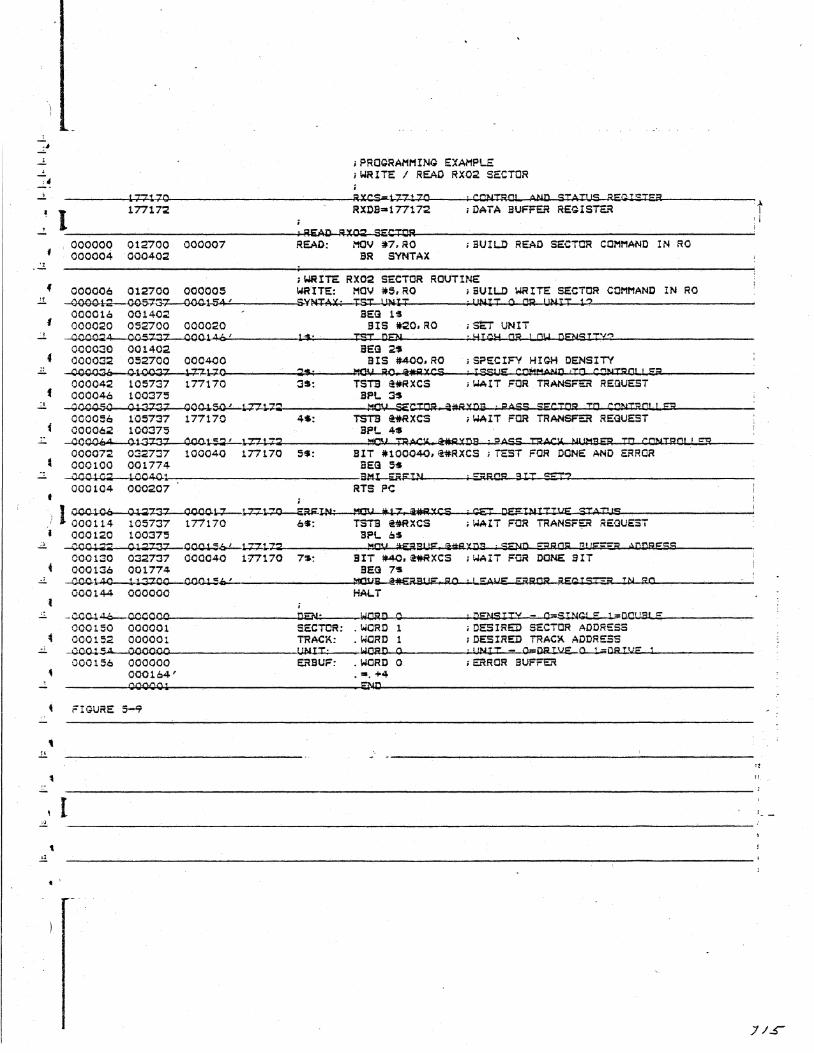
.. ~.:'
177170
;PROGRAMMING EXAMPLE iWRITE / READ RX02 SECTOR
IUC$=1.77170 . CO~TROL. AM!) STATl IS RE(~l<=:Ts:a
t , I
177172 RXDS"'177172 • DATA BUFFER REGIS~~ "I ~ --~--------------__ ----~----~'~R~E~~C+T~QRH-----------------__ --__ --____ ----------------~
.~ , "
I .2.
• 1l.
f 2-
{
• -
-~
..:l.
•
'i 1!.
" -\
2
t ..:l
000000 000004
012700 000007 000402
READ: HOV ~7,RO • BUILD READ SECTOR COMMAND IN RO BR SYNTAX
iWR!TE RX02 SECTOR ROUTINE 000006 012700 000005 WRITE: MO\l ~5t RO ; BUILD WRITE SECTOR COMMAND IN RO
-000012 OOS.73-7----000.j...S~4 .... '-----S¥NTAX .. TST I l~aT . IINIT 0 OR UNIT 1? 000016 001402 BEG 1$ 000020 052700 000020 BIS t20.RO • SET UNIT
~~4-~OCv!~5+7~3+7--vOvO~~~. ~/-_---~l~$~"~_-4TS~T~D~EN~ ______ ~·~~~I~C~W~O~~~L.O~W~Dlca~N~S~I~T~Y~~~. ----_____________ _ 000030 001402 SEG 2$ 000032 052700 000400 eIS #400.RO ; SPECIFY HIGH DENSITY
-«lOO:Jb 0 1.00:37 17+1-+0:;...... __ ~_--...;:;;: .. :s ..... - '--__ ... I'!C~I.I'I .... ! ..... R"'o..4i~III'it~5C ... X""C"'S ___ .. · .0.;1 s~S ... !"",JE=..· -"',-OUO~I't· MI'lA"'·~I>lDi.I-J.'T .... Ol,J.·-,-C,-CNI>lT .... 9 ... 0u.J,-I,-<:"~a ...... _______ _ 000042 105737 177170 35: TSIa e~RXCS ; WAIT FOR TRANSFER REQUEST 000046 100375 BPL 3$
-OOOOOO--vot'*"-l:~""",":J,,,,7~-vO,lJo.l..5.Q..!.;....~;Z.;;;~;,;-_______ HI!I'0'!;Al.1~5C:iI:.~#R xo.s . e ~SS SECTOR "'0 CONT1HJI! FR 000056 105737 177170 4$: rsrn ~*RXCS ; WAIT FOR TRANSFER REaUEST 00006~ 100375 B·PL 4$
-OOOO~4 0.137-37 OO(H"~~·"'2:-_______ ':=M~C!~/'-~iOIv08· oASS T9ACIoI NI1M8~ "'0 CONTRC' I ER 000072 032737 100040 177170 5$: BIT ~100040t@#RXCS ; TEST FOR DONE AND ERROR 000100 001774 BEG 5$ ~o 1 02 10040-1~-:----------------------B.1::I<11i!J.4-I ..... il~R~?P'l=-l .... ~"'"I-_--,;...;· <:"_i< .... R .... O""'~_;:s.9 .... IT+-c::;.ETo:.· .... 74--___________ _
000104 000207 RTS PC
1 OO.Q..l.Q.O 01. :;£'7-'37 0000 ~>-7+~·~~N"'"·:__ ..... I"tl'~ .... I_jj ... ~t 7~· , .... ic,~gq· ,,"X~CI.'S_.......,· C~ETe.;..-C""'EFI::.I=_:t·o.;N~IT ....... 11"'IEI:._-""" -.... , ... AT!~!S_--_______ ___' 000114 105737 t 77170 0$: TSTB @~RXCS ; WAIT FOR TRANSFER REOUEST 000120 100375 BPL oS ~~~O~~17~l..;Z~2~ ________ _I!I'MO~\~I_#~~~~~B~1~1P'~~i#=~~X~D~Sa_~;~s-~~~~Ou_;=-=~RuO~R~eufl~F~=-~-R~~A~OO~R~E~SbS _____ ___
000130 032737 000040 177170 7$: BIT l$4O.@WRXCS • WAIT FOR DONE SIT 000136 001774 BEG 7$
-OCO-i40 i 13700 OOO-l..5~.--------------MCl3Js_@#€ilEl!!F"O·' C'AI,/E ERROR ilE~TS=r;;;R TN SOC 000144 000000 HALT
- COO-l. 4.b-.-.o.ccoco DEN- woaD 0 ·OalSITY - O"'SI'JGl C' l=O..,C""I,J.JI"';l.I,I-'C':..-_____ ~_ 000150 000001 SECTOR: .WORD 1 • DESIRED SECTOR ADDRESS 000152 000001 TRACK: .. WORD 1 • DESIRED TRACi'. ADDRESS
-0001= .. .~~ ________________ ~II~N~I4T~-____ ~w~o~a~o~o~ ______ ~·~!J~N~;4T-=-~O~=O~~uO~R~I~v~=~ ____________ __ 000000 000150 000000 ERBUF: . WORD 0 ; ERROR BUFFER
000164' _ "'_ +4 000001 ENIl
i="IGURE 5-9
I 11
7 IS"
lib
5-1.2.3.4 COMMON PROGRAMMING PITFALLS AND SUGGESTIONS
This chapter will point out programming mistakes that can indications.
some of the more common cause data loss and/or error
1) Illegal track or sector address sent to controller A. Valid sectors are 1-26 (decimal)
(There is no sector 0) B. Valid track~ aTe 0-76 (decimal)
2) The READ STATUS co~mand requires up to two revolutions of the disk to complete. To avoid excessive delays, use this command only when necessary.
3) After reading or writing, the INITIALIZE DONE bi.t, RX2ES bi.t 2, may be checkedror an indicati.on or power failure. A short power outage will cause DONE to set without any erTor indication even though invalid data may have been read or written.
4) The drive select bits, RX2CS bits 4 and 5, are not looked at by the contToller during FILL BUFFER and EMPTY BUFFER functi ons.
5) It is recommended that a two-sector interleave be used.
6) Typically a FILL BUFFER command will precede at WRITE SECTOR command. Similarly, a READ SECTOR command will precede an EMPTY BUFFER command.
- L
5--1. 2.'4 INTERRUPTS
An ~nte~~upt ~s requested by the interface module whenever the INTERRUPT ENABLE and DONE bits of the RX2CS both become set. The standa~d ~nterrupt vecto~ address ~s locati~n 264.
//7

J It'
5-2 DEC PDp ... 8 FAI'1ILY PROGRAI"1MERS I INTERFACE
When connected to a PDP-8, the DSD 440 memory system is capable of writing either 8 bit or 12 bit data words on the diskette. In the 8 bit mode, 128 bytes can be written per sector with no waste. In the 12 bit mode, 64 twelve bit data words are written per sector and the controller fills the unused portion of the sector with zeros. In double density mode, 8 and 12 bit words can still be selected. the number of wor~s that will fit into each sector is doubled.
5-2. 1 INSTRUCTION SET
The 8 rOT instructions used to program the DSD 440 are shown in Table 5-3. These same lOT instructions are used in both Mode 1 and Mode 2 operation.
lOT MNEMONIC DESCRIPTION ------------- .... -...... ~--~------.--------------------------.-~-----67xO 67xl 67~2 67x3 67x4 67x5 67x6 67x7
TABLE 5-3
LCD XDR STR SER SDN INTR INIT
No Operation Load Command, Clear Accumulator Transfer Data Register Skip on Transfer Request, Clear Flag Skip on Error Flag, Clear Flag Skip on Done Flag, Clear Flag Enable or Disable Disk Interrupts Initialize Controller and Interface
5-2. 1. 1 THE LOAD COMMAND (LCD) INSTRUCTION
This instruction transPers the contents of the accumulator to the interface register and then clears the accumulator. The command word is layed out as shown in Figure 5-10 when the system is configured in Mode 1, and as shown in Figure 5-11 when the system is configured in Mode 2 and programmed for 12 bit word 1 eng th. Th e format 5 h own in F i9 ure 5-12 is used in Mode 2 when 8 bit word length is selected. In this case, the first 8 bit command segment is sent to the co~troller using the LCD instruction. The program must then execute the STR instruction bePore sending the upper four bits of the command register to the controller with the XDR instruction.
)
I
5-2.1.2 THE TRANSFER DATA REGISTER (XDR) INSTRUCTION
This instruction is used to transfer a word betwe~n the accumulator and the interface register. The DSD 440 controls the direction of transfer based on the context of the function in progress. The length of the word transferred is governed by the mode last selected (8-bit or 12-bit). If the Done flag is false, executing this instruction can indicate one of two things to the DSD 440: 1) The PDP-8 has accepted the last word supplied blJ the controller, or, 2) The PDP-8 has provided the last word requested by the controller. Data transfers from the accumulator always leave the accumulator unchange~. When the controller is done with the current function, (as i.ndi.cated by the Done flag), the XDR instruction can be used to transfer the error-status register from the interrace register to the accumulator. Data transfers to the accumulato~ are 12-bit JAM transfers in twelve-bit mode. and eight-bit or'ed transfers in eight-bit mode.
5-2.1.3 THE SKIP ON TRANSFER REGUEST (STR) INSTRUCTION
This instruction will cause the ne,t instruction to be skipped if the nSD 440 has set the Transfer Request flag. The instruction also clears the flag. The program should test Transfer Request Just before using the XDR instruction to transfer da~a orparam~ters to/from the controller.
5-2.1.4 THE SKIP ON ERROR (SER) INSTRUCTION
This instruction will cause the next instruction to be skipped if the Error flag has been set by the controller. The Error flag is then cleared. The controller alwaus sets the Done flag together with the Error flag (but not visa-versa). A typical program would execute an SON followed by a SER. (see examples)
5-2. 1. 5 THE SKIP ON DONE (SDN) INSTRUCTION
This instruction will cause the next instruction to be skipped if the Done flag has been set by the controller. The Done flag is then cleared by the instruction. If interrupts are enabled, the Done flag will generate an interrupt when it is first asserted by the controller.
//9

§Ee l:%:: :l)1I)U)
'000 ~oo -". _('110.'" «1==')
- ~~:.!i ...,""' ..... 1
/:1.0
LCD
LCD
LCLJ
XDR
0 :1. . .2 .3 .l- S .~ . ? &. 9 10 1/1
I I 1 I I~I I I I I I '- ·1 I r '--v----' V
IWJT use/) /1J~/Nr ~~l~E i="<J N<!.T IoN ;:'xt;()I(E S-It) #laIJG ..t COh)/Y/-9AJtl /?eGlsrER rCJ~m19T
0 / .3 ..J ~ ..5' .. ~ 7 8 9 10 1/
I I I IDENj 1%/ I I I I I 1 12 Orr />?oJ;)i;
'-v---' NOl' (jsea
FrGu~c 5-//
JYI/I/~r DR:VE '---v---J SEL FUNc..TION
/Tlo.oe- 2J·/2 /lJr$opc; cdl7JlJ7,.9AJO J?£6. PO!\J/YJ/17
4· S
MAJ~r
6 7 8 9 16 /1
I I I I I OR: 'IE: '----v--" SEL ;::-t../IV'CrION
<I S b 7 8' <f /0 /1
I I Df~ 10 10 101011 ,.t::'.r Gu~e S' -12 //lOOE..2.J fI IJ / r /J70,oC' .
Cofi7,.1?~AI.o k'E6IS T'e;:;J j:'"ORIYI/17 /S eQtJe~JCe
)
.. ~
):
5-2. 1. 6 THE INTERRUPT ENABLE/DISABLE (INTR) INSTRUCTION
If accumulator bit 11 is set wheM this instruction is executed, the interrupt enable flip flop is set. If bit 11 is cleared, then the interrupt enable, flip flop is reset. Interrupts are normally generated when the interrupt enable flip flop is set an~ the Done flag has Just become true. Interrupts will be disabled by ~ CLEAR ALL FLAGS instruction, a bus in it i ali z e , 0 l' apr a g r a mm e din it i ali. z e .
5-2. 1. 7 THE INITIALIZE (INIT) INSTRUCTION
Thi.s instruction initializes the DSD 440 system by "homing" all of the floppy disk drives to track O. The controller microproces~ar runs all of the hardware self-test routines (Section 4-6), If a diskette is properly inst~lled in drive 0, the data contained in track 1 sector 1 is read into the sector buffer. The error/status register is clea~ed and then the Initialile Dane bit (RXES bit 9) is set. This initialize sequence can take as long as 1:8 seconds to complete. Either this instruction or a CLEAR ALL FLAGS instruction is capable of starting this sequence of events.
).:l./
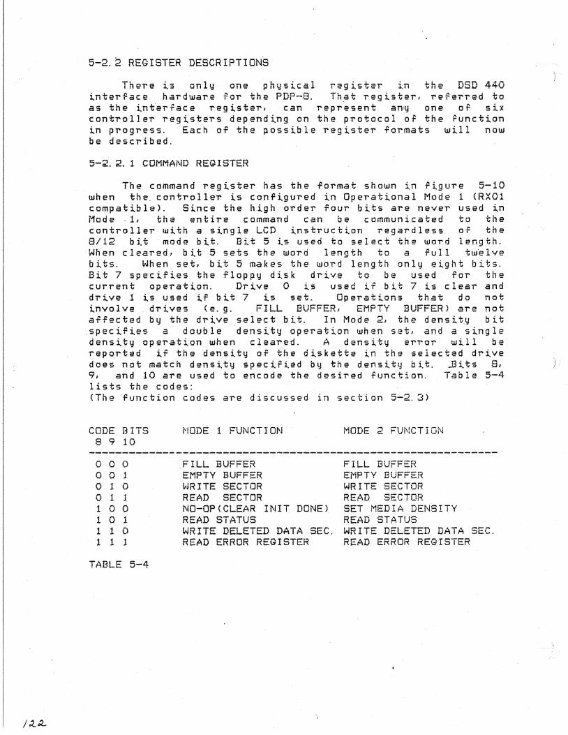
5-2.2 REGISTER DESCRIPTIONS
There is only one physical reg~ster in the DSD 440 interface hardware fol' the PDP-B. That re9:1.stel'. l'efel'l'ed to as the int'erface registel'. can repl'e5ent anJY one of six contl'o11el' regi5tel's depending on the protocol of the Punction in pl'ogress. Each of the possible l'egistel' fOl'mats will now be descl'ibed.
5-2.2: 1 COMMAND REGISTER
The command register has the format shown in fi9Ul'e 5-10 when the. contl'oller is configured i.nOperational Mode 1 d~XOl compatible). Since the high order four bits are never used in Mode ,1, the entire command can be communicated to the controller with a single LCD instl'uction regal'dless of the 8/12 bit mode bit. Bit 5is used to select the wOl'd length. When cleared, bit 5 sets the WOl'd length to a full tw~lve
bit 5 . W hen set, bit 5 ma k est hew 0 l' die n 9 tho n 1 y e i 9 h t bit s . Bit 7 specifies the floppy disk dl'ive to be u~ed for the current operation. Dl'ive 0 is used if bit 7 is clear and drive 1 is used if bit 7 is set. Operations that do not involve drives (e.g. FILL BUFFER, EMPTY BUFFER) are not affected by the drive select bit. In 1'-10de 2. the densit.y bit ,specifies a double 'denSity operation when s.t~ and a single density operation when cleared. A density ~l'l'or will be reported if the density of the diskette in the selected drive does not match density speciflied by the density bit. J3its 9. 9. and 10 are used to encode the desired function. Table 5-4 lists the codes: (The function codes are discussed in section 5-2.3)
CODE BITS 8 9 10
l'iODE 1 FUNCTION MODE 2 FUNCTION
-----------------------.... ------~-------.------------------~--~-000 001 010 011 100 101 1 1 () 111
TABl.E 5-4
FILL BUFFER EMPTY BUFFER ~JR ITE SECTOR READ SECTOR NO-QP(CLEAR INIT DONE) READ STATUS WRITE DELETED DATA SEC. READ ERROR REGISTER
FIl.L BUFFER EMPTY BUFFER WRITE SECTOR READ SECTOR SET MEDIA DENSITY READ STATUS WRITE DELETED DATA SEC. READ ERROR REGISTER
),

5-2.2.2 TRACK ADDRESS REGISTER
This register is written to the controller interface register with an XDR inst~uction when a particular funttion requires a track address. Functions which require track addresses include: WRITE SECTOR, READ SECTOR, WRITE-FORMAT TRACK. and WRITE DELETED DATA SECTOR. Valid numbers for this register are 0-76 decimal. The track address register works the same in both Mode 1 and Mode 2 system operation. Figure 5-13 shows a diagram of this"register.
5-2.2.3 SECTOR ADDRESS REGISTER
This register is written to th~ controller interface register with an XDR instruction when a particular function requires a sector address. Functions which require sector addresses include: WRITE SECTOR, READ SECTOR, and WRITE DELETED DATA SECTOR. Valid numbers for this register are 1-26 decimal. Fi.gure 5-14 shows a diagram of this register. This register works the same in both Mode "I and Mode 2 system operation.
5-2.2.4 DATA BUFFER REGISTER
All data transferred to and from the floppy disk must pass through this register. The state of bit 5 in the command register determines which bits of this register are s i 9 n if i. can t . I fbi t 5 wa s a z e r 0 I the nth e ma chi n e is configured for 12 bit operation and all 12 bits of the regi.ster contain valid data. If bit 5 was a one, then the machine is in 8 bit operation and only bits 4-11 contain valid data. This applies equally to both Mode 1 and Mode 2 system operation. Figure 5-15 shoUJs a diagram of this regist~r"
1';< 3
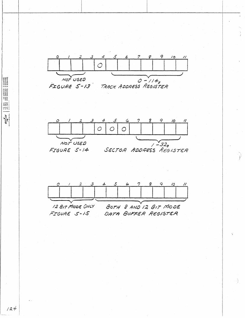
0 / 2 .3 4 .s /, ? ~ 9 10 //
I I I 10 1 I I I I I I I '--v--" \.. )
V Nor useD 0-//+,5'
FZ(lU;:;8 $-/.3 ~/tC}( Af)ORC'SS l?e(jISTel?
0 J 2 .3 4- S " ? 8 9 10 1/
I 1 I 1 0 1 0 10 I I I I I I '--y----/ \..> )
V Nor (J$£J) / -..328
FIGuli£ $- /4- S€CTO~ 1'9,l)./)PI£SS /fEGISrc/?
r
0 / .2 .3 4- S ~ ? 8 q /0 II
I I 1 I I I I I I I I I '- v "" /
V 12 8/T /l?oDe OM .. Y 8arH £' ~N.[) 12 81T f/loCJE
F.r(j()If£ $-1$ ORr;&) BUr;:ER /(C"G/S"Ter<
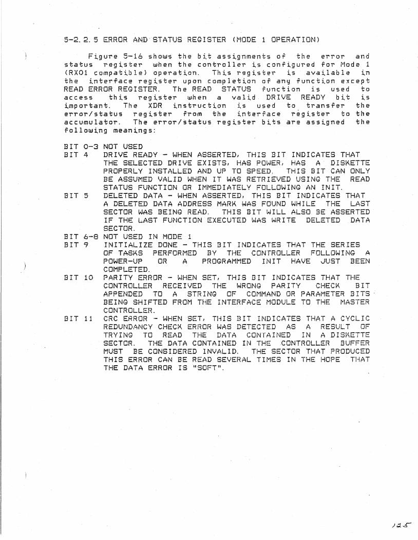
5-2.2. 5 ERROR AND' STATUS REGISTER n10DE 1 OPERATION)
Figu~e 5-16 shows the bit assignments of the er~or and status reg~s~er when the controller is configured for Mode 1 (RXOl compatible) ope~ation. This registe~ is available in the interface register upon completion of any function except READ ERROR REGISTER. The READ STATUS function is used to access this ~egister when a valid DRIVE READY bit is impo~tant. The XDR instruction is used to transfe~ the e~ro~/status registe~ from the inte~face r~gist~r to the accumulato~. The er~or;~tatus register bits are assigned the following meanings:
BIT 0-3 NOT USED BIT 4 DRIVE READY - WHEN ASSERTED, THIS BIT INDICATES THAT
THE SELECTED DRIVE EXISTS, HAS POWER, HAS A DISKETTE PROPERLY INSTALLED AND UP TO SPEED. THIS BIT CAN ONLY BE ASSUi"1ED VALID WHEN IT WAS RETRIEVED USING THE READ STATUS FUNCTION OR IMMEDIATELY FOLLOWING AN INIT.
BIT 5 DE4ETED DATA - WHEN ASSERTED, THIS BIT INDICATES THAT A DE4ETED DATA ADDRESS MARK WAS FOUND WHILE THE LAST SECTOR WAS BEING READ. THIS BIT WILL ALSO BE ASSERTED IF THE L.AST FUNCTION EXECUTED WAS WRITE DELETED DATA SECTOR.
BIT 6-8 NOT USED IN MODE 1 BIT 9 INITIALIZE DONE - THIS BIT INDICATES THAT THE SERIES
OF TASKS PERFORMED BY THE CONTROLLER FOLLOWING A POWER-UP OR A PROGRAMMED IN IT HAVE .JUST BEEN COMPLETED.
BIT 10 PARITY ERROR - WHEN SET, THIS BIT INDICATES THAT THE CONTROLLER RECEIVED THE WRONG PARITY CHECK BIT APPENDED TO A STR I NG OF COMt1AND OR PARAMETER BITS . BEING SHIFTED FROM THE INTERFACE i'"1ODULE TO THE t-1ASTER CONTROLLER.
BIT 11 CRC ERROR - WHEN SET, THIS BIT INDICATES THAT A CYCLIC REDUNDANCY CHECK ERROR WAS DETECTED AS A RESULT OF TRYING TO READ THE DATA CONTAINED IN A DIS~·q:::TTE SECTOR. THE D.<\TA CONTAINED IN THE .CONTROLLER BUFFER MUST BE CONSIDERED INVALID. THE SECTOR THAT PRODUCED THIS ERROR CAN BE READ SEVERAL TIMES IN THE HOPE THAT THE DATA ERROR I Sit SOFT II .
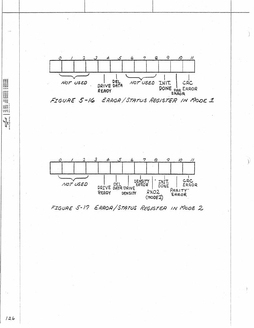
Ese 3i~~ 000 ,"",00
-" _~o.:II
alC)(Q:I -MMI"1,;
~:;~i
II II ~
NOT USED
FIGUR~ $-/1
... 3 ~ .56 7 8 9 10 1/
11. I I I I III I· I , I· I·· I DENSlrt' • INIT. I cRe
DRIVE DEL . ~RRoR DONE ERROR . DATA VRIVE PAP-ITy'.-
'REAO'f DENsnv RXO:<' SRf<Of(. (moOE'2)
€Rl?aR/STI9TUS REGlsreR IN MoOE2
)
);
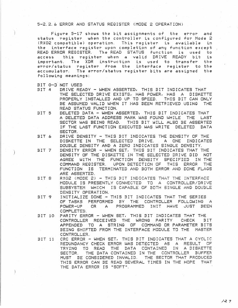
)
)
)
5-2.2.6 ERROR AND STATUS REGISTER (MODE 2 OPERATION)
Figure 5-17 shows the bit assignments of the error and status' register when the controller is configured for Mode 2 (RX02 compatible) operation. This register is available in the inte~face register upon completion of any function except READ ERROR REGISTER. The READ STATUS function is used to access this register when a valid DRIVE READY bit is important. The XDR instruction is used to transfer the error/status register from the interface register to the accumulator. The e~ror/status register bits a~e assigned the following meanings:
BIT 0-3 BIT 4
BIT 5
BIT 6
BIT 7
BIT 8
BIT 9
BIT 10
BIT 11
NOT USED DRIVE READy .... WHEN ASSERTED, THIS BIT INDICATES THf\T THE SEL.ECTED DRIVE EXISTS. HAS POWER, HAS A DISKETTE PROPERLY INSTALLED AND UP TO SPEED. THIS BIT CAN ONLY BE AS8UI'lED VALID WHEN IT HAS BEEN RETRIEVED USING THE READ STATUS FUNCTION. DEL.ETEDDATA - WHEN ASSERTED, THIS BIT INDICATES THAT A ·DEL.ETED DATA ADDRESS MARK WAS FOUND WHILE THE LAST SECTOR WAS BEING READ. THIS BIT WIL.L. AL.SO BE ASSERTED IF THE L.AST FUNCTION EXECUTED WAS WRITE DELETED DATA SECTOR. DRIVE DENSITY - THIS BIT INDICATES THE DENSITY OF THE DISKETTE IN THE SEL.ECTED DRIVE. A ONE INDICATES DOUBLE DENSITY AND A ZERO INDICATES SINGLE DENSITY. DENSITY ERROR - WHEN SET. THIS BIT INDICATES THAT THE DENSITY OF THE DISKETTE IN THE SEL.ECTED DRIVE DID NOT AGREE WITH THE FUNCTION DENSITY SPECIFIED IN THE COMMAND REGISTER. UPON DETECTION OF THIS ERROR THE FUNCTION IS TERMINATED AND BOTH ERROR AND DONE FLAGS ARE ASSERTED. RX02 (MODE 2) - THIS BIT INDICATES THAT THE INTERFACE i"10DULE IS PRESENTLY CONNECTED TO A CONTROLLER/DRIVE SUBSYSTEi-1 WHICH IS CAPf\BLE OF BOTH SINGLE AND DOUaU:: DENSITY OPERATION. INITIAL.IZE DONE- THIS BIT INDICATES THAT THE SERIES OF TASKS PERFORMED BY THE CONTROLLER FOLLOWING A POWER-UP OR A PROGRAMI'1ED INIT HAVE JUST BEEN COMPLETED. PARITY ERROR - WHEN SET, THIS BIT INDICATES THAT THE CONTROLL.ER RECEIVED THE WRONG PARITY CHECK BIT APPENDED TO A STRING OF COMMAND OR PARAMETER BITS BEING SHIFTED FROM THE INTERFACE 1-10DULE TO THE MASTER C ONTROL.LER. CRC ERROR - WHEN SET, THIS BIT INDICATES THAT A CYCLIC REDUNDANCY CHECK ERROR WAS DETECTED AS A RESULT OF TRYING TO READ THE DATA CONTAINED IN A DISKETTE SECTOR. THE DATA CONTAINED IN THE CONTROLLER BUFFER MUST BE CONSIDERED INVALID. THE SECTOR THAT PRODUCED THIS ERROR CAN BE READ SEVERAL TIi'1ES IN THE HOPE THAT THE DATA ERROR IS "SOFT".
.10<. ?

5-2.3 FUNCTION CODE DESCRIPTIONS
A floppy disk 'unction is initiated by writing one of the function codes shown in Table 5-4 to the command register using the LCD instruction. The Done flag should always be t~sted and cleared with the SDN instruction prior to issuing the 'command instruction to verify that the controller is really in the Done state. The protocol associated with each of the functions shown in Table 5-4 will now be described in detai 1.
5-2.3.1 FILL BUFFER (000)
This function is us~d to load the controller sector buffer with the data that is to be written into ~ sector o~ later transferred bac~ to the host computer. The amount and ~ormat of the data is determined by the operating mode of the controller (Mode 1 or Mode 2) and the word length bit of the command register. After the command is issued to the controller with the LCD instruction, the controller will assert the TransFer Request flag once for each 8 or 12 bit word that is needed from the hast computer to place in the sector buffer. The hast computer should test and clear the Transfer Requ~st flag with ~he STR instruction and then transfer a data ~ord to the controller with th~ XDR instruction. ~heft the controller has determined that the appropriate number of words has been transferred in this manner, the Done flag will be asserted and an interrupt will occur assuming interrupts have been enabled. If an XDR instruction is executed after Done is set, it wi-ll have the affect of loading the error/status register into the accumulator. The chart below shows the relationship between the number of XDR cycles needed to fill the buffer, the operati.ng mode, and the IJJord length:
OPERATING MODE DATA WORD LENGTH NUi"fSER OF CYCLES ----~--.------.----------.---.... -.. --...... ---..... ------------.... ------1 <RXOl COMP. ) 8 BITS 128 1 (RXOl COMPo ) 12 aITS 64 2 . (RX02 COI"1P. ) 8 BITS 256 DD, 128 SD 2 <RX02 COI"1P. ) 12 SITS 128 DD, 64 SD
TABLE 5-5
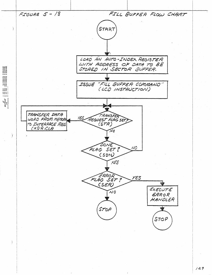
I
I r.rOO.RIE $- /8
T/?19.NSFcJt PJ:1T /r
I.a,.:;/) "ttN /?()ra -INCJEX l?e(;ISTER LJ/TN .l7L)./J.-9ESS 0;= O~Tr9 /0 BE STONe.!) IN SeCTaR 8UF;e/?1
..Z'.sSIJ~ IIFILL B().rp"er? CO/IJ/ll"tJN;:) Ii (LCD INST~UCTION)
wORO FRom M6'''-IHI4B-_-< 7tl INr€.RFIfC.€ J(£U
(xD r<ICL
ex eC (.) -r £" c£t?.I?oJ( h'/lNIJ'E~
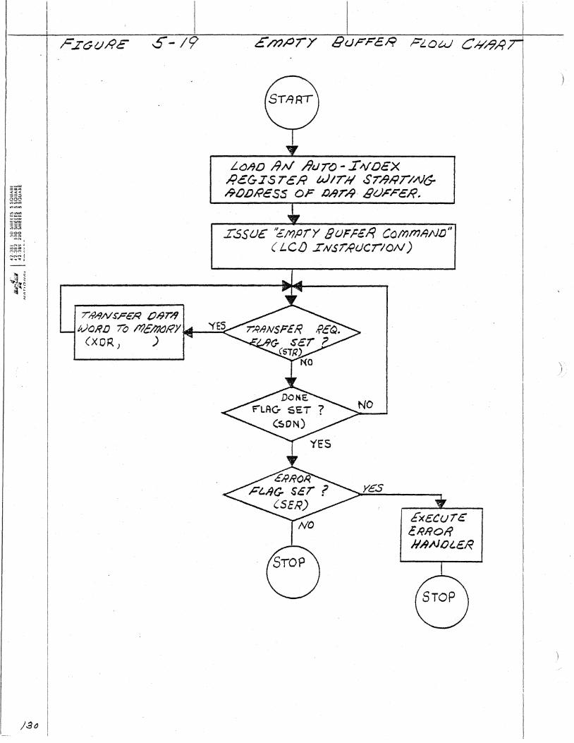
000 .r,s~
_""a- ~
~~~; NN~i "''''''''''l
).Eo
$-/9
TI?.-9NS.P'€,R O.l}'T/i
L().I7D 17/\1 /lUro - INDeX !;E&I5TcR wlrll Sr/?RT/N6-t90.oRess OF ,o/1r;9 ,6'(),&'F€I(.
ISS(J£ ''E:MfJry 8()FJ=E/? CQ/I)mI9N[)" ( LCD INST/iJUC,//ON)
/VOl( /J 70 IrJE/7JtJf(Y Wi�_---< (XOR) )
EX£CUic£ ERRol( )lANI)I..£R
5-2.3.2 EMPTY BUFFER (001)
This function is very similar to the FILL BUFFER function except that words are moved from the interface register to the accumulator every time the XDR instruction is executed. Table 5-5 indicates the number of XDR cycles as a function of the word length and operating mode. Execution of this func~lon
does NOT modify the contents of the controller sector buffer. When the controller asserts the Transfer Re~uest flag, this indicates that a word is currently in the interface register. The program must test the Transfer Re~uest flag with the STR instruction before moving the word to the accumulator with the
. XDR instruction. When the buffer has been fully emptied, the controller will assert the Done flag and place the error/status register into the interface register. An XDR instruction executed after Done has been set will move the error/status register into the accumulator. An interrupt will occur when the controller sets the Done flag, assuming interrupts have previously been enabled.
5-2.3.3 WRITE SECTOR (010)
This function is used to transfer the data contained in the sector buffer to a specified unit, track and sector. After the WRITE SECTOR function is decoded by the controlle~, the error/status register is cleared and the Transfer Re~uest flag is set. The program must test the Transfer Re~uest flag with the STR instruction, which will also clear the flag. The program must then transfer a valid sector address register to the controller using the XDR instruction. After the controller receives the sector address, l~ will set the Transfer Re~uest flag a second time. The program must test the Flag with the STR instruction, which clears the flag, and then transfer a valid track address register to the controller using the XDR instruction. The controller checks for density compatibility by comparing the actual diskette density with the density bit passed in the command register (if in Mode 2), or with low density (if in Mode 1). If the densities are incompatible, a density error is reported and the function is te~minated. Assuming compatible densities. the controller will now attempt to lacate the specified sector so that the data contained in the buffer, together with two eRC characters, can be written onto the diskette. The contents of the data buffer is not modified regardless of whether it is written successFully on the diskette or not. When the function has been completed, the error/status register is loaded into the interface register and the Done flag is set. An interrupt will be generated when Done is set assuming interrupts hav~ been enabled.
/.3/

_~Oo';;
~(Q=, :"1M(") ~
~':-:'Ni ..., .... ::1
PlfePI9RE A'PPA'OPA'I..97"E COMP7/?AJI) /;c£tS-ISrc;!; /7AJL) Iv'A'JTi!" IT ro CONr;'((OI..L.E/f
('-CD ..l N.sr/?ucr/oN)
iI?I7NS;::'€!1 DeSIReo SeCTOR ;9[).()~c5S fa cCW'/;rrat-i..e R ..
(X!) I( Z N'sr/?uc TION)
7~I7N.sFEI< f)6S1 Ra; r/?lfcff "l/Jf)I(C'SS 10 caNT~OL,e~
(x 0 R !.NST~UC.TIO N)
EXECUTE €RRO/f
~--Bt H..9Nf)tER ),
5-2.3.4 READ SECTOR (011)
The READ SECTOR function is used to locate a specified track and sector of a diskette and then transfer the contents of the data field into the controller's sector buffer. After the READ SECTCR function is decoded, the controller clears the erroristatus register. Next, the controller asserts the Transfer Request flag to request a sector address. The program should be in a loop, testing Transfer Request with the STR instruction. When the flag becomes true, the skip will take place and Transfer Request will be cleared automatically. At this point, the program loads the accumulator with the sector address register and executes the XDR instruc~~on to transfer the AC to the controller. The controller will assert the Transfer Request flag as soon as it is ready for a track address. The program should test Transfer Request and transfer a track address to the controller in the same manner used for the sector address. The controller verifies the legality of the track address supplied by the program. If illegal, the Error and Done flags are set and the erroristatus register is moved into the interface register, thus terminating the function. If the track address is legal, the controller moves the head ta the specified track and loads the head against the med1a. The controller checks for density compatibility by comparing the actual diskette density w~~n
the density bit passed 1n the command register <if in Mode 2), or with low density <if in Mode 1). If the densities are incompatible, a density error is reported and the function will be terminated. If the densities are compatible, the contfoller starts looking For the specified sector. If a sector match is not found within two diskette revolutions. an octal 70 is placed in the error register and the Done and Error flags are set to terminate the .function. Once the correct sector header is found. the controller starts looking for either a data address mark or a deleted data address mark (of the appropriate density). The controller uses that mark to synchronize with the data. The appropriate amount of data is transferred fro~ the diskette to the controller sector buffer. An error-free read is indicated if the address mark. data •. and two CRG check bytes produce a zero residue when sequentially passed through the eRe checker hardware circuits. If a eRe error is detected. the controller will set bit 11 of the erroristatus register, load an octal 200 into the error regi.ster. and then set the Error and Done flags. The function is always terminated when the error/status register is loaded into the interface register and the Done flag is set. Setting the Done flag will produce an interrupt if interrupts have been en~bled. If the data address mark found happened to have been a special mark called a "deleted data address maT'k", bit 5 of the error/status register will be set at the completion of this function.
/..33

5-2.3.5 SET MEDIA DENSITY (100)
If the controller is configured in Mode 1 (RXOl compatible), a command code of (100) does nothing except put the error/status register in the interface register and set the Done flag. If the controller is configured in j;.1ode 2 (RX02 compatible), this command code can be used to initiali.ze an entire diskette to a specified density.
FUNCTION PROTOCOL:
After receiving the entire command register, the controller checks to make sure that it is configured in Mode 2. If not, the function i.s immediately terminated. The Transfer Request flag is asserted to request a "key byte" from the user program. The key byte specifies the SET MEDIA DENSITY function if it is an ASCII "I" (0111)8. If this particular key byte is not transferred to the controller at this time, the E~ror and Done error flags will be set and the function will terminate. The error register will be loaded with a (250)8 to indicate an invalid key error.
SET MEDIA DENSITY:
As soon as the key byte "I" is received, the cont~oller
moVeS the head of the specified drive to track O. When sector 1 is found, the controller starts writing. If the density bit was a O. a single density Data Address Mark and 128 8-bit FM zeros are written followed by 2 CRC bytes. If the density bit was a 1, a double density Data Address Mark and 256 8-bit DEC MMFM zeros are written followed by 2 CRG bytes. After writing all 26 secto~s on track 0, the controller seeks to track 1. 2,· ...... 76 writing all 26 sectors on each trac!<. This process continues until every sector through track 76, sector 26 has been written or a bad header is found. ,ne Error and Done flag will be set if the operation terminates due to a bad header. The SET MEDIA DENSITY function requires about 15 seconds to complete and should never be interrupted before it is completed. IF this function does not terminate normally, an illegal diskette which has Data Address Marks of both densiti.es may have been created. If thi.s happens, the diskette should be completely re-written again. If the SET MEDIA DENSITY functi.on can not be made to complete normally. because of an unreadable header, the WRITE-FORMAT option can be used to re-write the bad header. The SET MEDIA DENSITY functi.on only wri.tes the data fields, nat the headers.
\ . )
)
)
5-2.3.6 READ STATUS (101)
When the controller decodes the READ STATUS command, several bits in the error/status register are updated. The error/status'register is then transferred to the interface register. Figures 5-16 and 5-17 show the format of the error/status register in Mode 1 and Mode 2 respectively. The INIT DONE status bit is always reset when this function is executed. The DRIVE READY bit is updated acco~ding to whether the selected drive has both power and a diskette properly installed and up to speed. Since the controller determine~ diskette rotational speed by measuring the amount of time between two successive index pulses. this function can require up to 250 milliseconds to -execute. Because of thi.s. excessive use of this function will result in substantially reduced throughput. The DELETED DATA bit. PARITY ERROR bit. and eRe ERROR bit are NOT modified by this function.
If the controller is confi~ured for Mode 2. operation, other bits in the error/status register will be modified in addition to those already mentioned. The DRIVE'DENSITY bit is updated to reflect the density of the diskette currently installed in the selected drive. The controller ,determines the densitg by loading the head. wherever-it happens to be. and trying to read the first sector that passes by. If the denSity of the diskette happens to be different from the density indicated by the d~nsity bit in the command register. then the DENSITY ERROR bit of the error/status register will be set.

J~6
5-2.3.7 WRITE DELETED DATA SECTOR (110)
This function is identical to the WRITE SECTOR function except that a deleted data address mark is written prior to the data field instead of a normal data address mark. See paragraph 5-2.3.3 for a description of the WRITE SECTOR function. When the WRITE DELETED DATA SEC/OR function is executed, the DELETED DATA bit will be set in the error/status register. When a .sector which was written using this -function is read at a later time, the DELETED DATA bit will be set in the erro~/status ~egister.
5-2.3.8 READ ERRQR REGISTER (111)
This function is used to obtain explicit error inform.ation arter the error flag has been detected using the SER instruction. When the controller decodes this -runction code, the error code is transrerred to the i.nterface register and the Done flag is set. The user program should detect Done with the SDN instructionl and then transfer the error cod.e from the interface register to the accumulator using the XDR instruction. This is the only function which does not terminate with the er~o~/statu. register left in the interface register. The interpretation of each er~or code is shown in table 5-6. Some of these codes are only possi.ble if the system is configured in Mode 2 CRX02 compatible).
)
I I.
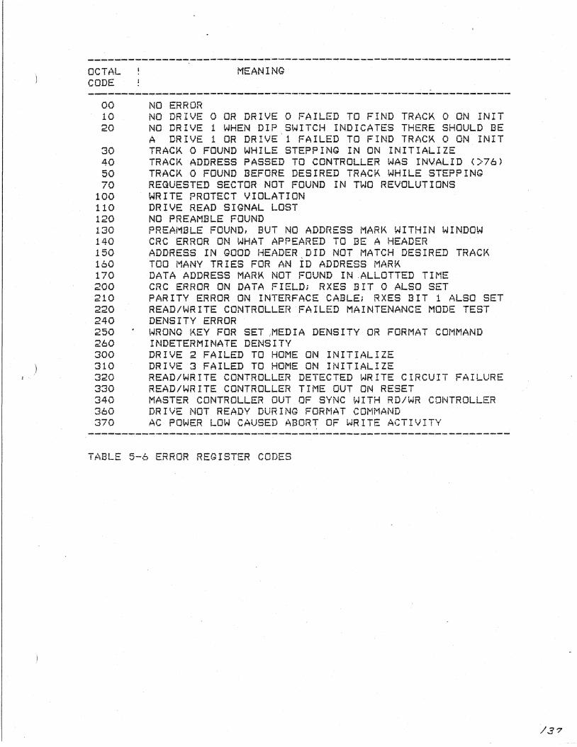
)
--..... -----~---- ..... -----------~-----------------------------... -----OCTAL CODE
1'-1EANING
--------_ ....... _-_._--------------------------------""!""---------~----00 10 20
30 40 50 70
100 110 120 130 140 150 160 170 200 210 220 240 250 260 300 310 320 330 340 360 370
NO ERROR NO DRIVE 0 OR DRIVE 0 FAILED TO FIND TRACK 0 ON INIT NO DRIVE 1 WHEN DIP SWITCH INDICATES THERE SHOULD BE A DRIVE 1 OR DRIVE'1 FAILED TO FIND TRACK 0 ON INIT TRACK 0 FOUND WHILE STEPPING IN ON INITIALIZE TRACK ADDRESS PASSED TO CONTROLLER WAS INVALID <>76) TRACK 0 FOUND BEFORE DESIRED TRACK WHILE STEPPING REQUESTED SECTOR NOT FOUND IN TWO REVOLUTIONS WRITE PROTECT VIOLATION DRIVE READ SIGNAL LOST NO PREAMBLE FOUND PREAMBLE FOUND, BUT NO ADDRESS MARK WITHIN WINDOW CRC ERROR ON WHAT APPEARED TO BE A HEADER ADDRESS IN GOOD HEADER DID NOT MATCH DESIRED TRACK TOO MANY TRIES FOR AN ID ADDRESS MARK DATA ADDRESS MARK NOT FOUND IN .ALLOTTED TIi'1E CRC ERROR ON DATA FIELD; RXES BIT 0 ALSO SET PARITY ERROR ON INTERFACE CABLE; RXES BIT 1 ALSO SET READ/WRITE CONTROLLEHFAILED MAINTENANCE MODE TEST DENSITY ERROR WRONG KEY FOR SET ,i"lEDIA DENSITY OR FORMAT COi"'lMAND INDETERMINATE DENSITY DRIVE 2 FAILED TO HOME ON INITIALIZE DRIVE 3 FAILED TO HOME ON INITIALIZE READ/WRITE CONTROLLER DETECTED WRITE CIRCUIT FAILURE READ/WRITE CONTROLLER TIME OUT ON RESET MASTER CONTROLLER OUT OF SYNC WITH RD/WR CONTROLLER DRIVE NOT READY DURING FORMAT COMMAND AC POWER LOW CAUSED ABORT OF WRITE ACTIVITY
---------------.... -----..... -----------.------"---~-------------------
TABLE 5-6 ERROR REGISTER CODES
/38'
5-2.3.9 POWER FAIL ,
When a power failure occurs or DC power to the DSD 440 is interrupted, the controller gradually drains the filter capacitors in the power supply and ceases to function. Just prior to any diskette wri.ting activity, the controller microprocessor checks the power level. If the voltage is below a certain level, the microprocessor will not begin writing. This feature can insure that complete sectors will alwa~s be written if the energy stored in the filter capacitors is sufficient to keep the controller functioning properly for at least one sector time (4.5 msec).
Wheri power is returned, the controller will perform the following sequence of events: 1) Done flag is cleared. 2) Controller executes the hardware self-tests. 3) All drives are homed to track 00. 4) The error/status register i~ cleared of all active error
bits. 5) The c on t roll er rea d s sec to,' 1, t r a c k 1 0 f un itO i n to
buffer. (If there is a diskette ready in drive 0) 6) The INITIAL!:lE DONE bit i.s set in error /statu s reg is ter. 7) The DRIVE READY and DRIVE DENSITY (if in Mode 2) bits of
the er~orlstatus register are updated according to status of drive O.
8) The Done flag is set. \ ) )/

5-2.3.10 DISKETTE" FORMATTING IN MULTIPLE DENSITIES
Each t~me the write-format command protocol is executed. one entire track is re-written. The protocol starts when the user program sends the WRITE SECTOR function code (010) to the controller. The state of the density bit. whether it is transmitted in bit 3 or bit 11. w~11 end up be~ng unimportant. After receiving the command. the controller clears the error/status register and sets the Transfer Request flag. The user program must test this flag with the STR instruct~on. which w~ll also clear the flag. Instead of a val~d sector address. the user program specifies a single density track format operation by transferring a 152(8) to the controller with the xdr instruction. If the track Format desired was DEC double density. then the number 153(8) is transferred. When the controller sees these "strange U sector addresses, it Jumps out of the WRITE SECTOR microcode and into special microcode designed to format tracks. The protocol continues as follows: The controller sets the transfer request flag to request a track aaaress. The user program should respond by writing a valid track address into the data buffer register. Next, the controller enters a loop where 26 sector addresses are requested. Each time the user program sees the TRANSFER REGUEST flag, another valid and unique sector address is written into the data buffer register. Note that the controller does NOT verify either the uni~ueness or the validity (in the range 1-26) of the sector addresses being passed at this ~~me. After the 26th sector address is received. the TRANSFER REQUEST flag will remain false. The controller will seek the heads to the specified track and awa~~ an index pulse. Starting at the index ma~k. the controller will write the entire t~ack according to the specified format. (See figures 1-3. 1-4) The sector addresses that 'were passed to the controller will be written in the sector heade~s in the same order that they were passed to the controller. This enabl~s all types of hard sector interleaving to be easily implemented by the programmer to improve the effective throughput of the disk system.
/S7

SECTION 6 HIGH LEVEL SOFTWARE AND THE DSD 440
This section of the manual discusses various aspects of using the DSD 440 w~~n specific high level software. For PDP-Ii and LSI-ii users, the software to be discussed will include the RT-l1 operating system and the FRD440 system diagnostic program. Most RT-l1 users who integrate a double density floppy disk into their system will find the procedures in this section very useful. The FRD440 program is shipped with the DSD 440 on a bootable diskette. The capabilities and use of this program are discussed.
6-1 GENERATING AN RX02 COMPATIBLE SYSTEM D I SJ.'ETTE
In order to use the DSD 440 memory system while it is configured in the RX02 compatible mode, el~ner the DYMNSJ. SYS
. , , ',--'~~~-or the DYMNFB. SYS monitor program must be ~ns~allea on tne --......,-_._-system aiskette. These programs are already installed in RTlI-Y03B on the GJ013-GX and GJ013-AX distributions of the Opera\;l.ng system. l'r the version of RTll distributed '1::0 you was intended to be booted on an RXOl flexible disk, RK05 hard disk, or some device other than the RX02, the procedure about to be described should be followed in order to generate an RX02 compatible system.
For simplicity, let us make the aSSUmp~lQn that you have a version of RTll intended for the RXOl floppy system. An RXOl type system will be required since your distribution of RT11-V03B has a "DX-monitorll. YOU1' DSD 440 can be con"PiglJred to look like an RXOL however it is shipped in RX02 compat:i:.ble mode. If another RXOl compatible floppy disk system is not conveniently available, instructions describing how to reconfigure the DSD 440 for RXOl compatible operation can be round in section 3-6 of this manual. Easica.lly, these instructions tell you to move switch 4 on the master controller circuit board to the 1I0penti side, and install a Jumper on the interface module (J12 on the LSI-ll interrace and J4a on the PDP-ll interface). -...~
The next itep is to bootstrap your RXOl compatible distribution of RT11-V03E on the system Just located. Once the operating system is loaded, you must locate a file named DYl'-lNSJ. SYS if you normally use a single Job moni"tor .. or a file name DYMNFB.SYS if you use a foreground/background monitor. This fUe might be on your present system di;skette, or i.t might be on some ather diskette included in your RTll dist~ibution kit. When you have located the "DY-monitor" file, IlLlt it aside for the time bei.ng. PI)'t a write-enabled blank diskette in Drive 1 and i.niti.ali.ze the di.rectory of that diskette by typing the following command to the RT11 monitor:
. IN IT DX!: INOG
Next, copy all or files on the Drive 0 diskette to the Dri.ve 1 d'iskette that you are goi.ng to want on your new RX02 compatible system diskette. If the fi.le DYMNXX. SYS. (where XX represents either SJ 01' FIB, whi.ch you were JLISt asked to locate, was NOT located on the Drive 0 di.sk~·ttE' then :.,lOU must. be sure that you leave at least 63 blocks of space on the Drive 1 diskette to accomodate this rile. <Leave 74 blocks if you are usi.ng the FB monitor.) A good command, whi.ch wi.II query you about each file is shown below:
.COPY/SYS/GU DXO: DX1:
As each file name is typed by the computer, type a "Y" i.f YOLI
want that particular Pile to be copied to the diskette in Drive L Be sure that the file DXr1NSJ.SYS or DXr-1NFB.SYS is included in the -files that you c.opy over. The "DY-monitor" file should also be included if it was found on your Drive 0 diskette.
)

Copy the DX bootstrap- onto the new Dri.ve 1 disket·t;e by typing the following command to the RTll monitor:
. COPY/BOOT DX1:DXMNSJ.SYS DX1:A
(Substitute DXI'-1NFB. SYS if foreground/background monitor monitor. )
you are using the instead of the single Job
Remove the diskette presently in Drive 0 and set .it aside. Move the diskette cur~ently in Drive lover to Drive 0 and re-boot the system. If you have not already copied the "DY-monitorllrile onto the Drive 0 diskette, place the diskette which contained that file in Drive 1. Copy the file onto the Drive 0 diskette using the Following command:
.COPY/SYS DX1:DYMNSJ.SYS DXO:DYMNSJ.SYS
The last step is to change the bootstrap on the diskette you have installed in Drive 0 so that when you bootstrap, th(? IIDY-monitor" will be loaded instead or the "OX-monitor". To do this, type the following command:
. COPY/BOOT DXO:DYMNSJ. SYS DXO:A
You 'now have an RX02 compatible bootabla diskette which should boot witho~t any trouble on the DSD 440 system when it is configured in mode 2 (RX02 compatible). When you ha\le reached this point, your new diskette will no longer boot bn RXOl compatible hardware. If you changed your DSD 440 to be RXOl compatible to perform the steps Just described. now is the time to change 'it back to RX02 cOfflpati,ble mode. Af"cer !.jOlI
have transferred this new diskette over to RX02 compatible hardware and ~uccessfully booted. l~ lS safe to delete the "OX-manito?" which you are no longer using. This is done by typing the following command:
.DELETE/SYS/NOQ DXMNSJ. SYS
The diskette can then be compacted and re-booted by following command:
. SQ/NOG DYO:
"
6-2 GENERATING DOUBLE DENSITY DISKETTES
Befo~e you can generate a double density system (or file storage) diskette, diskettes with double density data address marks m~st be generated. These data address marks are what the controller uses to distinguish single density diskettes from double density ~iskettes~ Ordinary IBM 3740 type single density diskettes can be very easily turned into double density diskettes if you have an RT11 utility program called FORMAT.SYS. I fl this file is not presentl1J on your system diskette, locate it on one of the diskettes included in yOI_Ii" RT11-V03B dist~ibution kit. Run the program by typing the command:
. R FORMAT
If the program is not on your system diskette. but is on the diskette loaded in Drive I. type the command:
. RUN DY 1: FORI"1AT
When this utility program is successfully loaded in memory and is read y to ace e pta c 0 mman d , it w 1.11 t y p e an * . At t h is point, remove any diskette in Drive 1 and replace i'e with the blank diskette which you want to make into a double density diskette. The IJJrite enable tab should obviously be in place. To run the program, type the following command to the *' prompt:
*DY1: IV
When the * prompt returns, you can insart another diskette 1"
D~ive 1 and repeat the process if you want to generat? ~ome additional double density diskettes. IF you want to return to the monitor, si.mpllJ t:JPe a CNTRL C.
Before you can transfer f diskettes. you must initial with the following command:
· INrT/NOG DY1:
les to the new double ze the directory. This
densit:lJ i.s done
You are now ready to transfer files to your new double density diskettes. IF the bootable system diskette you are currently using in Drive 0 is single density. it would probably be a good idea to generate a double density version of that diskette. To do that. type the following commands to the monitor:
· COPY/SYS DYO:*. * DY1:
· COPY/BOOT DYl:DYMNSJ. SYS DY1:A
When these commands are completed. you should place your new double density system diskette in Drive 0 and reboot the system. You should notice a lot of added room (indicated by the number of free blocks) on your system diskette.

·~-3 FRD440 FLOPPY DISK SYSTEM 'DIAGNOSTIC PROGRAM
All DSD 440 sy~tem5 intended for connection to either PDP-II br LSI-l1 computers are shipped with a diskette containing a comprehensive di.dgnostic program called "FRD440". This particular section of chapter 6 will explain what is required to run this program and how to run the program.
6-3. 1 PROGRAi"1 LOADING AND MONITOR PROTOCOL
FRD440 will require at least 12K words of memory to run. When provided on diskette. the file FRD440.SAV and its sources can be located via the RT11 compatible directory. This assumes that the RT11 operating system has been bootstrapped off of either another diskette or some other mass storage peripheral. From with in the R T 11 m 0 n l. 't or, 'I:;h e d i. a 9 nosh. c program can be loaded into memory and started by typing:
.RU <:DEV:>FRD440
Where <DEV::> mi.ght be DXO: J DX1: , Dy'O: I DY1 : as . ... approprl.a"e.
In addition. the diagnostic diskette can be bootstrapped directly on a wide variety of sl,Jstem conri.gurations. The bootstrap program previDusly described in seC~1cn 3-10 will successfully boot the diagnostic diskette on floppy disk controllers that are configured to respond to addresses 777170-777172 or 777150-777152. The bootstrap program determi~es whether the flDPP~ disk controller is presently configured in !"iode 1 (RXOI cornpah.ble) OT' r1c.de ;;: (RX()2 compatible). The file FRD440.SAV is automatically loaded into memory. Control is automatically transFerred to thia program. At this point, the diagnostic diskette should be removed from the floppy disk drive so it does not get accidentally wiped out. Note ~hat all information recorded en ~ne diagnostic disk,ette is recorded i.n single densj,tyformat. This, togatheT" wi.th the fact that both boot~trap and diagnostic programs will handle the RXOI and RX02 protocols, make this particular diagnostic diskette useable. on a large variety of DEC compatible flexible disk systems.
After FRD440 i.s loaded into memory, a bri.ef 'Jperational description is typed out on the terminal. The version number of the program is also indicated at this time. A memory map is typed out showing which ranges of the address space respond w1th SSYNC(or BRPLY) when accessed by the C. P. U.

\ i
FRD440 will type (CRLF)# when stayting. program attempts an INIT. If-the INIT cycle the program will type the prompt word:
II MODE: II
and then the is successfluL
This prompt string informs the operator that he can input a command. Each of the possible commands will be described in detail.
Legal responses to "t"10DE: II are li.sted below. Only the characters enclosed in parenthesis need be typed by the operator. The program will fill in the remaln~ng characters and then proceed to execute the function. The parenthesis should not be typed.
(A)CCEPTANCE TEST (H)ELP (l'-lA) P ADDR (F) ILL-EMPTY (SEGW)R (SEGR)D (RN)D RW (RD) RANDOM (SC)AN (RA)NDOM (81-<.) RANGE (SA) 125 (ST)ATUS (RES) STATUS (SV)-STATUS (REC)OVER STATUS (DUr1PC) (SI)NGLE (T)AP <SET }UNli (SET-)TRACK (SEC)TOR INCREMENT (SETW)COUNT (I)NTERRUPT STT (SETD)EVICE (SH)ORT (V)ERIFY (REE)NTER ACCEPTANCE TEST (SETM)EDIA DENSITY (X)FORMAT RE,;LLY (DUP) LIC.6.TE (C)OMPARE (DUt1PO) (DUt-iPB) (DUMPA)
/~7
6-3.2 FRD440 PROGRAN FUNCTIONi'>,L NODES
This section describes each Functional mode. What the test or function does, as well as any communication protocol with the operator is discussed. In the event that same specific detail about a given function is not described here, a well commented listing of the program can be generated from the source file~ included on the diagnostic diskette.
* ACCEPTANCE TEST
The ACCEPTANCE test i.5 generally used to verl.1"y that a floppy disk system is functioning properly after First being installed. The cummulative error status is maintained (see section 6~3.3), and can b~ observed at any time by simply ty ping a (LF>. The ACCEPTANCE 'lies t con s is t 5 0 f an oro ereci execution of many of the more specialized tests about to be described. It will run inciefinately uriless the operator stops the test with CTRL R. Error information will be displayed on the console terminal as it is detected. How to interpret the e~ror;status messages will be discussed in the next section.
* HELP
The HELP command will cause all of the valid "i"'IODE: II
't'esponses to ,be displayed on the console terminal. The "r10DE:" prompt is typed when this ·Function is complete.
* l'''fAP AODR
The MAP ADDRESS command will cause a memory and device address map of your system to be displayed on the console terminal. This is the same map that was displayed when the FRD440 pT'ogram was first loaded. The "['lODE: !I prompt i.s tl,)pad when this function is complete.
* FILL~EMPTY The FILL-EMPTY test checks everythi.ng associated with t;nt:
FILL BUFFER and Er'1PTY BUFFER controller commands. If the controller under test is configured in RXOl compatible mode. the nth e t est 1. s reI at i. vel y s im pie sin ceo n 1 y pro 9 r a 10m e d I 10 is involved. If the controller is configured as an RX02. the controller does FILL/EMPTIES into three different buff~rs so as to verify proper operation of all possible address bits. FILL/EMPTIES are done in both densities covering all possibla word counts. This test will run until the operator types a CTRL R.
\ \ ,/

* SEGWR
The SEGUENTIAL WRITE READ test sequentially writes pseudo-random data on all selected drives. The test then reads all the data and checks it against what was written. The message "WRITING" is typed on the console termi.nal when the test first starts writing. The message "READING" is t1Jped when the teit starts reading. This test will continue running until the riperator types CTRL R. In~s test ~ill do a set media density operation ir the diskette on a drive is not of the expected density.
NOTE: The following three tests require a SEQUENTIAL WRITE pass be don~ first in order to initialize the pseudo-random data. Data compare errors will be reported if this is not done.
* SEGRD
The SEGUENTIAL READ test sequentially reads the data on all selected drivesl comparing the data pa~tern against what was written. The program types "READING" at the beginning of each pass.
* RND RW
The RANDOM READ/WRITE test selects a random sector on one of the selected drives and then reads or writes it, ~hecking data when appropriate.
* RD RANDOM
The READ RANDOM· test will read randomly selected S&cto~s. The data ~~ chEcked following each read performed.
* SCAN
Ine SCAN test determi.nes the densit'J of, and sequeT"iti.all:_J reads all sectors on all selected drives and checks for eRC erT'ors. No direct data checking takes place in thi.s test, only status is checked.
* RANDOM
The RANDOM test reads randomly selected sectors Qn all selected drives. Only status is checked.
* S1-' RANGE
T' --C'-I I n e :.::;t:. .... ~'\
test r out ina that operator specified
function ~s an extremsly versitile drive does all possible seeks covering within the track and seek length boundaries.
J~1 ___ _
* SA 125
The SA 125 test is intended to be used in conjunction with a special test diskette available from Shugart Associates. The part number of this diskette is SA125. The test can determine the off-track margins and head alignment of a floppy driv~ without the use of any test equipment. These measurement~ can be made by reading one of two speciall~ written tracks on the SA125 diskette. These tracks were formatted with the heads in alignment and then data was written with increasing radial offsets from the track centerline. By determining which sectors are read correctly, the actual position of the head and the radial reliability margins can be observed. Each, track has the offset pattern written twice. As the SA 125 test i.s being ex::cuted, a graphic display indicating which sectors have been read correctly, is repeatedly output to the console devi.ce.
Symbols in the display have the F~llowi~g meanings:
* Error reading both sectors at a particular offset. L Error reading lower numbered sector at a particular offset. H Error reading higher ~umbered sector at a particular ofFset.
Both sectors re~d correctly. <.> Both zero offset sectors read correctly. HEAD@ Specifies the calculated head position (- is outwards)
RNG.= Total number of offsets across wh ich the head can read correctly. Good range = 15 (octal).
EXANPLE:
O\)T - * * l} ,..- ...... ....... -"'" * * * - IN HEAD @ O. 0 RNG~7
This display indicates that the drive can r~ad co~rectly those sectors wi.th oFf-sets of less than 4 mils. The rciTlge i.f!(ji.c::J-tea is bad.
EXAMPLE:
OUT - <:. :> H * * * * - IN HEAD Q -5. 0 RNG=10
This display indicates that the head outward.
is positioned too far
)
. ) ) /

10 run this test, the user ShOU10 tIH)!:: "SA" i.n response to the "i"lODE:!1 prompt typed by the FRD440 program. j\lext, the FRD440 program will ask "UNIT: ", The user should then i.n:S2rt a wri.te protected SA125 test diskette into the floppy drive to be tested, and then type the logical unit number of that drive followed by a space or a carriage return. Next, FRD440 wi.ll t y pet hem e s sag e " T R AC 1-, : 1 1.1 " . j 0 s e 1 e c t t est t rae k 1 1 1 (octal), the user simply types a carriage return. TD select the other test track, the LISE'r should type "107" follolJ,lI?G by a carriage return. At this point, the SA 125 test will output maps of the radial offsets of the sectors read correctly 7rom most outward offset (negative position) through most inward offset. The t~st can be terminated at any time by typing a CTRL R. Be sure to remove the SA125 test diskette when it is not being used.
* STATUS
The STATUS function will cause all of the current status i.nformation including nardwar2 errors, data er1'or';;, ailo pass counts to be displayed on the consola terminal. Di5playing status information does not reset the status counts. STATUS. The "NODE:" prompt i,s typed when tit 1. s rune t. i.Dn i.s complete.
* RES STATUS
The RESET STATUS function will first display all of the currently available status counts. Next, the operator will be querried as to whether he really wants ~o reset all -of the statlJS counts. If the operator responds I.lJith a "\-''', ill.1 oP the error .. pass, etc. counts ill 11 be reset to :::~.,..o. T:l'2 "i"IODE:" prompt: is i:;'.Jped when th 5 functi.on is complete.
* SV-STATUS
The SAVE STATUS command will cause all o-r the status counts associated with a particular drive to be written on t~ack 0 sector 1 of the diskette installed in that drive. Only the SET MEDIA DENSITY commands over-write track 0, so the sta~us data associated Wi_h each drive can be saFely stored away. This runction is made use or by the acceptance test so that it can surviv~ a loss oP C.P. U. memory without any loss ofcummulative error data. The uMODE: U prompt is typed when this Function is complete.
* RECOVER STATUS
The RECOVER STATUS function does exactly the o~posite funttion perfor~ed b,Y the SAVE STATUS Function. The status data stered away on track 0 sector 1 of the diskette 1n each drive is transferred batk from the diskette to the status/counter variables in memory. The lit-lODE:" prompt i.s typed :.uhenthis functio.n is complete.
* DUi1PC
The DUMPC Function is used to display the circular output buffer associated with all console terminal output: This function would be useful on systems wh~re the console terminal was a CRT of some kind. Messages that were previously output can be re-eXamined on the console.
* SINGLE
The SINGLE Function causes an op~rator specified drive, track, and sector address to be continuously read. This test would be useful in determining if a particular sector was prone to getting intermittant CRC errors. SINGLE cauld also be used to measure head/media wear because the head remains in contact with the media continuously.
* TAP
The TAP function repeatedly reads an operator specified sector, as above, but in this test the head is unloaded after each read operation. TAP could be used to measure head/media IJlear.
)
MODE SETTING COMMANDS:
';l. SET UNIT
This function enables the operator to specify which floppy disk drives are to be accessed by the various test functions. The default drives are units 0 and 1. This functi.on prompts with JlUNIT:''', expecting a nLlmber (0-3:>. Unit numbers are accepted, as long as they are valid. The 1It-1ODE:." prompt is issued as soon as an invalid character is entered.
* SET-TRACK
This function enables the operator to specify lower and upper tra~k limits for all the other test funttions. The deFault lower track limit is track 0 and ~pper track limit is track 76. The "MOD~: II prompt is issued after the new limits have been entered by the operator.
* SECTOR INCREMENT
This function enables the operator to specify the sector increment value. This number is added to the present sector address to determine the next sector address in many Df the test functions that read multiple sectors on a single track. If this number were simply I, and the diskette did not have an interleaved format. an entire revolution would probably be required to re~d each sector. On PDP-II prDcessors the deFault increment value is 2. On LSI-Ii p"ocessors, the default is 3. The 1ll"10DE: II prompt is i.ssued ,3fter the new value has been entered by the operator.
* SETWCOUNT
The BET WORD COUNT function enables the operator to spec~ry the number of words that will be transferred when the eSD 440 is instructed to perform a DMA FILL/EMPTY BUFFER operation. Only test functibns which do data checking use this word count variable. The FILEMP test controls word count independently of this variable. The deFault word count stored in this variable is 64 words in SD and 128 words in DD.
* INTERRUPT STT
The SET INTERRUPT STATUS function enables the operator to test the floppy disk system with interrupts either enabled or disabled. IF interrupts are enabl:::ci. the p,ogram makes sure that an inter,upt does in fact occu, whenever it is supposed to. The operator enters a 0 to disable interrupts and a 1 to enable interrupts.
/5..3

* SET DEVIC~E
This function facilitates testing controllers that are not configured 'at the standard device 110 address and inter?upt vector. It als~ enables the FRD440 test program to simultaneously exercise multiple controllers. The function protocol will ask the operator for device address, _ interrupt vector, and flag word. If a space is typed, the program·'.1!ill step past that 'Pield, leaving it intact.. To return to "1'-10DE: II, type a ·:;:CR> in response '1;0 "RXCS: II The flag word is organizEd as follows:
15 14 13 12 11 10 09 08 07 06 05 04 03 02 01 00 DMA DBS 850 DON MPX US3 US2 USI usa MPN MPN MPN
Where, when set to a L the bit labeled:
DMA indicates the device is capable of perForming DMA. DBS indicates the device is double sided. 850 indicates that the device uses Shugart SASSO drives. DDN ihdicates double density operation. MPX indicates a multiplexed 110 unit. US3 indicates this device contains a drive unit 3. US2 indicates this device contains a drive unit 2. USI' indicates this device ~ontains a drive unit 1. USO indicat~s this device contains a dri~e unl~ O. MPN coded multiplexed system numbers (normally 0)
The normal flaif variable is 4400 octal.
) * SHORT
This function changes some of .the variables used by the ACCEPTANCE test such that only the first 9 tracks of each select~d drive will be tested. It then starts the ACCEPTANCE test.
* VERIFY
The VERIFY test does a described above, and then it to the normal deFault values. CTRL p to inhibit all but ACCEPTANCE test.
* REENTER ACCEPT
sh ort ACCEPTANCE test, as resets the limit variables back It then induces an automatic error printout and Jumps to the
InlS function re-enters the ACCEPTANCE test, the seek tests have been performed.
FORl"1AT INITIAL! ZATION CO!'1MANDS:
* SET MEDIA DENSITY
This function enables the operator to initialize a diskette to single density or double density format. The 1-unction :ui.ll prompt for function conformation, uni.t, and desired density. Note that this function will cause any status that was saved on track 0 sector 1 to be erased.
* XFORMAT
This function is used to re-write diskgtte he~dersl as well as all the other data on a particular diskette. The function will prompt the operator for confi.rmation, un i.:::, ana standard or interleaved format. Standard t~ack header format is 01. 02. 03, 24. 25. 26 .' RT-ll maps block number$ 0,1... into the sector se!luence L 3.5,7. 9.11, 13, 15, to achieve what i.s called a'l "tWO-t.;J-3 IJ i.nterleave". Thi.s i.s done i.n order ·1:;0 provide a>nough ti.me to process each sector before the Mext sectorcome$ around on the disk. The interleave option in XFORi"lf~T wri·tes the follol..lJi.ng sequence of sector numbers on the diskette Following the index pulse:
01 19 12 03 21 14 05 23 16 07 25 18 09 02 20 11 04 22 13 06 24 15 08 26 17 10
When the two way logical sector interleave generated by RT-l1 is combined wi.th the physical sector sE'!luence l.l!ritten- on the diskette by the XFORMAT F0nctian, a net three way systam i.nterleave is achieved. This has been shown to greatly i.mprove s'Jstem throughput when there i.s hea'v'IJ I/O OV61'h280, as often occurs under the Foreground/Background monitor.
/sc
DUMP AND COPY UTILITY COMMANDS
* DUPL
The DUPLICATE utility command enables the operator to make a duplicate copy of a diskette. The Function will prompt for a source drive unit number and then a destination drive unit number. For each possible sector address, the function will do a READ SOURCE SECTOR, WRITE DESTINATION SECTOR, READ DESTINATION SECTOR, and Cor'IPARE DATA.
* COMPARE
The COMPARE utility command enables the operator to compare two diskettes starting at a specific address. The rl.1nction wi.ll prompt for: SOURCE UNIT, STARTING TRAO\., STARTING SECTOR, NUMBER OF SECTORS, and DESTINATION UNIT.
* DUNPO
lnlS utility command enables the operator ~o cause an octal dump of specified sectors to the console terminal. The function IJlil1 prompt ror: UNIT, STARTING TRACK, STARTING SECTOR, and NUMBER OF SECTORS.
* DUNPB
Thi.s utility command ~nable5 . the operator to cause a binary dump of specified sectors to the consDle terminal. The Function will prompt for: UNIT, ST,~RTING TRAC!!,., ST?\RTING SECTOR, andrlUI'"1BER OF SECTORS.
~- DUi"iPA
This utility command enables the operator to cause an ASCII dump of specified sectars to the console terminal. The function will prompt for: UNIT, STARTING TRACi·" STARTING SECTOR, and NUi'1BE.R OF SECTORS.
, ) ).
)
There are several control characters which FRD440 will respond to at any ti.me_ These characters, and the responses whi.ch they invoke, are listed below:
CTRL R CTRL S CTRL a CTRL P
'(LF::'~
CTRL D
RESTARTS THE PROGRAM AT THE "MODE:" PRm-1PT HANG OUTPUT TO TERMINAL UNTIL ANOTHER CHAR TYPED THROWS AWAY OUTPUT UNTIL ANOTHER CHAR TYPED THRm-JS AWAY ALL OUTPUT EXCEPT FOR ERRORS UNTIt_ . ANOTHER CHAR TYPED TYPES CURRENT TRACK/SECTOR I\ND STATUS COUNTS TRANSFERS CONTROL TO DDT (OCTAL DEBUGGING TOOL) IF DDT IS STILL RESIDENT IN MEMORY. ODT WILL BE OVERLAYED IF YOUR SYSTEM HAS LESS THAN 20K OF MEMORY. IN THIS CASE, CTRL D WILLSIHPLY TRANSFER CONTROL TO THE BEGINNING OF FRD440. IF YOU DO GET INTO THE ant MONITOR, A CTRL C CAN BE USED TO RETURN TO WHERE YOU CAME FROM.
CTRL W RETURNS PROGRAM CONTROL TO JUST PAST WHERE A TRAP WAS CAUSED
/s7

\
(
1
I \
\ ___ lSI
6-3. 3 FRD440 PROGRAM STATUS AND ERROR FR INTOUT~3
FRD440 will type out er~or and status information under a wide variety or circumstances. All printouts to the consol~ terminal are sent to a circular buffer in rnemortJ as ·well. The buffer size is determined by available memory. The circular buffer is useful if a hard copy console terminal is not being used and the operator desires to examine some error printouts that are no longer on the Pace of the CRT screen. The DUMPC function is used to examine messages in the circular buffer. The remainder of this section is an explanation of each of t~e status variables that might appear on the console terminal.
DEV(XXX> IS FR INTED ONLY WHEN RUNNING I'IULTIPLE CONTROLLERS. XXX IS THE LAST 3 OCTAL DIGITS OF THE RXCS ADDRESS FOR THE SYSTEM WHOSE ERROR/STATUS DATA IS BEING DISPLAYED.
UN <U> U REPRESENTS THE LOGICAL DRIVE UNIT NUMBER FOR WHICH THE ERROR/STATUS DATA IS BEING DISPLAYED.
TRAC!«.=(TK) TRACK ADDRESS AT TIME OF STATUS/ERROR PRINTOUT. '
SECTOR=<SC> SECTOR ADDRESS AT TIME OF STATUS/ERROR PRINTOUT.
RXCS=<XY> SHOWS THE CONTENTS OF THE COt-1MAND AND STATUS REGISTER.
RXDB=<XY:> SHOWS THE CONTENTS OF THE DATA BUFFER REGISTER'. IT SHOULD NORMALLY BE 0, OR 214 OCT{~L FOLLOWING AN IN!T.
INTERRUPT ERROR: <X) IF X IS LESS THAN 0, THIS INDICATES THAT A!'-I EXPECTED INTERRUPT FAILED TO OCCUR. IF X IS Gf(Ef\TER TH,c,\N 0, THIS INDICATES THAT MORE THAN ONE INTERRUPT OCCURRED.
#BAD=(XX) THIS VARIABLE INDICATES THE NUMBER OF STATUS ERRORS DETECTED.
#RD/WRT=<XX) THIS VARIABLE INDICATES THE NUMBER OF SECTORS THAT WERE TRANSFERRED ERROR-FREE. '
#XFERS=(XX> THIS Vf~RIABL..E INDICATES THE: NUi1BER OF FILL/ErlPTY COMMAND CYCLES THAT WERE COMPLETED SUCCESSFULLY,
B-DATA=<XX> NUMBER OF DATA ERRORS WHERE A BYTE OF DATA DID NOT COMPARE WITH THE VALUE THE PROGRAM WAS EXPECTING. THIS IS DIFFERE"NT TH·AN A eRe ERROR .. W,HICf-f W:JlJLD BE COUf·~TED AS BAD STATUS.
ERREG: <DEFINITIVE ERROR STATUS> ERROR CODE ASSOCIATED WITH THE ERROR CURRENTLY BEING DISPLAYED. THE MEl"NING OF EACH ERROR CODE CAN BE FOUND IN TABLE 5~2 OF THE USERS MANUAL.
/'
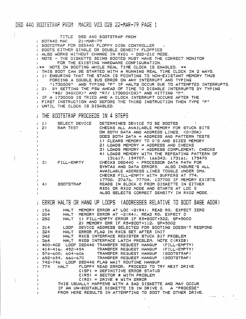
DSD 440 BOOTSTRAP PROM MACRO V03.02B 22-MAR-79 PAGE 1
.TITLE DSD 440 BOOTSTRAP PROM BOT440.MAC 21-MAR-79 BOOTSTRAP FOR D5D440 FLOPPY DISK CONTROLLER BOOTS EITHER SINGLE OR DOUBLE DENSITY FLOPPIES ALSO WORKS WITHOUT CHANGE IN RXOI - DSD-210 MODE. NOTE - THE DISKETTE BEING BOOTED MUST HAVE THE CORRECT MONITOR
FOR THE EXISTING HARDWARE CONFIGURATION. i** NOTE ON BOOTING WHILE REAL TIME CLOCK IS ENABLED. **
THIS BOOT CAN BE STARTED WITH A RUNNING REAL TIME CLOCK IN 2 WAYS. 1) ENSURING THAT THE STACK IS POINTING TO NON-EXISTANT MEMORY THUS
FORCING A DOUBLE BUS ERROR ON ANY INTERRUPT AND TYPING "173000G" AND TYPING "P" IF HALTS OCCUR DUE TO ATTEMPTED INTERRUPTS.
2) BY SETTING THE PSW AHEAD OF TIi'1E TO DISABLE INTERRUPTS BY TYP ING U$S/ 340<CR)" AND "R7/ 173000(CR::"" AND HITTING "P ".
IF A 173000G IS TRIED AND A CLOCK INTERRUPT OCCURS AFTER THE FIRST INSTRUCTION AND BEFORE THE THIRD INSTRUCTION THEN TYPE "P" UNTIL THE CLOCK IS DISABLED.
THE BOOTSTRAP PROCEEDS IN 4 STEPS 1)
2)
3)
4)
SELECT DEVICE RAM TEST
FILL-EMPTY
BOOTSTRAP .
DETERMINES DEVICE TO BE BOOTED ) CHECKS ALL AVAILABLE MEMORY FOR STUCK BITS ON BOTH DATA AND ADDRESS LINES. <0-30K) DOES BOTH DATA = ADORESS AND PATTERN TESTS 1) CLEARS MEMORY TO O'S AND SIZES MEMORY 2) LOADS MEMORY = ADDRESS AND CHECKS 3) LOADS MEMORY = ADDRESS COMPLEMENT, CHECKS 4) LOADS MEMORY WITH THE REPEATING PATTERN OF
131617, 154707, 166343, 173161, 175470 CHECKS DSD440 - PROCESSOR DATA PATH FOR SYNTAX AND DATA ERRORS. ALSO INSURE'S ALL AVAILABLE ADDRESS LINES TOGGLE UNDER DMA. CHECKS FILL-Ei'lPTY WITH BUFFERS AT 774, 17700, 37676, 77704, 137700 IF MEMORY EXISTS. READS IN BLOCK 0 FROM DISKETTE IN EITHER RXOI OR RX02 i"fODE AND STARTS AT LOC 0 ALSO SELECTS CORRECT DENSITY IN RX02 MODE.
ERROR HALTS OR HANG UP LOOPS (ADDRESSES RELATIVE TO BOOT BASE ADDR) 156 204 252
HALT HALT HALT
MEMORY ERROR AT LOC -2(R4), READ RO, EXPECT ZERO MEMORY ERROR AT -2(R4), READ RO, EXPECT 0 1) FILL-EMPTY ERROR IF R5=BOOT+522, SP=5000 2) MEMORY ERR IF R5=BOOT+112, SP=5002
314 LOOP DEVICE ADDRESS SELECTED FOR BOOTING DOESN'T RESPOND 324 HALT ERROR FLAG IN Rxes SET AFTER INIT 342 HALT RXCS INTERFACE REGISTER STUCK BIT PROBLEM 364 HALT RXDB INTERFACE LATCH PROBLEM, NOTE C(RXDB) 400-402 LOOP DSD440 TRANSFER REQUEST HANGUP (FILL-EMPTY) 414-416, 452-454 TRANSFER REQUEST HANGUP (FILL-EMPTY) 576-600, 604-606 TRANSFER REQUEST HANGUP (BOOTSTRAP) 652-654, 666-670 TRANSFER REQUEST HANGUP (BOOTSTRAP) 742-746 LOOP DSD440 FLAG WAIT ROUTINE HANGUP 774 HALT FLOPPY READ ERROR, PROCEED TO TRY NEXT DRIVE
C{SP) = DEFINITIVE ERROR STATUS C(R5) = SECTOR # WITH PROBLEM CCRO) = DRIVE * WITH ERROR
THIS USUALLY HAPPENS WITH A BAD DISKETTE AND MA.Y OCCUR IF AN UN-BOaTABLE DISKETTE IS IN DRIVE O. A "PROCEDE" FROM HERE RESULTS IN ATTEMPTING TO BOOT THE OTHER DRIVE.

j V
DSD 440 BOOTSTRAP PROM MACRO V03.02B 22-MAR-79 PAGE 1-1
000000
000004-
000010
000012
000016
000020
START ADDRESSES BOOT+O (TYPICALLY 173000) BOOTS DEVICE WITH RXCS AT 177170 BOOT+20 (TYPICALLY 173020) BOOTS DEVICE WITH RXCS AT 177150 900T+40 (TYPICALLY 173040) GENERAL DEVICE ENTRANCE - USER
SET'S RO=340. Rl=2, LOC 0 = DESIRED RXCS IF REAL TIME CLOCK MUST BE LEFT ON THEN SET $S/ 340<CR) AND R71 173040<CR) AND PROCEED
A "BOOT" ON AN 11/04 OR 11/34 PRINTS RO, R4, SP. R7 ON THE TERMINAL. IF AN ERROR HALT OCCURS AT BOOT+774 WHILE BOOTING THEN BOOTING AGAIN ON AN 11/04 OR 134 PRINTS OUT THE FOLLOWING.
RO = CURRENT DRIVE # BEING BOOTED FROM. R4 = LOAD ADDRESS WHERE ERROR OCCURRED SP = DEFINITIVE STATUS OF ERROR R7 = ERROR HALT ADDR+2
NOTE - A HALT OR HANGUP OCCURRING BETWEEN 742':"'746 THAT WILL NOT RESPOND TO BREAK OR HALT IS GENERALLY DUE TO LACK OF DMA GRANT CONTINUITY ON THE BUS. USER SHOULD PUT DSD440 INTERFACE CARD CLOSER TO THE PROCESSOR AND ENSURE GRANT CONTINUITY.
DSD440 - RX02 REGISTER SYNTAX DEFS RXCS=177170
IEHR INIIXMIXi"I\ X021??ISID I .ERR- 100000 ERR
40000 INI 30000 XM
.DBDMA= 4000 X02 400 DEN 200 TRa 16 FUN
DENITRal lEN I DONluNl\FUN I FUNI FUNI GOl ERROR FLAG LOAD INTO RXCS TO INITIALIZE EXTENDED MEMORY SELECT BITS = 1 IF RX02 MODE SYNTAX SET = 1 FOR DOUBLE DENSITY TRANSFER REGUEST - DATA TO/FROM RXDB FUNCTION <0-7::" - SET "GO" TO EXEC
REGISTER USAGE IN BOT440 SECTION RO UNIT # BOOTED FROM (0. 1)
XCS= 1.1 Rl POINTER TO RXCS XDB= 1.2 R2 POINTER TO RXDB
R3 READ COMI'1AND VAL WITH DENSITY BIT LDP= 1.4 R4 LOAD POINTER SCT= 1.5 R5 CURRENT SECTOR # (1. 3. 5, 7)
(SP) WORD COUNT FOR CURRENT DENSITY
START HERE FOR DEVICE 177170 BOOT 012706 BOT170: :MOV #-1. SP i INHIBIT INTERRUPTS IN ONE INSTRUCTION 177777 012700 MOV #340. RO SET PROCESSOR STATUS WORD 000340 106400 MTPS RO FROM REG SINCE READ-MODIFY-WRITE
CYCLE INTO PROM CAUSES TIMOUT ABOVE 5 WORDS BECOME I i'10V #340, RO I MOV RO, @#177776 I
/ NOP / IN PDP-l! BOOT 012710 MOV #177170, (RO) i SET DEVICE ADDRESS 177170 000406 BR BOT COM
012700 BOT1S0: i'10V #340. RO SET PROCESSOR STATUS WORD 000340

DSD 440 BOOTSTRAP PROM MACRO VD3.02B 22-MAR-79 PAGE 1-2
000024 106400 MTPS RO ; IN ORDER TO DISABLE INTERRUPTS. 000026 000240 NOP i MAKE MINIMAL CHANGES TO PDP-l1
ABOVE 2 WORDS BECOME / MOV RO, @#177776 / IN PDP-ll BOOT .~
000030 012710 MOV #177150, (RO) LOAD ALTERNATIVE DEVICE ADDR 177150
000034 005001 BOTCOM: CLR Rl ; SET UP MEM TEST PTR 000036 011021 t-10V (RO) , (Rl) + ; LOAD DEVICE ADDR INTO LOC 0
; GENERAL ENTRANCE - SET LOC 0 = RXCS VALUE, RO=340, Rl=2 000040 012706 BOTGEN:: MOV #5002, SP j INIT STACK
005002 000044 000005 RESET
000046 004467 000012
000052
000060
000062
000064 000066 000070 000072
000074 000076 000100
000104 000106 000110
000114
000120 000122 000124 000126 000130 000132
\000134
012766 000341 000002 000002
037177
005021 010421 010021 010102
005022 103403 020227 170000
103773 005042 004567 000022
004567 000150 000774 017700 037676 077704 137700 000000 000573
JSR R4, MEMHGH GET POINTER TO TRAP ROUTINE
; TRAP PROCESSOR FOR NON-EX 1ST ANT MEMORY TIMEOUT i SETS CARRY AND RETURNS ON NON-EXISTANT MEMORY TRAP
TRAP4: MOV #341, 2(SP) SETS CARRY ON TRAP TO 4
RTI ALSO SETS CURRENT PRIORITY HIGH
. WORD 37177 LSI-ll CHECKSUM WORD FOR
. WORD 57012 IF PDP-ll BOOT
NOW TEST FROM 10 TO TOP OF AVAILABLE CONTIGUOUS MEMORY INIT VECTORS AND SET LOW TEST LIMIT TO 10
BOTCHK
MEMHGH: CLR (Rl)+ BUMP TO LOC 4 MOV R4, (R1)+ LOAD TRAP VECTOR MOV RO, (Rl)+ LOAD TRAP PSW VALUE = 340 MOV Rl, R2 . i INIT TO LOW MEMORY = 10
; FIND TOP OF AVAILABLE MEMORY 2$: CLR (R2)+ FIND TOP OF MEMORY
BCS 4$ CARRY SET BY TRAP TO 4 CMP R2, #170000 AT END OF MEM ADDR SPACE?
STOP AT 160000 IF PDP-ll BLO 2$
4$: CLR -(R2) SET POINTER TO LAST LOCATION+2 JSR R5, MEMCHK TEST TO TOP OF MEMORY
FILL EMPTY TEST - DONE AT MULTIPLE BUFFER ADDRESSES IN ORDER TO TOGGLE ALL ADDRESS BITS IN SYSTEM MEMORY
JSR R5, FILEMP ; DO FILL-EMPTY BUFFER TEST
10+<5*100.)-10+<5*1624.)-10+<5*3262.)-10+<5*6540.:> 10+<5*9816.:> o i ADDRESS
BR 130T440
START FILL AT BEGINNING OF PATTERN REPETITION LEFT BY RAM TEST DO DMA TEST ACROSS ALL ADDRESS BITS THAT CAN BE SET IN AVAILABLE MEMORY SO ALL BITS TOGGLE OK TERMINATOR
j ***********

DSD 440 BOOTSTRAP PROM MACRO V03.02B 22-MAR-79 PAGE 2
000136 000140 000142 000144 000146 000150 000152 000154 000156 000160 000162
000164 000166 000170
000172 000174 000176 000200 000202 000204 000206 000210
010104 010400 010024 020402 103774 024404 001402 011400 000000 020401 101372
005124 020402 103775
010104 060414 005214 012400 001401 000000 020402 103771
ROUTINE TO TEST MEMORY FROM C(Rl) = LOW LIMIT TO C(R2) = UPPER LIMIT BEYOND TEST IF ERROR FOUND HALTS WITH R4 POINTING TO ERROR LOC. OR 2 BEYOND. RO = DATA READ
MEjV!CH~,: MOV 2$: MOV
MOV CMP
BLO CHKADP: eMP
BEG MOV HALT
NCKADP: eMP BHI
SETCOM: COM CMP
BLO
MOV CHKCOM: ADD
INC MOV
BEG HALT
NC~,COM: eMP BLO
Rl. R4 R4. RO RO. (R4)+ R4, R2 2$ -(R4), R4 NCKADP (R4), RO
R4, Rl CHKADP
(R4)+ R4, R2 SETCOM
Rl, R4 R4, (R4) (R4) (R4)+, RO
NCKCOM
R4. R2 CHKCOM
GET STARTING ADDRESS KILL Z FLAG <MOV R4, (R4)+> LOAD CONTENTS = ADDRESS AT END OF TEST?
CHECK BACK DOWN TO START ADDR
DATA READ IN ERROR IN RO STUCK BIT IN DATA OR ADDRESS!!
CONTINUE TILL AT START ADDR
MAKE LOC = AD DR COMPLEMENT AT END OF TEST?
START AT BEGINNING SHOULD BE ALL 1'5
DATA SHOULD = ALL ZEROES
STUCK DATA BIT IF NO HALT AT +156
SET UP TO LEAVE A PATTERN OF 1 011 001 110 001 111 B ROTATED RIGHT INTO 4 SUCCESSIVE WORDS USED AS MEM BACKGROUND AND FILL-EMPTY DATA.
000212 010104 MOV 000214 012703 SETPAT: MOV
131617
Rl, R4 #131617, R3
SET INITIAL ADDRESS SET INITIAL PATTERN
000220 000222 000224 000226 000230 000232
020402 4$: 103004 010324 006203 103773 000770
CI"1P BHIS
MOV ASR
BCS BR
000234 010104 CHKPAT: MOV 000236 012703 CHKPTL: MOV
131617 000242 000244 000246
000252 000254 000256 000260 000262 000264 000266
020324 001403 016400 177776 000000 020402 103003 006203 103767 000764 000205
3$: CMP B.EG . MOV
HALT 4$: eMP
BHIS ASR
BCS BR
FILEXT: RTS
R4, R2 CHKPAT R3. (R4)+ R3 4$ SETPAT
Rl. R4 #131617, R3
R3. (R4)+ 4$ -2(R4). RO
R4. R2 FILEXT R3 3$ CHKPTL R5
END OF ADDRESS RANGE? GO CHECK DATA IF AT END CARRY SET BY CMP INSTRUCTION. ROTATE AND LOAD AGAIN
SET INITIAL ADDRESS
DATA OK?
SET DATA READ FOR LOOKING
PATTERN SENSITIVITY ERROR AT END OF ADDRESS RANGE? YES - EXIT CARRY SET BY CMP INSTRUCTION
)

)
)
DSD 440 BOOTSTRAP PROM MACRO V03.02B 22-MAR-79 PAGE 3
000270 000272 000274
000300 000302 000304 000306 000310
000314 000316
000322 000324 000326
012504 001775 005764 000404 103773 005000 011001 010102 004767 000426 103777 032711 104000 100bcI 000000 001417
000330 012722 001420
000334 022711 005460
000340 001401 000342 000000 000344 022712
001420 000350 001005
000352
000356
000362 000364 000366 000370
000374
000400 000402 000404
000410 000412 000414 000416 000420 000422
000426 000430 0004.32 000434
000440
012712 ~73767 022712 173767 001401 000000 010102 012746 000200 012722 000401 105711 100376 032711 004000 001404 011612 105711 100376 010412 004767 000314 105711 100004 112412 012716 000100 000770
; FILL - EMPTY BUFFER TEST
FILEMP: MOV BEG
TST
BCS FILBUF: CLR
MOV MOV CALL
(R5)+, R4 FILEXT 404{R4)
FILEMP RO (RO), XCS XCS, XDB WTFLAG
GET BUFFER ADDRESS
DOES MEMORY EXIST?
NO - STEP TO END OF LIST
GET RXCS ADDR INIT FOR RXDB WAIT FOR DONE FLAG UP
BCS LOOP IF NO BUS RESPONSE BIT #. ERR!. DBDMA, (Rl> ; ERROR SET DR RX02?
BPL .+4; HALT IF ERROR HALT INTERFACE SETUP ERROR
BEG RXFIEM IF RXOI MODE THEN NO LATCH TEST DSD440 - RX02 INTERFACE LATCHED BIT TEST
MOV #1420, (XDB)+
CMP #5460, (XCS)
BEG .+4 HALT
CMP #1420. (XDB)
BNE RXHALT
RXDBTS: MOV
eMP
BEG RXHALT: HALT RXFIEM: !'10V
MOV
MOV
TSTB BPL
BIT
BEG MOV TSTB
BPL MOV
FILX01: CALL
TSTB BPL
MOVB MOV
BR
#173767. (XDB)
#173767, (XDB)
· +4
XCS. XDB #200, -(SP)
#40 I, ( XDB ) +
(XeS) · -2 #. DBDMA. (XCS)
FILX01 (SP), UDB) (XCS) · -2 R4. (XDB) WTFLAG
(Rl> EMPBFT (R4 )+, (XDB) #100, (SP)
FILXOI
L.,OAD INTO RXCS
DID THEY LATCH OK?
STUCK BITS IN RXCS LATCHED OK IN RXDB?
NO-BAD INTERFACE.
CHECK RXDB LATCH
DID THEY LATCH
HALT IF INCORRECT BIT LATCHUP SET UP RXDB POINTER SAVE THE WORD-COUNT
DO FILL COMMAND
WAIT FOR TRREG
RX02 STYLE FILL?
NO - DO RXOI STYLE PROG XFER WORDCOUNT (=200) WAIT FOR TRREG
BUFFER ADDR WAIT FOR DONE, ERROR, OR TRREQ
CHECK FOR TRREG ON RXOI IF DONE, GO DO EMPTY BUF TEST DO ANOTHER BYTE SINGLE DENSITY RXOI COUNT
CHECK FOR ANOTHER BYTE
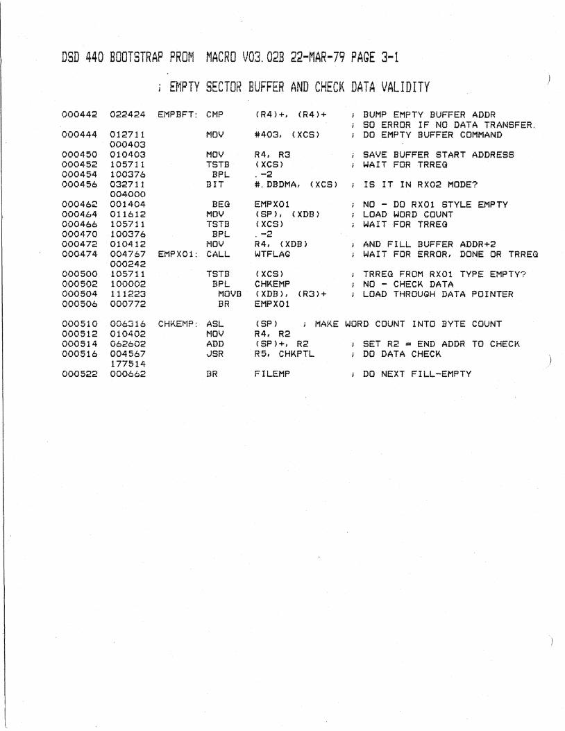
DSD 440 BOOTSTRAP PROM MACRO V03.02B22-MAR-79 PAGE 3-1 . EMPTY SECTOR BUFFER AND CHECK DATA VALIDITY ) J
000442 022424 EMPBFT: CMP (R4)+, (R4)+ BUMP ~MPTY BUFFER ADDR SO ERROR IF NO DATA TRANSFER.
000444 012711 MOV #40~, (XCS) DO EMPTY BUFFER COMMAND 000403
000450 010403 MOV R4, R3 SAVE BUFFER SiART ADDRESS 0004·52 105711 TSTB (XCS) WAIT FOR TRREQ 000454 100376 BPL . -2 000456 032711 BIT #. DBDMA, (XCS) IS IT IN RX02 MODE1
004000 000462 001404 BEG EMPXOl NO - DO RXOl STYLE EMPTY 0004.64 011612 MOV (SP) I (XDB) LOAD WORD COUNT 000466 105711 T8TB (XCS) WAIT FOR TRREG 000470 100376 BPL . -2 000472 010412 MOV R4, (XDB) AND FILL BUFFER ADDR+2 000474 004767 EMPXOl : CALL WTFLAG WAIT FOR ERROR, DONE OR TRREG
000242 000500 105711 TSTB (XCS) TRREQ FROM RXOl TYPE EMPTY? 000502 100002 BPL CHKEMP NO - CHECK DATA 000504 111223 MOVB (XDB) , (R3)+ LOAD THROUGH DATA POINTER 000506 000772 BR EMPXOl
000510 006316 CHKEMP: ASL (SP) ; MAKE WORD COUNT INTO BYTE COUNT 000512 010402 NOV R4, R2 000514 062602 ADD (SP )+, R2 SET R2 == END ADDR TO CHECK 000516 004567 JSR R5. CHKPTL DO DATA CHECK
) 177514 000522 000662 BR FILEMP DO NEXT FILL-EMPTY
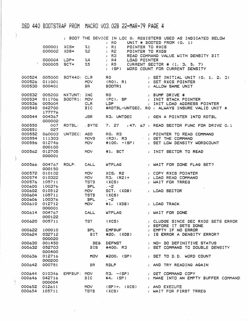
DSD 440 BOOTSTRAP PROM MACRO V03.02B 22-MAR-79 PAGE 4
i BOOT THE DEVICE IN lOCO, REGISTERS USED AS INDICATED BELOW RO UNIT # BOOTED FROM (0, 1)
000001 xes= %1 Rl POINTER TO RXCS 000002 XDB= %2 R2 POINTER TO RXDB
R3 READ COMi1AND VALUE WITH DENSITY BIT 000004 lDP= %4 R4 lOAD POINTER
, 000005 SCT= i.5 R5 CURRENT SECTOR # (L 3, 5, 7) (SP) WORD COUNT FOR CURRENT DENSITY
000524 000526 000530
000532 000534 000536 000540
000544
000550 000551 000552 000554 000556
005000 011001 000401
005200 011706 005004 042700 177776 004367 000002
007 027
060003 111303 012746 000100
000562 012705 000001
BOT440: ClR MOV BR
NXTUNT: INC BOOTR1: MOV
ClR BIC
JSR
RDTBl: . BYTE
UNTDEC: ADD MOVB MOV
!"IOV
000566 004767 RDlP: 000150
CAll
000572 000574 000576 000600 000602 000604 000606 000610
000614
000620
000622 000624
000630 000632
000636
000642
000644 000646
010102 010322 105711 100376 010512 105711 100376 012712 000001 004767 000122 005711
100010 032712 000020 001450 052703 000400 012716 000200 000751
010346 042716 000004
000652 012611 000654 105711
MOV MOV TSTB
BPL 1'1OV TSTB
BPL MOV
CAll
TST
BPl BIT
BEG BIS
MOV
BR
Et1PBUF: MOV BIC
MOV TSTB
RO (RO), R1 BOOTRl
SET INITIAL UNIT (0, 1, 2, 3) SET RXCS POINTER ALLOW SAME UNIT
RO BUMP DRIVE # (PC), SP INIT STACK POINTER LDP INIT LOAD ADDRESS POINTER #RDTBL-UNTDEC, RO ; ALWAYS INSURE VALID UNIT #.
R3, UNTDEC
7, 27 i 47, 67
RO, R3 (R3), R3 #100, - (SP)
#1, SCT
WTFLAG
XCS, R2 R3, (R2)+ (XCS) . -2 SCT, (XDB) (XCS) . -2 #1, (XDB)
WTFLAG
(XCS)
EMPBUF #20, (XDB)
DEFNST #400, R3
#200, (SP)
RDlP
R3, - (SP) #4, (SP)
(SP)+, (XCS) (XCS)
GEN A POINTER INTO RDTBL
READ SECTOR FUNC FOR DRIVE 0, 1
POINTER TO R"EAD COMMAND GET THE COMMAND SET lOW DENSITY WORDCOUNT
INIT SECTOR TO READ
WAIT FOR DONE FLAG SET?
COPY RXCS POINTER LOAD READ COMMAND WAIT FOR TRREG
lOAD SECTOR
LOAD TRACK
WA IT FOR DONE
ClUDGE SINCE DEC RX02 SETS ERROR BEFORE IT SETS DONE EMPTY IF NO ERROR IS ERROR A DENSITY ERROR?
NO- DO DEFINITIVE STATUS SET COMMAND TO DOUBLE DENSITY
SET TO D.D. WORD COUNT
AND TRY READING AGAIN
GET COMMAND COPY MAKE INTO AN EMPTY BUFFER COMMAND
AND EXECUTE WAIT FOR FIRST TRREG
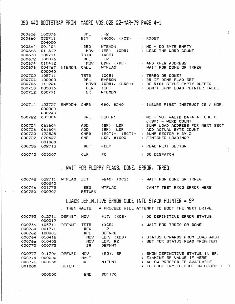
DSD 440 BOOTSTRAP PROM MACRO V03.02B 22-MAR-79 PAGE 4-1
000656 100376 BPL · -2 000660 . 032711 BIT #4000, (XCS) RX02?
004000 000664 001404 BEG WTEMDN NO - DO BYTE EMPTY 000666 011612 MOV (SP) , (XDB) LOAD THE WORD COUNT 000670 105711 TSTB (XCS) 000672 100376 BPL · -2 000674 010412 1"1OV LDP, (XDB) AND XFER ADDRESS 000676 004767 WTEMDN: CALL WTFLAG WAIT FOR DONE OR TRREG
000040 000702 105711 TSTB (XCS) TRREG OR DONE? 000704 100003 BPL EMPDON BR IF DONE FLAG SET 000706 111224 rl0VB (XDB ), (LDP)+ DO RXOl STYLE EMPTY BUFFER 000710 005016 CLR (SP) DON'T BUMP LOAD POINTER TWICE 000712 000771 BR WTEMDN
000714 123727 EMPDON: CMPB @#O, #240 INSURE FIRST INSTRUCT IS A NOP. 000000 000240
000722 001304 BNE BOOTR1 NO - NOT VALID DATA AT LOC 0 C(SP) = WORD COUNT
000724 061604 ADD (SP) , LDP BUMP LOAD ADDRESS FOR NEXT SECT 000726 061604 ADD (SP) , LDP ADD ACTUAL BYTE COUNT 000730 122525 CMPB ( SCT)+, (SCTH BUMP SECTOR # BY 2 000732 020427 CMP LDP, #1000 FINISHED LOADING?
001000 000736 002713 BLT RD.LP READ NEXT SECTOR
000740 005007 CLR PC GO DISPATCH
WAIT FOR FLOPPY FLAGS I DONE! ERROR! TRREG
000742 032711 WTFLAG: BIT #240, (XCS) WAIT FOR DONE OR TRREG 000240
000746 001775 BEG WTFLAG CAN'T TEST RX02 ERROR HERE 000750 000207 RETURN
LOADS DEFINITIVE ERROR CODE INTO STACK POINTER = SP THEN HALTS. A PROCEED WILL ATTEMPT TO BOOT THE NEXT DRIVE.
000752 012711 DEFNST: MOV #17, (XCS) DO DEFINITIVE ERROR STATUS 000017
000756 105711 DEFNWT: TSTB (XCS) WAIT FOR TRREG OR DONE 000760 001776 BEG · -2 000762 100003 BPL DEFNRD 000764 010412 MOV LDP, (XDB) STATUS UPWARDS FROM LOAD ADDR 000766 010402 MOV LDP, R2 SET FOR STATUS READ FROM MEM 000770 000772 BR DEFNWT
000772 011206 DEFNRD: MOV (R2) , SP SHOW DEFINITIVE STATUS IN SP. 000774 000000 HALT EXAMINE SP VALUE IF HERE 000776 000655 BR NXTUNT ALLOW PROCEED IF AVAILABLE 001000 BOTLST: : TO BOOT TRY TO BOOT ON OTHER Dr iE
000000' . END BOT170
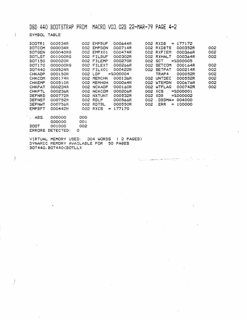
DSD 440 BOOTSTRAP PROM MACRO V03.02B 22-MAR-79 PAGE 4-2 SYMBOL TABLE
BOOTR1 000534R 002 Ei'1PBUF 000644R 002 RXDB = 177172 BOTCOM 000034R 002 EMPDON 000714R 002 RXDBTS 000352R 002 BOTGEN 000040RG 002 EMPXOl 000474R 002 RXFIEM 000366R 002 BOTLST 001000RG 002 FILBUF 000302R 002 RXHALT 000364R 002 BOT150 000020R 002 FILEMP 000270R 002 SCT =%000005 BOT170 OOOOOORG 002 FILEXT 000266R 002 SETCOM 000164R 002 BOT440 000524R 002 FILX01 000422R 002 SETPAT 000214R 002 CHKADP 000150R 002 LDP =%000004 TRAP4 000052R 002 CHKCOM 000174R 002 MEMCHK 000136R 002 UNfDEC 000552R 002 CHKEMP 000510R 002 MEMHGH 000064R 002 WTEMDN 000676R 002 CHKPAT 000234R 002 NCKADP 000160R 002 WTFLAG 000742R 002 CHKPTL 000236R 002 NCKCOM 000206R 002 XCS =%000001 DEFNRD 000772R 002 NXTUNT 000532R 002 XDB =%000002 DEFNST 000752R 002 RDLP 000566R 002 . DBDMA= 004000 DEFNWT 000756R 002 RDTBL 000550R 002 . ERR = 100000 EMPBFT 000442R 002 RXCS = 177170
I ABS. 000000 000 000000 001
BOOT 001000 002 ERRORS DETECTED: 0
VIRTUAL MEMORY USED: 304 WORDS ( 2 PAGES) DYNAMIC MEMORY AVAILABLE FOR 5.0 PAGES BOT440,BOT440<BOTLLX
) .'.-,' .~- --.' .. _' ~~ :'., .-
)

)
(
)
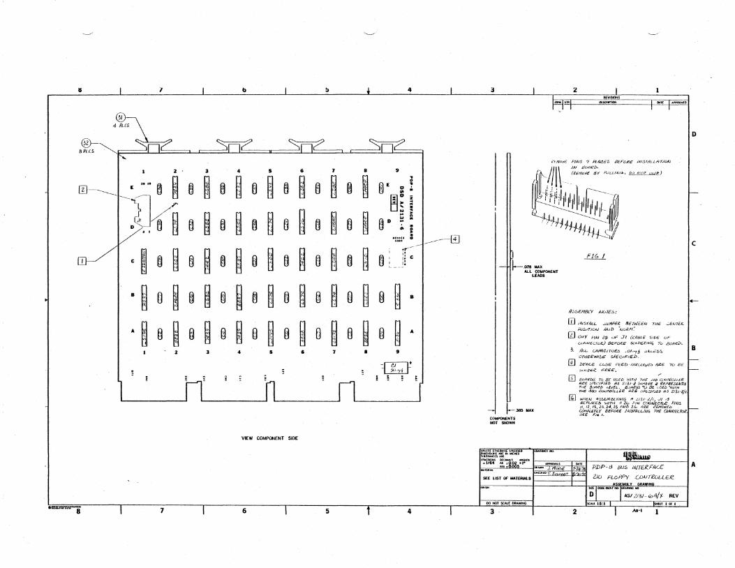
~
II 1 b ~ 4
®-~PL(5 r-
1 Z . 3 4 5 & 7 II II
ill-___ I __ £~ .. ~ ~m ~ 8 U .~ ~ ~ ~ ~§ ~ ~ ~ £ • = ~
;u1i 0 8 0 8 6 ~ 0 ~ ~ R 0 ~ g .~~ ! .::!~I 3 1 ____ -0
c: ~ ~ ~ ~ .~ H .~ 8 ~ 0 Q ~ .~. ~ .~ ~ ~ __ fc 8 ~ 0 ~ ~ ~ @ ~ ~ H fi i ~ ~ Q g Q .~ 8
A i B ~ B ~ e ~ a i ~ ~ H ~ B ~ § ~ A
Z 3 4 5 & 7 • II
~ 50"/1 ; :
VIEW COMPONENT SIDE
--8 7 6 5 4
.--..--.
3 2 .... SOON.
['(/liD),!: Pi.US ? Pi.ncGS IJcFaJ?6 JAI.5TIJLt.AT./441
111\ 1" done!>. !,·._.(UNW<E 8Y P"LU<''''. ~l..J:.!.l!:.)
1~~$
FJ6/
1-.Q18 MAX ALL COLIPCINENT
LEADS
~.385 MAX
COMPONENTS HOT SHOWN
/I;SEfllJLY AJU7€S:
ill lA/STALL ..Ju~IP€i! BE7W£EI.J THE ..:.EJ.J1i~ Po!HTIOAJ AuD ".uo.e;'/~
o cur f.~/AJ ltl- LJF= 31 (C.lldLE SIt;.E OF uJAJA,JiE croE) 8EF~E 50L/:IGEIA.'4 7u BOlle]).
3. /k.L tAMe'Toe::. .01"""13 lIAJ':"c6~ OTHEEWISE sPEC.J~/Cj). o DEVlC.E GuDEi FEcD-TflR6lK::,JI .... /leE 70 I!>~ !;loLDEe. 1=2EEi~
[i] JjoA~D/j. TO BE IJSeD WJTJj 71-1£ LI¢ (!t.JJJrRoit1:l!. /lEe. :.PfCJ':JEIl I'I.S ZI3J-Z (~f/l"IEce ~ eePRE.5EAlT.s THE 8~eD LE'(eL. BJAE'f)S Tu ae u5ED Wlm THE 440 CfJAlTi!OLa.e /feE .:f.Pc~.c.iEI> 1105 ZI3/-Z/J.,
~ V;~~:~~~~;J'II~/~(., Iip/~3:;:j}jE.~~~ P.lAI.s. /I, 12, /3., ,B, 2.4, Z5 AIJIl 2'" AU 2E"'(JIIED
CJJft1PLETLY 8E~E JAJ.5TIU.Ll.u6. THE C/JAIAJEC.TaR.1
,:jEE F/~ I.
·wi.fss·OfHf.IIWISf: Sia:lt1Ull ;DlMtNSlONSAIIlV.1MtHE1 ~ 1(.I.(lWtI:lSAIIt:, fRACllOHli OUMMlS MlGUI
o
c
B
s~:'4 ·::'!8~ "'1- APf'IIOV~~ ?-:'~18 PDP:'8 8LJS IAJTE~FA(£ A IlfDS": ~4 'P
... LIST f1f MATflllALS· 2/0 Fl.oPPy .COAlTeOl.LER.
iflNiStl
PO NOT SCAlE DAMWfl
3 2
.WING
A5I 213/- (oll/;' MV
~ As-I

-----~-- ~---------------~--------------
8 7 6
D
~~-
c
ILl" l,z.t,)
B
(~l-ITl.IP) 5TATU'o.-<fip
A
.==r.:.rn1~8 7 6
--"'~-~-,..,""'""~"----~--=
5 4 3 2 , kfvlSIONS
(~L) WI EI.j~ ':U~4 _"'_, ________ _ , I"/-!V-
I'.I!~J JilT ~,·f.I," L .IT!] loto{I~F~W:~---,_· ___ =t--~ .. ~f'1l0VEO'
Q~<.Jfi]<.. ~ ~. "Ul'LKEl ". ." ," ,. ' '. . "~14;9 ~ -----.". ~B_ i41j) '" ,~_ ~__----;-~
-., ,:;:1" ~1 "" "",' r7 ,.,,"' "n
~!Y'"rt-lJ'· ~ - ...... , bt,.,e,GO
jOT4-'.2 ~E.' -- ---~-'-'''''If J ("',6.)(~b) .... ?-,
c:.u-tt1 .... IDIl '~Ul 2., ~~)
"~~F~ ,'C'" . l'~ IT','" hI E""
b~l~ I
r""'.l')("')(4~)
/b .. n,?l)
~"Dt EI"'-
I ,"=
(k)
U()fE~~
I. ';S.C.I-II'..!-I.Io.:TlL '-::LOFi=.CL To j"J.'..T'-N(Je~ "I :"'I~ 1- (p
@ It::"E "I A1LIIED" OPTIOI-l "NITH L lil.(J COf..lTf:oLL£e~ L£VEI- ~ De C,eF0f::E
H(OOO
~.'-<I'~
Jill..h---l::I]
c,.ruIil~J
(t..e.)
lL.llT u PL .---G!]
~ 0~) K -14. 1 DATA- L 1:lLl
q,~
5 4 '~~=-~,~ L:J I ~,~" , --
2 I
.~".
o
c
.~-
B
A

8
D
c
-+1
B
A
..... """"""8
('51J:AP'U FtJ«.1,)
.... ,1 filii"> Mil ¢q L. 6
vJ. filII ., L
Clil. p,
w
~Ll1LJ!
c, T'-J H
7
ij.lt ... ~11 .. qC.
-:- JIAMP~t. "'l-l.oqlC.·I~ liJ I),£VJ::.E. CDbE
cfM'\
7
144l.. ..
m
6
6
5
l-.CD (4A)(;~' ',4L)
loT? (tol.nt,5c..)
lOT4 .. (:"HTt,";lC)
lOT? '!.H" 5D)
, 8 ~Jl..lTe (~H11.4(.)
'~/
4
1OCi}~.
~~~jS4" ~tk1L;;-1.-;-(]iIleCl~ JAJA.,.-'L ~ til. =ffl;
llUT (t.H1"I,~~)
3
c.:MMAlJbC/¢
4>' (In
""~
C .. IA1t-1A.ub :1·4 (t"'",U.)
$J? (I .~L)
" .. qn
.;<
u;..HHA,~l:I q.B
',,1>'-1 j .pq 1 ~, 'LI>
II (!I1ff1.44
2
!iUb 11m Ii.'NAI Jk) L (£!;J]
.. 4'1 (4p)
<-TA1u~ 44>} • tPZ- (~~IT I SA)
.' I/J?
·rl'L-STA~ (~"'TI,tA)
- <-TATu" <14) " 4», (4<.) • 4>"
.' cJ,.1
):.AlA. 'R.-1AJTI:i!J:,l(.c ( ....... TI,.:..!!.)
.1 I I 1 lMJ1 (e", ',4_)
~hT'.'!.l) );.II1A .. 4,,-
l~TE.eFALE SE~TIOI
't.~
ISHfIT Z-Oj t.
5 4 3 2
D
c
1.-
B
A
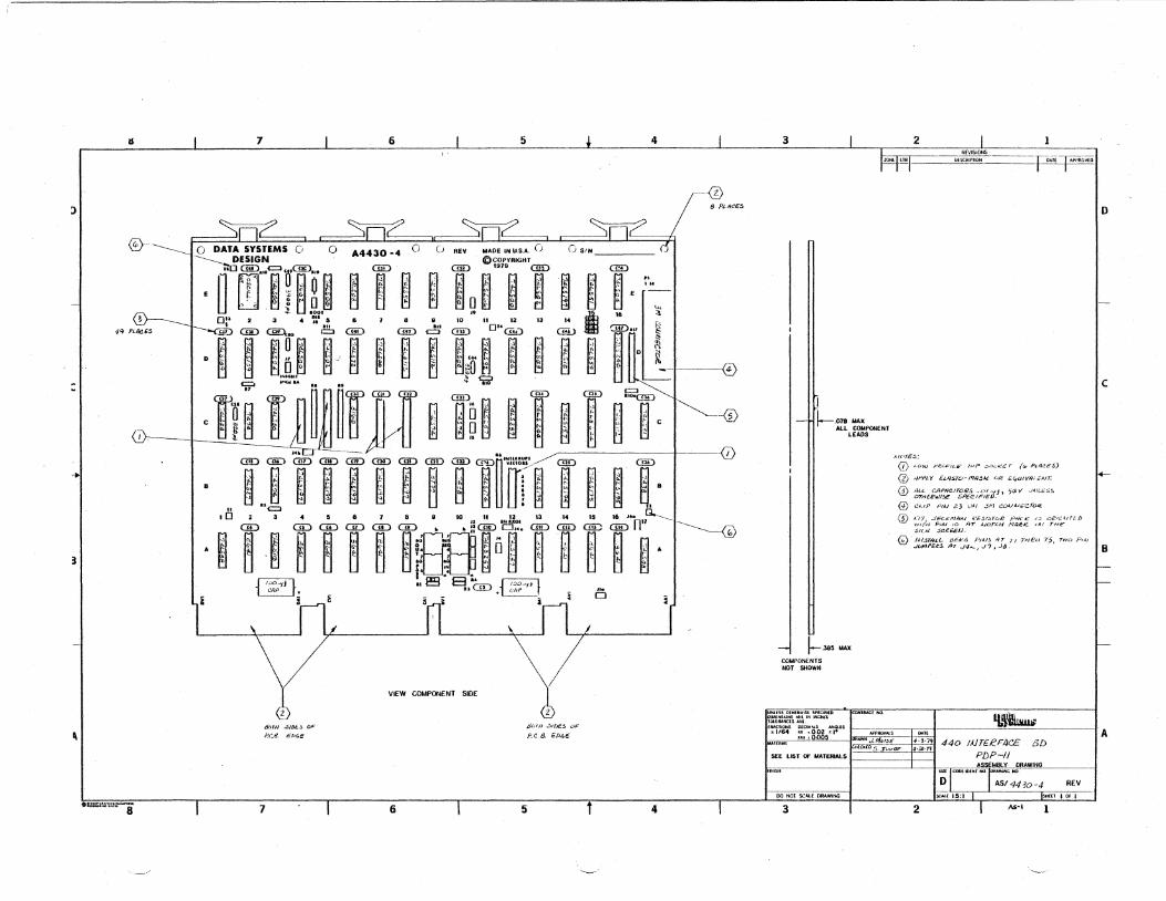
II
:>
@---------
<D~ _____ 49 PLlil!E5
@--_I
3
,
""""'''''''''''''-'8
7 6 5 4
-{f) 8 PLnCEf>
o DATA SYSTEMS 0 0 A4430 -4 0 () REV .. ADf INU,S,A, n __________ DESIGN @COPVRIGHT
~~.. m~'''<=~' n'GJD~'~ '0" ~" ~_ G!D~~' ~r: ~; G!D~~' ~ __ '_ 191.~ @D~~: ~ ~' CillJ~~' :'" E t ~ ~ (I " G ~. ; tf} ~ f" [;., ; £
c.'i:. ~I"(]t· ~ - ;:. Po {)O~ -, -- il., U,
.... 1001 ~& j ,. 'll D~I 2: 3 4~~1.~ 61 8 ~11 10 "',.'21314 147 ~
OS/N _____ _
"r- r- f! t, r. ,.... t·, I'- r- r- ~ t: I'- l, 0 ~ JlD~',:, @)~'~ GlU~; oo~_ ~~( GID~:;' ~' @D~;~' =~' CillJ~~'_ ~o @0~~,:, ~'" _ CE.l~':' ~~ CED,~f; ['" ~ o '<" A1 {)' _.' ' '" IJ, .... In lo&-t IA ~ lti '" ,I'l ~
J) ~ ;: 0 C> I" t ~ t' Q;~O ~ ll> ~ ~ _-I ® IN"'.U ~ i:::J
,iJi i1j~~JJ~ ~ t~i.1 i ~ J ~l, ~~ GD ~ u:? ~ ~ ~ ~ GID (ill) ~~'~:::~~:'_: ~" , @) I ~' ~- ~- ~. ~ ~- ~ ~' ~' ~ m~ ~ ~" ~ ~' ~ ~ r- ,.. r;, " :! ,t:. r,: ! 'r;; ~ r:. ~ '" B
~ : ~ -0:' t : 'l i ~ ~ I' 'I - - ' oJ; I
n <= ~ lOa 3 " 5 6 1 8 Q 10 n 11 It" UOI 13 14 15 16 J •• 17 ____ ~ _ _.
OD 1 " , ,,~~ G!D OJ". CllD C!!D <1!!:) G!D n I _________ ---@ mimiifi · ~ n -~n n 0 0 .~ ~.
i
~ .088 -~-' "~' ~ ~ ~ ~ ~ ~ ~" \I ~ 0 ~ i '~_ t,- ',~ ~ It 1 1 N \I ..... t .... ". ~, t ~ ~ ~ ....
I' • II ~ • a:oo 1 IJO~f ~
III ... eliP o
VIEW COMPONENT SIDE
dOTlJ ,sIDi:.:.. ()IC
Po~_ £l>GE
7 6
J1(~JII ..5IDE5 OF
PC,B. £D6e
5 4
3
~.010 MAX ALL COMPONENT
LEADS
1--.385 MAX
COMPONENTS NOT SHOWN
).lorE:::':
(f) t-uw ;>R.6FII.-E" /JIP ';'::J".c£ r (ID PlJ1(!£.s)
o ,WPL'( f..U'ifJ.10-f'1/J:'~ Ok! £4UIVIJ:£AJT..
ill ~~Ee~~~/rg:~;;~~f{j) 5'!))/ ,HILES::'
@ CliP PIJ.i 2:3 oAJ 31'1 C()JJAiG(!TOii!..
® 1.'1", ~ECt:_I'1IJAJ k.'E.$/!>lc..>j!! P";CK J:J ()RI/.;;llr~b \VIOJ PIA) 10 AT JJOr<:'H n4.eK.. /111 THE:-sn;.! :>c.eUJJ.
@ JU.'jTflLL tj£K6 P,U!. H TTl 7NeLl 75, 7'Wu PI.t./ .J/),.,PE:.i>'s /iT J4 ...... , J?, Ja.
o
c
;"'-
B
li,.USSOHUilwlSf. 5PlClfl£D ttUlbL ___ ., OIJAr~s".ltOs ~II[ II< !NCliiS Dl~
:~4}ii:S A~C+~oh2 ~l~L[S I' A b;UIlIAl UA ~O.005 440 IIJTERFJJCE 3D
PDP-II SEE LIST Of MATERIALS I =1==1 flNI!iH
ASI4430-./ REV
DO NOT SCALE DRAWING I IKIII( 1.5: I I ISlIm I Of I
3 2 As-!
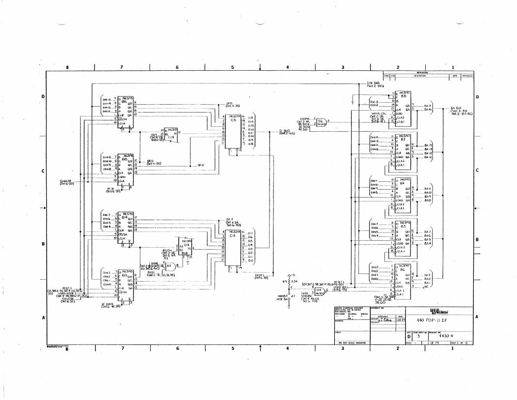
, '-.--' '--'"
8 7 6 5 4 3 2
,. tNOHI!. I
rJ.~:f-;~ --Ps"~~?G.U) ~:5:l\e _____ _
t~f~':i6Y--
'I.~'Lw. 440 PDP-II It
A
7 6 5 4
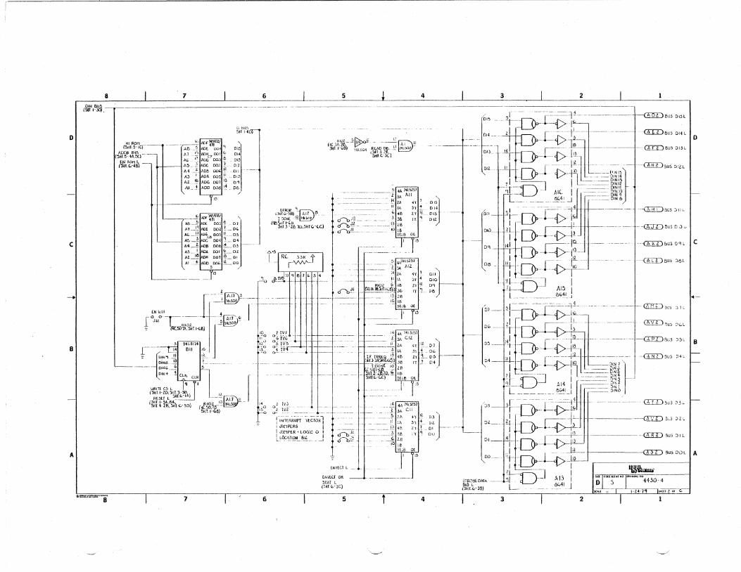
D
c
B
A
8 7 6 5 4
(!1Ir,~~.+---
'Iom=:m:nmr's
HI ROM (!lIlT.5·IC)~
, ADDR BlJ~ (!lIIT.5·4A.:iC)--
M/I'tltll-
D bl/:'! !HTI'IDr
-.--.-~.~ ADF:\WlZIJ J Ae._.~ ADt 00 9 01"
A7 .. ~ ADHC700: ~ 014-A" I? IIDG 00.1 ~ __ DI.3 A~ ._.} ADC. 002 1. .... 0:2 1\4 ~_; .. ADe oo~ ~~. _ ali A'j I. ADA 005 ~J ~ OiL:) A2. __ ~~ AOG 001 ~~ 0"1
AL.1. ADO DOlI ~~ _ De.
t+ - _-----110
'" 14~ 12/
~~~: 11\,0, ~ - O'J' Al_~ AD! 00 ! _ D"
A,,-....J.l AOOGO oo!l ~_ .. _ D~ A~~ DC DO"; _.Of. A4~."08 000 ~ __ Dj -Att_LAbA 001 .Loz A2.~ 007 ~~_ 01 AI __ . .! ADD 00(; ~Loo
5
"
LR~ ., '::lUT\'>~1S) --rAI1\~. I~NE.·~~
(46'~i ~~r6.1D.5HI" M(£)
RXOZ._~6 G._ -- Al ~ 1:<
(4C:/I\.1b RlAO D~14t.!:IOd, jl.IJ 1-~6) Hl~.V4 l~J.t~)
____ . ~ 411. 14l~l!t7 .~ __ . ___ ~_ __ Z~.3A All
._. ~ lA 4'i'\' -----------_ .. __ . ~ ~~ ~~. ~~
<i1>}3 db~j::~
._~ 3 ~B IY. '" . __ ~_~ lB
~ 16 She Of.
I "
O'~ 014 OLj .-
Oil
.w" 010
"",J:! Z'i ~ .. Oct IY ~ .. _ PO 1--- ~ fAi1'\o_
~-~-~
[N kWI I- l_~ __ -I <l 0--· ~-.--. 4 J.JA ---- AI1 - fi, ~ r~ !iClRXOl -' ~\- .
'l-1c: .1A,~T.I-<.6) ~
'YI' Oll}-
190 o? !~! I ______ [~ j""14.. j II orv···l-/·H-+--------
1. { . _'~ fill 10 I!-~ <>5 tV-' -. ~ . ~ "!N" ...'.' l2. " 0. iV4---l ___ DiNO ~ i" -0 0----·-
=l== ~:~~~ O-l---- -- -
CLI\ CLR
YJRIT( c!t l.. q (~III-lD. $i.JT. ~~'e
fU5U L ~r.c;.·IA) 12-(,"T.l-3A.6A-·- --~ 5HT."'lf).~t"'~D) RXOl I,:) AI7 11-(f. ~o.l"- T'l
I~ "A 14l~l57 ~ __ ~_:,\ ell
.. ------!:. ]A 4Y I" ' },r,~~~'~ ,~ ~~ "t-: ~.~ ~ ::--tDJ::r~~ 3" t> ~-. DO --_.Dit?~!tt -I~ 2B ".1 D4
:)"r{;:a£.~Q..~. I e "~ • ~lLB
"'T.I-G.B)
.. J50 -0 ~~ {~~' -~=~-_~ L.~~~:_
: INTf.RRuPT -VtCroRl I JlI:1Pf.RS I I J:.J;'1Pf.R • LOG:C 0 I
L~~:-~J2.N_ .B~~ ___ .. J
~ _ ~ ,<lA" 7415257
"_"_~" .sA ell
___ .. _ . __ f~: ~; t ~~)-ObJ.c. J 1--- --.~ ~~ 4E 2.1! 01 " -_.
~ . ~~"-~:-" __ ~ i~ :'1 ~ DU
7 6
lNVE.Cl L
tNVf.C.r OR ~r .. 'T L (,"T~'3C)
5
.'-....---"
~~ Ie Sb,B
I
4
3 2
--~--~ - ~L ~~_~~ ___ _
';1> - -~-C{:>- I~~_ i r-LY -- --r--D,4 -~ 2 S--i> 15 _____ _
" '~Li>181 _~ ~~~-ll ___ gll~:!
~ ----DINIZ 1 L ~ _ 1 I _ - --~ -DIN" -. - DIN'
-~~BUj DI4L
';-" a::I:D Bu' D I'; L
'-(A]I)BU5 DilL
11---<1"\: - Ale I ~--=~-::::::. DI~ ~ '9 ~--<L.....J 41 _____ 011\1 a
-L_~. -~---=~=~~! __ E----.-:--.. j ··--Q;:RDoc5 )liL ---- ~- --~I
0:0 --LL~~[}-L_i> I~ ______ . D'O __ Ll1l __ !_ ~~ .... --(K;[D Bu; 0 .:l "
Dq _L.l!!I_ I/\. j _ 1'-.....['L
j-LY -Yff.. 08.1 1!!.1- ~ G-1.-4>-T---
1 ---- J I ;4--~ - Alj I -~~ e~~j L -~.:::: __ -=---::-.:.:-.::_~L
D~ -- T __ Y::_~!;.L-'._ 1 -- -~I
05 ___ V4t --rlh.L~, I -LY'"
---@DBu. OqL
-.<Kill BU> ~E>l
GlTII) ~L:j J 1 L
fES!TI 50> ~(.L
--'--a:ED5cS JjL
/Dl-1;t~It-'" r-~~l~ _ ~11~
I =~--: 1 • -~=-~.:...-=:::_ ~,~1 --r- ~....J. AI4 I [.1'-.-- D'" I
'1 --<L-.J -- ._ DINO
--a:RI) ~Uj ::141..
''';)3
T- --- e.~I_1 -- _. __ --GII),Uj D3' 5r~:G -~ - ---- E~~ ··1· -'. ---- ------ (TiT" 3d ) l c
D
c
: .. --
B
rl·· ~- 1-::::::·-IL - -~-~ ~'--J~I··-lA.....L...J"..--_:~ _ -<!:[lJ 5u'; ~IL 1 -~ __ ~_I_I__ _~ __
DI-W-~_L,~jlL _ illDBUSDOL IA ILY 1./ -ll._ t .. 1 lI\...l~ ~ 00.-.-1''1- '-LY- 1./-1 •
I ----.-] 1 'j....:::-<f-'L AI3 I
STROIlEDATA --... ~ . LI _:e;;AI . .J BliH l __ . __ _ 15ijr.~-3B) _
3 2
IJ.\'i1w.ui
SCAt( _ -'-1-2.4·71
~'"'~I"-OO4430-4 1~H(jJTOf-,,-1
--../
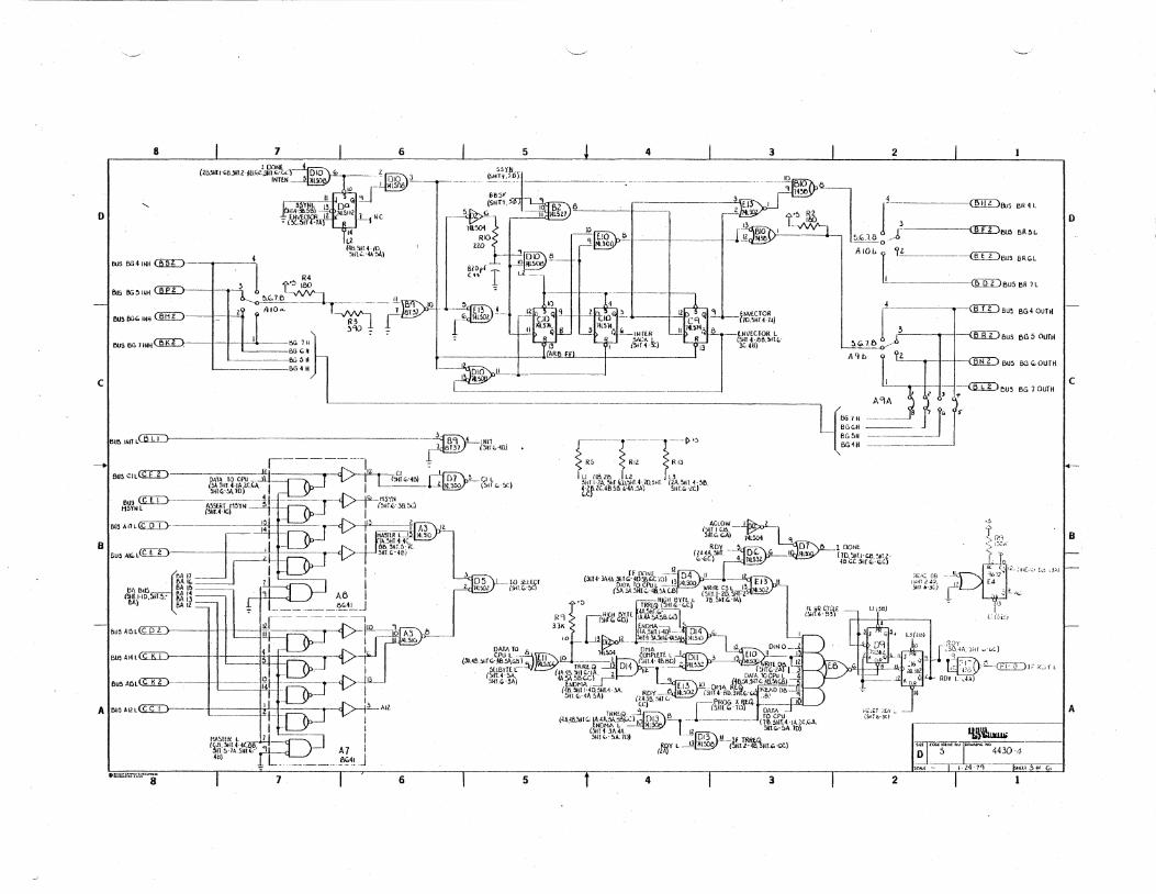
o
c
-.1
8
"
illJSOO41"11@D-
IlUs 1lG~1," ([fD---
BU5 OOG iNij C§E:D-
BuS BG [email protected]
7 6
? IiJiO)L ~
:--..4:1 R4
3 t~ . __ 'L' B 1'<--~-o-5."7~----lT--- . 1~ AIO~~ 1
-ooc.:.» ~511
---- -===BG 4 H
--"QEI3 ~{"J1~l50l
1
5 4 3 2
--~
----'--t=---.---- - c:~ ~:;: I lL-~--------@JIDBu5 OR4L
-I~-' ----Ll 15."111 0--6 -----~BlJ5 BR;.
A lOb l '1-l-·----·-·~B"' BR"l
---.. --~BU5 BR 1L
14 T CITDBU5 BG40urn
J.L----<t-t~ BUS BG:; ourH ~g~<y,
,-.~y I~ -1lG 1H~ ~~o f ~ A q b I 1z I I I ,QillD BUS BG '" Dunl
"'_HjI<=O"' ~,~'" --~~!L_! ___ _ ~ ----"
B~ lUll LGI:[D BU~ CIlC£:L.I:) r-"-- - __ __ 2 _ ~'TA- __ Je -------- _.1~1y--I"1l [(~"]~'---E':~ ., SliT 1-2A. ~Hr GJ:SHI 4-70.5HI. (ZA.~' 4-31:1, ."Zf,.lCAB5!l (.-4A,jA) SHT.Gl·ze) ~C)
L(IlGIM SG(.II
BG 5H BG4H
6 C l;hfIT1~1~i::0A-,u=~1 1 (51<''''0)
"~.\ITD ,-,,<"'" I ' " ' ~'5"'i-'i~-j _. ___ (SHT ~.,") 1 •
""AI1LUD-O. I' .~'. ,"- ~lU.G----=r£>r.-I" ..... ~r;'L __ _ -115'(N l.':itlT"-~) B 1 - - 1;;.1 . 1 ('ilT.·J""')
BU>AI<OL<TI::D ,-..!!i--I/\.._r-4> I" - -' J ,I -LY -tJMAlTL<~IA3
~ ~_I___ ~ .l,.'HT~i<P""'O
BA 11 1 I/\.. -r-'V ~~.:lH,.:i"7C BA B'I~ Rt I" =_ LY . ..J 10-'B)
AClOW __ ~~
(i1Jn~) rr,;;;'~ RDY 07 0 _I DONl
(U4A.~T. -- 0(' (, I I~L (1D.'~HT.I-CEl.~jlT,Z.'
.5
1 R"
~ I ~;~-~"
(~riID)115' ~:! - ~I I BA 12 -'=;-1 II +I~ AB I
1_ - - ~-=-~'-'- J
Jl -- -
~r=-J5=1--1>-+JF~fA3'LII -_T~I- -{>- I Jl~
____ "I _G-T I-r - - I
A IflU5AOl@I)--- ====fr-- r==;:--r-4>-jJL f--=:===W-I ~ 1
F"'" J~ i>1' " ~'",H(~ ~ I ""5"' •. ..'!L_-~1 1 [-<L..J A7 I __ .11",41 J
6U5 AlSl <£JU:)-----
BU, AI<l<£XD-
BuS AI5l cr:ED---
.""'""",,,",'8 7 6
"'''C) 4 14te.~l ~5,c.c jj.1r.~'G.C)
rf[lON[ ---'~~D4 II c~ (3IiH" 3A~A.~IJTt;;-~D~.a:."IJ\ 13 t"1L~ -~ -- E 13
10 jU 'J DATA fO CPu L - .. - wRlIt C3 L 13 _ (,"I.~.;'ti . ("." 'HT.'4. 8 .... ' A.G. Bl . ('111.1- 'D. ;fjf.",. ~tlOl .. t -Hts~1 BYfl. L 7f> ~l<r."-IA~
t~ 41Rt~?". HrG.·",q [~¥~-~~~)[
nq .~IGH B'tTl IA~A:A~ n C5fllG, '"0) ~:-' l
3.,1( (l~~Str-I-4O,l- 014 (, J 10 ----11~?,_- ~I~:.~'~~:~~ I4LSIO L2 DIN 0 __ -.1
DATA m B l~ f~~LfJE. L J D I tiD 11 _____ .J~i (" .• ,."'r~1';;'J:"'I-"\. IDf'..jQ _____ , 04 (sHr.HB8D)~ j L~,TtDftt-"
. '-~~ TRRLQ I l---~~~C'ZAll 3 StLeYIEc-- , (4A'~D5Jg(,·IA. 2. Il- [WI,. TO CPU L 3
(~~:t·~~) 4A'~6"1~c~_r . '" lJ3 iO -DMA ~tB.!lA.31/T';,~B'~~-=fr' (fB,~J:·.40,Sl1lA.jA RDy~ __ fj "14L"jOZ (:iHTb~.[).:m~(;u;~~~ DO- q
e.lll"·4A.t.A) (lA,J~. "jfH (.. --PROO, l( ~t.Q .. :_~ [JQ '-C) (511f." '10) DAT",-=r
TNRli~_ -- j . e ro CPli (4h4e~lT~ IA.4A.5A.'~"") ~fOi3\-l--J--- ---- (1B;ilT.4 'IAlUk .' lNDMA L --.~ SHT."-~A 10)
(~nt~tA~1b) ,,-!f(5lhlL_If TRRf. RQY L --..--!J.~ (51H.Z-4e9;,H.(,.o:)
(lA)
LI (56)
5 f 4 3 2
:iE_': 09 (!rll 2 4:.l, ~Tb'3C)
l: (~'i.:',)
: 'Ii(:.~' r;.~ d~.)
,:k6\A. :)~!I' ",-I;C)
rT;~'~:""~Dlf.,~(, t.q§t RDV L \JA)
q.~~
rr,,"g"~"I"'·'~_~ 4430~= 5C .... C --=---1 ~-:-r"l ISItLll ::. Of CO
1
o
c
..... _-
B
A

D
c
-I
B
A
8
till.l·4B."P. :lHI"'-4A.Ml
7
:0
6
~-
2W 14L>o'lR1 .. C.t\ ----I/..'5ii'~---
e.20pi'r r-~
(lb.lC.4~i~&,£:.- ---e.t/J.I-U.5ltl!,-
~~6)
03T1
l
5
~ -.. ~ -----
r---- - -A2
.'" >5YHL <I:ID-.--.-.---~-------A:\)lRI _"+-1 _____ -'
(~~'I') I r->. 1.1
e~ I.HRL ----. ~I ~. CN1D m,,"f.W~O) I
l' r-Pc.:-. ___ --
•• ... """""8· 7
,fJ" Ie '1. L -.f (IA.2C .9II'·;-JlI(ji·';:fitoet'0) .J
(".9IIrHA.'.rr"-lD) r~' CL -I
("l
6
SsrN (SOTJ·50)
1185'( (SlIf)-5D)
~~5Y"L (38.MS·'O)
.04
"'.tina.
(:;::~+l
5
"----,-
l
--------------------------------------,--------------------------------------~----------------
4 3 2
---~- z_~, --<Ji:I[)BU. "PRL
------'I~ t5 RI 100 '-~~---_"<fi)5\. lit""""" '''''' EN
>4~. [-:~~. __________ .• --""-"'--CTII:)e.U; NPOOUIH --------.----~ JII
--.[. __ t1A5.TtR L (8B. !lHrJ-1A. !.\\~I~)7A.
rr ll,0Nf - """ (~".jHT.3.,Dl:~HT~~-4 . ~ 40. ,I\,C.C. (~W~.q-.=t 1I~ e --(3(. t;.A\ 1 F OONl l
(lA.lilT"'.4QSI.'8I,_ I
IN!'i.1;\&-- J ~lL8Yll L _ (loI.~Il·4"'lrr&iuNrO -- i' ll'.~i) (5Hr."·U~.) T.Ci.
4 3 2
I DATA L 1M"'''')
l-Z4'1'I l5tlln .'-01 /Q
-'--=-
D
c
B
A

8
l1li' All L @:IJ:)~~~-- .
IIU,AIOL@D-
IlU,OL @D
c
.1I=~I~"''''i
7 6
6
5
---!~ __ AJL L~~-{5Jfl~.-IC)
5
'----'
4
'~~<l o---lli I TLOPPY otv. AODR. -----' L!Uf:1PLR· LOGIC 0
f 4
3
3
'--../'
2
D
~~.['r~6D)
__ • ~~~~1K1C) r(SH'.-SO)
J b ~1:SABLl '. 1 &lOT5TRI.P
2
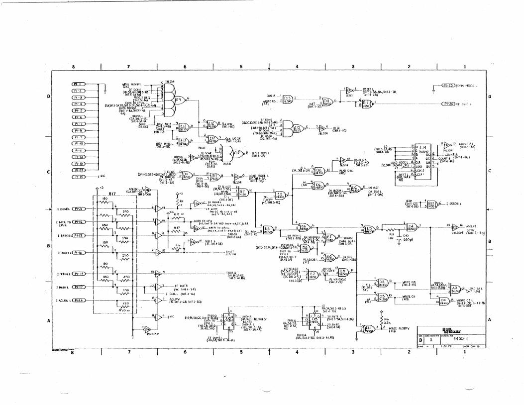
8 7
D
c
B
fDftTAl CEID I .~ ..
- I l.....iW-jl lACLOWl~---- ~1
I Nlo~ J L_._ . ________ ._
A
~
• ..... "'="""8 7
6 5 4 3 2
QltJI4 __ l.' I~Rt5t.T rzWEc>-~~ __ --E~- [om (5'iln:~~l6A,Sijll-l~, ~!"'A MODll
INIT 4 DII ~ - 12 " ('Ho'5Ci 1415 -- '--'-. -:fBi7/\, II I.-~~ ------- ------~IF Il.IlT l
IF OO~ll Z (;W::lC\,,"~tII>lIlr.OAlA\ --.
(,"I.I·l'UilT<~Vf-~' (5Al1~I~~lo\'iA)-~
lrOA.TA --(~6.'HT.I-1A)
L~,inmYl
~!-ill51 ) ,~---.~ (5Hf.I-1C 1illa~
.J;(;o. 'l1l1 ~·,28)
(31IH8,l1111-~~'_C,lIjl'O~51 (~~Ir.~h<l .. r.~-!Ji)
'"~DII~l~,l'19D1.L OMA '1 14 - - - ~ - (~'r:"t'£l" RlQ. -- l1LW4 !lilT.
""3-" rosLECr~
[1I~r&wp~D ,lL m'lD8l
A.I~-e "I '"'- 0 tN\tcr (3A)_~~ O.lTA~)
f~ l1t.'H" 0
'.1.-1'4 (IB,S" ;>8\ I 101 It _
f " (lB"J/.;!tiBll> """ ell -. (5ijl.l-:l6)
- . N~'%}~~~ (SHU. SHt.4·f>6)
1~IFDONf.L II( £ ,.,O.51t.SHT .. ·JIl ... ..,
'j:--~ - -----If",~~~~ 11) !>HT:t-~8 ,\oCC.ji 15 ue SteT- 't- }II, ...... J
~--~....MftJ,~;:~_.3A ,b) :i~H-IA.2'.lo.q) "/ o.lirA To chi L -_ .. . f5
R,7 £J ,,,6!. !.o.4.SUJ.l· 3"'." 8./:i1l , !Ill RDf:\~~ VVv'--1 0"':"'---- (~~~~!l.C) ('HTH l-l!~r.'r-~Dt (:i:~s~~C~~~';O'
lH14'BII) J~~!Q......5t!lj;r l ) MA5TtRL_~ [ 17'" {lC'''' .. U. 'l~ ~UHBl41Ill.H<oe.lIIrl.l.' DC, ._.
;.. ______ . "<I" . " r-:~ ~o - ""l! ---- ----- -- (OD.l0) (~.rt;,~U-
_' __ If DATA l"( 5HJI-ll1\
-- I DATA L- (SUT. <I-IA)
L.ACl.O'W (lC.SHT.I-c;.e.5t1U-)O)
6
TRRlQ (IA,4A~A.I<.C. S~r.l-4A,4~1
5 4
'''--,'
3
NXM 4~ (~n~o;-r--' BI1 " llRROR l SIIr.4·'~) L.1 '4 0
~!I 12._A~:lI:.Rr -- ~:lYN
1<L~04 r~fIT.4· 10J
._~II 13 .,Il O~ ~I~k~ 2 3 All It ii't5 1-rSH1BAl ~. 6tJ M ~7.""?~)L
i4C.5HT.:a.- ----' -- -- 514L'1 JHTI ~') -----'~' D5 10. _IIRITtC' '~e. WRiTE C' L
.AI 0 14L - T-- (10\ IO,~ (ShII-ZO,SHtZ-1B (4CI --. SHr;"B)
~JR" L I 3,3~ l Ell 3 Z ?" -rt"{f FlOPPY
D ':If.1~ iSitlU G.Of"
2
'~'
D
c
1 .... -
B
A
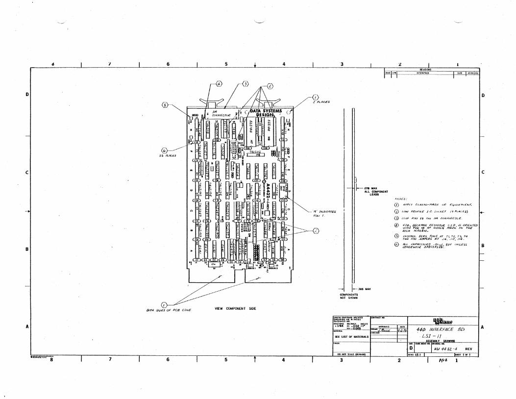
·.~.
d "/ 6 5 4
o ·5
3a FUJeES
c
B
BoTH SIpES fY Pea £D4E. VIEW COMPONENT SIDE
A
s..w="'S 7 6 5 4
<:j) 2 PLAcES
'3
I .018 MAX r-- ALL COMPONENT LEADS
'11' lAi/JiCIJTES
PJAJ /.
t.-.3B5 MAl(
COWf'ONEHTS NOT SHOWN
IUNlUSOltllRlWSl5Pf:Clf'l[D tllllltldlOHSAIIllttlNCttfS rouR.UM:tSAfll:
f'!'1~~ ~~~2~lS .1".l0 -". ".
SEE LIST Of MATERIALS
00 NOr SCALE DRAWING
3
~ REVISIONS
AI07cS:
ill fil'PL'f EL~STO-I'1IM~ Oli! £6JU.J~/kli.ur..
@ LOW P.eo~/LE J.C. ,:jv(.l::£T (9 PL<'9~E.sJ
G> CLfP Pill 23 OI.J 3M t!OA/A..JECTc./!.
@ ~~~J' ~'fu.t:'7:' R~€t';kO: ~llk'.IJAJ a~/:/ED .$ILJt Sl!I!.EEAl ..
® IAJST4LL 8EIi!r!' P~AJS AT TI; Tl, T~, T4 TWO PJAJ . ...JUNPEeS 1fT J4, ~1I2J J14.
@ ~!iE~~~JT~~~ci~~1-t~ 5pY IJAJI.€SS
~ .." 44¢J JIJT£RFACE BD
. LSI /1 L.ll!! ""' ...
AS! 44 aZ-4 REV
ISC.t./UI:I IsttUllfl1l·
2 ~ ..
o
c
1..-
B
A

~·"':r="""-ii· 7 6
5
Pfll/l (CJfMt~TE {!.hT l. 4 ~J (!>Hr ... ?Ii)
5 f 4
----~ -~-~~....- ----
3 2 , ___ ~",Ri"VISIONS
'loof9---- "f$C~ii;11ON -~~"-~~F~w
q,,~~-4<Wo LS]- 1/ IF.

o
c
--+1
B
8 7 6 5 4 3
l.££i"il"fE::]K)
1511 -- ---~"""----l --LL I~j
- "'~' '.111.. 1Hr..1I t1f£ '-~~1~. ",f. 'J/)Ilr ... ,. .. Ci'o...--l "1 -::- ,\,15 "., ~:n ~--, I" (d) ","'" -" ", ~. a,ET ,. eoy ~
PI-Ii[) IMTpL FVV~(. , "I
~ 1"/)0I0J5l t~1 J 4 (fi",--!/{' r ! ,] I ~,I~~--~
') : 1* ~. __ ]{: MI" (5e.)(~Hl!,(Pfi) \~lJ :/,; -/ ,/:.-.11 pYlt- L "-~:lJ!JiU,j ""0; p~c--;:: in
~.'.. ("""I-""'U (,' h'ETL 1'1611-"'''''' " :., ",II, """, ,,,,, ", I. ;:'::--,' ,,<, 'T '''J
I'''',-'J- h ~~G"e , (:'IrTI,.J<V
1NU ¢ - 1 J. JAJJT 74L~¢f-"j _1 /. ;t .. '~ ~~) I
E"'''''. bfl,J.JJ, J," .'" , II'? ~~) "~" Q c ~l '1'}~, hW"''' : II 'i;::" "M " L ~4'" ' .. 112. {DJ e[)'1 ----'. " , AI';; (t>Hll "JI){!>t).<~,IJf~.:..A) • ,;:~ ,- E."~", ' ' ' ', 1Do -, I
t·~ (:A~, H) - --.....1 I, ," _ • ~(U!w CfEJD-1~
(UTI ltUoe k it. l 9 , I
1", I Bi fl>-j1L.l no I , ~NJ"T (,,)
~. 6 I':-riTl.5P) _ . r:JLu/'r"-" ~I oH ..:'t:5/;.T_.b " ]JIU~ 1" i:.AJL.. - JF DOME L .--ot.r----------- ~ J<I- :::€ (UI) -;-.;/j 1'1
CEJjJ--.LTi'£f:1!¥ L- 1 r I) i 9 ," dJ tc£"~ f '~p .,,',,>' PI-If, , [ !p~ L
~ tj,;,-,~-;
d~'
~JICL.DWL , "<1,, .. 1
r",:;,.,,~ "TI~.l5 5 ~ '. I ° c~~. ""~"'- '0-c~ ~? HI. I. " 8<. a'o 0l',c'
'" D) ~l 1-;. ,*~';'f3,;.,: -' " . l!",f u "'4. __
~
CfEDG'ED-~
CtED-(fEfV--
C!!ElDCl'EJD-CK1D CZEJD--
tfroL (!;>JITJ.?A)
' '" , l ~-' 3.3.::.
2" " [5 " ,,~
'" U {>IN" (:; .. !J.I):,) ruNI/
-J) 12. bll} 1;JNI4J Ht~~~~~~1 ~, ~ J./cJ.. l.ilo/9 +~ 1----:t~I"_I,) 21 7 LA (,1.."l) 4.5.;. '8
"' ,'~ , 4- ~.. 1'" ',"" L~=:l=tif=tt+==tt====t+-"~;I ~""'>? f;'
:~:'~'~::~;:~ ~;:'''''''~ ,I ' .2~ illJ I" •.• l D,U4 ===1I,P b r'
~~" II IIf~~ E3 "~L",} ;-1 L.N,' (~l,-IC) u2-1I5 J'/4- IN
/il» i(C$£fl.-
,~~~ 1 !}~f['\-'=i-ro"
r'''''' I I I I ' '.-" i'iJ",OI57 II I~,,-r/~'0'(~')"-
• f~ j', ..• -. ----"~'Ill (~11"") l~i~ -"J-j" -1--t---~t - t~" '" o-JL----------L------ ,,1/ ~,. .1 I?:: 1 Jll ll _~~
"/1)
c~ 71zlI
Co DI1~---------I----------. c
4lA,5
~E,_ 2.:-0-1 (:'lin,,'i)
II/ r':;,"-''') .511j
(.!,.,T!-iI'J~iI5
( ,;.1':-",-'11
) ~t7-:It: J)t>~lE
(41)J
£1ftJIi-I-I!~II •
( .. ,,,) ,. ___ ?lrJ)l..
~
;--HJS,] --,.,~ ~-J
~'~I? !li-II VI711 /t- ,_'PilL /' 7413 _._1.i:!L~
rsn)
',,',.'.') N'if>1 '1'".25 i/~K
A 1('iiCj'5V)"'ADr"""L-C=,)[~' '~'''-,'' 'Fl0 - _j¥-t; ROUJ j~,)P .. ?,- Q-I-'W t-
(J~I) L1 _ .3 (aD)
}~lr[;I:'R/Jpr yEtm.f. JUI'H'(;i:!::.
J",IJf'[:t. -,;:: _u"/(. ¢ D8 3-3,t:Jl
[
'V
'I (!.L.:..eJ
IdO r~'.l' c 1.1-~s;
(~r:....J[-) (5t1i'i4B)
3"/<"'> '
~,'l 115 4> Jc<:=C,Jt:.h.JL pnj;~ L4_2~>r- .. --.----------......:
1jIt:'ir'''::~':.:I''~Uj:'''"8· 7 6 f 4 3 2
o
c
'.-
B
A
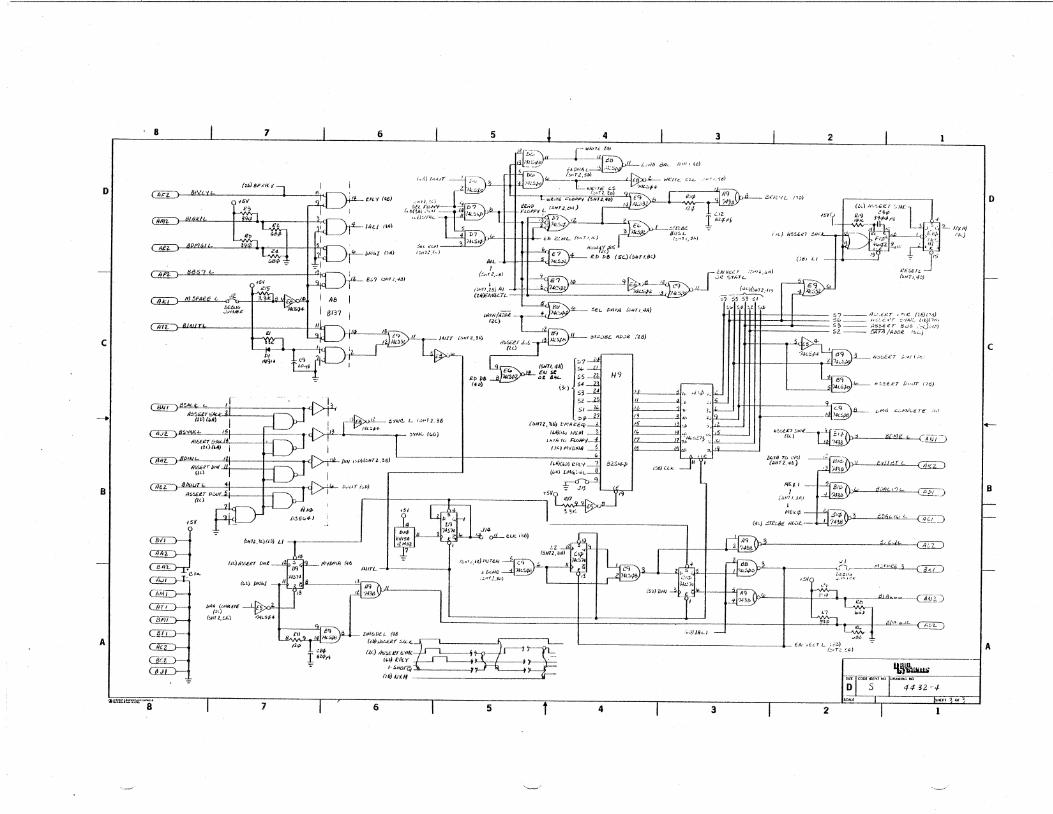
D
c
--'i
B
A
· 8
BAJI ,"'- ,r' A5SELr __ _
121»(",)
OJ'
, ..
~" '2 8A1... '-C.la.
JI
QHD-/JI'lR (tHROe
Ill) (flHfZ,:H;)
"·""="'"""'"8'
7
7
6 5
(~Tdtl}A,J (Z4'JEhVU .. TL
4
~El.. bliTA (':''''1'/.411)
JAOT 1:!;".rl.J .... ) ~r,z.:,t8~ ~b,)2 tZ.d)
il.D D6 r_A) I
··'---"ll (!JiJl.4A) .;-LL g~ ~L !OS II
(:I,) ~4 S~
SZ _-121 S/--1f,~.-ll
(:JN1l.U) PftUIi!,;~---1
(LlbM"J ""'Ai-..2. J..hTIoT() F«IN't-z
O'JI"l'lDM4 ~
H9
82':!.Iq..p
<t
" I.
'OJ I , ___ , JI~
I..L o!L- 4!u.: (?6J
pM60l3.t.. (rJ6 ~ L--,- 1l1."""'~r"~,,~ ~Lt: ll<-)~~r/;:''': ~_. ."
J .. .sk'or~ --I flD)AJt.H _____ _
6 5 f 4
'-'
3
3
2
e~'n.'IL. ('D)
ffrrr- I! =lll ~2 === ~:"L~2r . ;~";.~I'{~,);;~. 5>-_ r-I::>~,eer f;UI:> /:><.:.) • .J.'>J 52--· - ~/IJNJJ!. I!:...:..j
1/111 4~L I .~~ .J.,M~ c.;;.fI1it .. E.Te' .'}, I
1t!.'::.E.£1PMi'--r--i.j'"E~j HN1P l r~ (l4) l-ll:f.~~-
J:J.1A n. c.'PtJ (~HrZ.4f,)
HE.'J,.I I
{:>111I. lJl)
I MEk,¢!
~3 3 ___________________ ~,~.~<·~~~~~
~3 ,I u'Cr ~~fL,'_;.:
/').'Jm!.fi, ~~U
If.~ D 4432 -01
2 1
D
c
1.-
B
A
Ofj
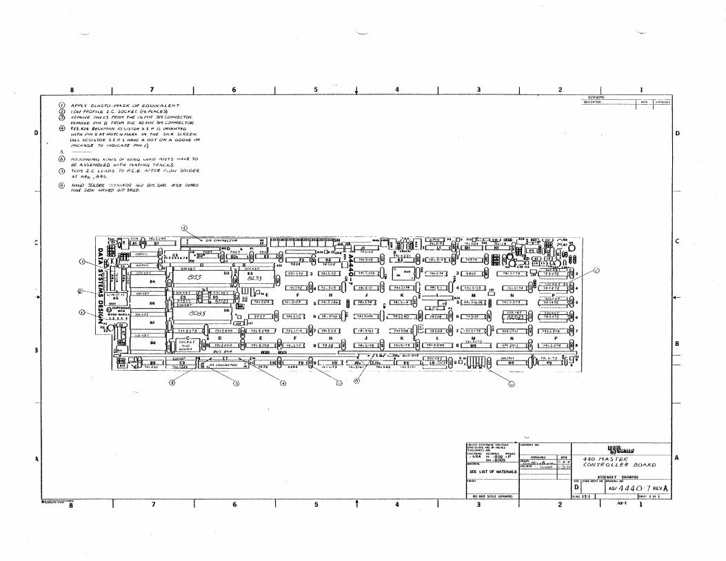
D
:
3
"
8 7
(D APPLY ELA,5TO-M-"ISt< OR EQUIVALENT.
® '-OW PROFILE. Le. 50CKEr. (Ib PtAC.S5) ® A'EMovE PIN 23 FROM TJ..JE t:b PIN 3/1 CONNE'TDA',
A,'EI"OvE PIN II FRoM THE 50 PIN 3M CDNNEC.TDR.
@ R13,RZ4 BECKMAN KE~15TON s.r p. I~ ,*IEt.J'TED
5,
'\11TH PIN 8 AT NOTCH HItRt< IIV Tn/! !jILl( SCREEN.
(ALL ~E5/ST01: ST.P. '.J HAVe A DOT OR A 600vE UN
.Ao\(""J\Qe TO IIIIO/CATif PIN I.)
@ IW.)OINIIVl, kL)W!:i OF BtfR4 L/OLO pv.5T5 HAVE TO
dE A!1SEI"I8LED WITH MATINlj TRAC.KS.
ill TKII1 J.C Lt:AO.5 To P.C.8. ArTci~ r~Ohl SOLDeR
AT A-4CL ,A4b.
® JIA"JD :AJLD£R '':'~.C.ILLIlTDi! I1A/JJ &5 BIIil5 nFliR, "bcIII:VS IIl1r£ 8aAl '''/I~/£l) .<W[) oo£D.
~-... '
6 5 4 3 2
=~~~~J;~;;~~~;~;;:~=-~=~1"1T''''Ui;Ff·;f~ -- -'~~8~"-: l-i::;-;~:(.4,~JG~~J~~C;!~i!if3~·.J·-~B C61 -X::O~;--... .., E J' '---\!j, • 'L_JJ::::l • O!C::::n::::Hi:::::3 r;;,-, fl! -
Q 7403"'. 7".'J~ Q ~.1I(]G J 745HZ K 4. L.fJ.....l..,.. Elfie 1i!1~ ~&c::::::lD CiiCl5t~@ C·~;::3®2P""'U8~L!~@.~~ :: .. " ')nlD
;~~~~~t}:i~~~==~~H~i~=~ au 9.J34 14S0Z 0... Cl~ ~. ;1 '~J [m::~:E:13 1'14<5 JZ ! 9 ~~(1 r IN .... JOB. "''''j l C1ED@ ,.."73! ~15ITfrg~
•• ® Icl 0" Icl 0 0 QI ~~fn1 ~~4174'-S;)'( ~rJ~ ~ 4~ul ~~1:70g1:J4 F H J K ®£~~L au M 0 N --sDl~§..-®
_.__ all f"?8!DLJ S'"/4tS':SL( ~ t NLS1"] Q'i"D;l.tJ ~5rj·it.51if'ID8 I 7~t.5Z7" (:N!4~~5 ... c~nIG" U g CI.!/N PS ij .--------!:!,[email protected]())U QIcl Q ~<o'" T Icl ~ rot ~ ~":lt4~ Go o:r::u:::1t:1 U:~LS.:>n fiI74-~()(J(Lr : .. ..1!lSu)93 I ".4SZ~I!J~lJ 6~eJ I ~ 1~~e6 z"r;ws 81@:f]JU n~ .... ')00 7oH.5373 74I.S~"4 (~[I J7~4<[l.[!z!J"Dl I2!L!>II~:l@71 741.504'( r/ii:'5Tt:'i"] :--:;;HOd"]n§~@ 1 jl41.S174 (O~ ~;=--"J@ L7fL~.37T:J81 ~ __ ...--.C_. 0 E F H J K ~ L ¥,o.:J N P
~81 14tH40 <91 14L5Z99 <®~ 80TIF:]@ ~@ ~@Q!L5~ 81 H~8 (Li,,!:2!Ll@ 1=p?'IT?C1@a 8uS aA~ I'rJT1, '---,--.-nGJ"".--':WO_ "u" ... ,,"
@ ~ Q
, --:- -,-- --- - I ,o<~"M.;l1cl • N~.Q """',' ~o!:rl' lJ§,:;:lf_'''~~/51 (r-lD-_~p,~90. - ell H9 < G ---- -- ---------------- ----------------------- -- - - --_.. ----
'6
if:t=\f~is.£-~~F tRActiONS «tIMAn .. 1/64 u. .D. •
.,. .. .. u ... ~D
...-~-~ H[CMO t..~J'·79.
SE~ LIST OF MATERtALS
liii~iiit"-
00 NOr SCALE PR~WINil
... 1;:::,:;. ... • .. .IIr' ... i 1 6 5 t 4 3 2
"-
REVISIONS
~~=F-';"=f"'O;W
o
c
.-
B
\~~ 44D MASTER IA CDNTRDLLER aDAFID
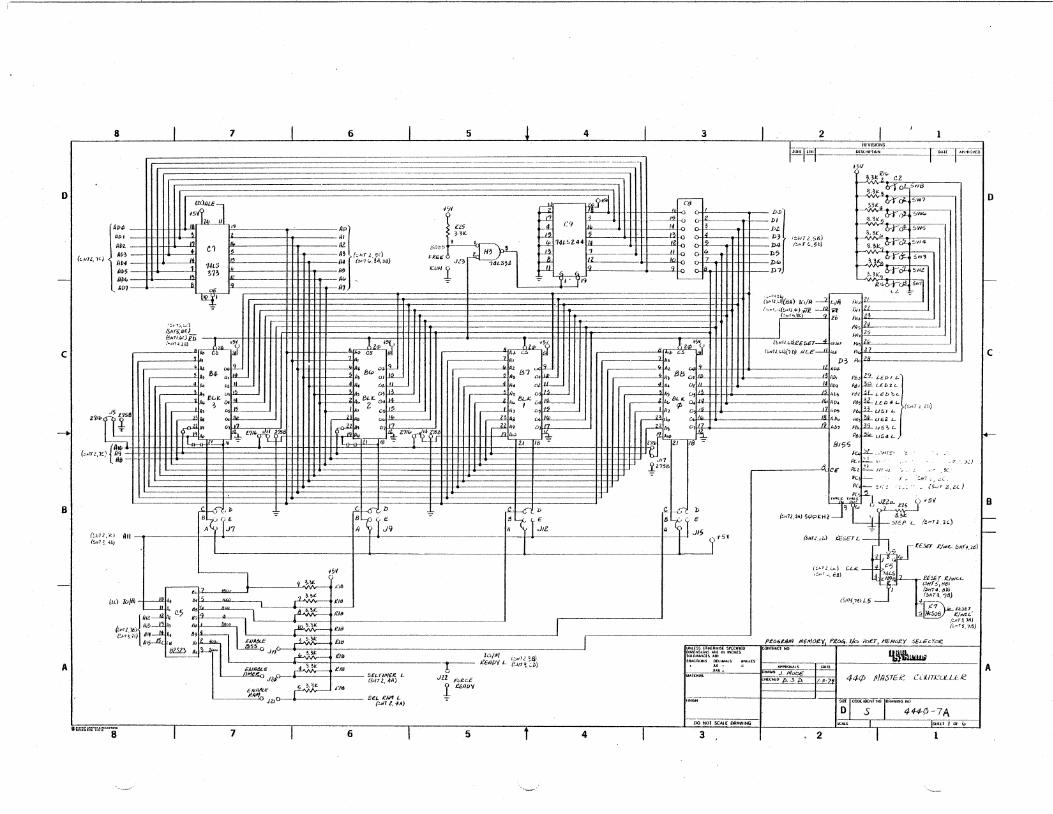
c
BI
Al
I
8 7 6 5 4 3 2
----
___ ---, RfVISIOOS
~~' ___ ~_' ____ f'~II~~I'MVro
3.\<. b1 oI-.~"'8
~l. r;:-,;--"8 '''-o;r~5W1 rl ~I ~ ~
f-c! " L....._ -. - - -----12.f-o 1>, ~,~< _ cYr.~ ,,'
r! -:----+-. +---"'f-o I ])"'1- 5W~ ~ f-~ (I ~ - '3 ])Z- . ~.3< 1rYcJt.. SwS
HI ~ 12.0 o-L- _ll' '::'l-iT':: , ';18) ~_ I: III At I OO&,p A' H3 • - ~ 14tSZ44 ~ ::" 1>4 (.,ro .• ,) B~"~-o2, SW4
e, ,:
, A~JI""Tl"') "EE~ t ~ -:':------ 1>7 h-r"'- 0""1 114 (.!>f'1r...'Ji I 3-S) JZ?; 74LS,l f----W 12 ID 7 Dt.:I ~ - '. --.
• A§ ~U"l :-u~ q D7 tpoL's;;;z I" "" __ ;,'K'l '1. ' "" ' ,',q '--- "'''&-r,cP-. SWII
"", _ R1 .,_,,, _,---- > '."'" I ~ • ~ (~'t.(..t(tjA) J[)/A ~ ['-'Iii! f}j.J.
" > {::,,.'-·~n ... ,l,4c.J..iiiZ --..12 Wl )'NJ III . (!.uy .... \kl 6 hu. 3
,.:.~·T;.t.,l I !'Ii 14 I$J,IT~Sc:) . ~ 25 (~1I.'C) iii _ A PlJ4
('"".'" ...!""- "9 ~'\'. k ";<' U~y {'·" .•• U.ET~ m" .. , ,,, --l -----11 ib cS ,,~cs ~ A~ CS 1.':(. .,. GS ~ (:;,m,I.t.){-H.'Y HLE-11 t.t£ p,.n
I I I' AI D~ Fh ~ -1 IlL CIjI,L 11& blp 04>~ 1. 87 • .4~ , Al. . Illi~
114 ()l~tL- 14 D"~ Ii. otU- A4 at .4D~ Pd,""&"U&-1.i..
-----1A~u. UlL- , O~~ 14, o~ "-> Utl/~ 54"~. l~l2L("'E!J?t..
, •• 84- .. lL- A. oli1<L.. '0 0.1_ ,131:10/1"" " ... ""~UD/~)
---1~. ~~ "'___ ----1 ... ~"o.fa- ----1'.Bj"""f--- ,------t .BLl 0., 'P. ,...~LEP.'- (: • .-r,,") J5 ~Al CII"'5 ....---J..41 o!j!J5 :-------lltl .:::.;II§ ,---1Al I/~ i.~ ,~lius, L. •
t.'I'" t'P.i8 ~Jlj w ~" (.J1oI1~ ~Aa a ~Illt ~ I . .4A.. 1f;I'~.Ul52L D!-r 1-",-" ... ", Iro-U .. o"Z,., 0 1'7 Wi" 0,'/1 19.'7 ""12.",,,-19~ ,~l'll"~l III! ~ ~Z.?I(,rrbl4~8 ~n.I,;) ':a- "A.~ rt" P61~U.s"L
{n.. 1·1 L"..:.;:' ,.'" I L Il",<>- I 18 "" I L I II I.":' ''''' ,I 18 "" BI'3? . (;»ITZ.,,) M - n:r.~, ,...,.,('£'
IifJ - 0111. R:'E-- ". ,·7 . J':')
i.1.?58 CE Jtl.f.i- II~ ·.L ',,,,~ .' .I(
t!.Jl1l,-/(j (5U1~ -lz;)
nil
.. Itt) lo/iil
- ""'I-- I _ .~H7 '. ?, Pc~ ~/:! ~~." _ (5HTZ.U)
. "'·U. r.:1if ·1 J2Z(L () .; 5>/
- b-c l> c'-Ci b ~ t~l5 ~
J7
q ~.l<
?I.~t:
§ ~,~~ tN~Muf
~J2I
r:tf1~9 , :!JrEP L /.!rl1l,U) 1;11 ~tE /I> 19: 1- e (!.m,4I1j ?~ph-li! l. ''-3
'A JIZ 4 JI, -:-I I I . I j .5' (.m .•• ) .<E;Er L
-t-L t£.5ET J?/we. #Hft,U.{)
.51
",8
"" ilia
tl'
£/a
. £/-
LIB
..:~/H
Jj6LTINEi! t-(.!.JllZ,411)
SEL t:Nf L. (~;J7 /,4")
r---JZ2 F()i!cE l UhD¥
101M I·,::.,OZ ~41 aliDY L (!JIT~':;'b)
UNLESS OTll£RmSl 'SI'iOrliil DJM(N5IUNSIIllfIhINCtlE5 lOfUWlCn ARt: fllllCfKJttS IIlt:lW.U
::,,: lioiiffliiAL
{:.~J2,u...) CLk.. ,:;'1~,12!)
Iij'('
Pj
'4'-' :.tt""GjI
(lIff'''''L5 :ti
USEr ~/Wc..L (M15,dl" (!»IT4, lib) (~JtT?, ?dJ
J,2--'7 - 74tSt)B
££SE7 t:/W~L'
(~rj 1AJ (:'~15,7d)
Pt.06UM miftJO~V. PL.04. J/o ~r. H6/o,t£Y SELt:~To.e F"lIiAClND
1--;""'IOVIIL5
~.J.ttl()Jt£ ClIlD JJ_~ 1), I/,S'7'
II.~ 44tJ> rrIllME£. C(~/T;':ULLL.e
~~~ 1=-=4~~~~OOI~A~.".'U~"----------· 444-(1-7 A
00 NOI SCAlf DRAWlOO llitlt:ff IOf c.
·'''''··°''''8 7 6 5 4 3 , 2
".-" c~' ' .. _-
p
c
1-
B
A
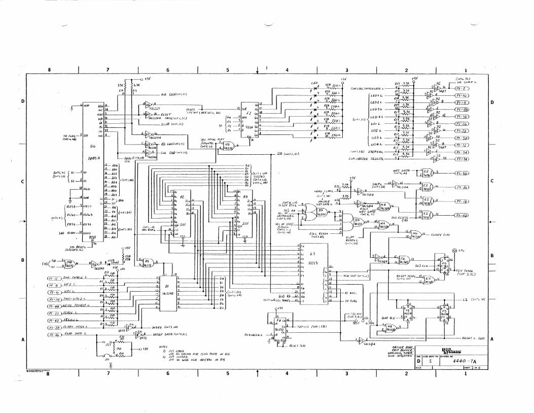
o
c
,-"
B
A
8
,r-"i""'p
7Z F/..IJ4----2I5JD (~JJrl,.M)
($Ii15,,1l) {\('I I 'il (s,Il'.'5")
'I!. l n
DO.
B~85~
'~~
7 6 5 4 3
---0 t5V J»V
~;t
'" /0
~.3~
", 3
~·-re~--~ '_ ",,£ (zA)(o"".,,) l,EP <'0
; I :;;' ' ,. ~,_",,, __ 142_-.2 l2$><-
" _, ~,,~ " I",,~ ,~jj : "r~eE5ET""i"""B)("-;;-;-;') ,.- 14 ct£ Q LL--JJ== f ft~ 244- (4AJ(:~I/T/,:u..) Ii 13 f:Z 4I~.&_~---1 r---- ,",-,~
Io/M r~ilTI.~L) t'.:p ~ V,IfIJ Q4~"-- f 4 il8 .. ~ f~-")C 1 7''''!l.ill
LAD4; 11L-- (WI
14LSl44
iP (4Il)/:JIII,ll)
CLK. (ltV i"lj{ I.U)
':if.. ,}z 8 4' ( { £28 I), _1 9334 GL; -- -~~~ (j, I I as
:3lL_tJI
:'JY£ ItA~r , yf (0) ,r- __ 8~,~-'-/L1~H15l-G~ 14- ~ j ~B acn.
10"",,,) 113 "~ ___ 'r 14'53 T
~/';'I-i7I,U)
"'"',,") l~ --RD. RD,
I7fjJ
'" n. A'J 1/.<I lkol
1 ~ 1/", ~ l/C,l 12
Jf, 1/....1.- ~ 1fc,1 1M 4-
5£L J;: SfA1/'_t+ ____ _ 1'51{[ I ~,.;) ~Ui~:;L
:SEt..iIUI1L (~1,!. ;;")
~ ~~
2
+5V '?3,t
(:."JI.U)
U5~L ____ 2?*-~~~----, fl1 3.3.t:
• '~H 11, l e) ::J rEP 1 AI L ------I:-f~
(~I/7I.LB)SlDE 5E.LEaL~-"---~
wn tJiJrR -r-Y£2ILL-----<1:~w (::'1,15,/11) Ll.f~~v-'
{l()1~r~;SL J/5V -----'--:~: £3 -~r TP~ i.£D9 ~~ ~vJ -':1;"
(i<J<5¢~. '''rr·.'Lij.fu"Ml Z '" 82" (G,ellc" ".,t, 51 -....i.~l4l.b H'I +5V ~ ~~ ___ t"i- 'L.. '2D'I TiNOL
01 Cf:.S£7 n:'AP! 13 tli!> (SliT 3 5C) ~/~",·,"·,)j)/~~ ~l L \L--J.U-U-l-Il.t=::-lJ,J);.'lil,t------+i-----L l (;'7r...{J/'1''''!~LL-1
. -1>1 -~. "ljT~4 vP t. 1," In.
(El::fi.:J IVPI L - ~J((~:;~:~~ (fE~~,J-' fwo-::'IDi L ____ ~ (::.;.,;.;" /;1)
~44~ WYJ1E ?I~OI :r l. _ D7
~fEIIDi L
(~·~"K~a~~~~~---_,-~~---~
@~~......E!NK L 'iL'('~Ji':' (~tI' ~ZB)
Cf!E7Z;) i'tM MTH L /!.lrl<l,':lA)C! t. L
J/6
¥ ""''''·''''':;'''''8' 7
) +5'1 JJOlt"; i) JrIOP€.M
JliJ 1/5 SJ/(-'~lJ.J ~ue 15,)11- PUPS IAI £15 i:) J2? cwSEb
jft> TO ~AJD ~-oe IbDj390 IAI 1115
6 5 i 4
I1I1::.r£K. .!lP85,
KAM 8I./F~~. __ IJW~ .... iNG Ni:I 'tlljrcH/)oc,./j~IK.€' fSiIITCOO[I~[J[' '" 444-0 -7 A MK "JT~ S , __
o ' ___ , '511£0'2 Of 6
3 2
o
c
<1-
B
A
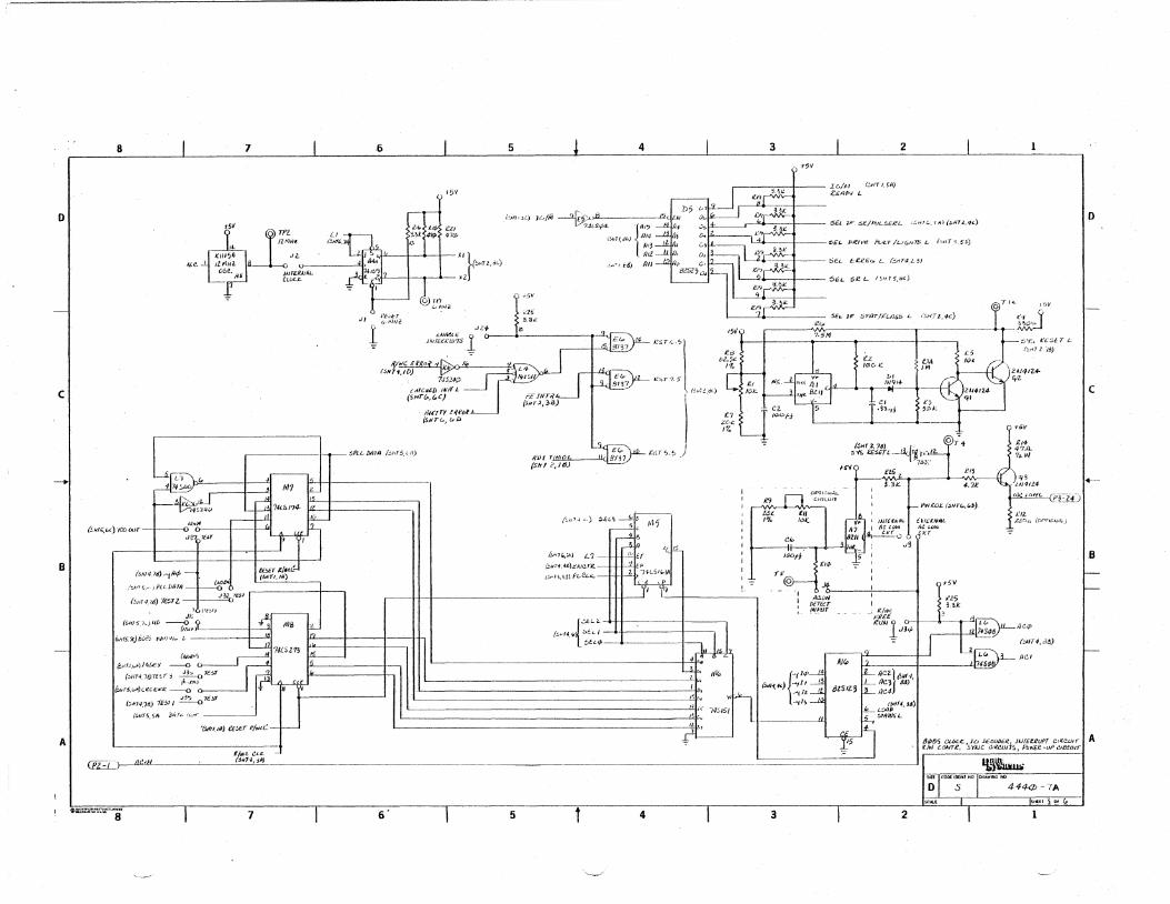
o
c
-"I
B
A
8 7
JI
6
·1-5V
J!.ll 47",
5
(~n'~.:.)
-Xl} . ~~~ W I u
n:~>cr l " ,,'''' I ,5v
"-2'5
OJMIF. J::':'.,. /,3':'
_H.1rE~·ic.~UI"TS J 0-----------'
Ji/~~----4:~4 (!'JNT'I,ID) - - -~ -- ~/I.JJ<;'ll
7.J51'" -=!J" L "TCIi~/:l 1/tIITL, FE INri:
(Sfir{p,{,C) (:;IIO,3d)
;JiI,arr !ilA.'o~'" {Slt'Tt.., (gil
,--_____ ~~SPLL/)IlJlj ('='145.(·fl) Ror TJJ::1.Qb (ShI2,JtJJ
(!,N'G",(,CJ '100 our --1--------0 U(1~ J~?~ 7E:.T
("HN7dJ-~M ~~' ,Mot.
/~1'7 £, •• ) PLLvIJiIl ------0 J3Z leo!
(_~fl14,)t:I) nS71. -.~
1 ('f'..') , J~;
I""",,!,," ~,:L-I ":1 1118 (~Hf5.?c)i,)!lj rJf.!jiN" L ~-- ' , ,
7415113 (JJo£r/\ ~
(f-li1!.l.;i,)1~{;ex ----0 ~ J';:.. "c!iT (';'I!T.J.7fj7t~Tj ~'{i J--:cr
" (1' .. I.-fl,) j. I (.:. ... f5 ..... II)c:.eCe.o:'e --0 ~
.)3':;. 7e.l1 (:.1t74.11j) ,(;£,11 --0 ,
(!.1I1"5 SA ~r~" "1'''- ---
'(51111, (II) ee,cT .e/wM.:'
lillie CUr:" 0---:-j- ") t/{~J).I (~HH,flA)
"·""~""""·8· 7
-~~~~
6' 5
(~'11., ~.) ,:lH'J
f.!,H7"i~) L '7 ~
l:;."r~,f.tl)£AJC.J.e.
15"I~.~j\ fd2LI<.-
{
C'<LI.'
(!."t4,1,(· :>t.L I
t,t.up
1
"--.-/'
4
,,15
4
3 2
'5" ~ ~" I Ic.,//I/ (,,:JIT I. 511)
R..GAD'I L
.~I--- ::5£~ IF" .::.e./PuL5€,eL ,'~/Or... ~A) (~~ll.,4-d o
-1')1/ -
i:;, bl..5.t:
,.:y"
[~J";" <7
L.C'i:. 1%
:;,EL PK:JY<2. fLeT/LlG,f.'J!i. L /,.,lIr"','5ll)
,,~_, I :::iEl. E:,ce£.~ L (:,,,r4j._!J)
!·1 :S~L 5.e L (9J75,~(J
1'9
lOf I~o
i.E/- JF'
~"'
(;", , ]e) "f)r-1 :;,Y5, fE'5ETL -!kll r~~ '1tl5 1'0 £/, 'VV\ --v\/'v--
3 3~ 4.7£ DPI"::OJ..\L :
I pwlOJ::. (':'Hrt,. ,"pJ
I 'it" ; /AI{EKJ,JAL tlltKNJlL
fl? I A~ lol'l/ lie ww 8ZI/ ,:vro .tkf
"3 C~
Ir)°l'i
.n -I /kJ£.iJrJ I fJETEcr I !~PVT
:::. '(~~ KC St r L
(.;;,-11 liE)
£/4 47.11. ~l-W
)L~!W~ ul!·j{, .... t.
Kit
rE?D
Ut;.~ (crTiclo,;j~)
4<'P
(:»lr4.3~)
Ai"-"-~rz:c::\3 pel
~-~". JE!~
8ZS lZ3 {"I1<P
f::.HJf.f(.) .... ,11 13 ..... jh .,1,
c
'.---
B
___ . '-frL] 8¢85 CLc.a: .. ,1"o )J£COIJE:R., J{}fEUuPT (!!IlCW, I A £./W c.CJM1£, 5YAjC dlee.wn, fb'lv'f~ -uP CI£i!lJIT
44+<1; -iA
SttUl3~-
3 2
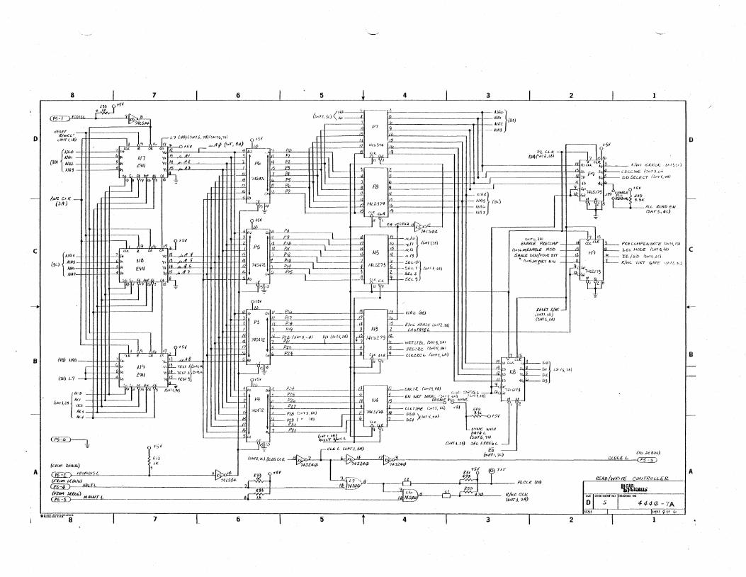
DI
c
-I
B
A
8 7 6 5 4 3 2
~ AJ/J4.} I~ JE:, la.)
'" , -AIM
<"'--' (f.HTl,5<.) J.j,_--.::!. -I
P7 eEser
.etwce 4'!lHrl,I~) 1. 1 r-L"1 (d6)(5H/!5.7d)f":'H7&..7I1) ,r"
~ ~ OE'" I,., $ +,., ~lIf p_r,8.) .' -" ",>~,. ~ I ~HV 1,5
-HI 7 1J r~ Ai.,
(lP) Aiaz
lAVa. I r- Il.; •. 'I PdJ ~l.l.4:_ iJq PL eLK. )J7 'il':!- ~ ,QJ '1, P 1/ 0 I IVI)('>II1!.ZIl) ~ eu:.'''' 191, VlL'i ~Z I-fp I/~ :~ L lOeo:. ,,,,fL--- !../Vi/( t:::K.K6A:. ,:OJ,'l:;r)
ST' U ~ rij I" -1""4" P5 Ilb -f-4 ~ - _I "D ,,,12- CD SELECT (~"" ... I
• /M9 ...,.,,] -----1 I., p;' .. _~.--- z.. .. .. ,lr. pq lc"l4------cec.c.WE (;'h7~,,:..,;
I4J I I'i U ~ -=- -t-"' f., ------!L 4)) 4 b, . I-a fL-.:~ ~J. f8 . __ -.J q "', t ..
'2. P? 13 ... __ AJIJ4} ~~- 6.2 ?4LSI7, .)59 ~~ 1(4, . ...,
r,;p I ~ 14l.;J3'/4- I _ 'JJ/J~ Co ~lB or' ?i..L etiAD lEAl
6iJC. eLI(_
(3/1 ) 5 -E . f-- }.II}, (8) J.J iEAbiMt 3. '!I.t:
Eft ,-~~J±tt
_ld!
-:- Dl t..L~t ~~ IA JJ41 ~ (~Hr5.4l.) 151/ II I ~
~1L Pd r------ 1#£5$4-
ILL t--...u1J> l:.tln .. 3'-) f _ IH----. L ____ ~ ~1-~I1} (~oj133i!» VlnilE P€'ECf.;JtIP_~ ael:t..t p~E;Clmpl!Ai:;II'E(:'N15,11~1 P5 (4. ;~ I /tJ ~I-AIZ: (t.I<T4.U)EJ.JRBLE MOl) _~ 1-19 LE:L ,.'O/:JE I!HTfJ,'lll)
7 P/~ ~~ 5 i.Lr.'(d' 6/~ UIJ/F0v2BIT -Cll to> Irf./SD (:'h75.lf-)
I, t""mo't> " ~
'. ~ p( l ". JL..: -fJE.L.c:bl ·'/!'111"~!Jlf.T EAJ -i==il;:i _r_ ~L ~"JiT ~hTt;- f':';'I!..$._J 745474:1 PJ4 I4Cj27) &. c: _ '" I
.ioL---~E.Lt (~";f.,tl) Q
o PI L-... ___ I--l It- r- 5H , . ~~ 4/4l£n~ 1.tL~u...~I-W-l-+.j...ttti~
{M"~_ 7 .. "'-
(~) AIR.' .' " 'IJJ<. . Al"? DJ
~ eJl' {t-LL .1 Ir;~ ~ t~ 8=1' yo '~I-SE<' , Z 8
. _____ 1'5 I:> II I
. ~ .. ! ~
-1-1-1---,
(4f/J 1/118 -~-I-+-I-l--4
(7P) 1..1 ~"""H-t+l-''l
?~.j. L...hl; -::'7A7"LIS L
l'"(cP 25 -EM wiT lJ{{fAL /='J,1j"-I"\ !r;."'T\.ll.)
1;.Ir/~,i:6 I~~ (LeTJfIE I':'~::~: f',;'VM!. ~/8 At;,. PZ8 (.!,.H,61i) - PSIZl }'jfi, ~ ;Ii) ~t5V /k...I. Pl.' (" 7JJ) DSI .
P.
P. ~~~~i:L wllll
0~ (jN15,7M
Lt'£1~j':JHTJ.ltS) (~HT5.~II)
(" ~5 Iv (':'IfTs.U) ~L [.e.e~L -
~ eLk:. L (~Nfl.M) eD (Tu 1JtlJlJ6J ,~.......... ~ r~ i.~ r:....,~ (6H1I,?t..) CLOC.,t L ~ ~ j:::
If_ 1lE8"") II<. (~NTl,7LJ8(jB5at. ~ ~/~ 11~3 ~
"IS" . 74-S2.4¢ r 14S2.44 14Slt/4 ~51 t5'( 171. 0.-::'£) m",",sL ~5 "It, (FIlClM lJ£&i(.' ~~L ____ ~ ______________________ ___
(f_ bf&NO) ~AJTL a,.
tHo lJl ..... ...... lZ.~ READ!WKITE (!OAIreOLLEIi! .-0 --:-- - PLcu (ZD)
liN" aLl< Wlr~. ,1/)
'l.~
444(/;-7A ~
"""""""""'-8 7 6 5 f 4 3 2
/
D
c
,-B
A
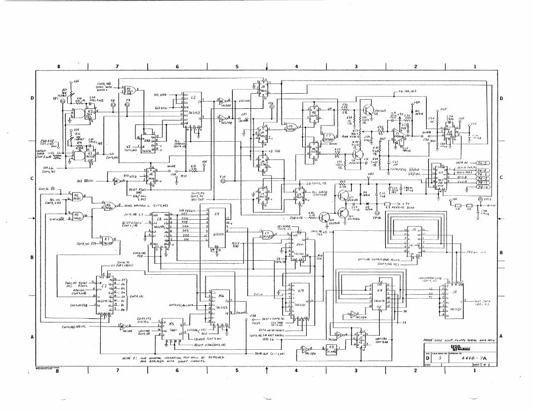
o
c,
-10-1
B
A
(·Mtk (fllP~, 7t)
{:;NT/,7£. fp
8
"''''''''''''''''"8
tol
(!Jm. JA) rEsET (X) t.J~(L
R/wu.t..(."ro,.A)
(!JI16,~IjJPza
(!JJIH,4a) Pif.ltL
7
7
o. D' V. °'1 DI J (!II14,US) D,
D,
1>'1
141f#
(51tH,'}!'!) at.Cl.l..L
a,,:we 1~111f.10)
6
A/D7£ I: ~ J(Ol!MtfL .:.>i'EeATICMiI PoT r>//t..L- BE K£MtJ"rIEb JW/J Jt.EIllAC£b WIT" ~HoKT e,1I::eUlTS.
6
5
5
4
"-'
3 2
o 'OF
{j.1!JF
c
~5'I o TI'J3
~ I L4 <5 ,'<,.. ", , I II r'O~1
pee~L ;~~) I B
r~E (Ul/PEJJ ;:"ITE (.~H' ~, ,~)
Hi ," rj~ r.
, I I' I 13
2
TI
I fJ~ , Dc
"I~-VJ~7J.w"'.1 (:JJor1 ~. z .. I ~
P'
3 PI ?4t-:j15f 4,..
PHIJ~E-LOl.e /.OOfJ, J:L(JI"P., f.EZlIJL .bIiTi9 PATJJ
lJ.~ 4-4ft!> - lA
l5ttrn~ Of'
1
"-
A
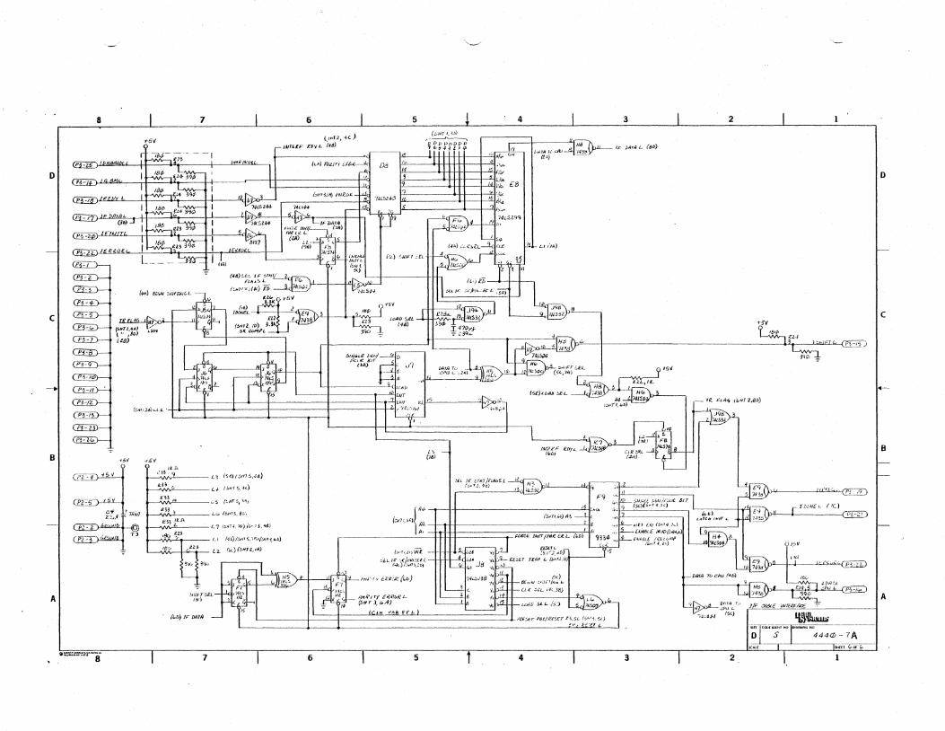
8
"'5~
o
c
-+1
~.
B ,>V r!i"
~e 3;:'.:F 2-2. "
Pl~ b -T3
A
• .. "' ..... ~.J!.·8·
.?nlK.:
'" !'Hia
2~3 3
.e~1 ~1l.
7
L3 (sa) (.YI151':'&)
Lf 1~lIr5 • .J.t.)
':"5 (~11T5, ~&1
L.:.:. (~ttH,er..·,
L11~H1-1.ijj)i~·1j."6)
LI 14b) (.!;J,f 'i:II',,)(.:JH~ uJ
L2. (GrL}(!JHTZ,IIIJ
!.JllfT51!.L (41)
(t..b) J,:' MTi3
7
6
llt1ll, o&C J lAiTELf:' LilY L (f.~
6
',~
5 4
14 r-,l;F 1~~~~!~~~t~;'Lj(> : 1< ft £8 1 ~.~
J J~ ~~
I< "/'~. I 74t.::'lQQ
I'J::..
{"'" (:3J<7{,3C) I/l
~,
L, (,6)
:£L 1~ !-TA1 jfLAuS L (.!;/.Tl, ;jot)
t:"""l<JWi:.~-'lB'" ::jE.Ll~:·(/MlL!UL . ';Z"J"
(-k.)I.5ln~."t» .'. ,. is
Pwl',iy E.R.E:.e. (4P)
!./~ I
K ~Aa FFI-
5 l 4
LI(M)
3
Jld~.l1 1~1'143i:1~ IF j.IIT4t... (lJb)
'~'
2
':""'Jf~"'FT'- <£ED ~"
(6C)L()~/1 :!£L
pI! H,h .9
"I'MIt (!;)In ",,) A3 ==:it
~~
3
_ Tt. ~Ll'1q .,1~7 2.db)
o 444.$ - 7A SHE£~-
2,
o
c
i"'-
B
A
D J1
'" I'J 14-n It /1 J~
Jifi
PSTAa. C' o<oa
B
A
PSI I PSJ",
8 7 6 5 4 3 2 R[VISIONS
loHIT~!-~F-==-~~I-;u;,'''I''IN-=-===-.:=-=i .-.~!f=-I·-~"u~~
~ 1~~9~ ____________________________________________ -, '84-/7' ~?L-__________________________________________ -,
84=i9' ~ I ~ A, ~n~ ________________________________ -. (16 -17' ?Sf-I9 '4 ~ ~~L-________________________ ~
,9 O.diV'
_ r-J I 'n 18 .(8.N3) - A. II~
JIll! (7A) .,.51/ I ~ +5V -'4SZ441
"I'::>- r' ~ I. ~?48'1 ~ --'1A~_1 z I 9,5v ~"'74IS7 I., ".""~~07-}
"'1452"'" 'J4,~4<t> Ii/2 L----12~. MY' "A, Bli _ 111ff ..,,~ 0"" (1C)
{07 -" B. C4 'DOl' .,' L ·.P '" ~ O~
(Zc.) O~ --1 " 148i1 w .. ., 1,2 I. ",., .0: : ;. •• "~ 04 . _____ _ .... _ _ D~--: "Al>DE£«' M 2'( !liN' lXJj .... 2f) C....... ~=MJ
~a~/JI;:"",..,'1 6,. A J 04---" a, &1. rb Z' l'( Jl /)JoI ~, L· ID , 84-/fD)
.v.:;._, ?4:J~4~ ~.. i, •• 134 z a 115 ,,<iI·p,JiL.:-----------------------------(B4-J8) , A, 1/4 .1,. '1"~J W'" I 84,?!l!.;
,--____ 1-____ --' iiI. ~ 'i1 " -;- :J 4. 12 '5~ ':...c - --::- rrz - -
'---~I t 8 :.;~t 15 ." '" ~~ iflj,'i >----Ii! , ~t~ m ~ ~zp ,. ..
I a. ~z Sf't ~ oe L.1' I!I ~14t1rI iJf. , spa (1J/:i!kE7C .uCifli$: ~ I!EO 11m J '-I .u.sn.~ I. 6i!.DiUUb PINS 1119 CAJ
,---k U ~ Bl. 87 7 .... ') 2 4f'; (I\'l)
U b /. m ~ ~ z_ ,UCJrE AloA/-.::..l~AJPIJ~L'; ruw€J{ ~ fEft" L ! ~ r.u'IJ'~ IIAJb" .:;,eQtlAJ£l
a 11 ..:.2. ~ a,." ... rhtl "AI 14613 4v/) 14')5 eNd's.
":" - :t5V - ,. Cit C4-t:!? A.ee .Ol-«.j, CZ)<!
~~'i ~ II<> w, I~ 95V
I 15 I~ ----\ , 1489 J2. . <jl+5V L-+------~r;';ii,'~ ~ ~ n. ""'" 1475 .. I':'- O~J
r- jd2, I ,74151 . 15 C? "'<N I JL. 02 ('ls) '{D~ ~rs;-C4 16 MIlt ''1 4> fI"~ Lb~l;1....- - _. -..!t 9P 14rL- 01
~"5' ~ (Z8) ot~, 1483 I~" ,,~ _______ ..lJ ... ",,:_~ 1 I. 1,'LOt/> t U& k -16'1 OI---.:t .l: NbbE.e~, II ,;". .z:i f,!) Z 4> IfIl 83=74)
~~.-~ 0g>-1Js. £l ,j t.... :111,. " ~ H-n. I ~ ~ ",..' . C4 L D5 J.. ..t83=i8i
~ ~D?4I2.{)j '''' D4 "t,• W'. ," ~ ~, (~~-r-"C '", t'" b" I" 12 lIJ3-3 ~ • D'o,I ....... · • ('83':t} • L ,,,I:: I • , c", ,.5' - "
83 2. I~ KEfL_ "~ 5<" _3 l~ S -." 4 II(. I "Ill nl!>"------+-------------+-·
~ 5t!H6M~Tt<! .ilRA'WJAJ6
Ii? At;
7i5 R4
(PIJJSJ ('hA/fl.)
3 HJ!E "~J
ii3 iiZ 1ii 1fij;
l r.l1#S..v 14324$
4 '4Sl4tJJ u,..ns OllIlU;tIS{ Sf'[ClhfD COfTOlRACT NO
----- ,5 'I. -~, .3 SI f':f::.~~~'t.~'<fS 'L~ '1Lt:Jt..K .(/w) /I. .,SI '\Itb ""?4 fRM:TIOhS (lU:IM~$ ANlillS ____ . __ ----.--_~ ____ ~-----===:::..-. ('7iiFJ') B,-I74~j --'--Jj ' ____ :: •. _ c ~N ~:; -h~j5 ~ ""TUlIA!. -- ~~'.'t1Ii1F1£tD(t:'»=1
ilL"JJocF.';J • ~ I--. .:...----t--~/lJ "t. /lZ I ~ IINlMi-------- _. !-5i .[s
i-.;.,,_-~I-~-
14Sl'I<fJ
00 NOT SCAll DRAWING
'="""""8' 7 6 5 4 3 2
-,-,'
D
c
:<1-
B
A

8 7
o
" r-\------· I I
I I I
cl I I 1 I I I I I I I I fowEt S.Uf'PL'f i L ________ .--.l
J
v B I ,- , v·-
r
tJ~ '\ .#' <'\.. \ t, C
I I I I
6 I Z.A> Vt>A.- I
7 II g a
J !
; ,~ ~v
I A I P
\)... II) Ik-t.
13 11 0 I 'lt11'J:"':~~"l~IW-<""""
B 7
6
/1/
Ac.. I-UJE
6 5 4
D~D 449q
Po'NE-~ l;lo;.li:!I[!,UTI(JW OOA~[)
Ac ~-tl'· ..... /ll~~<'tb~ ... ~ h.,/.,{o:
2 , RfIJISIONS
'1'~9· ____ ol~'!.'!IO_" _____ -=:'l-o;..li·=r";:f'PIIU"Ul
t.JOTE:;
[Q AS/III¢
II] A';/illi
[I] AS; II ",--z-[±] AS/III~-IZ-4' F0e'.. IlqlV
Ao/III,- Z441 FOg ZAqN
W AS./1114-8r:p'l'-CP R:>5! 511-J~LE: '.:itDED DglVE
A¥ 11\4 - 8'}¢ -cp FOe. l::lC.L.iliu::. !SIDED DelVE
~ Ao/II14-81fl¢-1
Ab/'H4 - B')41- I
Ii] AVIlI,
IT] "/1111" - '1-
~ ~ G]
@
r!TI EJ
A~/III~ -I
AS/III?
A~/1I18
A~/III" -2
AS/II'l.!J-
USED ONLY ON
/"
a-J ol;"-i--V(s
FO~ f:.IW':':'LE Sll'..E.D t.i:.IVE
~oe DOue.w=. SIDED bl".,'JE
DSD4iO
It-:!.~
o
c
.-
B
~f~!~i~\~'~t ~fa~D \~~ ,~...cllOHli :t';'"-:' ~Il~n DSD "="'==---- A MAUIiIAl----- DI'j';,Te.,BuTIOI-,I :S,(STEM
IliiIiH
00 I';OT SC4lf I)fIAWING
3 2

)

SPECIFICATIONS
CP127 POWER SUPPLY
AC INPUT:
DC OUTPUT:
LINE REGULATION:
LOAD REGULATION:
OUTPUT RIPPLE:
OVER VOLTAGE PROTECTION:
TRANSIENT RESPONSE:
SHORT CIRCUIT AND OVERLOAD PROTECTI ON:
STABILITY:
TEMPERATURE RATING:
TEMP-COEFFICIENT:
EFFICIENCY:
100/ 120/ 220/ 240 VAC + 10% 47 - 63 Hz -
+5 VDC @ lOA OVP at 6.2 + .4 VDC +24 VDC @ 1. 7A -12 VDC @ .5A (at 115 VAC INPUT)
~ .05% for a 10% line change
~ .05% for a 50% load change
5 mv peak to peak maximum
Built-in on 5V output
30 ~s for a 50% load change
Automatic current limit / foldback
~ 5% for a 24-hour warm-up
OOC to 500C ambient at full load, derate linearly to 40% at 70°C
.!. .03% / °c maximum
Approximately 55% combined efficiency with a full load on all outputs at l15VAC line voltage

)
)
CP127 POWER SUPPLY TROUBLE SHOOTING GUIDE
SYMPTOM
UNlf OVER-HEATING
. / LOW OUTPUT VOLTAGE v WITH HIGH RIPPLE
HIGH OUTPUT VOLTAGE AND RIPPLE, POOR REGULATION
HIGH INPUT CURRENT BLOWS FUSE
*DENOTES 24V COMPONENTS
POSSIBLE PROBLEM
1. OUTPUT OVERLOAD
2. AC INPUT TOO HIGH
3. INADEQUATE VENTILATION
4. IMPROPER TRANSFORMER PRIMARY CONNECTION "f2 iI' t/
Y.·1. OUTPUT OVERLOADED
2. U1 FAULTY (U2)*
X 3. CR1, 3 or 4 OPEN (CRS, 6, 7)*
4. C1, 2, or 3 OPEN (C7, 6)*
5. Q1, 2 or 3 OPEN (QS, 5)*
x 6. R2 or R7 OPEN (R14)*
7. SCR1 SHORTED OR OVP TRIGGERED
1. Q1, 2 or 3 SHORTED (Q4 or QS)*
2. U1 FAULTY (U2)*
3. R1 OPEN (R13 or R16)*
1. IMPROPER INPUT VOLTAGE OR FREQUENCY
2. C1, C2 or C3 SHORTED (C7 or C6)*
3. CR1, CR3 or CR4 SHORTED (CRS, CR6, CR7)*
4. CR9 - 12 SHORTED
5. C9, 10 SHORTED

)
, '\;
l '
Q I u ~ CD I I ~ I 0(
I I r-
f-
a
)
• ... ~
I-'~3l:!Nn
(..) i ...
OVA 211-
~
,0 •
J ::ii CD
J .....
f'''f'' f-. w N
J: iQ
- h
(..) i (J) f
~ ~
I"- iL-
!
~ l! 'f-
ill !~ a. i (..)
~
r ~~
N r I-h r-
:~
~! -• Q ~
I ! i -;. r\
~~ r IIlfO "'';' N
'" ~~
/ - '3
-
~ i::.,. 'Y'lOO ~
l! i
1 ·,f 19l:!0
!~ § P
VIl:!.\.
i~ Q i ~
I.. <;9
'i
<;1:10 - II :K ! .
C'J i .t. ~§
! \l!!: ~ +I +I ~
110 Z
;g §~~~~i!
+ to
~ ~Ii! ~ ~ C'J
£11:1 01 1..0 n~~" ~ I S
IGl:! .zn
80 r I
1..1&
~
~~ - r1 911:1 --1£1
~j rOV1\vz+ Zl II ~ ----:
Sf-,-
(y. w1 . ~
-~
OVAvG+
I
170 - i
ot <;11:1 I ....
-<
901
-I ot
8l:!0 ,.:[J 1..1:10
T+
) - I OGl:I 1 I 61l:! r-o l -
Y'l00 '0 r-----, I~O"'AOZI -
In I I I
~l:!
It:._ -QZ
81:1 I I 1
:J.31:19<;+
I r !
I )... ---v £ on
£1:1 I ~O"'AOOI
I.. <; I I
Ji~ 17l:!
>-O"'''OZ~ to
- I ~'" i
---v<;
1..1:10
I7J ,.
L ___ .J -In
+ 9f----4
"tl:!O
rOVN;+ GO 10
U)
L£I
1 T+
r Z i U)
S<;+ ZI II 01
L, <;1:1
- ().Il:!~ , ~
OOA<;+
£0 :
GIl:! -<
f-
~ I
~.
Ill:! ... 6 I:! Zt) ,..
l 91:!
-OIl:! £Or+
lVi:!O
-
l' I I
£1:10
GIl I J'!" GIl
: I.
fi • Q I u i CD I 0(
7 6
!
8 7 6
---.
4
r_
~ ,,,"'~!4=] 8-32
02 DIA MTG HOLES _,/ I:! PLACES
4 PLACES __ __
FLUSH NUT FAR SIDE3
--=."~-' ~---~-'~-'
3
1100 -1
r= I , ----. I
..-- -! - =t.@-: 275 f I _ _ __ _ ___ '" 11:=-~~=-~-L'--=-C_ --------_ J _ 1'1 '" _ ___~_
- -- ~OMJ~k1:r~ ID[:T~~~~;=J PARTS LIST
5 4
4-

)
SHUGART DRIVE JUMPER CONFIGURATION FOR DSD 440
, AS SHIPPED FROM SHUGART
TRACE DESIGNATOR DESCRIPTION
T3,T4,TS,T6 Terminations for Multiplexed Inputs Tl Terminator for Drive Select T2 Spare Terminator for Radial Head Load DS 1,DS2;DS3,DS4 Drive Select Input Pins RR Radial Ready RI Radial Index and Sector
SHIPPED FROM SHUGART OPEN SHORT
Plugged Plugged
X X DS 1 is Plugged
X X
R,l,S, Ready, Index, Sector Alternate Output Pads X HL Stepper Power From Head Load Plugged DS Stepper Power From Drive Select X WP Inhibit Write When Write Protected X NP Allow Write When Write Protected X 8,16,32, 8, 16,32 Sectors (SA801 Only) 8 & 16 32 D Alternate Input"In Use X 2,4,6,8,10,12,14,16,18 Nine Alternate I/O Pins X DI,D2,D4,DDS Customer Installable Decode Drive Select Option X A,B,X Radial Head Load Plugged C Alternate Input.Head Load X Z In Use from Drive Select Plugged y In Use from HD LD X DC Alternate Output.Disk Change X
AS SHIPPED IN DSD 440
TRACE SHIPPED FROM DSD DESIGNATOR DESCRIPTION OPEN SHORT
T3,T4.TS,T6 Terminations for Multiplexed Inputs Note I Tl Terminator for Drive Select Note 1 12 Spare Terminator for Radial Head Load X DS I,DS2.DS3 ,DS4 Drive Select Input Pins X ' Note 2 RR Radial Ready X RI Radial Index and Sector X
Ile.R).S. Ready, Index. Sector Alternate Output Pads X HL Stepper Power From !-lead Load X DS Stepper Power From Drive Select Plugged WP Inhibit Write When Write Protected X NP Allow Write When Write Protected' X 8,16.32, 8, 16,32 Sectors (SA801 Only) 8& 16 32 D __ A1tet-natelnput·ln Use Note 3 2,4,6,8,10,12.14,16,18 Nine Alternate I/O Pins Note 3 Dl,D2,D4,DDS Customer Installable Decode Drive Select Option X A,B,X Radial Head Load
rC) Alternate Input.Head Load L In Use from Drive Select y In Use from HD LD DC Alternate Output~Disk Change
NOTE I: Last drive on daisy chain should have jumper n, T3, T4, TS and T6 installed.
, NOTE 2: One jumper installed according to physical drive number.
NOTE 3: Pin D is connected to Pin 16 on physical drive.9 and Pin 8 on physical drive 1.
'loX" A,B
~ 'It X\
\ Plugged
J Plugged
\ -(J{. IrJe'O(l.Il$i NOTE 4: Jumper L is open and 800 option is
shorted. '
KEY: X - Specified signal is either open or shorted, depending upon in which column the "X" appears.
Plugged - Specified signal has a pair of wire wrap pins which are shorted together.
s


i
CP127 PARTS LIST
REF •. DES." CP127 DESCRIPTIQN ,-
C1, 2 16,000/15 CAPAC ITOR ALUM ELEC
C3 100/16 " " " CS 470/16 'u " " C6, 11 47/50 II " II
C7 ' 2,100/50 " " " C9, to 470/35 " " I'
C4, 8 • .001/100 CAPACITOR MYLAR ~ILM
CR 1 R n1 A RECTIFIER 30A 100V TO -3 ,
CR2, 8 IN 752 A D lODE ZENER" 3{)OMW
CR3, 4, 7,,9-12 IN','4003 RECTIFIER ,lA 20DV
CRS, 6 MR 501 RECTIfI ER 3A 100V .. ) Ql-4 2N 3055 TRANSISTOR NPN POWER'
Q5 TIP 31 A TRANSISTOR NPN POWER
R1, 2, 6, 12,9 6.B RESISTOR ~CF 5%
R3 47 II " " " "
R4 2.2K " " II " R$, 14 750, " " " II
'RB 1.5K I. II II II
R10 ,11 3.9 II II II II
'R13, 21 1.1 K " \I II " R17. 330 II II II II
R18~ 19, 20. 10K II II " II
R7, 16 1500", POTENTIOMETER ZW WW
R15 .12: " RES I.~TOR ZW WW 1Q%
SCR 1 SQ?PBLS3 SCRBA 30V
Ul, 2 ,123C., I.C. VOLTAGE REGULATOR


Data Systems Design, Inc .• 3130 Coronado Drive. Santa Clara. CA 95051 • (408) 249-9353
Related Documents