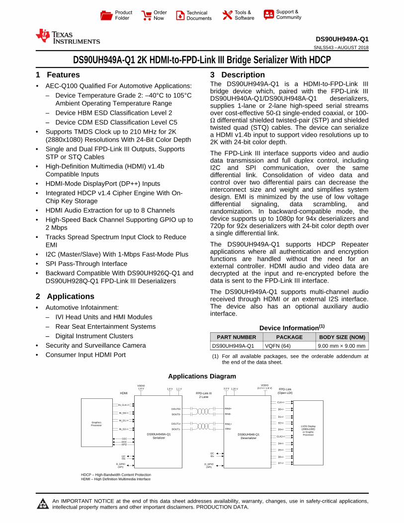
FPD-Link III 2 Lane VDDIO 1.8 V IDx DOUT0+ DOUT0- 1.1 V IN_CLK-/+ HDMI DDC CEC DOUT1+ DOUT1- RIN0+ RIN0- RIN1+ RIN1- CLK+/- CLK2+/- FPD-Link (Open LDI) D0+/- D1+/- D2+/- D3+/- D4+/- D5+/- D6+/- D7+/- DS90UH949A-Q1 Serializer DS90UH948-Q1 Deserializer IDx D_GPIO (SPI) D_GPIO (SPI) LVDS Display (2880x1080) or Graphic Processor Graphics Processor IN_D0-/+ IN_D1-/+ IN_D2-/+ I2C VDDIO (3.3 V / 1.8 V) 3.3 V I2C 1.25 V 1.8 V HDCP – High-Bandwidth Content Protection HDMI – High Definition Multimedia Interface HPD Product Folder Order Now Technical Documents Tools & Software Support & Community An IMPORTANT NOTICE at the end of this data sheet addresses availability, warranty, changes, use in safety-critical applications, intellectual property matters and other important disclaimers. PRODUCTION DATA. DS90UH949A-Q1 SNLS543 – AUGUST 2018 DS90UH949A-Q1 2K HDMI-to-FPD-Link III Bridge Serializer With HDCP 1 1 Features 1• AEC-Q100 Qualified For Automotive Applications: – Device Temperature Grade 2: –40°C to 105°C Ambient Operating Temperature Range – Device HBM ESD Classification Level 2 – Device CDM ESD Classification Level C5 • Supports TMDS Clock up to 210 MHz for 2K (2880x1080) Resolutions With 24-Bit Color Depth • Single and Dual FPD-Link III Outputs, Supports STP or STQ Cables • High-Definition Multimedia (HDMI) v1.4b Compatible Inputs • HDMI-Mode DisplayPort (DP++) Inputs • Integrated HDCP v1.4 Cipher Engine With On- Chip Key Storage • HDMI Audio Extraction for up to 8 Channels • High-Speed Back Channel Supporting GPIO up to 2 Mbps • Tracks Spread Spectrum Input Clock to Reduce EMI • I2C (Master/Slave) With 1-Mbps Fast-Mode Plus • SPI Pass-Through Interface • Backward Compatible With DS90UH926Q-Q1 and DS90UH928Q-Q1 FPD-Link III Deserializers 2 Applications • Automotive Infotainment: – IVI Head Units and HMI Modules – Rear Seat Entertainment Systems – Digital Instrument Clusters • Security and Surveillance Camera • Consumer Input HDMI Port 3 Description The DS90UH949A-Q1 is a HDMI-to-FPD-Link III bridge device which, paired with the FPD-Link III DS90UH940A-Q1/DS90UH948A-Q1 deserializers, supplies 1-lane or 2-lane high-speed serial streams over cost-effective 50-Ω single-ended coaxial, or 100- Ω differential shielded twisted-pair (STP) and shielded twisted quad (STQ) cables. The device can serialize a HDMI v1.4b input to support video resolutions up to 2K with 24-bit color depth. The FPD-Link III interface supports video and audio data transmission and full duplex control, including I2C and SPI communication, over the same differential link. Consolidation of video data and control over two differential pairs can decrease the interconnect size and weight and simplifies system design. EMI is minimized by the use of low voltage differential signaling, data scrambling, and randomization. In backward-compatible mode, the device supports up to 1080p for 94x deserializers and 720p for 92x deserializers with 24-bit color depth over a single differential link. The DS90UH949A-Q1 supports HDCP Repeater applications where all authentication and encryption functions are handled without the need for an external controller. HDMI audio and video data are decrypted at the input and re-encrypted before the data is sent to the FPD-Link III interface. The DS90UH949A-Q1 supports multi-channel audio received through HDMI or an external I2S interface. The device also has an optional auxiliary audio interface. Device Information (1) PART NUMBER PACKAGE BODY SIZE (NOM) DS90UH949A-Q1 VQFN (64) 9.00 mm × 9.00 mm (1) For all available packages, see the orderable addendum at the end of the data sheet. Applications Diagram

Welcome message from author
This document is posted to help you gain knowledge. Please leave a comment to let me know what you think about it! Share it to your friends and learn new things together.
Transcript
FPD-Link III2 Lane
VDDIO1.8 V
IDx
DOUT0+
DOUT0-
1.1 V
IN_CLK-/+
HDMI
DDCCEC
DOUT1+
DOUT1-
RIN0+
RIN0-
RIN1+
RIN1-
CLK+/-
CLK2+/-
FPD-Link(Open LDI)
D0+/-
D1+/-
D2+/-
D3+/-
D4+/-
D5+/-
D6+/-
D7+/-
DS90UH949A-Q1Serializer
DS90UH948-Q1Deserializer
IDx
D_GPIO (SPI)
D_GPIO(SPI)
LVDS Display(2880x1080) or Graphic Processor
Graphics Processor
IN_D0-/+
IN_D1-/+
IN_D2-/+
I2C
VDDIO(3.3 V / 1.8 V)3.3 V
I2C
1.25 V1.8 V
HDCP ± High-Bandwidth Content ProtectionHDMI ± High Definition Multimedia Interface
HPD
Product
Folder
Order
Now
Technical
Documents
Tools &
Software
Support &Community
An IMPORTANT NOTICE at the end of this data sheet addresses availability, warranty, changes, use in safety-critical applications,intellectual property matters and other important disclaimers. PRODUCTION DATA.
DS90UH949A-Q1SNLS543 –AUGUST 2018
DS90UH949A-Q1 2K HDMI-to-FPD-Link III Bridge Serializer With HDCP
1
1 Features1• AEC-Q100 Qualified For Automotive Applications:
– Device Temperature Grade 2: –40°C to 105°CAmbient Operating Temperature Range
– Device HBM ESD Classification Level 2– Device CDM ESD Classification Level C5
• Supports TMDS Clock up to 210 MHz for 2K(2880x1080) Resolutions With 24-Bit Color Depth
• Single and Dual FPD-Link III Outputs, SupportsSTP or STQ Cables
• High-Definition Multimedia (HDMI) v1.4bCompatible Inputs
• HDMI-Mode DisplayPort (DP++) Inputs• Integrated HDCP v1.4 Cipher Engine With On-
Chip Key Storage• HDMI Audio Extraction for up to 8 Channels• High-Speed Back Channel Supporting GPIO up to
2 Mbps• Tracks Spread Spectrum Input Clock to Reduce
EMI• I2C (Master/Slave) With 1-Mbps Fast-Mode Plus• SPI Pass-Through Interface• Backward Compatible With DS90UH926Q-Q1 and
DS90UH928Q-Q1 FPD-Link III Deserializers
2 Applications• Automotive Infotainment:
– IVI Head Units and HMI Modules– Rear Seat Entertainment Systems– Digital Instrument Clusters
• Security and Surveillance Camera• Consumer Input HDMI Port
3 DescriptionThe DS90UH949A-Q1 is a HDMI-to-FPD-Link IIIbridge device which, paired with the FPD-Link IIIDS90UH940A-Q1/DS90UH948A-Q1 deserializers,supplies 1-lane or 2-lane high-speed serial streamsover cost-effective 50-Ω single-ended coaxial, or 100-Ω differential shielded twisted-pair (STP) and shieldedtwisted quad (STQ) cables. The device can serializea HDMI v1.4b input to support video resolutions up to2K with 24-bit color depth.
The FPD-Link III interface supports video and audiodata transmission and full duplex control, includingI2C and SPI communication, over the samedifferential link. Consolidation of video data andcontrol over two differential pairs can decrease theinterconnect size and weight and simplifies systemdesign. EMI is minimized by the use of low voltagedifferential signaling, data scrambling, andrandomization. In backward-compatible mode, thedevice supports up to 1080p for 94x deserializers and720p for 92x deserializers with 24-bit color depth overa single differential link.
The DS90UH949A-Q1 supports HDCP Repeaterapplications where all authentication and encryptionfunctions are handled without the need for anexternal controller. HDMI audio and video data aredecrypted at the input and re-encrypted before thedata is sent to the FPD-Link III interface.
The DS90UH949A-Q1 supports multi-channel audioreceived through HDMI or an external I2S interface.The device also has an optional auxiliary audiointerface.
Device Information(1)
PART NUMBER PACKAGE BODY SIZE (NOM)DS90UH949A-Q1 VQFN (64) 9.00 mm × 9.00 mm
(1) For all available packages, see the orderable addendum atthe end of the data sheet.
Applications Diagram
2
DS90UH949A-Q1SNLS543 –AUGUST 2018 www.ti.com
Product Folder Links: DS90UH949A-Q1
Submit Documentation Feedback Copyright © 2018, Texas Instruments Incorporated
Table of Contents1 Features .................................................................. 12 Applications ........................................................... 13 Description ............................................................. 14 Revision History..................................................... 25 Pin Configuration and Functions ......................... 36 Specifications......................................................... 7
6.1 Absolute Maximum Ratings ..................................... 76.2 ESD Ratings ............................................................ 76.3 Recommended Operating Conditions....................... 76.4 Thermal Information .................................................. 86.5 DC Electrical Characteristics .................................... 86.6 AC Electrical Characteristics..................................... 96.7 DC and AC Serial Control Bus Characteristics....... 116.8 Recommended Timing for the Serial Control Bus .. 116.9 Timing Diagrams..................................................... 126.10 Typical Characteristics .......................................... 14
7 Detailed Description ............................................ 157.1 Overview ................................................................. 157.2 Functional Block Diagram ....................................... 157.3 Feature Description................................................. 16
7.4 Device Functional Modes........................................ 307.5 Programming........................................................... 337.6 Register Maps ......................................................... 37
8 Application and Implementation ........................ 728.1 Applications Information.......................................... 728.2 Typical Applications ................................................ 72
9 Power Supply Recommendations ...................... 789.1 Power Up Requirements and PDB Pin ................... 78
10 Layout................................................................... 8210.1 Layout Guidelines ................................................. 8210.2 Layout Example .................................................... 82
11 Device and Documentation Support ................. 8311.1 Documentation Support ....................................... 8311.2 Receiving Notification of Documentation Updates 8311.3 Community Resources.......................................... 8311.4 Trademarks ........................................................... 8311.5 Electrostatic Discharge Caution............................ 8311.6 Glossary ................................................................ 83
12 Mechanical, Packaging, and OrderableInformation ........................................................... 83
4 Revision HistoryNOTE: Page numbers for previous revisions may differ from page numbers in the current version.
DATE REVISION NOTESAugust 2018 * Initial release
VDD18
VD
DIO
SD
IN /
GP
IO0
RE
S0
IN_D0-
VTERM
IN_D0+
VDDHA11
IN_D1-
IN_D1+
SC
L
VDDHS11
VDD18
RES2
PDB
VD
DA
11
D_G
PIO
0 / M
OS
I
DOUT0-
DOUT0+
MC
LK
VDDS11
DOUT1-
DOUT1+
IN_D2-
VDDHA11
CE
C
IN_D2+
VDD18
1 2 3 4 5 6 7 8 9 10 11 12 13 14 15 16
32
31
30
29
28
27
26
25
24
23
22
21
20
19
18
17
48 47 46 45 44 43 42 41 40 39 38 37 36 35 34 33
49
50
51
52
53
54
55
56
57
58
59
60
61
62
63
64
VDDHA11
I2S
_DC
/ G
PIO
2
I2S
_DD
/ G
PIO
3
VDDHA11
LFT
MODE_SEL0
IDx
RX
_5V
IN_CLK-
IN_CLK+
VD
DL1
1
X1
RE
M_I
NT
B
SC
LK /
I2C
SE
L
VD
DL1
1
RES1
VDDHS11
DD
C_S
DA
NC
1
DD
C_S
CL
NC
0
SD
A
INT
B
D_G
PIO
3 / S
S
D_G
PIO
2 / S
PLK
I2S
_WC
/ G
PIO
7_R
EG
I2S
_DB
/ G
PIO
5_R
EG
I2S
_CLK
/ G
PIO
8_R
EG
I2S
_DA
/ G
PIO
6_R
EG
D_G
PIO
1 / M
ISO
MODE_SEL1
NC2H
PD
SW
C /
GP
IO1
DS90UH949A-Q1
DAP = GND
VDDP11
VD
DIO
64 VQFNTop View
3
DS90UH949A-Q1www.ti.com SNLS543 –AUGUST 2018
Product Folder Links: DS90UH949A-Q1
Submit Documentation FeedbackCopyright © 2018, Texas Instruments Incorporated
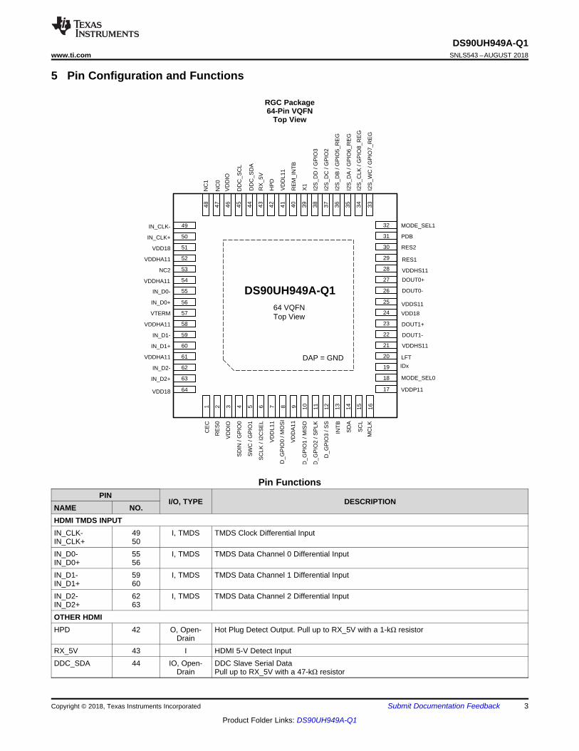
5 Pin Configuration and Functions
RGC Package64-Pin VQFN
Top View
Pin FunctionsPIN
I/O, TYPE DESCRIPTIONNAME NO.HDMI TMDS INPUTIN_CLK-IN_CLK+
4950
I, TMDS TMDS Clock Differential Input
IN_D0-IN_D0+
5556
I, TMDS TMDS Data Channel 0 Differential Input
IN_D1-IN_D1+
5960
I, TMDS TMDS Data Channel 1 Differential Input
IN_D2-IN_D2+
6263
I, TMDS TMDS Data Channel 2 Differential Input
OTHER HDMIHPD 42 O, Open-
DrainHot Plug Detect Output. Pull up to RX_5V with a 1-kΩ resistor
RX_5V 43 I HDMI 5-V Detect InputDDC_SDA 44 IO, Open-
DrainDDC Slave Serial DataPull up to RX_5V with a 47-kΩ resistor
4
DS90UH949A-Q1SNLS543 –AUGUST 2018 www.ti.com
Product Folder Links: DS90UH949A-Q1
Submit Documentation Feedback Copyright © 2018, Texas Instruments Incorporated
Pin Functions (continued)PIN
I/O, TYPE DESCRIPTIONNAME NO.DDC_SCL 45 I, Open-Drain DDC Slave Serial Clock
Pull up to RX_5V with a 47-kΩ resistorCEC 1 IO, Open-
DrainConsumer Electronic Control Channel Input/Output Interface.Pullup with a 27-kΩ resistor to 3.3 V
X1 39 I, LVCMOS Optional Oscillator Input: This pin is the optional reference clock for CEC. It must beconnected to a 25 MHz 0.1% (1000ppm), 45-55% duty cycle clock source at CMOS-level1.8 V. Leave it open if unused.
FPD-LINK III SERIALDOUT0- 26 O FPD-Link III Inverting Output 0
The output must be AC-coupled with a 0.1-μF capacitor for interfacing with 92x deserializersand 0.1-μF or 33-nF capacitor for 94x deserializers
DOUT0+ 27 O FPD-Link III True Output 0The output must be AC-coupled with a 0.1-µF capacitor for interfacing with 92x deserializersand 0.1-μF or 33-nF capacitor for 94x deserializers
DOUT1- 22 O FPD-Link III Inverting Output 1The output must be AC-coupled with a 0.1-µF capacitor for interfacing with 92x deserializersand 0.1-μF or 33-nF capacitor for 94x deserializers
DOUT1+ 23 O FPD-Link III True Output 1The output must be AC-coupled with a 0.1-µF capacitor for interfacing with 92x deserializersand 0.1-μF or 33-nF capacitor for 94x deserializers
LFT 20 Analog FPD-Link III Loop FilterConnect to a 10-nF capacitor to GND
CONTROLSDA 14 IO, Open-
DrainI2C Data Input / Output InterfaceOpen-drain. Must have an external pullup to resistor to 1.8 V or 3.3 V. See I2CSEL pin. DONOT FLOAT.Recommended pullup: 4.7 kΩ.
SCL 15 IO, Open-Drain
I2C Clock Input / Output InterfaceOpen-drain. Must have an external pullup resistor to 1.8 V or 3.3 V. See I2CSEL pin. DONOT FLOAT.Recommended pullup: 4.7 kΩ.
I2CSEL 6 I, LVCMOS I2C Voltage Level Strap OptionTie to VDDIO with a 10-kΩ resistor for 1.8-V I2C operation.Leave floating for 3.3-V I2C operation.This pin is read as an input at power up.
IDx 19 Analog I2C Serial Control Bus Device ID Address SelectMODE_SEL0 18 Analog Mode Select 0. See Table 6.MODE_SEL1 32 Analog Mode Select 1. See Table 6.PDB 31 I, LVCMOS Power-Down Mode Input PinINTB 13 O, Open-
DrainOpen-Drain. Remote interrupt. Active LOW.Pull up to VDDIO with a 4.7-kΩ resistor.
REM_INTB 40 O, Open-Drain
Remote interrupt. Mirrors status of INTB_IN from the deserializer.Note: External pull-up to 1.8 V required. Recommended pullup: 4.7 kΩ.INTB = H, Normal OperationINTB = L, Interrupt Request
SPI PINS (DUAL LINK MODE ONLY)MOSI 8 IO, LVCMOS SPI Master Out Slave In. Shared with D_GPIO0MISO 10 IO, LVCMOS SPI Master In Slave Out. Shared with D_GPIO1SPLK 11 IO, LVCMOS SPI Clock. Shared with D_GPIO2SS 12 IO, LVCMOS SPI Slave Select. Shared with D_GPIO3HIGH-SPEED (HS) BIDIRECTIONAL CONTROL CHANNEL GPIO PINS (DUAL LINK MODE ONLY)D_GPIO0 8 IO, LVCMOS HS GPIO0. Shared with MOSID_GPIO1 10 IO, LVCMOS HS GPIO1. Shared with MISOD_GPIO2 11 IO, LVCMOS HS GPIO2. Shared with SPLK
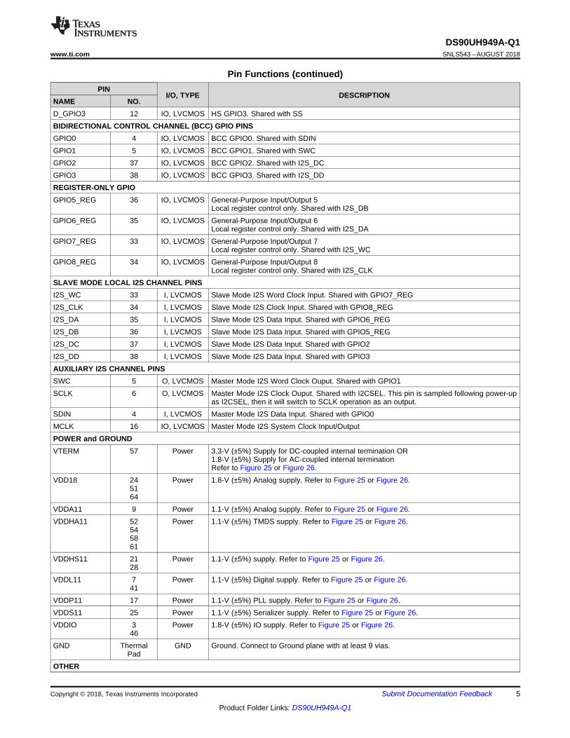
5
DS90UH949A-Q1www.ti.com SNLS543 –AUGUST 2018
Product Folder Links: DS90UH949A-Q1
Submit Documentation FeedbackCopyright © 2018, Texas Instruments Incorporated
Pin Functions (continued)PIN
I/O, TYPE DESCRIPTIONNAME NO.D_GPIO3 12 IO, LVCMOS HS GPIO3. Shared with SSBIDIRECTIONAL CONTROL CHANNEL (BCC) GPIO PINSGPIO0 4 IO, LVCMOS BCC GPIO0. Shared with SDINGPIO1 5 IO, LVCMOS BCC GPIO1. Shared with SWCGPIO2 37 IO, LVCMOS BCC GPIO2. Shared with I2S_DCGPIO3 38 IO, LVCMOS BCC GPIO3. Shared with I2S_DDREGISTER-ONLY GPIOGPIO5_REG 36 IO, LVCMOS General-Purpose Input/Output 5
Local register control only. Shared with I2S_DBGPIO6_REG 35 IO, LVCMOS General-Purpose Input/Output 6
Local register control only. Shared with I2S_DAGPIO7_REG 33 IO, LVCMOS General-Purpose Input/Output 7
Local register control only. Shared with I2S_WCGPIO8_REG 34 IO, LVCMOS General-Purpose Input/Output 8
Local register control only. Shared with I2S_CLKSLAVE MODE LOCAL I2S CHANNEL PINSI2S_WC 33 I, LVCMOS Slave Mode I2S Word Clock Input. Shared with GPIO7_REGI2S_CLK 34 I, LVCMOS Slave Mode I2S Clock Input. Shared with GPIO8_REGI2S_DA 35 I, LVCMOS Slave Mode I2S Data Input. Shared with GPIO6_REGI2S_DB 36 I, LVCMOS Slave Mode I2S Data Input. Shared with GPIO5_REGI2S_DC 37 I, LVCMOS Slave Mode I2S Data Input. Shared with GPIO2I2S_DD 38 I, LVCMOS Slave Mode I2S Data Input. Shared with GPIO3AUXILIARY I2S CHANNEL PINSSWC 5 O, LVCMOS Master Mode I2S Word Clock Ouput. Shared with GPIO1SCLK 6 O, LVCMOS Master Mode I2S Clock Ouput. Shared with I2CSEL. This pin is sampled following power-up
as I2CSEL, then it will switch to SCLK operation as an output.SDIN 4 I, LVCMOS Master Mode I2S Data Input. Shared with GPIO0MCLK 16 IO, LVCMOS Master Mode I2S System Clock Input/OutputPOWER and GROUNDVTERM 57 Power 3.3-V (±5%) Supply for DC-coupled internal termination OR
1.8-V (±5%) Supply for AC-coupled internal terminationRefer to Figure 25 or Figure 26.
VDD18 245164
Power 1.8-V (±5%) Analog supply. Refer to Figure 25 or Figure 26.
VDDA11 9 Power 1.1-V (±5%) Analog supply. Refer to Figure 25 or Figure 26.VDDHA11 52
545861
Power 1.1-V (±5%) TMDS supply. Refer to Figure 25 or Figure 26.
VDDHS11 2128
Power 1.1-V (±5%) supply. Refer to Figure 25 or Figure 26.
VDDL11 741
Power 1.1-V (±5%) Digital supply. Refer to Figure 25 or Figure 26.
VDDP11 17 Power 1.1-V (±5%) PLL supply. Refer to Figure 25 or Figure 26.VDDS11 25 Power 1.1-V (±5%) Serializer supply. Refer to Figure 25 or Figure 26.VDDIO 3
46Power 1.8-V (±5%) IO supply. Refer to Figure 25 or Figure 26.
GND ThermalPad
GND Ground. Connect to Ground plane with at least 9 vias.
OTHER
6
DS90UH949A-Q1SNLS543 –AUGUST 2018 www.ti.com
Product Folder Links: DS90UH949A-Q1
Submit Documentation Feedback Copyright © 2018, Texas Instruments Incorporated
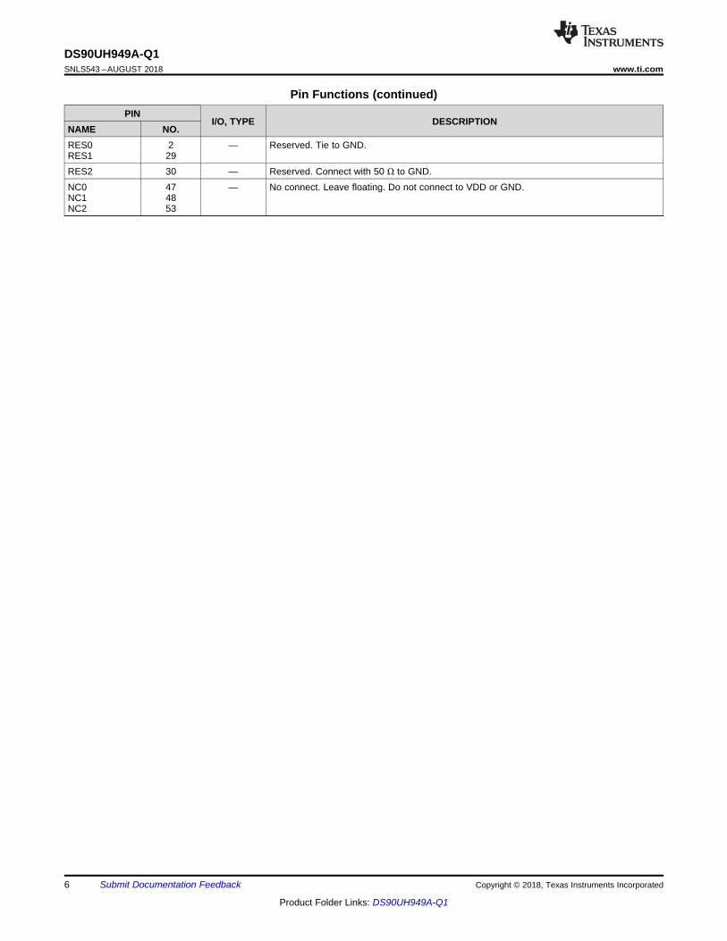
Pin Functions (continued)PIN
I/O, TYPE DESCRIPTIONNAME NO.RES0RES1
229
— Reserved. Tie to GND.
RES2 30 — Reserved. Connect with 50 Ω to GND.NC0NC1NC2
474853
— No connect. Leave floating. Do not connect to VDD or GND.
7
DS90UH949A-Q1www.ti.com SNLS543 –AUGUST 2018
Product Folder Links: DS90UH949A-Q1
Submit Documentation FeedbackCopyright © 2018, Texas Instruments Incorporated
(1) For soldering specifications, see product folder at www.ti.com and Absolute Maximum Ratings for Soldering (SNOA549).
6 Specifications
6.1 Absolute Maximum RatingsSee (1)
MIN MAX UNITVDD11 Supply voltage –0.3 1.7 VVDD18 Supply voltage –0.3 2.5 VVDDIO Supply voltage –0.3 2.5 V
OpenLDI inputs –0.3 2.75 VLVCMOS I/O voltage –0.3 VDDIO + 0.3 V1.8-V tolerant I/O –0.3 2.5 V3.3-V tolerant I/O –0.3 4 V5-V tolerant I/O –0.3 5.3 VFPD-Link III output voltage −0.3 1.7 VJunction temperature 150 °C
Tstg Storage temperature –65 150 °C
(1) AEC Q100-002 indicates that HBM stressing shall be in accordance with the ANSI/ESDA/JEDEC JS-001 specification.
6.2 ESD RatingsVALUE UNIT
V(ESD)Electrostaticdischarge
Human-body model (HBM), per AEC Q100-002 (1) ±2000
V
Charged-device model (CDM), per AEC Q100-011 ±750
(IEC 61000-4-2)RD = 330 Ω, CS = 150 pF
Air Discharge (Pins 22, 23, 26,and 27) ±15000
Contact Discharge (Pins 22, 23,26, and 27) ±8000
(ISO10605)RD = 330 Ω, CS = 150 pFRD = 2 kΩ, CS = 150 pF or 330 pF
Air Discharge (Pins 22, 23, 26,and 27) ±15000
Contact Discharge (Pins 22, 23,26, and 27) ±8000
(1) The input and output PLLs are calibrated at the ambient start up temperature (Ts) when the device is powered on or when reset usingthe PDB pin. The PLLs will stay locked up to the specified ending temperature.
6.3 Recommended Operating ConditionsOver operating free-air temperature range (unless otherwise noted)
MIN NOM MAX UNITVDD11 Supply voltage 1.045 1.1 1.155 VVDD18 Supply voltage 1.71 1.8 1.89 VVDDIO LVCMOS supply voltage 1.71 1.8 1.89 V
VDDI2C, 1.8-V operation 1.71 1.8 1.89 VVDDI2C, 3.3-V operation 3.135 3.3 3.465 VHDMI termination (VTERM), DC-coupled 3.135 3.3 3.465 VHDMI termination (VTERM), AC-coupled 1.71 1.8 1.89 V
TA Operating free air temperature –40 25 105 °C
TCLH1
Allowable ending ambient temperature for continuous PLL lockwhen ambient temperature is rising under following condition:-40C ≤ starting ambient temperature (Ts) < 0C. (1)
Ts 80 °C
TCLH2
Allowable ending ambient temperature for continuous PLL lockwhen ambient temperature is rising under following condition:0C ≤ starting ambient temperature (Ts) ≤ 105C. (1)
Ts 105 °C
8
DS90UH949A-Q1SNLS543 –AUGUST 2018 www.ti.com
Product Folder Links: DS90UH949A-Q1
Submit Documentation Feedback Copyright © 2018, Texas Instruments Incorporated
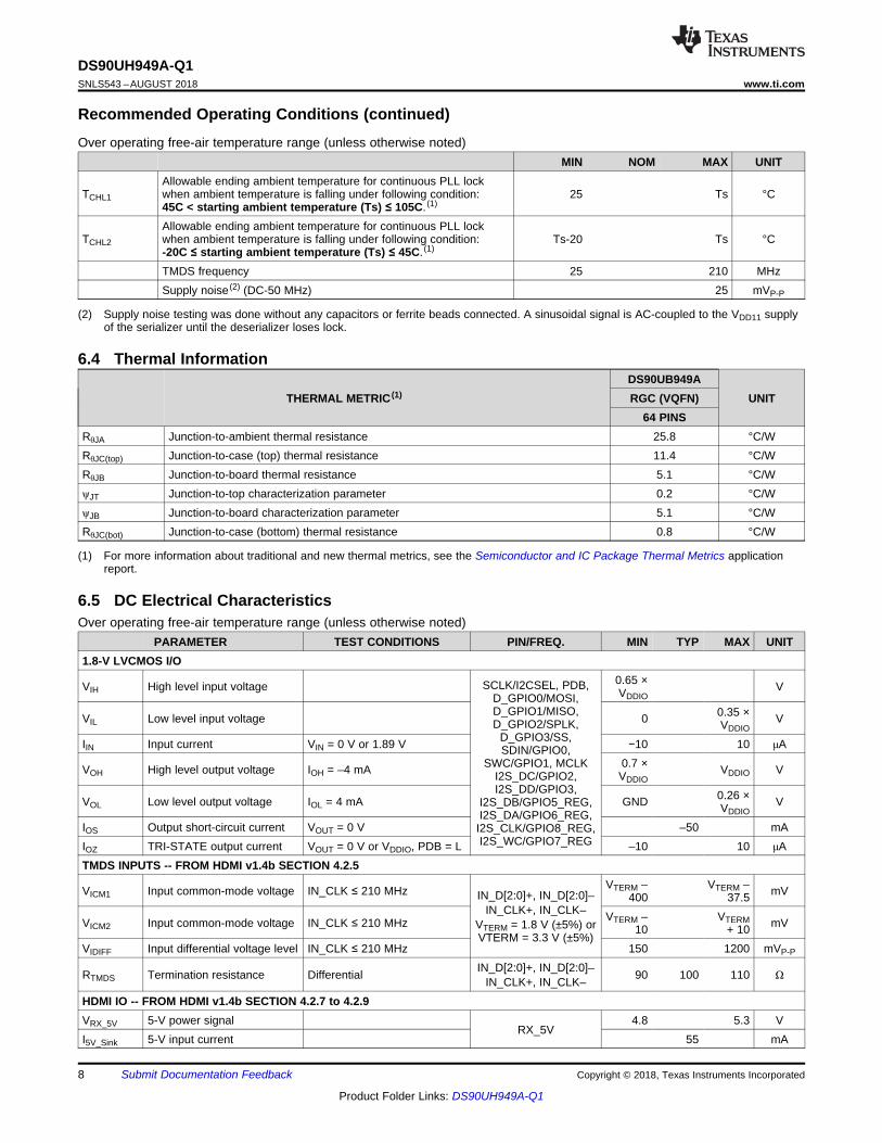
Recommended Operating Conditions (continued)Over operating free-air temperature range (unless otherwise noted)
MIN NOM MAX UNIT
(2) Supply noise testing was done without any capacitors or ferrite beads connected. A sinusoidal signal is AC-coupled to the VDD11 supplyof the serializer until the deserializer loses lock.
TCHL1
Allowable ending ambient temperature for continuous PLL lockwhen ambient temperature is falling under following condition:45C < starting ambient temperature (Ts) ≤ 105C. (1)
25 Ts °C
TCHL2
Allowable ending ambient temperature for continuous PLL lockwhen ambient temperature is falling under following condition:-20C ≤ starting ambient temperature (Ts) ≤ 45C. (1)
Ts-20 Ts °C
TMDS frequency 25 210 MHzSupply noise (2) (DC-50 MHz) 25 mVP-P
(1) For more information about traditional and new thermal metrics, see the Semiconductor and IC Package Thermal Metrics applicationreport.
6.4 Thermal Information
THERMAL METRIC (1)DS90UB949A
UNITRGC (VQFN)64 PINS
RθJA Junction-to-ambient thermal resistance 25.8 °C/WRθJC(top) Junction-to-case (top) thermal resistance 11.4 °C/WRθJB Junction-to-board thermal resistance 5.1 °C/WψJT Junction-to-top characterization parameter 0.2 °C/WψJB Junction-to-board characterization parameter 5.1 °C/WRθJC(bot) Junction-to-case (bottom) thermal resistance 0.8 °C/W
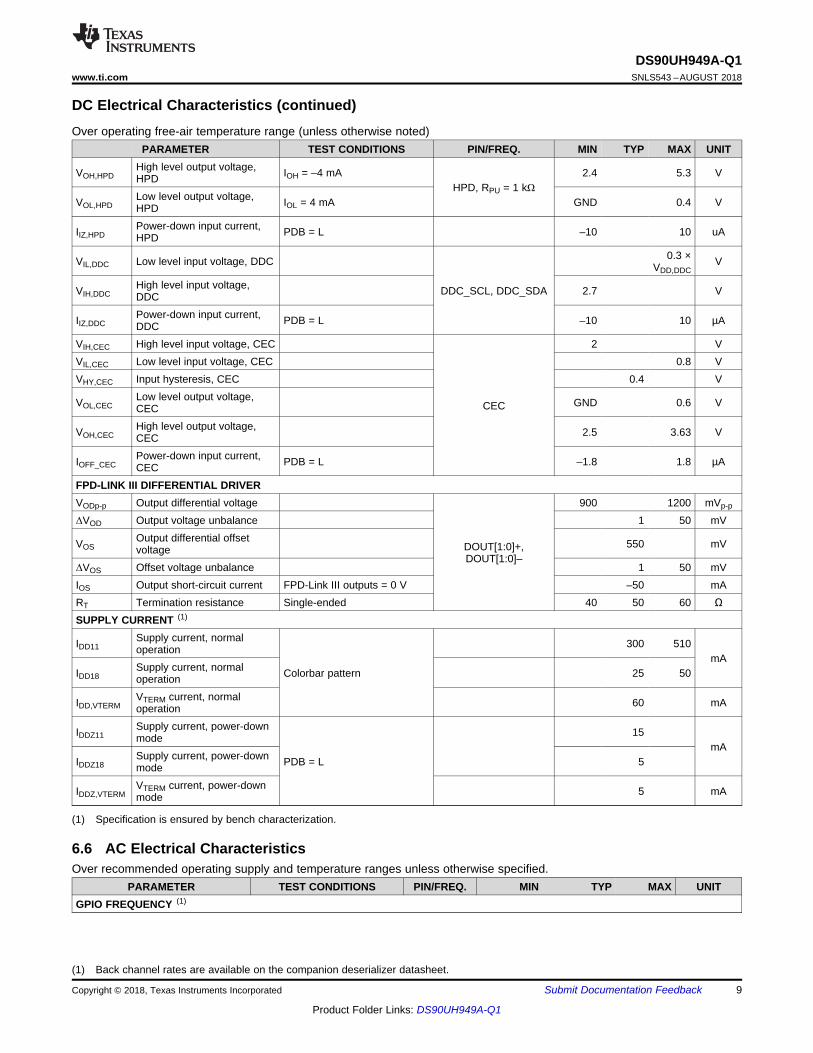
6.5 DC Electrical CharacteristicsOver operating free-air temperature range (unless otherwise noted)
PARAMETER TEST CONDITIONS PIN/FREQ. MIN TYP MAX UNIT1.8-V LVCMOS I/O
VIH High level input voltage SCLK/I2CSEL, PDB,D_GPIO0/MOSI,D_GPIO1/MISO,D_GPIO2/SPLK,
D_GPIO3/SS,SDIN/GPIO0,
SWC/GPIO1, MCLKI2S_DC/GPIO2,I2S_DD/GPIO3,
I2S_DB/GPIO5_REG,I2S_DA/GPIO6_REG,I2S_CLK/GPIO8_REG,I2S_WC/GPIO7_REG
0.65 ×VDDIO
V
VIL Low level input voltage 0 0.35 ×VDDIO
V
IIN Input current VIN = 0 V or 1.89 V −10 10 μA
VOH High level output voltage IOH = –4 mA 0.7 ×VDDIO
VDDIO V
VOL Low level output voltage IOL = 4 mA GND 0.26 ×VDDIO
V
IOS Output short-circuit current VOUT = 0 V –50 mAIOZ TRI-STATE output current VOUT = 0 V or VDDIO, PDB = L –10 10 μATMDS INPUTS -- FROM HDMI v1.4b SECTION 4.2.5
VICM1 Input common-mode voltage IN_CLK ≤ 210 MHz IN_D[2:0]+, IN_D[2:0]–IN_CLK+, IN_CLK–
VTERM = 1.8 V (±5%) orVTERM = 3.3 V (±5%)
VTERM –400
VTERM –37.5 mV
VICM2 Input common-mode voltage IN_CLK ≤ 210 MHz VTERM –10
VTERM+ 10 mV
VIDIFF Input differential voltage level IN_CLK ≤ 210 MHz 150 1200 mVP-P
RTMDS Termination resistance Differential IN_D[2:0]+, IN_D[2:0]–IN_CLK+, IN_CLK– 90 100 110 Ω
HDMI IO -- FROM HDMI v1.4b SECTION 4.2.7 to 4.2.9VRX_5V 5-V power signal
RX_5V4.8 5.3 V
I5V_Sink 5-V input current 55 mA
9
DS90UH949A-Q1www.ti.com SNLS543 –AUGUST 2018
Product Folder Links: DS90UH949A-Q1
Submit Documentation FeedbackCopyright © 2018, Texas Instruments Incorporated
DC Electrical Characteristics (continued)Over operating free-air temperature range (unless otherwise noted)
PARAMETER TEST CONDITIONS PIN/FREQ. MIN TYP MAX UNIT
(1) Specification is ensured by bench characterization.
VOH,HPDHigh level output voltage,HPD IOH = –4 mA
HPD, RPU = 1 kΩ2.4 5.3 V
VOL,HPDLow level output voltage,HPD IOL = 4 mA GND 0.4 V
IIZ,HPDPower-down input current,HPD PDB = L –10 10 uA
VIL,DDC Low level input voltage, DDC
DDC_SCL, DDC_SDA
0.3 ×VDD,DDC
V
VIH,DDCHigh level input voltage,DDC 2.7 V
IIZ,DDCPower-down input current,DDC PDB = L –10 10 µA
VIH,CEC High level input voltage, CEC
CEC
2 VVIL,CEC Low level input voltage, CEC 0.8 VVHY,CEC Input hysteresis, CEC 0.4 V
VOL,CECLow level output voltage,CEC GND 0.6 V
VOH,CECHigh level output voltage,CEC 2.5 3.63 V
IOFF_CECPower-down input current,CEC PDB = L –1.8 1.8 µA
FPD-LINK III DIFFERENTIAL DRIVERVODp-p Output differential voltage
DOUT[1:0]+,DOUT[1:0]–
900 1200 mVp-p
ΔVOD Output voltage unbalance 1 50 mV
VOSOutput differential offsetvoltage 550 mV
ΔVOS Offset voltage unbalance 1 50 mVIOS Output short-circuit current FPD-Link III outputs = 0 V –50 mART Termination resistance Single-ended 40 50 60 ΩSUPPLY CURRENT (1)
IDD11Supply current, normaloperation
Colorbar pattern
300 510mA
IDD18Supply current, normaloperation 25 50
IDD,VTERMVTERM current, normaloperation 60 mA
IDDZ11Supply current, power-downmode
PDB = L
15mA
IDDZ18Supply current, power-downmode 5
IDDZ,VTERMVTERM current, power-downmode 5 mA
(1) Back channel rates are available on the companion deserializer datasheet.
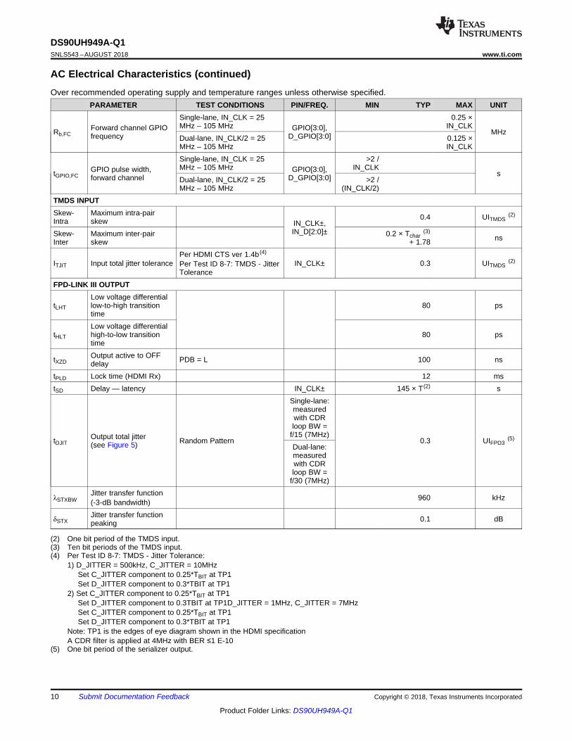
6.6 AC Electrical CharacteristicsOver recommended operating supply and temperature ranges unless otherwise specified.
PARAMETER TEST CONDITIONS PIN/FREQ. MIN TYP MAX UNITGPIO FREQUENCY (1)
10
DS90UH949A-Q1SNLS543 –AUGUST 2018 www.ti.com
Product Folder Links: DS90UH949A-Q1
Submit Documentation Feedback Copyright © 2018, Texas Instruments Incorporated
AC Electrical Characteristics (continued)Over recommended operating supply and temperature ranges unless otherwise specified.
PARAMETER TEST CONDITIONS PIN/FREQ. MIN TYP MAX UNIT
(2) One bit period of the TMDS input.(3) Ten bit periods of the TMDS input.(4) Per Test ID 8-7: TMDS - Jitter Tolerance:
1) D_JITTER = 500kHz, C_JITTER = 10MHzSet C_JITTER component to 0.25*TBIT at TP1Set D_JITTER component to 0.3*TBIT at TP1
2) Set C_JITTER component to 0.25*TBIT at TP1Set D_JITTER component to 0.3TBIT at TP1D_JITTER = 1MHz, C_JITTER = 7MHzSet C_JITTER component to 0.25*TBIT at TP1Set D_JITTER component to 0.3*TBIT at TP1
Note: TP1 is the edges of eye diagram shown in the HDMI specificationA CDR filter is applied at 4MHz with BER ≤1 E-10
(5) One bit period of the serializer output.
Rb,FCForward channel GPIOfrequency
Single-lane, IN_CLK = 25MHz – 105 MHz GPIO[3:0],
D_GPIO[3:0]
0.25 ×IN_CLK
MHzDual-lane, IN_CLK/2 = 25MHz – 105 MHz
0.125 ×IN_CLK
tGPIO,FCGPIO pulse width,forward channel
Single-lane, IN_CLK = 25MHz – 105 MHz GPIO[3:0],
D_GPIO[3:0]
>2 /IN_CLK
sDual-lane, IN_CLK/2 = 25MHz – 105 MHz
>2 /(IN_CLK/2)
TMDS INPUTSkew-Intra
Maximum intra-pairskew IN_CLK±,
IN_D[2:0]±
0.4 UITMDS(2)
Skew-Inter
Maximum inter-pairskew
0.2 × Tchar(3)
+ 1.78 ns
ITJIT Input total jitter tolerancePer HDMI CTS ver 1.4b (4)
Per Test ID 8-7: TMDS - JitterTolerance
IN_CLK± 0.3 UITMDS(2)
FPD-LINK III OUTPUT
tLHT
Low voltage differentiallow-to-high transitiontime
80 ps
tHLT
Low voltage differentialhigh-to-low transitiontime
80 ps
tXZDOutput active to OFFdelay PDB = L 100 ns
tPLD Lock time (HDMI Rx) 12 mstSD Delay — latency IN_CLK± 145 × T (2) s
tDJITOutput total jitter(see Figure 5) Random Pattern
Single-lane:measuredwith CDRloop BW =
f/15 (7MHz)0.3 UIFPD3
(5)Dual-lane:measuredwith CDRloop BW =
f/30 (7MHz)
λSTXBWJitter transfer function(-3-dB bandwidth) 960 kHz
δSTXJitter transfer functionpeaking 0.1 dB
11
DS90UH949A-Q1www.ti.com SNLS543 –AUGUST 2018
Product Folder Links: DS90UH949A-Q1
Submit Documentation FeedbackCopyright © 2018, Texas Instruments Incorporated
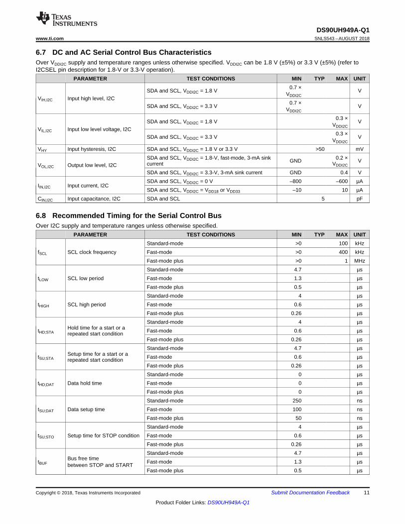
6.7 DC and AC Serial Control Bus CharacteristicsOver VDDI2C supply and temperature ranges unless otherwise specified. VDDI2C can be 1.8 V (±5%) or 3.3 V (±5%) (refer toI2CSEL pin description for 1.8-V or 3.3-V operation).
PARAMETER TEST CONDITIONS MIN TYP MAX UNIT
VIH,I2C Input high level, I2CSDA and SCL, VDDI2C = 1.8 V 0.7 ×
VDDI2CV
SDA and SCL, VDDI2C = 3.3 V 0.7 ×VDDI2C
V
VIL,I2C Input low level voltage, I2CSDA and SCL, VDDI2C = 1.8 V 0.3 ×
VDDI2CV
SDA and SCL, VDDI2C = 3.3 V 0.3 ×VDDI2C
V
VHY Input hysteresis, I2C SDA and SCL, VDDI2C = 1.8 V or 3.3 V >50 mV
VOL,I2C Output low level, I2CSDA and SCL, VDDI2C = 1.8-V, fast-mode, 3-mA sinkcurrent GND 0.2 ×
VDDI2CV
SDA and SCL, VDDI2C = 3.3-V, 3-mA sink current GND 0.4 V
IIN,I2C Input current, I2CSDA and SCL, VDDI2C = 0 V –800 –600 µASDA and SCL, VDDI2C = VDD18 or VDD33 –10 10 µA
CIN,I2C Input capacitance, I2C SDA and SCL 5 pF
6.8 Recommended Timing for the Serial Control BusOver I2C supply and temperature ranges unless otherwise specified.
PARAMETER TEST CONDITIONS MIN TYP MAX UNIT
fSCL SCL clock frequencyStandard-mode >0 100 kHzFast-mode >0 400 kHzFast-mode plus >0 1 MHz
tLOW SCL low periodStandard-mode 4.7 µsFast-mode 1.3 µsFast-mode plus 0.5 µs
tHIGH SCL high periodStandard-mode 4 µsFast-mode 0.6 µsFast-mode plus 0.26 µs
tHD;STAHold time for a start or arepeated start condition
Standard-mode 4 µsFast-mode 0.6 µsFast-mode plus 0.26 µs
tSU;STASetup time for a start or arepeated start condition
Standard-mode 4.7 µsFast-mode 0.6 µsFast-mode plus 0.26 µs
tHD;DAT Data hold timeStandard-mode 0 µsFast-mode 0 µsFast-mode plus 0 µs
tSU;DAT Data setup timeStandard-mode 250 nsFast-mode 100 nsFast-mode plus 50 ns
tSU;STO Setup time for STOP conditionStandard-mode 4 µsFast-mode 0.6 µsFast-mode plus 0.26 µs
tBUFBus free timebetween STOP and START
Standard-mode 4.7 µsFast-mode 1.3 µsFast-mode plus 0.5 µs
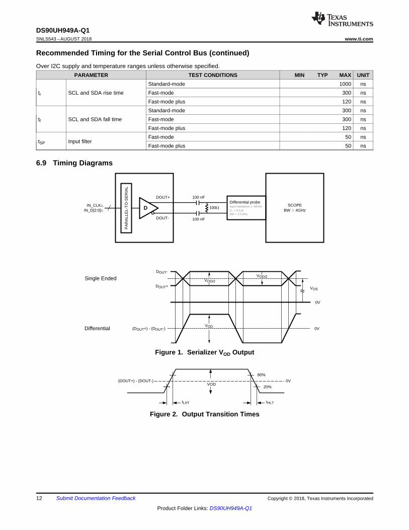
0V
tHLTtLHT
(DOUT+) - (DOUT-)
20%
80%
VOD
DOUT+
0V
0V
VOD/2
VOD
Single Ended
Differential
VOS
DOUT-
(DOUT+) - (DOUT-)
|
PA
RA
LLE
L-T
O-S
ER
IAL
IN_CLK±IN_D[2:0]±
100:
DOUT-
DOUT+
D
100 nF
100 nF
SCOPEBW û 4GHz
Differential probeInput Impedance û 100 k:
CL ú 0.5 pfBW û 3.5 GHz
VOD/2
12
DS90UH949A-Q1SNLS543 –AUGUST 2018 www.ti.com
Product Folder Links: DS90UH949A-Q1
Submit Documentation Feedback Copyright © 2018, Texas Instruments Incorporated
Recommended Timing for the Serial Control Bus (continued)Over I2C supply and temperature ranges unless otherwise specified.
PARAMETER TEST CONDITIONS MIN TYP MAX UNIT
tr SCL and SDA rise timeStandard-mode 1000 nsFast-mode 300 nsFast-mode plus 120 ns
tf SCL and SDA fall timeStandard-mode 300 nsFast-mode 300 nsFast-mode plus 120 ns
tSP Input filterFast-mode 50 nsFast-mode plus 50 ns
6.9 Timing Diagrams
Figure 1. Serializer VOD Output
Figure 2. Output Transition Times
SCL
SDA
tHD;STA
tLOW
tr
tHD;DATtHIGH
tf
tSU;DAT
tSU;STA tSU;STO
tf
START REPEATEDSTART
STOP
tHD;STA
START
tSP
trBUFt
DOUT(Diff.)
tDJIT
tBIT (1 UI)
EYE OPENING 0V
tDJIT
210
||
STARTBIT
STOPBITSYMBOL N
210
||
STARTBIT
STOPBITSYMBOL N-1
210
||
STARTBIT
STOPBITSYMBOL N-2
210
||
STARTBIT
STOPBITSYMBOL N-3
210
STOPBITSYMBOL N-4
||
DOUT
|
IN_CLK
tSD
NN-1 N+1 N+2
||
IN_D[2:0]
RX_5V
IN_CLK (Diff.)
DOUT(Diff.)
Driver OFF, VOD = 0V Driver On
VDDVDDIO
tPLD
PDB
13
DS90UH949A-Q1www.ti.com SNLS543 –AUGUST 2018
Product Folder Links: DS90UH949A-Q1
Submit Documentation FeedbackCopyright © 2018, Texas Instruments Incorporated
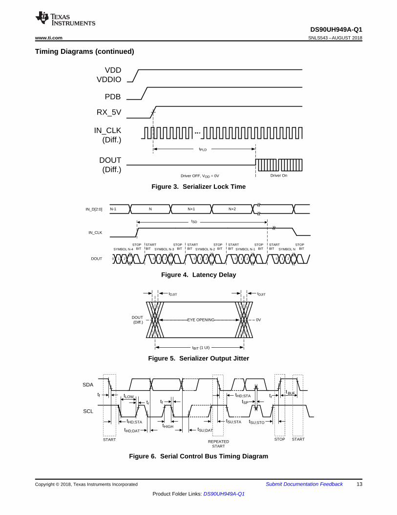
Timing Diagrams (continued)
Figure 3. Serializer Lock Time
Figure 4. Latency Delay
Figure 5. Serializer Output Jitter
Figure 6. Serial Control Bus Timing Diagram
I2S_WCI2S_D[A,B,C,D]
I2S_CLKVIH
VIL
tHCtLC
tsr thr
T
14
DS90UH949A-Q1SNLS543 –AUGUST 2018 www.ti.com
Product Folder Links: DS90UH949A-Q1
Submit Documentation Feedback Copyright © 2018, Texas Instruments Incorporated
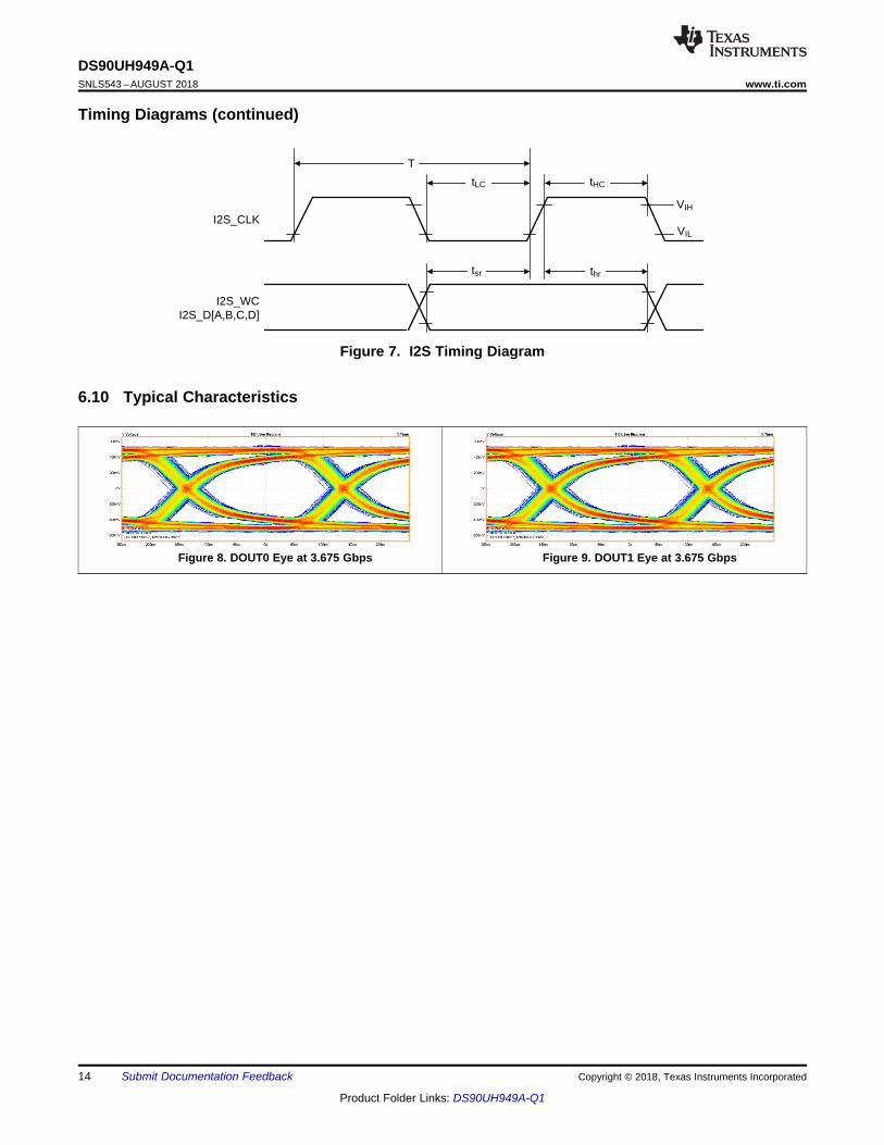
Timing Diagrams (continued)
Figure 7. I2S Timing Diagram
6.10 Typical Characteristics
Figure 8. DOUT0 Eye at 3.675 Gbps Figure 9. DOUT1 Eye at 3.675 Gbps
FPD-Link III Digital
HDMI ControllerDigital
HDMI RXPHY
FPD-Link III TXDigital
FPD3 TXAnalog
Bridge ControlDigital
TMDS
DDC
HPA
FPD-Link III
Audio PLL
AudioFIFO
PacketFIFO
KSVFIFO
EDID/ConfigNVM
EDIDI/F
I2S Audio
Video
HDCPKeyNVM
RX_5V
I2C OptionalSecondary
I2S
DigitalTMDS
Interface
FPD3 TXAnalog
FPD-Link IIIFPD-Link III TXDigital
PATGEN
HDCP
HDCP
15
DS90UH949A-Q1www.ti.com SNLS543 –AUGUST 2018
Product Folder Links: DS90UH949A-Q1
Submit Documentation FeedbackCopyright © 2018, Texas Instruments Incorporated
7 Detailed Description
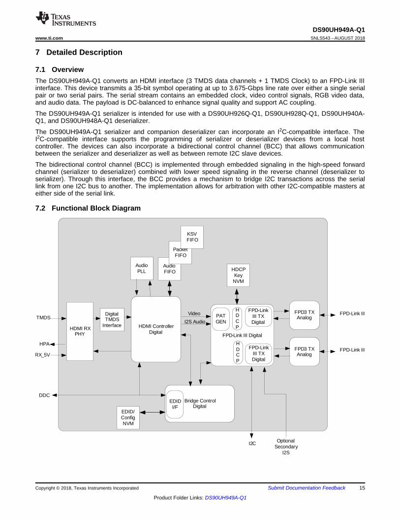
7.1 OverviewThe DS90UH949A-Q1 converts an HDMI interface (3 TMDS data channels + 1 TMDS Clock) to an FPD-Link IIIinterface. This device transmits a 35-bit symbol operating at up to 3.675-Gbps line rate over either a single serialpair or two serial pairs. The serial stream contains an embedded clock, video control signals, RGB video data,and audio data. The payload is DC-balanced to enhance signal quality and support AC coupling.
The DS90UH949A-Q1 serializer is intended for use with a DS90UH926Q-Q1, DS90UH928Q-Q1, DS90UH940A-Q1, and DS90UH948A-Q1 deserializer.
The DS90UH949A-Q1 serializer and companion deserializer can incorporate an I2C-compatible interface. TheI2C-compatible interface supports the programming of serializer or deserializer devices from a local hostcontroller. The devices can also incorporate a bidirectional control channel (BCC) that allows communicationbetween the serializer and deserializer as well as between remote I2C slave devices.
The bidirectional control channel (BCC) is implemented through embedded signaling in the high-speed forwardchannel (serializer to deserializer) combined with lower speed signaling in the reverse channel (deserializer toserializer). Through this interface, the BCC provides a mechanism to bridge I2C transactions across the seriallink from one I2C bus to another. The implementation allows for arbitration with other I2C-compatible masters ateither side of the serial link.
7.2 Functional Block Diagram
16
DS90UH949A-Q1SNLS543 –AUGUST 2018 www.ti.com
Product Folder Links: DS90UH949A-Q1
Submit Documentation Feedback Copyright © 2018, Texas Instruments Incorporated
7.3 Feature Description
7.3.1 High-Definition Multimedia Interface (HDMI)HDMI is a leading interface standard used to transmit digital video and audio from sources (such as a DVDplayer) to sinks (such as an LCD display). The interface is capable of transmitting high-definition video, audio,and also supports HDCP. Other HDMI signals consist of various control and status data that travel bidirectionally.
7.3.1.1 HDMI Receive ControllerThe HDMI Receiver is an HDMI version 1.4b compliant receiver. The HDMI receiver is capable of operation atgreater than 2K resolutions. The configuration used in the DS90UH949A-Q1 does not include version 1.4bfeatures such as the ethernet channel (HEC) or Audio Return Channel (ARC).
7.3.2 Transition Minimized Differential SignalingHDMI uses Transition Minimized Differential Signaling (TMDS) over four differential pairs (3 TMDS channels and1 TMDS clock) to transmit video and audio data. TMDS is widely used to transmit high-speed serial data. Thetechnology incorporates a form of 8b/10b encoding, and the differential signaling allows the device to reduceelectromagnetic interference (EMI) and achieve high skew tolerance.
7.3.3 Enhanced Display Data ChannelThe Display Data Channel (DDC) is a collection of digital communication protocols between a computer displayand a graphics adapter that enables the display to send the supported display modes to the adapter. The DDCalso allows the computer host to adjust monitor parameters, such as brightness and contrast.
7.3.4 Extended Display Identification Data (EDID)EDID is a data structure provided by a digital display to describe the display capabilities to a video source. Byproviding this information, the video source can then send video data with the proper timing and resolution thatthe display supports. The DS90UH949A-Q1 supports several options for delivering display identification (EDID)information to the HDMI graphics source. The EDID information is accessible through the DDC interface andcomply with the DDC and EDID requirements given in the HDMI v1.4b specification.
The EDID configurations supported are as follows:• External local EDID (EEPROM)• Internal EDID loaded into device memory• Remote EDID connected to I2C bus at deserializer side• Internal pre-programmed EDID
The EDID mode selected should be configurable from the MODE_SEL pins or from internal control registers. Forall modes, the EDID information should be accessible at the default address of 0xA0.
7.3.4.1 External Local EDID (EEPROM)The DS90UH949A-Q1 can be configured to allow a local EEPROM EDID device. The local EDID device mayimplement any EDID configuration allowable by the HDMI v1.4b and DVI 1.0 standards, including multipleextension blocks up to 32KB.
7.3.4.2 Internal EDID (SRAM)The DS90UH949A-Q1 also allows the internal loading of an EDID profile up to 256 bytes. This SRAM storage isvolatile and requires loading from an external I2C master (local or remote). The internal EDID is reloadable andreadable (local/remote) from control registers during normal operation.
7.3.4.3 External Remote EDIDThe serializer copies the remote EDID connected to the I2C bus of the remote deserializer into its internalSRAM. The remote EDID device can be a standalone I2C EEPROM, or integrated into the digital display panel.In this mode, the serializer automatically accesses the Bidirectional Control Channel to search for the EDIDinformation at the default address 0xA0. Once found, the serializer copies the remote EDID into local SRAM.
C1 C0
17
DS90UH949A-Q1www.ti.com SNLS543 –AUGUST 2018
Product Folder Links: DS90UH949A-Q1
Submit Documentation FeedbackCopyright © 2018, Texas Instruments Incorporated
Feature Description (continued)7.3.4.4 Internal Pre-Programmed EDIDThe serializer also has an internal eFuse that is loaded into the internal SRAM with pre-programmed 256-byteEDID data at start-up. This EDID profile supports several generic video (480p, 720p) and audio (2-channel audio)timing profiles within the single-link operating range of the device (25-MHz to 105-MHz pixel clock). In this mode,the internal EDID SRAM data is readable from the DDC interface. The EDID contents are below:
0x00 0xFF 0xFF 0xFF 0xFF 0xFF 0xFF 0x00 0x53 0x0E 0x49 0x09 0x01 0x00 0x00 0x000x1C 0x18 0x01 0x03 0x80 0x34 0x20 0x78 0x0A 0xEC 0x18 0xA3 0x54 0x46 0x98 0x250x0F 0x48 0x4C 0x00 0x00 0x00 0x01 0x01 0x01 0x01 0x01 0x01 0x01 0x01 0x01 0x010x01 0x01 0x01 0x01 0x01 0x01 0x01 0x1D 0x00 0x72 0x51 0xD0 0x1E 0x20 0x6E 0x500x55 0x00 0x00 0x20 0x21 0x00 0x00 0x18 0x00 0x00 0x00 0xFD 0x00 0x3B 0x3D 0x620x64 0x08 0x00 0x0A 0x20 0x20 0x20 0x20 0x20 0x20 0x00 0x00 0x00 0xFC 0x00 0x540x49 0x2D 0x44 0x53 0x39 0x30 0x55 0x78 0x39 0x34 0x39 0x0A 0x00 0x00 0x00 0x100x00 0x00 0x00 0x00 0x00 0x00 0x00 0x00 0x00 0x00 0x00 0x00 0x00 0x00 0x01 0x570x02 0x03 0x15 0x40 0x41 0x84 0x23 0x09 0x7F 0x05 0x83 0x01 0x00 0x00 0x66 0x030x0C 0x00 0x10 0x00 0x00 0x00 0x00 0x00 0x00 0x00 0x00 0x00 0x00 0x00 0x00 0x000x00 0x00 0x00 0x00 0x00 0x00 0x00 0x00 0x00 0x00 0x00 0x00 0x00 0x00 0x00 0x000x00 0x00 0x00 0x00 0x00 0x00 0x00 0x00 0x00 0x00 0x00 0x00 0x00 0x00 0x00 0x000x00 0x00 0x00 0x00 0x00 0x00 0x00 0x00 0x00 0x00 0x00 0x00 0x00 0x00 0x00 0x000x00 0x00 0x00 0x00 0x00 0x00 0x00 0x00 0x00 0x00 0x00 0x00 0x00 0x00 0x00 0x000x00 0x00 0x00 0x00 0x00 0x00 0x00 0x00 0x00 0x00 0x00 0x00 0x00 0x00 0x00 0x000x00 0x00 0x00 0x00 0x00 0x00 0x00 0x00 0x00 0x00 0x00 0x00 0x00 0x00 0x00 0x28
7.3.5 Consumer Electronics Control (CEC)Consumer Electronics Control (CEC) is designed to allow the system user to command and control up to tenCEC-enabled devices connected through HDMI using only one of their remote controls (for example, controllinga television set, set-top box, and DVD player using only the remote control of the TV). CEC also allows forindividual CEC-enabled devices to command and control each other without user intervention. CEC is a one-wire, open-drain bus with an external 27-kΩ (±10%) resistor pullup to 3.3 V.
CEC protocol can be implemented using an external clock reference or the 25-MHz internal oscillator inside theDS90UH949A-Q1.
7.3.6 +5-V Power Signal5 V is asserted by the HDMI source through the HDMI interface. The 5-V signal propagates through theconnector and cable until it reaches the sink. The 5-V supply is used for various HDMI functions, such as HPDand DDC signals.
7.3.7 Hot Plug Detect (HPD)The HPD pin is asserted by the sink to let the source know that it is ready to receive the HDMI signal. Thesource initiates the connection by first providing the 5-V power signal through the HDMI interface. The sink holdsHPD low until it is ready to receive signals from the source, at which point it will release HPD to be pulled up to 5V.
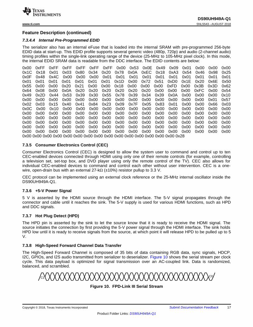
7.3.8 High-Speed Forward Channel Data TransferThe High-Speed Forward Channel is composed of 35 bits of data containing RGB data, sync signals, HDCP,I2C, GPIOs, and I2S audio transmitted from serializer to deserializer. Figure 10 shows the serial stream per clockcycle. This data payload is optimized for signal transmission over an AC-coupled link. Data is randomized,balanced, and scrambled.
Figure 10. FPD-Link III Serial Stream

18
DS90UH949A-Q1SNLS543 –AUGUST 2018 www.ti.com
Product Folder Links: DS90UH949A-Q1
Submit Documentation Feedback Copyright © 2018, Texas Instruments Incorporated
Feature Description (continued)The device supports TMDS clocks in the range of 25 MHz to 105 MHz over one lane, or 50 MHz to 210 MHzover two lanes. The FPD-Link III serial stream rate is 3.675 Gbps maximum (875 Mbps minimum) whentransmitting either over one lane or both lanes.
7.3.9 Back Channel Data TransferThe Backward Channel provides bidirectional communication between the display and host processor. Theinformation is carried from the deserializer to the serializer as serial frames. The back channel control data istransferred over both serial links along with the high-speed forward data, DC balance coding, and embeddedclock information. This architecture provides a backward path across the serial link together with a high-speedforward channel. The back channel contains the I2C, HDCP, CRC, and 4 bits of standard GPIO information witha line rate of 5, 10, or 20 Mbps (configured by the compatible deserializer).
7.3.10 FPD-Link III Port Register AccessThe DS90UH949A-Q1 contains two downstream ports, therefore some registers must be duplicated to allowcontrol and monitoring of the two ports. To facilitate this, a TX_PORT_SEL register controls access to the twosets of registers. Registers that are shared between ports (not duplicated) will be available independent of thesettings in the TX_PORT_SEL register.
Setting the TX_PORT0_SEL or TX_PORT1_SEL bit will allow a read of the register for the selected port. If bothbits are set, port1 registers will be returned. Writes will occur to ports for which the select bit is set, allowingsimultaneous writes to both ports if both select bits are set.
Setting the PORT1_I2C_EN bit will enable a second I2C slave address, allowing access to the second portregisters through the second I2C address. If this bit is set, the TX_PORT0_SEL and TX_PORT1_SEL bits will beignored.
7.3.11 Power Down (PDB)The Serializer has a PDB input pin to ENABLE or POWER DOWN the device. This pin may be controlled by anexternal device, or through VDDIO, where VDDIO = 1.71 V to 1.89 V. To save power, disable the link when thedisplay is not required (PDB = LOW). Ensure that this pin is not driven HIGH before all power supplies havereached final levels. When PDB is driven low, ensure that the pin is driven to 0 V for at least 3 ms beforereleasing or driving high. In the case where PDB is pulled up to VDDIO directly, a 10-kΩ pullup resistor and a >10-µF capacitor to ground are required (see Power Up Requirements and PDB Pin).
Toggling PDB low will POWER DOWN the device and RESET all control registers to default. During this time,PDB must be held low for a minimum of 3 ms before going high again.
7.3.12 Serial Link Fault DetectThe DS90UH949A-Q1 can detect fault conditions in the FPD-Link III interconnect. If a fault condition occurs, theLink Detect Status is 0 (cable is not detected) on bit 0 of address 0x0C (Table 10). The DS90UH949A-Q1 willdetect any of the following conditions:1. Cable open2. “+” to “-” short3. ”+” to GND short4. ”–” to GND short5. ”+” to battery short6. ”–” to battery short7. Cable is linked incorrectly (DOUT+/DOUT– connections reversed)
NOTEThe device will detect any of the above conditions, but does not report specifically whichone has occurred.
19
DS90UH949A-Q1www.ti.com SNLS543 –AUGUST 2018
Product Folder Links: DS90UH949A-Q1
Submit Documentation FeedbackCopyright © 2018, Texas Instruments Incorporated
Feature Description (continued)7.3.13 Interrupt Pin (INTB)The INTB pin is an active low interrupt output pin that acts as an interrupt for various local and remote interruptconditions (see registers 0xC6 and 0xC7 of Register Maps). For the remote interrupt condition, the INTB pinworks in conjunction with the INTB_IN pin on the deserializer. This interrupt signal, when configured, willpropagate from the deserializer to the serializer.1. On the Serializer, set register 0xC6[5] = 1 and 0xC6[0] = 12. Deserializer INTB_IN pin is set LOW by some downstream device.3. Serializer pulls INTB pin LOW. The signal is active LOW, so a LOW indicates an interrupt condition.4. External controller detects INTB = LOW; to determine interrupt source, read the HDCP_ISR register.5. A read to HDCP_ISR will clear the interrupt at the Serializer, releasing INTB.6. The external controller typically must then access the remote device to determine downstream interrupt
source and clear the interrupt driving the Deserializer INTB_IN. This would be when the downstream devicereleases the INTB_IN pin on the Deserializer. The system is now ready to return to step (2) at next fallingedge of INTB_IN.
7.3.14 Remote Interrupt Pin (REM_INTB)REM_INTB will mirror the status of INTB_IN pin on the deserializer and does not need to be cleared. If theserializer is not linked to the deserializer, REM_INTB will be high.
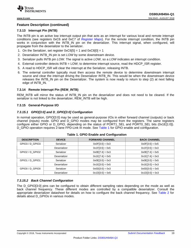
7.3.15 General-Purpose I/O
7.3.15.1 GPIO[3:0] and D_GPIO[3:0] ConfigurationIn normal operation, GPIO[3:0] may be used as general-purpose I/Os in either forward channel (outputs) or backchannel (inputs) mode. GPIO and D_GPIO modes may be configured from the registers. The same registersconfigure either GPIO or D_GPIO, depending on the status of PORT1_SEL and PORT0_SEL bits (0x1E[1:0]).D_GPIO operation requires 2-lane FPD-Link III mode. See Table 1 for GPIO enable and configuration.
Table 1. GPIO Enable and ConfigurationDESCRIPTION DEVICE FORWARD CHANNEL BACK CHANNEL
GPIO3 / D_GPIO3 Serializer 0x0F[3:0] = 0x3 0x0F[3:0] = 0x5Deserializer 0x1F[3:0] = 0x5 0x1F[3:0] = 0x3
GPIO2 / D_GPIO2 Serializer 0x0E[7:4] = 0x3 0x0E[7:4] = 0x5Deserializer 0x1E[7:4] = 0x5 0x1E[7:4] = 0x3
GPIO1 / D_GPIO1 Serializer 0x0E[3:0] = 0x3 0x0E[3:0] = 0x5Deserializer 0x1E[3:0] = 0x5 0x1E[3:0] = 0x3
GPIO0 / D_GPIO0 Serializer 0x0D[3:0] = 0x3 0x0D[3:0] = 0x5Deserializer 0x1D[3:0] = 0x5 0x1D[3:0] = 0x3
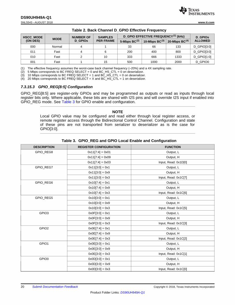
7.3.15.2 Back Channel ConfigurationThe D_GPIO[3:0] pins can be configured to obtain different sampling rates depending on the mode as well asback channel frequency. These different modes are controlled by a compatible deserializer. Consult theappropriate deserializer datasheet for details on how to configure the back channel frequency. See Table 2 fordetails about D_GPIOs in various modes.
20
DS90UH949A-Q1SNLS543 –AUGUST 2018 www.ti.com
Product Folder Links: DS90UH949A-Q1
Submit Documentation Feedback Copyright © 2018, Texas Instruments Incorporated
(1) The effective frequency assumes the worst-case back channel frequency (–20%) and a 4X sampling rate.(2) 5 Mbps corresponds to BC FREQ SELECT = 0 and BC_HS_CTL = 0 on deserializer.(3) 10 Mbps corresponds to BC FREQ SELECT = 1 and BC_HS_CTL = 0 on deserializer.(4) 20 Mbps corresponds to BC FREQ SELECT = X and BC_HS_CTL = 1 on deserializer.
Table 2. Back Channel D_GPIO Effective Frequency
HSCC_MODE(ON DES) MODE NUMBER OF
D_GPIOsSAMPLES
PER FRAMED_GPIO EFFECTIVE FREQUENCY (1) (kHz) D_GPIOs
ALLOWED5-Mbps BC (2) 10-Mbps BC (3) 20-Mbps BC (4)
000 Normal 4 1 33 66 133 D_GPIO[3:0]011 Fast 4 6 200 400 800 D_GPIO[3:0]010 Fast 2 10 333 666 1333 D_GPIO[1:0]001 Fast 1 15 500 1000 2000 D_GPIO0
7.3.15.3 GPIO_REG[8:5] ConfigurationGPIO_REG[8:5] are register-only GPIOs and may be programmed as outputs or read as inputs through localregister bits only. Where applicable, these bits are shared with I2S pins and will override I2S input if enabled intoGPIO_REG mode. See Table 3 for GPIO enable and configuration.
NOTELocal GPIO value may be configured and read either through local register access, orremote register access through the Bidirectional Control Channel. Configuration and stateof these pins are not transported from serializer to deserializer as is the case forGPIO[3:0].
Table 3. GPIO_REG and GPIO Local Enable and ConfigurationDESCRIPTION REGISTER CONFIGURATION FUNCTIONGPIO_REG8 0x11[7:4] = 0x01 Output, L
0x11[7:4] = 0x09 Output, H0x11[7:4] = 0x03 Input, Read: 0x1D[0]
GPIO_REG7 0x11[3:0] = 0x1 Output, L0x11[3:0] = 0x9 Output, H0x11[3:0] = 0x3 Input, Read: 0x1C[7]
GPIO_REG6 0x10[7:4] = 0x1 Output, L0x10[7:4] = 0x9 Output, H0x10[7:4] = 0x3 Input, Read: 0x1C[6]
GPIO_REG5 0x10[3:0] = 0x1 Output, L0x10[3:0] = 0x9 Output, H0x10[3:0] = 0x3 Input, Read: 0x1C[5]
GPIO3 0x0F[3:0] = 0x1 Output, L0x0F[3:0] = 0x9 Output, H0x0F[3:0] = 0x3 Input, Read: 0x1C[3]
GPIO2 0x0E[7:4] = 0x1 Output, L0x0E[7:4] = 0x9 Output, H0x0E[7:4] = 0x3 Input, Read: 0x1C[2]
GPIO1 0x0E[3:0] = 0x1 Output, L0x0E[3:0] = 0x9 Output, H0x0E[3:0] = 0x3 Input, Read: 0x1C[1]
GPIO0 0x0D[3:0] = 0x1 Output, L0x0D[3:0] = 0x9 Output, H0x0D[3:0] = 0x3 Input, Read: 0x1C[0]
D0 D1 D2 D3 DN
D0 D1 D2 D3 DN
SS
SPLK
MOSI
SS
SPLK
MOSI
SERIALIZER
DESERIALIZER
21
DS90UH949A-Q1www.ti.com SNLS543 –AUGUST 2018
Product Folder Links: DS90UH949A-Q1
Submit Documentation FeedbackCopyright © 2018, Texas Instruments Incorporated
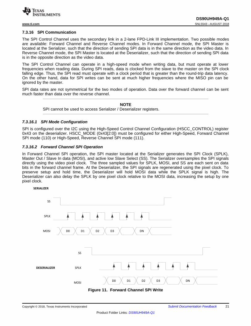
7.3.16 SPI CommunicationThe SPI Control Channel uses the secondary link in a 2-lane FPD-Link III implementation. Two possible modesare available: Forward Channel and Reverse Channel modes. In Forward Channel mode, the SPI Master islocated at the Serializer, such that the direction of sending SPI data is in the same direction as the video data. InReverse Channel mode, the SPI Master is located at the Deserializer, such that the direction of sending SPI datais in the opposite direction as the video data.
The SPI Control Channel can operate in a high-speed mode when writing data, but must operate at lowerfrequencies when reading data. During SPI reads, data is clocked from the slave to the master on the SPI clockfalling edge. Thus, the SPI read must operate with a clock period that is greater than the round-trip data latency.On the other hand, data for SPI writes can be sent at much higher frequencies where the MISO pin can beignored by the master.
SPI data rates are not symmetrical for the two modes of operation. Data over the forward channel can be sentmuch faster than data over the reverse channel.
NOTESPI cannot be used to access Serializer / Deserializer registers.
7.3.16.1 SPI Mode ConfigurationSPI is configured over the I2C using the High-Speed Control Channel Configuration (HSCC_CONTROL) register0x43 on the deserializer. HSCC_MODE (0x43[2:0]) must be configured for either High-Speed, Forward ChannelSPI mode (110) or High-Speed, Reverse Channel SPI mode (111).
7.3.16.2 Forward Channel SPI OperationIn Forward Channel SPI operation, the SPI master located at the Serializer generates the SPI Clock (SPLK),Master Out / Slave In data (MOSI), and active low Slave Select (SS). The Serializer oversamples the SPI signalsdirectly using the video pixel clock. The three sampled values for SPLK, MOSI, and SS are each sent on databits in the forward channel frame. At the Deserializer, the SPI signals are regenerated using the pixel clock. Topreserve setup and hold time, the Deserializer will hold MOSI data while the SPLK signal is high. TheDeserializer can also delay the SPLK by one pixel clock relative to the MOSI data, increasing the setup by onepixel clock.
Figure 11. Forward Channel SPI Write
D0
SS
SPLK
MOSI
SS
SPLK
MOSI
SERIALIZER
DESERIALIZER
RD0MISO
MISO RD0
D0
RD1
RD1
D1
22
DS90UH949A-Q1SNLS543 –AUGUST 2018 www.ti.com
Product Folder Links: DS90UH949A-Q1
Submit Documentation Feedback Copyright © 2018, Texas Instruments Incorporated
Figure 12. Forward Channel SPI Read
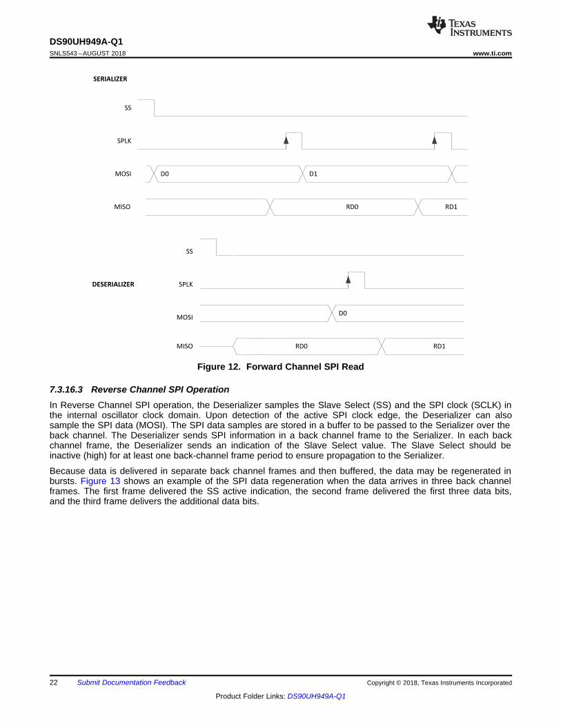
7.3.16.3 Reverse Channel SPI OperationIn Reverse Channel SPI operation, the Deserializer samples the Slave Select (SS) and the SPI clock (SCLK) inthe internal oscillator clock domain. Upon detection of the active SPI clock edge, the Deserializer can alsosample the SPI data (MOSI). The SPI data samples are stored in a buffer to be passed to the Serializer over theback channel. The Deserializer sends SPI information in a back channel frame to the Serializer. In each backchannel frame, the Deserializer sends an indication of the Slave Select value. The Slave Select should beinactive (high) for at least one back-channel frame period to ensure propagation to the Serializer.
Because data is delivered in separate back channel frames and then buffered, the data may be regenerated inbursts. Figure 13 shows an example of the SPI data regeneration when the data arrives in three back channelframes. The first frame delivered the SS active indication, the second frame delivered the first three data bits,and the third frame delivers the additional data bits.
D0
SS
SPLK
MOSI
SS
SPLK
MOSI
DESERIALIZER
SERIALIZER
RD0MISO
MISO RD0
D0
RD1
RD1
D1
D0 D1 D2 D3 DN
D0 D1 D2 D3 DN
SS
SPLK
MOSI
SS
SPLK
MOSI
DESERIALIZER
SERIALIZER
23
DS90UH949A-Q1www.ti.com SNLS543 –AUGUST 2018
Product Folder Links: DS90UH949A-Q1
Submit Documentation FeedbackCopyright © 2018, Texas Instruments Incorporated
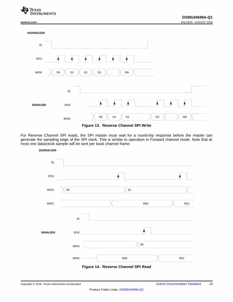
Figure 13. Reverse Channel SPI Write
For Reverse Channel SPI reads, the SPI master must wait for a round-trip response before the master cangenerate the sampling edge of the SPI clock. This is similar to operation in Forward channel mode. Note that atmost one data/clock sample will be sent per back channel frame.
Figure 14. Reverse Channel SPI Read
Word Select
Serializer
Bit Clock I2S_CLK
I2S_WCData I2S_Dx
4
I2STransmitter
24
DS90UH949A-Q1SNLS543 –AUGUST 2018 www.ti.com
Product Folder Links: DS90UH949A-Q1
Submit Documentation Feedback Copyright © 2018, Texas Instruments Incorporated
For both Reverse Channel SPI writes and reads, the SPI_SS signal should be deasserted for at least one backchannel frame period.
Table 4. SPI SS Deassertion RequirementBACK CHANNEL FREQUENCY DEASSERTION REQUIREMENT
5 Mbps 7.5 µs10 Mbps 3.75 µs20 Mbps 1.875 µs
7.3.17 Backward CompatibilityThis FPD-Link III serializer is backward compatible to the DS90UH926Q-Q1 and DS90UH928Q-Q1 for TMDSclock frequencies ranging from 25 MHz to 85 MHz. Enabling backward compatibility is not required. When pairedwith a backward-compatible device, the serializer will auto-detect to 1-lane FPD-Link III on the primary channel(DOUT0±).
7.3.18 Audio ModesThe DS90UH949A-Q1 supports several audio modes and functions:• HDMI Mode• DVI Mode• AUX Audio Channel
When using with the DS90UH926Q-Q1 because the default audio mode is I2S Surround Sound andDS90UH926Q-Q1 can't receive more than 2 channels of audio while in 24-bit mode, the DS90UH949A-Q1 willautomatically transmit 18-bit video to a DS90UH926Q-Q1. To transmit 24-bit video to a DS90UH926Q-Q1, I2SSurround must be disabled by writing to register 0x1A[0]=0.
7.3.18.1 HDMI AudioThe DS90UH949A-Q1 allows embedded audio in the HDMI interface to be transported over the FPD-Link IIIserial link and output on the compatible deserializer. Depending on the number of channels, HDMI audio can beoutput on several I2S pins on the deserializer, or it can be converted to TDM to output on one audio output pinon the deserializer.
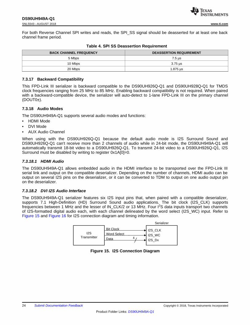
7.3.18.2 DVI I2S Audio InterfaceThe DS90UH949A-Q1 serializer features six I2S input pins that, when paired with a compatible deserializer,supports 7.1 High-Definition (HD) Surround Sound audio applications. The bit clock (I2S_CLK) supportsfrequencies between 1 MHz and the lesser of IN_CLK/2 or 13 MHz. Four I2S data inputs transport two channelsof I2S-formatted digital audio each, with each channel delineated by the word select (I2S_WC) input. Refer toFigure 15 and Figure 16 for I2S connection diagram and timing information.
Figure 15. I2S Connection Diagram
I2S_CLK
I2S_WC
I2S_Dx MSB LSB MSB LSB
25
DS90UH949A-Q1www.ti.com SNLS543 –AUGUST 2018
Product Folder Links: DS90UH949A-Q1
Submit Documentation FeedbackCopyright © 2018, Texas Instruments Incorporated
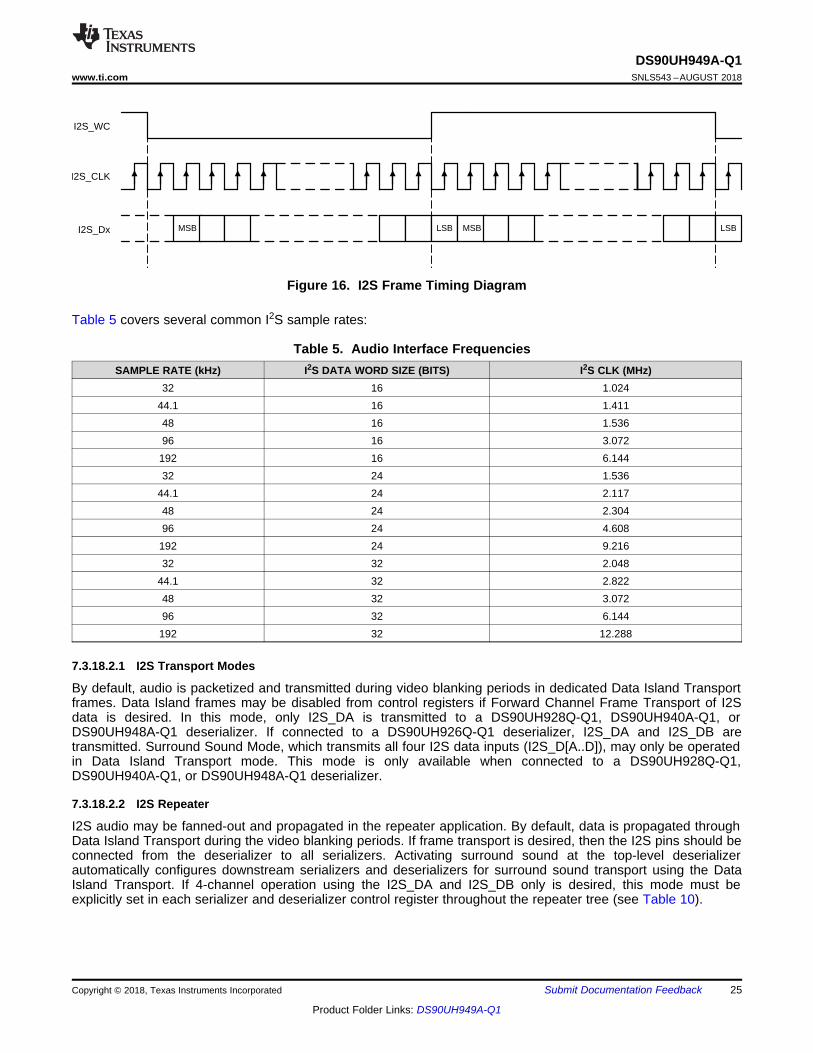
Figure 16. I2S Frame Timing Diagram
Table 5 covers several common I2S sample rates:
Table 5. Audio Interface FrequenciesSAMPLE RATE (kHz) I2S DATA WORD SIZE (BITS) I2S CLK (MHz)
32 16 1.02444.1 16 1.41148 16 1.53696 16 3.072
192 16 6.14432 24 1.536
44.1 24 2.11748 24 2.30496 24 4.608
192 24 9.21632 32 2.048
44.1 32 2.82248 32 3.07296 32 6.144
192 32 12.288
7.3.18.2.1 I2S Transport Modes
By default, audio is packetized and transmitted during video blanking periods in dedicated Data Island Transportframes. Data Island frames may be disabled from control registers if Forward Channel Frame Transport of I2Sdata is desired. In this mode, only I2S_DA is transmitted to a DS90UH928Q-Q1, DS90UH940A-Q1, orDS90UH948A-Q1 deserializer. If connected to a DS90UH926Q-Q1 deserializer, I2S_DA and I2S_DB aretransmitted. Surround Sound Mode, which transmits all four I2S data inputs (I2S_D[A..D]), may only be operatedin Data Island Transport mode. This mode is only available when connected to a DS90UH928Q-Q1,DS90UH940A-Q1, or DS90UH948A-Q1 deserializer.
7.3.18.2.2 I2S Repeater
I2S audio may be fanned-out and propagated in the repeater application. By default, data is propagated throughData Island Transport during the video blanking periods. If frame transport is desired, then the I2S pins should beconnected from the deserializer to all serializers. Activating surround sound at the top-level deserializerautomatically configures downstream serializers and deserializers for surround sound transport using the DataIsland Transport. If 4-channel operation using the I2S_DA and I2S_DB only is desired, this mode must beexplicitly set in each serializer and deserializer control register throughout the repeater tree (see Table 10).
I2S_WC
I2S_CLK
I2S Mode DIN1
(Single)
t1/fS (256 BCKs at Single Rate, 128 BCKs at Dual Rate)t
023 22 23 22 0 23 22 0 23 22 0 23 22 0 23 22 0 23 22 0 23 22 0 23 22
Ch 2t32 BCKst
Ch 3t32 BCKst
Ch 4t32 BCKst
Ch 5t32 BCKst
Ch 6t32 BCKst
Ch 7t32 BCKst
Ch 8t32 BCKst
Ch 1t32 BCKst
26
DS90UH949A-Q1SNLS543 –AUGUST 2018 www.ti.com
Product Folder Links: DS90UH949A-Q1
Submit Documentation Feedback Copyright © 2018, Texas Instruments Incorporated
7.3.18.3 AUX Audio ChannelThe AUX Audio Channel is a single separate I2S audio data channel that may be transported independently ofthe main audio stream received in either HDMI Mode or DVI Mode. This channel is shared with the GPIO[1:0]interface and is supported by the DS90UH940A-Q1 and DS90UH948A-Q1 deserializers.
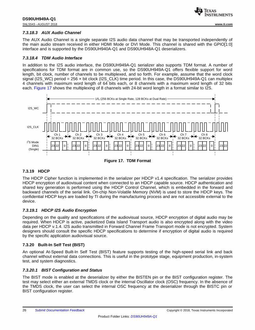
7.3.18.4 TDM Audio InterfaceIn addition to the I2S audio interface, the DS90UH949A-Q1 serializer also supports TDM format. A number ofspecifications for TDM format are in common use, so the DS90UH949A-Q1 offers flexible support for wordlength, bit clock, number of channels to be multiplexed, and so forth. For example, assume that the word clocksignal (I2S_WC) period = 256 × bit clock (I2S_CLK) time period. In this case, the DS90UH949A-Q1 can multiplex4 channels with maximum word length of 64 bits each, or 8 channels with a maximum word length of 32 bitseach. Figure 17 shows the multiplexing of 8 channels with 24-bit word length in a format similar to I2S.
Figure 17. TDM Format
7.3.19 HDCPThe HDCP Cipher function is implemented in the serializer per HDCP v1.4 specification. The serializer providesHDCP encryption of audiovisual content when connected to an HDCP capable source. HDCP authentication andshared key generation is performed using the HDCP Control Channel, which is embedded in the forward andbackward channels of the serial link. On-chip Non-Volatile Memory (NVM) is used to store the HDCP keys. Theconfidential HDCP keys are loaded by TI during the manufacturing process and are not accessible external to thedevice.
7.3.19.1 HDCP I2S Audio EncryptionDepending on the quality and specifications of the audiovisual source, HDCP encryption of digital audio may berequired. When HDCP is active, packetized Data Island Transport audio is also encrypted along with the videodata per HDCP v.1.4. I2S audio transmitted in Forward Channel Frame Transport mode is not encrypted. Systemdesigners should consult the specific HDCP specifications to determine if encryption of digital audio is requiredby the specific application audiovisual source.
7.3.20 Built-In Self Test (BIST)An optional At-Speed Built-In Self Test (BIST) feature supports testing of the high-speed serial link and backchannel without external data connections. This is useful in the prototype stage, equipment production, in-systemtest, and system diagnostics.
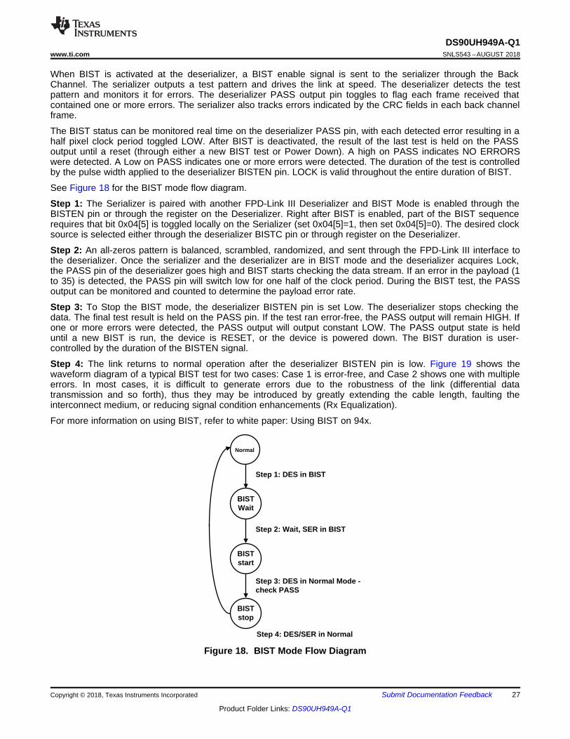
7.3.20.1 BIST Configuration and StatusThe BIST mode is enabled at the deserializer by either the BISTEN pin or the BIST configuration register. Thetest may select either an external TMDS clock or the internal Oscillator clock (OSC) frequency. In the absence ofthe TMDS clock, the user can select the internal OSC frequency at the deserializer through the BISTC pin orBIST configuration register.
BISTstart
BISTstop
BISTWait
Step 1: DES in BIST
Step 2: Wait, SER in BIST
Step 3: DES in Normal Mode - check PASS
Step 4: DES/SER in Normal
Normal
27
DS90UH949A-Q1www.ti.com SNLS543 –AUGUST 2018
Product Folder Links: DS90UH949A-Q1
Submit Documentation FeedbackCopyright © 2018, Texas Instruments Incorporated
When BIST is activated at the deserializer, a BIST enable signal is sent to the serializer through the BackChannel. The serializer outputs a test pattern and drives the link at speed. The deserializer detects the testpattern and monitors it for errors. The deserializer PASS output pin toggles to flag each frame received thatcontained one or more errors. The serializer also tracks errors indicated by the CRC fields in each back channelframe.
The BIST status can be monitored real time on the deserializer PASS pin, with each detected error resulting in ahalf pixel clock period toggled LOW. After BIST is deactivated, the result of the last test is held on the PASSoutput until a reset (through either a new BIST test or Power Down). A high on PASS indicates NO ERRORSwere detected. A Low on PASS indicates one or more errors were detected. The duration of the test is controlledby the pulse width applied to the deserializer BISTEN pin. LOCK is valid throughout the entire duration of BIST.
See Figure 18 for the BIST mode flow diagram.
Step 1: The Serializer is paired with another FPD-Link III Deserializer and BIST Mode is enabled through theBISTEN pin or through the register on the Deserializer. Right after BIST is enabled, part of the BIST sequencerequires that bit 0x04[5] is toggled locally on the Serializer (set 0x04[5]=1, then set 0x04[5]=0). The desired clocksource is selected either through the deserializer BISTC pin or through register on the Deserializer.
Step 2: An all-zeros pattern is balanced, scrambled, randomized, and sent through the FPD-Link III interface tothe deserializer. Once the serializer and the deserializer are in BIST mode and the deserializer acquires Lock,the PASS pin of the deserializer goes high and BIST starts checking the data stream. If an error in the payload (1to 35) is detected, the PASS pin will switch low for one half of the clock period. During the BIST test, the PASSoutput can be monitored and counted to determine the payload error rate.
Step 3: To Stop the BIST mode, the deserializer BISTEN pin is set Low. The deserializer stops checking thedata. The final test result is held on the PASS pin. If the test ran error-free, the PASS output will remain HIGH. Ifone or more errors were detected, the PASS output will output constant LOW. The PASS output state is helduntil a new BIST is run, the device is RESET, or the device is powered down. The BIST duration is user-controlled by the duration of the BISTEN signal.
Step 4: The link returns to normal operation after the deserializer BISTEN pin is low. Figure 19 shows thewaveform diagram of a typical BIST test for two cases: Case 1 is error-free, and Case 2 shows one with multipleerrors. In most cases, it is difficult to generate errors due to the robustness of the link (differential datatransmission and so forth), thus they may be introduced by greatly extending the cable length, faulting theinterconnect medium, or reducing signal condition enhancements (Rx Equalization).
For more information on using BIST, refer to white paper: Using BIST on 94x.
Figure 18. BIST Mode Flow Diagram
X XX
TxCLKOUT±
BISTEN(DES)
PASS
DATA(internal)
PASS
BIST Duration
Prior Result
BIST ResultHeld
PASS
FAIL
X = bit error(s)
TxOUT[3:0]±
DATA(internal)
Case 1 - P
assC
ase 2 - Fail
Prior Result
Normal PRBS BIST Test Normal
DE
S O
utputs
28
DS90UH949A-Q1SNLS543 –AUGUST 2018 www.ti.com
Product Folder Links: DS90UH949A-Q1
Submit Documentation Feedback Copyright © 2018, Texas Instruments Incorporated
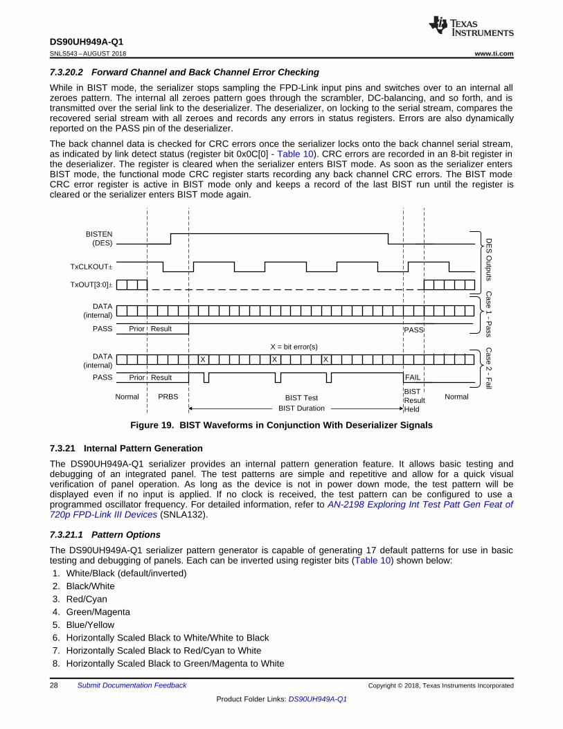
7.3.20.2 Forward Channel and Back Channel Error CheckingWhile in BIST mode, the serializer stops sampling the FPD-Link input pins and switches over to an internal allzeroes pattern. The internal all zeroes pattern goes through the scrambler, DC-balancing, and so forth, and istransmitted over the serial link to the deserializer. The deserializer, on locking to the serial stream, compares therecovered serial stream with all zeroes and records any errors in status registers. Errors are also dynamicallyreported on the PASS pin of the deserializer.
The back channel data is checked for CRC errors once the serializer locks onto the back channel serial stream,as indicated by link detect status (register bit 0x0C[0] - Table 10). CRC errors are recorded in an 8-bit register inthe deserializer. The register is cleared when the serializer enters BIST mode. As soon as the serializer entersBIST mode, the functional mode CRC register starts recording any back channel CRC errors. The BIST modeCRC error register is active in BIST mode only and keeps a record of the last BIST run until the register iscleared or the serializer enters BIST mode again.
Figure 19. BIST Waveforms in Conjunction With Deserializer Signals
7.3.21 Internal Pattern GenerationThe DS90UH949A-Q1 serializer provides an internal pattern generation feature. It allows basic testing anddebugging of an integrated panel. The test patterns are simple and repetitive and allow for a quick visualverification of panel operation. As long as the device is not in power down mode, the test pattern will bedisplayed even if no input is applied. If no clock is received, the test pattern can be configured to use aprogrammed oscillator frequency. For detailed information, refer to AN-2198 Exploring Int Test Patt Gen Feat of720p FPD-Link III Devices (SNLA132).
7.3.21.1 Pattern OptionsThe DS90UH949A-Q1 serializer pattern generator is capable of generating 17 default patterns for use in basictesting and debugging of panels. Each can be inverted using register bits (Table 10) shown below:1. White/Black (default/inverted)2. Black/White3. Red/Cyan4. Green/Magenta5. Blue/Yellow6. Horizontally Scaled Black to White/White to Black7. Horizontally Scaled Black to Red/Cyan to White8. Horizontally Scaled Black to Green/Magenta to White
29
DS90UH949A-Q1www.ti.com SNLS543 –AUGUST 2018
Product Folder Links: DS90UH949A-Q1
Submit Documentation FeedbackCopyright © 2018, Texas Instruments Incorporated
9. Horizontally Scaled Black to Blue/Yellow to White10. Vertically Scaled Black to White/White to Black11. Vertically Scaled Black to Red/Cyan to White12. Vertically Scaled Black to Green/Magenta to White13. Vertically Scaled Black to Blue/Yellow to White14. Custom Color (or its inversion) configured in PGRS15. Black-White/White-Black Checkerboard (or custom checkerboard color, configured in PGCTL)16. YCBR/RBCY VCOM pattern, orientation is configurable from PGCTL17. Color Bars (White, Yellow, Cyan, Green, Magenta, Red, Blue, Black) – Note: not included in the auto-
scrolling feature
Additionally, the Pattern Generator incorporates one user-configurable, full-screen, 24-bit color controlled by thePGRS, PGGS, and PGBS registers. This is pattern #14. One of the pattern options is statically selected in thePGCTL register when Auto-Scrolling is disabled. The PGTSC and PGTSO1-8 registers control the patternselection and order when Auto-Scrolling is enabled.
7.3.21.2 Color ModesBy default, the Pattern Generator operates in 24-bit color mode where all bits of the Red, Green, and Blueoutputs are enabled. 18-bit color mode can be activated from the configuration registers (Table 10). In 18-bitmode, the 6 most significant bits (bits 7-2) of the Red, Green, and Blue outputs are enabled. The 2 leastsignificant bits will be 0.
7.3.21.3 Video Timing ModesThe Pattern Generator has two video timing modes – external and internal. In external timing mode, the PatternGenerator detects the video frame timing present on the DE and VS inputs. If Vertical Sync signaling is notpresent on VS, the Pattern Generator determines Vertical Blank by detecting when the number of inactive pixelclocks (DE = 0) exceeds twice the detected active line length. In internal timing mode, the Pattern Generatoruses custom video timing as configured in the control registers. The internal timing generation may also bedriven by an external clock. By default, external timing mode is enabled. Internal timing or Internal timing withExternal Clock are enabled by the control registers (Table 10).
7.3.21.4 External TimingIn external timing mode, the Pattern Generator passes the incoming DE, HS, and VS signals unmodified to thevideo control outputs after a two pixel clock delay. The Pattern Generator extracts the active frame dimensionsfrom the incoming signals to properly scale the brightness patterns. If the incoming video stream does not usethe VS signal, the Pattern Generator determines the Vertical Blank time by detecting a long period of pixel clockswithout DE asserted.
7.3.21.5 Pattern InversionThe Pattern Generator also incorporates a global inversion control, located in the PGCFG register, which causesthe output pattern to be bitwise-inverted. For example, the full screen Red pattern becomes full-screen cyan, andthe Vertically Scaled Black to Green pattern becomes Vertically Scaled White to Magenta.
7.3.21.6 Auto ScrollingThe Pattern Generator supports an Auto-Scrolling mode, in which the output pattern cycles through a list ofenabled pattern types. A sequence of up to 16 patterns may be defined in the registers. The patterns mayappear in any order in the sequence and may also appear more than once.
7.3.21.7 Additional FeaturesAdditional pattern generator features can be accessed through the Pattern Generator Indirect Register Map. Itconsists of the Pattern Generator Indirect Address (PGIA reg_0x66 — Table 10) and the Pattern GeneratorIndirect Data (PGID reg_0x67 — Table 10). See AN-2198 Exploring Int Test Patt Gen Feat of 720p FPD-Link IIIDevices (SNLA132).
SerializerR4
MODE_SEL0
1.8 V
R3
VR4
R6
1.8 V
R5
VR6
MODE_SEL1
30
DS90UH949A-Q1SNLS543 –AUGUST 2018 www.ti.com
Product Folder Links: DS90UH949A-Q1
Submit Documentation Feedback Copyright © 2018, Texas Instruments Incorporated
7.3.22 Spread Spectrum Clock ToleranceThe DS90UH949A-Q1 (for DVI mode) tolerates a spread spectrum input clock to help reduce EMI. The followingtriangular SSC profile is supported:• Frequency deviation ≤ 2.5%• Modulation rate ≤ 100 kHz
Note: Maximum frequency deviation and maximum modulation rate are not supported simultaneously. Sometypical examples:• Frequency deviation: 2.5%, modulation rate: 50 kHz• Frequency deviation: 1.25%, modulation rate: 100 kHz
7.4 Device Functional Modes
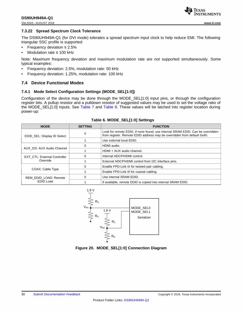
7.4.1 Mode Select Configuration Settings (MODE_SEL[1:0])Configuration of the device may be done through the MODE_SEL[1:0] input pins, or through the configurationregister bits. A pullup resistor and a pulldown resistor of suggested values may be used to set the voltage ratio ofthe MODE_SEL[1:0] inputs. See Table 7 and Table 8. These values will be latched into register location duringpower-up:
Table 6. MODE_SEL[1:0] SettingsMODE SETTING FUNCTION
EDID_SEL: Display ID Select0 Look for remote EDID, if none found, use internal SRAM EDID. Can be overridden
from register. Remote EDID address may be overridden from default 0xA0.1 Use external local EDID.
AUX_I2S: AUX Audio Channel0 HDMI audio.1 HDMI + AUX audio channel.
EXT_CTL: External ControllerOverride
0 Internal HDCP/HDMI control.1 External HDCP/HDMI control from I2C interface pins.
COAX: Cable Type0 Enable FPD-Link III for twisted pair cabling.1 Enable FPD-Link III for coaxial cabling.
REM_EDID_LOAD: RemoteEDID Load
0 Use internal SRAM EDID.1 If available, remote EDID is copied into internal SRAM EDID.
Figure 20. MODE_SEL[1:0] Connection Diagram
31
DS90UH949A-Q1www.ti.com SNLS543 –AUGUST 2018
Product Folder Links: DS90UH949A-Q1
Submit Documentation FeedbackCopyright © 2018, Texas Instruments Incorporated
(1) This resistor does not need to be 1% tolerance. 5% is acceptable.
Table 7. Configuration Select (MODE_SEL0)
NO. RATIOVR4/VDD18
TARGET VR4(V)
SUGGESTEDRESISTOR PULLUP
R3 kΩ (1% tol)
SUGGESTEDRESISTOR
PULLDOWN R4 kΩ(1% tol)
EDID_SEL AUX_I2S
1 0 0 OPEN Any value less than100 (1)
0 0
2 0.208 0.374 118 30.9 0 13 0.553 0.995 82.5 102 1 04 0.668 1.202 68.1 137 1 1
(1) This resistor does not need to be 1% tolerance. 5% is acceptable.
Table 8. Configuration Select (MODE_SEL1)
NO. RATIOVR6/VDD18
TARGET VR6(V)
SUGGESTEDRESISTORPULLUP R5kΩ (1% tol)
SUGGESTEDRESISTOR
PULLDOWN R6kΩ (1% tol)
EXT_CTL COAX REM_EDID_LOAD
1 0 0 OPEN Any value less than100 (1) 0 0 0
2 0.208 0.374 118 30.9 0 0 13 0.323 0.582 107 51.1 0 1 04 0.440 0.792 113 88.7 0 1 15 0.553 0.995 82.5 102 1 0 06 0.668 1.202 68.1 137 1 0 17 0.789 1.420 56.2 210 1 1 0
8 1 1.8 Any value lessthan 100 (1) OPEN 1 1 1
The strapped values can be viewed and/or modified in the following locations:• EDID_SEL : Latched into BRIDGE_CTL[0], EDID_DISABLE (0x4F[0]).• AUX_I2S : Latched into BRIDGE_CFG[1], AUDIO_MODE[1] (0x54[1]).• EXT_CTL: Latched into BRIDGE_CFG[7], EXT_CONTROL (0x54[7]).• COAX : Latched into DUAL_CTL1[7], COAX_MODE (0x5B[7]).• REM_EDID_LOAD : Latched into BRIDGE_CFG[5] (0x54[5]).
7.4.2 FPD-Link III Modes of OperationThe FPD-Link III transmit logic supports several modes of operation, dependent on the downstream receiver aswell as the video being delivered. The following modes are supported:
7.4.2.1 Single Link OperationSingle Link mode transmits the video over a single FPD-Link III to a single receiver. Single link mode supportsfrequencies up to 105 MHz for 24-bit video when paired with the DS90UH940A-Q1/DS90UH948A-Q1. This modeis compatible with the DS90UH926Q-Q1/DS90UH928Q-Q1 when operating below 85 MHz. If the downstreamdevice is capable, the secondary FPD-Link III link could be used for high-speed control.
In Forced Single mode (set through DUAL_CTL1 register), the secondary TX Phy and back channel aredisabled.
32
DS90UH949A-Q1SNLS543 –AUGUST 2018 www.ti.com
Product Folder Links: DS90UH949A-Q1
Submit Documentation Feedback Copyright © 2018, Texas Instruments Incorporated
7.4.2.2 Dual Link OperationIn Dual Link mode, the FPD-Link III TX splits a single video stream and sends alternating pixels on twodownstream links. If HDCP is enabled, a single HDCP connection is created for the video that is sent on the twolinks. The receiver must be a DS90UH948A-Q1 or DS90UH940A-Q1, capable of receiving the dual-stream video.Dual link mode is capable of supporting an HDMI clock frequency of up to 210 MHz, with each FPD-Link III TXport running at one-half the frequency. This allows support for full 2K video. The secondary FPD-Link III linkcould be used for high-speed control.
Dual Link mode may be automatically configured when connected to a DS90UH948A-Q1/DS90UH940A-Q1, ifthe video meets minimum frequency requirements. Dual Link mode may also be forced using the DUAL_CTL1register.
For dual lane operation, if the High-Speed Control Channel (HSCC) is desired, force the back channelcapabilities for Port 1.
• Force the backchannel capability for Port1:– Set Reg0x1E=0x02 (Select Port1 in Port Select register)– Set Reg0x20=0x8F (Make Port1 Dual link capable in Deserializer Capabilities register)– Set Reg0x1E=0x01 (Select Port0 in Port Select register to restore the register default value)
• For forcing Dual Lane mode, use the following configuration:– Set Reg0x5B[2:0]=011b (Disable Auto-detect and Force Dual Link mode in DUAL_CTL1 register)
Any device configuration including this one should be written as a part of the 949A Init A sequence as shown inFigure 33
7.4.2.3 Replicate ModeIn this mode, the FPD-Link III TX operates as a 1:2 HDCP Repeater. A second HDCP core is implemented tosupport HDCP authentication and encryption to independent HDCP-capable receivers. The same video (up to105 MHz, 24-bit color) is delivered to each receiver.
Replicate mode may be automatically configured when connected to two independent Deserializers.
7.4.2.4 Auto-Detection of FPD-Link III ModesThe DS90UH949A-Q1 automatically detects the capabilities of downstream links and can resolve whether asingle device, dual-capable device, or multiple single link devices are connected.
In addition to the downstream device capabilities, the DS90UH949A-Q1 will be able to detect the HDMI pixelclock frequency to select the proper operating mode.
If the DS90UH949A-Q1 detects two independent devices, it will operate in Replicate mode, sending the singlechannel video on both connections. If the device detects a device on the secondary link, but not the first, it cansend the video only on the second link.
Auto-detection can be disabled to allow forced modes of operation using the Dual Link Control Register(DUAL_CTL1).
The frequency detection circuit may cause change in Single / Dual mode during a temperature ramp. When theambient temperature around the DS90UH949A-Q1 changes by more than 40°C and when PCLK is between 60MHz and 78 MHz, the auto-detect feature can switch device configuration from Single-lane to Dual-lane mode (orvice-versa) even though the input PCLK has not changed. This causes a configuration change in Deserializerresulting in a momentary loss of lock that may result in display flicker. It is recommended to configure the deviceto force Single or Dual Lane mode of operation.• For forcing Single Lane mode, use the following configuration:
– If the Deserializer is set in HSCC mode prior to forcing Single Lane mode, force the backchannelcapability for Port1:– Set Reg0x1E=0x02 (Select Port1 in Port Select register)– Set Reg0x20=0x8F (Make Port1 Dual link capable in Deserializer Capabilities register)– Set Reg0x1E=0x01 (Select Port0 in Port Select register to restore the register default value)
– Set Reg0x5B[2:0]=100b (Enable Auto-detect and disable Dual Link mode in DUAL_CTL1 register)
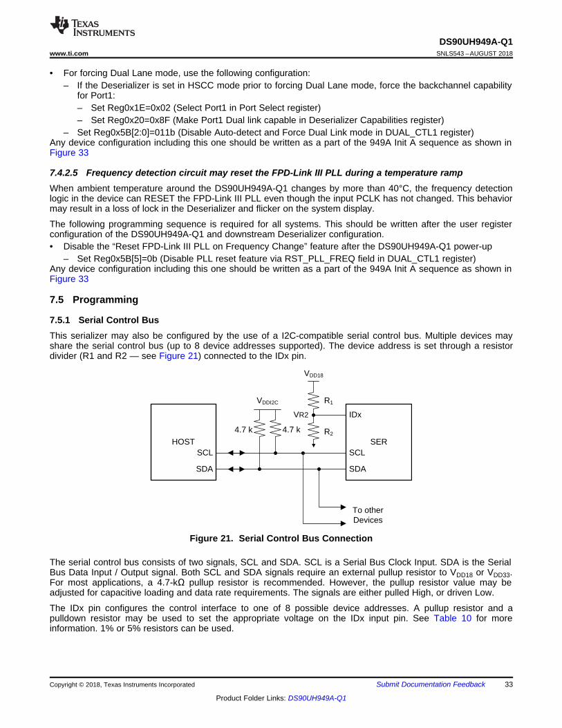
HOST SERSCL
SDA
4.7 k 4.7 k R2
SCL
SDA
To other Devices
IDx
VDD18
R1VDDI2C
VR2
33
DS90UH949A-Q1www.ti.com SNLS543 –AUGUST 2018
Product Folder Links: DS90UH949A-Q1
Submit Documentation FeedbackCopyright © 2018, Texas Instruments Incorporated
• For forcing Dual Lane mode, use the following configuration:– If the Deserializer is set in HSCC mode prior to forcing Dual Lane mode, force the backchannel capability
for Port1:– Set Reg0x1E=0x02 (Select Port1 in Port Select register)– Set Reg0x20=0x8F (Make Port1 Dual link capable in Deserializer Capabilities register)
– Set Reg0x5B[2:0]=011b (Disable Auto-detect and Force Dual Link mode in DUAL_CTL1 register)Any device configuration including this one should be written as a part of the 949A Init A sequence as shown inFigure 33
7.4.2.5 Frequency detection circuit may reset the FPD-Link III PLL during a temperature rampWhen ambient temperature around the DS90UH949A-Q1 changes by more than 40°C, the frequency detectionlogic in the device can RESET the FPD-Link III PLL even though the input PCLK has not changed. This behaviormay result in a loss of lock in the Deserializer and flicker on the system display.
The following programming sequence is required for all systems. This should be written after the user registerconfiguration of the DS90UH949A-Q1 and downstream Deserializer configuration.• Disable the “Reset FPD-Link III PLL on Frequency Change” feature after the DS90UH949A-Q1 power-up
– Set Reg0x5B[5]=0b (Disable PLL reset feature via RST_PLL_FREQ field in DUAL_CTL1 register)Any device configuration including this one should be written as a part of the 949A Init A sequence as shown inFigure 33
7.5 Programming
7.5.1 Serial Control BusThis serializer may also be configured by the use of a I2C-compatible serial control bus. Multiple devices mayshare the serial control bus (up to 8 device addresses supported). The device address is set through a resistordivider (R1 and R2 — see Figure 21) connected to the IDx pin.
Figure 21. Serial Control Bus Connection
The serial control bus consists of two signals, SCL and SDA. SCL is a Serial Bus Clock Input. SDA is the SerialBus Data Input / Output signal. Both SCL and SDA signals require an external pullup resistor to VDD18 or VDD33.For most applications, a 4.7-kΩ pullup resistor is recommended. However, the pullup resistor value may beadjusted for capacitive loading and data rate requirements. The signals are either pulled High, or driven Low.
The IDx pin configures the control interface to one of 8 possible device addresses. A pullup resistor and apulldown resistor may be used to set the appropriate voltage on the IDx input pin. See Table 10 for moreinformation. 1% or 5% resistors can be used.
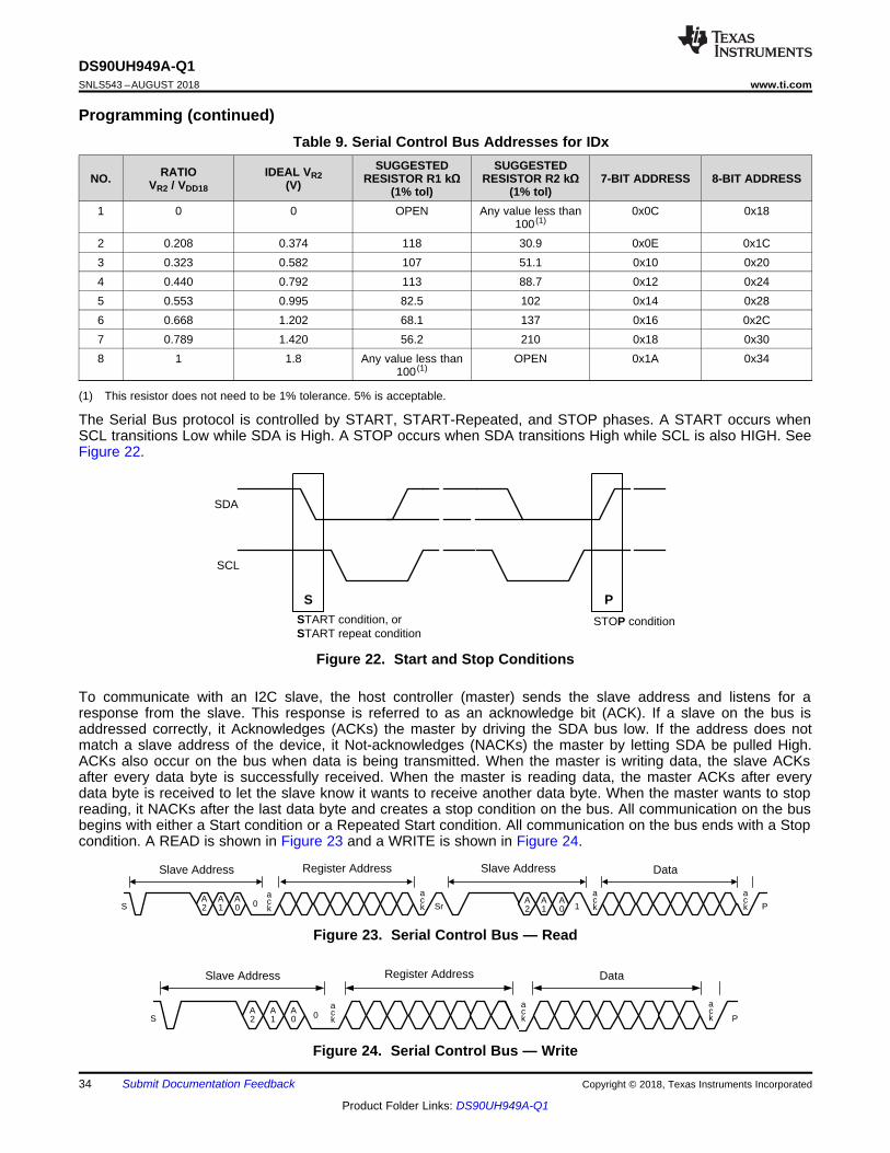
Slave Address Register Address Data
S 0ack
ack
ack P
A0
A1
A2
Slave Address Register Address Slave Address Data
S 0 1ack
ack
ack
ackSr P
A0
A1
A2
A1
A2
A0
SDA
SCL
S PSTART condition, orSTART repeat condition
STOP condition
34
DS90UH949A-Q1SNLS543 –AUGUST 2018 www.ti.com
Product Folder Links: DS90UH949A-Q1
Submit Documentation Feedback Copyright © 2018, Texas Instruments Incorporated
Programming (continued)
(1) This resistor does not need to be 1% tolerance. 5% is acceptable.
Table 9. Serial Control Bus Addresses for IDx
NO. RATIOVR2 / VDD18
IDEAL VR2(V)
SUGGESTEDRESISTOR R1 kΩ
(1% tol)
SUGGESTEDRESISTOR R2 kΩ
(1% tol)7-BIT ADDRESS 8-BIT ADDRESS
1 0 0 OPEN Any value less than100 (1)
0x0C 0x18
2 0.208 0.374 118 30.9 0x0E 0x1C3 0.323 0.582 107 51.1 0x10 0x204 0.440 0.792 113 88.7 0x12 0x245 0.553 0.995 82.5 102 0x14 0x286 0.668 1.202 68.1 137 0x16 0x2C7 0.789 1.420 56.2 210 0x18 0x308 1 1.8 Any value less than
100 (1)OPEN 0x1A 0x34
The Serial Bus protocol is controlled by START, START-Repeated, and STOP phases. A START occurs whenSCL transitions Low while SDA is High. A STOP occurs when SDA transitions High while SCL is also HIGH. SeeFigure 22.
Figure 22. Start and Stop Conditions
To communicate with an I2C slave, the host controller (master) sends the slave address and listens for aresponse from the slave. This response is referred to as an acknowledge bit (ACK). If a slave on the bus isaddressed correctly, it Acknowledges (ACKs) the master by driving the SDA bus low. If the address does notmatch a slave address of the device, it Not-acknowledges (NACKs) the master by letting SDA be pulled High.ACKs also occur on the bus when data is being transmitted. When the master is writing data, the slave ACKsafter every data byte is successfully received. When the master is reading data, the master ACKs after everydata byte is received to let the slave know it wants to receive another data byte. When the master wants to stopreading, it NACKs after the last data byte and creates a stop condition on the bus. All communication on the busbegins with either a Start condition or a Repeated Start condition. All communication on the bus ends with a Stopcondition. A READ is shown in Figure 23 and a WRITE is shown in Figure 24.
Figure 23. Serial Control Bus — Read
Figure 24. Serial Control Bus — Write
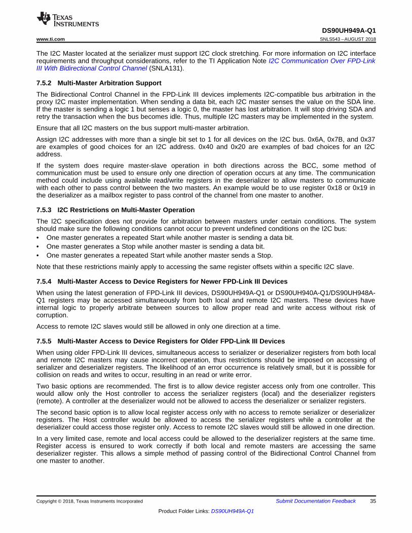
35
DS90UH949A-Q1www.ti.com SNLS543 –AUGUST 2018
Product Folder Links: DS90UH949A-Q1
Submit Documentation FeedbackCopyright © 2018, Texas Instruments Incorporated
The I2C Master located at the serializer must support I2C clock stretching. For more information on I2C interfacerequirements and throughput considerations, refer to the TI Application Note I2C Communication Over FPD-LinkIII With Bidirectional Control Channel (SNLA131).
7.5.2 Multi-Master Arbitration SupportThe Bidirectional Control Channel in the FPD-Link III devices implements I2C-compatible bus arbitration in theproxy I2C master implementation. When sending a data bit, each I2C master senses the value on the SDA line.If the master is sending a logic 1 but senses a logic 0, the master has lost arbitration. It will stop driving SDA andretry the transaction when the bus becomes idle. Thus, multiple I2C masters may be implemented in the system.
Ensure that all I2C masters on the bus support multi-master arbitration.
Assign I2C addresses with more than a single bit set to 1 for all devices on the I2C bus. 0x6A, 0x7B, and 0x37are examples of good choices for an I2C address. 0x40 and 0x20 are examples of bad choices for an I2Caddress.
If the system does require master-slave operation in both directions across the BCC, some method ofcommunication must be used to ensure only one direction of operation occurs at any time. The communicationmethod could include using available read/write registers in the deserializer to allow masters to communicatewith each other to pass control between the two masters. An example would be to use register 0x18 or 0x19 inthe deserializer as a mailbox register to pass control of the channel from one master to another.
7.5.3 I2C Restrictions on Multi-Master OperationThe I2C specification does not provide for arbitration between masters under certain conditions. The systemshould make sure the following conditions cannot occur to prevent undefined conditions on the I2C bus:• One master generates a repeated Start while another master is sending a data bit.• One master generates a Stop while another master is sending a data bit.• One master generates a repeated Start while another master sends a Stop.
Note that these restrictions mainly apply to accessing the same register offsets within a specific I2C slave.
7.5.4 Multi-Master Access to Device Registers for Newer FPD-Link III DevicesWhen using the latest generation of FPD-Link III devices, DS90UH949A-Q1 or DS90UH940A-Q1/DS90UH948A-Q1 registers may be accessed simultaneously from both local and remote I2C masters. These devices haveinternal logic to properly arbitrate between sources to allow proper read and write access without risk ofcorruption.
Access to remote I2C slaves would still be allowed in only one direction at a time.
7.5.5 Multi-Master Access to Device Registers for Older FPD-Link III DevicesWhen using older FPD-Link III devices, simultaneous access to serializer or deserializer registers from both localand remote I2C masters may cause incorrect operation, thus restrictions should be imposed on accessing ofserializer and deserializer registers. The likelihood of an error occurrence is relatively small, but it is possible forcollision on reads and writes to occur, resulting in an read or write error.
Two basic options are recommended. The first is to allow device register access only from one controller. Thiswould allow only the Host controller to access the serializer registers (local) and the deserializer registers(remote). A controller at the deserializer would not be allowed to access the deserializer or serializer registers.
The second basic option is to allow local register access only with no access to remote serializer or deserializerregisters. The Host controller would be allowed to access the serializer registers while a controller at thedeserializer could access those register only. Access to remote I2C slaves would still be allowed in one direction.
In a very limited case, remote and local access could be allowed to the deserializer registers at the same time.Register access is ensured to work correctly if both local and remote masters are accessing the samedeserializer register. This allows a simple method of passing control of the Bidirectional Control Channel fromone master to another.
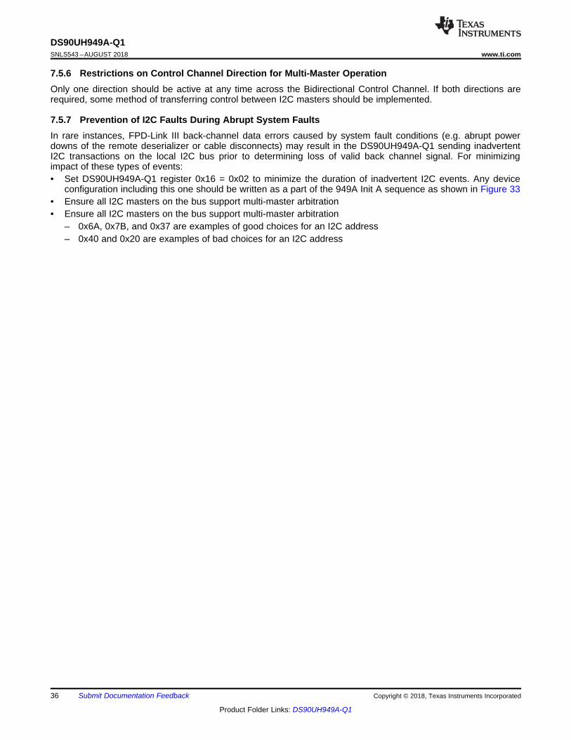
36
DS90UH949A-Q1SNLS543 –AUGUST 2018 www.ti.com
Product Folder Links: DS90UH949A-Q1
Submit Documentation Feedback Copyright © 2018, Texas Instruments Incorporated
7.5.6 Restrictions on Control Channel Direction for Multi-Master OperationOnly one direction should be active at any time across the Bidirectional Control Channel. If both directions arerequired, some method of transferring control between I2C masters should be implemented.
7.5.7 Prevention of I2C Faults During Abrupt System FaultsIn rare instances, FPD-Link III back-channel data errors caused by system fault conditions (e.g. abrupt powerdowns of the remote deserializer or cable disconnects) may result in the DS90UH949A-Q1 sending inadvertentI2C transactions on the local I2C bus prior to determining loss of valid back channel signal. For minimizingimpact of these types of events:• Set DS90UH949A-Q1 register 0x16 = 0x02 to minimize the duration of inadvertent I2C events. Any device
configuration including this one should be written as a part of the 949A Init A sequence as shown in Figure 33• Ensure all I2C masters on the bus support multi-master arbitration• Ensure all I2C masters on the bus support multi-master arbitration
– 0x6A, 0x7B, and 0x37 are examples of good choices for an I2C address– 0x40 and 0x20 are examples of bad choices for an I2C address
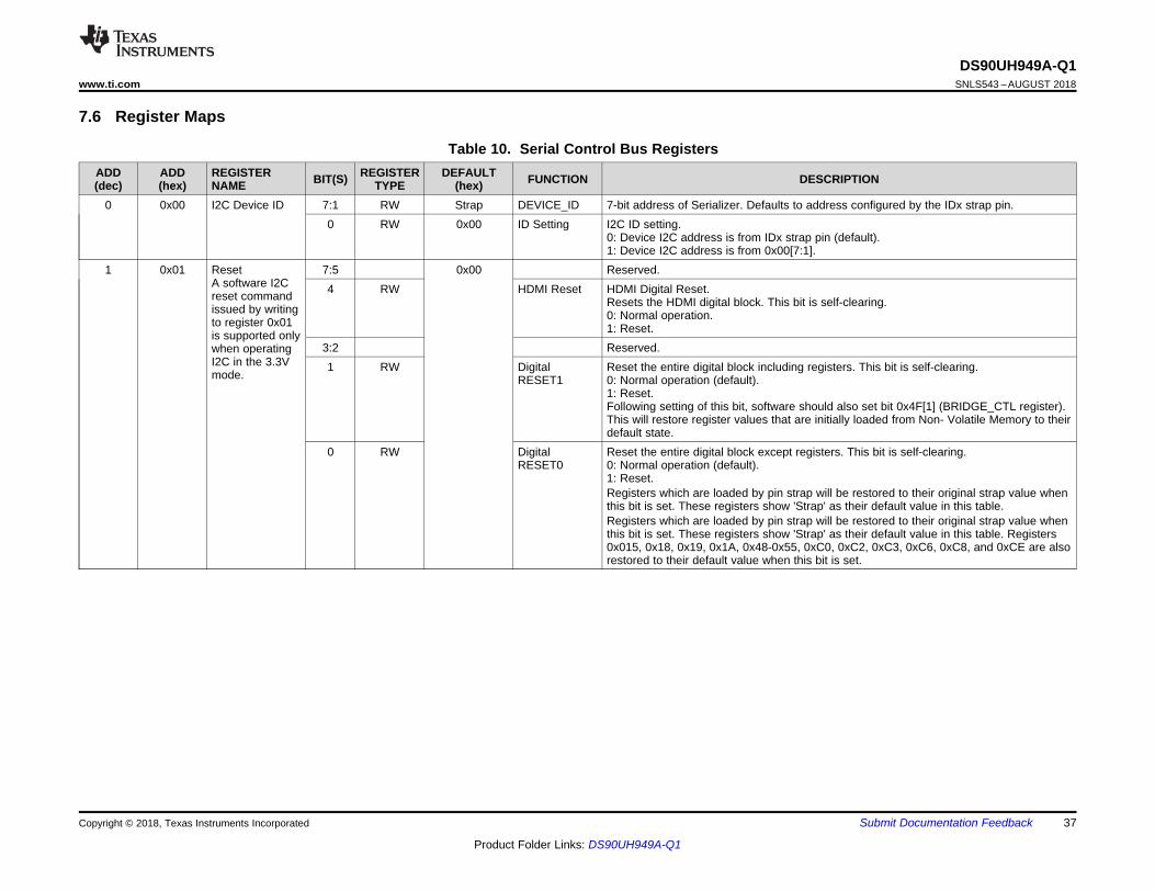
DS90UH949A-Q1www.ti.com SNLS543 –AUGUST 2018
37
Product Folder Links: DS90UH949A-Q1
Submit Documentation FeedbackCopyright © 2018, Texas Instruments Incorporated
7.6 Register Maps
Table 10. Serial Control Bus RegistersADD(dec)
ADD(hex)
REGISTERNAME BIT(S) REGISTER
TYPEDEFAULT
(hex) FUNCTION DESCRIPTION
0 0x00 I2C Device ID 7:1 RW Strap DEVICE_ID 7-bit address of Serializer. Defaults to address configured by the IDx strap pin.0 RW 0x00 ID Setting I2C ID setting.
0: Device I2C address is from IDx strap pin (default).1: Device I2C address is from 0x00[7:1].
1 0x01 ResetA software I2Creset commandissued by writingto register 0x01is supported onlywhen operatingI2C in the 3.3Vmode.
7:5 0x00 Reserved.4 RW HDMI Reset HDMI Digital Reset.
Resets the HDMI digital block. This bit is self-clearing.0: Normal operation.1: Reset.
3:2 Reserved.1 RW Digital
RESET1Reset the entire digital block including registers. This bit is self-clearing.0: Normal operation (default).1: Reset.Following setting of this bit, software should also set bit 0x4F[1] (BRIDGE_CTL register).This will restore register values that are initially loaded from Non- Volatile Memory to theirdefault state.
0 RW DigitalRESET0
Reset the entire digital block except registers. This bit is self-clearing.0: Normal operation (default).1: Reset.Registers which are loaded by pin strap will be restored to their original strap value whenthis bit is set. These registers show 'Strap' as their default value in this table.Registers which are loaded by pin strap will be restored to their original strap value whenthis bit is set. These registers show 'Strap' as their default value in this table. Registers0x015, 0x18, 0x19, 0x1A, 0x48-0x55, 0xC0, 0xC2, 0xC3, 0xC6, 0xC8, and 0xCE are alsorestored to their default value when this bit is set.
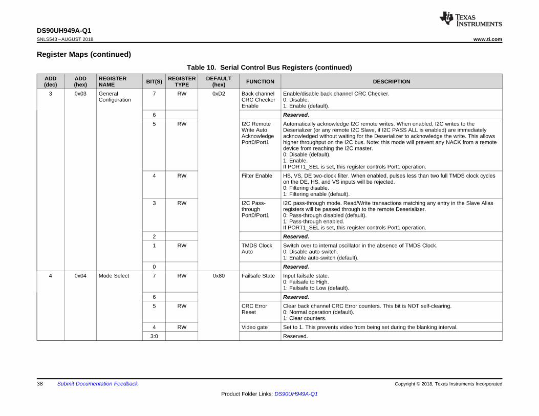
DS90UH949A-Q1SNLS543 –AUGUST 2018 www.ti.com
38
Product Folder Links: DS90UH949A-Q1
Submit Documentation Feedback Copyright © 2018, Texas Instruments Incorporated
Register Maps (continued)Table 10. Serial Control Bus Registers (continued)
ADD(dec)
ADD(hex)
REGISTERNAME BIT(S) REGISTER
TYPEDEFAULT
(hex) FUNCTION DESCRIPTION
3 0x03 GeneralConfiguration
7 RW 0xD2 Back channelCRC CheckerEnable
Enable/disable back channel CRC Checker.0: Disable.1: Enable (default).
6 Reserved.5 RW I2C Remote
Write AutoAcknowledgePort0/Port1
Automatically acknowledge I2C remote writes. When enabled, I2C writes to theDeserializer (or any remote I2C Slave, if I2C PASS ALL is enabled) are immediatelyacknowledged without waiting for the Deserializer to acknowledge the write. This allowshigher throughput on the I2C bus. Note: this mode will prevent any NACK from a remotedevice from reaching the I2C master.0: Disable (default).1: Enable.If PORT1_SEL is set, this register controls Port1 operation.
4 RW Filter Enable HS, VS, DE two-clock filter. When enabled, pulses less than two full TMDS clock cycleson the DE, HS, and VS inputs will be rejected.0: Filtering disable.1: Filtering enable (default).
3 RW I2C Pass-throughPort0/Port1
I2C pass-through mode. Read/Write transactions matching any entry in the Slave Aliasregisters will be passed through to the remote Deserializer.0: Pass-through disabled (default).1: Pass-through enabled.If PORT1_SEL is set, this register controls Port1 operation.
2 Reserved.1 RW TMDS Clock
AutoSwitch over to internal oscillator in the absence of TMDS Clock.0: Disable auto-switch.1: Enable auto-switch (default).
0 Reserved.4 0x04 Mode Select 7 RW 0x80 Failsafe State Input failsafe state.
0: Failsafe to High.1: Failsafe to Low (default).
6 Reserved.5 RW CRC Error
ResetClear back channel CRC Error counters. This bit is NOT self-clearing.0: Normal operation (default).1: Clear counters.
4 RW Video gate Set to 1. This prevents video from being set during the blanking interval.3:0 Reserved.
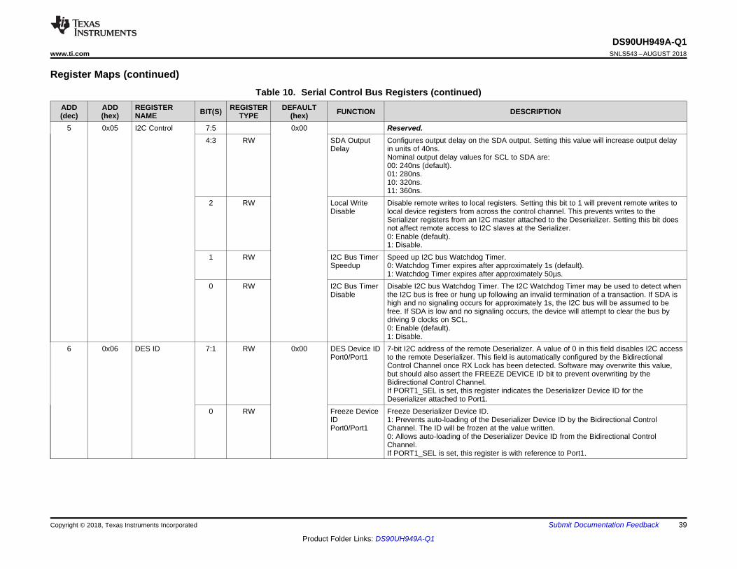
DS90UH949A-Q1www.ti.com SNLS543 –AUGUST 2018
39
Product Folder Links: DS90UH949A-Q1
Submit Documentation FeedbackCopyright © 2018, Texas Instruments Incorporated
Register Maps (continued)Table 10. Serial Control Bus Registers (continued)
ADD(dec)
ADD(hex)
REGISTERNAME BIT(S) REGISTER
TYPEDEFAULT
(hex) FUNCTION DESCRIPTION
5 0x05 I2C Control 7:5 0x00 Reserved.4:3 RW SDA Output
DelayConfigures output delay on the SDA output. Setting this value will increase output delayin units of 40ns.Nominal output delay values for SCL to SDA are:00: 240ns (default).01: 280ns.10: 320ns.11: 360ns.
2 RW Local WriteDisable
Disable remote writes to local registers. Setting this bit to 1 will prevent remote writes tolocal device registers from across the control channel. This prevents writes to theSerializer registers from an I2C master attached to the Deserializer. Setting this bit doesnot affect remote access to I2C slaves at the Serializer.0: Enable (default).1: Disable.
1 RW I2C Bus TimerSpeedup
Speed up I2C bus Watchdog Timer.0: Watchdog Timer expires after approximately 1s (default).1: Watchdog Timer expires after approximately 50µs.
0 RW I2C Bus TimerDisable
Disable I2C bus Watchdog Timer. The I2C Watchdog Timer may be used to detect whenthe I2C bus is free or hung up following an invalid termination of a transaction. If SDA ishigh and no signaling occurs for approximately 1s, the I2C bus will be assumed to befree. If SDA is low and no signaling occurs, the device will attempt to clear the bus bydriving 9 clocks on SCL.0: Enable (default).1: Disable.
6 0x06 DES ID 7:1 RW 0x00 DES Device IDPort0/Port1
7-bit I2C address of the remote Deserializer. A value of 0 in this field disables I2C accessto the remote Deserializer. This field is automatically configured by the BidirectionalControl Channel once RX Lock has been detected. Software may overwrite this value,but should also assert the FREEZE DEVICE ID bit to prevent overwriting by theBidirectional Control Channel.If PORT1_SEL is set, this register indicates the Deserializer Device ID for theDeserializer attached to Port1.
0 RW Freeze DeviceIDPort0/Port1
Freeze Deserializer Device ID.1: Prevents auto-loading of the Deserializer Device ID by the Bidirectional ControlChannel. The ID will be frozen at the value written.0: Allows auto-loading of the Deserializer Device ID from the Bidirectional ControlChannel.If PORT1_SEL is set, this register is with reference to Port1.
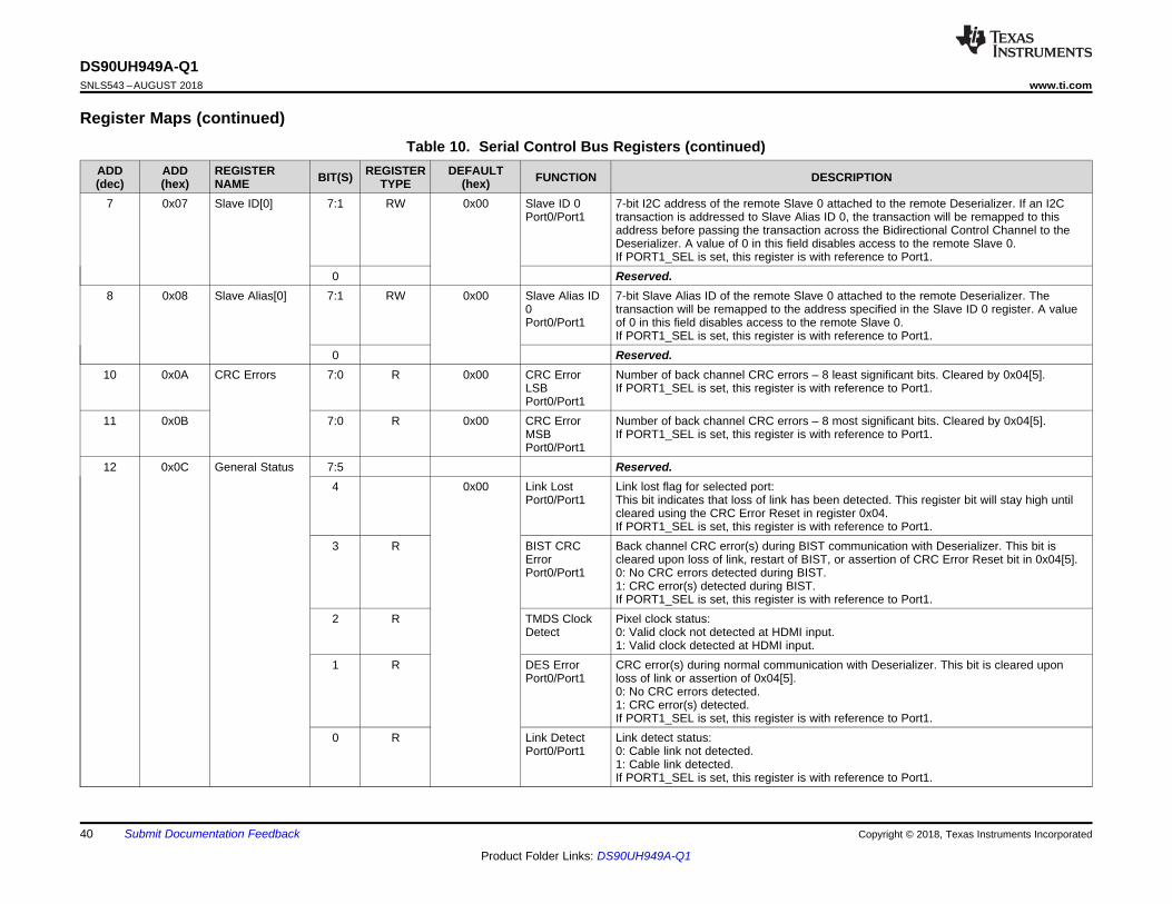
DS90UH949A-Q1SNLS543 –AUGUST 2018 www.ti.com
40
Product Folder Links: DS90UH949A-Q1
Submit Documentation Feedback Copyright © 2018, Texas Instruments Incorporated
Register Maps (continued)Table 10. Serial Control Bus Registers (continued)
ADD(dec)
ADD(hex)
REGISTERNAME BIT(S) REGISTER
TYPEDEFAULT
(hex) FUNCTION DESCRIPTION
7 0x07 Slave ID[0] 7:1 RW 0x00 Slave ID 0Port0/Port1
7-bit I2C address of the remote Slave 0 attached to the remote Deserializer. If an I2Ctransaction is addressed to Slave Alias ID 0, the transaction will be remapped to thisaddress before passing the transaction across the Bidirectional Control Channel to theDeserializer. A value of 0 in this field disables access to the remote Slave 0.If PORT1_SEL is set, this register is with reference to Port1.
0 Reserved.8 0x08 Slave Alias[0] 7:1 RW 0x00 Slave Alias ID
0Port0/Port1
7-bit Slave Alias ID of the remote Slave 0 attached to the remote Deserializer. Thetransaction will be remapped to the address specified in the Slave ID 0 register. A valueof 0 in this field disables access to the remote Slave 0.If PORT1_SEL is set, this register is with reference to Port1.
0 Reserved.10 0x0A CRC Errors 7:0 R 0x00 CRC Error
LSBPort0/Port1
Number of back channel CRC errors – 8 least significant bits. Cleared by 0x04[5].If PORT1_SEL is set, this register is with reference to Port1.
11 0x0B 7:0 R 0x00 CRC ErrorMSBPort0/Port1
Number of back channel CRC errors – 8 most significant bits. Cleared by 0x04[5].If PORT1_SEL is set, this register is with reference to Port1.
12 0x0C General Status 7:5 Reserved.4 0x00 Link Lost
Port0/Port1Link lost flag for selected port:This bit indicates that loss of link has been detected. This register bit will stay high untilcleared using the CRC Error Reset in register 0x04.If PORT1_SEL is set, this register is with reference to Port1.
3 R BIST CRCErrorPort0/Port1
Back channel CRC error(s) during BIST communication with Deserializer. This bit iscleared upon loss of link, restart of BIST, or assertion of CRC Error Reset bit in 0x04[5].0: No CRC errors detected during BIST.1: CRC error(s) detected during BIST.If PORT1_SEL is set, this register is with reference to Port1.
2 R TMDS ClockDetect
Pixel clock status:0: Valid clock not detected at HDMI input.1: Valid clock detected at HDMI input.
1 R DES ErrorPort0/Port1
CRC error(s) during normal communication with Deserializer. This bit is cleared uponloss of link or assertion of 0x04[5].0: No CRC errors detected.1: CRC error(s) detected.If PORT1_SEL is set, this register is with reference to Port1.
0 R Link DetectPort0/Port1
Link detect status:0: Cable link not detected.1: Cable link detected.If PORT1_SEL is set, this register is with reference to Port1.
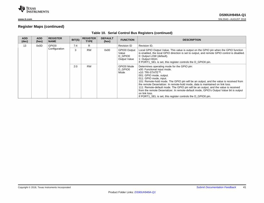
DS90UH949A-Q1www.ti.com SNLS543 –AUGUST 2018
41
Product Folder Links: DS90UH949A-Q1
Submit Documentation FeedbackCopyright © 2018, Texas Instruments Incorporated
Register Maps (continued)Table 10. Serial Control Bus Registers (continued)
ADD(dec)
ADD(hex)
REGISTERNAME BIT(S) REGISTER
TYPEDEFAULT
(hex) FUNCTION DESCRIPTION
13 0x0D GPIO0Configuration
7:4 R Revision ID Revision ID.3 RW 0x00 GPIO0 Output
ValueD_GPIO0Output Value
Local GPIO Output Value. This value is output on the GPIO pin when the GPIO functionis enabled, the local GPIO direction is set to output, and remote GPIO control is disabled.0: Output LOW (default).1: Output HIGH.If PORT1_SEL is set, this register controls the D_GPIO0 pin.
2:0 RW GPIO0 ModeD_GPIO0Mode
Determines operating mode for the GPIO pin:x00: Functional input mode.x10: TRI-STATE™.001: GPIO mode, output.011: GPIO mode, input.101: Remote-hold mode. The GPIO pin will be an output, and the value is received fromthe remote Deserializer. In remote-hold mode, data is maintained on link loss.111: Remote-default mode. The GPIO pin will be an output, and the value is receivedfrom the remote Deserializer. In remote-default mode, GPIO's Output Value bit is outputon link loss.If PORT1_SEL is set, this register controls the D_GPIO0 pin.
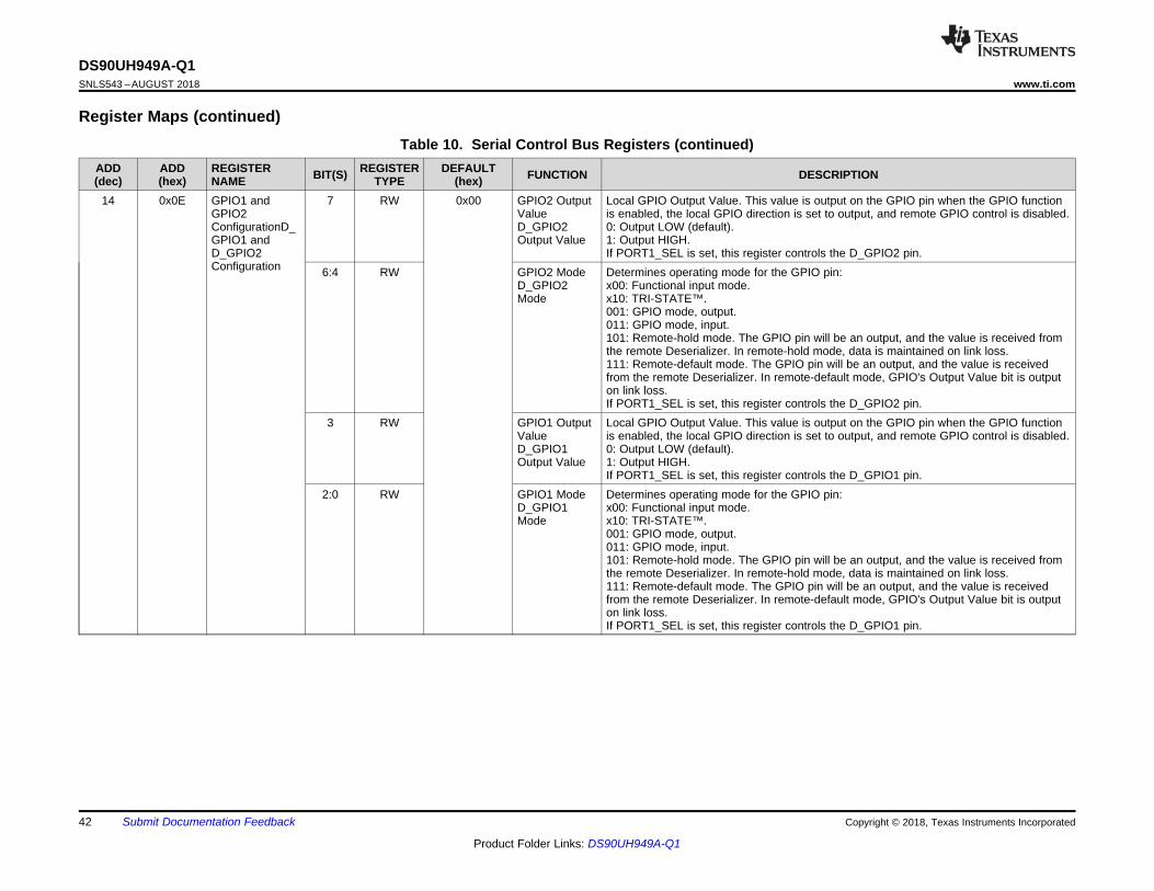
DS90UH949A-Q1SNLS543 –AUGUST 2018 www.ti.com
42
Product Folder Links: DS90UH949A-Q1
Submit Documentation Feedback Copyright © 2018, Texas Instruments Incorporated
Register Maps (continued)Table 10. Serial Control Bus Registers (continued)
ADD(dec)
ADD(hex)
REGISTERNAME BIT(S) REGISTER
TYPEDEFAULT
(hex) FUNCTION DESCRIPTION
14 0x0E GPIO1 andGPIO2ConfigurationD_GPIO1 andD_GPIO2Configuration
7 RW 0x00 GPIO2 OutputValueD_GPIO2Output Value
Local GPIO Output Value. This value is output on the GPIO pin when the GPIO functionis enabled, the local GPIO direction is set to output, and remote GPIO control is disabled.0: Output LOW (default).1: Output HIGH.If PORT1_SEL is set, this register controls the D_GPIO2 pin.
6:4 RW GPIO2 ModeD_GPIO2Mode
Determines operating mode for the GPIO pin:x00: Functional input mode.x10: TRI-STATE™.001: GPIO mode, output.011: GPIO mode, input.101: Remote-hold mode. The GPIO pin will be an output, and the value is received fromthe remote Deserializer. In remote-hold mode, data is maintained on link loss.111: Remote-default mode. The GPIO pin will be an output, and the value is receivedfrom the remote Deserializer. In remote-default mode, GPIO's Output Value bit is outputon link loss.If PORT1_SEL is set, this register controls the D_GPIO2 pin.
3 RW GPIO1 OutputValueD_GPIO1Output Value
Local GPIO Output Value. This value is output on the GPIO pin when the GPIO functionis enabled, the local GPIO direction is set to output, and remote GPIO control is disabled.0: Output LOW (default).1: Output HIGH.If PORT1_SEL is set, this register controls the D_GPIO1 pin.
2:0 RW GPIO1 ModeD_GPIO1Mode
Determines operating mode for the GPIO pin:x00: Functional input mode.x10: TRI-STATE™.001: GPIO mode, output.011: GPIO mode, input.101: Remote-hold mode. The GPIO pin will be an output, and the value is received fromthe remote Deserializer. In remote-hold mode, data is maintained on link loss.111: Remote-default mode. The GPIO pin will be an output, and the value is receivedfrom the remote Deserializer. In remote-default mode, GPIO's Output Value bit is outputon link loss.If PORT1_SEL is set, this register controls the D_GPIO1 pin.
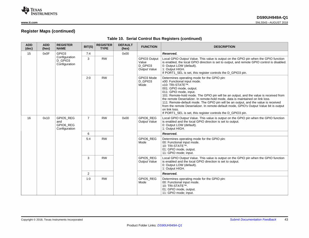
DS90UH949A-Q1www.ti.com SNLS543 –AUGUST 2018
43
Product Folder Links: DS90UH949A-Q1
Submit Documentation FeedbackCopyright © 2018, Texas Instruments Incorporated
Register Maps (continued)Table 10. Serial Control Bus Registers (continued)
ADD(dec)
ADD(hex)
REGISTERNAME BIT(S) REGISTER
TYPEDEFAULT
(hex) FUNCTION DESCRIPTION
15 0x0F GPIO3ConfigurationD_GPIO3Configuration
7:4 0x00 Reserved.3 RW GPIO3 Output
ValueD_GPIO3Output Value
Local GPIO Output Value. This value is output on the GPIO pin when the GPIO functionis enabled, the local GPIO direction is set to output, and remote GPIO control is disabled.0: Output LOW (default).1: Output HIGH.If PORT1_SEL is set, this register controls the D_GPIO3 pin.
2:0 RW GPIO3 ModeD_GPIO3Mode
Determines operating mode for the GPIO pin:x00: Functional input mode.x10: TRI-STATE™.001: GPIO mode, output.011: GPIO mode, input.101: Remote-hold mode. The GPIO pin will be an output, and the value is received fromthe remote Deserializer. In remote-hold mode, data is maintained on link loss.111: Remote-default mode. The GPIO pin will be an output, and the value is receivedfrom the remote Deserializer. In remote-default mode, GPIO's Output Value bit is outputon link loss.If PORT1_SEL is set, this register controls the D_GPIO3 pin.
16 0x10 GPIO5_REGandGPIO6_REGConfiguration
7 RW 0x00 GPIO6_REGOutput Value
Local GPIO Output Value. This value is output on the GPIO pin when the GPIO functionis enabled and the local GPIO direction is set to output.0: Output LOW (default).1: Output HIGH.
6 Reserved.5:4 RW GPIO6_REG
ModeDetermines operating mode for the GPIO pin:00: Functional input mode.10: TRI-STATE™.01: GPIO mode, output.11: GPIO mode; input.
3 RW GPIO5_REGOutput Value
Local GPIO Output Value. This value is output on the GPIO pin when the GPIO functionis enabled and the local GPIO direction is set to output.0: Output LOW (default).1: Output HIGH.
2 Reserved.1:0 RW GPIO5_REG
ModeDetermines operating mode for the GPIO pin:00: Functional input mode.10: TRI-STATE™.01: GPIO mode, output.11: GPIO mode; input.
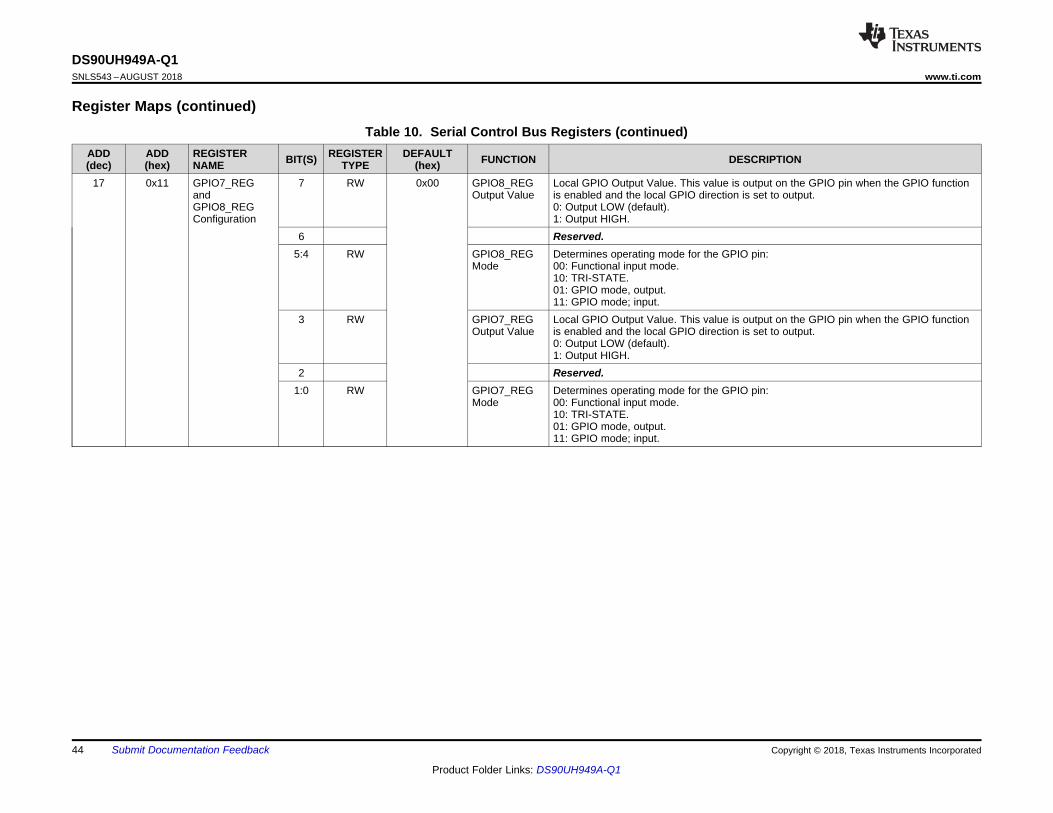
DS90UH949A-Q1SNLS543 –AUGUST 2018 www.ti.com
44
Product Folder Links: DS90UH949A-Q1
Submit Documentation Feedback Copyright © 2018, Texas Instruments Incorporated
Register Maps (continued)Table 10. Serial Control Bus Registers (continued)
ADD(dec)
ADD(hex)
REGISTERNAME BIT(S) REGISTER
TYPEDEFAULT
(hex) FUNCTION DESCRIPTION
17 0x11 GPIO7_REGandGPIO8_REGConfiguration
7 RW 0x00 GPIO8_REGOutput Value
Local GPIO Output Value. This value is output on the GPIO pin when the GPIO functionis enabled and the local GPIO direction is set to output.0: Output LOW (default).1: Output HIGH.
6 Reserved.5:4 RW GPIO8_REG
ModeDetermines operating mode for the GPIO pin:00: Functional input mode.10: TRI-STATE.01: GPIO mode, output.11: GPIO mode; input.
3 RW GPIO7_REGOutput Value
Local GPIO Output Value. This value is output on the GPIO pin when the GPIO functionis enabled and the local GPIO direction is set to output.0: Output LOW (default).1: Output HIGH.
2 Reserved.1:0 RW GPIO7_REG
ModeDetermines operating mode for the GPIO pin:00: Functional input mode.10: TRI-STATE.01: GPIO mode, output.11: GPIO mode; input.
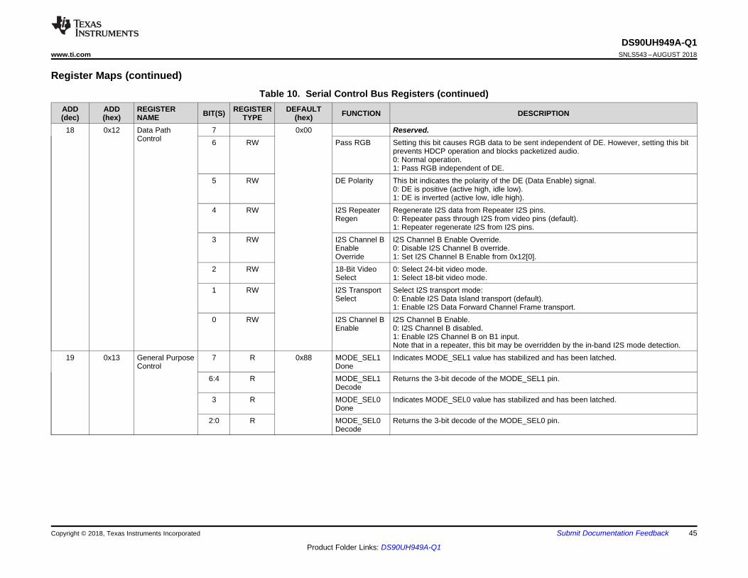
DS90UH949A-Q1www.ti.com SNLS543 –AUGUST 2018
45
Product Folder Links: DS90UH949A-Q1
Submit Documentation FeedbackCopyright © 2018, Texas Instruments Incorporated
Register Maps (continued)Table 10. Serial Control Bus Registers (continued)
ADD(dec)
ADD(hex)
REGISTERNAME BIT(S) REGISTER
TYPEDEFAULT
(hex) FUNCTION DESCRIPTION
18 0x12 Data PathControl
7 0x00 Reserved.6 RW Pass RGB Setting this bit causes RGB data to be sent independent of DE. However, setting this bit
prevents HDCP operation and blocks packetized audio.0: Normal operation.1: Pass RGB independent of DE.
5 RW DE Polarity This bit indicates the polarity of the DE (Data Enable) signal.0: DE is positive (active high, idle low).1: DE is inverted (active low, idle high).
4 RW I2S RepeaterRegen
Regenerate I2S data from Repeater I2S pins.0: Repeater pass through I2S from video pins (default).1: Repeater regenerate I2S from I2S pins.
3 RW I2S Channel BEnableOverride
I2S Channel B Enable Override.0: Disable I2S Channel B override.1: Set I2S Channel B Enable from 0x12[0].
2 RW 18-Bit VideoSelect
0: Select 24-bit video mode.1: Select 18-bit video mode.
1 RW I2S TransportSelect
Select I2S transport mode:0: Enable I2S Data Island transport (default).1: Enable I2S Data Forward Channel Frame transport.
0 RW I2S Channel BEnable
I2S Channel B Enable.0: I2S Channel B disabled.1: Enable I2S Channel B on B1 input.Note that in a repeater, this bit may be overridden by the in-band I2S mode detection.
19 0x13 General PurposeControl
7 R 0x88 MODE_SEL1Done
Indicates MODE_SEL1 value has stabilized and has been latched.
6:4 R MODE_SEL1Decode
Returns the 3-bit decode of the MODE_SEL1 pin.
3 R MODE_SEL0Done
Indicates MODE_SEL0 value has stabilized and has been latched.
2:0 R MODE_SEL0Decode
Returns the 3-bit decode of the MODE_SEL0 pin.
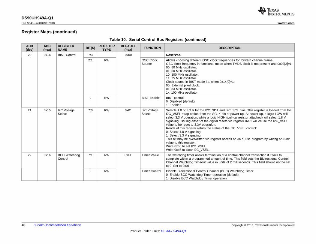
DS90UH949A-Q1SNLS543 –AUGUST 2018 www.ti.com
46
Product Folder Links: DS90UH949A-Q1
Submit Documentation Feedback Copyright © 2018, Texas Instruments Incorporated
Register Maps (continued)Table 10. Serial Control Bus Registers (continued)
ADD(dec)
ADD(hex)
REGISTERNAME BIT(S) REGISTER
TYPEDEFAULT
(hex) FUNCTION DESCRIPTION
20 0x14 BIST Control 7:3 0x00 Reserved.2:1 RW OSC Clock
SourceAllows choosing different OSC clock frequencies for forward channel frame.OSC clock frequency in functional mode when TMDS clock is not present and 0x03[2]=1:00: 50 MHz oscillator.01: 50 MHz oscillator.10: 100 MHz oscillator.11: 25 MHz oscillator.Clock source in BIST mode i.e. when 0x14[0]=1:00: External pixel clock.01: 33 MHz oscillator.1x: 100 MHz oscillator.
0 RW BIST Enable BIST control:0: Disabled (default).1: Enabled.
21 0x15 I2C VoltageSelect
7:0 RW 0x01 I2C VoltageSelect
Selects 1.8 or 3.3 V for the I2C_SDA and I2C_SCL pins. This register is loaded from theI2C_VSEL strap option from the SCLK pin at power-up. At power-up, a logic LOW willselect 3.3 V operation, while a logic HIGH (pull-up resistor attached) will select 1.8 Vsignaling. Issuing either of the digital resets via register 0x01 will cause the I2C_VSELvalue to be reset to 3.3V operation.Reads of this register return the status of the I2C_VSEL control:0: Select 1.8 V signaling.1: Select 3.3 V signaling.This bit may be overwritten via register access or via eFuse program by writing an 8-bitvalue to this register:Write 0xb5 to set I2C_VSEL.Write 0xb6 to clear I2C_VSEL.
22 0x16 BCC WatchdogControl
7:1 RW 0xFE Timer Value The watchdog timer allows termination of a control channel transaction if it fails tocomplete within a programmed amount of time. This field sets the Bidirectional ControlChannel Watchdog Timeout value in units of 2 milliseconds. This field should not be setto 0. Set to 0x01.
0 RW Timer Control Disable Bidirectional Control Channel (BCC) Watchdog Timer:0: Enable BCC Watchdog Timer operation (default).1: Disable BCC Watchdog Timer operation.
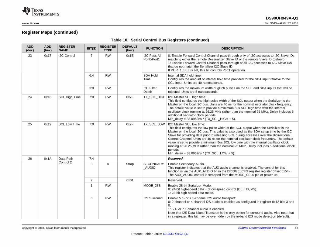
DS90UH949A-Q1www.ti.com SNLS543 –AUGUST 2018
47
Product Folder Links: DS90UH949A-Q1
Submit Documentation FeedbackCopyright © 2018, Texas Instruments Incorporated
Register Maps (continued)Table 10. Serial Control Bus Registers (continued)
ADD(dec)
ADD(hex)
REGISTERNAME BIT(S) REGISTER
TYPEDEFAULT
(hex) FUNCTION DESCRIPTION
23 0x17 I2C Control 7 RW 0x1E I2C Pass AllPort0/Port1
0: Enable Forward Control Channel pass-through only of I2C accesses to I2C Slave IDsmatching either the remote Deserializer Slave ID or the remote Slave ID (default).1: Enable Forward Control Channel pass-through of all I2C accesses to I2C Slave IDsthat do not match the Serializer I2C Slave ID.If PORT1_SEL is set, this bit controls Port1 operation.
6:4 RW SDA HoldTime
Internal SDA hold time:Configures the amount of internal hold time provided for the SDA input relative to theSCL input. Units are 40 nanoseconds.
3:0 RW I2C FilterDepth
Configures the maximum width of glitch pulses on the SCL and SDA inputs that will berejected. Units are 5 nanoseconds.
24 0x18 SCL High Time 7:0 RW 0x7F TX_SCL_HIGH I2C Master SCL high time:This field configures the high pulse width of the SCL output when the Serializer is theMaster on the local I2C bus. Units are 40 ns for the nominal oscillator clock frequency.The default value is set to provide a minimum 5us SCL high time with the internaloscillator clock running at 26.25 MHz rather than the nominal 25 MHz. Delay includes 5additional oscillator clock periods.Min_delay = 38.0952ns * (TX_SCL_HIGH + 5).
25 0x19 SCL Low Time 7:0 RW 0x7F TX_SCL_LOW I2C Master SCL low time:This field configures the low pulse width of the SCL output when the Serializer is theMaster on the local I2C bus. This value is also used as the SDA setup time by the I2CSlave for providing data prior to releasing SCL during accesses over the BidirectionalControl Channel. Units are 40 ns for the nominal oscillator clock frequency. The defaultvalue is set to provide a minimum 5us SCL low time with the internal oscillator clockrunning at 26.25 MHz rather than the nominal 25 MHz. Delay includes 5 additional clockperiods.Min_delay = 38.0952ns * (TX_SCL_LOW + 5).
26 0x1A Data PathControl 2
7:4 Reserved.3 R Strap SECONDARY
_AUDIOEnable Secondary Audio.This register indicates that the AUX audio channel is enabled. The control for thisfunction is via the AUX_AUDIO bit in the BRIDGE_CFG register register offset 0x54).The AUX_AUDIO control is strapped from the MODE_SEL0 pin at power-up.
2 0x01 Reserved.1 RW MODE_28B Enable 28-bit Serializer Mode.
0: 24-bit high-speed data + 3 low-speed control (DE, HS, VS).1: 28-bit high-speed data mode.
0 RW I2S Surround Enable 5.1- or 7.1-channel I2S audio transport:0: 2-channel or 4-channel I2S audio is enabled as configured in register 0x12 bits 3 and0.1: 5.1- or 7.1-channel audio is enabled.Note that I2S Data Island Transport is the only option for surround audio. Also note thatin a repeater, this bit may be overridden by the in-band I2S mode detection (default).
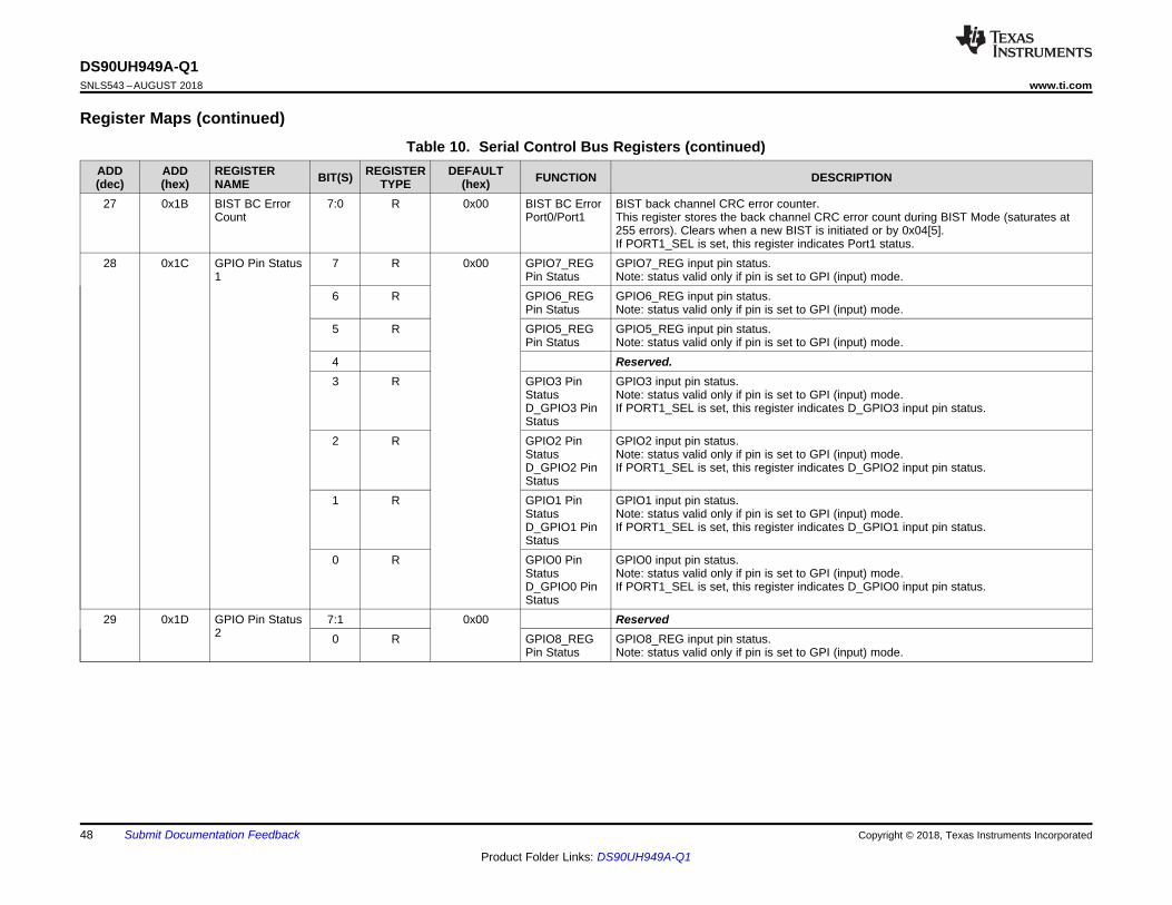
DS90UH949A-Q1SNLS543 –AUGUST 2018 www.ti.com
48
Product Folder Links: DS90UH949A-Q1
Submit Documentation Feedback Copyright © 2018, Texas Instruments Incorporated
Register Maps (continued)Table 10. Serial Control Bus Registers (continued)
ADD(dec)
ADD(hex)
REGISTERNAME BIT(S) REGISTER
TYPEDEFAULT
(hex) FUNCTION DESCRIPTION
27 0x1B BIST BC ErrorCount
7:0 R 0x00 BIST BC ErrorPort0/Port1
BIST back channel CRC error counter.This register stores the back channel CRC error count during BIST Mode (saturates at255 errors). Clears when a new BIST is initiated or by 0x04[5].If PORT1_SEL is set, this register indicates Port1 status.
28 0x1C GPIO Pin Status1
7 R 0x00 GPIO7_REGPin Status
GPIO7_REG input pin status.Note: status valid only if pin is set to GPI (input) mode.
6 R GPIO6_REGPin Status
GPIO6_REG input pin status.Note: status valid only if pin is set to GPI (input) mode.
5 R GPIO5_REGPin Status
GPIO5_REG input pin status.Note: status valid only if pin is set to GPI (input) mode.
4 Reserved.3 R GPIO3 Pin
StatusD_GPIO3 PinStatus
GPIO3 input pin status.Note: status valid only if pin is set to GPI (input) mode.If PORT1_SEL is set, this register indicates D_GPIO3 input pin status.
2 R GPIO2 PinStatusD_GPIO2 PinStatus
GPIO2 input pin status.Note: status valid only if pin is set to GPI (input) mode.If PORT1_SEL is set, this register indicates D_GPIO2 input pin status.
1 R GPIO1 PinStatusD_GPIO1 PinStatus
GPIO1 input pin status.Note: status valid only if pin is set to GPI (input) mode.If PORT1_SEL is set, this register indicates D_GPIO1 input pin status.
0 R GPIO0 PinStatusD_GPIO0 PinStatus
GPIO0 input pin status.Note: status valid only if pin is set to GPI (input) mode.If PORT1_SEL is set, this register indicates D_GPIO0 input pin status.
29 0x1D GPIO Pin Status2
7:1 0x00 Reserved0 R GPIO8_REG
Pin StatusGPIO8_REG input pin status.Note: status valid only if pin is set to GPI (input) mode.
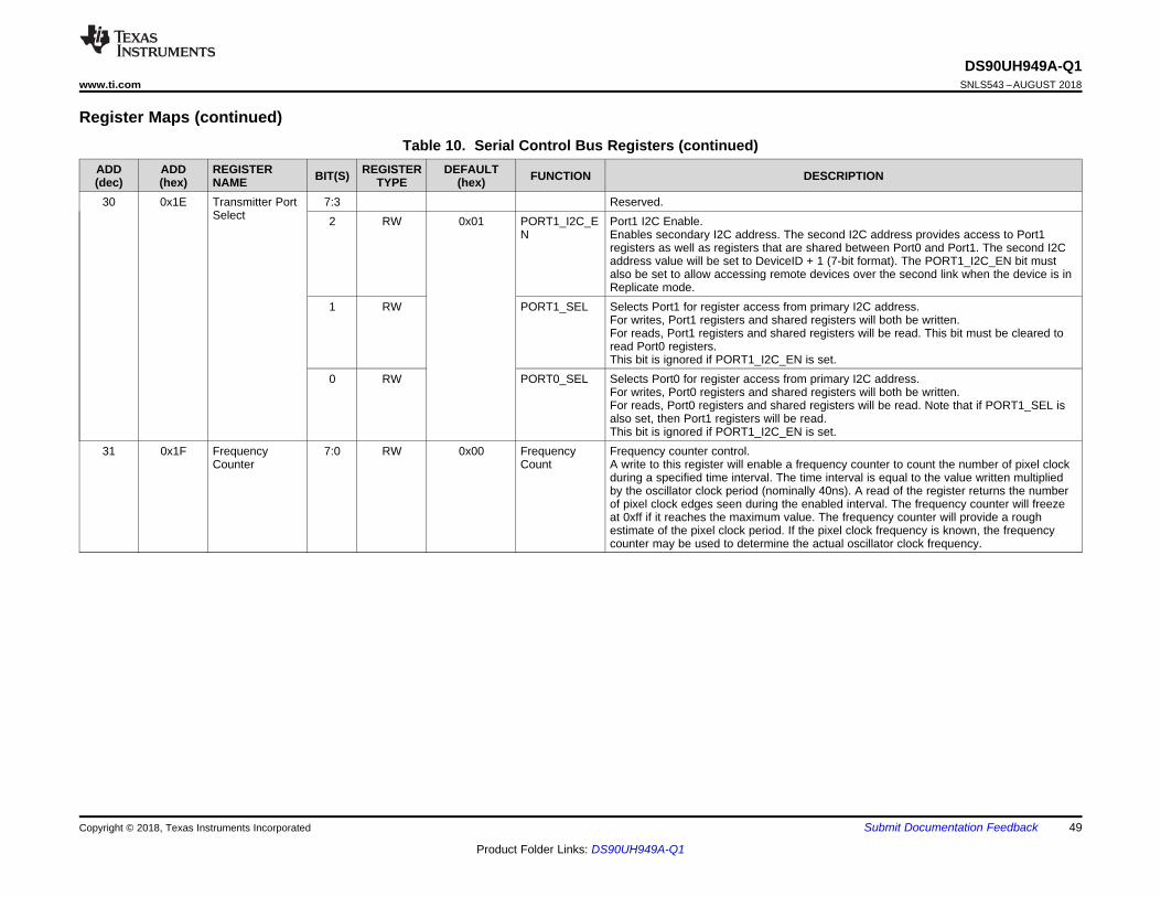
DS90UH949A-Q1www.ti.com SNLS543 –AUGUST 2018
49
Product Folder Links: DS90UH949A-Q1
Submit Documentation FeedbackCopyright © 2018, Texas Instruments Incorporated
Register Maps (continued)Table 10. Serial Control Bus Registers (continued)
ADD(dec)
ADD(hex)
REGISTERNAME BIT(S) REGISTER
TYPEDEFAULT
(hex) FUNCTION DESCRIPTION
30 0x1E Transmitter PortSelect
7:3 Reserved.2 RW 0x01 PORT1_I2C_E
NPort1 I2C Enable.Enables secondary I2C address. The second I2C address provides access to Port1registers as well as registers that are shared between Port0 and Port1. The second I2Caddress value will be set to DeviceID + 1 (7-bit format). The PORT1_I2C_EN bit mustalso be set to allow accessing remote devices over the second link when the device is inReplicate mode.
1 RW PORT1_SEL Selects Port1 for register access from primary I2C address.For writes, Port1 registers and shared registers will both be written.For reads, Port1 registers and shared registers will be read. This bit must be cleared toread Port0 registers.This bit is ignored if PORT1_I2C_EN is set.
0 RW PORT0_SEL Selects Port0 for register access from primary I2C address.For writes, Port0 registers and shared registers will both be written.For reads, Port0 registers and shared registers will be read. Note that if PORT1_SEL isalso set, then Port1 registers will be read.This bit is ignored if PORT1_I2C_EN is set.
31 0x1F FrequencyCounter
7:0 RW 0x00 FrequencyCount
Frequency counter control.A write to this register will enable a frequency counter to count the number of pixel clockduring a specified time interval. The time interval is equal to the value written multipliedby the oscillator clock period (nominally 40ns). A read of the register returns the numberof pixel clock edges seen during the enabled interval. The frequency counter will freezeat 0xff if it reaches the maximum value. The frequency counter will provide a roughestimate of the pixel clock period. If the pixel clock frequency is known, the frequencycounter may be used to determine the actual oscillator clock frequency.
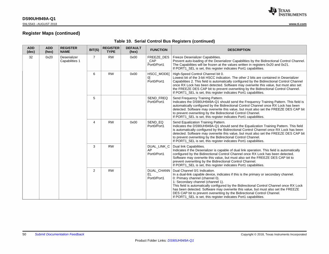
DS90UH949A-Q1SNLS543 –AUGUST 2018 www.ti.com
50
Product Folder Links: DS90UH949A-Q1
Submit Documentation Feedback Copyright © 2018, Texas Instruments Incorporated
Register Maps (continued)Table 10. Serial Control Bus Registers (continued)
ADD(dec)
ADD(hex)
REGISTERNAME BIT(S) REGISTER
TYPEDEFAULT
(hex) FUNCTION DESCRIPTION
32 0x20 DeserializerCapabilities 1
7 RW 0x00 FREEZE_DES_CAPPort0/Port1
Freeze Deserializer Capabilities.Prevent auto-loading of the Deserializer Capabilities by the Bidirectional Control Channel.The Capabilities will be frozen at the values written in registers 0x20 and 0x21.If PORT1_SEL is set, this register indicates Port1 capabilities.
6 RW 0x00 HSCC_MODE[0]Port0/Port1
High-Speed Control Channel bit 0.Lowest bit of the 3-bit HSCC indication. The other 2 bits are contained in DeserializerCapabilities 2. This field is automatically configured by the Bidirectional Control Channelonce RX Lock has been detected. Software may overwrite this value, but must also setthe FREEZE DES CAP bit to prevent overwriting by the Bidirectional Control Channel.If PORT1_SEL is set, this register indicates Port1 capabilities.
5 SEND_FREQPort0/Port1
Send Frequency Training Pattern.Indicates the DS90UH949A-Q1 should send the Frequency Training Pattern. This field isautomatically configured by the Bidirectional Control Channel once RX Lock has beendetected. Software may overwrite this value, but must also set the FREEZE DES CAP bitto prevent overwriting by the Bidirectional Control Channel.If PORT1_SEL is set, this register indicates Port1 capabilities.
4 RW 0x00 SEND_EQPort0/Port1
Send Equalization Training Pattern.Indicates the DS90UH949A-Q1 should send the Equalization Training Pattern. This fieldis automatically configured by the Bidirectional Control Channel once RX Lock has beendetected. Software may overwrite this value, but must also set the FREEZE DES CAP bitto prevent overwriting by the Bidirectional Control Channel.If PORT1_SEL is set, this register indicates Port1 capabilities.
3 RW DUAL_LINK_CAPPort0/Port1
Dual link Capabilities.Indicates if the Deserializer is capable of dual link operation. This field is automaticallyconfigured by the Bidirectional Control Channel once RX Lock has been detected.Software may overwrite this value, but must also set the FREEZE DES CAP bit toprevent overwriting by the Bidirectional Control Channel.If PORT1_SEL is set, this register indicates Port1 capabilities.
2 RW DUAL_CHANNELPort0/Port1
Dual Channel 0/1 Indication.In a dual-link capable device, indicates if this is the primary or secondary channel.0: Primary channel (channel 0).1: Secondary channel (channel 1).This field is automatically configured by the Bidirectional Control Channel once RX Lockhas been detected. Software may overwrite this value, but must also set the FREEZEDES CAP bit to prevent overwriting by the Bidirectional Control Channel.If PORT1_SEL is set, this register indicates Port1 capabilities.
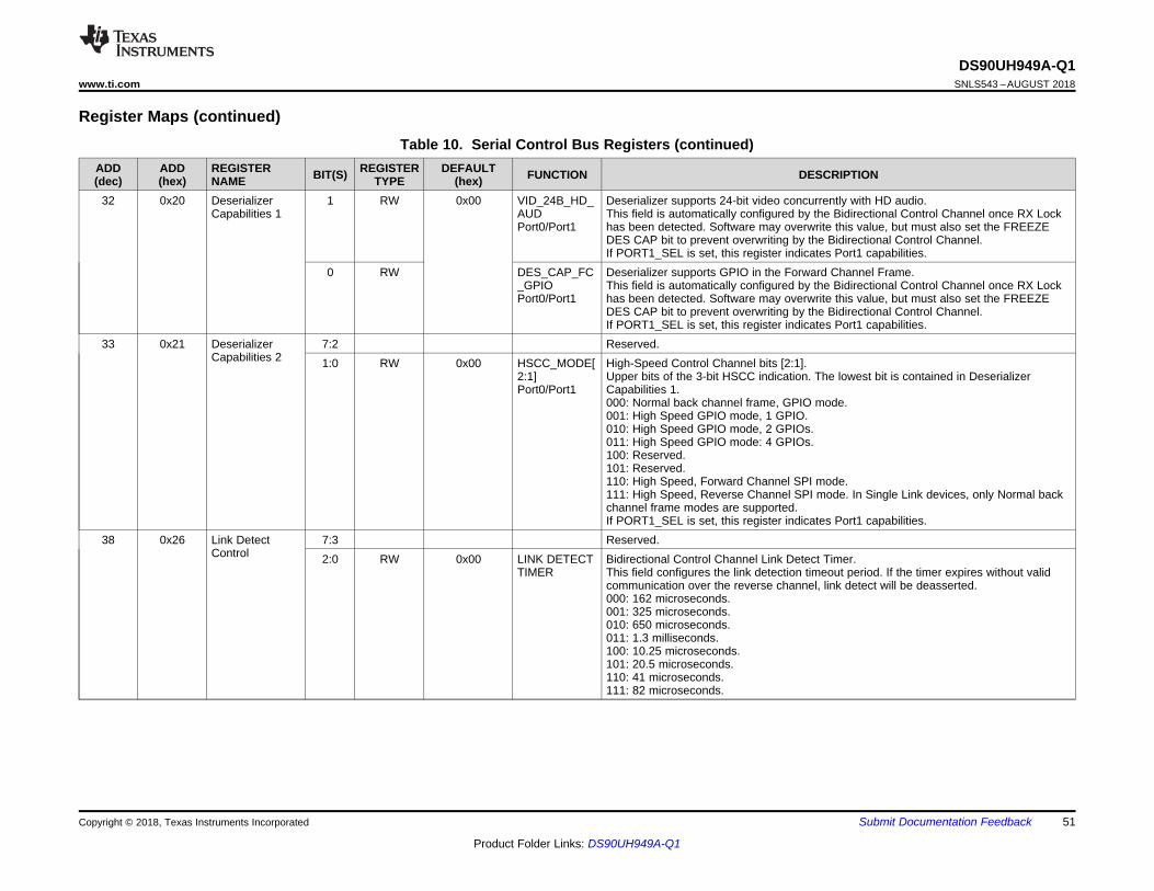
DS90UH949A-Q1www.ti.com SNLS543 –AUGUST 2018
51
Product Folder Links: DS90UH949A-Q1
Submit Documentation FeedbackCopyright © 2018, Texas Instruments Incorporated
Register Maps (continued)Table 10. Serial Control Bus Registers (continued)
ADD(dec)
ADD(hex)
REGISTERNAME BIT(S) REGISTER
TYPEDEFAULT
(hex) FUNCTION DESCRIPTION
32 0x20 DeserializerCapabilities 1
1 RW 0x00 VID_24B_HD_AUDPort0/Port1
Deserializer supports 24-bit video concurrently with HD audio.This field is automatically configured by the Bidirectional Control Channel once RX Lockhas been detected. Software may overwrite this value, but must also set the FREEZEDES CAP bit to prevent overwriting by the Bidirectional Control Channel.If PORT1_SEL is set, this register indicates Port1 capabilities.
0 RW DES_CAP_FC_GPIOPort0/Port1
Deserializer supports GPIO in the Forward Channel Frame.This field is automatically configured by the Bidirectional Control Channel once RX Lockhas been detected. Software may overwrite this value, but must also set the FREEZEDES CAP bit to prevent overwriting by the Bidirectional Control Channel.If PORT1_SEL is set, this register indicates Port1 capabilities.
33 0x21 DeserializerCapabilities 2
7:2 Reserved.1:0 RW 0x00 HSCC_MODE[
2:1]Port0/Port1
High-Speed Control Channel bits [2:1].Upper bits of the 3-bit HSCC indication. The lowest bit is contained in DeserializerCapabilities 1.000: Normal back channel frame, GPIO mode.001: High Speed GPIO mode, 1 GPIO.010: High Speed GPIO mode, 2 GPIOs.011: High Speed GPIO mode: 4 GPIOs.100: Reserved.101: Reserved.110: High Speed, Forward Channel SPI mode.111: High Speed, Reverse Channel SPI mode. In Single Link devices, only Normal backchannel frame modes are supported.If PORT1_SEL is set, this register indicates Port1 capabilities.
38 0x26 Link DetectControl
7:3 Reserved.2:0 RW 0x00 LINK DETECT
TIMERBidirectional Control Channel Link Detect Timer.This field configures the link detection timeout period. If the timer expires without validcommunication over the reverse channel, link detect will be deasserted.000: 162 microseconds.001: 325 microseconds.010: 650 microseconds.011: 1.3 milliseconds.100: 10.25 microseconds.101: 20.5 microseconds.110: 41 microseconds.111: 82 microseconds.
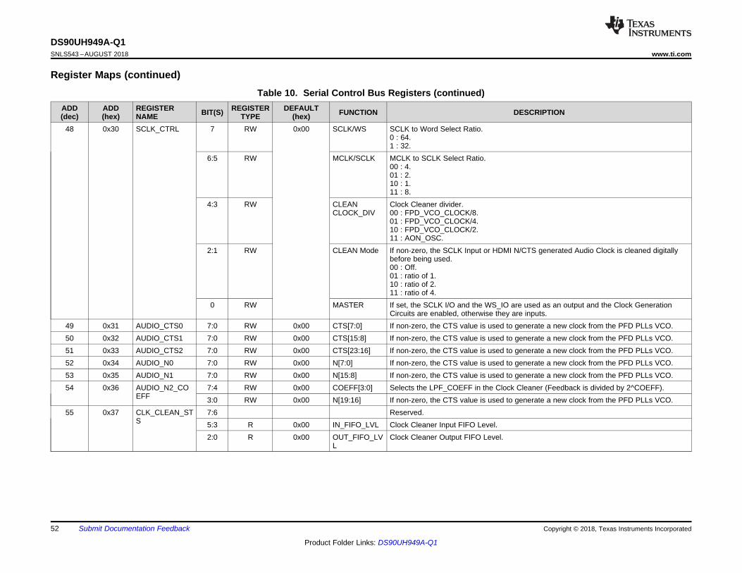
DS90UH949A-Q1SNLS543 –AUGUST 2018 www.ti.com
52
Product Folder Links: DS90UH949A-Q1
Submit Documentation Feedback Copyright © 2018, Texas Instruments Incorporated
Register Maps (continued)Table 10. Serial Control Bus Registers (continued)
ADD(dec)
ADD(hex)
REGISTERNAME BIT(S) REGISTER
TYPEDEFAULT
(hex) FUNCTION DESCRIPTION
48 0x30 SCLK_CTRL 7 RW 0x00 SCLK/WS SCLK to Word Select Ratio.0 : 64.1 : 32.
6:5 RW MCLK/SCLK MCLK to SCLK Select Ratio.00 : 4.01 : 2.10 : 1.11 : 8.
4:3 RW CLEANCLOCK_DIV
Clock Cleaner divider.00 : FPD_VCO_CLOCK/8.01 : FPD_VCO_CLOCK/4.10 : FPD_VCO_CLOCK/2.11 : AON_OSC.
2:1 RW CLEAN Mode If non-zero, the SCLK Input or HDMI N/CTS generated Audio Clock is cleaned digitallybefore being used.00 : Off.01 : ratio of 1.10 : ratio of 2.11 : ratio of 4.
0 RW MASTER If set, the SCLK I/O and the WS_IO are used as an output and the Clock GenerationCircuits are enabled, otherwise they are inputs.
49 0x31 AUDIO_CTS0 7:0 RW 0x00 CTS[7:0] If non-zero, the CTS value is used to generate a new clock from the PFD PLLs VCO.50 0x32 AUDIO_CTS1 7:0 RW 0x00 CTS[15:8] If non-zero, the CTS value is used to generate a new clock from the PFD PLLs VCO.51 0x33 AUDIO_CTS2 7:0 RW 0x00 CTS[23:16] If non-zero, the CTS value is used to generate a new clock from the PFD PLLs VCO.52 0x34 AUDIO_N0 7:0 RW 0x00 N[7:0] If non-zero, the CTS value is used to generate a new clock from the PFD PLLs VCO.53 0x35 AUDIO_N1 7:0 RW 0x00 N[15:8] If non-zero, the CTS value is used to generate a new clock from the PFD PLLs VCO.54 0x36 AUDIO_N2_CO
EFF7:4 RW 0x00 COEFF[3:0] Selects the LPF_COEFF in the Clock Cleaner (Feedback is divided by 2^COEFF).3:0 RW 0x00 N[19:16] If non-zero, the CTS value is used to generate a new clock from the PFD PLLs VCO.
55 0x37 CLK_CLEAN_STS
7:6 Reserved.5:3 R 0x00 IN_FIFO_LVL Clock Cleaner Input FIFO Level.2:0 R 0x00 OUT_FIFO_LV
LClock Cleaner Output FIFO Level.
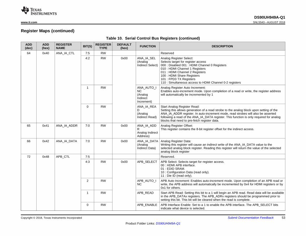
DS90UH949A-Q1www.ti.com SNLS543 –AUGUST 2018
53
Product Folder Links: DS90UH949A-Q1
Submit Documentation FeedbackCopyright © 2018, Texas Instruments Incorporated
Register Maps (continued)Table 10. Serial Control Bus Registers (continued)
ADD(dec)
ADD(hex)
REGISTERNAME BIT(S) REGISTER
TYPEDEFAULT
(hex) FUNCTION DESCRIPTION
64 0x40 ANA_IA_CTL 7:5 RW Reserved4:2 RW 0x00 ANA_IA_SEL
(AnalogIndirect Select)
Analog Register Select:Selects target for register access000 : Disabled 001 : HDMI Channel 0 Registers010 : HDMI Channel 1 Registers011 : HDMI Channel 2 Registers100 : HDMI Share Registers101 : FPD3 TX Registers110 : Simultaneous access to HDMI Channel 0-2 registers
1 RW ANA_AUTO_INC(AnalogIndirectIncrement)
Analog Register Auto Increment:Enables auto-increment mode. Upon completion of a read or write, the register addresswill automatically be incremented by 1
0 RW ANA_IA_READ(AnalogIndirect Read)
Start Analog Register Read:Setting this allows generation of a read strobe to the analog block upon setting of theANA_IA_ADDR register. In auto-increment mode, read strobes will also be assertedfollowing a read of the ANA_IA_DATA register. This function is only required for analogblocks that need to pre-fetch register data.
65 0x41 ANA_IA_ADDR 7:0 RW 0x00 ANA_IA_ADDRAnalog IndirectAddress)
Analog Register Offset:This register contains the 8-bit register offset for the indirect access.
66 0x42 ANA_IA_DATA 7:0 RW 0x00 ANA_IA_DATA(AnalogIndirect Data)
Analog Register Data:Writing this register will cause an indirect write of the ANA_IA_DATA value to theselected analog block register. Reading this register will return the value of the selectedanalog block register
72 0x48 APB_CTL 7:5 Reserved.4:3 RW 0x00 APB_SELECT APB Select: Selects target for register access.
00 : HDMI APB interface.01 : EDID SRAM.10 : Configuration Data (read only).11 : Die ID (read only).
2 RW APB_AUTO_INC
APB Auto Increment: Enables auto-increment mode. Upon completion of an APB read orwrite, the APB address will automatically be incremented by 0x4 for HDMI registers or by0x1 for others.
1 RW APB_READ Start APB Read: Setting this bit to a 1 will begin an APB read. Read data will be availablein the APB_DATAx registers. The APB_ADRx registers should be programmed prior tosetting this bit. This bit will be cleared when the read is complete.
0 RW APB_ENABLE APB Interface Enable: Set to a 1 to enable the APB interface. The APB_SELECT bitsindicate what device is selected.
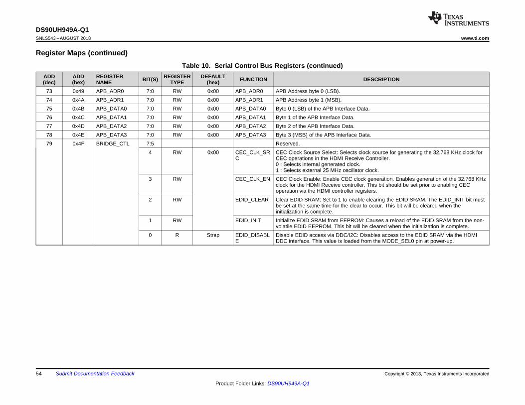
DS90UH949A-Q1SNLS543 –AUGUST 2018 www.ti.com
54
Product Folder Links: DS90UH949A-Q1
Submit Documentation Feedback Copyright © 2018, Texas Instruments Incorporated
Register Maps (continued)Table 10. Serial Control Bus Registers (continued)
ADD(dec)
ADD(hex)
REGISTERNAME BIT(S) REGISTER
TYPEDEFAULT
(hex) FUNCTION DESCRIPTION
73 0x49 APB_ADR0 7:0 RW 0x00 APB_ADR0 APB Address byte 0 (LSB).74 0x4A APB_ADR1 7:0 RW 0x00 APB_ADR1 APB Address byte 1 (MSB).75 0x4B APB_DATA0 7:0 RW 0x00 APB_DATA0 Byte 0 (LSB) of the APB Interface Data.76 0x4C APB_DATA1 7:0 RW 0x00 APB_DATA1 Byte 1 of the APB Interface Data.77 0x4D APB_DATA2 7:0 RW 0x00 APB_DATA2 Byte 2 of the APB Interface Data.78 0x4E APB_DATA3 7:0 RW 0x00 APB_DATA3 Byte 3 (MSB) of the APB Interface Data.79 0x4F BRIDGE_CTL 7:5 Reserved.
4 RW 0x00 CEC_CLK_SRC
CEC Clock Source Select: Selects clock source for generating the 32.768 KHz clock forCEC operations in the HDMI Receive Controller.0 : Selects internal generated clock.1 : Selects external 25 MHz oscillator clock.
3 RW CEC_CLK_EN CEC Clock Enable: Enable CEC clock generation. Enables generation of the 32.768 KHzclock for the HDMI Receive controller. This bit should be set prior to enabling CECoperation via the HDMI controller registers.
2 RW EDID_CLEAR Clear EDID SRAM: Set to 1 to enable clearing the EDID SRAM. The EDID_INIT bit mustbe set at the same time for the clear to occur. This bit will be cleared when theinitialization is complete.
1 RW EDID_INIT Initialize EDID SRAM from EEPROM: Causes a reload of the EDID SRAM from the non-volatile EDID EEPROM. This bit will be cleared when the initialization is complete.
0 R Strap EDID_DISABLE
Disable EDID access via DDC/I2C: Disables access to the EDID SRAM via the HDMIDDC interface. This value is loaded from the MODE_SEL0 pin at power-up.
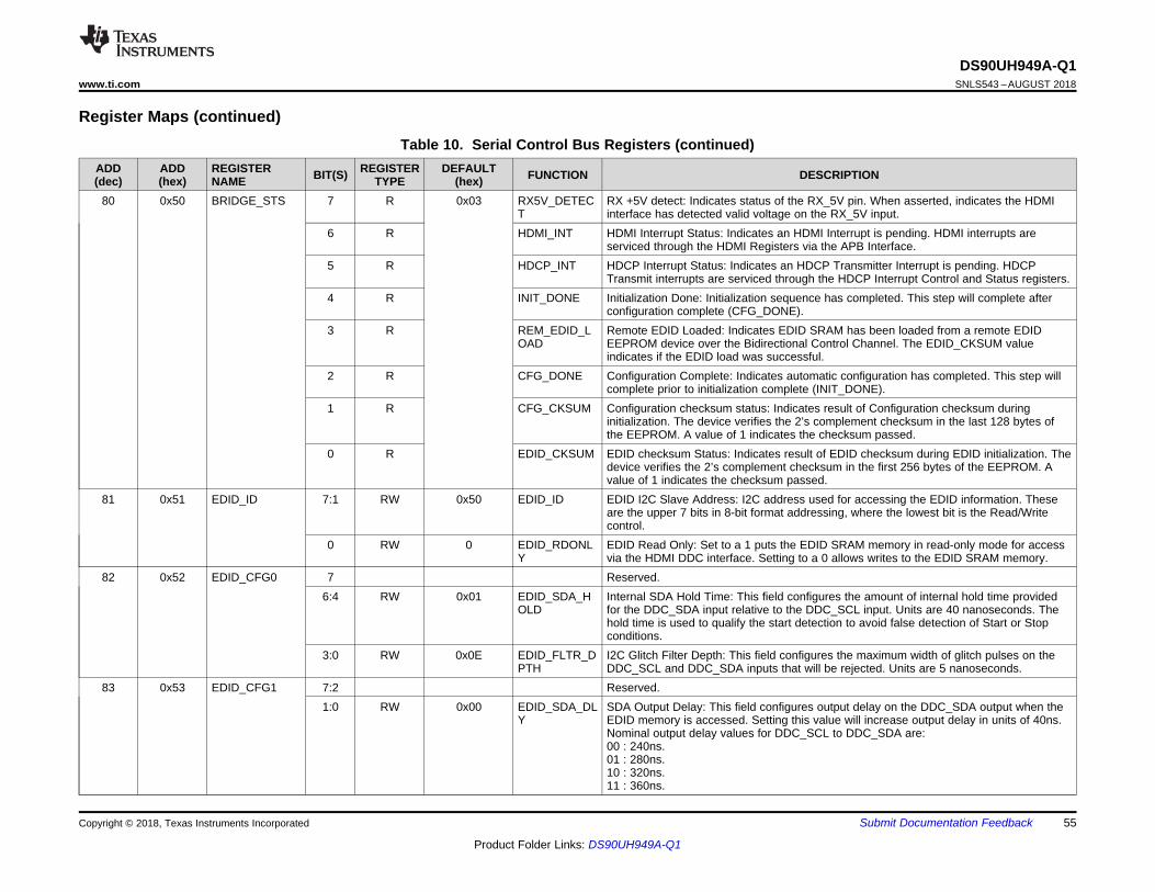
DS90UH949A-Q1www.ti.com SNLS543 –AUGUST 2018
55
Product Folder Links: DS90UH949A-Q1
Submit Documentation FeedbackCopyright © 2018, Texas Instruments Incorporated
Register Maps (continued)Table 10. Serial Control Bus Registers (continued)
ADD(dec)
ADD(hex)
REGISTERNAME BIT(S) REGISTER
TYPEDEFAULT
(hex) FUNCTION DESCRIPTION
80 0x50 BRIDGE_STS 7 R 0x03 RX5V_DETECT
RX +5V detect: Indicates status of the RX_5V pin. When asserted, indicates the HDMIinterface has detected valid voltage on the RX_5V input.
6 R HDMI_INT HDMI Interrupt Status: Indicates an HDMI Interrupt is pending. HDMI interrupts areserviced through the HDMI Registers via the APB Interface.
5 R HDCP_INT HDCP Interrupt Status: Indicates an HDCP Transmitter Interrupt is pending. HDCPTransmit interrupts are serviced through the HDCP Interrupt Control and Status registers.
4 R INIT_DONE Initialization Done: Initialization sequence has completed. This step will complete afterconfiguration complete (CFG_DONE).
3 R REM_EDID_LOAD
Remote EDID Loaded: Indicates EDID SRAM has been loaded from a remote EDIDEEPROM device over the Bidirectional Control Channel. The EDID_CKSUM valueindicates if the EDID load was successful.
2 R CFG_DONE Configuration Complete: Indicates automatic configuration has completed. This step willcomplete prior to initialization complete (INIT_DONE).
1 R CFG_CKSUM Configuration checksum status: Indicates result of Configuration checksum duringinitialization. The device verifies the 2’s complement checksum in the last 128 bytes ofthe EEPROM. A value of 1 indicates the checksum passed.
0 R EDID_CKSUM EDID checksum Status: Indicates result of EDID checksum during EDID initialization. Thedevice verifies the 2’s complement checksum in the first 256 bytes of the EEPROM. Avalue of 1 indicates the checksum passed.
81 0x51 EDID_ID 7:1 RW 0x50 EDID_ID EDID I2C Slave Address: I2C address used for accessing the EDID information. Theseare the upper 7 bits in 8-bit format addressing, where the lowest bit is the Read/Writecontrol.
0 RW 0 EDID_RDONLY
EDID Read Only: Set to a 1 puts the EDID SRAM memory in read-only mode for accessvia the HDMI DDC interface. Setting to a 0 allows writes to the EDID SRAM memory.
82 0x52 EDID_CFG0 7 Reserved.6:4 RW 0x01 EDID_SDA_H
OLDInternal SDA Hold Time: This field configures the amount of internal hold time providedfor the DDC_SDA input relative to the DDC_SCL input. Units are 40 nanoseconds. Thehold time is used to qualify the start detection to avoid false detection of Start or Stopconditions.
3:0 RW 0x0E EDID_FLTR_DPTH
I2C Glitch Filter Depth: This field configures the maximum width of glitch pulses on theDDC_SCL and DDC_SDA inputs that will be rejected. Units are 5 nanoseconds.
83 0x53 EDID_CFG1 7:2 Reserved.1:0 RW 0x00 EDID_SDA_DL
YSDA Output Delay: This field configures output delay on the DDC_SDA output when theEDID memory is accessed. Setting this value will increase output delay in units of 40ns.Nominal output delay values for DDC_SCL to DDC_SDA are:00 : 240ns.01 : 280ns.10 : 320ns.11 : 360ns.
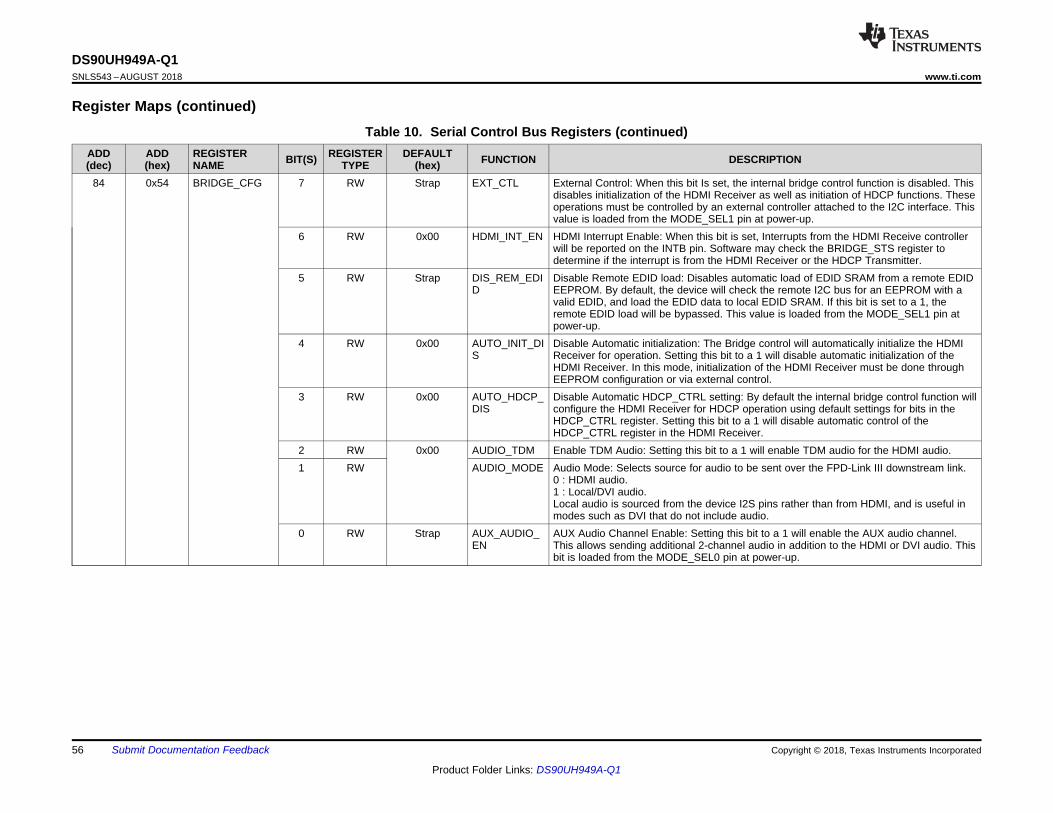
DS90UH949A-Q1SNLS543 –AUGUST 2018 www.ti.com
56
Product Folder Links: DS90UH949A-Q1
Submit Documentation Feedback Copyright © 2018, Texas Instruments Incorporated
Register Maps (continued)Table 10. Serial Control Bus Registers (continued)
ADD(dec)
ADD(hex)
REGISTERNAME BIT(S) REGISTER
TYPEDEFAULT
(hex) FUNCTION DESCRIPTION
84 0x54 BRIDGE_CFG 7 RW Strap EXT_CTL External Control: When this bit Is set, the internal bridge control function is disabled. Thisdisables initialization of the HDMI Receiver as well as initiation of HDCP functions. Theseoperations must be controlled by an external controller attached to the I2C interface. Thisvalue is loaded from the MODE_SEL1 pin at power-up.
6 RW 0x00 HDMI_INT_EN HDMI Interrupt Enable: When this bit is set, Interrupts from the HDMI Receive controllerwill be reported on the INTB pin. Software may check the BRIDGE_STS register todetermine if the interrupt is from the HDMI Receiver or the HDCP Transmitter.
5 RW Strap DIS_REM_EDID
Disable Remote EDID load: Disables automatic load of EDID SRAM from a remote EDIDEEPROM. By default, the device will check the remote I2C bus for an EEPROM with avalid EDID, and load the EDID data to local EDID SRAM. If this bit is set to a 1, theremote EDID load will be bypassed. This value is loaded from the MODE_SEL1 pin atpower-up.
4 RW 0x00 AUTO_INIT_DIS
Disable Automatic initialization: The Bridge control will automatically initialize the HDMIReceiver for operation. Setting this bit to a 1 will disable automatic initialization of theHDMI Receiver. In this mode, initialization of the HDMI Receiver must be done throughEEPROM configuration or via external control.
3 RW 0x00 AUTO_HDCP_DIS
Disable Automatic HDCP_CTRL setting: By default the internal bridge control function willconfigure the HDMI Receiver for HDCP operation using default settings for bits in theHDCP_CTRL register. Setting this bit to a 1 will disable automatic control of theHDCP_CTRL register in the HDMI Receiver.
2 RW 0x00 AUDIO_TDM Enable TDM Audio: Setting this bit to a 1 will enable TDM audio for the HDMI audio.1 RW AUDIO_MODE Audio Mode: Selects source for audio to be sent over the FPD-Link III downstream link.
0 : HDMI audio.1 : Local/DVI audio.Local audio is sourced from the device I2S pins rather than from HDMI, and is useful inmodes such as DVI that do not include audio.
0 RW Strap AUX_AUDIO_EN
AUX Audio Channel Enable: Setting this bit to a 1 will enable the AUX audio channel.This allows sending additional 2-channel audio in addition to the HDMI or DVI audio. Thisbit is loaded from the MODE_SEL0 pin at power-up.
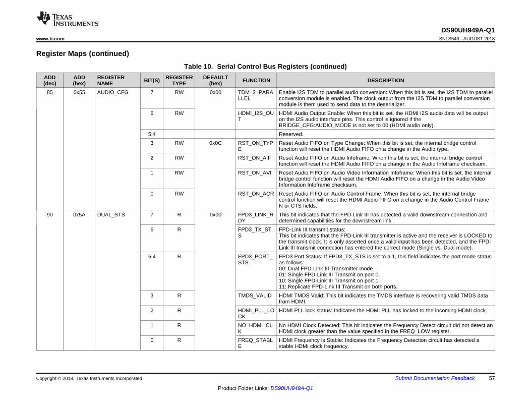
DS90UH949A-Q1www.ti.com SNLS543 –AUGUST 2018
57
Product Folder Links: DS90UH949A-Q1
Submit Documentation FeedbackCopyright © 2018, Texas Instruments Incorporated
Register Maps (continued)Table 10. Serial Control Bus Registers (continued)
ADD(dec)
ADD(hex)
REGISTERNAME BIT(S) REGISTER
TYPEDEFAULT
(hex) FUNCTION DESCRIPTION
85 0x55 AUDIO_CFG 7 RW 0x00 TDM_2_PARALLEL
Enable I2S TDM to parallel audio conversion: When this bit is set, the I2S TDM to parallelconversion module is enabled. The clock output from the I2S TDM to parallel conversionmodule is them used to send data to the deserializer.
6 RW HDMI_I2S_OUT
HDMI Audio Output Enable: When this bit is set, the HDMI I2S audio data will be outputon the I2S audio interface pins. This control is ignored if theBRIDGE_CFG:AUDIO_MODE is not set to 00 (HDMI audio only).
5:4 Reserved.3 RW 0x0C RST_ON_TYP
EReset Audio FIFO on Type Change: When this bit is set, the internal bridge controlfunction will reset the HDMI Audio FIFO on a change in the Audio type.
2 RW RST_ON_AIF Reset Audio FIFO on Audio Infoframe: When this bit is set, the internal bridge controlfunction will reset the HDMI Audio FIFO on a change in the Audio Infoframe checksum.
1 RW RST_ON_AVI Reset Audio FIFO on Audio Video Information Infoframe: When this bit is set, the internalbridge control function will reset the HDMI Audio FIFO on a change in the Audio VideoInformation Infoframe checksum.
0 RW RST_ON_ACR Reset Audio FIFO on Audio Control Frame: When this bit is set, the internal bridgecontrol function will reset the HDMI Audio FIFO on a change in the Audio Control FrameN or CTS fields.
90 0x5A DUAL_STS 7 R 0x00 FPD3_LINK_RDY
This bit indicates that the FPD-Link III has detected a valid downstream connection anddetermined capabilities for the downstream link.
6 R FPD3_TX_STS
FPD-Link III transmit status:This bit indicates that the FPD-Link III transmitter is active and the receiver is LOCKED tothe transmit clock. It is only asserted once a valid input has been detected, and the FPD-Link III transmit connection has entered the correct mode (Single vs. Dual mode).
5:4 R FPD3_PORT_STS
FPD3 Port Status: If FPD3_TX_STS is set to a 1, this field indicates the port mode statusas follows:00: Dual FPD-Link III Transmitter mode.01: Single FPD-Link III Transmit on port 0.10: Single FPD-Link III Transmit on port 1.11: Replicate FPD-Link III Transmit on both ports.
3 R TMDS_VALID HDMI TMDS Valid: This bit indicates the TMDS interface is recovering valid TMDS datafrom HDMI.
2 R HDMI_PLL_LOCK
HDMI PLL lock status: Indicates the HDMI PLL has locked to the incoming HDMI clock.
1 R NO_HDMI_CLK
No HDMI Clock Detected: This bit indicates the Frequency Detect circuit did not detect anHDMI clock greater than the value specified in the FREQ_LOW register.
0 R FREQ_STABLE
HDMI Frequency is Stable: Indicates the Frequency Detection circuit has detected astable HDMI clock frequency.
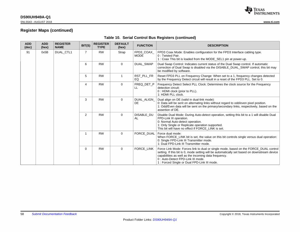
DS90UH949A-Q1SNLS543 –AUGUST 2018 www.ti.com
58
Product Folder Links: DS90UH949A-Q1
Submit Documentation Feedback Copyright © 2018, Texas Instruments Incorporated
Register Maps (continued)Table 10. Serial Control Bus Registers (continued)
ADD(dec)
ADD(hex)
REGISTERNAME BIT(S) REGISTER
TYPEDEFAULT
(hex) FUNCTION DESCRIPTION
91 0x5B DUAL_CTL1 7 RW Strap FPD3_COAX_MODE
FPD3 Coax Mode: Enables configuration for the FPD3 Interface cabling type.0 : Twisted Pair.1 : Coax This bit is loaded from the MODE_SEL1 pin at power-up.
6 RW 0 DUAL_SWAP Dual Swap Control: Indicates current status of the Dual Swap control. If automaticcorrection of Dual Swap is disabled via the DISABLE_DUAL_SWAP control, this bit maybe modified by software.
5 RW 1 RST_PLL_FREQ
Reset FPD3 PLL on Frequency Change: When set to a 1, frequency changes detectedby the Frequency Detect circuit will result in a reset of the FPD3 PLL. Set to 0.
4 RW 0 FREQ_DET_PLL
Frequency Detect Select PLL Clock: Determines the clock source for the Frequencydetection circuit:0 : HDMI clock (prior to PLL).1: HDMI PLL clock.
3 RW 0 DUAL_ALIGN_DE
Dual align on DE (valid in dual-link mode):0: Data will be sent on alternating links without regard to odd/even pixel position.1: Odd/Even data will be sent on the primary/secondary links, respectively, based on theassertion of DE.
2 RW 0 DISABLE_DUAL
Disable Dual Mode: During Auto-detect operation, setting this bit to a 1 will disable DualFPD-Link III operation.0: Normal Auto-detect operation.1: Only Single or Replicate operation supported.This bit will have no effect if FORCE_LINK is set.
1 RW 0 FORCE_DUAL Force dual mode:When FORCE_LINK bit is set, the value on this bit controls single versus dual operation:0: Single FPD-Link III Transmitter mode.1: Dual FPD-Link III Transmitter mode.
0 RW 0 FORCE_LINK Force Link Mode: Forces link to dual or single mode, based on the FORCE_DUAL controlsetting. If this bit is 0, mode setting will be automatically set based on downstream devicecapabilities as well as the incoming data frequency.0 : Auto-Detect FPD-Link III mode.1 : Forced Single or Dual FPD-Link III mode.
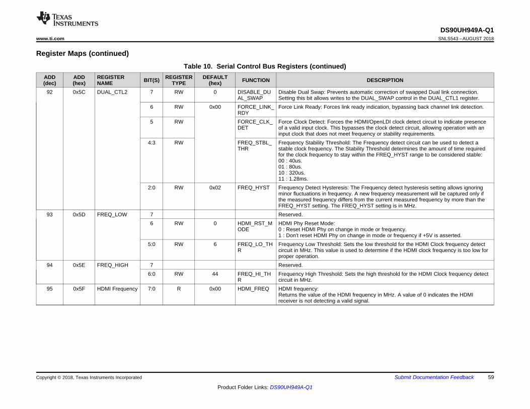
DS90UH949A-Q1www.ti.com SNLS543 –AUGUST 2018
59
Product Folder Links: DS90UH949A-Q1
Submit Documentation FeedbackCopyright © 2018, Texas Instruments Incorporated
Register Maps (continued)Table 10. Serial Control Bus Registers (continued)
ADD(dec)
ADD(hex)
REGISTERNAME BIT(S) REGISTER
TYPEDEFAULT
(hex) FUNCTION DESCRIPTION
92 0x5C DUAL_CTL2 7 RW 0 DISABLE_DUAL_SWAP
Disable Dual Swap: Prevents automatic correction of swapped Dual link connection.Setting this bit allows writes to the DUAL_SWAP control in the DUAL_CTL1 register.
6 RW 0x00 FORCE_LINK_RDY
Force Link Ready: Forces link ready indication, bypassing back channel link detection.
5 RW FORCE_CLK_DET
Force Clock Detect: Forces the HDMI/OpenLDI clock detect circuit to indicate presenceof a valid input clock. This bypasses the clock detect circuit, allowing operation with aninput clock that does not meet frequency or stability requirements.
4:3 RW FREQ_STBL_THR
Frequency Stability Threshold: The Frequency detect circuit can be used to detect astable clock frequency. The Stability Threshold determines the amount of time requiredfor the clock frequency to stay within the FREQ_HYST range to be considered stable:00 : 40us.01 : 80us.10 : 320us.11 : 1.28ms.
2:0 RW 0x02 FREQ_HYST Frequency Detect Hysteresis: The Frequency detect hysteresis setting allows ignoringminor fluctuations in frequency. A new frequency measurement will be captured only ifthe measured frequency differs from the current measured frequency by more than theFREQ_HYST setting. The FREQ_HYST setting is in MHz.
93 0x5D FREQ_LOW 7 Reserved.6 RW 0 HDMI_RST_M
ODEHDMI Phy Reset Mode:0 : Reset HDMI Phy on change in mode or frequency.1 : Don't reset HDMI Phy on change in mode or frequency if +5V is asserted.
5:0 RW 6 FREQ_LO_THR
Frequency Low Threshold: Sets the low threshold for the HDMI Clock frequency detectcircuit in MHz. This value is used to determine if the HDMI clock frequency is too low forproper operation.
94 0x5E FREQ_HIGH 7 Reserved.6:0 RW 44 FREQ_HI_TH
RFrequency High Threshold: Sets the high threshold for the HDMI Clock frequency detectcircuit in MHz.
95 0x5F HDMI Frequency 7:0 R 0x00 HDMI_FREQ HDMI frequency:Returns the value of the HDMI frequency in MHz. A value of 0 indicates the HDMIreceiver is not detecting a valid signal.
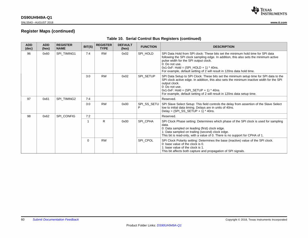
DS90UH949A-Q1SNLS543 –AUGUST 2018 www.ti.com
60
Product Folder Links: DS90UH949A-Q1
Submit Documentation Feedback Copyright © 2018, Texas Instruments Incorporated
Register Maps (continued)Table 10. Serial Control Bus Registers (continued)
ADD(dec)
ADD(hex)
REGISTERNAME BIT(S) REGISTER
TYPEDEFAULT
(hex) FUNCTION DESCRIPTION
96 0x60 SPI_TIMING1 7:4 RW 0x02 SPI_HOLD SPI Data Hold from SPI clock: These bits set the minimum hold time for SPI datafollowing the SPI clock sampling edge. In addition, this also sets the minimum activepulse width for the SPI output clock.0: Do not use.0x1-0xF: Hold = (SPI_HOLD + 1) * 40ns.For example, default setting of 2 will result in 120ns data hold time.
3:0 RW 0x02 SPI_SETUP SPI Data Setup to SPI Clock: These bits set the minimum setup time for SPI data to theSPI clock active edge. In addition, this also sets the minimum inactive width for the SPIoutput clock.0: Do not use.0x1-0xF: Hold = (SPI_SETUP + 1) * 40ns.For example, default setting of 2 will result in 120ns data setup time.
97 0x61 SPI_TIMING2 7:4 Reserved.3:0 RW 0x00 SPI_SS_SETU
PSPI Slave Select Setup: This field controls the delay from assertion of the Slave Selectlow to initial data timing. Delays are in units of 40ns.Delay = (SPI_SS_SETUP + 1) * 40ns.
98 0x62 SPI_CONFIG 7:2 Reserved.1 R 0x00 SPI_CPHA SPI Clock Phase setting: Determines which phase of the SPI clock is used for sampling
data.0: Data sampled on leading (first) clock edge.1: Data sampled on trailing (second) clock edge.This bit is read-only, with a value of 0. There is no support for CPHA of 1.
0 RW SPI_CPOL SPI Clock Polarity setting: Determines the base (inactive) value of the SPI clock.0: base value of the clock is 0.1: base value of the clock is 1.This bit affects both capture and propagation of SPI signals.
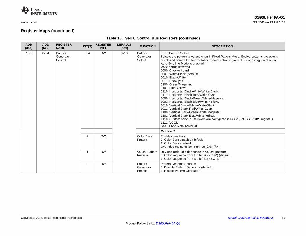
DS90UH949A-Q1www.ti.com SNLS543 –AUGUST 2018
61
Product Folder Links: DS90UH949A-Q1
Submit Documentation FeedbackCopyright © 2018, Texas Instruments Incorporated
Register Maps (continued)Table 10. Serial Control Bus Registers (continued)
ADD(dec)
ADD(hex)
REGISTERNAME BIT(S) REGISTER
TYPEDEFAULT
(hex) FUNCTION DESCRIPTION
100 0x64 PatternGeneratorControl
7:4 RW 0x10 PatternGeneratorSelect
Fixed Pattern SelectSelects the pattern to output when in Fixed Pattern Mode. Scaled patterns are evenlydistributed across the horizontal or vertical active regions. This field is ignored whenAuto-Scrolling Mode is enabled.xxxx: normal/inverted.0000: Checkerboard.0001: White/Black (default).0010: Black/White.0011: Red/Cyan.0100: Green/Magenta.0101: Blue/Yellow.0110: Horizontal Black-White/White-Black.0111: Horizontal Black-Red/White-Cyan.1000: Horizontal Black-Green/White-Magenta.1001: Horizontal Black-Blue/White-Yellow.1010: Vertical Black-White/White-Black.1011: Vertical Black-Red/White-Cyan.1100: Vertical Black-Green/White-Magenta.1101: Vertical Black-Blue/White-Yellow.1110: Custom color (or its inversion) configured in PGRS, PGGS, PGBS registers.1111: VCOM.See TI App Note AN-2198.
3 Reserved.2 RW Color Bars
PatternEnable color bars:0: Color Bars disabled (default).1: Color Bars enabled.Overrides the selection from reg_0x64[7:4].
1 RW VCOM PatternReverse
Reverse order of color bands in VCOM pattern:0: Color sequence from top left is (YCBR) (default).1: Color sequence from top left is (RBCY).
0 RW PatternGeneratorEnable
Pattern Generator enable:0: Disable Pattern Generator (default).1: Enable Pattern Generator.
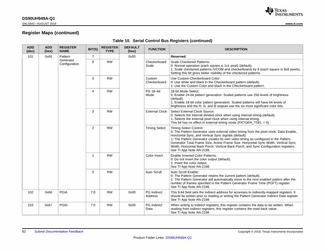
DS90UH949A-Q1SNLS543 –AUGUST 2018 www.ti.com
62
Product Folder Links: DS90UH949A-Q1
Submit Documentation Feedback Copyright © 2018, Texas Instruments Incorporated
Register Maps (continued)Table 10. Serial Control Bus Registers (continued)
ADD(dec)
ADD(hex)
REGISTERNAME BIT(S) REGISTER
TYPEDEFAULT
(hex) FUNCTION DESCRIPTION
101 0x65 PatternGeneratorConfiguration
7 0x00 Reserved.6 RW Checkerboard
ScaleScale Checkered Patterns:0: Normal operation (each square is 1x1 pixel) (default).1: Scale checkered patterns (VCOM and checkerboard) by 8 (each square is 8x8 pixels).Setting this bit gives better visibility of the checkered patterns.
5 RW CustomCheckerboard
Use Custom Checkerboard Color:0: Use white and black in the Checkerboard pattern (default).1: Use the Custom Color and black in the Checkerboard pattern.
4 RW PG 18–bitMode
18-bit Mode Select:0: Enable 24-bit pattern generation. Scaled patterns use 256 levels of brightness(default).1: Enable 18-bit color pattern generation. Scaled patterns will have 64 levels ofbrightness and the R, G, and B outputs use the six most significant color bits.
3 RW External Clock Select External Clock Source:0: Selects the internal divided clock when using internal timing (default).1: Selects the external pixel clock when using internal timing.This bit has no effect in external timing mode (PATGEN_TSEL = 0).
2 RW Timing Select Timing Select Control:0: The Pattern Generator uses external video timing from the pixel clock, Data Enable,Horizontal Sync, and Vertical Sync signals (default).1: The Pattern Generator creates its own video timing as configured in the PatternGenerator Total Frame Size, Active Frame Size. Horizontal Sync Width, Vertical SyncWidth, Horizontal Back Porch, Vertical Back Porch, and Sync Configuration registers.See TI App Note AN-2198.
1 RW Color Invert Enable Inverted Color Patterns:0: Do not invert the color output (default).1: Invert the color output.See TI App Note AN-2198.
0 RW Auto Scroll Auto Scroll Enable:0: The Pattern Generator retains the current pattern (default).1: The Pattern Generator will automatically move to the next enabled pattern after thenumber of frames specified in the Pattern Generator Frame Time (PGFT) register.See TI App Note AN-2198.
102 0x66 PGIA 7:0 RW 0x00 PG IndirectAddress
This 8-bit field sets the indirect address for accesses to indirectly-mapped registers. Itshould be written prior to reading or writing the Pattern Generator Indirect Data register.See TI App Note AN-2198
103 0x67 PGID 7:0 RW 0x00 PG IndirectData
When writing to indirect registers, this register contains the data to be written. Whenreading from indirect registers, this register contains the read back value.See TI App Note AN-2198
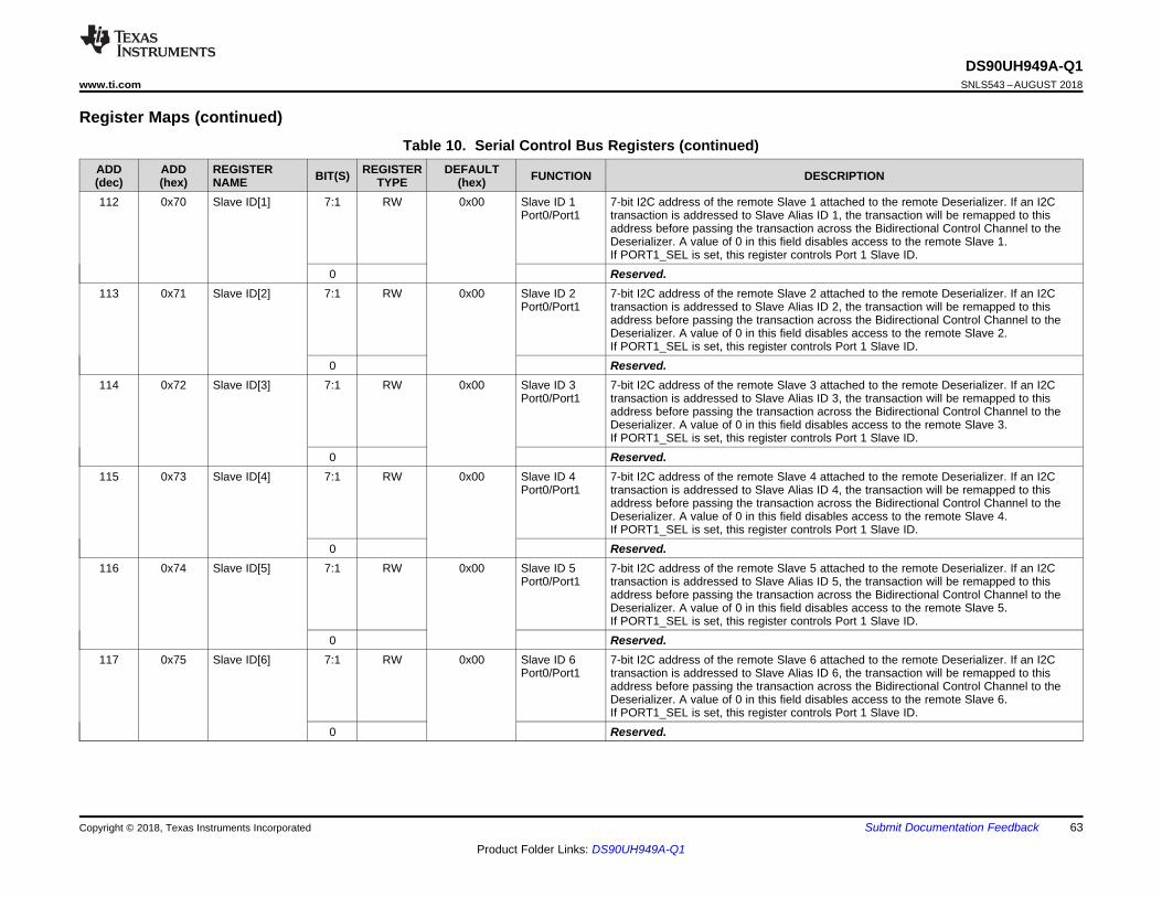
DS90UH949A-Q1www.ti.com SNLS543 –AUGUST 2018
63
Product Folder Links: DS90UH949A-Q1
Submit Documentation FeedbackCopyright © 2018, Texas Instruments Incorporated
Register Maps (continued)Table 10. Serial Control Bus Registers (continued)
ADD(dec)
ADD(hex)
REGISTERNAME BIT(S) REGISTER
TYPEDEFAULT
(hex) FUNCTION DESCRIPTION
112 0x70 Slave ID[1] 7:1 RW 0x00 Slave ID 1Port0/Port1
7-bit I2C address of the remote Slave 1 attached to the remote Deserializer. If an I2Ctransaction is addressed to Slave Alias ID 1, the transaction will be remapped to thisaddress before passing the transaction across the Bidirectional Control Channel to theDeserializer. A value of 0 in this field disables access to the remote Slave 1.If PORT1_SEL is set, this register controls Port 1 Slave ID.
0 Reserved.113 0x71 Slave ID[2] 7:1 RW 0x00 Slave ID 2
Port0/Port17-bit I2C address of the remote Slave 2 attached to the remote Deserializer. If an I2Ctransaction is addressed to Slave Alias ID 2, the transaction will be remapped to thisaddress before passing the transaction across the Bidirectional Control Channel to theDeserializer. A value of 0 in this field disables access to the remote Slave 2.If PORT1_SEL is set, this register controls Port 1 Slave ID.
0 Reserved.114 0x72 Slave ID[3] 7:1 RW 0x00 Slave ID 3
Port0/Port17-bit I2C address of the remote Slave 3 attached to the remote Deserializer. If an I2Ctransaction is addressed to Slave Alias ID 3, the transaction will be remapped to thisaddress before passing the transaction across the Bidirectional Control Channel to theDeserializer. A value of 0 in this field disables access to the remote Slave 3.If PORT1_SEL is set, this register controls Port 1 Slave ID.
0 Reserved.115 0x73 Slave ID[4] 7:1 RW 0x00 Slave ID 4
Port0/Port17-bit I2C address of the remote Slave 4 attached to the remote Deserializer. If an I2Ctransaction is addressed to Slave Alias ID 4, the transaction will be remapped to thisaddress before passing the transaction across the Bidirectional Control Channel to theDeserializer. A value of 0 in this field disables access to the remote Slave 4.If PORT1_SEL is set, this register controls Port 1 Slave ID.
0 Reserved.116 0x74 Slave ID[5] 7:1 RW 0x00 Slave ID 5
Port0/Port17-bit I2C address of the remote Slave 5 attached to the remote Deserializer. If an I2Ctransaction is addressed to Slave Alias ID 5, the transaction will be remapped to thisaddress before passing the transaction across the Bidirectional Control Channel to theDeserializer. A value of 0 in this field disables access to the remote Slave 5.If PORT1_SEL is set, this register controls Port 1 Slave ID.
0 Reserved.117 0x75 Slave ID[6] 7:1 RW 0x00 Slave ID 6
Port0/Port17-bit I2C address of the remote Slave 6 attached to the remote Deserializer. If an I2Ctransaction is addressed to Slave Alias ID 6, the transaction will be remapped to thisaddress before passing the transaction across the Bidirectional Control Channel to theDeserializer. A value of 0 in this field disables access to the remote Slave 6.If PORT1_SEL is set, this register controls Port 1 Slave ID.
0 Reserved.
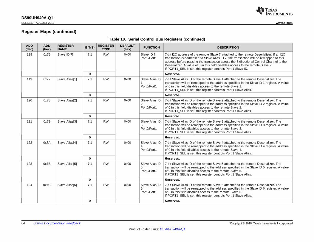
DS90UH949A-Q1SNLS543 –AUGUST 2018 www.ti.com
64
Product Folder Links: DS90UH949A-Q1
Submit Documentation Feedback Copyright © 2018, Texas Instruments Incorporated
Register Maps (continued)Table 10. Serial Control Bus Registers (continued)
ADD(dec)
ADD(hex)
REGISTERNAME BIT(S) REGISTER
TYPEDEFAULT
(hex) FUNCTION DESCRIPTION
118 0x76 Slave ID[7] 7:1 RW 0x00 Slave ID 7Port0/Port1
7-bit I2C address of the remote Slave 7 attached to the remote Deserializer. If an I2Ctransaction is addressed to Slave Alias ID 7, the transaction will be remapped to thisaddress before passing the transaction across the Bidirectional Control Channel to theDeserializer. A value of 0 in this field disables access to the remote Slave 7.If PORT1_SEL is set, this register controls Port 1 Slave ID.
0 Reserved.119 0x77 Slave Alias[1] 7:1 RW 0x00 Slave Alias ID
1Port0/Port1
7-bit Slave Alias ID of the remote Slave 1 attached to the remote Deserializer. Thetransaction will be remapped to the address specified in the Slave ID 1 register. A valueof 0 in this field disables access to the remote Slave 1.If PORT1_SEL is set, this register controls Port 1 Slave Alias.
0 Reserved.120 0x78 Slave Alias[2] 7:1 RW 0x00 Slave Alias ID
2Port0/Port1
7-bit Slave Alias ID of the remote Slave 2 attached to the remote Deserializer. Thetransaction will be remapped to the address specified in the Slave ID 2 register. A valueof 0 in this field disables access to the remote Slave 2.If PORT1_SEL is set, this register controls Port 1 Slave Alias.
0 Reserved.121 0x79 Slave Alias[3] 7:1 RW 0x00 Slave Alias ID
3Port0/Port1
7-bit Slave Alias ID of the remote Slave 3 attached to the remote Deserializer. Thetransaction will be remapped to the address specified in the Slave ID 3 register. A valueof 0 in this field disables access to the remote Slave 3.If PORT1_SEL is set, this register controls Port 1 Slave Alias.
0 Reserved.122 0x7A Slave Alias[4] 7:1 RW 0x00 Slave Alias ID
4Port0/Port1
7-bit Slave Alias ID of the remote Slave 4 attached to the remote Deserializer. Thetransaction will be remapped to the address specified in the Slave ID 4 register. A valueof 0 in this field disables access to the remote Slave 4.If PORT1_SEL is set, this register controls Port 1 Slave Alias.
0 Reserved.123 0x7B Slave Alias[5] 7:1 RW 0x00 Slave Alias ID
5Port0/Port1
7-bit Slave Alias ID of the remote Slave 5 attached to the remote Deserializer. Thetransaction will be remapped to the address specified in the Slave ID 5 register. A valueof 0 in this field disables access to the remote Slave 5.If PORT1_SEL is set, this register controls Port 1 Slave Alias.
0 Reserved.124 0x7C Slave Alias[6] 7:1 RW 0x00 Slave Alias ID
6Port0/Port1
7-bit Slave Alias ID of the remote Slave 6 attached to the remote Deserializer. Thetransaction will be remapped to the address specified in the Slave ID 6 register. A valueof 0 in this field disables access to the remote Slave 6.If PORT1_SEL is set, this register controls Port 1 Slave Alias.
0 Reserved.
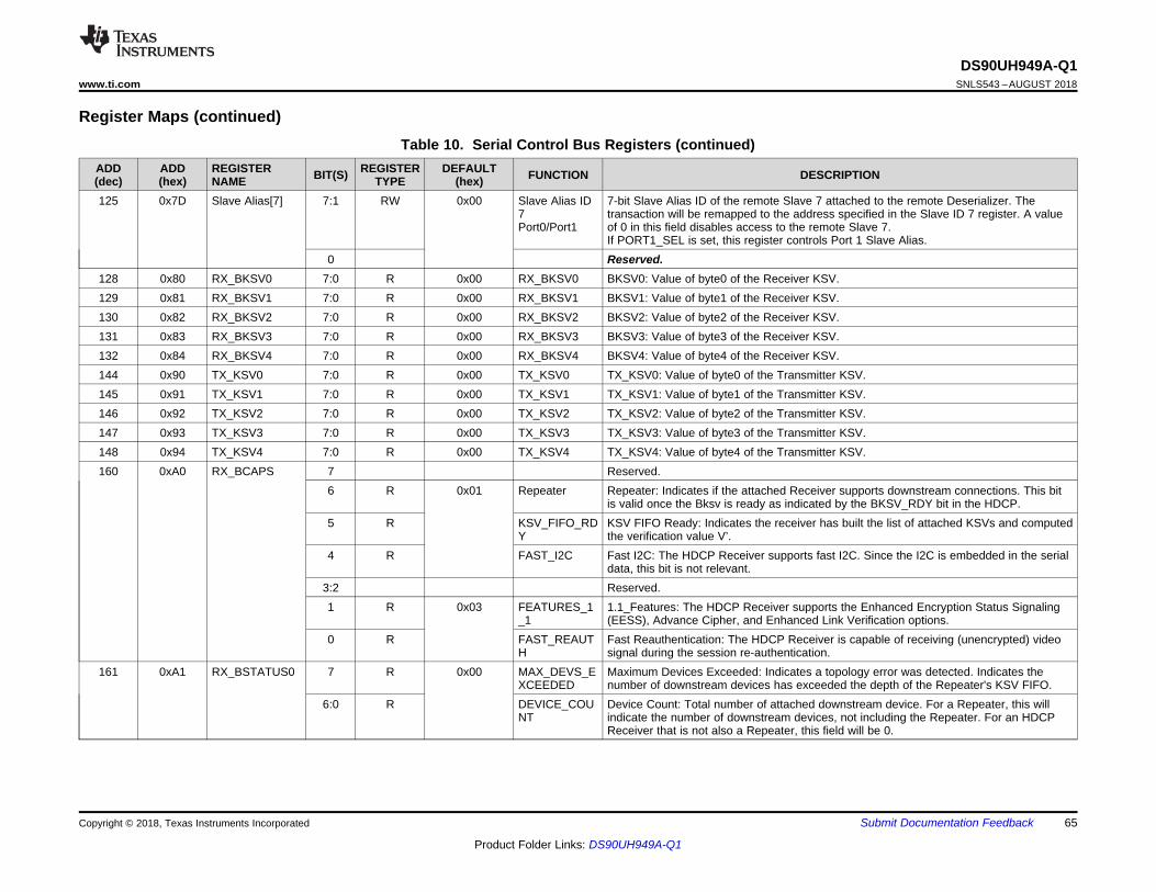
DS90UH949A-Q1www.ti.com SNLS543 –AUGUST 2018
65
Product Folder Links: DS90UH949A-Q1
Submit Documentation FeedbackCopyright © 2018, Texas Instruments Incorporated
Register Maps (continued)Table 10. Serial Control Bus Registers (continued)
ADD(dec)
ADD(hex)
REGISTERNAME BIT(S) REGISTER
TYPEDEFAULT
(hex) FUNCTION DESCRIPTION
125 0x7D Slave Alias[7] 7:1 RW 0x00 Slave Alias ID7Port0/Port1
7-bit Slave Alias ID of the remote Slave 7 attached to the remote Deserializer. Thetransaction will be remapped to the address specified in the Slave ID 7 register. A valueof 0 in this field disables access to the remote Slave 7.If PORT1_SEL is set, this register controls Port 1 Slave Alias.
0 Reserved.128 0x80 RX_BKSV0 7:0 R 0x00 RX_BKSV0 BKSV0: Value of byte0 of the Receiver KSV.129 0x81 RX_BKSV1 7:0 R 0x00 RX_BKSV1 BKSV1: Value of byte1 of the Receiver KSV.130 0x82 RX_BKSV2 7:0 R 0x00 RX_BKSV2 BKSV2: Value of byte2 of the Receiver KSV.131 0x83 RX_BKSV3 7:0 R 0x00 RX_BKSV3 BKSV3: Value of byte3 of the Receiver KSV.132 0x84 RX_BKSV4 7:0 R 0x00 RX_BKSV4 BKSV4: Value of byte4 of the Receiver KSV.144 0x90 TX_KSV0 7:0 R 0x00 TX_KSV0 TX_KSV0: Value of byte0 of the Transmitter KSV.145 0x91 TX_KSV1 7:0 R 0x00 TX_KSV1 TX_KSV1: Value of byte1 of the Transmitter KSV.146 0x92 TX_KSV2 7:0 R 0x00 TX_KSV2 TX_KSV2: Value of byte2 of the Transmitter KSV.147 0x93 TX_KSV3 7:0 R 0x00 TX_KSV3 TX_KSV3: Value of byte3 of the Transmitter KSV.148 0x94 TX_KSV4 7:0 R 0x00 TX_KSV4 TX_KSV4: Value of byte4 of the Transmitter KSV.160 0xA0 RX_BCAPS 7 Reserved.
6 R 0x01 Repeater Repeater: Indicates if the attached Receiver supports downstream connections. This bitis valid once the Bksv is ready as indicated by the BKSV_RDY bit in the HDCP.
5 R KSV_FIFO_RDY
KSV FIFO Ready: Indicates the receiver has built the list of attached KSVs and computedthe verification value V’.
4 R FAST_I2C Fast I2C: The HDCP Receiver supports fast I2C. Since the I2C is embedded in the serialdata, this bit is not relevant.
3:2 Reserved.1 R 0x03 FEATURES_1
_11.1_Features: The HDCP Receiver supports the Enhanced Encryption Status Signaling(EESS), Advance Cipher, and Enhanced Link Verification options.
0 R FAST_REAUTH
Fast Reauthentication: The HDCP Receiver is capable of receiving (unencrypted) videosignal during the session re-authentication.
161 0xA1 RX_BSTATUS0 7 R 0x00 MAX_DEVS_EXCEEDED
Maximum Devices Exceeded: Indicates a topology error was detected. Indicates thenumber of downstream devices has exceeded the depth of the Repeater's KSV FIFO.
6:0 R DEVICE_COUNT
Device Count: Total number of attached downstream device. For a Repeater, this willindicate the number of downstream devices, not including the Repeater. For an HDCPReceiver that is not also a Repeater, this field will be 0.
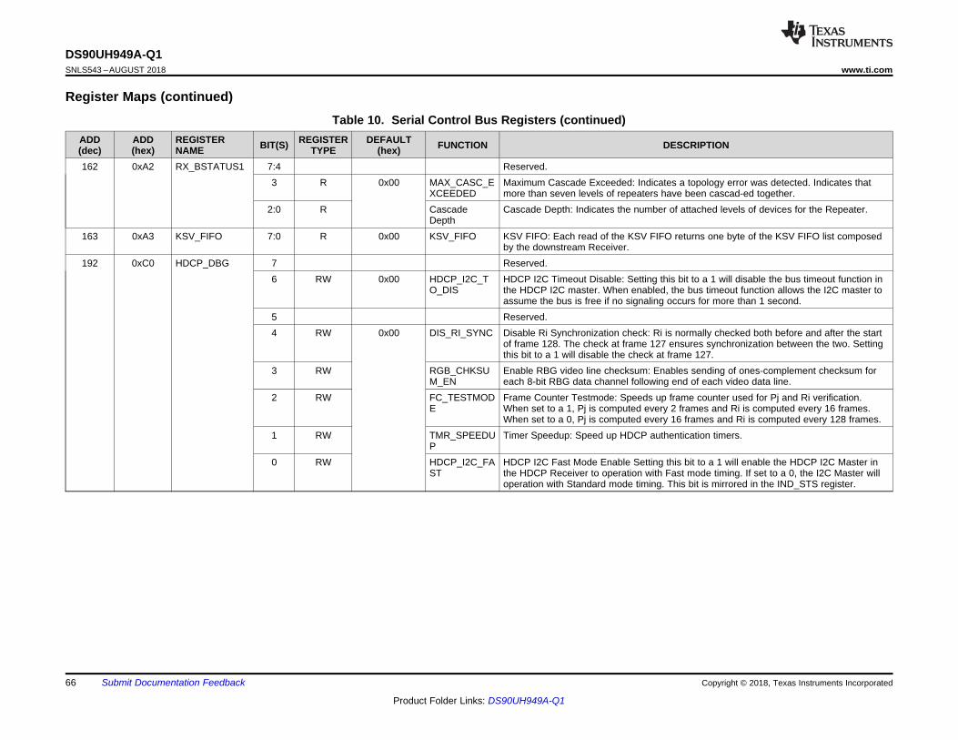
DS90UH949A-Q1SNLS543 –AUGUST 2018 www.ti.com
66
Product Folder Links: DS90UH949A-Q1
Submit Documentation Feedback Copyright © 2018, Texas Instruments Incorporated
Register Maps (continued)Table 10. Serial Control Bus Registers (continued)
ADD(dec)
ADD(hex)
REGISTERNAME BIT(S) REGISTER
TYPEDEFAULT
(hex) FUNCTION DESCRIPTION
162 0xA2 RX_BSTATUS1 7:4 Reserved.3 R 0x00 MAX_CASC_E
XCEEDEDMaximum Cascade Exceeded: Indicates a topology error was detected. Indicates thatmore than seven levels of repeaters have been cascad-ed together.
2:0 R CascadeDepth
Cascade Depth: Indicates the number of attached levels of devices for the Repeater.
163 0xA3 KSV_FIFO 7:0 R 0x00 KSV_FIFO KSV FIFO: Each read of the KSV FIFO returns one byte of the KSV FIFO list composedby the downstream Receiver.
192 0xC0 HDCP_DBG 7 Reserved.6 RW 0x00 HDCP_I2C_T
O_DISHDCP I2C Timeout Disable: Setting this bit to a 1 will disable the bus timeout function inthe HDCP I2C master. When enabled, the bus timeout function allows the I2C master toassume the bus is free if no signaling occurs for more than 1 second.
5 Reserved.4 RW 0x00 DIS_RI_SYNC Disable Ri Synchronization check: Ri is normally checked both before and after the start
of frame 128. The check at frame 127 ensures synchronization between the two. Settingthis bit to a 1 will disable the check at frame 127.
3 RW RGB_CHKSUM_EN
Enable RBG video line checksum: Enables sending of ones-complement checksum foreach 8-bit RBG data channel following end of each video data line.
2 RW FC_TESTMODE
Frame Counter Testmode: Speeds up frame counter used for Pj and Ri verification.When set to a 1, Pj is computed every 2 frames and Ri is computed every 16 frames.When set to a 0, Pj is computed every 16 frames and Ri is computed every 128 frames.
1 RW TMR_SPEEDUP
Timer Speedup: Speed up HDCP authentication timers.
0 RW HDCP_I2C_FAST
HDCP I2C Fast Mode Enable Setting this bit to a 1 will enable the HDCP I2C Master inthe HDCP Receiver to operation with Fast mode timing. If set to a 0, the I2C Master willoperation with Standard mode timing. This bit is mirrored in the IND_STS register.
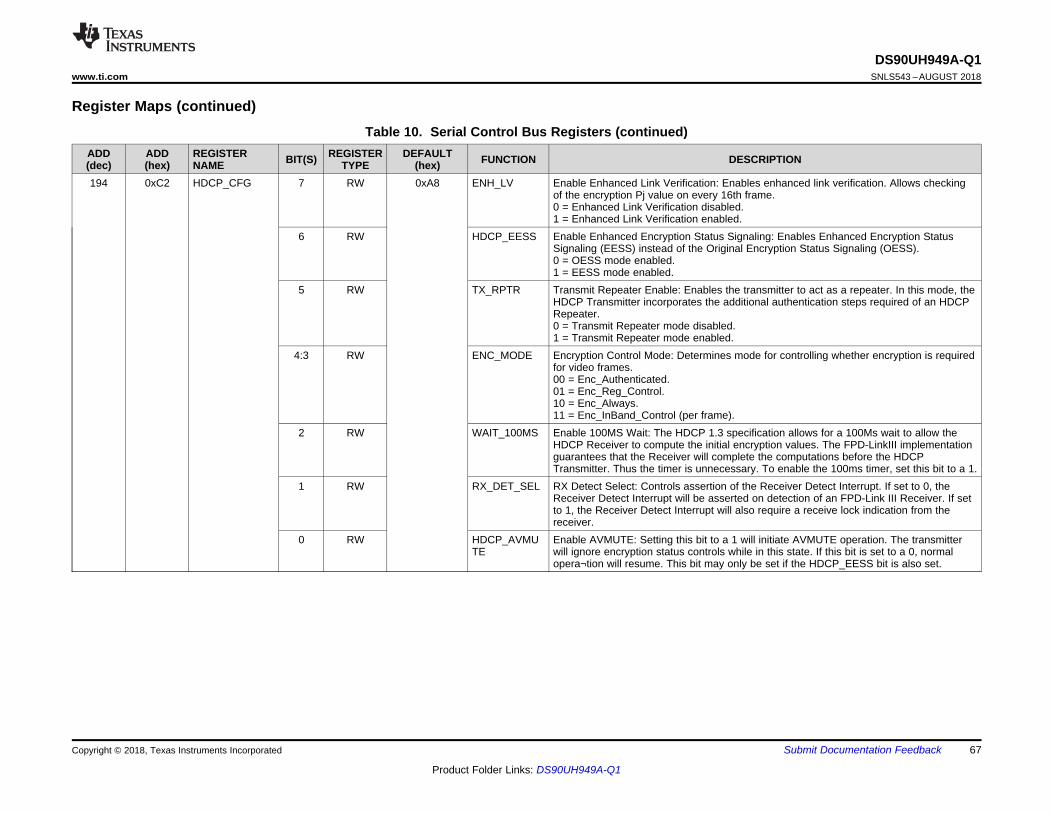
DS90UH949A-Q1www.ti.com SNLS543 –AUGUST 2018
67
Product Folder Links: DS90UH949A-Q1
Submit Documentation FeedbackCopyright © 2018, Texas Instruments Incorporated
Register Maps (continued)Table 10. Serial Control Bus Registers (continued)
ADD(dec)
ADD(hex)
REGISTERNAME BIT(S) REGISTER
TYPEDEFAULT
(hex) FUNCTION DESCRIPTION
194 0xC2 HDCP_CFG 7 RW 0xA8 ENH_LV Enable Enhanced Link Verification: Enables enhanced link verification. Allows checkingof the encryption Pj value on every 16th frame.0 = Enhanced Link Verification disabled.1 = Enhanced Link Verification enabled.
6 RW HDCP_EESS Enable Enhanced Encryption Status Signaling: Enables Enhanced Encryption StatusSignaling (EESS) instead of the Original Encryption Status Signaling (OESS).0 = OESS mode enabled.1 = EESS mode enabled.
5 RW TX_RPTR Transmit Repeater Enable: Enables the transmitter to act as a repeater. In this mode, theHDCP Transmitter incorporates the additional authentication steps required of an HDCPRepeater.0 = Transmit Repeater mode disabled.1 = Transmit Repeater mode enabled.
4:3 RW ENC_MODE Encryption Control Mode: Determines mode for controlling whether encryption is requiredfor video frames.00 = Enc_Authenticated.01 = Enc_Reg_Control.10 = Enc_Always.11 = Enc_InBand_Control (per frame).
2 RW WAIT_100MS Enable 100MS Wait: The HDCP 1.3 specification allows for a 100Ms wait to allow theHDCP Receiver to compute the initial encryption values. The FPD-LinkIII implementationguarantees that the Receiver will complete the computations before the HDCPTransmitter. Thus the timer is unnecessary. To enable the 100ms timer, set this bit to a 1.
1 RW RX_DET_SEL RX Detect Select: Controls assertion of the Receiver Detect Interrupt. If set to 0, theReceiver Detect Interrupt will be asserted on detection of an FPD-Link III Receiver. If setto 1, the Receiver Detect Interrupt will also require a receive lock indication from thereceiver.
0 RW HDCP_AVMUTE
Enable AVMUTE: Setting this bit to a 1 will initiate AVMUTE operation. The transmitterwill ignore encryption status controls while in this state. If this bit is set to a 0, normalopera¬tion will resume. This bit may only be set if the HDCP_EESS bit is also set.
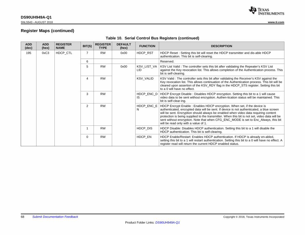
DS90UH949A-Q1SNLS543 –AUGUST 2018 www.ti.com
68
Product Folder Links: DS90UH949A-Q1
Submit Documentation Feedback Copyright © 2018, Texas Instruments Incorporated
Register Maps (continued)Table 10. Serial Control Bus Registers (continued)
ADD(dec)
ADD(hex)
REGISTERNAME BIT(S) REGISTER
TYPEDEFAULT
(hex) FUNCTION DESCRIPTION
195 0xC3 HDCP_CTL 7 RW 0x00 HDCP_RST HDCP Reset : Setting this bit will reset the HDCP transmitter and dis-able HDCPauthentication. This bit is self-clearing.
6 Reserved.5 RW 0x00 KSV_LIST_VA
LIDKSV List Valid : The controller sets this bit after validating the Repeater’s KSV Listagainst the Key revocation list. This allows completion of the Authentication process. Thisbit is self-clearing.
4 RW KSV_VALID KSV Valid : The controller sets this bit after validating the Receiver’s KSV against theKey revocation list. This allows continuation of the Authentication process. This bit will becleared upon assertion of the KSV_RDY flag in the HDCP_STS register. Setting this bitto a 0 will have no effect.
3 RW HDCP_ENC_DIS
HDCP Encrypt Disable : Disables HDCP encryption. Setting this bit to a 1 will causevideo data to be sent without encryption. Authen-tication status will be maintained. Thisbit is self-clear-ing.
2 RW HDCP_ENC_EN
HDCP Encrypt Enable : Enables HDCP encryption. When set, if the device isauthenticated, encrypted data will be sent. If device is not authenticated, a blue screenwill be sent. Encryption should always be enabled when video data requiring contentprotection is being supplied to the transmitter. When this bit is not set, video data will besent without encryption. Note that when CFG_ENC_MODE is set to Enc_Always, this bitwill be read only with a value of 1.
1 RW HDCP_DIS HDCP Disable: Disables HDCP authentication. Setting this bit to a 1 will disable theHDCP authentication. This bit is self-clearing.
0 RW HDCP_EN HDCP Enable/Restart: Enables HDCP authentication. If HDCP is already en-abled,setting this bit to a 1 will restart authentication. Setting this bit to a 0 will have no effect. Aregister read will return the current HDCP enabled status.
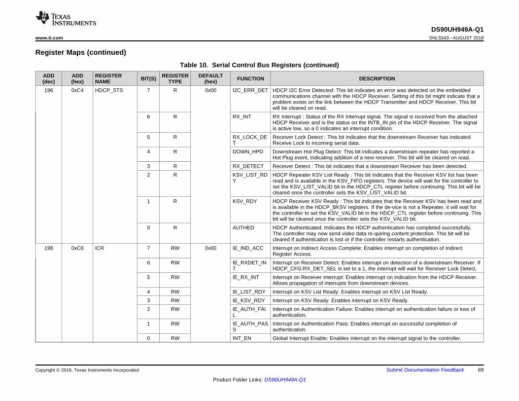
DS90UH949A-Q1www.ti.com SNLS543 –AUGUST 2018
69
Product Folder Links: DS90UH949A-Q1
Submit Documentation FeedbackCopyright © 2018, Texas Instruments Incorporated
Register Maps (continued)Table 10. Serial Control Bus Registers (continued)
ADD(dec)
ADD(hex)
REGISTERNAME BIT(S) REGISTER
TYPEDEFAULT
(hex) FUNCTION DESCRIPTION
196 0xC4 HDCP_STS 7 R 0x00 I2C_ERR_DET HDCP I2C Error Detected: This bit indicates an error was detected on the embeddedcommunications channel with the HDCP Receiver. Setting of this bit might indicate that aproblem exists on the link between the HDCP Transmitter and HDCP Receiver. This bitwill be cleared on read.
6 R RX_INT RX Interrupt : Status of the RX Interrupt signal. The signal is received from the attachedHDCP Receiver and is the status on the INTB_IN pin of the HDCP Receiver. The signalis active low, so a 0 indicates an interrupt condition.
5 R RX_LOCK_DET
Receiver Lock Detect : This bit indicates that the downstream Receiver has indicatedReceive Lock to incoming serial data.
4 R DOWN_HPD Downstream Hot Plug Detect: This bit indicates a downstream repeater has reported aHot Plug event, indicating addition of a new receiver. This bit will be cleared on read.
3 R RX_DETECT Receiver Detect : This bit indicates that a downstream Receiver has been detected.2 R KSV_LIST_RD
YHDCP Repeater KSV List Ready : This bit indicates that the Receiver KSV list has beenread and is available in the KSV_FIFO registers. The device will wait for the controller toset the KSV_LIST_VALID bit in the HDCP_CTL register before continuing. This bit will becleared once the controller sets the KSV_LIST_VALID bit.
1 R KSV_RDY HDCP Receiver KSV Ready : This bit indicates that the Receiver KSV has been read andis available in the HDCP_BKSV registers. If the de-vice is not a Repeater, it will wait forthe controller to set the KSV_VALID bit in the HDCP_CTL register before continuing. Thisbit will be cleared once the controller sets the KSV_VALID bit.
0 R AUTHED HDCP Authenticated: Indicates the HDCP authentication has completed successfully.The controller may now send video data re-quiring content protection. This bit will becleared if authentication is lost or if the controller restarts authentication.
198 0xC6 ICR 7 RW 0x00 IE_IND_ACC Interrupt on Indirect Access Complete: Enables interrupt on completion of IndirectRegister Access.
6 RW IE_RXDET_INT
Interrupt on Receiver Detect: Enables interrupt on detection of a downstream Receiver. IfHDCP_CFG:RX_DET_SEL is set to a 1, the interrupt will wait for Receiver Lock Detect.
5 RW IE_RX_INT Interrupt on Receiver interrupt: Enables interrupt on indication from the HDCP Receiver.Allows propagation of interrupts from downstream devices.
4 RW IE_LIST_RDY Interrupt on KSV List Ready: Enables interrupt on KSV List Ready.3 RW IE_KSV_RDY Interrupt on KSV Ready: Enables interrupt on KSV Ready.2 RW IE_AUTH_FAI
LInterrupt on Authentication Failure: Enables interrupt on authentication failure or loss ofauthentication.
1 RW IE_AUTH_PASS
Interrupt on Authentication Pass: Enables interrupt on successful completion ofauthentication.
0 RW INT_EN Global Interrupt Enable: Enables interrupt on the interrupt signal to the controller.
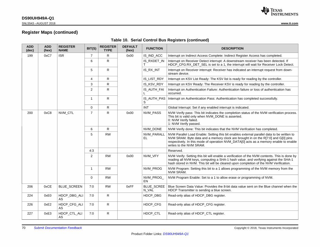
DS90UH949A-Q1SNLS543 –AUGUST 2018 www.ti.com
70
Product Folder Links: DS90UH949A-Q1
Submit Documentation Feedback Copyright © 2018, Texas Instruments Incorporated
Register Maps (continued)Table 10. Serial Control Bus Registers (continued)
ADD(dec)
ADD(hex)
REGISTERNAME BIT(S) REGISTER
TYPEDEFAULT
(hex) FUNCTION DESCRIPTION
199 0xC7 ISR 7 R 0x00 IS_IND_ACC Interrupt on Indirect Access Complete: Indirect Register Access has completed.6 R IS_RXDET_IN
TInterrupt on Receiver Detect interrupt: A downstream receiver has been detected. IfHDCP_CFG:RX_DET_SEL is set to a 1, the interrupt will wait for Receiver Lock Detect.
5 R IS_RX_INT Interrupt on Receiver interrupt: Receiver has indicated an interrupt request from down-stream device.
4 R IS_LIST_RDY Interrupt on KSV List Ready: The KSV list is ready for reading by the controller.3 R IS_KSV_RDY Interrupt on KSV Ready: The Receiver KSV is ready for reading by the controller.2 R IS_AUTH_FAI
LInterrupt on Authentication Failure: Authentication failure or loss of authentication hasoccurred.
1 R IS_AUTH_PASS
Interrupt on Authentication Pass: Authentication has completed successfully.
0 R INT Global Interrupt: Set if any enabled interrupt is indicated.200 0xC8 NVM_CTL 7 R 0x00 NVM_PASS NVM Verify pass: This bit indicates the completion status of the NVM verification process.
This bit is valid only when NVM_DONE is asserted.0: NVM Verify failed.1: NVM Verify passed.
6 R NVM_DONE NVM Verify done: This bit indicates that the NVM Verifcation has completed.5 RW NVM_PARALL
ELNVM Parallel Load Enable: Setting this bit enables external parallel data to be written toNVM SRAM. Byte data and a memory clock are brought in on the R[7:0] and G[0] pinsrespectively. In this mode of operation NVM_DATA[0] acts as a memory enable to enablewrites to the NVM SRAM.
4:3 Reserved.2 RW 0x00 NVM_VFY NVM Verify: Setting this bit will enable a verification of the NVM contents. This is done by
reading all NVM keys, computing a SHA-1 hash value, and verifying against the SHA-1hash stored in NVM. This bit will be cleared upon completion of the NVM Verification.
1 RW NVM_PROG NVM Program: Setting this bit to a 1 allows programming of the NVM memory from theNVM SRAM.
0 RW NVM_PROG_EN
NVM Program Enable: Set to a 1 to allow erase or programming of NVM.
206 0xCE BLUE_SCREEN 7:0 RW 0xFF BLUE_SCREEN_VAL
Blue Screen Data Value: Provides the 8-bit data value sent on the Blue channel when theHDCP Transmitter is sending a blue screen.
224 0xE0 HDCP_DBG_ALIAS
7:0 R HDCP_DBG Read-only alias of HDCP_DBG register.
226 0xE2 HDCP_CFG_ALIAS
7:0 R HDCP_CFG Read-only alias of HDCP_CFG register.
227 0xE3 HDCP_CTL_ALIAS
7:0 R HDCP_CTL Read-only alias of HDCP_CTL register.
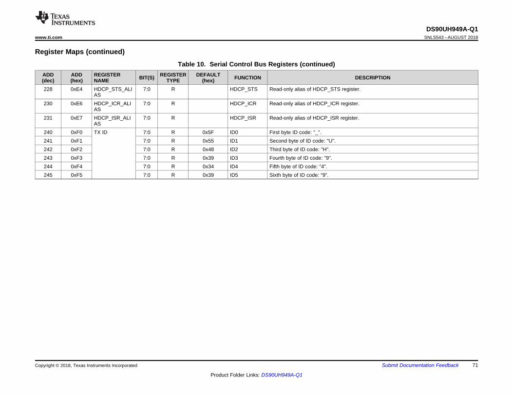
DS90UH949A-Q1www.ti.com SNLS543 –AUGUST 2018
71
Product Folder Links: DS90UH949A-Q1
Submit Documentation FeedbackCopyright © 2018, Texas Instruments Incorporated
Register Maps (continued)Table 10. Serial Control Bus Registers (continued)
ADD(dec)
ADD(hex)
REGISTERNAME BIT(S) REGISTER
TYPEDEFAULT
(hex) FUNCTION DESCRIPTION
228 0xE4 HDCP_STS_ALIAS
7:0 R HDCP_STS Read-only alias of HDCP_STS register.
230 0xE6 HDCP_ICR_ALIAS
7:0 R HDCP_ICR Read-only alias of HDCP_ICR register.
231 0xE7 HDCP_ISR_ALIAS
7:0 R HDCP_ISR Read-only alias of HDCP_ISR register.
240 0xF0 TX ID 7:0 R 0x5F ID0 First byte ID code: "_".241 0xF1 7:0 R 0x55 ID1 Second byte of ID code: "U".242 0xF2 7:0 R 0x48 ID2 Third byte of ID code: "H".243 0xF3 7:0 R 0x39 ID3 Fourth byte of ID code: "9".244 0xF4 7:0 R 0x34 ID4 Fifth byte of ID code: "4".245 0xF5 7:0 R 0x39 ID5 Sixth byte of ID code: “9”.
72
DS90UH949A-Q1SNLS543 –AUGUST 2018 www.ti.com
Product Folder Links: DS90UH949A-Q1
Submit Documentation Feedback Copyright © 2018, Texas Instruments Incorporated
8 Application and Implementation
NOTEInformation in the following applications sections is not part of the TI componentspecification, and TI does not warrant its accuracy or completeness. TI’s customers areresponsible for determining suitability of components for their purposes. Customers shouldvalidate and test their design implementation to confirm system functionality.
8.1 Applications InformationThe DS90UH949A-Q1, in conjunction with the DS90UH940A-Q1/DS90UH948A-Q1 deserializer, is intended tointerface between a host (graphics processor) and a display, supporting 24-bit color depth (RGB888) and high-definition (2K) digital video format. The DS90UH949A-Q1 can receive an 8-bit RGB stream with a pixel clock rateup to 210 MHz together with four I2S audio streams when paired with the DS90UH940A-Q1/DS90UH948A-Q1deserializer.
8.2 Typical ApplicationsBypass capacitors should be placed near the power supply pins. A capacitor and resistor are placed on the PDBpin to delay the enabling of the device until power is stable. See Figure 25 and Figure 26 typical STP and coaxconnection diagrams.
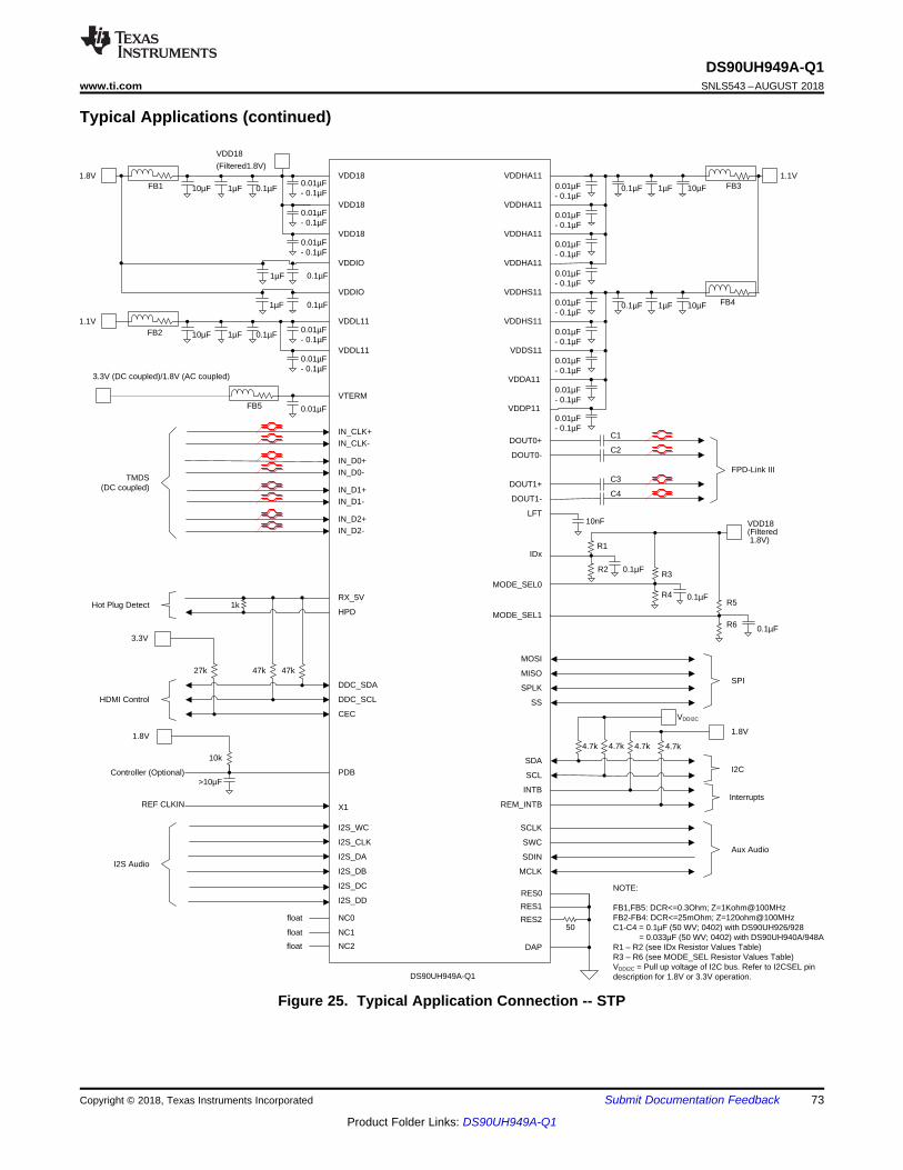
VDD18
VDD18
VDD18
VDDIO
VDDIO
VDDHS11
VDDS11VDDL11
VDDHA11
VDDHA11
VDDHA11
VDDHA11
VDDHS11
IN_CLK+IN_CLK-
IN_D0+IN_D0-
IN_D1+IN_D1-
IN_D2+IN_D2-
RX_5V
HPD
DDC_SDA
DDC_SCL
CEC
X1
I2S_WC
I2S_CLK
I2S_DA
I2S_DB
I2S_DC
I2S_DD
PDB
NC0
NC1
VDDL11
DAP
1.1V1.8V
1.1V
1.8V
TMDS(DC coupled)
HDMI Control
I2S Audio
Hot Plug Detect
FB1
FB2
FB3
FB4
>10µF
10k
27k 47k 47k
3.3V
1k
VTERM
3.3V (DC coupled)/1.8V (AC coupled)
FB5
0.01µF- 0.1µF
0.01µF- 0.1µF
0.01µF- 0.1µF
0.1µF
0.1µF
0.01µF- 0.1µF
0.01µF- 0.1µF
0.01µF
1µF
1µF
DOUT0+
DOUT0-
DOUT1+
DOUT1-
LFT
RES2
MODE_SEL0
IDx
MODE_SEL1
SDA
SCL
MOSI
MISO
SPLK
SS
SCLK
SWC
SDIN
MCLK
INTB
1.8V
Aux Audio
I2C
SPI
FPD-Link III
VDD18(Filtered 1.8V)
C1
C2
C3
C4
10nF
R1
R2R3
R4R5
R6
4.7k 4.7k 4.7k
VDDA11
VDDP11
0.01µF- 0.1µF
0.01µF- 0.1µF
0.01µF- 0.1µF
0.01µF- 0.1µF
0.01µF- 0.1µF
0.01µF- 0.1µF
0.01µF- 0.1µF
0.01µF- 0.1µF
0.01µF- 0.1µF
NOTE:
FB1,FB5: DCR<=0.3Ohm; Z=1Kohm@100MHzFB2-FB4: DCR<=25mOhm; Z=120ohm@100MHzC1-C4 = 0.1µF (50 WV; 0402) with DS90UH926/928C1-C4 = 0.033µF (50 WV; 0402) with DS90UH940A/948AR1 ± R2 (see IDx Resistor Values Table)R3 ± R6 (see MODE_SEL Resistor Values Table)VDDI2C = Pull up voltage of I2C bus. Refer to I2CSEL pin description for 1.8V or 3.3V operation.
10µF 1µF
float
float
0.1µF
0.1µF
0.1µF
Controller (Optional)
10µF 1µF 0.1µF
0.1µF
1µF 10µF0.1µF
1µF 10µF0.1µF
DS90UH949A-Q1
RES1
InterruptsREF CLKIN
VDD18
(Filtered1.8V)
RES0
VDDI2C
NC2float
50
REM_INTB
4.7k
73
DS90UH949A-Q1www.ti.com SNLS543 –AUGUST 2018
Product Folder Links: DS90UH949A-Q1
Submit Documentation FeedbackCopyright © 2018, Texas Instruments Incorporated
Typical Applications (continued)
Figure 25. Typical Application Connection -- STP
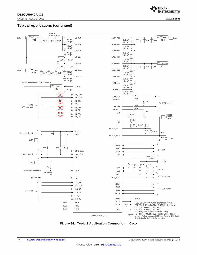
VDD18
VDD18
VDD18
VDDIO
VDDIO
VDDHS11
VDDS11VDDL11
VDDHA11
VDDHA11
VDDHA11
VDDHA11
VDDHS11
IN_CLK+IN_CLK-
IN_D0+IN_D0-
IN_D1+IN_D1-
IN_D2+IN_D2-
RX_5V
HPD
DDC_SDA
DDC_SCL
CEC
X1
I2S_WC
I2S_CLK
I2S_DA
I2S_DB
I2S_DC
I2S_DD
PDB
NC0
NC1
VDDL11
DAP
1.1V1.8V
1.1V
1.8V
TMDS(DC coupled)
HDMI Control
I2S Audio
Hot Plug Detect
FB1
FB2
FB3
FB4
>10µF
10k
27k 47k 47k
3.3V
VTERM
3.3V (DC coupled)/1.8V (AC coupled)
FB5
0.01µF- 0.1µF
0.01µF- 0.1µF
0.01µF- 0.1µF
0.1µF
0.1µF
0.01µF- 0.1µF
0.01µF- 0.1µF
0.01µF
1µF
1µF
DOUT0+
DOUT0-
DOUT1+
DOUT1-
LFT
RES2
MODE_SEL0
IDx
MODE_SEL1
SDA
SCL
MOSI
MISO
SPLK
SS
SCLK
SWC
SDIN
MCLK
INTB
1.8V
Aux Audio
I2C
SPI
FPD-Link III
VDD18(Filtered1.8V)
C1
C2
C3
C4
10nF
R1
R2R3
R4R5
R6
4.7k 4.7k 4.7k
VDDA11
VDDP11
0.01µF- 0.1µF
0.01µF- 0.1µF
0.01µF- 0.1µF
0.01µF- 0.1µF
0.01µF- 0.1µF
0.01µF- 0.1µF
0.01µF- 0.1µF
0.01µF- 0.1µF
0.01µF- 0.1µF
NOTE:
FB1,FB5: DCR<=0.3Ohm; Z=1Kohm@100MHzFB2-FB4: DCR<=25mOhm; Z=120ohm@100MHzC1,C3 = 0.033µF (50 WV; 0402) C2,C4 = 0.015µF (50 WV; 0402) R1 ± R2 (see IDx Resistor Values Table)R3 ± R6 (see MODE_SEL Resistor Values Table)VDDI2C = Pull up voltage of I2C bus. Refer to I2CSEL pin description for 1.8V or 3.3V operation.
10µF 1µF
float
float
0.1µF
0.1µF
0.1µF
Controller (Optional)
10µF 1µF 0.1µF
0.1µF
1µF 10µF0.1µF
1µF 10µF0.1µF
DS90UH949A-Q1
RES1
InterruptsREF CLKIN
VDD18(Filtered 1.8V)
RES0
VDDI2C
NC2float
50
50
50
REM_INTB
4.7k
1k
74
DS90UH949A-Q1SNLS543 –AUGUST 2018 www.ti.com
Product Folder Links: DS90UH949A-Q1
Submit Documentation Feedback Copyright © 2018, Texas Instruments Incorporated
Typical Applications (continued)
Figure 26. Typical Application Connection -- Coax
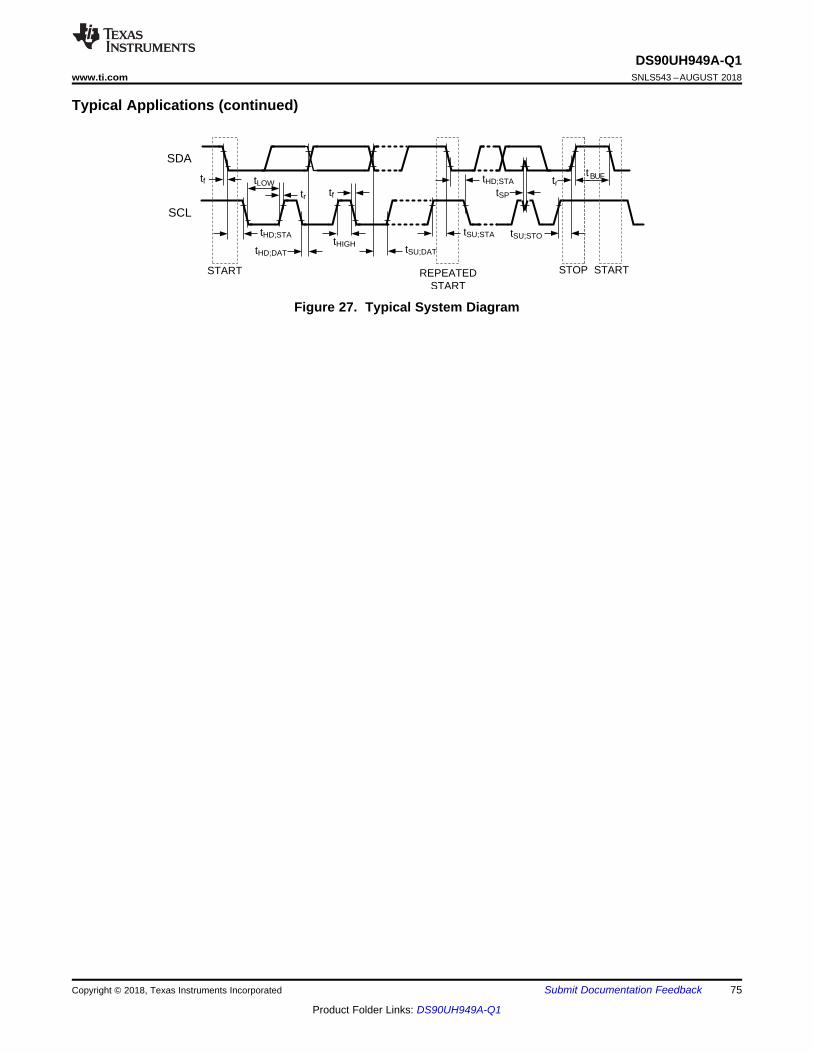
SCL
SDA
tHD;STA
tLOW
tr
tHD;DATtHIGH
tf
tSU;DAT
tSU;STA tSU;STO
tf
START REPEATEDSTART
STOP
tHD;STA
START
tSP
trBUFt
75
DS90UH949A-Q1www.ti.com SNLS543 –AUGUST 2018
Product Folder Links: DS90UH949A-Q1
Submit Documentation FeedbackCopyright © 2018, Texas Instruments Incorporated
Typical Applications (continued)
Figure 27. Typical System Diagram
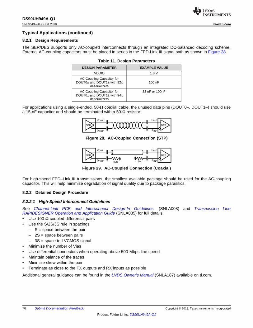
DOUT-
DOUT+
SER
RIN-
RIN+
DES
50Q 50Q
DOUT-
DOUT+
SER
RIN-
RIN+
DES
76
DS90UH949A-Q1SNLS543 –AUGUST 2018 www.ti.com
Product Folder Links: DS90UH949A-Q1
Submit Documentation Feedback Copyright © 2018, Texas Instruments Incorporated
Typical Applications (continued)8.2.1 Design RequirementsThe SER/DES supports only AC-coupled interconnects through an integrated DC-balanced decoding scheme.External AC-coupling capacitors must be placed in series in the FPD-Link III signal path as shown in Figure 28.
Table 11. Design ParametersDESIGN PARAMETER EXAMPLE VALUE
VDDIO 1.8 VAC Coupling Capacitor for
DOUT0± and DOUT1± with 92xdeserializers
100 nF
AC Coupling Capacitor forDOUT0± and DOUT1± with 94x
deserializers
33 nF or 100nF
For applications using a single-ended, 50-Ω coaxial cable, the unused data pins (DOUT0–, DOUT1–) should usea 15-nF capacitor and should be terminated with a 50-Ω resistor.
Figure 28. AC-Coupled Connection (STP)
Figure 29. AC-Coupled Connection (Coaxial)
For high-speed FPD–Link III transmissions, the smallest available package should be used for the AC-couplingcapacitor. This will help minimize degradation of signal quality due to package parasitics.
8.2.2 Detailed Design Procedure
8.2.2.1 High-Speed Interconnect GuidelinesSee Channel-Link PCB and Interconnect Design-In Guidelines, (SNLA008) and Transmission LineRAPIDESIGNER Operation and Application Guide (SNLA035) for full details.• Use 100-Ω coupled differential pairs• Use the S/2S/3S rule in spacings
– S = space between the pair– 2S = space between pairs– 3S = space to LVCMOS signal
• Minimize the number of Vias• Use differential connectors when operating above 500-Mbps line speed• Maintain balance of the traces• Minimize skew within the pair• Terminate as close to the TX outputs and RX inputs as possible
Additional general guidance can be found in the LVDS Owner's Manual (SNLA187) available on ti.com.
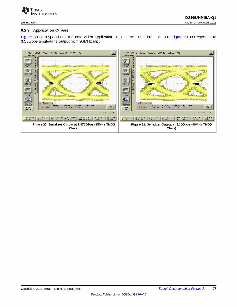
77
DS90UH949A-Q1www.ti.com SNLS543 –AUGUST 2018
Product Folder Links: DS90UH949A-Q1
Submit Documentation FeedbackCopyright © 2018, Texas Instruments Incorporated
8.2.3 Application CurvesFigure 30 corresponds to 1080p60 video application with 2-lane FPD-Link III output. Figure 31 corresponds to3.36Gbps single-lane output from 96MHz input
Figure 30. Serializer Output at 2.975Gbps (85MHz TMDSClock)
Figure 31. Serializer Output at 3.36Gbps (96MHz TMDSClock)
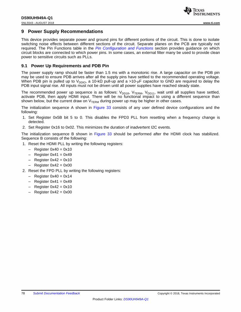
78
DS90UH949A-Q1SNLS543 –AUGUST 2018 www.ti.com
Product Folder Links: DS90UH949A-Q1
Submit Documentation Feedback Copyright © 2018, Texas Instruments Incorporated
9 Power Supply RecommendationsThis device provides separate power and ground pins for different portions of the circuit. This is done to isolateswitching noise effects between different sections of the circuit. Separate planes on the PCB are typically notrequired. The Pin Functions table in the Pin Configuration and Functions section provides guidance on whichcircuit blocks are connected to which power pins. In some cases, an external filter many be used to provide cleanpower to sensitive circuits such as PLLs.
9.1 Power Up Requirements and PDB PinThe power supply ramp should be faster than 1.5 ms with a monotonic rise. A large capacitor on the PDB pinmay be used to ensure PDB arrives after all the supply pins have settled to the recommended operating voltage.When PDB pin is pulled up to VDDIO, a 10-kΩ pull-up and a >10-μF capacitor to GND are required to delay thePDB input signal rise. All inputs must not be driven until all power supplies have reached steady state.
The recommended power up sequence is as follows: VDD18, VTERM, VDD11, wait until all supplies have settled,activate PDB, then apply HDMI input. There will be no functional impact to using a different sequence thanshown below, but the current draw on VTERM during power up may be higher in other cases.
The initialization sequence A shown in Figure 33 consists of any user defined device configurations and thefollowing:1. Set Register 0x5B bit 5 to 0. This disables the FPD3 PLL from resetting when a frequency change is
detected.2. Set Register 0x16 to 0x02. This minimizes the duration of inadvertent I2C events.
The initialization sequence B shown in Figure 33 should be performed after the HDMI clock has stabilized.Sequence B consists of the following:1. Reset the HDMI PLL by writing the following registers:
– Register 0x40 = 0x10– Register 0x41 = 0x49– Register 0x42 = 0x10– Register 0x42 = 0x00
2. Reset the FPD PLL by writing the following registers:– Register 0x40 = 0x14– Register 0x41 = 0x49– Register 0x42 = 0x10– Register 0x42 = 0x00
VDDIOVDD18
VDD11
PDB(*)
VDDIO
VPDB_LOW
(*) TI recommends that the designer assert PDB (active High) with a microcontroller rather than an RC filter network to help ensure proper sequencing of PDB pin after settling of power supplies.
VPDB_HIGH
tr0
t1
tr1
t3
GND
GND
GND
t2
t4 t3
VTERM
tr0
GND
GPIOt5
t0
79
DS90UH949A-Q1www.ti.com SNLS543 –AUGUST 2018
Product Folder Links: DS90UH949A-Q1
Submit Documentation FeedbackCopyright © 2018, Texas Instruments Incorporated
Power Up Requirements and PDB Pin (continued)
Figure 32. Recommended Power Sequencing
VTERM must come before VDD18 When VTERM = 1.8V; this requirement is not applicable when VTERM =3.3V.
VDDx
PDB
t2
...HDMI ...HDMI clock
+/-0.5% variation
t3
I2C Local
Init A Init B
Valid DataDOUT0/1
t6
80
DS90UH949A-Q1SNLS543 –AUGUST 2018 www.ti.com
Product Folder Links: DS90UH949A-Q1
Submit Documentation Feedback Copyright © 2018, Texas Instruments Incorporated
Power Up Requirements and PDB Pin (continued)
Figure 33. Initialization Sequencing
The Init A and Init B sequence should consist of any user defined device configurations.
Table 12. Power-Up Sequencing ConstraintsSymbol Description Test Conditions Min Typ Max Units
VDD18, VDDIO VDD18 / VDDIO voltagerange 1.71 1.89 V
VTERM VTERM voltage rangeDC-coupled HDMI termination 3.135 3.465 VAC-coupled HDMI termination 1.71 1.89 V
VDD11 VDD11 voltage range 1.045 1.155 V
VPDB_LOW
PDB LOW thresholdNote: VPDB should not exceedlimit for respective I/O voltagebefore 90% voltage of VDD12
VDDIO = 1.8V ± 5% 0.35 *VDDIO V
VPDB_HIGH PDB HIGH threshold VDDIO = 1.8V ± 5% 0.65 *VDDIO V
tr0VTERM / VDDIO / VDD18 rise
time
These time constants are specified forrise time of power supply voltage ramp
(10% -90%).1.5 ms
tr1 VDD11 rise timeThese time constants are specified forrise time of power supply voltage ramp
(10% -90%).1.5 ms
t0 VDDIO / VDD18 delay time VTERM needs to ramp-up before VDD18and VDDIO. 0 ms
t1 VDD11 delay time VDDIO and VDD18 need to ramp-upbefore VDD11. 0 ms
t2 PDB delay time PDB should be released after all suppliesare stable. 0 ms
t3 I2C ready time Starting from PDB high, the local I2Caccess is available after this time. 2 ms
t4 Hard reset time PDB negative pulse width required for thedevice reset. 2 ms
81
DS90UH949A-Q1www.ti.com SNLS543 –AUGUST 2018
Product Folder Links: DS90UH949A-Q1
Submit Documentation FeedbackCopyright © 2018, Texas Instruments Incorporated
Power Up Requirements and PDB Pin (continued)Table 12. Power-Up Sequencing Constraints (continued)
Symbol Description Test Conditions Min Typ Max Units
t5 PDB to HDMI delay time Keep GPIOs low or high until after PDBrelease. 0 ms
t6HDMI Clock Stable to PLL
Reset (Init B)HDMI Clock must be within 0.5% of the
target frequency and stable. 1 µs
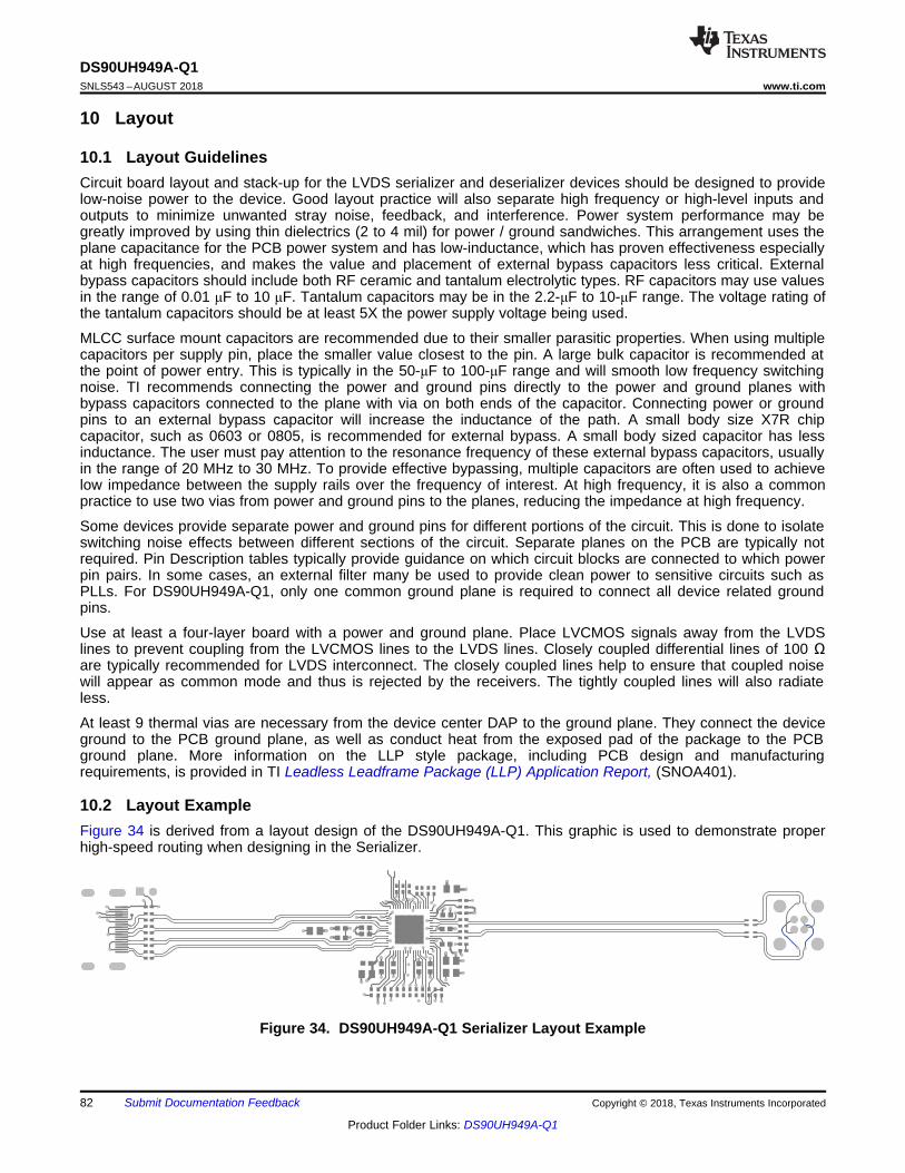
82
DS90UH949A-Q1SNLS543 –AUGUST 2018 www.ti.com
Product Folder Links: DS90UH949A-Q1
Submit Documentation Feedback Copyright © 2018, Texas Instruments Incorporated
10 Layout
10.1 Layout GuidelinesCircuit board layout and stack-up for the LVDS serializer and deserializer devices should be designed to providelow-noise power to the device. Good layout practice will also separate high frequency or high-level inputs andoutputs to minimize unwanted stray noise, feedback, and interference. Power system performance may begreatly improved by using thin dielectrics (2 to 4 mil) for power / ground sandwiches. This arrangement uses theplane capacitance for the PCB power system and has low-inductance, which has proven effectiveness especiallyat high frequencies, and makes the value and placement of external bypass capacitors less critical. Externalbypass capacitors should include both RF ceramic and tantalum electrolytic types. RF capacitors may use valuesin the range of 0.01 μF to 10 μF. Tantalum capacitors may be in the 2.2-μF to 10-μF range. The voltage rating ofthe tantalum capacitors should be at least 5X the power supply voltage being used.
MLCC surface mount capacitors are recommended due to their smaller parasitic properties. When using multiplecapacitors per supply pin, place the smaller value closest to the pin. A large bulk capacitor is recommended atthe point of power entry. This is typically in the 50-μF to 100-μF range and will smooth low frequency switchingnoise. TI recommends connecting the power and ground pins directly to the power and ground planes withbypass capacitors connected to the plane with via on both ends of the capacitor. Connecting power or groundpins to an external bypass capacitor will increase the inductance of the path. A small body size X7R chipcapacitor, such as 0603 or 0805, is recommended for external bypass. A small body sized capacitor has lessinductance. The user must pay attention to the resonance frequency of these external bypass capacitors, usuallyin the range of 20 MHz to 30 MHz. To provide effective bypassing, multiple capacitors are often used to achievelow impedance between the supply rails over the frequency of interest. At high frequency, it is also a commonpractice to use two vias from power and ground pins to the planes, reducing the impedance at high frequency.
Some devices provide separate power and ground pins for different portions of the circuit. This is done to isolateswitching noise effects between different sections of the circuit. Separate planes on the PCB are typically notrequired. Pin Description tables typically provide guidance on which circuit blocks are connected to which powerpin pairs. In some cases, an external filter many be used to provide clean power to sensitive circuits such asPLLs. For DS90UH949A-Q1, only one common ground plane is required to connect all device related groundpins.
Use at least a four-layer board with a power and ground plane. Place LVCMOS signals away from the LVDSlines to prevent coupling from the LVCMOS lines to the LVDS lines. Closely coupled differential lines of 100 Ωare typically recommended for LVDS interconnect. The closely coupled lines help to ensure that coupled noisewill appear as common mode and thus is rejected by the receivers. The tightly coupled lines will also radiateless.
At least 9 thermal vias are necessary from the device center DAP to the ground plane. They connect the deviceground to the PCB ground plane, as well as conduct heat from the exposed pad of the package to the PCBground plane. More information on the LLP style package, including PCB design and manufacturingrequirements, is provided in TI Leadless Leadframe Package (LLP) Application Report, (SNOA401).
10.2 Layout ExampleFigure 34 is derived from a layout design of the DS90UH949A-Q1. This graphic is used to demonstrate properhigh-speed routing when designing in the Serializer.
Figure 34. DS90UH949A-Q1 Serializer Layout Example
83
DS90UH949A-Q1www.ti.com SNLS543 –AUGUST 2018
Product Folder Links: DS90UH949A-Q1
Submit Documentation FeedbackCopyright © 2018, Texas Instruments Incorporated
11 Device and Documentation Support
11.1 Documentation Support
11.1.1 Related DocumentationFor related documentation see the following:• Soldering Specifications Application Report, (SNOA549)• IC Package Thermal Metrics Application Report, (SPRA953)• Channel-Link PCB and Interconnect Design-In Guidelines, (SNLA008)• Transmission Line RAPIDESIGNER Operation and Application Guide, (SNLA035)• Leadless Leadframe Package (LLP) Application Report, (SNOA401)• LVDS Owner's Manual, (SNLA187)• I2C Communication Over FPD-Link III With Bidirectional Control Channel, (SNLA131)• Using the I2S Audio Interface of DS90Ux92x FPD-Link III Devices, (SNLA221)• Exploring the Internal Test Pattern Generation Feature of 720p FPD-Link III Devices, (SNLA132)
11.2 Receiving Notification of Documentation UpdatesTo receive notification of documentation updates, navigate to the device product folder on ti.com. In the upperright corner, click on Alert me to register and receive a weekly digest of any product information that haschanged. For change details, review the revision history included in any revised document.
11.3 Community ResourcesThe following links connect to TI community resources. Linked contents are provided "AS IS" by the respectivecontributors. They do not constitute TI specifications and do not necessarily reflect TI's views; see TI's Terms ofUse.
TI E2E™ Online Community TI's Engineer-to-Engineer (E2E) Community. Created to foster collaborationamong engineers. At e2e.ti.com, you can ask questions, share knowledge, explore ideas and helpsolve problems with fellow engineers.
Design Support TI's Design Support Quickly find helpful E2E forums along with design support tools andcontact information for technical support.
11.4 TrademarksTRI-STATE, E2E are trademarks of Texas Instruments.All other trademarks are the property of their respective owners.
11.5 Electrostatic Discharge CautionThis integrated circuit can be damaged by ESD. Texas Instruments recommends that all integrated circuits be handled withappropriate precautions. Failure to observe proper handling and installation procedures can cause damage.
ESD damage can range from subtle performance degradation to complete device failure. Precision integrated circuits may be moresusceptible to damage because very small parametric changes could cause the device not to meet its published specifications.
11.6 GlossarySLYZ022 — TI Glossary.
This glossary lists and explains terms, acronyms, and definitions.
12 Mechanical, Packaging, and Orderable InformationThe following pages include mechanical, packaging, and orderable information. This information is the mostcurrent data available for the designated devices. This data is subject to change without notice and revision ofthis document. For browser-based versions of this data sheet, refer to the left-hand navigation.
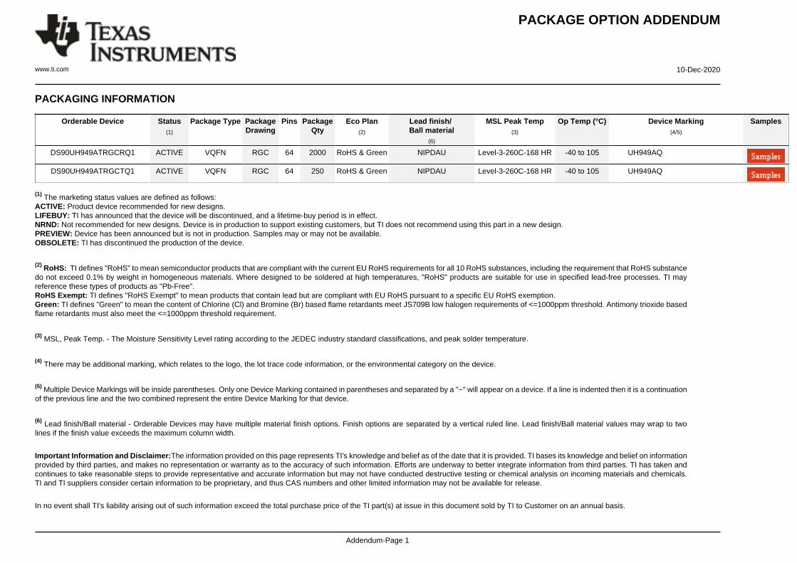
PACKAGE OPTION ADDENDUM
www.ti.com 10-Dec-2020
Addendum-Page 1
PACKAGING INFORMATION
Orderable Device Status(1)
Package Type PackageDrawing
Pins PackageQty
Eco Plan(2)
Lead finish/Ball material
(6)
MSL Peak Temp(3)
Op Temp (°C) Device Marking(4/5)
Samples
DS90UH949ATRGCRQ1 ACTIVE VQFN RGC 64 2000 RoHS & Green NIPDAU Level-3-260C-168 HR -40 to 105 UH949AQ
DS90UH949ATRGCTQ1 ACTIVE VQFN RGC 64 250 RoHS & Green NIPDAU Level-3-260C-168 HR -40 to 105 UH949AQ
(1) The marketing status values are defined as follows:ACTIVE: Product device recommended for new designs.LIFEBUY: TI has announced that the device will be discontinued, and a lifetime-buy period is in effect.NRND: Not recommended for new designs. Device is in production to support existing customers, but TI does not recommend using this part in a new design.PREVIEW: Device has been announced but is not in production. Samples may or may not be available.OBSOLETE: TI has discontinued the production of the device.
(2) RoHS: TI defines "RoHS" to mean semiconductor products that are compliant with the current EU RoHS requirements for all 10 RoHS substances, including the requirement that RoHS substancedo not exceed 0.1% by weight in homogeneous materials. Where designed to be soldered at high temperatures, "RoHS" products are suitable for use in specified lead-free processes. TI mayreference these types of products as "Pb-Free".RoHS Exempt: TI defines "RoHS Exempt" to mean products that contain lead but are compliant with EU RoHS pursuant to a specific EU RoHS exemption.Green: TI defines "Green" to mean the content of Chlorine (Cl) and Bromine (Br) based flame retardants meet JS709B low halogen requirements of <=1000ppm threshold. Antimony trioxide basedflame retardants must also meet the <=1000ppm threshold requirement.
(3) MSL, Peak Temp. - The Moisture Sensitivity Level rating according to the JEDEC industry standard classifications, and peak solder temperature.
(4) There may be additional marking, which relates to the logo, the lot trace code information, or the environmental category on the device.
(5) Multiple Device Markings will be inside parentheses. Only one Device Marking contained in parentheses and separated by a "~" will appear on a device. If a line is indented then it is a continuationof the previous line and the two combined represent the entire Device Marking for that device.
(6) Lead finish/Ball material - Orderable Devices may have multiple material finish options. Finish options are separated by a vertical ruled line. Lead finish/Ball material values may wrap to twolines if the finish value exceeds the maximum column width.
Important Information and Disclaimer:The information provided on this page represents TI's knowledge and belief as of the date that it is provided. TI bases its knowledge and belief on informationprovided by third parties, and makes no representation or warranty as to the accuracy of such information. Efforts are underway to better integrate information from third parties. TI has taken andcontinues to take reasonable steps to provide representative and accurate information but may not have conducted destructive testing or chemical analysis on incoming materials and chemicals.TI and TI suppliers consider certain information to be proprietary, and thus CAS numbers and other limited information may not be available for release.
In no event shall TI's liability arising out of such information exceed the total purchase price of the TI part(s) at issue in this document sold by TI to Customer on an annual basis.
PACKAGE OPTION ADDENDUM
www.ti.com 10-Dec-2020
Addendum-Page 2
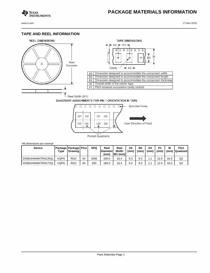
TAPE AND REEL INFORMATION
*All dimensions are nominal
Device PackageType
PackageDrawing
Pins SPQ ReelDiameter
(mm)
ReelWidth
W1 (mm)
A0(mm)
B0(mm)
K0(mm)
P1(mm)
W(mm)
Pin1Quadrant
DS90UH949ATRGCRQ1 VQFN RGC 64 2000 330.0 16.4 9.3 9.3 1.1 12.0 16.0 Q2
DS90UH949ATRGCTQ1 VQFN RGC 64 250 180.0 16.4 9.3 9.3 1.1 12.0 16.0 Q2
PACKAGE MATERIALS INFORMATION
www.ti.com 17-Nov-2019
Pack Materials-Page 1
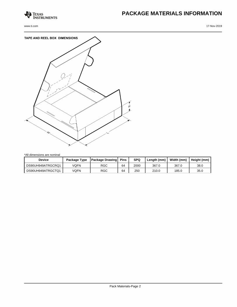
*All dimensions are nominal
Device Package Type Package Drawing Pins SPQ Length (mm) Width (mm) Height (mm)
DS90UH949ATRGCRQ1 VQFN RGC 64 2000 367.0 367.0 38.0
DS90UH949ATRGCTQ1 VQFN RGC 64 250 210.0 185.0 35.0
PACKAGE MATERIALS INFORMATION
www.ti.com 17-Nov-2019
Pack Materials-Page 2
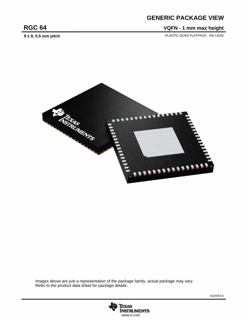
www.ti.com
GENERIC PACKAGE VIEW
Images above are just a representation of the package family, actual package may vary.Refer to the product data sheet for package details.
VQFN - 1 mm max heightRGC 64PLASTIC QUAD FLATPACK - NO LEAD9 x 9, 0.5 mm pitch
4224597/A
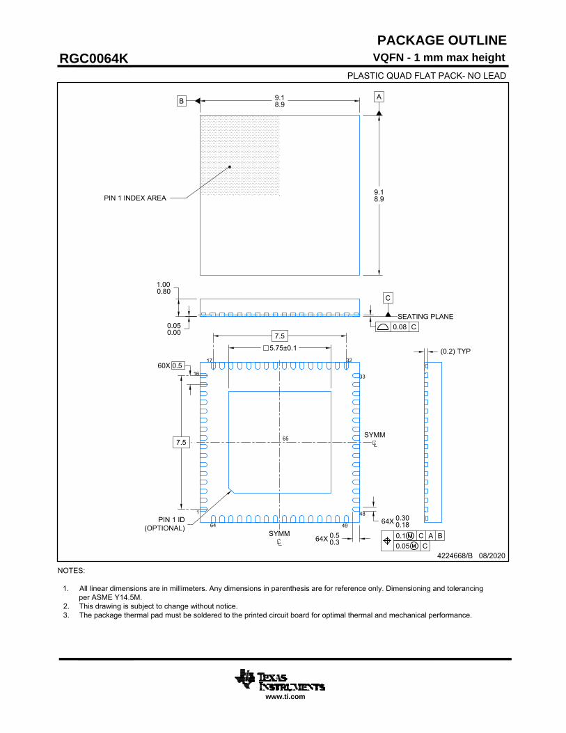
NOTES:
1. All linear dimensions are in millimeters. Any dimensions in parenthesis are for reference only. Dimensioning and tolerancingper ASME Y14.5M.
2. This drawing is subject to change without notice.3. The package thermal pad must be soldered to the printed circuit board for optimal thermal and mechanical performance.
PACKAGE OUTLINE
4224668/B 08/2020
www.ti.com
VQFN - 1 mm max height
PLASTIC QUAD FLAT PACK- NO LEAD
RGC0064K
A
0.08 C
0.1 C A B0.05 C
B
SYMM
SYMM
PIN 1 INDEX AREA
9.18.9
9.18.9
1.000.80
0.050.00
SEATING PLANE
(0.2) TYP 5.75±0.17.5
7.5
60X 0.5
64X 0.300.18
64X 0.50.3
C
1
16
17 32
33
48
4964
65
PIN 1 ID(OPTIONAL)
AutoCAD SHX Text
AutoCAD SHX Text
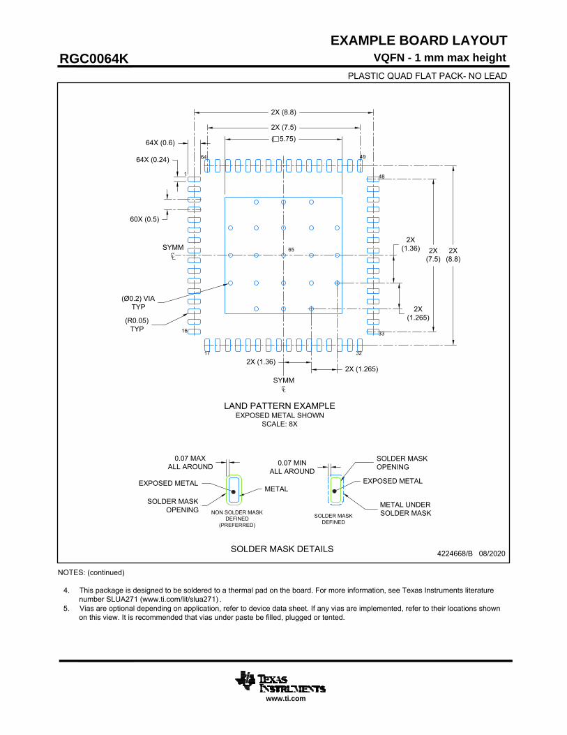
NOTES: (continued)
4. This package is designed to be soldered to a thermal pad on the board. For more information, see Texas Instruments literaturenumber SLUA271 (www.ti.com/lit/slua271) .
5. Vias are optional depending on application, refer to device data sheet. If any vias are implemented, refer to their locations shown on this view. It is recommended that vias under paste be filled, plugged or tented.
EXAMPLE BOARD LAYOUT
4224668/B 08/2020
www.ti.com
VQFN - 1 mm max height
RGC0064K
PLASTIC QUAD FLAT PACK- NO LEAD
SYMM
SYMM
LAND PATTERN EXAMPLEEXPOSED METAL SHOWN
SCALE: 8X
( 5.75)2X (7.5)
2X (8.8)
64X (0.6)
64X (0.24)
60X (0.5)
2X(8.8)
2X(7.5)
(R0.05)TYP
2X(1.36)
2X(1.265)
2X (1.36)2X (1.265)
(Ø0.2) VIATYP
SOLDER MASK DETAILS
NON SOLDER MASKDEFINED
(PREFERRED)
SOLDER MASKDEFINED
METAL
SOLDER MASKOPENING
EXPOSED METAL
SOLDER MASKOPENING
METAL UNDERSOLDER MASK
EXPOSED METAL
0.07 MAXALL AROUND 0.07 MIN
ALL AROUND
1
16
17 32
33
48
4964
65
AutoCAD SHX Text
AutoCAD SHX Text
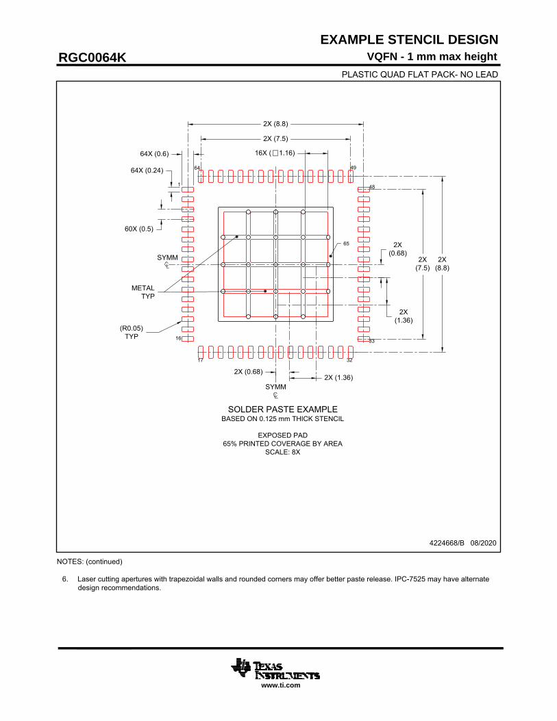
NOTES: (continued)
6. Laser cutting apertures with trapezoidal walls and rounded corners may offer better paste release. IPC-7525 may have alternatedesign recommendations.
EXAMPLE STENCIL DESIGN
4224668/B 08/2020
www.ti.com
VQFN - 1 mm max height
RGC0064K
PLASTIC QUAD FLAT PACK- NO LEAD
SOLDER PASTE EXAMPLEBASED ON 0.125 mm THICK STENCIL
EXPOSED PAD65% PRINTED COVERAGE BY AREA
SCALE: 8X
SYMM
SYMM
16X ( 1.16)
2X (7.5)
2X (8.8)
64X (0.6)
64X (0.24)
60X (0.5)
2X(8.8)
2X(7.5)
(R0.05)TYP
1
16
17 32
33
48
4964
65 2X(0.68)
2X(1.36)
2X (0.68)2X (1.36)
METALTYP
AutoCAD SHX Text
AutoCAD SHX Text

IMPORTANT NOTICE AND DISCLAIMER
TI PROVIDES TECHNICAL AND RELIABILITY DATA (INCLUDING DATASHEETS), DESIGN RESOURCES (INCLUDING REFERENCE DESIGNS), APPLICATION OR OTHER DESIGN ADVICE, WEB TOOLS, SAFETY INFORMATION, AND OTHER RESOURCES “AS IS” AND WITH ALL FAULTS, AND DISCLAIMS ALL WARRANTIES, EXPRESS AND IMPLIED, INCLUDING WITHOUT LIMITATION ANY IMPLIED WARRANTIES OF MERCHANTABILITY, FITNESS FOR A PARTICULAR PURPOSE OR NON-INFRINGEMENT OF THIRD PARTY INTELLECTUAL PROPERTY RIGHTS.These resources are intended for skilled developers designing with TI products. You are solely responsible for (1) selecting the appropriate TI products for your application, (2) designing, validating and testing your application, and (3) ensuring your application meets applicable standards, and any other safety, security, or other requirements. These resources are subject to change without notice. TI grants you permission to use these resources only for development of an application that uses the TI products described in the resource. Other reproduction and display of these resources is prohibited. No license is granted to any other TI intellectual property right or to any third party intellectual property right. TI disclaims responsibility for, and you will fully indemnify TI and its representatives against, any claims, damages, costs, losses, and liabilities arising out of your use of these resources.TI’s products are provided subject to TI’s Terms of Sale (www.ti.com/legal/termsofsale.html) or other applicable terms available either on ti.com or provided in conjunction with such TI products. TI’s provision of these resources does not expand or otherwise alter TI’s applicable warranties or warranty disclaimers for TI products.
Mailing Address: Texas Instruments, Post Office Box 655303, Dallas, Texas 75265Copyright © 2020, Texas Instruments Incorporated
Related Documents