1 SLYU046 – January 2019 Submit Documentation Feedback Copyright © 2019, Texas Instruments Incorporated DRV5055-5057EVM User's Guide SLYU046 – January 2019 DRV5055-5057EVM This user’s guide describes the characteristics, operation, and use of the DRV5055, DRV5056, and DRV5057 (DRV505x) evaluation module (EVM). This EVM is designed to evaluate the performance of the DRV505x ratiometric, linear, Hall effect sensors. Throughout this document, the terms evaluation board, evaluation module, and EVM are synonymous with the DRV5055-5057EVM. This document includes a schematic, reference printed circuit board (PCB) layouts, and a complete bill of materials (BOM).

Welcome message from author
This document is posted to help you gain knowledge. Please leave a comment to let me know what you think about it! Share it to your friends and learn new things together.
Transcript

1SLYU046–January 2019Submit Documentation Feedback
Copyright © 2019, Texas Instruments Incorporated
DRV5055-5057EVM
User's GuideSLYU046–January 2019
DRV5055-5057EVM
This user’s guide describes the characteristics, operation, and use of the DRV5055, DRV5056, andDRV5057 (DRV505x) evaluation module (EVM). This EVM is designed to evaluate the performance of theDRV505x ratiometric, linear, Hall effect sensors. Throughout this document, the terms evaluation board,evaluation module, and EVM are synonymous with the DRV5055-5057EVM. This document includes aschematic, reference printed circuit board (PCB) layouts, and a complete bill of materials (BOM).

www.ti.com
2 SLYU046–January 2019Submit Documentation Feedback
Copyright © 2019, Texas Instruments Incorporated
DRV5055-5057EVM
Contents1 Overview ...................................................................................................................... 32 Operation ..................................................................................................................... 53 Hardware...................................................................................................................... 64 Schematics, PCB Layout, and Bill of Materials .......................................................................... 9
List of Figures
1 Microcontroller Source Code Operation .................................................................................. 62 Gain Variants A1 to A4 .................................................................................................... 103 LCD, Microcontroller and Switch ......................................................................................... 114 Push-Button, Slider Switch, and Programming User Inputs .......................................................... 125 LED and Indicators, Slider Switch Status Reader, and DRV5057 Multiplexer .................................... 136 Supply Input and Power Conditioning ................................................................................... 147 Top Overlay ................................................................................................................. 158 Top Layer ................................................................................................................... 159 Bottom Overlay ............................................................................................................. 1510 Bottom Layer................................................................................................................ 15
List of Tables
1 DRV505x Device Summary ................................................................................................ 32 Kit Contents .................................................................................................................. 33 Related Documentation ..................................................................................................... 44 Bill of Materials ............................................................................................................. 16
TrademarksAll trademarks are the property of their respective owners.

www.ti.com Overview
3SLYU046–January 2019Submit Documentation Feedback
Copyright © 2019, Texas Instruments Incorporated
DRV5055-5057EVM
1 OverviewThe DRV505x family of linear Hall effect sensors sense magnetic fields ranging from 19 mT to 176 mT fullscale, depending on device and supply voltage. For each device, four gains are available. These devicesoperate from a single 3-V to 5.5-V power supply, drawing a maximum of 10 mA of supply current. Thesedevices are currently available in a 3-pin SOT-23 or 3-pin TO-92 package. This EVM uses a 3.3-V supply,and Table 1 lists the gains at this voltage for each device.
Table 1. DRV505x Device Summary
Product Gain at 3.3V VCC
DRV5055A1 60 mV/mTDRV5055A2 30 mV/mTDRV5055A3 15 mV/mTDRV5055A4 7.5 mV/mTDRV5056A1 120 mV/mTDRV5056A2 60 mV/mTDRV5056A3 30 mV/mTDRV5056A4 15 mV/mTDRV5057A1 1.2 %D/mTDRV5057A2 0.6 %D/mTDRV5057A3 0.3 %D/mTDRV5057A4 0.15 %D/mT
1.1 Kit ContentsTable 2 lists the contents of the DRV5055-5057EVM kit. Contact the nearest Texas Instruments ProductInformation Center if any component is missing.
Table 2. Kit Contents
Item QuantityDRV5055-5057EVM test board 1
Cylindrical magnet 1USB cable 1
Overview www.ti.com
4 SLYU046–January 2019Submit Documentation Feedback
Copyright © 2019, Texas Instruments Incorporated
DRV5055-5057EVM
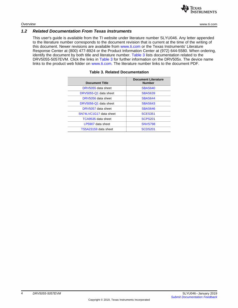
1.2 Related Documentation From Texas InstrumentsThis user's guide is available from the TI website under literature number SLYU046. Any letter appendedto the literature number corresponds to the document revision that is current at the time of the writing ofthis document. Newer revisions are available from www.ti.com or the Texas Instruments' LiteratureResponse Center at (800) 477-8924 or the Product Information Center at (972) 644-5580. When ordering,identify the document by both title and literature number. Table 3 lists documentation related to theDRV5055-5057EVM. Click the links in Table 3 for further information on the DRV505x. The device namelinks to the product web folder on www.ti.com. The literature number links to the document PDF.
Table 3. Related Documentation
Document TitleDocument Literature
NumberDRV5055 data sheet SBAS640
DRV5055-Q1 data sheet SBAS639DRV5056 data sheet SBAS644
DRV5056-Q1 data sheet SBAS643DRV5057 data sheet SBAS646
SN74LVC1G17 data sheet SCES351TCA9535 data sheet SCPS201LP5907 data sheet SNVS798
TS5A23159 data sheet SCDS201

www.ti.com Operation
5SLYU046–January 2019Submit Documentation Feedback
Copyright © 2019, Texas Instruments Incorporated
DRV5055-5057EVM
2 Operation
2.1 Quick Start SetupThe following instructions describe how to set up and use the DRV5055-5057EVM.
Step 1. Insert the USB cable into the EVM onboard USB receptacle.Step 2. For proper calibration, make certain that there are no magnets within a few feet of the EVM
when the EVM powers up.Step 3. Plug the USB cable into any USB power adapter (for example, laptop, desktop, power bank,
and so on). LED D13 on the far bottom right of the board indicates the board is powered,calibrated, and is taking sample measurements from the DRV5055A1 (default EVM startupdevice).
2.2 MeasurementsThe DRV5055-5057EVM measures a magnetic field with multiple devices and the respective gainvariants. Push-button S1 selects the different gain variants of the DRV505x devices. The devices arearranged such that gain variants increase sequentially from right to left, and the device families(DRV505x) are also arranged in an increasing order from right to left. The LCD displays the measurementcorresponding to the selected device. The measurement format is adjusted by the slide switch labeledDisplay Mode (K1).
Step 1. Click the Device Select Switch until an LED indicates the device of interest is selected.Step 2. Adjust the Display Mode slide switch to the measurement format of interest. Voltage mode
(labeled V) is blank for the DRV5057 devices.Step 3. Introduce magnetic stimulus (for example, the magnet included in the evaluation kit).

Startup 1. Setup Microcontroller Registers2. Calibrate Measurements
Collect DRV5055
A1 Samples
A: # of collected samples <32B: Pushbutton PressedC: 32 samples collected
B
A
Display Measurement and Check Measurement Mode
C
Collect DRV5055
A2 Samples
A
Collect DRV5055
A3 Samples
A
Collect DRV5055
A4 Samples
A
Collect DRV5056
A1 Samples
A
Collect DRV5056
A2 Samples
A
Collect DRV5056
A3 Samples
A
Collect DRV5056
A4 Samples
A
Collect DRV5057
A1 Samples
A
Collect DRV5057
A2 Samples
Collect DRV5057
A3 Samples
A
Collect DRV5057
A4 Samples
A
C C C C C C C C C C CB B B B B B B B B B
B
A
Hardware www.ti.com
6 SLYU046–January 2019Submit Documentation Feedback
Copyright © 2019, Texas Instruments Incorporated
DRV5055-5057EVM
3 HardwareThe DRV505x is a linear Hall effect magnetic-sense solution that provides ease of use and highperformance. The DRV5055-5057EVM is intended to provide basic functional evaluation of this devicefamily. The fixture layout is not intended to be a model for the target circuit, nor is it laid out forelectromagnetic compatibility (EMC) testing. The DRV5055-5057EVM consists of one PCB with each ofthe gain variants of the DRV5055, DRV5056, and DRV5057. The EVM kit also provides a USB cable forquick power-up, as well as a magnet for quick qualitative assessment of the DRV505x variantsperformance.
3.1 FeaturesThe layout of the DRV5055-5057EVM printed circuit board (PCB) is designed to provide the followingfeatures:• Evaluation of all gain options for the DRV505x• Easily access device pins through test points• Easily read voltage, mT, % duty cycle values, and microcontroller ADC memory values from the
onboard LCD, where applicable• Toggle between devices with a press of the Device Select Switch, push-button S1.
See the links in Table 3 for comprehensive information about the DRV505x family of devices.
3.2 Theory of OperationThe DRV5055-5057EVM is a plug-and-play board, requiring only that the user supply power and provide amagnetic stimulus after the initial calibration. The ease of operation can be attributed to the onboardmicrocontroller. The source code for the microcontroller is available on the DRV5055, DRV5056, andDRV5057 web folders under Tools and Software. The basic operation of the microcontroller source codeis outlined in the state machine diagram shown in Figure 1. Upon receiving power, the microcontrollerregisters are set up to properly interact with the other devices on the board. Then, a preliminarymeasurement of each DRV5055, DRV5056, and DRV5057 gain variant is taken. Make sure that themagnetic stimulus of interest is not present at this time because this measurement sets the 0 point in themT measurement display. After calibration is complete, the LED for the DRV5055A1 powers on bydefault. At this point, the EVM microcontroller begins continuously sampling the DRV5055A1. Pressingpush-button S1 results in the EVM sampling the next adjacent device. After every 32 samples are taken,the device calculates an average, and processes the data to fit the format selected by the slider switch K1.
Figure 1. Microcontroller Source Code Operation

www.ti.com Hardware
7SLYU046–January 2019Submit Documentation Feedback
Copyright © 2019, Texas Instruments Incorporated
DRV5055-5057EVM
3.3 CircuitryThis section summarizes the DRV5055-5057EVM components.
3.3.1 C1, J1, R1, and R2J1 serves as the connector for an external MSP-FET Flash Emulation Tool to connect to the board.
C1, R1, and R2 are the additional passives required for the emulation tool to effectively communicate withthe MSP430FR4133 for the purposes of programming and debugging.
The MSPFETFlash can be obtained separately at http://www.ti.com/tool/MSP-FET. Alternatively, if anMSP430FR4133 Launchpad (or compatible device) is already available, that board can be configured toprogram the DRV5055-5057EVM microcontroller.
3.3.2 C2-C7, C14-C19, C29, C32, C33, C36, C38, C43C2-C7 and C14-C19 are the 1-µF supply bypass capacitors for the DRV505x.
C29, C32, C33, C36, C38, and C43 are the supply bypass capacitors for the MSP430FR4133,SN74LVC1G17, LP5907MFX-3.3, TCA9535, CD74HC153M96, and TS5A23159, respectively.
3.3.3 C8-C13, C24, C25, R3-R10These components are used to form low-pass filters on the outputs of all of the DRV5055Ay andDRV5056Ay devices, where y = 1 to 4. The capacitors also allow the ADC input node to remain relativelystable throughout the ADC sample transition. R11-R14 are used to condition the PWM output of theDRV5057Ay devices.
3.3.4 J2J2 is the male USB connector that allows the device to be powered through a PC USB port or USBadapter.
3.3.5 K1, R47, R48, R49K1 serves as a slide switch that pulls GPIO extender TCA9535 GPIO pins P00, P01, and P02 either toGND or to 3.3-V VCC through pullup resistors R47, R48, and R49.
3.3.6 R16 and S1R16 is a pullup resistor that ties push-button switch S1 to the 3.3-V VCC when S1 is not pushed.
3.3.7 C55, R51, and U14C55 and R51 form a low-pass filter with the push-button stimulus, and are used with SN74LVC1G17Schmitt Trigger (U14) to mitigate the effects of bounce from the push-button.
3.3.8 U1-U4, U5-U8, U9-U12U1 to U4 correspond to each of the gain variants of the DRV5057 device. The gains are arranged highestto lowest with U1 being the A4 variant while U4 is the A1 variant. U5 to U8 correspond to each of the gainvariants of the DRV5056 device. The gains are arranged highest to lowest with U5 being the A4 variantwhile U8 is the A1 variant. U9-U12 correspond to each of the gain variants of the DRV5055 device. Thegains are arranged highest to lowest with U9 being the A4 variant while U12 is the A1 variant.
3.3.9 U16 C33, C35, R19, R50U16 is the LP590MFX-3.3 low dropout regulator (LDO) that converts the input voltage from the USBpower source to a stable 3.3 V.

Hardware www.ti.com
8 SLYU046–January 2019Submit Documentation Feedback
Copyright © 2019, Texas Instruments Incorporated
DRV5055-5057EVM
3.3.10 U17, R20-R46, D5-D16U17 is the TCA9535 GPIO extender. This particular device is used to compliment theMSP430FR4133IG56R that by itself has an insufficient number of pins to perform all tasks required by theboard. The MSP430FR4133 and TCA9535 communicate through the I2C protocol, which requires pullupresistors R32 and R33. The TCA9535 is the slave device, whereas the MSP430FR4133 is the masterdevice.
U16 communicates the K1 state on pins P00, P01, and P02 to the MSP430FR4133.
Pins P03-P07 and P10-P16 are defined as outputs for toggling LEDs D5-D16 according to commandsfrom the MSP430FR4133.
Resistors R20-R31 are 10-kΩ resistors meant to limit current through LEDs D5-D16 when a correspondingTCA9535 output pin is toggled low.
Resistors R35-R46 are for power saving when any the corresponding TCA9535 output pin is high.
By default, TCA9535 GPIOs are all disabled and thus to enable these GPIOs the 10-kΩ, R34, ties pin 1 to3.3-V VCC.
3.3.11 U19U19 is the VI-401-DP-RC-S LCD that displays the measurements of a selected device for a given selectedmeasurement format.
3.3.12 U20U20 is the CD74HC153M96 dual 4-1 multiplexer used to switch between the outputs of DRV5057Aydevices. The selected output is then fed through to the MSP430FR4133.
3.3.13 M1, C49-C42M1 is the MSP430FR4133 that samples the analog output from the DRV505x and converts those outputsinto a bit pattern that conveys the correct output measurement on the LCD display. M1 uses capacitorsC49-C42 to convert the input voltage to a boosted square wave output signal capable of driving the LCDdisplay. M1 also gathers information from push-button S1, U17, the signal fed through U20, and signalsfrom U5-U12. M1 also commands U17 to turn on the LEDs of interest.
3.3.14 U21U21 is a switch that serves as a GPIO extender to provide on additional pin with a voltage signal suitablefor the LCD.

www.ti.com Schematics, PCB Layout, and Bill of Materials
9SLYU046–January 2019Submit Documentation Feedback
Copyright © 2019, Texas Instruments Incorporated
DRV5055-5057EVM
4 Schematics, PCB Layout, and Bill of Materials
NOTE: Board layouts are not to scale. These figures are intended to show how the board is laid out. The figures are not intended to be used formanufacturing DRV5055-5057EVM PCBs.
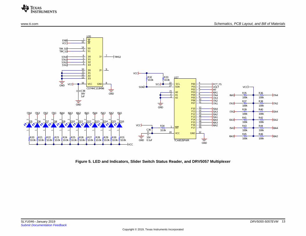
4.1 SchematicsFigure 2 to Figure 6 show the schematic of the DRV5055-5057EVM. Figure 2 pertains to DRV505x devices that the DRV5055-5057EVM is meantto demo. Figure 3 shows the schematic of the microcontroller that does all the processing of the measurement data and user input, as well as theLCD that the microcontroller drives. Figure 4 displays the circuitry for user inputs and programming inputs. Figure 5 corresponds to the GPIOextender used for turning on the respective LED indicators and reading the status of the slider switch. Figure 6 is the schematic of the power stageused to transform the 5-V USB input to a 3.3-V supply rail for all other onboard devices.

Schematics, PCB Layout, and Bill of Materials www.ti.com
10 SLYU046–January 2019Submit Documentation Feedback
Copyright © 2019, Texas Instruments Incorporated
DRV5055-5057EVM
Figure 2. Gain Variants A1 to A4

www.ti.com Schematics, PCB Layout, and Bill of Materials
11SLYU046–January 2019Submit Documentation Feedback
Copyright © 2019, Texas Instruments Incorporated
DRV5055-5057EVM
Figure 3. LCD, Microcontroller and Switch

Schematics, PCB Layout, and Bill of Materials www.ti.com
12 SLYU046–January 2019Submit Documentation Feedback
Copyright © 2019, Texas Instruments Incorporated
DRV5055-5057EVM
Figure 4. Push-Button, Slider Switch, and Programming User Inputs
www.ti.com Schematics, PCB Layout, and Bill of Materials
13SLYU046–January 2019Submit Documentation Feedback
Copyright © 2019, Texas Instruments Incorporated
DRV5055-5057EVM
Figure 5. LED and Indicators, Slider Switch Status Reader, and DRV5057 Multiplexer

Schematics, PCB Layout, and Bill of Materials www.ti.com
14 SLYU046–January 2019Submit Documentation Feedback
Copyright © 2019, Texas Instruments Incorporated
DRV5055-5057EVM
Figure 6. Supply Input and Power Conditioning

www.ti.com Schematics, PCB Layout, and Bill of Materials
15SLYU046–January 2019Submit Documentation Feedback
Copyright © 2019, Texas Instruments Incorporated
DRV5055-5057EVM
4.2 PCB LayoutFigure 7 through Figure 10 illustrate the PCB layers of the DRV5055-5057EVM.
Figure 7. Top Overlay
Figure 8. Top Layer
Figure 9. Bottom Overlay
Figure 10. Bottom Layer

Schematics, PCB Layout, and Bill of Materials www.ti.com
16 SLYU046–January 2019Submit Documentation Feedback
Copyright © 2019, Texas Instruments Incorporated
DRV5055-5057EVM
4.3 Bill of MaterialsTable 4 provides the parts list for the DRV5055-5057EVM.
Table 4. Bill of Materials
Designator Quantity Value Description Package Reference Part Number ManufacturerC1 1 2200pF CAP, CERM, 2200 pF, 50 V,+/- 5%, C0G/NP0,
06030603 GRM1885C1H222JA0
1DMuRata
C2, C3, C4, C5, C6, C7, C14,C15, C16,C17, C18, C19, C35,
C38
14 1uF CAP, CERM, 1 uF, 16 V, +/- 10%, X7R, 0603 0603 C1608X7R1C105K080AC
TDK
C8, C9, C10, C11,C12, C13, C24,C25, C44
9 1.5uF CAP, CERM, 1.5 uF, 35 V, +/- 10%, X5R, 0603 0603 C1608X5R1V155K080AC
TDK
C29, C33 2 10uF CAP, CERM, 10 µF, 16 V,+/- 10%, X7R, 0805 0805 CL21B106KOQNNNE Samsung Electro-Mechanics
C32, C36, C39, C40, C41, C42,C43
7 0.1uF CAP, CERM, 0.1 uF, 10 V, +/- 10%, X7R, 0603 0603 0603ZC104KAT2A AVX
D5, D6, D7, D8, D9, D10, D11,D12,D13, D14, D15, D16
12 Green LED, Green, SMD LED_0805 APT2012LZGCK Kingbright
H1 1 Magnet Neodymium Iron Boron (NdFeB) N350.187" Dia x 1.000" H (4.76mm x 25.4mm)
8182 Radial Magnet, Inc.
H2 1 USB 1.1 Cable A Female to A Male 5.90'(1.80m) Shielded
AK669-18 Assmann WSWComponents
H9, H10, H11, H12 4 Bumpon, Hemisphere, 0.44 X 0.20, Clear Transparent Bumpon SJ-5303 (CLEAR) 3MJ1 1 Header, 100mil, 5x1, Gold, TH Header, 100mil, 5x1, TH HTSW-105-07-G-S SamtecJ2 1 Connector, Plug, USB Type A, R/A, Top Mount
SMTUSB Type A right angle 48037-1000 Molex
K1 1 Switch, Slide, SP3T, On-On-On, 3 Pos, 0.3A, 30VDC, TH
12.6x4.3mm SS-13D16-VG 4 PA C&K Components
M1 1 16 MHz Ultra-Low-Power Microcontroller with 16KB FRAM, 2 KB SRAM, 60 IO, 10 ch ADC10,LCD, IR Logic, DGG0056A (TSSOP-56)
DGG0056A MSP430FR4133IG56R Texas Instruments
R1 1 47k RES, 47 k, 5%, 0.1 W, 0603 0603 RC0603JR-0747KL Yageo AmericaR2, R19 2 0 RES, 0, 5%, 0.1 W, 0603 0603 ERJ-3GEY0R00V Panasonic
R3, R4, R5, R6,R7, R8, R9, R10,R11, R12, R13, R14, R51
13 100 RES, 100, 1%, 0.1 W, AEC-Q200 Grade 0, 0603 0603 ERJ-3EKF1000V Panasonic
R16,R20, R21, R22, R23, R24,R25, R26, R27, R28, R29, R30,R31, R32, R33, R34, R47, R48,
R49R52, R53, R54, R55
23 10.0k RES, 10.0 k, 0.1%, 0.1 W, 0603 0603 RG1608P-103-B-T5 Susumu Co Ltd
R35, R36, R37, R38, R39, R40,R41, R42, R43R44, R45, R46
12 100k RES, 100 k, 5%, 0.1 W, AEC-Q200 Grade 0,0603
0603 ERJ-3GEYJ104V Panasonic
R50 1 0.5 RES, 0.5, 1%, 0.125 W, 0603 0603 CSR0603FKR500 Susumu Co Ltd

www.ti.com Schematics, PCB Layout, and Bill of Materials
17SLYU046–January 2019Submit Documentation Feedback
Copyright © 2019, Texas Instruments Incorporated
DRV5055-5057EVM
Table 4. Bill of Materials (continued)Designator Quantity Value Description Package Reference Part Number Manufacturer
TP1 1 Test Point, Compact, Black, TH 5006 KeystoneTP2,TP3, TP4, TP5, TP6, TP7,TP8, TP9, TP10, TP11, TP12,
TP13, TP14, TP15, TP16
15 Test Point, Compact, Black, SMT 5015 Keystone
U1 1 Automotive PWM-Output Linear Hall EffectSensor, LPG0003A (TO-92-3)
LPG0003A PDRV5057A4ELPGQ1 Texas Instruments
U2 1 Automotive PWM-Output Linear Hall EffectSensor, LPG0003A (TO-92-3)
LPG0003A PDRV5057A3ELPGQ1 Texas Instruments
U3 1 Automotive PWM-Output Linear Hall EffectSensor, LPG0003A (TO-92-3)
LPG0003A PDRV5057A2ELPGQ1 Texas Instruments
U4 1 Automotive PWM-Output Linear Hall EffectSensor, LPG0003A (TO-92-3)
LPG0003A PDRV5057A1ELPGQ1 Texas Instruments
U5 1 Automotive PWM-Output Linear Hall EffectSensor, LPG0003A (TO-92-3)
LPG0003A PDRV5056A4ELPGQ1 Texas Instruments
U6 1 Automotive PWM-Output Linear Hall EffectSensor, LPG0003A (TO-92-3)
LPG0003A PDRV5056A3ELPGQ1 Texas Instruments
U7 1 Automotive PWM-Output Linear Hall EffectSensor, LPG0003A (TO-92-3)
LPG0003A PDRV5056A2ELPGQ1 Texas Instruments
U8 1 Automotive PWM-Output Linear Hall EffectSensor, LPG0003A (TO-92-3)
LPG0003A PDRV5056A1ELPGQ1 Texas Instruments
U9 1 Automotive Ratiometric Linear Hall EffectSensor, LPG0003A (TO-92-3)
LPG0003A PDRV5055A4ELPGQ1 Texas Instruments
U10 1 Automotive Ratiometric Linear Hall EffectSensor, LPG0003A (TO-92-3)
LPG0003A PDRV5055A3ELPGQ1 Texas Instruments
U11 1 Automotive Unipolar Ratiometric Linear HallEffect Sensor, LPG0003A (TO-92-3)
LPG0003A PDRV5055A2ELPGQ1 Texas Instruments
U12 1 Automotive Ratiometric Linear Hall EffectSensor, LPG0003A (TO-92-3)
LPG0003A PDRV5055A1ELPGQ1 Texas Instruments
U14 1 Single Schmitt-Trigger Buffer, DCK0005A,SMALL T&R
DCK0005A SN74LVC1G17DCKT Texas Instruments
U16 1 250-mA Ultra-Low-Noise, Low-IQ LDO,DBV0005A (SOT-23-5)
DBV0005A LP5907MFX-3.3/NOPB Texas Instruments
U17 1 Remote 16-Bit I2C and SMBus, Low-Power I/OExpander with Interrupt Output and ConfigRegister, 1.65 to 5.5 V, -40 to 85 degC, 24-pinTSSOP (PW), Green (RoHS & no Sb/Br)
PW0024A TCA9535PWR Texas Instruments
U19 1 LCD 7-Segment, TH 50.8x22.86mm VI-401-DP-RC-S VaritronixU20 1 High Speed CMOS Logic Dual 4-Input
Multiplexers, D0016A, LARGE T&RD0016A CD74HC153M96 Texas Instruments
Schematics, PCB Layout, and Bill of Materials www.ti.com
18 SLYU046–January 2019Submit Documentation Feedback
Copyright © 2019, Texas Instruments Incorporated
DRV5055-5057EVM
Table 4. Bill of Materials (continued)Designator Quantity Value Description Package Reference Part Number Manufacturer
U21 1 1-Ohm 5-V/3.3-V 2-Channel SPDT Switch,DGS0010A (VSSOP-10)
DGS0010A TS5A23159DGSR Texas Instruments
S1 1 Switch, Tactile, SPST-NO, 0.02A, 15V, TH 6.0x5.0x6mm EVQ-21405R Panasonic

STANDARD TERMS FOR EVALUATION MODULES1. Delivery: TI delivers TI evaluation boards, kits, or modules, including any accompanying demonstration software, components, and/or
documentation which may be provided together or separately (collectively, an “EVM” or “EVMs”) to the User (“User”) in accordancewith the terms set forth herein. User's acceptance of the EVM is expressly subject to the following terms.1.1 EVMs are intended solely for product or software developers for use in a research and development setting to facilitate feasibility
evaluation, experimentation, or scientific analysis of TI semiconductors products. EVMs have no direct function and are notfinished products. EVMs shall not be directly or indirectly assembled as a part or subassembly in any finished product. Forclarification, any software or software tools provided with the EVM (“Software”) shall not be subject to the terms and conditionsset forth herein but rather shall be subject to the applicable terms that accompany such Software
1.2 EVMs are not intended for consumer or household use. EVMs may not be sold, sublicensed, leased, rented, loaned, assigned,or otherwise distributed for commercial purposes by Users, in whole or in part, or used in any finished product or productionsystem.
2 Limited Warranty and Related Remedies/Disclaimers:2.1 These terms do not apply to Software. The warranty, if any, for Software is covered in the applicable Software License
Agreement.2.2 TI warrants that the TI EVM will conform to TI's published specifications for ninety (90) days after the date TI delivers such EVM
to User. Notwithstanding the foregoing, TI shall not be liable for a nonconforming EVM if (a) the nonconformity was caused byneglect, misuse or mistreatment by an entity other than TI, including improper installation or testing, or for any EVMs that havebeen altered or modified in any way by an entity other than TI, (b) the nonconformity resulted from User's design, specificationsor instructions for such EVMs or improper system design, or (c) User has not paid on time. Testing and other quality controltechniques are used to the extent TI deems necessary. TI does not test all parameters of each EVM.User's claims against TI under this Section 2 are void if User fails to notify TI of any apparent defects in the EVMs within ten (10)business days after delivery, or of any hidden defects with ten (10) business days after the defect has been detected.
2.3 TI's sole liability shall be at its option to repair or replace EVMs that fail to conform to the warranty set forth above, or creditUser's account for such EVM. TI's liability under this warranty shall be limited to EVMs that are returned during the warrantyperiod to the address designated by TI and that are determined by TI not to conform to such warranty. If TI elects to repair orreplace such EVM, TI shall have a reasonable time to repair such EVM or provide replacements. Repaired EVMs shall bewarranted for the remainder of the original warranty period. Replaced EVMs shall be warranted for a new full ninety (90) daywarranty period.
WARNINGEvaluation Kits are intended solely for use by technically qualified,professional electronics experts who are familiar with the dangers
and application risks associated with handling electrical mechanicalcomponents, systems, and subsystems.
User shall operate the Evaluation Kit within TI’s recommendedguidelines and any applicable legal or environmental requirementsas well as reasonable and customary safeguards. Failure to set up
and/or operate the Evaluation Kit within TI’s recommendedguidelines may result in personal injury or death or propertydamage. Proper set up entails following TI’s instructions for
electrical ratings of interface circuits such as input, output andelectrical loads.
NOTE:EXPOSURE TO ELECTROSTATIC DISCHARGE (ESD) MAY CAUSE DEGREDATION OR FAILURE OF THE EVALUATIONKIT; TI RECOMMENDS STORAGE OF THE EVALUATION KIT IN A PROTECTIVE ESD BAG.

www.ti.com
2
3 Regulatory Notices:3.1 United States
3.1.1 Notice applicable to EVMs not FCC-Approved:FCC NOTICE: This kit is designed to allow product developers to evaluate electronic components, circuitry, or softwareassociated with the kit to determine whether to incorporate such items in a finished product and software developers to writesoftware applications for use with the end product. This kit is not a finished product and when assembled may not be resold orotherwise marketed unless all required FCC equipment authorizations are first obtained. Operation is subject to the conditionthat this product not cause harmful interference to licensed radio stations and that this product accept harmful interference.Unless the assembled kit is designed to operate under part 15, part 18 or part 95 of this chapter, the operator of the kit mustoperate under the authority of an FCC license holder or must secure an experimental authorization under part 5 of this chapter.3.1.2 For EVMs annotated as FCC – FEDERAL COMMUNICATIONS COMMISSION Part 15 Compliant:
CAUTIONThis device complies with part 15 of the FCC Rules. Operation is subject to the following two conditions: (1) This device may notcause harmful interference, and (2) this device must accept any interference received, including interference that may causeundesired operation.Changes or modifications not expressly approved by the party responsible for compliance could void the user's authority tooperate the equipment.
FCC Interference Statement for Class A EVM devicesNOTE: This equipment has been tested and found to comply with the limits for a Class A digital device, pursuant to part 15 ofthe FCC Rules. These limits are designed to provide reasonable protection against harmful interference when the equipment isoperated in a commercial environment. This equipment generates, uses, and can radiate radio frequency energy and, if notinstalled and used in accordance with the instruction manual, may cause harmful interference to radio communications.Operation of this equipment in a residential area is likely to cause harmful interference in which case the user will be required tocorrect the interference at his own expense.
FCC Interference Statement for Class B EVM devicesNOTE: This equipment has been tested and found to comply with the limits for a Class B digital device, pursuant to part 15 ofthe FCC Rules. These limits are designed to provide reasonable protection against harmful interference in a residentialinstallation. This equipment generates, uses and can radiate radio frequency energy and, if not installed and used in accordancewith the instructions, may cause harmful interference to radio communications. However, there is no guarantee that interferencewill not occur in a particular installation. If this equipment does cause harmful interference to radio or television reception, whichcan be determined by turning the equipment off and on, the user is encouraged to try to correct the interference by one or moreof the following measures:
• Reorient or relocate the receiving antenna.• Increase the separation between the equipment and receiver.• Connect the equipment into an outlet on a circuit different from that to which the receiver is connected.• Consult the dealer or an experienced radio/TV technician for help.
3.2 Canada3.2.1 For EVMs issued with an Industry Canada Certificate of Conformance to RSS-210 or RSS-247
Concerning EVMs Including Radio Transmitters:This device complies with Industry Canada license-exempt RSSs. Operation is subject to the following two conditions:(1) this device may not cause interference, and (2) this device must accept any interference, including interference that maycause undesired operation of the device.
Concernant les EVMs avec appareils radio:Le présent appareil est conforme aux CNR d'Industrie Canada applicables aux appareils radio exempts de licence. L'exploitationest autorisée aux deux conditions suivantes: (1) l'appareil ne doit pas produire de brouillage, et (2) l'utilisateur de l'appareil doitaccepter tout brouillage radioélectrique subi, même si le brouillage est susceptible d'en compromettre le fonctionnement.
Concerning EVMs Including Detachable Antennas:Under Industry Canada regulations, this radio transmitter may only operate using an antenna of a type and maximum (or lesser)gain approved for the transmitter by Industry Canada. To reduce potential radio interference to other users, the antenna typeand its gain should be so chosen that the equivalent isotropically radiated power (e.i.r.p.) is not more than that necessary forsuccessful communication. This radio transmitter has been approved by Industry Canada to operate with the antenna typeslisted in the user guide with the maximum permissible gain and required antenna impedance for each antenna type indicated.Antenna types not included in this list, having a gain greater than the maximum gain indicated for that type, are strictly prohibitedfor use with this device.

www.ti.com
3
Concernant les EVMs avec antennes détachablesConformément à la réglementation d'Industrie Canada, le présent émetteur radio peut fonctionner avec une antenne d'un type etd'un gain maximal (ou inférieur) approuvé pour l'émetteur par Industrie Canada. Dans le but de réduire les risques de brouillageradioélectrique à l'intention des autres utilisateurs, il faut choisir le type d'antenne et son gain de sorte que la puissance isotroperayonnée équivalente (p.i.r.e.) ne dépasse pas l'intensité nécessaire à l'établissement d'une communication satisfaisante. Leprésent émetteur radio a été approuvé par Industrie Canada pour fonctionner avec les types d'antenne énumérés dans lemanuel d’usage et ayant un gain admissible maximal et l'impédance requise pour chaque type d'antenne. Les types d'antennenon inclus dans cette liste, ou dont le gain est supérieur au gain maximal indiqué, sont strictement interdits pour l'exploitation del'émetteur
3.3 Japan3.3.1 Notice for EVMs delivered in Japan: Please see http://www.tij.co.jp/lsds/ti_ja/general/eStore/notice_01.page 日本国内に
輸入される評価用キット、ボードについては、次のところをご覧ください。http://www.tij.co.jp/lsds/ti_ja/general/eStore/notice_01.page
3.3.2 Notice for Users of EVMs Considered “Radio Frequency Products” in Japan: EVMs entering Japan may not be certifiedby TI as conforming to Technical Regulations of Radio Law of Japan.
If User uses EVMs in Japan, not certified to Technical Regulations of Radio Law of Japan, User is required to follow theinstructions set forth by Radio Law of Japan, which includes, but is not limited to, the instructions below with respect to EVMs(which for the avoidance of doubt are stated strictly for convenience and should be verified by User):1. Use EVMs in a shielded room or any other test facility as defined in the notification #173 issued by Ministry of Internal
Affairs and Communications on March 28, 2006, based on Sub-section 1.1 of Article 6 of the Ministry’s Rule forEnforcement of Radio Law of Japan,
2. Use EVMs only after User obtains the license of Test Radio Station as provided in Radio Law of Japan with respect toEVMs, or
3. Use of EVMs only after User obtains the Technical Regulations Conformity Certification as provided in Radio Law of Japanwith respect to EVMs. Also, do not transfer EVMs, unless User gives the same notice above to the transferee. Please notethat if User does not follow the instructions above, User will be subject to penalties of Radio Law of Japan.
【無線電波を送信する製品の開発キットをお使いになる際の注意事項】 開発キットの中には技術基準適合証明を受けていないものがあります。 技術適合証明を受けていないもののご使用に際しては、電波法遵守のため、以下のいずれかの措置を取っていただく必要がありますのでご注意ください。1. 電波法施行規則第6条第1項第1号に基づく平成18年3月28日総務省告示第173号で定められた電波暗室等の試験設備でご使用
いただく。2. 実験局の免許を取得後ご使用いただく。3. 技術基準適合証明を取得後ご使用いただく。
なお、本製品は、上記の「ご使用にあたっての注意」を譲渡先、移転先に通知しない限り、譲渡、移転できないものとします。上記を遵守頂けない場合は、電波法の罰則が適用される可能性があることをご留意ください。 日本テキサス・イ
ンスツルメンツ株式会社東京都新宿区西新宿6丁目24番1号西新宿三井ビル
3.3.3 Notice for EVMs for Power Line Communication: Please see http://www.tij.co.jp/lsds/ti_ja/general/eStore/notice_02.page電力線搬送波通信についての開発キットをお使いになる際の注意事項については、次のところをご覧ください。http://www.tij.co.jp/lsds/ti_ja/general/eStore/notice_02.page
3.4 European Union3.4.1 For EVMs subject to EU Directive 2014/30/EU (Electromagnetic Compatibility Directive):
This is a class A product intended for use in environments other than domestic environments that are connected to alow-voltage power-supply network that supplies buildings used for domestic purposes. In a domestic environment thisproduct may cause radio interference in which case the user may be required to take adequate measures.

www.ti.com
4
4 EVM Use Restrictions and Warnings:4.1 EVMS ARE NOT FOR USE IN FUNCTIONAL SAFETY AND/OR SAFETY CRITICAL EVALUATIONS, INCLUDING BUT NOT
LIMITED TO EVALUATIONS OF LIFE SUPPORT APPLICATIONS.4.2 User must read and apply the user guide and other available documentation provided by TI regarding the EVM prior to handling
or using the EVM, including without limitation any warning or restriction notices. The notices contain important safety informationrelated to, for example, temperatures and voltages.
4.3 Safety-Related Warnings and Restrictions:4.3.1 User shall operate the EVM within TI’s recommended specifications and environmental considerations stated in the user
guide, other available documentation provided by TI, and any other applicable requirements and employ reasonable andcustomary safeguards. Exceeding the specified performance ratings and specifications (including but not limited to inputand output voltage, current, power, and environmental ranges) for the EVM may cause personal injury or death, orproperty damage. If there are questions concerning performance ratings and specifications, User should contact a TIfield representative prior to connecting interface electronics including input power and intended loads. Any loads appliedoutside of the specified output range may also result in unintended and/or inaccurate operation and/or possiblepermanent damage to the EVM and/or interface electronics. Please consult the EVM user guide prior to connecting anyload to the EVM output. If there is uncertainty as to the load specification, please contact a TI field representative.During normal operation, even with the inputs and outputs kept within the specified allowable ranges, some circuitcomponents may have elevated case temperatures. These components include but are not limited to linear regulators,switching transistors, pass transistors, current sense resistors, and heat sinks, which can be identified using theinformation in the associated documentation. When working with the EVM, please be aware that the EVM may becomevery warm.
4.3.2 EVMs are intended solely for use by technically qualified, professional electronics experts who are familiar with thedangers and application risks associated with handling electrical mechanical components, systems, and subsystems.User assumes all responsibility and liability for proper and safe handling and use of the EVM by User or its employees,affiliates, contractors or designees. User assumes all responsibility and liability to ensure that any interfaces (electronicand/or mechanical) between the EVM and any human body are designed with suitable isolation and means to safelylimit accessible leakage currents to minimize the risk of electrical shock hazard. User assumes all responsibility andliability for any improper or unsafe handling or use of the EVM by User or its employees, affiliates, contractors ordesignees.
4.4 User assumes all responsibility and liability to determine whether the EVM is subject to any applicable international, federal,state, or local laws and regulations related to User’s handling and use of the EVM and, if applicable, User assumes allresponsibility and liability for compliance in all respects with such laws and regulations. User assumes all responsibility andliability for proper disposal and recycling of the EVM consistent with all applicable international, federal, state, and localrequirements.
5. Accuracy of Information: To the extent TI provides information on the availability and function of EVMs, TI attempts to be as accurateas possible. However, TI does not warrant the accuracy of EVM descriptions, EVM availability or other information on its websites asaccurate, complete, reliable, current, or error-free.
6. Disclaimers:6.1 EXCEPT AS SET FORTH ABOVE, EVMS AND ANY MATERIALS PROVIDED WITH THE EVM (INCLUDING, BUT NOT
LIMITED TO, REFERENCE DESIGNS AND THE DESIGN OF THE EVM ITSELF) ARE PROVIDED "AS IS" AND "WITH ALLFAULTS." TI DISCLAIMS ALL OTHER WARRANTIES, EXPRESS OR IMPLIED, REGARDING SUCH ITEMS, INCLUDING BUTNOT LIMITED TO ANY EPIDEMIC FAILURE WARRANTY OR IMPLIED WARRANTIES OF MERCHANTABILITY OR FITNESSFOR A PARTICULAR PURPOSE OR NON-INFRINGEMENT OF ANY THIRD PARTY PATENTS, COPYRIGHTS, TRADESECRETS OR OTHER INTELLECTUAL PROPERTY RIGHTS.
6.2 EXCEPT FOR THE LIMITED RIGHT TO USE THE EVM SET FORTH HEREIN, NOTHING IN THESE TERMS SHALL BECONSTRUED AS GRANTING OR CONFERRING ANY RIGHTS BY LICENSE, PATENT, OR ANY OTHER INDUSTRIAL ORINTELLECTUAL PROPERTY RIGHT OF TI, ITS SUPPLIERS/LICENSORS OR ANY OTHER THIRD PARTY, TO USE THEEVM IN ANY FINISHED END-USER OR READY-TO-USE FINAL PRODUCT, OR FOR ANY INVENTION, DISCOVERY ORIMPROVEMENT, REGARDLESS OF WHEN MADE, CONCEIVED OR ACQUIRED.
7. USER'S INDEMNITY OBLIGATIONS AND REPRESENTATIONS. USER WILL DEFEND, INDEMNIFY AND HOLD TI, ITSLICENSORS AND THEIR REPRESENTATIVES HARMLESS FROM AND AGAINST ANY AND ALL CLAIMS, DAMAGES, LOSSES,EXPENSES, COSTS AND LIABILITIES (COLLECTIVELY, "CLAIMS") ARISING OUT OF OR IN CONNECTION WITH ANYHANDLING OR USE OF THE EVM THAT IS NOT IN ACCORDANCE WITH THESE TERMS. THIS OBLIGATION SHALL APPLYWHETHER CLAIMS ARISE UNDER STATUTE, REGULATION, OR THE LAW OF TORT, CONTRACT OR ANY OTHER LEGALTHEORY, AND EVEN IF THE EVM FAILS TO PERFORM AS DESCRIBED OR EXPECTED.
www.ti.com
5
8. Limitations on Damages and Liability:8.1 General Limitations. IN NO EVENT SHALL TI BE LIABLE FOR ANY SPECIAL, COLLATERAL, INDIRECT, PUNITIVE,
INCIDENTAL, CONSEQUENTIAL, OR EXEMPLARY DAMAGES IN CONNECTION WITH OR ARISING OUT OF THESETERMS OR THE USE OF THE EVMS , REGARDLESS OF WHETHER TI HAS BEEN ADVISED OF THE POSSIBILITY OFSUCH DAMAGES. EXCLUDED DAMAGES INCLUDE, BUT ARE NOT LIMITED TO, COST OF REMOVAL ORREINSTALLATION, ANCILLARY COSTS TO THE PROCUREMENT OF SUBSTITUTE GOODS OR SERVICES, RETESTING,OUTSIDE COMPUTER TIME, LABOR COSTS, LOSS OF GOODWILL, LOSS OF PROFITS, LOSS OF SAVINGS, LOSS OFUSE, LOSS OF DATA, OR BUSINESS INTERRUPTION. NO CLAIM, SUIT OR ACTION SHALL BE BROUGHT AGAINST TIMORE THAN TWELVE (12) MONTHS AFTER THE EVENT THAT GAVE RISE TO THE CAUSE OF ACTION HASOCCURRED.
8.2 Specific Limitations. IN NO EVENT SHALL TI'S AGGREGATE LIABILITY FROM ANY USE OF AN EVM PROVIDEDHEREUNDER, INCLUDING FROM ANY WARRANTY, INDEMITY OR OTHER OBLIGATION ARISING OUT OF OR INCONNECTION WITH THESE TERMS, , EXCEED THE TOTAL AMOUNT PAID TO TI BY USER FOR THE PARTICULAREVM(S) AT ISSUE DURING THE PRIOR TWELVE (12) MONTHS WITH RESPECT TO WHICH LOSSES OR DAMAGES ARECLAIMED. THE EXISTENCE OF MORE THAN ONE CLAIM SHALL NOT ENLARGE OR EXTEND THIS LIMIT.
9. Return Policy. Except as otherwise provided, TI does not offer any refunds, returns, or exchanges. Furthermore, no return of EVM(s)will be accepted if the package has been opened and no return of the EVM(s) will be accepted if they are damaged or otherwise not ina resalable condition. If User feels it has been incorrectly charged for the EVM(s) it ordered or that delivery violates the applicableorder, User should contact TI. All refunds will be made in full within thirty (30) working days from the return of the components(s),excluding any postage or packaging costs.
10. Governing Law: These terms and conditions shall be governed by and interpreted in accordance with the laws of the State of Texas,without reference to conflict-of-laws principles. User agrees that non-exclusive jurisdiction for any dispute arising out of or relating tothese terms and conditions lies within courts located in the State of Texas and consents to venue in Dallas County, Texas.Notwithstanding the foregoing, any judgment may be enforced in any United States or foreign court, and TI may seek injunctive reliefin any United States or foreign court.
Mailing Address: Texas Instruments, Post Office Box 655303, Dallas, Texas 75265Copyright © 2019, Texas Instruments Incorporated

IMPORTANT NOTICE AND DISCLAIMER
TI PROVIDES TECHNICAL AND RELIABILITY DATA (INCLUDING DATASHEETS), DESIGN RESOURCES (INCLUDING REFERENCEDESIGNS), APPLICATION OR OTHER DESIGN ADVICE, WEB TOOLS, SAFETY INFORMATION, AND OTHER RESOURCES “AS IS”AND WITH ALL FAULTS, AND DISCLAIMS ALL WARRANTIES, EXPRESS AND IMPLIED, INCLUDING WITHOUT LIMITATION ANYIMPLIED WARRANTIES OF MERCHANTABILITY, FITNESS FOR A PARTICULAR PURPOSE OR NON-INFRINGEMENT OF THIRDPARTY INTELLECTUAL PROPERTY RIGHTS.These resources are intended for skilled developers designing with TI products. You are solely responsible for (1) selecting the appropriateTI products for your application, (2) designing, validating and testing your application, and (3) ensuring your application meets applicablestandards, and any other safety, security, or other requirements. These resources are subject to change without notice. TI grants youpermission to use these resources only for development of an application that uses the TI products described in the resource. Otherreproduction and display of these resources is prohibited. No license is granted to any other TI intellectual property right or to any thirdparty intellectual property right. TI disclaims responsibility for, and you will fully indemnify TI and its representatives against, any claims,damages, costs, losses, and liabilities arising out of your use of these resources.TI’s products are provided subject to TI’s Terms of Sale (www.ti.com/legal/termsofsale.html) or other applicable terms available either onti.com or provided in conjunction with such TI products. TI’s provision of these resources does not expand or otherwise alter TI’s applicablewarranties or warranty disclaimers for TI products.
Mailing Address: Texas Instruments, Post Office Box 655303, Dallas, Texas 75265Copyright © 2019, Texas Instruments Incorporated
Related Documents