Supply correction I 2 C I/F REG Back-EMF detection ROM Gate drive Gate drive Control and playback engine M LRA or ERM OUT– OUT+ GND REG IN/TRIG SDA SCL EN VDD Product Folder Order Now Technical Documents Tools & Software Support & Community An IMPORTANT NOTICE at the end of this data sheet addresses availability, warranty, changes, use in safety-critical applications, intellectual property matters and other important disclaimers. PRODUCTION DATA. DRV2605 SLOS825E – DECEMBER 2012 – REVISED APRIL 2018 DRV2605 Haptic Driver for ERM and LRA With Built-In Library and Smart-Loop Architecture 1 1 Features 1• Flexible Haptic/Vibra Driver – LRA (Linear Resonance Actuator) – ERM (Eccentric Rotating Mass) • I 2 C Controlled Digital Playback Engine – Real-Time Playback Mode via I 2 C • Smart Loop Architecture (1) – Automatic Overdrive/Braking (ERM/LRA) – Automatic Resonance Tracking (LRA) – Automatic Actuator Diagnostic (ERM/LRA) – Automatic Level Calibration (ERM/LRA) • Licensed Immersion™ TouchSense ® 2200 features: – Integrated Immersion Effect Library – Audio to Vibe • Optional PWM Input with 0% to 100% Duty Cycle Control Range • Optional Analog Input Control • Optional Hardware Trigger Pin • Efficient Output Drive • Fast Start Up Time • Constant Acceleration Over Supply Voltage • 1.8 V Compatible, VDD Tolerant Digital Pins (1) Patent pending control algorithm 2 Applications • Mobile Phones and Tablets • Watches and Wearable Technology • Remote Controls, Mice, and Peripheral Devices • Touch-Enabled Devices • Human-Machine Interfaces 3 Description The DRV2605 device is designed to provide extremely-flexible haptic control of ERM and LRA actuators over a shared I 2 C-compatible bus. This control relieves the host processor from ever generating pulse-width modulated (PWM) drive signals, saving both costly timer interrupts and hardware pins. The DRV2605 device provides an extensive integrated library over 100 licensed effects from Immersion for ERM and LRA which eliminates the need to design haptics waveforms. The DRV2605 device offers a licensed version of the TouchSense 2200 software from Immersion, which includes the 2200 Effects Library, and 2200 audio-to- vibe features. Additionally, the real-time playback mode allows the host processor to bypass the library playback engine and play waveforms directly from the host through I 2 C. The DRV2605 device also contains a smart-loop architecture, which allows effortless auto resonant drive for LRA as well as feedback-optimized ERM drive. This feedback provides automatic overdrive and braking, which creates a simplified input waveform paradigm as well as reliable motor control and consistent motor performance. The audio-to- haptics mode automatically converts an audio input signal to meaningful haptic effects. The DRV2605 device features a trinary-modulated output stage, providing greater efficiency than linear- based output drivers. The 9-ball WCSP footprint, flexible operation, and low component count make the DRV2605 device the ideal choice for portable and touch-enabled vibratory and haptic applications. For an important notice regarding Immersion software, see the Legal Notice section. Device Information (1) PART NUMBER PACKAGE BODY SIZE (MAX) DRV2605 DSBGA (9) 1.50 mm × 1.50 mm (1) For all available packages, see the orderable addendum at the end of the datasheet.

Welcome message from author
This document is posted to help you gain knowledge. Please leave a comment to let me know what you think about it! Share it to your friends and learn new things together.
Transcript

Supply correction
I2C I/F
REG
Back-EMF detection
ROM
Gate drive
Gate drive
Control and playback engine
MLRA or
ERM
OUT±
OUT+
GND
REG
IN/TRIG
SDA
SCL
EN
VDD
Product
Folder
Order
Now
Technical
Documents
Tools &
Software
Support &Community
An IMPORTANT NOTICE at the end of this data sheet addresses availability, warranty, changes, use in safety-critical applications,intellectual property matters and other important disclaimers. PRODUCTION DATA.
DRV2605SLOS825E –DECEMBER 2012–REVISED APRIL 2018
DRV2605 Haptic Driver for ERM and LRA With Built-In Library and Smart-LoopArchitecture
1
1 Features1• Flexible Haptic/Vibra Driver
– LRA (Linear Resonance Actuator)– ERM (Eccentric Rotating Mass)
• I2C Controlled Digital Playback Engine– Real-Time Playback Mode via I2C
• Smart Loop Architecture(1)
– Automatic Overdrive/Braking (ERM/LRA)– Automatic Resonance Tracking (LRA)– Automatic Actuator Diagnostic (ERM/LRA)– Automatic Level Calibration (ERM/LRA)
• Licensed Immersion™ TouchSense® 2200features:– Integrated Immersion Effect Library– Audio to Vibe
• Optional PWM Input with 0% to 100% Duty CycleControl Range
• Optional Analog Input Control• Optional Hardware Trigger Pin• Efficient Output Drive• Fast Start Up Time• Constant Acceleration Over Supply Voltage• 1.8 V Compatible, VDD Tolerant Digital Pins(1) Patent pending control algorithm
2 Applications• Mobile Phones and Tablets• Watches and Wearable Technology• Remote Controls, Mice, and Peripheral Devices• Touch-Enabled Devices• Human-Machine Interfaces
3 DescriptionThe DRV2605 device is designed to provideextremely-flexible haptic control of ERM and LRAactuators over a shared I2C-compatible bus. Thiscontrol relieves the host processor from evergenerating pulse-width modulated (PWM) drivesignals, saving both costly timer interrupts andhardware pins.
The DRV2605 device provides an extensiveintegrated library over 100 licensed effects fromImmersion for ERM and LRA which eliminates theneed to design haptics waveforms.
The DRV2605 device offers a licensed version of theTouchSense 2200 software from Immersion, whichincludes the 2200 Effects Library, and 2200 audio-to-vibe features. Additionally, the real-time playbackmode allows the host processor to bypass the libraryplayback engine and play waveforms directly from thehost through I2C.
The DRV2605 device also contains a smart-looparchitecture, which allows effortless auto resonantdrive for LRA as well as feedback-optimized ERMdrive. This feedback provides automatic overdriveand braking, which creates a simplified inputwaveform paradigm as well as reliable motor controland consistent motor performance. The audio-to-haptics mode automatically converts an audio inputsignal to meaningful haptic effects.
The DRV2605 device features a trinary-modulatedoutput stage, providing greater efficiency than linear-based output drivers. The 9-ball WCSP footprint,flexible operation, and low component count makethe DRV2605 device the ideal choice for portable andtouch-enabled vibratory and haptic applications.
For an important notice regarding Immersionsoftware, see the Legal Notice section.
Device Information(1)
PART NUMBER PACKAGE BODY SIZE (MAX)DRV2605 DSBGA (9) 1.50 mm × 1.50 mm
(1) For all available packages, see the orderable addendum atthe end of the datasheet.

2
DRV2605SLOS825E –DECEMBER 2012–REVISED APRIL 2018 www.ti.com
Product Folder Links: DRV2605
Submit Documentation Feedback Copyright © 2012–2018, Texas Instruments Incorporated
Table of Contents1 Features .................................................................. 12 Applications ........................................................... 13 Description ............................................................. 14 Revision History..................................................... 25 Pin Configuration and Functions ......................... 46 Specifications......................................................... 5
6.1 Absolute Maximum Ratings ...................................... 56.2 ESD Ratings.............................................................. 56.3 Recommended Operating Conditions....................... 56.4 Thermal Information .................................................. 56.5 Electrical Characteristics........................................... 66.6 Timing Requirements ................................................ 66.7 Switching Characteristics .......................................... 66.8 Typical Characteristics .............................................. 8
7 Detailed Description ............................................ 107.1 Overview ................................................................. 107.2 Functional Block Diagram ....................................... 107.3 Feature Description................................................. 117.4 Device Functional Modes........................................ 18
7.5 Programming........................................................... 227.6 Register Map........................................................... 33
8 Application and Implementation ........................ 498.1 Application Information............................................ 498.2 Typical Application .................................................. 508.3 Initialization Setup ................................................... 53
9 Power Supply Recommendations ...................... 5410 Layout................................................................... 55
10.1 Layout Guidelines ................................................. 5510.2 Layout Example .................................................... 56
11 Device and Documentation Support ................. 5711.1 Legal Notice .......................................................... 5711.2 Waveform Library Effects List ............................... 5711.3 Receiving Notification of Documentation Updates 5811.4 Community Resources.......................................... 5811.5 Trademarks ........................................................... 5811.6 Electrostatic Discharge Caution............................ 5811.7 Glossary ................................................................ 58
12 Mechanical, Packaging, and OrderableInformation ........................................................... 58
4 Revision HistoryNOTE: Page numbers for previous revisions may differ from page numbers in the current version.
Changes from Revision D (December 2015) to Revision E Page
• Changed the DEFAULT value for bit 5-4 of Table 25 From: 1 To 3 ................................................................................... 46• Changed the DEFAULT value for bit 3-2 of Table 25 From: 2 To 1 ................................................................................... 46• Changed the DEFAULT value for bit 1-0 of Table 25 From: 2 To 1 ................................................................................... 46• Changed the typical value of C(VDD) in Table 30 From: 0.1 µF To: 1 µF .............................................................................. 49• Changed C(VDD) from 0.1 to 1 µF in Figure 56...................................................................................................................... 50• Changed the input-voltage supply range From: 2 V to 5.2 V To: 2.5 V to 5.5 V in the Power Supply
Recommendations secton .................................................................................................................................................... 54
Changes from Revision C (September 2014) to Revision D Page
• Changed th(1) Hold time, SCL to SDA from 10 ns to 50 ns in Timing Requirements ............................................................. 6• Changed the default value of NG_THRESH[1:0] from 1 to 2 in the Register Map Control3 Register Field Descriptions ... 47
Changes from Revision B (February 2014) to Revision C Page
• Changed Features bullet from Royalty-Free Integrated Immersion Library to Waveform Event Sequencer andTrigger ................................................................................................................................................................................... 1
• Changed Feature bullet from Audio To Haptics Mode to Top Level: Licensed Immersion TouchSense 2200 features: ..... 1• Changed from Audio To Haptics Mode to Audio to Vibe ...................................................................................................... 1• Changed second paragraph of Description for clarification.................................................................................................... 1• Updated document to new datasheet style ............................................................................................................................ 4• Deleted Operating free-air temperature range, TA (information replaced by Thermal Information table) ............................. 5• Changed EN pulldown resistance added to Electrical Characteristics .................................................................................. 6• Changed connection terminal of input impedance from GND to V(CM_ANA) in Electrical Characteristics section.................... 6

3
DRV2605www.ti.com SLOS825E –DECEMBER 2012–REVISED APRIL 2018
Product Folder Links: DRV2605
Submit Documentation FeedbackCopyright © 2012–2018, Texas Instruments Incorporated
• Moved switching parameters to new Switching Characteristics table ................................................................................... 6• Added TI Haptic Broadcast Mode section ............................................................................................................................ 23• Changed AC couple capacitor recommendation from 0.1 µF to 1 µF to be consistent with Recommended External
Components table................................................................................................................................................................. 31• Added Immersion Legal Notice ........................................................................................................................................... 57
Changes from Revision A (March 2013) to Revision B Page
• Changed from 1 page data sheet to full data sheet in product folder .................................................................................... 1
Changes from Original (December 2012) to Revision A Page
• Changed minimum supported resonant frequency from 50 Hz to 125 Hz ............................................................................ 5• Added digital pulldown resistance parameter to Electrical Characteristics ............................................................................ 6• Changed |IIH| MAX value from 3 to 3.5µA per CMS #C1303020 ........................................................................................... 6• Changed calibration diagram to include DRIVE_TIME into ERM requirements .................................................................. 26• Changed bitfield name from "LRA_DRIVE_MODE" to "OTP_STATUS".............................................................................. 48• Changed C(REG) from 0.1 to 1 µF in Figure 56...................................................................................................................... 50

1 2 3
A
B
C
Not to scale
EN REG OUT+
IN/TRIG SDA GND
SCL VDD OUT±
4
DRV2605SLOS825E –DECEMBER 2012–REVISED APRIL 2018 www.ti.com
Product Folder Links: DRV2605
Submit Documentation Feedback Copyright © 2012–2018, Texas Instruments Incorporated
(1) I = input, O = output, I/O = input and output, P = power
5 Pin Configuration and Functions
YZF Package9-Pin DSBGA With 0.5-mm Pitch
(Top View)
Pin FunctionsPIN
TYPE (1) DESCRIPTIONNO. NAMEA1 EN I Device enableA2 REG O The REG pin is the 1.8-V regulator output. A 1-µF capacitor is required.A3 OUT+ O Positive haptic driver differential output
B1 IN/TRIG I Multi-mode Input. I2C selectable as PWM, analog, or trigger. If not used, this pin shouldbe connected to GND
B2 SDA I/O I2C dataB3 GND P Supply groundC1 SCL I I2C clockC3 OUT– O Negative haptic-driver differential outputC2 VDD P Supply input (2.5 to 5.5 V). A 0.1-µF capacitor is required.

5
DRV2605www.ti.com SLOS825E –DECEMBER 2012–REVISED APRIL 2018
Product Folder Links: DRV2605
Submit Documentation FeedbackCopyright © 2012–2018, Texas Instruments Incorporated
6 Specifications
6.1 Absolute Maximum Ratingsover operating free-air temperature range, TA = 25°C (unless otherwise noted)
MIN MAX UNIT
Input voltage
VDD –0.3 6 VEN –0.3 VDD + 0.3 VSDA –0.3 VDD + 0.3 VSCL –0.3 VDD + 0.3 VIN/TRIG –0.3 VDD + 0.3 V
Operating free-air temperature, TA –40 85 °COperating junction temperature, TJ –40 150 °CStorage temperature, Tstg –65 150 °C
(1) JEDEC document JEP155 states that 500-V HBM allows safe manufacturing with a standard ESD control process. Pins listed as ±2000V may actually have higher performance.
(2) JEDEC document JEP157 states that 250-V CDM allows safe manufacturing with a standard ESD control process. Pins listed as ±500 Vmay actually have higher performance.
6.2 ESD RatingsVALUE UNIT
V(ESD) Electrostatic dischargeHuman body model (HBM), per ANSI/ESDA/JEDEC JS-001, all pins (1) ±2000
VCharged device model (CDM), per JEDEC specification JESD22-C101,all pins (2) ±500
(1) Ensured by design. Not production tested.
6.3 Recommended Operating Conditionsover operating free-air temperature range (unless otherwise noted)
MIN MAX UNITVDD Supply voltage VDD 2.5 5.5 Vƒ(PWM) PWM input frequency (1) IN/TRIG Pin 10 250 kHzZL Load impedance (1) VDD = 5.2 V 8 Ω
VIL Digital low-level input voltage EN, IN/TRIG, SDA, SCL 0.5 VVIH Digital high-level input voltage EN, IN/TRIG, SDA, SCL 1.3 VVI(ANA) Input voltage (analog mode) IN/TRIG 0 1.8 Vƒ(LRA) LRA Frequency Range (1) 125 300 Hz
(1) For more information about traditional and new thermal metrics, see the Semiconductor and IC Package Thermal Metrics applicationreport.
6.4 Thermal Information
THERMAL METRIC (1)
DRV2605
UNITYZF (DSBGA)
(9-PINS)
RθJA Junction-to-ambient thermal resistance 145.2 °C/W
RθJC(top) Junction-to-case (top) thermal resistance 0.9 °C/W
RθJB Junction-to-board thermal resistance 105 °C/W
φJT Junction-to-top characterization parameter 5.1 °C/W
φJB Junction-to-board characterization parameter 103.3 °C/W

6
DRV2605SLOS825E –DECEMBER 2012–REVISED APRIL 2018 www.ti.com
Product Folder Links: DRV2605
Submit Documentation Feedback Copyright © 2012–2018, Texas Instruments Incorporated
6.5 Electrical CharacteristicsTA = 25°C, VDD = 3.6 V (unless otherwise noted)
PARAMETER TEST CONDITIONS MIN TYP MAX UNITV(REG) Voltage at the REG pin 1.84 VIIL Digital low-level input current EN VDD = 5.5 V , VI = 0 V 1 µA
IIH Digital high-level input current
IN/TRIG, SDA, SCLVDD = 5.5 V, VI = VDD
1µA
ENVDD = 5.5 V, VI = VDD
3.5
VOL Digital low-level output voltage SDAIOL= 4 mA 0.4 V
R(EN-GND) Digital pull-down resistance ENVDD = 5.5 V , VI = VDD
2 MΩ
I(SD) Shutdown current V(EN) = 0 V 1.75 4 µAII(standby) Standby current V(EN) = 1.8 V, STANDBY = 1 1.9 5 µAIQ Quiescent current V(EN) = 1.8 V, STANDBY = 0, no signal 0.6 1 mAZI Input impedance IN/TRIG to V(CM_ANA) 100 kΩ
V(CM_ANA)IN/TRIG common-mode voltage(AC-coupled) AC_COUPLE = 1 0.9 V
ZO(SD) Output impedance in shutdown OUT+ to GND, OUT– to GND 15 kΩ
ZL(th)Load impedance threshold forover-current detection OUT+ to GND, OUT– to GND 4 Ω
I(BAT_AV)Average battery current duringoperation
Duty cycle = 90%, LRA mode, no load 2.5 3.25mA
Duty cycle = 90%, ERM mode, no load 2.5 3.25
6.6 Timing RequirementsTA = 25°C, VDD = 3.6 V (unless otherwise noted)
MIN NOM MAX UNITƒ(SCL) Frequency at the SCL pin with no wait states 400 kHztw(H) Pulse duration, SCL high
See Figure 1.
0.6 µstw(L) Pulse duration, SCL low 1.3 µstsu(1) Setup time, SDA to SCL 100 nsth(1) Hold time, SCL to SDA 50 ns
t(BUF)Bus free time between stop and startcondition
See Figure 2.
1.3 µs
tsu(2) Setup time, SCL to start condition 0.6 µsth(2) Hold time, start condition to SCL 0.6 µstsu(3) Setup time, SCL to stop condition 0.6 µs
6.7 Switching CharacteristicsTA = 25°C, VDD = 3.6 V (unless otherwise noted)
PARAMETER TEST CONDITIONS MIN TYP MAX UNIT
t(start) Start-up time
Time from the GO bit or external triggercommand to output signal 0.7
msTime from EN high to output signal(PWM/Analog Modes) 1.5
ƒO(PWM) PWM Output Frequency 19.5 20.5 21.5 kHz

t(BUF)
SCL
SDA
Start Condition Stop Condition
tsu(2) th(2) tsu(3)
tw(H) tw(L)
SCL
SDA
tsu(1) th(1)
7
DRV2605www.ti.com SLOS825E –DECEMBER 2012–REVISED APRIL 2018
Product Folder Links: DRV2605
Submit Documentation FeedbackCopyright © 2012–2018, Texas Instruments Incorporated
Figure 1. SCL and SDA Timing
Figure 2. Timing for Start and Stop Conditions

Time (s)
Vol
tage
(2V
/div
)
0 40m 80m 120m 160m 200m
ENSDAAcceleration[OUT+] − [OUT−] (Filtered)
Time (s)
Vol
tage
(2V
/div
)
0 40m 80m 120m 160m 200m
ENIN/TRIGAcceleration[OUT+] − [OUT−] (Filtered)
Time (s)
Vol
tage
(2V
/div
)
0 200m 400m 600m 800m 1
SDAAcceleration[OUT+] − [OUT−] (Filtered)
Time (s)
Vol
tage
(2V
/div
)
0 200m 400m 600m 800m 1
SDAAcceleration[OUT+] − [OUT−] (Filtered)
Time (s)
Vol
tage
(2V
/div
)
0 40m 80m 120m 160m 200m
IN/TRIGAcceleration[OUT+] − [OUT−] (Filtered)
Time (s)
Vol
tage
(2V
/div
)
0 40m 80m 120m 160m 200m
IN/TRIGAcceleration[OUT+] − [OUT−] (Filtered)
8
DRV2605SLOS825E –DECEMBER 2012–REVISED APRIL 2018 www.ti.com
Product Folder Links: DRV2605
Submit Documentation Feedback Copyright © 2012–2018, Texas Instruments Incorporated
6.8 Typical Characteristics
VDD = 3.6 V ERM open loopStrong click - 60% External edge trigger
Figure 3. ERM Click with and Without Braking (ROM)
VDD = 3.6 V LRA closed loopStrong click - 100% External level trigger
Figure 4. LRA Click with Braking (ROM)
VDD = 3.6 V ERM open loopSequence = 0x01, 0x48 Internal trigger
Figure 5. ERM Click-Bounce (ROM)
VDD = 3.6 V LRA closed loopTransition click 1 - 100% Internal trigger
Figure 6. LRA Transition-Click (ROM)
VDD = 3.6 V ERM closed loop RTP Mode
Figure 7. ERM Buzz (RTP)
VDD = 3.6 V LRA closed loop PWM Mode
Figure 8. LRA Click With and Without Braking (PWM)

Time (s)
Vol
tage
(2V
/div
)
0 1m 2m 3m 4m 5m 6m 7m 8m 9m 10m
SDAERM ModeLRA Mode
VDD − Supply Voltage (V)
I DD −
Sup
ply
Cur
rent
(m
A)
2.0 2.4 2.8 3.2 3.6 4.0 4.4 4.8 5.250
60
70
80
90
100LRA Mode, RL = 25 Ω + 100 µH, 2 Vrms
9
DRV2605www.ti.com SLOS825E –DECEMBER 2012–REVISED APRIL 2018
Product Folder Links: DRV2605
Submit Documentation FeedbackCopyright © 2012–2018, Texas Instruments Incorporated
Typical Characteristics (continued)
VDD = 4.2 V Closed loop No filter
Figure 9. Startup Latency for ERM and LRA
Figure 10. Supply Current vs Supply Voltage (Full Vibration)

Supply correction
I2C I/F
REG
Back-EMF detection
ROM
Gate drive
Gate drive
Control and playback engine
MLRA or
ERM
OUT±
OUT+
GND
REG
IN/TRIG
SDA
SCL
EN
VDD
10
DRV2605SLOS825E –DECEMBER 2012–REVISED APRIL 2018 www.ti.com
Product Folder Links: DRV2605
Submit Documentation Feedback Copyright © 2012–2018, Texas Instruments Incorporated
7 Detailed Description
7.1 OverviewThe DRV2605 device is a haptic driver that relies on the back-EMF produced by an actuator to provide a closed-loop system that offers extremely flexible control of LRA and ERM actuators over a shared I2C-compatible bus orPWM input signal. This schema helps improve actuator performance in terms of acceleration consistency, starttime, and brake time.
The improved smart-loop architecture inside the DRV2605 device provides effortless auto-resonant drive forLRA, as well as feedback-optimized ERM drive allowing for automatic overdrive and braking. These featurescreate a simplified input waveform paradigm as well as reliable motor control and consistent motor performance.The DRV2605 device also allows for open-loop driving by using internally-generated PWM. Additionally, theaudio-to-vibe mode automatically converts an audio input signal to meaningful haptic effects.
The DRV2605 device offers a licensed version of TouchSense 2200 software from Immersion which eliminatesthe requirement to design haptic waveforms because the software includes over 100 licensed effects ( 5ERMlibraries and 1 LRA library) and audio-to-vibe features. The waveforms can be instantly played back through anI2C or can be triggered through a hardware trigger pin. Additionally, the real-time playback mode allows the hostprocessor to bypass the library playback engine and play waveforms directly from the host through the I2C.
The DRV2605 device features a trinary-modulated output stage that provides more efficiency than linear-basedoutput drivers.
7.2 Functional Block Diagram

11
DRV2605www.ti.com SLOS825E –DECEMBER 2012–REVISED APRIL 2018
Product Folder Links: DRV2605
Submit Documentation FeedbackCopyright © 2012–2018, Texas Instruments Incorporated
7.3 Feature Description
7.3.1 Support for ERM and LRA ActuatorsThe DRV2605 device supports both ERM and LRA actuators. The ERM_LRA bit in register 0x1A must beconfigured to select the type of actuator that the device uses.
7.3.2 Smart-Loop ArchitectureThe smart-loop architecture is an advanced closed-loop system that optimizes the performance of the actuatorand allows for failure detection. The architecture consists of automatic resonance tracking and reporting (for anLRA), automatic level calibration, accelerated startup and braking, diagnostics routines, and other proprietaryalgorithms.
7.3.2.1 Auto-Resonance Engine for LRAThe DRV2605 auto-resonance engine tracks the resonant frequency of an LRA in real time, effectively lockingonto the resonance frequency after half of a cycle. If the resonant frequency shifts in the middle of a waveformfor any reason, the engine tracks the frequency from cycle to cycle. The auto-resonance engine accomplishesthe tracking by constantly monitoring the back-EMF of the actuator. The auto-resonance engine is not affected bythe auto calibration process, which is only used for level calibration. No calibration is required for the autoresonance engine. See the Auto-Resonance Engine Programming for the LRA section for auto-resonance engineprogramming information.
7.3.2.2 Real-Time Resonance-Frequency Reporting for LRAThe smart-loop architecture makes the resonant frequency of the LRA available through I2C (see the LRAResonance Period (Address: 0x22) section). Because frequency reporting occurs in real time, the frequencymust be polled while the DRV2605 device synchronizes with the LRA. The data should not be polled when theactuator is idle or braking.
7.3.2.3 Automatic Overdrive and BrakingA key feature of the DRV2605 is the smart-loop architecture which employs actuator feedback control for bothERMs and LRAs. The feedback control desensitizes the input waveform from the motor-response behavior byproviding automatic overdrive and automatic braking.
An open-loop haptic system typically drives an overdrive voltage at startup that is higher than the steady-staterated voltage of the actuator to decrease the startup latency of the actuator. Likewise, a braking algorithm mustbe employed for effective braking. When using an open-loop driver, these behaviors must be contained in theinput waveform data. Figure 11 shows how two different ERMs with different startup behaviors (Motor A andMotor B) can both be driven optimally by the smart-loop architecture with a simple input for both motors. Thesmart-loop architecture works equally well for LRAs with a combination of feedback control and an auto-resonance engine.

Input and output
Accleration
Ideal Open-Loop Waveform for Motor A
Output with feedback
Ideal Open-Loop Waveform for Motor B
Same simple input forboth motors
Feedback providesoptimum output drive
12
DRV2605SLOS825E –DECEMBER 2012–REVISED APRIL 2018 www.ti.com
Product Folder Links: DRV2605
Submit Documentation Feedback Copyright © 2012–2018, Texas Instruments Incorporated
Feature Description (continued)
Figure 11. Waveform Simplification With Smart Loop
7.3.2.3.1 Startup Boost
To reduce the actuator start-time performance, the DRV2605 device has an overdrive boost feature that applieshigher loop gain to transient response of the actuator. The STARTUP_BOOST bit enables the feature.
7.3.2.3.2 Brake Factor
To reduce the actuator brake-time performance, the DRV2605 device provides a means to increase the gainratio between braking and driving gain. Higher feedback-gain ratios reduce the brake time, however, the gainratios also reduce the stability of the closed-loop system. The FB_BRAKE_FACTOR[2:0] bits can be adjusted toset the brake factor.
7.3.2.3.3 Brake Stabilizer
To improve brake stability at high brake-factor gain ratios, the DRV2605 device has a brake-stabilizermechanism that automatically reduces the loop gain when the braking is near completion. TheBRAKE_STABILIZER bit enables the feature.
7.3.2.4 Automatic Level CalibrationThe smart-loop architecture uses actuator feedback by monitoring the back-EMF behavior of the actuator. Thelevel of back-EMF voltage can vary across actuator manufacturers because of the specific actuator construction.Auto calibration compensates for the variation and also performs scaling for the desired actuator according to thespecified rated voltage and overdrive clamp-register settings. When auto calibration is performed, a 100% signallevel at any of the DRV2605 input interfaces supplies the rated voltage to the actuator at steady-state. Thefeedback allows the output level to increase above the rated voltage level for automatic overdrive and braking,but without allowing the output level to exceed the programmable overdrive clamp voltage.
In the event where the automatic level-calibration routine fails, the DIAG_RESULT bit in register 0x00 is assertedto flag the problem. Calibration failures are typically fixed by adjusting the registers associated with the automaticlevel-calibration routine or, for LRA actuators, the registers associated with the automatic-resonance detectionengine. See the Automatic-Level Calibration Programming section for automatic-level calibration programming.

13
DRV2605www.ti.com SLOS825E –DECEMBER 2012–REVISED APRIL 2018
Product Folder Links: DRV2605
Submit Documentation FeedbackCopyright © 2012–2018, Texas Instruments Incorporated
Feature Description (continued)7.3.2.4.1 Automatic Compensation for Resistive Losses
The DRV2605 device automatically compensates for resistive losses in the driver. During the automatic level-calibration routine, the impedance of the actuator is checked and the compensation factor is determined andstored in the A_CAL_COMP[7:0] bit.
7.3.2.4.2 Automatic Back-EMF Normalization
The DRV2605 device automatically compensates for differences in back-EMF magnitude between actuators. Thecompensation factor is determined during the automatic level-calibration routine and the factor is stored in theA_CAL_BEMF[7:0] bit.
7.3.2.4.3 Calibration Time Adjustment
The duration of the automatic level-calibration routine has an impact on accuracy. The impact is highlydependent on the start-time characteristic of the actuator. The auto-calibration routine expects the actuator tohave reached a steady acceleration before the calibration factors are calculated. Because the start-timecharacteristic can be different for each actuator, the AUTO_CAL_TIME[1:0] bit can change the duration of theautomatic level-calibration routine to optimize calibration performance.
7.3.2.4.4 Loop-Gain Control
The DRV2605 device allows the user to control how fast the driver attempts to match the back-EMF (and thusmotor velocity) and the input signal level. Higher loop-gain (or faster settling) options result in less-stableoperation than lower loop gain (or slower settling). The LOOP_GAIN[1:0] bit controls the loop gain.
7.3.2.4.5 Back-EMF Gain Control
The BEMF_GAIN[1:0] bit sets the analog gain for the back-EMF amplifier. The auto-calibration routineautomatically populates the bit with the most appropriate value for the actuator.
Modifying the SAMPLE_TIME[1:0] bit also adjusts the back-EMF gain. The higher the sample time, the higherthe gain.
By default, the back-EMF is sampled once during a period. In the event that a twice per-period sampling isdesired, assert the LRA_DRIVE_MODE bit.
7.3.2.5 Actuator DiagnosticsThe DRV2605 device is capable of determining whether the actuator is not present (open) or shorted. If a fault isdetected during the diagnostic process, the DIAG_RESULT bit is asserted.
7.3.3 Open-Loop Operation for LRAWhen using the PWM input in open-loop mode, the DRV2605 device employs a fixed divider that observes thePWM signal and commutates the output drive signal at the PWM frequency divided by 128. To accomplish LRAdrive, the host should drive the PWM frequency at 128 times the desired operating frequency.
7.3.4 Open-Loop Operation for ERMThe DRV2605 device offers ERM open-loop operation through the PWM input. The output voltage is based onthe duty cycle of the provided PWM signal, where the OD_CLAMP[7:0] bit in register 0x17 sets the full-scaleamplitude. For details see the Rated Voltage Programming section.
7.3.5 Flexible Front-End InterfaceThe DRV2605 device offers multiple ways to launch and control haptic effects. The MODE[2:0] bit in register0x01 is used to select the interface mode.

ERM Library ALIBRARY_SEL[2:0] = 1
ERM Library ELIBRARY_SEL[2:0] = 5
LRA LibraryLIBRARY_SEL[2:0] = 6
14
DRV2605SLOS825E –DECEMBER 2012–REVISED APRIL 2018 www.ti.com
Product Folder Links: DRV2605
Submit Documentation Feedback Copyright © 2012–2018, Texas Instruments Incorporated
Feature Description (continued)7.3.5.1 PWM InterfaceWhen the DRV2605 device is in PWM interface mode, the device accepts PWM data at the IN/TRIG pin. TheDRV2605 device drives the actuator continuously in PWM interface mode until the user sets the device tostandby mode or to enter another interface mode. In standby mode, the strength of vibration is determined by theduty cycle.
For the LRA, the DRV2605 device automatically tracks the resonance frequency unless the LRA_OPEN_LOOPbit in register 0x1D is set. If the LRA_OPEN_LOOP bit is set, the LRA is driven according to the frequency of thePWM input signal. Specifically, the driving frequency is the PWM frequency divided by 128.
7.3.5.2 Internal Memory InterfaceThe DRV2605 device has six internal-ROM libraries designed by Immersion called TS2200. The first five librariesare specifically tuned for five categories of ERMs operated in open-loop mode (see Table 1). Library 6 is aclosed-loop library tuned for LRAs. The library selection occurs through register 0x03 (see the (Address: 0x03)section).
Figure 12. Library Selection

15
DRV2605www.ti.com SLOS825E –DECEMBER 2012–REVISED APRIL 2018
Product Folder Links: DRV2605
Submit Documentation FeedbackCopyright © 2012–2018, Texas Instruments Incorporated
Feature Description (continued)Table 1. ERM Library Table
LIBRARY RATED VOLTAGE OVERDRIVE VOLTAGE RISE TIME BRAKE TIMEA 1.3 V 3 V 40 ms to 60 ms 20 ms to 40 msB 3 V 3 V 40 ms to 60 ms 5 ms to 15 msC 3 V 3 V 60 ms to 80 ms 10 ms to 20 msD 3 V 3 V 100 ms to 140 ms 15 ms to 25 msE 3 V 3 V > 140 ms > 30 ms
7.3.5.2.1 Waveform Sequencer
The waveform sequencer queues waveform identifiers for playback. Eight sequence registers queue up to eightwaveforms for sequential playback. A waveform identifier is an integer value referring to the index position of awaveform in the ROM library. Playback begins at register address 0x04 when the user asserts the GO bit(register 0x0C). When playback of that waveform ends, the waveform sequencer plays the waveform identifierheld in register 0x05 if the next waveform is non-zero. The waveform sequencer continues in this way until itreaches an identifier value of zero or until all eight identifiers are played (register addresses 0x04 through 0x0B),whichever scenario is reached first.
The waveform identifier range is 1 to 127. The MSB of each sequence register can implement a delay betweensequence waveforms. When the MSB is high, bits [6:0] indicate the length of the wait time. The wait time for thatstep then becomes WAV_FRM_SEQ[6:0] × 10 ms.
7.3.5.2.2 Library Parameterization
The ROM waveforms are augmented by the time offset registers (registers 0x0D to 0x10). The augmentationoccurs only for the ROM waveforms and not for the other interfaces (such as PWM and RTP). The purpose ofthe functionality is to add time stretching (or time shrinking) to the waveform. This functionality is useful forcustomizing the entire library of waveforms for a specific actuator rise time and fall time.
The time parameters that can be stretched or shrunk include:
ODT Overdrive time
SPT Sustain positive time
SNT Sustain Negative Time
BRT Brake Time
The time values are additive offsets and are 8-bit signed values. The default offset of the time values is 0.Positive values add and negative values subtract from the time value of the effect that is currently played. Themost positive value in the waveform is automatically interpreted as the overdrive time, and the most negativevalue in the waveform is automatically interpreted as the brake time. The time-offset parameters are applied toboth voltage-time pairs and linear ramps. For linear ramps, linear interpolation is stretched (or shrunk) over thetwo operative points for the period (see Equation 1).
t + t(ofs)
where• t(ofs) is the time offset (1)
7.3.5.3 Real-Time Playback (RTP) InterfaceThe real-time playback mode is a simple, single 8-bit register interface that holds an amplitude value. When real-time playback is enabled, the real-time playback register is sent directly to the playback engine. The amplitudevalue is played until the user sends the device to standby mode or removes the device from RTP mode. TheRTP mode operates exactly like the PWM mode except that the user enters a register value over the I2C ratherthan a duty cycle through the input pin. Therefore, any API (application-programming interface) designed for usewith a PWM generator in the host processor can write the data values over the I2C rather than writing the datavalues to the host timer. This ability frees a timer in the host while retaining compatibility with the originalsoftware.

16
DRV2605SLOS825E –DECEMBER 2012–REVISED APRIL 2018 www.ti.com
Product Folder Links: DRV2605
Submit Documentation Feedback Copyright © 2012–2018, Texas Instruments Incorporated
For the LRA, the DRV2605 device automatically tracks the resonance frequency.
7.3.5.4 Analog Input InterfaceWhen the DRV2605 device is in analog-input interface mode, the device accepts an analog voltage at theIN/TRIG pin. The DRV2605 device drives the actuator continuously in analog-input interface mode until the usersets the device to standby mode or to enter another interface mode. The reference voltage in standby mode is1.8 V. Therefore, the 1.8-V reference voltage is interpreted as a 100% input value. A reference voltage of 0.9 Vis interpreted as a 50% input value and a reference voltage of 0 V is interpreted as a 0% input value. The inputvalue in standby mode is analogous to the duty-cycle percentage in PWM mode.
For the LRA, the DRV2605 automatically tracks the resonance frequency.
7.3.5.5 Audio-to-Vibe InterfaceThe DRV2605 device features an audio-to-vibe mode that converts an audio input signal into meaningful hapticeffects using the Immersion audio-to-vibe technology. Audio-to-Vibe mode adds a vibratory bass extension toportable devices which allows users to feel the audio and visual content. Audio-to-Vibe mode is a key featurebecause it allows for existing applications to include haptic sensations without requiring additional softwaredrivers. Additionally, event-driven audio effects generated within an operating system can be used toautomatically provide a product with haptic sensations. See the Waveform Playback Using Audio-to-Vibe Modesection for details.
7.3.5.6 Input Trigger OptionThe DRV2605 device includes continuous haptic modes (such as PWM and RTP mode) as well as triggeredmodes (such as the internal memory interface). The haptic effects in the continuous haptic modes begin as soonas the device enters the mode and stop when the device goes into standby mode or exits the continuous hapticmode. For the triggered mode, the DRV2605 device has a variety of trigger options that are explained in thissection.
In the continuous haptic modes, the IN/TRIG pin provides external trigger control of the GO bit, which allowsGPIO control to fire ROM waveforms. The external trigger control can provide improved latencies in systemswhere a significant delay exists between the desired effect time and the time a GO command can be sent overthe I2C interface.
NOTEThe triggered effect must already be selected to take advantage of the lower latency. Thisoption works best for accelerating a pre-queued high-priority effect (such as a buttonpress) or for the repeated firing of the same effect (such as scrolling).
7.3.5.6.1 I2C Trigger
Setting the GO bit (in register 0x0C) launches the waveform. The user can cancel the launching of the waveformby clearing the GO bit.
7.3.5.6.2 Edge Trigger
A low-to-high transition on the IN/TRIG pin sets the GO bit. The playback sequence indicated in the waveformsequencer plays as normal. The user can cancel the transaction by clearing the GO bit. An additional low-to-hightransition while the GO bit is high also cancels the transaction which clears and resets the GO bit. Clearing thetrigger pin (high-to-low transition) does nothing, therefore the user can send a short pulse without knowing howlong the waveform is. The pulse width should be at least 1 µs to ensure detection.

Level Trigger
Haptic Waveform
Level Trigger
Haptic Waveform
Cancellation
Haptic Waveform
Edge Trigger
Haptic Waveform
Edge Trigger
Cancellation
17
DRV2605www.ti.com SLOS825E –DECEMBER 2012–REVISED APRIL 2018
Product Folder Links: DRV2605
Submit Documentation FeedbackCopyright © 2012–2018, Texas Instruments Incorporated
Figure 13. Edge Trigger Mode
7.3.5.6.3 Level Trigger
The actions of the GO bit directly follow the IN/TRIG pin. When the IN/TRIG pin is high, the GO bit is high. Whenthe IN/TRIG pin goes low, the GO bit clears. Therefore, a falling edge cancels the transaction. The level triggercan implement a GPIO-controlled buzz on-off controller if an appropriately long waveform is selected. The usermust hold the IN/TRIG high for the entire duration of the waveform to complete the effect.
Figure 14. Level Trigger Mode
7.3.6 Edge Rate ControlThe DRV2605 output driver implements edge rate control (ERC). The ERC ensures that the rise and fallcharacteristics of the output drivers do not emit levels of radiation that could interfere with other circuitry commonin mobile and portable platforms. Because of ERC most system do not require external output filters, capacitors,or ferrite beads.
7.3.7 Constant Vibration StrengthThe DRV2605 PWM input uses a digital level-shifter. Therefore, as long as the input voltage meets the VIH andVIL levels, the vibration strength remains the same even if the digital levels vary. The DRV2605 device alsofeatures power-supply feedback. If the supply voltage drifts over time (because of battery discharge, forexample), the vibration strength remains the same as long as enough supply voltage is available to sustain therequired output voltage.
7.3.8 Battery Voltage ReportingDuring playback, the DRV2605 device provides real-time voltage measurement of the VDD pin. The VBAT[7:0] bitlocated in register 0x21 provides this information.

StandbyShutdown
Active
EN = 0
EN = 0
EN = 1
STANDBY = 0
STANDBY = 1
DEV_RESET = 1
18
DRV2605SLOS825E –DECEMBER 2012–REVISED APRIL 2018 www.ti.com
Product Folder Links: DRV2605
Submit Documentation Feedback Copyright © 2012–2018, Texas Instruments Incorporated
7.3.9 One-Time Programmable (OTP) Memory for ConfigurationThe DRV2605 device contains nonvolatile, on-chip, OTP memory for specific configuration parameters. Whenwritten, the DRV2605 device retains the device settings in registers 0x16 through 0x1A including after powercycling. This retention allows the user to account for small variations in actuator manufacturing from unit to unitas well as to shorten the device-initialization process for device-specific parameters such as actuator type,actuator-rated voltage, and other parameters. An additional benefit of OTP is that the DRV2605 memory can becustomized at the device-test level without driving changes in the device software.
7.3.10 Low-Power StandbySetting the device to standby reduces the idle power consumption without resetting the registers. In Low-PowerStandby mode, the DRV2605 device features a fast turnon time when it is requested to play a waveform.
7.3.11 Device Protection
7.3.11.1 Thermal ProtectionThe DRV2605 device has thermal protection that causes the device to shut down if it becomes too hot. In theevent where the thermal protection kicks in, the DRV2605 device asserts a flag (bit OVER_TEMP in register0x00) to notify the host processor.
7.3.11.2 Overcurrent Protection of the ActuatorIf the impedance at the output pin of the DRV2605 device is too low, the device latches the over-current flag(OC_DETECT bit in register 0x00) and shuts down. The device periodically monitors the status of the short andremains in this condition until the short is removed. When the short is removed, the DRV2605 device restarts inthe default state.
7.4 Device Functional Modes
7.4.1 Power StatesThe DRV2605 device has three different power states which allow for different power-consumption levels andfunctions. Figure 15 shows the transition in to and out of each state.
Figure 15. Power-State Transition Diagram
7.4.1.1 Operation With VDD < 2.5 V (Minimum VDD)Operating the device with a VDD value below 2 V is not recommended.
7.4.1.2 Operation With VDD > 6 V (Absolute Maximum VDD)The DRV2605 device is designed to operate at up to 5.5 V, with an absolute maximum voltage of 6 V. If exposedto voltages above 6 V, the device can suffer permanent damage.

Ready
GO Signal = 1
Check for Output Shorts
Run Process
No ShortWait 1 s
Short Found
ProcessDone
Short Found
Change Modes
GO Signal = 1
Optional
19
DRV2605www.ti.com SLOS825E –DECEMBER 2012–REVISED APRIL 2018
Product Folder Links: DRV2605
Submit Documentation FeedbackCopyright © 2012–2018, Texas Instruments Incorporated
Device Functional Modes (continued)7.4.1.3 Operation With EN ControlThe EN pin of the DRV2605 device gates the active operation. When the EN pin is logic high, the DRV2605device is active. When the EN pin is logic low, the device enters the shutdown state, which is the lowest powerstate of the device. The device registers are not reset. The EN pin operation is particularly useful for constant-source PWM and analog input modes to maintain compatibility with non-I2C device signaling. The EN pin mustbe high to write I2C device registers. However, if the EN pin is low the DRV2605 device can still acknowledge(ACK) during an I2C transaction, however, no read or write is possible. To completely reset the device to thepowerup state, set the DEV_RESET bit in register 0x01.
7.4.1.4 Operation With STANDBY ControlThe STANDBY bit in register 0x01 forces the device in an out of the standby state. The STANDBY bit is assertedby default. When the STANDBY bit is asserted, the DRV2605 device goes into a low-power state. In the standbystate the device retains register values and the ability to have I2C communication. The properties of the standbystate also feature a fast turn, wake up, and play, on-time. Asserting the STANDBY bit has an immediate effect.For example, if a waveform is played, it immediately stops when the STANDBY bit is asserted.
Clear the STANDBY bit to exit the standby state (and go to the ready state).
7.4.1.5 Operation With DEV_RESET ControlThe DEV_RESET bit in register 0x01 performs the equivalent of power cycling the device. Any playbackoperations are immediately interrupted, and all registers are reset to the default values. The Dev_Reset bitautomatically-clears after the reset operation is complete.
7.4.1.6 Operation in the Active StateIn the active state, the DRV2605 device has I2C communication and is capable of playing waveforms, runningcalibration, and running diagnostics. These operations are referred to as processes. Figure 16 shows the flow ofstarting, or firing, a process. Notice that the GO signal fires the processes. Note that the GO signal is not thesame as the GO bit. Figure 17 shows a diagram of the GO-signal behavior.
Note: If an output short is present before a waveform is played, changing modes (with the MODE[2:0] bit in register 0x01) isrequired to resume normal playback.
Figure 16. Diagram of Active States
7.4.2 Changing Modes of OperationThe DRV2605 has multiple modes for playing waveforms, as well as a calibration mode and a diagnostic mode.Table 2 lists the available modes.
Table 2. Mode Selection TableMODE MODE[2:0] N_PWM_ANALOG
Internal trigger mode 0 XExternal Trigger mode (edge) 1 X

MODE[2:0] = 4 (Audio-to-haptics)
MODE[2:0] = 5 (RTP mode)
GO SignalMODE[2:0] = 3 (PWM and analog input)
Also accessible
(R/W) through I2C
MODE[2:0] = 1 (External trigger ² edge)
MODE[2:0] = 2 (External trigger ² level)
IN/TRIG (Trigger)
GO Bit
GO Bit
20
DRV2605SLOS825E –DECEMBER 2012–REVISED APRIL 2018 www.ti.com
Product Folder Links: DRV2605
Submit Documentation Feedback Copyright © 2012–2018, Texas Instruments Incorporated
Table 2. Mode Selection Table (continued)MODE MODE[2:0] N_PWM_ANALOG
External trigger mode (level) 2 XAnalog input mode 3 0
PWM mode 3 1Audio-to-vibe mode 4 X
RTP mode 5 XDiagnostics mode 6 XCalibration mode 7 X
7.4.3 Operation of the GO BitThe GO bit is the primary way to assert the GO signal, which fires processes in the DRV2605 device. Theprimary purpose of the GO bit is to fire the playback of the waveform identifiers in the waveform sequencer(registers 0x04 to 0x0B). However, The GO bit can also fire the calibration or diagnostics processes.
When using the GO bit to play waveforms in internal trigger mode, the GO bit is asserted by writing 0x01 toregister 0x0C. In this case, the GO bit can be thought of as a software trigger for haptic waveforms. The GO bitremains high until the playback of the haptic waveform sequence is complete. Clearing the GO bit duringwaveform playback cancels the waveform sequence. The GO bit can also be asserted by the external triggerwhen in external trigger mode. The GO bit in register 0x0C mirrors the state of the external trigger.
Setting RTP mode , PWM mode, or audio-to-vibe mode also sets the GO bit. However, setting the GO bit in thisway has no impact on the GO bit located in register 0x0C.
Figure 17. GO-Signal Logic
7.4.4 Operation During Exceptional ConditionsThis section lists different exceptional conditions and the ways that the DRV2605 device operates during theseconditions. This section also describes how the device goes into and out of these states.
7.4.4.1 Operation With No Actuator AttachedIn LRA closed-loop mode, if a waveform is played without an actuator connected to the OUT+ and OUT– pins,the output pins toggle. However, the toggling frequency is not predictable. In LRA open-loop mode, the outputpins toggle at the specified open-loop frequency.
7.4.4.2 Operation With a Short at REG PinIf the REG pin is shorted to GND, the device automatically shuts down. When the short is removed, the devicestarts in the default condition.
7.4.4.3 Operation With a Short at OUT+, OUT–, or BothIf any of the output pins (OUT+ or OUT–) is shorted to VDD, GND, or to each other while the device is playing awaveform, the OC_DETECT bit is asserted and remains asserted until the short is removed. A current-protectioncircuit automatically enables to shutdown the current through the short.

21
DRV2605www.ti.com SLOS825E –DECEMBER 2012–REVISED APRIL 2018
Product Folder Links: DRV2605
Submit Documentation FeedbackCopyright © 2012–2018, Texas Instruments Incorporated
If the driver is playing a waveform the DRV2605 device checks for shorts in the output through either a haptic-playback, auto-calibration, or diagnostics process. If the short occurs when the device is idle, the short is notdetected until the device attempts to run a waveform.

± ±(LRA-OL_RMS) (LRA)9 î î 2'B&/$03>@ î ± ¦ î î
±
(ERM-OL_AV)V = 21.96 × 10 OD_CLAMP[7:0]
6u
±
(LRA-CL_RMS)±
(SAMPLE_TIME) (LRA)
20.71× 10 × RATED_VOLTAGE[7:0]V =
± î W î ¦
±
(ERM-CL_AV)V = 21.33 × 10 RATED_VOLTAGE[7:0]
22
DRV2605SLOS825E –DECEMBER 2012–REVISED APRIL 2018 www.ti.com
Product Folder Links: DRV2605
Submit Documentation Feedback Copyright © 2012–2018, Texas Instruments Incorporated
7.5 Programming
7.5.1 Auto-Resonance Engine Programming for the LRA
7.5.1.1 Drive-Time ProgrammingThe resonance frequency of each LRA actuator varies based on many factors and is generally dominated bymechanical properties. The auto-resonance engine-tracking system is optimized by providing information aboutthe resonance frequency of the actuator. The DRIVE_TIME[4:0] bit is used as an initial guess for the half-periodof the LRA. The drive time is automatically and quickly adjusted for optimum drive. For example, if the LRA has aresonance frequency of 200 Hz, then the drive time should be set to 2.5 ms.
For ERM actuators, the DRIVE_TIME[4:0] bit controls the rate for back-EMF sampling. Lower drive times implyhigher back-EMF sampling frequencies which cause higher peak-to-average ratios in the output signal, andrequires more supply headroom. Higher drive times imply lower back-EMF sampling frequencies which cause thefeedback to react at a slower rate.
7.5.1.2 Current-Dissipation Time ProgrammingTo sense the back-EMF of the actuator, the DRV2605 device goes into high impedance mode. However, beforethe device enters high impedance mode, the device must dissipate the current in the actuator. The DRV2605device controls the time allocated for dissipation-current through the IDISS_TIME[1:0] bit.
7.5.1.3 Blanking Time ProgrammingAfter the current in the actuator dissipates, the DRV2605 device waits for a blanking time of the signal to settlebefore the back-EMF analog-to-digital (AD) conversion converts. The BLANKING_TIME[1:0] bit controls this time.
7.5.2 Automatic-Level Calibration Programming
7.5.2.1 Rated Voltage ProgrammingThe rated voltage is the driving voltage that the driver will output during steady state. However, in closed-loopdrive mode, temporarily having an output voltage that is higher than the rated voltage is possible. See theOverdrive Voltage-Clamp Programming section for details.
The RATED_VOLTAGE[7:0] bit in register 0x16 sets the rated voltage for the closed-loop drive modes. For theERM, Equation 2 calculates the average steady-state voltage when a full-scale input signal is provided. For theLRA, Equation 3 calculates the root-mean-square (RMS) voltage when driven to steady state with a full-scaleinput signal.
(2)
(3)
In open-loop mode, the RATED_VOLTAGE[7:0] bit is ignored. Instead, the OD_CLAMP[7:0] bit (in register 0x17)is used to set the rated voltage for the open-loop drive modes. For the ERM, Equation 4 calculates the ratedvoltage with a full-scale input signal. For the LRA, Equation 5 calculates the RMS voltage with a full-scale inputsignal.
(4)
(5)
The auto-calibration routine uses the RATED_VOLTAGE[7:0] and OD_CLAMP[7:0] bits as inputs and thereforethese registers must be written before calibration is performed. Any modification of this register value should befollowed by calibration to appropriately set A_CAL_BEMF[7:0].

±
(LRA_clamp)V = 21.96 × 10 × OD_CLAMP[7:0]
± ±(DRIVE_TIME)
(ERM_ clamp)(DRIVE_TIME) (IDISS_TIME) (BLANKING_TIME)
î î 2'B&/$03>@ î W ± î V =
t t t
23
DRV2605www.ti.com SLOS825E –DECEMBER 2012–REVISED APRIL 2018
Product Folder Links: DRV2605
Submit Documentation FeedbackCopyright © 2012–2018, Texas Instruments Incorporated
Programming (continued)7.5.2.2 Overdrive Voltage-Clamp ProgrammingDuring closed-loop operation, the actuator feedback allows the output voltage go above the rated voltage duringthe automatic overdrive and automatic braking periods. The OD_CLAMP[7:0] bit (in Register 0x17) sets a clampso that the automatic overdrive is bounded. The OD_CLAMP[7:0] bit also serves as the full-scale referencevoltage for open-loop operation. The OD_CLAMP[7:0] bit always represents the maximum peak voltage that isallowed, regardless of the mode.
NOTEIf the supply voltage (VDD) is less than the overdrive clamp voltage, the output driver isunable to reach the clamp voltage value because the output voltage cannot exceed thesupply voltage. If the rated voltage exceeds the overdrive clamp voltage, the overdriveclamp voltage has priority over the rated voltage.
In ERM mode, use Equation 6 to calculate the allowed maximum voltage. In LRA mode, use Equation 7 tocalculate the maximum peak voltage.
(6)
(7)
7.5.3 I2C Interface
7.5.3.1 TI Haptic Broadcast ModeThe DRV2605 device features the TI haptic broadcast mode where the DRV2605 responds to the slave address0x58 (7-bit) or 1011000. Haptic broadcast mode is useful in the event that multiple drivers implementing the TIhaptic broadcast mode are installed in the system. In such a scenario, writing the GO bit to the TI hapticbroadcast slave address will cause all haptic drivers to trigger the process at the same time.
7.5.3.2 General I2C OperationThe I2C bus employs two signals, SDA (data) and SCL (clock), to communicate between integrated circuits in asystem. The bus transfers data serially, one bit at a time. The 8-bit address and data bytes are transferred withthe most-significant bit (MSB) first. In addition, each byte transferred on the bus is acknowledged by the receivingdevice with an acknowledge bit. Each transfer operation begins with the master device driving a start conditionon the bus and ends with the master device driving a stop condition on the bus. The bus uses transitions on thedata pin (SDA) while the clock is at logic high to indicate start and stop conditions. A high-to-low transition on theSDA signal indicates a start, and a low-to-high transition indicates a stop. Normal data-bit transitions must occurwithin the low time of the clock period. Figure 18 shows a typical sequence. The master device generates the 7-bit slave address and the read-write (R/W) bit to start communication with a slave device. The master devicethen waits for an acknowledge condition. The slave device holds the SDA signal low during the acknowledgeclock period to indicate acknowledgment. When this acknowledgment occurs, the master transmits the next byteof the sequence. Each device is addressed by a unique 7-bit slave address plus a R/W bit (1 byte). Allcompatible devices share the same signals through a bidirectional bus using a wired-AND connection.
The number of bytes that can be transmitted between start and stop conditions is not limited. When the last wordtransfers, the master generates a stop condition to release the bus. Figure 18 shows a generic data-transfersequence.
Use external pullup resistors for the SDA and SCL signals to set the logic-high level for the bus. Pullup resistorswith values between 660 Ω and 4.7 kΩ are recommended. Do not allow the SDA and SCL voltages to exceedthe DRV2605 supply voltage, VDD.
NOTEThe DRV2605 slave address is 0x5A (7-bit), or 1011010 in binary.

Stop condition
Start condition
I2C device address
and R/W bit
Subaddress Data byte
Acknowledge Acknowledge Acknowledge
A5A6 D6A4 D5A3 D4A2 D3ACK D2A0 D1D7 D0A1 ACKA4 A3 A2 A1 A0 W ACK A7 A6 A5
7-bit slave address A 8-bit register address (N) A8-bit register data for address
(N)A
8-bit register data for address (N)
A
StopStart
R/W
b7 b6 b5 b4 b3 b2 b1 b0 b7 b6 b5 b4 b3 b2 b1 b0 b7 b6 b5 b4 b3 b2 b1 b0 b7 b6 b5 b4 b3 b2 b1 b0
24
DRV2605SLOS825E –DECEMBER 2012–REVISED APRIL 2018 www.ti.com
Product Folder Links: DRV2605
Submit Documentation Feedback Copyright © 2012–2018, Texas Instruments Incorporated
Programming (continued)
Figure 18. Typical I2C Sequence
The DRV2605 device operates as an I2C-slave 1.8-V logic thresholds, but can operate up to the VDD voltage.The device address is 0x5A (7-bit), or 1011010 in binary which is equivalent to 0xB4 (8-bit) for writing and 0xB5(8-bit) for reading.
7.5.3.3 Single-Byte and Multiple-Byte TransfersThe serial control interface supports both single-byte and multiple-byte R/W operations for all registers.
During multiple-byte read operations, the DRV2605 device responds with data one byte at a time and beginningat the signed register. The device responds as long as the master device continues to respond withacknowledges.
The DRV2605 supports sequential I2C addressing. For write transactions, a sequential I2C write transaction hastaken place if a register is issued followed by data for that register as well as the remaining registers that follow.For I2C sequential-write transactions, the register issued then serves as the starting point and the amount of datatransmitted subsequently before a stop or start is transmitted determines how many registers are written.
7.5.3.4 Single-Byte WriteAs shown in Figure 19, a single-byte data-write transfer begins with the master device transmitting a startcondition followed by the I2C device address and the read-write bit. The read-write bit determines the direction ofthe data transfer. For a write-data transfer, the read-write bit must be set to 0. After receiving the correct I2Cdevice address and the read-write bit, the DRV2605 responds with an acknowledge bit. Next, the mastertransmits the register byte corresponding to the DRV2605 internal-memory address that is accessed. Afterreceiving the register byte, the device responds again with an acknowledge bit. Finally, the master devicetransmits a stop condition to complete the single-byte data-write transfer.
Figure 19. Single-Byte Write Transfer

W
Start condition
I2C device address
and R/W bit
Subaddress
Acknowledge Acknowledge Acknowledge
R
Acknowledge
First data byteRepeat start condition
I2C device address
and R/W bit
Stop condition
AcknowledgeAcknowledge
Other data byte Last data byte
A6 A0 ACK A7 A6 A1 A0 ACK A6 A5 A0 ACK D7 D0 ACK D7 D0 ACK D7 D0 ACK
A6 A5 A1 A0 W A7 A6 A1 A0 A6 A5 D0
Stop Condition
Start Condition
I2C device address and
R/W bit
Subaddress
Acknowledge Acknowledge Acknowledge
A0 R
Acknowledge
D7
Data ByteRepeat start condition
I2C device address and
R/W bit
ACK ACK ACK ACK
Stop conditionStart
conditionI2C device address
and R/W bit
Subaddress First data byte
Acknowledge Acknowledge AcknowledgeAcknowledge
Other data bytes
Acknowledge
Last data byte
D0 ACK D7 D0 ACKD0 ACK D7D1ACK D7 D6A0A1ACK A7 A6WA0A1A0A1
25
DRV2605www.ti.com SLOS825E –DECEMBER 2012–REVISED APRIL 2018
Product Folder Links: DRV2605
Submit Documentation FeedbackCopyright © 2012–2018, Texas Instruments Incorporated
Programming (continued)7.5.3.5 Multiple-Byte Write and Incremental Multiple-Byte WriteA multiple-byte data write transfer is identical to a single-byte data write transfer except that multiple data bytesare transmitted by the master device to the DRV2605 device as shown in Figure 20. After receiving each databyte, the DRV2605 device responds with an acknowledge bit.
Figure 20. Multiple-Byte Write Transfer
7.5.3.6 Single-Byte ReadFigure 21 shows that a single-byte data-read transfer begins with the master device transmitting a start conditionfollowed by the I2C device address and the read-write bit. For the data-read transfer, both a write followed by aread actually occur. Initially, a write occurs to transfer the address byte of the internal memory address to beread. As a result, the read-write bit is set to 0.
After receiving the DRV2605 address and the read-write bit, the DRV2605 device responds with an acknowledgebit. The master then sends the internal memory address byte, after which the device issues an acknowledge bit.The master device transmits another start condition followed by the DRV2605 address and the read-write bitagain. This time, the read-write bit is set to 1, indicating a read transfer. Next, the DRV2605 device transmits thedata byte from the memory address that is read. After receiving the data byte, the master device transmits a not-acknowledge followed by a stop condition to complete the single-byte data read transfer. See the note in theGeneral I2C Operation section.
Figure 21. Single-Byte Read Transfer
7.5.3.7 Multiple-Byte ReadA multiple-byte data-read transfer is identical to a single-byte data-read transfer except that multiple data bytesare transmitted by the DRV2605 device to the master device as shown in Figure 22. With the exception of thelast data byte, the master device responds with an acknowledge bit after receiving each data byte.
Figure 22. Multiple-Byte Read Transfer

Auto-calibration engine
ERM_LRA
FB_BRAKE_FACTOR[2:0]
LOOP_GAIN[1:0]
RATED_VOLTAGE[7:0]
BEMF_GAIN[1:0]
A_CAL_COMP[7:0]
A_CAL_BEMF[7:0]
DIAG_RESULT
OD_CLAMP[7:0]
AUTO_CAL_TIME[1:0]
DRIVE_TIME[4:0]
SAMPLE_TIME[1:0]
BLANKING_TIME[1:0]
IDISS_TIME[1:0]
LRA
only
Inputs Outputs
26
DRV2605SLOS825E –DECEMBER 2012–REVISED APRIL 2018 www.ti.com
Product Folder Links: DRV2605
Submit Documentation Feedback Copyright © 2012–2018, Texas Instruments Incorporated
Programming (continued)7.5.4 Programming for Open-Loop OperationThe DRV2605 device can be used in open-loop mode and closed-loop mode. If open-loop operation is desired,the first step is to determine which actuator type is to use, either ERM or LRA.
7.5.4.1 Programming for ERM Open-Loop OperationTo configure the DRV2605 device in ERM open-loop operation, the ERM must be selected by writing theN_ERM_LRA bit to 0 (in register 0x1A), and the ERM_OPEN_LOOP bit to 1 in register 0x1D.
7.5.4.2 Programming for LRA Open-Loop OperationTo configure the DRV2605 device in LRA open-loop operation, the LRA must be selected by writing theN_ERM_LRA bit to 1 in register 0x1A, and the LRA_OPEN_LOOP bit to 1 in register 0x1D.
7.5.5 Programming for Closed-Loop OperationFor closed-loop operation, the device must be calibrated according to the actuator selection. When calibratedaccordingly, the user is only required to provide the desired waveform. The DRV2605 device automaticallyadjusts the level and, for the LRA, automatically adjusts the driving frequency.
7.5.6 Auto Calibration ProcedureThe calibration engine requires a number of bits as inputs before the engine can be executed (see Figure 23).When the inputs are configured, the calibration routine can be executed. After calibration execution occurs, theoutput parameters are written over the specified register locations. Figure 23 shows all of the required inputs andgenerated outputs. To ensure proper auto-resonance operation, the LRA actuator type requires more inputparameters than the ERM. The LRA parameters are ignored when the device is in ERM mode.
Figure 23. Calibration-Engine Functional Diagram
Variation occurs between different actuators even if the actuators are of the same model. To ensure optimalresults, TI recommends that the calibration routine be run at least once for each actuator. The OTP feature of theDRV2605 device can store the calibration values. Because of the stored values, the calibration procedure doesnot have run every time. Having a single set of calibration register values that can be loaded during the systeminitialization is possible.

27
DRV2605www.ti.com SLOS825E –DECEMBER 2012–REVISED APRIL 2018
Product Folder Links: DRV2605
Submit Documentation FeedbackCopyright © 2012–2018, Texas Instruments Incorporated
Programming (continued)The following instructions list the step-by-step register configuration for auto-calibration. For additional details seethe Register Map section.1. Apply the supply voltage to the DRV2605 device, and pull the EN pin high. The supply voltage should allow
for adequate drive voltage of the selected actuator.2. Write a value of 0x07 to register 0x01. This value moves the DRV2605 device out of STANDBY and places
the MODE[2:0] bits in auto-calibration mode.3. Populate the input parameters required by the auto-calibration engine:
a. ERM_LRA — selection will depend on desired actuator.b. FB_BRAKE_FACTOR[2:0] — A value of 2 is valid for most actuators.c. LOOP_GAIN[1:0] — A value of 2 is valid for most actuators.d. RATED_VOLTAGE[7:0] — See the Rated Voltage Programming section for calculating the correct
register value.e. OD_CLAMP[7:0] — See the Overdrive Voltage-Clamp Programming section for calculating the correct
register value.f. AUTO_CAL_TIME[1:0] — A value of 3 is valid for most actuators.g. DRIVE_TIME[3:0] — See the Drive-Time Programming for calculating the correct register value.h. SAMPLE_TIME[1:0] — A value of 3 is valid for most actuators.i. BLANKING_TIME[1:0] — A value of 1 is valid for most actuators.j. IDISS_TIME[1:0] — A value of 1 is valid for most actuators.
4. Set the GO bit (write 0x01 to register 0x0C) to start the auto-calibration process. When auto calibration iscomplete, the GO bit automatically clears. The auto-calibration results are written in the respective registersas shown in Figure 23.
5. Check the status of the DIAG_RESULT bit (in register 0x00) to ensure that the auto-calibration routine iscomplete without faults.
6. Evaluate system performance with the auto-calibrated settings. Note that the evaluation should occur duringthe final assembly of the device because the auto-calibration process can affect actuator performance andbehavior. If any adjustment is required, the inputs can be modified and this sequence can be repeated. If theperformance is satisfactory, the user can do any of the following:a. Repeat the calibration process upon subsequent power ups.b. Store the auto-calibration results in host processor memory and rewrite them to the DRV2605 device
upon subsequent power ups. The device retains these settings when in STANDBY mode or when the ENpin is low.
c. Program the results permanently in nonvolatile, on-chip OTP memory. Even when a device power cycleoccurs, the device retains the auto-calibration settings. See the Programming On-Chip OTP Memorysection for additional information.
7.5.7 Programming On-Chip OTP MemoryThe OTP memory can only be written once. To permanently program the OTP memory in registers 0x16 through0x1A, use the following steps:1. Write registers 0x16 through 0x1A with the desired configuration and calibration values which provide
satisfactory performance.2. Ensure that the supply voltage (VDD) is between 4 V and 4.4 V. This voltage is required for the nonvolatile
memory to program properly.3. Set the OTP_PROGRAM bit by writing a value of 0x01 to register 0x1E. When the OTP memory is written
which can only occur once in the device, the OTP_STATUS bit (in register 0x1E) only reads 1.4. Reset the device by power cycling the device or setting the DEV_RESET bit in register 0x01, and then read
registers 0x16 to 0x1A to ensure that the programmed values were retained.

Input
Steady-State Output Magnitude
OD_CLAMP[7:0]
0 V
Open Loop ERM_OPEN_LOOP = 1 OR LRA_OPEN_LOOP = 1
PWM
Input Interface
0% 50% 100%
RTP (8-bit) DATA_FORMAT_RTP = 1 0x00 0x7F 0xFF
0x81 0x00 0x7F
-OD_CLAMP[7:0]
RTP (8-bit) DATA_FORMAT_RTP = 0
28
DRV2605SLOS825E –DECEMBER 2012–REVISED APRIL 2018 www.ti.com
Product Folder Links: DRV2605
Submit Documentation Feedback Copyright © 2012–2018, Texas Instruments Incorporated
Programming (continued)7.5.8 Waveform Playback Programming
7.5.8.1 Data Formats for Waveform PlaybackThe DRV2605 smart-loop architecture has three modes of operation. Each of the modes can drive either ERM orLRA devices.1. Open-loop mode2. Closed-loop mode (unidirectional)3. Closed-loop mode (bidirectional)
Each mode has different advantages and disadvantages. The DRV2605 device brings new cutting-edge actuatorcontrol with closed-loop operation around the back-EMF for automatic overdrive and braking. However, someexisting haptic implementations already include overdrive and braking that are embedded in the waveform data.Open-loop mode is used to preserve compatibility with such systems.
The following sections show how the input data for each DRV2605 interface is translated to the output drivesignal.
7.5.8.1.1 Open-Loop Mode
In open-loop mode, the reference level for full-scale drive is set by the OD_CLAMP[7:0] bit in Register 0x17. Amid-scale input value gives no drive signal, and a less-than mid-scale gives a negative drive value. For an ERM,a negative drive value results in counter-rotation, or braking. For an LRA, a negative drive value results in a 180-degree phase shift in commutation.
The RTP mode has 8 bits of resolution over the I2C bus. The RTP data can either be in a signed (2scomplement) or unsigned format as defined by the DATA_FORMAT_RTP bit.
Figure 24.

Input
Steady-State Output Magnitude
RATED_VOLTAGE[7:0]
½ RATED_VOLTAGE[7:0]
Full Braking
PWM
Input Interface
0% 50% 100%
0x00
Closed Loop, BIDIR_INPUT = 0
0x7F 0xFFRTP (8-bit) DATA_FORMAT_RTP = 1
29
DRV2605www.ti.com SLOS825E –DECEMBER 2012–REVISED APRIL 2018
Product Folder Links: DRV2605
Submit Documentation FeedbackCopyright © 2012–2018, Texas Instruments Incorporated
Programming (continued)7.5.8.1.2 Closed-Loop Mode, Unidirectional
In closed-loop unidirectional mode, the DRV2605 device provides automatic overdrive and braking for both ERMand LRA actuators. Closed-loop unidirectional mode is the easiest mode to use and understand. Closed-loopunidirectional mode uses the full 8-bit resolution of the driver. Closed-loop unidirectional mode offers the bestperformance; however, the data format is not physically compatible with the open-loop mode data that can beused in some existing systems
The reference level for steady-state full-scale drive is set by the RATED_VOLTAGE[7:0] bit (when auto-calibration is performed). The output voltage can momentarily exceed the rated voltage for automatic overdriveand braking, but does not exceed the OD_CLAMP[7:0] voltage. Braking occurs automatically based on the inputsignal when the back-EMF feedback determines that braking is necessary.
Because the system is unidirectional in closed-loop unidirectional mode, only unsigned data should be used. TheRTP mode has 8 bits of resolution over the I2C bus. Setting the DATA_FORMAT_RTP bit to 0 (signed) is notrecommended for closed-loop unidirectional mode.
Figure 25.
NOTEThe TS2200 library data is stored in bidirectional format and cannot be used inunidirectional mode.
For the RTP interface, set the DATA_FORMAT_RTP bit to 1 (unsigned).

Input
Steady-State Output Magnitude
RATED_VOLTAGE[7:0]
½ RATED_VOLTAGE[7:0]
PWM
Input Interface
0% 50% 100%
0x00
Closed Loop, BIDIR_INPUT = 1
0x7F 0xFF
Full Braking
0x81 0x00 0x7F0x3F
0xBF
75%
RTP (8-bit) DATA_FORMAT_RTP = 1
RTP (8-bit) DATA_FORMAT_RTP = 0
30
DRV2605SLOS825E –DECEMBER 2012–REVISED APRIL 2018 www.ti.com
Product Folder Links: DRV2605
Submit Documentation Feedback Copyright © 2012–2018, Texas Instruments Incorporated
Programming (continued)7.5.8.1.3 Closed-Loop Mode, Bidirectional
In closed-loop bidirectional mode, the DRV2605 device provides automatic overdrive and braking for both ERMand LRA devices. Closed-loop bidirectional mode preserves compatibility with data created in open-loopsignaling by maintaining zero drive-strength at the mid-scale value. When input values less than the mid-scalevalue are given, the DRV2605 device interprets them as the same as the mid-scale with zero drive.
The reference level for steady-state full-scale drive is set by the RATED_VOLTAGE[7:0] bit (when autocalibration is performed). The output voltage can momentarily exceed the rated voltage for automatic overdriveand braking, but does not exceed the OD_CLAMP[7:0] voltage. Braking occurs automatically based on the inputsignal when the back-EMF feedback determines that braking is necessary. Although the Closed-Loop modepreserves compatibility with existing device data formats, it provides closed loop benefits and is the defaultconfiguration at power up.
The RTP mode has 8 bits of resolution over the I2C bus. The RTP data can either be in signed (2s complement)or unsigned format as defined by the DATA_FORMAT_RTP bit.
Figure 26.
NOTEClosed-loop bidirectional mode is compatible with all DRV2605 interfaces except forTS2200 Library A (with fixed overdrive programming). Library A should only be used inopen-loop mode. Libraries B through F (no overdrive) can take advantage of the automaticoverdrive and braking of closed-loop bidirectional mode.

31
DRV2605www.ti.com SLOS825E –DECEMBER 2012–REVISED APRIL 2018
Product Folder Links: DRV2605
Submit Documentation FeedbackCopyright © 2012–2018, Texas Instruments Incorporated
Programming (continued)7.5.8.2 Waveform Setup and PlaybackPlayback of a haptic effect can occur in multiple ways. Using the PWM mode, RTP mode, audio-to-vibe mode,and analog-input mode can provide the waveform in real time. The waveforms can also be played from the ROMin which case the waveform playback engine is used and the waveform is either played by an internal GO bit(register 0x0C), or by an external trigger.
7.5.8.2.1 Waveform Playback Using RTP Mode
The user can enter the RTP mode by writing the MODE[2:0] bit to 5 in register 0x01. When in RTP mode, theDRV2605 device drives the actuator continuously with the amplitude specified in the RTP_INPUT[7:0] bit (inregister 0x02). Because the amplitude tracks the value specified in the RTP_INPUT[7:0] bit, the I2C bus canstream waveforms.
7.5.8.2.2 Waveform Playback Using the Analog-Input Mode
The user can enter the analog-input mode by setting the MODE[2:0] bit to 3 in register 0x01 and by setting theN_PWM_ANALOG bit to 1 in register 0x1D. When in analog-input mode, the DRV2605 device accepts an analogvoltage at the IN/TRIG pin. The DRV2605 device drives the actuator continuously in analog-input mode until theuser sets the device into STANDBY mode or enters another interface mode. The reference voltage in analog-input mode is 1.8 V. Therefore a 1.8-V reference voltage is interpreted as a 100% input value, a 0.9-V referencevoltage is interpreted as 50%, and a 0-V reference voltage is interpreted as 0%. The input value is analogous tothe duty-cycle percentage in PWM mode. The interpretation of these percentages varies according to theselected mode of operation. See the Data Formats for Waveform Playback section for details.
7.5.8.2.3 Waveform Playback Using PWM Mode
The user can enter the PWM mode by setting the MODE[2:0] bit to 3 in register 0x01 and by setting theN_PWM_ANALOG bit to 0 in register 0x1D. When in PWM mode, the DRV2605 device accepts PWM data at theIN/TRIG pin. The DRV2605 device drives the actuator continuously in PWM mode until the user sets the deviceto STANDBY mode or to enter another interface mode. The interpretation of the duty-cycle information variesaccording to the selected mode of operation. See the Data Formats for Waveform Playback section for details.
7.5.8.2.4 Waveform Playback Using Audio-to-Vibe Mode
To take advantage of the audio-to-vibe feature, connect the DRV2605 device to a line-out source as shown inFigure 55. The full-scale range of the IN/TRIG pin in the audio-to-vibe mode is 1.8 VPP. A 1-µF capacitor isrecommended to AC couple the audio source and the IN/TRIG pin. For sources smaller than 1.8 VPP, theATH_MAX_INPUT bit in register 0x13 can scale down the input range.
The device enters audio-to-vibe mode when the MODE[2:0] bit is set to 4 in register 0x01 and when theAC_COUPLE bit in register 0x1B and the N_PWM_ANALOG bit in register 0x1D are set to 1. See the RegisterMap section for details.
7.5.8.2.5 Waveform Sequencer
If the user uses library effects, the effects must first be loaded into the waveform sequencer, and then the effectscan be launched by using any of the trigger options (see the Waveform Triggers section for details).
The waveform sequencer (see the Waveform Sequencer (Address: 0x04 to 0x0B) section) queues waveform-library identifiers for playback. Eight sequence registers queue up to eight library waveforms for sequentialplayback. A waveform identifier is an integer value referring to the index position of a waveform in the ROMlibrary. Playback begins at register address 0x04 when the user asserts the GO bit (register 0x0C). Whenplayback of that waveform ends, the waveform sequencer plays the next waveform identifier held in register0x05, if the next waveform is non-zero. The waveform sequencer continues in this way until the sequencerreaches an identifier value of zero or until all eight identifiers are played (register addresses 0x04 through 0x0B),whichever comes first.
The waveform identifier range is 1 to 123. The MSB of each sequence register can be used to implement a delaybetween sequence waveforms. When the MSB is high, bits 6-0 indicate the length of the wait time. The wait timefor that step then becomes WAV_FRM_SEQ[6:0] × 10 ms.
WAV_FRM_SEQ0[7:0]
WAV_FRM_SEQ1[7:0]
WAV_FRM_SEQ2[7:0]
WAV_FRM_SEQ3[7:0]
WAV_FRM_SEQ4[7:0]
WAV_FRM_SEQ5[7:0]
WAV_FRM_SEQ6[7:0]
WAV_FRM_SEQ7[7:0]
Effect 1
Effect 2
Effect 3
Effect 4
Effect 5
Effect 123
GO ROM LibraryWaveform Sequencer
32
DRV2605SLOS825E –DECEMBER 2012–REVISED APRIL 2018 www.ti.com
Product Folder Links: DRV2605
Submit Documentation Feedback Copyright © 2012–2018, Texas Instruments Incorporated
Programming (continued)
Figure 27. Waveform Sequencer Programming
7.5.8.2.6 Waveform Triggers
When the waveform sequencer has the effect (or effects) loaded, the waveform sequencer can be triggered byan internal trigger, external trigger (edge), or external trigger (level). To trigger using the internal trigger set theMODE[2:0] bit to 0 in register 0x01. To trigger using the external trigger (edge), set the MODE[2:0] bit to 1 andthen follow the trigger instructions listed in the Edge Trigger section. To trigger using the external trigger (level),set the MODE[2:0] bit to 2 and then follow the trigger instructions listed in the Level Trigger section.

DRV2605www.ti.com SLOS825E –DECEMBER 2012–REVISED APRIL 2018
33
Product Folder Links: DRV2605
Submit Documentation FeedbackCopyright © 2012–2018, Texas Instruments Incorporated
7.6 Register Map
Table 3. Register Map OverviewREGNO. DEFAULT BIT 7 BIT 6 BIT 5 BIT 4 BIT 3 BIT 2 BIT 1 BIT 0
0x00 0x60 DEVICE_ID[2:0] Reserved DIAG_RESULT FB_STS OVER_TEMP OC_DETECT
0x01 0x40 DEV_RESET STANDBY Reserved MODE[2:0]
0x02 0x00 RTP_INPUT[7:0]
0x03 0x00 Reserved HI_Z Reserved LIBRARY_SEL[2] LIBRARY_SEL[1] LIBRARY_SEL[0]
0x04 0x01 WAIT1 WAV_FRM_SEQ1[6:0]
0x05 0x00 WAIT2 WAV_FRM_SEQ2[6:0]
0x06 0x00 WAIT3 WAV_FRM_SEQ3[6:0]
0x07 0x00 WAIT4 WAV_FRM_SEQ4[6:0]
0x08 0x00 WAIT5 WAV_FRM_SEQ5[6:0]
0x09 0x00 WAIT6 WAV_FRM_SEQ6[6:0]
0x0A 0x00 WAIT7 WAV_FRM_SEQ7[6:0]
0x0B 0x00 WAIT8 WAV_FRM_SEQ8[6:0]
0x0C 0x00 Reserved GO
0x0D 0x00 ODT[7:0]
0x0E 0x00 SPT[7:0]
0x0F 0x00 SNT[7:0]
0x10 0x00 BRT[7:0]
0x11 0x05 Reserved ATH_PEAK_TIME[1:0] ATH_FILTER[1:0]
0x12 0x19 ATH_MIN_INPUT[7:0]
0x13 0xFF ATH_MAX_INPUT[7:0]
0x14 0x19 ATH_MIN_DRIVE[7:0]
0x15 0xFF ATH_MAX_DRIVE[7:0]
0x16 0x3F RATED_VOLTAGE[7:0]
0x17 0x89 OD_CLAMP[7:0]
0x18 0x0D A_CAL_COMP[7:0]
0x19 0x6D A_CAL_BEMF[7:0]
0x1A 0x36 N_ERM_LRA FB_BRAKE_FACTOR[2:0] LOOP_GAIN[1:0] BEMF_GAIN[1:0]
0x1B 0x93 STARTUP_BOOST Reserved AC_COUPLE DRIVE_TIME[4:0]
0x1C 0xF5 BIDIR_INPUT BRAKE_STABILIZER SAMPLE_TIME[1:0] BLANKING_TIME[1:0] IDISS_TIME[1:0]
0x1D 0xA0 NG_THRESH[1:0] ERM_OPEN_LOOP SUPPLY_COMP_DIS DATA_FORMAT_RTP LRA_DRIVE_MODE N_PWM_ANALOG LRA_OPEN_LOOP
0x1E 0x20 Reserved AUTO_CAL_TIME[1:0] Reserved OTP_STATUS Reserved OTP_PROGRAM
0x21 0x00 VBAT[7:0]
0x22 0x00 LRA_PERIOD[7:0]

34
DRV2605SLOS825E –DECEMBER 2012–REVISED APRIL 2018 www.ti.com
Product Folder Links: DRV2605
Submit Documentation Feedback Copyright © 2012–2018, Texas Instruments Incorporated
7.6.1 Status (Address: 0x00)
Figure 28. Status Register
7 6 5 4 3 2 1 0
DEVICE_ID[2:0] Reserved DIAG_RESULT FB_STS OVER_TEMP OC_DETECT
RO-0 RO-1 RO-1 RO-0 RO-0 RO-0 RO-0
Table 4. Status Register Field DescriptionsBIT FIELD TYPE DEFAULT DESCRIPTION
7-5 DEVICE_ID[2:0] RO 3 Device identifier. The DEVICE_ID bit indicates the part number to the user.The user software can ascertain the device capabilities by reading thisregister.
3: DRV2605 (contains licensed ROM library, does not contain RAM)
4: DRV2604 (contains RAM, does not contain licensed ROM library)
6: DRV2604L (low-voltage version of the DRV2604 device)
7: DRV2605L (low-voltage version of the DRV2605 device)4 Reserved
3 DIAG_RESULT RO 0 This flag stores the result of the auto-calibration routine and the diagnosticroutine. The flag contains the result for whichever routine was executedlast. The flag clears upon read. Test result is not valid until the GO bit self-clears at the end of the routine.
Auto-calibration mode:
0: Auto-calibration passed (optimum result converged)
1: Auto-calibration failed (result did not converge)
Diagnostic mode:
0: Actuator is functioning normally
1: Actuator is not present or is shorted, timing out, or givingout–of-range back-EMF
2 FB_STS RO 0 Contains status for the feedback controller. This indicates when the ERMback-EMF has been zero for more than ~10 ms in ERM mode, andindicates when the LRA frequency tracking has lost frequency lock in LRAmode. This bit is for debug purposes only, and can sometimes be setunder normal operation when extensive braking periods are used. This bitwill clear upon read.
0: Feedback controller has not timed out
1: Feedback controller has timed out1 OVER_TEMP RO 0 Latching overtemperature detection flag. If the device becomes too hot, it
shuts down. This bit clears upon read.
0: Device is functioning normally
1: Device has exceeded the temperature threshold0 OC_DETECT RO 0 Latching overcurrent detection flag. If the load impedance is below the
load-impedance threshold, the device shuts down and periodically attemptsto restart until the impedance is above the threshold.
0: No overcurrent event is detected
1: Overcurrent event is detected
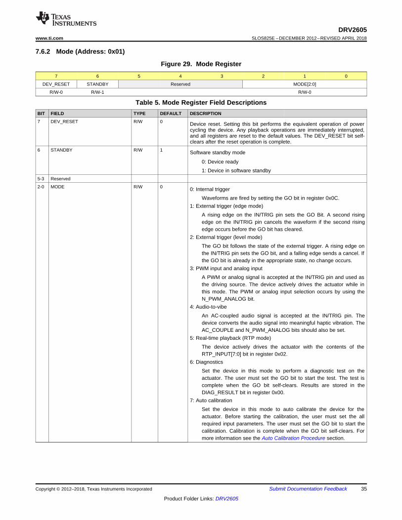
35
DRV2605www.ti.com SLOS825E –DECEMBER 2012–REVISED APRIL 2018
Product Folder Links: DRV2605
Submit Documentation FeedbackCopyright © 2012–2018, Texas Instruments Incorporated
7.6.2 Mode (Address: 0x01)
Figure 29. Mode Register
7 6 5 4 3 2 1 0
DEV_RESET STANDBY Reserved MODE[2:0]
R/W-0 R/W-1 R/W-0
Table 5. Mode Register Field DescriptionsBIT FIELD TYPE DEFAULT DESCRIPTION
7 DEV_RESET R/W 0 Device reset. Setting this bit performs the equivalent operation of powercycling the device. Any playback operations are immediately interrupted,and all registers are reset to the default values. The DEV_RESET bit self-clears after the reset operation is complete.
6 STANDBY R/W 1 Software standby mode
0: Device ready
1: Device in software standby5-3 Reserved
2-0 MODE R/W 0 0: Internal trigger
Waveforms are fired by setting the GO bit in register 0x0C.1: External trigger (edge mode)
A rising edge on the IN/TRIG pin sets the GO Bit. A second risingedge on the IN/TRIG pin cancels the waveform if the second risingedge occurs before the GO bit has cleared.
2: External trigger (level mode)
The GO bit follows the state of the external trigger. A rising edge onthe IN/TRIG pin sets the GO bit, and a falling edge sends a cancel. Ifthe GO bit is already in the appropriate state, no change occurs.
3: PWM input and analog input
A PWM or analog signal is accepted at the IN/TRIG pin and used asthe driving source. The device actively drives the actuator while inthis mode. The PWM or analog input selection occurs by using theN_PWM_ANALOG bit.
4: Audio-to-vibe
An AC-coupled audio signal is accepted at the IN/TRIG pin. Thedevice converts the audio signal into meaningful haptic vibration. TheAC_COUPLE and N_PWM_ANALOG bits should also be set.
5: Real-time playback (RTP mode)
The device actively drives the actuator with the contents of theRTP_INPUT[7:0] bit in register 0x02.
6: Diagnostics
Set the device in this mode to perform a diagnostic test on theactuator. The user must set the GO bit to start the test. The test iscomplete when the GO bit self-clears. Results are stored in theDIAG_RESULT bit in register 0x00.
7: Auto calibration
Set the device in this mode to auto calibrate the device for theactuator. Before starting the calibration, the user must set the allrequired input parameters. The user must set the GO bit to start thecalibration. Calibration is complete when the GO bit self-clears. Formore information see the Auto Calibration Procedure section.
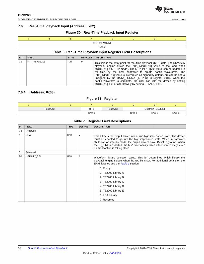
36
DRV2605SLOS825E –DECEMBER 2012–REVISED APRIL 2018 www.ti.com
Product Folder Links: DRV2605
Submit Documentation Feedback Copyright © 2012–2018, Texas Instruments Incorporated
7.6.3 Real-Time Playback Input (Address: 0x02)
Figure 30. Real-Time Playback Input Register
7 6 5 4 3 2 1 0
RTP_INPUT[7:0]
R/W-0
Table 6. Real-Time Playback Input Register Field DescriptionsBIT FIELD TYPE DEFAULT DESCRIPTION
7-0 RTP_INPUT[7:0] R/W 0 This field is the entry point for real-time playback (RTP) data. The DRV2605playback engine drives the RTP_INPUT[7:0] value to the load whenMODE[2:0] = 5 (RTP mode). The RTP_INPUT[7:0] value can be updated inreal-time by the host controller to create haptic waveforms. TheRTP_INPUT[7:0] value is interpreted as signed by default, but can be set tounsigned by the DATA_FORMAT_RTP bit in register 0x1D. When thehaptic waveform is complete, the user can idle the device by settingMODE[2:0] = 0, or alternatively by setting STANDBY = 1.
7.6.4 (Address: 0x03)
Figure 31. Register
7 6 5 4 3 2 1 0
Reserved HI_Z Reserved LIBRARY_SEL[2:0]
R/W-0 R/W-0 R/W-0 R/W-1
Table 7. Register Field DescriptionsBIT FIELD TYPE DEFAULT DESCRIPTION
7-5 Reserved
4 HI_Z R/W 0 This bit sets the output driver into a true high-impedance state. The devicemust be enabled to go into the high-impedance state. When in hardwareshutdown or standby mode, the output drivers have 15 kO to ground. Whenthe HI_Z bit is asserted, the hi-Z functionality takes effect immediately, evenif a transaction is taking place.
3 Reserved
2-0 LIBRARY_SEL R/W 1 Waveform library selection value. This bit determines which library theplayback engine selects when the GO bit is set. For additional details on theERM libraries see the Table 1 section.
0: Empty
1: TS2200 Library A
2: TS2200 Library B
3: TS2200 Library C
4: TS2200 Library D
5: TS2200 Library E
6: LRA Library
7: Reserved

37
DRV2605www.ti.com SLOS825E –DECEMBER 2012–REVISED APRIL 2018
Product Folder Links: DRV2605
Submit Documentation FeedbackCopyright © 2012–2018, Texas Instruments Incorporated
7.6.5 Waveform Sequencer (Address: 0x04 to 0x0B)
Figure 32. Waveform Sequencer Register7 6 5 4 3 2 1 0
WAIT WAV_FRM_SEQ[6:0]
R/W-0 R/W-0
Table 8. Waveform Sequencer Register Field DescriptionsBIT FIELD TYPE DEFAULT DESCRIPTION
7 WAIT R/W 0 When this bit is set, the WAV_FRM_SEQ[6:0] bit is interpreted as a waittime in which the playback engine idles. This bit is used to insert timeddelays between sequentially played waveforms.
Delay time = 10 ms × WAV_FRM_SEQ[6:0]If WAIT = 0, then WAV_FRM_SEQ[6:0] is interpreted as a waveformidentifier for sequence playback.
6-0 WAV_FRM_SEQ R/W 0 Waveform sequence value. This bit holds the waveform identifier of thewaveform to be played. A waveform identifier is an integer value referringto the index position of a waveform in a ROM library. Playback begins atregister address 0x04 when the user asserts the GO bit (register 0x0C).When playback of that waveform ends, the waveform sequencer plays thenext waveform identifier held in register 0x05, if the next waveformidentifier is non-zero. The waveform sequencer continues in this way untilthe sequencer reaches an identifier value of zero, or all eight identifiers areplayed (register addresses 0x04 through 0x0B), whichever comes first.
7.6.6 GO (Address: 0x0C)
Figure 33. GO Register7 6 5 4 3 2 1 0
Reserved GO
R/W-0
Table 9. GO Register Field DescriptionsBIT FIELD TYPE DEFAULT DESCRIPTION
7-1 Reserved
0 GO R/W 0 This bit is used to fire processes in the DRV2605 device. The processfired by the GO bit is selected by the MODE[2:0] bit (register 0x01). Theprimary function of this bit is to fire playback of the waveform identifiers inthe waveform sequencer (registers 0x04 to 0x0B), in which case, this bitcan be thought of a software trigger for haptic waveforms. The GO bitremains high until the playback of the haptic waveform sequence iscomplete. Clearing the GO bit during waveform playback cancels thewaveform sequence. Using one of the external trigger modes can causethe GO bit to be set or cleared by the external trigger pin. This bit can alsobe used to fire the auto-calibration process or the diagnostic process.

38
DRV2605SLOS825E –DECEMBER 2012–REVISED APRIL 2018 www.ti.com
Product Folder Links: DRV2605
Submit Documentation Feedback Copyright © 2012–2018, Texas Instruments Incorporated
7.6.7 Overdrive Time Offset (Address: 0x0D)
Figure 34. Overdrive Time Offset Register7 6 5 4 3 2 1 0
ODT[7:0]
R/W-0
Table 10. Overdrive Time Offset Register Field DescriptionsBIT FIELD TYPE DEFAULT DESCRIPTION
7-0 ODT R/W 0 This bit adds a time offset to the overdrive portion of the librarywaveforms. Some motors require more overdrive time than others,therefore this register allows the user to add or remove overdrive timefrom the library waveforms. The maximum voltage value in the librarywaveform is automatically determined to be the overdrive portion. Thisregister is only useful in open-loop mode. Overdrive is automatic forclosed-loop mode. The offset is interpreted as 2s complement, thereforethe time offset can be positive or negative.
Overdrive Time Offset (ms) = ODT[7:0] × 5 ms
7.6.8 Sustain Time Offset, Positive (Address: 0x0E)
Figure 35. Sustain Time Offset, Positive Register7 6 5 4 3 2 1 0
SPT[7:0]
R/W-0
Table 11. Sustain Time Offset, Positive Register Field DescriptionsBIT FIELD TYPE DEFAULT DESCRIPTION
7-0 SPT R/W 0 This bit adds a time offset to the positive sustain portion of the librarywaveforms. Some motors have a faster or slower response time thanothers, therefore this register allows the user to add or remove positivesustain time from the library waveforms. Any positive voltage value otherthan the overdrive portion is considered as a sustain positive value. Theoffset is interpreted as 2s complement, therefore the time offset can positiveor negative.
Sustain-Time Positive Offset (ms) = SPT[7:0] ×5 ms

39
DRV2605www.ti.com SLOS825E –DECEMBER 2012–REVISED APRIL 2018
Product Folder Links: DRV2605
Submit Documentation FeedbackCopyright © 2012–2018, Texas Instruments Incorporated
7.6.9 Sustain Time Offset, Negative (Address: 0x0F)
Figure 36. Sustain Time Offset, Negative Register7 6 5 4 3 2 1 0
SNT[7:0]
R/W-0
Table 12. Sustain Time Offset, Negative Register Field DescriptionsBIT FIELD TYPE DEFAULT DESCRIPTION
7-0 SNT R/W 0 This bit adds a time offset to the negative sustain portion of the librarywaveforms. Some motors have a faster or slower response time thanothers, therefore this register allows the user to add or remove negativesustain time from the library waveforms. Any negative voltage value otherthan the overdrive portion is considered as a sustaining negative value. Theoffset is interpreted as two’s complement, therefore the time offset can bepositive or negative.
Sustain-Time Negative Offset (ms) = SNT[7:0] ×5 ms
7.6.10 Brake Time Offset (Address: 0x10)
Figure 37. Brake Time Offset Register7 6 5 4 3 2 1 0
BRT[7:0]
R/W-0
Table 13. Brake Time Offset Register Field DescriptionsBIT FIELD TYPE DEFAULT DESCRIPTION
7-0 BRT R/W 0 This bit adds a time offset to the braking portion of the library waveforms.Some motors require more braking time than others, therefore this registerallows the user to add or take away brake time from the library waveforms.The most negative voltage value in the library waveform is automaticallydetermined to be the braking portion. This register is only useful in open-loopmode. Braking is automatic for closed-loop mode. The offset is interpreted as2s complement, therefore the time offset can be positive or negative.
Brake Time Offset (ms) = BRT[7:0] × 5 ms

40
DRV2605SLOS825E –DECEMBER 2012–REVISED APRIL 2018 www.ti.com
Product Folder Links: DRV2605
Submit Documentation Feedback Copyright © 2012–2018, Texas Instruments Incorporated
7.6.11 Audio-to-Vibe Control (Address: 0x11)
Figure 38. Audio-to-Vibe Control Register7 6 5 4 3 2 1 0
Reserved ATH_PEAK_TIME[1:0] ATH_FILTER[1:0]
R/W-0 R/W-1 R/W-0 R/W-1
Table 14. Audio-to-Vibe Control Register Field DescriptionsBIT FIELD TYPE DEFAULT DESCRIPTION
7-4 Reserved
3-2 ATH_PEAK_TIME[1:0] R/W 1 This bit sets the peak detection time for the audio-to-vibe signal path:
0: 10 ms
1: 20 ms
2: 30 ms
3: 40 ms1-0 ATH_FILTER[1:0] R/W 1 This bit sets the low-pass filter frequency for the audio-to-vibe signal path:
0: 100 Hz
1: 125 Hz
2: 150 Hz
3: 200 Hz
7.6.12 Audio-to-Vibe Minimum Input Level (Address: 0x12)
Figure 39. Audio-to-Vibe Minimum Input Level Register7 6 5 4 3 2 1 0
ATH_MIN_INPUT[7:0]
R/W-0 R/W-0 R/W-0 R/W-1 R/W-1 R/W-0 R/W-0 R/W-1
LEGEND: R/W = Read/Write; R = Read only; -n = value after reset
Table 15. Audio-to-Vibe Minimum Input Level Register Field DescriptionsBIT FIELD TYPE DEFAULT DESCRIPTION
7-0 ATH_MIN_INPUT[7:0] R/W 0x19 This bit sets the minimum voltage level at the IN/TRIG pin that is detected bythe audio-to-vibe engine. Levels below this are ignored.
ATH_MIN_INPUT Voltage (VPP) = ATH_MIN_INPUT[7:0] × 1.8 V / 255
7.6.13 Audio-to-Vibe Maximum Input Level (Address: 0x13)
Figure 40. Audio-to-Vibe Maximum Input Level Register7 6 5 4 3 2 1 0
ATH_MAX_INPUT[7:0]
R/W-1
Table 16. Audio-to-Vibe Maximum Input Level Register Field DescriptionsBIT FIELD TYPE DEFAULT DESCRIPTION
7-0 ATH_MAX_INPUT[7:0] R/W 0xFF This bit sets the full-scale voltage level at the IN/TRIG pin for audio-to-vibemode.
ATH_MAX_INPUT Voltage (VPP) = ATH_MAX_INPUT[7:0] × 1.8 V / 255
7.6.14 Audio-to-Vibe Minimum Output Drive (Address: 0x14)

41
DRV2605www.ti.com SLOS825E –DECEMBER 2012–REVISED APRIL 2018
Product Folder Links: DRV2605
Submit Documentation FeedbackCopyright © 2012–2018, Texas Instruments Incorporated
Figure 41. Audio-to-Vibe Minimum Output Drive Register7 6 5 4 3 2 1 0
ATH_MIN_DRIVE[7:0]
R/W-0 R/W-0 R/W-0 R/W-1 R/W-1 R/W-0 R/W-0 R/W-1
Table 17. Audio-to-Vibe Minimum Output Drive Register Field DescriptionsBIT FIELD TYPE DEFAULT DESCRIPTION
7-0 ATH_MIN_DRIVE[7:0] R/W 0x19 This bit sets the minimum output level that is applied to the actuator driveengine.
ATH_MIN_DRIVE (%) = ATH_MIN_DRIVE[7:0] / 255 × 100%
7.6.15 Audio-to-Vibe Maximum Output Drive (Address: 0x15)
Figure 42. Audio-to-Vibe Maximum Output Drive Register7 6 5 4 3 2 1 0
ATH_MAX_DRIVE[7:0]
R/W-1
Table 18. Audio-to-Vibe Maximum Output Drive Register Field DescriptionsBIT FIELD TYPE DEFAULT DESCRIPTION
7-0 ATH_MAX_DRIVE[7:0] R/W 0xFF This bit sets the maximum output level that is applied to the actuator driveengine.
ATH_MAX_DRIVE (%) = ATH_MAX_DRIVE[7:0] / 255 × 100%

42
DRV2605SLOS825E –DECEMBER 2012–REVISED APRIL 2018 www.ti.com
Product Folder Links: DRV2605
Submit Documentation Feedback Copyright © 2012–2018, Texas Instruments Incorporated
7.6.16 Rated Voltage (Address: 0x16)
Figure 43. Rated Voltage Register7 6 5 4 3 2 1 0
RATED_VOLTAGE[7:0]
R/W-0 R/W-0 R/W-1 R/W-1 R/W-1 R/W-1 R/W-1 R/W-1
Table 19. Rated Voltage Register Field DescriptionsBIT FIELD TYPE DEFAULT DESCRIPTION
7-0 RATED_VOLTAGE[7:0] R/W 0x3F This bit sets the reference voltage for full-scale output during closed-loopoperation. The auto-calibration routine uses this register as an input, thereforethis register must be written with the rated voltage value of the motor beforecalibration is performed. This register is ignored for open-loop operationbecause the overdrive voltage sets the reference for that case. Anymodification of this register value should be followed by calibration to setA_CAL_BEMF appropriately.See the Rated Voltage Programming section for calculating the correct registervalue.
7.6.17 Overdrive Clamp Voltage (Address: 0x17)
Figure 44. Overdrive Clamp Voltage Register7 6 5 4 3 2 1 0
OD_CLAMP[7:0]
R/W-1 R/W-0 R/W-0 R/W-1 R/W-1 R/W-0 R/W-0 R/W-1
Table 20. Overdrive Clamp Voltage Register Field DescriptionsBIT FIELD TYPE DEFAULT DESCRIPTION
7 OD_CLAMP[7:0] R/W 0x89 During closed-loop operation the actuator feedback allows the output voltageto go above the rated voltage during the automatic overdrive and automaticbraking periods. This register sets a clamp so that the automatic overdrive isbounded. This bit also serves as the full-scale reference voltage for open-loopoperation.See the Overdrive Voltage-Clamp Programming section for calculating thecorrect register value.
7.6.18 Auto-Calibration Compensation Result (Address: 0x18)
Figure 45. Auto-Calibration Compensation-Result Register7 6 5 4 3 2 1 0
A_CAL_COMP[7:0]
R/W-0 R/W-0 R/W-0 R/W-0 R/W-1 R/W-1 R/W-0 R/W-1
Table 21. Auto-Calibration Compensation-Result Register Field DescriptionsBIT FIELD TYPE DEFAULT DESCRIPTION
7-0 A_CAL_COMP[7:0] R/W 0x0D This register contains the voltage-compensation result after execution of autocalibration. The value stored in the A_CAL_COMP bit compensates for anyresistive losses in the driver. The calibration routine checks the impedance ofthe actuator to automatically determine an appropriate value. The auto-calibration compensation-result value is multiplied by the drive gain duringplayback.
Auto-calibration compensation coefficient = 1 + A_CAL_COMP[7:0] / 255

43
DRV2605www.ti.com SLOS825E –DECEMBER 2012–REVISED APRIL 2018
Product Folder Links: DRV2605
Submit Documentation FeedbackCopyright © 2012–2018, Texas Instruments Incorporated
7.6.19 Auto-Calibration Back-EMF Result (Address: 0x19)
Figure 46. Auto-Calibration Back-EMF Result Register7 6 5 4 3 2 1 0
A_CAL_BEMF[7:0]
R/W-0 R/W-1 R/W-1 R/W-0 R/W-1 R/W-1 R/W-0 R/W-1
Table 22. Auto-Calibration Back-EMF Result Register Field DescriptionsBIT FIELD TYPE DEFAULT DESCRIPTION
7-0 A_CAL_BEMF[7:0] R/W 0x6D This register contains the rated back-EMF result after execution of autocalibration. The A_CAL_BEMF[7:0] bit is the level of back-EMF voltage that theactuator gives when the actuator is driven at the rated voltage. The DRV2605playback engine uses this the value stored in this bit to automatically determinethe appropriate feedback gain for closed-loop operation.
Auto-calibration back-EMF (V) = (A_CAL_BEMF[7:0] / 255) × 1.22 V /BEMF_GAIN[1:0]

44
DRV2605SLOS825E –DECEMBER 2012–REVISED APRIL 2018 www.ti.com
Product Folder Links: DRV2605
Submit Documentation Feedback Copyright © 2012–2018, Texas Instruments Incorporated
7.6.20 Feedback Control (Address: 0x1A)
Figure 47. Feedback Control Register7 6 5 4 3 2 1 0
N_ERM_LRA FB_BRAKE_FACTOR[2:0] LOOP_GAIN[1:0] BEMF_GAIN[1:0]
R/W-0 R/W-0 R/W-1 R/W-1 R/W-0 R/W-1 R/W-1 R/W-0
Table 23. Feedback Control Register Field DescriptionsBIT FIELD TYPE DEFAULT DESCRIPTION
7 N_ERM_LRA R/W 0 This bit sets the DRV2605 device in ERM or LRA mode. This bit should be setprior to running auto calibration.
0: ERM Mode
1: LRA Mode6-4 FB_BRAKE_FACTOR[2:0] R/W 3 This bit selects the feedback gain ratio between braking gain and driving gain.
In general, adding additional feedback gain while braking is desirable so that theactuator brakes as quickly as possible. Large ratios provide less-stableoperation than lower ones. The advanced user can select to optimize thisregister. Otherwise, the default value should provide good performance for mostactuators. This value should be set prior to running auto calibration.
0: 1x
1: 2x
2: 3x
3: 4x
4: 6x
5: 8x
6: 16x
7: Braking disabled3-2 LOOP_GAIN[1:0] R/W 1 This bit selects a loop gain for the feedback control. The LOOP_GAIN[1:0] bit
sets how fast the loop attempts to make the back-EMF (and thus motor velocity)match the input signal level. Higher loop-gain (faster settling) options provideless-stable operation than lower loop gain (slower settling). The advanced usercan select to optimize this register. Otherwise, the default value should providegood performance for most actuators. This value should be set prior to runningauto calibration.
0: Low
1: Medium (default)
2: High
3: Very High1-0 BEMF_GAIN[1:0] R/W 2 This bit sets the analog gain of the back-EMF amplifier. This value is interpreted
differently between ERM mode and LRA mode. Auto calibration automaticallypopulates the BEMF_GAIN bit with the most appropriate value for the actuator.
ERM Mode
0: 0.33x
1: 1.0x
2: 1.8x (default)
3: 4.0x
LRA Mode
0: 5x
1: 10x
2: 20x (default)
3: 30x

45
DRV2605www.ti.com SLOS825E –DECEMBER 2012–REVISED APRIL 2018
Product Folder Links: DRV2605
Submit Documentation FeedbackCopyright © 2012–2018, Texas Instruments Incorporated
7.6.21 Control1 (Address: 0x1B)
Figure 48. Control1 Register7 6 5 4 3 2 1 0
STARTUP_BOOST Reserved AC_COUPLE DRIVE_TIME[4:0]
R/W-1 R/W-0 R/W-1 R/W-0 R/W-0 R/W-1 R/W-1
Table 24. Control1 Register Field DescriptionsBIT FIELD TYPE DEFAULT DESCRIPTION
7 STARTUP_BOOST R/W 1 This bit applies higher loop gain during overdrive to enhance actuator transientresponse.
6 Reserved
5 AC_COUPLE R/W 0 This bit applies a 0.9-V common mode voltage to the IN/TRIG pin when an AC-coupling capacitor is used. This bit is only useful for analog input mode. This bitshould not be asserted for PWM mode or external trigger mode.
0: Common-mode drive disabled for DC-coupling or digital inputs modes
1: Common-mode drive enabled for AC coupling4-0 DRIVE_TIME[4:0] R/W 0x13 LRA Mode: Sets initial guess for LRA drive-time in LRA mode. Drive time is
automatically adjusted for optimum drive in real time; however, this registershould be optimized for the approximate LRA frequency. If the bit is set too low,it can affect the actuator startup time. If the bit is set too high, it can causeinstability.
Optimum drive time (ms) ≈ 0.5 × LRA Period
Drive time (ms) = DRIVE_TIME[4:0] × 0.1 ms + 0.5 msERM Mode: Sets the sample rate for the back-EMF detection. Lower drive timescause higher peak-to-average ratios in the output signal, requiring more supplyheadroom. Higher drive times cause the feedback to react at a slower rate.
Drive Time (ms) = DRIVE_TIME[4:0] × 0.2 ms + 1 ms
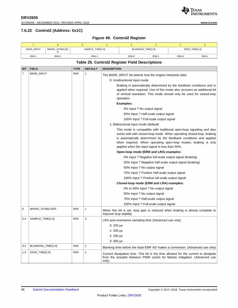
46
DRV2605SLOS825E –DECEMBER 2012–REVISED APRIL 2018 www.ti.com
Product Folder Links: DRV2605
Submit Documentation Feedback Copyright © 2012–2018, Texas Instruments Incorporated
7.6.22 Control2 (Address: 0x1C)
Figure 49. Control2 Register7 6 5 4 3 2 1 0
BIDIR_INPUT BRAKE_STABILIZER
SAMPLE_TIME[1:0] BLANKING_TIME[1:0] IDISS_TIME[1:0]
R/W-1 R/W-1 R/W-1 R/W-0 R/W-1 R/W-0 R/W-1
Table 25. Control2 Register Field DescriptionsBIT FIELD TYPE DEFAULT DESCRIPTION
7 BIDIR_INPUT R/W 1 The BIDIR_INPUT bit selects how the engine interprets data.
0: Unidirectional input mode
Braking is automatically determined by the feedback conditions and isapplied when required. Use of this mode also recovers an additional bitof vertical resolution. This mode should only be used for closed-loopoperation.
Examples::0% Input ? No output signal
50% Input ? Half-scale output signal
100% Input ? Full-scale output signal
1: Bidirectional input mode (default)
This mode is compatible with traditional open-loop signaling and alsoworks well with closed-loop mode. When operating closed-loop, brakingis automatically determined by the feedback conditions and appliedwhen required. When operating open-loop modes, braking is onlyapplied when the input signal is less than 50%.
Open-loop mode (ERM and LRA) examples:0% Input ? Negative full-scale output signal (braking)
25% Input ? Negative half-scale output signal (braking)
50% Input ? No output signal
75% Input ? Positive half-scale output signal
100% Input ? Positive full-scale output signal
Closed-loop mode (ERM and LRA) examples:0% to 50% Input ? No output signal
50% Input ? No output signal
75% Input ? Half-scale output signal
100% Input ? Full-scale output signal6 BRAKE_STABILIZER R/W 1 When this bit is set, loop gain is reduced when braking is almost complete to
improve loop stability5-4 SAMPLE_TIME[1:0] R/W 3 LRA auto-resonance sampling time (Advanced use only)
0: 150 µs
1: 200 µs
2: 250 µs
3: 300 µs3-2 BLANKING_TIME[1:0] R/W 1 Blanking time before the back-EMF AD makes a conversion. (Advanced use only)1-0 IDISS_TIME[1:0] R/W 1 Current dissipation time. This bit is the time allowed for the current to dissipate
from the actuator between PWM cycles for flyback mitigation. (Advanced useonly)

47
DRV2605www.ti.com SLOS825E –DECEMBER 2012–REVISED APRIL 2018
Product Folder Links: DRV2605
Submit Documentation FeedbackCopyright © 2012–2018, Texas Instruments Incorporated
7.6.23 Control3 (Address: 0x1D)
Figure 50. Control3 Register7 6 5 4 3 2 1 0
NG_THRESH[1:0] ERM_OPEN_LOOP SUPPLY_COMP_DIS
DATA_FORMAT_RTP
LRA_DRIVE_MODE N_PWM_ANALOG LRA_OPEN_LOOP
R/W-1 R/W-0 R/W-1 R/W-0 R/W-0 R/W-0 R/W-0 R/W-0
Table 26. Control3 Register Field DescriptionsBIT FIELD TYPE DEFAULT DESCRIPTION
7-6 NG_THRESH[1:0] R/W 2 This bit is the noise-gate threshold for PWM and analog inputs.
0: Disabled
1: 2%
2: 4% (Default)
3: 8%5 ERM_OPEN_LOOP R/W 1 This bit selects mode of operation while in ERM mode. Closed-loop operation is
usually desired for because of automatic overdrive and braking properties.However, many existing waveform libraries were designed for open-loopoperation, therefore open-loop operation can be required for compatibility.
0: Closed Loop
1: Open Loop4 SUPPLY_COMP_DIS R/W 0 This bit disables supply compensation. The DRV2605 device generally provides
constant drive output over variation in the power supply input (VDD). In somesystems, supply compensation can have already been implemented upstream,therefore disabling the DRV2605 supply compensation can be useful.
0: Supply compensation enabled
1: Supply compensation disabled3 DATA_FORMAT_RTP R/W 0 This bit selects the input data interpretation for RTP (Real-Time Playback)
mode.
0: Signed
1: Unsigned2 LRA_DRIVE_MODE R/W 0 This bit selects the drive mode for the LRA algorithm. This bit determines how
often the drive amplitude is updated. Updating once per cycle provides asymmetrical output signal, while updating twice per cycle provides more precisecontrol.
0: Once per cycle
1: Twice per cycle1 N_PWM_ANALOG R/W 0 This bit selects the input mode for the IN/TRIG pin when MODE[2:0] = 3. In
PWM input mode, the duty cycle of the input signal determines the amplitude ofthe waveform. In analog input mode, the amplitude of the input determines theamplitude of the waveform.
0: PWM Input
1: Analog Input0 LRA_OPEN_LOOP R/W 0 This bit selects an open-loop drive option for LRA Mode. When asserted, the
playback engine drives the LRA at the selected frequency independently of theresonance frequency. In PWM input mode, the playback engine recovers theLRA commutation frequency from the PWM input, dividing the frequency by128. Therefore the PWM input frequency must be equal to 128 times theresonant frequency of the LRA.
0: Auto-resonance mode
1: LRA open-loop mode

48
DRV2605SLOS825E –DECEMBER 2012–REVISED APRIL 2018 www.ti.com
Product Folder Links: DRV2605
Submit Documentation Feedback Copyright © 2012–2018, Texas Instruments Incorporated
7.6.24 Control4 (Address: 0x1E)
Figure 51. Control4 Register7 6 5 4 3 2 1 0
Reserved AUTO_CAL_TIME[1:0] Reserved OTP_STATUS Reserved OTP_PROGRAM
R/W-1 R/W-0 R-0 R/W-0
Table 27. Control4 Register Field DescriptionsBIT FIELD TYPE DEFAULT DESCRIPTION
7-6 Reserved
5-4 AUTO_CAL_TIME[1:0] R/W 2 This bit sets the length of the auto calibration time. The AUTO_CAL_TIME[1:0]bit should be enough time for the motor acceleration to settle when driven at theRATED_VOLTAGE[7:0] value.
0: 150 ms (minimum), 350 ms (maximum)
1: 250 ms (minimum), 450 ms (maximum)
2: 500 ms (minimum), 700 ms (maximum)
3: 1000 ms (minimum), 1200 ms (maximum)3 Reserved
2 OTP_STATUS R 0 OTP Memory status
0: OTP Memory has not been programmed
1: OTP Memory has been programmed1 Reserved
0 OTP_PROGRAM R/W 0 This bit launches the programming process for one-time programmable (OTP)memory which programs the contents of register 0x16 through 0x1A intononvolatile memory. This process can only be executed one time per device.See the Programming On-Chip OTP Memory section for details.
7.6.25 V(BAT) Voltage Monitor (Address: 0x21)
Figure 52. V(BAT) Voltage-Monitor Register7 6 5 4 3 2 1 0
VBAT[7:0]
R/W-0
Table 28. V(BAT) Voltage-Monitor Register Field DescriptionsBIT FIELD TYPE DEFAULT DESCRIPTION
7-0 VBAT[7:0] R/W 0 This bit provides a real-time reading of the supply voltage at the VDD pin. Thedevice must be actively sending a waveform to take a reading.
VDD (V) = VBAT[7:0] × 5.6V / 255
7.6.26 LRA Resonance Period (Address: 0x22)
Figure 53. LRA Resonance-Period Register7 6 5 4 3 2 1 0
LRA_PERIOD[7:0]
R/W-0
Table 29. LRA Resonance-Period Register Field DescriptionsBIT FIELD TYPE DEFAULT DESCRIPTION
7-0 LRA_PERIOD[7:0] R/W 0 This bit reports the measurement of the LRA resonance period. The device mustbe actively sending a waveform to take a reading.
LRA period (us) = LRA_Period[7:0] × 98.46 µs

Application
Processor
SCL
SDA
GPIO
ANALOG
SCL
SDA
EN
IN/TRIG
REG
OUT–
VDD
GND
OUT+
DRV2605
2.5 V – 5.5 V
C(REG)
C(VDD)
MLRA or
ERM
C(IN)
(optional )
R(PU) R(PU)
Application
Processor
SCL
SDA
GPIO
PWM/GPIO
SCL
SDA
EN
IN/TRIG
REG
OUT±
VDD
GND
OUT+
DRV2605
2.5 V - 5.5 V
C(REG)
C(VDD)
MLRA or
ERM
R(PU) R(PU)
49
DRV2605www.ti.com SLOS825E –DECEMBER 2012–REVISED APRIL 2018
Product Folder Links: DRV2605
Submit Documentation FeedbackCopyright © 2012–2018, Texas Instruments Incorporated
8 Application and Implementation
NOTEInformation in the following applications sections is not part of the TI componentspecification, and TI does not warrant its accuracy or completeness. TI’s customers areresponsible for determining suitability of components for their purposes. Customers shouldvalidate and test their design implementation to confirm system functionality.
8.1 Application InformationThe typical application for a haptic driver is in a touch-enabled system that already has an application processorwhich makes the decision on when to execute haptic effects.
The DRV2605 device can be used fully with I2C communications (either using RTP or the memory interface). Asystem designer can chose to use external triggers to play low-latency effects (such as from a physical button) orcan decide to use the PWM interface. Figure 54 shows a typical haptic system implementation. The systemdesigner should not use the internal regulator (REG) to power any external load.
A system designer can also implement audio-to-vibe. Figure 55 shows a typical haptic system implementationsupporting audio-to-vibe.
Figure 54. I2C Control with Optional PWM Input or External Trigger
Figure 55. I2C Control With Audio-to-Vibe Input and Optional AC Coupling
Table 30. Recommended External ComponentsCOMPONENT DESCRIPTION SPECIFICATION TYPICAL VALUE
C(VDD) Input capacitor Capacitance 1 µFC(REG) Regulator capacitor Capacitance 1 µFC(IN) AC coupling capacitor (optional) Capacitance 1 µFR(PU) Pullup resistor Resistance 2.2 kΩ
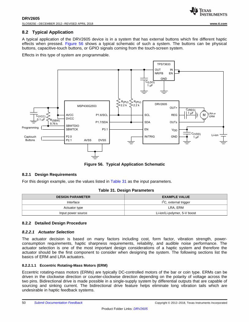
TPS73633
GND
IN
EN
OUT
NR/FB
SCL
SDA
EN
IN/TRIG
REG
OUT±
VDD
GND
OUT+
DRV2605MSP430G2553
P1.6/SCL
P1.7/SDA
P3.1
DVSSAVSS
AVCC
DVCC
P2.0
P2.1
SBWTDIO
SBWTCK
C(LDO)
1 µF
R(PU)
2.2 k
R(PU)
2.2 k
C(REG)
1 µFM
LRA or
ERM
C(VDD)
1 µF
R(SBW)
9.76 k
C(VCC)
0.1 µF
Captouch
Buttons
Programming
Li-ion
50
DRV2605SLOS825E –DECEMBER 2012–REVISED APRIL 2018 www.ti.com
Product Folder Links: DRV2605
Submit Documentation Feedback Copyright © 2012–2018, Texas Instruments Incorporated
8.2 Typical ApplicationA typical application of the DRV2605 device is in a system that has external buttons which fire different hapticeffects when pressed. Figure 56 shows a typical schematic of such a system. The buttons can be physicalbuttons, capacitive-touch buttons, or GPIO signals coming from the touch-screen system.
Effects in this type of system are programmable.
Figure 56. Typical Application Schematic
8.2.1 Design RequirementsFor this design example, use the values listed in Table 31 as the input parameters.
Table 31. Design ParametersDESIGN PARAMETER EXAMPLE VALUE
Interface I2C, external triggerActuator type LRA, ERM
Input power source Li-ion/Li-polymer, 5-V boost
8.2.2 Detailed Design Procedure
8.2.2.1 Actuator SelectionThe actuator decision is based on many factors including cost, form factor, vibration strength, power-consumption requirements, haptic sharpness requirements, reliability, and audible noise performance. Theactuator selection is one of the most important design considerations of a haptic system and therefore theactuator should be the first component to consider when designing the system. The following sections list thebasics of ERM and LRA actuators.
8.2.2.1.1 Eccentric Rotating-Mass Motors (ERM)
Eccentric rotating-mass motors (ERMs) are typically DC-controlled motors of the bar or coin type. ERMs can bedriven in the clockwise direction or counter-clockwise direction depending on the polarity of voltage across thetwo pins. Bidirectional drive is made possible in a single-supply system by differential outputs that are capable ofsourcing and sinking current. The bidirectional drive feature helps eliminate long vibration tails which areundesirable in haptic feedback systems.

Acc
eler
atio
n (g
)
¦(RESONANCE)
Frequency (Hz)
+
±
VOMotor-spin direction
IL
IL
OUT+
OUT±
±
+
VOMotor-spin direction
IL
IL
OUT+
OUT±
51
DRV2605www.ti.com SLOS825E –DECEMBER 2012–REVISED APRIL 2018
Product Folder Links: DRV2605
Submit Documentation FeedbackCopyright © 2012–2018, Texas Instruments Incorporated
Figure 57. Motor Spin Direction in ERM Motors
Another common approach to driving DC motors is the concept of overdrive voltage. To overcome the inertia ofthe mass of the motor, the DC motors are often overdriven for a short amount of time before returning to therated voltage of the motor to sustain the rotation of the motor. Overdrive is also used to stop (or brake) a motorquickly. Refer to the data sheet of the particular motor used with the DRV2605 device for safe and reliableoverdrive voltage and duration.
8.2.2.1.2 Linear Resonance Actuators (LRA)
Linear resonant actuators (LRAs) vibrate optimally at the resonant frequency. LRAs have a high-Q frequencyresponse because of a rapid drop in vibration performance at the offsets of 3 to 5 Hz from the resonantfrequency. Many factors also cause a shift or drift in the resonant frequency of the actuator such as temperature,aging, the mass of the product to which the LRA is mounted, and in the case of a portable product, the manner inwhich the product is held. Furthermore, as the actuator is driven to the maximum allowed voltage, many LRAswill shift several hertz in frequency because of mechanical compression. All of these factors make a real-timetracking auto-resonant algorithm critical when driving LRA to achieve consistent, optimized performance.
Figure 58. Typical LRA Response
8.2.2.1.2.1 Auto-Resonance Engine for LRA
The DRV2605 auto-resonance engine tracks the resonant frequency of an LRA in real time effectively lockinginto the resonance frequency after half a cycle. If the resonant frequency shifts in the middle of a waveform forany reason, the engine tracks the frequency from cycle to cycle. The auto resonance engine accomplishes thistracking by constantly monitoring the back-EMF of the actuator. Note that the auto resonance engine is notaffected by the auto-calibration process which is only used for level calibration. No calibration is required for theauto resonance engine.
8.2.2.2 Capacitor SelectionThe DRV2605 device has a switching output stage which pulls transient currents through the VDD pin. TIrecommends placing a 0.1-µF low equivalent-series-resistance (ESR) supply-bypass capacitor of the X5R orX7R type near the VDD supply pin for proper operation of the output driver and the digital portion of the device.Place a 1-µF X5R or X7R-type capacitor from the REG pin to ground.

Time (s)
Vol
tage
(2V
/div
)
0 40m 80m 120m 160m 200m
IN/TRIGAcceleration[OUT+] − [OUT−] (Filtered)
Time (s)
Vol
tage
(2V
/div
)
0 40m 80m 120m 160m 200m
IN/TRIGAcceleration[OUT+] − [OUT−] (Filtered)
52
DRV2605SLOS825E –DECEMBER 2012–REVISED APRIL 2018 www.ti.com
Product Folder Links: DRV2605
Submit Documentation Feedback Copyright © 2012–2018, Texas Instruments Incorporated
8.2.2.3 Interface SelectionThe I2C interface is required to configure the device. The device can be used fully with the I2C interface and witheither RTP or internal memory. The advantage of using the I2C interface is that no additional GPIO (for theIN/TRIG pin) is required for firing effects, and no PWM signal is required to be generated. Therefore the IN/TRIGpin can be connected to GND. Using the external trigger pin has the advantage that no I2C transaction isrequired to fire the pre-loaded effect, which is a good choice for interfacing with a button. The PWM interface isavailable for backward compatibility. If audio-to-vibe is desired, then use C(IN) as shown in Figure 55.
8.2.2.4 Power Supply SelectionThe DRV2605 device supports a wide range of voltages in the input. Ensuring that the battery voltage is highenough to support the desired vibration strength with the selected actuator is an important design consideration.The typical application uses Li-ion or Li-polymer batteries which provide enough voltage headroom to drive mostcommon actuators.
If very strong vibrations are desired, a boost converter can be placed between the power supply and the VDD pinto provide a constant voltage with a healthy headroom (5-V rails are common in some systems) which isparticularly true if two AA batteries in series are being used to power the system.
8.2.3 Application Curves
VDD = 3.6 V ERM open loopStrong click
- 60%External edge
trigger
VDD = 3.6 V LRA closed loopStrong click -
100%External level
trigger
Figure 59. ERM Click with and without Braking Figure 60. LRA Click With and Without Braking

53
DRV2605www.ti.com SLOS825E –DECEMBER 2012–REVISED APRIL 2018
Product Folder Links: DRV2605
Submit Documentation FeedbackCopyright © 2012–2018, Texas Instruments Incorporated
8.3 Initialization Setup
8.3.1 Initialization Procedure1. After powerup, wait at least 250 µs before the DRV2605 device accepts I2C commands.2. Assert the EN pin (logic high). The EN pin can be asserted any time during or after the 250-µs wait period.3. Write the MODE register (address 0x01) to value 0x00 to remove the device from standby mode.4. If the nonvolatile auto-calibration memory has been programmed as described in the Auto Calibration
Procedure section, skip Step 5 and proceed to Step 6.5. Perform the steps as described in the Auto Calibration Procedure section. Alternatively, rewrite the results
from a previous calibration.6. If using the embedded ROM library, write the library selection register (address 0x03) to select a library.7. The default setup is closed-loop bidirectional mode. To use other modes and features, write Control1 (0x1B),
Control2 (0x1C), and Control3 (0x1D) as required. Open-loop operation is recommended for ERM modewhen using the ROM libraries.
8. Put the device in standby mode or deassert the EN pin, whichever is the most convenient. Both settings arelow-power modes. The user can select the desired MODE (address 0x01) at the same time the STANDBYbit is set.
8.3.2 Typical Usage Examples
8.3.2.1 Play a Waveform or Waveform Sequence from the ROM Waveform Memory1. Initialize the device as listed in the Initialization Procedure section.2. Assert the EN pin (active high) if it was previously deasserted.3. If register 0x01 already holds the desired value and the STANDBY bit is low, the user can skip this step.
Select the desired MODE[2:0] value of 0 (internal trigger), 1 (external edge trigger), or 2 (external leveltrigger) in the MODE register (address 0x01). If the STANDBY bit was previously asserted, this bit should bedeasserted (logic low) at this time.
4. Select the waveform index to be played and write it to address 0x04. Alternatively, a sequence of waveformindices can be written to register 0x04 through 0x0B. See the Waveform Sequencer section for details.
5. If using the internal trigger mode, set the GO bit (in register 0x0C) to fire the effect or sequence of effects. Ifusing an external trigger mode, send an appropriate trigger pulse to the IN/TRIG pin. See the WaveformTriggers section for details.
6. If desired, the user can repeat Step 5 to fire the effect or sequence again.7. Put the device in low-power mode by deasserting the EN pin or setting the STANDBY bit.
8.3.2.2 Play a Real-Time Playback (RTP) Waveform1. Initialize the device as shown in the Initialization Procedure section.2. Assert the EN pin (active high) if it was previously deasserted.3. Set the MODE[2:0] value to 5 (RTP Mode) at address 0x01. If the STANDBY bit was previously asserted,
this bit should be deasserted (logic low) at this time. If register 0x01 already holds the desired value and theSTANDBY bit is low, the user can skip this step.
4. Write the desired drive amplitude to the real-time playback input register (address 0x02).5. When the desired sequence of drive amplitudes is complete, put the device in low-power mode by
deasserting the EN pin or setting the STANDBY bit.

54
DRV2605SLOS825E –DECEMBER 2012–REVISED APRIL 2018 www.ti.com
Product Folder Links: DRV2605
Submit Documentation Feedback Copyright © 2012–2018, Texas Instruments Incorporated
Initialization Setup (continued)8.3.2.3 Play a PWM or Analog Input Waveform1. Initialize the device as shown in the Initialization Procedure section.2. Assert the EN pin (active high) if it was previously deasserted.3. If register 0x01 already holds the desired value and the STANDBY bit is low, the user can skip this step. Set
the MODE value to 3 (PWM/Analog Mode) at address 0x01. If the STANDBY bit was previously asserted,this bit should be deasserted (logic low) at this time.
4. Select the input mode (PWM or analog) in the Control3 register (address 0x1D). If this mode was selectedduring the initialization procedure, the user can skip this step.
5. Send the desired PWM or analog input waveform sequence from the external source. See the Data Formatsfor Waveform Playback section for drive amplitude scaling.
6. When the desired drive sequence is complete, put the device in low-power mode by deasserting the EN pinor setting the STANDBY bit.
9 Power Supply RecommendationsThe DRV2605 device is designed to operate from an input-voltage supply range between 2.5 V to 5.5 V. Thedecoupling capacitor for the power supply should be placed closed to the device pin.
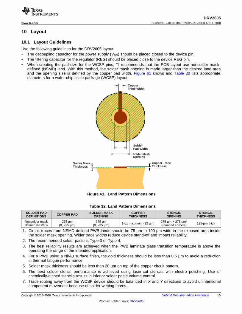
CopperTrace Width
Solder MaskThickness
SolderPad Width
Solder MaskOpening
Copper TraceThickness
55
DRV2605www.ti.com SLOS825E –DECEMBER 2012–REVISED APRIL 2018
Product Folder Links: DRV2605
Submit Documentation FeedbackCopyright © 2012–2018, Texas Instruments Incorporated
10 Layout
10.1 Layout GuidelinesUse the following guidelines for the DRV2605 layout:• The decoupling capacitor for the power supply (VDD) should be placed closed to the device pin.• The filtering capacitor for the regulator (REG) should be placed close to the device REG pin.• When creating the pad size for the WCSP pins, TI recommends that the PCB layout use nonsolder mask-
defined (NSMD) land. With this method, the solder mask opening is made larger than the desired land areaand the opening size is defined by the copper pad width. Figure 61 shows and Table 32 lists appropriatediameters for a wafer-chip scale package (WCSP) layout.
Figure 61. Land Pattern Dimensions
Table 32. Land Pattern DimensionsSOLDER PADDEFINITIONS COPPER PAD SOLDER MASK
OPENINGCOPPER
THICKNESSSTENCILOPENING
STENCILTHICKNESS
Nonsolder maskdefined (NSMD)
275 µm(0, –25 µm)
375 µm(0, –25 µm) 1-oz maximum (32 µm) 275 µm × 275 µm2
(rounded corners) 125-µm thick
1. Circuit traces from NSMD defined PWB lands should be 75-µm to 100-µm wide in the exposed area insidethe solder mask opening. Wider trace widths reduce device stand-off and impact reliability.
2. The recommended solder paste is Type 3 or Type 4.3. The best reliability results are achieved when the PWB laminate glass transition temperature is above the
operating the range of the intended application.4. For a PWB using a Ni/Au surface finish, the gold thickness should be less than 0.5 µm to avoid a reduction
in thermal fatigue performance.5. Solder mask thickness should be less than 20 µm on top of the copper circuit pattern.6. The best solder stencil performance is achieved using laser-cut stencils with electro polishing. Use of
chemically-etched stencils results in inferior solder paste volume control.7. Trace routing away from the WCSP device should be balanced in X and Y directions to avoid unintentional
component movement because of solder-wetting forces.

C(REG)
C(VDD)
VDD
REG OUT+
GND
OUTt
SDAIN
SCL
EN
Via
Via should connectto a ground plane
56
DRV2605SLOS825E –DECEMBER 2012–REVISED APRIL 2018 www.ti.com
Product Folder Links: DRV2605
Submit Documentation Feedback Copyright © 2012–2018, Texas Instruments Incorporated
10.1.1 Trace WidthThe recommended trace width at the solder pins is 75 µm to 100 µm to prevent solder wicking onto wider PCBtraces. Maintain this trace width until the pin pattern has escaped, then the trace width can be increased forimproved current flow. The width and length of the 75-µm to 100-µm traces should be as symmetrical as possiblearound the device to provide even solder reflow on each of the pins.
10.2 Layout Example
Figure 62. DRV2605 Layout Example DSBGA
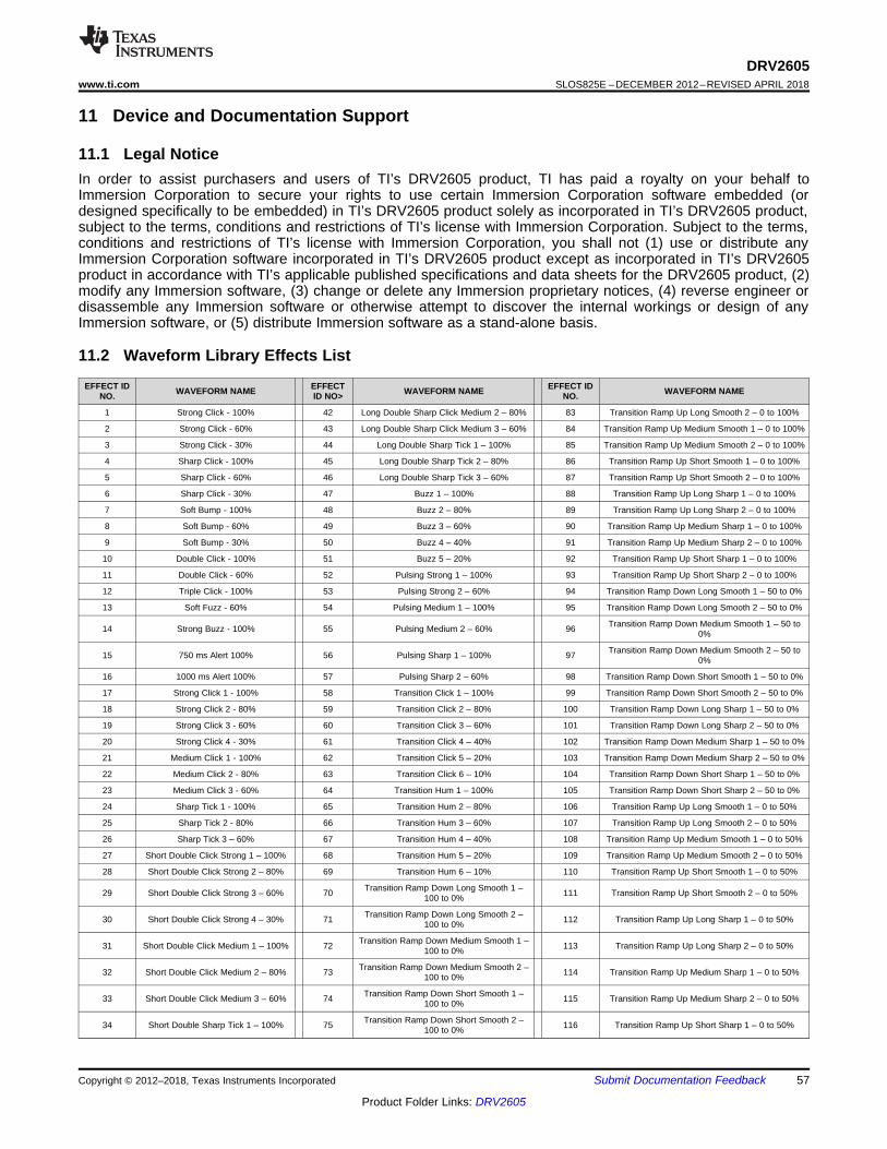
57
DRV2605www.ti.com SLOS825E –DECEMBER 2012–REVISED APRIL 2018
Product Folder Links: DRV2605
Submit Documentation FeedbackCopyright © 2012–2018, Texas Instruments Incorporated
11 Device and Documentation Support
11.1 Legal NoticeIn order to assist purchasers and users of TI’s DRV2605 product, TI has paid a royalty on your behalf toImmersion Corporation to secure your rights to use certain Immersion Corporation software embedded (ordesigned specifically to be embedded) in TI’s DRV2605 product solely as incorporated in TI’s DRV2605 product,subject to the terms, conditions and restrictions of TI’s license with Immersion Corporation. Subject to the terms,conditions and restrictions of TI’s license with Immersion Corporation, you shall not (1) use or distribute anyImmersion Corporation software incorporated in TI’s DRV2605 product except as incorporated in TI’s DRV2605product in accordance with TI’s applicable published specifications and data sheets for the DRV2605 product, (2)modify any Immersion software, (3) change or delete any Immersion proprietary notices, (4) reverse engineer ordisassemble any Immersion software or otherwise attempt to discover the internal workings or design of anyImmersion software, or (5) distribute Immersion software as a stand-alone basis.
11.2 Waveform Library Effects List
EFFECT IDNO. WAVEFORM NAME EFFECT
ID NO> WAVEFORM NAME EFFECT IDNO. WAVEFORM NAME
1 Strong Click - 100% 42 Long Double Sharp Click Medium 2 – 80% 83 Transition Ramp Up Long Smooth 2 – 0 to 100%
2 Strong Click - 60% 43 Long Double Sharp Click Medium 3 – 60% 84 Transition Ramp Up Medium Smooth 1 – 0 to 100%
3 Strong Click - 30% 44 Long Double Sharp Tick 1 – 100% 85 Transition Ramp Up Medium Smooth 2 – 0 to 100%
4 Sharp Click - 100% 45 Long Double Sharp Tick 2 – 80% 86 Transition Ramp Up Short Smooth 1 – 0 to 100%
5 Sharp Click - 60% 46 Long Double Sharp Tick 3 – 60% 87 Transition Ramp Up Short Smooth 2 – 0 to 100%
6 Sharp Click - 30% 47 Buzz 1 – 100% 88 Transition Ramp Up Long Sharp 1 – 0 to 100%
7 Soft Bump - 100% 48 Buzz 2 – 80% 89 Transition Ramp Up Long Sharp 2 – 0 to 100%
8 Soft Bump - 60% 49 Buzz 3 – 60% 90 Transition Ramp Up Medium Sharp 1 – 0 to 100%
9 Soft Bump - 30% 50 Buzz 4 – 40% 91 Transition Ramp Up Medium Sharp 2 – 0 to 100%
10 Double Click - 100% 51 Buzz 5 – 20% 92 Transition Ramp Up Short Sharp 1 – 0 to 100%
11 Double Click - 60% 52 Pulsing Strong 1 – 100% 93 Transition Ramp Up Short Sharp 2 – 0 to 100%
12 Triple Click - 100% 53 Pulsing Strong 2 – 60% 94 Transition Ramp Down Long Smooth 1 – 50 to 0%
13 Soft Fuzz - 60% 54 Pulsing Medium 1 – 100% 95 Transition Ramp Down Long Smooth 2 – 50 to 0%
14 Strong Buzz - 100% 55 Pulsing Medium 2 – 60% 96 Transition Ramp Down Medium Smooth 1 – 50 to0%
15 750 ms Alert 100% 56 Pulsing Sharp 1 – 100% 97 Transition Ramp Down Medium Smooth 2 – 50 to0%
16 1000 ms Alert 100% 57 Pulsing Sharp 2 – 60% 98 Transition Ramp Down Short Smooth 1 – 50 to 0%
17 Strong Click 1 - 100% 58 Transition Click 1 – 100% 99 Transition Ramp Down Short Smooth 2 – 50 to 0%
18 Strong Click 2 - 80% 59 Transition Click 2 – 80% 100 Transition Ramp Down Long Sharp 1 – 50 to 0%
19 Strong Click 3 - 60% 60 Transition Click 3 – 60% 101 Transition Ramp Down Long Sharp 2 – 50 to 0%
20 Strong Click 4 - 30% 61 Transition Click 4 – 40% 102 Transition Ramp Down Medium Sharp 1 – 50 to 0%
21 Medium Click 1 - 100% 62 Transition Click 5 – 20% 103 Transition Ramp Down Medium Sharp 2 – 50 to 0%
22 Medium Click 2 - 80% 63 Transition Click 6 – 10% 104 Transition Ramp Down Short Sharp 1 – 50 to 0%
23 Medium Click 3 - 60% 64 Transition Hum 1 – 100% 105 Transition Ramp Down Short Sharp 2 – 50 to 0%
24 Sharp Tick 1 - 100% 65 Transition Hum 2 – 80% 106 Transition Ramp Up Long Smooth 1 – 0 to 50%
25 Sharp Tick 2 - 80% 66 Transition Hum 3 – 60% 107 Transition Ramp Up Long Smooth 2 – 0 to 50%
26 Sharp Tick 3 – 60% 67 Transition Hum 4 – 40% 108 Transition Ramp Up Medium Smooth 1 – 0 to 50%
27 Short Double Click Strong 1 – 100% 68 Transition Hum 5 – 20% 109 Transition Ramp Up Medium Smooth 2 – 0 to 50%
28 Short Double Click Strong 2 – 80% 69 Transition Hum 6 – 10% 110 Transition Ramp Up Short Smooth 1 – 0 to 50%
29 Short Double Click Strong 3 – 60% 70 Transition Ramp Down Long Smooth 1 –100 to 0% 111 Transition Ramp Up Short Smooth 2 – 0 to 50%
30 Short Double Click Strong 4 – 30% 71 Transition Ramp Down Long Smooth 2 –100 to 0% 112 Transition Ramp Up Long Sharp 1 – 0 to 50%
31 Short Double Click Medium 1 – 100% 72 Transition Ramp Down Medium Smooth 1 –100 to 0% 113 Transition Ramp Up Long Sharp 2 – 0 to 50%
32 Short Double Click Medium 2 – 80% 73 Transition Ramp Down Medium Smooth 2 –100 to 0% 114 Transition Ramp Up Medium Sharp 1 – 0 to 50%
33 Short Double Click Medium 3 – 60% 74 Transition Ramp Down Short Smooth 1 –100 to 0% 115 Transition Ramp Up Medium Sharp 2 – 0 to 50%
34 Short Double Sharp Tick 1 – 100% 75 Transition Ramp Down Short Smooth 2 –100 to 0% 116 Transition Ramp Up Short Sharp 1 – 0 to 50%

58
DRV2605SLOS825E –DECEMBER 2012–REVISED APRIL 2018 www.ti.com
Product Folder Links: DRV2605
Submit Documentation Feedback Copyright © 2012–2018, Texas Instruments Incorporated
Waveform Library Effects List (continued)EFFECT ID
NO. WAVEFORM NAME EFFECTID NO> WAVEFORM NAME EFFECT ID
NO. WAVEFORM NAME
35 Short Double Sharp Tick 2 – 80% 76 Transition Ramp Down Long Sharp 1 – 100to 0% 117 Transition Ramp Up Short Sharp 2 – 0 to 50%
36 Short Double Sharp Tick 3 – 60% 77 Transition Ramp Down Long Sharp 2 – 100to 0% 118 Long buzz for programmatic stopping – 100%
37 Long Double Sharp Click Strong 1 –100% 78 Transition Ramp Down Medium Sharp 1 –
100 to 0% 119 Smooth Hum 1 (No kick or brake pulse) – 50%
38 Long Double Sharp Click Strong 2 –80% 79 Transition Ramp Down Medium Sharp 2 –
100 to 0% 120 Smooth Hum 2 (No kick or brake pulse) – 40%
39 Long Double Sharp Click Strong 3 –60% 80 Transition Ramp Down Short Sharp 1 – 100
to 0% 121 Smooth Hum 3 (No kick or brake pulse) – 30%
40 Long Double Sharp Click Strong 4 –30% 81 Transition Ramp Down Short Sharp 2 – 100
to 0% 122 Smooth Hum 4 (No kick or brake pulse) – 20%
41 Long Double Sharp Click Medium 1 –100% 82 Transition Ramp Up Long Smooth 1 – 0 to
100% 123 Smooth Hum 5 (No kick or brake pulse) – 10%
11.3 Receiving Notification of Documentation UpdatesTo receive notification of documentation updates, navigate to the device product folder on ti.com. In the upperright corner, click on Alert me to register and receive a weekly digest of any product information that haschanged. For change details, review the revision history included in any revised document.
11.4 Community ResourcesThe following links connect to TI community resources. Linked contents are provided "AS IS" by the respectivecontributors. They do not constitute TI specifications and do not necessarily reflect TI's views; see TI's Terms ofUse.
TI E2E™ Online Community TI's Engineer-to-Engineer (E2E) Community. Created to foster collaborationamong engineers. At e2e.ti.com, you can ask questions, share knowledge, explore ideas and helpsolve problems with fellow engineers.
Design Support TI's Design Support Quickly find helpful E2E forums along with design support tools andcontact information for technical support.
11.5 TrademarksE2E is a trademark of Texas Instruments.Immersion is a trademark of Immersion Corporation.TouchSense is a registered trademark of Immersion Corporation.All other trademarks are the property of their respective owners.
11.6 Electrostatic Discharge CautionThese devices have limited built-in ESD protection. The leads should be shorted together or the device placed in conductive foamduring storage or handling to prevent electrostatic damage to the MOS gates.
11.7 GlossarySLYZ022 — TI Glossary.
This glossary lists and explains terms, acronyms, and definitions.
12 Mechanical, Packaging, and Orderable InformationThe following pages include mechanical, packaging, and orderable information. This information is the mostcurrent data available for the designated devices. This data is subject to change without notice and revision ofthis document. For browser-based versions of this data sheet, refer to the left-hand navigation.

PACKAGE OPTION ADDENDUM
www.ti.com 22-Mar-2018
Addendum-Page 1
PACKAGING INFORMATION
Orderable Device Status(1)
Package Type PackageDrawing
Pins PackageQty
Eco Plan(2)
Lead/Ball Finish(6)
MSL Peak Temp(3)
Op Temp (°C) Device Marking(4/5)
Samples
DRV2605YZFR ACTIVE DSBGA YZF 9 3000 Green (RoHS& no Sb/Br)
SNAGCU Level-1-260C-UNLIM -40 to 85 2605
DRV2605YZFT ACTIVE DSBGA YZF 9 250 Green (RoHS& no Sb/Br)
SNAGCU Level-1-260C-UNLIM -40 to 85 2605
(1) The marketing status values are defined as follows:ACTIVE: Product device recommended for new designs.LIFEBUY: TI has announced that the device will be discontinued, and a lifetime-buy period is in effect.NRND: Not recommended for new designs. Device is in production to support existing customers, but TI does not recommend using this part in a new design.PREVIEW: Device has been announced but is not in production. Samples may or may not be available.OBSOLETE: TI has discontinued the production of the device.
(2) RoHS: TI defines "RoHS" to mean semiconductor products that are compliant with the current EU RoHS requirements for all 10 RoHS substances, including the requirement that RoHS substancedo not exceed 0.1% by weight in homogeneous materials. Where designed to be soldered at high temperatures, "RoHS" products are suitable for use in specified lead-free processes. TI mayreference these types of products as "Pb-Free".RoHS Exempt: TI defines "RoHS Exempt" to mean products that contain lead but are compliant with EU RoHS pursuant to a specific EU RoHS exemption.Green: TI defines "Green" to mean the content of Chlorine (Cl) and Bromine (Br) based flame retardants meet JS709B low halogen requirements of <=1000ppm threshold. Antimony trioxide basedflame retardants must also meet the <=1000ppm threshold requirement.
(3) MSL, Peak Temp. - The Moisture Sensitivity Level rating according to the JEDEC industry standard classifications, and peak solder temperature.
(4) There may be additional marking, which relates to the logo, the lot trace code information, or the environmental category on the device.
(5) Multiple Device Markings will be inside parentheses. Only one Device Marking contained in parentheses and separated by a "~" will appear on a device. If a line is indented then it is a continuationof the previous line and the two combined represent the entire Device Marking for that device.
(6) Lead/Ball Finish - Orderable Devices may have multiple material finish options. Finish options are separated by a vertical ruled line. Lead/Ball Finish values may wrap to two lines if the finishvalue exceeds the maximum column width.
Important Information and Disclaimer:The information provided on this page represents TI's knowledge and belief as of the date that it is provided. TI bases its knowledge and belief on informationprovided by third parties, and makes no representation or warranty as to the accuracy of such information. Efforts are underway to better integrate information from third parties. TI has taken andcontinues to take reasonable steps to provide representative and accurate information but may not have conducted destructive testing or chemical analysis on incoming materials and chemicals.TI and TI suppliers consider certain information to be proprietary, and thus CAS numbers and other limited information may not be available for release.
In no event shall TI's liability arising out of such information exceed the total purchase price of the TI part(s) at issue in this document sold by TI to Customer on an annual basis.

PACKAGE OPTION ADDENDUM
www.ti.com 22-Mar-2018
Addendum-Page 2
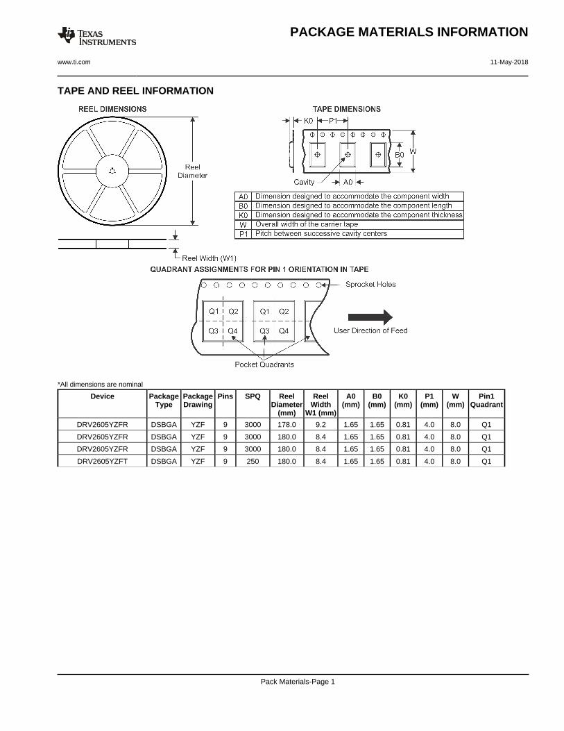
TAPE AND REEL INFORMATION
*All dimensions are nominal
Device PackageType
PackageDrawing
Pins SPQ ReelDiameter
(mm)
ReelWidth
W1 (mm)
A0(mm)
B0(mm)
K0(mm)
P1(mm)
W(mm)
Pin1Quadrant
DRV2605YZFR DSBGA YZF 9 3000 178.0 9.2 1.65 1.65 0.81 4.0 8.0 Q1
DRV2605YZFR DSBGA YZF 9 3000 180.0 8.4 1.65 1.65 0.81 4.0 8.0 Q1
DRV2605YZFR DSBGA YZF 9 3000 180.0 8.4 1.65 1.65 0.81 4.0 8.0 Q1
DRV2605YZFT DSBGA YZF 9 250 180.0 8.4 1.65 1.65 0.81 4.0 8.0 Q1
PACKAGE MATERIALS INFORMATION
www.ti.com 11-May-2018
Pack Materials-Page 1

*All dimensions are nominal
Device Package Type Package Drawing Pins SPQ Length (mm) Width (mm) Height (mm)
DRV2605YZFR DSBGA YZF 9 3000 270.0 225.0 227.0
DRV2605YZFR DSBGA YZF 9 3000 182.0 182.0 20.0
DRV2605YZFR DSBGA YZF 9 3000 182.0 182.0 20.0
DRV2605YZFT DSBGA YZF 9 250 182.0 182.0 20.0
PACKAGE MATERIALS INFORMATION
www.ti.com 11-May-2018
Pack Materials-Page 2

IMPORTANT NOTICE
Texas Instruments Incorporated (TI) reserves the right to make corrections, enhancements, improvements and other changes to itssemiconductor products and services per JESD46, latest issue, and to discontinue any product or service per JESD48, latest issue. Buyersshould obtain the latest relevant information before placing orders and should verify that such information is current and complete.TI’s published terms of sale for semiconductor products (http://www.ti.com/sc/docs/stdterms.htm) apply to the sale of packaged integratedcircuit products that TI has qualified and released to market. Additional terms may apply to the use or sale of other types of TI products andservices.Reproduction of significant portions of TI information in TI data sheets is permissible only if reproduction is without alteration and isaccompanied by all associated warranties, conditions, limitations, and notices. TI is not responsible or liable for such reproduceddocumentation. Information of third parties may be subject to additional restrictions. Resale of TI products or services with statementsdifferent from or beyond the parameters stated by TI for that product or service voids all express and any implied warranties for theassociated TI product or service and is an unfair and deceptive business practice. TI is not responsible or liable for any such statements.Buyers and others who are developing systems that incorporate TI products (collectively, “Designers”) understand and agree that Designersremain responsible for using their independent analysis, evaluation and judgment in designing their applications and that Designers havefull and exclusive responsibility to assure the safety of Designers' applications and compliance of their applications (and of all TI productsused in or for Designers’ applications) with all applicable regulations, laws and other applicable requirements. Designer represents that, withrespect to their applications, Designer has all the necessary expertise to create and implement safeguards that (1) anticipate dangerousconsequences of failures, (2) monitor failures and their consequences, and (3) lessen the likelihood of failures that might cause harm andtake appropriate actions. Designer agrees that prior to using or distributing any applications that include TI products, Designer willthoroughly test such applications and the functionality of such TI products as used in such applications.TI’s provision of technical, application or other design advice, quality characterization, reliability data or other services or information,including, but not limited to, reference designs and materials relating to evaluation modules, (collectively, “TI Resources”) are intended toassist designers who are developing applications that incorporate TI products; by downloading, accessing or using TI Resources in anyway, Designer (individually or, if Designer is acting on behalf of a company, Designer’s company) agrees to use any particular TI Resourcesolely for this purpose and subject to the terms of this Notice.TI’s provision of TI Resources does not expand or otherwise alter TI’s applicable published warranties or warranty disclaimers for TIproducts, and no additional obligations or liabilities arise from TI providing such TI Resources. TI reserves the right to make corrections,enhancements, improvements and other changes to its TI Resources. TI has not conducted any testing other than that specificallydescribed in the published documentation for a particular TI Resource.Designer is authorized to use, copy and modify any individual TI Resource only in connection with the development of applications thatinclude the TI product(s) identified in such TI Resource. NO OTHER LICENSE, EXPRESS OR IMPLIED, BY ESTOPPEL OR OTHERWISETO ANY OTHER TI INTELLECTUAL PROPERTY RIGHT, AND NO LICENSE TO ANY TECHNOLOGY OR INTELLECTUAL PROPERTYRIGHT OF TI OR ANY THIRD PARTY IS GRANTED HEREIN, including but not limited to any patent right, copyright, mask work right, orother intellectual property right relating to any combination, machine, or process in which TI products or services are used. Informationregarding or referencing third-party products or services does not constitute a license to use such products or services, or a warranty orendorsement thereof. Use of TI Resources may require a license from a third party under the patents or other intellectual property of thethird party, or a license from TI under the patents or other intellectual property of TI.TI RESOURCES ARE PROVIDED “AS IS” AND WITH ALL FAULTS. TI DISCLAIMS ALL OTHER WARRANTIES ORREPRESENTATIONS, EXPRESS OR IMPLIED, REGARDING RESOURCES OR USE THEREOF, INCLUDING BUT NOT LIMITED TOACCURACY OR COMPLETENESS, TITLE, ANY EPIDEMIC FAILURE WARRANTY AND ANY IMPLIED WARRANTIES OFMERCHANTABILITY, FITNESS FOR A PARTICULAR PURPOSE, AND NON-INFRINGEMENT OF ANY THIRD PARTY INTELLECTUALPROPERTY RIGHTS. TI SHALL NOT BE LIABLE FOR AND SHALL NOT DEFEND OR INDEMNIFY DESIGNER AGAINST ANY CLAIM,INCLUDING BUT NOT LIMITED TO ANY INFRINGEMENT CLAIM THAT RELATES TO OR IS BASED ON ANY COMBINATION OFPRODUCTS EVEN IF DESCRIBED IN TI RESOURCES OR OTHERWISE. IN NO EVENT SHALL TI BE LIABLE FOR ANY ACTUAL,DIRECT, SPECIAL, COLLATERAL, INDIRECT, PUNITIVE, INCIDENTAL, CONSEQUENTIAL OR EXEMPLARY DAMAGES INCONNECTION WITH OR ARISING OUT OF TI RESOURCES OR USE THEREOF, AND REGARDLESS OF WHETHER TI HAS BEENADVISED OF THE POSSIBILITY OF SUCH DAMAGES.Unless TI has explicitly designated an individual product as meeting the requirements of a particular industry standard (e.g., ISO/TS 16949and ISO 26262), TI is not responsible for any failure to meet such industry standard requirements.Where TI specifically promotes products as facilitating functional safety or as compliant with industry functional safety standards, suchproducts are intended to help enable customers to design and create their own applications that meet applicable functional safety standardsand requirements. Using products in an application does not by itself establish any safety features in the application. Designers mustensure compliance with safety-related requirements and standards applicable to their applications. Designer may not use any TI products inlife-critical medical equipment unless authorized officers of the parties have executed a special contract specifically governing such use.Life-critical medical equipment is medical equipment where failure of such equipment would cause serious bodily injury or death (e.g., lifesupport, pacemakers, defibrillators, heart pumps, neurostimulators, and implantables). Such equipment includes, without limitation, allmedical devices identified by the U.S. Food and Drug Administration as Class III devices and equivalent classifications outside the U.S.TI may expressly designate certain products as completing a particular qualification (e.g., Q100, Military Grade, or Enhanced Product).Designers agree that it has the necessary expertise to select the product with the appropriate qualification designation for their applicationsand that proper product selection is at Designers’ own risk. Designers are solely responsible for compliance with all legal and regulatoryrequirements in connection with such selection.Designer will fully indemnify TI and its representatives against any damages, costs, losses, and/or liabilities arising out of Designer’s non-compliance with the terms and provisions of this Notice.
Mailing Address: Texas Instruments, Post Office Box 655303, Dallas, Texas 75265Copyright © 2018, Texas Instruments Incorporated
Related Documents