Drive current enhancement in tunnel field-effect transistors by graded heterojunction approach Nguyen Dang Chien and Luu The Vinh Citation: J. Appl. Phys. 114, 094507 (2013); doi: 10.1063/1.4820011 View online: http://dx.doi.org/10.1063/1.4820011 View Table of Contents: http://jap.aip.org/resource/1/JAPIAU/v114/i9 Published by the AIP Publishing LLC. Additional information on J. Appl. Phys. Journal Homepage: http://jap.aip.org/ Journal Information: http://jap.aip.org/about/about_the_journal Top downloads: http://jap.aip.org/features/most_downloaded Information for Authors: http://jap.aip.org/authors

Welcome message from author
This document is posted to help you gain knowledge. Please leave a comment to let me know what you think about it! Share it to your friends and learn new things together.
Transcript
Drive current enhancement in tunnel field-effect transistors by gradedheterojunction approachNguyen Dang Chien and Luu The Vinh Citation: J. Appl. Phys. 114, 094507 (2013); doi: 10.1063/1.4820011 View online: http://dx.doi.org/10.1063/1.4820011 View Table of Contents: http://jap.aip.org/resource/1/JAPIAU/v114/i9 Published by the AIP Publishing LLC. Additional information on J. Appl. Phys.Journal Homepage: http://jap.aip.org/ Journal Information: http://jap.aip.org/about/about_the_journal Top downloads: http://jap.aip.org/features/most_downloaded Information for Authors: http://jap.aip.org/authors
Drive current enhancement in tunnel field-effect transistors by gradedheterojunction approach
Nguyen Dang Chien1,2,a) and Luu The Vinh3
1Department of Electrical Engineering, National Chi Nan University, Nantou 54561, Taiwan2Faculty of Physics, University of Da Lat, Lam Dong 671463, Vietnam3Faculty of Electronic Technology, Industrial University of Ho Chi Minh City,Ho Chi Minh City 727905, Vietnam
(Received 26 June 2013; accepted 16 August 2013; published online 4 September 2013)
The heterostructure technique has recently demonstrated an excellent solution to resolve the
trade-off between on- and off-state currents in tunnel field-effect transistors (TFETs). This
paper shows the weakness of abrupt heterojunctions and explores the physics of drive current
enhancement as well as generalizes the proposed graded heterojunction approach in both n-type
and p-type TFETs. It is shown that the presence of thermal emission barriers formed by abrupt
band offsets is the physical reason of the on-current lowering observed in abrupt heterojunction
TFETs. By employing graded heterojunctions in TFETs, the thermal emission barriers for
electrons and holes are completely eliminated to narrow the tunnel widths in n-type and p-type
TFETs, respectively. With the significant improvement in on-current, this novel approach of
graded heterojunctions provides an effective technique for enhancing the drive current in
heterostructure-based TFET devices. VC 2013 AIP Publishing LLC.
[http://dx.doi.org/10.1063/1.4820011]
I. INTRODUCTION
With an achievable sub-60 mV/decade subthreshold
swing at room-temperature, which is impossible in conven-
tional metal-oxide-semiconductor field-effect transistors
(MOSFETs) due to the kT/q limit, tunnel field-effect transis-
tors (TFETs) have been considered as an excellent alterna-
tive in ultra-scaled power integrated circuits.1,2 Always
operated in highly reversed conditions of p-n junctions,
TFETs also present a significantly low power dissipation
which is generally a critical issue in regular MOSFETs when
scaling into sub-100 nm regimes.3,4 Instead of applying the
electric field, in the other hand, the conduction current in
TFETs is essentially generated by the band-to-band tunnel-
ing (BTBT) of carriers through the forbidden-band gap. The
tunnel barrier and hence the tunnel probability are mainly
governed by the applied voltage to produce an ideal on-off
switching with a steep subthreshold swing.2,5 Furthermore,
TFETs also exhibit competitive advantages over standard
MOSFETs in term of scaling devices because of small
tunneling regions.6,7
Although numerous advanced techniques have been
proposed to more effectively control the tunnel width,5,8,9
Si-based TFETs exhibit a low on-state current because of
the high-bandgap of silicon. Enhancing the on-current
becomes the most challenge in TFET devices. To improve
the on-current and to suppress the ambipolar off-state
leakage, asymmetric structures of abrupt heterojunctions
using low-bandgap materials, such as SiGe and InGaAs,
have been introduced to TFETs.10,11 Since the bandgap
decreases with increasing Ge (In) concentration in SiGe
(InGaAs), it is expected that a higher Ge (In) concentration
can lead to a higher on-state tunneling current.10,12 In
abrupt Si/Si1�xGex p-type TFETs, however, increasing Ge
mole fraction is only helpful in increasing the on-current
up to a medium fraction approximately 0.3.13 The continu-
ing increase in the Ge fraction, by contrast, degrades the
on-current. This on-current lowering limits the exploitation
of the low-bandgap of Ge-rich source for enhancing
the tunneling current. Although it is phenomenologically
explained to be due to the extension of the tunnel width
at high Ge concentrations,6,13 the physical reason of the
tunnel width extension has not been adequately clarified.
Therefore, it is difficult to explain why the on-current low-
ering does not occur in SiGe-source n-type TFETs.10,14
Additionally, previous publications6,15 have shown that the
on-current lowering in abrupt Si/SiGe p-type TFETs can be
resolved by applying the graded heterojunction technique,
but the physical reason still remains uncertainty. The cur-
rent enhancement in graded p-type TFETs is simply attrib-
uted to the narrowed tunnel barriers. However, the question
why the tunnel barriers are narrowed has not been properly
understood. It is problematic to affirm whether the graded
heterojunctions are benefitable and when they are needed
in n-type TFET devices to enhance the on-current.
Consequently, the application of graded heterojunctions in
n-type TFETs has not been reported so far.
By two-dimensional simulations,16 this paper elucidates
the physics insight of the abrupt heterojunction limitation
and explores the physical principle of the drive current
enhancement by graded heterojunctions. With the physical
mechanism clarified in abrupt p-type TFETs, the on-current
lowering can similarly be predicted and relevant explana-
tions can be made for abrupt n-type TFETs. Importantly,
graded heterojunctions have been numerically demonstrated
a)Author to whom correspondence should be addressed. Electronic mail:
0021-8979/2013/114(9)/094507/6/$30.00 VC 2013 AIP Publishing LLC114, 094507-1
JOURNAL OF APPLIED PHYSICS 114, 094507 (2013)
in n-type TFETs to generalize the graded heterojunction
approach for use in both n-type and p-type TFETs to resolve
the weakness of abrupt heterojunctions. The paper is divided
into five sections, including the Introduction (Sec. I) and the
Conclusion (Sec. V). Section II describes the device archi-
tectures and the physical models used in the study. The
weakness of abrupt heterojunctions is presented in Sec. III,
whereas the physical principle of current enhancement by
graded heterojunctions is clarified in Sec. IV.
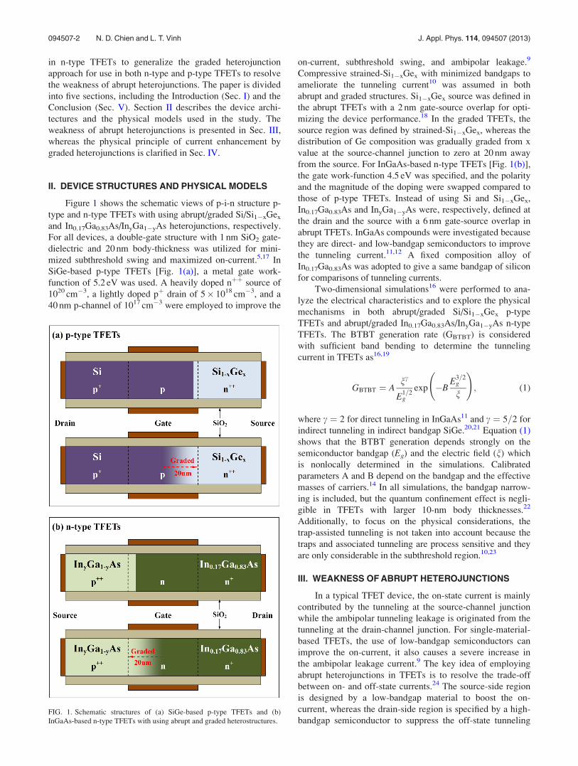
II. DEVICE STRUCTURES AND PHYSICAL MODELS
Figure 1 shows the schematic views of p-i-n structure p-
type and n-type TFETs with using abrupt/graded Si/Si1�xGex
and In0.17Ga0.83As/InyGa1�yAs heterojunctions, respectively.
For all devices, a double-gate structure with 1 nm SiO2 gate-
dielectric and 20 nm body-thickness was utilized for mini-
mized subthreshold swing and maximized on-current.5,17 In
SiGe-based p-type TFETs [Fig. 1(a)], a metal gate work-
function of 5.2 eV was used. A heavily doped nþþ source of
1020 cm�3, a lightly doped pþ drain of 5� 1018 cm�3, and a
40 nm p-channel of 1017 cm�3 were employed to improve the
on-current, subthreshold swing, and ambipolar leakage.9
Compressive strained-Si1�xGex with minimized bandgaps to
ameliorate the tunneling current10 was assumed in both
abrupt and graded structures. Si1�xGex source was defined in
the abrupt TFETs with a 2 nm gate-source overlap for opti-
mizing the device performance.18 In the graded TFETs, the
source region was defined by strained-Si1�xGex, whereas the
distribution of Ge composition was gradually graded from x
value at the source-channel junction to zero at 20 nm away
from the source. For InGaAs-based n-type TFETs [Fig. 1(b)],
the gate work-function 4.5 eV was specified, and the polarity
and the magnitude of the doping were swapped compared to
those of p-type TFETs. Instead of using Si and Si1�xGex,
In0.17Ga0.83As and InyGa1�yAs were, respectively, defined at
the drain and the source with a 6 nm gate-source overlap in
abrupt TFETs. InGaAs compounds were investigated because
they are direct- and low-bandgap semiconductors to improve
the tunneling current.11,12 A fixed composition alloy of
In0.17Ga0.83As was adopted to give a same bandgap of silicon
for comparisons of tunneling currents.
Two-dimensional simulations16 were performed to ana-
lyze the electrical characteristics and to explore the physical
mechanisms in both abrupt/graded Si/Si1�xGex p-type
TFETs and abrupt/graded In0.17Ga0.83As/InyGa1�yAs n-type
TFETs. The BTBT generation rate (GBTBT) is considered
with sufficient band bending to determine the tunneling
current in TFETs as16,19
GBTBT ¼ Anc
E1=2g
exp �BE
3=2g
n
!; (1)
where c ¼ 2 for direct tunneling in InGaAs11 and c ¼ 5=2 for
indirect tunneling in indirect bandgap SiGe.20,21 Equation (1)
shows that the BTBT generation depends strongly on the
semiconductor bandgap (Eg) and the electric field (n) which
is nonlocally determined in the simulations. Calibrated
parameters A and B depend on the bandgap and the effective
masses of carriers.14 In all simulations, the bandgap narrow-
ing is included, but the quantum confinement effect is negli-
gible in TFETs with larger 10-nm body thicknesses.22
Additionally, to focus on the physical considerations, the
trap-assisted tunneling is not taken into account because the
traps and associated tunneling are process sensitive and they
are only considerable in the subthreshold region.10,23
III. WEAKNESS OF ABRUPT HETEROJUNCTIONS
In a typical TFET device, the on-state current is mainly
contributed by the tunneling at the source-channel junction
while the ambipolar tunneling leakage is originated from the
tunneling at the drain-channel junction. For single-material-
based TFETs, the use of low-bandgap semiconductors can
improve the on-current, it also causes a severe increase in
the ambipolar leakage current.9 The key idea of employing
abrupt heterojunctions in TFETs is to resolve the trade-off
between on- and off-state currents.24 The source-side region
is designed by a low-bandgap material to boost the on-
current, whereas the drain-side region is specified by a high-
bandgap semiconductor to suppress the off-state tunnelingFIG. 1. Schematic structures of (a) SiGe-based p-type TFETs and (b)
InGaAs-based n-type TFETs with using abrupt and graded heterostructures.
094507-2 N. D. Chien and L. T. Vinh J. Appl. Phys. 114, 094507 (2013)
current. The interface of high- and low-bandgap materials
has to be located within the channel. To optimize the on- and
off-currents, the heterojunction should be overlapped several
nanometers by the gate.18 Owing to the direct contact of two
different band structure materials, abrupt conduction and
valence band offsets are formed at the abrupt heterojunction
interface. These abrupt band offsets with specific situations
limit the use of low-bandgap materials to enhance the
on-current in abrupt heterojunction-based TFETs as shown
in this section.
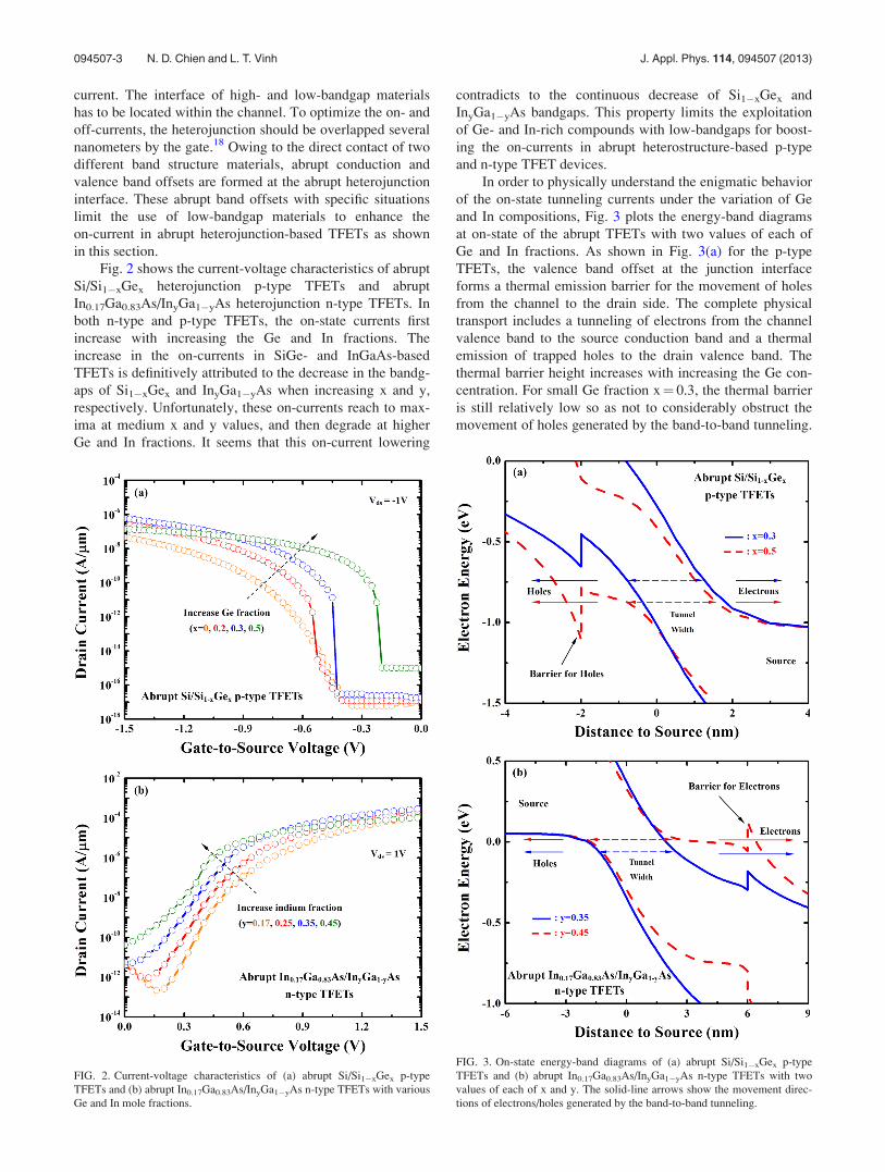
Fig. 2 shows the current-voltage characteristics of abrupt
Si/Si1�xGex heterojunction p-type TFETs and abrupt
In0.17Ga0.83As/InyGa1�yAs heterojunction n-type TFETs. In
both n-type and p-type TFETs, the on-state currents first
increase with increasing the Ge and In fractions. The
increase in the on-currents in SiGe- and InGaAs-based
TFETs is definitively attributed to the decrease in the bandg-
aps of Si1�xGex and InyGa1�yAs when increasing x and y,
respectively. Unfortunately, these on-currents reach to max-
ima at medium x and y values, and then degrade at higher
Ge and In fractions. It seems that this on-current lowering
contradicts to the continuous decrease of Si1�xGex and
InyGa1�yAs bandgaps. This property limits the exploitation
of Ge- and In-rich compounds with low-bandgaps for boost-
ing the on-currents in abrupt heterostructure-based p-type
and n-type TFET devices.
In order to physically understand the enigmatic behavior
of the on-state tunneling currents under the variation of Ge
and In compositions, Fig. 3 plots the energy-band diagrams
at on-state of the abrupt TFETs with two values of each of
Ge and In fractions. As shown in Fig. 3(a) for the p-type
TFETs, the valence band offset at the junction interface
forms a thermal emission barrier for the movement of holes
from the channel to the drain side. The complete physical
transport includes a tunneling of electrons from the channel
valence band to the source conduction band and a thermal
emission of trapped holes to the drain valence band. The
thermal barrier height increases with increasing the Ge con-
centration. For small Ge fraction x¼ 0.3, the thermal barrier
is still relatively low so as not to considerably obstruct the
movement of holes generated by the band-to-band tunneling.
FIG. 2. Current-voltage characteristics of (a) abrupt Si/Si1�xGex p-type
TFETs and (b) abrupt In0.17Ga0.83As/InyGa1�yAs n-type TFETs with various
Ge and In mole fractions.
FIG. 3. On-state energy-band diagrams of (a) abrupt Si/Si1�xGex p-type
TFETs and (b) abrupt In0.17Ga0.83As/InyGa1�yAs n-type TFETs with two
values of each of x and y. The solid-line arrows show the movement direc-
tions of electrons/holes generated by the band-to-band tunneling.
094507-3 N. D. Chien and L. T. Vinh J. Appl. Phys. 114, 094507 (2013)
In high Ge fraction x¼ 0.5 TFET, the high thermal barrier
severely obstructs holes to move from the channel to the
drain. Numerous holes stuck in the well mitigate the band
bending in the channel, which consequently causes an
extended tunnel barrier and a narrowed tunneling region.
Therefore, the on-state tunneling current is decreased in
x¼ 0.5 TFET irrespective of the decreased bandgap. The
decrease in the bandgap is only helpful till a relatively small
value of Ge fraction. Based on understanding the physical
mechanism of the on-current lowering in the p-type TFETs,
a similar situation can be predicted and relevant explanations
can be made for the n-type TFETs in Fig. 3(b). Since the
band offset of In0.17Ga0.83As/InyGa1�yAs heterojunctions
considerably occurs at the conduction band, significant
thermal barriers for electrons are formed in abrupt
In0.17Ga0.83As/InyGa1�yAs heterojunctions. The complete
physical transport in these abrupt heterojunction n-type
TFETs includes a tunneling of electrons from the source
valence band to the channel conduction band followed by a
thermal emission of trapped electrons to the drain conduction
band. Holes generated in the tunneling process move back-
ward to the source. A higher In mole fraction causes a higher
thermal barrier which explains for the current lowering in
the In-rich TFET. Notably, in the n-type TFETs, only con-
duction band offset forms a thermal barrier for electrons,
whereas the valence band offset does not influence the flow
of electrons and holes at all. Similarly in the p-type TFETs,
only valence band offset causes an undesirable thermal
barrier for holes. Therefore, it can be generalized that the
on-current lowering only occurs in abrupt heterojunction
n- and p-type TFETs if the conduction and valence band
offsets are significant in abrupt heterojunctions, respectively.
Because most of the band offset of silicon-germanium heter-
ojunctions occurs at the valence band, the conduction
band offset is negligible. The on-current lowering can only
be observed in abrupt Si/Si1�xGex p-type TFETs. No such
on-current lowering is observed in n-type TFET
counterparts.10,14
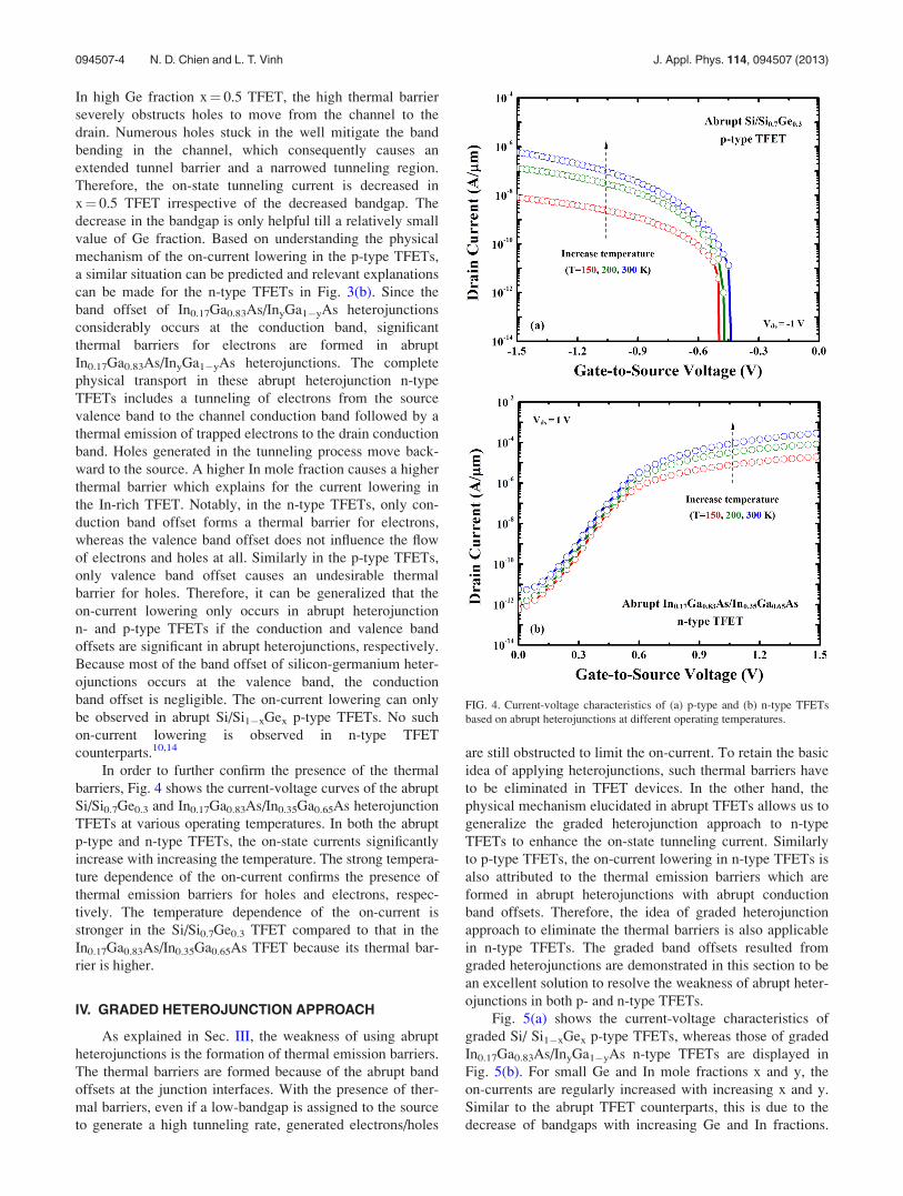
In order to further confirm the presence of the thermal
barriers, Fig. 4 shows the current-voltage curves of the abrupt
Si/Si0.7Ge0.3 and In0.17Ga0.83As/In0.35Ga0.65As heterojunction
TFETs at various operating temperatures. In both the abrupt
p-type and n-type TFETs, the on-state currents significantly
increase with increasing the temperature. The strong tempera-
ture dependence of the on-current confirms the presence of
thermal emission barriers for holes and electrons, respec-
tively. The temperature dependence of the on-current is
stronger in the Si/Si0.7Ge0.3 TFET compared to that in the
In0.17Ga0.83As/In0.35Ga0.65As TFET because its thermal bar-
rier is higher.
IV. GRADED HETEROJUNCTION APPROACH
As explained in Sec. III, the weakness of using abrupt
heterojunctions is the formation of thermal emission barriers.
The thermal barriers are formed because of the abrupt band
offsets at the junction interfaces. With the presence of ther-
mal barriers, even if a low-bandgap is assigned to the source
to generate a high tunneling rate, generated electrons/holes
are still obstructed to limit the on-current. To retain the basic
idea of applying heterojunctions, such thermal barriers have
to be eliminated in TFET devices. In the other hand, the
physical mechanism elucidated in abrupt TFETs allows us to
generalize the graded heterojunction approach to n-type
TFETs to enhance the on-state tunneling current. Similarly
to p-type TFETs, the on-current lowering in n-type TFETs is
also attributed to the thermal emission barriers which are
formed in abrupt heterojunctions with abrupt conduction
band offsets. Therefore, the idea of graded heterojunction
approach to eliminate the thermal barriers is also applicable
in n-type TFETs. The graded band offsets resulted from
graded heterojunctions are demonstrated in this section to be
an excellent solution to resolve the weakness of abrupt heter-
ojunctions in both p- and n-type TFETs.
Fig. 5(a) shows the current-voltage characteristics of
graded Si/ Si1�xGex p-type TFETs, whereas those of graded
In0.17Ga0.83As/InyGa1�yAs n-type TFETs are displayed in
Fig. 5(b). For small Ge and In mole fractions x and y, the
on-currents are regularly increased with increasing x and y.
Similar to the abrupt TFET counterparts, this is due to the
decrease of bandgaps with increasing Ge and In fractions.
FIG. 4. Current-voltage characteristics of (a) p-type and (b) n-type TFETs
based on abrupt heterojunctions at different operating temperatures.
094507-4 N. D. Chien and L. T. Vinh J. Appl. Phys. 114, 094507 (2013)
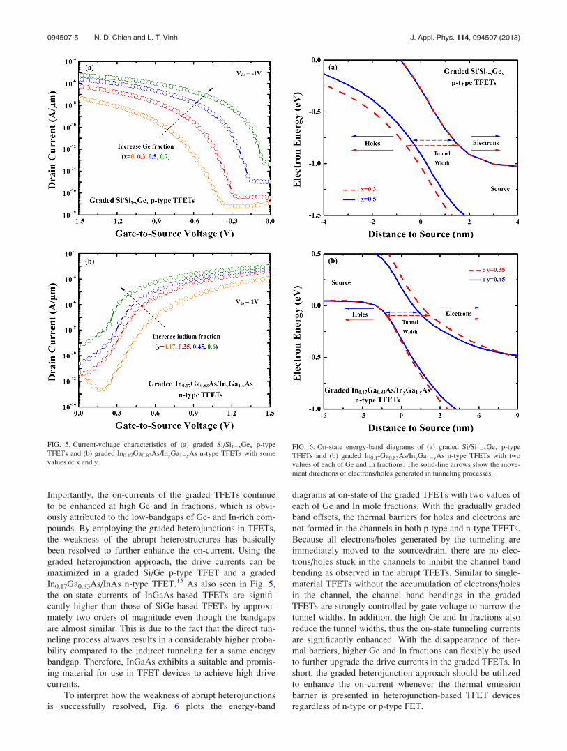
Importantly, the on-currents of the graded TFETs continue
to be enhanced at high Ge and In fractions, which is obvi-
ously attributed to the low-bandgaps of Ge- and In-rich com-
pounds. By employing the graded heterojunctions in TFETs,
the weakness of the abrupt heterostructures has basically
been resolved to further enhance the on-current. Using the
graded heterojunction approach, the drive currents can be
maximized in a graded Si/Ge p-type TFET and a graded
In0.17Ga0.83As/InAs n-type TFET.15 As also seen in Fig. 5,
the on-state currents of InGaAs-based TFETs are signifi-
cantly higher than those of SiGe-based TFETs by approxi-
mately two orders of magnitude even though the bandgaps
are almost similar. This is due to the fact that the direct tun-
neling process always results in a considerably higher proba-
bility compared to the indirect tunneling for a same energy
bandgap. Therefore, InGaAs exhibits a suitable and promis-
ing material for use in TFET devices to achieve high drive
currents.
To interpret how the weakness of abrupt heterojunctions
is successfully resolved, Fig. 6 plots the energy-band
diagrams at on-state of the graded TFETs with two values of
each of Ge and In mole fractions. With the gradually graded
band offsets, the thermal barriers for holes and electrons are
not formed in the channels in both p-type and n-type TFETs.
Because all electrons/holes generated by the tunneling are
immediately moved to the source/drain, there are no elec-
trons/holes stuck in the channels to inhibit the channel band
bending as observed in the abrupt TFETs. Similar to single-
material TFETs without the accumulation of electrons/holes
in the channel, the channel band bendings in the graded
TFETs are strongly controlled by gate voltage to narrow the
tunnel widths. In addition, the high Ge and In fractions also
reduce the tunnel widths, thus the on-state tunneling currents
are significantly enhanced. With the disappearance of ther-
mal barriers, higher Ge and In fractions can flexibly be used
to further upgrade the drive currents in the graded TFETs. In
short, the graded heterojunction approach should be utilized
to enhance the on-current whenever the thermal emission
barrier is presented in heterojunction-based TFET devices
regardless of n-type or p-type FET.
FIG. 5. Current-voltage characteristics of (a) graded Si/Si1�xGex p-type
TFETs and (b) graded In0.17Ga0.83As/InyGa1�yAs n-type TFETs with some
values of x and y.
FIG. 6. On-state energy-band diagrams of (a) graded Si/Si1�xGex p-type
TFETs and (b) graded In0.17Ga0.83As/InyGa1�yAs n-type TFETs with two
values of each of Ge and In fractions. The solid-line arrows show the move-
ment directions of electrons/holes generated in tunneling processes.
094507-5 N. D. Chien and L. T. Vinh J. Appl. Phys. 114, 094507 (2013)
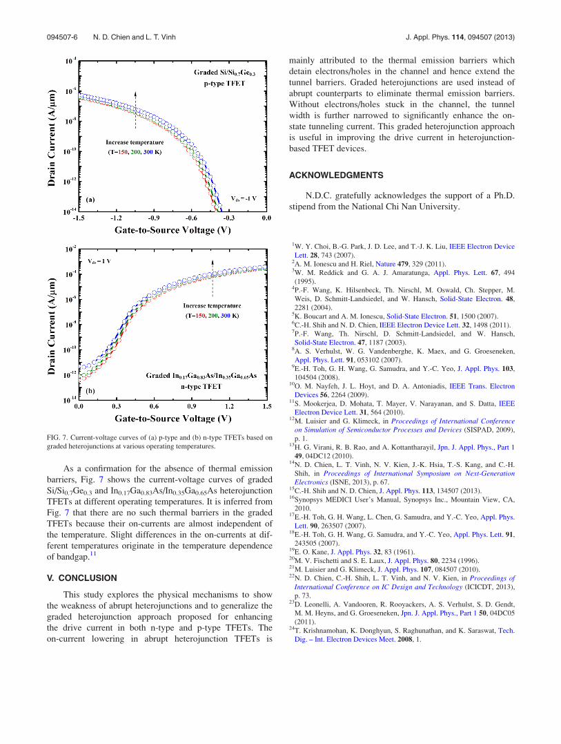
As a confirmation for the absence of thermal emission
barriers, Fig. 7 shows the current-voltage curves of graded
Si/Si0.7Ge0.3 and In0.17Ga0.83As/In0.35Ga0.65As heterojunction
TFETs at different operating temperatures. It is inferred from
Fig. 7 that there are no such thermal barriers in the graded
TFETs because their on-currents are almost independent of
the temperature. Slight differences in the on-currents at dif-
ferent temperatures originate in the temperature dependence
of bandgap.11
V. CONCLUSION
This study explores the physical mechanisms to show
the weakness of abrupt heterojunctions and to generalize the
graded heterojunction approach proposed for enhancing
the drive current in both n-type and p-type TFETs. The
on-current lowering in abrupt heterojunction TFETs is
mainly attributed to the thermal emission barriers which
detain electrons/holes in the channel and hence extend the
tunnel barriers. Graded heterojunctions are used instead of
abrupt counterparts to eliminate thermal emission barriers.
Without electrons/holes stuck in the channel, the tunnel
width is further narrowed to significantly enhance the on-
state tunneling current. This graded heterojunction approach
is useful in improving the drive current in heterojunction-
based TFET devices.
ACKNOWLEDGMENTS
N.D.C. gratefully acknowledges the support of a Ph.D.
stipend from the National Chi Nan University.
1W. Y. Choi, B.-G. Park, J. D. Lee, and T.-J. K. Liu, IEEE Electron Device
Lett. 28, 743 (2007).2A. M. Ionescu and H. Riel, Nature 479, 329 (2011).3W. M. Reddick and G. A. J. Amaratunga, Appl. Phys. Lett. 67, 494
(1995).4P.-F. Wang, K. Hilsenbeck, Th. Nirschl, M. Oswald, Ch. Stepper, M.
Weis, D. Schmitt-Landsiedel, and W. Hansch, Solid-State Electron. 48,
2281 (2004).5K. Boucart and A. M. Ionescu, Solid-State Electron. 51, 1500 (2007).6C.-H. Shih and N. D. Chien, IEEE Electron Device Lett. 32, 1498 (2011).7P.-F. Wang, Th. Nirschl, D. Schmitt-Landsiedel, and W. Hansch,
Solid-State Electron. 47, 1187 (2003).8A. S. Verhulst, W. G. Vandenberghe, K. Maex, and G. Groeseneken,
Appl. Phys. Lett. 91, 053102 (2007).9E.-H. Toh, G. H. Wang, G. Samudra, and Y.-C. Yeo, J. Appl. Phys. 103,
104504 (2008).10O. M. Nayfeh, J. L. Hoyt, and D. A. Antoniadis, IEEE Trans. Electron
Devices 56, 2264 (2009).11S. Mookerjea, D. Mohata, T. Mayer, V. Narayanan, and S. Datta, IEEE
Electron Device Lett. 31, 564 (2010).12M. Luisier and G. Klimeck, in Proceedings of International Conference
on Simulation of Semiconductor Processes and Devices (SISPAD, 2009),
p. 1.13H. G. Virani, R. B. Rao, and A. Kottantharayil, Jpn. J. Appl. Phys., Part 1
49, 04DC12 (2010).14N. D. Chien, L. T. Vinh, N. V. Kien, J.-K. Hsia, T.-S. Kang, and C.-H.
Shih, in Proceedings of International Symposium on Next-GenerationElectronics (ISNE, 2013), p. 67.
15C.-H. Shih and N. D. Chien, J. Appl. Phys. 113, 134507 (2013).16Synopsys MEDICI User’s Manual, Synopsys Inc., Mountain View, CA,
2010.17E.-H. Toh, G. H. Wang, L. Chen, G. Samudra, and Y.-C. Yeo, Appl. Phys.
Lett. 90, 263507 (2007).18E.-H. Toh, G. H. Wang, G. Samudra, and Y.-C. Yeo, Appl. Phys. Lett. 91,
243505 (2007).19E. O. Kane, J. Appl. Phys. 32, 83 (1961).20M. V. Fischetti and S. E. Laux, J. Appl. Phys. 80, 2234 (1996).21M. Luisier and G. Klimeck, J. Appl. Phys. 107, 084507 (2010).22N. D. Chien, C.-H. Shih, L. T. Vinh, and N. V. Kien, in Proceedings of
International Conference on IC Design and Technology (ICICDT, 2013),
p. 73.23D. Leonelli, A. Vandooren, R. Rooyackers, A. S. Verhulst, S. D. Gendt,
M. M. Heyns, and G. Groeseneken, Jpn. J. Appl. Phys., Part 1 50, 04DC05
(2011).24T. Krishnamohan, K. Donghyun, S. Raghunathan, and K. Saraswat, Tech.
Dig. – Int. Electron Devices Meet. 2008, 1.
FIG. 7. Current-voltage curves of (a) p-type and (b) n-type TFETs based on
graded heterojunctions at various operating temperatures.
094507-6 N. D. Chien and L. T. Vinh J. Appl. Phys. 114, 094507 (2013)
Related Documents


