1 SPRUIB9 – December 2016 Submit Documentation Feedback Copyright © 2016, Texas Instruments Incorporated DRA72x EVM CPU Board User's Guide User's Guide SPRUIB9 – December 2016 DRA72x EVM CPU Board User's Guide Contents 1 Introduction ................................................................................................................... 3 2 Overview ...................................................................................................................... 3 3 Hardware...................................................................................................................... 9 4 Signal Multiplex Logic...................................................................................................... 23 5 USB3-Supported Configurations ......................................................................................... 31 6 References .................................................................................................................. 34 List of Figures 1 CPU Board ................................................................................................................... 4 2 CPU Board – Front .......................................................................................................... 7 3 CPU Board – Back .......................................................................................................... 8 4 CPU Board Block Diagram ................................................................................................. 9 5 Power Distribution Block Diagram ....................................................................................... 10 6 Reset Structure ............................................................................................................. 11 7 SoC Pinmux for GPMC and QSPI ....................................................................................... 24 8 Mux Diagram for GPMC and QSPI ...................................................................................... 24 9 SoC Pinmux for GPMC/VIN1/VOUT3 .................................................................................. 25 10 Mux Diagram for GPMC/VIN1/VOUT3 .................................................................................. 26 11 SoC Pinmux for GPMC/EMMC ........................................................................................... 26 12 Mux Diagram for GPMC and EMMC .................................................................................... 27 13 SoC Pinmux for VIN2A and EMU ........................................................................................ 27 14 Mux Diagram for VIN2A and EMU ....................................................................................... 28 15 SoC Pinmux for VIN2A and RGMII1..................................................................................... 28 16 Mux Diagram for VIN2A and RGMII1.................................................................................... 29 17 SoC Pinmux for RGMII0 and VIN1B..................................................................................... 29 18 Mux Diagram for RGMII0 and VIN1B.................................................................................... 30 19 SoC Pinmux for SPI2 and UART3 ....................................................................................... 30 20 Mux Diagram for SPI2 and UART3 ...................................................................................... 30 21 SoC Pinmux for DCAN2 ................................................................................................... 31 22 Mux Diagram for DCAN2 and I2C ....................................................................................... 31 23 Option 1 ..................................................................................................................... 32 24 Option 2 ..................................................................................................................... 33 25 Option 3...................................................................................................................... 34 List of Tables 1 EVM Wake-Up Board and Kits (Obsolete) ............................................................................... 4 2 Production Boards (Obsolete).............................................................................................. 5 3 Production Kits (Obsolete).................................................................................................. 5 4 EVM Wake-Up Board and Kits (Production) ............................................................................. 5 5 Production Boards (Production) ........................................................................................... 5

Welcome message from author
This document is posted to help you gain knowledge. Please leave a comment to let me know what you think about it! Share it to your friends and learn new things together.
Transcript
1SPRUIB9–December 2016Submit Documentation Feedback
Copyright © 2016, Texas Instruments Incorporated
DRA72x EVM CPU Board User's Guide
User's GuideSPRUIB9–December 2016
DRA72x EVM CPU Board User's Guide
Contents1 Introduction ................................................................................................................... 32 Overview ...................................................................................................................... 33 Hardware...................................................................................................................... 94 Signal Multiplex Logic...................................................................................................... 235 USB3-Supported Configurations ......................................................................................... 316 References .................................................................................................................. 34
List of Figures
1 CPU Board ................................................................................................................... 42 CPU Board – Front .......................................................................................................... 73 CPU Board – Back .......................................................................................................... 84 CPU Board Block Diagram ................................................................................................. 95 Power Distribution Block Diagram ....................................................................................... 106 Reset Structure ............................................................................................................. 117 SoC Pinmux for GPMC and QSPI ....................................................................................... 248 Mux Diagram for GPMC and QSPI ...................................................................................... 249 SoC Pinmux for GPMC/VIN1/VOUT3 .................................................................................. 2510 Mux Diagram for GPMC/VIN1/VOUT3 .................................................................................. 2611 SoC Pinmux for GPMC/EMMC........................................................................................... 2612 Mux Diagram for GPMC and EMMC .................................................................................... 2713 SoC Pinmux for VIN2A and EMU ........................................................................................ 2714 Mux Diagram for VIN2A and EMU ....................................................................................... 2815 SoC Pinmux for VIN2A and RGMII1..................................................................................... 2816 Mux Diagram for VIN2A and RGMII1.................................................................................... 2917 SoC Pinmux for RGMII0 and VIN1B..................................................................................... 2918 Mux Diagram for RGMII0 and VIN1B.................................................................................... 3019 SoC Pinmux for SPI2 and UART3 ....................................................................................... 3020 Mux Diagram for SPI2 and UART3 ...................................................................................... 3021 SoC Pinmux for DCAN2................................................................................................... 3122 Mux Diagram for DCAN2 and I2C ....................................................................................... 3123 Option 1 ..................................................................................................................... 3224 Option 2 ..................................................................................................................... 3325 Option 3...................................................................................................................... 34
List of Tables
1 EVM Wake-Up Board and Kits (Obsolete) ............................................................................... 42 Production Boards (Obsolete).............................................................................................. 53 Production Kits (Obsolete).................................................................................................. 54 EVM Wake-Up Board and Kits (Production) ............................................................................. 55 Production Boards (Production) ........................................................................................... 5
www.ti.com
2 SPRUIB9–December 2016Submit Documentation Feedback
Copyright © 2016, Texas Instruments Incorporated
DRA72x EVM CPU Board User's Guide
6 Production Kits (Production) ............................................................................................... 57 EVM Kit Truth Table......................................................................................................... 58 EVM Supplies............................................................................................................... 119 Reset Signals Structure ................................................................................................... 1210 SoC Boot Mode Switch Settings ......................................................................................... 1311 Board Controls for Memory Booting Options ........................................................................... 1412 Board Controls for Signaling and Operational Modes................................................................. 1413 User LEDs................................................................................................................... 1714 Power Monitor Mapping ................................................................................................... 1815 I2C Device Address Chart ................................................................................................ 1916 SoC GPIO Map ............................................................................................................. 1917 I/O Expander Map.......................................................................................................... 2018 EEPROM Data Format .................................................................................................... 2219 Onboard Mux Settings and Control ..................................................................................... 23
TrademarksARM, Cortex are registered trademarks of ARM Limited.Bluetooth is a registered trademark of Bluetooth SIG.POWERVR is a trademark of Imagination Technologies Limited.Wi-Fi is a trademark of Wi-Fi Alliance.
www.ti.com Introduction
3SPRUIB9–December 2016Submit Documentation Feedback
Copyright © 2016, Texas Instruments Incorporated
DRA72x EVM CPU Board User's Guide
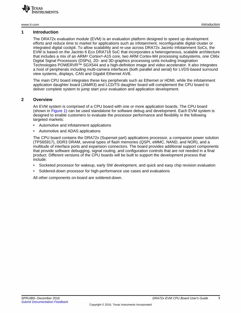
1 IntroductionThe DRA72x evaluation module (EVM) is an evaluation platform designed to speed up developmentefforts and reduce time to market for applications such as infotainment, reconfigurable digital cluster orintegrated digital cockpit. To allow scalability and re-use across DRA72x Jacinto Infotainment SoCs, theEVM is based on the Jacinto 6 Eco DRA718 SoC that incorporates a heterogeneous, scalable architecturethat includes a mix of an ARM® Cortex®-A15 core, two ARM Cortex-M4 processing subsystems, one C66xDigital Signal Processors (DSPs), 2D- and 3D-graphics processing units including ImaginationTechnologies POWERVR™ SGX544 and a high-definition image and video accelerator. It also integratesa host of peripherals including multi-camera interfaces (both parallel and serial) for LVDS-based surroundview systems, displays, CAN and Gigabit Ethernet AVB.
The main CPU board integrates these key peripherals such as Ethernet or HDMI, while the infotainmentapplication daughter board (JAMR3) and LCD/TS daughter board will complement the CPU board todeliver complete system to jump start your evaluation and application development.
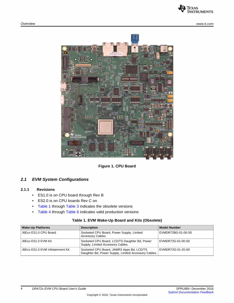
2 OverviewAn EVM system is comprised of a CPU board with one or more application boards. The CPU board(shown in Figure 1) can be used standalone for software debug and development. Each EVM system isdesigned to enable customers to evaluate the processor performance and flexibility in the followingtargeted markets:• Automotive and infotainment applications• Automotive and ADAS applications
The CPU board contains the DRA72x (Superset part) applications processor, a companion power solution(TPS65917), DDR3 DRAM, several types of flash memories (QSPI, eMMC, NAND, and NOR), and amultitude of interface ports and expansion connectors. The board provides additional support componentsthat provide software debugging, signal routing, and configuration controls that are not needed in a finalproduct. Different versions of the CPU boards will be built to support the development process thatinclude:• Socketed processor for wakeup, early SW development, and quick and easy chip revision evaluation• Soldered-down processor for high-performance use cases and evaluations
All other components on-board are soldered-down.
Overview www.ti.com
4 SPRUIB9–December 2016Submit Documentation Feedback
Copyright © 2016, Texas Instruments Incorporated
DRA72x EVM CPU Board User's Guide
Figure 1. CPU Board
2.1 EVM System Configurations
2.1.1 Revisions• ES1.0 is on CPU board through Rev B• ES2.0 is on CPU boards Rev C on• Table 1 through Table 3 indicates the obsolete versions• Table 4 through Table 6 indicates valid production versions
Table 1. EVM Wake-Up Board and Kits (Obsolete)
Wake-Up Platforms Description Model NumberJ6Eco ES1.0 CPU Board Socketed CPU Board, Power Supply, Limited
Accessory Cables.EVMDR72BG-01-00-S0
J6Eco ES1.0 EVM Kit Socketed CPU Board, LCD/TS Daughter Bd, PowerSupply, Limited Accessory Cables.
EVMDR72G-01-00-S0
J6Eco ES1.0 EVM Infotainment Kit Socketed CPU Board, JAMR3 Apps Bd, LCD/TSDaughter Bd, Power Supply, Limited Accessory Cables.
EVMDR72G-01-20-S0
www.ti.com Overview
5SPRUIB9–December 2016Submit Documentation Feedback
Copyright © 2016, Texas Instruments Incorporated
DRA72x EVM CPU Board User's Guide
Table 2. Production Boards (Obsolete)
Production Boards Description Model NumberJ6Eco CPU Bd ES1.0 GP CPU Board, Power Supply, Limited Accessory Cables. EVMDR72BG-01-00-00J6Eco CPU Bd ES1.0 HS CPU Board, Power Supply, Limited Accessory Cables. EVMDR72BH-01-00-00
Table 3. Production Kits (Obsolete)
Production Kits Description Model NumberJ6Eco ES1.0 GP EVM Kit CPU Board, 10.1” LCD/TS Daughter Bd, Power Supply,
Limited Accessory Cables.EVMDR72G-01-01-00
J6Eco ES1.0 GP EVM Infotainment Kit CPU Board, JAMR3 Apps Bd, 10.1” LCD/TS DaughterBd, Power Supply, Limited Accessory Cables.
EVMDR72G-01-21-00
Table 4. EVM Wake-Up Board and Kits (Production)
Wake-Up Platforms Description Model NumberDRA72x/TDA2Ex ES2.0 CPU Bd Socketed CPU Board, and Limited Accessory Cables. EVMDR72BG-02-00-S0
Table 5. Production Boards (Production)
Production Boards Description Model NumberDRA72x/TDA2Ex CPU Bd ES2.0 GP CPU Board, Power Supply, Limited Accessory Cables. EVMDR72BG-02-00-00DRA72x/TDA2Ex CPU Bd ES2.0 HS CPU Board, Power Supply, Limited Accessory Cables. EVMDR72BH-02-00-0010.1” LCD/TS Daughter Board 10.1-inch 1920X1200 LCD (24-bit color) with projective
and capacitive touch-screenEVM5777LCDTS-V3-0
JAMR3 Application Board Head-unit DIN form-factor Application Board with radiotuners, multiple audio I/Os, and video input extendibility
EVM5777JAMR3-V1-0
Vision Application Board Support for multiple camera inputs for surround view,stereo vision, and proprietary camera board interfaces,AD7611 HDMI receiver
EVM5777VISION-V2-0
Table 6. Production Kits (Production)
Production Kits Description Model NumberDRA72x/TDA2Ex ES2.0 GP EVM Kit CPU Board, 10.1” LCD/TS Daughter Bd, and Limited
Accessory Cables.EVMDR72G-02-00-00
DRA72x ES2.0 GP EVM Infotainment Kit CPU Board, JAMR3 Apps Bd, 10.1” LCD/TS Daughter Bd,and Limited Accessory Cables.
EVMDR72G-02-20-00
TDA2Ex ES2.0 GP EVM Vision Kit CPU Board, Vision Apps Bd, and Limited AccessoryCables.
EVMTDA2EG-02-40-00
Table 7. EVM Kit Truth Table
Kit Name CPU Bd JAMR3 App BdLCD/TS Daughter
Bd Vision App Bd
2.1-mm to 2.5-mmPower Supply
AdapterGP EVM X X XGP EVM Infotainment X X X XGP EVM Vision X X X
2.2 CPU Board Feature List• Processor:
– Superset SOC (23-mm × 23-mm package, 0.8-mm pitch with 28 × 28 via-channel array)– Support for corresponding socket
Overview www.ti.com
6 SPRUIB9–December 2016Submit Documentation Feedback
Copyright © 2016, Texas Instruments Incorporated
DRA72x EVM CPU Board User's Guide
• Memory:– EMIF1 - DDR3L-1333 (with ECC): 2-Gbyte (four 4-Gbit × 8 + one 4-Gbit × 8 ECC)– Quad SPI flash: 256 Mbit– eMMC flash: 8 Gbit (v.4.51 compliant)– NAND flash: 2 Gbit– NOR flash: 512 Mbit– I2C EEPROM, 256 Kbit– MicroSD card cage
• Boot mode selection DIP switch• Onboard temperature sensor
– TMP102• JTAG/Emulator:
– 60-pin MIPI-60 JTAG/Trace connector– 20-pin CTI adapter: 10 × 2, 1.27-mm pitch– 14-pin adapter: 7 × 2, 2.54-mm pitch
• Audio input and output:– AIC3106 codec: Headphone OUT, Line OUT, Line IN, Microphone IN
• Supported interfaces and peripherals:– CAN interface – 2-wire PHY on DCAN1– Two USB host receptacles:
• USB3.0 (micro-USB)• USB2.0 (mini-USB)
– PCIe ×1 (×2 support with component change)– Video – one HDMI Out, one FPD-Link III, one LCD– Camera sensors support through Leopard Imaging Module interface, parallel and CSI2– CSI2 generic connector interface– MLB and MLBP on Mictor connector– RS232 through USB FTDI converter (mini-A/B USB)– COM8 module connector interface for Bluetooth® and WLAN support– Gigabit Ethernet PHY (RJ45) x 2 (DP83867)– SATA interface– I2C GPIO expander– LCD daughter board connector
• Expansion connectors to support specific applications• Power supply:
– 12-V DC input– Optimized power management IC (TPS65917)– Compliant with power-sequencing requirements– Integrated power measurement
12 Volt
DC Input
FPD-Link
Transmit
USART/
Termina
PWR Toggle
RJ45 EthernetUSB2.0
Parallel CAM
Leopard Imaging
USB ID
Dip Sw
MOST Audio
Local Bus
HDMI
Transmit
PCIe
USB3.0
WLAN/BT
COM8Q
SATA
Wake
Pwr-On Reset
CPU Reset
SYSBOOT
Switches
60p MIPI
JTAG Codec Audio
User LEDs
EVM Config
Switches
Pwr LED
INA/Pwr
Measure
DDR3L Memory
PMIC
CAN
Mic Lin Lout HP
QSPI
Codec
Ethernet
Dual CSI2
CAM Interface
Processor
www.ti.com Overview
7SPRUIB9–December 2016Submit Documentation Feedback
Copyright © 2016, Texas Instruments Incorporated
DRA72x EVM CPU Board User's Guide
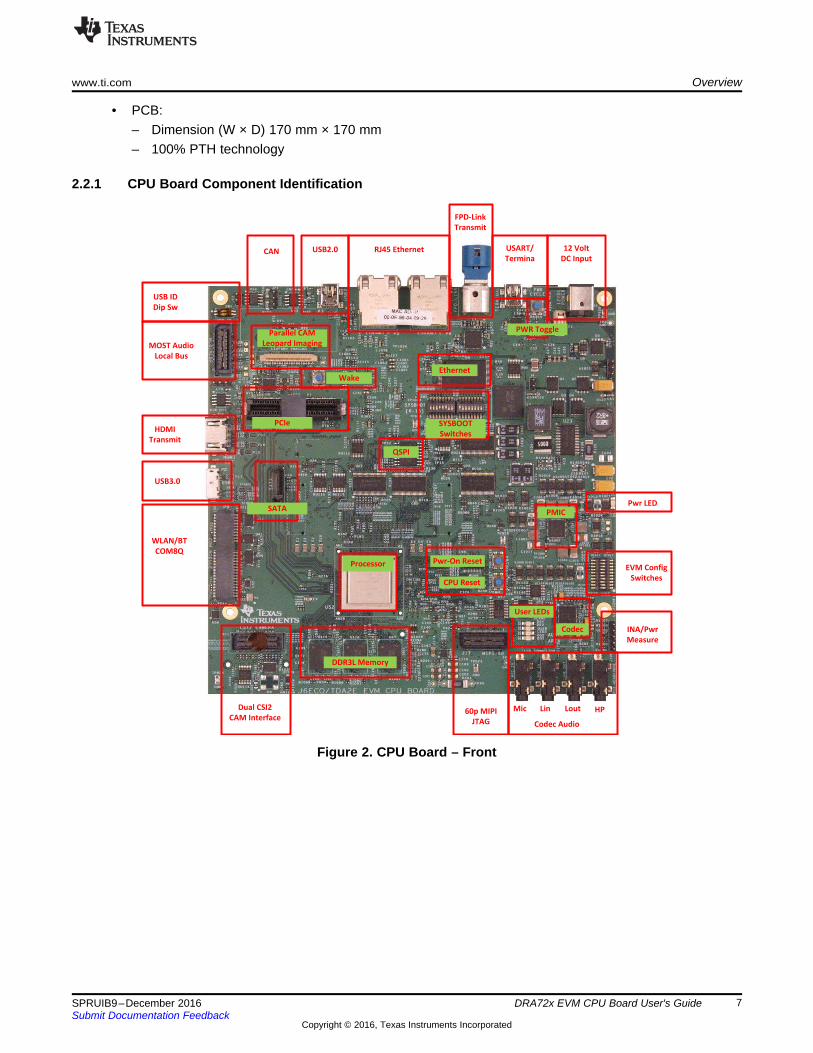
• PCB:– Dimension (W × D) 170 mm × 170 mm– 100% PTH technology
2.2.1 CPU Board Component Identification
Figure 2. CPU Board – Front
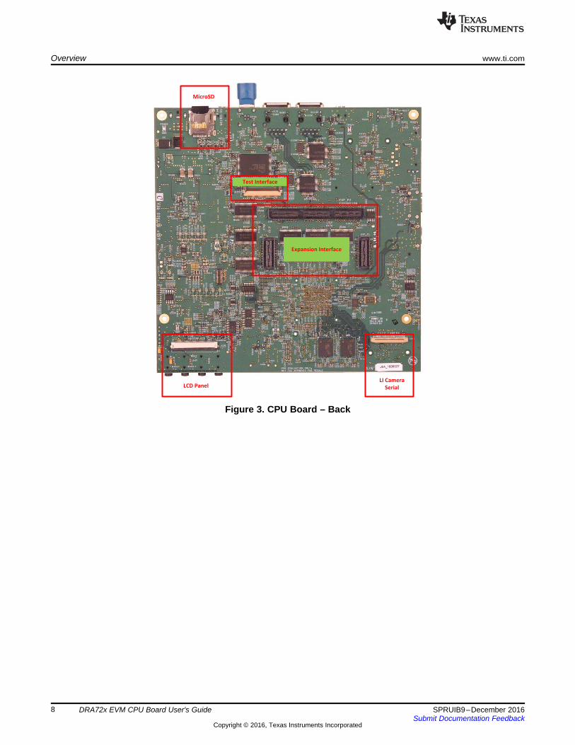
Expansion Interface
LI Camera
Serial
MicroSD
LCD Panel
Test Interface
Overview www.ti.com
8 SPRUIB9–December 2016Submit Documentation Feedback
Copyright © 2016, Texas Instruments Incorporated
DRA72x EVM CPU Board User's Guide
Figure 3. CPU Board – Back

www.ti.com Hardware
9SPRUIB9–December 2016Submit Documentation Feedback
Copyright © 2016, Texas Instruments Incorporated
DRA72x EVM CPU Board User's Guide
3 Hardware
3.1 Hardware ArchitectureFigure 4 shows the functional block diagram.
Figure 4. CPU Board Block Diagram
TPS65917-Q1
(J6eco PMIC)
TPS22965
(power switch)
So
C
CO
RE
SU
PP
LIE
S
VDD_RTC
VDD_IVAHD
VDD_GPU
VDD_CORE
VDD_DSP
VDD_MPU
TPS43351-Q1
3.1A @1.15V
0.01mA @1.03V
1.8A @1.03V
2.3A @1.15V
LDO4(USB)(200mA max) x
EV
M S
YS
TE
MO
TH
ER
SU
PP
LIE
S
x5V0
x3V3
SMPS5(2A max)
SMPS4(1.5A max)
1.8
V S
UP
PLI
ES
VDD_1V8
VDDA_1V8 (PLLs)
12V Power
Source
0.4A @ 1.8V
0.02A @ 1.8V
3.3V
5.0V
0.51A @ 1.35V
GPIO4
x DD
R
EMIF1
VBUCKB
VBUCKA
AVS
AVS
AVS
TPS51200 VTT
Dual Voltage Rails(Set to 3.3V)
DDR_REF
VDD_DDR
VDDA_USB3V3
2.30A @ 3.3V
3A @ 5V
0.30A @ 1.8V
LDO1(300mA max)
VDDSHV8 (SDIO)TBD @ 1.8, 3.3V
VDDA_RTC
VDDSHV5 (RTC IO)
LDO2(300mA max)
TBD @ .68V
TBD @ 1.8V
0.5A @ 0.68V
VDDA_1V8 (PHYs)TBD @ 1.8V
LDO3(200mA max)
xvddshv5
SMPS3(3A max)
SMPS1(3.5A max)
SMPS2(3.5A max)
x1V8
LDO5(LN)(100mA max)
EMIF2
LDOVRTC/ANA
required by PMIC
LDOVANA(10mA max)
LDOVRTC(25mA max)
1.8V
1.35V
1.8V
1.8V
3.3V
1.8/3.3V
.010
.010
INA226
.010
.010
.010
.010
.010
.010
.010
.010
.010
.010
xvddshv1
x
TP
S4
33
51
via
TP
S2
29
65
sw
itch
xvddshv10xvddshv11xvddshv2xvddshv3xvddshv4xvddshv6xvddshv7xvddshv9
xvdds_ddr1xvdds_ddr2
xSMPS5
xvddshv8
xLDO1
xddr1_vref0xddr2_vref0
xTPS51200
xvdda33v_usb1
xLDO4(USB)
xvdda33v_usb2
.010
.010
xvdda_rtc
xSMPS4
xvdda_pcie0
xvdda_usb1xvdda_usb2xvdda_hdmixvdda_pcie
xvdda_csixvdda_sataxvdda_usb3
x
LDO
3
xvdda_gmac_core
xvdda_perxvdda_ddrxvdda_debugxvdda_pllspare
xvdda_gpuxvdda_dsp_ivaxvdda_videoxvdda_mpu_abexvdda_osc
x
LDO
5 (
LN)
xvdds_mlbpxvdds18vxvdds18v_ddr1xvdds18v_ddr2
x
SM
PS
4
.005
.010
.010
.010
.010
Pwr Bd I2C1
Pwr Bd I2C2
.010
.010
xvdd_mpuxvdd_dspxvdd_gpuxvdd_iva
xSMPS1
xvddxvdd_rtc
xSMPS3x
SMPS3xSMPS3xSMPS2xSMPS2
.0101.8V
TBD @ 1.8V
Hardware www.ti.com
10 SPRUIB9–December 2016Submit Documentation Feedback
Copyright © 2016, Texas Instruments Incorporated
DRA72x EVM CPU Board User's Guide
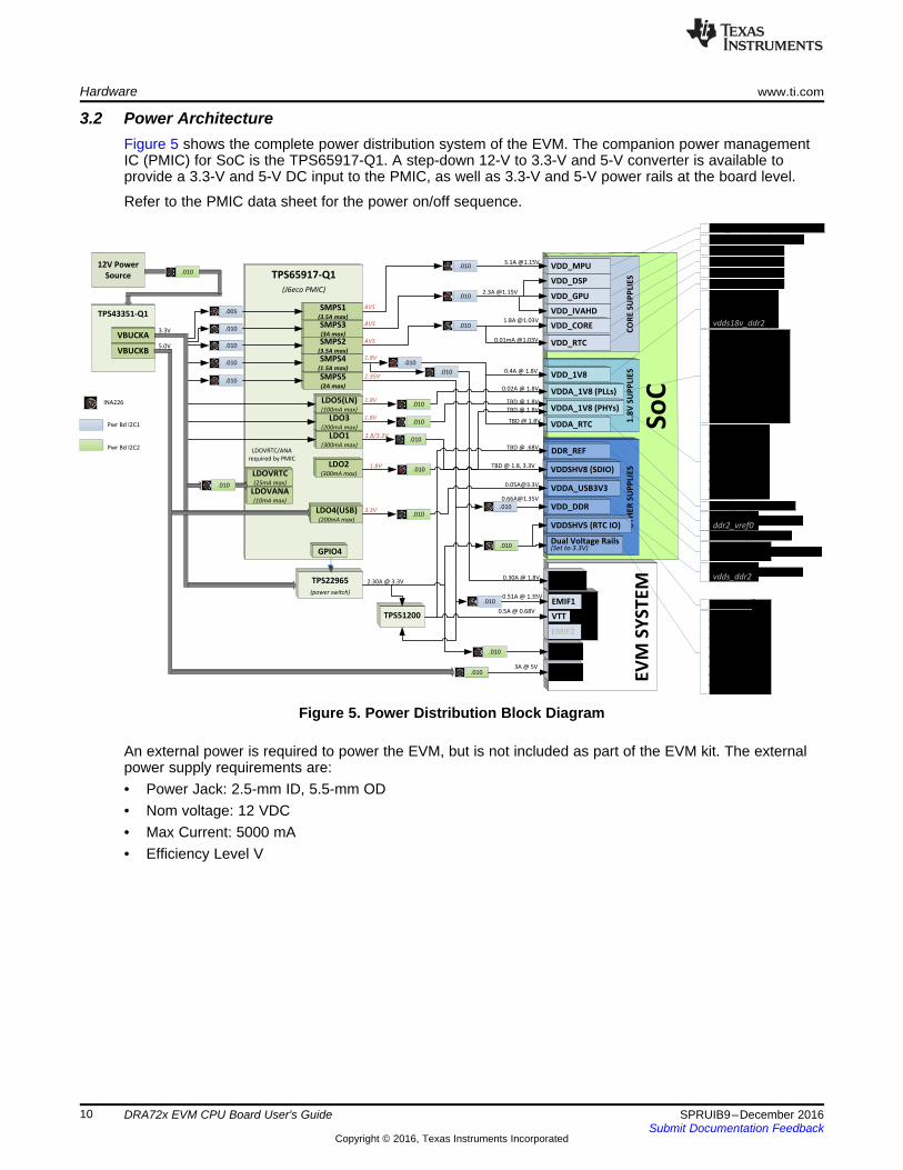
3.2 Power ArchitectureFigure 5 shows the complete power distribution system of the EVM. The companion power managementIC (PMIC) for SoC is the TPS65917-Q1. A step-down 12-V to 3.3-V and 5-V converter is available toprovide a 3.3-V and 5-V DC input to the PMIC, as well as 3.3-V and 5-V power rails at the board level.
Refer to the PMIC data sheet for the power on/off sequence.
Figure 5. Power Distribution Block Diagram
An external power is required to power the EVM, but is not included as part of the EVM kit. The externalpower supply requirements are:• Power Jack: 2.5-mm ID, 5.5-mm OD• Nom voltage: 12 VDC• Max Current: 5000 mA• Efficiency Level V
www.ti.com Hardware
11SPRUIB9–December 2016Submit Documentation Feedback
Copyright © 2016, Texas Instruments Incorporated
DRA72x EVM CPU Board User's Guide
Table 8 includes recommended and tested supplies for use with the EVM.
Table 8. EVM Supplies
Digi-Key Part NumberManufacturer PartNumber Manufacturer Output Connector Notes
102-3417-ND SDI65-12-U-P5 CUI Inc Barrel Plug, 2.1-mm I.D. ×5.5-mm O.D. × 9.5 mm
Required adapter,provided in EVM kit
62-1221-ND KTPS65-1250DT-3P-VI-C-P1
Volgen America/KagaElectronics USA
Barrel Plug, 2.1-mm I.D. ×5.5-mm O.D. × 9.5 mm
Required adapter,provided in EVM kit
102-3419-ND SDI65-12-UD-P5 CUI Inc Barrel Plug, 2.1-mm I.D. ×5.5-mm O.D. × 9.5 mm
Required adapter,provided in EVM kit
SDI65-12-U-P6-ND SDI65-12-U-P6 CUI Inc Barrel Plug, 2.1-mm I.D. ×5.5-mm O.D. × 9.5 mm
SDI65-12-UD-P6-ND SDI65-12-UD-P6 CUI Inc Barrel Plug, 2.1-mm I.D. ×5.5-mm O.D. × 9.5 mm
External Power Supply Regulatory Compliance Certifications: Recommended selection and use of anexternal power supply which meets TI’s required minimum electrical ratings, in addition to complying withapplicable regional product regulatory and safety certification requirements, such as UL, CSA, VDE, CCC,PSE, and so forth.
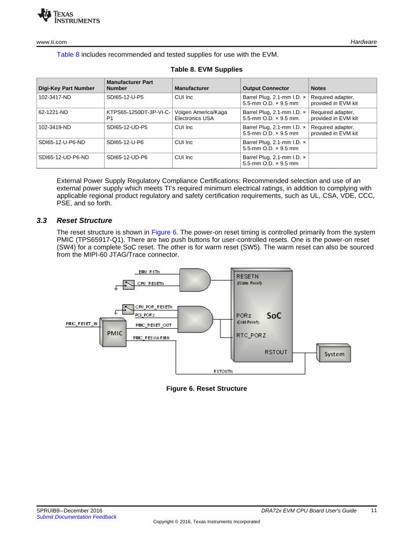
3.3 Reset StructureThe reset structure is shown in Figure 6. The power-on reset timing is controlled primarily from the systemPMIC (TPS65917-Q1). There are two push buttons for user-controlled resets. One is the power-on reset(SW4) for a complete SoC reset. The other is for warm reset (SW5). The warm reset can also be sourcedfrom the MIPI-60 JTAG/Trace connector.
Figure 6. Reset Structure
Hardware www.ti.com
12 SPRUIB9–December 2016Submit Documentation Feedback
Copyright © 2016, Texas Instruments Incorporated
DRA72x EVM CPU Board User's Guide
Table 9 summarizes the reset signals.
Table 9. Reset Signals Structure
Reset Type Reset Signal Sources CommentsPower-on reset (as whole system reset) CPU_POR_RESETn PORn push button reset
PCI_PORz PCIe inbound resetPMIC_RESET_OUT Power on reset from PMIC
Warm reset CPU_RESETn Warm push button resetEMU_RSTn Reset from emulator
PMIC power-on reset PMIC_RESET_IN PMIC reset inputProcessor reset out RSTOUTn Reset output from processor to system,
PMIC (warm reset input)
3.4 ClocksThe SoC supports three primary clock inputs. The device clock (OSC0) is provided by a 20-MHz crystal,and the auxiliary clock (OSC1) is provided by a 22.5792-MHz crystal. The RTC clock input is provided bya 32.768-KHz crystal.
In addition to the SoC clock inputs, the EVM includes other clock sources. A 25-MHz oscillator is providedto a CDCM9102 clock driver for sourcing the PCI 100-MHz reference clock. Each Ethernet PHY alsoincludes a local 25-Mhz crystal to provide its network reference clock.
3.5 Memory
3.5.1 SDRAM MemoryThe EVM includes 2 GBytes of DDR3L memory, and can operate at clock speeds up to 667 MHz (DDR3-1333). The memory is configured with four devices of 4 Gbit each (x8b devices). ECC is also supported.
DDR3L device used: Micron MT41K512M8RH-125-AA:E (4 × 8bit at 4 Gbit/ea) (or equivalent).
EEC device used: Micron MT41K512M8RH-125-AA:E (1 × 8bit at 4 Gbit) (or equivalent).
The DDR3L power is generated from the PMIC (TPS65917-Q1) and set to 1.35 V. It uses fly-by topologywith VTT termination. VTT supply is generated using a sink and source termination regulator (TPS51200).
3.5.2 QSPI Flash MemoryAs a primary non-volatile boot device, the EVM includes 256 Mbit of Quad-SPI flash memory. The deviceis supported on chip select zero of the QSPI interface. The interface can be configured to support eitherserial mode (1x) or quad mode (4x).
QSPI device used: Spansion S25FL256S
Booting from the QSPI flash memory is supported on the EVM. No EVM configuration is required, as theQSPI flash is connected by default. Ensure the correct SoC boot mode using the SYS_BOOT switches(SW2, SW3).
3.5.3 EMMC Flash MemoryAs a primary non-volatile storage device, the EVM includes 8 GBytes of eMMC flash memory. Thememory device is EMMC v4.51-compliant, and connects to MMC2 port of the SoC. The design cansupports rates up to HS-200.
EMMC device used: Micron MTFC8GLWDM-3M AIT Z
Booting from the EMMC flash memory is supported on the EVM. The on-board mux must be set to enableEMMC by setting the SW5.p3 to ON. Ensure the correct SoC boot mode is set using the SYS_BOOTswitches (SW2, SW3).

www.ti.com Hardware
13SPRUIB9–December 2016Submit Documentation Feedback
Copyright © 2016, Texas Instruments Incorporated
DRA72x EVM CPU Board User's Guide
3.5.4 MicroSD Card CageFor non-volatile storage expansion, the EVM includes a microSD card cage. The cage is connected to theMMC1 port of the SoC. To support higher-speed cards that operate at lower voltages, the IO supply ischanged from 3v3 to 1v8 through the PMIC LDO configuration (see the PMIC data manual for instructionson how to change the voltage level). The SD card power can be cycled using the IO expander (EXP2,PP5). For specific information regarding supported card types, densities, and speeds, see the device-specific data manual for SoC.
Booting from the microSD card cage is supported on the EVM. No configuration is required, as the SDcard is selected by default. Ensure the correct SoC boot mode is set using the SYS_BOOT switches(SW2, SW3).
3.5.5 GPMC NOR Flash MemoryA 512-Mbit NOR flash memory (x16) is supported as a non-volatile memory option on the EVM. It issupported on chip select CS0, and thus can also be used as a boot device. To access, the onboard muxmust be enabled by setting SW5.p2 to ON. For booting, ensure the correct SoC boot mode is selectedusing the SYS_BOOT switches (SW2, SW3).
NOR device used: Spansion S29GL512S10TFI010
3.5.6 GPMC NAND Flash MemoryA 2-Gbit NAND flash memory (x16) is supported as a non-volatile memory option on the EVM. It issupported on chip select CS0, and thus can also be used as a boot device. To access, the onboard muxmust be enabled by setting SW5.p1 to ON. For booting, ensure the correct SoC boot mode is selectedusing the SYS_BOOT switches (SW2, SW3).
NAND device used: Micron MT29F2G16AADWP:D
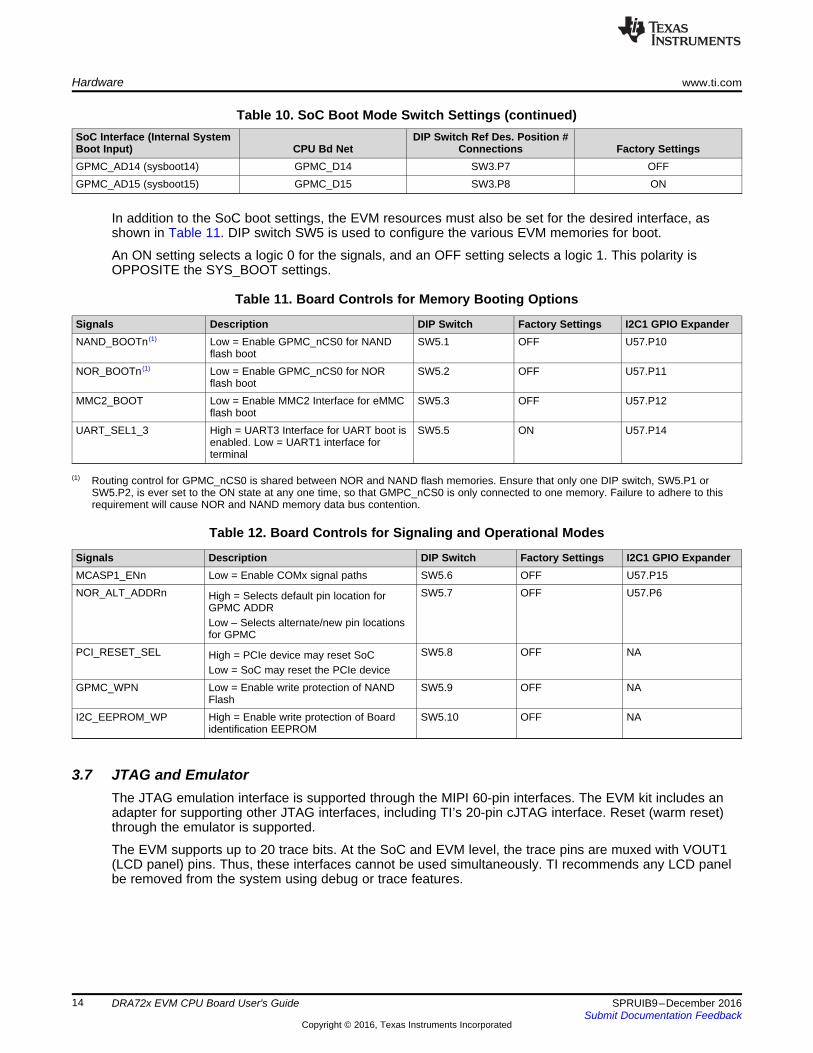
3.6 Boot ModesThe SoC supports a variety of different boot modes, determined by the 16-bit system boot setting presenton the shared specific I/O balls during the power-on sequence (see the TRM for details). Boot modeselection is accomplished by setting the DIP switches SW2 and SW3 as shown in Table 10, prior tocycling of power.
These SoC resources can be redeployed to support alternate interfaces after boot-up, by way of both SoCand EVM mux settings.
An ON setting selects a logic 1 for the signals, and an OFF setting selects a logic 0.
Table 10. SoC Boot Mode Switch Settings
SoC Interface (Internal SystemBoot Input) CPU Bd Net
DIP Switch Ref Des. Position #Connections Factory Settings
GPMC_AD0 (sysboot0) GPMC_D00 SW2.P1 ONGPMC_AD1 (sysboot1) GPMC_D01 SW2.P2 OFFGPMC_AD2 (sysboot2) GPMC_D02 SW2.P3 ONGPMC_AD3 (sysboot3) GPMC_D03 SW2.P4 OFFGPMC_AD4 (sysboot4) GPMC_D04 SW2.P5 ONGPMC_AD5 (sysboot5) GPMC_D05 SW2.P6 OFFGPMC_AD6 (sysboot6) GPMC_D06 SW2.P7 OFFGPMC_AD7 (sysboot7) GPMC_D07 SW2.P8 OFFGPMC_AD8 (sysboot8) GPMC_D08 SW3.P1 ONGPMC_AD9 (sysboot9) GPMC_D09 SW3.P2 OFFGPMC_AD10 (sysboot10) GPMC_D10 SW3.P3 OFFGPMC_AD11 (sysboot11) GPMC_D11 SW3.P4 OFFGPMC_AD12 (sysboot12) GPMC_D12 SW3.P5 OFFGPMC_AD13 (sysboot13) GPMC_D13 SW3.P6 OFF
Hardware www.ti.com
14 SPRUIB9–December 2016Submit Documentation Feedback
Copyright © 2016, Texas Instruments Incorporated
DRA72x EVM CPU Board User's Guide
Table 10. SoC Boot Mode Switch Settings (continued)SoC Interface (Internal SystemBoot Input) CPU Bd Net
DIP Switch Ref Des. Position #Connections Factory Settings
GPMC_AD14 (sysboot14) GPMC_D14 SW3.P7 OFFGPMC_AD15 (sysboot15) GPMC_D15 SW3.P8 ON
In addition to the SoC boot settings, the EVM resources must also be set for the desired interface, asshown in Table 11. DIP switch SW5 is used to configure the various EVM memories for boot.
An ON setting selects a logic 0 for the signals, and an OFF setting selects a logic 1. This polarity isOPPOSITE the SYS_BOOT settings.
(1) Routing control for GPMC_nCS0 is shared between NOR and NAND flash memories. Ensure that only one DIP switch, SW5.P1 orSW5.P2, is ever set to the ON state at any one time, so that GMPC_nCS0 is only connected to one memory. Failure to adhere to thisrequirement will cause NOR and NAND memory data bus contention.
Table 11. Board Controls for Memory Booting Options
Signals Description DIP Switch Factory Settings I2C1 GPIO ExpanderNAND_BOOTn (1) Low = Enable GPMC_nCS0 for NAND
flash bootSW5.1 OFF U57.P10
NOR_BOOTn (1) Low = Enable GPMC_nCS0 for NORflash boot
SW5.2 OFF U57.P11
MMC2_BOOT Low = Enable MMC2 Interface for eMMCflash boot
SW5.3 OFF U57.P12
UART_SEL1_3 High = UART3 Interface for UART boot isenabled. Low = UART1 interface forterminal
SW5.5 ON U57.P14
Table 12. Board Controls for Signaling and Operational Modes
Signals Description DIP Switch Factory Settings I2C1 GPIO ExpanderMCASP1_ENn Low = Enable COMx signal paths SW5.6 OFF U57.P15NOR_ALT_ADDRn High = Selects default pin location for
GPMC ADDRLow – Selects alternate/new pin locationsfor GPMC
SW5.7 OFF U57.P6
PCI_RESET_SEL High = PCIe device may reset SoCLow = SoC may reset the PCIe device
SW5.8 OFF NA
GPMC_WPN Low = Enable write protection of NANDFlash
SW5.9 OFF NA
I2C_EEPROM_WP High = Enable write protection of Boardidentification EEPROM
SW5.10 OFF NA
3.7 JTAG and EmulatorThe JTAG emulation interface is supported through the MIPI 60-pin interfaces. The EVM kit includes anadapter for supporting other JTAG interfaces, including TI’s 20-pin cJTAG interface. Reset (warm reset)through the emulator is supported.
The EVM supports up to 20 trace bits. At the SoC and EVM level, the trace pins are muxed with VOUT1(LCD panel) pins. Thus, these interfaces cannot be used simultaneously. TI recommends any LCD panelbe removed from the system using debug or trace features.
www.ti.com Hardware
15SPRUIB9–December 2016Submit Documentation Feedback
Copyright © 2016, Texas Instruments Incorporated
DRA72x EVM CPU Board User's Guide
3.8 UART TerminalThe EVM supports a single UART connection for a user terminal. A FT232 device is used to transport theUART information over USB to a host PC. The EVM is designed to use UART1 as the primary terminalconnection, but can also support an alternate configuration to use UART3 (required to support peripheraland UART booting). The USB-side of the FT232 device is powered from the USB port, and the connectionstays active regardless of the power state of the EVM.
USART device to be used: FTD Chip FT232RQ
A USB mini-AB receptacle is used to support USB connection, and is included as part of the EVM kit.
3.9 DCAN and CAN InterfacesThe EVM supports access to two DCAN interfaces though pin headers. It supports a single 3-pin CANinterface, connecting DCAN1 through a CAN transceiver.
CAN device used: Texas Instruments SN65HVDA541
3.10 Universal Serial Bus (USB)Two independent USB ports are supported on the EVM. USB3.0 Super-Speed bus (USB1) is supportedusing port USB1 to a mini-AB type connector. This interface supports rates up to 5 Gbps. USB2.0interface is supported using port USB2 to a micro-AB type connector. It can support rates up to 480 Mbps.Both ports can operate either as host or device mode. VBUS can be supplied to a peripheral when in hostmode by enabling the VBUS switch (controlled through the SoC). However, the EVM cannot be poweredfrom VBUS when operating in device mode.
The EVM includes capabilities to set and read each connector ID pin. This is supported using the IOexpander (EXP2 P1 for USB1, P2 for USB2). In addition, DIP switch SW1 provides the ability to manualset the individual ID value either high (OFF) or low (ON).
3.11 Wired EthernetDual Gigabit Ethernet ports are supported on the EVM. RGMII ports 0 and 1 drive the Texas InstrumentsDP83867 Gigabit PHYs. The PHYs are configured through the Management Data Input/Output bus(MDIO), with address set to 0x2 (port 0) and 0x3 (port 1). PHYs are reset at power-on, but can also beindependently reset using the IO expander. Both ports share a common interrupt signal (GPIO6_16).
IO Expander Control: EXP1, P10 (PHY 0 Reset), P11 (PHY 1 Reset)
NOTE: For PHY configuration, the user must configure the DP83867 RGMII Control register(RGMIICTL) for RGMII mode, and the RGMII Delay Control register (RGMIIDCTL) for 0-nsTX delay, and 2.25-ns RX delay. Set the IO Drive Strength register (IO_IMPEDANCE_CTRL)to maximum drive.
3.12 Video OutputThe EVM supports three different options for supporting video output: HDMI, Display Panel, and FPD Link.Each can be supported independently, or all used simultaneously.
3.12.1 HDMI DisplayThe SoC includes a dedicated HDMI display interface, which is supported on to a type A HDMI connector.The interface will support 1080p with 24b color. A communication channel (DDC/CEC) is supported to theHDMI connector for communication with the HDMI panel. A monitor detect indication is also provided. TheDDC/CED interface and monitor detect signals (HPD) are translated through the transceiver, and can becontrolled using IO from the expander.
DDC Transceiver used: Texas Instruments TPD12S016
IO Expander Control: EXP3, P4 (Lvl Shift Reg Enable, HPD), P5 (DDC/CEC Enable)
Hardware www.ti.com
16 SPRUIB9–December 2016Submit Documentation Feedback
Copyright © 2016, Texas Instruments Incorporated
DRA72x EVM CPU Board User's Guide
3.12.2 LCD Touch PanelThe EVM supports a LCD panel interface for supporting video output to a LCD panel. The SoC VOUT1resource is used drive up to 24b RGB data to interface. The interface supports resource connections forinterfacing with a touch panel for advanced user interfaces. These include a control bus (I2C1) andinterrupt for touch indications (GPIO)
An LCD panel is not included with the CPU EVM, but can be ordered and included as part of an assemblykit.
Connector used: Molex
3.12.3 FPD-Link III Output and PanelThe EVM includes a FPD-Link III parallel-to-serial interface on VOUT3. It supports up to 24bits of data andcan operate at pixel rates up to 85 MHz. The interrupt is supported to enable back-channelcommunication, typically needed if supporting touch screen. The transceiver is configured using I2C (port5, 0x1B).
Serializer device used: Texas Instruments DS90UH925Q
Connector used: Automotive HSD Connector, right-angle plug for PCB, Rosenberger D4S20D-40ML5-Z.
3.13 Video Input
3.13.1 Parallel ImagingParallel video input is supported through connections from external sensors and transceivers. The SoCport VIN2A is routed to a connector interface designed to mate with camera sensors from LeopardImaging. This approach provides flexibility for customers to select from a variety of available modules,while also supporting connections of custom solutions. The attached module can be configured usingeither I2C (port 5) or SPI (port 1).
Connector used: FPC 36 position, 0.5 mm, Molex 052559-3679.
3.13.2 Serial ImagingSerial video input is supported through connections from external sensors and transceivers. The SoC portCSI2-0 is routed to connector interfaced designed to mate with camera sensors from Leopard Imaging.This approach provides flexibility for customers to select from a variety of available modules. Both serialports (CSI2-0 and CSI2-1) are routed to an expansion connector for supporting a variety of customsolutions. Both interfaces support additional signals for the control and configuration of the attachedmodules. These interfaces (I2C port 5, SPI port 1) are translated to 1.8-V IO (with resistor option to leaveat 3.3-V IO).
LI Connector used: FPC 36 position, 0.5 mm, Molex 052559-3679
Connector used: Samtec QSH-020-01-L-D-DP-A
3.14 PCIeThe EVM supports a PCIe (single-lane) interface for connecting with a variety of external modules. Asecond lane is available with a component modification (FL2, FL3). An on-board clock generatorCDCM9102 provides the 100-MHz reference clock to both the SoC and attached modules. The EVMsupport two different PCIe reset configurations, select using DIP switch SW5 position 8. The defaultsetting of ON lets SoC reset the PCIe peripheral. The switch setting of OFFlets the PCIe peripheral resetthe SoC.
www.ti.com Hardware
17SPRUIB9–December 2016Submit Documentation Feedback
Copyright © 2016, Texas Instruments Incorporated
DRA72x EVM CPU Board User's Guide
3.15 Media Local Bus (MLB)The EVM supports a Media Local Bus interface for connecting to external hardware (such as SMSCOS81110/2+0 Physical Interface Board). The interface supports both 3-pin MediaLB and 6-pin MediaLB+configurations.
Connector used: Samtec QSH-020-01-L-D-DP-A
3.16 AudioThe EVM supports onboard AIC3106 audio codec for analog audio conversions. Analog inputs aresupported on two 3.5-mm audio jacks, including stereo line inputs (P12) and mono microphone (P11).Analog outputs are supported on two 3.5-mm audio jacks, providing stereo line outputs (P13) and stereoheadset (P14). The digital audio is connected to the SoC using multi-channel serial port (McASP3). Thecodec requires a master clock (AHCLKX). The audio codec is configured using I2C1, and is accessed ataddress 0x19.
3.17 COM8 Module InterfaceA connector is provided to facilitate the plugging in of TI COM8Q modules, which provide features such asBluetooth and Wi-Fi™. The COM8Q interface requires a 3.6-V power supply; thus, a dedicated regulatoris provided. All signals on the COM8Q interface are required to 1.8 volts, thus voltage translators areplaced to convert from the standard IO levels of 3.3 V. UART interface (UART3) is used for BT-HCI port,I2S port (McASP7) is used for BT-audio, and MMC4 port is use for WiFi communication.
Connector used: Samtec MEC6-150-02-S-D-RA1
3.18 User Interface LEDsThe CPU board has four user interface LEDs for debug, status indication, and so forth. Table 13 detailsthe user interface LED and its control.
Table 13. User LEDs
LED Controlled ByDS4 IO Expander EXP1, position P7DS3 IO Expander EXP1, position P6DS2 IO Expander EXP1, position P5DS1 IO Expander EXP1, position P4
3.19 Power MonitoringThe CPU board has provisions to monitor power for many of the systems core power rails. Themeasurement system is implemented using the TI INA226 I2C current shunt and power monitors. TheINA226 device monitors both the power supply voltage and shunt current measurements. Information isconnected from the INA226 devices using dedicated I2C buses. The INA226s can be controlled throughan off-board module (FTDI USART, MSP430, or a similar device).
Hardware www.ti.com
18 SPRUIB9–December 2016Submit Documentation Feedback
Copyright © 2016, Texas Instruments Incorporated
DRA72x EVM CPU Board User's Guide
Table 14 shows a mapping of the current monitoring system. INA226 are located at each shunt location.
Table 14. Power Monitor Mapping
I2C BUS AI2C Addr Power Net Shunt /
ResistorDescription
0x40 SMPS1_IN 5m-Ω TPS65917 SMPS1 power input (MPU)0x41 SMPS2_IN 10m-Ω TPS65917 SMPS1 power input (GPU/DSP)0x42 SMPS3_IN 10m-Ω TPS65917 SMPS1 power input (CORE)0x43 SMPS4_IN 10m-Ω TPS65917 SMPS1 power input (1V8)0x44 SMPS5_IN 10m-Ω TPS65917 SMPS1 power input (DDR)0x45 J6_VDD_MPU 10m-Ω CPU MPU power rail (TPS65917 SMPS1)0x46 J6_VDD_GPU 10m-Ω CPU GPU/DSP/IVA (TPS65917 SMPS2)0x47 J6_VDD_CORE 10m-Ω CPU CORE power rail (TPS65917 SMPS3)0x48 J6_VDD_1V8 10m-Ω CPU 1v8 power rail(s)0x49 EVM_VDD_1V8 10m-Ω EVM 1v8 Peripheral Rail0x4A J6_VDD_DDR 10m-Ω CPU DDR Power Rail0x4B EVM_VDD_DDR 10m-Ω DDR Power Rail
I2C BUS BI2C Addr Power Net Shunt /
ResistorDescription
0x40 VDDSHV8 10m-Ω CPU IO Rail for SD/MMC0x41 VDDSHV5 10m-Ω CPU IO Rail for RTC0x42 VDDA_PHY 10m-Ω CPU PHY LDO Rail0x43 VDDA_USB3v3 10m-Ω CPU USB PHY LDO Rail0x44 VDDA_PLL 10m-Ω CPU PLL LDO Rail0x45 EVM_5v0 10m-Ω EVM 5v0 Peripheral Rail0x46 EVM_3v3 10m-Ω EVM 3v3 Peripheral Rail0x47 VCCA_IN 10m-Ω Total System power rail0x48 EVM_12V 10m-Ω Total System 12v power rail0x49 1v8_PHY2 10m-Ω CPU PHY LDO Rail

www.ti.com Hardware
19SPRUIB9–December 2016Submit Documentation Feedback
Copyright © 2016, Texas Instruments Incorporated
DRA72x EVM CPU Board User's Guide
3.20 I2C Peripheral MapTable 15 shows the list of I2C interfaces available on the EVM, with a list of device connected to each I2Cinterface and its corresponding device address.
Table 15. I2C Device Address Chart
CPU Board Part No I2C1 I2C3 I2C4 I2C5 Device Addr (7b)EEPROM 24WC256 X 0x50Digital Temperature Sensor TMP102AIDRLT X 0x48GPIO Expander #1 PCF8575 X 0x20GPIO Expander #2 PCF8575 X 0x21GPIO Expander #3 PCF8575 X 0x26MLB Connector Connector X NALCD Interface Connector X NACOM8 Connector Connector X NAAudio Codec TLV320AIC3106 X 0X19Expansion Connector Connector X X X NAPMIC LP8733 X 0x60
LP8732 X 0x61FPD Link DS90UH925Q X 0x1BLI Camera Connector X NACSI2 Camera Connector X NA
3.21 GPIO ListTable 16 shows the list of SoC GPIOs. Signals used for GPIO on expansion boards are not included inthis list, as they are dependent upon the application board used.
Table 16. SoC GPIO Map
Feature Peripheral Device EVM Bd Net Function SoC GPIOConnectivity on Module COM8 Connector GP5[4] BT_EN GPIO5_4Connectivity on Module COM8 Connector GP5[5] GPS_PPS_OUT GPIO5_5Connectivity on Module COM8 Connector GP5[6] GPS_TIME_STAMP GPIO5_6Connectivity on Module COM8 Connector GP5[7] WLAN_IRQ GPIO5_7Connectivity on Module COM8 Connector GP5[8] WL_EN GPIO5_8Media Local Bus(MLB) MLB Connector GP5[9] NA GPIO5_9Media Local Bus(MLB) MLB Connector GP6_[28] NA GPIO6_28IO Expander PCF8575 PCF8575_INT IOEXP_IRQ GPIO3_30Gig Ethernet Ethernet PHY ENET_INTSn ENET_IRQ GPIO6_16LCD Touch Panel Display Connector GP1[15] TS_LCD_IRQ GPIO1_15FPD-Link Panel FPD-Link Txmt VOUT2_INTB FPDTX_IRQ GPIO3_38Power Mgmt PMIC WAKEUP3 PMIC_IRQ GPIO1_3SD Card Micro-SD MMC1_SDCD CARD_DETECT GPIO6_27Test Automated Test GP5[0] USER_DEFINED GPIO5_0
NOTE: Functional signals of pinmux are not consider for this table. For more details, see theDRA72x_TDA2Ex CPU EVM Schematic Rev D (http://www.ti.com/lit/zip/sprr236).
Hardware www.ti.com
20 SPRUIB9–December 2016Submit Documentation Feedback
Copyright © 2016, Texas Instruments Incorporated
DRA72x EVM CPU Board User's Guide
3.22 IO Expander List
Table 17. I/O Expander Map
Device Slave Address I2C I/FExpander
IO Netname Description
EXP1 0b0010 000(0x20) I2C1
INT# PCF8575_INT Interrupt output to SoCP0 TS_LCD_GPIO1 Press Button Switch 1P1 TS_LCD_GPIO2 Press Button Switch 2P2 TS_LCD_GPIO3 Press Button Switch 3P3 TS_LCD_GPIO4 Press Button Switch 4P4 USER_LED1 User LED 1P5 USER_LED2 User LED 2P6 USER_LED3 User LED 3P7 USER_LED4 User LED 4P10 EXP_ETH0_RSTn RGMII0 ResetP11 EXP_ETH1_RSTn RGMII1 ResetP12 USB1-VBUS_OCN USB1 Over Current IndicationP13 USB2-VBUS_OCN USB2 Over Current IndicationP14 PCI_SW_RESETn PCI Interface SW ResetP15 CON_LCD_PWR_DN LCD Board Master power enableP16 OpenP17 TMP102_ALERT Temperature Sensor Alarm
EXP2 0b0010 001(0x21) I2C1
INT# PCF8575_INT Interrupt output to SoC
P0 SEL_GPMC_AD_VID_S0 MUX out control signal for GPMC Vs VOUT3Bvs VIN1A
P1 USB1_ID USB1 ID PINP2 USB2_ID USB2 ID PINP3 SEL_I2C3_CAN2 MUX out control signal for I2C3 Vs DCAN2P4 SEL_ENET_MUX_S0 MUX out control signal for RGMII0 Vs VINP5 MMC_PWR_ON Power on regulator to MMC card
P6 NOR_ALT_ADDRn MUX out control signals for alternate location ofGPMC control signals
P7 SEL_GPMC_AD_VID_S2 MUX out control signal for GPMC vs VOUT3Bvs VIN1A
P10 NAND_BOOTn NAND boot Chip select enable signalP11 NOR_BOOTn NOR boot Chip select enable signalP12 MMC2_BOOT MUX out control signal for GPMC Vs MMC2P13 QSPI_SELn Not used, as QSPI is enabled with resistor mux
P14 UART_SEL1_3 MUX out control signal for UART1 vs UART forterminal access
P15 MCASP1_ENn COM8 interface level shifter enable signalP16 SEL_UART3_SPI2 MUX out control signal for UART3 Vs SPI2P17 Open
www.ti.com Hardware
21SPRUIB9–December 2016Submit Documentation Feedback
Copyright © 2016, Texas Instruments Incorporated
DRA72x EVM CPU Board User's Guide
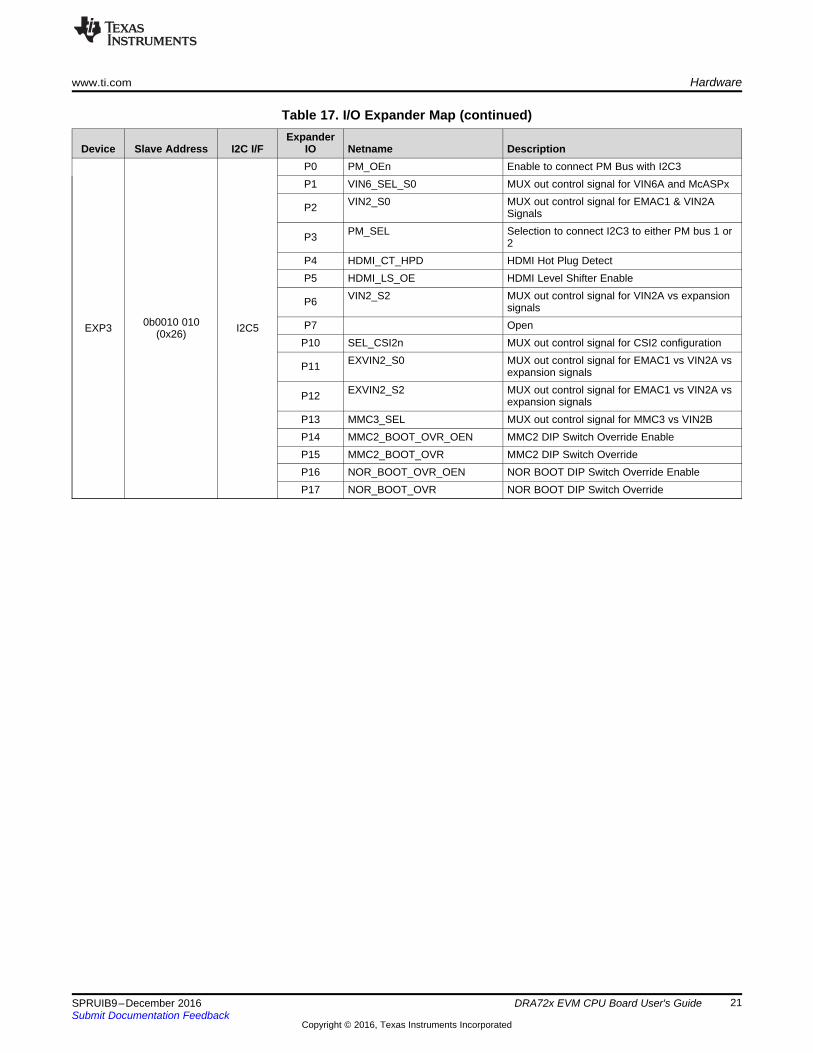
Table 17. I/O Expander Map (continued)
Device Slave Address I2C I/FExpander
IO Netname Description
EXP3 0b0010 010(0x26) I2C5
P0 PM_OEn Enable to connect PM Bus with I2C3P1 VIN6_SEL_S0 MUX out control signal for VIN6A and McASPx
P2 VIN2_S0 MUX out control signal for EMAC1 & VIN2ASignals
P3 PM_SEL Selection to connect I2C3 to either PM bus 1 or2
P4 HDMI_CT_HPD HDMI Hot Plug DetectP5 HDMI_LS_OE HDMI Level Shifter Enable
P6 VIN2_S2 MUX out control signal for VIN2A vs expansionsignals
P7 OpenP10 SEL_CSI2n MUX out control signal for CSI2 configuration
P11 EXVIN2_S0 MUX out control signal for EMAC1 vs VIN2A vsexpansion signals
P12 EXVIN2_S2 MUX out control signal for EMAC1 vs VIN2A vsexpansion signals
P13 MMC3_SEL MUX out control signal for MMC3 vs VIN2BP14 MMC2_BOOT_OVR_OEN MMC2 DIP Switch Override EnableP15 MMC2_BOOT_OVR MMC2 DIP Switch OverrideP16 NOR_BOOT_OVR_OEN NOR BOOT DIP Switch Override EnableP17 NOR_BOOT_OVR NOR BOOT DIP Switch Override
Hardware www.ti.com
22 SPRUIB9–December 2016Submit Documentation Feedback
Copyright © 2016, Texas Instruments Incorporated
DRA72x EVM CPU Board User's Guide
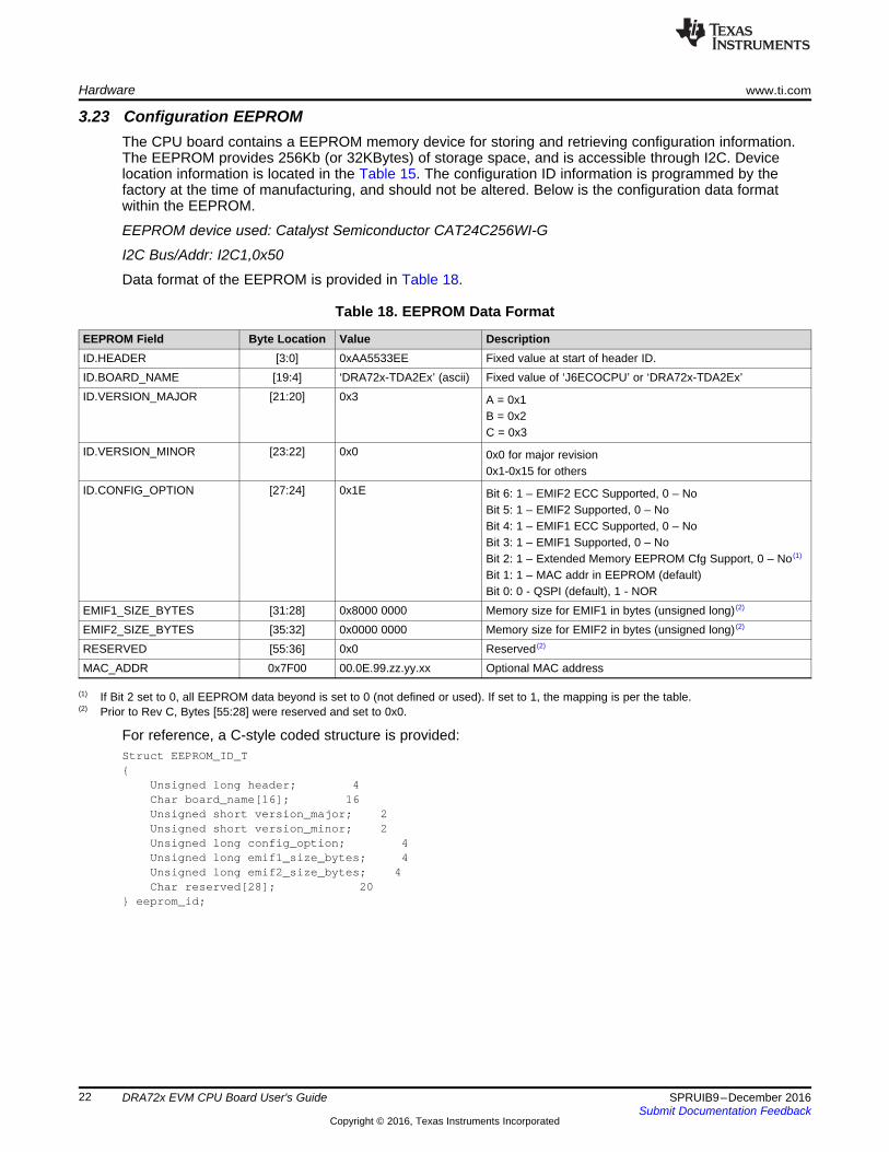
3.23 Configuration EEPROMThe CPU board contains a EEPROM memory device for storing and retrieving configuration information.The EEPROM provides 256Kb (or 32KBytes) of storage space, and is accessible through I2C. Devicelocation information is located in the Table 15. The configuration ID information is programmed by thefactory at the time of manufacturing, and should not be altered. Below is the configuration data formatwithin the EEPROM.
EEPROM device used: Catalyst Semiconductor CAT24C256WI-G
I2C Bus/Addr: I2C1,0x50
Data format of the EEPROM is provided in Table 18.
(1) If Bit 2 set to 0, all EEPROM data beyond is set to 0 (not defined or used). If set to 1, the mapping is per the table.(2) Prior to Rev C, Bytes [55:28] were reserved and set to 0x0.
Table 18. EEPROM Data Format
EEPROM Field Byte Location Value DescriptionID.HEADER [3:0] 0xAA5533EE Fixed value at start of header ID.ID.BOARD_NAME [19:4] ‘DRA72x-TDA2Ex’ (ascii) Fixed value of ‘J6ECOCPU’ or ‘DRA72x-TDA2Ex’ID.VERSION_MAJOR [21:20] 0x3 A = 0x1
B = 0x2C = 0x3
ID.VERSION_MINOR [23:22] 0x0 0x0 for major revision0x1-0x15 for others
ID.CONFIG_OPTION [27:24] 0x1E Bit 6: 1 – EMIF2 ECC Supported, 0 – NoBit 5: 1 – EMIF2 Supported, 0 – NoBit 4: 1 – EMIF1 ECC Supported, 0 – NoBit 3: 1 – EMIF1 Supported, 0 – NoBit 2: 1 – Extended Memory EEPROM Cfg Support, 0 – No (1)
Bit 1: 1 – MAC addr in EEPROM (default)Bit 0: 0 - QSPI (default), 1 - NOR
EMIF1_SIZE_BYTES [31:28] 0x8000 0000 Memory size for EMIF1 in bytes (unsigned long) (2)
EMIF2_SIZE_BYTES [35:32] 0x0000 0000 Memory size for EMIF2 in bytes (unsigned long) (2)
RESERVED [55:36] 0x0 Reserved (2)
MAC_ADDR 0x7F00 00.0E.99.zz.yy.xx Optional MAC address
For reference, a C-style coded structure is provided:Struct EEPROM_ID_T{
Unsigned long header; 4Char board_name[16]; 16Unsigned short version_major; 2Unsigned short version_minor; 2Unsigned long config_option; 4Unsigned long emif1_size_bytes; 4Unsigned long emif2_size_bytes; 4Char reserved[28]; 20
} eeprom_id;
www.ti.com Signal Multiplex Logic
23SPRUIB9–December 2016Submit Documentation Feedback
Copyright © 2016, Texas Instruments Incorporated
DRA72x EVM CPU Board User's Guide
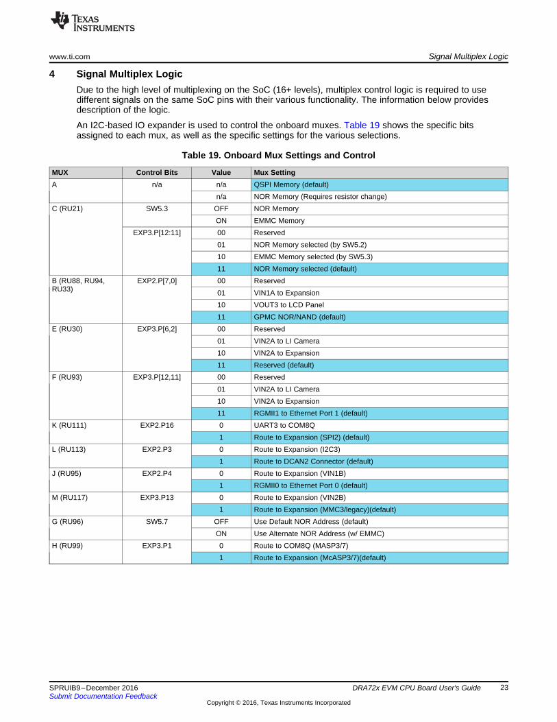
4 Signal Multiplex LogicDue to the high level of multiplexing on the SoC (16+ levels), multiplex control logic is required to usedifferent signals on the same SoC pins with their various functionality. The information below providesdescription of the logic.
An I2C-based IO expander is used to control the onboard muxes. Table 19 shows the specific bitsassigned to each mux, as well as the specific settings for the various selections.
Table 19. Onboard Mux Settings and Control
MUX Control Bits Value Mux SettingA n/a n/a QSPI Memory (default)
n/a NOR Memory (Requires resistor change)C (RU21) SW5.3 OFF NOR Memory
ON EMMC MemoryEXP3.P[12:11] 00 Reserved
01 NOR Memory selected (by SW5.2)10 EMMC Memory selected (by SW5.3)11 NOR Memory selected (default)
B (RU88, RU94,RU33)
EXP2.P[7,0] 00 Reserved01 VIN1A to Expansion10 VOUT3 to LCD Panel11 GPMC NOR/NAND (default)
E (RU30) EXP3.P[6,2] 00 Reserved01 VIN2A to LI Camera10 VIN2A to Expansion11 Reserved (default)
F (RU93) EXP3.P[12,11] 00 Reserved01 VIN2A to LI Camera10 VIN2A to Expansion11 RGMII1 to Ethernet Port 1 (default)
K (RU111) EXP2.P16 0 UART3 to COM8Q1 Route to Expansion (SPI2) (default)
L (RU113) EXP2.P3 0 Route to Expansion (I2C3)1 Route to DCAN2 Connector (default)
J (RU95) EXP2.P4 0 Route to Expansion (VIN1B)1 RGMII0 to Ethernet Port 0 (default)
M (RU117) EXP3.P13 0 Route to Expansion (VIN2B)1 Route to Expansion (MMC3/legacy)(default)
G (RU96) SW5.7 OFF Use Default NOR Address (default)ON Use Alternate NOR Address (w/ EMMC)
H (RU99) EXP3.P1 0 Route to COM8Q (MASP3/7)1 Route to Expansion (McASP3/7)(default)
NOR Memory
QSPI Memory
QSPI1QSPI1_SCLK, _D[3:0], _CS[0],
_RTCLK
Mux
A
A1 B1
B2
R-Mux
GPMC_A[18:13], _CS[2]SoC
GPMCGPMC_A[18:13], _CS[2]
Signal Multiplex Logic www.ti.com
24 SPRUIB9–December 2016Submit Documentation Feedback
Copyright © 2016, Texas Instruments Incorporated
DRA72x EVM CPU Board User's Guide
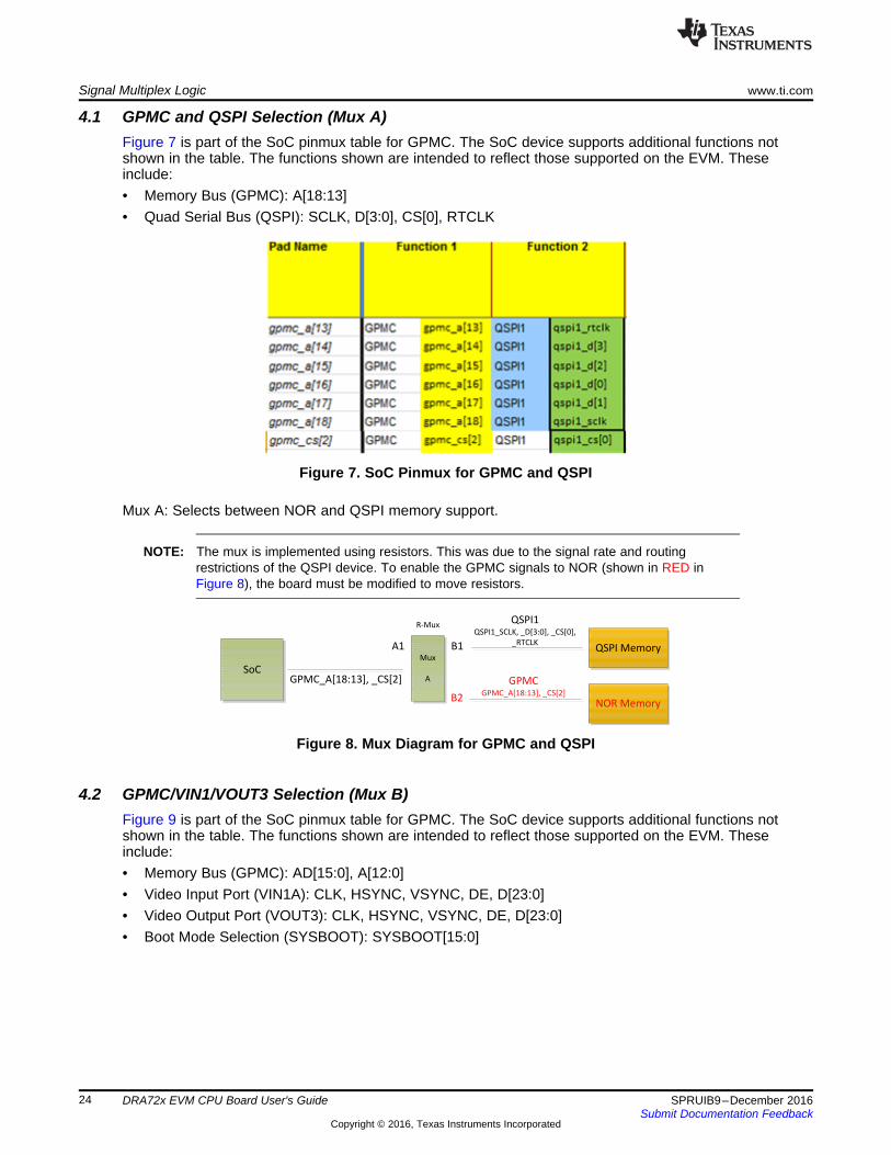
4.1 GPMC and QSPI Selection (Mux A)Figure 7 is part of the SoC pinmux table for GPMC. The SoC device supports additional functions notshown in the table. The functions shown are intended to reflect those supported on the EVM. Theseinclude:• Memory Bus (GPMC): A[18:13]• Quad Serial Bus (QSPI): SCLK, D[3:0], CS[0], RTCLK
Figure 7. SoC Pinmux for GPMC and QSPI
Mux A: Selects between NOR and QSPI memory support.
NOTE: The mux is implemented using resistors. This was due to the signal rate and routingrestrictions of the QSPI device. To enable the GPMC signals to NOR (shown in RED inFigure 8), the board must be modified to move resistors.
Figure 8. Mux Diagram for GPMC and QSPI
4.2 GPMC/VIN1/VOUT3 Selection (Mux B)Figure 9 is part of the SoC pinmux table for GPMC. The SoC device supports additional functions notshown in the table. The functions shown are intended to reflect those supported on the EVM. Theseinclude:• Memory Bus (GPMC): AD[15:0], A[12:0]• Video Input Port (VIN1A): CLK, HSYNC, VSYNC, DE, D[23:0]• Video Output Port (VOUT3): CLK, HSYNC, VSYNC, DE, D[23:0]• Boot Mode Selection (SYSBOOT): SYSBOOT[15:0]
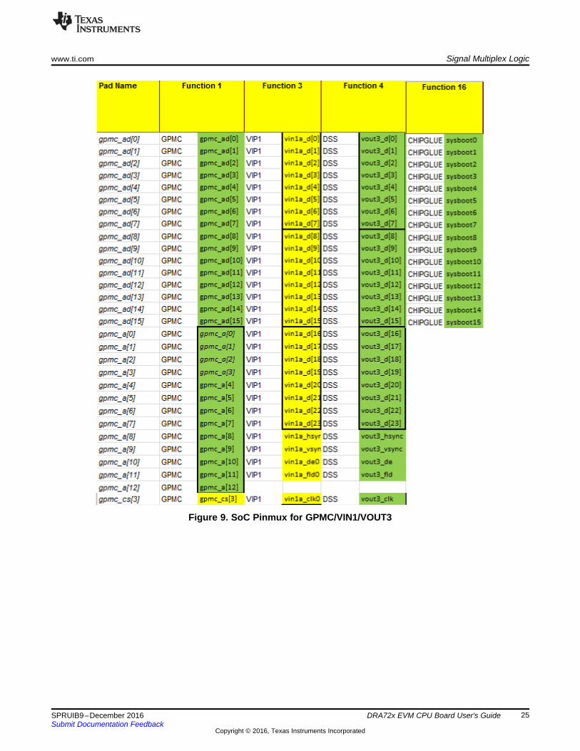
www.ti.com Signal Multiplex Logic
25SPRUIB9–December 2016Submit Documentation Feedback
Copyright © 2016, Texas Instruments Incorporated
DRA72x EVM CPU Board User's Guide
Figure 9. SoC Pinmux for GPMC/VIN1/VOUT3
NAND
Memory
FPD Link
Transmitter
VOUT3VOUT3_CLK, _VS, _HS, _DE,
_D[23:0]
Mux
B
A1 B1
B2
GPMC_A[12:0], _AD[15:0]SoC
GPMCGPMC_A[12:0], _AD[15:0]
CBT16214A1=B1 or A1=B2 or A1 = B3
B3
NOR Memory
DIP Switch
(SYSBOOT)
VIN1AVIN1A_CLK, _VS, _HS, _DE, _D[23:0]
Expansion
Connector
Signal Multiplex Logic www.ti.com
26 SPRUIB9–December 2016Submit Documentation Feedback
Copyright © 2016, Texas Instruments Incorporated
DRA72x EVM CPU Board User's Guide
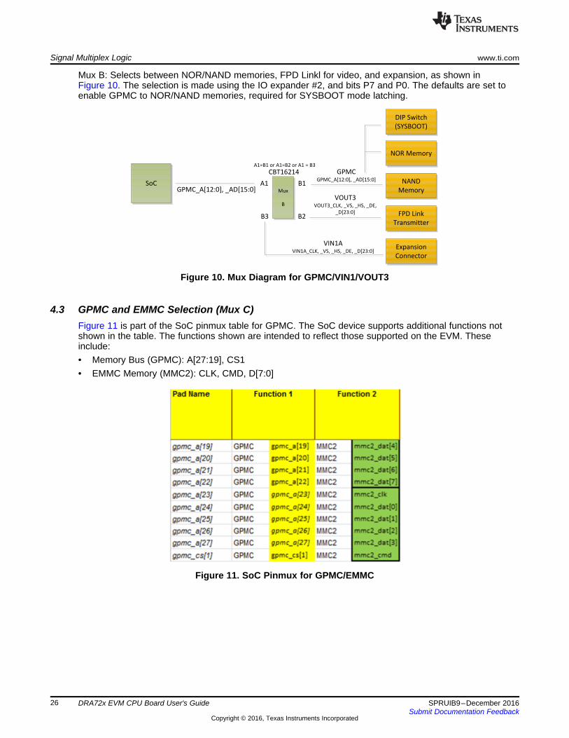
Mux B: Selects between NOR/NAND memories, FPD Linkl for video, and expansion, as shown inFigure 10. The selection is made using the IO expander #2, and bits P7 and P0. The defaults are set toenable GPMC to NOR/NAND memories, required for SYSBOOT mode latching.
Figure 10. Mux Diagram for GPMC/VIN1/VOUT3
4.3 GPMC and EMMC Selection (Mux C)Figure 11 is part of the SoC pinmux table for GPMC. The SoC device supports additional functions notshown in the table. The functions shown are intended to reflect those supported on the EVM. Theseinclude:• Memory Bus (GPMC): A[27:19], CS1• EMMC Memory (MMC2): CLK, CMD, D[7:0]
Figure 11. SoC Pinmux for GPMC/EMMC
NOR Memory
EMMC
Memory
MMC2MMC2_CLK, _CMD, _DA[7:0]
Mux
C
A1 B1
B2
GPMC_A[27:19], _CS[1]SoC
GPMCGPMC_A[27:19], _CS[1]
CBT16212A1=B1 or A1=B2
www.ti.com Signal Multiplex Logic
27SPRUIB9–December 2016Submit Documentation Feedback
Copyright © 2016, Texas Instruments Incorporated
DRA72x EVM CPU Board User's Guide
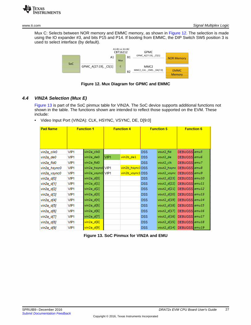
Mux C: Selects between NOR memory and EMMC memory, as shown in Figure 12. The selection is madeusing the IO expander #3, and bits P15 and P14. If booting from EMMC, the DIP Switch SW5 position 3 isused to select interface (by default).
Figure 12. Mux Diagram for GPMC and EMMC
4.4 VIN2A Selection (Mux E)Figure 13 is part of the SoC pinmux table for VIN2A. The SoC device supports additional functions notshown in the table. The functions shown are intended to reflect those supported on the EVM. Theseinclude:• Video Input Port (VIN2A): CLK, HSYNC, VSYNC, DE, D[9:0]
Figure 13. SoC Pinmux for VIN2A and EMU
VIN2AVIN2A_CLK, _VS, _HS, _DE, _D[9:0]
Mux
E
A1 B1
B2
VIN2A_CLK, _VS, _HS, _DE,
_D[9:0]
SoC
CBT16214A1=B2 or A1 = B3
B3
LI Camera
Connector
Expansion
Connector
VIN2AVIN2A_CLK, _VS, _HS, _DE, _D[9:0]
Signal Multiplex Logic www.ti.com
28 SPRUIB9–December 2016Submit Documentation Feedback
Copyright © 2016, Texas Instruments Incorporated
DRA72x EVM CPU Board User's Guide
Mux E: Selects between LI camera and expansion, as shown in Figure 14. The selection is made usingthe IO expander #3, and bits P6 and P2. The default mode is set to expansion.
Figure 14. Mux Diagram for VIN2A and EMU
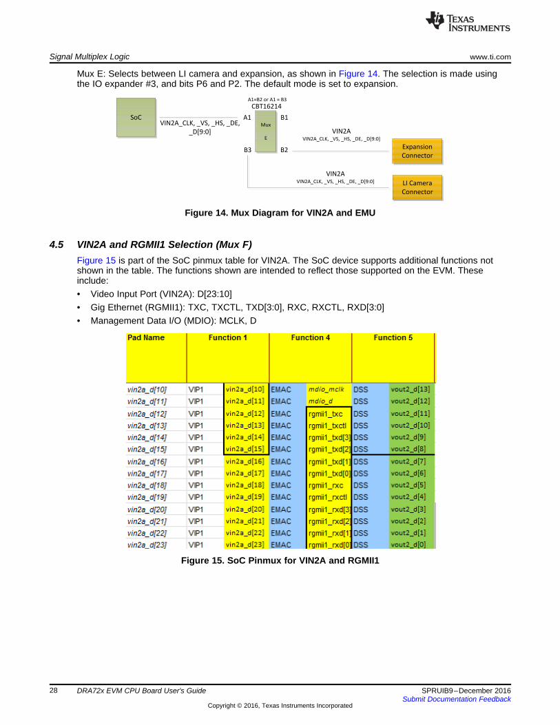
4.5 VIN2A and RGMII1 Selection (Mux F)Figure 15 is part of the SoC pinmux table for VIN2A. The SoC device supports additional functions notshown in the table. The functions shown are intended to reflect those supported on the EVM. Theseinclude:• Video Input Port (VIN2A): D[23:10]• Gig Ethernet (RGMII1): TXC, TXCTL, TXD[3:0], RXC, RXCTL, RXD[3:0]• Management Data I/O (MDIO): MCLK, D
Figure 15. SoC Pinmux for VIN2A and RGMII1
VIN2AVIN2A_D[23:10]
Mux
F
A1 B1
B2
VIN2A_D[23:10]SoC
CBT16214A1=B1 or A1=B2 or A1 = B3
B3
LI Camera
Connector
Expansion
Connector
VIN2AVIN2A_D[13:10]
Ethernet
RGMII1, MDIORGMII1_TXC, _TXCTL, _TXD[3:0], _RXD, _RXCTL, _RXD[3:0]
MDIO_CLK, _D
www.ti.com Signal Multiplex Logic
29SPRUIB9–December 2016Submit Documentation Feedback
Copyright © 2016, Texas Instruments Incorporated
DRA72x EVM CPU Board User's Guide
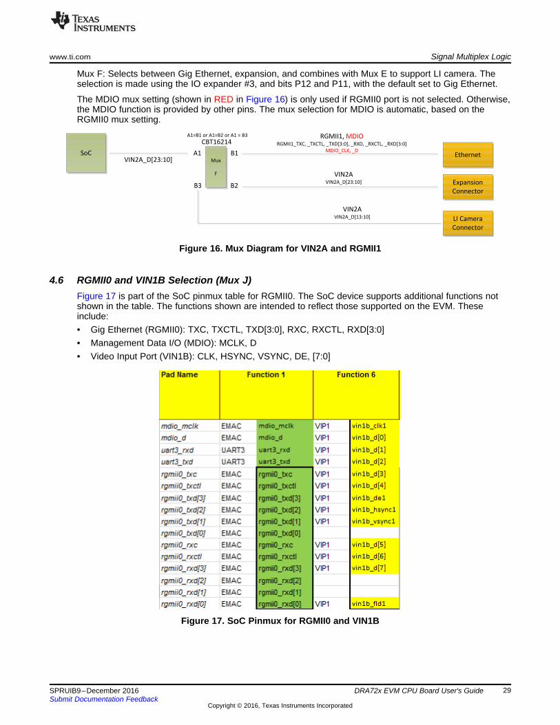
Mux F: Selects between Gig Ethernet, expansion, and combines with Mux E to support LI camera. Theselection is made using the IO expander #3, and bits P12 and P11, with the default set to Gig Ethernet.
The MDIO mux setting (shown in RED in Figure 16) is only used if RGMII0 port is not selected. Otherwise,the MDIO function is provided by other pins. The mux selection for MDIO is automatic, based on theRGMII0 mux setting.
Figure 16. Mux Diagram for VIN2A and RGMII1
4.6 RGMII0 and VIN1B Selection (Mux J)Figure 17 is part of the SoC pinmux table for RGMII0. The SoC device supports additional functions notshown in the table. The functions shown are intended to reflect those supported on the EVM. Theseinclude:• Gig Ethernet (RGMII0): TXC, TXCTL, TXD[3:0], RXC, RXCTL, RXD[3:0]• Management Data I/O (MDIO): MCLK, D• Video Input Port (VIN1B): CLK, HSYNC, VSYNC, DE, [7:0]
Figure 17. SoC Pinmux for RGMII0 and VIN1B

COM8Q
Connector
Expansion
Connector
SPI2SPI2_SCLK, _D[1:0], _CS[0]
Mux
K
A1 B1
B2
SPI2_SCLK, _D[1:0], _CS[0]SoC
UART3UART3_TX, _RX, _CTS, _RTS
CBT3257A1=B1 or A1=B2
Ethernet
Expansion
Connector
VIN1BVIN1B_CLK, _VS, _HS, _DE, _DA[7:0]
Mux
J
A1 B1
B2
RGMII0_TXC, _TXCTL, _TXD[3:0],
_RXC, RXCTL, _RXD[3:0]
UART3_RXD, _TXD
MDIO_MCLK, _D
SoC
CBT16212A1=B1 or A1=B2
RGMII0, MDIORGMII0_TXC, _TXCTL, _TXD[3:0],
_RXD, _RXCTL, _RXD[3:0]
MDIO_MCLK, _D
Signal Multiplex Logic www.ti.com
30 SPRUIB9–December 2016Submit Documentation Feedback
Copyright © 2016, Texas Instruments Incorporated
DRA72x EVM CPU Board User's Guide
Mux J: Selects between Gig Ethernet and expansion, as shown in Figure 18. The selection is made usingthe IO expander #2 and bit P4, defaulting to Gig Ethernet.
Figure 18. Mux Diagram for RGMII0 and VIN1B
4.7 SPI2 and UART3 Selection (Mux K)Figure 19 is part of the SoC pinmux table for SPI2. The SoC device supports additional functions notshown in the table. The functions shown are intended to reflect those supported on the EVM. Theseinclude:• SPI Serial Bus (SPI2): SCLK, D[1:0], CS[0]• UART Serial Bus (UART3): TXD, RXD, CTSN, RTSN
Figure 19. SoC Pinmux for SPI2 and UART3
Mux K: Selects between Bluetooth (COM8Q module) and expansion interface, as shown in Figure 20. Theselection is made using the IO expander #2 and bits P16, defaulting to expansion.
Figure 20. Mux Diagram for SPI2 and UART3
DCAN2
Connector
DCAN2DCAN2_TX, _RX
Mux
L
A1 B1
B2
GPIO6_[15:14]SoC
I2C3I2C3_SCL, _SDA
CBT3257A1=B1 or A1=B2
Expansion
Connector
www.ti.com Signal Multiplex Logic
31SPRUIB9–December 2016Submit Documentation Feedback
Copyright © 2016, Texas Instruments Incorporated
DRA72x EVM CPU Board User's Guide
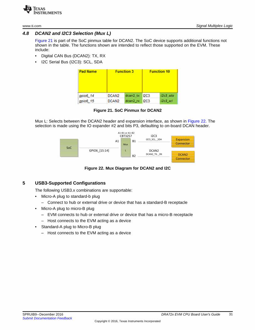
4.8 DCAN2 and I2C3 Selection (Mux L)Figure 21 is part of the SoC pinmux table for DCAN2. The SoC device supports additional functions notshown in the table. The functions shown are intended to reflect those supported on the EVM. Theseinclude:• Digital CAN Bus (DCAN2): TX, RX• I2C Serial Bus (I2C3): SCL, SDA
Figure 21. SoC Pinmux for DCAN2
Mux L: Selects between the DCAN2 header and expansion interface, as shown in Figure 22. Theselection is made using the IO expander #2 and bits P3, defaulting to on-board DCAN header.
Figure 22. Mux Diagram for DCAN2 and I2C
5 USB3-Supported ConfigurationsThe following USB3.x combinations are supportable:• Micro-A plug to standard-b plug
– Connect to hub or external drive or device that has a standard-B receptacle• Micro-A plug to micro-B plug
– EVM connects to hub or external drive or device that has a micro-B receptacle– Host connects to the EVM acting as a device
• Standard-A plug to Micro-B plug– Host connects to the EVM acting as a device
USB3-Supported Configurations www.ti.com
32 SPRUIB9–December 2016Submit Documentation Feedback
Copyright © 2016, Texas Instruments Incorporated
DRA72x EVM CPU Board User's Guide
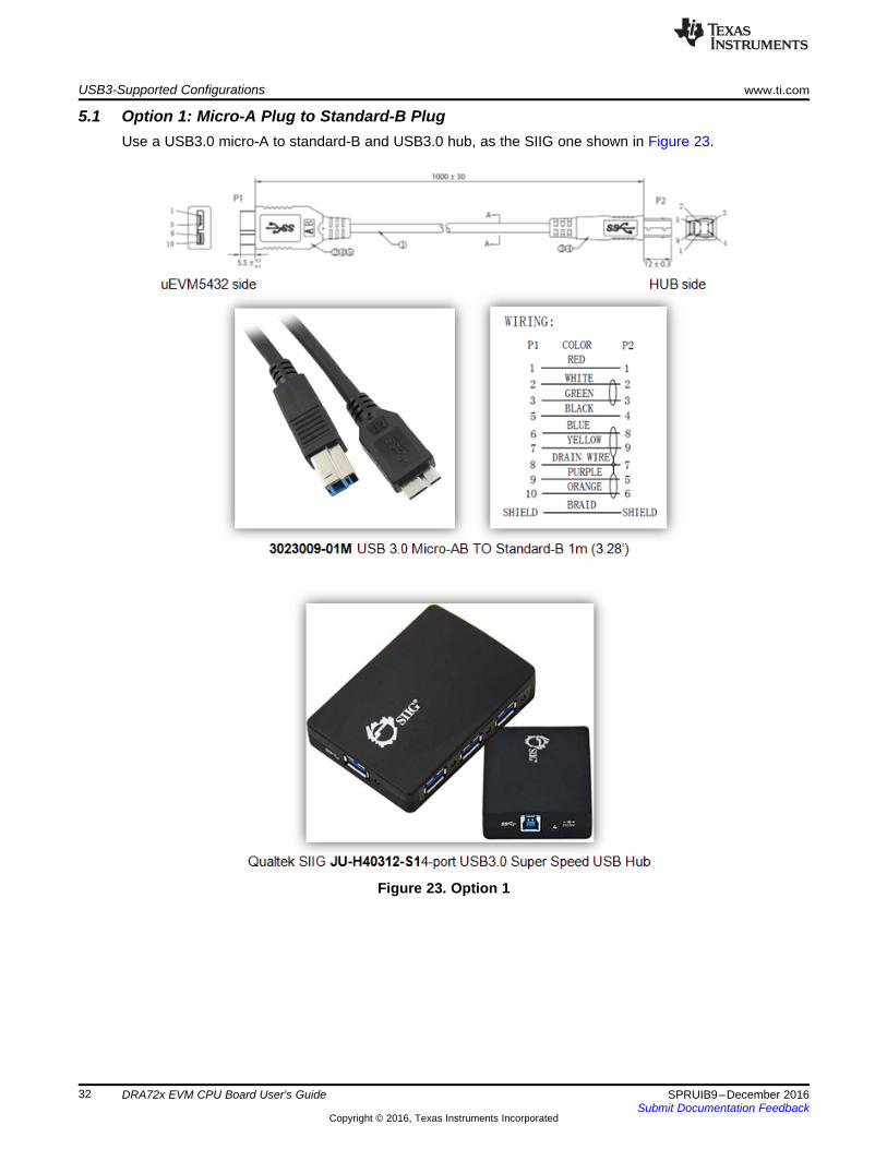
5.1 Option 1: Micro-A Plug to Standard-B PlugUse a USB3.0 micro-A to standard-B and USB3.0 hub, as the SIIG one shown in Figure 23.
Figure 23. Option 1
www.ti.com USB3-Supported Configurations
33SPRUIB9–December 2016Submit Documentation Feedback
Copyright © 2016, Texas Instruments Incorporated
DRA72x EVM CPU Board User's Guide
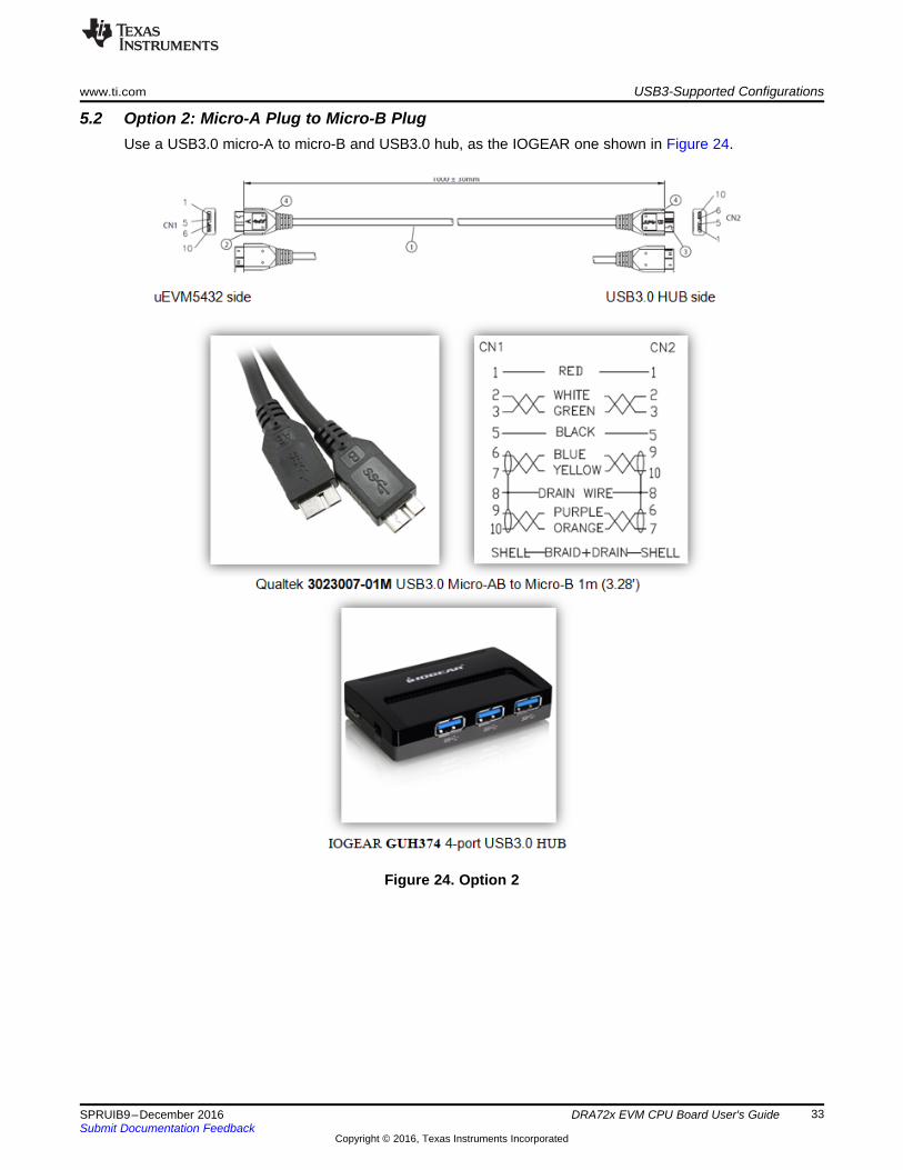
5.2 Option 2: Micro-A Plug to Micro-B PlugUse a USB3.0 micro-A to micro-B and USB3.0 hub, as the IOGEAR one shown in Figure 24.
Figure 24. Option 2
USB3-Supported Configurations www.ti.com
34 SPRUIB9–December 2016Submit Documentation Feedback
Copyright © 2016, Texas Instruments Incorporated
DRA72x EVM CPU Board User's Guide
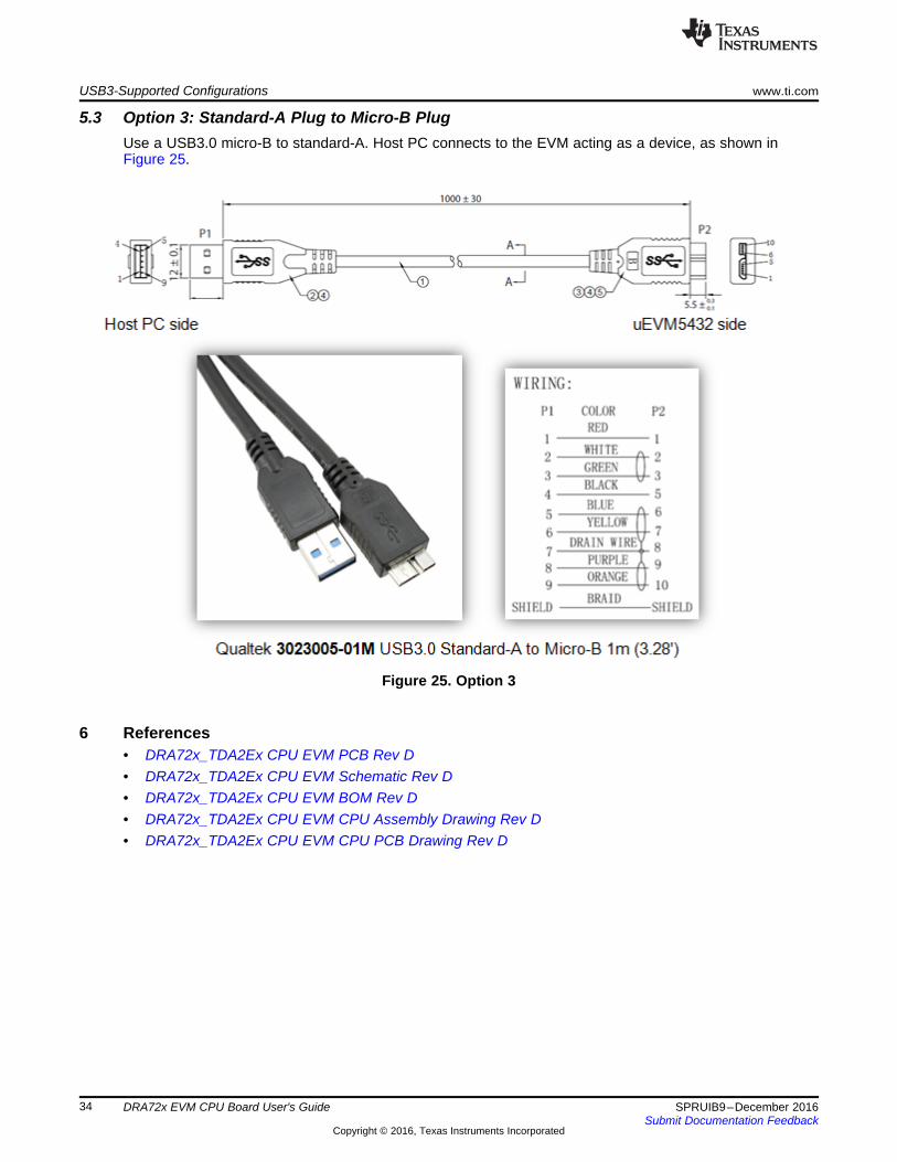
5.3 Option 3: Standard-A Plug to Micro-B PlugUse a USB3.0 micro-B to standard-A. Host PC connects to the EVM acting as a device, as shown inFigure 25.
Figure 25. Option 3
6 References• DRA72x_TDA2Ex CPU EVM PCB Rev D• DRA72x_TDA2Ex CPU EVM Schematic Rev D• DRA72x_TDA2Ex CPU EVM BOM Rev D• DRA72x_TDA2Ex CPU EVM CPU Assembly Drawing Rev D• DRA72x_TDA2Ex CPU EVM CPU PCB Drawing Rev D
STANDARD TERMS AND CONDITIONS FOR EVALUATION MODULES1. Delivery: TI delivers TI evaluation boards, kits, or modules, including demonstration software, components, and/or documentation
which may be provided together or separately (collectively, an “EVM” or “EVMs”) to the User (“User”) in accordance with the termsand conditions set forth herein. Acceptance of the EVM is expressly subject to the following terms and conditions.1.1 EVMs are intended solely for product or software developers for use in a research and development setting to facilitate feasibility
evaluation, experimentation, or scientific analysis of TI semiconductors products. EVMs have no direct function and are notfinished products. EVMs shall not be directly or indirectly assembled as a part or subassembly in any finished product. Forclarification, any software or software tools provided with the EVM (“Software”) shall not be subject to the terms and conditionsset forth herein but rather shall be subject to the applicable terms and conditions that accompany such Software
1.2 EVMs are not intended for consumer or household use. EVMs may not be sold, sublicensed, leased, rented, loaned, assigned,or otherwise distributed for commercial purposes by Users, in whole or in part, or used in any finished product or productionsystem.
2 Limited Warranty and Related Remedies/Disclaimers:2.1 These terms and conditions do not apply to Software. The warranty, if any, for Software is covered in the applicable Software
License Agreement.2.2 TI warrants that the TI EVM will conform to TI's published specifications for ninety (90) days after the date TI delivers such EVM
to User. Notwithstanding the foregoing, TI shall not be liable for any defects that are caused by neglect, misuse or mistreatmentby an entity other than TI, including improper installation or testing, or for any EVMs that have been altered or modified in anyway by an entity other than TI. Moreover, TI shall not be liable for any defects that result from User's design, specifications orinstructions for such EVMs. Testing and other quality control techniques are used to the extent TI deems necessary or asmandated by government requirements. TI does not test all parameters of each EVM.
2.3 If any EVM fails to conform to the warranty set forth above, TI's sole liability shall be at its option to repair or replace such EVM,or credit User's account for such EVM. TI's liability under this warranty shall be limited to EVMs that are returned during thewarranty period to the address designated by TI and that are determined by TI not to conform to such warranty. If TI elects torepair or replace such EVM, TI shall have a reasonable time to repair such EVM or provide replacements. Repaired EVMs shallbe warranted for the remainder of the original warranty period. Replaced EVMs shall be warranted for a new full ninety (90) daywarranty period.
3 Regulatory Notices:3.1 United States
3.1.1 Notice applicable to EVMs not FCC-Approved:This kit is designed to allow product developers to evaluate electronic components, circuitry, or software associated with the kitto determine whether to incorporate such items in a finished product and software developers to write software applications foruse with the end product. This kit is not a finished product and when assembled may not be resold or otherwise marketed unlessall required FCC equipment authorizations are first obtained. Operation is subject to the condition that this product not causeharmful interference to licensed radio stations and that this product accept harmful interference. Unless the assembled kit isdesigned to operate under part 15, part 18 or part 95 of this chapter, the operator of the kit must operate under the authority ofan FCC license holder or must secure an experimental authorization under part 5 of this chapter.3.1.2 For EVMs annotated as FCC – FEDERAL COMMUNICATIONS COMMISSION Part 15 Compliant:
CAUTIONThis device complies with part 15 of the FCC Rules. Operation is subject to the following two conditions: (1) This device may notcause harmful interference, and (2) this device must accept any interference received, including interference that may causeundesired operation.Changes or modifications not expressly approved by the party responsible for compliance could void the user's authority tooperate the equipment.
FCC Interference Statement for Class A EVM devicesNOTE: This equipment has been tested and found to comply with the limits for a Class A digital device, pursuant to part 15 ofthe FCC Rules. These limits are designed to provide reasonable protection against harmful interference when the equipment isoperated in a commercial environment. This equipment generates, uses, and can radiate radio frequency energy and, if notinstalled and used in accordance with the instruction manual, may cause harmful interference to radio communications.Operation of this equipment in a residential area is likely to cause harmful interference in which case the user will be required tocorrect the interference at his own expense.
SPACER
SPACER
SPACER
SPACER
SPACER
SPACER
SPACER
SPACER
FCC Interference Statement for Class B EVM devicesNOTE: This equipment has been tested and found to comply with the limits for a Class B digital device, pursuant to part 15 ofthe FCC Rules. These limits are designed to provide reasonable protection against harmful interference in a residentialinstallation. This equipment generates, uses and can radiate radio frequency energy and, if not installed and used in accordancewith the instructions, may cause harmful interference to radio communications. However, there is no guarantee that interferencewill not occur in a particular installation. If this equipment does cause harmful interference to radio or television reception, whichcan be determined by turning the equipment off and on, the user is encouraged to try to correct the interference by one or moreof the following measures:
• Reorient or relocate the receiving antenna.• Increase the separation between the equipment and receiver.• Connect the equipment into an outlet on a circuit different from that to which the receiver is connected.• Consult the dealer or an experienced radio/TV technician for help.
3.2 Canada3.2.1 For EVMs issued with an Industry Canada Certificate of Conformance to RSS-210
Concerning EVMs Including Radio Transmitters:This device complies with Industry Canada license-exempt RSS standard(s). Operation is subject to the following two conditions:(1) this device may not cause interference, and (2) this device must accept any interference, including interference that maycause undesired operation of the device.
Concernant les EVMs avec appareils radio:Le présent appareil est conforme aux CNR d'Industrie Canada applicables aux appareils radio exempts de licence. L'exploitationest autorisée aux deux conditions suivantes: (1) l'appareil ne doit pas produire de brouillage, et (2) l'utilisateur de l'appareil doitaccepter tout brouillage radioélectrique subi, même si le brouillage est susceptible d'en compromettre le fonctionnement.
Concerning EVMs Including Detachable Antennas:Under Industry Canada regulations, this radio transmitter may only operate using an antenna of a type and maximum (or lesser)gain approved for the transmitter by Industry Canada. To reduce potential radio interference to other users, the antenna typeand its gain should be so chosen that the equivalent isotropically radiated power (e.i.r.p.) is not more than that necessary forsuccessful communication. This radio transmitter has been approved by Industry Canada to operate with the antenna typeslisted in the user guide with the maximum permissible gain and required antenna impedance for each antenna type indicated.Antenna types not included in this list, having a gain greater than the maximum gain indicated for that type, are strictly prohibitedfor use with this device.
Concernant les EVMs avec antennes détachablesConformément à la réglementation d'Industrie Canada, le présent émetteur radio peut fonctionner avec une antenne d'un type etd'un gain maximal (ou inférieur) approuvé pour l'émetteur par Industrie Canada. Dans le but de réduire les risques de brouillageradioélectrique à l'intention des autres utilisateurs, il faut choisir le type d'antenne et son gain de sorte que la puissance isotroperayonnée équivalente (p.i.r.e.) ne dépasse pas l'intensité nécessaire à l'établissement d'une communication satisfaisante. Leprésent émetteur radio a été approuvé par Industrie Canada pour fonctionner avec les types d'antenne énumérés dans lemanuel d’usage et ayant un gain admissible maximal et l'impédance requise pour chaque type d'antenne. Les types d'antennenon inclus dans cette liste, ou dont le gain est supérieur au gain maximal indiqué, sont strictement interdits pour l'exploitation del'émetteur
3.3 Japan3.3.1 Notice for EVMs delivered in Japan: Please see http://www.tij.co.jp/lsds/ti_ja/general/eStore/notice_01.page 日本国内に
輸入される評価用キット、ボードについては、次のところをご覧ください。http://www.tij.co.jp/lsds/ti_ja/general/eStore/notice_01.page
3.3.2 Notice for Users of EVMs Considered “Radio Frequency Products” in Japan: EVMs entering Japan may not be certifiedby TI as conforming to Technical Regulations of Radio Law of Japan.
If User uses EVMs in Japan, not certified to Technical Regulations of Radio Law of Japan, User is required by Radio Law ofJapan to follow the instructions below with respect to EVMs:1. Use EVMs in a shielded room or any other test facility as defined in the notification #173 issued by Ministry of Internal
Affairs and Communications on March 28, 2006, based on Sub-section 1.1 of Article 6 of the Ministry’s Rule forEnforcement of Radio Law of Japan,
2. Use EVMs only after User obtains the license of Test Radio Station as provided in Radio Law of Japan with respect toEVMs, or
3. Use of EVMs only after User obtains the Technical Regulations Conformity Certification as provided in Radio Law of Japanwith respect to EVMs. Also, do not transfer EVMs, unless User gives the same notice above to the transferee. Please notethat if User does not follow the instructions above, User will be subject to penalties of Radio Law of Japan.
SPACER
SPACER
SPACER
SPACER
SPACER
【無線電波を送信する製品の開発キットをお使いになる際の注意事項】 開発キットの中には技術基準適合証明を受けていないものがあります。 技術適合証明を受けていないもののご使用に際しては、電波法遵守のため、以下のいずれかの措置を取っていただく必要がありますのでご注意ください。1. 電波法施行規則第6条第1項第1号に基づく平成18年3月28日総務省告示第173号で定められた電波暗室等の試験設備でご使用
いただく。2. 実験局の免許を取得後ご使用いただく。3. 技術基準適合証明を取得後ご使用いただく。
なお、本製品は、上記の「ご使用にあたっての注意」を譲渡先、移転先に通知しない限り、譲渡、移転できないものとします。上記を遵守頂けない場合は、電波法の罰則が適用される可能性があることをご留意ください。 日本テキサス・イ
ンスツルメンツ株式会社東京都新宿区西新宿6丁目24番1号西新宿三井ビル
3.3.3 Notice for EVMs for Power Line Communication: Please see http://www.tij.co.jp/lsds/ti_ja/general/eStore/notice_02.page電力線搬送波通信についての開発キットをお使いになる際の注意事項については、次のところをご覧ください。http://www.tij.co.jp/lsds/ti_ja/general/eStore/notice_02.page
SPACER4 EVM Use Restrictions and Warnings:
4.1 EVMS ARE NOT FOR USE IN FUNCTIONAL SAFETY AND/OR SAFETY CRITICAL EVALUATIONS, INCLUDING BUT NOTLIMITED TO EVALUATIONS OF LIFE SUPPORT APPLICATIONS.
4.2 User must read and apply the user guide and other available documentation provided by TI regarding the EVM prior to handlingor using the EVM, including without limitation any warning or restriction notices. The notices contain important safety informationrelated to, for example, temperatures and voltages.
4.3 Safety-Related Warnings and Restrictions:4.3.1 User shall operate the EVM within TI’s recommended specifications and environmental considerations stated in the user
guide, other available documentation provided by TI, and any other applicable requirements and employ reasonable andcustomary safeguards. Exceeding the specified performance ratings and specifications (including but not limited to inputand output voltage, current, power, and environmental ranges) for the EVM may cause personal injury or death, orproperty damage. If there are questions concerning performance ratings and specifications, User should contact a TIfield representative prior to connecting interface electronics including input power and intended loads. Any loads appliedoutside of the specified output range may also result in unintended and/or inaccurate operation and/or possiblepermanent damage to the EVM and/or interface electronics. Please consult the EVM user guide prior to connecting anyload to the EVM output. If there is uncertainty as to the load specification, please contact a TI field representative.During normal operation, even with the inputs and outputs kept within the specified allowable ranges, some circuitcomponents may have elevated case temperatures. These components include but are not limited to linear regulators,switching transistors, pass transistors, current sense resistors, and heat sinks, which can be identified using theinformation in the associated documentation. When working with the EVM, please be aware that the EVM may becomevery warm.
4.3.2 EVMs are intended solely for use by technically qualified, professional electronics experts who are familiar with thedangers and application risks associated with handling electrical mechanical components, systems, and subsystems.User assumes all responsibility and liability for proper and safe handling and use of the EVM by User or its employees,affiliates, contractors or designees. User assumes all responsibility and liability to ensure that any interfaces (electronicand/or mechanical) between the EVM and any human body are designed with suitable isolation and means to safelylimit accessible leakage currents to minimize the risk of electrical shock hazard. User assumes all responsibility andliability for any improper or unsafe handling or use of the EVM by User or its employees, affiliates, contractors ordesignees.
4.4 User assumes all responsibility and liability to determine whether the EVM is subject to any applicable international, federal,state, or local laws and regulations related to User’s handling and use of the EVM and, if applicable, User assumes allresponsibility and liability for compliance in all respects with such laws and regulations. User assumes all responsibility andliability for proper disposal and recycling of the EVM consistent with all applicable international, federal, state, and localrequirements.
5. Accuracy of Information: To the extent TI provides information on the availability and function of EVMs, TI attempts to be as accurateas possible. However, TI does not warrant the accuracy of EVM descriptions, EVM availability or other information on its websites asaccurate, complete, reliable, current, or error-free.
SPACER
SPACER
SPACER
SPACER
SPACER
SPACER
SPACER6. Disclaimers:
6.1 EXCEPT AS SET FORTH ABOVE, EVMS AND ANY WRITTEN DESIGN MATERIALS PROVIDED WITH THE EVM (AND THEDESIGN OF THE EVM ITSELF) ARE PROVIDED "AS IS" AND "WITH ALL FAULTS." TI DISCLAIMS ALL OTHERWARRANTIES, EXPRESS OR IMPLIED, REGARDING SUCH ITEMS, INCLUDING BUT NOT LIMITED TO ANY IMPLIEDWARRANTIES OF MERCHANTABILITY OR FITNESS FOR A PARTICULAR PURPOSE OR NON-INFRINGEMENT OF ANYTHIRD PARTY PATENTS, COPYRIGHTS, TRADE SECRETS OR OTHER INTELLECTUAL PROPERTY RIGHTS.
6.2 EXCEPT FOR THE LIMITED RIGHT TO USE THE EVM SET FORTH HEREIN, NOTHING IN THESE TERMS ANDCONDITIONS SHALL BE CONSTRUED AS GRANTING OR CONFERRING ANY RIGHTS BY LICENSE, PATENT, OR ANYOTHER INDUSTRIAL OR INTELLECTUAL PROPERTY RIGHT OF TI, ITS SUPPLIERS/LICENSORS OR ANY OTHER THIRDPARTY, TO USE THE EVM IN ANY FINISHED END-USER OR READY-TO-USE FINAL PRODUCT, OR FOR ANYINVENTION, DISCOVERY OR IMPROVEMENT MADE, CONCEIVED OR ACQUIRED PRIOR TO OR AFTER DELIVERY OFTHE EVM.
7. USER'S INDEMNITY OBLIGATIONS AND REPRESENTATIONS. USER WILL DEFEND, INDEMNIFY AND HOLD TI, ITSLICENSORS AND THEIR REPRESENTATIVES HARMLESS FROM AND AGAINST ANY AND ALL CLAIMS, DAMAGES, LOSSES,EXPENSES, COSTS AND LIABILITIES (COLLECTIVELY, "CLAIMS") ARISING OUT OF OR IN CONNECTION WITH ANYHANDLING OR USE OF THE EVM THAT IS NOT IN ACCORDANCE WITH THESE TERMS AND CONDITIONS. THIS OBLIGATIONSHALL APPLY WHETHER CLAIMS ARISE UNDER STATUTE, REGULATION, OR THE LAW OF TORT, CONTRACT OR ANYOTHER LEGAL THEORY, AND EVEN IF THE EVM FAILS TO PERFORM AS DESCRIBED OR EXPECTED.
8. Limitations on Damages and Liability:8.1 General Limitations. IN NO EVENT SHALL TI BE LIABLE FOR ANY SPECIAL, COLLATERAL, INDIRECT, PUNITIVE,
INCIDENTAL, CONSEQUENTIAL, OR EXEMPLARY DAMAGES IN CONNECTION WITH OR ARISING OUT OF THESETERMS ANDCONDITIONS OR THE USE OF THE EVMS PROVIDED HEREUNDER, REGARDLESS OF WHETHER TI HASBEEN ADVISED OF THE POSSIBILITY OF SUCH DAMAGES. EXCLUDED DAMAGES INCLUDE, BUT ARE NOT LIMITEDTO, COST OF REMOVAL OR REINSTALLATION, ANCILLARY COSTS TO THE PROCUREMENT OF SUBSTITUTE GOODSOR SERVICES, RETESTING, OUTSIDE COMPUTER TIME, LABOR COSTS, LOSS OF GOODWILL, LOSS OF PROFITS,LOSS OF SAVINGS, LOSS OF USE, LOSS OF DATA, OR BUSINESS INTERRUPTION. NO CLAIM, SUIT OR ACTION SHALLBE BROUGHT AGAINST TI MORE THAN ONE YEAR AFTER THE RELATED CAUSE OF ACTION HAS OCCURRED.
8.2 Specific Limitations. IN NO EVENT SHALL TI'S AGGREGATE LIABILITY FROM ANY WARRANTY OR OTHER OBLIGATIONARISING OUT OF OR IN CONNECTION WITH THESE TERMS AND CONDITIONS, OR ANY USE OF ANY TI EVMPROVIDED HEREUNDER, EXCEED THE TOTAL AMOUNT PAID TO TI FOR THE PARTICULAR UNITS SOLD UNDERTHESE TERMS AND CONDITIONS WITH RESPECT TO WHICH LOSSES OR DAMAGES ARE CLAIMED. THE EXISTENCEOF MORE THAN ONE CLAIM AGAINST THE PARTICULAR UNITS SOLD TO USER UNDER THESE TERMS ANDCONDITIONS SHALL NOT ENLARGE OR EXTEND THIS LIMIT.
9. Return Policy. Except as otherwise provided, TI does not offer any refunds, returns, or exchanges. Furthermore, no return of EVM(s)will be accepted if the package has been opened and no return of the EVM(s) will be accepted if they are damaged or otherwise not ina resalable condition. If User feels it has been incorrectly charged for the EVM(s) it ordered or that delivery violates the applicableorder, User should contact TI. All refunds will be made in full within thirty (30) working days from the return of the components(s),excluding any postage or packaging costs.
10. Governing Law: These terms and conditions shall be governed by and interpreted in accordance with the laws of the State of Texas,without reference to conflict-of-laws principles. User agrees that non-exclusive jurisdiction for any dispute arising out of or relating tothese terms and conditions lies within courts located in the State of Texas and consents to venue in Dallas County, Texas.Notwithstanding the foregoing, any judgment may be enforced in any United States or foreign court, and TI may seek injunctive reliefin any United States or foreign court.
Mailing Address: Texas Instruments, Post Office Box 655303, Dallas, Texas 75265Copyright © 2016, Texas Instruments Incorporated
spacer

IMPORTANT NOTICE
Texas Instruments Incorporated and its subsidiaries (TI) reserve the right to make corrections, enhancements, improvements and otherchanges to its semiconductor products and services per JESD46, latest issue, and to discontinue any product or service per JESD48, latestissue. Buyers should obtain the latest relevant information before placing orders and should verify that such information is current andcomplete. All semiconductor products (also referred to herein as “components”) are sold subject to TI’s terms and conditions of salesupplied at the time of order acknowledgment.TI warrants performance of its components to the specifications applicable at the time of sale, in accordance with the warranty in TI’s termsand conditions of sale of semiconductor products. Testing and other quality control techniques are used to the extent TI deems necessaryto support this warranty. Except where mandated by applicable law, testing of all parameters of each component is not necessarilyperformed.TI assumes no liability for applications assistance or the design of Buyers’ products. Buyers are responsible for their products andapplications using TI components. To minimize the risks associated with Buyers’ products and applications, Buyers should provideadequate design and operating safeguards.TI does not warrant or represent that any license, either express or implied, is granted under any patent right, copyright, mask work right, orother intellectual property right relating to any combination, machine, or process in which TI components or services are used. Informationpublished by TI regarding third-party products or services does not constitute a license to use such products or services or a warranty orendorsement thereof. Use of such information may require a license from a third party under the patents or other intellectual property of thethird party, or a license from TI under the patents or other intellectual property of TI.Reproduction of significant portions of TI information in TI data books or data sheets is permissible only if reproduction is without alterationand is accompanied by all associated warranties, conditions, limitations, and notices. TI is not responsible or liable for such altereddocumentation. Information of third parties may be subject to additional restrictions.Resale of TI components or services with statements different from or beyond the parameters stated by TI for that component or servicevoids all express and any implied warranties for the associated TI component or service and is an unfair and deceptive business practice.TI is not responsible or liable for any such statements.Buyer acknowledges and agrees that it is solely responsible for compliance with all legal, regulatory and safety-related requirementsconcerning its products, and any use of TI components in its applications, notwithstanding any applications-related information or supportthat may be provided by TI. Buyer represents and agrees that it has all the necessary expertise to create and implement safeguards whichanticipate dangerous consequences of failures, monitor failures and their consequences, lessen the likelihood of failures that might causeharm and take appropriate remedial actions. Buyer will fully indemnify TI and its representatives against any damages arising out of the useof any TI components in safety-critical applications.In some cases, TI components may be promoted specifically to facilitate safety-related applications. With such components, TI’s goal is tohelp enable customers to design and create their own end-product solutions that meet applicable functional safety standards andrequirements. Nonetheless, such components are subject to these terms.No TI components are authorized for use in FDA Class III (or similar life-critical medical equipment) unless authorized officers of the partieshave executed a special agreement specifically governing such use.Only those TI components which TI has specifically designated as military grade or “enhanced plastic” are designed and intended for use inmilitary/aerospace applications or environments. Buyer acknowledges and agrees that any military or aerospace use of TI componentswhich have not been so designated is solely at the Buyer's risk, and that Buyer is solely responsible for compliance with all legal andregulatory requirements in connection with such use.TI has specifically designated certain components as meeting ISO/TS16949 requirements, mainly for automotive use. In any case of use ofnon-designated products, TI will not be responsible for any failure to meet ISO/TS16949.
Products ApplicationsAudio www.ti.com/audio Automotive and Transportation www.ti.com/automotiveAmplifiers amplifier.ti.com Communications and Telecom www.ti.com/communicationsData Converters dataconverter.ti.com Computers and Peripherals www.ti.com/computersDLP® Products www.dlp.com Consumer Electronics www.ti.com/consumer-appsDSP dsp.ti.com Energy and Lighting www.ti.com/energyClocks and Timers www.ti.com/clocks Industrial www.ti.com/industrialInterface interface.ti.com Medical www.ti.com/medicalLogic logic.ti.com Security www.ti.com/securityPower Mgmt power.ti.com Space, Avionics and Defense www.ti.com/space-avionics-defenseMicrocontrollers microcontroller.ti.com Video and Imaging www.ti.com/videoRFID www.ti-rfid.comOMAP Applications Processors www.ti.com/omap TI E2E Community e2e.ti.comWireless Connectivity www.ti.com/wirelessconnectivity
Mailing Address: Texas Instruments, Post Office Box 655303, Dallas, Texas 75265Copyright © 2016, Texas Instruments Incorporated
Related Documents