Dr Renato Turchetta CMOS Sensor Design Group CCLRC Technology Large Area Monolithic Active Pixel Sensors

Welcome message from author
This document is posted to help you gain knowledge. Please leave a comment to let me know what you think about it! Share it to your friends and learn new things together.
Transcript
Dr Renato TurchettaCMOS Sensor Design GroupCCLRC Technology
Large Area Monolithic Active
Pixel Sensors
2Workshop on Silicon Detector Systems for the CBM experiment GSI Darmstadt, April 18-20, 2007
Outline Introduction on CMOS MAPS
Large sensors for imaging
The INMAPS process
CALICE
Conclusions
3Workshop on Silicon Detector Systems for the CBM experiment GSI Darmstadt, April 18-20, 2007
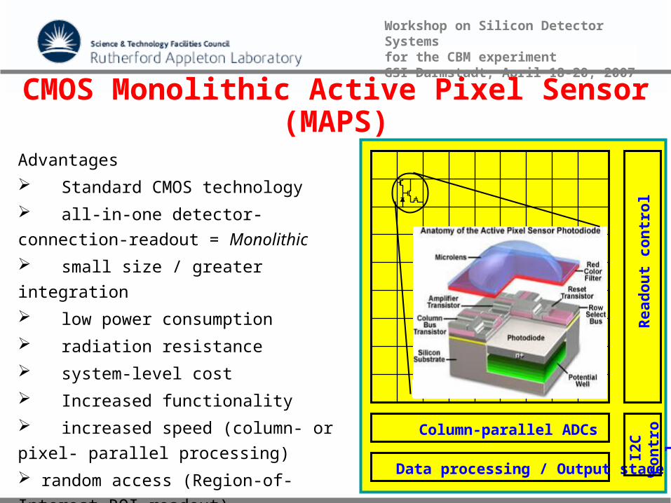
CMOS Monolithic Active Pixel Sensor (MAPS)
Advantages
Standard CMOS technology
all-in-one detector-connection-
readout = Monolithic
small size / greater integration
low power consumption
radiation resistance
system-level cost
Increased functionality
increased speed (column- or pixel-
parallel processing)
random access (Region-of-Interest
ROI readout)
Column-parallel ADCs
Data processing / Output stage
Read
ou
t con
trol
I2C
con
trol
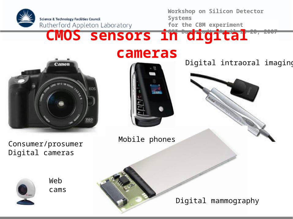
4Workshop on Silicon Detector Systems for the CBM experiment GSI Darmstadt, April 18-20, 2007 CMOS sensors in digital
cameras
Consumer/prosumerDigital cameras
Digital intraoral imaging
Digital mammography
Mobile phones
Web cams
5Workshop on Silicon Detector Systems for the CBM experiment GSI Darmstadt, April 18-20, 2007
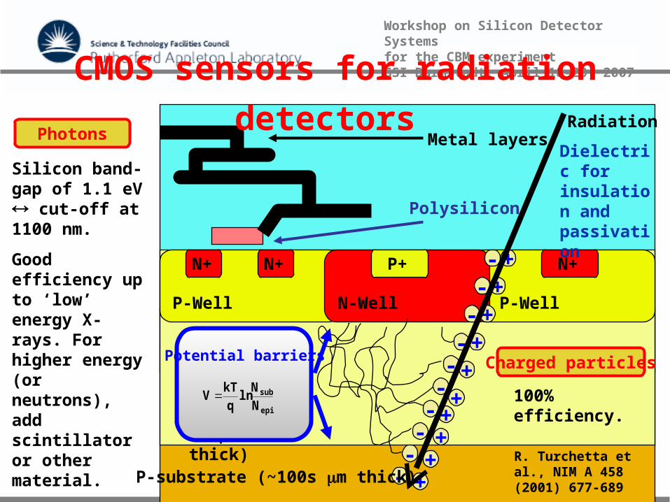
Metal layers
Polysilicon
P-Well N-Well P-Well
N+ N+ P+ N+
CMOS sensors for radiation
detectors Dielectric for insulation and passivation
Silicon band-gap of 1.1 eV cut-off at 1100 nm.
Good efficiency up to ‘low’ energy X-rays. For higher energy (or neutrons), add scintillator or other material.
Need removal of substrate for detection of UV, low energy electrons.
Photons
Charged particles
100% efficiency.
Radiation
--
--
--
- ++
+++
++
- +- +- +
P-substrate (~100s m thick)
P-epitaxial layer(up to to 20 m thick)
Potential barriers
epi
sub
N
Nln
q
kTV
R. Turchetta et al., NIM A 458 (2001) 677-689
6Workshop on Silicon Detector Systems for the CBM experiment GSI Darmstadt, April 18-20, 2007
Outline Introduction on CMOS MAPS
Large sensors for imaging
The INMAPS process
CALICE
Conclusions
7Workshop on Silicon Detector Systems for the CBM experiment GSI Darmstadt, April 18-20, 2007
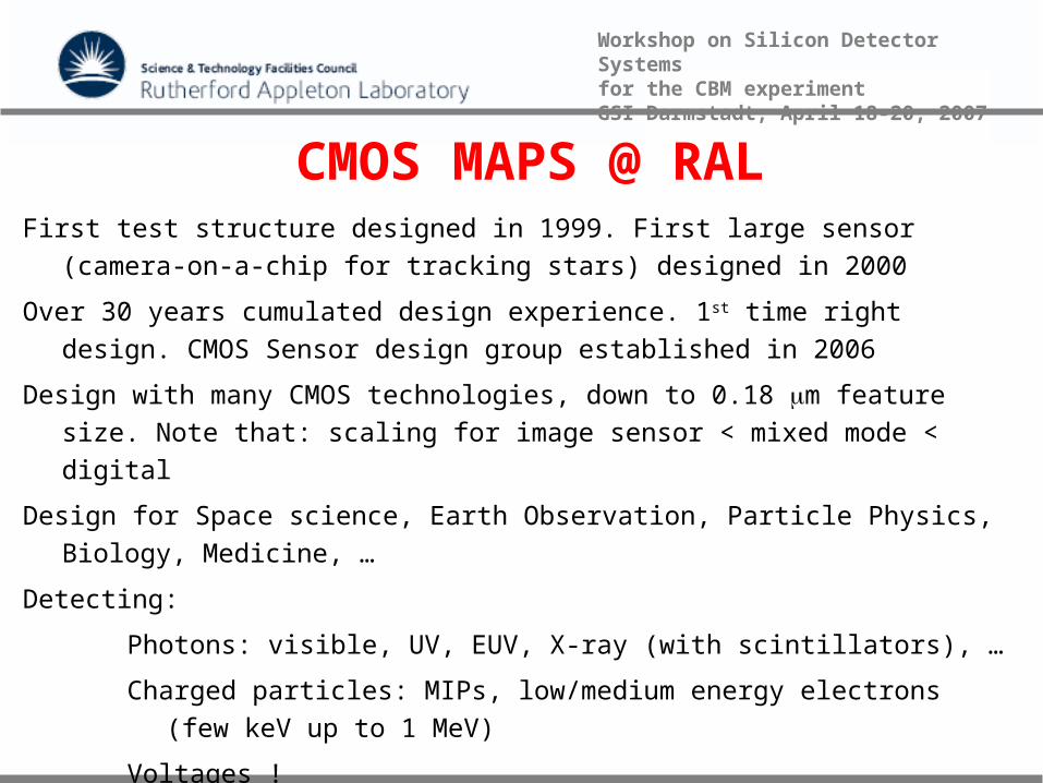
CMOS MAPS @ RALFirst test structure designed in 1999. First large sensor (camera-on-a-chip
for tracking stars) designed in 2000
Over 30 years cumulated design experience. 1st time right design. CMOS Sensor design group established in 2006
Design with many CMOS technologies, down to 0.18 m feature size. Note that: scaling for image sensor < mixed mode < digital
Design for Space science, Earth Observation, Particle Physics, Biology, Medicine, …
Detecting:
Photons: visible, UV, EUV, X-ray (with scintillators), …
Charged particles: MIPs, low/medium energy electrons (few keV up to 1 MeV)
Voltages !
8Workshop on Silicon Detector Systems for the CBM experiment GSI Darmstadt, April 18-20, 2007
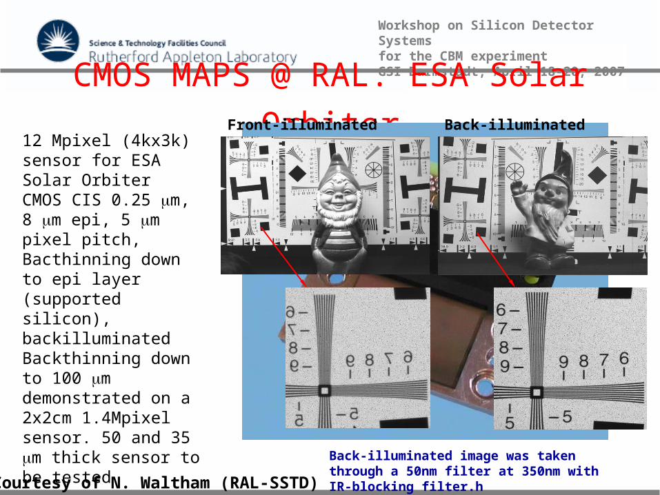
CMOS MAPS @ RAL. ESA Solar Orbiter12 Mpixel (4kx3k) sensor for ESA Solar OrbiterCMOS CIS 0.25 m, 8 m epi, 5 m pixel pitch,Bacthinning down to epi layer (supported silicon), backilluminatedBackthinning down to 100 m demonstrated on a 2x2cm 1.4Mpixel sensor. 50 and 35 m thick sensor to be tested
Front-illuminated Back-illuminated
Back-illuminated image was taken through a 50nm filter at 350nm with IR-blocking filter.h
Courtesy of N. Waltham (RAL-SSTD)
9Workshop on Silicon Detector Systems for the CBM experiment GSI Darmstadt, April 18-20, 2007
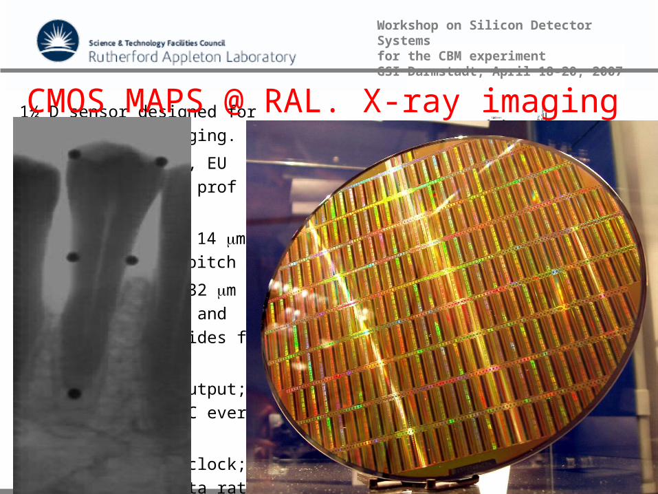
1½ D sensor designed for X-ray medical imaging.
I-ImaS consortium, EU funded and led by prof R. Speller (UCL)
CMOS CIS 0.35 m, 14 m epi, 32 m pixel pitch
512*32 pixels at 32 m pitch plus 4 rows and columns on both sides for edge effects
14 bit digital output; one 14-bit SAR ADC every 32 channel
20 MHz internal clock; 40 MHz digital data rate
CMOS MAPS @ RAL. X-ray imaging
10Workshop on Silicon Detector Systems for the CBM experiment GSI Darmstadt, April 18-20, 2007
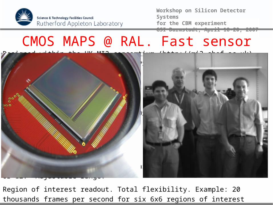
CMOS MAPS @ RAL. Fast sensorDesigned within the UK-MI3 consortium (http://mi3.shef.ac.uk), aiming at developing novel CMOS APS. Led by prof N. Allinson (Sheffield Univesity)
CMOS CIS 0.35 m, 14 and 20 m epi, 25 m pixel pitch
Backthinned down to the epi
Format 512x512 + black pixels (520x520 full format)
3T pixel with flushed reset
Noise < 25 e- rms
Full well capacity > 105 e-
On-chip SAR ADCs, one for 4 columns. Selectable resolution: 10 or 12. Adjustable range.
Region of interest readout. Total flexibility. Example: 20 thousands frames per second for six 6x6 regions of interest
11Workshop on Silicon Detector Systems for the CBM experiment GSI Darmstadt, April 18-20, 2007
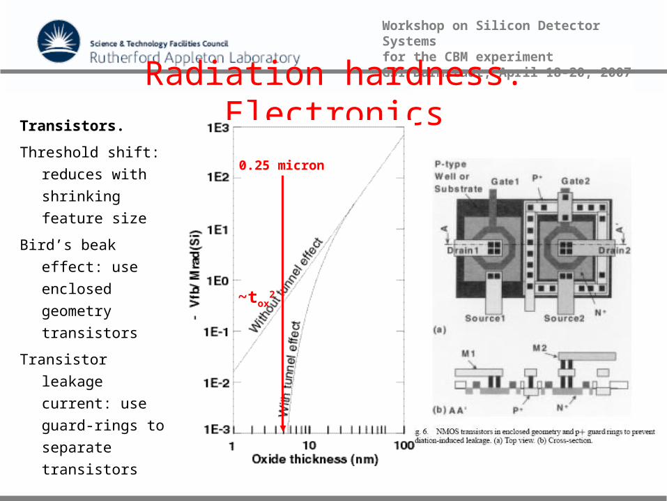
Radiation hardness. ElectronicsTransistors.
Threshold shift:
reduces with
shrinking
feature size
Bird’s beak effect:
use enclosed
geometry
transistors
Transistor leakage
current: use
guard-rings to
separate
transistors
~tox2
0.25 micron
12Workshop on Silicon Detector Systems for the CBM experiment GSI Darmstadt, April 18-20, 2007
Radiation hardness. SensorsDiodes.
Radiation damage increases leakage current
Charge collection is mainly by diffusion
Radiation damage reduces minority carrier lifetime diffusion distance is
reduced
This latter is going to be the ultimate limit, unless an electric field is added
So thickness of epi not so important after irradiation
Distance of diodes can be important
Surface damage can be important
Depends on details of technology and layout.
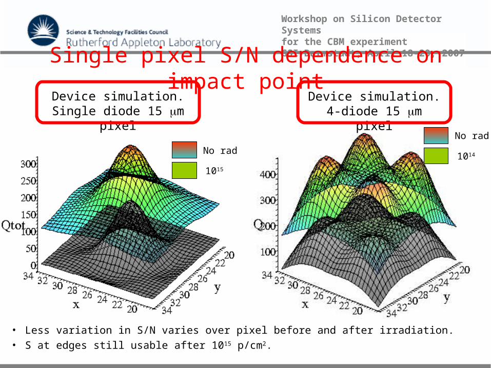
13Workshop on Silicon Detector Systems for the CBM experiment GSI Darmstadt, April 18-20, 2007 Single pixel S/N dependence on impact
point
1015
No rad1014
No rad
Device simulation.4-diode 15 m pixel
• Less variation in S/N varies over pixel before and after irradiation.• S at edges still usable after 1015 p/cm2.
Device simulation.Single diode 15 m pixel
14Workshop on Silicon Detector Systems for the CBM experiment GSI Darmstadt, April 18-20, 2007
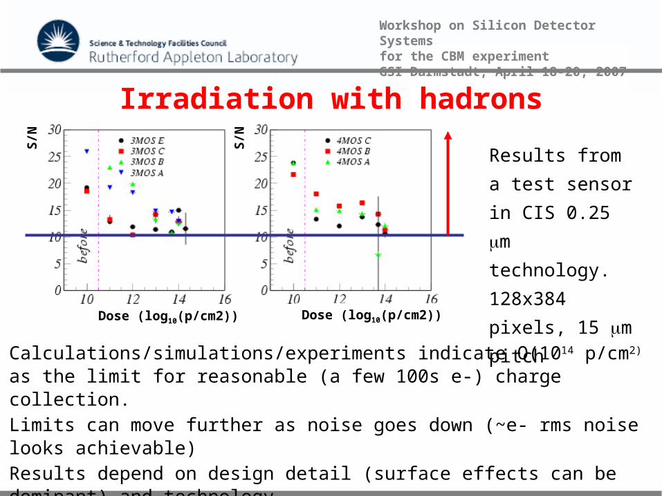
Irradiation with hadrons
S/N
Dose (log10(p/cm2))
S/N
Dose (log10(p/cm2))
Calculations/simulations/experiments indicate O(1014 p/cm2) as the limit for reasonable (a few 100s e-) charge collection.Limits can move further as noise goes down (~e- rms noise looks achievable)Results depend on design detail (surface effects can be dominant) and technology
Results from a
test sensor in
CIS 0.25 m
technology.
128x384 pixels,
15 m pitch
15Workshop on Silicon Detector Systems for the CBM experiment GSI Darmstadt, April 18-20, 2007
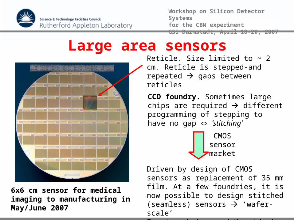
Large area sensorsReticle. Size limited to ~ 2 cm. Reticle is stepped-and repeated gaps between reticles
CCD foundry. Sometimes large chips are required different programming of stepping to have no gap ‘stitching’
CMOS sensor market
Driven by design of CMOS sensors as replacement of 35 mm film. At a few foundries, it is now possible to design stitched (seamless) sensors ‘wafer-scale’Foundry choice rapidly widening
6x6 cm sensor for medical imaging to manufacturing in May/June 2007
16Workshop on Silicon Detector Systems for the CBM experiment GSI Darmstadt, April 18-20, 2007
Outline Introduction on CMOS MAPS
Large sensors for imaging
The INMAPS process
CALICE
Conclusions
17Workshop on Silicon Detector Systems for the CBM experiment GSI Darmstadt, April 18-20, 2007
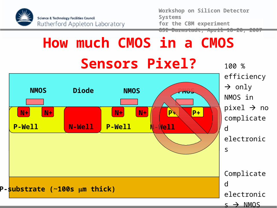
How much CMOS in a CMOS
Sensors Pixel?
NMOS
P-Well N-Well P-Well
N+ N+
P-substrate (~100s m thick)
N+ N+
N-Well
P+ P+
Diode NMOS PMOS
100 %
efficiency
only NMOS
in pixel no
complicated
electronics
Complicated
electronics
NMOS
and
PMOS,i.e.
CMOS low
efficiency
18Workshop on Silicon Detector Systems for the CBM experiment GSI Darmstadt, April 18-20, 2007
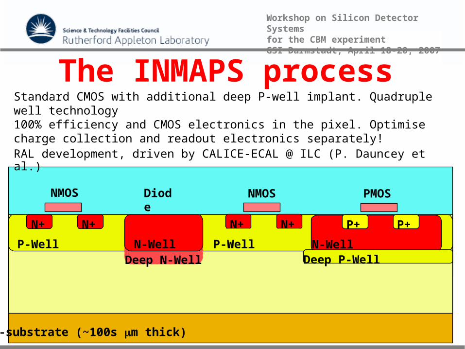
The INMAPS process
NMOS
P-Well P-Well
N+ N+
P-substrate (~100s m thick)
N+ N+
N-Well
P+ P+
Diode NMOS PMOS
Deep P-WellN-Well
Deep N-Well
Standard CMOS with additional deep P-well implant. Quadruple well technology100% efficiency and CMOS electronics in the pixel. Optimise charge collection and readout electronics separately!RAL development, driven by CALICE-ECAL @ ILC (P. Dauncey et al.)
19Workshop on Silicon Detector Systems for the CBM experiment GSI Darmstadt, April 18-20, 2007
Outline Introduction on CMOS MAPS
Large sensors for imaging
The INMAPS process
CALICE
Conclusions
20Workshop on Silicon Detector Systems for the CBM experiment GSI Darmstadt, April 18-20, 2007
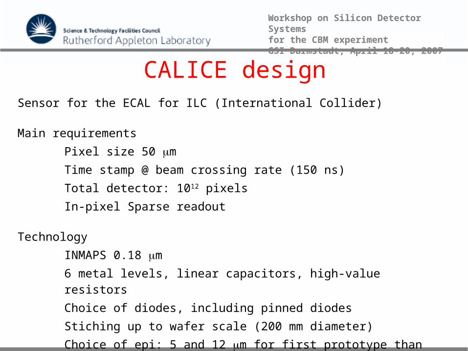
CALICE designSensor for the ECAL for ILC (International Collider)
Main requirements
Pixel size 50 m
Time stamp @ beam crossing rate (150 ns)
Total detector: 1012 pixels
In-pixel Sparse readout
Technology
INMAPS 0.18 m
6 metal levels, linear capacitors, high-value resistors
Choice of diodes, including pinned diodes
Stiching up to wafer scale (200 mm diameter)
Choice of epi: 5 and 12 m for first prototype than up to 20 m
21Workshop on Silicon Detector Systems for the CBM experiment GSI Darmstadt, April 18-20, 2007
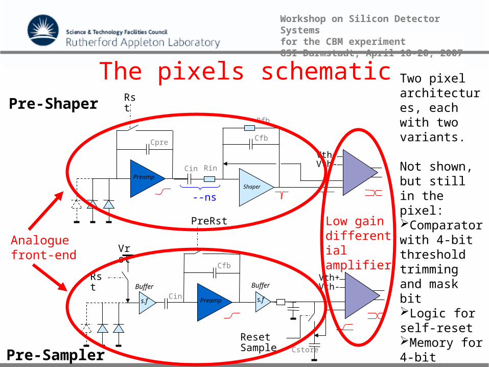
The pixels schematic
Rst
Vrst
Preamp
PreRst
Buffer
s.f
Cfb
CinBuffer
s.f
Vth+Vth-
ResetSample Cstore
--ns
Preamp
Shaper
Rst
CpreCfb
Rfb
RinCin
Vth+Vth-
Pre-Shaper
Pre-Sampler
Analogue front-end
Low gain differential amplifier
Two pixel architectures, each with two variants.
Not shown, but still in the pixel:Comparator with 4-bit threshold trimming and mask bitLogic for self-resetMemory for 4-bit trimming and mask
22Workshop on Silicon Detector Systems for the CBM experiment GSI Darmstadt, April 18-20, 2007
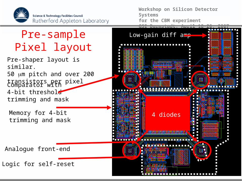
Pre-sample Pixel layout
Analogue front-end
Memory for 4-bit trimming and mask
Comparator with 4-bit threshold trimming and mask
Pre-shaper layout is similar.50 m pitch and over 200 transistors per pixel
Logic for self-reset
Low-gain diff amp
4 diodes
23Workshop on Silicon Detector Systems for the CBM experiment GSI Darmstadt, April 18-20, 2007
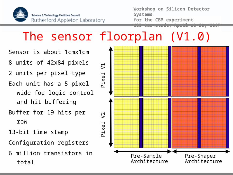
The sensor floorplan (V1.0)
Pre-SampleArchitecture
Pre-ShaperArchitecture
Sensor is about 1cmx1cm
8 units of 42x84 pixels
2 units per pixel type
Each unit has a 5-pixel wide
for logic control and hit
buffering
Buffer for 19 hits per row
13-bit time stamp
Configuration registers
6 million transistors in total
Pix
el V
1
Pix
el V
2
24Workshop on Silicon Detector Systems for the CBM experiment GSI Darmstadt, April 18-20, 2007
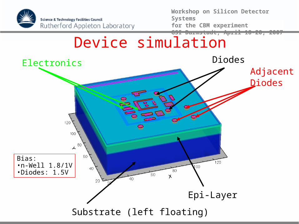
Device simulation
Bias:•n-Well 1.8/1V•Diodes: 1.5V
DiodesAdjacent Diodes
Electronics
Substrate (left floating)
Epi-Layer
25Workshop on Silicon Detector Systems for the CBM experiment GSI Darmstadt, April 18-20, 2007
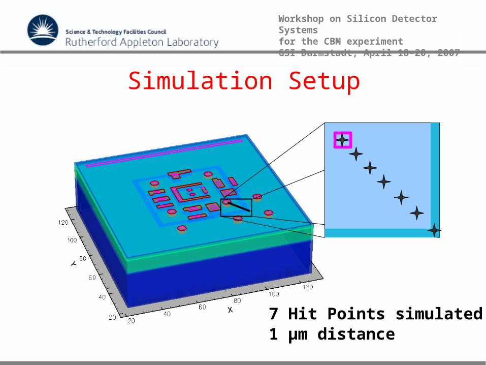
Simulation Setup
7 Hit Points simulated1 µm distance
26Workshop on Silicon Detector Systems for the CBM experiment GSI Darmstadt, April 18-20, 2007
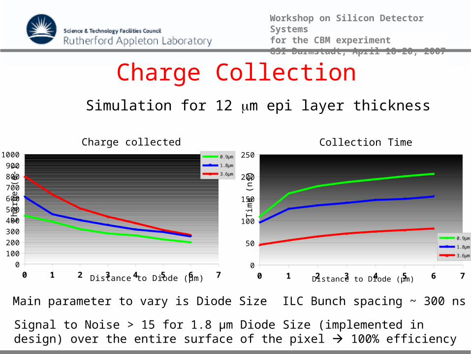
0 1 2 3 4 5 6 70
50
100
150
200
250
Collection Time
0.9µm
1.8µm
3.6µm
Distance to Diode (µm)
Tim
e (
ns)
Charge Collection
0 1 2 3 4 5 6 70
100
200
300
400
500
600
700
800
900
1000
Charge collected0.9µm
1.8µm
3.6µm
Distance to Diode (µm)
Ch
arg
e (
e-)
Main parameter to vary is Diode Size ILC Bunch spacing ~ 300 ns
Simulation for 12 m epi layer thickness
Signal to Noise > 15 for 1.8 µm Diode Size (implemented in design) over the entire surface of the pixel 100% efficiency
27Workshop on Silicon Detector Systems for the CBM experiment GSI Darmstadt, April 18-20, 2007
Outline Introduction on CMOS MAPS
Large sensors for imaging
The INMAPS process
CALICE
Conclusions
28Workshop on Silicon Detector Systems for the CBM experiment GSI Darmstadt, April 18-20, 2007
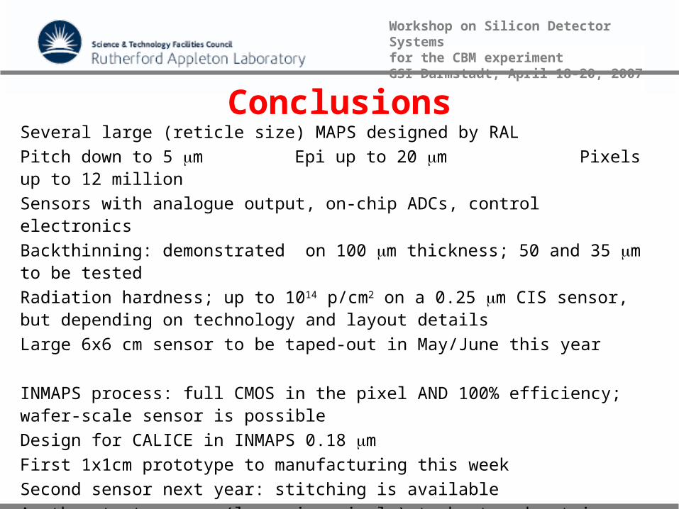
ConclusionsSeveral large (reticle size) MAPS designed by RALPitch down to 5 m Epi up to 20 m Pixels up to 12 millionSensors with analogue output, on-chip ADCs, control electronicsBackthinning: demonstrated on 100 m thickness; 50 and 35 m to be testedRadiation hardness; up to 1014 p/cm2 on a 0.25 m CIS sensor, but depending on technology and layout detailsLarge 6x6 cm sensor to be taped-out in May/June this year
INMAPS process: full CMOS in the pixel AND 100% efficiency; wafer-scale sensor is possibleDesign for CALICE in INMAPS 0.18 mFirst 1x1cm prototype to manufacturing this weekSecond sensor next year: stitching is availableAnother test sensor (low noise pixels) to be taped-out in June plus one more in next 12 months
29Workshop on Silicon Detector Systems for the CBM experiment GSI Darmstadt, April 18-20, 2007
AcknowledgementsCALICE UK: P. Dauncey, J.A. Ballin, A.-M. Magnan, M. Noy (Imperial
College London), J.P. Crooks, M. Stanitzki, K.D. Stefanov, M. Tyndel, E.G.
Villani (Rutherford Appleton Laboratory), Y. Mikami, O. Miller, V. Rajovic,
N.K. Watson, J.A. Wilson (University of Birmingham)
MI3: N. Allinson (Sheffield) plus everyone else from Sheffield, UCL,
Liverpool, Glasgow, Brunel, LMB-MRC Cambridge, York, Surrey, Institute
of Cancer Research-Royal Marsden Hospital and RAL
I-ImaS: R. Speller (UCL) plus everyone else from UCL, Imperial College,
University of Trieste (Italy), University of Ioannina, CTI, ANCO (Greece),
ACTA (Netherlands), SINTEF (Norway) and RAL
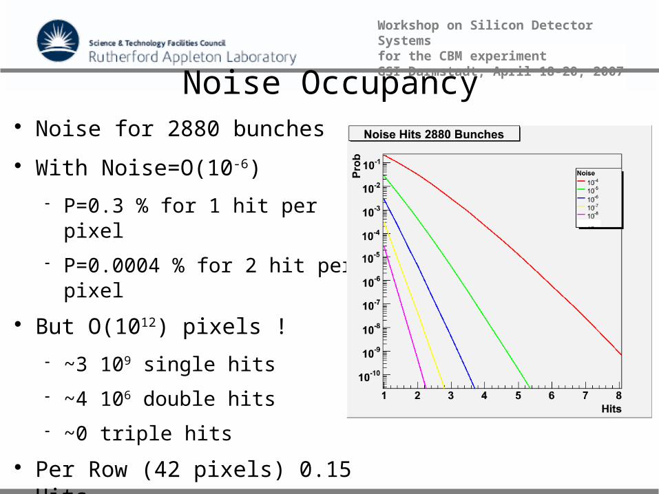
30Workshop on Silicon Detector Systems for the CBM experiment GSI Darmstadt, April 18-20, 2007 Noise Occupancy
Noise for 2880 bunches
With Noise=O(10-6)
P=0.3 % for 1 hit per pixel
P=0.0004 % for 2 hit per pixel
But O(1012) pixels !
~3 109 single hits
~4 106 double hits
~0 triple hits
Per Row (42 pixels) 0.15 Hits
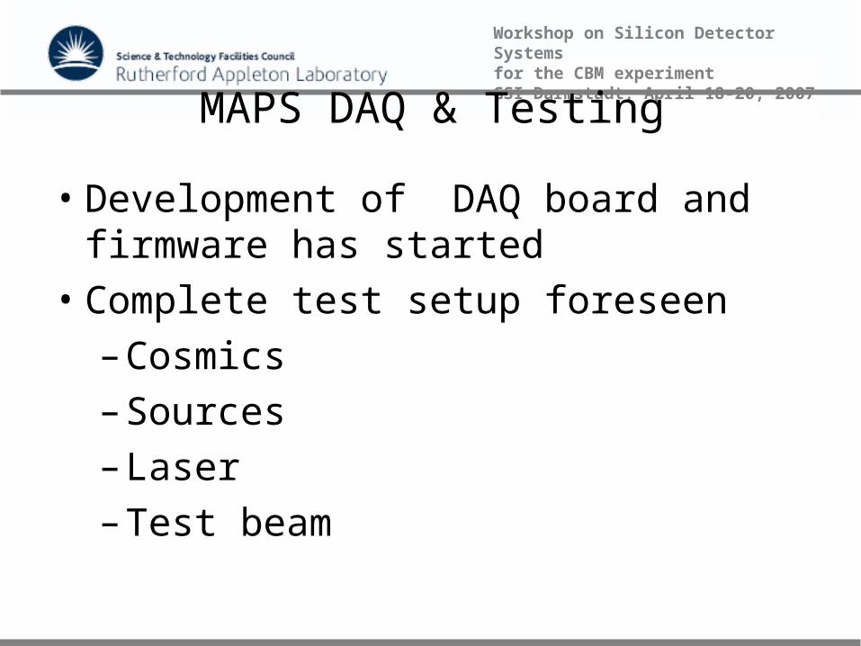
31Workshop on Silicon Detector Systems for the CBM experiment GSI Darmstadt, April 18-20, 2007 MAPS DAQ & Testing
• Development of DAQ board and firmware has started
• Complete test setup foreseen
– Cosmics
– Sources
– Laser
– Test beam
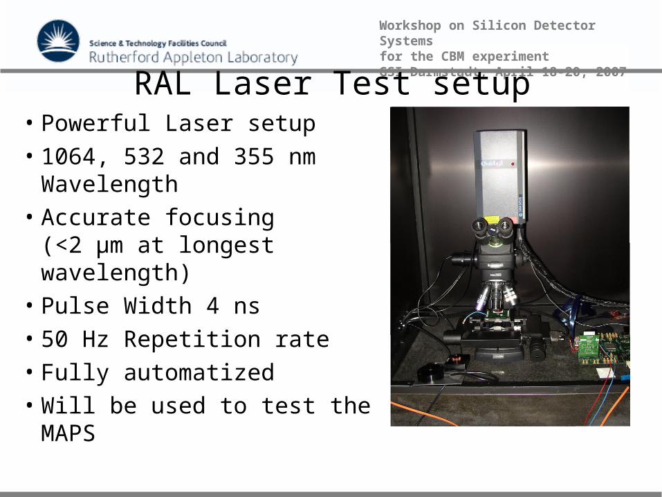
32Workshop on Silicon Detector Systems for the CBM experiment GSI Darmstadt, April 18-20, 2007 RAL Laser Test setup
• Powerful Laser setup• 1064, 532 and 355 nm
Wavelength• Accurate focusing
(<2 µm at longest wavelength)• Pulse Width 4 ns• 50 Hz Repetition rate• Fully automatized• Will be used to test the MAPS
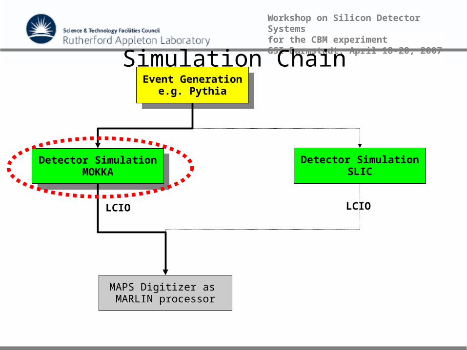
33Workshop on Silicon Detector Systems for the CBM experiment GSI Darmstadt, April 18-20, 2007 Simulation Chain
Event Generatione.g. Pythia
Event Generatione.g. Pythia
Detector SimulationMOKKA
Detector SimulationMOKKA
MAPS Digitizer as MARLIN processor
LCIO
Detector SimulationSLIC
LCIO
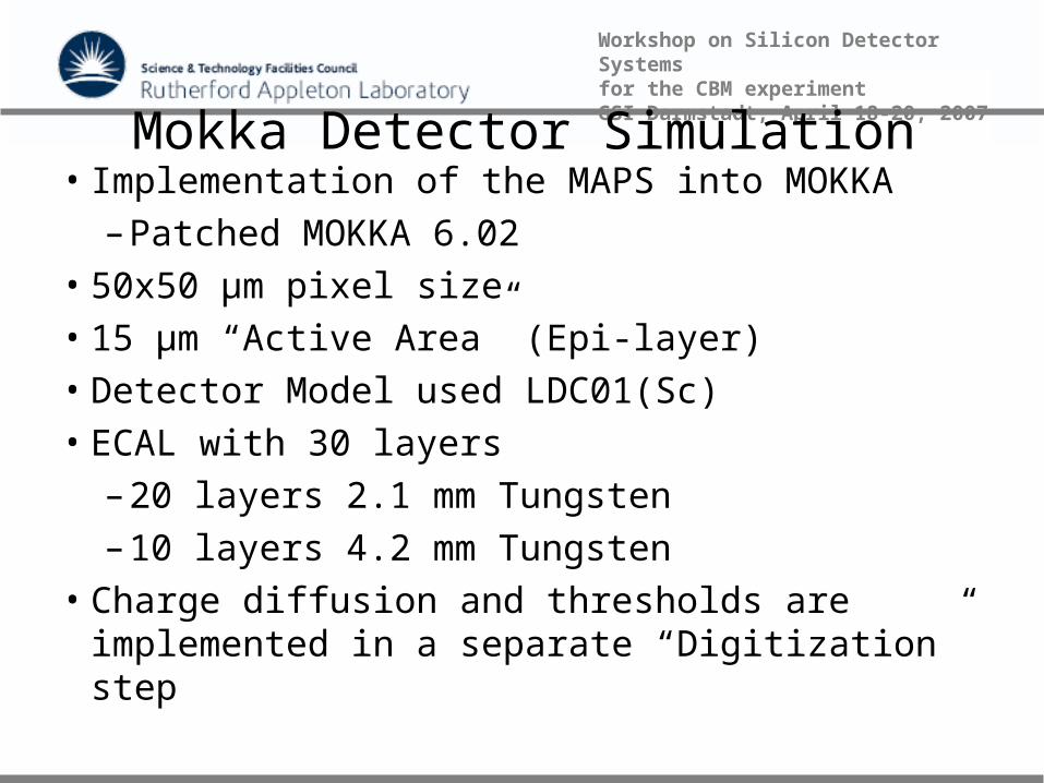
34Workshop on Silicon Detector Systems for the CBM experiment GSI Darmstadt, April 18-20, 2007 Mokka Detector Simulation
• Implementation of the MAPS into MOKKA
– Patched MOKKA 6.02
• 50x50 µm pixel size
• 15 µm “Active Area” (Epi-layer)
• Detector Model used LDC01(Sc)
• ECAL with 30 layers
– 20 layers 2.1 mm Tungsten
– 10 layers 4.2 mm Tungsten
• Charge diffusion and thresholds are implemented in a separate “Digitization” step
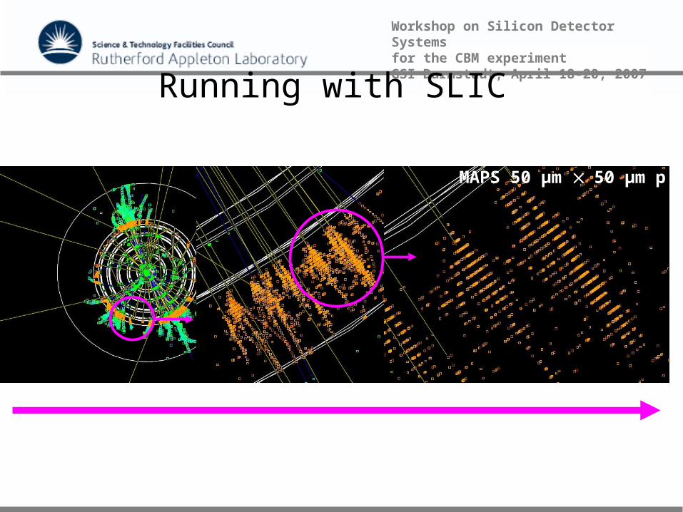
35Workshop on Silicon Detector Systems for the CBM experiment GSI Darmstadt, April 18-20, 2007 Running with SLIC
MAPS 50 μm 50 μm p
36Workshop on Silicon Detector Systems for the CBM experiment GSI Darmstadt, April 18-20, 2007 Beam background
• Done using GuineaPIG
• Trying to estimate beam induced background in the ECAL
• Testing two scenarios
– 500 GeV Baseline
– 1 TeV High Lum
• 1 TeV High Lum is “worst-case” scenario
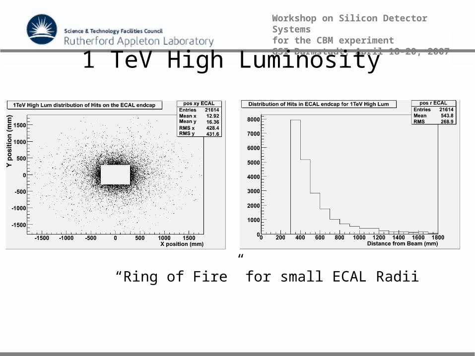
37Workshop on Silicon Detector Systems for the CBM experiment GSI Darmstadt, April 18-20, 2007 1 TeV High Luminosity
“Ring of Fire” for small ECAL Radii
38Workshop on Silicon Detector Systems for the CBM experiment GSI Darmstadt, April 18-20, 2007
0.0E+00 1.0E+03 2.0E+03 3.0E+03 4.0E+03 5.0E+030.0E+00
2.0E-03
4.0E-03
6.0E-03
8.0E-03
1.0E-02
1.2E-02
1.4E-02
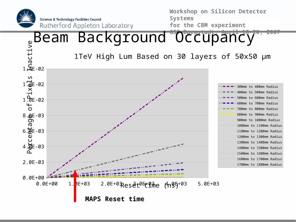
1TeV High Lum Based on 30 layers of 50x50 µm
300mm to 400mm Radius
400mm to 500mm Radius
500mm to 600mm Radius
600mm to 700mm Radius
700mm to 800mm Radius
800mm to 900mm Radius
900mm to 1000mm Radius
1000mm to 1100mm Radius
1100mm to 1200mm Radius
1200mm to 1300mm Radius
1300mm to 1400mm Radius
1400mm to 1500mm Radius
1500mm to 1600mm Radius
1600mm to 1700mm Radius
1700mm to 1800mm Radius
Reset time (ns)
Per
cent
age
of P
ixel
s In
activ
e
Beam Background Occupancy
MAPS Reset time
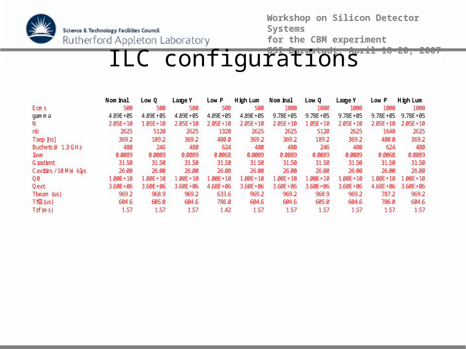
39Workshop on Silicon Detector Systems for the CBM experiment GSI Darmstadt, April 18-20, 2007 ILC configurations
Nominal Low Q Large Y Low P High Lum Nominal Low Q Large Y Low P High LumEcms 500 500 500 500 500 1000 1000 1000 1000 1000gamma 4.89E+05 4.89E+05 4.89E+05 4.89E+05 4.89E+05 9.78E+05 9.78E+05 9.78E+05 9.78E+05 9.78E+05N 2.05E+10 1.05E+10 2.05E+10 2.05E+10 2.05E+10 2.05E+10 1.05E+10 2.05E+10 2.05E+10 2.05E+10nb 2625 5120 2625 1320 2625 2625 5120 2625 1640 2625Tsep [ns] 369.2 189.2 369.2 480.0 369.2 369.2 189.2 369.2 480.0 369.2Buchets @ 1.3 GHz 480 246 480 624 480 480 246 480 624 480Iave 0.0089 0.0089 0.0089 0.0068 0.0089 0.0089 0.0089 0.0089 0.0068 0.0089Gradient 31.50 31.50 31.50 31.50 31.50 31.50 31.50 31.50 31.50 31.50Cavities / 10 MW klys 26.00 26.00 26.00 26.00 26.00 26.00 26.00 26.00 26.00 26.00Q0 1.00E+10 1.00E+10 1.00E+10 1.00E+10 1.00E+10 1.00E+10 1.00E+10 1.00E+10 1.00E+10 1.00E+10Qext 3.60E+06 3.60E+06 3.60E+06 4.68E+06 3.60E+06 3.60E+06 3.60E+06 3.60E+06 4.68E+06 3.60E+06Tbeam (us) 969.2 968.9 969.2 633.6 969.2 969.2 968.9 969.2 787.2 969.2Tfill (us) 604.6 605.0 604.6 786.0 604.6 604.6 605.0 604.6 786.0 604.6Trf (ms) 1.57 1.57 1.57 1.42 1.57 1.57 1.57 1.57 1.57 1.57
40Workshop on Silicon Detector Systems for the CBM experiment GSI Darmstadt, April 18-20, 2007
CMOS Image Sensor Technology. 1
In general, any CMOS process have different flavours.
The basic one is digital. Then MixedMode/RF, High Voltage, …, CIS
(CMOS Image Sensor).
Transistors don’t change. Modules added: high value resistors, linear
capacitors, …
For CIS:
one/two masks/implants added to improve image quality / reduce
leakage current

41Workshop on Silicon Detector Systems for the CBM experiment GSI Darmstadt, April 18-20, 2007
CMOS Image Sensor Technology. 2
Masks for colour filters, microlenses. Special BEOL for improved oxide
transmission
Stitching for sensors larger than reticle is becoming more common due
to push for 35mm film replacement
0.18m available, 0.13m starting this year in different places. Pixel
transistors still at 0.35m equivalent
Epitaxial wafers are generally used: better quality, reduced cross-talk
Thickness: depends on foundry, generally up to 20 m thick epi layer
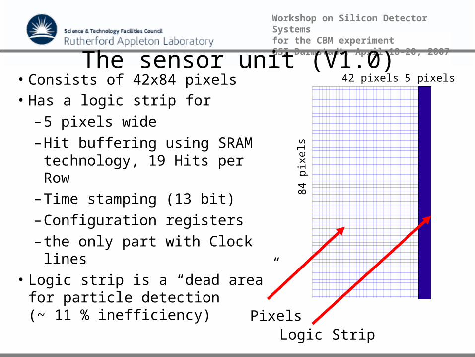
42Workshop on Silicon Detector Systems for the CBM experiment GSI Darmstadt, April 18-20, 2007 The sensor unit (V1.0)
• Consists of 42x84 pixels• Has a logic strip for
– 5 pixels wide– Hit buffering using SRAM
technology, 19 Hits per Row– Time stamping (13 bit)– Configuration registers– the only part with Clock lines
• Logic strip is a “dead area” for particle detection (~ 11 % inefficiency) Pixels
Logic Strip
42 pixels 5 pixels
84
pix
els
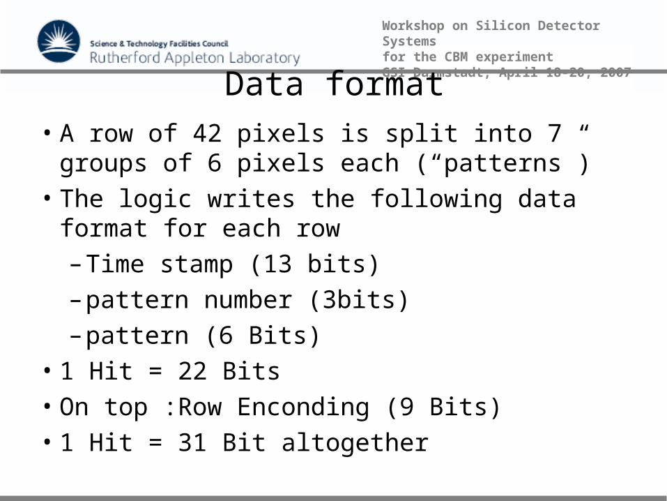
43Workshop on Silicon Detector Systems for the CBM experiment GSI Darmstadt, April 18-20, 2007 Data format
• A row of 42 pixels is split into 7 groups of 6 pixels each (“patterns”)
• The logic writes the following data format for each row– Time stamp (13 bits)– pattern number (3bits)– pattern (6 Bits)
• 1 Hit = 22 Bits• On top :Row Enconding (9 Bits)• 1 Hit = 31 Bit altogether
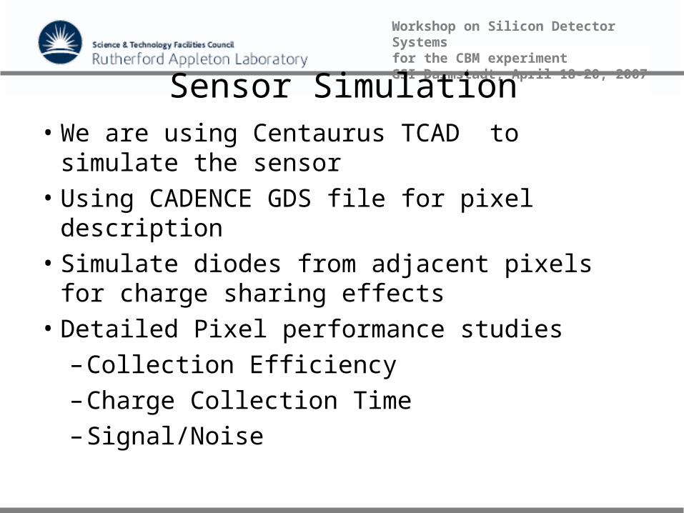
44Workshop on Silicon Detector Systems for the CBM experiment GSI Darmstadt, April 18-20, 2007 Sensor Simulation
• We are using Centaurus TCAD to simulate the sensor
• Using CADENCE GDS file for pixel description• Simulate diodes from adjacent pixels for
charge sharing effects• Detailed Pixel performance studies
– Collection Efficiency– Charge Collection Time– Signal/Noise
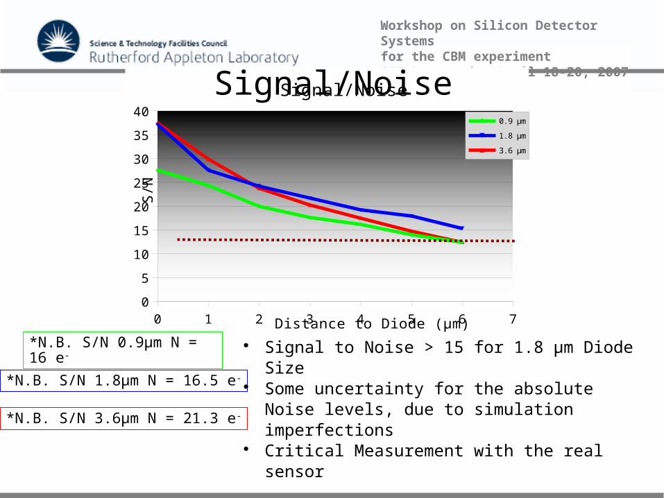
45Workshop on Silicon Detector Systems for the CBM experiment GSI Darmstadt, April 18-20, 2007
0 1 2 3 4 5 6 70
5
10
15
20
25
30
35
40
Signal/Noise
0.9 µm
1.8 µm
3.6 µm
Distance to Diode (µm)
S/N
Signal/Noise
*N.B. S/N 0.9µm N = 16 e-
*N.B. S/N 1.8µm N = 16.5 e-
*N.B. S/N 3.6µm N = 21.3 e-
Signal to Noise > 15 for 1.8 µm Diode Size Some uncertainty for the absolute Noise
levels, due to simulation imperfections Critical Measurement with the real sensor
46Workshop on Silicon Detector Systems for the CBM experiment GSI Darmstadt, April 18-20, 2007 The ECAL MAPS
• Pixel Size (50 x 50 µm)
• Binary Readout (1 bit ADC realized as Comparator)
• 4 Diodes for Charge Collection
• Time Stamping with 13 bits (8192 bunches)
• Hit buffering for entire bunch train
• Capability to mask individual pixels
• Threshold adjustment for each pixel
For the MAPS ECAL a specific MAPS was designed:
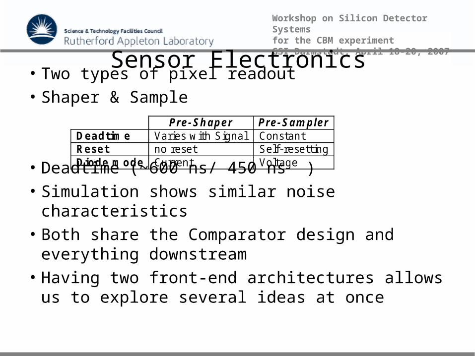
47Workshop on Silicon Detector Systems for the CBM experiment GSI Darmstadt, April 18-20, 2007 Sensor Electronics
• Two types of pixel readout
• Shaper & Sample
• Deadtime (~600 ns/ 450 ns )
• Simulation shows similar noise characteristics
• Both share the Comparator design and everything downstream
• Having two front-end architectures allows us to explore several ideas at once
Pre-Shaper Pre-SamplerDeadtime Varies with Signal ConstantReset no reset Self-resettingDiode mode Current Voltage
Related Documents