DRAFT DRAFT DRAFT DR DRAFT DRAFT DRAFT DRAF DRAFT DRAFT DRAFT DRAFT DRAFT D DRAFT DRAFT DRAFT DRAFT DRAFT DRAFT DRA 1. General description The LPC3220/30/40/50 embedded microcontrollers were designed for low power, high performance applications. NXP achieved their performance goals using a 90 nanometer process to implement an ARM926EJ-S CPU core with a vector floating point co-processor and a large set of standard peripherals including USB On-The-Go. The LPC3220/30/40/50 operates at CPU frequencies of up to 266 MHz. The NXP implementation uses a ARM926EJ-S CPU core with a Harvard architecture, 5-stage pipeline, and an integral Memory Management Unit (MMU). The MMU provides the virtual memory capabilities needed to support the multi-programming demands of modern operating systems. The ARM926EJ-S also has a hardware based set of DSP instruction extensions, which includes single cycle MAC operations, and hardware based native Jazelle Java Byte-code execution. The NXP implementation has a 32 kB instruction cache and a 32 kB data cache. For low power consumption, the LPC3220/30/40/50 takes advantage of NXP’s advanced technology development to optimize intrinsic power and uses software controlled architectural enhancements to optimize application based power management. The LPC3220/30/40/50 also includes 256 kB of on-chip static RAM, a NAND flash interface, an Ethernet MAC, an LCD controller that supports STN and TFT panels, and an external bus interface that supports SDR and DDR SDRAM as well as static devices. In addition, the LPC3220/30/40/50 includes a USB 2.0 full-speed interface, seven UARTs, two I 2 C-bus interfaces, two SPI/SSP ports, two I 2 S-bus interfaces, two single output PWMs, a motor control PWM, six general purpose timers with capture inputs and compare outputs, a Secure Digital (SD) interface, and a 10-bit Analog-to-Digital Converter (ADC) with a touch screen sense option. 2. Features and benefits ARM926EJS processor, running at CPU clock speeds up to 266 MHz. Vector Floating Point (VFP) coprocessor. 32 kB instruction cache and 32 kB data cache. Up to 256 kB of Internal SRAM (IRAM). Selectable boot-up from various external devices: NAND flash, SPI memory, USB, UART, or static memory. LPC3220/30/40/50 16/32-bit ARM microcontrollers; hardware floating-point coprocessor, USB On-The-Go, and EMC memory interface Rev. 01.03 — 16 March 2010 Product data sheet

Welcome message from author
This document is posted to help you gain knowledge. Please leave a comment to let me know what you think about it! Share it to your friends and learn new things together.
Transcript
DRAFT
DR
T DR
DR
RAF
DR
FT D
DR
DRA
AFT DRAF
AFT DRAFT DRAFT D
AFT DRAFT DRAFT DRAFT DRA
AFT DRAFT DRAFT DRAFT DRAFT DRAFT
1. General description
The LPC3220/30/40/50 embedded microcontrollers were designed for low power, high performance applications. NXP achieved their performance goals using a 90 nanometer process to implement an ARM926EJ-S CPU core with a vector floating point co-processor and a large set of standard peripherals including USB On-The-Go. The LPC3220/30/40/50 operates at CPU frequencies of up to 266 MHz.
The NXP implementation uses a ARM926EJ-S CPU core with a Harvard architecture, 5-stage pipeline, and an integral Memory Management Unit (MMU). The MMU provides the virtual memory capabilities needed to support the multi-programming demands of modern operating systems. The ARM926EJ-S also has a hardware based set of DSP instruction extensions, which includes single cycle MAC operations, and hardware based native Jazelle Java Byte-code execution. The NXP implementation has a 32 kB instruction cache and a 32 kB data cache.
For low power consumption, the LPC3220/30/40/50 takes advantage of NXP’s advanced technology development to optimize intrinsic power and uses software controlled architectural enhancements to optimize application based power management.
The LPC3220/30/40/50 also includes 256 kB of on-chip static RAM, a NAND flash interface, an Ethernet MAC, an LCD controller that supports STN and TFT panels, and an external bus interface that supports SDR and DDR SDRAM as well as static devices. In addition, the LPC3220/30/40/50 includes a USB 2.0 full-speed interface, seven UARTs, two I2C-bus interfaces, two SPI/SSP ports, two I2S-bus interfaces, two single output PWMs, a motor control PWM, six general purpose timers with capture inputs and compare outputs, a Secure Digital (SD) interface, and a 10-bit Analog-to-Digital Converter (ADC) with a touch screen sense option.
2. Features and benefits
ARM926EJS processor, running at CPU clock speeds up to 266 MHz.Vector Floating Point (VFP) coprocessor.32 kB instruction cache and 32 kB data cache.Up to 256 kB of Internal SRAM (IRAM).Selectable boot-up from various external devices: NAND flash, SPI memory, USB, UART, or static memory.
LPC3220/30/40/5016/32-bit ARM microcontrollers; hardware floating-point coprocessor, USB On-The-Go, and EMC memory interfaceRev. 01.03 — 16 March 2010 Product data sheet
DRAFT
DRAFT DRAFT DR
DRAFT DRAFT DRAFRAF
DRAFT DRAFT DRAF
FT D
DRAFT DRAFT DRAF
DRA
NXP Semiconductors LPC3220/30/40/5016/32-bit ARM microcontrollers
T DT DRAFT DRA
T DRAFT DRAFT DRAFT
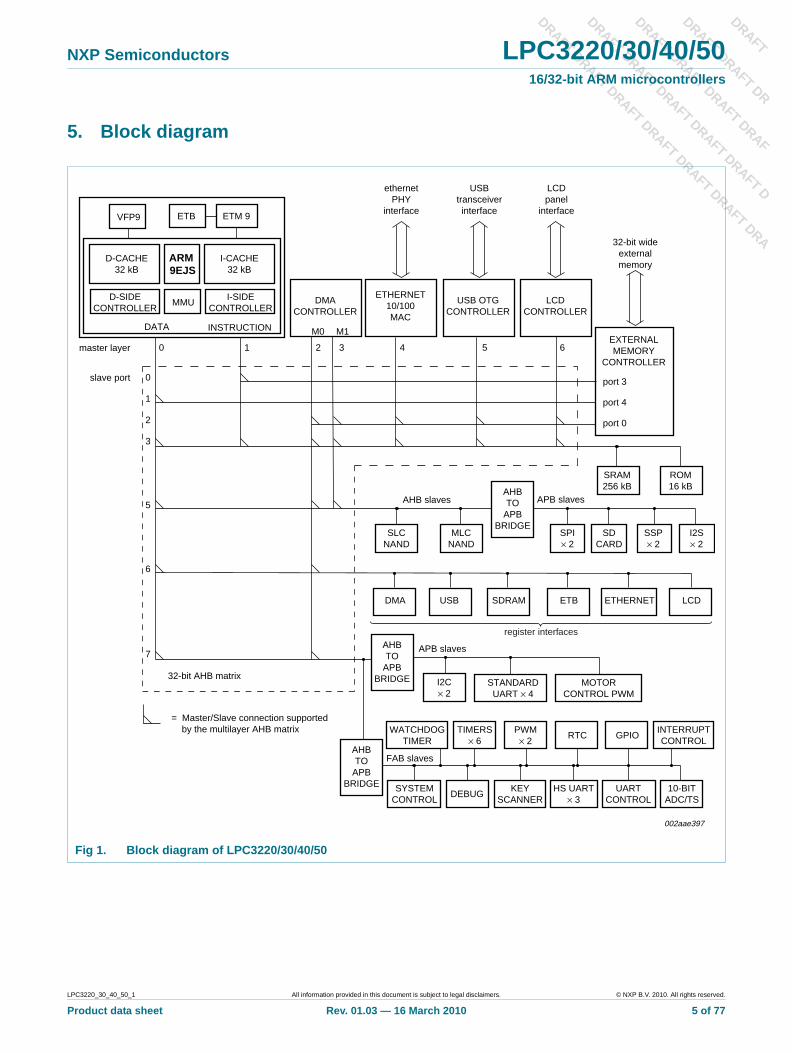
Multi-layer AHB system that provides a separate bus for each AHB master, including both an instruction and data bus for the CPU, two data busses for the DMA controller, and another bus for the USB controller, one for the LCD, and a final one for the Ethernet MAC. There are no arbitration delays in the system unless two masters attempt to access the same slave at the same time.External memory controller for DDR and SDR SDRAM as well as for static devices. Two NAND flash controllers: One for single-level NAND flash devices and the other for multi-level NAND flash devices.Master Interrupt Controller (MIC) and two Slave Interrupt Controllers (SIC), supporting 74 interrupt sources.Eight channel General Purpose DMA (GPDMA) controller on the AHB that can be used with the SD card port, the high-speed UARTs, I2S-bus interfaces, and SPI interfaces, as well as memory-to-memory transfers.Serial interfaces:
10/100 Ethernet MAC with dedicated DMA Controller.USB interface supporting either device, host (OHCI compliant), or On-The-Go (OTG) with an integral DMA controller and dedicated PLL to generate the required 48 MHz USB clock.Four standard UARTs with fractional baud rate generation and 64 byte FIFOs. One of the standard UARTs supports IrDA.Three additional high-speed UARTs intended for on-board communications that support baud rates up to 921 600 when using a 13 MHz main oscillator. All high-speed UARTs provide 64 byte FIFOs.Two SPI controllers.Two SSP controllers.Two I2C-bus interfaces with standard open-drain pins. The I2C-bus interfaces support single master, slave, and multi-master I2C-bus configurations.Two I2S-bus interfaces, each with separate input and output channels. Each channel can be operated independently on three pins, or both input and output channels can be used with only four pins and a shared clock.
Additional peripherals:LCD controller supporting both STN and TFT panels, with dedicated DMA controller. Programmable display resolution up to 1024 × 768.Secure Digital (SD) memory card interface, which conforms to the SD Memory Card Specification Version 1.01.General Purpose (GP) input, output, and I/O pins. Includes 12 GP input pins, 24 GP output pins, and 51 GP I/O pins.10-bit, 400 kHz Analog-to-Digital Converter (ADC) with input multiplexing from three pins. Optionally, the ADC can operate as a touch screen controller.Real-Time Clock (RTC) with separate power pin and dedicated 32 kHz oscillator. NXP implemented the RTC in an independent on-chip power domain so it can remain active while the rest of the chip is not powered. The RTC also includes a 32-byte scratch pad memory.32-bit general purpose high-speed timer with a 16-bit pre-scaler. This timer includes one external capture input pin and a capture connection to the RTC clock. Interrupts may be generated using three match registers.
LPC3220_30_40_50_1 All information provided in this document is subject to legal disclaimers. © NXP B.V. 2010. All rights reserved.
Product data sheet Rev. 01.03 — 16 March 2010 2 of 77

DRAFT
DRAFT DRAFT DR
DRAFT DRAFT DRAFRAF
DRAFT DRAFT DRAF
FT D
DRAFT DRAFT DRAF
DRA
NXP Semiconductors LPC3220/30/40/5016/32-bit ARM microcontrollers
T DT DRAFT DRA
T DRAFT DRAFT DRAFT
Six enhanced timer/counters which are architecturally identical except for the peripheral base address. Two capture inputs and two match outputs are pinned out to four timers. Timer 1 brings out a third match output, timers 2 and 3 bring out all four match outputs, timer 4 has one match output, and timer 5 has no inputs or outputs.32-bit millisecond timer driven from the RTC clock. This timer can generate interrupts using two match registers.WatchDog timer clocked by the peripheral clock.Two single-output PWM blocks.Motor control PWM.Keyboard scanner function allows automatic scanning of an up to 8 × 8 key matrix.Up to 18 external interrupts.
Standard ARM test/debug interface for compatibility with existing tools.Emulation Trace Buffer (ETB) with 2048 × 24 bit RAM allows trace via JTAG.Stop mode saves power while allowing many peripheral functions to restart CPU activity.On-chip crystal oscillator.An on-chip PLL allows CPU operation up to the maximum CPU rate without the requirement for a high frequency crystal. Another PLL allows operation from the 32 kHz RTC clock rather than the external crystal.Boundary scan for simplified board testing.User-accessible unique serial ID number for each chip.296 pin TFBGA package with a 15 × 15 × 0.7 mm body.
3. Applications
ConsumerMedicalIndustrialNetwork control
LPC3220_30_40_50_1 All information provided in this document is subject to legal disclaimers. © NXP B.V. 2010. All rights reserved.
Product data sheet Rev. 01.03 — 16 March 2010 3 of 77

DRAFT
DRAFT DRAFT DR
DRAFT DRAFT DRAFRAF
DRAFT DRAFT DRAF
FT D
DRAFT DRAFT DRAF
DRA
NXP Semiconductors LPC3220/30/40/5016/32-bit ARM microcontrollers
T DT DRAFT DRA
T DRAFT DRAFT DRAFT
4. Ordering information
[1] F = −40 °C to +85 °C temperature range. Note that Revision “A” parts with and without the /01 suffix are identical. For example, LPC3220FET296 Revision “A” is identical to LPC3220FET296/01 Revision “A”.
[2] Available in Revision “-” and “A”.
[3] Available starting with Revision “A”.
4.1 Ordering options
Table 1. Ordering informationType number[1] Package
Name Description VersionLPC3220FET296[2] TFBGA296 plastic thin fine-pitch ball grid array package; 296 balls SOT1048-1
LPC3230FET296[2] TFBGA296 plastic thin fine-pitch ball grid array package; 296 balls SOT1048-1
LPC3240FET296[2] TFBGA296 plastic thin fine-pitch ball grid array package; 296 balls SOT1048-1
LPC3250FET296[2] TFBGA296 plastic thin fine-pitch ball grid array package; 296 balls SOT1048-1
LPC3220FET296/01[3] TFBGA296 plastic thin fine-pitch ball grid array package; 296 balls SOT1048-1
LPC3230FET296/01[3] TFBGA296 plastic thin fine-pitch ball grid array package; 296 balls SOT1048-1
LPC3240FET296/01[3] TFBGA296 plastic thin fine-pitch ball grid array package; 296 balls SOT1048-1
LPC3250FET296/01[3] TFBGA296 plastic thin fine-pitch ball grid array package; 296 balls SOT1048-1
Table 2. Part optionsType number SRAM (kB) 10/100 Ethernet LCD
controllerTemperature range (°C) Package
LPC3220FET296 128 0 0 −40 to +85 TFBGA296
LPC3230FET296 256 0 1 −40 to +85 TFBGA296
LPC3240FET296 256 1 0 −40 to +85 TFBGA296
LPC3250FET296 256 1 1 −40 to +85 TFBGA296
LPC3220FET296/01 128 0 0 −40 to +85 TFBGA296
LPC3230FET296/01 256 0 1 −40 to +85 TFBGA296
LPC3240FET296/01 256 1 0 −40 to +85 TFBGA296
LPC3250FET296/01 256 1 1 −40 to +85 TFBGA296
LPC3220_30_40_50_1 All information provided in this document is subject to legal disclaimers. © NXP B.V. 2010. All rights reserved.
Product data sheet Rev. 01.03 — 16 March 2010 4 of 77
DRAFT
DRAFT DRAFT DR
DRAFT DRAFT DRAFRAF
DRAFT DRAFT DRAF
FT D
DRAFT DRAFT DRAF
DRA
NXP Semiconductors LPC3220/30/40/5016/32-bit ARM microcontrollers
T DT DRAFT DRA
T DRAFT DRAFT DRAFT
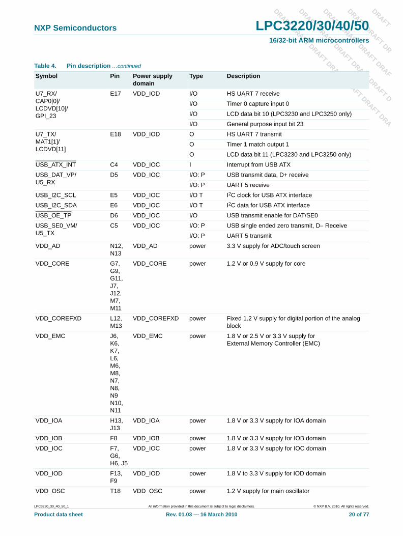
5. Block diagram
Fig 1. Block diagram of LPC3220/30/40/50
ARM 9EJS
D-CACHE32 kB
I-CACHE32 kB
DATA INSTRUCTION
ethernetPHY
interface
USBtransceiverinterface
LCDpanel
interface
EXTERNALMEMORY
CONTROLLER
ROM16 kB
SRAM256 kB
USB DMA ETBSDRAM
STANDARDUART × 4
I2C× 2
TIMERS× 6
WATCHDOGTIMER
DEBUGSYSTEM
CONTROLHS UART
× 3KEY
SCANNER10-BIT
ADC/TSUART
CONTROL
RTCPWM
× 2GPIO
M1M0
AHBTO
APBBRIDGE
AHBTO
APBBRIDGE
AHBTO
APBBRIDGE
master layer 0 1 2 3 4 5 6
slave port 0
1
7
6
5
3
2
= Master/Slave connection supported by the multilayer AHB matrix
32-bit AHB matrix
APB slaves
FAB slaves
AHB slaves APB slaves
port 3
port 4
port 0
32-bit wideexternalmemory
ETB ETM 9VFP9
LCDETHERNET
MOTORCONTROL PWM
002aae397
MMUD-SIDE
CONTROLLERI-SIDE
CONTROLLERDMA
CONTROLLER
ETHERNET10/100MAC
USB OTGCONTROLLER
LCDCONTROLLER
MLCNAND
SLCNAND
SDCARD
SPI× 2
I2S× 2
SSP× 2
INTERRUPTCONTROL
register interfaces
LPC3220_30_40_50_1 All information provided in this document is subject to legal disclaimers. © NXP B.V. 2010. All rights reserved.
Product data sheet Rev. 01.03 — 16 March 2010 5 of 77
DRAFT
DRAFT DRAFT DR
DRAFT DRAFT DRAFRAF
DRAFT DRAFT DRAF
FT D
DRAFT DRAFT DRAF
DRA
NXP Semiconductors LPC3220/30/40/5016/32-bit ARM microcontrollers
T DT DRAFT DRA
T DRAFT DRAFT DRAFT
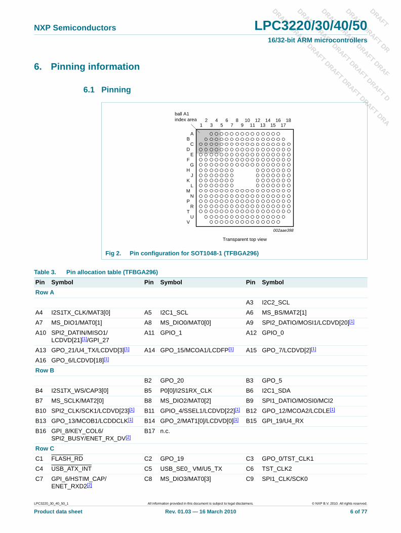
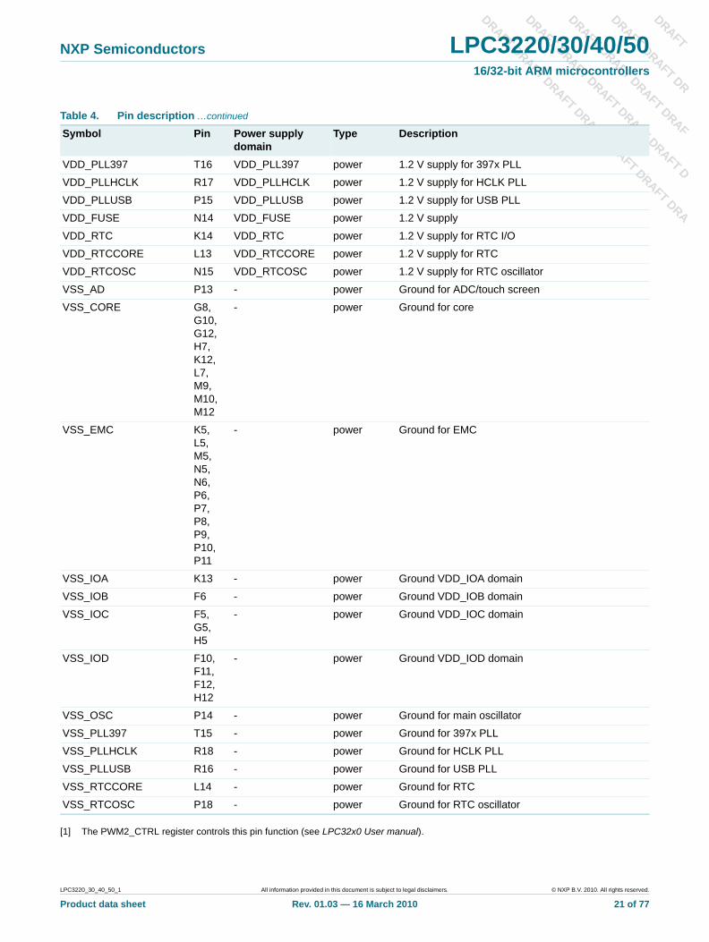
6. Pinning information
6.1 Pinning
Fig 2. Pin configuration for SOT1048-1 (TFBGA296)
002aae398
Transparent top view
VU
TR
PN
L
J
M
K
HG
FE
D
BC
A
2 4 6 8 10 1213
1415 17
16 181 3 5 7 9 11
ball A1index area
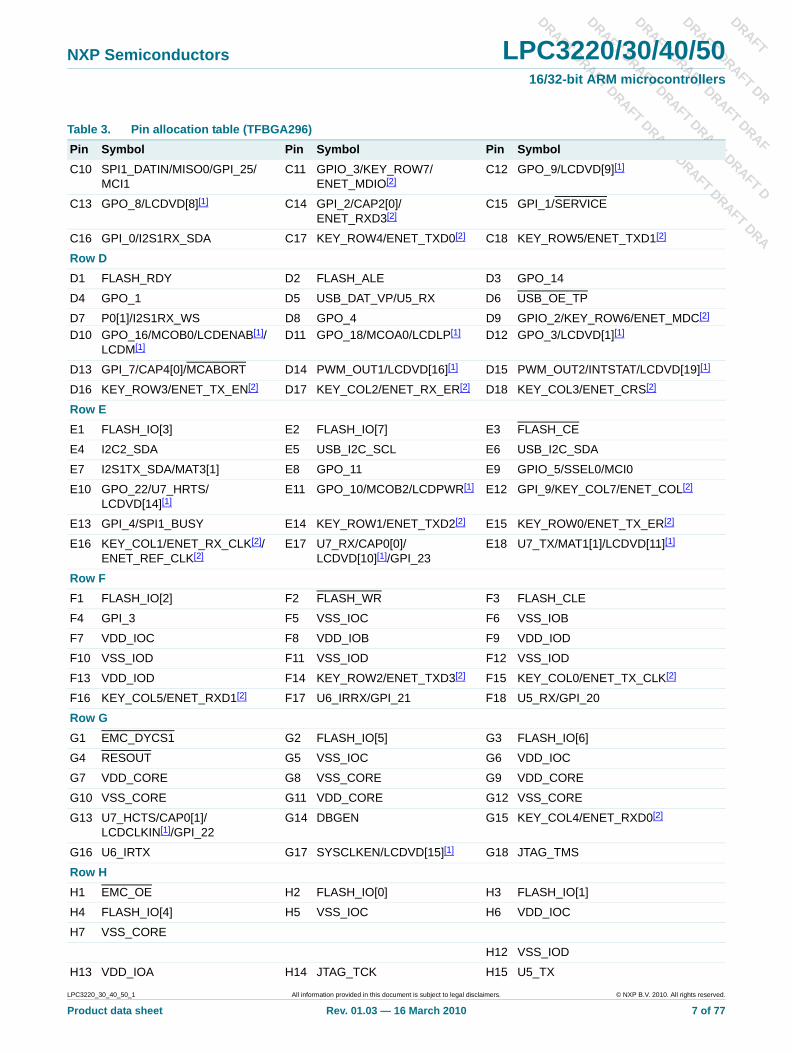
Table 3. Pin allocation table (TFBGA296)Pin Symbol Pin Symbol Pin SymbolRow A
A3 I2C2_SCL
A4 I2S1TX_CLK/MAT3[0] A5 I2C1_SCL A6 MS_BS/MAT2[1]
A7 MS_DIO1/MAT0[1] A8 MS_DIO0/MAT0[0] A9 SPI2_DATIO/MOSI1/LCDVD[20][1]
A10 SPI2_DATIN/MISO1/LCDVD[21][1]/GPI_27
A11 GPIO_1 A12 GPIO_0
A13 GPO_21/U4_TX/LCDVD[3][1] A14 GPO_15/MCOA1/LCDFP[1] A15 GPO_7/LCDVD[2][1]
A16 GPO_6/LCDVD[18][1]
Row BB2 GPO_20 B3 GPO_5
B4 I2S1TX_WS/CAP3[0] B5 P0[0]/I2S1RX_CLK B6 I2C1_SDA
B7 MS_SCLK/MAT2[0] B8 MS_DIO2/MAT0[2] B9 SPI1_DATIO/MOSI0/MCI2
B10 SPI2_CLK/SCK1/LCDVD[23][1] B11 GPIO_4/SSEL1/LCDVD[22][1] B12 GPO_12/MCOA2/LCDLE[1]
B13 GPO_13/MCOB1/LCDDCLK[1] B14 GPO_2/MAT1[0]/LCDVD[0][1] B15 GPI_19/U4_RX
B16 GPI_8/KEY_COL6/SPI2_BUSY/ENET_RX_DV[2]
B17 n.c.
Row CC1 FLASH_RD C2 GPO_19 C3 GPO_0/TST_CLK1
C4 USB_ATX_INT C5 USB_SE0_ VM/U5_TX C6 TST_CLK2
C7 GPI_6/HSTIM_CAP/ENET_RXD2[2]
C8 MS_DIO3/MAT0[3] C9 SPI1_CLK/SCK0
LPC3220_30_40_50_1 All information provided in this document is subject to legal disclaimers. © NXP B.V. 2010. All rights reserved.
Product data sheet Rev. 01.03 — 16 March 2010 6 of 77
DRAFT
DRAFT DRAFT DR
DRAFT DRAFT DRAFRAF
DRAFT DRAFT DRAF
FT D
DRAFT DRAFT DRAF
DRA
NXP Semiconductors LPC3220/30/40/5016/32-bit ARM microcontrollers
T DT DRAFT DRA
T DRAFT DRAFT DRAFT
C10 SPI1_DATIN/MISO0/GPI_25/MCI1
C11 GPIO_3/KEY_ROW7/ENET_MDIO[2]
C12 GPO_9/LCDVD[9][1]
C13 GPO_8/LCDVD[8][1] C14 GPI_2/CAP2[0]/ENET_RXD3[2]
C15 GPI_1/SERVICE
C16 GPI_0/I2S1RX_SDA C17 KEY_ROW4/ENET_TXD0[2] C18 KEY_ROW5/ENET_TXD1[2]
Row DD1 FLASH_RDY D2 FLASH_ALE D3 GPO_14
D4 GPO_1 D5 USB_DAT_VP/U5_RX D6 USB_OE_TP
D7 P0[1]/I2S1RX_WS D8 GPO_4 D9 GPIO_2/KEY_ROW6/ENET_MDC[2]
D10 GPO_16/MCOB0/LCDENAB[1]/LCDM[1]
D11 GPO_18/MCOA0/LCDLP[1] D12 GPO_3/LCDVD[1][1]
D13 GPI_7/CAP4[0]/MCABORT D14 PWM_OUT1/LCDVD[16][1] D15 PWM_OUT2/INTSTAT/LCDVD[19][1]
D16 KEY_ROW3/ENET_TX_EN[2] D17 KEY_COL2/ENET_RX_ER[2] D18 KEY_COL3/ENET_CRS[2]
Row EE1 FLASH_IO[3] E2 FLASH_IO[7] E3 FLASH_CE
E4 I2C2_SDA E5 USB_I2C_SCL E6 USB_I2C_SDA
E7 I2S1TX_SDA/MAT3[1] E8 GPO_11 E9 GPIO_5/SSEL0/MCI0
E10 GPO_22/U7_HRTS/LCDVD[14][1]
E11 GPO_10/MCOB2/LCDPWR[1] E12 GPI_9/KEY_COL7/ENET_COL[2]
E13 GPI_4/SPI1_BUSY E14 KEY_ROW1/ENET_TXD2[2] E15 KEY_ROW0/ENET_TX_ER[2]
E16 KEY_COL1/ENET_RX_CLK[2]/ENET_REF_CLK[2]
E17 U7_RX/CAP0[0]/LCDVD[10][1]/GPI_23
E18 U7_TX/MAT1[1]/LCDVD[11][1]
Row FF1 FLASH_IO[2] F2 FLASH_WR F3 FLASH_CLE
F4 GPI_3 F5 VSS_IOC F6 VSS_IOB
F7 VDD_IOC F8 VDD_IOB F9 VDD_IOD
F10 VSS_IOD F11 VSS_IOD F12 VSS_IOD
F13 VDD_IOD F14 KEY_ROW2/ENET_TXD3[2] F15 KEY_COL0/ENET_TX_CLK[2]
F16 KEY_COL5/ENET_RXD1[2] F17 U6_IRRX/GPI_21 F18 U5_RX/GPI_20
Row GG1 EMC_DYCS1 G2 FLASH_IO[5] G3 FLASH_IO[6]
G4 RESOUT G5 VSS_IOC G6 VDD_IOC
G7 VDD_CORE G8 VSS_CORE G9 VDD_CORE
G10 VSS_CORE G11 VDD_CORE G12 VSS_CORE
G13 U7_HCTS/CAP0[1]/LCDCLKIN[1]/GPI_22
G14 DBGEN G15 KEY_COL4/ENET_RXD0[2]
G16 U6_IRTX G17 SYSCLKEN/LCDVD[15][1] G18 JTAG_TMS
Row HH1 EMC_OE H2 FLASH_IO[0] H3 FLASH_IO[1]
H4 FLASH_IO[4] H5 VSS_IOC H6 VDD_IOC
H7 VSS_CORE
H12 VSS_IOD
H13 VDD_IOA H14 JTAG_TCK H15 U5_TX
Table 3. Pin allocation table (TFBGA296)Pin Symbol Pin Symbol Pin Symbol
LPC3220_30_40_50_1 All information provided in this document is subject to legal disclaimers. © NXP B.V. 2010. All rights reserved.
Product data sheet Rev. 01.03 — 16 March 2010 7 of 77

DRAFT
DRAFT DRAFT DR
DRAFT DRAFT DRAFRAF
DRAFT DRAFT DRAF
FT D
DRAFT DRAFT DRAF
DRA
NXP Semiconductors LPC3220/30/40/5016/32-bit ARM microcontrollers
T DT DRAFT DRA
T DRAFT DRAFT DRAFT
H16 HIGHCORE/LCDVD[17][1] H17 JTAG_NTRST H18 JTAG_RTCK
Row JJ1 EMC_A[20]/P1[20] J2 EMC_A[21]/P1[21] J3 EMC_A[22]/P1[22]
J4 EMC_A[23]/P1[23] J5 VDD_IOC J6 VDD_EMC
J7 VDD_CORE
J12 VDD_CORE
J13 VDD_IOA J14 U3_RX/GPI_18 J15 JTAG_TDO
J16 JTAG_TDI J17 U3_TX J18 U2_HCTS/U3_CTS/GPI_16
Row KK1 EMC_A[19]/P1[19] K2 EMC_A[18]/P1[18] K3 EMC_A[16]/P1[16]
K4 EMC_A[17]/P1[17] K5 VSS_EMC K6 VDD_EMC
K7 VDD_EMC
K12 VSS_CORE
K13 VSS_IOA K14 VDD_RTC K15 U1_RX/CAP1[0]/GPI_15
K16 U1_TX K17 U2_TX/U3_DTR K18 U2_RX/U3_DSR/GPI_17
Row LL1 EMC_A[15]/P1[15] L2 EMC_CKE1 L3 EMC_A[0]/P1[0]
L4 EMC_A[1]/P1[1] L5 VSS_EMC L6 VDD_EMC
L7 VSS_CORE
L12 VDD_COREFXD
L13 VDD_RTCCORE L14 VSS_RTCCORE L15 P0[4]/I2S0RX_WS/LCDVD[6][1]
L16 P0[5]/I2S0TX_SDA/LCDVD[7][1] L17 P0[6]/I2S0TX_CLK/LCDVD[12][1]
L18 P0[7]/I2S0TX_WS/LCDVD[13][1]
Row MM1 EMC_A[2]/P1[2] M2 EMC_A[3]/P1[3] M3 EMC_A[4]/P1[4]
M4 EMC_A[8]/P1[8] M5 VSS_EMC M6 VDD_EMC
M7 VDD_CORE M8 VDD_EMC M9 VSS_CORE
M10 VSS_CORE M11 VDD_CORE M12 VSS_CORE
M13 VDD_COREFXD M14 RESET M15 ONSW
M16 GPO_23/U2_HRTS/U3_RTS M17 P0[2]/I2S0RX_SDA/LCDVD[4][1]
M18 P0[3]/I2S0RX_CLK/LCDVD[5][1]
Row NN1 EMC_A[5]/P1[5] N2 EMC_A[6]/P1[6] N3 EMC_A[7/P1[7]
N4 EMC_A[12]/P1[12] N5 VSS_EMC N6 VSS_EMC
N7 VDD_EMC N8 VDD_EMC N9 VDD_EMC
N10 VDD_EMC N11 VDD_EMC N12 VDD_AD
N13 VDD_AD N14 VDD_FUSE N15 VDD_RTCOSC
N16 GPI_5/U3_DCD N17 GPI_28/U3_RI N18 GPO_17
Row PP1 EMC_A[9]/P1[9] P2 EMC_A[10]/P1[10] P3 EMC_A[11]/P1[11]
P4 EMC_DQM[1] P5 EMC_DQM[3] P6 VSS_EMC
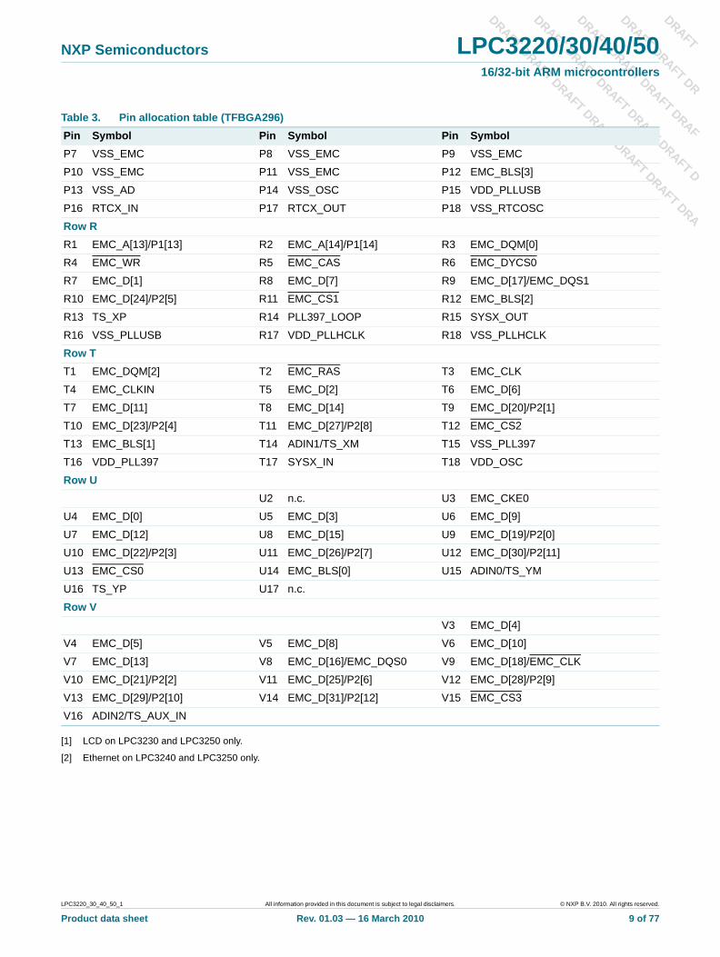
Table 3. Pin allocation table (TFBGA296)Pin Symbol Pin Symbol Pin Symbol
LPC3220_30_40_50_1 All information provided in this document is subject to legal disclaimers. © NXP B.V. 2010. All rights reserved.
Product data sheet Rev. 01.03 — 16 March 2010 8 of 77
DRAFT
DRAFT DRAFT DR
DRAFT DRAFT DRAFRAF
DRAFT DRAFT DRAF
FT D
DRAFT DRAFT DRAF
DRA
NXP Semiconductors LPC3220/30/40/5016/32-bit ARM microcontrollers
T DT DRAFT DRA
T DRAFT DRAFT DRAFT
[1] LCD on LPC3230 and LPC3250 only.
[2] Ethernet on LPC3240 and LPC3250 only.
P7 VSS_EMC P8 VSS_EMC P9 VSS_EMC
P10 VSS_EMC P11 VSS_EMC P12 EMC_BLS[3]
P13 VSS_AD P14 VSS_OSC P15 VDD_PLLUSB
P16 RTCX_IN P17 RTCX_OUT P18 VSS_RTCOSC
Row RR1 EMC_A[13]/P1[13] R2 EMC_A[14]/P1[14] R3 EMC_DQM[0]
R4 EMC_WR R5 EMC_CAS R6 EMC_DYCS0
R7 EMC_D[1] R8 EMC_D[7] R9 EMC_D[17]/EMC_DQS1
R10 EMC_D[24]/P2[5] R11 EMC_CS1 R12 EMC_BLS[2]
R13 TS_XP R14 PLL397_LOOP R15 SYSX_OUT
R16 VSS_PLLUSB R17 VDD_PLLHCLK R18 VSS_PLLHCLK
Row TT1 EMC_DQM[2] T2 EMC_RAS T3 EMC_CLK
T4 EMC_CLKIN T5 EMC_D[2] T6 EMC_D[6]
T7 EMC_D[11] T8 EMC_D[14] T9 EMC_D[20]/P2[1]
T10 EMC_D[23]/P2[4] T11 EMC_D[27]/P2[8] T12 EMC_CS2
T13 EMC_BLS[1] T14 ADIN1/TS_XM T15 VSS_PLL397
T16 VDD_PLL397 T17 SYSX_IN T18 VDD_OSC
Row UU2 n.c. U3 EMC_CKE0
U4 EMC_D[0] U5 EMC_D[3] U6 EMC_D[9]
U7 EMC_D[12] U8 EMC_D[15] U9 EMC_D[19]/P2[0]
U10 EMC_D[22]/P2[3] U11 EMC_D[26]/P2[7] U12 EMC_D[30]/P2[11]
U13 EMC_CS0 U14 EMC_BLS[0] U15 ADIN0/TS_YM
U16 TS_YP U17 n.c.
Row VV3 EMC_D[4]
V4 EMC_D[5] V5 EMC_D[8] V6 EMC_D[10]
V7 EMC_D[13] V8 EMC_D[16]/EMC_DQS0 V9 EMC_D[18]/EMC_CLK
V10 EMC_D[21]/P2[2] V11 EMC_D[25]/P2[6] V12 EMC_D[28]/P2[9]
V13 EMC_D[29]/P2[10] V14 EMC_D[31]/P2[12] V15 EMC_CS3
V16 ADIN2/TS_AUX_IN
Table 3. Pin allocation table (TFBGA296)Pin Symbol Pin Symbol Pin Symbol
LPC3220_30_40_50_1 All information provided in this document is subject to legal disclaimers. © NXP B.V. 2010. All rights reserved.
Product data sheet Rev. 01.03 — 16 March 2010 9 of 77
DRAFT
DRAFT DRAFT DR
DRAFT DRAFT DRAFRAF
DRAFT DRAFT DRAF
FT D
DRAFT DRAFT DRAF
DRA
NXP Semiconductors LPC3220/30/40/5016/32-bit ARM microcontrollers
T DT DRAFT DRA
T DRAFT DRAFT DRAFT
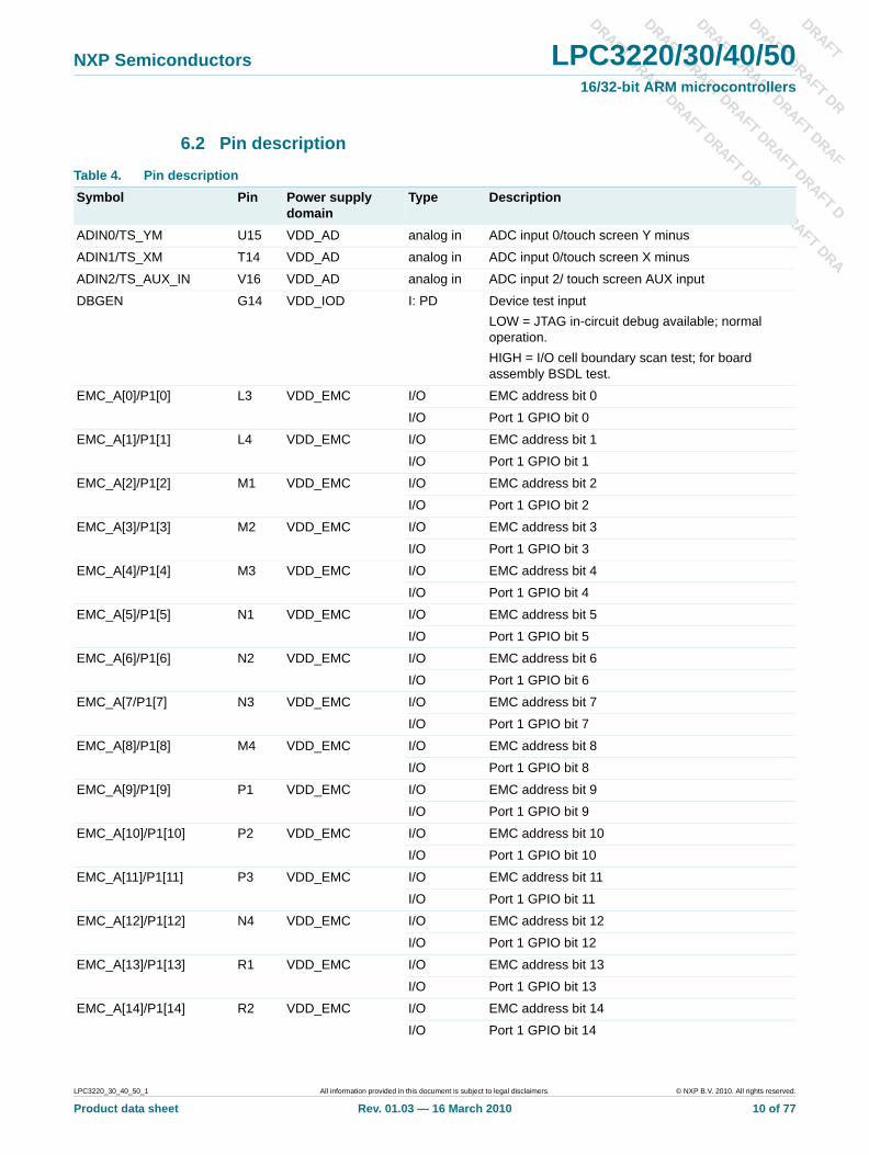
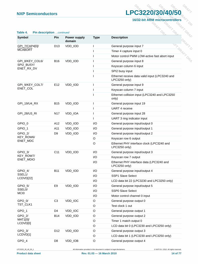
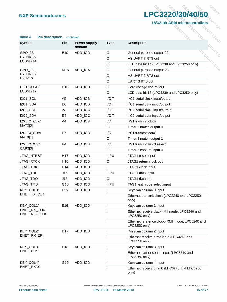
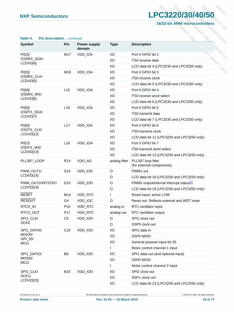
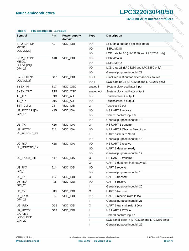
6.2 Pin description
Table 4. Pin descriptionSymbol Pin Power supply
domainType Description
ADIN0/TS_YM U15 VDD_AD analog in ADC input 0/touch screen Y minus
ADIN1/TS_XM T14 VDD_AD analog in ADC input 0/touch screen X minus
ADIN2/TS_AUX_IN V16 VDD_AD analog in ADC input 2/ touch screen AUX input
DBGEN G14 VDD_IOD I: PD Device test inputLOW = JTAG in-circuit debug available; normal operation.HIGH = I/O cell boundary scan test; for board assembly BSDL test.
EMC_A[0]/P1[0] L3 VDD_EMC I/O EMC address bit 0
I/O Port 1 GPIO bit 0
EMC_A[1]/P1[1] L4 VDD_EMC I/O EMC address bit 1
I/O Port 1 GPIO bit 1
EMC_A[2]/P1[2] M1 VDD_EMC I/O EMC address bit 2
I/O Port 1 GPIO bit 2
EMC_A[3]/P1[3] M2 VDD_EMC I/O EMC address bit 3
I/O Port 1 GPIO bit 3
EMC_A[4]/P1[4] M3 VDD_EMC I/O EMC address bit 4
I/O Port 1 GPIO bit 4
EMC_A[5]/P1[5] N1 VDD_EMC I/O EMC address bit 5
I/O Port 1 GPIO bit 5
EMC_A[6]/P1[6] N2 VDD_EMC I/O EMC address bit 6
I/O Port 1 GPIO bit 6
EMC_A[7/P1[7] N3 VDD_EMC I/O EMC address bit 7
I/O Port 1 GPIO bit 7
EMC_A[8]/P1[8] M4 VDD_EMC I/O EMC address bit 8
I/O Port 1 GPIO bit 8
EMC_A[9]/P1[9] P1 VDD_EMC I/O EMC address bit 9
I/O Port 1 GPIO bit 9
EMC_A[10]/P1[10] P2 VDD_EMC I/O EMC address bit 10
I/O Port 1 GPIO bit 10
EMC_A[11]/P1[11] P3 VDD_EMC I/O EMC address bit 11
I/O Port 1 GPIO bit 11
EMC_A[12]/P1[12] N4 VDD_EMC I/O EMC address bit 12
I/O Port 1 GPIO bit 12
EMC_A[13]/P1[13] R1 VDD_EMC I/O EMC address bit 13
I/O Port 1 GPIO bit 13
EMC_A[14]/P1[14] R2 VDD_EMC I/O EMC address bit 14
I/O Port 1 GPIO bit 14
LPC3220_30_40_50_1 All information provided in this document is subject to legal disclaimers. © NXP B.V. 2010. All rights reserved.
Product data sheet Rev. 01.03 — 16 March 2010 10 of 77

DRAFT
DRAFT DRAFT DR
DRAFT DRAFT DRAFRAF
DRAFT DRAFT DRAF
FT D
DRAFT DRAFT DRAF
DRA
NXP Semiconductors LPC3220/30/40/5016/32-bit ARM microcontrollers
T DT DRAFT DRA
T DRAFT DRAFT DRAFT
EMC_A[15]/P1[15] L1 VDD_EMC I/O EMC address bit 15
I/O Port 1 GPIO bit 15
EMC_A[16]/P1[16] K3 VDD_EMC I/O EMC address bit 16
I/O Port 1 GPIO bit 16
EMC_A[17]/P1[17] K4 VDD_EMC I/O EMC address bit 17
I/O Port 1 GPIO bit 17
EMC_A[18]/P1[18] K2 VDD_EMC I/O EMC address bit 18
I/O Port 1 GPIO bit 18
EMC_A[19]/P1[19] K1 VDD_EMC I/O EMC address bit 19
I/O Port 1 GPIO bit 19
EMC_A[20]/P1[20] J1 VDD_EMC I/O EMC address bit 20
I/O Port 1 GPIO bit 20
EMC_A[21]/P1[21] J2 VDD_EMC I/O EMC address bit 21
I/O Port 1 GPIO bit 21
EMC_A[22]/P1[22] J3 VDD_EMC I/O EMC address bit 22
I/O Port 1 GPIO bit 22
EMC_A[23]/P1[23] J4 VDD_EMC I/O EMC address bit 23
I/O Port 1 GPIO bit 23
EMC_BLS[0] U14 VDD_EMC O Static memory byte lane 0 select
EMC_BLS[1] T13 VDD_EMC O Static memory byte lane 1 select
EMC_BLS[2] R12 VDD_EMC O Static memory byte lane 2 select
EMC_BLS[3] P12 VDD_EMC O Static memory byte lane 3 select
EMC_CAS R5 VDD_EMC O SDRAM column address strobe out, active LOW
EMC_CKE0 U3 VDD_EMC O Clock enable out for SDRAM bank 0
EMC_CKE1 L2 VDD_EMC O Clock enable out for SDRAM bank 1
EMC_CLK T3 VDD_EMC O SDRAM clock out
EMC_CLKIN T4 VDD_EMC I SDRAM clock feedback
EMC_CS0 U13 VDD_EMC O EMC static memory chip select 0
EMC_CS1 R11 VDD_EMC O EMC static memory chip select 1
EMC_CS2 T12 VDD_EMC O EMC static memory chip select 2
EMC_CS3 V15 VDD_EMC O EMC static memory chip select 3
EMC_D[0] U4 VDD_EMC I/O: BK EMC data bit 0
EMC_D[1] R7 VDD_EMC I/O: BK EMC data bit 1
EMC_D[2] T5 VDD_EMC I/O: BK EMC data bit 2
EMC_D[3] U5 VDD_EMC I/O: BK EMC data bit 3
EMC_D[4] V3 VDD_EMC I/O: BK EMC data bit 4
EMC_D[5] V4 VDD_EMC I/O: BK EMC data bit 5
EMC_D[6] T6 VDD_EMC I/O: BK EMC data bit 6
EMC_D[7] R8 VDD_EMC I/O: BK EMC data bit 7
EMC_D[8] V5 VDD_EMC I/O: BK EMC data bit 8
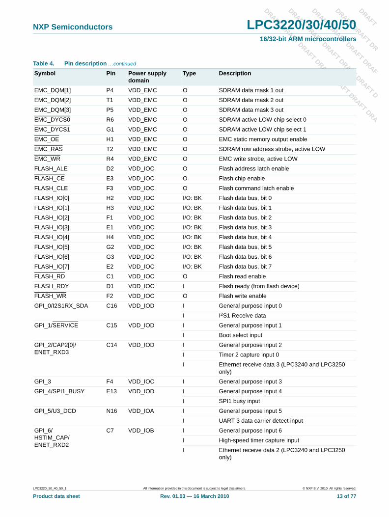
Table 4. Pin description …continued
Symbol Pin Power supply domain
Type Description
LPC3220_30_40_50_1 All information provided in this document is subject to legal disclaimers. © NXP B.V. 2010. All rights reserved.
Product data sheet Rev. 01.03 — 16 March 2010 11 of 77

DRAFT
DRAFT DRAFT DR
DRAFT DRAFT DRAFRAF
DRAFT DRAFT DRAF
FT D
DRAFT DRAFT DRAF
DRA
NXP Semiconductors LPC3220/30/40/5016/32-bit ARM microcontrollers
T DT DRAFT DRA
T DRAFT DRAFT DRAFT
EMC_D[9] U6 VDD_EMC I/O: BK EMC data bit 9
EMC_D[10] V6 VDD_EMC I/O: BK EMC data bit 10
EMC_D[11] T7 VDD_EMC I/O: BK EMC data bit 11
EMC_D[12] U7 VDD_EMC I/O: BK EMC data bit 12
EMC_D[13] V7 VDD_EMC I/O: BK EMC data bit 13
EMC_D[14] T8 VDD_EMC I/O: BK EMC data bit 14
EMC_D[15] U8 VDD_EMC I/O: BK EMC data bit 15
EMC_D[16]/ EMC_DQS0
V8 VDD_EMC I/O: BK EMC data bit 16
I/O: BK DDR data strobe 0
EMC_D[17]/ EMC_DQS1
R9 VDD_EMC I/O: BK EMC data bit 17
I/O: BK DDR data strobe 1
EMC_D[18]/ EMC_CLK
V9 VDD_EMC I/O: P EMC data bit 18
I/O: P DDR inverted clock output
EMC_D[19]/P2[0] U9 VDD_EMC I/O: P EMC data bit 19
I/O: P Port 2 GPIO bit 0
EMC_D[20]/P2[1] T9 VDD_EMC I/O: P EMC data bit 20
I/O: P Port 2 GPIO bit 1
EMC_D[21]/P2[2] V10 VDD_EMC I/O: P EMC data bit 21
I/O: P Port 2 GPIO bit 2
EMC_D[22]/P2[3] U10 VDD_EMC I/O: P EMC data bit 22
I/O: P Port 2 GPIO bit 3
EMC_D[23]/P2[4] T10 VDD_EMC I/O: P EMC data bit 23
I/O: P Port 2 GPIO bit 4
EMC_D[24]/P2[5] R10 VDD_EMC I/O: P EMC data bit 24
I/O: P Port 2 GPIO bit 5
EMC_D[25]/P2[6] V11 VDD_EMC I/O: P EMC data bit 25
I/O: P Port 2 GPIO bit 6
EMC_D[26]/P2[7] U11 VDD_EMC I/O: P EMC data bit 26
I/O: P Port 2 GPIO bit 7
EMC_D[27]/P2[8] T11 VDD_EMC I/O: P EMC data bit 27
I/O: P Port 2 GPIO bit 8
EMC_D[28]/P2[9] V12 VDD_EMC I/O: P EMC data bit 28
I/O: P Port 2 GPIO bit 9
EMC_D[29]/P2[10] V13 VDD_EMC I/O: P EMC data bit 29
I/O: P Port 2 GPIO bit 10
EMC_D[30]/P2[11] U12 VDD_EMC I/O: P EMC data bit 30
I/O: P Port 2 GPIO bit 11
EMC_D[31]/P2[12] V14 VDD_EMC I/O: P EMC data bit 31
I/O: P Port 2 GPIO bit 12
EMC_DQM[0] R3 VDD_EMC O SDRAM data mask 0 out
Table 4. Pin description …continued
Symbol Pin Power supply domain
Type Description
LPC3220_30_40_50_1 All information provided in this document is subject to legal disclaimers. © NXP B.V. 2010. All rights reserved.
Product data sheet Rev. 01.03 — 16 March 2010 12 of 77
DRAFT
DRAFT DRAFT DR
DRAFT DRAFT DRAFRAF
DRAFT DRAFT DRAF
FT D
DRAFT DRAFT DRAF
DRA
NXP Semiconductors LPC3220/30/40/5016/32-bit ARM microcontrollers
T DT DRAFT DRA
T DRAFT DRAFT DRAFT
EMC_DQM[1] P4 VDD_EMC O SDRAM data mask 1 out
EMC_DQM[2] T1 VDD_EMC O SDRAM data mask 2 out
EMC_DQM[3] P5 VDD_EMC O SDRAM data mask 3 out
EMC_DYCS0 R6 VDD_EMC O SDRAM active LOW chip select 0
EMC_DYCS1 G1 VDD_EMC O SDRAM active LOW chip select 1
EMC_OE H1 VDD_EMC O EMC static memory output enable
EMC_RAS T2 VDD_EMC O SDRAM row address strobe, active LOW
EMC_WR R4 VDD_EMC O EMC write strobe, active LOW
FLASH_ALE D2 VDD_IOC O Flash address latch enable
FLASH_CE E3 VDD_IOC O Flash chip enable
FLASH_CLE F3 VDD_IOC O Flash command latch enable
FLASH_IO[0] H2 VDD_IOC I/O: BK Flash data bus, bit 0
FLASH_IO[1] H3 VDD_IOC I/O: BK Flash data bus, bit 1
FLASH_IO[2] F1 VDD_IOC I/O: BK Flash data bus, bit 2
FLASH_IO[3] E1 VDD_IOC I/O: BK Flash data bus, bit 3
FLASH_IO[4] H4 VDD_IOC I/O: BK Flash data bus, bit 4
FLASH_IO[5] G2 VDD_IOC I/O: BK Flash data bus, bit 5
FLASH_IO[6] G3 VDD_IOC I/O: BK Flash data bus, bit 6
FLASH_IO[7] E2 VDD_IOC I/O: BK Flash data bus, bit 7
FLASH_RD C1 VDD_IOC O Flash read enable
FLASH_RDY D1 VDD_IOC I Flash ready (from flash device)
FLASH_WR F2 VDD_IOC O Flash write enable
GPI_0/I2S1RX_SDA C16 VDD_IOD I General purpose input 0
I I2S1 Receive data
GPI_1/SERVICE C15 VDD_IOD I General purpose input 1
I Boot select input
GPI_2/CAP2[0]/ENET_RXD3
C14 VDD_IOD I General purpose input 2
I Timer 2 capture input 0
I Ethernet receive data 3 (LPC3240 and LPC3250 only)
GPI_3 F4 VDD_IOC I General purpose input 3
GPI_4/SPI1_BUSY E13 VDD_IOD I General purpose input 4
I SPI1 busy input
GPI_5/U3_DCD N16 VDD_IOA I General purpose input 5
I UART 3 data carrier detect input
GPI_6/HSTIM_CAP/ENET_RXD2
C7 VDD_IOB I General purpose input 6
I High-speed timer capture input
I Ethernet receive data 2 (LPC3240 and LPC3250 only)
Table 4. Pin description …continued
Symbol Pin Power supply domain
Type Description
LPC3220_30_40_50_1 All information provided in this document is subject to legal disclaimers. © NXP B.V. 2010. All rights reserved.
Product data sheet Rev. 01.03 — 16 March 2010 13 of 77
DRAFT
DRAFT DRAFT DR
DRAFT DRAFT DRAFRAF
DRAFT DRAFT DRAF
FT D
DRAFT DRAFT DRAF
DRA
NXP Semiconductors LPC3220/30/40/5016/32-bit ARM microcontrollers
T DT DRAFT DRA
T DRAFT DRAFT DRAFT
GPI_7/CAP4[0]/MCABORT
D13 VDD_IOD I General purpose input 7
I Timer 4 capture input 0
I Motor control PWM LOW-active fast abort input
GPI_8/KEY_COL6/SPI2_BUSY/ENET_RX_DV
B16 VDD_IOD I General purpose input 8
I Keyscan column 6 input
I SPI2 busy input
I Ethernet receive data valid input (LPC3240 and LPC3250 only)
GPI_9/KEY_COL7/ENET_COL
E12 VDD_IOD I General purpose input 9
I Keyscan column 7 input
I Ethernet collision input (LPC3240 and LPC3250 only)
GPI_19/U4_RX B15 VDD_IOD I General purpose input 19
I UART 4 receive
GPI_28/U3_RI N17 VDD_IOA I General purpose input 28
I UART 3 ring indicator input
GPIO_0 A12 VDD_IOD I/O General purpose input/output 0
GPIO_1 A11 VDD_IOD I/O General purpose input/output 1
GPIO_2/KEY_ROW6/ENET_MDC
D9 VDD_IOD I/O General purpose input/output 2
O Keyscan row 6 output
O Ethernet PHY interface clock (LPC3240 and LPC3250 only)
GPIO_3/KEY_ROW7/ENET_MDIO
C11 VDD_IOD I/O General purpose input/output 3
I/O Keyscan row 7 output
I/O Ethernet PHY interface data (LPC3240 and LPC3250 only)
GPIO_4/SSEL1/LCDVD[22]
B11 VDD_IOD I/O General purpose input/output 4
I/O SSP1 Slave Select
I/O LCD data bit 22 (LPC3230 and LPC3250 only)
GPIO_5/SSEL0/MCI0
E9 VDD_IOD I/O General purpose input/output 5
I/O SSP0 Slave Select
I/O Motor control channel 0 input
GPO_0/TST_CLK1
C3 VDD_IOC O General purpose output 0
O Test clock 1 out
GPO_1 D4 VDD_IOC O General purpose output 1
GPO_2/MAT1[0]/LCDVD[0]
B14 VDD_IOD O General purpose output 2
O Timer 1 match output 0
O LCD data bit 0 (LPC3230 and LPC3250 only)
GPO_3/LCDVD[1]
D12 VDD_IOD O General purpose output 3
O LCD data bit 1 (LPC3230 and LPC3250 only)
GPO_4 D8 VDD_IOB O General purpose output 4
Table 4. Pin description …continued
Symbol Pin Power supply domain
Type Description
LPC3220_30_40_50_1 All information provided in this document is subject to legal disclaimers. © NXP B.V. 2010. All rights reserved.
Product data sheet Rev. 01.03 — 16 March 2010 14 of 77

DRAFT
DRAFT DRAFT DR
DRAFT DRAFT DRAFRAF
DRAFT DRAFT DRAF
FT D
DRAFT DRAFT DRAF
DRA
NXP Semiconductors LPC3220/30/40/5016/32-bit ARM microcontrollers
T DT DRAFT DRA
T DRAFT DRAFT DRAFT
GPO_5 B3 VDD_IOC O General purpose output 5
GPO_6/LCDVD[18]
A16 VDD_IOD O General purpose output 6
O LCD data bit 18 (LPC3230 and LPC3250 only)
GPO_7/LCDVD[2]
A15 VDD_IOD O General purpose output 7
O LCD data bit 2 (LPC3230 and LPC3250 only)
GPO_8/LCDVD[8]
C13 VDD_IOD O General purpose output 8
O LCD data bit 8 (LPC3230 and LPC3250 only)
GPO_9/LCDVD[9]
C12 VDD_IOD O General purpose output 9
O LCD data bit 9 (LPC3230 and LPC3250 only)
GPO_10/MCOB2/LCDPWR
E11 VDD_IOD O General purpose output 10
O Motor control PWM channel 2, output B
O LCD panel power enable (LPC3230 and LPC3250 only)
GPO_11 E8 VDD_IOB O General purpose output 11
GPO_12/MCOA2/LCDLE
B12 VDD_IOD O General purpose output 12
O Motor control PWM channel 2, output A
O LCD line end signal (LPC3230 and LPC3250 only)
GPO_13/MCOB1/LCDDCLK
B13 VDD_IOD O General purpose output 13
O Motor control PWM channel 1, output B
O LCD clock output (LPC3230 and LPC3250 only)
GPO_14 D3 VDD_IOC O General purpose output 14
GPO_15/MCOA1/LCDFP
A14 VDD_IOD O General purpose output 15
O Motor control PWM channel 1, output A
O LCD frame/sync pulse (LPC3230 and LPC3250 only)
GPO_16/MCOB0/LCDENAB/LCDM
D10 VDD_IOD O General purpose output 16
O Motor control PWM channel 0, output B
O LCD STN AC bias/TFT data enable (LPC3230 and LPC3250 only)
GPO_17 N18 VDD_IOA O General purpose output 17
GPO_18/MCOA0/LCDLP
D11 VDD_IOD O General purpose output 18
O Motor control PWM channel 0, output A
O LCD line sync/horizontal sync (LPC3230 and LPC3250 only)
GPO_19 C2 VDD_IOC O General purpose output 19
GPO_20 B2 VDD_IOC O General purpose output 20
GPO_21/U4_TX/LCDVD[3]
A13 VDD_IOD O General purpose output 21
O UART 4 transmit
O LCD data bit 3 (LPC3230 and LPC3250 only)
Table 4. Pin description …continued
Symbol Pin Power supply domain
Type Description
LPC3220_30_40_50_1 All information provided in this document is subject to legal disclaimers. © NXP B.V. 2010. All rights reserved.
Product data sheet Rev. 01.03 — 16 March 2010 15 of 77
DRAFT
DRAFT DRAFT DR
DRAFT DRAFT DRAFRAF
DRAFT DRAFT DRAF
FT D
DRAFT DRAFT DRAF
DRA
NXP Semiconductors LPC3220/30/40/5016/32-bit ARM microcontrollers
T DT DRAFT DRA
T DRAFT DRAFT DRAFT
GPO_22/U7_HRTS/LCDVD[14]
E10 VDD_IOD O General purpose output 22
O HS UART 7 RTS out
O LCD data bit 14 (LPC3230 and LPC3250 only)
GPO_23/U2_HRTS/U3_RTS
M16 VDD_IOA O General purpose output 23
O HS UART 2 RTS out
O UART 3 RTS out
HIGHCORE/LCDVD[17]
H16 VDD_IOD O Core voltage control out
O LCD data bit 17 (LPC3230 and LPC3250 only)
I2C1_SCL A5 VDD_IOB I/O T I2C1 serial clock input/output
I2C1_SDA B6 VDD_IOB I/O T I2C1 serial data input/output
I2C2_SCL A3 VDD_IOC I/O T I2C2 serial clock input/output
I2C2_SDA E4 VDD_IOC I/O T I2C2 serial data input/output
I2S1TX_CLK/MAT3[0]
A4 VDD_IOB I/O I2S1 transmit clock
O Timer 3 match output 0
I2S1TX_SDA/MAT3[1]
E7 VDD_IOB I/O I2S1 transmit data
O Timer 3 match output 1
I2S1TX_WS/CAP3[0]
B4 VDD_IOB I/O I2S1 transmit word select
I/O Timer 3 capture input 0
JTAG_NTRST H17 VDD_IOD I: PU JTAG1 reset input
JTAG_RTCK H18 VDD_IOD O JTAG1 return clock out
JTAG_TCK H14 VDD_IOD I JTAG1 clock input
JTAG_TDI J16 VDD_IOD I: PU JTAG1 data input
JTAG_TDO J15 VDD_IOD O JTAG1 data out
JTAG_TMS G18 VDD_IOD I: PU TAG1 test mode select input
KEY_COL0/ENET_TX_CLK
F15 VDD_IOD I Keyscan column 0 input
I Ethernet transmit clock (LPC3240 and LPC3250 only)
KEY_COL1/ENET_RX_CLK/ENET_REF_CLK
E16 VDD_IOD I Keyscan column 1 input
I Ethernet receive clock (MII mode, LPC3240 and LPC3250 only)
I Ethernet reference clock (RMII mode, LPC3240 and LPC3250 only)
KEY_COL2/ENET_RX_ER
D17 VDD_IOD I Keyscan column 2 input
I Ethernet receive error input (LPC3240 and LPC3250 only)
KEY_COL3/ENET_CRS
D18 VDD_IOD I Keyscan column 3 input
I Ethernet carrier sense input (LPC3240 and LPC3250 only)
KEY_COL4/ENET_RXD0
G15 VDD_IOD I Keyscan column 4 input
I Ethernet receive data 0 (LPC3240 and LPC3250 only)
Table 4. Pin description …continued
Symbol Pin Power supply domain
Type Description
LPC3220_30_40_50_1 All information provided in this document is subject to legal disclaimers. © NXP B.V. 2010. All rights reserved.
Product data sheet Rev. 01.03 — 16 March 2010 16 of 77

DRAFT
DRAFT DRAFT DR
DRAFT DRAFT DRAFRAF
DRAFT DRAFT DRAF
FT D
DRAFT DRAFT DRAF
DRA
NXP Semiconductors LPC3220/30/40/5016/32-bit ARM microcontrollers
T DT DRAFT DRA
T DRAFT DRAFT DRAFT
KEY_COL5/ENET_RXD1
F16 VDD_IOD I Keyscan column 5 input
I Ethernet receive data 1 (LPC3240 and LPC3250 only)
KEY_ROW0/ENET_TX_ER
E15 VDD_IOD I/O T Keyscan row 0 out
I/O T Ethernet transmit error (LPC3240 and LPC3250 only)
KEY_ROW1/ENET_TXD2
E14 VDD_IOD I/O T Keyscan row 1 out
I/O T Ethernet transmit data 2 (LPC3240 and LPC3250 only)
KEY_ROW2/ENET_TXD3
F14 VDD_IOD I/O T Keyscan row 2 out
I/O T Ethernet transmit data 3 (LPC3240 and LPC3250 only)
KEY_ROW3/ENET_TX_EN
D16 VDD_IOD I/O T Keyscan row 3 out
I/O T Ethernet transmit enable (LPC3240 and LPC3250 only)
KEY_ROW4/ENET_TXD0
C17 VDD_IOD I/O T Keyscan row 4 out
I/O T Ethernet transmit data 0 (LPC3240 and LPC3250 only)
KEY_ROW5/ENET_TXD1
C18 VDD_IOD I/O T Keyscan row 5 out
I/O T Ethernet transmit data 1 (LPC3240 and LPC3250 only)
MS_BS/MAT2[1] A6 VDD_IOD I/O: P MS/SD card command out
O Timer 2 match output 1
MS_DIO0/MAT0[0] A8 VDD_IOD I/O: P MS/SD card data 0
O Timer 0 match output 0
MS_DIO1/MAT0[1]
A7 VDD_IOD I/O: P MS/SD card data 1
O Timer 0 match output 1
MS_DIO2/MAT0[2]
B8 VDD_IOD I/O: P MS/SD card data 2
O Timer 0 match output 2
MS_DIO3/MAT0[3]
C8 VDD_IOD I/O: P MS/SD card data 3
O Timer 0 match output 3
MS_SCLK/MAT2[0]
B7 VDD_IOD I/O MS/SD card clock output
O Timer 2 match output 0
n.c. B17,U17,U2
- - not connected
ONSW M15 VDD_RTC O RTC match output for external power control
P0[0]/I2S1RX_CLK
B5 VDD_IOB I/O Port 0 GPIO bit 0
I/O I2S1 receive clock
P0[1]/I2S1RX_WS
D7 VDD_IOB I/O Port 0 GPIO bit 1
I/O I2S1 receive word select
Table 4. Pin description …continued
Symbol Pin Power supply domain
Type Description
LPC3220_30_40_50_1 All information provided in this document is subject to legal disclaimers. © NXP B.V. 2010. All rights reserved.
Product data sheet Rev. 01.03 — 16 March 2010 17 of 77
DRAFT
DRAFT DRAFT DR
DRAFT DRAFT DRAFRAF
DRAFT DRAFT DRAF
FT D
DRAFT DRAFT DRAF
DRA
NXP Semiconductors LPC3220/30/40/5016/32-bit ARM microcontrollers
T DT DRAFT DRA
T DRAFT DRAFT DRAFT
P0[2]/I2S0RX_SDA/LCDVD[4]
M17 VDD_IOA I/O Port 0 GPIO bit 2
I/O I2S0 receive data
I/O LCD data bit 4 (LPC3230 and LPC3250 only)
P0[3]/I2S0RX_CLK/LCDVD[5]
M18 VDD_IOA I/O Port 0 GPIO bit 3
I/O I2S0 receive clock
I/O LCD data bit 5 (LPC3230 and LPC3250 only)
P0[4]/I2S0RX_WS/LCDVD[6]
L15 VDD_IOA I/O Port 0 GPIO bit 4
I/O I2S0 receive word select
I/O LCD data bit 6 (LPC3230 and LPC3250 only)
P0[5]/I2S0TX_SDA/LCDVD[7]
L16 VDD_IOA I/O Port 0 GPIO bit 5
I/O I2S0 transmit data
I/O LCD data bit 7 (LPC3230 and LPC3250 only)
P0[6]/I2S0TX_CLK/LCDVD[12]
L17 VDD_IOA I/O Port 0 GPIO bit 6
I/O I2S0 transmit clock
I/O LCD data bit 12 (LPC3230 and LPC3250 only)
P0[7]/I2S0TX_WS/LCDVD[13]
L18 VDD_IOA I/O Port 0 GPIO bit 7
I/O I2S0 transmit word select
I/O LCD data bit 13 (LPC3230 and LPC3250 only)
PLL397_LOOP R14 VDD_AD analog filter PLL397 loop filter (for external components)
PWM_OUT1/LCDVD[16]
D14 VDD_IOD O PWM1 out
O LCD data bit 16 (LPC3230 and LPC3250 only)
PWM_OUT2/INTSTAT/LCDVD[19]
D15 VDD_IOD O PWM2 output/internal interrupt status[1]
O LCD data bit 19 (LPC3230 and LPC3250 only)
RESET M14 VDD_RTC I Reset input, active LOW
RESOUT G4 VDD_IOC O Reset out. Reflects external and WDT reset
RTCX_IN P16 VDD_RTC analog in RTC oscillator input
RTCX_OUT P17 VDD_RTC analog out RTC oscillator output
SPI1_CLK/SCK0
C9 VDD_IOD O SPI1 clock out
O SSP0 clock out
SPI1_DATIN/MISO0/GPI_25/MCI1
C10 VDD_IOD I/O SPI1 data in
I/O SSP0 MISO
I/O General purpose input bit 25
I Motor control channel 1 input
SPI1_DATIO/MOSI0/MCI2
B9 VDD_IOD I/O SPI1 data out (and optional input)
I/O SSP0 MOSI
I Motor control channel 2 input
SPI2_CLK/SCK1/LCDVD[23]
B10 VDD_IOD I/O SPI2 clock out
I/O SSP1 clock out
I/O LCD data bit 23 (LPC3230 and LPC3250 only)
Table 4. Pin description …continued
Symbol Pin Power supply domain
Type Description
LPC3220_30_40_50_1 All information provided in this document is subject to legal disclaimers. © NXP B.V. 2010. All rights reserved.
Product data sheet Rev. 01.03 — 16 March 2010 18 of 77
DRAFT
DRAFT DRAFT DR
DRAFT DRAFT DRAFRAF
DRAFT DRAFT DRAF
FT D
DRAFT DRAFT DRAF
DRA
NXP Semiconductors LPC3220/30/40/5016/32-bit ARM microcontrollers
T DT DRAFT DRA
T DRAFT DRAFT DRAFT
SPI2_DATIO/MOSI1/LCDVD[20]
A9 VDD_IOD I/O SPI2 data out (and optional input)
I/O SSP1 MOSI
I/O LCD data bit 20 (LPC3230 and LPC3250 only)
SPI2_DATIN/MISO1/LCDVD[21]/GPI_27
A10 VDD_IOD I/O SPI2 data in
I/O SSP1 MISO
I/O LCD data 21 (LPC3230 and LPC3250 only)
I/O General purpose input bit 27
SYSCLKEN/LCDVD[15]
G17 VDD_IOD I/O T Clock request out for external clock source
I/O T LCD data bit 15 (LPC3230 and LPC3250 only)
SYSX_IN T17 VDD_OSC analog in System clock oscillator input
SYSX_OUT R15 VDD_OSC analog out System clock oscillator output
TS_XP R13 VDD_AD I/O Touchscreen X output
TS_YP U16 VDD_AD I/O Touchscreen Y output
TST_CLK2 C6 VDD_IOB O Test clock 2 out
U1_RX/CAP1[0]/GPI_15
K15 VDD_IOA I/O HS UART 1 receive
I/O Timer 1 capture input 0
I/O General purpose input bit 15
U1_TX K16 VDD_IOA O HS UART 1 transmit
U2_HCTS/U3_CTS/GPI_16
J18 VDD_IOA I/O HS UART 2 Clear to Send input
I UART 3 Clear to Send
I/O General purpose input bit 16
U2_RX/U3_DSR/GPI_17
K18 VDD_IOA I/O HS UART 2 receive
I/O UART 3 data set ready
I/O General purpose input bit 17
U2_TX/U3_DTR K17 VDD_IOA O HS UART 2 transmit
O UART 3 data terminal ready out
U3_RX/GPI_18
J14 VDD_IOD I/O UART 3 receive
I/O General purpose input bit 18
U3_TX J17 VDD_IOD O UART 3 transmit
U5_RX/GPI_20
F18 VDD_IOD I/O UART 5 receive
I General purpose input bit 20
U5_TX H15 VDD_IOD O UART 5 transmit
U6_IRRX/GPI_21
F17 VDD_IOD I/O UART 6 receive (with IrDA)
I General purpose input bit 21
U6_IRTX G16 VDD_IOD O UART 6 transmit (with IrDA)
U7_HCTS/CAP0[1]/LCDCLKIN/GPI_22
G13 VDD_IOD I HS UART 7 CTS in
I Timer 0 capture input 1
I LCD panel clock in (LPC3230 and LPC3250 only)
I General purpose input bit 22
Table 4. Pin description …continued
Symbol Pin Power supply domain
Type Description
LPC3220_30_40_50_1 All information provided in this document is subject to legal disclaimers. © NXP B.V. 2010. All rights reserved.
Product data sheet Rev. 01.03 — 16 March 2010 19 of 77
DRAFT
DRAFT DRAFT DR
DRAFT DRAFT DRAFRAF
DRAFT DRAFT DRAF
FT D
DRAFT DRAFT DRAF
DRA
NXP Semiconductors LPC3220/30/40/5016/32-bit ARM microcontrollers
T DT DRAFT DRA
T DRAFT DRAFT DRAFT
U7_RX/CAP0[0]/LCDVD[10]/GPI_23
E17 VDD_IOD I/O HS UART 7 receive
I/O Timer 0 capture input 0
I/O LCD data bit 10 (LPC3230 and LPC3250 only)
I/O General purpose input bit 23
U7_TX/MAT1[1]/LCDVD[11]
E18 VDD_IOD O HS UART 7 transmit
O Timer 1 match output 1
O LCD data bit 11 (LPC3230 and LPC3250 only)
USB_ATX_INT C4 VDD_IOC I Interrupt from USB ATX
USB_DAT_VP/U5_RX
D5 VDD_IOC I/O: P USB transmit data, D+ receive
I/O: P UART 5 receive
USB_I2C_SCL E5 VDD_IOC I/O T I2C clock for USB ATX interface
USB_I2C_SDA E6 VDD_IOC I/O T I2C data for USB ATX interface
USB_OE_TP D6 VDD_IOC I/O USB transmit enable for DAT/SE0
USB_SE0_VM/U5_TX
C5 VDD_IOC I/O: P USB single ended zero transmit, D− Receive
I/O: P UART 5 transmit
VDD_AD N12, N13
VDD_AD power 3.3 V supply for ADC/touch screen
VDD_CORE G7,G9,G11, J7,J12,M7,M11
VDD_CORE power 1.2 V or 0.9 V supply for core
VDD_COREFXD L12,M13
VDD_COREFXD power Fixed 1.2 V supply for digital portion of the analog block
VDD_EMC J6,K6,K7,L6,M6,M8,N7,N8,N9N10,N11
VDD_EMC power 1.8 V or 2.5 V or 3.3 V supply for External Memory Controller (EMC)
VDD_IOA H13,J13
VDD_IOA power 1.8 V or 3.3 V supply for IOA domain
VDD_IOB F8 VDD_IOB power 1.8 V or 3.3 V supply for IOB domain
VDD_IOC F7, G6, H6, J5
VDD_IOC power 1.8 V or 3.3 V supply for IOC domain
VDD_IOD F13,F9
VDD_IOD power 1.8 V to 3.3 V supply for IOD domain
VDD_OSC T18 VDD_OSC power 1.2 V supply for main oscillator
Table 4. Pin description …continued
Symbol Pin Power supply domain
Type Description
LPC3220_30_40_50_1 All information provided in this document is subject to legal disclaimers. © NXP B.V. 2010. All rights reserved.
Product data sheet Rev. 01.03 — 16 March 2010 20 of 77
DRAFT
DRAFT DRAFT DR
DRAFT DRAFT DRAFRAF
DRAFT DRAFT DRAF
FT D
DRAFT DRAFT DRAF
DRA
NXP Semiconductors LPC3220/30/40/5016/32-bit ARM microcontrollers
T DT DRAFT DRA
T DRAFT DRAFT DRAFT
[1] The PWM2_CTRL register controls this pin function (see LPC32x0 User manual).
VDD_PLL397 T16 VDD_PLL397 power 1.2 V supply for 397x PLL
VDD_PLLHCLK R17 VDD_PLLHCLK power 1.2 V supply for HCLK PLL
VDD_PLLUSB P15 VDD_PLLUSB power 1.2 V supply for USB PLL
VDD_FUSE N14 VDD_FUSE power 1.2 V supply
VDD_RTC K14 VDD_RTC power 1.2 V supply for RTC I/O
VDD_RTCCORE L13 VDD_RTCCORE power 1.2 V supply for RTC
VDD_RTCOSC N15 VDD_RTCOSC power 1.2 V supply for RTC oscillator
VSS_AD P13 - power Ground for ADC/touch screen
VSS_CORE G8, G10, G12, H7, K12, L7, M9, M10, M12
- power Ground for core
VSS_EMC K5, L5, M5, N5, N6, P6, P7, P8, P9, P10, P11
- power Ground for EMC
VSS_IOA K13 - power Ground VDD_IOA domain
VSS_IOB F6 - power Ground VDD_IOB domain
VSS_IOC F5,G5,H5
- power Ground VDD_IOC domain
VSS_IOD F10,F11,F12,H12
- power Ground VDD_IOD domain
VSS_OSC P14 - power Ground for main oscillator
VSS_PLL397 T15 - power Ground for 397x PLL
VSS_PLLHCLK R18 - power Ground for HCLK PLL
VSS_PLLUSB R16 - power Ground for USB PLL
VSS_RTCCORE L14 - power Ground for RTC
VSS_RTCOSC P18 - power Ground for RTC oscillator
Table 4. Pin description …continued
Symbol Pin Power supply domain
Type Description
LPC3220_30_40_50_1 All information provided in this document is subject to legal disclaimers. © NXP B.V. 2010. All rights reserved.
Product data sheet Rev. 01.03 — 16 March 2010 21 of 77
DRAFT
DRAFT DRAFT DR
DRAFT DRAFT DRAFRAF
DRAFT DRAFT DRAF
FT D
DRAFT DRAFT DRAF
DRA
NXP Semiconductors LPC3220/30/40/5016/32-bit ARM microcontrollers
T DT DRAFT DRA
T DRAFT DRAFT DRAFT
[1] See LPC32x0 User manual for details.
[1] The VDD_IOA, VDD_IOB, VDD_IOC, and VDD_IOD supply domains can be operated at a voltage independent of the other domains as long as all pins connected to the same peripheral are at the same voltage level. There are two special cases for determining supply domain voltages (for details see application note AN10777):a) Ethernet configured in MII mode: VDD_IOD must be the same as VDD_IOB.b) UART3 when used with hardware flow control or when sharing an RS-232 transceiver with another
UART: VDD_IOA must be the same as VDD_IOD.
Table 5. Digital I/O pad types[1]
Parameter AbbreviationI/O type I = input.
O = output.I/O = bidirectional.I/O T = bidirectional or high impedance.
Pin detail BK: pin has a bus keeper function that weakly retains the last level driven on an I/O pin when it is switched from output to input.PU: pin has a nominal 50 μA internal pull-up connected.PD: pin has a nominal 50 μA internal pull-down connected.P: pin has programmable input characteristics.
Table 6. Supply domainsSupply domain Voltage range Related supply
pinsDescription
VDD_CORE 0.9 V to 1.39 V VDD_CORE Core power domain.
VDD_COREFXD 1.2 V VDD_COREFXD Fixed 1.2 V supply for digital portion of the analog block.
other core domains
1.2 V VDD_PLL397, VDD_PLLHCLK, VDD_PLLUSB, VDD_FUSE, VDD_OSC
1.2 V supplies, tied to VDD_COREFXD.
VDD_RTC 0.9 V to 1.39 V VDD_RTC, VDD_RTCCORE, VDD_RTCOSC
RTC supply domain. Can be connected to a battery backed-up power source.
VDD_AD 2.7 V to 3.6 V VDD_AD 3.3 V supply for ADC and touch screen.
VDD_EMC 1.7 V to 1.95 V 2.3 V to 2.7 V 2.7 V to 3.6 V
VDD_EMC External memory interface IO pins in 1.8 V range, 2.5 V range, or 3.3 V range.
VDD_IOA[1] 1.7 V to 1.95 V or 2.7 V to 3.6 V
VDD_IOA Peripheral supply.
VDD_IOB[1] 1.7 V to 1.95 V or 2.7 V to 3.6 V
VDD_IOB Peripheral supply.
VDD_IOC[1] 1.7 V to 1.95 V or 2.3 V to 3.6 V
VDD_IOC Peripheral supply.
VDD_IOD[1] 1.7 V to 1.95 V or 2.7 V to 3.6 V
VDD_IOD Peripheral supply.
LPC3220_30_40_50_1 All information provided in this document is subject to legal disclaimers. © NXP B.V. 2010. All rights reserved.
Product data sheet Rev. 01.03 — 16 March 2010 22 of 77
DRAFT
DRAFT DRAFT DR
DRAFT DRAFT DRAFRAF
DRAFT DRAFT DRAF
FT D
DRAFT DRAFT DRAF
DRA
NXP Semiconductors LPC3220/30/40/5016/32-bit ARM microcontrollers
T DT DRAFT DRA
T DRAFT DRAFT DRAFT
7. Functional description
7.1 CPU and subsystems
7.1.1 CPUNXP created the LPC3220/30/40/50 using an ARM926EJ-S CPU core that includes a Harvard architecture and a 5-stage pipeline. To this ARM core, NXP implemented a 32 kB instruction cache, a 32 kB data cache and a Vector Floating Point coprocessor. The ARM926EJ-S core also has an integral Memory Management Unit (MMU) to provide the virtual memory capabilities required to support the multi-programming demands of modern operating systems. The basic ARM926EJ-S core V5TE instruction set includes DSP instruction extensions for native Jazelle Java Byte-code execution in hardware. The LPC3220/30/40/50 operates at CPU frequencies up to 266 MHz.
7.1.2 Vector Floating Point (VFP) coprocessor The LPC3220/30/40/50 includes a VFP co-processor providing full support for single-precision and double-precision add, subtract, multiply, divide, and multiply-accumulate operations at CPU clock speeds. It is compliant with the IEEE 754 standard for binary Floating-Point Arithmetic. This hardware floating point capability makes the microcontroller suitable for advanced motor control and DSP applications. The VFP has 3 separate pipelines for floating-point MAC operations, divide or square root operations, and Load/Store operations. These pipelines operate in parallel and can complete execution out of order. All single-precision instructions execute in one cycle, except the divide and square root instructions. All double-precision multiply and multiply-accumulate instructions take two cycles. The VFP also provides format conversions between floating-point and integer word formats.
7.1.3 Emulation and debuggingThe LPC3220/30/40/50 supports emulation and debugging via a dedicated JTAG serial port. An Embedded Trace Buffer allows tracing program execution. The dedicated JTAG port allows debugging of all chip features without impact to any pins that may be used in the application.
7.1.3.1 Embedded ICEStandard ARM EmbeddedICE logic provides on-chip debug support. The debugging of the target system requires a host computer running the debugger software and an Embedded ICE protocol converter. The Embedded ICE protocol converter converts the Remote Debug Protocol commands to the JTAG data needed to access the ARM core.
The ARM core has a Debug Communication Channel (DCC) function built-in. The debug communication channel allows a program running on the target to communicate with the host debugger or another separate host without stopping the program flow or entering the debug state.
LPC3220_30_40_50_1 All information provided in this document is subject to legal disclaimers. © NXP B.V. 2010. All rights reserved.
Product data sheet Rev. 01.03 — 16 March 2010 23 of 77
DRAFT
DRAFT DRAFT DR
DRAFT DRAFT DRAFRAF
DRAFT DRAFT DRAF
FT D
DRAFT DRAFT DRAF
DRA
NXP Semiconductors LPC3220/30/40/5016/32-bit ARM microcontrollers
T DT DRAFT DRA
T DRAFT DRAFT DRAFT
7.1.3.2 Embedded trace bufferThe Embedded Trace Module (ETM) is connected directly to the ARM core. It compresses the trace information and exports it through a narrow trace port. An internal Embedded Trace Buffer (ETB) of 2048 × 24 bits captures the trace information under software debugger control. Data from the ETB is recovered by the debug software through the JTAG port.
The trace contains information about when the ARM core switches between states. Instruction shows the flow of execution of the processor and provides a list of all the instructions that were executed. Instruction trace is significantly compressed by only broadcasting branch addresses as well as a set of status signals that indicate the pipeline status on a cycle by cycle basis. For data accesses either data or address or both can be traced.
7.2 AHB matrixThe LPC3220/30/40/50 has a multi-layer AHB matrix for inter-block communication. AHB is an ARM defined high-speed bus, which is part of the ARM bus architecture. AHB is a high-bandwidth low-latency bus that supports multi-master arbitration and a bus grant/request mechanism. For systems that have only one (CPU), or two (CPU and DMA) bus masters a simple AHB works well. However, if a system requires multiple bus masters and the CPU needs access to external memory, a single AHB bus can cause a bottleneck.
To increase performance, the LPC3220/30/40/50 uses an expanded AHB architecture known as Multi-layer AHB. A Multi-layer AHB replaces the request/grant and arbitration mechanism used in a simple AHB with an interconnect matrix that moves arbitration out toward the slave devices. Thus, if a CPU and a DMA controller want access to the same memory, the interconnect matrix arbitrates between the two when granting access to the memory. This advanced architecture allows simultaneous access by bus masters to different resources with an increase in arbitration complexity. In this architectural implementation, removing guaranteed central arbitration and allowing more than one bus master to be active at the same time provides better overall microcontroller performance.
In the LPC3220/30/40/50, the multi-Layer AHB system has a separate bus for each of seven AHB Masters:
• CPU data bus• CPU instruction bus• General purpose DMA Master 0• General purpose DMA Master 1• Ethernet controller• USB controller• LCD controller
There are no arbitration delays unless two masters attempt to access the same slave at the same time.
LPC3220_30_40_50_1 All information provided in this document is subject to legal disclaimers. © NXP B.V. 2010. All rights reserved.
Product data sheet Rev. 01.03 — 16 March 2010 24 of 77
DRAFT
DRAFT DRAFT DR
DRAFT DRAFT DRAFRAF
DRAFT DRAFT DRAF
FT D
DRAFT DRAFT DRAF
DRA
NXP Semiconductors LPC3220/30/40/5016/32-bit ARM microcontrollers
T DT DRAFT DRA
T DRAFT DRAFT DRAFT
7.2.1 APBMany peripheral functions are accessed by on-chip APBs that are attached to the higher speed AHB. The APB performs reads and writes to peripheral registers in three peripheral clocks.
7.2.2 FABSome peripherals are placed on a special bus called FAB that allows faster CPU access to those peripheral functions. A write access to FAB peripherals takes a single AHB clock and a read access to FAB peripherals takes two AHB clocks.
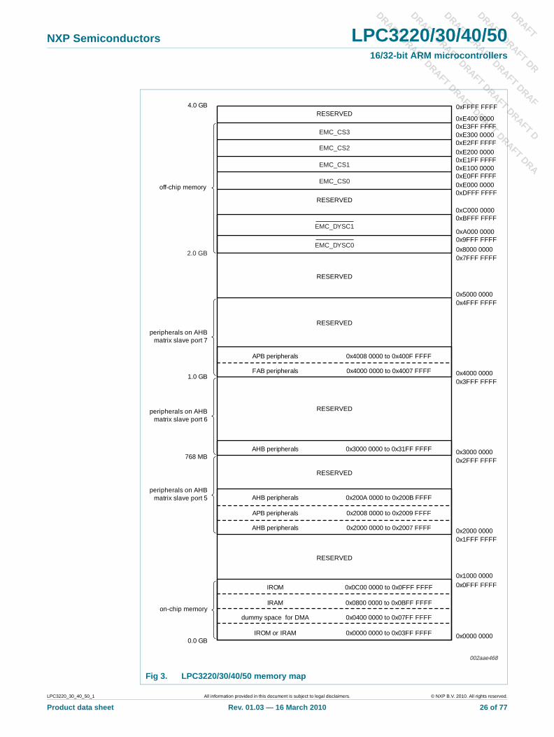
7.3 Physical memory mapThe physical memory map incorporates several distinct regions, as shown in Figure 3. When an application is running, the CPU interrupt vectors are re-mapped to allow them to reside in on-chip SRAM (IRAM).
LPC3220_30_40_50_1 All information provided in this document is subject to legal disclaimers. © NXP B.V. 2010. All rights reserved.
Product data sheet Rev. 01.03 — 16 March 2010 25 of 77
DRAFT
DRAFT DRAFT DR
DRAFT DRAFT DRAFRAF
DRAFT DRAFT DRAF
FT D
DRAFT DRAFT DRAF
DRA
NXP Semiconductors LPC3220/30/40/5016/32-bit ARM microcontrollers
T DT DRAFT DRA
T DRAFT DRAFT DRAFT
Fig 3. LPC3220/30/40/50 memory map
on-chip memory
0x4000 0000
0x0000 00000.0 GB
768 MB
1.0 GB
4.0 GB
peripherals on AHBmatrix slave port 5
0x0FFF FFFF
0x2000 0000
0x3000 00000x2FFF FFFF
0x1FFF FFFF
0x8000 0000
0xFFFF FFFF
0x1000 0000
0x3FFF FFFF
0x4FFF FFFF0x5000 0000
0x7FFF FFFF
peripherals on AHBmatrix slave port 6
peripherals on AHBmatrix slave port 7
off-chip memory
IROM or IRAM 0x0000 0000 to 0x03FF FFFF
dummy space for DMA 0x0400 0000 to 0x07FF FFFF
IRAM 0x0800 0000 to 0x0BFF FFFF
IROM 0x0C00 0000 to 0x0FFF FFFF
AHB peripherals 0x2000 0000 to 0x2007 FFFF
AHB peripherals 0x200A 0000 to 0x200B FFFF
APB peripherals 0x2008 0000 to 0x2009 FFFF
RESERVED
AHB peripherals 0x3000 0000 to 0x31FF FFFF
RESERVED
FAB peripherals 0x4000 0000 to 0x4007 FFFF
APB peripherals 0x4008 0000 to 0x400F FFFF
RESERVED
RESERVED
RESERVED
RESERVED
RESERVED
0x9FFF FFFF0xA000 0000
0xBFFF FFFF0xC000 0000
0xDFFF FFFF0xE000 00000xE0FF FFFF0xE100 00000xE1FF FFFF0xE200 00000xE2FF FFFF0xE300 00000xE3FF FFFF0xE400 0000
2.0 GBEMC_DYSC0
EMC_DYSC1
EMC_CS0
EMC_CS1
EMC_CS2
EMC_CS3
002aae468
LPC3220_30_40_50_1 All information provided in this document is subject to legal disclaimers. © NXP B.V. 2010. All rights reserved.
Product data sheet Rev. 01.03 — 16 March 2010 26 of 77

DRAFT
DRAFT DRAFT DR
DRAFT DRAFT DRAFRAF
DRAFT DRAFT DRAF
FT D
DRAFT DRAFT DRAF
DRA
NXP Semiconductors LPC3220/30/40/5016/32-bit ARM microcontrollers
T DT DRAFT DRA
T DRAFT DRAFT DRAFT
7.4 Internal memory
7.4.1 On-chip ROMThe built-in 16 kB ROM contains a program which runs a boot procedure to load code from one of four external sources, UART5, SSP0 (SPI mode), EMC Static CS0 memory, or NAND FLASH.
After reset, execution always begins from the internal ROM. The bootstrap software first reads the SERVICE input (GPI_1). If SERVICE is LOW, the bootstrap starts a service boot and can download a program over serial link UART5 to IRAM and transfer execution to the downloaded code.
If the SERVICE pin is HIGH, the bootstrap routine jumps to normal boot. The normal boot process first tests SPI memory for boot information if present it uploads the boot code and transfers execution to the uploaded software. If the SPI is not present or no software is loaded, the bootloader will test the EMC Static CS0 memory for the presence of boot code and if present boots from static memory, If this test fails the boot loader will test external NAND flash for boot code and boot if code is present.
The boot loader consumes no user memory space because it is in ROM.
7.4.2 On-chip SRAMOn-chip SRAM may be used for code and/or data storage. The SRAM may be accessed as 8, 16, or 32 bit memory. The LPC3220/30/40/50 provides 256 kB of internal SRAM.
7.5 External memory interfacesThe LPC3220/30/40/50 includes three external memory interfaces, NAND Flash controllers, Secure Digital Memory Controller, and an external memory controller for SDRAM, DDR SDRAM, and Static Memory devices.
7.5.1 NAND flash controllersThe LPC3220/30/40/50 includes two NAND flash controllers, one for multi-level cell NAND flash devices and one for single-level cell NAND flash devices. The two NAND flash controllers use the same pins to interface to external NAND flash devices, so only one interface is active at a time.
7.5.1.1 Multi-Level Cell (MLC) NAND flash controllerThe MLC NAND flash controller interfaces to either multi-level or single-level NAND flash devices. An external NAND flash device is used to allow the bootloader to automatically load a portion of the application code into internal SRAM for execution following reset.
The MLC NAND flash controller supports small (528 byte) and large (2114 byte) pages. Programmable NAND timing parameters allow support for a variety of NAND flash devices. A built-in Reed-Solomon encoder/decoder provides error detection and correction capability. A 528 byte data buffer reduces the need for CPU supervision during loading. The MLC NAND flash controller also provides DMA support.
LPC3220_30_40_50_1 All information provided in this document is subject to legal disclaimers. © NXP B.V. 2010. All rights reserved.
Product data sheet Rev. 01.03 — 16 March 2010 27 of 77
DRAFT
DRAFT DRAFT DR
DRAFT DRAFT DRAFRAF
DRAFT DRAFT DRAF
FT D
DRAFT DRAFT DRAF
DRA
NXP Semiconductors LPC3220/30/40/5016/32-bit ARM microcontrollers
T DT DRAFT DRA
T DRAFT DRAFT DRAFT
7.5.1.2 Single-Level Cell (SLC) NAND flash controllerThe SLC NAND flash controller interfaces to single-level NAND flash devices. DMA page transfers are supported, including a 20-byte DMA read and write FIFO. Hardware support for ECC (Error Checking and Correction) is included for the main data area. Software can correct a single bit error.
7.5.2 SD card controllerThe SD interface allows access to external SD memory cards. The SD card interface conforms to the SD Memory Card Specification Version 1.01.
7.5.2.1 Features
• 1-bit and 4-bit data line interface support.• DMA is supported through the system DMA controller.• Provides all functions specific to the SD memory card. These include the clock
generation unit, power management control, command and data transfer.
7.5.3 External memory controllerThe LPC3220/30/40/50 includes a memory controller that supports data bus SDRAM, DDR SDRAM, and static memory devices. The memory controller provides an interface between the system bus and external (off-chip) memory devices.
The controller supports 16-bit and 32-bit wide SDR SDRAM devices of 64 Mbit, 128 Mbit, 128 Mbit, 256 Mbit, and 512 Mbit sizes, as well as 16-bit wide data bus DDR SDRAM devices of 64 Mbit, 128 Mbit, 128 Mbit, 256 Mbit, and 512 Mbit sizes. Two dynamic memory chip selects are supplied, supporting two groups of SDRAM:
• DYCS0 in the address range 0x8000 0000 to 0x9FFF FFFF• DYCS1 in the address range 0xA000 0000 to 0xBFFF FFFF
The memory controller also supports 8-bit, 16-bit, and 32-bit wide asynchronous static memory devices, including RAM, ROM, and flash, with or without asynchronous page mode. Four static memory chip selects are supplied for SRAM devices:
• CS0 in the address range 0xE000 0000 to 0xE0FF FFFF • CS1 in the address range 0xE100 0000 to 0xE1FF FFFF • CS2 in the address range 0xE200 0000 to 0xE2FF FFFF • CS3 in the address range 0xE300 0000 to 0xE3FF FFFF
The SDRAM controller uses three data ports to allow simultaneous requests from multiple on-chip AHB bus masters and has the following features.
• Dynamic memory interface supports SDRAM, DDR-SDRAM, and low-power variants. • Read and write buffers to reduce latency and improve performance.• Static memory features include
– asynchronous page mode read– programmable wait states– bus turnaround cycles– output enable and write enable delays
LPC3220_30_40_50_1 All information provided in this document is subject to legal disclaimers. © NXP B.V. 2010. All rights reserved.
Product data sheet Rev. 01.03 — 16 March 2010 28 of 77
DRAFT
DRAFT DRAFT DR
DRAFT DRAFT DRAFRAF
DRAFT DRAFT DRAF
FT D
DRAFT DRAFT DRAF
DRA
NXP Semiconductors LPC3220/30/40/5016/32-bit ARM microcontrollers
T DT DRAFT DRA
T DRAFT DRAFT DRAFT
– extended wait• Power-saving modes dynamically control EMC_CKE[1:0] and EMC_CLK.• Dynamic memory self-refresh mode supported by software.• Controller supports 2 k, 4 k, and 8 k row address synchronous memory parts. That is,
typical 512 MB, 256 MB, 128 MB, and 16 MB parts, with 8, 16, or 32 data bits per device.
• Two reset domains enable dynamic memory contents to be preserved over a soft reset.
• This controller does not support synchronous static memory devices (burst mode devices).
7.6 AHB master peripheralsThe LPC3220/30/40/50 implements four AHB master peripherals, which include a General Purpose Direct Memory Access (GPDMA) controller, a 10/100 Ethernet Media Access Controller (MAC), a Universal Serial Bus (USB) controller, and an LCD controller. Each of these four peripherals contain an integral DMA controller optimized to support the performance demands of the peripheral.
7.6.1 General Purpose DMA (GPDMA) controller The GPDMA controller allows peripheral-to memory, memory-to-peripheral, peripheral-to-peripheral, and memory-to-memory transactions. Each DMA stream provides unidirectional serial DMA transfers for a single source and destination. For example, a bidirectional port requires one stream for transmit and one for receive. The source and destination areas can each be either a memory region or a peripheral, and can be accessed through the same AHB master, or one area by each master. The DMA controller supports the following peripheral device transfers.
• Secure Digital (SD) Memory interface• High-speed UARTs• I2S0 and I2S1 ports• SPI1 and SPI2 interfaces• SSP0 and SSP1 interfaces• Memory
The DMA controls eight DMA channels with hardware prioritization. The DMA controller interfaces to the system via two AHB bus masters, each with a full 32-bit data bus width. DMA operations may be set up for 8-bit, 16-bit, and 32-bit data widths, and can be either big-endian or little-endian. Incrementing or non-incrementing addressing for source and destination are supported, as well as programmable DMA burst size. Scatter or gather DMA is supported through the use of linked lists. This means that the source and destination areas do not have to occupy contiguous areas of memory.
7.6.2 Ethernet MACThe Ethernet block contains a full featured 10 Mbit/s or 100 Mbit/s Ethernet MAC designed to provide optimized performance through the use of DMA hardware acceleration. Features include a generous suite of control registers, half or full duplex operation, flow control, control frames, hardware acceleration for transmit retry, receive
LPC3220_30_40_50_1 All information provided in this document is subject to legal disclaimers. © NXP B.V. 2010. All rights reserved.
Product data sheet Rev. 01.03 — 16 March 2010 29 of 77
DRAFT
DRAFT DRAFT DR
DRAFT DRAFT DRAFRAF
DRAFT DRAFT DRAF
FT D
DRAFT DRAFT DRAF
DRA
NXP Semiconductors LPC3220/30/40/5016/32-bit ARM microcontrollers
T DT DRAFT DRA
T DRAFT DRAFT DRAFT
packet filtering and wake-up on LAN activity. Automatic frame transmission and reception with scatter-gather DMA off-loads many operations from the CPU. The Ethernet DMA can access off-chip memory via the EMC, as well as the IRAM. The Ethernet block interfaces between an off-chip Ethernet PHY using the Media Independent Interface (MII) or Reduced MII (RMII) protocol and the on-chip Media Independent Interface Management (MIIM) serial bus.
7.6.2.1 Features
• Ethernet standards support:– Supports 10 Mbit/s or 100 Mbit/s PHY devices including 10 Base-T, 100 Base-TX,
100 Base-FX, and 100 Base-T4.– Fully compliant with IEEE standard 802.3.– Fully compliant with 802.3x Full Duplex Flow Control and Half Duplex back
pressure.– Flexible transmit and receive frame options.– Virtual Local Area Network (VLAN) frame support.
• Memory management:– Independent transmit and receive buffers memory mapped to SRAM.– DMA managers with scatter/gather DMA and arrays of frame descriptors.– Memory traffic optimized by buffering and pre-fetching.
• Enhanced Ethernet features:– Receive filtering.– Multicast and broadcast frame support for both transmit and receive.– Optional automatic Frame Check Sequence (FCS) insertion with Circular
Redundancy Check (CRC) for transmit.– Selectable automatic transmit frame padding.– Over-length frame support for both transmit and receive allows any length frames.– Promiscuous receive mode.– Automatic collision back-off and frame retransmission.– Includes power management by clock switching. Wake-on-LAN power
management support allows system wake-up using the receive filters or a magic frame detection filter.
• Physical interface– Attachment of external PHY chip through standard MII or RMII interface.– PHY register access is available via the MIIM interface.
7.6.3 USB interfaceThe LPC3220/30/40/50 supports USB in either device, host, or OTG configuration.
7.6.3.1 USB device controllerThe USB device controller enables 12 Mbit/s data exchange with a USB host controller. It consists of register interface, serial interface engine, endpoint buffer memory and DMA controller. The serial interface engine decodes the USB data stream and writes data to the appropriate end point buffer memory. The status of a completed USB transfer or error
LPC3220_30_40_50_1 All information provided in this document is subject to legal disclaimers. © NXP B.V. 2010. All rights reserved.
Product data sheet Rev. 01.03 — 16 March 2010 30 of 77
DRAFT
DRAFT DRAFT DR
DRAFT DRAFT DRAFRAF
DRAFT DRAFT DRAF
FT D
DRAFT DRAFT DRAF
DRA
NXP Semiconductors LPC3220/30/40/5016/32-bit ARM microcontrollers
T DT DRAFT DRA
T DRAFT DRAFT DRAFT
condition is indicated via status registers. An interrupt is also generated if enabled. The DMA controller when enabled transfers data between the endpoint buffer and the USB RAM.
Features
• Fully compliant with USB 2.0 full-speed specification.• Supports 32 physical (16 logical) endpoints.• Supports control, bulk, interrupt and isochronous endpoints.• Scalable realization of endpoints at run time.• Endpoint maximum packet size selection (up to USB maximum specification) by
software at run time.• RAM message buffer size based on endpoint realization and maximum packet size.• Supports bus-powered capability with low suspend current.• Supports DMA transfer on all non-control endpoints.• One duplex DMA channel serves all endpoints.• Allows dynamic switching between CPU controlled and DMA modes.• Double buffer implementation for bulk and isochronous endpoints.
7.6.3.2 USB host controllerThe host controller enables data exchange with various USB devices attached to the bus. It consists of register interface, serial interface engine and DMA controller. The register interface complies to the OHCI specification.
Features
• OHCI compliant.• OHCI specifies the operation and interface of the USB host controller and software
driver.• The host controller has four USB states visible to the software driver:
– USBOperational: Process lists and generate SOF tokens.– USBReset: Forces reset signaling on the bus, SOF disabled.– USBSuspend: Monitor USB for wake-up activity.– USBResume: Forces resume signaling on the bus.
• HCCA register points to interrupt and isochronous descriptors list.• ControlHeadED and BulkHeadED registers point to control and bulk descriptors list.
7.6.3.3 USB OTG controllerUSB OTG (On-The-Go) is a supplement to the USB 2.0 specification that augments the capability of existing mobile devices and USB peripherals by adding host functionality for connection to USB peripherals.
Features
• Fully compliant with On-The-Go supplement to the USB Specification 2.0 Revision 1.0.
LPC3220_30_40_50_1 All information provided in this document is subject to legal disclaimers. © NXP B.V. 2010. All rights reserved.
Product data sheet Rev. 01.03 — 16 March 2010 31 of 77
DRAFT
DRAFT DRAFT DR
DRAFT DRAFT DRAFRAF
DRAFT DRAFT DRAF
FT D
DRAFT DRAFT DRAF
DRA
NXP Semiconductors LPC3220/30/40/5016/32-bit ARM microcontrollers
T DT DRAFT DRA
T DRAFT DRAFT DRAFT
• Supports Host Negotiation Protocol (HNP) and Session Request Protocol (SRP) for dual-role devices under software control. HNP is partially implemented in hardware.
• Provides programmable timers required for HNP and SRP.• Supports slave mode operation through AHB slave interface.• Supports the OTG ATX from NXP (ISP 1302) or any external CEA-2011OTG
specification compliant ATX.
7.6.4 LCD controllerThe LCD controller provides all of the necessary control signals to interface directly to a variety of color and monochrome LCD panels. Both STN (single and dual panel) and TFT panels can be operated. The display resolution is selectable and can be up to 1024 × 768 pixels. Several color modes are provided, up to a 24-bit true-color non-palettized mode.
An on-chip 512-byte color palette allows reducing bus utilization (i.e. memory size of the displayed data) while still supporting a large number of colors.
The LCD interface includes its own DMA controller to allow it to operate independently of the CPU and other system functions. A built-in FIFO acts as a buffer for display data, providing flexibility for system timing. Hardware cursor support can further reduce the amount of CPU time needed to operate the display.
7.6.4.1 Features
• AHB bus master interface to access frame buffer.• Setup and control via a separate AHB slave interface.• Dual 16-deep programmable 64-bit wide FIFOs for buffering incoming display data.• Supports single and dual-panel monochrome Super Twisted Nematic (STN) displays
with 4-bit or 8-bit interfaces.• Supports single and dual-panel color STN displays.• Supports Thin Film Transistor (TFT) color displays.• Programmable display resolution including, but not limited to: 320 × 200, 320 × 240,
640 × 200, 640 × 240, 640 × 480, 800 × 600, and 1024 × 768.• Hardware cursor support for single-panel displays.• 15 gray-level monochrome, 3375 color STN, and 32 k color palettized TFT support.• 1, 2, or 4 bits-per-pixel (bpp) palettized displays for monochrome STN.• 1, 2, 4, or 8 bpp palettized color displays for color STN and TFT.• 16 bpp true-color non-palettized, for color STN and TFT.• 24 bpp true-color non-palettized, for color TFT.• Programmable timing for different display panels.• 256 entry, 16-bit palette RAM, arranged as a 128 × 32 bit RAM.• Frame, line, and pixel clock signals.• AC bias signal for STN, data enable signal for TFT panels.• Supports little and big-endian, and Windows CE data formats.• LCD panel clock may be generated from the peripheral clock or from a clock input pin.
LPC3220_30_40_50_1 All information provided in this document is subject to legal disclaimers. © NXP B.V. 2010. All rights reserved.
Product data sheet Rev. 01.03 — 16 March 2010 32 of 77
DRAFT
DRAFT DRAFT DR
DRAFT DRAFT DRAFRAF
DRAFT DRAFT DRAF
FT D
DRAFT DRAFT DRAF
DRA
NXP Semiconductors LPC3220/30/40/5016/32-bit ARM microcontrollers
T DT DRAFT DRA
T DRAFT DRAFT DRAFT
7.7 System functionsTo enhance the performance of the LPC3220/30/40/50 incorporates the following system functions, an Interrupt Controller (INTC), a watchdog timer, a millisecond timer, and several power control features. These functions are described in the following sections
7.7.1 Interrupt controllerThe interrupt controller is comprised of three basic interrupt controller blocks, supporting a total of 73 interrupt sources. Each interrupt source can be individually enabled/disabled and configured for high or low level triggering, or rising or falling edge triggering. Each interrupt may also be steered to either the FIQ or IRQ input of the ARM9. Raw interrupt status and masked interrupt status registers allow versatile condition evaluation. In addition to peripheral functions, each of the six general purpose input/output pins and 12 of the 22 general purpose input pins are connected directly to the interrupt controller.
7.7.2 Watchdog timerThe watchdog timer block is clocked by the main peripheral clock, which clocks a 32-bit counter. A match register is compared to the Timer. When configured for watchdog functionality, a match drives the match output low. The match output is gated with an enable signal that gives the opportunity to generate two type of reset signal: one that only resets chip internally, and another that goes through a programmable pulse generator before it goes to the external pin RESOUT and to the internal chip reset.
7.7.2.1 Features
• Programmable 32-bit timer.• Internally resets the device if not periodically reloaded.• Flag to indicate that a watchdog reset has occurred.• Programmable watchdog pulse output on RESOUT pin.• Can be used as a standard timer if watchdog is not used.• Pause control to stop counting when core is in debug state.
7.7.3 Millisecond timerThe millisecond timer is clocked by 32 kHz RTC clock, so a prescaler is not needed to obtain a lower count rate.
The millisecond timer includes three match registers that are compared to the Timer/Counter value. A match can generate an interrupt and the cause the Timer/Counter either continue to run, stop, or be reset.
7.7.3.1 Features
• 32-bit Timer/Counter, running from the 32 kHz RTC clock.• Counter or Timer operation.• Three 32-bit match registers that allow:
– Continuous operation with optional interrupt generation on match.– Stop timer on match with optional interrupt generation.– Reset timer on match with optional interrupt generation.
• Pause control to stop counting when core is in debug state.
LPC3220_30_40_50_1 All information provided in this document is subject to legal disclaimers. © NXP B.V. 2010. All rights reserved.Product data sheet Rev. 01.03 — 16 March 2010 33 of 77

DRAFT
DRAFT DRAFT DR
DRAFT DRAFT DRAFRAF
DRAFT DRAFT DRAF
FT D
DRAFT DRAFT DRAF
DRA
NXP Semiconductors LPC3220/30/40/5016/32-bit ARM microcontrollers
T DT DRAFT DRA
T DRAFT DRAFT DRAFT
7.7.4 Clocking and power control features
7.7.4.1 ClockingClocking in the LPC3220/30/40/50 is designed to be versatile, so that system and peripheral requirements may be met, while allowing optimization of power consumption. Clocks to most functions may be turned off if not needed and some peripherals do this automatically.
The LPC3220/30/40/50 supports three operational modes, two of which are specifically designed to reduce power consumption. The modes are: Run mode, Direct run mode, and Stop mode.These three operational modes give control over processing speed and power consumption. In addition, clock rates to different functional blocks may be changed by switching clock sources, changing PLL values, or altering clock divider configurations. This allows a trade-off of power versus processing speed based on application requirements.
7.7.4.2 Crystal oscillatorThe main oscillator is the basis for the clocks most chip functions use by default. Optionally, many functions can be clocked instead by the output of a PLL (with a fixed 397x rate multiplication) which runs from the RTC oscillator. In this mode, the main oscillator may be turned off unless the USB interface is enabled. If a SYSCLK frequency other than 13 MHz is required in the application, or if the USB block is not used, the main oscillator may be used with a frequency of between 1 MHz and 20 MHz.
7.7.4.3 PLLsThe LPC3220/30/40/50 includes three PLLs: The 397x PLL allows boosting the RTC frequency to 13.008896 MHz for use as the primary system clock. The USB PLL provides the 48 MHz clock required by the USB block, and the HCLK PLL provides the basis for the CPU clock, the AHB bus clock, and the main peripheral clock.
The 397x PLL multiplies the 32768 Hz RTC clock by 397 to obtain a 13.008896 MHz clock. The 397x PLL is designed for low power operation and low jitter. This PLL requires an external RC loop filter for proper operation.
The HCLK PLL accepts an input clock from either the main oscillator or the output of the 397x PLL. The USB PLL only accepts an input clock from the main oscillator.The USB input clock runs through a divide-by-N pre-divider before entering the USB PLL.
The input to the HCLK and USB PLLs may initially be divided down by a pre-divider value ‘N’, which may have the values 1, 2, 3, or 4. This pre-divider can allow a greater number of possibilities for the output frequency. Following the PLL input divider is the PLL multiplier. This can multiply the pre-divider output by a value ‘M’, in the range of 1 through 256. The resulting frequency must be in the range of 156 MHz to 320 MHz. The multiplier works by dividing the output of a Current Controlled Oscillator (CCO) by the value of M, then using a phase detector to compare the divided CCO output to the pre-divider output. The error value is used to adjust the CCO frequency.
At the PLL output, there is a post-divider that can be used to bring the CCO frequency down to the desired PLL output frequency. The post-divider value can divide the CCO output by 1, 2, 4, 8, or 16. The post-divider can also be bypassed, allowing the PLL CCO
LPC3220_30_40_50_1 All information provided in this document is subject to legal disclaimers. © NXP B.V. 2010. All rights reserved.
Product data sheet Rev. 01.03 — 16 March 2010 34 of 77
DRAFT
DRAFT DRAFT DR
DRAFT DRAFT DRAFRAF
DRAFT DRAFT DRAF
FT D
DRAFT DRAFT DRAF
DRA
NXP Semiconductors LPC3220/30/40/5016/32-bit ARM microcontrollers
T DT DRAFT DRA
T DRAFT DRAFT DRAFT
output to be used directly. The maximum PLL output frequency supported by the CPU is 266 MHz. The only output frequency supported by the USB PLL is 48 MHz, and the clock has strict requirements for nominal frequency (500 ppm) and jitter (500 ps).
7.7.4.4 Power control modesThe LPC3220/30/40/50 supports three operational modes, two of which are specifically designed to reduce power consumption. The modes are: Run mode, Direct Run mode, and Stop mode.
Run mode is the normal operating mode for applications that require the CPU, AHB bus, or any peripheral function other than the USB block to run faster than the main oscillator frequency. In Run mode, the CPU can run at up to 266 MHz and the AHB bus can run at up to 133 MHz.
Direct Run mode allows reducing the CPU and AHB bus rates in order to save power. Direct Run mode can also be the normal operating mode for applications that do not require the CPU, AHB bus, or any peripheral function other than the USB block to run faster than the main oscillator frequency. Direct Run mode is the default mode following chip reset.
Stop mode causes all CPU and AHB operation to cease, and stops clocks to peripherals other than the USB block.
7.7.4.5 ResetReset is accomplished by an active LOW signal on the RESET input pin. A reset pulse with a minimum width of 10 main oscillator clocks after the oscillator is stable is required to guarantee a valid chip reset. At power-up, 10 milliseconds should be allowed for the oscillator to start up and stabilize after VDD reaches operational voltage. An internal reset with a minimum duration of 10 clock pulses will also be applied if the watchdog timer generates an internal device reset.
The RESET pin is located in the RTC power domain. This means that the RTC power must be present for an external reset to have any effect. The RTC power domain nominally runs from 1.2 V, but the RESET pin can be driven as high as 1.95 V.
7.8 Communication peripheral interfacesIn addition to the Ethernet MAC and USB interfaces there are many more serial communication peripheral interfaces available on the LPC3220/30/40/50. Here is a list of the serial communication interfaces:
• Seven UARTs; four standard UARTs and three high-speed UARTs• Two SPI serial I/O controllers• Two SSP serial I/O controllers• Two I2C serial I/O controllers• Two I2S audio controllers
A short functional description of each of these peripherals is provided in the following sections.
LPC3220_30_40_50_1 All information provided in this document is subject to legal disclaimers. © NXP B.V. 2010. All rights reserved.
Product data sheet Rev. 01.03 — 16 March 2010 35 of 77
DRAFT
DRAFT DRAFT DR
DRAFT DRAFT DRAFRAF
DRAFT DRAFT DRAF
FT D
DRAFT DRAFT DRAF
DRA
NXP Semiconductors LPC3220/30/40/5016/32-bit ARM microcontrollers
T DT DRAFT DRA
T DRAFT DRAFT DRAFT
7.8.1 UARTsThe LPC3220/30/40/50 contains seven UARTs. Four are standard UARTs, and three are high-speed UARTs.
7.8.1.1 Standard UARTsThe four standard UARTs are compatible with the INS16Cx50. These UARTs support rates up to 460800 bit/s from a 13 MHz peripheral clock.
Features
• Each standard UART has 64 byte Receive and Transmit FIFOs.• Receiver FIFO trigger points at 16, 32 , 48 , and 60 Bytes.• Transmitter FIFO trigger points at 0, 4 , 8, and 16 Bytes.• Register locations conform to the “550” industry standard.• Each standard UART has a fractional rate pre-divider and an internal baud rate
generator.• The standard UARTs support three clocking modes: on, off, and auto-clock. The
auto-clock mode shuts off the clock to the UART when it is idle.• UART 6 includes an IrDA mode to support infrared communication.• The standard UARTs are designed to support data rates of (2400, 4800, 9600,
19200, 38400, 57600, 115200, 230400, 460800) bit/s.• Each UART includes an internal loopback mode.
7.8.1.2 High-speed UARTsThe three high-speed UARTs are designed to support rates up to 921600 bit/s from a 13 MHz peripheral clock for on-board communication in low noise conditions. This is accomplished by changing the over sampling from 16× to 14× and altering the rate generation logic.
Features
• Each high-speed UART has 64-byte Receive and Transmit FIFOs.• Receiver FIFO trigger points at 1, 4, 8, 16, 32, and 48 B.• Transmitter FIFO trigger points at 0, 4, and 8 B.• Each high-speed UART has an internal baud rate generator.• The high-speed UARTs are designed to support data rates of (2400, 4800, 9600,
19200, 38400, 57600, 115200, 230400, 460800, 921600) bit/s.• The three high speed UARTs only support (8N1) 8-bit data word length, 1-stop bit, no
parity, and no flow control as a the communications protocol.• Each UART includes an internal loopback mode.
7.8.2 SPI serial I/O controllerThe LPC3220/30/40/50 has two Serial Peripheral Interfaces (SPI). The SPI is a 3-wire serial interface that is able to interface with a large range of serial peripheral or memory devices (SPI mode 0 to 3 compatible slave devices).
LPC3220_30_40_50_1 All information provided in this document is subject to legal disclaimers. © NXP B.V. 2010. All rights reserved.
Product data sheet Rev. 01.03 — 16 March 2010 36 of 77
DRAFT
DRAFT DRAFT DR
DRAFT DRAFT DRAFRAF
DRAFT DRAFT DRAF
FT D
DRAFT DRAFT DRAF
DRA
NXP Semiconductors LPC3220/30/40/5016/32-bit ARM microcontrollers
T DT DRAFT DRA
T DRAFT DRAFT DRAFT
Only a single master and a single slave can communicate on the interface during a given data transfer. During a data transfer the master always sends a byte of data to the slave, and the slave always sends a byte of data to the master. The SPI implementation on the LPC3220/30/40/50 does not support operation as a slave.
7.8.2.1 Features
• Supports slaves compatible with SPI modes 0 to 3.• Half duplex synchronous transfers.• DMA support for data transmit and receive.• 1-bit to 16-bit word length.• Choice of LSB or MSB first data transmission.• 64 × 16-bit input or output FIFO.• Bit rates up to 52 Mbit/s.• Busy input function.• DMA time out interrupt to allow detection of end of reception when using DMA.• Timed interrupt to facilitate emptying the FIFO at the end of a transmission.• SPI clock and data pins may be used as general purpose pins if the SPI is not used.• Slave selects can be supported using GPO or GPIO pins
7.8.3 SSP serial I/O controllerThe LPC3220/30/40/50 contains two SSP controllers. The SSP controller is capable of operation on a SPI, 4-wire SSI, or Microwire bus. It can interact with multiple masters and slaves on the bus. Only a single master and a single slave can communicate on the bus during a given data transfer. The SSP supports full duplex transfers, with frames of 4 bits to 16 bits of data flowing from the master to the slave and from the slave to the master. In practice, often only one of these data flows carries meaningful data.
7.8.3.1 Features
• Compatible with Motorola SPI, 4-wire TI SSI, and National Semiconductor Microwire buses
• Synchronous serial communication• Master or slave operation• 8-frame FIFOs for both transmit and receive• 4-bit to 16-bit frame• Maximum SPI bus data bit rate of 1⁄2 (Master mode) and 1⁄12 (Slave mode) of the input
clock rate• DMA transfers supported by GPDMA
7.8.4 I2C-bus serial I/O controllerThere are two I2C-bus interfaces in the LPC32x0 family of controllers. These I2C blocks can be configured as a master, multi-master or slave supporting up to 400 kHz. The I2C blocks also support 7 or 10 bit addressing. Each has a four word FIFO for both transmit and receive. An interrupt signal is available from each block.
LPC3220_30_40_50_1 All information provided in this document is subject to legal disclaimers. © NXP B.V. 2010. All rights reserved.
Product data sheet Rev. 01.03 — 16 March 2010 37 of 77
DRAFT
DRAFT DRAFT DR
DRAFT DRAFT DRAFRAF
DRAFT DRAFT DRAF
FT D
DRAFT DRAFT DRAF
DRA
NXP Semiconductors LPC3220/30/40/5016/32-bit ARM microcontrollers
T DT DRAFT DRA
T DRAFT DRAFT DRAFT
There is a separate slave transmit FIFO. The slave transmit FIFO (TXS) and its level are only available when the controller is configured as a Master/Slave device and is operating in a multi-master environment. Separate TX FIFOs are needed in a multi-master because a controller might have a message queued for transmission when an external master addresses it to be come a slave-transmitter, a second source of data is needed.
Note that the I2C clock must be enabled in the I2CCLK_CTRL register before using the I2C. The I2C clock can be disabled between communications, if used as a single master I2C-bus interface, software has full control of when I2C communication is taking place on the bus.
7.8.4.1 Features
• The two I2C-bus blocks are standard I2C-bus compliant interfaces that may be used in Single-master, Multi-master or Slave modes.
• Programmable clock to allow adjustment of I2C-bus transfer rates.• Bidirectional data transfer.• Serial clock synchronization allows devices with different bit rates to communicate via
one serial bus.• Serial clock synchronization can be used as a handshake mechanism to suspend and
resume serial transfer.
7.8.5 I2S-bus audio controllerThe I2S-bus provides a standard communication interface for digital audio applications The I2S-bus specification defines a 3-wire serial bus using one data line, one clock line, and one word select signal. Each I2S connection can act as a master or a slave. The master connection determines the frequency of the clock line and all other slaves are driven by this clock source. The two I2S-bus interfaces on the LPC3220/30/40/50 provides a separate transmit and receive channel, providing a total of two transmit channels and two receive channels. Each I2S channel supports monaural or stereo formatted data.
7.8.5.1 Features
• The interface has separate input/output channels each of which can operate in master or slave mode.
• Capable of handling 8-bit, 16-bit, and 32-bit word sizes.• Mono and stereo audio data supported.• Supports standard sampling frequencies (8 kHz, 11.025 kHz, 16 kHz, 22.05 kHz,
32 kHz, 44.1 kHz, 48 kHz, 96 kHz).• Word select period can be configured in master mode (separately for I2S input and
output).• Two eight-word FIFO data buffers are provided, one for transmit and one for receive.• Generates interrupt requests when buffer levels cross a programmable boundary.• Two DMA requests, controlled by programmable buffer levels. These are connected
to the GPDMA block.• Controls include reset, stop, and mute options separately for I2S input and I2S output.
LPC3220_30_40_50_1 All information provided in this document is subject to legal disclaimers. © NXP B.V. 2010. All rights reserved.
Product data sheet Rev. 01.03 — 16 March 2010 38 of 77

DRAFT
DRAFT DRAFT DR
DRAFT DRAFT DRAFRAF
DRAFT DRAFT DRAF
FT D
DRAFT DRAFT DRAF
DRA
NXP Semiconductors LPC3220/30/40/5016/32-bit ARM microcontrollers
T DT DRAFT DRA
T DRAFT DRAFT DRAFT
7.9 Other peripheralsIn addition to the communication peripherals there are many general purpose peripherals available in the LPC3220/30/40/50. Here is a list of the general purpose peripherals.
• GPI/O• Keyboard scanner• Touch screen controller and 10-bit Analog-to-Digital-Converter• Real-time clock• High-speed timer• Four general purpose 32-bit timer/external event counters• Two simple PWMs• One motor control PWM
A short functional description of each of these peripherals is provided in the following sections.
7.9.1 General purpose parallel I/OSome device pins that are not dedicated to a specific peripheral function have been designed to be general purpose inputs, outputs, or input/outputs. Also, some pins may be configured either as a specific peripheral function or a general purpose input, output, or input/output. A total of 51 pins can potentially be used as general purpose input/outputs, 24 as general purpose outputs, and 22 as general purpose inputs.
GPIO pins may be dynamically configured as inputs or outputs. Separate registers allow setting or clearing any number of GPIO and GPO outputs controlled by that register simultaneously. The value of the output register for standard GPIOs and GPO pins may be read back, as well as the current actual state of the port pins.
In addition to GPIO pins on port 0, port 1, and port 2, there are 22 GPI, 24 GPO, and six GPIO pins. When the SDRAM bus is configured for 16 data bits, 13 of the remaining SDRAM data pins may be used as GPIOs.
7.9.1.1 Features
• Bit-level set and clear registers allow a single instruction set or clear of any number of bits in one port.
• A single register selects direction for pins that support both input and output modes.• Direction control of individual bits.• For input/output pins, both the programmed output state and the actual pin state can
be read.• There are a total of 12 general purpose inputs, 24 general purpose outputs, and six
general purpose input/outputs.• Additionally, 13 SDRAM data lines may be used as GPIOs if a 16-bit SDRAM
interface is used (rather than a 32-bit interface).
LPC3220_30_40_50_1 All information provided in this document is subject to legal disclaimers. © NXP B.V. 2010. All rights reserved.
Product data sheet Rev. 01.03 — 16 March 2010 39 of 77

DRAFT
DRAFT DRAFT DR
DRAFT DRAFT DRAFRAF
DRAFT DRAFT DRAF
FT D
DRAFT DRAFT DRAF
DRA
NXP Semiconductors LPC3220/30/40/5016/32-bit ARM microcontrollers
T DT DRAFT DRA
T DRAFT DRAFT DRAFT
7.9.2 Keyboard scannerThe keyboard scanner function can automatically scan a keyboard of up to 64 keys in an 8 × 8 matrix. In operation, the keyboard scanner’s internal state machine will normally be in an idle state, with all KEY_ROWn pins set high, waiting for a change in the column inputs to indicate that one or more keys have been pressed.
When a keypress is detected, the matrix is scanned by setting one output pin high at a time and reading the column inputs. After de-bouncing, the keypad state is stored and an interrupt is generated. The keypad is then continuously scanned waiting for ‘extra key pressed’ or ‘key released’. Any new keypad state is scanned and stored into the matrix registers followed by a new interrupt request to the interrupt controller. It is possible to detect and separate up to 64 multiple keys pressed.
7.9.2.1 Features
• Supports up to 64 keys in 8 × 8 matrix.• Programmable de-bounce period.• A key press can wake up the CPU from Stop mode.
7.9.3 Touch screen controller and 10-bit ADC The LPC3220/30/40/50 microcontrollers includes Touch Screen Controller (TSC) hardware, which automatically measures and determines the X and Y coordinates where a touch screen is pressed. In addition, the TSC can measure an analog input signal on the AUX_IN pin.
Optionally, the TSC can operate as an Analog-to-Digital Converter (ADC). The ADC supports three channels and uses 10-bit successive approximation to produce results with a resolution of 10 bits in 11 clock cycles.
The analog portion of the ADC has its own power supply to enhance the low noise characteristics of the converter. This voltage is only supplied internally when the core has voltage. However, the ADC block is not affected by any difference in ramp-up time for VDD_AD and VDD_CORE voltage supplies.
7.9.3.1 Features
• Measurement range of 0 V to VDD_AD (nominally 3.3 V).• Low-noise ADC.• 10-bit resolution.• Three input channels.• Uses 32 kHz RTC clock or peripheral clock.
7.9.4 Real-Time Clock (RTC) and battery RAMThe RTC runs at 32768 Hz using a very low power oscillator. The RTC counts seconds and can generate alarm interrupts that can wake up the device from Stop mode. The RTC clock can also clock the 397x PLL, the Millisecond Timer, the ADC, the Keyboard Scanner and the PWMs. The RTC up-counter value represents a number of seconds elapsed since second 0, which is an application determined time. The RTC counter will reach maximum value after about 136 years. The RTC down-counter is initiated with all ones.
LPC3220_30_40_50_1 All information provided in this document is subject to legal disclaimers. © NXP B.V. 2010. All rights reserved.
Product data sheet Rev. 01.03 — 16 March 2010 40 of 77
DRAFT
DRAFT DRAFT DR
DRAFT DRAFT DRAFRAF
DRAFT DRAFT DRAF
FT D
DRAFT DRAFT DRAF
DRA
NXP Semiconductors LPC3220/30/40/5016/32-bit ARM microcontrollers
T DT DRAFT DRA
T DRAFT DRAFT DRAFT
Two 32-bit match registers are readable and writable by the processor. A match will result in an interrupt provided that the interrupt is enabled. The ONSW output pin can also be triggered by a match event and cause an external power supply to turn on all of the operating voltages, as a way to startup after power has been removed.
The RTC block is implemented in a separate voltage domain. The block is supplied via a separate supply pin from a battery or other power source.
The RTC block also contains 32 words (128 bytes) of very low voltage SRAM. This SRAM is able to hold its contents down to the minimum RTC operating voltage.
7.9.4.1 Features
• Measures the passage of time in seconds.• 32-bit up and down seconds counters.• Ultra-low power design to support battery powered systems.• Dedicated 32 kHz oscillator.• An output pin is included to assist in waking up when the chip has had power removed
to all functions except the RTC.• Two 32-bit match registers with interrupt option.• 32 words (128 bytes) of very low voltage SRAM.• The RTC and battery RAM power have an independent power domain and dedicated
supply pins, which can be powered from a battery or power supply.
Remark: The LPC3220/30/40/50 will run at voltages down to 0.9 V at frequencies below 14 MHz. However, the ARM core cannot access the RTC registers and battery RAM when the core supply voltage is at 0.9 V and the RTC supply is at 1.2 V.
7.9.5 Enhanced 32-bit timers/external event countersThe LPC3220/30/40/50 includes six 32-bit Timer/Counters. The Timer/Counter is designed to count cycles of the system derived clock or an externally-supplied clock. It can optionally generate interrupts or perform other actions at specified timer values, based on four match registers. The Timer/Counter also includes four capture inputs to trap the timer value when an input signal transitions, optionally generating an interrupt.
7.9.5.1 Features
• A 32-bit Timer/Counter with a programmable 32-bit pre-scaler.• Counter or Timer operation.• Up to four 32-bit capture channels per timer, that can take a snapshot of the timer
value when an input signal transitions. A capture event may also optionally generate an interrupt.
• Four 32-bit match registers that allow:– continuous operation with optional interrupt generation on match– stop timer on match with optional interrupt generation– reset timer on match with optional interrupt generation
• Up to four external outputs corresponding to match registers, with the following capabilities:
LPC3220_30_40_50_1 All information provided in this document is subject to legal disclaimers. © NXP B.V. 2010. All rights reserved.
Product data sheet Rev. 01.03 — 16 March 2010 41 of 77
DRAFT
DRAFT DRAFT DR
DRAFT DRAFT DRAFRAF
DRAFT DRAFT DRAF
FT D
DRAFT DRAFT DRAF
DRA
NXP Semiconductors LPC3220/30/40/5016/32-bit ARM microcontrollers
T DT DRAFT DRA
T DRAFT DRAFT DRAFT
– set LOW on match– set HIGH on match– toggle on match– do nothing on match
7.9.6 High-speed timerThe high-speed timer block is clocked by the main peripheral clock. The clock is first divided down in a 16-bit programmable pre-scale counter which clocks a 32-bit timer/counter.
The high-speed timer includes three match registers that are compared to the timer/counter value. A match can generate an interrupt and cause the timer/counter to either continue to run, stop, or be reset. The high-speed timer also includes two capture registers that can take a snapshot of the timer/counter value when an input signal transitions. A capture event may also generate an interrupt.
7.9.6.1 Features
• 32-bit timer/counter with programmable 16-bit pre-scaler.• Counter or timer operation.• Two 32-bit capture registers.• Three 32-bit match registers that allow:
– Continuous operation with optional interrupt generation on match.– Stop timer on match with optional interrupt generation.– Reset timer on match with optional interrupt generation.
• Pause control to stop counting when core is in debug state.
7.9.7 Pulse Width Modulators (PWMs)The LPC3220/30/40/50 provides two simple PWMs. They are clocked separately by either the main peripheral clock or the 32 kHz RTC clock. Both PWMs have a duty cycle programmable in 255 steps.
7.9.7.1 Features
• Clocked by the main peripheral clock or the 32 kHz RTC clock.• Programmable 4-bit pre-scaler.• Duty cycle programmable in 255 steps.• Output frequency up to 50 kHz when using a 13 MHz peripheral clock.
7.9.8 Motor control pulse width modulatorThe Motor Control PWM (MCPWM) provides a set of features for three-phase AC and DC motor control applications in a single peripheral. The MCPWM can also be configured for use in other generalized timing, counting, capture, and compare applications.
7.9.8.1 Features
• 32-bit timer• 32-bit period register
LPC3220_30_40_50_1 All information provided in this document is subject to legal disclaimers. © NXP B.V. 2010. All rights reserved.
Product data sheet Rev. 01.03 — 16 March 2010 42 of 77
DRAFT
DRAFT DRAFT DR
DRAFT DRAFT DRAFRAF
DRAFT DRAFT DRAF
FT D
DRAFT DRAFT DRAF
DRA
NXP Semiconductors LPC3220/30/40/5016/32-bit ARM microcontrollers
T DT DRAFT DRA
T DRAFT DRAFT DRAFT
• 32-bit pulse-width (match) register • 10-bit dead-time register and an associated 10-bit dead-time counter • 32-bit capture register• Two PWM (match) outputs (pins MCOA0/1/2 and MCOB0/1/2) with opposite polarities• Period interrupt, pulse-width interrupt, and capture interrupt
8. Basic architecture
The LPC3220/30/40/50 is a general purpose ARM926EJ-S 32-bit microprocessor with a 32 kB instruction cache and a 32 kB data cache. The microcontroller offers high performance and very low power consumption. The ARM architecture is based on RISC principles, which results in the instruction set and related decode mechanism being much simpler than equivalent micro programmed CISCs. This simplicity results in a high instruction throughput and impressive real-time interrupt response from a small and cost-effective processor core.
The ARM926EJ-S core employs a 5-stage pipeline so processing and memory system accesses can occur continuously. At any one point in time, several operations are in progress: subsequent instruction fetch, next instruction decode, instruction execution, memory access, and write-back. The combination of architectural enhancements gives the ARM9 about 30 % better performance than an ARM7 running at the same clock rate:
• Approximately 1.3 clocks per instruction for the ARM926 compared to 1.9 clocks per instruction for ARM7TDMI.
• Approximately 1.1 Dhrystone MIPS/MHz for the ARM926 compared to 0.9 Dhrystone MIPS/MHz for ARM7TDMI.
The ARM926EJ-S processor also employs an operational state known as Thumb, which makes it ideally suited to high-volume applications with memory restrictions, or applications where code density is an issue.
The key idea behind Thumb state is the use of a super-reduced instruction set. Essentially, the ARM926EJ-S processor core has two instruction sets:
1. The standard 32-bit ARM set2. The 16-bit Thumb set
The Thumb set’s smaller 16-bit instruction length allows it to approach twice the density of standard ARM code while retaining many of ARM’s 32-bit performance advantage over a traditional 16-bit processor using 16-bit registers. This is possible because Thumb code operates using the same 32-bit register set as ARM code. Thumb code size is up to 65 % smaller than ARM code size, and 160 % of the performance of an equivalent ARM processor connected to a 16-bit memory system. Additionally, the ARM926EJ-S core includes enhanced DSP instructions and multiplier, as well as an enhanced 32-bit MAC block.
LPC3220_30_40_50_1 All information provided in this document is subject to legal disclaimers. © NXP B.V. 2010. All rights reserved.
Product data sheet Rev. 01.03 — 16 March 2010 43 of 77
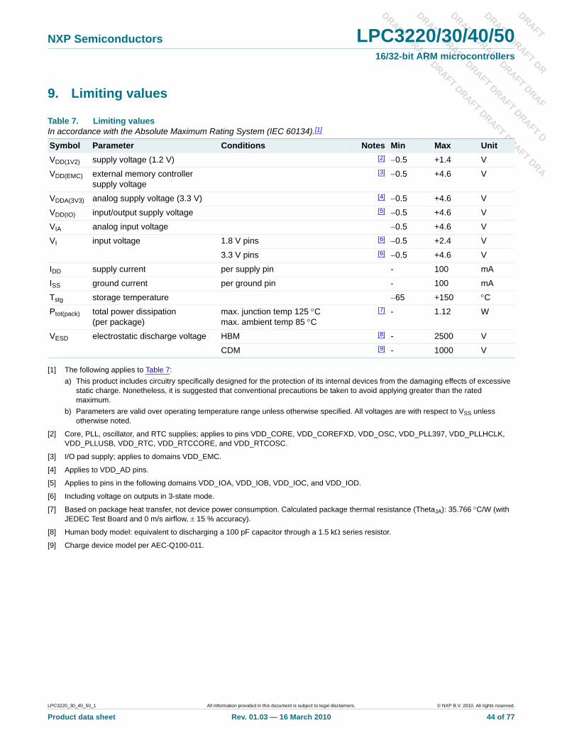
DRAFT
DRAFT DRAFT DR
DRAFT DRAFT DRAFRAF
DRAFT DRAFT DRAF
FT D
DRAFT DRAFT DRAF
DRA
NXP Semiconductors LPC3220/30/40/5016/32-bit ARM microcontrollers
T DT DRAFT DRA
T DRAFT DRAFT DRAFT
9. Limiting values
[1] The following applies to Table 7:a) This product includes circuitry specifically designed for the protection of its internal devices from the damaging effects of excessive
static charge. Nonetheless, it is suggested that conventional precautions be taken to avoid applying greater than the rated maximum.
b) Parameters are valid over operating temperature range unless otherwise specified. All voltages are with respect to VSS unless otherwise noted.
[2] Core, PLL, oscillator, and RTC supplies; applies to pins VDD_CORE, VDD_COREFXD, VDD_OSC, VDD_PLL397, VDD_PLLHCLK, VDD_PLLUSB, VDD_RTC, VDD_RTCCORE, and VDD_RTCOSC.
[3] I/O pad supply; applies to domains VDD_EMC.
[4] Applies to VDD_AD pins.
[5] Applies to pins in the following domains VDD_IOA, VDD_IOB, VDD_IOC, and VDD_IOD.
[6] Including voltage on outputs in 3-state mode.
[7] Based on package heat transfer, not device power consumption. Calculated package thermal resistance (ThetaJA): 35.766 °C/W (with JEDEC Test Board and 0 m/s airflow, ± 15 % accuracy).
[8] Human body model: equivalent to discharging a 100 pF capacitor through a 1.5 kΩ series resistor.
[9] Charge device model per AEC-Q100-011.
Table 7. Limiting valuesIn accordance with the Absolute Maximum Rating System (IEC 60134).[1]
Symbol Parameter Conditions Notes Min Max UnitVDD(1V2) supply voltage (1.2 V) [2] −0.5 +1.4 V
VDD(EMC) external memory controller supply voltage
[3] −0.5 +4.6 V
VDDA(3V3) analog supply voltage (3.3 V) [4] −0.5 +4.6 V
VDD(IO) input/output supply voltage [5] −0.5 +4.6 V
VIA analog input voltage −0.5 +4.6 V
VI input voltage 1.8 V pins [6] −0.5 +2.4 V
3.3 V pins [6] −0.5 +4.6 V
IDD supply current per supply pin - 100 mA
ISS ground current per ground pin - 100 mA
Tstg storage temperature −65 +150 °C
Ptot(pack) total power dissipation (per package)
max. junction temp 125 °Cmax. ambient temp 85 °C
[7] - 1.12 W
VESD electrostatic discharge voltage HBM [8] - 2500 V
CDM [9] - 1000 V
LPC3220_30_40_50_1 All information provided in this document is subject to legal disclaimers. © NXP B.V. 2010. All rights reserved.
Product data sheet Rev. 01.03 — 16 March 2010 44 of 77
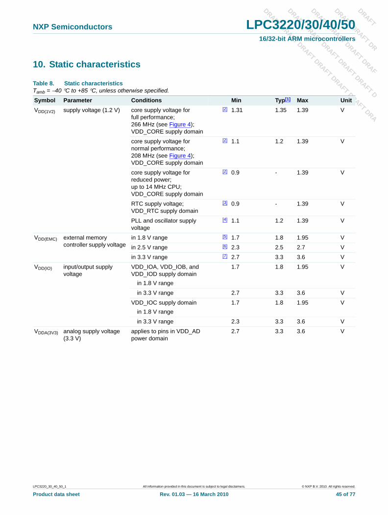
DRAFT
DRAFT DRAFT DR
DRAFT DRAFT DRAFRAF
DRAFT DRAFT DRAF
FT D
DRAFT DRAFT DRAF
DRA
NXP Semiconductors LPC3220/30/40/5016/32-bit ARM microcontrollers
T DT DRAFT DRA
T DRAFT DRAFT DRAFT
10. Static characteristics
Table 8. Static characteristicsTamb = −40 °C to +85 °C, unless otherwise specified.
Symbol Parameter Conditions Min Typ[1] Max UnitVDD(1V2) supply voltage (1.2 V) core supply voltage for
full performance; 266 MHz (see Figure 4); VDD_CORE supply domain
[2] 1.31 1.35 1.39 V
core supply voltage for normal performance; 208 MHz (see Figure 4);VDD_CORE supply domain
[2] 1.1 1.2 1.39 V
core supply voltage for reduced power; up to 14 MHz CPU;VDD_CORE supply domain
[2] 0.9 - 1.39 V
RTC supply voltage;VDD_RTC supply domain
[3] 0.9 - 1.39 V
PLL and oscillator supply voltage
[4] 1.1 1.2 1.39 V
VDD(EMC) external memory controller supply voltage
in 1.8 V range [5] 1.7 1.8 1.95 V
in 2.5 V range [6] 2.3 2.5 2.7 V
in 3.3 V range [7] 2.7 3.3 3.6 V
VDD(IO) input/output supply voltage
VDD_IOA, VDD_IOB, and VDD_IOD supply domain
in 1.8 V range
1.7 1.8 1.95 V
in 3.3 V range 2.7 3.3 3.6 V
VDD_IOC supply domainin 1.8 V range
1.7 1.8 1.95 V
in 3.3 V range 2.3 3.3 3.6 V
VDDA(3V3) analog supply voltage(3.3 V)
applies to pins in VDD_AD power domain
2.7 3.3 3.6 V
LPC3220_30_40_50_1 All information provided in this document is subject to legal disclaimers. © NXP B.V. 2010. All rights reserved.
Product data sheet Rev. 01.03 — 16 March 2010 45 of 77
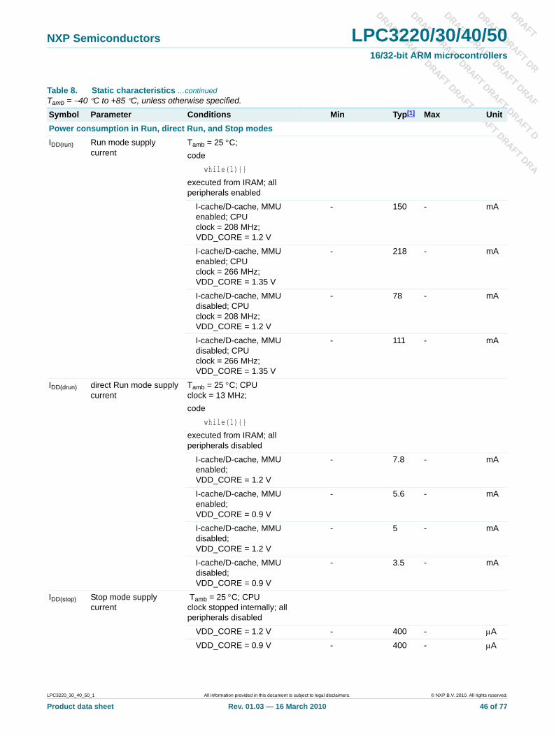
DRAFT
DRAFT DRAFT DR
DRAFT DRAFT DRAFRAF
DRAFT DRAFT DRAF
FT D
DRAFT DRAFT DRAF
DRA
NXP Semiconductors LPC3220/30/40/5016/32-bit ARM microcontrollers
T DT DRAFT DRA
T DRAFT DRAFT DRAFT
Power consumption in Run, direct Run, and Stop modesIDD(run) Run mode supply
currentTamb = 25 °C; code
while(1){}
executed from IRAM; all peripherals enabled
I-cache/D-cache, MMU enabled; CPU clock = 208 MHz; VDD_CORE = 1.2 V
- 150 - mA
I-cache/D-cache, MMU enabled; CPU clock = 266 MHz; VDD_CORE = 1.35 V
- 218 - mA
I-cache/D-cache, MMU disabled; CPU clock = 208 MHz; VDD_CORE = 1.2 V
- 78 - mA
I-cache/D-cache, MMU disabled; CPU clock = 266 MHz; VDD_CORE = 1.35 V
- 111 - mA
IDD(drun) direct Run mode supply current
Tamb = 25 °C; CPU clock = 13 MHz; code
while(1){}
executed from IRAM; all peripherals disabled
I-cache/D-cache, MMU enabled; VDD_CORE = 1.2 V
- 7.8 - mA
I-cache/D-cache, MMU enabled; VDD_CORE = 0.9 V
- 5.6 - mA
I-cache/D-cache, MMU disabled; VDD_CORE = 1.2 V
- 5 - mA
I-cache/D-cache, MMU disabled; VDD_CORE = 0.9 V
- 3.5 - mA
IDD(stop) Stop mode supply current
Tamb = 25 °C; CPU clock stopped internally; all peripherals disabled
VDD_CORE = 1.2 V - 400 - μA
VDD_CORE = 0.9 V - 400 - μA
Table 8. Static characteristics …continuedTamb = −40 °C to +85 °C, unless otherwise specified.
Symbol Parameter Conditions Min Typ[1] Max Unit
LPC3220_30_40_50_1 All information provided in this document is subject to legal disclaimers. © NXP B.V. 2010. All rights reserved.
Product data sheet Rev. 01.03 — 16 March 2010 46 of 77
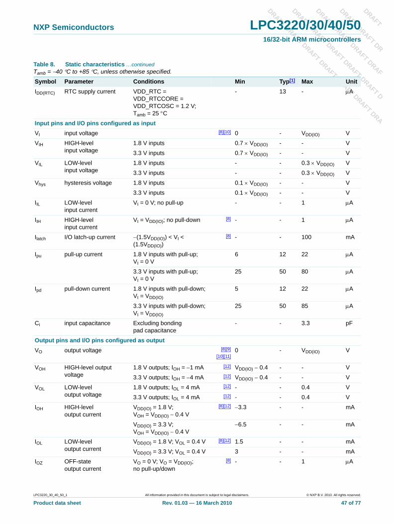
DRAFT
DRAFT DRAFT DR
DRAFT DRAFT DRAFRAF
DRAFT DRAFT DRAF
FT D
DRAFT DRAFT DRAF
DRA
NXP Semiconductors LPC3220/30/40/5016/32-bit ARM microcontrollers
T DT DRAFT DRA
T DRAFT DRAFT DRAFT
IDD(RTC) RTC supply current VDD_RTC = VDD_RTCCORE = VDD_RTCOSC = 1.2 V;Tamb = 25 °C
- 13 - μA
Input pins and I/O pins configured as inputVI input voltage [8][10] 0 - VDD(IO) V
VIH HIGH-level input voltage
1.8 V inputs 0.7 × VDD(IO) - - V
3.3 V inputs 0.7 × VDD(IO) - - V
VIL LOW-level input voltage
1.8 V inputs - - 0.3 × VDD(IO) V
3.3 V inputs - - 0.3 × VDD(IO) V
Vhys hysteresis voltage 1.8 V inputs 0.1 × VDD(IO) - - V
3.3 V inputs 0.1 × VDD(IO) - - V
IIL LOW-levelinput current
VI = 0 V; no pull-up - - 1 μA
IIH HIGH-level input current
VI = VDD(IO); no pull-down [8] - - 1 μA
Ilatch I/O latch-up current −(1.5VDD(IO)) < VI < (1.5VDD(IO))
[8] - - 100 mA
Ipu pull-up current 1.8 V inputs with pull-up; VI = 0 V
6 12 22 μA
3.3 V inputs with pull-up; VI = 0 V
25 50 80 μA
Ipd pull-down current 1.8 V inputs with pull-down; VI = VDD(IO)
5 12 22 μA
3.3 V inputs with pull-down; VI = VDD(IO)
25 50 85 μA
Ci input capacitance Excluding bonding pad capacitance
- - 3.3 pF
Output pins and I/O pins configured as outputVO output voltage [8][9]
[10][11]0 - VDD(IO) V
VOH HIGH-level output voltage
1.8 V outputs; IOH = −1 mA [12] VDD(IO) − 0.4 - - V
3.3 V outputs; IOH = −4 mA [12] VDD(IO) − 0.4 - - V
VOL LOW-level output voltage
1.8 V outputs; IOL = 4 mA [12] - - 0.4 V
3.3 V outputs; IOL = 4 mA [12] - - 0.4 V
IOH HIGH-level output current
VDD(IO) = 1.8 V; VOH = VDD(IO) − 0.4 V
[8][12] −3.3 - - mA
VDD(IO) = 3.3 V; VOH = VDD(IO) − 0.4 V
−6.5 - - mA
IOL LOW-level output current
VDD(IO) = 1.8 V; VOL = 0.4 V [8][12] 1.5 - - mA
VDD(IO) = 3.3 V; VOL = 0.4 V 3 - - mA
IOZ OFF-state output current
VO = 0 V; VO = VDD(IO);no pull-up/down
[8] - - 1 μA
Table 8. Static characteristics …continuedTamb = −40 °C to +85 °C, unless otherwise specified.
Symbol Parameter Conditions Min Typ[1] Max Unit
LPC3220_30_40_50_1 All information provided in this document is subject to legal disclaimers. © NXP B.V. 2010. All rights reserved.
Product data sheet Rev. 01.03 — 16 March 2010 47 of 77
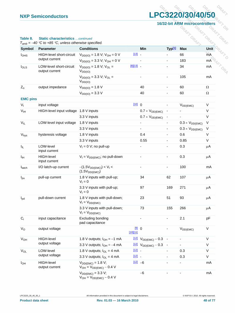
DRAFT
DRAFT DRAFT DR
DRAFT DRAFT DRAFRAF
DRAFT DRAFT DRAF
FT D
DRAFT DRAFT DRAF
DRA
NXP Semiconductors LPC3220/30/40/5016/32-bit ARM microcontrollers
T DT DRAFT DRA
T DRAFT DRAFT DRAFT
IOHS HIGH-level short-circuit output current
VDD(IO) = 1.8 V; VOH = 0 V [13] - - 66 mA
VDD(IO) = 3.3 V; VOH = 0 V - - 183 mA
IOLS LOW-level short-circuit output current
VDD(IO) = 1.8 V; VOL = VDD(IO)
[8][13] - - 34 mA
VDD(IO) = 3.3 V; VOL = VDD(IO)
- - 105 mA
Zo output impedance VDD(IO) = 1.8 V 40 - 60 Ω
VDD(IO) = 3.3 V 40 - 60 Ω
EMC pinsVI input voltage [10] 0 - VDD(EMC) V
VIH HIGH-level input voltage 1.8 V inputs 0.7 × VDD(EMC) - - V
3.3 V inputs 0.7 × VDD(EMC) - - V
VIL LOW-level input voltage 1.8 V inputs - - 0.3 × VDD(EMC) V
3.3 V inputs - - 0.3 × VDD(EMC) V
Vhys hysteresis voltage 1.8 V inputs 0.4 - 0.6 V
3.3 V inputs 0.55 - 0.85 V
IIL LOW-level input current
VI = 0 V; no pull-up - - 0.3 μA
IIH HIGH-levelinput current
VI = VDD(EMC); no pull-down - - 0.3 μA
Ilatch I/O latch-up current −(1.5VDD(EMC)) < VI < (1.5VDD(EMC))
- - 100 mA
Ipu pull-up current 1.8 V inputs with pull-up; VI = 0
34 62 107 μA
3.3 V inputs with pull-up; VI = 0
97 169 271 μA
Ipd pull-down current 1.8 V inputs with pull-down; VI = VDD(EMC)
23 51 93 μA
3.3 V inputs with pull-down; VI = VDD(EMC)
73 155 266 μA
Ci input capacitance Excluding bondingpad capacitance
- - 2.1 pF
VO output voltage [9][10][11]
0 - VDD(EMC) V
VOH HIGH-level output voltage
1.8 V outputs; IOH = −1 mA [12] VDD(EMC) − 0.3 - - V
3.3 V outputs; IOH = −4 mA [12] VDD(EMC) − 0.3 - - V
VOL LOW-level output voltage
1.8 V outputs; IOL = 4 mA [12] - - 0.3 V
3.3 V outputs; IOL = 4 mA [12] - - 0.3 V
IOH HIGH-level output current
VDD(EMC) = 1.8 V; VOH = VDD(EMC) − 0.4 V
[12] −6 - - mA
VDD(EMC) = 3.3 V; VOH = VDD(EMC) − 0.4 V
−6 - - mA
Table 8. Static characteristics …continuedTamb = −40 °C to +85 °C, unless otherwise specified.
Symbol Parameter Conditions Min Typ[1] Max Unit
LPC3220_30_40_50_1 All information provided in this document is subject to legal disclaimers. © NXP B.V. 2010. All rights reserved.
Product data sheet Rev. 01.03 — 16 March 2010 48 of 77
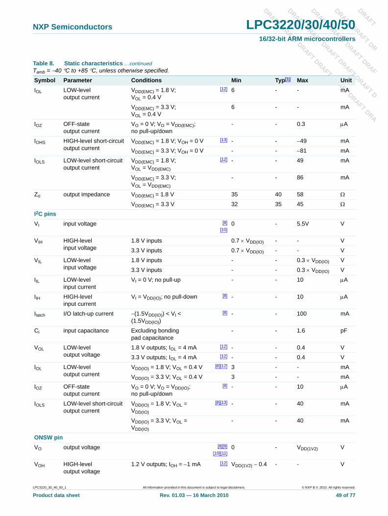
DRAFT
DRAFT DRAFT DR
DRAFT DRAFT DRAFRAF
DRAFT DRAFT DRAF
FT D
DRAFT DRAFT DRAF
DRA
NXP Semiconductors LPC3220/30/40/5016/32-bit ARM microcontrollers
T DT DRAFT DRA
T DRAFT DRAFT DRAFT
IOL LOW-level output current
VDD(EMC) = 1.8 V; VOL = 0.4 V
[12] 6 - - mA
VDD(EMC) = 3.3 V; VOL = 0.4 V
6 - - mA
IOZ OFF-state output current
VO = 0 V; VO = VDD(EMC);no pull-up/down
- - 0.3 μA
IOHS HIGH-level short-circuit output current
VDD(EMC) = 1.8 V; VOH = 0 V [13] - - −49 mA
VDD(EMC) = 3.3 V; VOH = 0 V - - −81 mA
IOLS LOW-level short-circuit output current
VDD(EMC) = 1.8 V; VOL = VDD(EMC)
[12] - - 49 mA
VDD(EMC) = 3.3 V; VOL = VDD(EMC)
- - 86 mA
Zo output impedance VDD(EMC) = 1.8 V 35 40 58 Ω
VDD(EMC) = 3.3 V 32 35 45 Ω
I2C pinsVI input voltage [8]
[10]0 - 5.5V V
VIH HIGH-level input voltage
1.8 V inputs 0.7 × VDD(IO) - - V
3.3 V inputs 0.7 × VDD(IO) - - V
VIL LOW-level input voltage
1.8 V inputs - - 0.3 × VDD(IO) V
3.3 V inputs - - 0.3 × VDD(IO) V
IIL LOW-level input current
VI = 0 V; no pull-up - - 10 μA
IIH HIGH-level input current
VI = VDD(IO); no pull-down [8] - - 10 μA
Ilatch I/O latch-up current −(1.5VDD(IO)) < VI < (1.5VDD(IO))
[8] - - 100 mA
Ci input capacitance Excluding bonding pad capacitance
- - 1.6 pF
VOL LOW-level output voltage
1.8 V outputs; IOL = 4 mA [12] - - 0.4 V
3.3 V outputs; IOL = 4 mA [12] - - 0.4 V
IOL LOW-level output current
VDD(IO) = 1.8 V; VOL = 0.4 V [8][12] 3 - - mA
VDD(IO) = 3.3 V; VOL = 0.4 V 3 - - mA
IOZ OFF-state output current
VO = 0 V; VO = VDD(IO);no pull-up/down
[8] - - 10 μA
IOLS LOW-level short-circuit output current
VDD(IO) = 1.8 V; VOL = VDD(IO)
[8][13] - - 40 mA
VDD(IO) = 3.3 V; VOL = VDD(IO)
- - 40 mA
ONSW pinVO output voltage [8][9]
[10][11]0 - VDD(1V2) V
VOH HIGH-level output voltage
1.2 V outputs; IOH = −1 mA [12] VDD(1V2) − 0.4 - - V
Table 8. Static characteristics …continuedTamb = −40 °C to +85 °C, unless otherwise specified.
Symbol Parameter Conditions Min Typ[1] Max Unit
LPC3220_30_40_50_1 All information provided in this document is subject to legal disclaimers. © NXP B.V. 2010. All rights reserved.
Product data sheet Rev. 01.03 — 16 March 2010 49 of 77

DRAFT
DRAFT DRAFT DR
DRAFT DRAFT DRAFRAF
DRAFT DRAFT DRAF
FT D
DRAFT DRAFT DRAF
DRA
NXP Semiconductors LPC3220/30/40/5016/32-bit ARM microcontrollers
T DT DRAFT DRA
T DRAFT DRAFT DRAFT
[1] Typical ratings are not guaranteed. The values listed are at room temperature (25 °C), nominal supply voltages.
[2] Applies to VDD_CORE pins.
[3] Applies to pins VDD_RTC, VDD_RTCCORE, and VDD_RTCOSC.
[4] Applies to pins VDD_COREFXD, VDD_OSC, VDD_PLL397, VDD_PLLHCLK, and VDD_PLLUSB.
[5] Applies when using 1.8 V Mobile DDR or Mobile SDR SDRAM.
[6] Applies when using 2.5 V DDR memory.
[7] Applies when using 3.3 V SDR SDRAM and SRAM.
[8] Referenced to the applicable VDD for the pin.
[9] Including voltage on outputs in 3-state mode.
[10] The applicable VDD voltage for the pin must be present.
[11] 3-state outputs go into 3-state mode when the applicable VDD voltage for the pin is grounded.
[12] Accounts for 100 mV voltage drop in all supply lines.
[13] Allowed as long as the current limit does not exceed the maximum current allowed by the device.
VOL LOW-level output voltage
1.2 V outputs; IOL = 4 mA [12] - - 0.4 V
IOH HIGH-level output current
VOH = VDD(1V2) − 0.4 V [8][12] −4 - - mA
IOL LOW-level output current
VOL = 0.4 V [8][12] 3 - - mA
IOZ OFF-state output current
VO = 0 V; VO = VDD(1V2);no pull-up/down
[8] - - 1.5 μA
IOHS HIGH-level short-circuit output current
VDD(1V2) = 1.8 V; VOH = 0 V [13] - - −135 mA
IOLS LOW-level short-circuit output current
VOL = VDD(1V2) [8][13] - - 135 mA
Zo output impedance VDD(1V2) = 1.2 V 40 - 60 Ω
Oscillator input/output pins Vi(xtal) crystal input voltage on pins RTCX_IN and
SYSX_IN−0.5 - +1.3 V
Vo(xtal) crystal output voltage on pins RTCX_OUT and SYSX_OUT
−0.5 - +1.3 V
Reset pinVI input voltage [8]
[10]0 - 1.95 V
VIH HIGH-level input voltage 1.2 V inputs 0.7 × VDD(1V2) - - V
VIL LOW-level input voltage 1.2 V inputs - - 0.3 × VDD(1V2) V
IIL LOW-level input current VI = 0 V; no pull-up - - 1 μA
IIH HIGH-level input current VI = VDD; no pull-down [8] - - 1 μA
IOZ OFF-state output current VO = 0 V; VO = VDD; no pull-up/down
[8] - - 1 μA
Ilatch I/O latch-up current −(1.5VDD) < VI < (1.5VDD) [8] - - 100 mA
Table 8. Static characteristics …continuedTamb = −40 °C to +85 °C, unless otherwise specified.
Symbol Parameter Conditions Min Typ[1] Max Unit
LPC3220_30_40_50_1 All information provided in this document is subject to legal disclaimers. © NXP B.V. 2010. All rights reserved.
Product data sheet Rev. 01.03 — 16 March 2010 50 of 77
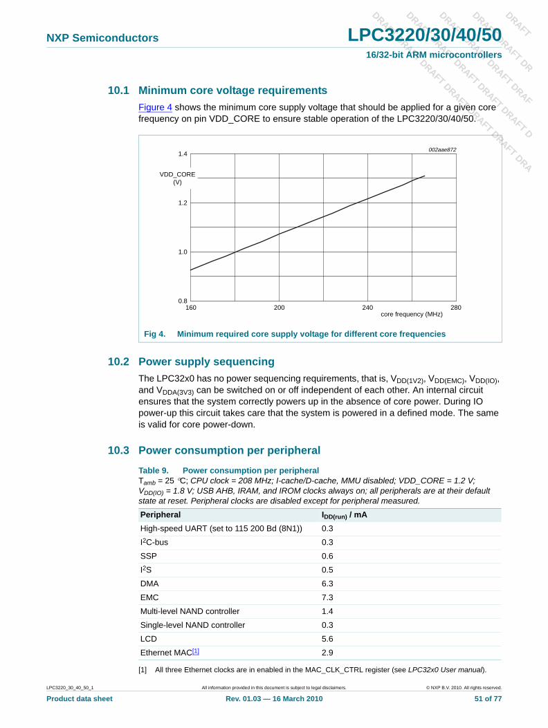
DRAFT
DRAFT DRAFT DR
DRAFT DRAFT DRAFRAF
DRAFT DRAFT DRAF
FT D
DRAFT DRAFT DRAF
DRA
NXP Semiconductors LPC3220/30/40/5016/32-bit ARM microcontrollers
T DT DRAFT DRA
T DRAFT DRAFT DRAFT
10.1 Minimum core voltage requirementsFigure 4 shows the minimum core supply voltage that should be applied for a given core frequency on pin VDD_CORE to ensure stable operation of the LPC3220/30/40/50.
10.2 Power supply sequencingThe LPC32x0 has no power sequencing requirements, that is, VDD(1V2), VDD(EMC), VDD(IO), and VDDA(3V3) can be switched on or off independent of each other. An internal circuit ensures that the system correctly powers up in the absence of core power. During IO power-up this circuit takes care that the system is powered in a defined mode. The same is valid for core power-down.
10.3 Power consumption per peripheral
[1] All three Ethernet clocks are in enabled in the MAC_CLK_CTRL register (see LPC32x0 User manual).
Fig 4. Minimum required core supply voltage for different core frequencies
core frequency (MHz)160 280240200
002aae872
1.0
1.2
1.4
0.8
VDD_CORE(V)
Table 9. Power consumption per peripheralTamb = 25 °C; CPU clock = 208 MHz; I-cache/D-cache, MMU disabled; VDD_CORE = 1.2 V; VDD(IO) = 1.8 V; USB AHB, IRAM, and IROM clocks always on; all peripherals are at their default state at reset. Peripheral clocks are disabled except for peripheral measured.
Peripheral IDD(run) / mA High-speed UART (set to 115 200 Bd (8N1)) 0.3
I2C-bus 0.3
SSP 0.6
I2S 0.5
DMA 6.3
EMC 7.3
Multi-level NAND controller 1.4
Single-level NAND controller 0.3
LCD 5.6
Ethernet MAC[1] 2.9
LPC3220_30_40_50_1 All information provided in this document is subject to legal disclaimers. © NXP B.V. 2010. All rights reserved.
Product data sheet Rev. 01.03 — 16 March 2010 51 of 77
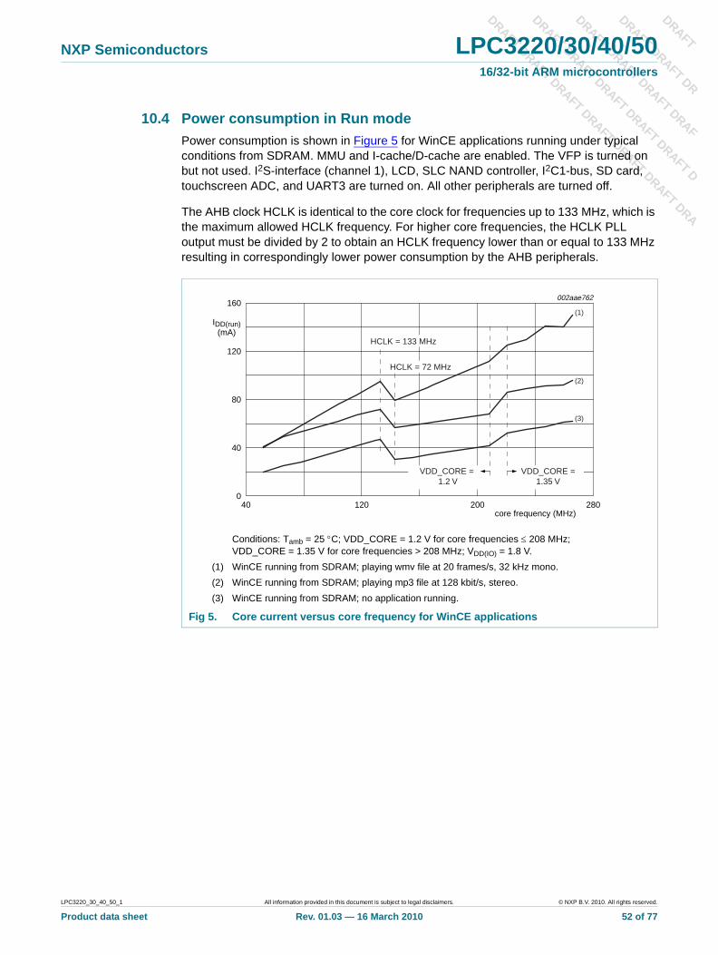
DRAFT
DRAFT DRAFT DR
DRAFT DRAFT DRAFRAF
DRAFT DRAFT DRAF
FT D
DRAFT DRAFT DRAF
DRA
NXP Semiconductors LPC3220/30/40/5016/32-bit ARM microcontrollers
T DT DRAFT DRA
T DRAFT DRAFT DRAFT
10.4 Power consumption in Run modePower consumption is shown in Figure 5 for WinCE applications running under typical conditions from SDRAM. MMU and I-cache/D-cache are enabled. The VFP is turned on but not used. I2S-interface (channel 1), LCD, SLC NAND controller, I2C1-bus, SD card, touchscreen ADC, and UART3 are turned on. All other peripherals are turned off.
The AHB clock HCLK is identical to the core clock for frequencies up to 133 MHz, which is the maximum allowed HCLK frequency. For higher core frequencies, the HCLK PLL output must be divided by 2 to obtain an HCLK frequency lower than or equal to 133 MHz resulting in correspondingly lower power consumption by the AHB peripherals.
Conditions: Tamb = 25 °C; VDD_CORE = 1.2 V for core frequencies ≤ 208 MHz; VDD_CORE = 1.35 V for core frequencies > 208 MHz; VDD(IO) = 1.8 V.
(1) WinCE running from SDRAM; playing wmv file at 20 frames/s, 32 kHz mono.(2) WinCE running from SDRAM; playing mp3 file at 128 kbit/s, stereo.(3) WinCE running from SDRAM; no application running.
Fig 5. Core current versus core frequency for WinCE applications
core frequency (MHz)40 280200120
002aae762
80
40
120
160
IDD(run)(mA)
0
(1)
(2)
(3)
HCLK = 133 MHz
HCLK = 72 MHz
VDD_CORE = 1.2 V
VDD_CORE =1.35 V
LPC3220_30_40_50_1 All information provided in this document is subject to legal disclaimers. © NXP B.V. 2010. All rights reserved.
Product data sheet Rev. 01.03 — 16 March 2010 52 of 77
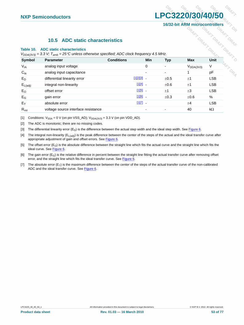
DRAFT
DRAFT DRAFT DR
DRAFT DRAFT DRAFRAF
DRAFT DRAFT DRAF
FT D
DRAFT DRAFT DRAF
DRA
NXP Semiconductors LPC3220/30/40/5016/32-bit ARM microcontrollers
T DT DRAFT DRA
T DRAFT DRAFT DRAFT
10.5 ADC static characteristics
[1] Conditions: VSSA = 0 V (on pin VSS_AD); VDDA(3V3) = 3.3 V (on pin VDD_AD).
[2] The ADC is monotonic; there are no missing codes.
[3] The differential linearity error (ED) is the difference between the actual step width and the ideal step width. See Figure 6.
[4] The integral non-linearity (EL(adj)) is the peak difference between the center of the steps of the actual and the ideal transfer curve after appropriate adjustment of gain and offset errors. See Figure 6.
[5] The offset error (EO) is the absolute difference between the straight line which fits the actual curve and the straight line which fits the ideal curve. See Figure 6.
[6] The gain error (EG) is the relative difference in percent between the straight line fitting the actual transfer curve after removing offset error, and the straight line which fits the ideal transfer curve. See Figure 6.
[7] The absolute error (ET) is the maximum difference between the center of the steps of the actual transfer curve of the non-calibrated ADC and the ideal transfer curve. See Figure 6.
Table 10. ADC static characteristicsVDDA(3V3) = 3.3 V; Tamb = 25°C unless otherwise specified; ADC clock frequency 4.5 MHz.
Symbol Parameter Conditions Min Typ Max UnitVIA analog input voltage 0 - VDDA(3V3) V
Cia analog input capacitance - - 1 pF
ED differential linearity error [1][2][3] - ±0.5 ±1 LSB
EL(adj) integral non-linearity [1][4] - ±0.6 ±1 LSB
EO offset error [1][5] - ±1 ±3 LSB
EG gain error [1][6] - ±0.3 ±0.6 %
ET absolute error [1][7] - ±4 LSB
Rvsi voltage source interface resistance - - 40 kΩ
LPC3220_30_40_50_1 All information provided in this document is subject to legal disclaimers. © NXP B.V. 2010. All rights reserved.
Product data sheet Rev. 01.03 — 16 March 2010 53 of 77
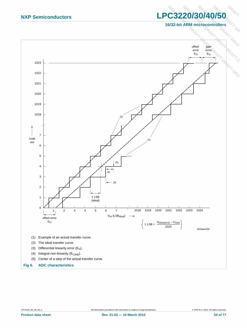
DRAFT
DRAFT DRAFT DR
DRAFT DRAFT DRAFRAF
DRAFT DRAFT DRAF
FT D
DRAFT DRAFT DRAF
DRA
NXP Semiconductors LPC3220/30/40/5016/32-bit ARM microcontrollers
T DT DRAFT DRA
T DRAFT DRAFT DRAFT
(1) Example of an actual transfer curve.(2) The ideal transfer curve.(3) Differential linearity error (ED).(4) Integral non-linearity (EL(adj)).(5) Center of a step of the actual transfer curve.
Fig 6. ADC characteristics
002aae434
1023
1022
1021
1020
1019
(2)
(1)
10241018 1019 1020 1021 1022 102371 2 3 4 5 6
7
6
5
4
3
2
1
0
1018
(5)
(4)
(3)
1 LSB(ideal)
codeout
VDDA(3V3) − VSSA
1024
offset errorEO
gainerrorEG
offset errorEO
VIA (LSBideal)
1 LSB =
LPC3220_30_40_50_1 All information provided in this document is subject to legal disclaimers. © NXP B.V. 2010. All rights reserved.
Product data sheet Rev. 01.03 — 16 March 2010 54 of 77
DRAFT
DRAFT DRAFT DR
DRAFT DRAFT DRAFRAF
DRAFT DRAFT DRAF
FT D
DRAFT DRAFT DRAF
DRA
NXP Semiconductors LPC3220/30/40/5016/32-bit ARM microcontrollers
T DT DRAFT DRA
T DRAFT DRAFT DRAFT
11. Dynamic characteristics
11.1 Clocking and I/O port pins
[1] Parameters are valid over operating temperature range unless otherwise specified.
[2] After supply voltages are stable
[3] Supplied by an external crystal.
11.2 Static memory controller
Table 11. Dynamic characteristicsTamb = −40 °C to +85 °C, unless otherwise specified.[1]
Symbol Parameter Conditions Min Typ Max UnitResettw(RESET)ext external RESET pulse width [2] 10 - - ms
External clockfext external clock frequency [3] 1 13 20 MHz
Port pinstr rise time - 5 - ns
tf fall time - 5 - ns
Table 12. Dynamic characteristics: static external memory interfaceCL = 25 pF, Tamb = 20 °C, VDD(EMC) = 1.8 V, 2.5 V, or 3.3 V.
Symbol Parameter Notes Min Typ Max UnitCommon to read and write cyclesTCLCL clock cycle time [1] 7.5 9.6 - ns
tCSLAV CS LOW to address valid time - 0 - ns
Read cycle parameterstOELAV OE LOW to address valid time [2] - 0 − WAITOEN × TCLCL - ns
tBLSLAV BLS LOW to address valid time [2] - 0 − WAITOEN × TCLCL - ns
tCSLOEL CS LOW to OE LOW time - 0 + WAITOEN × TCLCL - ns
tCSLBLSL CS LOW to BLS LOW time [2] - 0 + WAITOEN × TCLCL - ns
tOELOEH OE LOW to OE HIGH time [2][3] - (WAITRD − WAITOEN + 1) × TCLCL - ns
tBLSLBLSH BLS LOW to BLS HIGH time [2][3] - (WAITRD − WAITOEN + 1) × TCLCL - ns
tsu(DQ) data input/output set-up time [6] - 8.4 - ns
th(DQ) data input/output hold time [6] - 0 - ns
tCSHOEH CS HIGH to OE HIGH time - 0 - ns
tCSHBLSH CS HIGH to BLS HIGH time - 0 - ns
tOEHANV OE HIGH to address invalid time - 1 × TCLCL - ns
tBLSHANV BLS HIGH to address invalid time - 1 × TCLCL - ns
Write cycle parameterstCSLDV CS LOW to data valid time - 0 - ns
tCSLWEL CS LOW to WE LOW time [4] - (WAITWEN + 1) × TCLCL - ns
tCSLBLSL CS LOW to BLS LOW time [4] - (WAITWEN + 1) × TCLCL - ns
tWELDV WE LOW to data valid time [4] - 0 − (WAITWEN + 1) × TCLCL - ns
LPC3220_30_40_50_1 All information provided in this document is subject to legal disclaimers. © NXP B.V. 2010. All rights reserved.
Product data sheet Rev. 01.03 — 16 March 2010 55 of 77
DRAFT
DRAFT DRAFT DR
DRAFT DRAFT DRAFRAF
DRAFT DRAFT DRAF
FT D
DRAFT DRAFT DRAF
DRA
NXP Semiconductors LPC3220/30/40/5016/32-bit ARM microcontrollers
T DT DRAFT DRA
T DRAFT DRAFT DRAFT
[1] TCLCL = 1/HCLK
[2] Refer to the LPC32x0 user manual EMCStaticWaitOen0-3 register for the programming of WAITOEN value.
[3] Refer to the LPC32x0 user manual EMCStaticWaitRd0-3 register for the programming of WAITRD value.
[4] Refer to the LPC32x0 user manual EMCStaticWaitWen0-3 register for the programming of WAITWEN value.
[5] Refer to the LPC32x0 user manual EMCStaticWaitWr0-3 register for the programming of WAITWR value.
[6] Earliest of CS HIGH, OE HIGH, address change to data invalid.
tWELWEH WE LOW to WE HIGH time [4][5] - (WAITWR − WAITWEN + 1) × TCLCL - ns
tBLSLBLSH BLS LOW to BLS HIGH time [4][5] - (WAITWR − WAITWEN + 1) × TCLCL - ns
tWEHANV WE HIGH to address invalid time - 1 × TCLCL - ns
tWEHDNV WE HIGH to data invalid time - 1 × TCLCL - ns
tBLSHANV BLS HIGH to address invalid time - 1 × TCLCL - ns
tBLSHDNV BLS HIGH to data invalid time - 1 × TCLCL - ns
Table 12. Dynamic characteristics: static external memory interface …continuedCL = 25 pF, Tamb = 20 °C, VDD(EMC) = 1.8 V, 2.5 V, or 3.3 V.
Symbol Parameter Notes Min Typ Max Unit
Fig 7. External memory read access
EMC_CS[3:0]
EMC_A[23:0]
EMC_D[31:0]
EMC_OE
EMC_BLS[3:0]
tCSLAV
tOELAV
tOELOEH
tCSLOEL
tsu(DQ)th(DQ)
tCSHOEH
tOEHANV
002aae402
tBLSLAV tCSHBLSH
tBLSLBLSH
tCSLBLSL tBLSHANV
LPC3220_30_40_50_1 All information provided in this document is subject to legal disclaimers. © NXP B.V. 2010. All rights reserved.
Product data sheet Rev. 01.03 — 16 March 2010 56 of 77
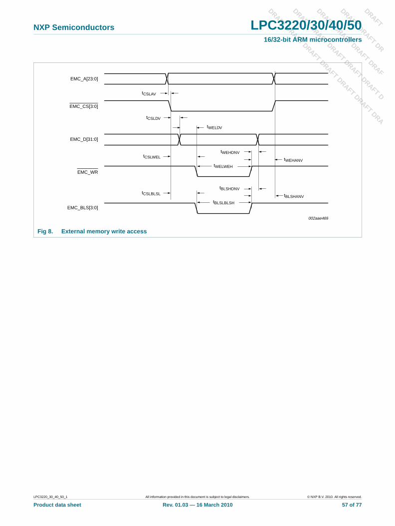
DRAFT
DRAFT DRAFT DR
DRAFT DRAFT DRAFRAF
DRAFT DRAFT DRAF
FT D
DRAFT DRAFT DRAF
DRA
NXP Semiconductors LPC3220/30/40/5016/32-bit ARM microcontrollers
T DT DRAFT DRA
T DRAFT DRAFT DRAFT
Fig 8. External memory write access
EMC_A[23:0]
EMC_D[31:0]
tCSLWEL
tCSLBLSL
tWELDV
tCSLDV
tWELWEH
tWEHANV
tBLSHANV
tWEHDNV
tBLSHDNV
002aae469
tCSLAV
EMC_CS[3:0]
tBLSLBLSHEMC_BLS[3:0]
EMC_WR
LPC3220_30_40_50_1 All information provided in this document is subject to legal disclaimers. © NXP B.V. 2010. All rights reserved.
Product data sheet Rev. 01.03 — 16 March 2010 57 of 77

DRAFT
DRAFT DRAFT DR
DRAFT DRAFT DRAFRAF
DRAFT DRAFT DRAF
FT D
DRAFT DRAFT DRAF
DRA
NXP Semiconductors LPC3220/30/40/5016/32-bit ARM microcontrollers
T DT DRAFT DRA
T DRAFT DRAFT DRAFT
11.3 SDR SDRAM Controller
[1] Parameters are valid over operating temperature range unless otherwise specified.
[2] Typical values valid for EMC pads set to fast slew rate: VDD_EMC = 1.8 V, VDD_CORE = 1.2 V or slower slew rate: VDD_EMC = 3.3 V, VDD_CORE = 1.2 V (see SDRAMCLK_CTRL register in the LPC32x0 User manual).
[3] All min or max values valid for EMC pads set to fast slew rate: VDD_EMC = 1.8 V, VDD_CORE = 1.2 V or slower slew rate: VDD_EMC = 3.3 V, VDD_CORE = 1.2 V.
[4] foper = 1/tCK.
[5] Applies to signals: EMC_DQM[3:0], EMC_DYCSm, EMC_RAS, EMC_CAS, EMC_WR, EMC_CKEm.
[6] CMD_DLY = COMMAND_DELAY bitfield in SDRAMCLK_CTRL[18:14] register, see External memory controller (EMC) chapter in LPC32x0 User manual.
Table 13. EMC SDR SDRAM memory interface dynamic characteristicsCL = 25 pF, Tamb = −40 °C to +85 °C, unless otherwise specified.[1][3]
Symbol Parameter Min Typical[2] Max Unitfoper operating frequency [4] 104 133 MHz
tCK clock cycle time 7.5 9.6 - ns
tCL CK LOW-level width - 4.8 - ns
tCH CK HIGH-level width - 4.8 - ns
td(V)ctrl control valid delay time [5][6] - (CMD_DLY × 0.25) + 2.7 ns
th(ctrl) control hold time [5][6] (CMD_DLY × 0.25) + 1.2 - ns
td(AV) address valid delay time [6] - (CMD_DLY × 0.25) + 3.2 ns
th(A) address hold time [6] (CMD_DLY × 0.25) + 1.2 - ns
td(QV) data output valid delay time [6] - (CMD_DLY × 0.25) + 3.5 ns
th(Q) data output hold time [6] (CMD_DLY × 0.25) + 1.2 - ns
tsu(D) data input set-up time - 0.6 - ns
th(D) data input hold time - 0.9 - ns
tQZ data output high-impedance time - - < tCK ns
Fig 9. SDR SDRAM signal timing
002aae420
EMC_CLK
output signal (O)
input signal (I)
td(V)ctrl, td(AV), td(QV) th(ctrl), th(Q), th(A)
th(D)tsu(D)
tCK
tCLtCH
tQZ
LPC3220_30_40_50_1 All information provided in this document is subject to legal disclaimers. © NXP B.V. 2010. All rights reserved.
Product data sheet Rev. 01.03 — 16 March 2010 58 of 77

DRAFT
DRAFT DRAFT DR
DRAFT DRAFT DRAFRAF
DRAFT DRAFT DRAF
FT D
DRAFT DRAFT DRAF
DRA
NXP Semiconductors LPC3220/30/40/5016/32-bit ARM microcontrollers
T DT DRAFT DRA
T DRAFT DRAFT DRAFT
11.4 DDR SDRAM controller
[1] All values valid for EMC pads set to fast slew rate at 1.8 V unless otherwise specified (see SDRAMCLK_CTRL register in the LPC32x0 User manual).
[2] CMD_DLY = COMMAND_DELAY bitfield in SDRAMCLK_CTRL[18:14] register, see External memory controller (EMC) chapter in LPC32x0 User manual.
[3] Applies to signals EMC_DQM[1:0], EMC_DYCSm, EMC_RAS, EMC_CAS, EMC_WR, EMC_CKEm.
[4] DQS_DELAY, see LPC32x0 user manual, External Memory Controller Chapter, Section 8 DDR DQS delay calibration for details on configuring this value.
[5] Test conditions for measurements: Tamb = −40 °C to +85 °C; operating frequency range foper = 52 MHz to 133 MHz; EMC_DQMm and EMC_D[31:0] driving 2 inches of 50 Ω characteristic impedance trace with 10 pf capacitive load; no external source series termination resistors used. EMC pads set to fast slew rate at 1.8 V or 2.5 V (see SDRAMCLK_CTRL register in the LPC32x0 User manual).
Table 14. EMC DDR SDRAM memory interface dynamic characteristics[1]
CL = 25 pF, Tamb = 25 °C, unless otherwise specified.
Symbol Parameter Conditions Min Typical Max Unitfoper operating frequency - 104 133 MHz
tCK clock cycle time 7.5 9.6 - ns
tCL CK LOW-level width - 0.5 × tCK - ns
tCH CK HIGH-level width - 0.5 × tCK - ns
td(V)ctrl control valid delay time [2][3] - (CMD_DLY × 0.25) + 1.5 - ns
th(ctrl) control hold time [2][3] - (CMD_DLY × 0.25) − 1.5 - ns
td(AV) address valid delay time [2] - (CMD_DLY × 0.25) + 1.5 - ns
th(A) address hold time [2] - (CMD_DLY × 0.25) − 1.5 - ns
tsu(Q) data output set-up time EMC_D and EMC_DQM to EMC_DQS out
[5] 0.08 × tCK
0.15 × tCK 0.25 × tCK
ns
th(Q) data output hold time EMC_D and EMC_DQM to EMC_DQS out
[5] 0.25 × tCK
0.35 × tCK 0.42 × tCK
ns
tDQSH DQS HIGH time for WRITE command
- 0.5 × tCK - ns
tDQSL DQS LOW time for WRITE command
- 0.5 × tCK - ns
tDQSS WRITE command to first DQS latching transition time
for DQS out - tCK + 0.7 - ns
tDSS DQS falling edge to CK set-up time for DQS in - 0.5 × tCK - ns
tDSH DQS falling edge hold time from CK for DQS in - 0.5 × tCK - ns
td(DQS) DQS delay time for DQS in [4] - DQS_DELAY - ns
tsu(D) data input set-up time - 0.3 - ns
th(D) data input hold time - 0.5 - ns
LPC3220_30_40_50_1 All information provided in this document is subject to legal disclaimers. © NXP B.V. 2010. All rights reserved.
Product data sheet Rev. 01.03 — 16 March 2010 59 of 77
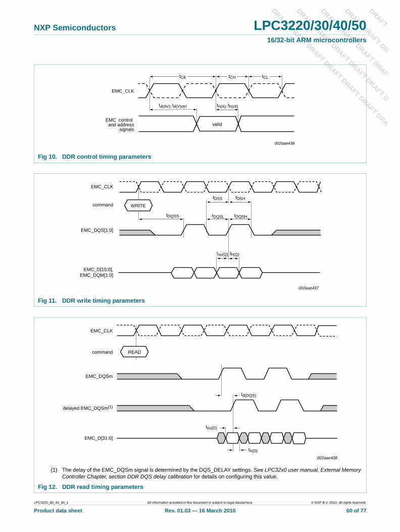
DRAFT
DRAFT DRAFT DR
DRAFT DRAFT DRAFRAF
DRAFT DRAFT DRAF
FT D
DRAFT DRAFT DRAF
DRA
NXP Semiconductors LPC3220/30/40/5016/32-bit ARM microcontrollers
T DT DRAFT DRA
T DRAFT DRAFT DRAFT
Fig 10. DDR control timing parameters
EMC_CLK
EMC control and address
signals
002aae436
tCK tCH tCL
td(AV); td(V)ctrl th(A); th(ctl)
valid
Fig 11. DDR write timing parameters
command
EMC_D[15:0], EMC_DQM[1:0]
tDQSL tDQSHtDQSS
th(Q)
EMC_DQS[1:0]
EMC_CLK
002aae437
WRITE
tsu(Q)
tDSHtDSS
(1) The delay of the EMC_DQSm signal is determined by the DQS_DELAY settings. See LPC32x0 user manual, External Memory Controller Chapter, section DDR DQS delay calibration for details on configuring this value.
Fig 12. DDR read timing parameters
EMC_CLK
command
EMC_D[31:0]
tsu(D)
EMC_DQSm
002aae438
th(D)
READ
delayed EMC_DQSm(1)
td(DQS)
LPC3220_30_40_50_1 All information provided in this document is subject to legal disclaimers. © NXP B.V. 2010. All rights reserved.
Product data sheet Rev. 01.03 — 16 March 2010 60 of 77
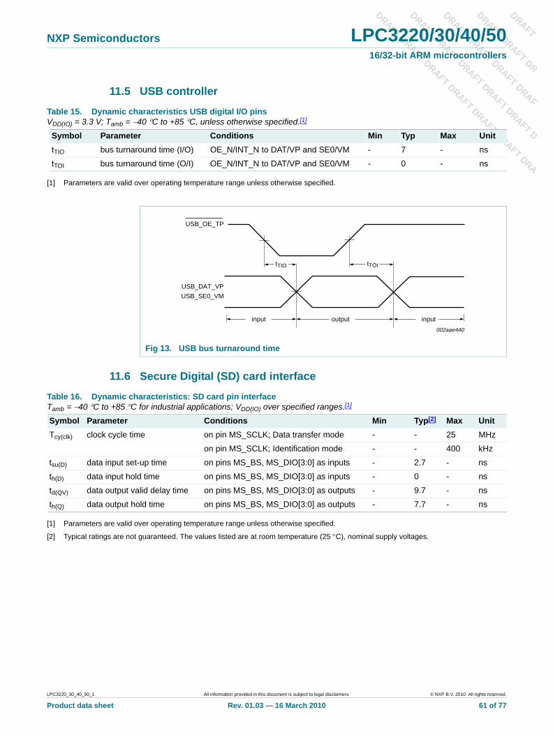
DRAFT
DRAFT DRAFT DR
DRAFT DRAFT DRAFRAF
DRAFT DRAFT DRAF
FT D
DRAFT DRAFT DRAF
DRA
NXP Semiconductors LPC3220/30/40/5016/32-bit ARM microcontrollers
T DT DRAFT DRA
T DRAFT DRAFT DRAFT
11.5 USB controller
[1] Parameters are valid over operating temperature range unless otherwise specified.
11.6 Secure Digital (SD) card interface
[1] Parameters are valid over operating temperature range unless otherwise specified.
[2] Typical ratings are not guaranteed. The values listed are at room temperature (25 °C), nominal supply voltages.
Table 15. Dynamic characteristics USB digital I/O pinsVDD(IO) = 3.3 V; Tamb = −40 °C to +85 °C, unless otherwise specified.[1]
Symbol Parameter Conditions Min Typ Max UnittTIO bus turnaround time (I/O) OE_N/INT_N to DAT/VP and SE0/VM - 7 - ns
tTOI bus turnaround time (O/I) OE_N/INT_N to DAT/VP and SE0/VM - 0 - ns
Fig 13. USB bus turnaround time
002aae440
USB_DAT_VP
tTIO tTOI
USB_OE_TP
USB_SE0_VM
input output input
Table 16. Dynamic characteristics: SD card pin interfaceTamb = −40 °C to +85 °C for industrial applications; VDD(IO) over specified ranges.[1]
Symbol Parameter Conditions Min Typ[2] Max UnitTcy(clk) clock cycle time on pin MS_SCLK; Data transfer mode - - 25 MHz
on pin MS_SCLK; Identification mode - - 400 kHz
tsu(D) data input set-up time on pins MS_BS, MS_DIO[3:0] as inputs - 2.7 - ns
th(D) data input hold time on pins MS_BS, MS_DIO[3:0] as inputs - 0 - ns
td(QV) data output valid delay time on pins MS_BS, MS_DIO[3:0] as outputs - 9.7 - ns
th(Q) data output hold time on pins MS_BS, MS_DIO[3:0] as outputs - 7.7 - ns
LPC3220_30_40_50_1 All information provided in this document is subject to legal disclaimers. © NXP B.V. 2010. All rights reserved.
Product data sheet Rev. 01.03 — 16 March 2010 61 of 77

DRAFT
DRAFT DRAFT DR
DRAFT DRAFT DRAFRAF
DRAFT DRAFT DRAF
FT D
DRAFT DRAFT DRAF
DRA
NXP Semiconductors LPC3220/30/40/5016/32-bit ARM microcontrollers
T DT DRAFT DRA
T DRAFT DRAFT DRAFT
11.7 MLC NAND flash memory controller
[1] THCLK = 1/HCLK
[2] CEAD = bitfield TCEA_DELAY[1:0] in register MLC_TIME_REG[25:24]
[3] WL = bitfield WR_LOW[3:0] in register MLC_TIME_REG[3:0]
[4] WH = bitfield WR_HIGH[3:0] in register MLC_TIME_REG[7:4]
[5] RL = bitfield RD_LOW[3:0] in register MLC_TIME_REG[11:8]
[6] RH = bitfield RD_HIGH [3:0] in register MLC_TIME_REG[15:12]
[7] RHZ = bitfield NAND_TA[2:0] in register MLC_TIME_REG[18:16]
[8] BD = bitfield BUSY_DELAY[4:0] in register MLC_TIME_REG[23:19]
Fig 14. SD card pin interface timing
002aae441
MS_SCLK
MS_DIO[3:0](O)
MS_DIO[3:0] (I)
td(QV)
th(D)tsu(D)
Tcy(clk)
th(Q)
MS_BS (O)
MS_BS (I)
Table 17. Dynamic characteristics of the MLC NAND flash memory controllerTamb = −40 °C to +85 °C.
Symbol Parameter Min Typ Max UnittCELREL CE LOW to RE LOW time [1][2] - THCLK × CEAD - ns
tRC RE cycle time [1][5][6] - THCLK × (RL + 1) + THCLK × (RH − RL) - ns
tREH RE HIGH hold time [1][5][6] - THCLK × (RH − RL) - ns
tRHZ RE HIGH to output high-impedance time [1][5][7] - THCLK × (RH − RL) + THCLK × RHZ - ns
tRP RE pulse width [1][5] - THCLK × (RL + 1) - ns
tREHRBL RE HIGH to R/B LOW time [1][8] - THCLK × BD - ns
tWB WE HIGH to R/B LOW time [1][8] - THCLK × BD - ns
tWC WE cycle time [1][3][4] - THCLK × (WL + 1) + THCLK × (WH − WL) - ns
tWH WE HIGH hold time [1][3][4] - THCLK × (WH − WL) - ns
tWP WE pulse width [1][3] - THCLK × (WL + 1) - ns
LPC3220_30_40_50_1 All information provided in this document is subject to legal disclaimers. © NXP B.V. 2010. All rights reserved.
Product data sheet Rev. 01.03 — 16 March 2010 62 of 77
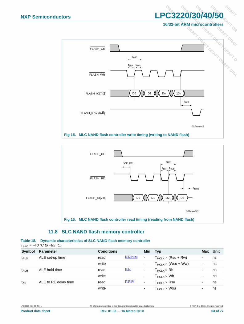
DRAFT
DRAFT DRAFT DR
DRAFT DRAFT DRAFRAF
DRAFT DRAFT DRAF
FT D
DRAFT DRAFT DRAF
DRA
NXP Semiconductors LPC3220/30/40/5016/32-bit ARM microcontrollers
T DT DRAFT DRA
T DRAFT DRAFT DRAFT
11.8 SLC NAND flash memory controller
Fig 15. MLC NAND flash controller write timing (writing to NAND flash)
Fig 16. MLC NAND flash controller read timing (reading from NAND flash)
tWB
FLASH_IO[7:0]
FLASH_WR
tWP
tWC
FLASH_RDY (R/B)
FLASH_CE
D0 D1 Dn 10h
tWH
002aae442
FLASH_IO[7:0]
tRP tREH
tRC
FLASH_RD
FLASH_CE
tCELREL
D0 D1 D2 D3
tRHZ
002aae443
Table 18. Dynamic characteristics of SLC NAND flash memory controller Tamb = −40 °C to +85 °C.
Symbol Parameter Conditions Min Typ Max UnittALS ALE set-up time read [1][2][4][6] - THCLK × (Rsu + Rw) - ns
write - THCLK × (Wsu + Ww) - ns
tALH ALE hold time read [1][7] - THCLK × Rh - ns
write - THCLK × Wh - ns
tAR ALE to RE delay time read [1][2][6] - THCLK × Rsu - ns
write - THCLK × Wsu - ns
LPC3220_30_40_50_1 All information provided in this document is subject to legal disclaimers. © NXP B.V. 2010. All rights reserved.
Product data sheet Rev. 01.03 — 16 March 2010 63 of 77
DRAFT
DRAFT DRAFT DR
DRAFT DRAFT DRAFRAF
DRAFT DRAFT DRAF
FT D
DRAFT DRAFT DRAF
DRA
NXP Semiconductors LPC3220/30/40/5016/32-bit ARM microcontrollers
T DT DRAFT DRA
T DRAFT DRAFT DRAFT
tCEA CE access time read [1][2][4][6][8] - THCLK × (Rsu + Rw) - ns
write - THCLK × (Wsu + Ww) - ns
tCS CE set-up time read [1][2][4][6][8] - THCLK × (Rsu + Rw) - ns
write - THCLK × (Wsu + Ww) - ns
tCH CE hold time read [1][3] - THCLK × Rh - ns
write - THCLK × Wh - ns
tCLS CLE set-up time read [1][2][4][6][8] - THCLK × (Rsu + Rw) - ns
write - THCLK × (Wsu + Ww) - ns
tCLH CLE hold time read [1][3] - THCLK × Rh - ns
write - THCLK × Wh - ns
tCLR CLE to RE delay time read [1][2][6] - THCLK × Rsu - ns
write - THCLK × Wsu - ns
tDH data hold time output from NAND controller; read
[1][3][7] - THCLK × Rh - ns
output from NAND controller; write
- THCLK × Wh - ns
tDS data set-up time output from NAND controller; read
[1][2][4][6][8] - THCLK × (Rsu + Rw) - ns
output from NAND controller; write
- THCLK × (Wsu + Ww) -
tIR output high-impedance to RE LOW time
read [1][2][6] - THCLK × Rsu - ns
write - THCLK × Wsu - ns
tRC RE cycle time read [1][2] - THCLK × (Rsu + Rw + Rh) - ns
tREA RE access time read [1][4] - THCLK × Rw - ns
tREH RE high hold time read [1][2][3] - THCLK × (Rsu + Rh) - ns
tRHOH RE HIGH to output hold time input hold for flash controller; read
- 0 - -
input hold for flash controller; write
- 0 - -
tRHZ RE HIGH to output high-impedance time
read [1] - THCLK × Rh - ns
tRP RE pulse width read [1][4] - THCLK × Rw - ns
tRR ready to RE LOW time read [1][2][3] - THCLK × Rsu - ns
tWB WE HIGH to R/B LOW time write [1][8] - THCLK × Ww - ns
tWC WE cycle time write [1][6][7][8] - THCLK × (Wsu + Ww + Wh) - ns
Table 18. Dynamic characteristics of SLC NAND flash memory controller …continuedTamb = −40 °C to +85 °C.
Symbol Parameter Conditions Min Typ Max Unit
LPC3220_30_40_50_1 All information provided in this document is subject to legal disclaimers. © NXP B.V. 2010. All rights reserved.
Product data sheet Rev. 01.03 — 16 March 2010 64 of 77
DRAFT
DRAFT DRAFT DR
DRAFT DRAFT DRAFRAF
DRAFT DRAFT DRAF
FT D
DRAFT DRAFT DRAF
DRA
NXP Semiconductors LPC3220/30/40/5016/32-bit ARM microcontrollers
T DT DRAFT DRA
T DRAFT DRAFT DRAFT
[1] THCLK = 1/HCLK
[2] Rsu = bitfield R_SETUP[3:0] in register SLC_TAC[3:0] for reads
[3] Rh = bitfield R_HOLD[3:0] in register SLC_TAC[7:4] for reads
[4] Rw = bitfield R_WIDTH[3:0] in register SLC_TAC[11:8] for reads
[5] Rb = bitfield R_RDY[3:0] in register SLC_TAC[15:12] for reads
[6] Wsu = bitfield W_SETUP[3:0] in register SLC_TAC[19:16] for writes
[7] Wh = bitfield W_HOLD[3:0] in register SLC_TAC[23:20] for writes
[8] Ww = bitfield W_WIDTH[3:0] in register SLC_TAC[27:24] for writes
[9] Wb = bitfield W_RDY[3:0] in register SLC_TAC[31:28] for writes
tWH WE HIGH hold time write [1][6][7] - THCLK × (Wsu + Wh) - ns
tWHR WE HIGH to RE LOW time write [1][6][7] - THCLK × (Wsu + Wh) - ns
tWP WE pulse width write [1][8] - THCLK × Ww - ns
tREHRBL RE HIGH to R/B LOW time write [1][8] - THCLK × Ww - ns
Table 18. Dynamic characteristics of SLC NAND flash memory controller …continuedTamb = −40 °C to +85 °C.
Symbol Parameter Conditions Min Typ Max Unit
Fig 17. MLC NAND flash memory write timing (writing to NAND flash)
command
tDS tDH
tWB
FLASH_IO[7:0] address
tDS tDH
tALS tALH
tDS tDH
tWP tWH tWC
tCS tCH tCH
tCLS tCLH
command address data
D0 D1 Dn
tALS
tCLH
tALS tALH
tWP tWP tWH
tCLS
tCS
002aae444
FLASH_CE
FLASH_CLE
FLASH_WR
FLASH_ALE
FLASH_RDY
LPC3220_30_40_50_1 All information provided in this document is subject to legal disclaimers. © NXP B.V. 2010. All rights reserved.
Product data sheet Rev. 01.03 — 16 March 2010 65 of 77
DRAFT
DRAFT DRAFT DR
DRAFT DRAFT DRAFRAF
DRAFT DRAFT DRAF
FT D
DRAFT DRAFT DRAF
DRA
NXP Semiconductors LPC3220/30/40/5016/32-bit ARM microcontrollers
T DT DRAFT DRA
T DRAFT DRAFT DRAFT
Fig 18. MLC NAND Flash memory read timing (reading from NAND flash)
command
tDS tDH
tWB
FLASH_IO[7:0] address
tDS tDH
tALS tALH
tDS tDH
tRP tREH tRC
tRR
tAR
tCS tCH tCEA
tCLR
tCLS tCLH
command address data
tCOH
tREA
D0 D1 D2 D3
tRHZ
tRHOH
tALS tALH
tCLS
tCS
tWP tWHtWP
002aae445
FLASH_ALE
FLASH_CLE
FLASH_RDY
FLASH_WR
FLASH_RD
FLASH_CE
LPC3220_30_40_50_1 All information provided in this document is subject to legal disclaimers. © NXP B.V. 2010. All rights reserved.
Product data sheet Rev. 01.03 — 16 March 2010 66 of 77
DRAFT
DRAFT DRAFT DR
DRAFT DRAFT DRAFRAF
DRAFT DRAFT DRAF
FT D
DRAFT DRAFT DRAF
DRA
NXP Semiconductors LPC3220/30/40/5016/32-bit ARM microcontrollers
T DT DRAFT DRA
T DRAFT DRAFT DRAFT
11.9 SPI and SSP Controller
11.9.1 SPI
[1] THCLK = period time of SPI IP block input clock (HCLK)
Fig 19. MLC NAND flash memory status timing
tCS tCH tCEA
70 h
tDS tDH
status
tRHOH
tCLS tCLH
command data
tCLR
tCOH
tREA
tIR
FLASH_IO[7:0]
tWHR
tWP
tRHZ
FLASH_CLE
FLASH_WR
FLASH_CE
FLASH_RD
002aae446
Table 19. Dynamic characteristics of SPI pins on SPI master controllerTamb = −40 °C to +85 °C.
Symbol Parameter Min Typ Max UnitCommon to SPI1 and SPI2TSPICYC SPI cycle time [1] 2 × THCLK - 256 × THCLK ns
SPI1tSPIDSU SPI data set-up time - 6 - ns
tSPIDH SPI data hold time - 0 - ns
tSPIDV SPI enable to output data valid time - 2 - ns
tSPIOH SPI output data hold time - 0 - ns
SPI2tSPIDSU SPI data set-up time - 10 - ns
tSPIDH SPI data hold time - 0 - ns
tSPIDV SPI enable to output data valid time - 2 - ns
tSPIOH SPI output data hold time - 0 - ns
LPC3220_30_40_50_1 All information provided in this document is subject to legal disclaimers. © NXP B.V. 2010. All rights reserved.
Product data sheet Rev. 01.03 — 16 March 2010 67 of 77
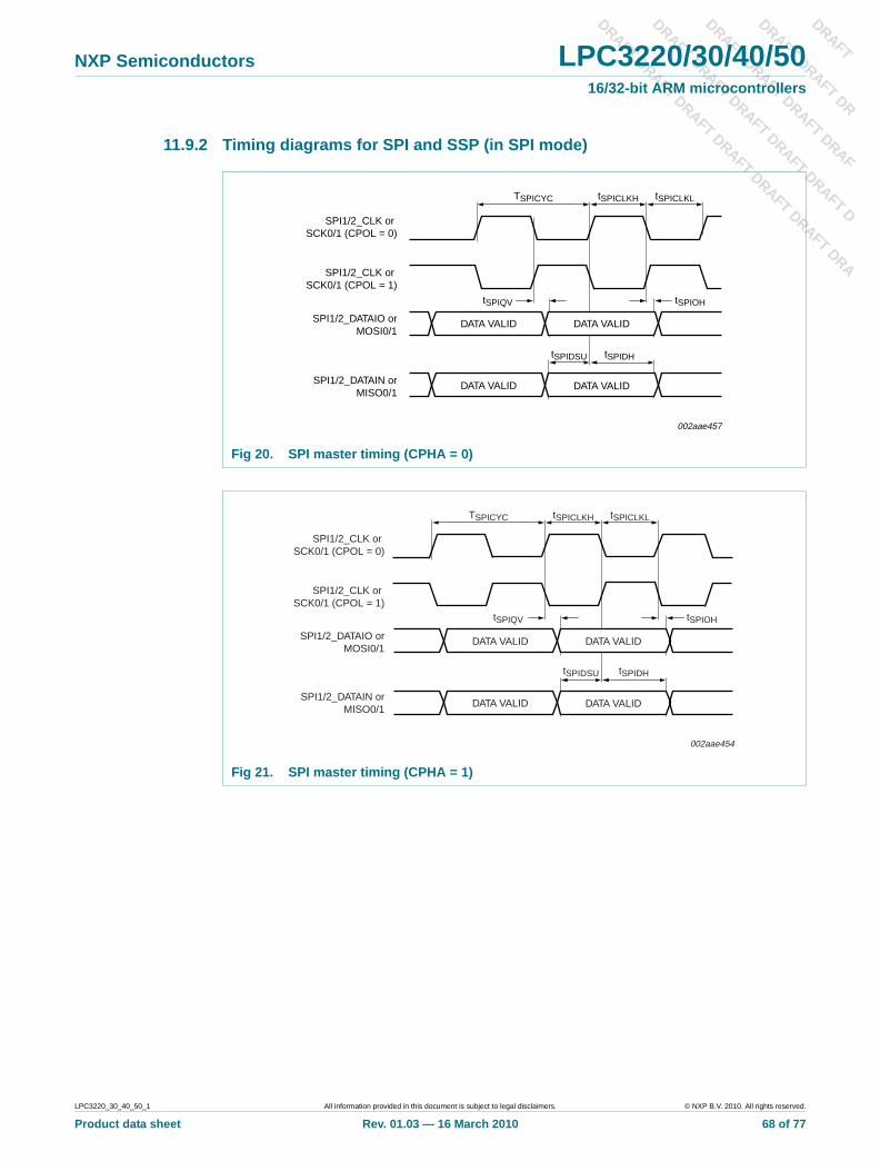
DRAFT
DRAFT DRAFT DR
DRAFT DRAFT DRAFRAF
DRAFT DRAFT DRAF
FT D
DRAFT DRAFT DRAF
DRA
NXP Semiconductors LPC3220/30/40/5016/32-bit ARM microcontrollers
T DT DRAFT DRA
T DRAFT DRAFT DRAFT
11.9.2 Timing diagrams for SPI and SSP (in SPI mode)
Fig 20. SPI master timing (CPHA = 0)
Fig 21. SPI master timing (CPHA = 1)
002aae457
TSPICYC tSPICLKH tSPICLKL
tSPIDSU tSPIDH
DATA VALID DATA VALID
tSPIOH
DATA VALID DATA VALID
tSPIQV
SPI1/2_CLK or SCK0/1 (CPOL = 0)
SPI1/2_CLK or SCK0/1 (CPOL = 1)
SPI1/2_DATAIO orMOSI0/1
SPI1/2_DATAIN orMISO0/1
002aae454
TSPICYC tSPICLKH tSPICLKL
tSPIDSU tSPIDH
tSPIQV
DATA VALID DATA VALID
tSPIOH
DATA VALID DATA VALID
SPI1/2_CLK or SCK0/1 (CPOL = 0)
SPI1/2_CLK or SCK0/1 (CPOL = 1)
SPI1/2_DATAIO orMOSI0/1
SPI1/2_DATAIN orMISO0/1
LPC3220_30_40_50_1 All information provided in this document is subject to legal disclaimers. © NXP B.V. 2010. All rights reserved.
Product data sheet Rev. 01.03 — 16 March 2010 68 of 77
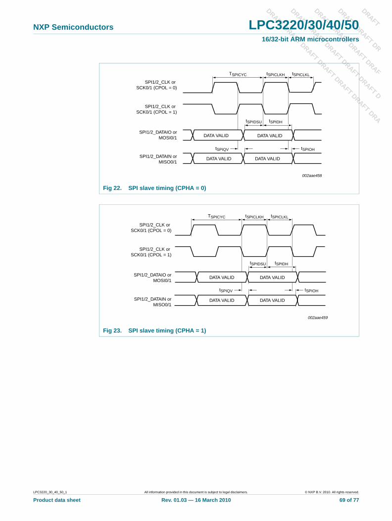
DRAFT
DRAFT DRAFT DR
DRAFT DRAFT DRAFRAF
DRAFT DRAFT DRAF
FT D
DRAFT DRAFT DRAF
DRA
NXP Semiconductors LPC3220/30/40/5016/32-bit ARM microcontrollers
T DT DRAFT DRA
T DRAFT DRAFT DRAFT
Fig 22. SPI slave timing (CPHA = 0)
Fig 23. SPI slave timing (CPHA = 1)
002aae458
TSPICYC tSPICLKH tSPICLKL
tSPIDSU tSPIDH
tSPIQV
DATA VALID DATA VALID
tSPIOH
DATA VALID DATA VALID
SPI1/2_CLK or SCK0/1 (CPOL = 0)
SPI1/2_CLK or SCK0/1 (CPOL = 1)
SPI1/2_DATAIO orMOSI0/1
SPI1/2_DATAIN orMISO0/1
002aae459
TSPICYC tSPICLKH tSPICLKL
tSPIDSU tSPIDH
tSPIQV
DATA VALID DATA VALID
tSPIOH
DATA VALID DATA VALID
SPI1/2_CLK or SCK0/1 (CPOL = 0)
SPI1/2_CLK or SCK0/1 (CPOL = 1)
SPI1/2_DATAIO orMOSI0/1
SPI1/2_DATAIN orMISO0/1
LPC3220_30_40_50_1 All information provided in this document is subject to legal disclaimers. © NXP B.V. 2010. All rights reserved.
Product data sheet Rev. 01.03 — 16 March 2010 69 of 77

DRAFT
DRAFT DRAFT DR
DRAFT DRAFT DRAFRAF
DRAFT DRAFT DRAF
FT D
DRAFT DRAFT DRAF
DRA
NXP Semiconductors LPC3220/30/40/5016/32-bit ARM microcontrollers
T DT DRAFT DRA
T DRAFT DRAFT DRAFT
12. Package outline
Fig 24. Package outline SOT1048-1 (TFBGA296)
REFERENCESOUTLINEVERSION
EUROPEANPROJECTION
ISSUE DATEIEC JEDEC JEITA
SOT1048-1 MO-216
SOT1048-1
07-10-1907-11-02
UNIT Amax
mm 1.2 0.40.3
0.800.65
15.114.9
15.114.9 0.8 13.6 0.15 0.08 0.1
A1
DIMENSIONS (mm are the original dimensions)
TFBGA296: plastic thin fine-pitch ball grid array package; 296 balls
0 5 10 mm
scale
A2 b
0.50.4
D E e e1 e2
13.6
v w y
0.12
y1
C
yCy1
X
AB
CD
EF
H
K
G
L
J
MN
PR
TU
2 4 6 8 10 12 14 161 3 5 7 9 11 13 15
1817
b
e2
e1e
e
1/2 e
1/2 e
AC B∅ v M
C∅ w M
ball A1index area
V
B A
ball A1index area
D
E
detail X
AA2
A1
LPC3220_30_40_50_1 All information provided in this document is subject to legal disclaimers. © NXP B.V. 2010. All rights reserved.
Product data sheet Rev. 01.03 — 16 March 2010 70 of 77
DRAFT
DRAFT DRAFT DR
DRAFT DRAFT DRAFRAF
DRAFT DRAFT DRAF
FT D
DRAFT DRAFT DRAF
DRA
NXP Semiconductors LPC3220/30/40/5016/32-bit ARM microcontrollers
T DT DRAFT DRA
T DRAFT DRAFT DRAFT
13. Abbreviations
Table 20. AbbreviationsAcronym DescriptionADC Analog-to-Digital Converter
AHB Advanced High-performance Bus
AMBA Advanced Microcontroller Bus Architecture
APB Advanced Peripheral Bus
BSDL Boundary Scan Description Language
CISC Complex Instruction Set Computer
DDR SDRAM Double Data Rate Synchronous Dynamic Random Access Memory
DMA Direct Memory Access
DSP Digital Signal Processing
ETM Embedded Trace Macrocell
FAB Fast Access Bus
FIFO First In, First Out
FIQ Fast Interrupt Request
GPIO General Purpose Input/Output
I/O Input/Output
IRQ Interrupt Request
HS High-Speed
IrDA Infrared Data Association
JTAG Joint Test Action Group
LCD Liquid Crystal Display
MAC Media Access Control
MIIM Media Independent Interface Management
OHCI Open Host Controller Interface
OTG On-The-Go
PHY Physical Layer
PLL Phase-Locked Loop
PWM Pulse Width Modulator
RAM Random Access Memory
RMII Reduced Media Independent Interface
SE0 Single Ended Zero
SDR SDRAM Single Data Rate Synchronous Dynamic Random Access Memory
SPI Serial Peripheral Interface
SSI Serial Synchronous Interface
SSP Synchronous Serial Port
TFT Thin Film Transistor
TTL Transistor-Transistor Logic
STN Super Twisted Nematic
LPC3220_30_40_50_1 All information provided in this document is subject to legal disclaimers. © NXP B.V. 2010. All rights reserved.
Product data sheet Rev. 01.03 — 16 March 2010 71 of 77
DRAFT
DRAFT DRAFT DR
DRAFT DRAFT DRAFRAF
DRAFT DRAFT DRAF
FT D
DRAFT DRAFT DRAF
DRA
NXP Semiconductors LPC3220/30/40/5016/32-bit ARM microcontrollers
T DT DRAFT DRA
T DRAFT DRAFT DRAFT
UART Universal Asynchronous Receiver/Transmitter
USB Universal Serial Bus
VFP Vector Floating Point processor
Table 20. Abbreviations …continued
Acronym Description
LPC3220_30_40_50_1 All information provided in this document is subject to legal disclaimers. © NXP B.V. 2010. All rights reserved.
Product data sheet Rev. 01.03 — 16 March 2010 72 of 77
DRAFT
DRAFT DRAFT DR
DRAFT DRAFT DRAFRAF
DRAFT DRAFT DRAF
FT D
DRAFT DRAFT DRAF
DRA
NXP Semiconductors LPC3220/30/40/5016/32-bit ARM microcontrollers
T DT DRAFT DRA
T DRAFT DRAFT DRAFT
14. Revision history
Table 21. Revision historyDocument ID Release date Data sheet status Change notice SupersedesLPC3220_30_40_50_1.03 <tbd> Product data sheet - LPC3220_30_40_50_1.02
Modifications: • Power supply domain for pins SYSX_IN and SYSX_OUT pins corrected in Table 4.• Power supply domain for pin VDD_OSC corrected in Table 4.• Description of DEBUG pin updated in Table 4.• Document template updated.
LPC3220_30_40_50_1.02 <tbd> Product data sheet - LPC3220_30_40_50_1 and LPC3220_30_40_50_1.01
Modifications: • Added power consumption data (Table 8, Table 9, and Figure 5).• Changed VESD to 2500 V (HBM) and 1000 V (CDM) in Table 7.• Static memory controller: added tsu(DQ) value in Table 12.• DDR SDRAM controller: updated tDQSS value in Table 14.• Changed data sheet status to Product data sheet.• Added Table 6 “Supply domains”.• Corrected pin functions for pin T14 (ADIN1/TS_XM) and pin U15 (ADIN0/TS_YM) in
Table 3 and Table 4.• Parts LPC3220/01, LPC3230/01, LPC3240/01, LPC3250/01 added.• Minimum and maximum characterization data added for parameters tsu(Q) and th(Q) over
temperature range −40 °C to + 85 °C (see Table 14).• DDR SDRAM characteristics extended to maximum operating frequency foper = 133 MHz
(see Table 14).• Parameter VDD(EMC) table notes updated in Table 8.
LPC3220_30_40_50_1 20090206 Preliminary data sheet - -
LPC3220_30_40_50_1 All information provided in this document is subject to legal disclaimers. © NXP B.V. 2010. All rights reserved.
Product data sheet Rev. 01.03 — 16 March 2010 73 of 77
DRAFT
DRAFT DRAFT DR
DRAFT DRAFT DRAFRAF
DRAFT DRAFT DRAF
FT D
DRAFT DRAFT DRAF
DRA
NXP Semiconductors LPC3220/30/40/5016/32-bit ARM microcontrollers
T DT DRAFT DRA
T DRAFT DRAFT DRAFT
15. Legal information
15.1 Data sheet status
[1] Please consult the most recently issued document before initiating or completing a design.
[2] The term ‘short data sheet’ is explained in section “Definitions”.
[3] The product status of device(s) described in this document may have changed since this document was published and may differ in case of multiple devices. The latest product status information is available on the Internet at URL http://www.nxp.com.
15.2 DefinitionsDraft — The document is a draft version only. The content is still under internal review and subject to formal approval, which may result in modifications or additions. NXP Semiconductors does not give any representations or warranties as to the accuracy or completeness of information included herein and shall have no liability for the consequences of use of such information.
Short data sheet — A short data sheet is an extract from a full data sheet with the same product type number(s) and title. A short data sheet is intended for quick reference only and should not be relied upon to contain detailed and full information. For detailed and full information see the relevant full data sheet, which is available on request via the local NXP Semiconductors sales office. In case of any inconsistency or conflict with the short data sheet, the full data sheet shall prevail.
Product specification — The information and data provided in a Product data sheet shall define the specification of the product as agreed between NXP Semiconductors and its customer, unless NXP Semiconductors and customer have explicitly agreed otherwise in writing. In no event however, shall an agreement be valid in which the NXP Semiconductors product is deemed to offer functions and qualities beyond those described in the Product data sheet.
15.3 DisclaimersLimited warranty and liability — Information in this document is believed to be accurate and reliable. However, NXP Semiconductors does not give any representations or warranties, expressed or implied, as to the accuracy or completeness of such information and shall have no liability for the consequences of use of such information.
In no event shall NXP Semiconductors be liable for any indirect, incidental, punitive, special or consequential damages (including - without limitation - lost profits, lost savings, business interruption, costs related to the removal or replacement of any products or rework charges) whether or not such damages are based on tort (including negligence), warranty, breach of contract or any other legal theory.
Notwithstanding any damages that customer might incur for any reason whatsoever, NXP Semiconductors’ aggregate and cumulative liability towards customer for the products described herein shall be limited in accordance with the Terms and conditions of commercial sale of NXP Semiconductors.
Right to make changes — NXP Semiconductors reserves the right to make changes to information published in this document, including without limitation specifications and product descriptions, at any time and without notice. This document supersedes and replaces all information supplied prior to the publication hereof.
Suitability for use — NXP Semiconductors products are not designed, authorized or warranted to be suitable for use in medical, military, aircraft, space or life support equipment, nor in applications where failure or
malfunction of an NXP Semiconductors product can reasonably be expected to result in personal injury, death or severe property or environmental damage. NXP Semiconductors accepts no liability for inclusion and/or use of NXP Semiconductors products in such equipment or applications and therefore such inclusion and/or use is at the customer’s own risk.
Applications — Applications that are described herein for any of these products are for illustrative purposes only. NXP Semiconductors makes no representation or warranty that such applications will be suitable for the specified use without further testing or modification.
NXP Semiconductors does not accept any liability related to any default, damage, costs or problem which is based on a weakness or default in the customer application/use or the application/use of customer’s third party customer(s) (hereinafter both referred to as “Application”). It is customer’s sole responsibility to check whether the NXP Semiconductors product is suitable and fit for the Application planned. Customer has to do all necessary testing for the Application in order to avoid a default of the Application and the product. NXP Semiconductors does not accept any liability in this respect.
Limiting values — Stress above one or more limiting values (as defined in the Absolute Maximum Ratings System of IEC 60134) will cause permanent damage to the device. Limiting values are stress ratings only and (proper) operation of the device at these or any other conditions above those given in the Recommended operating conditions section (if present) or the Characteristics sections of this document is not warranted. Constant or repeated exposure to limiting values will permanently and irreversibly affect the quality and reliability of the device.
Terms and conditions of commercial sale — NXP Semiconductors products are sold subject to the general terms and conditions of commercial sale, as published at http://www.nxp.com/profile/terms, unless otherwise agreed in a valid written individual agreement. In case an individual agreement is concluded only the terms and conditions of the respective agreement shall apply. NXP Semiconductors hereby expressly objects to applying the customer’s general terms and conditions with regard to the purchase of NXP Semiconductors products by customer.
No offer to sell or license — Nothing in this document may be interpreted or construed as an offer to sell products that is open for acceptance or the grant, conveyance or implication of any license under any copyrights, patents or other industrial or intellectual property rights.
Export control — This document as well as the item(s) described herein may be subject to export control regulations. Export might require a prior authorization from national authorities.
Quick reference data — The Quick reference data is an extract of the product data given in the Limiting values and Characteristics sections of this document, and as such is not complete, exhaustive or legally binding.
Non-automotive qualified products — Unless this data sheet expressly states that this specific NXP Semiconductors product is automotive qualified, the product is not suitable for automotive use. It is neither qualified nor tested in accordance with automotive testing or application requirements. NXP Semiconductors accepts no liability for inclusion and/or use of non-automotive qualified products in automotive equipment or applications.
Document status[1][2] Product status[3] Definition
Objective [short] data sheet Development This document contains data from the objective specification for product development.
Preliminary [short] data sheet Qualification This document contains data from the preliminary specification.
Product [short] data sheet Production This document contains the product specification.
LPC3220_30_40_50_1 All information provided in this document is subject to legal disclaimers. © NXP B.V. 2010. All rights reserved.
Product data sheet Rev. 01.03 — 16 March 2010 74 of 77
DRAFT
DRAFT DRAFT DR
DRAFT DRAFT DRAFRAF
DRAFT DRAFT DRAF
FT D
DRAFT DRAFT DRAF
DRA
NXP Semiconductors LPC3220/30/40/5016/32-bit ARM microcontrollers
T DT DRAFT DRA
T DRAFT DRAFT DRAFT
In the event that customer uses the product for design-in and use in automotive applications to automotive specifications and standards, customer (a) shall use the product without NXP Semiconductors’ warranty of the product for such automotive applications, use and specifications, and (b) whenever customer uses the product for automotive applications beyond NXP Semiconductors’ specifications such use shall be solely at customer’s own risk, and (c) customer fully indemnifies NXP Semiconductors for any liability, damages or failed product claims resulting from customer design and use of the product for automotive applications beyond NXP Semiconductors’ standard warranty and NXP Semiconductors’ product specifications.
15.4 TrademarksNotice: All referenced brands, product names, service names and trademarks are the property of their respective owners.
I2C-bus — logo is a trademark of NXP B.V.
16. Contact information
For more information, please visit: http://www.nxp.com
For sales office addresses, please send an email to: [email protected]
LPC3220_30_40_50_1 All information provided in this document is subject to legal disclaimers. © NXP B.V. 2010. All rights reserved.
Product data sheet Rev. 01.03 — 16 March 2010 75 of 77

DRAFT
DRAFT DRAFT DR
DRAFT DRAFT DRAFRAF
DRAFT DRAFT DRAF
FT D
DRAFT DRAFT DRAF
DRA
NXP Semiconductors LPC3220/30/40/5016/32-bit ARM microcontrollers
T DT DRAFT DRA
T DRAFT DRAFT DRAFT
17. Contents
1 General description . . . . . . . . . . . . . . . . . . . . . . 12 Features and benefits . . . . . . . . . . . . . . . . . . . . 13 Applications . . . . . . . . . . . . . . . . . . . . . . . . . . . . 34 Ordering information. . . . . . . . . . . . . . . . . . . . . 44.1 Ordering options . . . . . . . . . . . . . . . . . . . . . . . . 45 Block diagram . . . . . . . . . . . . . . . . . . . . . . . . . . 56 Pinning information. . . . . . . . . . . . . . . . . . . . . . 66.1 Pinning . . . . . . . . . . . . . . . . . . . . . . . . . . . . . . . 66.2 Pin description . . . . . . . . . . . . . . . . . . . . . . . . 107 Functional description . . . . . . . . . . . . . . . . . . 237.1 CPU and subsystems . . . . . . . . . . . . . . . . . . . 237.1.1 CPU . . . . . . . . . . . . . . . . . . . . . . . . . . . . . . . . 237.1.2 Vector Floating Point (VFP) coprocessor . . . . 237.1.3 Emulation and debugging. . . . . . . . . . . . . . . . 237.1.3.1 Embedded ICE . . . . . . . . . . . . . . . . . . . . . . . . 237.1.3.2 Embedded trace buffer . . . . . . . . . . . . . . . . . . 247.2 AHB matrix . . . . . . . . . . . . . . . . . . . . . . . . . . . 247.2.1 APB . . . . . . . . . . . . . . . . . . . . . . . . . . . . . . . . 257.2.2 FAB. . . . . . . . . . . . . . . . . . . . . . . . . . . . . . . . . 257.3 Physical memory map . . . . . . . . . . . . . . . . . . 257.4 Internal memory . . . . . . . . . . . . . . . . . . . . . . . 277.4.1 On-chip ROM . . . . . . . . . . . . . . . . . . . . . . . . . 277.4.2 On-chip SRAM . . . . . . . . . . . . . . . . . . . . . . . . 277.5 External memory interfaces . . . . . . . . . . . . . . 277.5.1 NAND flash controllers . . . . . . . . . . . . . . . . . . 277.5.1.1 Multi-Level Cell (MLC) NAND flash controller. 277.5.1.2 Single-Level Cell (SLC) NAND flash controller 287.5.2 SD card controller . . . . . . . . . . . . . . . . . . . . . . 287.5.2.1 Features . . . . . . . . . . . . . . . . . . . . . . . . . . . . . 287.5.3 External memory controller. . . . . . . . . . . . . . . 287.6 AHB master peripherals . . . . . . . . . . . . . . . . . 297.6.1 General Purpose DMA (GPDMA) controller . 297.6.2 Ethernet MAC . . . . . . . . . . . . . . . . . . . . . . . . . 297.6.2.1 Features . . . . . . . . . . . . . . . . . . . . . . . . . . . . . 307.6.3 USB interface . . . . . . . . . . . . . . . . . . . . . . . . . 307.6.3.1 USB device controller . . . . . . . . . . . . . . . . . . . 307.6.3.2 USB host controller. . . . . . . . . . . . . . . . . . . . . 317.6.3.3 USB OTG controller . . . . . . . . . . . . . . . . . . . . 317.6.4 LCD controller. . . . . . . . . . . . . . . . . . . . . . . . . 327.6.4.1 Features . . . . . . . . . . . . . . . . . . . . . . . . . . . . . 327.7 System functions . . . . . . . . . . . . . . . . . . . . . . 337.7.1 Interrupt controller . . . . . . . . . . . . . . . . . . . . . 337.7.2 Watchdog timer. . . . . . . . . . . . . . . . . . . . . . . . 337.7.2.1 Features . . . . . . . . . . . . . . . . . . . . . . . . . . . . . 337.7.3 Millisecond timer. . . . . . . . . . . . . . . . . . . . . . . 337.7.3.1 Features . . . . . . . . . . . . . . . . . . . . . . . . . . . . . 337.7.4 Clocking and power control features . . . . . . . 347.7.4.1 Clocking . . . . . . . . . . . . . . . . . . . . . . . . . . . . . 347.7.4.2 Crystal oscillator . . . . . . . . . . . . . . . . . . . . . . . 347.7.4.3 PLLs . . . . . . . . . . . . . . . . . . . . . . . . . . . . . . . . 347.7.4.4 Power control modes . . . . . . . . . . . . . . . . . . . 357.7.4.5 Reset . . . . . . . . . . . . . . . . . . . . . . . . . . . . . . . 357.8 Communication peripheral interfaces . . . . . . 357.8.1 UARTs. . . . . . . . . . . . . . . . . . . . . . . . . . . . . . . 36
7.8.1.1 Standard UARTs. . . . . . . . . . . . . . . . . . . . . . . 367.8.1.2 High-speed UARTs . . . . . . . . . . . . . . . . . . . . 367.8.2 SPI serial I/O controller . . . . . . . . . . . . . . . . . 367.8.2.1 Features. . . . . . . . . . . . . . . . . . . . . . . . . . . . . 377.8.3 SSP serial I/O controller. . . . . . . . . . . . . . . . . 377.8.3.1 Features. . . . . . . . . . . . . . . . . . . . . . . . . . . . . 377.8.4 I2C-bus serial I/O controller . . . . . . . . . . . . . . 377.8.4.1 Features. . . . . . . . . . . . . . . . . . . . . . . . . . . . . 387.8.5 I2S-bus audio controller . . . . . . . . . . . . . . . . . 387.8.5.1 Features. . . . . . . . . . . . . . . . . . . . . . . . . . . . . 387.9 Other peripherals . . . . . . . . . . . . . . . . . . . . . . 397.9.1 General purpose parallel I/O . . . . . . . . . . . . . 397.9.1.1 Features. . . . . . . . . . . . . . . . . . . . . . . . . . . . . 397.9.2 Keyboard scanner . . . . . . . . . . . . . . . . . . . . . 407.9.2.1 Features. . . . . . . . . . . . . . . . . . . . . . . . . . . . . 407.9.3 Touch screen controller and 10-bit ADC . . . . 407.9.3.1 Features. . . . . . . . . . . . . . . . . . . . . . . . . . . . . 407.9.4 Real-Time Clock (RTC) and battery RAM . . . 407.9.4.1 Features. . . . . . . . . . . . . . . . . . . . . . . . . . . . . 417.9.5 Enhanced 32-bit timers/external event
counters . . . . . . . . . . . . . . . . . . . . . . . . . . . . . 417.9.5.1 Features. . . . . . . . . . . . . . . . . . . . . . . . . . . . . 417.9.6 High-speed timer . . . . . . . . . . . . . . . . . . . . . . 427.9.6.1 Features. . . . . . . . . . . . . . . . . . . . . . . . . . . . . 427.9.7 Pulse Width Modulators (PWMs) . . . . . . . . . . 427.9.7.1 Features. . . . . . . . . . . . . . . . . . . . . . . . . . . . . 427.9.8 Motor control pulse width modulator . . . . . . . 427.9.8.1 Features. . . . . . . . . . . . . . . . . . . . . . . . . . . . . 428 Basic architecture . . . . . . . . . . . . . . . . . . . . . . 439 Limiting values . . . . . . . . . . . . . . . . . . . . . . . . 4410 Static characteristics . . . . . . . . . . . . . . . . . . . 4510.1 Minimum core voltage requirements . . . . . . . 5110.2 Power supply sequencing . . . . . . . . . . . . . . . 5110.3 Power consumption per peripheral . . . . . . . . 5110.4 Power consumption in Run mode . . . . . . . . . 5210.5 ADC static characteristics . . . . . . . . . . . . . . . 5311 Dynamic characteristics. . . . . . . . . . . . . . . . . 5511.1 Clocking and I/O port pins . . . . . . . . . . . . . . . 5511.2 Static memory controller . . . . . . . . . . . . . . . . 5511.3 SDR SDRAM Controller. . . . . . . . . . . . . . . . . 5811.4 DDR SDRAM controller . . . . . . . . . . . . . . . . . 5911.5 USB controller . . . . . . . . . . . . . . . . . . . . . . . . 6111.6 Secure Digital (SD) card interface . . . . . . . . . 6111.7 MLC NAND flash memory controller . . . . . . . 6211.8 SLC NAND flash memory controller . . . . . . . 6311.9 SPI and SSP Controller . . . . . . . . . . . . . . . . . 6711.9.1 SPI . . . . . . . . . . . . . . . . . . . . . . . . . . . . . . . . . 6711.9.2 Timing diagrams for SPI and SSP
(in SPI mode) . . . . . . . . . . . . . . . . . . . . . . . . . 6812 Package outline. . . . . . . . . . . . . . . . . . . . . . . . 7013 Abbreviations . . . . . . . . . . . . . . . . . . . . . . . . . 7114 Revision history . . . . . . . . . . . . . . . . . . . . . . . 7315 Legal information . . . . . . . . . . . . . . . . . . . . . . 7415.1 Data sheet status . . . . . . . . . . . . . . . . . . . . . . 74
LPC3220_30_40_50_1 All information provided in this document is subject to legal disclaimers. © NXP B.V. 2010. All rights reserved.
Product data sheet Rev. 01.03 — 16 March 2010 76 of 77
DRAFT
DRAFT DRAFT DR
DRAFT DRAFT DRAFRAF
DRAFT DRAFT DRAF
FT D
DRAFT DRAFT DRAF
DRA
NXP Semiconductors LPC3220/30/40/5016/32-bit ARM microcontrollers
T DT DRAFT DRA
T DRAFT DRAFT DRAFT
15.2 Definitions. . . . . . . . . . . . . . . . . . . . . . . . . . . . 7415.3 Disclaimers . . . . . . . . . . . . . . . . . . . . . . . . . . . 7415.4 Trademarks. . . . . . . . . . . . . . . . . . . . . . . . . . . 7516 Contact information. . . . . . . . . . . . . . . . . . . . . 7517 Contents . . . . . . . . . . . . . . . . . . . . . . . . . . . . . . 76
© NXP B.V. 2010. All rights reserved.For more information, please visit: http://www.nxp.comFor sales office addresses, please send an email to: [email protected]
Date of release: 16 March 2010Document identifier: LPC3220_30_40_50_1
Please be aware that important notices concerning this document and the product(s)described herein, have been included in section ‘Legal information’.
Related Documents