HAL Id: tel-02046789 https://tel.archives-ouvertes.fr/tel-02046789 Submitted on 22 Feb 2019 HAL is a multi-disciplinary open access archive for the deposit and dissemination of sci- entific research documents, whether they are pub- lished or not. The documents may come from teaching and research institutions in France or abroad, or from public or private research centers. L’archive ouverte pluridisciplinaire HAL, est destinée au dépôt et à la diffusion de documents scientifiques de niveau recherche, publiés ou non, émanant des établissements d’enseignement et de recherche français ou étrangers, des laboratoires publics ou privés. Double barrier magnetic tunnel junctions for innovative spintronic devices Paulo Veloso Coelho To cite this version: Paulo Veloso Coelho. Double barrier magnetic tunnel junctions for innovative spintronic devices. Condensed Matter [cond-mat]. Université Grenoble Alpes, 2018. English. NNT : 2018GREAY048. tel-02046789

Welcome message from author
This document is posted to help you gain knowledge. Please leave a comment to let me know what you think about it! Share it to your friends and learn new things together.
Transcript
HAL Id: tel-02046789https://tel.archives-ouvertes.fr/tel-02046789
Submitted on 22 Feb 2019
HAL is a multi-disciplinary open accessarchive for the deposit and dissemination of sci-entific research documents, whether they are pub-lished or not. The documents may come fromteaching and research institutions in France orabroad, or from public or private research centers.
L’archive ouverte pluridisciplinaire HAL, estdestinée au dépôt et à la diffusion de documentsscientifiques de niveau recherche, publiés ou non,émanant des établissements d’enseignement et derecherche français ou étrangers, des laboratoirespublics ou privés.
Double barrier magnetic tunnel junctions for innovativespintronic devices
Paulo Veloso Coelho
To cite this version:Paulo Veloso Coelho. Double barrier magnetic tunnel junctions for innovative spintronic devices.Condensed Matter [cond-mat]. Université Grenoble Alpes, 2018. English. NNT : 2018GREAY048.tel-02046789
THÈSEPour obtenir le grade de
DOCTEUR DE LA COMMUNAUTÉ UNIVERSITÉ GRENOBLE ALPESSpécialité : PHYSIQUE DES MATERIAUXArrêté ministériel : 25 mai 2016
Présentée par
Paulo VELOSO COELHO
Thèse dirigée par Claire (phys) BARADUC, CEAet codirigée par Mairbek (phys) CHSHIEV, UGA
préparée au sein du Laboratoire Spintronique et Technologie des Composantsdans l'École Doctorale Physique
Doubles jonctions tunnel magnétiques pour dispositifs spintroniques innovants
Double barrier magnetic tunnel junctions for innovative spintronic devices
Thèse soutenue publiquement le 30 octobre 2018,devant le jury composé de :
Monsieur CORIOLAN VIOREL TIUSANPROFESSEUR, UNIV. TECHNIQUE (CLUJ-NAPOCA) - ROUMANIE, RapporteurMonsieur MICHEL HEHNPROFESSEUR, UNIVERSITE DE LORRAINE, RapporteurMonsieur JAN VOGELDIRECTEUR DE RECHERCHE, CNRS DELEGATION ALPES, PrésidentMonsieur DAFINE RAVELOSONADIRECTEUR DE RECHERCHE, CNRS DELEGATION ILE-DE-FRANCE SUD, Examinateur


I have not failed. I’ve just found 10,000 ways that won’t work.Thomas Edison


Acknowledgments
The first and main acknowledgments are for my two supervisors Claire Baraduc and Mairbek Chshiev
who provided and trusted me with the opportunity of following a PhD at Spintec. First, my deepest thanks
to Claire, for always being available for fruitful discussions about our most peculiar results and guiding my
work flow. Of course, always in a good mood and with an encouraging sense of humor, even in stressful
situations. Thanks to Mair for his incredible knowledge and most helpful insights from his theoretical
background. Always providing that unique idea we would take ages to come up with.
To all Spintec staff, from Director to secretaries, to take care of any problem I had with professionalism
and for their support. Special acknowledgments to the researchers of the MRAM group for inviting me to
their meetings which translated into helpful discussions about some less obvious results and for path to
follow. Here, I would like to highlight the help and advice provided by Bernard Dieny, Lucian Prejbeanu
and Antoine Chavant. A special thank you to Ricardo Sousa for allowing me to use his automated
setup to characterize my wafers and also allowing for the only conversations I had in Portuguese at
the lab. Very sincere acknowledgments as well for Andrey Timopheev and Nikita Strelkov for helping in
the macrospin simulations, respectively, for in-plane and out-of-plane double MTJs. Thanks to Clarisse
Ducruet (Crocus Technology) and Stephane Aufret for the deposition of most part my wafers. To Laurent
Vila for all the e-beam lithographies of my wafers. To the cleanroom process engineers, Guillaume
Lavaitte, Nathalie Lamard and Jude Guelfucci for helping me with the fabrication process whenever
needed. To all my fellow PhD and Pos-Doc friends at Spintec, with special focus to those who shared
with me room 324: Titiksha Srivastava, Mathieu Fabre and Jyotirmoy Chatterjee. We had some very
funny moments in that office, specially after working hours when noise was not a problem. A more
professional thank you to Jyotirmoy whose help and dedication was paramount to the development of the
patent we share but also to push the development of the double junctions with perpendicular anisotropy.
A unique thank you to a very special and fun group of friends that ”spin-off” from Spintec a.k.a ”Les
Cosmo”: Dali, Romeo, Jude et Guillaume. I will always happily remember all the ”heures heureuses” we
had in the city center with good beer and very funny conversations about the most ”sensitive” subjects
(ahahah).
A kind word as well for my flatmates from ”ColocAbel”: Marion, Patrick, Estelle, Jeanne and Theo.
Thank you for all the very nice coloc dinners and parties we have made at the apartment. It was a really
nice to have shared almost 3 years with you guys in Grenoble.
Although 3 years were spent in France, I must not forget that the majority of the manuscript writing
iii

was done in Braga while working at the International Iberian Nanotechnology Laboratory (INL). For that,
I have to thank as well my current supervisor Ricardo Ferreira for allowing me to work on the manuscript
during the ”not so busy” times. Of course, my current working fellows Cosimo and Mohamed. As well as
my new spintronics group friends, Lara, Alex, Tim, Elvira, Leandro and Luana.
Cannot forget my friends ”for life” from my hometown who contributed to keep me connected to my
country and made all the comebacks so worthwhile.
Finally, I have to dedicate this ultimate accomplishment of becoming a Dr. to my parents, Lurdes and
Paulo. I know it was a dream of yours that required so much sacrifice from you. I will be forever grateful
to you. To my little sister Sonia who I love so much. As well, in memory of my grandfather Jose and
my grandmother Ana, I am sure you would be very proud of me and I would love to have you around to
celebrate.
iv
Abstract
One of the dilemmas faced by the present STT-MRAM technology is the reduction of the power
consumption and increase of data access speed without jeopardizing the data retention. A possible
solution lies on the double barrier magnetic tunnel junction (DBMTJ) where the amplitude of the spin
transfer torque (STT) on the storage layer can be tuned through a proper magnetic configuration of
the outer electrodes. Thus providing more reliable read/write operation modes for MRAM. Despite the
reduction in half of the switching current, previous studies on DBMTJs with in-plane magnetization report
undesired switchings in read mode associated with field-like torque (T⊥). In this thesis, we further
investigate the complex interplay between damping-like and field-like torques in these double barrier
structures. Measurements using DC current and short voltage pulses in DBMTJ with symmetric and
asymmetric barriers have revealed a strong presence of the field-like torque both in write and read
modes. Moreover, in DBMTJs with symmetric barriers set in read mode, we demonstrate pure field-like
torque switching which is proportional to a quadratic voltage and adjusted by a b2 prefactor: T⊥ ∝ b2V2.
Furthermore, this torque favors a antiparallel alignment between the storage layer magnetization and the
two references’ magnetizations. The results obtained experimentally were in agreement with macrospin
simulation performed with a proper tuning of the damping-like and field-like torque prefactors. In order
to suppress the field-like torque and aiming for a further reduction of the writing currents and enhanced
scalability of MTJs, we developed and realized DBMTJs with perpendicular anisotropy (p-DBMTJs).
Novel seedless multilayers with improved perpendicular magnetic anisotropy to be used as top reference
were designed and implemented in functional p-DBMTJs. The optimized p-DBMTJs were patterned into
sub-300nm nanopillars and the spin transfer torque studied experimentally in write and read modes.
The use of W instead of Ta as a spacer in the FeCoB/spacer/FeCoB composite storage layer showed
a 3x improvement of STT efficiency. In write mode, p-DBMTJs have also demonstrated a considerable
enhancement of STT efficiency when compared to single barrier p-MTJs. In read mode, switching has
been prevented at the center of the bistable region but its thermal stability degraded with high voltage.
Among several proposed explanations of this phenomenon, the reduction of the saturation magnetization
and effective anisotropy with increasing temperature has been supported by macrospin simulations as
v

the most probable one.
Keywords
Spintronics, Double Barrier Magnetic Tunnel Junction, Spin Transfer Torque, Perpendicular Magnetic
Anisotropy, MRAM
vi
Resume
Un des dilemmes au quel doit faire face la technologie MRAM est la reduction de la consommation
energetique et l’amelioration des vitesses d’acces aux donnees sans compromettre la retention des
donnees. Une des solutions possibles passe par les jonctions tunnel magnetiques a double barriere
(JTMDB) dont l’amplitude du couple de transfert de spin de la couche de stockage peut etre reglee par
le choix de la configuration magnetique des electrodes. Cela permet ainsi des modes d’operation lec-
ture/ecriture plus fiables pour les MRAM. Malgre la reduction de moite du courant de commutation, une
etude precedente sur les JTMDB avec aimantation dans le plan signale des commutations indesirables
en mode lecture liees au couple de transfert de spin perpendiculaire (T⊥). Dans cette these, nous
etudions plus en detail l’interaction complexe entre les couples de transfert de spin planaire et perpen-
diculaire dans ces structures a double barriere. Les mesures effectuees en utilisant courant DC ou des
impulsions en tension de courte duree dans des JTMDB avec des barrieres symetriques et asymetriques
ont montre la presence du couple de transfert de spin perpendiculaire en mode lecture et en mode
ecriture. De plus, dans les JTMDB avec barrieres symetriques en mode lecture, nous demontrons la
commutation pure declenchee par le couple de transfert de spin perpendiculaire qui est proportionnel
a la tension quadratique et ajuste par le prefacteur b2: T⊥ ∝ b2V2. En outre, ce couple de transfert
de spin favorise l’alignement antiparallele entre les aimantations de la couche de stockage et les deux
couches de reference. Les resultats obtenus experimentalement sont en accord avec des simulations
macrospin effectuee avec un choix adequat des prefacteurs des couples de transfert de spin planaire et
perpendiculaire. Afin de supprimer l’influence du couple de transfert de spin perpendiculaire, reduire en-
core plus le courant d’ecriture et permettre la miniaturisation des JTM, nous avons developpe et fabrique
des JTMDB avec anisotropie perpendiculaire (p-JTMDB). Des nouvelles multicouches sans couche de
croissance avec une anisotropie magnetique perpendiculaire ameliore ont ete concues et introduites
dans p-JTMDB fonctionnelles comme reference du haut. Les p-JTMDB optimisees ont ete fabriquees
en nanopiliers de diametre inferieur a 300 nm et le couple de transfert de spin etudie experimentalement
en mode lecture et ecriture. L’utilisation du W au lieu de Ta comme couche intercalaire dans la couche
de stockage FeCoB/Couche intercalaire/FeCoB a montre une amelioration de l’efficacite du couple de
transfert de spin d’un facteur 3. En mode ecriture, les p-JTMDB ont aussi demontre un considerable ren-
forcement de l’efficacite du couple de transfert de spin par comparaison aux p-JTM a simple barriere. En
mode lecture, la commutation est empechee au centre de la region bistable mais la stabilite thermique
de l’etat magnetique se degrade aux tensions elevees. Parmi plusieurs explications proposees pour ce
phenomene, la reduction de la aimantation a saturation et de l’anisotropie effective avec l’augmentation
vii

de la temperature par effet Joule semble la plus probable selon des simulations macrospin.
Mots-cles
Spintronique, Jonctions Tunnel Magnetiques a Double Barriere, Couple de Transfert de Spin, Anisotropie
Magnetique Perpendiculaire, MRAM
viii

Contents
Introduction 1
1 Theoretical Concepts 3
1.1 Introduction . . . . . . . . . . . . . . . . . . . . . . . . . . . . . . . . . . . . . . . . . . . . 4
1.2 Spin Polarized Tunneling . . . . . . . . . . . . . . . . . . . . . . . . . . . . . . . . . . . . . 4
1.2.1 Spin polarized current . . . . . . . . . . . . . . . . . . . . . . . . . . . . . . . . . . 4
1.2.2 Tunnel Magnetoresistance . . . . . . . . . . . . . . . . . . . . . . . . . . . . . . . . 5
1.2.2.A TMR dependence on the ferromagnet spin polarization . . . . . . . . . . 8
1.2.2.B TMR dependence on the tunnel barrier: the Butler’s model . . . . . . . . 8
1.2.3 TMR in double barrier MTJ . . . . . . . . . . . . . . . . . . . . . . . . . . . . . . . 10
1.3 Spin Transfer Torque . . . . . . . . . . . . . . . . . . . . . . . . . . . . . . . . . . . . . . . 12
1.3.1 STT at electron level . . . . . . . . . . . . . . . . . . . . . . . . . . . . . . . . . . . 13
1.3.2 Field-like Torque . . . . . . . . . . . . . . . . . . . . . . . . . . . . . . . . . . . . . 15
1.3.3 STT in Magnetic Tunnel Junctions . . . . . . . . . . . . . . . . . . . . . . . . . . . 17
1.4 Phase Diagram of Magnetic Tunnel Junctions . . . . . . . . . . . . . . . . . . . . . . . . . 18
1.4.1 Phase diagram boundaries . . . . . . . . . . . . . . . . . . . . . . . . . . . . . . . 18
1.4.2 Critical Switching Current . . . . . . . . . . . . . . . . . . . . . . . . . . . . . . . . 20
1.4.2.A Thermally activated switching . . . . . . . . . . . . . . . . . . . . . . . . 20
1.5 Magnetoresistive Random Access Memories (MRAM) . . . . . . . . . . . . . . . . . . . . 22
1.5.1 Introduction to Random Access Memories . . . . . . . . . . . . . . . . . . . . . . . 22
1.5.2 Introduction to MRAM . . . . . . . . . . . . . . . . . . . . . . . . . . . . . . . . . . 23
1.5.3 Several families of MRAM . . . . . . . . . . . . . . . . . . . . . . . . . . . . . . . . 25
1.5.3.A Field-Written Toggle MRAM . . . . . . . . . . . . . . . . . . . . . . . . . . 25
1.5.3.B Thermally Assisted (TAS) MRAM . . . . . . . . . . . . . . . . . . . . . . . 25
1.5.3.C 3-terminal MRAM . . . . . . . . . . . . . . . . . . . . . . . . . . . . . . . 26
1.5.4 STT-MRAM . . . . . . . . . . . . . . . . . . . . . . . . . . . . . . . . . . . . . . . . 27
1.5.4.A Main challenges . . . . . . . . . . . . . . . . . . . . . . . . . . . . . . . . 27
1.5.4.B Limitation of single barrier MTJ . . . . . . . . . . . . . . . . . . . . . . . . 28
1.5.4.C Double Barrier MTJ . . . . . . . . . . . . . . . . . . . . . . . . . . . . . . 29
2 Nanofabrication Process 35
2.1 Introduction . . . . . . . . . . . . . . . . . . . . . . . . . . . . . . . . . . . . . . . . . . . . 36
ix
2.2 Pillar E-Beam Lithography . . . . . . . . . . . . . . . . . . . . . . . . . . . . . . . . . . . . 36
2.3 Pillar Etch . . . . . . . . . . . . . . . . . . . . . . . . . . . . . . . . . . . . . . . . . . . . . 37
2.4 Definition of Bottom Electrode . . . . . . . . . . . . . . . . . . . . . . . . . . . . . . . . . . 39
2.5 Pillar Passivation . . . . . . . . . . . . . . . . . . . . . . . . . . . . . . . . . . . . . . . . . 40
2.6 Definition of Top Electrode and Contacts Metalization . . . . . . . . . . . . . . . . . . . . 41
2.7 Electrical Characterization - Wafer Mapping . . . . . . . . . . . . . . . . . . . . . . . . . . 41
3 Spin transfer torque in double barrier tunnel junctions with in-plane anisotropy 45
3.1 Introduction . . . . . . . . . . . . . . . . . . . . . . . . . . . . . . . . . . . . . . . . . . . . 46
3.1.1 MTJ Stack . . . . . . . . . . . . . . . . . . . . . . . . . . . . . . . . . . . . . . . . 46
3.1.2 Setting of two magnetic configurations . . . . . . . . . . . . . . . . . . . . . . . . . 47
3.1.3 Junctions characterization . . . . . . . . . . . . . . . . . . . . . . . . . . . . . . . . 49
3.2 DC current measurements . . . . . . . . . . . . . . . . . . . . . . . . . . . . . . . . . . . . 51
3.2.1 Write Mode . . . . . . . . . . . . . . . . . . . . . . . . . . . . . . . . . . . . . . . . 51
3.2.1.A Asymmetric barriers: top thick barrier . . . . . . . . . . . . . . . . . . . . 51
3.2.1.B Asymmetric barriers: bottom thick barrier . . . . . . . . . . . . . . . . . . 57
3.2.1.C Symmetric barriers . . . . . . . . . . . . . . . . . . . . . . . . . . . . . . 58
3.2.1.D Critical current density comparison with single barrier MTJ . . . . . . . . 62
3.2.2 Read Mode . . . . . . . . . . . . . . . . . . . . . . . . . . . . . . . . . . . . . . . . 65
3.2.2.A Asymmetric barriers: top thick barrier . . . . . . . . . . . . . . . . . . . . 66
3.2.2.B Asymmetric barriers: bottom thick barrier . . . . . . . . . . . . . . . . . . 70
3.2.2.C Symmetric barriers . . . . . . . . . . . . . . . . . . . . . . . . . . . . . . 73
3.3 Voltage Pulses Measurements . . . . . . . . . . . . . . . . . . . . . . . . . . . . . . . . . 75
3.3.1 Experimental Setup and Method . . . . . . . . . . . . . . . . . . . . . . . . . . . . 75
3.3.2 Write Mode . . . . . . . . . . . . . . . . . . . . . . . . . . . . . . . . . . . . . . . . 77
3.3.2.A Phase diagrams: global qualitative analysis . . . . . . . . . . . . . . . . . 77
3.3.2.B Determination and analysis of critical switching quantities . . . . . . . . . 82
3.3.3 Read Mode . . . . . . . . . . . . . . . . . . . . . . . . . . . . . . . . . . . . . . . . 86
3.3.3.A Phase diagrams: global qualitative analysis . . . . . . . . . . . . . . . . . 86
3.3.3.B Analysis of critical switching quantities . . . . . . . . . . . . . . . . . . . . 87
3.3.4 Conclusion: Field-like torque in write and read modes . . . . . . . . . . . . . . . . 88
3.3.5 Mode switch . . . . . . . . . . . . . . . . . . . . . . . . . . . . . . . . . . . . . . . 90
3.4 Macrospin Simulations . . . . . . . . . . . . . . . . . . . . . . . . . . . . . . . . . . . . . . 96
3.4.1 Model and LLGS equation . . . . . . . . . . . . . . . . . . . . . . . . . . . . . . . . 96
3.4.2 Influence of In-plane and Out-of-plane torques on STT switching . . . . . . . . . . 100
3.4.3 Linear dependence of Out-of-plane torque . . . . . . . . . . . . . . . . . . . . . . . 106
3.4.4 Quadratic dependence of In-plane torque . . . . . . . . . . . . . . . . . . . . . . . 108
3.5 Summmary . . . . . . . . . . . . . . . . . . . . . . . . . . . . . . . . . . . . . . . . . . . . 109
x
4 Development and optimization of a new functional top reference for DBMTJs with perpen-
dicular anisotropy 113
4.1 Introduction . . . . . . . . . . . . . . . . . . . . . . . . . . . . . . . . . . . . . . . . . . . . 114
4.2 Perpendicular Magnetic Anisotropy . . . . . . . . . . . . . . . . . . . . . . . . . . . . . . . 114
4.2.1 PMA from spin-orbit interactions and metal/oxide interface . . . . . . . . . . . . . . 115
4.2.2 Methods for effective anisotropy determination . . . . . . . . . . . . . . . . . . . . 116
4.3 Perpendicular DBMTJ with improved top reference . . . . . . . . . . . . . . . . . . . . . . 117
4.3.1 Development of a top reference in a single perpendicular MTJ . . . . . . . . . . . 117
4.3.1.A Optimization of the texture breaking layer . . . . . . . . . . . . . . . . . . 118
4.3.1.B p- MTJ with SAF top reference . . . . . . . . . . . . . . . . . . . . . . . . 119
4.3.2 Analytical calculations of offset field: towards zero field Read/Write mode opera-
tion in p-DBMTJ . . . . . . . . . . . . . . . . . . . . . . . . . . . . . . . . . . . . . 123
4.3.2.A Analytical calculations of the stray field . . . . . . . . . . . . . . . . . . . 124
4.3.2.B Top reference optimization for zero offset field in Read/Write modes . . . 125
4.3.3 Magnetic characterization of perpendicular DBMTJs . . . . . . . . . . . . . . . . . 129
4.3.3.A Newly Developed DBMTJ vs. Co/Pd-based multilayers top SAF DBMTJ . 129
4.3.3.B PMA improvement of p-DBMTJ and influence of the MgO barriers on the
storage layer . . . . . . . . . . . . . . . . . . . . . . . . . . . . . . . . . . 132
4.3.3.C Alternative p-DBMTJ with thin bottom SAF reference . . . . . . . . . . . 134
4.4 Summary . . . . . . . . . . . . . . . . . . . . . . . . . . . . . . . . . . . . . . . . . . . . . 135
5 Spin Transfer Torque in Perpendicular DBMTJ 137
5.1 Setting read and write modes in p-DBMTJ nanometric devices . . . . . . . . . . . . . . . 138
5.2 Spin Transfer Torque . . . . . . . . . . . . . . . . . . . . . . . . . . . . . . . . . . . . . . . 141
5.2.1 Write Mode . . . . . . . . . . . . . . . . . . . . . . . . . . . . . . . . . . . . . . . . 141
5.2.1.A Influence of the composite free layer spacer on STT of a p-DBMTJ . . . . 141
5.2.1.B Double barrier vs. single barrier perpendicular MTJ . . . . . . . . . . . . 144
5.2.2 Read Mode . . . . . . . . . . . . . . . . . . . . . . . . . . . . . . . . . . . . . . . . 148
5.2.3 Possible reasons for unexpected phase diagrams of p-DBMTJs . . . . . . . . . . . 152
5.2.3.A Thermal induced anisotropy reorientation (TIAR) . . . . . . . . . . . . . . 152
5.2.3.B STT exerted on a polarizing layer . . . . . . . . . . . . . . . . . . . . . . 153
5.2.3.C Presence of second order anisotropy (K2) . . . . . . . . . . . . . . . . . . 155
5.2.3.D Voltage Controlled Magnetic Anisotropy . . . . . . . . . . . . . . . . . . . 157
5.2.3.E Thermal reduction of anisotropy . . . . . . . . . . . . . . . . . . . . . . . 157
5.3 Summary . . . . . . . . . . . . . . . . . . . . . . . . . . . . . . . . . . . . . . . . . . . . . 159
Conclusion 163
Bibliography 167
xi


Abbreviations
• AFM, Antiferromagnet
• AP, Antiparallel
• CIPT, Current-in-plane-tunneling
• DBMTJ, Double Barrier Magnetic Tunnel
Junction
• FM, Ferromagnet
• FL, Free Layer
• GMR, Giant Magnetoresistance
• IP, In-plane
• LLGS, Landau-Lifshitz-Gilbert- Slonczewski
• MR, Magnetoresistance
• MRAM, Magnetoresistive Random-Access
Memory
• MTJ, Magnetic Tunnel Junction
• NM, Non-magnetic
• NSML, Novel Seedless Multilayers
• P, Parallel
• p-DBMTJ, perpendicular Double Barrier
Magnetic Tunnel Junction
• PMA, Perpendicular Magnetic Anisotropy
• PMMA, Poly(Methyl Methacrylate)
• PPMS, Physical Properties Measurement
System
• RA, Resistance-Area product
• RAM, Random Access Memory
• RIE, Reactive Ion Etching
• RKKY, Ruderman-Kittel-Kasuya-Yosida
• SAF, Synthetic Antiferromagnet
• SEM, Scanning Electron Microscope
• STT, Spin Transfer Torque
• TIAR, Thermally Induced Anisotropy Reori-
entation
• TBL, Texture Breaking Layer
• TMR, Tunnel Magnetoresistance
• VSM, Vibrating Sample Magnetometer
• VCMA, Voltage Controlled Magnetic
Anisotropy
xiii


List of Symbols
• G, Conductance
• H, Magnetic Field
• Hc, Coercive Field
• Hd, Demagnetizing Field
• Hk, Anisotropy Field
• Hoff , Offset Field
• Isw, Switching Current
• Jsw, Switching Current Density
• Keff , Effective Anisotropy Energy Density
• M, Magnetization
• Ms, Saturation Magnetization
• P, Polarization
• R, Resistance
• s, Spin
• TB, Blocking Temperature
• Tc, Curie Temperature
• T‖, Damping-like Torque
• T⊥, Field-like Torque
• α, Damping constant
• ∆, Thermal Stability Factor
• µ, Magnetic Moment
• µB, Bohr magneton
• ε, Demagnetization Factor
• ρ, Density of States
• τ , Pulse Width
xv

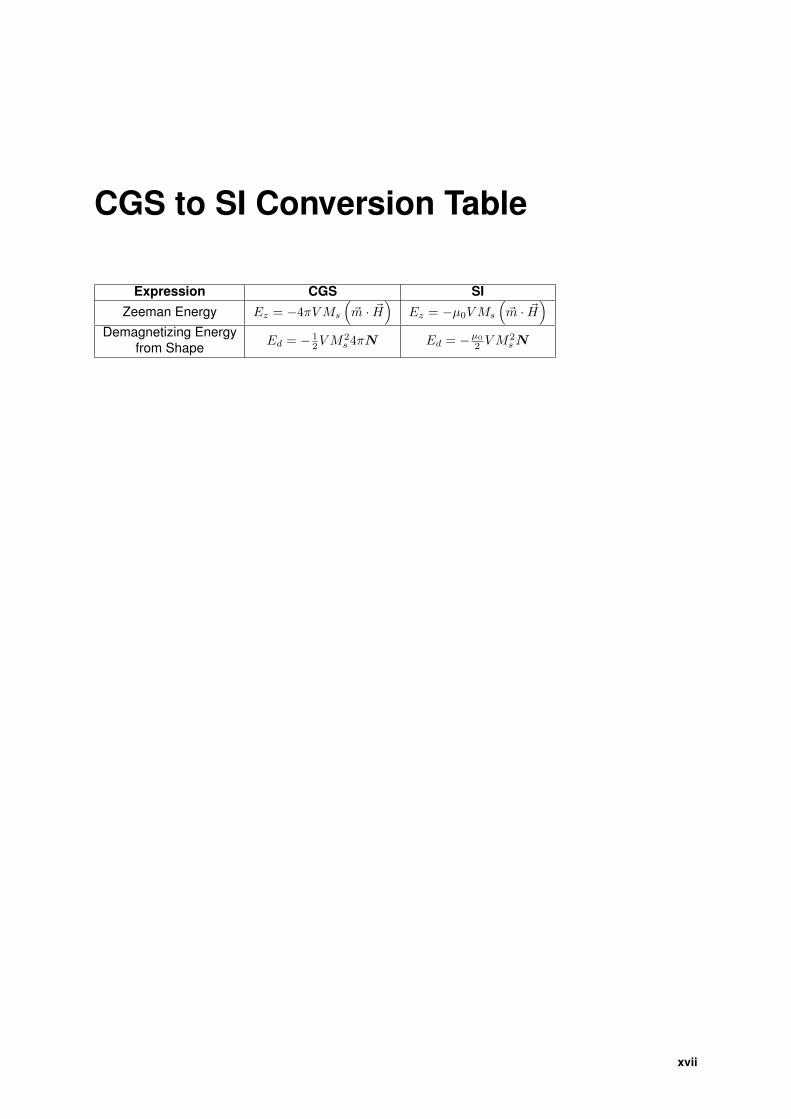
CGS to SI Conversion Table
Expression CGS SIZeeman Energy Ez = −4πVMs
(~m · ~H
)Ez = −µ0VMs
(~m · ~H
)Demagnetizing Energy
from Shape Ed = − 12VM
2s 4πN Ed = −µ0
2 VM2sN
xvii

Introduction
The conservation and transmission of information is one of the key features which have enabled
the human species to thrive throughout millennia. The ability to store the acquired knowledge and the
possibility to spread it has transformed us in the most resilient, versatile and dominant species in the
world. We currently live in a ”data-driven” era. With the advent of the Internet and a continuously
growing automation of all sectors of activity, data treatment and storage are two domains which require
more research and development in order to keep up with technology exponential growth.
Throughout the years, man has been developing more reliable, cheaper and denser memories. In
fact, the predictions of Moore’s law have been confirmed year after year with the exponential increase of
electronic components on a chip. Therefore, it urges the need for developments in downsize scalability
of memory devices. In addition, the universal memory demands a low production cost but also for data
to be stored and accessed in no time. Non-volatility is also a required criterion which consists in the
conservation of the stored data even when the power is off. This perfect memory would eliminate the
current drawbacks in nowadays memories which is the slow access to the stored data and its high prices.
Thus providing higher speed data manipulation at a low cost. The growing market for memories is of the
order 10-100×109e, stimulated by the ascent of the Big Data and the Internet of Things.
In the past few years, the Magnetoresistive Random Access Memory (MRAM) has become a po-
tential candidate and has attracted the attention of the largest companies of the industry of electronics
including Samsung, IBM, Toshiba and GlobalFoundries. Everspin Technologies is one of the first compa-
nies that has pushed the MRAM production to an industrial scale. Their most recent chips demonstrate
access times of 30ns and data retention larger than 20 years. Among the different types of MRAM, the
STT-MRAM has shown to be one of the most promising and competitive non-volatile memory technolo-
gies. Moreover, it has been appointed as one of the emerging technologies that can scale down to the
16 nm nod by the International Technology Roadmap for Semiconductors (ITRS). This device uses a
current induced effect, the spin transfer torque (STT), to switch the magnetization of the storage layer of
the key element of the MRAM, the magnetic tunnel junction (MTJ).
In this thesis, we further investigate one alternative to the current STT-MRAM based on single MTJ:
the double barrier magnetic tunnel junction (DBMTJ). This work carries on the first developments on
DBMTJs made during the thesis of P.-Y. Clement [1]. His most important result was the demonstration
of the possibility to modulate the STT amplitude in DBMTJs depending on the alignment of the mag-
netization of the two reference layers. Therefore, it enables a reduction of the power consumption in
the writing process and simultaneously allows for higher access speeds in the reading process. The
1

first objective of this thesis is to provide a better and deeper understanding of the damping-like and
field-like torques interplay on write and read mode on in-plane magnetized DBMTJs. Finally, we aimed
for the materials optimization of a DBMTJ with perpendicular anisotropy, as well as the demonstration
and investigation of STT in patterned sub-100nm perpendicular double barrier magnetic tunnel junctions
(p-DBMTJs).
This thesis is divided in five main chapters. In chapter 1, we recall the two most important physics
concepts behind the STT-MRAM which are the tunnel magnetoresistance and the spin transfer torque.
We present also a general overview about MRAM. Chapter 2 describes in more detail the fabrication
techniques required for the fabrication of nanometric DBMTJs and a brief description of the electric
characterization performed on our samples. In chapter 3 we study the STT in DBMTJs with in-plane
anisotropy with measurements performed with DC current and voltage pulse measurements performed.
In addition, macrospin simulations help to get a deeper insight on the role of each damping-like and
field-like torques’ components and comparisons are made with the experimental results. Chapter 4
focuses on the materials development of a new functional top reference compatible with [Co/Pt]-based
multilayers as well as an optimization of the stack of DBMTJ with perpendicular anisotropy. Finally,
chapter 5 shows the results of STT in patterned sub-300nm perpendicular DBMTJs in write and read
modes and the analysis of unexpected phase diagrams obtained for this type of devices.
2

1Theoretical Concepts
Contents1.1 Introduction . . . . . . . . . . . . . . . . . . . . . . . . . . . . . . . . . . . . . . . . . . 41.2 Spin Polarized Tunneling . . . . . . . . . . . . . . . . . . . . . . . . . . . . . . . . . . . 41.3 Spin Transfer Torque . . . . . . . . . . . . . . . . . . . . . . . . . . . . . . . . . . . . . 121.4 Phase Diagram of Magnetic Tunnel Junctions . . . . . . . . . . . . . . . . . . . . . . . 181.5 Magnetoresistive Random Access Memories (MRAM) . . . . . . . . . . . . . . . . . . 22
3
1.1 Introduction
In the last decades, the need for even larger storage capacity has constantly driven storage tech-
nology towards further miniaturization. Prior to 1990, all hard-disk drives used the same inductive head
for reading and writing. Further downscaling the size of stored bits caused signal amplitude reduction,
which necessitated more powerful detectors. Solving this problem required a technological disruption.
Anisotropic magnetoresistance (AMR) effect proved to be the successful solution. The first magnetore-
sistive read-head was implemented in 1990 by IBM. This new technology used an effect discovered by
Thomson in 1857: in ferromagnetic metals, the electrical resistance depends on the direction of the
current with respect to the magnetization direction. The magnetoresistance ratio (MR), defined as the
normalized resistance contrast between maximum and minimum resistance, varies between 0.1 % to a
maximum of 5% [2] at room temperature in usual ferromagnetic metals and alloys.
In that context, the most remarkable event was the discovery of giant magnetoresistance (GMR)
in magnetic multilayered structures, simultaneously by the groups of A. Fert [3] and P. Grunberg [4] in
1988. For this great contribution to science, they were awarded the Nobel Prize in Physics, in 2007.
It was observed that the resistance of antiferromagnetically coupled Fe/Cr/Fe multilayers dropped by
80 %, at 4.2 K, upon application of an applied magnetic field, an effect attributed to spin-dependent
scattering of conduction electrons at the interfaces between the Fe/Cr layer.
The GMR discovery opened a new research domain on spin-dependent transport, called spintronics
[5], since it combines both magnetism and electronics. By contrast to common electronics, spintronics
uses not only the charge of the electron but its spin to operate the device. The applicative potential of the
GMR was so important that less than 10 years elapsed between the discovery of the effect and the first
implementattion of GMR read-head in a product. More precisely, it was the invention of the spin valve [6]
that ramped up the usage of MR-based devices in industry. In fact, spin valves replaced AMR-based
HDD read heads in 1997. However, their low resistance (incompatible with CMOS access transistors)
and MR (20 to 30% in optimized CPP1 geometry spin valves [7]) do not make GMR devices suitable for
applications as magnetic memory. The solution would pass by the magnetic tunnel junction (MTJ) which
demonstrated much higher MR ratios [8] at room temperature.
1.2 Spin Polarized Tunneling
1.2.1 Spin polarized current
In quantum mechanics, electron has a new property, the spin (s) which corresponds to its intrinsic
angular momentum. Whereas the orbital angular momentum is related to the operator ~L, the spin is
associated to operator ~S. The electron spin is characterized by a quantum number s = ±1/2 with two
available states called ”spin-up”(s = 1/2) and ”spin-down” (s = −1/2). The electron spin gives rise to a
magnetic moment ~µ = (g e/2me) ~S where g ≈ 2 is the Lande factor, e andme are the electron charge and
mass, respectively. Thus the electron magnetic moment is close to the Bohr magneton µB = e ~/2me.
1Current Perpendicular to Plane
4
In most solids, the discrete magnetic moments (on each atom) do not interact with each other (para-
magnetism and diamagnetism). However, in some cases, one observes a magnetic order. In ferro-
magnets, the interaction between magnetic moments, called exchange, stems from the combined effect
of Coulomb interaction and Pauli exclusion principle. This exchange results in a parallel alignment of
discrete moments, creating a non-null magnetic moment per unit volume (or magnetization M ), even in
the absence of magnetic field.
A precise description of the electronic properties of ferromagnetic metals (Fe, Co, Ni) must take
band theory into consideration. These studies show hybridization between the spin polarized d valence
band and s conduction band [9], resulting in a high spin polarization (about 30-40 %) of the conduction
electrons. Nevertheless, a simplified model (Stoner Model [10]) is widely used: it considers the interplay
between exchange and kinetic energy of free electrons. The exchange energy forces the electrons
to have the same spin state, though they need to occupy higher energy states, which increases their
kinetic energy. If the gain in kinetic energy does not compensate the reduction of exchange energy
U , a ferromagnetic order appears. Ferromagnetism occurs if the Stoner criterion ρ(EF )U > 1 is met,
where ρ(EF ) is the density of states (DOS) at Fermi level and U the exchange energy. Within this
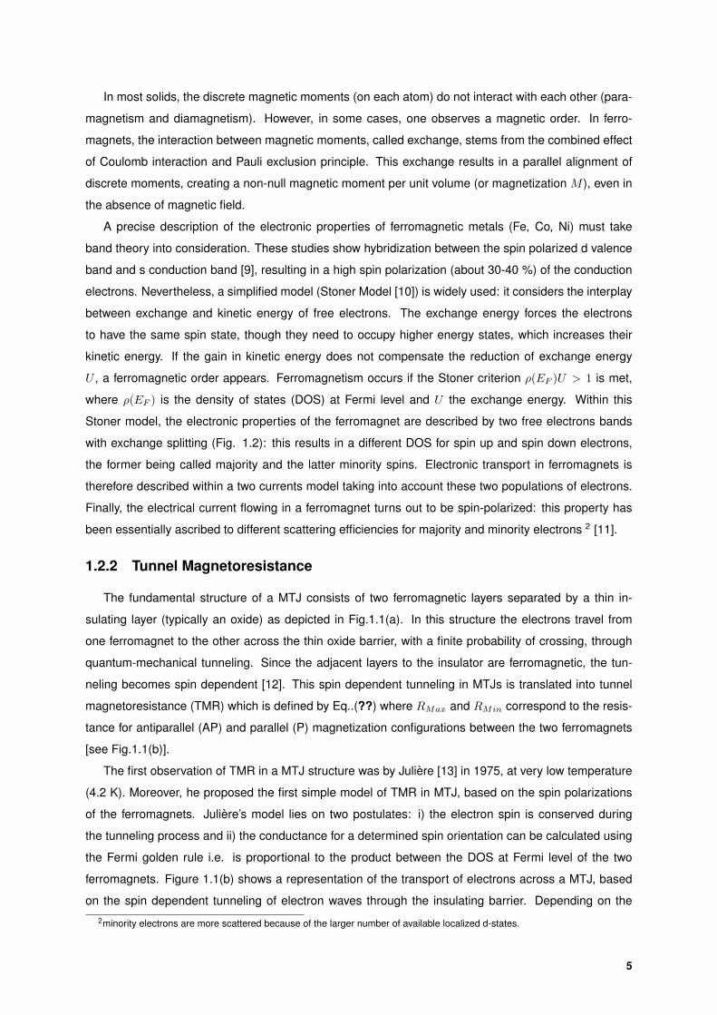
Stoner model, the electronic properties of the ferromagnet are described by two free electrons bands
with exchange splitting (Fig. 1.2): this results in a different DOS for spin up and spin down electrons,
the former being called majority and the latter minority spins. Electronic transport in ferromagnets is
therefore described within a two currents model taking into account these two populations of electrons.
Finally, the electrical current flowing in a ferromagnet turns out to be spin-polarized: this property has
been essentially ascribed to different scattering efficiencies for majority and minority electrons 2 [11].
1.2.2 Tunnel Magnetoresistance
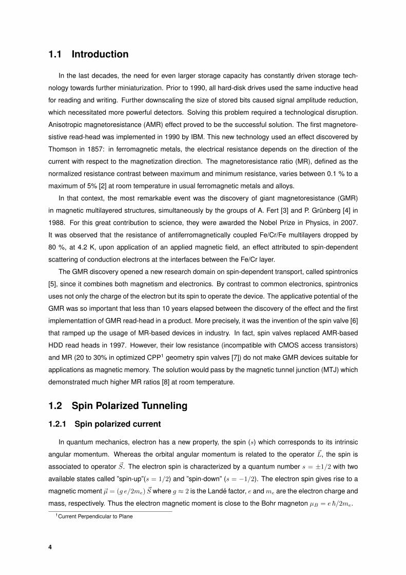
The fundamental structure of a MTJ consists of two ferromagnetic layers separated by a thin in-
sulating layer (typically an oxide) as depicted in Fig.1.1(a). In this structure the electrons travel from
one ferromagnet to the other across the thin oxide barrier, with a finite probability of crossing, through
quantum-mechanical tunneling. Since the adjacent layers to the insulator are ferromagnetic, the tun-
neling becomes spin dependent [12]. This spin dependent tunneling in MTJs is translated into tunnel
magnetoresistance (TMR) which is defined by Eq..(??) where RMax and RMin correspond to the resis-
tance for antiparallel (AP) and parallel (P) magnetization configurations between the two ferromagnets
[see Fig.1.1(b)].
The first observation of TMR in a MTJ structure was by Juliere [13] in 1975, at very low temperature
(4.2 K). Moreover, he proposed the first simple model of TMR in MTJ, based on the spin polarizations
of the ferromagnets. Juliere’s model lies on two postulates: i) the electron spin is conserved during
the tunneling process and ii) the conductance for a determined spin orientation can be calculated using
the Fermi golden rule i.e. is proportional to the product between the DOS at Fermi level of the two
ferromagnets. Figure 1.1(b) shows a representation of the transport of electrons across a MTJ, based
on the spin dependent tunneling of electron waves through the insulating barrier. Depending on the2minority electrons are more scattered because of the larger number of available localized d-states.
5
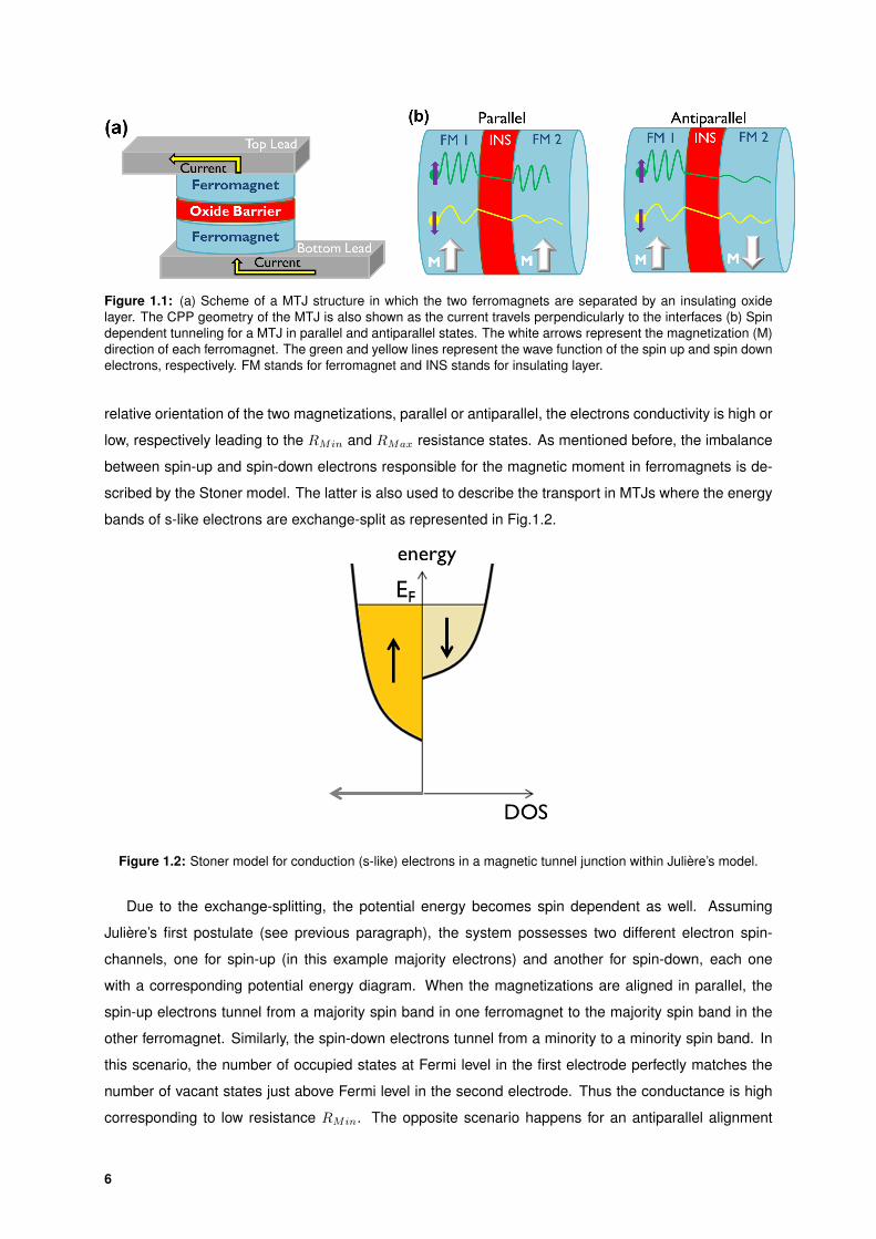
Figure 1.1: (a) Scheme of a MTJ structure in which the two ferromagnets are separated by an insulating oxidelayer. The CPP geometry of the MTJ is also shown as the current travels perpendicularly to the interfaces (b) Spindependent tunneling for a MTJ in parallel and antiparallel states. The white arrows represent the magnetization (M)direction of each ferromagnet. The green and yellow lines represent the wave function of the spin up and spin downelectrons, respectively. FM stands for ferromagnet and INS stands for insulating layer.
relative orientation of the two magnetizations, parallel or antiparallel, the electrons conductivity is high or
low, respectively leading to the RMin and RMax resistance states. As mentioned before, the imbalance
between spin-up and spin-down electrons responsible for the magnetic moment in ferromagnets is de-
scribed by the Stoner model. The latter is also used to describe the transport in MTJs where the energy
bands of s-like electrons are exchange-split as represented in Fig.1.2.
Figure 1.2: Stoner model for conduction (s-like) electrons in a magnetic tunnel junction within Juliere’s model.
Due to the exchange-splitting, the potential energy becomes spin dependent as well. Assuming
Juliere’s first postulate (see previous paragraph), the system possesses two different electron spin-
channels, one for spin-up (in this example majority electrons) and another for spin-down, each one
with a corresponding potential energy diagram. When the magnetizations are aligned in parallel, the
spin-up electrons tunnel from a majority spin band in one ferromagnet to the majority spin band in the
other ferromagnet. Similarly, the spin-down electrons tunnel from a minority to a minority spin band. In
this scenario, the number of occupied states at Fermi level in the first electrode perfectly matches the
number of vacant states just above Fermi level in the second electrode. Thus the conductance is high
corresponding to low resistance RMin. The opposite scenario happens for an antiparallel alignment
6
between magnetizations. The majority band electrons from one ferromagnet tunnel to the minority band
of the other ferromagnet and vice versa. The conductance is thus much lower corresponding to the high
resistance RMax.
Figure 1.3: Electronic density of states of the ferromagnetic electrodes in a MTJ with magnetizations aligned (a)parallel and (b) antiparallel. EF is the energy at Fermi level.
The conductance for the parallel (GP ) and antiparallel (GAP ) magnetic states can be expressed in
terms of the DOS for spin-up (+) and spin-down (-) electrons, for each of the ferromagnets 3 [14]:
GP , GAP ∝ ρ+1 ρ
+2 + ρ−1 ρ
−2 (1.1)
By considering Fig.1.3(a), GP is given by:
GP = α [ρ1ρ2 + (1− ρ1) (1− ρ2)] (1.2)
where α is a proportionality constant. In antiparallel alignment of the magnetizations, as shown in
Fig.1.3(b), the majority and minority bands interchange spins. Therefore, the conductance for this state
is given by:
GAP = α [ρ1 (1− ρ2) + ρ2 (1− ρ1)] (1.3)
The difference in conductance (∆G) between the parallel and antiparallel magnetic states is thus
given by the following:
∆G = α [(2ρ1 − 1) (2ρ2 − 1)] = αP1P2 (1.4)
where P1 and P2 are, respectively, the polarizations in FM1 and FM2 as defined below:
Pi =ρ↑i − ρ
↓i
ρ↑i + ρ↓i(1.5)
where i = 1 or 2.3+ and - are chosen to code for the spin values whereas ↑ and ↓ code for majority and minority spins.
7
The combination of equations (??),(1.2) and (1.3) results on the Juliere’s formula for the TMR, which
relates the TMR with the effective spin polarization (P1 and P2) of the two ferromagnets:
TMR =RAP −RP
RP=G−1AP −G
−1P
G−1P
=2P1P2
1− P1P2. (1.6)
The model conceived by Juliere was later refined by Slonczewski in 1989 where an angular de-
pendence of TMR was included. This upgraded model was the first to consider the FM/Insulator/FM
trilayer as a single quantum mechanical system [15]. The model considers a rectangular barrier of fi-
nite height contrary to Julliere’s model.The ferromagnets are characterized by parabolic bands of free
electrons whose momentum is conserved when flowing across the MTJ. The main change with respect
to Julliere’s model is a new definition of the spin polarization that takes into account the barrier height.
Finally, the MTJ conductance expressed as a function of the angle θ between the magnetizations of
each ferromagnetic layer is given by:
G(θ) =GP +GAP
2+GP −GAP
2cos θ (1.7)
1.2.2.A TMR dependence on the ferromagnet spin polarization
The development of magnetic memories and/or sensors encouraged the pursuit for higher TMR
values in MTJs. The first generation of MTJs used amorphous barriers of AlOx which never showed TMR
values superior to 70% at room temperature. Equation ((1.6)) has been used to infer the spin polarization
of several ferromagnetic alloys, using experimentally acquired TMR as input value. Commonly used 3d
ferromagnetic metals and alloys based on Ni, Co or Fe present spin polarization values (at T < 40 K)
that range from 0.35 for Ni [16] up to 0.53 for Co72Fe20B8 [17] and 0.55 for Ni40Fe60 [18].
Juliere’s model (Equation (1.6)) suggests that TMR should increase with increasing spin polarization
of the ferromagnetic layers. Therefore, the use of more exotic materials, such as half-metals ferromag-
nets, has been exploited in order to increase TMR. Such materials have only one spin band occupied
at Fermi level which results in a spin polarization close to unit [19]. Very low temperatures studies per-
formed by Bowen [20] and Sakuraba [21] have demonstrated record high TMR, respectively, 1800% (at
4 K) in La2/3Sr1/3MnO3/SrTiO3/La2/3Sr1/3MnO3 and 570% (at 2 K) in Co2MnSi/AlO/Co2MnSi. Never-
theless, these extremely high TMR values succumbed at room temperature.
1.2.2.B TMR dependence on the tunnel barrier: the Butler’s model
A breakthrough was obtained in the pusuit of high TMR at room temperature by using cristalline MgO
(001) as a tunnel barrier. At present time, the highest TMR value reported at room temperature is of
500% [22], obtained for MTJs with 3d ferromagnetic alloys based on (Co26Fe76)80B20/MgO/(Co26Fe76)80B20.
The use of MgO crystalline barriers allows a quite efficient spin filtering enabling high TMR, comparable
to the use of half-metal as MTJ electrodes. The corresponding tunneling theory was first proposed by
Butler et al. in 2001 [23], based on the analysis of band diagrams of body-centered cubic (bcc) Fe (001
oriented). This model is based on Bloch waves: the electrons flowing through a crystalline structure are
8
under the effect of a periodic potential whose origin is the electric field generated by the atoms of the
matrix. These Bloch waves are deeply dependent of the structure of the material, therefore in a crystal,
dependent on its symmetries. In bcc (001 oriented) structures, there are four Bloch states that describe
the transport: ∆1, ∆2, ∆′2 and ∆5. Moreover, majority and minority electrons have different Bloch states
symmetries. In the case of bcc Fe (001 oriented), for majority electrons, only ∆1 Bloch state is above
EF associated to a high Fermi velocity. Meanwhile, for minority electrons, ∆′2 and ∆5 bands intersect
the Fermi level energy, though with a much lower Fermi velocity. Another important aspect is the energy
gap between the ∆1 bands for majority and minority electrons: the ∆1 band for minority electrons is
completely below EF , thus the band diagram is comparable to half-metals. Therefore, a quite efficient
spin filtering of ∆1 Bloch states is expected.
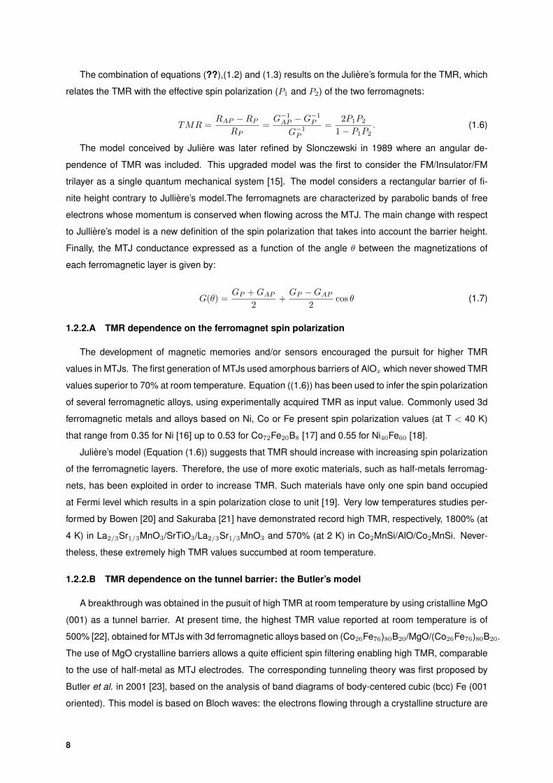
Figure 1.4: Illustration of tunneling through (a) an amorphous barrier (Al2O3) and (b) crystalline barrier [MgO (001)].Image taken from [24].
Therefore the tunneling processes in an amorphous barrier and a crystalline one are quite different,
which explains the TMR difference in MTJs using one or the other barrier. The tunneling process in
a MTJ with an Al2O3 barrier is illustrated in Fig.1.4(a). The top ferromagnet is considered to be Fe
(001) which, as mentioned in the previous paragraph, presents Bloch states with different symmetries of
wave functions. However, as the oxide barrier is amorphous, no crystallographic symmetry is present,
and Bloch states of different symmetries may couple with evanescent states in the amorphous barrier,
resulting in finite (yet different) tunneling probabilities, which is usually called incoherent tunneling. In
this case, Bloch states with positive (∆1) and negative (∆2 and ∆5) spin polarization contribute to the
tunneling current, thus the net spin polarization of the electrode is reduced, resulting in low (< 70%)
TMR values.
For MTJs with crystalline MgO (001 oriented) barriers, the tunneling is handled by evanescent waves
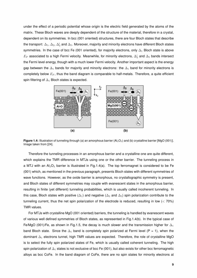
of various well defined symmetries of Bloch states, as represented in Fig.1.4(b). In the typical case of
Fe/MgO (001)/Fe, as shown in Fig.1.5, the decay is much slower and the transmission higher for ∆1
band Bloch state. Since the ∆1 band is completely spin polarized at Fermi level (P = 1), when the
dominant ∆1 electrons tunnel, high TMR values are expected. Therefore, the role of crystalline MgO
is to select the fully spin polarized states of Fe, which is usually called coherent tunneling. The high
spin polarization of ∆1 states is not exclusive of bcc Fe (001), but also exists for other bcc ferromagnetic
alloys as bcc CoFe. In the band diagram of CoFe, there are no spin states for minority electrons at
9
Figure 1.5: Density of Bloch states in Fe/MgO/Fe, for (Top Left) majority, (Top Right) minority electrons. (Bottom)Density of states for an antiparallel alignment between the magnetizations of the Fe electrodes. Image takenfrom [25]
Fermi level but only one ∆1 Bloch state for majority electrons [26], which increases the spin filtering
effect and consequently TMR. In the case of CoFeB/MgO/CoFeB MTJs (the type of structures used
in this thesis), as-grown CoFeB layer is amorphous whereas MgO is polycrystalline. Then annealing
induces the migration of B towards its getter (Ta layer) and CoFe crystallizes, starting from the MgO
barrier that serves as a crystallization germ.
Comparatively to Al2O3, MgO barriers based MTJs present higher TMR values. In 2004, Yuasa
et al. [27] reported 88% TMR at room temperature for fully epitaxial Fe/MgO/Fe MTJ deposited by
molecular beam epitaxy (MBE). The experimental results rapidly improved to ratios up to 200% [28].
Nevertheless, junctions prepared by sputtering techniques have been preferred and developed. Since
they present a higher TMR ratio and the sputtering deposition is more convenient for industrial purposes.
With a proper tuning of the thickness and compositions of the CoFeB electrodes, TMR as high as 500%
was reported [22] at room temperature.
1.2.3 TMR in double barrier MTJ
The first reports of magnetic structures using two or more barriers date from early 1990’s with a
theoretical study on spin polarized tunneling and MR on double barrier tunnel junctions [29] and ex-
perimental results with nonmagnetic triple barrier junctions [30] to explore resonant tunneling. Due to
the challenging deposition and fabrication processes involved, the first experimental results on planar
double barrier MTJ were only published in 1998 by F. Montaigne et al. [31] for Co/Al2O3/Co/Al2O3/NiFe.
10
They demonstrated that the decay of MR with bias voltage is lower for a double barrier MTJ than for a
similar single barrier one. In fact, TMR would drop from maximum (at zero bias) to half, for a voltage
4x lower in a double barrier structure than in a single barrier. This result was one of the first hints, sug-
gesting that a more complex behavior than sequential tunneling was involved and/or coupled to some
coherent/resonant tunneling.
The structures of the form FM/Oxide/NM or FM/Oxide/FM were also very attractive due to the pos-
sibility of formation of well defined quantum well states in the middle metal layer sandwiched between
the two oxide layers. The first theoretical studies on the coherent tunneling regime of this type of struc-
tures with symmetric barriers showed that spin polarized resonant tunneling leads to improved TMR
values [32]. However, when the properties of one barrier are different of the other, not only TMR was
enhanced but also a new concept of spin diode has been theoretically proposed [33] where the current-
voltage (I-V) diode features depend on the magnetic configuration of the ferromagnetic layers which
compose the double MTJ. The concept would be later validated experimentally by A. Iovan et al. [34].
Unfortunately, the observation of direct spin-dependent resonant tunneling is rather challenging since
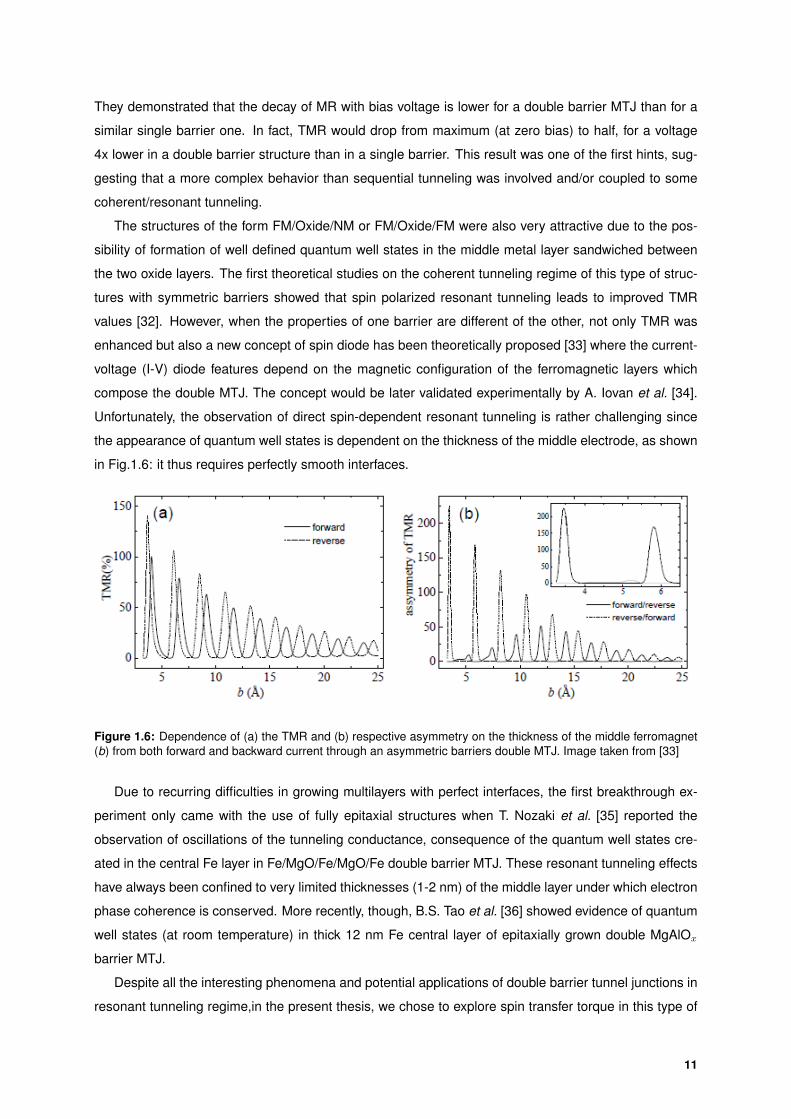
the appearance of quantum well states is dependent on the thickness of the middle electrode, as shown
in Fig.1.6: it thus requires perfectly smooth interfaces.
Figure 1.6: Dependence of (a) the TMR and (b) respective asymmetry on the thickness of the middle ferromagnet(b) from both forward and backward current through an asymmetric barriers double MTJ. Image taken from [33]
Due to recurring difficulties in growing multilayers with perfect interfaces, the first breakthrough ex-
periment only came with the use of fully epitaxial structures when T. Nozaki et al. [35] reported the
observation of oscillations of the tunneling conductance, consequence of the quantum well states cre-
ated in the central Fe layer in Fe/MgO/Fe/MgO/Fe double barrier MTJ. These resonant tunneling effects
have always been confined to very limited thicknesses (1-2 nm) of the middle layer under which electron
phase coherence is conserved. More recently, though, B.S. Tao et al. [36] showed evidence of quantum
well states (at room temperature) in thick 12 nm Fe central layer of epitaxially grown double MgAlOx
barrier MTJ.
Despite all the interesting phenomena and potential applications of double barrier tunnel junctions in
resonant tunneling regime,in the present thesis, we chose to explore spin transfer torque in this type of
11

structures, envisaging its application as STT-MRAM. The first ever double MTJ STT-MRAM was demon-
strated by Z. Diao et al. [37] in 2007 for double MgO barriers exhibiting 70% maximum TMR values and
with in-plane magnetized ferromagnetic layers. Improvements in the sputtering deposition tools allowed
an increase in TMR for the double MTJ with values overcoming 200% [38, 39]. The last generation of
double MTJ has perpendicular magnetic anisotropy and until the present date, G. Hu et al. [40] and Z.
Duan et al. [41] have demonstrated STT p-DBMTJ, respectively, with 114% and 150% maximum TMR
ratios.
1.3 Spin Transfer Torque
As mentioned in the previous section, current is spin polarized when it passes through a ferromag-
netic material. Indeed, it can be viewed as an effect of the magnetization of the ferromagnet onto the
electrons spin-angular momentum. The spin transfer torque (STT) can be simply understood as the
reciprocal action: a spin polarized current passing through a ferromagnet acts on its magnetization.
First, we present the macroscopic picture of the mechanism of STT considering a macrospin behavior
of the system. The simplest example is to consider a trilayer structure composed of FM1/NM/FM2 where
NM is a thin non-magnetic spacer 4, as shown in Fig.1.7. Considering that electrons first cross through
FM1 and flow towards FM2, in the first ferromagnet, these electrons get spin polarized along the direction
of the magnetization ~M1. Whereas the only electrons coming out of FM2 are spin polarized along ~M2.
If ~M1 is not collinear with ~M2, the latter should necessarily absorb a part of angular moment carried
by conduction electrons polarized in FM1. The spin of the electrons traveling through FM2 should
align along its magnetization as this one exerts a torque on their magnetic moments. Reciprocally, the
conduction electrons must apply an equal, but opposite, torque on ~M2 which induces precession, or if
strong enough, reverses FM2 magnetization.
Figure 1.7: a) Schematics of the trilayer structure FM1/NM/FM2 where the corresponding magnetizations ~M1 and~M2 are misaligned by an angle θ. b) Illustration of the in-plane torques applied on each of the magnetizations. ~µ1,~µ2 and ~T represent, respectively, the ingoing, outgoing and transferred magnetic moments. Adapted from [42].
Still considering the same trilayer structure (Fig.1.7), the incident electrons in FM1 possess a mag-
netic moment ~µ1 ‖ ~M1 and the electrons departing from FM2 a magnetic moment ~µ2 ‖ ~M2. The
non-collinearity between the two moments implies that some magnetic moment is transferred to the
system. However, this transferred moment per time unit (i.e. torque) can change the direction of the4A metallic layer in the case of a spin-valve or an oxide in the case of a MTJ
12
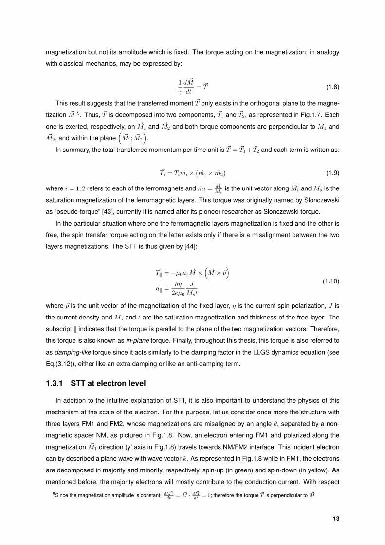
magnetization but not its amplitude which is fixed. The torque acting on the magnetization, in analogy
with classical mechanics, may be expressed by:
1
γ
d ~M
dt= ~T (1.8)
This result suggests that the transferred moment ~T only exists in the orthogonal plane to the magne-
tization ~M 5. Thus, ~T is decomposed into two components, ~T1 and ~T2, as represented in Fig.1.7. Each
one is exerted, respectively, on ~M1 and ~M2 and both torque components are perpendicular to ~M1 and~M2, and within the plane
(~M1; ~M2
).
In summary, the total transferred momentum per time unit is ~T = ~T1 + ~T2 and each term is written as:
~Ti = Ti ~mi × (~m1 × ~m2) (1.9)
where i = 1, 2 refers to each of the ferromagnets and ~mi =~Mi
Msis the unit vector along ~Mi and Ms is the
saturation magnetization of the ferromagnetic layers. This torque was originally named by Slonczewski
as ”pseudo-torque” [43], currently it is named after its pioneer researcher as Slonczewski torque.
In the particular situation where one the ferromagnetic layers magnetization is fixed and the other is
free, the spin transfer torque acting on the latter exists only if there is a misalignment between the two
layers magnetizations. The STT is thus given by [44]:
~T‖ = −µ0a‖ ~M ×(~M × ~p
)a‖ =
~η2eµ0
J
Mst
(1.10)
where ~p is the unit vector of the magnetization of the fixed layer, η is the current spin polarization, J is
the current density and Ms and t are the saturation magnetization and thickness of the free layer. The
subscript ‖ indicates that the torque is parallel to the plane of the two magnetization vectors. Therefore,
this torque is also known as in-plane torque. Finally, throughout this thesis, this torque is also referred to
as damping-like torque since it acts similarly to the damping factor in the LLGS dynamics equation (see
Eq.(3.12)), either like an extra damping or like an anti-damping term.
1.3.1 STT at electron level
In addition to the intuitive explanation of STT, it is also important to understand the physics of this
mechanism at the scale of the electron. For this purpose, let us consider once more the structure with
three layers FM1 and FM2, whose magnetizations are misaligned by an angle θ, separated by a non-
magnetic spacer NM, as pictured in Fig.1.8. Now, an electron entering FM1 and polarized along the
magnetization ~M1 direction (y’ axis in Fig.1.8) travels towards NM/FM2 interface. This incident electron
can by described a plane wave with wave vector k. As represented in Fig.1.8 while in FM1, the electrons
are decomposed in majority and minority, respectively, spin-up (in green) and spin-down (in yellow). As
mentioned before, the majority electrons will mostly contribute to the conduction current. With respect
5Since the magnetization amplitude is constant, dM2
dt= ~M · d ~M
dt= 0; therefore the torque ~T is perpendicular to ~M
13
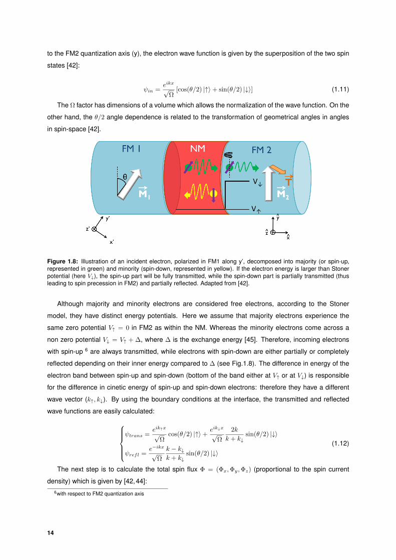
to the FM2 quantization axis (y), the electron wave function is given by the superposition of the two spin
states [42]:
ψin =eikx√
Ω[cos(θ/2) |↑〉+ sin(θ/2) |↓〉] (1.11)
The Ω factor has dimensions of a volume which allows the normalization of the wave function. On the
other hand, the θ/2 angle dependence is related to the transformation of geometrical angles in angles
in spin-space [42].
Figure 1.8: Illustration of an incident electron, polarized in FM1 along y’, decomposed into majority (or spin-up,represented in green) and minority (spin-down, represented in yellow). If the electron energy is larger than Stonerpotential (here V↓), the spin-up part will be fully transmitted, while the spin-down part is partially transmitted (thusleading to spin precession in FM2) and partially reflected. Adapted from [42].
Although majority and minority electrons are considered free electrons, according to the Stoner
model, they have distinct energy potentials. Here we assume that majority electrons experience the
same zero potential V↑ = 0 in FM2 as within the NM. Whereas the minority electrons come across a
non zero potential V↓ = V↑ + ∆, where ∆ is the exchange energy [45]. Therefore, incoming electrons
with spin-up 6 are always transmitted, while electrons with spin-down are either partially or completely
reflected depending on their inner energy compared to ∆ (see Fig.1.8). The difference in energy of the
electron band between spin-up and spin-down (bottom of the band either at V↑ or at V↓) is responsible
for the difference in cinetic energy of spin-up and spin-down electrons: therefore they have a different
wave vector (k↑, k↓). By using the boundary conditions at the interface, the transmitted and reflected
wave functions are easily calculated:
ψtrans =
eik↑x√Ω
cos(θ/2) |↑〉+eik↓x√
Ω
2k
k + k↓sin(θ/2) |↓〉
ψrefl =e−ikx√
Ω
k − k↓k + k↓
sin(θ/2) |↓〉(1.12)
The next step is to calculate the total spin flux Φ = (Φx,Φy,Φz) (proportional to the spin current
density) which is given by [42,44]:6with respect to FM2 quantization axis
14
Φ+ = Φx + iΦz = i
~2
2m
(ψ↓dψ∗↑dx− ψ∗↑
dψ↓dx
)Φy =
~2
2mIm
(ψ∗↑dψ↑dx− ψ∗↓
dψ↓dx
) (1.13)
By applying Eq.(1.13) onto equations (1.11) and (1.12), the spin flux becomes:
Φin =~2
2mΩ(k sin θx+ k cos θy)
Φtrans =~2
2mΩk sin θ (cos [(k↑ − k↓)x] x− sin [(k↑ − k↓)x] z)
+~2
2mΩ
[k cos2(θ/2)− k↓
(2k
k + k↓
)2
sin2(θ/2)
]y
Φrefl =~2
2mΩk
(k − k↓k + k↓
)2
sin2(θ/2)y
(1.14)
One of the first conclusions of the analysis of eqs.(1.14) is that if the energy of incoming electrons is
larger than ∆, then at the NM/FM2 interface the spin flux is continuous: Φin + Φrefl = Φtrans. Another
one concerns the reflected electrons. It is possible to observe that the reflected spin current density is
only along y which means that transverse [in the (x, z) plane] spin current is zero. This means that these
components of the incoming spin flux were fully transmitted in the form of two oscillations with a phase
shift of π2 and period 2π
k↑−k↓ . In fact, this result is a direct consequence of the zero potential ”felt” by
spin-up electrons in the y direction. Thus, the real torque exerted on ~M2 only exists on the (x, z) plane
which means that the torque deposited is orthogonal to the magnetization. In addition, the reflected
spin current (represented in yellow going backwards in Fig.1.8) results from the spin-down electrons
which are partly reflected on the potential barrier. When these ”recoil” electrons enter FM1 they start to
precess along the local field and transfer their moment to ~M1. Therefore, these reflected electrons are
responsible for a ”back-torque” on FM1 magnetization.
In summary, the torques exerted by incoming electrons in FM2 and the reflected electrons in FM1
have the same direction. Electrons spin polarized along ~M1 try to tilt ~M2 along their direction, while the
reflected electrons which are polarized in antiparallel to ~M2 try to tilt ~M1 away from the latter.
1.3.2 Field-like Torque
In 1993, M.D. Stiles [46] explained that the oscillating exchange coupling observed in magnetic het-
erostructures (with same structure as FM1/NM/FM2) is created by conduction electrons, which are be-
low the Fermi energy level, traveling back and forth across the structure. Therefore, this RKKY coupling
would exist, even in the absence of a bias current applied to the system. Although the electrons travel-
ing from both electrodes do not actually create a charge current, whenever a misalignment between the
magnetizations of the two ferromagnets exists, a non negligible spin current appears. This spin current
acts on the magnetizations in the form of a transverse torque.
Similarly to the case of the damping-like torque, the origin of this torque is better understood if ana-
lyzed at electron level. Again, we consider an incident electron traveling towards the NM/FM2 interface.
Since the electron is locally affected by the exchange field, it is expected, from the induced precession,
15
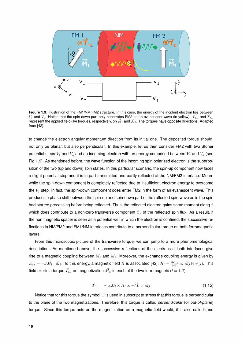
Figure 1.9: Illustration of the FM1/NM/FM2 structure. In this case, the energy of the incident electron lies betweenV↑ and V↓. Notice that the spin-down part only penetrates FM2 as an evanescent wave (in yellow). ~T1⊥ and ~T2⊥represent the applied field-like torques, respectively, on ~M1 and ~M2. The torques have opposite directions. Adaptedfrom [42].
to change the electron angular momentum direction from its initial one. The deposited torque should,
not only be planar, but also perpendicular. In this example, let us then consider FM2 with two Stoner
potential steps V↑ and V↓ and an incoming electron with an energy comprised between V↑ and V↓ (see
Fig.1.9). As mentioned before, the wave function of the incoming spin polarized electron is the superpo-
sition of the two (up and down) spin states. In this particular scenario, the spin-up component now faces
a slight potential step and it is in part transmitted and partly reflected at the NM/FM2 interface. Mean-
while the spin-down component is completely reflected due to insufficient electron energy to overcome
the V↓ step. In fact, the spin-down component does enter FM2 in the form of an evanescent wave. This
produces a phase shift between the spin-up and spin-down part of the reflected spin-wave as is the spin
had started precessing before being reflected. Thus, the reflected electron gains some moment along x
which does contribute to a non-zero transverse component Φx of the reflected spin flux. As a result, if
the non magnetic spacer is seen as a potential well in which the electron is confined, the successive re-
flections in NM/FM2 and FM1/NM interfaces contribute to a perpendicular torque on both ferromagnetic
layers.
From this microscopic picture of the transverse torque, we can jump to a more phenomenological
description. As mentioned above, the successive reflections of the electrons at both interfaces give
rise to a magnetic coupling between ~M1 and ~M2. Moreover, the exchange coupling energy is given by
Eex = −J ~M1 · ~M2. To this energy, a magnetic field ~H is associated [42]: ~Hi = ∂Eex∂ ~Mi
∝ ~Mj (i 6= j). This
field exerts a torque ~Ti⊥ on magnetization ~Mi, in each of the two ferromagnets (i = 1, 2):
~Ti⊥ = −γ0~Mi × ~Hi ∝ − ~Mi × ~Mj (1.15)
Notice that for this torque the symbol ⊥ is used in subscript to stress that this torque is perpendicular
to the plane of the two magnetizations. Therefore, this torque is called perpendicular (or out-of-plane)
torque. Since this torque acts on the magnetization as a magnetic field would, it is also called (and
16

specially throughout the present thesis) field-like torque.
Finally, the perpendicular torque has yet a quite interesting property [47]: ~T1⊥ + ~T2⊥ = 0. Due to the
conservation of angular momentum, the two torques are equal but opposite, thus ~T1⊥ = −~T2⊥.
1.3.3 STT in Magnetic Tunnel Junctions
We have demonstrated above the general results of both types of torques existing in a magnetic
heterostructure when under the effect of spin currents. Although the damping-like torque ~T‖ = a‖ ~M ×(~M × ~p
)and the field-like torque ~T⊥ = a⊥ ~M × ~p formulas remain valid in all systems, the prefactors a‖
and a⊥ are not the same for MTJ as for general metallic systems (ex. spin-valve).
The calculation of these prefactors has been studied by various groups, always taking into consid-
eration that spin transfer torque is directly associated with spin current density Jspin by ~T = ~∇Jspinand that it is directly dependent on the characteristics of the ferromagnets composing the MTJ. Several
approaches have been used in order to have a reliable description of STT in MTJs: diffusion theory by
means of transmission/reflexion matrices at the interfaces [48, 49] or even the use of Green functions
within the Keldysh formalism [50, 51]. These studies have allowed the demonstration of the planar and
perpendicular torques dependencies with applied voltage:
~T‖(V ) =(a1V + a2V
2)~M ×
(~M × ~p
)(1.16)
~T⊥(V ) =(b0 + b2V
2)~M × ~p (1.17)
where the ai and bi (i = 0, 1, 2) are parameters which depend on the nature of the ferromagnetic elec-
trodes. In MTJs, the b0 term does not depend on voltage and it is called interlayer exchange coupling
(IEC) [15]. The positive or negative sign of the IEC is correlated, respectively, to a ferromagnetic or
antiferromagnetic coupling between the FM layers adjacent to the tunnel barrier. The IEC value varies
with the oxide thickness but also with the technique used to deposit the MTJ, therefore highly correlated
with the junction’s resistance-area (RA) product [52].
Figure 1.10 shows the results of theoretical investigations of STT in MTJs using the tight-binding
model under the non-equilibrium Green functions formalism conducted by M. Chshiev et al. [51]. First,
the damping-like torque T‖ follows a linear behavior (a1) for bias values around zero but, as the applied
voltage increases (in absolute value), the quadratic component (a2) can become preponderant and
contribute to reverse the sign of the torque. In Fig.1.10(a), it is also important to remark the higher
is the exchange split (∆ = ε↓−ε↑2 ), the more pronounced is the curve slope, meaning that the linear
contribution (a1) is substantially higher too. This linear behavior of the torque, associated with a sign
change with current polarity, is typical of metallic systems. We see here that it is not necessarily always
the case in MTJ. Nevertheless, a change of sign with current polarity is absolutely necessary to obtain an
hysteretic behavior of resistance as a function of the applied current, which is crucial for the development
of memories.
The field-like torque has a parabolic shape as a function of applied voltage. The V 2 dependence is
the most accepted and experimentally observed form of the perpendicular torque [53–55]. Nevertheless,
17
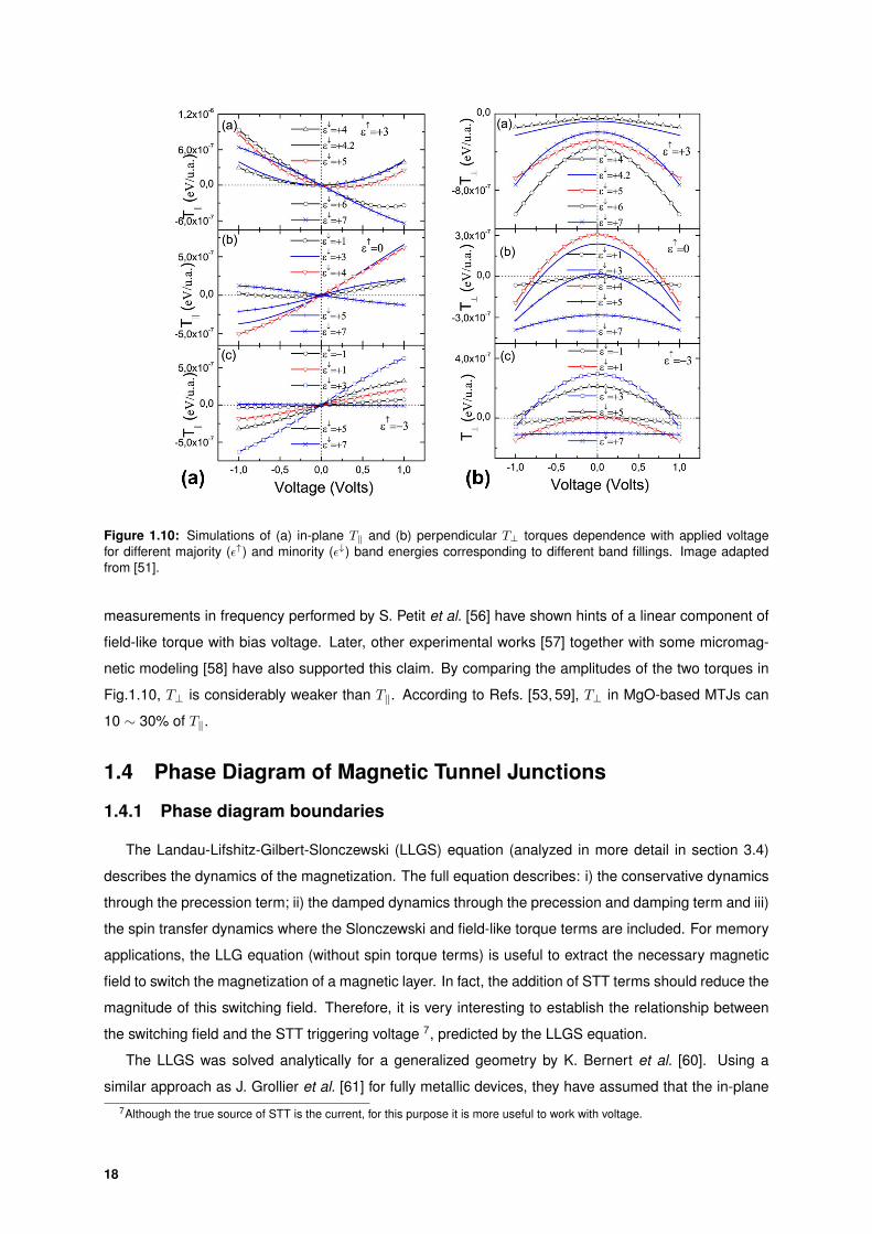
Figure 1.10: Simulations of (a) in-plane T‖ and (b) perpendicular T⊥ torques dependence with applied voltagefor different majority (ε↑) and minority (ε↓) band energies corresponding to different band fillings. Image adaptedfrom [51].
measurements in frequency performed by S. Petit et al. [56] have shown hints of a linear component of
field-like torque with bias voltage. Later, other experimental works [57] together with some micromag-
netic modeling [58] have also supported this claim. By comparing the amplitudes of the two torques in
Fig.1.10, T⊥ is considerably weaker than T‖. According to Refs. [53, 59], T⊥ in MgO-based MTJs can
10 ∼ 30% of T‖.
1.4 Phase Diagram of Magnetic Tunnel Junctions
1.4.1 Phase diagram boundaries
The Landau-Lifshitz-Gilbert-Slonczewski (LLGS) equation (analyzed in more detail in section 3.4)
describes the dynamics of the magnetization. The full equation describes: i) the conservative dynamics
through the precession term; ii) the damped dynamics through the precession and damping term and iii)
the spin transfer dynamics where the Slonczewski and field-like torque terms are included. For memory
applications, the LLG equation (without spin torque terms) is useful to extract the necessary magnetic
field to switch the magnetization of a magnetic layer. In fact, the addition of STT terms should reduce the
magnitude of this switching field. Therefore, it is very interesting to establish the relationship between
the switching field and the STT triggering voltage 7, predicted by the LLGS equation.
The LLGS was solved analytically for a generalized geometry by K. Bernert et al. [60]. Using a
similar approach as J. Grollier et al. [61] for fully metallic devices, they have assumed that the in-plane7Although the true source of STT is the current, for this purpose it is more useful to work with voltage.
18
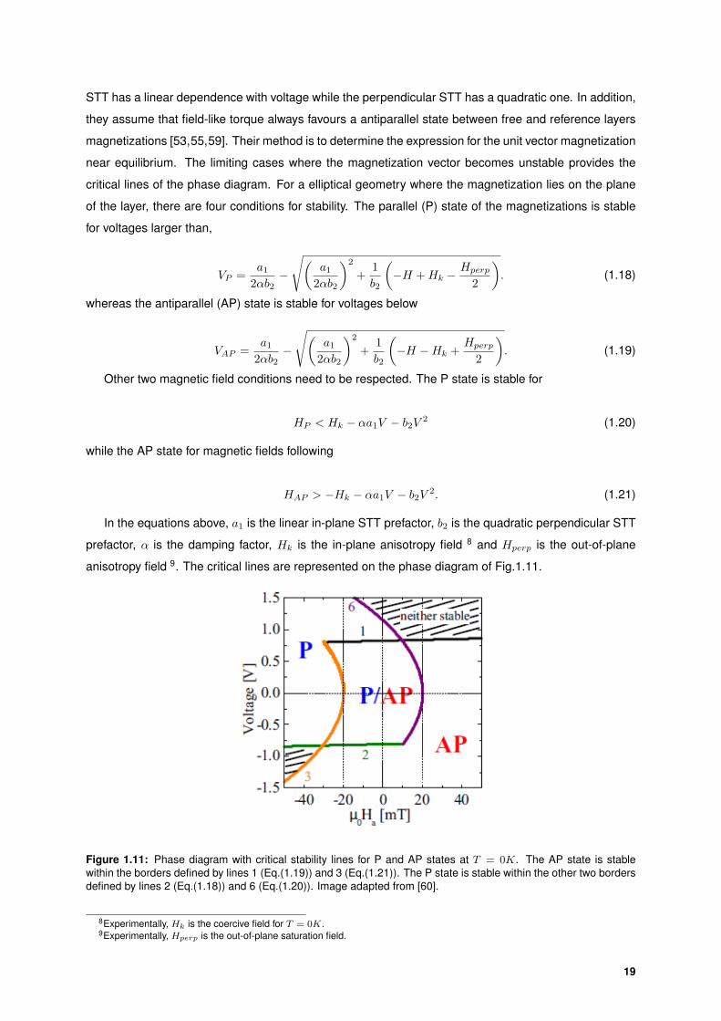
STT has a linear dependence with voltage while the perpendicular STT has a quadratic one. In addition,
they assume that field-like torque always favours a antiparallel state between free and reference layers
magnetizations [53,55,59]. Their method is to determine the expression for the unit vector magnetization
near equilibrium. The limiting cases where the magnetization vector becomes unstable provides the
critical lines of the phase diagram. For a elliptical geometry where the magnetization lies on the plane
of the layer, there are four conditions for stability. The parallel (P) state of the magnetizations is stable
for voltages larger than,
VP =a1
2αb2−
√(a1
2αb2
)2
+1
b2
(−H +Hk −
Hperp
2
). (1.18)
whereas the antiparallel (AP) state is stable for voltages below
VAP =a1
2αb2−
√(a1
2αb2
)2
+1
b2
(−H −Hk +
Hperp
2
). (1.19)
Other two magnetic field conditions need to be respected. The P state is stable for
HP < Hk − αa1V − b2V 2 (1.20)
while the AP state for magnetic fields following
HAP > −Hk − αa1V − b2V 2. (1.21)
In the equations above, a1 is the linear in-plane STT prefactor, b2 is the quadratic perpendicular STT
prefactor, α is the damping factor, Hk is the in-plane anisotropy field 8 and Hperp is the out-of-plane
anisotropy field 9. The critical lines are represented on the phase diagram of Fig.1.11.
Figure 1.11: Phase diagram with critical stability lines for P and AP states at T = 0K. The AP state is stablewithin the borders defined by lines 1 (Eq.(1.19)) and 3 (Eq.(1.21)). The P state is stable within the other two bordersdefined by lines 2 (Eq.(1.18)) and 6 (Eq.(1.20)). Image adapted from [60].
8Experimentally, Hk is the coercive field for T = 0K.9Experimentally, Hperp is the out-of-plane saturation field.
19
1.4.2 Critical Switching Current
As we have mentioned before, the LLGS equation [44, 62, 63] has three main terms: damping, pre-
cession and STT (including both in-plane and out-of-plane torques). For small-angle excitations and in
a simple geometry under a macrospin approximation, it is possible to determine the current value for the
spin torque to overcome the damping term, this current is usually called critical switching current (Isw0).
In a in-plane (IP) magnetized MTJ (with T = 0K), this is the minimum current necessary to switch the
magnetization of the free layer and it is given by [64]:
IIPsw0 =2eαMstfA(H +Hk + 2πMs)
~ η(1.22)
where α is the Gilbert damping constant, η is the spin transfer efficiency, H is the applied magnetic
field and Ms, tf , A and Hk are, respectively, the saturation magnetization, thickness, cross-section
and in-plane anisotropy field of the free layer. One of the main challenges for the magnetoresistive
memories is to have a minimal power consumption, thus it is important to aim for the smallest possible
Isw0. The straightforward solutions are: 1) to use materials whose damping constant is as low as
possible (α ≈ 0.007 for CoFeB), 2) reduce the thickness of the free layer and 3) use materials for the
free layer with high spin transfer efficiency η. However, one of the most dominant terms in Eq.(1.22) is
the 2πMs term (typically 2πMs H,Hk) related to the thin-film demagnetization effect, which favors
an in-plane orientation for ~M . This term is due to the fact that switching in-plane junctions requires
that magnetization becomes out-of-plane during switching, which means overcoming the dipolar energy
barrier. Therefore, one strategy to reduce the critical switching current is to suppress the influence of
the demagnetizing field. That is possible by using MTJs with perpendicular anisotropy. In that case,
magnetization goes through plane during switching, which does not cost any dipolar energy. The critical
switching current (at H = 0 and T = 0K) for an MTJ with out-of-plane magnetization is given by [65]:
IPPsw0 =2e
~αMstfAHk
η(1.23)
1.4.2.A Thermally activated switching
The critical switching currents (or current densities) defined above are also called intrinsic, since
they are defined for operation, i.e. at T = 0K. However, for the vast majority of applications, MTJs work
at room temperature (T = 300K). In fact, thermal fluctuations help the magnetization to overcome the
energy barrier, thus changing its orientation. For a magnetic moment, this phenomenon is described by
the Neel-Brown [66] model (similar to an Arrhenius law). Moreover, the characteristic time τ for the MTJ
to pass from one state to the other (i.e. for a full reversal of the free layer magnetization) is given by:
τ = τ0 exp
(EbkbT
)(1.24)
where Eb is the energy barrier to overcome, kB is the Boltzmann constant and τ0 is an intrinsic attempt
time (typically τ0 =1 ns).
20
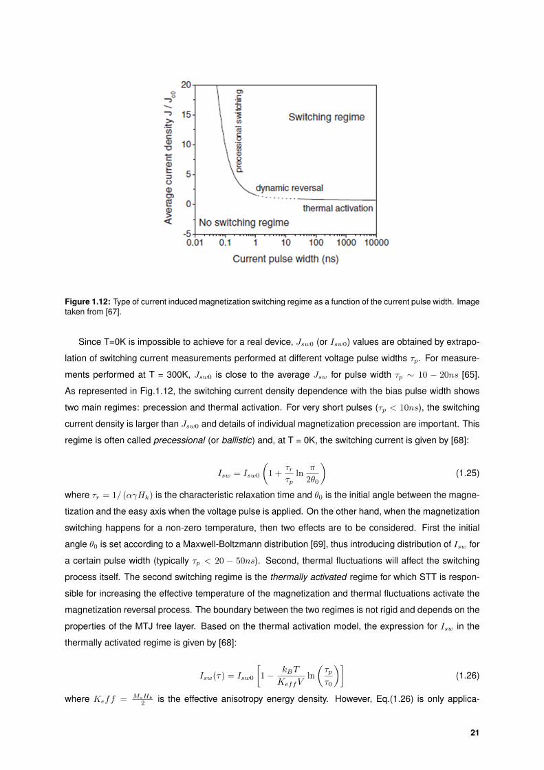
Figure 1.12: Type of current induced magnetization switching regime as a function of the current pulse width. Imagetaken from [67].
Since T=0K is impossible to achieve for a real device, Jsw0 (or Isw0) values are obtained by extrapo-
lation of switching current measurements performed at different voltage pulse widths τp. For measure-
ments performed at T = 300K, Jsw0 is close to the average Jsw for pulse width τp ∼ 10 − 20ns [65].
As represented in Fig.1.12, the switching current density dependence with the bias pulse width shows
two main regimes: precession and thermal activation. For very short pulses (τp < 10ns), the switching
current density is larger than Jsw0 and details of individual magnetization precession are important. This
regime is often called precessional (or ballistic) and, at T = 0K, the switching current is given by [68]:
Isw = Isw0
(1 +
τrτp
lnπ
2θ0
)(1.25)
where τr = 1/ (αγHk) is the characteristic relaxation time and θ0 is the initial angle between the magne-
tization and the easy axis when the voltage pulse is applied. On the other hand, when the magnetization
switching happens for a non-zero temperature, then two effects are to be considered. First the initial
angle θ0 is set according to a Maxwell-Boltzmann distribution [69], thus introducing distribution of Isw for
a certain pulse width (typically τp < 20 − 50ns). Second, thermal fluctuations will affect the switching
process itself. The second switching regime is the thermally activated regime for which STT is respon-
sible for increasing the effective temperature of the magnetization and thermal fluctuations activate the
magnetization reversal process. The boundary between the two regimes is not rigid and depends on the
properties of the MTJ free layer. Based on the thermal activation model, the expression for Isw in the
thermally activated regime is given by [68]:
Isw(τ) = Isw0
[1− kBT
KeffVln
(τpτ0
)](1.26)
where Keff = MsHk2 is the effective anisotropy energy density. However, Eq.(1.26) is only applica-
21

ble for MTJs with in-plane magnetization. For perpendicular anisotropy systems, a slight modification
is needed, and Isw becomes Isw = Isw0
[1−
√kBTKeffV
ln(τpτ0
)]. This correction is necessary so the
experimental results fit with the analytical perpendicular Isw expression [70].
1.5 Magnetoresistive Random Access Memories (MRAM)
1.5.1 Introduction to Random Access Memories
A computer is a system that processes information. Even before being processed, the data need to
be stored. This task is attributed to memories. The memory has four main building blocks:
• Processor registers: the fastest possible access (1 CPU cycle) and small in size (few kb);
• Cache: accelerates the data processing by reducing the access time;
• Random access memory (RAM): Contains all the necessary data to run a program. The data is
gradually transmitted to the processor according to the program needs. GB in size and best access
speed is ∼ 10 Gb/s;
• Disk storage: Stores the data provided to the RAM. TB in size. The more mature technology is the
Hard Disk Drive (HDD), though being rapidly replaced by Solid State Drive (SSD) since 2017. The
latter has a maximum access speed of 2000 MB/s.
Nevertheless, this structure is a requirement of the existing memory technology. The current chal-
lenges for the market of memories are: decrease power consumption and device size, increase read/write
speed, endurance, data retention and improve non-volatility. This last one separates the memories in
two groups: volatile and non-volatile. The volatile memories only keep data stored while power is on.
On the other hand, non-volatile memories store data even with power off (for a large but finite number
of read/write cycles). Currently, processor registers, cache and some RAM elements (ex. Static RAM
and Dynamic RAM) are volatile, while data storage devices (ex. HDD, SSD and flash memory drives)
are non-volatile.
Another important aspect that allows to distinguish different types of memories is their core tech-
nology, i.e. the physical support of the memory data. For one group, the memory feature relies on the
atoms displacement in space. This is the case of a simple CD-RW (compact disk-rewritable) but also the
phase-change RAM (PCRAM) and the resistive RAM (ReRAM). Another group relies on the displace-
ment of electrical charges. This is the case for the dynamic RAM (DRAM) which stores charges in a
separate tiny capacitor within an integrated circuit. With a similar construction as the DRAM but using
a ferroelectric layer instead of a dielectric layer, there is also the ferroelectric RAM (FeRAM). The flash
memory stores electrons in an array of floating-gate transistors. While the static RAM (SRAM) has two
possible circuits for charges. These electric charge based memories are the mainstream technologies
used in current personal computers. The last group relies on the orientation of magnetic moments. One
of the first memories, using this type of technology, was magnetic-core memory used between 1955 and
1975. Here, the magnetic moments of a small toroidal magnet were read and written by a metallic line
22

capable of generating a magnetic field. Later, this type of memories evolved into magnetic tape based
devices such as audio cassettes or VHS, floppy disks, HDD and finally the magnetoresistive random
access memory (MRAM).
Figure 1.13: Performance comparison between emerging and well-established RAMs. Source: Yole, InMRAM(2017)
Finally, the table in Fig.1.13 compares the performance between emerging and established RAM
memories, focusing on fundamental requirements for memories such as volatility, endurance, device
and cell size or power consumption.
1.5.2 Introduction to MRAM
The two main concepts, magnetoresistance and spin transfer torque, presented in sections 1.2.2
and 1.3 are the base technologies for a wide range of devices used for different applications. From
data storage to magnetic field sensors, or even microwave oscillators, these two spin current based
phenomena are usually present.
Magnetoresistance is the physical property which allows to distinguish the stable magnetic states
in a spin-valve or MTJ. For memory applications where high coercivity is essential, only two stable
states exist at zero magnetic field. One where the reference and free layer magnetizations are parallel
corresponding to a state of minimum MR (in a memory corresponds to a ”0”). And another state where
the two magnetizations are antiparallel and MR is now maximum (in a memory corresponds to a ”1”).
In general, but specially for memories, the larger the MR, the better. First, there is nearly no readout
error since the very large difference in resistance between ”1” and ”0” states enables an easier readout
process: the difference between the two states is well above the noise level. Second, a high TMR is
favorable to find a suitable reading voltage. Since MR decreases with applied voltage [8,24,27], reading
cannot be performed at a high voltage that may compromise the distinction between ”1” and ”0”. On
23
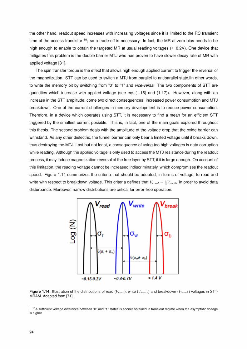
the other hand, readout speed increases with increasing voltages since it is limited to the RC transient
time of the access transistor 10; so a trade-off is necessary. In fact, the MR at zero bias needs to be
high enough to enable to obtain the targeted MR at usual reading voltages (≈ 0.2V). One device that
mitigates this problem is the double barrier MTJ who has proven to have slower decay rate of MR with
applied voltage [31].
The spin transfer torque is the effect that allows high enough applied current to trigger the reversal of
the magnetization. STT can be used to switch a MTJ from parallel to antiparallel state,iIn other words,
to write the memory bit by switching from ”0” to ”1” and vice-versa. The two components of STT are
quantities which increase with applied voltage (see eqs.(1.16) and (1.17)). However, along with an
increase in the STT amplitude, come two direct consequences: increased power consumption and MTJ
breakdown. One of the current challenges in memory development is to reduce power consumption.
Therefore, in a device which operates using STT, it is necessary to find a mean for an efficient STT
triggered by the smallest current possible. This is, in fact, one of the main goals explored throughout
this thesis. The second problem deals with the amplitude of the voltage drop that the oxide barrier can
withstand. As any other dielectric, the tunnel barrier can only bear a limited voltage until it breaks down,
thus destroying the MTJ. Last but not least, a consequence of using too high voltages is data corruption
while reading. Although the applied voltage is only used to access the MTJ resistance during the readout
process, it may induce magnetization reversal of the free layer by STT, if it is large enough. On account of
this limitation, the reading voltage cannot be increased indiscriminately, which compromises the readout
speed. Figure 1.14 summarizes the criteria that should be adopted, in terms of voltage, to read and
write with respect to breakdown voltage. This criteria defines that Vread = 14Vwrite in order to avoid data
disturbance. Moreover, narrow distributions are critical for error-free operation.
Figure 1.14: Illustration of the distributions of read (Vread), write (Vwrite) and breakdown (Vbreak) voltages in STT-MRAM. Adapted from [71].
10A sufficient voltage difference between ”0” and ”1” states is sooner obtained in transient regime when the asymptotic voltageis higher.
24
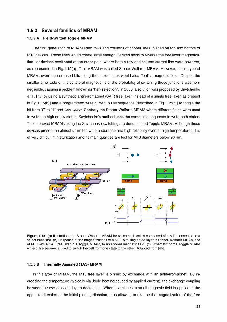
1.5.3 Several families of MRAM
1.5.3.A Field-Written Toggle MRAM
The first generation of MRAM used rows and columns of copper lines, placed on top and bottom of
MTJ devices. These lines would create large enough Oersted fields to reverse the free layer magnetiza-
tion, for devices positioned at the cross point where both a row and column current line were powered,
as represented in Fig.1.15(a). This MRAM was called Stoner-Wolfarth MRAM. However, in this type of
MRAM, even the non-used bits along the current lines would also ”feel” a magnetic field. Despite the
smaller amplitude of this collateral magnetic field, the probability of switching those junctions was non-
negligible, causing a problem known as ”half-selection”. In 2003, a solution was proposed by Savtchenko
et al. [72] by using a synthetic antiferromagnet (SAF) free layer [instead of a single free layer, as present
in Fig.1.15(b)] and a programmed write-current pulse sequence [described in Fig.1.15(c)] to toggle the
bit from ”0” to ”1” and vice-versa. Contrary the Stoner-Wolfarth MRAM where different fields were used
to write the high or low states, Savtchenko’s method uses the same field sequence to write both states.
The improved MRAMs using the Savtchenko switching are denominated Toggle MRAM. Although these
devices present an almost unlimited write endurance and high reliability even at high temperatures, it is
of very difficult miniaturization and its main qualities are lost for MTJ diameters below 90 nm.
Figure 1.15: (a) Illustration of a Stoner-Wolfarth MRAM for which each cell is composed of a MTJ connected to aselect transistor. (b) Response of the magnetizations of a MTJ with single free layer in Stoner-Wolfarth MRAM andof MTJ with a SAF free layer in a Toggle MRAM, to an applied magnetic field. (c) Schematic of the Toggle MRAMwrite-pulse sequence used to switch the cell from one state to the other. Adapted from [65].
1.5.3.B Thermally Assisted (TAS) MRAM
In this type of MRAM, the MTJ free layer is pinned by exchange with an antiferromagnet. By in-
creasing the temperature (typically via Joule heating caused by applied current), the exchange coupling
between the two adjacent layers decreases. When it vanishes, a small magnetic field is applied in the
opposite direction of the initial pinning direction, thus allowing to reverse the magnetization of the free
25
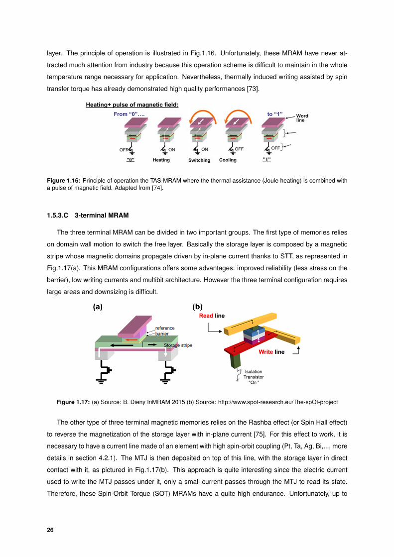
layer. The principle of operation is illustrated in Fig.1.16. Unfortunately, these MRAM have never at-
tracted much attention from industry because this operation scheme is difficult to maintain in the whole
temperature range necessary for application. Nevertheless, thermally induced writing assisted by spin
transfer torque has already demonstrated high quality performances [73].
Figure 1.16: Principle of operation the TAS-MRAM where the thermal assistance (Joule heating) is combined witha pulse of magnetic field. Adapted from [74].
1.5.3.C 3-terminal MRAM
The three terminal MRAM can be divided in two important groups. The first type of memories relies
on domain wall motion to switch the free layer. Basically the storage layer is composed by a magnetic
stripe whose magnetic domains propagate driven by in-plane current thanks to STT, as represented in
Fig.1.17(a). This MRAM configurations offers some advantages: improved reliability (less stress on the
barrier), low writing currents and multibit architecture. However the three terminal configuration requires
large areas and downsizing is difficult.
Figure 1.17: (a) Source: B. Dieny InMRAM 2015 (b) Source: http://www.spot-research.eu/The-spOt-project
The other type of three terminal magnetic memories relies on the Rashba effect (or Spin Hall effect)
to reverse the magnetization of the storage layer with in-plane current [75]. For this effect to work, it is
necessary to have a current line made of an element with high spin-orbit coupling (Pt, Ta, Ag, Bi,..., more
details in section 4.2.1). The MTJ is then deposited on top of this line, with the storage layer in direct
contact with it, as pictured in Fig.1.17(b). This approach is quite interesting since the electric current
used to write the MTJ passes under it, only a small current passes through the MTJ to read its state.
Therefore, these Spin-Orbit Torque (SOT) MRAMs have a quite high endurance. Unfortunately, up to
26
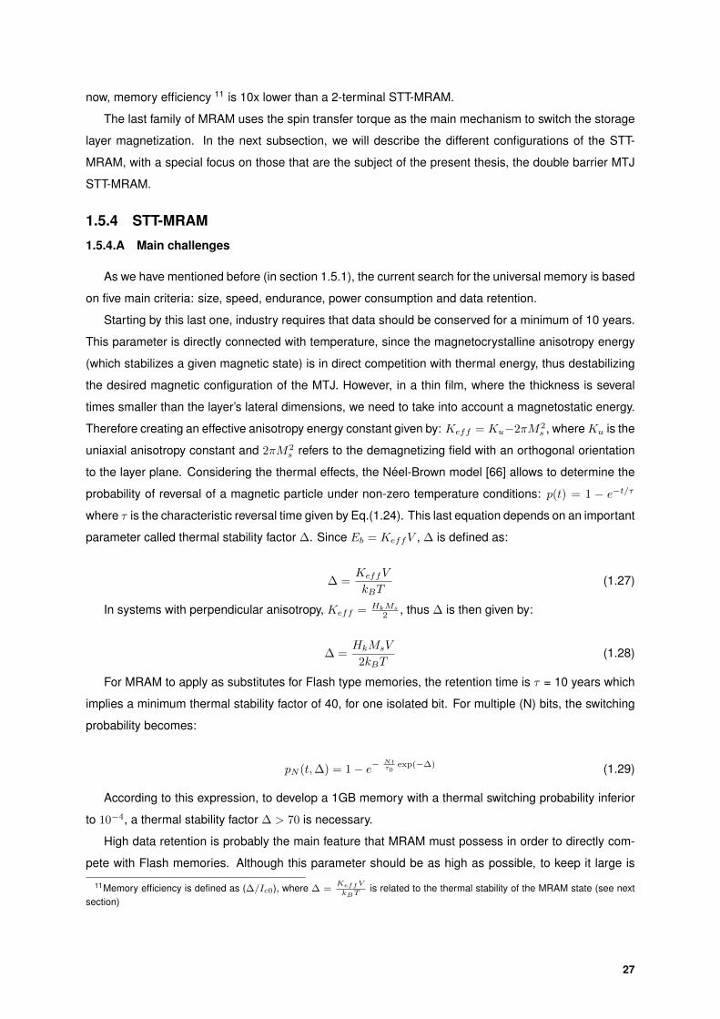
now, memory efficiency 11 is 10x lower than a 2-terminal STT-MRAM.
The last family of MRAM uses the spin transfer torque as the main mechanism to switch the storage
layer magnetization. In the next subsection, we will describe the different configurations of the STT-
MRAM, with a special focus on those that are the subject of the present thesis, the double barrier MTJ
STT-MRAM.
1.5.4 STT-MRAM
1.5.4.A Main challenges
As we have mentioned before (in section 1.5.1), the current search for the universal memory is based
on five main criteria: size, speed, endurance, power consumption and data retention.
Starting by this last one, industry requires that data should be conserved for a minimum of 10 years.
This parameter is directly connected with temperature, since the magnetocrystalline anisotropy energy
(which stabilizes a given magnetic state) is in direct competition with thermal energy, thus destabilizing
the desired magnetic configuration of the MTJ. However, in a thin film, where the thickness is several
times smaller than the layer’s lateral dimensions, we need to take into account a magnetostatic energy.
Therefore creating an effective anisotropy energy constant given by: Keff = Ku−2πM2s , whereKu is the
uniaxial anisotropy constant and 2πM2s refers to the demagnetizing field with an orthogonal orientation
to the layer plane. Considering the thermal effects, the Neel-Brown model [66] allows to determine the
probability of reversal of a magnetic particle under non-zero temperature conditions: p(t) = 1 − e−t/τ
where τ is the characteristic reversal time given by Eq.(1.24). This last equation depends on an important
parameter called thermal stability factor ∆. Since Eb = KeffV , ∆ is defined as:
∆ =KeffV
kBT(1.27)
In systems with perpendicular anisotropy, Keff = HkMs
2 , thus ∆ is then given by:
∆ =HkMsV
2kBT(1.28)
For MRAM to apply as substitutes for Flash type memories, the retention time is τ = 10 years which
implies a minimum thermal stability factor of 40, for one isolated bit. For multiple (N) bits, the switching
probability becomes:
pN (t,∆) = 1− e−Ntτ0
exp(−∆) (1.29)
According to this expression, to develop a 1GB memory with a thermal switching probability inferior
to 10−4, a thermal stability factor ∆ > 70 is necessary.
High data retention is probably the main feature that MRAM must possess in order to directly com-
pete with Flash memories. Although this parameter should be as high as possible, to keep it large is
11Memory efficiency is defined as (∆/Ic0), where ∆ =KeffV
kBTis related to the thermal stability of the MRAM state (see next
section)
27
utterly challenging when aiming at downscaling the devices dimensions. Reducing the MTJ size im-
plies a reduction of storage layer volume V . According to eqs.(1.27)-(1.28), the only way to maintain
∆ (assuming room temperature operation) is to increase Keff . However, if we admit that saturation
magnetization Ms remains constant, Keff only increases through an increase of Ku (and consequently
Hk). In the end, size reduction while keeping high data retention, comes with a price to pay which is the
increase of the critical switching current density (see Eq.(1.22)). The problem of the enhanced switching
current is in itself a disadvantage in terms of power consumption, but also in terms of integration of
STT-MRAM device with C-MOS. In fact, the larger Isw0, the larger needs to be the transistor coupled to
the MTJ.
So far, three main challenges of the STT-MRAM have been pointed out: increase data retention for
a small as possible device without compromising its power consumption. One of the possible solutions
to tackle these problems is the STT-MRAM using perpendicularly magnetized MTJs. Comparing the
switching current for this type of MTJ (Eq.(1.23)) with the one for in-plane magnetized MTJ (Eq.(1.22)),
it is possible to observe that the 2πMs term (associated with the demagnetizing fields) vanishes, imme-
diately reducing the critical switching current. In addition, data retention can be maintained high since
the materials (Co/Pt and Co/Pd multilayers) used in the perpendicular MTJs (p-MTJs) also have strong
perpendicular anisotropies. Unfortunately, along with an higher Keff comes an higher α compromising
Isw0, if these materials are used in the free layer. Therefore, the solution found was to add an extra MgO
layer on top of CoFeB (common storage layer material with low α) in order to increase anisotropy. An-
other solution could be to play with the junction shape: for small diameter, in-plane anisotropy decreases
thus Keff increases until shape anisotropy favors out-of-plane magnetization for a dot in the shape of a
cylinder. Extended explanations about perpendicularly magnetized MTJs can be found in chapter 4.
1.5.4.B Limitation of single barrier MTJ
As we have mentioned in subsection 1.5.2, and specially for certain applications where the memory
is much often read than written, increasing the readout speed implies to increase the read voltage as
well. A typical MTJ has three different voltage distributions, respectively, to read, write and breakdown.
The criteria established by Everspin R©Technologies is that these voltages should be separated by 6x the
sum of the two standard deviations (σ) of the two adjacent distributions, as represented in Fig.1.14. This
criterion is crucial to ensure that a read voltage does not disturb the previously written state. With the
currently used materials, deposition and nanofabrication techniques, the target writing voltage distribu-
tion is centered at ∼0.5 V. This value forces the read voltage to be as low as 0.15 V. In fact, the current
used to read the state of the MTJ will also induce STT, which if high enough, may reverse the storage
layer magnetization. To ensure ∆ > 70 and a maximum switching probability of 10−4, the ratio between
the read and write current is IreadIwrite
≈ 0.28 [1], which can be rounded down to IreadIwrite
= 14 . These read
voltage (or current) limitations also condition the readout speed due to the capacitor leakage current of
the selection transistors.
In the following subsection, we will see that double barrier tunnel junctions with dual references allow
to increase the read voltage without jeopardizing the magnetic state of the storage layer.
28
1.5.4.C Double Barrier MTJ
The double barrier magnetic tunnel junctions (DBMTJ) is composed by three main magnetic blocks:
reference layer, storage layer and control layer (see Fig.1.18). In this structure, the storage layer is
sandwiched between two tunnel barriers. The reference and control layers play the role of polarizers
whose magnetizations can be set independently of the storage layer. There are two possible magnetic
configurations of the DBMTJ depending on the orientation of the magnetizations of reference and control
layers. Choosing between these two configurations allows to modulate the amplitude of STT exerted on
the storage layer. In consequence, two modes of operation are created, one suited to read and the other
to write the memory dot.
(i) Read and Write modes of operation
One of the possible magnetic configurations is the parallel alignment between reference and control
layers magnetizations [Fig.1.18(a)]. In this configuration, the torques coming from the reference (T r)
and control (T c) layers have opposite directions. Therefore, the total torque exerted on the storage layer
is expressed as:
T read = |T r| − |T c| (1.30)
The total torque is thus minimum or even cancels out in case of ideal symmetric top and bottom
tunnel barriers. This scenario presents the opportunity to apply larger voltages on the DBMTJ without
risk of storage layer magnetization reversal. Faster readout speed is then possible in this configuration.
This operation mode is called read mode.
By constrast, when the reference and control layer magnetizations are in antiparallel alignment
[Fig.1.18(b)], the two torques, T r and T c, exerted on the storage layer add up. The total torque ap-
plied in now given by:
Twrite = |T r|+ |T c| (1.31)
In this situation, the STT is enhanced and writing the storage layer may be performed with lower
currents than in the case of a single barrier MTJ. This operation mode is called write mode.
The process to set the two different operation modes by switching the direction of the magnetization
of the control layer without affecting the one of the reference layer for in-plane anisotropy DBMTJ is
explained in more detail in subsection 3.1.2.
The operation modes and their setting have also been demonstrated in DBMTJs with perpendicular
magnetization in section 5.1.
(ii) STT in a DBMTJ
29

Figure 1.18: (a) Read and (b) write modes of operation in DBMTJ. AFM stands for antiferromagnet. T r and T c
correspond to the torques exerted on the storage layer coming, respectively, from reference and control layers.
As mentioned above, the most defining feature of the DBMTJ is the modulation of STT acting on the
storage layer by manipulation of the magnetic configurations between reference and control layer. There-
fore, it is important to discuss in more detail the theory of spin-torque switching of DBMTJs. The most
recent study of this theory was performed by D. Worledge [76] in 2017 where he uses the single-domain
model to derive the analytical formula for critical switching current Isw0 of DBMTJs with perpendicular
magnetization (p-DBMTJs).
The study starts by defining the basics of STT for a single barrier MTJ [77]. The torque is defined in
function of the angle θ between the free and reference layer magnetizations and an applied voltage V
across the MTJ:
T (θ, V ) =~2e
PRR⊥
V sin θ (1.32)
where PR is the spin polarization of the reference layer and R⊥ is the resistance when free and reference
layer magnetizations are perpendicular. In addition, the resistance variation with θ in a MTJ is given
by [77]:
R(θ) =R⊥
1 + PFPR cos θ(1.33)
where PF is the spin polarization of the free layer. The combination of Ohm’s law (V = RI) and
Eq.(1.33), replaced in Eq.(1.32) enables to derive torque as a function of current:
T (θ, I) =~2e
PR I
1 + PFPR cos θsin θ (1.34)
According to this last equation, torque is larger when θ = π (MTJ in antiparallel AP state) than when
θ = 0 (MTJ in parallel P state). Empirically, this is why, for a constant applied voltage, AP→P switching
current is smaller than P→AP.
In the case of the double barrier MTJ, apart from the storage layer and reference layer, we need
to account for another polarizing layer on top of the top tunnel barrier, the control layer. Therefore, we
30
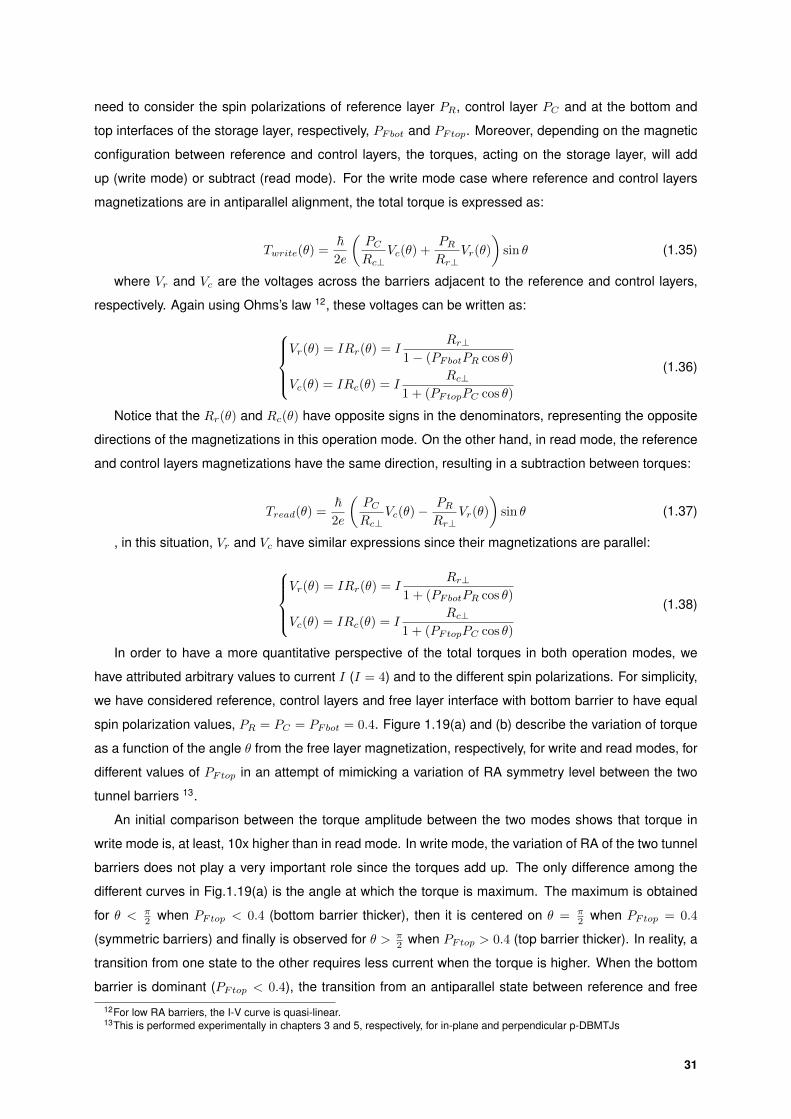
need to consider the spin polarizations of reference layer PR, control layer PC and at the bottom and
top interfaces of the storage layer, respectively, PFbot and PFtop. Moreover, depending on the magnetic
configuration between reference and control layers, the torques, acting on the storage layer, will add
up (write mode) or subtract (read mode). For the write mode case where reference and control layers
magnetizations are in antiparallel alignment, the total torque is expressed as:
Twrite(θ) =~2e
(PCRc⊥
Vc(θ) +PRRr⊥
Vr(θ)
)sin θ (1.35)
where Vr and Vc are the voltages across the barriers adjacent to the reference and control layers,
respectively. Again using Ohms’s law 12, these voltages can be written as:
Vr(θ) = IRr(θ) = I
Rr⊥1− (PFbotPR cos θ)
Vc(θ) = IRc(θ) = IRc⊥
1 + (PFtopPC cos θ)
(1.36)
Notice that the Rr(θ) and Rc(θ) have opposite signs in the denominators, representing the opposite
directions of the magnetizations in this operation mode. On the other hand, in read mode, the reference
and control layers magnetizations have the same direction, resulting in a subtraction between torques:
Tread(θ) =~2e
(PCRc⊥
Vc(θ)−PRRr⊥
Vr(θ)
)sin θ (1.37)
, in this situation, Vr and Vc have similar expressions since their magnetizations are parallel:
Vr(θ) = IRr(θ) = I
Rr⊥1 + (PFbotPR cos θ)
Vc(θ) = IRc(θ) = IRc⊥
1 + (PFtopPC cos θ)
(1.38)
In order to have a more quantitative perspective of the total torques in both operation modes, we
have attributed arbitrary values to current I (I = 4) and to the different spin polarizations. For simplicity,
we have considered reference, control layers and free layer interface with bottom barrier to have equal
spin polarization values, PR = PC = PFbot = 0.4. Figure 1.19(a) and (b) describe the variation of torque
as a function of the angle θ from the free layer magnetization, respectively, for write and read modes, for
different values of PFtop in an attempt of mimicking a variation of RA symmetry level between the two
tunnel barriers 13.
An initial comparison between the torque amplitude between the two modes shows that torque in
write mode is, at least, 10x higher than in read mode. In write mode, the variation of RA of the two tunnel
barriers does not play a very important role since the torques add up. The only difference among the
different curves in Fig.1.19(a) is the angle at which the torque is maximum. The maximum is obtained
for θ < π2 when PFtop < 0.4 (bottom barrier thicker), then it is centered on θ = π
2 when PFtop = 0.4
(symmetric barriers) and finally is observed for θ > π2 when PFtop > 0.4 (top barrier thicker). In reality, a
transition from one state to the other requires less current when the torque is higher. When the bottom
barrier is dominant (PFtop < 0.4), the transition from an antiparallel state between reference and free
12For low RA barriers, the I-V curve is quasi-linear.13This is performed experimentally in chapters 3 and 5, respectively, for in-plane and perpendicular p-DBMTJs
31
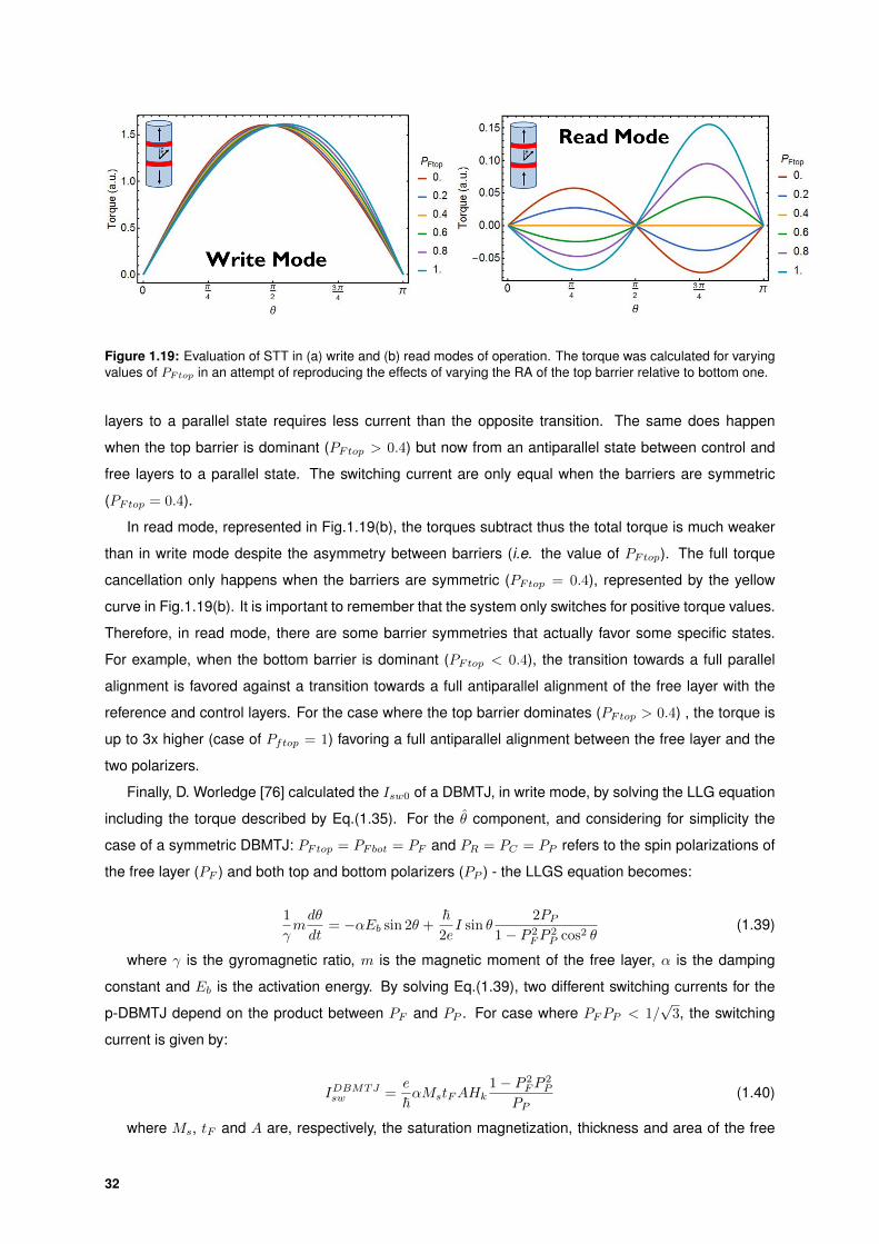
Figure 1.19: Evaluation of STT in (a) write and (b) read modes of operation. The torque was calculated for varyingvalues of PFtop in an attempt of reproducing the effects of varying the RA of the top barrier relative to bottom one.
layers to a parallel state requires less current than the opposite transition. The same does happen
when the top barrier is dominant (PFtop > 0.4) but now from an antiparallel state between control and
free layers to a parallel state. The switching current are only equal when the barriers are symmetric
(PFtop = 0.4).
In read mode, represented in Fig.1.19(b), the torques subtract thus the total torque is much weaker
than in write mode despite the asymmetry between barriers (i.e. the value of PFtop). The full torque
cancellation only happens when the barriers are symmetric (PFtop = 0.4), represented by the yellow
curve in Fig.1.19(b). It is important to remember that the system only switches for positive torque values.
Therefore, in read mode, there are some barrier symmetries that actually favor some specific states.
For example, when the bottom barrier is dominant (PFtop < 0.4), the transition towards a full parallel
alignment is favored against a transition towards a full antiparallel alignment of the free layer with the
reference and control layers. For the case where the top barrier dominates (PFtop > 0.4) , the torque is
up to 3x higher (case of Pftop = 1) favoring a full antiparallel alignment between the free layer and the
two polarizers.
Finally, D. Worledge [76] calculated the Isw0 of a DBMTJ, in write mode, by solving the LLG equation
including the torque described by Eq.(1.35). For the θ component, and considering for simplicity the
case of a symmetric DBMTJ: PFtop = PFbot = PF and PR = PC = PP refers to the spin polarizations of
the free layer (PF ) and both top and bottom polarizers (PP ) - the LLGS equation becomes:
1
γmdθ
dt= −αEb sin 2θ +
~2eI sin θ
2PP1− P 2
FP2P cos2 θ
(1.39)
where γ is the gyromagnetic ratio, m is the magnetic moment of the free layer, α is the damping
constant and Eb is the activation energy. By solving Eq.(1.39), two different switching currents for the
p-DBMTJ depend on the product between PF and PP . For case where PFPP < 1/√
3, the switching
current is given by:
IDBMTJsw =
e
~αMstFAHk
1− P 2FP
2P
PP(1.40)
where Ms, tF and A are, respectively, the saturation magnetization, thickness and area of the free
32
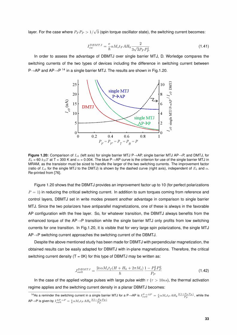
layer. For the case where PFPP > 1/√
3 (spin torque oscillator state), the switching current becomes:
IDBMTJsw =
e
~αMstFAHk
2
3√
3PFP 2P
(1.41)
In order to assess the advantage of DBMTJ over single barrier MTJ, D. Worledge compares the
switching currents of the two types of devices including the difference in switching current between
P→AP and AP→P 14 in a single barrier MTJ. The results are shown in Fig.1.20.
Figure 1.20: Comparison of Ic0 (left axis) for single barrier MTJ P→AP, single barrier MTJ AP→P, and DMTJ, forEb = 60 kBT at T = 300 K and α = 0.004. The blue P→AP curve is the criterion for use of the single barrier MTJ inMRAM, as the transistor must be sized to handle the larger of the two switching currents. The improvement factor(ratio of Ic0 for the single MTJ to the DMTJ) is shown by the dashed curve (right axis), independent of Eb and α.Re-printed from [76].
Figure 1.20 shows that the DBMTJ provides an improvement factor up to 10 (for perfect polarizations
P = 1) in reducing the critical switching current. In addition to sum torques coming from reference and
control layers, DBMTJ set in write modes present another advantage in comparison to single barrier
MTJ. Since the two polarizers have antiparallel magnetizations, one of these is always in the favorable
AP configuration with the free layer. So, for whatever transition, the DBMTJ always benefits from the
enhanced torque of the AP→P transition while the single barrier MTJ only profits from low switching
currents for one transition. In Fig.1.20, it is visible that for very large spin polarizations, the single MTJ
AP→P switching current approaches the switching current of the DBMTJ.
Despite the above mentioned study has been made for DBMTJ with perpendicular magnetization, the
obtained results can be easily adapted for DBMTJ with in-plane magnetizations. Therefore, the critical
switching current density (T = 0K) for this type of DBMTJ may be written as:
JDBMTJsw0 =
2eαMstf (H +Hk + 2πMs)
~1− P 2
FP2P
PP(1.42)
In the case of the applied voltage pulses with large pulse width τ (τ > 10ns), the thermal activation
regime applies and the switching current density in a planar DBMTJ becomes:
14As a reminder the switching current in a single barrier MTJ for a P→AP is IP→APsw0 = e~αMstFAHk
2(1+PFPP )PP
, while the
AP→P is given by IAP→Psw0 = e~αMstFAHk
2(1−PFPP )PP
33
JDBMTJsw (τ) = JDBMTJ
sw0
[1− kBT
KeffVln
(τ
τ0
)](1.43)
In summary, the double barrier tunnel junction presents two major advantages. The write mode allows for
a decrease of the writing current, mitigating the energy consumption of the device. While the read mode
allows for a readout process performed at higher voltages corresponding to higher speed in accessing
information.
The most relevant reports on spin torque in double barrier MTJ with in-plane magnetizations belong
to Huai et al. [78] and Diao et al. [37] focusing mainly on the reduction of the critical switching current
with antiparallel polarizers. In 2014 and 2015, Clement et al. [79, 80] have studied STT in both read
and write operation modes in planar DBMTJs. Cuchet et al. [81] have demonstrated the first realization
of a DBMTJ with perpendicular magnetization. More recently, IBM (by Hu et al. [40] ) and Samsung
(by Duan et al. [41]), have demonstrated STT switching in perpendicularly magnetized DBMTJ (with
TMR > 100%) where critical switching currents were found to be 2x lower than in comparable single
barrier perpendicular MTJs.
34

2Nanofabrication Process
Contents2.1 Introduction . . . . . . . . . . . . . . . . . . . . . . . . . . . . . . . . . . . . . . . . . . 362.2 Pillar E-Beam Lithography . . . . . . . . . . . . . . . . . . . . . . . . . . . . . . . . . . 362.3 Pillar Etch . . . . . . . . . . . . . . . . . . . . . . . . . . . . . . . . . . . . . . . . . . . . 372.4 Definition of Bottom Electrode . . . . . . . . . . . . . . . . . . . . . . . . . . . . . . . 392.5 Pillar Passivation . . . . . . . . . . . . . . . . . . . . . . . . . . . . . . . . . . . . . . . 402.6 Definition of Top Electrode and Contacts Metalization . . . . . . . . . . . . . . . . . . 412.7 Electrical Characterization - Wafer Mapping . . . . . . . . . . . . . . . . . . . . . . . . 41
35

2.1 Introduction
In this chapter, the fabrication steps necessary to transform a full sheet DBMTJ into patterned de-
vices are described in detail. The DBMTJs used for fabrication were initially deposited by magnetron
sputtering using two different physical vapor deposition tools: Timaris (in-plane DBMTJs) and Actemium
(perpendicular DBMTJs). The DBMTJ samples were deposited on 50mm silicon wafers with 500µm of
thermal SiO2.
In summary, the main technological steps to fabricate DBMTJ pillars of nanometric size are the
following:
• Electron beam lithography to define pillars with diameters below 800nm;
• Optical lithography to design the larger patterns (ex. bottom and top contacts);
• Physical and chemical etching to transfer the designs made by lithography into the thin films;
• Deposition of hard mask, planarization and contact metalization;
• In between steps, the process control inspections are made using optical microscope, scanning
electron microscope (SEM) and profilometer to measure the different layers thicknesses;
2.2 Pillar E-Beam Lithography
For the electron beam (e-beam) lithography of the nanometric pillars (circles or ellipses) a positive
resist (PMMA) is used, meaning that the exposed resist is removed after development. For this reason,
and to act as a protective layer while etching the pillar, an hard mask is deposited after the DBMTJ
deposition. This hard mask is defined by a thin Ru layer of 7 nm and thicker layer of 150 nm of Ta.
Tantalum was chosen since it is a material easily etched by SF6-based plasma, whereas the Ru acts as
a stopping layer.
After the hard mask deposition, the wafer is coated with electron sensitive positive resist - PMMA -
with an overall thickness of 80 nm, which is baked at 180C for 5 minutes. Following the PMMA coating,
the sample is placed inside an e-beam tool [Fig.2.1(a)] - JEOL 6300 FS - with a field emission source
gun, enabling the design of features with lateral resolution inferior to 20 nm. In fact, two sets of pillar
sizes were used, respectively, for in-plane and perpendicular DBMTJs. For planar DBMTJs, the devices
have two types of cross section geometries - circular and elliptical. The pillars with circular cross sections
have nominal diameters of 80 nm, 100 nm, 200 nm and 1 µm. While the ellipses have nominal axes
dimensions of 40 nm x 140 nm. In the case of perpendicular DBMTJs, shape anisotropy is negligible
therefore only pillars with circular cross sections were defined with the following nominal diameters: 40
nm, 50 nm, 80 nm, 100 nm, 200 nm and 300 nm. As represented in Fig.2.1(b), after the exposure and
development of the PMMA, 20 nm of Cr are deposited by electron beam physical vapor deposition. This
step is completed by a lift-off with acetone [Fig.2.1(c)] which allows for the Cr to remain only on the
empty spaces without PMMA and to serve as protective layer of the pillar hard mask.
36
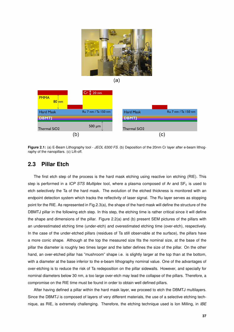
Figure 2.1: (a) E-Beam Lithography tool - JEOL 6300 FS. (b) Deposition of the 20nm Cr layer after e-beam lithog-raphy of the nanopillars. (c) Lift-off.
2.3 Pillar Etch
The first etch step of the process is the hard mask etching using reactive ion etching (RIE). This
step is performed in a ICP STS Multiplex tool, where a plasma composed of Ar and SF6 is used to
etch selectively the Ta of the hard mask. The evolution of the etched thickness is monitored with an
endpoint detection system which tracks the reflectivity of laser signal. The Ru layer serves as stopping
point for the RIE. As represented in Fig.2.3(a), the shape of the hard mask will define the structure of the
DBMTJ pillar in the following etch step. In this step, the etching time is rather critical since it will define
the shape and dimensions of the pillar. Figure 2.2(a) and (b) present SEM pictures of the pillars with
an underestimated etching time (under-etch) and overestimated etching time (over-etch), respectively.
In the case of the under-etched pillars (residues of Ta still observable at the surface), the pillars have
a more conic shape. Although at the top the measured size fits the nominal size, at the base of the
pillar the diameter is roughly two times larger and the latter defines the size of the pillar. On the other
hand, an over-etched pillar has ”mushroom” shape i.e. is slightly larger at the top than at the bottom,
with a diameter at the base inferior to the e-beam lithography nominal value. One of the advantages of
over-etching is to reduce the risk of Ta redeposition on the pillar sidewalls. However, and specially for
nominal diameters below 30 nm, a too large over-etch may lead the collapse of the pillars. Therefore, a
compromise on the RIE time must be found in order to obtain well defined pillars.
After having defined a pillar within the hard mask layer, we proceed to etch the DBMTJ multilayers.
Since the DBMTJ is composed of layers of very different materials, the use of a selective etching tech-
nique, as RIE, is extremely challenging. Therefore, the etching technique used is Ion Milling, in IBE
37
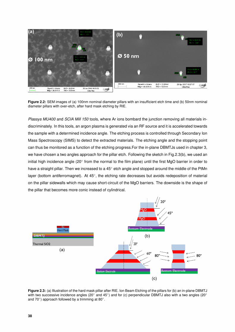
Figure 2.2: SEM images of (a) 100nm nominal diameter pillars with an insufficient etch time and (b) 50nm nominaldiameter pillars with over-etch, after hard mask etching by RIE.
Plassys MU400 and SCIA Mill 150 tools, where Ar ions bombard the junction removing all materials in-
discriminately. In this tools, an argon plasma is generated via an RF source and it is accelerated towards
the sample with a determined incidence angle. The etching process is controlled through Secondary Ion
Mass Spectroscopy (SIMS) to detect the extracted materials. The etching angle and the stopping point
can thus be monitored as a function of the etching progress.For the in-plane DBMTJs used in chapter 3,
we have chosen a two angles approach for the pillar etch. Following the sketch in Fig.2.3(b), we used an
initial high incidence angle (20 from the normal to the film plane) until the first MgO barrier in order to
have a straight pillar. Then we increased to a 45 etch angle and stopped around the middle of the PtMn
layer (bottom antiferromagnet). At 45, the etching rate decreases but avoids redeposition of material
on the pillar sidewalls which may cause short-circuit of the MgO barriers. The downside is the shape of
the pillar that becomes more conic instead of cylindrical.
Figure 2.3: (a) Illustration of the hard mask pillar after RIE. Ion Beam Etching of the pillars for (b) an in-plane DBMTJwith two successive incidence angles (20 and 45) and for (c) perpendicular DBMTJ also with a two angles (20
and 70) approach followed by a trimming at 80.
38
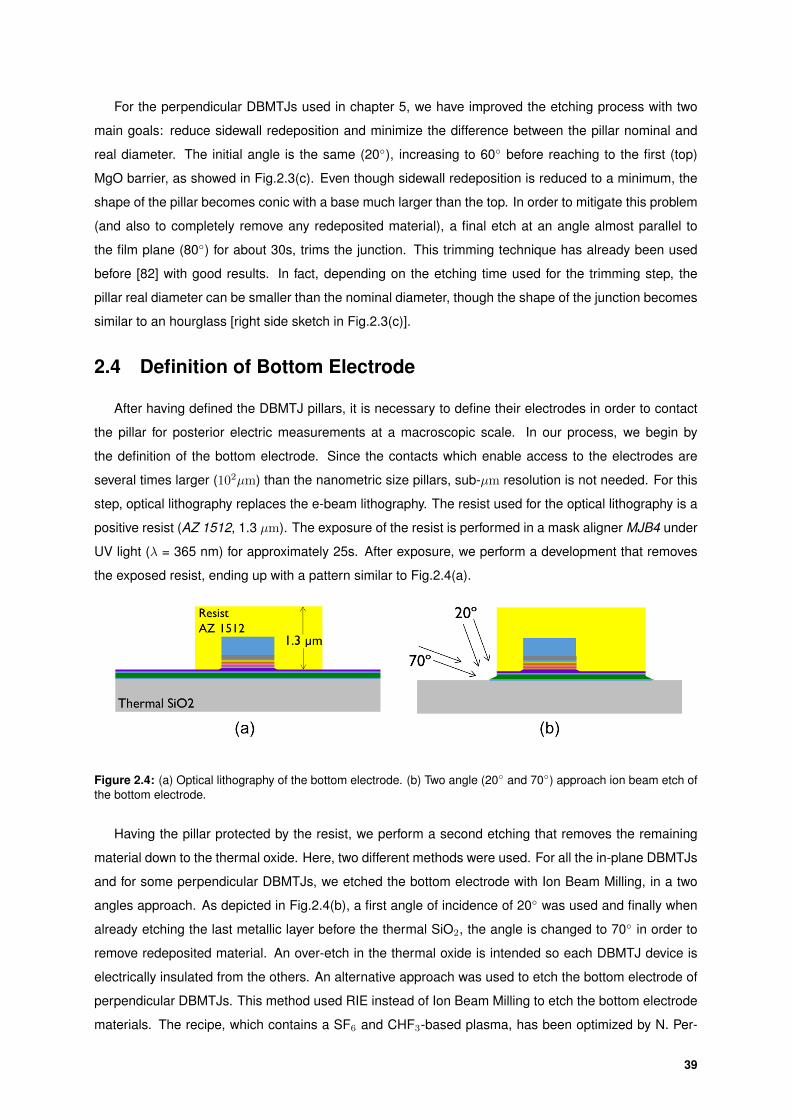
For the perpendicular DBMTJs used in chapter 5, we have improved the etching process with two
main goals: reduce sidewall redeposition and minimize the difference between the pillar nominal and
real diameter. The initial angle is the same (20), increasing to 60 before reaching to the first (top)
MgO barrier, as showed in Fig.2.3(c). Even though sidewall redeposition is reduced to a minimum, the
shape of the pillar becomes conic with a base much larger than the top. In order to mitigate this problem
(and also to completely remove any redeposited material), a final etch at an angle almost parallel to
the film plane (80) for about 30s, trims the junction. This trimming technique has already been used
before [82] with good results. In fact, depending on the etching time used for the trimming step, the
pillar real diameter can be smaller than the nominal diameter, though the shape of the junction becomes
similar to an hourglass [right side sketch in Fig.2.3(c)].
2.4 Definition of Bottom Electrode
After having defined the DBMTJ pillars, it is necessary to define their electrodes in order to contact
the pillar for posterior electric measurements at a macroscopic scale. In our process, we begin by
the definition of the bottom electrode. Since the contacts which enable access to the electrodes are
several times larger (102µm) than the nanometric size pillars, sub-µm resolution is not needed. For this
step, optical lithography replaces the e-beam lithography. The resist used for the optical lithography is a
positive resist (AZ 1512, 1.3 µm). The exposure of the resist is performed in a mask aligner MJB4 under
UV light (λ = 365 nm) for approximately 25s. After exposure, we perform a development that removes
the exposed resist, ending up with a pattern similar to Fig.2.4(a).
Figure 2.4: (a) Optical lithography of the bottom electrode. (b) Two angle (20 and 70) approach ion beam etch ofthe bottom electrode.
Having the pillar protected by the resist, we perform a second etching that removes the remaining
material down to the thermal oxide. Here, two different methods were used. For all the in-plane DBMTJs
and for some perpendicular DBMTJs, we etched the bottom electrode with Ion Beam Milling, in a two
angles approach. As depicted in Fig.2.4(b), a first angle of incidence of 20 was used and finally when
already etching the last metallic layer before the thermal SiO2, the angle is changed to 70 in order to
remove redeposited material. An over-etch in the thermal oxide is intended so each DBMTJ device is
electrically insulated from the others. An alternative approach was used to etch the bottom electrode of
perpendicular DBMTJs. This method used RIE instead of Ion Beam Milling to etch the bottom electrode
materials. The recipe, which contains a SF6 and CHF3-based plasma, has been optimized by N. Per-
39
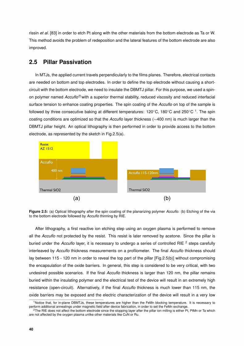
rissin et al. [83] in order to etch Pt along with the other materials from the bottom electrode as Ta or W.
This method avoids the problem of redeposition and the lateral features of the bottom electrode are also
improved.
2.5 Pillar Passivation
In MTJs, the applied current travels perpendicularly to the films planes. Therefore, electrical contacts
are needed on bottom and top electrodes. In order to define the top electrode without causing a short-
circuit with the bottom electrode, we need to insulate the DBMTJ pillar. For this purpose, we used a spin-
on polymer named Accuflo R©with a superior thermal stability, reduced viscosity and reduced interfacial
surface tension to enhance coating properties. The spin coating of the Accuflo on top of the sample is
followed by three consecutive baking at different temperatures: 120C, 180C and 250C 1. The spin
coating conditions are optimized so that the Accuflo layer thickness (∼400 nm) is much larger than the
DBMTJ pillar height. An optical lithography is then performed in order to provide access to the bottom
electrode, as represented by the sketch in Fig.2.5(a).
Figure 2.5: (a) Optical lithography after the spin coating of the planarizing polymer Accuflo. (b) Etching of the viato the bottom electrode followed by Accuflo thinning by RIE.
After lithography, a first reactive ion etching step using an oxygen plasma is performed to remove
all the Accuflo not protected by the resist. This resist is later removed by acetone. Since the pillar is
buried under the Accuflo layer, it is necessary to undergo a series of controlled RIE 2 steps carefully
interleaved by Accuflo thickness measurements on a profilometer. The final Accuflo thickness should
lay between 115 - 120 nm in order to reveal the top part of the pillar [Fig.2.5(b)] without compromising
the encapsulation of the oxide barriers. In general, this step is considered to be very critical, with two
undesired possible scenarios. If the final Accuflo thickness is larger than 120 nm, the pillar remains
buried within the insulating polymer and the electrical test of the device will result in an extremely high
resistance (open-circuit). Alternatively, if the final Accuflo thickness is much lower than 115 nm, the
oxide barriers may be exposed and the electric characterization of the device will result in a very low1Notice that, for in-plane DBMTJs, these temperatures are higher than the FeMn blocking temperature. It is necessary to
perform additional annealings under magnetic field after device fabrication, in order to set the FeMn exchange.2The RIE does not affect the bottom electrode since the stopping layer after the pillar ion milling is either Pt, PtMn or Ta which
are not affected by the oxygen plasma unlike other materials like CuN or Ru.
40
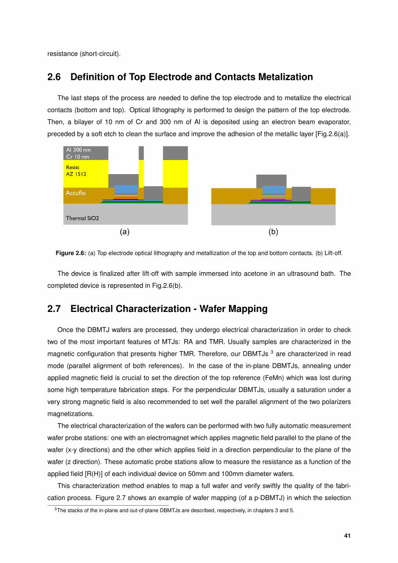
resistance (short-circuit).
2.6 Definition of Top Electrode and Contacts Metalization
The last steps of the process are needed to define the top electrode and to metallize the electrical
contacts (bottom and top). Optical lithography is performed to design the pattern of the top electrode.
Then, a bilayer of 10 nm of Cr and 300 nm of Al is deposited using an electron beam evaporator,
preceded by a soft etch to clean the surface and improve the adhesion of the metallic layer [Fig.2.6(a)].
Figure 2.6: (a) Top electrode optical lithography and metallization of the top and bottom contacts. (b) Lift-off.
The device is finalized after lift-off with sample immersed into acetone in an ultrasound bath. The
completed device is represented in Fig.2.6(b).
2.7 Electrical Characterization - Wafer Mapping
Once the DBMTJ wafers are processed, they undergo electrical characterization in order to check
two of the most important features of MTJs: RA and TMR. Usually samples are characterized in the
magnetic configuration that presents higher TMR. Therefore, our DBMTJs 3 are characterized in read
mode (parallel alignment of both references). In the case of the in-plane DBMTJs, annealing under
applied magnetic field is crucial to set the direction of the top reference (FeMn) which was lost during
some high temperature fabrication steps. For the perpendicular DBMTJs, usually a saturation under a
very strong magnetic field is also recommended to set well the parallel alignment of the two polarizers
magnetizations.
The electrical characterization of the wafers can be performed with two fully automatic measurement
wafer probe stations: one with an electromagnet which applies magnetic field parallel to the plane of the
wafer (x-y directions) and the other which applies field in a direction perpendicular to the plane of the
wafer (z direction). These automatic probe stations allow to measure the resistance as a function of the
applied field [R(H)] of each individual device on 50mm and 100mm diameter wafers.
This characterization method enables to map a full wafer and verify swiftly the quality of the fabri-
cation process. Figure 2.7 shows an example of wafer mapping (of a p-DBMTJ) in which the selection3The stacks of the in-plane and out-of-plane DBMTJs are described, respectively, in chapters 3 and 5.
41

Figure 2.7: Wafer mapping of a p-DBMTJ 50mm wafer. The color scale represents TMR. The yield of the waferwas 80%, considering 25% ≤ TMR ≤ 100%.
criterion is TMR. Other type of analysis can also be done based on the results provided by the automatic
tester. Figure 2.8 shows the relationship between RA and TMR for devices with different diameters. The
example shown corresponds to successfully fabricated wafer where TMR does not change with small
variations of RA (mostly due to difference between nominal and real device diameters). A good wafer
presents a yield of working junctions of 80%. The data of figs.2.8 and 2.8 was obtained from a wafer
whose stack is of a p-DBMTJ with a thicker bottom barrier. For this particular example of a successful
wafer, RA (average ± 1σ) is of 59 ± 11 Ω.µm2 and a 19% 1σ uniformity across the wafer. In addition,
TMR (average ± 1σ) is 57 ± 5 % with a 9% 1σ uniformity across the wafer.
For information, the typical behaviors of poor quality devices with signs of sidewall redeposition (black
dashed line) and parallel resistance (red dashed line) are shown in the same figure. While the first
problem is mostly associated with less successful physical etch of the nanopillars, the second behavior
is a clear sign of insufficient thinning of the Accuflo layer and imperfect connection to the pillar. These
fabrication issues were the main reasons the 50% success rate of the wafers fabricated during the thesis.
42
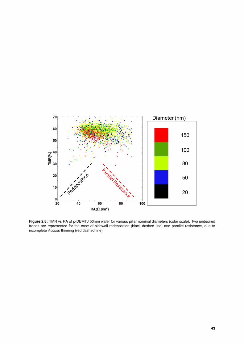
Figure 2.8: TMR vs RA of p-DBMTJ 50mm wafer for various pillar nominal diameters (color scale). Two undesiredtrends are represented for the case of sidewall redeposition (black dashed line) and parallel resistance, due toincomplete Accuflo thinning (red dashed line).
43

44
3Spin transfer torque in double barrier
tunnel junctions with in-planeanisotropy
Contents3.1 Introduction . . . . . . . . . . . . . . . . . . . . . . . . . . . . . . . . . . . . . . . . . . 463.2 DC current measurements . . . . . . . . . . . . . . . . . . . . . . . . . . . . . . . . . . 513.3 Voltage Pulses Measurements . . . . . . . . . . . . . . . . . . . . . . . . . . . . . . . . 753.4 Macrospin Simulations . . . . . . . . . . . . . . . . . . . . . . . . . . . . . . . . . . . . 963.5 Summmary . . . . . . . . . . . . . . . . . . . . . . . . . . . . . . . . . . . . . . . . . . . 109
45
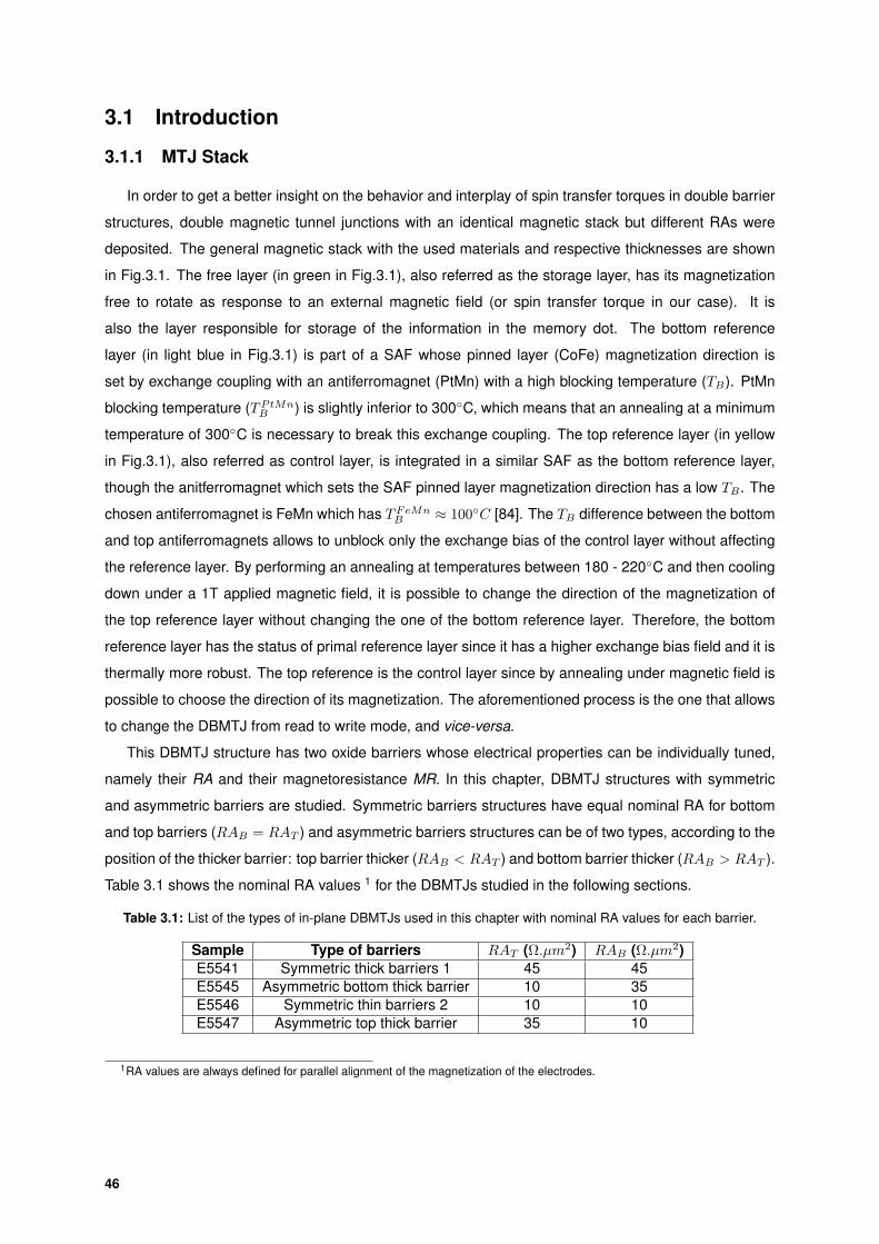
3.1 Introduction
3.1.1 MTJ Stack
In order to get a better insight on the behavior and interplay of spin transfer torques in double barrier
structures, double magnetic tunnel junctions with an identical magnetic stack but different RAs were
deposited. The general magnetic stack with the used materials and respective thicknesses are shown
in Fig.3.1. The free layer (in green in Fig.3.1), also referred as the storage layer, has its magnetization
free to rotate as response to an external magnetic field (or spin transfer torque in our case). It is
also the layer responsible for storage of the information in the memory dot. The bottom reference
layer (in light blue in Fig.3.1) is part of a SAF whose pinned layer (CoFe) magnetization direction is
set by exchange coupling with an antiferromagnet (PtMn) with a high blocking temperature (TB). PtMn
blocking temperature (TPtMnB ) is slightly inferior to 300C, which means that an annealing at a minimum
temperature of 300C is necessary to break this exchange coupling. The top reference layer (in yellow
in Fig.3.1), also referred as control layer, is integrated in a similar SAF as the bottom reference layer,
though the anitferromagnet which sets the SAF pinned layer magnetization direction has a low TB . The
chosen antiferromagnet is FeMn which has TFeMnB ≈ 100C [84]. The TB difference between the bottom
and top antiferromagnets allows to unblock only the exchange bias of the control layer without affecting
the reference layer. By performing an annealing at temperatures between 180 - 220C and then cooling
down under a 1T applied magnetic field, it is possible to change the direction of the magnetization of
the top reference layer without changing the one of the bottom reference layer. Therefore, the bottom
reference layer has the status of primal reference layer since it has a higher exchange bias field and it is
thermally more robust. The top reference is the control layer since by annealing under magnetic field is
possible to choose the direction of its magnetization. The aforementioned process is the one that allows
to change the DBMTJ from read to write mode, and vice-versa.
This DBMTJ structure has two oxide barriers whose electrical properties can be individually tuned,
namely their RA and their magnetoresistance MR. In this chapter, DBMTJ structures with symmetric
and asymmetric barriers are studied. Symmetric barriers structures have equal nominal RA for bottom
and top barriers (RAB = RAT ) and asymmetric barriers structures can be of two types, according to the
position of the thicker barrier: top barrier thicker (RAB < RAT ) and bottom barrier thicker (RAB > RAT ).
Table 3.1 shows the nominal RA values 1 for the DBMTJs studied in the following sections.
Table 3.1: List of the types of in-plane DBMTJs used in this chapter with nominal RA values for each barrier.
Sample Type of barriers RAT (Ω.µm2) RAB (Ω.µm2)E5541 Symmetric thick barriers 1 45 45E5545 Asymmetric bottom thick barrier 10 35E5546 Symmetric thin barriers 2 10 10E5547 Asymmetric top thick barrier 35 10
1RA values are always defined for parallel alignment of the magnetization of the electrodes.
46
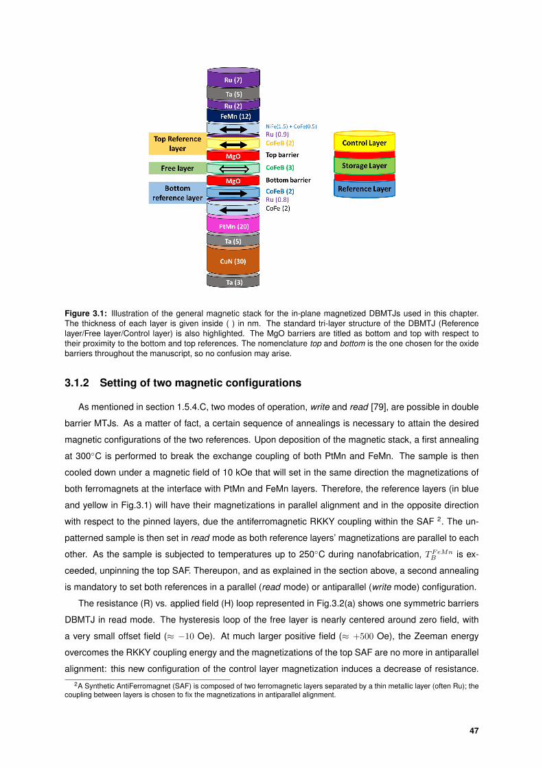
Figure 3.1: Illustration of the general magnetic stack for the in-plane magnetized DBMTJs used in this chapter.The thickness of each layer is given inside ( ) in nm. The standard tri-layer structure of the DBMTJ (Referencelayer/Free layer/Control layer) is also highlighted. The MgO barriers are titled as bottom and top with respect totheir proximity to the bottom and top references. The nomenclature top and bottom is the one chosen for the oxidebarriers throughout the manuscript, so no confusion may arise.
3.1.2 Setting of two magnetic configurations
As mentioned in section 1.5.4.C, two modes of operation, write and read [79], are possible in double
barrier MTJs. As a matter of fact, a certain sequence of annealings is necessary to attain the desired
magnetic configurations of the two references. Upon deposition of the magnetic stack, a first annealing
at 300C is performed to break the exchange coupling of both PtMn and FeMn. The sample is then
cooled down under a magnetic field of 10 kOe that will set in the same direction the magnetizations of
both ferromagnets at the interface with PtMn and FeMn layers. Therefore, the reference layers (in blue
and yellow in Fig.3.1) will have their magnetizations in parallel alignment and in the opposite direction
with respect to the pinned layers, due the antiferromagnetic RKKY coupling within the SAF 2. The un-
patterned sample is then set in read mode as both reference layers’ magnetizations are parallel to each
other. As the sample is subjected to temperatures up to 250C during nanofabrication, TFeMnB is ex-
ceeded, unpinning the top SAF. Thereupon, and as explained in the section above, a second annealing
is mandatory to set both references in a parallel (read mode) or antiparallel (write mode) configuration.
The resistance (R) vs. applied field (H) loop represented in Fig.3.2(a) shows one symmetric barriers
DBMTJ in read mode. The hysteresis loop of the free layer is nearly centered around zero field, with
a very small offset field (≈ −10 Oe). At much larger positive field (≈ +500 Oe), the Zeeman energy
overcomes the RKKY coupling energy and the magnetizations of the top SAF are no more in antiparallel
alignment: this new configuration of the control layer magnetization induces a decrease of resistance.2A Synthetic AntiFerromagnet (SAF) is composed of two ferromagnetic layers separated by a thin metallic layer (often Ru); the
coupling between layers is chosen to fix the magnetizations in antiparallel alignment.
47

Figure 3.2: Resistance vs. applied field loop for a symmetric barriers double junction, whose nominal dimensionsare 40 x 140 nm, set in (a) read mode (parallel references) and (b) write mode (antiparallel references). Acquired ata bias current of 1µA. The inset illustrations show the different configurations of the magnetizations of the tri-layerstructure for different values of the applied field. The top pinned layer (in light blue) is added to show the rotation ofits magnetization when the Zeeman energy overcomes the exchange coupling energy.
Similarly, at sufficiently large negative applied fields (≈ −1000 Oe), the exchange coupling is broken,
allowing the pinned layer to rotate. This transition is associated with a slight increase in resistance. As
the DBMTJ is set in write mode [Fig.3.2(b)], free layer offset and transition fields change sign.
Thus, there are a total of four distinct magnetic states (see Fig.3.2): 1) free layer is parallel to both
references (P - P), 2) free layer is antiparallel to both references (AP - AP), 3) free layer is parallel to
bottom reference and antiparallel to top reference (P - AP) and 4) the opposite state (AP - P). The RA
product of these four states can be translated in four equations, which are described by the following
system:
RA1 = RAB +RAT
RA2 = RAB(1 + TMRB) +RAT (1 + TMRT )
RA3 = RAB +RAT (1 + TMRT )
RA4 = RAB(1 + TMRB) +RAT
(3.1)
in which RAn is the resistance-area product of the DBMTJ in #n magnetic state, TMRB and TMRT
are the tunnel magnetorestiance of bottom and top barriers, respectively. These equations allow the
determination of the RA and TMR of each barrier individually which is important to ensure that the
properties of the DBMTJ upon deposition have not significantly changed after patterning. In spite of
having four unknowns (RAB , RAT , TMRB and TMRT ) and a system of four equations, one of these
parameters needs to be known a priori since one of the four equations can be obtained by a linear
combination of the others. The margin of error for the parameters extracted by equations 3.1 depends
on the accuracy of the pre-determined variable and the estimation of the lateral dimensions of the pillar.
These parameters can also be retrieved by fitting the data obtained via current-in-plane-tunneling (CIPT)
with a mathematical model developed specifically for double barrier MTJs [85,86].
48
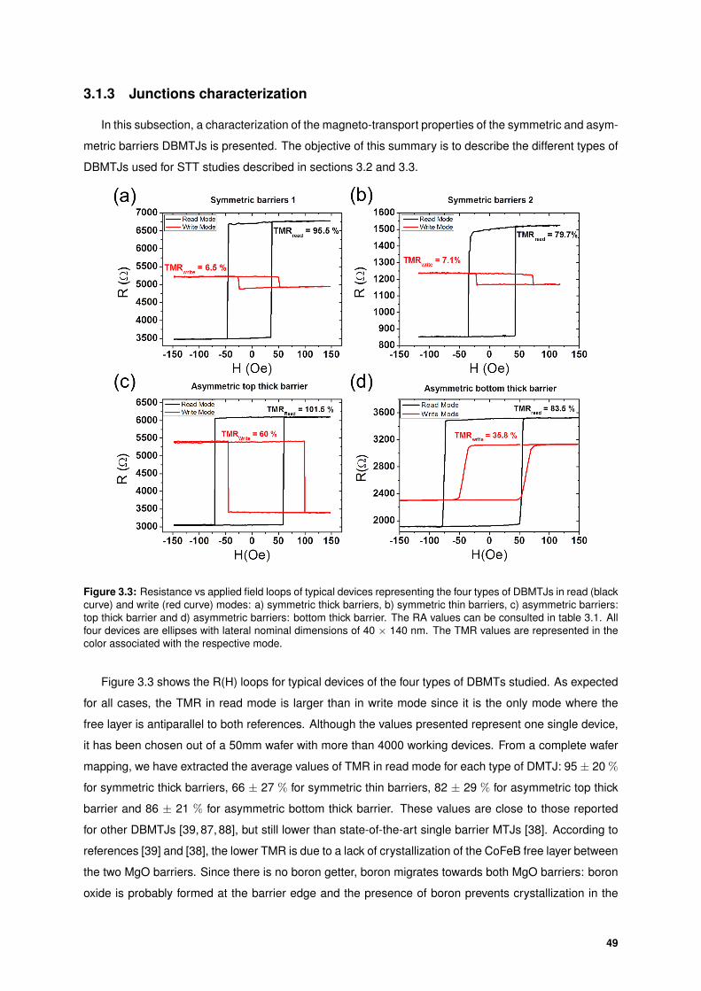
3.1.3 Junctions characterization
In this subsection, a characterization of the magneto-transport properties of the symmetric and asym-
metric barriers DBMTJs is presented. The objective of this summary is to describe the different types of
DBMTJs used for STT studies described in sections 3.2 and 3.3.
Figure 3.3: Resistance vs applied field loops of typical devices representing the four types of DBMTJs in read (blackcurve) and write (red curve) modes: a) symmetric thick barriers, b) symmetric thin barriers, c) asymmetric barriers:top thick barrier and d) asymmetric barriers: bottom thick barrier. The RA values can be consulted in table 3.1. Allfour devices are ellipses with lateral nominal dimensions of 40 × 140 nm. The TMR values are represented in thecolor associated with the respective mode.
Figure 3.3 shows the R(H) loops for typical devices of the four types of DBMTs studied. As expected
for all cases, the TMR in read mode is larger than in write mode since it is the only mode where the
free layer is antiparallel to both references. Although the values presented represent one single device,
it has been chosen out of a 50mm wafer with more than 4000 working devices. From a complete wafer
mapping, we have extracted the average values of TMR in read mode for each type of DMTJ: 95 ± 20 %
for symmetric thick barriers, 66 ± 27 % for symmetric thin barriers, 82 ± 29 % for asymmetric top thick
barrier and 86 ± 21 % for asymmetric bottom thick barrier. These values are close to those reported
for other DBMTJs [39, 87, 88], but still lower than state-of-the-art single barrier MTJs [38]. According to
references [39] and [38], the lower TMR is due to a lack of crystallization of the CoFeB free layer between
the two MgO barriers. Since there is no boron getter, boron migrates towards both MgO barriers: boron
oxide is probably formed at the barrier edge and the presence of boron prevents crystallization in the
49

vicinity of both barriers, thus reducing the TMR. The TMR in write mode is variable since the free layer
is on a hybrid state relatively to the two references and thus the situation is very different for symmetric
or asymmetric barriers structure. The TMR in write mode is given by the difference in resistance (∆R)
between #3 and #4 states [see Fig.3.2(b)], ∆R3−4 = RTTMRT −RBTMRB , divided by the resistance
of the state with lower resistance. In the case of asymmetric barriers DBMTJ [see figs.3.3(c) and (d)] the
values of TMRwrite are large sinceRAT 6= RAB . For symmetric DBMTJ, no TMR should be observed in
write mode (∆R3−4 = 0), if the barriers were perfectly symmetric (RAT = RAB and TMRT = TMRB).
However, a small asymmetry is observed in nominally symmetric barriers that accounts for the small
TMR observed (6-7 %). It can be explained by the difference in growth conditions of the top barrier with
respect to the bottom one. Therefore, it is of particular importance to calculate the individual RA and
TMR of each barrier to ensure the comprehension of the results observed for the current induced spin
transfer torque switching in these structures. Table 3.2 presents the calculated parameters of top and
bottom barriers for each junction of Fig.3.3, using the system of equations 3.1. Since in the system only
3 equations are independent, one of the parameters needed to be set a priori. RT was the parameter
set with its nominal value because, according to [39] and also observed by P.-Y. Clement [1], the top
barrier has superior texture quality than the bottom barrier 3. Despite the general amorphous state of
the CoFeB in the free layer, at the interface with the top barrier lattice planes are formed, promoting a
better texture and favoring the (001) orientation of the MgO. Consequently, top barrier should have RA
values closer to nominal 4 and a better TMR.
In the case of the two symmetric barriers structures, though perfect symmetry was not achieved, the
two barriers have very similar RAs (difference below 5 Ω.µm2) which translates in the very low TMR of
these DMTJs in write mode. It is also noticible that the top barrier has a slightly higher RA and TMR
than the bottom barrier. For the two asymmetric barriers structures, the obtained values for RA are in
most agreement with barriers nominal values. However, for the structures with thicker bottom barrier, we
observe that TMRT > TMRB , whereas the thicker barrier was expected to have the larger TMR. If we
take into account the above mentioned higher crystalline quality of the top barrier, then the difference in
TMR of a barrier with same nominal RA (10 Ω.µm2) above or below the free layer might be explained.
While the same barrier has a TMR of 94 % when grown on top of the free layer, it reduces down to 42%
when grown below it.
Table 3.2: Calculation of RA and TMR for each individual barrier for the devices exhibited in Fig.3.3. RAT was theparameter chosen to remain fixed. The lateral dimensions taken into account for the calculation were 140 × 220nm since the pillar has a conical shape due to the angle used during IBE etch.
Type of barriers RAT (Ω.µm2) RAB (Ω.µm2) TMRT (%) TMRB (%)Symmetric thick barriers 45 42.3 96.8 90.5
Asymmetric bottom thick barrier 10 36.3 94.5 80.5Symmetric thin barriers 10 9.4 80.2 75.5
Asymmetric top thick barrier 35 12.8 104.7 42.5
3This is just an assumption since only TEM analysis of a the DBMTJ vertical cross section would help to support this statement.However, one hypothesis lies on the possibility of better growth of the top barrier since the FL CoFeB layer (3 nm) is thicker thanthe CoFeB layer (2 nm) of the bottom SAF below the bottom MgO barrier.
4Note that this statement cannot be supported by the CIPT measurements for barriers with RA values so close to each other,since the error margin is too large.
50
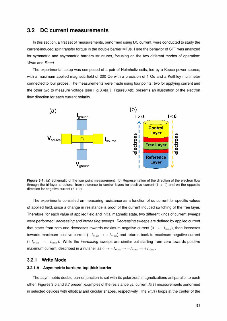
3.2 DC current measurements
In this section, a first set of measurements, performed using DC current, were conducted to study the
current-induced spin transfer torque in the double barrier MTJs. Here the behavior of STT was analyzed
for symmetric and asymmetric barriers structures, focusing on the two different modes of operation:
Write and Read.
The experimental setup was composed of a pair of Helmholtz coils, fed by a Kepco power source,
with a maximum applied magnetic field of 200 Oe with a precision of 1 Oe and a Keithley multimeter
connected to four probes. The measurements were made using four points: two for applying current and
the other two to measure voltage [see Fig.3.4(a)]. Figure3.4(b) presents an illustration of the electron
flow direction for each current polarity.
Figure 3.4: (a) Schematic of the four point measurement. (b) Representation of the direction of the electron flowthrough the tri-layer structure: from reference to control layers for positive current (I > 0) and on the oppositedirection for negative current (I < 0).
The experiments consisted on measuring resistance as a function of dc current for specific values
of applied field, since a change in resistance is proof of the current induced switching of the free layer.
Therefore, for each value of applied field and initial magnetic state, two different kinds of current sweeps
were performed: decreasing and increasing sweeps. Decreasing sweeps are defined by applied current
that starts from zero and decreases towards maximum negative current (0 → −Imax), then increases
towards maximum positive current (−Imax → +Imax) and returns back to maximum negative current
(+Imax → −Imax). While the increasing sweeps are similar but starting from zero towards positive
maximum current, described in a nutshell as 0→ +Imax → −Imax → +Imax.
3.2.1 Write Mode
3.2.1.A Asymmetric barriers: top thick barrier
The asymmetric double barrier junction is set with its polarizers’ magnetizations antiparallel to each
other. Figures 3.5 and 3.7 present examples of the resistance vs. currentR(I) measurements performed
in selected devices with elliptical and circular shapes, respectively. The R(H) loops at the center of the
51

images have markers (black and green colors) indicating the applied field and the initial magnetic state
state chosen for the realization of the sweeps. By analyzing the two R(I) plots on the bottom of Fig.3.5
represented by the black and green squares, the switching from the AP-P state to P-AP occurs only for
positive current. Considering the junction’s initial state [state 4 of Fig.3.2(b)] and the electron flow for
positive current [see Fig.3.4(b)], the electrons will be initially polarized in the reference layer, carrying
the same moment as ~pr. The free layer’s magnetic moment, ~m, is antiparallel to ~pr, thus the incident
electrons arriving at the free layer apply a torque, destabilizing its initial state, i. e. favoring the reversal
of the free layer’s magnetization. Then the transmitted electrons travel from ~m to ~pc which are parallel at
the initial state. Although, the torque exerted by the incident electrons on ~pc favor its initial configuration,
most part of the electrons reflected at the interface between the top barrier and the control layer carry
the opposite moment to ~pc and are thus responsible for a second transfer of angular momentum onto
~m, assisting on its reversal. The total torque applied onto the free layer is then the sum of the torques
coming from both reference and control layers, | T‖total |=| T‖r | + | T‖c |. We conclude that, for an
asymmetric DBMTJ with a thicker top barrier, an electron flow from reference to control layer (I > 0 in
our case) favors the transition from AP-P towards P-AP state. Starting from the same initial state AP-P
but applying a negative current, and following a similar interpretation, it is trivial to conclude that the sum
of the torques exerted on ~m favor the stabilization of its initial configuration. The decreasing sweep of
Fig.3.5(b) demonstrates the conservation of the AP-P state when a negative current is injected into the
system. Reversal of the storage layer only happens when the current polarity changes.
Figure 3.5: Descriptive resistance vs current plots of an elliptical asymmetric top thick barrier junction of nominaldimensions 40 ×140 nm [same as in Fig.3.3(c)], set in write mode. The R(H) loop at the center shows the bistableregion (where switching is possible) of the DBMTJ when the reference layers’ magnetization are in antiparallelalignment. DMTJ’s coercive field is Hc = 72Oe and offset field is Hoff = 27Oe. (a)-(b) Decreasing and (c)-(d)increasing sweeps are represented by the black and green markers, respectively while their shape refers to theinitial magnetic configuration of the DBMTJ: AP-P (square) or P-AP (triangle).
Following the same line of thought and physical interpretation, if the initial configuration is now P-AP,
the requirements to reverse or favor the direction of ~m are inverted. Therefore, electron flow from con-
52
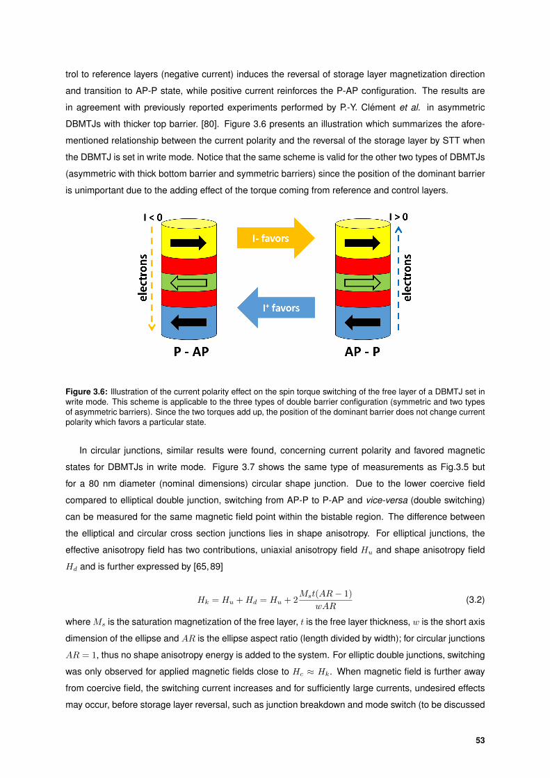
trol to reference layers (negative current) induces the reversal of storage layer magnetization direction
and transition to AP-P state, while positive current reinforces the P-AP configuration. The results are
in agreement with previously reported experiments performed by P.-Y. Clement et al. in asymmetric
DBMTJs with thicker top barrier. [80]. Figure 3.6 presents an illustration which summarizes the afore-
mentioned relationship between the current polarity and the reversal of the storage layer by STT when
the DBMTJ is set in write mode. Notice that the same scheme is valid for the other two types of DBMTJs
(asymmetric with thick bottom barrier and symmetric barriers) since the position of the dominant barrier
is unimportant due to the adding effect of the torque coming from reference and control layers.
Figure 3.6: Illustration of the current polarity effect on the spin torque switching of the free layer of a DBMTJ set inwrite mode. This scheme is applicable to the three types of double barrier configuration (symmetric and two typesof asymmetric barriers). Since the two torques add up, the position of the dominant barrier does not change currentpolarity which favors a particular state.
In circular junctions, similar results were found, concerning current polarity and favored magnetic
states for DBMTJs in write mode. Figure 3.7 shows the same type of measurements as Fig.3.5 but
for a 80 nm diameter (nominal dimensions) circular shape junction. Due to the lower coercive field
compared to elliptical double junction, switching from AP-P to P-AP and vice-versa (double switching)
can be measured for the same magnetic field point within the bistable region. The difference between
the elliptical and circular cross section junctions lies in shape anisotropy. For elliptical junctions, the
effective anisotropy field has two contributions, uniaxial anisotropy field Hu and shape anisotropy field
Hd and is further expressed by [65,89]
Hk = Hu +Hd = Hu + 2Mst(AR− 1)
wAR(3.2)
where Ms is the saturation magnetization of the free layer, t is the free layer thickness, w is the short axis
dimension of the ellipse and AR is the ellipse aspect ratio (length divided by width); for circular junctions
AR = 1, thus no shape anisotropy energy is added to the system. For elliptic double junctions, switching
was only observed for applied magnetic fields close to Hc ≈ Hk. When magnetic field is further away
from coercive field, the switching current increases and for sufficiently large currents, undesired effects
may occur, before storage layer reversal, such as junction breakdown and mode switch (to be discussed
53
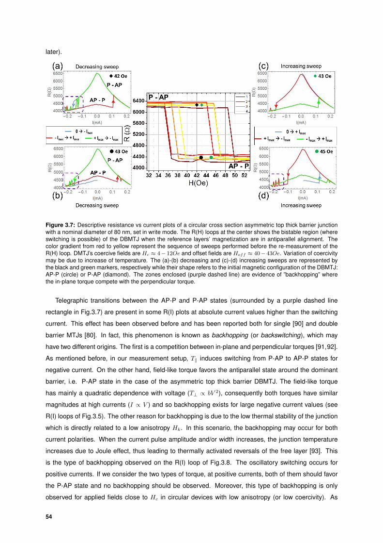
later).
Figure 3.7: Descriptive resistance vs current plots of a circular cross section asymmetric top thick barrier junctionwith a nominal diameter of 80 nm, set in write mode. The R(H) loops at the center shows the bistable region (whereswitching is possible) of the DBMTJ when the reference layers’ magnetization are in antiparallel alignment. Thecolor gradient from red to yellow represent the sequence of sweeps performed before the re-measurement of theR(H) loop. DMTJ’s coercive fields are Hc ≈ 4− 12Oe and offset fields are Hoff ≈ 40− 43Oe. Variation of coercivitymay be due to increase of temperature. The (a)-(b) decreasing and (c)-(d) increasing sweeps are represented bythe black and green markers, respectively while their shape refers to the initial magnetic configuration of the DBMTJ:AP-P (circle) or P-AP (diamond). The zones enclosed (purple dashed line) are evidence of ”backhopping” wherethe in-plane torque compete with the perpendicular torque.
Telegraphic transitions between the AP-P and P-AP states (surrounded by a purple dashed line
rectangle in Fig.3.7) are present in some R(I) plots at absolute current values higher than the switching
current. This effect has been observed before and has been reported both for single [90] and double
barrier MTJs [80]. In fact, this phenomenon is known as backhopping (or backswitching), which may
have two different origins. The first is a competition between in-plane and perpendicular torques [91,92].
As mentioned before, in our measurement setup, T‖ induces switching from P-AP to AP-P states for
negative current. On the other hand, field-like torque favors the antiparallel state around the dominant
barrier, i.e. P-AP state in the case of the asymmetric top thick barrier DBMTJ. The field-like torque
has mainly a quadratic dependence with voltage (T⊥ ∝ bV 2), consequently both torques have similar
magnitudes at high currents (I ∝ V ) and so backhopping exists for large negative current values (see
R(I) loops of Fig.3.5). The other reason for backhopping is due to the low thermal stability of the junction
which is directly related to a low anisotropy Hk. In this scenario, the backhopping may occur for both
current polarities. When the current pulse amplitude and/or width increases, the junction temperature
increases due to Joule effect, thus leading to thermally activated reversals of the free layer [93]. This
is the type of backhopping observed on the R(I) loop of Fig.3.8. The oscillatory switching occurs for
positive currents. If we consider the two types of torque, at positive currents, both of them should favor
the P-AP state and no backhopping should be observed. Moreover, this type of backhopping is only
observed for applied fields close to Hc in circular devices with low anisotropy (or low coercivity). As
54
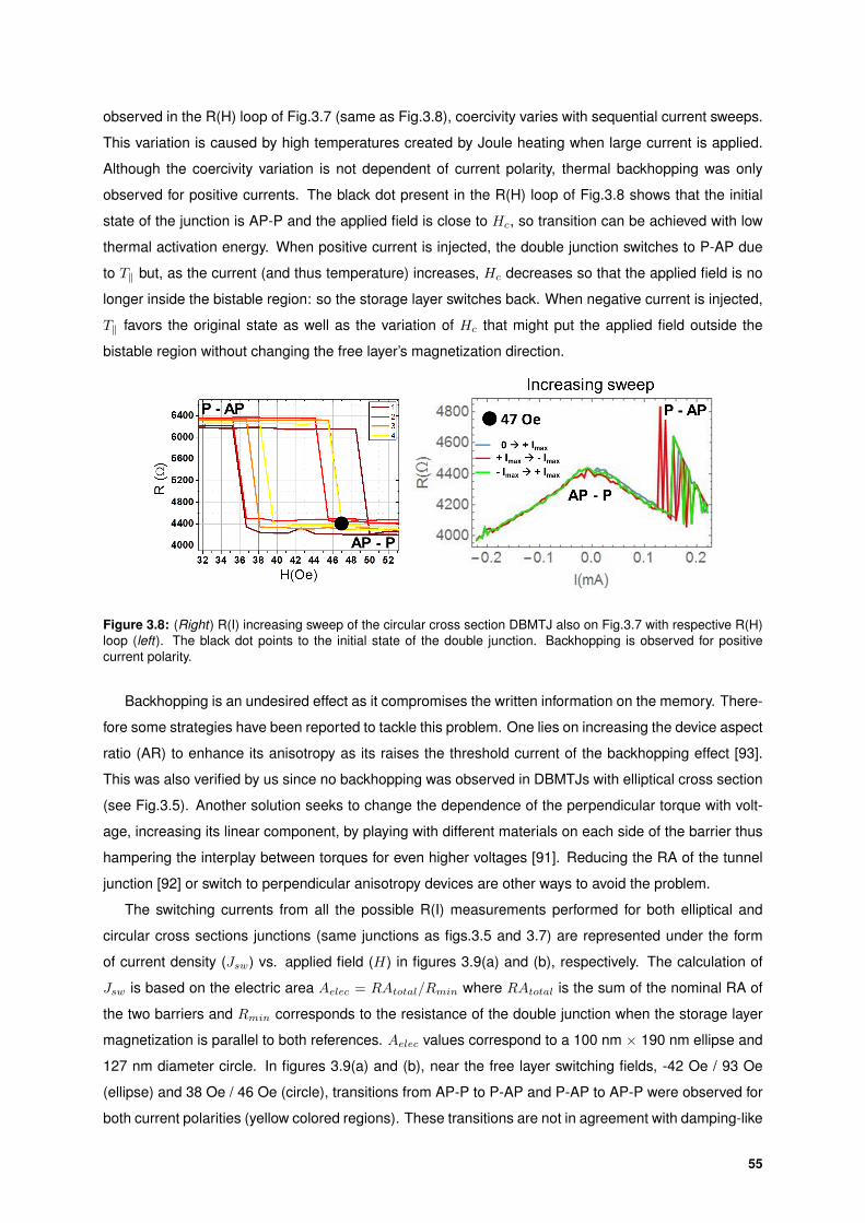
observed in the R(H) loop of Fig.3.7 (same as Fig.3.8), coercivity varies with sequential current sweeps.
This variation is caused by high temperatures created by Joule heating when large current is applied.
Although the coercivity variation is not dependent of current polarity, thermal backhopping was only
observed for positive currents. The black dot present in the R(H) loop of Fig.3.8 shows that the initial
state of the junction is AP-P and the applied field is close to Hc, so transition can be achieved with low
thermal activation energy. When positive current is injected, the double junction switches to P-AP due
to T‖ but, as the current (and thus temperature) increases, Hc decreases so that the applied field is no
longer inside the bistable region: so the storage layer switches back. When negative current is injected,
T‖ favors the original state as well as the variation of Hc that might put the applied field outside the
bistable region without changing the free layer’s magnetization direction.
Figure 3.8: (Right) R(I) increasing sweep of the circular cross section DBMTJ also on Fig.3.7 with respective R(H)loop (left). The black dot points to the initial state of the double junction. Backhopping is observed for positivecurrent polarity.
Backhopping is an undesired effect as it compromises the written information on the memory. There-
fore some strategies have been reported to tackle this problem. One lies on increasing the device aspect
ratio (AR) to enhance its anisotropy as its raises the threshold current of the backhopping effect [93].
This was also verified by us since no backhopping was observed in DBMTJs with elliptical cross section
(see Fig.3.5). Another solution seeks to change the dependence of the perpendicular torque with volt-
age, increasing its linear component, by playing with different materials on each side of the barrier thus
hampering the interplay between torques for even higher voltages [91]. Reducing the RA of the tunnel
junction [92] or switch to perpendicular anisotropy devices are other ways to avoid the problem.
The switching currents from all the possible R(I) measurements performed for both elliptical and
circular cross sections junctions (same junctions as figs.3.5 and 3.7) are represented under the form
of current density (Jsw) vs. applied field (H) in figures 3.9(a) and (b), respectively. The calculation of
Jsw is based on the electric area Aelec = RAtotal/Rmin where RAtotal is the sum of the nominal RA of
the two barriers and Rmin corresponds to the resistance of the double junction when the storage layer
magnetization is parallel to both references. Aelec values correspond to a 100 nm × 190 nm ellipse and
127 nm diameter circle. In figures 3.9(a) and (b), near the free layer switching fields, -42 Oe / 93 Oe
(ellipse) and 38 Oe / 46 Oe (circle), transitions from AP-P to P-AP and P-AP to AP-P were observed for
both current polarities (yellow colored regions). These transitions are not in agreement with damping-like
55
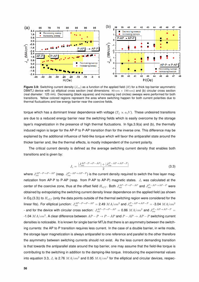
Figure 3.9: Switching current density (Jsw) as a function of the applied field (H) for a thick top barrier asymmetricDBMTJ device with (a) elliptical cross section (real dimensions: 80nm × 190nm) and (b) circular cross section(real diameter: 125 nm). Decreasing (black squares) and increasing (red circles) sweeps were performed for bothtransitions. Yellow colored regions represent the area where switching happen for both current polarities due tothermal fluctuations and low energy barrier near the coercive fields.
torque which has a dominant linear dependence with voltage (T‖ ∝ a1V ). These undesired transitions
are due to a reduced energy barrier near the switching fields which is easily overcome by the storage
layer’s magnetization in the presence of high thermal fluctuations. In figs.3.9(a) and (b), the thermally
induced region is larger for the AP-P to P-AP transition than for the inverse one. This difference may be
explained by the additional influence of field-like torque which will favor the antiparallel state around the
thicker barrier and, like the thermal effects, is mostly independent of the current polarity.
The critical current density is defined as the average switching current density that enables both
transitions and is given by:
Jc =|JAP−P→P−APsw |+ |JP−AP→AP−Psw |
2(3.3)
where JAP−P→P−APsw (resp. JP−AP→AP−Psw ) is the current density required to switch the free layer mag-
netization from AP-P to P-AP (resp. from P-AP to AP-P) magnetic states. Jc was calculated at the
center of the coercive zone, thus at the offset field Hoff . Both JAP−P→P−APsw and JP−AP→AP−Psw were
obtained by extrapolating the switching current density linear dependence on the applied field (as shown
in Eq.(3.3)) to Hoff (only the data points outside of the thermal switching region were considered for the
linear fits). For elliptical junction: JAP−P→P−APsw = 2.49 MA/cm2 and JP−AP→AP−Psw = -3.04 MA/cm2
- and for the device with circular cross section: JAP−P→P−APsw = 0.86 MA/cm2 and JP−AP→AP−Psw =
-1.04 MA/cm2. A clear difference between AP −P → P −AP and P −AP → AP −P switching current
densities is noticeable. It is known for single barrier MTJs that there is an asymmetry between the switch-
ing currents: the AP to P transition requires less current. In the case of a double barrier, in write mode,
the storage layer magnetization is always antiparallel to one reference and parallel to the other therefore
the asymmetry between switching currents should not exist. As the less current demanding transition
is that towards the antiparallel state around the top barrier, one may assume that the field-like torque is
contributing to the switching in addition to the damping-like torque. Introducing the experimental values
into equation 3.3, Jc is 2.76 MA/cm2 and 0.95 MA/cm2 for the elliptical and circular devices, respec-
56
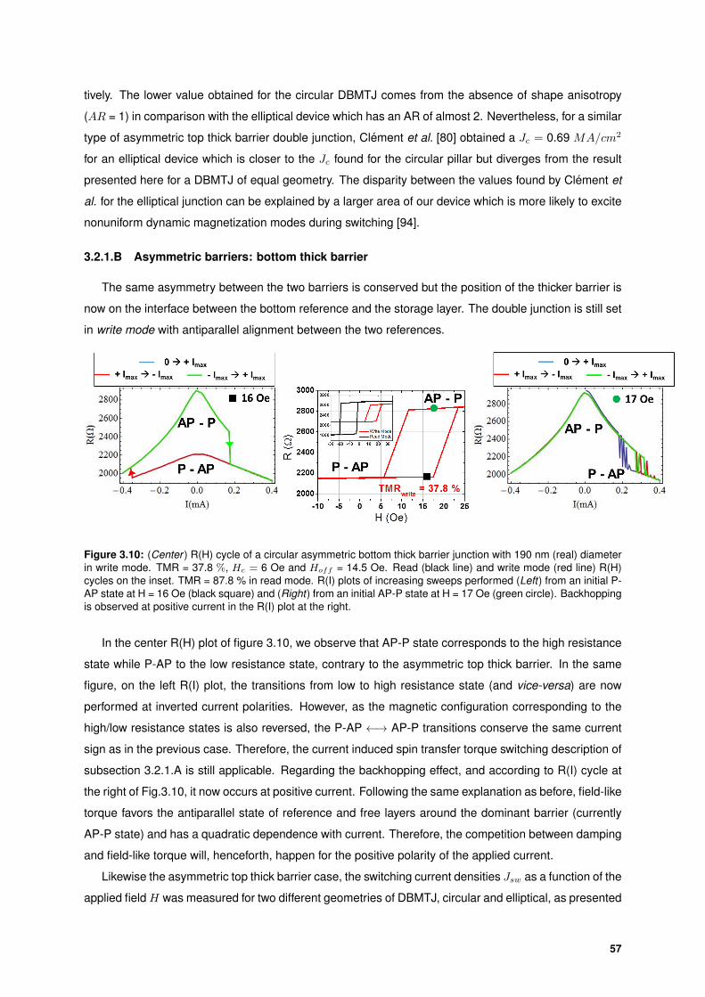
tively. The lower value obtained for the circular DBMTJ comes from the absence of shape anisotropy
(AR = 1) in comparison with the elliptical device which has an AR of almost 2. Nevertheless, for a similar
type of asymmetric top thick barrier double junction, Clement et al. [80] obtained a Jc = 0.69 MA/cm2
for an elliptical device which is closer to the Jc found for the circular pillar but diverges from the result
presented here for a DBMTJ of equal geometry. The disparity between the values found by Clement et
al. for the elliptical junction can be explained by a larger area of our device which is more likely to excite
nonuniform dynamic magnetization modes during switching [94].
3.2.1.B Asymmetric barriers: bottom thick barrier
The same asymmetry between the two barriers is conserved but the position of the thicker barrier is
now on the interface between the bottom reference and the storage layer. The double junction is still set
in write mode with antiparallel alignment between the two references.
Figure 3.10: (Center ) R(H) cycle of a circular asymmetric bottom thick barrier junction with 190 nm (real) diameterin write mode. TMR = 37.8 %, Hc = 6 Oe and Hoff = 14.5 Oe. Read (black line) and write mode (red line) R(H)cycles on the inset. TMR = 87.8 % in read mode. R(I) plots of increasing sweeps performed (Left) from an initial P-AP state at H = 16 Oe (black square) and (Right) from an initial AP-P state at H = 17 Oe (green circle). Backhoppingis observed at positive current in the R(I) plot at the right.
In the center R(H) plot of figure 3.10, we observe that AP-P state corresponds to the high resistance
state while P-AP to the low resistance state, contrary to the asymmetric top thick barrier. In the same
figure, on the left R(I) plot, the transitions from low to high resistance state (and vice-versa) are now
performed at inverted current polarities. However, as the magnetic configuration corresponding to the
high/low resistance states is also reversed, the P-AP ←→ AP-P transitions conserve the same current
sign as in the previous case. Therefore, the current induced spin transfer torque switching description of
subsection 3.2.1.A is still applicable. Regarding the backhopping effect, and according to R(I) cycle at
the right of Fig.3.10, it now occurs at positive current. Following the same explanation as before, field-like
torque favors the antiparallel state of reference and free layers around the dominant barrier (currently
AP-P state) and has a quadratic dependence with current. Therefore, the competition between damping
and field-like torque will, henceforth, happen for the positive polarity of the applied current.
Likewise the asymmetric top thick barrier case, the switching current densities Jsw as a function of the
applied fieldH was measured for two different geometries of DBMTJ, circular and elliptical, as presented
57
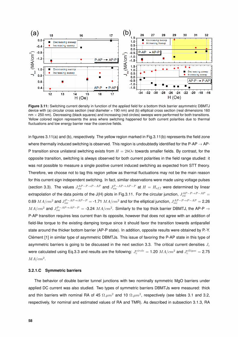
Figure 3.11: Switching current density in function of the applied field for a bottom thick barrier asymmetric DBMTJdevice with (a) circular cross section (real diameter = 190 nm) and (b) elliptical cross section (real dimensions 160nm × 250 nm). Decreasing (black squares) and increasing (red circles) sweeps were performed for both transitions.Yellow colored region represents the area where switching happened for both current polarities due to thermalfluctuations and low energy barrier near the coercive fields.
in figures 3.11(a) and (b), respectively. The yellow region marked in Fig.3.11(b) represents the field zone
where thermally induced switching is observed. This region is undoubtedly identified for the P-AP→ AP-
P transition since unilateral switching exists from H = 28Oe towards smaller fields. By contrast, for the
opposite transition, switching is always observed for both current polarities in the field range studied: it
was not possible to measure a single positive current induced switching as expected from STT theory.
Therefore, we choose not to tag this region yellow as thermal fluctuations may not be the main reason
for this current sign independent switching. In fact, similar observations were made using voltage pulses
(section 3.3). The values JAP−P→P−APsw and JP−AP→AP−Psw at H = Hoff were determined by linear
extrapolation of the data points of the J(H) plots in Fig.3.11. For the circular junction, JAP−P→P−APsw =
0.69 MA/cm2 and JP−AP→AP−Psw = -1.71 MA/cm2 and for the elliptical junction, JAP−P→P−APsw = 2.26
MA/cm2 and JP−AP→AP−Psw = -3.24 MA/cm2. Similarly to the top thick barrier DBMTJ, the AP-P →
P-AP transition requires less current than its opposite, however that does not agree with an addition of
field-like torque to the existing damping torque since it should favor the transition towards antiparallel
state around the thicker bottom barrier (AP-P state). In addition, opposite results were obtained by P.-Y.
Clement [1] in similar type of asymmetric DBMTJs. This issue of favoring the P-AP state in this type of
asymmetric barriers is going to be discussed in the next section 3.3. The critical current densities Jc
were calculated using Eq.3.3 and results are the following: Jcirclec = 1.20 MA/cm2 and Jellipsec = 2.75
MA/cm2.
3.2.1.C Symmetric barriers
The behavior of double barrier tunnel junctions with two nominally symmetric MgO barriers under
applied DC current was also studied. Two types of symmetric barriers DBMTJs were measured: thick
and thin barriers with nominal RA of 45 Ω.µm2 and 10 Ω.µm2, respectively (see tables 3.1 and 3.2,
respectively, for nominal and estimated values of RA and TMR). As described in subsection 3.1.3, RA
58
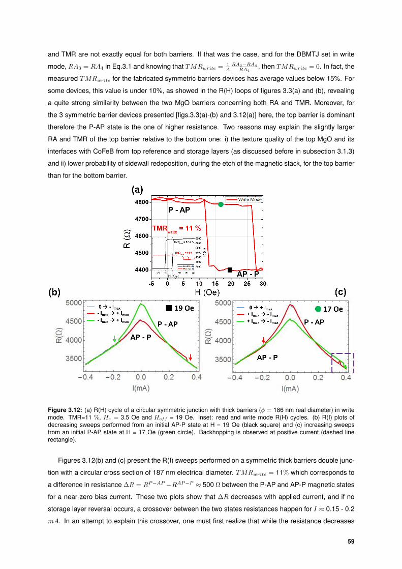
and TMR are not exactly equal for both barriers. If that was the case, and for the DBMTJ set in write
mode, RA3 = RA4 in Eq.3.1 and knowing that TMRwrite = 1ARA3−RA4
RA4, then TMRwrite = 0. In fact, the
measured TMRwrite for the fabricated symmetric barriers devices has average values below 15%. For
some devices, this value is under 10%, as showed in the R(H) loops of figures 3.3(a) and (b), revealing
a quite strong similarity between the two MgO barriers concerning both RA and TMR. Moreover, for
the 3 symmetric barrier devices presented [figs.3.3(a)-(b) and 3.12(a)] here, the top barrier is dominant
therefore the P-AP state is the one of higher resistance. Two reasons may explain the slightly larger
RA and TMR of the top barrier relative to the bottom one: i) the texture quality of the top MgO and its
interfaces with CoFeB from top reference and storage layers (as discussed before in subsection 3.1.3)
and ii) lower probability of sidewall redeposition, during the etch of the magnetic stack, for the top barrier
than for the bottom barrier.
Figure 3.12: (a) R(H) cycle of a circular symmetric junction with thick barriers (φ = 186 nm real diameter) in writemode. TMR=11 %, Hc = 3.5 Oe and Hoff = 19 Oe. Inset: read and write mode R(H) cycles. (b) R(I) plots ofdecreasing sweeps performed from an initial AP-P state at H = 19 Oe (black square) and (c) increasing sweepsfrom an initial P-AP state at H = 17 Oe (green circle). Backhopping is observed at positive current (dashed linerectangle).
Figures 3.12(b) and (c) present the R(I) sweeps performed on a symmetric thick barriers double junc-
tion with a circular cross section of 187 nm electrical diameter. TMRwrite = 11% which corresponds to
a difference in resistance ∆R = RP−AP −RAP−P ≈ 500 Ω between the P-AP and AP-P magnetic states
for a near-zero bias current. These two plots show that ∆R decreases with applied current, and if no
storage layer reversal occurs, a crossover between the two states resistances happen for I ≈ 0.15 - 0.2
mA. In an attempt to explain this crossover, one must first realize that while the resistance decreases
59
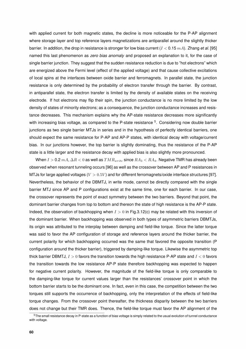
with applied current for both magnetic states, the decline is more noticeable for the P-AP alignment
where storage layer and top reference layers magnetizations are antiparallel around the slightly thicker
barrier. In addition, the drop in resistance is stronger for low bias current (I < 0.15mA). Zhang et al. [95]
named this last phenomenon as zero bias anomaly and proposed an explanation to it, for the case of
single barrier junction. They suggest that the sudden resistance reduction is due to ”hot electrons” which
are energized above the Fermi level (effect of the applied voltage) and that cause collective excitations
of local spins at the interfaces between oxide barrier and ferromagnets. In parallel state, the junction
resistance is only determined by the probability of electron transfer through the barrier. By contrast,
in antiparallel state, the electron transfer is limited by the density of available states on the receiving
electrode. If hot electrons may flip their spin, the junction conductance is no more limited by the low
density of states of minority electrons; as a consequence, the junction conductance increases and resis-
tance decreases. This mechanism explains why the AP-state resistance decreases more significantly
with increasing bias voltage, as compared to the P-state resistance 5. Considering now double barrier
junctions as two single barrier MTJs in series and in the hypothesis of perfectly identical barriers, one
should expect the same resistance for P-AP and AP-P states, with identical decay with voltage/current
bias. In our junctions however, the top barrier is slightly dominating, thus the resistance of the P-AP
state is a little larger and the resistance decay with applied bias is also slightly more pronounced.
When I > 0.2 mA, ∆R < 0 as well as TMRwrite since RA3 < RA4. Negative TMR has already been
observed when resonant tunneling occurs [96] as well as the crossover between AP and P resistances in
MTJs for large applied voltages (V > 0.5V ) and for different ferromagnets/oxide interface structures [97].
Nevertheless, the behavior of the DBMTJ, in write mode, cannot be directly compared with the single
barrier MTJ since AP and P configurations exist at the same time, one for each barrier. In our case,
the crossover represents the point of exact symmetry between the two barriers. Beyond that point, the
dominant barrier changes from top to bottom and thereon the state of high resistance is the AP-P state.
Indeed, the observation of backhopping when I > 0 in Fig.3.12(c) may be related with this inversion of
the dominant barrier. When backhopping was observed in both types of asymmetric barriers DBMTJs,
its origin was attributed to the interplay between damping and field-like torque. Since the latter torque
was said to favor the AP configuration of storage and reference layers around the thicker barrier, the
current polarity for which backhopping occurred was the same that favored the opposite transition (P
configuration around the thicker barrier), triggered by damping-like torque. Likewise the asymmetric top
thick barrier DBMTJ, I > 0 favors the transition towards the high resistance P-AP state and I < 0 favors
the transition towards the low resistance AP-P state therefore backhopping was expected to happen
for negative current polarity. However, the magnitude of the field-like torque is only comparable to
the damping-like torque for current values larger than the resistances’ crossover point in which the
bottom barrier starts to be the dominant one. In fact, even in this case, the competition between the two
torques still supports the occurrence of backhopping, only the interpretation of the effects of field-like
torque changes. From the crossover point thereafter, the thickness disparity between the two barriers
does not change but their TMR does. Thence, the field-like torque must favor the AP alignment of the5The small resistance decay in P-state as a function of bias voltage is simply related to the usual evolution of tunnel conductance
with voltage.
60
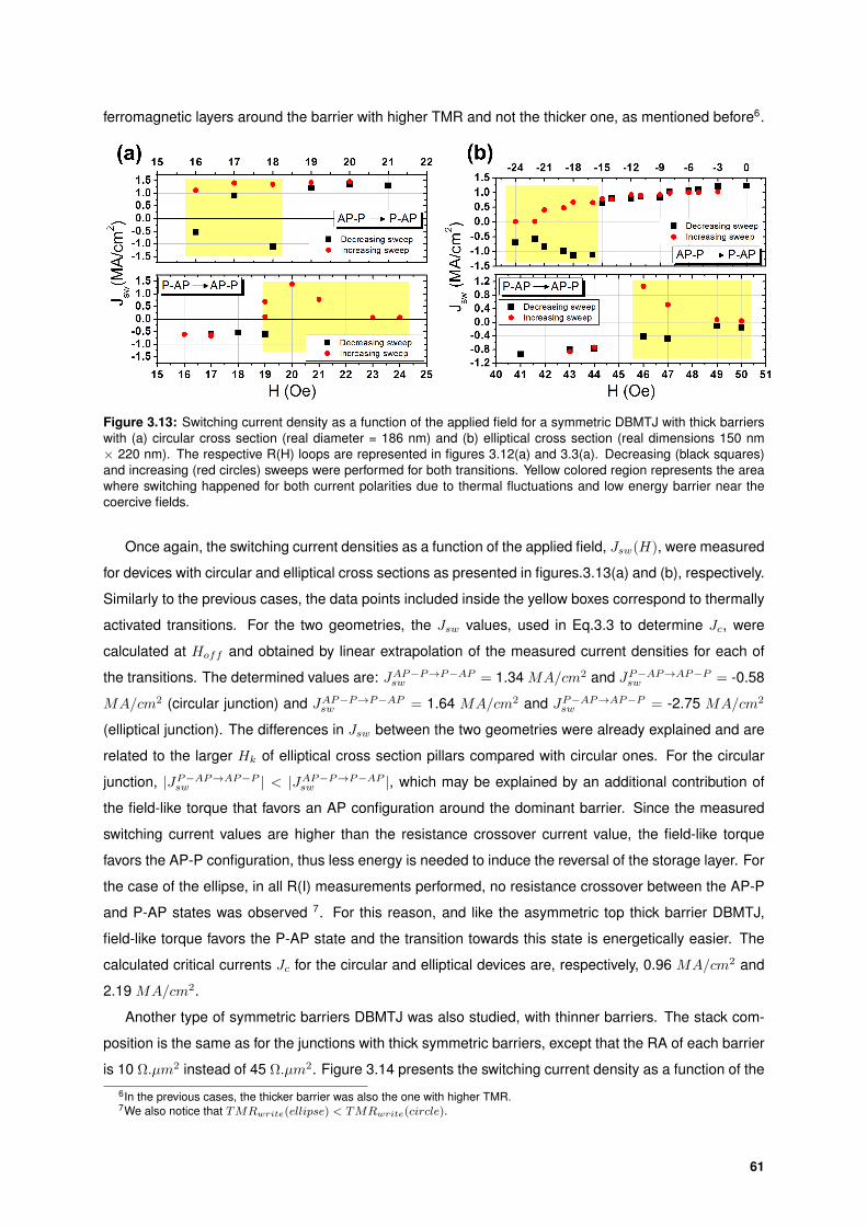
ferromagnetic layers around the barrier with higher TMR and not the thicker one, as mentioned before6.
Figure 3.13: Switching current density as a function of the applied field for a symmetric DBMTJ with thick barrierswith (a) circular cross section (real diameter = 186 nm) and (b) elliptical cross section (real dimensions 150 nm× 220 nm). The respective R(H) loops are represented in figures 3.12(a) and 3.3(a). Decreasing (black squares)and increasing (red circles) sweeps were performed for both transitions. Yellow colored region represents the areawhere switching happened for both current polarities due to thermal fluctuations and low energy barrier near thecoercive fields.
Once again, the switching current densities as a function of the applied field, Jsw(H), were measured
for devices with circular and elliptical cross sections as presented in figures.3.13(a) and (b), respectively.
Similarly to the previous cases, the data points included inside the yellow boxes correspond to thermally
activated transitions. For the two geometries, the Jsw values, used in Eq.3.3 to determine Jc, were
calculated at Hoff and obtained by linear extrapolation of the measured current densities for each of
the transitions. The determined values are: JAP−P→P−APsw = 1.34 MA/cm2 and JP−AP→AP−Psw = -0.58
MA/cm2 (circular junction) and JAP−P→P−APsw = 1.64 MA/cm2 and JP−AP→AP−Psw = -2.75 MA/cm2
(elliptical junction). The differences in Jsw between the two geometries were already explained and are
related to the larger Hk of elliptical cross section pillars compared with circular ones. For the circular
junction, |JP−AP→AP−Psw | < |JAP−P→P−APsw |, which may be explained by an additional contribution of
the field-like torque that favors an AP configuration around the dominant barrier. Since the measured
switching current values are higher than the resistance crossover current value, the field-like torque
favors the AP-P configuration, thus less energy is needed to induce the reversal of the storage layer. For
the case of the ellipse, in all R(I) measurements performed, no resistance crossover between the AP-P
and P-AP states was observed 7. For this reason, and like the asymmetric top thick barrier DBMTJ,
field-like torque favors the P-AP state and the transition towards this state is energetically easier. The
calculated critical currents Jc for the circular and elliptical devices are, respectively, 0.96 MA/cm2 and
2.19 MA/cm2.
Another type of symmetric barriers DBMTJ was also studied, with thinner barriers. The stack com-
position is the same as for the junctions with thick symmetric barriers, except that the RA of each barrier
is 10 Ω.µm2 instead of 45 Ω.µm2. Figure 3.14 presents the switching current density as a function of the6In the previous cases, the thicker barrier was also the one with higher TMR.7We also notice that TMRwrite(ellipse) < TMRwrite(circle).
61
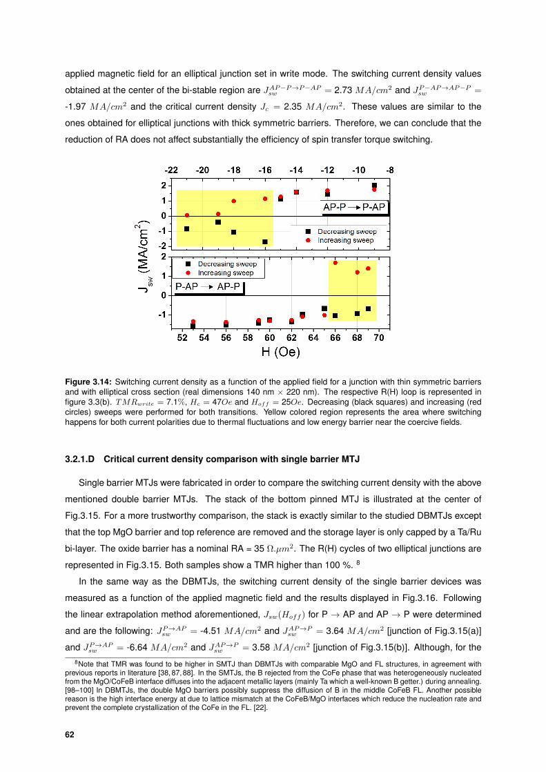
applied magnetic field for an elliptical junction set in write mode. The switching current density values
obtained at the center of the bi-stable region are JAP−P→P−APsw = 2.73 MA/cm2 and JP−AP→AP−Psw =
-1.97 MA/cm2 and the critical current density Jc = 2.35 MA/cm2. These values are similar to the
ones obtained for elliptical junctions with thick symmetric barriers. Therefore, we can conclude that the
reduction of RA does not affect substantially the efficiency of spin transfer torque switching.
Figure 3.14: Switching current density as a function of the applied field for a junction with thin symmetric barriersand with elliptical cross section (real dimensions 140 nm × 220 nm). The respective R(H) loop is represented infigure 3.3(b). TMRwrite = 7.1%, Hc = 47Oe and Hoff = 25Oe. Decreasing (black squares) and increasing (redcircles) sweeps were performed for both transitions. Yellow colored region represents the area where switchinghappens for both current polarities due to thermal fluctuations and low energy barrier near the coercive fields.
3.2.1.D Critical current density comparison with single barrier MTJ
Single barrier MTJs were fabricated in order to compare the switching current density with the above
mentioned double barrier MTJs. The stack of the bottom pinned MTJ is illustrated at the center of
Fig.3.15. For a more trustworthy comparison, the stack is exactly similar to the studied DBMTJs except
that the top MgO barrier and top reference are removed and the storage layer is only capped by a Ta/Ru
bi-layer. The oxide barrier has a nominal RA = 35 Ω.µm2. The R(H) cycles of two elliptical junctions are
represented in Fig.3.15. Both samples show a TMR higher than 100 %. 8
In the same way as the DBMTJs, the switching current density of the single barrier devices was
measured as a function of the applied magnetic field and the results displayed in Fig.3.16. Following
the linear extrapolation method aforementioned, Jsw(Hoff ) for P → AP and AP → P were determined
and are the following: JP→APsw = -4.51 MA/cm2 and JAP→Psw = 3.64 MA/cm2 [junction of Fig.3.15(a)]
and JP→APsw = -6.64 MA/cm2 and JAP→Psw = 3.58 MA/cm2 [junction of Fig.3.15(b)]. Although, for the8Note that TMR was found to be higher in SMTJ than DBMTJs with comparable MgO and FL structures, in agreement with
previous reports in literature [38, 87, 88]. In the SMTJs, the B rejected from the CoFe phase that was heterogeneously nucleatedfrom the MgO/CoFeB interface diffuses into the adjacent metallic layers (mainly Ta which a well-known B getter.) during annealing.[98–100] In DBMTJs, the double MgO barriers possibly suppress the diffusion of B in the middle CoFeB FL. Another possiblereason is the high interface energy at due to lattice mismatch at the CoFeB/MgO interfaces which reduce the nucleation rate andprevent the complete crystallization of the CoFe in the FL. [22].
62
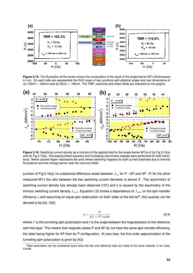
Figure 3.15: The illustration at the center shows the composition of the stack of the single barrier MTJ (thicknessesin nm). On each side are represented the R(H) loops of two junctions with elliptical shape and real dimensions of(a) 100nm × 200nm and (b) 95nm × 185nm. The TMR, coercivity and offset fields are indicated on the graphs.
Figure 3.16: Switching current density as a function of the applied field for the single barrier MTJs of (a) Fig.3.15(a)and (b) Fig.3.15(b). Decreasing (black squares) and increasing (red circles) sweeps were performed for both transi-tions. Yellow colored region represents the area where switching happens for both current polarities due to thermalfluctuations and low energy barrier near the coercive fields.
junction of Fig.3.16(a) no substantial difference exists between Jsw for P→AP and AP→P, for the other
measured MTJ the ratio between the two switching current densities is almost 2. This asymmetry of
switching current density has already been observed [101] and it is caused by the asymmetry of the
intrinsic switching current density Jsw0. Equation1.22 shows a dependence of Jsw0 on the spin-transfer
efficiency η and assuming an equal spin polarization on both sides of the barrier9, this quantity can be
derived to be [43,102]:
η =P
2(1 + P 2 cosθ)(3.4)
where P is the tunneling spin polarization and θ is the angle between the magnetization of the reference
and free layer. This means that magnetic states P and AP do not have the same spin transfer efficiency,
the latter being higher for AP than for P configuration. At zero bias, the first order approximation of the
tunneling spin polarization is given by [43]:9Spin polarization can be considered equal since the free and reference layer are made of the same material, in our case,
CoFeB.
63
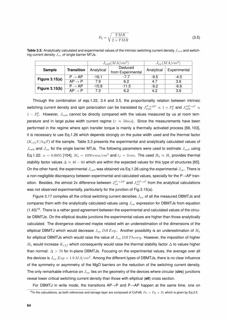
P0 =
√TMR
2 + TMR(3.5)
Table 3.3: Analytically calculated and experimental values of the intrinsic switching current density Jsw0 and switch-ing current density Jsw of single barrier MTJs.
Jsw0(MA/cm2) Jsw(MA/cm2)
Sample Transition Analytical Deducedfrom Experimental Analytical Experimental
Figure 3.15(a) P→ AP -16.1 -7.7 -9.5 -4.5AP→ P 7.9 6.2 4.7 3.6
Figure 3.15(b) P→ AP -15.8 -11.5 -9.2 -6.6AP→ P 7.3 6.2 4.2 3.6
Through the combination of eqs.1.22, 3.4 and 3.5, the proportionality relation between intrinsic
switching current density and spin polarization can be translated by JP→APsw0 ∝ 1 + P 20 and JAP→Psw0 ∝
1 − P 20 . However, Jsw0 cannot be directly compared with the values measured by us at room tem-
perature and in large pulse width current regime (τ ≈ 50ms). Since the measurements have been
performed in the regime where spin transfer torque is mainly a thermally activated process [68, 103],
it is necessary to use Eq.1.26 which depends strongly on the pulse width used and the thermal factor
(KeffV/kBT ) of the sample. Table 3.3 presents the experimental and analytically calculated values of
Jsw0 and Jsw for the single barrier MTJs. The following parameters were used to estimate Jsw0 using
Eq.1.22: α = 0.0055 [104], Ms = 1050 emu/cm3 and tf = 3nm. The used Hk ≈ Hc provides thermal
stability factor values ∆ ≈ 40 − 60 which are within the expected values for this type of structures [65].
On the other hand, the experimental Jsw0 was obtained via Eq.1.26 using the experimental Jsw. There is
a non-negligible discrepancy between experimental and calculated values, specially for the P→AP tran-
sition. Besides, the almost 2x difference between JP→APsw and JAP→Psw from the analytical calculations
was not observed experimentally, particularly for the junction of Fig.3.15(a).
Figure 3.17 compiles all the critical switching current densities Jsw of all the measured DBMTJs and
compares them with the analytically calculated values using Jsw expression for DBMTJs from equation
(1.43)10. There is a rather good agreement between the experimental and calculated values of the circu-
lar DBMTJs. On the elliptical double junctions the experimental values are higher than those analytically
calculated. The divergence observed maybe related with an underestimation of the dimensions of the
elliptical DBMTJ which would decrease JswDBExp.. Another possibility is an underestimation of Hk
for elliptical DBMTJs which would raise the value of JswDB Theory. However, the imposition of higher
Hk would increase Keff which consequently would raise the thermal stability factor ∆ to values higher
than normal: ∆ > 70 for in-plane DBMTJs. Focusing on the experimental values, the average over all
the devices is Jsw Exp = 1.9MA/cm2. Among the different types of DBMTJs, there is no clear influence
of the symmetry or asymmetry of the MgO barriers on the reduction of the switching current density.
The only remarkable influence on Jsw lies on the geometry of the devices where circular (circ) junctions
reveal lower critical switching current density than those with elliptical (ell) cross section.
For DBMTJ in write mode, the transitions AP→P and P→AP happen at the same time, one on10In the calculations, as both references and storage layer are composed of CoFeB, PF = PR = P0 which is given by Eq.3.5
64
Figure 3.17: Display of the experimental critical current density JswDBExp. (black squares) with respective ana-lytical calculated values JcDB Theory (red triangles) for all the measured types of DBMTJs. The acronyms of thedifferent DBMTJs are on the legend box next to the plot. The dashed line correspond, respectively to the critical(Jsw SMTJ) of a single barrier MTJs measured.
each barrier; thus, the two switching current densities of the single barrier were averaged using Eq.3.3.
Therefore, in Fig.3.17 the dashed line represent the averaged experimental critical switching current
density Jsw SMTJ = 4.1MA/cm2 for the measured single barrier MTJ. The ratio Jsw DBMTJJsw SMTJ ≈ 2 which
corresponds to a 2x improvement of the critical switching current density of DBMTJs relative to a single
barrier MTJ. This ratio is in agreement with previously obtained results using double barrier MTJs [37]11.
This result proves that the STT-DBMTJ is a suitable device to improve the power consumption of MRAM
upon writing.
3.2.2 Read Mode
In this configuration, the magnetizations of the two references are parallel to each other which means
that independently of the magnetization direction of the storage layer [parallel or antiparallel to both ref-
erences, respectively, states 1 and 2 of Fig.3.2(a)], the damping-like torques from each of the references
(T‖r and T‖c) have opposite signs. Therefore, the total torque exerted on the storage layer is given by
T‖total =∣∣T‖r − T‖c∣∣ . Therefore, T‖total in read mode is lower than T‖total in write mode. This implies
that a larger current is needed to flip the magnetization of the storage layer (i.e. to write). This mag-
netic configuration of the two references is not advantageous for writing but rather positive for a more
efficient and fast readout process. In addition, the DBMTJs in read mode present maximum TMR since
the TMR from each barrier does not subtract in opposition to write mode and it is independent of the
symmetry/asymmetry of the barriers (see TMR values on inset of R(H) cycles of Fig.3.3). As mentioned11In the publication by Diao et al., for DBMTJs with similar composition and TMR as ours, lower Jsw values were obtained. The
difference is explained by the substantially lowerMs of their free layer (800 emu/cm3) CoFeB compared to ours (1050 emu/cm3).
65
before, TMR decreases with applied voltage [24, 95], but at a slower rate for DBMTJs [31]. These two
last features are essential to yield an effective sense path resistance change (ideally larger than 100%)
between the two memory states: 1 (maximum resistance) and 0 (minimum resistance).
P.-Y. Clement [1] has performed similar measurements on DBMTJs in read mode and came across
some interesting and unexpected results. Current sweeps performed in DBMTJs with nominally symmet-
ric barriers revealed switchings from P-P→ AP-AP as shown in the various plots of Fig.3.18. Decreasing
sweeps [Fig.3.18(a)-(c)] and increasing sweeps [Fig.3.18(d)-(f)] showed that the switching occurred for
both current polarities. These switchings can be attributed to field-like torque since, in read mode, the
components coming from the reference and control layers add up. The dual polarity switching is mainly
due to the quadratic behavior of the field-like torque with voltage, T⊥ ∝ V 2. Nevertheless, a slight asym-
metry exists between switching at negative or positive current. For the same applied field, a smaller
negative than positive bias is needed to trigger the switch. The existence of a small (but non-negligible)
in-plane torque could explain this bias asymmetry. However, it does not abide by the rules of applied
current direction since, according to the measurement configuration (see Fig.3.20), it is the positive cur-
rent that should help to destabilize the P-P configuration and not negative current as observed. On the
other hand, in asymmetric barriers DBMTJ, it has never been observed any switching. More precisely,
no storage layer reversal was observed for currents lower than those capable of causing a Joule effect
mode switch. Although the absence of switching in read mode is a positive result, in asymmetric barriers
structures when the references’ magnetizations are set parallel, the damping-like torque is reduced (but
not canceled) whereas the field-like torque is enhanced. Therefore, it was expected, at least, a switching
from P-P→AP-AP as field-like torque would tend to destabilize the initial P-P state and favor an AP align-
ment between storage and reference layers around the dominant barrier. Some possible explanations
to the abnormal non-switching were: i) Neel coupling between storage layer and bottom reference due
to the low thickness of the bottom MgO barrier; ii) the non-homogeneous oxidation of the bottom barrier
may add a non-negligible linear component to the field-like torque [49] and reverse its effects favoring
the P alignment between storage and reference layers.
In the following subsections are presented the results of the DC current sweeps performed on the
DBMTJs with symmetric and asymmetric barriers. The precision of the applied magnetic field is thence
improved compared to that used by P.-Y. Clement, thus in our measurements a considerably higher
number of data points was possible to obtain. In addition, we present a brief analysis of the results
based on the effects of the two components of the spin transfer torque: damping-like and field-like.
3.2.2.A Asymmetric barriers: top thick barrier
In this subsection the asymmetric top thicker barrier double junctions, which RA properties can be
consulted in table 3.2, were set in read mode after an annealing under a 1T applied magnetic field. Sim-
ilarly to write mode, the samples’ resistance was measured while current was swept for both polarities.
The switching current densities Jsw obtained as a function of the applied magnetic field H are plotted in
Fig.3.19. Figures 3.19(a) and (b) correspond, respectively, to junctions with elliptical and circular cross
sections which are the same devices as those measured in Fig.3.9. The read mode R(H) loop of the
66
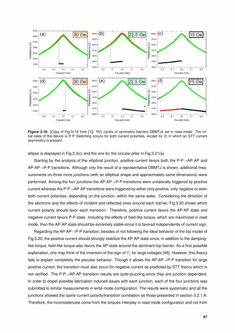
Figure 3.18: [Copy of Fig.IV.18 from [1]]. R(I) cycles of symmetric barriers DBMTJs set in read mode. The ini-tial state of the device is P-P. Switching occurs for both current polarities, except for (f) in which an STT currentasymmetry is present.
ellipse is displayed in Fig.3.3(c) and the one for the circular pillar in Fig.3.21(a).
Starting by the analysis of the elliptical junction, positive current favors both the P-P→AP-AP and
AP-AP→P-P transitions. Although only the result of a representative DBMTJ is shown, additional mea-
surements on three more junctions (with an elliptical shape and approximately same dimensions) were
performed. Among the four junctions the AP-AP→P-P transitions were unilaterally triggered by positive
current whereas the P-P→AP-AP transitions were triggered by either only positive, only negative or even
both current polarities, depending on the junction, within the same wafer. Considering the direction of
the electrons and the effects of incident and reflected ones around each barrier, Fig.3.20 shows which
current polarity should favor each transition. Therefore, positive current favors the AP-AP state and
negative current favors P-P state. Including the effects of field-like torque, which are maximized in read
mode, then the AP-AP state should be extremely stable since it is favored independently of current sign.
Regarding the AP-AP→P-P transition, besides of not following the ideal behavior of the toy model of
Fig.3.20, the positive current should strongly stabilize the AP-AP state since, in addition to the damping-
like torque, field-like torque also favors the AP state around the dominant top barrier. As a first possible
explanation, one may think of the inversion of the sign of T‖ for large voltages [49]. However, this theory
fails to explain completely the peculiar behavior. Though it allows the AP-AP→P-P transition for large
positive current, the transition must also occur for negative current as predicted by STT theory which is
not verified. The P-P→AP-AP transition results are quite puzzling since they are junction dependent.
In order to dispel possible fabrication induced issues with each junction, each of the four junctions was
submitted to similar measurements in write mode configuration. The results were systematic and all the
junctions showed the same current polarity/transition correlation as those presented in section 3.2.1.A.
Therefore, the inconsistencies come from the torques interplay in read mode configuration and not from
67

Figure 3.19: Switching current density in function of the applied field for asymmetric top thicker DBMTJs with(a) elliptical cross section (real dimensions: 90 nm x 190 nm) and (b) circular cross section (real diameter: 127nm). The R(H) loops corresponding to devices (a) and (b) are presented in Fig.3.3(c) and Fig.3.21(a), respectively.Decreasing (black squares) and increasing (red circles) sweeps were performed for both transitions. Yellow coloredregion represents the area where switching happened for both current polarities due to thermal fluctuations and lowenergy barrier near the coercive fields.
Figure 3.20: The ideal case read mode transitions favored by each current polarity in an asymmetric top thickbarrier DBMTJ where T top‖ > T bottom‖ .
possible damages in the junctions.
For the junction of Fig.3.19(b) (example of a junction showing the most commonly observed behav-
ior), for both the P-P→AP-AP and AP-AP→P-P transitions, there is no prevalence of one current polarity
over the other. Moreover, the existence of black squares and red circles for both polarities means that
within the sweep associated with the mark (black for decreasing sweep and red for increasing sweep)
more than one of that particular transition occurred for the same applied field (usually backhopping or
thermally activated switching). As it has already been mentioned in previous subsections, devices with
circular cross section possess a lower Hk due to the absence of in-plane shape anisotropy. Thus the
field range where bistability is allowed is much smaller than in elliptical junctions and, as Jsw0 is directly
proportional to Hk (see Eq.1.22), their switching current is also smaller. Thus these circular junctions are
the only samples in which double transitions could be observed and measured in the same R(I) sweep
below breakdown voltage. Figures 3.21(b)-(d) exhibit some R(I) plots performed for applied magnetic
68
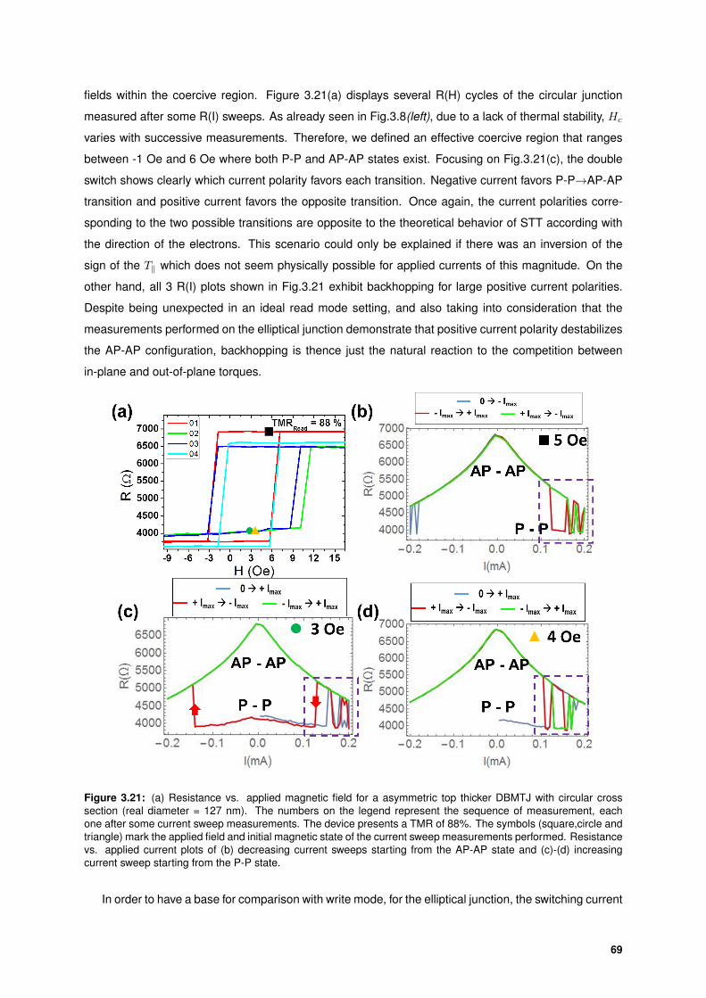
fields within the coercive region. Figure 3.21(a) displays several R(H) cycles of the circular junction
measured after some R(I) sweeps. As already seen in Fig.3.8(left), due to a lack of thermal stability, Hc
varies with successive measurements. Therefore, we defined an effective coercive region that ranges
between -1 Oe and 6 Oe where both P-P and AP-AP states exist. Focusing on Fig.3.21(c), the double
switch shows clearly which current polarity favors each transition. Negative current favors P-P→AP-AP
transition and positive current favors the opposite transition. Once again, the current polarities corre-
sponding to the two possible transitions are opposite to the theoretical behavior of STT according with
the direction of the electrons. This scenario could only be explained if there was an inversion of the
sign of the T‖ which does not seem physically possible for applied currents of this magnitude. On the
other hand, all 3 R(I) plots shown in Fig.3.21 exhibit backhopping for large positive current polarities.
Despite being unexpected in an ideal read mode setting, and also taking into consideration that the
measurements performed on the elliptical junction demonstrate that positive current polarity destabilizes
the AP-AP configuration, backhopping is thence just the natural reaction to the competition between
in-plane and out-of-plane torques.
Figure 3.21: (a) Resistance vs. applied magnetic field for a asymmetric top thicker DBMTJ with circular crosssection (real diameter = 127 nm). The numbers on the legend represent the sequence of measurement, eachone after some current sweep measurements. The device presents a TMR of 88%. The symbols (square,circle andtriangle) mark the applied field and initial magnetic state of the current sweep measurements performed. Resistancevs. applied current plots of (b) decreasing current sweeps starting from the AP-AP state and (c)-(d) increasingcurrent sweep starting from the P-P state.
In order to have a base for comparison with write mode, for the elliptical junction, the switching current
69

density at the offset field Jsw(Hoff ) was determined by extrapolation of the linear fit performed on the
data points outside the yellow colored region [see Fig.3.19(a)]. The switching current density values for
each transition are the following: JP−P→AP−APsw = 1.60 MA/cm2 and JAP−AP→P−Psw = 2.32 MA/cm2.
Surprisingly, the Jsw values obtained for the same asymmetric DBMTJ in write mode are higher than the
ones hereby obtained in read mode.
3.2.2.B Asymmetric barriers: bottom thick barrier
We also studied the effects of DC current induced switching in asymmetric bottom thick barrier
DBMTJs set in read mode. The R(I) measurements have been performed in several junctions with
elliptical and circular cross sections. The obtained switching current densities for one junction of each
geometry are displayed in Fig.3.22. For fair comparison, the critical switching current densities Jsw were
evaluated at the center of the coercive area (Hoff ) where the energy barrier to overcome is supposed to
be the same for the two transitions. In the case of the elliptical junction [Fig.3.11(a)], the switching current
densities at Hoff =-1.5 Oe are JP−P→AP−APsw = 2.24 MA/cm2 and JAP−AP→P−Psw = 3.35 MA/cm2.
Whereas for the circular pillar of Fig.3.11(b), Hoff =-14 Oe and JP−P→AP−APsw = 2.32 MA/cm2 and
JAP−AP→P−Psw = 0.85 MA/cm2. The obtained values, in read mode, for the circular device are higher
than those determined for a device of equal geometry in write mode. By contrast, the values obtained for
the elliptical junction are similar to Jsw values determined in write mode. Despite the difference between
read and write mode Jsw for the circular junction, the switching current densities in read mode are too
close to the ones obtained in write mode to ensure no data corruption while reading.
Figure 3.22: Switching current density in function of the applied field for asymmetric bottom thicker DBMTJs with(a) elliptical (real dimensions: 115 nm x 225 nm) and (b) circular cross section (real diameter: 185 nm). Decreasing(black squares) and increasing (red circles) sweeps were performed for both transitions. Yellow colored regionrepresents the area where switching happened for both current polarities due to thermal fluctuations and low energybarrier near the coercive fields.
The bias polarity/transition qualitative analysis of the torques interplay has revealed no clear correla-
tion between the direction of switching and the direction of the electrons. A result that is comparable to
the one obtained in the previous subsection for the asymmetric barriers DBMTJ with a thick top barrier.
According to theory, and taking into account Fig.3.20, with the position of the barriers inverted, the cur-
70

rent bias polarity favoring a certain type of transition also inverts. Consequently, I > 0 favors now the
P-P state and I < 0 favors the AP-AP state. Although in the junctions (chosen as examples) the positive
bias favors all the transitions, in other measured junctions the two possible transitions were triggered by
both current polarities, similarly to the asymmetric DBMTJs with top thick barrier. Besides not matching
the theoretical description, this statistically polarity independent switching does not allow to understand
the interplay of the two STT components on magnetization reversal.
Figure 3.23: Resistance vs. applied current sweeps performed in an asymmetric bottom thick DBMTJ device withcircular cross section (φ = 160nm) set in read mode in an initial (a) P-P state and (c) AP-AP state. The purpledashed open squares highlight the zone where backhopping occured. (b) Read/write modes R(H) cycles. Thesquare mark the position inside the coercive region where the displayed R(I) sweeps were performed.
Another way to evaluate the torques in a junction is through the analysis of backhopping events. In
one of the measured circular junctions, backhopping was observed. Figures 3.23(a) and (c) display two
R(I) plots where this telegraphic transitions were present. As mentioned before, when backhopping is
observed for only one polarity of the applied current, it results from the competition between damping
and field-like torque. Otherwise, backhopping is considered to be thermally induced. In the cases of
the figure, backhopping occurs only for negative current polarity. As above mentioned, this is the same
polarity which, according to theory and position of the thicker barrier, favors the P-P→AP-AP transition.
Thus, if the results were in line with theory, for negative bias, in-plane and out-of-plane torques favor that
same transition and backhopping (from torque competition) should then be observed for the opposite
bias polarity. The same disagreement with theory in a circular junction where backhopping was observed
happened in section 3.2.2.A.
Although no correlation of the switching events with the bias polarity in both type of asymmetric
DBMTJs (top thick barrier and bottom thick barrier) could have been done, the results of the backhopping
events showed some coherence with the change of position of the thick barrier of the DBMTJ. Despite
the torque mediated backhopping events have only been observed in one circular junction of each type of
asymmetric barriers DBMTJ, their consistency in polarity change with dominant barrier position change
may allow for a conclusion on the torques interplay in these asymmetric barrier DBMTJ set in read
mode. Allowing for an interpretation in opposition to theoretical predictions, for asymmetric DBMTJs
with bottom thick barrier, the AP-AP→P-P transition is triggered by negative current. Whereas the same
transition is triggered by positive current for asymmetric DBMTJs with top thick barrier. The polarity
71

dependent effects are result from residual in-plane torque while the maximized field-like torque (in read
mode) favors the AP-AP state.
Figure 3.24 presents very rare (only observed twice) results of DC current measurements performed
in asymmetric DBMTJ with bottom thick barrier. This peculiar result is shown and analyzed in order to
record one of the possible consequences of multiple measurements and mode switchings in DBMTJs.
First by analyzing the R(H) cycles of Fig.3.24(b) we notice that the resistance of the write mode AP-P
state is larger than the resistance of the read mode AP-AP state. Figure 3.3(d) presents normal R(H)
read/write mode cycles for asymmetric bottom thicker DBMTJs where the maximum resistance state is
the AP-AP. It is, however, important to state that this junction was set initially in write mode by annealing
under a 1T magnetic field and R(I) sweeps were performed before it switched to read mode by mode
switch caused by Joule effect under applied current and field. Figure 3.24(a) presents resistance as
a function of applied current for the junction prepared in read mode. In this specific case, the applied
current is not high enough to cause STT switching of the storage layer. However, an interesting and
asymmetric resistance dependence with current bias polarity is observed. Resistance decreases with
both current polarities but the trend is much more pronounced under positive bias. This asymmetric
behavior is translated by the difference of resistance ∆R = 45Ω when |I| = 0.4mA at opposite polarities.
This asymmetry also exists when the DBMTJ is in the AP-AP state [Fig.3.24(c)] though now ∆R < 15Ω.
This anomalous resistance bias dependence may be connected with structural differences between the
ferromagnet/oxide interfaces [105] around top and bottom barriers.
Figure 3.24: R(I) sweeps performed in a selected asymmetric bottom thicker DBMTJ (real dimensions: 115 nmx 225 nm) set in read mode with inital (a) P-P state and (c) AP-AP state. When in the low resistance state, thedevice present an asymmetric resistance dependence with bias current. (b) The respective read and write modeR(H) cycles. The colored circles point the applied field and initial magnetic state for each of the R(I) sweeps.
As seen before, MTJs have two types of conductivity regimes: ohmic at low bias, whereas for large
bias the dynamic conductance has an almost parabolic dependence with DC bias [106]. Resistance
and TMR dependence with bias voltage has been heavily studied and several experiments have been
conducted around the late 1990s [16, 105, 107–110]. While the cusp-like peak feature at zero bias
was attributed to magnon excitations at the ferromagnet-insulator interface (”hot electrons”) [95], the
behavior at higher bias was thought to be deeply connected with the quality of the interface, barrier type
and the materials used for the ferromagnets. Moreover, it was proven that the materials chosen for the
insulating barrier and ferromagnets, and thence their interfaces change the sign of the spin polarization
72
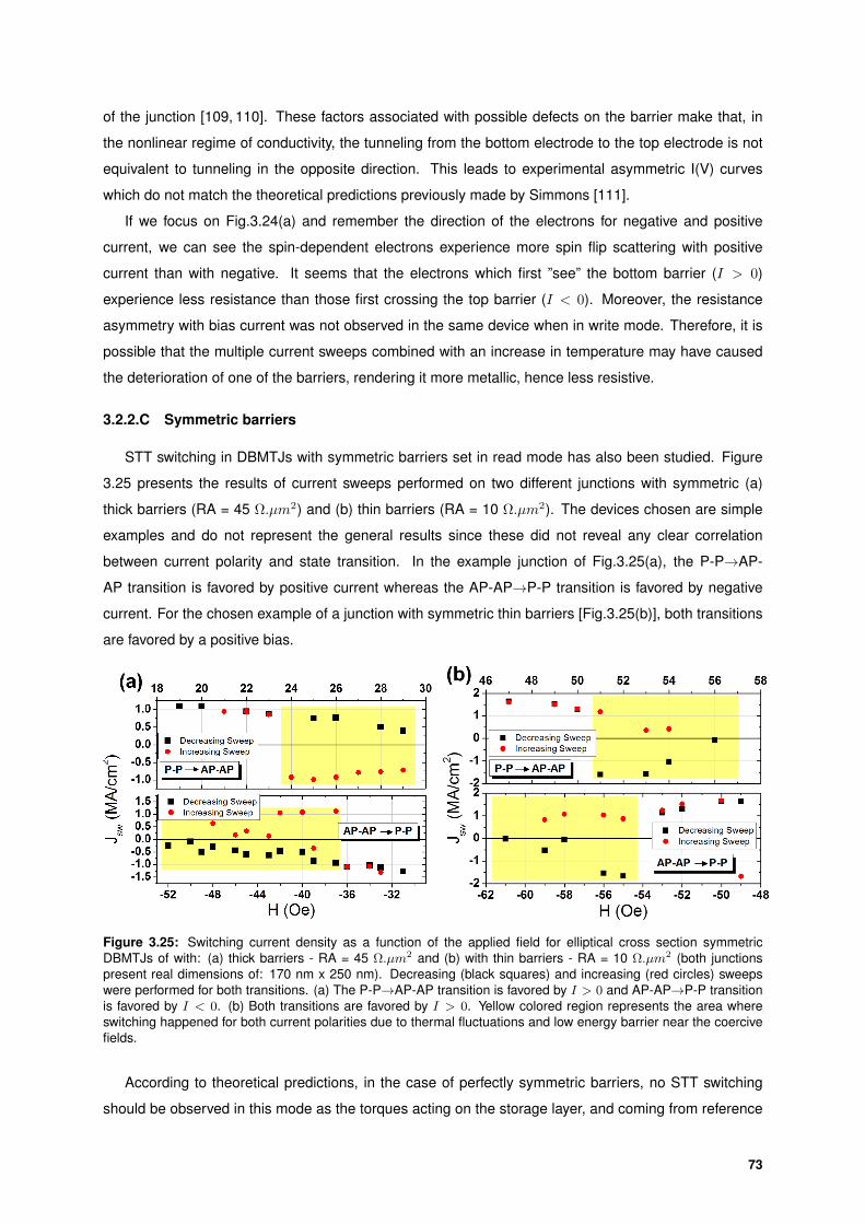
of the junction [109, 110]. These factors associated with possible defects on the barrier make that, in
the nonlinear regime of conductivity, the tunneling from the bottom electrode to the top electrode is not
equivalent to tunneling in the opposite direction. This leads to experimental asymmetric I(V) curves
which do not match the theoretical predictions previously made by Simmons [111].
If we focus on Fig.3.24(a) and remember the direction of the electrons for negative and positive
current, we can see the spin-dependent electrons experience more spin flip scattering with positive
current than with negative. It seems that the electrons which first ”see” the bottom barrier (I > 0)
experience less resistance than those first crossing the top barrier (I < 0). Moreover, the resistance
asymmetry with bias current was not observed in the same device when in write mode. Therefore, it is
possible that the multiple current sweeps combined with an increase in temperature may have caused
the deterioration of one of the barriers, rendering it more metallic, hence less resistive.
3.2.2.C Symmetric barriers
STT switching in DBMTJs with symmetric barriers set in read mode has also been studied. Figure
3.25 presents the results of current sweeps performed on two different junctions with symmetric (a)
thick barriers (RA = 45 Ω.µm2) and (b) thin barriers (RA = 10 Ω.µm2). The devices chosen are simple
examples and do not represent the general results since these did not reveal any clear correlation
between current polarity and state transition. In the example junction of Fig.3.25(a), the P-P→AP-
AP transition is favored by positive current whereas the AP-AP→P-P transition is favored by negative
current. For the chosen example of a junction with symmetric thin barriers [Fig.3.25(b)], both transitions
are favored by a positive bias.
Figure 3.25: Switching current density as a function of the applied field for elliptical cross section symmetricDBMTJs of with: (a) thick barriers - RA = 45 Ω.µm2 and (b) with thin barriers - RA = 10 Ω.µm2 (both junctionspresent real dimensions of: 170 nm x 250 nm). Decreasing (black squares) and increasing (red circles) sweepswere performed for both transitions. (a) The P-P→AP-AP transition is favored by I > 0 and AP-AP→P-P transitionis favored by I < 0. (b) Both transitions are favored by I > 0. Yellow colored region represents the area whereswitching happened for both current polarities due to thermal fluctuations and low energy barrier near the coercivefields.
According to theoretical predictions, in the case of perfectly symmetric barriers, no STT switching
should be observed in this mode as the torques acting on the storage layer, and coming from reference
73
layer T‖r and control layer T‖c, cancel each other. Nevertheless, the two barriers are never completely
symmetric otherwise TMRwrite = 0, which we have never experimentally observed. As already dis-
cussed in section 3.2.1.C, for the majority of the junctions, the top barrier presents slightly higher RA
and TMR values than the bottom barrier, thus being the dominating one. Therefore, a residual in-
plane component of STT could be responsible for STT switching as described in a theoretical picture by
Fig.3.20. For the junction of Fig.3.25(a), the relation between magnetic state and switching current polar-
ity matches the theoretical description. However, the same is not verified for the junction of Fig.3.25(b).
In order to improve our interpretation of symmetric DBMTJs in read mode, several more devices were
measured. Unfortunately, the destabilization of any of the two states was triggered by either one or
the other current polarities with some asymmetries but that change from device to device randomly.
Concerning Jsw(Hoff ), for the device (a): JP−P→AP−APsw = 2.80 MA/cm2 and JAP−AP→P−Psw = -2.15
MA/cm2, while for device (b): JP−P→AP−APsw = 5.95 MA/cm2 and JAP−AP→P−Psw = 6.03 MA/cm2.
The considerable difference of Jsw between symmetric DBMTJs with thick and thin barriers may be re-
lated with superior thermal effects present in the DBMTJs with thick barriers. This thermal effect helps
on reducing the current needed to trigger STT induced switching.
Despite only showing results on elliptical junctions, we have also tried to perform the same mea-
surements on junctions with circular shape. However, due to their low endurance, we were not able to
conclude a complete set of measurements to include here, before reaching breakdown. Moreover, in
circular geometry devices, we tried to evaluate backhopping as one of the possible ways to study the
interplay of both STT components. Yet, the only backhopping observed was due to thermal fluctuations
of the switching field (Hc) (similarly to the one observed in Fig.3.8) since it happened indiscriminately for
both current polarities.
In summary, the obtained results are surprising, relatively to the theoretical predictions and do not
meet the initial purpose of a ”switching free” mode. The same problems observed by P.-Y. Clement [1]
were again retrieved with the aggravating factor of having observed AP-AP→P-P switching besides the
P-P→AP-AP. The read mode transitions, in all three types of DBMTJs, do not show any correlation
with a bias polarity. Neither the position of the thicker barrier shows any particular influence on the
switchings. The only observed exceptions are the backhopping events which exist for opposite polarities
with different positions of the thicker barrier. Concerning symmetric barriers DBMTJs, comparatively
to those of ref. [80], ours were of superior symmetry (TMRwrite < 10%), which means that total in-
plane torque should be even lower, thus a lower probability of STT switching. Along with the confusing
dependence of STT with bias polarity, the Jsw values are within the range of those found for DBMTJs in
write mode, jeopardizing the reliability of written data. It was also expected that less current would be
necessary to switch from P-P to AP-AP since field-like torque (maximized in read mode), should assist
the remnant damping-like torque. Though the obtained data does not support this claim. Once again,
the bias polarity dependent backhopping events observed in the asymmetric barriers DBMTJs are the
only evidence of the competition between damping-like and field-like torque. Globally, the randomness
of the obtained results may come from the type of measurements performed where thermally activated
74
switching is dominant and may overshadow the STT induced switching.
3.3 Voltage Pulses Measurements
In the previous chapter, the STT induced switching was triggered by DC current with a large active
time τ in the order of milliseconds. This pulse width regime (τ > 100ns) is the thermally activated regime
in which thermal fluctuations help the magnetization to overcome the energy barrier thus inducing its
reversal. Moreover, this type of regime can easily set off undesired thermal backhopping. In the specific
case of DBMTJ, the addition of a second barrier also acts as a heat tampon, increasing the temperature
inside the junction as well as slowing its dissipation [112]. In spite of the positive results obtained for
write mode, the read mode revealed unwanted switchings for all the types of DBMTJs measured. While
the P-P→AP-AP transitions could easily be explained by the presence of a strong field-like torque in
read mode, those in the opposite direction were completely unexpected and could not be related with
theoretical descriptions of STT. However, in some devices, switching occurred regardless of current
polarity which hints at the possibility of a strong thermally assisted switching.
In order to tackle the aforementioned temperature issue, similar measurements were performed but
with an applied bias voltage with a pulse width τ ≈ 30− 100ns. Although not yet in the precessional (or
ballistic) regime (τ < 10− 20ns), within this range the switching dynamics is close to macrospin and the
thermal fluctuations are reduced. The switching current densities Jsw(τ) are thus expected to increase
and to come closer to the intrinsic switching current density Jsw0 (see Eq.(1.43)).
3.3.1 Experimental Setup and Method
Figure.3.26(left) presents a schematic representation of the wafer probing setup used to measure
the DBMTJs by applying short voltage pulses. The wafer is placed under the electromagnetic coils
with elongated magnetic core that concentrate the magnetic flux in a direction parallel to the plane of
the wafer. The current applied to the coils of the electromagnet is supplied by a Kepco power source.
This power source is controlled by a wave generator which enables to control the frequency of the input
current, and thence the frequency of the applied magnetic field. The field is typically swept at frequencies
between 5 - 15 Hz, which are limited by the inductance of the coils. Between the coils, a RF probe is
in contact with the wafer: it delivers the applied voltage and it allows a subsequent measurement of
resistance at lower bias. The voltage pulses, whose properties are set by the waveform generator, are
created at the pulse generator and then sent via the AC port of the bias tee while the low continuous
bias to measure the resistance is sent through the DC port of the bias tee. The low DC bias is generated
and the junction resistance measured by the sourcemeter.
The phase diagrams shown in the following sections were obtained by performing several R(H) loops
for different applied voltages. The measurement method to obtain the phase diagrams is given by the
scheme in Fig.3.27. As mentioned in the paragraph above the magnetic field is swept thanks to an elec-
tromagnet. At each field step, a pulse generator delivers pulses. In the same field step, the resistance
level is measured thanks to a low current delivered by a sourcemeter and the voltage measured thanks
75
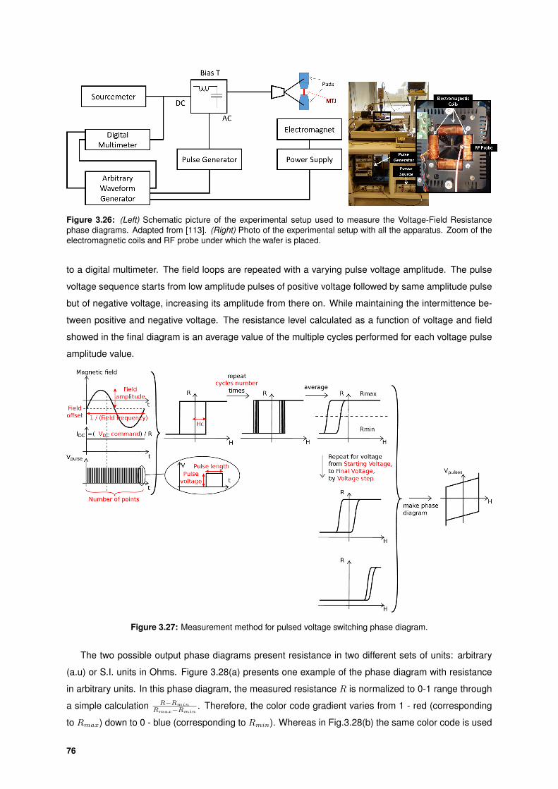
Figure 3.26: (Left) Schematic picture of the experimental setup used to measure the Voltage-Field Resistancephase diagrams. Adapted from [113]. (Right) Photo of the experimental setup with all the apparatus. Zoom of theelectromagnetic coils and RF probe under which the wafer is placed.
to a digital multimeter. The field loops are repeated with a varying pulse voltage amplitude. The pulse
voltage sequence starts from low amplitude pulses of positive voltage followed by same amplitude pulse
but of negative voltage, increasing its amplitude from there on. While maintaining the intermittence be-
tween positive and negative voltage. The resistance level calculated as a function of voltage and field
showed in the final diagram is an average value of the multiple cycles performed for each voltage pulse
amplitude value.
Figure 3.27: Measurement method for pulsed voltage switching phase diagram.
The two possible output phase diagrams present resistance in two different sets of units: arbitrary
(a.u) or S.I. units in Ohms. Figure 3.28(a) presents one example of the phase diagram with resistance
in arbitrary units. In this phase diagram, the measured resistance R is normalized to 0-1 range through
a simple calculation R−RminRmax−Rmin . Therefore, the color code gradient varies from 1 - red (corresponding
to Rmax) down to 0 - blue (corresponding to Rmin). Whereas in Fig.3.28(b) the same color code is used
76
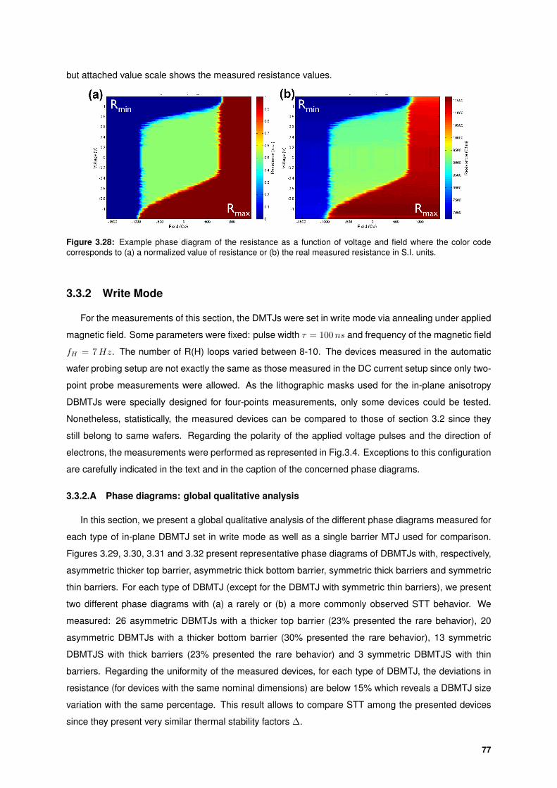
but attached value scale shows the measured resistance values.
Figure 3.28: Example phase diagram of the resistance as a function of voltage and field where the color codecorresponds to (a) a normalized value of resistance or (b) the real measured resistance in S.I. units.
3.3.2 Write Mode
For the measurements of this section, the DMTJs were set in write mode via annealing under applied
magnetic field. Some parameters were fixed: pulse width τ = 100ns and frequency of the magnetic field
fH = 7Hz. The number of R(H) loops varied between 8-10. The devices measured in the automatic
wafer probing setup are not exactly the same as those measured in the DC current setup since only two-
point probe measurements were allowed. As the lithographic masks used for the in-plane anisotropy
DBMTJs were specially designed for four-points measurements, only some devices could be tested.
Nonetheless, statistically, the measured devices can be compared to those of section 3.2 since they
still belong to same wafers. Regarding the polarity of the applied voltage pulses and the direction of
electrons, the measurements were performed as represented in Fig.3.4. Exceptions to this configuration
are carefully indicated in the text and in the caption of the concerned phase diagrams.
3.3.2.A Phase diagrams: global qualitative analysis
In this section, we present a global qualitative analysis of the different phase diagrams measured for
each type of in-plane DBMTJ set in write mode as well as a single barrier MTJ used for comparison.
Figures 3.29, 3.30, 3.31 and 3.32 present representative phase diagrams of DBMTJs with, respectively,
asymmetric thicker top barrier, asymmetric thick bottom barrier, symmetric thick barriers and symmetric
thin barriers. For each type of DBMTJ (except for the DBMTJ with symmetric thin barriers), we present
two different phase diagrams with (a) a rarely or (b) a more commonly observed STT behavior. We
measured: 26 asymmetric DBMTJs with a thicker top barrier (23% presented the rare behavior), 20
asymmetric DBMTJs with a thicker bottom barrier (30% presented the rare behavior), 13 symmetric
DBMTJS with thick barriers (23% presented the rare behavior) and 3 symmetric DBMTJS with thin
barriers. Regarding the uniformity of the measured devices, for each type of DBMTJ, the deviations in
resistance (for devices with the same nominal dimensions) are below 15% which reveals a DBMTJ size
variation with the same percentage. This result allows to compare STT among the presented devices
since they present very similar thermal stability factors ∆.
77
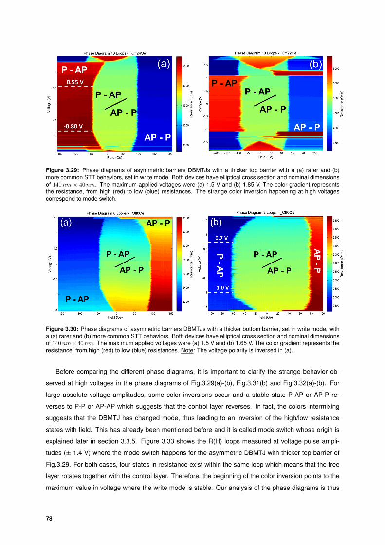
Figure 3.29: Phase diagrams of asymmetric barriers DBMTJs with a thicker top barrier with a (a) rarer and (b)more common STT behaviors, set in write mode. Both devices have elliptical cross section and nominal dimensionsof 140nm × 40nm. The maximum applied voltages were (a) 1.5 V and (b) 1.85 V. The color gradient representsthe resistance, from high (red) to low (blue) resistances. The strange color inversion happening at high voltagescorrespond to mode switch.
Figure 3.30: Phase diagrams of asymmetric barriers DBMTJs with a thicker bottom barrier, set in write mode, witha (a) rarer and (b) more common STT behaviors. Both devices have elliptical cross section and nominal dimensionsof 140nm× 40nm. The maximum applied voltages were (a) 1.5 V and (b) 1.65 V. The color gradient represents theresistance, from high (red) to low (blue) resistances. Note: The voltage polarity is inversed in (a).
Before comparing the different phase diagrams, it is important to clarify the strange behavior ob-
served at high voltages in the phase diagrams of Fig.3.29(a)-(b), Fig.3.31(b) and Fig.3.32(a)-(b). For
large absolute voltage amplitudes, some color inversions occur and a stable state P-AP or AP-P re-
verses to P-P or AP-AP which suggests that the control layer reverses. In fact, the colors intermixing
suggests that the DBMTJ has changed mode, thus leading to an inversion of the high/low resistance
states with field. This has already been mentioned before and it is called mode switch whose origin is
explained later in section 3.3.5. Figure 3.33 shows the R(H) loops measured at voltage pulse ampli-
tudes (± 1.4 V) where the mode switch happens for the asymmetric DBMTJ with thicker top barrier of
Fig.3.29. For both cases, four states in resistance exist within the same loop which means that the free
layer rotates together with the control layer. Therefore, the beginning of the color inversion points to the
maximum value in voltage where the write mode is stable. Our analysis of the phase diagrams is thus
78

Figure 3.31: Phase diagrams of DBMTJs with symmetric thick barriers (RAtop = RAbottom = 45 Ωµm2), set inwrite mode, with a (a) rarer and (b) more common STT behaviors. Both devices have elliptical cross section andnominal dimensions of 140nm × 40nm. The maximum applied voltages were (a) 1.85 V and (b) 1.95 V. The colorgradient represents the resistance, from high (red) to low (blue) resistances.
Figure 3.32: Phase diagrams of DBMTJs with symmetric thin barriers (RAtop = RAbottom = 10 Ω.µm2), set in writemode. Mode switch happens for (a) |V | > 1 V and (b) for |V | > 0.5 V Both devices have elliptical cross sectionand nominal dimensions of 140nm × 40nm. The maximum applied voltage was 1.3 V for both devices. The colorgradient represents the resistance, from high (red) to low (blue) resistances.
confined to voltages below this mode switch triggering point.
First, we analyze the common feature among the phase diagrams with a rarer STT behavior. In
fact, the shared feature is the presence of an observable damping-like torque which presents a linear
dependence with applied voltage T‖ ≈ a1V . In the phase diagrams of figs.3.29(a), 3.30(a) and 3.31(a),
the P-AP state is favored by positive voltage and the AP-P state by negative voltage 12. The direction
of the electron flow is coherent with the theoretical description of STT with the usual polarity convention
and follows the results obtained from the R(I) sweeps of subsection 3.2.1. Nevertheless, among the
referred phase diagrams, only those belonging to asymmetric DBMTJs with a thicker bottom barrier and
a DBMTJ with symmetric thick barriers show exclusively the linear trend with voltage of the damping-like
torque. In the phase diagram of Fig.3.29(a) (asymmetric DBMTJ with thicker top barrier), the P-AP state12This is not true in Fig.3.30(a) because the measurement was conducted with probes in the inverse position of the standard
measurement of Fig.3.4. Therefore the electrons direction was inverted and the P-AP and AP-P states are favored by the oppositepolarities of a normal measurement.
79
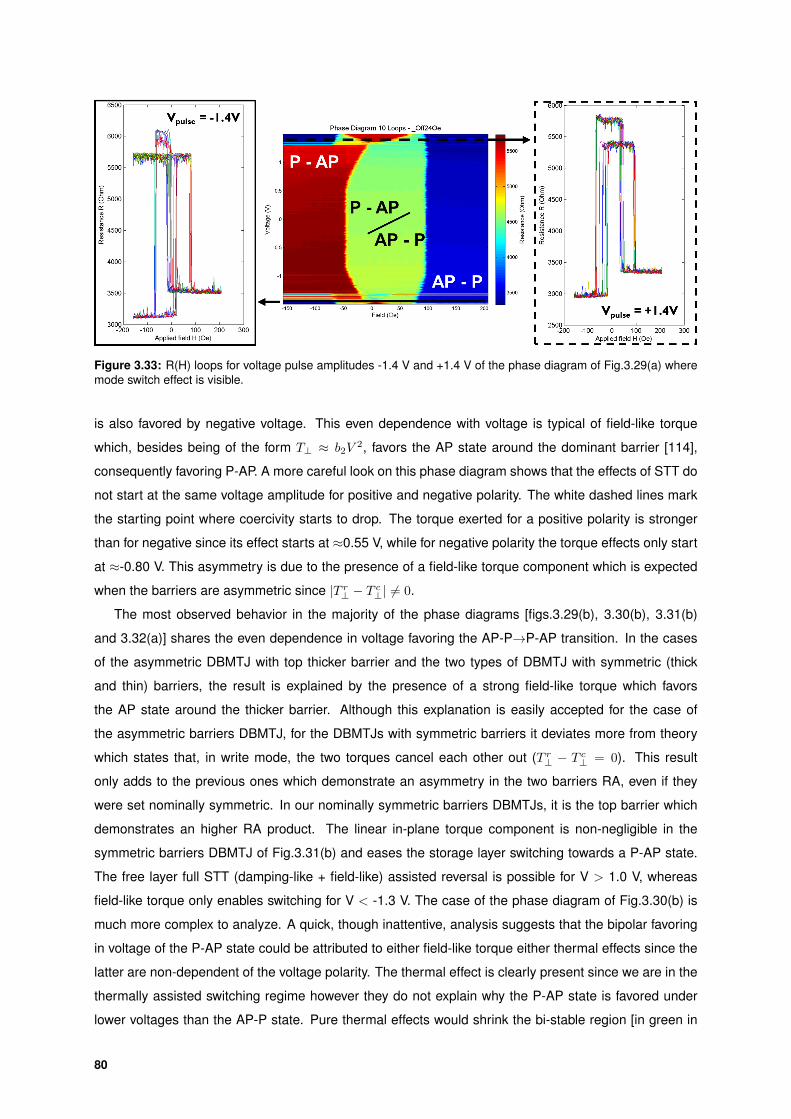
Figure 3.33: R(H) loops for voltage pulse amplitudes -1.4 V and +1.4 V of the phase diagram of Fig.3.29(a) wheremode switch effect is visible.
is also favored by negative voltage. This even dependence with voltage is typical of field-like torque
which, besides being of the form T⊥ ≈ b2V2, favors the AP state around the dominant barrier [114],
consequently favoring P-AP. A more careful look on this phase diagram shows that the effects of STT do
not start at the same voltage amplitude for positive and negative polarity. The white dashed lines mark
the starting point where coercivity starts to drop. The torque exerted for a positive polarity is stronger
than for negative since its effect starts at ≈0.55 V, while for negative polarity the torque effects only start
at ≈-0.80 V. This asymmetry is due to the presence of a field-like torque component which is expected
when the barriers are asymmetric since |T r⊥ − T c⊥| 6= 0.
The most observed behavior in the majority of the phase diagrams [figs.3.29(b), 3.30(b), 3.31(b)
and 3.32(a)] shares the even dependence in voltage favoring the AP-P→P-AP transition. In the cases
of the asymmetric DBMTJ with top thicker barrier and the two types of DBMTJ with symmetric (thick
and thin) barriers, the result is explained by the presence of a strong field-like torque which favors
the AP state around the thicker barrier. Although this explanation is easily accepted for the case of
the asymmetric barriers DBMTJ, for the DBMTJs with symmetric barriers it deviates more from theory
which states that, in write mode, the two torques cancel each other out (T r⊥ − T c⊥ = 0). This result
only adds to the previous ones which demonstrate an asymmetry in the two barriers RA, even if they
were set nominally symmetric. In our nominally symmetric barriers DBMTJs, it is the top barrier which
demonstrates an higher RA product. The linear in-plane torque component is non-negligible in the
symmetric barriers DBMTJ of Fig.3.31(b) and eases the storage layer switching towards a P-AP state.
The free layer full STT (damping-like + field-like) assisted reversal is possible for V > 1.0 V, whereas
field-like torque only enables switching for V < -1.3 V. The case of the phase diagram of Fig.3.30(b) is
much more complex to analyze. A quick, though inattentive, analysis suggests that the bipolar favoring
in voltage of the P-AP state could be attributed to either field-like torque either thermal effects since the
latter are non-dependent of the voltage polarity. The thermal effect is clearly present since we are in the
thermally assisted switching regime however they do not explain why the P-AP state is favored under
lower voltages than the AP-P state. Pure thermal effects would shrink the bi-stable region [in green in
80

Fig.3.30(b)] evenly with increasing applied voltage. In addition, this scenario is not easily explicable via
a normal field-like torque since an antiparallel magnetic configuration between reference and storage
layers was expected around the thicker barrier, corresponding to the AP-P state. According to Bernert
et al. [60] simulations, the only way to have the curvature of the boundary favoring the low resistance
state (P state, in their case with single barrier MTJ) was to set the field-like torque negative. For the
moment, no reports in literature suggest the possibility of a negative field-like torque prefactor with
quadratic dependence on voltage that favors the parallel alignment of two magnetizations around the
tunnel barrier. Another possible explanation is to assume the top barrier to be the dominant one for STT.
Taking into account the conical shape of the DBMTJ (effect of ion milling angles on the pillar shape), the
top barrier should have a smaller area. For a same current, it corresponds to a higher current density
J on that barrier and since torque is carried by the electrons, a higher number of electrons traveling
across the top barrier would mean a higher torque being applied from the top barrier interface with the
free layer.
Figure 3.34: Phase diagrams of single barrier MTJs (RA = 35 Ω.µm2) with (a) expected STT behavior and (b)predominance of thermal switching. Both devices have elliptical cross section and nominal dimensions of 140nm×40nm. The maximum applied voltages were (a) 1.9 V and (b) 1.85 V. The color gradient represents the resistance,from maximum (red) to minimum (blue) resistances.
We performed similar measurements on single barrier MTJs with (RA = 35 Ω.µm2). Figure 3.34
presents the phase diagrams of two chosen MTJs that exhibit (a) the expected STT behavior and (b) a
quasi-absence of STT, with the storage layer switching being mostly driven by thermal effects. Relatively
to voltage polarity and STT, in Fig.3.34(a), positive voltage favors the stabilization of a parallel (P) align-
ment between free and reference layers whereas negative voltage favors the antiparallel (AP) alignment
between them. This is in agreement with the theoretical description of an active in-plane torque. On
phase diagram (b) from |V | > 1V the coercivity Hc of the free layer reduces linearly with voltage. In
this case, we do not observe any dependence on the direction of injected electrons (voltage polarity),
therefore no correlation with STT. This Hc reduction is a consequence of Joule heating due to current in-
jection that will induce a reduction of the magnetic anisotropy Hk of the system. The coercivity evolution
with temperature T [115] may be expressed by adapting the Neel-Brown formula [66,116] as follows:
81
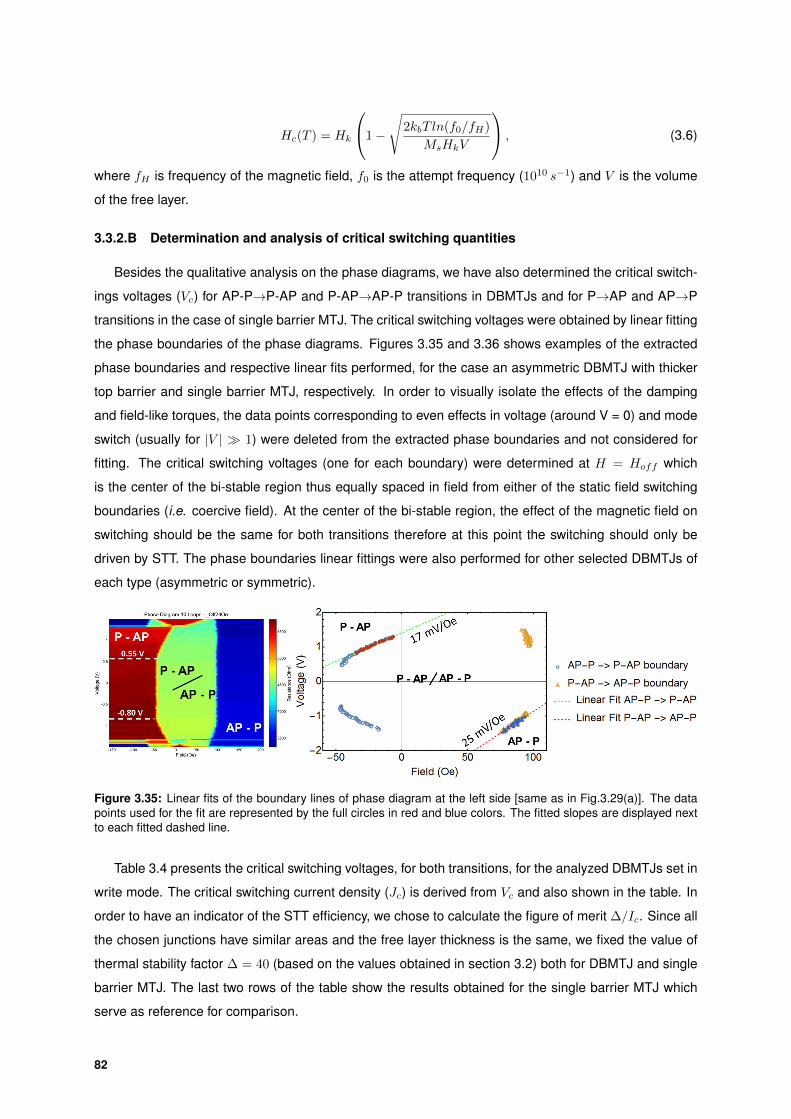
Hc(T ) = Hk
1−
√2kbT ln(f0/fH)
MsHkV
, (3.6)
where fH is frequency of the magnetic field, f0 is the attempt frequency (1010 s−1) and V is the volume
of the free layer.
3.3.2.B Determination and analysis of critical switching quantities
Besides the qualitative analysis on the phase diagrams, we have also determined the critical switch-
ings voltages (Vc) for AP-P→P-AP and P-AP→AP-P transitions in DBMTJs and for P→AP and AP→P
transitions in the case of single barrier MTJ. The critical switching voltages were obtained by linear fitting
the phase boundaries of the phase diagrams. Figures 3.35 and 3.36 shows examples of the extracted
phase boundaries and respective linear fits performed, for the case an asymmetric DBMTJ with thicker
top barrier and single barrier MTJ, respectively. In order to visually isolate the effects of the damping
and field-like torques, the data points corresponding to even effects in voltage (around V = 0) and mode
switch (usually for |V | 1) were deleted from the extracted phase boundaries and not considered for
fitting. The critical switching voltages (one for each boundary) were determined at H = Hoff which
is the center of the bi-stable region thus equally spaced in field from either of the static field switching
boundaries (i.e. coercive field). At the center of the bi-stable region, the effect of the magnetic field on
switching should be the same for both transitions therefore at this point the switching should only be
driven by STT. The phase boundaries linear fittings were also performed for other selected DBMTJs of
each type (asymmetric or symmetric).
Figure 3.35: Linear fits of the boundary lines of phase diagram at the left side [same as in Fig.3.29(a)]. The datapoints used for the fit are represented by the full circles in red and blue colors. The fitted slopes are displayed nextto each fitted dashed line.
Table 3.4 presents the critical switching voltages, for both transitions, for the analyzed DBMTJs set in
write mode. The critical switching current density (Jc) is derived from Vc and also shown in the table. In
order to have an indicator of the STT efficiency, we chose to calculate the figure of merit ∆/Ic. Since all
the chosen junctions have similar areas and the free layer thickness is the same, we fixed the value of
thermal stability factor ∆ = 40 (based on the values obtained in section 3.2) both for DBMTJ and single
barrier MTJ. The last two rows of the table show the results obtained for the single barrier MTJ which
serve as reference for comparison.
82
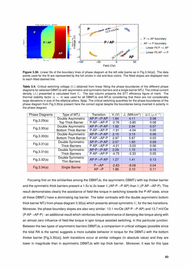
Figure 3.36: Linear fits of the boundary lines of phase diagram at the left side [same as in Fig.3.34(a)]. The datapoints used for the fit are represented by the full circles in red and blue colors. The fitted slopes are displayed nextto each fitted dashed line.
Table 3.4: Critical switching voltage (Vc) obtained from linear fitting the phase boundaries of the different phasediagrams for selected DBMTJs with asymmetric and symmetric barriers and a single barrier MTJ. The critical currentdensity (Jc) presented is calculated from Vc. The last column presents the STT efficiency figure of merit. Thethermal stability factor ∆ = 40 was used for all DBMTJs and MTJs considering that there are not considerablylarge deviations in size of the elliptical pillars. Note: The critical switching quantities for the phase boundaries of thephase diagram from Fig.3.30(a) present here the correct signal despite the boundaries being inverted in polarity inthe phase diagram.
Phase Diagrams Type of MTJ Transition Vc(V) Jc (MA/cm2) ∆/Ic(µA−1)AP-P→P-AP 1.84 4.11 0.08Fig.3.29(a) Double Asymmetric
Top Thick Barrier P-AP→AP-P -2.76 -3.80 0.08AP-P→P-AP 1.92 2.94 0.07Fig.3.30(a) Double Asymmetric
Bottom Thick Barrier P-AP→AP-P -1.91 -4.04 0.05AP-P→P-AP 2.15 3.10 0.06Fig.3.30(b) Double Asymmetric
Bottom Thick Barrier P-AP→AP-P 2.97 5.87 0.03AP-P→P-AP 2.57 1.93 0.09Fig.3.31(a) Double Symmetric
Thick Barriers P-AP→AP-P -4.21 -3.03 0.06AP-P→P-AP 2.29 1.72 0.10Fig.3.31(b) Double Symmetric
Thick Barriers P-AP→AP-P -4.75 -3.33 0.05
Fig.3.32(a) Double SymmetricThin Barriers AP-P→P-AP 1.27 1.41 0.13
P→AP -2.83 -8.08 0.04Fig.3.34(a) Single Barrier AP→P 1.86 3.10 0.11
Focusing first on the similarities among the DBMTJs, the asymmetric DBMTJ with top thicker barrier
and the symmetric thick barriers present a 1.5x to 2x lower Vc(AP-P→P-AP) than Vc(P-AP→AP-P). This
result demonstrates clearly the assistance of field-like torque in switching towards the P-AP state, since
all these DBMTJ have a dominating top barrier. The latter contrasts with the double asymmetric bottom
thick barrier MTJ from phase diagram 3.30(a) which presents almost symmetric Vc for the two transitions.
Moreover, the phase boundary slopes are also very similar: 13.1 mv/Oe (AP-P→P-AP) and 13.7 mV/Oe
(P-AP→AP-P) - an additional result which reinforces the predominance of damping-like torque along with
an almost zero influence of field-like torque in spin torque assisted switching, in this particular junction.
Between the two types of asymmetric barriers DBMTJs, a comparison in critical voltages (possible since
the total RA is the same) suggests a more suitable behavior in torque for the DBMTJ with the bottom
thicker barrier [Fig.3.30(a)], both transitions occur at similar voltages (in absolute value) and they are
lower in magnitude than in asymmetric DBMTJs with top thick barrier. Moreover, it was for this type
83
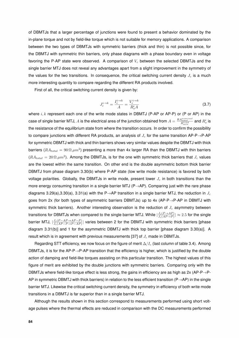
of DBMTJs that a larger percentage of junctions were found to present a behavior dominated by the
in-plane torque and not by field-like torque which is not suitable for memory applications. A comparison
between the two types of DBMTJs with symmetric barriers (thick and thin) is not possible since, for
the DBMTJ with symmetric thin barriers, only phase diagrams with a phase boundary even in voltage
favoring the P-AP state were observed. A comparison of Vc between the selected DBMTJs and the
single barrier MTJ does not reveal any advantages apart from a slight improvement in the symmetry of
the values for the two transitions. In consequence, the critical switching current density Jc is a much
more interesting quantity to compare regarding the different RA products involved.
First of all, the critical switching current density is given by:
J i→kc =Ii→kc
A=V i→kc
RisA(3.7)
where i, k represent each one of the write mode states in DBMTJ (P-AP or AP-P) or (P or AP) in the
case of single barrier MTJ, A is the electrical area of the junction obtained from A =RAnominaltotal
Rreadmin
and Ris is
the resistance of the equilibrium state from where the transition occurs. In order to confirm the possibility
to compare junctions with different RA products, an analysis of Jc for the same transition AP-P→P-AP
for symmetric DBMTJ with thick and thin barriers shows very similar values despite the DBMTJ with thick
barriers (RAtotal = 90 Ω.µm2) presenting a more than 4x larger RA than the DBMTJ with thin barriers
(RAtotal = 20 Ω.µm2). Among the DBMTJs, is for the one with symmetric thick barriers that Jc values
are the lowest within the same transition. On other end is the double asymmetric bottom thick barrier
DBMTJ from phase diagram 3.30(b) where P-AP state (low write mode resistance) is favored by both
voltage polarities. Globally, the DBMTJs in write mode, present lower Jc in both transitions than the
more energy consuming transition in a single barrier MTJ (P→AP). Comparing just with the rare phase
diagrams 3.29(a),3.30(a), 3.31(a) with the P→AP transition in a single barrier MTJ, the reduction in Jc
goes from 2x (for both types of asymmetric barriers DBMTJs) up to 4x (AP-P→P-AP in DBMTJ with
symmetric thick barriers). Another interesting observation is the reduction of Jc asymmetry between
transitions for DBMTJs when compared to the single barrier MTJ. While |Jc(P→AP )Jc(AP→P ) | ≈ 2.5 for the single
barrier MTJ, |Jc(P−AP→AP−P )Jc(AP−P→P−AP ) | varies between 2 for the DBMTJ with symmetric thick barriers [phase
diagram 3.31(b)] and 1 for the asymmetric DBMTJ with thick top barrier [phase diagram 3.30(a)]. A
result which is in agreement with previous measurements [37] of Jc made in DBMTJs.
Regarding STT efficiency, we now focus on the figure of merit ∆/Ic (last column of table 3.4). Among
DBMTJs, it is for the AP-P→P-AP transition that the efficiency is higher, which is justified by the double
action of damping and field-like torques assisting on this particular transition. The highest values of this
figure of merit are exhibited by the double junctions with symmetric barriers. Comparing only with the
DBMTJs where field-like torque effect is less strong, the gains in efficiency are as high as 2x (AP-P→P-
AP in symmetric DBMTJ with thick barriers) in relation to the less efficient transition (P→AP) in the single
barrier MTJ. Likewise the critical switching current density, the symmetry in efficiency of both write mode
transitions in a DBMTJ is far superior than in a single barrier MTJ.
Although the results shown in this section correspond to measurements performed using short volt-
age pulses where the thermal effects are reduced in comparison with the DC measurements performed
84
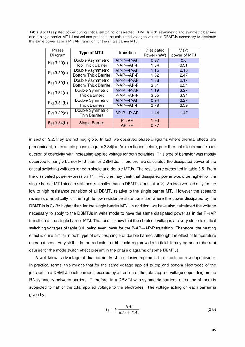
Table 3.5: Dissipated power during critical switching for selected DBMTJs with asymmetric and symmetric barriersand a single barrier MTJ. Last column presents the calculated voltages values in DBMTJs necessary to dissipatethe same power as in a P→AP transition for the single barrier MTJ.
PhaseDiagram Type of MTJ Transition Dissipated
Power (mW)V (V)
power of MTJAP-P→P-AP 0.97 2.6Fig.3.29(a) Double Asymmetric
Top Thick Barrier P-AP→AP-P 1.34 3.31AP-P→P-AP 1.15 2.10Fig.3.30(a) Double Asymmetric
Bottom Thick Barrier P-AP→AP-P 1.62 2.47AP-P→P-AP 1.38 2.17Fig.3.30(b) Double Asymmetric
Bottom Thick Barrier P-AP→AP-P 3.61 2.54AP-P→P-AP 1.19 3.27Fig.3.31(a) Double Symmetric
Thick Barriers P-AP→AP-P 3.05 3.34AP-P→P-AP 0.94 3.27Fig.3.31(b) Double Symmetric
Thick Barriers P-AP→AP-P 3.79 3.39
Fig.3.32(a) Double SymmetricThin Barriers AP-P→P-AP 1.44 1.47
P→AP 1.93Fig.3.34(b) Single Barrier AP→P 0.77
in section 3.2, they are not negligible. In fact, we observed phase diagrams where thermal effects are
predominant, for example phase diagram 3.34(b). As mentioned before, pure thermal effects cause a re-
duction of coercivity with increasing applied voltage for both polarities. This type of behavior was mostly
observed for single barrier MTJ than for DBMTJs. Therefore, we calculated the dissipated power at the
critical switching voltages for both single and double MTJs. The results are presented in table 3.5. From
the dissipated power expression P =V 2c
R , one may think that dissipated power would be higher for the
single barrier MTJ since resistance is smaller than in DBMTJs for similar Vc. An idea verified only for the
low to high resistance transition of all DBMTJ relative to the single barrier MTJ. However the scenario
reverses dramatically for the high to low resistance state transition where the power dissipated by the
DBMTJs is 2x-3x higher than for the single barrier MTJ. In addition, we have also calculated the voltage
necessary to apply to the DBMTJs in write mode to have the same dissipated power as in the P→AP
transition of the single barrier MTJ. The results show that the obtained voltages are very close to critical
switching voltages of table 3.4, being even lower for the P-AP→AP-P transition. Therefore, the heating
effect is quite similar in both type of devices, single or double barrier. Although the effect of temperature
does not seem very visible in the reduction of bi-stable region width in field, it may be one of the root
causes for the mode switch effect present in the phase diagrams of some DBMTJs.
A well-known advantage of dual barrier MTJ in diffusive regime is that it acts as a voltage divider.
In practical terms, this means that for the same voltage applied to top and bottom electrodes of the
junction, in a DBMTJ, each barrier is exerted by a fraction of the total applied voltage depending on the
RA symmetry between barriers. Therefore, in a DBMTJ with symmetric barriers, each one of them is
subjected to half of the total applied voltage to the electrodes. The voltage acting on each barrier is
given by:
Vi = VRAi
RAi +RAk(3.8)
85
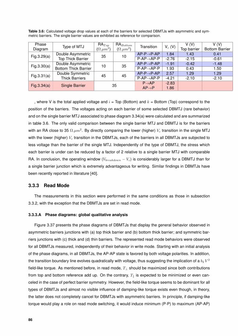
Table 3.6: Calculated voltage drop values at each of the barriers for selected DBMTJs with asymmetric and sym-metric barriers. The single barrier values are exhibited as reference for comparison.
PhaseDiagram Type of MTJ RATop
(Ω.µm2)RABottom(Ω.µm2) Transition Vc (V) V (V)
Top barrierV (V)
Bottom BarrierAP-P→P-AP 1.84 1.43 0.41Fig.3.29(a) Double Asymmetric
Top Thick Barrier 35 10 P-AP→AP-P -2.76 -2.15 -0.61AP-P→P-AP -1.91 -0.42 -1.48Fig.3.30(a) Double Asymmetric
Bottom Thick Barrier 10 35 P-AP→AP-P 1.93 0.43 1.50AP-P→P-AP 2.57 1.29 1.29Fig.3.31(a) Double Symmetric
Thick Barriers 45 45 P-AP→AP-P -4.21 -2.10 -2.10P→AP -2.83Fig.3.34(a) Single Barrier 35 AP→P 1.86
, where V is the total applied voltage and i = Top (Bottom) and k = Bottom (Top) correspond to the
position of the barriers. The voltages acting on each barrier of some selected DBMTJ (rare behavior)
and on the single barrier MTJ associated to phase diagram 3.34(a) were calculated and are summarized
in table 3.6. The only valid comparison between the single barrier MTJ and DBMTJ is for the barriers
with an RA close to 35 Ω.µm2. By directly comparing the lower (higher) Vc transition in the single MTJ
with the lower (higher) Vc transition in the DBMTJs, each of the barriers in all DBMTJs are subjected to
less voltage than the barrier of the single MTJ. Independently of the type of DBMTJ, the stress which
each barrier is under can be reduced by a factor of 2 relative to a single barrier MTJ with comparable
RA. In conclusion, the operating window (Vbreakdown − Vc) is considerably larger for a DBMTJ than for
a single barrier junction which is extremely advantageous for writing. Similar findings in DBMTJs have
been recently reported in literature [40].
3.3.3 Read Mode
The measurements in this section were performed in the same conditions as those in subsection
3.3.2, with the exception that the DBMTJs are set in read mode.
3.3.3.A Phase diagrams: global qualitative analysis
Figure 3.37 presents the phase diagrams of DBMTJs that display the general behavior observed in
asymmetric barriers junctions with (a) top thick barrier and (b) bottom thick barrier; and symmetric bar-
riers junctions with (c) thick and (d) thin barriers. The represented read mode behaviors were observed
for all DBMTJs measured, independently of their behavior in write mode. Starting with an initial analysis
of the phase diagrams, in all DBMTJs, the AP-AP state is favored by both voltage polarities. In addition,
the transition boundary line evolves quadratically with voltage, thus suggesting the implication of a b2 V 2
field-like torque. As mentioned before, in read mode, T⊥ should be maximized since both contributions
from top and bottom reference add up. On the contrary, T‖ is expected to be minimized or even can-
celed in the case of perfect barrier symmetry. However, the field-like torque seems to be dominant for all
types of DBMTJs and almost no visible influence of damping-like torque exists even though, in theory,
the latter does not completely cancel for DBMTJs with asymmetric barriers. In principle, if damping-like
torque would play a role on read mode switching, it would induce minimum (P-P) to maximum (AP-AP)
86
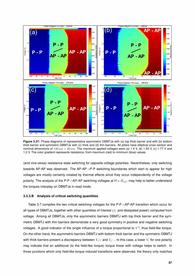
Figure 3.37: Phase diagrams of representative asymmetric DBMTJs with (a) top thick barrier and with (b) bottomthick barrier and symmetric DBMTJs with (c) thick and (d) thin barriers. All pillars have elliptical cross section andnominal dimensions of 140nm × 40nm. The maximum applied voltages were (a) 1.4 V, (b) 1.55 V, (c) 1.77 V and1.2 V. The color gradient represents resistance, from maximum (red) to minimum (blue) values.
(and vice-versa) resistance state switching for opposite voltage polarities. Nevertheless, only switching
towards AP-AP was observed. The AP-AP→P-P switching boundaries which start to appear for high
voltages are mostly certainly created by thermal effects since they occur independently of the voltage
polarity. The analysis of the P-P→AP-AP switching voltages at H = Hoff may help to better understand
the torques interplay on DBMTJs in read mode.
3.3.3.B Analysis of critical switching quantities
Table 3.7 compiles the two critical switching voltages for the P-P→AP-AP transition which occur for
all types of DBMTJs, together with other quantities of interest (Jc and dissipated power) computed from
voltage. Among all DBMTJs, only the asymmetric barriers DBMTJ with top thick barrier and the sym-
metric DBMTJ with thin barriers demonstrate a very good symmetry in positive and negative switching
voltages. A good indicator of the single influence of a torque proportional to V 2, thus field-like torque.
On the other hand, the asymmetric barriers DBMTJ with bottom thick barrier and the symmetric DBMTJ
with thick barriers present a discrepancy between Vc+ and Vc−. In this case, a lower Vc for one polarity
may indicate that an additional (to the field-like torque) torque linear with voltage helps to switch. In
those junctions which only field-like torque induced transitions were observed, the theory only matches
87

the experimental results for the symmetric DBMTJ with thin barriers since T‖ ≈ 0. For the asymmetric
DBMTJ with top thick barrier, T‖ should not be totally zero and the positive voltage should favor more
the AP-AP state while negative voltage should favor the P-P state, as represented in the ideal case of
Fig.3.20. The possible of non-zero T‖ for the symmetric DBMTJ with thick barriers can be explained by
the dominant behavior of one barrier over the other. In this case, and judging by the fact that Vc+ > Vc−,
the top barrier would be the ruling one. The read mode switching behavior of the asymmetric DBMTJ
with bottom thick barrier, though revealing the presence of a T‖ 6= 0, the fact that Vc+ > Vc− does not
follow the theoretical description for which the AP-AP state should be more favored by negative voltage.
However, it does support the hypothesis of a dominant top barrier (even if smaller in RA than the bottom)
which has already been observed for the same type of DBMTJ in write mode. The dominating effect of
the top barrier may be justified by its smaller area than the bottom barrier due to fabrication but also due
to better growth conditions (supported by previous observations in DBMTJs by Feng et al. [39]) which
confer an higher TMR to the top barrier than the bottom one.
Table 3.7: Positive (V+) and negative (V-) critical switching voltages (Vc) obtained from linear fitting the P-P→AP-APphase boundaries of the different phase diagrams for selected DBMTJs with asymmetric and symmetric barriers,set in read mode. The critical current densities (Jc) presented are calculated from Vc. The last column presents thedissipated power by the DBMTJs at the critical voltages for both polarities.
PhaseDiagram Type of MTJ Transition Vc (V) Jc (MA/cm2) Dissipated Power
(mW)P-P→AP-AP (V+) 1.79 3.99 0.80Fig.3.37(a) Double Asymmetric
Top Thick Barrier P-P→AP-AP (V-) -1.80 -4.00 0.81P-P→AP-AP (V+) 1.71 3.81 1.44Fig.3.37(b) Double Asymmetric
Bottom Thick Barrier P-P→AP-AP (V-) -1.94 -4.31 1.84P-P→AP-AP (V+) 1.65 1.83 0.79Fig.3.37(c) Double Symmetric
Thick Barriers P-P→AP-AP (V-) -1.85 -2.06 0.99P-P→AP-AP (V+) 1.38 6.92 2.35Fig.3.37(d) Double Symmetric
Thin Barriers P-P→AP-AP (V-) -1.33 -6.67 2.18
Between the two symmetric barriers there is a difference on the critical switching voltages in read
mode. Although one might think that the lower Vc obtained for the DBMTJ with thin barriers could
be justified by a stronger field-like than for the DBMTJ with thicker barrier, thermal effects cannot be
neglected. In fact, according to the values of the dissipated power in table 3.7, the thermal effects are 2x
higher for the symmetric DBMTJ with thin barriers than for the one with thicker barriers. These effects
may be the real reason behind the lower Vc values obtained for these type of DBMTJ. In addition, the
AP-AP→P-P switching boundaries which start to appear for high voltages on the asymmetric DBMTJ
with thick bottom barrier and symmetric DBMTJ with thin barriers coincide with the highest dissipated
power values also demonstrated by those DBMTJ, supporting substantially the thermal nature of those
transitions.
3.3.4 Conclusion: Field-like torque in write and read modes
From the performed measurements on the DBMTJs and analysis of their respective phase diagrams,
there is one effect common to them all: field-like torque.
In write mode, the most surprising result was the observation of field-like torque induced switching
88

in DBMTJ with symmetric barriers. According to theory, in a double barrier MTJ with the control and
reference layers’ magnetizations in antiparallel alignment (i.e. write mode), the two field-like torque com-
ponents of the torques acting on the free layer should subtract. Moreover, in a structure with symmetric
barriers, the cancellation should be perfect, thus T⊥ = 0. However, for the majority of the symmetric
DBMTJs measured, with thick or thin barriers, the field-like torque even dependence with V dominates
the switching and favors the antiparallel alignment around the top barrier, therefore favoring the P-AP
state. Even for the small group of symmetric barriers double junctions [example in Fig.3.31(a)] where
the damping-like torque induced switching is visible, the field-like torque is non-negligible and allows for
a more efficient transition towards P-AP. The non-zero T⊥ may have two possible origins. One is the
shape of the DBMTJ pillar which is most probably conical (due to ion beam etching) therefore creating a
top barrier with a smaller area than the bottom barrier. This creates an asymmetry of the current density
across the two oxide barriers. The larger J on top the barrier translates on a larger number of electrons
carrying torque per unit area corresponding to a larger field-like torque coming from the control layer
than from the bottom reference layer. The other reason is related with the quality of the barriers. It is
possible that the top barrier may have a superior texture quality than the bottom, providing higher TMR
on top than on bottom barrier. Comparison with previous works is difficult since there are not many
reports on DBMTJs. Furthermore the existing reports are somehow contradictory. Feng et al. [39] report
that, despite the amorphous state of the middle CoFeB (free layer) due to a lack of B diffusion because
of the existence of two MgO barriers, they see evidence of the formation of lattice planes along the
upper CoFeB/Top MgO interface. Their proposed explanation for an higher TMR of the top barrier than
the bottom barrier in nominally symmetric barrier double junctions. On the other hand, Gan et al. [38]
report a lower TMR on the top barrier than the bottom barrier since the degree of crystallization of the
top CoFeB (control layer) is slightly less than the bottom CoFeB reference layer. The other peculiar STT
behavior observed in write mode was for asymmetric DBMTJ with thick bottom barrier. In spite of few
double junctions presenting the expected behavior dominated by the damping-like torque, in many oth-
ers switching towards the P-AP state occurred for both voltage polarities [Fig.3.30(b)]. An unexpected
observation even considering a dominant field-like torque. Theory suggests that field-like torque favors
an antiparallel alignment between free and reference layers around the dominating barrier. In this type of
DBMTJs it was thought that the dominant barrier would be the bottom one since it presents the highest
RA. However, if the aforementioned explanations are true, there is the possibility of the top barrier, even
if it presents a lower RA, to be the dominant one. That would fit with the experimental observations.
Another possibility, yet much less probable, it is to consider a negative field-like torque T⊥ = b2V2,
where b2 < 0. This scenario was only verified in simulations performed by Bernet et al. [60], with no
experimental reports to sustain this claim.
In read mode, field-like torque is expected to be maximized since TRead⊥total = TControl⊥ + TReference⊥ .
Therefore, favoring the AP-AP configuration, where the free layer is antiparallel to both control and
reference layers. The experimental results of all DBMTJs are in agreement with theoretical predictions.
The only divergence with theory concerns damping-like torque specially in the asymmetric DBMTJ with
bottom thick barrier. Here again, although the presence of a remaining T‖ was expected (no complete
89
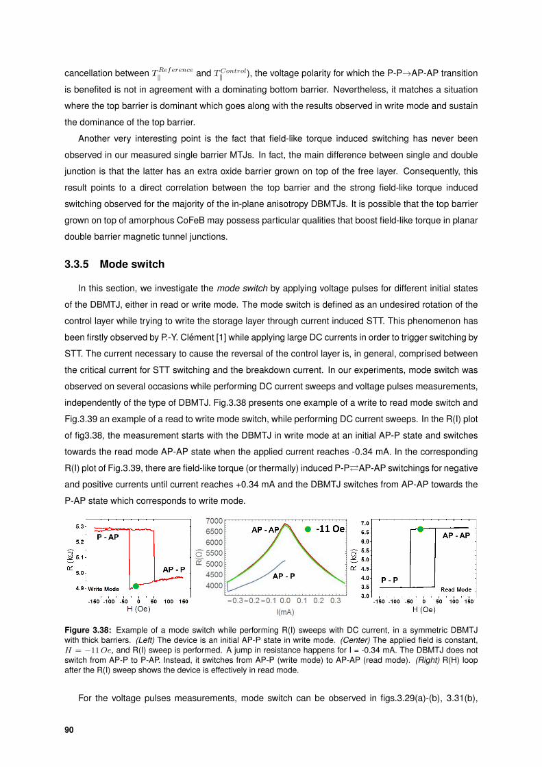
cancellation between TReference‖ and TControl‖ ), the voltage polarity for which the P-P→AP-AP transition
is benefited is not in agreement with a dominating bottom barrier. Nevertheless, it matches a situation
where the top barrier is dominant which goes along with the results observed in write mode and sustain
the dominance of the top barrier.
Another very interesting point is the fact that field-like torque induced switching has never been
observed in our measured single barrier MTJs. In fact, the main difference between single and double
junction is that the latter has an extra oxide barrier grown on top of the free layer. Consequently, this
result points to a direct correlation between the top barrier and the strong field-like torque induced
switching observed for the majority of the in-plane anisotropy DBMTJs. It is possible that the top barrier
grown on top of amorphous CoFeB may possess particular qualities that boost field-like torque in planar
double barrier magnetic tunnel junctions.
3.3.5 Mode switch
In this section, we investigate the mode switch by applying voltage pulses for different initial states
of the DBMTJ, either in read or write mode. The mode switch is defined as an undesired rotation of the
control layer while trying to write the storage layer through current induced STT. This phenomenon has
been firstly observed by P.-Y. Clement [1] while applying large DC currents in order to trigger switching by
STT. The current necessary to cause the reversal of the control layer is, in general, comprised between
the critical current for STT switching and the breakdown current. In our experiments, mode switch was
observed on several occasions while performing DC current sweeps and voltage pulses measurements,
independently of the type of DBMTJ. Fig.3.38 presents one example of a write to read mode switch and
Fig.3.39 an example of a read to write mode switch, while performing DC current sweeps. In the R(I) plot
of fig3.38, the measurement starts with the DBMTJ in write mode at an initial AP-P state and switches
towards the read mode AP-AP state when the applied current reaches -0.34 mA. In the corresponding
R(I) plot of Fig.3.39, there are field-like torque (or thermally) induced P-PAP-AP switchings for negative
and positive currents until current reaches +0.34 mA and the DBMTJ switches from AP-AP towards the
P-AP state which corresponds to write mode.
Figure 3.38: Example of a mode switch while performing R(I) sweeps with DC current, in a symmetric DBMTJwith thick barriers. (Left) The device is an initial AP-P state in write mode. (Center) The applied field is constant,H = −11Oe, and R(I) sweep is performed. A jump in resistance happens for I = -0.34 mA. The DBMTJ does notswitch from AP-P to P-AP. Instead, it switches from AP-P (write mode) to AP-AP (read mode). (Right) R(H) loopafter the R(I) sweep shows the device is effectively in read mode.
For the voltage pulses measurements, mode switch can be observed in figs.3.29(a)-(b), 3.31(b),
90
3.32 and 3.37(a),(c)-(d). The oscillation between the two modes, usually observed for |V | > 1V , are
characterized by sudden color changes in the phase diagrams. Figure 3.33 shows the R(H) loops of
the mode switch regions where both write and read mode R(H) curves exist. In the phase diagrams
of DBMTJs with a thicker top barrier, the mode switch is easier to detect because the stables states of
maximum and minimum resistance of read mode exist for magnetic fields of opposite sign in write mode.
For example, in Fig.3.29(b), the stable write mode P-AP state (high resistance, in orange color) exist for
H 0 as well as the stable read mode P-P state (minimum resistance, in dark blue color).
Figure 3.39: Example of a read to write mode switch while performing R(I) sweeps with DC current, in a symmetricDBMTJ with thick barriers. (Left) The DBMTJ is an initial P-P state in read mode. (Center) The applied field isconstant, H = −14Oe, and R(I) sweep is performed. STT switching happens for negative currents, however for I= 0.34 mA the junction switches from AP-AP to P-AP state. Therefore switching from read to write mode. (Right)R(H) loop after the R(I) sweep shows the device is effectively in write mode. Moreover, at H = -14 Oe the DBMTJ isin a stable P-AP state, outside the bi-stable region.
The first attempt to explain this effect was also proposed by P.-Y. Clement [1] who claimed that it was
caused by thermal effects. More precisely, the applied current would increase locally the temperature of
the double junction above the blocking temperature of the FeMn (see section 3.1.1), unpinning the hard
layer of the top SAF. Upon the rupture of the exchange coupling between the antiferromagnet and the
adjacent ferromagnet, even a small applied magnetic field would be strong enough to reverse the control
layer. According to this explanation and considering the effect to be purely caused by high temperatures,
the mode switch should also happen for applied magnetic fields outside the coercive region and given
the field is in the direction which enables to reverse the control layer from its original configuration:
parallel (read mode) or antiparallel (write mode) to the bottom reference layer. In order to verify this
hypothesis, we conducted experiments using voltage pulses in different DBMTJ states both for read
and write modes. Unlike the DC current measurements, the temperature effects are minimized using
short pulses, thus higher voltages should be needed to attain temperatures superior to TFeMnb . For the
aforementioned purpose, we studied the regions of field around -500 Oe and 500 Oe (marked by dashed
boxes) on the left side R(H) cycles of figs.3.40 and 3.41). In these regions, the free layer cannot switch
by STT or by applied magnetic field.
Figure 3.40 presents the tests realized with the DBMTJ set in read mode. The R(H) cycles at the left
show the initial state of the DBMTJ and the tested zone (red dashed square). For the case on the top,
where the DBMTJ stable states are either AP-AP or AP-P in the tested field range (due to the rotation
of the control layer), mode switch happens for V = +1.22 V and the control layer does not switch back
even for higher voltages. The R(H) plot of the top left shows that the antiferromagnetic RKKY coupling
between the ferromagnetic layers of the top SAF is broken around 500 Oe. In the top phase diagram,
91
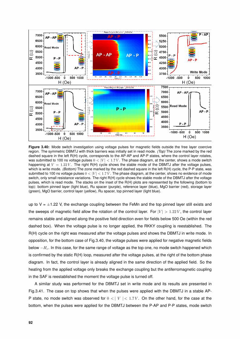
Figure 3.40: Mode switch investigation using voltage pulses for magnetic fields outside the free layer coerciveregion. The symmetric DBMTJ with thick barriers was initially set in read mode. (Top) The zone marked by the reddashed square in the left R(H) cycle, corresponds to the AP-AP and AP-P states, where the control layer rotates,was submitted to 100 ns voltage pulses 0 < |V | < 1.7V . The phase diagram, at the center, shows a mode switchhappening at V = 1.22V . The right R(H) cycle shows the stable mode of the DBMTJ after the voltage pulses,which is write mode. (Bottom) The zone marked by the red dashed square in the left R(H) cycle, the P-P state, wassubmitted to 100 ns voltage pulses 0 < |V | < 1.7V . The phase diagram, at the center, shows no evidence of modeswitch, only small resistance variations. The right R(H) cycle shows the stable mode of the DBMTJ after the voltagepulses, which is read mode. The stacks on the inset of the R(H) plots are represented by the following (bottom totop): bottom pinned layer (light blue), Ru spacer (purple), reference layer (blue), MgO barrier (red), storage layer(green), MgO barrier, control layer (yellow), Ru spacer, top pinned layer (light blue).
up to V = ±1.22 V, the exchange coupling between the FeMn and the top pinned layer still exists and
the sweeps of magnetic field allow the rotation of the control layer. For |V | > 1.22V , the control layer
remains stable and aligned along the positive field direction even for fields below 500 Oe (within the red
dashed box). When the voltage pulse is no longer applied, the RKKY coupling is reestablished. The
R(H) cycle on the right was measured after the voltage pulses and shows the DBMTJ in write mode. In
opposition, for the bottom case of Fig.3.40, the voltage pulses were applied for negative magnetic fields
below −Hc. In this case, for the same range of voltage as the top one, no mode switch happened which
is confirmed by the static R(H) loop, measured after the voltage pulses, at the right of the bottom phase
diagram. In fact, the control layer is already aligned in the same direction of the applied field. So the
heating from the applied voltage only breaks the exchange coupling but the antiferromagnetic coupling
in the SAF is reestablished the moment the voltage pulse is turned off.
A similar study was performed for the DBMTJ set in write mode and its results are presented in
Fig.3.41. The case on top shows that when the pulses were applied with the DBMTJ in a stable AP-
P state, no mode switch was observed for 0 < | V |< 1.7V . On the other hand, for the case at the
bottom, when the pulses were applied for the DBMTJ between the P-AP and P-P states, mode switch
92
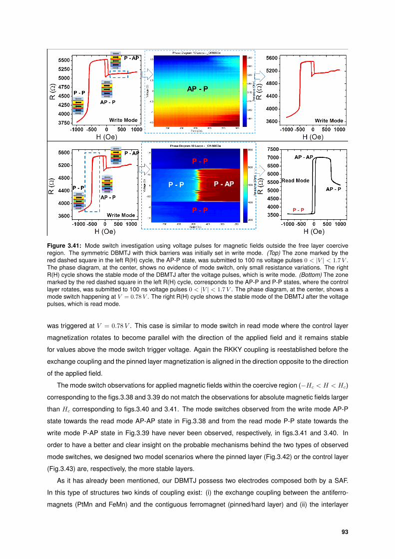
Figure 3.41: Mode switch investigation using voltage pulses for magnetic fields outside the free layer coerciveregion. The symmetric DBMTJ with thick barriers was initially set in write mode. (Top) The zone marked by thered dashed square in the left R(H) cycle, the AP-P state, was submitted to 100 ns voltage pulses 0 < |V | < 1.7V .The phase diagram, at the center, shows no evidence of mode switch, only small resistance variations. The rightR(H) cycle shows the stable mode of the DBMTJ after the voltage pulses, which is write mode. (Bottom) The zonemarked by the red dashed square in the left R(H) cycle, corresponds to the AP-P and P-P states, where the controllayer rotates, was submitted to 100 ns voltage pulses 0 < |V | < 1.7V . The phase diagram, at the center, shows amode switch happening at V = 0.78V . The right R(H) cycle shows the stable mode of the DBMTJ after the voltagepulses, which is read mode.
was triggered at V = 0.78V . This case is similar to mode switch in read mode where the control layer
magnetization rotates to become parallel with the direction of the applied field and it remains stable
for values above the mode switch trigger voltage. Again the RKKY coupling is reestablished before the
exchange coupling and the pinned layer magnetization is aligned in the direction opposite to the direction
of the applied field.
The mode switch observations for applied magnetic fields within the coercive region (−Hc < H < Hc)
corresponding to the figs.3.38 and 3.39 do not match the observations for absolute magnetic fields larger
than Hc corresponding to figs.3.40 and 3.41. The mode switches observed from the write mode AP-P
state towards the read mode AP-AP state in Fig.3.38 and from the read mode P-P state towards the
write mode P-AP state in Fig.3.39 have never been observed, respectively, in figs.3.41 and 3.40. In
order to have a better and clear insight on the probable mechanisms behind the two types of observed
mode switches, we designed two model scenarios where the pinned layer (Fig.3.42) or the control layer
(Fig.3.43) are, respectively, the more stable layers.
As it has already been mentioned, our DBMTJ possess two electrodes composed both by a SAF.
In this type of structures two kinds of coupling exist: (i) the exchange coupling between the antiferro-
magnets (PtMn and FeMn) and the contiguous ferromagnet (pinned/hard layer) and (ii) the interlayer
93
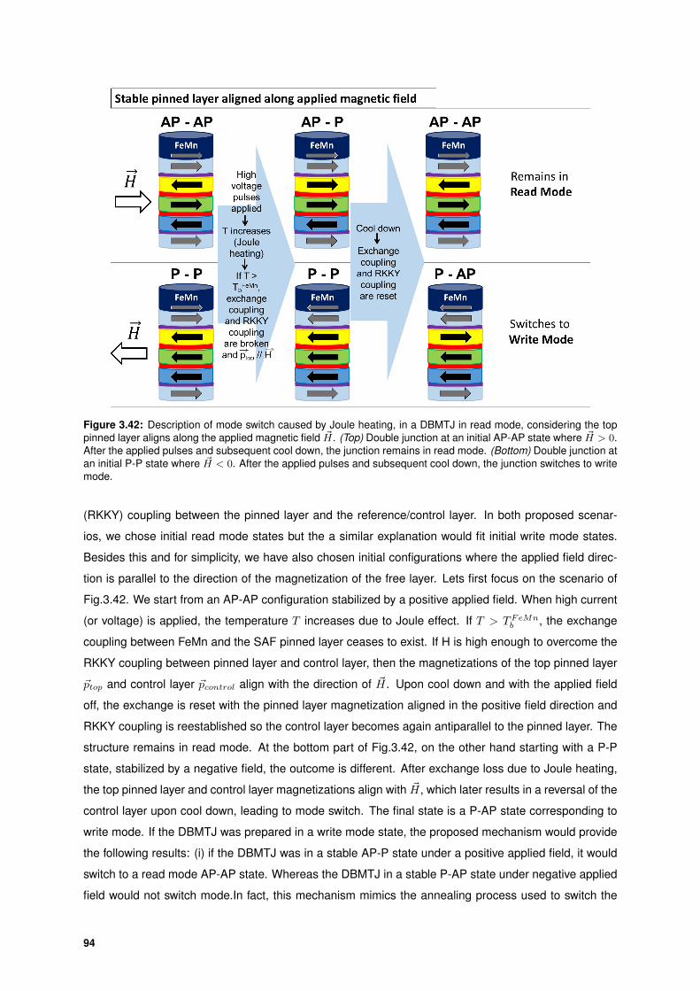
Figure 3.42: Description of mode switch caused by Joule heating, in a DBMTJ in read mode, considering the toppinned layer aligns along the applied magnetic field ~H. (Top) Double junction at an initial AP-AP state where ~H > 0.After the applied pulses and subsequent cool down, the junction remains in read mode. (Bottom) Double junction atan initial P-P state where ~H < 0. After the applied pulses and subsequent cool down, the junction switches to writemode.
(RKKY) coupling between the pinned layer and the reference/control layer. In both proposed scenar-
ios, we chose initial read mode states but the a similar explanation would fit initial write mode states.
Besides this and for simplicity, we have also chosen initial configurations where the applied field direc-
tion is parallel to the direction of the magnetization of the free layer. Lets first focus on the scenario of
Fig.3.42. We start from an AP-AP configuration stabilized by a positive applied field. When high current
(or voltage) is applied, the temperature T increases due to Joule effect. If T > TFeMnb , the exchange
coupling between FeMn and the SAF pinned layer ceases to exist. If H is high enough to overcome the
RKKY coupling between pinned layer and control layer, then the magnetizations of the top pinned layer
~ptop and control layer ~pcontrol align with the direction of ~H. Upon cool down and with the applied field
off, the exchange is reset with the pinned layer magnetization aligned in the positive field direction and
RKKY coupling is reestablished so the control layer becomes again antiparallel to the pinned layer. The
structure remains in read mode. At the bottom part of Fig.3.42, on the other hand starting with a P-P
state, stabilized by a negative field, the outcome is different. After exchange loss due to Joule heating,
the top pinned layer and control layer magnetizations align with ~H, which later results in a reversal of the
control layer upon cool down, leading to mode switch. The final state is a P-AP state corresponding to
write mode. If the DBMTJ was prepared in a write mode state, the proposed mechanism would provide
the following results: (i) if the DBMTJ was in a stable AP-P state under a positive applied field, it would
switch to a read mode AP-AP state. Whereas the DBMTJ in a stable P-AP state under negative applied
field would not switch mode.In fact, this mechanism mimics the annealing process used to switch the
94
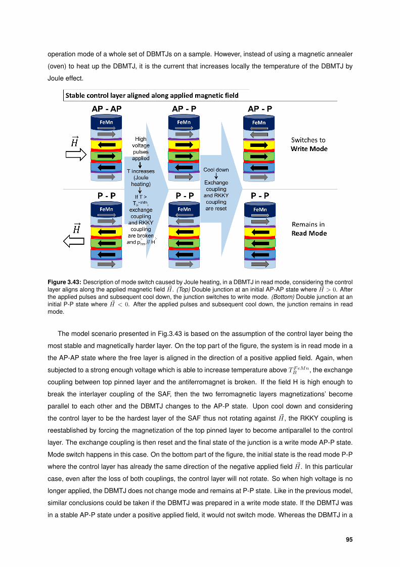
operation mode of a whole set of DBMTJs on a sample. However, instead of using a magnetic annealer
(oven) to heat up the DBMTJ, it is the current that increases locally the temperature of the DBMTJ by
Joule effect.
Figure 3.43: Description of mode switch caused by Joule heating, in a DBMTJ in read mode, considering the controllayer aligns along the applied magnetic field ~H. (Top) Double junction at an initial AP-AP state where ~H > 0. Afterthe applied pulses and subsequent cool down, the junction switches to write mode. (Bottom) Double junction at aninitial P-P state where ~H < 0. After the applied pulses and subsequent cool down, the junction remains in readmode.
The model scenario presented in Fig.3.43 is based on the assumption of the control layer being the
most stable and magnetically harder layer. On the top part of the figure, the system is in read mode in a
the AP-AP state where the free layer is aligned in the direction of a positive applied field. Again, when
subjected to a strong enough voltage which is able to increase temperature above TFeMnB , the exchange
coupling between top pinned layer and the antiferromagnet is broken. If the field H is high enough to
break the interlayer coupling of the SAF, then the two ferromagnetic layers magnetizations’ become
parallel to each other and the DBMTJ changes to the AP-P state. Upon cool down and considering
the control layer to be the hardest layer of the SAF thus not rotating against ~H, the RKKY coupling is
reestablished by forcing the magnetization of the top pinned layer to become antiparallel to the control
layer. The exchange coupling is then reset and the final state of the junction is a write mode AP-P state.
Mode switch happens in this case. On the bottom part of the figure, the initial state is the read mode P-P
where the control layer has already the same direction of the negative applied field ~H. In this particular
case, even after the loss of both couplings, the control layer will not rotate. So when high voltage is no
longer applied, the DBMTJ does not change mode and remains at P-P state. Like in the previous model,
similar conclusions could be taken if the DBMTJ was prepared in a write mode state. If the DBMTJ was
in a stable AP-P state under a positive applied field, it would not switch mode. Whereas the DBMTJ in a
95
stable P-AP state under negative applied field would switch to the read mode P-P state.
The mode switch events observed during the DC current measurements (figs.3.38and3.39) are in
agreement with the model of the more stable pinned layer of Fig.3.42. Whereas the mode switch events
observed from the voltage pulses for applied magnetic fields far from the coercive region (figs.3.40 and
3.41) are in agreement with the model of the stable control layer of Fig.3.43. Although the mode switch
events observed for fields below Hc follow a model similar to a mode switch process by magnetic an-
nealing, they do not recreate the process completely since the cool down is performed under a very
strong magnetic field 1T (10 kOe) and on the measurements the fields are much smaller. Therefore the
demagnetizing fields from the magnetic layer below may influence the sense of rotation of the magnetic
layers of the SAF. On the contrary, the mode switch experiments with short voltage pulses were per-
formed for larger fields (|H| |Hc|) so the free layer is not able to rotate. The model attached to this
experiment lies on a reliable fact: control layer magnetically harder than the pinned layer. The top SAF
ferromagnetic layers are composed by different materials: control layer composed of 2 nm of CoFeB and
the top pinned layer composed by a (1.5 nm NiFe/ 0.5 nm CoFe) bilayer. The saturation magnetization
of the CoFeB is ≈1100 emu/cm3. The saturation magnetization of the bilayer can be calculated, given
Ms(NiFe)≈800 emu/cm3 and Ms(CoFe) ≈1400 emu/cm3, by:
Ms(NiFe+ CoFe) =Ms(NiFe)tNiFe +Ms(CoFe)tCoFe
tNiFe + tCoFe(3.9)
After calculation, Ms(NiFe + CoFe) ≈950 emu/cm3 which is lower than Ms(CoFeB). Therefore,
the for applied fields around ±500 Oe, the control layer rotates if set against the applied field direction
and when the exchange coupling is broken by heat, rests as the hard magnetic layer of the SAF. So the
RKKY antiferromagnetic coupling is reset before the exchange coupling. The second model (Fig.3.43)
may be the more reliable explanation on the mechanism behind mode switch. However, if the applied
fields are very large (H > 1kOe) then the RKKY coupling is not reset before the exchange and we have
a mechanism just like the magnetic annealing which is described by the first model (Fig.3.42).
3.4 Macrospin Simulations
It is crucial to compare the experimental results with a theoretical model. In this section, we present
the results obtained by performing macrospin (single-domain) simulations of a double barrier MTJ sub-
jected to short voltage pulses. The macrospin simulations program was developed by Andrey Timo-
pheev.
3.4.1 Model and LLGS equation
The model system designed is represented in Fig.3.44(a). For simplicity, the volume of the three
layers was not taken into account and only the dimensions of the storage layer was considered for
calculation of its demagnetizing field. Each one of the arrows represents one of the torques T‖ and T⊥
acting on the storage layer stemming from one of the two polarizers (control and reference layers). In
96
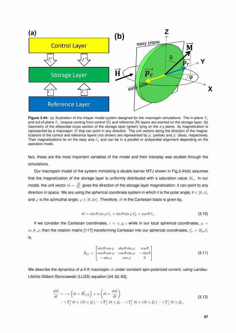
Figure 3.44: (a) Illustration of the trilayer model system designed for the macrospin simulations. The in-plane T‖and out-of-plane T⊥ torques coming from control (C) and reference (R) layers are exerted on the storage layer. (b)Geometry of the ellipsoidal cross section of the storage layer (green) lying on the z-y plane. Its magnetization isrepresented by a macrospin ~M that can point in any direction. The unit vectors along the direction of the magne-tizations of the control and reference layers (not shown) are represented by ~pc (yellow) and ~pr (blue), respectively.Their magnetizations lie on the easy axis ~ey and can be in a parallel or antiparallel alignment depending on theoperation mode.
fact, these are the most important variables of the model and their interplay was studied through the
simulations.
Our macropsin model of the system mimicking a double barrier MTJ shown in Fig.3.44(b) assumes
that the magnetization of the storage layer is uniformly distributed with a saturation value Ms. In our
model, the unit vector ~m =~MMs
gives the direction of the storage layer magnetization: it can point to any
direction in space. We are using the spherical coordinate system in which θ is the polar angle, θ ∈ [0, π],
and ϕ is the azimuthal angle, ϕ ∈ [0, 2π]. Therefore, ~m in the Cartesian basis is given by,
~m = sin θ cosϕ~ex + sin θ sinϕ~ey + cos θ ~ez. (3.10)
If we consider the Cartesian coordinates, i = x, y, z while in our local spherical coordinates, µ =
m, θ, ϕ, then the rotation matrix [117] transforming Cartesian into our spherical coordinates, ~eµ = Rµi~ei
is,
Rµi =
sin θ cosϕ sin θ sinϕ cos θcos θ cosϕ cos θ sinϕ − sin θ− sinϕ cosϕ 0
(3.11)
We describe the dynamics of a 0 K macrospin ~m under constant spin-polarized current, using Landau-
Lifshitz-Gilbert-Slonczewski (LLGS) equation [44,62,63],
d~m
dt= −γ
(~m× ~Heff
)+ α
(~m× d~m
dt
)− γ T c‖ ~m× (~m× ~pc)− γ T c⊥ ~m× ~pc − γ T r‖ ~m× (~m× ~pr)− γ T r⊥ ~m× ~pr,
(3.12)
97
where ~Heff is the effective field (which accounts for magnetostatics, external field and uniaxial
anisotropy), ~pc and ~pr are the unit vectors along the magnetization direction of control and reference
layers, respectively, γ is the gyromagnetic ratio, α is the Gilbert damping constant, T c,r‖ and T c,r⊥ are
in-plane and out-of-plane STT prefactors, respectively, whose subscripts c, r stand for control and refer-
ence which represent the origin of the torque.
In a geometric point of view, in-plane and out-of-plane torque terms of Eq.(3.12) are equivalent to the
damping and precession terms, respectively, of the Landau-Lifshitz (LL) equation. Following a similar
procedure as done in Ref. [115], Eq.(3.12) can be transformed into LL form by performing a cross product
of ~m on both sides of the equation,
~m× d~m
dt= −γ ~m×
(~m× ~Heff
)+ α ~m×
(~m× d~m
dt
)− γ T c‖ ~m× [~m× (~m× ~pc)]− γ T c⊥ ~m× (~m× ~pc)
− γ T r‖ ~m× [~m× (~m× ~pr)]− γ T r⊥ ~m× (~m× ~pr) .
(3.13)
Substituting the second term (damping term) of Eq.(3.12) with the result of Eq.(3.13) and following
the vector triple product relationship 13, it yields,
(1 + α2
)γ
d~m
dt= −~m×
[~Heff −
(αT c‖ − T
c⊥
)~pc −
(αT r‖ − T
r⊥
)~pr
]− ~m
~m×
[α ~Heff +
(αT c⊥ + T c‖
)~pc +
(αT r⊥ + T r‖
)~pr
].
(3.14)
Besides the advantages for further analytical treatment, the numerical integration of the LLGS equa-
tion in the form of Eq.(3.14) is faster. Moreover, and to reduce the number of input equations to compute
from three (Cartesian base: x, y, z) to two, Eq.(3.14) was converted to spherical coordinates [117,118].
Thus, in terms of θ and ϕ, the modified LLGS can be written as,
(1 + α2
)γ
dθ
dt= Heff,ϕ + αHeff,θ − T c‖ (αpc,ϕ − pc,θ)− T c⊥ (pc,ϕ + αpc,θ)
− T r‖ (αpr,ϕ − pr,θ)− T r⊥ (pr,ϕ + αpr,θ) ,
(1 + α2
)γ
sin θdϕ
dt= αHeff,ϕ −Heff,θ + T c‖ (αpc,θ + pc,ϕ) + T c⊥ (pc,θ − αpc,ϕ)
+ T r‖ (αpr,θ + pr,ϕ) + T c⊥ (pr,θ − αpr,ϕ)
(3.15)
Here Heff,θ, Heff,ϕ and pc,θ, pr,ϕ, pc,θ, pr,ϕ, are the ~eθ and ~eϕ components of ~Heff and ~pc,r, respec-
tively.
Besides the demonstration of a more solvable form of the LLGS equation, it is convenient to further
describe some of its terms, notably those involving Heff and the STT terms, T‖ and T⊥. The first term
(precessional) of the right-hand side of (3.12) has the form of a torque. The torque is exerted by an
effective field which is derived from the total energy E of the storage layer with volume V 14,
13In particular: ~m×(~m× d~m
dt
)= ~m
(~m · d~m
dt
)− d~m
dt(~m · ~m) = − d~m
dtand ~m× (~m× ~p) = ~m (~m · ~p)− ~p
14The volume V is used here in the energy expressions, though it is unitary in our simulations for simplicity of calculations.
98
~Heff = − 1
V
∂E
∂ ~M(3.16)
The potential energy 15 for the storage layer [64, 119] is E = Ed + Ez, where Ed is the self-
demagnetizing energy due to the shape of the storage layer and Ez is the Zeeman energy from the
external applied field H. The self-demagnetizing energy coming from shape anisotropy is defined as,
Ed =1
2VMs
(~m · ~Hd
)=
1
2VMs (~m ·N · ~m) =
1
2VM2
s 4π(Nx cos2 θ sin2 ϕ+Ny sin2 θ sin2 ϕ+Nz cosθ
),
(3.17)
where ~Hd = MsN · ~m is the demagnetizing field and N is the demagnetizing tensor. The demagne-
tizing factors are Nx, Ny, Nz, respectively, for ~ex, ~ey, ~ez and were calculated following Ref. [120] for an
ellipsoid with 140nm×130nm×3nm (in order to have an Hc < 50Oe). Finally, the Zeeman energy due to
a field H applied along ~ey is expressed by,
Ez = 4πVMs
(~m · ~H
)= 4πMsH sin θ sinϕ. (3.18)
The Heff,θ and Heff,ϕ components in expression (3.15) may be then found by applying ∇E(θ, ϕ) =
(∂E/∂θ)~eθ + (∂E/∂ϕ)~eϕ on Eq.(3.16).
Relatively to the STT terms, we need to defined the dependence of the STT components T‖ and
T⊥ with voltage V . For positive voltage, electrons flow from reference to free layer and from free layer
to control layer. Thus, the effect of current on the free layer, due to STT, is reversed. Therefore we
chose the following convention: torque stemming from reference layer is function of V , whereas torque
stemming from control layer is function of −V . Finally, the STT components are defined as,
T c‖ = ac1(−V ) + ac2(−V )2
T c⊥ = bc1(−V ) + bc2(−V )2
T r‖ = ar1V + ar2V2
T r⊥ = br1V + br2V2.
(3.19)
In addition, it is important to stress that the voltage applied to each barrier individually is not purely
V . In fact, V is the total voltage applied to the DBMTJ. In eqs.(3.19), the fraction of V applied to each
barrier is controlled by the prefactors a1, a2, b1, b2, where the attached subscripts r and c are respectively
connected to the bottom and top barriers, the ones respectively closer to the reference (r) and control
(c) layers. For example, for an asymmetric barriers DBMTJ with a bottom barrier 2x more resistive than
the top barrier (RAbottom = 2RAtop), the prefactors should respect a similar ratio: ar1,2 = 2 ac1,2 and
br1,2 = 2 bc1,2.
This choice was made to have an extra degree of freedom in the definition of the torque components.
The parameters used for the simulation are presented in table 3.8.
The simulations were realized in order to mimic the phase diagrams of section 3.3, using finite writing
voltage pulses with τ = 100ns. For each value of voltage V, the field H was swept from -100 Oe to 10015The uniaxial anisotropy energy is defined as Eu = Ku sin2 θ sin2 ϕ, albeit its influence is negligible, thus it is not included in
our model.
99
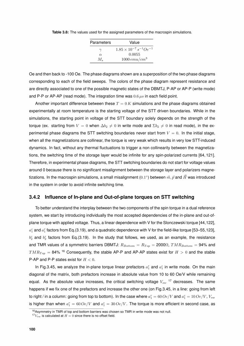
Table 3.8: The values used for the assigned parameters of the macrospin simulations.
Parameters Value
γ 1.85× 10⁻⁷ s−1Oe−1
α 0.0055Ms 1000 emu/cm3
Oe and then back to -100 Oe. The phase diagrams shown are a superposition of the two phase diagrams
corresponding to each of the field sweeps. The colors of the phase diagram represent resistance and
are directly associated to one of the possible magnetic states of the DBMTJ, P-AP or AP-P (write mode)
and P-P or AP-AP (read mode). The integration time was 0.6µs in each field point.
Another important difference between these T = 0K simulations and the phase diagrams obtained
experimentally at room temperature is the starting voltage of the STT driven boundaries. While in the
simulations, the starting point in voltage of the STT boundary solely depends on the strength of the
torque (ex. starting from V = 0 when ∆b2 6= 0 in write mode and Σb2 6= 0 in read mode), in the ex-
perimental phase diagrams the STT switching boundaries never start from V = 0. In the initial stage,
when all the magnetizations are collinear, the torque is very weak which results in very low STT-induced
dynamics. In fact, without any thermal fluctuations to trigger a non collinearity between the magnetiza-
tions, the switching time of the storage layer would be infinite for any spin-polarized currents [64, 121].
Therefore, in experimental phase diagrams, the STT switching boundaries do not start for voltage values
around 0 because there is no significant misalignment between the storage layer and polarizers magne-
tizations. In the macrospin simulations, a small misalignment (0.1) between ~m, ~p and ~H was introduced
in the system in order to avoid infinite switching time.
3.4.2 Influence of In-plane and Out-of-plane torques on STT switching
To better understand the interplay between the two components of the spin torque in a dual reference
system, we start by introducing individually the most accepted dependencies of the in-plane and out-of-
plane torque with applied voltage. Thus, a linear dependence with V for the Slonczewski torque [44,122],
ac1 and ar1 factors from Eq.(3.19), and a quadratic dependence with V for the field-like torque [53–55,123],
bc2 and br2 factors from Eq.(3.19). In the study that follows, we used, as an example, the resistance
and TMR values of a symmetric barriers DBMTJ: RBottom = RTop = 2000Ω, TMRBottom = 94% and
TMRTop = 84% 16 Consequently, the stable AP-P and AP-AP states exist for H > 0 and the stable
P-AP and P-P states exist for H < 0.
In Fig.3.45, we analyze the in-plane torque linear prefactors ar1 and ac1 in write mode. On the main
diagonal of the matrix, both prefactors increase in absolute value from 10 to 60 Oe/V while remaining
equal. As the absolute value increases, the critical switching voltage Vsw17 decreases. The same
happens if we fix one of the prefactors and increase the other one (on Fig.3.45, in a line: going from left
to right / in a column: going from top to bottom). In the case where ar1 = 60Oe/V and ac1 = 10Oe/V , Vsw
is higher than when ar1 = 60Oe/V and ac1 = 30Oe/V . The torque is more efficient in second case, as
16Asymmetry in TMR of top and bottom barriers was chosen so TMR in write mode was not null.17Vsw is calculated at H = 0 since there is no offset field.
100
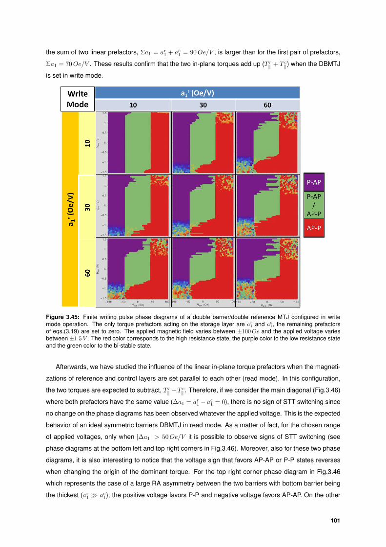
the sum of two linear prefactors, Σa1 = ar1 + ac1 = 90Oe/V , is larger than for the first pair of prefactors,
Σa1 = 70Oe/V . These results confirm that the two in-plane torques add up (T r‖ + T c‖ ) when the DBMTJ
is set in write mode.
Figure 3.45: Finite writing pulse phase diagrams of a double barrier/double reference MTJ configured in writemode operation. The only torque prefactors acting on the storage layer are ar1 and ac1, the remaining prefactorsof eqs.(3.19) are set to zero. The applied magnetic field varies between ±100Oe and the applied voltage variesbetween ±1.5V . The red color corresponds to the high resistance state, the purple color to the low resistance stateand the green color to the bi-stable state.
Afterwards, we have studied the influence of the linear in-plane torque prefactors when the magneti-
zations of reference and control layers are set parallel to each other (read mode). In this configuration,
the two torques are expected to subtract, T r‖ −Tc‖ . Therefore, if we consider the main diagonal (Fig.3.46)
where both prefactors have the same value (∆a1 = ar1 − ac1 = 0), there is no sign of STT switching since
no change on the phase diagrams has been observed whatever the applied voltage. This is the expected
behavior of an ideal symmetric barriers DBMTJ in read mode. As a matter of fact, for the chosen range
of applied voltages, only when |∆a1| > 50Oe/V it is possible to observe signs of STT switching (see
phase diagrams at the bottom left and top right corners in Fig.3.46). Moreover, also for these two phase
diagrams, it is also interesting to notice that the voltage sign that favors AP-AP or P-P states reverses
when changing the origin of the dominant torque. For the top right corner phase diagram in Fig.3.46
which represents the case of a large RA asymmetry between the two barriers with bottom barrier being
the thickest (ar1 ac1), the positive voltage favors P-P and negative voltage favors AP-AP. On the other
101

extreme of the anti-diagonal (bottom left corner), the case of an asymmetric barriers DBMTJ with thicker
top barrier (ar1 ac1), the STT switching voltages change polarity and follow the theoretical predictions
for the ideal case of this type of asymmetric barriers DBMTJ represented by in Fig.3.20 in section 3.2.
Figure 3.46: Finite writing pulse phase diagrams of a double barrier/double reference MTJ configured in readmode operation. The only torque prefactors acting on the storage layer are ar1 and ac1, the remaining prefactorsof eqs.(3.19) are set to zero. The applied magnetic field varies between ±100Oe and the applied voltage variesbetween ±1.5V . The red color corresponds to the high resistance state, the purple color to the low resistance stateand the green color to the bi-stable state.
Concerning the quadratic prefactors of the out-of-plane torque, we started by studying their influence
when the DBMTJ is set in write mode. According to theory, when the magnetizations of both polarizers
are in an antiparallel alignment, then T r⊥ − T c⊥. This is confirmed for the ideal case of a DBMTJ with
perfectly symmetric barriers (br2 = bc2) corresponding to the main diagonal in Fig.3.47. In this case, the
total torque is zero and no spin torque switching is observed. When br2 6= bc2 then the total field-like
torque is non-zero, and two scenarios are possible. Considering that in our case, the bottom barrier is
thicker (larger voltage drop), it seems coherent to assume that br2 > bc2. In this case, the AP-P state is
favored for both voltage polarities (top right corner and adjacent phase diagrams in Fig.3.47). On the
other hand, when br2 < bc2 then it is the P-AP state that is favored by both voltage polarities. For the
phase diagrams of Fig.3.47, the P-AP state corresponds to the low resistance state while in the case of
a top thicker barrier DBMTJ, the P-AP state would correspond to a high resistance state (in red color). In
fact, the phase diagrams at the bottom left corner are those most in agreement with the most common
102
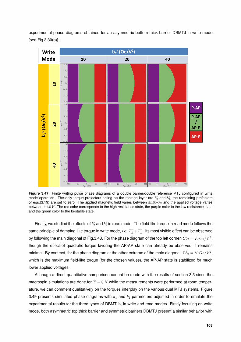
experimental phase diagrams obtained for an asymmetric bottom thick barrier DBMTJ in write mode
[see Fig.3.30(b)].
Figure 3.47: Finite writing pulse phase diagrams of a double barrier/double reference MTJ configured in writemode operation. The only torque prefactors acting on the storage layer are br2 and bc2, the remaining prefactorsof eqs.(3.19) are set to zero. The applied magnetic field varies between ±100Oe and the applied voltage variesbetween ±1.5V . The red color corresponds to the high resistance state, the purple color to the low resistance stateand the green color to the bi-stable state.
Finally, we studied the effects of br2 and bc2 in read mode. The field-like torque in read mode follows the
same principle of damping-like torque in write mode, i.e. T r⊥+T c⊥. Its most visible effect can be observed
by following the main diagonal of Fig.3.48. For the phase diagram of the top left corner, Σb2 = 20Oe/V 2,
though the effect of quadratic torque favoring the AP-AP state can already be observed, it remains
minimal. By contrast, for the phase diagram at the other extreme of the main diagonal, Σb2 = 80Oe/V 2,
which is the maximum field-like torque (for the chosen values), the AP-AP state is stabilized for much
lower applied voltages.
Although a direct quantitative comparison cannot be made with the results of section 3.3 since the
macrospin simulations are done for T = 0K while the measurements were performed at room temper-
ature, we can comment qualitatively on the torques interplay on the various dual MTJ systems. Figure
3.49 presents simulated phase diagrams with a1 and b2 parameters adjusted in order to emulate the
experimental results for the three types of DBMTJs, in write and read modes. Firstly focusing on write
mode, both asymmetric top thick barrier and symmetric barriers DBMTJ present a similar behavior with
103
Figure 3.48: Finite writing pulse phase diagrams of a double barrier/double reference MTJ configured in readmode operation. The only torque prefactors acting on the storage layer are br2 and bc2, the remaining prefactorsof eqs.(3.19) are set to zero. The applied magnetic field varies between ±100Oe and the applied voltage variesbetween ±1.5V . The red color corresponds to the high resistance state, the purple color to the low resistance stateand the green color to the bi-stable state.
each voltage polarity favoring one particular state. The larger ∆a1 (with ac1 > ar1) imposed for the asym-
metric top thick barrier DBMTJ than for the symmetric barriers one is reasonable sinceRAtop > RAbottom
for the first and RAtop ≈ RAbottom for the latter 18. The effects of field-like torque are visible in the asym-
metric top thick barrier DBMTJ but not in the case of symmetric barriers. As seen before, the quadratic
field-like torque in write mode only plays a role if ∆b2 6= 0. For asymmetric barriers ∆b2 = 20Oe/V 2 (first
case) and for symmetric barriers ∆b2 = 0 for the latter. The case of the asymmetric thick bottom barrier
DBMTJ is the most curious: to reproduce the experimental trend, thus to allow the low resistance state
(P-AP) to be stabilized by both voltage polarities, the larger b2 prefactor must belong to the polarizer
adjacent to the thin barrier of the DBMTJ.
In read mode, the field-like torque is dominant since T total⊥ = T c⊥ + T r⊥ and the stabilization of AP-AP
state is obtained for all type of DBMTJs.
Comparing our simulations with the numerical simulations performed on in-plane MTJs by Bernert
et al. [60], we found good agreement on the relationship between the torques and the magnetic config-
urations they favor. One of the most interesting results, which was also observed by us, is the favoring18Note: Though RAtop ≈ RAbottom, as P-AP corresponds to high resistance state in write mode, then either RAtop >
RAbottom or TMRtop > TMRbottom.
104
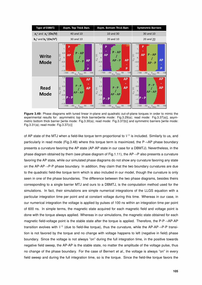
Figure 3.49: Phase diagrams with tuned linear in-plane and quadratic out-of-plane torques in order to mimic theexperimental results for: asymmetric top thick barrier[write mode: Fig.3.29(a); read mode: Fig.3.37(a)], asym-metric bottom thick barrier [write mode: Fig.3.30(a); read mode: Fig.3.37(b)] and symmetric barriers [write mode:Fig.3.31(a); read mode: Fig.3.37(c)]
of AP state of the MTJ when a field-like torque term proportional to V 2 is included. Similarly to us, and
particularly in read mode (Fig.3.48) where this torque term is maximized, the P→AP phase boundary
presents a curvature favoring the AP state (AP-AP state in our case for a DBMTJ). Nevertheless, in the
phase diagram obtained by them (see phase diagram of Fig.1.11), the AP→P also presents a curvature
favoring the AP state, while our simulated phase diagrams do not show any curvature favoring any state
on the AP-AP→P-P phase boundary. In addition, they claim that the two boundary curvatures are due
to the quadratic field-like torque term which is also included in our model, though the curvature is only
seen in one of the phase boundaries. The difference between the two phase diagrams, besides theirs
corresponding to a single barrier MTJ and ours to a DBMTJ, is the computation method used for the
simulations. In fact, their simulations are simple numerical integrations of the LLGS equation with a
particular integration time per point and at constant voltage during this time. Whereas in our case, in
our numerical integration the voltage is applied by pulses of 100 ns within an integration time per point
of 600 ns. In simple terms, the magnetic state acquired for each magnetic field and voltage point is
done with the torque always applied. Whereas in our simulations, the magnetic state obtained for each
magnetic field-voltage point is the stable state after the torque is applied. Therefore, the P-P→AP-AP
transition evolves with V 2 (due to field-like torque), thus the curvature, while the AP-AP→P-P transi-
tion is not favored by the torque and no change with voltage happens to left (negative in field) phase
boundary. Since the voltage is not always ”on” during the full integration time, in the positive towards
negative field sweep, the AP-AP is the stable state, no matter the amplitude of the voltage pulse, thus
no change of the phase boundary. For the case of Bernert et al., the voltage is always ”on” in every
field sweep and during the full integration time, so is the torque. Since the field-like torque favors the
105
Figure 3.50: Phase diagram of DBMTJ set in read mode, obtained by simulation where voltage is applied constantlyinstead by 100 ns pulses. Therefore, reproducing the phase diagrams obtained by Bernert et al. [60].
AP state and it increases its strength with increasing voltage, whether is a negative towards positive or
a positive towards negative field sweep, the junction will want to stay in the AP state. In their phase
diagram, if the voltage is increased, both switching fields shift to the left for both voltage polarities, but
the width of the loop remains twice the anisotropy. Switching to the AP state will thus require less field to
be applied while the field necessary to induce the opposite transition will be increased in the presence
of a finite bias voltage [60]. In order to validate our statements we performed a simulation of DBMTJ
in read mode, applying constant voltage instead of 100 ns pulses, as shown in Fig.3.50. We obtained
a phase diagram with curvature in both phase boundaries similarly to Bernert et al.. Since the phase
diagrams in section 3.3 where obtained using pulsed voltage, our simulations reproduce the experiment
(except the temperature effects) and the simulated phase diagrams are, in general, in good agreement
with the experimental results obtained.
3.4.3 Linear dependence of Out-of-plane torque
Though on the vast majority of theoretical and experimental studies, the perpendicular STT is de-
scribed as being proportional to V 2, some other claim the existence of a linear voltage dependent
prefactor which also plays a role on the applied torque. Measurements in frequency [56] and switching
current in symmetric [57] and asymmetric MTJs [91] revealed that this out-of-plane torque was propor-
tional to the bias current and changed sign with bias voltage. Therefore a linear term in the dependence
of field-like torque effective field on bias voltage should exist in addition to a quadratic one, which is in
agreement with former theoretical predictions [48].
As a base scenario, we have chosen to set initial quadratic field-like torque prefactors, bc2 = 20Oe/V 2
and br2 = 10Oe/V 2, which are the quadratic prefactors that better fit the experimental phase diagrams in
the case of a bottom thicker asymmetric barriers DBMTJs. In addition to the quadratic fixed prefactors,
we have included and studied the effects of the linear prefactor b1 on the spin torque switching, both in
write and read modes. The corresponding phase diagrams are shown in Fig.3.51.
Analyzing first the write mode, we can observe that the inclusion of the b1 prefactor improves the
efficiency of switching towards the P-AP state for positive voltages while reducing it for negative voltages,
106
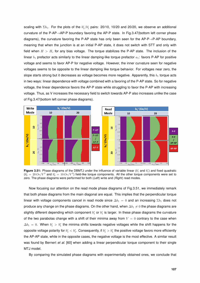
scaling with Σb1. For the plots of the br1/bc1 pairs: 20/10, 10/20 and 20/20, we observe an additional
curvature of the P-AP→AP-P boundary favoring the AP-P state. In Fig.3.47(bottom left corner phase
diagrams), the curvature favoring the P-AP state has only been seen for the AP-P→P-AP boundary,
meaning that when the junction is at an initial P-AP state, it does not switch with STT and only with
field when H > Hc for any bias voltage. The torque stabilizes the P-AP state. The inclusion of the
linear b1 prefactor acts similarly to the linear damping-like torque prefactor a1: favors P-AP for positive
voltage and seems to favor AP-P for negative voltage. However, the inner curvature seen for negative
voltages seems to be opposite to the linear damping like torque behavior. For voltages near zero, the
slope starts strong but it decreases as voltage becomes more negative. Apparently, this b1 torque acts
in two ways: linear dependence with voltage combined with a favoring of the P-AP state. So for negative
voltage, the linear dependence favors the AP-P state while struggling to favor the P-AP with increasing
voltage. Thus, as V increases the necessary field to switch towards AP-P also increases unlike the case
of Fig.3.47(bottom left corner phase diagrams).
Figure 3.51: Phase diagrams of the DBMTJ under the influence of variable linear (bc1 and br1) and fixed quadratic(bc2 = 20Oe/V 2 and br2 = 10Oe/V 2) field-like torque components. All the other torque components were set tozero. The phase diagrams were performed for both (Left) write and (Right) read modes.
Now focusing our attention on the read mode phase diagrams of Fig.3.51, we immediately remark
that both phase diagrams from the main diagonal are equal. This implies that the perpendicular torque
linear with voltage components cancel in read mode since ∆b1 = 0 and an increasing Σb1 does not
produce any change on the phase diagrams. On the other hand, when ∆b1 6= 0 the phase diagrams are
slightly different depending which component br1 or bc1 is larger. In these phase diagrams the curvature
of the two parabolas change with a shift of their minima away from V = 0 contrary to the case when
∆b1 = 0. When bc1 > br1 the minima shifts towards negative voltages while the shift happens for the
opposite voltage polarity for bc1 < br1. Consequently, if bc1 > br1 the positive voltage favors more efficiently
the AP-AP state, while in the opposite cases, the negative voltage is the most effective. A similar result
was found by Bernert et al. [60] when adding a linear perpendicular torque component to their single
MTJ model.
By comparing the simulated phase diagrams with experimentally obtained ones, we conclude that
107

the presence of a linear voltage dependence of the out-of-plane torque (even if small in magnitude) may
explain the slight asymmetries in voltage of the parabolas boundaries favoring P-AP (in write mode, see
figs.3.29,3.30 and 3.31) and AP-AP (in read mode, see Fig.3.37).
3.4.4 Quadratic dependence of In-plane torque
Although it is unlikely to happen, we found interesting to study the effects of a quadratic component of
in-plane torque component (a2) in our dual MTJ system. The only quasi-quadratic behavior measured for
the damping-like torque was observed by Kubota et al. [59] and Sankey et al. [53] for CoFeB/MgO/CoFeB
MTJs where this torque would reverse its sign under very large positive voltages. This trend of in-plane
torque with bias voltage had been predicted theoretically [50, 51, 124] for half-metals with an exchange
splitting ∆ ≈ 1 − 1.5 19. The quadratic dependence with voltage as only been accounted in theory for
the particular case of 1/4 majority band filling and ε↓ = 4.2 ev (see as an example Fig. 4 from [51]). This
situation is described, by Chshiev et al. [51], to be only possible due to a maximum in charge current
as a function of band filling so that the appropriate exchange splitting between ε↑ and ε↓ around the
maximum causes the corresponding charge currents to be equal.
Figure 3.52: Phase diagrams of the DBMTJ under the influence of variable (ac2 and ar2) in-plane torque components.All the other torque components were set to zero. The phase diagrams were performed for both (Left) write and(Right) read modes.
Figure 3.52 shows the phase diagrams for variable paired values of ac2 and ar2 set in write and read
modes. For the case of the DBMTJ in write mode, no current induced switching occurs for the phase
diagrams on the main diagonal corresponding to ∆a2 = 0. For the phase diagrams of the anti-diagonal,
depending on the dominant prefactor ac2 or ar2, the AP-P or P-AP state is favored for both voltage polari-
ties, respectively. In fact, contrary to what happens with the field-like torque b2 component in write mode
(see Fig.3.47), the favored state is the one for which the storage layer is in antiparallel alignment to the
reference carrying the lowest a2 value. Judging from the phase diagrams for which ∆a2 = 0 and those
with ∆a2 6= 0, we can conclude that the quadratic components of damping-like torque subtract in write
mode, as expected.19The exchange splitting is defined as ∆ = ε↓ − ε↑ for Ref. [50] while ∆ = (ε↓ − ε↑)/2 for Refs. [51,124].
108

In read mode, the introduction of the a2 prefactor favors and stabilizes the P-P state. Similarly to the
b2 prefactor of field-like torque, ac2 and ar2 add up. With the increase of Σa2, the AP-AP→P-P switching
is more efficient. For different ∆a2, conserving a similar Σa2 (phase diagrams on the anti-diagonal),
the phase diagrams present no differences. Although the opposite behaviors of the quadratic in-plane
and out-of-plane torques are explained by the opposite signs of these two torques with bias voltage,
the shapes of their read mode phase diagram parabolas are quite distinct. In the case of an acting
quadratic field-like torque (see Fig.3.48), the variation of the switching voltage with applied field is rather
smooth and the P-P→AP-AP boundary parabola’s concavity closes more with increasing Σb2 though
conserving a quadratic curve behavior. On the contrary, for the case of a quadratic damping-like torque,
the switching voltage does not start from V = 0, yet there is a trigger voltage for which the switching
begins. This trigger voltage Vtrigg reduces with increasing Σa2, with Vtrigg = 1.4V for Σa2 = 20Oe/V 2
decreasing to Vtrigg = 0.9V for Σa2 = 80Oe/V 2. In addition, the switching boundary is almost linear
and the slope (in V/Oe) reduces with increasing Σa2.
In our experiments, none of the measured DBMTJs presented phase diagrams similar to those of
Fig.3.52. As mentioned at the beginning of this section, this in-plane torque component was only con-
sidered in theoretical publications.
3.5 Summmary
In this chapter we have characterized and performed current/voltage induced switching measure-
ments of double barrier magnetic tunnel junctions with in-plane anisotropy with different RA ratios be-
tween top and bottom barrier: asymmetric bottom thick barrier (RAtop = 10 Ω.µm2 and RAbottom =
35 Ω.µm2), asymmetric top thick barrier (RAtop = 35 Ω.µm2 and RAbottom = 10 Ω.µm2), thick (RAtop =
RAbottom = 45 Ω.µm2) and thin (RAtop = RAbottom = 10 Ω.µm2) symmetric barriers.
First, STT switching measurements were performed using DC current, for the dual barrier MTJs set
in write and read operation modes. In write mode, the results did not reveal a correlation between the
RA ratios of the DBMTJs and the switching current densities. Backhopping events were observed for
circular DBMTJs, independently of the degree of RA symmetry between the oxide barriers. Its origin is
mainly connected with the interplay between the in-plane and perpendicular torques. Nevertheless, the
DBMTJs presented approximately two times lower switching current densities (JDBMTJsw = 1.9MA/cm2)
than a single barrier MTJ (JSBMTJsw = 4.1MA/cm2). Thus showing that the DBMTJ is a reliable alterna-
tive to reduce power consumption in STT-MRAM devices. In read mode, additionally to the P-P→AP-AP
transitions reported by P.-Y. Clement [1] for symmetric barriers structures, we have also observed switch-
ings in the opposite direction for all measured devices. The calculated switching current densities were
of the same magnitude of those reported for write mode.
In order to mitigate the temperature effects during switching, we performed finite voltage pulse
(τ = 100ns) measurements on the same types of DBMTJs. In write mode, the DBMTJs presented
two types of behaviors: i) a predominant effect of linear damping-like torque (T‖ ∝ a V ) where each of
the voltage polarities stabilizes a different state and ii) a predominant effect of a quadratic perpendicular
109
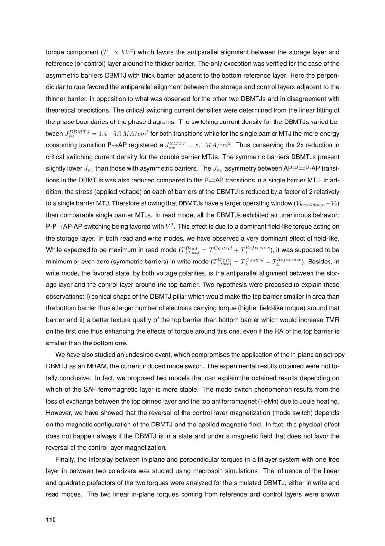
torque component (T⊥ ∝ b V 2) which favors the antiparallel alignment between the storage layer and
reference (or control) layer around the thicker barrier. The only exception was verified for the case of the
asymmetric barriers DBMTJ with thick barrier adjacent to the bottom reference layer. Here the perpen-
dicular torque favored the antiparallel alignment between the storage and control layers adjacent to the
thinner barrier, in opposition to what was observed for the other two DBMTJs and in disagreement with
theoretical predictions. The critical switching current densities were determined from the linear fitting of
the phase boundaries of the phase diagrams. The switching current density for the DBMTJs varied be-
tween JDBMTJsw = 1.4−5.9MA/cm2 for both transitions while for the single barrier MTJ the more energy
consuming transition P→AP registered a JSMTJsw = 8.1MA/cm2. Thus conserving the 2x reduction in
critical switching current density for the double barrier MTJs. The symmetric barriers DBMTJs present
slightly lower Jsw than those with asymmetric barriers. The Jsw asymmetry between AP-PP-AP transi-
tions in the DBMTJs was also reduced compared to the PAP transitions in a single barrier MTJ. In ad-
dition, the stress (applied voltage) on each of barriers of the DBMTJ is reduced by a factor of 2 relatively
to a single barrier MTJ. Therefore showing that DBMTJs have a larger operating window (Vbreakdown−Vc)
than comparable single barrier MTJs. In read mode, all the DBMTJs exhibited an unanimous behavior:
P-P→AP-AP switching being favored with V 2. This effect is due to a dominant field-like torque acting on
the storage layer. In both read and write modes, we have observed a very dominant effect of field-like.
While expected to be maximum in read mode (TRead⊥total = TControl⊥ + TReference⊥ ), it was supposed to be
minimum or even zero (symmetric barriers) in write mode (TWrite⊥total = TControl⊥ − TReference⊥ ). Besides, in
write mode, the favored state, by both voltage polarities, is the antiparallel alignment between the stor-
age layer and the control layer around the top barrier. Two hypothesis were proposed to explain these
observations: i) conical shape of the DBMTJ pillar which would make the top barrier smaller in area than
the bottom barrier thus a larger number of electrons carrying torque (higher field-like torque) around that
barrier and ii) a better texture quality of the top barrier than bottom barrier which would increase TMR
on the first one thus enhancing the effects of torque around this one, even if the RA of the top barrier is
smaller than the bottom one.
We have also studied an undesired event, which compromises the application of the in-plane anisotropy
DBMTJ as an MRAM, the current induced mode switch. The experimental results obtained were not to-
tally conclusive. In fact, we proposed two models that can explain the obtained results depending on
which of the SAF ferromagnetic layer is more stable. The mode switch phenomenon results from the
loss of exchange between the top pinned layer and the top antiferromagnet (FeMn) due to Joule heating.
However, we have showed that the reversal of the control layer magnetization (mode switch) depends
on the magnetic configuration of the DBMTJ and the applied magnetic field. In fact, this physical effect
does not happen always if the DBMTJ is in a state and under a magnetic field that does not favor the
reversal of the control layer magnetization.
Finally, the interplay between in-plane and perpendicular torques in a trilayer system with one free
layer in between two polarizers was studied using macrospin simulations. The influence of the linear
and quadratic prefactors of the two torques were analyzed for the simulated DBMTJ, either in write and
read modes. The two linear in-plane torques coming from reference and control layers were shown
110
to add up in write mode and subtract in read mode. While the opposite happens for the quadratic
components of the out-of-plane torque. The reproduction of the experimental results was possible by
setting a larger value to the torque prefactors coming from the polarizer adjacent to the thickest barrier.
Except for the case of the asymmetric bottom thick barrier whose phase diagrams were only replicated
if bc2 > br2, i.e., a larger perpendicular torque coming from the control layer adjacent to thinner barrier.
The inclusion of a perpendicular torque linear with the bias voltage was shown to explain the small shifts
in voltage of the parabolas’ concavities (not centered in V = 0), for both write and read modes. A V 2
dependent damping-like torque was also studied but its behavior did not show any resemblance with the
experimental results, proving this torque dependence is not present in the double barrier system.
111

112

4Development and optimization of a
new functional top reference forDBMTJs with perpendicular
anisotropy
Contents4.1 Introduction . . . . . . . . . . . . . . . . . . . . . . . . . . . . . . . . . . . . . . . . . . 1144.2 Perpendicular Magnetic Anisotropy . . . . . . . . . . . . . . . . . . . . . . . . . . . . . 1144.3 Perpendicular DBMTJ with improved top reference . . . . . . . . . . . . . . . . . . . 1174.4 Summary . . . . . . . . . . . . . . . . . . . . . . . . . . . . . . . . . . . . . . . . . . . . 135
113
4.1 Introduction
In section 1.5.4, the advantages of STT-MRAM based on magnetic tunnel junctions with perpendicu-
lar magnetic anisotropy (PMA) have been described. In spite of TMR or damping not yet comparable to
those attained by in-plane magnetized systems, scalability, data retention (thermal stability) and power
consumption are the key features of this technology for industrial applications. In order to further reduce
the switching current density without compromising the thermal stability, one of the strategies lies on a
double barrier/double reference system. As already been demonstrated for in-plane [80] and, more re-
cently, for perpendicular [76] anisotropy DBMTJs, the STT acting on the storage layer is enhanced when
the two references magnetizations are in antiparallel alignment. High quality perpendicular MTJs with
bottom reference (showing high TMR and good thermal stability of the reference layer) have been vastly
demonstrated due to the high effective anisotropy (Keff ≈ 107erg/cm3) displayed by bottom references
based on Co/Pt multilayers ([Co/Pt]n) grown on Pt and Ru seed layers [125–129]. While high thermal
stability was obtained for these [Co/Pt]n acting as bottom electrode with well textured seed layers, the
same does not happen when the growth is made on top of FeCoB/MgO/FeCoB under-layers due to a
poor fcc (111) texture [when (Co/Pt) is deposited directly in FeCoB electrode] [130,131]. Therefore, the
development of a DBMTJ with perpendicular anisotropy is rather challenging, mainly due to the complex
engineering of a top electrode with high PMA.
In this chapter, we present part of the work developed in direct collaboration with fellow PhD student
Jyotirmoy Chatterjee. The objective of our research was to develop and optimize a functional stack with
high PMA to be used as a top reference in a DBMTJ with perpendicular anisotropy (p-DBMTJ). The
development of such novel seedless multilayers (NSML) 1 with high PMA is addressed in the thesis
manuscript of J. Chatterjee [132]. Here we describe the optimization of the top reference with the novel
multilayers included as one part of the SAF structure and show characterization of the full p-DBMTJ
stacks.
4.2 Perpendicular Magnetic Anisotropy
In magnetic materials, magnetization may align into certain preferential directions. This phenomenon
is called magnetic anisotropy. The control of anisotropy is thus crucial for applications using the prop-
erties of magnetic systems. For MRAM, two stable positions should exist in the absence of external
stimulus, which can be obtained by inducing an anisotropy axis in the materials. This preferred axis is
called easy axis. The volume energy of the system is defined as
E = −Keff cos2(θ) (4.1)
where θ is the angle between the magnetization and the anisotropy axis and Keff is the effective
magnetic anisotropy energy constant. In fact magnetic anisotropy has different contributions: mag-
netocrystalline, magnetoelastic, shape and surface anisotropies. Thus, Keff is defined by Keff =
1The composition of the NSML cannot be disclosed because of intellectual property issues.
114
Kv − 2πM2s + 2Ks
t , where Kv is the volume anisotropy energy (magnetocristalline and magnetoelas-
tic anisotropies), −2πM2s is the shape anisotropy related to the demagnetizing field, Ks the surface
anisotropy energy and t the thickness of the magnetic element.
PMA is obtained when the easy axis is normal to the magnetic film/layer. The following sections
address the different sources of PMA.
4.2.1 PMA from spin-orbit interactions and metal/oxide interface
Spin-orbit interaction is the main and common origin of PMA in magnetic multilayers and magne-
tocrystalline anisotropy in bulk magnetic materials. This interaction connects the electron’s spin with
its orbital motion and gives rise to an orbital moment Lz. The lattice arrangement plays an important
role in this phenomenon since the spin moment couples with the lattice [133]. Large values of Lz were
predicted for transition metal monolayers (Co, Ni,...) [134] and magnetic multilayers [135,136] including
heavy metals (ex. Pt, Pd, Au, Ta, rare earths,...) which display strong spin-orbit coupling.
In fact, this type of materials is of particular interest for Hard Disk Drive perpendicularly magnetized
media. Chemically ordered transition metal alloys like CoPtCr, L10 ordered FePt, FePd and CoPt [137,
138] present PMA due to the spin-orbit-coupling of Pt and Pd associated with low crystal symmetry
which results in a high magnetocrystalline anisotropy. In these cases, PMA is said to have a bulk origin.
However, the FePt and FePd alloys require very high (and stack incompatible) annealing temperatures
to exhibit high PMA. And, along the CoPtCr and CoPt, they have a large damping factor, not suitable to
the free layer.
With the reduction of thickness of magnetic films and their arrangement in multilayers, interface ef-
fects become measurable, contrary to bulk materials where these effects are negligible compared to the
volume contributions. The role played by surface anisotropy is now put into evidence. This anisotropy
was first predicted by L. Neel [116] and was attributed to a change in the symmetry at the interfaces.
The most studied and interesting multilayers were [Co/NM]n where NM stands for non magnetic metal.
By manipulating the local distribution of the Co atoms at the interfaces, it is possible to change the phys-
ical and magnetic properties of the multilayers (ex. new crystallographic phases and new anisotropy
directions may appear). The discovery of PMA in (Co/Pd) multilayers [140], followed by (Co/Pt) [141]
and (Co/Au) [142] has triggered a large interest in these type of multilayers since they profit both from
the strong spin-orbit coupling (Pt, Pd and Au elements) but also from the interfacial effects at the ferro-
magnet/heavy metal interfaces. Besides the theoretical interest of these multilayers as model systems,
they also present advantages for the spintronics industry:
• large Keff of the order 107 erg/cm3 which allows to fabricate devices with lateral size as small as
10nm with sufficient thermal stability.
• high flexibility of their physical features by adjusting their growth parameters, layer thickness and
annealing treatments.
• deposition of the multilayers may be performed using multiple technologies, from sputtering de-
position(compatible with industrial requirements) to molecular beam epitaxy (more complex and
115

expensive).
Despite the weak spin-orbit coupling, another form of interface anisotropy was observed at the
metal/oxide interface, displaying similar magnitudes as those reported for [Co/Pt]n. It was first found
in Pt/CoFe/AlOx stacks [143] with a strong dependence on the degree of oxidation at the interface. In
fact, for the same stack, the variation in oxidation time may turn the magnetization from out-of-plane
to in-plane and vice-versa [144]. This phenomenon has been observed for a large variety of oxides
(AlOx, TaOx, MgO,...), either crystalline or amorphous, both for plasma and natural oxidation [145]. The
origin of this interface anisotropy has been attributed to the hybridization between the 3d orbitals of the
transition metal and the 2p orbitals of oxygen [146]. Moreover, it also been demonstrated that annealing
the sample to temperatures higher than 300C also improves the PMA at the metal/oxide interface by
easing the migration of oxygen atoms towards the interface [147].
Although [Co/Pt]n and [Co/Pd]n are very good candidates for a hard perpendicular reference layer
due to their high values of Keff , their use as storage layer in a MTJ is not ideal. They present large Ms
and damping factor α, which do not allow to reduce the critical switching current. By contrast, metal/oxide
interface anisotropy allows that even materials with weak spin-orbit coupling but low Ms and α, which
is the case of FeCoB/MgO, are used in a p-MTJ [148]. Furthermore, the use of a MgO layer (capping
layer) on top of FeCoB has proven to reinforce its PMA [149, 150], allowing for larger thicknesses and
thus larger TMR. These properties therefore enable the development of double barrier tunnel junctions
with FeCoB-based storage layers.
4.2.2 Methods for effective anisotropy determination
The saturation magnetization Ms of a particular magnetic stack can be measured using a supercon-
ducting quantum interference device (SQUID) or Vibrating sample magnetometry (VSM). This parameter
together with the anisotropy field Hk are essential to determine Keff since, in its simplest form Keff
may be expressed as
Keff =MsHk
2. (4.2)
Keff corresponds to the energy needed to trigger the reversal of the magnetization from the easy
axis to the hard axis. As shown in Fig.4.1, it can be extracted from VSM curves measured along easy
and hard axes: Keff is given by the difference between the areas below the easy and hard axes, which
corresponds to the colored area in Fig.4.1.:
Keff =
∫Easy Axis
M dH −∫HardAxis
M dH (4.3)
The Keff values presented in this section are the average of the areas between the easy and hard
axes of M(H) plots, for both H < 0 and H > 0. The possible sources of error come mostly from the
determination ofMs = MA t whereM is the magnetic moment measured, A is the area and t the thickness
of the magnetic layer.
116

Figure 4.1: Measurement of the magnetization M as a function of magnetic field H applied parallel (red) andperpendicular (blue) to the easy axis of anisotropy. The effective anisotropy energy Keff is equivalent to the areain orange. Hc is the coercive field.
4.3 Perpendicular DBMTJ with improved top reference
In this section we present the experimental results obtained from the integration of the novel seedless
multilayers (more details in Ref. [132]) in a top reference single barrier p-MTJ, up to the development of
a full perpendicular DBMTJ.
4.3.1 Development of a top reference in a single perpendicular MTJ
As mentioned before, [Co/Pt]n has very high Keff . As for other type of multilayers, growth conditions
are of paramount importance in order to ensure a strong effective anisotropy. One of the factors re-
sponsible for the growth quality and type of texture is the deposition technique. Epitaxial (100) [Co/Pd]n
revealed higher values of Kv and Ks than polycrystalline (111) multilayers [151]. Another important
factor is the buffer/seed layer whose type and thickness influence the PMA of (Co/NM) multilayers.
(Co/Pt)n [130, 131] and (Co/Ni)n [152] demonstrated higher PMA when grown on top of thick Pt buffer
layers. [Co/Pt]n (or [Co/Ni]n) fcc (111) crystal structure is not compatible with MgO (001). Therefore,
the use of these multilayers as MTJ top reference would cause a severe loss of TMR. The strategy is
to keep FeCoB at the interface with MgO to preserve a high TMR, and add the Co-based multilayer to
reinforce PMA. A texture breaking layer (TBL) is thus needed to decouple the crystallization of FeCoB
from (Co/NM) fcc (111) multilayer without losing the ferromagnetic coupling of the two layers so they
behave as a single macrospin [153]. Previous works [154,155] demonstrated that [Co/Pd]n can be used
as top reference, since PMA is considerably higher than [Co/Pt]n (6× 10⁶ erg/cm3 for [Co/Pd] instead of
1× 10⁶ erg/cm3 for [Co/Pt]) in the absence of a well textured seed layer. Our novel seedless multilayers
(NSML) have also demonstrated a unique potential to be used as top reference since they display higher
Keff when grown on top of a TBL than on top a of proper buffer layer [132].
117

4.3.1.A Optimization of the texture breaking layer
In order to choose the best material as TBL we have deposited half top reference MTJ consisting of:
Ta 3/FeCoB 0.3/MgO/FeCoB 1.1/TBL/NSML/Ru 5 (thickness in nm) where TBL = Ta or W. We have also
studied the effect of the annealing temperature on Keff . Figure 4.2 shows Ms2 and Keff as a function
of TBL thickness 3 for stacks with the two types of TBL and for two different annealing temperatures,
350C and 400C. While Ta has been widely used as TBL between [Co/Pt]n and FeCoB in bottom
references of p-MTJ [153], W has recently been found to improve PMA when used as cap layer on top
of FeCoB storage layers, enhancing the thermal stability [156].
Figure 4.2: (a) Saturation magnetization and (b) effective PMA as a function of the texture breaking layer (TBL)thickness for half top reference p-MTJ Ta 3/FeCoB 0.3/MgO/FeCoB 1.1/TBL/NSML/Ru 5 (nm). The TBL elementsare Ta (black squares) and W (red circles). The stacks were annealed at two different temperatures 350C (solidmarkers) and 400C (open markers).
In Fig.4.2(a), Ms decreases with increasing TBL thickness, independently from the TBL composition
or annealing temperature. Moreover on average, its value is lower for W than Ta. In fact, for a 0.35 nm
TBL,the stack with W has a smaller Ms than the one with Ta, even when annealed at 400C. Besides the
effective anisotropy can be viewed as the competition between two main factors, the intrinsic anisotropy
Ku (that includes Kv and 2Kst ) and the demagnetization energy 2πM2
s . Since Ms decreases with in-
creasing TBL thickness, Keff consequently increases with TBL thickness as observed in Fig.4.2(b).
The increase of Keff with TBL thickness is verified for Ta (for both annealing temperatures) and for W
annealed at 400C. By contrast, for W annealed at 350C, the trend is inverted. It seems that, despite
the decrease of Ms, Ku is also affected, thus leading to the slight decrease of Keff with increasing TBL
thickness.
Although stacks with 0.3 nm W and 0.4 nm Ta annealed at 350C show the highest Keff , we chose
a TBL of W with 0.4 nm. In fact, annealing at 400C is preferred in order to obtain a high TMR ratio.
Therefore, our choice of TBL is the best option to obtain both a strong perpendicular anisotropy and a
good TMR ratio. The integration of this texture breaking layer in the top reference p-MTJ is discussed in
the following section.2In the Ms calculation, the total thickness used for the volume calculation is the sum of the thicknesses of FeCoB and various
layers of Co and Pt of the NSML.3The small range of thicknesses studied was chosen after an optimization over a larger range using only W [132]. The objective
here was to compare W with Ta and also study the influence of annealing temperature on Keff .
118
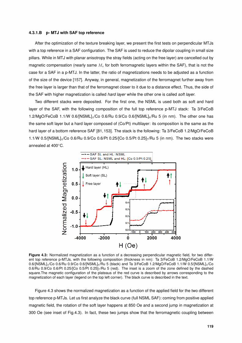
4.3.1.B p- MTJ with SAF top reference
After the optimization of the texture breaking layer, we present the first tests on perpendicular MTJs
with a top reference in a SAF configuration. The SAF is used to reduce the dipolar coupling in small size
pillars. While in MTJ with planar anisotropy the stray fields (acting on the free layer) are cancelled out by
magnetic compensation (nearly same Ms for both ferromagnetic layers within the SAF), that is not the
case for a SAF in a p-MTJ. In the latter, the ratio of magnetizations needs to be adjusted as a function
of the size of the device [157]. Anyway, in general, magnetization of the ferromagnet further away from
the free layer is larger than that of the ferromagnet closer to it due to a distance effect. Thus, the side of
the SAF with higher magnetization is called hard layer while the other one is called soft layer.
Two different stacks were deposited. For the first one, the NSML is used both as soft and hard
layer of the SAF, with the following composition of the full top reference p-MTJ stack: Ta 3/FeCoB
1.2/MgO/FeCoB 1.1/W 0.6/[NSML]4/Co 0.6/Ru 0.9/Co 0.6/[NSML]8/Ru 5 (in nm). The other one has
the same soft layer but a hard layer composed of (Co/Pt) multilayer: its composition is the same as the
hard layer of a bottom reference SAF [81,153]. The stack is the following: Ta 3/FeCoB 1.2/MgO/FeCoB
1.1/W 0.5/[NSML]4/Co 0.6/Ru 0.9/Co 0.6/Pt 0.25/[Co 0.5/Pt 0.25]7/Ru 5 (in nm). The two stacks were
annealed at 400C.
Figure 4.3: Normalized magnetization as a function of a decreasing perpendicular magnetic field, for two differ-ent top reference p-MTJs, with the following composition (thickness in nm): Ta 3/FeCoB 1.2/MgO/FeCoB 1.1/W0.6/[NSML]4/Co 0.6/Ru 0.9/Co 0.6/[NSML]8/Ru 5 (black) and Ta 3/FeCoB 1.2/MgO/FeCoB 1.1/W 0.5/[NSML]4/Co0.6/Ru 0.9/Co 0.6/Pt 0.25/[Co 0.5/Pt 0.25]7/Ru 5 (red). The inset is a zoom of the zone defined by the dashedsquare.The magnetic configuration of the plateaus of the red curve is described by arrows corresponding to themagnetization of each layer (legend on the top left corner). The black curve is described in the text.
Figure 4.3 shows the normalized magnetization as a function of the applied field for the two different
top reference p-MTJs. Let us first analyze the black curve (full NSML SAF): coming from positive applied
magnetic field, the rotation of the soft layer happens at 850 Oe and a second jump in magnetization at
300 Oe (see inset of Fig.4.3). In fact, these two jumps show that the ferromagnetic coupling between
119

FeCoB and NSML in the soft layer is broken; the two layers can no longer be described as a macrospin
but are two separated layers with different spin-flop fields (the smaller one corresponding to the FeCoB).
The free layer rotates at 150 Oe with an offset field of ≈100 Oe. Finally, the hard layer rotates at -1125
Oe to reach a full negative saturation state. For the other stack with [Co/Pt]n as hard layer, the rotation of
the layers is described by arrows at each plateau of the red curve in Fig.4.3. This second stack presents
multiple advantages when compared with the first one. First, coming from positive fields, the rotation of
the soft layer happens at much higher field (2500 Oe) with no sign of decoupling between FeCoB and
NSML. Moreover the plateau between this rotation and the onset of the rotation of the free layer (2320
Oe) is 3x larger than the one of the black curve (690 Oe). This means that a thinner W layer 4 ensures
good ferromagnetic coupling within the soft layer and high PMA. In this case, the hard and soft layer do
not switch together. In fact, near H = -1320 Oe, there is a double reversal or crossover of the hard and
soft layers. When the hard layer rotates towards the direction of negative fields, the soft layer switches
in the opposite direction due to the strong RKKY coupling that forces an antiferromagnetic coupling
between the two layers. Finally, the rotation towards negative saturation of the soft layer takes place
in two steps, which suggests that even 0.5 nm of W are not thin enough to guarantee ferromagnetic
coupling between the two constituents of the SAF soft layer.
Figure 4.4: Normalized magnetization as a function of the decreasing perpendicular field H for top reference p-MTJs with the following structure: Ta 3/ FeCoB 1.2/MgO/FeCoB 1.1/W 0.4/[NSML]3/Co x/Ru 0.9/Co x/Pt 0.25/[Co0.5/Pt 0.25]6/Ru 5 (in nm), where x = 0.5 nm for the black points and x = 0.6 nm for the red points. The arrowsrepresent the magnetizations of the hard (black), soft (green) and free (red) layers.
Another important point that was shortly studied for improving the top reference SAF was the inter-
layer coupling across the Ru spacer. Likewise the previously optimized bottom SAF [155], we have fixed
the Ru thickness at 0.9 nm to ensure a stable antiferromagnetic coupling between the two layers of the
SAF. Although larger RKKY coupling amplitudes could be reached with a smaller Ru thickness (≈0.4
nm), the spacing between antiferromagnetic and ferromagnetic coupling peaks is rather small [158] and4At this stage of our work, the optimized W TBL was 0.6 nm at multilayer level. When inserted in the full top reference p-MTJ, it
showed to be too thick to keep the ferromagnetic coupling between FeCoB and NSML within the soft layer. Later it was optimizedto 0.4 nm.
120
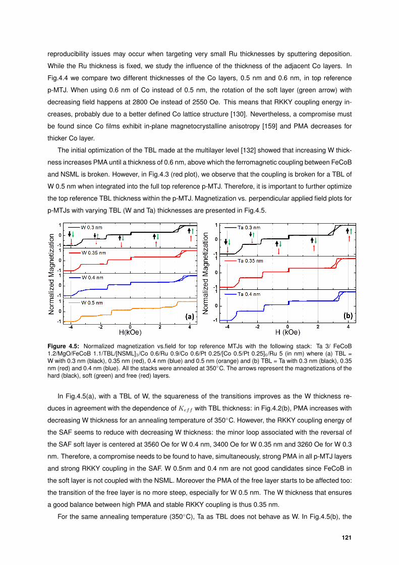
reproducibility issues may occur when targeting very small Ru thicknesses by sputtering deposition.
While the Ru thickness is fixed, we study the influence of the thickness of the adjacent Co layers. In
Fig.4.4 we compare two different thicknesses of the Co layers, 0.5 nm and 0.6 nm, in top reference
p-MTJ. When using 0.6 nm of Co instead of 0.5 nm, the rotation of the soft layer (green arrow) with
decreasing field happens at 2800 Oe instead of 2550 Oe. This means that RKKY coupling energy in-
creases, probably due to a better defined Co lattice structure [130]. Nevertheless, a compromise must
be found since Co films exhibit in-plane magnetocrystalline anisotropy [159] and PMA decreases for
thicker Co layer.
The initial optimization of the TBL made at the multilayer level [132] showed that increasing W thick-
ness increases PMA until a thickness of 0.6 nm, above which the ferromagnetic coupling between FeCoB
and NSML is broken. However, in Fig.4.3 (red plot), we observe that the coupling is broken for a TBL of
W 0.5 nm when integrated into the full top reference p-MTJ. Therefore, it is important to further optimize
the top reference TBL thickness within the p-MTJ. Magnetization vs. perpendicular applied field plots for
p-MTJs with varying TBL (W and Ta) thicknesses are presented in Fig.4.5.
Figure 4.5: Normalized magnetization vs.field for top reference MTJs with the following stack: Ta 3/ FeCoB1.2/MgO/FeCoB 1.1/TBL/[NSML]3/Co 0.6/Ru 0.9/Co 0.6/Pt 0.25/[Co 0.5/Pt 0.25]6/Ru 5 (in nm) where (a) TBL =W with 0.3 nm (black), 0.35 nm (red), 0.4 nm (blue) and 0.5 nm (orange) and (b) TBL = Ta with 0.3 nm (black), 0.35nm (red) and 0.4 nm (blue). All the stacks were annealed at 350C. The arrows represent the magnetizations of thehard (black), soft (green) and free (red) layers.
In Fig.4.5(a), with a TBL of W, the squareness of the transitions improves as the W thickness re-
duces in agreement with the dependence of Keff with TBL thickness: in Fig.4.2(b), PMA increases with
decreasing W thickness for an annealing temperature of 350C. However, the RKKY coupling energy of
the SAF seems to reduce with decreasing W thickness: the minor loop associated with the reversal of
the SAF soft layer is centered at 3560 Oe for W 0.4 nm, 3400 Oe for W 0.35 nm and 3260 Oe for W 0.3
nm. Therefore, a compromise needs to be found to have, simultaneously, strong PMA in all p-MTJ layers
and strong RKKY coupling in the SAF. W 0.5nm and 0.4 nm are not good candidates since FeCoB in
the soft layer is not coupled with the NSML. Moreover the PMA of the free layer starts to be affected too:
the transition of the free layer is no more steep, especially for W 0.5 nm. The W thickness that ensures
a good balance between high PMA and stable RKKY coupling is thus 0.35 nm.
For the same annealing temperature (350C), Ta as TBL does not behave as W. In Fig.4.5(b), the
121

minor loop becomes steeper for larger Ta thickness, indicating that PMA increases with increasing Ta
thickness. In addition, the interlayer exchange coupling between soft and hard layer of the SAF also
improves: the soft layer minor loop is centered at 3045 Oe for Ta 0.3 nm, 3215 Oe for Ta 0.35 nm and
3370 Oe for Ta 0.4 nm.
In conclusion, for an annealing temperature of 350C, a TBL of Ta 0.4 nm shows the best properties,
followed closely by W 0.35 nm. For the top reference of the DBMTJ, we chose a TBL of 0.35 nm
W because the overall thermal stability is higher [156] which consequently allows high temperature
annealing as a guarantee of higher TMR without a major loss in PMA.
One of the key aspects of the development of a double barrier magnetic tunnel junction is the storage
layer. Its optimization aims to improve important p-MTJ parameters for memory applications such as
thermal stability, TMR and PMA. In order to improve TMR and, more importantly thermal stability, one
strategy lies on the increase of the storage layer thickness [160]. However, this increase must not
compromise PMA.
Figure 4.6: Normalized magnetization as a function of decreasing perpendicular field for top reference p-MTJ witha composite free layer with the following composition: Ta 3/FeCoB 0.3/MgO/FeCoB x/W 0.2/FeCoB x/MgO/FeCoB1.1/W 0.4/[NSML]3/Co 0.6/Ru 0.9/Co 0.6/Pt 0.25/[Co 0.5/Pt 0.25]6/Ru 5 (in nm), where x = 1.0 (black), x = 1.2 (red)and x = 1.4 (blue). The inset shows the zoom of the storage layer minor loop.
Since the storage layer PMA originates at the FeCoB/MgO interface, the use of two FeCoB/MgO in-
terfaces doubles the interface anisotropy, allowing an increase of the storage layer thickness (see section
4.2.1). In fact, it has been reported a 2x increase of the thermal stability factor when using a composite
storage layer of the form FeCoB/Insertion/FeCoB [149] in comparison with a single FeCoB layer. The
principal function of the insertion layer between the two FeCoB layers is to help their crystallization by
attracting/absorbing boron [100]. The two most used materials are Ta and W. Recently, the use of W
as an insertion layer has proven to enable higher TMR [161] and the boron extraction has proven to
improve the perpendicular anisotropy of storage layer [162].
Even though the total thickness of the storage layer can be increased, the thickness of each of the
FeCoB layers needs to be carefully adjusted in order to maintain high PMA. Figure 4.6 shows the normal-
122
ized M(H) plots of top reference p-MTJs with composite storage layer and two MgO barriers with the fol-
lowing composition: Ta 3/FeCoB 0.3/MgO/FeCoB x/W 0.2/FeCoB x/MgO/FeCoB 1.1/W 0.4/[NSML]3/Co
0.6/Ru 0.9/Co 0.6/Pt 0.25/[Co 0.5/Pt 0.25]6/Ru 5 (in nm), with x varying between 1.0 nm and 1.4 nm. Fo-
cusing on the inset of Fig.4.6, as the FeCoB thickness increases from 1.0 up to 1.4 nm the squareness
of the minor loop starts fading. For 1.0 nm, the free layer presents a coercivity of 25 Oe, decreasing to
2.5 Oe for 1.2 nm, whereas for 1.4 nm the free layer anisotropy becomes mostly in-plane. Therefore, the
thickness of each of the FeCoB layers of the storage layer should not exceed 1.1-1.2 nm. However, we
expect a reduction of TMR ratio for very thin free layer; a balance between TMR and PMA must thus be
found. No changes were observed in the top SAF.
4.3.2 Analytical calculations of offset field: towards zero field Read/Write modeoperation in p-DBMTJ
Zero field operation is a primordial requirement for MTJ to be used as a STT-MRAM in industrial
applications. All research towards decreasing the device’s critical switching current is useless otherwise.
Although the junction might operate at very low currents, the overall power consumption may increase
if the addition of a current line is necessary to induce an Oersted field in order to compensate for the
hysteresis loop offset field of the free layer. The offset field Hoff may be expressed as:
Hoff = Hcp −Hd. (4.4)
The first term (Hcp) of this equation corresponds to the coupling between the magnetic layers. This
term contains different contributions: Neel ”orange peel” coupling [163], which may be either ferromag-
netic (for low PMA) or antiferromagnetic (for high PMA) [164] and interlayer exchange coupling, mediated
by electrons, which is usually antiferromagnetic [165]. The second term accounts for the effect of the
stray fields (Hd) arising from the reference layers (two in case of a DBMTJ).Whereas the coupling field
is independent of the junction size, the dipolar field starts dominating for diameters below 200 nm [157]
which covers our target sizes range (20 - 150 nm). Thus, the offset field expression (4.4) may be ap-
proximated to Hoff ≈ −Hd.
More recently, it has been demonstrated by Bandiera et al., for a bottom reference perpendicular
MTJ, [157] that the stray field of the SAF on the free layer cannot be exactly canceled. Only the spatial
average of the stray field can be reduced to zero. Moreover, they showed that the distance between the
SAF layers and the storage layer needs to be taken into account. Thus, in order to have zero offset field,
the hard layer must have a larger Mst than the soft layer (see section 4.3.1.B) and the ratio between
them must be adjusted as a function of the device lateral size.
Here we perform simple analytical calculations of the stray fields acting at the center of the free layer,
coming from the bottom and top references. The number of repetitions n of the multilayers from the
soft and hard layers of the top reference are varied in order to have the lowest Hoff for both modes of
operation (read and write) of the DBMTJ.
123
4.3.2.A Analytical calculations of the stray field
In a domain where there is no free current, ∇×H = 0, thence the dipolar field may expressed using
a magnetic scalar potential ψ:
Hd = −∇ψ. (4.5)
The expression of the scalar potential at position r is thus given by
ψ(r) =1
4π
(∫ρm(r′)
|r − r′|dV ′ +
∮σm(r′)
|r − r′|dS′
), (4.6)
where ρm = −∇.M and σm = −M .n are the density and surface magnetostatic charges. First,
considering only one magnetic layer for the reference under the free layer [Fig.4.7(a)] and assuming the
magnetization of the reference layer is uniform, then ρm = 0 and σm = ±Ms. The magnetic potential is
calculated by integrating over the two surfaces at the top and bottom of the reference layer:
ψ(r) =1
4π
(∫∫top
+Ms
|r − r′|dS′ +
∫∫bottom
−Ms
|r − r′|dS′
). (4.7)
Considering the symmetry axis z with its origin at the center of the free layer, the magnetic potential
on z becomes:
ψ(z) =1
4π
(∫ R
r′=0
+Ms√(d1 + z)2 + r′2
2πr′dr′ +
∫ R
r′=0
−Ms√(d2 + z)2 + r′2
2πr′dr′
), (4.8)
where d1 and d2 are the distances from the center of the free layer to the top and bottom surface of
the reference, respectively, and R is the radius of the circular cross section of the cylinder [Fig.4.7(a)].
The first term refers to the top surface while the second term refers to the bottom surface. Solving
Eq.(4.8), ψ(z) turns out as
ψ(z) =Ms
2
[√(d1 + z)2 +R2 − |d1 + z| −
√(d2 + z)2 +R2 + |d2 + z|
](4.9)
Finally, the dipolar field can be calculated by replacing ψ(z) in Eq.(4.5), thus Hd = −∂ψ∂z ~ez. Therefore,
Hd(z) =Ms
2
[d2 + z√
(d2 + z)2 +R2− d1 + z√
(d1 + z)2 +R2
]~ez (4.10)
At the center of the free layer (r=0, z = 0),
Hd(z) =Ms
2
(d2√
d22 +R2
− d1√d2
1 +R2
)~ez (4.11)
Nevertheless, the reference layers of our devices are SAFs which means that we need to consider
two magnetic layers for the reference, thence the soft and hard layers where the latter is further away
from the free layer than the soft layer. Figure 4.7(b) shows an illustration of the tetralayer structure.
Since the dipolar field is addictive, the expression for our SAF reference is
124

Figure 4.7: Illustration of the surface charge distribution on a MTJ with (a) single layer reference (blue) and (b) aSAF reference (blue). The thick black arrows represent the direction of the magnetization. MSL1
s , MSL2s and MHL
s
are the saturation magnetizations of the first half of the soft layer (FeCoB), the other half of the soft layer ([Co/Pt]n)and hard layer of the SAF, respectively. The pairs d1-d2, d3-d4 and d5-d6 are the distances from the center of thefree layer to the top and bottom surfaces of the the first half of the soft layer (FeCoB), the other half of the soft layer([Co/Pt]n) and hard layer of the SAF, respectively. R represents the radius of the cylindrical structures.
Hd =MSL1s
2
(d2√
d22 +R2
− d1√d2
1 +R2
)+MSL2s
2
(d4√
d24 +R2
− d3√d2
3 +R2
)
− MHLs
2
(d6√
d26 +R2
− d5√d2
5 +R2
),
(4.12)
where MSL1s , MSL2
s and MHLs are the saturation magnetizations of the first half of the soft layer
(FeCoB), the other half of the soft layer ([Co/Pt]n) and hard layer of the SAF, respectively. The pairs
d1-d2, d3-d4 and d5-d6 are the distances from the center of the free layer to the top and bottom surfaces
of the the first half of the soft layer (FeCoB), the other half of the soft layer ([Co/Pt]n) and hard layer of the
SAF, respectively. Notice that the soft and hard layer terms have opposite signs since the magnetizations
are antiparallel to each other, therefore the two stray fields subtract.
Equation (4.12) accounts for the stray fields created by a bottom reference. In the case of a DBMTJ,
one needs to take into account a second reference on top of the free layer, thus the total dipolar fields
acting of the DBMTJ free layer may be expressed as HDBMTJd = Hbottom
d + Htopd , where Hbottom
d and
Htopd have the form of Eq.(4.12). The signs of the magnetizations are adjusted according to the operation
mode. In read mode, the magnetizations of the bottom and top SAF soft layers are parallel, thus they
must have the same sign while the the two hard layers must also have the same sign but opposite to the
soft layers one. In write mode, the magnetizations of the bottom and top SAF soft layers are antiparallel,
thus they must have opposite signs, as well as the magnetizations of the two hard layers.
4.3.2.B Top reference optimization for zero offset field in Read/Write modes
First, the offset fields Hd have been calculated for p-MTJs with composite free layer and with a
single (bottom or top) reference. Figure 4.8 shows the stray fields as a function of the pillar diameter
125

for both types of p-MTJs. The saturation magnetizations used for the bottom reference were: MSL1s =
1100 emu/cm3 (relative to the 1.2 nm FeCoB layer), MSL2s = 1000 emu/cm3 and MHL
s = 1000 emu/cm3
(based on experimental measurements). The distances d1 to d6 can be easily calculated from the bottom
pinned p-MTJ stack illustration placed between figs.4.8(a) and (b). Figs.4.8(a) and (b) present the stray
field calculation for the two possible configurations of the bottom reference SAF. By analyzing the plots,
we can distinguish two different critical diameters. One is 45 nm, for which the offset field is zero; below
this diameter the offset field is negative (resp. positive) for MHLs oriented in the positive (resp. negative)
direction of the z axis (positive for MHLs oriented in the negative direction), thus meaning that the stray
field of the soft layer dominates for this device size range. The other critical diameter is 80 nm for which
the stray field is maximum (90 Oe) for positively oriented MHLs [minimum (-90 Oe) for negatively oriented
MHLs ], then for larger diameters, the absolute value of the offset field decreases.
Figure 4.8: Stray field Hd as a function of the MTJ diameter for: p-MTJ with a bottom reference SAF whose HLmagnetization is oriented in the (a) positive or (b) negative direction of the z axis and p-MTJ with a top reference SAFwhose HL magnetization is oriented in the (c) positive or (d) negative direction of the z axis. The stack illustrationsrepresent (top) the bottom and (bottom) the top reference p-MTJs. nHL represents the multilayer repetitions of thehard layer. d1 to d6 represent the distances of each marked layer surface to the center of the free layer. The arrowsrepresent the magnetizations of the free (red), SAF soft (blue) and SAF hard (black) layers.
For the case of the top pinned p-MTJ, the saturation magnetizations used for the top reference
were: MSL1s = 1100 emu/cm3 (relative to the 1.1 nm FeCoB layer), MSL2
s = 400 emu/cm3 and MHLs =
800 emu/cm3 (based on experimental measurements) 5. The distances d1 to d6 can be easily calculated
from the top pinned p-MTJ stack illustration placed between figs.4.8(c) and (d). Likewise the bottom
pinned p-MTJ, figs.4.8(c) and (d) correspond to the two possible magnetic configuration of the top SAF.
For this particular case, we have studied the stray field as a function of the MTJ diameter for 4 and 65The used MSL2
s is higher than the MSL2s ≈ 300 emu/cm3 obtained in section 4.3.1.A because the latter was measured only
for the NSML while the one used here was determined from the top reference p-MTJ M(H) loop, where texture effects are moresignificant. In addition, in the stack used in this section, there is an additional 0.6 nm Co layer which also justifies for the higherMSL2s value obtained. Regarding the hard layer, the Ms obtained for the [Co/Pt] multilayers in a top pinned p-MTJ was found to
be smaller than in a bottom pinned p-MTJ which possesses a thick Pt buffer layer which may justify the difference between thetwo MHL
s values.
126
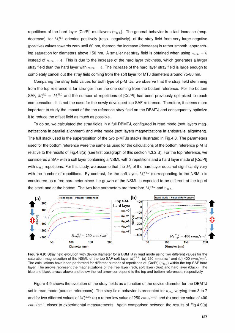
repetitions of the hard layer [Co/Pt] multilayers (nHL). The general behavior is a fast increase (resp.
decrease), for MHLs oriented positively (resp. negatively), of the stray field from very large negative
(positive) values towards zero until 80 nm, thereon the increase (decrease) is rather smooth, approach-
ing saturation for diameters above 150 nm. A smaller net stray field is obtained when using nHL = 6
instead of nHL = 4. This is due to the increase of the hard layer thickness, which generates a larger
stray field than the hard layer with nHL = 4. The increase of the hard layer stray field is large enough to
completely cancel out the stray field coming from the soft layer for MTJ diameters around 75-80 nm.
Comparing the stray field values for both type of p-MTJs, we observe that the stray field stemming
from the top reference is far stronger than the one coming from the bottom reference. For the bottom
SAF, MSLs = MHL
s and the number of repetitions of [Co/Pt] has been previously optimized to reach
compensation. It is not the case for the newly developed top SAF reference. Therefore, it seems more
important to study the impact of the top reference stray field on the DBMTJ and consequently optimize
it to reduce the offset field as much as possible.
To do so, we calculated the stray fields in a full DBMTJ, configured in read mode (soft layers mag-
netizations in parallel alignment) and write mode (soft layers magnetizations in antiparallel alignment).
The full stack used is the superposition of the two p-MTJs stacks illustrated in Fig.4.8. The parameters
used for the bottom reference were the same as used for the calculations of the bottom reference p-MTJ
relative to the results of Fig.4.8(a) (see first paragraph of this section 4.3.2.B). For the top reference, we
considered a SAF with a soft layer containing a NSML with 3 repetitions and a hard layer made of [Co/Pt]
with nHL repetitions. For this study, we assume that the Ms of the hard layer does not significantly vary
with the number of repetitions. By contrast, for the soft layer, MSL2s (corresponding to the NSML) is
considered as a free parameter since the growth of the NSML is expected to be different at the top of
the stack and at the bottom. The two free parameters are therefore MSL2s and nHL.
Figure 4.9: Stray field evolution with device diameter for a DBMTJ in read mode using two different values for thesaturation magnetization of the NSML of the top SAF soft layer MSL2
s : (a) 250 emu/cm3 and (b) 400 emu/cm3.The calculations have been performed for different number of repetitions of [Co/Pt] (nHL) within the top SAF hardlayer. The arrows represent the magnetizations of the free layer (red), soft layer (blue) and hard layer (black). Theblue and black arrows above and below the red arrow correspond to the top and bottom references, respectively.
Figure 4.9 shows the evolution of the stray fields as a function of the device diameter for the DBMTJ
set in read mode (parallel references). The stray field behavior is presented for nHL varying from 3 to 7
and for two different values of MSL2s : (a) a rather low value of 250 emu/cm3 and (b) another value of 400
emu/cm3, closer to experimental measurements. Again comparison between the results of Fig.4.9(a)
127
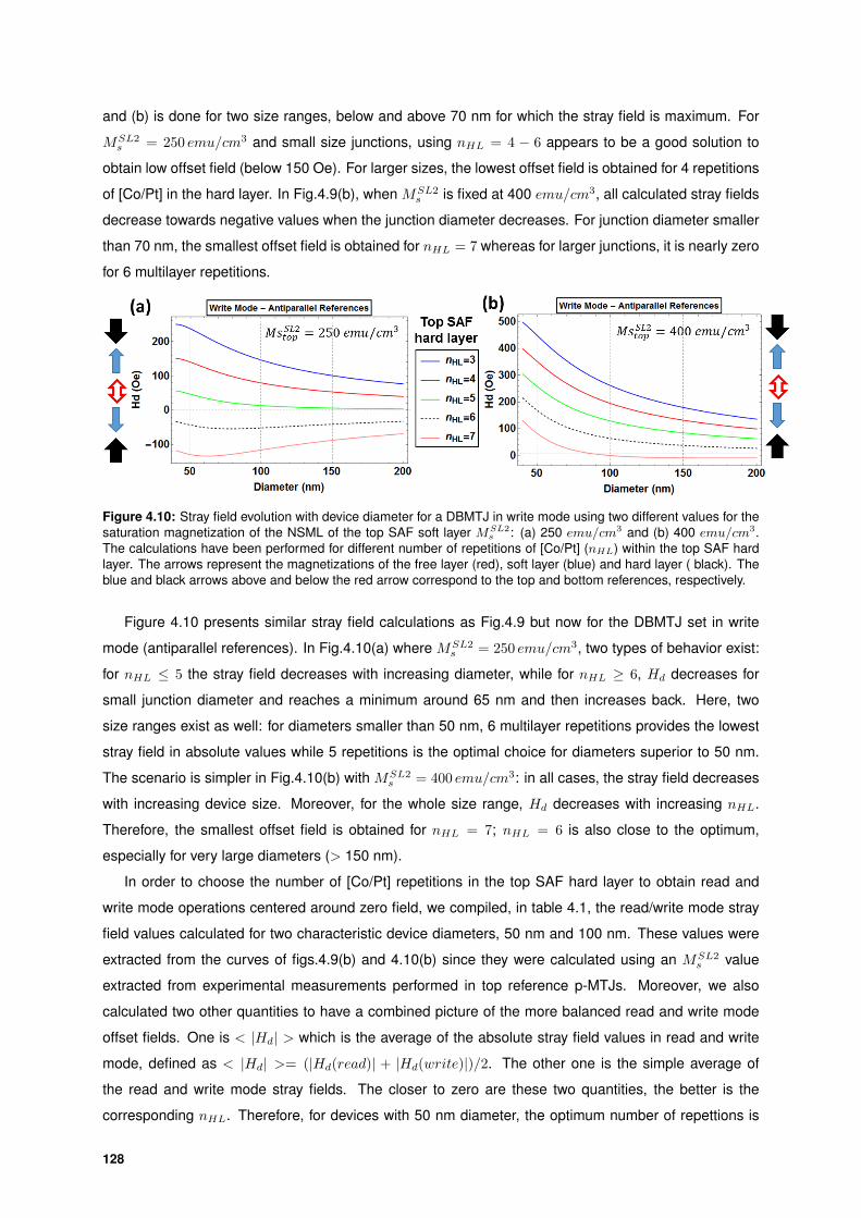
and (b) is done for two size ranges, below and above 70 nm for which the stray field is maximum. For
MSL2s = 250 emu/cm3 and small size junctions, using nHL = 4 − 6 appears to be a good solution to
obtain low offset field (below 150 Oe). For larger sizes, the lowest offset field is obtained for 4 repetitions
of [Co/Pt] in the hard layer. In Fig.4.9(b), when MSL2s is fixed at 400 emu/cm3, all calculated stray fields
decrease towards negative values when the junction diameter decreases. For junction diameter smaller
than 70 nm, the smallest offset field is obtained for nHL = 7 whereas for larger junctions, it is nearly zero
for 6 multilayer repetitions.
Figure 4.10: Stray field evolution with device diameter for a DBMTJ in write mode using two different values for thesaturation magnetization of the NSML of the top SAF soft layer MSL2
s : (a) 250 emu/cm3 and (b) 400 emu/cm3.The calculations have been performed for different number of repetitions of [Co/Pt] (nHL) within the top SAF hardlayer. The arrows represent the magnetizations of the free layer (red), soft layer (blue) and hard layer ( black). Theblue and black arrows above and below the red arrow correspond to the top and bottom references, respectively.
Figure 4.10 presents similar stray field calculations as Fig.4.9 but now for the DBMTJ set in write
mode (antiparallel references). In Fig.4.10(a) where MSL2s = 250 emu/cm3, two types of behavior exist:
for nHL ≤ 5 the stray field decreases with increasing diameter, while for nHL ≥ 6, Hd decreases for
small junction diameter and reaches a minimum around 65 nm and then increases back. Here, two
size ranges exist as well: for diameters smaller than 50 nm, 6 multilayer repetitions provides the lowest
stray field in absolute values while 5 repetitions is the optimal choice for diameters superior to 50 nm.
The scenario is simpler in Fig.4.10(b) with MSL2s = 400 emu/cm3: in all cases, the stray field decreases
with increasing device size. Moreover, for the whole size range, Hd decreases with increasing nHL.
Therefore, the smallest offset field is obtained for nHL = 7; nHL = 6 is also close to the optimum,
especially for very large diameters (> 150 nm).
In order to choose the number of [Co/Pt] repetitions in the top SAF hard layer to obtain read and
write mode operations centered around zero field, we compiled, in table 4.1, the read/write mode stray
field values calculated for two characteristic device diameters, 50 nm and 100 nm. These values were
extracted from the curves of figs.4.9(b) and 4.10(b) since they were calculated using an MSL2s value
extracted from experimental measurements performed in top reference p-MTJs. Moreover, we also
calculated two other quantities to have a combined picture of the more balanced read and write mode
offset fields. One is < |Hd| > which is the average of the absolute stray field values in read and write
mode, defined as < |Hd| >= (|Hd(read)| + |Hd(write)|)/2. The other one is the simple average of
the read and write mode stray fields. The closer to zero are these two quantities, the better is the
corresponding nHL. Therefore, for devices with 50 nm diameter, the optimum number of repettions is
128
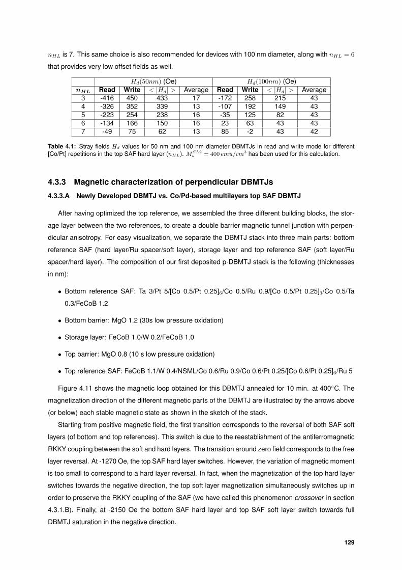
nHL is 7. This same choice is also recommended for devices with 100 nm diameter, along with nHL = 6
that provides very low offset fields as well.
Hd(50nm) (Oe) Hd(100nm) (Oe)nHL Read Write < |Hd| > Average Read Write < |Hd| > Average
3 -416 450 433 17 -172 258 215 434 -326 352 339 13 -107 192 149 435 -223 254 238 16 -35 125 82 436 -134 166 150 16 23 63 43 437 -49 75 62 13 85 -2 43 42
Table 4.1: Stray fields Hd values for 50 nm and 100 nm diameter DBMTJs in read and write mode for different[Co/Pt] repetitions in the top SAF hard layer (nHL). MSL2
s = 400 emu/cm3 has been used for this calculation.
4.3.3 Magnetic characterization of perpendicular DBMTJs
4.3.3.A Newly Developed DBMTJ vs. Co/Pd-based multilayers top SAF DBMTJ
After having optimized the top reference, we assembled the three different building blocks, the stor-
age layer between the two references, to create a double barrier magnetic tunnel junction with perpen-
dicular anisotropy. For easy visualization, we separate the DBMTJ stack into three main parts: bottom
reference SAF (hard layer/Ru spacer/soft layer), storage layer and top reference SAF (soft layer/Ru
spacer/hard layer). The composition of our first deposited p-DBMTJ stack is the following (thicknesses
in nm):
• Bottom reference SAF: Ta 3/Pt 5/[Co 0.5/Pt 0.25]6/Co 0.5/Ru 0.9/[Co 0.5/Pt 0.25]3/Co 0.5/Ta
0.3/FeCoB 1.2
• Bottom barrier: MgO 1.2 (30s low pressure oxidation)
• Storage layer: FeCoB 1.0/W 0.2/FeCoB 1.0
• Top barrier: MgO 0.8 (10 s low pressure oxidation)
• Top reference SAF: FeCoB 1.1/W 0.4/NSML/Co 0.6/Ru 0.9/Co 0.6/Pt 0.25/[Co 0.6/Pt 0.25]6/Ru 5
Figure 4.11 shows the magnetic loop obtained for this DBMTJ annealed for 10 min. at 400C. The
magnetization direction of the different magnetic parts of the DBMTJ are illustrated by the arrows above
(or below) each stable magnetic state as shown in the sketch of the stack.
Starting from positive magnetic field, the first transition corresponds to the reversal of both SAF soft
layers (of bottom and top references). This switch is due to the reestablishment of the antiferromagnetic
RKKY coupling between the soft and hard layers. The transition around zero field corresponds to the free
layer reversal. At -1270 Oe, the top SAF hard layer switches. However, the variation of magnetic moment
is too small to correspond to a hard layer reversal. In fact, when the magnetization of the top hard layer
switches towards the negative direction, the top soft layer magnetization simultaneously switches up in
order to preserve the RKKY coupling of the SAF (we have called this phenomenon crossover in section
4.3.1.B). Finally, at -2150 Oe the bottom SAF hard layer and top SAF soft layer switch towards full
DBMTJ saturation in the negative direction.
129

Figure 4.11: Magnetic cycle measured by VSM with perpendicular field for the newly developed perpendicularDBMTJ. The inset shows the minor loops performed on the free layer with either parallel (red) or antiparallel (green)configuration of the references, corresponding, respectively, to read and write modes. The stack represented on theleft side of the plot serves as legend for the arrows, describing the magnetization direction of the different magneticparts of the DBMTJ.
Similarly to in-plane anisotropy DBMTJ, the perpendicular DBMTJ has also two modes of operation:
read and write. As shown in the inset of Fig.4.11, minor loops can be performed on the storage layer with
either parallel (red) or antiparallel (green) alignment of the reference layers. The two configurations can
be achieved by applying the proper field sweep. Coming from positive field saturation and decreasing
the applied field until ≈-1000 Oe allows both the reference layers (top and bottom SAF soft layers) to
be aligned parallel, i.e. in read mode. The free layer hysteresis loop is obtained by increasing the field
again towards positive values. If the field is further increased, the hysteresis loop of the soft layers can
also be performed (blue triangles in Fig.4.11). To set the two references antiparallel to each other (i.e.
write mode), it is necessary to decrease the field down to ≈-1500 Oe. The minor loop of the free layer,
in write mode, can then be measured by increasing the field towards positive values.
It is possible to extract the coupling fields (Hcp) acting on the storage layer from both interfaces,
from the minor loops in inset of Fig.4.11. When the DBMTJ is in read mode, the coupling fields add
up while they subtract in write mode. So in read mode, Hreadoff = Hcp,bottom + Hcp,top = 47Oe and
Hwriteoff = Hcp,bottom−Hcp,top = −27Oe, in write mode. After solving the two equations,Hcp,bottom = 10Oe
and Hcp,top = 37Oe. Both couplings are ferromagnetic which means that that some Neel ”orange peel”
coupling exists at both MgO interfaces. The ferromagnetic coupling is considerably larger for the top
barrier and can be attibuted to metallic pinholes since the top barrier is the thinnest.
Let us now compare this perpendicular DMTJ with new top reference to previous samples. L. Cuchet
et al. [81] were the first to grow perpendicularly magnetized DBMTJ. They have developed a double
barrier MTJ using (Co/Pt) multilayer based bottom reference and (Co/Pd) multilayer top reference. Their
DBMTJ stack composition is the following:
130
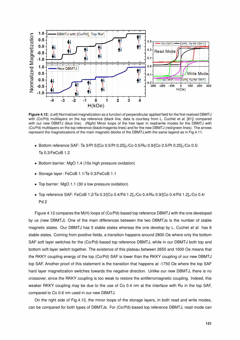
Figure 4.12: (Left) Normalized magnetization as a function of perpendicular applied field for the first realized DBMTJwith (Co/Pd) multilayers on the top reference (black line, data is courtesy from L. Cuchet et al. [81]) comparedwith our new DBMTJ (blue line). (Right) Minor loops of the free layer in read/write modes for the DBMTJ with(Co/Pd) multilayers on the top reference (black/magenta lines) and for the new DBMTJ (red/green lines). The arrowsrepresent the magnetizations of the main magnetic blocks of the DBMTJ,with the same legend as in Fig.4.11.
• Bottom reference SAF: Ta 3/Pt 5/[Co 0.5/Pt 0.25]6/Co 0.5/Ru 0.9/[Co 0.5/Pt 0.25]3/Co 0.5/
Ta 0.3/FeCoB 1.2
• Bottom barrier: MgO 1.4 (10s high pressure oxidation)
• Storage layer: FeCoB 1.1/Ta 0.3/FeCoB 1.1
• Top barrier: MgO 1.1 (30 s low pressure oxidation)
• Top reference SAF: FeCoB 1.2/Ta 0.3/[Co 0.4/Pd 1.2]4/Co 0.4/Ru 0.9/[Co 0.4/Pd 1.2]8/Co 0.4/
Pd 2
Figure 4.12 compares the M(H) loops of (Co/Pd)-based top reference DBMTJ with the one developed
by us (new DBMTJ). One of the main differences between the two DBMTJs is the number of stable
magnetic states. Our DBMTJ has 5 stable states whereas the one develop by L. Cuchet et al. has 6
stable states. Coming from positive fields, a transition happens around 2800 Oe where only the bottom
SAF soft layer switches for the (Co/Pd)-based top reference DBMTJ, while in our DBMTJ both top and
bottom soft layer switch together. The existence of this plateau between 2650 and 1600 Oe means that
the RKKY coupling energy of the top (Co/Pd) SAF is lower than the RKKY coupling of our new DBMTJ
top SAF. Another proof of this statement is the transition that happens at -1750 Oe where the top SAF
hard layer magnetization switches towards the negative direction. Unlike our new DBMTJ, there is no
crossover, since the RKKY coupling is too weak to restore the antiferromagnetic coupling. Indeed, this
weaker RKKY coupling may be due to the use of Co 0.4 nm at the interface with Ru in the top SAF,
compared to Co 0.6 nm used in our new DBMTJ.
On the right side of Fig.4.12, the minor loops of the storage layers, in both read and write modes,
can be compared for both types of DBMTJs. For (Co/Pd)-based top reference DBMTJ, read mode can
131
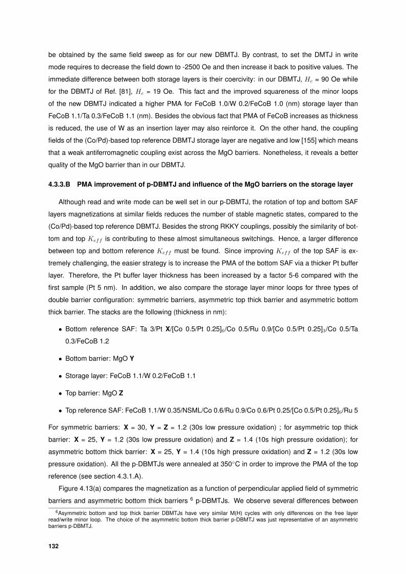
be obtained by the same field sweep as for our new DBMTJ. By contrast, to set the DMTJ in write
mode requires to decrease the field down to -2500 Oe and then increase it back to positive values. The
immediate difference between both storage layers is their coercivity: in our DBMTJ, Hc = 90 Oe while
for the DBMTJ of Ref. [81], Hc = 19 Oe. This fact and the improved squareness of the minor loops
of the new DBMTJ indicated a higher PMA for FeCoB 1.0/W 0.2/FeCoB 1.0 (nm) storage layer than
FeCoB 1.1/Ta 0.3/FeCoB 1.1 (nm). Besides the obvious fact that PMA of FeCoB increases as thickness
is reduced, the use of W as an insertion layer may also reinforce it. On the other hand, the coupling
fields of the (Co/Pd)-based top reference DBMTJ storage layer are negative and low [155] which means
that a weak antiferromagnetic coupling exist across the MgO barriers. Nonetheless, it reveals a better
quality of the MgO barrier than in our DBMTJ.
4.3.3.B PMA improvement of p-DBMTJ and influence of the MgO barriers on the storage layer
Although read and write mode can be well set in our p-DBMTJ, the rotation of top and bottom SAF
layers magnetizations at similar fields reduces the number of stable magnetic states, compared to the
(Co/Pd)-based top reference DBMTJ. Besides the strong RKKY couplings, possibly the similarity of bot-
tom and top Keff is contributing to these almost simultaneous switchings. Hence, a larger difference
between top and bottom reference Keff must be found. Since improving Keff of the top SAF is ex-
tremely challenging, the easier strategy is to increase the PMA of the bottom SAF via a thicker Pt buffer
layer. Therefore, the Pt buffer layer thickness has been increased by a factor 5-6 compared with the
first sample (Pt 5 nm). In addition, we also compare the storage layer minor loops for three types of
double barrier configuration: symmetric barriers, asymmetric top thick barrier and asymmetric bottom
thick barrier. The stacks are the following (thickness in nm):
• Bottom reference SAF: Ta 3/Pt X/[Co 0.5/Pt 0.25]6/Co 0.5/Ru 0.9/[Co 0.5/Pt 0.25]3/Co 0.5/Ta
0.3/FeCoB 1.2
• Bottom barrier: MgO Y
• Storage layer: FeCoB 1.1/W 0.2/FeCoB 1.1
• Top barrier: MgO Z
• Top reference SAF: FeCoB 1.1/W 0.35/NSML/Co 0.6/Ru 0.9/Co 0.6/Pt 0.25/[Co 0.5/Pt 0.25]6/Ru 5
For symmetric barriers: X = 30, Y = Z = 1.2 (30s low pressure oxidation) ; for asymmetric top thick
barrier: X = 25, Y = 1.2 (30s low pressure oxidation) and Z = 1.4 (10s high pressure oxidation); for
asymmetric bottom thick barrier: X = 25, Y = 1.4 (10s high pressure oxidation) and Z = 1.2 (30s low
pressure oxidation). All the p-DBMTJs were annealed at 350C in order to improve the PMA of the top
reference (see section 4.3.1.A).
Figure 4.13(a) compares the magnetization as a function of perpendicular applied field of symmetric
barriers and asymmetric bottom thick barriers 6 p-DBMTJs. We observe several differences between6Asymmetric bottom and top thick barrier DBMTJs have very similar M(H) cycles with only differences on the free layer
read/write minor loop. The choice of the asymmetric bottom thick barrier p-DBMTJ was just representative of an asymmetricbarriers p-DBMTJ.
132

Figure 4.13: (a) VSM magnetic cycles of the p-DBMTJ with symmetric barriers (black line) and asymmetric bottomthick barrier (orange line). The arrows represent the magnetizations of the main magnetic blocks of the DBMTJ(legend in Fig.4.11). (b) Minor loops of the free layer in read/write modes for the DBMTJ with symmetric barri-ers (red/green lines) and with asymmetric bottom thick barrier (blue/magenta lines).(c) Read mode minor loopscomparing symmetric (red), asymmetric with top (cyan) and bottom (blue) thick barrier.
these samples and the previously studied DMTJ with thinner Pt buffer layer. The first difference is the
field at which reversal occurs for both soft layers: 3500 Oe for the asymmetric barriers p-DBMTJ and
3000 Oe for the symmetric barriers one. The second is related with the appearance of a new stable
state after the top SAF crossover: this new state is created by the rotation of the top SAF soft layer
magnetization towards the negative field direction. This rotation occurs at H = -2650 Oe and H = -
2850 Oe for symmetric and asymmetric barriers p-DBMTJ, respectively. Consequently, the new state
has a stable plateau of 500 Oe for symmetric barriers and of 200 Oe for asymmetric barriers. These
differences between the new samples and the initial one result from the use of a thicker Pt buffer layer.
The thickest layer (30 nm) has been used for the symmetric barriers structure. However, a Pt buffer of 25
nm seems a better choice since it delays the rotation of the top SAF after the crossover, which increases
the field range for stable write mode state by 700 Oe compared to the initial DBMTJ of Fig.4.11.
In Fig.4.13(b), the free layer minor loops, for read and write modes, are shown. In terms of coercivity,
both types of DBMTJs present similar values for read and write modes. The symmetric barriers p-
DBMTJ displays Hreadc = Hwrite
c = 8.5Oe and the asymmetric bottom thicker p-DBMTJ exhibits Hreadc =
Hwritec = 9Oe. The most interesting differences come from the offset fields. The one with symmetric
barriers presents an Hreadoff = −63.5Oe while the Hwrite
off = −0.5Oe. For the bottom thick barrier p-
DBMTJ, Hreadoff = −32Oe and Hwrite
off = −17.5Oe. By separating the effect of each interface as in
section 4.3.3.A, we find that Hcp,bottom = −32Oe and Hcp,top = −31.5Oe for the case of symmetric
barriers whereas Hcp,bottom = −25Oe and Hcp,top = −7.25Oe for the case of thick bottom barrier.
133
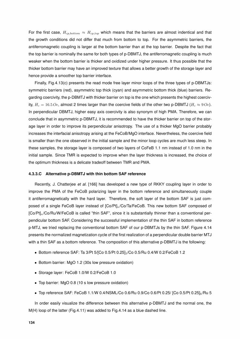
For the first case, Hcp,bottom ≈ Hcp,top which means that the barriers are almost indentical and that
the growth conditions did not differ that much from bottom to top. For the asymmetric barriers, the
antiferromagnetic coupling is larger at the bottom barrier than at the top barrier. Despite the fact that
the top barrier is nominally the same for both types of p-DBMTJ, the antiferromagnetic coupling is much
weaker when the bottom barrier is thicker and oxidized under higher pressure. It thus possible that the
thicker bottom barrier may have an improved texture that allows a better growth of the storage layer and
hence provide a smoother top barrier interface.
Finally, Fig.4.13(c) presents the read mode free layer minor loops of the three types of p-DBMTJs:
symmetric barriers (red), asymmetric top thick (cyan) and asymmetric bottom thick (blue) barriers. Re-
garding coercivity, the p-DBMTJ with thicker barrier on top is the one which presents the highest coerciv-
ity, Hc = 16.5Oe, almost 2 times larger than the coercive fields of the other two p-DBMTJ (Hc ≈ 9Oe).
In perpendicular DBMTJ, higher easy axis coercivity is also synonym of high PMA. Therefore, we can
conclude that in asymmetric p-DBMTJ, it is recommended to have the thicker barrier on top of the stor-
age layer in order to improve its perpendicular anisotropy. The use of a thicker MgO barrier probably
increases the interfacial anisotropy arising at the FeCoB/MgO interface. Nevertheless, the coercive field
is smaller than the one observed in the initial sample and the minor loop cycles are much less steep. In
these samples, the storage layer is composed of two layers of CoFeB 1.1 nm instead of 1.0 nm in the
initial sample. Since TMR is expected to improve when the layer thickness is increased, the choice of
the optimum thickness is a delicate tradeoff between TMR and PMA.
4.3.3.C Alternative p-DBMTJ with thin bottom SAF reference
Recently, J. Chatterjee et al. [166] has developed a new type of RKKY coupling layer in order to
improve the PMA of the FeCoB polarizing layer in the bottom reference and simultaneously couple
it antiferromagnetically with the hard layer. Therefore, the soft layer of the bottom SAF is just com-
posed of a single FeCoB layer instead of [Co/Pt]n/Co/Ta/FeCoB. This new bottom SAF composed of
[Co/Pt]n/Co/Ru/W/FeCoB is called ”thin SAF”, since it is substantially thinner than a conventional per-
pendicular bottom SAF. Considering the successful implementation of the thin SAF in bottom reference
p-MTJ, we tried replacing the conventional bottom SAF of our p-DBMTJs by the thin SAF. Figure 4.14
presents the normalized magnetization cycle of the first realization of a perpendicular double barrier MTJ
with a thin SAF as a bottom reference. The composition of this alternative p-DBMTJ is the following:
• Bottom reference SAF: Ta 3/Pt 5/[Co 0.5/Pt 0.25]3/Co 0.5/Ru 0.4/W 0.2/FeCoB 1.2
• Bottom barrier: MgO 1.2 (30s low pressure oxidation)
• Storage layer: FeCoB 1.0/W 0.2/FeCoB 1.0
• Top barrier: MgO 0.8 (10 s low pressure oxidation)
• Top reference SAF: FeCoB 1.1/W 0.4/NSML/Co 0.6/Ru 0.9/Co 0.6/Pt 0.25/ [Co 0.5/Pt 0.25]6/Ru 5
In order easily visualize the difference between this alternative p-DBMTJ and the normal one, the
M(H) loop of the latter (Fig.4.11) was added to Fig.4.14 as a blue dashed line.
134
Figure 4.14: Magnetic cycle of the perpendicular DBMTJ with thin bottom SAF (in black). The write (green) andread (red) mode free layer minor loops were also measured, with an extension in positive field of the latter allowingalso to measure the minor loop corresponding to the two SAF soft layers rotation. The M(H) cycle of the newp-DBMTJ with a conventional bottom SAF reference, already presented in Fig.4.11 (blue dashed line) is includedfor comparison. The arrows represent the magnetizations of the main magnetic blocks of the DBMTJ (legend inFig.4.11.
While the read mode minor loop can be measured in the exact same way as described in section
4.3.3.A for the conventional p-DBMTJ, the same does not happen for write mode. The write mode
configuration is also obtained by applying a negative magnetic field sweep to the p-DBMTJ, but instead
of stopping at -1500 Oe as previously mentioned, the applied field must not overcome -1250 Oe. The
write mode plateau of 700 Oe once measured for the normal DBMTJ is now reduced to 250 Oe. Indeed,
for this thinner p-DBMTJ, the hard layer/soft layer crossover does happen not only for the top reference
but also for the bottom one, the latter corresponding to the transition at ≈ -900 Oe. After this first
crossover, the two reference layers magnetizations are in antiparallel alignment. Then, around -1270
Oe, happens the crossover of the top SAF hard and soft layers, similarly to what has been observed for
the conventional p-DBMTJ (blue dashed line).
In conclusion, we demonstrated write and read mode configurations in the thin bottom SAF p-DBMTJ.
Despite the less stable write mode configuration, this alternative p-DBMTJ presents a substantial advan-
tage to the conventional DBMTJ, a reduced total thickness. Since the physical etching process of such
a thick stack is a challenging task, this thinner p-DBMTJ may pave a way towards an easier integration
of the p-DBMTJ as an STT-MRAM by reducing its nanofabrication complexity.
4.4 Summary
This chapter describes all the steps followed in the development of a new DBMTJ, from the integration
of the NSML as top reference to the full realization of the double barrier magnetic tunnel junction.
First, we have shown that use of W as texture breaking layer improves the magnetic properties,
mainly PMA, of the NSML even for annealing at 400C. Towards the development of a functional top
135
reference, we have demonstrated that a top SAF structure where the soft layer is constituted by Fe-
CoB/W/NSML and the hard layer composed of [Co/Pt]n has better performances than a top SAF where
both layers contain NSML. For the top reference p-MTJ, composition and thickness of the texture break-
ing layer and storage layer have been tested in order to enhance the perpendicular anisotropy. The best
option is an insertion layer of W 0.35 nm and a composite storage layer of the form FeCoB/W/FeCoB,
where W has 0.2 nm and the FeCoB thickness should lie between 1.0 and 1.2 nm.
Analytical calculations of the stray field have been performed to dimension the p-DBMTJ stack, aim-
ing at read and write mode operations centered around zero field. Since the top SAF is the thicker part
of the p-DBMTJ, our study mainly addresses the effect of the number of multilayer repetitions in this
reference, for junctions of different diameters. Based of the experimental value of the top SAF soft layer
saturation magnetization (400 emu/cm3), the optimal number of [Co/Pt] repetitions in the top SAF hard
layer is 7. For these parameters and for devices diameters between 50 and 100 nm, the read and write
mode offset fields, are expected to be inferior than 100 Oe.
We have also demonstrated the realization of a new p-DBMTJ using a top SAF reference including
the NSML in the soft layer and [Co/Pt]n as hard layer. Setting these junctions into read and write mode
magnetic configurations has also been shown. This new p-DBMTJ has been compared to the first
perpendicular DBMTJ reported by L. Cuchet et al. [81] where (Co/Pd) multilayers is used for the top
reference. Our p-DBMTJ displays a storage layer with higher perpendicular anisotropy and write mode
operation can be set by sweeping field down to -1500 Oe instead of -2500 Oe.
With the objective of increasing the field window where the write mode state is stable, we have
decided to increase the thickness of the bottom reference Pt buffer layer to improve this reference per-
pendicular anisotropy. By increasing the Pt buffer thickness from 5 nm up to 25 nm, the plateau where
the references are in antiparallel configuration rises from 800 Oe up to 1300 Oe. The impact of the
symmetry or asymmetry of the MgO barriers on the PMA of the storage layer has also been studied.
The highest coercivity has been observed for the case where the top barrier is thicker than the bottom
barrier which is explained by an improvement of the FeCoB/MgO interfacial anisotropy. The analysis of
the coupling fields around each barrier also showed that the growth of the second barrier is affected by
the thickness of the first one. In fact the top barrier coupling fields have shown to be smaller when the
bottom barrier is rather thick.
Finally, we have demonstrated the first realization of perpendicular DBMTJ using a bottom thin SAF
of the form [Co/Pt]n/Co/Ru/W/FeCoB, where Ru/W is a new type of RKKY coupling layer developed by J.
Chatterjee et al. [166], instead of the conventional bottom SAF of the form [Co/Pt]n/Ru/[Co/Pt]n/Ta/FeCoB.
Although the write mode magnetic field window is smaller than with the conventional bottom SAF, read
and write mode minor loop could be performed, demonstrating that the two mode operations are still
possible. Moreover, the overall thickness of the stack is smaller than for conventional p-DBMTJ and
consequently less challenging for device nanofabrication.
136
5Spin Transfer Torque in Perpendicular
DBMTJ
Contents5.1 Setting read and write modes in p-DBMTJ nanometric devices . . . . . . . . . . . . . 1385.2 Spin Transfer Torque . . . . . . . . . . . . . . . . . . . . . . . . . . . . . . . . . . . . . 1415.3 Summary . . . . . . . . . . . . . . . . . . . . . . . . . . . . . . . . . . . . . . . . . . . . 159
137

5.1 Setting read and write modes in p-DBMTJ nanometric devices
After the realization of the perpendicular DBMTJ stacks and demonstration of the two possible mag-
netic configurations - parallel and antiparallel references - we proceeded to the patterning of the full
sheet stacks into nanometric size pillars with nominal diameters ranging from 300 nm down to 20 nm
(detailed nanofabrication process chapter 2).
As seen in section 4.3.2.B, with the reduction of the lateral size of the devices comes an increase of
the stray fields acting on the storage layer. The target magnetic fields to set the read and write modes in
a patterned p-DBMTJ device should not be the same for a thin film. In order to isolate these two modes in
nanometric sized p-DBMTJ devices, measurements of resistance (R) as a function of applied magnetic
field (H) were performed in a Physical Properties Measurement System (PPMS) where magnetic fields
up to ±17 kOe could be reached. The R(H) sweeps were performed for two types of DBMTJs with
different top references. Figure 5.1 shows the measurements made for p-DBMTJ provided by L. Cuchet
et al. [81] with (Co/Pd) multilayers based top reference, whose full stack composition is (thickness in
nm):
• Bottom reference SAF: Ta 3/Pt 5/[Co 0.5/Pt 0.25]6/Co 0.5/Ru 0.9/[Co 0.5/Pt 0.25]3/Co 0.5/
Ta 0.3/FeCoB 1.2
• Bottom barrier: MgO 1.2 (30 s low pressure oxidation)
• Storage layer: FeCoB 1.2/Ta 0.3/FeCoB 1.2
• Top barrier: MgO 1.2 (30 s low pressure oxidation)
• Top reference SAF: FeCoB 1.2/Ta 0.3/[Co 0.4/Pd 1.2]4/Co 0.4/Ru 0.9/[Co 0.4/Pd 1.2]8/Co 0.4/
Pd 2
Whereas Fig. 5.2 presents the measurements performed in our newly developed p-DBMTJ with a
top reference based on NSML whose full stack is the following (thickness in nm):
• Bottom reference SAF: Ta 3/Ru 15/W 3/Ta 1/Pt 5/[Co 0.5/Pt 0.25]6/Co 0.5/Ru 0.9/[Co 0.5/Pt
0.25]3/Co 0.5/Ta 0.3/FeCoB 1.2
• Bottom barrier: MgO 1.2 (30s low pressure oxidation)
• Storage layer: FeCoB 1.05/W 0.2/FeCoB 1.05
• Top barrier: MgO 1.2 (30s low pressure oxidation)
• Top reference SAF: FeCoB 1.1/W 0.4/NSML/Co 0.6/Ru 0.9/Co 0.6/Pt 0.25/[Co 0.6/Pt 0.25]6/Ru 8
First of all, the sample used in Fig.5.1 was saturated under a very large negative field (-12 kOe) in
order to set all the magnetizations aligned in the same direction. The first field sweep was performed
from -4 kOe to +4 kOe [Fig.5.1(a)]. The first rotation happens around -1.5 kOe where the top SAF
recovers its antiferromagnetic coupling with the soft layer magnetization reversing towards the positive
138
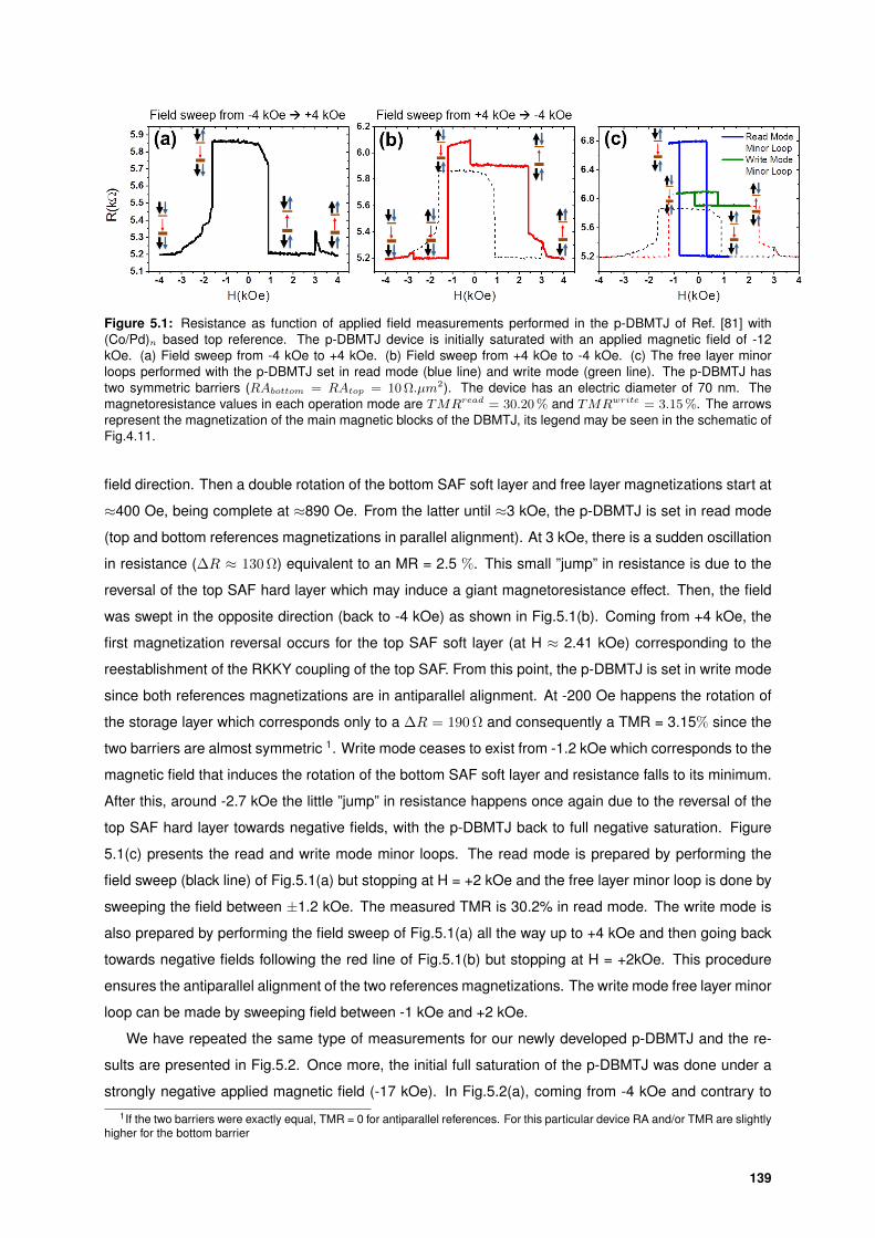
Figure 5.1: Resistance as function of applied field measurements performed in the p-DBMTJ of Ref. [81] with(Co/Pd)n based top reference. The p-DBMTJ device is initially saturated with an applied magnetic field of -12kOe. (a) Field sweep from -4 kOe to +4 kOe. (b) Field sweep from +4 kOe to -4 kOe. (c) The free layer minorloops performed with the p-DBMTJ set in read mode (blue line) and write mode (green line). The p-DBMTJ hastwo symmetric barriers (RAbottom = RAtop = 10 Ω.µm2). The device has an electric diameter of 70 nm. Themagnetoresistance values in each operation mode are TMRread = 30.20 % and TMRwrite = 3.15 %. The arrowsrepresent the magnetization of the main magnetic blocks of the DBMTJ, its legend may be seen in the schematic ofFig.4.11.
field direction. Then a double rotation of the bottom SAF soft layer and free layer magnetizations start at
≈400 Oe, being complete at ≈890 Oe. From the latter until ≈3 kOe, the p-DBMTJ is set in read mode
(top and bottom references magnetizations in parallel alignment). At 3 kOe, there is a sudden oscillation
in resistance (∆R ≈ 130 Ω) equivalent to an MR = 2.5 %. This small ”jump” in resistance is due to the
reversal of the top SAF hard layer which may induce a giant magnetoresistance effect. Then, the field
was swept in the opposite direction (back to -4 kOe) as shown in Fig.5.1(b). Coming from +4 kOe, the
first magnetization reversal occurs for the top SAF soft layer (at H ≈ 2.41 kOe) corresponding to the
reestablishment of the RKKY coupling of the top SAF. From this point, the p-DBMTJ is set in write mode
since both references magnetizations are in antiparallel alignment. At -200 Oe happens the rotation of
the storage layer which corresponds only to a ∆R = 190 Ω and consequently a TMR = 3.15% since the
two barriers are almost symmetric 1. Write mode ceases to exist from -1.2 kOe which corresponds to the
magnetic field that induces the rotation of the bottom SAF soft layer and resistance falls to its minimum.
After this, around -2.7 kOe the little ”jump” in resistance happens once again due to the reversal of the
top SAF hard layer towards negative fields, with the p-DBMTJ back to full negative saturation. Figure
5.1(c) presents the read and write mode minor loops. The read mode is prepared by performing the
field sweep (black line) of Fig.5.1(a) but stopping at H = +2 kOe and the free layer minor loop is done by
sweeping the field between ±1.2 kOe. The measured TMR is 30.2% in read mode. The write mode is
also prepared by performing the field sweep of Fig.5.1(a) all the way up to +4 kOe and then going back
towards negative fields following the red line of Fig.5.1(b) but stopping at H = +2kOe. This procedure
ensures the antiparallel alignment of the two references magnetizations. The write mode free layer minor
loop can be made by sweeping field between -1 kOe and +2 kOe.
We have repeated the same type of measurements for our newly developed p-DBMTJ and the re-
sults are presented in Fig.5.2. Once more, the initial full saturation of the p-DBMTJ was done under a
strongly negative applied magnetic field (-17 kOe). In Fig.5.2(a), coming from -4 kOe and contrary to1If the two barriers were exactly equal, TMR = 0 for antiparallel references. For this particular device RA and/or TMR are slightly
higher for the bottom barrier
139

Figure 5.2: Resistance as function of applied field measurements performed in the newly developed p-DBMTJwith NSML based top reference. The p-DBMTJ device is initially saturated with an applied magnetic field of -17kOe. (a) Field sweep from -4 kOe to +4 kOe. (b) Field sweep from +4 kOe to -4 kOe. (c) The free layer minorloops performed with the p-DBMTJ set in read mode (blue line) and write mode (green line). The p-DBMTJ hastwo symmetric barriers (RAbottom = RAtop = 8.5 Ω.µm2). The device has an electric diameter of 53 nm. Themagnetoresistance values in each operation mode are TMRread = 32 % and TMRwrite = 8 %. The arrowsrepresent the magnetizations of the main magnetic blocks of the DBMTJ, its legend may be seen in the schematicof Fig.4.11.
what was observed in Fig.5.1(a), both top and bottom SAF soft layers rotate at similar field (H ≈ -970
Oe), recovering the antiferromagnetic coupling of both SAFs. The double junction is then at maximum
resistance with the storage layer antiparallel to both references. It returns back to a parallel alignment for
H = 570 Oe. After reaching +4 kOe, by performing the sweep in the opposite direction, a different path
in resistance is also found as presented in Fig.5.2(b). In fact, when the field is increased past +3 kOe,
similarly to the p-DBMTJ in Fig.5.1, the top SAF hard layer magnetization reverses. However, unlike the
previous p-DBMTJ, there is no apparent change in resistance due to this reversal. Going back towards
negative fields, close to H = 600 Oe, the p-DBMTJ reaches an intermediate state of resistance corre-
sponding to the reestablishment of the RKKY coupling between the two magnetic parts of the top SAF.
Therefore the device is set in write mode. The free layer rotates around -560 Oe. And the p-DBMTJ
is back to minimum resistance when H = -1500 Oe due to the reversal of the bottom SAF soft layer.
Finally, in Fig.5.2(c), we have isolated the two possible free layer minor loops. The read mode can be
obtained in exactly the same way as for (Co/Pd) multilayers p-DBMTJ: initial saturation at very large
negative fields and field towards positive values stopping around +2 kOe. The minor loop results from
a sweep between ±1.5 kOe. Notice that in Fig.5.2(c), the field was swept past -2 kOe which led to the
reversal of the bottom SAF soft layer at a larger negative value of switching field (-1860 Oe) than when
the p-DBMTJ was set in write mode [red line in Fig.5.2(b)] due to the different stray fields involved. The
write mode is also prepared in a similar way as the other p-DBMTJ where the double junction needs
to be swept from large negative fields up to +4 kOe and then reduce the field down to -1 kOe [follow
red line in Fig.5.2(b)]. The free layer minor loop was obtained by sweeping the field between -1 kOe
and +1.5 kOe. In addition and despite both studied p-DBMTJs having nominal symmetric barriers, the
write mode minor loops of figures 5.1(c) and 5.2(c) are different. This is due to a slight difference of
RA and/or TMR between the two barriers caused by different growth conditions and as a consequence
of the nanofabrication process. The bottom barrier of the p-DBMTJ of Fig.5.1 and top barrier of the
p-DBMTJ of Fig.5.2 dominate comparatively to the other barrier.
140
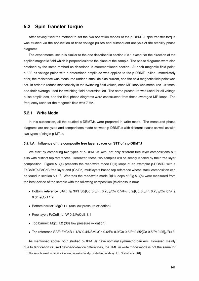
5.2 Spin Transfer Torque
After having fixed the method to set the two operation modes of the p-DBMTJ, spin transfer torque
was studied via the application of finite voltage pulses and subsequent analysis of the stability phase
diagrams.
The experimental setup is similar to the one described in section 3.3.1 except for the direction of the
applied magnetic field which is perpendicular to the plane of the sample. The phase diagrams were also
obtained by the same method as described in aforementioned section. At each magnetic field point,
a 100 ns voltage pulse with a determined amplitude was applied to the p-DBMTJ pillar. Immediately
after, the resistance was measured under a small dc bias current, and the next magnetic field point was
set. In order to reduce stochasticity in the switching field values, each MR loop was measured 10 times,
and their average used for switching field determination. The same procedure was used for all voltage
pulse amplitudes, and the final phase diagrams were constructed from these averaged MR loops. The
frequency used for the magnetic field was 7 Hz.
5.2.1 Write Mode
In this subsection, all the studied p-DBMTJs were prepared in write mode. The measured phase
diagrams are analyzed and comparisons made between p-DBMTJs with different stacks as well as with
two types of single p-MTJs.
5.2.1.A Influence of the composite free layer spacer on STT of a p-DBMTJ
We start by comparing two types of p-DBMTJs with, not only different free layer compositions but
also with distinct top references. Hereafter, these two samples will be simply labeled by their free layer
composition. Figure 5.3(a) presents the read/write mode R(H) loops of an exemplar p-DBMTJ with a
FeCoB/Ta/FeCoB free layer and (Co/Pd) multilayers based top reference whose stack composition can
be found in section 5.1. 2. Whereas the read/write mode R(H) loops of Fig.5.3(b) were measured from
the best device of the sample with the following composition (thickness in nm):
• Bottom reference SAF: Ta 3/Pt 30/[Co 0.5/Pt 0.25]6/Co 0.5/Ru 0.9/[Co 0.5/Pt 0.25]3/Co 0.5/Ta
0.3/FeCoB 1.2
• Bottom barrier: MgO 1.2 (30s low pressure oxidation)
• Free layer: FeCoB 1.1/W 0.2/FeCoB 1.1
• Top barrier: MgO 1.2 (30s low pressure oxidation)
• Top reference SAF: FeCoB 1.1/W 0.4/NSML/Co 0.6/Ru 0.9/Co 0.6/Pt 0.25/[Co 0.5/Pt 0.25]6/Ru 8
As mentioned above, both studied p-DBMTJs have nominal symmetric barriers. However, mainly
due to fabrication caused device-to-device differences, the TMR in write mode mode is not the same for2The sample used for fabrication was deposited and provided as courtesy of L. Cuchet et al. [81]
141
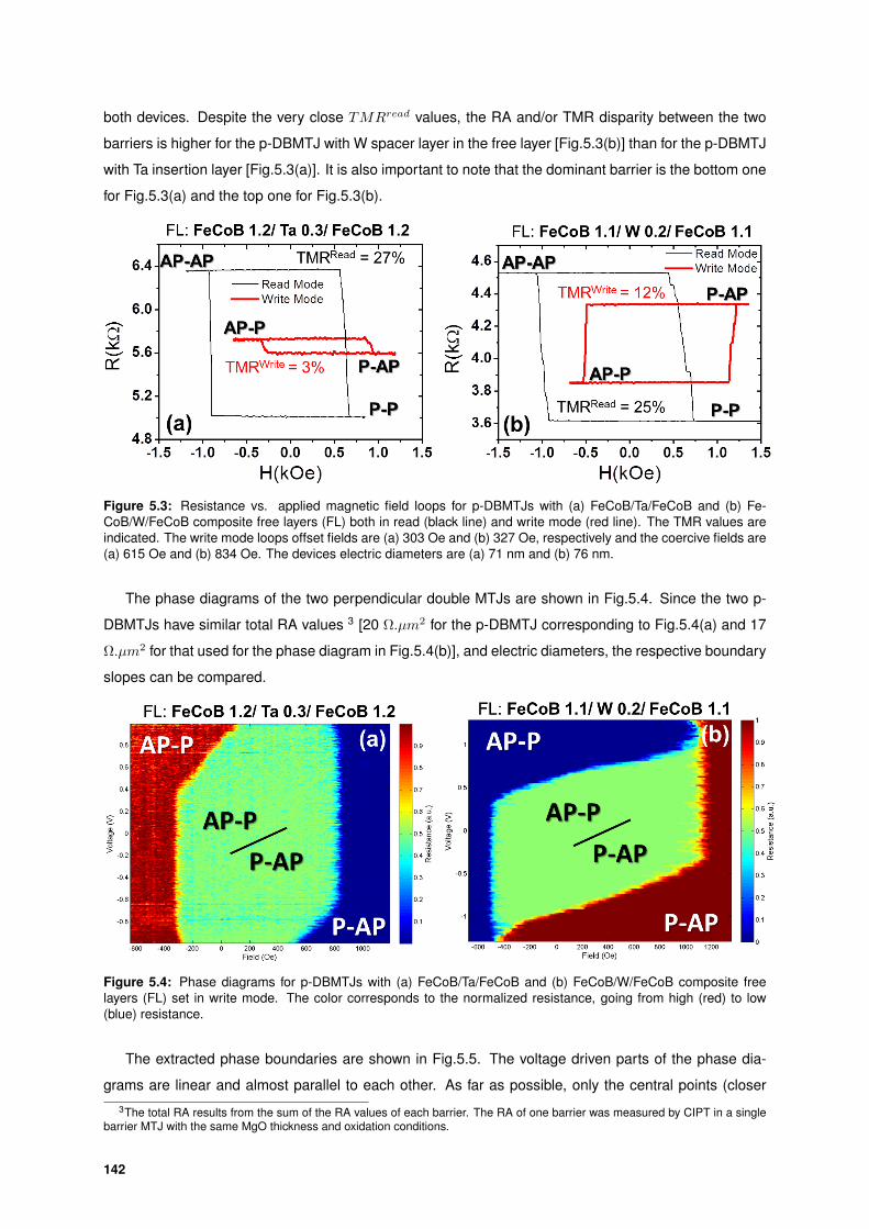
both devices. Despite the very close TMRread values, the RA and/or TMR disparity between the two
barriers is higher for the p-DBMTJ with W spacer layer in the free layer [Fig.5.3(b)] than for the p-DBMTJ
with Ta insertion layer [Fig.5.3(a)]. It is also important to note that the dominant barrier is the bottom one
for Fig.5.3(a) and the top one for Fig.5.3(b).
Figure 5.3: Resistance vs. applied magnetic field loops for p-DBMTJs with (a) FeCoB/Ta/FeCoB and (b) Fe-CoB/W/FeCoB composite free layers (FL) both in read (black line) and write mode (red line). The TMR values areindicated. The write mode loops offset fields are (a) 303 Oe and (b) 327 Oe, respectively and the coercive fields are(a) 615 Oe and (b) 834 Oe. The devices electric diameters are (a) 71 nm and (b) 76 nm.
The phase diagrams of the two perpendicular double MTJs are shown in Fig.5.4. Since the two p-
DBMTJs have similar total RA values 3 [20 Ω.µm2 for the p-DBMTJ corresponding to Fig.5.4(a) and 17
Ω.µm2 for that used for the phase diagram in Fig.5.4(b)], and electric diameters, the respective boundary
slopes can be compared.
Figure 5.4: Phase diagrams for p-DBMTJs with (a) FeCoB/Ta/FeCoB and (b) FeCoB/W/FeCoB composite freelayers (FL) set in write mode. The color corresponds to the normalized resistance, going from high (red) to low(blue) resistance.
The extracted phase boundaries are shown in Fig.5.5. The voltage driven parts of the phase dia-
grams are linear and almost parallel to each other. As far as possible, only the central points (closer3The total RA results from the sum of the RA values of each barrier. The RA of one barrier was measured by CIPT in a single
barrier MTJ with the same MgO thickness and oxidation conditions.
142
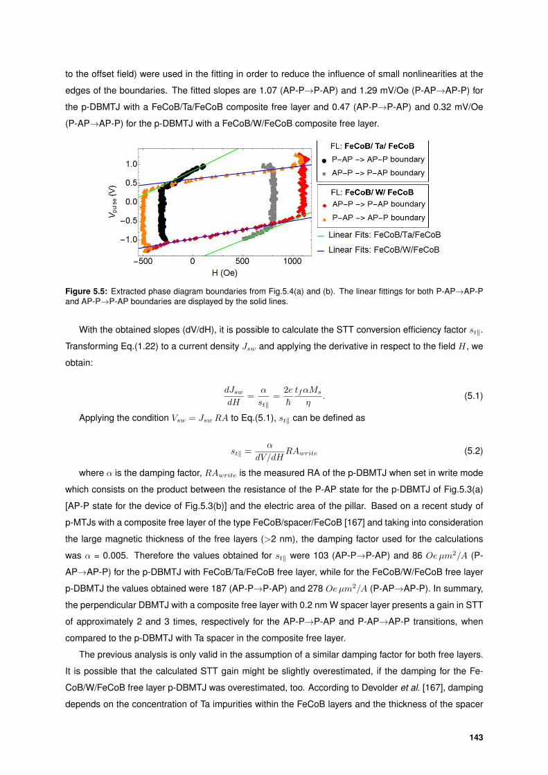
to the offset field) were used in the fitting in order to reduce the influence of small nonlinearities at the
edges of the boundaries. The fitted slopes are 1.07 (AP-P→P-AP) and 1.29 mV/Oe (P-AP→AP-P) for
the p-DBMTJ with a FeCoB/Ta/FeCoB composite free layer and 0.47 (AP-P→P-AP) and 0.32 mV/Oe
(P-AP→AP-P) for the p-DBMTJ with a FeCoB/W/FeCoB composite free layer.
Figure 5.5: Extracted phase diagram boundaries from Fig.5.4(a) and (b). The linear fittings for both P-AP→AP-Pand AP-P→P-AP boundaries are displayed by the solid lines.
With the obtained slopes (dV/dH), it is possible to calculate the STT conversion efficiency factor st‖.
Transforming Eq.(1.22) to a current density Jsw and applying the derivative in respect to the field H, we
obtain:
dJswdH
=α
st‖=
2e
~tfαMs
η. (5.1)
Applying the condition Vsw = Jsw RA to Eq.(5.1), st‖ can be defined as
st‖ =α
dV/dHRAwrite (5.2)
where α is the damping factor, RAwrite is the measured RA of the p-DBMTJ when set in write mode
which consists on the product between the resistance of the P-AP state for the p-DBMTJ of Fig.5.3(a)
[AP-P state for the device of Fig.5.3(b)] and the electric area of the pillar. Based on a recent study of
p-MTJs with a composite free layer of the type FeCoB/spacer/FeCoB [167] and taking into consideration
the large magnetic thickness of the free layers (>2 nm), the damping factor used for the calculations
was α = 0.005. Therefore the values obtained for st‖ were 103 (AP-P→P-AP) and 86 Oeµm2/A (P-
AP→AP-P) for the p-DBMTJ with FeCoB/Ta/FeCoB free layer, while for the FeCoB/W/FeCoB free layer
p-DBMTJ the values obtained were 187 (AP-P→P-AP) and 278 Oeµm2/A (P-AP→AP-P). In summary,
the perpendicular DBMTJ with a composite free layer with 0.2 nm W spacer layer presents a gain in STT
of approximately 2 and 3 times, respectively for the AP-P→P-AP and P-AP→AP-P transitions, when
compared to the p-DBMTJ with Ta spacer in the composite free layer.
The previous analysis is only valid in the assumption of a similar damping factor for both free layers.
It is possible that the calculated STT gain might be slightly overestimated, if the damping for the Fe-
CoB/W/FeCoB free layer p-DBMTJ was overestimated, too. According to Devolder et al. [167], damping
depends on the concentration of Ta impurities within the FeCoB layers and the thickness of the spacer
143
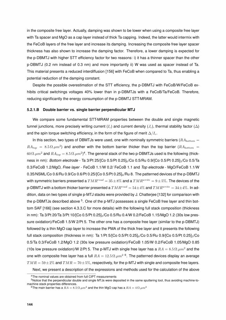
in the composite free layer. Actually, damping was shown to be lower when using a composite free layer
with Ta spacer and MgO as a cap layer instead of thick Ta capping. Indeed, the latter would intermix with
the FeCoB layers of the free layer and increase its damping. Increasing the composite free layer spacer
thickness has also shown to increase the damping factor. Therefore, a lower damping is expected for
the p-DBMTJ with higher STT efficiency factor for two reasons: i) it has a thinner spacer than the other
p-DBMTJ (0.2 nm instead of 0.3 nm) and more importantly ii) W was used as spacer instead of Ta.
This material presents a reduced interdiffusion [156] with FeCoB when compared to Ta, thus enabling a
potential reduction of the damping constant.
Despite the possible overestimation of the STT efficiency, the p-DBMTJ with FeCoB/W/FeCoB ex-
hibits critical switchings voltages 40% lower than in p-DBMTJs with a FeCoB/Ta/FeCoB. Therefore,
reducing significantly the energy consumption of the p-DBMTJ STT-MRAM.
5.2.1.B Double barrier vs. single barrier perpendicular MTJ
We compare some fundamental STT-MRAM properties between the double and single magnetic
tunnel junctions, more precisely writing current (Ic) and current density (Jc), thermal stability factor (∆)
and the spin torque switching efficiency, in the form of the figure of merit ∆/Ic.
In this section, two types of DBMTJs were used, one with nominally symmetric barriers (RAbottom =
RAtop = 8.5 Ω.µm2) and another with the bottom barrier thicker than the top barrier (RAbottom =
60 Ω.µm2 and RAtop = 8.5 Ω.µm2)4. The general stack of the two p-DBMTJs used is the following (thick-
ness in nm): Bottom electrode - Ta 3/Pt 25/[Co 0.5/Pt 0.25]6/Co 0.5/Ru 0.9/[Co 0.5/Pt 0.25]3/Co 0.5/Ta
0.3/FeCoB 1.2/MgO, Free layer - FeCoB 1.1/W 0.2/ FeCoB 1.1 and Top electrode - MgO/FeCoB 1.1/W
0.35/NSML/Co 0.6/Ru 0.9/Co 0.6/Pt 0.25/[Co 0.5/Pt 0.25]6/Ru 8. The patterned devices of the p-DBMTJ
with symmetric barriers presented a TMRread = 35±8% and a TMRwrite = 9±5%. The devices of the
p-DBMTJ with a bottom thicker barrier presented a TMRread = 54±4% and TMRwrite = 34±4%. In ad-
dition, data on two types of single p-MTJ stacks were provided by J. Chatterjee [132] for comparison with
the p-DBMTJs described above 5. One of the p-MTJ possesses a single FeCoB free layer and thin bot-
tom SAF [166] (see section 4.3.3.C for more details) with the following full stack composition (thickness
in nm): Ta 3/Pt 20/Ta 3/Pt 10/[Co 0.5/Pt 0.25]3/Co 0.5/Ru 0.4/W 0.2/FeCoB 1.15/MgO 1.2 (30s low pres-
sure oxidation)/FeCoB 1.5/W 2/Pt 5. The other one has a composite free layer (similar to the p-DBMTJ)
followed by a thin MgO cap layer to increase the PMA of the thick free layer and it presents the following
full stack composition (thickness in nm): Ta 1/Pt 5/[Co 0.5/Pt 0.25]6/Co 0.5/Ru 0.9/[Co 0.5/Pt 0.25]3/Co
0.5/Ta 0.3/FeCoB 1.2/MgO 1.2 (30s low pressure oxidation)/FeCoB 1.05/W 0.2/FeCoB 1.05/MgO 0.85
(10s low pressure oxidation)/W 2/Pt 5. The p-MTJ with single free layer has a RA = 8.5 Ω.µm2 and the
one with composite free layer has a full RA = 12.5 Ω.µm2 6. The patterned devices display an average
TMR = 59±2% and TMR = 70±5%, respectively, for the p-MTJ with single and composite free layers.
Next, we present a description of the expressions and methods used for the calculation of the above4The nominal values are obtained from full CIPT measurements5Notice that the perpendicular double and single MTJs were deposited in the same sputtering tool, thus avoiding machine-to-
machine stack properties differences.6The main barrier has a RA = 8.5 Ω.µm2 and the thin MgO cap has a RA = 4 Ω.µm2
144
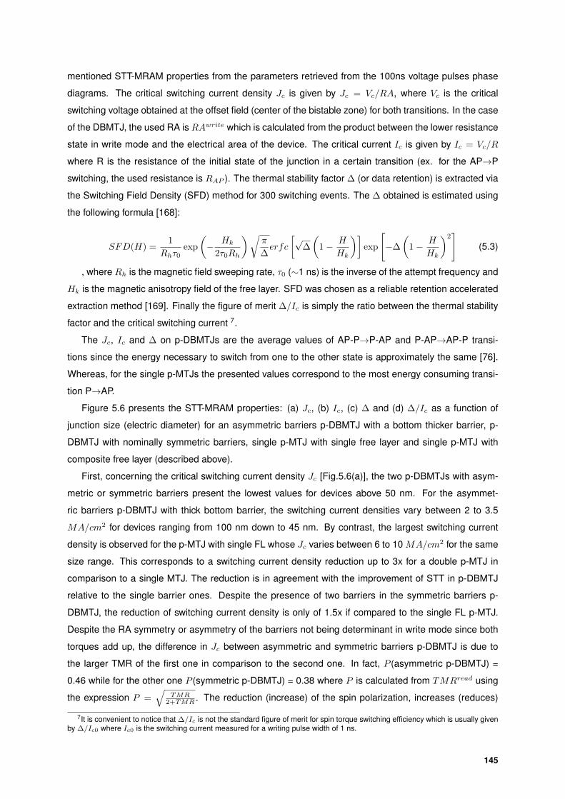
mentioned STT-MRAM properties from the parameters retrieved from the 100ns voltage pulses phase
diagrams. The critical switching current density Jc is given by Jc = Vc/RA, where Vc is the critical
switching voltage obtained at the offset field (center of the bistable zone) for both transitions. In the case
of the DBMTJ, the used RA is RAwrite which is calculated from the product between the lower resistance
state in write mode and the electrical area of the device. The critical current Ic is given by Ic = Vc/R
where R is the resistance of the initial state of the junction in a certain transition (ex. for the AP→P
switching, the used resistance is RAP ). The thermal stability factor ∆ (or data retention) is extracted via
the Switching Field Density (SFD) method for 300 switching events. The ∆ obtained is estimated using
the following formula [168]:
SFD(H) =1
Rhτ0exp
(− Hk
2τ0Rh
)√π
∆erfc
[√∆
(1− H
Hk
)]exp
[−∆
(1− H
Hk
)2]
(5.3)
, where Rh is the magnetic field sweeping rate, τ0 (∼1 ns) is the inverse of the attempt frequency and
Hk is the magnetic anisotropy field of the free layer. SFD was chosen as a reliable retention accelerated
extraction method [169]. Finally the figure of merit ∆/Ic is simply the ratio between the thermal stability
factor and the critical switching current 7.
The Jc, Ic and ∆ on p-DBMTJs are the average values of AP-P→P-AP and P-AP→AP-P transi-
tions since the energy necessary to switch from one to the other state is approximately the same [76].
Whereas, for the single p-MTJs the presented values correspond to the most energy consuming transi-
tion P→AP.
Figure 5.6 presents the STT-MRAM properties: (a) Jc, (b) Ic, (c) ∆ and (d) ∆/Ic as a function of
junction size (electric diameter) for an asymmetric barriers p-DBMTJ with a bottom thicker barrier, p-
DBMTJ with nominally symmetric barriers, single p-MTJ with single free layer and single p-MTJ with
composite free layer (described above).
First, concerning the critical switching current density Jc [Fig.5.6(a)], the two p-DBMTJs with asym-
metric or symmetric barriers present the lowest values for devices above 50 nm. For the asymmet-
ric barriers p-DBMTJ with thick bottom barrier, the switching current densities vary between 2 to 3.5
MA/cm2 for devices ranging from 100 nm down to 45 nm. By contrast, the largest switching current
density is observed for the p-MTJ with single FL whose Jc varies between 6 to 10 MA/cm2 for the same
size range. This corresponds to a switching current density reduction up to 3x for a double p-MTJ in
comparison to a single MTJ. The reduction is in agreement with the improvement of STT in p-DBMTJ
relative to the single barrier ones. Despite the presence of two barriers in the symmetric barriers p-
DBMTJ, the reduction of switching current density is only of 1.5x if compared to the single FL p-MTJ.
Despite the RA symmetry or asymmetry of the barriers not being determinant in write mode since both
torques add up, the difference in Jc between asymmetric and symmetric barriers p-DBMTJ is due to
the larger TMR of the first one in comparison to the second one. In fact, P (asymmetric p-DBMTJ) =
0.46 while for the other one P (symmetric p-DBMTJ) = 0.38 where P is calculated from TMRread using
the expression P =√
TMR2+TMR . The reduction (increase) of the spin polarization, increases (reduces)
7It is convenient to notice that ∆/Ic is not the standard figure of merit for spin torque switching efficiency which is usually givenby ∆/Ic0 where Ic0 is the switching current measured for a writing pulse width of 1 ns.
145
Figure 5.6: Multiple STT-MRAM fundamental properties - (a) critical current density Jc, (b) critical current Ic, (c)thermal stability factor ∆ and (d) STT efficiency figure of merit ∆/Ic - as function of the junction electric size, fortwo types of p-DBMTJs (solid squares) and two types of single p-MTJs (open circles). The presented values weredetermined from data obtained from voltage writing pulse phase diagrams. The lines in (a),(b) and (d) are guides tothe eye.
the switching current (as shown by Eq. (1.40) supposing that PF = PR = P ). Nevertheless, Jc reduc-
tion factor is smaller (1.5x-2x) if we compare the p-DBMTJs with the p-MTJ with composite FL. With
exception of the p-MTJ with composite FL, the double and single p-MTJs exhibit an increasing Jc with
reducing junction size, which is abnormal since Jc should be constant regardless of the junction dimen-
sions. This unexpected trend is due to the linear increase of critical switching current Ic with junction
diameter, as presented in Fig.5.6(b). According to eqs.(1.23)-(1.40) and supposing an almost constant
Hk with junction size, Ic was expected to scale linearly with area A and consequently to scale with r2
where r is the radius of a circular junction. Although the expected trend has been observed in previous
reports of p-MTJs [170, 171], it has also been reported that, outside the macrospin model (diameter >
30 nm), device-to-device variations on the thermal stability factor ∆ affect Ic. In term of absolute values,
Ic reduction is of ∼3x when using the asymmetric barriers p-DBMTJ instead of a single FL p-MTJ. On
the other hand, between single barrier p-MTJs the difference is not that drastic (similarly to ref. [149]),
even though the use of a composite free layer p-MTJ slightly improves Ic.
Figure 5.6(c) presents the variation of the thermal stability factor ∆ with junction size for the different
146

structures. For the double and single p-MTJs with composite free layer, the values oscillate between
50 and 90. For the single 1.5 nm free layer p-MTJ, the experimental values vary between 30 - 40.
Therefore, the employment of the composite free layer provides a gain in the thermal stability factor. A
result that goes along with a previous report by Sato et al. [149]. In a more general picture, for the device
size range studied, ∆ has shown to be almost constant [171,172]: there is no apparent trend of ∆ with
junction size. There are two types of switching depending on the lateral dimensions of the junction. For
device diameters above the nucleation size (> 30− 40nm), the switching process consists in nucleating
a reversed domain in the free layer and propagating a domain wall. For smaller sizes, the magnetization
switches coherently, following a macrospin description. For large structures, the first process requires
much less energy than the coherent magnetization reversal [173]. While the energy to create a domain
wall increases linearly with diameter, the needed energy for a coherent rotation scales quadratically with
the diameter. The single-domain model and nudged elastic band simulations [174] have predicted a
linear increase of ∆ with junction lateral size (even for large sizes), which goes against experimental
observations. A subvolume nucleation mechanism [172] as well as a edge nucleation mode [175] have
been reported as possible explanations for the conservation of ∆ for large areas. More recently a ∆(H)
model extension to the domain wall mediated switching [176] has corroborated the linear increase of
thermal stability with device diameter, in line with the above mentioned simulations.
Finally, Fig.5.6(d) presents the ratio between the thermal stability factor and the critical switching cur-
rent (∆/Ic). A closer analysis to Eq.(1.23) shows that Ic is actually proportional 8 to ∆ (Eq.(1.28)), thus
affected by variations of the latter. According to ref. [171], the variations can be mitigated if one consid-
ers the figure of merit ∆/Ic. This ratio was described as a measure of effective damping, characterizing
the energy loss of spin transfer switching, or as a measure of the efficiency of STT switching [170]. Our
∆/Ic data, for all the studied perpendicular double or single MTJs, scales with inverse of the diameter (at
least for device diameters larger than 30 nm) following a similar trend as previous reports [170,171,177].
Moreover, the same authors reported a saturation of this ratio for sizes below transition to quasi-uniform
regime. Unfortunately, due to fabrication limitations, we do not have a sufficient amount of devices with
diameters below 30 nm to confirm the ∆/Ic saturation. Comparing the various types of p-MTJs, again
the p-DBMTJ with a thicker bottom barrier presents the higher STT efficiency along the whole studied
size range. The contrast between this type of structure and the single FL p-MTJ increases as dimen-
sions reduce. For junctions sizes of ≈80 nm, the gain in efficiency is of ≈4x, whereas for devices ≈45
nm, the gain rises to ≈6x. On the other hand, the gain in STT efficiency drastically declines to 1.5x
when comparing the asymmetric p-DBMTJ with single p-MTJs with a composite free layer. This figure of
merit can also be perceived as the inverse of an effective damping, and as discussed in section 5.2.1.A,
the damping factor (α) of a FeCoB/Spacer/FeCoB free layer is actually smaller than in a single free
layer. Therefore, in a composite FL, Ic reduces due to a lower α and ∆ increases since the thickness
(and consequently the volume) of the free layer is almost two times larger, enabling the enhancement
of ∆/Ic. The symmetric barriers p-DBMTJ also presents a higher STT efficiency than the single FL
8Under the macrospin model, the critical switching current can be re-written including the thermal stability factor: Ic =4e~ ∆αkBT
η
147
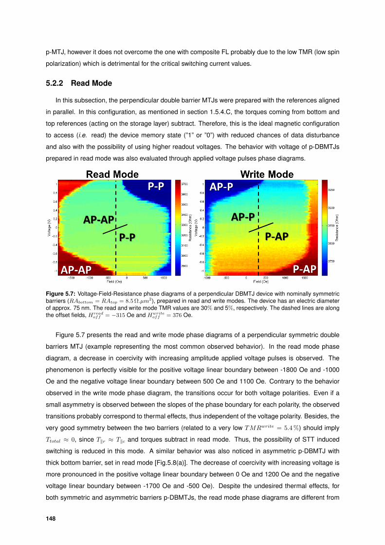
p-MTJ, however it does not overcome the one with composite FL probably due to the low TMR (low spin
polarization) which is detrimental for the critical switching current values.
5.2.2 Read Mode
In this subsection, the perpendicular double barrier MTJs were prepared with the references aligned
in parallel. In this configuration, as mentioned in section 1.5.4.C, the torques coming from bottom and
top references (acting on the storage layer) subtract. Therefore, this is the ideal magnetic configuration
to access (i.e. read) the device memory state (”1” or ”0”) with reduced chances of data disturbance
and also with the possibility of using higher readout voltages. The behavior with voltage of p-DBMTJs
prepared in read mode was also evaluated through applied voltage pulses phase diagrams.
Figure 5.7: Voltage-Field-Resistance phase diagrams of a perpendicular DBMTJ device with nominally symmetricbarriers (RAbottom = RAtop = 8.5 Ω.µm2), prepared in read and write modes. The device has an electric diameterof approx. 75 nm. The read and write mode TMR values are 30% and 5%, respectively. The dashed lines are alongthe offset fields, Hread
off = −315 Oe and Hwriteoff = 376 Oe.
Figure 5.7 presents the read and write mode phase diagrams of a perpendicular symmetric double
barriers MTJ (example representing the most common observed behavior). In the read mode phase
diagram, a decrease in coercivity with increasing amplitude applied voltage pulses is observed. The
phenomenon is perfectly visible for the positive voltage linear boundary between -1800 Oe and -1000
Oe and the negative voltage linear boundary between 500 Oe and 1100 Oe. Contrary to the behavior
observed in the write mode phase diagram, the transitions occur for both voltage polarities. Even if a
small asymmetry is observed between the slopes of the phase boundary for each polarity, the observed
transitions probably correspond to thermal effects, thus independent of the voltage polarity. Besides, the
very good symmetry between the two barriers (related to a very low TMRwrite = 5.4 %) should imply
Ttotal ≈ 0, since T‖r ≈ T‖c and torques subtract in read mode. Thus, the possibility of STT induced
switching is reduced in this mode. A similar behavior was also noticed in asymmetric p-DBMTJ with
thick bottom barrier, set in read mode [Fig.5.8(a)]. The decrease of coercivity with increasing voltage is
more pronounced in the positive voltage linear boundary between 0 Oe and 1200 Oe and the negative
voltage linear boundary between -1700 Oe and -500 Oe). Despite the undesired thermal effects, for
both symmetric and asymmetric barriers p-DBMTJs, the read mode phase diagrams are different from
148
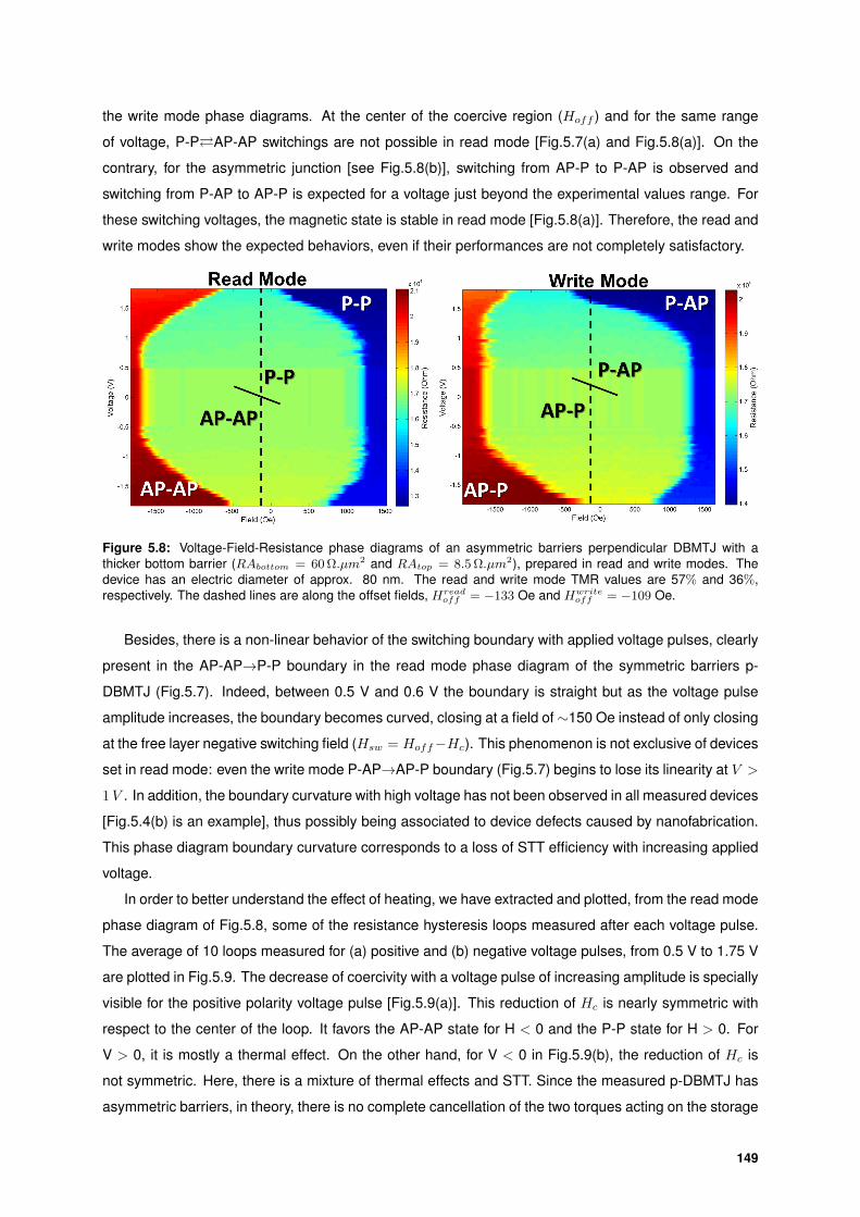
the write mode phase diagrams. At the center of the coercive region (Hoff ) and for the same range
of voltage, P-PAP-AP switchings are not possible in read mode [Fig.5.7(a) and Fig.5.8(a)]. On the
contrary, for the asymmetric junction [see Fig.5.8(b)], switching from AP-P to P-AP is observed and
switching from P-AP to AP-P is expected for a voltage just beyond the experimental values range. For
these switching voltages, the magnetic state is stable in read mode [Fig.5.8(a)]. Therefore, the read and
write modes show the expected behaviors, even if their performances are not completely satisfactory.
Figure 5.8: Voltage-Field-Resistance phase diagrams of an asymmetric barriers perpendicular DBMTJ with athicker bottom barrier (RAbottom = 60 Ω.µm2 and RAtop = 8.5 Ω.µm2), prepared in read and write modes. Thedevice has an electric diameter of approx. 80 nm. The read and write mode TMR values are 57% and 36%,respectively. The dashed lines are along the offset fields, Hread
off = −133 Oe and Hwriteoff = −109 Oe.
Besides, there is a non-linear behavior of the switching boundary with applied voltage pulses, clearly
present in the AP-AP→P-P boundary in the read mode phase diagram of the symmetric barriers p-
DBMTJ (Fig.5.7). Indeed, between 0.5 V and 0.6 V the boundary is straight but as the voltage pulse
amplitude increases, the boundary becomes curved, closing at a field of ∼150 Oe instead of only closing
at the free layer negative switching field (Hsw = Hoff−Hc). This phenomenon is not exclusive of devices
set in read mode: even the write mode P-AP→AP-P boundary (Fig.5.7) begins to lose its linearity at V >
1V . In addition, the boundary curvature with high voltage has not been observed in all measured devices
[Fig.5.4(b) is an example], thus possibly being associated to device defects caused by nanofabrication.
This phase diagram boundary curvature corresponds to a loss of STT efficiency with increasing applied
voltage.
In order to better understand the effect of heating, we have extracted and plotted, from the read mode
phase diagram of Fig.5.8, some of the resistance hysteresis loops measured after each voltage pulse.
The average of 10 loops measured for (a) positive and (b) negative voltage pulses, from 0.5 V to 1.75 V
are plotted in Fig.5.9. The decrease of coercivity with a voltage pulse of increasing amplitude is specially
visible for the positive polarity voltage pulse [Fig.5.9(a)]. This reduction of Hc is nearly symmetric with
respect to the center of the loop. It favors the AP-AP state for H < 0 and the P-P state for H > 0. For
V > 0, it is mostly a thermal effect. On the other hand, for V < 0 in Fig.5.9(b), the reduction of Hc is
not symmetric. Here, there is a mixture of thermal effects and STT. Since the measured p-DBMTJ has
asymmetric barriers, in theory, there is no complete cancellation of the two torques acting on the storage
149

Figure 5.9: Average of 10 hysteresis loops measured after application of (a) positive and (b) negative polarityvoltage pulses of increasing amplitude from 0.5 V to 1.75 V in steps of 0.25V. The loops are part of the read modephase diagram of Fig.5.8, thus measured from the same device. The small resistance variations and the observedsteps of the free layer switching fields are measurement setup artifacts.
layer, thus switching is possible even in read mode. Taking into consideration the direction of the injected
current, the negative voltage facilitates the P-P→AP-AP transition.
The behavior described above has already been reported by Bandiera et al. (see Fig.3 from [73])
in perpendicular magnetized single barrier MTJs with a CoFeB 1.2/[Pd 1.2/Co 0.3]3 (thicknesses in nm)
free layer. In their work, the thermally induced reorientation of the FL magnetic anisotropy from perpen-
dicular to in-plane helps the STT switching of the FL magnetization. Curiously, similar phase diagrams
have been measured at Spintec by J. Chatterjee [132] in single barrier p-MTJs with composite free
layer with an extra thin MgO layer as capping. Figure 5.10 presents two representative phase diagrams
for devices with different diameters, where the thermal effect appears to be considerably stronger for
Fig.5.10(a) and almost inexistent in Fig. 5.10(b). A closer look to Fig.5.10(a) shows that the decrease
of coercivity due to heating happens for voltage pulses with an amplitude larger than 0.45 V (for both
polarities). The common feature between this p-MTJ and the p-DBMTJ is the free layer which is com-
posite (FeCoB/W/FeCoB) and sandwiched between two MgO barriers. In fact, the latter may be the
source of the thermal effect, at such low voltages, as the MgO layers could be acting as thermal barriers
concentrating heat within the composite free layer. Another interesting recurring observation is that the
thermal effect is stronger for larger diameter devices. The most probable explanation lies on the Joule
effect which is stronger for the junctions with smaller R since the dissipated power (for the same voltage)
scales with 1/R.
In some cases, phase diagrams show an even stronger distorsion with a clear curvature observed
on the switching boundaries, mainly for high amplitude voltage pulses [see Fig.5.11(a)]. The observed
curvature in write mode, at high voltage, is synonym of loss of STT efficiency since the window of field
where the STT induced free layer reversal is possible is reduced. In the read mode phase diagram of
Fig.5.11, the curvature of the boundary is observed for applied voltage pulses larger than 1V (white
dashed line in the figure). This curvature may be related to a thermal effect or to the beginning of the
rotation of one the polarizing layers (control or reference), as a result of STT exerted on the polarizer.
150
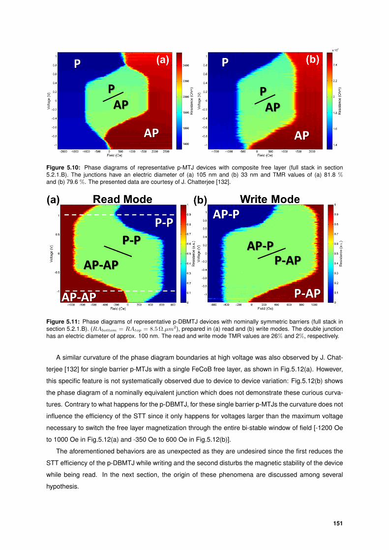
Figure 5.10: Phase diagrams of representative p-MTJ devices with composite free layer (full stack in section5.2.1.B). The junctions have an electric diameter of (a) 105 nm and (b) 33 nm and TMR values of (a) 81.8 %and (b) 79.6 %. The presented data are courtesy of J. Chatterjee [132].
Figure 5.11: Phase diagrams of representative p-DBMTJ devices with nominally symmetric barriers (full stack insection 5.2.1.B). (RAbottom = RAtop = 8.5 Ω.µm2), prepared in (a) read and (b) write modes. The double junctionhas an electric diameter of approx. 100 nm. The read and write mode TMR values are 26% and 2%, respectively.
A similar curvature of the phase diagram boundaries at high voltage was also observed by J. Chat-
terjee [132] for single barrier p-MTJs with a single FeCoB free layer, as shown in Fig.5.12(a). However,
this specific feature is not systematically observed due to device to device variation: Fig.5.12(b) shows
the phase diagram of a nominally equivalent junction which does not demonstrate these curious curva-
tures. Contrary to what happens for the p-DBMTJ, for these single barrier p-MTJs the curvature does not
influence the efficiency of the STT since it only happens for voltages larger than the maximum voltage
necessary to switch the free layer magnetization through the entire bi-stable window of field [-1200 Oe
to 1000 Oe in Fig.5.12(a) and -350 Oe to 600 Oe in Fig.5.12(b)].
The aforementioned behaviors are as unexpected as they are undesired since the first reduces the
STT efficiency of the p-DBMTJ while writing and the second disturbs the magnetic stability of the device
while being read. In the next section, the origin of these phenomena are discussed among several
hypothesis.
151
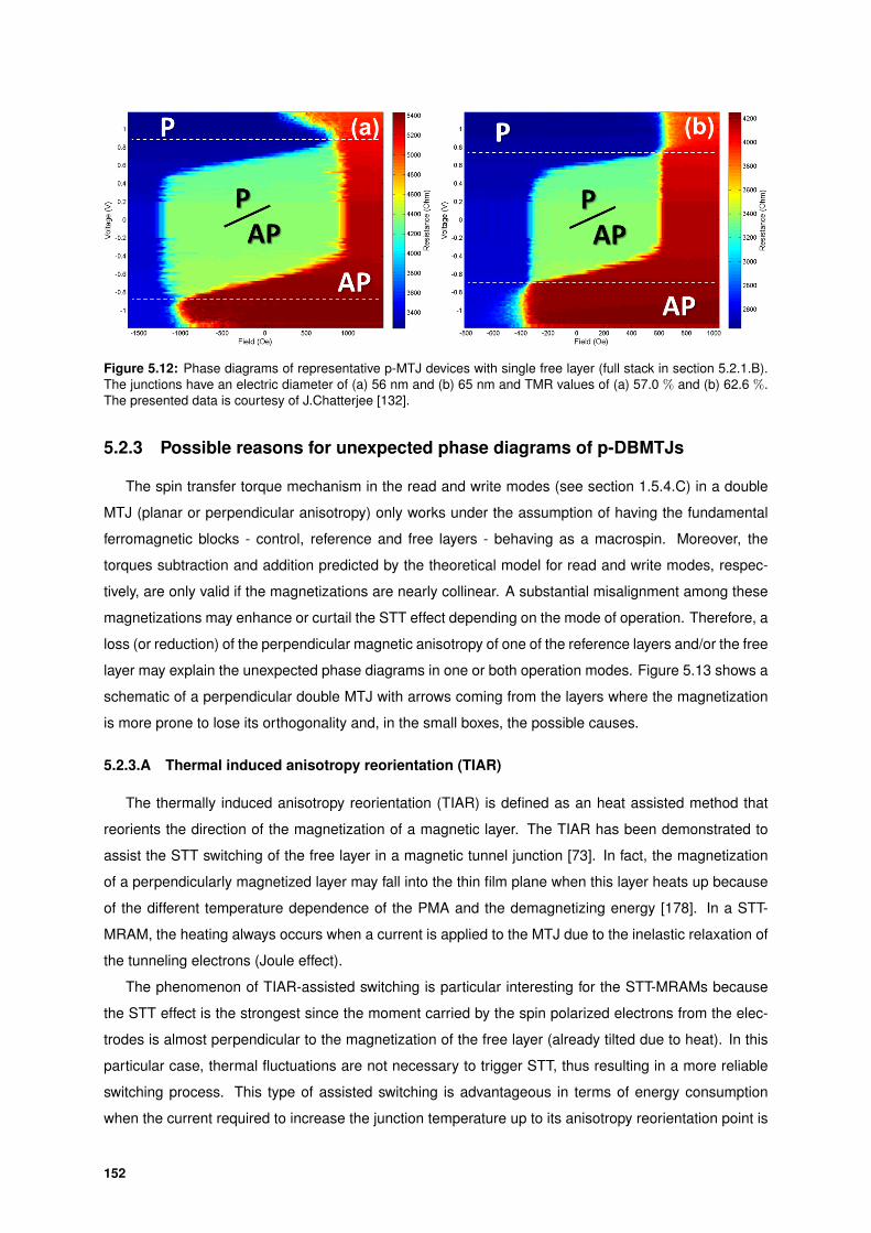
Figure 5.12: Phase diagrams of representative p-MTJ devices with single free layer (full stack in section 5.2.1.B).The junctions have an electric diameter of (a) 56 nm and (b) 65 nm and TMR values of (a) 57.0 % and (b) 62.6 %.The presented data is courtesy of J.Chatterjee [132].
5.2.3 Possible reasons for unexpected phase diagrams of p-DBMTJs
The spin transfer torque mechanism in the read and write modes (see section 1.5.4.C) in a double
MTJ (planar or perpendicular anisotropy) only works under the assumption of having the fundamental
ferromagnetic blocks - control, reference and free layers - behaving as a macrospin. Moreover, the
torques subtraction and addition predicted by the theoretical model for read and write modes, respec-
tively, are only valid if the magnetizations are nearly collinear. A substantial misalignment among these
magnetizations may enhance or curtail the STT effect depending on the mode of operation. Therefore, a
loss (or reduction) of the perpendicular magnetic anisotropy of one of the reference layers and/or the free
layer may explain the unexpected phase diagrams in one or both operation modes. Figure 5.13 shows a
schematic of a perpendicular double MTJ with arrows coming from the layers where the magnetization
is more prone to lose its orthogonality and, in the small boxes, the possible causes.
5.2.3.A Thermal induced anisotropy reorientation (TIAR)
The thermally induced anisotropy reorientation (TIAR) is defined as an heat assisted method that
reorients the direction of the magnetization of a magnetic layer. The TIAR has been demonstrated to
assist the STT switching of the free layer in a magnetic tunnel junction [73]. In fact, the magnetization
of a perpendicularly magnetized layer may fall into the thin film plane when this layer heats up because
of the different temperature dependence of the PMA and the demagnetizing energy [178]. In a STT-
MRAM, the heating always occurs when a current is applied to the MTJ due to the inelastic relaxation of
the tunneling electrons (Joule effect).
The phenomenon of TIAR-assisted switching is particular interesting for the STT-MRAMs because
the STT effect is the strongest since the moment carried by the spin polarized electrons from the elec-
trodes is almost perpendicular to the magnetization of the free layer (already tilted due to heat). In this
particular case, thermal fluctuations are not necessary to trigger STT, thus resulting in a more reliable
switching process. This type of assisted switching is advantageous in terms of energy consumption
when the current required to increase the junction temperature up to its anisotropy reorientation point is
152

Figure 5.13: Schematic of the possible reasons behind the reduction of perpendicular magnetic anisotropy of thefree layer and control layer, which may explain the undesired switchings in read mode and STT efficiency loss of thep-DBMTJ in write mode.
lower than the MTJ critical switching current. This condition has higher probabilities of being fulfilled in
a double barrier MTJ since the two MgO barriers act as thermal barriers [179] confining heat, especially
within the free layer.
Fig.5.14 shows a comparison between the phase diagram of Fig.5.8(a) of an asymmetric barriers p-
DBMTJ in read mode and the phase diagram obtained in a p-MTJ where TIAR-assisted current-induced
switching was observed [180]. The similarity between the two phase diagrams is substantial. In fact, the
behavior of the phase boundaries for both voltage polarities is identical. The only difference is that in the
phase diagram of Fig.5.14(a) the phase boundaries do not intersect the dashed line (center of the loop)
since higher voltage were not tried to avoid the double junction breakdown. Therefore, TIAR-assisted
switching may also be present in our p-DBMTJs.
5.2.3.B STT exerted on a polarizing layer
The reference magnetization, like the storage layer one, is subjected to STT but it is usually not
sufficient to induce magnetization dynamics or reversal. If the current is still applied after the free layer
switch, the torque on the reference may destabilize it (”back-torque”). In literature, the dynamics of
the reference layer (in perpendicularly magnetized MTJs) were seldom studied. Recently, L. Thomas
et al. [181] have reported experimental data on STT-induced dynamics of a SAF reference layer in p-
STT-MRAM devices. They observed mutual switching of the free and reference layers when the voltage
increases. This mutual torque is described as reminiscent of the Slonczewski windmill. Indeed, this
windmill torque effect with switching of both layers is only possible if, in the reference SAF, the soft layer
(adjacent to the MgO barrier) has higher magnetic moment than the hard layer. In the other scenario,
153

Figure 5.14: (a) Phase diagram of an asymmetric barriers perpendicular DBMTJ with a thicker bottom barrier(RAbottom = 60 Ω.µm2 and RAtop = 8.5 Ω.µm2), prepared in read mode. Same as in Fig.5.8(a). Next to (b) thephase diagram of a 110 nm diameter pillar of a single barrier p-MTJ where the switching happening at the appliedfield marked by the dashed red line is TIAR-assisted. This phase diagram correspond to Fig.17 in the paper [180]by Prejbeanu et al.
.
hard layer magnetic moment larger than soft layer one (same as the SAFs used in our p-DBMTJs),
the windmill is preceded by another dynamical regime, in which the soft layer magnetization tilts from
and precesses around the out-of-plane axis. This magnetization reorientation is the result of interplay
between the STT and the SAF exchange field.
Figure 5.15: Phase diagrams of a p-DBMTJ with nominally symmetric barriers (full stack in section 5.2.1.B).(RAbottom = RAtop = 8.5 Ω.µm2), prepared in read mode. The junction has an electric diameter of approx. 100nm. The read mode TMR is 26% (b) Illustration of the possible magnetization configuration of the p-DMTJ device inread mode for voltages above and below 1 V.
Unlike Ref. [181] we did not perform time-resolved resistance measurements, but some of the per-
formed finite voltage pulse phase diagrams showed evidence of an initial rotation of the reference layer.
A concrete example in p-DBMTJs is the curvature of the bi-stable area [in green in read mode phase
diagram of Fig.5.15(a)] for voltages above (below) 1 V (-1 V). Since the phase diagram only shows the
154
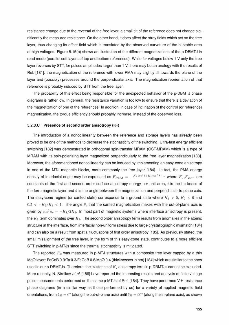
resistance change due to the reversal of the free layer, a small tilt of the reference does not change sig-
nificantly the measured resistance. On the other hand, it does affect the stray fields which act on the free
layer, thus changing its offset field which is translated by the observed curvature of the bi-stable area
at high voltages. Figure 5.15(b) shows an illustration of the different magnetizations of the p-DBMTJ in
read mode (parallel soft layers of top and bottom references). While for voltages below 1 V only the free
layer reverses by STT, for pulses amplitudes larger than 1 V, there may be an analogy with the results of
Ref. [181]: the magnetization of the reference with lower PMA may slightly tilt towards the plane of the
layer and (possibly) precesses around the perpendicular axis. The magnetization reorientation of that
reference is probably induced by STT from the free layer.
The probability of this effect being responsible for the unexpected behavior of the p-DBMTJ phase
diagrams is rather low. In general, the resistance variation is too low to ensure that there is a deviation of
the magnetization of one of the references. In addition, in case of inclination of the control (or reference)
magnetization, the torque efficiency should probably increase, instead of the observed loss.
5.2.3.C Presence of second order anisotropy (K2)
The introduction of a noncollinearity between the reference and storage layers has already been
proved to be one of the methods to decrease the stochasticity of the switching. Ultra-fast energy efficient
switching [182] was demonstrated in orthogonal spin-transfer MRAM (OST-MRAM) which is a type of
MRAM with its spin-polarizing layer magnetized perpendicularly to the free layer magnetization [183].
Moreover, the aforementioned noncollinearity can be induced by implementing an easy-cone anisotropy
in one of the MTJ magnetic blocks, more commonly the free layer [184]. In fact, the PMA energy
density of interfacial origin may be expressed as EPMA = −K1 cos2 θ+K2 cos4 θ+...t where K1,K2,... are
constants of the first and second order surface anisotropy energy per unit area, t is the thickness of
the ferromagnetic layer and θ is the angle between the magnetization and perpendicular to plane axis.
The easy-cone regime (or canted state) corresponds to a ground state where K1 > 0, K2 < 0 and
0.5 < −K2/K1 < 1. The angle θc that the canted magnetization makes with the out-of-plane axis is
given by cos2 θc = −K1/2K2. In most part of magnetic systems where interface anisotropy is present,
the K1 term dominates over K2. The second order anisotropy term results from anomalies in the atomic
structure at the interface, from interfacial non-uniform stress due to large crystallographic mismatch [184]
and can also be a result from spatial fluctuations of first order anisotropy [185]. As previously stated, the
small misalignment of the free layer, in the form of this easy-cone state, contributes to a more efficient
STT switching in p-MTJs since the thermal stochasticity is mitigated.
The reported K2 was measured in p-MTJ structures with a composite free layer capped by a thin
MgO layer: FeCoB 0.9/Ta 0.3/FeCoB 0.8/MgO 0.4 (thicknesses in nm) [184] which are similar to the ones
used in our p-DBMTJs. Therefore, the existence ofK2 anisotropy term in p-DBMTJs cannot be excluded.
More recently, N. Strelkov et al. [186] have reported the interesting results and analysis of finite voltage
pulse measurements performed on the same p-MTJs of Ref. [184]. They have performed V-H resistance
phase diagrams (in a similar way as those performed by us) for a variety of applied magnetic field
orientations, from θH = 0 (along the out-of-plane axis) until θH = 90 (along the in-plane axis), as shown
155
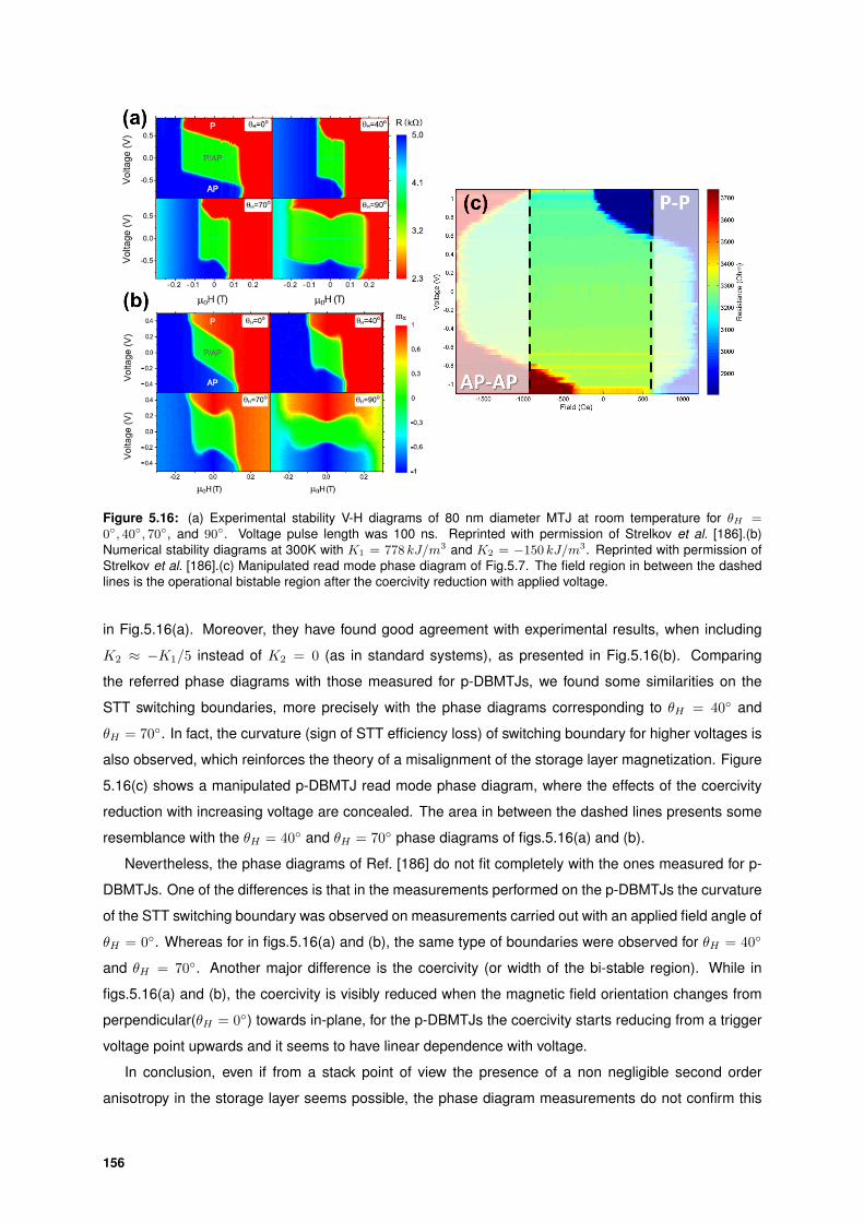
Figure 5.16: (a) Experimental stability V-H diagrams of 80 nm diameter MTJ at room temperature for θH =0, 40, 70, and 90. Voltage pulse length was 100 ns. Reprinted with permission of Strelkov et al. [186].(b)Numerical stability diagrams at 300K with K1 = 778 kJ/m3 and K2 = −150 kJ/m3. Reprinted with permission ofStrelkov et al. [186].(c) Manipulated read mode phase diagram of Fig.5.7. The field region in between the dashedlines is the operational bistable region after the coercivity reduction with applied voltage.
in Fig.5.16(a). Moreover, they have found good agreement with experimental results, when including
K2 ≈ −K1/5 instead of K2 = 0 (as in standard systems), as presented in Fig.5.16(b). Comparing
the referred phase diagrams with those measured for p-DBMTJs, we found some similarities on the
STT switching boundaries, more precisely with the phase diagrams corresponding to θH = 40 and
θH = 70. In fact, the curvature (sign of STT efficiency loss) of switching boundary for higher voltages is
also observed, which reinforces the theory of a misalignment of the storage layer magnetization. Figure
5.16(c) shows a manipulated p-DBMTJ read mode phase diagram, where the effects of the coercivity
reduction with increasing voltage are concealed. The area in between the dashed lines presents some
resemblance with the θH = 40 and θH = 70 phase diagrams of figs.5.16(a) and (b).
Nevertheless, the phase diagrams of Ref. [186] do not fit completely with the ones measured for p-
DBMTJs. One of the differences is that in the measurements performed on the p-DBMTJs the curvature
of the STT switching boundary was observed on measurements carried out with an applied field angle of
θH = 0. Whereas for in figs.5.16(a) and (b), the same type of boundaries were observed for θH = 40
and θH = 70. Another major difference is the coercivity (or width of the bi-stable region). While in
figs.5.16(a) and (b), the coercivity is visibly reduced when the magnetic field orientation changes from
perpendicular(θH = 0) towards in-plane, for the p-DBMTJs the coercivity starts reducing from a trigger
voltage point upwards and it seems to have linear dependence with voltage.
In conclusion, even if from a stack point of view the presence of a non negligible second order
anisotropy in the storage layer seems possible, the phase diagram measurements do not confirm this
156
possibility. The angle reorientation of the magnetization does not appear to be consistent with an easy-
cone state but dependent of the amplitude of the applied voltage pulses.
5.2.3.D Voltage Controlled Magnetic Anisotropy
As previously mentioned Fe-rich FeCoB presents high perpendicular magnetic anisotropy at the in-
terface with oxides as MgO which is, consequently, sensitive to voltages applied across the dielectric
layer [187]. The PMA of FeCoB varies with its thickness and near the critical transition (perpendicular to
in-plane), the magnetization configuration is more sensitive to external voltages [188] and thus enabling
the realization of electric-field-controlled MTJ devices. This possibility of changing the PMA at ferromag-
net/oxide interface by applying an electric field is often called voltage controlled magnetic anisotropy
(VCMA).
Despite the enormous potential of STT-MRAM as a versatile non-volatile memory, it still presents
some drawbacks in energy efficiency. The need for driving significant charge currents through the device
to switch by STT, together with a nonzero voltage drop across the MTJ leads to a considerable power
dissipation. The use of voltage rather than current to control magnetization allows for a decrease of the
dissipated power since no charge flow is usually required in such type of structures based on voltage
controlled effects. Although most of the electric field controlled PMA effects have been demonstrated in
samples grown by molecular beam epitaxy, Wang et al. [189] presented the first device, deposited by
sputtering, whose magnetization could be reversed by an electric field. Moreover, the manipulation of
magnetic anisotropy through voltage has been proven to be dependent on its polarity [190]. Thus, the
direction of the applied electric field dictates the increase or decrease of the magnetic anisotropy energy.
In our p-DBMTJs, the used voltages to switch the free layer magnetization correspond to energies of
the order 10−11 J which are some orders of magnitude higher than the ones used in VCMA experiments
(10−15 J) [191]. Moreover, the MgO barriers used are quite thin, corresponding to RA values, at least,
two orders of magnitude lower than the ones used in VCMA reported experiments. In fact, the VCMA
effect was mostly observed in high-resistance MTJs, where the STT is suppressed due to small leakage
currents [187]. Unlike STT-MRAM, in VCMA memory devices the leakage current is small, thus the
electric field across the tunnel barrier (i.e. the applied voltage) is able to control the switching behavior.
Besides the previous reasons, VCMA is polarity dependent which does not agree with our obtained
results (see figs.5.7 and 5.11) where the loss of PMA happens for both voltage polarities.
In conclusion, although applied voltage (translated as an electric field) has been proven to control
the magnetization spatial orientation of ferromagnetic layers, VCMA stands as the least probable reason
for the loss of STT efficiency and unexpected behaviors observed in our p-DBMTJs.
5.2.3.E Thermal reduction of anisotropy
In Fig.5.17, we observe an important reduction of coercivity with applied voltage. At negative field,
this reduction of coercive field is nearly the same for positive and negative voltage 9. This independence
with voltage sign suggests Joule heating and a subsequent decrease of perpendicular anisotropy with9At positive field, the interplay between thermal effect and residual STT is more visible
157
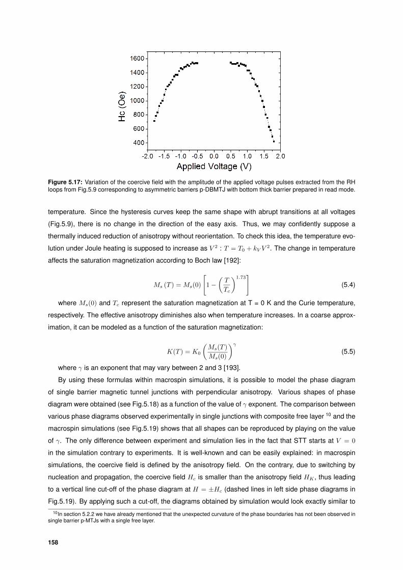
Figure 5.17: Variation of the coercive field with the amplitude of the applied voltage pulses extracted from the RHloops from Fig.5.9 corresponding to asymmetric barriers p-DBMTJ with bottom thick barrier prepared in read mode.
temperature. Since the hysteresis curves keep the same shape with abrupt transitions at all voltages
(Fig.5.9), there is no change in the direction of the easy axis. Thus, we may confidently suppose a
thermally induced reduction of anisotropy without reorientation. To check this idea, the temperature evo-
lution under Joule heating is supposed to increase as V 2 : T = T0 + kV V2. The change in temperature
affects the saturation magnetization according to Boch law [192]:
Ms (T ) = Ms(0)
[1−
(T
Tc
)1.73]
(5.4)
where Ms(0) and Tc represent the saturation magnetization at T = 0 K and the Curie temperature,
respectively. The effective anisotropy diminishes also when temperature increases. In a coarse approx-
imation, it can be modeled as a function of the saturation magnetization:
K(T ) = K0
(Ms(T )
Ms(0)
)γ(5.5)
where γ is an exponent that may vary between 2 and 3 [193].
By using these formulas within macrospin simulations, it is possible to model the phase diagram
of single barrier magnetic tunnel junctions with perpendicular anisotropy. Various shapes of phase
diagram were obtained (see Fig.5.18) as a function of the value of γ exponent. The comparison between
various phase diagrams observed experimentally in single junctions with composite free layer 10 and the
macrospin simulations (see Fig.5.19) shows that all shapes can be reproduced by playing on the value
of γ. The only difference between experiment and simulation lies in the fact that STT starts at V = 0
in the simulation contrary to experiments. It is well-known and can be easily explained: in macrospin
simulations, the coercive field is defined by the anisotropy field. On the contrary, due to switching by
nucleation and propagation, the coercive field Hc is smaller than the anisotropy field HK , thus leading
to a vertical line cut-off of the phase diagram at H = ±Hc (dashed lines in left side phase diagrams in
Fig.5.19). By applying such a cut-off, the diagrams obtained by simulation would look exactly similar to10In section 5.2.2 we have already mentioned that the unexpected curvature of the phase boundaries has not been observed in
single barrier p-MTJs with a single free layer.
158
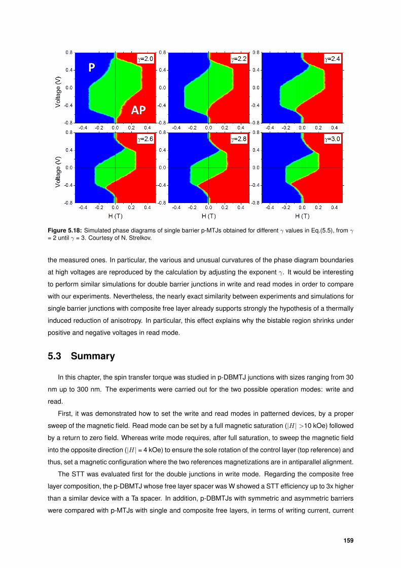
Figure 5.18: Simulated phase diagrams of single barrier p-MTJs obtained for different γ values in Eq.(5.5), from γ= 2 until γ = 3. Courtesy of N. Strelkov.
the measured ones. In particular, the various and unusual curvatures of the phase diagram boundaries
at high voltages are reproduced by the calculation by adjusting the exponent γ. It would be interesting
to perform similar simulations for double barrier junctions in write and read modes in order to compare
with our experiments. Nevertheless, the nearly exact similarity between experiments and simulations for
single barrier junctions with composite free layer already supports strongly the hypothesis of a thermally
induced reduction of anisotropy. In particular, this effect explains why the bistable region shrinks under
positive and negative voltages in read mode.
5.3 Summary
In this chapter, the spin transfer torque was studied in p-DBMTJ junctions with sizes ranging from 30
nm up to 300 nm. The experiments were carried out for the two possible operation modes: write and
read.
First, it was demonstrated how to set the write and read modes in patterned devices, by a proper
sweep of the magnetic field. Read mode can be set by a full magnetic saturation (|H| >10 kOe) followed
by a return to zero field. Whereas write mode requires, after full saturation, to sweep the magnetic field
into the opposite direction (|H| = 4 kOe) to ensure the sole rotation of the control layer (top reference) and
thus, set a magnetic configuration where the two references magnetizations are in antiparallel alignment.
The STT was evaluated first for the double junctions in write mode. Regarding the composite free
layer composition, the p-DBMTJ whose free layer spacer was W showed a STT efficiency up to 3x higher
than a similar device with a Ta spacer. In addition, p-DBMTJs with symmetric and asymmetric barriers
were compared with p-MTJs with single and composite free layers, in terms of writing current, current
159

Figure 5.19: Comparison between experimental (P state in dark blue and AP state in dark red) and simulated(P state in light blue and AP state in light red)) phase diagrams for single barrier p-MTJ. The experimental phasediagrams were obtained for measurements performed in single barrier p-MTJs with composite free layer. In thesimulated phase diagram at the left, the dashed lines represent Hc and the solid lines represent HK . Cortesy of N.Strelkov.
density and thermal stability factor. In general, the less current consuming device was the asymmetric
barriers p-DBMTJ with a thick bottom barrier which exhibited a reduction of approximately 3x in writing
current when compared to a single barrier p-MTJ with single free layer. In terms of STT switching
efficiency, which was represented by the figure of merit ∆/Ic, both p-DBMTJs presented better results
than the single free layer p-MTJ. In 45 nm devices, ∆/Ic = 1.5µA−1 for asymmetric barriers p-DBMTJs
while for the single free layer p-MTJ, ∆/Ic = 0.25µA−1 which translates in an efficiency gain of 6x.
On the other hand, the efficiency gain was only of 1.5x when compared to a p-MTJ with a composite
free layer which usually possesses a higher PMA. Between the symmetric and asymmetric barriers p-
DBMTJs, the one with a thicker bottom barrier presented higher STT efficiency probably due to an higher
TMR exhibited by the thickest barrier.
In read mode, at H = Hoff , no switching is observed at voltages that produce switching in write mode.
Although switching is thus prevented in read mode, we observe that the bistable region significantly
shrinks at high voltage, which reduces the stability of the data. Several possible explanations to the unex-
pected read mode behavior were proposed and studied. The most probable is ascribed to a temperature
rise due to Joule effect and heat confinement between the two MgO barriers. This increase of temper-
ature produces a reduction of the saturation magnetization and of the effective anisotropy. Macrospin
numerical simulation taking into account this effect reproduce well the distortions of the phase diagram
160

observed in single junctions with composite free layer, identical to the free layer of the p-DBMTJs. Sim-
ilar distortions observed in the phase diagrams of p-DBMTJ are, therefore, most probably due to the
same effect.
161

162
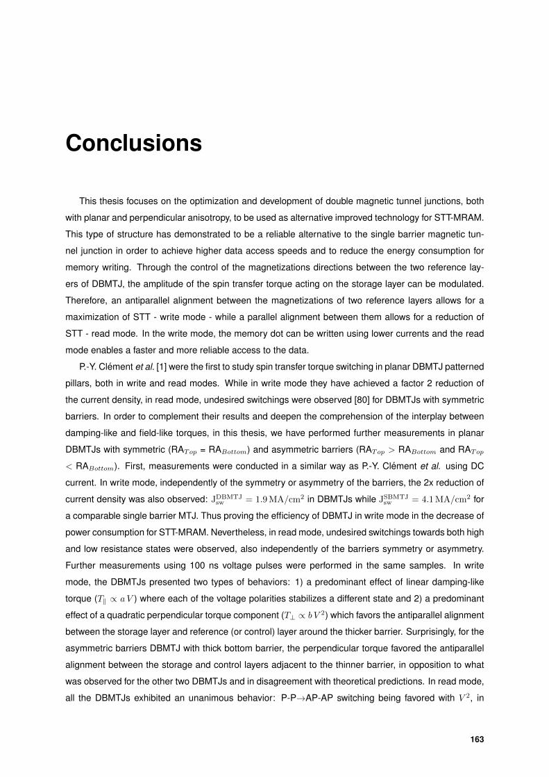
Conclusions
This thesis focuses on the optimization and development of double magnetic tunnel junctions, both
with planar and perpendicular anisotropy, to be used as alternative improved technology for STT-MRAM.
This type of structure has demonstrated to be a reliable alternative to the single barrier magnetic tun-
nel junction in order to achieve higher data access speeds and to reduce the energy consumption for
memory writing. Through the control of the magnetizations directions between the two reference lay-
ers of DBMTJ, the amplitude of the spin transfer torque acting on the storage layer can be modulated.
Therefore, an antiparallel alignment between the magnetizations of two reference layers allows for a
maximization of STT - write mode - while a parallel alignment between them allows for a reduction of
STT - read mode. In the write mode, the memory dot can be written using lower currents and the read
mode enables a faster and more reliable access to the data.
P.-Y. Clement et al. [1] were the first to study spin transfer torque switching in planar DBMTJ patterned
pillars, both in write and read modes. While in write mode they have achieved a factor 2 reduction of
the current density, in read mode, undesired switchings were observed [80] for DBMTJs with symmetric
barriers. In order to complement their results and deepen the comprehension of the interplay between
damping-like and field-like torques, in this thesis, we have performed further measurements in planar
DBMTJs with symmetric (RATop = RABottom) and asymmetric barriers (RATop > RABottom and RATop
< RABottom). First, measurements were conducted in a similar way as P.-Y. Clement et al. using DC
current. In write mode, independently of the symmetry or asymmetry of the barriers, the 2x reduction of
current density was also observed: JDBMTJsw = 1.9 MA/cm2 in DBMTJs while JSBMTJ
sw = 4.1 MA/cm2 for
a comparable single barrier MTJ. Thus proving the efficiency of DBMTJ in write mode in the decrease of
power consumption for STT-MRAM. Nevertheless, in read mode, undesired switchings towards both high
and low resistance states were observed, also independently of the barriers symmetry or asymmetry.
Further measurements using 100 ns voltage pulses were performed in the same samples. In write
mode, the DBMTJs presented two types of behaviors: 1) a predominant effect of linear damping-like
torque (T‖ ∝ a V ) where each of the voltage polarities stabilizes a different state and 2) a predominant
effect of a quadratic perpendicular torque component (T⊥ ∝ b V 2) which favors the antiparallel alignment
between the storage layer and reference (or control) layer around the thicker barrier. Surprisingly, for the
asymmetric barriers DBMTJ with thick bottom barrier, the perpendicular torque favored the antiparallel
alignment between the storage and control layers adjacent to the thinner barrier, in opposition to what
was observed for the other two DBMTJs and in disagreement with theoretical predictions. In read mode,
all the DBMTJs exhibited an unanimous behavior: P-P→AP-AP switching being favored with V 2, in
163
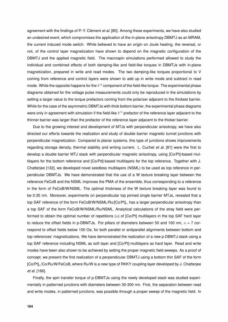
agreement with the findings of P.-Y. Clement et al. [80]. Among these experiments, we have also studied
an undesired event, which compromises the application of the in-plane anisotropy DBMTJ as an MRAM,
the current induced mode switch. While believed to have an origin on Joule heating, the reversal, or
not, of the control layer magnetization have shown to depend on the magnetic configuration of the
DBMTJ and the applied magnetic field. The macrospin simulations performed allowed to study the
individual and combined effects of both damping-like and field-like torques in DBMTJs with in-plane
magnetization, prepared in write and read modes. The two damping-like torques proportional to V
coming from reference and control layers were shown to add up in write mode and subtract in read
mode. While the opposite happens for the V 2 component of the field-like torque. The experimental phase
diagrams obtained for the voltage pulse measurements could only be reproduced in the simulations by
setting a larger value to the torque prefactors coming from the polarizer adjacent to the thickest barrier.
While for the case of the asymmetric DBMTJs with thick bottom barrier, the experimental phase diagrams
were only in agreement with simulation if the field-like V 2 prefactor of the reference layer adjacent to the
thinner barrier was larger than the prefactor of the reference layer adjacent to the thicker barrier.
Due to the growing interest and development of MTJs with perpendicular anisotropy, we have also
directed our efforts towards the realization and study of double barrier magnetic tunnel junctions with
perpendicular magnetization. Compared to planar systems, this type of junctions shows improvements
regarding storage density, thermal stability and writing current. L. Cuchet et al. [81] were the first to
develop a double barrier MTJ stack with perpendicular magnetic anisotropy, using [Co/Pt]-based mul-
tilayers for the bottom reference and [Co/Pd]-based multilayers for the top reference. Together with J.
Chatterjee [132], we developed novel seedless multilayers (NSML) to be used as top reference in per-
pendicular DBMTJs. We have demonstrated that the use of a W texture breaking layer between the
reference FeCoB and the NSML improves the PMA of the ensemble, thus corresponding to a reference
in the form of FeCoB/W/NSML. The optimal thickness of the W texture breaking layer was found to
be 0.35 nm. Moreover, experiments on perpendicular top pinned single barrier MTJs, revealed that a
top SAF reference of the form FeCoB/W/NSML/Ru/[Co/Pt]n has a larger perpendicular anisotropy than
a top SAF of the form FeCoB/W/NSML/Ru/NSML. Analytical calculations of the stray field were per-
formed to obtain the optimal number of repetitions (n) of [Co/Pt] multilayers in the top SAF hard layer
to reduce the offset fields in p-DBMTJs. For pillars of diameters between 50 and 100 nm, n = 7 cor-
respond to offset fields below 100 Oe, for both parallel or antiparallel alignments between bottom and
top references’ magnetizations. We have demonstrated the realization of a new p-DBMTJ stack using a
top SAF reference including NSML as soft layer and [Co/Pt]-multilayers as hard layer. Read and write
modes have been also shown to be achieved by setting the proper magnetic field sweeps. As a proof of
concept, we present the first realization of a perpendicular DBMTJ using a bottom thin SAF of the form
[Co/Pt]n/Co/Ru/W/FeCoB, where Ru/W is a new type of RKKY coupling layer developed by J. Chatterjee
et al. [166].
Finally, the spin transfer torque of p-DBMTJs using the newly developed stack was studied experi-
mentally in patterned junctions with diameters between 30-300 nm. First, the separation between read
and write modes, in patterned junctions, was possible through a proper sweep of the magnetic field. In
164
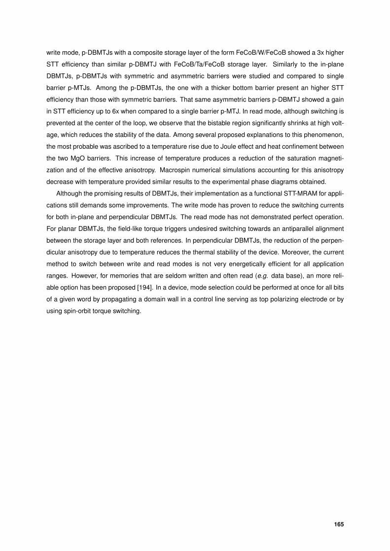
write mode, p-DBMTJs with a composite storage layer of the form FeCoB/W/FeCoB showed a 3x higher
STT efficiency than similar p-DBMTJ with FeCoB/Ta/FeCoB storage layer. Similarly to the in-plane
DBMTJs, p-DBMTJs with symmetric and asymmetric barriers were studied and compared to single
barrier p-MTJs. Among the p-DBMTJs, the one with a thicker bottom barrier present an higher STT
efficiency than those with symmetric barriers. That same asymmetric barriers p-DBMTJ showed a gain
in STT efficiency up to 6x when compared to a single barrier p-MTJ. In read mode, although switching is
prevented at the center of the loop, we observe that the bistable region significantly shrinks at high volt-
age, which reduces the stability of the data. Among several proposed explanations to this phenomenon,
the most probable was ascribed to a temperature rise due to Joule effect and heat confinement between
the two MgO barriers. This increase of temperature produces a reduction of the saturation magneti-
zation and of the effective anisotropy. Macrospin numerical simulations accounting for this anisotropy
decrease with temperature provided similar results to the experimental phase diagrams obtained.
Although the promising results of DBMTJs, their implementation as a functional STT-MRAM for appli-
cations still demands some improvements. The write mode has proven to reduce the switching currents
for both in-plane and perpendicular DBMTJs. The read mode has not demonstrated perfect operation.
For planar DBMTJs, the field-like torque triggers undesired switching towards an antiparallel alignment
between the storage layer and both references. In perpendicular DBMTJs, the reduction of the perpen-
dicular anisotropy due to temperature reduces the thermal stability of the device. Moreover, the current
method to switch between write and read modes is not very energetically efficient for all application
ranges. However, for memories that are seldom written and often read (e.g. data base), an more reli-
able option has been proposed [194]. In a device, mode selection could be performed at once for all bits
of a given word by propagating a domain wall in a control line serving as top polarizing electrode or by
using spin-orbit torque switching.
165

166
Bibliography
[1] P.-Y. Clement, Transport electronique dans les jonctions tunnel magnetiques a double barriere.
PhD thesis, Universite de Grenoble, 2014.
[2] W. Thomson, “Xix. on the electro-dynamic qualities of metals:—effects of magnetization on the
electric conductivity of nickel and of iron,” Proceedings of the Royal Society of London, vol. 8,
pp. 546–550, 1857.
[3] M. N. Baibich, J. M. Broto, A. Fert, F. N. Van Dau, F. Petroff, P. Etienne, G. Creuzet, A. Friederich,
and J. Chazelas, “Giant magnetoresistance of (001) fe/(001) cr magnetic superlattices,” Physical
review letters, vol. 61, no. 21, p. 2472, 1988.
[4] G. Binasch, P. Grunberg, F. Saurenbach, and W. Zinn, “Enhanced magnetoresistance in layered
magnetic structures with antiferromagnetic interlayer exchange,” Physical review B, vol. 39, no. 7,
p. 4828, 1989.
[5] S. Wolf, D. Awschalom, R. Buhrman, J. Daughton, S. Von Molnar, M. Roukes, A. Y. Chtchelkanova,
and D. Treger, “Spintronics: a spin-based electronics vision for the future,” Science, vol. 294,
no. 5546, pp. 1488–1495, 2001.
[6] B. Dieny, V. S. Speriosu, S. S. Parkin, B. A. Gurney, D. R. Wilhoit, and D. Mauri, “Giant magne-
toresistive in soft ferromagnetic multilayers,” Physical Review B, vol. 43, no. 1, p. 1297, 1991.
[7] H. Fukuzawa, H. Yuasa, S. Hashimoto, K. Koi, H. Iwasaki, M. Takagishi, Y. Tanaka, and M. Sa-
hashi, “Mr ratio enhancement by nol current-confined-path structures in cpp spin valves,” IEEE
Transactions on Magnetics, vol. 40, no. 4, pp. 2236–2238, 2004.
[8] J. S. Moodera, L. R. Kinder, T. M. Wong, and R. Meservey, “Large magnetoresistance at room
temperature in ferromagnetic thin film tunnel junctions,” Physical review letters, vol. 74, no. 16,
p. 3273, 1995.
[9] M. B. Stearns, “Simple explanation of tunneling spin-polarization of fe, co, ni and its alloys,” Journal
of Magnetism and Magnetic Materials, vol. 5, no. 2, pp. 167–171, 1977.
[10] E. C. Stoner, “Collective electron ferromagnetism in metals and alloys,” J. phys. radium, vol. 12,
no. 3, pp. 372–388, 1951.
[11] A. Fert and I. Campbell, “Two-current conduction in nickel,” Physical Review Letters, vol. 21, no. 16,
p. 1190, 1968.
167
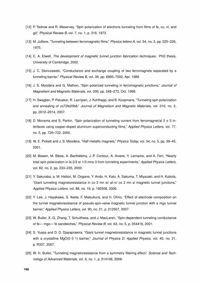
[12] P. Tedrow and R. Meservey, “Spin polarization of electrons tunneling from films of fe, co, ni, and
gd,” Physical Review B, vol. 7, no. 1, p. 318, 1973.
[13] M. Julliere, “Tunneling between ferromagnetic films,” Physics letters A, vol. 54, no. 3, pp. 225–226,
1975.
[14] C. A. Elwell, The development of magnetic tunnel junction fabrication techniques. PhD thesis,
University of Cambridge, 2002.
[15] J. C. Slonczewski, “Conductance and exchange coupling of two ferromagnets separated by a
tunneling barrier,” Physical Review B, vol. 39, pp. 6995–7002, Apr. 1989.
[16] J. S. Moodera and G. Mathon, “Spin polarized tunneling in ferromagnetic junctions,” Journal of
Magnetism and Magnetic Materials, vol. 200, pp. 248–273, Oct. 1999.
[17] H. Swagten, P. Paluskar, R. Lavrijsen, J. Kohlhepp, and B. Koopmans, “Tunneling spin polarization
and annealing of co72fe20b8,” Journal of Magnetism and Magnetic Materials, vol. 310, no. 2,
pp. 2012–2014, 2007.
[18] D. Monsma and S. Parkin, “Spin polarization of tunneling current from ferromagnet/al 2 o 3 in-
terfaces using copper-doped aluminum superconducting films,” Applied Physics Letters, vol. 77,
no. 5, pp. 720–722, 2000.
[19] W. E. Pickett and J. S. Moodera, “Half metallic magnets,” Physics Today, vol. 54, no. 5, pp. 39–45,
2001.
[20] M. Bowen, M. Bibes, A. Barthelemy, J.-P. Contour, A. Anane, Y. Lemaıtre, and A. Fert, “Nearly
total spin polarization in la 2/3 sr 1/3 mno 3 from tunneling experiments,” Applied Physics Letters,
vol. 82, no. 2, pp. 233–235, 2003.
[21] Y. Sakuraba, a. M. Hattori, M. Oogane, Y. Ando, H. Kato, A. Sakuma, T. Miyazaki, and H. Kubota,
“Giant tunneling magnetoresistance in co 2 mn si/ al–o/ co 2 mn si magnetic tunnel junctions,”
Applied Physics Letters, vol. 88, no. 19, p. 192508, 2006.
[22] Y. Lee, J. Hayakawa, S. Ikeda, F. Matsukura, and H. Ohno, “Effect of electrode composition on
the tunnel magnetoresistance of pseudo-spin-valve magnetic tunnel junction with a mgo tunnel
barrier,” Applied Physics Letters, vol. 90, no. 21, p. 212507, 2007.
[23] W. Butler, X.-G. Zhang, T. Schulthess, and J. MacLaren, “Spin-dependent tunneling conductance
of fe— mgo— fe sandwiches,” Physical Review B, vol. 63, no. 5, p. 054416, 2001.
[24] S. Yuasa and D. D. Djayaprawira, “Giant tunnel magnetoresistance in magnetic tunnel junctions
with a crystalline MgO(0 0 1) barrier,” Journal of Physics D: Applied Physics, vol. 40, no. 21,
p. R337, 2007.
[25] W. H. Butler, “Tunneling magnetoresistance from a symmetry filtering effect,” Science and Tech-
nology of Advanced Materials, vol. 9, no. 1, p. 014106, 2008.
168
[26] X.-G. Zhang and W. Butler, “Large magnetoresistance in bcc co/ mg o/ co and fe co/ mg o/ fe co
tunnel junctions,” Physical Review B, vol. 70, no. 17, p. 172407, 2004.
[27] S. Yuasa, A. Fukushima, T. Nagahama, K. Ando, and Y. Suzuki, “High tunnel magnetoresistance
at room temperature in fully epitaxial fe/mgo/fe tunnel junctions due to coherent spin-polarized
tunneling,” Japanese Journal of Applied Physics, vol. 43, no. 4B, p. L588, 2004.
[28] S. S. Parkin, C. Kaiser, A. Panchula, P. M. Rice, B. Hughes, M. Samant, and S.-H. Yang, “Gi-
ant tunnelling magnetoresistance at room temperature with mgo (100) tunnel barriers,” Nature
materials, vol. 3, no. 12, p. 862, 2004.
[29] X. Zhang, B.-Z. Li, G. Sun, and F.-C. Pu, “Spin-polarized tunneling and magnetoresistance in
ferromagnet/insulator(semiconductor) single and double tunnel junctions subjected to an electric
field,” Physical Review B, vol. 56, pp. 5484–5488, Sept. 1997.
[30] M. Watanabe, T. Suemasu, S. Muratake, and M. Asada, “Negative differential resistance of metal
(cosi2)/insulator (caf2) triple-barrier resonant tunneling diode,” Applied physics letters, vol. 62,
no. 3, pp. 300–302, 1993.
[31] F. Montaigne, J. Nassar, A. Vaures, F. N. Van Dau, F. Petroff, A. Schuhl, and A. Fert, “Enhanced
tunnel magnetoresistance at high bias voltage in double-barrier planar junctions,” Applied Physics
Letters, vol. 73, pp. 2829–2831, Nov. 1998.
[32] M. Wilczynski and J. Barnas, “Tunnel magnetoresistance in ferromagnetic double-barrier planar
junctions: coherent tunneling regime,” Journal of magnetism and magnetic materials, vol. 221,
no. 3, pp. 373–381, 2000.
[33] M. Chshiev, D. Stoeffler, A. Vedyayev, and K. Ounadjela, “Magnetic diode effect in double-barrier
tunnel junctions,” EPL (Europhysics Letters), vol. 58, no. 2, p. 257, 2002.
[34] A. Iovan, S. Andersson, Y. G. Naidyuk, A. Vedyaev, B. Dieny, and V. Korenivski, “Spin diode based
on fe/mgo double tunnel junction,” Nano letters, vol. 8, no. 3, pp. 805–809, 2008.
[35] T. Nozaki, N. Tezuka, and K. Inomata, “Quantum oscillation of the tunneling conductance in
fully epitaxial double barrier magnetic tunnel junctions,” Physical review letters, vol. 96, no. 2,
p. 027208, 2006.
[36] B. Tao, H. Yang, Y. Zuo, X. Devaux, G. Lengaigne, M. Hehn, D. Lacour, S. Andrieu, M. Chshiev,
T. Hauet, et al., “Long-range phase coherence in double-barrier magnetic tunnel junctions with a
large thick metallic quantum well,” Physical review letters, vol. 115, no. 15, p. 157204, 2015.
[37] Z. Diao, A. Panchula, Y. Ding, M. Pakala, S. Wang, Z. Li, D. Apalkov, H. Nagai, A. Driskill-Smith,
L.-C. Wang, E. Chen, and Y. Huai, “Spin transfer switching in dual MgO magnetic tunnel junctions,”
Applied Physics Letters, vol. 90, p. 132508, Mar. 2007.
169
[38] H. D. Gan, S. Ikeda, W. Shiga, J. Hayakawa, K. Miura, H. Yamamoto, H. Hasegawa, F. Matsukura,
T. Ohkubo, K. Hono, and H. Ohno, “Tunnel magnetoresistance properties and film structures of
double MgO barrier magnetic tunnel junctions,” Applied Physics Letters, vol. 96, p. 192507, May
2010.
[39] W. Feng, C. Fowley, K. Bernert, V. Sluka, E. Kowalska, Y. Aleksandrov, J. Lindner, J. Fassbender,
H. D. Gan, A. Kunz, R. Hubner, J. M. D. Coey, and A. M. Deac, “Effect of Deposition Conditions and
Annealing Temperature on Tunnel Magnetoresistance and the Structure of MgO-Based Double-
Barrier Magnetic Tunnel Junctions,” IEEE Transactions on Magnetics, vol. 51, pp. 1–4, Nov. 2015.
[40] G. Hu, J. H. Lee, J. J. Nowak, J. Z. Sun, J. Harms, A. Annunziata, S. Brown, W. Chen, Y. H. Kim,
G. Lauer, L. Liu, N. Marchack, S. Murthy, E. J. O’Sullivan, J. H. Park, M. Reuter, R. P. Robertazzi,
P. L. Trouilloud, Y. Zhu, and D. C. Worledge, “STT-MRAM with double magnetic tunnel junctions,”
in 2015 IEEE International Electron Devices Meeting (IEDM), pp. 26.3.1–26.3.4, Dec. 2015.
[41] Z. Duan, S. Schafer, V. Voznyuk, X. Tang, G. Feng, D. Lee, L. Zheng, D. Apalkov, R. Beach, and
V. Nikitin, “High TMR Dual-MTJ STT-MRAM Design with Perpendicular Magnetic Anisotropy,” in
2017 Conference on Magnetism and Magnetic Materials (MMM), (Pittsburgh), 2017.
[42] C. Baraduc, M. Chshiev, and U. Ebels, “Introduction to spin transfer torque,” in Nanomagnetism
And Spintronics: Fabrication, Materials, Characterization and Applications, pp. 173–192, World
Scientific, 2011.
[43] J. C. Slonczewski, “Currents, torques, and polarization factors in magnetic tunnel junctions,” Phys-
ical Review B, vol. 71, p. 024411, Jan. 2005.
[44] J. C. Slonczewski, “Current-driven excitation of magnetic multilayers,” Journal of Magnetism and
Magnetic Materials, vol. 159, pp. L1–L7, June 1996.
[45] X. Waintal, E. B. Myers, P. W. Brouwer, and D. Ralph, “Role of spin-dependent interface scattering
in generating current-induced torques in magnetic multilayers,” Physical Review B, vol. 62, no. 18,
p. 12317, 2000.
[46] M. D. Stiles, “Exchange coupling in magnetic heterostructures,” Physical Review B, vol. 48, no. 10,
p. 7238, 1993.
[47] D. C. Ralph and M. D. Stiles, “Spin transfer torques,” Journal of Magnetism and Magnetic Materials,
vol. 320, pp. 1190–1216, Apr. 2008.
[48] J. Xiao, G. E. W. Bauer, and A. Brataas, “Spin-transfer torque in magnetic tunnel junctions: Scat-
tering theory,” Physical Review B, vol. 77, p. 224419, June 2008.
[49] A. Kalitsov, W. Silvestre, M. Chshiev, and J. P. Velev, “Spin torque in magnetic tunnel junctions
with asymmetric barriers,” Physical Review B, vol. 88, p. 104430, Sept. 2013.
170
[50] I. Theodonis, N. Kioussis, A. Kalitsov, M. Chshiev, and W. H. Butler, “Anomalous Bias Dependence
of Spin Torque in Magnetic Tunnel Junctions,” Physical Review Letters, vol. 97, p. 237205, Dec.
2006.
[51] M. Chshiev, I. Theodonis, A. Kalitsov, N. Kioussis, and W. H. Butler, “Voltage Dependence of
Spin Transfer Torque In Magnetic Tunnel Junctions,” IEEE Transactions on Magnetics, vol. 44,
pp. 2543–2546, Nov. 2008.
[52] W. Skowronski, M. Czapkiewicz, M. Frankowski, J. Wrona, T. Stobiecki, G. Reiss, K. Chalapat,
G. S. Paraoanu, and S. van Dijken, “Influence of MgO tunnel barrier thickness on spin-transfer
ferromagnetic resonance and torque in magnetic tunnel junctions,” Physical Review B, vol. 87,
p. 094419, Mar. 2013.
[53] J. C. Sankey, Y.-T. Cui, J. Z. Sun, J. C. Slonczewski, R. A. Buhrman, and D. C. Ralph, “Mea-
surement of the spin-transfer-torque vector in magnetic tunnel junctions,” Nature Physics, vol. 4,
pp. 67–71, Jan. 2008.
[54] C. Wang, Y.-T. Cui, J. Z. Sun, J. A. Katine, R. A. Buhrman, and D. C. Ralph, “Bias and angular
dependence of spin-transfer torque in magnetic tunnel junctions,” Physical Review B, vol. 79,
p. 224416, June 2009.
[55] C. Heiliger and M. D. Stiles, “Ab Initio,” Physical Review Letters, vol. 100, p. 186805, May 2008.
[56] S. Petit, C. Baraduc, C. Thirion, U. Ebels, Y. Liu, M. Li, P. Wang, and B. Dieny, “Spin-Torque Influ-
ence on the High-Frequency Magnetization Fluctuations in Magnetic Tunnel Junctions,” Physical
Review Letters, vol. 98, p. 077203, Feb. 2007.
[57] Z. Li, S. Zhang, Z. Diao, Y. Ding, X. Tang, D. M. Apalkov, Z. Yang, K. Kawabata, and Y. Huai,
“Perpendicular Spin Torques in Magnetic Tunnel Junctions,” Physical Review Letters, vol. 100,
p. 246602, June 2008.
[58] O. G. Heinonen, S. W. Stokes, and J. Y. Yi, “Perpendicular Spin Torque in Magnetic Tunnel Junc-
tions,” Physical Review Letters, vol. 105, p. 066602, Aug. 2010.
[59] H. Kubota, A. Fukushima, K. Yakushiji, T. Nagahama, S. Yuasa, K. Ando, H. Maehara,
Y. Nagamine, K. Tsunekawa, D. D. Djayaprawira, N. Watanabe, and Y. Suzuki, “Quantitative mea-
surement of voltage dependence of spin-transfer torque in MgO-based magnetic tunnel junctions,”
Nature Physics, vol. 4, pp. 37–41, Jan. 2008.
[60] K. Bernert, V. Sluka, C. Fowley, J. Lindner, J. Fassbender, and A. M. Deac, “Phase diagrams of
MgO magnetic tunnel junctions including the perpendicular spin-transfer torque in different ge-
ometries,” Physical Review B, vol. 89, p. 134415, Apr. 2014.
[61] J. Grollier, V. Cros, H. Jaffres, A. Hamzic, J. M. George, G. Faini, J. Ben Youssef, H. Le Gall, and
A. Fert, “Field dependence of magnetization reversal by spin transfer,” Physical Review B, vol. 67,
p. 174402, May 2003.
171
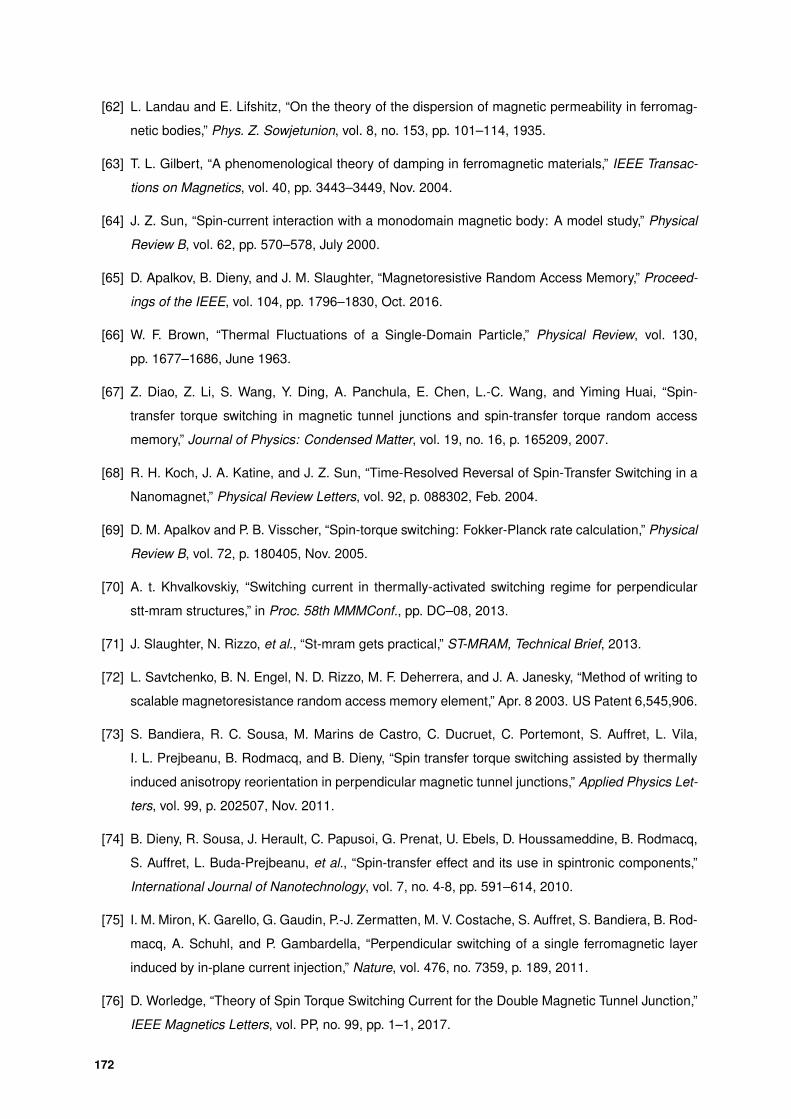
[62] L. Landau and E. Lifshitz, “On the theory of the dispersion of magnetic permeability in ferromag-
netic bodies,” Phys. Z. Sowjetunion, vol. 8, no. 153, pp. 101–114, 1935.
[63] T. L. Gilbert, “A phenomenological theory of damping in ferromagnetic materials,” IEEE Transac-
tions on Magnetics, vol. 40, pp. 3443–3449, Nov. 2004.
[64] J. Z. Sun, “Spin-current interaction with a monodomain magnetic body: A model study,” Physical
Review B, vol. 62, pp. 570–578, July 2000.
[65] D. Apalkov, B. Dieny, and J. M. Slaughter, “Magnetoresistive Random Access Memory,” Proceed-
ings of the IEEE, vol. 104, pp. 1796–1830, Oct. 2016.
[66] W. F. Brown, “Thermal Fluctuations of a Single-Domain Particle,” Physical Review, vol. 130,
pp. 1677–1686, June 1963.
[67] Z. Diao, Z. Li, S. Wang, Y. Ding, A. Panchula, E. Chen, L.-C. Wang, and Yiming Huai, “Spin-
transfer torque switching in magnetic tunnel junctions and spin-transfer torque random access
memory,” Journal of Physics: Condensed Matter, vol. 19, no. 16, p. 165209, 2007.
[68] R. H. Koch, J. A. Katine, and J. Z. Sun, “Time-Resolved Reversal of Spin-Transfer Switching in a
Nanomagnet,” Physical Review Letters, vol. 92, p. 088302, Feb. 2004.
[69] D. M. Apalkov and P. B. Visscher, “Spin-torque switching: Fokker-Planck rate calculation,” Physical
Review B, vol. 72, p. 180405, Nov. 2005.
[70] A. t. Khvalkovskiy, “Switching current in thermally-activated switching regime for perpendicular
stt-mram structures,” in Proc. 58th MMMConf., pp. DC–08, 2013.
[71] J. Slaughter, N. Rizzo, et al., “St-mram gets practical,” ST-MRAM, Technical Brief, 2013.
[72] L. Savtchenko, B. N. Engel, N. D. Rizzo, M. F. Deherrera, and J. A. Janesky, “Method of writing to
scalable magnetoresistance random access memory element,” Apr. 8 2003. US Patent 6,545,906.
[73] S. Bandiera, R. C. Sousa, M. Marins de Castro, C. Ducruet, C. Portemont, S. Auffret, L. Vila,
I. L. Prejbeanu, B. Rodmacq, and B. Dieny, “Spin transfer torque switching assisted by thermally
induced anisotropy reorientation in perpendicular magnetic tunnel junctions,” Applied Physics Let-
ters, vol. 99, p. 202507, Nov. 2011.
[74] B. Dieny, R. Sousa, J. Herault, C. Papusoi, G. Prenat, U. Ebels, D. Houssameddine, B. Rodmacq,
S. Auffret, L. Buda-Prejbeanu, et al., “Spin-transfer effect and its use in spintronic components,”
International Journal of Nanotechnology, vol. 7, no. 4-8, pp. 591–614, 2010.
[75] I. M. Miron, K. Garello, G. Gaudin, P.-J. Zermatten, M. V. Costache, S. Auffret, S. Bandiera, B. Rod-
macq, A. Schuhl, and P. Gambardella, “Perpendicular switching of a single ferromagnetic layer
induced by in-plane current injection,” Nature, vol. 476, no. 7359, p. 189, 2011.
[76] D. Worledge, “Theory of Spin Torque Switching Current for the Double Magnetic Tunnel Junction,”
IEEE Magnetics Letters, vol. PP, no. 99, pp. 1–1, 2017.
172
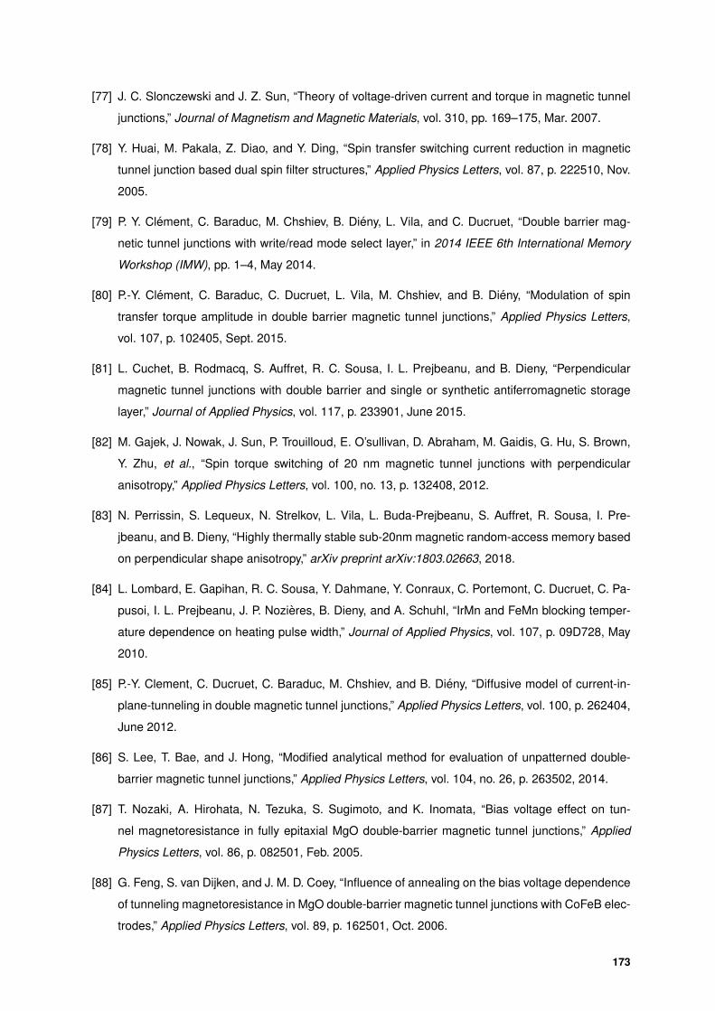
[77] J. C. Slonczewski and J. Z. Sun, “Theory of voltage-driven current and torque in magnetic tunnel
junctions,” Journal of Magnetism and Magnetic Materials, vol. 310, pp. 169–175, Mar. 2007.
[78] Y. Huai, M. Pakala, Z. Diao, and Y. Ding, “Spin transfer switching current reduction in magnetic
tunnel junction based dual spin filter structures,” Applied Physics Letters, vol. 87, p. 222510, Nov.
2005.
[79] P. Y. Clement, C. Baraduc, M. Chshiev, B. Dieny, L. Vila, and C. Ducruet, “Double barrier mag-
netic tunnel junctions with write/read mode select layer,” in 2014 IEEE 6th International Memory
Workshop (IMW), pp. 1–4, May 2014.
[80] P.-Y. Clement, C. Baraduc, C. Ducruet, L. Vila, M. Chshiev, and B. Dieny, “Modulation of spin
transfer torque amplitude in double barrier magnetic tunnel junctions,” Applied Physics Letters,
vol. 107, p. 102405, Sept. 2015.
[81] L. Cuchet, B. Rodmacq, S. Auffret, R. C. Sousa, I. L. Prejbeanu, and B. Dieny, “Perpendicular
magnetic tunnel junctions with double barrier and single or synthetic antiferromagnetic storage
layer,” Journal of Applied Physics, vol. 117, p. 233901, June 2015.
[82] M. Gajek, J. Nowak, J. Sun, P. Trouilloud, E. O’sullivan, D. Abraham, M. Gaidis, G. Hu, S. Brown,
Y. Zhu, et al., “Spin torque switching of 20 nm magnetic tunnel junctions with perpendicular
anisotropy,” Applied Physics Letters, vol. 100, no. 13, p. 132408, 2012.
[83] N. Perrissin, S. Lequeux, N. Strelkov, L. Vila, L. Buda-Prejbeanu, S. Auffret, R. Sousa, I. Pre-
jbeanu, and B. Dieny, “Highly thermally stable sub-20nm magnetic random-access memory based
on perpendicular shape anisotropy,” arXiv preprint arXiv:1803.02663, 2018.
[84] L. Lombard, E. Gapihan, R. C. Sousa, Y. Dahmane, Y. Conraux, C. Portemont, C. Ducruet, C. Pa-
pusoi, I. L. Prejbeanu, J. P. Nozieres, B. Dieny, and A. Schuhl, “IrMn and FeMn blocking temper-
ature dependence on heating pulse width,” Journal of Applied Physics, vol. 107, p. 09D728, May
2010.
[85] P.-Y. Clement, C. Ducruet, C. Baraduc, M. Chshiev, and B. Dieny, “Diffusive model of current-in-
plane-tunneling in double magnetic tunnel junctions,” Applied Physics Letters, vol. 100, p. 262404,
June 2012.
[86] S. Lee, T. Bae, and J. Hong, “Modified analytical method for evaluation of unpatterned double-
barrier magnetic tunnel junctions,” Applied Physics Letters, vol. 104, no. 26, p. 263502, 2014.
[87] T. Nozaki, A. Hirohata, N. Tezuka, S. Sugimoto, and K. Inomata, “Bias voltage effect on tun-
nel magnetoresistance in fully epitaxial MgO double-barrier magnetic tunnel junctions,” Applied
Physics Letters, vol. 86, p. 082501, Feb. 2005.
[88] G. Feng, S. van Dijken, and J. M. D. Coey, “Influence of annealing on the bias voltage dependence
of tunneling magnetoresistance in MgO double-barrier magnetic tunnel junctions with CoFeB elec-
trodes,” Applied Physics Letters, vol. 89, p. 162501, Oct. 2006.
173
[89] Z. Qian, R. Bai, C. Yang, Q. Li, Y. Sun, D. Huo, L. Li, H. Zhan, Y. Li, and J. Zhu, “Effective
anisotropy field in the free layer of patterned spin-valve resistors,” Journal of Applied Physics,
vol. 109, p. 103904, May 2011.
[90] J. Sun, M. Gaidis, G. Hu, E. O’Sullivan, S. Brown, J. Nowak, P. Trouilloud, and D. Worledge, “High-
bias backhopping in nanosecond time-domain spin-torque switches of mgo-based magnetic tunnel
junctions,” Journal of Applied Physics, vol. 105, no. 7, p. 07D109, 2009.
[91] S.-c. Oh, S.-y. Park, A. Manchon, M. Chshiev, J.-h. Han, H.-w. Lee, J.-e. Lee, K.-t. Nam, Y. Jo, Y.-c.
Kong, B. Dieny, and K.-j. Lee, “Bias-voltage dependence of perpendicular spin-transfer torque in
asymmetric MgO-based magnetic tunnel junctions,” Nature Physics, vol. 5, no. 12, pp. 898–902,
2009.
[92] W. Skowronski, P. Ogrodnik, J. Wrona, T. Stobiecki, R. Swirkowicz, J. Barnas, G. Reiss, and
S. van Dijken, “Backhopping effect in magnetic tunnel junctions: Comparison between theory and
experiment,” Journal of Applied Physics, vol. 114, p. 233905, Dec. 2013.
[93] T. Min, J. Sun, R. Beach, D. Tang, and P. Wang, “Back-hopping after spin torque transfer induced
magnetization switching in magnetic tunneling junction cells,” Journal of Applied Physics, vol. 105,
no. 7, p. 07D126, 2009.
[94] P. K. Amiri, Z. M. Zeng, P. Upadhyaya, G. Rowlands, H. Zhao, I. N. Krivorotov, J. P. Wang, H. W.
Jiang, J. A. Katine, J. Langer, K. Galatsis, and K. L. Wang, “Low Write-Energy Magnetic Tunnel
Junctions for High-Speed Spin-Transfer-Torque MRAM,” IEEE Electron Device Letters, vol. 32,
pp. 57–59, Jan. 2011.
[95] S. Zhang, P. M. Levy, A. C. Marley, and S. S. P. Parkin, “Quenching of Magnetoresistance by Hot
Electrons in Magnetic Tunnel Junctions,” Physical Review Letters, vol. 79, pp. 3744–3747, Nov.
1997.
[96] E. Y. Tsymbal, A. Sokolov, I. F. Sabirianov, and B. Doudin, “Resonant Inversion of Tunneling
Magnetoresistance,” Physical Review Letters, vol. 90, p. 186602, May 2003.
[97] C. Heiliger, P. Zahn, B. Y. Yavorsky, and I. Mertig, “Influence of the interface structure on the bias
dependence of tunneling magnetoresistance,” Physical Review B, vol. 72, p. 180406, Nov. 2005.
[98] S. Yuasa, Y. Suzuki, T. Katayama, and K. Ando, “Characterization of growth and crystallization pro-
cesses in CoFeB-MgO-CoFeB magnetic tunnel junction structure by reflective high-energy elec-
tron diffraction,” Applied Physics Letters, vol. 87, no. 24, p. 242503, 2005.
[99] T. Miyajima, T. Ibusuki, S. Umehara, M. Sato, S. Eguchi, M. Tsukada, and Y. Kataoka, “Transmis-
sion electron microscopy study on the crystallization and boron distribution of CoFeB-MgO-CoFeB
magnetic tunnel junctions with various capping layers,” Applied Physics Letters, vol. 94, no. 12,
p. 122501, 2009.
174
[100] S. V. Karthik, Y. K. Takahashi, T. Ohkubo, K. Hono, S. Ikeda, and H. Ohno, “Transmission electron
microscopy investigation of CoFeB/MgO/CoFeB pseudospin valves annealed at different temper-
atures,” Journal of Applied Physics, vol. 106, p. 023920, July 2009.
[101] W. Zhu, H. Li, Y. Chen, and X. Wang, “Current Switching in MgO-Based Magnetic Tunneling
Junctions,” IEEE Transactions on Magnetics, vol. 47, pp. 156–160, Jan. 2011.
[102] Z. Diao, D. Apalkov, M. Pakala, Y. Ding, A. Panchula, and Y. Huai, “Spin transfer switching and spin
polarization in magnetic tunnel junctions with MgO and AlOx barriers,” Applied Physics Letters,
vol. 87, p. 232502, Dec. 2005.
[103] Z. Li and S. Zhang, “Thermally assisted magnetization reversal in the presence of a spin-transfer
torque,” Physical Review B, vol. 69, p. 134416, Apr. 2004.
[104] S. Iihama, S. Mizukami, H. Naganuma, M. Oogane, Y. Ando, and T. Miyazaki, “Gilbert damping
constants of Ta/CoFeB/MgO(Ta) thin films measured by optical detection of precessional magne-
tization dynamics,” Physical Review B, vol. 89, p. 174416, May 2014.
[105] C. L. Platt, B. Dieny, and A. E. Berkowitz, “Spin polarized tunneling in reactively sputtered tunnel
junctions,” Journal of Applied Physics, vol. 81, pp. 5523–5525, Apr. 1997.
[106] E. L. Wolf, Principles of electron tunneling spectroscopy, vol. 152. Oxford University Press, 2012.
[107] Y. Lu, X. W. Li, G. Xiao, R. A. Altman, W. J. Gallagher, A. Marley, K. Roche, and S. Parkin, “Bias
voltage and temperature dependence of magnetotunneling effect,” Journal of Applied Physics,
vol. 83, pp. 6515–6517, June 1998.
[108] J. Zhang and R. M. White, “Voltage dependence of magnetoresistance in spin dependent tunneling
junctions,” Journal of Applied Physics, vol. 83, pp. 6512–6514, June 1998.
[109] M. Sharma, S. X. Wang, and J. H. Nickel, “Inversion of Spin Polarization and Tunneling Magnetore-
sistance in Spin-Dependent Tunneling Junctions,” Physical Review Letters, vol. 82, pp. 616–619,
Jan. 1999.
[110] J. M. D. Teresa, A. Barthelemy, A. Fert, J. P. Contour, F. Montaigne, and P. Seneor, “Role of
Metal-Oxide Interface in Determining the Spin Polarization of Magnetic Tunnel Junctions,” Science,
vol. 286, pp. 507–509, Oct. 1999.
[111] J. G. Simmons, “Generalized Formula for the Electric Tunnel Effect between Similar Electrodes
Separated by a Thin Insulating Film,” Journal of Applied Physics, vol. 34, pp. 1793–1803, June
1963.
[112] J. Wang and P. Freitas, “Low-current blocking temperature writing of double barrier magnetic ran-
dom access memory cells,” Applied physics letters, vol. 84, no. 6, pp. 945–947, 2004.
[113] A. Chavent, Reduction du champ d’ecriture de me moires magnetiques a ecriture assistee ther-
miquement a l’aide du couple de transfert de spin. PhD thesis, Universite de Grenoble, 2016.
175
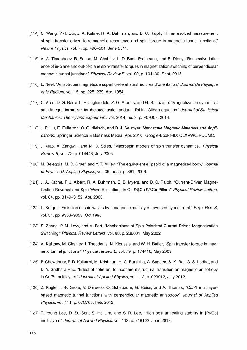
[114] C. Wang, Y.-T. Cui, J. A. Katine, R. A. Buhrman, and D. C. Ralph, “Time-resolved measurement
of spin-transfer-driven ferromagnetic resonance and spin torque in magnetic tunnel junctions,”
Nature Physics, vol. 7, pp. 496–501, June 2011.
[115] A. A. Timopheev, R. Sousa, M. Chshiev, L. D. Buda-Prejbeanu, and B. Dieny, “Respective influ-
ence of in-plane and out-of-plane spin-transfer torques in magnetization switching of perpendicular
magnetic tunnel junctions,” Physical Review B, vol. 92, p. 104430, Sept. 2015.
[116] L. Neel, “Anisotropie magnetique superficielle et surstructures d’orientation,” Journal de Physique
et le Radium, vol. 15, pp. 225–239, Apr. 1954.
[117] C. Aron, D. G. Barci, L. F. Cugliandolo, Z. G. Arenas, and G. S. Lozano, “Magnetization dynamics:
path-integral formalism for the stochastic Landau–Lifshitz–Gilbert equation,” Journal of Statistical
Mechanics: Theory and Experiment, vol. 2014, no. 9, p. P09008, 2014.
[118] J. P. Liu, E. Fullerton, O. Gutfleisch, and D. J. Sellmyer, Nanoscale Magnetic Materials and Appli-
cations. Springer Science & Business Media, Apr. 2010. Google-Books-ID: QLXVW0JRDUMC.
[119] J. Xiao, A. Zangwill, and M. D. Stiles, “Macrospin models of spin transfer dynamics,” Physical
Review B, vol. 72, p. 014446, July 2005.
[120] M. Beleggia, M. D. Graef, and Y. T. Millev, “The equivalent ellipsoid of a magnetized body,” Journal
of Physics D: Applied Physics, vol. 39, no. 5, p. 891, 2006.
[121] J. A. Katine, F. J. Albert, R. A. Buhrman, E. B. Myers, and D. C. Ralph, “Current-Driven Magne-
tization Reversal and Spin-Wave Excitations in Co $/$Cu $/$Co Pillars,” Physical Review Letters,
vol. 84, pp. 3149–3152, Apr. 2000.
[122] L. Berger, “Emission of spin waves by a magnetic multilayer traversed by a current,” Phys. Rev. B,
vol. 54, pp. 9353–9358, Oct 1996.
[123] S. Zhang, P. M. Levy, and A. Fert, “Mechanisms of Spin-Polarized Current-Driven Magnetization
Switching,” Physical Review Letters, vol. 88, p. 236601, May 2002.
[124] A. Kalitsov, M. Chshiev, I. Theodonis, N. Kioussis, and W. H. Butler, “Spin-transfer torque in mag-
netic tunnel junctions,” Physical Review B, vol. 79, p. 174416, May 2009.
[125] P. Chowdhury, P. D. Kulkarni, M. Krishnan, H. C. Barshilia, A. Sagdeo, S. K. Rai, G. S. Lodha, and
D. V. Sridhara Rao, “Effect of coherent to incoherent structural transition on magnetic anisotropy
in Co/Pt multilayers,” Journal of Applied Physics, vol. 112, p. 023912, July 2012.
[126] Z. Kugler, J.-P. Grote, V. Drewello, O. Schebaum, G. Reiss, and A. Thomas, “Co/Pt multilayer-
based magnetic tunnel junctions with perpendicular magnetic anisotropy,” Journal of Applied
Physics, vol. 111, p. 07C703, Feb. 2012.
[127] T. Young Lee, D. Su Son, S. Ho Lim, and S.-R. Lee, “High post-annealing stability in [Pt/Co]
multilayers,” Journal of Applied Physics, vol. 113, p. 216102, June 2013.
176
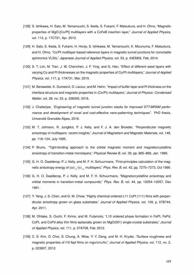
[128] S. Ishikawa, H. Sato, M. Yamanouchi, S. Ikeda, S. Fukami, F. Matsukura, and H. Ohno, “Magnetic
properties of MgO-[Co/Pt] multilayers with a CoFeB insertion layer,” Journal of Applied Physics,
vol. 113, p. 17C721, Apr. 2013.
[129] H. Sato, S. Ikeda, S. Fukami, H. Honjo, S. Ishikawa, M. Yamanouchi, K. Mizunuma, F. Matsukura,
and H. Ohno, “Co/Pt multilayer based reference layers in magnetic tunnel junctions for nonvolatile
spintronics VLSIs,” Japanese Journal of Applied Physics, vol. 53, p. 04EM02, Feb. 2014.
[130] S. T. Lim, M. Tran, J. W. Chenchen, J. F. Ying, and G. Han, “Effect of different seed layers with
varying Co and Pt thicknesses on the magnetic properties of Co/Pt multilayers,” Journal of Applied
Physics, vol. 117, p. 17A731, Mar. 2015.
[131] M. Bersweiler, K. Dumesnil, D. Lacour, and M. Hehn, “Impact of buffer layer and Pt thickness on the
interface structure and magnetic properties in (Co/Pt) multilayers,” Journal of Physics: Condensed
Matter, vol. 28, no. 33, p. 336005, 2016.
[132] J. Chatterjee, ”Engineering of magnetic tunnel junction stacks for improved STT-MRAM perfor-
mance and development of novel and cost-effective nano-patterning techniques”. PhD thesis,
Universite Grenoble-Alpes, 2018.
[133] M. T. Johnson, R. Jungblut, P. J. Kelly, and F. J. A. den Broeder, “Perpendicular magnetic
anisotropy of multilayers: recent insights,” Journal of Magnetism and Magnetic Materials, vol. 148,
pp. 118–124, July 1995.
[134] P. Bruno, “Tight-binding approach to the orbital magnetic moment and magnetocrystalline
anisotropy of transition-metal monolayers,” Physical Review B, vol. 39, pp. 865–868, Jan. 1989.
[135] G. H. O. Daalderop, P. J. Kelly, and M. F. H. Schuurmans, “First-principles calculation of the mag-
netic anisotropy energy of (co)n /(x)m multilayers,” Phys. Rev. B, vol. 42, pp. 7270–7273, Oct 1990.
[136] G. H. O. Daalderop, P. J. Kelly, and M. F. H. Schuurmans, “Magnetocrystalline anisotropy and
orbital moments in transition-metal compounds,” Phys. Rev. B, vol. 44, pp. 12054–12057, Dec
1991.
[137] Y. Yang, J. S. Chen, and G. M. Chow, “Highly chemical ordered L11 CoPt (111) films with perpen-
dicular anisotropy grown on glass substrates,” Journal of Applied Physics, vol. 109, p. 07B744,
Apr. 2011.
[138] M. Ohtake, S. Ouchi, F. Kirino, and M. Futamoto, “L10 ordered phase formation in FePt, FePd,
CoPt, and CoPd alloy thin films epitaxially grown on MgO(001) single-crystal substrates,” Journal
of Applied Physics, vol. 111, p. 07A708, Feb. 2012.
[139] C. S. Kim, D. Choi, S. Chung, A. Wise, Y. Y. Dang, and M. H. Kryder, “Surface roughness and
magnetic properties of l10 fept films on mgo/crru/tin,” Journal of Applied Physics, vol. 112, no. 2,
p. 023907, 2012.
177
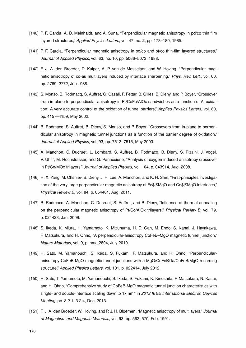
[140] P. F. Carcia, A. D. Meinhaldt, and A. Suna, “Perpendicular magnetic anisotropy in pd/co thin film
layered structures,” Applied Physics Letters, vol. 47, no. 2, pp. 178–180, 1985.
[141] P. F. Carcia, “Perpendicular magnetic anisotropy in pd/co and pt/co thin-film layered structures,”
Journal of Applied Physics, vol. 63, no. 10, pp. 5066–5073, 1988.
[142] F. J. A. den Broeder, D. Kuiper, A. P. van de Mosselaer, and W. Hoving, “Perpendicular mag-
netic anisotropy of co-au multilayers induced by interface sharpening,” Phys. Rev. Lett., vol. 60,
pp. 2769–2772, Jun 1988.
[143] S. Monso, B. Rodmacq, S. Auffret, G. Casali, F. Fettar, B. Gilles, B. Dieny, and P. Boyer, “Crossover
from in-plane to perpendicular anisotropy in Pt/CoFe/AlOx sandwiches as a function of Al oxida-
tion: A very accurate control of the oxidation of tunnel barriers,” Applied Physics Letters, vol. 80,
pp. 4157–4159, May 2002.
[144] B. Rodmacq, S. Auffret, B. Dieny, S. Monso, and P. Boyer, “Crossovers from in-plane to perpen-
dicular anisotropy in magnetic tunnel junctions as a function of the barrier degree of oxidation,”
Journal of Applied Physics, vol. 93, pp. 7513–7515, May 2003.
[145] A. Manchon, C. Ducruet, L. Lombard, S. Auffret, B. Rodmacq, B. Dieny, S. Pizzini, J. Vogel,
V. Uhlır, M. Hochstrasser, and G. Panaccione, “Analysis of oxygen induced anisotropy crossover
in Pt/Co/MOx trilayers,” Journal of Applied Physics, vol. 104, p. 043914, Aug. 2008.
[146] H. X. Yang, M. Chshiev, B. Dieny, J. H. Lee, A. Manchon, and K. H. Shin, “First-principles investiga-
tion of the very large perpendicular magnetic anisotropy at Fe$|$MgO and Co$|$MgO interfaces,”
Physical Review B, vol. 84, p. 054401, Aug. 2011.
[147] B. Rodmacq, A. Manchon, C. Ducruet, S. Auffret, and B. Dieny, “Influence of thermal annealing
on the perpendicular magnetic anisotropy of Pt/Co/AlOx trilayers,” Physical Review B, vol. 79,
p. 024423, Jan. 2009.
[148] S. Ikeda, K. Miura, H. Yamamoto, K. Mizunuma, H. D. Gan, M. Endo, S. Kanai, J. Hayakawa,
F. Matsukura, and H. Ohno, “A perpendicular-anisotropy CoFeB–MgO magnetic tunnel junction,”
Nature Materials, vol. 9, p. nmat2804, July 2010.
[149] H. Sato, M. Yamanouchi, S. Ikeda, S. Fukami, F. Matsukura, and H. Ohno, “Perpendicular-
anisotropy CoFeB-MgO magnetic tunnel junctions with a MgO/CoFeB/Ta/CoFeB/MgO recording
structure,” Applied Physics Letters, vol. 101, p. 022414, July 2012.
[150] H. Sato, T. Yamamoto, M. Yamanouchi, S. Ikeda, S. Fukami, K. Kinoshita, F. Matsukura, N. Kasai,
and H. Ohno, “Comprehensive study of CoFeB-MgO magnetic tunnel junction characteristics with
single- and double-interface scaling down to 1x nm,” in 2013 IEEE International Electron Devices
Meeting, pp. 3.2.1–3.2.4, Dec. 2013.
[151] F. J. A. den Broeder, W. Hoving, and P. J. H. Bloemen, “Magnetic anisotropy of multilayers,” Journal
of Magnetism and Magnetic Materials, vol. 93, pp. 562–570, Feb. 1991.
178
[152] E. Liu, J. Swerts, S. Couet, S. Mertens, Y. Tomczak, T. Lin, V. Spampinato, A. Franquet,
S. Van Elshocht, G. Kar, A. Furnemont, and J. De Boeck, “[Co/Ni]-CoFeB hybrid free layer stack
materials for high density magnetic random access memory applications,” Applied Physics Letters,
vol. 108, p. 132405, Mar. 2016.
[153] L. Cuchet, B. Rodmacq, S. Auffret, R. C. Sousa, C. Ducruet, and B. Dieny, “Influence of a ta spacer
on the magnetic and transport properties of perpendicular magnetic tunnel junctions,” Applied
Physics Letters, vol. 103, no. 5, p. 052402, 2013.
[154] S. Bandiera, ”....”. PhD thesis, Universite de Grenoble, 2012.
[155] L. Cuchet, ”Magnetic and transport properties of single and double perpendicular magnetic double
junctions”. PhD thesis, Universite de Grenoble, 2015.
[156] J. Chatterjee, R. C. Sousa, N. Perrissin, S. Auffret, C. Ducruet, and B. Dieny, “Enhanced annealing
stability and perpendicular magnetic anisotropy in perpendicular magnetic tunnel junctions using
W layer,” Applied Physics Letters, vol. 110, p. 202401, May 2017.
[157] S. Bandiera, R. C. Sousa, Y. Dahmane, C. Ducruet, C. Portemont, V. Baltz, S. Auffret, I. L. Pre-
jbeanu, and B. Dieny, “Comparison of Synthetic Antiferromagnets and Hard Ferromagnets as
Reference Layer in Magnetic Tunnel Junctions With Perpendicular Magnetic Anisotropy,” IEEE
Magnetics Letters, vol. 1, pp. 3000204–3000204, 2010.
[158] S. S. P. Parkin, “Systematic variation of the strength and oscillation period of indirect magnetic ex-
change coupling through the 3d, 4d, and 5d transition metals,” Phys. Rev. Lett., vol. 67, pp. 3598–
3601, Dec 1991.
[159] S. V. Halilov, A. Y. Perlov, P. M. Oppeneer, A. N. Yaresko, and V. N. Antonov, “Magnetocrystalline
anisotropy energy in cubic Fe, Co, and Ni: Applicability of local-spin-density theory reexamined,”
Physical Review B, vol. 57, pp. 9557–9560, Apr. 1998.
[160] H. Sato, M. Yamanouchi, K. Miura, S. Ikeda, R. Koizumi, F. Matsukura, and H. Ohno, “CoFeB
Thickness Dependence of Thermal Stability Factor in CoFeB/MgO Perpendicular Magnetic Tunnel
Junctions,” IEEE Magnetics Letters, vol. 3, pp. 3000204–3000204, 2012.
[161] D.-Y. Lee, S.-H. Hong, S.-E. Lee, and J.-G. Park, “Dependency of Tunneling-Magnetoresistance
Ratio on Nanoscale Spacer Thickness and Material for Double MgO Based Perpendicular-
Magnetic-Tunneling-Junction,” Scientific Reports, vol. 6, p. 38125, Dec. 2016.
[162] J.-H. Kim, J.-B. Lee, G.-G. An, S.-M. Yang, W.-S. Chung, H.-S. Park, and J.-P.
Hong, “Ultrathin W space layer-enabled thermal stability enhancement in a perpendicular
MgO/CoFeB/W/CoFeB/MgO recording frame,” Scientific Reports, vol. 5, p. 16903, Nov. 2015.
[163] L. Neel, “Magnetisme-sur un nouveau mode de couplage entre les animantations de deux
couches minces ferromagnetiques,” Comptes Rendus Hebdomadaires Des Seances De L
Academie Des Sciences, vol. 255, no. 15, p. 1676, 1962.
179
[164] J. Moritz, F. Garcia, J. Toussaint, B. Dieny, and J. Nozieres, “Orange peel coupling in multilay-
ers with perpendicular magnetic anisotropy: Application to (co/pt)-based exchange-biased spin-
valves,” EPL (Europhysics Letters), vol. 65, no. 1, p. 123, 2004.
[165] L. E. Nistor, B. Rodmacq, S. Auffret, A. Schuhl, M. Chshiev, and B. Dieny, “Oscillatory interlayer
exchange coupling in mgo tunnel junctions with perpendicular magnetic anisotropy,” Physical Re-
view B, vol. 81, no. 22, p. 220407, 2010.
[166] J. Chatterjee, S. Auffret, R. Sousa, P. Coelho, I.-L. Prejbeanu, and B. Dieny, “Novel multifunctional
rkky coupling layer for ultrathin perpendicular synthetic antiferromagnet,” Scientific Reports, vol. 8,
no. 1, p. 11724, 2018.
[167] T. Devolder, J. V. Kim, J. Swerts, S. Couet, S. Rao, W. Kim, S. Mertens, G. Kar, and V. Nikitin,
“Material developments and domain wall based nanosecond-scale switching process in perpen-
dicularly magnetized STT-MRAM cells (invited),” IEEE Transactions on Magnetics, vol. PP, no. 99,
pp. 1–1, 2017.
[168] X. Feng and P. B. Visscher, “Sweep-rate-dependent coercivity simulation of FePt particle arrays,”
Journal of Applied Physics, vol. 95, pp. 7043–7045, May 2004.
[169] L. Tillie, E. Nowak, R. C. Sousa, M. C. Cyrille, B. Delaet, T. Magis, A. Persico, J. Langer, B. Ocker,
I. L. Prejbeanu, and L. Perniola, “Data retention extraction methodology for perpendicular STT-
MRAM,” in 2016 IEEE International Electron Devices Meeting (IEDM), pp. 27.3.1–27.3.4, Dec.
2016.
[170] J. Z. Sun, S. L. Brown, W. Chen, E. A. Delenia, M. C. Gaidis, J. Harms, G. Hu, X. Jiang, R. Kilaru,
W. Kula, G. Lauer, L. Q. Liu, S. Murthy, J. Nowak, E. J. O’Sullivan, S. S. P. Parkin, R. P. Robertazzi,
P. M. Rice, G. Sandhu, T. Topuria, and D. C. Worledge, “Spin-torque switching efficiency in CoFeB-
MgO based tunnel junctions,” Physical Review B, vol. 88, p. 104426, Sept. 2013.
[171] H. Sato, E. C. I. Enobio, M. Yamanouchi, S. Ikeda, S. Fukami, S. Kanai, F. Matsukura, and H. Ohno,
“Properties of magnetic tunnel junctions with a MgO/CoFeB/Ta/CoFeB/MgO recording structure
down to junction diameter of 11nm,” Applied Physics Letters, vol. 105, p. 062403, Aug. 2014.
[172] J. Z. Sun, R. P. Robertazzi, J. Nowak, P. L. Trouilloud, G. Hu, D. W. Abraham, M. C. Gaidis, S. L.
Brown, E. J. O’Sullivan, W. J. Gallagher, and D. C. Worledge, “Effect of subvolume excitation and
spin-torque efficiency on magnetic switching,” Physical Review B, vol. 84, p. 064413, Aug. 2011.
[173] R. Dittrich, A. Thiaville, J. Miltat, and T. Schrefl, “Rigorous micromagnetic computation of con-
figurational anisotropy energies in nanoelements,” Journal of Applied Physics, vol. 93, no. 10,
pp. 7891–7893, 2003.
[174] D. Apalkov, A. Khvalkovskiy, and V. Nikitin, “Nudged elastic band calculation of switching modes
and energy barriers in perpendicular MRAM,” in Proc. 11th Joint MMM-Intermag Conf., 2013.
180
[175] Y. X. Wang, Z. Wang, H. Gan, and B. K. Yen Hui, “Perpendicular STT-MRAM thermal stability
scaling and robust retention design,” in Proc. MMM Conf., 2014, 2014.
[176] L. Thomas, G. Jan, S. Le, Y. J. Lee, H. Liu, J. Zhu, S. Serrano-Guisan, R. Y. Tong, K. Pi, D. Shen,
R. He, J. Haq, Z. Teng, R. Annapragada, V. Lam, Y. J. Wang, T. Zhong, T. Torng, and P. K. Wang,
“Solving the paradox of the inconsistent size dependence of thermal stability at device and chip-
level in perpendicular STT-MRAM,” in 2015 IEEE International Electron Devices Meeting (IEDM),
pp. 26.4.1–26.4.4, Dec. 2015.
[177] L. Thomas, G. Jan, J. Zhu, H. Liu, Y.-J. Lee, S. Le, R.-Y. Tong, K. Pi, Y.-J. Wang, D. Shen, R. He,
J. Haq, J. Teng, V. Lam, K. Huang, T. Zhong, T. Torng, and P.-K. Wang, “Perpendicular spin transfer
torque magnetic random access memories with high spin torque efficiency and thermal stability
for embedded applications (invited),” Journal of Applied Physics, vol. 115, no. 17, p. 172615, 2014.
[178] P. J. Jensen and K. H. Bennemann, “Direction of the magnetization of thin films and sandwiches
as a function of temperature,” Physical Review B, vol. 42, pp. 849–855, July 1990.
[179] J. Wang and P. P. Freitas, “Low-current blocking temperature writing of double barrier magnetic
random access memory cells,” Applied Physics Letters, vol. 84, pp. 945–947, Feb. 2004.
[180] I. L. Prejbeanu, S. Bandiera, J. Alvarez-Herault, R. C. Sousa, B. Dieny, and J.-P. Nozieres, “Ther-
mally assisted MRAMs: ultimate scalability and logic functionalities,” Journal of Physics D: Applied
Physics, vol. 46, no. 7, p. 074002, 2013.
[181] L. Thomas, M. Benzaouia, S. Serrano-Guisan, G. Jan, S. Le, Y. Lee, H. Liu, J. Zhu, J. Iwata-
Harms, R. Tong, Y. Yang, V. Sundar, S. Patel, J. Haq, D. Shen, R. He, V. Lam, J. Teng, P. Liu,
A. Wang, T. Zhong, T. Torng, and P. Wang, “Spin Transfer Torque driven dynamics of the synthetic
antiferromagnetic reference layer of perpendicular MRAM devices,” in 2017 IEEE International
Magnetics Conference (INTERMAG), pp. 1–1, Apr. 2017.
[182] A. D. Kent, B. Ozyilmaz, and E. del Barco, “Spin-transfer-induced precessional magnetization
reversal,” Applied Physics Letters, vol. 84, pp. 3897–3899, Apr. 2004.
[183] O. Redon, B. Dieny, and B. Rodmacq, “Magnetic spin polarization and magnetization rotation de-
vice with memory and writing process, using such a device,” Mar. 11 2003. US Patent 6,532,164.
[184] A. A. Timopheev, R. Sousa, M. Chshiev, H. T. Nguyen, and B. Dieny, “Second order anisotropy
contribution in perpendicular magnetic tunnel junctions,” Scientific Reports, vol. 6, p. srep26877,
June 2016.
[185] B. Dieny and A. Vedyayev, “Crossover from easy-plane to perpendicular anisotropy in magnetic
thin films: canted anisotropy due to partial coverage or interfacial roughness,” EPL (Europhysics
Letters), vol. 25, no. 9, p. 723, 1994.
181
[186] N. Strelkov, A. Timopheev, R. C. Sousa, M. Chshiev, L. D. Buda-Prejbeanu, and B. Dieny, “Stability
phase diagram of a perpendicular magnetic tunnel junction in noncollinear geometry,” Physical
Review B, vol. 95, p. 184409, May 2017.
[187] J. Zhu, J. Katine, G. E. Rowlands, Y.-J. Chen, Z. Duan, J. G. Alzate, P. Upadhyaya, J. Langer, P. K.
Amiri, K. L. Wang, et al., “Voltage-induced ferromagnetic resonance in magnetic tunnel junctions,”
Physical review letters, vol. 108, no. 19, p. 197203, 2012.
[188] J. Alzate, P. Amiri, S. Cherepov, J. Zhu, P. Upadhyaya, M. Lewis, I. Krivorotov, J. Katine, J. Langer,
K. Galatsis, et al., “Voltage-induced switching of cofeb-mgo magnetic tunnel junctions,” in 56th
Conference on Magnetism and Magnetic Materials, pp. EG–11, 2011.
[189] W.-g. Wang, M. Li, S. Hageman, and C. L. Chien, “Electric-field-assisted switching in magnetic
tunnel junctions,” Nature Materials, vol. 11, no. 1, pp. 64–8, 2012.
[190] M. Endo, S. Kanai, S. Ikeda, F. Matsukura, and H. Ohno, “Electric-field effects on thickness depen-
dent magnetic anisotropy of sputtered MgO/Co40fe40b20/Ta structures,” Applied Physics Letters,
vol. 96, p. 212503, May 2010.
[191] P. K. Amiri and K. L. Wang, “Voltage-controlled magnetic anisotropy in spintronic devices,” in Spin,
vol. 2, p. 1240002, World Scientific, 2012.
[192] K.-M. Lee, J. W. Choi, J. Sok, and B.-C. Min, “Temperature dependence of the interfacial magnetic
anisotropy in w/cofeb/mgo,” AIP Advances, vol. 7, no. 6, p. 065107, 2017.
[193] E. R. Callen and H. Callen, “Anisotropic magnetization,” Journal of Physics and Chemistry of
Solids, vol. 16, no. 3-4, pp. 310–328, 1960.
[194] B. Dieny, “Magnetic device, and method for reading from and writing to said device,” Aug. 2014.
U.S. Classification 365/158, 365/173, 365/148, 977/935, 365/171, 977/933; International Clas-
sification H01L27/22, G11C11/00, B82Y25/00, H01L43/08, G11C11/16, H01F10/32; Cooper-
ative Classification G11C11/1659, G11C11/1675, G11C11/1673, H01F10/3272, H01F10/329,
H01L43/08, Y10S977/933, Y10S977/935, H01F10/3254, G11C11/161, H01L27/228, B82Y25/00.
182
Related Documents