DNA Chips: Micro-Arrays and Emerging Nanotechnologies ME 381: Introduction to MEMS Final Project December 8, 2003 Raphael Anstey Matthieu Chardon Travis Harper

Welcome message from author
This document is posted to help you gain knowledge. Please leave a comment to let me know what you think about it! Share it to your friends and learn new things together.
Transcript
DNA Chips: Micro-Arrays and Emerging Nanotechnologies
ME 381: Introduction to MEMS
Final Project
December 8, 2003
Raphael Anstey Matthieu Chardon
Travis Harper
Intro to Microelectronic Mechanical Systems DNA Chip Team
TABLE OF CONTENTS Abstract…………………………………………………………………………………………….…………….02
I. Introduction………………………………………………….……………………………………………...03 Background and Motivation……………………………………………………………………………... 03 Applications………………………………………………………………………………..………………….. 03 What is DNA and how does it work?……………………………………..………………………….. 04 II. Manufacturing and Hybridization…..……………………………………………...……………….07 The Human Genome………………………………………………………………………………………….07 In Situ Photolithography Manufacturing…………………………………………….……………….. 07 Array Hybridization………………………………………………………….………………………………09 Scaling Considerations…………………………………………………….………….…………………… 10 Dip Pen Nanolithography……………………………………………………………………….…………..11 III. Sensing………………………………………………………………………………………..………..……13 Introduction……………………………………………………………………………………...……….………13 Laser Induced Fluorescence…………………………………………………………………….….……….13 DNA Chip Implementation………………………………………………………………………………….14 Tagging and Sensing DNA: A Cell Yeast Study…………………………………...……………….15 LIF Conclusion…………………………………………………………………………………………………..18 Electrochemical Sensing………………………………………………………...…..…….…………………19 Companies in the Electochemical Sensing Business…………..................…………………………22 Electrochemical Sensing Conclusion………………………………………..…….……………….…….23 IV. Proposed Concept……………………………………………………………..…..……………………..24 List of Figures……………………………………………………………………….…………………….……..25 References……………………………………………………………………………..…………..………………26 Biographical Sketches…………………………………………………………………..………………..……27
2
Intro to Microelectronic Mechanical Systems DNA Chip Team
ABSTRACT
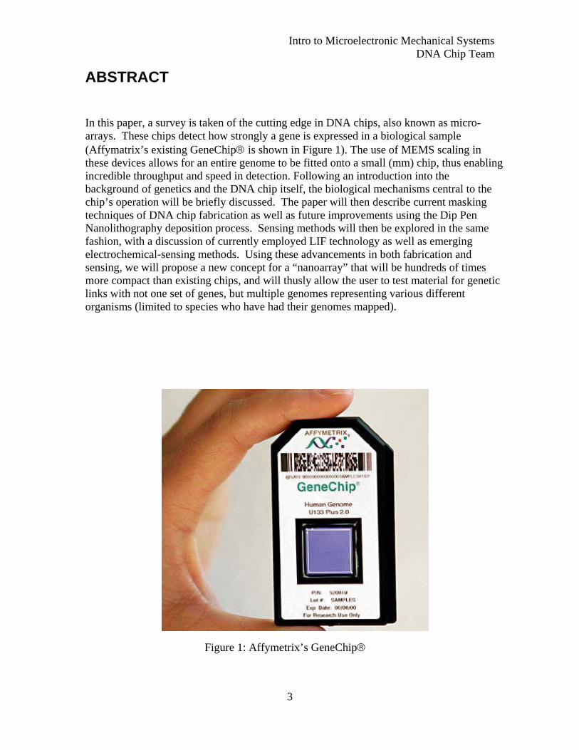
In this paper, a survey is taken of the cutting edge in DNA chips, also known as micro-arrays. These chips detect how strongly a gene is expressed in a biological sample (Affymatrix’s existing GeneChip® is shown in Figure 1). The use of MEMS scaling in these devices allows for an entire genome to be fitted onto a small (mm) chip, thus enabling incredible throughput and speed in detection. Following an introduction into the background of genetics and the DNA chip itself, the biological mechanisms central to the chip’s operation will be briefly discussed. The paper will then describe current masking techniques of DNA chip fabrication as well as future improvements using the Dip Pen Nanolithography deposition process. Sensing methods will then be explored in the same fashion, with a discussion of currently employed LIF technology as well as emerging electrochemical-sensing methods. Using these advancements in both fabrication and sensing, we will propose a new concept for a “nanoarray” that will be hundreds of times more compact than existing chips, and will thusly allow the user to test material for genetic links with not one set of genes, but multiple genomes representing various different organisms (limited to species who have had their genomes mapped).
Figure 1: Affymetrix’s GeneChip®
3
Intro to Microelectronic Mechanical Systems DNA Chip Team
I. INTRODUCTION
A) Background and Motivation Watson and Crick’s discovery of DNA 50 years ago has drastically changed the way we look at ourselves. Ever since, humans have striven to take advantage of the seemingly unlimited potential that this four-acid code offers. Due to its code-like nature, DNA makes us all the same, and all different - the same because we are all built on the same 4 letter language or code, and different because there are endless coding possibilities. DNA is the building block - the blue print for life and this is why it prompted the scientific society to find out the meaning of this code. Different techniques were developed to decode DNA but all were time consuming and expensive. In fact, the “Human Genome Project,” sponsored by the US government, took 13 years to complete and $451 million dollars [1]. The emergence of new technologies, however, has altered this trend as the DNA Chip was created.
Concurrent with the development of the human genome technologies was a surge in the technology of MEMS (Microelectronic Mechanical Systems), a field that has steadily matured from methods employed for computer microchip fabrication. As of late, these two advancements have been combined to produce the DNA chip, also know as the Gene Chip or Micro-DNA array. The DNA Chip is a MEMS device created especially to decode a DNA sequence in record time and at a record price. These chips are used to detect specific DNA strands and are exceptional because they require an extremely small sample volume - only enough to barely coat a MEMS chip (mm). Chips are essentially composed of MEMS fabricated channels or trenches that have had DNA code bonded to them. The DNA are naturally in long chains and are split from the double helix into single strands that will entangle any matching strands introduced onto the chip. It is important to note that each single strand of DNA contains a complex sequence of four acids that will only combine with a strand of exactly the opposite acid sequence. It is this phenomenon that makes the DNA chip both functional and reliable. Once a mating piece of DNA material is introduced onto the chip in the vicinity of the original chip-bonded DNA, hybridization (re-combination) of the double helix occurs. At this point, the subsequent match must be indicated using a phosphorescent reaction, LIF (Laser Induced Fluorescence), or other methods. Thus, the end result is an array of lit and unlit areas to indicate combinations. A tiny chip can contain thousands of distinct DNA segments (genes) that can independently indicate successful and unsuccessful matches very quickly. This kind of biological testing power has prompted some to coin the term lab-on-chip.
B) Applications Being able to decode DNA quickly has been a great step in understanding our world. In fact, discovering new sequences can lead to three great improvements in our society. First, scientists will be able to discover new genes. These genes will not only explain the size
4

Intro to Microelectronic Mechanical Systems DNA Chip Team
and shapes of proteins but will also better an organism when introduced in their genome. For example, it is possible to find on the market tomatoes that take longer to rot. This allows people to keep tomatoes longer and allows farmers to let their tomatoes grow for longer times instead of picking them early. This idea can be applied to many things, limited only by ethics and personal beliefs. The second main application is disease diagnosis. People will be able to get their karyotype checked to see if they have any genetic diseases. For example, they can see if they are prone to getting cancer in the future. This will allow a person to act in consequence such as following a certain style of life and having regular tests performed. The final major application is drug discovery. Some people are more resistant than others to diseases. This fact leads pharmacists to geneticists to try to understand this phenomenon. A common example would be diabetes. People suffering from diabetes lack a protein called insulin, which helps regulate the sugar level in the blood stream. Like any other protein insulin has its corresponding genetic code which scientist found by reverse engineering. It was therefore easy to implant this gene in bacteria to have it produce this insulin that now all people suffering from diabetes use. This concept can be applied to many diseases. Finding the protein that would help cure a disease can only be done by the study of many different individuals and therefore the DNA Chip is the best way to do this.
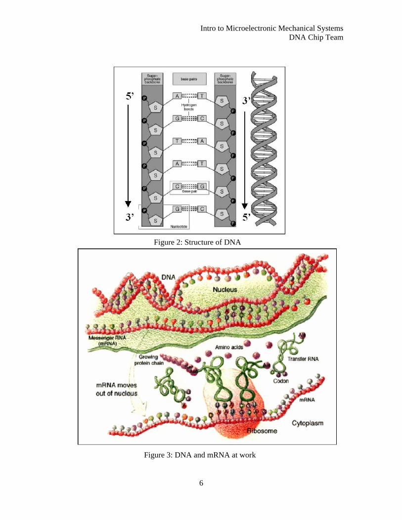
C) What is DNA and how does it Work? In order to understand DNA chips and our proposed concept, we must first be comfortable with the biological concepts that drive genetic functions. DNA stands for Deoxyribonucleic Acid, which, as described earlier, is composed of four primary building blocks that are generally classified as nucleotides [2]. Each of these nucleotides contains one of the four-nitrogen bases (Adenine, Guanine, Cytosine, and Thymine) that make up the genetic code. Also included is a phosphate sugar backbone. See Figure 2. These nucleotides are arranged in exceedingly long double helix strands that reside within the nuclei of all cells. Essential to DNA’s functioning is the concept of genes and mRNA. A gene is a segment of DNA that defines a specific hereditary characteristic, usually corresponding to a single mRNA carrying the information for constructing a protein [3]. Scientists have determined that only 3% of DNA contains genes. These regions of active code are known as “exons”, and are mixed in with segments containing inactive code, also known as “introns”. In order for genes to synthesize proteins, the information carried on introns must be consolidated and transported outside the nucleus by mRNA. This “Messenger” Ribonucleic Acid (mRNA) has copied and spliced the genetic material off of a DNA strand and as stated above, corresponds to one specific gene. Protein is then synthesized in the cell’s cytoplasm. See Figure 3.
5
Intro to Microelectronic Mechanical Systems DNA Chip Team
Figure 2: Structure of DNA
Figure 3: DNA and mRNA at work
6

Intro to Microelectronic Mechanical Systems DNA Chip Team
Another key mechanism that is utilized by gene chips is that of Hybridization. This term refers to the recombination of complimentary strands of DNA. Gene chips utilize this selective nature by planting single strands of a gene onto one location of the chip. The driving rationale being that a genetic single-strand sample or “target” introduced onto the chip will chemically attach itself to the chip’s resident “probe” if it contains the opposite bases in the proper sequence. Thus the re-combination or Hybridization of the target and probe indicates that the two strands are the same gene and are genetic matches. Watson and Crick examine their preliminary model of DNA in the figure below.
Figure 4: Watson and Crick examine their DNA model
7
Intro to Microelectronic Mechanical Systems DNA Chip Team
II. MANUFACTURING AND HYBRIDIZATION
A) The Human Genome Project Among the most instrumental scientific studies in the history of time, the human genome project has played a vital role in the understanding of the human life. This government funded, eleven-year, three billion dollar project began in 1990, intended to produce a DNA sequence representing the functional blueprint and evolutionary history of the human species. Objectives included the identification of all of the approximately 30,000 genes in human DNA and the determination of sequences of the three billion chemical base pairs that make DNA up. The findings of this study have been applied to many diverse fields, including molecular medicine, DNA identification, microbial genomics, bioarcheology, and bioprocessing [4]. Thousands of genes and their products in a given living organism function in a complicated and orchestrated way that creates the mystery of life. The whole picture of a gene function is, therefore, hard to obtain in varying one gene per experiment, as evidenced in the human genome project. Simultaneously analyzing expression levels of a large number of genes provides the opportunity to study the activity of an entire genome much more efficiently. Successful manufacturing of the DNA chip permits these kinds of analyses, making the DNA chip an obvious choice to accelerate the characterization of a wide variety of genome experiments. Rampant improvements in time and monetary efficiency are noted, making DNA chip technologies an increasingly important scientific industry.
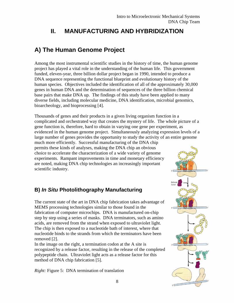
B) In Situ Photolithography Manufacturing The current state of the art in DNA chip fabrication takes advantage of MEMS processing technologies similar to those found in the fabrication of computer microchips. DNA is manufactured on-chip step by step using a series of masks. DNA terminators, such as amino acids, are removed from the strand when exposed to ultraviolet light. The chip is then exposed to a nucleotide bath of interest, where that nucleotide binds to the strands from which the terminators have been removed [2]. In the image on the right, a termination codon at the A site is recognized by a release factor, resulting in the release of the cpolypeptide chain. Ultraviolet light acts as a release factor for this method of DNA chip fabrication [5].
ompleted
Right: Figure 5: DNA termination of translation
8
Intro to Microelectronic Mechanical Systems DNA Chip Team
9
Substrate
Mask
UV Light
Substrate
Mask
UV Light
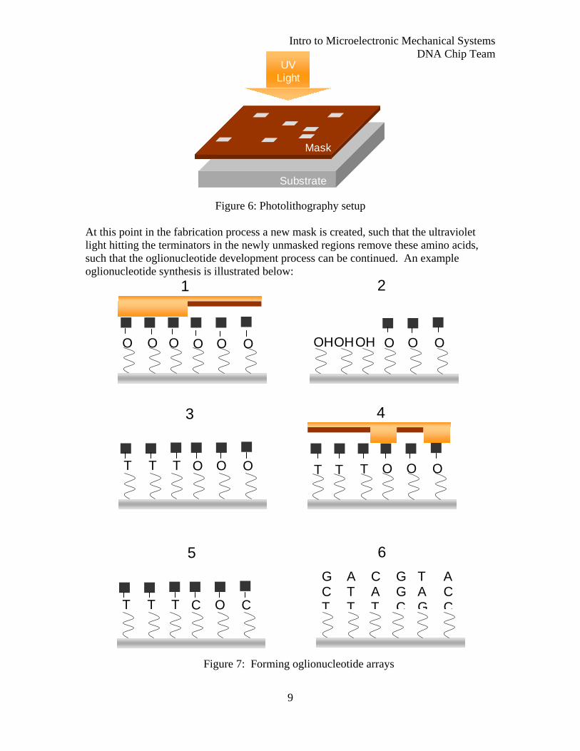
Figure 6: Photolithography setup
21
At this point in the fabrication process a new mask is created, such that the ultraviolet light hitting the terminators in the newly unmasked regions remove these amino acids, such that the oglionucleotide development process can be continued. An example oglionucleotide synthesis is illustrated below:
O O O O O O
OH O O O OHOH
T O O OT T
3
O O O
4 TT T 65
T C O CT T
GCT
ATT
CAT
GGC
TAG
ACC
Figure 7: Forming oglionucleotide arrays

Intro to Microelectronic Mechanical Systems DNA Chip Team
1. The DNA base is deposited onto the substrate. The three strands on the left are
unmasked and exposed to ultraviolet light rays. 2. Terminators are removed, leaving DNA in a unstable energy state 3. Substrate is exposed to a T-rich nucleotide bath, binding T acids to regions
without terminators. Other regions are unaffected. 4. Second mask is applied, exposing new set of strands to ultraviolet light 5. C-rich nucleotide bath yields the adhesion of the C acid to exposed strands 6. Completed oglionucleotide array, ready for DNA chip experimentation
While this technique successfully yields robust and easily identifiable oglionucleotide arrays, there are some several key issues with this technique. First, the stepwise nature of fabrication requires several masks. Depending on the strand length desired, one can spend quite a lot of time alternating between photolithography and nucleotide bathing. Other problems with this technique will be discussed in later sections.
C) Array Hybridization Given the single strand oglionucleotides fabricated as illustrated in the previous section, one can move on to hybridization. As discussed in the introduction, it is the hybridization of DNA strands, the binding of complementary strands into a double helix, which allows scientists to characterize DNA using the DNA chip. Because each strand of DNA has a thickness of only approximately 2 nm, millions of identical strands are found in each site. As will be discussed in the later sections, each site has an associated microarray dot in a microarray image describing fluorescent sensing. Illustrated below are the hybridization processes both using conventional techniques [6] and the DNA chip[7]. The DNA chip section represents complementary strands in the area of a single microarray dot:
Conventional Method
Figure 8: Convential hybridization characterization process
In the illustration above, short fragments of DNA are identified. The DNA is denatured (separated) and placed in a solution, forming a reference segment for the DNA fragment of interest. An unknown DNA sample is introduced to the reference segment. If present, the complement will hybridize. Photosensitive chemicals, bound to the DNA, yield information about hybridization results. The experiment is replicated for every type of denatured sequence to be tested.
10

Intro to Microelectronic Mechanical Systems DNA Chip Team
11
DNA Chip
Identical single strands synthesized in situ using photolithography
All single strands at the site hybridize
Non-complementary strands in other areas of the chip do not.
Information from millions of strands in single dot
Figure 9: DNA chip hybridization process
Unlike the first method illustrated, this method requires only one experiment.
D) Scaling Considerations es a high density of information relative to
wever,
g
esents some problems, however. Current e in
his problem is found in the implementation of Dip Pen Nanolithography.
It is evident that the DNA chip providtraditional techniques developed in the creation of the human genome project. Hoopportunities for vast improvements in the densification of genomic experimentation exist with innovations in nanotechnology [8]. The combination of the high number ofexperiments required to characterize a gene and the sample availability considerations that often present themselves in the analysis of specific DNA sequences make the scalindown of the DNA chip highly desirable. Bringing the DNA chip to the nanoscale prfabrication techniques can no longer be implemented because of resolution issues. Thsitu photolithography technique previously discussed generates a spot size between twenty and forty micrometers, well above the nanoscale. An alternative solution to t

Intro to Microelectronic Mechanical SystemDNA Chip Team
s
12
E) Dip Pen Nanolithography Dip Pen Nanolithography (DPN) is a revNorthwestern University. This technique
olutionary scientific technique developed at allows for the deposition of inks, including
NA, at nanometer resolution [9]. DPN takes advantage of a problem often found when he
Figure
ften times when using the AFM, a meniscus of water forms between the substrate and e cantilever tip, yielding unreliable results. DPN takes advantage of this meniscus by
sing it to write pattern on to substrates, as one would write with a pen on paper. An lustration of the DPN deposition process and an example of attainable spot size are own below [11]:
Dworking with the atomic force microscope (AFM). The AFM is used to characterize ttopography of a sample, measuring the force between a cantilever beam and the sample. The process of scanning a sample with an AFM can be compared to that of reading Braille. An AFM is shown below [10], along with an illustration of the way it works:
10: Atomic force microscopy, instrumentation and functionalization
Othuilsh
Figure 11: Dip Pen Nanolithography deposition process
Intro to Microelectronic Mechanical Systems DNA Chip Team
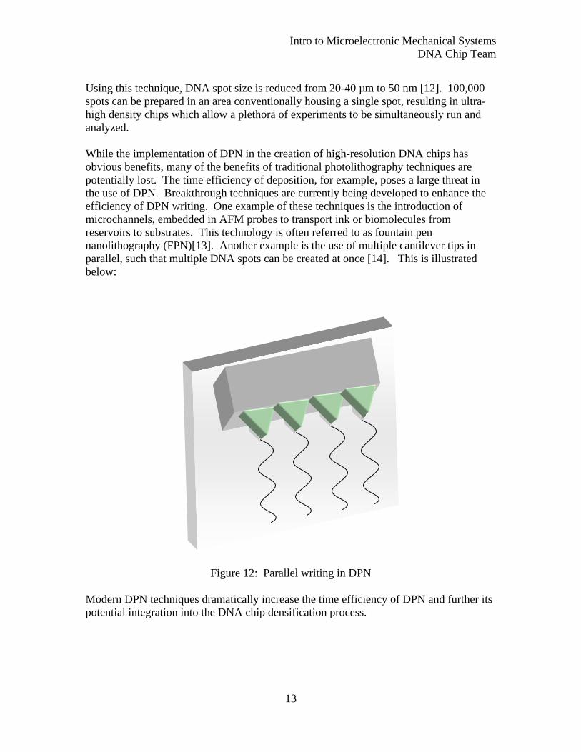
sing this technique, DNA spot size is reduced from 20-40 µm to 50 nm [12]. 100,000
pots can be prepared in an area conventionally housing a single spot, resulting in ultra-
plementation of DPN in the creation of high-resolution DNA chips has bvious benefits, many of the benefits of traditional photolithography techniques are
n e
s in lustrated
Figure 12: Parallel writing in DPN Modern DPN techniques dramatically increase the time efficiency of DPN and further its potential integration into the DNA chip densification process.
Ushigh density chips which allow a plethora of experiments to be simultaneously run and analyzed. While the imopotentially lost. The time efficiency of deposition, for example, poses a large threat ithe use of DPN. Breakthrough techniques are currently being developed to enhance thefficiency of DPN writing. One example of these techniques is the introduction of microchannels, embedded in AFM probes to transport ink or biomolecules from reservoirs to substrates. This technology is often referred to as fountain pen nanolithography (FPN)[13]. Another example is the use of multiple cantilever tipparallel, such that multiple DNA spots can be created at once [14]. This is ilbelow:
13

Intro to Microelectronic Mechanical Systems DNA Chip Team
III. SENSING
) Introduction
ost people purchas ffymetrix® metrix.com
A When m e a DNA Chip from companies like A(www.affy ) they are m at they get from
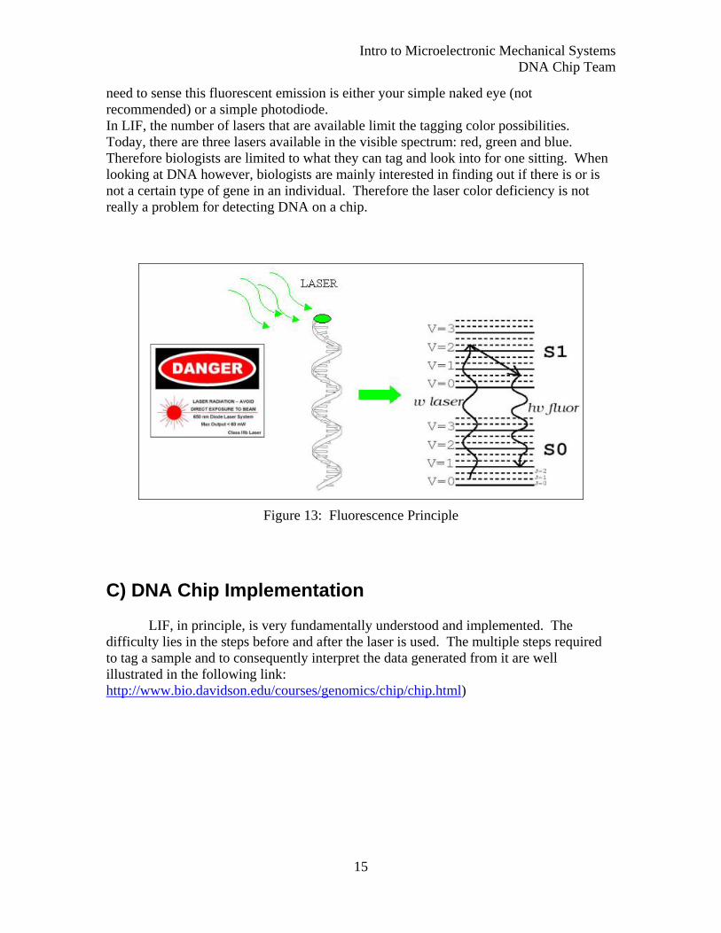
come up with these techniques are still in the realm of the imagination. Today there exist only a couple reliable ways of sensing the hybridization of DNA. First there is the Laser Induced Fluorescence (LIF) method. Any chip that is found on the market that comes from Affymetrix® or Nanogen® will probably employ this technique. It is reliable and very easy to use and understand. It is bulky, however, and requires large amounts of hardware and software. We will discuss this technique in the first part of this section. The second major way of sensing the hybridization of DNA is through Electrochemical sensing. It seems that only Clinical Micro Sensors Inc. in association with Motorola® is proposing a product on the market that uses this technology. This sensing method will be discussed in the second part of this discussion. This method requires almost no hardware or software and it is accurate, make it a potentially better choice. In the nanoworld sensing is the determining factor to any proposed design. Both of the above technologies function properly. They are used in everyday experimentation. However, one must keep in mind why these chips were developed in the first place: to be more cost effective and faster than the other ways of analyzing DNA. Have they kept with their statement of purpose? B) Laser Induced Fluorescence (LIF) Laser Induced Fluorescence (LIF) is used in many sensing application. The idea is one of tagging and tracking. Comparable to the naturalist would, where marine scientists tag a seal with a GPS tracking device to track it around the Earth, the biologist tags a DNA strand with a small fluorescent die to track it on the DNA chip. This method is not only used in tracking DNA, but also to track other molecules. It is a very well understood method of tracking, explaining its appearance on the DNA chip. The physics behind LIF is as follows: The fluorescent tag emits light when it is hit by a laser that has a wavelength that is equal to the inverse of its natural frequency. As shown on Figure 1, the green fluorescent tag will rise in energy levels as the laser hits it. Then as its energy level reaches levels above V = 2, it will become unstable and emit a green ray of light to release excess energy. The green fluorescent tag will consequently come back down to more stable energy levels such as V = 1. This cycle happens many times over, allowing the user to sense this fluorescent tag. The only device that you would
ostly concerned with the feedback ththe chip. The readings must therefore be accurate and reliable. To companies like the one cited above this is where the art of sensing comes into play. While we should not call it an art per se, as many ways of sensing are robust, the way scientists and engineers
14
Intro to Microelectronic Mechanical Systems DNA Chip Team
need to sense this fluorescent emission is either your simple naked eye (not photodiode.
t are available limit the tagging color possibilities. ers available in the visible spectrum: red, green and blue. imited to what they can tag and look into for one sitting. When
recommended) or a simpleIn LIF, the number of lasers thaToday, there are three las
herefore biologists are lTlooking at DNA however, biologists are mainly interested in finding out if there is or is not a certain type of gene in an individual. Therefore the laser color deficiency is not really a problem for detecting DNA on a chip.
Figure 13: Fluorescence Principle
) DNA Chip Implementation C LIF, in principle, is very fundamentally understood and implemented. The difficulty lies in the steps before and after the laser is used. The multiple steps required to tag a sample and to consequently interpret the data generated from it are well illustrated in the following link: http://www.bio.davidson.edu/courses/genomics/chip/chip.html)
15

Intro to Microelectronic Mechanical Systems DNA Chip Team
D) Tagging and Sensing DNA: A Cell Yeast Stud
y
the
. uge one will find that all the cells have
igrated to the bottom of the test tubes.
In this case study we will examine two types of yeast cells [14]: one that hadpossibility to live with oxygen and the other without (Figure 14). One hopes that by placing these two yeast cells into two different habitats that they will produce different types of genes as they try to adapt to their new environments. First, one must have the yeast cells multiply so that the sample of mRNA will be largeThen by spinning theses two samples in a centrifm
Figure 14: Yeast cell incubation schematic
Second, once the cells are f the tube, the mRNA is
ply extracted. First one must pipette out all the yellow growth liquid from the test e. Then, one must add an extraction buffer (in blue), which will bond the mRNA only gure 15). Pipetteing the blue extradition liquid and placing it in a clean tube will
irmly agglomerated at the bottom ofsimtubFi(
separate the mRNA.
Figure 15: Extraction of mRNA
16
Intro to Microelectronic Mechanical Systems DNA Chip Team
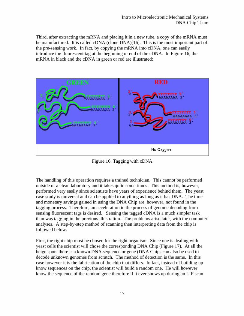
hird, after extracting the mRNA and placing it in a new tube, a copy of the mRT NA must e man b ufactured. It is called cDNA (clone DNA)[16]. This is the most important part of
the pre-sensing work. In fact, by copying the mRNA into cDNA, one can easily introduce the fluorescent tag at the beginning or end of the cDNA. In Figure 16, the mRNA in black and the cDNA in green or red are illustrated:
Figure 16: Tagging with cDNA
ast and can be applied to anything as long as it has DNA. The time
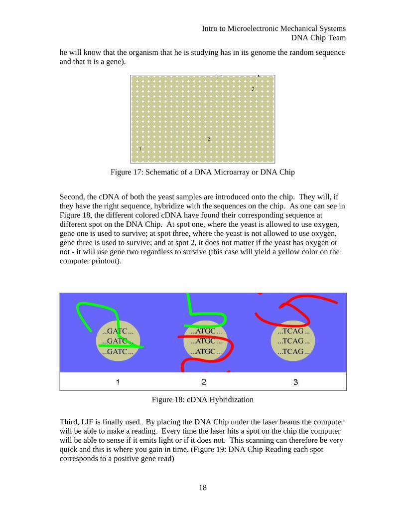
nd monetary savings gained in using the DNA Chip are, however, not found in the tagging process. Therefore, an acceleration in the process of genome decoding from sensing fluorescent tags is desired. Sensing the tagged cDNA is a much simpler task than was tagging in the previous illustration. The problems arise later, with the computer analyses. A step-by-step method of scanning then interpreting data from the chip is followed below. First, the right chip must be chosen for the right organism. Since one is dealing with yeast cells the scientist will chose the corresponding DNA Chip (Figure 17). At all the beige spots there is a known DNA sequence or gene (DNA Chips can also be used to decode unknown genomes from scratch. The method of detection is the same. In this case however it is the fabrication of the chip that differs. In fact, instead of building up know sequences on the chip, the scientist will build a random one. He will however know the sequence of the random gene therefore if it ever shows up during an LIF scan
The handling of this operation requires a trained technician. This cannot be performed outside of a clean laboratory and it takes quite some times. This method is, however, performed very easily since scientists have years of experience behind them. The yecase study is universal a
17
Intro to Microelectronic Mechanical Systems DNA Chip Team
he will know that the organism that he is studying has in its genome the random sequence and that it is a gene).
Figure 17: Schematic of a DNA Microarray or DNA Chip
Second, the cDNA of both the yeast samples are introduced onto the chip. They will, if they have the right sequence, hybridize with the sequences on the chip. As one can see in Figure 18, the different colored cDNA have found their corresponding sequence at different spot on the DNA Chip. At spot one, where the yeast is allowed to use oxygen, gene one is used to survive; at spot three, where the yeast is not allowed to use oxygen, gene three is used to survive; and at spot 2, it does not matter if the yeast has oxygen or not - it will use gene two regardless to survive (this case will yield a yellow color on the computer printout).
Figure 18: cDNA Hybridization
Third, LIF is finally used. By placing the DNA Chip under the laser beams the computwill be able to make a reading. Every time the laser hits a spot on the chip the computerwill be able to sense if it emits light or if it does not. This scanning can therefore be veryquick and this is where you gain in time. (Figure 19: DNA Chip Reading each spot corresponds to a positive gene read)
er
18

Intro to Microelectronic Mechanical Systems DNA Chip Team
Figure 19: Computer Reading of a DNA Chip
Figure 20: LIF Schematic
E) LIF Conclusion When factoring the time it takes to make a chip, the bottleneck with the LIF technique, when considering time savin and the tagging with
ere were some sort of way to do
of
g, is the extraction of the mRNA this quickly and on board of the chip, testing cDNA. If th
time would dramatically drop. The other major problem is that scientists require a large setup to actually run the tests. Figure 21 shows an advertisement for the Nanogene’s DNA Chip testing equipment. As we can see it is not very small. This is why it will be difficult to take the LIF sensing techniques out of the labs, which is a downside if you are a medical doctor, a police officer, or any other profession requiring DNA testing outlab.
19

Intro to Microelectronic Mechanical Systems DNA Chip Team
Furthermore as research advances in the realm of nanotechnology, new discoveries are pushing microfabricated objects to smaller and smaller scales. In other words hundreds of DNA Chips of tomorrow will fit on the DNA chip of today. As this continues to occur, LIF can prove to be unreliable [15]. In fact, there exist with the chips of today sensing resolution problems, where the computer has difficulty differentiating between the spots on the DNA Chip at lower resolutions. As the chip gets smaller and the spots come closer and closer together it will become more difficult to adequate analyze images. These are, however, problems that can be resolved with hard work and research. This type of testing is still the most widely used today and it has many more years to go. It is called a lab on a chip because of all of the benefits it provided, and it did help scientists in the acceleration of the human genome project.
Figure 21: Nanogene’s Testing Equipment
F) Electrochemical Sensing Electrochemical Sensing is based on the principle of oxidation/reduction reaction. Some part of the DNA strand is replaced so that it acts as a catalyst to a chemical reaction that goes on in the surroundings of t ion there would be an electron
ansfer from the catalyst to its surroundings generating therefore an electron flow from e DNA strand to the surroundings. Since this flow would probably be very small, it
sensitive tunneling tip sensor. A CMOS circuit next to the analyze this data. The problem with this method is that
he strand. During the reacttrthcould be measured by the veryDNA testing space would thenyou must find a catalyst that will not react with its surroundings if no hybridization occurred. Results from Experimentation All the data from the experimentation came from the following thesis:
20
Intro to Microelectronic Mechanical Systems DNA Chip Team
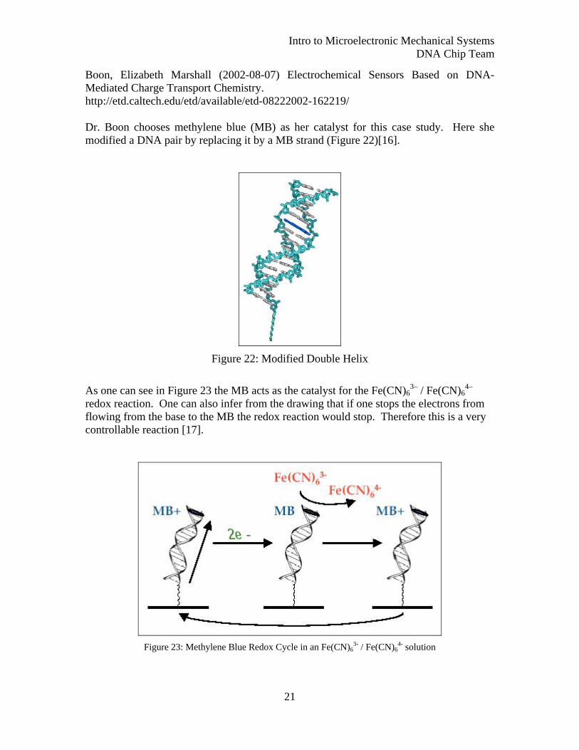
Boon, Elizabeth Marshall (2002-08-07) Electrochemical Sensors Based on DNAMediated Charge Transport Chemistry. http://etd.caltech.edu/etd/available/etd-08222002-162219/ Dr. Boon chooses methylene blue (MB) as her catalyst for this case study. Here shmodified a DNA pair by replacing it by a MB strand (Figure 22)[16].
-
e
Figure 22: Modified Double Helix
As one can see in Figur N)63– / Fe(CN)6
4– edox reaction. One can also infer from the drawing that if one stops the electrons from
ore this is a very
e 23 the MB acts as the catalyst for the Fe(C
rflowing from the base to the MB the redox reaction would stop. Therefcontrollable reaction [17].
Figure 23: Methylene Blue Redox Cycle in an Fe(CN) 3- / Fe(CN) 4- sol6 6 ution
21

Intro to Microelectronic Mechanical Systems DNA Chip Team
The beauty of this method is that if a pair in the DNA strand is mismatched the electron flow from the base to the MB catalyst stops [16][17]. As you can see in Figure 24, when
d with C the current flow rops [16].
A is in matched with T current flows, but when A is matched
Figure 24: Current flow comparison
With this in mind it is therefore possible to build a new type of DNA chip that would rely on an electrochemical method of sensing. In fact, if there were hybridization then one could detect a current and correlate it to a gene [16]. Furthermore, this method seems much more reliable than LIF, since it is able to sense with accuracy down to one mismatch. In other words, if a sample succeeded in partially hybridizing with a probe, the LIF sensing method would not be able to detect this mismatch. This is why that in the LIF method of sensing, millions of the same probes are placed in the same spots of the chip in order to reduce the statistical chance of a false sensing. This takes up valuable space. Though electrochemical sensing ideally only one probe per gene is needed, though one would still want a larger sample to detect the strength of gene expression. Considering that there are 40,000 known genes in the human genome and that the radius of the double helix is 2 nm, if one were to leave 4 nm between each probe and 10 probes per gene, one could build a chip of side length of smaller than one millimeter. That is approximately 1000 timshown earlie talyst and
e right solutions to avoid the destruction of the chip being tested.
es smaller than the Affymetrix Human Genome Chip that was r. The difficult part in this endeavor would be to find the right ca
th
22
Intro to Microelectronic Mechanical Systems DNA Chip Team
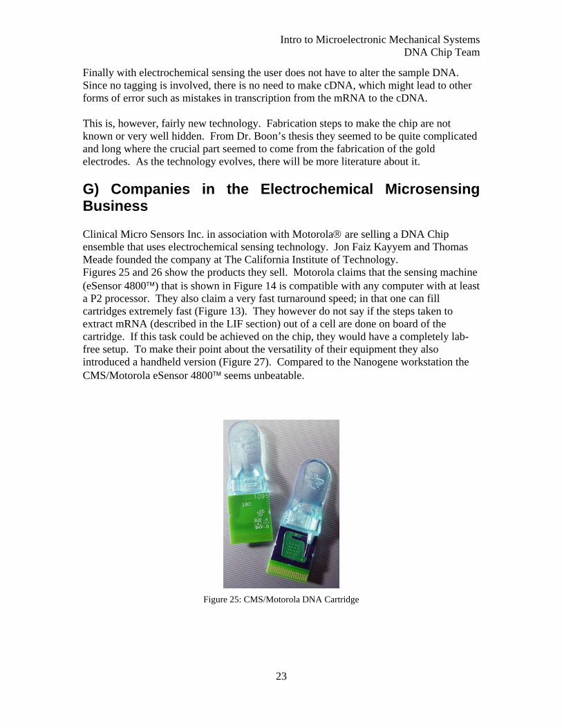
Finally with electrochemical sensing the user does not have to alter the sample DNA. Since no tagging is involved, there is no need to make cDNA, which might lead to other forms of error such as mistakes in transcription from the mRNA to the cDNA. This is, however, fairly new technology. Fabrication steps to make the chip are not known or very well hidden. From Dr. Boon’s thesis they seemed to be quite complicated and long where the crucial part seemed to come from the fabrication of the gold electrodes. As the technology evolves, there will be more literature about it. G) Companies in the Electrochemical Microsensing Business Clinical Micro Sensors Inc. in association with Motorola® are selling a DNA Chip ensemble that uses electrochemical sensing technology. Jon Faiz Kayyem and Thomas Meade founded the company chnology. Figures 25 and 26 show the products they sell. s that the sensing machine (eSensor 4800™) that is shown in Figure 14 is compatible with any computer with at least a P2 processor. They also claim a very fast turnaround speed; in that one can fill cartridges extremely fast (Figure 13). They however do not say if the steps taken to extract mRNA (described in the LIF section) out of a cell are done on board of the cartridge. If this task could be achieved on the chip, they would have a completely lab-free setup. To make their point about the versatility of their equipment they also introduced a handheld version (Figure 27). Compared to the Nanogene workstation the CMS/Motorola eSensor 4800™ seems unbeatable.
at The California Institute of Te Motorola claim
Figure 25: CMS/Motorola DNA Cartridge
23

Intro to Microelectronic Mechanical Systems DNA Chip Team
Figure 26: CMS/Motorola eSensor™ 4800
Figure 27: Handheld Sensor
H) Electrochemical Sensing Conclusion This technology is new, and still requires a lot of development. The fact that Motorola is interested in signals, however, acts as evidence that they believe that this is the method of sensing DNA is the future. The problem is that none of these methods, LIF or Electrochemical Sensing, provide a good and simple way of extracting mRNA from a cell. The idea of the DNA Chip is that it should be a lab on a chip. This means that the whole lab should be on the chip not just the sensing. This technology is however amazing, and the group cannot wait to
see what is in store.
24

Intro to Microelectronic Mechanical Systems DNA Chip Team
IV. PROPOSED CONCEPT By coupling the DPN and Electrochemical sensing methods outlined above, significant opportunity for further improvement to DNA chips is evident. As shown above, DPN technology enables us to easily deposit pre-made probes and masks precisely at a nanometer scale. Our concept utilizes this breakthrough to miniaturize the size of each gene spot from 20-40 µm to 50 nm (sizes in spot and square diameters). Since we know that each DNA strand has a width of 2 nm in vertical orientation, this would allow a sample size of approximately 400 strands [2]. If a greater sample size is needed, we need simply to enlarge our better statistical analysis. Even with 2 is seen.
ow that we have reduced the size of the chip, we must consider sensing techniques. From the above section on sensing, we know that computers still have resolution difficulties with gene dots on the micro scale. Thus, using the same LIF techniques with this new concept is out of the question. The illuminated markers would be so close to each other that a computer would not be able to differentiate between two adjacent dots that contain strands of two different genes. Accordingly, electrochemical sensing would be the alternative, as it solves the resolution issue by using electrons instead of photons to indicate a match. To use this method, we would have to essentially create two separate chips that would later be superimposed onto one another for the final resultant chip. The first chip would contain the electronics needed, namely millions and millions of current switches that would sense the flow of electrons through the DNA strand anchors. Traditional Si CMOS chips would be most appropriate in this case. This component of the chip would produce a consolidated electric signal that would display results on a computer program.
uperimposed over this electronic chip would be the biological component that needs to old the wet conductive solution as well as the modified probes and electronic anchors. ere, one could Si etch out an outer wall that would contain the conductive solution on
sks for the deposition of he chip. Thus, the entire
ll
ce rganisms could be
multaneously contained on only one chip.
gene spot to 100-200 nm to achieve 10,000-40,000 strands for the larger nanospots, a size reduction of 10
N
ShHthe chip. Using DPN again, we could then pattern nanoscale mahe gold or platinum anchors and electrodes to specific parts of tt
chip would be realized when the biological chip electrodes are aligned and placed above the electronic chip’s current switches. Once a sample of targets is incubated onto the finished chip, only hybridized probes wihave current flowing through their electrodes and the corresponding current switches below. The electronic silicon chip will consolidate this combination of “on” and “off” signals into one dense signal that will be deciphered and analyzed by software. Onhese details are worked out, the entire genomes of multiple ot
si
25
Intro to Microelectronic Mechanical Systems DNA Chip Team
ist of Figures
9: DNA chip hybridization process
of a DNA Microarray or DNA Chip 18. cDNA Hybridization
25. CMS/Motorola DNA Cartridge
L
1. Affymetrix GeneChip® 2. Structure of DNA 3. DNA and mRNA at work 4. Watson and Crick examine their DNA model 5. DNA termination of translation 6. Photolithography setup 7: Forming oglionucleotide arrays 8: Convential hybridization characterization process
10: Atomic force microscopy, instrumentation and functionalization 11: Dip Pen Nanolithography deposition process 12: Parallel writing in DPN 13. Fluorescence Principle 14. Yeast cell incubation schematic 15. Extraction of mRNA 16. Tagging with cDNA 17. Schematic
19. Computer Reading of a DNA Chip 20. LIF Schematic 21. Nanogene’s Testing Equipment 22. Modified Double Helix 23. Methylene Blue Redox Cycle in an Fe(CN)6
3- / Fe(CN)64- solution
24. Current flow comparison
26. CMS/Motorola eSensor™ 4800 27. Handheld Sensor
26

Intro to Microelectronic Mechanical Systems DNA Chip Team
References
Genome Project”. http://www.genome.gov/10001772
• [1] “About the Human
Expression Data.
• [2] R. Shamir. Analysis of Gene 2002 ribes/lec01.pdfhttp://www.math.tau.ac.il/~rshamir/ge/02/sc
y of the Cell• [3] B. Alberts. et al. Molecular Biolog . Garland Publishing, Inc., 1994.
an_Genome/project/benefits.shtml• [4] “Benefits of the Human Genome Projec
ources/Humt.” 2003
http://www.ornl.gov/sci/techres
roach, 2• [5] G. Cooper. The Cell, A Molecular App nd ed. ASM Press, 2000
• [6] C. Henke. “DNA-Chip technologies.” 1998 www.devicelink.com/ivdt/ archive/98/09/009.html
• [7] L. Shi. “DNA Microarray (Genome Chip).” 2002 http://www.gene-chips.com/
• [8] S. Salamone. “The incredible shrinking microarray.” 2002 eport1191.htmlhttp://www.bio-itworld.com/news/090902_r
t• [9] H. Zhang, et al. “Biofunc
nanolithography.” Nanotechionalized nanoarrays of inorganic structures prepared by dip-pen
microscope?” 2003
s/whatsafm.html
nology 14(2003) pp.1113-1117
• [10] “What is an atomic force http://www.che.utoledo.edu/nadarajah/webpage
ace Science and Dip Pen Nanolithography.” 2002 .html
• [11] C. Mirkin. “Surf
http://www.chem.nwu.edu/~mkngrp/dippen
• [12] L. Kalaugher. “Dip-pen nanolithography sets a pattern.” 2002 http://nanotechweb.org/articles/news/1/6/4/1
• [13] K.H. Kim, et al. “Massively parallel m
nanolithography (FPN).” 2003 SEM Annuaulti-tip nanoscale writer with fluidic capabilities – fountain pen l Conf. and Expo. on Exp. and Appl. Mech., Session 52, Paper estern.edu/~espinosa/Papers/SEM-FPN.pdf191, pp. 235-238 http://clifton.mech.northw
://www.bio.davidson.edu/courses/genomics/chip/chip.html • [14] “LIF Sensing.” http
• [15] S. Drachici, Data Analysis Tools for DNA Microarrays.
Chapman & Hall/CRC, 2003
[16] E. Boon. “Electrochemical Sensors Based on DNA-Mediated Charge Transport Chemistry.” 2002 http://etd.caltech.edu/etd/available/etd-08222002-162219/
•
• [17] “The Fe(CN)63– / Fe(CN)6
4– charge transfer reaction on Au(111) revisited in the presence and absence of a two-dimensional condensed organic film.” http://darwin.inf.fu-berlin.de/2003/73/chapter_7.pdf
, 2003
27
Intro to Microelectronic Mechanical Systems DNA Chip Team
Biographica
l Sketches
ily to on ec my with Honors
and th .S. in Mechanical Engineering at orthw ctive Polymer research for the ab a njoys leading the chool’s rowing team, Chipotle, and long walks on the beach.
atthi d there until the 6th
gra , there he moved back to rance to attend the Lycee Internatinal de Saint Germain en Laye where he graduated
wit S ced English option. He is currently pursuing a B.S. in Mechanical Eninte st realm of MEMS and hopes to continue his stud o enjoys rock climbing, extreme sports, big rims and low pha id Travis Harper grad at He is urrently pursuing a B.S. in Materials Science and Engineering at Northwestern
University, concentrating in nanotechnology. wor in ti, OH. Travis enjoys his time as a ac sity Marching Band and in Phi Mu on and pulling all-nighters.
Raphael Anstey was born in New York City in 1982, but later moved with his famn ticut where he subsequently graduated from Greens Farms AcadeC o er distinctions. He currently is pursuing a B
estern University and is involved in Electro-ANL or tory for Intelligent Mechanical Systems (LIMS). Raphael also es
M eu Chardon was born in Paris, France in 1981, and remainede when he moved to the USA. After his short four-year stay
Fh a cientific Baccalaureate with an advan
gineering at Northwestern University. He is particularly re ed in sensing and control especially in the
y in that field. He alst r es.
was born in Chicago in 1982, remaining there throughout his life. He u ed from St. Rita High School with honors and numerous other awards.
cHe is a cooperative engineering student,
g at General Electric Aircraft Engines in Cincinnakn tive leader and participant in the Northwestern Univer
Alpha. He also enjoys reality televisi
28
Related Documents


