ADVANCE INFORMATION Product Folder Order Now Technical Documents Tools & Software Support & Community An IMPORTANT NOTICE at the end of this data sheet addresses availability, warranty, changes, use in safety-critical applications, intellectual property matters and other important disclaimers. ADVANCE INFORMATION for pre-production products; subject to change without notice. DM505 SPRS976C – NOVEMBER 2016 – REVISED MAY 2017 DM505 SoC for Vision Analytics 15mm Package (ABF) Silicon Revision 2.0 1 Device Overview 1 1.1 Features 1 • Architecture Designed for Vision Analytics Applications • Video and Image Processing Support – Full-HD Video (1920x1080p, 60 fps) – Video Input and Video Output • Up to 2 C66x Floating-Point VLIW DSP – Fully Object-Code Compatible with C67x and C64x+ – Up to Thirty-two 16 x 16-bit Fixed-point Multiplies per Cycle • Up to 512 kB of On-Chip L3 RAM • Level 3 (L3) and Level 4 (L4) Interconnects • Memory Interface (EMIF) Module – Supports DDR3/DDR3L Up to DDR-1066 – Supports DDR2 Up to DDR-800 – Supports LPDDR2 Up to DDR-667 – Up to 2-GB Supported • Dual ARM ® Cortex ® -M4 Image Processor (IPU) • Vision AccelerationPac – Embedded Vision Engine (EVE) • Display Subsystem – Display Controller With DMA Engine – CVIDEO / SD-DAC TV Analog Composite Output • Video Input Port (VIP) Module – Support for Up to 4 Multiplexed Input Ports • On-chip Temperature Sensor That is Capable of Generating Temperature Alerts • General-Purpose Memory Controller (GPMC) • Enhanced Direct Memory Access (EDMA) Controller • 3-Port (2 External) Gigabit Ethernet (GMAC) Switch • Controller Area Network (DCAN) Module – CAN 2.0B Protocol • Modular Controller Area Network (MCAN) Module – CAN 2.0B Protocol • Eight 32-Bit General-Purpose Timers • Three Configurable UART Modules • Four Multichannel Serial Peripheral Interfaces (McSPI) • Quad SPI Interface • Two Inter-Integrated Circuit (I 2 C) Ports • Three Multichannel Audio Serial Ports (McASP) Modules • MultiMedia Card/Secure Digital/Secure Digital Input Output Interface (MMC/SD/SDIO) • Up to 126 General-Purpose I/O (GPIO) Pins • Power, Reset, and Clock Management • On-Chip Debug With CTools Technology • Automotive AEC-Q100 Qualified • 15 x 15mm, 0.65-mm Pitch, 367 Pin PBGA (ABF) • Seven Dual Clock Comparators (DCC) • Memory Cyclic Redundancy Check (CRC) • TESOC (LBIST/PBIST) That Enables Field Testing of Logic and On-Chip Memory • Error Signaling Module (ESM) • Five Instances of Real-Time Interrupt (RTI) Modules That Can be Used as Watch Dog Timers • 8-Channel 10-bit ADC • MIPI CSI-2 Camera Serial Interface • PWMSS • Full HW Image Pipe: DPC, CFA, 3D-NF, RGB- YUV – WDR, HW LDC and Perspective

Welcome message from author
This document is posted to help you gain knowledge. Please leave a comment to let me know what you think about it! Share it to your friends and learn new things together.
Transcript

AD
VA
NC
E I
NF
OR
MA
TIO
N
Product
Folder
Order
Now
Technical
Documents
Tools &
Software
Support &Community
An IMPORTANT NOTICE at the end of this data sheet addresses availability, warranty, changes, use in safety-critical applications,intellectual property matters and other important disclaimers. ADVANCE INFORMATION for pre-production products; subject tochange without notice.
DM505SPRS976C –NOVEMBER 2016–REVISED MAY 2017
DM505 SoC for Vision Analytics15mm Package (ABF) Silicon Revision 2.0
1 Device Overview
1
1.1 Features1
• Architecture Designed for Vision AnalyticsApplications
• Video and Image Processing Support– Full-HD Video (1920x1080p, 60 fps)– Video Input and Video Output
• Up to 2 C66x Floating-Point VLIW DSP– Fully Object-Code Compatible with C67x and
C64x+– Up to Thirty-two 16 x 16-bit Fixed-point
Multiplies per Cycle• Up to 512 kB of On-Chip L3 RAM• Level 3 (L3) and Level 4 (L4) Interconnects• Memory Interface (EMIF) Module
– Supports DDR3/DDR3L Up to DDR-1066– Supports DDR2 Up to DDR-800– Supports LPDDR2 Up to DDR-667– Up to 2-GB Supported
• Dual ARM® Cortex®-M4 Image Processor (IPU)• Vision AccelerationPac
– Embedded Vision Engine (EVE)• Display Subsystem
– Display Controller With DMA Engine– CVIDEO / SD-DAC TV Analog Composite
Output• Video Input Port (VIP) Module
– Support for Up to 4 Multiplexed Input Ports• On-chip Temperature Sensor That is Capable of
Generating Temperature Alerts• General-Purpose Memory Controller (GPMC)• Enhanced Direct Memory Access (EDMA)
Controller• 3-Port (2 External) Gigabit Ethernet (GMAC)
Switch
• Controller Area Network (DCAN) Module– CAN 2.0B Protocol
• Modular Controller Area Network (MCAN) Module– CAN 2.0B Protocol
• Eight 32-Bit General-Purpose Timers• Three Configurable UART Modules• Four Multichannel Serial Peripheral Interfaces
(McSPI)• Quad SPI Interface• Two Inter-Integrated Circuit (I2C) Ports• Three Multichannel Audio Serial Ports (McASP)
Modules• MultiMedia Card/Secure Digital/Secure Digital
Input Output Interface (MMC/SD/SDIO)• Up to 126 General-Purpose I/O (GPIO) Pins• Power, Reset, and Clock Management• On-Chip Debug With CTools Technology• Automotive AEC-Q100 Qualified• 15 x 15mm, 0.65-mm Pitch, 367 Pin PBGA (ABF)• Seven Dual Clock Comparators (DCC)• Memory Cyclic Redundancy Check (CRC)• TESOC (LBIST/PBIST) That Enables Field Testing
of Logic and On-Chip Memory• Error Signaling Module (ESM)• Five Instances of Real-Time Interrupt (RTI)
Modules That Can be Used as Watch Dog Timers• 8-Channel 10-bit ADC• MIPI CSI-2 Camera Serial Interface• PWMSS• Full HW Image Pipe: DPC, CFA, 3D-NF, RGB-
YUV– WDR, HW LDC and Perspective

AD
VA
NC
E IN
FO
RM
AT
ION
2
DM505SPRS976C –NOVEMBER 2016–REVISED MAY 2017 www.ti.com
Submit Documentation FeedbackDevice Overview Copyright © 2016–2017, Texas Instruments Incorporated
1.2 Applications• Drones• Robotics
• Industrial Transportation (Forklift, Rail, Agriculture)• Factory and Building Automation cameras
1.3 DescriptionThe DM505 is a highly optimized device for Vision Analytics and Machine Vision processing in Industrialproducts such as drones, robots, forklifts, railroad and agriculture equipment. The Processor enablessophisticated embedded vision processing integrating an optimal mix of real time performance, low power,small form factor and camera processing for systems to interact in more intelligent, useful ways with thephysical world and the people in it.
The DM505 incorporates a heterogeneous, scalable architecture that includes a mix of TI’s fixed andfloating-point TMS320C66x digital signal processor (DSP) generation cores, Vision AccelerationPac(EVE), and dual-Cortex-M4 processors. The device allows low power designs to meet demandingembedded system budgets without sacrificing real-time processing performance to enable small formfactor designs. The DM505 also integrates a host of peripherals including interfaces for multi-camera input(both parallel and serial), display outputs, audio and serial I/O, CAN and GigB Ethernet AVB.
TI provides application specific hardware and software through our Design Network Partners and acomplete set of development tools for the ARM, and DSP, including C compilers with TI RTOS toaccelerate time to market.
Device InformationPART NUMBER PACKAGE BODY SIZE
DM505 S-PBGA (367) 15.0 mm x 15.0 mm

AD
VA
NC
E I
NF
OR
MA
TIO
NSPRS916_Intro_001
JTAG
PLLs
OSC
Clock Comparator (7xDCC)
Error Handler (ESM)
TESOC (LBIST/PBIST)
1x CRC
5x RTI
Memory Controllers
GPMC 8b/16bwith up to 16b ECC
LPDDR2 / DDR2/DDR3 / DDR3L
32b with 8b ECC
Timer x8
Mailbox/Spinlock
10-bit ADC
Control Module
Safety
EDMA
GPIO x4
PWMSSx1
MMUx1
PRCM
System
I2C x2
SPI x4
QSPI x1
SDIO x1
DCAN with ECC
UART x3
McASP x3
Serial Interfaces
GMAC
Connectivity
EDMA 2TC
L2256KBCache
C66x
L1D 32KB
L1P 32KB
DSP Subsystem x2
Video Input Port
CALLVDSRX
CSI2
ISP
Video Front End
up to 512KB RAMwith ECC
IPU with ECC
Dual Cortex M432KB ROM
EVE 16MAC
EDMA 2TC
VisionAccelerator
OSDResizing
CSC
SD-DAC
DVOUT
DisplaySubsystem
Interconnect
DM505
Copyright © 2016, Texas Instruments Incorporated
MCAN(CAN-FD)with ECC
3
DM505www.ti.com SPRS976C –NOVEMBER 2016–REVISED MAY 2017
Submit Documentation FeedbackDevice OverviewCopyright © 2016–2017, Texas Instruments Incorporated
1.4 Functional Block DiagramFigure 1-1 is functional block diagram of the superset.
Figure 1-1. DM505 Block Diagram

AD
VA
NC
E IN
FO
RM
AT
ION
4
DM505SPRS976C –NOVEMBER 2016–REVISED MAY 2017 www.ti.com
Submit Documentation FeedbackTable of Contents Copyright © 2016–2017, Texas Instruments Incorporated
Table of Contents1 Device Overview ......................................... 1
1.1 Features ............................................. 11.2 Applications........................................... 21.3 Description............................................ 21.4 Functional Block Diagram ........................... 3
2 Revision History ......................................... 53 Device Comparison ..................................... 6
3.1 Device Comparison Table ............................ 64 Terminal Configuration and Functions.............. 8
4.1 Pin Diagram .......................................... 84.2 Pin Attributes ......................................... 84.3 Signal Descriptions.................................. 374.4 Pin Multiplexing ..................................... 634.5 Connections for Unused Pins ....................... 74
5 Specifications ........................................... 755.1 Absolute Maximum Ratings ......................... 755.2 ESD Ratings ........................................ 765.3 Power on Hour (POH) Limits........................ 765.4 Recommended Operating Conditions............... 775.5 Operating Performance Points ...................... 795.6 Power Consumption Summary...................... 885.7 Electrical Characteristics ............................ 885.8 Thermal Characteristics ............................. 955.9 Timing Requirements and Switching
Characteristics....................................... 976 Detailed Description.................................. 174
6.1 Description ......................................... 1746.2 Functional Block Diagram ......................... 1746.3 DSP Subsystem ................................... 1756.4 IPU ................................................. 1806.5 EVE ................................................ 181
6.6 Memory Subsystem................................ 1836.7 Interprocessor Communication .................... 1866.8 Interrupt Controller................................. 1876.9 EDMA .............................................. 1876.10 Peripherals ......................................... 1896.11 On-Chip Debug .................................... 201
7 Applications, Implementation, and Layout ...... 2057.1 Introduction ........................................ 2057.2 Power Optimizations ............................... 2067.3 Core Power Domains .............................. 2177.4 Single-Ended Interfaces ........................... 2267.5 Differential Interfaces .............................. 2297.6 Clock Routing Guidelines .......................... 2317.7 LPDDR2 Board Design and Layout Guidelines.... 2327.8 DDR2 Board Design and Layout Guidelines....... 2417.9 DDR3 Board Design and Layout Guidelines....... 2537.10 CVIDEO/SD-DAC Guidelines and Electrical
Data/Timing ........................................ 2768 Device and Documentation Support .............. 278
8.1 Device Nomenclature .............................. 2788.2 Tools and Software ................................ 2808.3 Documentation Support............................ 2808.4 Receiving Notification of Documentation Updates. 2818.5 Community Resources............................. 2818.6 Trademarks ........................................ 2818.7 Electrostatic Discharge Caution ................... 2828.8 Export Control Notice .............................. 2828.9 Glossary............................................ 282
9 Mechanical Packaging Information ............... 2839.1 Mechanical Data ................................... 283

AD
VA
NC
E I
NF
OR
MA
TIO
N
5
DM505www.ti.com SPRS976C –NOVEMBER 2016–REVISED MAY 2017
Submit Documentation FeedbackRevision HistoryCopyright © 2016–2017, Texas Instruments Incorporated
2 Revision History
Changes from January 24, 2017 to May 5, 2017 (from B Revision (January 2017) to C Revision) Page
• Updated DM Title ..................................................................................................................... 1• Updated MCAN reference in block diagram....................................................................................... 3• Moved device hex code from TRM to DM......................................................................................... 6• Added missing balls in Table 4-25 ............................................................................................... 60• Added missing PAD_CONF registers for dcan1 and dcan2................................................................... 64• Updated References in Section 5.5.3 ............................................................................................ 80• Added missing notes in Electrical Characteristics section ..................................................................... 91• Fixed typo in VIN2 IOSETs Table ............................................................................................... 112• Added DSS clock jitter footnotes on timing tables............................................................................. 114• Updated Timing Specification Tables for QSPI ................................................................................ 149• Removed 1149.7 (cJTAG) support .............................................................................................. 171• Updated DM Title .................................................................................................................. 175• Updated MCAN reference in block diagram.................................................................................... 175

AD
VA
NC
E IN
FO
RM
AT
ION
6
DM505SPRS976C –NOVEMBER 2016–REVISED MAY 2017 www.ti.com
Submit Documentation FeedbackDevice Comparison Copyright © 2016–2017, Texas Instruments Incorporated
3 Device Comparison
3.1 Device Comparison TableTable 3-1 shows a comparison between devices, highlighting the differences.
Table 3-1. Device Comparison
Features DeviceDM505M DM505L
FeaturesCTRL_WKUP_STD_FUSE_DIE_ID_2 [31:24] Base PN register bitfieldvalue(3)
156 (0x9C65) 156 (0x9C5D)
Processors/ AcceleratorsSpeed Grades R RC66x™ VLIW DSP DSP1 Yes Yes
DSP2 Yes NoDisplay Subsystem VOUT1 Yes Yes
SD_DAC Yes YesEmbedded Vision Engine (EVE) EVE1 Yes YesARM Dual Cortex-M4 Image ProcessingUnit (IPU)
IPU1 Yes Yes
Imaging Subsystem Processor (ISS) withMIPI CSI-2 and CPI ports
ISP Yes YesWDR & Mesh LDC(1) Yes YesCAL_A Yes YesCAL_B Yes YesLVDS-RX Yes YesCPI Yes Yes
Video Input Port(VIP)
VIP1 vin1a Yes Yesvin1b Yes Yesvin2a Yes Yesvin2b Yes Yes
Program/Data StorageOn-Chip Shared Memory (RAM) OCMC_RAM1 512 kB 256 kBGeneral-Purpose Memory Controller(GPMC)
GPMC Yes Yes
LPDDR2/DDR2/DDR3/DDR3L MemoryController
EMIF1 (optional withSECDED)
up to 2GB up to 2GB
PeripheralsController Area Network Interface (CAN) DCAN1 Yes Yes
MCAN Yes(2) Yes(2)
Enhanced DMA (EDMA) EDMA Yes YesEmbedded 8 channel ADC ADC Yes YesEthernet Subsystem (Ethernet SS) GMAC_SW[0] RGMII Only RGMII Only
GMAC_SW[1] RGMII Only RGMII OnlyGeneral-Purpose IO (GPIO) GPIO Up to 126 Up to 126Inter-Integrated Circuit Interface (I2C) I2C 2 2System Mailbox Module MAILBOX 2 2Multichannel Audio Serial Port (McASP) McASP1 16 serializers 16 serializers
McASP2 6 serializers 6 serializersMcASP3 6 serializers 6 serializers

AD
VA
NC
E I
NF
OR
MA
TIO
N
7
DM505www.ti.com SPRS976C –NOVEMBER 2016–REVISED MAY 2017
Submit Documentation FeedbackDevice ComparisonCopyright © 2016–2017, Texas Instruments Incorporated
Table 3-1. Device Comparison (continued)Features Device
DM505M DM505LMultiMedia Card/Secure Digital/SecureDigital Input Output Interface(MMC/SD/SDIO)
MMC 1x SDIO 4b 1x SDIO 4b
Multichannel Serial Peripheral Interface(McSPI)
McSPI 4 4
Quad SPI (QSPI) QSPI Yes YesSpinlock Module SPINLOCK Yes YesTimers, General-Purpose TIMER 8 8Dual Clock Comparators (DCC) DCC 7 7Pulse-Width Modulation Subsystem(PWMSS)
PWMSS1 Yes Yes
Universal AsynchronousReceiver/Transmitter (UART)
UART 3 3
Memory Cyclic Redundancy Check (CRC) CRC Yes YesTESOC (LBIST/PBIST) LBIST/PBIST Yes YesError Signaling Module (ESM) ESM Yes YesReal Time Interrupt (RTI) RTI 5 5
(1) Wide Dynamic Range and Lens Distortion Correction.(2) Device supports FD (Flexible Data Rate)(3) For more details about the CTRL_WKUP_STD_FUSE_DIE_ID_2 register and Base PN bitfield, see the DM50x Technical Reference
Manual.

AD
VA
NC
E IN
FO
RM
AT
ION
A
C
E
G
J
L
N
R
U
W
AA
1
2
3
4
5
6
7
8
9
10
11
12
13
14
15
16
17
18
19
20
21
22
B
D
F
H
K
M
P
T
V
Y
AB
SPRS916_BALL_01
8
DM505SPRS976C –NOVEMBER 2016–REVISED MAY 2017 www.ti.com
Submit Documentation FeedbackTerminal Configuration and Functions Copyright © 2016–2017, Texas Instruments Incorporated
4 Terminal Configuration and Functions
4.1 Pin DiagramFigure 4-1 shows the ball locations for the 367 plastic ball grid array (PBGA) package and are used inconjunction with Table 4-1 through Table 4-27 to locate signal names and ball grid numbers.
Figure 4-1. ABF S-PBGA-N367 Package (Bottom View)
NOTEThe following bottom balls are not connected: C4 / C7 / C9 / C11 / C13 / C15 / C19 / D4 / D5/ D9 / D11 / D13 / D17 / D18 / D19 / D20 / E4 / E5 / E6 / E9 / E11 / E13 / E15 / E18 / E19 /F5 / F9 / F11 / F18 / G13 / G15 / G17 / G20 / H3 / H4 / H5 / H6 / J8 / J9 / J12 / J13 / J14 /J18 / J19 / J20 / K3 / K4 / K5 / K6 / L9 / L10 / L11 / L13 / L14 / L17 / L18 / L19 / L20 / M3 /M4 / M5 / M6 / N9 / N11 / N13 / N14 / N17 / N18 / N19 / N20 / P3 / P4 / P5 / P6 / R8 / R10 /R11 / R13 / R14 / R15 / R17 / R18 / R19 / R20 / T3 / T6 / U5 / U10 / U12 / U14 / U18 / V4 /V5 / V6 / V8 / V10 / V12 / V14 / V17 / V18 / V19 / W3 / W4 / W5 / W10 / W12 / W14 / W18 /W19 / W20 / Y4 / Y7 / Y10 / Y12 / Y14 / Y16 / Y19.
These balls do not exist on the package.
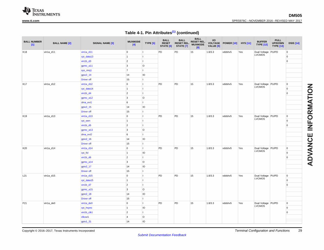
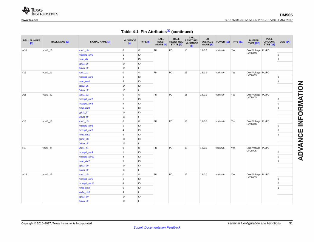
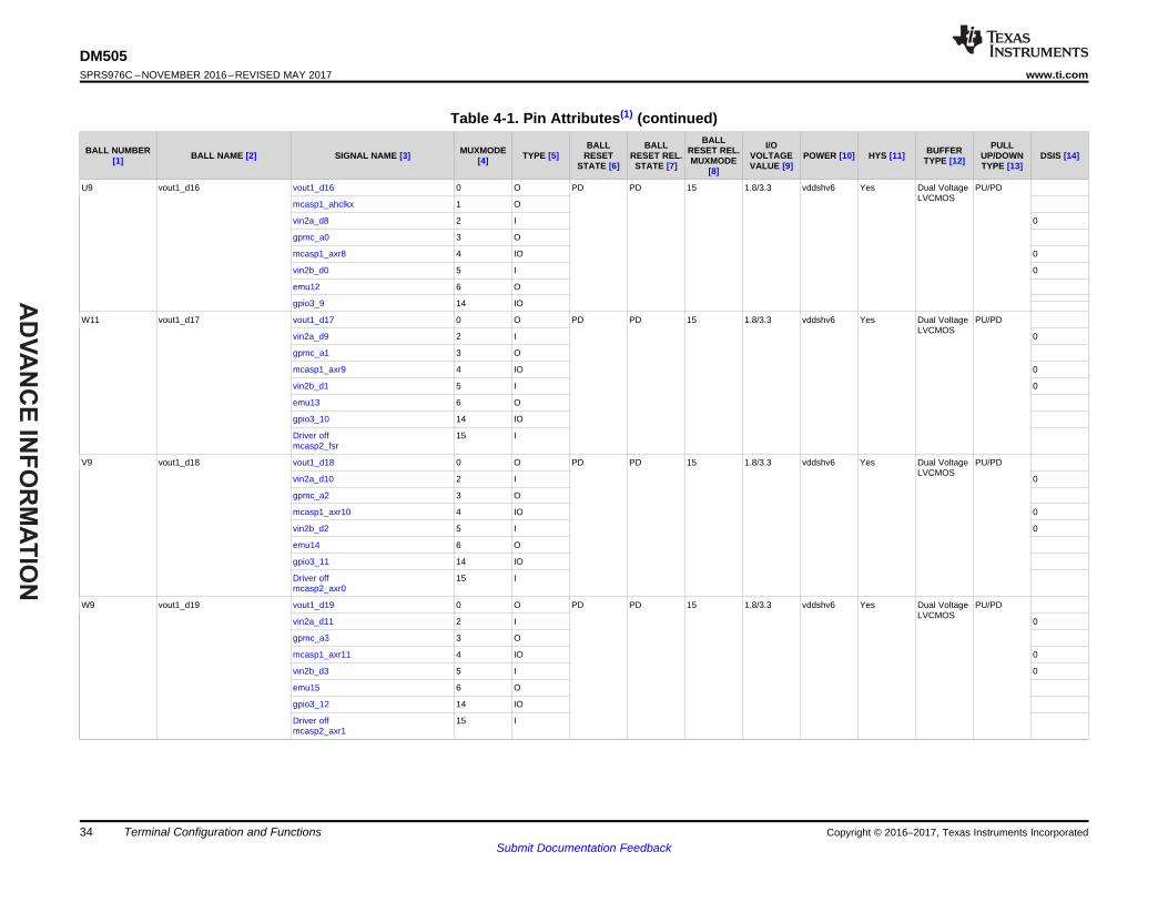
4.2 Pin AttributesTable 4-1 describes the terminal characteristics and the signals multiplexed on each ball. The following listdescribes the table column headers:1. BALL NUMBER: Ball number(s) on the bottom side associated with each signal on the bottom.2. BALL NAME: Mechanical name from package device (name is taken from muxmode 0).3. SIGNAL NAME: Names of signals multiplexed on each ball (also notice that the name of the ball is the
signal name in muxmode 0).
NOTETable 4-1 does not take into account the subsystem multiplexing signals. Subsystemmultiplexing signals are described in Section 4.3, Signal Descriptions.
NOTEIn the Driver off mode, the buffer is configured in high-impedance.

AD
VA
NC
E I
NF
OR
MA
TIO
N
9
DM505www.ti.com SPRS976C –NOVEMBER 2016–REVISED MAY 2017
Submit Documentation FeedbackTerminal Configuration and FunctionsCopyright © 2016–2017, Texas Instruments Incorporated
4. MUXMODE: Multiplexing mode number:(a) MUXMODE 0 is the primary mode; this means that when MUXMODE=0 is set, the function
mapped on the pin corresponds to the name of the pin. The primary muxmode is not necessarilythe default muxmode.
NOTEThe default mode is the mode at the release of the reset; also see the RESET REL.MUXMODE column.
(b) MUXMODE 1 through 15 are possible muxmodes for alternate functions. On each pin, somemuxmodes are effectively used for alternate functions, while some muxmodes are not used. OnlyMUXMODE values which correspond to defined functions should be used.
5. TYPE: Signal type and direction:– I = Input– O = Output– IO = Input or Output– D = Open drain– DS = Differential Signaling– A = Analog– PWR = Power– GND = Ground– CAP = LDO Capacitor
6. BALL RESET STATE: The state of the terminal at power-on reset:– drive 0 (OFF): The buffer drives VOL (pulldown or pullup resistor not activated).– drive 1 (OFF): The buffer drives VOH (pulldown or pullup resistor not activated).– OFF: High-impedance– PD: High-impedance with an active pulldown resistor– PU: High-impedance with an active pullup resistor
7. BALL RESET REL. STATE: The state of the terminal at the deactivation of the rstoutn signal (alsomapped to the PRCM SYS_WARM_OUT_RST signal).– drive 0 (OFF): The buffer drives VOL (pulldown or pullup resistor not activated).– drive clk (OFF): The buffer drives a toggling clock (pulldown or pullup resistor not activated).– drive 1 (OFF): The buffer drives VOH (pulldown or pullup resistor not activated).– OFF: High-impedance– PD: High-impedance with an active pulldown resistor– PU: High-impedance with an active pullup resistor
NOTEFor more information on the CORE_PWRON_RET_RST reset signal and its reset sources,see the Power, Reset, and Clock Management / Reset Management Functional Descriptionsection of the Device TRM.
8. BALL RESET REL. MUXMODE: This muxmode is automatically configured at the release of therstoutn signal (also mapped to the PRCM SYS_WARM_OUT_RST signal).
9. IO VOLTAGE VALUE: This column describes the IO voltage value (the corresponding power supply).10. POWER: The voltage supply that powers the terminal IO buffers.11. HYS: Indicates if the input buffer is with hysteresis:
– Yes: With hysteresis– No: Without hysteresis
An empty box means "Yes".

AD
VA
NC
E IN
FO
RM
AT
ION
10
DM505SPRS976C –NOVEMBER 2016–REVISED MAY 2017 www.ti.com
Submit Documentation FeedbackTerminal Configuration and Functions Copyright © 2016–2017, Texas Instruments Incorporated
NOTEFor more information, see the hysteresis values in Section 5.7, DC Electrical Characteristics.
12. BUFFER TYPE: Drive strength of the associated output buffer.
NOTEFor programmable buffer strength:– The default value is given in Table 4-1.– A note describes all possible values according to the selected muxmode.
13. PULL UP / DOWN TYPE: Denotes the presence of an internal pullup or pulldown resistor. Pullup andpulldown resistors can be enabled or disabled via software.
14. DSIS: The deselected input state (DSIS) indicates the state driven on the peripheral input (logic "0" orlogic "1") when the peripheral pin function is not selected by any of the CTRL_CORE_PADx registers.– 0: Logic 0 driven on the peripheral's input signal port.– 1: Logic 1 driven on the peripheral's input signal port.– blank: Pin state driven on the peripheral's input signal port.
NOTEConfiguring two pins to the same input signal is not supported as it can yield unexpectedresults. This can be easily prevented with the proper software configuration (Hi-Z mode is notan input signal).
NOTEWhen a pad is set into a multiplexing mode which is not defined by pin multiplexing, thatpad’s behavior is undefined. This should be avoided.

AD
VA
NC
E IN
FO
RM
AT
ION
Copyright © 2016–2017, Texas Instruments Incorporated Terminal Configuration and FunctionsSubmit Documentation Feedback
11
DM505www.ti.com SPRS976C –NOVEMBER 2016–REVISED MAY 2017
Table 4-1. Pin Attributes(1)
BALL NUMBER[1] BALL NAME [2] SIGNAL NAME [3] MUXMODE
[4] TYPE [5]BALL
RESETSTATE [6]
BALLRESET REL.STATE [7]
BALLRESET REL.MUXMODE
[8]
I/OVOLTAGEVALUE [9]
POWER [10] HYS [11] BUFFERTYPE [12]
PULLUP/DOWNTYPE [13]
DSIS [14]
M19 adc_in0 adc_in0 0 A 15 1.8 vdda_adc NA GPADC NA
M20 adc_in1 adc_in1 0 A 15 1.8 vdda_adc NA GPADC NA
M21 adc_in2 adc_in2 0 A 15 1.8 vdda_adc NA GPADC NA
M22 adc_in3 adc_in3 0 A 15 1.8 vdda_adc NA GPADC NA
N22 adc_in4 adc_in4 0 A 15 1.8 vdda_adc NA GPADC NA
N21 adc_in5 adc_in5 0 A 15 1.8 vdda_adc NA GPADC NA
P19 adc_in6 adc_in6 0 A 15 1.8 vdda_adc NA GPADC NA
P18 adc_in7 adc_in7 0 A 15 1.8 vdda_adc NA GPADC NA
P20 adc_vrefp adc_vrefp 0 A 15 1.8 vdda_adc NA GPADC NA
N15 cap_vddram_core1 cap_vddram_core1 CAP
M15 cap_vddram_core2 cap_vddram_core2 CAP
M14 cap_vddram_dspeve cap_vddram_dspeve CAP
A11 csi2_0_dx0 csi2_0_dx0 0 IO 1.8 vdda_csi Yes LVCMOSCSI2
PU/PD
A12 csi2_0_dx1 csi2_0_dx1 0 IO 1.8 vdda_csi Yes LVCMOSCSI2
PU/PD
A13 csi2_0_dx2 csi2_0_dx2 0 IO 1.8 vdda_csi Yes LVCMOSCSI2
PU/PD
A15 csi2_0_dx3 csi2_0_dx3 0 IO 1.8 vdda_csi Yes LVCMOSCSI2
PU/PD
A16 csi2_0_dx4 csi2_0_dx4 0 IO 1.8 vdda_csi Yes LVCMOSCSI2
PU/PD
B11 csi2_0_dy0 csi2_0_dy0 0 IO 1.8 vdda_csi Yes LVCMOSCSI2
PU/PD
B12 csi2_0_dy1 csi2_0_dy1 0 IO 1.8 vdda_csi Yes LVCMOSCSI2
PU/PD
B13 csi2_0_dy2 csi2_0_dy2 0 IO 1.8 vdda_csi Yes LVCMOSCSI2
PU/PD
B15 csi2_0_dy3 csi2_0_dy3 0 IO 1.8 vdda_csi Yes LVCMOSCSI2
PU/PD
B16 csi2_0_dy4 csi2_0_dy4 0 IO 1.8 vdda_csi Yes LVCMOSCSI2
PU/PD
T18 cvideo_rset cvideo_rset 0 A 15 1.8 vdda_dac NA AVDAC NA
T17 cvideo_tvout cvideo_tvout 0 A 15 1.8 vdda_dac NA AVDAC NA
P17 cvideo_vfb cvideo_vfb 0 A 15 1.8 vdda_dac NA AVDAC NA
N6 dcan1_rx dcan1_rx 0 IO PU PU 15 1.8/3.3 vddshv1 Yes Dual VoltageLVCMOS
PU/PD
gpio4_10 14 IO
Driver off 15 I
N5 dcan1_tx dcan1_tx 0 IO PU PU 15 1.8/3.3 vddshv1 Yes Dual VoltageLVCMOS
PU/PD
gpio4_9 14 IO
Driver off 15 I

AD
VA
NC
E IN
FO
RM
AT
ION
Copyright © 2016–2017, Texas Instruments IncorporatedTerminal Configuration and FunctionsSubmit Documentation Feedback
12
DM505SPRS976C –NOVEMBER 2016–REVISED MAY 2017 www.ti.com
Table 4-1. Pin Attributes(1) (continued)
BALL NUMBER[1] BALL NAME [2] SIGNAL NAME [3] MUXMODE
[4] TYPE [5]BALL
RESETSTATE [6]
BALLRESET REL.STATE [7]
BALLRESET REL.MUXMODE
[8]
I/OVOLTAGEVALUE [9]
POWER [10] HYS [11] BUFFERTYPE [12]
PULLUP/DOWNTYPE [13]
DSIS [14]
U4 ddr1_a0 ddr1_a0 0 O PD drive 1 (OFF) 1.35/1.5/1.8 vdds_ddr1 NA LVCMOSDDR
PUx/PDy
C1 ddr1_a1 ddr1_a1 0 O PD drive 1 (OFF) 1.35/1.5/1.8 vdds_ddr2 NA LVCMOSDDR
PUx/PDy
D3 ddr1_a2 ddr1_a2 0 O PD drive 1 (OFF) 1.35/1.5/1.8 vdds_ddr2 NA LVCMOSDDR
PUx/PDy
R4 ddr1_a3 ddr1_a3 0 O PD drive 1 (OFF) 1.35/1.5/1.8 vdds_ddr1 NA LVCMOSDDR
PUx/PDy
T4 ddr1_a4 ddr1_a4 0 O PD drive 1 (OFF) 1.35/1.5/1.8 vdds_ddr1 NA LVCMOSDDR
PUx/PDy
N3 ddr1_a5 ddr1_a5 0 O PD drive 1 (OFF) 1.35/1.5/1.8 vdds_ddr1 NA LVCMOSDDR
PUx/PDy
T2 ddr1_a6 ddr1_a6 0 O PD drive 1 (OFF) 1.35/1.5/1.8 vdds_ddr1 NA LVCMOSDDR
PUx/PDy
N2 ddr1_a7 ddr1_a7 0 O PD drive 1 (OFF) 1.35/1.5/1.8 vdds_ddr1 NA LVCMOSDDR
PUx/PDy
T1 ddr1_a8 ddr1_a8 0 O PD drive 1 (OFF) 1.35/1.5/1.8 vdds_ddr1 NA LVCMOSDDR
PUx/PDy
U1 ddr1_a9 ddr1_a9 0 O PD drive 1 (OFF) 1.35/1.5/1.8 vdds_ddr1 NA LVCMOSDDR
PUx/PDy
D1 ddr1_a10 ddr1_a10 0 O PD drive 1 (OFF) 1.35/1.5/1.8 vdds_ddr2 NA LVCMOSDDR
PUx/PDy
R3 ddr1_a11 ddr1_a11 0 O PD drive 1 (OFF) 1.35/1.5/1.8 vdds_ddr1 NA LVCMOSDDR
PUx/PDy
U2 ddr1_a12 ddr1_a12 0 O PD drive 1 (OFF) 1.35/1.5/1.8 vdds_ddr1 NA LVCMOSDDR
PUx/PDy
C3 ddr1_a13 ddr1_a13 0 O PD drive 1 (OFF) 1.35/1.5/1.8 vdds_ddr2 NA LVCMOSDDR
PUx/PDy
R2 ddr1_a14 ddr1_a14 0 O PD drive 1 (OFF) 1.35/1.5/1.8 vdds_ddr1 NA LVCMOSDDR
PUx/PDy
V1 ddr1_a15 ddr1_a15 0 O PD drive 1 (OFF) 1.35/1.5/1.8 vdds_ddr1 NA LVCMOSDDR
PUx/PDy
B3 ddr1_ba0 ddr1_ba0 0 O PD drive 1 (OFF) 1.35/1.5/1.8 vdds_ddr2 NA LVCMOSDDR
PUx/PDy
A3 ddr1_ba1 ddr1_ba1 0 O PD drive 1 (OFF) 1.35/1.5/1.8 vdds_ddr2 NA LVCMOSDDR
PUx/PDy
D2 ddr1_ba2 ddr1_ba2 0 O PD drive 1 (OFF) 1.35/1.5/1.8 vdds_ddr2 NA LVCMOSDDR
PUx/PDy
F2 ddr1_casn ddr1_casn 0 O PD drive 1 (OFF) 1.35/1.5/1.8 vdds_ddr2 NA LVCMOSDDR
PUx/PDy
G1 ddr1_ck ddr1_ck 0 O PD drive clk(OFF)
1.35/1.5/1.8 vdds_ddr2 NA LVCMOSDDR
PUx/PDy
F3 ddr1_cke0 ddr1_cke0 0 O PD drive 0 (OFF) 1.35/1.5/1.8 vdds_ddr2 NA LVCMOSDDR
PUx/PDy
B2 ddr1_csn0 ddr1_csn0 0 O PD drive 1 (OFF) 1.35/1.5/1.8 vdds_ddr2 NA LVCMOSDDR
PUx/PDy

AD
VA
NC
E IN
FO
RM
AT
ION
Copyright © 2016–2017, Texas Instruments Incorporated Terminal Configuration and FunctionsSubmit Documentation Feedback
13
DM505www.ti.com SPRS976C –NOVEMBER 2016–REVISED MAY 2017
Table 4-1. Pin Attributes(1) (continued)
BALL NUMBER[1] BALL NAME [2] SIGNAL NAME [3] MUXMODE
[4] TYPE [5]BALL
RESETSTATE [6]
BALLRESET REL.STATE [7]
BALLRESET REL.MUXMODE
[8]
I/OVOLTAGEVALUE [9]
POWER [10] HYS [11] BUFFERTYPE [12]
PULLUP/DOWNTYPE [13]
DSIS [14]
AA6 ddr1_d0 ddr1_d0 0 IO PD PD 1.35/1.5/1.8 vdds_ddr1 NA LVCMOSDDR
PUx/PDy
AA8 ddr1_d1 ddr1_d1 0 IO PD PD 1.35/1.5/1.8 vdds_ddr1 NA LVCMOSDDR
PUx/PDy
Y8 ddr1_d2 ddr1_d2 0 IO PD PD 1.35/1.5/1.8 vdds_ddr1 NA LVCMOSDDR
PUx/PDy
AA7 ddr1_d3 ddr1_d3 0 IO PD PD 1.35/1.5/1.8 vdds_ddr1 NA LVCMOSDDR
PUx/PDy
AB4 ddr1_d4 ddr1_d4 0 IO PD PD 1.35/1.5/1.8 vdds_ddr1 NA LVCMOSDDR
PUx/PDy
Y5 ddr1_d5 ddr1_d5 0 IO PD PD 1.35/1.5/1.8 vdds_ddr1 NA LVCMOSDDR
PUx/PDy
AA4 ddr1_d6 ddr1_d6 0 IO PD PD 1.35/1.5/1.8 vdds_ddr1 NA LVCMOSDDR
PUx/PDy
Y6 ddr1_d7 ddr1_d7 0 IO PD PD 1.35/1.5/1.8 vdds_ddr1 NA LVCMOSDDR
PUx/PDy
AA18 ddr1_d8 ddr1_d8 0 IO PD PD 1.35/1.5/1.8 vdds_ddr3 NA LVCMOSDDR
PUx/PDy
Y21 ddr1_d9 ddr1_d9 0 IO PD PD 1.35/1.5/1.8 vdds_ddr3 NA LVCMOSDDR
PUx/PDy
AA21 ddr1_d10 ddr1_d10 0 IO PD PD 1.35/1.5/1.8 vdds_ddr3 NA LVCMOSDDR
PUx/PDy
Y22 ddr1_d11 ddr1_d11 0 IO PD PD 1.35/1.5/1.8 vdds_ddr3 NA LVCMOSDDR
PUx/PDy
AA19 ddr1_d12 ddr1_d12 0 IO PD PD 1.35/1.5/1.8 vdds_ddr3 NA LVCMOSDDR
PUx/PDy
AB20 ddr1_d13 ddr1_d13 0 IO PD PD 1.35/1.5/1.8 vdds_ddr3 NA LVCMOSDDR
PUx/PDy
Y17 ddr1_d14 ddr1_d14 0 IO PD PD 1.35/1.5/1.8 vdds_ddr3 NA LVCMOSDDR
PUx/PDy
AB18 ddr1_d15 ddr1_d15 0 IO PD PD 1.35/1.5/1.8 vdds_ddr3 NA LVCMOSDDR
PUx/PDy
AA3 ddr1_d16 ddr1_d16 0 IO PD PD 1.35/1.5/1.8 vdds_ddr1 NA LVCMOSDDR
PUx/PDy
AA2 ddr1_d17 ddr1_d17 0 IO PD PD 1.35/1.5/1.8 vdds_ddr1 NA LVCMOSDDR
PUx/PDy
Y3 ddr1_d18 ddr1_d18 0 IO PD PD 1.35/1.5/1.8 vdds_ddr1 NA LVCMOSDDR
PUx/PDy
V2 ddr1_d19 ddr1_d19 0 IO PD PD 1.35/1.5/1.8 vdds_ddr1 NA LVCMOSDDR
PUx/PDy
U3 ddr1_d20 ddr1_d20 0 IO PD PD 1.35/1.5/1.8 vdds_ddr1 NA LVCMOSDDR
PUx/PDy
V3 ddr1_d21 ddr1_d21 0 IO PD PD 1.35/1.5/1.8 vdds_ddr1 NA LVCMOSDDR
PUx/PDy
Y2 ddr1_d22 ddr1_d22 0 IO PD PD 1.35/1.5/1.8 vdds_ddr1 NA LVCMOSDDR
PUx/PDy

AD
VA
NC
E IN
FO
RM
AT
ION
Copyright © 2016–2017, Texas Instruments IncorporatedTerminal Configuration and FunctionsSubmit Documentation Feedback
14
DM505SPRS976C –NOVEMBER 2016–REVISED MAY 2017 www.ti.com
Table 4-1. Pin Attributes(1) (continued)
BALL NUMBER[1] BALL NAME [2] SIGNAL NAME [3] MUXMODE
[4] TYPE [5]BALL
RESETSTATE [6]
BALLRESET REL.STATE [7]
BALLRESET REL.MUXMODE
[8]
I/OVOLTAGEVALUE [9]
POWER [10] HYS [11] BUFFERTYPE [12]
PULLUP/DOWNTYPE [13]
DSIS [14]
Y1 ddr1_d23 ddr1_d23 0 IO PD PD 1.35/1.5/1.8 vdds_ddr1 NA LVCMOSDDR
PUx/PDy
U21 ddr1_d24 ddr1_d24 0 IO PD PD 1.35/1.5/1.8 vdds_ddr3 NA LVCMOSDDR
PUx/PDy
T20 ddr1_d25 ddr1_d25 0 IO PD PD 1.35/1.5/1.8 vdds_ddr3 NA LVCMOSDDR
PUx/PDy
R21 ddr1_d26 ddr1_d26 0 IO PD PD 1.35/1.5/1.8 vdds_ddr3 NA LVCMOSDDR
PUx/PDy
U20 ddr1_d27 ddr1_d27 0 IO PD PD 1.35/1.5/1.8 vdds_ddr3 NA LVCMOSDDR
PUx/PDy
R22 ddr1_d28 ddr1_d28 0 IO PD PD 1.35/1.5/1.8 vdds_ddr3 NA LVCMOSDDR
PUx/PDy
V20 ddr1_d29 ddr1_d29 0 IO PD PD 1.35/1.5/1.8 vdds_ddr3 NA LVCMOSDDR
PUx/PDy
W22 ddr1_d30 ddr1_d30 0 IO PD PD 1.35/1.5/1.8 vdds_ddr3 NA LVCMOSDDR
PUx/PDy
U22 ddr1_d31 ddr1_d31 0 IO PD PD 1.35/1.5/1.8 vdds_ddr3 NA LVCMOSDDR
PUx/PDy
AB8 ddr1_dqm0 ddr1_dqm0 0 IO PD PD 1.35/1.5/1.8 vdds_ddr1 NA LVCMOSDDR
PUx/PDy
Y18 ddr1_dqm1 ddr1_dqm1 0 IO PD PD 1.35/1.5/1.8 vdds_ddr3 NA LVCMOSDDR
PUx/PDy
AB3 ddr1_dqm2 ddr1_dqm2 0 IO PD PD 1.35/1.5/1.8 vdds_ddr1 NA LVCMOSDDR
PUx/PDy
W21 ddr1_dqm3 ddr1_dqm3 0 IO PD PD 1.35/1.5/1.8 vdds_ddr3 NA LVCMOSDDR
PUx/PDy
AB13 ddr1_dqm_ecc ddr1_dqm_ecc 0 IO PD PD 1.35/1.5/1.8 vdds_ddr1 NA LVCMOSDDR
PUx/PDy
AA5 ddr1_dqs0 ddr1_dqs0 0 IO PD PD 1.35/1.5/1.8 vdds_ddr1 NA LVCMOSDDR
PUx/PDy
AA20 ddr1_dqs1 ddr1_dqs1 0 IO PD PD 1.35/1.5/1.8 vdds_ddr3 NA LVCMOSDDR
PUx/PDy
W1 ddr1_dqs2 ddr1_dqs2 0 IO PD PD 1.35/1.5/1.8 vdds_ddr1 NA LVCMOSDDR
PUx/PDy
T21 ddr1_dqs3 ddr1_dqs3 0 IO PD PD 1.35/1.5/1.8 vdds_ddr3 NA LVCMOSDDR
PUx/PDy
AB5 ddr1_dqsn0 ddr1_dqsn0 0 IO PU PU 1.35/1.5/1.8 vdds_ddr1 NA LVCMOSDDR
PUx/PDy
Y20 ddr1_dqsn1 ddr1_dqsn1 0 IO PU PU 1.35/1.5/1.8 vdds_ddr3 NA LVCMOSDDR
PUx/PDy
W2 ddr1_dqsn2 ddr1_dqsn2 0 IO PU PU 1.35/1.5/1.8 vdds_ddr1 NA LVCMOSDDR
PUx/PDy
T22 ddr1_dqsn3 ddr1_dqsn3 0 IO PU PU 1.35/1.5/1.8 vdds_ddr3 NA LVCMOSDDR
PUx/PDy
AB10 ddr1_dqsn_ecc ddr1_dqsn_ecc 0 IO PU PU 1.35/1.5/1.8 vdds_ddr1 NA LVCMOSDDR
PUx/PDy

AD
VA
NC
E IN
FO
RM
AT
ION
Copyright © 2016–2017, Texas Instruments Incorporated Terminal Configuration and FunctionsSubmit Documentation Feedback
15
DM505www.ti.com SPRS976C –NOVEMBER 2016–REVISED MAY 2017
Table 4-1. Pin Attributes(1) (continued)
BALL NUMBER[1] BALL NAME [2] SIGNAL NAME [3] MUXMODE
[4] TYPE [5]BALL
RESETSTATE [6]
BALLRESET REL.STATE [7]
BALLRESET REL.MUXMODE
[8]
I/OVOLTAGEVALUE [9]
POWER [10] HYS [11] BUFFERTYPE [12]
PULLUP/DOWNTYPE [13]
DSIS [14]
AA10 ddr1_dqs_ecc ddr1_dqs_ecc 0 IO PD PD 1.35/1.5/1.8 vdds_ddr1 NA LVCMOSDDR
PUx/PDy
Y11 ddr1_ecc_d0 ddr1_ecc_d0 0 IO PD PD 1.35/1.5/1.8 vdds_ddr1 NA LVCMOSDDR
PUx/PDy
AA12 ddr1_ecc_d1 ddr1_ecc_d1 0 IO PD PD 1.35/1.5/1.8 vdds_ddr1 NA LVCMOSDDR
PUx/PDy
AA11 ddr1_ecc_d2 ddr1_ecc_d2 0 IO PD PD 1.35/1.5/1.8 vdds_ddr1 NA LVCMOSDDR
PUx/PDy
Y9 ddr1_ecc_d3 ddr1_ecc_d3 0 IO PD PD 1.35/1.5/1.8 vdds_ddr1 NA LVCMOSDDR
PUx/PDy
AA13 ddr1_ecc_d4 ddr1_ecc_d4 0 IO PD PD 1.35/1.5/1.8 vdds_ddr1 NA LVCMOSDDR
PUx/PDy
AB11 ddr1_ecc_d5 ddr1_ecc_d5 0 IO PD PD 1.35/1.5/1.8 vdds_ddr1 NA LVCMOSDDR
PUx/PDy
AA9 ddr1_ecc_d6 ddr1_ecc_d6 0 IO PD PD 1.35/1.5/1.8 vdds_ddr1 NA LVCMOSDDR
PUx/PDy
AB9 ddr1_ecc_d7 ddr1_ecc_d7 0 IO PD PD 1.35/1.5/1.8 vdds_ddr1 NA LVCMOSDDR
PUx/PDy
G2 ddr1_nck ddr1_nck 0 O PD drive clk(OFF)
1.35/1.5/1.8 vdds_ddr2 NA LVCMOSDDR
PUx/PDy
P2 ddr1_odt0 ddr1_odt0 0 O PD drive 0 (OFF) 1.35/1.5/1.8 vdds_ddr1 NA LVCMOSDDR
PUx/PDy
F1 ddr1_rasn ddr1_rasn 0 O PD drive 1 (OFF) 1.35/1.5/1.8 vdds_ddr2 NA LVCMOSDDR
PUx/PDy
N1 ddr1_rst ddr1_rst 0 O PD drive 0 (OFF) 1.35/1.5/1.8 vdds_ddr1 NA LVCMOSDDR
PUx/PDy
E3 ddr1_wen ddr1_wen 0 O PD drive 1 (OFF) 1.35/1.5/1.8 vdds_ddr2 NA LVCMOSDDR
PUx/PDy
H1 emu0 emu0 0 IO PU PU 0 1.8/3.3 vddshv1 Yes Dual VoltageLVCMOS
PU/PD
gpio4_28 14 IO
Driver off 15 I
H2 emu1 emu1 0 IO PU PU 0 1.8/3.3 vddshv1 Yes Dual VoltageLVCMOS
PU/PD
gpio4_29 14 IO
Driver off 15 I
E8 gpmc_ad0 gpmc_ad0 0 IO OFF OFF 15 1.8/3.3 vddshv2 Yes Dual VoltageLVCMOS
PU/PD 0
rgmii1_rxd2 1 I 0
gpio1_14 14 IO
sysboot0 15 I
A7 gpmc_ad1 gpmc_ad1 0 IO OFF OFF 15 1.8/3.3 vddshv2 Yes Dual VoltageLVCMOS
PU/PD 0
rgmii1_rxd1 1 I 0
gpio1_15 14 IO
sysboot1 15 I

AD
VA
NC
E IN
FO
RM
AT
ION
Copyright © 2016–2017, Texas Instruments IncorporatedTerminal Configuration and FunctionsSubmit Documentation Feedback
16
DM505SPRS976C –NOVEMBER 2016–REVISED MAY 2017 www.ti.com
Table 4-1. Pin Attributes(1) (continued)
BALL NUMBER[1] BALL NAME [2] SIGNAL NAME [3] MUXMODE
[4] TYPE [5]BALL
RESETSTATE [6]
BALLRESET REL.STATE [7]
BALLRESET REL.MUXMODE
[8]
I/OVOLTAGEVALUE [9]
POWER [10] HYS [11] BUFFERTYPE [12]
PULLUP/DOWNTYPE [13]
DSIS [14]
F8 gpmc_ad2 gpmc_ad2 0 IO OFF OFF 15 1.8/3.3 vddshv2 Yes Dual VoltageLVCMOS
PU/PD 0
rgmii1_rxd0 1 I 0
gpio1_16 14 IO
sysboot2 15 I
B7 gpmc_ad3 gpmc_ad3 0 IO OFF OFF 15 1.8/3.3 vddshv2 Yes Dual VoltageLVCMOS
PU/PD 0
qspi1_rtclk 1 I 0
gpio1_17 14 IO
sysboot3 15 I
A6 gpmc_ad4 gpmc_ad4 0 IO OFF OFF 15 1.8/3.3 vddshv2 Yes Dual VoltageLVCMOS
PU/PD 0
cam_strobe 1 O
gpio1_18 14 IO
sysboot4 15 I
F7 gpmc_ad5 gpmc_ad5 0 IO OFF OFF 15 1.8/3.3 vddshv2 Yes Dual VoltageLVCMOS
PU/PD 0
uart2_txd 2 O
timer6 3 IO
spi3_d1 4 IO 0
gpio1_19 14 IO
sysboot5mcasp2_aclkx
15 I
E7 gpmc_ad6 gpmc_ad6 0 IO OFF OFF 15 1.8/3.3 vddshv2 Yes Dual VoltageLVCMOS
PU/PD 0
uart2_rxd 2 I 1
timer5 3 IO
spi3_d0 4 IO 0
gpio1_20 14 IO
sysboot6mcasp2_fsx
15 I
C6 gpmc_ad7 gpmc_ad7 0 IO OFF OFF 15 1.8/3.3 vddshv2 Yes Dual VoltageLVCMOS
PU/PD 0
cam_shutter 1 O
timer4 3 IO
spi3_sclk 4 IO 0
gpio1_21 14 IO
Driver offmcasp2_ahclkx
15 I
B6 gpmc_ad8 gpmc_ad8 0 IO OFF OFF 15 1.8/3.3 vddshv2 Yes Dual VoltageLVCMOS
PU/PD 0
timer7 3 IO
spi3_cs0 4 IO 1
gpio1_22 14 IO
sysboot8mcasp2_aclkr
15 I

AD
VA
NC
E IN
FO
RM
AT
ION
Copyright © 2016–2017, Texas Instruments Incorporated Terminal Configuration and FunctionsSubmit Documentation Feedback
17
DM505www.ti.com SPRS976C –NOVEMBER 2016–REVISED MAY 2017
Table 4-1. Pin Attributes(1) (continued)
BALL NUMBER[1] BALL NAME [2] SIGNAL NAME [3] MUXMODE
[4] TYPE [5]BALL
RESETSTATE [6]
BALLRESET REL.STATE [7]
BALLRESET REL.MUXMODE
[8]
I/OVOLTAGEVALUE [9]
POWER [10] HYS [11] BUFFERTYPE [12]
PULLUP/DOWNTYPE [13]
DSIS [14]
A5 gpmc_ad9 gpmc_ad9 0 IO OFF OFF 15 1.8/3.3 vddshv2 Yes Dual VoltageLVCMOS
PU/PD 0
eCAP1_in_PWM1_out 3 IO 0
spi3_cs1 4 IO 1
gpio1_23 14 IO
sysboot9mcasp2_fsr
15 I
D6 gpmc_ad10 gpmc_ad10 0 IO OFF OFF 15 1.8/3.3 vddshv2 Yes Dual VoltageLVCMOS
PU/PD 0
timer2 3 IO
gpio1_24 14 IO
sysboot10mcasp2_axr0
15 I
C5 gpmc_ad11 gpmc_ad11 0 IO OFF OFF 15 1.8/3.3 vddshv2 Yes Dual VoltageLVCMOS
PU/PD 0
timer3 3 IO
gpio1_25 14 IO
sysboot11mcasp2_axr1
15 I
B5 gpmc_ad12 gpmc_ad12 0 IO OFF OFF 15 1.8/3.3 vddshv2 Yes Dual VoltageLVCMOS
PU/PD 0
gpio1_26 14 IO
sysboot12mcasp2_axr2
15 I
D7 gpmc_ad13 gpmc_ad13 0 IO OFF OFF 15 1.8/3.3 vddshv2 Yes Dual VoltageLVCMOS
PU/PD 0
rgmii1_rxc 1 I 0
gpio1_27 14 IO
sysboot13mcasp2_axr3
15 I
B4 gpmc_ad14 gpmc_ad14 0 IO OFF OFF 15 1.8/3.3 vddshv2 Yes Dual VoltageLVCMOS
PU/PD 0
spi2_cs1 4 IO 1
gpio1_28 14 IO
sysboot14mcasp2_axr4
15 I
A4 gpmc_ad15 gpmc_ad15 0 IO OFF OFF 15 1.8/3.3 vddshv2 Yes Dual VoltageLVCMOS
PU/PD 0
spi2_cs0 4 IO 1
gpio1_29 14 IO
sysboot15mcasp2_axr5
15 I

AD
VA
NC
E IN
FO
RM
AT
ION
Copyright © 2016–2017, Texas Instruments IncorporatedTerminal Configuration and FunctionsSubmit Documentation Feedback
18
DM505SPRS976C –NOVEMBER 2016–REVISED MAY 2017 www.ti.com
Table 4-1. Pin Attributes(1) (continued)
BALL NUMBER[1] BALL NAME [2] SIGNAL NAME [3] MUXMODE
[4] TYPE [5]BALL
RESETSTATE [6]
BALLRESET REL.STATE [7]
BALLRESET REL.MUXMODE
[8]
I/OVOLTAGEVALUE [9]
POWER [10] HYS [11] BUFFERTYPE [12]
PULLUP/DOWNTYPE [13]
DSIS [14]
F12 gpmc_advn_ale gpmc_advn_ale 0 O PD PD 15 1.8/3.3 vddshv2 Yes Dual VoltageLVCMOS
PU/PD
rgmii1_txd2 1 O
ehrpwm1_tripzone_input 4 IO 0
clkout1 5 O
dma_evt4 6 I
gpio1_3 14 IO
Driver off 15 I
D12 gpmc_ben0 gpmc_ben0 0 O PD PD 15 1.8/3.3 vddshv2 Yes Dual VoltageLVCMOS
PU/PD
rgmii1_txctl 1 O
ehrpwm1A 4 O
dma_evt2 6 I
gpio1_1 14 IO
Driver off 15 I
E12 gpmc_ben1 gpmc_ben1 0 O PD PD 15 1.8/3.3 vddshv2 Yes Dual VoltageLVCMOS
PU/PD
rgmii1_txd3 1 O
ehrpwm1B 4 O
dma_evt3 6 I
gpio1_2 14 IO
Driver off 15 I
C12 gpmc_clk gpmc_clk 0 IO PD PD 15 1.8/3.3 vddshv2 Yes Dual VoltageLVCMOS
PU/PD 0
rgmii1_txc 1 O
clkout0 5 O
dma_evt1 6 I
gpio1_0 14 IO
Driver off 15 I
C10 gpmc_cs0 gpmc_cs0 0 O PU PU 15 1.8/3.3 vddshv2 Yes Dual VoltageLVCMOS
PU/PD
rgmii1_rxctl 1 I 0
gpio1_6 14 IO
Driver off 15 I
E10 gpmc_cs1 gpmc_cs1 0 O PU PU 15 1.8/3.3 vddshv2 Yes Dual VoltageLVCMOS
PU/PD
qspi1_cs0 1 IO 1
gpio1_7 14 IO
Driver off 15 I
D10 gpmc_cs2 gpmc_cs2 0 O PU PU 15 1.8/3.3 vddshv2 Yes Dual VoltageLVCMOS
PU/PD
qspi1_d3 1 IO 0
gpio1_8 14 IO
Driver off 15 I

AD
VA
NC
E IN
FO
RM
AT
ION
Copyright © 2016–2017, Texas Instruments Incorporated Terminal Configuration and FunctionsSubmit Documentation Feedback
19
DM505www.ti.com SPRS976C –NOVEMBER 2016–REVISED MAY 2017
Table 4-1. Pin Attributes(1) (continued)
BALL NUMBER[1] BALL NAME [2] SIGNAL NAME [3] MUXMODE
[4] TYPE [5]BALL
RESETSTATE [6]
BALLRESET REL.STATE [7]
BALLRESET REL.MUXMODE
[8]
I/OVOLTAGEVALUE [9]
POWER [10] HYS [11] BUFFERTYPE [12]
PULLUP/DOWNTYPE [13]
DSIS [14]
A9 gpmc_cs3 gpmc_cs3 0 O PU PU 15 1.8/3.3 vddshv2 Yes Dual VoltageLVCMOS
PU/PD
qspi1_d2 1 IO 0
gpio1_9 14 IO
Driver off 15 I
B9 gpmc_cs4 gpmc_cs4 0 O PU PU 15 1.8/3.3 vddshv2 Yes Dual VoltageLVCMOS
PU/PD
qspi1_d0 1 IO 0
gpio1_10 14 IO
Driver off 15 I
F10 gpmc_cs5 gpmc_cs5 0 O PU PU 15 1.8/3.3 vddshv2 Yes Dual VoltageLVCMOS
PU/PD
qspi1_d1 1 IO 0
gpio1_11 14 IO
Driver off 15 I
C8 gpmc_cs6 gpmc_cs6 0 O PU PU 15 1.8/3.3 vddshv2 Yes Dual VoltageLVCMOS
PU/PD
qspi1_sclk 1 O
gpio1_12 14 IO
Driver off 15 I
A10 gpmc_oen_ren gpmc_oen_ren 0 O PD PD 15 1.8/3.3 vddshv2 Yes Dual VoltageLVCMOS
PU/PD
rgmii1_txd1 1 O
ehrpwm1_synci 4 I 0
clkout2 5 O
gpio1_4 14 IO
Driver off 15 I
D8 gpmc_wait0 gpmc_wait0 0 I PU PU 15 1.8/3.3 vddshv2 Yes Dual VoltageLVCMOS
PU/PD 1
rgmii1_rxd3 1 I 0
qspi1_rtclk 2 I 0
dma_evt4 6 I
gpio1_13 14 IO
Driver off 15 I
B10 gpmc_wen gpmc_wen 0 O PD PD 15 1.8/3.3 vddshv2 Yes Dual VoltageLVCMOS
PU/PD
rgmii1_txd0 1 O
ehrpwm1_synco 4 O
gpio1_5 14 IO
Driver off 15 I
L3 i2c1_scl i2c1_scl 0 IO OFF OFF 1.8/3.3 vddshv1 Yes Dual VoltageLVCMOS I2C
PU
L4 i2c1_sda i2c1_sda 0 IO OFF OFF 1.8/3.3 vddshv1 Yes Dual VoltageLVCMOS I2C
PU
L6 i2c2_scl i2c2_scl 0 IO OFF OFF 1.8/3.3 vddshv1 Yes Dual VoltageLVCMOS I2C
PU

AD
VA
NC
E IN
FO
RM
AT
ION
Copyright © 2016–2017, Texas Instruments IncorporatedTerminal Configuration and FunctionsSubmit Documentation Feedback
20
DM505SPRS976C –NOVEMBER 2016–REVISED MAY 2017 www.ti.com
Table 4-1. Pin Attributes(1) (continued)
BALL NUMBER[1] BALL NAME [2] SIGNAL NAME [3] MUXMODE
[4] TYPE [5]BALL
RESETSTATE [6]
BALLRESET REL.STATE [7]
BALLRESET REL.MUXMODE
[8]
I/OVOLTAGEVALUE [9]
POWER [10] HYS [11] BUFFERTYPE [12]
PULLUP/DOWNTYPE [13]
DSIS [14]
L5 i2c2_sda i2c2_sda 0 IO OFF OFF 1.8/3.3 vddshv1 Yes Dual VoltageLVCMOS I2C
PU
W6 mcan_rx mcan_rx 0 IO PU PU 15 1.8/3.3 vddshv6 Yes Dual VoltageLVCMOS
PU/PD 1
cam_nreset 1 IO
vin2a_vsync0 2 I
spi1_cs3 3 IO 1
uart3_txd 4 O
gpmc_cs7 5 O
vin1b_vsync1 7 I 0
gpio4_12 14 IO
Driver off 15 I
W7 mcan_tx mcan_tx 0 IO PU PU 15 1.8/3.3 vddshv6 Yes Dual VoltageLVCMOS
PU/PD 1
vin2a_de0 1 I
vin2a_hsync0 2 I
spi1_cs2 3 IO 1
uart3_rxd 4 I 1
gpmc_wait1 6 I1
vin1b_hsync1 7 I 0
vin1b_de1 8 I 0
gpio4_11 14 IO
Driver off 15 I
B17 mdio_d mdio_d 0 IO PU PU 15 1.8/3.3 vddshv4 Yes Dual VoltageLVCMOS
PU/PD 1
spi4_d0 4 IO 0
esm_error 5 IO 0
gpio3_18 14 IO
Driver off 15 I
B19 mdio_mclk mdio_mclk 0 O PU PU 15 1.8/3.3 vddshv4 Yes Dual VoltageLVCMOS
PU/PD 1
spi4_d1 4 IO 0
gpio3_17 14 IO
Driver off 15 I
G5 nmin nmin 0 I PU PU 1.8/3.3 vddshv1 Yes Dual VoltageLVCMOS
PU/PD 1
G3 porz porz 0 I 1.8/3.3 vddshv1 Yes IHHV1833 PU/PD
G4 resetn resetn 0 I PU PU 1.8/3.3 vddshv1 Yes Dual VoltageLVCMOS
PU/PD

AD
VA
NC
E IN
FO
RM
AT
ION
Copyright © 2016–2017, Texas Instruments Incorporated Terminal Configuration and FunctionsSubmit Documentation Feedback
21
DM505www.ti.com SPRS976C –NOVEMBER 2016–REVISED MAY 2017
Table 4-1. Pin Attributes(1) (continued)
BALL NUMBER[1] BALL NAME [2] SIGNAL NAME [3] MUXMODE
[4] TYPE [5]BALL
RESETSTATE [6]
BALLRESET REL.STATE [7]
BALLRESET REL.MUXMODE
[8]
I/OVOLTAGEVALUE [9]
POWER [10] HYS [11] BUFFERTYPE [12]
PULLUP/DOWNTYPE [13]
DSIS [14]
B18 rgmii0_rxc rgmii0_rxc 0 I PD PD 15 1.8/3.3 vddshv4 Yes Dual VoltageLVCMOS
PU/PD 0
cam_strobe 3 O
mmc_clk 5 IO 1
gpio3_25 14 IO
Driver off 15 I
C18 rgmii0_rxctl rgmii0_rxctl 0 I PD PD 15 1.8/3.3 vddshv4 Yes Dual VoltageLVCMOS
PU/PD 0
cam_shutter 3 O
mmc_cmd 5 IO 1
gpio3_26 14 IO
Driver off 15 I
A20 rgmii0_rxd0 rgmii0_rxd0 0 I PD PD 15 1.8/3.3 vddshv4 Yes Dual VoltageLVCMOS
PU/PD 0
mmc_dat3 5 IO 1
gpio3_30 14 IO
Driver off 15 I
C20 rgmii0_rxd1 rgmii0_rxd1 0 I PD PD 15 1.8/3.3 vddshv4 Yes Dual VoltageLVCMOS
PU/PD 0
mmc_dat2 5 IO 1
gpio3_29 14 IO
Driver off 15 I
B20 rgmii0_rxd2 rgmii0_rxd2 0 I PD PD 15 1.8/3.3 vddshv4 Yes Dual VoltageLVCMOS
PU/PD 0
mmc_dat1 5 IO 1
gpio3_28 14 IO
Driver off 15 I
A19 rgmii0_rxd3 rgmii0_rxd3 0 I PD PD 15 1.8/3.3 vddshv4 Yes Dual VoltageLVCMOS
PU/PD 0
mmc_dat0 5 IO 1
gpio3_27 14 IO
Driver off 15 I
C16 rgmii0_txc rgmii0_txc 0 O PD PD 15 1.8/3.3 vddshv4 Yes Dual VoltageLVCMOS
PU/PD
cam_strobe 3 O
spi4_sclk 4 IO 0
mmc_clk 5 IO 1
gpio3_19 14 IO
Driver off 15 I
C17 rgmii0_txctl rgmii0_txctl 0 O PD PD 15 1.8/3.3 vddshv4 Yes Dual VoltageLVCMOS
PU/PD
cam_shutter 3 O
spi4_cs0 4 IO 1
mmc_cmd 5 IO 1
gpio3_20 14 IO
Driver off 15 I

AD
VA
NC
E IN
FO
RM
AT
ION
Copyright © 2016–2017, Texas Instruments IncorporatedTerminal Configuration and FunctionsSubmit Documentation Feedback
22
DM505SPRS976C –NOVEMBER 2016–REVISED MAY 2017 www.ti.com
Table 4-1. Pin Attributes(1) (continued)
BALL NUMBER[1] BALL NAME [2] SIGNAL NAME [3] MUXMODE
[4] TYPE [5]BALL
RESETSTATE [6]
BALLRESET REL.STATE [7]
BALLRESET REL.MUXMODE
[8]
I/OVOLTAGEVALUE [9]
POWER [10] HYS [11] BUFFERTYPE [12]
PULLUP/DOWNTYPE [13]
DSIS [14]
F17 rgmii0_txd0 rgmii0_txd0 0 O PD PD 15 1.8/3.3 vddshv4 Yes Dual VoltageLVCMOS
PU/PD
mmc_dat3 5 IO 1
gpio3_24 14 IO
Driver off 15 I
E17 rgmii0_txd1 rgmii0_txd1 0 O PD PD 15 1.8/3.3 vddshv4 Yes Dual VoltageLVCMOS
PU/PD
mmc_dat2 5 IO 1
gpio3_23 14 IO
Driver off 15 I
D16 rgmii0_txd2 rgmii0_txd2 0 O PD PD 15 1.8/3.3 vddshv4 Yes Dual VoltageLVCMOS
PU/PD
eCAP1_in_PWM1_out 3 IO 0
mmc_dat1 5 IO 1
gpio3_22 14 IO
Driver off 15 I
E16 rgmii0_txd3 rgmii0_txd3 0 O PD PD 15 1.8/3.3 vddshv4 Yes Dual VoltageLVCMOS
PU/PD
mmc_dat0 5 IO 1
gpio3_21 14 IO
Driver off 15 I
F4 rstoutn rstoutn 0 O PD drive 1 (OFF) 1.8/3.3 vddshv1 Yes Dual VoltageLVCMOS
PU/PD
J6 rtck rtck 0 O PU drive clk(OFF)
0 1.8/3.3 vddshv1 Yes Dual VoltageLVCMOS
PU/PD
gpio4_27 14 IO
Driver off 15 I
R6 spi1_cs0 spi1_cs0 0 IO PU PU 15 1.8/3.3 vddshv1 Yes Dual VoltageLVCMOS
PU/PD 1
uart3_txd 1 O
gpio4_3 14 IO
Driver off 15 I
R5 spi1_cs1 spi1_cs1 0 IO PU PU 15 1.8/3.3 vddshv1 Yes Dual VoltageLVCMOS
PU/PD 1
spi3_cs1 1 IO 1
timer6 4 IO
ehrpwm1_tripzone_input 7 IO 0
gpio4_4 14 IO
Driver off 15 I
T5 spi1_d0 spi1_d0 0 IO OFF OFF 15 1.8/3.3 vddshv1 Yes Dual VoltageLVCMOS
PU/PD 0
uart3_rtsn 1 O
gpio4_2 14 IO
Driver off 15 I

AD
VA
NC
E IN
FO
RM
AT
ION
Copyright © 2016–2017, Texas Instruments Incorporated Terminal Configuration and FunctionsSubmit Documentation Feedback
23
DM505www.ti.com SPRS976C –NOVEMBER 2016–REVISED MAY 2017
Table 4-1. Pin Attributes(1) (continued)
BALL NUMBER[1] BALL NAME [2] SIGNAL NAME [3] MUXMODE
[4] TYPE [5]BALL
RESETSTATE [6]
BALLRESET REL.STATE [7]
BALLRESET REL.MUXMODE
[8]
I/OVOLTAGEVALUE [9]
POWER [10] HYS [11] BUFFERTYPE [12]
PULLUP/DOWNTYPE [13]
DSIS [14]
U6 spi1_d1 spi1_d1 0 IO OFF OFF 15 1.8/3.3 vddshv1 Yes Dual VoltageLVCMOS
PU/PD 0
uart3_ctsn 1 I 1
gpio4_1 14 IO
Driver off 15 I
M2 spi1_sclk spi1_sclk 0 IO PD PD 15 1.8/3.3 vddshv1 Yes Dual VoltageLVCMOS
PU/PD 0
uart3_rxd 1 I 1
gpio4_0 14 IO
Driver off 15 I
L2 spi2_cs0 spi2_cs0 0 IO PU PU 15 1.8/3.3 vddshv1 Yes Dual VoltageLVCMOS
PU/PD 1
uart3_txd 1 O
ehrpwm1B 2 O
timer4 3 IO
gpio4_8 14 IO
Driver off 15 I
R7 spi2_d0 spi2_d0 0 IO OFF OFF 15 1.8/3.3 vddshv1 Yes Dual VoltageLVCMOS
PU/PD 0
uart3_rtsn 1 O
timer1 3 IO
gpio4_7 14 IO
sysboot7 15 I
N4 spi2_d1 spi2_d1 0 IO OFF OFF 15 1.8/3.3 vddshv1 Yes Dual VoltageLVCMOS
PU/PD 0
uart3_ctsn 1 I 1
timer5 3 IO
eCAP1_in_PWM1_out 7 IO 0
gpio4_6 14 IO
Driver off 15 I
L1 spi2_sclk spi2_sclk 0 IO PD PD 15 1.8/3.3 vddshv1 Yes Dual VoltageLVCMOS
PU/PD 0
uart3_rxd 1 I 1
ehrpwm1A 2 O
timer3 3 IO
gpio4_5 14 IO
Driver off 15 I
J2 tclk tclk 0 I PU PU 0 1.8/3.3 vddshv1 Yes IQ1833 PU/PD
J1 tdi tdi 0 I PU PU 0 1.8/3.3 vddshv1 Yes Dual VoltageLVCMOS
PU/PD
gpio4_25 14 IO
Driver off 15 I
J4 tdo tdo 0 O PU PU 0 1.8/3.3 vddshv1 Yes Dual VoltageLVCMOS
PU/PD
gpio4_26 14 IO
Driver off 15 I

AD
VA
NC
E IN
FO
RM
AT
ION
Copyright © 2016–2017, Texas Instruments IncorporatedTerminal Configuration and FunctionsSubmit Documentation Feedback
24
DM505SPRS976C –NOVEMBER 2016–REVISED MAY 2017 www.ti.com
Table 4-1. Pin Attributes(1) (continued)
BALL NUMBER[1] BALL NAME [2] SIGNAL NAME [3] MUXMODE
[4] TYPE [5]BALL
RESETSTATE [6]
BALLRESET REL.STATE [7]
BALLRESET REL.MUXMODE
[8]
I/OVOLTAGEVALUE [9]
POWER [10] HYS [11] BUFFERTYPE [12]
PULLUP/DOWNTYPE [13]
DSIS [14]
J3 tms tms 0 IO OFF OFF 0 1.8/3.3 vddshv1 Yes Dual VoltageLVCMOS
PU/PD
J5 trstn trstn 0 I PD PD 1.8/3.3 vddshv1 Yes Dual VoltageLVCMOS
PU/PD
F14 uart1_ctsn uart1_ctsn 0 I PU PU 15 1.8/3.3 vddshv3 Yes Dual VoltageLVCMOS
PU/PD 1
xref_clk1 1 I
uart3_rxd 2 I 1
gpmc_a16 3 O
spi4_sclk 4 IO 0
spi1_cs2 5 IO 1
timer3 6 IO
ehrpwm1_synci 7 I 0
clkout0 8 O
vin2a_hsync0 9 I
gpmc_a12 10 O
gpmc_clk 11 IO 0
dcan1_tx 12 IO
gpio4_15 14 IO
Driver off 15 I
C14 uart1_rtsn uart1_rtsn 0 O PU PU 15 1.8/3.3 vddshv3 Yes Dual VoltageLVCMOS
PU/PD
uart3_txd 2 O
gpmc_a17 3 O
spi4_cs0 4 IO 1
spi1_cs3 5 IO 1
timer4 6 IO
ehrpwm1_synco 7 O
qspi1_rtclk 8 I 0
vin2a_vsync0 9 I
gpmc_a13 10 O
dcan1_rx 12 IO
gpio4_16 14 IO
Driver off 15 I

AD
VA
NC
E IN
FO
RM
AT
ION
Copyright © 2016–2017, Texas Instruments Incorporated Terminal Configuration and FunctionsSubmit Documentation Feedback
25
DM505www.ti.com SPRS976C –NOVEMBER 2016–REVISED MAY 2017
Table 4-1. Pin Attributes(1) (continued)
BALL NUMBER[1] BALL NAME [2] SIGNAL NAME [3] MUXMODE
[4] TYPE [5]BALL
RESETSTATE [6]
BALLRESET REL.STATE [7]
BALLRESET REL.MUXMODE
[8]
I/OVOLTAGEVALUE [9]
POWER [10] HYS [11] BUFFERTYPE [12]
PULLUP/DOWNTYPE [13]
DSIS [14]
F13 uart1_rxd uart1_rxd 0 I PU PU 15 1.8/3.3 vddshv3 Yes Dual VoltageLVCMOS
PU/PD 1
spi4_d1 4 IO 0
qspi1_rtclk 5 I 0
gpmc_a12 10 O
mcan_tx 12 IO 1
gpio4_13 14 IO
Driver off 15 I
E14 uart1_txd uart1_txd 0 O PU PU 15 1.8/3.3 vddshv3 Yes Dual VoltageLVCMOS
PU/PD
spi4_d0 4 IO 0
gpmc_a13 10 O
mcan_rx 12 IO 1
gpio4_14 14 IO
Driver off 15 I
F15 uart2_ctsn uart2_ctsn 0 I OFF OFF 15 1.8/3.3 vddshv3 Yes Dual VoltageLVCMOS
PU/PD 1
xref_clk1 2 I
gpmc_a18 3 O
spi3_sclk 4 IO 0
qspi1_cs1 5 IO 1
timer7 6 IO
vin2a_hsync0 9 I
gpmc_clk 10 IO 0
mcan_tx 12 IO 1
gpio4_19 14 IO
Driver off 15 I
F16 uart2_rtsn uart2_rtsn 0 O PU PU 15 1.8/3.3 vddshv3 Yes Dual VoltageLVCMOS
PU/PD
eCAP1_in_PWM1_out 1 IO 0
gpmc_a19 3 O
spi3_cs0 4 IO 1
timer8 6 IO
vin2a_vsync0 9 I
mcan_rx 12 IO 1
gpio4_20 14 IO
Driver off 15 I

AD
VA
NC
E IN
FO
RM
AT
ION
Copyright © 2016–2017, Texas Instruments IncorporatedTerminal Configuration and FunctionsSubmit Documentation Feedback
26
DM505SPRS976C –NOVEMBER 2016–REVISED MAY 2017 www.ti.com
Table 4-1. Pin Attributes(1) (continued)
BALL NUMBER[1] BALL NAME [2] SIGNAL NAME [3] MUXMODE
[4] TYPE [5]BALL
RESETSTATE [6]
BALLRESET REL.STATE [7]
BALLRESET REL.MUXMODE
[8]
I/OVOLTAGEVALUE [9]
POWER [10] HYS [11] BUFFERTYPE [12]
PULLUP/DOWNTYPE [13]
DSIS [14]
D14 uart2_rxd uart2_rxd 0 I PU PU 15 1.8/3.3 vddshv3 Yes Dual VoltageLVCMOS
PU/PD 1
spi3_d1 4 IO 0
timer1 6 IO
ehrpwm1A 7 O
gpmc_clk 10 IO 0
gpmc_a12 11 O
dcan1_tx 12 IO
gpio4_17 14 IO
Driver off 15 I
D15 uart2_txd uart2_txd 0 O PU PU 15 1.8/3.3 vddshv3 Yes Dual VoltageLVCMOS
PU/PD
spi3_d0 4 IO 0
timer2 6 IO
ehrpwm1B 7 O
gpmc_a13 11 O
dcan1_rx 12 IO
gpio4_18 14 IO
Driver off 15 I
H12, H13, H7,J10, J11, J15,K12, L12, L15,N12, N16, P10,P14
vdd vdd PWR
P22 vdda_adc vdda_adc PWR
A14 vdda_csi vdda_csi PWR
U19 vdda_dac vdda_dac PWR
N8 vdda_ddr_dsp vdda_ddr_dsp PWR
M8 vdda_gmac_core vdda_gmac_core PWR
E21 vdda_osc vdda_osc PWR
H14 vdda_per vdda_per PWR
G12, J7, L16,P13, T11
vdds18v vdds18v PWR
P7, T9 vdds18v_ddr1 vdds18v_ddr1 PWR
G7 vdds18v_ddr2 vdds18v_ddr2 PWR
T16, V21 vdds18v_ddr3 vdds18v_ddr3 PWR
K2, K7, L7, M7 vddshv1 vddshv1 PWR
B8, G11, G8, G9 vddshv2 vddshv2 PWR
G14 vddshv3 vddshv3 PWR
A18, E20 vddshv4 vddshv4 PWR
H17, J16, J21 vddshv5 vddshv5 PWR

AD
VA
NC
E IN
FO
RM
AT
ION
Copyright © 2016–2017, Texas Instruments Incorporated Terminal Configuration and FunctionsSubmit Documentation Feedback
27
DM505www.ti.com SPRS976C –NOVEMBER 2016–REVISED MAY 2017
Table 4-1. Pin Attributes(1) (continued)
BALL NUMBER[1] BALL NAME [2] SIGNAL NAME [3] MUXMODE
[4] TYPE [5]BALL
RESETSTATE [6]
BALLRESET REL.STATE [7]
BALLRESET REL.MUXMODE
[8]
I/OVOLTAGEVALUE [9]
POWER [10] HYS [11] BUFFERTYPE [12]
PULLUP/DOWNTYPE [13]
DSIS [14]
AA16, T10, T12,T13
vddshv6 vddshv6 PWR
AA1, AB6, R1, T7,T8
vdds_ddr1 vdds_ddr1 PWR
C2, E2, G6 vdds_ddr2 vdds_ddr2 PWR
AA22, AB19, T15 vdds_ddr3 vdds_ddr3 PWR
K8, L8, M9, P11,P12, P8, P9
vdd_dspeve vdd_dspeve PWR
F22 vin1a_clk0 vin1a_clk0 0 I PD PD 15 1.8/3.3 vddshv5 Yes Dual VoltageLVCMOS
PU/PD 0
cpi_pclk 1 I 0
clkout0 4 O
gpio1_30 14 IO
Driver offmcasp3_aclkx
15 I
G18 vin1a_d0 vin1a_d0 0 I PD PD 15 1.8/3.3 vddshv5 Yes Dual VoltageLVCMOS
PU/PD 0
cpi_data2 1 I 0
gpio2_3 14 IO
Driver offmcasp3_axr1
15 I
G21 vin1a_d1 vin1a_d1 0 I PD PD 15 1.8/3.3 vddshv5 Yes Dual VoltageLVCMOS
PU/PD 0
cpi_data3 1 I 0
gpio2_4 14 IO
Driver offmcasp3_axr2
15 I
G22 vin1a_d2 vin1a_d2 0 I PD PD 15 1.8/3.3 vddshv5 Yes Dual VoltageLVCMOS
PU/PD 0
cpi_data4 1 I 0
gpio2_5 14 IO
Driver offmcasp3_axr3
15 I
H18 vin1a_d3 vin1a_d3 0 I PD PD 15 1.8/3.3 vddshv5 Yes Dual VoltageLVCMOS
PU/PD 0
cpi_data5 1 I 0
gpio2_6 14 IO
Driver offmcasp3_axr4
15 I
H20 vin1a_d4 vin1a_d4 0 I PD PD 15 1.8/3.3 vddshv5 Yes Dual VoltageLVCMOS
PU/PD 0
cpi_data6 1 I 0
gpio2_7 14 IO
Driver offmcasp3_axr5
15 I

AD
VA
NC
E IN
FO
RM
AT
ION
Copyright © 2016–2017, Texas Instruments IncorporatedTerminal Configuration and FunctionsSubmit Documentation Feedback
28
DM505SPRS976C –NOVEMBER 2016–REVISED MAY 2017 www.ti.com
Table 4-1. Pin Attributes(1) (continued)
BALL NUMBER[1] BALL NAME [2] SIGNAL NAME [3] MUXMODE
[4] TYPE [5]BALL
RESETSTATE [6]
BALLRESET REL.STATE [7]
BALLRESET REL.MUXMODE
[8]
I/OVOLTAGEVALUE [9]
POWER [10] HYS [11] BUFFERTYPE [12]
PULLUP/DOWNTYPE [13]
DSIS [14]
H19 vin1a_d5 vin1a_d5 0 I PD PD 15 1.8/3.3 vddshv5 Yes Dual VoltageLVCMOS
PU/PD 0
cpi_data7 1 I 0
gpio2_8 14 IO
xref_clk2mcasp3_ahclkx
15 I
H22 vin1a_d6 vin1a_d6 0 I PD PD 15 1.8/3.3 vddshv5 Yes Dual VoltageLVCMOS
PU/PD 0
cpi_data8 1 I 0
gpio2_9 14 IO
Driver offmcasp3_fsx
15 I
H21 vin1a_d7 vin1a_d7 0 I PD PD 15 1.8/3.3 vddshv5 Yes Dual VoltageLVCMOS
PU/PD 0
cpi_data9 1 I 0
gpio2_10 14 IO
Driver off 15 I
J17 vin1a_d8 vin1a_d8 0 I PD PD 15 1.8/3.3 vddshv5 Yes Dual VoltageLVCMOS
PU/PD 0
cpi_data10 1 I 0
vin1b_d0 2 I 0
gpmc_a8 3 O
sys_nirq2 7 I
gpio2_11 14 IO
Driver off 15 I
K22 vin1a_d9 vin1a_d9 0 I PD PD 15 1.8/3.3 vddshv5 Yes Dual VoltageLVCMOS
PU/PD 0
cpi_data11 1 I 0
vin1b_d1 2 I 0
gpmc_a9 3 O
sys_nirq1 7 I
gpio2_12 14 IO
Driver off 15 I
K21 vin1a_d10 vin1a_d10 0 I PD PD 15 1.8/3.3 vddshv5 Yes Dual VoltageLVCMOS
PU/PD 0
cpi_data12 1 I 0
vin1b_d2 2 I 0
gpmc_a10 3 O
sys_nirq2 7 I
gpio2_13 14 IO
Driver off 15 I
AD
VA
NC
E IN
FO
RM
AT
ION
Copyright © 2016–2017, Texas Instruments Incorporated Terminal Configuration and FunctionsSubmit Documentation Feedback
29
DM505www.ti.com SPRS976C –NOVEMBER 2016–REVISED MAY 2017
Table 4-1. Pin Attributes(1) (continued)
BALL NUMBER[1] BALL NAME [2] SIGNAL NAME [3] MUXMODE
[4] TYPE [5]BALL
RESETSTATE [6]
BALLRESET REL.STATE [7]
BALLRESET REL.MUXMODE
[8]
I/OVOLTAGEVALUE [9]
POWER [10] HYS [11] BUFFERTYPE [12]
PULLUP/DOWNTYPE [13]
DSIS [14]
K18 vin1a_d11 vin1a_d11 0 I PD PD 15 1.8/3.3 vddshv5 Yes Dual VoltageLVCMOS
PU/PD 0
cpi_data13 1 I 0
vin1b_d3 2 I 0
gpmc_a11 3 O
sys_nirq1 7 I
gpio2_14 14 IO
Driver off 15 I
K17 vin1a_d12 vin1a_d12 0 I PD PD 15 1.8/3.3 vddshv5 Yes Dual VoltageLVCMOS
PU/PD 0
cpi_data14 1 I 0
vin1b_d4 2 I 0
gpmc_a12 3 O
dma_evt1 6 I
gpio2_15 14 IO
Driver off 15 I
K19 vin1a_d13 vin1a_d13 0 I PD PD 15 1.8/3.3 vddshv5 Yes Dual VoltageLVCMOS
PU/PD 0
cpi_wen 1 I 0
vin1b_d5 2 I 0
gpmc_a13 3 O
dma_evt2 6 I
gpio2_16 14 IO
Driver off 15 I
K20 vin1a_d14 vin1a_d14 0 I PD PD 15 1.8/3.3 vddshv5 Yes Dual VoltageLVCMOS
PU/PD 0
cpi_fid 1 IO 0
vin1b_d6 2 I 0
gpmc_a14 3 O
gpio2_17 14 IO
Driver off 15 I
L21 vin1a_d15 vin1a_d15 0 I PD PD 15 1.8/3.3 vddshv5 Yes Dual VoltageLVCMOS
PU/PD 0
cpi_data15 1 I 0
vin1b_d7 2 I 0
gpmc_a15 3 O
gpio2_18 14 IO
Driver off 15 I
F21 vin1a_de0 vin1a_de0 0 I PD PD 15 1.8/3.3 vddshv5 Yes Dual VoltageLVCMOS
PU/PD 0
cpi_hsync 1 IO 0
vin1b_clk1 2 I 0
clkout1 4 O
gpio1_31 14 IO

AD
VA
NC
E IN
FO
RM
AT
ION
Copyright © 2016–2017, Texas Instruments IncorporatedTerminal Configuration and FunctionsSubmit Documentation Feedback
30
DM505SPRS976C –NOVEMBER 2016–REVISED MAY 2017 www.ti.com
Table 4-1. Pin Attributes(1) (continued)
BALL NUMBER[1] BALL NAME [2] SIGNAL NAME [3] MUXMODE
[4] TYPE [5]BALL
RESETSTATE [6]
BALLRESET REL.STATE [7]
BALLRESET REL.MUXMODE
[8]
I/OVOLTAGEVALUE [9]
POWER [10] HYS [11] BUFFERTYPE [12]
PULLUP/DOWNTYPE [13]
DSIS [14]
F20 vin1a_fld0 vin1a_fld0 0 I PD PD 15 1.8/3.3 vddshv5 Yes Dual VoltageLVCMOS
PU/PD 0
cpi_vsync 1 IO 0
vin2b_clk1 2 I 0
clkout2 4 O
gpio2_0 14 IO
Driver offmcasp3_aclkr
15 I
F19 vin1a_hsync0 vin1a_hsync0 0 I PD PD 15 1.8/3.3 vddshv5 Yes Dual VoltageLVCMOS
PU/PD 0
cpi_data0 1 I 0
vin1a_de0 2 I 0
gpio2_1 14 IO
Driver offmcasp3_fsr
15 I
G19 vin1a_vsync0 vin1a_vsync0 0 I PD PD 15 1.8/3.3 vddshv5 Yes Dual VoltageLVCMOS
PU/PD 0
cpi_data1 1 I 0
gpio2_2 14 IO
Driver offmcasp3_axr0
15 I
L22 vin2a_clk0 vin2a_clk0 0 I PD PD 15 1.8/3.3 vddshv5 Yes Dual VoltageLVCMOS
PU/PD
gpio2_19 14 IO
Driver off 15 I
M17 vin2a_de0 vin2a_de0 0 I PD PD 15 1.8/3.3 vddshv5 Yes Dual VoltageLVCMOS
PU/PD
cam_strobe 1 O
vin2b_hsync1 2 I 0
vin2b_de1 5 I 0
gpio4_21 14 IO
Driver off 15 I
M18 vin2a_fld0 vin2a_fld0 0 I PD PD 15 1.8/3.3 vddshv5 Yes Dual VoltageLVCMOS
PU/PD
cam_shutter 1 O
vin2b_vsync1 2 I 0
gpio4_22 14 IO
Driver off 15 I
AB17 vout1_clk vout1_clk 0 O PD PD 15 1.8/3.3 vddshv6 Yes Dual VoltageLVCMOS
PU/PD
vin1a_d12 2 I 0
clkout0 4 O
vin2a_clk0 9 I
gpio2_20 14 IO
Driver off 15 I
AD
VA
NC
E IN
FO
RM
AT
ION
Copyright © 2016–2017, Texas Instruments Incorporated Terminal Configuration and FunctionsSubmit Documentation Feedback
31
DM505www.ti.com SPRS976C –NOVEMBER 2016–REVISED MAY 2017
Table 4-1. Pin Attributes(1) (continued)
BALL NUMBER[1] BALL NAME [2] SIGNAL NAME [3] MUXMODE
[4] TYPE [5]BALL
RESETSTATE [6]
BALLRESET REL.STATE [7]
BALLRESET REL.MUXMODE
[8]
I/OVOLTAGEVALUE [9]
POWER [10] HYS [11] BUFFERTYPE [12]
PULLUP/DOWNTYPE [13]
DSIS [14]
W16 vout1_d0 vout1_d0 0 O PD PD 15 1.8/3.3 vddshv6 Yes Dual VoltageLVCMOS
PU/PD
mcasp1_axr0 1 IO 0
mmc_clk 5 IO 1
gpio2_25 14 IO
Driver off 15 I
V16 vout1_d1 vout1_d1 0 O PD PD 15 1.8/3.3 vddshv6 Yes Dual VoltageLVCMOS
PU/PD
mcasp1_axr1 1 IO 0
mmc_cmd 5 IO 1
gpio2_26 14 IO
Driver off 15 I
U15 vout1_d2 vout1_d2 0 O PD PD 15 1.8/3.3 vddshv6 Yes Dual VoltageLVCMOS
PU/PD
mcasp1_axr2 1 IO 0
mcasp1_axr8 4 IO 0
mmc_dat0 5 IO 1
gpio2_27 14 IO
Driver off 15 I
V15 vout1_d3 vout1_d3 0 O PD PD 15 1.8/3.3 vddshv6 Yes Dual VoltageLVCMOS
PU/PD
mcasp1_axr3 1 IO 0
mcasp1_axr9 4 IO 0
mmc_dat1 5 IO 1
gpio2_28 14 IO
Driver off 15 I
Y15 vout1_d4 vout1_d4 0 O PD PD 15 1.8/3.3 vddshv6 Yes Dual VoltageLVCMOS
PU/PD
mcasp1_axr4 1 IO 0
mcasp1_axr10 4 IO 0
mmc_dat2 5 IO 1
gpio2_29 14 IO
Driver off 15 I
W15 vout1_d5 vout1_d5 0 O PD PD 15 1.8/3.3 vddshv6 Yes Dual VoltageLVCMOS
PU/PD
mcasp1_axr5 1 IO 0
mcasp1_axr11 4 IO 0
mmc_dat3 5 IO 1
vin2a_clk0 9 I
gpio2_30 14 IO
Driver off 15 I

AD
VA
NC
E IN
FO
RM
AT
ION
Copyright © 2016–2017, Texas Instruments IncorporatedTerminal Configuration and FunctionsSubmit Documentation Feedback
32
DM505SPRS976C –NOVEMBER 2016–REVISED MAY 2017 www.ti.com
Table 4-1. Pin Attributes(1) (continued)
BALL NUMBER[1] BALL NAME [2] SIGNAL NAME [3] MUXMODE
[4] TYPE [5]BALL
RESETSTATE [6]
BALLRESET REL.STATE [7]
BALLRESET REL.MUXMODE
[8]
I/OVOLTAGEVALUE [9]
POWER [10] HYS [11] BUFFERTYPE [12]
PULLUP/DOWNTYPE [13]
DSIS [14]
AA15 vout1_d6 vout1_d6 0 O PD PD 15 1.8/3.3 vddshv6 Yes Dual VoltageLVCMOS
PU/PD
mcasp1_axr6 1 IO 0
mcasp1_axr12 4 IO 0
esm_error 5 IO 0
emu2 6 O
vin2a_de0 9 I
gpio2_31 14 IO
Driver off 15 I
AB15 vout1_d7 vout1_d7 0 O PD PD 15 1.8/3.3 vddshv6 Yes Dual VoltageLVCMOS
PU/PD
mcasp1_axr7 1 IO 0
eCAP1_in_PWM1_out 3 IO 0
mcasp1_axr13 4 IO 0
emu3 6 O
vin2a_fld0 9 I
gpio3_0 14 IO
Driver off 15 I
AA14 vout1_d8 vout1_d8 0 O PD PD 15 1.8/3.3 vddshv6 Yes Dual VoltageLVCMOS
PU/PD
mcasp1_axr8 1 IO 0
vin2a_d0 2 I 0
gpmc_a20 3 O
emu4 6 O
gpio3_1 14 IO
Driver off 15 I
AB14 vout1_d9 vout1_d9 0 O PD PD 15 1.8/3.3 vddshv6 Yes Dual VoltageLVCMOS
PU/PD
mcasp1_axr9 1 IO 0
vin2a_d1 2 I 0
gpmc_a21 3 O
emu5 6 O
gpio3_2 14 IO
Driver off 15 I
U13 vout1_d10 vout1_d10 0 O PD PD 15 1.8/3.3 vddshv6 Yes Dual VoltageLVCMOS
PU/PD
mcasp1_axr10 1 IO 0
vin2a_d2 2 I 0
gpmc_a22 3 O
emu6 6 O
gpio3_3 14 IO
Driver off 15 I

AD
VA
NC
E IN
FO
RM
AT
ION
Copyright © 2016–2017, Texas Instruments Incorporated Terminal Configuration and FunctionsSubmit Documentation Feedback
33
DM505www.ti.com SPRS976C –NOVEMBER 2016–REVISED MAY 2017
Table 4-1. Pin Attributes(1) (continued)
BALL NUMBER[1] BALL NAME [2] SIGNAL NAME [3] MUXMODE
[4] TYPE [5]BALL
RESETSTATE [6]
BALLRESET REL.STATE [7]
BALLRESET REL.MUXMODE
[8]
I/OVOLTAGEVALUE [9]
POWER [10] HYS [11] BUFFERTYPE [12]
PULLUP/DOWNTYPE [13]
DSIS [14]
V13 vout1_d11 vout1_d11 0 O PD PD 15 1.8/3.3 vddshv6 Yes Dual VoltageLVCMOS
PU/PD
mcasp1_axr11 1 IO 0
vin2a_d3 2 I 0
gpmc_a23 3 O
emu7 6 O
gpio3_4 14 IO
Driver off 15 I
Y13 vout1_d12 vout1_d12 0 O PD PD 15 1.8/3.3 vddshv6 Yes Dual VoltageLVCMOS
PU/PD
mcasp1_axr12 1 IO 0
vin2a_d4 2 I 0
gpmc_a24 3 O
emu8 6 O
gpio3_5 14 IO
Driver offmcasp2_ahclkx
15 I
W13 vout1_d13 vout1_d13 0 O PD PD 15 1.8/3.3 vddshv6 Yes Dual VoltageLVCMOS
PU/PD
mcasp1_axr13 1 IO 0
vin2a_d5 2 I 0
gpmc_a25 3 O
emu9 6 O
gpio3_6 14 IO
Driver offmcasp2_aclkr
15 I
U11 vout1_d14 vout1_d14 0 O PD PD 15 1.8/3.3 vddshv6 Yes Dual VoltageLVCMOS
PU/PD
mcasp1_axr14 1 IO 0
vin2a_d6 2 I 0
gpmc_a26 3 O
emu10 6 O
gpio3_7 14 IO
Driver offmcasp2_aclkx
15 I
V11 vout1_d15 vout1_d15 0 O PD PD 15 1.8/3.3 vddshv6 Yes Dual VoltageLVCMOS
PU/PD
mcasp1_axr15 1 IO 0
vin2a_d7 2 I 0
gpmc_a27 3 O
emu11 6 O
gpio3_8 14 IO
Driver offmcasp2_fsx
15 I
AD
VA
NC
E IN
FO
RM
AT
ION
Copyright © 2016–2017, Texas Instruments IncorporatedTerminal Configuration and FunctionsSubmit Documentation Feedback
34
DM505SPRS976C –NOVEMBER 2016–REVISED MAY 2017 www.ti.com
Table 4-1. Pin Attributes(1) (continued)
BALL NUMBER[1] BALL NAME [2] SIGNAL NAME [3] MUXMODE
[4] TYPE [5]BALL
RESETSTATE [6]
BALLRESET REL.STATE [7]
BALLRESET REL.MUXMODE
[8]
I/OVOLTAGEVALUE [9]
POWER [10] HYS [11] BUFFERTYPE [12]
PULLUP/DOWNTYPE [13]
DSIS [14]
U9 vout1_d16 vout1_d16 0 O PD PD 15 1.8/3.3 vddshv6 Yes Dual VoltageLVCMOS
PU/PD
mcasp1_ahclkx 1 O
vin2a_d8 2 I 0
gpmc_a0 3 O
mcasp1_axr8 4 IO 0
vin2b_d0 5 I 0
emu12 6 O
gpio3_9 14 IO
W11 vout1_d17 vout1_d17 0 O PD PD 15 1.8/3.3 vddshv6 Yes Dual VoltageLVCMOS
PU/PD
vin2a_d9 2 I 0
gpmc_a1 3 O
mcasp1_axr9 4 IO 0
vin2b_d1 5 I 0
emu13 6 O
gpio3_10 14 IO
Driver offmcasp2_fsr
15 I
V9 vout1_d18 vout1_d18 0 O PD PD 15 1.8/3.3 vddshv6 Yes Dual VoltageLVCMOS
PU/PD
vin2a_d10 2 I 0
gpmc_a2 3 O
mcasp1_axr10 4 IO 0
vin2b_d2 5 I 0
emu14 6 O
gpio3_11 14 IO
Driver offmcasp2_axr0
15 I
W9 vout1_d19 vout1_d19 0 O PD PD 15 1.8/3.3 vddshv6 Yes Dual VoltageLVCMOS
PU/PD
vin2a_d11 2 I 0
gpmc_a3 3 O
mcasp1_axr11 4 IO 0
vin2b_d3 5 I 0
emu15 6 O
gpio3_12 14 IO
Driver offmcasp2_axr1
15 I

AD
VA
NC
E IN
FO
RM
AT
ION
Copyright © 2016–2017, Texas Instruments Incorporated Terminal Configuration and FunctionsSubmit Documentation Feedback
35
DM505www.ti.com SPRS976C –NOVEMBER 2016–REVISED MAY 2017
Table 4-1. Pin Attributes(1) (continued)
BALL NUMBER[1] BALL NAME [2] SIGNAL NAME [3] MUXMODE
[4] TYPE [5]BALL
RESETSTATE [6]
BALLRESET REL.STATE [7]
BALLRESET REL.MUXMODE
[8]
I/OVOLTAGEVALUE [9]
POWER [10] HYS [11] BUFFERTYPE [12]
PULLUP/DOWNTYPE [13]
DSIS [14]
U8 vout1_d20 vout1_d20 0 O PD PD 15 1.8/3.3 vddshv6 Yes Dual VoltageLVCMOS
PU/PD
vin2a_d12 2 I 0
gpmc_a4 3 O
mcasp1_axr12 4 IO 0
vin2b_d4 5 I 0
emu16 6 O
gpio3_13 14 IO
Driver offmcasp2_axr2
15 I
W8 vout1_d21 vout1_d21 0 O PD PD 15 1.8/3.3 vddshv6 Yes Dual VoltageLVCMOS
PU/PD
vin2a_d13 2 I 0
gpmc_a5 3 O
mcasp1_axr13 4 IO 0
vin2b_d5 5 I 0
emu17 6 O
gpio3_14 14 IO
Driver offmcasp2_axr3
15 I
U7 vout1_d22 vout1_d22 0 O PD PD 15 1.8/3.3 vddshv6 Yes Dual VoltageLVCMOS
PU/PD
vin2a_d14 2 I 0
gpmc_a6 3 O
mcasp1_axr14 4 IO 0
vin2b_d6 5 I 0
emu18 6 O
gpio3_15 14 IO
Driver offmcasp2_axr4
15 I
V7 vout1_d23 vout1_d23 0 O PD PD 15 1.8/3.3 vddshv6 Yes Dual VoltageLVCMOS
PU/PD
vin2a_d15 2 I 0
gpmc_a7 3 O
mcasp1_axr15 4 IO 0
vin2b_d7 5 I 0
emu19 6 O
gpio3_16 14 IO
Driver offmcasp2_axr5
15 I

AD
VA
NC
E IN
FO
RM
AT
ION
Copyright © 2016–2017, Texas Instruments IncorporatedTerminal Configuration and FunctionsSubmit Documentation Feedback
36
DM505SPRS976C –NOVEMBER 2016–REVISED MAY 2017 www.ti.com
Table 4-1. Pin Attributes(1) (continued)
BALL NUMBER[1] BALL NAME [2] SIGNAL NAME [3] MUXMODE
[4] TYPE [5]BALL
RESETSTATE [6]
BALLRESET REL.STATE [7]
BALLRESET REL.MUXMODE
[8]
I/OVOLTAGEVALUE [9]
POWER [10] HYS [11] BUFFERTYPE [12]
PULLUP/DOWNTYPE [13]
DSIS [14]
U17 vout1_de vout1_de 0 O PD PD 15 1.8/3.3 vddshv6 Yes Dual VoltageLVCMOS
PU/PD
mcasp1_aclkx 1 IO 0
vin1a_d13 2 I 0
clkout1 4 O
gpio2_21 14 IO
Driver off 15 I
W17 vout1_fld vout1_fld 0 O PD PD 15 1.8/3.3 vddshv6 Yes Dual VoltageLVCMOS
PU/PD
mcasp1_fsx 1 IO 0
vin1a_d14 2 I 0
clkout2 4 O
gpio2_22 14 IO
Driver off 15 I
AA17 vout1_hsync vout1_hsync 0 O PD PD 15 1.8/3.3 vddshv6 Yes Dual VoltageLVCMOS
PU/PD
mcasp1_aclkr 1 IO 0
vin1a_d15 2 I 0
vin2a_de0 9 I
gpio2_23 14 IO
Driver off 15 I
U16 vout1_vsync vout1_vsync 0 O PD PD 15 1.8/3.3 vddshv6 Yes Dual VoltageLVCMOS
PU/PD
mcasp1_fsr 1 IO 0
vin2a_fld0 9 I
gpio2_24 14 IO
Driver off 15 I
A1, A17, A22, A8,AB1, AB12, AB16,AB2, AB21, AB22,AB7, B22, E1,G10, G16, H10,H11, H15, H16,H8, H9, J22, K1,K10, K11, K13,K14, K15, K16,K9, M10, M11,M12, M13, M16,N10, N7, P1, P15,P16, R12, R16,R9, T14, V22
vss vss GND
P21 vssa_adc vssa_adc GND
B14 vssa_csi vssa_csi GND
T19 vssa_dac vssa_dac GND
D21 vssa_osc0 vssa_osc0 GND
C22 vssa_osc1 vssa_osc1 GND

AD
VA
NC
E IN
FO
RM
AT
ION
Copyright © 2016–2017, Texas Instruments Incorporated Terminal Configuration and FunctionsSubmit Documentation Feedback
37
DM505www.ti.com SPRS976C –NOVEMBER 2016–REVISED MAY 2017
Table 4-1. Pin Attributes(1) (continued)
BALL NUMBER[1] BALL NAME [2] SIGNAL NAME [3] MUXMODE
[4] TYPE [5]BALL
RESETSTATE [6]
BALLRESET REL.STATE [7]
BALLRESET REL.MUXMODE
[8]
I/OVOLTAGEVALUE [9]
POWER [10] HYS [11] BUFFERTYPE [12]
PULLUP/DOWNTYPE [13]
DSIS [14]
E22 xi_osc0 xi_osc0 0 I 1.8 vdda_osc Yes LVCMOSAnalog
PD
B21 xi_osc1 xi_osc1 0 I 1.8 vdda_osc Yes LVCMOSAnalog
PD
D22 xo_osc0 xo_osc0 0 O 1.8 vdda_osc Yes LVCMOSAnalog
PD
C21 xo_osc1 xo_osc1 0 A 1.8 vdda_osc Yes LVCMOSAnalog
PD
M1 xref_clk0 xref_clk0 0 I PD PD 15 1.8/3.3 vddshv1 Yes Dual VoltageLVCMOS
PU/PD
clkout0 1 O
spi3_cs0 4 IO 1
spi2_cs1 5 IO 1
spi1_cs0 6 IO 1
spi1_cs1 7 IO 1
gpio3_31 14 IO
Driver off 15 I
(1) NA in this table stands for Not Applicable.(2) For more information on recommended operating conditions, see , Recommended Operating Conditions.(3) The pullup or pulldown block strength is equal to: minimum = 50 μA, typical = 100 μA, maximum = 250 μA.(4) The output impedance settings of this IO cell are programmable; by default, the value is DS[1:0] = 10, this means 40 Ω. For more information on DS[1:0] register configuration, see the
Device TRM.(5) In PUx / PDy, x and y = 60 to 300 μA.
The output impedance settings (or drive strengths) of this IO are programmable (60 Ω, 80 Ω, 120 Ω) depending on the values of the I[2:0] registers.
4.3 Signal DescriptionsMany signals are available on multiple pins, according to the software configuration of the pin multiplexing options.1. SIGNAL NAME: The name of the signal passing through the pin.
NOTEThe subsystem multiplexing signals are not described in Table 4-1 and Table 4-28.
2. DESCRIPTION: Description of the signal3. TYPE: Signal direction and type:
– I = Input– O = Output– IO = Input or output

AD
VA
NC
E IN
FO
RM
AT
ION
Copyright © 2016–2017, Texas Instruments IncorporatedTerminal Configuration and FunctionsSubmit Documentation Feedback
38
DM505SPRS976C –NOVEMBER 2016–REVISED MAY 2017 www.ti.com
– D = Open Drain– DS = Differential– A = Analog– PWR = Power– GND = Ground
4. BALL: Associated ball(s) bottom
NOTEFor more information, see the Control Module / Control Module Register Manual section of the device TRM.
4.3.1 VIP
NOTEFor more information, see the Video Input Port (VIP) section of the device TRM.
CAUTION
The IO timings provided in Section 5.9, Timing Requirements and Switching Characteristics are only valid for VIN1 andVIN2 if signals within a single IOSET are used. The IOSETs are defined in the Table 5-29 and Table 5-30.
Table 4-2. VIP Signal Descriptions
SIGNAL NAME DESCRIPTION TYPE BALLVideo Input 1
vin1a_clk0 Video Input 1 Port A Clock input. Input clock for 8-bit 16-bit or 24-bit Port A video capture. Input data is sampled onthe CLK0 edge.
I F22
vin1a_d0 Video Input 1 Port A Data input I G18vin1a_d1 Video Input 1 Port A Data input I G21vin1a_d2 Video Input 1 Port A Data input I G22vin1a_d3 Video Input 1 Port A Data input I H18vin1a_d4 Video Input 1 Port A Data input I H20vin1a_d5 Video Input 1 Port A Data input I H19vin1a_d6 Video Input 1 Port A Data input I H22vin1a_d7 Video Input 1 Port A Data input I H21vin1a_d8 Video Input 1 Port A Data input I J17

AD
VA
NC
E IN
FO
RM
AT
ION
Copyright © 2016–2017, Texas Instruments Incorporated Terminal Configuration and FunctionsSubmit Documentation Feedback
39
DM505www.ti.com SPRS976C –NOVEMBER 2016–REVISED MAY 2017
Table 4-2. VIP Signal Descriptions (continued)SIGNAL NAME DESCRIPTION TYPE BALL
vin1a_d9 Video Input 1 Port A Data input I K22vin1a_d10 Video Input 1 Port A Data input I K21vin1a_d11 Video Input 1 Port A Data input I K18vin1a_d12 Video Input 1 Port A Data input I AB17, K17vin1a_d13 Video Input 1 Port A Data input I K19, U17vin1a_d14 Video Input 1 Port A Data input I K20, W17vin1a_d15 Video Input 1 Port A Data input I AA17, L21vin1a_de0 Video Input 1 Port A Field ID input I F19, F21vin1a_fld0 Video Input 1 Port A Field ID input I F20
vin1a_hsync0 Video Input 1 Port A Horizontal Sync input I F19vin1a_vsync0 Video Input 1 Port A Vertical Sync input I G19
vin1b_clk1 Video Input 1 Port B Clock input I F21vin1b_d0 Video Input 1 Port B Data input I J17vin1b_d1 Video Input 1 Port B Data input I K22vin1b_d2 Video Input 1 Port B Data input I K21vin1b_d3 Video Input 1 Port B Data input I K18vin1b_d4 Video Input 1 Port B Data input I K17vin1b_d5 Video Input 1 Port B Data input I K19vin1b_d6 Video Input 1 Port B Data input I K20vin1b_d7 Video Input 1 Port B Data input I L21vin1b_de1 Video Input 1 Port B Field ID input I W7
vin1b_hsync1 Video Input 1 Port B Horizontal Sync input I W7vin1b_vsync1 Video Input 1 Port B Vertical Sync input I W6
Video Input 2vin2a_clk0 Video Input 2 Port A Clock input I AB17, L22, W15vin2a_d0 Video Input 2 Port A Data input I AA14vin2a_d1 Video Input 2 Port A Data input I AB14vin2a_d2 Video Input 2 Port A Data input I U13vin2a_d3 Video Input 2 Port A Data input I V13vin2a_d4 Video Input 2 Port A Data input I Y13vin2a_d5 Video Input 2 Port A Data input I W13vin2a_d6 Video Input 2 Port A Data input I U11vin2a_d7 Video Input 2 Port A Data input I V11
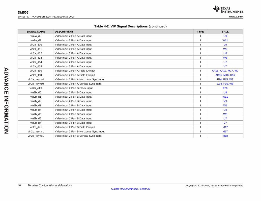
AD
VA
NC
E IN
FO
RM
AT
ION
Copyright © 2016–2017, Texas Instruments IncorporatedTerminal Configuration and FunctionsSubmit Documentation Feedback
40
DM505SPRS976C –NOVEMBER 2016–REVISED MAY 2017 www.ti.com
Table 4-2. VIP Signal Descriptions (continued)SIGNAL NAME DESCRIPTION TYPE BALL
vin2a_d8 Video Input 2 Port A Data input I U9vin2a_d9 Video Input 2 Port A Data input I W11vin2a_d10 Video Input 2 Port A Data input I V9vin2a_d11 Video Input 2 Port A Data input I W9vin2a_d12 Video Input 2 Port A Data input I U8vin2a_d13 Video Input 2 Port A Data input I W8vin2a_d14 Video Input 2 Port A Data input I U7vin2a_d15 Video Input 2 Port A Data input I V7vin2a_de0 Video Input 2 Port A Field ID input I AA15, AA17, M17, W7vin2a_fld0 Video Input 2 Port A Field ID input I AB15, M18, U16
vin2a_hsync0 Video Input 2 Port A Horizontal Sync input I F14, F15, W7vin2a_vsync0 Video Input 2 Port A Vertical Sync input I C14, F16, W6
vin2b_clk1 Video Input 2 Port B Clock input I F20vin2b_d0 Video Input 2 Port B Data input I U9vin2b_d1 Video Input 2 Port B Data input I W11vin2b_d2 Video Input 2 Port B Data input I V9vin2b_d3 Video Input 2 Port B Data input I W9vin2b_d4 Video Input 2 Port B Data input I U8vin2b_d5 Video Input 2 Port B Data input I W8vin2b_d6 Video Input 2 Port B Data input I U7vin2b_d7 Video Input 2 Port B Data input I V7vin2b_de1 Video Input 2 Port B Field ID input I M17
vin2b_hsync1 Video Input 2 Port B Horizontal Sync input I M17vin2b_vsync1 Video Input 2 Port B Vertical Sync input I M18

AD
VA
NC
E I
NF
OR
MA
TIO
N
41
DM505www.ti.com SPRS976C –NOVEMBER 2016–REVISED MAY 2017
Submit Documentation FeedbackTerminal Configuration and FunctionsCopyright © 2016–2017, Texas Instruments Incorporated
4.3.2 DSS
Table 4-3. DSS Signal Descriptions
SIGNAL NAME DESCRIPTION TYPE BALLDPI Video Output 1
vout1_clk Video Output 1 Clock output O AB17vout1_d0 Video Output 1 Data output O W16vout1_d1 Video Output 1 Data output O V16vout1_d2 Video Output 1 Data output O U15vout1_d3 Video Output 1 Data output O V15vout1_d4 Video Output 1 Data output O Y15vout1_d5 Video Output 1 Data output O W15vout1_d6 Video Output 1 Data output O AA15vout1_d7 Video Output 1 Data output O AB15vout1_d8 Video Output 1 Data output O AA14vout1_d9 Video Output 1 Data output O AB14vout1_d10 Video Output 1 Data output O U13vout1_d11 Video Output 1 Data output O V13vout1_d12 Video Output 1 Data output O Y13vout1_d13 Video Output 1 Data output O W13vout1_d14 Video Output 1 Data output O U11vout1_d15 Video Output 1 Data output O V11vout1_d16 Video Output 1 Data output O U9vout1_d17 Video Output 1 Data output O W11vout1_d18 Video Output 1 Data output O V9vout1_d19 Video Output 1 Data output O W9vout1_d20 Video Output 1 Data output O U8vout1_d21 Video Output 1 Data output O W8vout1_d22 Video Output 1 Data output O U7vout1_d23 Video Output 1 Data output O V7vout1_de Video Output 1 Data Enable output O U17vout1_fld Video Output 1 Field ID output.This signal is not used for embedded sync modes. O W17
vout1_hsync Video Output 1 Horizontal Sync output.This signal is not used for embedded syncmodes.
O AA17
vout1_vsync Video Output 1 Vertical Sync output.This signal is not used for embedded sync modes. O U16
4.3.3 SD_DAC
NOTEFor more information, see theVideo Encoder / Video Encoder Overview of the device TRM.
Table 4-4. CVIDEO SD_DAC Signal Descriptions
SIGNAL NAME DESCRIPTION TYPE BALLcvideo_tvout SD_DAC TV analog composite output A T17cvideo_vfb SD_DAC input feedback thru resistor to out A P17cvideo_rset SD_DAC input reference current resistor setting A T18

AD
VA
NC
E IN
FO
RM
AT
ION
42
DM505SPRS976C –NOVEMBER 2016–REVISED MAY 2017 www.ti.com
Submit Documentation FeedbackTerminal Configuration and Functions Copyright © 2016–2017, Texas Instruments Incorporated
4.3.4 ADC
NOTEFor more information, see the ADC / ADC Overview of the device TRM.
Table 4-5. ADC Signal Descriptions
SIGNAL NAME DESCRIPTION TYPE BALLadc_in0 ADC analog channel input 0 A M19adc_in1 ADC analog channel input 1 A M20adc_in2 ADC analog channel input 2 A M21adc_in3 ADC analog channel input 3 A M22adc_in4 ADC analog channel input 4 A N22adc_in5 ADC analog channel input 5 A N21adc_in6 ADC analog channel input 6 A P19adc_in7 ADC analog channel input 7 A P18
adc_vrefp ADC positive reference voltage A P20
4.3.5 Camera Control
NOTEFor more information, see the Imaging Subsystem (ISS) section of the device TRM.
Table 4-6. Camera Control Signal Descriptions
SIGNAL NAME DESCRIPTION TYPE BALLcam_strobe Camera flash activation trigger O A6, B18, C16, M17cam_shutter Camera mechanical shutter control O C6, C18, C17, M18cam_nreset Camera sensor reset IO W6
4.3.6 CPI
Table 4-7. CPI Signal Descriptions
SIGNAL NAME DESCRIPTION TYPE BALLcpi_pclk Camera pixel clock I F22
cpi_hsync Camera horizontal synchonization IO F21cpi_vsync Camera vertical synchonization IO F20cpi_data0 Camera parallel data 0 I F19cpi_data1 Camera parallel data 1 I G19cpi_data2 Camera parallel data 2 I G18cpi_data3 Camera parallel data 3 I G21cpi_data4 Camera parallel data 4 I G22cpi_data5 Camera parallel data 5 I H18cpi_data6 Camera parallel data 6 I H20cpi_data7 Camera parallel data 7 I H19cpi_data8 Camera parallel data 8 I H22cpi_data9 Camera parallel data 9 I H21cpi_data10 Camera parallel data 10 I J17cpi_data11 Camera parallel data 11 I K22cpi_data12 Camera parallel data 12 I K21
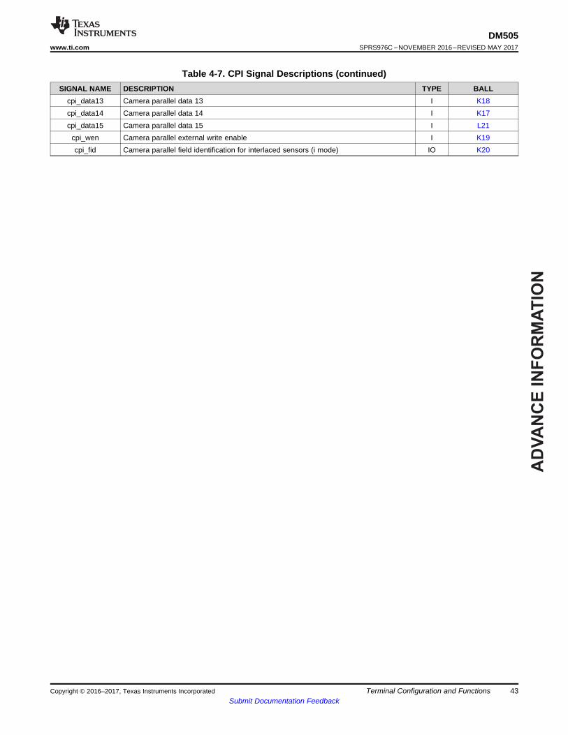
AD
VA
NC
E I
NF
OR
MA
TIO
N
43
DM505www.ti.com SPRS976C –NOVEMBER 2016–REVISED MAY 2017
Submit Documentation FeedbackTerminal Configuration and FunctionsCopyright © 2016–2017, Texas Instruments Incorporated
Table 4-7. CPI Signal Descriptions (continued)SIGNAL NAME DESCRIPTION TYPE BALL
cpi_data13 Camera parallel data 13 I K18cpi_data14 Camera parallel data 14 I K17cpi_data15 Camera parallel data 15 I L21
cpi_wen Camera parallel external write enable I K19cpi_fid Camera parallel field identification for interlaced sensors (i mode) IO K20

AD
VA
NC
E IN
FO
RM
AT
ION
44
DM505SPRS976C –NOVEMBER 2016–REVISED MAY 2017 www.ti.com
Submit Documentation FeedbackTerminal Configuration and Functions Copyright © 2016–2017, Texas Instruments Incorporated
4.3.7 CSI2
NOTEFor more information, see the Imaging Subsystem of the device TRM.
CAUTION
The IO timings provided in Section 5.9 Timing Requirements and SwitchingCharacteristics are only valid if signals within a single IOSET are used. TheIOSETs are defined in Table 5-32.
Table 4-8. CSI 2 Signal Descriptions
SIGNAL NAME DESCRIPTION TYPE BALLcsi2_0_dx0 Serial Differential data/clock positive input - lane 0 (position 1) I A11csi2_0_dy0 Serial Differential data/clock negative input - lane 0 (position 1) I B11csi2_0_dx1 Serial Differential data/clock positive input - lane 1 (position 2) I A12csi2_0_dy1 Serial Differential data/clock negative input - lane 1 (position 2) I B12csi2_0_dx2 Serial Differential data/clock positive input - lane 2 (position 3) I A13csi2_0_dy2 Serial Differential data/clock negative input - lane 2 (position 3) I B13csi2_0_dx3 Serial Differential data/clock positive input - lane 3 (position 4) I A15csi2_0_dy3 Serial Differential data/clock negative input - lane 3 (position 4) I B15csi2_0_dx4 Serial Differential data positive input only - lane 4 (position 5) (1) I A16csi2_0_dy4 Serial Differential data negative input only - lane 4 (position 5) (1) I B16
(1) Lane 4 (position 5) supports only data. For more information see Imaging Subsystem of the device TRM.
4.3.8 EMIF
NOTEFor more information, see the Memory Subsystem / EMIF Controller section of the deviceTRM.
NOTEThe index number 1 which is part of the EMIF1 signal prefixes (ddr1_*) listed in Table 4-9,EMIF1 Signal Descriptions, column "SIGNAL NAME" is not to be confused with DDR1 typeof SDRAM memories.
Table 4-9. EMIF1 Signal Descriptions
SIGNAL NAME DESCRIPTION TYPE BALLddr1_cke0 EMIF1 Clock Enable 0 O F3ddr1_nck EMIF1 Negative Clock O G2ddr1_odt0 EMIF1 On-Die Termination for Chip Select 0 O P2ddr1_rasn EMIF1 Row Address Strobe; When LPDDR2 is used this signal functions as to
ddr1_ca0O F1
ddr1_rst EMIF1 Reset output O N1ddr1_wen EMIF1 Write Enable; When LPDDR2 is used this signal functions as ddr1_ca2 O E3ddr1_csn0 EMIF1 Chip Select 0 O B2
ddr1_ck EMIF1 Clock O G1

AD
VA
NC
E I
NF
OR
MA
TIO
N
45
DM505www.ti.com SPRS976C –NOVEMBER 2016–REVISED MAY 2017
Submit Documentation FeedbackTerminal Configuration and FunctionsCopyright © 2016–2017, Texas Instruments Incorporated
Table 4-9. EMIF1 Signal Descriptions (continued)SIGNAL NAME DESCRIPTION TYPE BALL
ddr1_casn EMIF1 Column Address Strobe; When LPDDR2 is used this signal functions asddr1_ca1
O F2
ddr1_ba0 EMIF1 Bank Address; When LPDDR2 is used this signal functions as ddr1_ca7 O B3ddr1_ba1 EMIF1 Bank Address; When LPDDR2 is used this signal functions as ddr1_ca8 O A3ddr1_ba2 EMIF1 Bank Address; When LPDDR2 is used this signal functions as ddr1_ca9 O D2ddr1_a0 EMIF1 Address Bus O U4ddr1_a1 EMIF1 Address Bus; When LPDDR2 is used this signal functions as ddr1_ca5 O C1ddr1_a2 EMIF1 Address Bus; When LPDDR2 is used this signal functions as ddr1_ca6 O D3ddr1_a3 EMIF1 Address Bus O R4ddr1_a4 EMIF1 Address Bus O T4ddr1_a5 EMIF1 Address Bus O N3ddr1_a6 EMIF1 Address Bus O T2ddr1_a7 EMIF1 Address Bus O N2ddr1_a8 EMIF1 Address Bus O T1ddr1_a9 EMIF1 Address Bus O U1ddr1_a10 EMIF1 Address Bus; When LPDDR2 is used this signal functions as ddr1_ca4 O D1ddr1_a11 EMIF1 Address Bus O R3ddr1_a12 EMIF1 Address Bus O U2ddr1_a13 EMIF1 Address Bus; When LPDDR2 is used this signal functions as ddr1_ca3 O C3ddr1_a14 EMIF1 Address Bus O R2ddr1_a15 EMIF1 Address Bus O V1ddr1_d0 EMIF1 Data Bus IO AA6ddr1_d1 EMIF1 Data Bus IO AA8ddr1_d2 EMIF1 Data Bus IO Y8ddr1_d3 EMIF1 Data Bus IO AA7ddr1_d4 EMIF1 Data Bus IO AB4ddr1_d5 EMIF1 Data Bus IO Y5ddr1_d6 EMIF1 Data Bus IO AA4ddr1_d7 EMIF1 Data Bus IO Y6ddr1_d8 EMIF1 Data Bus IO AA18ddr1_d9 EMIF1 Data Bus IO Y21ddr1_d10 EMIF1 Data Bus IO AA21ddr1_d11 EMIF1 Data Bus IO Y22ddr1_d12 EMIF1 Data Bus IO AA19ddr1_d13 EMIF1 Data Bus IO AB20ddr1_d14 EMIF1 Data Bus IO Y17ddr1_d15 EMIF1 Data Bus IO AB18ddr1_d16 EMIF1 Data Bus IO AA3ddr1_d17 EMIF1 Data Bus IO AA2ddr1_d18 EMIF1 Data Bus IO Y3ddr1_d19 EMIF1 Data Bus IO V2ddr1_d20 EMIF1 Data Bus IO U3ddr1_d21 EMIF1 Data Bus IO V3ddr1_d22 EMIF1 Data Bus IO Y2ddr1_d23 EMIF1 Data Bus IO Y1ddr1_d24 EMIF1 Data Bus IO U21ddr1_d25 EMIF1 Data Bus IO T20ddr1_d26 EMIF1 Data Bus IO R21

AD
VA
NC
E IN
FO
RM
AT
ION
46
DM505SPRS976C –NOVEMBER 2016–REVISED MAY 2017 www.ti.com
Submit Documentation FeedbackTerminal Configuration and Functions Copyright © 2016–2017, Texas Instruments Incorporated
Table 4-9. EMIF1 Signal Descriptions (continued)SIGNAL NAME DESCRIPTION TYPE BALL
ddr1_d27 EMIF1 Data Bus IO U20ddr1_d28 EMIF1 Data Bus IO R22ddr1_d29 EMIF1 Data Bus IO V20ddr1_d30 EMIF1 Data Bus IO W22ddr1_d31 EMIF1 Data Bus IO U22
ddr1_ecc_d0 EMIF1 ECC Data Bus IO Y11ddr1_ecc_d1 EMIF1 ECC Data Bus IO AA12ddr1_ecc_d2 EMIF1 ECC Data Bus IO AA11ddr1_ecc_d3 EMIF1 ECC Data Bus IO Y9ddr1_ecc_d4 EMIF1 ECC Data Bus IO AA13ddr1_ecc_d5 EMIF1 ECC Data Bus IO AB11ddr1_ecc_d6 EMIF1 ECC Data Bus IO AA9ddr1_ecc_d7 EMIF1 ECC Data Bus IO AB9ddr1_dqm0 EMIF1 Data Mask IO AB8ddr1_dqm1 EMIF1 Data Mask IO Y18ddr1_dqm2 EMIF1 Data Mask IO AB3ddr1_dqm3 EMIF1 Data Mask IO W21
ddr1_dqm_ecc EMIF1 ECC Data Mask IO AB13ddr1_dqs0 Data strobe 0 input/output for byte 0 of the 32-bit data bus. This signal is output to the
EMIF1 memory when writing and input when reading.IO AA5
ddr1_dqs1 Data strobe 1 input/output for byte 1 of the 32-bit data bus. This signal is output to theEMIF1 memory when writing and input when reading.
IO AA20
ddr1_dqs2 Data strobe 2 input/output for byte 2 of the 32-bit data bus. This signal is output to theEMIF1 memory when writing and input when reading.
IO W1
ddr1_dqs3 Data strobe 3 input/output for byte 3 of the 32-bit data bus. This signal is output to theEMIF1 memory when writing and input when reading.
IO T21
ddr1_dqsn0 Data strobe 0 invert IO AB5ddr1_dqsn1 Data strobe 1 invert IO Y20ddr1_dqsn2 Data strobe 2 invert IO W2ddr1_dqsn3 Data strobe 3 invert IO T22
ddr1_dqsn_ecc EMIF1 ECC Complementary Data strobe IO AB10ddr1_dqs_ecc EMIF1 ECC Data strobe input/output. This signal is output to the EMIF1 memory when
writing and input when reading.IO AA10
4.3.9 GPMC
NOTEFor more information, see the Memory Subsystem / General-Purpose Memory Controllersection of the device TRM.
Table 4-10. GPMC Signal Descriptions
SIGNAL NAME DESCRIPTION TYPE BALLgpmc_ad0 GPMC Data 0 in A/D non-multiplexed mode and additionally Address 1
in A/D multiplexed modeIO E8
gpmc_ad1 GPMC Data 1 in A/D non-multiplexed mode and additionally Address 2in A/D multiplexed mode
IO A7
gpmc_ad2 GPMC Data 2 in A/D non-multiplexed mode and additionally Address 3in A/D multiplexed mode
IO F8
gpmc_ad3 GPMC Data 3 in A/D non-multiplexed mode and additionally Address 4in A/D multiplexed mode
IO B7

AD
VA
NC
E I
NF
OR
MA
TIO
N
47
DM505www.ti.com SPRS976C –NOVEMBER 2016–REVISED MAY 2017
Submit Documentation FeedbackTerminal Configuration and FunctionsCopyright © 2016–2017, Texas Instruments Incorporated
Table 4-10. GPMC Signal Descriptions (continued)SIGNAL NAME DESCRIPTION TYPE BALL
gpmc_ad4 GPMC Data 4 in A/D non-multiplexed mode and additionally Address 5in A/D multiplexed mode
IO A6
gpmc_ad5 GPMC Data 5 in A/D non-multiplexed mode and additionally Address 6in A/D multiplexed mode
IO F7
gpmc_ad6 GPMC Data 6 in A/D non-multiplexed mode and additionally Address 7in A/D multiplexed mode
IO E7
gpmc_ad7 GPMC Data 7 in A/D non-multiplexed mode and additionally Address 8in A/D multiplexed mode
IO C6
gpmc_ad8 GPMC Data 8 in A/D non-multiplexed mode and additionally Address 9in A/D multiplexed mode
IO B6
gpmc_ad9 GPMC Data 9 in A/D non-multiplexed mode and additionally Address10 in A/D multiplexed mode
IO A5
gpmc_ad10 GPMC Data 10 in A/D non-multiplexed mode and additionally Address11 in A/D multiplexed mode
IO D6
gpmc_ad11 GPMC Data 11 in A/D non-multiplexed mode and additionally Address12 in A/D multiplexed mode
IO C5
gpmc_ad12 GPMC Data 12 in A/D non-multiplexed mode and additionally Address13 in A/D multiplexed mode
IO B5
gpmc_ad13 GPMC Data 13 in A/D non-multiplexed mode and additionally Address14 in A/D multiplexed mode
IO D7
gpmc_ad14 GPMC Data 14 in A/D non-multiplexed mode and additionally Address15 in A/D multiplexed mode
IO B4
gpmc_ad15 GPMC Data 15 in A/D non-multiplexed mode and additionally Address16 in A/D multiplexed mode
IO A4
gpmc_a0 GPMC Address 0. Only used to effectively address 8-bit data non-multiplexed memories
O U9
gpmc_a1 GPMC address 1 in A/D non-multiplexed mode and Address 17 in A/Dmultiplexed mode
O W11
gpmc_a2 GPMC address 2 in A/D non-multiplexed mode and Address 18 in A/Dmultiplexed mode
O V9
gpmc_a3 GPMC address 3 in A/D non-multiplexed mode and Address 19 in A/Dmultiplexed mode
O W9
gpmc_a4 GPMC address 4 in A/D non-multiplexed mode and Address 20 in A/Dmultiplexed mode
O U8
gpmc_a5 GPMC address 5 in A/D non-multiplexed mode and Address 21 in A/Dmultiplexed mode
O W8
gpmc_a6 GPMC address 6 in A/D non-multiplexed mode and Address 22 in A/Dmultiplexed mode
O U7
gpmc_a7 GPMC address 7 in A/D non-multiplexed mode and Address 23 in A/Dmultiplexed mode
O V7
gpmc_a8 GPMC address 8 in A/D non-multiplexed mode and Address 24 in A/Dmultiplexed mode
O J17
gpmc_a9 GPMC address 9 in A/D non-multiplexed mode and Address 25 in A/Dmultiplexed mode
O K22
gpmc_a10 GPMC address 10 in A/D non-multiplexed mode and Address 26 in A/Dmultiplexed mode
O K21
gpmc_a11 GPMC address 11 in A/D non-multiplexed mode and unused in A/Dmultiplexed mode
O K18
gpmc_a12 GPMC address 12 in A/D non-multiplexed mode and unused in A/Dmultiplexed mode
O D14, F13, F14, K17
gpmc_a13 GPMC address 13 in A/D non-multiplexed mode and unused in A/Dmultiplexed mode
O C14, D15, E14, K19
gpmc_a14 GPMC address 14 in A/D non-multiplexed mode and unused in A/Dmultiplexed mode
O K20
gpmc_a15 GPMC address 15 in A/D non-multiplexed mode and unused in A/Dmultiplexed mode
O L21

AD
VA
NC
E IN
FO
RM
AT
ION
48
DM505SPRS976C –NOVEMBER 2016–REVISED MAY 2017 www.ti.com
Submit Documentation FeedbackTerminal Configuration and Functions Copyright © 2016–2017, Texas Instruments Incorporated
Table 4-10. GPMC Signal Descriptions (continued)SIGNAL NAME DESCRIPTION TYPE BALL
gpmc_a16 GPMC address 16 in A/D non-multiplexed mode and unused in A/Dmultiplexed mode
O F14
gpmc_a17 GPMC address 17 in A/D non-multiplexed mode and unused in A/Dmultiplexed mode
O C14
gpmc_a18 GPMC address 18 in A/D non-multiplexed mode and unused in A/Dmultiplexed mode
O F15
gpmc_a19 GPMC address 19 in A/D non-multiplexed mode and unused in A/Dmultiplexed mode
O F16
gpmc_a20 GPMC address 20 in A/D non-multiplexed mode and unused in A/Dmultiplexed mode
O AA14
gpmc_a21 GPMC address 21 in A/D non-multiplexed mode and unused in A/Dmultiplexed mode
O AB14
gpmc_a22 GPMC address 22 in A/D non-multiplexed mode and unused in A/Dmultiplexed mode
O U13
gpmc_a23 GPMC address 23 in A/D non-multiplexed mode and unused in A/Dmultiplexed mode
O V13
gpmc_a24 GPMC address 24 in A/D non-multiplexed mode and unused in A/Dmultiplexed mode
O Y13
gpmc_a25 GPMC address 25 in A/D non-multiplexed mode and unused in A/Dmultiplexed mode
O W13
gpmc_a26 GPMC address 26 in A/D non-multiplexed mode and unused in A/Dmultiplexed mode
O U11
gpmc_a27 GPMC address 27 in A/D non-multiplexed mode and Address 27 in A/Dmultiplexed mode
O V11
gpmc_cs0 GPMC Chip Select 0 (active low) O C10gpmc_cs1 GPMC Chip Select 1 (active low) O E10gpmc_cs2 GPMC Chip Select 2 (active low) O D10gpmc_cs3 GPMC Chip Select 3 (active low) O A9gpmc_cs4 GPMC Chip Select 4 (active low) O B9gpmc_cs5 GPMC Chip Select 5 (active low) O F10gpmc_cs6 GPMC Chip Select 6 (active low) O C8gpmc_cs7 GPMC Chip Select 7 (active low) O W6
gpmc_clk(1) GPMC Clock output IO C12, D14, F14, F15gpmc_advn_ale GPMC address valid active low or address latch enable O F12gpmc_oen_ren GPMC output enable active low or read enable O A10
gpmc_wen GPMC write enable active low O B10gpmc_ben0 GPMC lower-byte enable active low O D12gpmc_ben1 GPMC upper-byte enable active low O E12gpmc_wait0 GPMC external indication of wait 0 I D8gpmc_wait1 GPMC external indication of wait 1 I W7
(1) The gpio6_16.clkout0 signal can be used as an “always-on” alternative to gpmc_clk provided that the external device can support theassociated timing. See Table 5-34 GPMC/NOR Flash Interface Switching Characteristics - Synchronous Mode - 1 Load and Table 5-36GPMC/NOR Flash Interface Switching Characteristics - Synchronous Mode - 5 Loads for timing information.
4.3.10 Timers
NOTEFor more information, see the Timers section of the device TRM.

AD
VA
NC
E I
NF
OR
MA
TIO
N
49
DM505www.ti.com SPRS976C –NOVEMBER 2016–REVISED MAY 2017
Submit Documentation FeedbackTerminal Configuration and FunctionsCopyright © 2016–2017, Texas Instruments Incorporated
Table 4-11. Timers Signal Descriptions
SIGNAL NAME DESCRIPTION TYPE BALLtimer1 PWM output/event trigger input IO D14, R7timer2 PWM output/event trigger input IO D15, D6timer3 PWM output/event trigger input IO C5, F14, L1timer4 PWM output/event trigger input IO C14, C6, L2timer5 PWM output/event trigger input IO E7, N4timer6 PWM output/event trigger input IO F7, R5timer7 PWM output/event trigger input IO B6, F15timer8 PWM output/event trigger input IO F16
4.3.11 I2C
NOTEFor more information, see the Serial Communication Interface / Multimaster I2C Controller /I2C Environment / I2C Pins for Typical Connections in I2C Mode section of the device TRM.
Table 4-12. I2C Signal Descriptions
SIGNAL NAME DESCRIPTION TYPE BALLInter-Integrated Circuit Interface (I2C1)
i2c1_scl I2C1 Clock IOD L3i2c1_sda I2C1 Data IOD L4
Inter-Integrated Circuit Interface (I2C2)i2c2_scl I2C2 Clock IOD L6i2c2_sda I2C2 Data IOD L5
4.3.12 UART
NOTEFor more information see the Serial Communication Interface UART section of the deviceTRM.
CAUTION
The IO timings provided in Section 5.9, Timing Requirements and SwitchingCharacteristics are only valid if signals within a single IOSET are used. TheIOSETs are defined in Table 5-45.
Table 4-13. UART Signal Descriptions
SIGNAL NAME DESCRIPTION TYPE BALLUniversal Asynchronous Receiver/Transmitter (UART1)
uart1_ctsn UART1 clear to send active low I F14uart1_rtsn UART1 request to send active low O C14uart1_rxd UART1 Receive Data I F13uart1_txd UART1 Transmit Data O E14
Universal Asynchronous Receiver/Transmitter (UART2)uart2_ctsn UART2 clear to send active low I F15uart2_rtsn UART2 request to send active low O F16

AD
VA
NC
E IN
FO
RM
AT
ION
50
DM505SPRS976C –NOVEMBER 2016–REVISED MAY 2017 www.ti.com
Submit Documentation FeedbackTerminal Configuration and Functions Copyright © 2016–2017, Texas Instruments Incorporated
Table 4-13. UART Signal Descriptions (continued)SIGNAL NAME DESCRIPTION TYPE BALL
uart2_rxd UART2 Receive Data I D14, E7uart2_txd UART2 Transmit Data O D15, F7
Universal Asynchronous Receiver/Transmitter (UART3)uart3_ctsn UART3 clear to send active low I N4, U6uart3_rtsn UART3 request to send active low O R7, T5uart3_rxd UART3 Receive Data I F14, L1, M2, W7uart3_txd UART3 Transmit Data O C14, L2, R6, W6
4.3.13 McSPI
NOTEFor more information, see the Serial Communication Interface / Multichannel SerialPeripheral Interface (McSPI) section of the device TRM.
CAUTION
The IO timings provided in Section 5.9, Timing Requirements and SwitchingCharacteristics are applicable for all combinations of signals for SPI2 and SPI4.However, the timings are only valid for SPI1 and SPI3 if signals within a singleIOSET are used. The IOSETS are defined in the Table 5-48.
Table 4-14. SPI Signal Descriptions
SIGNAL NAME DESCRIPTION TYPE BALLSerial Peripheral Interface 1
spi1_sclk SPI1 Clock IO M2spi1_d0 SPI1 Data. Can be configured as either MISO or MOSI. IO T5spi1_d1 SPI1 Data. Can be configured as either MISO or MOSI. IO U6spi1_cs0 SPI1 Chip Select IO M1, R6spi1_cs1 SPI1 Chip Select IO M1, R5spi1_cs2 SPI1 Chip Select IO F14, W7spi1_cs3 SPI1 Chip Select IO C14, W6
Serial Peripheral Interface 2spi2_sclk SPI2 Clock IO L1spi2_d0 SPI2 Data. Can be configured as either MISO or MOSI. IO R7spi2_d1 SPI2 Data. Can be configured as either MISO or MOSI. IO N4spi2_cs0 SPI2 Chip Select IO A4, L2spi2_cs1 SPI2 Chip Select IO B4, M1
Serial Peripheral Interface 3spi3_sclk SPI3 Clock IO C6, F15spi3_d0 SPI3 Data. Can be configured as either MISO or MOSI. IO D15, E7spi3_d1 SPI3 Data. Can be configured as either MISO or MOSI. IO D14, F7spi3_cs0 SPI3 Chip Select IO B6, F16, M1spi3_cs1 SPI3 Chip Select IO A5, R5
Serial Peripheral Interface 4spi4_sclk SPI4 Clock IO C16, F14spi4_d0 SPI4 Data. Can be configured as either MISO or MOSI. IO B17, E14

AD
VA
NC
E I
NF
OR
MA
TIO
N
51
DM505www.ti.com SPRS976C –NOVEMBER 2016–REVISED MAY 2017
Submit Documentation FeedbackTerminal Configuration and FunctionsCopyright © 2016–2017, Texas Instruments Incorporated
Table 4-14. SPI Signal Descriptions (continued)SIGNAL NAME DESCRIPTION TYPE BALL
spi4_d1 SPI4 Data. Can be configured as either MISO or MOSI. IO B19, F13spi4_cs0 SPI4 Chip Select IO C14, C17
4.3.14 QSPI
NOTEFor more information see the Serial Communication Interface / Quad Serial PeripheralInterface section of the device TRM.
CAUTION
The IO timings provided in Section 5.9, Timing Requirements and SwitchingCharacteristics are only valid if signals within a single IOSET are used. TheIOSETs are defined in Table 5-51.
Table 4-15. QSPI Signal Descriptions
SIGNAL NAME DESCRIPTION TYPE BALLqspi1_sclk QSPI1 Serial Clock O C8qspi1_rtclk QSPI1 Return Clock Input.Must be connected from QSPI1_SCLK on PCB. Refer
to PCB Guidelines for QSPI1I B7, C14, D8, F13
qspi1_d0 QSPI1 Data[0]. This pin is output data for all commands/writes and for dual readand quad read modes it becomes input data pin during read phase.
IO B9
qspi1_d1 QSPI1 Data[1]. Input read data in all modes. IO F10qspi1_d2 QSPI1 Data[2]. This pin is used only in quad read mode as input data pin during
read phaseIO A9
qspi1_d3 QSPI1 Data[3]. This pin is used only in quad read mode as input data pin duringread phase
IO D10
qspi1_cs0 QSPI1 Chip Select[0]. This pin is used for QSPI1 boot modes. IO E10qspi1_cs1 QSPI1 Chip Select[1] IO F15
4.3.15 McASP
NOTEFor more information, see the Serial Communication Interface / Multichannel Audio SerialPort (McASP) section of the device TRM.
CAUTION
The IO timings provided in Section 5.9, Timing Requirements and SwitchingCharacteristics are only valid if signals within a single IOSET are used. TheIOSETs are defined in Table 5-58.
Table 4-16. McASP Signal Descriptions
SIGNAL NAME DESCRIPTION TYPE BALLMultichannel Audio Serial Port 1
mcasp1_axr0 McASP1 Transmit/Receive Data IO W16mcasp1_axr1 McASP1 Transmit/Receive Data IO V16

AD
VA
NC
E IN
FO
RM
AT
ION
52
DM505SPRS976C –NOVEMBER 2016–REVISED MAY 2017 www.ti.com
Submit Documentation FeedbackTerminal Configuration and Functions Copyright © 2016–2017, Texas Instruments Incorporated
Table 4-16. McASP Signal Descriptions (continued)SIGNAL NAME DESCRIPTION TYPE BALLmcasp1_axr2 McASP1 Transmit/Receive Data IO U15mcasp1_axr3 McASP1 Transmit/Receive Data IO V15mcasp1_axr4 McASP1 Transmit/Receive Data IO Y15mcasp1_axr5 McASP1 Transmit/Receive Data IO W15mcasp1_axr6 McASP1 Transmit/Receive Data IO AA15mcasp1_axr7 McASP1 Transmit/Receive Data IO AB15mcasp1_axr8 McASP1 Transmit/Receive Data IO AA14, U15, U9mcasp1_axr9 McASP1 Transmit/Receive Data IO AB14, V15, W11mcasp1_axr10 McASP1 Transmit/Receive Data IO U13, V9, Y15mcasp1_axr11 McASP1 Transmit/Receive Data IO V13, W15, W9mcasp1_axr12 McASP1 Transmit/Receive Data IO AA15, U8, Y13mcasp1_axr13 McASP1 Transmit/Receive Data IO AB15, W13, W8mcasp1_axr14 McASP1 Transmit/Receive Data IO K20, U11, U7mcasp1_axr15 McASP1 Transmit/Receive Data IO L21, V11, V7
mcasp1_fsx McASP1 Transmit Frame Sync IO W17mcasp1_aclkr McASP1 Receive Bit Clock IO AA17mcasp1_fsr McASP1 Receive Frame Sync IO U16
mcasp1_ahclkx McASP1 Transmit High-Frequency Master Clock O U9mcasp1_aclkx McASP1 Transmit Bit Clock IO U17
Multichannel Audio Serial Port 2mcasp2_axr0 McASP2 Transmit/Receive Data IO D6, V9mcasp2_axr1 McASP2 Transmit/Receive Data IO C5, W9mcasp2_axr2 McASP2 Transmit/Receive Data IO B5, U8mcasp2_axr3 McASP2 Transmit/Receive Data IO D7, W8mcasp2_axr4 McASP2 Transmit/Receive Data IO B4, U7mcasp2_axr5 McASP2 Transmit/Receive Data IO A4, V7mcasp2_fsx McASP2 Transmit Frame Sync IO E7, V11
mcasp2_aclkr McASP2 Receive Bit Clock IO B6, W13mcasp2_fsr McASP2 Receive Frame Sync IO A5, W11
mcasp2_ahclkx McASP2 Transmit High-Frequency Master Clock O C6, Y13mcasp2_aclkx McASP2 Transmit Bit Clock IO F7, U11
Multichannel Audio Serial Port 3mcasp3_axr0 McASP3 Transmit/Receive Data IO G19mcasp3_axr1 McASP3 Transmit/Receive Data IO G18mcasp3_axr2 McASP3 Transmit/Receive Data IO G21mcasp3_axr3 McASP3 Transmit/Receive Data IO G22mcasp3_axr4 McASP3 Transmit/Receive Data IO H18mcasp3_axr5 McASP3 Transmit/Receive Data IO H20mcasp3_fsx McASP3 Transmit Frame Sync IO H22
mcasp3_ahclkx McASP3 Transmit High-Frequency Master Clock O H19mcasp3_aclkx McASP3 Transmit Bit Clock IO F22mcasp3_aclkr McASP3 Receive Bit Clock IO F20mcasp3_fsr McASP3 Receive Frame Sync IO F19

AD
VA
NC
E I
NF
OR
MA
TIO
N
53
DM505www.ti.com SPRS976C –NOVEMBER 2016–REVISED MAY 2017
Submit Documentation FeedbackTerminal Configuration and FunctionsCopyright © 2016–2017, Texas Instruments Incorporated
4.3.16 DCAN and MCAN
NOTEFor more information, see the Serial Communication Interface / DCAN section of the deviceTRM.
CAUTION
The IO timings provided in Section 5.9, Timing Requirements and SwitchingCharacteristics are only valid if signals within a single IOSET are used. TheIOSETs are defined in Table 5-61.
Table 4-17. DCAN and MCAN Signal Descriptions
SIGNAL NAME DESCRIPTION TYPE BALLDCAN 1
dcan1_rx DCAN1 receive data pin IO C14, D15, N6dcan1_tx DCAN1 transmit data pin IO D14, F14, N5
MCANmcan_rx MCAN receive data pin IO E14, F16, W6mcan_tx MCAN transmit data pin IO F13, F15, W7
4.3.17 GMAC_SW
NOTEFor more information, see the Serial Communication Interfaces / Gigabit Ethernet Switch(GMAC_SW) section of the device TRM.
Table 4-18. GMAC Signal Descriptions
SIGNAL NAME DESCRIPTION TYPE BALLrgmii0_rxc RGMII0 Receive Clock I B18rgmii0_rxctl RGMII0 Receive Control I C18rgmii0_rxd0 RGMII0 Receive Data I A20rgmii0_rxd1 RGMII0 Receive Data I C20rgmii0_rxd2 RGMII0 Receive Data I B20rgmii0_rxd3 RGMII0 Receive Data I A19rgmii0_txc RGMII0 Transmit Clock O C16rgmii0_txctl RGMII0 Transmit Enable O C17rgmii0_txd0 RGMII0 Transmit Data O F17rgmii0_txd1 RGMII0 Transmit Data O E17rgmii0_txd2 RGMII0 Transmit Data O D16rgmii0_txd3 RGMII0 Transmit Data O E16rgmii1_rxc RGMII1 Receive Clock I D7rgmii1_rxctl RGMII1 Receive Control I C10rgmii1_rxd0 RGMII1 Receive Data I F8rgmii1_rxd1 RGMII1 Receive Data I A7rgmii1_rxd2 RGMII1 Receive Data I E8rgmii1_rxd3 RGMII1 Receive Data I D8rgmii1_txc RGMII1 Transmit Clock O C12

AD
VA
NC
E IN
FO
RM
AT
ION
54
DM505SPRS976C –NOVEMBER 2016–REVISED MAY 2017 www.ti.com
Submit Documentation FeedbackTerminal Configuration and Functions Copyright © 2016–2017, Texas Instruments Incorporated
Table 4-18. GMAC Signal Descriptions (continued)SIGNAL NAME DESCRIPTION TYPE BALL
rgmii1_txctl RGMII1 Transmit Enable O D12rgmii1_txd0 RGMII1 Transmit Data O B10rgmii1_txd1 RGMII1 Transmit Data O A10rgmii1_txd2 RGMII1 Transmit Data O F12rgmii1_txd3 RGMII1 Transmit Data O E12
mdio_d Management Data IO B17mdio_mclk Management Data Serial Clock O B19
4.3.18 SDIO Controller
NOTEFor more information, see the SDIO Controller section of the device TRM.
CAUTION
The IO timings provided in Section 5.9, Timing Requirements and SwitchingCharacteristics are only valid if signals within a single IOSET are used. TheIOSETs are defined in Table 5-76.
Table 4-19. SDIO Controller Signal Descriptions
SIGNAL NAME DESCRIPTION TYPE BALLMulti Media Card 1
mmc_clk MMC1 clock IO B18, C16, W16mmc_cmd MMC1 command IO C17, C18, V16mmc_dat0 MMC1 data bit 0 IO A19, E16, U15mmc_dat1 MMC1 data bit 1 IO B20, D16, V15mmc_dat2 MMC1 data bit 2 IO C20, E17, Y15mmc_dat3 MMC1 data bit 3 IO A20, F17, W15
4.3.19 GPIO
NOTEFor more information, see the General-Purpose Interface section of the device TRM.
CAUTION
The IO timings provided in Section 5.9, Timing Requirements and SwitchingCharacteristics are only valid if signals within a single IOSET are used. TheIOSETs are defined in Table 5-77.
Table 4-20. GPIOs Signal Descriptions
SIGNAL NAME DESCRIPTION TYPE BALLGPIO 1
gpio1_0 General-Purpose Input/Output IO C12gpio1_1 General-Purpose Input/Output IO D12

AD
VA
NC
E I
NF
OR
MA
TIO
N
55
DM505www.ti.com SPRS976C –NOVEMBER 2016–REVISED MAY 2017
Submit Documentation FeedbackTerminal Configuration and FunctionsCopyright © 2016–2017, Texas Instruments Incorporated
Table 4-20. GPIOs Signal Descriptions (continued)SIGNAL NAME DESCRIPTION TYPE BALL
gpio1_2 General-Purpose Input/Output IO E12gpio1_3 General-Purpose Input/Output IO F12gpio1_4 General-Purpose Input/Output IO A10gpio1_5 General-Purpose Input/Output IO B10gpio1_6 General-Purpose Input/Output IO C10gpio1_7 General-Purpose Input/Output IO E10gpio1_8 General-Purpose Input/Output IO D10gpio1_9 General-Purpose Input/Output IO A9gpio1_10 General-Purpose Input/Output IO B9gpio1_11 General-Purpose Input/Output IO F10gpio1_12 General-Purpose Input/Output IO C8gpio1_13 General-Purpose Input/Output IO D8gpio1_14 General-Purpose Input/Output IO E8gpio1_15 General-Purpose Input/Output IO A7gpio1_16 General-Purpose Input/Output IO F8gpio1_17 General-Purpose Input/Output IO B7gpio1_18 General-Purpose Input/Output IO A6gpio1_19 General-Purpose Input/Output IO F7gpio1_20 General-Purpose Input/Output IO E7gpio1_21 General-Purpose Input/Output IO C6gpio1_22 General-Purpose Input/Output IO B6gpio1_23 General-Purpose Input/Output IO A5gpio1_24 General-Purpose Input/Output IO D6gpio1_25 General-Purpose Input/Output IO C5gpio1_26 General-Purpose Input/Output IO B5gpio1_27 General-Purpose Input/Output IO D7gpio1_28 General-Purpose Input/Output IO B4gpio1_29 General-Purpose Input/Output IO A4gpio1_30 General-Purpose Input/Output IO F22gpio1_31 General-Purpose Input/Output IO F21
GPIO 2gpio2_0 General-Purpose Input/Output IO F20gpio2_1 General-Purpose Input/Output IO F19gpio2_2 General-Purpose Input/Output IO G19gpio2_3 General-Purpose Input/Output IO G18gpio2_4 General-Purpose Input/Output IO G21gpio2_5 General-Purpose Input/Output IO G22gpio2_6 General-Purpose Input/Output IO H18gpio2_7 General-Purpose Input/Output IO H20gpio2_8 General-Purpose Input/Output IO H19gpio2_9 General-Purpose Input/Output IO H22gpio2_10 General-Purpose Input/Output IO H21gpio2_11 General-Purpose Input/Output IO J17gpio2_12 General-Purpose Input/Output IO K22gpio2_13 General-Purpose Input/Output IO K21gpio2_14 General-Purpose Input/Output IO K18gpio2_15 General-Purpose Input/Output IO K17

AD
VA
NC
E IN
FO
RM
AT
ION
56
DM505SPRS976C –NOVEMBER 2016–REVISED MAY 2017 www.ti.com
Submit Documentation FeedbackTerminal Configuration and Functions Copyright © 2016–2017, Texas Instruments Incorporated
Table 4-20. GPIOs Signal Descriptions (continued)SIGNAL NAME DESCRIPTION TYPE BALL
gpio2_16 General-Purpose Input/Output IO K19gpio2_17 General-Purpose Input/Output IO K20gpio2_18 General-Purpose Input/Output IO L21gpio2_19 General-Purpose Input/Output IO L22gpio2_20 General-Purpose Input/Output IO AB17gpio2_21 General-Purpose Input/Output IO U17gpio2_22 General-Purpose Input/Output IO W17gpio2_23 General-Purpose Input/Output IO AA17gpio2_24 General-Purpose Input/Output IO U16gpio2_25 General-Purpose Input/Output IO W16gpio2_26 General-Purpose Input/Output IO V16gpio2_27 General-Purpose Input/Output IO U15gpio2_28 General-Purpose Input/Output IO V15gpio2_29 General-Purpose Input/Output IO Y15gpio2_30 General-Purpose Input/Output IO W15gpio2_31 General-Purpose Input/Output IO AA15
GPIO 3gpio3_0 General-Purpose Input/Output IO AB15gpio3_1 General-Purpose Input/Output IO AA14gpio3_2 General-Purpose Input/Output IO AB14gpio3_3 General-Purpose Input/Output IO U13gpio3_4 General-Purpose Input/Output IO V13gpio3_5 General-Purpose Input/Output IO Y13gpio3_6 General-Purpose Input/Output IO W13gpio3_7 General-Purpose Input/Output IO U11gpio3_8 General-Purpose Input/Output IO V11gpio3_9 General-Purpose Input/Output IO U9gpio3_10 General-Purpose Input/Output IO W11gpio3_11 General-Purpose Input/Output IO V9gpio3_12 General-Purpose Input/Output IO W9gpio3_13 General-Purpose Input/Output IO U8gpio3_14 General-Purpose Input/Output IO W8gpio3_15 General-Purpose Input/Output IO U7gpio3_16 General-Purpose Input/Output IO V7gpio3_17 General-Purpose Input/Output IO B19gpio3_18 General-Purpose Input/Output IO B17gpio3_19 General-Purpose Input/Output IO C16gpio3_20 General-Purpose Input/Output IO C17gpio3_21 General-Purpose Input/Output IO E16gpio3_22 General-Purpose Input/Output IO D16gpio3_23 General-Purpose Input/Output IO E17gpio3_24 General-Purpose Input/Output IO F17gpio3_25 General-Purpose Input/Output IO B18gpio3_26 General-Purpose Input/Output IO C18gpio3_27 General-Purpose Input/Output IO A19gpio3_28 General-Purpose Input/Output IO B20gpio3_29 General-Purpose Input/Output IO C20

AD
VA
NC
E I
NF
OR
MA
TIO
N
57
DM505www.ti.com SPRS976C –NOVEMBER 2016–REVISED MAY 2017
Submit Documentation FeedbackTerminal Configuration and FunctionsCopyright © 2016–2017, Texas Instruments Incorporated
Table 4-20. GPIOs Signal Descriptions (continued)SIGNAL NAME DESCRIPTION TYPE BALL
gpio3_30 General-Purpose Input/Output IO A20gpio3_31 General-Purpose Input/Output IO M1
GPIO 4gpio4_0 General-Purpose Input/Output IO M2gpio4_1 General-Purpose Input/Output IO U6gpio4_2 General-Purpose Input/Output IO T5gpio4_3 General-Purpose Input/Output IO R6gpio4_4 General-Purpose Input/Output IO R5gpio4_5 General-Purpose Input/Output IO L1gpio4_6 General-Purpose Input/Output IO N4gpio4_7 General-Purpose Input/Output IO R7gpio4_8 General-Purpose Input/Output IO L2gpio4_9 General-Purpose Input/Output IO N5gpio4_10 General-Purpose Input/Output IO N6gpio4_11 General-Purpose Input/Output IO W7gpio4_12 General-Purpose Input/Output IO W6gpio4_13 General-Purpose Input/Output IO F13gpio4_14 General-Purpose Input/Output IO E14gpio4_15 General-Purpose Input/Output IO F14gpio4_16 General-Purpose Input/Output IO C14gpio4_17 General-Purpose Input/Output IO D14gpio4_18 General-Purpose Input/Output IO D15gpio4_19 General-Purpose Input/Output IO F15gpio4_20 General-Purpose Input/Output IO F16gpio4_21 General-Purpose Input/Output IO M17gpio4_22 General-Purpose Input/Output IO M18gpio4_25 General-Purpose Input/Output IO J1gpio4_26 General-Purpose Input/Output IO J4gpio4_27 General-Purpose Input/Output IO J6gpio4_28 General-Purpose Input/Output IO H1gpio4_29 General-Purpose Input/Output IO H2
4.3.20 ePWM
NOTEFor more information, see Pulse Width Modulation Subsystem (PWMSS) section of thedevice TRM.
Table 4-21. PWM Signal Descriptions
SIGNAL NAME DESCRIPTION TYPE BALLPWMSS1
ehrpwm1A EHRPWM1 Output A O D12, D14, L1ehrpwm1B EHRPWM1 Output B O D15, E12, L2
ehrpwm1_tripzone_input EHRPWM1 Trip Zone Input IO F12, R5eCAP1_in_PWM1_out ECAP1 Capture Input / PWM Output IO A5, AB15, D16, F16,
N4ehrpwm1_synci EHRPWM1 Sync Input I A10, F14

AD
VA
NC
E IN
FO
RM
AT
ION
58
DM505SPRS976C –NOVEMBER 2016–REVISED MAY 2017 www.ti.com
Submit Documentation FeedbackTerminal Configuration and Functions Copyright © 2016–2017, Texas Instruments Incorporated
Table 4-21. PWM Signal Descriptions (continued)SIGNAL NAME DESCRIPTION TYPE BALLehrpwm1_synco EHRPWM1 Sync Output O B10, C14
4.3.21 Emulation and Debug Subsystem
NOTEFor more information, see the On-Chip Debug Support section of the device TRM.
Table 4-22. Debug Signal Descriptions
SIGNAL NAME DESCRIPTION TYPE BALLrtck JTAG return clock O J6tclk JTAG test clock I J2tdi JTAG test data I J1tdo JTAG test port data O J4tms JTAG test port mode select. An external pull-up resistor should be used on this
ball.IO J3
trstn JTAG test reset I J5emu0 Emulator pin 0 IO H1emu1 Emulator pin 1 IO H2emu2 Emulator pin 2 O AA15emu3 Emulator pin 3 O AB15emu4 Emulator pin 4 O AA14emu5 Emulator pin 5 O AB14emu6 Emulator pin 6 O U13emu7 Emulator pin 7 O V13emu8 Emulator pin 8 O Y13emu9 Emulator pin 9 O W13
emu10 Emulator pin 10 O U11emu11 Emulator pin 11 O V11emu12 Emulator pin 12 O U9emu13 Emulator pin 13 O W11emu14 Emulator pin 14 O V9emu15 Emulator pin 15 O W9emu16 Emulator pin 16 O U8emu17 Emulator pin 17 O W8emu18 Emulator pin 18 O U7emu19 Emulator pin 19 O V7
4.3.22 System and Miscellaneous
4.3.22.1 Sysboot
NOTEFor more information, see the Initialization (ROM Code) section of the device TRM.

AD
VA
NC
E I
NF
OR
MA
TIO
N
59
DM505www.ti.com SPRS976C –NOVEMBER 2016–REVISED MAY 2017
Submit Documentation FeedbackTerminal Configuration and FunctionsCopyright © 2016–2017, Texas Instruments Incorporated
Table 4-23. Sysboot Signal Descriptions
SIGNAL NAME DESCRIPTION TYPE BALLsysboot0 Boot Mode Configuration 0. The value latched on this pin upon porz reset release
will determine the boot mode configuration of the device.I E8
sysboot1 Boot Mode Configuration 1. The value latched on this pin upon porz reset releasewill determine the boot mode configuration of the device.
I A7
sysboot2 Boot Mode Configuration 2. The value latched on this pin upon porz reset releasewill determine the boot mode configuration of the device.
I F8
sysboot3 Boot Mode Configuration 3. The value latched on this pin upon porz reset releasewill determine the boot mode configuration of the device.
I B7
sysboot4 Boot Mode Configuration 4. The value latched on this pin upon porz reset releasewill determine the boot mode configuration of the device.
I A6
sysboot5 Boot Mode Configuration 5. The value latched on this pin upon porz reset releasewill determine the boot mode configuration of the device.
I F7
sysboot6 Boot Mode Configuration 6. The value latched on this pin upon porz reset releasewill determine the boot mode configuration of the device.
I E7
sysboot7 Boot Mode Configuration 7. The value latched on this pin upon porz reset releasewill determine the boot mode configuration of the device.
I R7
sysboot8 Boot Mode Configuration 8. The value latched on this pin upon porz reset releasewill determine the boot mode configuration of the device.
I B6
sysboot9 Boot Mode Configuration 9. The value latched on this pin upon porz reset releasewill determine the boot mode configuration of the device.
I A5
sysboot10 Boot Mode Configuration 10. The value latched on this pin upon porz reset releasewill determine the boot mode configuration of the device.
I D6
sysboot11 Boot Mode Configuration 11. The value latched on this pin upon porz reset releasewill determine the boot mode configuration of the device.
I C5
sysboot12 Boot Mode Configuration 12. The value latched on this pin upon porz reset releasewill determine the boot mode configuration of the device.
I B5
sysboot13 Boot Mode Configuration 13. The value latched on this pin upon porz reset releasewill determine the boot mode configuration of the device.
I D7
sysboot14 Boot Mode Configuration 14. The value latched on this pin upon porz reset releasewill determine the boot mode configuration of the device.
I B4
sysboot15 Boot Mode Configuration 15. The value latched on this pin upon porz reset releasewill determine the boot mode configuration of the device.
I A4
4.3.22.2 Power, Reset and Clock Management (PRCM)
NOTEFor more information, see Power, Reset, and Clock Management section of the device TRM.
Table 4-24. PRCM Signal Descriptions
SIGNAL NAME DESCRIPTION TYPE BALLclkout0 Device Clock output 1. Can be used externally for devices with non-critical timing
requirements, or for debug, or as a reference clock on GPMC as described inTable 5-34 GPMC/NOR Flash Interface Switching Characteristics - SynchronousMode - 1 Load and Table 5-36 GPMC/NOR Flash Interface SwitchingCharacteristics - Synchronous Mode - 5 Loads.
O AB17, C12, F14, F22,M1
clkout1 Device Clock output 2. Can be used as a system clock for other devices. O F12, F21, U17clkout2 Device Clock output 3. Can be used as a system clock for other devices. O A10, F20, W17rstoutn Reset out (Active low). This pin asserts low in response to any global reset condition
on the device.O F4
resetn Device Reset Input I G4porz Power on Reset (active low). This pin must be asserted low until all device supplies
are valid (see reset sequence/requirements).I G3
xref_clk0 External Reference Clock 0. For Audio and other Peripherals. I M1

AD
VA
NC
E IN
FO
RM
AT
ION
60
DM505SPRS976C –NOVEMBER 2016–REVISED MAY 2017 www.ti.com
Submit Documentation FeedbackTerminal Configuration and Functions Copyright © 2016–2017, Texas Instruments Incorporated
Table 4-24. PRCM Signal Descriptions (continued)SIGNAL NAME DESCRIPTION TYPE BALL
xref_clk1 External Reference Clock 1. For Audio and other Peripherals. I F14, F15xref_clk2 External Reference Clock 2. For Audio and other Peripherals. I H19xi_osc0 System Oscillator OSC0 Crystal input / LVCMOS clock input. Functions as the input
connection to a crystal when the internal oscillator OSC0 is used. Functions as anLVCMOS-compatible input clock when an external oscillator is used.
I E22
xi_osc1 Auxiliary Oscillator OSC1 Crystal input / LVCMOS clock input. Functions as theinput connection to a crystal when the internal oscillator OSC1 is used. Functions asan LVCMOS-compatible input clock when an external oscillator is used
I B21
xo_osc0 System Oscillator OSC0 Crystal output O D22xo_osc1 Auxiliary Oscillator OSC1 Crystal output O C21
4.3.22.3 Enhanced Direct Memory Access (EDMA)
NOTEFor more information, see the DMA Controllers / Enhanced DMA section of the device TRM.
Table 4-25. EDMA Signal Descriptions
SIGNAL NAME DESCRIPTION TYPE BALLdma_evt1 Enhanced DMA Event Input 1 I C12, K17dma_evt2 Enhanced DMA Event Input 2 I D12, K19dma_evt3 Enhanced DMA Event Input 3 I E12dma_evt4 Enhanced DMA Event Input 4 I F12, D8
4.3.22.4 Interrupt Controllers (INTC)
NOTEFor more information, see the Interrupt Controllers section of the device TRM.
Table 4-26. INTC Signal Descriptions
SIGNAL NAME DESCRIPTION TYPE BALLnmin Non maskable interrupt input - active-low. This pin can be optionally routed to the
DSP NMI input or as generic input to the ARM cores.I G5
sys_nirq1 External interrupt event to any device INTC I K18, K22sys_nirq2 External interrupt event to any device INTC I J17, K21esm_error This signal indicates a severe device failure. For more information see Error
Signaling Module in the device TRM.IO AA15 , B17
4.3.23 Power Supplies
NOTEFor more information, see Power, Reset, and Clock Management / PRCM SubsystemEnvironment / External Voltage Inputs section of the device TRM.

AD
VA
NC
E I
NF
OR
MA
TIO
N
61
DM505www.ti.com SPRS976C –NOVEMBER 2016–REVISED MAY 2017
Submit Documentation FeedbackTerminal Configuration and FunctionsCopyright © 2016–2017, Texas Instruments Incorporated
Table 4-27. Power Supply Signal Descriptions
SIGNAL NAME DESCRIPTION TYPE BALLvdd Core voltage domain supply PWR H7 , H12 , H13 , J10 ,
J11 , J15 , K12 , L12 ,L15 , N12 , N16 ,
P10 , P14vss Ground GND A1 , A8 , A17 , A22 ,
B22 , E1 , G10 ,G16 , H8 , H9 , H10 ,
H11 , H15 , H16 ,J22 , K1 , K9 , K10 ,
K11 , K13 , K14 ,K15 , K16 , M10 ,M11 , M12 , M13 ,
M16 , N7 , N10 , P1 ,P15 , P16 , R9 , R12 ,
R16 , T14 , V22 ,AB1 , AB2 , AB7 ,
AB12 , AB16 , AB21 ,AB22
vdd_dspeve DSP-EVE voltage domain supply PWR K8 , L8 , M9 , P8 ,P9 , P11 , P12
vdda_per PER PLL and PER HSDIVIDER analog power supply PWR H14vdda_ddr_dsp EVE PLL, DPLL_DDR and DDR HSDIVIDER analog power supply PWR N8
vdda_gmac_core GMAC PLL, GMAC HSDIVIDER, DPLL_CORE and CORE HSDIVIDERanalog power supply
PWR M8
vdda_osc IO supply for oscillator section PWR E21vssa_osc0 OSC0 analog ground GND D21vssa_osc1 OSC1 analog ground GND C22vdda_csi CSI analog power supply PWR A14vssa_csi CSI analog ground GND B14vdda_dac DAC analog power supply PWR U19vssa_dac DAC analog ground GND T19vdda_adc ADC analog power supply PWR P22vssa_adc ADC analog ground GND P21vdds18v 1.8V power supply and Power Group bias supply PWR G12, J7, L16, P13,
T11vdds18v_ddr1 1.8v bias supply for Byte0, Byte2, ECC Byte, Addr Cmd PWR P7, T9vdds18v_ddr2 1.8v bias supply for Addr Cmd PWR G7vdds18v_ddr3 1.8v bias supply for Byte1, Byte3 PWR T16, V21
vdds_ddr1 IO power supply for Byte0, Byte2, ECC Byte, Addr Cmd PWR R1, T7, T8, AA1, AB6vdds_ddr2 IO power supply for Addr Cmd PWR C2, E2, G6vdds_ddr3 IO power supply for Byte1, Byte3 PWR T15, AA22, AB19vddshv1 Dual Voltage (1.8V or 3.3V) power supply for the GENERAL Power
Group pinsPWR K2, K7, L7, M7
vddshv2 Dual Voltage (1.8V or 3.3V) power supply for the GPMC Power Grouppins
PWR G8, G9, G11, B8
vddshv3 Dual Voltage (1.8V or 3.3V) power supply for the UART1 and UART2Power Group pins
PWR G14
vddshv4 Dual Voltage (1.8V or 3.3V) power supply for the RGMII Power Grouppins
PWR A18, E20
vddshv5 Dual Voltage (1.8V or 3.3V) power supply for the VIN1 Power Grouppins
PWR H17, J16, J21
vddshv6 Dual Voltage (1.8V or 3.3V) power supply for the VOUT1 Power Grouppins
PWR T10, T12, T13, AA16
cap_vddram_core1(1) SRAM array supply for core voltage domain memories CAP N15cap_vddram_core2(1) SRAM array supply for core voltage domain memories CAP M15

AD
VA
NC
E IN
FO
RM
AT
ION
62
DM505SPRS976C –NOVEMBER 2016–REVISED MAY 2017 www.ti.com
Submit Documentation FeedbackTerminal Configuration and Functions Copyright © 2016–2017, Texas Instruments Incorporated
Table 4-27. Power Supply Signal Descriptions (continued)SIGNAL NAME DESCRIPTION TYPE BALL
cap_vddram_dspeve(1) SRAM array supply for DSP-EVE memories CAP M14
(1) This pin must always be connected via a 1-uF capacitor to vss.

AD
VA
NC
E IN
FO
RM
AT
ION
Copyright © 2016–2017, Texas Instruments Incorporated Terminal Configuration and FunctionsSubmit Documentation Feedback
63
DM505www.ti.com SPRS976C –NOVEMBER 2016–REVISED MAY 2017
4.4 Pin MultiplexingTable 4-28 describes the device pin multiplexing (no characteristics are provided in this table).
NOTETable 4-28, Pin Multiplexing doesn't take into account subsystem multiplexing signals. Subsystem multiplexing signals are described inSection 4.3, Signal Descriptions.
NOTEFor more information, see the Control Module / Control Module Functional Description / Pad Configuration Registers section of the DeviceTRM.
NOTEConfiguring two pins to the same input signal is not supported as it can yield unexpected results. This can be easily prevented with theproper software configuration (Hi-Z mode is not an input signal).
NOTEWhen a pad is set into a pin multiplexing mode which is not defined by pin multiplexing, that pad’s behavior is undefined. This should beavoided.
NOTEIn some cases Table 4-28 may present more than one signal per muxmode for the same ball. First signal in the list is the dominantfunction as selected via CTRL_CORE_PAD_* register.
All other signals are virtual functions that present alternate multiplexing options. This virtual functions are controlled viaCTRL_CORE_ALT_SELECT_MUX or CTRL_CORE_VIP_MUX_SELECT register. For more information on how to use this options,please refer to Device TRM, Chapter Control Module, Section Pad Configuration Registers.
CAUTION
The IO timings provided in Section 5.9, Timing Requirements and Switching Characteristics are only valid if signalswithin a single IOSET are used. The IOSETs are defined in the corresponding tables.

AD
VA
NC
E IN
FO
RM
AT
ION
Copyright © 2016–2017, Texas Instruments IncorporatedTerminal Configuration and FunctionsSubmit Documentation Feedback
64
DM505SPRS976C –NOVEMBER 2016–REVISED MAY 2017 www.ti.com
Table 4-28. Pin Multiplexing
ADDRESS REGISTER NAME BALLNUMBER
MUXMODE[15:0] SETTINGS
0 1 2 3 4 5 6 7 8 9 10 11 12 14 15
E22 xi_osc0
N2 ddr1_a7
AB4 ddr1_d4
W1 ddr1_dqs2
U3 ddr1_d20
C1 ddr1_a1
M19 adc_in0
U1 ddr1_a9
Y6 ddr1_d7
A15 csi2_0_dx3
V1 ddr1_a15
AA2 ddr1_d17
T1 ddr1_a8
R3 ddr1_a11
AA3 ddr1_d16
Y1 ddr1_d23
Y17 ddr1_d14
AA20 ddr1_dqs1
AA6 ddr1_d0
F3 ddr1_cke0
Y20 ddr1_dqsn1
N21 adc_in5
T2 ddr1_a6
W2 ddr1_dqsn2
E3 ddr1_wen
P18 adc_in7
AA11 ddr1_ecc_d2
B3 ddr1_ba0
T17 cvideo_tvout
W22 ddr1_d30
B21 xi_osc1
V3 ddr1_d21
T20 ddr1_d25
A11 csi2_0_dx0
G2 ddr1_nck
U21 ddr1_d24
Y9 ddr1_ecc_d3

AD
VA
NC
E IN
FO
RM
AT
ION
Copyright © 2016–2017, Texas Instruments Incorporated Terminal Configuration and FunctionsSubmit Documentation Feedback
65
DM505www.ti.com SPRS976C –NOVEMBER 2016–REVISED MAY 2017
Table 4-28. Pin Multiplexing (continued)
ADDRESS REGISTER NAME BALLNUMBER
MUXMODE[15:0] SETTINGS
0 1 2 3 4 5 6 7 8 9 10 11 12 14 15
R21 ddr1_d26
U4 ddr1_a0
AB18 ddr1_d15
A3 ddr1_ba1
D2 ddr1_ba2
B15 csi2_0_dy3
AA21 ddr1_d10
AA8 ddr1_d1
B13 csi2_0_dy2
AB8 ddr1_dqm0
M22 adc_in3
D1 ddr1_a10
Y3 ddr1_d18
C21 xo_osc1
M20 adc_in1
R22 ddr1_d28
AA9 ddr1_ecc_d6
N3 ddr1_a5
P2 ddr1_odt0
T4 ddr1_a4
AB10 ddr1_dqsn_ecc
AB3 ddr1_dqm2
AA12 ddr1_ecc_d1
AA4 ddr1_d6
T18 cvideo_rset
N22 adc_in4
R4 ddr1_a3
V20 ddr1_d29
AB13 ddr1_dqm_ecc
AA5 ddr1_dqs0
A16 csi2_0_dx4
R2 ddr1_a14
Y2 ddr1_d22
Y21 ddr1_d9
W21 ddr1_dqm3
P20 adc_vrefp

AD
VA
NC
E IN
FO
RM
AT
ION
Copyright © 2016–2017, Texas Instruments IncorporatedTerminal Configuration and FunctionsSubmit Documentation Feedback
66
DM505SPRS976C –NOVEMBER 2016–REVISED MAY 2017 www.ti.com
Table 4-28. Pin Multiplexing (continued)
ADDRESS REGISTER NAME BALLNUMBER
MUXMODE[15:0] SETTINGS
0 1 2 3 4 5 6 7 8 9 10 11 12 14 15
Y5 ddr1_d5
F2 ddr1_casn
AB20 ddr1_d13
B11 csi2_0_dy0
AB9 ddr1_ecc_d7
D22 xo_osc0
U2 ddr1_a12
P19 adc_in6
AA18 ddr1_d8
U22 ddr1_d31
Y18 ddr1_dqm1
A13 csi2_0_dx2
T22 ddr1_dqsn3
G1 ddr1_ck
P17 cvideo_vfb
G3 porz
T21 ddr1_dqs3
Y22 ddr1_d11
AA19 ddr1_d12
AB5 ddr1_dqsn0
U20 ddr1_d27
AA13 ddr1_ecc_d4
B16 csi2_0_dy4
F1 ddr1_rasn
D3 ddr1_a2
AA10 ddr1_dqs_ecc
AA7 ddr1_d3
B2 ddr1_csn0
N1 ddr1_rst
V2 ddr1_d19
Y8 ddr1_d2
B12 csi2_0_dy1
C3 ddr1_a13
A12 csi2_0_dx1
AB11 ddr1_ecc_d5
M21 adc_in2

AD
VA
NC
E IN
FO
RM
AT
ION
Copyright © 2016–2017, Texas Instruments Incorporated Terminal Configuration and FunctionsSubmit Documentation Feedback
67
DM505www.ti.com SPRS976C –NOVEMBER 2016–REVISED MAY 2017
Table 4-28. Pin Multiplexing (continued)
ADDRESS REGISTER NAME BALLNUMBER
MUXMODE[15:0] SETTINGS
0 1 2 3 4 5 6 7 8 9 10 11 12 14 15
Y11 ddr1_ecc_d0
0x1400 CTRL_CORE_PAD_GPMC_CLK
C12 gpmc_clk rgmii1_txc clkout0 dma_evt1 gpio1_0 Driver off
0x1404 CTRL_CORE_PAD_GPMC_BEN0
D12 gpmc_ben0 rgmii1_txctl ehrpwm1A dma_evt2 gpio1_1 Driver off
0x1408 CTRL_CORE_PAD_GPMC_BEN1
E12 gpmc_ben1 rgmii1_txd3 ehrpwm1B dma_evt3 gpio1_2 Driver off
0x140C CTRL_CORE_PAD_GPMC_ADVN_ALE
F12 gpmc_advn_ale
rgmii1_txd2 ehrpwm1_tripzone_input
clkout1 dma_evt4 gpio1_3 Driver off
0x1410 CTRL_CORE_PAD_GPMC_OEN_REN
A10 gpmc_oen_ren
rgmii1_txd1 ehrpwm1_synci
clkout2 gpio1_4 Driver off
0x1414 CTRL_CORE_PAD_GPMC_WEN
B10 gpmc_wen rgmii1_txd0 ehrpwm1_synco
gpio1_5 Driver off
0x1418 CTRL_CORE_PAD_GPMC_CS0
C10 gpmc_cs0 rgmii1_rxctl gpio1_6 Driver off
0x141C CTRL_CORE_PAD_GPMC_CS1
E10 gpmc_cs1 qspi1_cs0 gpio1_7 Driver off
0x1420 CTRL_CORE_PAD_GPMC_CS2
D10 gpmc_cs2 qspi1_d3 gpio1_8 Driver off
0x1424 CTRL_CORE_PAD_GPMC_CS3
A9 gpmc_cs3 qspi1_d2 gpio1_9 Driver off
0x1428 CTRL_CORE_PAD_GPMC_CS4
B9 gpmc_cs4 qspi1_d0 gpio1_10 Driver off
0x142C CTRL_CORE_PAD_GPMC_CS5
F10 gpmc_cs5 qspi1_d1 gpio1_11 Driver off
0x1430 CTRL_CORE_PAD_GPMC_CS6
C8 gpmc_cs6 qspi1_sclk gpio1_12 Driver off
0x1434 CTRL_CORE_PAD_GPMC_WAIT0
D8 gpmc_wait0 rgmii1_rxd3 qspi1_rtclk dma_evt4 gpio1_13 Driver off
0x1438 CTRL_CORE_PAD_GPMC_AD0
E8 gpmc_ad0 rgmii1_rxd2 gpio1_14 sysboot0
0x143C CTRL_CORE_PAD_GPMC_AD1
A7 gpmc_ad1 rgmii1_rxd1 gpio1_15 sysboot1
0x1440 CTRL_CORE_PAD_GPMC_AD2
F8 gpmc_ad2 rgmii1_rxd0 gpio1_16 sysboot2
0x1444 CTRL_CORE_PAD_GPMC_AD3
B7 gpmc_ad3 qspi1_rtclk gpio1_17 sysboot3
0x1448 CTRL_CORE_PAD_GPMC_AD4
A6 gpmc_ad4 cam_strobe gpio1_18 sysboot4
0x144C CTRL_CORE_PAD_GPMC_AD5
F7 gpmc_ad5 uart2_txd timer6 spi3_d1 gpio1_19 sysboot5mcasp2_aclkx
0x1450 CTRL_CORE_PAD_GPMC_AD6
E7 gpmc_ad6 uart2_rxd timer5 spi3_d0 gpio1_20 sysboot6mcasp2_fsx
0x1454 CTRL_CORE_PAD_GPMC_AD7
C6 gpmc_ad7 cam_shutter timer4 spi3_sclk gpio1_21 Driver offmcasp2_ahclkx

AD
VA
NC
E IN
FO
RM
AT
ION
Copyright © 2016–2017, Texas Instruments IncorporatedTerminal Configuration and FunctionsSubmit Documentation Feedback
68
DM505SPRS976C –NOVEMBER 2016–REVISED MAY 2017 www.ti.com
Table 4-28. Pin Multiplexing (continued)
ADDRESS REGISTER NAME BALLNUMBER
MUXMODE[15:0] SETTINGS
0 1 2 3 4 5 6 7 8 9 10 11 12 14 15
0x1458 CTRL_CORE_PAD_GPMC_AD8
B6 gpmc_ad8 timer7 spi3_cs0 gpio1_22 sysboot8mcasp2_aclkr
0x145C CTRL_CORE_PAD_GPMC_AD9
A5 gpmc_ad9 eCAP1_in_PWM1_out
spi3_cs1 gpio1_23 sysboot9mcasp2_fsr
0x1460 CTRL_CORE_PAD_GPMC_AD10
D6 gpmc_ad10 timer2 gpio1_24 sysboot10mcasp2_axr0
0x1464 CTRL_CORE_PAD_GPMC_AD11
C5 gpmc_ad11 timer3 gpio1_25 sysboot11mcasp2_axr1
0x1468 CTRL_CORE_PAD_GPMC_AD12
B5 gpmc_ad12 gpio1_26 sysboot12mcasp2_axr2
0x146C CTRL_CORE_PAD_GPMC_AD13
D7 gpmc_ad13 rgmii1_rxc gpio1_27 sysboot13mcasp2_axr3
0x1470 CTRL_CORE_PAD_GPMC_AD14
B4 gpmc_ad14 spi2_cs1 gpio1_28 sysboot14mcasp2_axr4
0x1474 CTRL_CORE_PAD_GPMC_AD15
A4 gpmc_ad15 spi2_cs0 gpio1_29 sysboot15mcasp2_axr5
0x1478 CTRL_CORE_PAD_VIN1A_CLK0
F22 vin1a_clk0 cpi_pclk clkout0 gpio1_30 Driver offmcasp3_aclkx
0x147C CTRL_CORE_PAD_VIN1A_DE0
F21 vin1a_de0 cpi_hsync vin1b_clk1 clkout1 gpio1_31 Driver off
0x1480 CTRL_CORE_PAD_VIN1A_FLD0
F20 vin1a_fld0 cpi_vsync vin2b_clk1 clkout2 gpio2_0 Driver offmcasp3_aclkr
0x1484 CTRL_CORE_PAD_VIN1A_HSYNC0
F19 vin1a_hsync0
cpi_data0 vin1a_de0 gpio2_1 Driver offmcasp3_fsr
0x1488 CTRL_CORE_PAD_VIN1A_VSYNC0
G19 vin1a_vsync0
cpi_data1 gpio2_2 Driver offmcasp3_axr0
0x148C CTRL_CORE_PAD_VIN1A_D0
G18 vin1a_d0 cpi_data2 gpio2_3 Driver offmcasp3_axr1
0x1490 CTRL_CORE_PAD_VIN1A_D1
G21 vin1a_d1 cpi_data3 gpio2_4 Driver offmcasp3_axr2
0x1494 CTRL_CORE_PAD_VIN1A_D2
G22 vin1a_d2 cpi_data4 gpio2_5 Driver offmcasp3_axr3
0x1498 CTRL_CORE_PAD_VIN1A_D3
H18 vin1a_d3 cpi_data5 gpio2_6 Driver offmcasp3_axr4
0x149C CTRL_CORE_PAD_VIN1A_D4
H20 vin1a_d4 cpi_data6 gpio2_7 Driver offmcasp3_axr5

AD
VA
NC
E IN
FO
RM
AT
ION
Copyright © 2016–2017, Texas Instruments Incorporated Terminal Configuration and FunctionsSubmit Documentation Feedback
69
DM505www.ti.com SPRS976C –NOVEMBER 2016–REVISED MAY 2017
Table 4-28. Pin Multiplexing (continued)
ADDRESS REGISTER NAME BALLNUMBER
MUXMODE[15:0] SETTINGS
0 1 2 3 4 5 6 7 8 9 10 11 12 14 15
0x14A0 CTRL_CORE_PAD_VIN1A_D5
H19 vin1a_d5 cpi_data7 gpio2_8 xref_clk2mcasp3_ahclkx
0x14A4 CTRL_CORE_PAD_VIN1A_D6
H22 vin1a_d6 cpi_data8 gpio2_9 Driver offmcasp3_fsx
0x14A8 CTRL_CORE_PAD_VIN1A_D7
H21 vin1a_d7 cpi_data9 gpio2_10 Driver off
0x14AC CTRL_CORE_PAD_VIN1A_D8
J17 vin1a_d8 cpi_data10 vin1b_d0 gpmc_a8 sys_nirq2 gpio2_11 Driver off
0x14B0 CTRL_CORE_PAD_VIN1A_D9
K22 vin1a_d9 cpi_data11 vin1b_d1 gpmc_a9 sys_nirq1 gpio2_12 Driver off
0x14B4 CTRL_CORE_PAD_VIN1A_D10
K21 vin1a_d10 cpi_data12 vin1b_d2 gpmc_a10 sys_nirq2 gpio2_13 Driver off
0x14B8 CTRL_CORE_PAD_VIN1A_D11
K18 vin1a_d11 cpi_data13 vin1b_d3 gpmc_a11 sys_nirq1 gpio2_14 Driver off
0x14BC CTRL_CORE_PAD_VIN1A_D12
K17 vin1a_d12 cpi_data14 vin1b_d4 gpmc_a12 dma_evt1 gpio2_15 Driver off
0x14C0 CTRL_CORE_PAD_VIN1A_D13
K19 vin1a_d13 cpi_wen vin1b_d5 gpmc_a13 dma_evt2 gpio2_16 Driver off
0x14C4 CTRL_CORE_PAD_VIN1A_D14
K20 vin1a_d14 cpi_fid vin1b_d6 gpmc_a14 gpio2_17 Driver off
0x14C8 CTRL_CORE_PAD_VIN1A_D15
L21 vin1a_d15 cpi_data15 vin1b_d7 gpmc_a15 gpio2_18 Driver off
0x14CC CTRL_CORE_PAD_VIN2A_CLK0
L22 vin2a_clk0 gpio2_19 Driver off
0x14D0 CTRL_CORE_PAD_VIN2A_DE0
M17 vin2a_de0 cam_strobe vin2b_hsync1
vin2b_de1 gpio4_21 Driver off
0x14D4 CTRL_CORE_PAD_VIN2A_FLD0
M18 vin2a_fld0 cam_shutter vin2b_vsync1
gpio4_22 Driver off
0x14D8 CTRL_CORE_PAD_VOUT1_CLK
AB17 vout1_clk vin1a_d12 clkout0 vin2a_clk0 gpio2_20 Driver off
0x14DC CTRL_CORE_PAD_VOUT1_DE
U17 vout1_de mcasp1_aclkx
vin1a_d13 clkout1 gpio2_21 Driver off
0x14E0 CTRL_CORE_PAD_VOUT1_FLD
W17 vout1_fld mcasp1_fsx vin1a_d14 clkout2 gpio2_22 Driver off
0x14E4 CTRL_CORE_PAD_VOUT1_HSYNC
AA17 vout1_hsync mcasp1_aclkr
vin1a_d15 vin2a_de0 gpio2_23 Driver off
0x14E8 CTRL_CORE_PAD_VOUT1_VSYNC
U16 vout1_vsync mcasp1_fsr vin2a_fld0 gpio2_24 Driver off
0x14EC CTRL_CORE_PAD_VOUT1_D0
W16 vout1_d0 mcasp1_axr0
mmc_clk gpio2_25 Driver off
0x14F0 CTRL_CORE_PAD_VOUT1_D1
V16 vout1_d1 mcasp1_axr1
mmc_cmd gpio2_26 Driver off
0x14F4 CTRL_CORE_PAD_VOUT1_D2
U15 vout1_d2 mcasp1_axr2
mcasp1_axr8
mmc_dat0 gpio2_27 Driver off
0x14F8 CTRL_CORE_PAD_VOUT1_D3
V15 vout1_d3 mcasp1_axr3
mcasp1_axr9
mmc_dat1 gpio2_28 Driver off

AD
VA
NC
E IN
FO
RM
AT
ION
Copyright © 2016–2017, Texas Instruments IncorporatedTerminal Configuration and FunctionsSubmit Documentation Feedback
70
DM505SPRS976C –NOVEMBER 2016–REVISED MAY 2017 www.ti.com
Table 4-28. Pin Multiplexing (continued)
ADDRESS REGISTER NAME BALLNUMBER
MUXMODE[15:0] SETTINGS
0 1 2 3 4 5 6 7 8 9 10 11 12 14 15
0x14FC CTRL_CORE_PAD_VOUT1_D4
Y15 vout1_d4 mcasp1_axr4
mcasp1_axr10
mmc_dat2 gpio2_29 Driver off
0x1500 CTRL_CORE_PAD_VOUT1_D5
W15 vout1_d5 mcasp1_axr5
mcasp1_axr11
mmc_dat3 vin2a_clk0 gpio2_30 Driver off
0x1504 CTRL_CORE_PAD_VOUT1_D6
AA15 vout1_d6 mcasp1_axr6
mcasp1_axr12
esm_error emu2 vin2a_de0 gpio2_31 Driver off
0x1508 CTRL_CORE_PAD_VOUT1_D7
AB15 vout1_d7 mcasp1_axr7
eCAP1_in_PWM1_out
mcasp1_axr13
emu3 vin2a_fld0 gpio3_0 Driver off
0x150C CTRL_CORE_PAD_VOUT1_D8
AA14 vout1_d8 mcasp1_axr8
vin2a_d0 gpmc_a20 emu4 gpio3_1 Driver off
0x1510 CTRL_CORE_PAD_VOUT1_D9
AB14 vout1_d9 mcasp1_axr9
vin2a_d1 gpmc_a21 emu5 gpio3_2 Driver off
0x1514 CTRL_CORE_PAD_VOUT1_D10
U13 vout1_d10 mcasp1_axr10
vin2a_d2 gpmc_a22 emu6 gpio3_3 Driver off
0x1518 CTRL_CORE_PAD_VOUT1_D11
V13 vout1_d11 mcasp1_axr11
vin2a_d3 gpmc_a23 emu7 gpio3_4 Driver off
0x151C CTRL_CORE_PAD_VOUT1_D12
Y13 vout1_d12 mcasp1_axr12
vin2a_d4 gpmc_a24 emu8 gpio3_5 Driver offmcasp2_ahclkx
0x1520 CTRL_CORE_PAD_VOUT1_D13
W13 vout1_d13 mcasp1_axr13
vin2a_d5 gpmc_a25 emu9 gpio3_6 Driver offmcasp2_aclkr
0x1524 CTRL_CORE_PAD_VOUT1_D14
U11 vout1_d14 mcasp1_axr14
vin2a_d6 gpmc_a26 emu10 gpio3_7 Driver offmcasp2_aclkx
0x1528 CTRL_CORE_PAD_VOUT1_D15
V11 vout1_d15 mcasp1_axr15
vin2a_d7 gpmc_a27 emu11 gpio3_8 Driver offmcasp2_fsx
0x152C CTRL_CORE_PAD_VOUT1_D16
U9 vout1_d16 mcasp1_ahclkx
vin2a_d8 gpmc_a0 mcasp1_axr8
vin2b_d0 emu12 gpio3_9 Driver off
0x1530 CTRL_CORE_PAD_VOUT1_D17
W11 vout1_d17 vin2a_d9 gpmc_a1 mcasp1_axr9
vin2b_d1 emu13 gpio3_10 Driver offmcasp2_fsr
0x1534 CTRL_CORE_PAD_VOUT1_D18
V9 vout1_d18 vin2a_d10 gpmc_a2 mcasp1_axr10
vin2b_d2 emu14 gpio3_11 Driver offmcasp2_axr0
0x1538 CTRL_CORE_PAD_VOUT1_D19
W9 vout1_d19 vin2a_d11 gpmc_a3 mcasp1_axr11
vin2b_d3 emu15 gpio3_12 Driver offmcasp2_axr1
0x153C CTRL_CORE_PAD_VOUT1_D20
U8 vout1_d20 vin2a_d12 gpmc_a4 mcasp1_axr12
vin2b_d4 emu16 gpio3_13 Driver offmcasp2_axr2
0x1540 CTRL_CORE_PAD_VOUT1_D21
W8 vout1_d21 vin2a_d13 gpmc_a5 mcasp1_axr13
vin2b_d5 emu17 gpio3_14 Driver offmcasp2_axr3
0x1544 CTRL_CORE_PAD_VOUT1_D22
U7 vout1_d22 vin2a_d14 gpmc_a6 mcasp1_axr14
vin2b_d6 emu18 gpio3_15 Driver offmcasp2_axr4
0x1548 CTRL_CORE_PAD_VOUT1_D23
V7 vout1_d23 vin2a_d15 gpmc_a7 mcasp1_axr15
vin2b_d7 emu19 gpio3_16 Driver offmcasp2_axr5

AD
VA
NC
E IN
FO
RM
AT
ION
Copyright © 2016–2017, Texas Instruments Incorporated Terminal Configuration and FunctionsSubmit Documentation Feedback
71
DM505www.ti.com SPRS976C –NOVEMBER 2016–REVISED MAY 2017
Table 4-28. Pin Multiplexing (continued)
ADDRESS REGISTER NAME BALLNUMBER
MUXMODE[15:0] SETTINGS
0 1 2 3 4 5 6 7 8 9 10 11 12 14 15
0x154C CTRL_CORE_PAD_MCAN_TX
W7 mcan_tx vin2a_de0 vin2a_hsync0
spi1_cs2 uart3_rxd gpmc_wait1 vin1b_hsync1
vin1b_de1 gpio4_11 Driver off
0x1550 CTRL_CORE_PAD_MCAN_RX
W6 mcan_rx cam_nreset vin2a_vsync0
spi1_cs3 uart3_txd gpmc_cs7 vin1b_vsync1
gpio4_12 Driver off
0x1554 CTRL_CORE_PAD_MDIO_MCLK
B19 mdio_mclk spi4_d1 gpio3_17 Driver off
0x1558 CTRL_CORE_PAD_MDIO_D
B17 mdio_d spi4_d0 esm_error gpio3_18 Driver off
0x155C CTRL_CORE_PAD_RGMII0_TXC
C16 rgmii0_txc cam_strobe spi4_sclk mmc_clk gpio3_19 Driver off
0x1560 CTRL_CORE_PAD_RGMII0_TXCTL
C17 rgmii0_txctl cam_shutter spi4_cs0 mmc_cmd gpio3_20 Driver off
0x1564 CTRL_CORE_PAD_RGMII0_TXD3
E16 rgmii0_txd3 mmc_dat0 gpio3_21 Driver off
0x1568 CTRL_CORE_PAD_RGMII0_TXD2
D16 rgmii0_txd2 eCAP1_in_PWM1_out
mmc_dat1 gpio3_22 Driver off
0x156C CTRL_CORE_PAD_RGMII0_TXD1
E17 rgmii0_txd1 mmc_dat2 gpio3_23 Driver off
0x1570 CTRL_CORE_PAD_RGMII0_TXD0
F17 rgmii0_txd0 mmc_dat3 gpio3_24 Driver off
0x1574 CTRL_CORE_PAD_RGMII0_RXC
B18 rgmii0_rxc cam_strobe mmc_clk gpio3_25 Driver off
0x1578 CTRL_CORE_PAD_RGMII0_RXCTL
C18 rgmii0_rxctl cam_shutter mmc_cmd gpio3_26 Driver off
0x157C CTRL_CORE_PAD_RGMII0_RXD3
A19 rgmii0_rxd3 mmc_dat0 gpio3_27 Driver off
0x1580 CTRL_CORE_PAD_RGMII0_RXD2
B20 rgmii0_rxd2 mmc_dat1 gpio3_28 Driver off
0x1584 CTRL_CORE_PAD_RGMII0_RXD1
C20 rgmii0_rxd1 mmc_dat2 gpio3_29 Driver off
0x1588 CTRL_CORE_PAD_RGMII0_RXD0
A20 rgmii0_rxd0 mmc_dat3 gpio3_30 Driver off
0x158C CTRL_CORE_PAD_XREF_CLK0
M1 xref_clk0 clkout0 spi3_cs0 spi2_cs1 spi1_cs0 spi1_cs1 gpio3_31 Driver off
0x1590 CTRL_CORE_PAD_SPI1_SCLK
M2 spi1_sclk uart3_rxd gpio4_0 Driver off
0x1594 CTRL_CORE_PAD_SPI1_D1
U6 spi1_d1 uart3_ctsn gpio4_1 Driver off
0x1598 CTRL_CORE_PAD_SPI1_D0
T5 spi1_d0 uart3_rtsn gpio4_2 Driver off
0x159C CTRL_CORE_PAD_SPI1_CS0
R6 spi1_cs0 uart3_txd gpio4_3 Driver off
0x15A0 CTRL_CORE_PAD_SPI1_CS1
R5 spi1_cs1 spi3_cs1 timer6 ehrpwm1_tripzone_input
gpio4_4 Driver off
0x15A4 CTRL_CORE_PAD_SPI2_SCLK
L1 spi2_sclk uart3_rxd ehrpwm1A timer3 gpio4_5 Driver off
0x15A8 CTRL_CORE_PAD_SPI2_D1
N4 spi2_d1 uart3_ctsn timer5 eCAP1_in_PWM1_out
gpio4_6 Driver off

AD
VA
NC
E IN
FO
RM
AT
ION
Copyright © 2016–2017, Texas Instruments IncorporatedTerminal Configuration and FunctionsSubmit Documentation Feedback
72
DM505SPRS976C –NOVEMBER 2016–REVISED MAY 2017 www.ti.com
Table 4-28. Pin Multiplexing (continued)
ADDRESS REGISTER NAME BALLNUMBER
MUXMODE[15:0] SETTINGS
0 1 2 3 4 5 6 7 8 9 10 11 12 14 15
0x15AC CTRL_CORE_PAD_SPI2_D0
R7 spi2_d0 uart3_rtsn timer1 gpio4_7 sysboot7
0x15B0 CTRL_CORE_PAD_SPI2_CS0
L2 spi2_cs0 uart3_txd ehrpwm1B timer4 gpio4_8 Driver off
0x15B8 CTRL_CORE_PAD_DCAN1_RX
N6 dcan1_rx gpio4_10 Driver off
0x15C4 CTRL_CORE_PAD_DCAN1_TX
N5 dcan1_tx gpio4_9 Driver off
0x15BC CTRL_CORE_PAD_UART1_RXD
F13 uart1_rxd spi4_d1 qspi1_rtclk gpmc_a12 mcan_tx gpio4_13 Driver off
0x15C0 CTRL_CORE_PAD_UART1_TXD
E14 uart1_txd spi4_d0 gpmc_a13 mcan_rx gpio4_14 Driver off
0x15C4 CTRL_CORE_PAD_UART1_CTSN
F14 uart1_ctsn xref_clk1 uart3_rxd gpmc_a16 spi4_sclk spi1_cs2 timer3 ehrpwm1_synci
clkout0 vin2a_hsync0
gpmc_a12 gpmc_clk dcan1_tx gpio4_15 Driver off
0x15C8 CTRL_CORE_PAD_UART1_RTSN
C14 uart1_rtsn uart3_txd gpmc_a17 spi4_cs0 spi1_cs3 timer4 ehrpwm1_synco
qspi1_rtclk vin2a_vsync0
gpmc_a13 dcan1_rx gpio4_16 Driver off
0x15CC CTRL_CORE_PAD_UART2_RXD
D14 uart2_rxd spi3_d1 timer1 ehrpwm1A gpmc_clk gpmc_a12 dcan1_tx gpio4_17 Driver off
0x15D0 CTRL_CORE_PAD_UART2_TXD
D15 uart2_txd spi3_d0 timer2 ehrpwm1B gpmc_a13 dcan1_rx gpio4_18 Driver off
0x15D4 CTRL_CORE_PAD_UART2_CTSN
F15 uart2_ctsn xref_clk1 gpmc_a18 spi3_sclk qspi1_cs1 timer7 vin2a_hsync0
gpmc_clk mcan_tx gpio4_19 Driver off
0x15D8 CTRL_CORE_PAD_UART2_RTSN
F16 uart2_rtsn eCAP1_in_PWM1_out
gpmc_a19 spi3_cs0 timer8 vin2a_vsync0
mcan_rx gpio4_20 Driver off
0x15DC CTRL_CORE_PAD_I2C1_SDA
L4 i2c1_sda
0x15E0 CTRL_CORE_PAD_I2C1_SCL
L3 i2c1_scl
0x15E4 CTRL_CORE_PAD_I2C2_SDA
L5 i2c2_sda
0x15E8 CTRL_CORE_PAD_I2C2_SCL
L6 i2c2_scl
0x15EC CTRL_CORE_PAD_TMS
J3 tms
0x15F0 CTRL_CORE_PAD_TDI
J1 tdi gpio4_25 Driver off
0x15F4 CTRL_CORE_PAD_TDO
J4 tdo gpio4_26 Driver off
0x15F8 CTRL_CORE_PAD_TCLK
J2 tclk
0x15FC CTRL_CORE_PAD_TRSTN
J5 trstn
0x1600 CTRL_CORE_PAD_RTCK
J6 rtck gpio4_27 Driver off
0x1604 CTRL_CORE_PAD_EMU0
H1 emu0 gpio4_28 Driver off
0x1608 CTRL_CORE_PAD_EMU1
H2 emu1 gpio4_29 Driver off

AD
VA
NC
E IN
FO
RM
AT
ION
Copyright © 2016–2017, Texas Instruments Incorporated Terminal Configuration and FunctionsSubmit Documentation Feedback
73
DM505www.ti.com SPRS976C –NOVEMBER 2016–REVISED MAY 2017
Table 4-28. Pin Multiplexing (continued)
ADDRESS REGISTER NAME BALLNUMBER
MUXMODE[15:0] SETTINGS
0 1 2 3 4 5 6 7 8 9 10 11 12 14 15
0x160C CTRL_CORE_PAD_RESETN
G4 resetn
0x1610 CTRL_CORE_PAD_NMIN
G5 nmin
0x1614 CTRL_CORE_PAD_RSTOUTN
F4 rstoutn
1. NA in table stands for Not Applicable.

AD
VA
NC
E IN
FO
RM
AT
ION
74
DM505SPRS976C –NOVEMBER 2016–REVISED MAY 2017 www.ti.com
Submit Documentation FeedbackTerminal Configuration and Functions Copyright © 2016–2017, Texas Instruments Incorporated
4.5 Connections for Unused PinsThis section describes the connection requirements of the unused and reserved balls.
NOTEThe following balls are reserved: A2 / F6 / A21 / B1
These balls must be left unconnected.
NOTEAll unused power supply balls must be supplied with the voltages specified in theSection 5.4, Recommended Operating Conditions, unless alternative tie-off options areincluded in Section 4.3, Signal Descriptions.
Table 4-29. Unused balls specific connection requirements
Balls Connection Requirements
B21 / E22 / J5/ AA10 These balls must be connected to GND through an external pullresistor if unused
J2 / G5 / G4 / L3 / L4 / AB10 / J3 These balls must be connect to the corresponding power supplythrough an external pull resistor if unused
M19 / M20 / M21 / M22 / N22 / N21 / P19 / P18 / P20 These balls must be connected together to GND through a singleexternal 10k-ohm resistor if unused.
NOTEAll other unused signal balls with a Pad Configuration Register can be left unconnected withtheir internal pull-up or pull-down resistor enabled.
NOTEAll other unused signal balls without Pad Configuration Register can be left unconnected.

AD
VA
NC
E I
NF
OR
MA
TIO
N
75
DM505www.ti.com SPRS976C –NOVEMBER 2016–REVISED MAY 2017
Submit Documentation FeedbackSpecificationsCopyright © 2016–2017, Texas Instruments Incorporated
5 Specifications
NOTEFor more information, see Power, Reset and Clock Management / PRCM SubsystemEnvironment / External Voltage Inputs or Initialization / Preinitialization / Power Requirementssection of the Device TRM.
NOTEThe index number 1 which is part of the EMIF1 signal prefixes (ddr1_*) listed inSection 4.3.8, EMIF Signal Descriptions, column "SIGNAL NAME" are not to be confusedwith DDR1 type of SDRAM memories.
NOTEAudio Back End (ABE) module is not supported for this family of devices, but “ABE” name isstill present in some clock or DPLL names.
CAUTION
All IO Cells are NOT Fail-safe compliant and should not be externally driven inabsence of their IO supply.
5.1 Absolute Maximum Ratingsover operating free-air temperature range (unless otherwise noted)
PARAMETER(3) MIN MAX UNITVSUPPLY (Steady-State) Supply Voltage Ranges (Steady-
State)Core (vdd, vdd_dspeve) -0.3 1.5 VAnalog (vdda_per, vdda_ddr_dsp,vdda_gmac_core, vdda_osc,vdda_csi, vdda_dac, vdda_adc)
-0.3 2.0 V
vdds_ddr1, vdds_ddr2, vdds_ddr3(1.35V mode)
-0.3 1.65 V
vdds_ddr1, vdds_ddr2, vdds_ddr3(1.5V mode)
-0.3 1.8 V
vdds18v, vdds18v_ddr1,vdds18v_ddr2, vdds18v_ddr3
-0.3 2.1 V
vddshv1-6 (1.8V mode) -0.3 2.1 Vvddshv1-6 (3.3V mode) -0.3 3.8 V
VIO (Steady-State) Input and Output Voltage Ranges(Steady-State)
Core I/Os -0.3 1.5 VAnalog I/Os -0.3 2.0 VI/O 1.35V -0.3 1.65 VI/O 1.5V -0.3 1.8 V1.8V I/Os -0.3 2.1 V3.3V I/Os -0.3 3.8 V
SR Maximum slew rate, all supplies 105 V/sVIO (Transient Overshoot /Undershoot)
Input and Output Voltage Ranges (Transient Overshoot / Undershoot)Note: valid for up to 20% of the signal period
0.2*VDD(4)
V
TJ Operating junction temperature range Automotive -40 +125 °CTSTG Storage temperature range after soldered onto PC Board -55 +150 °CLatch-up I-Test I-test(5), All I/Os (if different levels then one line per level) -100 100 mALatch-up OV-Test Over-voltage Test(6), All supplies (if different levels then one line per level) N/A 1.5*Vsup
ply maxV

AD
VA
NC
E IN
FO
RM
AT
ION
76
DM505SPRS976C –NOVEMBER 2016–REVISED MAY 2017 www.ti.com
Submit Documentation FeedbackSpecifications Copyright © 2016–2017, Texas Instruments Incorporated
(1) Stresses beyond those listed as absolute maximum ratings may cause permanent damage to the device. These are stress ratings only,and functional operation of the device at these or any other conditions beyond those listed under Section 5.4, Recommended OperatingConditions, is not implied. Exposure to absolute maximum rated conditions for extended periods may affect device reliability.
(2) All voltage values are with respect to VSS, unless otherwise noted.(3) See I/Os supplied by this power pin in Table 4-1 Ball Characteristics.(4) VDD is the voltage on the corresponding power-supply pin(s) for the IO.(5) Per JEDEC JESD78 at 125°C with specified I/O pin injection current and clamp voltage of 1.5 times maximum recommended I/O
voltage and negative 0.5 times maximum recommended I/O voltage.(6) Per JEDEC JESD78 at 125°C.
5.2 ESD Ratings
VALUE UNIT
VESD Electrostatic discharge
Human-Body model (HBM), per AEC Q100-002(1) ±1000
VCharged-device model (CDM), per AECQ100-011
All pins ±250Corner pins (A1,AB1, A22, AB22) ±750
(1) AEC Q100-002 indicates that HBM stressing shall be in accordance with the ANSI/ESDA/JEDEC JS-001 specification.
5.3 Power on Hour (POH) LimitsIP Duty Cycle Voltage Domain Voltage (V) (max) Frequency (MHz)
(max)Tj(°C) POH
All 100% All All Support OPPs Automotive Profile(1) 20000
(1) Automotive profile is defined as 20000 power on hours with junction temperature as follows: 5%@-40°C, 65%@70°C, 20%@110°C,10%@125°C.
(2) The information in this section is provided solely for your convenience and does not extend or modify the warranty provided under TI’sstandard terms and conditions for TI semiconductor products.
(3) POH is a functional of voltage, temperature and time. Usage at higher voltages and temperatures will result in a reduction in POH toachieve the same reliability performance. For assessment of alternate use cases, contact your local TI representative.

AD
VA
NC
E I
NF
OR
MA
TIO
N
77
DM505www.ti.com SPRS976C –NOVEMBER 2016–REVISED MAY 2017
Submit Documentation FeedbackSpecificationsCopyright © 2016–2017, Texas Instruments Incorporated
5.4 Recommended Operating Conditionsover operating free-air temperature range (unless otherwise noted)
PARAMETER DESCRIPTION MIN (2) NOM MAX DC (3) MAX (2) UNITInput Power Supply Voltage Rangevdd Core voltage domain supply See Section 5.5 Vvdd_dspeve DSP-EVE voltage domain supply See Section 5.5 Vvdda_per PER PLL and PER HSDIVIDER
analog power supply1.71 1.80 1.836 1.89 V
Maximum noise (peak-peak) 50 mVPPmax
vdda_ddr_dsp EVE PLL, DPLL_DDR and DDRHSDIVIDER analog power supply
1.71 1.80 1.836 1.89 V
Maximum noise (peak-peak) 50 mVPPmax
vdda_gmac_core GMAC PLL, GMAC HSDIVIDER,DPLL_CORE and CORE HSDIVIDERanalog power supply
1.71 1.80 1.836 1.89 V
Maximum noise (peak-peak) 50 mVPPmax
vdda_osc I/O supply for oscillator section 1.71 1.80 1.836 1.89 VMaximum noise (peak-peak) 50 mVPPmax
vdda_csi CSI analog power supply 1.71 1.80 1.836 1.89 VMaximum noise (peak-peak) 50 mVPPmax
vdda_dac DAC analog power supply 1.71 1.80 1.836 1.89 VMaximum noise (peak-peak) 50 mVPPmax
vdda_adc ADC analog power supply 1.71 1.80 1.836 1.89 VMaximum noise (peak-peak) 50 mVPPmax
vdds18v 1.8V power supply and Power Groupbias supply
1.71 1.80 1.836 1.89 V
Maximum noise (peak-peak) 50 mVPPmax
vdds18v_ddr1 1.8v bias supply for Byte0, Byte2,ECC Byte, Addr Cmd
1.71 1.80 1.836 1.89 V
Maximum noise (peak-peak) 50 mVPPmax
vdds18v_ddr2 1.8v bias supply for Addr Cmd 1.71 1.80 1.836 1.89 VMaximum noise (peak-peak) 50 mVPPmax
vdds18v_ddr3 1.8v bias supply for Byte1, Byte3 1.71 1.80 1.836 1.89 VMaximum noise (peak-peak) 50 mVPPmax
vdds_ddr1 EMIF power supply(1.5V for DDR3 mode /1.35V DDR3L mode)
1.35-VMode
1.28 1.35 1.377 1.42 V
1.5-V Mode 1.43 1.50 1.53 1.57Maximum noise (peak-peak)
1.35-VMode
50 mVPPmax
1.5-V Modevdds_ddr2 EMIF power supply
(1.5V for DDR3 mode /1.35V DDR3L mode)
1.35-VMode
1.28 1.35 1.377 1.42 V
1.5-V Mode 1.43 1.50 1.53 1.57Maximum noise (peak-peak)
1.35-VMode
50 mVPPmax
1.5-V Modevdds_ddr3 EMIF power supply
(1.5V for DDR3 mode /1.35V DDR3L mode)
1.35-VMode
1.28 1.35 1.377 1.42 V
1.5-V Mode 1.43 1.50 1.53 1.57Maximum noise (peak-peak)
1.35-VMode
50 mVPPmax
1.5-V Mode

AD
VA
NC
E IN
FO
RM
AT
ION
78
DM505SPRS976C –NOVEMBER 2016–REVISED MAY 2017 www.ti.com
Submit Documentation FeedbackSpecifications Copyright © 2016–2017, Texas Instruments Incorporated
over operating free-air temperature range (unless otherwise noted)PARAMETER DESCRIPTION MIN (2) NOM MAX DC (3) MAX (2) UNIT
vddshv1 Dual Voltage (1.8V or3.3V) power supply forthe GENERAL PowerGroup pins
1.8-V Mode 1.71 1.80 1.836 1.89 V3.3-V Mode 3.135 3.30 3.366 3.465
Maximum noise (peak-peak)
1.8-V Mode 50 mVPPmax
3.3-V Modevddshv2 Dual Voltage (1.8V or
3.3V) power supply forthe GPMC Power Grouppins
1.8-V Mode 1.71 1.80 1.836 1.89 V3.3-V Mode 3.135 3.30 3.366 3.465
Maximum noise (peak-peak)
1.8-V Mode 50 mVPPmax
3.3-V Modevddshv3 Dual Voltage (1.8V or
3.3V) power supply forthe UART1 and UART2Power Group pins
1.8-V Mode 1.71 1.80 1.836 1.89 V3.3-V Mode 3.135 3.30 3.366 3.465
Maximum noise (peak-peak)
1.8-V Mode 50 mVPPmax
3.3-V Modevddshv4 Dual Voltage (1.8V or
3.3V) power supply forthe RGMII Power Grouppins
1.8-V Mode 1.71 1.80 1.836 1.89 V3.3-V Mode 3.135 3.30 3.366 3.465
Maximum noise (peak-peak)
1.8-V Mode 50 mVPPmax
3.3-V Modevddshv5 Dual Voltage (1.8V or
3.3V) power supply forthe VIN1 Power Grouppins
1.8-V Mode 1.71 1.80 1.836 1.89 V3.3-V Mode 3.135 3.30 3.366 3.465
Maximum noise (peak-peak)
1.8-V Mode 50 mVPPmax
3.3-V Modevddshv6 Dual Voltage (1.8V or
3.3V) power supply forthe VOUT1 PowerGroup pins
1.8-V Mode 1.71 1.80 1.836 1.89 V3.3-V Mode 3.135 3.30 3.366 3.465
Maximum noise (peak-peak)
1.8-V Mode 50 mVPPmax
3.3-V Modevss Ground supply 0 Vvssa_osc0 OSC0 analog ground 0 Vvssa_osc1 OSC1 analog ground 0 Vvssa_csi CSI analog ground supply 0 Vvssa_dac DAC analog ground supply 0 Vvssa_adc ADC analog ground supply 0 VTJ
(1) Operating junctiontemperature range
Automotive -40 125 °C
(1) Refer to Power on Hours table for limitations.(2) The voltage at the device ball should never be below the MIN voltage or above the MAX voltage for any amount of time. This
requirement includes dynamic voltage events such as AC ripple, voltage transients, voltage dips, etc.(3) The DC voltage at the device ball should never be above the MAX DC voltage to avoid impact on device reliability and lifetime POH
(Power-On-Hours). The MAX DC voltage is defined as the highest allowed DC regulated voltage, without transients, seen at the ball.(4) Logic functions and parameter values are not assured out of the range specified in the recommended operating conditions.

AD
VA
NC
E I
NF
OR
MA
TIO
N
79
DM505www.ti.com SPRS976C –NOVEMBER 2016–REVISED MAY 2017
Submit Documentation FeedbackSpecificationsCopyright © 2016–2017, Texas Instruments Incorporated
5.5 Operating Performance PointsThis section describes the operating conditions of the device. This section also contains the description ofeach OPP (operating performance point) for processor clocks and device core clocks.
CAUTION
The OPP voltage and frequency values may change following the siliconcharacterization result.
Table 5-1 describes the maximum supported frequency per speed grade for the devices.
Table 5-1. Speed Grade Maximum Frequency
Device Speed Maximum frequency (MHz)DSP EVE IPU L3 DDR3/DDR3L DDR2 LPDDR2 ADC
DM505xxR 745 667 212.8 266 532 (DDR-1066) 400 (DDR-800) 333 (DDR-667) 20
5.5.1 AVS RequirementsAdaptive Voltage Scaling (AVS) is required on most of the vdd_* supplies as defined in Table 5-2.
Table 5-2. AVS Requirements per vdd_* Supply
Supply AVS Required?vdd Yes, for all OPPsvdd_dspeve Yes, for all OPPs
5.5.2 Voltage And Core Clock SpecificationsTable 5-3 shows the recommended OPP per voltage domain.
Table 5-3. Voltage Domains Operating Performance Points
DOMAIN CONDITIONOPP_NOM OPP_OD OPP_HIGH
MIN (2) NOM (1) MAX (2) MIN (2) NOM (1) MAX (2) MIN (2) NOM (1) MAX DC (3) MAX (2)
VD_CORE (V)
BOOT (BeforeAVS is enabled)
(4)1.11 1.15 1.20 Not Applicable Not Applicable
After AVS isenabled (4)
AVSVoltage
(5) –3.5%
AVSVoltage
(5)1.20 Not Applicable Not Applicable
VD_DSPEVE(V)
BOOT (BeforeAVS is enabled)
(4)1.11 1.15 1.20 Not Applicable Not Applicable
After AVS isenabled (4)
AVSVoltage
(5) –3.5%
AVSVoltage
(5)1.20
AVSVoltage
(5) –3.5%
AVSVoltage
(5)
AVSVoltage(5) + 5%
AVSVoltage
(5) –3.5%
AVSVoltage
(5)
AVSVoltage (5)
+ 2%
AVSVoltage(5) + 5%

AD
VA
NC
E IN
FO
RM
AT
ION
80
DM505SPRS976C –NOVEMBER 2016–REVISED MAY 2017 www.ti.com
Submit Documentation FeedbackSpecifications Copyright © 2016–2017, Texas Instruments Incorporated
(1) In a typical implementation, the power supply should target the NOM voltage.(2) The voltage at the device ball should never be below the MIN voltage or above the MAX voltage for any amount of time. This
requirement includes dynamic voltage events such as AC ripple, voltage transients, voltage dips, etc.(3) The DC voltage at the device ball should never be above the MAX DC voltage to avoid impact on device reliability and lifetime POH
(Power-On-Hours). The MAX DC voltage is defined as the highest allowed DC regulated voltage, without transients, seen at the ball.(4) For all OPPs, AVS must be enabled to avoid impact on device reliability, lifetime POH (Power-On-Hours), and device power.(5) The AVS Voltages are device-dependent, voltage domain-dependent, and OPP-dependent. They must be read from the
STD_FUSE_OPP. For information about STD_FUSE_OPP Registers address, please refer to Control Module Section of the TRM. Thepower supply should be adjustable over the following ranges for each required OPP:– OPP_NOM: 0.85V - 1.15V– OPP_OD: 0.94V - 1.15V– OPP_HIGH: 1.05V - 1.25VThe AVS Voltages will be within the above specified ranges.
Table 5-4 describes the standard processor clocks speed characteristics vs OPP of the device.
Table 5-4. Supported OPP vs Max Frequency(2)
DESCRIPTION OPP_NOM OPP_OD OPP_HIGHMax Freq. (MHz) Max Freq. (MHz) Max Freq. (MHz)
VD_DSPEVEDSP_CLK 500 709 745EVE_FCLK 500 667 667VD_CORECORE_IPU1_CLK 212.8 N/A N/AL3_CLK 266 N/A N/ADDR3 / DDR3L 532 (DDR-1066) N/A N/ADDR2 400 (DDR-800) N/A N/ALPPDR2 333 (DDR-667) N/A N/AADC 20 N/A N/A
(1) N/A in this table stands for Not Applicable.(2) Maximum supported frequency is limited according to the Device Speed Grade (see Table 5-1).
5.5.3 Maximum Supported FrequencyDevice modules either receive their clock directly from an external clock input, directly from a PLL, or froma PRCM. Table 5-5 lists the clock source options for each module on this device, along with the maximumfrequency that module can accept. To ensure proper module functionality, the device PLLs and dividersmust be programmed not to exceed the maximum frequencies listed in this table.
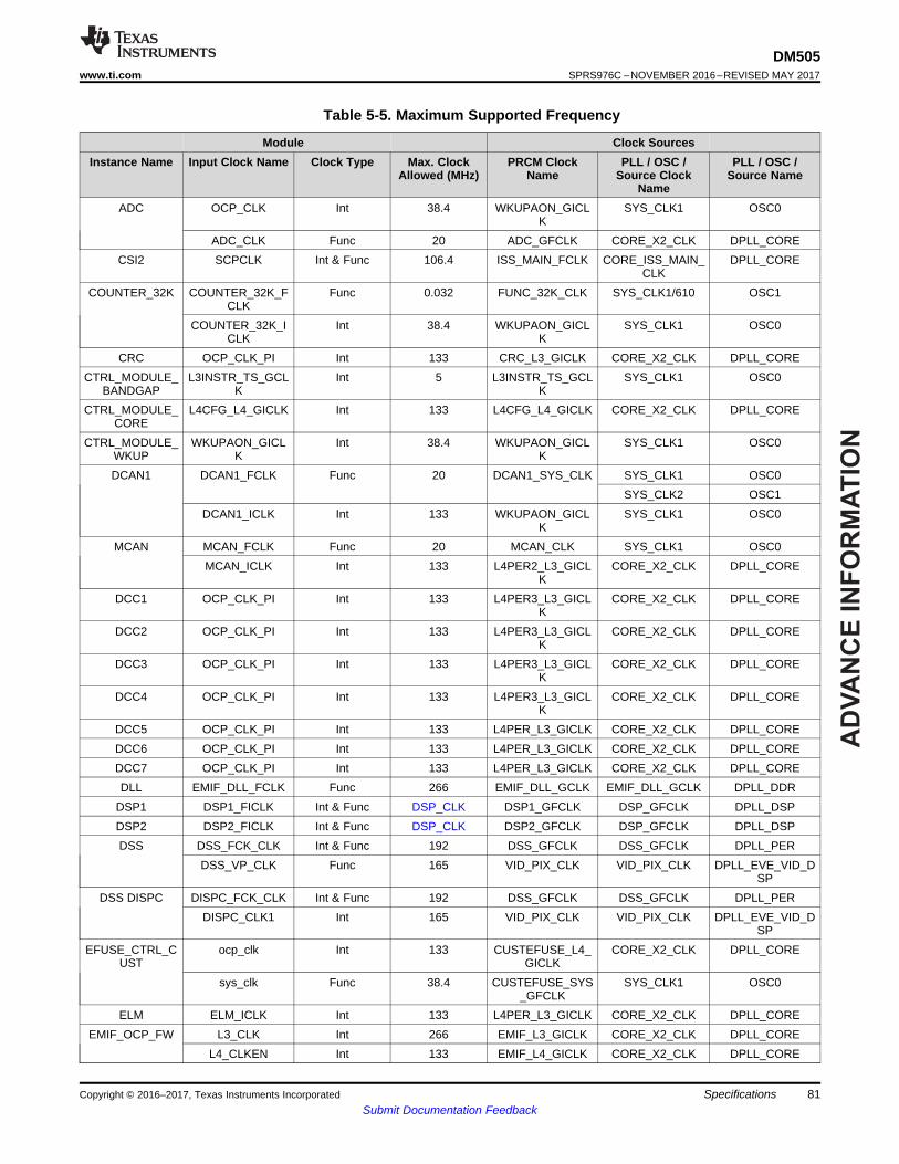
AD
VA
NC
E I
NF
OR
MA
TIO
N
81
DM505www.ti.com SPRS976C –NOVEMBER 2016–REVISED MAY 2017
Submit Documentation FeedbackSpecificationsCopyright © 2016–2017, Texas Instruments Incorporated
Table 5-5. Maximum Supported Frequency
Module Clock SourcesInstance Name Input Clock Name Clock Type Max. Clock
Allowed (MHz)PRCM Clock
NamePLL / OSC /
Source ClockName
PLL / OSC /Source Name
ADC OCP_CLK Int 38.4 WKUPAON_GICLK
SYS_CLK1 OSC0
ADC_CLK Func 20 ADC_GFCLK CORE_X2_CLK DPLL_CORECSI2 SCPCLK Int & Func 106.4 ISS_MAIN_FCLK CORE_ISS_MAIN_
CLKDPLL_CORE
COUNTER_32K COUNTER_32K_FCLK
Func 0.032 FUNC_32K_CLK SYS_CLK1/610 OSC1
COUNTER_32K_ICLK
Int 38.4 WKUPAON_GICLK
SYS_CLK1 OSC0
CRC OCP_CLK_PI Int 133 CRC_L3_GICLK CORE_X2_CLK DPLL_CORECTRL_MODULE_
BANDGAPL3INSTR_TS_GCL
KInt 5 L3INSTR_TS_GCL
KSYS_CLK1 OSC0
CTRL_MODULE_CORE
L4CFG_L4_GICLK Int 133 L4CFG_L4_GICLK CORE_X2_CLK DPLL_CORE
CTRL_MODULE_WKUP
WKUPAON_GICLK
Int 38.4 WKUPAON_GICLK
SYS_CLK1 OSC0
DCAN1 DCAN1_FCLK Func 20 DCAN1_SYS_CLK SYS_CLK1 OSC0SYS_CLK2 OSC1
DCAN1_ICLK Int 133 WKUPAON_GICLK
SYS_CLK1 OSC0
MCAN MCAN_FCLK Func 20 MCAN_CLK SYS_CLK1 OSC0MCAN_ICLK Int 133 L4PER2_L3_GICL
KCORE_X2_CLK DPLL_CORE
DCC1 OCP_CLK_PI Int 133 L4PER3_L3_GICLK
CORE_X2_CLK DPLL_CORE
DCC2 OCP_CLK_PI Int 133 L4PER3_L3_GICLK
CORE_X2_CLK DPLL_CORE
DCC3 OCP_CLK_PI Int 133 L4PER3_L3_GICLK
CORE_X2_CLK DPLL_CORE
DCC4 OCP_CLK_PI Int 133 L4PER3_L3_GICLK
CORE_X2_CLK DPLL_CORE
DCC5 OCP_CLK_PI Int 133 L4PER_L3_GICLK CORE_X2_CLK DPLL_COREDCC6 OCP_CLK_PI Int 133 L4PER_L3_GICLK CORE_X2_CLK DPLL_COREDCC7 OCP_CLK_PI Int 133 L4PER_L3_GICLK CORE_X2_CLK DPLL_COREDLL EMIF_DLL_FCLK Func 266 EMIF_DLL_GCLK EMIF_DLL_GCLK DPLL_DDR
DSP1 DSP1_FICLK Int & Func DSP_CLK DSP1_GFCLK DSP_GFCLK DPLL_DSPDSP2 DSP2_FICLK Int & Func DSP_CLK DSP2_GFCLK DSP_GFCLK DPLL_DSPDSS DSS_FCK_CLK Int & Func 192 DSS_GFCLK DSS_GFCLK DPLL_PER
DSS_VP_CLK Func 165 VID_PIX_CLK VID_PIX_CLK DPLL_EVE_VID_DSP
DSS DISPC DISPC_FCK_CLK Int & Func 192 DSS_GFCLK DSS_GFCLK DPLL_PERDISPC_CLK1 Int 165 VID_PIX_CLK VID_PIX_CLK DPLL_EVE_VID_D
SPEFUSE_CTRL_C
USTocp_clk Int 133 CUSTEFUSE_L4_
GICLKCORE_X2_CLK DPLL_CORE
sys_clk Func 38.4 CUSTEFUSE_SYS_GFCLK
SYS_CLK1 OSC0
ELM ELM_ICLK Int 133 L4PER_L3_GICLK CORE_X2_CLK DPLL_COREEMIF_OCP_FW L3_CLK Int 266 EMIF_L3_GICLK CORE_X2_CLK DPLL_CORE
L4_CLKEN Int 133 EMIF_L4_GICLK CORE_X2_CLK DPLL_CORE

AD
VA
NC
E IN
FO
RM
AT
ION
82
DM505SPRS976C –NOVEMBER 2016–REVISED MAY 2017 www.ti.com
Submit Documentation FeedbackSpecifications Copyright © 2016–2017, Texas Instruments Incorporated
Table 5-5. Maximum Supported Frequency (continued)Module Clock Sources
Instance Name Input Clock Name Clock Type Max. ClockAllowed (MHz)
PRCM ClockName
PLL / OSC /Source Clock
Name
PLL / OSC /Source Name
EMIF_PHY EMIF_PHY1_FCLK Func DDR EMIF_PHY_GCLK EMIF_PHY_GCLK DPLL_DDREMIF EMIF_ICLK Int 266 EMIF_L3_GICLK CORE_X2_CLK DPLL_CORE
EMIF_L3_ICLK Int 266 L3_EOCP_GICLK - -EMIF_PHY_FCLK Func 532 EMIF_PHY_GCLK EMIF_PHY_GCLK DPLL_DDREMIF_DLL_FCLK Int 266 EMIF_DLL_GCLK - DPLL_DDR
ESM OCP_CLK Int 133 L4_ICLK L3_ICLK CORE_CLKEVE EVE_FCLK Func EVE_FCLK EVE_GFCLK EVE_GCLK DPLL_DSP
EVE_GFCLK DPLL_EVEGMAC_SW CPTS_RFT_CLK Func 266 GMAC_RFT_CLK L3_ICLK DPLL_CORE
SYS_CLK1 OSC0MAIN_CLK Int 125 GMAC_MAIN_CLK GMAC_250M_CLK DPLL_GMAC
MHZ_250_CLK Func 250 GMII_250MHZ_CLK
GMII_250MHZ_CLK
DPLL_GMAC
MHZ_5_CLK Func 5 RGMII_5MHZ_CLK RGMII_5MHZ_CLK RMII_CLKMHZ_50_CLK Func 50 RMII_50MHZ_CLK GMAC_RMII_HS_
CLKDPLL_GMAC
GPIO1 GPIO1_ICLK Int 38.4 WKUPAON_GICLK
SYS_CLK1 OSC0
GPIO1_DBCLK Func 0.032 WKUPAON_SYS_GFCLK
WKUPAON_32K_GFCLK
OSC0
GPIO2 GPIO2_ICLK Int 133 L4PER_L3_GICLK CORE_X2_CLK DPLL_COREGPIO2_DBCLK Func 0.032 GPIO_GFCLK FUNC_32K_CLK OSC0
GPIO3 GPIO3_ICLK Int 133 L4PER_L3_GICLK CORE_X2_CLK DPLL_COREGPIO3_DBCLK Func 0.032 GPIO_GFCLK FUNC_32K_CLK OSC0
GPIO4 GPIO4_ICLK Int 133 L4PER_L3_GICLK CORE_X2_CLK DPLL_COREGPIO4_DBCLK Func 0.032 GPIO_GFCLK FUNC_32K_CLK OSC0
GPMC GPMC_ICLK Int 266 L3MAIN1_L3_GICLK
CORE_X2_CLK DPLL_CORE
I2C1 I2C1_ICLK Int 133 L4PER_L3_GICLK CORE_X2_CLK DPLL_COREI2C1_FCLK Func 96 PER_96M_GFCLK FUNC_192M_CLK DPLL_PER
I2C2 I2C2_ICLK Int 133 L4PER_L3_GICLK CORE_X2_CLK DPLL_COREI2C2_FCLK Func 96 PER_96M_GFCLK FUNC_192M_CLK DPLL_PER
IEEE1500_2_OCP
PI_L3CLK Int & Func 266 L3INIT_L3_GICLK CORE_X2_CLK DPLL_CORE
IPU1 IPU1_GFCLK Int & Func IPU_CLK IPU1_GFCLK SYS_CLK1 OSC0CORE_IPU_ISS_B
OOST_CLKDPLL_CORE
L3_INSTR L3_CLK Int L3_CLK L3INSTR_L3_GICLK
CORE_X2_CLK DPLL_CORE
L4_CFG L4_CFG_CLK Int 133 L4CFG_L3_GICLK CORE_X2_CLK DPLL_COREL4_PER1 L4_PER1_CLK Int 133 L4PER_L3_GICLK CORE_X2_CLK DPLL_COREL4_PER2 L4_PER2_CLK Int 133 L4PER2_L3_GICL
KCORE_X2_CLK DPLL_CORE
L4_PER3 L4_PER3_CLK Int 133 L4PER3_L3_GICLK
CORE_X2_CLK DPLL_CORE
L4_WKUP L4_WKUP_CLK Int 38.4 WKUPAON_GICLK
SYS_CLK1 OSC0
MAILBOX1 MAILBOX1_FLCK Int 133 L4CFG_L3_GICLK CORE_X2_CLK DPLL_CORE

AD
VA
NC
E I
NF
OR
MA
TIO
N
83
DM505www.ti.com SPRS976C –NOVEMBER 2016–REVISED MAY 2017
Submit Documentation FeedbackSpecificationsCopyright © 2016–2017, Texas Instruments Incorporated
Table 5-5. Maximum Supported Frequency (continued)Module Clock Sources
Instance Name Input Clock Name Clock Type Max. ClockAllowed (MHz)
PRCM ClockName
PLL / OSC /Source Clock
Name
PLL / OSC /Source Name
MAILBOX2 MAILBOX2_FLCK Int 133 L4CFG_L3_GICLK CORE_X2_CLK DPLL_COREMCASP1 MCASP1_AHCLK
RFunc 100 MCASP1_AHCLK
RABE_24M_GFCLK DPLL_DDR
ABE_SYS_CLK SYS_CLK1FUNC_24M_GFCL
KDPLL_PER
SYS_CLK1 OSC0ATLCLKIN0 Module ATLATLCLKIN1 Module ATLATLCLKIN2 Module ATLATLCLKIN3 Module ATLSYS_CLK2 OSC1
XREF_CLK0 REF_CLKIN0XREF_CLK1 REF_CLKIN1XREF_CLK2 REF_CLKIN2
MCASP1_AHCLKX Func 100 MCASP1_AHCLKX ABE_24M_GFCLK DPLL_DDRABE_SYS_CLK SYS_CLK1
FUNC_24M_GFCLK
DPLL_PER
SYS_CLK1 OSC0ATLCLKIN0 Module ATLATLCLKIN1 Module ATLATLCLKIN2 Module ATLATLCLKIN3 Module ATLSYS_CLK2 OSC1
XREF_CLK0 REF_CLKIN0XREF_CLK1 REF_CLKIN1XREF_CLK2 REF_CLKIN2
MCASP1_FCLK Func 10 MCASP1_AUX_GFCLK
L4_ICLK DPLL_CORESYS_CLK1 OSC0
MCASP1_ICLK Int 133 IPU_L3_GICLK CORE_X2_CLK DPLL_CORE

AD
VA
NC
E IN
FO
RM
AT
ION
84
DM505SPRS976C –NOVEMBER 2016–REVISED MAY 2017 www.ti.com
Submit Documentation FeedbackSpecifications Copyright © 2016–2017, Texas Instruments Incorporated
Table 5-5. Maximum Supported Frequency (continued)Module Clock Sources
Instance Name Input Clock Name Clock Type Max. ClockAllowed (MHz)
PRCM ClockName
PLL / OSC /Source Clock
Name
PLL / OSC /Source Name
MCASP2 MCASP2_AHCLKR
Func 100 MCASP6_AHCLKR
ABE_24M_GFCLK DPLL_DDRABE_SYS_CLK SYS_CLK1
FUNC_24M_GFCLK
DPLL_PER
SYS_CLK1 OSC0ATLCLKIN0 Module ATLATLCLKIN1 Module ATLATLCLKIN2 Module ATLATLCLKIN3 Module ATLSYS_CLK2 OSC1
XREF_CLK0 REF_CLKIN0XREF_CLK1 REF_CLKIN1XREF_CLK2 REF_CLKIN2
MCASP2_AHCLKX Func 100 MCASP4_AHCLKX ABE_24M_GFCLK DPLL_DDRABE_SYS_CLK SYS_CLK1
FUNC_24M_GFCLK
DPLL_PER
SYS_CLK1 OSC0ATLCLKIN0 Module ATLATLCLKIN1 Module ATLATLCLKIN2 Module ATLATLCLKIN3 Module ATLSYS_CLK2 OSC1
XREF_CLK0 REF_CLKIN0XREF_CLK1 REF_CLKIN1XREF_CLK2 REF_CLKIN2
MCASP2_FCLK Func 10 MCASP4_AUX_GFCLK
L4_ICLK DPLL_CORESYS_CLK1 OSC0
MCASP2_ICLK Int 133 IPU_L3_GICLK CORE_X2_CLK DPLL_CORE

AD
VA
NC
E I
NF
OR
MA
TIO
N
85
DM505www.ti.com SPRS976C –NOVEMBER 2016–REVISED MAY 2017
Submit Documentation FeedbackSpecificationsCopyright © 2016–2017, Texas Instruments Incorporated
Table 5-5. Maximum Supported Frequency (continued)Module Clock Sources
Instance Name Input Clock Name Clock Type Max. ClockAllowed (MHz)
PRCM ClockName
PLL / OSC /Source Clock
Name
PLL / OSC /Source Name
MCASP3 MCASP3_AHCLKR
Func 100 MCASP7_AHCLKR
ABE_24M_GFCLK DPLL_DDRABE_SYS_CLK SYS_CLK1
FUNC_24M_GFCLK
DPLL_PER
SYS_CLK1 OSC0ATLCLKIN0 Module ATLATLCLKIN1 Module ATLATLCLKIN2 Module ATLATLCLKIN3 Module ATLSYS_CLK2 OSC1
XREF_CLK0 REF_CLKIN0XREF_CLK1 REF_CLKIN1XREF_CLK2 REF_CLKIN2
MCASP3_AHCLKX Func 100 MCASP5_AHCLKX ABE_24M_GFCLK DPLL_DDRABE_SYS_CLK SYS_CLK1
FUNC_24M_GFCLK
DPLL_PER
SYS_CLK1 OSC0ATLCLKIN0 Module ATLATLCLKIN1 Module ATLATLCLKIN2 Module ATLATLCLKIN3 Module ATLSYS_CLK2 OSC1
XREF_CLK0 REF_CLKIN0XREF_CLK1 REF_CLKIN1XREF_CLK2 REF_CLKIN2
MCASP3_FCLK Func 10 MCASP5_AUX_GFCLK
L4_ICLK DPLL_CORESYS_CLK1 OSC0
MCASP3_ICLK Int 133 IPU_L3_GICLK CORE_X2_CLK DPLL_COREMcSPI1 SPI1_ICLK Int 133 L4PER_L3_GICLK CORE_X2_CLK DPLL_CORE
SPI1_FCLK Func 48 PER_48M_GFCLK FUNC_192M_CLK DPLL_PERMcSPI2 SPI1_ICLK Int 133 L4PER_L3_GICLK CORE_X2_CLK DPLL_CORE
SPI1_FCLK Func 48 PER_48M_GFCLK FUNC_192M_CLK DPLL_PERMcSPI3 SPI1_ICLK Int 133 L4PER_L3_GICLK CORE_X2_CLK DPLL_CORE
SPI1_FCLK Func 48 PER_48M_GFCLK FUNC_192M_CLK DPLL_PERMcSPI4 SPI1_ICLK Int 133 L4PER_L3_GICLK CORE_X2_CLK DPLL_CORE
SPI1_FCLK Func 48 PER_48M_GFCLK FUNC_192M_CLK DPLL_PERMMC1 MMC1_CLK_32K Func 0.032 L3INIT_32K_GFCL
KFUNC_32K_CLK OSC0
MMC1_FCLK Func 192 MMC1_GFCLK FUNC_192M_CLK DPLL_PER128 FUNC_128M_CLK DPLL_PER
MMC1_ICLK1 Int 266 L3INIT_L3_GICLK CORE_X2_CLK DPLL_COREMMC1_ICLK2 Int 266 L3INIT_L4_GICLK CORE_X2_CLK DPLL_CORE
MMU_EDMA MMU1_CLK Int 266 L3MAIN1_L3_GICLK
CORE_X2_CLK DPLL_CORE

AD
VA
NC
E IN
FO
RM
AT
ION
86
DM505SPRS976C –NOVEMBER 2016–REVISED MAY 2017 www.ti.com
Submit Documentation FeedbackSpecifications Copyright © 2016–2017, Texas Instruments Incorporated
Table 5-5. Maximum Supported Frequency (continued)Module Clock Sources
Instance Name Input Clock Name Clock Type Max. ClockAllowed (MHz)
PRCM ClockName
PLL / OSC /Source Clock
Name
PLL / OSC /Source Name
OCMC_RAM1 OCMC_L3_CLK_1 Int 266 L3MAIN1_L3_GICLK
CORE_X2_CLK DPLL_CORE
OCP_WP_NOC PICLKOCPL3 Int 266 L3INSTR_L3_GICLK
CORE_X2_CLK DPLL_CORE
OCP2SCP1 L4CFG_ADAPTER_CLKIN_1
Int 133 L3INIT_L4_GICLK CORE_X2_CLK DPLL_CORE
PWMSS1 PWMSS1_GICLK Int & Func 133 L4PER2_L3_GICLK
CORE_X2_CLK DPLL_CORE
QSPI QSPI_ICLK Int 266 L4PER2_L3_GICLK
CORE_X2_CLK DPLL_CORE
QSPI_FCLK Func 128 QSPI_GFCLK FUNC_128M_CLK DPLL_PERPER_QSPI_CLK DPLL_PER
RTI1 OCP_CLK_PI Int 133 L4_ICLK CORE_X2_CLK DPLL_CORERTI_CLK_PI Counter 13 RTI_CLK SYS_CLK1 OSC1
SYS_CLK2 OSC2FUNC_32K_CLK OSC1
RTI2 OCP_CLK_PI Int 133 L4_ICLK CORE_X2_CLK DPLL_CORERTI_CLK_PI Counter 13 RTI_CLK SYS_CLK1 OSC1
SYS_CLK2 OSC2FUNC_32K_CLK OSC1
RTI3 OCP_CLK_PI Int 133 L4_ICLK CORE_X2_CLK DPLL_CORERTI_CLK_PI Counter 13 RTI_CLK SYS_CLK1 OSC1
SYS_CLK2 OSC2FUNC_32K_CLK OSC1
RTI4 OCP_CLK_PI Int 133 L4_ICLK CORE_X2_CLK DPLL_CORERTI_CLK_PI Counter 13 RTI_CLK SYS_CLK1 OSC1
SYS_CLK2 OSC2FUNC_32K_CLK OSC1
RTI5 OCP_CLK_PI Int 133 L4_ICLK CORE_X2_CLK DPLL_CORERTI_CLK_PI Counter 13 RTI_CLK SYS_CLK1 OSC1
SYS_CLK2 OSC2FUNC_32K_CLK OSC1
SD_DAC CLKDAC Func 50 VID_PIX_CLK VID_PIX_CLK DPLL_EVE_VID_DSP
SL2 piclk Int IVA_GCLK IVA_GCLK IVA_GFCLK DPLL_IVASMARTREFLEX_
COREMCLK Int 133 COREAON_L4_GI
CLKCORE_X2_CLK DPLL_CORE
SYSCLK Func 38.4 WKUPAON_ICLK SYS_CLK1 OSC0SMARTREFLEX_
DSPEVEMCLK Int 133 COREAON_L4_GI
CLKCORE_X2_CLK DPLL_CORE
SYSCLK Func 38.4 WKUPAON_ICLK SYS_CLK1 OSC0SPINLOCK SPINLOCK_ICLK Int 133 L4CFG_L3_GICLK CORE_X2_CLK DPLL_CORE
TESOC L3_CLK Func 266 L3INSTR_L3_GICLK
CORE_X2_CLK DPLL_CORE
EXT_CLK Func 50 EXT_CLK TESOC_EXT_CLK DPLL_CORE

AD
VA
NC
E I
NF
OR
MA
TIO
N
87
DM505www.ti.com SPRS976C –NOVEMBER 2016–REVISED MAY 2017
Submit Documentation FeedbackSpecificationsCopyright © 2016–2017, Texas Instruments Incorporated
Table 5-5. Maximum Supported Frequency (continued)Module Clock Sources
Instance Name Input Clock Name Clock Type Max. ClockAllowed (MHz)
PRCM ClockName
PLL / OSC /Source Clock
Name
PLL / OSC /Source Name
TIMER1 TIMER1_ICLK Int 133 WKUPAON_GICLK
SYS_CLK1 OSC0
TIMER1_FCLK Func 38.4 TIMER1_GFCLK SYS_CLK1 OSC0FUNC_32K_CLK SYS_32K
SYS_CLK2 OSC1XREF_CLK0 xref_clk0XREF_CLK1 xref_clk1
TIMER2 TIMER2_ICLK Int 133 L4PER_L3_GICLK CORE_X2_CLK DPLL_CORETIMER2_FCLK Func 100 TIMER2_GFCLK SYS_CLK1 OSC0
FUNC_32K_CLK SYS_32KSYS_CLK2 OSC1
XREF_CLK0 xref_clk0XREF_CLK1 xref_clk1
TIMER3 TIMER3_ICLK Int 133 L4PER_L3_GICLK CORE_X2_CLK DPLL_CORETIMER3_FCLK Func 100 TIMER3_GFCLK SYS_CLK1 OSC0
FUNC_32K_CLK SYS_32KSYS_CLK2 OSC1
XREF_CLK0 xref_clk0XREF_CLK1 xref_clk1
TIMER4 TIMER4_ICLK Int 133 L4PER_L3_GICLK CORE_X2_CLK DPLL_CORETIMER4_FCLK Func 100 TIMER4_GFCLK SYS_CLK1 OSC0
FUNC_32K_CLK SYS_32KSYS_CLK2 OSC1
XREF_CLK0 xref_clk0XREF_CLK1 xref_clk1
TIMER5 TIMER5_ICLK Int 133 IPU_L3_GICLK CORE_X2_CLK DPLL_CORETIMER5_FCLK Func 100 TIMER5_GFCLK SYS_CLK1 OSC0
FUNC_32K_CLK SYS_32KSYS_CLK2 OSC1
XREF_CLK0 xref_clk0XREF_CLK1 xref_clk1
CLKOUTMUX0_CLK
CLKOUTMUX0_CLK
TIMER6 TIMER6_ICLK Int 133 IPU_L3_GICLK CORE_X2_CLK DPLL_CORETIMER6_FCLK Func 100 TIMER6_GFCLK SYS_CLK1 OSC0
FUNC_32K_CLK OSC0SYS_CLK2 OSC1
XREF_CLK0 xref_clk0XREF_CLK1 xref_clk1
CLKOUTMUX0_CLK
CLKOUTMUX0_CLK

AD
VA
NC
E IN
FO
RM
AT
ION
88
DM505SPRS976C –NOVEMBER 2016–REVISED MAY 2017 www.ti.com
Submit Documentation FeedbackSpecifications Copyright © 2016–2017, Texas Instruments Incorporated
Table 5-5. Maximum Supported Frequency (continued)Module Clock Sources
Instance Name Input Clock Name Clock Type Max. ClockAllowed (MHz)
PRCM ClockName
PLL / OSC /Source Clock
Name
PLL / OSC /Source Name
TIMER7 TIMER7_ICLK Int 133 IPU_L3_GICLK CORE_X2_CLK DPLL_CORETIMER7_FCLK Func 100 TIMER7_GFCLK SYS_CLK1 OSC0
FUNC_32K_CLK OSC0SYS_CLK2 OSC1
XREF_CLK0 xref_clk0XREF_CLK1 xref_clk1
CLKOUTMUX0_CLK
CLKOUTMUX0_CLK
TIMER8 TIMER8_ICLK Int 133 IPU_L3_GICLK CORE_X2_CLK DPLL_CORETIMER8_FCLK Func 100 TIMER8_GFCLK SYS_CLK1 OSC0
FUNC_32K_CLK OSC0SYS_CLK2 OSC1
XREF_CLK0 xref_clk0XREF_CLK1 xref_clk1
CLKOUTMUX0_CLK
CLKOUTMUX0_CLK
TPCC TPCC_GCLK Int 266 L3MAIN1_L3_GICLK
CORE_X2_CLK DPLL_CORE
TPTC1 TPTC0_GCLK Int 266 L3MAIN1_L3_GICLK
CORE_X2_CLK DPLL_CORE
TPTC2 TPTC1_GCLK Int 266 L3MAIN1_L3_GICLK
CORE_X2_CLK DPLL_CORE
UART1 UART1_FCLK Func 48 UART1_GFCLK FUNC_192M_CLK DPLL_PERUART1_ICLK Int 133 L4PER_L3_GICLK CORE_X2_CLK DPLL_CORE
UART2 UART2_FCLK Func 48 UART2_GFCLK FUNC_192M_CLK DPLL_PERUART2_ICLK Int 133 L4PER_L3_GICLK CORE_X2_CLK DPLL_CORE
UART3 UART3_FCLK Func 48 UART3_GFCLK FUNC_192M_CLK DPLL_PERUART3_ICLK Int 133 L4PER_L3_GICLK CORE_X2_CLK DPLL_CORE
VIP1 L3_CLK_PROC_CLK
Int & Func 266 VIP1_GCLK CORE_X2_CLK DPLL_CORECORE_ISS_MAIN_
CLKDPLL_CORE
5.6 Power Consumption Summary
NOTEMaximum power consumption for this SoC depends on the specific use conditions for theend system. Contact your TI representative for assistance in estimating maximum powerconsumption for the end system use case.
5.7 Electrical Characteristics
NOTEThe data specified in Table 5-6 through Table 5-11 are subject to change.

AD
VA
NC
E I
NF
OR
MA
TIO
N
89
DM505www.ti.com SPRS976C –NOVEMBER 2016–REVISED MAY 2017
Submit Documentation FeedbackSpecificationsCopyright © 2016–2017, Texas Instruments Incorporated
NOTEThe interfaces or signals described in Table 5-6 through Table 5-11 correspond to theinterfaces or signals available in multiplexing mode 0 (Function 1).
All interfaces or signals multiplexed on the balls described in these tables have the same DCelectrical characteristics, unless multiplexing involves a PHY/GPIO combination in whichcase different DC electrical characteristics are specified for the different multiplexing modes(Functions).
Table 5-6. LVCMOS DDR DC Electrical Characteristicsover operating free-air temperature range (unless otherwise noted)
PARAMETER MIN NOM MAX UNITSignal Names in MUXMODE 0 (Single-Ended Signals) ABF: ddr1_d[31:0], ddr1_a[15:0], ddr1_dqm[3:0], ddr1_ba[2:0], ddr1_csn[1:0],ddr1_cke[1:0], ddr1_odt[0], ddr1_casn, ddr1_rasn, ddr1_wen, ddr1_rst, ddr1_ecc_d[7:0], ddr1_dqm_ecc;Driver Mode
VOH High-level output threshold (IOH = 0.1 mA) 0.9*VDDS VVOL Low-level output threshold (IOL = 0.1 mA) 0.1*VDDS V
CPAD Pad capacitance (including package capacitance) 3 pFZO Output impedance (drive
strength)l[2:0] = 000
(Imp80)80 Ω
l[2:0] = 001(Imp60)
60
l[2:0] = 010(Imp48)
48
l[2:0] = 011(Imp40)
40
l[2:0] = 100(Imp34)
34
Single-Ended Receiver ModeVIH High-level input threshold DDR3/DDR3L VREF+0.1 VDDS+0.2 VVIL Low-level input threshold DDR3/DDR3L -0.2 VREF-0.1 VVCM Input common-mode voltage VREF
-1%VDDSVREF+
1%VDDSV
CPAD Pad capacitance (including package capacitance) pFSignal Names in MUXMODE 0 (Differential Signals): ddr1_dqs[3:0], ddr1_dqsn[3:0], ddr1_ck, ddr1_nck, ddr1_dqs_ecc, ddr1_dqsn_ecc;Driver Mode
VOH High-level output threshold (IOH = 0.1 mA) 0.9*VDDS VVOL Low-level output threshold (IOL = 0.1 mA) 0.1*VDDS V
CPAD Pad capacitance (including package capacitance) 3 pFZO Output impedance (drive
strength)l[2:0] = 000
(Imp80)80 Ω
l[2:0] = 001(Imp60)
60
l[2:0] = 010(Imp48)
48
l[2:0] = 011(Imp40)
40
l[2:0] = 100(Imp34)
34
Single-Ended Receiver ModeVIH High-level input threshold DDR3/DDR3L VREF+0.1 VDDS+0.2 VVIL Low-level input threshold DDR3/DDR3L -0.2 VREF-0.1 VVCM Input common-mode voltage VREF
-1%VDDSVREF+
1%VDDSV
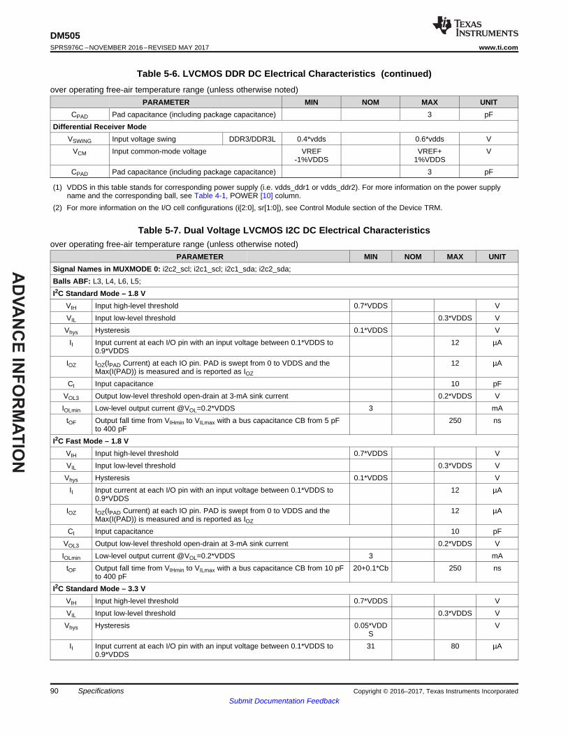
AD
VA
NC
E IN
FO
RM
AT
ION
90
DM505SPRS976C –NOVEMBER 2016–REVISED MAY 2017 www.ti.com
Submit Documentation FeedbackSpecifications Copyright © 2016–2017, Texas Instruments Incorporated
Table 5-6. LVCMOS DDR DC Electrical Characteristics (continued)over operating free-air temperature range (unless otherwise noted)
PARAMETER MIN NOM MAX UNITCPAD Pad capacitance (including package capacitance) 3 pF
Differential Receiver ModeVSWING Input voltage swing DDR3/DDR3L 0.4*vdds 0.6*vdds V
VCM Input common-mode voltage VREF-1%VDDS
VREF+1%VDDS
V
CPAD Pad capacitance (including package capacitance) 3 pF
(1) VDDS in this table stands for corresponding power supply (i.e. vdds_ddr1 or vdds_ddr2). For more information on the power supplyname and the corresponding ball, see Table 4-1, POWER [10] column.
(2) For more information on the I/O cell configurations (i[2:0], sr[1:0]), see Control Module section of the Device TRM.
Table 5-7. Dual Voltage LVCMOS I2C DC Electrical Characteristicsover operating free-air temperature range (unless otherwise noted)
PARAMETER MIN NOM MAX UNITSignal Names in MUXMODE 0: i2c2_scl; i2c1_scl; i2c1_sda; i2c2_sda;Balls ABF: L3, L4, L6, L5;I2C Standard Mode – 1.8 V
VIH Input high-level threshold 0.7*VDDS VVIL Input low-level threshold 0.3*VDDS VVhys Hysteresis 0.1*VDDS V
II Input current at each I/O pin with an input voltage between 0.1*VDDS to0.9*VDDS
12 µA
IOZ IOZ(IPAD Current) at each IO pin. PAD is swept from 0 to VDDS and theMax(I(PAD)) is measured and is reported as IOZ
12 µA
CI Input capacitance 10 pFVOL3 Output low-level threshold open-drain at 3-mA sink current 0.2*VDDS VIOLmin Low-level output current @VOL=0.2*VDDS 3 mA
tOF Output fall time from VIHmin to VILmax with a bus capacitance CB from 5 pFto 400 pF
250 ns
I2C Fast Mode – 1.8 VVIH Input high-level threshold 0.7*VDDS VVIL Input low-level threshold 0.3*VDDS VVhys Hysteresis 0.1*VDDS V
II Input current at each I/O pin with an input voltage between 0.1*VDDS to0.9*VDDS
12 µA
IOZ IOZ(IPAD Current) at each IO pin. PAD is swept from 0 to VDDS and theMax(I(PAD)) is measured and is reported as IOZ
12 µA
CI Input capacitance 10 pFVOL3 Output low-level threshold open-drain at 3-mA sink current 0.2*VDDS VIOLmin Low-level output current @VOL=0.2*VDDS 3 mA
tOF Output fall time from VIHmin to VILmax with a bus capacitance CB from 10 pFto 400 pF
20+0.1*Cb 250 ns
I2C Standard Mode – 3.3 VVIH Input high-level threshold 0.7*VDDS VVIL Input low-level threshold 0.3*VDDS VVhys Hysteresis 0.05*VDD
SV
II Input current at each I/O pin with an input voltage between 0.1*VDDS to0.9*VDDS
31 80 µA
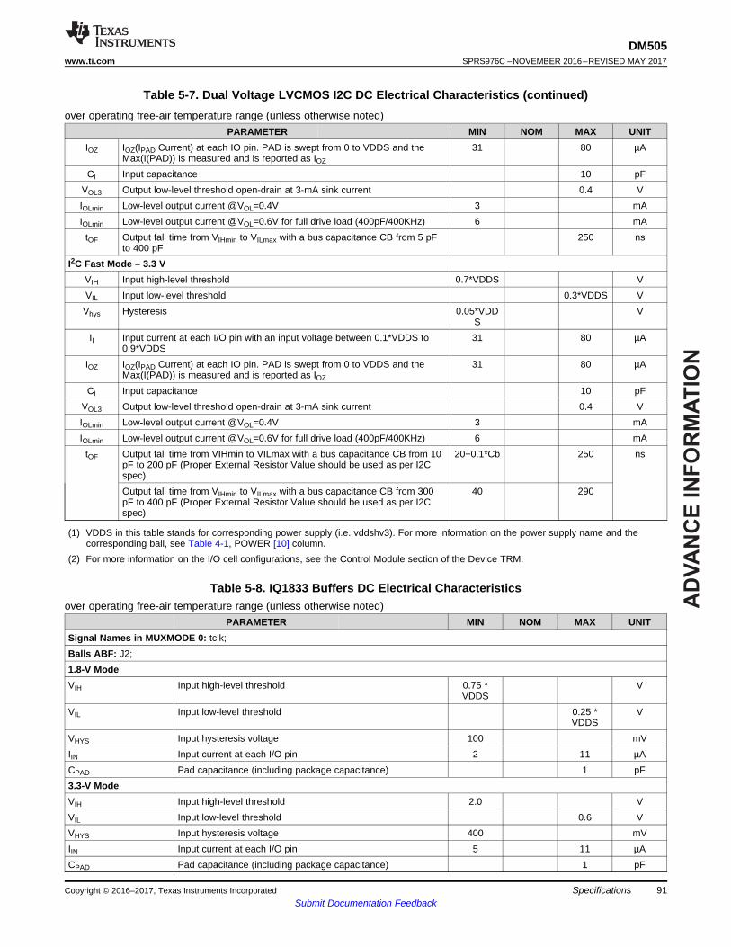
AD
VA
NC
E I
NF
OR
MA
TIO
N
91
DM505www.ti.com SPRS976C –NOVEMBER 2016–REVISED MAY 2017
Submit Documentation FeedbackSpecificationsCopyright © 2016–2017, Texas Instruments Incorporated
Table 5-7. Dual Voltage LVCMOS I2C DC Electrical Characteristics (continued)over operating free-air temperature range (unless otherwise noted)
PARAMETER MIN NOM MAX UNITIOZ IOZ(IPAD Current) at each IO pin. PAD is swept from 0 to VDDS and the
Max(I(PAD)) is measured and is reported as IOZ
31 80 µA
CI Input capacitance 10 pFVOL3 Output low-level threshold open-drain at 3-mA sink current 0.4 VIOLmin Low-level output current @VOL=0.4V 3 mAIOLmin Low-level output current @VOL=0.6V for full drive load (400pF/400KHz) 6 mA
tOF Output fall time from VIHmin to VILmax with a bus capacitance CB from 5 pFto 400 pF
250 ns
I2C Fast Mode – 3.3 VVIH Input high-level threshold 0.7*VDDS VVIL Input low-level threshold 0.3*VDDS VVhys Hysteresis 0.05*VDD
SV
II Input current at each I/O pin with an input voltage between 0.1*VDDS to0.9*VDDS
31 80 µA
IOZ IOZ(IPAD Current) at each IO pin. PAD is swept from 0 to VDDS and theMax(I(PAD)) is measured and is reported as IOZ
31 80 µA
CI Input capacitance 10 pFVOL3 Output low-level threshold open-drain at 3-mA sink current 0.4 VIOLmin Low-level output current @VOL=0.4V 3 mAIOLmin Low-level output current @VOL=0.6V for full drive load (400pF/400KHz) 6 mA
tOF Output fall time from VIHmin to VILmax with a bus capacitance CB from 10pF to 200 pF (Proper External Resistor Value should be used as per I2Cspec)
20+0.1*Cb 250 ns
Output fall time from VIHmin to VILmax with a bus capacitance CB from 300pF to 400 pF (Proper External Resistor Value should be used as per I2Cspec)
40 290
(1) VDDS in this table stands for corresponding power supply (i.e. vddshv3). For more information on the power supply name and thecorresponding ball, see Table 4-1, POWER [10] column.
(2) For more information on the I/O cell configurations, see the Control Module section of the Device TRM.
Table 5-8. IQ1833 Buffers DC Electrical Characteristicsover operating free-air temperature range (unless otherwise noted)
PARAMETER MIN NOM MAX UNITSignal Names in MUXMODE 0: tclk;Balls ABF: J2;1.8-V ModeVIH Input high-level threshold 0.75 *
VDDSV
VIL Input low-level threshold 0.25 *VDDS
V
VHYS Input hysteresis voltage 100 mVIIN Input current at each I/O pin 2 11 µACPAD Pad capacitance (including package capacitance) 1 pF3.3-V ModeVIH Input high-level threshold 2.0 VVIL Input low-level threshold 0.6 VVHYS Input hysteresis voltage 400 mVIIN Input current at each I/O pin 5 11 µACPAD Pad capacitance (including package capacitance) 1 pF

AD
VA
NC
E IN
FO
RM
AT
ION
92
DM505SPRS976C –NOVEMBER 2016–REVISED MAY 2017 www.ti.com
Submit Documentation FeedbackSpecifications Copyright © 2016–2017, Texas Instruments Incorporated
Table 5-8. IQ1833 Buffers DC Electrical Characteristics (continued)over operating free-air temperature range (unless otherwise noted)(1) VDDS in this table stands for corresponding power supply (i.e. vddshv1). For more information on the power supply name and the
corresponding ball, see Table 4-1, POWER [10] column.
Table 5-9. IHHV1833 Buffers DC Electrical Characteristicsover operating free-air temperature range (unless otherwise noted)
PARAMETER MIN NOM MAX UNITSignal Names in MUXMODE 0: porz;Balls ABF: G3;1.8-V ModeVIH Input high-level threshold 1.2 VVIL Input low-level threshold 0.4 VVHYS Input hysteresis voltage 40 mVIIN Input current at each I/O pin 0.02 1 µACPAD Pad capacitance (including package capacitance) 1 pF3.3-V ModeVIH Input high-level threshold 1.2 VVIL Input low-level threshold 0.4 VVHYS Input hysteresis voltage 40 mVIIN Input current at each I/O pin 5 8 µACPAD Pad capacitance (including package capacitance) 1 pF
Table 5-10. LVCMOS Analog OSC Buffers DC Electrical Characteristicsover operating free-air temperature range (unless otherwise noted)
PARAMETER DESCRIPTION MIN NOM MAX UNITSignal Names in MUXMODE 0: xi_osc0, xo_osc0, xi_osc1, xo_osc1;Balls ABF: E22, D22, B21, C21;
VIH Input high-level threshold 0.65*VDDS VVIL Input low-level threshold 0.35*VDDS VIOH hfenable=0 1.18 mA
hfenable=1 2 mAIOL hfenable=0 2 mA
hfenable=1 3.2 mAVHYS Input hysteresis voltage MODE-1 150 mVCPAD Capacitance connected on input and output Pad on
Board, CL1=CL212 24 pF
(1) VDDS in this table stands for corresponding power supply (i.e. vdda_osc). For more information on the power supply name and thecorresponding ball, see Table 4-1, POWER [10] column.
Table 5-11. LVCMOS CSI2 DC Electrical Characteristicsover operating free-air temperature range (unless otherwise noted)
PARAMETER MIN NOM MAX UNITSignals MUXMODE0 : csi2_0_dx[4:0]; csi2_0_dy[4:0];Bottom Balls: A11 / B11 / A12 / B12 / A13 / B13 / A15 / B15 / A16 / B16MIPI D-PHY Mode Low-Power Receiver (LP-RX)
VIH Input high-level voltage 880 1350 mVVIL Input low-level voltage 550 mV
VITH Input high-level threshold 880 mVVITL Input low-level threshold 550 mV

AD
VA
NC
E I
NF
OR
MA
TIO
N
93
DM505www.ti.com SPRS976C –NOVEMBER 2016–REVISED MAY 2017
Submit Documentation FeedbackSpecificationsCopyright © 2016–2017, Texas Instruments Incorporated
Table 5-11. LVCMOS CSI2 DC Electrical Characteristics (continued)over operating free-air temperature range (unless otherwise noted)
PARAMETER MIN NOM MAX UNITVHYS Input hysteresis 25 mV
MIPI D-PHY Mode Ultralow Power Receiver (ULP-RX)VIH Input high-level voltage 880 mVVIL Input low-level voltage 300 mV
VITH Input high-level threshold 880 mVVITL Input low-level threshold 300 mVVHYS Input hysteresis 25 mV
MIPI D-PHY Mode High-Speed Receiver (HS-RX)VIDTH Differential input high-level threshold 70 mVVIDTL Differential input low-level threshold –70 mV
VIDMAX Maximum differential input voltage 270 mVVIHHS Single-ended input high voltage 460 mVVILHS Single-ended input low voltage –40 mV
VCMRXDC Differential input common-mode voltage 70 330 mVZID Differential input impedance 80 100 125 Ω
(1) VITH is the voltage at which the receiver is required to detect a high state in the input signal.(2) VITL is the voltage at which the receiver is required to detect a low state in the input signal. VITL is larger than the maximum single-ended
line high voltage during HS transmission. Therefore, both low-power (LP) receivers will detect low during HS signaling.(3) To reduce noise sensitivity on the received signal, the LP receiver is required to incorporate a hysteresis, VHYST. VHYST is the difference
between the VITH threshold and the VITL threshold.(4) VITL is the voltage at which the receiver is required to detect a low state in the input signal. Specification is relaxed for detecting 0 during
ultralow power (ULP) state. The LP receiver is not required to detect HS single-ended voltage as 0 in this state.(5) Excluding possible additional RF interference of 200 mVPP beyond 450 MHz.(6) This value includes a ground difference of 50 mV between the transmitter and the receiver, the static common-mode level tolerance and
variations below 450 MHz.(7) This number corresponds to the VODMAX transmitter.(8) Common mode is defined as the average voltage level of X and Y: VCMRX = (VX + VY) / 2.(9) Common mode ripple may be due to tR or tF and transmission line impairments in the PCB.(10) For more information regarding the pin name (or ball name) and corresponding signal name, see Table 4-8 CSI 2 Signal Descriptions.
Table 5-12. Dual Voltage LVCMOS DC Electrical Characteristicsover operating free-air temperature range (unless otherwise noted)
PARAMETER DESCRIPTION MIN NOM MAX UNIT1.8-V Mode
VIH Input high-level threshold 0.65*VDDS VVIL Input low-level threshold 0.35*VDDS V
VHYS Input hysteresis voltage 100 mVVOH Output high-level threshold (IOH = 2 mA) VDDS-0.45 VVOL Output low-level threshold (IOL = 2 mA) 0.45 V
IDRIVE Pin Drive strength at PAD Voltage = 0.45V or VDDS-0.45V
6 mA
IIN Input current at each I/O pin 16 µAIOZ IOZ(IPAD Current) at each IO pin. PAD is swept from 0
to VDDS and the Max(I(PAD)) is measured and isreported as IOZ
11.5 µA
IIN with pulldown enabled Input current at each I/O pin with weak pulldownenabled measured when PAD = VDDS
60 120 200 µA
IIN with pullup enabled Input current at each I/O pin with weak pullup enabledmeasured when PAD = 0
60 120 210 µA

AD
VA
NC
E IN
FO
RM
AT
ION
94
DM505SPRS976C –NOVEMBER 2016–REVISED MAY 2017 www.ti.com
Submit Documentation FeedbackSpecifications Copyright © 2016–2017, Texas Instruments Incorporated
Table 5-12. Dual Voltage LVCMOS DC Electrical Characteristics (continued)over operating free-air temperature range (unless otherwise noted)
PARAMETER DESCRIPTION MIN NOM MAX UNITCPAD Pad capacitance (including package capacitance) 4 pFZO Output impedance (drive strength) 40 Ω
3.3-V ModeVIH Input high-level threshold 2 VVIL Input low-level threshold 0.8 V
VHYS Input hysteresis voltage 200 mVVOH Output high-level threshold (IOH =100µA) VDDS-0.2 VVOL Output low-level threshold (IOL = 100µA) 0.2 V
IDRIVE Pin Drive strength at PAD Voltage = 0.45V or VDDS-0.45V
6 mA
IIN Input current at each I/O pin 64 µAIOZ IOZ(IPAD Current) at each IO pin. PAD is swept from 0
to VDDS and the Max(I(PAD)) is measured and isreported as IOZ
64 µA
IIN with pulldown enabled Input current at each I/O pin with weak pulldownenabled measured when PAD = VDDS
10 100 290 µA
IIN with pullup enabled Input current at each I/O pin with weak pullup enabledmeasured when PAD = 0
40 100 200 µA
CPAD Pad capacitance (including package capacitance) 4 pFZO Output impedance (drive strength) 40 Ω
(1) VDDS in this table stands for corresponding power supply. For more information on the power supply name and the corresponding ball,see Table 4-1, POWER [10] column.
Table 5-13. Analog-to-Digital ADC Subsystem Electrical Specificationsover operating free-air temperature range (unless otherwise noted)
PARAMETER CONDITIONS MIN NOM MAX UNITAnalog InputFull-scale Input Range adc_vrefp VVref Should be less than or equal to vdds_18v. 1.62 vdds_18v VDifferential Non-Linearity(DNL) -1 1 LSB
Integral Non-Linearity (INL) adc_vrefp = vdds_18v ±2 LSBGain Error adc_vrefp = vdds_18v ±4 LSBOffset Error adc_vrefp = vdds_18v ±3 LSBInput Sampling Capacitance 3.2 5 pFInput Frequency adc_in[7:0] 0 30 kHz
Signal-to-Noise Ratio (SNR) Input Signal: 30 kHz sine wave at -0.5 dBFull Scale 50 dB
Total Harmonic Distortion(THD) 1.8 Vpp, 30 kHz sine wave 60 dB
Spurious Free DynamicRange 1.8 Vpp, 30 kHz sine wave 60 dB
Signal-to-Noise PlusDistortion 1.8 Vpp, 30 kHz sine wave 50 dB
adc_vrefp Input Impedance 20 Ω
Sampling DynamicsTime from Start to Start 17 Clock CyclesConversion Time + Error Correction 10 + 1 Clock CyclesAcquisition time 4 Clock Cycles

AD
VA
NC
E I
NF
OR
MA
TIO
N
95
DM505www.ti.com SPRS976C –NOVEMBER 2016–REVISED MAY 2017
Submit Documentation FeedbackSpecificationsCopyright © 2016–2017, Texas Instruments Incorporated
Table 5-13. Analog-to-Digital ADC Subsystem Electrical Specifications (continued)over operating free-air temperature range (unless otherwise noted)
PARAMETER CONDITIONS MIN NOM MAX UNITThroughput Rate CLK = 20 MHz (Pin : clk) 1 MSPSChannel to Channel Isolation 90 dB
ADC Clock Frequency SeeTable 5-1 MHz
(1) Connect adc_vrefp to vdda_adc when not using a positive external reference voltage.(2) This parameter is valid when the respective AIN terminal is configured to operate as a general-purpose ADC input.(3) The maximum sample rate assumes a conversion time of 13 ADC clock cycles with the acquisition time configured for the minimum of 2
ADC clock cycles, where it takes a total of 15 ADC clock cycles to sample the analog input and convert it to a positive binary weighteddigital value.
5.8 Thermal CharacteristicsFor reliability and operability concerns, the maximum junction temperature of the Device has to be at orbelow the TJ value identified in , Recommended Operating Conditions.
A BCI compact thermal model for this Device is available and recommended for use when modelingthermal performance in a system.
Therefore, it is recommended to perform thermal simulations at the system level with the worst casedevice power consumption.
5.8.1 Package Thermal CharacteristicsTable 5-14 provides the thermal resistance characteristics for the package used on this device.
NOTEPower dissipation of 4.14 W and an ambient temperature of 65ºC is assumed for ABFpackage.
Table 5-14. Thermal Resistance Characteristics
NO. PARAMETER
DESCRIPTION °C/W(1) AIR FLOW (m/s)(2)
T1 RΘJC Junction-to-case 1.41 N/AT2 RΘJB Junction-to-board 5.96 N/AT3
RΘJA
Junction-to-free air 15.4 0T4
Junction-to-moving air13.1 1
T5 12.2 2T6 11.6 3T7
ΨJT
Junction-to-free air 0.94 0T8
Junction-to-package top0.94 1
T9 0.94 2T10 0.94 3T11
ΨJB
Junction-to-free air 5.12 0T12
Junction-to-board4.78 1
T13 4.63 2T14 4.52 3
(1) These values are based on a JEDEC defined 2S2P system (with the exception of the Theta JC [RΘJC] value, which is based on aJEDEC defined 1S0P system) and will change based on environment as well as application. For more information, see theseEIA/JEDEC standards:– JESD51-2, Integrated Circuits Thermal Test Method Environment Conditions - Natural Convection (Still Air)– JESD51-3, Low Effective Thermal Conductivity Test Board for Leaded Surface Mount Packages– JESD51-6, Integrated Circuit Thermal Test Method Environmental Conditions - Forced Convection (Moving Air)

AD
VA
NC
E IN
FO
RM
AT
ION
96
DM505SPRS976C –NOVEMBER 2016–REVISED MAY 2017 www.ti.com
Submit Documentation FeedbackSpecifications Copyright © 2016–2017, Texas Instruments Incorporated
– JESD51-7, High Effective Thermal Conductivity Test Board for Leaded Surface Mount Packages– JESD51-9, Test Boards for Area Array Surface Mount Packages
(2) m/s = meters per second

AD
VA
NC
E I
NF
OR
MA
TIO
N
97
DM505www.ti.com SPRS976C –NOVEMBER 2016–REVISED MAY 2017
Submit Documentation FeedbackSpecificationsCopyright © 2016–2017, Texas Instruments Incorporated
5.9 Timing Requirements and Switching Characteristics
5.9.1 Timing Parameters and InformationThe timing parameter symbols used in the timing requirement and switching characteristic tables arecreated in accordance with JEDEC Standard 100. To shorten the symbols, some of pin names and otherrelated terminologies have been abbreviated as follows:
Table 5-15. Timing Parameters
SUBSCRIPTSSYMBOL PARAMETER
c Cycle time (period)d Delay time
dis Disable timeen Enable timeh Hold timesu Setup time
START Start bitt Transition timev Valid timew Pulse duration (width)X Unknown, changing, or don't care levelF Fall timeH HighL LowR Rise timeV ValidIV InvalidAE Active EdgeFE First EdgeLE Last EdgeZ High impedance
5.9.2 Interface Clock Specifications
5.9.2.1 Interface Clock Terminology
The interface clock is used at the system level to sequence the data and/or to control transfers accordinglywith the interface protocol.
5.9.2.2 Interface Clock Frequency
The two interface clock characteristics are:• The maximum clock frequency• The maximum operating frequency
The interface clock frequency documented in this document is the maximum clock frequency, whichcorresponds to the maximum frequency programmable on this output clock. This frequency defines themaximum limit supported by the Device IC and does not take into account any system consideration(PCB, peripherals).
The system designer will have to consider these system considerations and the Device IC timingcharacteristics as well to define properly the maximum operating frequency that corresponds to themaximum frequency supported to transfer the data on this interface.

AD
VA
NC
E IN
FO
RM
AT
ION
vdds18v, vdds18v_ddr1, vdds18v_ddr2,vdds18v_ddr3
I/O Buffer Voltages
vdda_adc, vdda_csi, vdda_dac, vdda_ddr_dsp,vdda_gmac_core, vdda_osc, vdda_per
vdds_ddr1, vdds_ddr2, vdds_ddr3
vdd
vdd_dspeve
CORE AVS Voltage
DSPEVE AVS Voltage
vddshv1, vddshv2, vddshv3,
vddshv4, vddshv5(3)
, vddshv6
PLL and Analog PHY Voltages
EMIF Voltages
resetn, porz
xi_osc0
Valid Configsysboot[15:0]
rstoutn
Note 3
Note 4
Note 5
Note 6
Note 8
Note 7
Note 9Note 10
Note 11
SPRS916_ELCH_01
98
DM505SPRS976C –NOVEMBER 2016–REVISED MAY 2017 www.ti.com
Submit Documentation FeedbackSpecifications Copyright © 2016–2017, Texas Instruments Incorporated
5.9.3 Power Supply SequencesThis section describes the power-up and power-down sequence required to ensure proper deviceoperation.
Figure 5-1 and Figure 5-2, describes the Device Power Sequencing.
Figure 5-1. Power-Up Sequencing(1) Grey shaded areas are windows where it is valid to ramp-up a voltage rail.(2) Blue dashed lines are not valid windows but show alternate ramp-up possibilities based on whether I/O voltage levels are 1.8V or 3.3V
(see associated note for more details).(3) vdds18v_* and vdda_* rails should not be combined for best performance to avoid transient switching noise impacts on analog domains.
vdda_* should not ramp-up before vdds18v_* but could ramp concurrently if design ensures final operational voltage will not be reacheduntil after vdds18v. The preferred sequence is to follow all vdds18v_* to ensure circuit components and PCB design do not cause aninadvertent violation.
(4) vdds_ddr* should not ramp-up before vdds18v_*. The preferred sequence is to follow all vdds18v_* to ensure circuit components andPCB design do not cause an inadvertent violation. vdds_ddr* can ramp-up before, concurrently or after vdda_*, there are nodependencies between vdds_ddr* and vdda_* domains.– vdds_ddr* supplies can be combined with vdds18v_* and vdds18v_ddr supplies for DDR2 mode of operation (1.8V) and ramped up
together for simplified power sequencing.– If vdds18v_ddr and vdds_ddr* are kept separate from vdds18v_* on board, then this combined DDR supply can come up together
or after the vdds18v_* supply. The DDR supply in this case should never ramp up before the vdds18v_*.(5) vdd should not ramp-up before vdds18v_* or vdds_ddr* domains.(6) vdd_dspeve must not exceed vdd core supply and maintain at least 150mV lower voltage on vdd_dspeve vs vdd. vdd_dspeve could
ramp concurrently with vdd if design ensures final operational voltage will not be reached until after vdd and maintains minimum of150mV less than vdd during entire ramp time. The preferred sequence is to follow vdd to ensure circuit components and PCB design donot cause an inadvertent violation.
(7) If any of the vddshv[1-6] power rails are used for 1.8V I/O signaling, then these rails can be combined with vdds18v_*.If 3.3V I/O signaling is required, then these rails must be the last to ramp following vdd_dspeve.

AD
VA
NC
E I
NF
OR
MA
TIO
N
porz
vdds18v_ddr1, vdds18v_ddr2,
vdds18v_ddr3, vdds18v,
vdda_osc, vdda_per, vdda_ddr_dsp,
vdda_gmac_core, vdda_csi,
vdda_dac, vdda_adc
vdds_ddr1, vdds_ddr2, vdds_ddr3
vdd
vdd_dspeve
vddshv1, vddshv2, vddshv3,
vddshv4, vddshv5, vddshv6
xi_osc0
SPRS91 _ELCH_026
Note 3
Note 4
Note 5
Note 6
Note 7
DSPEVE voltage
CORE voltage
EMIF voltage
99
DM505www.ti.com SPRS976C –NOVEMBER 2016–REVISED MAY 2017
Submit Documentation FeedbackSpecificationsCopyright © 2016–2017, Texas Instruments Incorporated
(8) resetn and porz must remain asserted low for a minimum of 12P(12) after xi_osc0 is stable at a valid frequency.(9) Setup time: SYSBOOT[15:0] pins must be valid 2P(12) before is de-asserted high.(10) Hold time: SYSBOOT[15:0] pins must be valid 15P(12) after is de-asserted high.(11) resetn to rstoutn delay is 2ms.(12) * P = 1/(SYS_CLK1/610) frequency in ns.(13) Ramped Up is defined as reaching the minimum operational voltage level for the corresponding power domain. For information about
voltage levels, refer to , Recommended Operating Conditions.
Figure 5-2. Power-Down Sequencing(1) Grey shaded areas show valid times to ramp down each supply.(2) Dashed lines are not valid ramp times but show alternate ramp possibilities based on the associated note.(3) If any of the vddshv* are used as 1.8V only, then these rails can ramp down at the same time as vdds18v_* or be combined with
vdds18v_*. If vddshv* are used as 3.3V, they can start ramping down no sooner than 100µs after PORz low assertion and must rampeddown before vdd_dspeve. If all vddshv_* are 1.8V, then neither vdd_dspeve or vdd should start ramping down no sooner than 100µsafter PORz low assertion.
(4) vdd_dspeve can ramp down before or at the same time as vdd/vpp.(5) vdds_ddr* can start ramping down no sooner than 500µs after vdd and must be ramped down before vdds18v. vdds_ddr* can start
ramping down before, concurrently or after vdda_*, there are no dependencies between vdds_ddr* and vdda_* domains.– vdds_ddr* supplies can be combined with vdds18v_* and vdds18v_ddr supplies for DDR2 mode of operation (1.8V) and ramped
down together for simplified power sequencing.– If vdds18v_ddr and vdds_ddr* are kept separate from vdds18v_* on board, then this combined DDR supply can come down
together or before the vdds18v_* supply. The DDR supply in this case should never ramp down after the vdds18v_*.(6) vdda_* can ramp down before or at the same time as vdds18v_*.(7) xi_osc0 can be turned off anytime after porz assertion and must be turned off before vdda_osc voltage rail is shutdown.(8) Ramped Down is defined as reaching a voltage level of no more than 0.6V.
Figure 5-3 describes vddshv[1-6] supplies falling after vdds18v supplies delta.
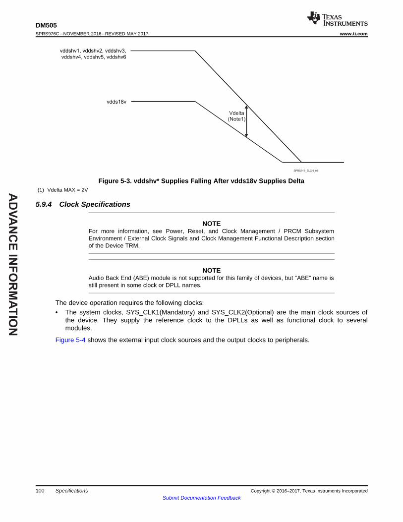
AD
VA
NC
E IN
FO
RM
AT
ION
vddshv1, vddshv2, vddshv3,
vddshv4, vddshv5, vddshv6
vdds18v
Vdelta(Note1)
SPRS916_ELCH_03
100
DM505SPRS976C –NOVEMBER 2016–REVISED MAY 2017 www.ti.com
Submit Documentation FeedbackSpecifications Copyright © 2016–2017, Texas Instruments Incorporated
Figure 5-3. vddshv* Supplies Falling After vdds18v Supplies Delta(1) Vdelta MAX = 2V
5.9.4 Clock Specifications
NOTEFor more information, see Power, Reset, and Clock Management / PRCM SubsystemEnvironment / External Clock Signals and Clock Management Functional Description sectionof the Device TRM.
NOTEAudio Back End (ABE) module is not supported for this family of devices, but “ABE” name isstill present in some clock or DPLL names.
The device operation requires the following clocks:• The system clocks, SYS_CLK1(Mandatory) and SYS_CLK2(Optional) are the main clock sources of
the device. They supply the reference clock to the DPLLs as well as functional clock to severalmodules.
Figure 5-4 shows the external input clock sources and the output clocks to peripherals.
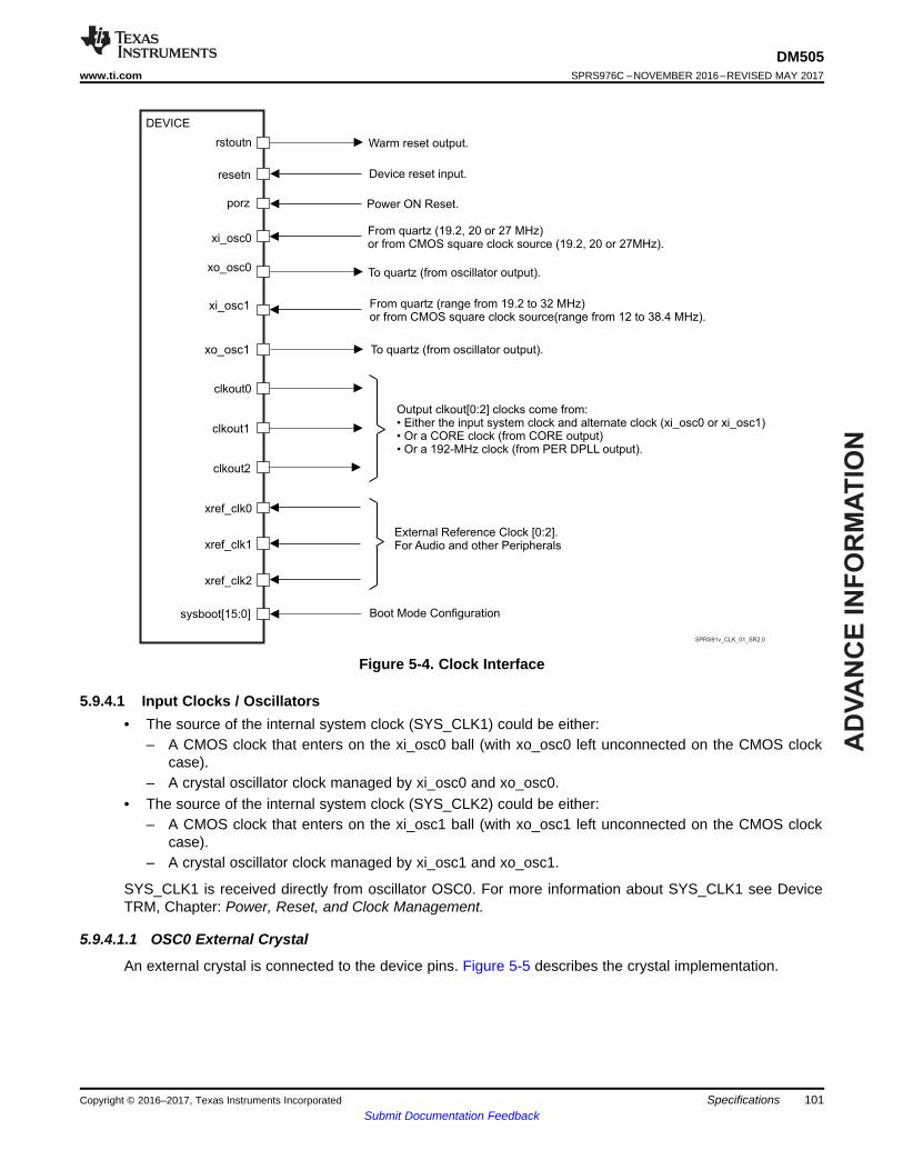
AD
VA
NC
E I
NF
OR
MA
TIO
N
DEVICE
clkout0
To quartz (from oscillator output).
resetn
rstoutn
External Reference Clock [0:2].For Audio and other Peripheralsxref_clk1
sysboot[15:0]
From quartz (19.2, 20 or 27 MHz)or from CMOS square clock source (19.2, 20 or 27MHz).
Boot Mode Configuration
xi_osc1
Warm reset output.
Device reset input.
porz Power ON Reset.
xi_osc0
xo_osc0
xo_osc1
From quartz (range from MHz)or from CMOS square clock source(range from MHz).
19.2 to 3212 to 38.4
To quartz (from oscillator output).
clkout1
clkout2
xref_clk0
Output clkout[0:2] clocks come from:• Either the input system clock and alternate clock (xi_osc0 or xi_osc1)• Or a CORE clock (from CORE output)• Or a 192-MHz clock (from PER DPLL output).
SPRS91v_CLK_01_SR2.0
xref_clk2
101
DM505www.ti.com SPRS976C –NOVEMBER 2016–REVISED MAY 2017
Submit Documentation FeedbackSpecificationsCopyright © 2016–2017, Texas Instruments Incorporated
Figure 5-4. Clock Interface
5.9.4.1 Input Clocks / Oscillators• The source of the internal system clock (SYS_CLK1) could be either:
– A CMOS clock that enters on the xi_osc0 ball (with xo_osc0 left unconnected on the CMOS clockcase).
– A crystal oscillator clock managed by xi_osc0 and xo_osc0.• The source of the internal system clock (SYS_CLK2) could be either:
– A CMOS clock that enters on the xi_osc1 ball (with xo_osc1 left unconnected on the CMOS clockcase).
– A crystal oscillator clock managed by xi_osc1 and xo_osc1.
SYS_CLK1 is received directly from oscillator OSC0. For more information about SYS_CLK1 see DeviceTRM, Chapter: Power, Reset, and Clock Management.
5.9.4.1.1 OSC0 External Crystal
An external crystal is connected to the device pins. Figure 5-5 describes the crystal implementation.

AD
VA
NC
E IN
FO
RM
AT
ION
CL=C Cf1 2f
(C +C )2f1 f
vssa_osc0
Device
xo_osc0xi_osc0
Cf1
CrystalRd
Cf2
(Optional)
SPRS91v_CLK_02
102
DM505SPRS976C –NOVEMBER 2016–REVISED MAY 2017 www.ti.com
Submit Documentation FeedbackSpecifications Copyright © 2016–2017, Texas Instruments Incorporated
Figure 5-5. Crystal Implementation
NOTEThe load capacitors, Cf1 and Cf2 in Figure 5-5, should be chosen such that the belowequation is satisfied. CL in the equation is the load specified by the crystal manufacturer. Alldiscrete components used to implement the oscillator circuit should be placed as close aspossible to the associated oscillator xi_osc0, xo_osc0, and vssa_osc0 pins.
Figure 5-6. Load capacitance equation
The crystal must be in the fundamental mode of operation and parallel resonant. Table 5-16 summarizesthe required electrical constraints.
Table 5-16. OSC0 Crystal Electrical Characteristics
NAME DESCRIPTION MIN TYP MAX UNITfp Parallel resonance crystal frequency 19.2, 20, 27 MHz
Cf1 Cf1 load capacitance for crystal parallel resonance with Cf1 = Cf2 12 24 pFCf2 Cf2 load capacitance for crystal parallel resonance with Cf1 = Cf2 12 24 pF
ESR(Cf1,Cf2) Crystal ESR 100 Ω
CO Crystal shunt capacitance
ESR = 30 ΩESR = 40 Ω
19.2 MHz, 20 MHz, 27MHz 7 pF
ESR = 50 Ω19.2 MHz, 20 MHz 7 pF27 MHz 5 pF
ESR = 60 Ω19.2 MHz, 20 MHz 7 pF27 MHz Not Supported -
ESR = 80 Ω19.2 MHz, 20 MHz 5 pF27 MHz Not Supported -
ESR = 100Ω19.2 MHz, 20 MHz 3 pF27 MHz Not Supported -
LM Crystal motional inductance for fp = 20 MHz 10.16 mHCM Crystal motional capacitance 3.42 fF
tj(xiosc0) Frequency accuracy(1), xi_osc0Ethernet not used ±200 ppmEthernet RGMII usingderived clock ±50 ppm

AD
VA
NC
E I
NF
OR
MA
TIO
N
vssa_osc0
Device
xo_osc0xi_osc0
NC
SPRS91v_CLK_03
103
DM505www.ti.com SPRS976C –NOVEMBER 2016–REVISED MAY 2017
Submit Documentation FeedbackSpecificationsCopyright © 2016–2017, Texas Instruments Incorporated
(1) Crystal characteristics should account for tolerance+stability+aging.
When selecting a crystal, the system design must consider the temperature and aging characteristics of abased on the worst case environment and expected life expectancy of the system.
Table 5-17 details the switching characteristics of the oscillator and the requirements of the input clock.
Table 5-17. Oscillator Switching Characteristics—Crystal Mode
NAME DESCRIPTION MIN TYP MAX UNITfp Oscillation frequency 19.2, 20, 27 MHz MHztsX Start-up time 4 ms
5.9.4.1.2 OSC0 Input Clock
A 1.8-V LVCMOS-Compatible Clock Input can be used instead of the internal oscillator to provide theSYS_CLK1 clock input to the system. The external connections to support this are shown in Figure 5-7.The xi_osc0 pin is connected to the 1.8-V LVCMOS-Compatible clock source. The xi_osc0 pin is leftunconnected. The vssa_osc0 pin is connected to board ground (vss).
Figure 5-7. 1.8-V LVCMOS-Compatible Clock Input
Table 5-18 summarizes the OSC0 input clock electrical characteristics.
Table 5-18. OSC0 Input Clock Electrical Characteristics—Bypass Mode
NAME DESCRIPTION MIN TYP MAX UNITf Frequency 19.2, 20, 27 MHz
CIN Input capacitance 2.184 2.384 2.584 pFIIN Input current (3.3V mode) 4 6 10 µA
Table 5-19 details the OSC0 input clock timing requirements.
Table 5-19. OSC0 Input Clock Timing Requirements
NAME DESCRIPTION MIN TYP MAX UNITCK0 1 / tc(xiosc0) Frequency, xi_osc0 19.2, 20, 27 MHzCK1 tw(xiosc0) Pulse duration, xi_osc0 low or high 0.45 × tc(xiosc0) 0.55 × tc(xiosc0) ns
tj(xiosc0) Period jitter(1), xi_osc0 0.01 × tc(xiosc0) nstR(xiosc0) Rise time, xi_osc0 5 nstF(xiosc0) Fall time, xi_osc0 5 ns
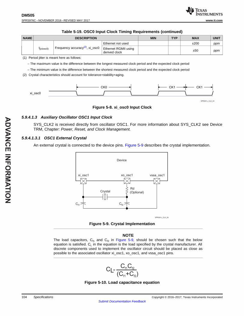
AD
VA
NC
E IN
FO
RM
AT
ION
CL=C Cf1 2f
(C +C )2f1 f
xi_osc1 vssa_osc1
Device
xo_osc1
Cf1
CrystalRd
Cf2
(Optional)
SPRS91v_CLK_05
xi_osc0
CK0 CK1 CK1
SPRS91v_CLK_04
104
DM505SPRS976C –NOVEMBER 2016–REVISED MAY 2017 www.ti.com
Submit Documentation FeedbackSpecifications Copyright © 2016–2017, Texas Instruments Incorporated
Table 5-19. OSC0 Input Clock Timing Requirements (continued)NAME DESCRIPTION MIN TYP MAX UNIT
tj(xiosc0) Frequency accuracy(2), xi_osc0Ethernet not used ±200 ppmEthernet RGMII usingderived clock ±50 ppm
(1) Period jitter is meant here as follows:
– The maximum value is the difference between the longest measured clock period and the expected clock period
– The minimum value is the difference between the shortest measured clock period and the expected clock period(2) Crystal characteristics should account for tolerance+stability+aging.
Figure 5-8. xi_osc0 Input Clock
5.9.4.1.3 Auxiliary Oscillator OSC1 Input Clock
SYS_CLK2 is received directly from oscillator OSC1. For more information about SYS_CLK2 see DeviceTRM, Chapter: Power, Reset, and Clock Management.
5.9.4.1.3.1 OSC1 External Crystal
An external crystal is connected to the device pins. Figure 5-9 describes the crystal implementation.
Figure 5-9. Crystal Implementation
NOTEThe load capacitors, Cf1 and Cf2 in Figure 5-9, should be chosen such that the belowequation is satisfied. CL in the equation is the load specified by the crystal manufacturer. Alldiscrete components used to implement the oscillator circuit should be placed as close aspossible to the associated oscillator xi_osc1, xo_osc1, and vssa_osc1 pins.
Figure 5-10. Load capacitance equation

AD
VA
NC
E I
NF
OR
MA
TIO
N
105
DM505www.ti.com SPRS976C –NOVEMBER 2016–REVISED MAY 2017
Submit Documentation FeedbackSpecificationsCopyright © 2016–2017, Texas Instruments Incorporated
The crystal must be in the fundamental mode of operation and parallel resonant. Table 5-20 summarizesthe required electrical constraints.
Table 5-20. OSC1 Crystal Electrical Characteristics
NAME DESCRIPTION MIN TYP MAX UNITfp Parallel resonance crystal frequency Range from 19.2 to 32 MHz
Cf1 Cf1 load capacitance for crystal parallel resonance with Cf1 = Cf2 12 24 pFCf2 Cf2 load capacitance for crystal parallel resonance with Cf1 = Cf2 12 24 pF
ESR(Cf1,Cf2) Crystal ESR 100 Ω
CO Crystal shunt capacitance
ESR = 30 Ω 19.2 MHz ≤ fp ≤ 32 MHz 7 pFESR = 40 Ω 19.2 MHz ≤ fp ≤ 32 MHz 5 pF
ESR = 50 Ω
19.2 MHz ≤ fp ≤ 25 MHz 7 pF25 MHz < fp ≤ 27 MHz 5 pF27 MHz < fp ≤ 32 MHz Not Supported -
ESR = 60 Ω
19.2 MHz ≤ fp ≤ 23 MHz 7 pF23 MHz < fp ≤ 25 MHz 5 pF25 MHz < fp ≤ 32 MHz Not Supported -
ESR = 80 Ω
19.2 MHz ≤ fp ≤ 23 MHz 5 pF23 MHz < fp ≤ 25 MHz 3 pF25 MHz < fp ≤ 32 MHz Not Supported -
ESR = 100 Ω19.2 MHz ≤ fp ≤ 20 MHz 3 pF20 MHz < fp ≤ 32 MHz Not Supported -
LM Crystal motional inductance for fp = 20 MHz 10.16 mHCM Crystal motional capacitance 3.42 fF
tj(xiosc0) Frequency accuracy(1), xi_osc1Ethernet not used ±200 ppmEthernet RGMII usingderived clock ±50 ppm
(1) Crystal characteristics should account for tolerance+stability+aging.
When selecting a crystal, the system design must take into account the temperature and agingcharacteristics of a crystal versus the user environment and expected lifetime of the system.
Table 5-21 details the switching characteristics of the oscillator and the requirements of the input clock.
Table 5-21. Oscillator Switching Characteristics—Crystal Mode
NAME DESCRIPTION MIN TYP MAX UNITfp Oscillation frequency Range from 19.2 to 32 MHztsX Start-up time 4 ms
5.9.4.1.3.2 OSC1 Input Clock
A 1.8-V LVCMOS-Compatible Clock Input can be used instead of the internal oscillator to provide theSYS_CLK2 clock input to the system. The external connections to support this are shown in, Figure 5-11.The xi_osc1 pin is connected to the 1.8-V LVCMOS-Compatible clock sources. The xo_osc1 pin is leftunconnected. The vssa_osc1 pin is connected to board ground (VSS).

AD
VA
NC
E IN
FO
RM
AT
ION
vssa_osc1
Device
xo_osc1xi_osc1
NC
SPRS91v_CLK_06
106
DM505SPRS976C –NOVEMBER 2016–REVISED MAY 2017 www.ti.com
Submit Documentation FeedbackSpecifications Copyright © 2016–2017, Texas Instruments Incorporated
Figure 5-11. 1.8-V LVCMOS-Compatible Clock Input
Table 5-22 summarizes the OSC1 input clock electrical characteristics.
Table 5-22. OSC1 Input Clock Electrical Characteristics—Bypass Mode
NAME DESCRIPTION MIN TYP MAX UNITf Frequency Range from 12 to 38.4 MHz
CIN Input capacitance 2.819 3.019 3.219 pFIIN Input current (3.3V mode) 4 6 10 µAtsX Start-up time(1) See(2) ms
(1) To switch from bypass mode to crystal or from crystal mode to bypass mode, there is a waiting time about 100 μs; however, if the chipcomes from bypass mode to crystal mode the crystal will start-up after time mentioned in Table 5-21, tsX parameter.
(2) Before the processor boots up and the oscillator is set to bypass mode, there is a waiting time when the internal oscillator is inapplication mode and receives a wave. The switching time in this case is about 100 μs.
Table 5-23 details the OSC1 input clock timing requirements.
Table 5-23. OSC1 Input Clock Timing Requirements
NAME DESCRIPTION MIN TYP MAX UNITCK0 1 / tc(xiosc1) Frequency, xi_osc1 Range from 12 to 38.4 MHzCK1 tw(xiosc1) Pulse duration, xi_osc1 low or high 0.45 × tc(xiosc1) 0.55 × tc(xiosc1) ns
tj(xiosc1) Period jitter(1), xi_osc1 0.01 × tc(xiosc1)(3) ns
tR(xiosc1) Rise time, xi_osc1 5 nstF(xiosc1) Fall time, xi_osc1 5 ns
tj(xiosc1) Frequency accuracy(2), xi_osc1Ethernet not used ±200 ppmEthernet RGMII usingderived clock ±50 ppm
(1) Period jitter is meant here as follows:
– The maximum value is the difference between the longest measured clock period and the expected clock period
– The minimum value is the difference between the shortest measured clock period and the expected clock period(2) Crystal characteristics should account for tolerance+stability+aging.(3) The Period jitter requirement for osc1 can be relaxed to 0.02*tc(xiosc1) under the following constraints:
a. The osc1/SYS_CLK2 clock bypasses all device PLLsb. The osc1/SYS_CLK2 clock is only used to source the DSS pixel clock outputs

AD
VA
NC
E I
NF
OR
MA
TIO
N
xi_osc1
CK0 CK1 CK1
SPRS91v_CLK_07
107
DM505www.ti.com SPRS976C –NOVEMBER 2016–REVISED MAY 2017
Submit Documentation FeedbackSpecificationsCopyright © 2016–2017, Texas Instruments Incorporated
Figure 5-12. xi_osc1 Input Clock
5.9.4.1.4 RC On-die Oscillator Clock
RCOSC_32K_CLK is received directly through a network of resistor and capacitor (an RC network) insideof the SoC. This RC oscillator do not have good frequency stability. The Frequency range is described inTable 5-24, which depends on the temperature. For more information about RCOSC_32K_CLK see theDevice TRM, Chapter: Power, Reset, and Clock Management.
Table 5-24. RC On-die Oscillator Clock Frequency Range
NAME DESCRIPTION MIN TYP MAX UNITRCOSC_32K_CLK Internal RC Oscillator Range from 28 to 42 kHz
5.9.4.2 Output Clocks
NOTENOTE TO USERS:
The content of this section is UNDER DEVELOPMENT!
5.9.4.3 DPLLs, DLLs
NOTEFor more information, see:• Power, Reset, and Clock Management / Clock Management Functional Description /
Internal Clock Sources / Generators / Generic DPLL Overview Sectionand
• Display Subsystem / Display Subsystem Overview section of the Device TRM.
To generate high-frequency clocks, the device supports multiple on-chip DPLLs controlled directly by thePRCM module. They are of two types: type A and type B DPLLs.
• They have their own independent power domain (each one embeds its own switch and can becontrolled as an independent functional power domain)
• They are fed with ALWAYS ON system clock, with independent control per DPLL.The different DPLLs managed by the PRCM are listed below:• DPLL_CORE: It supplies all interface clocks and also few module functional clocks.• DPLL_PER: It supplies several clock sources: a 192-MHz clock for the display functional clock , a
96-MHz functional clock to subsystems and peripherals.• DPLL_GMAC_DSP: It supplies RGMII, EVE1 and DSP0 module functional clocks.• DPLL_EVE_VID_DSP: It provides a few module functional clocks (EVE_GFCLK, VID_PIX_CLK
and DSP1_CLK).• DPLL_DDR: It generates clocks for the one External Memory Interface (EMIF) controller and its
associated EMIF PHYs.

AD
VA
NC
E IN
FO
RM
AT
ION
108
DM505SPRS976C –NOVEMBER 2016–REVISED MAY 2017 www.ti.com
Submit Documentation FeedbackSpecifications Copyright © 2016–2017, Texas Instruments Incorporated
NOTEThe following DPLLs are controlled by the clock manager located in the always-on Corepower domain (CM_CORE_AON):• DPLL_CORE, DPLL_DDR, DPLL_GMAC_DSP, DPLL_PER, DPLL_EVE_VID_DSP.
For more information on CM_CORE_AON and CM_CORE or PRCM DPLLs, see the Power, Reset, andClock Management (PRCM) chapter of the Device TRM.
5.9.4.3.1 DPLL Characteristics
The DPLL has three relevant input clocks. One of them is the reference clock (CLKINP) used to generatedthe synthesized clock but can also be used as the bypass clock whenever the DPLL enters a bypassmode. It is therefore mandatory. The second one is a fast bypass clock (CLKINPULOW) used whenselected as the bypass clock and is optional. The third clock (CLKINPHIF) is explained in the nextparagraph.
The DPLL has three output clocks (namely CLKOUT, CLKOUTX2, and CLKOUTHIF). CLKOUT andCLKOUTX2 run at the bypass frequency whenever the DPLL enters a bypass mode. Both of them aregenerated from the lock frequency divided by a post-divider (namely M2 post-divider). The third clock,CLKOUTHIF, has no automatic bypass capability. It is an output of a post-divider (M3 post-divider) withthe input clock selectable between the internal lock clock (Fdpll) and CLKINPHIF input of the PLL throughan asynchronous multplexing.
For more information, see the Power, Reset, and Clock Management chapter of the Device TRM.
Table 5-25 summarizes DPLL type described in Section 5.9.4.3, DPLLs, DLLs Specifications.
Table 5-25. DPLL Control Type
DPLL NAME TYPE CONTROLLED BY PRCMDPLL_CORE Table 5-26 (Type A) Yes(1)
DPLL_EVE_VID_DSP Table 5-26 (Type A) Yes(1)
DPLL_GMAC_DSP Table 5-26 (Type A) Yes(1)
DPLL_PER Table 5-26 (Type A) Yes(1)
DPLL_DDR Table 5-26 (Type A) Yes(1)
(1) DPLL is in the always-on domain.
Table 5-26 and summarize the DPLL characteristics and assume testing over recommended operatingconditions.

AD
VA
NC
E I
NF
OR
MA
TIO
N
109
DM505www.ti.com SPRS976C –NOVEMBER 2016–REVISED MAY 2017
Submit Documentation FeedbackSpecificationsCopyright © 2016–2017, Texas Instruments Incorporated
Table 5-26. DPLL Type A Characteristics
NAME DESCRIPTION MIN TYP MAX UNIT COMMENTSfinput CLKINP input frequency 0.032 52 MHz FINP
finternal Internal reference frequency 0.15 52 MHz REFCLKfCLKINPHIF CLKINPHIF input frequency 10 1400 MHz FINPHIF
fCLKINPULOW CLKINPULOW input frequency 0.001 600 MHzBypass mode: fCLKOUT =fCLKINPULOW / (M1 + 1) ifulowclken = 1(6)
fCLKOUT CLKOUT output frequency 20(1) 1400(2) MHz [M / (N + 1)] × FINP × [1 / M2](in locked condition)
fCLKOUTx2 CLKOUTx2 output frequency 40(1) 2200(2) MHz 2 × [M / (N + 1)] × FINP × [1 /M2] (in locked condition)
fCLKOUTHIF CLKOUTHIF output frequency20(3) 1400(4) MHz FINPHIF / M3 if clkinphifsel = 1
40(3) 2200(4) MHz 2 × [M / (N + 1)] × FINP × [1 /M3] if clkinphifsel = 0
fCLKDCOLDODCOCLKLDO outputfrequency 40 2800 MHz 2 × [M / (N + 1)] × FINP (in
locked condition)
tlock Frequency lock time 6 + 350 ×REFCLK µs
plock Phase lock time 6 + 500 ×REFCLK µs
trelock-LRelock time—Frequency lock(5)
(LP relock time from bypass)6 + 70 ×REFCLK µs DPLL in LP relock time:
lowcurrstdby = 1
prelock-LRelock time—Phase lock(5) (LPrelock time from bypass)
6 + 120 ×REFCLK µs DPLL in LP relock time:
lowcurrstdby = 1
trelock-FRelock time—Frequency lock(5)
(fast relock time from bypass)3.55 + 70 ×
REFCLK µs DPLL in fast relock time:lowcurrstdby = 0
prelock-FRelock time—Phase lock(5)
(fast relock time from bypass)3.55 + 120 ×
REFCLK µs DPLL in fast relock time:lowcurrstdby = 0
(1) The minimum frequencies on CLKOUT and CLKOUTX2 are assuming M2 = 1.
For M2 > 1, the minimum frequency on these clocks will further scale down by factor of M2.(2) The maximum frequencies on CLKOUT and CLKOUTX2 are assuming M2 = 1.(3) The minimum frequency on CLKOUTHIF is assuming M3 = 1. For M3 > 1, the minimum frequency on this clock will further scale down
by factor of M3.(4) The maximum frequency on CLKOUTHIF is assuming M3 = 1.(5) Relock time assumes typical operating conditions, 10°C maximum temperature drift.(6) Bypass mode: fCLKOUT = FINP if ulowclken = 0. For more information, see the Device TRM.
AD
VA
NC
E IN
FO
RM
AT
ION
110
DM505SPRS976C –NOVEMBER 2016–REVISED MAY 2017 www.ti.com
Submit Documentation FeedbackSpecifications Copyright © 2016–2017, Texas Instruments Incorporated
5.9.4.3.2 DLL Characteristics
Table 5-27 summarizes the DLL characteristics and assumes testing over recommended operatingconditions.
Table 5-27. DLL Characteristics
NAME DESCRIPTION MIN TYP MAX UNITfinput Input clock frequency (EMIF_DLL_FCLK) 266 MHztlock Lock time 50k cycles
trelock Relock time (a change of the DLL frequency implies that DLL must relock) 50k cycles
5.9.4.3.2.1 DPLL and DLL Noise Isolation
NOTEFor more information on DPLL and DLL decoupling capacitor requirements, see the ExternalCapacitors / Voltage Decoupling Capacitors / I/O and Analog Voltage Decoupling / VDDAPower Domain section.
5.9.5 Recommended Clock and Control Signal Transition BehaviorAll clocks and control signals must transition between VIH and VIL (or between VIL and VIH) in a monotonicmanner. Monotonic transitions are more easily guaranteed with faster switching signals. Slower inputtransitions are more susceptible to glitches due to noise and special care should be taken for slow inputclocks.
5.9.6 Peripherals
5.9.6.1 Timing Test Conditions
All timing requirements and switching characteristics are valid over the recommended operating conditionsunless otherwise specified.

AD
VA
NC
E I
NF
OR
MA
TIO
N
vinx_clki(positive-edge clocking)
V4
vinx_d[23:0]/sig
V5
vinx_clki(negative-edge clocking)
SPRS8xx_VIP_02
vinx_clki
V2
V1
V3
SPRS91v_VIP_01
111
DM505www.ti.com SPRS976C –NOVEMBER 2016–REVISED MAY 2017
Submit Documentation FeedbackSpecificationsCopyright © 2016–2017, Texas Instruments Incorporated
5.9.6.2 VIP
The device includes 1 Video Input Ports (VIP).
Table 5-28, Figure 5-13 and Figure 5-14 presents timings and switching characteristics of the VIPs.
Table 5-28. Timing Requirements for VIP (1)(2)
NO. PARAMETER DESCRIPTION MIN MAX UNITV1 tc(CLK) Cycle time, vinx_clki(3)(5) 5.99 (1) nsV2 tw(CLKH) Pulse duration, vinx_clki high(3)(5) 0.45*P (2) nsV3 tw(CLKL) Pulse duration, vinx_clki low(3)(5) 0.45*P (2) nsV4 tsu(CTL/DATA-CLK) Input setup time, Control (vinx_dei, vinx_vsynci, vinx_fldi,
vinx_hsynci) and Data (vinx_dn) valid to vinx_clki transition (3)(4)(5)2.52 ns
V5 th(CLK-CTL/DATA) Input hold time, Control (vinx_dei, vinx_vsynci, vinx_fldi,vinx_hsynci) and Data (vinx_dn) valid from vinx_clki transition(3)(4)(5)
-0.05 ns
(1) For maximum frequency of 165 MHz.(2) P = vinx_clki period.(3) x in vinx = 1a, 1b, 2a and 2b.(4) n in dn = 0 to 7 when x = 1b, 2b;
n = 0 to 23 when x = 1a and 2a;(5) i in clki, dei, vsynci, hsynci and fldi = 0 or 1.
Figure 5-13. Video Input Ports clock signal
Figure 5-14. Video Input Ports timings
CAUTION
The IO timings provided in this section are only valid for VIN1 and VIN2 ifsignals within a single IOSET are used. The IOSETs are defined in the Table 5-29 and Table 5-30.
In Table 5-29 and Table 5-30 are presented the specific groupings of signals (IOSET) for use with vin1a,vin1b, vin2a and vin2b.

AD
VA
NC
E IN
FO
RM
AT
ION
112
DM505SPRS976C –NOVEMBER 2016–REVISED MAY 2017 www.ti.com
Submit Documentation FeedbackSpecifications Copyright © 2016–2017, Texas Instruments Incorporated
Table 5-29. VIN1 IOSETs
SIGNALS IOSET1 IOSET2 IOSET3 IOSET4BALL MUX BALL MUX BALL MUX BALL MUX
vin1avin1a_clk0 F22 0 F22 0 F22 0 F22 0vin1a_de0 F21 0 F21 0 F21 0 F19 2vin1a_fld0 F20 0
vin1a_hsync0 F19 0vin1a_vsync0 G19 0 G19 0 G19 0 G19 0
vin1a_d0 G18 0 G18 0 G18 0 G18 0vin1a_d1 G21 0 G21 0 G21 0 G21 0vin1a_d2 G22 0 G22 0 G22 0 G22 0vin1a_d3 H18 0 H18 0 H18 0 H18 0vin1a_d4 H20 0 H20 0 H20 0 H20 0vin1a_d5 H19 0 H19 0 H19 0 H19 0vin1a_d6 H22 0 H22 0 H22 0 H22 0vin1a_d7 H21 0 H21 0 H21 0 H21 0vin1a_d8 J17 0 J17 0vin1a_d9 K22 0 K22 0vin1a_d10 K21 0 K21 0vin1a_d11 K18 0 K18 0vin1a_d12 K17 0 AB17 2vin1a_d13 K19 0 U17 2vin1a_d14 K20 0 W17 2vin1a_d15 L21 0 AA17 2
vin1bvin1b_clk1 F21 2
vin1b_hsync1 W7 7vin1b_vsync1 W6 7
vin1b_d0 J17 2vin1b_d1 K22 2vin1b_d2 K21 2vin1b_d3 K18 2vin1b_d4 K17 2vin1b_d5 K19 2vin1b_d6 K20 2vin1b_d7 L21 2
Table 5-30. VIN2 IOSETs
SIGNALS IOSET1 IOSET2 IOSET3BALL MUX BALL MUX BALL MUX
vin2avin2a_clk0 L22 0 AB17 9 L22 0vin2a_de0 M17 0 AA17 9vin2a_fld0 M18 0 U16 9
vin2a_hsync0 W7 2 F14 9vin2a_vsync0 W6 2 W6 2 C14 9
vin2a_d0 AA14 2 AA14 2 AA14 2vin2a_d1 AB14 2 AB14 2 AB14 2

AD
VA
NC
E I
NF
OR
MA
TIO
N
113
DM505www.ti.com SPRS976C –NOVEMBER 2016–REVISED MAY 2017
Submit Documentation FeedbackSpecificationsCopyright © 2016–2017, Texas Instruments Incorporated
Table 5-30. VIN2 IOSETs (continued)SIGNALS IOSET1 IOSET2 IOSET3
BALL MUX BALL MUX BALL MUXvin2a_d2 U13 2 U13 2 U13 2vin2a_d3 V13 2 V13 2 V13 2vin2a_d4 Y13 2 Y13 2 Y13 2vin2a_d5 W13 2 W13 2 W13 2vin2a_d6 U11 2 U11 2 U11 2vin2a_d7 V11 2 V11 2 V11 2vin2a_d8 U9 2vin2a_d9 W11 2vin2a_d10 V9 2vin2a_d11 W9 2vin2a_d12 U8 2vin2a_d13 W8 2vin2a_d14 U7 2vin2a_d15 V7 2
vin2bvin2b_clk1 F20 2
vin2b_hsync1 M17 2vin2b_vsync1 M18 2
vin2b_d0 U9 5vin2b_d1 W11 5vin2b_d2 V9 5vin2b_d3 W9 5vin2b_d4 U8 5vin2b_d5 W8 5vin2b_d6 U7 5vin2b_d7 V7 5
5.9.6.3 DSS
Display Parallel Interfaces (DPI) channels are available in DSS named DPI Video Output 1.
Every VOUT interface consists of:• 24-bit data bus (data[23:0])• Horizontal synchronization signal (HSYNC)• Vertical synchronization signal (VSYNC)• Data enable (DE)• Field ID (FID)• Pixel clock (CLK)
NOTEFor more information, see the Display Subsystem section of the Device TRM.

AD
VA
NC
E IN
FO
RM
AT
ION
vouti_clk
vouti_vsync
vouti_hsync
vouti_d[23:0]
vouti_de
vouti_fld
data_1 data_2 data_n
odd even
D1
D2
D3
D6
D6
D5
D6
D6
SWPS049-018
D4
vouti_clk
Falling-edge Clock Reference
Rising-edge Clock Reference
114
DM505SPRS976C –NOVEMBER 2016–REVISED MAY 2017 www.ti.com
Submit Documentation FeedbackSpecifications Copyright © 2016–2017, Texas Instruments Incorporated
CAUTION
All pads/balls configured as vouti_* signals must be programmed to use slowslew rate by setting the corresponding CTRL_CORE_PAD_*[SLEWCONTROL]register field to SLOW (0b1).
Table 5-31 and Figure 5-15 assume testing over the recommended operating conditions and electricalcharacteristic conditions.
Table 5-31. DPI Video Output 1 Switching Characteristics(1)(2)
NO. PARAMETER DESCRIPTION MODE MIN MAX UNITD1 tc(clk) Cycle time, output pixel clock vouti_clk 6.73 nsD2 tw(clkL) Pulse duration, output pixel clock vouti_clk low P*0.5-1 nsD3 tw(clkH) Pulse duration, output pixel clock vouti_clk high P*0.5-1 nsD5 td(clk-ctlV) Delay time, output pixel clock vouti_clk transition to output
data vouti_d[23:0] validDPI1 -1.33 1.01 ns
D6 td(clk-dV) Delay time, output pixel clock vouti_clk transition to outputcontrol signals vouti_vsync, vouti_hsync, vouti_de, andvouti_fld valid
DPI1 -1.33 1.01 ns
(1) P = output vout1_clk period in ns.(2) All pads/balls configured as vouti_* signals must be programmed to use slow slew rate by setting the corresponding
CTRL_CORE_PAD_*[SLEWCONTROL] register field to SLOW (0b1).(3) SERDES transceivers may be sensitive to the jitter profile of vouti_clk. See Application Note SPRAC62 for additional guidance.
Figure 5-15. DPI Video Output(1)(2)(3)
(1) The configuration of assertion of the data can be programmed on the falling or rising edge of the pixel clock.(2) The polarity and the pulse width of vout1_hsync and vout1_vsync are programmable, refer to the DSS section of the device TRM.(3) The vout1_clk frequency can be configured, refer to the DSS section of the device TRM.

AD
VA
NC
E I
NF
OR
MA
TIO
N
115
DM505www.ti.com SPRS976C –NOVEMBER 2016–REVISED MAY 2017
Submit Documentation FeedbackSpecificationsCopyright © 2016–2017, Texas Instruments Incorporated
5.9.6.4 ISS
NOTEFor more information, see the Imaging Subsystem chapter of the device TRM.
The imaging subsystem (ISS) deals with the processing of the pixel data coming from an external imagesensor or data from memory (image format encoding and decoding can be done to and from memory).With its subparts, such as interfaces and interconnects, image signal processor (ISP), and still imagecoprocessor (SIMCOP), the ISS is a key component for the following use cases:• Rear View Camera• Front View Stereo Camera• Surround View Camera
The ISS is mainly composed of CAL_A, CAL_B, LVDS-RX camera interfaces, a parallel interface (CPI),an ISP, and a block-based imaging accelerator (SIMCOP).
• The Camera Adapter Layer (CAL_A) supports MIPI® CSI2 protocol with four data lanes. The CAL_A istargeted as sensor capture interface and write DMA, while CAL_B is targeted as read DMA engine anddoes not support sensor capture.
• The LVDS receiver (LVDS-RX) support Sony / Aptina / Omnivision / Panasonic / AltaSens serialinterfaces.
• The parallel interface (CPI) supports up to 16 data lanes.
All interfaces can use the image signal processor (ISP), but not concurrently. When one interface uses theISP, the other must send data to memory. However, the ISP can still be used to process this data inmemory-to-memory. Time multiplex processing is also possible.
The camera adaptation layer (CAL) deals with the processing of the pixel data coming from an externalimage sensor, data from memory. The CAL is a key component for the following multimedia applications:camera viewfinder, video record, and still image capture. The CAL has two serial camera interfaces(primary and secondary):• The primary serial interface (CSI2 Port A) is compliant with MIPI CSI-2 protocol with four data lanes.
5.9.6.4.1 CSI-2 MIPI D-PHY—1.5 V and 1.8 V
The CSI-2 port A is compliant with the MIPI D-PHY RX specification v1.00.00 and the MIPI CSI-2specification v1.00, with 4 data differential lanes plus 1 clock differential lane in synchronous mode,double data rate:• 1.5 Gbps (750 MHz) @OPP_NOM for each lane.
CAUTION
The IO timings provided in this section are only valid if signals within a singleIOSET are used. The IOSETs are defined in Table 5-32.
In Table 5-32 are presented the specific groupings of signals (IOSET) for use with ISS.
Table 5-32. Camera Parallel Interface (CPI) IOSETs
SIGNALS IOSET1 IOSET2BALL MUX BALL MUX
cpi_pclk F22 1 F22 1cpi_data0 F19 1 F19 1cpi_data1 G19 1 G19 1
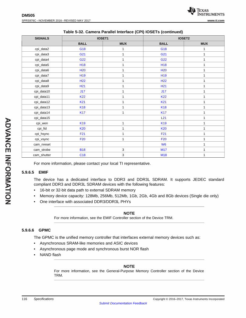
AD
VA
NC
E IN
FO
RM
AT
ION
116
DM505SPRS976C –NOVEMBER 2016–REVISED MAY 2017 www.ti.com
Submit Documentation FeedbackSpecifications Copyright © 2016–2017, Texas Instruments Incorporated
Table 5-32. Camera Parallel Interface (CPI) IOSETs (continued)SIGNALS IOSET1 IOSET2
BALL MUX BALL MUXcpi_data2 G18 1 G18 1cpi_data3 G21 1 G21 1cpi_data4 G22 1 G22 1cpi_data5 H18 1 H18 1cpi_data6 H20 1 H20 1cpi_data7 H19 1 H19 1cpi_data8 H22 1 H22 1cpi_data9 H21 1 H21 1cpi_data10 J17 1 J17 1cpi_data11 K22 1 K22 1cpi_data12 K21 1 K21 1cpi_data13 K18 1 K18 1cpi_data14 K17 1 K17 1cpi_data15 L21 1
cpi_wen K19 1 K19 1cpi_fid K20 1 K20 1
cpi_hsync F21 1 F21 1cpi_vsync F20 1 F20 1
cam_nreset W6 1cam_strobe B18 3 M17 1cam_shutter C18 3 M18 1
For more information, please contact your local TI representative.
5.9.6.5 EMIF
The device has a dedicated interface to DDR3 and DDR3L SDRAM. It supports JEDEC standardcompliant DDR3 and DDR3L SDRAM devices with the following features:• 16-bit or 32-bit data path to external SDRAM memory• Memory device capacity: 128Mb, 256Mb, 512Mb, 1Gb, 2Gb, 4Gb and 8Gb devices (Single die only)• One interface with associated DDR3/DDR3L PHYs
NOTEFor more information, see the EMIF Controller section of the Device TRM.
5.9.6.6 GPMC
The GPMC is the unified memory controller that interfaces external memory devices such as:• Asynchronous SRAM-like memories and ASIC devices• Asynchronous page mode and synchronous burst NOR flash• NAND flash
NOTEFor more information, see the General-Purpose Memory Controller section of the DeviceTRM.
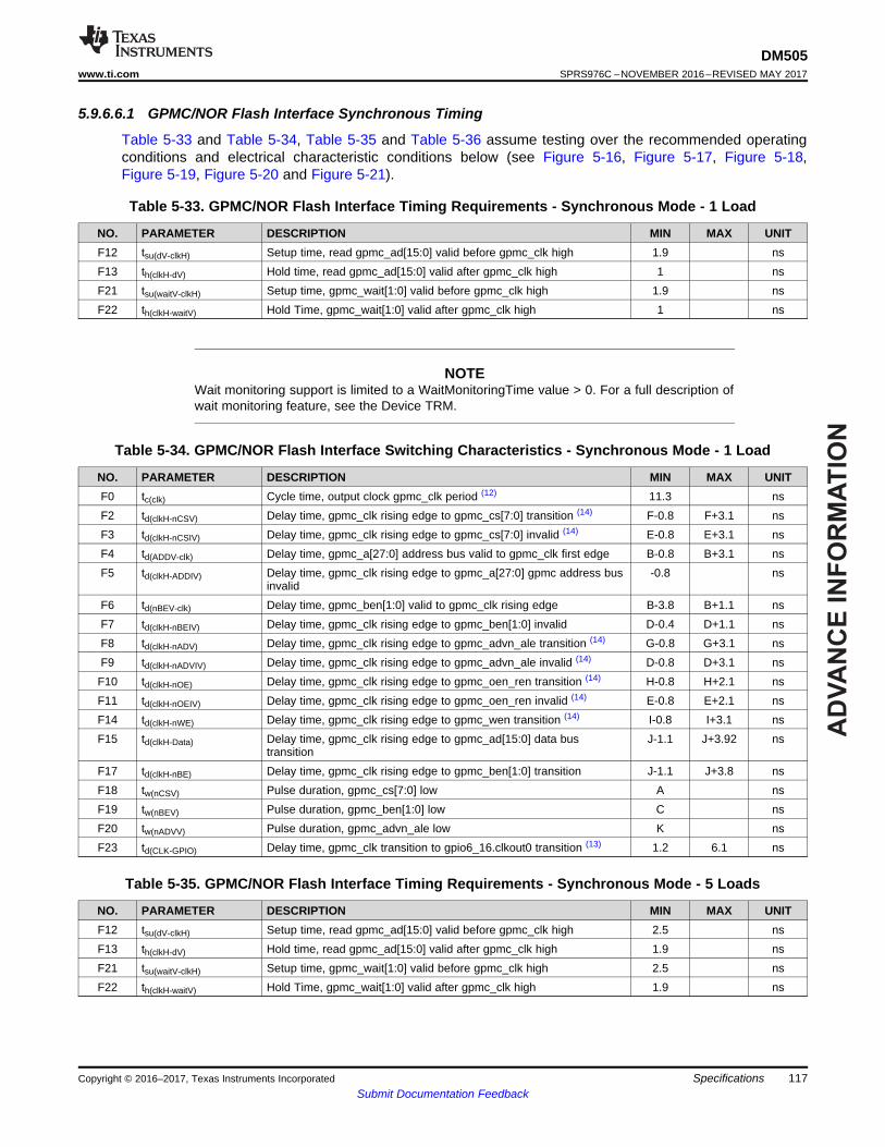
AD
VA
NC
E I
NF
OR
MA
TIO
N
117
DM505www.ti.com SPRS976C –NOVEMBER 2016–REVISED MAY 2017
Submit Documentation FeedbackSpecificationsCopyright © 2016–2017, Texas Instruments Incorporated
5.9.6.6.1 GPMC/NOR Flash Interface Synchronous Timing
Table 5-33 and Table 5-34, Table 5-35 and Table 5-36 assume testing over the recommended operatingconditions and electrical characteristic conditions below (see Figure 5-16, Figure 5-17, Figure 5-18,Figure 5-19, Figure 5-20 and Figure 5-21).
Table 5-33. GPMC/NOR Flash Interface Timing Requirements - Synchronous Mode - 1 Load
NO. PARAMETER DESCRIPTION MIN MAX UNITF12 tsu(dV-clkH) Setup time, read gpmc_ad[15:0] valid before gpmc_clk high 1.9 nsF13 th(clkH-dV) Hold time, read gpmc_ad[15:0] valid after gpmc_clk high 1 nsF21 tsu(waitV-clkH) Setup time, gpmc_wait[1:0] valid before gpmc_clk high 1.9 nsF22 th(clkH-waitV) Hold Time, gpmc_wait[1:0] valid after gpmc_clk high 1 ns
NOTEWait monitoring support is limited to a WaitMonitoringTime value > 0. For a full description ofwait monitoring feature, see the Device TRM.
Table 5-34. GPMC/NOR Flash Interface Switching Characteristics - Synchronous Mode - 1 Load
NO. PARAMETER DESCRIPTION MIN MAX UNITF0 tc(clk) Cycle time, output clock gpmc_clk period (12) 11.3 nsF2 td(clkH-nCSV) Delay time, gpmc_clk rising edge to gpmc_cs[7:0] transition (14) F-0.8 F+3.1 nsF3 td(clkH-nCSIV) Delay time, gpmc_clk rising edge to gpmc_cs[7:0] invalid (14) E-0.8 E+3.1 nsF4 td(ADDV-clk) Delay time, gpmc_a[27:0] address bus valid to gpmc_clk first edge B-0.8 B+3.1 nsF5 td(clkH-ADDIV) Delay time, gpmc_clk rising edge to gpmc_a[27:0] gpmc address bus
invalid-0.8 ns
F6 td(nBEV-clk) Delay time, gpmc_ben[1:0] valid to gpmc_clk rising edge B-3.8 B+1.1 nsF7 td(clkH-nBEIV) Delay time, gpmc_clk rising edge to gpmc_ben[1:0] invalid D-0.4 D+1.1 nsF8 td(clkH-nADV) Delay time, gpmc_clk rising edge to gpmc_advn_ale transition (14) G-0.8 G+3.1 nsF9 td(clkH-nADVIV) Delay time, gpmc_clk rising edge to gpmc_advn_ale invalid (14) D-0.8 D+3.1 nsF10 td(clkH-nOE) Delay time, gpmc_clk rising edge to gpmc_oen_ren transition (14) H-0.8 H+2.1 nsF11 td(clkH-nOEIV) Delay time, gpmc_clk rising edge to gpmc_oen_ren invalid (14) E-0.8 E+2.1 nsF14 td(clkH-nWE) Delay time, gpmc_clk rising edge to gpmc_wen transition (14) I-0.8 I+3.1 nsF15 td(clkH-Data) Delay time, gpmc_clk rising edge to gpmc_ad[15:0] data bus
transitionJ-1.1 J+3.92 ns
F17 td(clkH-nBE) Delay time, gpmc_clk rising edge to gpmc_ben[1:0] transition J-1.1 J+3.8 nsF18 tw(nCSV) Pulse duration, gpmc_cs[7:0] low A nsF19 tw(nBEV) Pulse duration, gpmc_ben[1:0] low C nsF20 tw(nADVV) Pulse duration, gpmc_advn_ale low K nsF23 td(CLK-GPIO) Delay time, gpmc_clk transition to gpio6_16.clkout0 transition (13) 1.2 6.1 ns
Table 5-35. GPMC/NOR Flash Interface Timing Requirements - Synchronous Mode - 5 Loads
NO. PARAMETER DESCRIPTION MIN MAX UNITF12 tsu(dV-clkH) Setup time, read gpmc_ad[15:0] valid before gpmc_clk high 2.5 nsF13 th(clkH-dV) Hold time, read gpmc_ad[15:0] valid after gpmc_clk high 1.9 nsF21 tsu(waitV-clkH) Setup time, gpmc_wait[1:0] valid before gpmc_clk high 2.5 nsF22 th(clkH-waitV) Hold Time, gpmc_wait[1:0] valid after gpmc_clk high 1.9 ns

AD
VA
NC
E IN
FO
RM
AT
ION
118
DM505SPRS976C –NOVEMBER 2016–REVISED MAY 2017 www.ti.com
Submit Documentation FeedbackSpecifications Copyright © 2016–2017, Texas Instruments Incorporated
Table 5-36. GPMC/NOR Flash Interface Switching Characteristics - Synchronous Mode - 5 Loads
NO. PARAMETER DESCRIPTION MIN MAX UNITF0 tc(clk) Cycle time, output clock gpmc_clk period (12) 15.04 nsF2 td(clkH-nCSV) Delay time, gpmc_clk rising edge to gpmc_cs[7:0] transition (14) F+0.7 (6) F+6.1 (6) nsF3 td(clkH-nCSIV) Delay time, gpmc_clk rising edge to gpmc_cs[7:0] invalid (14) E+0.7 (5) E+6.1 (5) nsF4 td(ADDV-clk) Delay time, gpmc_a[27:0] address bus valid to gpmc_clk first edge B+0.7 (2) B+6.1 (2) nsF5 td(clkH-ADDIV) Delay time, gpmc_clk rising edge to gpmc_a[27:0] gpmc address bus
invalid0.7 ns
F6 td(nBEV-clk) Delay time, gpmc_ben[1:0] valid to gpmc_clk rising edge B-4.9 B+0.4 nsF7 td(clkH-nBEIV) Delay time, gpmc_clk rising edge to gpmc_ben[1:0] invalid D-0.4 D+4.9 nsF8 td(clkH-nADV) Delay time, gpmc_clk rising edge to gpmc_advn_ale transition (14) G+0.7 (7) G+6.1 (7) nsF9 td(clkH-nADVIV) Delay time, gpmc_clk rising edge to gpmc_advn_ale invalid (14) D+0.7 (4) D+6.1 (4) nsF10 td(clkH-nOE) Delay time, gpmc_clk rising edge to gpmc_oen_ren transition (14) H+0.7 (8) H+5.1 (8) nsF11 td(clkH-nOEIV) Delay time, gpmc_clk rising edge to gpmc_oen_ren invalid (14) E+0.7 (5) E+5.1 (5) nsF14 td(clkH-nWE) Delay time, gpmc_clk rising edge to gpmc_wen transition (14) I+0.7 (9) I+6.1 (9) nsF15 td(clkH-Data) Delay time, gpmc_clk rising edge to gpmc_ad[15:0] data bus
transitionJ-0.4 (10) J+4.9
(10)ns
F17 td(clkH-nBE) Delay time, gpmc_clk rising edge to gpmc_ben[1:0] transition J-0.4 (10) J+4.9(10)
ns
F18 tw(nCSV) Pulse duration, gpmc_cs[7:0] low A (1) nsF19 tw(nBEV) Pulse duration, gpmc_ben[1:0] low C (3) nsF20 tw(nADVV) Pulse duration, gpmc_advn_ale low K (11) nsF23 td(CLK-GPIO) Delay time, gpmc_clk transition to gpio6_16.clkout0 transition (13) 1.2 6.1 ns
(1) For single read: A = (CSRdOffTime - CSOnTime) * (TimeParaGranularity + 1) * GPMC_FCLK periodFor burst read: A = (CSRdOffTime - CSOnTime + (n - 1) * PageBurstAccessTime) * (TimeParaGranularity + 1) * GPMC_FCLK periodFor burst write: A = (CSWrOffTime - CSOnTime + (n - 1) * PageBurstAccessTime) * (TimeParaGranularity + 1) * GPMC_FCLK periodwith n the page burst access number.
(2) B = ClkActivationTime * GPMC_FCLK(3) For single read: C = RdCycleTime * (TimeParaGranularity + 1) * GPMC_FCLK
For burst read: C = (RdCycleTime + (n – 1) * PageBurstAccessTime) * (TimeParaGranularity + 1) * GPMC_FCLKFor Burst write: C = (WrCycleTime + (n – 1) * PageBurstAccessTime) * (TimeParaGranularity + 1) * GPMC_FCLK with n the page burstaccess number.
(4) For single read: D = (RdCycleTime – AccessTime) * (TimeParaGranularity + 1) * GPMC_FCLKFor burst read: D = (RdCycleTime – AccessTime) * (TimeParaGranularity + 1) * GPMC_FCLKFor burst write: D = (WrCycleTime – AccessTime) * (TimeParaGranularity + 1) * GPMC_FCLK
(5) For single read: E = (CSRdOffTime – AccessTime) * (TimeParaGranularity + 1) * GPMC_FCLKFor burst read: E = (CSRdOffTime – AccessTime) * (TimeParaGranularity + 1) * GPMC_FCLKFor burst write: E = (CSWrOffTime – AccessTime) * (TimeParaGranularity + 1) * GPMC_FCLK
(6) For nCS falling edge (CS activated):Case GpmcFCLKDivider = 0 :F = 0.5 * CSExtraDelay * GPMC_FCLKCase GpmcFCLKDivider = 1:F = 0.5 * CSExtraDelay * GPMC_FCLK if (ClkActivationTime and CSOnTime are odd) or (ClkActivationTime and CSOnTime are even)F = (1 + 0.5 * CSExtraDelay) * GPMC_FCLK otherwiseCase GpmcFCLKDivider = 2:F = 0.5 * CSExtraDelay * GPMC_FCLK if ((CSOnTime – ClkActivationTime) is a multiple of 3)F = (1 + 0.5 * CSExtraDelay) * GPMC_FCLK if ((CSOnTime – ClkActivationTime – 1) is a multiple of 3)F = (2 + 0.5 * CSExtraDelay) * GPMC_FCLK if ((CSOnTime – ClkActivationTime – 2) is a multiple of 3)Case GpmcFCLKDivider = 3:F = 0.5 * CSExtraDelay * GPMC_FCLK if ((CSOnTime - ClkActivationTime) is a multiple of 4)F = (1 + 0.5 * CSExtraDelay) * GPMC_FCLK if ((CSOnTime - ClkActivationTime - 1) is a multiple of 4)F = (2 + 0.5 * CSExtraDelay) * GPMC_FCLK if ((CSOnTime - ClkActivationTime - 2) is a multiple of 4)F = (3 + 0.5 * CSExtraDelay) * GPMC_FCLK if ((CSOnTime - ClkActivationTime - 3) is a multiple of 4)
(7) For ADV falling edge (ADV activated):Case GpmcFCLKDivider = 0 :G = 0.5 * ADVExtraDelay * GPMC_FCLKCase GpmcFCLKDivider = 1:G = 0.5 * ADVExtraDelay * GPMC_FCLK if (ClkActivationTime and ADVOnTime are odd) or (ClkActivationTime and ADVOnTime areeven)G = (1 + 0.5 * ADVExtraDelay) * GPMC_FCLK otherwise

AD
VA
NC
E I
NF
OR
MA
TIO
N
119
DM505www.ti.com SPRS976C –NOVEMBER 2016–REVISED MAY 2017
Submit Documentation FeedbackSpecificationsCopyright © 2016–2017, Texas Instruments Incorporated
Case GpmcFCLKDivider = 2:G = 0.5 * ADVExtraDelay * GPMC_FCLK if ((ADVOnTime – ClkActivationTime) is a multiple of 3)G = (1 + 0.5 * ADVExtraDelay) * GPMC_FCLK if ((ADVOnTime – ClkActivationTime – 1) is a multiple of 3)G = (2 + 0.5 * ADVExtraDelay) * GPMC_FCLK if ((ADVOnTime – ClkActivationTime – 2) is a multiple of 3)For ADV rising edge (ADV deactivated) in Reading mode:Case GpmcFCLKDivider = 0:G = 0.5 * ADVExtraDelay * GPMC_FCLKCase GpmcFCLKDivider = 1:G = 0.5 * ADVExtraDelay * GPMC_FCLK if (ClkActivationTime and ADVRdOffTime are odd) or (ClkActivationTime and ADVRdOffTimeare even)G = (1 + 0.5 * ADVExtraDelay) * GPMC_FCLK otherwiseCase GpmcFCLKDivider = 2:G = 0.5 * ADVExtraDelay * GPMC_FCLK if ((ADVRdOffTime – ClkActivationTime) is a multiple of 3)G = (1 + 0.5 * ADVExtraDelay) * GPMC_FCLK if ((ADVRdOffTime – ClkActivationTime – 1) is a multiple of 3)G = (2 + 0.5 * ADVExtraDelay) * GPMC_FCLK if ((ADVRdOffTime – ClkActivationTime – 2) is a multiple of 3)Case GpmcFCLKDivider = 3:G = 0.5 * ADVExtraDelay * GPMC_FCLK if ((ADVRdOffTime – ClkActivationTime) is a multiple of 4)G = (1 + 0.5 * ADVExtraDelay) * GPMC_FCLK if ((ADVRdOffTime – ClkActivationTime – 1) is a multiple of 4)G = (2 + 0.5 * ADVExtraDelay) * GPMC_FCLK if ((ADVRdOffTime – ClkActivationTime – 2) is a multiple of 4)G = (3 + 0.5 * ADVExtraDelay) * GPMC_FCLK if ((ADVRdOffTime – ClkActivationTime – 3) is a multiple of 4)For ADV rising edge (ADV deactivated) in Writing mode:Case GpmcFCLKDivider = 0:G = 0.5 * ADVExtraDelay * GPMC_FCLKCase GpmcFCLKDivider = 1:G = 0.5 * ADVExtraDelay * GPMC_FCLK if (ClkActivationTime and ADVWrOffTime are odd) or (ClkActivationTime and ADVWrOffTimeare even)G = (1 + 0.5 * ADVExtraDelay) * GPMC_FCLK otherwiseCase GpmcFCLKDivider = 2:G = 0.5 * ADVExtraDelay * GPMC_FCLK if ((ADVWrOffTime – ClkActivationTime) is a multiple of 3)G = (1 + 0.5 * ADVExtraDelay) * GPMC_FCLK if ((ADVWrOffTime – ClkActivationTime – 1) is a multiple of 3)G = (2 + 0.5 * ADVExtraDelay) * GPMC_FCLK if ((ADVWrOffTime – ClkActivationTime – 2) is a multiple of 3)Case GpmcFCLKDivider = 3:G = 0.5 * ADVExtraDelay * GPMC_FCLK if ((ADVWrOffTime – ClkActivationTime) is a multiple of 4)G = (1 + 0.5 * ADVExtraDelay) * GPMC_FCLK if ((ADVWrOffTime – ClkActivationTime – 1) is a multiple of 4)G = (2 + 0.5 * ADVExtraDelay) * GPMC_FCLK if ((ADVWrOffTime – ClkActivationTime – 2) is a multiple of 4)G = (3 + 0.5 * ADVExtraDelay) * GPMC_FCLK if ((ADVWrOffTime – ClkActivationTime – 3) is a multiple of 4)
(8) For OE falling edge (OE activated):Case GpmcFCLKDivider = 0:- H = 0.5 * OEExtraDelay * GPMC_FCLKCase GpmcFCLKDivider = 1:- H = 0.5 * OEExtraDelay * GPMC_FCLK if (ClkActivationTime and OEOnTime are odd) or (ClkActivationTime and OEOnTime are even)- H = (1 + 0.5 * OEExtraDelay) * GPMC_FCLK otherwiseCase GpmcFCLKDivider = 2:- H = 0.5 * OEExtraDelay * GPMC_FCLK if ((OEOnTime – ClkActivationTime) is a multiple of 3)- H = (1 + 0.5 * OEExtraDelay) * GPMC_FCLK if ((OEOnTime – ClkActivationTime – 1) is a multiple of 3)- H = (2 + 0.5 * OEExtraDelay) * GPMC_FCLK if ((OEOnTime – ClkActivationTime – 2) is a multiple of 3)Case GpmcFCLKDivider = 3:- H = 0.5 * OEExtraDelay * GPMC_FCLK if ((OEOnTime - ClkActivationTime) is a multiple of 4)- H = (1 + 0.5 * OEExtraDelay) * GPMC_FCLK if ((OEOnTime - ClkActivationTime - 1) is a multiple of 4)- H = (2 + 0.5 * OEExtraDelay) * GPMC_FCLK if ((OEOnTime - ClkActivationTime - 2) is a multiple of 4)- H = (3 + 0.5 * OEExtraDelay)) * GPMC_FCLK if ((OEOnTime - ClkActivationTime - 3) is a multiple of 4)For OE rising edge (OE desactivated):Case GpmcFCLKDivider = 0:- H = 0.5 * OEExtraDelay * GPMC_FCLKCase GpmcFCLKDivider = 1:- H = 0.5 * OEExtraDelay * GPMC_FCLK if (ClkActivationTime and OEOffTime are odd) or (ClkActivationTime and OEOffTime are even)- H = (1 + 0.5 * OEExtraDelay) * GPMC_FCLK otherwiseCase GpmcFCLKDivider = 2:- H = 0.5 * OEExtraDelay * GPMC_FCLK if ((OEOffTime – ClkActivationTime) is a multiple of 3)- H = (1 + 0.5 * OEExtraDelay) * GPMC_FCLK if ((OEOffTime – ClkActivationTime – 1) is a multiple of 3)- H = (2 + 0.5 * OEExtraDelay) * GPMC_FCLK if ((OEOffTime – ClkActivationTime – 2) is a multiple of 3)Case GpmcFCLKDivider = 3:- H = 0.5 * OEExtraDelay * GPMC_FCLK if ((OEOffTime – ClkActivationTime) is a multiple of 4)- H = (1 + 0.5 * OEExtraDelay) * GPMC_FCLK if ((OEOffTime – ClkActivationTime – 1) is a multiple of 4)- H = (2 + 0.5 * OEExtraDelay) * GPMC_FCLK if ((OEOffTime – ClkActivationTime – 2) is a multiple of 4)- H = (3 + 0.5 * OEExtraDelay) * GPMC_FCLK if ((OEOffTime – ClkActivationTime – 3) is a multiple of 4)
(9) For WE falling edge (WE activated):Case GpmcFCLKDivider = 0:- I = 0.5 * WEExtraDelay * GPMC_FCLKCase GpmcFCLKDivider = 1:- I = 0.5 * WEExtraDelay * GPMC_FCLK if (ClkActivationTime and WEOnTime are odd) or (ClkActivationTime and WEOnTime areeven)

AD
VA
NC
E IN
FO
RM
AT
ION
120
DM505SPRS976C –NOVEMBER 2016–REVISED MAY 2017 www.ti.com
Submit Documentation FeedbackSpecifications Copyright © 2016–2017, Texas Instruments Incorporated
- I = (1 + 0.5 * WEExtraDelay) * GPMC_FCLK otherwiseCase GpmcFCLKDivider = 2:- I = 0.5 * WEExtraDelay * GPMC_FCLK if ((WEOnTime – ClkActivationTime) is a multiple of 3)- I = (1 + 0.5 * WEExtraDelay) * GPMC_FCLK if ((WEOnTime – ClkActivationTime – 1) is a multiple of 3)- I = (2 + 0.5 * WEExtraDelay) * GPMC_FCLK if ((WEOnTime – ClkActivationTime – 2) is a multiple of 3)Case GpmcFCLKDivider = 3:- I = 0.5 * WEExtraDelay * GPMC_FCLK if ((WEOnTime - ClkActivationTime) is a multiple of 4)- I = (1 + 0.5 * WEExtraDelay) * GPMC_FCLK if ((WEOnTime - ClkActivationTime - 1) is a multiple of 4)- I = (2 + 0.5 * WEExtraDelay) * GPMC_FCLK if ((WEOnTime - ClkActivationTime - 2) is a multiple of 4)- I = (3 + 0.5 * WEExtraDelay) * GPMC_FCLK if ((WEOnTime - ClkActivationTime - 3) is a multiple of 4)For WE rising edge (WE desactivated):Case GpmcFCLKDivider = 0:- I = 0.5 * WEExtraDelay * GPMC_FCLKCase GpmcFCLKDivider = 1:- I = 0.5 * WEExtraDelay * GPMC_FCLK if (ClkActivationTime and WEOffTime are odd) or (ClkActivationTime and WEOffTime areeven)- I = (1 + 0.5 * WEExtraDelay) * GPMC_FCLK otherwiseCase GpmcFCLKDivider = 2:- I = 0.5 * WEExtraDelay * GPMC_FCLK if ((WEOffTime – ClkActivationTime) is a multiple of 3)- I = (1 + 0.5 * WEExtraDelay) * GPMC_FCLK if ((WEOffTime – ClkActivationTime – 1) is a multiple of 3)- I = (2 + 0.5 * WEExtraDelay) * GPMC_FCLK if ((WEOffTime – ClkActivationTime – 2) is a multiple of 3)Case GpmcFCLKDivider = 3:- I = 0.5 * WEExtraDelay * GPMC_FCLK if ((WEOffTime - ClkActivationTime) is a multiple of 4)- I = (1 + 0.5 * WEExtraDelay) * GPMC_FCLK if ((WEOffTime - ClkActivationTime - 1) is a multiple of 4)- I = (2 + 0.5 * WEExtraDelay) * GPMC_FCLK if ((WEOffTime - ClkActivationTime - 2) is a multiple of 4)- I = (3 + 0.5 * WEExtraDelay) * GPMC_FCLK if ((WEOffTime - ClkActivationTime - 3) is a multiple of 4)
(10) J = GPMC_FCLK period, where GPMC_FCLK is the General Purpose Memory Controller internal functional clock(11) For read:
K = (ADVRdOffTime – ADVOnTime) * (TimeParaGranularity + 1) * GPMC_FCLKFor write: K = (ADVWrOffTime – ADVOnTime) * (TimeParaGranularity + 1) * GPMC_FCLK
(12) The gpmc_clk output clock maximum and minimum frequency is programmable in the I/F module by setting the GPMC_CONFIG1_CSxconfiguration register bit fields GpmcFCLKDivider
(13) gpio6_16 programmed to MUXMODE=9 (clkout1), CM_CLKSEL_CLKOUTMUX1 programmed to 7 (CORE_DPLL_OUT_DCLK),CM_CLKSEL_CORE_DPLL_OUT_CLK_CLKOUTMUX programmed to 1.
(14) CSEXTRADELAY = 0, ADVEXTRADELAY = 0, WEEXTRADELAY = 0, OEEXTRADELAY = 0. Extra half-GPMC_FCLK cycle delaymode is not timed.

AD
VA
NC
E I
NF
OR
MA
TIO
N
gpmc_clk
gpmc_csi
gpmc_a[ :1]1027gpmc_a[ ]
gpmc_be 1n
gpmc_ben0
gpmc_adv _alen
gpmc_oen_ren
gpmc_ad[15:0]
gpmc_waitj
Address (MSB)
Address (LSB) D 0
F0
F12
F13
F6
F2
F8
F3
F7
F9
F11
F1
F1
F8
F19
F18
F20
F10
F4 F5
F6 F7
F19
F4
F22 F21
F23
GPMC_01
gpio6_16.clkout0
F23
121
DM505www.ti.com SPRS976C –NOVEMBER 2016–REVISED MAY 2017
Submit Documentation FeedbackSpecificationsCopyright © 2016–2017, Texas Instruments Incorporated
Figure 5-16. GPMC / Multiplexed 16bits NOR Flash - Synchronous Single Read -(GpmcFCLKDivider = 0)(1)(2)
(1) In gpmc_csi, i = 0 to 7.(2) In gpmc_waitj, j = 0 to 1.

AD
VA
NC
E IN
FO
RM
AT
ION
gpmc_clk
gpmc_csi
gpmc_a[2 :1]7
gpmc_be 1n
gpmc_ben0
gpmc_ _aleadvn
gpmc_oen_ren
gpmc_ad[15:0]
gpmc_waitj
Address
D 0
F0
F12
F13
F6
F2
F8
F3
F7
F9
F11
F1
F1
F8
F19
F18
F20
F10
F6 F7
F19
F4
F22 F21
F23
GPMC_02
gpio6_16.clkout0
F23
122
DM505SPRS976C –NOVEMBER 2016–REVISED MAY 2017 www.ti.com
Submit Documentation FeedbackSpecifications Copyright © 2016–2017, Texas Instruments Incorporated
Figure 5-17. GPMC / Non-Multiplexed 16bits NOR Flash - Synchronous Single Read -(GpmcFCLKDivider = 0)(1)(2)
(1) In gpmc_csi, i = 0 to 7.(2) In gpmc_waitj, j = 0 to 1.

AD
VA
NC
E I
NF
OR
MA
TIO
N
gpmc_clk
gpmc_csi
gpmc_a[ :1]1027gpmc_a[ ]
gpmc_ 1ben
gpmc_ben0
gpmc_ _aleadvn
gpmc_oen_ren
gpmc_ad[15:0]
gpmc_waitj
Address (MSB)
Valid
Valid
Address (LSB) D0 D1 D2 D3
F6
F4
F2
F8 F8
F10
F13
F12
F12
F11
F9
F7
F3
F0 F1
F1
F5
F6F7
F22 F21
F4
F18
F20
F19
F19
F23
GPMC_03
gpio6_16.clkout0
F23
123
DM505www.ti.com SPRS976C –NOVEMBER 2016–REVISED MAY 2017
Submit Documentation FeedbackSpecificationsCopyright © 2016–2017, Texas Instruments Incorporated
Figure 5-18. GPMC / Multiplexed 16bits NOR Flash - Synchronous Burst Read 4x16 bits -(GpmcFCLKDivider = 0)(1)(2)
(1) In gpmc_csi, i= 0 to 7.(2) In gpmc_waitj, j = 0 to 1.

AD
VA
NC
E IN
FO
RM
AT
ION
gpmc_clk
gpmc_csi
gpmc_a[2 :1]7
gpmc_be 1n
gpmc_ben0
gpmc_ _aleadvn
gpmc_oen_ren
gpmc_ad[15:0]
gpmc_waitj
Address
Valid
Valid
D0 D1 D2 D3
F6
F2
F8 F8
F10
F13
F12
F12
F11
F9
F7
F3
F0 F1
F1
F6F7
F22 F21
F4
F18
F20
F19
F19
F23
GPMC_04
gpio6_16.clkout0
F23
124
DM505SPRS976C –NOVEMBER 2016–REVISED MAY 2017 www.ti.com
Submit Documentation FeedbackSpecifications Copyright © 2016–2017, Texas Instruments Incorporated
Figure 5-19. GPMC / Non-Multiplexed 16bits NOR Flash - Synchronous Burst Read 4x16 bits -(GpmcFCLKDivider = 0)(1)(2)
(1) In gpmc_csi, i = 0 to 7.(2) In gpmc_waitj, j = 0 to 1.

AD
VA
NC
E I
NF
OR
MA
TIO
N
gpmc_clk
gpmc_csi
gpmc_a[ :1]1027gpmc_a[ ]
gpmc_ 1ben
gpmc_ben0
gpmc_ _aleadvn
gpmc_wen
gpmc_ad[15:0]
gpmc_waitj
Address (MSB)
Address (LSB) D 0 D 1 D 2 D 3
F4
F15 F15 F15
F1
F1
F2
F6
F8F8
F0
F3
F17
F17
F17
F9
F6 F17
F17
F17
F18
F20
F14
F14
F22 F21
GPMC_05
gpio6_16.clkout0
F23F23
125
DM505www.ti.com SPRS976C –NOVEMBER 2016–REVISED MAY 2017
Submit Documentation FeedbackSpecificationsCopyright © 2016–2017, Texas Instruments Incorporated
Figure 5-20. GPMC / Multiplexed 16bits NOR Flash - Synchronous Burst Write 4x16bits -(GpmcFCLKDivider = 0)(1)(2)
(1) In “gpmc_csi”, i = 0 to 7.(2) In “gpmc_waitj”, j = 0 to 1.

AD
VA
NC
E IN
FO
RM
AT
ION
gpmc_clk
gpmc_csi
gpmc_a[2 :1]7
gpmc_ 1ben
gpmc_ben0
gpmc_ _aleadvn
gpmc_wen
gpmc_ad[15:0]
gpmc_waitj
Address
D 0 D 1 D 2 D 3
F4
F15 F15 F15
F1
F1
F2
F6
F8F8
F0
F3
F17
F17
F17
F9
F6 F17
F17
F17
F18
F20
F14
F14
F22 F21
GPMC_06
gpio6_16.clkout0
F23 F23
126
DM505SPRS976C –NOVEMBER 2016–REVISED MAY 2017 www.ti.com
Submit Documentation FeedbackSpecifications Copyright © 2016–2017, Texas Instruments Incorporated
Figure 5-21. GPMC / Non-Multiplexed 16bits NOR Flash - Synchronous Burst Write 4x16bits -(GpmcFCLKDivider = 0)(1)(2)
(1) In “gpmc_csi”, i = 1 to 7.(2) In “gpmc_waitj”, j = 0 to 1.
5.9.6.6.2 GPMC/NOR Flash Interface Asynchronous Timing
Table 5-37 and Table 5-38 assume testing over the recommended operating conditions and electricalcharacteristic conditions below (see Figure 5-22, Figure 5-23, Figure 5-24, Figure 5-25, Figure 5-26 andFigure 5-27).
Table 5-37. GPMC/NOR Flash Interface Timing Requirements - Asynchronous Mode
NO. PARAMETER DESCRIPTION MIN MAX UNITFA5 tacc(DAT) Data Maximum Access Time (GPMC_FCLK cycles) H (1) cyclesFA20 tacc1-pgmode(DAT) Page Mode Successive Data Maximum Access Time (GPMC_FCLK
cycles)P (2) cycles
FA21 tacc2-pgmode(DAT) Page Mode First Data Maximum Access Time (GPMC_FCLK cycles) H (1) cycles- tsu(DV-OEH) Setup time, read gpmc_ad[15:0] valid before gpmc_oen_ren high 1.9 ns- th(OEH-DV) Hold time, read gpmc_ad[15:0] valid after gpmc_oen_ren high 1 ns

AD
VA
NC
E I
NF
OR
MA
TIO
N
127
DM505www.ti.com SPRS976C –NOVEMBER 2016–REVISED MAY 2017
Submit Documentation FeedbackSpecificationsCopyright © 2016–2017, Texas Instruments Incorporated
(1) H = Access Time * (TimeParaGranularity + 1)(2) P = PageBurstAccessTime * (TimeParaGranularity + 1)
Table 5-38. GPMC/NOR Flash Interface Switching Characteristics - Asynchronous Mode
NO. PARAMETER DESCRIPTION MIN MAX UNIT- tr(DO) Rising time, gpmc_ad[15:0] output data 0.447 4.067 ns- tf(DO) Fallling time, gpmc_ad[15:0] output data 0.43 4.463 ns
FA0 tw(nBEV) Pulse duration, gpmc_ben[1:0] valid time N nsFA1 tw(nCSV) Pulse duration, gpmc_cs[7:0] low A nsFA3 td(nCSV-nADVIV) Delay time, gpmc_cs[7:0] valid to gpmc_advn_ale invalid B - 0.2 B + 2.0 nsFA4 td(nCSV-nOEIV) Delay time, gpmc_cs[7:0] valid to gpmc_oen_ren invalid (Single read) C - 0.2 C + 2.0 nsFA9 td(AV-nCSV) Delay time, address bus valid to gpmc_cs[7:0] valid J - 0.2 J + 2.0 nsFA10 td(nBEV-nCSV) Delay time, gpmc_ben[1:0] valid to gpmc_cs[7:0] valid J - 0.2 J + 2.0 nsFA12 td(nCSV-nADVV) Delay time, gpmc_cs[7:0] valid to gpmc_advn_ale valid K - 0.2 K + 2.0 nsFA13 td(nCSV-nOEV) Delay time, gpmc_cs[7:0] valid to gpmc_oen_ren valid L - 0.2 L + 2.0 nsFA16 tw(AIV) Pulse duration, address invalid between 2 successive R/W accesses G nsFA18 td(nCSV-nOEIV) Delay time, gpmc_cs[7:0] valid to gpmc_oen_ren invalid (Burst read) I - 0.2 I + 2.0 nsFA20 tw(AV) Pulse duration, address valid : 2nd, 3rd and 4th accesses D nsFA25 td(nCSV-nWEV) Delay time, gpmc_cs[7:0] valid to gpmc_wen valid E - 2 E + 2.0 nsFA27 td(nCSV-nWEIV) Delay time, gpmc_cs[7:0] valid to gpmc_wen invalid F - 0.2 F + 2.0 nsFA28 td(nWEV-DV) Delay time, gpmc_ wen valid to data bus valid 2 nsFA29 td(DV-nCSV) Delay time, data bus valid to gpmc_cs[7:0] valid J - 0.2 J + 2.0 nsFA37 td(nOEV-AIV) Delay time, gpmc_oen_ren valid to gpmc_ad[15:0] multiplexed
address bus phase end2 ns
(1) For single read: N = RdCycleTime * (TimeParaGranularity + 1) * GPMC_FCLKFor single write: N = WrCycleTime * (TimeParaGranularity + 1) * GPMC_FCLKFor burst read: N = (RdCycleTime + (n – 1) * PageBurstAccessTime) * (TimeParaGranularity + 1) * GPMC_FCLKFor burst write: N = (WrCycleTime + (n – 1) * PageBurstAccessTime) * (TimeParaGranularity + 1) * GPMC_FCLK
(2) For single read: A = (CSRdOffTime - CSOnTime) * (TimeParaGranularity + 1) * GPMC_FCLKFor single write: A = (CSWrOffTime – CSOnTime) * (TimeParaGranularity + 1) * GPMC_FCLKFor burst read: A = (CSRdOffTime - CSOnTime + (n - 1) * PageBurstAccessTime) * (TimeParaGranularity + 1) * GPMC_FCLK periodFor burst write: A = (CSWrOffTime - CSOnTime + (n - 1) * PageBurstAccessTime) * (TimeParaGranularity + 1) * GPMC_FCLK periodwith n the page burst access number.
(3) For reading: B = ((ADVRdOffTime – CSOnTime) * (TimeParaGranularity + 1) + 0.5 * (ADVExtraDelay – CSExtraDelay)) * GPMC_FCLKFor writing: B = ((ADVWrOffTime – CSOnTime) * (TimeParaGranularity + 1) + 0.5 * (ADVExtraDelay – CSExtraDelay)) * GPMC_FCLK
(4) C = ((OEOffTime – CSOnTime) * (TimeParaGranularity + 1) + 0.5 * (OEExtraDelay – CSExtraDelay)) * GPMC_FCLKFor single read: C= RdCycleTime * (TimeParaGranularity + 1) * GPMC_FCLK
(5) J = (CSOnTime * (TimeParaGranularity + 1) + 0.5 * CSExtraDelay) * GPMC_FCLK(6) K = ((ADVOnTime – CSOnTime) * (TimeParaGranularity + 1) + 0.5 * (ADVExtraDelay – CSExtraDelay)) * GPMC_FCLK(7) L = ((OEOnTime – CSOnTime) * (TimeParaGranularity + 1) + 0.5 * (OEExtraDelay – CSExtraDelay)) * GPMC_FCLK(8) G = Cycle2CycleDelay * GPMC_FCLK * (TimeParaGranularity + 1)(9) I = ((OEOffTime + (n – 1) * PageBurstAccessTime – CSOnTime) * (TimeParaGranularity + 1) + 0.5 * (OEExtraDelay – CSExtraDelay)) *
GPMC_FCLK(10) D = PageBurstAccessTime * (TimeParaGranularity + 1) * GPMC_FCLK(11) E = ((WEOnTime – CSOnTime) * (TimeParaGranularity + 1) + 0.5 * (WEExtraDelay – CSExtraDelay)) * GPMC_FCLK(12) F = ((WEOffTime – CSOnTime) * (TimeParaGranularity + 1) + 0.5 * (WEExtraDelay – CSExtraDelay)) * GPMC_FCLK

AD
VA
NC
E IN
FO
RM
AT
ION
GPMC_FCLK
gpmc_clk
gpmc_csi
gpmc_a[ :1]27
gpmc_ben0
gpmc_be 1n
gpmc_ _aleadvn
gpmc_oen_ren
gpmc_ d[15:0]a
gpmc_waitj
DIR
Valid Address
Valid
Valid
Data IN 0 Data IN 0
OUTOUT IN OUT
FA0
FA9
FA10
FA3
FA1
FA4
FA12
FA13
FA0
FA10
FA5
FA14
FA15
GPMC_07
128
DM505SPRS976C –NOVEMBER 2016–REVISED MAY 2017 www.ti.com
Submit Documentation FeedbackSpecifications Copyright © 2016–2017, Texas Instruments Incorporated
Figure 5-22. GPMC / NOR Flash - Asynchronous Read - Single Word Timing(1)(2)(3)
(1) In gpmc_csi, i = 0 to 7. In gpmc_waitj, j = 0 to 1.(2) FA5 parameter illustrates amount of time required to internally sample input data. It is expressed in number of GPMC functional clock
cycles. From start of read cycle and after FA5 functional clock cycles, input Data will be internally sampled by active functional clockedge. FA5 value must be stored inside AccessTime register bits field.
(3) GPMC_FCLK is an internal clock (GPMC functional clock) not provided externally.(4) The "DIR" (direction control) output signal is NOT pinned out on any of the device pads. It is an internal signal only representing a signal
direction on the GPMC data bus.

AD
VA
NC
E I
NF
OR
MA
TIO
N
GPMC_FCLK
gpmc_clk
gpmc_csi
gpmc_a[ :1]27
gpmc_ben0
gpmc_be 1n
gpmc_ _aleadvn
gpmc_oen_ren
gpmc_ d[15:0]a
gpmc_waitj
DIR
Address 0 Address 1
Valid Valid
Valid Valid
Data Upper
OUTOUT IN OUT IN
FA9
FA10
FA3
FA9
FA3
FA13 FA13
FA1 FA1
FA4 FA4
FA12 FA12
FA10
FA0 FA0
FA16
FA0 FA0
FA10 FA10
FA5 FA5
FA14
FA15
FA14
FA15
GPMC_08
129
DM505www.ti.com SPRS976C –NOVEMBER 2016–REVISED MAY 2017
Submit Documentation FeedbackSpecificationsCopyright © 2016–2017, Texas Instruments Incorporated
Figure 5-23. GPMC / NOR Flash - Asynchronous Read - 32-bit Timing(1)(2)(3)
(1) In “gpmc_csi”, i = 0 to 7. In “gpmc_waitj”, j = 0 to 1.(2) FA5 parameter illustrates amount of time required to internally sample input Data. It is expressed in number of GPMC functional clock
cycles. From start of read cycle and after FA5 functional clock cycles, input Data will be internally sampled by active functional clockedge. FA5 value should be stored inside AccessTime register bits field
(3) GPMC_FCLK is an internal clock (GPMC functional clock) not provided externally(4) The "DIR" (direction control) output signal is NOT pinned out on any of the device pads. It is an internal signal only representing a signal
direction on the GPMC data bus.

AD
VA
NC
E IN
FO
RM
AT
ION
GPMC_FCLK
gpmc_clk
gpmc_csi
gpmc_a[ :1]27
gpmc_ben0
gpmc_be 1n
gpmc_ _aleadvn
gpmc_oen_ren
gpmc_ d[15:0]a
gpmc_waitj
DIR
Add0 Add1 Add2 Add3 Add4
D0 D1 D2 D3 D3
OUTOUT IN OUT
FA1
FA0
FA18
FA13
FA12
FA0
FA9
FA10
FA10
FA21 FA20 FA20 FA20
FA14
FA15
SPRS91v_GPMC_09
130
DM505SPRS976C –NOVEMBER 2016–REVISED MAY 2017 www.ti.com
Submit Documentation FeedbackSpecifications Copyright © 2016–2017, Texas Instruments Incorporated
Figure 5-24. GPMC / NOR Flash - Asynchronous Read - Page Mode 4x16-bit Timing(1)(2)(3)(4)
(1) In “gpmc_csi”, i = 0 to 7. In “gpmc_waitj”, j = 0 to 1(2) FA21 parameter illustrates amount of time required to internally sample first input Page Data. It is expressed in number of GPMC
functional clock cycles. From start of read cycle and after FA21 functional clock cycles, First input Page Data will be internally sampledby active functional clock edge. FA21 calculation is detailled in a separated application note (ref …) and should be stored insideAccessTime register bits field.
(3) FA20 parameter illustrates amount of time required to internally sample successive input Page Data. It is expressed in number of GPMCfunctional clock cycles. After each access to input Page Data, next input Page Data will be internally sampled by active functional clockedge after FA20 functional clock cycles. FA20 is also the duration of address phases for successive input Page Data (excluding firstinput Page Data). FA20 value should be stored in PageBurstAccessTime register bits field.
(4) GPMC_FCLK is an internal clock (GPMC functional clock) not provided externally(5) The "DIR" (direction control) output signal is NOT pinned out on any of the device pads. It is an internal signal only representing a signal
direction on the GPMC data bus.

AD
VA
NC
E I
NF
OR
MA
TIO
N
gpmc_fclk
gpmc_clk
gpmc_csi
gpmc_a[ :1]27
gpmc_ben0
gpmc_be 1n
gpmc_ _aleadvn
gpmc_wen
gpmc_ d[15:0]a
gpmc_waitj
DIR
Valid Address
Data OUT
OUT
FA0
FA1
FA10
FA3
FA25
FA29
FA9
FA12
FA27
FA0
FA10
GPMC_10
131
DM505www.ti.com SPRS976C –NOVEMBER 2016–REVISED MAY 2017
Submit Documentation FeedbackSpecificationsCopyright © 2016–2017, Texas Instruments Incorporated
Figure 5-25. GPMC / NOR Flash - Asynchronous Write - Single Word Timing(1)
(1) In “gpmc_csi”, i = 0 to 7. In “gpmc_waitj”, j = 0 to 1.(2) The "DIR" (direction control) output signal is NOT pinned out on any of the device pads. It is an internal signal only representing a signal
direction on the GPMC data bus.
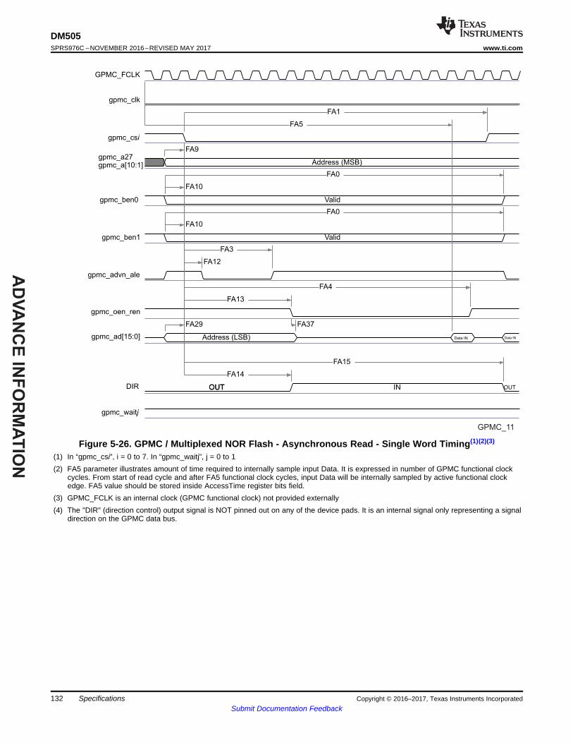
AD
VA
NC
E IN
FO
RM
AT
ION
GPMC_FCLK
gpmc_clk
gpmc_csi
gpmc_a27
gpmc_ben0
gpmc_ 1ben
gpmc_ _aleadvn
gpmc_oen_ren
gpmc_a [15:0]d
DIR
gpmc_waitj
Address (MSB)
Valid
Valid
Address (LSB) Data IN Data IN
OUTOUT IN OUT
FA0
FA9
FA10
FA3
FA13
FA29
FA1
FA37
FA12
FA4
FA10
FA0
FA5
FA14
FA15
GPMC_11
gpmc_a[10:1]
132
DM505SPRS976C –NOVEMBER 2016–REVISED MAY 2017 www.ti.com
Submit Documentation FeedbackSpecifications Copyright © 2016–2017, Texas Instruments Incorporated
Figure 5-26. GPMC / Multiplexed NOR Flash - Asynchronous Read - Single Word Timing(1)(2)(3)
(1) In “gpmc_csi”, i = 0 to 7. In “gpmc_waitj”, j = 0 to 1(2) FA5 parameter illustrates amount of time required to internally sample input Data. It is expressed in number of GPMC functional clock
cycles. From start of read cycle and after FA5 functional clock cycles, input Data will be internally sampled by active functional clockedge. FA5 value should be stored inside AccessTime register bits field.
(3) GPMC_FCLK is an internal clock (GPMC functional clock) not provided externally(4) The "DIR" (direction control) output signal is NOT pinned out on any of the device pads. It is an internal signal only representing a signal
direction on the GPMC data bus.

AD
VA
NC
E I
NF
OR
MA
TIO
N
gpmc_fclk
gpmc_clk
gpmc_csi
gpmc_ben0
gpmc_ 1ben
gpmc_ _aleadvn
gpmc_wen
gpmc_ad[15:0]
gpmc_waitj
DIR
Address (MSB)
Valid Address (LSB) Data OUT
OUT
FA0
FA1
FA9
FA10
FA3
FA25
FA29
FA12
FA27
FA28
FA0
FA10
GPMC_12
gpmc_a27gpmc_a[10:1]
133
DM505www.ti.com SPRS976C –NOVEMBER 2016–REVISED MAY 2017
Submit Documentation FeedbackSpecificationsCopyright © 2016–2017, Texas Instruments Incorporated
Figure 5-27. GPMC / Multiplexed NOR Flash - Asynchronous Write - Single Word Timing(1)
(1) In “gpmc_csi”, i = 0 to 7. In “gpmc_waitj”, j = 0 to 1.(2) The "DIR" (direction control) output signal is NOT pinned out on any of the device pads. It is an internal signal only representing a signal
direction on the GPMC data bus.
5.9.6.6.3 GPMC/NAND Flash Interface Asynchronous Timing
Table 5-39 and Table 5-40 assume testing over the recommended operating conditions and electricalcharacteristic conditions below (see Figure 5-28, Figure 5-29, Figure 5-30 and Figure 5-31).
Table 5-39. GPMC/NAND Flash Interface Timing Requirements(1)
NO. PARAMETER DESCRIPTION MIN MAX UNITGNF12 tacc(DAT) Data maximum access time (GPMC_FCLK Cycles) J cycles
- tsu(DV-OEH) Setup time, read gpmc_ad[15:0] valid before gpmc_oen_ren high 1.9 ns- th(OEH-DV) Hold time, read gpmc_ad[15:0] valid after gpmc_oen_ren high 1 ns
(1) J = AccessTime * (TimeParaGranularity + 1)
Table 5-40. GPMC/NAND Flash Interface Switching Characteristics
NO. PARAMETER DESCRIPTION MIN MAX UNIT- tr(DO) Rising time, gpmc_ad[15:0] output data 0.447 4.067 ns- tf(DO) Fallling time, gpmc_ad[15:0] output data 0.43 4.463 ns
GNF0 tw(nWEV) Pulse duration, gpmc_wen valid time A (1) nsGNF1 td(nCSV-nWEV) Delay time, gpmc_cs[7:0] valid to gpmc_wen valid B - 0.2 (2) B + 2.0
(2)ns

AD
VA
NC
E IN
FO
RM
AT
ION
134
DM505SPRS976C –NOVEMBER 2016–REVISED MAY 2017 www.ti.com
Submit Documentation FeedbackSpecifications Copyright © 2016–2017, Texas Instruments Incorporated
Table 5-40. GPMC/NAND Flash Interface Switching Characteristics (continued)NO. PARAMETER DESCRIPTION MIN MAX UNIT
GNF2 td(CLEH-nWEV) Delay time, gpmc_ben[1:0] high to gpmc_wen valid C - 0.2 (3) C + 2.0(3)
ns
GNF3 td(nWEV-DV) Delay time, gpmc_ad[15:0] valid to gpmc_wen valid D - 0.2 (4) D + 2.0(4)
ns
GNF4 td(nWEIV-DIV) Delay time, gpmc_wen invalid to gpmc_ad[15:0] invalid E - 0.2 (5) E + 2.0(5)
ns
GNF5 td(nWEIV-CLEIV) Delay time, gpmc_wen invalid to gpmc_ben[1:0] invalid F - 0.2 (6) F + 2.0(6)
ns
GNF6 td(nWEIV-nCSIV) Delay time, gpmc_wen invalid to gpmc_cs[7:0] invalid G - 0.2 (7) G + 2.0(7)
ns
GNF7 td(ALEH-nWEV) Delay time, gpmc_advn_ale high to gpmc_wen valid C - 0.2 (3) C + 2.0(3)
ns
GNF8 td(nWEIV-ALEIV) Delay time, gpmc_wen invalid to gpmc_advn_ale invalid F - 0.2 (6) F + 2.0(6)
ns
GNF9 tc(nWE) Cycle time, write cycle time H (8) nsGNF10 td(nCSV-nOEV) Delay time, gpmc_cs[7:0] valid to gpmc_oen_ren valid I - 0.2 (9) I + 2.0 (9) nsGNF13 tw(nOEV) Pulse duration, gpmc_oen_ren valid time K nsGNF14 tc(nOE) Cycle time, read cycle time L (10) nsGNF15 td(nOEIV-nCSIV) Delay time, gpmc_oen_ren invalid to gpmc_cs[7:0] invalid M - 0.2
(11)M + 2.0
(11)ns
(1) A = (WEOffTime – WEOnTime) * (TimeParaGranularity + 1) * GPMC_FCLK(2) B = ((WEOnTime – CSOnTime) * (TimeParaGranularity + 1) + 0.5 * (WEExtraDelay – CSExtraDelay)) * GPMC_FCLK(3) C = ((WEOnTime – ADVOnTime) * (TimeParaGranularity + 1) + 0.5 * (WEExtraDelay – ADVExtraDelay)) * GPMC_FCLK(4) D = (WEOnTime * (TimeParaGranularity + 1) + 0.5 * WEExtraDelay ) * GPMC_FCLK(5) E = (WrCycleTime – WEOffTime * (TimeParaGranularity + 1) – 0.5 * WEExtraDelay ) * GPMC_FCLK(6) F = (ADVWrOffTime – WEOffTime * (TimeParaGranularity + 1) + 0.5 * (ADVExtraDelay – WEExtraDelay ) * GPMC_FCLK(7) G = (CSWrOffTime – WEOffTime * (TimeParaGranularity + 1) + 0.5 * (CSExtraDelay – WEExtraDelay ) * GPMC_FCLK(8) H = WrCycleTime * (1 + TimeParaGranularity) * GPMC_FCLK(9) I = ((OEOffTime + (n – 1) * PageBurstAccessTime – CSOnTime) * (TimeParaGranularity + 1) + 0.5 * (OEExtraDelay – CSExtraDelay)) *
GPMC_FCLK(10) K = (OEOffTime – OEOnTime) * (1 + TimeParaGranularity) * GPMC_FCLK(11) L = RdCycleTime * (1 + TimeParaGranularity) * GPMC_FCLK(12) M = (CSRdOffTime – OEOffTime * (TimeParaGranularity + 1) + 0.5 * (CSExtraDelay – OEExtraDelay ) * GPMC_FCLK

AD
VA
NC
E I
NF
OR
MA
TIO
N
GPMC_FCLK
gpmc_csi
gpmc_ben0
gpmc_ _aleadvn
gpmc_oen_ren
gpmc_wen
gpmc_ad[15:0] Address
GNF0
GNF1
GNF7
GNF3 GNF4
GNF6
GNF8
GNF9
GPMC_14
GPMC_FCLK
gpmc_csi
gpmc_ben0
gpmc_ _aleadvn
gpmc_oen_ren
gpmc_wen
gpmc_ad[15:0] Command
GNF0
GNF1
GNF2
GNF3 GNF4
GNF5
GNF6
GPMC_13
135
DM505www.ti.com SPRS976C –NOVEMBER 2016–REVISED MAY 2017
Submit Documentation FeedbackSpecificationsCopyright © 2016–2017, Texas Instruments Incorporated
Figure 5-28. GPMC / NAND Flash - Command Latch Cycle Timing(1)
(1) In gpmc_csi, i = 0 to 7.
Figure 5-29. GPMC / NAND Flash - Address Latch Cycle Timing(1)
(1) In gpmc_csi, i = 0 to 7.

AD
VA
NC
E IN
FO
RM
AT
ION
GPMC_FCLK
gpmc_csi
gpmc_ben0
gpmc_ _aleadvn
gpmc_oen_ren
gpmc_wen
gpmc_ad[15:0] DATA
GNF0
GNF1
GNF4
GNF6
GNF9
GNF3
GPMC_16
GPMC_FCLK
gpmc_csi
gpmc_ben0
gpmc_ _aleadvn
gpmc_oen_ren
gpmc_ad[15:0]
gpmc_waitj
DATA
GNF10
GNF13
GNF14
GNF15
GNF12
GPMC_15
136
DM505SPRS976C –NOVEMBER 2016–REVISED MAY 2017 www.ti.com
Submit Documentation FeedbackSpecifications Copyright © 2016–2017, Texas Instruments Incorporated
Figure 5-30. GPMC / NAND Flash - Data Read Cycle Timing(1)(2)(3)
(1) GNF12 parameter illustrates amount of time required to internally sample input Data. It is expressed in number of GPMC functionalclock cycles. From start of read cycle and after GNF12 functional clock cycles, input data will be internally sampled by active functionalclock edge. GNF12 value must be stored inside AccessTime register bits field.
(2) GPMC_FCLK is an internal clock (GPMC functional clock) not provided externally.(3) In gpmc_csi, i = 0 to 7. In gpmc_waitj, j = 0 to 1.
Figure 5-31. GPMC / NAND Flash - Data Write Cycle Timing(1)
(1) In gpmc_csi, i = 0 to 7.
NOTETo configure the desired virtual mode the user must set MODESELECT bit andDELAYMODE bitfield for each corresponding pad control register.
The pad control registers are presented Table 4-28 and described in Device TRM, ControlModule section.
AD
VA
NC
E I
NF
OR
MA
TIO
N
137
DM505www.ti.com SPRS976C –NOVEMBER 2016–REVISED MAY 2017
Submit Documentation FeedbackSpecificationsCopyright © 2016–2017, Texas Instruments Incorporated
5.9.6.7 GP Timers
The device has eight GP timers: TIMER1 through TIMER8.• TIMER1 (1-ms tick) includes a specific function to generate accurate tick interrupts to the operating
system and it belongs to the PD_WKUPAON domain.• TIMER2 through TIMER8 belong to the PD_COREAON module.
Each timer can be clocked from the system clock (19.2, 20, or 27 MHz) or the 32-kHz clock. Select theclock source at the power, reset, and clock management (PRCM) module level.
Each timer provides an interrupt through the device IRQ_CROSSBAR.
Each timer is connected to an external pin by their PWM output or their event capture input pin (forexternal timer triggering).
5.9.6.7.1 GP Timer Features
The following are the main features of the GP timer controllers:• Level 4 (L4) slave interface support:
– 32-bit data bus width– 32- or 16-bit access supported– 8-bit access not supported– 10-bit address bus width– Burst mode not supported– Write nonposted transaction mode supported
• Interrupts generated on overflow, compare, and capture• Free-running 32-bit upward counter• Compare and capture modes• Autoreload mode• Start and stop mode• Programmable divider clock source (2n, where n = [0:8])• Dedicated input trigger for capture mode and dedicated output trigger/PWM signal• Dedicated GP output signal for using the TIMERi_GPO_CFG signal• On-the-fly read/write register (while counting)• 1-ms tick with 32.768-Hz functional clock generated (only TIMER1)
5.9.6.8 I2C
The device includes 2 inter-integrated circuit (I2C) modules which provide an interface to other devicescompliant with Philips Semiconductors Inter-IC bus (I2C-bus™) specification version 2.1. Externalcomponents attached to this 2-wire serial bus can transmit/receive 8-bit data to/from the device throughthe I2C module.
NOTENote that, I2C1 and I2C2, due to characteristics of the open drain IO cells, HS mode is notsupported.
NOTEInter-integrated circuit i (i=1 to 2) module is also referred to as I2Ci.

AD
VA
NC
E IN
FO
RM
AT
ION
138
DM505SPRS976C –NOVEMBER 2016–REVISED MAY 2017 www.ti.com
Submit Documentation FeedbackSpecifications Copyright © 2016–2017, Texas Instruments Incorporated
NOTEFor more information, see the Multimaster I2C Controller section of the Device TRM.
Table 5-41 and Figure 5-32 assume testing over the recommended operating conditions and electricalcharacteristic conditions below.
Table 5-41. Timing Requirements for I2C Input Timings(1)
NO. PARAMETER DESCRIPTIONSTANDARD MODE FAST MODE
UNITMIN MAX MIN MAX
1 tc(SCL) Cycle time, SCL 10 2.5 µs
2 tsu(SCLH-SDAL)Setup time, SCL high before SDA low (for arepeated START condition) 4.7 0.6 µs
3 th(SDAL-SCLL)Hold time, SCL low after SDA low (for a STARTand a repeated START condition) 4 0.6 µs
4 tw(SCLL) Pulse duration, SCL low 4.7 1.3 µs5 tw(SCLH) Pulse duration, SCL high 4 0.6 µs6 tsu(SDAV-SCLH) Setup time, SDA valid before SCL high 250 100(2) ns7 th(SCLL-SDAV) Hold time, SDA valid after SCL low 0(3) 3.45(4) 0(3) 0.9(4) µs
8 tw(SDAH)Pulse duration, SDA high between STOP andSTART conditions 4.7 1.3 µs
9 tr(SDA) Rise time, SDA 1000 20 + 0.1Cb(5) 300 ns
10 tr(SCL) Rise time, SCL 1000 20 + 0.1Cb(5) 300 ns
11 tf(SDA) Fall time, SDA 300 20 + 0.1Cb(5) 300 ns
12 tf(SCL) Fall time, SCL 300 20 + 0.1Cb(5) 300 ns
13 tsu(SCLH-SDAH)Setup time, SCL high before SDA high (forSTOP condition) 4 0.6 µs
14 tw(SP) Pulse duration, spike (must be suppressed) 0 50 ns15 Cb
(5) Capacitive load for each bus line 400 400 pF
(1) The I2C pins SDA and SCL do not feature fail-safe I/O buffers. These pins could potentially draw current when the device is powereddown.
(2) A Fast-mode I2C-bus™ device can be used in a Standard-mode I2C-bus system, but the requirement tsu(SDA-SCLH)≥ 250 ns must then bemet. This will automatically be the case if the device does not stretch the LOW period of the SCL signal. If such a device does stretchthe LOW period of the SCL signal, it must output the next data bit to the SDA line tr max + tsu(SDA-SCLH)= 1000 + 250 = 1250 ns(according to the Standard-mode I2C-Bus Specification) before the SCL line is released.
(3) A device must internally provide a hold time of at least 300 ns for the SDA signal (referred to the VIHmin of the SCL signal) to bridge theundefined region of the falling edge of SCL.
(4) The maximum th(SDA-SCLL) has only to be met if the device does not stretch the low period [tw(SCLL)] of the SCL signal.(5) Cb = total capacitance of one bus line in pF. If mixed with HS-mode devices, faster fall-times are allowed.

AD
VA
NC
E I
NF
OR
MA
TIO
N
10
8
4
3
7
12
5
6 14
2
3
13
Stop Start RepeatedStart
Stop
I2Ci_SDA
I2Ci_SCL
1
11 9
SPRS91v_I2C_01
139
DM505www.ti.com SPRS976C –NOVEMBER 2016–REVISED MAY 2017
Submit Documentation FeedbackSpecificationsCopyright © 2016–2017, Texas Instruments Incorporated
Figure 5-32. I2C Receive Timing
Table 5-42 and Figure 5-33 assume testing over the recommended operating conditions and electricalcharacteristic conditions below.
Table 5-42. Switching Characteristics Over Recommended Operating Conditions for I2C Output Timings(2)
NO. PARAMETER DESCRIPTIONSTANDARD MODE FAST MODE
UNITMIN MAX MIN MAX
16 tc(SCL) Cycle time, SCL 10 2.5 µs
17 tsu(SCLH-SDAL)Setup time, SCL high before SDA low (for arepeated START condition) 4.7 0.6 µs
18 th(SDAL-SCLL)Hold time, SCL low after SDA low (for aSTART and a repeated START condition) 4 0.6 µs
19 tw(SCLL) Pulse duration, SCL low 4.7 1.3 µs20 tw(SCLH) Pulse duration, SCL high 4 0.6 µs21 tsu(SDAV-SCLH) Setup time, SDA valid before SCL high 250 100 ns
22 th(SCLL-SDAV)Hold time, SDA valid after SCL low (for I2Cbus devices) 0 3.45 0 0.9 µs
23 tw(SDAH)Pulse duration, SDA high between STOP andSTART conditions 4.7 1.3 µs
24 tr(SDA) Rise time, SDA 1000 20 + 0.1Cb(1) 300 ns
25 tr(SCL) Rise time, SCL 1000 20 + 0.1Cb(1) 300 ns
26 tf(SDA) Fall time, SDA 300 20 + 0.1Cb(1) 300 ns
27 tf(SCL) Fall time, SCL 300 20 + 0.1Cb(1) 300 ns
28 tsu(SCLH-SDAH)Setup time, SCL high before SDA high (forSTOP condition) 4 0.6 µs
29 Cp Capacitance for each I2C pin 10 10 pF

AD
VA
NC
E IN
FO
RM
AT
ION
25
23
19
18
22
27
20
21
17
18
28
Stop Start RepeatedStart
Stop
I2Ci_SDA
I2Ci_SCL
16
26 24
SPRS91v_I2C_02
140
DM505SPRS976C –NOVEMBER 2016–REVISED MAY 2017 www.ti.com
Submit Documentation FeedbackSpecifications Copyright © 2016–2017, Texas Instruments Incorporated
(1) Cb = total capacitance of one bus line in pF. If mixed with HS-mode devices, faster fall-times are allowed.(2) Software must properly configure the I2C module registers to achieve the timings shown in this table. See the Device TRM for details.
Figure 5-33. I2C Transmit Timing
5.9.6.9 UART
The UART performs serial-to-parallel conversions on data received from a peripheral device and parallel-to-serial conversion on data received from the CPU. There are 3 UART modules in the device. EachUART can be used for configuration and data exchange with a number of external peripheral devices orinterprocessor communication between devices.
The UARTi (where i = 1 to 3) include the following features:• 16C750 compatibility• 64-byte FIFO buffer for receiver and 64-byte FIFO for transmitter• Baud generation based on programmable divisors N (where N = 1…16 384) operating from a fixed
functional clock of 48 MHz or 192 MHz• Break character detection and generation• Configurable data format:
– Data bit: 5, 6, 7, or 8 bits– Parity bit: Even, odd, none– Stop-bit: 1, 1.5, 2 bit(s)
• Flow control: Hardware (RTS/CTS) or software (XON/XOFF)
NOTEFor more information, see the UART section of the Device TRM.
Table 5-43, Table 5-44 and Figure 5-34 assume testing over the recommended operating conditions andelectrical characteristic conditions below.
Table 5-43. Timing Requirements for UARTNO. PARAMETER DESCRIPTION MIN MAX UNIT
4 tw(RX) Pulse width, receive data bit, 15/30/100pF high or low 0.96U(1) 1.05U(1) ns5 tw(CTS) Pulse width, receive start bit, 15/30/100pF high or low 0.96U(1) 1.05U(1) ns
td(RTS-TX) Delay time, transmit start bit to transmit data P(2) nstd(CTS-TX) Delay time, receive start bit to transmit data P(2) ns

AD
VA
NC
E I
NF
OR
MA
TIO
N
3
2
Start
Bit
Data Bits
UARTi_TXD
5
Data Bits
Bit
Start
4
UARTi_RXD
SPRS91v_UART_01
141
DM505www.ti.com SPRS976C –NOVEMBER 2016–REVISED MAY 2017
Submit Documentation FeedbackSpecificationsCopyright © 2016–2017, Texas Instruments Incorporated
(1) U = UART baud time = 1/programmed baud rate(2) P = Clock period of the reference clock (FCLK, usually 48 MHz or 192MHz).
Table 5-44. Switching Characteristics Over Recommended Operating Conditions for UARTNO. PARAMETER DESCRIPTION MIN MAX UNIT
f(baud) Maximum programmable baud rate15 pF 12
MHz30 pF 0.23100 pF 0.115
2 tw(TX) Pulse width, transmit data bit, 15/30/100 pF high or low U - 2(1) U + 2(1) ns3 tw(RTS) Pulse width, transmit start bit, 15/30/100 pF high or low U - 2(1) U + 2(1) ns
(1) U = UART baud time = 1/programmed baud rate
Figure 5-34. UART Timing
CAUTION
The IO timings provided in this section are only valid if signals within a singleIOSET are used. The IOSETs are defined in Table 5-45.
In Table 5-45 are presented the specific groupings of signals (IOSET) for use with UART.
Table 5-45. UART1-3 IOSETs
SIGNALS IOSET1 IOSET2 IOSET3BALL MUX BALL MUX BALL MUX
UART1uart1_rxd F13 0 F13 0uart1_txd E14 0 E14 0uart1_rtsn C14 0uart1_ctsn F14 0
UART2uart2_rxd E7 2 D14 0uart2_txd F7 2 D15 0uart2_rtsn F16 0uart2_ctsn F15 0
UART3uart3_rxd W7 4 L1 1 M2 1uart3_txd W6 4 L2 1 R6 1uart3_rtsn R7 1 T5 1

AD
VA
NC
E IN
FO
RM
AT
ION
142
DM505SPRS976C –NOVEMBER 2016–REVISED MAY 2017 www.ti.com
Submit Documentation FeedbackSpecifications Copyright © 2016–2017, Texas Instruments Incorporated
Table 5-45. UART1-3 IOSETs (continued)SIGNALS IOSET1 IOSET2 IOSET3
BALL MUX BALL MUX BALL MUXuart3_ctsn N4 1 U6 1
5.9.6.10 McSPI
The McSPI is a master/slave synchronous serial bus. There are four separate McSPI modules (SPI1,SPI2, SPI3, and SPI4) in the device. All these four modules support up to four external devices (four chipselects) and are able to work as both master and slave.
The McSPI modules include the following main features:• Serial clock with programmable frequency, polarity, and phase for each channel• Wide selection of SPI word lengths, ranging from 4 to 32 bits• Up to four master channels, or single channel in slave mode• Master multichannel mode:
– Full duplex/half duplex– Transmit-only/receive-only/transmit-and-receive modes– Flexible input/output (I/O) port controls per channel– Programmable clock granularity– SPI configuration per channel. This means, clock definition, polarity enabling and word width
• Power management through wake-up capabilities• Programmable timing control between chip select and external clock generation• Built-in FIFO available for a single channel.• Each SPI module supports multiple chip select pins spim_cs[i], where i = 1 to 4.
NOTEFor more information, see the Serial Communication Interface section of the device TRM.
NOTEThe McSPIm module (m = 1 to 4) is also referred to as SPIm.
Table 5-46, Figure 5-35 and Figure 5-36 Present Timing Requirements for McSPI - Master Mode.
Table 5-46. Timing Requirements for SPI - Master Mode
NO. PARAMETER DESCRIPTION MODE MIN MAX UNITSM1 tc(SPICLK) Cycle time, spi_sclk (1) (2) SPI1/2/3/
420.8 ns
SM2 tw(SPICLKL) Typical Pulse duration, spi_sclk low (1) 0.5*P-1(3)
ns
SM3 tw(SPICLKH) Typical Pulse duration, spi_sclk high (1) 0.5*P-1(3)
ns
SM4 tsu(MISO-SPICLK) Setup time, spi_d[x] valid before spi_sclk active edge (1) 2.29 nsSM5 th(SPICLK-MISO) Hold time, spi_d[x] valid after spi_sclk active edge (1) 2.67 nsSM6 td(SPICLK-SIMO) Delay time, spi_sclk active edge to spi_d[x] transition (1) SPI1/2/4 -3.57 3.57 ns
SPI3 -3.57 3.57 nsSM7 td(CS-SIMO) Delay time, spi_cs[x] active edge to spi_d[x] transition 3.57 ns
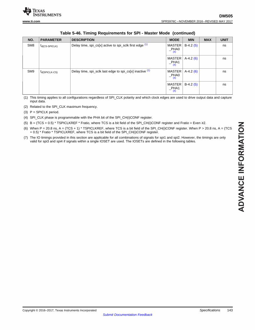
AD
VA
NC
E I
NF
OR
MA
TIO
N
143
DM505www.ti.com SPRS976C –NOVEMBER 2016–REVISED MAY 2017
Submit Documentation FeedbackSpecificationsCopyright © 2016–2017, Texas Instruments Incorporated
Table 5-46. Timing Requirements for SPI - Master Mode (continued)NO. PARAMETER DESCRIPTION MODE MIN MAX UNITSM8 td(CS-SPICLK) Delay time, spi_cs[x] active to spi_sclk first edge (1) MASTER
_PHA0(4)
B-4.2 (5) ns
MASTER_PHA1
(4)
A-4.2 (6) ns
SM9 td(SPICLK-CS) Delay time, spi_sclk last edge to spi_cs[x] inactive (1) MASTER_PHA0
(4)
A-4.2 (6) ns
MASTER_PHA1
(4)
B-4.2 (5) ns
(1) This timing applies to all configurations regardless of SPI_CLK polarity and which clock edges are used to drive output data and captureinput data.
(2) Related to the SPI_CLK maximum frequency.(3) P = SPICLK period.(4) SPI_CLK phase is programmable with the PHA bit of the SPI_CH(i)CONF register.(5) B = (TCS + 0.5) * TSPICLKREF * Fratio, where TCS is a bit field of the SPI_CH(i)CONF register and Fratio = Even ≥2.(6) When P = 20.8 ns, A = (TCS + 1) * TSPICLKREF, where TCS is a bit field of the SPI_CH(i)CONF register. When P > 20.8 ns, A = (TCS
+ 0.5) * Fratio * TSPICLKREF, where TCS is a bit field of the SPI_CH(i)CONF register.(7) The IO timings provided in this section are applicable for all combinations of signals for spi1 and spi2. However, the timings are only
valid for spi3 and spi4 if signals within a single IOSET are used. The IOSETs are defined in the following tables.

AD
VA
NC
E IN
FO
RM
AT
ION
spim_cs(OUT)
spi _sclk(OUT)m
spi _sclkm (OUT)
spi _m d(OUT)
spim_cs(OUT)
spi _sclkm (OUT)
spi _sclkm (OUT)
spi _m d(OUT)
Bit n-1 Bit n-2 Bit n-3 Bit n-4 Bit 0
Bit n-1 Bit n-2 Bit n-3 Bit 1 Bit0
PHA=0
EPOL=1
POL=0
POL=1
PHA=1
EPOL=1
POL=0
POL=1
SM8 SM9
SM6
SM3
SM1
SM2
SM1
SM8 SM9SM3
SM1
SM2
SM1
SM6
SM7 SM6
SM2
SM3
SM2
SM3
SM6 SM6 SM6
SPRS91v_McSPI_01
144
DM505SPRS976C –NOVEMBER 2016–REVISED MAY 2017 www.ti.com
Submit Documentation FeedbackSpecifications Copyright © 2016–2017, Texas Instruments Incorporated
Figure 5-35. McSPI - Master Mode Transmit

AD
VA
NC
E I
NF
OR
MA
TIO
N
spim_cs(OUT)
spi _sclkm (OUT)
spi _sclkm (OUT)
spi _m d(IN)
spim_cs(OUT)
spi _sclkm (OUT)
spi _sclkm (OUT)
spi _m d(IN)
Bit n-1 Bit n-2 Bit n-3 Bit n-4 Bit 0
Bit n-1 Bit n-2 Bit n-3 Bit 1 Bit 0
PHA=0
EPOL=1
PHA=1
EPOL=1
POL=0
POL=1
POL=0
POL=1
SM8 SM9
SM3
SM1
SM2
SM1
SM8 SM9SM3
SM1
SM2
SM1
SM2
SM3
SM2
SM3
SM4
SM5
SM4
SM5
SM4
SM4
SM5
SM5
SPRS91v_McSPI_02
145
DM505www.ti.com SPRS976C –NOVEMBER 2016–REVISED MAY 2017
Submit Documentation FeedbackSpecificationsCopyright © 2016–2017, Texas Instruments Incorporated
Figure 5-36. McSPI - Master Mode Receive
Table 5-47, Figure 5-37 and Figure 5-38 Present Timing Requirements for McSPI - Slave Mode.
Table 5-47. Timing Requirements for SPI - Slave Mode(5)
NO. PARAMETER DESCRIPTION MODE MIN MAX UNITSS1 (1)
(2)tc(SPICLK) Cycle time, spi_sclk SPI1 25 ns
SPI2/3/4 33.3 nsSS2 (1) tw(SPICLKL)
(3) Typical Pulse duration, spi_sclk low 0.45*P nsSS3 (1) tw(SPICLKH)
(3) Typical Pulse duration, spi_sclk high 0.45*P nsSS4 (1) tsu(SIMO-SPICLK) Setup time, spi_d[x] valid before spi_sclk active edge 2.82 nsSS5 (1) th(SPICLK-SIMO) Hold time, spi_d[x] valid after spi_sclk active edge 2.82 nsSS6 (1) td(SPICLK-SOMI) Delay time, spi_sclk active edge to mcspi_somi transition SPI1 2 9.8 ns
SPI2/3/4 2 21 nsSS7 (4) td(CS-SOMI) Delay time, spi_cs[x] active edge to mcspi_somi transition 16 ns

AD
VA
NC
E IN
FO
RM
AT
ION
spim_cs(IN)
spi _sclkm (IN)
spi _sclkm (IN)
spi _m d(OUT)
spim_cs(IN)
spi _sclkm (IN)
spi _sclkm (IN)
spi _m d(OUT)
Bit n-1 Bit n-2 Bit n-3 Bit n-4 Bit 0
Bit n-1 Bit n-2 Bit n-3 Bit 1 Bit 0
PHA=0
EPOL=1
POL=0
POL=1
POL=0
POL=1
PHA=1
EPOL=1
SS6
SS3
SS1
SS3
SS1
SS3
SS1
SS2
SS1
SS6
SS6
SS8 SS9
SS7
SS8
SS2
SS3
SS2
SS2
SS6 SS6SS6
SS9
SPRS91v_McSPI_03
146
DM505SPRS976C –NOVEMBER 2016–REVISED MAY 2017 www.ti.com
Submit Documentation FeedbackSpecifications Copyright © 2016–2017, Texas Instruments Incorporated
Table 5-47. Timing Requirements for SPI - Slave Mode(5) (continued)NO. PARAMETER DESCRIPTION MODE MIN MAX UNIT
SS8 (1) tsu(CS-SPICLK) Setup time, spi_cs[x] valid before spi_sclk first edge 2.82 nsSS9 (1) th(SPICLK-CS) Hold time, spi_cs[x] valid after spi_sclk last edge 2.82 ns
(1) This timing applies to all configurations regardless of SPI_CLK polarity and which clock edges are used to drive output data and captureinput data.
(2) When operating the SPI interface in RX-only mode, the minimum Cycle time is 26ns (38.4MHz)(3) P = SPICLK period.(4) PHA = 0; SPI_CLK phase is programmable with the PHA bit of the SPI_CH(i)CONF register.(5) The IO timings provided in this section are applicable for all combinations of signals for spi1 and spi2. However, the timings are only
valid for spi3 and spi4 if signals within a single IOSET are used. The IOSETs are defined in the following tables.
Figure 5-37. McSPI - Slave Mode Transmit

AD
VA
NC
E I
NF
OR
MA
TIO
N
spim_cs(IN)
spi _sclkm (IN)
spi _sclkm (IN)
spi _m d(IN)
spim_cs(IN)
spi _sclkm (IN)
spi _sclkm (IN)
spi _m d(IN)
Bit n-1 Bit n-2 Bit n-3 Bit n-4 Bit 0
Bit n-1 Bit n-2 Bit n-3 Bit 1 Bit0
PHA=0
EPOL=1
POL=0
POL=1
POL=0
POL=1
PHA=1
EPOL=1
SS3
SS1
SS3
SS1
SS3
SS1
SS2
SS1
SS8 SS9
SS8 SS9
SS2
SS3
SS2
SS2
SS4
SS5
SS5
SS4
SS4
SS5
SS4
SS5
SPRS91v_McSPI_04
147
DM505www.ti.com SPRS976C –NOVEMBER 2016–REVISED MAY 2017
Submit Documentation FeedbackSpecificationsCopyright © 2016–2017, Texas Instruments Incorporated
Figure 5-38. McSPI - Slave Mode Receive
CAUTION
The IO timings provided in this section are applicable for all combinations ofsignals for SPI2 and SPI4. However, the timings are only valid for SPI1 andSPI3 if signals within a single IOSET are used. The IOSETS are defined in theTable 5-48.
In Table 5-48 are presented the specific groupings of signals (IOSET) for use with McSPI.
Table 5-48. McSPI1/3 IOSETs
SIGNALS IOSET1 IOSET2 IOSET3BALL MUX BALL MUX BALL MUX
SPI1spi1_sclk M2 0 M2 0 M2 0

AD
VA
NC
E IN
FO
RM
AT
ION
148
DM505SPRS976C –NOVEMBER 2016–REVISED MAY 2017 www.ti.com
Submit Documentation FeedbackSpecifications Copyright © 2016–2017, Texas Instruments Incorporated
Table 5-48. McSPI1/3 IOSETs (continued)SIGNALS IOSET1 IOSET2 IOSET3
BALL MUX BALL MUX BALL MUXspi1_d1 U6 0 U6 0 U6 0spi1_d0 T5 0 T5 0 T5 0spi1_cs0 R6 0 R6 0 R6 0spi1_cs1 R5 0spi1_cs2 F14 5spi1_cs3 C14 5
SPI3spi3_sclk F15 4 C6 4spi3_d1 D14 4 F7 4spi3_d0 D15 4 E7 4spi3_cs0 F16 4 B6 4
5.9.6.11 QSPI
The Quad SPI (QSPI) module is a type of SPI module that allows single, dual or quad read access toexternal SPI devices. This module has a memory mapped register interface, which provides a directinterface for accessing data from external SPI devices and thus simplifying software requirements. Itworks as a master only. There is one QSPI module in the device and it is primary intended for fastbooting from quad-SPI flash memories.General SPI features:• Programmable clock divider• Six pin interface (DCLK, CS_N, DOUT, DIN, QDIN1, QDIN2)• 4 external chip select signals• Support for 3-, 4- or 6-pin SPI interface• Programmable CS_N to DOUT delay from 0 to 3 DCLKs• Programmable signal polarities• Programmable active clock edge• Software controllable interface allowing for any type of SPI transfer
NOTEFor more information, see the Quad Serial Peripheral Interface section of the Device TRM.
CAUTION
The IO Timings provided in this section are only valid when all QSPI ChipSelects used in a system are configured to use the same Clock Mode (eitherClock Mode 0 or Clock Mode 3).
Table 5-49 and Table 5-50 present Timing and Switching Characteristics for Quad SPI Interface.

AD
VA
NC
E I
NF
OR
MA
TIO
N
149
DM505www.ti.com SPRS976C –NOVEMBER 2016–REVISED MAY 2017
Submit Documentation FeedbackSpecificationsCopyright © 2016–2017, Texas Instruments Incorporated
Table 5-49. Switching Characteristics for QSPI
No PARAMETER DESCRIPTION Mode MIN MAX UNIT1 tc(SCLK) Cycle time, sclk Default
TimingMode,Clock
Mode 0
10.4 ns
DefaultTimingMode,Clock
Mode 3
15.625 ns
2 tw(SCLKL) Pulse duration, sclk low Y*P-1 (1) ns3 tw(SCLKH) Pulse duration, sclk high Y*P-1 (1) ns4 td(CS-SCLK) Delay time, sclk falling edge to cs active edge, CS3:0 Default
TimingMode
-M*P-1(2) (3)
-M*P+1(2) (3)
ns
5 td(SCLK-CS) Delay time, sclk falling edge to cs inactive edge, CS3:0 DefaultTimingMode
N*P-1 (2)(3)
N*P+1(2) (3)
ns
6 td(SCLK-D1) Delay time, sclk falling edge to d[0] transition DefaultTimingMode
-1 1 ns
7 tena(CS-D1LZ) Enable time, cs active edge to d[0] driven (lo-z) -P-3.5 -P+2.5 ns8 tdis(CS-D1Z) Disable time, cs active edge to d[0] tri-stated (hi-z) -P-2.5 -P+2.0 ns9 td(SCLK-D1) Delay time, sclk first falling edge to first d[0] transition PHA=0
Only,DefaultTimingMode
-1-P -1-P ns
(1) The Y parameter is defined as follows: If DCLK_DIV is 0 or ODD then, Y equals 0.5. If DCLK_DIV is EVEN then, Y equals(DCLK_DIV/2) / (DCLK_DIV+1). For best performance, it is recommended to use a DCLK_DIV of 0 or ODD to minimize the duty cycledistortion. The HSDIVIDER on CLKOUTX2_H13 output of DPLL_PER can be used to achieve the desired clock divider ratio. Allrequired details about clock division factor DCLK_DIV can be found in the device TRM.
(2) P = SCLK period.(3) M=QSPI_SPI_DC_REG.DDx + 1 when Clock Mode 0. M=QSPI_SPI_DC_REG.DDx when Clock Mode 3. N = 2 when Clock Mode 0. N
= 3 when Clock Mode 3.

AD
VA
NC
E IN
FO
RM
AT
ION
cs
sclk
rtclk
d[0]
d[3:1]
Bit n-1 Bit n-2 Bit 1 Bit 0
PHA=0
POL=0
POL=0
Command Command Read Data Read Data
Bit 1 Bit 0Read Data Read Data
Q4
Q7 Q9
Q2 Q3Q1
Q6
Q5
SPRS85v_TIMING_OSPI1_02
Q12 Q13 Q12 Q13
Q12 Q13 Q12 Q13
cs
sclk
d[0]
d[3:1]
Bit n-1 Bit n-2 Bit 1 Bit 0
PHA=1
POL=1
Command Command Read Data Read Data
Bit 1 Bit 0Read Data Read Data
Q4
Q7 Q6
Q3 Q2Q1
Q6
Q5
SPRS85v_TIMING_OSPI1_01
Q12 Q13
Q14
Q15
Q12 Q13
Q14
Q15
150
DM505SPRS976C –NOVEMBER 2016–REVISED MAY 2017 www.ti.com
Submit Documentation FeedbackSpecifications Copyright © 2016–2017, Texas Instruments Incorporated
Figure 5-39. QSPI Read (Clock Mode 3)
Figure 5-40. QSPI Read (Clock Mode 0)

AD
VA
NC
E I
NF
OR
MA
TIO
N
cs
sclk
d[0]
d[3:1]
Bit n-1 Bit n-2 Bit 1 Bit 0
PHA=1
POL=1
Command Command Write Data Write Data
Q4
Q7Q6
Q3 Q2Q1
Q6 Q6
Q5
SPRS85v_TIMING_OSPI1_03
Q8Q6
151
DM505www.ti.com SPRS976C –NOVEMBER 2016–REVISED MAY 2017
Submit Documentation FeedbackSpecificationsCopyright © 2016–2017, Texas Instruments Incorporated
Table 5-50. Timing Requirements for QSPI
No PARAMETER DESCRIPTION Mode MIN MAX UNIT12 tsu(D-RTCLK) Setup time, d[3:0] valid before falling rtclk edge Default
TimingMode,Clock
Mode 0
2.9 ns
tsu(D-SCLK) Setup time, d[3:0] valid before falling sclk edge DefaultTimingMode,Clock
Mode 3
5.7 ns
13 th(RTCLK-D) Hold time, d[3:0] valid after falling rtclk edge DefaultTimingMode,Clock
Mode 0
-0.1 ns
th(SCLK-D) Hold time, d[3:0] valid after falling sclk edge DefaultTimingMode,Clock
Mode 3
0.1 ns
14 tsu(D-SCLK) Setup time, final d[3:0] bit valid before final falling sclk edge DefaultTimingMode,Clock
Mode 3
5.7-P (1) ns
15 th(SCLK-D) Hold time, final d[3:0] bit valid after final falling sclk edge DefaultTimingMode,Clock
Mode 3
0.1+P (1) ns
(1) P = SCLK period.(2) Clock Modes 1 and 2 are not supported.(3) The Device captures data on the falling clock edge in Clock Mode 0 and 3, as opposed to the traditional rising clock edge. Although
non-standard, the falling-edge-based setup and hold time timings have been designed to be compatible with standard SPI devices thatlaunch data on the falling edge in Clock Modes 0 and 3.
Figure 5-41. QSPI Write (Clock Mode 3)

AD
VA
NC
E IN
FO
RM
AT
ION
cs
sclk
d[0]
d[3:1]
Bit n-1 Bit n-2 Bit 1 Bit 0
PHA=0
POL=0
Command Command Write Data Write Data
Q4
Q7
Q2 Q3Q1
Q6 Q6
Q5
SPRS85v_TIMING_OSPI1_04
Q8Q9 Q6
152
DM505SPRS976C –NOVEMBER 2016–REVISED MAY 2017 www.ti.com
Submit Documentation FeedbackSpecifications Copyright © 2016–2017, Texas Instruments Incorporated
Figure 5-42. QSPI Write (Clock Mode 0)
NOTETo configure the desired virtual mode the user must set MODESELECT bit andDELAYMODE bitfield for each corresponding pad control register.
The pad control registers are presented in Table 4-28 and described in Device TRM, ControlModule section.
CAUTION
The IO timings provided in this section are only valid if signals within a singleIOSET are used. The IOSETs are defined in Table 5-51.
In Table 5-51 are presented the specific groupings of signals (IOSET) for use with QSPI.
Table 5-51. QSPI IOSETs
SIGNALS IOSET1 IOSET2 IOSET3 IOSET4BALL MUX BALL MUX BALL MUX BALL MUX
qspi1_sclk C8 1 C8 1 C8 1 C8 1qspi1_rtclk C14 8 B7 1 F13 5 D8 2qspi1_d0 B9 1 B9 1 B9 1 B9 1qspi1_d1 F10 1 F10 1 F10 1 F10 1qspi1_d2 A9 1 A9 1 A9 1 A9 1qspi1_d3 D10 1 D10 1 D10 1 D10 1qspi1_cs0 E10 1 E10 1 E10 1 E10 1qspi1_cs1 F15 5

AD
VA
NC
E I
NF
OR
MA
TIO
N
153
DM505www.ti.com SPRS976C –NOVEMBER 2016–REVISED MAY 2017
Submit Documentation FeedbackSpecificationsCopyright © 2016–2017, Texas Instruments Incorporated
5.9.6.12 McASP
The multichannel audio serial port (McASP) functions as a general-purpose audio serial port optimized forthe needs of multichannel audio applications. The McASP is useful for time-division multiplexed (TDM)stream, Inter-Integrated Sound (I2S) protocols, and inter-component digital audio interface transmission(DIT).
NOTEFor more information, see the Serial Communication Interface section of the Device TRM.
Table 5-52, Table 5-53, Table 5-54 and Figure 5-43 present Timing Requirements for McASP1 toMcASP3.
Table 5-52. Timing Requirements for McASP1 (1)
NO. PARAMETER DESCRIPTION MODE MIN MAX UNIT1 tc(AHCLKRX) Cycle time, AHCLKR/X 20 ns2 tw(AHCLKRX) Pulse duration, AHCLKR/X high or low 0.35P (2) ns3 tc(ACLKRX) Cycle time, ACLKR/X Any Other Conditions 20 ns
ACLKX/AFSX (In Sync Mode),ACLKR/AFSR (In Async Mode), and
AXR are all inputs
15.258 ns
4 tw(ACLKRX) Pulse duration, ACLKR/X high or low Any Other Conditions 0.5R - 3(3)
ns
ACLKX/AFSX (In Sync Mode),ACLKR/AFSR (In Async Mode), and
AXR are all inputs
0.38R (3) ns
5 tsu(AFSRX-ACLK) Setup time, AFSR/X input valid beforeACLKR/X
ACLKR/X int 18.5 nsACLKR/X ext in
ACLKR/X ext out3 ns
6 th(ACLK-AFSRX) Hold time, AFSR/X input valid afterACLKR/X
ACLKR/X int -1 nsACLKR/X ext in
ACLKR/X ext out0.4 ns
7 tsu(AXR-ACLK) Setup time, AXR input valid beforeACLKR/X
ACLKR/X int 18.5 nsACLKR/X ext in
ACLKR/X ext out3 ns
8 th(ACLK-AXR) Hold time, AXR input valid afterACLKR/X
ACLKR/X int -1 nsACLKR/X ext in
ACLKR/X ext out0.4 ns
(1) ACLKR internal: ACLKRCTL.CLKRM=1, PDIR.ACLKR = 1ACLKR external input: ACLKRCTL.CLKRM=0, PDIR.ACLKR=0ACLKR external output: ACLKRCTL.CLKRM=0, PDIR.ACLKR=1ACLKX internal: ACLKXCTL.CLKXM=1, PDIR.ACLKX = 1ACLKX external input: ACLKXCTL.CLKXM=0, PDIR.ACLKX=0ACLKX external output: ACLKXCTL.CLKXM=0, PDIR.ACLKX=1
(2) P = AHCLKR/X period in ns.(3) R = ACLKR/X period in ns.
Table 5-53. Timing Requirements for McASP2 (1)
NO. PARAMETER DESCRIPTION MODE MIN MAX UNIT1 tc(AHCLKRX) Cycle time, AHCLKR/X 20 ns2 tw(AHCLKRX) Pulse duration, AHCLKR/X high or low 0.35P (2) ns3 tc(ACLKRX) Cycle time, ACLKR/X Any Other Conditions 20 ns
IOSET1 only, ACLKX/AFSX (In SyncMode), ACLKR/AFSR (In AsyncMode), and AXR are all inputs
15.258 ns

AD
VA
NC
E IN
FO
RM
AT
ION
154
DM505SPRS976C –NOVEMBER 2016–REVISED MAY 2017 www.ti.com
Submit Documentation FeedbackSpecifications Copyright © 2016–2017, Texas Instruments Incorporated
Table 5-53. Timing Requirements for McASP2 (1) (continued)NO. PARAMETER DESCRIPTION MODE MIN MAX UNIT
4 tw(ACLKRX) Pulse duration, ACLKR/X high or low Any Other Conditions 0.5R - 3(3)
ns
IOSET1 only, ACLKX/AFSX (In SyncMode), ACLKR/AFSR (In AsyncMode), and AXR are all inputs
0.38R (3) ns
5 tsu(AFSRX-ACLK) Setup time, AFSR/X input valid beforeACLKR/X
ACLKR/X int 18.5 nsIOSET1 (vout1_*): ACLKR/X ext in
IOSET1 (vout1_*): ACLKR/X ext out4 ns
IOSET2 (gpmc_*): ACLKR/X ext inIOSET2 (gpmc_*): ACLKR/X ext out
3 ns
6 th(ACLK-AFSRX) Hold time, AFSR/X input valid afterACLKR/X
ACLKR/X int -1 nsACLKR/X ext in
ACLKR/X ext out0.4 ns
7 tsu(AXR-ACLK) Setup time, AXR input valid beforeACLKR/X
ACLKR/X int 18.5 nsIOSET1 (vout1_*): ACLKR/X ext in
IOSET1 (vout1_*): ACLKR/X ext out11.5 ns
IOSET2 (gpmc_*): ACLKR/X ext inIOSET2 (gpmc_*): ACLKR/X ext out
3 ns
8 th(ACLK-AXR) Hold time, AXR input valid afterACLKR/X
ACLKR/X int -1 nsACLKR/X ext in
ACLKR/X ext out0.4 ns
(1) ACLKR internal: ACLKRCTL.CLKRM=1, PDIR.ACLKR = 1ACLKR external input: ACLKRCTL.CLKRM=0, PDIR.ACLKR=0ACLKR external output: ACLKRCTL.CLKRM=0, PDIR.ACLKR=1ACLKX internal: ACLKXCTL.CLKXM=1, PDIR.ACLKX = 1ACLKX external input: ACLKXCTL.CLKXM=0, PDIR.ACLKX=0ACLKX external output: ACLKXCTL.CLKXM=0, PDIR.ACLKX=1
(2) P = AHCLKR/X period in ns.(3) R = ACLKR/X period in ns.
Table 5-54. Timing Requirements for McASP3 (1)
NO. PARAMETER DESCRIPTION MODE MIN MAX UNIT1 tc(AHCLKRX) Cycle time, AHCLKR/X 20 ns2 tw(AHCLKRX) Pulse duration, AHCLKR/X high or low 0.35P ns3 tc(ACLKRX) Cycle time, ACLKR/X 20 ns4 tw(ACLKRX) Pulse duration, ACLKR/X high or low 0.5R - 3 ns5 tsu(AFSRX-ACLK) Setup time, AFSR/X input valid before
ACLKR/XACLKR/X int 18.2 ns
ACLKR/X ext inACLKR/X ext out
4 ns
6 th(ACLK-AFSRX) Hold time, AFSR/X input valid afterACLKR/X
ACLKR/X int -1 nsACLKR/X ext in
ACLKR/X ext out0.4 ns
tsu(AXR-ACLK) Setup time, AXR input valid beforeACLKX
ACLKX int (ASYNC=0) 18.2 nsACLKR/X ext in
ACLKR/X ext out11.5 ns
8 th(ACLK-AXR) Hold time, AXR input valid afterACLKX
ACLKX int (ASYNC=0) -1 nsACLKR/X ext in
ACLKR/X ext out-1 ns
(1) ACLKR internal: ACLKRCTL.CLKRM=1, PDIR.ACLKR = 1 (NOT SUPPORTED)ACLKR external input: ACLKRCTL.CLKRM=0, PDIR.ACLKR=0ACLKR external output: ACLKRCTL.CLKRM=0, PDIR.ACLKR=1ACLKX internal: ACLKXCTL.CLKXM=1, PDIR.ACLKX = 1ACLKX external input: ACLKXCTL.CLKXM=0, PDIR.ACLKX=0ACLKX external output: ACLKXCTL.CLKXM=0, PDIR.ACLKX=1

AD
VA
NC
E I
NF
OR
MA
TIO
N
8
7
4
43
2
21
A0 A1 B0 B1A30 A31 B30 B31 C0 C1 C2 C3 C31
AHCLKR/X (Falling Edge Polarity)
AHCLKR/X (Rising Edge Polarity)
AFSR/X (Bit Width, 0 Bit Delay)
AFSR/X (Bit Width, 1 Bit Delay)
AFSR/X (Bit Width, 2 Bit Delay)
AFSR/X (Slot Width, 0 Bit Delay)
AFSR/X (Slot Width, 1 Bit Delay)
AFSR/X (Slot Width, 2 Bit Delay)
AXR[n] (Data In/Receive)
6
5
ACLKR/X (CLKRP = CLKXP = 0)(A)
ACLKR/X (CLKRP = CLKXP = 1)(B)
SPRS91v_McASP_01
155
DM505www.ti.com SPRS976C –NOVEMBER 2016–REVISED MAY 2017
Submit Documentation FeedbackSpecificationsCopyright © 2016–2017, Texas Instruments Incorporated
(2) P = AHCLKR/X period in ns.(3) R = ACLKR/X period in ns.
A. For CLKRP = CLKXP = 0, the McASP transmitter is configured for rising edge (to shift data out) and the McASPreceiver is configured for falling edge (to shift data in).
B. For CLKRP = CLKXP = 1, the McASP transmitter is configured for falling edge (to shift data out) and the McASPreceiver is configured for rising edge (to shift data in).
Figure 5-43. McASP Input Timing
Table 5-55, Table 5-56, Table 5-57 and Figure 5-44 present Switching Characteristics OverRecommended Operating Conditions for McASP1 to McASP3.
Table 5-55. Switching Characteristics Over Recommended Operating Conditions for McASP1 (1)
NO. PARAMETER DESCRIPTION MODE MIN MAX UNIT9 tc(AHCLKRX) Cycle time, AHCLKR/X 20 ns10 tw(AHCLKRX) Pulse duration, AHCLKR/X high or low 0.5P -
2.5 (2)ns
11 tc(ACLKRX) Cycle time, ACLKR/X 20 ns12 tw(ACLKRX) Pulse duration, ACLKR/X high or low 0.5P -
2.5 (3)ns

AD
VA
NC
E IN
FO
RM
AT
ION
156
DM505SPRS976C –NOVEMBER 2016–REVISED MAY 2017 www.ti.com
Submit Documentation FeedbackSpecifications Copyright © 2016–2017, Texas Instruments Incorporated
Table 5-55. Switching Characteristics Over Recommended Operating Conditions for McASP1(1) (continued)
NO. PARAMETER DESCRIPTION MODE MIN MAX UNIT13 td(ACLK-AFSXR) Delay time, ACLKR/X transmit edge to AFSX/R output valid ACLKR/
X int0 6 ns
ACLKR/X ext inACLKR/X ext out
2 22.2 ns
14 td(ACLK-AXR) Delay time, ACLKR/X transmit edge to AXR output valid ACLKR/X int
0 6 ns
ACLKR/X ext inACLKR/X ext out
2 22.2 ns
(1) ACLKR internal: ACLKRCTL.CLKRM=1, PDIR.ACLKR = 1ACLKR external input: ACLKRCTL.CLKRM=0, PDIR.ACLKR=0ACLKR external output: ACLKRCTL.CLKRM=0, PDIR.ACLKR=1ACLKX internal: ACLKXCTL.CLKXM=1, PDIR.ACLKX = 1ACLKX external input: ACLKXCTL.CLKXM=0, PDIR.ACLKX=0ACLKX external output: ACLKXCTL.CLKXM=0, PDIR.ACLKX=1
(2) P = AHCLKR/X period in ns.(3) R = ACLKR/X period in ns.
Table 5-56. Switching Characteristics Over Recommended Operating Conditions for McASP2 (1)
NO. PARAMETER DESCRIPTION MODE MIN MAX UNIT9 tc(AHCLKRX) Cycle time, AHCLKR/X 20 ns10 tw(AHCLKRX) Pulse duration, AHCLKR/X high or low 0.5P -
2.5 (2)ns
11 tc(ACLKRX) Cycle time, ACLKR/X 20 ns12 tw(ACLKRX) Pulse duration, ACLKR/X high or low 0.5P -
2.5 (3)ns
13 td(ACLK-AFSXR) Delay time, ACLKR/X transmit edge to AFSX/R output valid ACLKR/X int
0 6 ns
ACLKR/X ext inACLKR/X ext out
2 22.2 ns
14 td(ACLK-AXR) Delay time, ACLKR/X transmit edge to AXR output valid ACLKR/X int
0 6 ns
ACLKR/X ext inACLKR/X ext out
2 22.2 ns
(1) ACLKR internal: ACLKRCTL.CLKRM=1, PDIR.ACLKR = 1ACLKR external input: ACLKRCTL.CLKRM=0, PDIR.ACLKR=0ACLKR external output: ACLKRCTL.CLKRM=0, PDIR.ACLKR=1ACLKX internal: ACLKXCTL.CLKXM=1, PDIR.ACLKX = 1ACLKX external input: ACLKXCTL.CLKXM=0, PDIR.ACLKX=0ACLKX external output: ACLKXCTL.CLKXM=0, PDIR.ACLKX=1
(2) P = AHCLKR/X period in ns.(3) R = ACLKR/X period in ns.
Table 5-57. Switching Characteristics Over Recommended Operating Conditions for McASP3 (1)
NO. PARAMETER DESCRIPTION MODE MIN MAX UNIT9 tc(AHCLKRX) Cycle time, AHCLKR/X 20 ns10 tw(AHCLKRX) Pulse duration, AHCLKR/X high or low 0.5P -
2.5ns

AD
VA
NC
E I
NF
OR
MA
TIO
N
157
DM505www.ti.com SPRS976C –NOVEMBER 2016–REVISED MAY 2017
Submit Documentation FeedbackSpecificationsCopyright © 2016–2017, Texas Instruments Incorporated
Table 5-57. Switching Characteristics Over Recommended Operating Conditions for McASP3(1) (continued)
NO. PARAMETER DESCRIPTION MODE MIN MAX UNIT11 tc(ACLKRX) Cycle time, ACLKR/X 20 ns12 tw(ACLKRX) Pulse duration, ACLKR/X high or low 0.5P -
2.5ns
13 td(ACLK-AFSXR) Delay time, ACLKR/X transmit edge to AFSX/R output valid ACLKR/X int
0 6 ns
ACLKR/X ext inACLKR/X ext out
2 23.1 ns
14 td(ACLK-AXR) Delay time, ACLKR/X transmit edge to AXR output valid ACLKR/X int
0 6 ns
ACLKR/X ext inACLKR/X ext out
2 23.1 ns
(1) ACLKR internal: ACLKRCTL.CLKRM=1, PDIR.ACLKR = 1ACLKR external input: ACLKRCTL.CLKRM=0, PDIR.ACLKR=0ACLKR external output: ACLKRCTL.CLKRM=0, PDIR.ACLKR=1ACLKX internal: ACLKXCTL.CLKXM=1, PDIR.ACLKX = 1ACLKX external input: ACLKXCTL.CLKXM=0, PDIR.ACLKX=0ACLKX external output: ACLKXCTL.CLKXM=0, PDIR.ACLKX=1
(2) P = AHCLKR/X period in ns.(3) R = ACLKR/X period in ns.

AD
VA
NC
E IN
FO
RM
AT
ION
15
14
131313
1313
1313
12
1211
1010
9
A0 A1 B0 B1A30 A31 B30 B31 C0 C1 C2 C3 C31
AHCLKR/X (Falling Edge Polarity)
AHCLKR/X (Rising Edge Polarity)
AFSR/X (Bit Width, 0 Bit Delay)
AFSR/X (Bit Width, 1 Bit Delay)
AFSR/X (Bit Width, 2 Bit Delay)
AFSR/X (Slot Width, 0 Bit Delay)
AFSR/X (Slot Width, 1 Bit Delay)
AFSR/X (Slot Width, 2 Bit Delay)
AXR[n] (Data Out/Transmit)
ACLKR/X (CLKRP = CLKXP = 0)(B)
ACLKR/X (CLKRP = CLKXP = 1)(A)
SPRS91v_McASP_02
158
DM505SPRS976C –NOVEMBER 2016–REVISED MAY 2017 www.ti.com
Submit Documentation FeedbackSpecifications Copyright © 2016–2017, Texas Instruments Incorporated
A. For CLKRP = CLKXP = 1, the McASP transmitter is configured for falling edge (to shift data out) and the McASPreceiver is configured for rising edge (to shift data in).
B. For CLKRP = CLKXP = 0, the McASP transmitter is configured for rising edge (to shift data out) and the McASPreceiver is configured for falling edge (to shift data in).
Figure 5-44. McASP Output Timing
NOTETo configure the desired virtual mode the user must set MODESELECT bit andDELAYMODE bitfield for each corresponding pad control register.
The pad control registers are presented Table 4-28 and described in Device TRM, ControlModule section.

AD
VA
NC
E I
NF
OR
MA
TIO
N
159
DM505www.ti.com SPRS976C –NOVEMBER 2016–REVISED MAY 2017
Submit Documentation FeedbackSpecificationsCopyright © 2016–2017, Texas Instruments Incorporated
CAUTION
The IO timings provided in this section are only valid if signals within a singleIOSET are used. The IOSETs are defined in Table 5-58.
In Table 5-58 are presented the specific groupings of signals (IOSET) for use with McASP1.
Table 5-58. McASP1 IOSETs
SIGNALS IOSET1 IOSET2 IOSET3BALL MUX BALL MUX BALL MUX
mcasp1_aclkx U17 1 U17 1 U17 1mcasp1_fsx W17 1 W17 1 W17 1
mcasp1_aclkr AA17 1mcasp1_fsr U16 1
mcasp1_axr0 W16 1 W16 1 W16 1mcasp1_axr1 V16 1 V16 1 V16 1mcasp1_axr2 U15 1mcasp1_axr3 V15 1mcasp1_axr4 Y15 1mcasp1_axr5 W15 1mcasp1_axr6 AA15 1mcasp1_axr7 AB15 1mcasp1_axr8 AA14 1 AA14 1 U15 4mcasp1_axr9 AB14 1 AB14 1 V15 4mcasp1_axr10 U13 1 Y15 4mcasp1_axr11 V13 1 W15 4mcasp1_axr12 Y13 1 AA15 4mcasp1_axr13 W13 1 AB15 4mcasp1_axr14 U11 1 U7 4mcasp1_axr15 V11 1 V7 4
5.9.6.13 DCAN and MCAN
5.9.6.13.1 DCAN
The device provides one DCAN interface for supporting distributed realtime control with a high level ofsecurity.
The DCAN interface implements the following features:• Supports CAN protocol version 2.0 part A, B• Bit rates up to 1 MBit/s• 64 message objects• Individual identifier mask for each message object• Programmable FIFO mode for message objects• Programmable loop-back modes for self-test operation• Suspend mode for debug support• Automatic bus on after Bus-Off state by a programmable 32-bit timer• Message RAM single error correction and double error detection (SECDED) mechanism• Direct access to Message RAM during test mode• Support for two interrupt lines: Level 0 and Level 1, plus separate ECC interrupt line

AD
VA
NC
E IN
FO
RM
AT
ION
160
DM505SPRS976C –NOVEMBER 2016–REVISED MAY 2017 www.ti.com
Submit Documentation FeedbackSpecifications Copyright © 2016–2017, Texas Instruments Incorporated
• Local power down and wakeup support• Automatic message RAM initialization• Support for DMA access
5.9.6.13.2 MCAN
The device supports one MCAN module connecting to the CAN network through external (for the device)transceiver for connection to the physical layer. The MCAN module supports up to 5 Mbit/s data rate andis compliant to ISO 11898-1:2015.
The MCAN module implements the following features:• Conforms with ISO 11898-1:2015• Full CAN FD support (up to 64 data bytes)• AUTOSAR and SAE J1939 support• Up to 32 dedicated Transmit Buffers• Configurable Transmit FIFO, up to 32 elements• Configurable Transmit Queue, up to 32 elements• Configurable Transmit Event FIFO, up to 32 elements• Up to 64 dedicated Receive Buffers• Two configurable Receive FIFOs, up to 64 elements each• Up to 128 filter elements• Internal Loopback mode for self-test• Maskable interrupts, two interrupt lines• Two clock domains (CAN clock/Host clock)• Parity/ECC support - Message RAM single error correction and double error detection (SECDED)
mechanism• Local power-down and wakeup support• Timestamp Counter
NOTEFor more information, see the Serial Communication Interfaces / DCAN and MCAN sectionsof the Device TRM.
Table 5-59, Table 5-60 and Figure 5-45 Present timing and switching characteristics for DCAN and MCANInterface.
Table 5-59. Timing Requirements for DCAN Receive(1)
NO. PARAMETER DESCRIPTION MIN NOM MAX UNITf(baud) Maximum programmable baud rate 1 Mbps
1 tw(DCANRX) Pulse duration, receive data bit (DCANx_RX) H - 15 H + 15 ns
(1) H = period of baud rate, 1/programmed baud rate.
Table 5-60. Switching Characteristics Over Recommended Operating Conditions for DCAN Transmit (1)
NO. PARAMETER DESCRIPTION MIN MAX UNITf(baud) Maximum programmable baud rate 1 Mbps
2 tw(DCANTX) Pulse duration, transmit data bit (DCANx_TX) H - 15 H + 15 ns

AD
VA
NC
E I
NF
OR
MA
TIO
N
1
DCANx_RX
2
DCANx_TX
SPRS91v_DCAN_01
161
DM505www.ti.com SPRS976C –NOVEMBER 2016–REVISED MAY 2017
Submit Documentation FeedbackSpecificationsCopyright © 2016–2017, Texas Instruments Incorporated
(1) H = period of baud rate, 1/programmed baud rate.
Figure 5-45. DCAN and MCAN Timings
CAUTION
The IO timings provided in this section are only valid if signals within a singleIOSET are used. The IOSETs are defined in Table 5-61.
In Table 5-61 are presented the specific groupings of signals (IOSET) for use with DCAN and MCAN.
Table 5-61. DCAN and MCAN IOSETs
SIGNALS IOSET1 IOSET2 IOSET3 IOSET4BALL MUX BALL MUX BALL MUX BALL MUX
DCAN1dcan1_tx N5 0 D14 12 F14 12dcan1_rx N6 0 D15 12 C14 12
MCANmcan_tx W7 0 F13 12 F15 12mcan_rx W6 0 E14 12 F16 12
5.9.6.14 GMAC_SW
The two-port gigabit ethernet switch subsystem (GMAC_SW) provides ethernet packet communicationand can be configured as an ethernet switch. It provides Reduced Gigabit Media Independent Interface(RGMII), and the Management Data Input/Output (MDIO) for physical layer device (PHY) management.
NOTEFor more information, see the Gigabit Ethernet Switch (GMAC_SW) section of the DeviceTRM.
NOTEThe Gigabit, Reduced and Media Independent Interface n (n = 0 to 1) are also referred to asRGMIIn
5.9.6.14.1 GMAC MDIO Interface Timings
Table 5-62, Table 5-63 and Figure 5-46 present timing requirements for MDIO.

AD
VA
NC
E IN
FO
RM
AT
ION
1
MDIO4
MDIO5
MDIO7
MDIO2
MDIO3
MDIO6 MDIO6
MDCLK
MDIO(input)
MDIO(output)
SPRS91v_GMAC_07
162
DM505SPRS976C –NOVEMBER 2016–REVISED MAY 2017 www.ti.com
Submit Documentation FeedbackSpecifications Copyright © 2016–2017, Texas Instruments Incorporated
Table 5-62. Timing Requirements for MDIO Input
No PARAMETER DESCRIPTION MIN MAX UNIT1 tc(MDC) Cycle time, MDC 400 ns2 tw(MDCH) Pulse Duration, MDC High 160 ns3 tw(MDCL) Pulse Duration, MDC Low 160 ns4 tsu(MDIO-MDC) Setup time, MDIO valid before MDC High 90 ns5 th(MDIO_MDC) Hold time, MDIO valid from MDC High 0 ns
Table 5-63. Switching Characteristics Over Recommended Operating Conditions for MDIO Output
No PARAMETER DESCRIPTION MIN MAX UNIT6 tt(MDC) Transition time, MDC 5 ns7 td(MDC-MDIO) Delay time, MDC High to MDIO valid 10 390 ns
Figure 5-46. GMAC MDIO diagrams

AD
VA
NC
E I
NF
OR
MA
TIO
N
rgmii _rxd[3:0]n(B)
rgmii _rxctln(B)
rgmii _rxcn(A)
5
RXERRRXDV
1st Half-byte
2nd Half-byte
RGRXD[7:4]RGRXD[3:0]
23
1
4
4
6
SPRS91v_GMAC_08
163
DM505www.ti.com SPRS976C –NOVEMBER 2016–REVISED MAY 2017
Submit Documentation FeedbackSpecificationsCopyright © 2016–2017, Texas Instruments Incorporated
5.9.6.14.2 GMAC RGMII Timings
Table 5-64, Table 5-65 and Figure 5-47 present timing requirements for receive RGMIIn operation.
Table 5-64. Timing Requirements for rgmiin_rxc - RGMIIn OperationNO. PARAMETER DESCRIPTION SPEED MIN MAX UNIT
1 tc(RXC) Cycle time, rgmiin_rxc 10 Mbps 360 440 ns100 Mbps 36 44 ns1000 Mbps 7.2 8.8 ns
2 tw(RXCH) Pulse duration, rgmiin_rxc high 10 Mbps 160 240 ns100 Mbps 16 24 ns1000 Mbps 3.6 4.4 ns
3 tw(RXCL) Pulse duration, rgmiin_rxc low 10 Mbps 160 240 ns100 Mbps 16 24 ns1000 Mbps 3.6 4.4 ns
4 tt(RXC) Transition time, rgmiin_rxc 10 Mbps 0.75 ns100 Mbps 0.75 ns1000 Mbps 0.75 ns
Table 5-65. Timing Requirements for GMAC RGMIIn Input Receive for 10/100/1000 MbpsNO. PARAMETER DESCRIPTION MIN MAX UNIT
5 tsu(RXD-RXCH) Setup time, receive selected signals valid before rgmiin_rxc high/low 1.15 ns6 th(RXCH-RXD) Hold time, receive selected signals valid after rgmiin_rxc high/low 1.15 ns
(1) For RGMII, receive selected signals include: rgmiin_rxd[3:0] and rgmiin_rxctl.(2) RGMII0 requires that the 4 data pins rgmii0_rxd[3:0] and rgmii0_rxctl have their board propagation delays matched within 50pS of
rgmii0_rxc.(3) RGMII1 requires that the 4 data pins rgmii1_rxd[3:0] and rgmii1_rxctl have their board propagation delays matched within 50pS of
rgmii1_rxc.
A. rgmiin_rxc must be externally delayed relative to the data and control pins.B. Data and control information is received using both edges of the clocks. rgmiin_rxd[3:0] carries data bits 3-0 on the
rising edge of rgmiin_rxc and data bits 7-4 on the falling edge ofrgmiin_rxc. Similarly, rgmiin_rxctl carries RXDV onrising edge of rgmiin_rxc and RXERR on falling edge of rgmiin_rxc.
Figure 5-47. GMAC Receive Interface Timing, RGMIIn operation
Table 5-66, Table 5-67 and Figure 5-48 present switching characteristics for rgmiin_txctl - RGMIInOperation for 10/100/1000 Mbit/s
AD
VA
NC
E IN
FO
RM
AT
ION
164
DM505SPRS976C –NOVEMBER 2016–REVISED MAY 2017 www.ti.com
Submit Documentation FeedbackSpecifications Copyright © 2016–2017, Texas Instruments Incorporated
Table 5-66. Switching Characteristics Over Recommended Operating Conditions for rgmiin_txctl - RGMIInOperation for 10/100/1000 Mbit/s
NO. PARAMETER DESCRIPTION SPEED MIN MAX UNIT1 tc(TXC) Cycle time, rgmiin_txc 10 Mbps 360 440 ns
100 Mbps 36 44 ns1000 Mbps 7.2 8.8 ns
2 tw(TXCH) Pulse duration, rgmiin_txc high 10 Mbps 160 240 ns100 Mbps 16 24 ns1000 Mbps 3.6 4.4 ns
3 tw(TXCL) Pulse duration, rgmiin_txc low 10 Mbps 160 240 ns100 Mbps 16 24 ns1000 Mbps 3.6 4.4 ns
4 tt(TXC) Transition time, rgmiin_txc 10 Mbps 0.75 ns100 Mbps 0.75 ns1000 Mbps 0.75 ns
Table 5-67. Switching Characteristics for GMAC RGMIIn Output Transmit for 10/100/1000 Mbps (1)
NO. PARAMETER DESCRIPTION MODE MIN MAX UNIT5 tosu(TXD-TXC) Output Setup time, transmit selected signals
valid to rgmiin_txc high/lowRGMII0, Internal DelayEnabled, 1000 Mbps
ns
RGMII0, Internal DelayEnabled, 10/100 Mbps
1.2 ns
RGMII1, Internal DelayEnabled, 1000 Mbps
ns
RGMII1, Internal DelayEnabled, 10/100 Mbps
1.2 ns
6 toh(TXC-TXD) Output Hold time, transmit selected signalsvalid after rgmiin_txc high/low
RGMII0, Internal DelayEnabled, 1000 Mbps
ns
RGMII0, Internal DelayEnabled, 10/100 Mbps
1.2 ns
RGMII1, Internal DelayEnabled, 1000 Mbps
ns
RGMII1, Internal DelayEnabled, 10/100 Mbps
1.2 ns
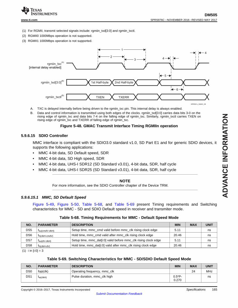
AD
VA
NC
E I
NF
OR
MA
TIO
N
rgmii _txcn(A)
rgmii _txdn [3:0](B)
rgmii _txctln(B)
5
1st Half-byte
TXERRTXEN
2nd Half-byte
4
4
23
1
6
[internal delay enabled]
SPRS91v_GMAC_09
165
DM505www.ti.com SPRS976C –NOVEMBER 2016–REVISED MAY 2017
Submit Documentation FeedbackSpecificationsCopyright © 2016–2017, Texas Instruments Incorporated
(1) For RGMII, transmit selected signals include: rgmiin_txd[3:0] and rgmiin_txctl.(2) RGMII0 1000Mbps operation is not supported.(3) RGMII1 1000Mbps operation is not supported.
A. TXC is delayed internally before being driven to the rgmiin_txc pin. This internal delay is always enabled.B. Data and control information is transmitted using both edges of the clocks. rgmiin_txd[3:0] carries data bits 3-0 on the
rising edge of rgmiin_txc and data bits 7-4 on the falling edge of rgmiin_txc. Similarly, rgmiin_txctl carries TXEN onrising edge of rgmiin_txc and TXERR of falling edge of rgmiin_txc.
Figure 5-48. GMAC Transmit Interface Timing RGMIIn operation
5.9.6.15 SDIO Controller
MMC interface is compliant with the SDIO3.0 standard v1.0, SD Part E1 and for generic SDIO devices, itsupports the following applications:• MMC 4-bit data, SD Default speed, SDR• MMC 4-bit data, SD High speed, SDR• MMC 4-bit data, UHS-I SDR12 (SD Standard v3.01), 4-bit data, SDR, half cycle• MMC 4-bit data, UHS-I SDR25 (SD Standard v3.01), 4-bit data, SDR, half cycle
NOTEFor more information, see the SDIO Controller chapter of the Device TRM.
5.9.6.15.1 MMC, SD Default Speed
Figure 5-49, Figure 5-50, Table 5-68, and Table 5-69 present Timing requirements and Switchingcharacteristics for MMC - SD and SDIO Default speed in receiver and transmiter mode.
Table 5-68. Timing Requirements for MMC - Default Speed Mode
NO. PARAMETER DESCRIPTION MIN MAX UNITDS5 tsu(cmdV-clkH) Setup time, mmc_cmd valid before mmc_clk rising clock edge 5.11 nsDS6 th(clkH-cmdV) Hold time, mmc_cmd valid after mmc_clk rising clock edge 20.46 nsDS7 tsu(dV-clkH) Setup time, mmc_dat[i:0] valid before mmc_clk rising clock edge 5.11 nsDS8 th(clkH-dV) Hold time, mmc_dat[i:0] valid after mmc_clk rising clock edge 20.46 ns
(1) i in [i:0] = 3
Table 5-69. Switching Characteristics for MMC - SD/SDIO Default Speed Mode
NO. PARAMETER DESCRIPTION MIN MAX UNITDS0 fop(clk) Operating frequency, mmc_clk 24 MHzDS1 tw(clkH) Pulse duration, mmc_clk high 0.5*P-
0.270ns

AD
VA
NC
E IN
FO
RM
AT
ION
DS2
DS1
DS0
DS3
DS4
mmc_clk
mmc_cmd
mmc_dat[3:0]
SPRS91v_MMC_02
DS2
DS1
DS0
DS6
DS5
DS8
DS7
mmc_clk
mmc_cmd
mmc_dat[3:0]
SPRS91v_MMC_01
166
DM505SPRS976C –NOVEMBER 2016–REVISED MAY 2017 www.ti.com
Submit Documentation FeedbackSpecifications Copyright © 2016–2017, Texas Instruments Incorporated
Table 5-69. Switching Characteristics for MMC - SD/SDIO Default Speed Mode (continued)NO. PARAMETER DESCRIPTION MIN MAX UNITDS2 tw(clkL) Pulse duration, mmc_clk low 0.5*P-
0.270ns
DS3 td(clkL-cmdV) Delay time, mmc_clk falling clock edge to mmc_cmd transition -14.93 14.93 nsDS4 td(clkL-dV) Delay time, mmc_clk falling clock edge to mmc_dat[i:0] transition -14.93 14.93 ns
(1) P = output mmc_clk period in ns(2) i in [i:0] = 3
Figure 5-49. MMC/SD/SDIOj in - Default Speed - Receiver Mode
Figure 5-50. MMC/SD/SDIOj in - Default Speed - Transmiter Mode
5.9.6.15.2 MMC, SD High Speed
Figure 5-51, Figure 5-52, Table 5-70, and Table 5-71 present Timing requirements and Switchingcharacteristics for MMC - SD and SDIO High speed in receiver and transmiter mode.
Table 5-70. Timing Requirements for MMC - SD/SDIO High Speed Mode
NO. PARAMETER DESCRIPTION MIN MAX UNITHS3 tsu(cmdV-clkH) Setup time, mmc_cmd valid before mmc_clk rising clock edge 5.3 nsHS4 th(clkH-cmdV) Hold time, mmc_cmd valid after mmc_clk rising clock edge 2.6 nsHS7 tsu(dV-clkH) Setup time, mmc_dat[i:0] valid before mmc_clk rising clock edge 5.3 nsHS8 th(clkH-dV) Hold time, mmc_dat[i:0] valid after mmc_clk rising clock edge 2.6 ns

AD
VA
NC
E I
NF
OR
MA
TIO
N
mmc_clk
mmc_cmd
mmc_dat[3:0]
HS1
HS2LHS2H
HS5
HS6
HS5
HS6
SPRS91v_MMC_04
mmc_clk
mmc_cmd
mmc_dat[3:0]
HS1
HS2L HS2H
HS3 HS4
HS7 HS8
SPRS91v_MMC_03
167
DM505www.ti.com SPRS976C –NOVEMBER 2016–REVISED MAY 2017
Submit Documentation FeedbackSpecificationsCopyright © 2016–2017, Texas Instruments Incorporated
(1) i in [i:0] = 3
Table 5-71. Switching Characteristics for MMC - SD/SDIO High Speed Mode
NO. PARAMETER DESCRIPTION MIN MAX UNITHS1 fop(clk) Operating frequency, mmc_clk 48 MHz
HS2H tw(clkH) Pulse duration, mmc_clk high 0.5*P-0.270
ns
HS2L tw(clkL) Pulse duration, mmc_clk low 0.5*P-0.270
ns
HS5 td(clkL-cmdV) Delay time, mmc_clk falling clock edge to mmc_cmd transition -7.6 3.6 nsHS6 td(clkL-dV) Delay time, mmc_clk falling clock edge to mmc_dat[i:0] transition -7.6 3.6 ns
(1) P = output mmc_clk period in ns(2) i in [i:0] = 3
Figure 5-51. MMC/SD/SDIOj in - High Speed - Receiver Mode
Figure 5-52. MMC/SD/SDIOj in - High Speed - Transmiter Mode
5.9.6.15.3 MMC, SD and SDIO SDR12 Mode
Figure 5-53, Figure 5-54, Table 5-72, and Table 5-73 present Timing requirements and Switchingcharacteristics for MMC - SD and SDIO SDR12 in receiver and transmiter mode.
Table 5-72. Timing Requirements for MMC - SDR12 Mode
NO. PARAMETER DESCRIPTION MIN MAX UNITSDR125 tsu(cmdV-clkH) Setup time, mmc_cmd valid before mmc_clk rising clock edge 25.99 nsSDR126 th(clkH-cmdV) Hold time, mmc_cmd valid after mmc_clk rising clock edge 1.6 nsSDR127 tsu(dV-clkH) Setup time, mmc_dat[i:0] valid before mmc_clk rising clock edge 25.99 nsSDR128 th(clkH-dV) Hold time, mmc_dat[i:0] valid after mmc_clk rising clock edge 1.6 ns
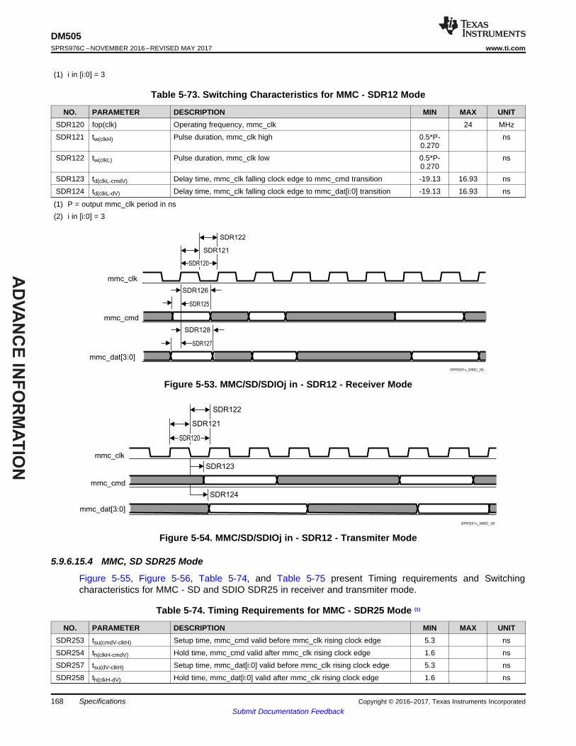
AD
VA
NC
E IN
FO
RM
AT
ION
SDR122
SDR121
SDR120
SDR123
SDR124
mmc_clk
mmc_cmd
mmc_dat[3:0]
SPRS91v_MMC_06
SDR122
SDR121
SDR120
SDR126
SDR125
SDR128
SDR127
mmc_clk
mmc_cmd
mmc_dat[3:0]
SPRS91v_MMC_05
168
DM505SPRS976C –NOVEMBER 2016–REVISED MAY 2017 www.ti.com
Submit Documentation FeedbackSpecifications Copyright © 2016–2017, Texas Instruments Incorporated
(1) i in [i:0] = 3
Table 5-73. Switching Characteristics for MMC - SDR12 Mode
NO. PARAMETER DESCRIPTION MIN MAX UNITSDR120 fop(clk) Operating frequency, mmc_clk 24 MHzSDR121 tw(clkH) Pulse duration, mmc_clk high 0.5*P-
0.270ns
SDR122 tw(clkL) Pulse duration, mmc_clk low 0.5*P-0.270
ns
SDR123 td(clkL-cmdV) Delay time, mmc_clk falling clock edge to mmc_cmd transition -19.13 16.93 nsSDR124 td(clkL-dV) Delay time, mmc_clk falling clock edge to mmc_dat[i:0] transition -19.13 16.93 ns
(1) P = output mmc_clk period in ns(2) i in [i:0] = 3
Figure 5-53. MMC/SD/SDIOj in - SDR12 - Receiver Mode
Figure 5-54. MMC/SD/SDIOj in - SDR12 - Transmiter Mode
5.9.6.15.4 MMC, SD SDR25 Mode
Figure 5-55, Figure 5-56, Table 5-74, and Table 5-75 present Timing requirements and Switchingcharacteristics for MMC - SD and SDIO SDR25 in receiver and transmiter mode.
Table 5-74. Timing Requirements for MMC - SDR25 Mode (1)
NO. PARAMETER DESCRIPTION MIN MAX UNITSDR253 tsu(cmdV-clkH) Setup time, mmc_cmd valid before mmc_clk rising clock edge 5.3 nsSDR254 th(clkH-cmdV) Hold time, mmc_cmd valid after mmc_clk rising clock edge 1.6 nsSDR257 tsu(dV-clkH) Setup time, mmc_dat[i:0] valid before mmc_clk rising clock edge 5.3 nsSDR258 th(clkH-dV) Hold time, mmc_dat[i:0] valid after mmc_clk rising clock edge 1.6 ns
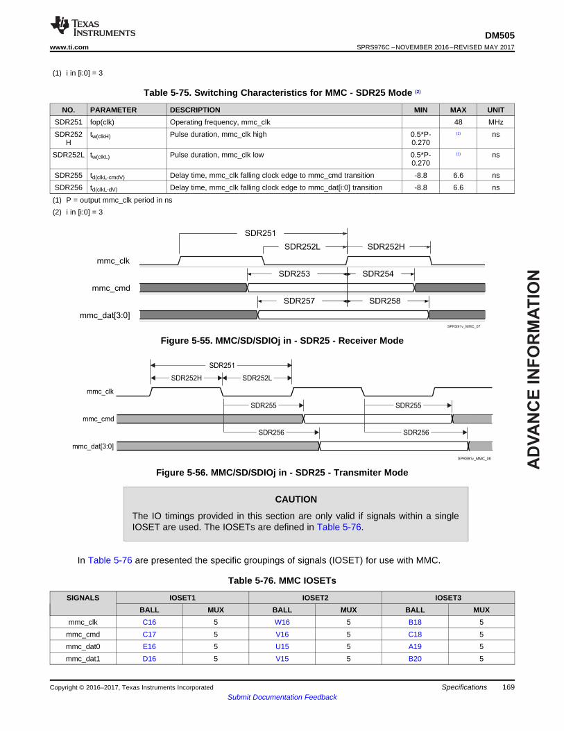
AD
VA
NC
E I
NF
OR
MA
TIO
N
mmc_clk
mmc_cmd
mmc_dat[3:0]
SDR251
SDR252LSDR252H
SDR255
SDR256
SDR255
SDR256
SPRS91v_MMC_08
mmc_clk
mmc_cmd
mmc_dat[3:0]
SDR254
SDR258
SDR253
SDR257
SDR251
SDR252HSDR252L
SPRS91v_MMC_07
169
DM505www.ti.com SPRS976C –NOVEMBER 2016–REVISED MAY 2017
Submit Documentation FeedbackSpecificationsCopyright © 2016–2017, Texas Instruments Incorporated
(1) i in [i:0] = 3
Table 5-75. Switching Characteristics for MMC - SDR25 Mode (2)
NO. PARAMETER DESCRIPTION MIN MAX UNITSDR251 fop(clk) Operating frequency, mmc_clk 48 MHzSDR252
Htw(clkH) Pulse duration, mmc_clk high 0.5*P-
0.270(1) ns
SDR252L tw(clkL) Pulse duration, mmc_clk low 0.5*P-0.270
(1) ns
SDR255 td(clkL-cmdV) Delay time, mmc_clk falling clock edge to mmc_cmd transition -8.8 6.6 nsSDR256 td(clkL-dV) Delay time, mmc_clk falling clock edge to mmc_dat[i:0] transition -8.8 6.6 ns
(1) P = output mmc_clk period in ns(2) i in [i:0] = 3
Figure 5-55. MMC/SD/SDIOj in - SDR25 - Receiver Mode
Figure 5-56. MMC/SD/SDIOj in - SDR25 - Transmiter Mode
CAUTION
The IO timings provided in this section are only valid if signals within a singleIOSET are used. The IOSETs are defined in Table 5-76.
In Table 5-76 are presented the specific groupings of signals (IOSET) for use with MMC.
Table 5-76. MMC IOSETs
SIGNALS IOSET1 IOSET2 IOSET3BALL MUX BALL MUX BALL MUX
mmc_clk C16 5 W16 5 B18 5mmc_cmd C17 5 V16 5 C18 5mmc_dat0 E16 5 U15 5 A19 5mmc_dat1 D16 5 V15 5 B20 5

AD
VA
NC
E IN
FO
RM
AT
ION
170
DM505SPRS976C –NOVEMBER 2016–REVISED MAY 2017 www.ti.com
Submit Documentation FeedbackSpecifications Copyright © 2016–2017, Texas Instruments Incorporated
Table 5-76. MMC IOSETs (continued)SIGNALS IOSET1 IOSET2 IOSET3
BALL MUX BALL MUX BALL MUXmmc_dat2 E17 5 Y15 5 C20 5mmc_dat3 F17 5 W15 5 A20 5
5.9.6.16 GPIO
The general-purpose interface combines four general-purpose input/output (GPIO) banks. Each GPIOmodule provides up to 32 dedicated general-purpose pins with input and output capabilities; thus, thegeneral-purpose interface supports up to 126 pins.
These pins can be configured for the following applications:• Data input (capture)/output (drive)• Keyboard interface with a debounce cell• Interrupt generation in active mode upon the detection of external events. Detected events are
processed by two parallel independent interrupt-generation submodules to support biprocessoroperations
• Wake-up request generation in idle mode upon the detection of external events
NOTEFor more information, see the General-Purpose Interface chapter of the Device TRM.
NOTEThe general-purpose input/output i (i = 1 to 4) bank is also referred to as GPIOi.
CAUTION
The IO timings provided in this section are only valid if signals within a singleIOSET are used. The IOSETs are defined in Table 5-77.
In Table 5-77 are presented the specific groupings of signals (IOSET) for use with GPIO.
Table 5-77. GPIO2/3/4 IOSETs
SIGNALS IOSET1 IOSET2BALL MUX BALL MUX
GPIO2gpio2_11 J17 14gpio2_12 K22 14gpio2_13 K21 14gpio2_14 K18 14gpio2_20 AB17 14gpio2_23 AA17 14 AA17 14gpio2_24 U16 14 U16 14gpio2_27 U15 14gpio2_28 V15 14gpio2_29 Y15 14gpio2_30 W15 14gpio2_31 AA15 14
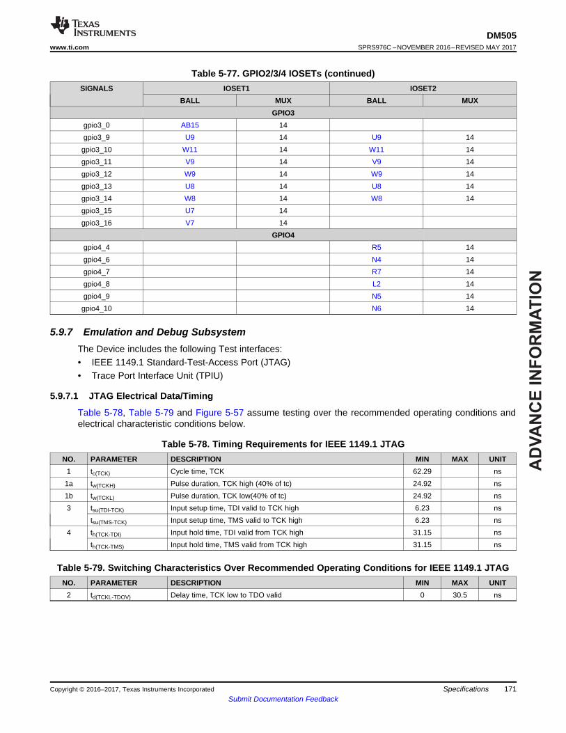
AD
VA
NC
E I
NF
OR
MA
TIO
N
171
DM505www.ti.com SPRS976C –NOVEMBER 2016–REVISED MAY 2017
Submit Documentation FeedbackSpecificationsCopyright © 2016–2017, Texas Instruments Incorporated
Table 5-77. GPIO2/3/4 IOSETs (continued)SIGNALS IOSET1 IOSET2
BALL MUX BALL MUXGPIO3
gpio3_0 AB15 14gpio3_9 U9 14 U9 14gpio3_10 W11 14 W11 14gpio3_11 V9 14 V9 14gpio3_12 W9 14 W9 14gpio3_13 U8 14 U8 14gpio3_14 W8 14 W8 14gpio3_15 U7 14gpio3_16 V7 14
GPIO4gpio4_4 R5 14gpio4_6 N4 14gpio4_7 R7 14gpio4_8 L2 14gpio4_9 N5 14gpio4_10 N6 14
5.9.7 Emulation and Debug SubsystemThe Device includes the following Test interfaces:• IEEE 1149.1 Standard-Test-Access Port (JTAG)• Trace Port Interface Unit (TPIU)
5.9.7.1 JTAG Electrical Data/Timing
Table 5-78, Table 5-79 and Figure 5-57 assume testing over the recommended operating conditions andelectrical characteristic conditions below.
Table 5-78. Timing Requirements for IEEE 1149.1 JTAGNO. PARAMETER DESCRIPTION MIN MAX UNIT
1 tc(TCK) Cycle time, TCK 62.29 ns1a tw(TCKH) Pulse duration, TCK high (40% of tc) 24.92 ns1b tw(TCKL) Pulse duration, TCK low(40% of tc) 24.92 ns3 tsu(TDI-TCK) Input setup time, TDI valid to TCK high 6.23 ns
tsu(TMS-TCK) Input setup time, TMS valid to TCK high 6.23 ns4 th(TCK-TDI) Input hold time, TDI valid from TCK high 31.15 ns
th(TCK-TMS) Input hold time, TMS valid from TCK high 31.15 ns
Table 5-79. Switching Characteristics Over Recommended Operating Conditions for IEEE 1149.1 JTAGNO. PARAMETER DESCRIPTION MIN MAX UNIT
2 td(TCKL-TDOV) Delay time, TCK low to TDO valid 0 30.5 ns

AD
VA
NC
E IN
FO
RM
AT
ION
5
6
87
TCK
RTCK
SPRS91v_JTAG_02
3
TCK
TDO
TDI/TMS
2
4
11a 1b
SPRS91v_JTAG_01
172
DM505SPRS976C –NOVEMBER 2016–REVISED MAY 2017 www.ti.com
Submit Documentation FeedbackSpecifications Copyright © 2016–2017, Texas Instruments Incorporated
Figure 5-57. JTAG Timing
Table 5-80, Table 5-81 and Figure 5-58 assume testing over the recommended operating conditions andelectrical characteristic conditions below.
Table 5-80. Timing Requirements for IEEE 1149.1 JTAG With RTCKNO. PARAMETER DESCRIPTION MIN MAX UNIT
1 tc(TCK) Cycle time, TCK 62.29 ns1a tw(TCKH) Pulse duration, TCK high (40% of tc) 24.92 ns1b tw(TCKL) Pulse duration, TCK low(40% of tc) 24.92 ns3 tsu(TDI-TCK) Input setup time, TDI valid to TCK high 6.23 ns
tsu(TMS-TCK) Input setup time, TMS valid to TCK high 6.23 ns4 th(TCK-TDI) Input hold time, TDI valid from TCK high 31.15 ns
th(TCK-TMS) Input hold time, TMS valid from TCK high 31.15 ns
Table 5-81. Switching Characteristics Over Recommended Operating Conditions forIEEE 1149.1 JTAG With RTCK
NO. PARAMETER DESCRIPTION MIN MAX UNIT5 td(TCK-RTCK) Delay time, TCK to RTCK with no selected subpaths (i.e. ICEPick is
the only tap selected - when the ARM is in the scan chain, the delaytime is a function of the ARM functional clock).
0 27 ns
6 tc(RTCK) Cycle time, RTCK 62.29 ns7 tw(RTCKH) Pulse duration, RTCK high (40% of tc) 24.92 ns8 tw(RTCKL) Pulse duration, RTCK low (40% of tc) 24.92 ns
Figure 5-58. JTAG With RTCK Timing
5.9.7.2 Trace Port Interface Unit (TPIU)
5.9.7.2.1 TPIU PLL DDR Mode
Table 5-82 and Figure 5-59 assume testing over the recommended operating conditions and electricalcharacteristic conditions below.

AD
VA
NC
E I
NF
OR
MA
TIO
N
TRACECLK
TRACECTL
TRACEDATA[X:0]
TPIU4 TPIU4
TPIU2
TPIU1
TPIU3
TPIU5 TPIU5
SPRS91v_TPIU_01
173
DM505www.ti.com SPRS976C –NOVEMBER 2016–REVISED MAY 2017
Submit Documentation FeedbackSpecificationsCopyright © 2016–2017, Texas Instruments Incorporated
Table 5-82. Switching Characteristics for TPIU
NO. PARAMETER DESCRIPTION MIN MAX UNITTPIU1 tc(clk) Cycle time, TRACECLK period 5.56 nsTPIU4 td(clk-ctlV) Skew time, TRACECLK transition to TRACECTL transition -1.61 1.98 nsTPIU5 td(clk-dataV) Skew time, TRACECLK transition to TRACEDATA[17:0] transition -1.61 1.98 ns
(1) P = TRACECLK period in ns(2) The listed pulse duration is a typical value
Figure 5-59. TPIU—PLL DDR Transmit Mode(1)
(1) In d[X:0], X is equal to 15 or 17.
AD
VA
NC
E IN
FO
RM
AT
ION
174
DM505SPRS976C –NOVEMBER 2016–REVISED MAY 2017 www.ti.com
Submit Documentation FeedbackDetailed Description Copyright © 2016–2017, Texas Instruments Incorporated
6 Detailed Description
6.1 DescriptionThe DM505 is a highly optimized device for Vision Analytics and Machine Vision processing in Industrialproducts such as drones, robots, forklifts, railroad and agriculture equipment. The Processor enablessophisticated embedded vision processing integrating an optimal mix of real time performance, low power,small form factor and camera processing for systems to interact in more intelligent, useful ways with thephysical world and the people in it.
The DM505 incorporates a heterogeneous, scalable architecture that includes a mix of TI’s fixed andfloating-point TMS320C66x digital signal processor (DSP) generation cores, Vision AccelerationPac(EVE), and dual-Cortex-M4 processors. The device allows low power designs to meet demandingembedded system budgets without sacrificing real-time processing performance to enable small formfactor designs. The DM505 also integrates a host of peripherals including interfaces for multi-camera input(both parallel and serial), display outputs, audio and serial I/O, CAN and GigB Ethernet AVB.
TI provides application specific hardware and software through our Design Network Partners and acomplete set of development tools for the ARM, and DSP, including C compilers with TI RTOS toaccelerate time to market.
6.2 Functional Block DiagramFigure 6-1 is functional block diagram for the device.

AD
VA
NC
E I
NF
OR
MA
TIO
N
SPRS916_Intro_001
JTAG
PLLs
OSC
Clock Comparator (7xDCC)
Error Handler (ESM)
TESOC (LBIST/PBIST)
1x CRC
5x RTI
Memory Controllers
GPMC 8b/16bwith up to 16b ECC
LPDDR2 / DDR2/DDR3 / DDR3L
32b with 8b ECC
Timer x8
Mailbox/Spinlock
10-bit ADC
Control Module
Safety
EDMA
GPIO x4
PWMSSx1
MMUx1
PRCM
System
I2C x2
SPI x4
QSPI x1
SDIO x1
DCAN with ECC
UART x3
McASP x3
Serial Interfaces
GMAC
Connectivity
EDMA 2TC
L2256KBCache
C66x
L1D 32KB
L1P 32KB
DSP Subsystem x2
Video Input Port
CALLVDSRX
CSI2
ISP
Video Front End
up to 512KB RAMwith ECC
IPU with ECC
Dual Cortex M432KB ROM
EVE 16MAC
EDMA 2TC
VisionAccelerator
OSDResizing
CSC
SD-DAC
DVOUT
DisplaySubsystem
Interconnect
DM505
Copyright © 2016, Texas Instruments Incorporated
MCAN(CAN-FD)with ECC
175
DM505www.ti.com SPRS976C –NOVEMBER 2016–REVISED MAY 2017
Submit Documentation FeedbackDetailed DescriptionCopyright © 2016–2017, Texas Instruments Incorporated
Figure 6-1. DM505 Block Diagram
6.3 DSP SubsystemThe device includes two identical instances (DSP1 and DSP2) of a digital signal processor (DSP)subsystem, based on the TI's standard TMS320C66x™ DSP CorePac core.
The TMS320C66x DSP core enhances the TMS320C674x™ core, which merges the C674x™ floatingpoint and the C64x+™ fixed-point instruction set architectures. The C66x DSP is object-code compatiblewith the C64x+/C674x DSPs.
For more information on the TMS320C66x core CPU, see the TMS320C66x DSP CPU and Instruction SetReference Guide, (SPRUGH7).
Each of the two DSP subsystems integrated in the device includes the following components:

AD
VA
NC
E IN
FO
RM
AT
ION
176
DM505SPRS976C –NOVEMBER 2016–REVISED MAY 2017 www.ti.com
Submit Documentation FeedbackDetailed Description Copyright © 2016–2017, Texas Instruments Incorporated
• A TMS320C66x™ CorePac DSP core that encompasses:– L1 program-dedicated (L1P) cacheable memory– L1 data-dedicated (L1D) cacheable memory– L2 (program and data) cacheable memory– Extended Memory Controller (XMC)– External Memory Controller (EMC)– DSP CorePac located interrupt controller (INTC)– DSP CorePac located power-down controller (PDC)
• Dedicated enhanced data memory access engine - EDMA, to transfer data from/to memories andperipherals external to the DSP subsystem and to local DSP memory (most commonly L2 SRAM). Theexternal DMA requests are passed through DSP system level (SYS) wakeup logic, and collected fromthe DSP1/DSP2 dedicated outputs of the device DMA Events Crossbar for each of the twosubsystems.
• A level 2 (L2) interconnect network (DSP NoC) to allow connectivity between different modules of thesubsystem or the remainder of the device via the device L3_MAIN interconnect.
• Two memory management units (on EDMA L2 interconnect and DSP MDMA paths) for accessing thedevice L3_MAIN interconnect address space.
• Dedicated system control logic (DSP_SYSTEM) responsible for power management, clock generation,and connection to the device power, reset, and clock management (PRCM) module
The TMS320C66x Instruction Set Architecture (ISA) is the latest for the C6000 family. As with itspredecessors (C64x, C64x+ and C674x), the C66x is an advanced VLIW architecture with 8 functionalunits (two multiplier units and six arithmetic logic units) that operate in parallel. The C66x CPU has a totalof 64 general-purpose 32-bit registers.
Some features of the DSP C6000 family devices are:• Advanced VLIW CPU with eight functional units (two multipliers and six ALUs) which:
– Executes up to eight instructions per cycle for up to ten times the performance of typical DSPs– Allows designers to develop highly effective RISC-like code for fast development time
• Instruction packing:– Gives code size equivalence for eight instructions executed serially or in parallel– Reduces code size, program fetches, and power consumption
• Conditional execution of most instructions:– Reduces costly branching– Increases parallelism for higher sustained performance
• Efficient code execution on independent functional units:– Industry's most efficient C compiler on DSP benchmark suite– Industry's first assembly optimizer for fast development and improved parallelization
• 8-/16-/32-bit/64-bit data support, providing efficient memory support for a variety of applications.• 40-bit arithmetic options which add extra precision for vocoders and other computationally intensive
applications.• Saturation and normalization to provide support for key arithmetic operations.• Field manipulation and instruction extract, set, clear, and bit counting support common operation found
in control and data manipulation applications.
The C66x CPU has the following additional features:• Each multiplier can perform two 16 × 16-bit or four 8 × 8 bit multiplies every clock cycle.• Quad 8-bit and dual 16-bit instruction set extensions with data flow support.• Support for non-aligned 32-bit (word) and 64-bit (double word) memory accesses.• Special communication-specific instructions have been added to address common operations in error-
correcting codes.

AD
VA
NC
E I
NF
OR
MA
TIO
N
177
DM505www.ti.com SPRS976C –NOVEMBER 2016–REVISED MAY 2017
Submit Documentation FeedbackDetailed DescriptionCopyright © 2016–2017, Texas Instruments Incorporated
• Bit count and rotate hardware extends support for bit-level algorithms.• Compact instructions: Common instructions (AND, ADD, LD, MPY) have 16-bit versions to reduce
code size.• Protected mode operation: A two-level system of privileged program execution to support higher-
capability operating systems and system features such as memory protection.• Exceptions support for error detection and program redirection to provide robust code execution• Hardware support for modulo loop operation to reduce code size and allow interrupts during fully-
pipelined code• Each multiplier can perform 32 × 32 bit multiplies• Additional instructions to support complex multiplies allowing up to eight 16-bit multiply/add/subtracts
per clock cycle
The TMS320C66x has the following key improvements to the ISA:• 4x Multiply Accumulate improvement for both fixed and floating point• Improvement of the floating point arithmetic• Enhancement of the vector processing capability for fixed and floating point• Addition of domain-specific instructions for complex arithmetic and matrix operations
On the C66x ISA, the vector processing capability is improved by extending the width of the SIMDinstructions. The C674x DSP supports 2-way SIMD operations for 16-bit data and 4-way SIMDoperations for 8-bit data. C66x enhances this capabilities with the addition of SIMD instructions for 32-bitdata allowing operation on 128-bit vectors. For example the QMPY32 instruction is able to perform theelement to element multiplication between two vectors of four 32-bit data each.
C66x ISA includes a set of specific instructions to handle complex arithmetic and matrix operations.

AD
VA
NC
E IN
FO
RM
AT
ION
178
DM505SPRS976C –NOVEMBER 2016–REVISED MAY 2017 www.ti.com
Submit Documentation FeedbackDetailed Description Copyright © 2016–2017, Texas Instruments Incorporated
• TMS320C66x DSP CorePac memory components:– A 32-KiB L1 program memory (L1P) configurable as cache and/or SRAM:
• When configured as a cache, the L1P is a 1-way set-associative cache with a 32-byte cacheline
• The DSP CorePac L1P memory controller provides bandwidth management, memoryprotection, and power-down functions
• The L1P is capable of cache block and global coherence operations• The L1P controller has an Error Detection (ED) mechanism, including necessary SRAM• The L1P memory can be fully configured as a cache or SRAM• Page size for L1P memory is 2KB
– A 32-KiB L1 data memory (L1D) configurable as cache and / or SRAM:• When configured as a cache, the L1D is a 2-way set-associative cache with a 64-byte cache
line• The DSP CorePac L1D memory controller provides bandwidth management, memory
protection, and power-down functions• The L1D memory can be fully configured as a cache or SRAM• No support for error correction or detection• Page size for L1D memory is 2KB
– A 288-KiB (program and data) L2 memory, only part of which is cacheable:• When configured as a cache, the L2 memory is a 4-way set associative cache with a 128-byte
cache line• Only 256 KiB of L2 memory can be configured as cache or SRAM• 32 KiB of the L2 memory is always mapped as SRAM• The L2 memory controller has an Error Correction Code (ECC) and ED mechanism, including
necessary SRAM• The L2 memory controller supports hardware prefetching and also provides bandwidth
management, memory protection, and power-down functions.• Page size for L2 memory is 16KB
• The External Memory Controller (EMC) is a bridge from the C66x CorePac to the rest of the DSPsubsystem and device. It has :– a 32-bit configuration port (CFG) providing access to local subsystem resources (like DSP_EDMA,
DSP_SYSTEM, and so forth) or to L3_MAIN resources accessible via the CFG address range.– a 128-bit slave-DMA port (SDMA) which provides accesses of system masters outside the DSP
subsystem to resources inside the DSP subsystem or C66x DSP CorePac memories, i.e. when theDSP subsystem is the slave in a transaction.
• The Extended Memory Controller (XMC) processes requests from the L2 Cache Controller (whichare a result of CPU instruction fetches, load/store commands, cache operations) to device resourcesvia the C66x DSP CorePac 128-bit master DMA (MDMA) port:– Memory protection for addresses outside C66x DSP CorePac generated over device L3_MAIN on
the MDMA port– Prefetch, multi-in-flight requests
• A DSP local Interrupt Controller (INTC) in the DSP C66x CorePac, interfaces the system events tothe DSP C66x core CPU interrupt and exceptions inputs. The DSP subsystem C66x CorePac interruptcontroller supports up to 128 system events of which 64 interrupts are external to DSP subsystems,collected from the DSP1/DSP2 dedicated outputs of the device Interrupt Crossbar.

AD
VA
NC
E I
NF
OR
MA
TIO
N
179
DM505www.ti.com SPRS976C –NOVEMBER 2016–REVISED MAY 2017
Submit Documentation FeedbackDetailed DescriptionCopyright © 2016–2017, Texas Instruments Incorporated
• Local Enhanced Direct Memory Access (EDMA) controller features:– Channel controller (CC) : 64-channel, 128 PaRAM, 2 Queues– 2 x Third-party Transfer Controllers (TPTC0 and TPTC1):
• Each TC has a 128-bit read port and a 128-bit write port• 2KiB FIFOs on each TPTC
– 1-dimensional/2-dimensional (1D/2D) addressing– Chaining capability
• DSP subsystem integrated MMUs:– Two MMUs are integrated:
• The MMU0 is located between DSP MDMA master port and the device L3_MAIN interconnectand can be optionally bypassed
• The MMU1 is located between the EDMA master port and the device L3_MAIN interconnect• A DSP local Power-Down Controller (PDC) is responsible to power-down various parts of the DSP
C66x CorePac, or the entire DSP C66x CorePac.• The DSP subsystem System Control logic provides:
– Slave idle and master standby protocols with device PRCM for powerdown– OCP Disconnect handshake for init and target busses– Asynchronous reset– Power-down modes:
• "Clockstop" mode featuring wake-up on interrupt event. The DMA event wake-up is managed insoftware.
• The device DSP subsystem is supplied by a PRCM DPLL, but each DSP1/2 has integrated its ownPLL module outside the C66x CorePac for clock gating and division.
• Each of the two device DSP subsystem has following port instances to connect to remaining partof the device. See also :– A 128-bit initiator (DSP MDMA master) port for MDMA/Cache requests– A 128-bit initiator (DSP EDMA master) port for EDMA requests– A 32-bit initiator (DSP CFG master) port for configuration requests– A 128-bit target (DSP slave) port for requests to DSP memories and various peripherals
• C66x DSP subsystems (DSPSS) safety aspects:– Above mentioned memory ECC/ED mechanisms– MMUs enable mapping of only the necessary application space to the processor– Memory Protection Units internal to the DSPSS (in L1P, L1D and L2 memory controllers) and
external to DSPSS (firewalls) to help define legal accesses and raise exceptions on illegalaccesses
– Exceptions: Memory errors, various DSP errors, MMU errors and some system errors are detectedand cause exceptions. The exceptions could be handled by the DSP or by a designated safetyprocessor at the chip level. Note that it may not be possible for the safety processor to completelyhandle some exceptions
Unsupported features on the C66x DSP core for the device are:• The Extended Memory Controller MPAX (memory protection and address extension) 36-bit addressing
is NOT supported
Known DSP subsystem power mode restrictions for the device are:• "Full logic / RAM retention" mode featuring wake-up on both interrupt or DMA event (logic in “always
on” domain). Only OFF mode is supported by DSP subsystem, requiring full boot.

AD
VA
NC
E IN
FO
RM
AT
ION
180
DM505SPRS976C –NOVEMBER 2016–REVISED MAY 2017 www.ti.com
Submit Documentation FeedbackDetailed Description Copyright © 2016–2017, Texas Instruments Incorporated
For more information about C66x debug/trace support, see chapter On-Chip Debug Support of the deviceTRM.
6.4 IPUThe Imaging Processor Unit (IPU) subsystem contains two ARM® Cortex-M4 cores (IPU_C0 and IPU_C1)that share a common level 1 (L1) cache (called unicache). The two Cortex-M4 cores are completelyhomogeneous to one another. Any task possible using one Cortex-M4 core is also possible using theother Cortex-M4 core. Both Cortex-M4 cores could be used for tasks such as running RTOS, controllingISP, SIMCOP, DSS, and other functions. It is software responsibility to distribute the various tasksbetween the Cortex-M4 cores for optimal performance. The integrated interrupt handling of the IPUsubsystem allows it to function as an efficient control unit.
IPU is the boot master of this device with its own boot ROM.
The key features of the IPU subsystem are:• Two ARM Cortex-M4 microprocessors (IPU_C0 and IPU_C1):
– ARMv7-M and Thumb®-2 instruction set architecture (ISA)– ARMv6 SIMD and digital signal processor (DSP) extensions– Single-cycle MAC– Integrated nested vector interrupt controller (NVIC) (also called IPU_Cx_INTC, where x = 0, 1)– Integrated bus matrix:
• Bus arbiter• Bit-banding – atomic bit manipulation• Write buffer• Memory interface (I and D) plus system interface (S) and private peripheral bus (PPB)
– Registers:• Thirteen general-purpose 32-bit registers• Link register (LR)• Program counter (PC)• Program status register, xPSR• Two banked SP registers
– Integrated power management– Extensive debug capabilities
• Unicache interface:– AHBLite to unicache interface– Instruction and data interface– Supports interleaved Cortex-M4 requests
• L1 cache (IPU_UNICACHE):– 32KiB divided into 16 banks– 4-way– Runs at twice the Cortex-M4 CPU frequency– Cache configuration lock/freeze/preload– Internal MMU:
• 16-entry region-based address translation• Read/write control and access type control• Runs at twice the Cortex-M4 CPU frequency• Execute Never (XN) MMU protection policy• Little-endian format
– OCP port for configuration and cache maintenance• Subsystem counter timer module (SCTM) connected to unicache

AD
VA
NC
E I
NF
OR
MA
TIO
N
181
DM505www.ti.com SPRS976C –NOVEMBER 2016–REVISED MAY 2017
Submit Documentation FeedbackDetailed DescriptionCopyright © 2016–2017, Texas Instruments Incorporated
• L2 master interface (MIF):– Splitter for access to memory or OCP ports– Interleaved bank request for fast memory access
• L2 internal memories:– 16KiB ROM – IPU_ROM; used for device boot/initialization– 64KiB banked RAM – IPU_RAM
• L2 MMU (IPU_MMU): 32 entries with Table Walking Logic (TWL)• Wake-up generator (IPU_WUGEN): Generates wake-up request from external interrupts• Two OCP ports at IPU boundary (connected to the L3_MAIN interconnect):
– Master port – allows the IPU to access system resources (memories and peripherals)– Slave port – allows other requestors to access a part of the IPU internal memory space
• Power management:– Local power-management control: Configurable through the IPU_WUGEN registers.– Two sleep modes supported by Cortex-M4, controlled by its integrated interrupt controller (NVIC).– Cortex-M4 system is clock-gated in both sleep modes.– NVIC interrupt interface stays awake.– Supports L1 cache and L2 memories retention.
• Error-Correcting Code (ECC) supported for both L1 unicache and L2 RAM• Debug/emulation features supported
For more information, see chapter Dual Cortex-M4 IPU Subsystem of the device TRM.
6.5 EVEThe embedded vision engine (EVE) module is a programmable imaging and vision processing engine,intended for use in devices that serve customer electronics imaging and vision applications. Itsprogrammability meets late-in-development or post-silicon processing requirements, and lets third partiesor customers add differentiating features in imaging and vision products.
The device includes one instantiation of the EVE engine. A single EVE module consists of an ARP32scalar core, a vector coprocessor (VCOP) vector core, and an Enhanced DMA (EDMA3) controller.
The EVE engine includes the following main features:• Two 128-bit interconnect initiator ports used for:
– Paging between system-level memory (L3 SRAM/DDR) and EVE memory (primarily IBUF, WBUF)– ARP32 program fetches to system memory (through program cache)– ARP32 load or store requests to system memory– ARP32 program cache-related read requests, including prefetch/preload requests
• 128-bit interconnect target port used for system-level host or DMA access to EVE memory or MMRspace
• Scalar core (ARP32) with the following features:– 32KB program cache (direct mapped and prefetch)– 32KB data memory (DMEM)
• Vector core (VCOP):– 32KB working buffer (WBUF)– 16KB image buffer low copy A (IBUFLA)– 16KB image buffer low copy B (IBUFLB)– 16KB image buffer high copy A (IBUFHA)– 16KB image buffer high copy B (IBUFHB)
• EDMA channel controller (EDMACC): 128 PaRAM entries, 2 Queues• EDMA transfer controllers: two instances, 2k FIFO each

AD
VA
NC
E IN
FO
RM
AT
ION
182
DM505SPRS976C –NOVEMBER 2016–REVISED MAY 2017 www.ti.com
Submit Documentation FeedbackDetailed Description Copyright © 2016–2017, Texas Instruments Incorporated
• Memory Management Units (MMUs):– 32-entry TLB per MMU– Page walking with hardware– EDMA accesses and ARP32 program or data accesses to system memory space– Can limit EVE accesses to desired subset of system addresses
• Configuration interconnect for MMR and debug accesses• High-performance interconnect for high throughput and high concurrency data transfers between
connected endpoints• Multiple interrupts for interrupt mapping, DMA event mapping, and interprocessor handshaking• Support for slave idle and master standby protocols for clock gating• No support for retention and memory array off modes• Error detection on all memories:
– Single bit error detect on DMEM, WBUF, IBUFLA, IBUFLB, IBUFHA, and IBUFHB– Double bit error detect on program cache
• Invalid instruction detection in the two processor units (ARP32 and VCOP)• Debug support:
– Subsystem Counter Timer Module (SCTM) for counting and measuring of VCOP, EVE programcache, and EDMA performance-related state
– Software Messaging System Event Trace (SMSET) for trace of software messages and hardwareevents
– ARP32 debug support: State visibility, breakpoint, run control, cross-triggering– VCOP debug support: State visibility and run control
• Interprocessor communication: Internal Mailbox for DSP/EVE communication
For more information, see chapter Embedded Vision Engine of the device TRM.

AD
VA
NC
E I
NF
OR
MA
TIO
N
183
DM505www.ti.com SPRS976C –NOVEMBER 2016–REVISED MAY 2017
Submit Documentation FeedbackDetailed DescriptionCopyright © 2016–2017, Texas Instruments Incorporated
6.6 Memory Subsystem
6.6.1 EMIFThe EMIF module provides connectivity between DDR memory types and manages data bus read/writeaccesses between external memory and device subsystems which have master access to the L3_MAINinterconnect and DMA capability.
The EMIF module has the following capabilities:• Supports JEDEC standard-compliant LPDDR2/DDR2-SDRAM and DDR3/DDR3L-SDRAM memory
types• 2-GiB SDRAM address range over one chip-select• Supports SDRAM devices with one, two, four or eight internal banks• Supports SDRAM devices with single die (one chip select supported)• Supports SDRAM devices with single or dual die packages• Data bus widths:
– 128-bit L3_MAIN (system) interconnect data bus width– 32-bit SDRAM data bus width– 16-bit SDRAM data bus width used in narrow mode
• Supported CAS latencies:– DDR3: 5, 6, 7, 8, 9, 10 and 11– DDR2: 2, 3, 4, 5, 6 and 7– LPDDR2: 3, 4, 5, 6, 7, and 8
• Supports 256-, 512-, 1024-, and 2048-word page sizes• Supported burst length: 8• Supports sequential burst type• SDRAM auto initialization from reset or configuration change• Supports self refresh and power-down modes for low power• Partial array self-refresh mode for low power when DDR3 is used• Output impedance (ZQ) calibration for DDR3• Supports on-die termination (ODT) for DDR2 and DDR3• Supports prioritized refresh• Programmable SDRAM refresh rate and backlog counter• Programmable SDRAM timing parameters• Write and read leveling/calibration and data eye training for DDR3• ECC on the SDRAM data bus:
– 7-bit ECC over 32-bit data– 6-bit ECC over 16-bit data when narrow mode is used– 1-bit error correction and 2-bit error detection– Programmable address ranges to define ECC protected region– ECC calculated and stored on all writes to ECC protected address region– ECC verified on all reads from ECC protected address region– Statistics for 1-bit ECC and 2-bit ECC errors– The total width of the ECC DDR data bus is 8 bits
The EMIF module does not support:• Burst chop for DDR3• Interleave burst type• Auto precharge because of better Bank Interleaving performance

AD
VA
NC
E IN
FO
RM
AT
ION
184
DM505SPRS976C –NOVEMBER 2016–REVISED MAY 2017 www.ti.com
Submit Documentation FeedbackDetailed Description Copyright © 2016–2017, Texas Instruments Incorporated
• OCD calibration for DDR2• CAS Read Latency of 2 and CAS Write Latency of 1 for DDR2• DLL disabling from EMIF side
For more information, see section DDR External Memory Interface (EMIF) in chapter Memory Subsystemof the device TRM.
6.6.2 GPMCThe General Purpose Memory Controller (GPMC) is an external memory controller of the device. Its dataaccess engine provides a flexible programming model for communication with all standard memories.
The GPMC supports the following various access types:• Asynchronous read/write access• Asynchronous read page access (4, 8, and 16 Word16)• Synchronous read/write access• Synchronous read/write burst access without wrap capability (4, 8 and 16 Word16)• Synchronous read/write burst access with wrap capability (4, 8 and 16 Word16)• Address-data-multiplexed (AD) access• Address-address-data (AAD) multiplexed access• Little- and big-endian access
The GPMC can communicate with a wide range of external devices:• External asynchronous or synchronous 8-bit wide memory or device (non burst device)• External asynchronous or synchronous 16-bit wide memory or device• External 16-bit non-multiplexed NOR flash device• External 16-bit address and data multiplexed NOR Flash device• External 8-bit and 16-bit NAND flash device• External 16-bit pseudo-SRAM (pSRAM) device
The main features of the GPMC are:• 8- or 16-bit-wide data path to external memory device• Supports up to eight CS regions of programmable size and programmable base addresses in a total
address space of 1 GiB• Supports transactions controlled by a firewall• On-the-fly error code detection using the Bose-ChaudhurI-Hocquenghem (BCH) (t = 4, 8, or 16) or
Hamming code to improve the reliability of NAND with a minimum effect on software (NAND flash with512-byte page size or greater)
• Fully pipelined operation for optimal memory bandwidth use• The clock to the external memory is provided from GPMC functional clock divided by 1, 2, 3, or 4• Supports programmable autoclock gating when no access is detected• Independent and programmable control signal timing parameters for setup and hold time on a per-chip
basis. Parameters are set according to the memory device timing parameters, with a timing granularityof one GPMC functional clock cycle.
• Flexible internal access time control (WAIT state) and flexible handshake mode using external WAITpin monitoring
• Support bus keeping• Support bus turnaround• Prefetch and write posting engine associated with a device DMA to achieve full performance from the
NAND device with minimum effect on NOR/SRAM concurrent access
AD
VA
NC
E I
NF
OR
MA
TIO
N
185
DM505www.ti.com SPRS976C –NOVEMBER 2016–REVISED MAY 2017
Submit Documentation FeedbackDetailed DescriptionCopyright © 2016–2017, Texas Instruments Incorporated
For more information, see section General-Purpose Memory Controller (GPMC) in chapter MemorySubsystem of the device TRM.
6.6.3 ELMWhen reading from NAND flash memories, some level of error-correction is required. In the case of NANDmodules with no internal correction capability, sometimes referred to as bare NANDs, the correctionprocess is delegated to the memory controller.
The ELM supports the following features:• 4, 8, and 16 bits per 512-byte block error location based on BCH algorithm• Eight simultaneous processing contexts• Page-based and continuous modes• Interrupt generation when error location process completes:
– When the full page has been processed in page mode– For each syndrome polynomial (checksum-like information) in continuous mode
For more information, see section Error Location Module in chapter Memory Subsystem of the deviceTRM.
6.6.4 OCMCThere is one on-chip memory controller (OCMC) in the device.
The OCM Controller supports the following features:• L3_MAIN data interface:
– Used for maximum throughput performance– 128-bit data bus width– Burst supported
• L4 interface:– Used for access to configuration registers– 32-bit data bus width– Only single accesses supported– The L4 associated OCMC clock is two times lower than the L3 associated OCMC clock
• Error correction and detection:– Single error correction and dual error detection– 9-bit Hamming error correction code (ECC) calculated on 128-bit data word which is concatenated
with memory address bits– Hamming distance of 4– Enable/Disable mode control through a dedicated register– Single bit error correction on a read transaction– Exclusion of repeated addresses from correctable error address trace history– ECC valid for all write transactions to an enabled region– Sub-128-bit writes supported via read modify write
• ECC Error Status Reporting:– Trace history buffer (FIFO) with depth of 4 for corrected error address– Trace history buffer with depth of 4 for non correctable error address and also including double
error detection– Interrupt generation for correctable and uncorrectable detected errors
AD
VA
NC
E IN
FO
RM
AT
ION
186
DM505SPRS976C –NOVEMBER 2016–REVISED MAY 2017 www.ti.com
Submit Documentation FeedbackDetailed Description Copyright © 2016–2017, Texas Instruments Incorporated
• ECC Diagnostics Configuration:– Counters for single error correction (SEC), double error detection (DED) and address error events
(AEE)– Programmable threshold registers for exeptions associated with SEC, DED and AEE counters– Register control for enabling and disabling of diagnostics– Configuration registers and ECC status accessible through L4 interconnect
• Circular buffer for sliced based VIP frame transfers:– Up to 12 programmable circular buffers mapped with unique virtual frame addresses– On the fly (with no additional latency) address translation from virtual to OCMC circular buffer
memory space– Virtual frame size up to 8 MiB and circular buffer size up to 1 MiB– Error handling and reporting of illegal CBUF addressing– Underflow and Overflow status reporting and error handling– Last access read/write address history
• Two Interrupt outputs configured independently to service either ECC or CBUF interrupt events
The OCM controller does not have a memory protection logic and does not support endianism conversion.
For more information, see section On-Chip Memory (OCM) Subsystem in chapter Memory Subsystem ofthe device TRM.
6.7 Interprocessor Communication
6.7.1 MailboxCommunication between the on-chip processors of the device uses a queued mailbox-interruptmechanism.
The queued mailbox-interrupt mechanism allows the software to establish a communication channelbetween two processors through a set of registers and associated interrupt signals by sending andreceiving messages (mailboxes).
The device implements the following mailbox types:• System mailbox:
– Number of instances: 2– Used for communication between: DSP1, DSP2, IPU subsystems– Reference name: MAILBOX1, MAILBOX2
Each mailbox module supports the following features:• Parameters configurable at design time
– Number of users– Number of mailbox message queues– Number of messages (FIFO depth) for each message queue
• 32-bit message width• Message reception and queue-not-full notification using interrupts• Support of 16-/32-bit addressing scheme• Power management support
For more information, see chapter Mailbox of the device TRM.
6.7.2 SpinlockThe Spinlock module provides hardware assistance for synchronizing the processes running on multipleprocessors in the device:• Digital signal processor (DSP) subsystems – DSP1 and DSP2

AD
VA
NC
E I
NF
OR
MA
TIO
N
187
DM505www.ti.com SPRS976C –NOVEMBER 2016–REVISED MAY 2017
Submit Documentation FeedbackDetailed DescriptionCopyright © 2016–2017, Texas Instruments Incorporated
• Dual Cortex-M4 image processing unit (IPU) subsystems – IPU1 and IPU2The Spinlock module implements 256 spinlocks (or hardware semaphores), which provide an efficientway to perform a lock operation of a device resource using a single read-access, avoiding the need ofa readmodify- write bus transfer that the programmable cores are not capable of.
For more information, see chapter Spinlock of the device TRM.
6.8 Interrupt ControllerThe device has a large number of interrupts to service the needs of its many peripherals and subsystems.The DSP (x2), and IPU, and EVE subsystems are capable of servicing these interrupts via their integratedinterrupt controllers. In addition, each processor's interrupt controller is preceded by an Interrupt ControllerCrossbar (IRQ_CROSSBAR) that provides flexibility in mapping the device interrupts to processorinterrupt inputs. For more information about IRQ crossbar, see chapter Control Module of the DeviceTRM.
C66x DSP Subsystem Interrupt Controller (DSPx_INTC, where x = 1, 2)
There are two Digital Signal Processing (DSP) subsystems in the device - DSP1, and DSP2. Each DSPsubsystem integrates an interrupt controller - DSPx_INTC, which interfaces the system events to the C66xcore interrupt and exceptions inputs. It combines up to 128 interrupts into 12 prioritized interruptspresented to the C66x CPU.
For detailed information about this module, see chapter DSP Subsystems of the Device TRM.
Dual Cortex-M4 IPU Subsystem Interrupt Controller (IPU_Cx_INTC, where x = 1, 2)
There is one Image Processing Unit (IPU) subsystem in the device. The IPU subsystem integrates twoARM® Cortex-M4 cores.
A Nested Vectored Interrupt Controller (NVIC) is integrated within each Cortex-M4. The interrupt mappingis the same for the two cores to facilitate parallel processing. The NVIC supports:• 96 external interrupts (in addition to 16 Cortex-M4 internal interrupts), which are dynamically prioritized
with 16 levels of priority defined for each core• Low-latency exception and interrupt handling• Prioritization and handling of exceptions• Control of the local power management• Debug accesses to the processor core
For detailed information about this module, refer to ARM Cortex-M4 Technical Reference Manual(available at infocenter.arm.com/help/index.jsp).
EVE Subsystem Interrupt Controller (EVE_INTC)
There is one Embedded Video Engine (EVE) subsystems in the device. The EVE subsystem integrates aninterrupt controller - EVE_INTC, which handles incoming interrupts, merging them with internal interruptsources to drive ARP32's interrupt inputs. It also allows ARP32 to generate outgoing interrupts or eventsto synchronize with other system processors and EDMA.
The EVE_INTC supports up to 32 active-high level interrupt inputs. Its architecture allows both hardwareand software prioritization.
For detailed information about this module, see chapter Embedded Vision Engine of the Device TRM.
6.9 EDMAThe enhanced direct memory access module, also called EDMA, performs high-performance datatransfers between two slave points, memories and peripheral devices without microprocessor unit (MPU)or digital signal processor (DSP) support during transfer. EDMA transfer is programmed through a logicalEDMA channel, which allows the transfer to be optimally tailored to the requirements of the application.

AD
VA
NC
E IN
FO
RM
AT
ION
188
DM505SPRS976C –NOVEMBER 2016–REVISED MAY 2017 www.ti.com
Submit Documentation FeedbackDetailed Description Copyright © 2016–2017, Texas Instruments Incorporated
The EDMA can also perform transfers between external memories and between device subsystemsinternal memories, with some performance loss caused by resource sharing between the read and writeports.
EDMA controller is based on two major principal blocks:• EDMA third-party channel controller (EDMA_TPCC)• EDMA third-party transfer controller (EDMA_TPTC)
The EDMA_TPCC channel controller has following features:• Fully orthogonal transfer description:
– Three transfer dimensions.– A-synchronized transfers: one-dimension serviced per event.– AB-synchronized transfers: two-dimensions serviced per event.– Independent indexes on source and destination.– Chaining feature allows a 3-D transfer based on a single event.
• Flexible transfer definition:– Increment or FIFO transfer addressing modes.– Linking mechanism allows automatic PaRAM set update.– Chaining allows multiple transfers to execute with one event.
• Interrupt generation for the following:– Transfer completion.– Error conditions.
• Debug visibility:– Queue water marking/threshold.– Error and status recording to facilitate debug.
• 64 DMA request channels:– Event synchronization.– Chain synchronization (completion of one transfer triggers another transfer).
• Eight QDMA channels:– QDMA channels trigger automatically upon writing to a parameter RAM (PaRAM) set entry.– Support for programmable QDMA channel to PaRAM mapping.
• 512 PaRAM sets:– Each PaRAM set can be used for a DMA channel, QDMA channel, or link set.
• Two transfer controllers/event queues.• 16 event entries per event queue.• Memory protection support:
– Proxy memory protection for TR submission.– Active memory protection for accesses to PaRAM and registers.The EDMA_TPTC transfer controller has the following features:• Two transfer controllers (TC).• 128-bit wide read and write ports per TC.• Up to four in-flight transfer requests (TRs).• Programmable priority level.• Supports two-dimensional transfers with independent indexes on source and destination
(EDMA_TPCC manages the 3rd dimension).• Support for increment or constant addressing mode transfers.• Interrupt and error support.• Memory-Mapped Register (MMR) bit fields are fixed position in 32-bit MMR regardless of
endianness.

AD
VA
NC
E I
NF
OR
MA
TIO
N
189
DM505www.ti.com SPRS976C –NOVEMBER 2016–REVISED MAY 2017
Submit Documentation FeedbackDetailed DescriptionCopyright © 2016–2017, Texas Instruments Incorporated
EDMA controller uses the shared MMU1 module for transfering to and from DSP module. Thisprovides several benefits including:• Protection of Host CPU memory regions from accidental corruption by EDMA TPTCs.• Direct allocation of buffers in user space without the need for translation between CPU and DSP
applications utilizing EDMA TPTCs.Accesses by the EDMA TPTCs (both TPTC0 and TPTC1) may optionally be routed through theMMU1.The TPTC0 and TPTC1 routing allows EDMA transfer controller to be used to perform transfers usingonly the virtual addresses of the associated buffers.
For more information chapter Enhanced DMA of the device TRM.
6.10 Peripherals
6.10.1 VIPThe VIP module provides video capture functions for the device. VIP incorporates a multi-channel rawvideo parser, various video processing blocks, and a flexible Video Port Direct Memory Access (VPDMA)engine to store incoming video in various formats. The device uses a single instantiation of the VIPmodule giving the ability of capturing up to two video streams.
A VIP module includes the following main features:• Two independently configurable external video input capture slices (Slice 0 and Slice 1) each of which
has two video input ports, Port A and Port B, where Port A can be configured as a 16/8-bit port, andPort B is a fixed 8-bit port.
• Each video Port A can be operated as a port with clock independent input channels (with interleaved orseparated Y/C data input). Embedded sync and external sync modes are supported for all inputconfigurations.
• Support for a single external asynchronous pixel clock, up to 165MHz per port.• Pixel Clock Input Domain Port A supports up to one 16-bit input data bus, including BT.1120 style
embedded sync for 16-bit data.• Embedded Sync data interface mode supports single or multiplexed sources• Discrete Sync data interface mode supports only single source input• 16-bit data input plus discrete syncs can be configured to include:
– 8-bit YUV422 (Y and U/V time interleaved)– 16-bit YUV422 (CbY and CrY time interleaved)– 16-bit RGB565– 16-bit RAW Capture
• Discrete sync modes include:– VSYNC + HSYNC (FID determined by FID signal pin or HSYNC/VSYNC skew)– VSYNC + ACTVID + FID– VBLANK + ACTVID (ACTVID toggles in VBLANK) + FID– VBLANK + ACTVID (no ACTVID toggles in VBLANK) + FID
• Multichannel parser (embedded syncs only)– Embedded syncs only– Pixel (2x or 4x) or Line multiplexed modes supported– Performs demultiplexing and basic error checking– Supports maximum of 9 channels in Line Mux (8 normal + 1 split line)

AD
VA
NC
E IN
FO
RM
AT
ION
190
DM505SPRS976C –NOVEMBER 2016–REVISED MAY 2017 www.ti.com
Submit Documentation FeedbackDetailed Description Copyright © 2016–2017, Texas Instruments Incorporated
• Ancillary data capture support– For 16-bit input, ancillary data may be extracted from any single channel– For 8-bit time interleaved input, ancillary data can be chosen from the Luma channel, the Chroma
channel, or both channels– Horizontal blanking interval data capture only supported when using discrete syncs (VSYNC +
HSYNC or VSYNC + HBLANK)– Ancillary data extraction supported on multichannel capture as well as single source streams
• Format conversion and scaling– Programmable color space conversion– YUV422 to YUV444 conversion– YUV444 to YUV422 conversion– YUV422 to YUV420 conversion– YUV422 Source: YUV422 to YUV422, YUV422 to YUV420, YUV422 to YUV444, YUV422 to
RGB888– Supports RAW to RAW (no processing)– Scaling and format conversions do not work for multiplexed input
• Supports up to 2047 pixels wide input - when scaling is engaged• Supports up to 3840 pixels wide input - when only chroma up/down sampling is engaged, without
scaling• Supports up to 4095 pixels wide input - without scaling and chroma up/down sampling• The maximum supported input resolution is further limited by pixel clock and feature-dependent
constraints
For more information, see chapter Video Input Port of the device TRM.
6.10.2 DSSThe Display Subsystem (DSS) provides the logic to interface display peripherals. DSS integrates a DMAengine as part of DISPC module, which allows direct access to the memory frame buffer. Various pixelprocessing capabilities are supported, such as: color space conversion, filtering, scaling, blending, colorkeying, etc.
The supported display interfaces are:• One parallel CMOS output, which can be used for MIPI® DPI 2.0, or BT-656 or BT-1120.• One TV output, which is connected to the internal Video Encoder module (VENC). The VENC drives a
single video digital-to-analog converter (SD_DAC) supporting composite video mode.
The modules integrated in the display subsystem are:• Display controller (DISPC), with the following main features
– One direct memory access (DMA) engine– One graphics pipeline (GFX), two video pipelines (VID1 and VID2), and one write-back pipeline
(WB)– Two overlay managers– Active Matrix color support for 12/16/18/24-bit (truncated or dithered encoded pixel values)– One Video Port (VP) with programmable timing generator to support:
• DPI: up to 165 MHz pixel clock video formats defined in CEA-861-E and VESA DMT standards• VENC: NTSC/PAL standards with 60Hz/50Hz refresh rates
– Supported maximum FrameBuffer width of 4096 for all pixel formats– Configurable output mode: progressive or interlaced– Selection between RGB and YUV422 output pixel formats (YUV4:2:2 only available when BT-656
or BT-1120 output mode is enabled)For more information, see section Display Controller in chapter Display Subsystem of the device TRM.
AD
VA
NC
E I
NF
OR
MA
TIO
N
191
DM505www.ti.com SPRS976C –NOVEMBER 2016–REVISED MAY 2017
Submit Documentation FeedbackDetailed DescriptionCopyright © 2016–2017, Texas Instruments Incorporated
• Video Encoder (VENC) with 10-bit standard definition video DAC (SD_DAC).For more information, see section Video Encoder in chapter Display Subsystem of the device TRM.
DSS provides two interfaces to L3_MAIN interconnect• One 128-bit master port (with MFLAG support). The DMA engine in DISPC uses this single master to
read/write data from/to device system memory.• One 32-bit slave port. Used for registers configuration. It is further connected internally to DISPC and
VENC modules.
For more information, see chapter Display Subsystem of the device TRM.
6.10.3 ADCThe analog-to-digital converter (ADC) module is a successive-approximation-register (SAR) general-purpose analog-to-digital converter.
The main features of the ADC include:• 10-bit data.• 8 general-purpose ADC channels.• 750 KSPS at 13.5-MHz ADC_CLK.• Programmable FSM sequencer.• Support interrupts and status, with masking.
For more information, see chapter ADC of the device TRM.
6.10.4 ISSThe imaging subsystem (ISS) deals with the processing of the pixel data coming from an external imagesensor or data from memory (image format encoding and decoding can be done to and from memory).With its subparts, such as interfaces and interconnects, image signal processor (ISP), and still imagecoprocessor (SIMCOP), the ISS is a key component for the following applications:• Rear View Camera• Front View Stereo Camera• Surround View Camera
The ISS offers the following features:• ISS interfaces:
– Camera Adapter Layer (CAL_A) module, which serves as sensor capture interface supportingMIPI® CSI-2 protocol via external MIPI D-PHY module (CSI2_PHY1), and in addition provides writeDMA capability
– CAL_B module, serving as internal read DMA engine, without direct sensor capture interfacecapability
– Parallel interface (CPI) (16 bits wide, with up to 212.8 MPix/s throughput, and supporting BT656,SYNC modes)
– LVDS receiver– 128-bit-wide data interface to L3_MAIN interconnect
For more information, see chapter Imaging Subsystem of the device TRM.
6.10.5 TimersThe device includes several types of timers used by the system software, including eight general-purpose(GP) timers, and a 32-kHz synchronized timer (COUNTER_32K).
6.10.5.1 General-Purpose Timers
The device has eight GP timers: TIMER1 through TIMER8.

AD
VA
NC
E IN
FO
RM
AT
ION
192
DM505SPRS976C –NOVEMBER 2016–REVISED MAY 2017 www.ti.com
Submit Documentation FeedbackDetailed Description Copyright © 2016–2017, Texas Instruments Incorporated
• TIMER1 (1-ms tick) includes a specific function to generate accurate tick interrupts to the operatingsystem and it belongs to the PD_WKUPAON domain.
• TIMER2 through TIMER8 belong to the PD_COREAON module.
Each timer can be clocked from the system clock (19.2, 20, or 27 MHz) or the 32-kHz clock. Select theclock source at the power, reset, and clock management (PRCM) module level.
Each timer provides an interrupt through the device IRQ_CROSSBAR.
The following are the main features of the GP timer controllers:• Level 4 (L4) slave interface support:
– 32-bit data bus width– 32-/16-bit access supported– 8-bit access not supported– 10-bit address bus width– Burst mode not supported– Write nonposted transaction mode supported
• Interrupts generated on overflow, compare, and capture• Free-running 32-bit upward counter• Compare and capture modes• Autoreload mode• Start and stop mode• Programmable divider clock source (2n, where n = [0:8])• Dedicated input trigger for capture mode and dedicated output trigger/PWM signal• Dedicated GP output signal for using the TIMERi_GPO_CFG signal• On-the-fly read/write register (while counting)• 1-ms tick with 32.768-Hz functional clock generated (only TIMER1)
For more information, see section General-Purpose Timers in chapter Timers of the device TRM.
6.10.5.2 32-kHz Synchronized Timer (COUNTER_32K)
The 32-kHz synchronized timer (COUNTER_32K) is a 32-bit counter clocked by the falling edge of the 32-kHz system clock.
The main features of the 32-kHz synchronized timer controller are:• L4 slave interface (OCP) support:
– 32-bit data bus width– 32-/16-bit access supported– 8-bit access not supported– 16-bit address bus width– Burst mode not supported– Write nonposted transaction mode not supported
• Only read operations are supported on the module registers; no write operation is supported (noerror/no action on write).
• Free-running 32-bit upward counter• Start and keep counting after power-on reset• Automatic roll over to 0; highest value reached: 0xFFFF FFFF• On-the-fly read (while counting)
For more information, see section 32-kHz Synchronized Timer (COUNTER_32K) in chapter Timers of thedevice TRM.

AD
VA
NC
E I
NF
OR
MA
TIO
N
193
DM505www.ti.com SPRS976C –NOVEMBER 2016–REVISED MAY 2017
Submit Documentation FeedbackDetailed DescriptionCopyright © 2016–2017, Texas Instruments Incorporated
6.10.6 I2CThe device contains five multimaster inter-integrated circuit (I2C) controllers (I2Ci modules, where i = 1, 2)each of which provides an interface between a local host (LH), such as a digital signal processor (DSP),and any I2C-bus-compatible device that connects through the I2C serial bus. External componentsattached to the I2C bus can serially transmit and receive up to 8 bits of data to and from the LH devicethrough the 2-wire I2C interface.
Each multimaster I2C controller can be configured to act like a slave or master I2C-compatible device.
For more information, see section Multimaster I2C Controller in chapter Serial Communication Interfacesof the device TRM.
6.10.7 UARTThe UART is a simple L4 slave peripheral that utilizes the EDMA for data transfer or IRQ polling via CPU.There are 3 UART modules in the device. Each UART can be used for configuration and data exchangewith a number of external peripheral devices or interprocessor communication between devices.
6.10.7.1 UART Features
The UARTi (where i = 1 to 3) include the following features:• 16C750 compatibility• 64-byte FIFO buffer for receiver and 64-byte FIFO for transmitter• Programmable interrupt trigger levels for FIFOs• Baud generation based on programmable divisors N (where N = 1…16,384) operating from a fixed
functional clock of 48 MHz or 192 MHz
Oversampling is programmed by software as 16 or 13. Thus, the baud rate computation is one of twooptions:• Baud rate = (functional clock / 16) / N• Baud rate = (functional clock / 13) / N• This software programming mode enables higher baud rates with the same error amount without
changing the clock source• Break character detection and generation• Configurable data format:
– Data bit: 5, 6, 7, or 8 bits– Parity bit: Even, odd, none– Stop-bit: 1, 1.5, 2 bit(s)
• Flow control: Hardware (RTS/CTS) or software (XON/XOFF)• The 48 MHz functional clock option allows baud rates up to 3.6Mbps• The 192 MHz functional clock option allows baud rates up to 12Mbps
For more information, see section UART in chapter Serial Communication Interfaces of the device TRM.
6.10.8 McSPIThe McSPI is a master/slave synchronous serial bus. There are four separate McSPI modules (SPI1,SPI2, SPI3, and SPI4) in the device. All these four modules are able to work as both master and slaveand support the following chip selects:• McSPI1: spi1_cs[0], spi1_cs[1], spi1_cs[2], spi1_cs[3]• McSPI2: spi2_cs[0], spi2_cs[1]• McSPI3: spi3_cs[0], spi3_cs[1]• McSPI4: spi4_cs[0]
The McSPI modules include the following main features:
AD
VA
NC
E IN
FO
RM
AT
ION
194
DM505SPRS976C –NOVEMBER 2016–REVISED MAY 2017 www.ti.com
Submit Documentation FeedbackDetailed Description Copyright © 2016–2017, Texas Instruments Incorporated
• Serial clock with programmable frequency, polarity, and phase for each channel• Wide selection of SPI word lengths, ranging from 4 to 32 bits• Up to four master channels, or single channel in slave mode• Master multichannel mode:
– Full duplex/half duplex– Transmit-only/receive-only/transmit-and-receive modes– Flexible input/output (I/O) port controls per channel– Programmable clock granularity– SPI configuration per channel. This means, clock definition, polarity enabling and word width
• Single interrupt line for multiple interrupt source events• Power management through wake-up capabilities• Enable the addition of a programmable start-bit for SPI transfer per channel (start-bit mode)• Supports start-bit write command• Supports start-bit pause and break sequence• Programmable timing control between chip select and external clock generation• Built-in FIFO available for a single channel
For more information, see section Multichannel Serial Peripheral Interface in chapter SerialCommunication Interfaces of the device TRM.
AD
VA
NC
E I
NF
OR
MA
TIO
N
195
DM505www.ti.com SPRS976C –NOVEMBER 2016–REVISED MAY 2017
Submit Documentation FeedbackDetailed DescriptionCopyright © 2016–2017, Texas Instruments Incorporated
6.10.9 QSPIThe quad serial peripheral interface (QSPI™) module is a kind of SPI module that allows single, dual, orquad read access to external SPI devices. This module has a memory mapped register interface, whichprovides a direct interface for accessing data from external SPI devices and thus simplifying softwarerequirements. The QSPI works as a master only.
The QSPI supports the following features:• General SPI features:
– Programmable clock divider– Six pin interface– Programmable length (from 1 to 128 bits) of the words transferred– Programmable number (from 1 to 4096) of the words transferred– 4 external chip-select signals– Support for 3-, 4-, or 6-pin SPI interface– Optional interrupt generation on word or frame (number of words) completion– Programmable delay between chip select activation and output data from 0 to 3 QSPI clock cycles– Programmable signal polarities– Programmable active clock edge– Software-controllable interface allowing for any type of SPI transfer– Control through L3_MAIN configuration port
• Serial flash interface (SFI) features:– Serial flash read/write interface– Additional registers for defining read and write commands to the external serial flash device– 1 to 4 address bytes– Fast read support, where fast read requires dummy bytes after address bytes; 0 to 3 dummy bytes
can be configured.– Dual read support– Quad read support– Little-endian support only– Linear increment addressing mode only
The QSPI supports only dual and quad reads. Dual or quad writes are not supported. In addition, there isno "pass through" mode supported where the data present on the QSPI input is sent to its output.
For more information, see section Quad Serial Peripheral Interface in chapter Serial CommunicationInterfaces of the device TRM.
6.10.10 McASPThe McASP functions as a general-purpose audio serial port optimized to the requirements of variousaudio applications. The McASP module can operate in both transmit and receive modes. The McASP isuseful for time-division multiplexed (TDM) stream, Inter-IC Sound (I2S) protocols reception andtransmission as well as for an intercomponent digital audio interface transmission (DIT). The McASP hasthe flexibility to gluelessly connect to a Sony/Philips digital interface (S/PDIF) transmit physical layercomponent.
Although intercomponent digital audio interface reception (DIR) mode (i.e. S/PDIF stream receiving) is notnatively supported by the McASP module, a specific TDM mode implementation for the McASP receiversallows an easy connection to external DIR components (for example, S/PDIF to I2S format converters).
The device has integrated 3 McASP modules with:• McASP1 supports 16 channels with independent TX/RX clock/sync domain• McASP2 and McASP3 support 6 channels with independent TX/RX clock/sync domain

AD
VA
NC
E IN
FO
RM
AT
ION
196
DM505SPRS976C –NOVEMBER 2016–REVISED MAY 2017 www.ti.com
Submit Documentation FeedbackDetailed Description Copyright © 2016–2017, Texas Instruments Incorporated
For more information, see section Multichannel Audio Serial Port in chapter Serial CommunicationInterfaces of the device TRM.
6.10.11 DCANThe Controller Area Network (CAN) is a serial communications protocol which efficiently supportsdistributed real-time applications. CAN has high immunity to electrical interference and the ability to self-diagnose and repair data errors. In a CAN network, many short messages are broadcast to the entirenetwork, which provides for data consistency in every node of the system.
The device supports:• One DCAN module, referred to as DCAN1
The DCAN interface implements the following features:• Supports CAN protocol version 2.0 part A, B• Bit rates up to 1 MBit/s• 64 message objects in a dedicated message RAM• Individual identifier mask for each message object• Programmable FIFO mode for message objects• Programmable loop-back modes for self-test operation• Suspend mode for debug support• Automatic bus on after Bus-Off state by a programmable 32-bit timer• Message RAM single error correction and double error detection (SECDED) mechanism• Direct access to message RAM during test mode• Support for two interrupt lines: Level 0 and Level 1, plus separate ECC interrupt line• Local power down and wakeup support• Automatic message RAM initialization• Support for DMA access
For more information, see section DCAN in chapter Serial Communication Interfaces of the device TRM.
6.10.12 MCANThe Controller Area Network (CAN) is a serial communications protocol which efficiently supportsdistributed real-time control with a high level of security. CAN has high immunity to electrical interferenceand the ability to self-diagnose and repair data errors. In a CAN network, many short messages arebroadcast to the entire network, which provides for data consistency in every node of the system.
The MCAN module supports both classic CAN and CAN FD (CAN with Flexible Data-Rate) specifications.CAN FD feature allows high throughput and increased payload per data frame. The classic CAN and CANFD devices can coexist on the same network without any conflict.
The MCAN module implements the following features:• Conforms with ISO 11898-1:2015• Full CAN FD support (up to 64 data bytes)• AUTOSAR and SAE J1939 support• Up to 32 dedicated Transmit Buffers• Configurable Transmit FIFO, up to 32 elements• Configurable Transmit Queue, up to 32 elements• Configurable Transmit Event FIFO, up to 32 elements• Up to 64 dedicated Receive Buffers• Two configurable Receive FIFOs, up to 64 elements each• Up to 128 filter elements

AD
VA
NC
E I
NF
OR
MA
TIO
N
197
DM505www.ti.com SPRS976C –NOVEMBER 2016–REVISED MAY 2017
Submit Documentation FeedbackDetailed DescriptionCopyright © 2016–2017, Texas Instruments Incorporated
• Internal Loopback mode for self-test• Maskable interrupts, two interrupt lines• Two clock domains (CAN clock/Host clock)• Parity/ECC support - Message RAM single error correction and double error detection (SECDED)
mechanism• Local power-down and wakeup support• Timestamp Counter
For more information, see section MCAN in chapter Serial Communication Interfaces of the device TRM.
6.10.13 GMAC_SWThe three-port gigabit ethernet switch subsystem (GMAC_SW) provides ethernet packet communicationand can be configured as an ethernet switch. It provides the reduced gigabit media independent interface(RGMII), and the management data input output (MDIO) for physical layer device (PHY) management.
The GMAC_SW subsystem provides the following features:• Two Ethernet ports (port 1 and port 2) with RGMII interfaces plus internal Communications Port
Programming Interface (CPPI 3.1) on port 0• Synchronous 10/100/1000 Mbit operation• Wire rate switching (802.1d)• Non-blocking switch fabric• Flexible logical FIFO-based packet buffer structure• Four priority level Quality Of Service (QOS) support (802.1p)• CPPI 3.1 compliant DMA controllers• Support for Audio/Video Bridging (P802.1Qav/D6.0)• Support for IEEE 1588 Clock Synchronization (2008 Annex D and Annex F)
– Timing FIFO and time stamping logic embedded in the subsystem• Device Level Ring (DLR) Support• Energy Efficient Ethernet (EEE) support (802.3az)• Flow Control Support (802.3x)• Address Lookup Engine (ALE)
– 1024 total address entries plus VLANs– Wire rate lookup– Host controlled time-based aging– Multiple spanning tree support (spanning tree per VLAN)– L2 address lock and L2 filtering support– MAC authentication (802.1x)– Receive-based or destination-based multicast and broadcast rate limits– MAC address blocking– Source port locking– OUI (Vendor ID) host accept/deny feature– Remapping of priority level of VLAN or ports
• VLAN support– 802.1Q compliant
• Auto add port VLAN for untagged frames on ingress• Auto VLAN removal on egress and auto pad to minimum frame size
• Ethernet Statistics:– EtherStats and 802.3Stats Remote network Monitoring (RMON) statistics gathering (shared)– Programmable statistics interrupt mask when a statistic is above one half its 32-bit value
AD
VA
NC
E IN
FO
RM
AT
ION
198
DM505SPRS976C –NOVEMBER 2016–REVISED MAY 2017 www.ti.com
Submit Documentation FeedbackDetailed Description Copyright © 2016–2017, Texas Instruments Incorporated
• Flow Control Support (802.3x)• Digital loopback and FIFO loopback modes supported• Maximum frame size 2016 bytes (2020 with VLAN)• 8k (2048 × 32) internal CPPI buffer descriptor memory• Management Data Input/Output (MDIO) module for PHY Management• Programmable interrupt control with selected interrupt pacing• Emulation support• Programmable Transmit Inter Packet Gap (IPG)• Reset isolation (switch function remains active even in case of all device resets except for POR pin
reset and ICEPICK cold reset)• Full duplex mode supported in 10/100/1000 Mbps. Half-duplex mode supported only in 10/100 Mbps.• IEEE 802.3 gigabit Ethernet conformant
For more information, see section Gigabit Ethernet Switch (GMAC_SW) in chapter Serial CommunicationInterfaces of the device TRM.
6.10.14 SDIOThe SDIO host controller provides an interface between a local host (LH) such as a microprocessor unit ordigital signal processor and SDIO cards. It handles SDIO transactions with minimal LH intervention.
The SDIO host controller deals with SDIO protocol at transmission level, data packing, adding cyclicredundancy checks (CRCs), start/end bit, and checking for syntactical correctness.
The application interface can send every SDIO command and poll for the status of the adapter or wait foran interrupt request, which is sent back in case of exceptions or to warn of end of operation.
The application interface can read card responses or flag registers. It can also mask individual interruptsources. All these operations can be performed by reading and writing control registers. The SDIO hostcontroller also supports two slave DMA channels.
Compliance with standards:• SDIO command/response sets and interrupt/read-wait suspend-resume operations as defined in the
SD part E1 specification v3.00• SD command/response sets as defined in the SD Physical Layer specification v3.01• SD Host Controller Standard Specification sets as defined in the SD card specification Part A2 v3.00
Main features of the SD/SDIO host controllers:• Flexible architecture allowing support for new command structure• 32-bit wide access bus to maximize bus throughput• Designed for low power• Programmable clock generation• L4 slave interface supports:
– 32-bit data bus width– 8/16/32 bit access supported– 9-bit address bus width– Streaming burst supported only with burst length up to 7– WNP supported
• Built-in 1024-byte buffer for read or write• Two DMA channels, one interrupt line• Supported data transfer rates up to SDR25 mode• The SDIO controller is connected to 1,8V/3.3V compatible I/Os to support 1,8V/3.3V signaling
AD
VA
NC
E I
NF
OR
MA
TIO
N
199
DM505www.ti.com SPRS976C –NOVEMBER 2016–REVISED MAY 2017
Submit Documentation FeedbackDetailed DescriptionCopyright © 2016–2017, Texas Instruments Incorporated
The differences between the SDIO host controller and a standard SD host controller defined by the SDCard Specification, Part A2, SD Host Controller Standard Specification, v3.00 are:• The clock divider in the SDIO host controller supports a wider range of frequency than specified in the
SD Memory Card Specifications, v3.0. The SDIO host controller supports odd and even clock ratioes.• The SDIO host controller supports configurable busy time-out.• There is no external LED control
For more information, see chapter SDIO Controller of the device TRM.

AD
VA
NC
E IN
FO
RM
AT
ION
200
DM505SPRS976C –NOVEMBER 2016–REVISED MAY 2017 www.ti.com
Submit Documentation FeedbackDetailed Description Copyright © 2016–2017, Texas Instruments Incorporated
6.10.15 GPIOThe general-purpose interface combines four general-purpose input/output (GPIO) banks.
Each GPIO module provides 32 dedicated general-purpose pins with input and output capabilities; thus,the general-purpose interface supports up to 126 pins.
These pins can be configured for the following applications:• Data input (capture)/output (drive)• Keyboard interface with a debounce cell• Interrupt generation in active mode upon the detection of external events. Detected events are
processed by two parallel independent interrupt-generation submodules to support biprocessoroperations.
• Wake-up request generation in idle mode upon the detection of external events
For more information, see chapter General-Purpose Interface of the device TRM.
6.10.16 ePWMAn effective PWM peripheral must be able to generate complex pulse width waveforms with minimal CPUoverhead or intervention. It needs to be highly programmable and very flexible while being easy tounderstand and use. The ePWM unit described here addresses these requirements by allocating allneeded timing and control resources on a per PWM channel basis. Cross coupling or sharing of resourceshas been avoided; instead, the ePWM is built up from smaller single channel modules with separateresources and that can operate together as required to form a system. This modular approach results inan orthogonal architecture and provides a more transparent view of the peripheral structure, helping usersto understand its operation quickly.
Each ePWM module supports the following features:• Dedicated 16-bit time-base counter with period and frequency control• Two PWM outputs (EPWM1A and EPWM2B) that can be used in the following configurations:
– Two independent PWM outputs with single-edge operation– Two independent PWM outputs with dual-edge symmetric operation– One independent PWM output with dual-edge asymmetric operation
• Asynchronous override control of PWM signals through software.• Hardware-locked (synchronized) phase relationship on a cycle-by-cycle basis.• Dead-band generation with independent rising and falling edge delay control.• Programmable trip zone allocation of both cycle-by-cycle trip and one-shot trip on fault conditions.• A trip condition can force either high, low, or high-impedance state logic levels at PWM outputs.• Programmable event prescaling minimizes CPU overhead on interrupts.• PWM chopping by high-frequency carrier signal, useful for pulse transformer gate drives.
For more information, see section Enhanced PWM (ePWM) Module in chapter Pulse-Width ModulationSubsystem of the device TRM.
6.10.17 eCAPUses for eCAP include:• Sample rate measurements of audio inputs• Speed measurements of rotating machinery (for example, toothed sprockets sensed via Hall sensors)• Elapsed time measurements between position sensor pulses• Period and duty cycle measurements of pulse train signals• Decoding current or voltage amplitude derived from duty cycle encoded current/voltage sensors
The eCAP module includes the following features:
AD
VA
NC
E I
NF
OR
MA
TIO
N
201
DM505www.ti.com SPRS976C –NOVEMBER 2016–REVISED MAY 2017
Submit Documentation FeedbackDetailed DescriptionCopyright © 2016–2017, Texas Instruments Incorporated
• 32-bit time base counter• 4-event time-stamp registers (each 32 bits)• Edge polarity selection for up to four sequenced time-stamp capture events• Interrupt on either of the four events• Single shot capture of up to four event time-stamps• Continuous mode capture of time-stamps in a four-deep circular buffer• Absolute time-stamp capture• Difference (Delta) mode time-stamp capture• All above resources dedicated to a single input pin• When not used in capture mode, the ECAP module can be configured as a single channel PWM output
For more information, see section Enhanced Capture (eCAP) Module in chapter Pulse-Width ModulationSubsystem of the device TRM.
6.10.18 eQEPA single track of slots patterns the periphery of an incremental encoder disk. These slots create analternating pattern of dark and light lines. The disk count is defined as the number of dark/light line pairsthat occur per revolution (lines per revolution). As a rule, a second track is added to generate a signal thatoccurs once per revolution (index signal: QEPI), which can be used to indicate an absolute position.Encoder manufacturers identify the index pulse using different terms such as index, marker, homeposition, and zero reference.
To derive direction information, the lines on the disk are read out by two different photo-elements that"look" at the disk pattern with a mechanical shift of 1/4 the pitch of a line pair between them. This shift isrealized with a reticle or mask that restricts the view of the photo-element to the desired part of the disklines. As the disk rotates, the two photo-elements generate signals that are shifted 90 degrees out ofphase from each other. These are commonly called the quadrature QEPA and QEPB signals. Theclockwise direction for most encoders is defined as the QEPA channel going positive before the QEPBchannel.
The encoder wheel typically makes one revolution for every revolution of the motor or the wheel may be ata geared rotation ratio with respect to the motor. Therefore, the frequency of the digital signal coming fromthe QEPA and QEPB outputs varies proportionally with the velocity of the motor. For example, a 2000-lineencoder directly coupled to a motor running at 5000 revolutions per minute (rpm) results in a frequency of166.6 KHz, so by measuring the frequency of either the QEPA or QEPB output, the processor candetermine the velocity of the motor.
For more information, see section Enhanced Quadrature Encoder Pulse (eQEP) Module in chapter Pulse-Width Modulation Subsystem of the device TRM.
6.11 On-Chip DebugDebugging a system that contains an embedded processor involves an environment that connects high-level debugging software running on a host computer to a low-level debug interface supported by thetarget device. Between these levels, a debug and trace controller (DTC) facilitates communicationbetween the host debugger and the debug support logic on the target chip.
The DTC is a combination of hardware and software that connects the host debugger to the target system.The DTC uses one or more hardware interfaces and/or protocols to convert actions dictated by thedebugger user to JTAG® commands and scans that execute the core hardware.
The debug software and hardware components let the user control multiple central processing unit (CPU)cores embedded in the device in a global or local manner. This environment provides:• Synchronized global starting and stopping of multiple processors• Starting and stopping of an individual processor
AD
VA
NC
E IN
FO
RM
AT
ION
202
DM505SPRS976C –NOVEMBER 2016–REVISED MAY 2017 www.ti.com
Submit Documentation FeedbackDetailed Description Copyright © 2016–2017, Texas Instruments Incorporated
• Each processor can generate triggers that can be used to alter the execution flow of other processors
System topics include but are not limited to:• System clocking and power-down issues• Interconnection of multiple devices• Trigger channels
The device deploys Texas Instrument's CTools debug technology for on-chip debug and trace support. Itprovides the following features:• External debug interfaces:
– Primary debug interface - IEEE1149.1 (JTAG) or IEEE1149.7 (complementary superset of JTAG)• Used for debugger connection• Default mode is IEEE1149.1 but debugger can switch to IEEE1149.7 via an IEEE1149.7
adapter module• Controls ICEPick™ (generic test access port [TAP] for dynamic TAP insertion) to allow the
debugger to access several debug resources through its secondary (output) JTAG ports (formore information, see section ICEPick Secondary TAPs in chapter On-Chip Debug Support ofthe Device TRM).
– Debug (trace) port• Can be used to export processor or system trace off-chip (to an external trace receiver)• Can be used for cross-triggering with an external device• Configured through debug resources manager (DRM) module instantiated in the debug
subsystem• For more information about debug (trace) port, see sections Debug (Trace) Port and Concurrent
Debug Modes in chapter On-Chip Debug Support of the Device TRM.• JTAG based processor debug on:
– C66x in DSP1– Cortex-M4 (x2) in IPU– ARP32 in EVE
• Dynamic TAP insertion– Controlled by ICEPick– For more information, see section Dynamic TAP Insertion in chapter On-Chip Debug Support
• Power and clock management– Debugger can get the status of the power domain associated to each TAP.– Debugger may prevent the application software switching off the power domain.– Application power management behavior can be preserved during debug across power transitions.– For more information, see section Power and Clock Management in chapter On-Chip Debug
Support of the Device TRM.• Reset management
– Debugger can configure ICEPick to assert, block, or extend the reset of a given subsystem.– For more information, see section Reset Management in chapter On-Chip Debug Support of the
Device TRM.

AD
VA
NC
E I
NF
OR
MA
TIO
N
203
DM505www.ti.com SPRS976C –NOVEMBER 2016–REVISED MAY 2017
Submit Documentation FeedbackDetailed DescriptionCopyright © 2016–2017, Texas Instruments Incorporated
• Cross-triggering– Provides a way to propagate debug (trigger) events from one processor, subsystem, or module to
another:• Subsystem A can be programmed to generate a debug event, which can then be exported as a
global trigger across the device.• Subsystem B can be programmed to be sensitive to the trigger line input and to generate an
action on trigger detection.– Two global trigger lines are implemented– Device-level cross-triggering is handled by the XTRIG (TI cross-trigger) module implemented in the
debug subsystem– For more information about cross-triggering, see section Cross-Triggering in chapter On-Chip
Debug Support of the Device TRM.• Suspend
– Provides a way to stop a closely coupled hardware process running on a peripheral module whenthe host processor enters debug state
– For more information about suspend, see section Suspend in chapter On-Chip Debug Support ofthe Device TRM.
• Processor trace– C66x (DSP) processor trace is supported– Two exclusive trace sinks:
• CoreSight Trace Port Interface Unit (CS_TPIU) – trace export to an external trace receiver• CTools Trace Buffer Router (CT_TBR) in system bridge mode – trace export through USB
– For more information, see section Processor Trace in chapter On-Chip Debug Support of theDevice TRM.

AD
VA
NC
E IN
FO
RM
AT
ION
204
DM505SPRS976C –NOVEMBER 2016–REVISED MAY 2017 www.ti.com
Submit Documentation FeedbackDetailed Description Copyright © 2016–2017, Texas Instruments Incorporated
• System instrumentation (trace)– Supported by a CTools System Trace Module (CT_STM), implementing MIPI System Trace
Protocol (STP) (rev 2.0)– Real-time software trace
• System-on-chip (SoC) software instrumentation through CT_STM (STP2.0)– OCP watchpoint (OCP_WP_NOC)
• OCP target traffic monitoring: OCP_WP_NOC can be configured to generate a trigger uponwatchpoint match (that is, when target transaction attributes match the user-defined attributes).
• SoC events trace• DMA transfer profiling
– Statistics collector (performance probes)• Computes traffic statistics within a user-defined window and periodically reports to the user
through the CT_STM interface• Embedded in the L3_MAIN interconnect• 10 instances:
– 1 instance dedicated to target (SDRAM) load monitoring– 9 instances dedicated to master latency monitoring
– EVE instrumentation• Supported through a software message and system trace event (SMSET) module embedded in
the EVE subsystem– ISS instrumentation
• Supported through system trace event (CTSET) module embedded in the ISS subsystem– Power-management events profiling (PM instrumentation [PMI])
• Monitoring major power-management events. The PM state changes are handled as genericevents and encapsulated in STP messages.
– Clock-management events profiling CM instrumentation [CMI]) for CM_CORE_AON clocks• Monitoring major clock management events. The CM state changes are handled as generic
events and encapsulated in STP messages.• One instances
– CM1 Instrumentation (CMI1) module mapped in the PD_CORE_AON power domain– For more information, see section System Instrumentation in chapter On-Chip Debug Support of
the Device TRM.• Performance monitoring
– Supported by subsystem counter timer module (SCTM) for IPU
For more information, see chapter On-Chip Debug Support of the device TRM.

AD
VA
NC
E I
NF
OR
MA
TIO
N
205
DM505www.ti.com SPRS976C –NOVEMBER 2016–REVISED MAY 2017
Submit Documentation FeedbackApplications, Implementation, and LayoutCopyright © 2016–2017, Texas Instruments Incorporated
7 Applications, Implementation, and Layout
NOTEInformation in the following applications sections is not part of the TI componentspecification, and TI does not warrant its accuracy or completeness. TI’s customers areresponsible for determining suitability of components for their purposes. Customers shouldvalidate and test design implementation to confirm system functionality.
7.1 IntroductionThis chapter is intended to communicate, guide and illustrate a PCB design strategy resulting in a PCBthat can support TI’s latest Application Processor. This Processor is a high-performance processordesigned for automotive Infotainment based on enhanced OMAP™ architecture integrated on a 28-nmCMOS process technology.
These guidelines first focus on designing a robust Power Delivery Network (PDN) which is essential toachieve the desirable high performance processing available on Device. The general principles and step-by-step approach for implementing good power integrity (PI) with specific requirements will be describedfor the key Device power domains.
TI strongly believes that simulating a PCB’s proposed PDN is required for first pass PCB design success.Key Device processor high-current power domains need to be evaluated for Power Rail IR Drop,Decoupling Capacitor Loop-Inductance and Power Rail Target Impedance. Only then can a PCB’s PDNperformance be truly accessed by comparing these model PI parameters vs. TI’s recommended values.Ultimately for any high-volume product, TI recommends conducting a "Processor PDN Validation" test onprototype PCBs across processor "split lots" to verify PDN robustness meets desired performance goalsfor each customer’s worst-case scenario. Please contact your TI representative to receive guidance onPDN PI modeling and validation testing.
Likewise, the methodology and requirements needed to route Device high-speed, differential interfaces ,single-ended interfaces (i.e. DDR3, QSPI) and general purpose interfaces using LVCMOS drivers thatmeet timing requirements while minimizing signal integrity (SI) distortions on the PCB’s signaling traces.Signal trace lengths and flight times are aligned with FR-4 standard specification for PCBs.
Several different PCB layout stack-up examples have been presented to illustrate a typical number oflayers, signal assignments and controlled impedance requirements. Different Device interface signalsdemand more or less complexity for routing and controlled impedance stack-ups. Optimizing the PCB’sPDN stack-up needs with all of these different types of signal interfaces will ultimately determine the finallayer count and layer assignments in each customer’s PCB design.
This guideline must be used as a supplement in complement to TI’s Application Processor, PowerManagement IC (PMIC) and Audio Companion components along with other TI component technicaldocumentation (i.e. Technical Reference Manual, Data Manual, Data Sheets, Silicon Errata, Pin-OutSpreadsheet, Application Notes, etc.).
NOTENotwithstanding any provision to the contrary, TI makes no warranty expressed, implied, orstatutory, including any implied warranty of merchantability of fitness for a specific purpose,for customer boards. The data described in this appendix are intended as guidelines only.
NOTEThese PCB guidelines are in a draft maturity and consequently, are subject to changedepending on design verification testing conducted during IC development and validation.Note also that any references to Application Processor’s ballout or pin muxing are subject tochange following the processor’s ballout maturity.
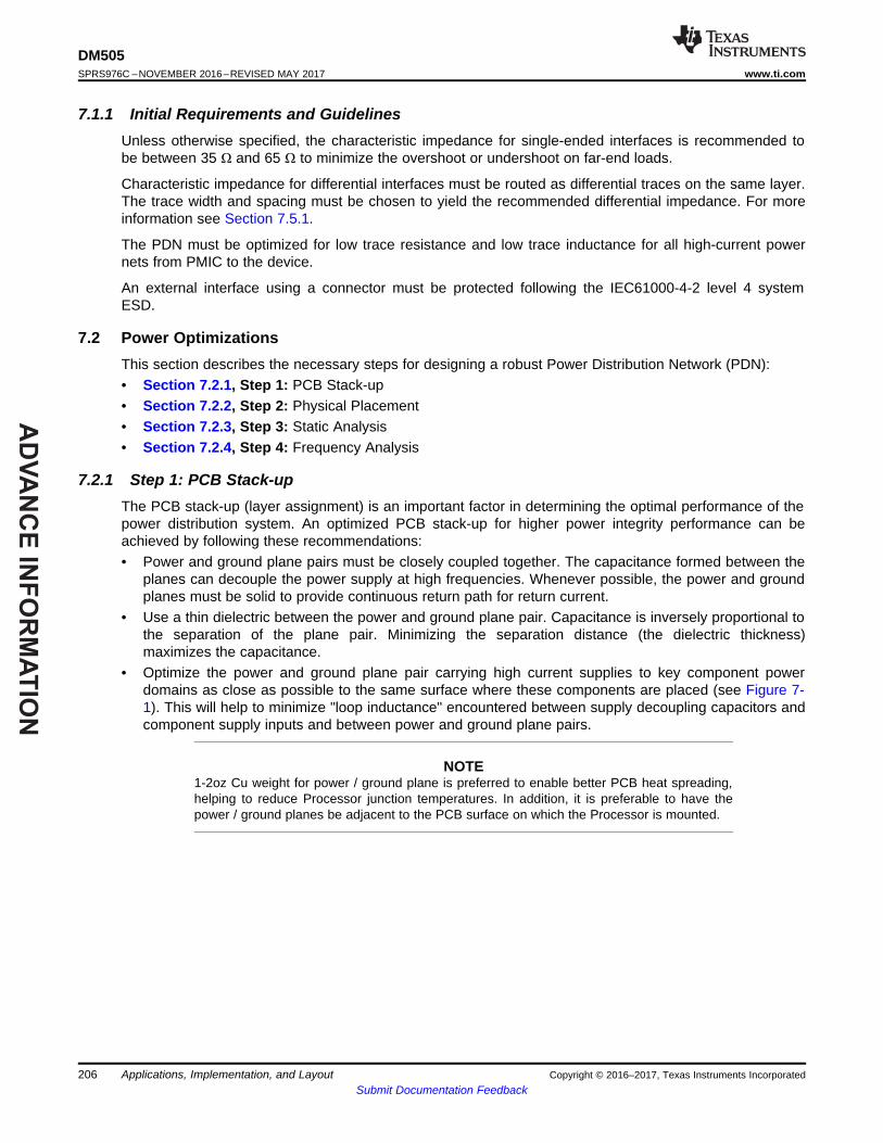
AD
VA
NC
E IN
FO
RM
AT
ION
206
DM505SPRS976C –NOVEMBER 2016–REVISED MAY 2017 www.ti.com
Submit Documentation FeedbackApplications, Implementation, and Layout Copyright © 2016–2017, Texas Instruments Incorporated
7.1.1 Initial Requirements and GuidelinesUnless otherwise specified, the characteristic impedance for single-ended interfaces is recommended tobe between 35 Ω and 65 Ω to minimize the overshoot or undershoot on far-end loads.
Characteristic impedance for differential interfaces must be routed as differential traces on the same layer.The trace width and spacing must be chosen to yield the recommended differential impedance. For moreinformation see Section 7.5.1.
The PDN must be optimized for low trace resistance and low trace inductance for all high-current powernets from PMIC to the device.
An external interface using a connector must be protected following the IEC61000-4-2 level 4 systemESD.
7.2 Power OptimizationsThis section describes the necessary steps for designing a robust Power Distribution Network (PDN):• Section 7.2.1, Step 1: PCB Stack-up• Section 7.2.2, Step 2: Physical Placement• Section 7.2.3, Step 3: Static Analysis• Section 7.2.4, Step 4: Frequency Analysis
7.2.1 Step 1: PCB Stack-upThe PCB stack-up (layer assignment) is an important factor in determining the optimal performance of thepower distribution system. An optimized PCB stack-up for higher power integrity performance can beachieved by following these recommendations:• Power and ground plane pairs must be closely coupled together. The capacitance formed between the
planes can decouple the power supply at high frequencies. Whenever possible, the power and groundplanes must be solid to provide continuous return path for return current.
• Use a thin dielectric between the power and ground plane pair. Capacitance is inversely proportional tothe separation of the plane pair. Minimizing the separation distance (the dielectric thickness)maximizes the capacitance.
• Optimize the power and ground plane pair carrying high current supplies to key component powerdomains as close as possible to the same surface where these components are placed (see Figure 7-1). This will help to minimize "loop inductance" encountered between supply decoupling capacitors andcomponent supply inputs and between power and ground plane pairs.
NOTE1-2oz Cu weight for power / ground plane is preferred to enable better PCB heat spreading,helping to reduce Processor junction temperatures. In addition, it is preferable to have thepower / ground planes be adjacent to the PCB surface on which the Processor is mounted.

AD
VA
NC
E I
NF
OR
MA
TIO
N
Package
DIE
TraceCapacitor
Via
Note: 1. BGA via pair loop inductance
2. Power/Ground net spreading inductance
3. Capacitor trace inductance
Loop inductance
1
2
3
Power/Ground
Ground/Power
SPRS91v_PCB_STACKUP_01
207
DM505www.ti.com SPRS976C –NOVEMBER 2016–REVISED MAY 2017
Submit Documentation FeedbackApplications, Implementation, and LayoutCopyright © 2016–2017, Texas Instruments Incorporated
Figure 7-1. Minimize Loop Inductance With Proper Layer Assignment
The placement of power and ground planes in the PCB stackup (determined by layer assignment) has asignificant impact on the parasitic inductances of power current path as shown in Figure 7-1. For thisreason, it is recommended to consider layer order in the early stages of the PCB PDN design cycle,putting high-priority supplies in the top half of the stackup (assuming high load and priority componentsare mounted on the top-side of PCB) and low-priority supplies in the bottom half of the stackup as shownin the examples below (vias have parasitic inductances which impact the bottom layers more, so it isadvised to put the sensitive and high-priority power supplies on the top/same layers).
7.2.2 Step 2: Physical PlacementA critical step in designing an optimized PDN is that proper care must be taken to making sure that theinitial floor planning of the PCB layout is done with good power integrity design guidelines in mind. Thefollowing points are important for optimizing a PCB’s PDN:• Minimizing the physical distance between power sources and key high load components is the first
step toward optimization. Placing source and load components on the same side of the PCB isdesirable. This will minimize via inductance impact for high current loads and steps
• External trace routing between components must be as wide as possible. The wider the traces, thelower the DC resistance and consequently the lower the static IR drop.
• Whenever possible for the internal layers (routing and plane), wide traces and copper area fills arepreferred for PDN layout. The routing of power nets in plane provide for more interplane capacitanceand improved high frequency performance of the PDN.
• Whenever possible, use a via to component pin/pad ratio of 1:1 or better (i.e. especially decouplingcapacitors, power inductors and current sensing resistors). Do not share vias among multiplecapacitors for connecting power supply and ground planes.
• Placement of vias must be as close as possible or even within a component’s solder pad if the PCBtechnology you are using provides this capability.
• To avoid any "ampacity” issue – maximum current-carrying capacity of each transitional via should beevaluated to determine the appropriate number of vias required to connect components.Adding vias to bring the "via-to-pad” ratio to 1:1 will improve PDN performance.
• For noise sensitive power supplies (i.e. Phase Lock-Loops, analog signals like audio and video), a Gndshield can be used to isolate coplanar supplies that may have high step currents or high frequencyswitching transitions from coupling into low-noise supplies.

AD
VA
NC
E IN
FO
RM
AT
ION
L
Wt
The resistance Rs of a plane conductorfor a unit length and unit width is calledthe (ohms per square).surface resistivity
1
σ ×
×
Rs = =t
lR = Rs
w
r
t
SPRS91v_PCB_STATIC_01
vdd
vdd_mpu
vss
SPRS91v_PCB_PHYS_05
208
DM505SPRS976C –NOVEMBER 2016–REVISED MAY 2017 www.ti.com
Submit Documentation FeedbackApplications, Implementation, and Layout Copyright © 2016–2017, Texas Instruments Incorporated
Figure 7-2. Coplanar Shielding of Power Net Using Ground Guard-band
7.2.3 Step 3: Static AnalysisDelivering reliable power to circuits is always of critical importance because voltage drops (also known asIR drops) can happen at every level within an electronic system, on-chip, within a package, and across theboard. Robust system performance can only be ensured by understanding how the system elements willperform under typical stressful Use Cases. Therefore, it is a good practice to perform a Static or DCAnalysis.
Static or DC analysis and design methodology results in a PDN design that minimizes voltage or IR dropsacross power and ground planes, traces and vias. This ensures the application processor’s internaltransistors will be operating within their specified voltage ranges for proper functionality. The amount of IRdrop that will be encounter is based upon amount power drawn for a desired Use Case and PCB trace(widths, geometry and number of parallel traces) and via (size, type and number) characteristics.
Components that are distant from their power source are particularly susceptible to IR drop. Designs thatrely on battery power must minimize voltage drops to avoid unacceptable power loss that can negativelyimpact system performance. Early assessments a PDN’s static (DC) performance helps to determinebasic power distribution parameters such as best system input power point, optimal PCB layer stackup,and copper area needed for load currents.
Figure 7-3. Depiction of Sheet Resistivity and Resistance
Ohm’s Law (V = I × R) relates conduction current to voltage drop. At DC, the relation coefficient is aconstant and represents the resistance of the conductor. Even current carrying conductors will dissipatepower at high currents even though their resistance may be very small. Both voltage drop and powerdissipation are proportional to the resistance of the conductor.
Figure 7-4 shows a PCB-level static IR drop budget defined between the power management device(PMIC) pins and the application processor’s balls when the PMIC is supplying power.• It is highly recommended to physically place the PMIC as close as possible to the processor and on
the same side. The orientation of the PMIC vs. the processor should be aligned to minimize distancefor the highest current rail.

AD
VA
NC
E I
NF
OR
MA
TIO
N
BGA pad on PCB
Source Component Load Component
Static IR drop and Effective Resistance
PCB
SPRS977_PCB_STATIC_02
209
DM505www.ti.com SPRS976C –NOVEMBER 2016–REVISED MAY 2017
Submit Documentation FeedbackApplications, Implementation, and LayoutCopyright © 2016–2017, Texas Instruments Incorporated
Figure 7-4. Static IR Drop Budget for PCB Only
The system-level IR drop budget is made up of three portions: on-chip, package, and PCB board. Static IRor dc analysis/design methodology consists of designing the PDN such that the voltage drop (under dcoperating conditions) across power and ground pads of the transistors of the application processor deviceis within a specified value of the nominal voltage for proper functionality of the device.
A PCB system-level voltage drop budget for proper device functionality is typically 1.5% of nominalvoltage. For a 1.35-V supply, this would be ≤20 mV.
To accurately analyze PCB static IR drop, the actual geometry of the PDN must be modeled properly andsimulated to accurately characterize long distribution paths, copper weight impacts, electro-migrationviolations of current-carrying vias, and "Swiss-cheese” effects via placement has on power rails. It isrecommended to perform the following analyses:• Lumped resistance/IR drop analysis• Distributed resistance/IR drop analysis
NOTEThe PMIC companion device supporting Processor has been designed with voltage sensingfeedback loop capabilities that enable a remote sense of the SMPS output voltage at thepoint of use.
The NOTE above means the SMPS feedback signals and returns must be routed across PCB andconnected to the Device input power ball for which a particular SMPS is supplying power. This feedbackloop provides compensation for some of the voltage drop encountered across the PDN within limits. Assuch, the effective resistance of the PDN within this loop should be determined in order to optimizevoltage compensation loop performance. The resistance of two PDN segments are of interest: one fromthe power inductor/bulk power filtering capacitor node to the Processor’s input power and second is theentire PDN route from SMPS output pin/ball to the Processor input power.
In the following sections each methodology is described in detail and an example has been provided ofanalysis flow that can be used by the PCB designer to validate compliance to the requirements on theirPCB PDN design.

AD
VA
NC
E IN
FO
RM
AT
ION
Grouped Power/Groundpins to create 1 equivalent
resistive branch
Multiport net
Branch
Port/Pin
Sources
Sinks
Sources
Sinks
SPRS91v_PCB_PDN_01
210
DM505SPRS976C –NOVEMBER 2016–REVISED MAY 2017 www.ti.com
Submit Documentation FeedbackApplications, Implementation, and Layout Copyright © 2016–2017, Texas Instruments Incorporated
7.2.3.1 PDN Resistance and IR Drop
Lumped methodology consists of grouping all of the power pins on both the PMIC (voltage source) andprocessor (current sink) devices. Then the PMIC source is set to an expected Use Case voltage level andthe processor load has its Use Case current sink value set as well. Now the lumped/effective resistancefor the power rail trace/plane routes can be determine based upon the actual layout’s power rail etch wide,shape, length, via count and placement Figure 7-5 illustrates the pin-grouping/lumped concept.
The lumped methodology consists of importing the PCB layout database (from Cadence Allegro tool orany other layout design tool) into the static IR drop modeling and simulation tool of preference for the PCBdesigner. This is followed by applying the correct PCB stack-up information (thickness, materialproperties) of the PCB dielectric and metallization layers. The material properties of dielectric consist ofpermittivity (Dk) and loss tangent (Df).
For the conductor layers, the correct conductivity needs to be programmed into the simulation tool. This isfollowed by pin-grouping of the power and ground nets, and applying appropriate voltage/current sources.The current and voltage information can be obtained from the power and voltage specifications of thedevice under different operating conditions / Use Cases.
Figure 7-5. Pin-grouping concept: Lumped and Distributed Methodologies
7.2.4 Step 4: Frequency AnalysisDelivering low noise voltage sources are very important to allowing a system to operate at the lowestpossible Operational Performance Point (OPP) for any one Use Case. An OPP is a combination of thesupply voltage level and clocking rate for key internal processor domains. A SCH and PCB designed toprovide low noise voltage supplies will then enable the processor to enter optimal OPPs for each UseCase that in turn will minimize power dissipation and junction temperatures on-die. Therefore, it is a goodengineering practice to perform a Frequency Analysis over the key power domains.
Frequency analysis and design methodology results in a PDN design that minimizes transient noisevoltages at the processor’s input power balls. This allows the processor’s internal transistors to operatenear the minimum specified operating supply voltage levels. To accomplish this one must evaluate how avoltage supply will change due to impedance variations over frequency. This analysis will focus on thedecoupling capacitor network (VDD_xxx and VSS/Gnd rails) at the load. Sufficient capacitance with adistribution of self-resonant points will provide for an overall lower impedance vs frequency response foreach power domain.
Decoupling components that are distant from their load’s input power are susceptible to encounteringspreading loop inductance from the PCB design. Early analysis of each key power domain’s frequencyresponse helps to determine basic decoupling capacitor placement, optimal footprint, layer assignment,and types needed for minimizing supply voltage noise/fluctuations due to switching and load currenttransients.
NOTEEvaluation of loop inductance values for decoupling capacitors placed ~300mils closer to theload’s input power balls has shown an 18% reduction in loop inductance due to reduceddistance.

AD
VA
NC
E I
NF
OR
MA
TIO
N
SPRS91v_PCB_FREQ_03
1.0e+01
1.0e+00
1.0e–01
1.0e–02
1.0e–03
1.0e–041.00e–002 1.00e+000 1.00e+002
Frequency (MHz)
1.00e+004 1.00e+006 1.00e+008
S-Parameter Magnitude
Job: GCM155R71E153KA55_15NF;
X =1/ CC ω X = LL ω
Resonant frequency(55 MHz) (minimum)
=
where :
æ ö-ç ÷
è ø
w =
2
2 1Z ESR +ωESL
ωC
2π
æ ö-ç ÷
è ø
21
ωESLωC
SPRS91v_PCB_FREQ_02
¦
C ESL ESRSPRS91v_PCB_FREQ_01
211
DM505www.ti.com SPRS976C –NOVEMBER 2016–REVISED MAY 2017
Submit Documentation FeedbackApplications, Implementation, and LayoutCopyright © 2016–2017, Texas Instruments Incorporated
• Decoupling capacitors must be carefully placed in order to minimize loop inductance impact on supplyvoltage transients. A real capacitor has characteristics not only of capacitance but also inductance andresistance.Figure 7-6 shows the parasitic model of a real capacitor. A real capacitor must be treated as an RLCcircuit with effective series resistance (ESR) and effective series inductance (ESL).
Figure 7-6. Characteristics of a Real Capacitor With ESL and ESRThe magnitude of the impedance of this series model is given as:
Figure 7-7. Series Model Impedance Equation
Figure 7-8 shows the resonant frequency response of a typical capacitor with a self-resonant frequency of55 MHz. The impedance of the capacitor is a combination of its series resistance and reactive capacitanceand inductance as shown in the equation above.
Figure 7-8. Typical Impedance Profile of a Capacitor

AD
VA
NC
E IN
FO
RM
AT
ION
Trace
Pad
Via
Mounting geometry for reduced inductance
Via-in-pad
SPRS91v_PCB_FREQ_04
212
DM505SPRS976C –NOVEMBER 2016–REVISED MAY 2017 www.ti.com
Submit Documentation FeedbackApplications, Implementation, and Layout Copyright © 2016–2017, Texas Instruments Incorporated
Because a capacitor has series inductance and resistance that impacts its effectiveness, it is importantthat the following recommendations are adopted in placing capacitors on the PDN.
Wherever possible, mount the capacitor with the geometry that minimizes the mounting inductance andresistance. This was shown earlier in Figure 7-1. The capacitor mounting inductance and resistancevalues include the inductance and resistance of the pads, trace, and vias. Whenever possible, usefootprints that have the lowest inductance configuration as shown in Figure 7-9
The length of a trace used to connect a capacitor has a big impact on parasitic inductance and resistanceof the mounting. This trace must be as short and as wide as possible. wherever possible, minimizedistance to supply and Gnd vias by locating vias nearby or within the capacitor’s solder pad landing.Further improvements can be made to the mounting by placing vias to the side of capacitor lands ordoubling the number of vias as shown in Figure 7-9. If the PCB manufacturing processes allow it and ifcost-effective, via-in-pad (VIP) geometries are strongly recommended.
In addition to mounting inductance and resistance associated with placing a capacitor on the PCB, theeffectiveness of a decoupling capacitor also depends on the spreading inductance and resistance that thecapacitor sees with respect to the load. The spreading inductance and resistance is strongly dependent onthe layer assignment in the PCB stack-up. Therefore, try to minimize X, Y and Z dimensions where the Zis due to PCB thickness (as shown in Figure 7-9).
From left (highest inductance) to right (lowest inductance) the capacitor footprint types shown in Figure 7-9 are known as:• 2-via, Skinny End Exit (2vSEE)• 2-via, Wide End Exit (2vWEE)• 2-via, Wide Side Exit (2vWSE)• 4-via, Wide Side Exit (4vWSE)• 2-via, In-Pad (2vIP)
Figure 7-9. Capacitor Placement Geometry for Improved Mounting Inductance
NOTEEvaluation of loop inductance values for decoupling capacitor footprints 2vSEE (worst case)vs 4vWSE (2nd best) has shown a 30% reduction in inductance when 4vWSE footprint wasused in place of 2vSEE.
Decoupling Capacitor (Dcap) Strategy:

AD
VA
NC
E I
NF
OR
MA
TIO
N
213
DM505www.ti.com SPRS976C –NOVEMBER 2016–REVISED MAY 2017
Submit Documentation FeedbackApplications, Implementation, and LayoutCopyright © 2016–2017, Texas Instruments Incorporated
1. Use lowest inductance footprint and trace connection scheme possible for given PCB technology andlayout area in order to minimize Dcap loop inductance to power pin as much as possible (see Figure 7-9).
2. Place Dcaps on "same-side” as component within their power plane outline to minimize "decouplingloop inductance”. Target distance to power pin should be less than ~500mils depending upon PCBlayout characteristics (plane's layer assignment and solid nature). Use PI modeling CAD tool to verifyminimum inductance for top vs bottom-side placement.
3. Place Dcaps on "opposite-side” as component within their power plane outline if "same-side” is notfeasible or if distance to power pin is greater than ~500mils for top-side location. Use PI modeling CADtool to verify minimum inductance for top vs bottom-side placement.
4. Use minimum 10mil trace width for all voltage and gnd planes connections (i.e. Dcap pads, componentpower pins, etc.).
5. Place all voltage and gnd plane vias "as close as possible” to point of use (i.e. Dcap pads, componentpower pins, etc.).
6. Use a "Power/Gnd pad/pin to via” ratio of 1:1 whenever possible. Do not exceed 2:1 ratio for smallnumber of vias within restricted PCB areas (i.e. underneath BGA components).
Frequency analysis for the CORE power domain (vdd) has yielded the Impedance vs Frequencyresponses shown in Section 7.3.7.2, vdd Example Analysis.
7.2.5 System ESD Generic Guidelines
7.2.5.1 System ESD Generic PCB Guideline
Protection devices must be placed close to the ESD source which means close to the connector. Thisallows the device to subtract the energy associated with an ESD strike before it reaches the internalcircuitry of the application board.
To help minimize the residual voltage pulse that will be built-up at the protection device due to its nonzeroturn-on impedance, it is mandatory to route the ESD device with minimum stub length so that the low-resistive, low-inductive path from the signal to the ground is granted and not increasing the impedancebetween signal and ground.
For ESD protection array being railed to a power supply when no decoupling capacitor is available in closevicinity, consider using a decoupling capacitor (≥ 0.1 µF) tight to the VCC pin of the ESD protection. Apositive strike will be partially diverted to this capacitance resulting in a lower residual voltage pulse.
Ensure that there is sufficient metallization for the supply of signals at the interconnect side (VCC andGND in Figure 7-10) from connector to external protection because the interconnect may see between 15-A to 30-A current in a short period of time during the ESD event.

AD
VA
NC
E IN
FO
RM
AT
ION
Minimize suchinductance by
optimizing layout
Keep distancebetween protectedcircuit and external
protection
Keepprotection closed by
connector
external
Externalprotection
Stubinductance
Groundinductance
SignalESDstrike
VCCConnecto
r
Stubinductance
Stubinductance
Bypasscapacitor
0.1 f(minimum)
m
Interconnectioninductance
vcc
VCC
Signal
Protectedcircuit
SPRS91v_PCB_ESD_01
214
DM505SPRS976C –NOVEMBER 2016–REVISED MAY 2017 www.ti.com
Submit Documentation FeedbackApplications, Implementation, and Layout Copyright © 2016–2017, Texas Instruments Incorporated
Figure 7-10. Placement Recommendation for an ESD External Protection
NOTETo ensure normal behavior of the ESD protection (unwanted leakage), it is better to groundthe ESD protection to the board ground rather than any local ground (example isolated shieldor audio ground).
7.2.5.2 Miscellaneous EMC Guidelines to Mitigate ESD Immunity• Avoid running critical signal traces (clocks, resets, interrupts, control signals, and so forth) near PCB
edges.• Add high frequency filtering: Decoupling capacitors close to the receivers rather than close to the
drivers to minimize ESD coupling.• Put a ground (guard) ring around the entire periphery of the PCB to act as a lightning rod.• Connect the guard ring to the PCB ground plane to provide a low impedance path for ESD-coupled
current on the ring.• Fill unused portions of the PCB with ground plane.• Minimize circuit loops between power and ground by using multilayer PCB with dedicated power and
ground planes.• Shield long line length (strip lines) to minimize radiated ESD.• Avoid running traces over split ground planes. It is better to use a bridge connecting the two planes in
one area.
AD
VA
NC
E I
NF
OR
MA
TIO
N
BAD BETTER
SPRS91v_PCB_EMC_01
215
DM505www.ti.com SPRS976C –NOVEMBER 2016–REVISED MAY 2017
Submit Documentation FeedbackApplications, Implementation, and LayoutCopyright © 2016–2017, Texas Instruments Incorporated
Figure 7-11. Trace Examples• Always route signal traces and their associated ground returns as close to one another as possible to
minimize the loop area enclosed by current flow:– At high frequencies current follows the path of least inductance.– At low frequencies current flows through the path of least resistance.
7.2.5.3 ESD Protection System Design Consideration
ESD protection system design consideration is covered in of this document. The following are additionalconsiderations for ESD protection in a system.• Metallic shielding for both ESD and EMI• Chassis GND isolation from the board GND• Air gap designed on board to absorb ESD energy• Clamping diodes to absorb ESD energy• Capacitors to divert ESD energy• The use of external ESD components on the DP/DM lines may affect signal quality and are not
recommended.
7.2.6 EMI / EMC Issues PreventionAll high-speed digital integrated circuits can be sources of unwanted radiation, which can affect nearbysensitive circuitry and cause the final product to have radiated emissions levels above the limits allowedby the EMC regulations if some preventative steps are not taken.
Likewise, analog and digital circuits can be susceptible to interference from the outside world and pickedup by the circuitry interconnections.
To minimize the potential for EMI/EMC issues, the following guidelines are recommended to be followed.
7.2.6.1 Signal Bandwidth
To evaluate the frequency of a digital signal, an estimated rule of thumb is to consider its bandwidth fBWwith respect to its rise time, tR:
fBW ≈ 0.35 / tRThis frequency actually corresponds to the break point in the signal spectrum, where the harmonics startto decay at 40 dB per decade instead of 20 dB per decade.

AD
VA
NC
E IN
FO
RM
AT
ION
216
DM505SPRS976C –NOVEMBER 2016–REVISED MAY 2017 www.ti.com
Submit Documentation FeedbackApplications, Implementation, and Layout Copyright © 2016–2017, Texas Instruments Incorporated
7.2.6.2 Signal Routing
7.2.6.2.1 Signal Routing—Sensitive Signals and Shielding
Keep radio frequency (RF) sensitive circuitry (like GPS receivers, GSM/WCDMA, Bluetooth/WLANtransceivers, frequency modulation (FM) radio) away from high-speed ICs (the device, power and audiomanager, chargers, memories, and so forth) and ideally on the opposite side of the PCB. For improvedprotection it is recommended to place these emission sources in a shield can. If the shield can have aremovable lid (two-piece shield), ensure there is low contact impedance between the fence and the lid.Leave some space between the lid and the components under it to limit the high-frequency currentsinduced in the lid. Limit the shield size to put any potential shield resonances above the frequencies ofinterest; see Figure 7-8, Typical Impedance Profile of a Capacitor.
7.2.6.2.2 Signal Routing—Outer Layer Routing
In case there is a need to use the outer layers for routing outside of shielded areas, it is recommended toroute only static signals and ensure that these static signals do not carry any high-frequency components(due to parasitic coupling with other signals). In case of long traces, make provision for a bypass capacitornear the signal source.
Routing of high-frequency clock signals on outer layers, even for a short distance, is discouraged,because their emissions energy is concentrated at the discrete harmonics and can become significanteven with poor radiators.
Coplanar shielding of traces on outer layers (placing ground near the sides of a track along its length) iseffective only if the distance between the trace sides and the ground is smaller that the trace height abovethe ground reference plane. For modern multilayer PCBs this is often not possible, so coplanar shieldingwill not be effective. Do not route high-frequency traces near the periphery of the PCB, as the lack of aground reference near the trace edges can increase EMI: see Section 7.2.6.3, Ground Guidelines.
7.2.6.3 Ground Guidelines
7.2.6.3.1 PCB Outer Layers
Ideally the areas on the top and bottom layers of the PCB that are not enclosed by a shield should befilled with ground after the routing is completed and connected with an adequate number of vias to theground on the inner ground planes.
7.2.6.3.2 Metallic Frames
Ensure that all metallic parts are well connected to the PCB ground (like LCD screens metallic frames,antennas reference planes, connector cages, flex cables grounds, and so forth). If using flex PCB ribboncables to bring high-frequency signals off the PCB, ensure they are adequately shielded (coaxial cables orflex ribbons with a solid reference ground).
7.2.6.3.3 Connectors
For high-frequency signals going to connectors choose a fully shielded connector, if possible (for example,SD card connectors). For signals going to external connectors or which are routed over long distances, itis recommended to reduce their bandwidth by using low-pass filters (resistor, capacitor (RC) combinationsor lossy ferrite inductors). These filters will help to prevent emissions from the board and can also improvethe immunity from external disturbances.
7.2.6.3.4 Guard Ring on PCB Edges
The major advantage of a multilayer PCB with ground-plane is the ground return path below each andevery signal or power trace.
As shown in Figure 7-12 the field lines of the signal return to PCB ground as long as an infinite ground isavailable.

AD
VA
NC
E I
NF
OR
MA
TIO
N
Signal
Power
Ground
Signal
SPRS91v_PCB_EMC_03
SPRS91v_PCB_EMC_02
217
DM505www.ti.com SPRS976C –NOVEMBER 2016–REVISED MAY 2017
Submit Documentation FeedbackApplications, Implementation, and LayoutCopyright © 2016–2017, Texas Instruments Incorporated
Traces near the PCB-edges do not have this infinite ground and therefore may radiate more than theothers. Thus, signals (clocks) or power traces (core power) identified to be critical must not be routed inthe vicinity of PCB edges, or, if not avoidable, must be accompanied by a guard ring on the PCB edge.
Figure 7-12. Field Lines of a Signal Above Ground
Figure 7-13. Guard Ring Routing
The intention of the guard ring is that HF-energy, that otherwise would have been emitted from the PCBedge, is reflected back into the board where it partially will be absorbed. For this purpose ground traces onthe borders of all layers (including power layer) must be applied as shown in Figure 7-13.
As these traces must have the same (HF–) potential as the ground plane they must be connected to theground plane at least every 10 mm.
7.2.6.3.5 Analog and Digital Ground
For the optimum solution, the AGND and the DGND planes must be connected together at the powersupply source in a same point. This ensures that both planes are at the same potential, while the transferof noise from the digital to the analog domain is minimized.
7.3 Core Power DomainsThis section provides boundary conditions and theoretical background to be applied as a guide foroptimizing a PCB design. The decoupling capacitor and PDN characteristics tables shown below giverecommended capacitors and PCB parameters to be followed for schematic and PCB designs. Boarddesigns that meet the static and dynamic PDN characteristics shown in tables below will be aligned to theexpected PDN performance needed to optimize SoC performance.
7.3.1 General Constraints and Theory• Max PCB static/DC voltage drop (IRd) budget of 1.5% of supply voltage when using PMICs without
remote sensing as measured from PMIC’s power inductor and filter capacitor node to Processor inputincluding any ground return losses.
• Max PCB static/DC voltage drop (IRd) budget can be relaxed to 7.5% of supply voltage when usingTI recommended PMICs with remote sensing at the load as measured from PMIC’s power inductorand filter capacitor node to Device’s supply input including any ground return losses.

AD
VA
NC
E IN
FO
RM
AT
ION
218
DM505SPRS976C –NOVEMBER 2016–REVISED MAY 2017 www.ti.com
Submit Documentation FeedbackApplications, Implementation, and Layout Copyright © 2016–2017, Texas Instruments Incorporated
• PMIC component DM and guidelines should be referenced for the following:– Routing remote feedback sensing to optimize per each SMPS’s implementation– Selecting power filtering capacitor values and PCB placement.
• Max Total Effective Resistance (Reff) budget can range from 4 – 100mΩ for key Device power rails notincluding ground returns depending upon maximum load currents and maximum DC voltage dropbudget (as discussed above).
• Max Device supply input voltage difference budget of 5mV under max current loading shall bemaintained across all balls connected to a common power rail. This represents any voltage differencethat may exist between a remote sense point to any power input.
• Max PCB Loop Inductance (LL) budget between Device’s power inputs and local bulk and highfrequency decoupling capacitors including ground returns should range from 0.4 – 2.5nH dependingupon maximum transient load currents.
• Max PCB dynamic/AC peak-to-peak transient noise voltage budgets between PMIC and Deviceincluding ground returns are as follows:– +/-3% of nominal supply voltage for frequencies below the PMIC bandwidth (typ Fpmic ~
200kHz)– +/-5% of nominal supply voltage for frequencies between Fpmic to Fpcb (typ 20 – 100MHz)
• Max PCB Impedance (Z) vs Frequency (F) budget between Device’s power inputs and PMIC’s outputpower filter node including ground return is determined by applying the Frequency Domain TargetImpedance Method to determine the PCB’s maximum frequency of interest (Fpcb). Ideally a properlydesigned and decoupled PDN will exhibit smoothly increasing Z vs. F curve. There are 2 generalregions of interest as can be seen in Figure 7-14.– 1st area is from DC (0Hz) up to Fpmic (typ a few 100 kHz) where a PMIC’s transient response
characteristic (i.e. Switching Freq, Compensation Loop BW) dominate. A PDN’s Z is typically verylow due to power filtering & bulk capacitor values when PDN has very low trace resistance (i.e.good Reff performance). The goal is to maintain a smoothly increasing Z that is less than Zt1 overthis low frequency range. This will ensure that a max transient current event will not cause avoltage drop more than the PMIC’s current step response can support (typ 3%).
– 2nd area is from Fpmic up to Fpcb (typ 20-100MHz) where a PCB’s inherent characteristics (i.e.parasitic capacitance, planar spreading inductances) dominate. A PDN’s Z will naturally increasewith frequency. At frequencies between Fpmic up to Fpcb, the goal is to maintain a smoothlyincreasing Z to be less than Zt2. This will ensue that the high frequency content of a max transientcurrent event will not cause a voltage drop to be more than 5% of the min supply voltage.

AD
VA
NC
E I
NF
OR
MA
TIO
N
219
DM505www.ti.com SPRS976C –NOVEMBER 2016–REVISED MAY 2017
Submit Documentation FeedbackApplications, Implementation, and LayoutCopyright © 2016–2017, Texas Instruments Incorporated
Figure 7-14. PDN’s Target impedance1.Voltage Rail Drop includes regulation accuracy, voltage distribution drops, and all dynamic eventssuch as transient noise, AC ripple, voltage dips etc.2.Typical max transient current is defined as 50% of max current draw possible.
7.3.2 Voltage DecouplingRecommended power supply decoupling capacitors main characteristics for commercial products whoseambient temperature is not to exceed +85C are shown in table below:
Table 7-1. Commercial Applications Recommended Decoupling Capacitors Characteristics(1)(2)(3)
Value Voltage[V]
Package Stability Dielectric Capacitance
Tolerance
TempRange [°C]
TempSensitivity
[%]
REFERENCE
22µF 6,3 0603 Class 2 X5R - / + 20% -55 to + 85 - / + 15 GRM188R60J226MEA0L10µF 4,0 0402 Class 2 X5R - / + 20% -55 to + 85 - / + 15 GRM155R60G106ME444.7µF 6,3 0402 Class 2 X5R - / + 20% -55 to + 85 - / + 15 GRM155R60J475ME952.2µF 6,3 0402 Class 2 X5R - / + 20% -55 to + 85 - / + 15 GRM155R60J225ME951µF 6,3 0201 Class 2 X5R - / + 20% -55 to + 85 - / + 15 GRM033R60J105MEA2

AD
VA
NC
E IN
FO
RM
AT
ION
220
DM505SPRS976C –NOVEMBER 2016–REVISED MAY 2017 www.ti.com
Submit Documentation FeedbackApplications, Implementation, and Layout Copyright © 2016–2017, Texas Instruments Incorporated
Table 7-1. Commercial Applications Recommended Decoupling CapacitorsCharacteristics(1)(2)(3) (continued)
Value Voltage[V]
Package Stability Dielectric Capacitance
Tolerance
TempRange [°C]
TempSensitivity
[%]
REFERENCE
470nF 6,3 0201 Class 2 X5R - / + 20% -55 to + 85 - / + 15 GRM033R60G474ME90220nF 6,3 0201 Class 2 X5R - / + 20% -55 to + 85 - / + 15 GRM033R60J224ME90100nF 6,3 0201 Class 2 X5R - / + 20% -55 to + 85 - / + 15 GRM033R60J104ME19
(1) Minimum value for each PCB capacitor: 100 nF.(2) Among the different capacitors, 470 nF is recommended (not required) to filter at 5-MHz to 10-MHz frequency range.(3) In comparison with the EIA Class 1 dielectrics, Class 2 dielectric capacitors tend to have severe temperature drift, high dependence of
capacitance on applied voltage, high voltage coefficient of dissipation factor, high frequency coefficient of dissipation, and problems withaging due to gradual change of crystal structure. Aging causes gradual exponential loss of capacitance and decrease of dissipationfactor.
Recommended power supply decoupling capacitors main characteristics for automotive products areshown in table below:
Table 7-2. Automotive Applications Recommended Decoupling Capacitors Characteristics (1)(2)
Value Voltage [V] Package Stability Dielectric Capacitance
Tolerance
TempRange [°C]
TempSensitivity
[%]
REFERENCE
22µF 6,3 1206 Class 2 X7R - / + 20% -55 to + 125 - / + 15 GCM31CR70J226ME2310µF 6,3 0805 Class 2 X7R - / + 20% -55 to + 125 - / + 15 GCM21BR70J106ME224.7µF 10 0805 Class 2 X7R - / + 20% -55 to + 125 - / + 15 GCM21BC71A475MA732.2µF 6,3 0603 Class 2 X7R - / + 20% -55 to + 125 - / + 15 GCM188R70J225ME221µF 16 0603 Class 2 X7R - / + 20% -55 to + 125 - / + 15 GCM188R71C105MA64
470nF 16 0603 Class 2 X7R - / + 20% -55 to + 125 - / + 15 GCM188R71C474MA55220nF 25 0603 Class 2 X7R - / + 20% -55 to + 125 - / + 15 GCM188L81C224MA37100nF 16 0402 Class 2 X7R - / + 20% -55 to + 125 - / + 15 GCM155R71C104MA55
(1) Minimum value for each PCB capacitor: 100 nF.(2) Among the different capacitors, 470 nF is recommended (not required) to filter at 5-MHz to 10-MHz frequency range.
7.3.3 Static PDN AnalysisOne power net parameter derived from a PCB’s PDN static analysis is the Effective Resistance (Reff).This is the total PCB power net routing resistance that is the sum of all the individual power net segmentsused to deliver a supply voltage to the point of load and includes any series resistive elements (i.e. currentsensing resistor) that may be installed between the PMIC outputs and Processor inputs.
7.3.4 Dynamic PDN AnalysisThree power net parameters derived from a PCB’s PDN dynamic analysis are the Loop Inductance (LL),Impedance (Z) and PCB Frequency of Interest (Fpcb).• LL values shown are the recommended max PCB trace inductance between a decoupling capacitor’s
power supply and ground reference terminals when viewed from the decoupling capacitor with a"theoretical shorted” applied across the Processor’s supply inputs to ground reference.
• Z values shown are the recommended max PCB trace impedances allowed between Fpmic up to Fpcbfrequency range that limits transient noise drops to no more than 5% of min supply voltage during maxtransient current events.
• Fpcb (Frequency of Interest) is defined to be a power rail’s max frequency after which adding areasonable number of decoupling capacitors no longer significantly reduces the power rail impedancebelow the desired impedance target (Zt2). This is due to the dominance of the PCB’s parasitic planarspreading and internal package inductances.

AD
VA
NC
E I
NF
OR
MA
TIO
N
221
DM505www.ti.com SPRS976C –NOVEMBER 2016–REVISED MAY 2017
Submit Documentation FeedbackApplications, Implementation, and LayoutCopyright © 2016–2017, Texas Instruments Incorporated
Table 7-3. Recommended PDN and Decoupling Characteristics (1)(2)(3)(4)(5)
PDN Analysis: Static Dynamic Number of Recommended Decoupling Capacitors perSupply
Supply Max Reff(7)
[mΩ]
Dec. Cap.Max LL(8) (6)
[nH]
MaxImpedance
[mΩ]
Frequencyrange
of Interest[MHz]
100nF(6)
220nF
470nF 1μF 2.2 μF 4.7 μF 10 μF 22 μF
vdd_dspeve 33 2.5 54 ≤20 6 1 1 1 1 1 1vdd 83 2 87 ≤50 6 1 1 1 1 1vdds_ddr1,vdds_ddr2,vdds_ddr3
33 2.5 200 ≤100 8 4 2 2 1
cap_vddram_core1 N/A 6 N/A N/A 1
cap_vddram_core2 N/A 6 N/A N/A 1
cap_vddram_dspeve N/A 6 N/A N/A 1
(1) For more information on peak-to-peak noise values, see the Recommended Operating Conditions table of the Electrical Characteristicschapter.
(2) ESL must be as low as possible and must not exceed 0.5 nH.(3) The PDN (Power Delivery Network) impedance characteristics are defined versus the device activity (that runs at different frequency)
based on the Recommended Operating Conditions table of the Electrical Characteristics chapter.(4) The static drop requirement drives the maximum acceptable PCB resistance between the PMIC or the external SMPS and the processor
power balls.(5) Assuming that the external SMPS (power IC) feedback sense is taken close to processor power balls.(6) High-frequency (30 to 70MHz) PCB decoupling capacitors(7) Maximum Total Reff from PMIC output to remote sensing feedback point located as close to the Device's point of load as possible.(8) Maximum Loop Inductance for decoupling capacitor.
7.3.5 Power Supply MappingTPS65917 is a Power management IC (PMIC) that can be used for the Device design. TI is nowinvestigating an optimized solution for high power use cases so the TPS65917 is subject to change. Analternate dual converter power solution using LP8732Q and LP8733Q are recommended. TI requires theuse of one of these PMIC solutions for the following reasons:• TI has validated its use with the Device• Board level margins including transient response and output accuracy are analyzed and optimized for
the entire system• Support for power sequencing requirements (refer to Section 5.9.3 Power Sequencing)• Support for Adaptive Voltage Scaling (AVS) Class 0 requirements, including TI provided software
It is possible that some voltage domains on the device are unused in some systems. In such cases, toensure device reliability, it is still required that the supply pins for the specific voltage domains areconnected to some core power supply output.
These unused supplies though can be combined with any of the core supplies that are used (active) in thesystem. e.g. if IVA and GPU domains are not used, they can be combined with the CORE domain,thereby having a single power supply driving the combined CORE, IVA and GPU domains.
For the combined rail, the following relaxations do apply:• The AVS voltage of active rail in the combined rail needs to be used to set the power supply• The decoupling capacitance should be set according to the active rail in the combined rail
Whenever we allow for combining of rails mapped on any of the SMPSes, the PDN guidelines that are themost stringent of the rails combined should be implemented for the particular supply rail.

AD
VA
NC
E IN
FO
RM
AT
ION
222
DM505SPRS976C –NOVEMBER 2016–REVISED MAY 2017 www.ti.com
Submit Documentation FeedbackApplications, Implementation, and Layout Copyright © 2016–2017, Texas Instruments Incorporated
Table 7-4 illustrates the approved and validated power supply connections to the Device for the SMPSoutputs of the TPS65917 and LP8732 combined with LP8733 PMICs.
Table 7-4. Power Supply Connections
TPS65917 Dual Converter Solution Valid Combination 1:SMPS1 LP8733Q Buck0 vdd_dspeveSMPS2 LP8733Q Buck1 vddSMPS3 LP8732Q Buck0 vdds18v, vdds18v_ddr[3:1], vddshv[6:1]SMPS4 LP8732Q Buck1 vdds_ddr1, vdds_ddr2, vdds_ddr3
Table 7-5 illustrates the LP8733 and LP8732 OTP IDs required for DM50x processor systems usingdifferent DDR memory types.
Table 7-5. OTP ID Memory Types Support
DDR Type LP8733Q LP8732QOTP Version OTP Version
DDR2 2A 2DLPDDR2 2A 2B
DDR3 2A 2FDDR3L 2A 2E
7.3.6 DPLL Voltage RequirementThe voltage input to the DPLLs has a low noise requirement. Board designs should supply these voltageinputs with a low noise LDO to ensure they are isolated from any potential digital switching noise. TheTPS65917 PMIC LDOLN output or LDO0 on LP8733Q dual power solution is specifically designed tomeet this low noise requirement.
NOTEFor more information about Input Voltage Sources, see DPLLs, DLLs Specifications
Table 7-6 presents the voltage inputs that supply the DPLLs.
Table 7-6. Input Voltage Power Supplies for the DPLLs
POWER SUPPLY DPLLsvdda_per DPLL_PER and PER HSDIVIDER analog power supply
vdda_ddr_dsp DPLL_DSP, DPLL_DDR and DDR HSDIVIDER analog power supplyvdda_gmac_core GMAC PLL, GMAC HSDIVIDER, DPLL_CORE and CORE HSDIVIDER analog power
supply
7.3.7 Example PCB DesignThe following sections describe an example PCB design and its resulting PDN performance for thevdd_dspeve key processor power domain.
NOTEMaterials presented in this section are based on generic PDN analysis on PCB boards andare not specific to systems integrating the Device.
7.3.7.1 Example Stack-up
Layer Assignments:
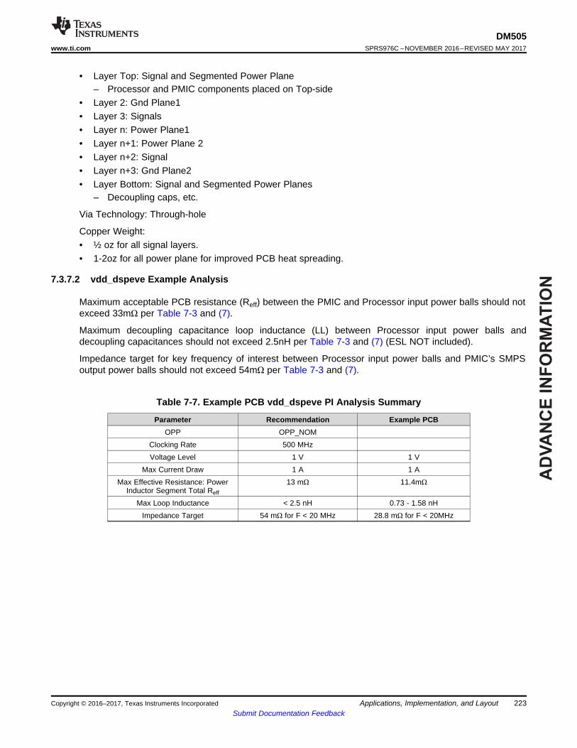
AD
VA
NC
E I
NF
OR
MA
TIO
N
223
DM505www.ti.com SPRS976C –NOVEMBER 2016–REVISED MAY 2017
Submit Documentation FeedbackApplications, Implementation, and LayoutCopyright © 2016–2017, Texas Instruments Incorporated
• Layer Top: Signal and Segmented Power Plane– Processor and PMIC components placed on Top-side
• Layer 2: Gnd Plane1• Layer 3: Signals• Layer n: Power Plane1• Layer n+1: Power Plane 2• Layer n+2: Signal• Layer n+3: Gnd Plane2• Layer Bottom: Signal and Segmented Power Planes
– Decoupling caps, etc.
Via Technology: Through-hole
Copper Weight:• ½ oz for all signal layers.• 1-2oz for all power plane for improved PCB heat spreading.
7.3.7.2 vdd_dspeve Example Analysis
Maximum acceptable PCB resistance (Reff) between the PMIC and Processor input power balls should notexceed 33mΩ per Table 7-3 and (7).
Maximum decoupling capacitance loop inductance (LL) between Processor input power balls anddecoupling capacitances should not exceed 2.5nH per Table 7-3 and (7) (ESL NOT included).
Impedance target for key frequency of interest between Processor input power balls and PMIC’s SMPSoutput power balls should not exceed 54mΩ per Table 7-3 and (7).
Table 7-7. Example PCB vdd_dspeve PI Analysis Summary
Parameter Recommendation Example PCBOPP OPP_NOM
Clocking Rate 500 MHzVoltage Level 1 V 1 V
Max Current Draw 1 A 1 AMax Effective Resistance: Power
Inductor Segment Total Reff
13 mΩ 11.4mΩ
Max Loop Inductance < 2.5 nH 0.73 - 1.58 nHImpedance Target 54 mΩ for F < 20 MHz 28.8 mΩ for F < 20MHz
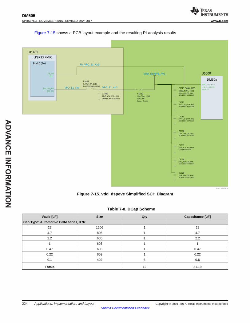
AD
VA
NC
E IN
FO
RM
AT
ION
Buck0 (3A)
L14020.47uH, 4A, 2520
DFE252012PD-R47M
DM50x
VDD_DSPEVE
LP8733 PMIC
SPRS977_PCB_CORE_02
Buck 0_SW_
(22,23)
VPO_S1_SW VPO_S1_AVS
C140922uF, 6.3V, X7R, 1206
GCM31CR70J226ME23
FB_B0
(2)
U1401
R101010mOhm, 1210
INA226&
Power Bench
U5000
C5079, 5080, 5085,
5100, 5101, 51110.1uF, 16V, X7R, 0402
GCM155R71C104KA55
C50210.22uF, 25V, X7R, 0603
GCM188R71E224KA55
C50190.47uF, 16V, X7R, 0603
GCM188R71C474KA55
C50181.0uF, 16V, X7R, 0603
GCM188R71C105KA64
C50372.2uF, 6.3V, X5R, 0603
C1005X5R0J225M
C50304.7uF, 16V, X7R, 0805
GCM21BR71C475KA73
C502622uF, 6.3V, X7R, 1206
GCM31CR70J226ME23
VDD_DSPEVE_AVS
(P12, P11, M9, P9,
K8, L8, P8)
FB_VPO_S1_AVS
224
DM505SPRS976C –NOVEMBER 2016–REVISED MAY 2017 www.ti.com
Submit Documentation FeedbackApplications, Implementation, and Layout Copyright © 2016–2017, Texas Instruments Incorporated
Figure 7-15 shows a PCB layout example and the resulting PI analysis results.
Figure 7-15. vdd_dspeve Simplified SCH Diagram
Table 7-8. DCap Scheme
Vaule [uF] Size Qty Capacitance [uF]Cap Type: Automotive GCM series, X7R
22 1206 1 224.7 805 1 4.72.2 603 1 2.21 603 1 1
0.47 603 1 0.470.22 603 1 0.220.1 402 6 0.6
Totals 12 31.19

AD
VA
NC
E I
NF
OR
MA
TIO
N
225
DM505www.ti.com SPRS976C –NOVEMBER 2016–REVISED MAY 2017
Submit Documentation FeedbackApplications, Implementation, and LayoutCopyright © 2016–2017, Texas Instruments Incorporated
IR Drop: vdd_dspeve
Figure 7-16. vdd_dspeve Voltage/IR Drop [All Layers]
Dynamic analysis of this PCB design for the CORE power domain determined the vdd_dspeve decouplingcapacitor loop inductance and impedance vs frequency analysis shown below. As you can see, the loopinductance values ranged from 0.68 –1.79nH and were less than maximum 2.0nH recommended.
Table 7-9. Decoupling Design Detail Summary
Cap ReferenceDescription
Loop Inductacne at50MHz [nH]
Footprint Types PCB Side Distance toBall-Field [mils]
Value Size
C5101 0.73 2vWEE Bottom 82 0.1 0402C5100 0.78 2vWEE Bottom 107 0.1 0402C5085 0.84 2vWEE Bottom 35 0.1 0402C5019 1.09 4vWE Top 631 0.47 0603C5111 1.09 4vWE Bottom 681 0.1 0402C5030 1.11 4vWE Top 738 4.7 0805C5037 1.11 4vWE Top 563 2.2 0603C5018 1.14 4vWE Top 681 1 0603C5021 1.17 4vWE Top 761 0.22 0603C5026 1.18 4vWE Top 792 22 1206C5079 1.32 4vWE Bottom 542 0.1 0402C5080 1.58 4vWE Bottom 602 0.1 0402

AD
VA
NC
E IN
FO
RM
AT
ION
226
DM505SPRS976C –NOVEMBER 2016–REVISED MAY 2017 www.ti.com
Submit Documentation FeedbackApplications, Implementation, and Layout Copyright © 2016–2017, Texas Instruments Incorporated
(1) Distances are wrt "middle of Ball Field", Ref pt between: U5000-M9 to middle of Dcap's power pad unless specifed
Figure 7-17 shows vdd_dspeve Impedance vs Frequency characteristics.
Figure 7-17. vdd_dspeve Impedance vs Frequency
7.4 Single-Ended Interfaces
7.4.1 General Routing GuidelinesThe following paragraphs detail the routing guidelines that must be observed when routing the variousfunctional LVCMOS interfaces.

AD
VA
NC
E I
NF
OR
MA
TIO
N
W
D+
S = 2 W = 200 µm
SPRS91v_PCB_SE_GND_01
227
DM505www.ti.com SPRS976C –NOVEMBER 2016–REVISED MAY 2017
Submit Documentation FeedbackApplications, Implementation, and LayoutCopyright © 2016–2017, Texas Instruments Incorporated
• Line spacing:– For a line width equal to W, the spacing between two lines must be 2W, at least. This minimizes the
crosstalk between switching signals between the different lines. On the PCB, this is not achievableeverywhere (for example, when breaking signals out from the device package), but it isrecommended to follow this rule as much as possible. When violating this guideline, minimize thelength of the traces running parallel to each other (see Figure 7-18).
Figure 7-18. Ground Guard Illustration• Length matching (unless otherwise specified):
– For bus or traces at frequencies less than 10 MHz, the trace length matching (maximum lengthdifference between the longest and the shortest lines) must be less than 25 mm.
– For bus or traces at frequencies greater than 10 MHz, the trace length matching (maximum lengthdifference between the longest and the shortest lines) must be less than 2.5 mm.
• Characteristic impedance– Unless otherwise specified, the characteristic impedance for single-ended interfaces is
recommended to be between 35-Ω and 65-Ω.• Multiple peripheral support
– For interfaces where multiple peripherals have to be supported in the star topology, the length ofeach branch has to be balanced. Before closing the PCB design, it is highly recommended to verifysignal integrity based on simulations including actual PCB extraction.
7.4.2 QSPI Board Design and Layout GuidelinesThe following section details the routing guidelines that must be observed when routing the QSPIinterfaces.
7.4.2.1 If QSPI is operated in Mode 0 (POL=0, PHA=0):
• The qspi1_sclk output signal must be looped back into the qspi1_rtclk input.• The signal propagation delay from the qspi1_sclk ball to the QSPI device CLK input pin (A to C) must
be approximately equal to the signal propagation delay from the QSPI device CLK pin to theqspi1_rtclk ball (C to D).
• The signal propagation delay from the QSPI device CLK pin to the qspi1_rtclk ball (C to D) must beapproximately equal to the signal propagation delay of the control and data signals between the QSPIdevice and the SoC device (E to F, or F to E).
• The signal propagation delay from the qspi1_sclk signal to the series terminators (R2 = 10 Ω) near theQSPI device must be < 450pS (~7cm as stripline or ~8cm as microstrip)
• 50 Ω PCB routing is recommended along with series terminations, as shown in Figure 7-19.

AD
VA
NC
E IN
FO
RM
AT
ION
A B C
D
E F
qspi1_sclk
qspi1_rtclk
R2
R2
R1
QSPI deviceclock input
QSPI deviceIOx, CS#
qspi1_d[x], qspi1_cs[y]
0 *Ω 10 Ω
10 Ω
Locate both R2 resistorsclose together near the QSPI device
SPRS906_PCB_QSPI_01
228
DM505SPRS976C –NOVEMBER 2016–REVISED MAY 2017 www.ti.com
Submit Documentation FeedbackApplications, Implementation, and Layout Copyright © 2016–2017, Texas Instruments Incorporated
• Propagation delays and matching:– A to C = C to D = E to F– Matching skew: < 60pS– A to B < 450pS– B to C = as small as possible (<60pS)
Figure 7-19. QSPI Interface High Level Schematic Mode 0 (POL=0, PHA=0)
NOTE*0 Ω resistor (R1), located as close as possible to the qspi1_sclk pin, is placeholder forfinetuning if needed.
7.4.2.2 If QSPI is operated in Mode 3 (POL=1, PHA=1):
• The qspi1_rtclk input can be left unconnected.• The signal propagation delay from the qspi1_sclk signal to the QSPI device CLK pin (A to C) must be
approximately equal to the signal propagation delay of the control and data signals between the QSPIdevice and the SoC device (E to F, or F to E).
• The signal propagation delay from the qspi1_sclk signal to the QSPI device CLK pin (A to C) must be< 450pS (~7cm as stripline or ~8cm as microstrip).
• 50 Ω PCB routing is recommended along with series terminations, as shown in Figure 7-20.• Propagation delays and matching:
– A to C = E to F.– Matching skew: < 60Ps– A to B < 450pS

AD
VA
NC
E I
NF
OR
MA
TIO
N
A C
E F
qspi1_sclk
R1
QSPI deviceclock input
QSPI deiceIOx, CS#
qspi1_d[x], qspi1_cs[y]
0 *Ω
SPRS91v_PCB_QSPI_01
229
DM505www.ti.com SPRS976C –NOVEMBER 2016–REVISED MAY 2017
Submit Documentation FeedbackApplications, Implementation, and LayoutCopyright © 2016–2017, Texas Instruments Incorporated
Figure 7-20. QSPI Interface High Level Schematic Mode 3 (POL=1, PHA=1)
NOTE*0 Ω resistor (R1), located as close as possible to the qspi1_sclk pin, is placeholder for fine-tuning if needed.
7.5 Differential Interfaces
7.5.1 General Routing GuidelinesTo maximize signal integrity, proper routing techniques for differential signals are important for high-speeddesigns. The following general routing guidelines describe the routing guidelines for differential lanes anddifferential signals.• As much as possible, no other high-frequency signals must be routed in close proximity to the
differential pair.• Must be routed as differential traces on the same layer. The trace width and spacing must be chosen
to yield the differential impedance value recommended.• Minimize external components on differential lanes (like external ESD, probe points).• Through-hole pins are not recommended.• Differential lanes mustn’t cross image planes (ground planes).• No sharp bend on differential lanes.• Number of vias on the differential pairs must be minimized, and identical on each line of the differential
pair. In case of multiple differential lanes in the same interface, all lines should have the same numberof vias.
• Shielded routing is to be promoted as much as possible (for instance, signals must be routed oninternal layers that are inside power and/or ground planes).

AD
VA
NC
E IN
FO
RM
AT
ION
230
DM505SPRS976C –NOVEMBER 2016–REVISED MAY 2017 www.ti.com
Submit Documentation FeedbackApplications, Implementation, and Layout Copyright © 2016–2017, Texas Instruments Incorporated
7.5.2 CSI2 Board Design and Routing GuidelinesThe MIPI D-PHY signals include the CSI2 camera serial interfaces to or from the Device.
For more information regarding the MIPI-PHY signals and corresponding balls, see Table 4-8, CSI2 SignalDescriptions.
For more information, you can also see the MIPI D-PHY specification v1-01-00_r0-03 (specifically theInterconnect and Lane Configuration and Annex B Interconnect Design Guidelines chapters).
In the next section, the PCB guidelines of the following differential interfaces are presented:• CSI2_0 MIPI CSI-2 at 1.5 Gbps
Table 7-10 lists the MIPI D-PHY interface signals in the Device.
Table 7-10. MIPI D-PHY Interface Signals in the Device
SIGNAL NAME BALL SIGNAL NAME BALLcsi2_0_dx0 A11 csi2_0_dy0 B11csi2_0_dx1 A12 csi2_0_dy1 B12csi2_0_dx2 A13 csi2_0_dy2 B13csi2_0_dx3 A15 csi2_0_dy3 B15csi2_0_dx4 A16 csi2_0_dy4 B16
7.5.2.1 CSI2_0 MIPI CSI-2 (1.5 Gbps)
7.5.2.1.1 General Guidelines
The general guidelines for the PCB differential lines are:• Differential trace impedance Z0 = 100 Ω (minimum = 85 Ω, maximum = 115 Ω)• Total conductor length from the Device package pins to the peripheral device package pins is 25 to 30
cm with common FR4 PCB and flex materials.
NOTELonger interconnect length can be supported at the expense of detailed simulations of thecomplete link including driver and receiver models.
The general rule of thumb for the space S = 2 × W is not designated (see Figure 7-18, Guard Illustration).It is because although the S = 2 × W rule is a good rule of thumb, it is not always the best solution. Theelectrical performance will be checked with the frequency-domain specification. Even though the designerdoes not follow the S = 2 × W rule, the differential lines are ok if the lines satisfy the frequency-domainspecification.
Because the MIPI signals are used for low-power, single-ended signaling in addition to their high-speeddifferential implementation, the pairs must be loosely coupled.
7.5.2.1.2 Length Mismatch Guidelines
7.5.2.1.2.1 CSI2_0 MIPI CSI-2 (1.5 Gbps)
The guidelines of the length mismatch for CSI-2 are presented in Table 7-11.
Table 7-11. Length Mismatch Guidelines for CSI-2 (1.5 Gbps)
PARAMETER TYPICAL VALUE UNITOperating speed 1500 MbpsUI (bit time) 667 psIntralane skew Have to satisfy mode-conversion S parameters(1)

AD
VA
NC
E I
NF
OR
MA
TIO
N
Device
rtc_osc_xortc_osc_xi_clkin32
Cf1
CrystalRd
Cf2
(Optional)
SPRS91v_PCB_CLK_OSC_02
231
DM505www.ti.com SPRS976C –NOVEMBER 2016–REVISED MAY 2017
Submit Documentation FeedbackApplications, Implementation, and LayoutCopyright © 2016–2017, Texas Instruments Incorporated
Table 7-11. Length Mismatch Guidelines for CSI-2 (1.5 Gbps) (continued)PARAMETER TYPICAL VALUE UNIT
Interlane skew (UI / 50) 13.34 ps
(1) sdc12, scd21, scd12, sdc21, scd11, sdc11, scd22, and sdc22
7.5.2.1.3 Frequency-domain Specification Guidelines
After the PCB design is finished, the S-parameters of the PCB differential lines will be extracted with a 3DMaxwell Equation Solver such as the high-frequency structure simulator (HFSS) or equivalent, andcompared to the frequency-domain specification as defined in the section 7 of the MIPI AllianceSpecification for D-PHY Version v1-01-00_r0-03.
If the PCB lines satisfy the frequency-domain specification, the design is finished. Otherwise, the designneeds to be improved.
7.6 Clock Routing Guidelines
7.6.1 Oscillator Ground ConnectionAlthough the impedance of a ground plane is low it is, of course, not zero. Therefore, any noise current inthe ground plane causes a voltage drop in the ground. Figure 7-21 shows the grounding scheme for slow(low frequency) clock generated from the internal oscillator.
Figure 7-21. Grounding Scheme for Low-Frequency Clock
Figure 7-22 shows the grounding scheme for high-frequency clock.

AD
VA
NC
E IN
FO
RM
AT
ION
ddr1_ck
1
ddr1_nck
SPRS917_LPDDR2_01
xi_oscj vssa_oscj
Device
xo_oscj
Cf1
CrystalRd
Cf2
(Optional)
SPRS91v_PCB_CLK_OSC_03
232
DM505SPRS976C –NOVEMBER 2016–REVISED MAY 2017 www.ti.com
Submit Documentation FeedbackApplications, Implementation, and Layout Copyright © 2016–2017, Texas Instruments Incorporated
(1) j in *_osc = 0 or 1
Figure 7-22. Grounding Scheme for High-Frequency Clock
7.7 LPDDR2 Board Design and Layout Guidelines
7.7.1 LPDDR2 Board DesignsTI only supports board designs using LPDDR2 memory that follow the guidelines in this document. Theswitching characteristics and timing diagram for the LPDDR2 memory interface are shown in Table 7-12and Figure 7-23.
Table 7-12. Switching Characteristics for LPDDR2 Memory Interface
NO. PARAMETER MIN MAX UNIT1 tc(DDR_CK) Cycle time, ddr1_ck and ddr1_nck 7.52 3.00(1) ns
(1) The JEDEC JESD209-2F standard defines the maximum clock period of 100 ns for all standard-speed bin LPDDR2 memory. Thedevice has only been tested per the limits published in this table.
Figure 7-23. LPDDR2 Memory Interface Clock Timing
7.7.2 LPDDR2 Device ConfigurationsThere is signal device configuration supported, supporting either 32b or 16b data widths. Table 7-13 listsall the supported configuration.
Table 7-13. Supported LPDDR2 Device Combinations
NUMBER OF LPDDR2DEVICES LPDDR2 DEVICE WIDTH (BITS) MIRRORED? LPDDR2 EMIF WIDTH (BITS)
1 32 / 16 N 32 / 16

AD
VA
NC
E I
NF
OR
MA
TIO
N
32-Bit LPDDR2Device
0.1 µF
32-Bit LPDDR2Interface
ddr1_d[31:0]
ddr1_dqm[3:0]
ddr1_dqs[3:0]
ddr1_dqsn[3:0]
ZQ0/1
Vref(CA)
Vref(DQ)
ZQ
ddr1_ecc_d[7:0]
ddr1_dqm_ecc
ddr1_dqs_eccddr1_dqsn_ecc
1 K
vdds_ddr
0.1 µF
0.1 µF 1 K
DDR_VREF
SPRS917_LPDDR2_02
RDAT
RDAT
RDAT
RDAT
ddr1_ck
ddr1_nck
ddr1_cke0
ddr1_csn0
RCA
RCA
RCA
RCA
ddr1_rasn (ddr1_ca0)(1)
ddr1_casn ((1)
ddr1_ca1)
ddr1_wen (ddr1_ca2)(1)
ddr1_a13 (ddr1_ca3)(1)
ddr1_a10 (ddr1_ca4)(1)
ddr1_a1 (ddr1_ca5)(1)
ddr1_a2 (ddr1_ca6)(1)
ddr1_ba0 (ddr1_ca7)(1)
ddr1_ba1 (ddr1_ca8)(1)
ddr1_ba2 (ddr1_ca9)(1)
RCA
RCA
RCA
RCA
RCA
RCA
RCA
RCA
RCA
RCA
DQ[31:0]
DM[3:0]
DQS_t[3:0]
CK_t
CK_c
CKE
CS_n
CA[0]
CA[1]
CA[2]
CA[3]
CA[4]
CA[5]
CA[6]
CA[7]
CA[8]
CA[9]
DQS_c[3:0]
1 K
vdds_ddr
1 K
vdds_ddr
8
233
DM505www.ti.com SPRS976C –NOVEMBER 2016–REVISED MAY 2017
Submit Documentation FeedbackApplications, Implementation, and LayoutCopyright © 2016–2017, Texas Instruments Incorporated
7.7.3 LPDDR2 Interface
7.7.3.1 LPDDR2 Interface Schematic
Figure 7-24 shows the schematic connections for 32-bit interface with or without ECC using one x32LPDDR2 device.
Figure 7-24. 32-Bit Interface with and without ECC using one x32 LPDDR2 device(1)(3)(4)
(1) When LPDDR2 memory are used, these signal function as ddr1_ca[9:0]. For more information, see Table 4-9, EMIF1 SignalDescriptions
(2) Rca is 10 Ω resistor and is to be placed near DM50x device.(3) The RDAT is 22 Ω resistor and is to be placed near DM50x device(4) If ECC is required, pins available behind data lane 3 (data would then only use 16bit (lanes 1 and 2))
When not using a part of LPDDR2 interface (using x16 or not using the LPDDR2 interface):• Connect the vdds_ddr supply to 1.8 V• Tie off ddr1_dqsx (x=0,1,2,3) that are unused to vss via 1 kΩ• Tie off ddr1_dqsnx (x=0,1,2,3) that are unused to vdds_ddr via 1 kΩ• All other unused pins can be left as NC.
AD
VA
NC
E IN
FO
RM
AT
ION
234
DM505SPRS976C –NOVEMBER 2016–REVISED MAY 2017 www.ti.com
Submit Documentation FeedbackApplications, Implementation, and Layout Copyright © 2016–2017, Texas Instruments Incorporated
Note: All the unused DDR ADDR_CTRL lines used for DDR3 operation should be left as NC.

AD
VA
NC
E I
NF
OR
MA
TIO
N
235
DM505www.ti.com SPRS976C –NOVEMBER 2016–REVISED MAY 2017
Submit Documentation FeedbackApplications, Implementation, and LayoutCopyright © 2016–2017, Texas Instruments Incorporated
7.7.3.2 Compatible JEDEC LPDDR2 Devices
Table 7-14 shows the supported LPDDR2 device configurations which are compatible with this interface.
Table 7-14. Compatible JEDEC LPDDR2 Devices (Per Interface)
NO. PARAMETER CONDITION MIN MAX UNIT1 JEDEC LPDDR2 device speed grade tc(DDR_CK) and tc(DDR_NCK) LPDDR2-6672 JEDEC LPDDR2 device bit width x16 x32 Bits3 JEDEC LPDDR2 device count 1 1 Devices
7.7.3.3 LPDDR2 PCB Stackup
Table 7-15 shows the minimum stackup requirements. Additional layers may be added to the PCBstackup to accommodate other circuitry, enhance signal integrity and electromagnetic interferenceperformance, or to reduce the size of the PCB footprint.
Table 7-15. Six-Layer PCB Stackup Suggestion
LAYER TYPE DESCRIPTION1 Signal Top signal routing2 Plane Ground3 Signal Signal routing4 Plane Split power plane5 Plane Ground6 Signal Bottom signal routing
PCB stackup specifications for LPDDR2 interface are listed in Table 7-16.
Table 7-16. PCB Stackup Specifications
NO. PARAMETER MIN TYP MAX UNIT1 PCB routing and plane layers 62 Signal routing layers 33 Full ground reference layers under LPDDR2 routing region(1) 14 Full vdds_ddr power reference layers under the LPDDR2 routing region(1) 15 Number of reference plane cuts allowed within LPDDR2 routing region(2) 06 Number of layers between LPDDR2 routing layer and reference plane(3) 07 PCB routing feature size 4 mils8 PCB trace width, w 4 mils9 PCB BGA escape via pad size(4) 18 20 mils10 PCB BGA escape via hole size 8 mils11 Single-ended impedance, Zo(5) 50 75 Ω12 Impedance control(6)(7) Zo-5 Zo Zo+5 Ω
(1) Ground reference layers are preferred over power reference layers. Be sure to include bypass caps to accommodate reference layerreturn current as the trace routes switch routing layers.
(2) No traces should cross reference plane cuts within the LPDDR2 routing region. High-speed signal traces crossing reference plane cutscreate large return current paths which can lead to excessive crosstalk and EMI radiation.
(3) Reference planes are to be directly adjacent to the signal plane to minimize the size of the return current loop.(4) An 18-mil pad assumes Via Channel is the most economical BGA escape. A 20-mil pad may be used if additional layers are available
for power routing. An 18-mil pad is required for minimum layer count escape.(5) Zo is the nominal singled-ended impedance selected for the PCB.(6) This parameter specifies the AC characteristic impedance tolerance for each segment of a PCB signal trace relative to the chosen Zo
defined by the single-ended impedance parameter.(7) Tighter impedance control is required to ensure flight time skew is minimal.
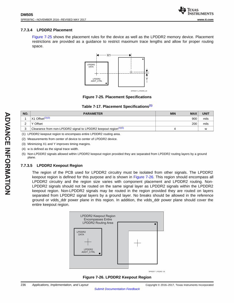
AD
VA
NC
E IN
FO
RM
AT
ION
LPDDR2ADDT_CTRL
LPDDR2DATA
SPRS917_LPDDR2_05
LPDDR2 Keepout RegionEncompasses Entire
LPDDR2 Routing Area
Y
X1
SPRS917_LPDDR2_04
LPDDR2DATA
LPDDR2ADDT_CTRL
236
DM505SPRS976C –NOVEMBER 2016–REVISED MAY 2017 www.ti.com
Submit Documentation FeedbackApplications, Implementation, and Layout Copyright © 2016–2017, Texas Instruments Incorporated
7.7.3.4 LPDDR2 Placement
Figure 7-25 shows the placement rules for the device as well as the LPDDR2 memory device. Placementrestrictions are provided as a guidance to restrict maximum trace lengths and allow for proper routingspace.
Figure 7-25. Placement Specifications
Table 7-17. Placement Specifications(1)
NO. PARAMETER MIN MAX UNIT1 X1 Offset(2)(3) 900 mils2 Y Offset 200 mils3 Clearance from non-LPDDR2 signal to LPDDR2 keepout region(4)(5) 4 w
(1) LPDDR2 keepout region to encompass entire LPDDR2 routing area.(2) Measurements from center of device to center of LPDDR2 device.(3) Minimizing X1 and Y improves timing margins.(4) w is defined as the signal trace width.(5) Non-LPDDR2 signals allowed within LPDDR2 keepout region provided they are separated from LPDDR2 routing layers by a ground
plane.
7.7.3.5 LPDDR2 Keepout Region
The region of the PCB used for LPDDR2 circuitry must be isolated from other signals. The LPDDR2keepout region is defined for this purpose and is shown in Figure 7-26. This region should encompass allLPDDR2 circuitry and the region size varies with component placement and LPDDR2 routing. Non-LPDDR2 signals should not be routed on the same signal layer as LPDDR2 signals within the LPDDR2keepout region. Non-LPDDR2 signals may be routed in the region provided they are routed on layersseparated from LPDDR2 signal layers by a ground layer. No breaks should be allowed in the referenceground or vdds_ddr power plane in this region. In addition, the vdds_ddr power plane should cover theentire keepout region.
Figure 7-26. LPDDR2 Keepout Region

AD
VA
NC
E I
NF
OR
MA
TIO
N
237
DM505www.ti.com SPRS976C –NOVEMBER 2016–REVISED MAY 2017
Submit Documentation FeedbackApplications, Implementation, and LayoutCopyright © 2016–2017, Texas Instruments Incorporated
7.7.3.6 LPDDR2 Net Classes
Table 7-18. Clock Net Class Definitions for the LPDDR2 Interface
CLOCK NET CLASS PIN NAMESCK ddr1_ck and ddr1_nck
DQS0 ddr1_dqs0 and ddr1_dqsn0DQS1 ddr1_dqs1 and ddr1_dqsn1DQS2 ddr1_dqs2 and ddr1_dqsn2DQS3 ddr1_dqs3 and ddr1_dqsn3
Table 7-19. Signal Net Class and Associated Clock Net Class for LPDDR2 Interface
SIGNAL NET CLASS ASSOCIATED CLOCKNET CLASS BALL NAMES
ADDR_CTRL CK ddr1_ba[2:0], ddr1_csn0, ddr1_cke0, ddr1_rasn, ddr1_casn, ddr1_wen,ddr1_a1, ddr1_a2, dr1_a10, ddr1_a13
DQ0 DQS0 ddr1_d[7:0], ddr1_dqm0, ddr1_dqs0, ddr1_dqsn0 (1)
DQ1 DQS1 ddr1_d[15:8], ddr1_dqm1, ddr1_dqs1, ddr1_dqsn1 (1)
DQ2 DQS2 ddr1_d[23:16], ddr1_dqm2, ddr1_dqs2, ddr1_dqsn2 (1)
DQ3 DQS3 ddr1_d[31:24], ddr1_dqm3, ddr1_dqs3, ddr1_dqsn3 (1)
(1) DQ data class includes DQS/N pins
7.7.3.7 LPDDR2 Signal Termination
On-device termination (ODT) is available for DQ[3:0] signal net classes, but is not specifically required fornormal operation. System designers may evaluate the need for additional series termination if requiredbased on signal integrity, EMI and overshoot/undershoot reduction.
On board series termination is recommended for all ADDR_CTRL and CK class signals. It isrecommended a resistor with value of 10 Ω to be placed close to the DM50x source pin (within 350 mils).
On board series termination is recommended for all DQx and DQSx class signals. It is recommended aresistor with value of 22 Ω to be placed close to the DM50x source pin (within 500 mils).
7.7.3.8 LPDDR2 DDR_VREF Routing
DDR_VREF is the reference voltage for the input buffers on the LPDDR2 memory. DDR_VREF isintended to be half the LPDDR2 power supply voltage and is typically generated with a voltage dividerconnected to the VDDS_DDR power supply. It should be routed as a nominal 20-mil wide trace with 0.1-µF bypass capacitors near each device connection. Narrowing of DDR_VREF is allowed to accommodaterouting congestion.
7.7.4 Routing Specification
7.7.4.1 DQS[x] and DQ[x] Routing Specification
DQS[x] lines are point-to-point differential and DQ[x] lines are point-to-point single ended. Figure 7-27 andFigure 7-28 represent the supported topologies. Figure 7-29 and Figure 7-30 show the DQS[x] and DQ[x]routing. Figure 7-31 shows the DQLM for the LPDDR2 interface.
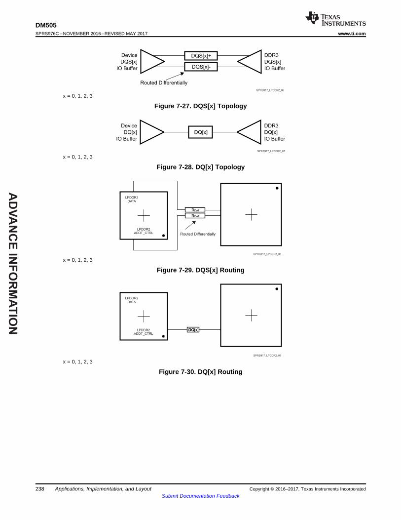
AD
VA
NC
E IN
FO
RM
AT
ION
SPRS917_LPDDR2_09
LPDDR2DATA
LPDDR2ADDT_CTRL
DQ[x]DQ[x]
Routed Differentially
SPRS917_LPDDR2_08
RDAT
RDAT
LPDDR2DATA
LPDDR2ADDT_CTRL
DQ[x]
Device
DQ[x]
IO Buffer
DDR3
DQ[x]
IO Buffer
SPRS917_LPDDR2_07
Device
DQS[x]
IO Buffer
DDR3
DQS[x]
IO Buffer
Routed Differentially
DQS[x]-
DQS[x]+
SPRS917_LPDDR2_06
238
DM505SPRS976C –NOVEMBER 2016–REVISED MAY 2017 www.ti.com
Submit Documentation FeedbackApplications, Implementation, and Layout Copyright © 2016–2017, Texas Instruments Incorporated
x = 0, 1, 2, 3
Figure 7-27. DQS[x] Topology
x = 0, 1, 2, 3
Figure 7-28. DQ[x] Topology
x = 0, 1, 2, 3
Figure 7-29. DQS[x] Routing
x = 0, 1, 2, 3
Figure 7-30. DQ[x] Routing

AD
VA
NC
E I
NF
OR
MA
TIO
N
DQLMYi
DQi
DQLMXi
i = 0, 1, 2, 3
LPDDR2interface
DQLM0 = DQLMX0 + DQLMY0
DQLM2 = DQLMX2 + DQLMY2DQLM1 = DQLMX1 + DQLMY1
DQLM3 = DQLMX3 + DQLMY3
DQ0 - DQ3 represent data bytes 0 - 3.
SPRS917_LPDDR2_10
239
DM505www.ti.com SPRS976C –NOVEMBER 2016–REVISED MAY 2017
Submit Documentation FeedbackApplications, Implementation, and LayoutCopyright © 2016–2017, Texas Instruments Incorporated
There are four DQLMs, one for each data byte, in a 32-bit interface and two DQLMs, one for each data byte, in a 16-bit interface. Each DQLM is the longest Manhattan distance of the byte.
Figure 7-31. DQLM for LPDDR2 Interface
Trace routing specifications for the DQ[x] and the DQS[x] are specified in Table 7-20.
Table 7-20. DQS[x] and DQ[x] Routing Specification(1)(2)
NO. PARAMETER MIN TYP MAX UNIT1 DQ0 nominal length(3)(4) DQLM0 mils2 DQ1 nominal length(3)(5) DQLM1 mils3 DQ2 nominal length (3)(6) DQLM2 mils4 DQ3 nominal length (3)(7) DQLM3 mils5 DQ[x] skew(8) 10 ps6 DQS[x] skew 5 ps7 Via count per each trace in DQ[x], DQS[x] 28 Via count difference across a given DQ[x], DQS[x] 09 DQS[x]-to-DQ[x] skew(8)(9) 10 ps10 Center-to-center DQ[x] to other LPDDR2 trace spacing(10)(11) 4 w11 Center-to-center DQ[x] to other DQ[x] trace spacing(10)(12) 3 w12 DQS[x] center-to-center spacing(13)
13 DQS[x] center-to-center spacing to other net(10) 4 w
(1) DQS[x] represents the DQS0, DQS1, DQS2, DQS3 clock net classes, and DQ[x] represents the DQ0, DQ1, DQ2, DQ3 signal netclasses.
(2) External termination disallowed. Data termination should use built-in ODT functionality.(3) DQLMn is the longest Manhattan distance of a byte.(4) DQLM0 is the longest Manhattan length for the DQ0 net class.(5) DQLM1 is the longest Manhattan length for the DQ1 net class.(6) DQLM2 is the longest Manhattan length for the DQ2 net class.(7) DQLM3 is the longest Manhattan length for the DQ3 net class.(8) Length matching is only done within a byte. Length matching across bytes is not required.(9) Each DQS clock net class is length matched to its associated DQ signal net class.(10) Center-to-center spacing is allowed to fall to minimum for up to 1000 mils of routed length.(11) Other LPDDR2 trace spacing means signals that are not part of the same DQ[x] signal net class.(12) This applies to spacing within same DQ[x] signal net class.(13) DQS[x] pair spacing is set to ensure proper differential impedance. Differential impedance should be Zo x 2, where Zo is the single-
ended impedance.

AD
VA
NC
E IN
FO
RM
AT
ION
SPRS917_LPDDR2_14
LPDDR2DATA
LPDDR2ADDT_CTRL
ADDR_CTRL
SPRS917_LPDDR2_13
RD
AT
LPDDR2DATA
LPDDR2ADDT_CTRL
ADDR_CTRLDevice
ADDR_CTRL
Output Buffer
LPDDR2
ADDR_CTRL
Input Buffer
SPRS917_LPDDR2_12
Device CK
Output Buffer
LPDDR2
Input Buffer
Routed Differentially
CK-
CK+
SPRS917_LPDDR2_11
240
DM505SPRS976C –NOVEMBER 2016–REVISED MAY 2017 www.ti.com
Submit Documentation FeedbackApplications, Implementation, and Layout Copyright © 2016–2017, Texas Instruments Incorporated
7.7.4.2 CK and ADDR_CTRL Routing Specification
CK signals are routed as point-to-point differential, and ADDR_CTRL signals are routed as point-to-pointsingle ended. The supported topology for CK and ADDR_CTRL are shown in Figure 7-32 throughFigure 7-35. Note that ADDR_CTRL are routed very similar to DQ and CK is routed very similar to DQS.
Figure 7-32. CK Signals Topology
Figure 7-33. ADDR_CTRL Signals Topology
Figure 7-34. CK Signals Routing
Figure 7-35. ADDR_CTRL Signals Routing

AD
VA
NC
E I
NF
OR
MA
TIO
N
CACLMY
CACLMX
CACLM = CACLMX + CACLMY
LPDDR2interface
SPRS917_LPDDR2_15
241
DM505www.ti.com SPRS976C –NOVEMBER 2016–REVISED MAY 2017
Submit Documentation FeedbackApplications, Implementation, and LayoutCopyright © 2016–2017, Texas Instruments Incorporated
CACLM is the longest Manhattan distance of the CK/ADDR_CTRL signal class.
Figure 7-36. CACLM for LPDDR2 Interface
Trace routing specifications for the CK and the ADD_CTRL are specified in Table 7-21.
Table 7-21. CK and ADDR_CTRL Routing Specification
NO. PARAMETER MIN TYP MAX UNIT1 CK and ADDR_CTRL nominal trace length(1) CACLM mils2 ADDR_CTRL skew 20 ps3 CK skew 5 ps4 Via count per each trace ADDR_CTRL, CK 25 Via count difference across ADDR_CTRL, CK 06 ADDR_CTRL-to-CK skew 20 ps7 Center-to-center ADDR_CTRL to other LPDDR2 trace spacing(2)(3) 4 w8 Center-to-center ADDR_CTRL to other ADDR_CTRL trace spacing(2) 3 w9 CK center-to-center spacing(4)
10 CK center-to-center spacing to other net(2) 4 w
(1) CACLM is the longest Manhattan distance of ADDR_CTRL and CK.(2) Center-to-center spacing is allowed to fall to minimum for up to 1000 mils of routed length.(3) Other LPDDR2 trace spacing means signals that are not part of the same CK, ADDR_CTRL signal net class.(4) CK pair spacing is set to ensure proper differential impedance. Differential impedance should be Zo x 2, where Zo is the single ended
impedance.
7.8 DDR2 Board Design and Layout Guidelines
7.8.1 DDR2 General Board Layout GuidelinesTo help ensure good signaling performance, consider the following board design guidelines:• Avoid crossing splits in the power plane.• Minimize Vref noise.• Use the widest trace that is practical between decoupling capacitors and memory module.• Maintain a single reference.• Minimize ISI by keeping impedances matched.• Minimize crosstalk by isolating sensitive bits, such as strobes, and avoiding return path discontinuities.• Use proper low-pass filtering on the Vref pins.• Keep the stub length as short as possible.• Add additional spacing for on-clock and strobe nets to eliminate crosstalk.

AD
VA
NC
E IN
FO
RM
AT
ION
ddrx_ck
1
PCB_DDR2_0
242
DM505SPRS976C –NOVEMBER 2016–REVISED MAY 2017 www.ti.com
Submit Documentation FeedbackApplications, Implementation, and Layout Copyright © 2016–2017, Texas Instruments Incorporated
• Maintain a common ground reference for all bypass and decoupling capacitors.• Take into account the differences in propagation delays between microstrip and stripline nets when
evaluating timing constraints.
7.8.2 DDR2 Board Design and Layout Guidelines
7.8.2.1 Board Designs
TI only supports board designs that follow the guidelines outlined in this document. The switchingcharacteristics and the timing diagram for the DDR2 memory controller are shown in Table 7-22 andFigure 7-37.
Table 7-22. Switching Characteristics Over Recommended Operating Conditions for DDR2 MemoryController
NO. PARAMETER DESCRIPTION MIN MAX UNIT
DDR21 tc(DDR_CLK) Cycle time, DDR_CLK 2.5 8 ns
Figure 7-37. DDR2 Memory Controller Clock Timing
7.8.2.2 DDR2 Interface
This section provides the timing specification for the DDR2 interface as a PCB design and manufacturingspecification. The design rules constrain PCB trace length, PCB trace skew, signal integrity, cross-talk,and signal timing. These rules, when followed, result in a reliable DDR2 memory system without the needfor a complex timing closure process. For more information regarding the guidelines for using this DDR2specification, see the Understanding TI’s PCB Routing Rule-Based DDR Timing Specification ApplicationReport (Literature Number: SPRAAV0).
7.8.2.2.1 DDR2 Interface Schematic
Figure 7-38 shows the DDR2 interface schematic for a x32 DDR2 memory system. In Figure 7-39 the x16DDR2 system schematic is identical except that the high-word DDR2 device is deleted.
When not using all or part of a DDR2 interface, the proper method of handling the unused pins is to tie offthe ddrx_dqsi pins to ground via a 1k-Ω resistor and to tie off the ddrx_dqsni pins to the correspondingvdds_ddrx supply via a 1k-Ω resistor. This needs to be done for each byte not used. The vdds_ddrx andddrx_vref0 power supply pins need to be connected to their respective power supplies even if DDRx is notbeing used. All other DDR interface pins can be left unconnected. Note that the supported modes for useof the DDR EMIF are 32-bits wide, 16-bits wide, or not used.

AD
VA
NC
E I
NF
OR
MA
TIO
N
DQ0
DQ7
DQM0
DQS0
DQS0n
DQ8
DQ15
DQM1
DQS1
DQS1n
BA0
BA2
A0
A14
CS
CAS
RAS
WE
CKE
CK
CK
1 K Ω 1%
vdds_ddrx(A)
DDR2
VREF
0.1 µF
VREF
0.1 µF 1 K Ω 1%
ODT
NC
ddrx_d0
ddrx_d7
ddrx_dqm0
ddrx_dqs0
ddrx_dqsn0
ddrx_d8
ddrx_d15
ddrx_dqm1
ddrx_dqs1
ddrx_dqsn1
ddrx_d16
ddrx_d23
ddrx_dqm2
ddrx_dqs2
ddrx_dqsn2
ddrx_d24
ddrx_d31
ddrx_dqm3ddrx_dqs3
ddrx_dqsn3
ddrx_ba0
ddrx_ba2
ddrx_a0
ddrx_a14
ddrx_csn0
ddrx_casn
ddrx_rasn
ddrx_wen
ddrx_cke
ddrx_ck
ddrx_nck
ddrx_odt0
ddrx_rst
PCB_DDR2_1
DQ16
DQ23
DQM2
DQS2
DQS2n
DQ24
DQ31
DQM3
DQS3
DQS3n
243
DM505www.ti.com SPRS976C –NOVEMBER 2016–REVISED MAY 2017
Submit Documentation FeedbackApplications, Implementation, and LayoutCopyright © 2016–2017, Texas Instruments Incorporated
A. vdds_ddrx is the power supply for the DDR2 memories and the Device DDR2 interface.B. One of these capacitors can be eliminated if the divider and its capacitors are placed near a VREF pin.
Figure 7-38. 32-Bit DDR2 High-Level Schematic

AD
VA
NC
E IN
FO
RM
AT
ION
DQ0
DQ7
LDM
LDQS
LDQS
DQ8
DQ15
UDM
UDQS
UDQS
BA0
BA2
A0
A14
CS
CAS
RAS
WE
CKE
CK
CK 1 K Ω 1%
vdds_ddrx(A)
DDR2
VREF
0.1 µF
VREF
0.1 µF 1 K Ω 1%
ODT
NC
NC
NC
1 KΩ
NC
NC
1 KΩ
1 KΩ
1 KΩ
vdds_ddrx(A)
vdds_ddrx(A)
NC
NC
ddrx_d0
ddrx_d7
ddrx_dqm0
ddrx_dqs0
ddrx_dqsn0
ddrx_d8
ddrx_d15
ddrx_dqm1
ddrx_dqs1
ddrx_dqsn1
ddrx_d16
ddrx_d23
ddrx_dqm2
ddrx_dqsn2
ddrx_dqs2
ddrx_d24
ddrx_d31
ddrx_dqm3
ddrx_dqsn3
ddrx_dqs3
ddrx_ba0
ddrx_odt0
ddrx_ba2
ddrx_a0
ddrx_a14
ddrx_csn0
ddrx_casn
ddrx_rasn
ddrx_wen
ddrx_cke
ddrx_ck
ddrx_nck
ddrx_rst
PCB_DDR2_2
NC
244
DM505SPRS976C –NOVEMBER 2016–REVISED MAY 2017 www.ti.com
Submit Documentation FeedbackApplications, Implementation, and Layout Copyright © 2016–2017, Texas Instruments Incorporated
A. vdds_ddrx is the power supply for the DDR2 memories and the Device DDR2 interface.B. One of these capacitors can be eliminated if the divider and its capacitors are placed near a VREF pin.
Figure 7-39. 16-Bit DDR2 High-Level Schematic

AD
VA
NC
E I
NF
OR
MA
TIO
N
245
DM505www.ti.com SPRS976C –NOVEMBER 2016–REVISED MAY 2017
Submit Documentation FeedbackApplications, Implementation, and LayoutCopyright © 2016–2017, Texas Instruments Incorporated
7.8.2.2.2 Compatible JEDEC DDR2 Devices
Table 7-23 shows the parameters of the JEDEC DDR2 devices that are compatible with this interface.Generally, the DDR2 interface is compatible with x16/x32 DDR2-800 speed grade DDR2 devices.
Table 7-23. Compatible JEDEC DDR2 Devices (Per Interface)
NO. PARAMETER MIN MAX UNITCJ21 JEDEC DDR2 device speed grade(1) DDR2-800CJ22 JEDEC DDR2 device bit width x16 x32 BitsCJ23 JEDEC DDR2 device count(2) 1 1 Devices
(1) Higher DDR2 speed grades are supported due to inherent JEDEC DDR2 backwards compatibility.(2) One DDR2 device is used for a 16-bit DDR2 and 32-bit DDR2 memory system.
7.8.2.2.3 PCB Stackup
The minimum stackup required for routing the Device is a six-layer stackup as shown in Table 7-24.Additional layers may be added to the PCB stackup to accommodate other circuitry or to reduce the sizeof the PCB footprint.
Table 7-24. Minimum PCB Stackup
LAYER TYPE DESCRIPTION1 Signal External Routing2 Plane Ground3 Plane Power4 Signal Internal routing5 Plane Ground6 Signal External Routing
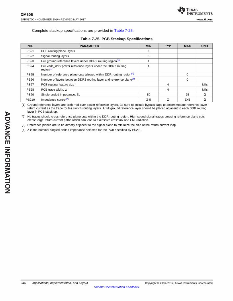
AD
VA
NC
E IN
FO
RM
AT
ION
246
DM505SPRS976C –NOVEMBER 2016–REVISED MAY 2017 www.ti.com
Submit Documentation FeedbackApplications, Implementation, and Layout Copyright © 2016–2017, Texas Instruments Incorporated
Complete stackup specifications are provided in Table 7-25.
Table 7-25. PCB Stackup Specifications
NO. PARAMETER MIN TYP MAX UNITPS21 PCB routing/plane layers 6PS22 Signal routing layers 3PS23 Full ground reference layers under DDR2 routing region(1) 1PS24 Full vdds_ddrx power reference layers under the DDR2 routing
region(1)1
PS25 Number of reference plane cuts allowed within DDR routing region(2) 0PS26 Number of layers between DDR2 routing layer and reference plane(3) 0PS27 PCB routing feature size 4 MilsPS28 PCB trace width, w 4 MilsPS29 Single-ended impedance, Zo 50 75 ΩPS210 Impedance control(4) Z-5 Z Z+5 Ω
(1) Ground reference layers are preferred over power reference layers. Be sure to include bypass caps to accommodate reference layerreturn current as the trace routes switch routing layers. A full ground reference layer should be placed adjacent to each DDR routinglayer in PCB stack up.
(2) No traces should cross reference plane cuts within the DDR routing region. High-speed signal traces crossing reference plane cutscreate large return current paths which can lead to excessive crosstalk and EMI radiation.
(3) Reference planes are to be directly adjacent to the signal plane to minimize the size of the return current loop.(4) Z is the nominal singled-ended impedance selected for the PCB specified by PS29.

AD
VA
NC
E I
NF
OR
MA
TIO
N
X1
Y1
PCB_DDR2_3
DDR2 Controller
A1
DDR2Memory
247
DM505www.ti.com SPRS976C –NOVEMBER 2016–REVISED MAY 2017
Submit Documentation FeedbackApplications, Implementation, and LayoutCopyright © 2016–2017, Texas Instruments Incorporated
7.8.2.2.4 Placement
Figure 7-40 shows the required placement for the Device as well as the DDR2 devices. The dimensionsfor this figure are defined in Table 7-26. The placement does not restrict the side of the PCB on which thedevices are mounted. The ultimate purpose of the placement is to limit the maximum trace lengths andallow for proper routing space. For a 16-bit DDR memory system, the high-word DDR2 device is omittedfrom the placement.
Figure 7-40. Device and DDR2 Device Placement
Table 7-26. Placement Specifications DDR2
NO. PARAMETER MIN MAX UNITKOD21 X1 1100 MilsKOD22 Y1 500 MilsKOD24 DDR2 keepout region (1)
KOD25 Clearance from non-DDR2 signal to DDR2 keepout region (2) (3) 4 W
(1) DDR2 keepout region to encompass entire DDR2 routing area.(2) Non-DDR2 signals allowed within DDR2 keepout region provided they are separated from DDR2 routing layers by a ground plane.(3) If a device has more than one DDR controller, the signals from the other controller(s) are considered non-DDR2 and should be
separated by this specification.

AD
VA
NC
E IN
FO
RM
AT
ION
PCB_DDR2_4
DD
R2 C
ontr
olle
r
DD
R2 D
evic
e
Device
A1
DDR2 Controller
248
DM505SPRS976C –NOVEMBER 2016–REVISED MAY 2017 www.ti.com
Submit Documentation FeedbackApplications, Implementation, and Layout Copyright © 2016–2017, Texas Instruments Incorporated
7.8.2.2.5 DDR2 Keepout Region
The region of the PCB used for the DDR2 circuitry must be isolated from other signals. The DDR2keepout region is defined for this purpose and is shown in Figure 7-41. The size of this region varies withthe placement and DDR routing. Additional clearances required for the keepout region are shown inTable 7-26.
The region shown in Table 7-26 should encompass all the DDR2 circuitry and varies depending onplacement. Non-DDR2 signals should not be routed on the DDR signal layers within the DDR2 keepoutregion. Non-DDR2 signals may be routed in the region, provided they are routed on layers separated fromDDR2 signal layers by a ground layer. No breaks should be allowed in the reference ground layers in thisregion. In addition, the vdds_ddrx power plane should cover the entire keepout region. Routes for the twoDDR interfaces must be separated by at least 4x; the more separation, the better.
Figure 7-41. DDR2 Keepout Region
7.8.2.2.6 Bulk Bypass Capacitors
Bulk bypass capacitors are required for moderate speed bypassing of the DDR2 and other circuitry.Table 7-27 contains the minimum numbers and capacitance required for the bulk bypass capacitors. Notethat this table only covers the bypass needs of the DDR2 interfaces and DDR2 device. Additional bulkbypass capacitance may be needed for other circuitry.
Table 7-27. Bulk Bypass Capacitors
NO. PARAMETER MIN TYP MAX UNITBC21 vdds_ddrx bulk bypass capacitor (≥1µF) count(1) 10 DevicesBC22 vdds_ddrx bulk bypass total capacitance 50 μF
(1) These devices should be placed near the devices they are bypassing, but preference should be given to the placement of the high-speed (HS) bypass capacitors and DDR2 signal routing.
7.8.2.2.7 High-Speed Bypass Capacitors
TI recommends that a PDN/power integrity analysis is performed to ensure that capacitor selection andplacement is optimal for a given implementation. This section provides guidelines that can serve as agood starting point.

AD
VA
NC
E I
NF
OR
MA
TIO
N
249
DM505www.ti.com SPRS976C –NOVEMBER 2016–REVISED MAY 2017
Submit Documentation FeedbackApplications, Implementation, and LayoutCopyright © 2016–2017, Texas Instruments Incorporated
High-speed (HS) bypass capacitors are critical for proper DDR2 interface operation. It is particularlyimportant to minimize the parasitic series inductance of the HS bypass capacitors, processor/DDR power,and processor/DDR ground connections. Table 7-28 contains the specification for the HS bypasscapacitors as well as for the power connections on the PCB. Generally speaking, it is good to:1. Fit as many HS bypass capacitors as possible.2. HS bypass capacitor value is < 1µF3. Minimize the distance from the bypass cap to the pins/balls being bypassed.4. Use the smallest physical sized capacitors possible with the highest capacitance readily available.5. Connect the bypass capacitor pads to their vias using the widest traces possible and using the largest
hole size via possible.6. Minimize via sharing. Note the limites on via sharing shown in Table 7-28.
Table 7-28. High-Speed Bypass Capacitors
NO. PARAMETER MIN TYP MAX UNITHS21 HS bypass capacitor package size(1) 0201 0402 10 MilsHS22 Distance, HS bypass capacitor to processor being bypassed(2)(3)(4) 400(12) MilsHS23 Processor HS bypass capacitor count (12) 12(11) DevicesHS24 Processor HS bypass capacitor total capacitance per vdds_ddrx rail
(12)3.4 μF
HS25 Number of connection vias for each device power/ground ball pervdds_ddrx rail (5)
1 Vias
HS26 Trace length from device power/ground ball to connection via(2) 35 70 MilsHS27 Distance, HS bypass capacitor to DDR device being bypassed(6) 150 MilsHS28 Number of connection vias for each HS capacitor(8)(9) 4 (14) ViasHS29 DDR2 device HS bypass capacitor count(7) 12 (13) DevicesHS210 DDR2 device HS bypass capacitor total capacitance(7) 0.85 μFHS211 Trace length from bypass capacitor connect to connection via(2)(9) 35 100 MilsHS212 Number of connection vias for each DDR2 device power/ground
ball(10)1 Vias
HS213 Trace length from DDR2 device power/ground ball to connectionvia(2)(8)
35 60 Mils
(1) LxW, 10-mil units, that is, a 0402 is a 40x20-mil surface-mount capacitor.(2) Closer/shorter is better.(3) Measured from the nearest processor power/ground ball to the center of the capacitor package.(4) Three of these capacitors should be located underneath the processor, between the cluster of vdds_ddrx balls and ground balls,
between the DDR interfaces on the package.(5) See the Via Channel™ escape for the processor package.(6) Measured from the DDR2 device power/ground ball to the center of the capacitor package.(7) Per DDR2 device.(8) An additional HS bypass capacitor can share the connection vias only if it is mounted on the opposite side of the board. No sharing of
vias is permitted on the same side of the board.(9) An HS bypass capacitor may share a via with a DDR device mounted on the same side of the PCB. A wide trace should be used for the
connection and the length from the capacitor pad to the DDR device pad should be less than 150 mils.(10) Up to a total of two pairs of DDR power/ground balls may share a via.(11) The capacitor recommendations in this data manual reflect only the needs of this processor. Please see the memory vendor’s
guidelines for determining the appropriate decoupling capacitor arrangement for the memory device itself.(12) For more information, see Section 7.3, Core Power Domains(13) For more information refer to DDR2 specification.(14) Preferred configuration is 4 vias: 2 to power and 2 to ground.
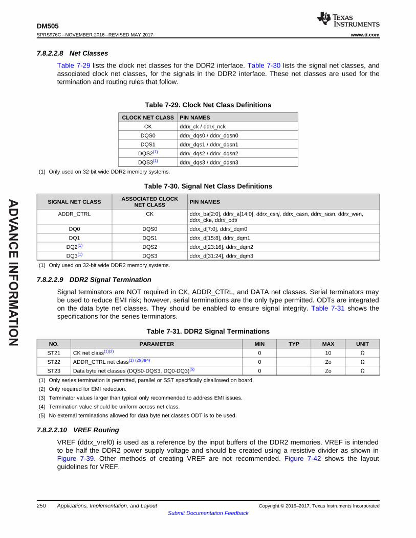
AD
VA
NC
E IN
FO
RM
AT
ION
250
DM505SPRS976C –NOVEMBER 2016–REVISED MAY 2017 www.ti.com
Submit Documentation FeedbackApplications, Implementation, and Layout Copyright © 2016–2017, Texas Instruments Incorporated
7.8.2.2.8 Net Classes
Table 7-29 lists the clock net classes for the DDR2 interface. Table 7-30 lists the signal net classes, andassociated clock net classes, for the signals in the DDR2 interface. These net classes are used for thetermination and routing rules that follow.
Table 7-29. Clock Net Class Definitions
CLOCK NET CLASS PIN NAMESCK ddrx_ck / ddrx_nck
DQS0 ddrx_dqs0 / ddrx_dqsn0DQS1 ddrx_dqs1 / ddrx_dqsn1
DQS2(1) ddrx_dqs2 / ddrx_dqsn2DQS3(1) ddrx_dqs3 / ddrx_dqsn3
(1) Only used on 32-bit wide DDR2 memory systems.
Table 7-30. Signal Net Class Definitions
SIGNAL NET CLASS ASSOCIATED CLOCKNET CLASS PIN NAMES
ADDR_CTRL CK ddrx_ba[2:0], ddrx_a[14:0], ddrx_csnj, ddrx_casn, ddrx_rasn, ddrx_wen,ddrx_cke, ddrx_odti
DQ0 DQS0 ddrx_d[7:0], ddrx_dqm0DQ1 DQS1 ddrx_d[15:8], ddrx_dqm1
DQ2(1) DQS2 ddrx_d[23:16], ddrx_dqm2DQ3(1) DQS3 ddrx_d[31:24], ddrx_dqm3
(1) Only used on 32-bit wide DDR2 memory systems.
7.8.2.2.9 DDR2 Signal Termination
Signal terminators are NOT required in CK, ADDR_CTRL, and DATA net classes. Serial terminators maybe used to reduce EMI risk; however, serial terminations are the only type permitted. ODTs are integratedon the data byte net classes. They should be enabled to ensure signal integrity. Table 7-31 shows thespecifications for the series terminators.
Table 7-31. DDR2 Signal Terminations
NO. PARAMETER MIN TYP MAX UNITST21 CK net class(1)(2) 0 10 ΩST22 ADDR_CTRL net class(1) (2)(3)(4) 0 Zo ΩST23 Data byte net classes (DQS0-DQS3, DQ0-DQ3)(5) 0 Zo Ω
(1) Only series termination is permitted, parallel or SST specifically disallowed on board.(2) Only required for EMI reduction.(3) Terminator values larger than typical only recommended to address EMI issues.(4) Termination value should be uniform across net class.(5) No external terminations allowed for data byte net classes ODT is to be used.
7.8.2.2.10 VREF Routing
VREF (ddrx_vref0) is used as a reference by the input buffers of the DDR2 memories. VREF is intendedto be half the DDR2 power supply voltage and should be created using a resistive divider as shown inFigure 7-39. Other methods of creating VREF are not recommended. Figure 7-42 shows the layoutguidelines for VREF.

AD
VA
NC
E I
NF
OR
MA
TIO
NPCB_DDR2_6
DDR2 Controller
DD
R2 D
evic
e
A’
PCB_DDR2_5
DDR2 Controller
DD
R2 D
evic
e
VREF Bypass Capacitor
Neck down to minimum in BGA escaperegions is acceptable. Narrowing toaccomodate via congestion for shortdistances is also acceptable. Best
performance is obtained if the widthof VREF is maximized.
VREF Nominal Max Tracewidth is 20 mils
1 K Ω 1%
vdds_ddrx(A)
VREF
0.1 µF
0.1 µF 1 K Ω 1%
A. vdds_ddrx is the power supply for the DDR2 memories and the Device DDR2 interface.
251
DM505www.ti.com SPRS976C –NOVEMBER 2016–REVISED MAY 2017
Submit Documentation FeedbackApplications, Implementation, and LayoutCopyright © 2016–2017, Texas Instruments Incorporated
Figure 7-42. VREF Routing and Topology
7.8.2.3 DDR2 CK and ADDR_CTRL Routing
Figure 7-43 shows the topology of the routing for the CK and ADDR_CTRL net classes. The route is apoint to point connection with required skew matching.
Figure 7-43. CK and ADDR_CTRL Routing and Topology
Table 7-32. CK and ADDR_CTRL Routing SpecificationNO. PARAMETER MIN MAX UNIT
RSC21 Center-to-center ddrx_ck - ddrx_nck spacing 2w
RSC22 ddrx_ck / ddrx_nck skew 5 ps
RSC25 Center-to-center CK to other DDR2 trace spacing(2) 4w
RSC26 CK/ADDR_CTRL trace length(3) 680 ps
RSC27 ADDR_CTRL-to-CK skew mismatch 25 ps
RSC28 ADDR_CTRL-to-ADDR_CTRL skew mismatch 25 ps
RSC29 Center-to-center ADDR_CTRL to other DDR2 trace spacing(2) 4w

AD
VA
NC
E IN
FO
RM
AT
ION
PCB_DDR2_7
DDR2 Controller
DD
R2 D
evic
e
E0
E1
E2
E3
252
DM505SPRS976C –NOVEMBER 2016–REVISED MAY 2017 www.ti.com
Submit Documentation FeedbackApplications, Implementation, and Layout Copyright © 2016–2017, Texas Instruments Incorporated
Table 7-32. CK and ADDR_CTRL Routing Specification (continued)NO. PARAMETER MIN MAX UNIT
RSC210 Center-to-center ADDR_CTRL to other ADDR_CTRL trace spacing(2) 3w
(1) Series terminator, if used, should be located closest to the Device.(2) Center-to-center spacing is allowed to fall to minimum 2w for up to 500 mils of routed length to accommodate BGA escape and routing
congestion.(3) This is the longest routing length of the CK and ADDR_CTRL net classes.
Figure 7-44 shows the topology and routing for the DQS and DQ net classes; the routes are point to point.Skew matching across bytes is not needed nor recommended. The termination resistor should be placednear the processor.
Figure 7-44. DQS and DQ Routing and Topology
Table 7-33. DQS and DQ Routing Specification
NO. PARAMETER MIN MAX UNITRSDQ21 Center-to-center DQS-DQSn spacing in E0|E1|E2|E3 2wRSDQ22 DQS-DQSn skew in E0|E1|E2|E3 5 psRSDQ23 Center-to-center DQS to other DDR2 trace spacing(1) 4wRSDQ24 DQS/DQ trace length (2)(3)(4) 325 psRSDQ25 DQ-to-DQS skew mismatch(2)(3)(4) 10 psRSDQ26 DQ-to-DQ skew mismatch(2)(3)(4) 10 psRSDQ27 DQ-to-DQ/DQS via count mismatch(2)(3)(4) 1 ViasRSDQ28 Center-to-center DQ to other DDR2 trace spacing(1)(5) 4wRSDQ29 Center-to-center DQ to other DQ trace spacing(1)(6)(7) 3wRSDQ210 DQ/DQS E skew mismatch(2)(3)(4) 25 ps
(1) Center-to-center spacing is allowed to fall to minimum 2w for up to 500 mils of routed length to accommodate BGA escape and routingcongestion.
(2) A 16-bit DDR memory system has two sets of data net classes; one for data byte 0, and one for data byte 1, each with an associatedDQS (2 DQSs) per DDR EMIF used.
(3) A 32-bit DDR memory system has four sets of data net classes; one each for data bytes 0 through 3, and each associated with a DQS(4 DQSs) per DDR EMIF used.
(4) There is no need, and it is not recommended, to skew match across data bytes; that is, from DQS0 and data byte 0 to DQS1 and databyte1.
(5) DQs from other DQS domains are considered other DDR2 trace.(6) DQs from other data bytes are considered other DDR2 trace.(7) This is the longest routing distance of each of the DQS and DQ net classes.
7.9 DDR3 Board Design and Layout Guidelines

AD
VA
NC
E I
NF
OR
MA
TIO
N
DDR_CLK
1
SPRS91v_PCB_DDR3_01
253
DM505www.ti.com SPRS976C –NOVEMBER 2016–REVISED MAY 2017
Submit Documentation FeedbackApplications, Implementation, and LayoutCopyright © 2016–2017, Texas Instruments Incorporated
7.9.1 DDR3 General Board Layout GuidelinesTo help ensure good signaling performance, consider the following board design guidelines:• Avoid crossing splits in the power plane.• Use the widest trace that is practical between decoupling capacitors and memory module.• Maintain a single reference• Minimize ISI by keeping impedances matched.• Minimize crosstalk by isolating sensitive bits, such as strobes, and avoiding return path discontinuities.• Keep the stub length as short as possible.• Add additional spacing for on-clock and strobe nets to eliminate crosstalk.• Maintain a common ground reference for all bypass and decoupling capacitors.• Take into account the differences in propagation delays between microstrip and stripline nets when
evaluating timing constraints.
7.9.2 DDR3 Board Design and Layout Guidelines
7.9.2.1 Board Designs
TI only supports board designs utilizing DDR3 memory that follow the guidelines in this document. Theswitching characteristics and timing diagram for the DDR3 memory controller are shown in Table 7-34 andFigure 7-45.
Table 7-34. Switching Characteristics Over Recommended Operating Conditions for DDR3 MemoryController
NO. PARAMETER MIN MAX UNIT1 tc(DDR_CLK) Cycle time, DDR_CLK 1.875 2.5(1) ns
(1) This is the absolute maximum the clock period can be. Actual maximum clock period may be limited by DDR3 speed grade andoperating frequency (see the DDR3 memory device data sheet).
Figure 7-45. DDR3 Memory Controller Clock Timing
7.9.2.2 DDR3 Device Combinations
Since there are several possible combinations of device counts and single- or dual-side mounting,Table 7-35 summarizes the supported device configurations.
Table 7-35. Supported DDR3 Device Combinations
NUMBER OF DDR3DEVICES
DDR3 DEVICE WIDTH(BITS)
ECC DEVICE WIDTH(BITS) MIRRORED? DDR3 EMIF WIDTH
(BITS)1 1x16 - N 162 2x8 - Y(1) 162 2x16 - N 322 2x16 - Y(1) 322 1x16 1x8 N 163 2x8 1x8 N 163 2x16 1x8 N 32

AD
VA
NC
E IN
FO
RM
AT
ION
254
DM505SPRS976C –NOVEMBER 2016–REVISED MAY 2017 www.ti.com
Submit Documentation FeedbackApplications, Implementation, and Layout Copyright © 2016–2017, Texas Instruments Incorporated
(1) Two DDR3 devices are mirrored when one device is placed on the top of the board and the second device is placed on the bottom ofthe board.
7.9.2.3 DDR3 Interface Schematic
7.9.2.3.1 32-Bit DDR3 Interface
The DDR3 interface schematic varies, depending upon the width of the DDR3 devices used and the widthof the bus used (16 or 32 bits). General connectivity is straightforward and very similar. 16-bit DDRdevices look like two 8-bit devices. Figure 7-46 and show the schematic connections for 32-bit interfacesusing x16 devices.
7.9.2.3.2 16-Bit DDR3 Interface
Note that the 16-bit wide interface schematic is practically identical to the 32-bit interface (see Figure 7-46); only the high-word DDR memories are removed and the unused DQS inputs are tied off.
When not using all or part of a DDR interface, the proper method of handling the unused pins is to tie offthe ddrx_dqsi pins to ground via a 1k-Ω resistor and to tie off the ddrx_dqsni pins to the correspondingvdds_ddrx supply via a 1k-Ω resistor. This needs to be done for each byte not used. Although thesesignals have internal pullups and pulldowns, external pullups and pulldowns provide additional protectionagainst external electrical noise causing activity on the signals.
The vdds_ddr and vdds18v_ddrx power supply pins need to be connected to their respective powersupplies even if upper data byte lanes are not being used. All other DDR interface pins can be leftunconnected. Note that the supported modes for use of the DDR EMIF are 32-bits wide, 16-bits wide, ornot used.

AD
VA
NC
E I
NF
OR
MA
TIO
N
DQ15
DQ8
UDM
UDQS
UDQS
DQ7
DQ0
LDM
LDQS
LDQS
CK
DQ15
UDM
UDQS
UDQS
ddrx_d31
ddrx_d24
16-Bit DDR3Devices
0.1 µF 0.1 µF
32-bit DDR3 EMIF
ddrx_dqm3
ddrx_dqs3
ddrx_dqsn3
ddrx_d23
ddrx_d16
ddrx_dqm2
ddrx_dqs2
ddrx_dqsn2
ddrx_d15
ddrx_d8
ddrx_dqm1
ddrx_dqs1
ddrx_dqsn1
ddrx_d7
ddrx_d0
ddrx_dqm0
ddrx_dqs0
ddrx_dqsn0
ddrx_ck
ddrx_nck
ddrx_odt0
ddrx_csn0ddrx_ba0
ddrx_ba1
ddrx_ba2
ddrx_a0
ddrx_a15
ddrx_casn
ddrx_rasn
ddrx_wen
ddrx_cke
ddrx_rst
8
8
8
8
16
DQ8
DQ7
D08
LDM
LDQS
LDQS
CK
ODT
BA1
BA0
BA2
CS
A0
A15
CAS
RAS
WE
RST
CKE
ZQ
VREFDQ
VREFCA
ZQ
CK
CK
ODT
BA1
BA0
BA2
CS
A0
A15
CAS
RAS
WE
RST
CKE
ZQ
VREFDQ
VREFCA
ZQ
Zo
Zo
Zo
Zo
DDR_VREF
DDR_VTT
DDR_1V5
Termination is required. See terminator comments.Zo
Value determined according to the DDR memory device data sheet.ZQ
0.1 µF
255
DM505www.ti.com SPRS976C –NOVEMBER 2016–REVISED MAY 2017
Submit Documentation FeedbackApplications, Implementation, and LayoutCopyright © 2016–2017, Texas Instruments Incorporated
Figure 7-46. 32-Bit, One-Bank DDR3 Interface Schematic Using Two 16-Bit DDR3 Devices

AD
VA
NC
E IN
FO
RM
AT
ION
256
DM505SPRS976C –NOVEMBER 2016–REVISED MAY 2017 www.ti.com
Submit Documentation FeedbackApplications, Implementation, and Layout Copyright © 2016–2017, Texas Instruments Incorporated
7.9.2.4 Compatible JEDEC DDR3 Devices
Table 7-36 shows the parameters of the JEDEC DDR3 devices that are compatible with this interface.Generally, the DDR3 interface is compatible with DDR3-1066 devices in the x8 or x16 widths.
Table 7-36. Compatible JEDEC DDR3 Devices
NO.
PARAMETER CONDITION MIN MAX UNIT
1 JEDEC DDR3 device speed grade(1) DDR clock rate = 400MHz DDR3-800 DDR3-1600400MHz< DDR clock rate ≤ 533MHz DDR3-1066 DDR3-1600
2 JEDEC DDR3 device bit width x8 x16 Bits3 JEDEC DDR3 device count(2) 1 3 Devices
(1) Refer to Table 7-34 Switching Characteristics Over Recommended Operating Conditions for DDR3 Memory Controller for the range ofsupported DDR clock rates.
(2) For valid DDR3 device configurations and device counts, see Table 7-35 DDR3 Device Combinations.
7.9.2.5 PCB Stackup
The minimum stackup for routing the DDR3 interface is a six-layer stack up as shown in Table 7-37.Additional layers may be added to the PCB stackup to accommodate other circuitry, enhance SI/EMIperformance, or to reduce the size of the PCB footprint. Complete stackup specifications are provided inTable 7-38.
Table 7-37. Six-Layer PCB Stackup Suggestion
LAYER TYPE DESCRIPTION1 Signal Top routing mostly vertical2 Plane Ground3 Plane Split power plane4 Plane Split power plane or Internal routing5 Plane Ground6 Signal Bottom routing mostly horizontal

AD
VA
NC
E I
NF
OR
MA
TIO
N
SPRS91v_PCB_DDR3_04
x1
y2
y2
DDR3Controller
Three Devices
257
DM505www.ti.com SPRS976C –NOVEMBER 2016–REVISED MAY 2017
Submit Documentation FeedbackApplications, Implementation, and LayoutCopyright © 2016–2017, Texas Instruments Incorporated
Table 7-38. PCB Stackup Specifications
NO. PARAMETER MIN TYP MAX UNITPS1 PCB routing/plane layers 6PS2 Signal routing layers 3PS3 Full ground reference layers under DDR3 routing region(1) 1PS4 Full 1.5-V power reference layers under the DDR3 routing region(1) 1PS5 Number of reference plane cuts allowed within DDR routing region(2) 0PS6 Number of layers between DDR3 routing layer and reference plane(3) 0PS7 PCB routing feature size 4 MilsPS8 PCB trace width, w 4 MilsPS9 Single-ended impedance, Zo 50 75 ΩPS10 Impedance control(5) Z-5 Z Z+5 Ω
(1) Ground reference layers are preferred over power reference layers. Be sure to include bypass caps to accommodate reference layerreturn current as the trace routes switch routing layers.
(2) No traces should cross reference plane cuts within the DDR routing region. High-speed signal traces crossing reference plane cutscreate large return current paths which can lead to excessive crosstalk and EMI radiation.
(3) Reference planes are to be directly adjacent to the signal plane to minimize the size of the return current loop.(4) An 18-mil pad assumes Via Channel is the most economical BGA escape. A 20-mil pad may be used if additional layers are available
for power routing. An 18-mil pad is required for minimum layer count escape.(5) Z is the nominal singled-ended impedance selected for the PCB specified by PS9.
7.9.2.6 Placement
Figure 7-47 shows the required placement for the processor as well as the DDR3 devices. Thedimensions for this figure are defined in Table 7-39. The placement does not restrict the side of the PCBon which the devices are mounted. The ultimate purpose of the placement is to limit the maximum tracelengths and allow for proper routing space. For a 16-bit DDR memory system, the high-word DDR3devices are omitted from the placement.
Figure 7-47. Placement Specifications

AD
VA
NC
E IN
FO
RM
AT
ION
258
DM505SPRS976C –NOVEMBER 2016–REVISED MAY 2017 www.ti.com
Submit Documentation FeedbackApplications, Implementation, and Layout Copyright © 2016–2017, Texas Instruments Incorporated
Table 7-39. Placement Specifications
No. PARAMETER MIN MAX UNITKOD31 X1 1700 MilsKOD34 Y1 1800 MilsKOD35 Y2 600 MilsKOD36 DDR3 keepout
region(1)
KOD37 Clearance from non-DDR3 signal toDDR3 keepoutregion (2)(3)
4 W
(1) DDR3 keepout region to encompass entire DDR3 routing area.(2) Non-DDR3 signals allowed within DDR3 keepout region provided they are separated from DDR3 routing layers by a ground plane.(3) If a device has more than one DDR controller, the signals from the other controller(s) are considered non-DDR3 and should be
separated by this specification.
7.9.2.7 DDR3 Keepout Region
The region of the PCB used for DDR3 circuitry must be isolated from other signals. The DDR3 keepoutregion is defined for this purpose and is shown in Figure 7-48. The size of this region varies with theplacement and DDR routing. Additional clearances required for the keepout region are shown in Table 7-39. Non-DDR3 signals should not be routed on the DDR signal layers within the DDR3 keepout region.Non-DDR3 signals may be routed in the region, provided they are routed on layers separated from theDDR signal layers by a ground layer. No breaks should be allowed in the reference ground layers in thisregion. In addition, the 1.5-V DDR3 power plane should cover the entire keepout region. Also note that thetwo signals from the DDR3 controller should be separated from each other by the specification in Table 7-39 (see KOD37).
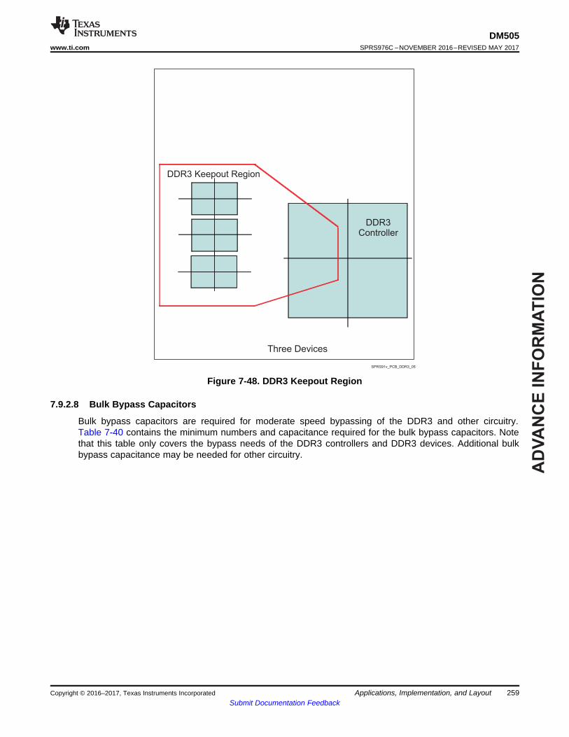
AD
VA
NC
E I
NF
OR
MA
TIO
N
SPRS91v_PCB_DDR3_05
Three Devices
DDR3 Keepout Region
DDR3Controller
259
DM505www.ti.com SPRS976C –NOVEMBER 2016–REVISED MAY 2017
Submit Documentation FeedbackApplications, Implementation, and LayoutCopyright © 2016–2017, Texas Instruments Incorporated
Figure 7-48. DDR3 Keepout Region
7.9.2.8 Bulk Bypass Capacitors
Bulk bypass capacitors are required for moderate speed bypassing of the DDR3 and other circuitry.Table 7-40 contains the minimum numbers and capacitance required for the bulk bypass capacitors. Notethat this table only covers the bypass needs of the DDR3 controllers and DDR3 devices. Additional bulkbypass capacitance may be needed for other circuitry.

AD
VA
NC
E IN
FO
RM
AT
ION
260
DM505SPRS976C –NOVEMBER 2016–REVISED MAY 2017 www.ti.com
Submit Documentation FeedbackApplications, Implementation, and Layout Copyright © 2016–2017, Texas Instruments Incorporated
Table 7-40. Bulk Bypass Capacitors
NO. PARAMETER MIN MAX UNIT1 vdds_ddrx bulk bypass capacitor count(1) 1 Devices2 vdds_ddrx bulk bypass total capacitance 22 μF
(1) These devices should be placed near the devices they are bypassing, but preference should be given to the placement of the high-speed (HS) bypass capacitors and DDR3 signal routing.
7.9.2.9 High-Speed Bypass Capacitors
High-speed (HS) bypass capacitors are critcal for proper DDR3 interface operation. It is particularlyimportant to minimize the parasitic series inductance of the HS bypass capacitors, processor/DDR power,and processor/DDR ground connections. Table 7-41 contains the specification for the HS bypasscapacitors as well as for the power connections on the PCB. Generally speaking, it is good to:1. Fit as many HS bypass capacitors as possible.2. Minimize the distance from the bypass cap to the pins/balls being bypassed.3. Use the smallest physical sized capacitors possible with the highest capacitance readily available.4. Connect the bypass capacitor pads to their vias using the widest traces possible and using the largest
hole size via possible.5. Minimize via sharing. Note the limites on via sharing shown in Table 7-41.
Table 7-41. High-Speed Bypass Capacitors
NO. PARAMETER MIN TYP MAX UNIT1 HS bypass capacitor package size(1) 0201 0402 10 Mils2 Distance, HS bypass capacitor to processor being bypassed(2)(3)(4) 400 Mils3 Processor HS bypass capacitor count per vdds_ddrx rail(12) See Table 7-3 and (11) Devices4 Processor HS bypass capacitor total capacitance per vdds_ddrx rail(12) See Table 7-3 and (11) μF5 Number of connection vias for each device power/ground ball(5) Vias6 Trace length from device power/ground ball to connection via(2) 35 70 Mils7 Distance, HS bypass capacitor to DDR device being bypassed(6) 150 Mils8 DDR3 device HS bypass capacitor count(7) 12 Devices9 DDR3 device HS bypass capacitor total capacitance(7) 0.85 μF10 Number of connection vias for each HS capacitor(8)(9) 2 Vias11 Trace length from bypass capacitor connect to connection via(2)(9) 35 100 Mils12 Number of connection vias for each DDR3 device power/ground ball(10) 1 Vias13 Trace length from DDR3 device power/ground ball to connection via(2)(8) 35 60 Mils
(1) LxW, 10-mil units, that is, a 0402 is a 40x20-mil surface-mount capacitor.(2) Closer/shorter is better.(3) Measured from the nearest processor power/ground ball to the center of the capacitor package.(4) Three of these capacitors should be located underneath the processor, between the cluster of DDR_1V5 balls and ground balls,
between the DDR interfaces on the package.(5) See the Via Channel™ escape for the processor package.(6) Measured from the DDR3 device power/ground ball to the center of the capacitor package.(7) Per DDR3 device.(8) An additional HS bypass capacitor can share the connection vias only if it is mounted on the opposite side of the board. No sharing of
vias is permitted on the same side of the board.(9) An HS bypass capacitor may share a via with a DDR device mounted on the same side of the PCB. A wide trace should be used for the
connection and the length from the capacitor pad to the DDR device pad should be less than 150 mils.(10) Up to a total of two pairs of DDR power/ground balls may share a via.(11) The capacitor recommendations in this data manual reflect only the needs of this processor. Please see the memory vendor’s
guidelines for determining the appropriate decoupling capacitor arrangement for the memory device itself.(12) For more information, see Section 7.3, Core Power Domains.

AD
VA
NC
E I
NF
OR
MA
TIO
N
261
DM505www.ti.com SPRS976C –NOVEMBER 2016–REVISED MAY 2017
Submit Documentation FeedbackApplications, Implementation, and LayoutCopyright © 2016–2017, Texas Instruments Incorporated
7.9.2.9.1 Return Current Bypass Capacitors
Use additional bypass capacitors if the return current reference plane changes due to DDR3 signalshopping from one signal layer to another. The bypass capacitor here provides a path for the return currentto hop planes along with the signal. As many of these return current bypass capacitors should be used aspossible. Since these are returns for signal current, the signal via size may be used for these capacitors.
7.9.2.10 Net Classes
Table 7-42 lists the clock net classes for the DDR3 interface. Table 7-43 lists the signal net classes, andassociated clock net classes, for signals in the DDR3 interface. These net classes are used for thetermination and routing rules that follow.
Table 7-42. Clock Net Class Definitions
CLOCK NET CLASS processor PIN NAMESCK ddrx_ck/ddrx_nck
DQS0 ddrx_dqs0 / ddrx_dqsn0DQS1 ddrx_dqs1 / ddrx_dqsn1
DQS2(1) ddrx_dqs2 / ddrx_dqsn2DQS3(1) ddrx_dqs3 / ddrx_dqsn3
(1) Only used on 32-bit wide DDR3 memory systems.
Table 7-43. Signal Net Class Definitions
SIGNAL NET CLASS ASSOCIATED CLOCKNET CLASS processor PIN NAMES
ADDR_CTRL CK ddrx_ba[2:0], ddrx_a[15:0], ddrx_csnj, ddrx_casn, ddrx_rasn, ddrx_wen,ddrx_cke, ddrx_odti
DQ0 DQS0 ddrx_d[7:0], ddrx_dqm0DQ1 DQS1 ddrx_d[15:8], ddrx_dqm1
DQ2(1) DQS2 ddrx_d[23:16], ddrx_dqm2DQ3(1) DQS3 ddrx_d[31:24], ddrx_dqm3
(1) Only used on 32-bit wide DDR3 memory systems.
7.9.2.11 DDR3 Signal Termination
Signal terminators are required for the CK and ADDR_CTRL net classes. The data lines are terminated byODT and, thus, the PCB traces should be unterminated. Detailed termination specifications are covered inthe routing rules in the following sections.
7.9.2.12 VTT
Like VREF, the nominal value of the VTT supply is half the DDR3 supply voltage. Unlike VREF, VTT isexpected to source and sink current, specifically the termination current for the ADDR_CTRL net classThevinen terminators. VTT is needed at the end of the address bus and it should be routed as a powersub-plane. VTT should be bypassed near the terminator resistors.
7.9.2.13 CK and ADDR_CTRL Topologies and Routing Definition
The CK and ADDR_CTRL net classes are routed similarly and are length matched to minimize skewbetween them. CK is a bit more complicated because it runs at a higher transition rate and is differential.The following subsections show the topology and routing for various DDR3 configurations for CK andADDR_CTRL. The figures in the following subsections define the terms for the routing specificationdetailed in Table 7-44.

AD
VA
NC
E IN
FO
RM
AT
ION
A1 A2
Processor
Address and Control
Output Buffer
DDR Address and Control Input Buffers
A3 A4 AT Vtt
Address and Control
Terminator
Rtt
AS
AS
AS
SPRS91v_PCB_DDR3_07
AS
-
AS
+
AS
-
AS
+
A1 A2
Processor
Differential Clock
Output Buffer
DDR Differential CK Input Buffers
Routed as Differential Pair
A3 A4 AT
Rcp
Clock Parallel
Terminator
A1 A2 A3 A4 AT
AS
-
AS
+
Rcp
Cac
DDR_1V5
0.1 µF
+
–
+ – + – + –
SPRS91v_PCB_DDR3_06
262
DM505SPRS976C –NOVEMBER 2016–REVISED MAY 2017 www.ti.com
Submit Documentation FeedbackApplications, Implementation, and Layout Copyright © 2016–2017, Texas Instruments Incorporated
7.9.2.13.1 Three DDR3 Devices
Three DDR3 devices are supported on the DDR EMIF consisting of two x16 DDR3 devices and onedevice for ECC, arranged as one bank (CS). These three devices may be mounted on a single side of thePCB, or may be mirrored in two pairs to save board space at a cost of increased routing complexity andparts on the backside of the PCB.
7.9.2.13.1.1 CK and ADDR_CTRL Topologies, Three DDR3 Devices
Figure 7-49 shows the topology of the CK net classes and Figure 7-50 shows the topology for thecorresponding ADDR_CTRL net classes.
Figure 7-49. CK Topology for Three DDR3 Devices
Figure 7-50. ADDR_CTRL Topology for Three DDR3 Devices
7.9.2.13.1.2 CK and ADDR_CTRL Routing, Three DDR3 Devices
Figure 7-51 shows the CK routing for three DDR3 devices placed on the same side of the PCB. Figure 7-52 shows the corresponding ADDR_CTRL routing.

AD
VA
NC
E I
NF
OR
MA
TIO
N
AS=
Rtt
A1
A2 A3 A4 AT Vtt
SPRS91v_PCB_DDR3_09
AS
+
AS
-=
Rcp
Rcp
Cac
DDR_1V5
0.1 µF
A1
A2 A3 A4
A2 A3 A4
A1
AT
AT
SPRS91v_PCB_DDR3_08
263
DM505www.ti.com SPRS976C –NOVEMBER 2016–REVISED MAY 2017
Submit Documentation FeedbackApplications, Implementation, and LayoutCopyright © 2016–2017, Texas Instruments Incorporated
Figure 7-51. CK Routing for Three Single-Side DDR3 Devices
Figure 7-52. ADDR_CTRL Routing for Three Single-Side DDR3 Devices
To save PCB space, the two DDR3 memories may be mounted as one mirrored pair at a cost ofincreased routing and assembly complexity. Figure 7-53 and Figure 7-54 show the routing for CK andADDR_CTRL, respectively, for two DDR3 devices mirrored in a pair configuration.
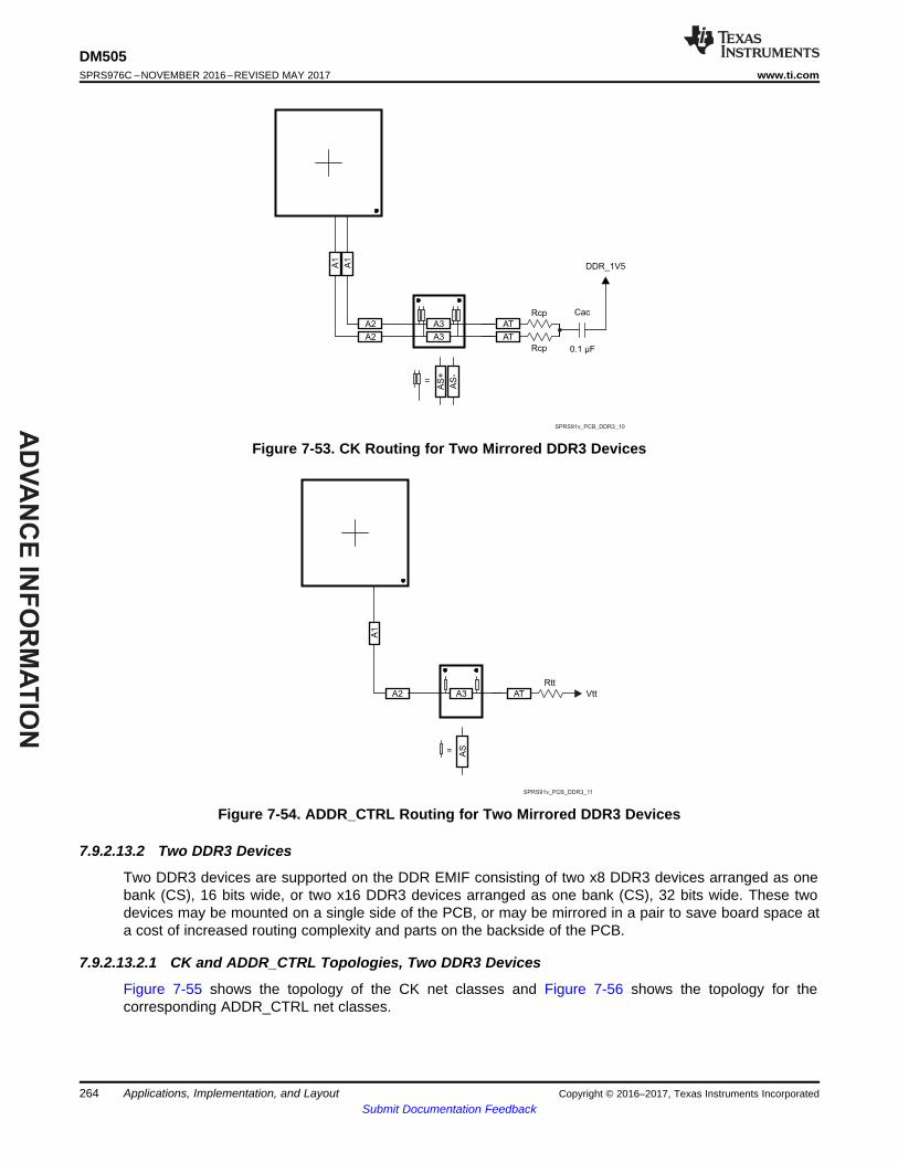
AD
VA
NC
E IN
FO
RM
AT
ION
AS=
Rtt
A1
A2 A3 AT Vtt
SPRS91v_PCB_DDR3_11
AS
+
AS
-
=
Rcp
Rcp
Cac
DDR_1V5
0.1 µFA
1
A2 A3
A2 A3A
1
AT
AT
SPRS91v_PCB_DDR3_10
264
DM505SPRS976C –NOVEMBER 2016–REVISED MAY 2017 www.ti.com
Submit Documentation FeedbackApplications, Implementation, and Layout Copyright © 2016–2017, Texas Instruments Incorporated
Figure 7-53. CK Routing for Two Mirrored DDR3 Devices
Figure 7-54. ADDR_CTRL Routing for Two Mirrored DDR3 Devices
7.9.2.13.2 Two DDR3 Devices
Two DDR3 devices are supported on the DDR EMIF consisting of two x8 DDR3 devices arranged as onebank (CS), 16 bits wide, or two x16 DDR3 devices arranged as one bank (CS), 32 bits wide. These twodevices may be mounted on a single side of the PCB, or may be mirrored in a pair to save board space ata cost of increased routing complexity and parts on the backside of the PCB.
7.9.2.13.2.1 CK and ADDR_CTRL Topologies, Two DDR3 Devices
Figure 7-55 shows the topology of the CK net classes and Figure 7-56 shows the topology for thecorresponding ADDR_CTRL net classes.

AD
VA
NC
E I
NF
OR
MA
TIO
N
A1 A2
Processor
Address and Control
Output Buffer
DDR Address and Control Input Buffers
A3 AT Vtt
Address and Control
Terminator
Rtt
AS
AS
SPRS91v_PCB_DDR3_13
AS
-
AS
+
A1 A2
Processor
Differential Clock
Output Buffer
DDR Differential CK Input Buffers
Routed as Differential Pair
A3 AT
Rcp
Clock Parallel
Terminator
A1 A2 A3 AT
AS
-
AS
+
Rcp
Cac
DDR_1V5
0.1 µF
+
–
+ – + –
SPRS91v_PCB_DDR3_12
265
DM505www.ti.com SPRS976C –NOVEMBER 2016–REVISED MAY 2017
Submit Documentation FeedbackApplications, Implementation, and LayoutCopyright © 2016–2017, Texas Instruments Incorporated
Figure 7-55. CK Topology for Two DDR3 Devices
Figure 7-56. ADDR_CTRL Topology for Two DDR3 Devices
7.9.2.13.2.2 CK and ADDR_CTRL Routing, Two DDR3 Devices
Figure 7-57 shows the CK routing for two DDR3 devices placed on the same side of the PCB. Figure 7-58shows the corresponding ADDR_CTRL routing.

AD
VA
NC
E IN
FO
RM
AT
ION
AS=
Rtt
A1
A2 A3 AT Vtt
SPRS91v_PCB_DDR3_15
AS
+
AS
-
=
Rcp
Rcp
Cac
DDR_1V5
0.1 µF
A1
A2 A3 AT
A2 A3 AT
A1
SPRS91v_PCB_DDR3_14
266
DM505SPRS976C –NOVEMBER 2016–REVISED MAY 2017 www.ti.com
Submit Documentation FeedbackApplications, Implementation, and Layout Copyright © 2016–2017, Texas Instruments Incorporated
Figure 7-57. CK Routing for Two Single-Side DDR3 Devices
Figure 7-58. ADDR_CTRL Routing for Two Single-Side DDR3 Devices
To save PCB space, the two DDR3 memories may be mounted as a mirrored pair at a cost of increasedrouting and assembly complexity. Figure 7-59 and Figure 7-60 show the routing for CK and ADDR_CTRL,respectively, for two DDR3 devices mirrored in a single-pair configuration.

AD
VA
NC
E I
NF
OR
MA
TIO
N
AS=
Rtt
A1
A2 A3 AT Vtt
SPRS91v_PCB_DDR3_17
AS
+
AS
-
=
Rcp
Rcp
Cac
DDR_1V5
0.1 µF
A1
A2 A3 AT
A2 A3 AT
A1
SPRS91v_PCB_DDR3_16
267
DM505www.ti.com SPRS976C –NOVEMBER 2016–REVISED MAY 2017
Submit Documentation FeedbackApplications, Implementation, and LayoutCopyright © 2016–2017, Texas Instruments Incorporated
Figure 7-59. CK Routing for Two Mirrored DDR3 Devices
Figure 7-60. ADDR_CTRL Routing for Two Mirrored DDR3 Devices
7.9.2.13.3 One DDR3 Device
A single DDR3 device is supported on the DDR EMIF consisting of one x16 DDR3 device arranged asone bank (CS), 16 bits wide.
7.9.2.13.3.1 CK and ADDR_CTRL Topologies, One DDR3 Device
Figure 7-61 shows the topology of the CK net classes and Figure 7-62 shows the topology for thecorresponding ADDR_CTRL net classes.
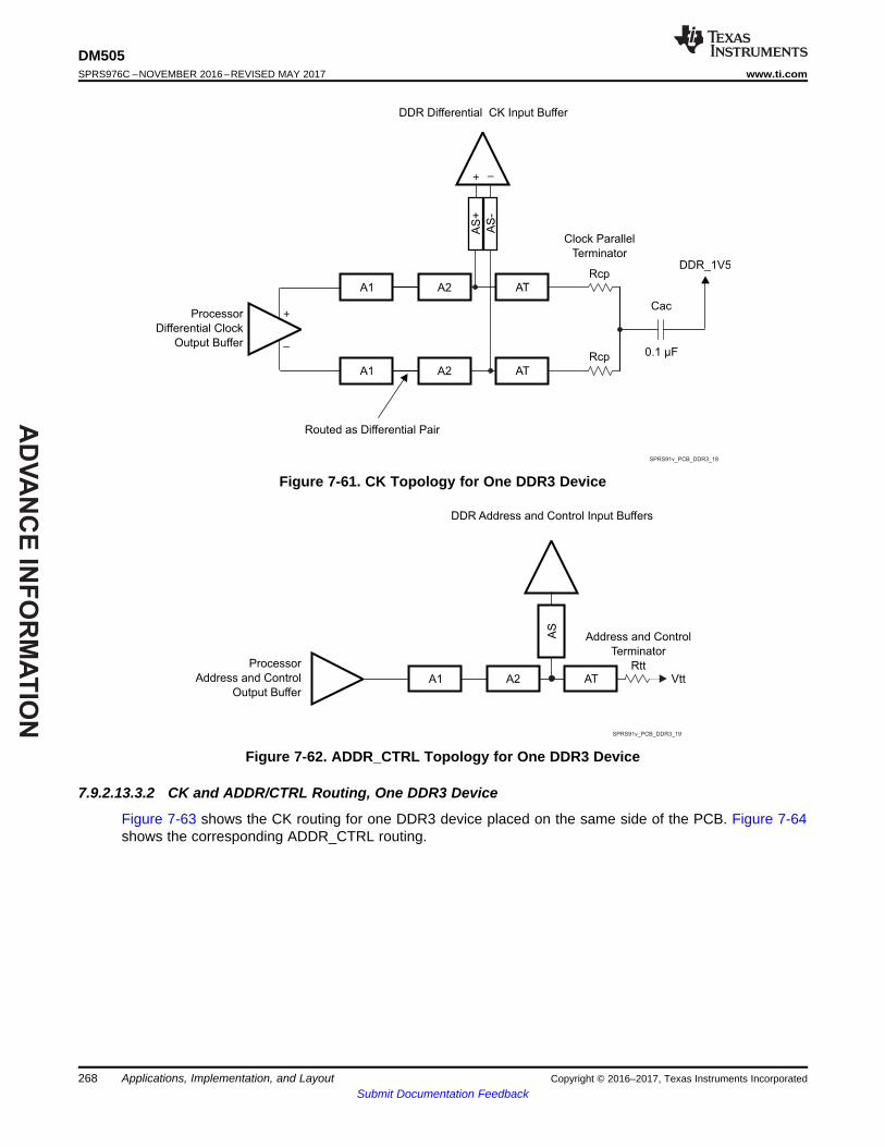
AD
VA
NC
E IN
FO
RM
AT
ION
A1 A2
Processor
Address and Control
Output Buffer
DDR Address and Control Input Buffers
AT Vtt
Address and Control
Terminator
Rtt
AS
SPRS91v_PCB_DDR3_19
A1 A2
Processor
Differential Clock
Output Buffer
DDR Differential CK Input Buffer
Routed as Differential Pair
AT
Rcp
Clock Parallel
Terminator
A1 A2 AT
AS
-
AS
+
Rcp
Cac
DDR_1V5
0.1 µF
+
–
+ –
SPRS91v_PCB_DDR3_18
268
DM505SPRS976C –NOVEMBER 2016–REVISED MAY 2017 www.ti.com
Submit Documentation FeedbackApplications, Implementation, and Layout Copyright © 2016–2017, Texas Instruments Incorporated
Figure 7-61. CK Topology for One DDR3 Device
Figure 7-62. ADDR_CTRL Topology for One DDR3 Device
7.9.2.13.3.2 CK and ADDR/CTRL Routing, One DDR3 Device
Figure 7-63 shows the CK routing for one DDR3 device placed on the same side of the PCB. Figure 7-64shows the corresponding ADDR_CTRL routing.

AD
VA
NC
E I
NF
OR
MA
TIO
N
AS=
Rtt
A1
A2 AT Vtt
SPRS91v_PCB_DDR3_21
AS
+
AS
-
=
Rcp
Rcp
Cac
DDR_1V5
0.1 µF
A1
A2 AT
A2 AT
A1
SPRS91v_PCB_DDR3_20
269
DM505www.ti.com SPRS976C –NOVEMBER 2016–REVISED MAY 2017
Submit Documentation FeedbackApplications, Implementation, and LayoutCopyright © 2016–2017, Texas Instruments Incorporated
Figure 7-63. CK Routing for One DDR3 Device
Figure 7-64. ADDR_CTRL Routing for One DDR3 Device
7.9.2.14 Data Topologies and Routing Definition
No matter the number of DDR3 devices used, the data line topology is always point to point, so itsdefinition is simple.
Care should be taken to minimize layer transitions during routing. If a layer transition is necessary, it isbetter to transition to a layer using the same reference plane. If this cannot be accommodated, ensurethere are nearby ground vias to allow the return currents to transition between reference planes if bothreference planes are ground or vdds_ddr. Ensure there are nearby bypass capacitors to allow the returncurrents to transition between reference planes if one of the reference planes is ground. The goal is tominimize the size of the return current loops.
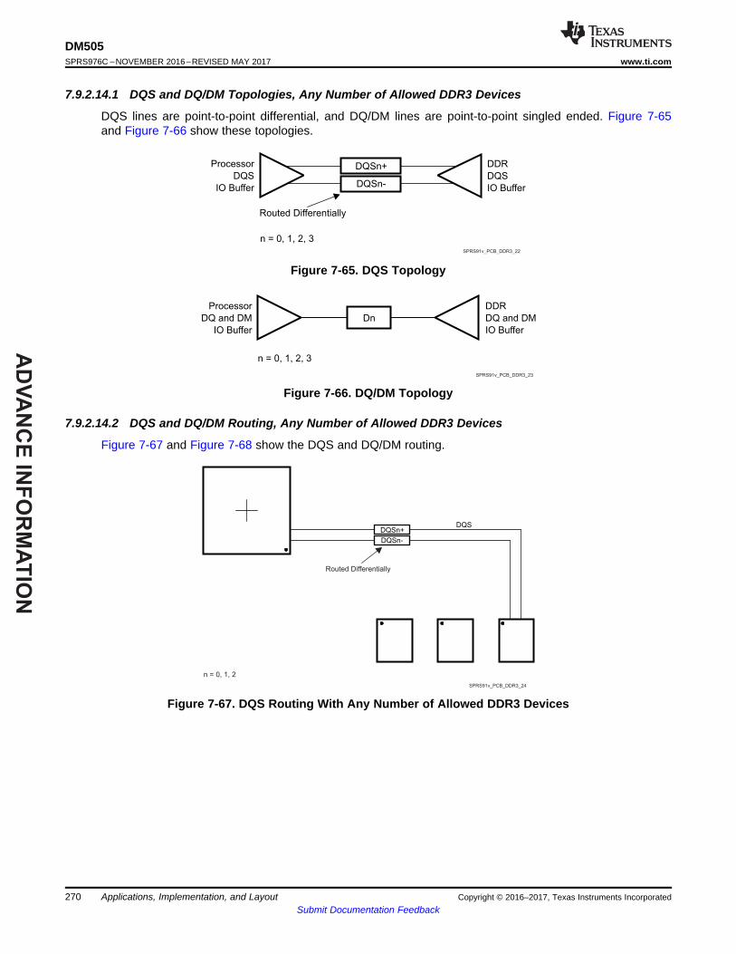
AD
VA
NC
E IN
FO
RM
AT
ION
DQSn+
DQSn-
n = 0, 1, 2
Routed Differentially
DQS
SPRS91v_PCB_DDR3_24
Dn
Processor
DQ and DM
IO Buffer
DDR
DQ and DM
IO Buffer
n = 0, 1, 2, 3
SPRS91v_PCB_DDR3_23
Processor
DQS
IO Buffer
DDR
DQS
IO Buffer
Routed Differentially
n = 0, 1, 2, 3
DQSn-
DQSn+
SPRS91v_PCB_DDR3_22
270
DM505SPRS976C –NOVEMBER 2016–REVISED MAY 2017 www.ti.com
Submit Documentation FeedbackApplications, Implementation, and Layout Copyright © 2016–2017, Texas Instruments Incorporated
7.9.2.14.1 DQS and DQ/DM Topologies, Any Number of Allowed DDR3 Devices
DQS lines are point-to-point differential, and DQ/DM lines are point-to-point singled ended. Figure 7-65and Figure 7-66 show these topologies.
Figure 7-65. DQS Topology
Figure 7-66. DQ/DM Topology
7.9.2.14.2 DQS and DQ/DM Routing, Any Number of Allowed DDR3 Devices
Figure 7-67 and Figure 7-68 show the DQS and DQ/DM routing.
Figure 7-67. DQS Routing With Any Number of Allowed DDR3 Devices

AD
VA
NC
E I
NF
OR
MA
TIO
N
Dn
n = 0, 1, 2
DQ and DM
SPRS91v_PCB_DDR3_25
271
DM505www.ti.com SPRS976C –NOVEMBER 2016–REVISED MAY 2017
Submit Documentation FeedbackApplications, Implementation, and LayoutCopyright © 2016–2017, Texas Instruments Incorporated
Figure 7-68. DQ/DM Routing With Any Number of Allowed DDR3 Devices
7.9.2.15 Routing Specification
7.9.2.15.1 CK and ADDR_CTRL Routing Specification
Skew within the CK and ADDR_CTRL net classes directly reduces setup and hold margin and, thus, thisskew must be controlled. The only way to practically match lengths on a PCB is to lengthen the shortertraces up to the length of the longest net in the net class and its associated clock. A metric to establishthis maximum length is Manhattan distance. The Manhattan distance between two points on a PCB is thelength between the points when connecting them only with horizontal or vertical segments. A reasonabletrace route length is to within a percentage of its Manhattan distance. CACLM is defined as Clock AddressControl Longest Manhattan distance.
Given the clock and address pin locations on the processor and the DDR3 memories, the maximumpossible Manhattan distance can be determined given the placement. Figure 7-69 and Figure 7-70 showthis distance for three loads and two loads, respectively. It is from this distance that the specifications onthe lengths of the transmission lines for the address bus are determined. CACLM is determined similarlyfor other address bus configurations; that is, it is based on the longest net of the CK/ADDR_CTRL netclass. For CK and ADDR_CTRL routing, these specifications are contained in Table 7-44.

AD
VA
NC
E IN
FO
RM
AT
ION
AS=
Rtt
A1
A2 A3 A4 AT Vtt
A8(A)
A8(A)
A8(A)
A8(A)
CACLMX
CACLMY
SPRS91v_PCB_DDR3_26
272
DM505SPRS976C –NOVEMBER 2016–REVISED MAY 2017 www.ti.com
Submit Documentation FeedbackApplications, Implementation, and Layout Copyright © 2016–2017, Texas Instruments Incorporated
A. It is very likely that the longest CK/ADDR_CTRL Manhattan distance will be for Address Input 8 (A8) on the DDR3memories. CACLM is based on the longest Manhattan distance due to the device placement. Verify the net class thatsatisfies this criteria and use as the baseline for CK/ADDR_CTRL skew matching and length control.
The length of shorter CK/ADDR_CTRL stubs as well as the length of the terminator stub are not included in thislength calculation. Non-included lengths are grayed out in the figure.
Assuming A8 is the longest, CALM = CACLMY + CACLMX + 300 mils.The extra 300 mils allows for routing down lower than the DDR3 memories and returning up to reach A8.
Figure 7-69. CACLM for Three Address Loads on One Side of PCB

AD
VA
NC
E I
NF
OR
MA
TIO
N
AS=
RttA
1
A2 A3 AT Vtt
A8(A)
A8(A)
A8(A)
CACLMX
CACLMY
SPRS91v_PCB_DDR3_27
273
DM505www.ti.com SPRS976C –NOVEMBER 2016–REVISED MAY 2017
Submit Documentation FeedbackApplications, Implementation, and LayoutCopyright © 2016–2017, Texas Instruments Incorporated
A. It is very likely that the longest CK/ADDR_CTRL Manhattan distance will be for Address Input 8 (A8) on the DDR3memories. CACLM is based on the longest Manhattan distance due to the device placement. Verify the net class thatsatisfies this criteria and use as the baseline for CK/ADDR_CTRL skew matching and length control.
The length of shorter CK/ADDR_CTRL stubs as well as the length of the terminator stub are not included in thislength calculation. Non-included lengths are grayed out in the figure.
Assuming A8 is the longest, CALM = CACLMY + CACLMX + 300 mils.The extra 300 mils allows for routing down lower than the DDR3 memories and returning up to reach A8.
Figure 7-70. CACLM for Two Address Loads on One Side of PCB
Table 7-44. CK and ADDR_CTRL Routing Specification(2)(3)
NO. PARAMETER MIN TYP MAX UNITCARS31 A1+A2 length 500(1) psCARS32 A1+A2 skew 29 psCARS33 A3 length 125 psCARS34 A3 skew(4) 6 psCARS35 A3 skew(5) 6 psCARS36 A4 length 125 psCARS37 A4 skew 6 psCARS38 AS length 5(1) 17 psCARS39 AS skew 1.3(1) 14 psCARS310 AS+/AS- length 5 12 psCARS311 AS+/AS- skew 1 psCARS312 AT length(6) 75 psCARS313 AT skew(7) 14 psCARS314 AT skew(8) 1 psCARS315 CK/ADDR_CTRL trace length 1020 psCARS316 Vias per trace 3(1) viasCARS317 Via count difference 1(15) viasCARS318 Center-to-center CK to other DDR3 trace spacing(9) 4wCARS319 Center-to-center ADDR_CTRL to other DDR3 trace spacing(9)(10) 4wCARS320 Center-to-center ADDR_CTRL to other ADDR_CTRL trace
spacing(9)3w

AD
VA
NC
E IN
FO
RM
AT
ION
274
DM505SPRS976C –NOVEMBER 2016–REVISED MAY 2017 www.ti.com
Submit Documentation FeedbackApplications, Implementation, and Layout Copyright © 2016–2017, Texas Instruments Incorporated
Table 7-44. CK and ADDR_CTRL Routing Specification(2)(3) (continued)NO. PARAMETER MIN TYP MAX UNIT
CARS321 CK center-to-center spacing(11)(12)
CARS322 CK spacing to other net(9) 4wCARS323 Rcp(13) Zo-1 Zo Zo+1 Ω
CARS324 Rtt(13)(14) Zo-5 Zo Zo+5 Ω
(1) Max value is based upon conservative signal integrity approach. This value could be extended only if detailed signal integrity analysis ofrice time and fall time confirms desired operation.
(2) The use of vias should be minimized.(3) Additional bypass capacitors are required when using the DDR_1V5 plane as the reference plane to allow the return current to jump
between the DDR_1V5 plane and the ground plane when the net class switches layers at a via.(4) Non-mirrored configuration (all DDR3 memories on same side of PCB).(5) Mirrored configuration (one DDR3 device on top of the board and one DDR3 device on the bottom).(6) While this length can be increased for convenience, its length should be minimized.(7) ADDR_CTRL net class only (not CK net class). Minimizing this skew is recommended, but not required.(8) CK net class only.(9) Center-to-center spacing is allowed to fall to minimum (2w) for up to 1250 mils of routed length.(10) The ADDR_CTRL net class of the other DDR EMIF is considered other DDR3 trace spacing.(11) CK spacing set to ensure proper differential impedance.(12) The most important thing to do is control the impedance so inadvertent impedance mismatches are not created. Generally speaking,
center-to-center spacing should be either 2w or slightly larger than 2w to achieve a differential impedance equal to twice the singleendedimpedance, Zo.
(13) Source termination (series resistor at driver) is specifically not allowed.(14) Termination values should be uniform across the net class.(15) Via count difference may increase by 1 only if accurate 3-D modeling of the signal flight times – including accurately modeled signal
propagation through vias – has been applied to ensure all segment skew maximums are not exceeded.
7.9.2.15.2 DQS and DQ Routing Specification
Skew within the DQS and DQ/DM net classes directly reduces setup and hold margin and thus this skewmust be controlled. The only way to practically match lengths on a PCB is to lengthen the shorter tracesup to the length of the longest net in the net class and its associated clock. As with CK and ADDR_CTRL,a reasonable trace route length is to within a percentage of its Manhattan distance. DQLMn is defined asDQ Longest Manhattan distance n, where n is the byte number. For a 32-bit interface, there are threeDQLMs, DQLM0-DQLM2. Likewise, for a 16-bit interface, there are two DQLMs, DQLM0-DQLM1.
NOTEIt is not required, nor is it recommended, to match the lengths across all bytes. Lengthmatching is only required within each byte.
Given the DQS and DQ/DM pin locations on the processor and the DDR3 memories, the maximumpossible Manhattan distance can be determined given the placement. Figure 7-71 shows this distance forfour loads. It is from this distance that the specifications on the lengths of the transmission lines for thedata bus are determined. For DQS and DQ/DM routing, these specifications are contained in Table 7-45.

AD
VA
NC
E I
NF
OR
MA
TIO
N
DQLMY0
DQLMY2
DQLMX2
DB2
2 1 0
DQ[16:23]/DM2/DQS2
DQLMX1
DB1
DB0
DQLMX0
DQ[8:15]/DM1/DQS1
DQ[0:7]/DM0/DQS0
DQLMY1
DB0 - DB2 represent data bytes 0 - 2.
SPRS91v_PCB_DDR3_28
275
DM505www.ti.com SPRS976C –NOVEMBER 2016–REVISED MAY 2017
Submit Documentation FeedbackApplications, Implementation, and LayoutCopyright © 2016–2017, Texas Instruments Incorporated
There are three DQLMs, one for each byte (32-bit interface). Each DQLM is the longest Manhattan distance of thebyte; therefore:DQLM0 = DQLMX0 + DQLMY0DQLM1 = DQLMX1 + DQLMY1DQLM2 = DQLMX2 + DQLMY2
Figure 7-71. DQLM for Any Number of Allowed DDR3 Devices
Table 7-45. Data Routing Specification(2)
NO. PARAMETER MIN TYP MAX UNITDRS31 DB0 length 340 psDRS32 DB1 length 340 psDRS33 DB2 length 340 psDRS35 DBn skew(3) 5 psDRS36 DQSn+ to DQSn- skew 1 psDRS37 DQSn to DBn skew(3)(4) 5(10) psDRS38 Vias per trace 2(1) viasDRS39 Via count difference 0(10) viasDRS310 Center-to-center DBn to other DDR3 trace spacing(6) 4 w(5)
DRS311 Center-to-center DBn to other DBn trace spacing(7) 3 w(5)
DRS312 DQSn center-to-center spacing(8)(9)
DRS313 DQSn center-to-center spacing to other net 4 w(5)
(1) Max value is based upon conservative signal integrity approach. This value could be extended only if detailed signal integrity analysis ofrice time and fall time confirms desired operation.
(2) External termination disallowed. Data termination should use built-in ODT functionality.(3) Length matching is only done within a byte. Length matching across bytes is neither required nor recommended.(4) Each DQS pair is length matched to its associated byte.(5) Center-to-center spacing is allowed to fall to minimum (2w) for up to 1250 mils of routed length.(6) Other DDR3 trace spacing means other DDR3 net classes not within the byte.(7) This applies to spacing within the net classes of a byte.(8) DQS pair spacing is set to ensure proper differential impedance.(9) The most important thing to do is control the impedance so inadvertent impedance mismatches are not created. Generally speaking,
center-to-center spacing should be either 2w or slightly larger than 2w to achieve a differential impedance equal to twice the singleendedimpedance, Zo.
(10) Via count difference may increase by 1 only if accurate 3-D modeling of the signal flight times – including accurately modeled signalpropagation through vias – has been applied to ensure DBn skew and DQSn to DBn skew maximums are not exceeded.

AD
VA
NC
E IN
FO
RM
AT
ION
RLOAD
cvideo_vfbReconstruction
Filter~9.5 MHz
(A) Amplifier3.7 V/V
CAC
(B)
75 W
ROUT
cvideo_tvout
cvideo_vfb
Reconstruction
Filter~9.5 MHz
(A)
CAC
(B)
276
DM505SPRS976C –NOVEMBER 2016–REVISED MAY 2017 www.ti.com
Submit Documentation FeedbackApplications, Implementation, and Layout Copyright © 2016–2017, Texas Instruments Incorporated
7.10 CVIDEO/SD-DAC Guidelines and Electrical Data/Timing
The device's analog video CVIDEO/SD-DAC TV analog composite output can be operate in one of twomodes: Normal mode and TVOUT Bypass mode. In Normal mode, the device’s internal video amplifier isused. In TVOUT Bypass mode, the internal video amplifier is bypassed and an external amplifier isrequired.
Figure 7-72 shows a typical circuit that permits connecting the analog video output from the device tostandard 75-Ω impedance video systems in Normal mode.
A. Reconstruction Filter (optional)B. AC coupling capacitor (optional)
Figure 7-72. TV Output (Normal Mode)
Figure 7-73 shows a typical circuit that permits connecting the analog video output from the device tostandard 75-Ω impedance video systems in TVOUT Bypass mode.
A. Reconstruction Filter (optional). Note: An amplifier with an integrated reconstruction filter can alternatively be usedinstead of a discrete reconstruction filter.
B. AC coupling capacitor (optional)
Figure 7-73. TV Output (TVOUT Bypass Mode)
During board design, the onboard traces and parasitics must be matched for the channel. The video DACoutput pins (cvideo_tvout / cvideo_vfb) are very high-frequency analog signals and must be routed withextreme care. As a result, the paths of these signals must be as short as possible, and as isolated aspossible from other interfering signals. In TVOUT Bypass mode, the load resistor and amplifier/buffershould be placed as close as possible to the cvideo_vfb pin. Other layout guidelines include:• Take special care to bypass the vdda_dac power supply pin with a capacitor.• In TVOUT Bypass mode, place the RLOAD resistor as close as possible to the Reconstruction Filter
and Amplifier. In addition, place the 75-Ω resistor as close as possible (< 0.5 inch) to theAmplifier/buffer output pin. To maintain a high-quality video signal, the onboard traces after the 75-Ωresistor should have a characteristic impedance of 75 Ω (± 20%).
• In Normal mode,cvideo_vfb is the most sensitive pin in the TV out system. The ROUT resistor shouldbe placed as close as possible to the device pins. To maintain a high-quality video signal, the onboardtraces leading to the cvideo_tvout pin should have a characteristic impedance of 75 Ω (± 20%) startingfrom the closest possible place to the device pin output.
• Minimize input trace lengths to the device to reduce parasitic capacitance.• Include solid ground return paths.• Match trace lengths as close as possible within a video format group.
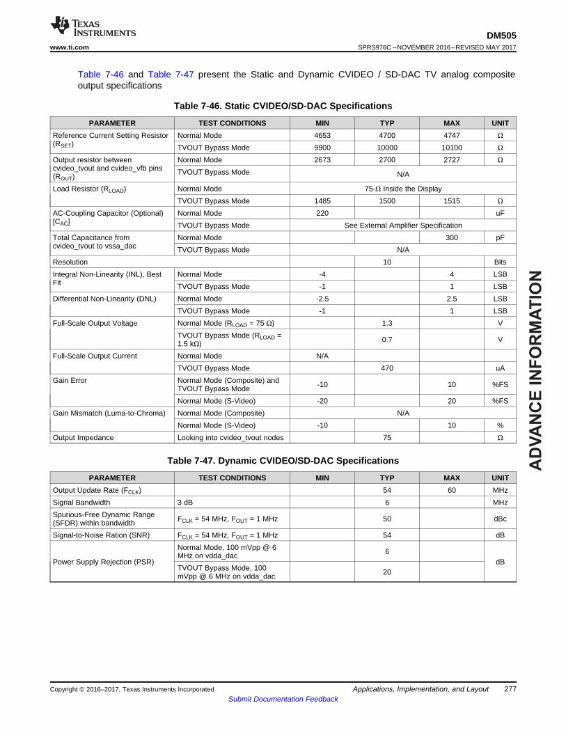
AD
VA
NC
E I
NF
OR
MA
TIO
N
277
DM505www.ti.com SPRS976C –NOVEMBER 2016–REVISED MAY 2017
Submit Documentation FeedbackApplications, Implementation, and LayoutCopyright © 2016–2017, Texas Instruments Incorporated
Table 7-46 and Table 7-47 present the Static and Dynamic CVIDEO / SD-DAC TV analog compositeoutput specifications
Table 7-46. Static CVIDEO/SD-DAC Specifications
PARAMETER TEST CONDITIONS MIN TYP MAX UNITReference Current Setting Resistor(RSET)
Normal Mode 4653 4700 4747 Ω
TVOUT Bypass Mode 9900 10000 10100 Ω
Output resistor betweencvideo_tvout and cvideo_vfb pins(ROUT)
Normal Mode 2673 2700 2727 Ω
TVOUT Bypass Mode N/A
Load Resistor (RLOAD) Normal Mode 75-Ω Inside the DisplayTVOUT Bypass Mode 1485 1500 1515 Ω
AC-Coupling Capacitor (Optional)[CAC]
Normal Mode 220 uFTVOUT Bypass Mode See External Amplifier Specification
Total Capacitance fromcvideo_tvout to vssa_dac
Normal Mode 300 pFTVOUT Bypass Mode N/A
Resolution 10 BitsIntegral Non-Linearity (INL), BestFit
Normal Mode -4 4 LSBTVOUT Bypass Mode -1 1 LSB
Differential Non-Linearity (DNL) Normal Mode -2.5 2.5 LSBTVOUT Bypass Mode -1 1 LSB
Full-Scale Output Voltage Normal Mode (RLOAD = 75 Ω) 1.3 VTVOUT Bypass Mode (RLOAD =1.5 kΩ) 0.7 V
Full-Scale Output Current Normal Mode N/ATVOUT Bypass Mode 470 uA
Gain Error Normal Mode (Composite) andTVOUT Bypass Mode -10 10 %FS
Normal Mode (S-Video) -20 20 %FSGain Mismatch (Luma-to-Chroma) Normal Mode (Composite) N/A
Normal Mode (S-Video) -10 10 %Output Impedance Looking into cvideo_tvout nodes 75 Ω
Table 7-47. Dynamic CVIDEO/SD-DAC Specifications
PARAMETER TEST CONDITIONS MIN TYP MAX UNITOutput Update Rate (FCLK) 54 60 MHzSignal Bandwidth 3 dB 6 MHzSpurious-Free Dynamic Range(SFDR) within bandwidth FCLK = 54 MHz, FOUT = 1 MHz 50 dBc
Signal-to-Noise Ration (SNR) FCLK = 54 MHz, FOUT = 1 MHz 54 dB
Power Supply Rejection (PSR)
Normal Mode, 100 mVpp @ 6MHz on vdda_dac 6
dBTVOUT Bypass Mode, 100mVpp @ 6 MHz on vdda_dac 20
AD
VA
NC
E IN
FO
RM
AT
ION
278
DM505SPRS976C –NOVEMBER 2016–REVISED MAY 2017 www.ti.com
Submit Documentation FeedbackDevice and Documentation Support Copyright © 2016–2017, Texas Instruments Incorporated
8 Device and Documentation Support
TI offers an extensive line of development tools, including tools to evaluate the performance of theprocessors, generate code, develop algorithm implementations, and fully integrate and debug softwareand hardware modules are listed below.
8.1 Device NomenclatureTo designate the stages in the product development cycle, TI assigns prefixes to the part numbers of allmicroprocessors (MPUs) and support tools. Each device has one of three prefixes: X, P, or null (no prefix)(for example, DM50x). Texas Instruments recommends two of three possible prefix designators for itssupport tools: TMDX and TMDS. These prefixes represent evolutionary stages of product developmentfrom engineering prototypes (TMDX) through fully qualified production devices and tools (TMDS).
Device development evolutionary flow:X Experimental device that is not necessarily representative of the final device's electrical
specifications and may not use production assembly flow.P Prototype device that is not necessarily the final silicon die and may not necessarily meet
final electrical specifications.null Production version of the silicon die that is fully qualified.
Support tool development evolutionary flow:TMDX Development-support product that has not yet completed Texas Instruments internal
qualification testing.TMDS Fully-qualified development-support product.
X and P devices and TMDX development-support tools are shipped against the following disclaimer:
"Developmental product is intended for internal evaluation purposes."
Production devices and TMDS development-support tools have been characterized fully, and the qualityand reliability of the device have been demonstrated fully. TI's standard warranty applies.
Predictions show that prototype devices (X or P) have a greater failure rate than the standard productiondevices. Texas Instruments recommends that these devices not be used in any production systembecause their expected end-use failure rate still is undefined. Only qualified production devices are to beused.
For orderable part numbers of DM50x devices in the ABF package type, see the Package OptionAddendum of this document, the TI website (www.ti.com), or contact your TI sales representative.
For additional description of the device nomenclature markings on the die, see the Silicon Errata (literaturenumber SPRZ443).

AD
VA
NC
E I
NF
OR
MA
TIO
N
SPRS916_PACK_01
a tzrYPPPBBBBB
XXXXXXX
PIN ONE INDICATOR O
G1YYY ZZZ
279
DM505www.ti.com SPRS976C –NOVEMBER 2016–REVISED MAY 2017
Submit Documentation FeedbackDevice and Documentation SupportCopyright © 2016–2017, Texas Instruments Incorporated
8.1.1 Standard Package Symbolization
Figure 8-1. Printed Device Reference
NOTESome devices have a cosmetic circular marking visible on the top of the device packagewhich results from the production test process. These markings are cosmetic only with noreliability impact.
8.1.2 Device Naming Convention
Table 8-1. Nomenclature Description
FIELDPARAMETER
FIELD DESCRIPTION VALUES DESCRIPTION
a Device evolution stage X PrototypeP Preproduction (production test flow, no
reliability data)BLANK Production
BBBBB Base production part number DM505 External DDR deviceDM504 POP Memory device
t Device Tier S SuperM MidL Low
z Device Speed B Indicates the speed grade for each of thecores in the device. For more information seeSection 3.1, Device Comparison Table andTable 5-1, Speed Grade Maximum Frequency
R
r Device revision BLANK SR 1.0A SR 1.0AB SR 2.0
Y Device type BLANK Standard devicesE Emulation (E) devicesJ JTAG lock & random key devices

AD
VA
NC
E IN
FO
RM
AT
ION
280
DM505SPRS976C –NOVEMBER 2016–REVISED MAY 2017 www.ti.com
Submit Documentation FeedbackDevice and Documentation Support Copyright © 2016–2017, Texas Instruments Incorporated
Table 8-1. Nomenclature Description (continued)FIELD
PARAMETERFIELD DESCRIPTION VALUES DESCRIPTION
D Secured devicesPPP Package designator ABF ABF S-PBGA-N367 (15mm x 15mm) Package
c Carrier designator BLANK TrayR Tape & Reel
XXXXXXX Lot Trace CodeYYY Production Code, For TI use onlyZZZ Production Code, For TI use onlyO Pin one designatorG1 ECAT—Green package designator
(1) To designate the stages in the product development cycle, TI assigns prefixes to the part numbers. These prefixes representevolutionary stages of product development from engineering prototypes through fully qualified production devices.Prototype devices are shipped against the following disclaimer:“This product is still in development and is intended for internal evaluation purposes.”Notwithstanding any provision to the contrary, TI makes no warranty expressed, implied, or statutory, including any implied warranty ofmerchantability of fitness for a specific purpose, of this device.
NOTEBLANK in the symbol or part number is collapsed so there are no gaps between characters.
8.2 Tools and SoftwareThe following products support development for DM50x platforms:
Development ToolsDM50x Clock Tree Tool is an interactive clock tree configuration software that allows the user to visualizethe device clock tree, interact with clock tree elements and view the effect on PRCM registers, interactwith the PRCM registers and view the effect on the device clock tree, and view a trace of all the deviceregisters affected by the user interaction with the clock tree.DM50x Register Descriptor Tool is an interactive device register configuration tool that allows users tovisualize the register state on power-on reset, and then customize the configuration of the device for thespecific use-case.DM50x Pad Configuration Tool is an interactive pad-configuration tool that allows the user to visualizethe device pad configuration state on power-on reset and then customize the configuration of the pads forthe specific use-case and identify the device register settings associated to that configuration.
For a complete listing of development-support tools for the processor platform, visit the Texas Instrumentswebsite at www.ti.com. For information on pricing and availability, contact the nearest TI field sales officeor authorized distributor.
8.3 Documentation SupportThe following documents describe the DM50x devices.
TRMDM50x SoC for Vision Analytics Technical Reference Manual Details the integration, the environment,
the functional description, and the programming models for each peripheral and subsystemin the DM50x family of devices.
ErrataDM50x Silicon Errata Describes known advisories, limitations, and cautions on silicon and provides
workarounds.

AD
VA
NC
E I
NF
OR
MA
TIO
N
281
DM505www.ti.com SPRS976C –NOVEMBER 2016–REVISED MAY 2017
Submit Documentation FeedbackDevice and Documentation SupportCopyright © 2016–2017, Texas Instruments Incorporated
8.3.1 FCC WarningThis equipment is intended for use in a laboratory test environment only. It generates, uses, and canradiate radio frequency energy and has not been tested for compliance with the limits of computingdevices pursuant to subpart J of part 15 of FCC rules, which are designed to provide reasonableprotection against radio frequency interference. Operation of this equipment in other environments maycause interference with radio communications, in which case the user at his own expense will berequired to take whatever measures may be required to correct this interference.
8.3.2 Information About Cautions and WarningsThis book may contain cautions and warnings.
CAUTION
This is an example of a caution statement.
A caution statement describes a situation that could potentially damage yoursoftware or equipment.
WARNING
This is an example of a warning statement.
A warning statement describes a situation that could potentially causeharm to you.
The information in a caution or a warning is provided for your protection. Please read each caution andwarning carefully.
8.4 Receiving Notification of Documentation UpdatesTo receive notification of documentation updates — including silicon errata — go to the product folder foryour device on ti.com. In the upper right-hand corner, click the "Alert me" button. This registers you toreceive a weekly digest of product information that has changed (if any). For change details, check therevision history of any revised document.
8.5 Community ResourcesThe following links connect to TI community resources. Linked contents are provided "AS IS" by therespective contributors. They do not constitute TI specifications and do not necessarily reflect TI's views;see TI's Terms of Use.TI Embedded Processors WikiTexas Instruments Embedded Processors Wiki.
Established to help developers get started with Embedded Processors from TexasInstruments and to foster innovation and growth of general knowledge about the hardwareand software surrounding these devices.
8.6 TrademarksC64x and ICEPick are trademarks of Texas Instruments Incorporated.
ARM, Thumb, and Cortex are registered trademarks of ARM Limited.
CoreSight is a trademark of ARM Limited.
QSPI is a trademark of Cadence Design Systems, Inc.
SD is a registered trademark of Toshiba Corporation.

AD
VA
NC
E IN
FO
RM
AT
ION
282
DM505SPRS976C –NOVEMBER 2016–REVISED MAY 2017 www.ti.com
Submit Documentation FeedbackDevice and Documentation Support Copyright © 2016–2017, Texas Instruments Incorporated
MMC and eMMC are trademarks of MultiMediaCard Association.
JTAG is a registered trademark of JTAG Technologies, Inc.
MIPI is registered trademarks of the Mobile Industry Processor Interface (MIPI) Alliance.
All other trademarks are the property of their respective owners.
8.7 Electrostatic Discharge CautionThis integrated circuit can be damaged by ESD. Texas Instruments recommends that all integrated circuits be handled withappropriate precautions. Failure to observe proper handling and installation procedures can cause damage.
ESD damage can range from subtle performance degradation to complete device failure. Precision integrated circuits may be moresusceptible to damage because very small parametric changes could cause the device not to meet its published specifications.
8.8 Export Control NoticeRecipient agrees to not knowingly export or re-export, directly or indirectly, any product or technical data(as defined by the U.S., EU, and other Export Administration Regulations) including software, or anycontrolled product restricted by other applicable national regulations, received from disclosing party undernondisclosure obligations (if any), or any direct product of such technology, to any destination to whichsuch export or re-export is restricted or prohibited by U.S. or other applicable laws, without obtaining priorauthorization from U.S. Department of Commerce and other competent Government authorities to theextent required by those laws.
8.9 GlossaryTI Glossary This glossary lists and explains terms, acronyms, and definitions.

AD
VA
NC
E I
NF
OR
MA
TIO
N
283
DM505www.ti.com SPRS976C –NOVEMBER 2016–REVISED MAY 2017
Submit Documentation FeedbackMechanical Packaging InformationCopyright © 2016–2017, Texas Instruments Incorporated
9 Mechanical Packaging Information
The following pages include mechanical packaging information. This information is the most current dataavailable for the designated devices. This data is subject to change without notice and revision of thisdocument. For browser-based versions of this data sheet, refer to the left-hand navigation.
9.1 Mechanical Data

PACKAGE OPTION ADDENDUM
www.ti.com 4-Mar-2022
Addendum-Page 1
PACKAGING INFORMATION
Orderable Device Status(1)
Package Type PackageDrawing
Pins PackageQty
Eco Plan(2)
Lead finish/Ball material
(6)
MSL Peak Temp(3)
Op Temp (°C) Device Marking(4/5)
Samples
DM505LRBABF ACTIVE FCBGA ABF 367 90 RoHS & Green Call TI Level-3-250C-168 HR -40 to 125 DM505LRBABF775775 ABF
DM505LRBABFR ACTIVE FCBGA ABF 367 750 RoHS & Green Call TI Level-3-250C-168 HR -40 to 125 DM505LRBABF775775 ABF
DM505MRBABF ACTIVE FCBGA ABF 367 90 RoHS & Green Call TI Level-3-250C-168 HR -40 to 125 DM505MRBABF775775 ABF
DM505MRBABFR ACTIVE FCBGA ABF 367 750 RoHS & Green Call TI Level-3-250C-168 HR -40 to 125 DM505MRBABF775775 ABF
(1) The marketing status values are defined as follows:ACTIVE: Product device recommended for new designs.LIFEBUY: TI has announced that the device will be discontinued, and a lifetime-buy period is in effect.NRND: Not recommended for new designs. Device is in production to support existing customers, but TI does not recommend using this part in a new design.PREVIEW: Device has been announced but is not in production. Samples may or may not be available.OBSOLETE: TI has discontinued the production of the device.
(2) RoHS: TI defines "RoHS" to mean semiconductor products that are compliant with the current EU RoHS requirements for all 10 RoHS substances, including the requirement that RoHS substancedo not exceed 0.1% by weight in homogeneous materials. Where designed to be soldered at high temperatures, "RoHS" products are suitable for use in specified lead-free processes. TI mayreference these types of products as "Pb-Free".RoHS Exempt: TI defines "RoHS Exempt" to mean products that contain lead but are compliant with EU RoHS pursuant to a specific EU RoHS exemption.Green: TI defines "Green" to mean the content of Chlorine (Cl) and Bromine (Br) based flame retardants meet JS709B low halogen requirements of <=1000ppm threshold. Antimony trioxide basedflame retardants must also meet the <=1000ppm threshold requirement.
(3) MSL, Peak Temp. - The Moisture Sensitivity Level rating according to the JEDEC industry standard classifications, and peak solder temperature.
(4) There may be additional marking, which relates to the logo, the lot trace code information, or the environmental category on the device.
(5) Multiple Device Markings will be inside parentheses. Only one Device Marking contained in parentheses and separated by a "~" will appear on a device. If a line is indented then it is a continuationof the previous line and the two combined represent the entire Device Marking for that device.

PACKAGE OPTION ADDENDUM
www.ti.com 4-Mar-2022
Addendum-Page 2
(6) Lead finish/Ball material - Orderable Devices may have multiple material finish options. Finish options are separated by a vertical ruled line. Lead finish/Ball material values may wrap to twolines if the finish value exceeds the maximum column width.
Important Information and Disclaimer:The information provided on this page represents TI's knowledge and belief as of the date that it is provided. TI bases its knowledge and belief on informationprovided by third parties, and makes no representation or warranty as to the accuracy of such information. Efforts are underway to better integrate information from third parties. TI has taken andcontinues to take reasonable steps to provide representative and accurate information but may not have conducted destructive testing or chemical analysis on incoming materials and chemicals.TI and TI suppliers consider certain information to be proprietary, and thus CAS numbers and other limited information may not be available for release.
In no event shall TI's liability arising out of such information exceed the total purchase price of the TI part(s) at issue in this document sold by TI to Customer on an annual basis.

www.ti.com
PACKAGE OUTLINE
C2.82 MAX
0.40.2 TYP
13.65TYP
13.65 TYP
0.65 TYP
0.65 TYP
367X 0.450.35
(2.39)
A 15.1214.88 B
15.1214.88
(0.68) TYP
(0.99)
(1.3)
(0.68) TYP
( 14.6)
( 11.6)
FCBGA - 2.82 mm max heightABF0367ABALL GRID ARRAY
4221430/C 04/2019
NOTES: 1. All linear dimensions are in millimeters. Any dimensions in parenthesis are for reference only. Dimensioning and tolerancing per ASME Y14.5M. 2. This drawing is subject to change without notice.3. Dimension is measured at the maximum solder ball diameter, parallel to primary datum C.4. Primary datum C and seating plane are defined by the spherical crown of the solder balls.
BALL A1 CORNER
SEATING PLANE
BALL TYP
0.1 C
NOTE 4
0.25 C
A
C
E
G J L
N
R
U
W
AA
12
3
0.15 C A B0.08 C
NOTE 3
SYMM
SYMM
45
67
89
1011
1213
1415
1617
1819
2021
22
B
D
F
H
K
M
P
T
V
Y
AB
SCALE 0.900

www.ti.com
EXAMPLE BOARD LAYOUT
367X 0.3650.335
(0.65) TYP
(0.65) TYP
( 0.35)METAL
0.05 MAX
SOLDER MASKOPENING
METALUNDERMASK
( 0.35)SOLDER MASKOPENING
0.05 MIN
FCBGA - 2.82 mm max heightABF0367ABALL GRID ARRAY
4221430/C 04/2019
NOTES: (continued) 5. Final dimensions may vary due to manufacturing tolerance considerations and also routing constraints. For more information, see Texas Instruments literature number SPRU811 (www.ti.com/lit/spru811).
SYMM
SYMM
LAND PATTERN EXAMPLESCALE:6X
ABAA
YWVUTRPNMLKJHGFEDC
1 2 3 4 5 6 7 8 9 10 11 12 13 14 15 16 17 18 19 20 21 22
BA
NON-SOLDER MASKDEFINED
(PREFERRED)
SOLDER MASK DETAILSNOT TO SCALE
SOLDER MASKDEFINED

www.ti.com
EXAMPLE STENCIL DESIGN
(0.65)TYP
(0.65) TYP
362X 0.3650.335
FCBGA - 2.82 mm max heightABF0367ABALL GRID ARRAY
4221430/C 04/2019
NOTES: (continued) 6. Laser cutting apertures with trapezoidal walls and rounded corners may offer better paste release.
SOLDER PASTE EXAMPLEBASED ON 0.125 mm THICK STENCIL
SCALE:6X
SYMM
SYMM
ABAA
YWVUTRPNMLKJHGFEDC
1 2 3 4 5 6 7 8 9 10 11 12 13 14 15 16 17 18 19 20 21 22
BA

IMPORTANT NOTICE AND DISCLAIMERTI PROVIDES TECHNICAL AND RELIABILITY DATA (INCLUDING DATA SHEETS), DESIGN RESOURCES (INCLUDING REFERENCE DESIGNS), APPLICATION OR OTHER DESIGN ADVICE, WEB TOOLS, SAFETY INFORMATION, AND OTHER RESOURCES “AS IS” AND WITH ALL FAULTS, AND DISCLAIMS ALL WARRANTIES, EXPRESS AND IMPLIED, INCLUDING WITHOUT LIMITATION ANY IMPLIED WARRANTIES OF MERCHANTABILITY, FITNESS FOR A PARTICULAR PURPOSE OR NON-INFRINGEMENT OF THIRD PARTY INTELLECTUAL PROPERTY RIGHTS.These resources are intended for skilled developers designing with TI products. You are solely responsible for (1) selecting the appropriate TI products for your application, (2) designing, validating and testing your application, and (3) ensuring your application meets applicable standards, and any other safety, security, regulatory or other requirements.These resources are subject to change without notice. TI grants you permission to use these resources only for development of an application that uses the TI products described in the resource. Other reproduction and display of these resources is prohibited. No license is granted to any other TI intellectual property right or to any third party intellectual property right. TI disclaims responsibility for, and you will fully indemnify TI and its representatives against, any claims, damages, costs, losses, and liabilities arising out of your use of these resources.TI’s products are provided subject to TI’s Terms of Sale or other applicable terms available either on ti.com or provided in conjunction with such TI products. TI’s provision of these resources does not expand or otherwise alter TI’s applicable warranties or warranty disclaimers for TI products.TI objects to and rejects any additional or different terms you may have proposed. IMPORTANT NOTICE
Mailing Address: Texas Instruments, Post Office Box 655303, Dallas, Texas 75265Copyright © 2022, Texas Instruments Incorporated
Related Documents