LAB MANUAL/DLD EXPERIMENT NO.1 TITLE : Study of IC-74LS153 as a Multiplexer. AIM : A) Design and Implement 8:1 MUX using IC-74LS153 & Verify its Truth Table. B) Design & Implement any given 4 variable function using IC74LS153. Verify its Truth- Table. APPARATUS : THEORY : MULTIPLEXER : Multiplexer means many to one. A multiplexer is a circuit with many inputs but only one output .The selection of particular input line is controlled by a set of selection lines. Normally there are n input lines and n select lines whose bit combination determines which input is selected.It’s a special combinational circuit that is one of the most widely used standard circuits in digital design . The multiplexer (or data selector) is a logic circuit that gates one out of several inputs to a single output. The output selected is controlled by a set of select inputs. 1 Sr.No Instrument Specifications 1 Digital Trainer Kit

DLD Lab Manual
Nov 30, 2015
DLD Lab Manual
Welcome message from author
This document is posted to help you gain knowledge. Please leave a comment to let me know what you think about it! Share it to your friends and learn new things together.
Transcript
LAB MANUAL/DLD
EXPERIMENT NO.1
TITLE: Study of IC-74LS153 as a Multiplexer.
AIM: A) Design and Implement 8:1 MUX using IC-74LS153 & Verify its Truth Table.
B) Design & Implement any given 4 variable function using IC74LS153. Verify its Truth-
Table.
APPARATUS:
THEORY:
MULTIPLEXER: Multiplexer means many to one. A multiplexer is a circuit with many inputs but
only one output .The selection of particular input line is controlled by a set of selection lines. Normally
there are n input lines and n select lines whose bit combination determines which input is selected. It’s a
special combinational circuit that is one of the most widely used standard circuits in digital design . The
multiplexer (or data selector) is a logic circuit that gates one out of several inputs to a single output. The
output selected is controlled by a set of select inputs.
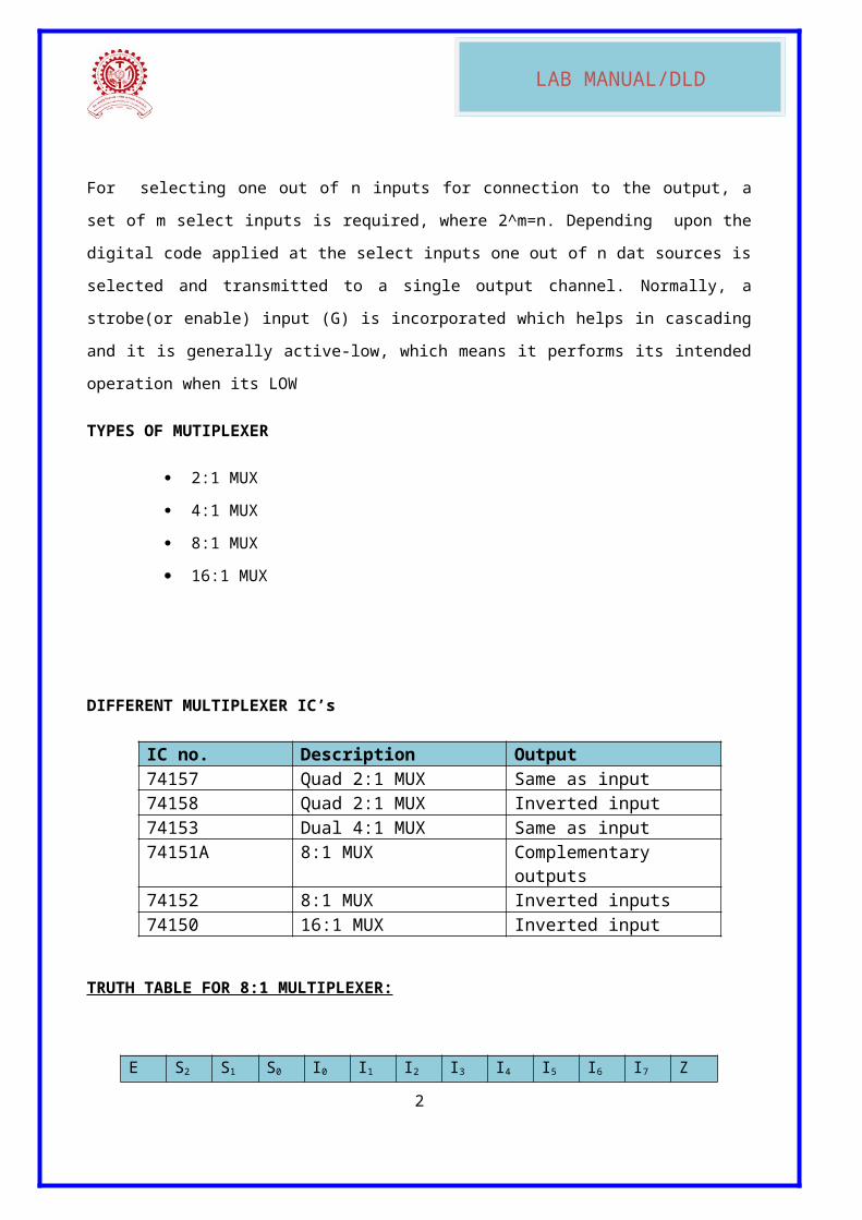
For selecting one out of n inputs for connection to the output, a set of m select inputs is required, where
2^m=n. Depending upon the digital code applied at the select inputs one out of n dat sources is selected
and transmitted to a single output channel. Normally, a strobe(or enable) input (G) is incorporated
which helps in cascading and it is generally active-low, which means it performs its intended operation
when its LOW
TYPES OF MUTIPLEXER
2:1 MUX
1
Sr.No Instrument Specifications
1 Digital Trainer Kit
LAB MANUAL/DLD
4:1 MUX
8:1 MUX
16:1 MUX
DIFFERENT MULTIPLEXER IC’s
IC no. Description Output74157 Quad 2:1 MUX Same as input74158 Quad 2:1 MUX Inverted input74153 Dual 4:1 MUX Same as input74151A 8:1 MUX Complementary outputs 74152 8:1 MUX Inverted inputs74150 16:1 MUX Inverted input
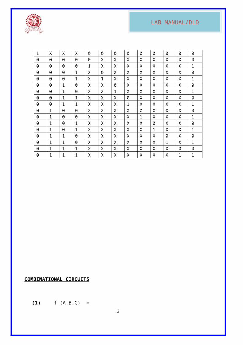
TRUTH TABLE FOR 8:1 MULTIPLEXER:
E S2 S1 S0 I0 I1 I2 I3 I4 I5 I6 I7 Z
1 X X X 0 0 0 0 0 0 0 0 00 0 0 0 0 X X X X X X X 00 0 0 0 1 X X X X X X X 10 0 0 1 X 0 X X X X X X 00 0 0 1 X 1 X X X X X X 10 0 1 0 X X 0 X X X X X 00 0 1 0 X X 1 X X X X X 10 0 1 1 X X X 0 X X X X 00 0 1 1 X X X 1 X X X X 10 1 0 0 X X X X 0 X X X 00 1 0 0 X X X X 1 X X X 10 1 0 1 X X X X X 0 X X 00 1 0 1 X X X X X 1 X X 10 1 1 0 X X X X X X 0 X 00 1 1 0 X X X X X X 1 X 10 1 1 1 X X X X X X X 0 00 1 1 1 X X X X X X X 1 1
2
LAB MANUAL/DLD
COMBINATIONAL CIRCUITS
(1) f (A,B,C) = E A B C Y
3

LAB MANUAL/DLD
(2) f (A,B,C) =
E A B C Y
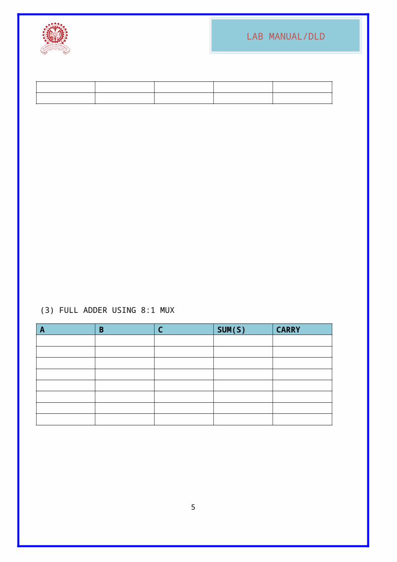
(3) FULL ADDER USING 8:1 MUX
A B C SUM(S) CARRY
4
LAB MANUAL/DLD
(4) f (A,B,C,D) =
A B C D Y
5

LAB MANUAL/DLD
ADVANTAGES OF MUX
2. It reduces number of wires.
3. It reduces the circuit complexity and cost.
4. We can implement many combinational circuits.
5. It simplifies the logic design
6. It doesn’t need the k maps and simplification
APPLICATIONS OF MULTIPLEXER
1. Used as a data selector to select one out of many data inputs.
2. Used for simplification of logic design.
3. In data acquisition system
4. In designing the combinational circuits.
5. In D/A converters.
6. To minimize the number of connections
6
LAB MANUAL/DLD
CONCLUSION:______________________________________________________________
____________________________________________________________________________
____________________________________________________________________________
EXPERIMENT NO.2
TITLE: BCD adder
AIM: Design and implement 1 digit BCD adder using IC 7483 (Full Adder)
APPARATUS:
THEORY:
BCD adder is a circuit that adds 2 BCD digits and procedures a sum of digit also in BCD. BCD
addition procedures can be summarized as follows,
7
Sr.No Instrument Specifications
1 Circuit Board
2 IC’s used
LAB MANUAL/DLD
1. Add 2 BCD number using binary addition.
2. If the 4-bit sum is greater than 9 or if carry is generated, the sum is invalid. To correct the
sum, add 0110 to sum if carry is generated from this addition, add it to the next higher
order BCD digit.
3. If the 4-bit sum is less than 9 or equal to 9, the sum is in proper BCD form Thus, to
implement, BCD adder we require,
a. A 4-bit binary adder for initial addition.
b. Logic circuit to detect sum greater than 9.
c. Another 4-bit adder to add 0110 in the sum if the sum is greater than 9 or
carry is
The logic circuit to determine sum greater than ‘9’ can be determined by
simplifying the boolean expression of the given truth table: -
TRUTH TABLE:-detection of invalid BCD:
Cout S3 S2 S1 S0 Y0 0 0 0 0 00 0 0 0 1 00 0 0 1 0 00 0 0 1 1 00 0 1 0 0 00 0 1 0 1 00 0 1 1 0 00 0 1 1 1 00 1 0 0 0 00 1 0 0 1 00 1 0 1 0 10 1 0 1 1 10 1 1 0 0 10 1 1 0 1 10 1 1 1 0 10 1 1 1 1 1
Cout S3 S2 S1 S0 Y1 0 0 0 0 1
8
LAB MANUAL/DLD
1 0 0 0 1 11 0 0 1 0 11 0 0 1 1 11 0 1 0 0 11 0 1 0 1 11 0 1 1 0 11 0 1 1 1 11 1 0 0 0 11 1 0 0 1 11 1 0 1 0 11 1 0 1 1 11 1 1 0 0 11 1 1 0 1 11 1 1 1 0 11 1 1 1 1 1
KARNAUGH MAP :-
1. Cout = 0
1. Cout = 0
9

LAB MANUAL/DLD
As shown in figure the BCD number are first added in the top 4-bit binary adder to produce a
binary sum zero( i.e. when sum is greater than equal to 9 and Cout =0) nothing (i.e. zero) is
added to the binary sum. When it is equal to 1 (i.e. when a sum greater than 9 or Cout=1)
binary 0110 is added to the binary sum. The output generated from the bottom binary adder can
be ignored, since it supplies information already available at the output carry terminal.
CIRCUIT DIAGRAM:
10

LAB MANUAL/DLD
CONCLUSION:______________________________________________________________
____________________________________________________________________________
____________________________________________________________________________
EXPERIMENT NO.3
TITLE: Asynchronous and synchronous counter.
AIM: Functional verification of ripple counter IC 7490 and synchronous counter IC 74191
(MOD-N operation).
APPARATUS:
THEORY:
11
Sr. No. Instrument Specifications
1. Digital Trainer Kit
2. IC’s used

LAB MANUAL/DLD
BASIC INTERNAL STRUCTURE OF IC 7490
IC 7490 is a TTL MSI decade counter. It contains four master slave flip-flops and additional gating to provide a divide-by-two counter and a three stage binary counter which provides a divide by 5 counter. (MOD-5) IC 7490 is a MOD-10 or decade counter. It can be used for designing symmetrical Bi-quinary divide by 10 counter. In this application clock is applied to input B and QD output is connected to input A. the output is obtained at QA output. It is a perfect square wave at a frequency equal to fclk/10.
PIN NAME AND DESCRIPTION
12
PIN NAME DESCRIPTION
1 Input B Clock input to internal MODS ripple counter
2 Ro(1), Ro(2) Gates, zero reset input. These are active low. When both are zero all output are zero.
3 VCC +5V DC
4 RQ(1), RQ(2) These are gate set with nine output.
5 QD, QC, QB Output of internal MOD counter.
6 GND Logic GND acts as reference.
7 QA Output of internal MOD-2 counter.
8 Input A Clock input to flip flop A which is negative edge triggered.

LAB MANUAL/DLD
PINDIAGRAM :
IC 7490 AS DECADE COUNTER
TRUTH TABLE FOR IC 7490
CLOCK QD QC QB QA
0 0 0 0 01 0 0 0 12 0 0 1 03 0 0 1 14 0 1 0 05 0 1 0 16 0 1 1 07 0 1 1 18 1 0 0 09 1 0 0 110 0 0 0 011 0 0 0 112 0 0 1 013 0 0 1 114 0 1 0 015 0 1 0 1
CIRCUIT DIAGRAM:
13

LAB MANUAL/DLD
IC 7490 AS MOD-6 COUNTER
TRUTH TABLE OF MOD-6 COUNTER:
CIRCUIT DIAGRAM:
SYMMETRICAL BI-QUINARY DIVIDED BY 10 COUNTER:
CLOCK QD QC QB QA
0 0 0 0 01 0 0 1 02 0 1 0 03 0 1 1 04 1 0 0 05 0 0 0 16 0 0 1 17 0 1 0 18 0 1 1 1
14
CLOCK QA QB QC QD
0 0 0 0 01 0 0 0 12 0 0 1 03 0 0 1 14 0 1 0 05 0 1 0 16 0 1 1 07 0 0 0 0

LAB MANUAL/DLD
9 1 0 0 1
SYNCHRONOUS COUNTER IC 74191:-
IC 74191 is a 16 pin IC that is synchronous, 4-bit binary, up/down reversible counter.
Synchronous operation is obtained by having all the flip-flops clocked simultaneously so that
the outputs change simultaneously. This method eliminates the output counting spikes
normally associated with an asynchronous (ripple) counter.
INPUTS:
1) Clock input: The clock of this IC is a positive edge triggered.
2) Enable : The IC gets activated when this pin is connected to ground.
3) Up/Down: This input determines the direction of count. When low, the IC counts up and
when high the IC counts down.
4) Load: The outputs of the IC may be preset to any level by placing low on the input load and
entering the data. The output will change independent of the level of the clock input.
15

LAB MANUAL/DLD
5) Data inputs A, B, C, and D: These are used to preset a particular data in the IC.
6) OUTPUTS QA, QB, QC, and QD: They are the outputs of the master slave JK flip-flops.
7) Max/Min : This is the special output IC. When the count is in up mode and reaches 15 i.e.
1111, which is over flow condition, then output of Max/Min goes high. When in down
count mode and 0000 is present at output it is underflow condition and again the output
goes high.
Ripple clock: This is also special output of the IC. Just like Max/Min, output of ripple clock
goes low for overflow and under flow conditions. But the only difference is that this output is
low for only the negative clock cycles and not for entire clock cycles (normally high).
PIN CONFIGURATION OF IC 74191:
PIN DESCRIPTION
16

LAB MANUAL/DLD
PIN NUMBER DESCRIPTION
Data input (PO to P3) 4 data inputs lines with P0 LSB and P3 as MSB
Parallel load PLData present on input lines appears as output
when P =0
Count enable input CE It enables counting when CE =0
Output (Q0 to Q3)4 output with Q0 as LSB and Q3 as MSB
UP/downIf this input is low, up counting takes place and if high, down counting takes place.
Clock input (CP) This is clock input for clock
Terminal counter (TC) As the counter reaches max (15) or min (0), it is indicated by a `high pulse` on TC output.
Ripple clock (RC)This is an active low output. It is normally high. As the counter reaches max (15) or min (0), it is indicated by a `high pulse` on ripple clock. It is used for cascading.
TRUTH TABLE:
17
Operating Mode Inputs Output
PL U/D
CE
CP
P0
to P3
Parallel Load L X X X L L
L X X X H H
Count Up H L L Î X Count Up
Count Down H H L Î X Count Down
Hold(no change)
H X H X X No Change

LAB MANUAL/DLD
MOD-10 UP COUNTER FROM 6 TO 15 USING IC 74191
TRUTH TABLE:
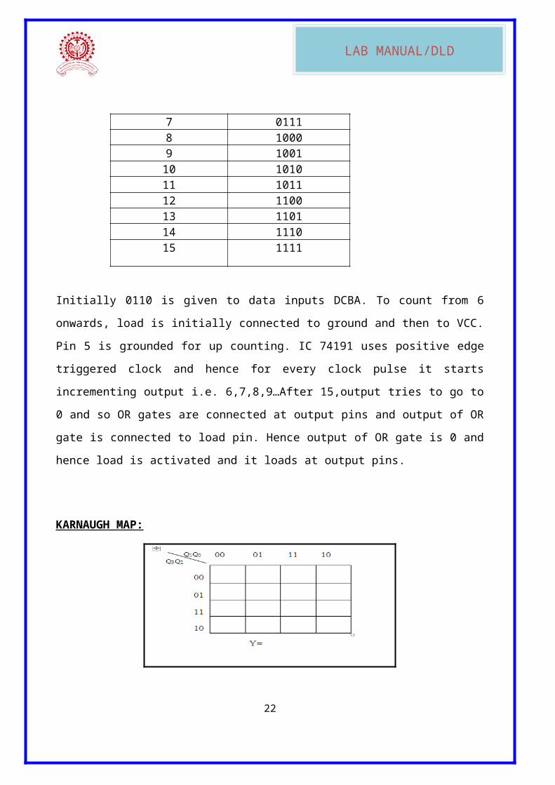
Decimal Binary6 01107 01118 10009 100110 101011 101112 110013 110114 111015 1111
Initially 0110 is given to data inputs DCBA. To count from 6 onwards, load is initially
connected to ground and then to VCC. Pin 5 is grounded for up counting. IC 74191 uses
positive edge triggered clock and hence for every clock pulse it starts incrementing output i.e.
6,7,8,9…After 15,output tries to go to 0 and so OR gates are connected at output pins and
output of OR gate is connected to load pin. Hence output of OR gate is 0 and hence load is
activated and it loads at output pins.
KARNAUGH MAP:
18
LAB MANUAL/DLD
BLOCK DIAGRAM OF MOD-10 UP COUNTER FROM 6 TO 15 USING IC 74191 :
CONCLUSION:______________________________________________________________
____________________________________________________________________________
__________________________________________________________________________
EXPERIMENT NO.4
TITLE: Shift Register
AIM : To verify function of Shift register IC 7495 and implementation of pulse train generator
Using the IC. Observe the output using logic analyzer.
APPARATUS:
19
Sr. No. Instrument Specifications
1. Digital Trainer Kit
2. IC ‘s used

LAB MANUAL/DLD
THEORY:
In digital circuits, a shift register is a cascade of flip flops, sharing the same clock, which has
the output of anyone but the last flip-flop connected to the "data" input of the next one in the
chain, resulting in a circuit that shifts by one position the one-dimensional "bit array" stored in
it, shifting in the data present at its input and shifting out the last bit in the array, when enabled
to do so by a transition of the clock input. More generally, a shift register may be
multidimensional, such that its "data in" input and stage outputs are themselves bit arrays: this
is implemented simply by running several shift registers of the same bit-length in parallel.Shift
registers can have both parallel and serial inputs and outputs. These are often configured as
serial-in, parallel-out (SIPO) or as parallel-in, serial-out (PISO). There are also types that have
both serial and parallel input and types with serial and parallel output. There are also bi-
directional shift registers which allow shifting in both directions: L→R or R→L. The serial
input and last output of a shift register can also be connected together to create a circular shift
register.
SERIAL-IN, SERIAL-OUT:
These are the simplest kind of shift registers. The data string is presented at 'Data In', and is
shifted right one stage each time 'Data Advance' is brought high. At each advance,
the bit on the far left (i.e. 'Data In') is shifted into the first flip-flop's output. The bit
on the far right (i.e. 'Data Out') is shifted out and lost.
The data are stored after each flip-flop on the 'Q' output, so there are four storage
'slots' available in this arrangement; hence it is a 4-Bit Register. To give an idea of
the shifting pattern, imagine that the register holds 0000 (so all storage slots are
empty). As 'Data In' presents 1,0,1,1,0,0,0,0 (in that order, with a pulse at 'Data
20
0 0 0 0
1 0 0 0
1 1 0 0
0 1 1 0
1 0 1 1
0 1 0 1
0 0 1 0
0 0 0 1

LAB MANUAL/DLD
Advance' each time. This is called clocking or strobing) to the register, this is the result. The
left hand column corresponds to the left-most flip-flop's output pin, and so on.
So the serial output of the entire register is 10110000 . As you can see if we were to continue to
input data, we would get exactly what was put in, but offset by four 'Data Advance' cycles.
This arrangement is the hardware equivalent of a queue. Also, at any time, the whole register
can be set to zero by bringing the reset (R) pins high.
This arrangement performs destructive readout - each datum is lost once it been shifted out of
the right-most bit.
SERIAL-IN, PARALLEL-OUT:
Data is input serially, as described in the SISO section above. Once the data has been input, it
may be either read off at each output simultaneously, or it can be shifted out and replaced.
PROCEDURE:
I) Symmetrical Schmitt trigger
i) Make connections as shown in the circuit diagram
21
LAB MANUAL/DLD
ii) Apply +VCC and –VEE as +/-12V respectively.
iii) Apply sine wave input with 10 V p-p, with freq = 1KHz
iv) Observe the waveforms on Dual mode of the CRO and verify the
UTP and LTP are according to the design and sketch the same. Observe the Hysteresis by keeping the CRO in X-Y mode & sketch the same.
PARALLEL IN SERIAL OUTPUT:
PARALLEL IN PARALLEL OUT:
22

LAB MANUAL/DLD
PIN DIAGRAM :
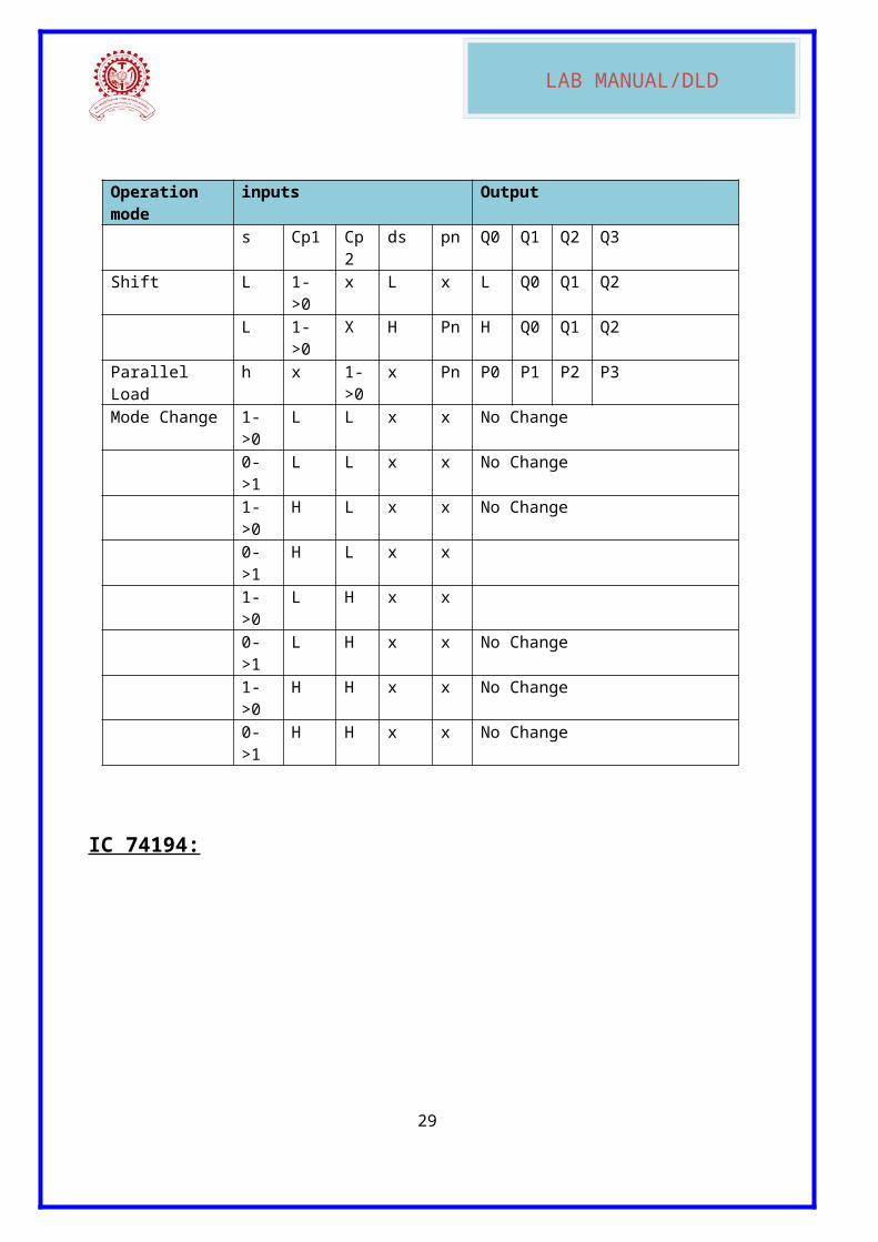
Operation mode inputs Outputs Cp1 Cp2 ds pn Q0 Q1 Q2 Q3
Shift L 1->0 x L x L Q0 Q1 Q2L 1->0 X H Pn H Q0 Q1 Q2
Parallel Load h x 1->0
x Pn P0 P1 P2 P3
Mode Change 1->0 L L x x No Change0->1 L L x x No Change1->0 H L x x No Change0->1 H L x x1->0 L H x x0->1 L H x x No Change1->0 H H x x No Change0->1 H H x x No Change
23

LAB MANUAL/DLD
IC 74194:
TRUTH TABLE:
Operating Mode
MR S1 S0 DSR DSL Pn Q0 Q1 Q2 Q3
Reset L L L L L
Hold H L L Q0 Q1 Q2 Q3
Shift Left H H L L Q1 Q2 Q3 LH H L H Q1 Q2 Q3 H
Shift Right H L H L L Q0 Q1 Q2H L H H H Q0 Q1 Q2
Parallel Load
H H H Pn P0 P1 P2 P3
24

LAB MANUAL/DLD
IMPLEMENT ATION OF PULSE TRAIN:
THEORY:
A sequence generator is the Sequential circuit, which generates a prescribed sequence as its output.
The output sequence is in synchronization with the clock input. It is possible to design a sequence
generator using shift register. The output of an n-bit shift register is applied at inputs to
combinational circuit called next “next state Decoder”. The output of the next state decoder is
applied as inputs of shift register the combinational circuit IDs designed as per the requirement of
sequence. The Given Sequence is 100011
TRUTH TABLE:
Q3 Q2 Q1 Q0 D I/P1 1 1 0 00 1 1 1 00 0 1 1 10 0 0 1 11 0 0 0 11 1 0 0 0
25

LAB MANUAL/DLD
CONCLUSION:______________________________________________________________
____________________________________________________________________________
_________________________________________________________________________
EXPERIMENT NO.5
TITLE: Two bit Comparator.
AIM: Write a code for 2-bit Comparator using VHDL language and simulate the code.
APPARATUS:
Sr. No. Instrument Specifications
1. Xilinx ISE 9.1i software
26
Q0 Q1\Q2 Q3
00 01 11 10
00011110

LAB MANUAL/DLD
THEORY:
COMPARATOR : A digital comparator or magnitude comparator is a hardware electronic
device that takes two numbers as input in binary form and determines whether one number is
greater than, less than or equal to the other number. Comparators are used in a central
processing units (CPU) and microcontrollers.
TRUTH TABLE:
KARNAUGH MAP:
1) A>B 2) A= B
27

LAB MANUAL/DLD
CONCLUSION:______________________________________________________________
____________________________________________________________________________
____________________________________________________________________________
EXPERIMENT NO. 6
TITLE: ALU.
AIM: Write a code for ALU using VHDL language and simulate the code
APPARATUS:
28
LAB MANUAL/DLD
THEORY :
The arithmetic logic unit executes arithmetic and logical operations. Arithmetic operations
include addition, subtraction, multiplication and division. Logical operations compare
numbers, letters and special characters. Relational operations (=, <, >) are used to describe the
comparison operations used by the arithmetic logic unit.
CONCLUSION:______________________________________________________________
____________________________________________________________________________
____________________________________________________________________________
EXPERIMENT NO.7
TITLE: D Flip Flop and JK Flip Flop.
AIM: Write a code for D f/f and JK f/f (using synchronous and asynchronous reset inputs)
UsingVHDL language and simulate the code.
29
Sr. No. Instrument Specifications
1. Xilinx ISE 9.1i software
Operation S2 S1 S0 OutputClear 0 0 0 0000B-A 0 0 1 B-AA-B 0 1 0 A-BADD 0 1 1 A+BXOR 1 0 0 A XOR BOR 1 0 1 A OR BAND 1 1 0 A . BPRESET 1 1 1 1111

LAB MANUAL/DLD
APPARATUS:
THEORY:
D FF: The Q output always takes on the state of the D input at the moment of a rising clock
edge (or falling edge if the clock input is active low).It is called the D flip-flop for this reason,
since the output takes the value of the D input or Data input, and Delays it by one clock count.
The D flip-flop can be interpreted as a primitive memory cell, zero-order hold, or delay line.
TRUTH TABLE:
Clock D Q Qprev
Rising edge 0 0 X
Rising edge 1 1 X
Non-Rising X Qprev
30
Sr. No. Instrument Specifications
1. Xilinx ISE 9.1i software

LAB MANUAL/DLD
JK FF:
The JK flip-flop augments the behavior of the SR flip-flop (J=Set, K=Reset) by interpreting
the S = R = 1 condition as a "flip" or toggle command. Specifically, the combination J = 1, K =
0 is a command to set the flip-flop; the combination J = 0, K = 1 is a command to reset the flip-
flop; and the combination J = K = 1 is a command to toggle the flip-flop, i.e., change its output
to the logical complement of its current value. Setting J = K = 0 does NOT result in a D flip-
flop, but rather, will hold the current state. To synthesize a D flip-flop, simply set K equal to
the complement of J. The JK flip-flop is therefore a universal flip-flop, because it can be
configured to work as an SR flip-flop, a D flip-flop, or a T flip-flop.
31

LAB MANUAL/DLD
CONCLUSION:______________________________________________________________
____________________________________________________________________________
____________________________________________________________________________
EXPERIMENT NO. 8
TITLE: UP/DOWN ripple counter.
AIM: Write a code for Four bits UP/DOWN ripple counter using mode control using VHDL
Language and simulate the code.
APPARATUS:
Sr.No Instrument Specifications
1 Xillinx ISE 9.1i software
THEORY:
32

LAB MANUAL/DLD
A counter that can change state in either direction, under control an up–down selector input, is
known as an up–down counter. When the selector is in the up state, the counter increments its
value; when the selector is in the down state, the counter decrements the count.
BLOCK DAIGRAM :
DETAIL DIAGRAM USING FF :
33

LAB MANUAL/DLD
CONCLUSION:______________________________________________________________
____________________________________________________________________________
____________________________________________________________________________
EXPERIMENT NO.9
TITLE: Four bit synchronous counters using flip flop
AIM: Write a code for Four bit synchronous counters using flip flop using VHDL language
And simulate the code.
APPARATUS:
Sr. No. Instrument Specifications
1. Xilinx ISE 9.1i software
34

LAB MANUAL/DLD
THEORY :
When Counter is clocked such that each Flip Flop in the counter is triggered at the same time,
the counter is called as Synchronous counter.
BLOCK DAIGRAM :
DETAIL DIAGRAM USING FF :
35

LAB MANUAL/DLD
CONCLUSION:______________________________________________________________
____________________________________________________________________________
____________________________________________________________________________
36
Related Documents