Review Discovery-based design of transparent conducting oxide films Gregory J. Exarhos ⁎ , Xiao-Dong Zhou Pacific Northwest National Laboratory, Richland, WA 99352, USA Available online 16 March 2007 Abstract The properties of TCO materials derive from the nature, number, and atomic arrangements of metal cations in crystalline or amorphous oxide structures, from the resident morphology, and from the presence of intrinsic or intentionally introduced defects. An enormous body of literature can be accessed from which empirical relationships between structure, composition, charge transport, and transparency have been developed. Previous reviews of this subject have indicated how such information may be used for engineering TCO properties; however, application of more rigorous science-based approaches to the design of materials with superior properties has only recently been tackled. This article summarizes current TCO research results, reviews processing approaches, presents a microscopic description of electronic conductivity in transparent metal oxide systems, and offers guidelines for the design and subsequent development of new materials. The review concludes with a glimpse of some recent work where impedance matching and quantum mechanical tunneling approaches would seem to provide future directions for improving transmissivity in these and similar conducting oxide systems. © 2007 Elsevier B.V. All rights reserved. Keywords: Transparent conducting oxide; Conductivity; Transparency; Modeling; Film deposition Contents 1. Introduction .............................................................. 7026 2. Mechanisms and modeling of charge transport ............................................ 7026 2.1. Classical theory of charge transport .............................................. 7027 2.2. Origins of the dielectric constant — The Harmonic Oscillator ................................. 7028 2.3. Electron energy bands in free carrier TCO's ......................................... 7029 2.4. Conduction pathways in free carrier TCO's .......................................... 7030 2.5. Other conduction mechanisms ................................................. 7031 2.5.1. Electrides ....................................................... 7031 2.5.2. Polarons ....................................................... 7032 3. Film deposition approaches ...................................................... 7033 3.1. Magnetron sputtering ..................................................... 7033 3.2. Pulsed laser deposition .................................................... 7035 3.3. Chemical vapor deposition .................................................. 7036 3.4. Solution deposition ...................................................... 7038 3.5. Spray pyrolysis ........................................................ 7039 3.6. Combinatorial deposition methods .............................................. 7040 4. Carrier mobility in TCO films — Theory and practice ........................................ 7041 4.1. Hall mobility in an n-type TCO ................................................ 7042 4.2. Enhanced electron mobility in TCO films ........................................... 7043 5. Future directions in TCO research .................................................. 7045 5.1. Hydrogen impurities in oxides ................................................ 7046 Thin Solid Films 515 (2007) 7025 – 7052 www.elsevier.com/locate/tsf ⁎ Corresponding author. Tel.: +1 509 376 4125; fax: +1 509 376 5106. E-mail address: [email protected] (G.J. Exarhos). 0040-6090/$ - see front matter © 2007 Elsevier B.V. All rights reserved. doi:10.1016/j.tsf.2007.03.014

Welcome message from author
This document is posted to help you gain knowledge. Please leave a comment to let me know what you think about it! Share it to your friends and learn new things together.
Transcript
Thin Solid Films 515 (2007) 7025–7052www.elsevier.com/locate/tsf
Review
Discovery-based design of transparent conducting oxide films
Gregory J. Exarhos ⁎, Xiao-Dong Zhou
Pacific Northwest National Laboratory, Richland, WA 99352, USA
Available online 16 March 2007
Abstract
The properties of TCO materials derive from the nature, number, and atomic arrangements of metal cations in crystalline or amorphous oxidestructures, from the resident morphology, and from the presence of intrinsic or intentionally introduced defects. An enormous body of literaturecan be accessed from which empirical relationships between structure, composition, charge transport, and transparency have been developed.Previous reviews of this subject have indicated how such information may be used for engineering TCO properties; however, application of morerigorous science-based approaches to the design of materials with superior properties has only recently been tackled. This article summarizescurrent TCO research results, reviews processing approaches, presents a microscopic description of electronic conductivity in transparent metaloxide systems, and offers guidelines for the design and subsequent development of new materials. The review concludes with a glimpse of somerecent work where impedance matching and quantum mechanical tunneling approaches would seem to provide future directions for improvingtransmissivity in these and similar conducting oxide systems.© 2007 Elsevier B.V. All rights reserved.
Keywords: Transparent conducting oxide; Conductivity; Transparency; Modeling; Film deposition
Contents
1. Introduction . . . . . . . . . . . . . . . . . . . . . . . . . . . . . . . . . . . . . . . . . . . . . . . . . . . . . . . . . . . . . . 70262. Mechanisms and modeling of charge transport . . . . . . . . . . . . . . . . . . . . . . . . . . . . . . . . . . . . . . . . . . . . 7026
2.1. Classical theory of charge transport . . . . . . . . . . . . . . . . . . . . . . . . . . . . . . . . . . . . . . . . . . . . . . 70272.2. Origins of the dielectric constant — The Harmonic Oscillator . . . . . . . . . . . . . . . . . . . . . . . . . . . . . . . . . 70282.3. Electron energy bands in free carrier TCO's . . . . . . . . . . . . . . . . . . . . . . . . . . . . . . . . . . . . . . . . . 70292.4. Conduction pathways in free carrier TCO's . . . . . . . . . . . . . . . . . . . . . . . . . . . . . . . . . . . . . . . . . . 70302.5. Other conduction mechanisms. . . . . . . . . . . . . . . . . . . . . . . . . . . . . . . . . . . . . . . . . . . . . . . . . 7031
2.5.1. Electrides . . . . . . . . . . . . . . . . . . . . . . . . . . . . . . . . . . . . . . . . . . . . . . . . . . . . . . . 70312.5.2. Polarons . . . . . . . . . . . . . . . . . . . . . . . . . . . . . . . . . . . . . . . . . . . . . . . . . . . . . . . 7032
3. Film deposition approaches . . . . . . . . . . . . . . . . . . . . . . . . . . . . . . . . . . . . . . . . . . . . . . . . . . . . . . 70333.1. Magnetron sputtering . . . . . . . . . . . . . . . . . . . . . . . . . . . . . . . . . . . . . . . . . . . . . . . . . . . . . 70333.2. Pulsed laser deposition . . . . . . . . . . . . . . . . . . . . . . . . . . . . . . . . . . . . . . . . . . . . . . . . . . . . 70353.3. Chemical vapor deposition . . . . . . . . . . . . . . . . . . . . . . . . . . . . . . . . . . . . . . . . . . . . . . . . . . 70363.4. Solution deposition . . . . . . . . . . . . . . . . . . . . . . . . . . . . . . . . . . . . . . . . . . . . . . . . . . . . . . 70383.5. Spray pyrolysis . . . . . . . . . . . . . . . . . . . . . . . . . . . . . . . . . . . . . . . . . . . . . . . . . . . . . . . . 70393.6. Combinatorial deposition methods . . . . . . . . . . . . . . . . . . . . . . . . . . . . . . . . . . . . . . . . . . . . . . 7040
4. Carrier mobility in TCO films — Theory and practice. . . . . . . . . . . . . . . . . . . . . . . . . . . . . . . . . . . . . . . . 70414.1. Hall mobility in an n-type TCO . . . . . . . . . . . . . . . . . . . . . . . . . . . . . . . . . . . . . . . . . . . . . . . . 70424.2. Enhanced electron mobility in TCO films. . . . . . . . . . . . . . . . . . . . . . . . . . . . . . . . . . . . . . . . . . . 7043
5. Future directions in TCO research . . . . . . . . . . . . . . . . . . . . . . . . . . . . . . . . . . . . . . . . . . . . . . . . . . 70455.1. Hydrogen impurities in oxides . . . . . . . . . . . . . . . . . . . . . . . . . . . . . . . . . . . . . . . . . . . . . . . . 7046
⁎ Corresponding author. Tel.: +1 509 376 4125; fax: +1 509 376 5106.E-mail address: [email protected] (G.J. Exarhos).
0040-6090/$ - see front matter © 2007 Elsevier B.V. All rights reserved.doi:10.1016/j.tsf.2007.03.014
7026 G.J. Exarhos, X.-D. Zhou / Thin Solid Films 515 (2007) 7025–7052
5.2. Oxide-based electrides . . . . . . . . . . . . . . . . . . . . . . . . . . . . . . . . . . . . . . . . . . . . . . . . . . . . 70475.3. Impedance matching designs . . . . . . . . . . . . . . . . . . . . . . . . . . . . . . . . . . . . . . . . . . . . . . . . . 7047
6. Conclusions . . . . . . . . . . . . . . . . . . . . . . . . . . . . . . . . . . . . . . . . . . . . . . . . . . . . . . . . . . . . . 7048Acknowledgements . . . . . . . . . . . . . . . . . . . . . . . . . . . . . . . . . . . . . . . . . . . . . . . . . . . . . . . . . . . . 7049References . . . . . . . . . . . . . . . . . . . . . . . . . . . . . . . . . . . . . . . . . . . . . . . . . . . . . . . . . . . . . . . . 7049
1. Introduction
Transparent conducting oxides (TCO's) comprise a class ofmaterials that can be thought of as conjugate property materials inwhich one property, in this case conductivity, is strongly coupledto a second property, namely, the lossy part of the refractive indexor the extinction coefficient. In this regard, materials, like metals,that are highly conductive, will not normally transmit visible light,while highly transparent media like oxide glasses behave asinsulators. The challenge for achieving materials that are bothconducting and optically transmissive is to understand thefundamental materials structure/property relationships that drivethese properties so that they may be decoupled such that thematerial both retains transparency while becoming electricallyconductive. To an extent, many phenomenological approachesbased upon well-understood physical principles have beenreported to achieve materials having these properties. Morerecent studies push the envelope of the earlier work throughunderstanding, at a fundamental level, the microscopic nature ofthe conductivity process in order to discover the role of chemicalstructure, bonding, and film morphology on charge transport.
The first realization of a TCO material occurred a centuryago when a thin film of sputter deposited cadmium metalunderwent incomplete thermal oxidation upon post-depositionheating in air [1]. While the electrical conductivity of thismaterial did in fact change with time, the oxide was indeedrepresentative of a free-carrier like conductor where a residentoxygen deficiency lends free carriers to associated metal defectenergy levels near the bottom of the metal-like conduction bandof the oxide. The generalization here is that certain slightlyreduced metal oxide systems can show n-type electricalconductivity provided that charge-compensating electrons canbe promoted to the conduction band of the metal oxide fromdefect energy levels lying close in energy to the conductionband minimum. Since this early discovery, appreciable valuesof electrical conductivity have been observed in many single,binary, ternary and quaternary metal oxide systems [2–7].However, while transmission through these materials in thevisible region of the spectrum can be quite good, electricalconductivities still remain considerably below those of metals.
More recently, p-type conductivity has been documented incertain metal oxide systems where the defect energy levels lieproximate to the valence band of the metal oxide [8]. In suchmaterials, electron promotion to these defect levels creates holesin the valence band thereby promoting conductivity. Again,good transmission in the visible region of the spectrum can beachieved but measured conductivities are considerably smallerthan those exhibited by the n-type materials owing to restrictedhole mobility in the valence band of the solid [9].
An alternative model for describing conductivity in metaloxide systems invokes the presence of localized charge states(polarons) that transport through the lattice by means of ahopping mechanism [10]. The analogy here is to conjugatedpolymer systems where addition of an electron withdrawinggroup like iodine will abstract electrons from the extendednetwork of carbon–carbon double bonds, forming localizedcharge states (holes) within the polymer chain. The motion ofthese trapped charge states along the chain is thermallyactivated and also enhanced by dynamic conformationalperturbations of the polymer structure; both effects promoteconductivity [10–13]. A similar mechanism can persist in metaloxide systems where strong covalent interactions betweenresident metal cations and oxygen prevail [14]. While visibletransparency can suffer somewhat, conductivities in these metaloxide systems markedly exceed those registered by p-type freecarrier oxide conductors [15]. The polaron model for describingconductivity in mixed metal oxide systems remains quitecontroversial.
A previous review of transparent conductors in this Journalappeared some two-dozen years ago. This earlier comprehen-sive article summarized work in this rapidly changing field andreferenced additional review papers on this topic [2–7]. Morerecent advances toward our understanding of TCO properties,processing issues, and current and prospective applications havebeen collected in the August 2000 issue of the MRS Bulletin[16]. In the ensuing years, this topic has been featured innumerous conference symposia and workshops, most recentlyat the ITCO conference in Crete [17].
The review presented here summarizes recent work in thisrapidly evolving area. Relationships between film processingparameters and attendant film properties are addressed alongwith current theoretical views on charge transport in oxidesemiconductors with a goal of providing a set of unified designcriteria for achieving optimum conductivity and high transmis-sivity. Key ideas that lead to a better understanding of chargemobility and property robustness are also discussed. Finally,future directions in which this field may grow are discussed onthe basis of several recent papers dealing with impedancematching in multilayered films and quantum mechanical tun-neling through a barrier.
2. Mechanisms and modeling of charge transport
The current understanding of conductivity in transparentmaterials is based upon a classical description of charge trans-port in metals coupled to the optical properties of the materialthrough the density of charge carriers and their effective mass.A summary of the key concepts provided below defines the
7027G.J. Exarhos, X.-D. Zhou / Thin Solid Films 515 (2007) 7025–7052
relevant parameters used to describe the performance of thesematerials. These include the conductivity (σ), sheet resistance(Rs), free carrier mobility (μ), free carrier density (N), and theimaginary or lossy part of the refractive index termed theextinction coefficient (κ) that is proportional to the absorptioncoefficient (α) through the wavelength (λ).
I ¼ I0expð�adÞ; with a ¼ 4pj=k ð1Þ
Here, I0 is the incident light intensity on a material ofthickness d, and I is defined as the transmitted intensity throughthe material. Proper use of this equation for thin films requiresthat optical scattering and reflection losses at the interfaces beconsidered.
A quantitative measure of performance of a TCO can bewritten in terms of the ratio of the electrical conductivity to theoptical absorption coefficient or,
r=a ¼ 1½RslnðT þ RÞ��1; ð2Þ
where, T and R represent the total transmittance and reflectanceof the material, and Rs is the sheet resistance (=resistivity/film-thickness) [18]. This figure-of-merit is used to assess the rela-tive performance of different TCO materials and is wavelengthdependent. It should be noted here that the factors appearing inEq. (2) are highly dependent upon processing conditions andhence, the resident microstructure and defect chemistry of thematerial. Thus, a highly optically scattering material, due to thepresence of a polycrystalline grain structure, will have bothdiminished transmission, and higher resistivity due to a decreasein charge mobility arising from scattering of charge carriers atgrain boundaries. The figure-of-merit provides a good qualita-tive estimate of TCO performance for materials having similarmicrostructure.
The section below begins with a classical description ofconductivity in condensed phases and is followed by a semi-empirical description of microscopic properties (e.g., atom size,arrangement, and coordination) of thesematerials thatwould seemto promote conductivity. Finally, key results of ab initio energyband structure calculations are summarized. Results from thesestudies can be integrated into a unified picture that can provideguidance for the development of next generation TCO materials.
2.1. Classical theory of charge transport
Consider metal as a regular 3-dimensional lattice of cationsbound together by a sea of electrons that are free to movethroughout the lattice. In the absence of an applied field, themotion is random. The current (IA) in a metal segment of lengthL is defined to be proportional to the voltage drop (V) across thatsegment:
IA ¼ V=RX; or V ¼ IARX: ð3ÞThe resistance RΩ is related to the length of the segment and
is inversely proportional to the cross-sectional area (A).
RX ¼ qL=A; ð4Þ
where ρ is the resistivity (Ω cm). For a uniform electric field (E)across L, V=EL and therefore,
IA ¼ V=RX ¼ EL=qL=A ¼ EA=q: ð5ÞNow, the current in a segment is related to the number
of electrons per unit volume, ne=Ne /Vvol, the drift velocity υd,the magnitude of the electron charge (e) and the cross-section(A).
IA ¼ neeAυd or q ¼ E=ðneeυdÞ: ð6ÞBased upon Ohm's law, ρ must be independent of E, so
therefore, the drift velocity (υd) must be proportional to E. In thepresence of an external electric field, a free electron feels a forceof magnitude eE. If this were the only force, the electron ofmass me would have an unbounded acceleration eE /me.However, a steady-state situation persists in which the electrondrift velocity is proportional to the applied field. Therefore,collision with a lattice ion retards electron movement. After thecollision, the velocity is unrelated to the drift velocity. If τ is theaverage time between collisions, the drift velocity of theelectron becomes,
υd ¼ ðeE=meÞs; ð7Þand therefore,
q ¼ E=ðnee½eEs=me�Þ ¼ me=ðnee2sÞ: ð8ÞThis can also be written in terms of the electron mean free
path, lT, where
lT ¼ υFs; and q ¼ meυF=nee2ls: ð9ÞFrom Ohm's law, the current density Je=σeE, where Je is the
number of carriers passing through a unit area per second, andσe is the conductivity. Physically, σe
o is the dc current densityper unit electric field, so in terms of the carrier concentration(number of electrons per unit volume),
Je ¼ NeeυF ¼ neeðes=meÞE: ð10Þ(This result is obtained by counting the number of carriers,electrons of Fermi velocity υF(=ℏkF /me), that will pass througha unit area per unit time, and dividing by the field E.) Theconductivity, σe
o, is 1 /ρ and now becomes:
roe ¼ nee2s=me ¼ Neele; ð11Þ
where μe is commonly called the carrier mobility (cm2 V−1 s−1).The mobility is given by:
le ¼ es=me: ð12Þ
This conductivity relationship is not as simplistic as it seemsand in fact does contain some hidden information. The aboveequation was derived for a “free” electron, but in a crystallinelattice, the electron indeed is subjected to other forces that act to“alter its mass”. Also, as a result of these other forces, thecollision time, τ, can influence the value of m. We can thereforegeneralize the electron mass to account for these forces and
7028 G.J. Exarhos, X.-D. Zhou / Thin Solid Films 515 (2007) 7025–7052
realize that essentially it is somewhat different from the mass ofa truly free electron. As the number of electron collisionsincrease, the effective mass of the electron changes (me⁎).
roe ¼ nee2s=m⁎e : ð13Þ
The above equation relates the conductivity to the number ofcharge carriers and their mobility. It is understood that themobility generalizes all the forces acting on the electron in theconducting solid. These then, are taken as the importantparameters to be used for characterizing charge transport inconducting materials.
2.2. Origins of the dielectric constant— TheHarmonicOscillator
The free carriers will interact with an applied optical fieldthrough the polarization. Consider a free carrier of massmweaklybound in a lattice by a restoring force with a force constant kf. Ifthe applied field oscillates at a high frequency so that the freecarrier mass inertia precludes motion, there will be no coupling tothe field, no loss due to absorption, and the transmission will behigh. However, if the weakly bound carrier can freely respond tothe field, there will be loss. A simple harmonic oscillator formal-ism can be used to model this interaction.
The carriers are displaced an average distance, x, from theequilibrium position resulting in an induced polarization (P).
P ¼ neex; ð14Þwhere ne is the free carrier density, and e is the charge. Thepolarization electric field is P /ε, where ε is the dielectricconstant of the medium. Since the force is just the chargemultiplied by the field, the equation of motion for the freecarrier, with a negative restoring force, can be written as,
md2x=dt2 ¼ �nee2x=e: ð15Þ
This equation of motion has an oscillatory solution,
x ¼ A exp iðnee2=meÞt ¼ A exp iðxptÞ; ð16Þwhere the plasma frequency, ωp, is given by,
xp ¼ fnee2=meg1=2: ð17ÞFrom the conductivity relationship derived previously,
x2p ¼ roe=es ¼ neele=es: ð18Þ
The conductivity is related to the plasma frequency. Motionof the free carriers is impeded owing to collisions with thelattice and resident defects, so we must introduce a dampingterm into the equation of motion. These “frictional” forces areproportional to the velocity (υ) and mass (m) and are inverselyproportional to the time between collisions (τ). Under theinfluence of an oscillatory electric field,
mdυ=dT þ ðm=sÞυ ¼ �eEðtÞ ¼ �e expðixtÞ; ð19Þwhere ω is the frequency of the applied field. A steady statesolution for the velocity is:
υ ¼ esEðtÞ=fm½1þ ixt�g: ð20Þ
Since the conductivity (σ) is defined as the current density(J=neeνF ) per unit electric field, the conductivity can be writtenas [19]:
r ¼ nee2s=mf1=ð1þ ixtÞg ¼ roef1=ð1þ ixtÞg; or ð21Þ
r ¼ roef1=ð1þ x2t2Þg þ iroefxt=ð1þ x2t2Þg: ð22ÞThe complex refractive index bnN is written in terms of a real
part (n) and a lossy part (κ) also known as the extinctioncoefficient.
bnN ¼ nþ ij: ð23ÞFrom Maxwell's equations, propagation of a wave through a
solid depends upon the dielectric constant (ε) that defines themagnitude of the displacement currents due to the time variationof the applied field, and the conductivity (σ), which is a measureof the real current in the material that is created by the electricfield. Therefore,
bnN2 ¼ ðnþ ijÞ2 ¼ eL=eo � ir=xeo; ð24Þwhere εL is the lattice contribution to the dielectric constant of thematerial (a number that represents the dielectric constant of theperfect lattice without any free carriers) and εo is the dielectricconstant or electric permittivity of free space. Rewriting theconductivity equation in terms of the complex dielectric constant
eo ¼ e Vo þ ieWo; ð25Þ
e V¼ n2 þ j2 ¼ eL=eo � r=xeofxt=ð1þ x2t2Þg¼ eL=eo � Nee
2s=mxeofxt=ð1þ x2t2Þg;¼ eL=eo � Neel=xeofxt=ð1þ x2t2Þg; and ð26Þ
e V¼ eL=eof1� x2p=ðx2 þ t�2Þg: ð27Þ
Similarily,
eW ¼ 2nj ¼ r=xeof1=ð1þ x2t2Þg;¼ nee
2s=mxeof1=ð1þ x2t2Þg;¼ neel=xeof1=ð1þ x2t2Þg; and ð28Þ
eW ¼ eL=xseofx2p=ðx2 þ t�2Þg: ð29Þ
The specular reflectivity (R) of a material is defined in termsof the dielectric constant:
R ¼ je1=2 � 1j2=je1=2 þ 1j2; ð30Þor, for a non-lossy material,
R ¼ ðn� 1Þ2=ðnþ 1Þ2: ð31ÞThese equations, then, relate the optical properties of a material
to the electrical properties through the conductivity and thedielectric constant. They canbe used to explore how the reflectanceof a material varies with the fundamental parameters appearing inthe above equations and ultimately can be used as a phenomeno-logical guide to the design of transparent conducting films.
7029G.J. Exarhos, X.-D. Zhou / Thin Solid Films 515 (2007) 7025–7052
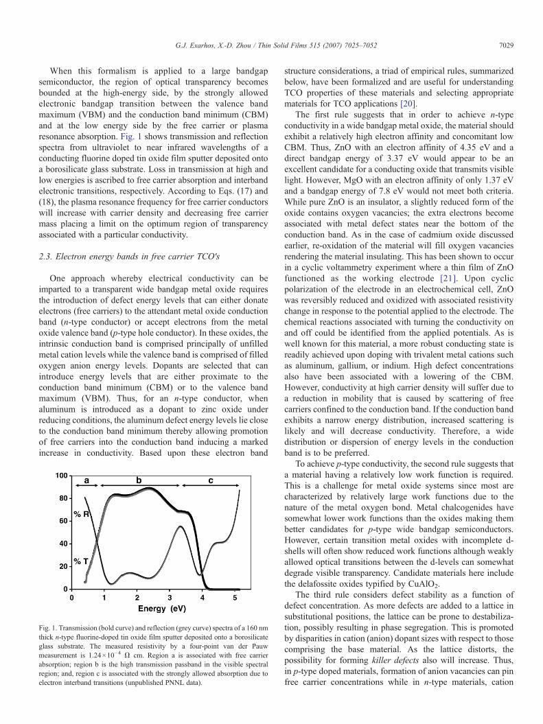
When this formalism is applied to a large bandgapsemiconductor, the region of optical transparency becomesbounded at the high-energy side, by the strongly allowedelectronic bandgap transition between the valence bandmaximum (VBM) and the conduction band minimum (CBM)and at the low energy side by the free carrier or plasmaresonance absorption. Fig. 1 shows transmission and reflectionspectra from ultraviolet to near infrared wavelengths of aconducting fluorine doped tin oxide film sputter deposited ontoa borosilicate glass substrate. Loss in transmission at high andlow energies is ascribed to free carrier absorption and interbandelectronic transitions, respectively. According to Eqs. (17) and(18), the plasma resonance frequency for free carrier conductorswill increase with carrier density and decreasing free carriermass placing a limit on the optimum region of transparencyassociated with a particular conductivity.
2.3. Electron energy bands in free carrier TCO's
One approach whereby electrical conductivity can beimparted to a transparent wide bandgap metal oxide requiresthe introduction of defect energy levels that can either donateelectrons (free carriers) to the attendant metal oxide conductionband (n-type conductor) or accept electrons from the metaloxide valence band (p-type hole conductor). In these oxides, theintrinsic conduction band is comprised principally of unfilledmetal cation levels while the valence band is comprised of filledoxygen anion energy levels. Dopants are selected that canintroduce energy levels that are either proximate to theconduction band minimum (CBM) or to the valence bandmaximum (VBM). Thus, for an n-type conductor, whenaluminum is introduced as a dopant to zinc oxide underreducing conditions, the aluminum defect energy levels lie closeto the conduction band minimum thereby allowing promotionof free carriers into the conduction band inducing a markedincrease in conductivity. Based upon these electron band
Fig. 1. Transmission (bold curve) and reflection (grey curve) spectra of a 160 nmthick n-type fluorine-doped tin oxide film sputter deposited onto a borosilicateglass substrate. The measured resistivity by a four-point van der Pauwmeasurement is 1.24×10⁻⁴ Ω cm. Region a is associated with free carrierabsorption; region b is the high transmission passband in the visible spectralregion; and, region c is associated with the strongly allowed absorption due toelectron interband transitions (unpublished PNNL data).
structure considerations, a triad of empirical rules, summarizedbelow, have been formalized and are useful for understandingTCO properties of these materials and selecting appropriatematerials for TCO applications [20].
The first rule suggests that in order to achieve n-typeconductivity in a wide bandgap metal oxide, the material shouldexhibit a relatively high electron affinity and concomitant lowCBM. Thus, ZnO with an electron affinity of 4.35 eV and adirect bandgap energy of 3.37 eV would appear to be anexcellent candidate for a conducting oxide that transmits visiblelight. However, MgO with an electron affinity of only 1.37 eVand a bandgap energy of 7.8 eV would not meet both criteria.While pure ZnO is an insulator, a slightly reduced form of theoxide contains oxygen vacancies; the extra electrons becomeassociated with metal defect states near the bottom of theconduction band. As in the case of cadmium oxide discussedearlier, re-oxidation of the material will fill oxygen vacanciesrendering the material insulating. This has been shown to occurin a cyclic voltammetry experiment where a thin film of ZnOfunctioned as the working electrode [21]. Upon cyclicpolarization of the electrode in an electrochemical cell, ZnOwas reversibly reduced and oxidized with associated resistivitychange in response to the potential applied to the electrode. Thechemical reactions associated with turning the conductivity onand off could be identified from the applied potentials. As iswell known for this material, a more robust conducting state isreadily achieved upon doping with trivalent metal cations suchas aluminum, gallium, or indium. High defect concentrationsalso have been associated with a lowering of the CBM.However, conductivity at high carrier density will suffer due toa reduction in mobility that is caused by scattering of freecarriers confined to the conduction band. If the conduction bandexhibits a narrow energy distribution, increased scattering islikely and will decrease conductivity. Therefore, a widedistribution or dispersion of energy levels in the conductionband is to be preferred.
To achieve p-type conductivity, the second rule suggests thata material having a relatively low work function is required.This is a challenge for metal oxide systems since most arecharacterized by relatively large work functions due to thenature of the metal oxygen bond. Metal chalcogenides havesomewhat lower work functions than the oxides making thembetter candidates for p-type wide bandgap semiconductors.However, certain transition metal oxides with incomplete d-shells will often show reduced work functions although weaklyallowed optical transitions between the d-levels can somewhatdegrade visible transparency. Candidate materials here includethe delafossite oxides typified by CuAlO2.
The third rule considers defect stability as a function ofdefect concentration. As more defects are added to a lattice insubstitutional positions, the lattice can be prone to destabiliza-tion, possibly resulting in phase segregation. This is promotedby disparities in cation (anion) dopant sizes with respect to thosecomprising the base material. As the lattice distorts, thepossibility for forming killer defects also will increase. Thus,in p-type doped materials, formation of anion vacancies can pinfree carrier concentrations while in n-type materials, cation
7030 G.J. Exarhos, X.-D. Zhou / Thin Solid Films 515 (2007) 7025–7052
vacancies become problematic. Killer defect formation, then,can be viewed as a response of the system to resist further insultto its structure and bonding arrangement. This considerationplaces restrictions on processing variables that can be chosen tomitigate killer defect formation. For example, to promote n-typeconductivity, reducing conditions that create filled defect levelsclose to the CBM are desirable. Some materials can accom-modate much larger defect concentrations before a structuralresponse tends to drive the system back to a more stable equilib-rium configuration with concomitant loss in conductivity.
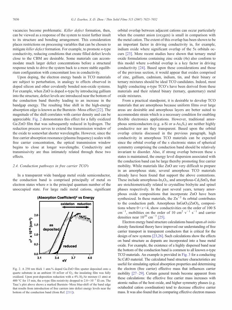
Upon doping, the electron energy bands in TCO materialsare subject to perturbation, in analogy to effects observed indoped silicon and other covalently bonded non-oxide systems.For example, when ZnO is doped n-type by introducing galliuminto the structure, defect levels are introduced near the bottom ofthe conduction band thereby leading to an increase in thebandgap energy. The resulting blue shift in the high-energyabsorption edge is known as the Burstein–Moss effect [22]. Themagnitude of the shift correlates with carrier density and can beappreciable. Fig. 2 demonstrates this effect for a fully oxidizedGa:ZnO film that was subsequently reduced in hydrogen. Thereduction process serves to extend the transmission window ofthe oxide to somewhat shorter wavelengths. However, since thefree carrier absorption resonance (plasma frequency) scales withfree carrier concentration, the optical transmission windowbegins to close at longer wavelengths. Conductivity andtransmissivity are thus intimately related through these twoeffects.
2.4. Conduction pathways in free carrier TCO's
In a transparent wide bandgap metal oxide semiconductor,the conduction band is comprised principally of metal nselectron states where n is the principal quantum number of theunoccupied state. For large radii metal cations, significant
Fig. 2. A 250 nm thick 1 atm.% doped Ga:ZnO film sputter deposited onto aquartz substrate in an ambient 10 mTorr of O2; the insulating film was fullyoxidized. Upon post-deposition reduction with a 4% H2/Ar mixture (1 atm) at400 °C for 15 min, the n-type film resistivity dropped to 2.0×10⁻³ Ω cm. TheTauc's plot above shows a marked Burstein–Moss blue-shift of the band edgethat results from introduction of free carriers into defect energy levels near thebottom of the conduction band (from Ref. [211]).
orbital overlap between adjacent cations can occur particularlywhen the counter anion (oxygen) is small in comparison withthe metal cation. The extent of this overlap has been shown to bean important factor in driving conductivity in, for example,indium oxide where significant overlap of the 5s orbitals oc-curs [23]. More recent studies have shown that ternary metaloxide formulations containing zinc oxide (4s) also conform tothis model where s-orbital overlap is a key factor in drivingconductivity [24]. Based upon these considerations and thoseof the previous section, it would appear that oxides comprisedof zinc, gallium, cadmium, indium, tin, and their binary orternary mixtures should be ideal TCO candidates. Indeed, mosthighly conducting n-type TCO's have been derived from thesematerials and their related binary (ternary, quaternary) metaloxide mixtures.
From a practical standpoint, it is desirable to develop TCOmaterials that are amorphous because uniform films over largeareas are desirable and amorphous layers are better suited toaccommodate strain which is a necessary condition for enablingflexible electronics applications. However, traditional amor-phous semiconductors (e.g. a-Si or a-As2S3) are neither highlyconductive nor are they transparent. Based upon the orbitaloverlap criteria discussed in the previous paragraph, highconductivity in amorphous TCO materials can be expectedsince the orbital overlap of the s electronic states of sphericalsymmetry comprising the conduction band should be relativelyinvariant to disorder. Also, if strong overlap between these sstates is maintained, the energy level dispersion associated withthe conduction band can be large thereby promoting free carriermobility. While materials like ZnO are very difficult to preparein an amorphous state, several amorphous TCO materialsalready have been found that support the above contentions.These include amorphous-In2O3, and amorphous-Cd2SnO4 thatare stoichiometrically related to crystalline bixbyite and spinelphases respectively. In the past several years, ternary amor-phous oxide compositions that incorporate ZnO have beensynthesized. In these materials, the Zn+2 4s orbital contributesto the conduction path. Amorphous InGaO3(ZnO)x composi-tions where 0bxb4, show conductivities on the order of 100 Scm−1, mobilities on the order of 10 cm2 v−1 s−1 and carrierdensities near 1020 cm−3 [25].
Electron energy band structure calculations based upon ab initiodensity functional theory have improved our understanding of freecarrier transport in transparent conductors that is critical for thedesign of new systems [23,26]. Such calculations show the effectson band structure as dopants are incorporated into a base metaloxide. For example, the existence of a highly dispersed band nearthe bottom of the conduction band is common to all known n-typeTCO materials. An example is provided in Fig. 3 for a conductingSc:CdO material. The calculated band structure characteristics areuseful for simulating optical absorption properties and determiningthe electron (free carrier) effective mass that influences carriermobility [27–29]. Certain general trends become apparent fromthese calculations: the effective free carrier mass increases withatomic radius of the host oxide, and higher symmetry phases (e.g.octahedral cation coordination) tend to decrease effective carriermass. It was also found that in comparing effective electron masses
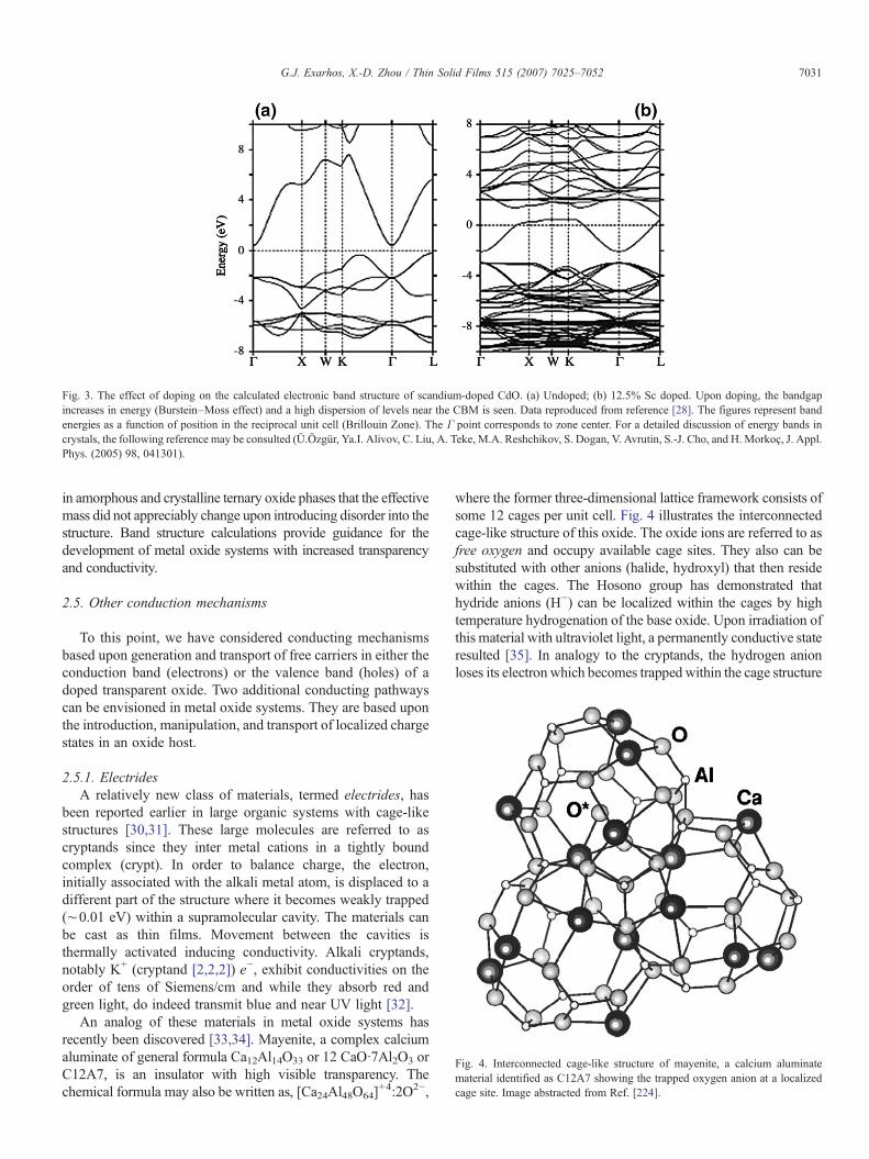
Fig. 3. The effect of doping on the calculated electronic band structure of scandium-doped CdO. (a) Undoped; (b) 12.5% Sc doped. Upon doping, the bandgapincreases in energy (Burstein–Moss effect) and a high dispersion of levels near the CBM is seen. Data reproduced from reference [28]. The figures represent bandenergies as a function of position in the reciprocal unit cell (Brillouin Zone). The Γ point corresponds to zone center. For a detailed discussion of energy bands incrystals, the following reference may be consulted (Ü.Özgür, Ya.I. Alivov, C. Liu, A. Teke, M.A. Reshchikov, S. Dogan, V. Avrutin, S.-J. Cho, and H. Morkoç, J. Appl.Phys. (2005) 98, 041301).
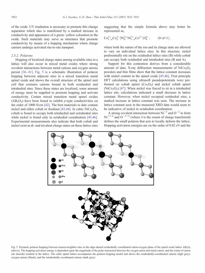
Fig. 4. Interconnected cage-like structure of mayenite, a calcium aluminatematerial identified as C12A7 showing the trapped oxygen anion at a localizedcage site. Image abstracted from Ref. [224].
7031G.J. Exarhos, X.-D. Zhou / Thin Solid Films 515 (2007) 7025–7052
in amorphous and crystalline ternary oxide phases that the effectivemass did not appreciably change upon introducing disorder into thestructure. Band structure calculations provide guidance for thedevelopment of metal oxide systems with increased transparencyand conductivity.
2.5. Other conduction mechanisms
To this point, we have considered conducting mechanismsbased upon generation and transport of free carriers in either theconduction band (electrons) or the valence band (holes) of adoped transparent oxide. Two additional conducting pathwayscan be envisioned in metal oxide systems. They are based uponthe introduction, manipulation, and transport of localized chargestates in an oxide host.
2.5.1. ElectridesA relatively new class of materials, termed electrides, has
been reported earlier in large organic systems with cage-likestructures [30,31]. These large molecules are referred to ascryptands since they inter metal cations in a tightly boundcomplex (crypt). In order to balance charge, the electron,initially associated with the alkali metal atom, is displaced to adifferent part of the structure where it becomes weakly trapped(∼0.01 eV) within a supramolecular cavity. The materials canbe cast as thin films. Movement between the cavities isthermally activated inducing conductivity. Alkali cryptands,notably K+ (cryptand [2,2,2]) e−, exhibit conductivities on theorder of tens of Siemens/cm and while they absorb red andgreen light, do indeed transmit blue and near UV light [32].
An analog of these materials in metal oxide systems hasrecently been discovered [33,34]. Mayenite, a complex calciumaluminate of general formula Ca12Al14O33 or 12 CaO·7Al2O3 orC12A7, is an insulator with high visible transparency. Thechemical formula may also be written as, [Ca24Al48O64]
+4:2O2−,
where the former three-dimensional lattice framework consists ofsome 12 cages per unit cell. Fig. 4 illustrates the interconnectedcage-like structure of this oxide. The oxide ions are referred to asfree oxygen and occupy available cage sites. They also can besubstituted with other anions (halide, hydroxyl) that then residewithin the cages. The Hosono group has demonstrated thathydride anions (H−) can be localized within the cages by hightemperature hydrogenation of the base oxide. Upon irradiation ofthis material with ultraviolet light, a permanently conductive stateresulted [35]. In analogy to the cryptands, the hydrogen anionloses its electron which becomes trapped within the cage structure
7032 G.J. Exarhos, X.-D. Zhou / Thin Solid Films 515 (2007) 7025–7052
of the oxide. UV irradiation is necessary to promote this changeseparation which also is manifested by a marked increase inconductivity and appearance of a green–yellow coloration to theoxide. Such materials may serve as structures that promoteconductivity by means of a hopping mechanism where chargecarriers undergo activated site-to-site transport.
2.5.2. PolaronsHopping of localized charge states among available sites in a
lattice will also occur in mixed metal oxides where strongcovalent interactions between metal cations and oxygen anionspersist [36–41]. Fig. 5 is a schematic illustration of polaronhopping between adjacent sites in a mixed transition metalspinel oxide and shows the overall structure of the spinel unitcell that contains cations bound in both octahedral andtetrahedral sites. Since these states are localized, some amountof energy must be supplied to promote hopping and activateconductivity. Certain mixed transition metal spinel oxides(AB2O4) have been found to exhibit p-type conductivities onthe order of 1000 S/cm [42]. The best materials to date containnickel and either cobalt or rhodium [43,44]. In cubic NiCo2O4,cobalt is found to occupy both tetrahedral and octrahedral siteswhile nickel is found only in octahedral coordination [45,46].Experimental measurements also indicate that both cobalt andnickel exist in di- and trivalent charge states on these lattice sites
Fig. 5. Dynamic polaron hopping between nearest-neighbor sites in the edge-shared(above). The hopping activation energy is dependent upon the magnitude of the polarsite disorder resident in the lattice. The cubic spinel lattice accompanies the polarooxygen anions (black), and the tetrahedrally-coordinated cations (dark grey).
suggesting that the simple formula above may better berepresented as,
Co2þ1�dCo3þd ½Ni2þd Ni3þ1�dCo
3þ�O2�4 ; ð0bdb1Þ;
where both the nature of the ion and its charge state are allowedto vary on individual lattice sites. In this structure, nickelpreferentially sits on the octahedral lattice sites (B) while cobaltcan occupy both octahedral and tetrahedral sites (B and A).
Support for this contention derives from a considerableamount of data. X-ray diffraction measurements of NiCo2O4
powders and thin films show that the lattice constant increaseswith nickel content in the spinel oxide [45,46]. First principleDFT calculations using ultrasoft pseudopotentials were per-formed on cobalt spinel (Co3O4) and nickel cobalt spinel(NiCo2O4) [47]. When nickel was forced to sit in a tetrahedrallattice site, calculations indicated a small decrease in latticeconstant. However, when nickel occupied octahedral sites, amarked increase in lattice constant was seen. The increase inlattice constant seen in the measured XRD data would seem tobe indicative of nickel in octahedral coordination.
A strong covalent interaction between Ni+3 and O−2 to formNi+3−δ and O−2 + δ (where δ is the extent of charge transferred)defines the small polaron that acts to locally deform the lattice.Hopping activation energies are on the order of 0.02 eVand the
octahedrally coordinated cation-oxygen plane of the spinel oxide lattice AB2O4
interaction between the oxygen anion and metal cation, and the extent of cationn hopping model and shows the octahedrally-coordinated cations (light grey),
7033G.J. Exarhos, X.-D. Zhou / Thin Solid Films 515 (2007) 7025–7052
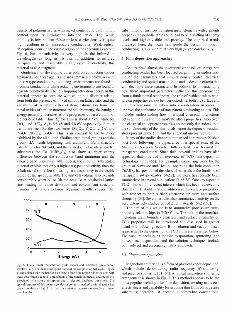
density of polarons scales with nickel content and with lithiumcontent upon its introduction into the lattice [15]. Whilemobility is low, ∼1 cm2/V.sec or less, carrier density is quitehigh resulting in an appreciable conductivity. Weak opticalabsorption occurs in the visible region of the spectrum as seen inFig. 6, but transmissivity is very high in the infrared towavelengths as long as 16 μm. In addition to infraredtransparency and reasonably high p-type conductivity, thismaterial is also magnetic.
Guidelines for developing other polaron conducting oxidesare based upon these results and are summarized below. As withother p-type conductors, oxidizing environments are found topromote conductivity while reducing environments are found todegrade conductivity. The low hopping activation energy in thismaterial appears to correlate with cation site disorder arisingfrom both the presence of mixed cations on lattice sites and thevariability of oxidation states of those cations. For transitionmetal oxides of similar structure and stoichiometry, the bandgapenergy generally increases as one progresses down a column ofthe periodic table. Thus, Eg for TiO2 is about 3.7 eV, while forZrO2, and HfO2, Eg is 5.5 eV and 5.8 eV respectively. Similartrends are seen for the two series (Sc2O3, Y2O3, La2O3) and(V2O5, Nb2O5, Ta2O5). This is in contrast to the behaviorexhibited by the alkali and alkaline earth metal groups and thegroup IIIA metals beginning with aluminum. Band structurecalculations for NiCo2O4 and the related spinel oxide where Rhsubstitutes for Co (NiRh2O4) also show a larger energydifference between the conduction band minimum and thevalence band maximum [48]. Indeed, the rhodium substitutedmaterial exhibits not only a higher p-type conductivity than thecobalt nickel spinel but shows higher transparency in the visibleregion of the spectrum [49]. The unit cell volume also expandsconsiderably when Ni or Rh replaces Co at octahedral latticesites leading to lattice distortion and concomitant structuraldisorder that favors polaron hopping. Results suggest that
Fig. 6. UV/VIS/NiR transmission (bold curve) and reflection (grey curve)spectra of a 70 nm thick cubic spinel oxide of the composition NiCo2O4. Regiona is associated with the near IR pass-band of the film, region b is associated withweak absorption due to d–d transitions of the transition metals, and region c isassociated with strong absorption due to electron interband transitions. Theoptical response of this polaron conductor contrasts markedly with that of a freecarrier conductor (Fig. 1) in that transmission increases markedly at longerwavelengths.
substitution of first row transition metal elements with elementsdeeper in the periodic table could lead to blue shifting of energylevels and higher visible transparency. The empirical trendsdiscussed here, then, can help guide the design of polaronconducting TCO's with relatively high p-type conductivity.
3. Film deposition approaches
As described above, the theoretical emphasis on transparentconducting oxides has been focused on gaining an understand-ing of the parameters that simultaneously control electricalconductivity and optical transmission and to develop criteria thatwill decouple these parameters. In addition to understandinghow these important parameters influence this phenomenonfrom a fundamental standpoint, the role of resident microstruc-ture on properties cannot be overlooked, i.e. both the surface andthe interface must be taken into consideration in order toimprove the performance of transparent conducting oxides. Thisincludes understanding how interfacial chemical interactionsbetween the film and the substrate affect properties. Moreover,the electrical and optical properties are not only dependent uponthe stoichiometry of the film but also upon the degree of residualstress present in the film and the attendant microstructure.
Many of the studies that are summarized here were publishedpost 2000 following the appearance of a special issue of theMaterials Research Society Bulletin that was focused ontransparent conductors. Since then, several articles have alsoappeared that provided an overview of TCO film depositiontechnology [8,50–55]. For example, pioneering work by thegroup of Kawazoe and Hosono regarding the hole conductor,CuAlO2, has positioned this class of materials at the forefront oftransparent p-type oxides [56,57]; the work has recently beensummarized in several publications [8,55,58]. One key aspect inTCO films of more recent interest which has been reviewed byBatzill and Diebold in 2005, addresses film surface properties,with respect to both surface electronic structure and surfacechemistry [53]. Several articles also summarized activity on thevery extensively studied doped ZnO materials [54,59,60].
The aim of this section is to summarize process-structure-property relationships in TCO films. The role of the interface,including grain boundary structure, and surface chemistry onTCO properties will be introduced and discussed in greaterdetail in a following section. Both solution and vacuum-basedapproaches to the deposition of TCO films are presented below.The vacuum techniques include evaporation, sputtering, andpulsed laser deposition, and the solution techniques includeboth sol–gel and an organic matrix approach.
3.1. Magnetron sputtering
Magnetron sputtering is a form of physical vapor deposition,which includes dc sputtering, radio frequency (rf) sputtering,and reactive sputtering [61–64]. A typical magnetron sputteringarrangement is shown in Fig. 7. This method appears to be themost popular technique for film deposition, owning to its costeffectiveness and capability for growing thin films on large areasubstrates; therefore, it became a somewhat conventional
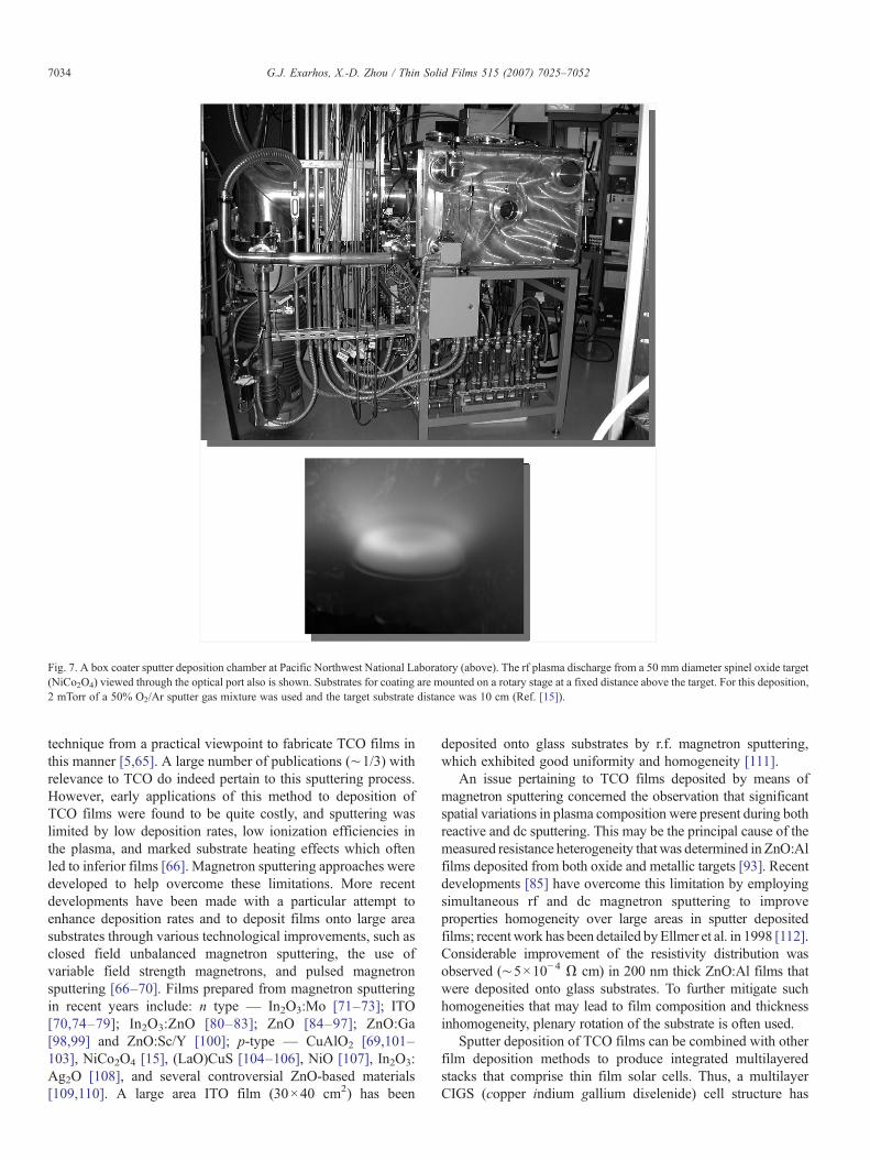
Fig. 7. A box coater sputter deposition chamber at Pacific Northwest National Laboratory (above). The rf plasma discharge from a 50 mm diameter spinel oxide target(NiCo2O4) viewed through the optical port also is shown. Substrates for coating are mounted on a rotary stage at a fixed distance above the target. For this deposition,2 mTorr of a 50% O2/Ar sputter gas mixture was used and the target substrate distance was 10 cm (Ref. [15]).
7034 G.J. Exarhos, X.-D. Zhou / Thin Solid Films 515 (2007) 7025–7052
technique from a practical viewpoint to fabricate TCO films inthis manner [5,65]. A large number of publications (∼1/3) withrelevance to TCO do indeed pertain to this sputtering process.However, early applications of this method to deposition ofTCO films were found to be quite costly, and sputtering waslimited by low deposition rates, low ionization efficiencies inthe plasma, and marked substrate heating effects which oftenled to inferior films [66]. Magnetron sputtering approaches weredeveloped to help overcome these limitations. More recentdevelopments have been made with a particular attempt toenhance deposition rates and to deposit films onto large areasubstrates through various technological improvements, such asclosed field unbalanced magnetron sputtering, the use ofvariable field strength magnetrons, and pulsed magnetronsputtering [66–70]. Films prepared from magnetron sputteringin recent years include: n type — In2O3:Mo [71–73]; ITO[70,74–79]; In2O3:ZnO [80–83]; ZnO [84–97]; ZnO:Ga[98,99] and ZnO:Sc/Y [100]; p-type — CuAlO2 [69,101–103], NiCo2O4 [15], (LaO)CuS [104–106], NiO [107], In2O3:Ag2O [108], and several controversial ZnO-based materials[109,110]. A large area ITO film (30×40 cm2) has been
deposited onto glass substrates by r.f. magnetron sputtering,which exhibited good uniformity and homogeneity [111].
An issue pertaining to TCO films deposited by means ofmagnetron sputtering concerned the observation that significantspatial variations in plasma composition were present during bothreactive and dc sputtering. This may be the principal cause of themeasured resistance heterogeneity that was determined in ZnO:Alfilms deposited from both oxide and metallic targets [93]. Recentdevelopments [85] have overcome this limitation by employingsimultaneous rf and dc magnetron sputtering to improveproperties homogeneity over large areas in sputter depositedfilms; recent work has been detailed byEllmer et al. in 1998 [112].Considerable improvement of the resistivity distribution wasobserved (∼5×10⁻⁴ Ω cm) in 200 nm thick ZnO:Al films thatwere deposited onto glass substrates. To further mitigate suchhomogeneities that may lead to film composition and thicknessinhomogeneity, plenary rotation of the substrate is often used.
Sputter deposition of TCO films can be combined with otherfilm deposition methods to produce integrated multilayeredstacks that comprise thin film solar cells. Thus, a multilayerCIGS (copper indium gallium diselenide) cell structure has
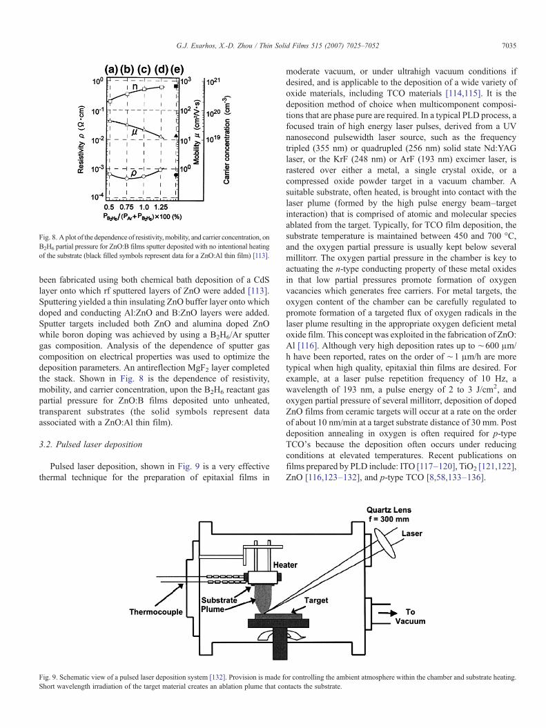
Fig. 8. A plot of the dependence of resistivity,mobility, and carrier concentration, onB2H6 partial pressure for ZnO:B films sputter deposited with no intentional heatingof the substrate (black filled symbols represent data for a ZnO:Al thin film) [113].
7035G.J. Exarhos, X.-D. Zhou / Thin Solid Films 515 (2007) 7025–7052
been fabricated using both chemical bath deposition of a CdSlayer onto which rf sputtered layers of ZnO were added [113].Sputtering yielded a thin insulating ZnO buffer layer onto whichdoped and conducting Al:ZnO and B:ZnO layers were added.Sputter targets included both ZnO and alumina doped ZnOwhile boron doping was achieved by using a B2H6/Ar sputtergas composition. Analysis of the dependence of sputter gascomposition on electrical properties was used to optimize thedeposition parameters. An antireflection MgF2 layer completedthe stack. Shown in Fig. 8 is the dependence of resistivity,mobility, and carrier concentration, upon the B2H6 reactant gaspartial pressure for ZnO:B films deposited unto unheated,transparent substrates (the solid symbols represent dataassociated with a ZnO:Al thin film).
3.2. Pulsed laser deposition
Pulsed laser deposition, shown in Fig. 9 is a very effectivethermal technique for the preparation of epitaxial films in
Fig. 9. Schematic view of a pulsed laser deposition system [132]. Provision is made fShort wavelength irradiation of the target material creates an ablation plume that co
moderate vacuum, or under ultrahigh vacuum conditions ifdesired, and is applicable to the deposition of a wide variety ofoxide materials, including TCO materials [114,115]. It is thedeposition method of choice when multicomponent composi-tions that are phase pure are required. In a typical PLD process, afocused train of high energy laser pulses, derived from a UVnanosecond pulsewidth laser source, such as the frequencytripled (355 nm) or quadrupled (256 nm) solid state Nd:YAGlaser, or the KrF (248 nm) or ArF (193 nm) excimer laser, israstered over either a metal, a single crystal oxide, or acompressed oxide powder target in a vacuum chamber. Asuitable substrate, often heated, is brought into contact with thelaser plume (formed by the high pulse energy beam–targetinteraction) that is comprised of atomic and molecular speciesablated from the target. Typically, for TCO film deposition, thesubstrate temperature is maintained between 450 and 700 °C,and the oxygen partial pressure is usually kept below severalmillitorr. The oxygen partial pressure in the chamber is key toactuating the n-type conducting property of these metal oxidesin that low partial pressures promote formation of oxygenvacancies which generates free carriers. For metal targets, theoxygen content of the chamber can be carefully regulated topromote formation of a targeted flux of oxygen radicals in thelaser plume resulting in the appropriate oxygen deficient metaloxide film. This concept was exploited in the fabrication of ZnO:Al [116]. Although very high deposition rates up to ∼600 μm/h have been reported, rates on the order of ∼1 μm/h are moretypical when high quality, epitaxial thin films are desired. Forexample, at a laser pulse repetition frequency of 10 Hz, awavelength of 193 nm, a pulse energy of 2 to 3 J/cm2, andoxygen partial pressure of several millitorr, deposition of dopedZnO films from ceramic targets will occur at a rate on the orderof about 10 nm/min at a target substrate distance of 30 mm. Postdeposition annealing in oxygen is often required for p-typeTCO's because the deposition often occurs under reducingconditions at elevated temperatures. Recent publications onfilms prepared by PLD include: ITO [117–120], TiO2 [121,122],ZnO [116,123–132], and p-type TCO [8,58,133–136].
or controlling the ambient atmosphere within the chamber and substrate heating.ntacts the substrate.
7036 G.J. Exarhos, X.-D. Zhou / Thin Solid Films 515 (2007) 7025–7052
Bhosle and Narayan investigated the role of substrate behaviorand deposition conditions on the electrical and optical propertiesof Ga:ZnO films [126]. The nature of grain orientation and grainboundary morphology that resulted from various depositionconditions, was found to play a significant role in carrierconcentration and the mobility in thin films deposited on glasssubstrates. They explained this correlation in terms of trapping ofelectrons and buildup of a potential barrier across the grainboundaries. A rather low electrical resistivity (∼1.9×10⁻⁴Ω cm)was obtained with Ga:ZnO films on glass substrates throughoptimization of the substrate temperature and attendant oxygenpressure, which was comparable to that of epitaxially depositedfilms on sapphire substrates (∼1.4×10⁻⁴ Ω cm) [126].
The PLD process is versatile and is amenable to couplingwith ultraviolet irradiation [137], oxygen radical assisteddeposition [116], or magnetic field promoted deposition [124].Thus, a magnetic field perpendicular to the laser plume wasuseful in preparing Al:ZnO through coupling with the PLDprocess. Deposited films exhibited a markedly low resistivity of8.54×10−5 Ω cm and an average transmittance exceeding 91%over the visible wavelength range. The authors argued that thelow resistivity was due to the fact that crystal growth disorderthat originated at the film substrate interface could be suppressedthrough application of an external magnetic field that interactedwith the plasma plume thereby yielding an increased mobility.C-axis orientation was promoted at the substrate, giving rise tothe observed increase in mobility [123,124].
Thus far, PLD has been the primary technique used todeposit TCO films that exhibit exceptionally low resistivity onthe order of 10− 5 Ω cm [123,124,138,139]; however,
Fig. 10. A collection of volatile organometallic precu
magnetron sputtering results in films having resistivity severaltimes greater than those derived from the PLD process. Sahuand Huang [140] predicted the electrical resistivity on the orderof 10−5 Ω cm in multilayered ZnO/Ag/ZnO films; unfortu-nately the measured value was not provided.
3.3. Chemical vapor deposition
The most common thin film deposition method in advancedsemiconductor processing involves thermally induced decom-position of a film precursor molecule as the volatile speciesinteracts with a hot surface. The decomposition product thendeposits on the substrate surface. In a typical CVD process,gaseous reactants from selected precursors often are directedthrough an activated environment (high temperature, light, orplasma), which acts to dissociate the precursor molecules. Filmsdeposit onto heated substrate surfaces to yield the desired filmsand targeted morphology. The deposition of thin films ofteninvolves heterogeneous chemical reactions that occur on/nearthe vicinity of the substrate surface [141]. This technique hasbeen used to form semiconductor films (crystalline andamorphous), insulators, and metals. Variations of this processingmethod include Atmospheric Pressure CVD (APCVD), LowPressure CVD (LPCVD) and Plasma Enhanced CVD (PECVD).
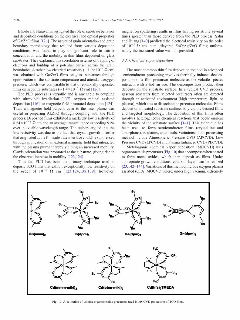
Metalorganic chemical vapor deposition (MOCVD) usesorganometallic precursors (Fig. 10) that decomposewhen heatedto form metal oxides, which then deposit as films. Underappropriate growth conditions, epitaxial layers can be realized[23,142–144]. Variations of this method include oxygen plasmaassisted (OPA) MOCVD where, under high vacuum, extremely
rsors used in MOCVD processing of TCO films.
7037G.J. Exarhos, X.-D. Zhou / Thin Solid Films 515 (2007) 7025–7052
low defect density and high chemical purity oxide films can begrown. In many cases, MOCVD does not necessarily requirehigh vacuum and deposition can indeed occur at moderatepressures (2 to 100 kPa). As a result, MOCVD has become apreferred process for the fabrication of compound semiconduc-tor films. The primary limitation of the MOCVD process isassociated with purity and cost of preparation of the requisitemetalorganic precursors, which in many cases tend to beextremely reactive, and hence require careful handling and oftenpurification by thorough recrystallization or sublimationprocedures. In addition, most metalorganics are volatile andquite often very toxic, thus requiring extraordinary handlingprocedures. However, films derived from this method can be ofhigh quality both chemically and structurally. Several examplesfollow to demonstrate this approach.
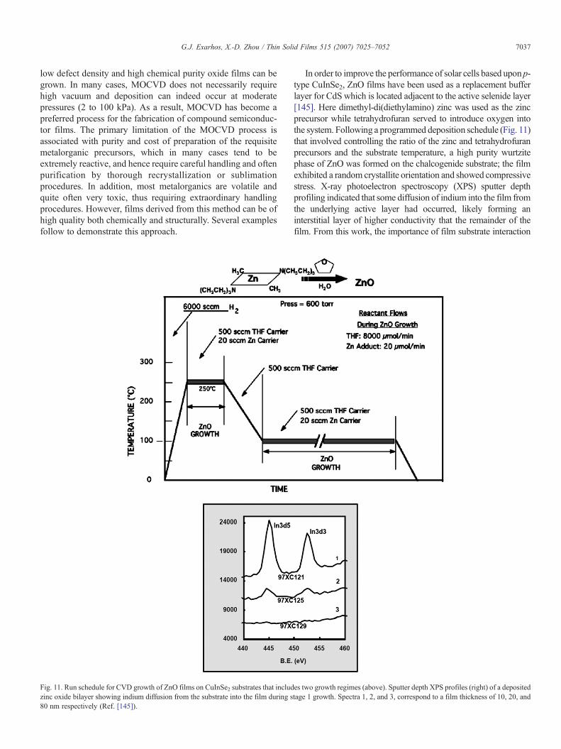
Fig. 11. Run schedule for CVD growth of ZnO films on CuInSe2 substrates that includzinc oxide bilayer showing indium diffusion from the substrate into the film during s80 nm respectively (Ref. [145]).
In order to improve the performance of solar cells based uponp-type CuInSe2, ZnO films have been used as a replacement bufferlayer for CdS which is located adjacent to the active selenide layer[145]. Here dimethyl-di(diethylamino) zinc was used as the zincprecursor while tetrahydrofuran served to introduce oxygen intothe system. Following a programmed deposition schedule (Fig. 11)that involved controlling the ratio of the zinc and tetrahydrofuranprecursors and the substrate temperature, a high purity wurtzitephase of ZnO was formed on the chalcogenide substrate; the filmexhibited a random crystallite orientation and showed compressivestress. X-ray photoelectron spectroscopy (XPS) sputter depthprofiling indicated that some diffusion of indium into the film fromthe underlying active layer had occurred, likely forming aninterstitial layer of higher conductivity that the remainder of thefilm. From this work, the importance of film substrate interaction
es two growth regimes (above). Sputter depth XPS profiles (right) of a depositedtage 1 growth. Spectra 1, 2, and 3, correspond to a film thickness of 10, 20, and
7038 G.J. Exarhos, X.-D. Zhou / Thin Solid Films 515 (2007) 7025–7052
cannot be overemphasized and should be investigated with respectto film properties alteration.
While not a great deal of attention has been devoted to thepreparation of cubic CdO films by this method owing to toxicityconcerns of the precursors, published work demonstrates theefficacy of this method for controlling film properties andmorphology [146,147]. By means of MOCVD using dimethylcadmium as a precursor, the properties of deposited films werefound to be very sensitive to deposition temperature from about100 °C to 450 °C. Below about 250 °C, randomly orientedcrystallites formed on heated glass substrates. At higherdeposition temperatures, crystallites with a preferred (200) crystalorientation resulted, and at higher temperatures, a highly orientedcrystalline morphology with nearly perfect intragrain structurewas formed. The n-type nature of the conductivity was found inall cases, but increasing deposition temperature was also found tomarkedly improve free carrier mobility while decreasing carrierconcentration.
In another example, CVD approaches were used to depositbinary metal oxide films based upon CdO and SnO2 [148,149].Two stable crystalline phases in this system are the orthorhom-bic and rhombohedral CdSnO3 (perovskite) structures and themore promising cubic spinel SnCd2O4 structure owing to theobserved increased carrier mobility and relatively low absorp-tion at visible wavelengths. In reported work, mixtures of bothperovskite and spinel structures have been found with filmsoften containing multiple compositions represented by SnxCd2-O2x+y, where 0bxb1, and 0byb2. In these multiple phasecontaining films, marked variations in both carrier density andcarrier mobility have been noted. The optical band gap alsoblueshifts upon incorporation of more tin oxide in the film. Withappropriate choice of precursor and deposition parameters,amorphous phases can also be formed. CVD approaches can betechnologically important in the fabrication of both crystallineand amorphous large-area coatings.
3.4. Solution deposition
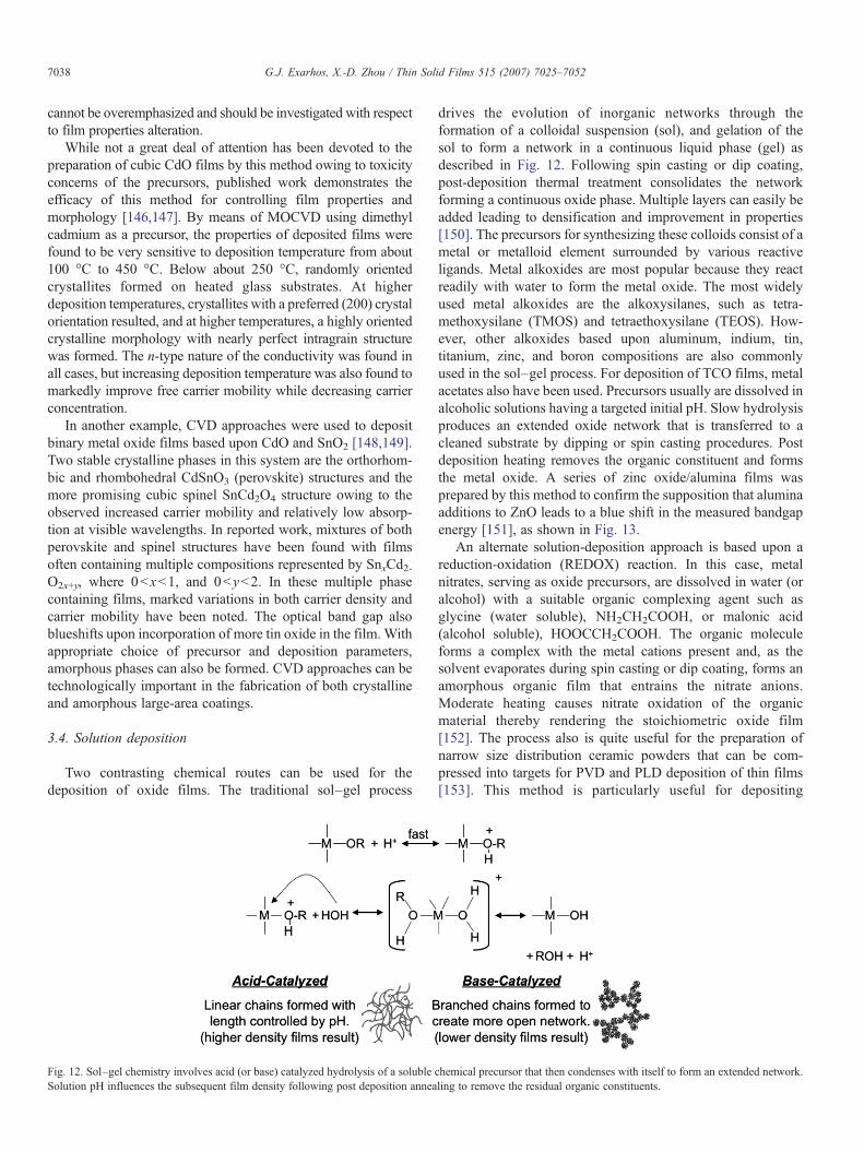
Two contrasting chemical routes can be used for thedeposition of oxide films. The traditional sol–gel process
Fig. 12. Sol–gel chemistry involves acid (or base) catalyzed hydrolysis of a solubleSolution pH influences the subsequent film density following post deposition annea
drives the evolution of inorganic networks through theformation of a colloidal suspension (sol), and gelation of thesol to form a network in a continuous liquid phase (gel) asdescribed in Fig. 12. Following spin casting or dip coating,post-deposition thermal treatment consolidates the networkforming a continuous oxide phase. Multiple layers can easily beadded leading to densification and improvement in properties[150]. The precursors for synthesizing these colloids consist of ametal or metalloid element surrounded by various reactiveligands. Metal alkoxides are most popular because they reactreadily with water to form the metal oxide. The most widelyused metal alkoxides are the alkoxysilanes, such as tetra-methoxysilane (TMOS) and tetraethoxysilane (TEOS). How-ever, other alkoxides based upon aluminum, indium, tin,titanium, zinc, and boron compositions are also commonlyused in the sol–gel process. For deposition of TCO films, metalacetates also have been used. Precursors usually are dissolved inalcoholic solutions having a targeted initial pH. Slow hydrolysisproduces an extended oxide network that is transferred to acleaned substrate by dipping or spin casting procedures. Postdeposition heating removes the organic constituent and formsthe metal oxide. A series of zinc oxide/alumina films wasprepared by this method to confirm the supposition that aluminaadditions to ZnO leads to a blue shift in the measured bandgapenergy [151], as shown in Fig. 13.
An alternate solution-deposition approach is based upon areduction-oxidation (REDOX) reaction. In this case, metalnitrates, serving as oxide precursors, are dissolved in water (oralcohol) with a suitable organic complexing agent such asglycine (water soluble), NH2CH2COOH, or malonic acid(alcohol soluble), HOOCCH2COOH. The organic moleculeforms a complex with the metal cations present and, as thesolvent evaporates during spin casting or dip coating, forms anamorphous organic film that entrains the nitrate anions.Moderate heating causes nitrate oxidation of the organicmaterial thereby rendering the stoichiometric oxide film[152]. The process also is quite useful for the preparation ofnarrow size distribution ceramic powders that can be com-pressed into targets for PVD and PLD deposition of thin films[153]. This method is particularly useful for depositing
chemical precursor that then condenses with itself to form an extended network.ling to remove the residual organic constituents.
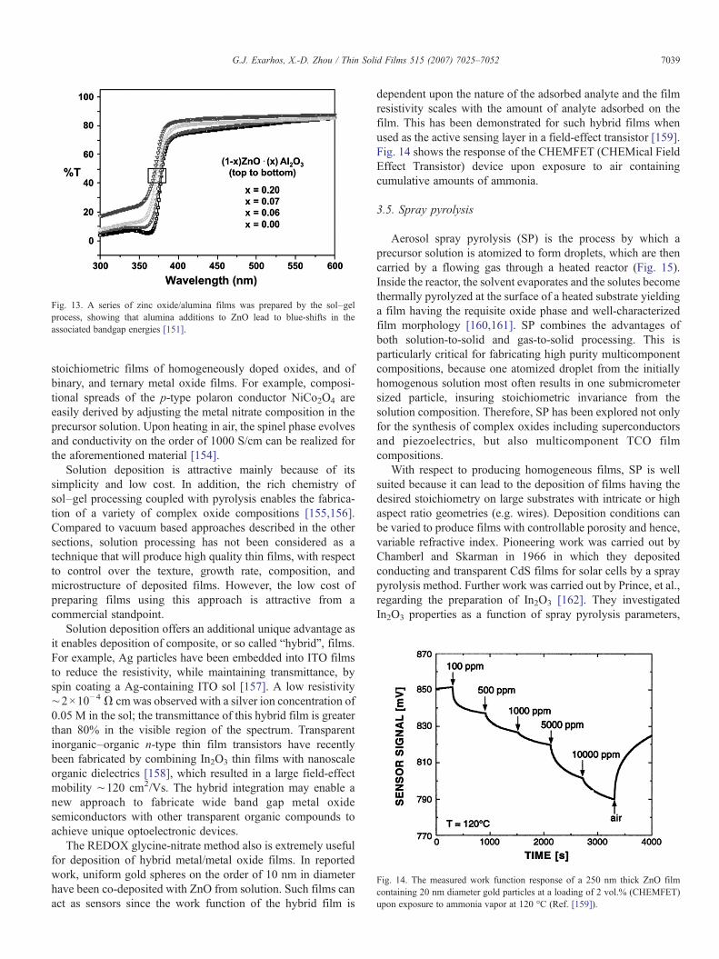
Fig. 14. The measured work function response of a 250 nm thick ZnO filmcontaining 20 nm diameter gold particles at a loading of 2 vol.% (CHEMFET)upon exposure to ammonia vapor at 120 °C (Ref. [159]).
Fig. 13. A series of zinc oxide/alumina films was prepared by the sol–gelprocess, showing that alumina additions to ZnO lead to blue-shifts in theassociated bandgap energies [151].
7039G.J. Exarhos, X.-D. Zhou / Thin Solid Films 515 (2007) 7025–7052
stoichiometric films of homogeneously doped oxides, and ofbinary, and ternary metal oxide films. For example, composi-tional spreads of the p-type polaron conductor NiCo2O4 areeasily derived by adjusting the metal nitrate composition in theprecursor solution. Upon heating in air, the spinel phase evolvesand conductivity on the order of 1000 S/cm can be realized forthe aforementioned material [154].
Solution deposition is attractive mainly because of itssimplicity and low cost. In addition, the rich chemistry ofsol–gel processing coupled with pyrolysis enables the fabrica-tion of a variety of complex oxide compositions [155,156].Compared to vacuum based approaches described in the othersections, solution processing has not been considered as atechnique that will produce high quality thin films, with respectto control over the texture, growth rate, composition, andmicrostructure of deposited films. However, the low cost ofpreparing films using this approach is attractive from acommercial standpoint.
Solution deposition offers an additional unique advantage asit enables deposition of composite, or so called “hybrid”, films.For example, Ag particles have been embedded into ITO filmsto reduce the resistivity, while maintaining transmittance, byspin coating a Ag-containing ITO sol [157]. A low resistivity∼2×10⁻⁴ Ω cm was observed with a silver ion concentration of0.05 M in the sol; the transmittance of this hybrid film is greaterthan 80% in the visible region of the spectrum. Transparentinorganic–organic n-type thin film transistors have recentlybeen fabricated by combining In2O3 thin films with nanoscaleorganic dielectrics [158], which resulted in a large field-effectmobility ∼120 cm2/Vs. The hybrid integration may enable anew approach to fabricate wide band gap metal oxidesemiconductors with other transparent organic compounds toachieve unique optoelectronic devices.
The REDOX glycine-nitrate method also is extremely usefulfor deposition of hybrid metal/metal oxide films. In reportedwork, uniform gold spheres on the order of 10 nm in diameterhave been co-deposited with ZnO from solution. Such films canact as sensors since the work function of the hybrid film is
dependent upon the nature of the adsorbed analyte and the filmresistivity scales with the amount of analyte adsorbed on thefilm. This has been demonstrated for such hybrid films whenused as the active sensing layer in a field-effect transistor [159].Fig. 14 shows the response of the CHEMFET (CHEMical FieldEffect Transistor) device upon exposure to air containingcumulative amounts of ammonia.
3.5. Spray pyrolysis
Aerosol spray pyrolysis (SP) is the process by which aprecursor solution is atomized to form droplets, which are thencarried by a flowing gas through a heated reactor (Fig. 15).Inside the reactor, the solvent evaporates and the solutes becomethermally pyrolyzed at the surface of a heated substrate yieldinga film having the requisite oxide phase and well-characterizedfilm morphology [160,161]. SP combines the advantages ofboth solution-to-solid and gas-to-solid processing. This isparticularly critical for fabricating high purity multicomponentcompositions, because one atomized droplet from the initiallyhomogenous solution most often results in one submicrometersized particle, insuring stoichiometric invariance from thesolution composition. Therefore, SP has been explored not onlyfor the synthesis of complex oxides including superconductorsand piezoelectrics, but also multicomponent TCO filmcompositions.
With respect to producing homogeneous films, SP is wellsuited because it can lead to the deposition of films having thedesired stoichiometry on large substrates with intricate or highaspect ratio geometries (e.g. wires). Deposition conditions canbe varied to produce films with controllable porosity and hence,variable refractive index. Pioneering work was carried out byChamberl and Skarman in 1966 in which they depositedconducting and transparent CdS films for solar cells by a spraypyrolysis method. Further work was carried out by Prince, et al.,regarding the preparation of In2O3 [162]. They investigatedIn2O3 properties as a function of spray pyrolysis parameters,
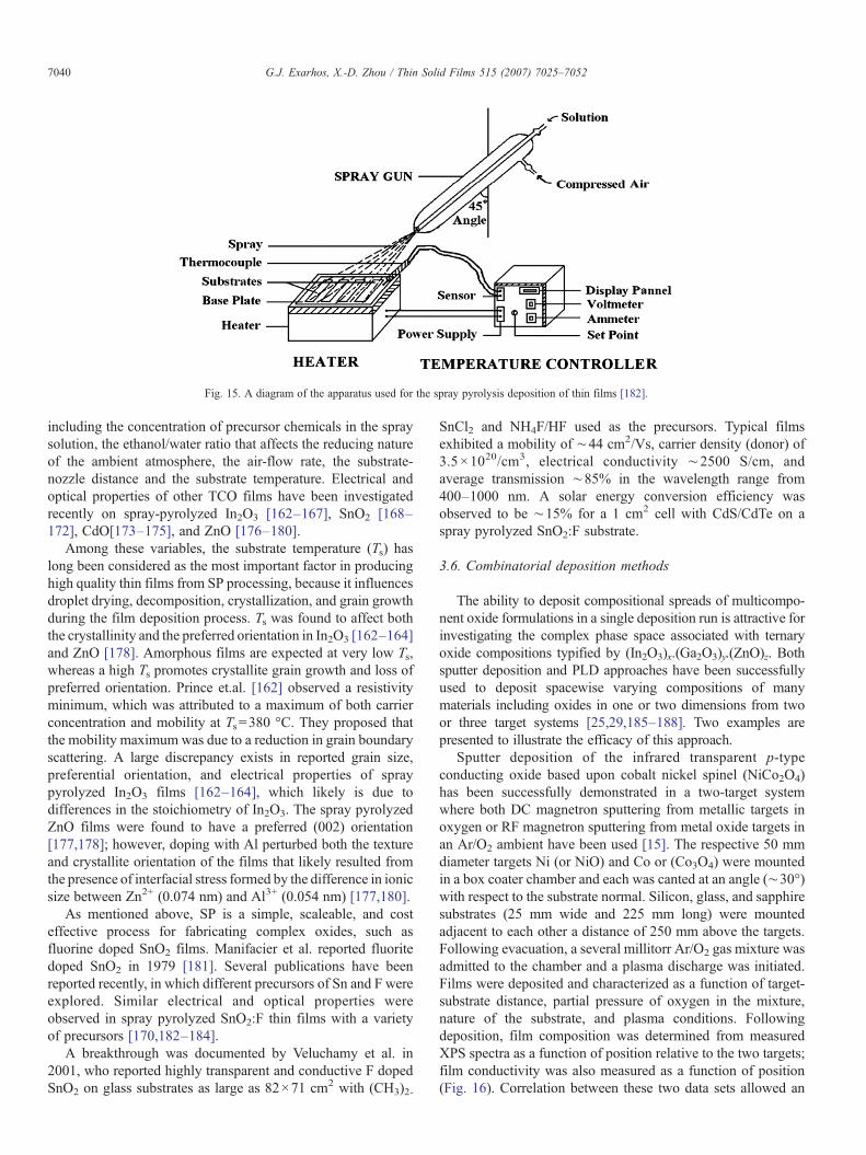
Fig. 15. A diagram of the apparatus used for the spray pyrolysis deposition of thin films [182].
7040 G.J. Exarhos, X.-D. Zhou / Thin Solid Films 515 (2007) 7025–7052
including the concentration of precursor chemicals in the spraysolution, the ethanol/water ratio that affects the reducing natureof the ambient atmosphere, the air-flow rate, the substrate-nozzle distance and the substrate temperature. Electrical andoptical properties of other TCO films have been investigatedrecently on spray-pyrolyzed In2O3 [162–167], SnO2 [168–172], CdO[173–175], and ZnO [176–180].
Among these variables, the substrate temperature (Ts) haslong been considered as the most important factor in producinghigh quality thin films from SP processing, because it influencesdroplet drying, decomposition, crystallization, and grain growthduring the film deposition process. Ts was found to affect boththe crystallinity and the preferred orientation in In2O3 [162–164]and ZnO [178]. Amorphous films are expected at very low Ts,whereas a high Ts promotes crystallite grain growth and loss ofpreferred orientation. Prince et.al. [162] observed a resistivityminimum, which was attributed to a maximum of both carrierconcentration and mobility at Ts=380 °C. They proposed thatthe mobility maximum was due to a reduction in grain boundaryscattering. A large discrepancy exists in reported grain size,preferential orientation, and electrical properties of spraypyrolyzed In2O3 films [162–164], which likely is due todifferences in the stoichiometry of In2O3. The spray pyrolyzedZnO films were found to have a preferred (002) orientation[177,178]; however, doping with Al perturbed both the textureand crystallite orientation of the films that likely resulted fromthe presence of interfacial stress formed by the difference in ionicsize between Zn2+ (0.074 nm) and Al3+ (0.054 nm) [177,180].
As mentioned above, SP is a simple, scaleable, and costeffective process for fabricating complex oxides, such asfluorine doped SnO2 films. Manifacier et al. reported fluoritedoped SnO2 in 1979 [181]. Several publications have beenreported recently, in which different precursors of Sn and F wereexplored. Similar electrical and optical properties wereobserved in spray pyrolyzed SnO2:F thin films with a varietyof precursors [170,182–184].
A breakthrough was documented by Veluchamy et al. in2001, who reported highly transparent and conductive F dopedSnO2 on glass substrates as large as 82×71 cm2 with (CH3)2-
SnCl2 and NH4F/HF used as the precursors. Typical filmsexhibited a mobility of ∼44 cm2/Vs, carrier density (donor) of3.5×1020/cm3, electrical conductivity ∼2500 S/cm, andaverage transmission ∼85% in the wavelength range from400–1000 nm. A solar energy conversion efficiency wasobserved to be ∼15% for a 1 cm2 cell with CdS/CdTe on aspray pyrolyzed SnO2:F substrate.
3.6. Combinatorial deposition methods
The ability to deposit compositional spreads of multicompo-nent oxide formulations in a single deposition run is attractive forinvestigating the complex phase space associated with ternaryoxide compositions typified by (In2O3)x.(Ga2O3)y.(ZnO)z. Bothsputter deposition and PLD approaches have been successfullyused to deposit spacewise varying compositions of manymaterials including oxides in one or two dimensions from twoor three target systems [25,29,185–188]. Two examples arepresented to illustrate the efficacy of this approach.
Sputter deposition of the infrared transparent p-typeconducting oxide based upon cobalt nickel spinel (NiCo2O4)has been successfully demonstrated in a two-target systemwhere both DC magnetron sputtering from metallic targets inoxygen or RF magnetron sputtering from metal oxide targets inan Ar/O2 ambient have been used [15]. The respective 50 mmdiameter targets Ni (or NiO) and Co or (Co3O4) were mountedin a box coater chamber and each was canted at an angle (∼30°)with respect to the substrate normal. Silicon, glass, and sapphiresubstrates (25 mm wide and 225 mm long) were mountedadjacent to each other a distance of 250 mm above the targets.Following evacuation, a several millitorr Ar/O2 gas mixture wasadmitted to the chamber and a plasma discharge was initiated.Films were deposited and characterized as a function of target-substrate distance, partial pressure of oxygen in the mixture,nature of the substrate, and plasma conditions. Followingdeposition, film composition was determined from measuredXPS spectra as a function of position relative to the two targets;film conductivity was also measured as a function of position(Fig. 16). Correlation between these two data sets allowed an
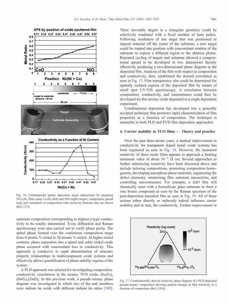
Fig. 16. Combinatorial sputter deposition target deployment for preparingNiCo2O4 films using Co3O4 (left) and NiO (right) targets; composition spread(top) and correlation of composition with resistivity (bottom) also are shown(Ref. [15]).
Fig. 17. Combinatorially derived resistivity phase diagram of a PLD depositedpseudo-ternary composition showing marked changes in film resistivity as afunction of composition (Ref. [189]).
7041G.J. Exarhos, X.-D. Zhou / Thin Solid Films 515 (2007) 7025–7052
optimum composition corresponding to highest p-type conduc-tivity to be readily determined. X-ray diffraction and Ramanspectroscopy were also carried out to verify phase purity. Thespinel phase formed over the continuous composition rangefrom 0 atomic % nickel to 50 atomic % nickel. At higher nickelcontents, phase separation into a spinel and cubic nickel oxidephase occurred with concomitant loss in conductivity. Thisapproach is conducive to rapid determination of structureproperty relationships in multicomponent oxide systems andeffectively allows quantification of phase stability regions of thesystem.
A PLD approach was selected for investigating composition-conductivity correlations in the ternary TCO oxide, (In2O3)x(SnO2)y(ZnO)z. In this previous work, a pseudo ternary phasediagram was investigated in which two of the end memberswere indium tin oxide with different indium tin ratios [189].
Three moveable targets in a triangular geometry could beselectively irradiated with a fixed number of laser pulses.Following irradiation of one target that was positioned todeposit material off the center of the substrate, a new targetcould be rotated into position with concomitant rotation of thesubstrate to expose a different region to the ablation plume.Repeated cycling of targets and substrate allowed a composi-tional spread to be developed in two dimensions therebyeffectively producing a two-dimensional phase diagram in thedeposited film. Analysis of the film with respect to compositionand conductivity, then, established the desired correlation asseen in Fig. 17. Film transparency also could be determined forspatially isolated regions of the deposited film by means ofsmall spot UV/VIS spectroscopy. A correlation betweencomposition, conductivity, and transmittance could then bedeveloped for this ternary oxide deposited in a single depositionexperiment.
Combinatorial deposition has developed into a generallyaccepted technique that promotes rapid characterization of filmproperties as a function of composition. The technique isamenable to both PLD and PVD film deposition approaches.
4. Carrier mobility in TCO films — Theory and practice
Over the past three-dozen years, a marked improvement inconductivity for transparent doped metal oxide systems hasbeen registered as seen in Fig. 18. However, the measuredresistivity of these oxide films appears to approach a limitingminimum value of about 10−4 Ω cm. Several approaches tofurther minimizing resistivity have been discussed above andinclude tailoring compositions, promoting composition homo-geneity, developing amorphous phase materials, engineering thedefect chemistry, minimizing film–substrate interactions, andcontrolling microstructure. For example, a ZnO film willchemically react with a borosilicate glass substrate to form azinc borate compound as seen by the Raman spectrum of thepost-deposition annealed film as seen in Fig. 19. All of theseactions either directly or indirectly indeed influence carriermobility and in turn, the conductivity. Further improvement in
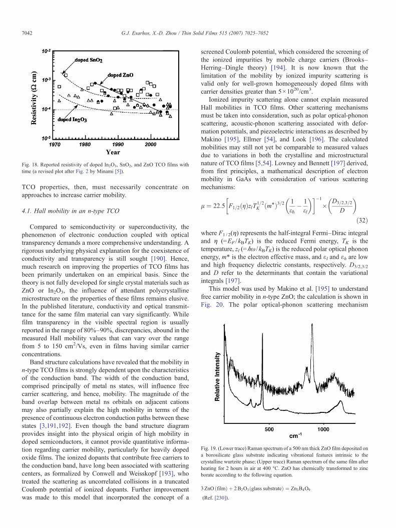
Fig. 18. Reported resistivity of doped In2O3, SnO2, and ZnO TCO films withtime (a revised plot after Fig. 2 by Minami [5]).
Fig. 19. (Lower trace) Raman spectrum of a 500 nm thick ZnO film deposited ona borosilicate glass substrate indicating vibrational features intrinsic to thecrystalline wurtzite phase; (Upper trace) Raman spectrum of the same film afterheating for 2 hours in air at 400 °C. ZnO has chemically transformed to zincborate according to the following equation.
3ZnO ðfilmÞ þ 2B2O3ðglass substrateÞ ¼ Zn3B4O9
(Ref. [230]).
7042 G.J. Exarhos, X.-D. Zhou / Thin Solid Films 515 (2007) 7025–7052
TCO properties, then, must necessarily concentrate onapproaches to increase carrier mobility.
4.1. Hall mobility in an n-type TCO
Compared to semiconductivity or superconductivity, thephenomenon of electronic conduction coupled with opticaltransparency demands a more comprehensive understanding. Arigorous underlying physical explanation for the coexistence ofconductivity and transparency is still sought [190]. Hence,much research on improving the properties of TCO films hasbeen primarily undertaken on an empirical basis. Since thetheory is not fully developed for single crystal materials such asZnO or In2O3, the influence of attendant polycrystallinemicrostructure on the properties of these films remains elusive.In the published literature, conductivity and optical transmit-tance for the same film material can vary significantly. Whilefilm transparency in the visible spectral region is usuallyreported in the range of 80%–90%, discrepancies, abound in themeasured Hall mobility values that can vary over the rangefrom 5 to 150 cm2/Vs, even in films having similar carrierconcentrations.
Band structure calculations have revealed that the mobility inn-type TCO films is strongly dependent upon the characteristicsof the conduction band. The width of the conduction band,comprised principally of metal ns states, will influence freecarrier scattering, and hence, mobility. The magnitude of theband overlap between metal ns orbitals on adjacent cationsmay also partially explain the high mobility in terms of thepresence of continuous electron conduction paths between thesestates [3,191,192]. Even though the band structure diagramprovides insight into the physical origin of high mobility indoped semiconductors, it cannot provide quantitative informa-tion regarding carrier mobility, particularly for heavily dopedoxide films. The ionized dopants that contribute free carriers tothe conduction band, have long been associated with scatteringcenters, as formalized by Conwell and Weisskopf [193], whotreated the scattering as uncorrelated collisions in a truncatedCoulomb potential of ionized dopants. Further improvementwas made to this model that incorporated the concept of a
screened Coulomb potential, which considered the screening ofthe ionized impurities by mobile charge carriers (Brooks–Herring–Dingle theory) [194]. It is now known that thelimitation of the mobility by ionized impurity scattering isvalid only for well-grown homogeneously doped films withcarrier densities greater than 5×10²⁰/cm3.
Ionized impurity scattering alone cannot explain measuredHall mobilities in TCO films. Other scattering mechanismsmust be taken into consideration, such as polar optical-phononscattering, acoustic-phonon scattering associated with defor-mation potentials, and piezoelectric interactions as described byMakino [195], Ellmer [54], and Look [196]. The calculatedmobilities may still not yet be comparable to measured valuesdue to variations in both the crystalline and microstructuralnature of TCO films [5,54]. Lowney and Bennett [197] derived,from first principles, a mathematical description of electronmobility in GaAs with consideration of various scatteringmechanisms:
l ¼ 22:5 F1=2ðgÞzlT1=2K ðm⁎Þ3=2 1
eJ� 1el
� �� ��1
� D3=2;3=2
D
� �
ð32Þwhere F1 / 2(η) represents the half-integral Fermi–Dirac integraland η (=EF /kBTK) is the reduced Fermi energy, TK is thetemperature, zl (=ℏω /kBTK) is the reduced polar optical phononenergy, m⁎ is the electron effective mass, and εl and εh are lowand high frequency dielectric constants, respectively. D3/2,3/2
and D refer to the determinants that contain the variationalintegrals [197].
This model was used by Makino et al. [195] to understandfree carrier mobility in n-type ZnO; the calculation is shown inFig. 20. The polar optical-phonon scattering mechanism
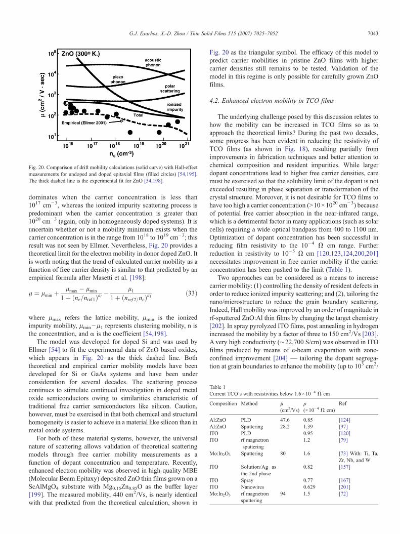
Fig. 20. Comparison of drift mobility calculations (solid curve) with Hall-effectmeasurements for undoped and doped epitaxial films (filled circles) [54,195].The thick dashed line is the experimental fit for ZnO [54,198].
Table 1Current TCO's with resistivities below 1.6×10⁻⁴ Ω cm
Composition Method μ(cm2/Vs)
ρ(×10−4 Ω cm)
Ref
Al:ZnO PLD 47.6 0.85 [124]Al:ZnO Sputtering 28.2 1.39 [97]ITO PLD 0.95 [120]ITO rf magnetron
sputtering1.2 [79]
Mo:In2O3 Sputtering 80 1.6 [73] With: Ti, Ta,Zr, Nb, and W
ITO Solution/Ag asthe 2nd phase
0.82 [157]
ITO Spray 0.77 [167]ITO Nanowires 0.629 [201]Mo:In2O3 rf magnetron
sputtering94 1.5 [72]
7043G.J. Exarhos, X.-D. Zhou / Thin Solid Films 515 (2007) 7025–7052
dominates when the carrier concentration is less than1017 cm−3, whereas the ionized impurity scattering process ispredominant when the carrier concentration is greater than1020 cm−3 (again, only in homogeneously doped systems). It isuncertain whether or not a mobility minimum exists when thecarrier concentration is in the range from 1018 to 1019 cm−3; thisresult was not seen by Ellmer. Nevertheless, Fig. 20 provides atheoretical limit for the electron mobility in donor doped ZnO. Itis worth noting that the trend of calculated carrier mobility as afunction of free carrier density is similar to that predicted by anempirical formula after Masetti et al. [198]:
l ¼ lmin þlmax � lmin
1þ ðne=nref1Þal �l1
1þ ðnref 2=neÞa1ð33Þ
where μmax refers the lattice mobility, μmin is the ionizedimpurity mobility, μmin−μ1 represents clustering mobility, n isthe concentration, and α is the coefficient [54,198].
The model was developed for doped Si and was used byEllmer [54] to fit the experimental data of ZnO based oxides,which appears in Fig. 20 as the thick dashed line. Boththeoretical and empirical carrier mobility models have beendeveloped for Si or GaAs systems and have been underconsideration for several decades. The scattering processcontinues to stimulate continued investigation in doped metaloxide semiconductors owing to similarities characteristic oftraditional free carrier semiconductors like silicon. Caution,however, must be exercised in that both chemical and structuralhomogeneity is easier to achieve in a material like silicon than inmetal oxide systems.
For both of these material systems, however, the universalnature of scattering allows validation of theoretical scatteringmodels through free carrier mobility measurements as afunction of dopant concentration and temperature. Recently,enhanced electron mobility was observed in high-quality MBE(Molecular Beam Epitaxy) deposited ZnO thin films grown on aScAlMgO4 substrate with Mg0.15Zn0.85O as the buffer layer[199]. The measured mobility, 440 cm2/Vs, is nearly identicalwith that predicted from the theoretical calculation, shown in
Fig. 20 as the triangular symbol. The efficacy of this model topredict carrier mobilities in pristine ZnO films with highercarrier densities still remains to be tested. Validation of themodel in this regime is only possible for carefully grown ZnOfilms.
4.2. Enhanced electron mobility in TCO films
The underlying challenge posed by this discussion relates tohow the mobility can be increased in TCO films so as toapproach the theoretical limits? During the past two decades,some progress has been evident in reducing the resistivity ofTCO films (as shown in Fig. 18), resulting partially fromimprovements in fabrication techniques and better attention tochemical composition and resident impurities. While largerdopant concentrations lead to higher free carrier densities, caremust be exercised so that the solubility limit of the dopant is notexceeded resulting in phase separation or transformation of thecrystal structure. Moreover, it is not desirable for TCO films tohave too high a carrier concentration (N10×1020 cm−3) becauseof potential free carrier absorption in the near-infrared range,which is a detrimental factor in many applications (such as solarcells) requiring a wide optical bandpass from 400 to 1100 nm.Optimization of dopant concentration has been successful inreducing film resistivity to the 10−4 Ω cm range. Furtherreduction in resistivity to 10−5 Ω cm [120,123,124,200,201]necessitates improvement in free carrier mobility if the carrierconcentration has been pushed to the limit (Table 1).
Two approaches can be considered as a means to increasecarrier mobility: (1) controlling the density of resident defects inorder to reduce ionized impurity scattering; and (2), tailoring thenano/microstructure to reduce the grain boundary scattering.Indeed, Hall mobility was improved by an order of magnitude inrf-sputtered ZnO:Al thin films by changing the target chemistry[202]. In spray pyrolyzed ITO films, post annealing in hydrogenincreased the mobility by a factor of three to 150 cm2/Vs [203].A very high conductivity (∼22,700 S/cm) was observed in ITOfilms produced by means of e-beam evaporation with zone-confined improvement [204] — tailoring the dopant segrega-tion at grain boundaries to enhance the mobility (up to 103 cm2/
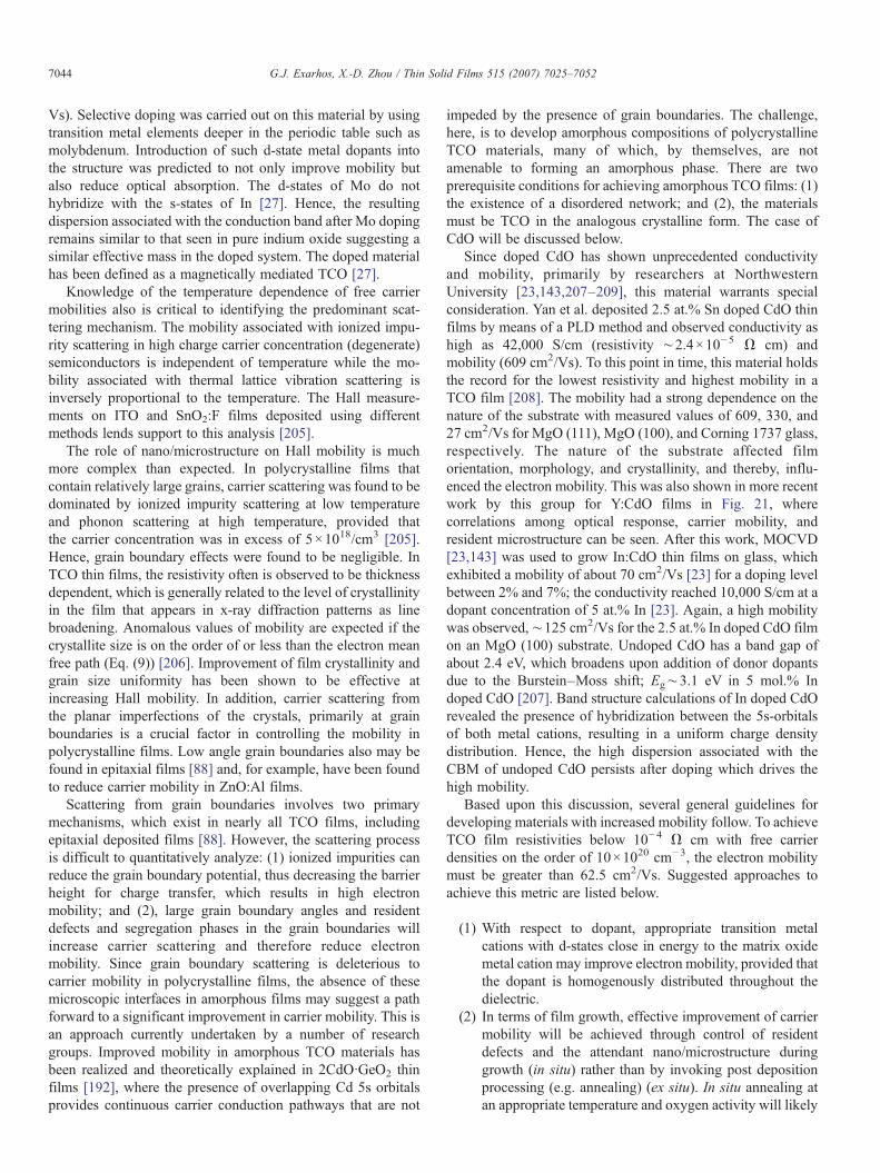
7044 G.J. Exarhos, X.-D. Zhou / Thin Solid Films 515 (2007) 7025–7052
Vs). Selective doping was carried out on this material by usingtransition metal elements deeper in the periodic table such asmolybdenum. Introduction of such d-state metal dopants intothe structure was predicted to not only improve mobility butalso reduce optical absorption. The d-states of Mo do nothybridize with the s-states of In [27]. Hence, the resultingdispersion associated with the conduction band after Mo dopingremains similar to that seen in pure indium oxide suggesting asimilar effective mass in the doped system. The doped materialhas been defined as a magnetically mediated TCO [27].
Knowledge of the temperature dependence of free carriermobilities also is critical to identifying the predominant scat-tering mechanism. The mobility associated with ionized impu-rity scattering in high charge carrier concentration (degenerate)semiconductors is independent of temperature while the mo-bility associated with thermal lattice vibration scattering isinversely proportional to the temperature. The Hall measure-ments on ITO and SnO2:F films deposited using differentmethods lends support to this analysis [205].
The role of nano/microstructure on Hall mobility is muchmore complex than expected. In polycrystalline films thatcontain relatively large grains, carrier scattering was found to bedominated by ionized impurity scattering at low temperatureand phonon scattering at high temperature, provided thatthe carrier concentration was in excess of 5×10¹⁸/cm3 [205].Hence, grain boundary effects were found to be negligible. InTCO thin films, the resistivity often is observed to be thicknessdependent, which is generally related to the level of crystallinityin the film that appears in x-ray diffraction patterns as linebroadening. Anomalous values of mobility are expected if thecrystallite size is on the order of or less than the electron meanfree path (Eq. (9)) [206]. Improvement of film crystallinity andgrain size uniformity has been shown to be effective atincreasing Hall mobility. In addition, carrier scattering fromthe planar imperfections of the crystals, primarily at grainboundaries is a crucial factor in controlling the mobility inpolycrystalline films. Low angle grain boundaries also may befound in epitaxial films [88] and, for example, have been foundto reduce carrier mobility in ZnO:Al films.
Scattering from grain boundaries involves two primarymechanisms, which exist in nearly all TCO films, includingepitaxial deposited films [88]. However, the scattering processis difficult to quantitatively analyze: (1) ionized impurities canreduce the grain boundary potential, thus decreasing the barrierheight for charge transfer, which results in high electronmobility; and (2), large grain boundary angles and residentdefects and segregation phases in the grain boundaries willincrease carrier scattering and therefore reduce electronmobility. Since grain boundary scattering is deleterious tocarrier mobility in polycrystalline films, the absence of thesemicroscopic interfaces in amorphous films may suggest a pathforward to a significant improvement in carrier mobility. This isan approach currently undertaken by a number of researchgroups. Improved mobility in amorphous TCO materials hasbeen realized and theoretically explained in 2CdO·GeO2 thinfilms [192], where the presence of overlapping Cd 5s orbitalsprovides continuous carrier conduction pathways that are not
impeded by the presence of grain boundaries. The challenge,here, is to develop amorphous compositions of polycrystallineTCO materials, many of which, by themselves, are notamenable to forming an amorphous phase. There are twoprerequisite conditions for achieving amorphous TCO films: (1)the existence of a disordered network; and (2), the materialsmust be TCO in the analogous crystalline form. The case ofCdO will be discussed below.
Since doped CdO has shown unprecedented conductivityand mobility, primarily by researchers at NorthwesternUniversity [23,143,207–209], this material warrants specialconsideration. Yan et al. deposited 2.5 at.% Sn doped CdO thinfilms by means of a PLD method and observed conductivity ashigh as 42,000 S/cm (resistivity ∼2.4×10⁻⁵ Ω cm) andmobility (609 cm2/Vs). To this point in time, this material holdsthe record for the lowest resistivity and highest mobility in aTCO film [208]. The mobility had a strong dependence on thenature of the substrate with measured values of 609, 330, and27 cm2/Vs for MgO (111), MgO (100), and Corning 1737 glass,respectively. The nature of the substrate affected filmorientation, morphology, and crystallinity, and thereby, influ-enced the electron mobility. This was also shown in more recentwork by this group for Y:CdO films in Fig. 21, wherecorrelations among optical response, carrier mobility, andresident microstructure can be seen. After this work, MOCVD[23,143] was used to grow In:CdO thin films on glass, whichexhibited a mobility of about 70 cm2/Vs [23] for a doping levelbetween 2% and 7%; the conductivity reached 10,000 S/cm at adopant concentration of 5 at.% In [23]. Again, a high mobilitywas observed,∼125 cm2/Vs for the 2.5 at.% In doped CdO filmon an MgO (100) substrate. Undoped CdO has a band gap ofabout 2.4 eV, which broadens upon addition of donor dopantsdue to the Burstein–Moss shift; Eg∼3.1 eV in 5 mol.% Indoped CdO [207]. Band structure calculations of In doped CdOrevealed the presence of hybridization between the 5s-orbitalsof both metal cations, resulting in a uniform charge densitydistribution. Hence, the high dispersion associated with theCBM of undoped CdO persists after doping which drives thehigh mobility.
Based upon this discussion, several general guidelines fordeveloping materials with increased mobility follow. To achieveTCO film resistivities below 10−4 Ω cm with free carrierdensities on the order of 10×1020 cm−3, the electron mobilitymust be greater than 62.5 cm2/Vs. Suggested approaches toachieve this metric are listed below.
(1) With respect to dopant, appropriate transition metalcations with d-states close in energy to the matrix oxidemetal cation may improve electron mobility, provided thatthe dopant is homogenously distributed throughout thedielectric.
(2) In terms of film growth, effective improvement of carriermobility will be achieved through control of residentdefects and the attendant nano/microstructure duringgrowth (in situ) rather than by invoking post depositionprocessing (e.g. annealing) (ex situ). In situ annealing atan appropriate temperature and oxygen activity will likely
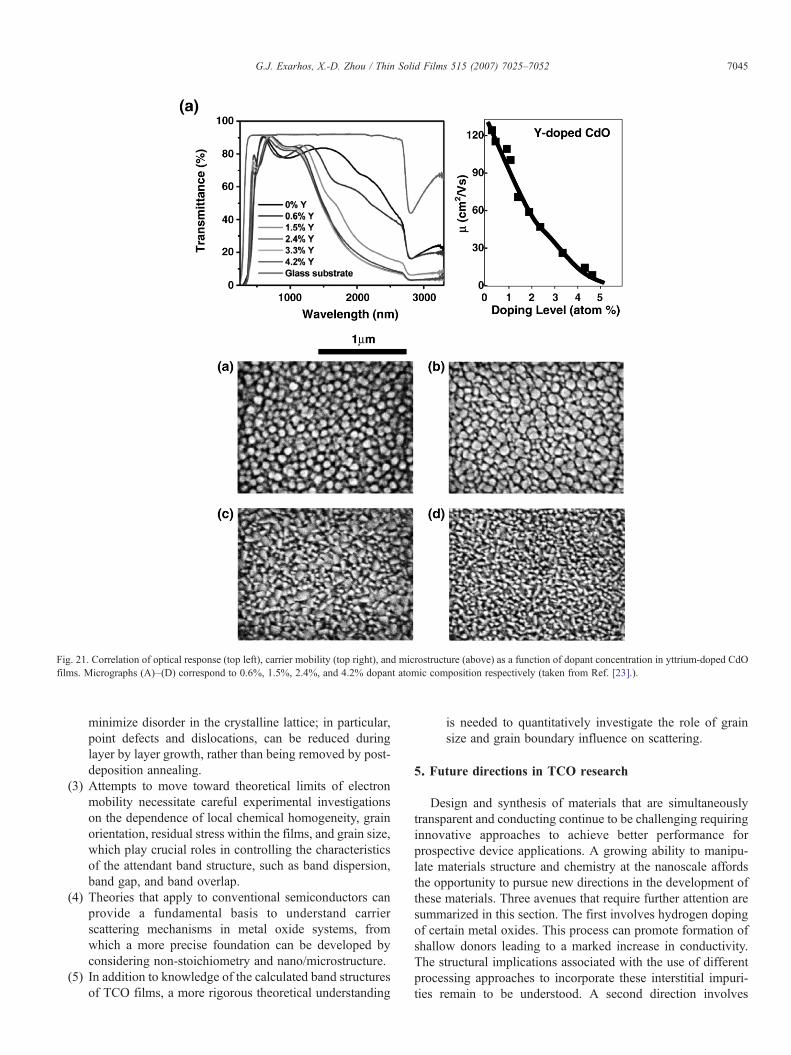
Fig. 21. Correlation of optical response (top left), carrier mobility (top right), and microstructure (above) as a function of dopant concentration in yttrium-doped CdOfilms. Micrographs (A)–(D) correspond to 0.6%, 1.5%, 2.4%, and 4.2% dopant atomic composition respectively (taken from Ref. [23].).
7045G.J. Exarhos, X.-D. Zhou / Thin Solid Films 515 (2007) 7025–7052
minimize disorder in the crystalline lattice; in particular,point defects and dislocations, can be reduced duringlayer by layer growth, rather than being removed by post-deposition annealing.
(3) Attempts to move toward theoretical limits of electronmobility necessitate careful experimental investigationson the dependence of local chemical homogeneity, grainorientation, residual stress within the films, and grain size,which play crucial roles in controlling the characteristicsof the attendant band structure, such as band dispersion,band gap, and band overlap.
(4) Theories that apply to conventional semiconductors canprovide a fundamental basis to understand carrierscattering mechanisms in metal oxide systems, fromwhich a more precise foundation can be developed byconsidering non-stoichiometry and nano/microstructure.
(5) In addition to knowledge of the calculated band structuresof TCO films, a more rigorous theoretical understanding
is needed to quantitatively investigate the role of grainsize and grain boundary influence on scattering.
5. Future directions in TCO research
Design and synthesis of materials that are simultaneouslytransparent and conducting continue to be challenging requiringinnovative approaches to achieve better performance forprospective device applications. A growing ability to manipu-late materials structure and chemistry at the nanoscale affordsthe opportunity to pursue new directions in the development ofthese materials. Three avenues that require further attention aresummarized in this section. The first involves hydrogen dopingof certain metal oxides. This process can promote formation ofshallow donors leading to a marked increase in conductivity.The structural implications associated with the use of differentprocessing approaches to incorporate these interstitial impuri-ties remain to be understood. A second direction involves
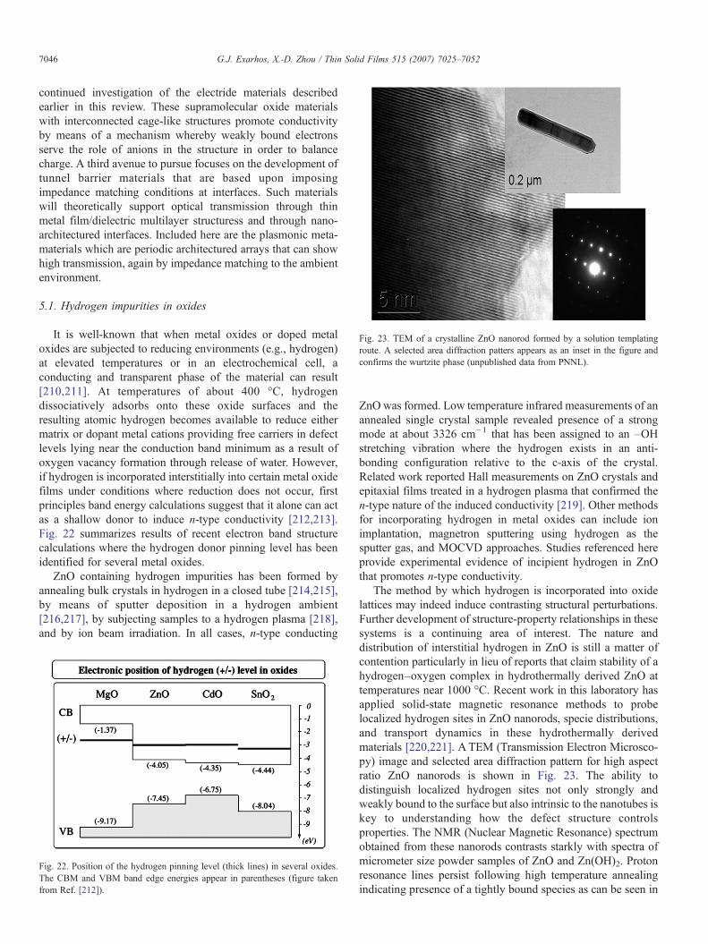
Fig. 23. TEM of a crystalline ZnO nanorod formed by a solution templatingroute. A selected area diffraction patters appears as an inset in the figure andconfirms the wurtzite phase (unpublished data from PNNL).
7046 G.J. Exarhos, X.-D. Zhou / Thin Solid Films 515 (2007) 7025–7052
continued investigation of the electride materials describedearlier in this review. These supramolecular oxide materialswith interconnected cage-like structures promote conductivityby means of a mechanism whereby weakly bound electronsserve the role of anions in the structure in order to balancecharge. A third avenue to pursue focuses on the development oftunnel barrier materials that are based upon imposingimpedance matching conditions at interfaces. Such materialswill theoretically support optical transmission through thinmetal film/dielectric multilayer structuress and through nano-architectured interfaces. Included here are the plasmonic meta-materials which are periodic architectured arrays that can showhigh transmission, again by impedance matching to the ambientenvironment.
5.1. Hydrogen impurities in oxides
It is well-known that when metal oxides or doped metaloxides are subjected to reducing environments (e.g., hydrogen)at elevated temperatures or in an electrochemical cell, aconducting and transparent phase of the material can result[210,211]. At temperatures of about 400 °C, hydrogendissociatively adsorbs onto these oxide surfaces and theresulting atomic hydrogen becomes available to reduce eithermatrix or dopant metal cations providing free carriers in defectlevels lying near the conduction band minimum as a result ofoxygen vacancy formation through release of water. However,if hydrogen is incorporated interstitially into certain metal oxidefilms under conditions where reduction does not occur, firstprinciples band energy calculations suggest that it alone can actas a shallow donor to induce n-type conductivity [212,213].Fig. 22 summarizes results of recent electron band structurecalculations where the hydrogen donor pinning level has beenidentified for several metal oxides.
ZnO containing hydrogen impurities has been formed byannealing bulk crystals in hydrogen in a closed tube [214,215],by means of sputter deposition in a hydrogen ambient[216,217], by subjecting samples to a hydrogen plasma [218],and by ion beam irradiation. In all cases, n-type conducting
Fig. 22. Position of the hydrogen pinning level (thick lines) in several oxides.The CBM and VBM band edge energies appear in parentheses (figure takenfrom Ref. [212]).
ZnO was formed. Low temperature infrared measurements of anannealed single crystal sample revealed presence of a strongmode at about 3326 cm−1 that has been assigned to an –OHstretching vibration where the hydrogen exists in an anti-bonding configuration relative to the c-axis of the crystal.Related work reported Hall measurements on ZnO crystals andepitaxial films treated in a hydrogen plasma that confirmed then-type nature of the induced conductivity [219]. Other methodsfor incorporating hydrogen in metal oxides can include ionimplantation, magnetron sputtering using hydrogen as thesputter gas, and MOCVD approaches. Studies referenced hereprovide experimental evidence of incipient hydrogen in ZnOthat promotes n-type conductivity.
The method by which hydrogen is incorporated into oxidelattices may indeed induce contrasting structural perturbations.Further development of structure-property relationships in thesesystems is a continuing area of interest. The nature anddistribution of interstitial hydrogen in ZnO is still a matter ofcontention particularly in lieu of reports that claim stability of ahydrogen–oxygen complex in hydrothermally derived ZnO attemperatures near 1000 °C. Recent work in this laboratory hasapplied solid-state magnetic resonance methods to probelocalized hydrogen sites in ZnO nanorods, specie distributions,and transport dynamics in these hydrothermally derivedmaterials [220,221]. A TEM (Transmission Electron Microsco-py) image and selected area diffraction pattern for high aspectratio ZnO nanorods is shown in Fig. 23. The ability todistinguish localized hydrogen sites not only strongly andweakly bound to the surface but also intrinsic to the nanotubes iskey to understanding how the defect structure controlsproperties. The NMR (Nuclear Magnetic Resonance) spectrumobtained from these nanorods contrasts starkly with spectra ofmicrometer size powder samples of ZnO and Zn(OH)2. Protonresonance lines persist following high temperature annealingindicating presence of a tightly bound species as can be seen in
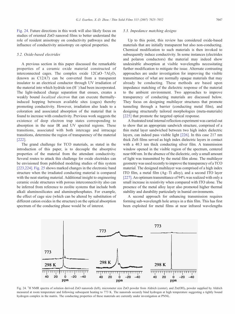
7047G.J. Exarhos, X.-D. Zhou / Thin Solid Films 515 (2007) 7025–7052
Fig. 24. Future directions in this work will also likely focus onstudies of oriented ZnO nanorod films to better understand therole of resident anisotropy on conductivity pathways and theinfluence of conductivity anisotropy on optical properties.
5.2. Oxide-based electrides
A previous section in this paper discussed the remarkableproperties of a ceramic oxide material constructed ofinterconnected cages. The complex oxide 12CaO–7Al2O3
(known as C12A7) can be converted from a transparentinsulator to an electrical conductor through UV irradiation ofthe material into which hydride ion (H−) had been incorporated.The light-induced charge separation that ensues, creates aweakly bound localized electron that can execute thermally-induced hopping between available sites (cages) therebypromoting conductivity. However, irradiation also leads to acoloration and associated absorption of the material that isfound to increase with conductivity. Previous work suggests theexistence of deep electron trap states corresponding toabsorption in the near IR and UV spectral regions. Thesetransitions, associated with both intercage and intracagetransitions, determine the region of transparency of the material[222].
The grand challenge for TCO materials, as stated in theintroduction of this paper, is to decouple the absorptiveproperties of the material from the attendant conductivity.Several routes to attack this challenge for oxide electrides canbe envisioned from published modeling studies of this system[223,224]. Fig. 25 shows marked changes in the electronic bandstructure when the irradiated conducting material is comparedwith the neat starting material. Additional insight to engineeringceramic oxide structures with porous interconnectivity also canbe inferred from reference to zeolite systems that include bothalkali aluminosilicates and aluminophosphates. For example,the effect of cage size (which can be altered by substitution ofdifferent cation oxides in the structure) on the optical absorptionspectrum of the conducting phase would be of interest.
Fig. 24. 1H NMR spectra of solution derived ZnO nanorods (left), micrometer sizemeasured at room temperature and following subsequent heating to 773 K. The nahydrogen complex in the matrix. The conducting properties of these materials are c
5.3. Impedance matching designs
Up to this point, this review has considered oxide-basedmaterials that are initially transparent but also non-conducting.Chemical modification to such materials is then invoked tosubsequently induce conductivity. In some instances (electridesand polaron conductors) the material may indeed showundesirable absorption at visible wavelengths necessitatingfurther modification to mitigate the issue. Alternate contrastingapproaches are under investigation for improving the visibletransmittance of what are normally opaque materials that mayalready be conducting. These methods are based uponimpedance matching of the dielectric response of the materialto the ambient environment. Two approaches to improvetransparency of conducting materials are discussed below.They focus on designing multilayer structures that promotetunneling through a barrier (conducting metal film), anddesigning structurally tailored morphologies (meta-materials)[225] that promote the targeted optical response.
A frustrated total internal reflection experiment was carried outto show that an appropriate sandwich structure, comprised of athin metal layer sandwiched between two high index dielectriclayers, can indeed pass visible light [226]. In this case 217 nmthick ZnS films served as high index dielectric layers in contactwith a 40.3 nm thick conducting silver film. A transmissionwindow opened in the visible region of the spectrum, centerednear 600 nm. In the absence of the dielectric, only a small amountof light was transmitted by the metal film alone. The multilayergeometrywas used recently to improve the transparency of a TCOmaterial. The designed multilayer was comprised of a high indexITO film, a metal film (Ag–Ti alloy), and a second ITO layer[227]. An optimum transmittance of 94%was realizedwith only asmall increase in resistivity when compared with ITO alone. Thepresence of the metal alloy layer also promoted higher thermalstability and durability particularly in humid environments.
A second approach for enhancing transmission requiresforming sub-wavelength hole arrays in a thin film. This has firstbeen exploited for metal films at near infrared wavelengths
ZnO powder from Aldrich (center), and Zn(OH)2 powder supplied by Aldrichnorods securely bind hydrogen at high temperature suggesting a tightly boundurrently under investigation at PNNL.
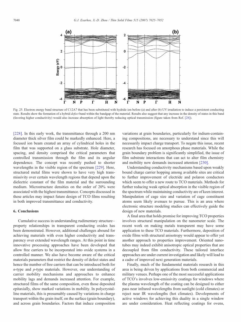
Fig. 25. Electron energy band structure of C12A7 that has been substituted with hydride ion before (a) and after (b) UV irradiation to induce a persistent conductingstate. Results show the formation of a hybrid defect band within the bandgap of the material. Results also suggest that any increase in the density of states in this band(favoring higher conductivity) would also increase absorption of light thereby reducing optical transmission (figure taken from Ref. [28]).
7048 G.J. Exarhos, X.-D. Zhou / Thin Solid Films 515 (2007) 7025–7052
[228]. In this early work, the transmittance through a 200 nmdiameter thick silver film could be markedly enhanced. Here, afocused ion beam created an array of cylindrical holes in thefilm that was supported on a glass substrate. Hole diameter,spacing, and density comprised the critical parameters thatcontrolled transmission through the film and its angulardependence. The concept was recently pushed to shorterwavelengths in the visible region of the spectrum [229]. Here,structured metal films were shown to have very high trans-missivity over certain wavelength regions that depend upon thedielectric constant of the film material and the surroundingmedium. Microstructure densities on the order of 20% wereassociated with the highest transmittance. Concepts discussed inthese articles may impact future design of TCO films resultingin both improved transmittance and conductivity.
6. Conclusions
Cumulative success in understanding rudimentary structure–property relationships in transparent conducting oxides hasbeen demonstrated. However, additional challenges abound forachieving materials with even higher conductivity and trans-parency over extended wavelength ranges. At this point in timeinnovative processing approaches have been developed thatallow free carriers to be incorporated into oxide systems in acontrolled manner. We also have become aware of the criticalmaterials parameters that restrict the density of defect states andhence the number of free carriers that can be introduced both forn-type and p-type materials. However, our understanding ofcarrier mobility mechanisms and approaches to enhancemobility lags and demands increased attention. For example,structured films of the same composition, even those depositedepitaxially, show marked variations in mobility. In polycrystal-line materials, this is presumably caused by variations in chargetransport within the grain itself, on the surface (grain boundary),and across grain boundaries. Factors that induce composition
variations at grain boundaries, particularly for indium-contain-ing compositions, are necessary to understand since this willnecessarily impact charge transport. To negate this issue, recentresearch has focused on amorphous phase materials. While thegrain boundary problem is significantly simplified, the issue offilm substrate interactions that can act to alter film chemistryand mobility now demands increased attention [230].
Understanding conductivity mechanisms based upon weaklybound charge carrier hopping among available sites are criticalto further improvement of electride and polaron conductorswhich seem to offer a new route to TCO materials. Methods forfurther reducing weak optical absorption in the visible region ofthe spectrumwhile maintaining conductivity are of keen interest.Manipulation of cage size and variation of cage constituentatoms seem likely avenues to pursue. This is an area whereelectronic structure modeling studies can effectively guide thedesign of new materials.
A final area that holds promise for improving TCO propertiesinvolves structural manipulation on the nanometer scale. Therecent work on making metals transparent may have someapplication to these TCO materials. Furthermore, deposition ofoxide films with structural anisotropy would appear to offer yetanother approach to properties improvement. Oriented nano-tubes may indeed exhibit anisotropic optical properties that aredecoupled from film conductivity. These tailored interfaceapproaches are under current investigation and likely will lead toa cadre of improved next generation materials.
Finally, much of the fundamental materials research in thisarea is being driven by applications from both commercial andmilitary venues. Perhaps one of the most successful applicationsof TCO's involves low-emissivity coatings for windows wherethe plasma wavelength of the coating can be designed to eitherpass near infrared wavelengths from sunlight (cold climates) orreject near IR wavelengths (hot climates). Developments ofactive windows for achieving this duality in a single windoware under consideration. Heat reflecting coatings for ovens,
7049G.J. Exarhos, X.-D. Zhou / Thin Solid Films 515 (2007) 7025–7052
coatings to dissipate static (copy machine glass plates, touch-panel controls, and electromagnetic shielding) compriseadditional consumer product applications that demand bettermaterials. Major markets in the solar cell, flat-panel display, andsolid-state lighting areas also require development of improvedTCO materials with increased robustness and resistance tochanges in optoelectronic properties. In addition to these severalimportant applications that will impact consumer products, theconundrum of building a material that is both conducting andtransparent will drive our curiosity to further developapproaches that lead to decoupling these variables.
Acknowledgements
Support by the Materials Sciences and EngineeringDivision of the Office of Basic Energy Sciences through theDOE Office of Science is gratefully acknowledged. Li-QiongWang is acknowledged for her work involving the preparationand magnetic resonance measurements of ZnO nanotubes.Sputter deposition of polaron conductors and TEM character-ization were performed in the Environmental MolecularSciences Laboratory, a national scientific user facility spon-sored by the Department of Energy's Office of Biological andEnvironmental Research and located at Pacific NorthwestNational Laboratory. Pacific Northwest National Laboratory(PNNL) is operated by Battelle Memorial Institute for the USDepartment of Energy under Contract DE-AC06-76RLO1830.
References
[1] K. Badeker, Ann. Phys. (Berlin) 22/4 (1907) 749.[2] K.L. Chopra, S. Major, D.K. Pandya, Thin Solid Films 102/1 (1983) 1.[3] H. Hosono, T. Kamiya, M. Hirano, Bull. Chem. Soc. Jpn. 79/1 (2006) 1.[4] H. Kawazoe, K. Ueda, J. Am. Ceram. Soc. 82/12 (1999) 3330.[5] T. Minami, Semicond. Sci. Technol. 20/4 (2005) S35.[6] D.S. Ginley, J.D. Perkins, H. Kawazoe, D.M. Newns, A.B. Kozyrev,
Proceedings of the Materials Research Society, Materials ResearchSociety, 2001, p. 433.
[7] D.C. Paine, H.-Y. Yeom, B. Yaglioglu, in: G.P. Crawford (Ed.), FlexibleFlat Panel Displays,Wiley Interscience, JohnWiley and Sons, 2005, p. 79.
[8] A.N. Banerjee, K.K. Chattopadhyay, Prog. Cryst. Growth Charact. Mater.50/1-3 (2005) 52.
[9] R. Kykyneshi, B.C. Nielsen, J. Tate, J. Li, A.W. Sleight, J. Appl. Phys.96/11 (2004) 6188.
[10] D. Emin, in: C.L. Chien, C.R. Westgate (Eds.), The Hall Effect and ItsApplications, Plenum Publishing, New York, 1980, p. 281.
[11] D. Bertho, C. Jouanin, Phys. Rev., B 35/2 (1987) 626.[12] D. Bott, Phys. Technol. 16/3 (1985) 121.[13] L.P. Yu, M. Chen, L.R. Dalton, Chem. Mater. 2/6 (1990) 649.[14] C.F. Windisch, G.J. Exarhos, K.F. Ferris, M.H. Engelhard, D.C. Stewart,
Thin Solid Films 398 (2001) 45.[15] R.R. Owings, G.J. Exarhos, C.F. Windisch, P.H. Holloway, J.G. Wen,
Thin Solid Films 483/1-2 (2005) 175.[16] D.S. Ginley, C. Bright, MRS Bull. 25/8 (2000) 15.[17] The 1st International Symposium on Transparent Conducting Oxide, IESL-
FORTH, Crete, Greece, 2006, http://www.certh.gr/65278BEC.en.aspx.[18] R.G. Gordon, MRS Bull. 25/8 (2000) 52.[19] J.M. Ziman, Principles of the Theory of Solids, Cambridge University
Press, 1972.[20] A. Zunger, Defects in Photovoltaic Materials and the Origin of Failure to
Dope Them, NREL/CP-590-31034, 2001.
[21] C.F.Windisch, G.J. Exarhos, J. Vac. Sci. Technol. A, Vac. Surf. Films 18/4(2000) 1677.
[22] E. Burstein, Phys. Rev. 93/3 (1954) 632.[23] Y. Yang, S. Jin, J.E. Medvedeva, J.R. Ireland, A.W. Metz, J. Ni, M.C.
Hersam, A.J. Freeman, T.J. Marks, J. Am. Chem. Soc. 127/24 (2005)8796.
[24] H. Hosono, M. Yasukawa, H. Kawazoe, J. Non-Cryst. Solids 203 (1996)334.
[25] M. Orita, H. Ohta, M. Hirano, S. Narushima, H. Hosono, Philos. Mag., B,Phys. Condens. Matter, Stat. Mech. Electron. Opt. Magn. Prop. 81/5(2001) 501.
[26] C. Persson, Y.J. Zhao, S. Lany, A. Zunger, Phys. Rev., B 72/3 (2005)035211.
[27] J.E. Medvedeva, Phys. Rev. Lett. 97/8 (2006) 086401.[28] J.E. Medvedeva, A.J. Freeman, Europhys. Lett. 69/4 (2005) 583.[29] H.Q. Chiang, J.F. Wager, R.L. Hoffman, J. Jeong, D.A. Keszler, Appl.
Phys. Lett. 86/1 (2005) 013503.[30] M.J. Wagner, R.H. Huang, J.L. Dye, J. Phys. Chem. 97/16 (1993) 3982.[31] M.J. Wagner, R.H. Huang, J.L. Eglin, J.L. Dye, Nature 368/6473 (1994)
726.[32] J.E. Hendrickson, W.P. Pratt, R.C. Phillips, J.L. Dye, J. Phys. Chem., B
102/20 (1998) 3917.[33] K.Hayashi, S.Matsuishi, T.Kamiya,M.Hirano,H.Hosono,Nature 419/6906
(2002) 462.[34] P.V. Sushko, A.L. Shluger, K. Hayashi, M. Hirano, H. Hosono, Phys.
Rev., B 73/1 (2006) 014101.[35] M. Miyakawa, Y. Toda, K. Hayashi, M. Hirano, T. Kamiya, N.
Matsunami, H. Hosono, J. Appl. Phys. 97/2 (2005) 023510.[36] J.B. Goodenough, Rep. Prog. Phys. 67 (2004) 1915.[37] J.C. Dyre, T.B. Schroder, Phys. Rev., B 54/21 (1996) 14884.[38] D. Emin, C.H. Seager, R.K. Quinn, Phys. Rev. Lett. 28/13 (1972) 813.[39] Y.N. Gartstein, E.M. Conwell, Phys. Rev., B 51/11 (1995) 6947.[40] K. Kuriyama, Phys. Rev., B 47/19 (1993) 12415.[41] B.H. Zhang, T. Katsura, A. Shatskiy, T. Matsuzaki, X.P. Wu, Phys. Rev.,
B 73/13 (2006) 134104.[42] L.D. Kadam, P.S. Patil, Mater. Chem. Phys. 68/1-3 (2001) 225.[43] R.R. Owings, P.H. Holloway, G.J. Exarhos, C.F. Windisch, Surf.
Interface Anal. 37/4 (2005) 424.[44] C.F. Windisch, K.F. Ferris, G.J. Exarhos, J. Vac. Sci. Technol. A, Vac.
Surf. Films 19/4 (2001) 1647.[45] N.W. Grimes, Phys. Technol. 6 (1975) 22.[46] C.F. Windisch, G.J. Exarhos, R.R. Owings, J. Appl. Phys. 95/10 (2004)
5435.[47] C.F. Windisch, K.F. Ferris, G.J. Exarhos, S.K. Sharma, Thin Solid Films
420 (2002) 89.[48] S. Goodwin-Jahansson, P.H. Holloway, G. McGuire, B.L. Cozzens, R.
Schwartz, G.J. Exarhos, Proc. SPIE 3987-32:225, 2000.[49] D. Attygalle, W.B.J. Ingler, X. Deng, ECS 210th Meeting Abstract:
Abstract, vol. 1554, 2001.[50] A.J. Freeman, K.R. Poeppelmeier, T.O. Mason, R.P.H. Chang, T.J.
Marks, Mrs Bull. 25/8 (2000) 45.[51] C.G. Granqvist, A. Hultaker, Thin Solid Films 411/1 (2002) 1.[52] M. Kemell, M. Ritala, M. Leskela, Crit. Rev. Solid State Mater. Sci. 30/1
(2005) 1.[53] M. Batzill, U. Diebold, Prog. Surf. Sci. 79/2-4 (2005) 47.[54] K. Ellmer, J. Phys. D: Appl. Phys. 34/21 (2001) 3097.[55] S. Sheng, G.J. Fang, C. Li, S. Xu, X.Z. Zhao, Phys. Status Solidi, A Appl.
Res. 203/8 (2006) 1891.[56] H. Kawazoe, M. Yasukawa, H. Hyodo, M. Kurita, H. Yanagi, H. Hosono,
Nature 389/6654 (1997) 939.[57] H. Kawazoe, H. Yanagi, K. Ueda, H. Hosono, MRS Bull. 25/8 (2000) 28.[58] M.A. Marquardt, N.A. Ashmore, D.P. Cann, Thin Solid Films 496/1
(2006) 146.[59] K. Ramamoorthy, K. Kumar, R. Chandramohan, K. Sankaranarayanan,
R. Saravanan, I.V. Kityk, P. Ramasamy, Opt. Commun. 262/1 (2006)91.
[60] U. Ozgur, Y.I. Alivov, C. Liu, A. Teke, M.A. Reshchikov, S. Dogan, V.Avrutin, S.J. Cho, H. Morkoc, J. Appl. Phys. 98/4 (2005) 041301.
7050 G.J. Exarhos, X.-D. Zhou / Thin Solid Films 515 (2007) 7025–7052
[61] P.F. Carcia, R.S. McLean, M.H. Reilly, Z.G. Li, L.J. Pillione, R.F.Messier, J. Vac. Sci. Technol. A, Vac. Surf. Films 21/3 (2003) 745.
[62] N.L. Dehuff, E.S. Kettenring, D. Hong, H.Q. Chiang, J.F. Wager, R.L.Hoffman, C.H. Park, D.A. Keszler, J. Appl. Phys. 97/6 (2005) 064505.
[63] K.B. Sundaram, A. Khan, J. Vac. Sci. Technol. A, Vac. Surf. Films 15/2(1997) 428.
[64] K. Yim, C. Lee, Cryst. Res. Technol. 41/12 (2006) 1198.[65] S. Rossnagel, in: W. Sproul, K. Legg (Eds.), Opportunities for
Innovation: Advanced Surf. Eng. Technomic Publishing Co., Switzer-land, 1995.
[66] P.J. Kelly, R.D. Arnell, Vacuum 56/3 (2000) 159.[67] P.J. Kelly, J. Hisek, Y. Zhou, R.D. Pilkington, R.D. Arnell, Surf. Eng. 20/3
(2004) 157.[68] P.J. Kelly, J. O'Brien, R.D. Arnell, Vacuum 74/1 (2004) 1.[69] E.M. Alkoy, P.J. Kelly, Vacuum 79/3-4 (2005) 221.[70] M.S. Hwang, H.J. Lee, H.S. Jeong, Y.W. Seo, S.J. Kwon, Surf. Coat.
Technol. 171/1-3 (2003) 29.[71] Y. Yoshida, T.A. Gessert, C.L. Perkins, T.J. Coutts, J. Vac. Sci. Technol.
A, Vac. Surf. Films 21/4 (2003) 1092.[72] N. Yamada, T. Tatejima, H. Ishizaki, T. Nakada, Jpn. J. Appl. Phys. Part 2,
Lett. Express Lett. 45/42-45 (2006) L1179.[73] A.E. Delahoy, S.Y. Guo, J. Vac. Sci. Technol. A, Vac. Surf. Films 23/4
(2005) 1215.[74] C.H. Jeong, J.T. Lim, J.H. Lee, M.S. Kim, J.W. Bae, G.Y. Yeom, Jpn. J.
Appl. Phys., Part 1 Regul. Pap. Brief Commun. Rev. Pap. 45/10B (2006)8457.
[75] H.C. Lee, O.O. Park, Vacuum 80/8 (2006) 880.[76] H.C. Lee, J.Y. Seo, Y.W. Choi, D.W. Lee, Vacuum 72/3 (2003) 269.[77] Y.S. Kim, Y.C. Park, S.G. Ansari, J.Y. Lee, B.S. Lee, H.S. Shin, Surf.
Coat. Technol. 173/2-3 (2003) 299.[78] D. Kim, J. Non-Cryst. Solids 331/1-3 (2003) 41.[79] R. Das, S. Ray, Jpn. J. Appl. Phys., Part 1 Regul. Pap. Short Notes Rev.
Pap. 44/3 (2005) 1367.[80] J.M. Park, J.S. Hong, J.Y. Yang, J.J. Kim, S.H. Park, H.M. Kim, J.S. Ahn,
J. Korean Phys. Soc. 48/6 (2006) 1530.[81] Y.S. Jung,H.Y. Seo,D.W.Lee,D.Y. Jeon, ThinSolid Films 445/1 (2003) 63.[82] R. Das, S. Ray, J. Phys. D: Appl. Phys. 36/2 (2003) 152.[83] H.Y. Yeom, N. Popovich, E. Chason, D.C. Paine, Thin Solid Films 411/1
(2002) 17.[84] T. Tohsophon, N. Sirikulrat, Sol. Energy Mater. Sol. Cells 90/18-19
(2006) 3444.[85] T. Minami, T. Miyata, Y. Ohtani, Y. Mochizuki, Jpn. J. Appl. Phys., Part 2
Lett. Express Lett. 45/12-16 (2006) L409.[86] J.G. Lu, Z.Z. Ye, Y.J. Zeng, L.P. Zhu, L. Wang, J. Yuan, B.H. Zhao, Q.L.
Liang, J. Appl. Phys. 100/7 (2006) 073714.[87] X.T. Hao, L.W. Tan, K.S. Ong, F.R. Zhu, J. Cryst. Growth 287/1 (2006) 44.[88] K. Ellmer, G. Vollweiler, Thin Solid Films 496/1 (2006) 104.[89] S.S. Lin, J.L. Huang, P. Sajgalik, Surf. Coat. Technol. 190/1 (2005) 39.[90] B.G. Choi, I.H. Kim, D.H. Kim, K.S. Lee, T.S. Lee, B. Cheong, Y.J. Baik,
W.M. Kim, J. Eur. Ceram. Soc. 25/12 (2005) 2161.[91] R. Das, S. Ray, Indian J. Phys. 78/9 (2004) 901.[92] J. Ma, X.T. Hao, S.Y. Zhang, H.L. Ma, J. Mater. Sci. Technol. 19/4 (2003)
363.[93] D. Herrmann, M. Oertel, R. Menner, M. Powalla, Surf. Coat. Technol.
174 (2003) 229.[94] C. Agashe, O. Kluth, G. Schope, H. Siekmann, J. Hupkes, B. Rech, Thin
Solid Films 442/1-2 (2003) 167.[95] X.T. Hao, J. Ma, D.H. Zhang, Y.G. Yang, H.L. Ma, C.F. Cheng, X.D. Liu,
Mater. Sci. Eng., B, Solid-State Mater. Adv. Technol. 90/1-2 (2002) 50.[96] Y. Igasaki, H. Kanma, Appl. Surf. Sci. 169 (2001) 508.[97] H.T. Cao, C. Sun, Z.L. Pei, A.Y. Wang, L.S. Wen, R.J. Hong, X. Jiang,
J. Mater. Sci., Mater. Electron. 15/3 (2004) 169.[98] E. Fortunato, V. Assuncao, A. Goncalves, A. Marques, H. Aguas, L.
Pereira, I. Ferreira, P. Vilarinho, R. Martins, Thin Solid Films 451–52(2004) 443.
[99] V. Assuncao, E. Fortunato, A. Marques, H. Aguas, I. Ferreira, M.E.V.Costa, R. Martins, Thin Solid Films 427/1-2 (2003) 401.
[100] T. Minami, T. Yamamoto, T. Miyata, Thin Solid Films 366/1-2 (2000) 63.
[101] A.S. Reddy, P.S. Reddy, S. Uthanna, G.M. Rao, J. Mater. Sci., Mater.Electron. 17/8 (2006) 615.
[102] R.E. Stauber, J.D. Perkins, P.A. Parilla, D.S. Ginley, Electrochem. Solid-State Lett. 2/12 (1999) 654.
[103] A.N. Banerjee, K.K. Chattopadhyay, J. Appl. Phys. 97/8 (2005) 084308.[104] H. Hiramatsu, K. Ueda, H. Ohta, M. Orita, M. Hirano, H. Hosono, Thin
Solid Films 411/1 (2002) 125.[105] H. Hiramatsu, M. Orita, M. Hirano, K. Ueda, H. Hosono, J. Appl. Phys.
91/11 (2002) 9177.[106] K. Ueda, S. Inoue, S. Hirose, H. Kawazoe, H. Hosono, Appl. Phys. Lett.
77/17 (2000) 2701.[107] H. Sato, T. Minami, S. Takata, T. Yamada, Thin Solid Films 236/1-2
(1993) 27.[108] T. Minami, K. Shimokawa, T. Miyata, J. Vac. Sci. Technol. A, Vac. Surf.
Films 16/3 (1998) 1218.[109] P.F. Carcia, R.S. McLean, M.H. Reilly, G. Nunes, Appl. Phys. Lett. 82/7
(2003) 1117.[110] A.V. Singh, R.M. Mehra, A. Wakahara, A. Yoshida, J. Appl. Phys. 93/1
(2003) 396.[111] I. Baia, M. Quintela, L. Mendes, P. Nunes, R. Martins, Thin Solid Films
337/1-2 (1999) 171.[112] K. Ellmer, R. Cebulla, R. Wendt, Thin Solid Films 317/1-2 (1998) 413.[113] Y. Hagiwara, T. Nakada, A. Kunioka, Sol. EnergyMater. Sol. Cells 67/1-4
(2001) 267.[114] S. Christoulakis, M. Suchea, M. Katharakis, N. Katsarakis, E.
Koudoumas, G. Kiriakidis, Rev. Adv. Mater. Sci. 10/4 (2005) 331.[115] M. Grundmann, H. von Wenckstern, R. Pickenhain, T. Nobis, A. Rahm,
M. Lorenz, Superlattices Microstruct. 38/4-6 (2005) 317.[116] K. Matsubara, P. Fons, K. Iwata, A. Yamada, S. Niki, Thin Solid Films
422/1-2 (2002) 176.[117] L. Dupont, C. Maugy, N. Naghavi, C. Guery, J.M. Tarascon, J. Solid State
Chem. 158/2 (2001) 119.[118] H. Izumi, T. Ishihara, H. Yoshioka, M.Motoyama, Thin Solid Films 411/1
(2002) 32.[119] S.H. Kim, N.M. Park, T.Y. Kim, G.Y. Sung, Thin Solid Films 475/1-2
(2005) 262.[120] J.B. Choi, J.H. Kim, K.A. Jeon, S.Y. Lee, Mater. Sci. Eng., B, Solid-State
Mater. Adv. Technol. 102/1-3 (2003) 376.[121] Y. Furubayashi, T. Hitosugi, Y. Yamamoto, Y. Hirose, G. Kinoda, K.
Inaba, T. Shimada, T. Hasegawa, Thin Solid Films 496/1 (2006) 157.[122] T. Hitosugi, Y. Furubayashi, A. Ueda, K. Itabashi, K. Inaba, Y. Hirose, G.
Kinoda, Y. Yamamoto, T. Shimada, T. Hasegawa, Jpn. J. Appl. Phys., Part2 Lett. Express Lett. 44/33–36 (2005) L1063.
[123] H. Agura, H. Okinaka, S. Hoki, T. Aoki, A. Suzuki, T. Matsushita, M.Okuda, Electr. Eng. Jpn. 151/2 (2005) 40.
[124] H. Agura, A. Suzuki, T. Matsushita, T. Aoki, M. Okuda, Thin Solid Films445/2 (2003) 263.
[125] V. Bhosle, J. Narayan, J. Appl. Phys. 100/9 (2006) 093519.[126] V. Bhosle, A. Tiwari, J. Narayan, J. Appl. Phys. 100/3 (2006) 033713.[127] S.J. Henley, M.N.R. Ashfold, D. Cherns, Surf. Coat. Technol. 177 (2004)
271.[128] W.J. Lee, C.R. Cho, K.M. Cho, S.Y. Jeong, J. Korean Phys. Soc. 47
(2005) S296.[129] K. Matsubara, P. Fons, K. Iwata, A. Yamada, K. Sakurai, H. Tampo, S.
Niki, Thin Solid Films 431 (2003) 369.[130] K. Ramamoorthy, C. Sanjeeviraja, M. Jayachandran, K. Sankaranaraya-
nan, V. Ganesan, P. Misra, L.M. Kukreja, Mater. Sci. Semicond. Process.8/4 (2005) 555.
[131] R.K. Shukla, A. Srivastava, A. Srivastava, K.C. Dubey, J. Cryst. Growth294/2 (2006) 427.
[132] A.V. Singh, R.M. Mehra, N. Buthrath, A. Wakahara, A. Yoshida, J. Appl.Phys. 90/11 (2001) 5661.
[133] U.S. Joshi, Y. Matsumoto, K. Itaka, M. Sumiya, H. Koinuma, Appl. Surf.Sci. 252/7 (2006) 2524.
[134] T. Minami, H. Tanaka, T. Shimakawa, T. Miyata, H. Sato, Jpn. J. Appl.Phys., Part 2 Lett. Express Lett. 43/7A (2004) L917.
[135] S. Sheng, G.J. Fang, C. Li, Z.Q. Chen, S. Ma, L.G. Fang, X.Z. Zhao,Semicond. Sci. Technol. 21/5 (2006) 586.
7051G.J. Exarhos, X.-D. Zhou / Thin Solid Films 515 (2007) 7025–7052
[136] H. Yanagi, S. Inoue, K. Ueda, H. Kawazoe, H. Hosono, N. Hamada,J. Appl. Phys. 88/7 (2000) 4159.
[137] V. Craciun, D. Craciun, X. Wang, T.J. Anderson, R.K. Singh, Thin SolidFilms 453–54 (2004) 256.
[138] A. Suzuki, T. Matsushita, T. Aoki, A. Mori, M. Okuda, Thin Solid Films411/1 (2002) 23.
[139] A. Suzuki, T. Matsushita, T. Aoki, Y. Yoneyama, M. Okuda, Jpn. J. Appl.Phys., Part 2- Lett. 40/4B (2001) L401.
[140] D.R. Sahu, J.L. Huang, Thin Solid Films 515/3 (2006) 876.[141] K.L. Choy, Prog. Mater. Sci. 48/2 (2003) 57.[142] J. Ni, H. Yan, A.C.Wang, Y. Yang, C.L. Stern, A.W.Metz, S. Jin, L.Wang,
T.J. Marks, J.R. Ireland, C.R. Kannewurf, J. Am. Chem. Soc. 127/15(2005) 5613.
[143] A.W. Metz, J.R. Ireland, J.G. Zheng, R. Lobo, Y. Yang, J. Ni, C.L. Stern,V.P. Dravid, N. Bontemps, C.R. Kannewurf, K.R. Poeppelmeier, T.J.Marks, J. Am. Chem. Soc. 126/27 (2004) 8477.
[144] A. Gulino, P. Dapporto, P. Rossi, I. Fragala, Chem. Mater. 14/12 (2002)4955.
[145] L.C. Olsen, F.W. Addis, L. Huang, W.N. Shafarman, P. Eschbach, G.J.Exarhos, Proc. 28th IEEE PVSC, 2000, p. 458.
[146] X. Li, Y. Yan, A. Mason, T.A. Gessert, T.J. Coutts, Electrochem. Solid-State Lett. 4/9 (2001) C66.
[147] X. Li, D.L. Young, H. Moutinho, Y. Yan, C. Narayanswamy, T.A.Gessert, T.J. Coutts, Electrochem. Solid-State Lett. 4/6 (2001) C43.
[148] A.W. Metz, M.A. Lane, C.R. Kannewurf, K.R. Poeppelmeier, T.J. Marks,Chem. Vap. Depos. 10/6 (2004) 297.
[149] X. Li, T. Gessert, C. DeHart, T. Barnes, H. Moutinho, Y. Yan, D. Young,M. Young, J. Perkins, T.J. Coutts, A Comparison of CompositeTransparent Conducting Oxides Based on the Binary Compounds CdOand SnO2, NREL/CP-520-31017, 2001.
[150] J.P. Chatelon, C. Terrier, J.A. Roger, Semicond. Sci. Technol. 14/7 (1999)642.
[151] D.C. Altamirano-Juarez, G. Torres-Delgado, R. Castanedo-Perez, O.Jimenez-Sandoval, J. Marquez-Marin, S. Jimenez-Sandoval, Superficiesy Vacío, vol. 13, 2001, p. 66.
[152] G.J. Exarhos, S.K. Sharma, Thin Solid Films 270/1-2 (1995) 27.[153] L.A. Chick, L.R. Pederson, G.D. Maupin, J.L. Bates, L.E. Thomas, G.J.
Exarhos, Mater. Lett. 10/1-2 (1990) 6.[154] L.R. Pederson, L.A. Chick, G.J. Exarhos, U.S. Pat. No. 4880772 (1989).[155] T.P. Niesen, M.R. De Guire, J. Electroceram. 6/3 (2001) 169.[156] T.P. Niesen, M.R. De Guire, Solid State Ion. 151/1-4 (2002) 61.[157] B. Houng, Appl. Phys. Lett. 87/25 (2005) 251922.[158] L. Wang, M.H. Yoon, G. Lu, Y. Yang, A. Facchetti, T.J. Marks, Nat.
Mater. 5/11 (2006) 893.[159] K. Domansky, A. Rose, W.H. Grover, G.J. Exarhos, Mater. Sci. Eng., B,
Solid-State Mater. Adv. Technol. 76/2 (2000) 116.[160] G.L. Messing, S.C. Zhang, G.V. Jayanthi, J. Am. Ceram. Soc. 76/11
(1993) 2707.[161] X.D. Zhou, S.C. Zhang, W. Huebner, P.D. Ownby, H.C. Gu, J. Mater. Sci.
36/15 (2001) 3759.[162] J.J. Prince, S. Ramamurthy, B. Subramanian, C. Sanjeeviraja, M.
Jayachandran, J. Cryst. Growth 240/1-2 (2002) 142.[163] P.K. Manoj, K.G. Gopchandran, P. Koshy, V.K. Vaidyan, B. Joseph, Opt.
Mater. 28/12 (2006) 1405.[164] D.J. Seo, S.H. Park, Physica, B 357/3-4 (2005) 420.[165] S. Mirzapour, S.M. Rozati, M.G. Takwale, B.R. Marathe, V.G. Bhide,
Mater. Res. Bull. 27/9 (1992) 1133.[166] Y. Sawada, C. Kobayashi, S. Seki, H. Funakubo, Thin Solid Films 409/1
(2002) 46.[167] Y. Sawada, Advanced Materials Processing Ii, vol. 437-4, Trans Tech
Publications Ltd, Zurich-Uetikon, 2003, p. 23.[168] M.M.Bagheri-Mohagheghi,M. Shokooh-Saremi, Thin Solid Films 441/1-2
(2003) 238.[169] K.S. Shamala, L.C.S. Murthy, K.N. Rao, Bull. Mater. Sci. 27/3 (2004) 295.[170] B. Thangaraju, Thin Solid Films 402/1-2 (2002) 71.[171] P. Veluchamy,M. Tsuji, T. Nishio, T. Aramoto, H. Higuchi, S. Kumazawa,
S. Shibutani, J. Nakajima, T. Arita, H. Ohyama, A. Hanafusa, T. Hibino,K. Omura, Sol. Energy Mater. Sol. Cells 67/1-4 (2001) 179.
[172] A. Gupta, D.K. Pandya, S.C. Kashyap, Jpn. J. Appl. Phys., Part 2 Lett.Express Lett. 43/12B (2004) L1592.
[173] K. Gurumurugan, D. Mangalaraj, S.K. Narayandass, C. Balasubrama-nian, Phys. Status Solidi, A Appl. Res. 143/1 (1994) 85.
[174] K. Gurumurugan, D. Mangalaraj, S.K. Narayandass, K. Sekar, C.P.G.Vallabhan, Semicond. Sci. Technol. 9/10 (1994) 1827.
[175] O. Vigil, L. Vaillant, F. Cruz, G. Santana, A. Morales-Acevedo, G.Contreras-Puente, Thin Solid Films 361 (2000) 53.
[176] J.H. Lee, S.Y. Lee, B.O. Park, Mater. Sci. Eng., B, Solid-State Mater.Adv. Technol. 127/2-3 (2006) 267.
[177] J.H. Lee, B.O. Park, Mater. Sci. Eng., B, Solid-State Mater. Adv. Technol.106/3 (2004) 242.
[178] P. Pushparajah, A.K. Arof, S. Radhakrishna, J. Phys. D: Appl. Phys. 27/7(1994) 1518.
[179] C. Gumus, O.M. Ozkendir, H. Kavak, Y. Ufuktepe, J. Optoelectron. Adv.Mater. 8/1 (2006) 299.
[180] A.F. Aktaruzzaman, G.L. Sharma, L.K.Malhotra, Thin Solid Films 198/1-2(1991) 67.
[181] J.C. Manifacier, L. Szepessy, J.F. Bresse, M. Perotin, R. Stuck, Mater.Res. Bull. 14/1 (1979) 109.
[182] E. Elangovan,K. Ramamurthi, J. Optoelectron. Adv.Mater. 5/1 (2003) 45.[183] K.Omura, P. Veluchamy,M.Tsuji, T.Nishio,M.Murozono, J. Electrochem.
Soc. 146/6 (1999) 2113.[184] G.C. Morris, A.E. McElnea, Appl. Surf. Sci. 92 (1996) 167.[185] T.J. Coutts, D.L. Young, X.N. Li, MRS Bull. 25/8 (2000) 58.[186] R. Cremer, D. Neuschutz, Surf. Coat. Technol. 146 (2001) 229.[187] T. Kamiya, K. Nomura, H. Hosono, ECS 210th Meeting Abstract:
Abstract, vol. 1598, 1996.[188] J. Perkins, M.F.A.M. van Hest, C.W. Teplin, J.L. Alleman, M.S. Dabney,
L.M. Gedvilas, B.M. Keyes, T.B., D.S. Ginley, M.P. Taylor, D.W.Readey, A.E. Delahoy, S. Guo, Optimization of Transparent ConductingOxides (TCOs) for PV, NREL/CP-520-37420, 2005.
[189] H.M. Christen, S.D. Silliman, K.S. Harshavardhan, Rev. Sci. Instrum. 72/6(2001) 2673.
[190] C. Kilic, A. Zunger, Phys. Rev. Lett. 88/9 (2002) 095501.[191] O.N. Mryasov, A.J. Freeman, Phys. Rev., B 64/23 (2001) 233111.[192] S. Narushima, M. Orita, M. Hirano, H. Hosono, Phys. Rev., B 66/3
(2002) 035203.[193] E. Conwell, V.F. Weisskopf, Phys. Rev. 77/3 (1950) 388.[194] H. Brooks, Phys. Rev. 83/4 (1951) 879.[195] T. Makino, Y. Segawa, A. Tsukazaki, A. Ohtomo, M. Kawasaki, Appl.
Phys. Lett. 87/2 (2005) 022101.[196] D.C. Look, J.W. Hemsky, J.R. Sizelove, Phys. Rev. Lett. 82/12 (1999)
2552.[197] J.R. Lowney, H.S. Bennett, J. Appl. Phys. 69/10 (1991) 7102.[198] G. Masetti, M. Severi, S. Solmi, IEEE Trans. Electron Devices 30/7
(1983) 764.[199] A. Tsukazaki, A. Ohtomo, M. Kawasaki, Appl. Phys. Lett. 88/15 (2006)
152106.[200] Y.Z. Chiou, K.W. Lin, J. Electrochem. Soc. 153/2 (2006) G141.[201] Q. Wan, E.N. Dattoli, W.Y. Fung, W. Guo, Y.B. Chen, X.Q. Pan, W. Lu,
Nano Lett. 6/12 (2006) 2909.[202] C. Agashe, O. Kluth, J. Hupkes, U. Zastrow, B. Rech, M. Wuttig, J. Appl.
Phys. 95/4 (2004) 1911.[203] S.H. Keshmiri, M. Rezaee-Roknabadi, S. Ashok, Thin Solid Films 413/1-2
(2002) 167.[204] I.A. Rauf, J. Appl. Phys. 79/8 (1996) 4057.[205] D.H. Zhang, H.L. Ma, Appl. Phys., AMater. Sci. Process. 62/5 (1996) 487.[206] H. Tanaka, K. Ihara, T. Miyata, H. Sato, T. Minami, J. Vac. Sci. Technol.
A, Vac. Surf. Films 22/4 (2004) 1757.[207] A. Wang, J.R. Babcock, N.L. Edleman, A.W. Metz, M.A. Lane, R. Asahi,
V.P. Dravid, C.R. Kannewurf, A.J. Freeman, T.J. Marks, Proc. Natl.Acad. Sci. U. S. A. 98/13 (2001) 7113.
[208] M. Yan,M. Lane, C.R. Kannewurf, R.P.H. Chang, Appl. Phys. Lett. 78/16(2001) 2342.
[209] S. Jin, Y. Yang, J.E. Medvedeva, J.R. Ireland, A.W. Metz, J. Ni, C.R.Kannewurf, A.J. Freeman, T.J. Marks, J. Am. Chem. Soc. 126/42 (2004)13787.
7052 G.J. Exarhos, X.-D. Zhou / Thin Solid Films 515 (2007) 7025–7052
[210] G.J. Exarhos, A. Rose, L.Q. Wang, C.F. Windisch, J. Vac. Sci. Technol.A, Vac. Surf. Films 16/3 (1998) 1926.
[211] G.J. Exarhos, A. Rose, C.F. Windisch, Thin Solid Films 308 (1997) 56.[212] C. Kilic, A. Zunger, Appl. Phys. Lett. 81/1 (2002) 73.[213] C.G. Van de Walle, Phys. Rev. Lett. 85/5 (2000) 1012.[214] S.J. Jokela, M.D. McCluskey, Phys. Rev., B 72/11 (2005) 113201.[215] M.D. McCluskey, S.J. Jokela, K.K. Zhuravlev, P.J. Simpson, K.G. Lynn,
Appl. Phys. Lett. 81/20 (2002) 3807.[216] L.Y. Chen, W.H. Chen, J.J. Wang, F.C.N. Hong, Y.K. Su, Appl. Phys.
Lett. 85/23 (2004) 5628.[217] F. Ruske, V. Sittinger, W. Werner, B. Szyszka, K.U. van Osten, K.
Dietrich, R. Rix, Surf. Coat. Technol. 200/1-4 (2005) 236.[218] Y.M. Strzhemechny, J. Nemergut, P.E. Smith, J. Bae, D.C. Look, L.J.
Brillson, J. Appl. Phys. 94/7 (2003) 4256.[219] Y.M. Strzhemechny, H.L. Mosbacker, S.H. Goss, D.C. Look, D.C.
Reynolds, C.W. Litton, N.Y. Garces, N.C. Giles, L.E. Halliburton, S.Niki, L.J. Brillson, J. Electron. Mater. 34/4 (2005) 399.
[220] M. Li, J. Zhai, H. Liu, Y.L. Song, L. Jiang, D.B. Zhu, J. Phys. Chem., B107/37 (2003) 9954.
[221] L.Q. Wang, G.J. Exarhos, C.F. Windisch, C. Yao, L.R. Pederson, X.-D.Zhou, Appl. Phys. Lett. (In press).
[222] P.V. Sushko, A.L. Shluger, K. Hayashi, M. Hirano, H. Hosono, Phys.Rev. Lett. 91/12 (2003) 126401.
[223] Z.Y. Li, J.L. Yang, J.G. Hou, Q.S. Zhu, Angew. Chem., Int. Ed. Engl. 43/47 (2004) 6479.
[224] J.E. Medvedeva, A.J. Freeman, Appl. Phys. Lett. 85/6 (2004) 955.[225] G. Dolling, M. Wegener, C.M. Soukoulis, S. Linden, Opt. Lett. 32/1
(2007) 53.[226] I.R. Hooper, T.W. Preist, J.R. Sambles, Phys. Rev. Lett. 97/5 (2006)
053902.[227] S.W. Chen, C.H. Koo, H.E. Huang, C.H. Chen, Mater. Trans. 46/11
(2005) 2536.[228] T.W. Ebbesen, H.J. Lezec, H.F. Ghaemi, T. Thio, P.A.Wolff, Nature 391/6668
(1998) 667.[229] J.W. Lee, M.A. Seo, J.Y. Sohn, Y.H. Ahn, D.S. Kim, S.C. Jeoung, C.
Lienau, Q.H. Park, Opt. Express 13/26 (2005) 10681.[230] A. Rose, G.J. Exarhos, Thin Solid Films 308 (1997) 42.
Related Documents
![Effect of preparation condition on the optical properties ...article.opticsjournal.org/pdf/10.11648.j.optics.20150403.11.pdf · time [ 1]. Transparent conducting oxide coating will](https://static.cupdf.com/doc/110x72/5e7b32fa2ad65a0a4843ac1f/effect-of-preparation-condition-on-the-optical-properties-time-1-transparent.jpg)