RADCELF Product Specification D-TACQ Solutions Ltd RADCELF TRIPLE-DDS RADAR SIGNAL GENERATOR Product Specification High Performance Simultaneous Data Acquisition Rev 2 Page 1 of 14 Date: 1 June 2017

Welcome message from author
This document is posted to help you gain knowledge. Please leave a comment to let me know what you think about it! Share it to your friends and learn new things together.
Transcript

RADCELF Product Specification D-TACQ Solutions Ltd
RADCELF
TRIPLE-DDS RADAR SIGNALGENERATOR
Product Specification
High Performance Simultaneous Data Acquisition
Rev 2 Page 1 of 14 Date: 1 June 2017

RADCELF Product Specification D-TACQ Solutions Ltd
Table of Contents1 Product Description........................................................................................3
1.1 Functional Block Diagram.......................................................................41.2 Product Variants......................................................................................51.3 Applications.............................................................................................51.4 Overview..................................................................................................51.5 Glossary..................................................................................................61.6 References..............................................................................................6
2 Physical...........................................................................................................72.1 Devices....................................................................................................72.2 MCX Connectors.....................................................................................7
2.2.1 Misc Connectors..............................................................................82.3 RADCELF Dimensions............................................................................8
2.3.1 Length 218mm.................................................................................82.3.2 Width 76.5mm..................................................................................82.3.3 Stack Height 50mm..........................................................................8
2.4 Appearance.............................................................................................92.4.1 Plan View.........................................................................................92.4.2 Side view of Stack up.......................................................................9
3 Interface Specification..................................................................................103.1 OCXO socket.........................................................................................103.2 I/O Connectors......................................................................................10
3.2.1 I& Q Output MCX Connectors........................................................103.2.2 Clock Input.....................................................................................103.2.3 Trigger Inputs.................................................................................10
3.3 Clock Monitors.......................................................................................103.4 Misc Connectors....................................................................................10
3.4.1 P16 3V3 External...........................................................................103.4.2 P17 5V External.............................................................................103.4.3 P18 PMOD Header........................................................................113.4.4 J1 AI 8 Slow monitor.......................................................................113.4.5 J2 DIO control................................................................................12
4 RADCELF Electrical Specification...............................................................134.1 DIO Connector.......................................................................................134.2 Analog Outputs......................................................................................13
5 RADCELF Specification...............................................................................14
Rev 2 Page 2 of 14 Date: 1 June 2017
RADCELF Product Specification D-TACQ Solutions Ltd
1 Product Description1. RADCELF is a complete clocking system suitable for HF RADAR
2. Circuit board forms the top layer of a 3-layer stack comprising
1. ACQ1001Q base unit with ZYNQ FPGA
2. ACQ435ELF digitizer module with 16 or 32 simultaneous AI.
3. RADCELF
3. Includes 3 x AD9854 DDS devices
1. ddsA : I+Q outputs, for main system control.
2. ddsB : I+Q outputs for system calibration.
3. ddsC : I output for clock remapping
4. Includes 2 x AD9512 CLKD Clock divider/buffer devices
1. clkdA : Select Oven Local Oscillator or CLK-IN
2. clkdB : Select Clock source for ddsA, ddsB.
5. All 5 devices are controlled from SPI from the ACQ1001. Multiple SPI channels are used to potentially provide simultaneous register update.
6. Key signal inputs to DDS are provided from the FPGA. All output clocks feed back to the FPGA for monitoring.
7. Provision for Oven Local Oscillator (power supply, socket and space for thermal management) or external clock
8. Signal inputs and outputs on MCX connectors. ddsA, ddsB TRG inputs.
9. Outputs optionally filtered by Minicircuits SXLP filters.
10. I/O expansion:
1. P18: PMOD connector. (12 pin header with FPGA IO)
2. J1: VMON (16 pin header, 8 x slow ADC channels, 1Hz, 10bit)
3. J2: DIO (16 pin header, 8 slow DIO)
4. USB 2.0, type A port, suitable for USB stick or remote devices.
RADCELF?
RAD : Radar
CELF : “Carrier Elf”, D-TACQ definition for 3 layer stacking board.
Rev 2 Page 3 of 14 Date: 1 June 2017

RADCELF Product Specification D-TACQ Solutions Ltd
1.1 Functional Block Diagram
Rev 2 Page 4 of 14 Date: 1 June 2017
SX
LP-3
0+F
ilterD
river
SX
LP-30
+F
ilterD
river
AD
951
2S
econ
dary
Clo
ckB
uffer /D
ivide
r
IOU
D/B
PS
K / O
SK
AD
985
4D
DS
A
SX
LP-3
0+F
ilterD
river
SX
LP-3
0+F
ilterD
river
OC
XO
SX
LP-3
0+F
ilterA
D9
854
DD
SC
Clo
ckR
emap
AD
985
4D
DS
B
AD
9512
Prim
aryC
lock
Buffer /
Divid
er
CLK
IN
SP
I
SP
I
IO
UT
QO
UT
IO
UT
QO
UT
SP
I
IOU
D/B
PS
K / O
SK
MC
X C
able C
on
nector
Log
ic Con
nection
with
FP
GA
KE
Y

RADCELF Product Specification D-TACQ Solutions Ltd
1.2 Product Variants
• RADCELF3 : 3 x DDS
• RADCELF2 : 2 x DDS (MOQ 20).
• SXLP filters are assumed to be either No Fit or free issue from customer
1.3 Applications
• High speed control and diagnostics.
1.4 Overview
RADCELF forms part of a complete working 32 channel digitizer appliance with Ethernet control. The appliance includes a full Linux OS with full virtual memory support. The DDS and CLKD
For IO expansion, additional ACQ1002S stacks may be daisy chained on the clock trigger highway, for expansion from 32 to 64, 96 and more simultaneous analog inputs.
Rev 2 Page 5 of 14 Date: 1 June 2017

RADCELF Product Specification D-TACQ Solutions Ltd
1.5 Glossary
• FMC: VITA57 FPGA Mezzanine Card.
• Xilinx ZYNQ Soc
• FPGA : Field Programmable Gate Array.
• LPC : FMC Low pin count wiring standard.
• ULPC: FMC Ultra low pin count (D-TACQ).
• ULPC+ D-TACQ Ultra low pin count with LVDS
• Extended, ELF : FMC Extended size module (D-TACQ).
1.6 References
• RADCELF User Guide.
Rev 2 Page 6 of 14 Date: 1 June 2017
RADCELF Product Specification D-TACQ Solutions Ltd
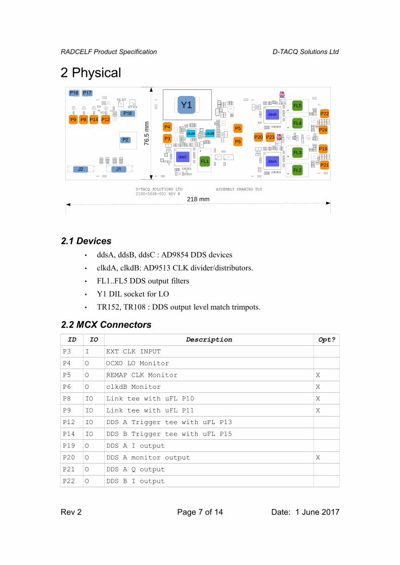
2 Physical
2.1 Devices
• ddsA, ddsB, ddsC : AD9854 DDS devices
• clkdA, clkdB: AD9513 CLK divider/distributors.
• FL1..FL5 DDS output filters
• Y1 DIL socket for LO
• TR152, TR108 : DDS output level match trimpots.
2.2 MCX Connectors
ID IO Description Opt?
P3 I EXT CLK INPUT
P4 O OCXO LO Monitor
P5 O REMAP CLK Monitor X
P6 O clkdB Monitor X
P8 IO Link tee with uFL P10 X
P9 IO Link tee with uFL P11 X
P12 IO DDS A Trigger tee with uFL P13
P14 IO DDS B Trigger tee with uFL P15
P19 O DDS A I output
P20 O DDS A monitor output X
P21 O DDS A Q output
P22 O DDS B I output
Rev 2 Page 7 of 14 Date: 1 June 2017
ASSEMBLY DRAWING TOP2100-5008-001 REV B D-TACQ SOLUTIONS LTD
P9
R84
P11
J2
P16
P8
R83
P10
P17
P14
R86
P15
MTG1
U18
C114
MTG8
C119
R3 R7
R2 R6
P12
R85C111
P13
L12 L14
C128
R4 R8
R5 R9
U17
D4
J1
R13 R17
R12 R16
D3
L13 L15 C112
C113
C118
R14 R20
R15 R18
U20
C115
P2
P18
C117 C116
U19
MTG2
C127
MTG7
C120
TP2
U8
C66 C67
TP3
C60
C56
L6
P3
P4
C45
C46
C44
U31
R185
C48
C49
C47
C43
C41
C42
R32
L3
R29
R28
L5
R34
R35
R33
C64C223
C51C59
U9
U7
C50 R47
R48
C17 C29
C34 C36
C10 C28
Y1
C65
C58
R49
C57
C23
C21
U5
R40
C33
C35
C52
C54
C53
C55
C27 C25
C22 R37
C38
R38 C37
R39
FL1
L4
R71
C93
C77 C72
C86
TP1
R72
C92
U10
C220
U29
C219
R73
C79 R74 C88 C90
C78 R66
C89
R68 C91
JP1
TP4
TP5
C221
C222
C82
C83
L8
R67
C108
TP6
C107
C105
C106
U30
L7
R81
U16
R78
R79
P6
P5
R82
C110
C126
MTG3
L11
MTG6
C121
R116
R115
C135
C132
C149
C150
L10
P20
R159
C182
C185
C195
C194
C136
C139
C133
C137
C177
C183
C179
C181
C138 C148
U22
C134
C140
R111
R110
P23
C184 C193
U26
C178
C180
R155
R154
C145 C146
C143
R112
R108
C189C192
C191
R156
C141
C147
C144
C142 C151
C206
C203
C187
C188
C190
C186
R152
C196
U27
C204
FL2
FL3
R179
R181
C205
FL4
FL5
C218
C215
C131
R102 R103 R104
C163 C164
U28
R148 C176
R147 R146
C208 C209
MTG4
C168 C167
U21
R136
R134
R138 C162
R183
R184
C216
C217
C213 C212
U25
R182 R180 R178
MTG5
C207
C125
P21
R130
R133
C166
P19
P24
C211
R174
R177
P22
C122
R98
R101
R142
R145
1
2
1 15
16 2
1
1
2
15
16
11
12Y1
P9 P8 P14 P12
J2 J1
P2
P4
P3
P5P4
P6P20 P23
P22
P23
P24
76.
5 m
m
P21
P19
FL1
FL2
FL3
FL4
FL5
P18
P16 P17
clkdA
ddsC
clkdB
ddsA
ddsB
TR152
TR108
RADCELF Product Specification D-TACQ Solutions Ltd
ID IO Description Opt?
P23 O DDS B monitor output X
P24 O DDS B Q output
2.2.1 Misc Connectors
ID Type Description Opt?
P2 USB-A USB 2.0 Master
P16 2-pin HDR 3V3 external X
P17 2-pin HDR 5V external X
P18 12 pin HDR PMOD Header
J1 16 pin HDR AI 8 slow monitor
J2 16 pin HDR DIO 8 slow control/monitor
2.3 RADCELF Dimensions
2.3.1 Length 218mm
2.3.2 Width 76.5mm
2.3.3 Stack Height 50mm
Rev 2 Page 8 of 14 Date: 1 June 2017

RADCELF Product Specification D-TACQ Solutions Ltd
2.4 Appearance
2.4.1 Plan View
2.4.2 Side view of Stack up
Top to Bottom:
• RADCELF
• ACQ435ELF : 16/32 channel simultaneous ADC
• ACQ1001: FPGA/Computer control module.
• Customer plinth base.
Rev 2 Page 9 of 14 Date: 1 June 2017
RADCELF Product Specification D-TACQ Solutions Ltd
3 Interface Specification.
3.1 OCXO socket
Standard 14 pin socket is provided for a OCXO.
Linear regulated 5V power at up to 1A (warm up) and 500 mA (steady state)
Sine or Square Wave output 2-7 dBm
Tested with Bliley NV79 .
Physical separation with mounting holes to allow the OCXO to be encased for thermal separation
3.2 I/O Connectors
3.2.1 I& Q Output MCX Connectors
All outputs are a nominal 7dBm output with 50 Ohm impedance
3.2.2 Clock Input
Connector P3 transformer coupled 2-7dBm 50 Ohm input Square or Sine Wave input.
3.2.3 Trigger Inputs
The two trigger input functionality is application dependent. These are 5V TTL compatible inputs with optional output functionality.
3.3 Clock Monitors
P4 allows the oscillator to be monitored it is a direct connection to the output of the OCXO Oscillator
P5 is a TTL output monitor of the square wave frequency of the Clock Remapping DDS – DDS C. This is the square-wave produced by the AD9654 comparator.
P6 is a TTL output monitor of the input Clock to the two main DDS devices DDS A and DDS B. This signal is controlled from the secondary AD9512 device and can therefore be overridden under software control to produce a divide by N output if desired.
P20 and P23 are TTL monitors of the square wave frequency of DDS A and DDS B. This is the square-wave produced by the AD9654 comparator.
3.4 Misc Connectors
3.4.1 P16 3V3 External
Auxiliary 3V3 output 100 mA max.
3.4.2 P17 5V External
Auxiliary 5V output 100 mA max.
Rev 2 Page 10 of 14 Date: 1 June 2017

RADCELF Product Specification D-TACQ Solutions Ltd
3.4.3 P18 PMOD Header
12 pin 0.1” box header socket for use with PMOD modules.
PMOD is a simple low-cost expansion standard.
Using the PMOD requires FPGA customisation depending on PMOD chosen. Please contact D-TACQ with requirements.
PMOD definition
3.4.4 J1 AI 8 Slow monitor
16 pin 0.1” box header plug for monitoring slow AI signals.
Input range: 0..5V, 10 bit conversion, 1Hz typical rate. 20K input impedance.
Access through Linux device driver.
2x LM7417 devices include temperature monitor.
Pin Channel
2 AI1
4 AI2
6 AI3
8 AI4
10 AI5
12 AI6
14 AI7
16 AI8
1,3,5,15 GND
Rev 2 Page 11 of 14 Date: 1 June 2017

RADCELF Product Specification D-TACQ Solutions Ltd
3.4.5 J2 DIO control
16 pin 0.1” box header plug for slow DIO control.
5V TTL. Access through Linux device driver.
Pin Channel
2 DIO1
4 DIO2
6 DIO3
8 DIO4
10 DIO5
12 DIO6
14 DIO7
16 DIO8
1,3,5,15 GND
Rev 2 Page 12 of 14 Date: 1 June 2017

RADCELF Product Specification D-TACQ Solutions Ltd
4 RADCELF Electrical Specification
4.1 DIO Connector
# Parameter Value
1 Number of Channels 8
2 Sample Rate I2C device with 1 Hz typical update
3 I/O Voltage Range 0-5V
4 Input Voltage High > 4.0V (@ 10mA)
5 Input Voltage Low < 0.2V (@ 10mA)
6 Input Voltage Withstand -0.5 to 6.5V
7 Output Current High -32mA, -100mA max total
8 Output Current Low 32mA, 100mA max total
4.2 Analog Outputs
Both A & B DDS devices drive both I & Q outputs via an output Amplifier of type OPA2694 with a nominal 7dBm drive capability. Potentiometer available on each DDS to set the nominal output amplitude R108 for DDS A and R152 for DDS B
Rev 2 Page 13 of 14 Date: 1 June 2017

RADCELF Product Specification D-TACQ Solutions Ltd
5 RADCELF Specification# Parameter Value
1 Form Factor D-TACQ CELF
2 Power source D-TACQ Carrier Only
3 Environmental 0ºC-50ºC Operational-10ºC-85ºC Non-Operational
4 Carrier Socket D-TACQ CELF Socket
Rev 2 Page 14 of 14 Date: 1 June 2017
Related Documents