Digitally Assisted RF Circuits EE633-Seminar Sohaib Afridi Sohaib Afridi SOHAIB SAADAT AFRIDI

Welcome message from author
This document is posted to help you gain knowledge. Please leave a comment to let me know what you think about it! Share it to your friends and learn new things together.
Transcript
Digitally Assisted RF Circuits
EE633-SeminarSohaib Afridi
EE633-SeminarSohaib Afridi
SOHAIB SAADAT AFRIDI

The Dream- “Software Radio”
DAC
ADC
WickedFast
Computation
ADC
[Schreier, "ADCs and DACs: Marching Towards the Antenna," GIRAFE workshop, ISSCC 2003]
SOHAIB SAADAT AFRIDI

Reality-“Heat-Sink Radio”
PA
DAC
ADC
Wicked
FastComputation
Expensive
ADC
[Schreier, "ADCs and DACs: Marching Towards the Antenna," GIRAFE workshop, ISSCC 2003]
SOHAIB SAADAT AFRIDI

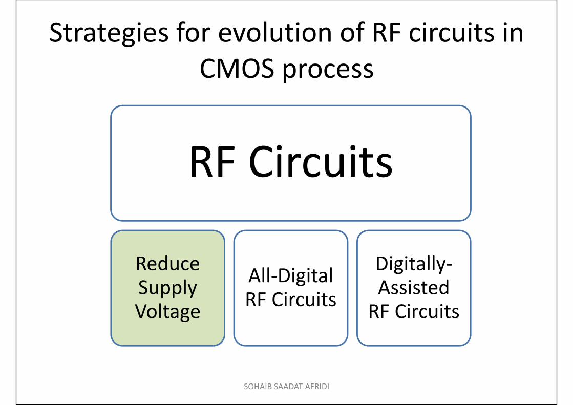
Strategies for evolution of RF circuits inCMOS process
RF CircuitsRF Circuits
ReduceSupplyVoltage
All-DigitalRF Circuits
Digitally-Assisted
RF Circuits
ReduceSupplyVoltage
All-DigitalRF Circuits
Digitally-Assisted
RF Circuits
SOHAIB SAADAT AFRIDI
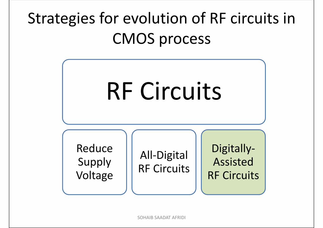
Strategies for evolution of RF circuits inCMOS process
RF CircuitsRF Circuits
ReduceSupplyVoltage
All-DigitalRF Circuits
Digitally-Assisted
RF Circuits
ReduceSupplyVoltage
All-DigitalRF Circuits
Digitally-Assisted
RF Circuits
SOHAIB SAADAT AFRIDI
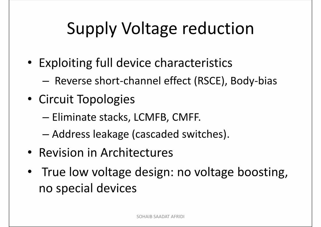
Supply Voltage reduction
• Exploiting full device characteristics– Reverse short-channel effect (RSCE), Body-bias
• Circuit Topologies– Eliminate stacks, LCMFB, CMFF.– Address leakage (cascaded switches).
• Revision in Architectures• True low voltage design: no voltage boosting,
no special devices
• Exploiting full device characteristics– Reverse short-channel effect (RSCE), Body-bias
• Circuit Topologies– Eliminate stacks, LCMFB, CMFF.– Address leakage (cascaded switches).
• Revision in Architectures• True low voltage design: no voltage boosting,
no special devices
• Exploiting full device characteristics– Reverse short-channel effect (RSCE), Body-bias
• Circuit Topologies– Eliminate stacks, LCMFB, CMFF.– Address leakage (cascaded switches).
• Revision in Architectures• True low voltage design: no voltage boosting,
no special devices
SOHAIB SAADAT AFRIDI

Strategies for evolution of RF circuits inCMOS process
RF CircuitsRF Circuits
ReduceSupplyVoltage
All-DigitalRF Circuits
Digitally-Assisted
RF Circuits
ReduceSupplyVoltage
All-DigitalRF Circuits
Digitally-Assisted
RF Circuits
SOHAIB SAADAT AFRIDI

All-Digital RF Circuits
• All Digital Synthesizer• All-digital phase-locked loop (ADPLL)
comprising: digitally-controlled oscillator(DCO), time-to-digital converter (TDC), anddigital loop filter.• Direct-sampling discrete-time receiver
comprising switched-cap circuits that performvarious FIR and IIR filter operations
• All Digital Synthesizer• All-digital phase-locked loop (ADPLL)
comprising: digitally-controlled oscillator(DCO), time-to-digital converter (TDC), anddigital loop filter.• Direct-sampling discrete-time receiver
comprising switched-cap circuits that performvarious FIR and IIR filter operations
• All Digital Synthesizer• All-digital phase-locked loop (ADPLL)
comprising: digitally-controlled oscillator(DCO), time-to-digital converter (TDC), anddigital loop filter.• Direct-sampling discrete-time receiver
comprising switched-cap circuits that performvarious FIR and IIR filter operations
SOHAIB SAADAT AFRIDI
Strategies for evolution of RF circuits inCMOS process
RF CircuitsRF Circuits
ReduceSupplyVoltage
All-DigitalRF Circuits
Digitally-Assisted
RF Circuits
ReduceSupplyVoltage
All-DigitalRF Circuits
Digitally-Assisted
RF Circuits
SOHAIB SAADAT AFRIDI

Why use Digital Assistance?
• To self-calibrate RF front-end.• Achieve tunability at the cost of low power
and low area digital gates.• Possibly replacing any RF functional block with
a digital RF block.
• To self-calibrate RF front-end.• Achieve tunability at the cost of low power
and low area digital gates.• Possibly replacing any RF functional block with
a digital RF block.
• To self-calibrate RF front-end.• Achieve tunability at the cost of low power
and low area digital gates.• Possibly replacing any RF functional block with
a digital RF block.
SOHAIB SAADAT AFRIDI
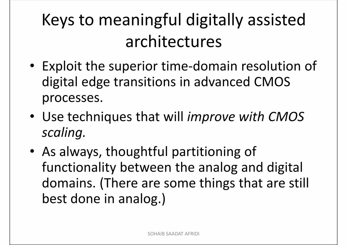
Keys to meaningful digitally assistedarchitectures
• Exploit the superior time-domain resolution ofdigital edge transitions in advanced CMOSprocesses.• Use techniques that will improve with CMOS
scaling.• As always, thoughtful partitioning of
functionality between the analog and digitaldomains. (There are some things that are stillbest done in analog.)
SOHAIB SAADAT AFRIDI
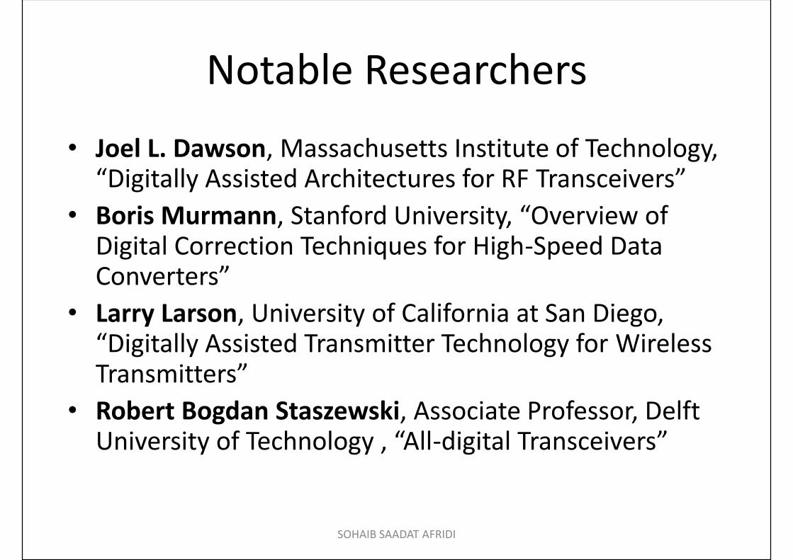
Notable Researchers
• Joel L. Dawson, Massachusetts Institute of Technology,“Digitally Assisted Architectures for RF Transceivers”
• Boris Murmann, Stanford University, “Overview ofDigital Correction Techniques for High-Speed DataConverters”
• Larry Larson, University of California at San Diego,“Digitally Assisted Transmitter Technology for WirelessTransmitters”
• Robert Bogdan Staszewski, Associate Professor, DelftUniversity of Technology , “All-digital Transceivers”
SOHAIB SAADAT AFRIDI
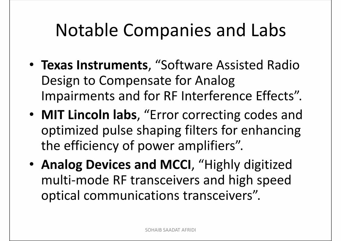
Notable Companies and Labs
• Texas Instruments, “Software Assisted RadioDesign to Compensate for AnalogImpairments and for RF Interference Effects”.• MIT Lincoln labs, “Error correcting codes and
optimized pulse shaping filters for enhancingthe efficiency of power amplifiers”.• Analog Devices and MCCI, “Highly digitized
multi-mode RF transceivers and high speedoptical communications transceivers”.
SOHAIB SAADAT AFRIDI
EXAMPLESEXAMPLES
SOHAIB SAADAT AFRIDI

Digitally Assisted PA Design
Mobile Phone Transceiver
Problem: Need the power amplifier to be both linear and efficient.
SOHAIB SAADAT AFRIDI

Power efficiency and Linearity
Power efficiencyBattery lifetime&Thermal management
Linearity Spectral efficiencyLinearity Spectral efficiency
SOHAIB SAADAT AFRIDI
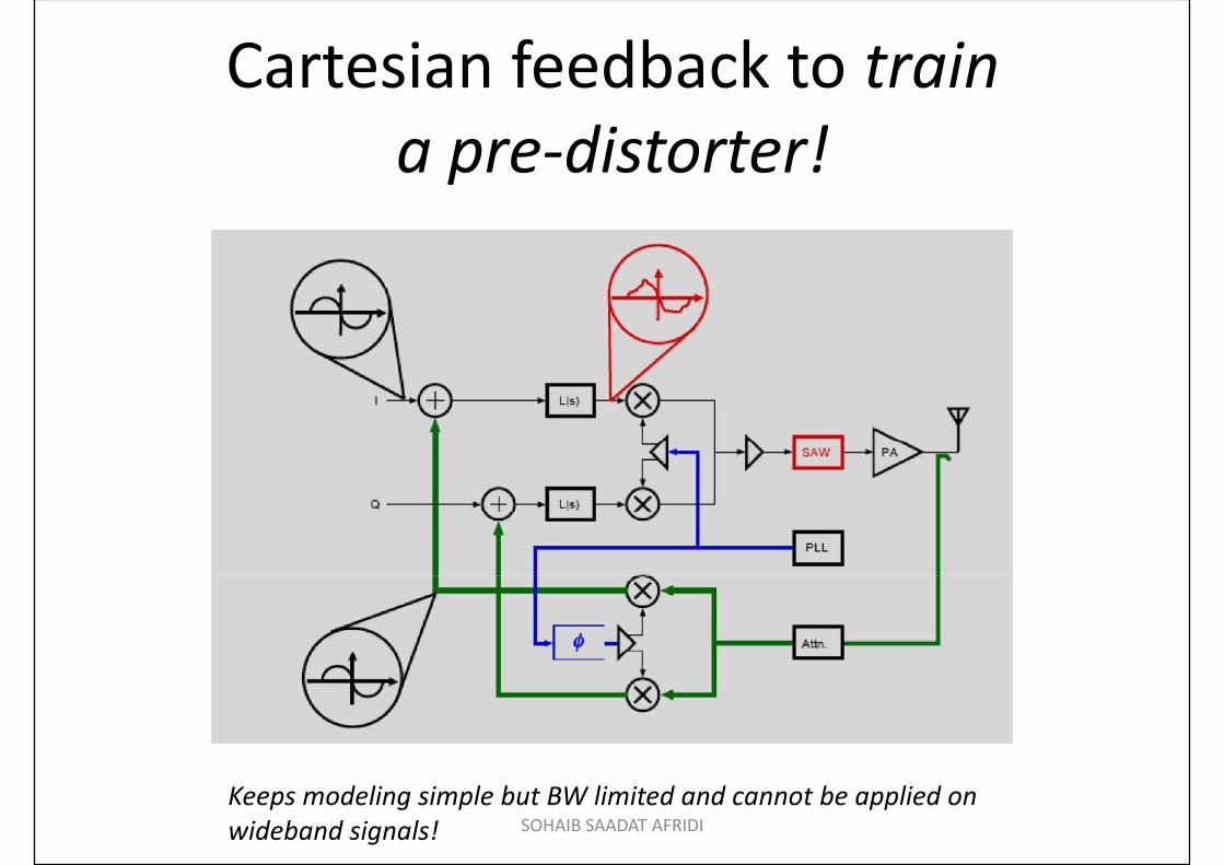
Cartesian feedback to traina pre-distorter!
Keeps modeling simple but BW limited and cannot be applied onwideband signals! SOHAIB SAADAT AFRIDI

Digitally assisted CartesianFeedback- Step 1
Slowly step through all symbols, and fill LUT.SOHAIB SAADAT AFRIDI
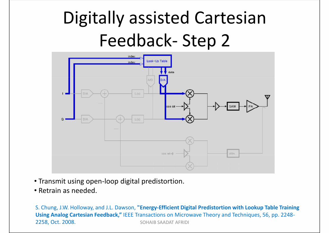
Digitally assisted CartesianFeedback- Step 2
• Transmit using open-loop digital predistortion.• Retrain as needed.
S. Chung, J.W. Holloway, and J.L. Dawson, "Energy-Efficient Digital Predistortion with Lookup Table TrainingUsing Analog Cartesian Feedback,” IEEE Transactions on Microwave Theory and Techniques, 56, pp. 2248-2258, Oct. 2008. SOHAIB SAADAT AFRIDI

Evolving the architecture
After defining the LUT through the initial calibration the Delta-Sigma modulatedpredistortion will take its place and predistort all the incoming symbols to thesystem.
SOHAIB SAADAT AFRIDI
A checklist of benefits
• Exploit CMOS scaling trends.– Digital ΣΔ modulators improve with digital device
speed.• Optimally partition functionality between
analog and digital domains.– Digital does the modeling, but does so by
exploiting feedback.• Use digital to clean up “sloppy” analog?– Yes. Use of low-precision D/As simplifies design.
SOHAIB SAADAT AFRIDI
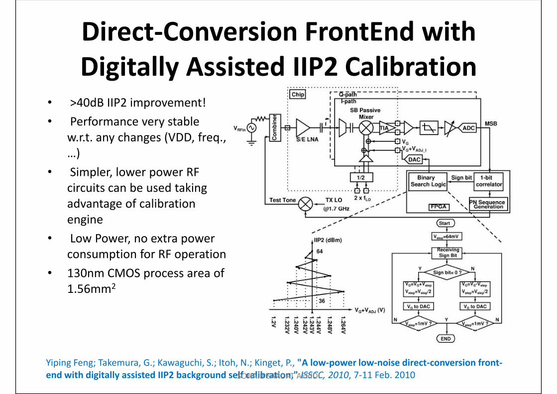
Direct-Conversion FrontEnd withDigitally Assisted IIP2 Calibration
• >40dB IIP2 improvement!• Performance very stable
w.r.t. any changes (VDD, freq.,…)
• Simpler, lower power RFcircuits can be used takingadvantage of calibrationengine
• Low Power, no extra powerconsumption for RF operation
• 130nm CMOS process area of1.56mm2
• >40dB IIP2 improvement!• Performance very stable
w.r.t. any changes (VDD, freq.,…)
• Simpler, lower power RFcircuits can be used takingadvantage of calibrationengine
• Low Power, no extra powerconsumption for RF operation
• 130nm CMOS process area of1.56mm2
• >40dB IIP2 improvement!• Performance very stable
w.r.t. any changes (VDD, freq.,…)
• Simpler, lower power RFcircuits can be used takingadvantage of calibrationengine
• Low Power, no extra powerconsumption for RF operation
• 130nm CMOS process area of1.56mm2
Yiping Feng; Takemura, G.; Kawaguchi, S.; Itoh, N.; Kinget, P., "A low-power low-noise direct-conversion front-end with digitally assisted IIP2 background self calibration," ISSCC, 2010, 7-11 Feb. 2010SOHAIB SAADAT AFRIDI

900MHz Receiver with InterferenceCancellation
Balankutty, A.; Kinget, P., VLSICircuits (VLSIC), 2010 IEEE Symposium on , vol., no., pp.183,184, 16-18 June 2010
• >20dB of attenuation for out of channel blockers• Digital calibration of LO phase (Φ) and alt. path gain is key enabler to automatically
tune the position of the cancellation notch• Consumes 26.4mW from a 0.6V, occupies 2.56mm2 low power 65nm CMOS process.
SOHAIB SAADAT AFRIDI

Noise Cancelling Amplier withFrequency Detector and Digital Control
•An LNA fabricated in 0.13um CMOS process.
•Improving the noise figure is fundamental.
•This is accomplished by finding thecombinations of bias voltages at varioustransistor gates that would produce theminimum noise figure at a given frequencywhile maintaining a specific gain that would bethe same at all frequencies.
•Improves Gain flatness by 1GHz and NoiseFigure keeps less than 4dB.
Stewart, D., "Digitally Assisted Radio-Frequency Integrated Circuits," M.A.Sc Thesis Queen's UniversityKingston, Ontario, Canada, July 2013 SOHAIB SAADAT AFRIDI

Gilbert Cell Mixer With an off-chipLinear Interpolator as digital assistance•A Gilbert mixer in 0.13um CMOS process.
•Off-chip microcontroller measuresthe input power through the RFpower detector and based on anearlier linearity sweep decides thebias voltages Gilbert Cell.
•IIP3 improved by 6dB.•IIP3 improved by 6dB.
Stewart, D., "Digitally Assisted Radio-Frequency Integrated Circuits," M.A.Sc Thesis Queen's UniversityKingston, Ontario, Canada, July 2013 SOHAIB SAADAT AFRIDI

Conclusions• CMOS Scaling is driving semiconductor technology and
will continue for another decade, but with significantdesign challenges.
• Design is becoming a prime differentiator.• There are many ways to take advantage of digital
circuits:– Calibration– Digital compensation for analog impairments– Clever use of CMOS switches– Using “digital” topologies for analog functions– Encoding information in timing of digital edges– …and more to come!
• CMOS Scaling is driving semiconductor technology andwill continue for another decade, but with significantdesign challenges.
• Design is becoming a prime differentiator.• There are many ways to take advantage of digital
circuits:– Calibration– Digital compensation for analog impairments– Clever use of CMOS switches– Using “digital” topologies for analog functions– Encoding information in timing of digital edges– …and more to come!
SOHAIB SAADAT AFRIDI

THANK YOU
SOHAIB SAADAT AFRIDI

ReferencesSupply Voltage reduction• P. Kinget, "Designing Analog and RF Circuits for Ultra-low Supply Voltages,",
plenary talk, IEEE European Solid-State Circuits Conference, pp. 58-67, September2007.
• S. Chatterjee, Y. Tsividis and P. Kinget, "0.5 V Analog Circuit Techniques and TheirApplication in OTA and Filter Design,“ invited, IEEE Journal of Solid-State Circuits,vol. 40, no 12, December 2005, pp. 2373 - 2387.
All Digital RF Circuits• Book: R. B. Staszewski and P. T. Balsara, “All-Digital Frequency Synthesizer in Deep-
Submicron CMOS”.
Digitally Assisted RF• Y. Feng, G. Takemura, S. Kawaguchi, N. Itoh and P. Kinget, "A Low-power Low-noise
Direct-Conversion Front End with Digitally Assisted IIP2 Background SelfCalibration," IEEE International Solid-State Circuits Conference, accepted, 2010.
• A. Balankutty and Peter Kinget, “0.6V, 5dB NF, -9.8dBm IIP3, 900MHz Receiverwith Interference Cancellation,” submitted to the IEEE Symposium on VLSI circuits,2010.
Supply Voltage reduction• P. Kinget, "Designing Analog and RF Circuits for Ultra-low Supply Voltages,",
plenary talk, IEEE European Solid-State Circuits Conference, pp. 58-67, September2007.
• S. Chatterjee, Y. Tsividis and P. Kinget, "0.5 V Analog Circuit Techniques and TheirApplication in OTA and Filter Design,“ invited, IEEE Journal of Solid-State Circuits,vol. 40, no 12, December 2005, pp. 2373 - 2387.
All Digital RF Circuits• Book: R. B. Staszewski and P. T. Balsara, “All-Digital Frequency Synthesizer in Deep-
Submicron CMOS”.
Digitally Assisted RF• Y. Feng, G. Takemura, S. Kawaguchi, N. Itoh and P. Kinget, "A Low-power Low-noise
Direct-Conversion Front End with Digitally Assisted IIP2 Background SelfCalibration," IEEE International Solid-State Circuits Conference, accepted, 2010.
• A. Balankutty and Peter Kinget, “0.6V, 5dB NF, -9.8dBm IIP3, 900MHz Receiverwith Interference Cancellation,” submitted to the IEEE Symposium on VLSI circuits,2010.
SOHAIB SAADAT AFRIDI
Related Documents