DIGITAL SYSTEMS: Course Objectives and Lecture Plan Aim: At the end of the course the student will be able to analyze, design, and evaluate digital circuits, of medium complexity, that are based on SSIs, MSIs, and programmable logic devices. Module 1: Number Systems and Codes (3) Number systems: Binary, octal, and hexa-decimal number systems, binary arithmetic. Codes: Binary code, excess-3 code, gray code, and error detection and correction codes. Module 2: Boolean Algebra and Logic Functions (5) Boolean algebra: Postulates and theorems. Logic functions, minimization of Boolean functions using algebraic, Karnaugh map and Quine – McClausky methods. Realization using logic gates Module 3: Logic Families (4) Logic families: Characteristics of logic families. TTL, CMOS, and ECL families. Module 4: Combinational Functions (8) Realizing logical expressions using different logic gates and comparing their performance. Hardware aspects logic gates and combinational ICs: delays and hazards. Design of combinational circuits using combinational ICs: Combinational functions: code conversion, decoding, comparison, multiplexing, demultiplexing, addition, and subtraction. Module 5: Analysis of Sequential Circuits (5) Structure of sequential circuits: Moore and Melay machines. Flip-flops, excitation tables, conversions, practical clocking aspects concerning flip-flops, timing and triggering considerations. Analysis of sequential circuits: State tables, state diagrams and timing diagrams. Module 6: Designing with Sequential MSIs (6) Realization of sequential functions using sequential MSIs: counting, shifting, sequence generation, and sequence detection. Module 7: PLDs (3) Programmable Logic Devices: Architecture and characteristics of PLDs, Module 8: Design of Digital Systems (6) State diagrams and their features. Design flow: functional partitioning, timing relationships, state assignment, output racing. Examples of design of digital systems using PLDs

Welcome message from author
This document is posted to help you gain knowledge. Please leave a comment to let me know what you think about it! Share it to your friends and learn new things together.
Transcript

DIGITAL SYSTEMS: Course Objectives and Lecture Plan
Aim: At the end of the course the student will be able to analyze, design, and evaluate digital circuits, of medium complexity, that are based on SSIs, MSIs, and programmable logic devices.
Module 1: Number Systems and Codes (3)
Number systems: Binary, octal, and hexa-decimal number systems, binary arithmetic. Codes: Binary code, excess-3 code, gray code, and error detection and correction codes.
Module 2: Boolean Algebra and Logic Functions (5)
Boolean algebra: Postulates and theorems. Logic functions, minimization of Boolean functions using algebraic, Karnaugh map and Quine – McClausky methods. Realization using logic gates
Module 3: Logic Families (4)
Logic families: Characteristics of logic families. TTL, CMOS, and ECL families.
Module 4: Combinational Functions (8)
Realizing logical expressions using different logic gates and comparing their performance. Hardware aspects logic gates and combinational ICs: delays and hazards. Design of combinational circuits using combinational ICs: Combinational functions: code conversion, decoding, comparison, multiplexing, demultiplexing, addition, and subtraction.
Module 5: Analysis of Sequential Circuits (5)
Structure of sequential circuits: Moore and Melay machines. Flip-flops, excitation tables, conversions, practical clocking aspects concerning flip-flops, timing and triggering considerations. Analysis of sequential circuits: State tables, state diagrams and timing diagrams.
Module 6: Designing with Sequential MSIs (6)
Realization of sequential functions using sequential MSIs: counting, shifting, sequence generation, and sequence detection.
Module 7: PLDs (3)
Programmable Logic Devices: Architecture and characteristics of PLDs,
Module 8: Design of Digital Systems (6)
State diagrams and their features. Design flow: functional partitioning, timing relationships, state assignment, output racing. Examples of design of digital systems using PLDs

Lecture Plan
Modules Learning Units Hours
per topic
Total Hours
1. Binary, octal and hexadecimal number systems, and conversion of number with one radix to another
1.5 1. Number Systems and Codes
2. Different binary codes 1.5
3
3. Boolean algebra and Boolean operators 1.5 4. Logic Functions 1 5. Minimization of logic functions using
Karnaugh -map 1.5
2. Logic Functions
6. Quine-McClausky method of minimization of logic functions
1
5
7. Introduction to Logic families 0.5 8. TTL family 1 9. CMOS family 1.5
3.Logic Families
10. Electrical characteristics of logic families 1
4
11. Introduction to combinational circuits, logic convention, and realization of simple combinational functions using gates
2
12. Implications of delay and hazard 1 13. Realization of adders and subtractors 2 14. Design of code converters, comparators,
and decoders 2
4. Combinational Circuits
15. Design of multiplexers, demultiplexers, 1
8
16. Introduction to sequential circuits: Moore and Mealy machines
1
17. Introduction to flip-flops like SR, JK, D & T with truth tables, logic diagrams, and timing relationships
1
18. Conversion of Flip-Flops, Excitation table 1
5. Analysis of Sequential Circuits
19. State tables, and realization of state stables 2
5
20. Design of shift registers and counters 2 21. Design of counters 2
6. Design with Sequential MSIs
22. Design of sequence generators and detectors
2
6
23. Introduction to Programmable Devices 1 7. PLDs 24. Architecture of PLDs 2
3
25. State diagrams and their features 2 26. Design flow 1
8. Design of Digital Systems
27. Design of digital systems using PLDs 3
6

Learning Objectives of the Course
1. Recall
1.1 List different criteria that could be used for optimization of a digital circuit.
1.2 List and describe different problems of digital circuits introduced by the hardware limitations.
2. Comprehension
2.1 Describe the significance of different criteria for design of digital circuits.
2.2 Describe the significance of different hardware related problems encountered in digital circuits.
2.3 Draw the timing diagrams for identified signals in a digital circuit.
3. Application
3.1 Determine the output and performance of given combinational and sequential circuits.
3.2 Determine the performance of a given digital circuit with regard to an identified optimization criterion.
4. Analysis
4.1 Compare the performances of combinational and sequential circuits implemented with SSIs/MSIs and PLDs.
4.2 Determine the function and performance of a given digital circuit.
4.3 Identify the faults in a given circuit and determine the consequences of the same on the circuit performance.
4.4 Draw conclusions on the behavior of a given digital circuit with regard to hazards, asynchronous inputs, and output races.
4.5 Determine the appropriateness of the choice of the ICs used in a given digital circuit.
4.6 Determine the transition sequence of a given state in a state diagram for a given input sequence.
5. Synthesis
5.1 Generate multiple digital solutions to a verbally described problem.
5.2 Modify a given digital circuit to change its performance as per specifications.
6. Evaluation
6.1 Evaluate the performance of a given digital circuit.
6.2 Assess the performance of a given digital circuit with Moore and Melay configurations.
6.3 Compare the performance of given digital circuits with respect to their speed, power consumption, number of ICs, and cost.
Digital Systems: Motivation
A digital circuit is one that is built with devices with two well-defined states. Such circuits
can process information represented in binary form. Systems based on digital circuits touch
all aspects our present day lives. The present day home products including electronic
games and appliances, communication and office automation products, computers with a
wide range of capabilities, and industrial instrumentation and control systems, electro-
medical equipment, and defence and aerospace systems are heavily dependent on digital
circuits. Many fields that emerged later to digital electronics have peaked and levelled off,
but the application of digital concepts appears to be still growing exponentially. This
unprecedented growth is powered by the semiconductor technology, which enables the
introduction of more and complex integrated circuits. The complexity of an integrated
circuit is measured in terms of the number of transistors that can be integrated into a
single unit. The number of transistors in a single integrated circuit has been doubling every
eighteen months (Moore’ Law) for several decades and reached the figure of almost one
billion transistors per chip. This allowed the circuit designers to provide more and more
complex functions in a single unit.
The introduction of programmable integrated circuits in the form of microprocessors in 70s
completely transformed every facet of electronics. While fixed function integrated circuits
and microprocessors coexisted for considerable time, the need to make the equipment
smaller and portable lead to replacement of fixed function devices with programmable
devices. With the all pervasive presence of the microprocessor and the increasing usage of
other programmable circuits like PLDs (Programmable Logic devices), FPGAs (Field
Programmable Gate Arrays) and ASICs (Application Specific Integrated Circuits), the very
nature of digital systems is continuously changing.
The central role of digital circuits in all our professional and personal lives makes it
imperative that every electrical and electronics engineer acquire good knowledge of
relevant basic concepts and ability to work with digital circuits.
At present many of the undergraduate programmes offer two to four courses in the area of
digital systems, with at least two of them being core courses. The course under
consideration constitutes the first course in the area of digital systems. The rate of
obsolescence of knowledge, design methods, and design tools is uncomfortably high. Even
the first level course in digital electronics is not exempt from this obsolescence.
Any course in electronics should enable the students to design circuits to meet some stated
requirements as encountered in real life situations. However, the design approaches should
be based on a sound understanding of the underlying principles. The basic feature of all
design problems is that all of them admit multiple solutions. The selection of the final
solution depends on a variety of criteria that could include the size and cost of the substrate
on which the components are assembled, the cost of components, manufacturability,

reliability, speed etc.
The course contents are designed to enable the students to design digital circuits of
medium level of complexity taking the functional and hardware aspects in an integrated
manner within the context of commercial and manufacturing constraints. However, no
compromises are made with regard to theoretical aspects of the subject.

Learning Objectives
Module 1: Number Systems and Codes (3)
Number systems: Binary, octal, and hexa-decimal number systems, binary
arithmetic. Codes: Binary code, excess-3 code, gray code, error detection and
correction codes.
Recall
1. Describe the format of numbers of different radices?
2. What is parity of a given number?
Comprehension
1. Explain how a number with one radix is converted into a number with another
radix.
2. Summarize the advantages of using different number systems.
3. Interpret the arithmetic operations of binary numbers.
4. Explain the usefulness of different coding schemes.
5. Explain how errors are detected and/or corrected using different codes.
Application
1. Convert a given number from one system to an equivalent number in another
system.
2. Illustrate the construction of a weighted code.
Analysis: Nil
Synthesis: Nil
Evaluation: Nil
Digital Electronics Module 1: Number Systems and Codes - Number Systems
N.J. RaoIndian Institute of Science
id379776 pdfMachine by Broadgun Software - a great PDF writer! - a great PDF creator! - http://www.pdfmachine.com http://www.broadgun.com
December 2006 N.J. Rao M1L1 2
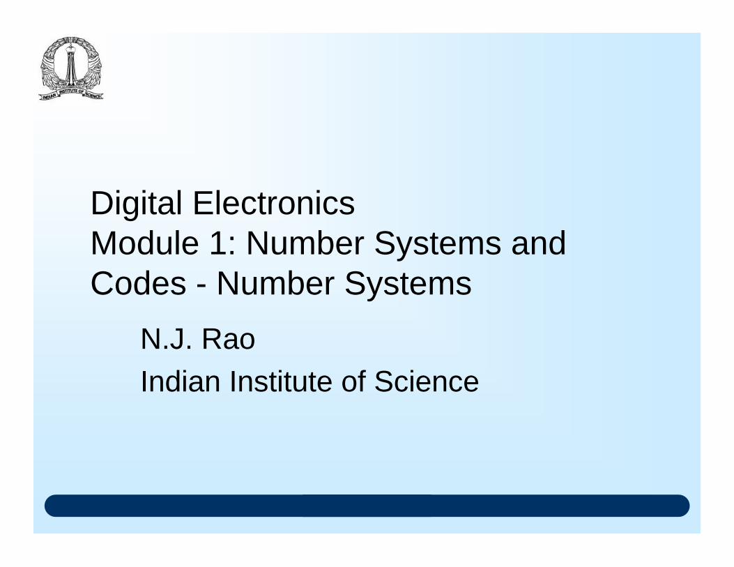
Numbers
We use numbers to communicate to perform tasks to quantify to measure
Numbers have become symbols of the present era Many consider what is not expressible in terms of
numbers is not worth knowing
December 2006 N.J. Rao M1L1 3
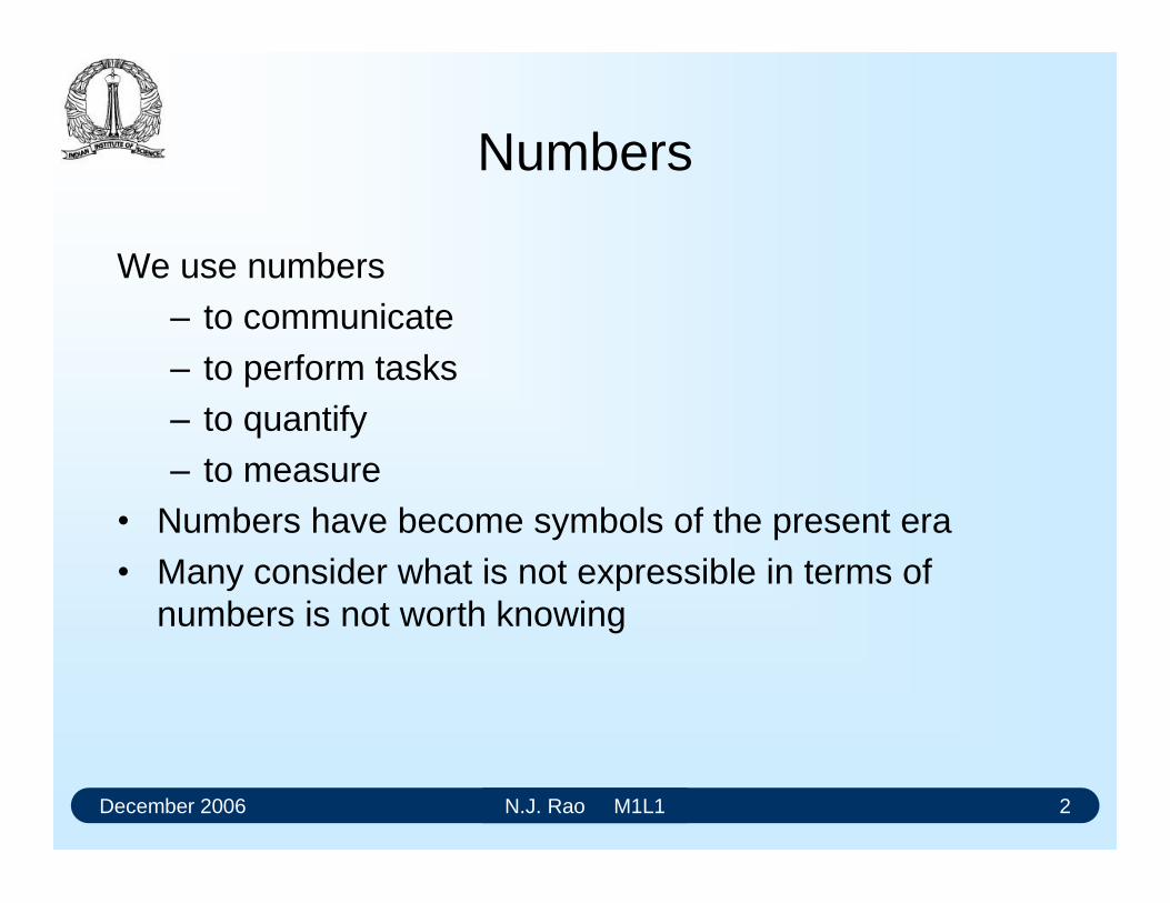
Number Systems in use
Symbolic number system uses Roman numerals (I = 1, V = 5, X = 10, L = 50,
C = 100, D = 500 and M = 1000) still used in some watchesWeighted position system Decimal system is the most commonly used Decimal numbers are based on Indian numerals Radix used is 10
December 2006 N.J. Rao M1L1 4
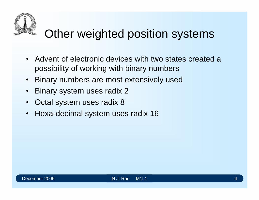
Other weighted position systems
Advent of electronic devices with two states created a possibility of working with binary numbers
Binary numbers are most extensively used Binary system uses radix 2 Octal system uses radix 8 Hexa-decimal system uses radix 16
December 2006 N.J. Rao M1L1 5
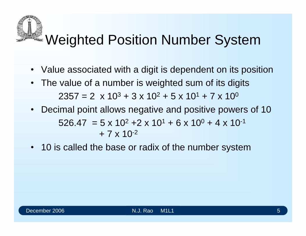
Weighted Position Number System
Value associated with a digit is dependent on its position The value of a number is weighted sum of its digits
2357 = 2 x 10³ + 3 x 10² + 5 x 101 + 7 x 100
Decimal point allows negative and positive powers of 10 526.47 = 5 x 10² +2 x 101 + 6 x 100 + 4 x 10⁻¹
+ 7 x 10⁻²
10 is called the base or radix of the number system
December 2006 N.J. Rao M1L1 6
General positional number system
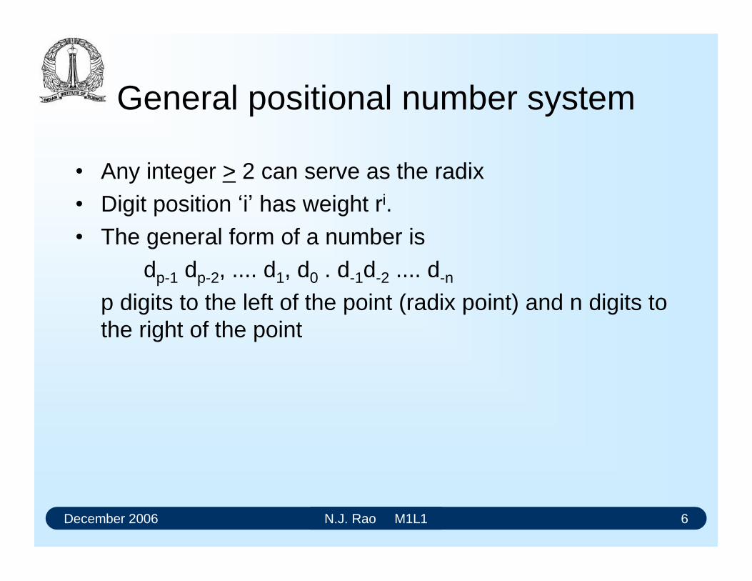
Any integer > 2 can serve as the radix Digit position i has weight ri. The general form of a number is
dp-1 dp-2, .... d1, d0 . d-1d-2 .... d-n
p digits to the left of the point (radix point) and n digits to the right of the point
December 2006 N.J. Rao M1L1 7
General positional number system (2)
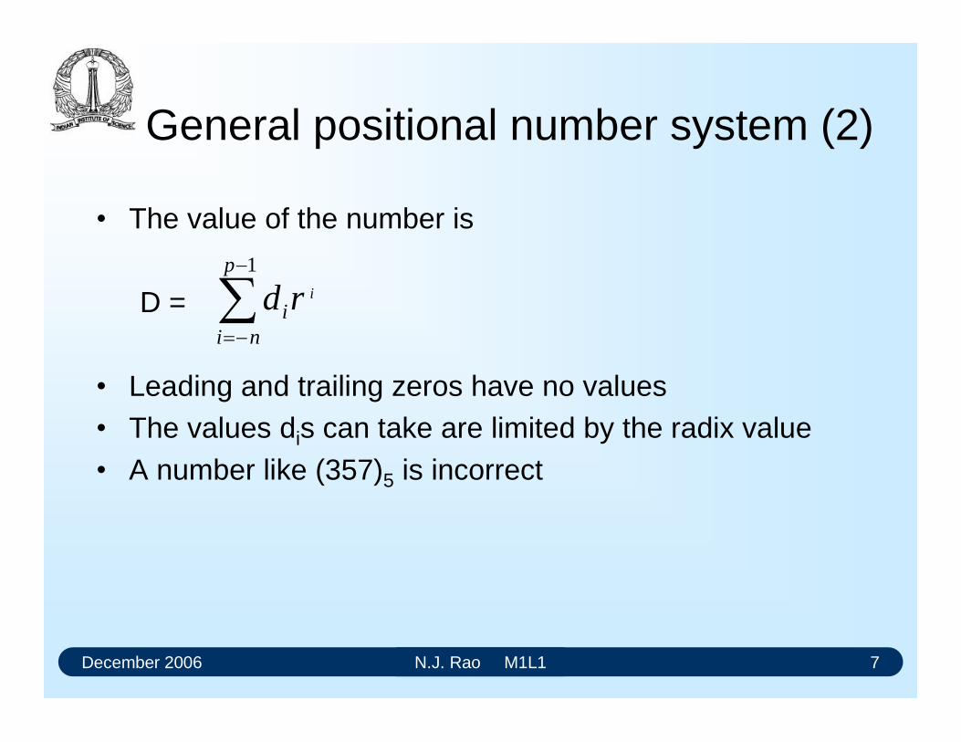
The value of the number is
D =
Leading and trailing zeros have no values The values dis can take are limited by the radix value A number like (357)5 is incorrect
1p
nii
ird
December 2006 N.J. Rao M1L1 8
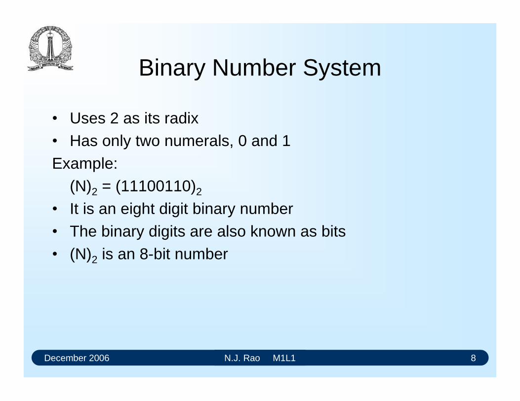
Binary Number System
Uses 2 as its radix Has only two numerals, 0 and 1 Example:
(N)2 = (11100110)2
It is an eight digit binary number The binary digits are also known as bits (N)2 is an 8-bit number
December 2006 N.J. Rao M1L1 9
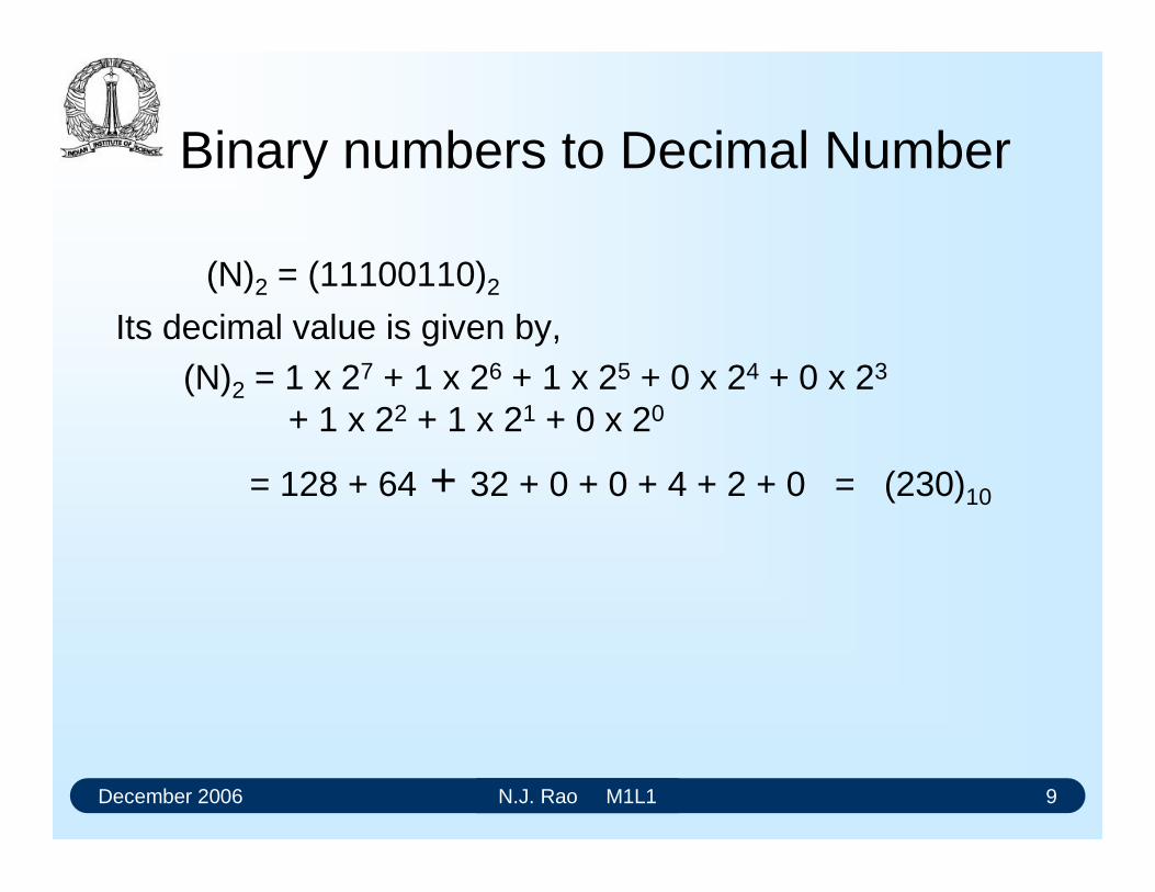
Binary numbers to Decimal Number
(N)2 = (11100110)2
Its decimal value is given by,(N)2 = 1 x 27 + 1 x 26 + 1 x 25 + 0 x 24 + 0 x 23
+ 1 x 22 + 1 x 21 + 0 x 20
= 128 + 64 + 32 + 0 + 0 + 4 + 2 + 0 = (230)10
December 2006 N.J. Rao M1L1 10
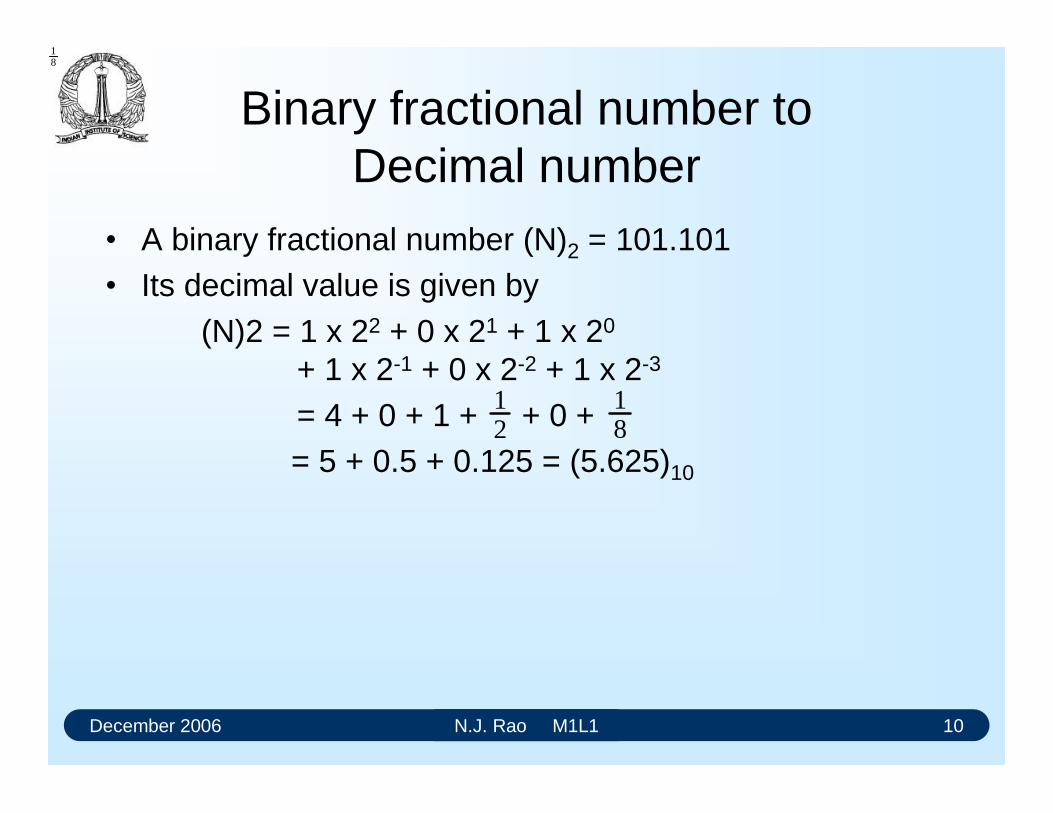
Binary fractional number to Decimal number
A binary fractional number (N)2 = 101.101 Its decimal value is given by
(N)2 = 1 x 22 + 0 x 21 + 1 x 20
+ 1 x 2-1 + 0 x 2-2 + 1 x 2-3
= 4 + 0 + 1 + + 0 + = 5 + 0.5 + 0.125 = (5.625)10
12
18
18
December 2006 N.J. Rao M1L1 11
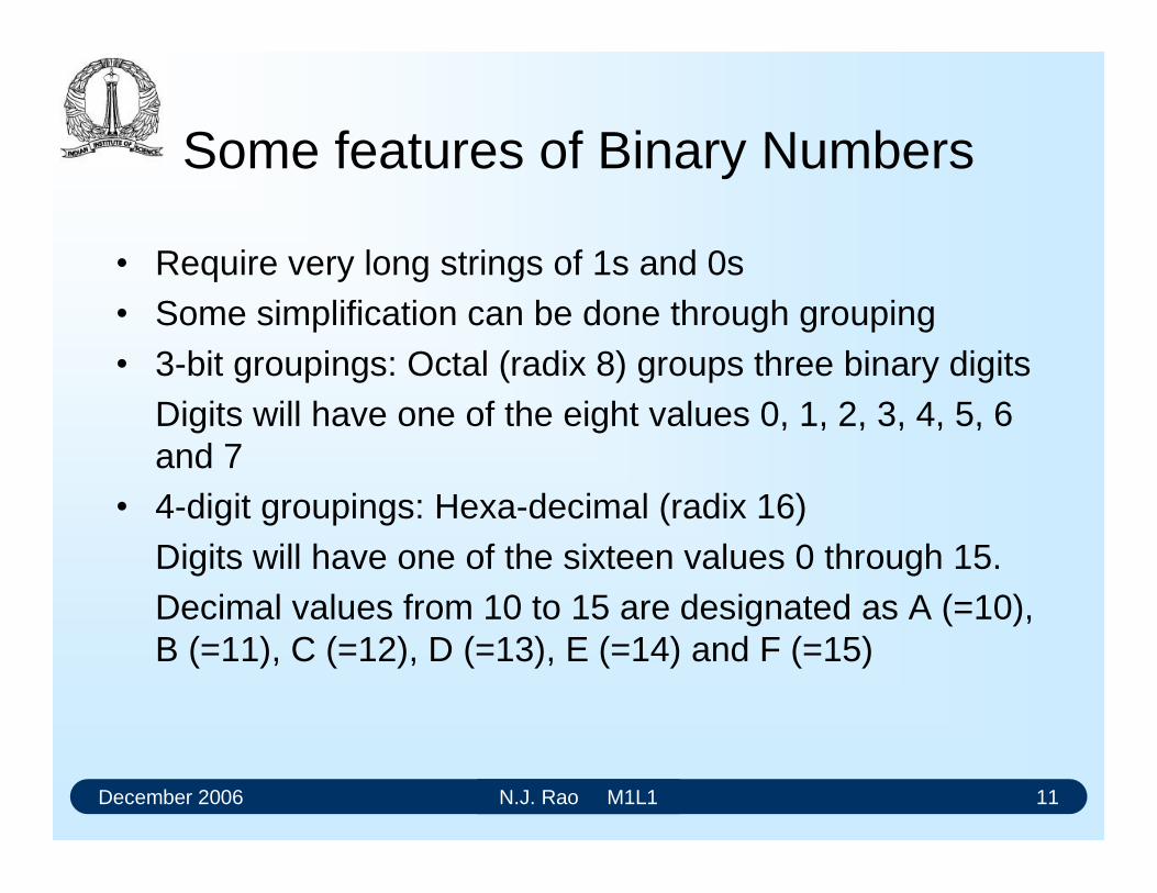
Some features of Binary Numbers
Require very long strings of 1s and 0s Some simplification can be done through grouping 3-bit groupings: Octal (radix 8) groups three binary digits
Digits will have one of the eight values 0, 1, 2, 3, 4, 5, 6 and 7
4-digit groupings: Hexa-decimal (radix 16)Digits will have one of the sixteen values 0 through 15. Decimal values from 10 to 15 are designated as A (=10), B (=11), C (=12), D (=13), E (=14) and F (=15)
December 2006 N.J. Rao M1L1 12
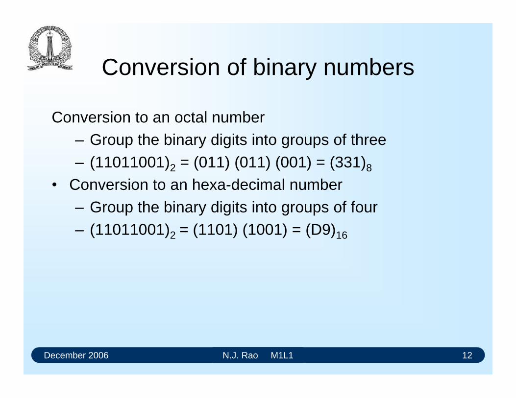
Conversion of binary numbers
Conversion to an octal number Group the binary digits into groups of three (11011001)2 = (011) (011) (001) = (331)8
Conversion to an hexa-decimal number Group the binary digits into groups of four (11011001)2 = (1101) (1001) = (D9)16
December 2006 N.J. Rao M1L1 13
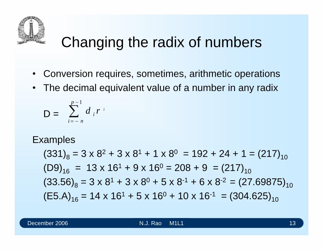
Changing the radix of numbers
Conversion requires, sometimes, arithmetic operations The decimal equivalent value of a number in any radix
D =
Examples(331)8 = 3 x 82 + 3 x 81 + 1 x 80 = 192 + 24 + 1 = (217)10
(D9)16 = 13 x 161 + 9 x 160 = 208 + 9 = (217)10
(33.56)8 = 3 x 81 + 3 x 80 + 5 x 8-1 + 6 x 8-2 = (27.69875)10
(E5.A)16 = 14 x 161 + 5 x 160 + 10 x 16-1 = (304.625)10
1p
nii
ird
December 2006 N.J. Rao M1L1 14
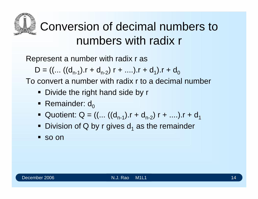
Conversion of decimal numbers to numbers with radix r
Represent a number with radix r asD = ((... ((dn-1).r + dn-2) r + ....).r + d1).r + d0
To convert a number with radix r to a decimal number Divide the right hand side by r Remainder: d0
Quotient: Q = ((... ((dn-1).r + dn-2) r + ....).r + d1
Division of Q by r gives d1 as the remainder so on
December 2006 N.J. Rao M1L1 15
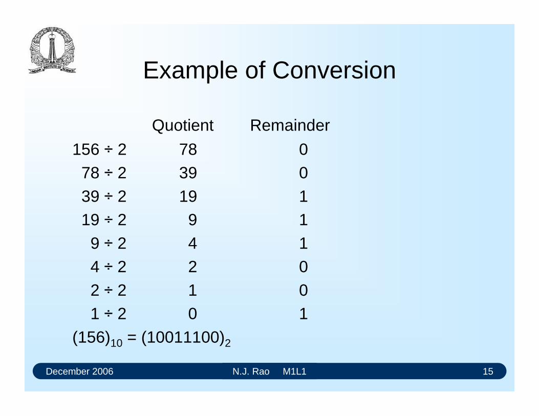
Example of Conversion
Quotient Remainder
156 ÷ 2 78 078 ÷ 2 39 039 ÷ 2 19 119 ÷ 2 9 19 ÷ 2 4 14 ÷ 2 2 02 ÷ 2 1 01 ÷ 2 0 1
(156)10 = (10011100)2
December 2006 N.J. Rao M1L1 16
Example of Conversion
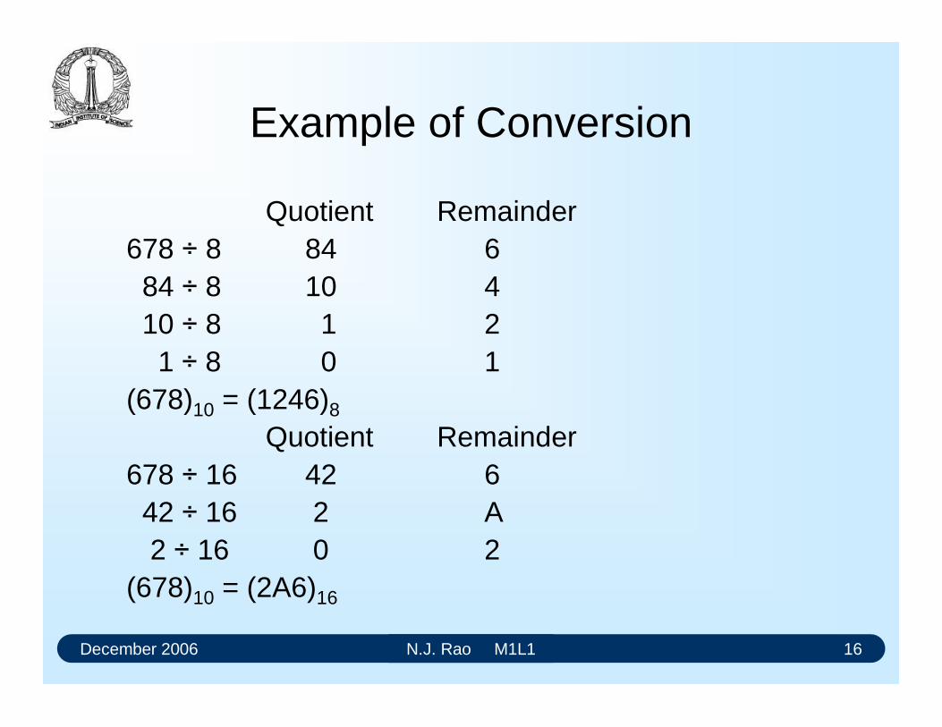
Quotient Remainder678 ÷ 8 84 684 ÷ 8 10 410 ÷ 8 1 21 ÷ 8 0 1
(678)10 = (1246)8
Quotient Remainder678 ÷ 16 42 642 ÷ 16 2 A2 ÷ 16 0 2
(678)10 = (2A6)16
December 2006 N.J. Rao M1L1 17
Negative Numbers
Sign-Magnitude representation + sign before a number indicates it as a positive
number - sign before a number indicates it as a negative
number Not very convenient on computers
Replace + sign by 0 and - by 1(+1100101)2 (01100101)2
(+101.001)2 (0101.001)2
(-10010)2 (110010)2
(-110.101)2 --. (1110.101)2
December 2006 N.J. Rao M1L1 18
Representing signed numbers
Diminished Radix Complement (DRC) or (r-1) - complement
Radix Complement (RXC) or r-complementBinary numbers DRC is known as ones-complement RXC is known as twos-complementDecimal numbers DRC is known as 9s-complement RXC is known as 10s-complement
December 2006 N.J. Rao M1L1 19
Ones Complement Representation
The most significant bit (MSD) represents the sign If MSD is a 0
The number is positive Remaining (n-1) bits directly indicate the magnitude
If the MSD is 1 The number is negative Complement of all the remaining (n-1) bits gives the
magnitude
December 2006 N.J. Rao M1L1 20
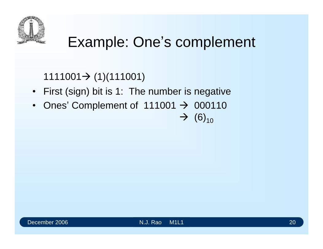
Example: Ones complement
1111001 (1)(111001)
First (sign) bit is 1: The number is negative Ones Complement of 111001 000110
(6)10
December 2006 N.J. Rao M1L1 21
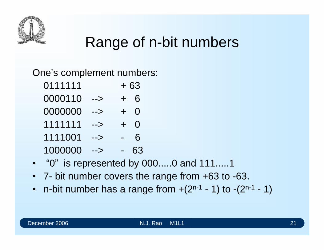
Range of n-bit numbers
Ones complement numbers:0111111 + 630000110 --> + 60000000 --> + 01111111 --> + 01111001 --> - 61000000 --> - 63
0 is represented by 000.....0 and 111.....1 7- bit number covers the range from +63 to -63. n-bit number has a range from +(2n-1 - 1) to -(2n-1 - 1)
December 2006 N.J. Rao M1L1 22
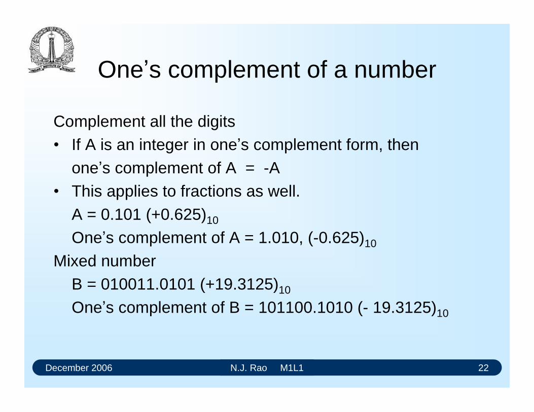
Ones complement of a number
Complement all the digits If A is an integer in ones complement form, then
ones complement of A = -A This applies to fractions as well.
A = 0.101 (+0.625)10
Ones complement of A = 1.010, (-0.625)10
Mixed numberB = 010011.0101 (+19.3125)10
Ones complement of B = 101100.1010 (- 19.3125)10
December 2006 N.J. Rao M1L1 23
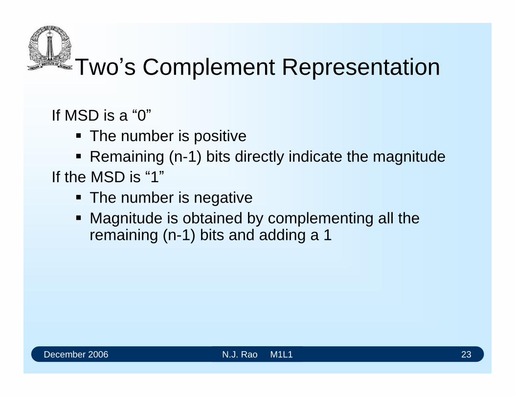
Twos Complement Representation
If MSD is a 0 The number is positive Remaining (n-1) bits directly indicate the magnitude
If the MSD is 1 The number is negative Magnitude is obtained by complementing all the
remaining (n-1) bits and adding a 1
December 2006 N.J. Rao M1L1 24
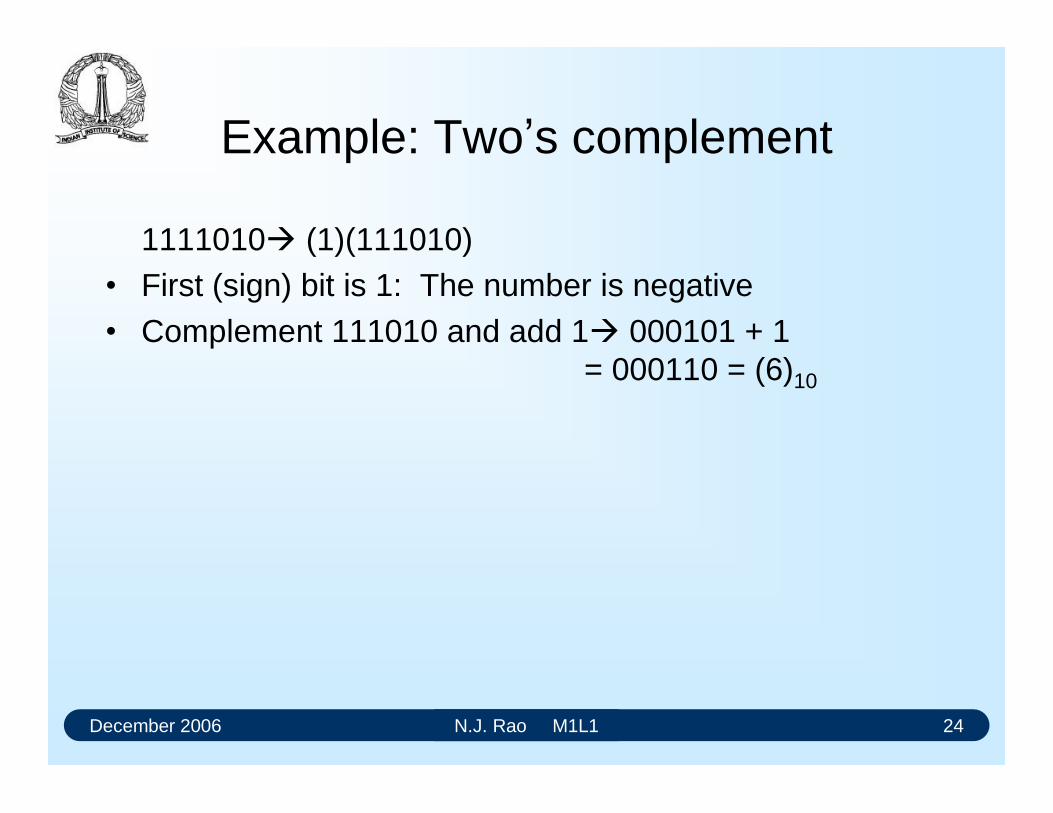
Example: Twos complement
1111010 (1)(111010) First (sign) bit is 1: The number is negative Complement 111010 and add 1 000101 + 1
= 000110 = (6)10
December 2006 N.J. Rao M1L1 25
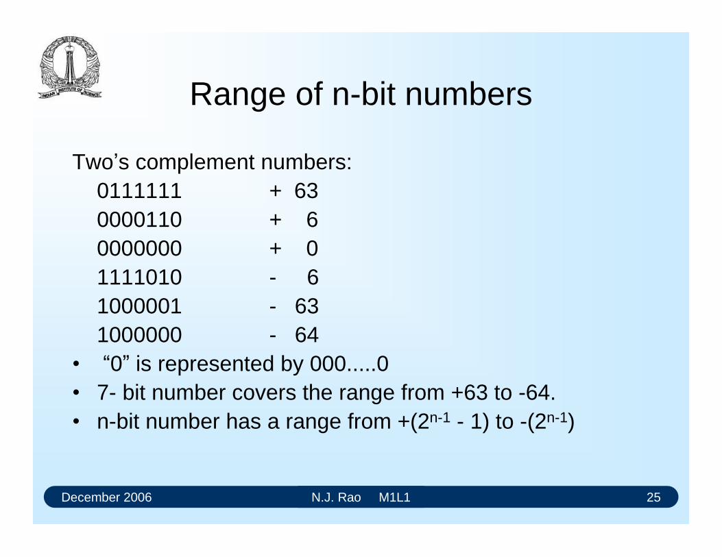
Range of n-bit numbers
Twos complement numbers:0111111 + 630000110 + 60000000 + 01111010 - 61000001 - 631000000 - 64
0 is represented by 000.....0 7- bit number covers the range from +63 to -64. n-bit number has a range from +(2n-1 - 1) to -(2n-1)
December 2006 N.J. Rao M1L1 26
Twos complement of a number
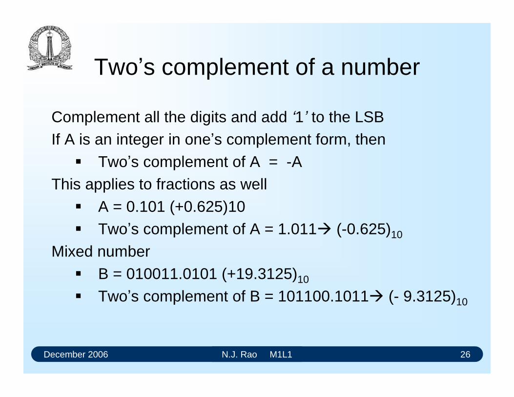
Complement all the digits and add 1 to the LSBIf A is an integer in ones complement form, then
Twos complement of A = -AThis applies to fractions as well
A = 0.101 (+0.625)10 Twos complement of A = 1.011 (-0.625)10
Mixed number B = 010011.0101 (+19.3125)10
Twos complement of B = 101100.1011 (- 9.3125)10
Number Systems
We all use numbers to communicate and perform several tasks in our daily lives.
Our present day world is characterized by measurements and numbers associated
with everything. In fact, many consider if we cannot express something in terms of
numbers is not worth knowing. While this is an extreme view that is difficult to
justify, there is no doubt that quantification and measurement, and consequently
usage of numbers, are desirable whenever possible. Manipulation of numbers is one
of the early skills that the present day child is trained to acquire. The present day
technology and the way of life require the usage of several number systems. Usage
of decimal numbers starts very early in one’s life. Therefore, when one is confronted
with number systems other than decimal, some time during the high-school years, it
calls for a fundamental change in one’s framework of thinking.
There have been two types of numbering systems in use through out the world.
One type is symbolic in nature. Most important example of this symbolic numbering
system is the one based on Roman numerals
I = 1, V = 5, X = 10, L = 50, C = 100, D = 500 and M = 1000
IIMVII - 2007
While this system was in use for several centuries in Europe it is completely
superseded by the weighted-position system based on Indian numerals. The Roman
number system is still used in some places like watches and release dates of movies.
The weighted-positional system based on the use of radix 10 is the most commonly
used numbering system in most of the transactions and activities of today’s world.
However, the advent of computers and the convenience of using devices that have
two well defined states brought the binary system, using the radix 2, into extensive
use. The use of binary number system in the field of computers and electronics also
lead to the use of octal (based on radix 8) and hex-decimal system (based on radix
16). The usage of binary numbers at various levels has become so essential that it
is also necessary to have a good understanding of all the binary arithmetic
operations.
Here we explore the weighted-position number systems and conversion from one
system to the other.
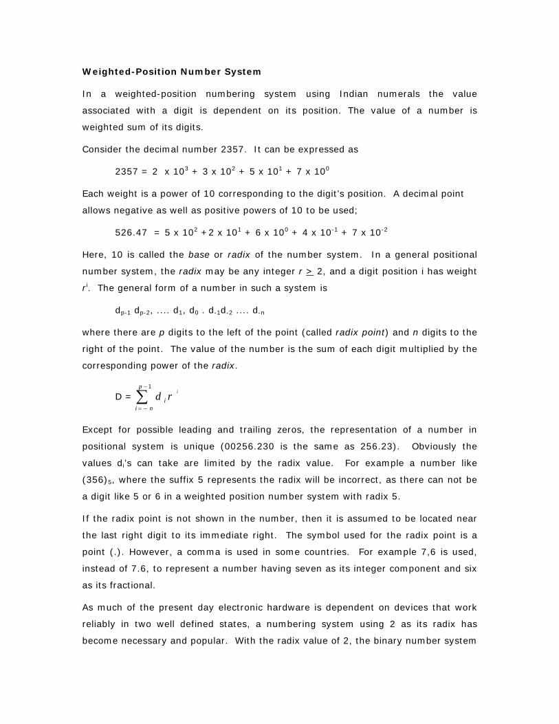
Weighted-Position Number System
In a weighted-position numbering system using Indian numerals the value
associated with a digit is dependent on its position. The value of a number is
weighted sum of its digits.
Consider the decimal number 2357. It can be expressed as
2357 = 2 x 10³ + 3 x 10² + 5 x 101 + 7 x 100
Each weight is a power of 10 corresponding to the digit’s position. A decimal point
allows negative as well as positive powers of 10 to be used;
526.47 = 5 x 10² +2 x 101 + 6 x 100 + 4 x 10⁻¹ + 7 x 10⁻²
Here, 10 is called the base or radix of the number system. In a general positional
number system, the radix may be any integer r > 2, and a digit position i has weight
ri. The general form of a number in such a system is
dp-1 dp-2, .... d1, d0 . d-1d-2 .... d-n
where there are p digits to the left of the point (called radix point) and n digits to the
right of the point. The value of the number is the sum of each digit multiplied by the
corresponding power of the radix.
D = ∑−
−=
1p
nii
ird
Except for possible leading and trailing zeros, the representation of a number in
positional system is unique (00256.230 is the same as 256.23). Obviously the
values di’s can take are limited by the radix value. For example a number like
(356)5, where the suffix 5 represents the radix will be incorrect, as there can not be
a digit like 5 or 6 in a weighted position number system with radix 5.
If the radix point is not shown in the number, then it is assumed to be located near
the last right digit to its immediate right. The symbol used for the radix point is a
point (.). However, a comma is used in some countries. For example 7,6 is used,
instead of 7.6, to represent a number having seven as its integer component and six
as its fractional.
As much of the present day electronic hardware is dependent on devices that work
reliably in two well defined states, a numbering system using 2 as its radix has
become necessary and popular. With the radix value of 2, the binary number system
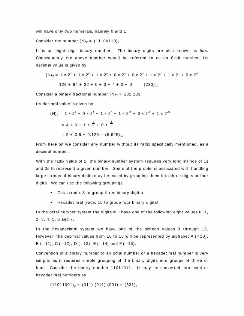
will have only two numerals, namely 0 and 1.
Consider the number (N)2 = (11100110)2.
It is an eight digit binary number. The binary digits are also known as bits.
Consequently the above number would be referred to as an 8-bit number. Its
decimal value is given by
(N)2 = 1 x 27 + 1 x 26 + 1 x 25 + 0 x 24 + 0 x 23 + 1 x 22 + 1 x 21 + 0 x 20
= 128 + 64 + 32 + 0 + 0 + 4 + 2 + 0 = (230)10
Consider a binary fractional number (N)2 = 101.101.
Its decimal value is given by
(N)2 = 1 x 22 + 0 x 21 + 1 x 20 + 1 x 2-1 + 0 x 2-2 + 1 x 2-3
= 4 + 0 + 1 + 12 + 0 +
18
= 5 + 0.5 + 0.125 = (5.625)10
From here on we consider any number without its radix specifically mentioned, as a
decimal number.
With the radix value of 2, the binary number system requires very long strings of 1s
and 0s to represent a given number. Some of the problems associated with handling
large strings of binary digits may be eased by grouping them into three digits or four
digits. We can use the following groupings.
Octal (radix 8 to group three binary digits)
Hexadecimal (radix 16 to group four binary digits)
In the octal number system the digits will have one of the following eight values 0, 1,
2, 3, 4, 5, 6 and 7.
In the hexadecimal system we have one of the sixteen values 0 through 15.
However, the decimal values from 10 to 15 will be represented by alphabet A (=10),
B (=11), C (=12), D (=13), E (=14) and F (=15).
Conversion of a binary number to an octal number or a hexadecimal number is very
simple, as it requires simple grouping of the binary digits into groups of three or
four. Consider the binary number 11011011. It may be converted into octal or
hexadecimal numbers as
(11011001)2 = (011) (011) (001) = (331)8

= (1101) (1001) = (D9)16
Note that adding a leading zero does not alter the value of the number. Similarly for
grouping the digits in the fractional part of a binary number, trailing zeros may be
added without changing the value of the number.
Number System Conversions
In general, conversion between numbers with different radices cannot be done by
simple substitutions. Such conversions would involve arithmetic operations. Let us
work out procedures for converting a number in any radix to radix 10, and vice-
versa. The decimal equivalent value of a number in any radix is given by the
formula
D = ∑−
−=
1p
nii
ird
where r is the radix of the number and there are p digits to the left of the radix point
and n digits to the right. Decimal value of the number is determined by converting
each digit of the number to its radix-10 equivalent and expanding the formula using
radix-10 arithmetic.
Some examples are:
(331)8 = 3 x 82 + 3 x 81 + 1 x 80 = 192 + 24 + 1 = (217)10
(D9)16 = 13 x 161 + 9 x 160 = 208 + 9 = (217)10
(33.56)8 = 3 x 81 + 3 x 80 + 5 x 8-1 + 6 x 8-2 = (27.69875)10
(E5.A)16 = 14 x 161 + 5 x 160 + 10 x 16-1 = (304.625)10
The conversion formula can be rewritten as
D = ((... ((dn-1).r + dn-2) r + ....).r + d1).r + d0
This forms the basis for converting a decimal number D to a number with radix r. If
we divide the right hand side of the above formula by r, the remainder will be d0,
and the quotient will be
Q = ((... ((dn-1).r + dn-2) r + ....).r + d1
Thus, d0 can be computed as the remainder of the long division of D by the radix r.
As the quotient Q has the same form as D, another long division by r will give d1 as
the remainder. This process can continue to produce all the digits of the number
with radix r. Consider the following examples.
Quotient Remainder
156 ÷ 2 78 0
78 ÷ 2 39 0
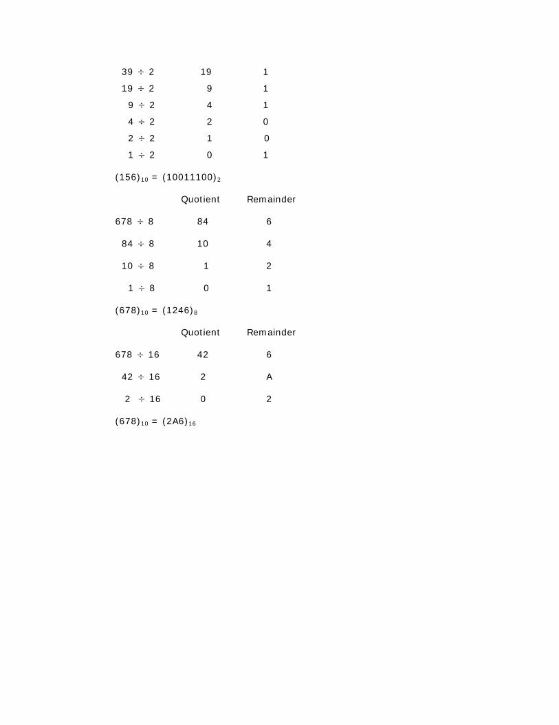
39 ÷ 2 19 1
19 ÷ 2 9 1
9 ÷ 2 4 1
4 ÷ 2 2 0
2 ÷ 2 1 0
1 ÷ 2 0 1
(156)10 = (10011100)2
Quotient Remainder
678 ÷ 8 84 6
84 ÷ 8 10 4
10 ÷ 8 1 2
1 ÷ 8 0 1
(678)10 = (1246)8
Quotient Remainder
678 ÷ 16 42 6
42 ÷ 16 2 A
2 ÷ 16 0 2
(678)10 = (2A6)16
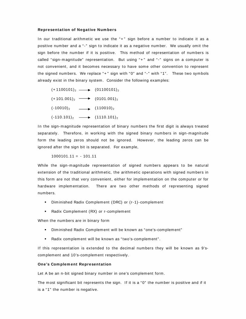
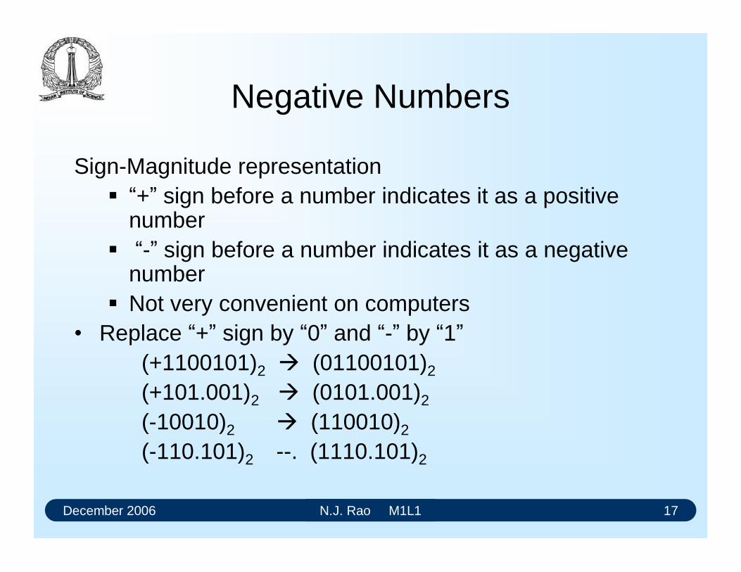
Representation of Negative Numbers
In our traditional arithmetic we use the “+” sign before a number to indicate it as a
positive number and a “-” sign to indicate it as a negative number. We usually omit the
sign before the number if it is positive. This method of representation of numbers is
called “sign-magnitude” representation. But using “+” and “-” signs on a computer is
not convenient, and it becomes necessary to have some other convention to represent
the signed numbers. We replace “+” sign with “0” and “-” with “1”. These two symbols
already exist in the binary system. Consider the following examples:
(+1100101)2 (01100101)2
(+101.001)2 (0101.001)2
(-10010)2 (110010)2
(-110.101)2 (1110.101)2
In the sign-magnitude representation of binary numbers the first digit is always treated
separately. Therefore, in working with the signed binary numbers in sign-magnitude
form the leading zeros should not be ignored. However, the leading zeros can be
ignored after the sign bit is separated. For example,
1000101.11 = - 101.11
While the sign-magnitude representation of signed numbers appears to be natural
extension of the traditional arithmetic, the arithmetic operations with signed numbers in
this form are not that very convenient, either for implementation on the computer or for
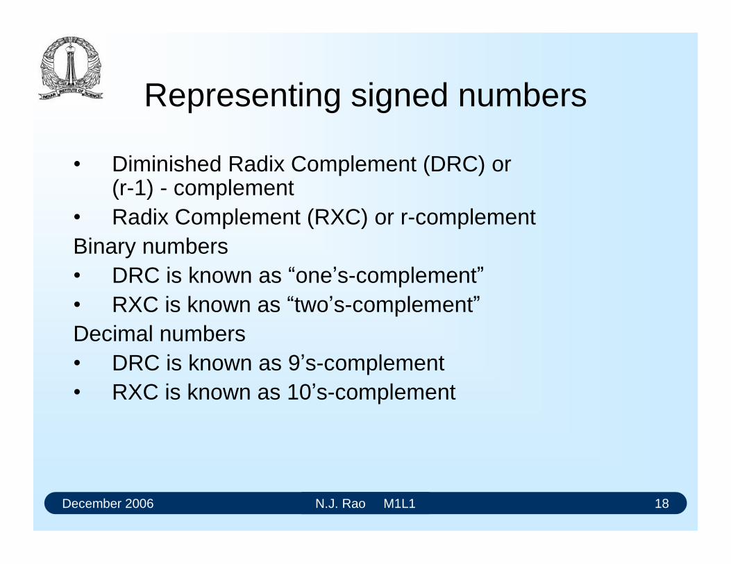
hardware implementation. There are two other methods of representing signed
numbers.
Diminished Radix Complement (DRC) or (r-1)-complement
Radix Complement (RX) or r-complement
When the numbers are in binary form
Diminished Radix Complement will be known as “one’s-complement”
Radix complement will be known as “two’s-complement”.
If this representation is extended to the decimal numbers they will be known as 9’s-
complement and 10’s-complement respectively.
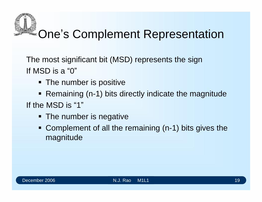
One’s Complement Representation
Let A be an n-bit signed binary number in one’s complement form.
The most significant bit represents the sign. If it is a “0” the number is positive and if it
is a “1” the number is negative.
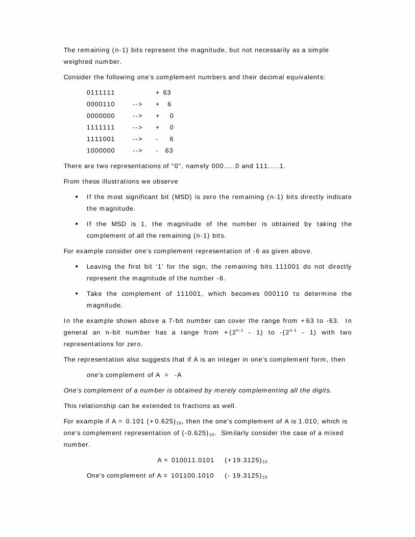
The remaining (n-1) bits represent the magnitude, but not necessarily as a simple
weighted number.
Consider the following one’s complement numbers and their decimal equivalents:
0111111 + 63
0000110 --> + 6
0000000 --> + 0
1111111 --> + 0
1111001 --> - 6
1000000 --> - 63
There are two representations of “0”, namely 000.....0 and 111.....1.
From these illustrations we observe
If the most significant bit (MSD) is zero the remaining (n-1) bits directly indicate
the magnitude.
If the MSD is 1, the magnitude of the number is obtained by taking the
complement of all the remaining (n-1) bits.
For example consider one’s complement representation of -6 as given above.
Leaving the first bit ‘1’ for the sign, the remaining bits 111001 do not directly
represent the magnitude of the number -6.
Take the complement of 111001, which becomes 000110 to determine the
magnitude.
In the example shown above a 7-bit number can cover the range from +63 to -63. In
general an n-bit number has a range from +(2n-1 - 1) to -(2n-1 - 1) with two
representations for zero.
The representation also suggests that if A is an integer in one’s complement form, then
one’s complement of A = -A
One’s complement of a number is obtained by merely complementing all the digits.
This relationship can be extended to fractions as well.
For example if A = 0.101 (+0.625)10, then the one’s complement of A is 1.010, which is
one’s complement representation of (-0.625)10. Similarly consider the case of a mixed
number.
A = 010011.0101 (+19.3125)10
One’s complement of A = 101100.1010 (- 19.3125)10
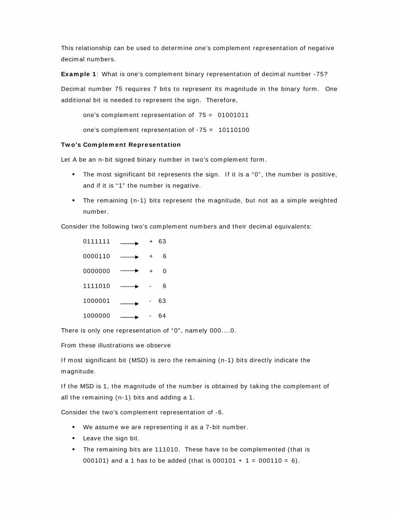
This relationship can be used to determine one’s complement representation of negative
decimal numbers.
Example 1: What is one’s complement binary representation of decimal number -75?
Decimal number 75 requires 7 bits to represent its magnitude in the binary form. One
additional bit is needed to represent the sign. Therefore,
one’s complement representation of 75 = 01001011
one’s complement representation of -75 = 10110100
Two’s Complement Representation
Let A be an n-bit signed binary number in two’s complement form.
The most significant bit represents the sign. If it is a “0”, the number is positive,
and if it is “1” the number is negative.
The remaining (n-1) bits represent the magnitude, but not as a simple weighted
number.
Consider the following two’s complement numbers and their decimal equivalents:
0111111 + 63
0000110 + 6
0000000 + 0
1111010 - 6
1000001 - 63
1000000 - 64
There is only one representation of “0”, namely 000....0.
From these illustrations we observe
If most significant bit (MSD) is zero the remaining (n-1) bits directly indicate the
magnitude.
If the MSD is 1, the magnitude of the number is obtained by taking the complement of
all the remaining (n-1) bits and adding a 1.
Consider the two’s complement representation of -6.
We assume we are representing it as a 7-bit number.
Leave the sign bit.
The remaining bits are 111010. These have to be complemented (that is
000101) and a 1 has to be added (that is 000101 + 1 = 000110 = 6).
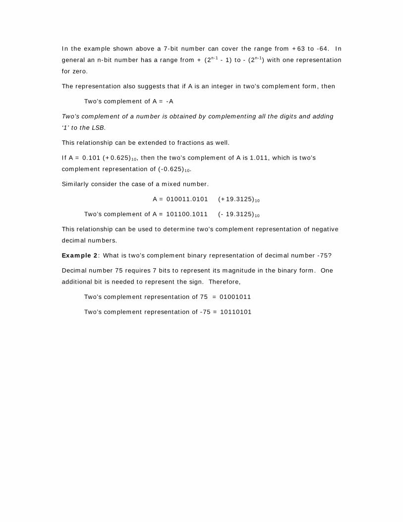
In the example shown above a 7-bit number can cover the range from +63 to -64. In
general an n-bit number has a range from + (2n-1 - 1) to - (2n-1) with one representation
for zero.
The representation also suggests that if A is an integer in two’s complement form, then
Two’s complement of A = -A
Two’s complement of a number is obtained by complementing all the digits and adding
‘1’ to the LSB.
This relationship can be extended to fractions as well.
If A = 0.101 (+0.625)10, then the two’s complement of A is 1.011, which is two’s
complement representation of (-0.625)10.
Similarly consider the case of a mixed number.
A = 010011.0101 (+19.3125)10
Two’s complement of A = 101100.1011 (- 19.3125)10
This relationship can be used to determine two’s complement representation of negative
decimal numbers.
Example 2: What is two’s complement binary representation of decimal number -75?
Decimal number 75 requires 7 bits to represent its magnitude in the binary form. One
additional bit is needed to represent the sign. Therefore,
Two’s complement representation of 75 = 01001011
Two’s complement representation of -75 = 10110101

M1L1: Number Systems
Multiple Choice Questions
1. Which number system is understood easily by the computer?
(a) Binary (b) Decimal (c) Octal (d) Hexadecimal
2. How many symbols are used in the decimal number system?
(a) 2 (b) 8 (c) 10 (d) 16
3. How are number systems generally classified?
a. Conditional or non conditional
b. Positional or non positional
c. Real or imaginary
d. Literal or numerical
4. What does (10)16 represent in decimal number system?
(a) 10 (b) 0A (c) 16 (d) 15
5. How many bits have to be grouped together to convert the binary number to its
corresponding octal number?
(a) 2 (b) 3 (c) 4 (d) 5
6. Which bit represents the sign bit in a signed number system?
a. Left most bit
b. Right most bit
c. Left centre
d. Right centre
7. The ones complement of 1010 is
(a) 1100 (b) 0101 (c) 0111 (d) 1011
8. How many bits are required to cover the numbers from +63 to -63 in one’s
complement representation?
(a) 6 (b) 7 (c) 8 (d) 9
M1L1: Number Systems
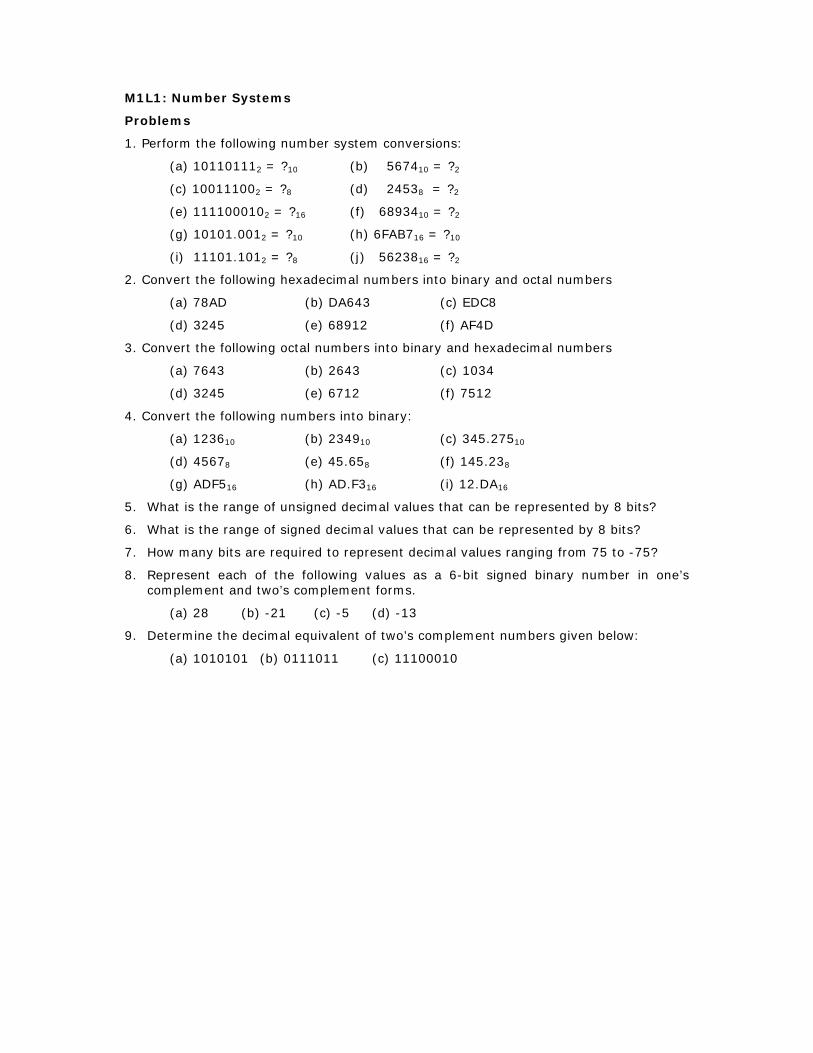
Problems
1. Perform the following number system conversions:
(a) 101101112 = ?10 (b) 567410 = ?2
(c) 100111002 = ?8 (d) 24538 = ?2
(e) 1111000102 = ?16 (f) 6893410 = ?2
(g) 10101.0012 = ?10 (h) 6FAB716 = ?10
(i) 11101.1012 = ?8 (j) 5623816 = ?2
2. Convert the following hexadecimal numbers into binary and octal numbers
(a) 78AD (b) DA643 (c) EDC8
(d) 3245 (e) 68912 (f) AF4D
3. Convert the following octal numbers into binary and hexadecimal numbers
(a) 7643 (b) 2643 (c) 1034
(d) 3245 (e) 6712 (f) 7512
4. Convert the following numbers into binary:
(a) 123610 (b) 234910 (c) 345.27510
(d) 45678 (e) 45.658 (f) 145.238
(g) ADF516 (h) AD.F316 (i) 12.DA16
5. What is the range of unsigned decimal values that can be represented by 8 bits?
6. What is the range of signed decimal values that can be represented by 8 bits?
7. How many bits are required to represent decimal values ranging from 75 to -75?
8. Represent each of the following values as a 6-bit signed binary number in one’s complement and two’s complement forms.
(a) 28 (b) -21 (c) -5 (d) -13
9. Determine the decimal equivalent of two’s complement numbers given below:
(a) 1010101 (b) 0111011 (c) 11100010
Digital Electronics Module 1:Number Systems and Codes - Codes
N.J. RaoIndian Institute of Science
id2733069 pdfMachine by Broadgun Software - a great PDF writer! - a great PDF creator! - http://www.pdfmachine.com http://www.broadgun.com
December 2006 N.J. Rao M1L2 2
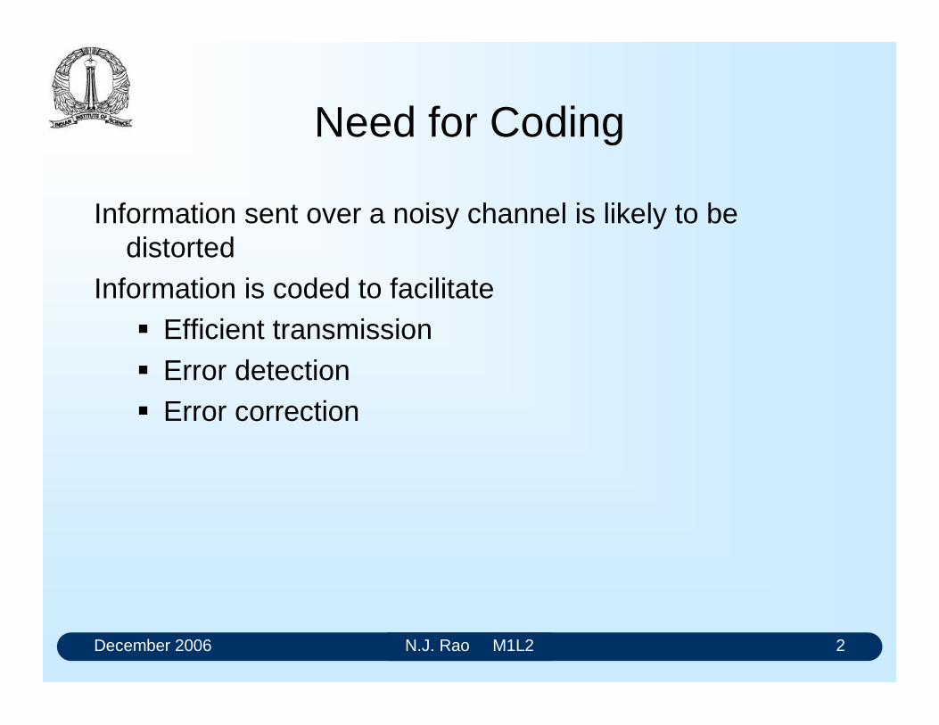
Need for Coding
Information sent over a noisy channel is likely to be distorted
Information is coded to facilitate Efficient transmission Error detection Error correction
December 2006 N.J. Rao M1L2 3
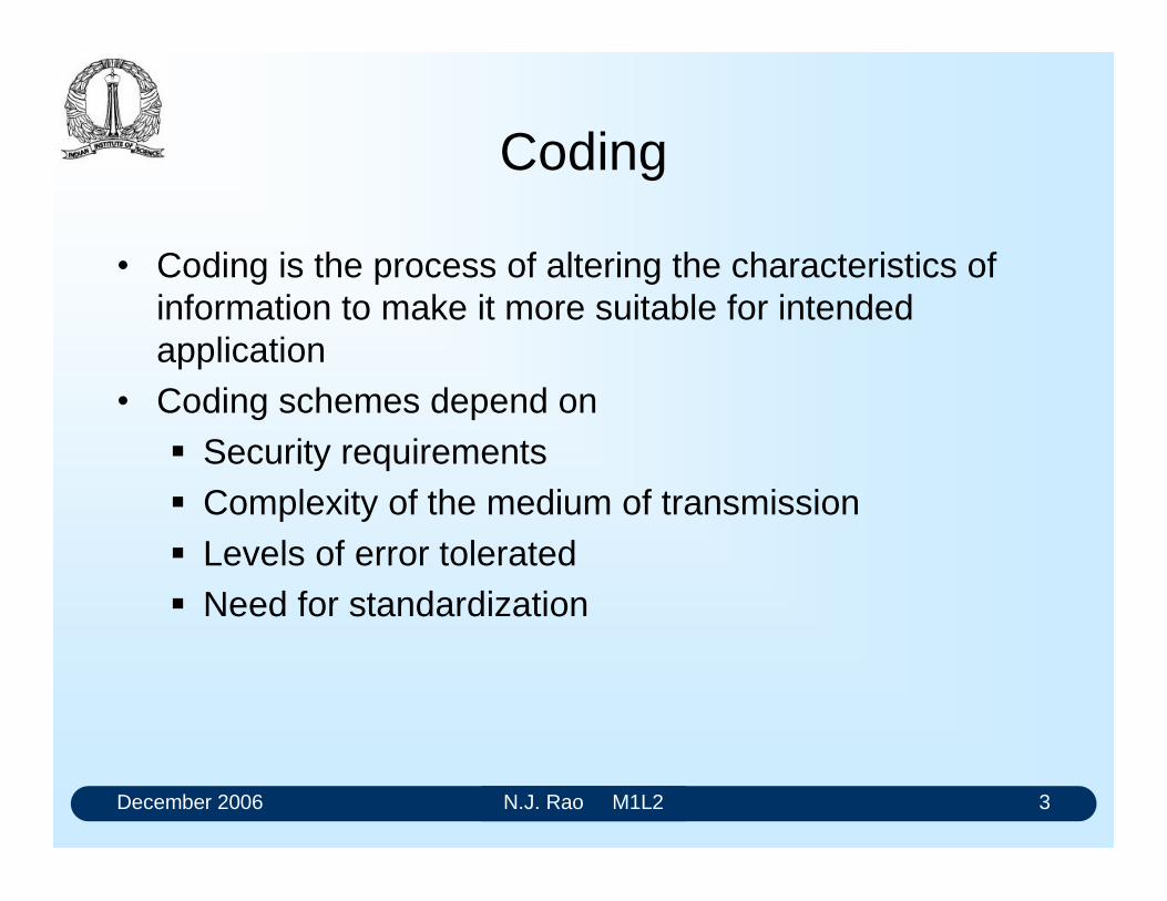
Coding
Coding is the process of altering the characteristics of information to make it more suitable for intended application
Coding schemes depend on Security requirements Complexity of the medium of transmission Levels of error tolerated Need for standardization
December 2006 N.J. Rao M1L2 4
Decoding
Decoding is the process of reconstructing source information from the received encoded information
Decoding can be more complex than coding if there is no prior knowledge of coding schemes
December 2006 N.J. Rao M1L2 5
Bit combinations
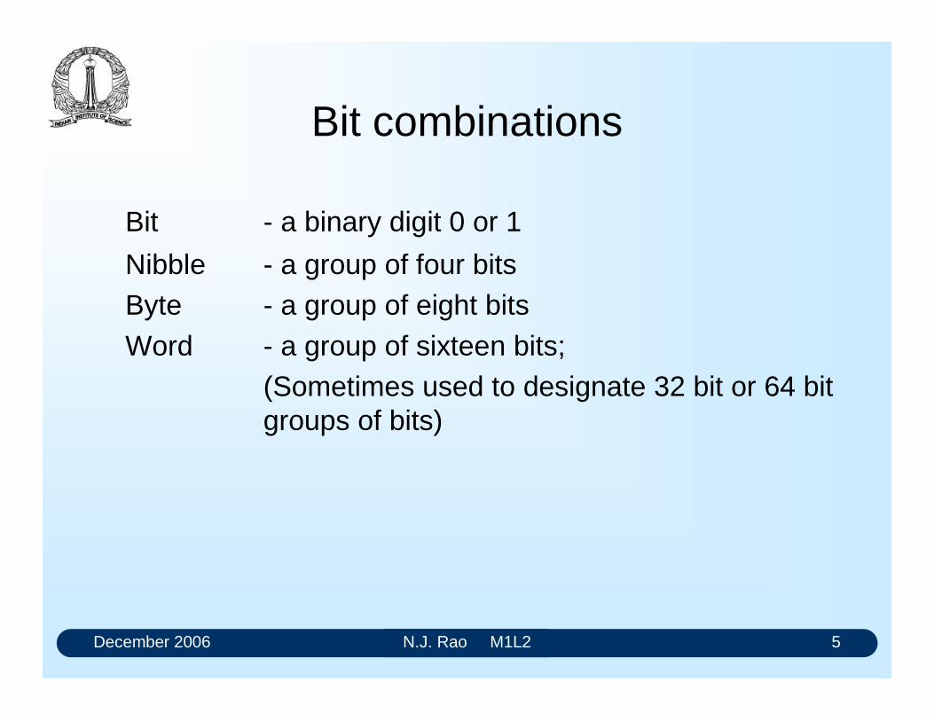
Bit - a binary digit 0 or 1
Nibble - a group of four bitsByte - a group of eight bitsWord - a group of sixteen bits;
(Sometimes used to designate 32 bit or 64 bit groups of bits)
December 2006 N.J. Rao M1L2 6
Binary coding
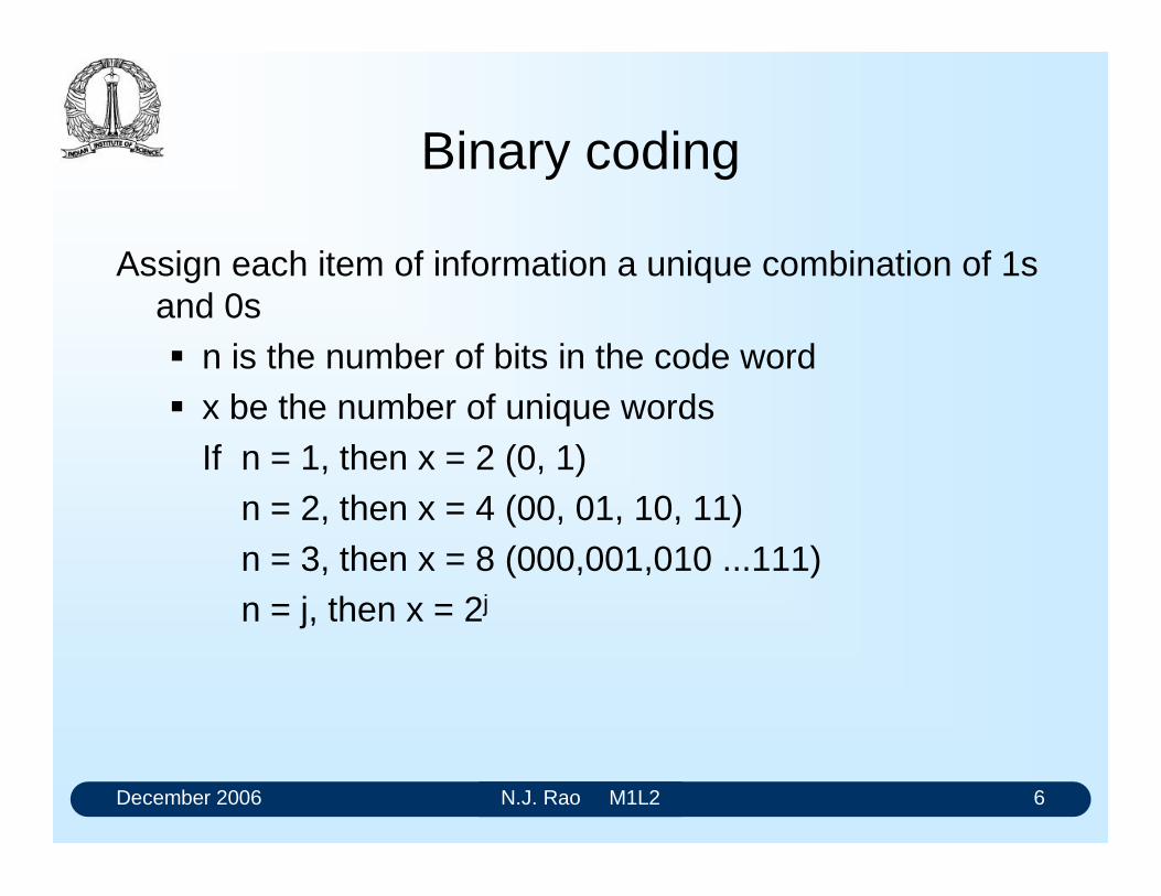
Assign each item of information a unique combination of 1s and 0s n is the number of bits in the code word x be the number of unique words
If n = 1, then x = 2 (0, 1)n = 2, then x = 4 (00, 01, 10, 11)n = 3, then x = 8 (000,001,010 ...111)n = j, then x = 2j
December 2006 N.J. Rao M1L2 7
Number of bits in a code word
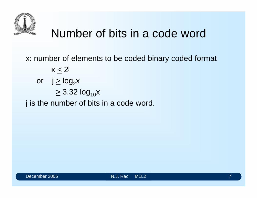
x: number of elements to be coded binary coded formatx < 2j
or j > log2x> 3.32 log10x
j is the number of bits in a code word.
December 2006 N.J. Rao M1L2 8
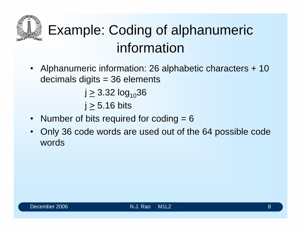
Example: Coding of alphanumeric information
Alphanumeric information: 26 alphabetic characters + 10 decimals digits = 36 elements
j > 3.32 log1036j > 5.16 bits
Number of bits required for coding = 6 Only 36 code words are used out of the 64 possible code
words
December 2006 N.J. Rao M1L2 9
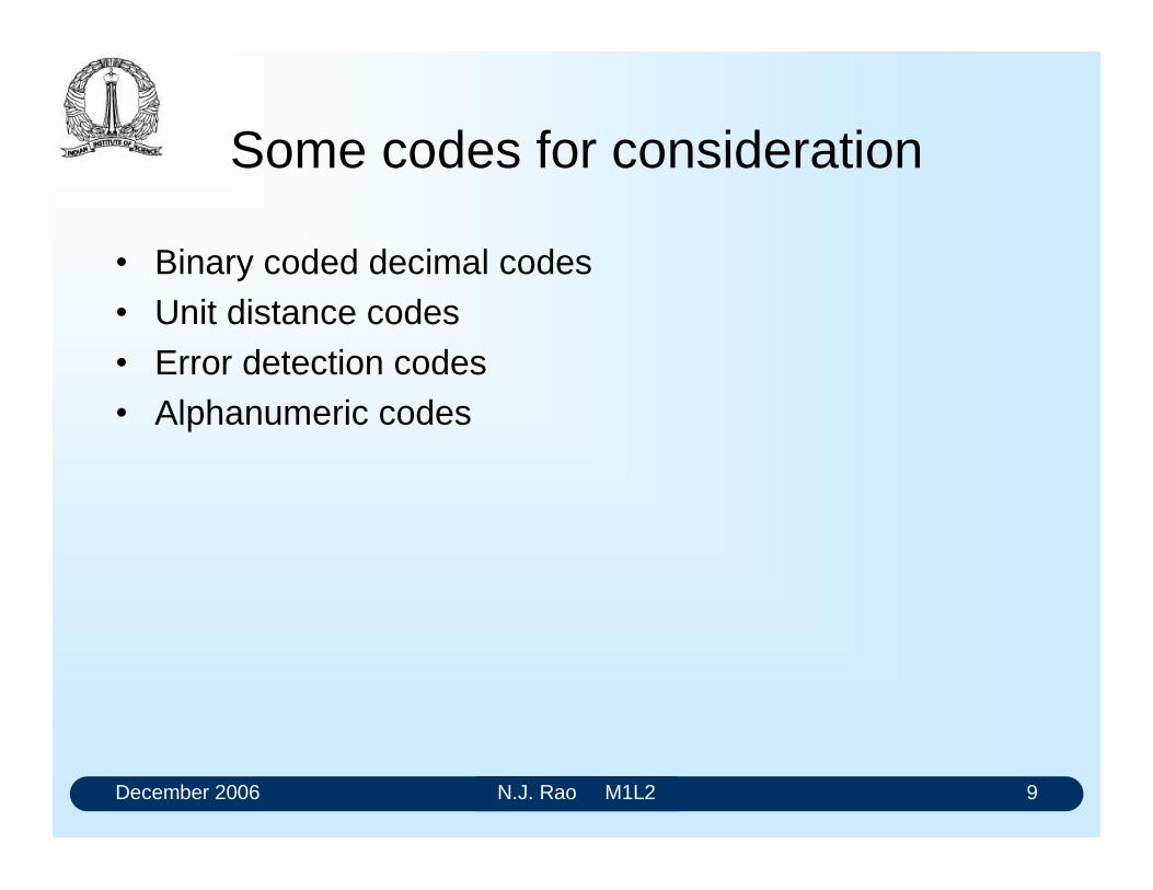
Some codes for consideration
Binary coded decimal codes Unit distance codes Error detection codes Alphanumeric codes
December 2006 N.J. Rao M1L2 10
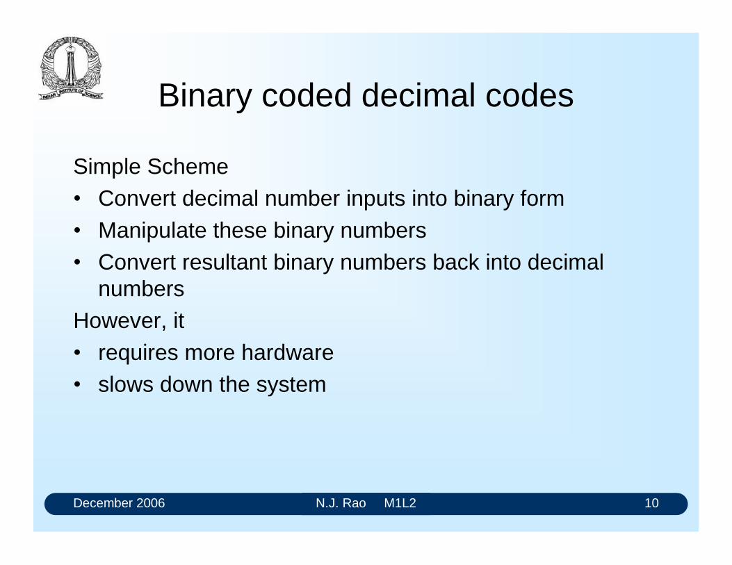
Binary coded decimal codes
Simple Scheme Convert decimal number inputs into binary form Manipulate these binary numbers Convert resultant binary numbers back into decimal
numbersHowever, it requires more hardware slows down the system
December 2006 N.J. Rao M1L2 11
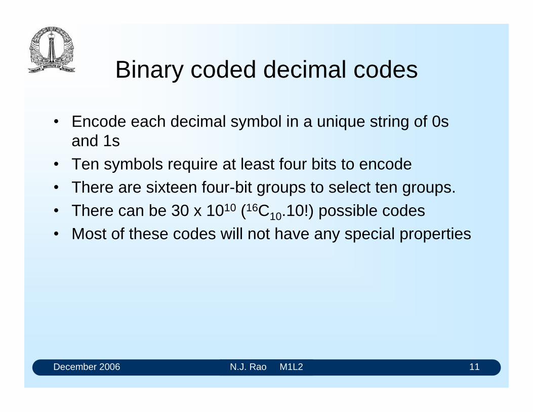
Binary coded decimal codes
Encode each decimal symbol in a unique string of 0s and 1s
Ten symbols require at least four bits to encode There are sixteen four-bit groups to select ten groups. There can be 30 x 1010 (16C10.10!) possible codes Most of these codes will not have any special properties
December 2006 N.J. Rao M1L2 12
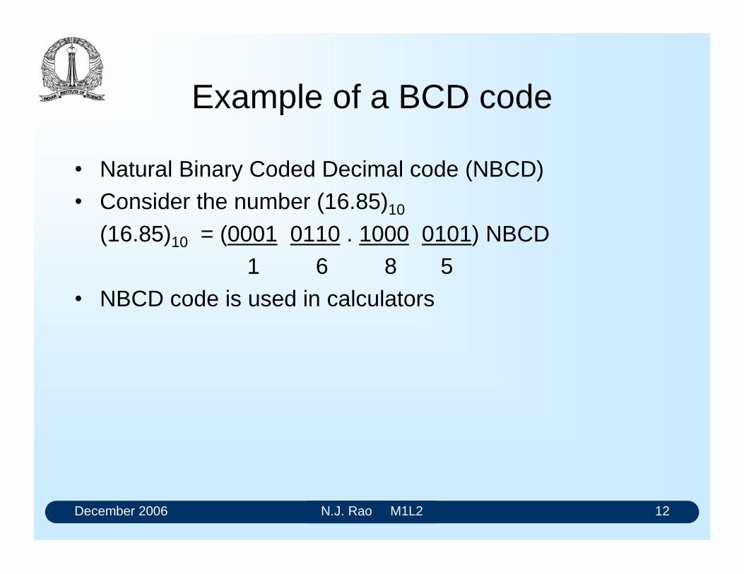
Example of a BCD code
Natural Binary Coded Decimal code (NBCD) Consider the number (16.85)10
(16.85)10 = (0001 0110 . 1000 0101) NBCD1 6 8 5
NBCD code is used in calculators
December 2006 N.J. Rao M1L2 13
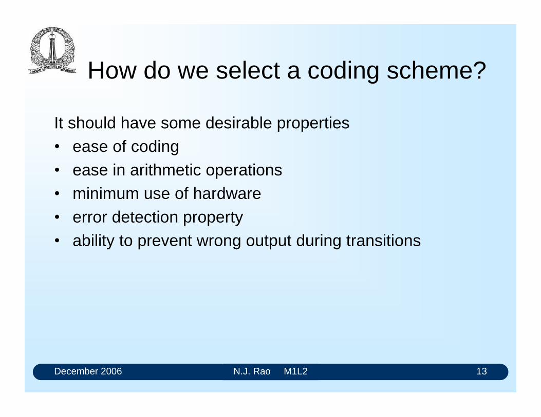
How do we select a coding scheme?
It should have some desirable properties ease of coding ease in arithmetic operations minimum use of hardware error detection property ability to prevent wrong output during transitions
December 2006 N.J. Rao M1L2 14
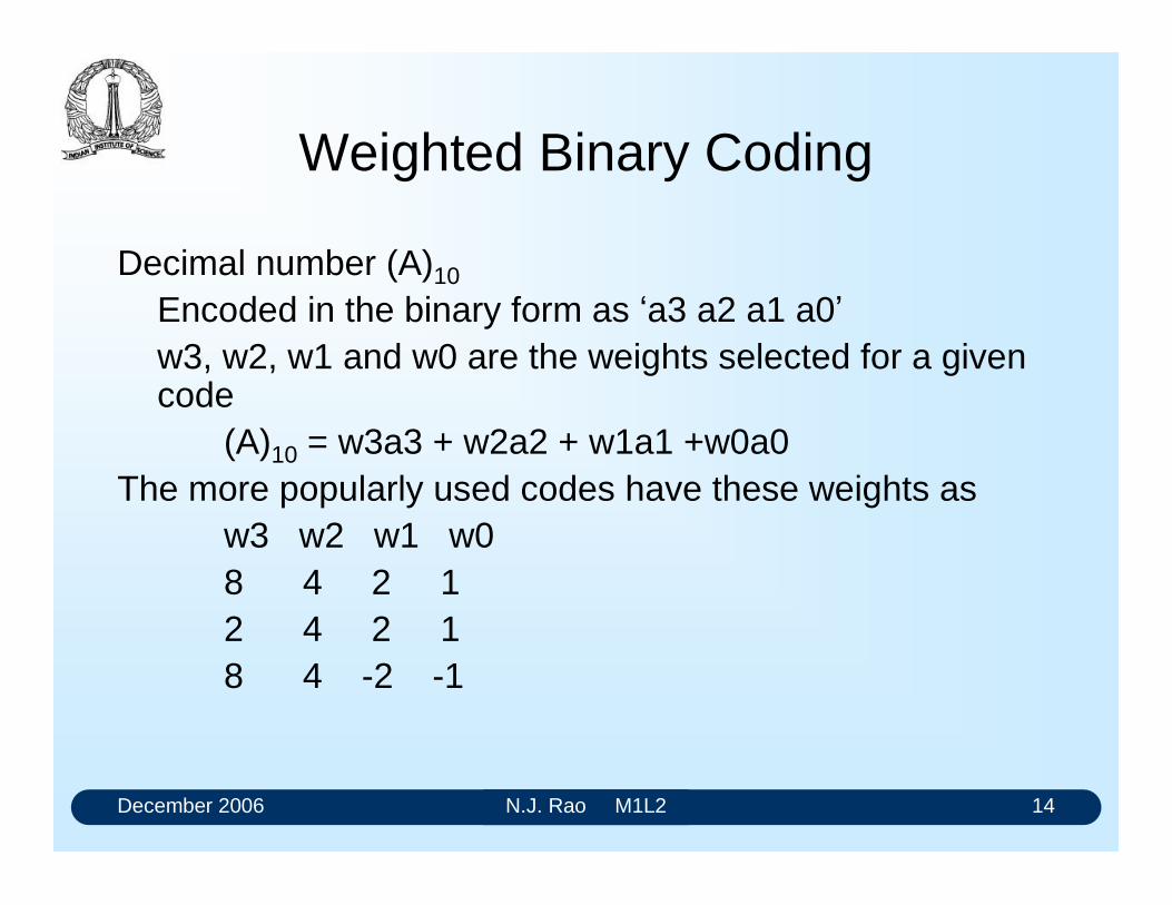
Weighted Binary Coding
Decimal number (A)10
Encoded in the binary form as a3 a2 a1 a0w3, w2, w1 and w0 are the weights selected for a given code
(A)10 = w3a3 + w2a2 + w1a1 +w0a0The more popularly used codes have these weights as
w3 w2 w1 w08 4 2 12 4 2 18 4 -2 -1
December 2006 N.J. Rao M1L2 15
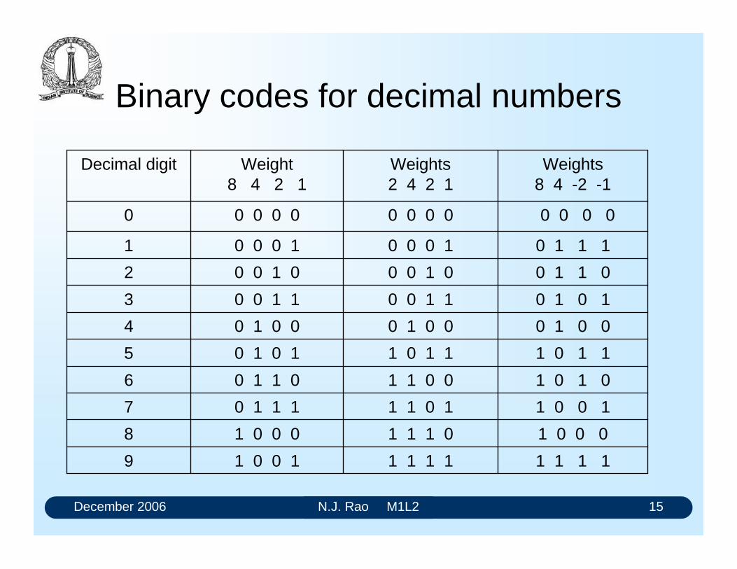
Binary codes for decimal numbers
1 1 1 11 1 1 11 0 0 19
1 0 0 01 1 1 01 0 0 08
1 0 0 11 1 0 10 1 1 17
1 0 1 01 1 0 00 1 1 06
1 0 1 11 0 1 10 1 0 15
0 1 0 00 1 0 0 0 1 0 04
0 1 0 10 0 1 10 0 1 13
0 1 1 00 0 1 00 0 1 02
0 1 1 10 0 0 10 0 0 11
0 0 0 0 0 0 0 00 0 0 00
Weights8 4 -2 -1
Weights2 4 2 1
Weight8 4 2 1
Decimal digit
December 2006 N.J. Rao M1L2 16
Binary coded decimal numbers
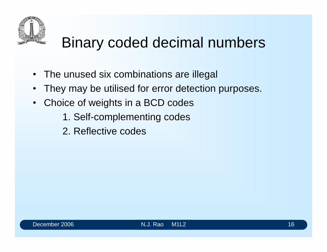
The unused six combinations are illegal They may be utilised for error detection purposes. Choice of weights in a BCD codes
1. Self-complementing codes2. Reflective codes
December 2006 N.J. Rao M1L2 17
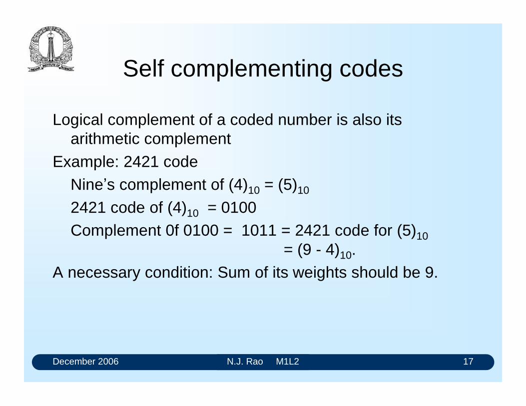
Self complementing codes
Logical complement of a coded number is also its arithmetic complement
Example: 2421 code Nines complement of (4)10 = (5)10
2421 code of (4)10 = 0100 Complement 0f 0100 = 1011 = 2421 code for (5)10
= (9 - 4)10. A necessary condition: Sum of its weights should be 9.
December 2006 N.J. Rao M1L2 18
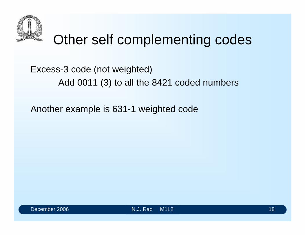
Other self complementing codes
Excess-3 code (not weighted)Add 0011 (3) to all the 8421 coded numbers
Another example is 631-1 weighted code
December 2006 N.J. Rao M1L2 19
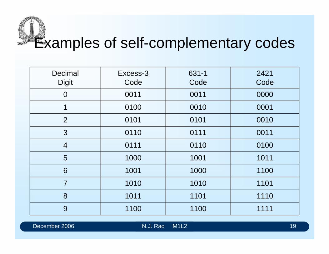
Examples of self-complementary codes
1111110011009
1110110110118
1101101010107
1100100010016
1011100110005
0100011001114
0011011101103
0010010101012
0001001001001
0000001100110
2421Code
631-1Code
Excess-3Code
DecimalDigit
December 2006 N.J. Rao M1L2 20
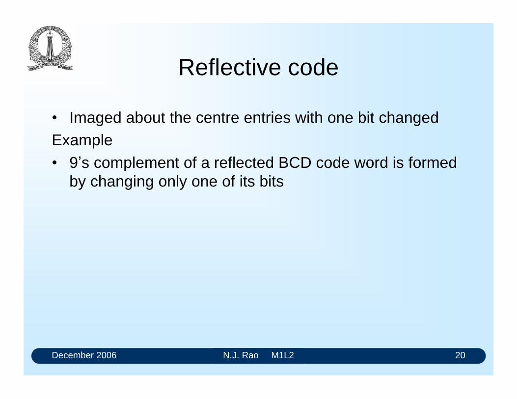
Reflective code
Imaged about the centre entries with one bit changedExample 9s complement of a reflected BCD code word is formed
by changing only one of its bits
December 2006 N.J. Rao M1L2 21
Examples of reflective BCD codes
010110009
101110018
100110107
111110116
000111005
000001004
111000113
100000102
101000011
010000000
Code-BCode-ADecimalDigit
December 2006 N.J. Rao M1L2 22
Unit Distance Codes
Adjacent codes differ only in one bit
Gray code is the most popular example Some of the Gray codes have also the reflective
properties
December 2006 N.J. Rao M1L2 23
3-bit and 4-bit Gray codes
1101-9
1100-8
01001007
01011016
01111115
01101104
00100103
00110112
00010011
00000000
4-bit Gray Code
3-bit Gray Code
Decimal Digit
1000-15
1001-14
1011-13
1010-12
1110-11
1111-10
4-bit Gray Code
3-bit Gray Code
Decimal Digit
December 2006 N.J. Rao M1L2 24
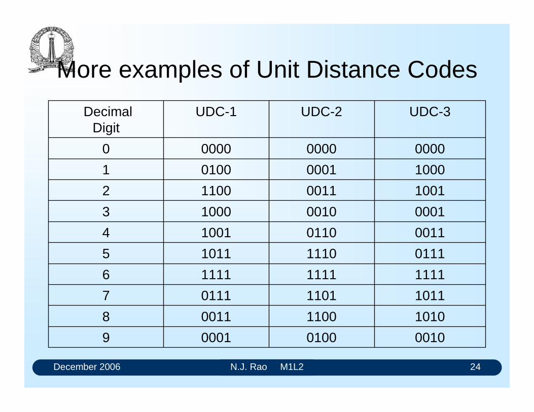
More examples of Unit Distance Codes
0010010000019
1010110000118
1011110101117
1111111111116
0111111010115
0011011010014
0001001010003
1001001111002
1000000101001
0000000000000
UDC-3UDC-2UDC-1DecimalDigit
December 2006 N.J. Rao M1L2 25
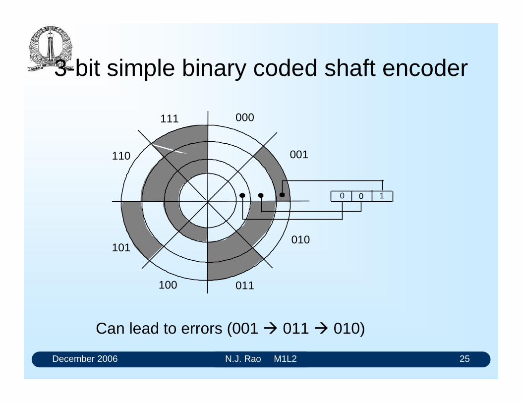
3-bit simple binary coded shaft encoder
000111
110
101
100 011
010
001
0 0 1
Can lead to errors (001 011 010)
December 2006 N.J. Rao M1L2 26
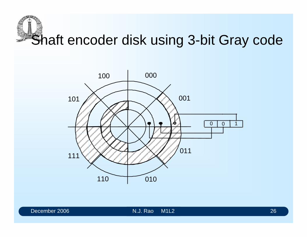
Shaft encoder disk using 3-bit Gray code
000 100
101
111
110 010
011
001
0 0 1
December 2006 N.J. Rao M1L2 27
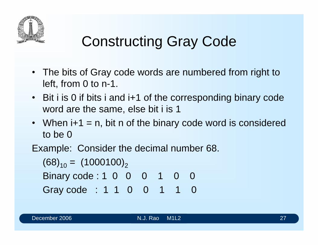
Constructing Gray Code
The bits of Gray code words are numbered from right to left, from 0 to n-1.
Bit i is 0 if bits i and i+1 of the corresponding binary code word are the same, else bit i is 1
When i+1 = n, bit n of the binary code word is considered to be 0
Example: Consider the decimal number 68.(68)10 = (1000100)2
Binary code : 1 0 0 0 1 0 0Gray code : 1 1 0 0 1 1 0
December 2006 N.J. Rao M1L2 28
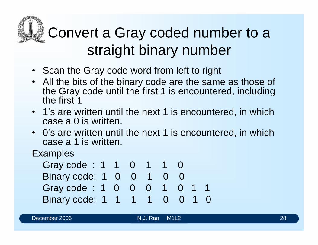
Convert a Gray coded number to a straight binary number
Scan the Gray code word from left to right All the bits of the binary code are the same as those of
the Gray code until the first 1 is encountered, including the first 1
1s are written until the next 1 is encountered, in which case a 0 is written.
0s are written until the next 1 is encountered, in which case a 1 is written.
Examples Gray code : 1 1 0 1 1 0Binary code: 1 0 0 1 0 0Gray code : 1 0 0 0 1 0 1 1Binary code: 1 1 1 1 0 0 1 0
December 2006 N.J. Rao M1L2 29
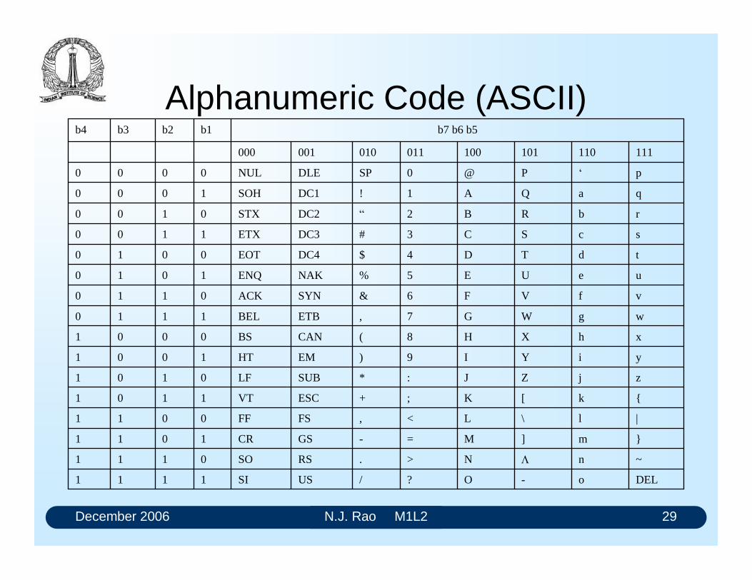
Alphanumeric Code (ASCII)
DELo-O?/USSI1111
~nN>.RSSO0111
m]M=-GSCR1011
|l\L<,FSFF0011
k[K;+ESCVT1101
zjZJ:*SUBLF0101
yiYI9)EMHT1001
xhXH8(CANBS0001
wgWG7,ETBBEL1110
vfVF6&SYNACK0110
ueUE5%NAKENQ1010
tdTD4$DC4EOT0010
scSC3#DC3ETX1100
rbRB2DC2STX0100
qaQA1!DC1SOH1000
pP@0SPDLENUL0000
111110101100011010001000
b7 b6 b5b1b2b3b4
December 2006 N.J. Rao M1L2 30
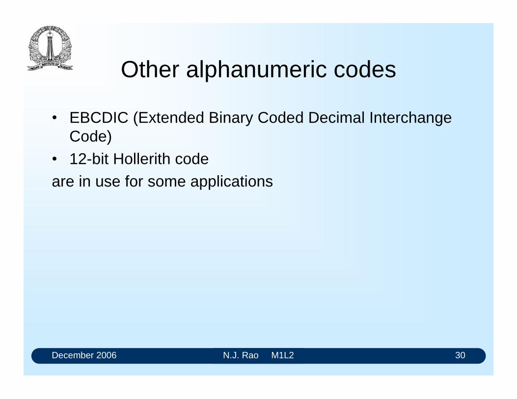
Other alphanumeric codes
EBCDIC (Extended Binary Coded Decimal Interchange Code)
12-bit Hollerith code are in use for some applications
December 2006 N.J. Rao M1L2 31
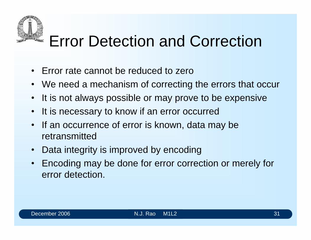
Error Detection and Correction
Error rate cannot be reduced to zero We need a mechanism of correcting the errors that occur It is not always possible or may prove to be expensive It is necessary to know if an error occurred If an occurrence of error is known, data may be
retransmitted Data integrity is improved by encoding Encoding may be done for error correction or merely for
error detection.
December 2006 N.J. Rao M1L2 32
Encoding for data integrity
Add a special code bit to a data word It is called the Parity Bit Parity bit can be added on an odd or even basis
December 2006 N.J. Rao M1L2 33
Parity
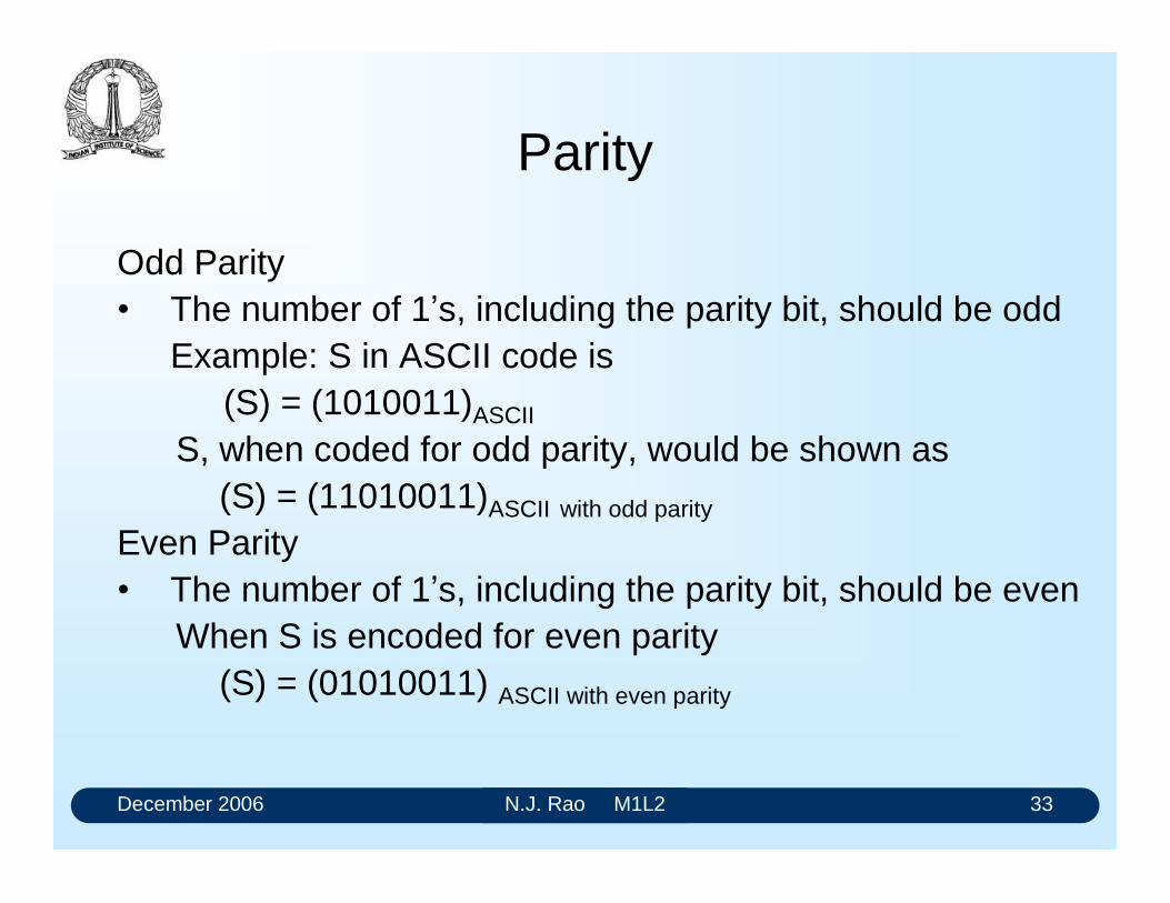
Odd Parity The number of 1s, including the parity bit, should be odd
Example: S in ASCII code is (S) = (1010011)ASCII
S, when coded for odd parity, would be shown as (S) = (11010011)ASCII with odd parity
Even Parity The number of 1s, including the parity bit, should be even
When S is encoded for even parity(S) = (01010011) ASCII with even parity
December 2006 N.J. Rao M1L2 34
Error detection with parity bits
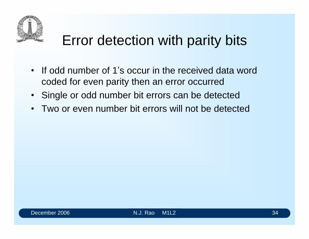
If odd number of 1s occur in the received data word coded for even parity then an error occurred
Single or odd number bit errors can be detected Two or even number bit errors will not be detected
December 2006 N.J. Rao M1L2 35
Error Correction
Parity bit allows us only to detect the presence of one bit error in a group of bits
It does not enable us to exactly locate the bit that changed
Parity bit scheme can be extended to locate the faulty bit in a block of information
December 2006 N.J. Rao M1L2 36
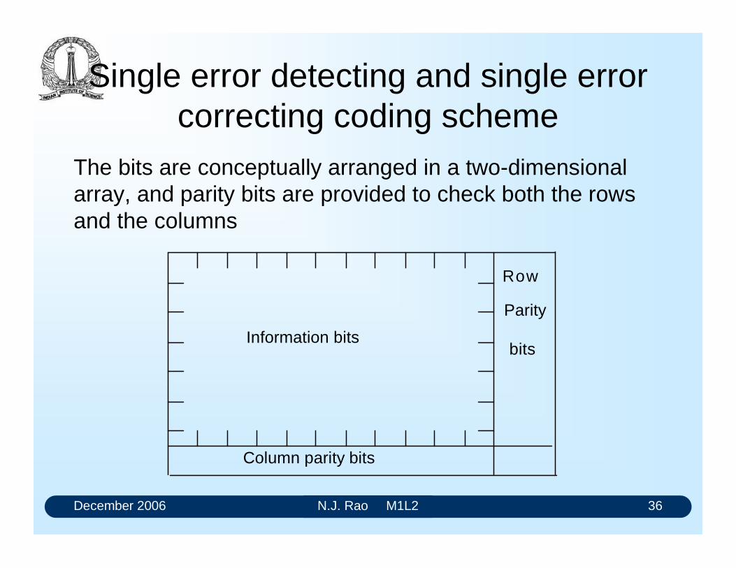
Single error detecting and single error correcting coding scheme
Column parity bits
Row
Parity
bitsInformation bits
The bits are conceptually arranged in a two-dimensional array, and parity bits are provided to check both the rows and the columns
December 2006 N.J. Rao M1L2 37
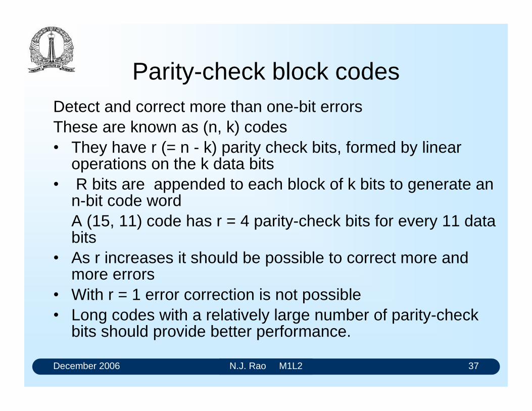
Parity-check block codesDetect and correct more than one-bit errorsThese are known as (n, k) codes They have r (= n - k) parity check bits, formed by linear
operations on the k data bits R bits are appended to each block of k bits to generate an
n-bit code wordA (15, 11) code has r = 4 parity-check bits for every 11 data bits
As r increases it should be possible to correct more and more errors
With r = 1 error correction is not possible Long codes with a relatively large number of parity-check
bits should provide better performance.
December 2006 N.J. Rao M1L2 38
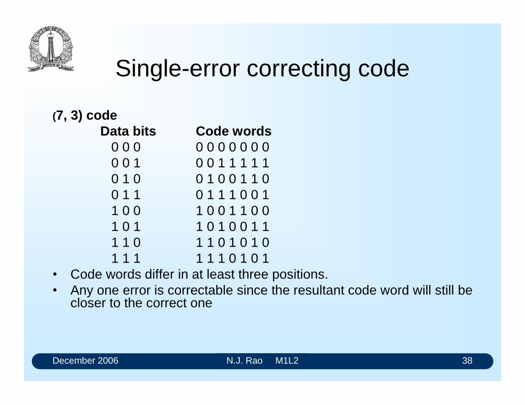
Single-error correcting code
(7, 3) codeData bits Code words
0 0 0 0 0 0 0 0 0 00 0 1 0 0 1 1 1 1 10 1 0 0 1 0 0 1 1 00 1 1 0 1 1 1 0 0 11 0 0 1 0 0 1 1 0 01 0 1 1 0 1 0 0 1 11 1 0 1 1 0 1 0 1 01 1 1 1 1 1 0 1 0 1
Code words differ in at least three positions. Any one error is correctable since the resultant code word will still be
closer to the correct one
December 2006 N.J. Rao M1L2 39
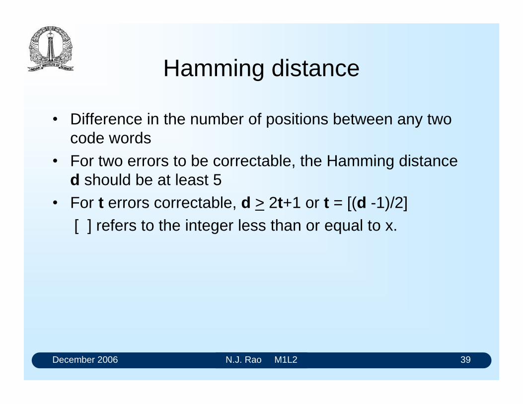
Hamming distance
Difference in the number of positions between any two code words
For two errors to be correctable, the Hamming distance d should be at least 5
For t errors correctable, d > 2t+1 or t = [(d -1)/2][ ] refers to the integer less than or equal to x.
December 2006 N.J. Rao M1L2 40
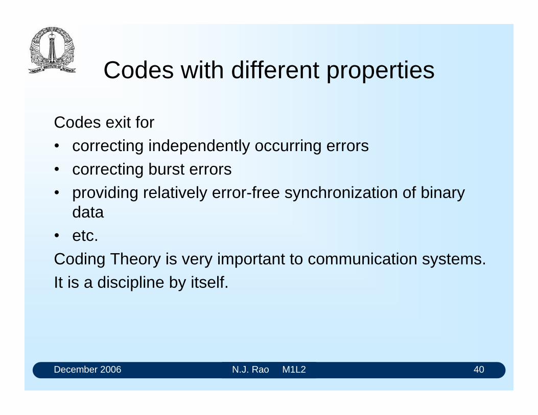
Codes with different properties
Codes exit for correcting independently occurring errors correcting burst errors providing relatively error-free synchronization of binary
data etc.Coding Theory is very important to communication systems.It is a discipline by itself.
CODES: Introduction
When we wish to send information over long distances unambiguously it becomes
necessary to modify (encoding) the information into some form before sending, and
convert (decode) at the receiving end to get back the original information. This
process of encoding and decoding is necessary because the channel through which
the information is sent may distort the transmitted information. Much of the
information is sent as numbers. While these numbers are created using simple
weighted-positional numbering systems, they need to be encoded before
transmission. The modifications to numbers were based on changing the weights,
but predominantly on some form of binary encoding. There are several codes in use
in the context of present day information technology, and more and more new codes
are being generated to meet the new demands.
Coding is the process of altering the characteristics of information to make
it more suitable for intended application
By assigning each item of information a unique combination of 1s and 0s we
transform some given information into binary coded form. The bit combinations are
referred to as “words” or “code words”. In the field of digital systems and computers
different bit combinations have different designations.
Bit - a binary digit 0 or 1
Nibble - a group of four bits
Byte - a group of eight bits
Word - a group of sixteen bits;
a word has two bytes or four nibbles
Sometimes ‘word’ is used to designate a larger group of bits also, for example 32 bit
or 64 bit words.
We need and use coding of information for a variety of reasons
to increase efficiency of transmission,
to make it error free,
to enable us to correct it if errors occurred,
to inform the sender if an error occurred in the received information etc.

for security reasons to limit the accessibility of information
to standardise a universal code that can be used by all
Coding schemes have to be designed to suit the security requirements and the
complexity of the medium over which information is transmitted.
Decoding is the process of reconstructing source information from the
encoded information. Decoding process can be more complex than coding if we
do not have prior knowledge of coding schemes.
In view of the modern day requirements of efficient, error free and secure
information transmission coding theory is an extremely important subject. However,
at this stage of learning digital systems we confine ourselves to familiarising with a
few commonly used codes and their properties.
We will be mainly concerned with binary codes. In binary coding we use binary digits
or bits (0 and 1) to code the elements of an information set. Let n be the number of
bits in the code word and x be the number of unique words.
If n = 1, then x = 2 (0, 1)
n = 2, then x = 4 (00, 01, 10, 11)
n = 3, then x = 8 (000,001,010 ...111)
.
n = j, then x = 2j
From this we can conclude that if we are given elements of information to code into
binary coded format,
x < 2j
or j > log2x
> 3.32 log10x
where j is the number of bits in a code word.
For example, if we want to code alphanumeric information (26 alphabetic characters
+ 10 decimals digits = 36 elements of information), we require
j > 3.32 log1036
j > 5.16 bits

Since bits are not defined as fractional parts, we take j = 6. In other words a
minimum six-bit code would be required to code 36 alphanumeric elements of
information. However, with a six-bit code only 36 code words are used out of the 64
code words possible.
In this Learning Unit we consider a few commonly used codes including
1. Binary coded decimal codes
2. Unit distance codes
3. Error detection codes
4. Alphanumeric codes
Binary Coded Decimal Codes
The main motivation for binary number system is that there are only two elements in
the binary set, namely 0 and 1. While it is advantageous to perform all
computations on hardware in binary forms, human beings still prefer to work with
decimal numbers. Any electronic system should then be able to accept decimal
numbers, and make its output available in the decimal form.
One method, therefore, would be to
convert decimal number inputs into binary form
manipulate these binary numbers as per the required functions, and
convert the resultant binary numbers into the decimal form
However, this kind of conversion requires more hardware, and in some cases
considerably slows down the system. Faster systems can afford the additional
circuitry, but the delays associated with the conversions would not be acceptable. In
case of smaller systems, the speed may not be the main criterion, but the additional
circuitry may make the system more expensive.
We can solve this problem by encoding decimal numbers as binary strings, and use
them for subsequent manipulations.
There are ten different symbols in the decimal number system: 0, 1, 2, . . ., 9. As
there are ten symbols we require at least four bits to represent them in the binary
form. Such a representation of decimal numbers is called binary coding of decimal
numbers.
As four bits are required to encode one decimal digit, there are sixteen four-bit
groups to select ten groups. This would lead to nearly 30 x 1010 (16C10.10!) possible
codes. However, most of them will not have any special properties that would be
useful in hardware design. We wish to choose codes that have some desirable
properties like
ease of coding
ease in arithmetic operations
minimum use of hardware
error detection property
ability to prevent wrong output during transitions
In a weighted code the decimal value of a code is the algebraic sum of the weights
of 1s appearing in the number. Let (A)10 be a decimal number encoded in the binary
form as a3a2a1a0. Then
(A)10 = w3a3 + w2a2 + w1a1 +w0a0
where w3, w2, w1 and w0 are the weights selected for a given code, and a3,a2,a1and
a0 are either 0s or 1s. The more popularly used codes have the weights as
w3 w2 w1 w0
8 4 2 1
2 4 2 1
8 4 -2 -1
The decimal numbers in these three codes are
Decimal digit
Weights 8 4 2 1
Weights 2 4 2 1
Weights 8 4 -2 -1
0 0 0 0 0 0 0 0 0 0 0 0 0 1 0 0 0 1 0 0 0 1 0 1 1 1 2 0 0 1 0 0 0 1 0 0 1 1 0 3 0 0 1 1 0 0 1 1 0 1 0 1 4 0 1 0 0 0 1 0 0 0 1 0 0 5 0 1 0 1 1 0 1 1 1 0 1 1 6 0 1 1 0 1 1 0 0 1 0 1 0 7 0 1 1 1 1 1 0 1 1 0 0 1 8 1 0 0 0 1 1 1 0 1 0 0 0 9 1 0 0 1 1 1 1 1 1 1 1 1
In all the cases only ten combinations are utilized to represent the decimal digits.
The remaining six combinations are illegal. However, they may be utilized for error
detection purposes.
Consider, for example, the representation of the decimal number 16.85 in Natural
Binary Coded Decimal code (NBCD)
(16.85)10 = (0001 0110 . 1000 0101)NBCD
1 6 8 5
There are many possible weights to write a number in BCD code. Some codes have
desirable properties, which make them suitable for specific applications. Two such
desirable properties are:
1. Self-complementing codes
2. Reflective codes
When we perform arithmetic operations, it is often required to take the
“complement” of a given number. If the logical complement of a coded number is
also its arithmetic complement, it will be convenient from hardware point of view. In
a self-complementing coded decimal number, (A)10, if the individual bits of a
number are complemented it will result in (9 - A)10.
Example: Consider the 2421 code.
The 2421 code of (4)10 is 0100.
Its complement is 1011 which is 2421 code for (5)10 = (9 - 4)10.
Therefore, 2421 code may be considered as a self-complementing code. A necessary
condition for a self-complimenting code is that the sum of its weights should be 9.
A self-complementing code, which is not weighted, is excess-3 code. It is derived
from 8421 code by adding 0011 to all the 8421 coded numbers.
Another self-complementing code is 631-1 weighted code.
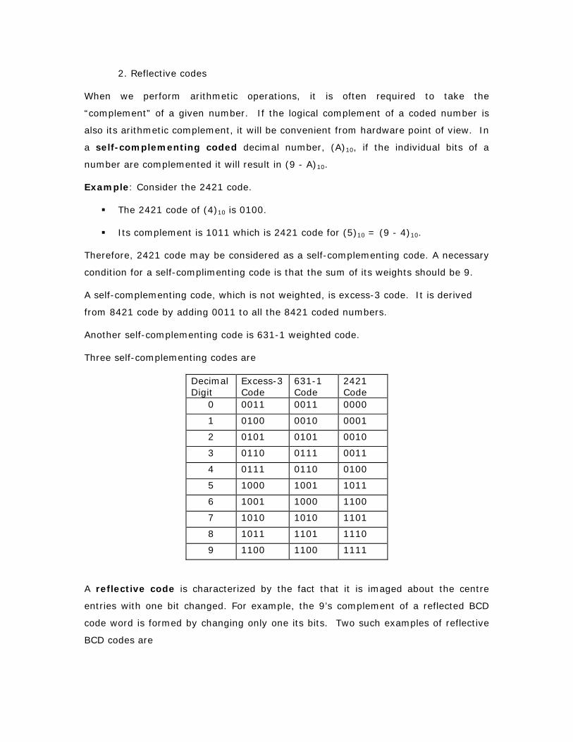
Three self-complementing codes are
Decimal Digit
Excess-3 Code
631-1 Code
2421 Code
0 0011 0011 0000
1 0100 0010 0001
2 0101 0101 0010
3 0110 0111 0011
4 0111 0110 0100
5 1000 1001 1011
6 1001 1000 1100
7 1010 1010 1101
8 1011 1101 1110
9 1100 1100 1111
A reflective code is characterized by the fact that it is imaged about the centre
entries with one bit changed. For example, the 9’s complement of a reflected BCD
code word is formed by changing only one its bits. Two such examples of reflective
BCD codes are

Decimal Code-A Code-B 0 0000 0100 1 0001 1010 2 0010 1000 3 0011 1110 4 0100 0000 5 1100 0001 6 1011 1111 7 1010 1001 8 1001 1011 9 1000 0101
The BCD codes are widely used and the reader should become familiar with reasons
for using them and their application. The most common application of NBCD codes is
in the calculator.
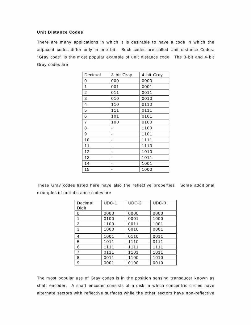
Unit Distance Codes
There are many applications in which it is desirable to have a code in which the
adjacent codes differ only in one bit. Such codes are called Unit distance Codes.
“Gray code” is the most popular example of unit distance code. The 3-bit and 4-bit
Gray codes are
Decimal 3-bit Gray 4-bit Gray 0 000 0000 1 001 0001 2 011 0011 3 010 0010 4 110 0110 5 111 0111 6 101 0101 7 100 0100 8 - 1100 9 - 1101 10 - 1111 11 - 1110 12 - 1010 13 - 1011 14 - 1001 15 - 1000
These Gray codes listed here have also the reflective properties. Some additional
examples of unit distance codes are
Decimal Digit
UDC-1 UDC-2
UDC-3
0 0000 0000 0000 1 0100 0001 1000 2 1100 0011 1001 3 1000 0010 0001
4 1001 0110 0011 5 1011 1110 0111 6 1111 1111 1111 7 0111 1101 1011 8 0011 1100 1010 9 0001 0100 0010
The most popular use of Gray codes is in the position sensing transducer known as
shaft encoder. A shaft encoder consists of a disk in which concentric circles have
alternate sectors with reflective surfaces while the other sectors have non-reflective
surfaces. The position is sensed by the reflected light from a light emitting diode.
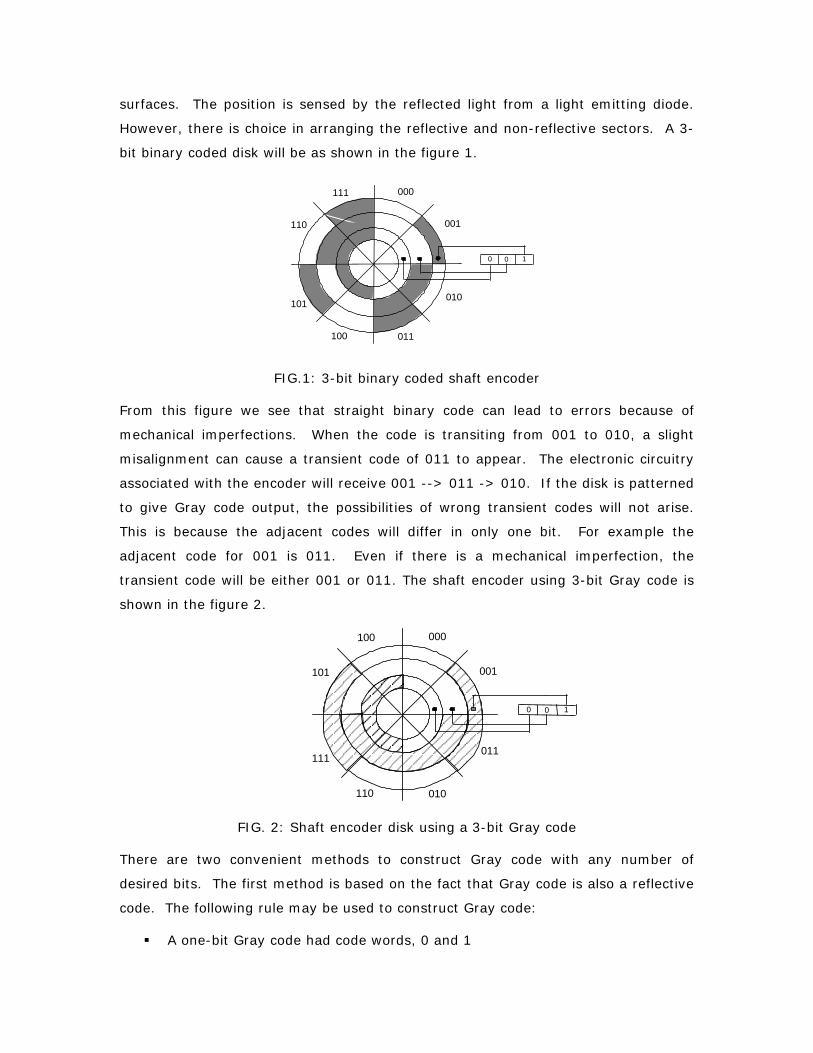
However, there is choice in arranging the reflective and non-reflective sectors. A 3-
bit binary coded disk will be as shown in the figure 1.
FIG.1: 3-bit binary coded shaft encoder
From this figure we see that straight binary code can lead to errors because of
mechanical imperfections. When the code is transiting from 001 to 010, a slight
misalignment can cause a transient code of 011 to appear. The electronic circuitry
associated with the encoder will receive 001 --> 011 -> 010. If the disk is patterned
to give Gray code output, the possibilities of wrong transient codes will not arise.
This is because the adjacent codes will differ in only one bit. For example the
adjacent code for 001 is 011. Even if there is a mechanical imperfection, the
transient code will be either 001 or 011. The shaft encoder using 3-bit Gray code is
shown in the figure 2.
000100
101
111
110 010
011
001
0 0 1
FIG. 2: Shaft encoder disk using a 3-bit Gray code
There are two convenient methods to construct Gray code with any number of
desired bits. The first method is based on the fact that Gray code is also a reflective
code. The following rule may be used to construct Gray code:
A one-bit Gray code had code words, 0 and 1
000111
110
101
100 011
010
001
0 0 1

The first 2n code words of an (n+1)-bit Gray code equal the code words of an
n-bit Gray code, written in order with a leading 0 appended.
The last 2n code words of a (n+1)-bit Gray code equal the code words of an
n-bit Gray code, written in reverse order with a leading 1 appended.
However, this method requires Gray codes with all bit lengths less than ‘n’ also be
generated as a part of generating n-bit Gray code. The second method allows us to
derive an n-bit Gray code word directly from the corresponding n-bit binary code
word:
The bits of an n-bit binary code or Gray code words are numbered from right
to left, from 0 to n-1.
Bit i of a Gray-code word is 0 if bits i and i+1 of the corresponding binary
code word are the same, else bit i is 1. When i+1 = n, bit n of the binary
code word is considered to be 0.
Example: Consider the decimal number 68.
(68)10 = (1000100)2
Binary code: 1 0 0 0 1 0 0
Gray code : 1 1 0 0 1 1 0
The following rules can be followed to convert a Gray coded number to a straight
binary number:
Scan the Gray code word from left to right. All the bits of the binary code are
the same as those of the Gray code until the first 1 is encountered, including
the first 1.
1’s are written until the next 1 is encountered, in which case a 0 is
written.
0’s are written until the next 1 is encountered, in which case a 1 is written.
Consider the following examples of Gray code numbers converted to binary numbers
Gray code : 1 1 0 1 1 0 1 0 0 0 1 0 1 1
Binary code: 1 0 0 1 0 0 1 1 1 1 0 0 1 0
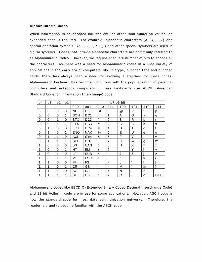
Alphanumeric Codes
When information to be encoded includes entities other than numerical values, an
expanded code is required. For example, alphabetic characters (A, B, ....Z) and
special operation symbols like +, -, /, *, (, ) and other special symbols are used in
digital systems. Codes that include alphabetic characters are commonly referred to
as Alphanumeric Codes. However, we require adequate number of bits to encode all
the characters. As there was a need for alphanumeric codes in a wide variety of
applications in the early era of computers, like teletype, punched tape and punched
cards, there has always been a need for evolving a standard for these codes.
Alphanumeric keyboard has become ubiquitous with the popularization of personal
computers and notebook computers. These keyboards use ASCII (American
Standard Code for Information Interchange) code
b4 b3 b2 b1 b7 b6 b5 000 001 010 011 100 101 110 111 0 0 0 0 NUL DLE SP 0 @ P ‘ p 0 0 0 1 SOH DC1 ! 1 A Q a q 0 0 1 0 STX DC2 “ 2 B R b r 0 0 1 1 ETX DC3 # 3 C S c s 0 1 0 0 EOT DC4 $ 4 D T d t 0 1 0 1 ENQ NAK % 5 E U e u 0 1 1 0 ACK SYN & 6 F V f v 0 1 1 1 BEL ETB , 7 G W g w 1 0 0 0 BS CAN ( 8 H X h x 1 0 0 1 HT EM ) 9 I Y i y 1 0 1 0 LF SUB * : J Z j z 1 0 1 1 VT ESC + ; K [ k 1 1 0 0 FF FS , < L \ l | 1 1 0 1 CR GS - = M ] m 1 1 1 0 SO RS . > N n ~ 1 1 1 1 SI US / ? O - o DEL
Alphanumeric codes like EBCDIC (Extended Binary Coded Decimal Interchange Code)
and 12-bit Hollerith code are in use for some applications. However, ASCII code is
now the standard code for most data communication networks. Therefore, the
reader is urged to become familiar with the ASCII code.
Error Detection and Correcting Codes
When data is transmitted in digital form from one place to another through a
transmission channel/medium, some data bits may be lost or modified. This loss of
data integrity occurs due to a variety of electrical phenomena in the transmission
channel. As there are needs to transmit millions of bits per second, the data
integrity should be very high. The error rate cannot be reduced to zero. Then we
would like to ideally have a mechanism of correcting the errors that occur. If this is
not possible or proves to be expensive, we would like to know if an error occurred.
If an occurrence of error is known, appropriate action, like retransmitting the data,
can be taken. One of the methods of improving data integrity is to encode the data
in a suitable manner. This encoding may be done for error correction or merely for
error detection.
A simple process of adding a special code bit to a data word can improve its
integrity. This extra bit will allow detection of a single error in a given code word in
which it is used, and is called the ‘Parity Bit’. This parity bit can be added on an odd
or even basis. The odd or even designation of a code word may be determined by
actual number of 1’s in the data (including the added parity bit) to which the parity
bit is added. For example, the S in ASCII code is
(S) = (1010011)ASCII
S, when coded for odd parity, would be shown as
(S) = (11010011)ASCII with odd parity
In this encoded ‘S’ the number of 1’s is five, which is odd.
When S is encoded for even parity
(S) = (01010011)ASCII with even parity.
In this case the coded word has even number (four) of ones.
Thus the parity encoding scheme is a simple one and requires only one extra bit. If
the system is using even parity and we find odd number of ones in the received data
word we know that an error has occurred. However, this scheme is meaningful only
for single errors. If two bits in a data word were received incorrectly the parity bit
scheme will not detect the faults. Then the question arises as to the level of
improvement in the data integrity if occurrence of only one bit error is detectable.
The improvement in the reliability can be mathematically determined.
Adding a parity bit allows us only to detect the presence of one bit error in a group of
bits. But it does not enable us to exactly locate the bit that changed. Therefore,
addition of one parity bit may be called an error detecting coding scheme. In a
digital system detection of error alone is not sufficient. It has to be corrected as
well. Parity bit scheme can be extended to locate the faulty bit in a block of
information. The information bits are conceptually arranged in a two-dimensional
array, and parity bits are provided to check both the rows and the columns.
If we can identify the code word that has an error with the parity bit, and the column
in which that error occurs by a way of change in the column parity bit, we can both
detect and correct the wrong bit of information. Hence such a scheme is single error
detecting and single error correcting coding scheme.
This method of using parity bits can be generalized for detecting and correcting more
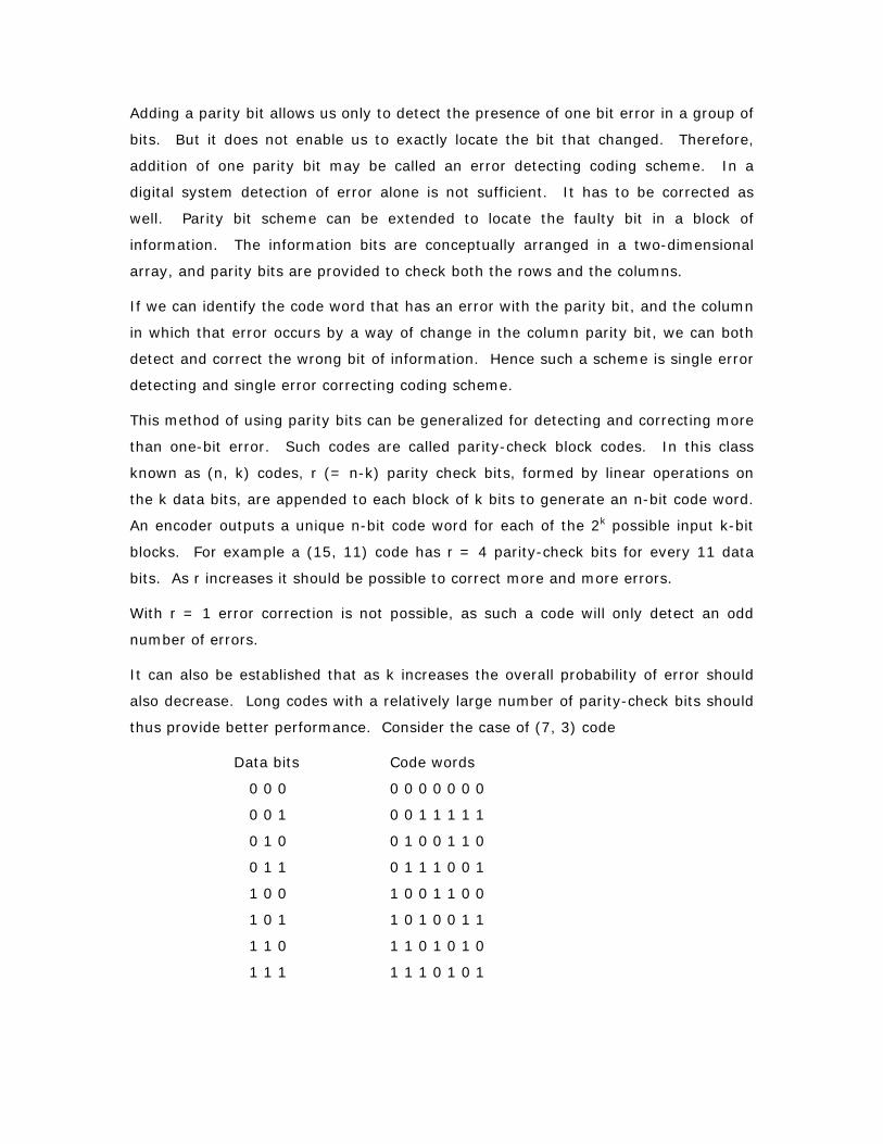
than one-bit error. Such codes are called parity-check block codes. In this class
known as (n, k) codes, r (= n-k) parity check bits, formed by linear operations on
the k data bits, are appended to each block of k bits to generate an n-bit code word.
An encoder outputs a unique n-bit code word for each of the 2k possible input k-bit
blocks. For example a (15, 11) code has r = 4 parity-check bits for every 11 data
bits. As r increases it should be possible to correct more and more errors.
With r = 1 error correction is not possible, as such a code will only detect an odd
number of errors.
It can also be established that as k increases the overall probability of error should
also decrease. Long codes with a relatively large number of parity-check bits should
thus provide better performance. Consider the case of (7, 3) code
Data bits Code words
0 0 0 0 0 0 0 0 0 0
0 0 1 0 0 1 1 1 1 1
0 1 0 0 1 0 0 1 1 0
0 1 1 0 1 1 1 0 0 1
1 0 0 1 0 0 1 1 0 0
1 0 1 1 0 1 0 0 1 1
1 1 0 1 1 0 1 0 1 0
1 1 1 1 1 1 0 1 0 1
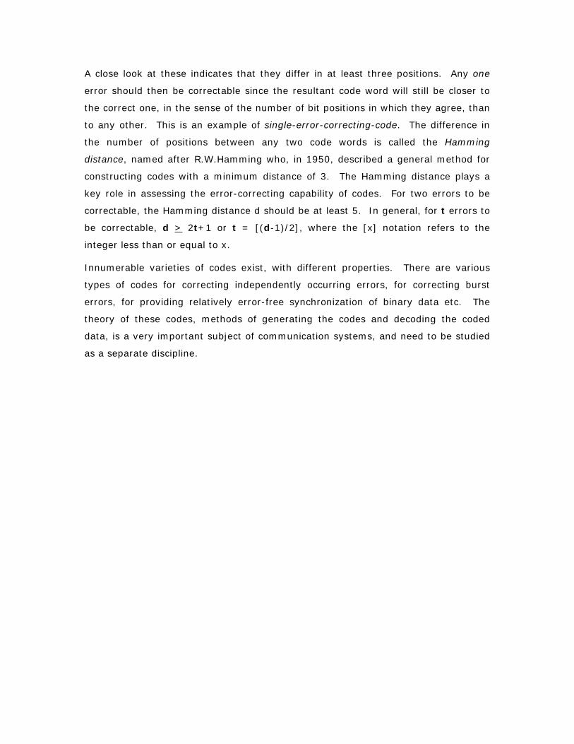
A close look at these indicates that they differ in at least three positions. Any one
error should then be correctable since the resultant code word will still be closer to
the correct one, in the sense of the number of bit positions in which they agree, than
to any other. This is an example of single-error-correcting-code. The difference in
the number of positions between any two code words is called the Hamming
distance, named after R.W.Hamming who, in 1950, described a general method for
constructing codes with a minimum distance of 3. The Hamming distance plays a
key role in assessing the error-correcting capability of codes. For two errors to be
correctable, the Hamming distance d should be at least 5. In general, for t errors to
be correctable, d > 2t+1 or t = [(d-1)/2], where the [x] notation refers to the
integer less than or equal to x.
Innumerable varieties of codes exist, with different properties. There are various
types of codes for correcting independently occurring errors, for correcting burst
errors, for providing relatively error-free synchronization of binary data etc. The
theory of these codes, methods of generating the codes and decoding the coded
data, is a very important subject of communication systems, and need to be studied
as a separate discipline.

Problems
M1L2: Codes
1. Write the following decimal number in Excess-3, 2421, 84-2-2 BCD codes:
(a) 563 (b) 678 (c) 1465 2. What is the use of self-complementing property? Demonstrate 631-1 BCD code is
self-complementary.
3. Develop two different 4-bit unit distance codes.
4. Prove that Gray code is both a reflective and unit distance code?
5. Determine the Gray code for (a) 3710 and (b) 9710.
6. Write your address in ASCII code.
7. Write 8-bit ASCII code sequence of the name of your town/city with even parity.
8. (a) Write the following statements in ASCII
A = 4.5 x B
X = 75/Y
(b) Attach an even parity bit to each code word of the ASCII strings written for the above statements
9. Find and correct the error in the following code sequence
0 1 0 1 0 0 1 1 0 0 1 1 0 1 1 1 0 1 1 0 1 0 0 0 1 0 0 0 1 1 1 1 0 0 0 0 1 0 0 1 0 1 0 1 0 --- Parity word
|__________ Parity bit
Digital Electronics Module 2: Boolean Algebra and Boolean Operators: Boolean Algebra
N.J. RaoIndian Institute of Science
id3639923 pdfMachine by Broadgun Software - a great PDF writer! - a great PDF creator! - http://www.pdfmachine.com http://www.broadgun.com
December 2006 N.J. Rao M2L1 2
Switching Signals
We encounter situations where the choice is binaryMove -StopOn - OffYes - No
An intended action takes place or does not take place Signals with two possible states are called switching
signals We need to work with a large number of such signals There is a need for formal methods of handling such
signals
December 2006 N.J. Rao M2L1 3
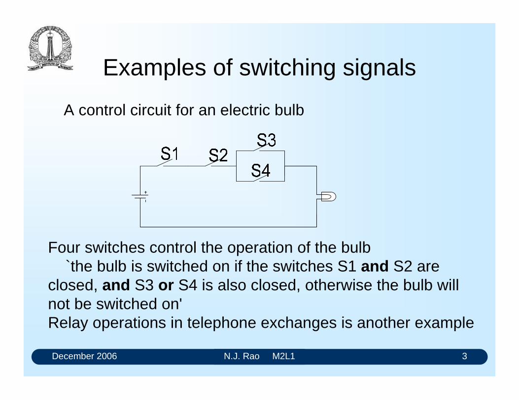
Examples of switching signals
A control circuit for an electric bulb
Four switches control the operation of the bulb`the bulb is switched on if the switches S1 and S2 are
closed, and S3 or S4 is also closed, otherwise the bulb will not be switched on' Relay operations in telephone exchanges is another example
December 2006 N.J. Rao M2L1 4
George Boole
English mathematician (1854)Wrote An Investigation of the Laws of ThoughtExamined the truth or falsehood of language statements Used special algebra of logic - Boole's Algebra (Boolean
Algebra) assigned a value 1 to statements that are completely correct assigned a value 0 to statements that are completely falseStatements are referred to digital variablesWe consider logical or digital variables to be synonymous
December 2006 N.J. Rao M2L1 5
Claude Shannon
Masters Thesis at Massachusetts Institute of Technology in 1938 A Symbolic Analysis of Relay and Switching Circuits
He applied Boolean algebra to the analysis and design of electrical switching circuits
December 2006 N.J. Rao M2L1 6
Realisation of switching circuits
Bipolar and MOS transistors are used as switches in building integrated circuits
Need to understand the electrical aspects of these circuits
December 2006 N.J. Rao M2L1 7
Learning Objectives
To know the basic axioms of Boolean algebra
To simplify logic functions (Boolean functions) using the basic properties of Boolean Algebra
December 2006 N.J. Rao M2L1 8
Boolean Algebra
A Boolean algebra consists of a finite set BS subject to equivalence relation "=" one unary operator not (symbolised by an over bar) two binary operators "+" and "."
such that for every element x and y BS, the operations (not x), x + y and x . y are uniquely definedx
December 2006 N.J. Rao M2L1 9
Boolean Algebra (2)
The unary operator not is defined by the relation
The not operator is also called the complement is the complement of xx
10;01
December 2006 N.J. Rao M2L1 10
Binary operator and
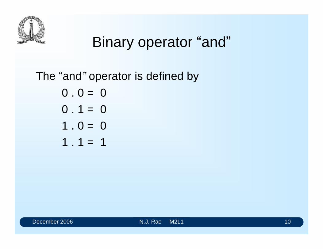
The and operator is defined by
0 . 0 = 0
0 . 1 = 01 . 0 = 0
1 . 1 = 1
December 2006 N.J. Rao M2L1 11
Binary operator or
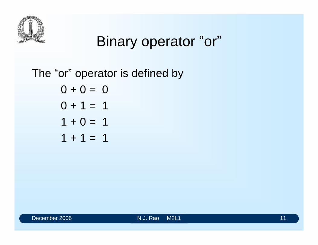
The or operator is defined by
0 + 0 = 00 + 1 = 1
1 + 0 = 11 + 1 = 1
December 2006 N.J. Rao M2L1 12
Huntington's (1909) postulates
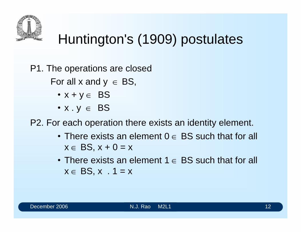
P1. The operations are closed
For all x and y BS, x + y BS x . y BS
P2. For each operation there exists an identity element.
There exists an element 0 BS such that for all x BS, x + 0 = x There exists an element 1 BS such that for all
x BS, x . 1 = x
December 2006 N.J. Rao M2L1 13
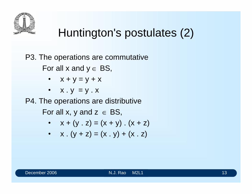
Huntington's postulates (2)
P3. The operations are commutative
For all x and y BS, x + y = y + x x . y = y . x
P4. The operations are distributive
For all x, y and z BS, x + (y . z) = (x + y) . (x + z) x . (y + z) = (x . y) + (x . z)
December 2006 N.J. Rao M2L1 14
Huntington's postulates (3)
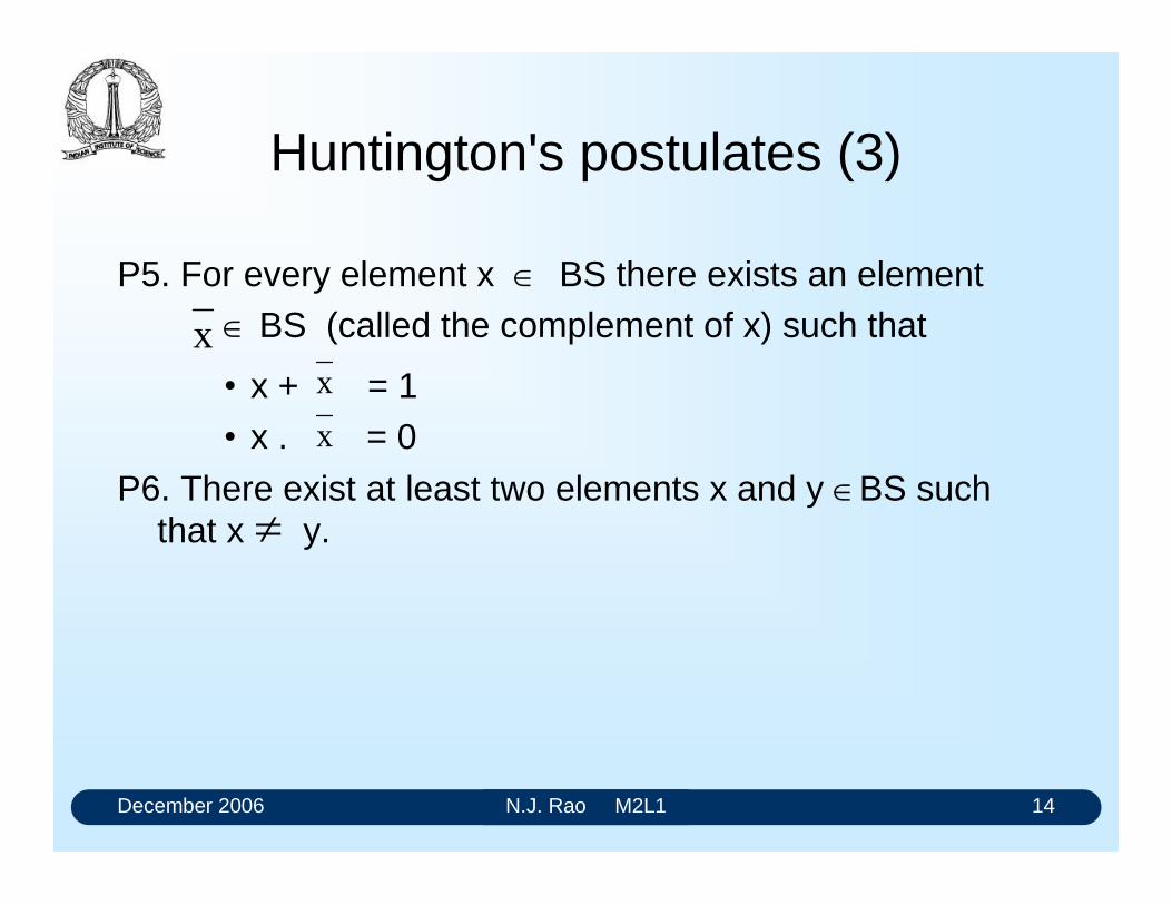
P5. For every element x BS there exists an element BS (called the complement of x) such that
x + = 1 x . = 0
P6. There exist at least two elements x and y BS such that x y.
xx
x
December 2006 N.J. Rao M2L1 15
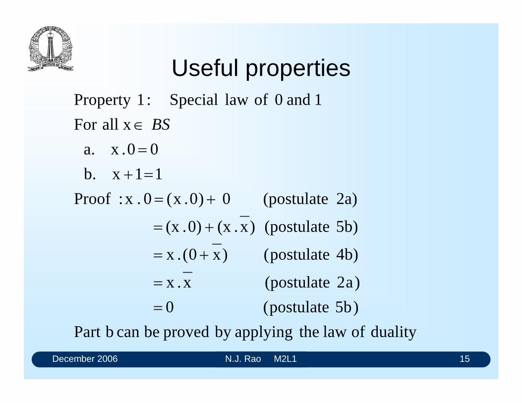
Useful properties
dualityoflawtheapplyingbyprovedbecanbPart
)5bpostulate(0
)a2(postulatex.x
4b)postulate()x0(.x
5b)(postulate)x.(x0).(x
2a) (postulate0)0.x(0 .x :Proof
11xb.
00.xa.
x allFor
1 and 0 of law Special :1Property
BS
December 2006 N.J. Rao M2L1 16
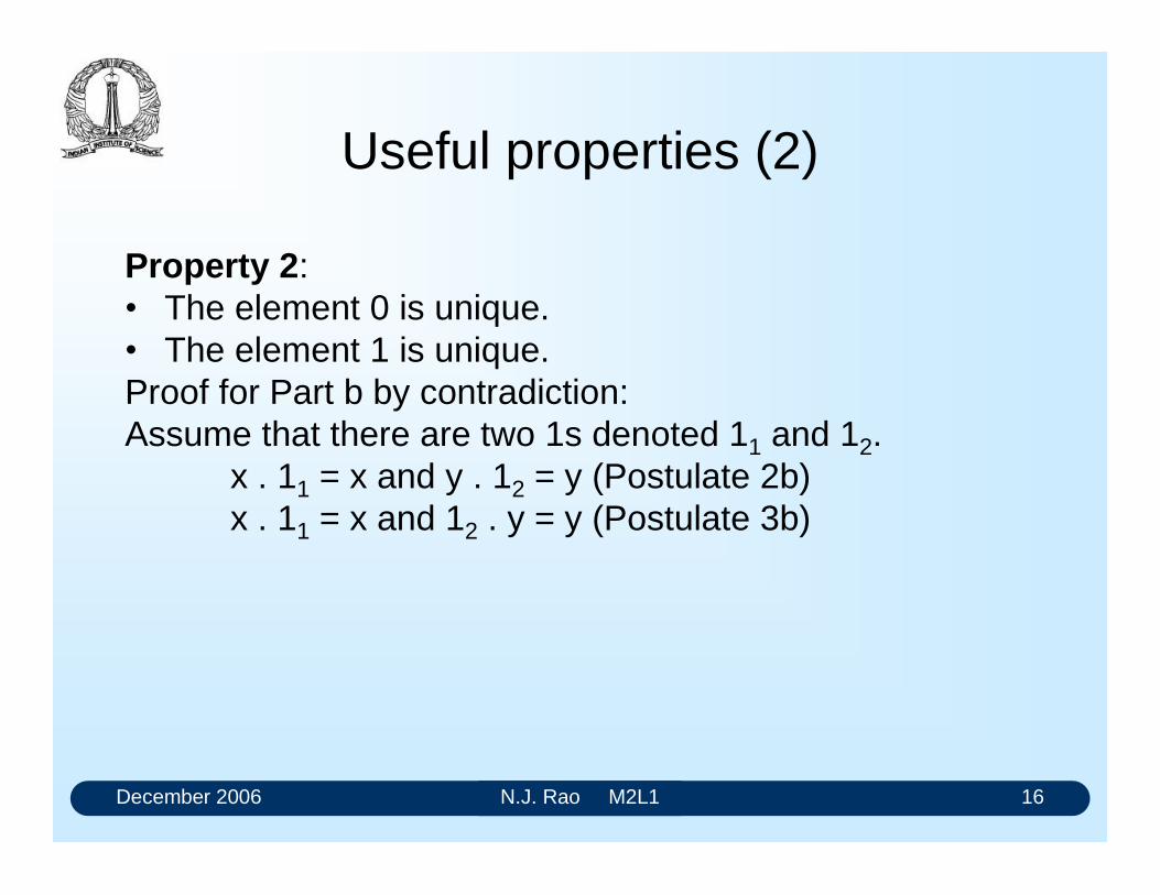
Useful properties (2)
Property 2: The element 0 is unique. The element 1 is unique.Proof for Part b by contradiction: Assume that there are two 1s denoted 11 and 12.
x . 11 = x and y . 12 = y (Postulate 2b)x . 11 = x and 12 . y = y (Postulate 3b)
December 2006 N.J. Rao M2L1 17
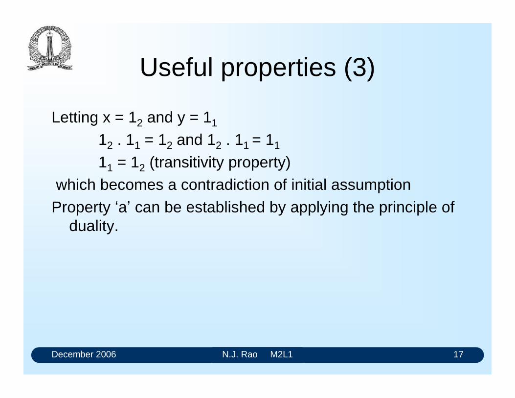
Useful properties (3)
Letting x = 12 and y = 11
12 . 11 = 12 and 12 . 11 = 11
11 = 12 (transitivity property)which becomes a contradiction of initial assumption
Property a can be established by applying the principle of duality.
December 2006 N.J. Rao M2L1 18
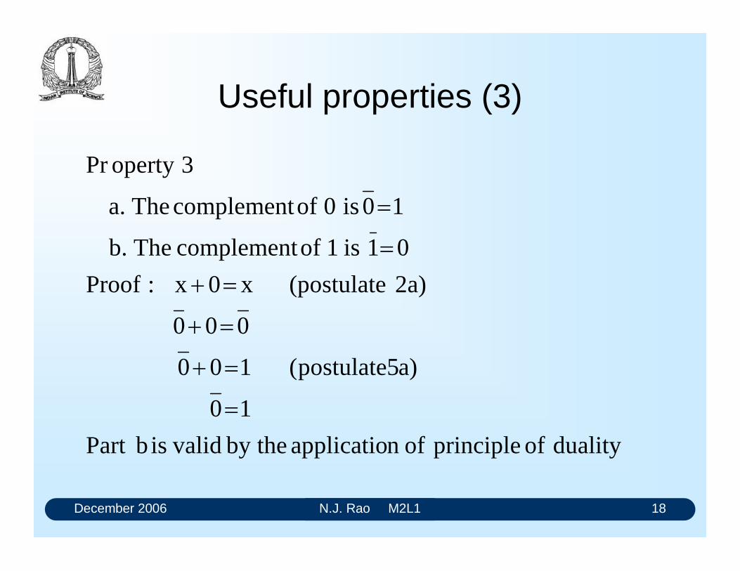
Useful properties (3)
duality of principle ofn applicatio by the validisbPart
10
a)postulate5(100
000
2a) (postulatex0x:Proof
01 is1 ofcomplement Theb.
10is0ofcomplementThea.
3opertyPr
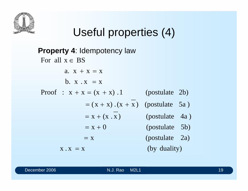
December 2006 N.J. Rao M2L1 19
Useful properties (4)
duality)(byxx.x
2a) (postulate x
5b) (postulate0x
)4a(postulate)x.(xx
)5a(postulate)x(x.x)x(
2b)(postulate 1 . x)(x x x:Proof
x x . x b.
x x x a.
BS x allFor
Property 4: Idempotency law
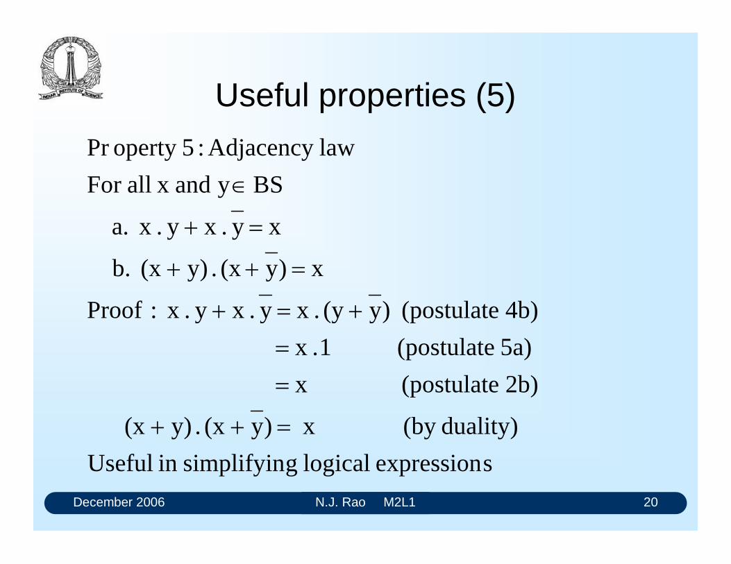
December 2006 N.J. Rao M2L1 20
Useful properties (5)
sexpression logical gsimplifyinin Useful
duality)(by x )y (x . y) (x
2b) (postulate x
5a) (postulate 1 . x
4b) (postulate )y (y . x y . x y . x :Proof
x )y (x . y) (x b.
x y . x y . x a.
BS y and x allFor
lawAdjacency :5operty Pr
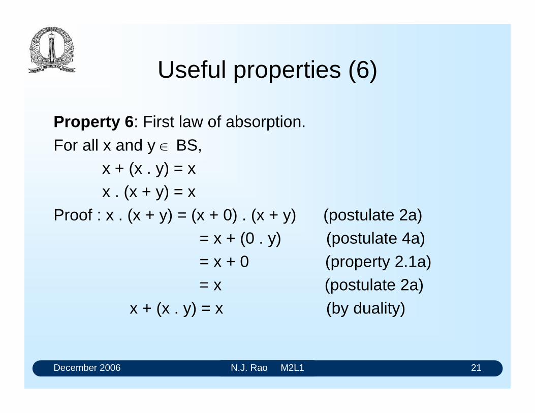
December 2006 N.J. Rao M2L1 21
Useful properties (6)
Property 6: First law of absorption.
For all x and y BS,x + (x . y) = x x . (x + y) = x
Proof : x . (x + y) = (x + 0) . (x + y) (postulate 2a) = x + (0 . y) (postulate 4a) = x + 0 (property 2.1a) = x (postulate 2a)
x + (x . y) = x (by duality)
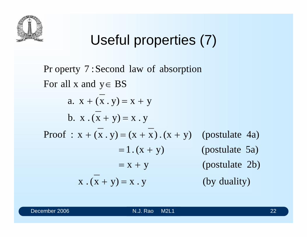
December 2006 N.J. Rao M2L1 22
Useful properties (7)
duality)(by y . x y) x( . x
2b) (postulate y x
5a) (postulate y) (x . 1
4a) (postulate y) (x . )x (x y) . x( x :Proof
y . x y) x( . x b.
y x y) . x( x a.
BS y and x allFor
absorption of law Second :7operty Pr
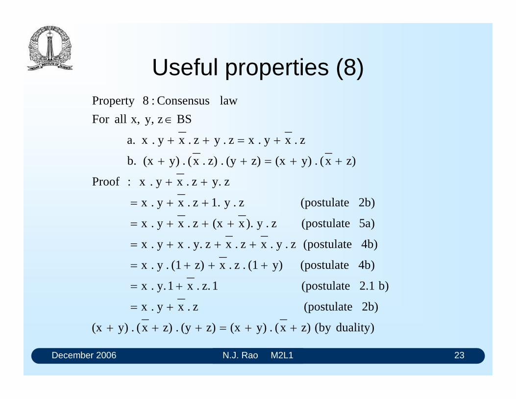
December 2006 N.J. Rao M2L1 23
Useful properties (8)
duality)(by z) x( . y) (x z) (y . z) x( . y) (x
2b) (postulate z . x y . x
b) 2.1 (postulate 1 z. . x 1 y. . x
4b) (postulate y) (1 . z . x z) (1 .y . x
4b) (postulate z .y . x z . x z y. . x y . x
5a) (postulate z .y ).x (x z . x y . x
2b) (postulate z .y 1. z . x y . x
z y. z . x y . x :Proof
z) x( . y) (x z) (y . z) . x( . y) (x b.
z . x y . x z .y z . x y . x a.
BS z y, x,allFor
law Consensus :8Property
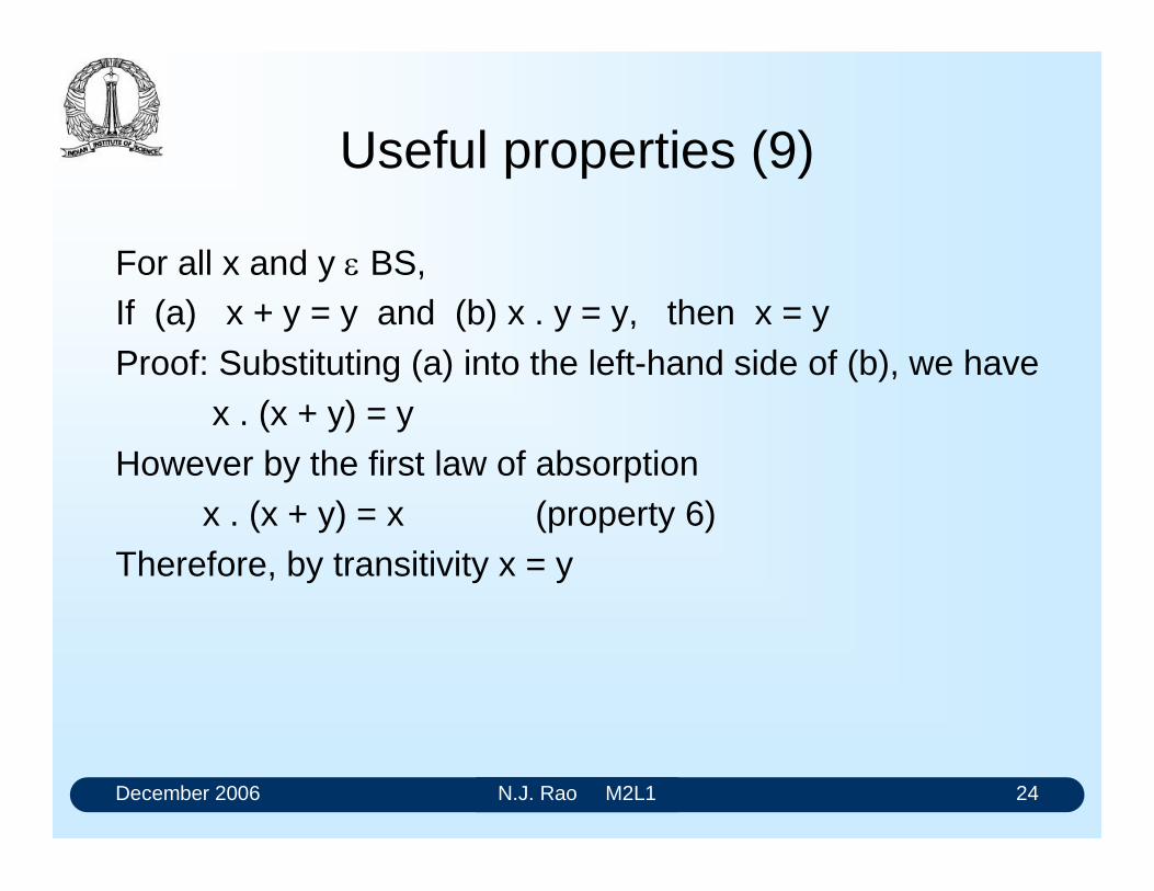
December 2006 N.J. Rao M2L1 24
Useful properties (9)
For all x and y BS, If (a) x + y = y and (b) x . y = y, then x = yProof: Substituting (a) into the left-hand side of (b), we have
x . (x + y) = yHowever by the first law of absorption
x . (x + y) = x (property 6)Therefore, by transitivity x = y
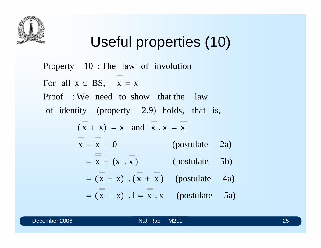
December 2006 N.J. Rao M2L1 25
Useful properties (10)
5a) (postulate x . x 1 . x) x(
4a) (postulate )x x( . x) x(
5b) (postulate )x .(x x
2a) (postulate 0 x x
x x . x and x x) x(
is, that holds, 2.9)(property identity of
law that theshow toneed We:Proof
x x BS, x allFor
involution of law The :10Property
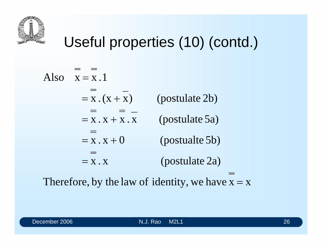
December 2006 N.J. Rao M2L1 26
Useful properties (10) (contd.)
x x have weidentity, of law by the Therefore,
2a) (postulate x . x
5b) (postualte 0 x . x
5a) (postulate x . x x . x
2b) (postulate )x (x . x
1 . x x Also
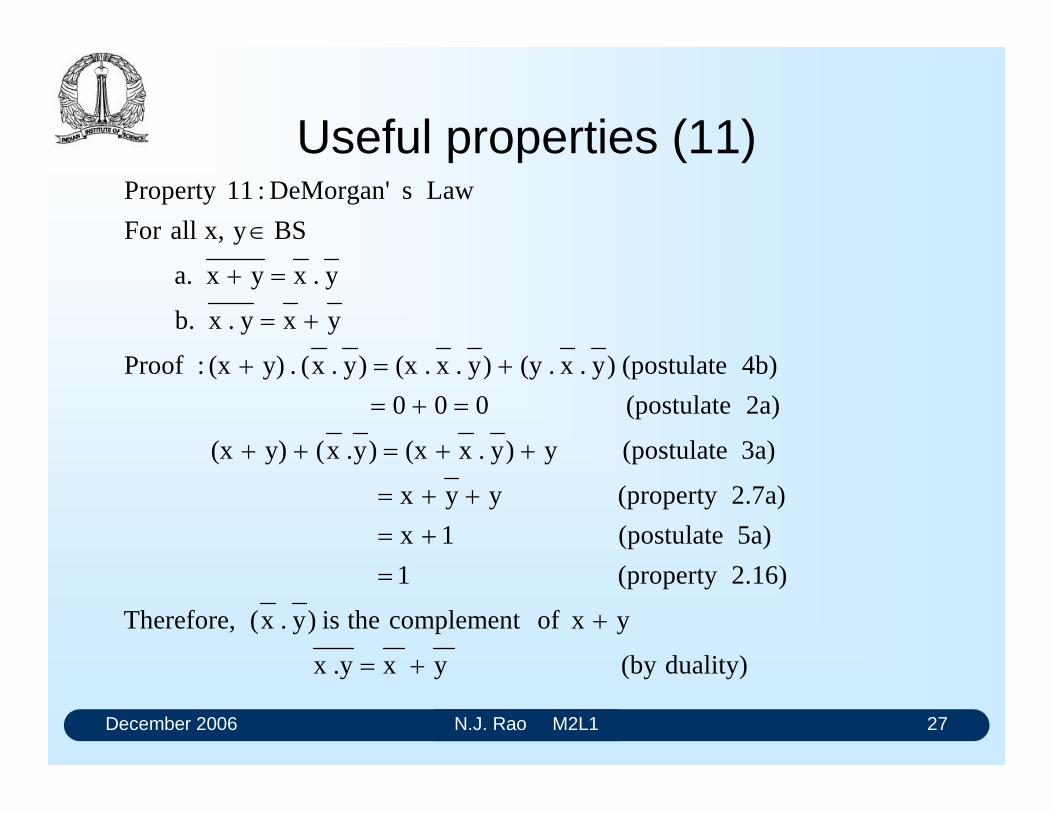
December 2006 N.J. Rao M2L1 27
Useful properties (11)
duality)(by y x .yx
y x of complement theis )y . x( Therefore,
2.16)(property 1
5a) (postulate 1 x
2.7a)(property y y x
3a) (postulatey )y . x (x )y. x( y) (x
2a) (postulate 0 0 0
4b) (postulate )y . x .(y )y . x .(x )y . x( . y) (x :Proof
y x y .x b.
y . x y x a.
BS y x,allFor
Law sDeMorgan' :11Property
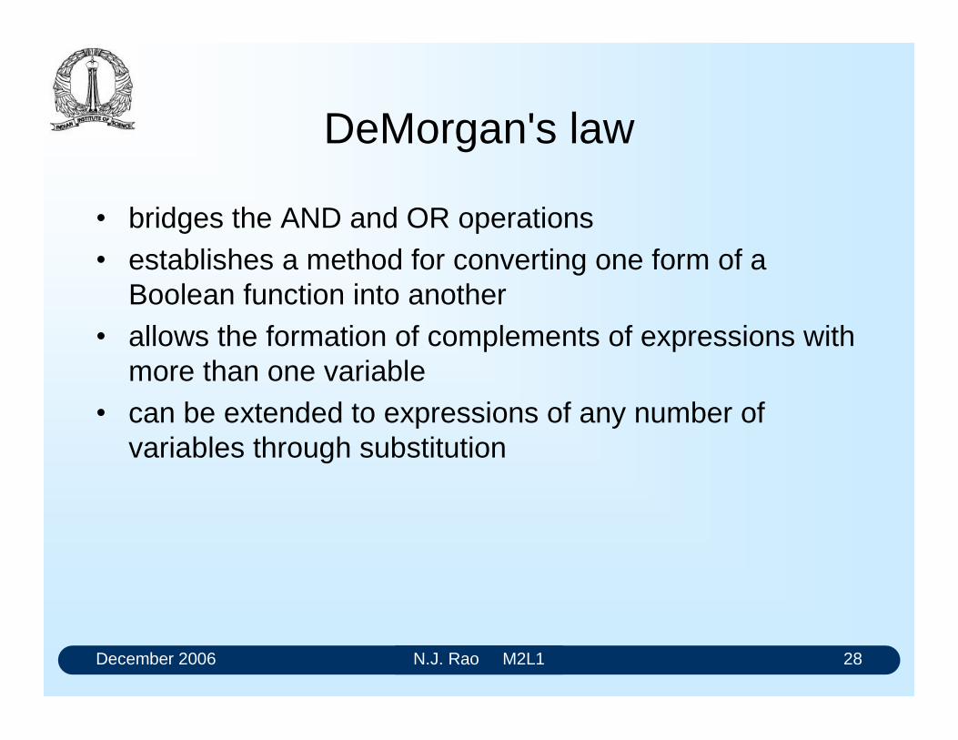
December 2006 N.J. Rao M2L1 28
DeMorgan's law
bridges the AND and OR operations establishes a method for converting one form of a
Boolean function into another allows the formation of complements of expressions with
more than one variable can be extended to expressions of any number of
variables through substitution
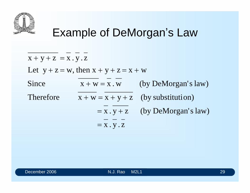
December 2006 N.J. Rao M2L1 29
Example of DeMorgans Law
z . y . x
law) sDeMorgan'(by z y . x
on)substituti(by z y x wx Therefore
law) sDeMorgan'(by w . x w x Since
w x z y then x w, z y Let
z . y . x z y x
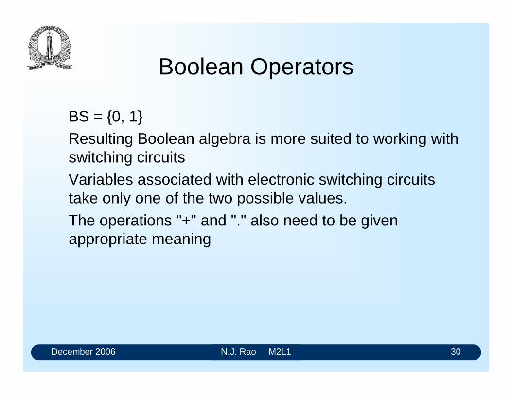
December 2006 N.J. Rao M2L1 30
Boolean Operators
BS = 0, 1Resulting Boolean algebra is more suited to working with switching circuitsVariables associated with electronic switching circuits take only one of the two possible values. The operations "+" and "." also need to be given appropriate meaning
December 2006 N.J. Rao M2L1 31
Binary Variables
Definition: A binary variable is one that can assume one of the two values 0 and 1.
These two values are meant to express two exactly opposite states. If A 0, then A = 1. If A 1, then A = 0
Examples: if switch A is not open then it is closed if switch A is not closed then it is open
Statement like "0 is less than 1" or " 1 is greater than 0 are invalid in
Boolean algebra
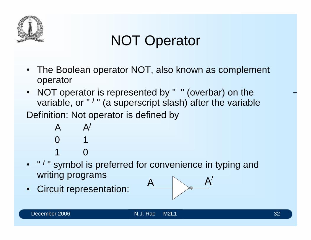
December 2006 N.J. Rao M2L1 32
NOT Operator
The Boolean operator NOT, also known as complement operator
NOT operator is represented by " " (overbar) on the variable, or " / " (a superscript slash) after the variable
Definition: Not operator is defined byA A/
0 1 1 0
" / " symbol is preferred for convenience in typing and writing programs
Circuit representation:
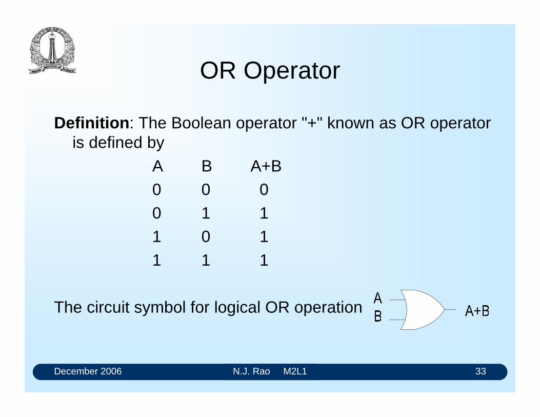
December 2006 N.J. Rao M2L1 33
OR Operator
Definition: The Boolean operator "+" known as OR operator is defined by
A B A+B0 0 00 1 11 0 11 1 1
The circuit symbol for logical OR operation
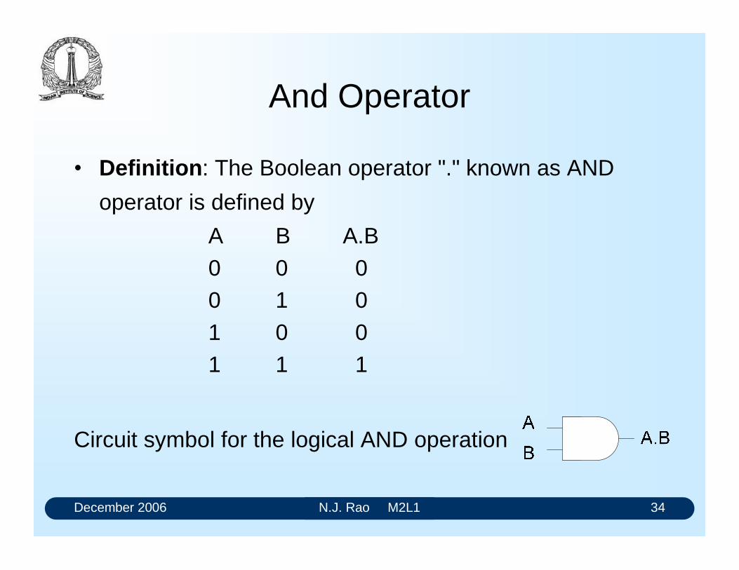
December 2006 N.J. Rao M2L1 34
And Operator
Definition: The Boolean operator "." known as AND
operator is defined by
A B A.B0 0 00 1 01 0 01 1 1
Circuit symbol for the logical AND operation
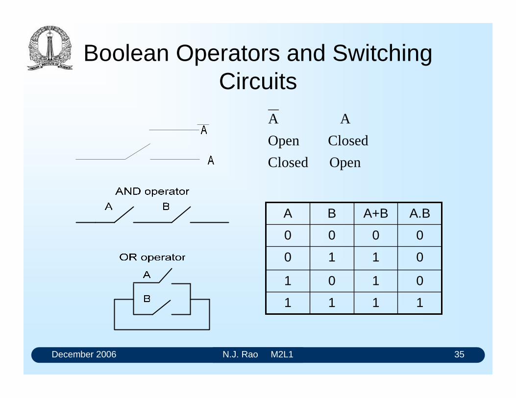
December 2006 N.J. Rao M2L1 35
Boolean Operators and Switching Circuits
Open Closed
Closed Open
A A
1111
0101
0110
0000
A.BA+BBA
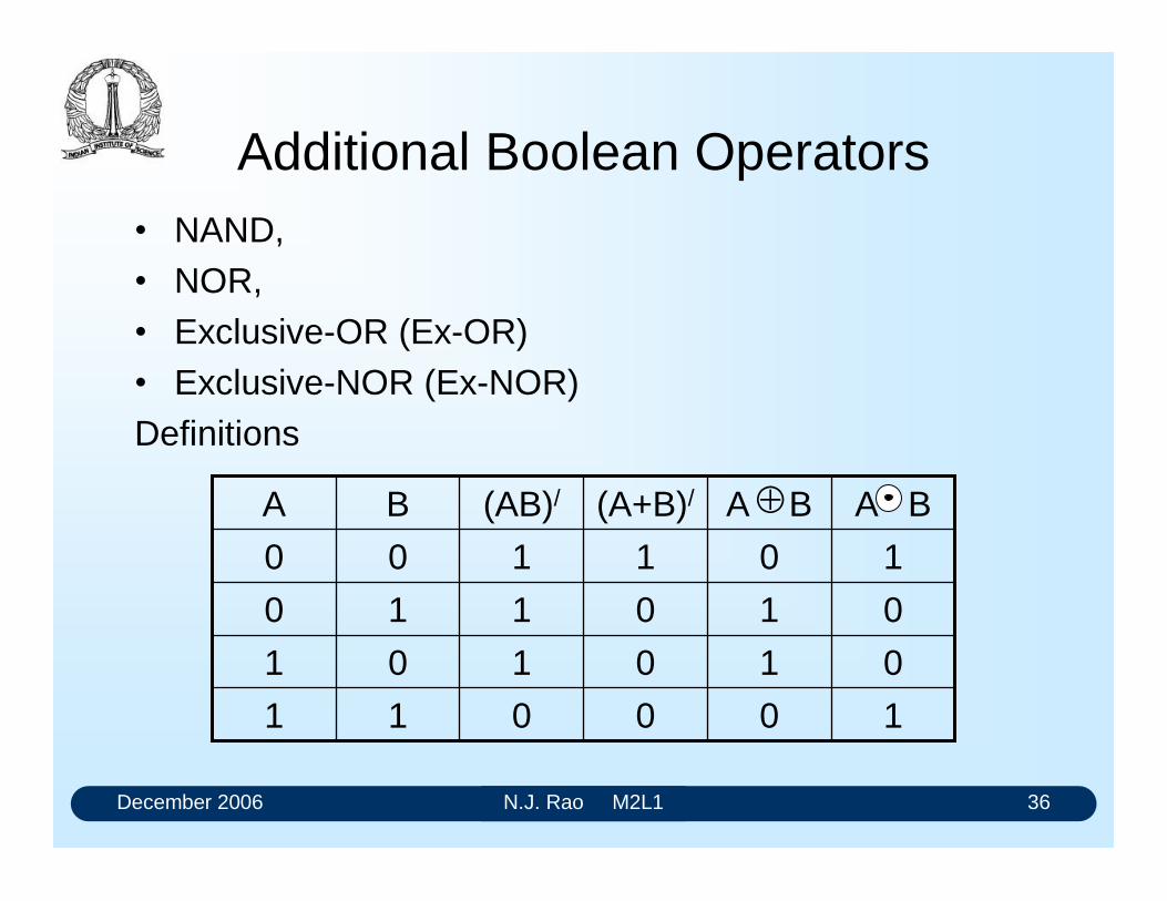
December 2006 N.J. Rao M2L1 36
Additional Boolean Operators NAND, NOR, Exclusive-OR (Ex-OR) Exclusive-NOR (Ex-NOR) Definitions
100011
010101
010110
101100
A BA B(A+B)/(AB)/BA
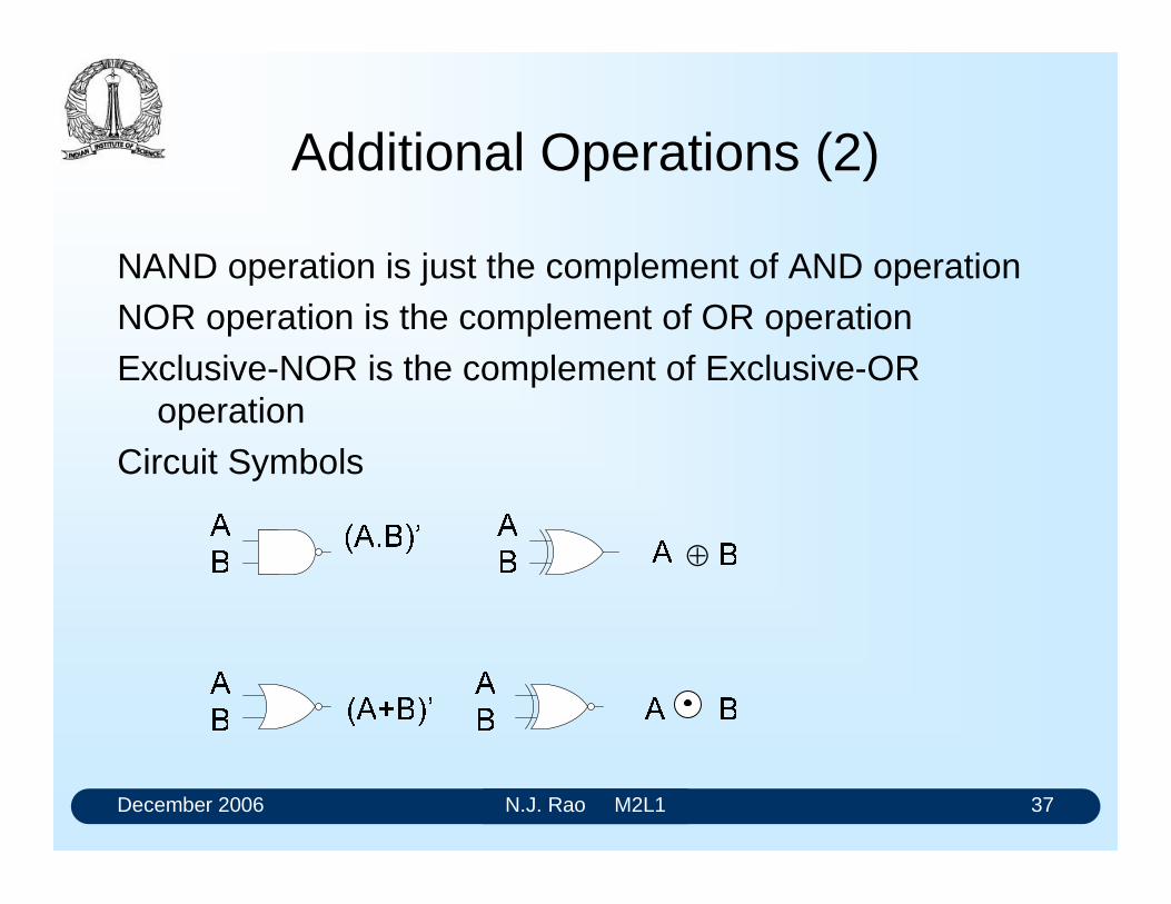
December 2006 N.J. Rao M2L1 37
Additional Operations (2)
NAND operation is just the complement of AND operation NOR operation is the complement of OR operationExclusive-NOR is the complement of Exclusive-OR
operationCircuit Symbols
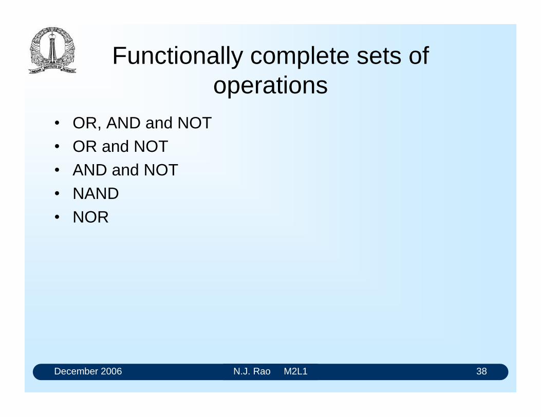
December 2006 N.J. Rao M2L1 38
Functionally complete sets of operations
OR, AND and NOT OR and NOT AND and NOT NAND NOR
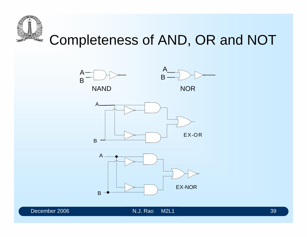
December 2006 N.J. Rao M2L1 39
Completeness of AND, OR and NOT
AB
NOR
AB
NAND
A
BEX-OR
A
BEX-NOR
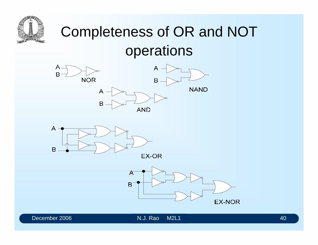
December 2006 N.J. Rao M2L1 40
Completeness of OR and NOT operations
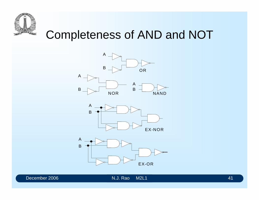
December 2006 N.J. Rao M2L1 41
Completeness of AND and NOT
A
BOR
A
BNOR
AB
NAND
A
B
EX-NOR
A
B
EX-OR
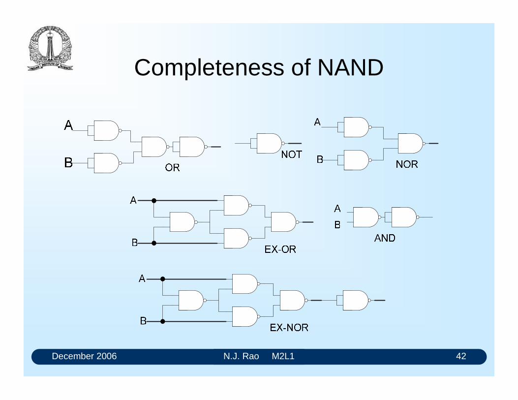
December 2006 N.J. Rao M2L1 42
Completeness of NAND
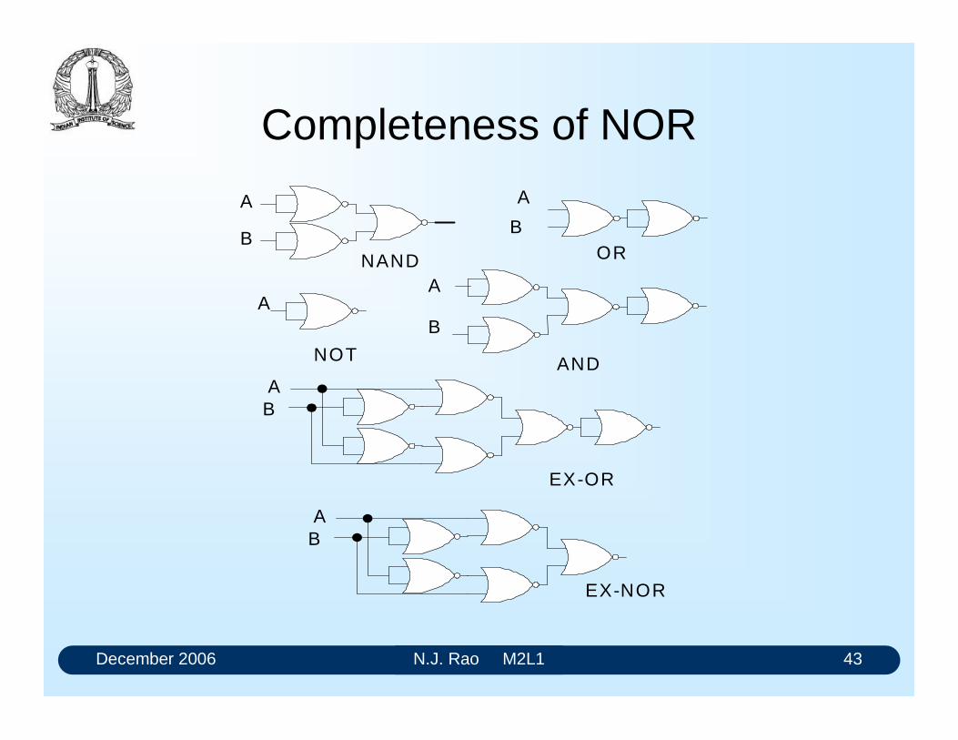
December 2006 N.J. Rao M2L1 43
Completeness of NOR
A
BOR
A
B
AND
A
NOT
A
BNAND
AB
EX-NOR
AB
EX-OR

WHAT IS BOOLEAN ALGEBRA?
Consider the electrical circuit that controls the lighting of a bulb.
Four switches control the operation of the bulb. The manner in which the operation of
the bulb is controlled can be stated as
The bulb switches on if the switches S1 and S2 are closed, and S3 or S4 is also
closed, otherwise the bulb will not switch on
From this statement one can make the following observations:
• Any switch has two states: “closed” or “open”
• The bulb is switched on only when the switches are in some well defined
combination of states.
• The possible combinations are expressed through two types of relationships:
“and” and “or”.
• The two possible combinations are
“S1 and S2 and S3 are closed”
“S1 and S2 and S4 are closed”
There are many situations of engineering interest where the variables take only a small
number of possible values.
Some examples:
• Relay network used in telephone exchanges of earlier era
• Testing through multiple choice questions
• Mechanical display boards in airports and railway stations
• Choices available at road junctions.
Can you identify a situation of significance where the variables can take only a small
number of distinctly defined states?
How do we implement functions similar to the example shown above? We need devices
that have finite number states. It seems to be easy to create devices with two well
defined states. It is more difficult and more expensive to create devices with more than
two states.
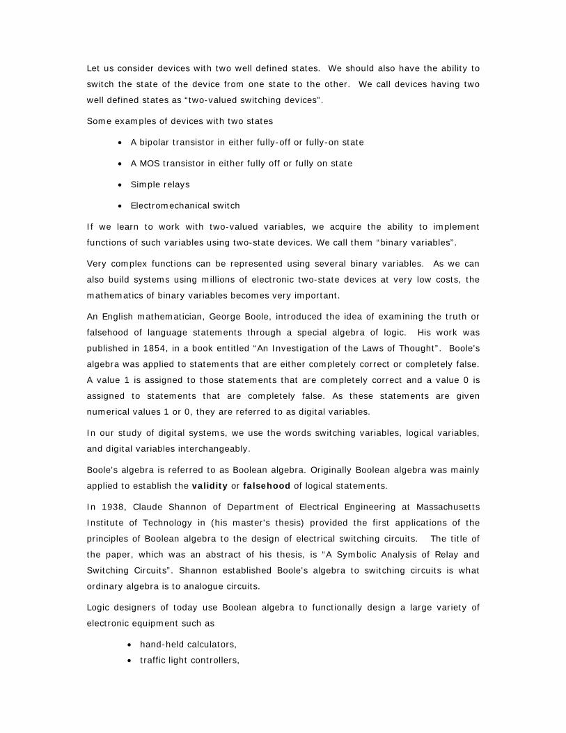
Let us consider devices with two well defined states. We should also have the ability to
switch the state of the device from one state to the other. We call devices having two
well defined states as “two-valued switching devices”.
Some examples of devices with two states
• A bipolar transistor in either fully-off or fully-on state
• A MOS transistor in either fully off or fully on state
• Simple relays
• Electromechanical switch
If we learn to work with two-valued variables, we acquire the ability to implement
functions of such variables using two-state devices. We call them “binary variables”.
Very complex functions can be represented using several binary variables. As we can
also build systems using millions of electronic two-state devices at very low costs, the
mathematics of binary variables becomes very important.
An English mathematician, George Boole, introduced the idea of examining the truth or
falsehood of language statements through a special algebra of logic. His work was
published in 1854, in a book entitled “An Investigation of the Laws of Thought”. Boole's
algebra was applied to statements that are either completely correct or completely false.
A value 1 is assigned to those statements that are completely correct and a value 0 is
assigned to statements that are completely false. As these statements are given
numerical values 1 or 0, they are referred to as digital variables.
In our study of digital systems, we use the words switching variables, logical variables,
and digital variables interchangeably.
Boole's algebra is referred to as Boolean algebra. Originally Boolean algebra was mainly
applied to establish the validity or falsehood of logical statements.
In 1938, Claude Shannon of Department of Electrical Engineering at Massachusetts
Institute of Technology in (his master's thesis) provided the first applications of the
principles of Boolean algebra to the design of electrical switching circuits. The title of
the paper, which was an abstract of his thesis, is “A Symbolic Analysis of Relay and
Switching Circuits”. Shannon established Boole's algebra to switching circuits is what
ordinary algebra is to analogue circuits.
Logic designers of today use Boolean algebra to functionally design a large variety of
electronic equipment such as
• hand-held calculators,
• traffic light controllers,

• personal computers,
• super computers,
• communication systems
• aerospace equipment
• etc.
We next explore Boolean algebra at the axiomatic level. However, we do not worry about
the devices that would be used to implement them and their limitations.

Boolean Algebra and Huntington Postulates
Any branch of mathematics starts with a set of self-evident statements known as
postulates, axioms or maxims. These are stated without any proof.
Boolean algebra is a specific instance of Algebra of Propositional Logic.
E.V.Huntington presented basic postulates of Boolean Algebra in 1904 in his paper
“Sets of Independent Postulates for the Algebra of Logic”. He defined a multi-valued
Boolean algebra on a set of finite number of elements.
In Boolean algebra as applied to the switching circuits, all variables and relations are
two-valued. The two values are normally chosen as 0 and 1, with 0 representing
false and 1 representing true. If x is a Boolean variable, then
x = 1 means x is true
x = 0 means x is false
When we apply Boolean algebra to digital circuits we will find that the qualifications
“asserted” and “not-asserted” are better names than “true” and “false”. That is when
x = 1 we say x is asserted, and when x = 0 we say x is not-asserted.
You are expected to be familiar with
• Concept of a set
• Meaning of equivalence relation
• The principle of substitution
Definition: A Boolean algebra consists of a finite set of elements BS subject to
• Equivalence relation "=",
• One unary operator “not” (symbolised by an over bar),
• Two binary operators "." and "+",
• For every element x and y ∈ BS the operations x (not x), x.y and x +y are
uniquely defined.
The unary operator ‘not’ is defined by the relation
1= 0; 0 = 1
The not operator is also called the complement, and consequently x is the
complement of x.
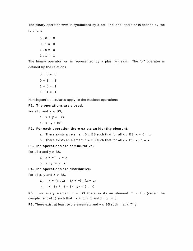
The binary operator ‘and’ is symbolized by a dot. The ‘and’ operator is defined by the
relations
0 . 0 = 0
0 . 1 = 0
1 . 0 = 0
1 . 1 = 1
The binary operator ‘or’ is represented by a plus (+) sign. The ‘or’ operator is
defined by the relations
0 + 0 = 0
0 + 1 = 1
1 + 0 = 1
1 + 1 = 1
Huntington's postulates apply to the Boolean operations
P1. The operations are closed.
For all x and y ∈ BS,
a. x + y ∈ BS
b. x . y ∈ BS
P2. For each operation there exists an identity element.
a. There exists an element 0 ∈ BS such that for all x ∈ BS, x + 0 = x
b. There exists an element 1 ∈ BS such that for all x ∈ BS, x . 1 = x
P3. The operations are commutative.
For all x and y ∈ BS,
a. x + y = y + x
b. x . y = y . x
P4. The operations are distributive.
For all x, y and z ∈ BS,
a. x + (y . z) = (x + y) . (x + z)
b. x . (y + z) = (x . y) + (x . z)
P5. For every element x ∈ BS there exists an element x ∈ BS (called the
complement of x) such that x + x = 1 and x . x = 0
P6. There exist at least two elements x and y ∈ BS such that x ≠ y.

Propositions from Huntington’s Postulates
We derive several new propositions using the basic Huntington’s postulates.
Through these propositions we will be able to explore the structures and implications
of that branch of mathematics. Such propositions are called theorems. A theorem
gives a relationship among the variables.
Definition: A Boolean expression is a constant, 1 or 0, a single Boolean variable or
its complement, or several constants and/or Boolean variables and/or their
complements used in combination with one or more binary operators.
According to this definition 0, 1, x and x are Boolean expressions. If A and B are
Boolean expressions, then A , B , A+B and A.B are also Boolean expressions.
Duality: Many of the Huntington’s postulates are given as pairs, and differ only by
the simultaneous interchange of operators "+" and "." and the elements "0" and "1".
This special property is called duality.
The property of duality can be utilized effectively to establish many useful properties
of Boolean algebra.
The duality principle
“If two expressions can be proven equivalent by applying a sequence of basic
postulates, then the dual expressions can be proven equivalent by simply applying
the sequence of dual postulates”
This implies that for each Boolean property, which we establish, the dual property is
also valid without needing additional proof.
Let us derive some useful properties:
Property 1: Special law of 0 and 1
For all x ∈ BS,
a. x . 0 = 0
b. x + 1 = 1
Proof: x . 0 = (x . 0) + 0 (postulate 2a)
= (x . 0) + (x . x ) (postulate 5b)
= x . (0 + x ) (postulate 4b)
= x . x (postulate 2a)
= 0 (postulate 5b)
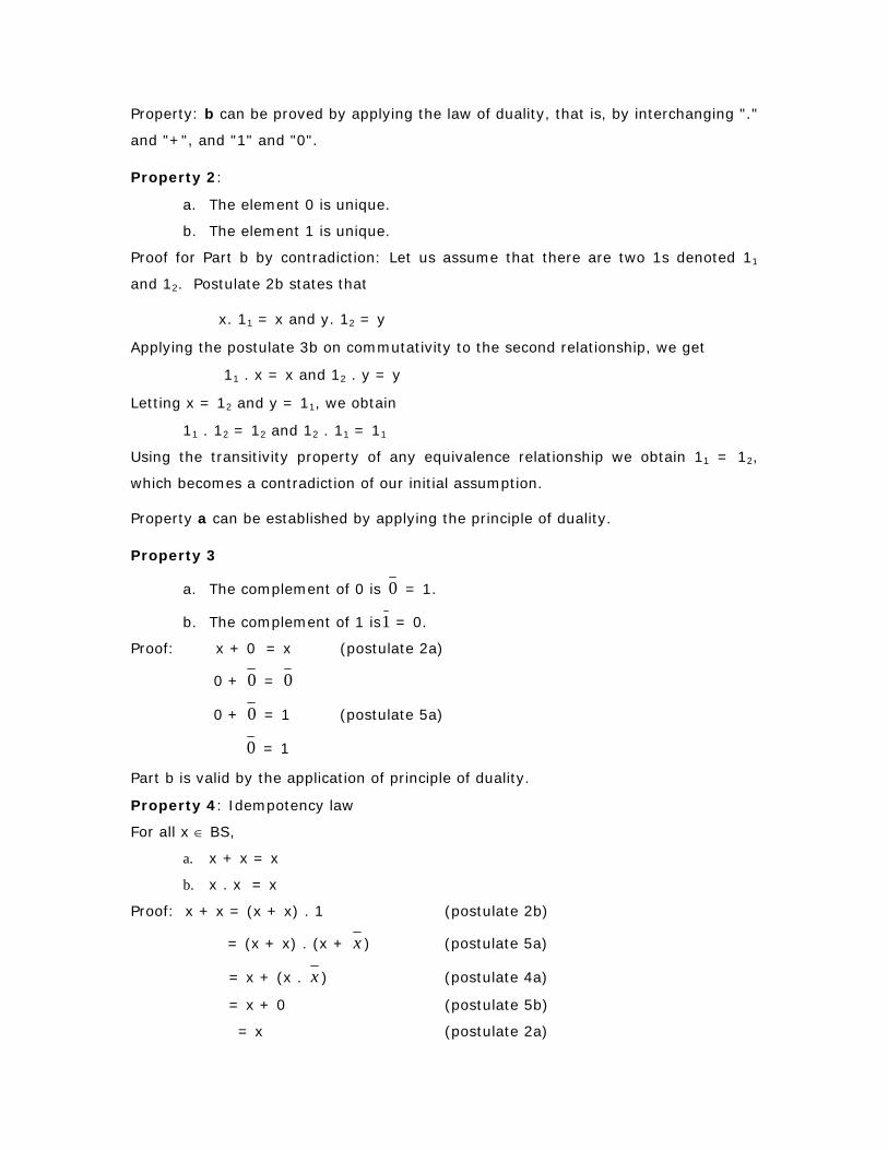
Property: b can be proved by applying the law of duality, that is, by interchanging "."
and "+", and "1" and "0".
Property 2:
a. The element 0 is unique.
b. The element 1 is unique.
Proof for Part b by contradiction: Let us assume that there are two 1s denoted 11
and 12. Postulate 2b states that
x. 11 = x and y. 12 = y
Applying the postulate 3b on commutativity to the second relationship, we get
11 . x = x and 12 . y = y
Letting x = 12 and y = 11, we obtain
11 . 12 = 12 and 12 . 11 = 11
Using the transitivity property of any equivalence relationship we obtain 11 = 12,
which becomes a contradiction of our initial assumption.
Property a can be established by applying the principle of duality.
Property 3
a. The complement of 0 is 0 = 1.
b. The complement of 1 is1 = 0.
Proof: x + 0 = x (postulate 2a)
0 + 0 = 0
0 + 0 = 1 (postulate 5a)
0 = 1
Part b is valid by the application of principle of duality.
Property 4: Idempotency law
For all x ∈ BS,
a. x + x = x
b. x . x = x
Proof: x + x = (x + x) . 1 (postulate 2b)
= (x + x) . (x + x ) (postulate 5a)
= x + (x . x ) (postulate 4a)
= x + 0 (postulate 5b)
= x (postulate 2a)
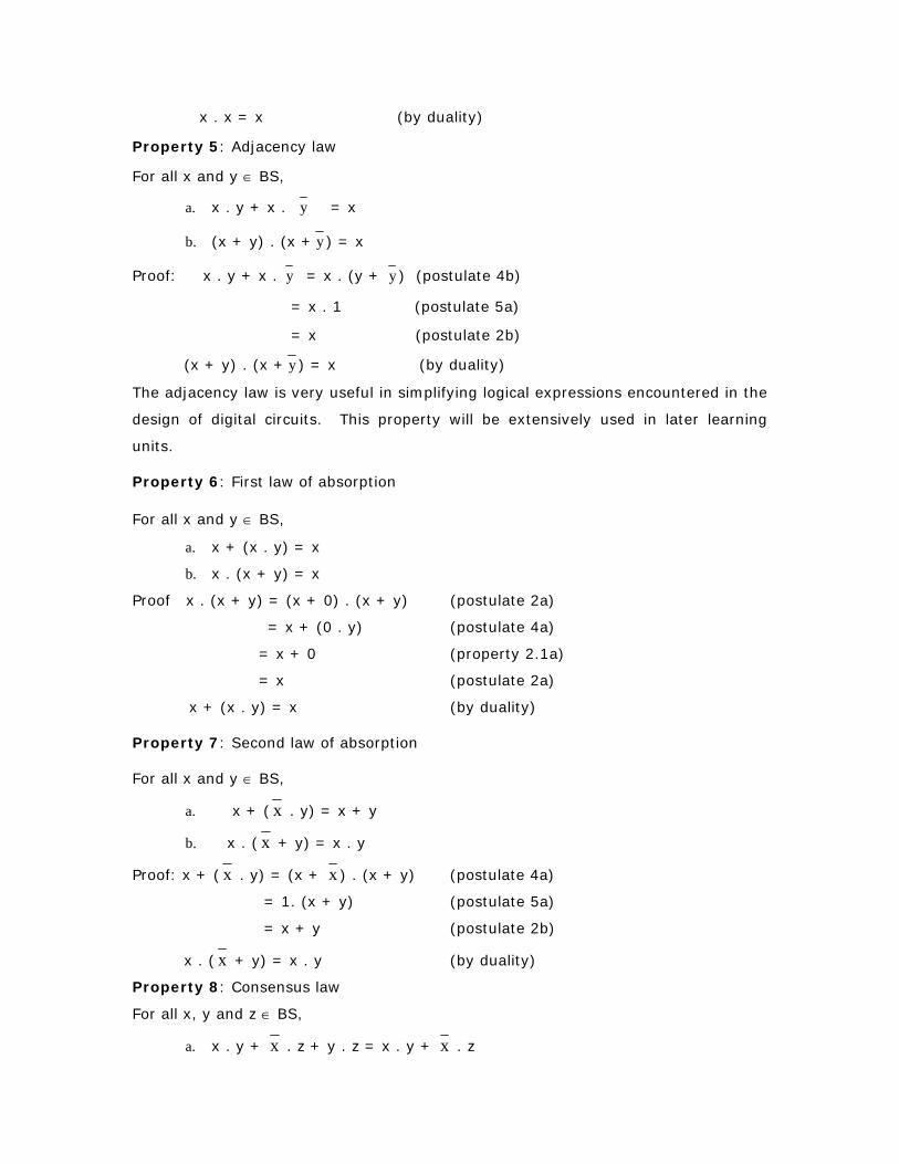
x . x = x (by duality)
Property 5: Adjacency law
For all x and y ∈ BS,
a. x . y + x . y = x
b. (x + y) . (x + y ) = x
Proof: x . y + x . y = x . (y + y ) (postulate 4b)
= x . 1 (postulate 5a)
= x (postulate 2b)
(x + y) . (x + y ) = x (by duality)
The adjacency law is very useful in simplifying logical expressions encountered in the
design of digital circuits. This property will be extensively used in later learning
units.
Property 6: First law of absorption
For all x and y ∈ BS,
a. x + (x . y) = x
b. x . (x + y) = x
Proof x . (x + y) = (x + 0) . (x + y) (postulate 2a)
= x + (0 . y) (postulate 4a)
= x + 0 (property 2.1a)
= x (postulate 2a)
x + (x . y) = x (by duality)
Property 7: Second law of absorption
For all x and y ∈ BS,
a. x + ( x . y) = x + y
b. x . ( x + y) = x . y
Proof: x + ( x . y) = (x + x ) . (x + y) (postulate 4a)
= 1. (x + y) (postulate 5a)
= x + y (postulate 2b)
x . ( x + y) = x . y (by duality)
Property 8: Consensus law
For all x, y and z ∈ BS,
a. x . y + x . z + y . z = x . y + x . z

b. (x + y) . ( x + z) . (y + z) = (x + y) . ( x + z)
Proof: x . y + x . z + y . z
= x . y + x . z + 1 . y . z (postulate 2b)
= x . y + x . z + (x + x ) . y . z (postulate 5a)
= x . y + x . z + x . y . z + x . y . z (postulate 4b)
= x . y + x . y . z + x . z + x . y . z (postulate 3a)
= x . y . (1 + z) + x . z . ( 1 + y) (postulate 4b)
= x . y . 1 + x . z . 1 (property 2.1b)
= x . y + x . z (postulate 2b)
(x + y) . ( x + z) . (y + z) = (x + y) . ( x + z) (by duality)
Property 9: Law of identity
For all x and y ε BS, if
a. x + y = y
b. x . y = y, then x = y
Proof: Substituting (a) into the left-hand side of (b), we have
x . (x + y) = y
However by the first law of absorption
x . (x + y) = x (property 6)
Therefore, by transitivity x = y
Property 10: The law of involution
For all x ∈ BS, x = x
Proof: We need to show that the law of identity (property 2.9) holds, that is,
( x + x) = x and x . x = x
x = 0x + (postulate 2a)
= )x.x(x + (postulate 5b)
= )xx).(xx( ++ (postulate 4a)
= 1).xx( + (postulate 5a)
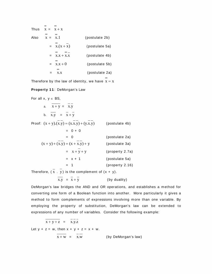
Thus x = xx +
Also x = 1.x (postulate 2b)
= )xx.(x + (postulate 5a)
= x.xx.x + (postulate 4b)
= 0x.x + (postulate 5b)
= x.x (postulate 2a)
Therefore by the law of identity, we have xx =
Property 11: DeMorgan's Law
For all x, y ∈ BS,
a. yx + = y.x
b. y.x = yx +
Proof: )y.x(y.)y.x(x.)y.x).(yx( +=+ (postulate 4b)
= 0 + 0
= 0 (postulate 2a)
y)y.x(x)y.x(y)(x ++=++ (postulate 3a)
= yyx ++ (property 2.7a)
= x + 1 (postulate 5a)
= 1 (property 2.16)
Therefore, ( x . y ) is the complement of (x + y).
x.y = yx + (by duality)
DeMorgan's law bridges the AND and OR operations, and establishes a method for
converting one form of a Boolean function into another. More particularly it gives a
method to form complements of expressions involving more than one variable. By
employing the property of substitution, DeMorgan's law can be extended to
expressions of any number of variables. Consider the following example:
zyx ++ = z.y.x
Let y + z = w, then x + y + z = x + w.
wx + = w.x (by DeMorgan's law)

wx + = zyx ++ (by substitution)
= zy.x + (by DeMorgan's law)
= z.y.x (by DeMorgan's law)
At the end of this Section the reader should remind himself that all the postulates
and properties of Boolean algebra are valid when the number of elements in the BS
is finite. The case of the set BS having only two elements is of more interest here
and in the topics that follow in this course on Design of Digital systems.
All the identities derived in this Section are listed in the Table 1 to serve as a ready
reference.
TABLE: Useful Identities of Boolean Algebra
Complementation 0xx. =
1xx =+
0 - 1 law x.0 = 0
x+1 = 1
x+0 = x
x.1 = x
Idempotency x.x = x
x+x = x
Involution xx =
Commutative law x . y = y . x
X + y = y + x
Associative law (x . y).z = x. (y.z)
(x + y) + z = x + (y+z)
Distributive law x + (y.z) = (x+y).(x+z)
X . (y+z) = x.y +x.z
Adjacency law xyx.x.y =+
xy)y).(x(x =++
Absorption law x + x . y = x

x . (x+y) = x
yx.yxx +=+
x.yy)xx.( =+
Consensus law .zxx.yy.z.zxx.y +=++
z)xy).((xz)z).(yxy).((x ++=+++
DeMorgan's law y.xyx =+
yxx.y +=
The properties of Boolean algebra when the set BS has two elements, namely 0 and
1, will be explored next.
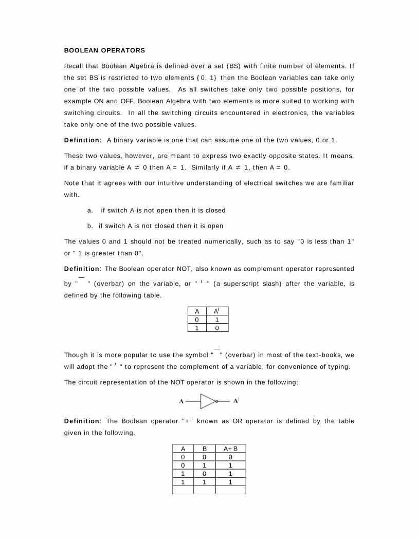
BOOLEAN OPERATORS
Recall that Boolean Algebra is defined over a set (BS) with finite number of elements. If
the set BS is restricted to two elements 0, 1 then the Boolean variables can take only
one of the two possible values. As all switches take only two possible positions, for
example ON and OFF, Boolean Algebra with two elements is more suited to working with
switching circuits. In all the switching circuits encountered in electronics, the variables
take only one of the two possible values.
Definition: A binary variable is one that can assume one of the two values, 0 or 1.
These two values, however, are meant to express two exactly opposite states. It means,
if a binary variable A ≠ 0 then A = 1. Similarly if A ≠ 1, then A = 0.
Note that it agrees with our intuitive understanding of electrical switches we are familiar
with.
a. if switch A is not open then it is closed
b. if switch A is not closed then it is open
The values 0 and 1 should not be treated numerically, such as to say "0 is less than 1"
or " 1 is greater than 0".
Definition: The Boolean operator NOT, also known as complement operator represented
by " " (overbar) on the variable, or " / " (a superscript slash) after the variable, is
defined by the following table.
A A/ 0 1 1 0
Though it is more popular to use the symbol " " (overbar) in most of the text-books, we
will adopt the " / " to represent the complement of a variable, for convenience of typing.
The circuit representation of the NOT operator is shown in the following:
Definition: The Boolean operator "+" known as OR operator is defined by the table
given in the following.
A B A+B 0 0 0 0 1 1 1 0 1 1 1 1
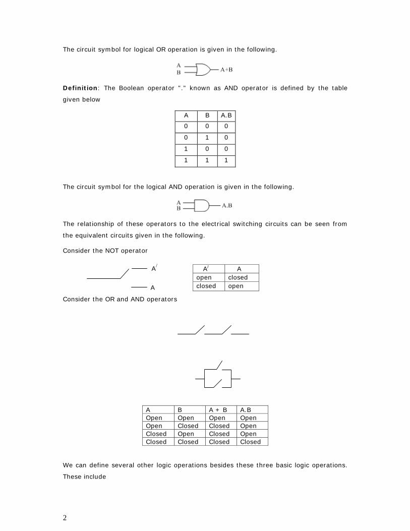
2
The circuit symbol for logical OR operation is given in the following.
Definition: The Boolean operator "." known as AND operator is defined by the table
given below
A B A.B
0 0 0
0 1 0
1 0 0
1 1 1
The circuit symbol for the logical AND operation is given in the following.
The relationship of these operators to the electrical switching circuits can be seen from
the equivalent circuits given in the following.
Consider the NOT operator
Consider the OR and AND operators
A B A + B A.B Open Open Open Open Open Closed Closed Open Closed Open Closed Open Closed Closed Closed Closed
We can define several other logic operations besides these three basic logic operations.
These include
A/ A open closed closed open
A
A/
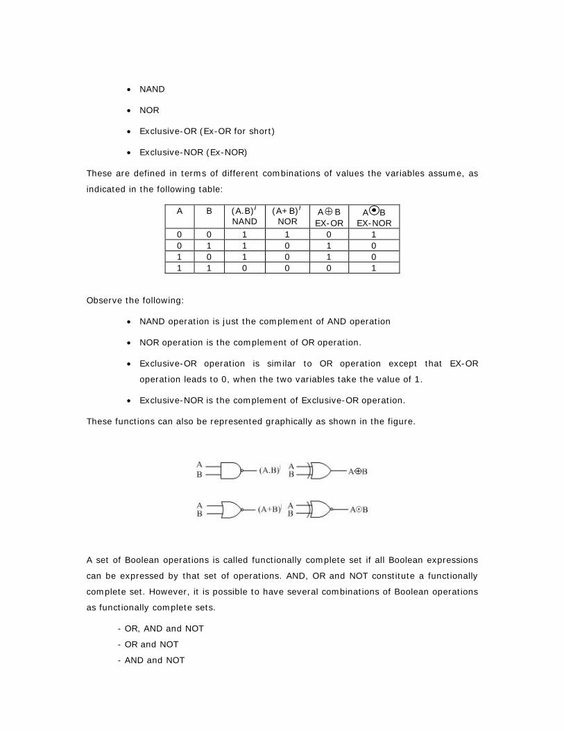
• NAND
• NOR
• Exclusive-OR (Ex-OR for short)
• Exclusive-NOR (Ex-NOR)
These are defined in terms of different combinations of values the variables assume, as
indicated in the following table:
A B (A.B)/
NAND (A+B)/
NOR A⊕B EX-OR
A B EX-NOR
0 0 1 1 0 1 0 1 1 0 1 0 1 0 1 0 1 0 1 1 0 0 0 1
Observe the following:
• NAND operation is just the complement of AND operation
• NOR operation is the complement of OR operation.
• Exclusive-OR operation is similar to OR operation except that EX-OR
operation leads to 0, when the two variables take the value of 1.
• Exclusive-NOR is the complement of Exclusive-OR operation.
These functions can also be represented graphically as shown in the figure.
A set of Boolean operations is called functionally complete set if all Boolean expressions
can be expressed by that set of operations. AND, OR and NOT constitute a functionally
complete set. However, it is possible to have several combinations of Boolean operations
as functionally complete sets.
- OR, AND and NOT
- OR and NOT
- AND and NOT
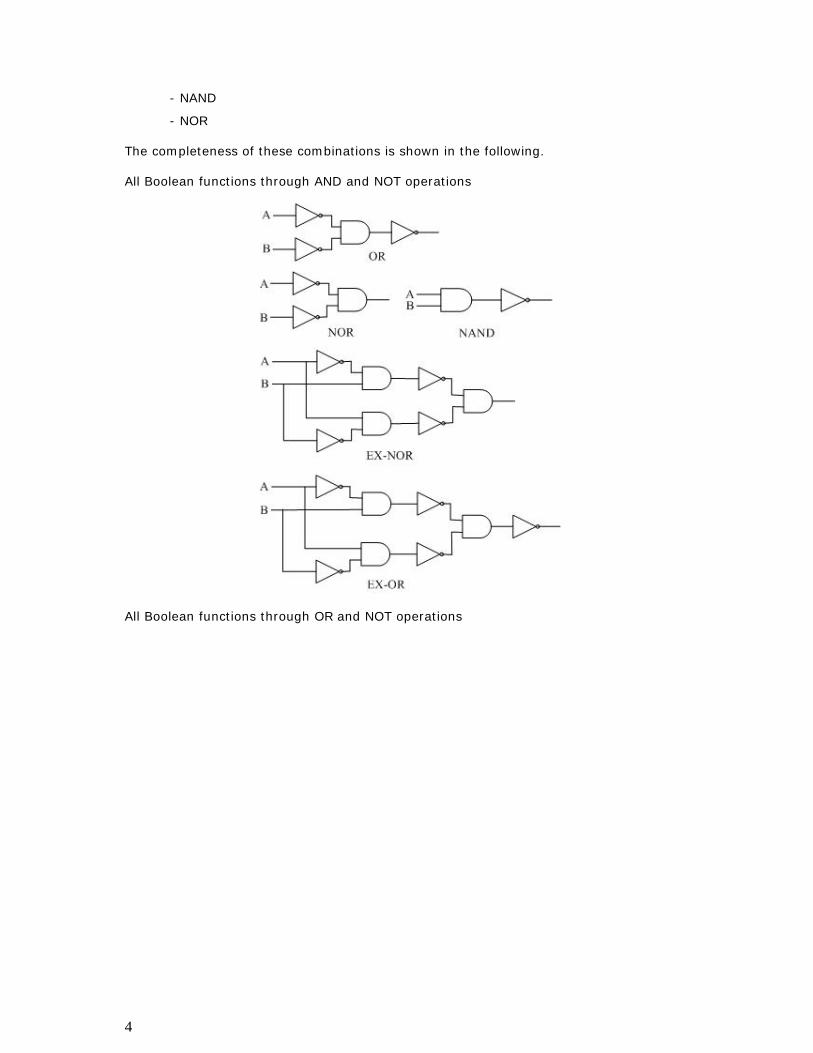
4
- NAND
- NOR
The completeness of these combinations is shown in the following.
All Boolean functions through AND and NOT operations
All Boolean functions through OR and NOT operations
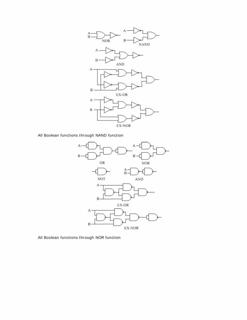
All Boolean functions through NAND function
All Boolean functions through NOR function
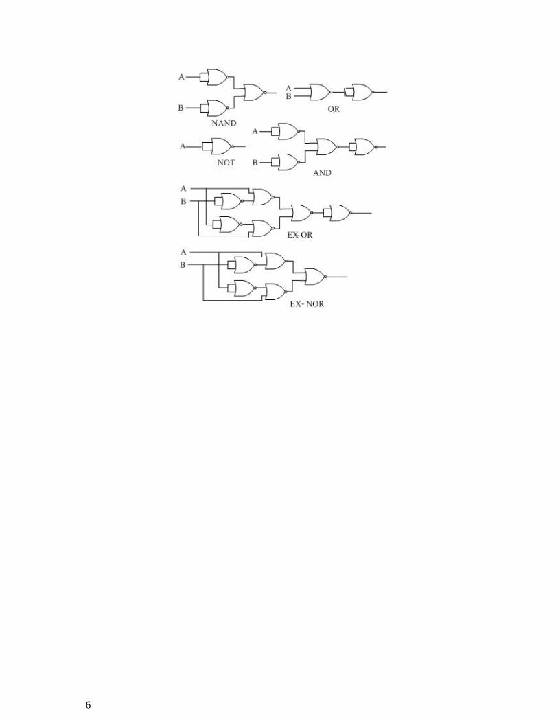
6

Digital Electronics Module 2: Boolean Algebra and Boolean Operators: Logic Functions
N.J. RaoIndian Institute of Science
id4015353 pdfMachine by Broadgun Software - a great PDF writer! - a great PDF creator! - http://www.pdfmachine.com http://www.broadgun.com
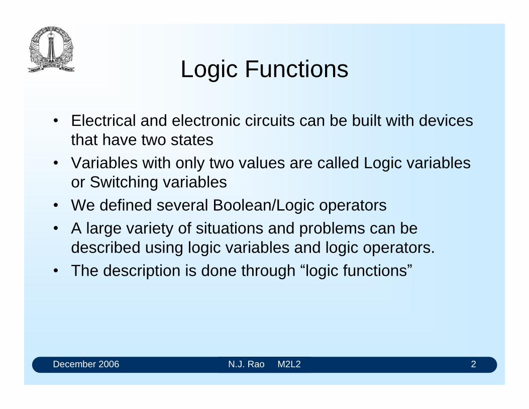
December 2006 N.J. Rao M2L2 2
Logic Functions
Electrical and electronic circuits can be built with devices that have two states
Variables with only two values are called Logic variables or Switching variables
We defined several Boolean/Logic operators A large variety of situations and problems can be
described using logic variables and logic operators. The description is done through logic functions
December 2006 N.J. Rao M2L2 3
Descriptions of logic functions
Algebraic Truth-table Logic circuit Hardware description language MapsEach form of representation is convenient in a different
context.
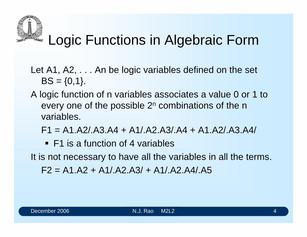
December 2006 N.J. Rao M2L2 4
Logic Functions in Algebraic Form
Let A1, A2, . . . An be logic variables defined on the set BS = 0,1.
A logic function of n variables associates a value 0 or 1 to every one of the possible 2n combinations of the n variables. F1 = A1.A2/.A3.A4 + A1/.A2.A3/.A4 + A1.A2/.A3.A4/ F1 is a function of 4 variables
It is not necessary to have all the variables in all the terms. F2 = A1.A2 + A1/.A2.A3/ + A1/.A2.A4/.A5
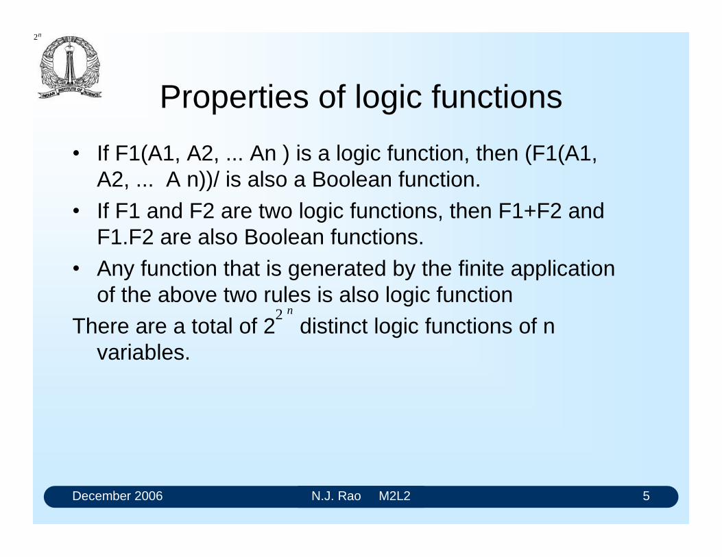
December 2006 N.J. Rao M2L2 5
Properties of logic functions
If F1(A1, A2, ... An ) is a logic function, then (F1(A1, A2, ... A n))/ is also a Boolean function.
If F1 and F2 are two logic functions, then F1+F2 and F1.F2 are also Boolean functions.
Any function that is generated by the finite application of the above two rules is also logic function
There are a total of 2 distinct logic functions of n variables.
2n
2 n
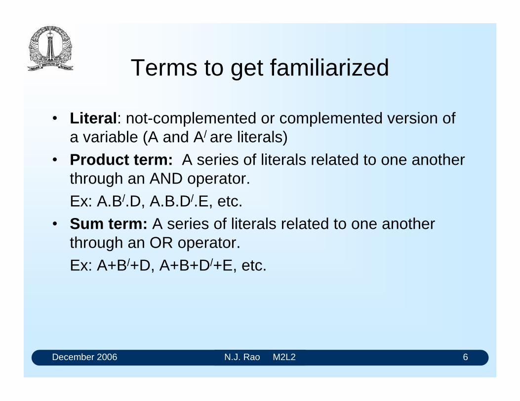
December 2006 N.J. Rao M2L2 6
Terms to get familiarized
Literal: not-complemented or complemented version of a variable (A and A/ are literals)
Product term: A series of literals related to one another through an AND operator. Ex: A.B/.D, A.B.D/.E, etc.
Sum term: A series of literals related to one another through an OR operator. Ex: A+B/+D, A+B+D/+E, etc.
December 2006 N.J. Rao M2L2 7
Truth Table
It is a tabular representation of a logic function. It gives the value of the function for all possible
combinations of the values of the variables For each combination, the function takes either 1 or 0 These combinations are listed in a table, which
constitute the truth table for the given function. The information contained in the truth table and in the
algebraic representation of the function are the same.
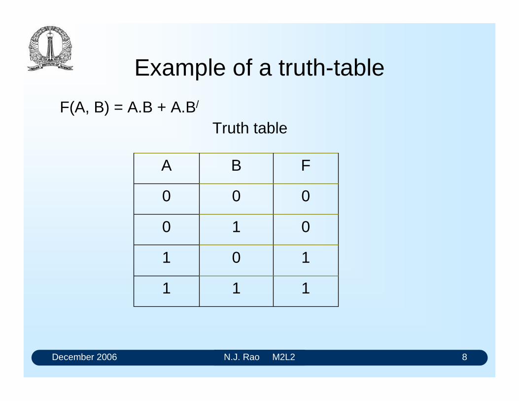
December 2006 N.J. Rao M2L2 8
Example of a truth-table
F(A, B) = A.B + A.B/
Truth table
111
101
010
000
FBA
December 2006 N.J. Rao M2L2 9
Truth and Truth Table
The term truth table came into usage long before Boolean algebra came to be associated with digital electronics.
Boolean functions were originally used to establish truth or falsehood of a statement.
When statement is true the "1" is associated with it When it is false "0" is associated. This usage got extended to the variables associated with
digital circuits
December 2006 N.J. Rao M2L2 10
Inappropriateness of truth and falsity
All variables in digital systems are indicative of actions. Examples: "CLEAR", "LOAD", "SHIFT", "ENABLE", and "COUNT"
They are suggestive of actions. When a variable is asserted, the intended action takes
place When a variable is not asserted the intended action does
not take place Associate "1" with the assertion of a variable, and "0"
with the non-assertion of that variable.
December 2006 N.J. Rao M2L2 11
Assertion and Non-assertion
F = A.B + A.B/
Read it as "F is asserted when A and B are asserted orA is asserted and B is not asserted".
We will continue to use the term "truth table" for historical reasons
We understand it as an input-output table associated with a logic function
but not as something that is concerned with the establishment of truth.
December 2006 N.J. Rao M2L2 12
Size of the Truth-Table
A five variable function would require 32 entries A six-variable function would require 64 entriesWhen the number of variables increase a simple artefact
may be adopted. A truth table will have entries only for those terms for
which the value of the function is "1", without loss of any information.
This is particularly effective when the function has
smaller number of terms.
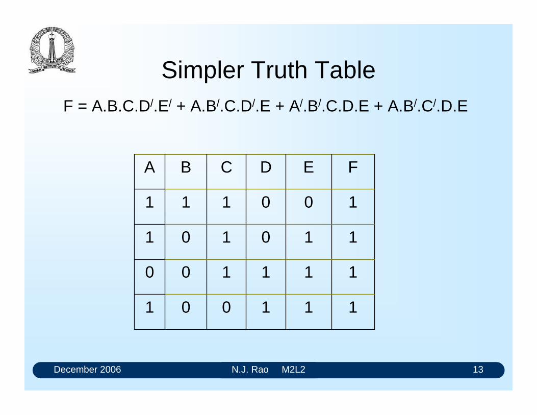
December 2006 N.J. Rao M2L2 13
Simpler Truth TableF = A.B.C.D/.E/ + A.B/.C.D/.E + A/.B/.C.D.E + A.B/.C/.D.E
111001
111100
110101
100111
FEDCBA
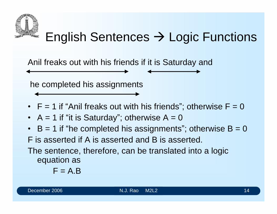
December 2006 N.J. Rao M2L2 14
English Sentences Logic Functions
Anil freaks out with his friends if it is Saturday and
he completed his assignments
F = 1 if Anil freaks out with his friends; otherwise F = 0 A = 1 if it is Saturday; otherwise A = 0 B = 1 if he completed his assignments; otherwise B = 0F is asserted if A is asserted and B is asserted. The sentence, therefore, can be translated into a logic
equation asF = A.B
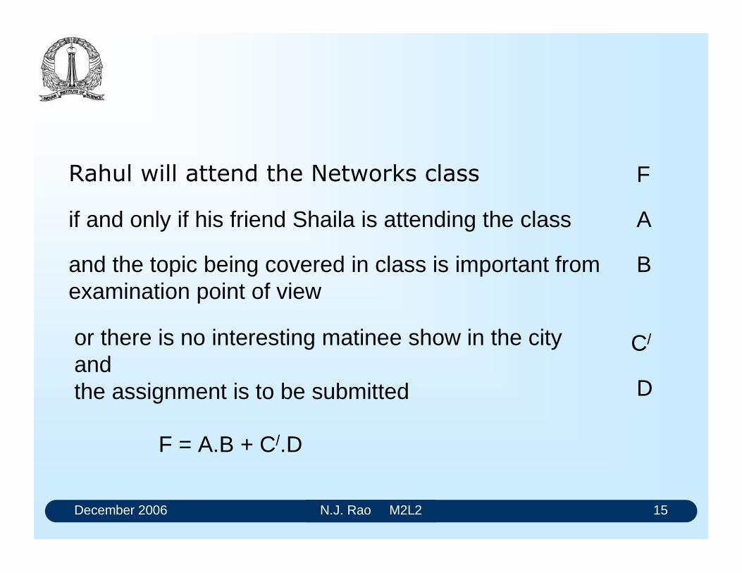
December 2006 N.J. Rao M2L2 15
Rahul will attend the Networks class
if and only if his friend Shaila is attending the class
and the topic being covered in class is important from examination point of view
or there is no interesting matinee show in the city and the assignment is to be submitted
F
A
B
C/
D
F = A.B + C/.D
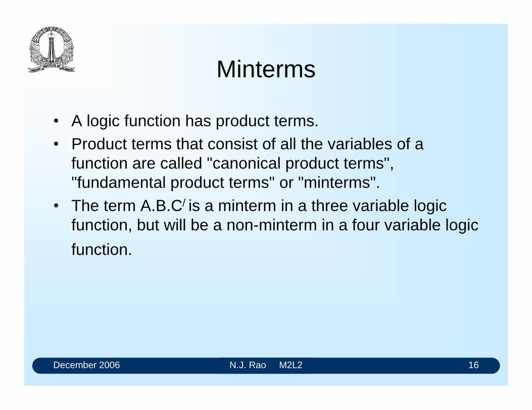
December 2006 N.J. Rao M2L2 16
Minterms
A logic function has product terms. Product terms that consist of all the variables of a
function are called "canonical product terms", "fundamental product terms" or "minterms".
The term A.B.C/ is a minterm in a three variable logic function, but will be a non-minterm in a four variable logic
function.
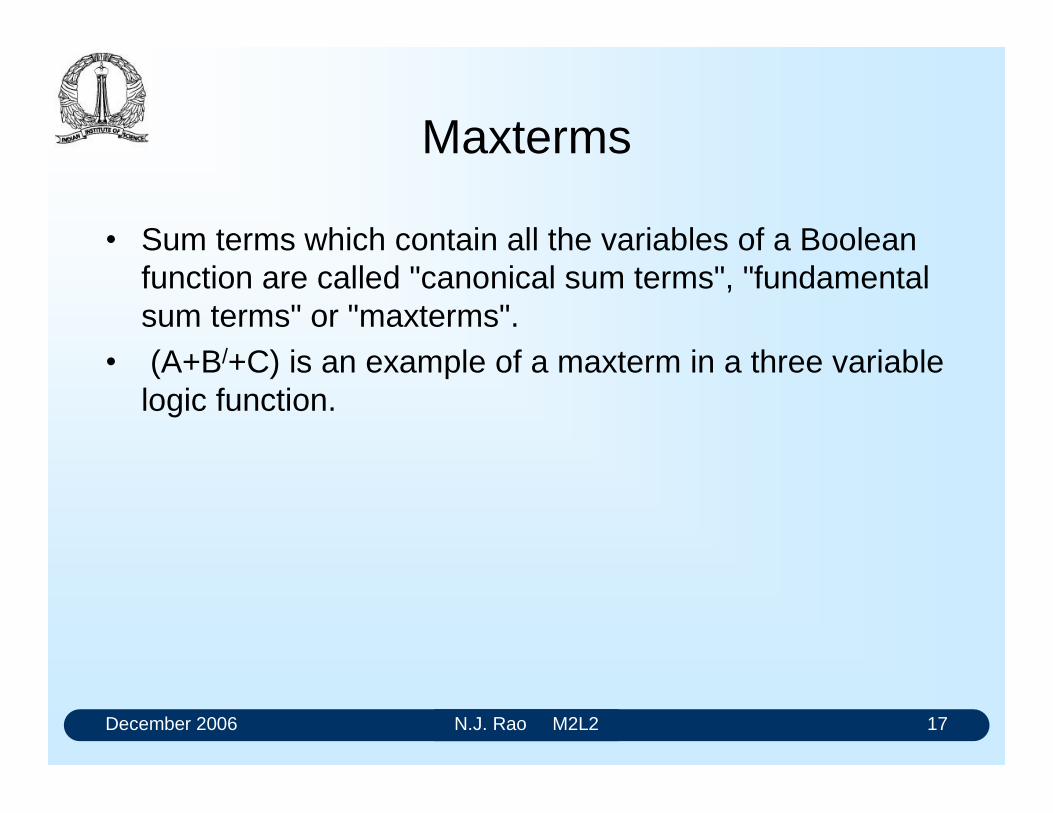
December 2006 N.J. Rao M2L2 17
Maxterms
Sum terms which contain all the variables of a Boolean function are called "canonical sum terms", "fundamental sum terms" or "maxterms".
(A+B/+C) is an example of a maxterm in a three variable logic function.
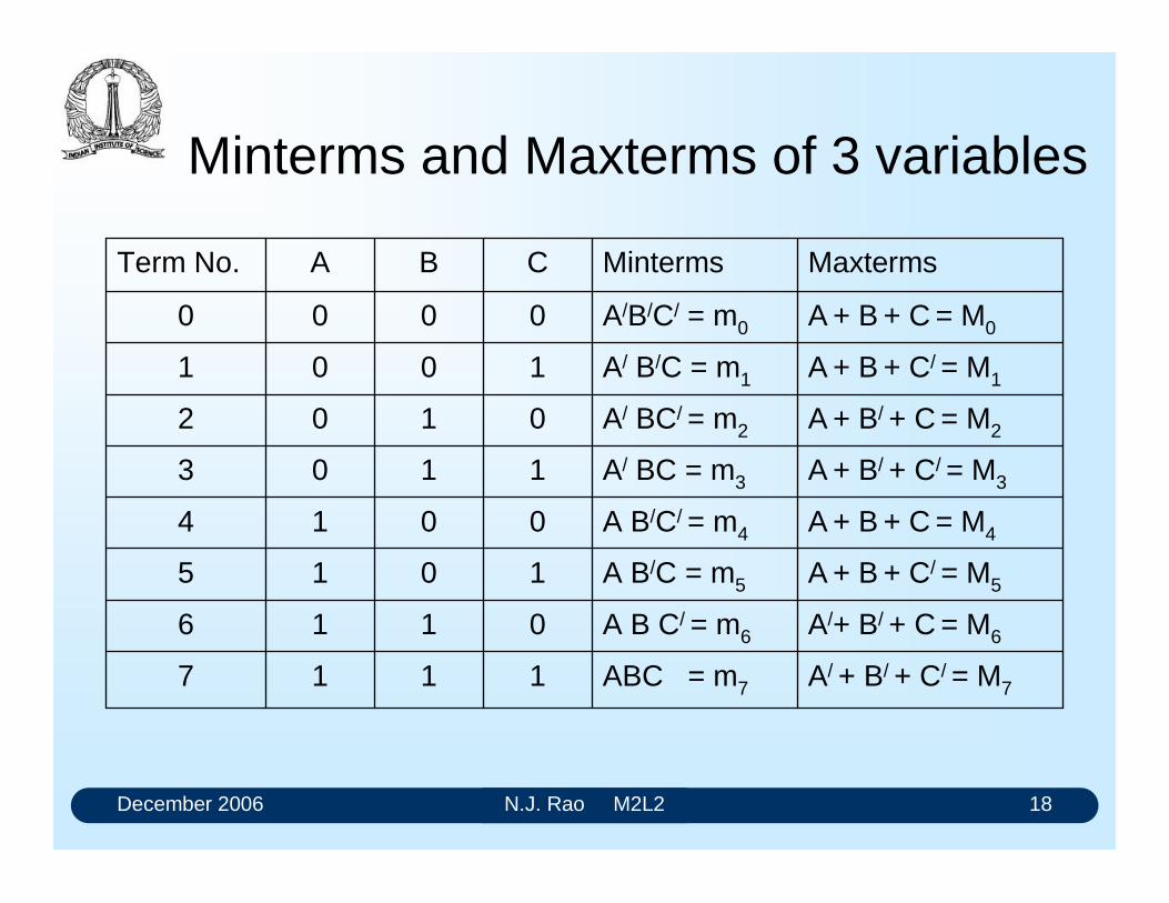
December 2006 N.J. Rao M2L2 18
Minterms and Maxterms of 3 variables
A/ + B/ + C/ = M7ABC = m71117
A/+ B/ + C = M6A B C/ = m60116
A + B + C/ = M5A B/C = m51015
A + B + C = M4A B/C/ = m40014
A + B/ + C/ = M3A/ BC = m31103
A + B/ + C = M2A/ BC/ = m20102
A + B + C/ = M1A/ B/C = m11001
A + B + C = M0A/B/C/ = m00000
MaxtermsMintermsCBATerm No.
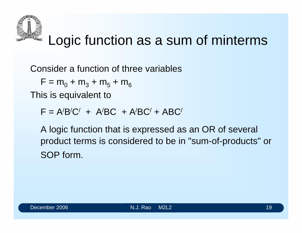
December 2006 N.J. Rao M2L2 19
Logic function as a sum of minterms
Consider a function of three variablesF = m0 + m3 + m5 + m6
This is equivalent to
F = A/B/C/ + A/BC + A/BC/ + ABC/
A logic function that is expressed as an OR of several product terms is considered to be in "sum-of-products" or
SOP form.
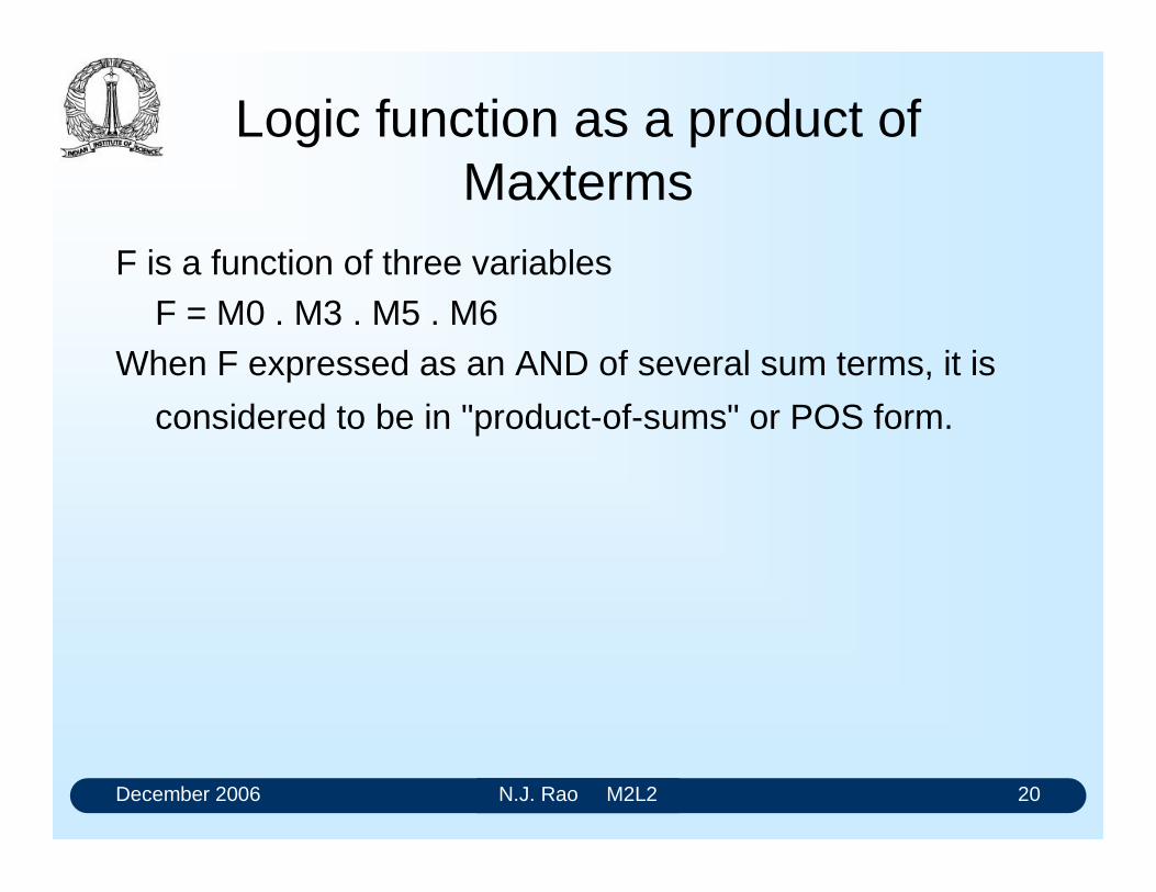
December 2006 N.J. Rao M2L2 20
Logic function as a product of Maxterms
F is a function of three variablesF = M0 . M3 . M5 . M6
When F expressed as an AND of several sum terms, it is
considered to be in "product-of-sums" or POS form.
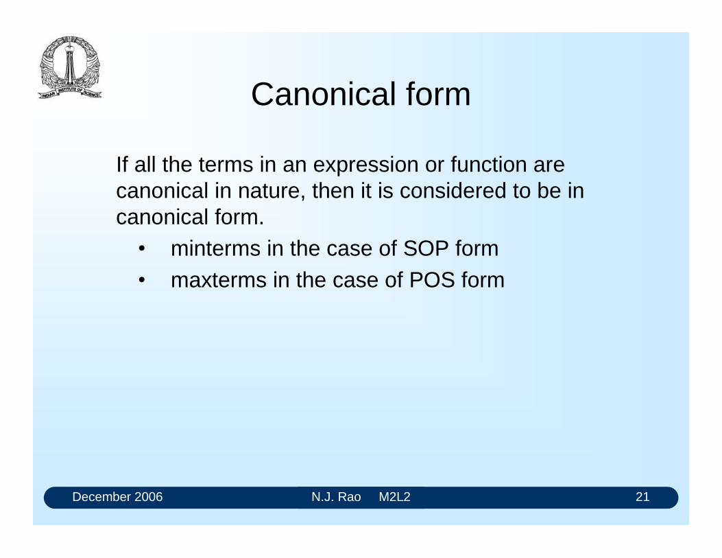
December 2006 N.J. Rao M2L2 21
Canonical form
If all the terms in an expression or function are canonical in nature, then it is considered to be in canonical form. minterms in the case of SOP form maxterms in the case of POS form
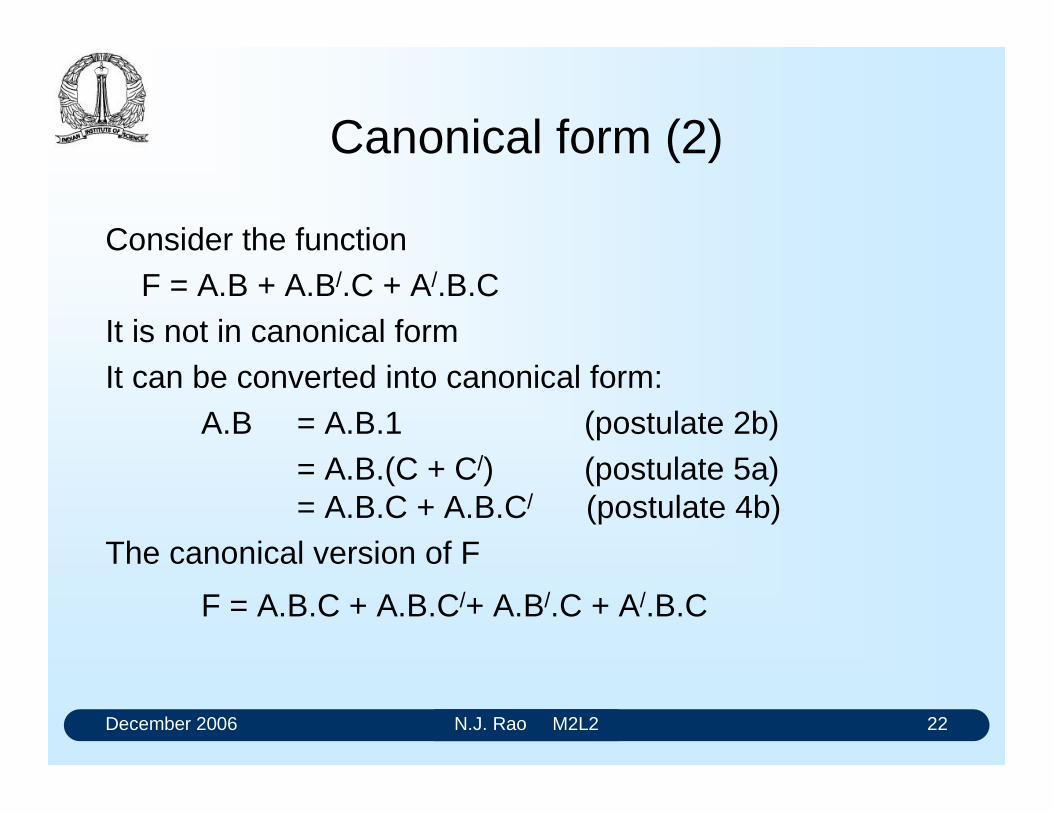
December 2006 N.J. Rao M2L2 22
Canonical form (2)
Consider the functionF = A.B + A.B/.C + A/.B.C
It is not in canonical formIt can be converted into canonical form:
A.B = A.B.1 (postulate 2b) = A.B.(C + C/) (postulate 5a) = A.B.C + A.B.C/ (postulate 4b)
The canonical version of F
F = A.B.C + A.B.C/+ A.B/.C + A/.B.C
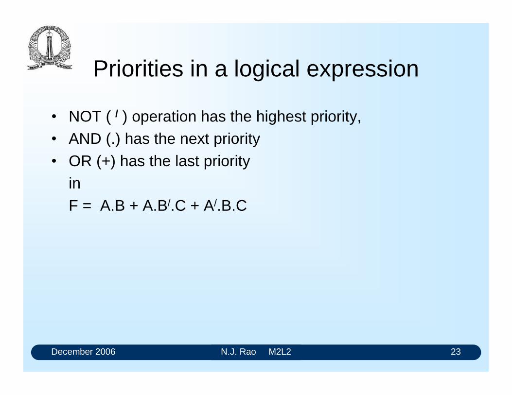
December 2006 N.J. Rao M2L2 23
Priorities in a logical expression
NOT ( / ) operation has the highest priority, AND (.) has the next priority OR (+) has the last priority
in F = A.B + A.B/.C + A/.B.C
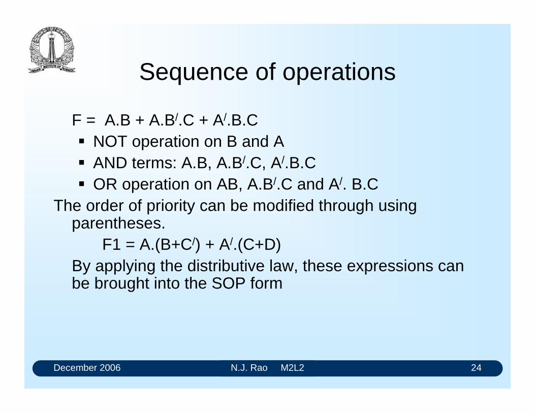
December 2006 N.J. Rao M2L2 24
Sequence of operations
F = A.B + A.B/.C + A/.B.C NOT operation on B and A AND terms: A.B, A.B/.C, A/.B.C OR operation on AB, A.B/.C and A/. B.C
The order of priority can be modified through using parentheses.
F1 = A.(B+C/) + A/.(C+D) By applying the distributive law, these expressions can be brought into the SOP form
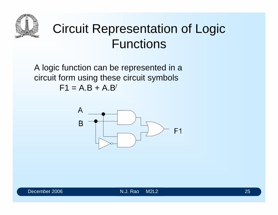
December 2006 N.J. Rao M2L2 25
Circuit Representation of Logic Functions
A logic function can be represented in a circuit form using these circuit symbols
F1 = A.B + A.B/
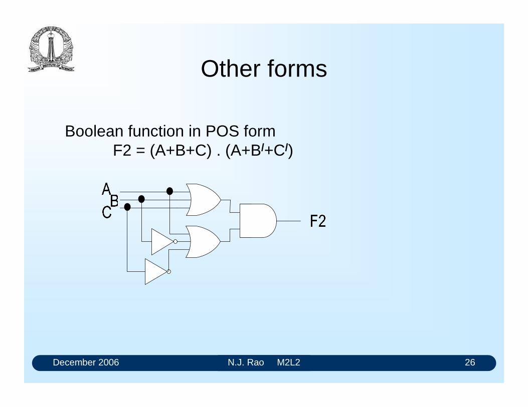
December 2006 N.J. Rao M2L2 26
Other forms
Boolean function in POS formF2 = (A+B+C) . (A+B/+C/)
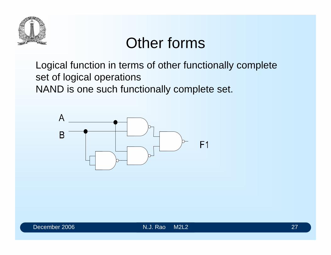
December 2006 N.J. Rao M2L2 27
Other formsLogical function in terms of other functionally complete set of logical operations NAND is one such functionally complete set.
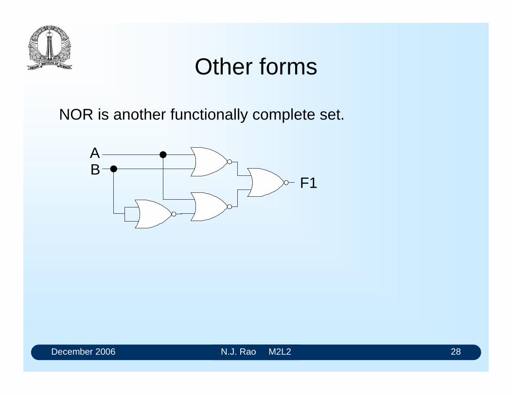
December 2006 N.J. Rao M2L2 28
Other forms
NOR is another functionally complete set.
AB
F1

Logic Functions
Many types of electrical and electronic circuits can be built with devices that have two
possible states. We are, therefore interested in working with variables, which can take
only two values. Such two valued variables are called Logic variables or Switching
variables.
We defined several Boolean operators, which can also be called Logic operators. We will
find that it is possible to describe a wide variety of situations and problems using logic
variables and logic operators. This is done through defining a “logic function” of logic
variables.
We can describe logic functions in several ways. These include
• Algebraic
• Truth-table
• Logic circuit
• Hardware description language
• Maps
We use all these forms to express logic functions in working with digital circuits. Each
form of representation is convenient in some context. Initially we will work with
algebraic, truth-table, and logic circuit representation of logic functions.
The objectives of this learning unit are
1. Writing the output of a logic network, whose word description is given, as a
function of the input variables either as a logic function, a truth-table, or a logic
circuit.
2. Create a truth-table if the description of a logic circuit is given in terms of a logic
function or as a logic circuit.
3. Write a logic function if the description of a logic circuit is given in terms of a
truth-table or as a logic circuit.
4. Create a logic circuit if its description is given in terms of a truth-table or as a
logic function.
5. Expand a given logic function in terms of its minterms or maxterms.
6. Convert a given truth-table into a logic function into minterm or maxterm forms.
7. Explain the nature and role of “don’t care” terms
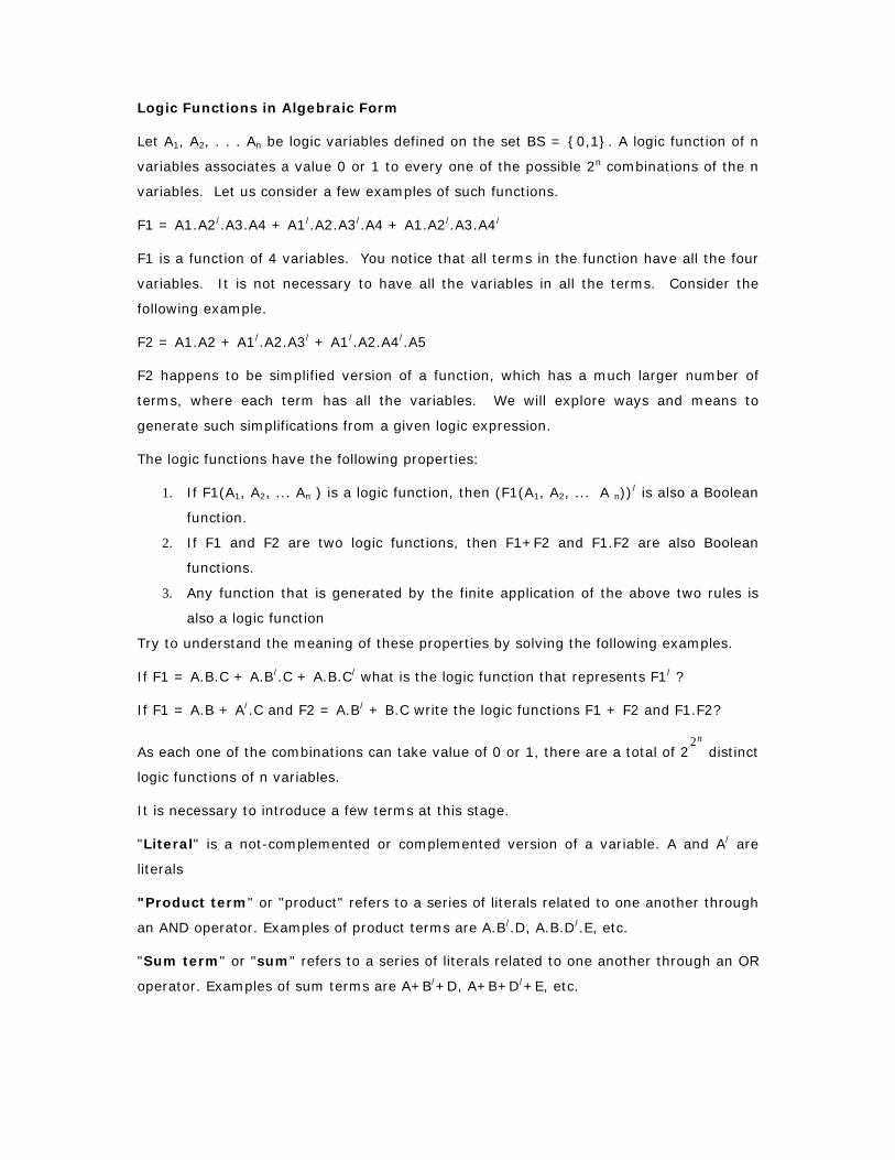
Logic Functions in Algebraic Form
Let A1, A2, . . . An be logic variables defined on the set BS = 0,1. A logic function of n
variables associates a value 0 or 1 to every one of the possible 2n combinations of the n
variables. Let us consider a few examples of such functions.
F1 = A1.A2/.A3.A4 + A1/.A2.A3/.A4 + A1.A2/.A3.A4/
F1 is a function of 4 variables. You notice that all terms in the function have all the four
variables. It is not necessary to have all the variables in all the terms. Consider the
following example.
F2 = A1.A2 + A1/.A2.A3/ + A1/.A2.A4/.A5
F2 happens to be simplified version of a function, which has a much larger number of
terms, where each term has all the variables. We will explore ways and means to
generate such simplifications from a given logic expression.
The logic functions have the following properties:
1. If F1(A1, A2, ... An ) is a logic function, then (F1(A1, A2, ... A n))/ is also a Boolean
function.
2. If F1 and F2 are two logic functions, then F1+F2 and F1.F2 are also Boolean
functions.
3. Any function that is generated by the finite application of the above two rules is
also a logic function
Try to understand the meaning of these properties by solving the following examples.
If F1 = A.B.C + A.B/.C + A.B.C/ what is the logic function that represents F1/ ?
If F1 = A.B + A/.C and F2 = A.B/ + B.C write the logic functions F1 + F2 and F1.F2?
As each one of the combinations can take value of 0 or 1, there are a total of 22n
distinct
logic functions of n variables.
It is necessary to introduce a few terms at this stage.
"Literal" is a not-complemented or complemented version of a variable. A and A/ are
literals
"Product term" or "product" refers to a series of literals related to one another through
an AND operator. Examples of product terms are A.B/.D, A.B.D/.E, etc.
"Sum term" or "sum" refers to a series of literals related to one another through an OR
operator. Examples of sum terms are A+B/+D, A+B+D/+E, etc.

The choice of terms "product" and "sum" is possibly due to the similarity of OR and AND
operator symbols "+" and "." to the traditional arithmetic addition and multiplication
operations.
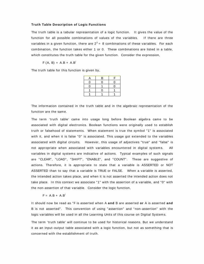
Truth Table Description of Logic Functions
The truth table is a tabular representation of a logic function. It gives the value of the
function for all possible combinations of values of the variables. If there are three
variables in a given function, there are 23 = 8 combinations of these variables. For each
combination, the function takes either 1 or 0. These combinations are listed in a table,
which constitutes the truth table for the given function. Consider the expression,
F (A, B) = A.B + A.B/
The truth table for this function is given by,
A B F 0 0 0 0 1 0 1 0 1 1 1 1
The information contained in the truth table and in the algebraic representation of the
function are the same.
The term ‘truth table’ came into usage long before Boolean algebra came to be
associated with digital electronics. Boolean functions were originally used to establish
truth or falsehood of statements. When statement is true the symbol "1" is associated
with it, and when it is false "0" is associated. This usage got extended to the variables
associated with digital circuits. However, this usage of adjectives "true" and "false" is
not appropriate when associated with variables encountered in digital systems. All
variables in digital systems are indicative of actions. Typical examples of such signals
are "CLEAR", "LOAD", "SHIFT", "ENABLE", and "COUNT". These are suggestive of
actions. Therefore, it is appropriate to state that a variable is ASSERTED or NOT
ASSERTED than to say that a variable is TRUE or FALSE. When a variable is asserted,
the intended action takes place, and when it is not asserted the intended action does not
take place. In this context we associate "1" with the assertion of a variable, and "0" with
the non-assertion of that variable. Consider the logic function,
F = A.B + A.B/
It should now be read as "F is asserted when A and B are asserted or A is asserted and
B is not asserted". This convention of using "assertion” and “non-assertion" with the
logic variables will be used in all the Learning Units of this course on Digital Systems.
The term ‘truth table’ will continue to be used for historical reasons. But we understand
it as an input-output table associated with a logic function, but not as something that is
concerned with the establishment of truth.
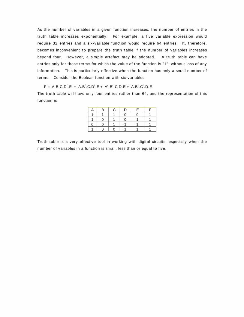
As the number of variables in a given function increases, the number of entries in the
truth table increases exponentially. For example, a five variable expression would
require 32 entries and a six-variable function would require 64 entries. It, therefore,
becomes inconvenient to prepare the truth table if the number of variables increases
beyond four. However, a simple artefact may be adopted. A truth table can have
entries only for those terms for which the value of the function is "1", without loss of any
information. This is particularly effective when the function has only a small number of
terms. Consider the Boolean function with six variables
F = A.B.C.D/.E/ + A.B/.C.D/.E + A/.B/.C.D.E + A.B/.C/.D.E
The truth table will have only four entries rather than 64, and the representation of this
function is
A B C D E F 1 1 1 0 0 1 1 0 1 0 1 1 0 0 1 1 1 1 1 0 0 1 1 1
Truth table is a very effective tool in working with digital circuits, especially when the
number of variables in a function is small, less than or equal to five.
Conversion of English Sentences to Logic Functions
Some of the problems that can be solved using digital circuits are expressed through one
or more sentences. For example,
At the traffic junction the amber light should come on 60 seconds after the red
light, and get witched off after 5 seconds.
If the number of coins put into the vending machine exceed five rupees it should
dispense a Thums Up bottle.
The lift should start moving only if the doors are closed and a floor number is
chosen.
These sentences should initially be translated into logic equations. This is done through
breaking each sentence into phrases and associating a logic variable with each phrase.
As stated earlier many of these phrases will be indicative of actions or directly represent
actions. We first mark each action related phrase in the sentence. Then we associate a
logic variable with it. Consider the following sentence, which has three phrases:
Anil freaks out with his friends if it is Saturday and he completed his assignments
We will now associate logic variables with each phrase. The words “if” and “and” are not
included in any phrase and they show the relationship among the phrases.
F = 1 if “Anil freaks out with his friends”; otherwise F = 0
A = 1 if “it is Saturday”; otherwise A = 0
B = 1 if “he completed his assignments”; otherwise B = 0
F is asserted if A is asserted and B is asserted. The sentence, therefore, can be
translated into a logic equation as
F = A.B
For simple problems it may be possible to directly write the logic function from the word
description. In more complex cases it is necessary to properly define the variables and
draw a truth-table before the logic function is prepared. Sometimes the given sentences
may have some vagueness, in which case clarifications need to be sought from the
source of the sentence. Let us consider another sentence with more number of
phrases.
Rahul will attend the Networks class if and only if his friend Shaila is attending the class
and the topic being covered in class is important from examination point of view or there
is no interesting matinee show in the city and the assignment is to be submitted. Let us
associate different logic variables with different phrases.
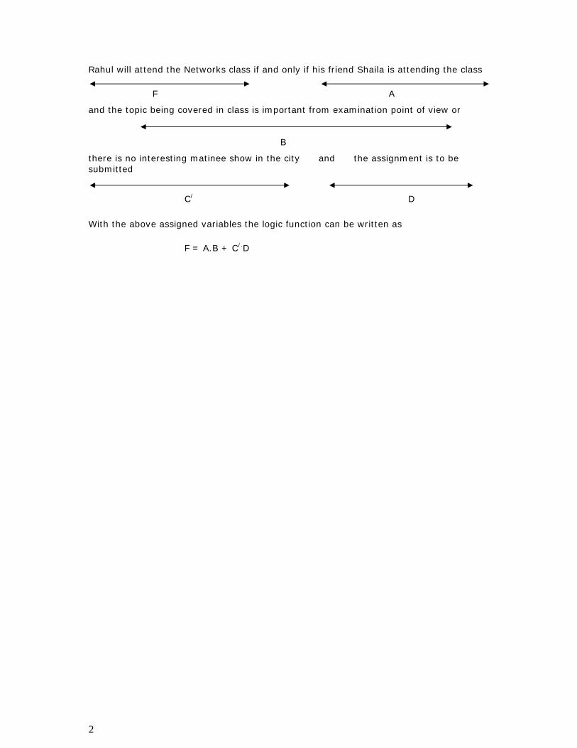
2
Rahul will attend the Networks class if and only if his friend Shaila is attending the class
F A
and the topic being covered in class is important from examination point of view or
B
there is no interesting matinee show in the city and the assignment is to be submitted
C/ D With the above assigned variables the logic function can be written as F = A.B + C/.D
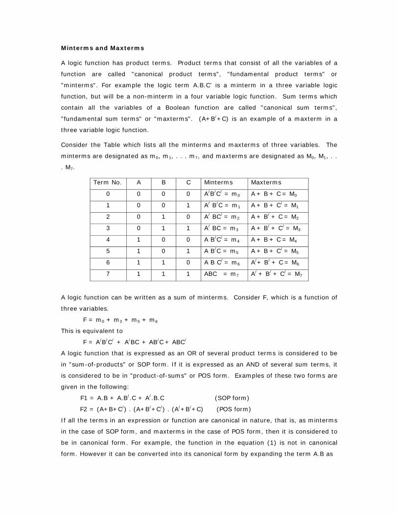
Minterms and Maxterms
A logic function has product terms. Product terms that consist of all the variables of a
function are called "canonical product terms", "fundamental product terms" or
"minterms". For example the logic term A.B.C' is a minterm in a three variable logic
function, but will be a non-minterm in a four variable logic function. Sum terms which
contain all the variables of a Boolean function are called "canonical sum terms",
"fundamental sum terms" or "maxterms". (A+B/+C) is an example of a maxterm in a
three variable logic function.
Consider the Table which lists all the minterms and maxterms of three variables. The
minterms are designated as m0, m1, . . . m7, and maxterms are designated as M0, M1, . .
. M7.
Term No. A B C Minterms Maxterms
0 0 0 0 A/B/C/ = m0 A + B + C = M0
1 0 0 1 A/ B/C = m1 A + B + C/ = M1
2 0 1 0 A/ BC/ = m2 A + B/ + C = M2
3 0 1 1 A/ BC = m3 A + B/ + C/ = M3
4 1 0 0 A B/C/ = m4 A + B + C = M4
5 1 0 1 A B/C = m5 A + B + C/ = M5
6 1 1 0 A B C/ = m6 A/+ B/ + C = M6
7 1 1 1 ABC = m7 A/ + B/ + C/ = M7
A logic function can be written as a sum of minterms. Consider F, which is a function of
three variables.
F = m0 + m3 + m5 + m6
This is equivalent to
F = A/B/C/ + A/BC + AB/C + ABC/
A logic function that is expressed as an OR of several product terms is considered to be
in "sum-of-products" or SOP form. If it is expressed as an AND of several sum terms, it
is considered to be in "product-of-sums" or POS form. Examples of these two forms are
given in the following:
F1 = A.B + A.B/.C + A/.B.C (SOP form)
F2 = (A+B+C/) . (A+B/+C/) . (A/+B/+C) (POS form)
If all the terms in an expression or function are canonical in nature, that is, as minterms
in the case of SOP form, and maxterms in the case of POS form, then it is considered to
be in canonical form. For example, the function in the equation (1) is not in canonical
form. However it can be converted into its canonical form by expanding the term A.B as
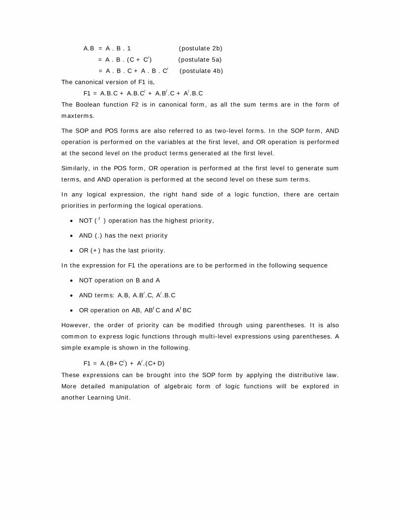
A.B = A . B . 1 (postulate 2b)
= A . B . (C + C/) (postulate 5a)
= A . B . C + A . B . C/ (postulate 4b)
The canonical version of F1 is,
F1 = A.B.C + A.B.C/ + A.B/.C + A/.B.C
The Boolean function F2 is in canonical form, as all the sum terms are in the form of
maxterms.
The SOP and POS forms are also referred to as two-level forms. In the SOP form, AND
operation is performed on the variables at the first level, and OR operation is performed
at the second level on the product terms generated at the first level.
Similarly, in the POS form, OR operation is performed at the first level to generate sum
terms, and AND operation is performed at the second level on these sum terms.
In any logical expression, the right hand side of a logic function, there are certain
priorities in performing the logical operations.
• NOT ( / ) operation has the highest priority,
• AND (.) has the next priority
• OR (+) has the last priority.
In the expression for F1 the operations are to be performed in the following sequence
• NOT operation on B and A
• AND terms: A.B, A.B/.C, A/.B.C
• OR operation on AB, AB/C and A/BC
However, the order of priority can be modified through using parentheses. It is also
common to express logic functions through multi-level expressions using parentheses. A
simple example is shown in the following.
F1 = A.(B+C/) + A/.(C+D)
These expressions can be brought into the SOP form by applying the distributive law.
More detailed manipulation of algebraic form of logic functions will be explored in
another Learning Unit.
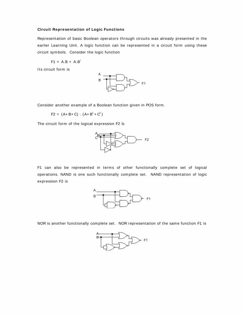
Circuit Representation of Logic Functions
Representation of basic Boolean operators through circuits was already presented in the
earlier Learning Unit. A logic function can be represented in a circuit form using these
circuit symbols. Consider the logic function
F1 = A.B + A.B/
Its circuit form is
Consider another example of a Boolean function given in POS form.
F2 = (A+B+C) . (A+B/+C/)
The circuit form of the logical expression F2 is
F1 can also be represented in terms of other functionally complete set of logical
operations. NAND is one such functionally complete set. NAND representation of logic
expression F2 is
NOR is another functionally complete set. NOR representation of the same function F1 is
Digital Electronics Module 2: Boolean Algebra and Boolean Operators: Karnaugh Map Method
N.J. RaoIndian Institute of Science
id4730802 pdfMachine by Broadgun Software - a great PDF writer! - a great PDF creator! - http://www.pdfmachine.com http://www.broadgun.com
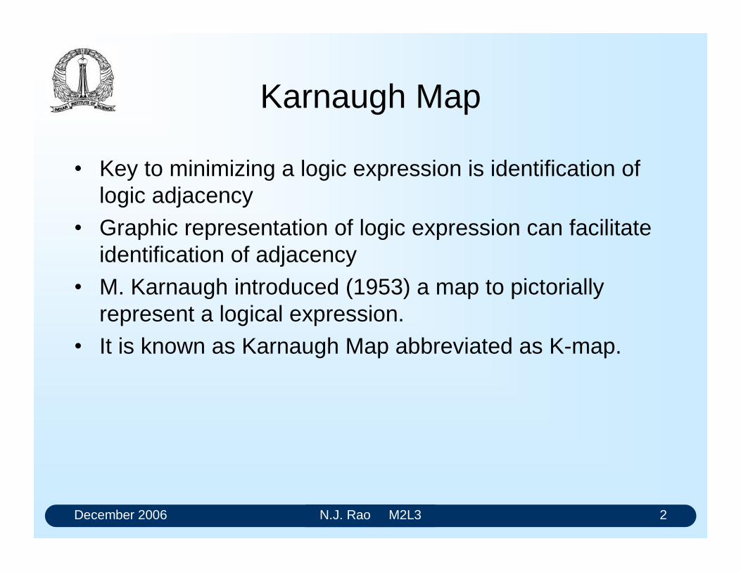
December 2006 N.J. Rao M2L3 2
Karnaugh Map
Key to minimizing a logic expression is identification of logic adjacency
Graphic representation of logic expression can facilitate identification of adjacency
M. Karnaugh introduced (1953) a map to pictorially represent a logical expression.
It is known as Karnaugh Map abbreviated as K-map.

December 2006 N.J. Rao M2L3 3
Karnaugh Map
K-Map is a pictorial form of the truth-table. The inherent structure of the map facilitates systematic
minimization K-map uses the ability of human perception to identify
patterns and relationships when the information is presented graphically
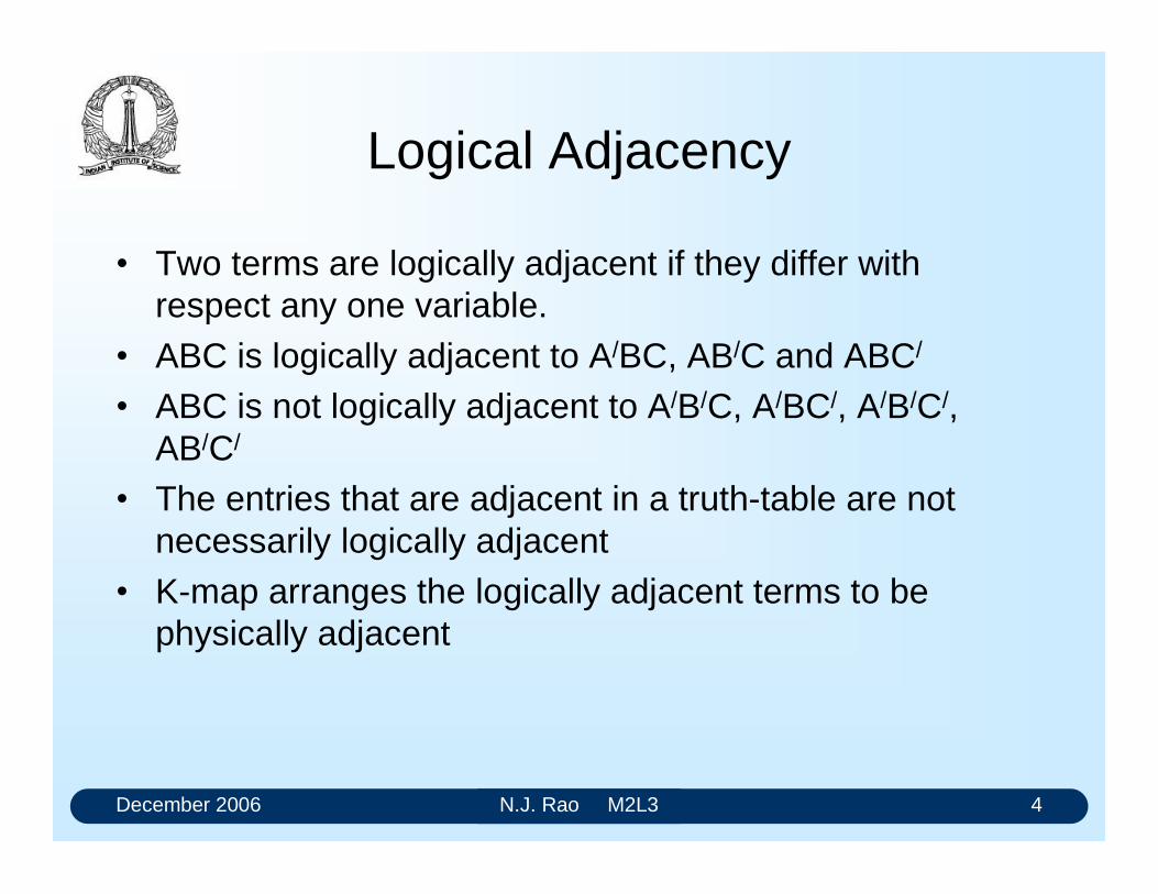
December 2006 N.J. Rao M2L3 4
Logical Adjacency
Two terms are logically adjacent if they differ with respect any one variable.
ABC is logically adjacent to A/BC, AB/C and ABC/
ABC is not logically adjacent to A/B/C, A/BC/, A/B/C/, AB/C/
The entries that are adjacent in a truth-table are not necessarily logically adjacent
K-map arranges the logically adjacent terms to be physically adjacent
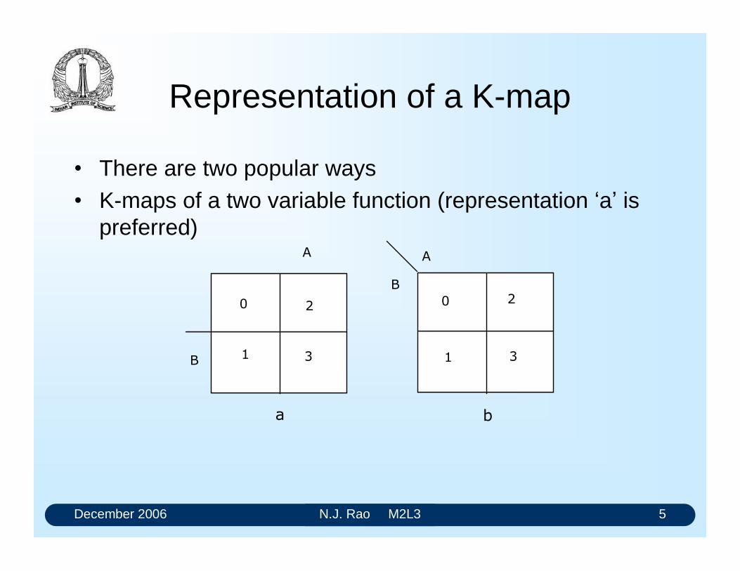
December 2006 N.J. Rao M2L3 5
Representation of a K-map
There are two popular ways K-maps of a two variable function (representation a is
preferred) A A
B
0 0
1 1
2 2
3 3 B
a b
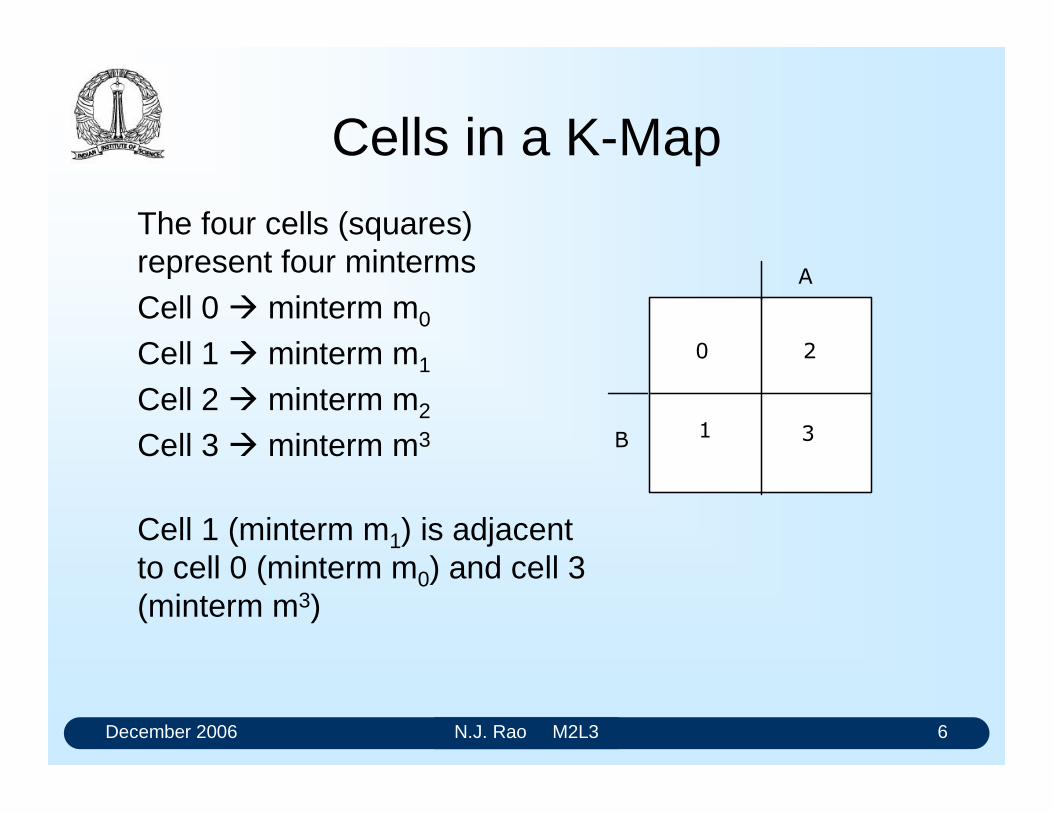
December 2006 N.J. Rao M2L3 6
Cells in a K-Map
The four cells (squares) represent four mintermsCell 0 minterm m0
Cell 1 minterm m1
Cell 2 minterm m2
Cell 3 minterm m3
Cell 1 (minterm m1) is adjacent to cell 0 (minterm m0) and cell 3 (minterm m3)
A
0
1
2
3 B
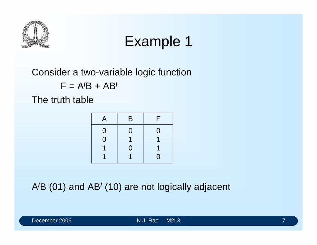
December 2006 N.J. Rao M2L3 7
Example 1
Consider a two-variable logic functionF = A/B + AB/
The truth table
A/B (01) and AB/ (10) are not logically adjacent
0110
0101
0011
FBA
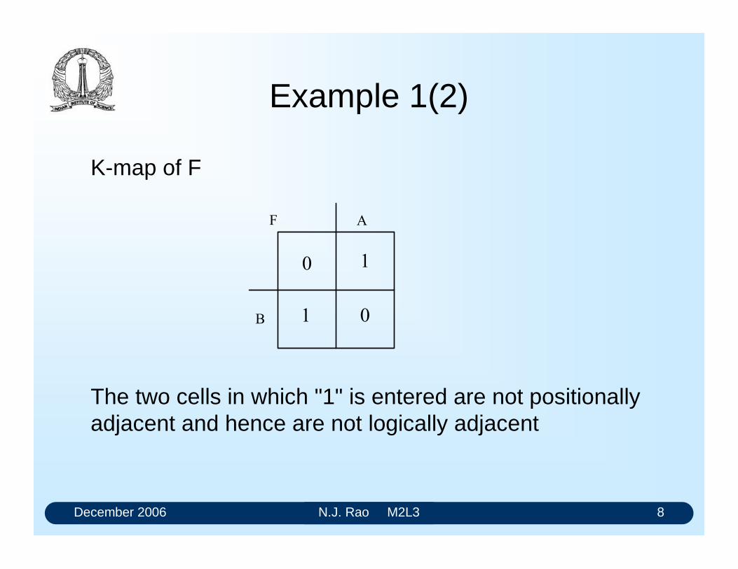
December 2006 N.J. Rao M2L3 8
Example 1(2)
$)
%
The two cells in which "1" is entered are not positionallyadjacent and hence are not logically adjacent
K-map of F
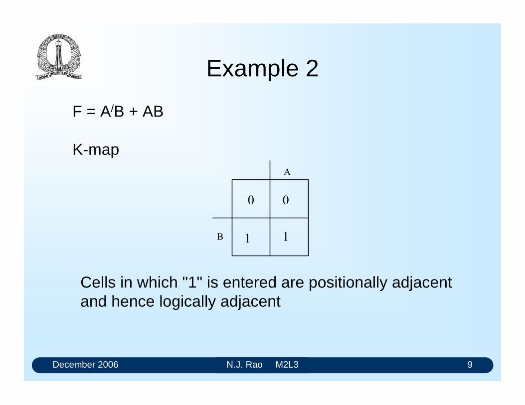
December 2006 N.J. Rao M2L3 9
Example 2
$
%
F = A/B + AB
K-map
Cells in which "1" is entered are positionally adjacent and hence logically adjacent
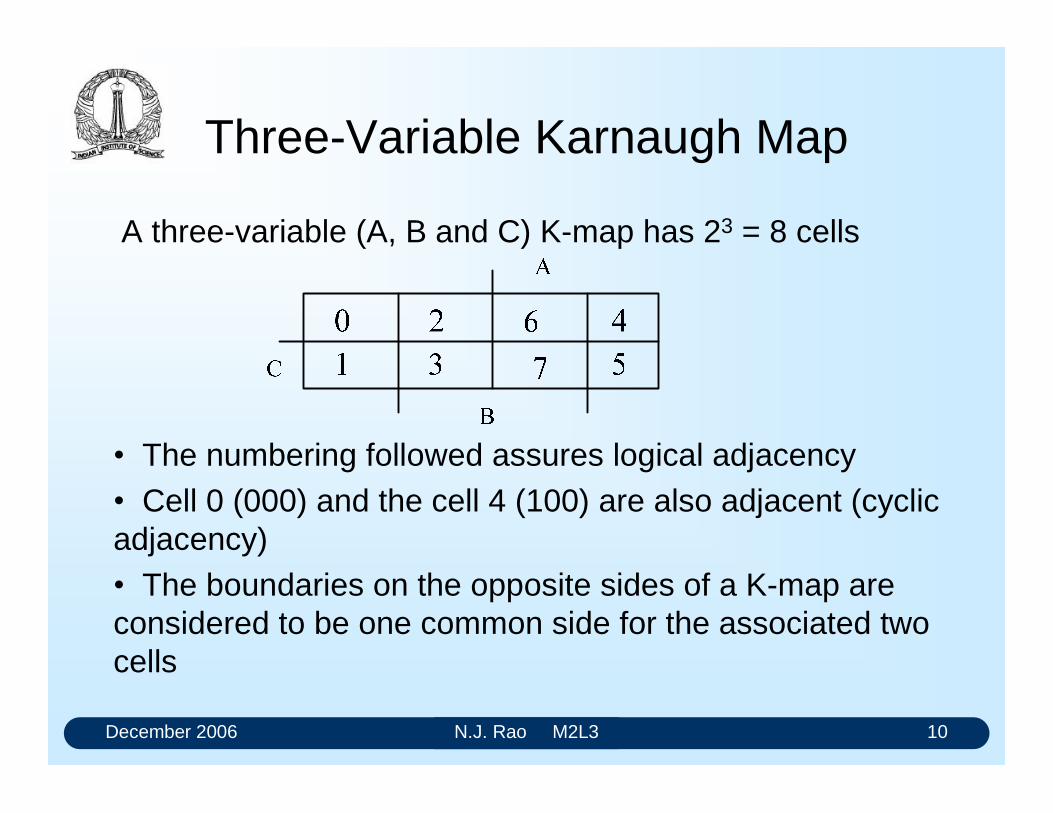
December 2006 N.J. Rao M2L3 10
Three-Variable Karnaugh Map
A three-variable (A, B and C) K-map has 23 = 8 cells
The numbering followed assures logical adjacency Cell 0 (000) and the cell 4 (100) are also adjacent (cyclic adjacency) The boundaries on the opposite sides of a K-map are considered to be one common side for the associated two cells
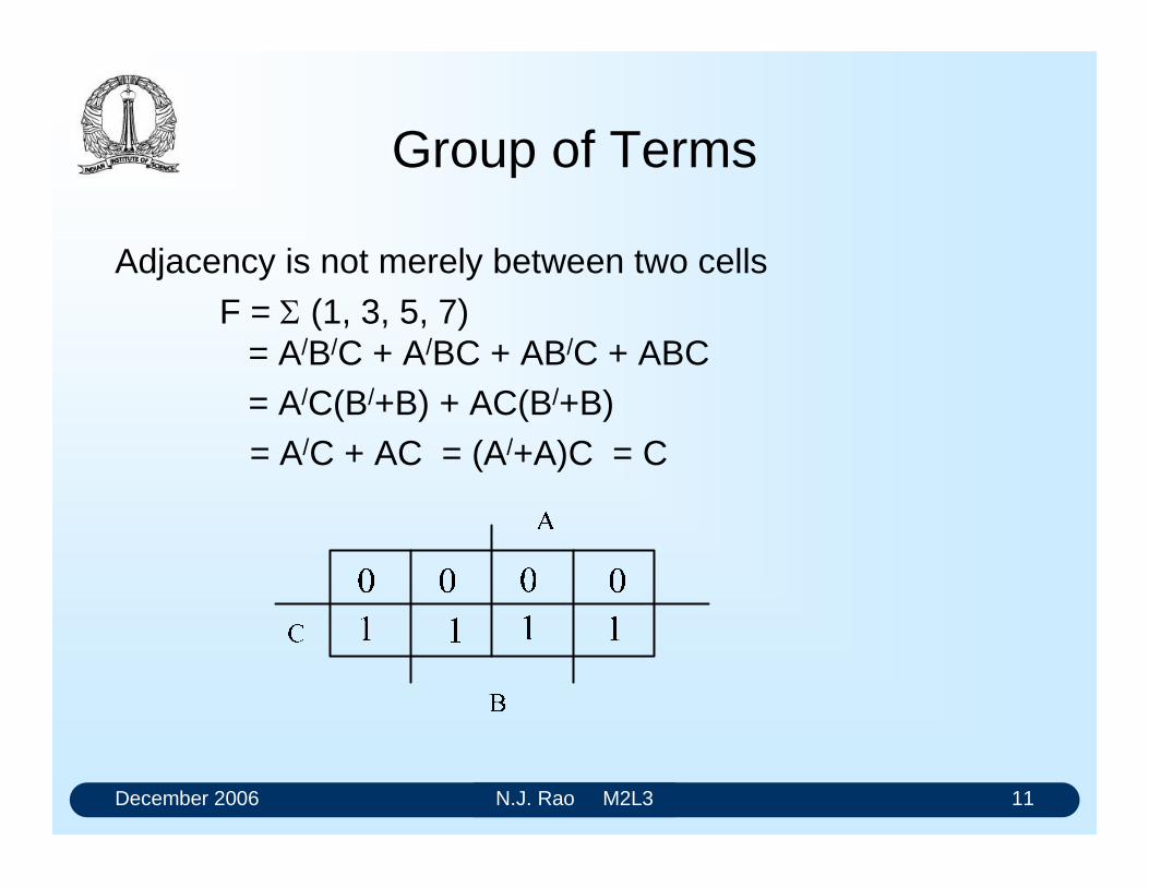
December 2006 N.J. Rao M2L3 11
Group of Terms
Adjacency is not merely between two cells
F = (1, 3, 5, 7) = A/B/C + A/BC + AB/C + ABC = A/C(B/+B) + AC(B/+B) = A/C + AC = (A/+A)C = C
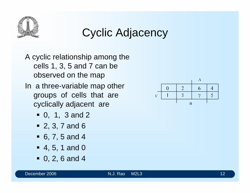
December 2006 N.J. Rao M2L3 12
Cyclic Adjacency
A cyclic relationship among the cells 1, 3, 5 and 7 can be observed on the map
In a three-variable map other groups of cells that are cyclically adjacent are 0, 1, 3 and 2 2, 3, 7 and 6 6, 7, 5 and 4 4, 5, 1 and 0 0, 2, 6 and 4
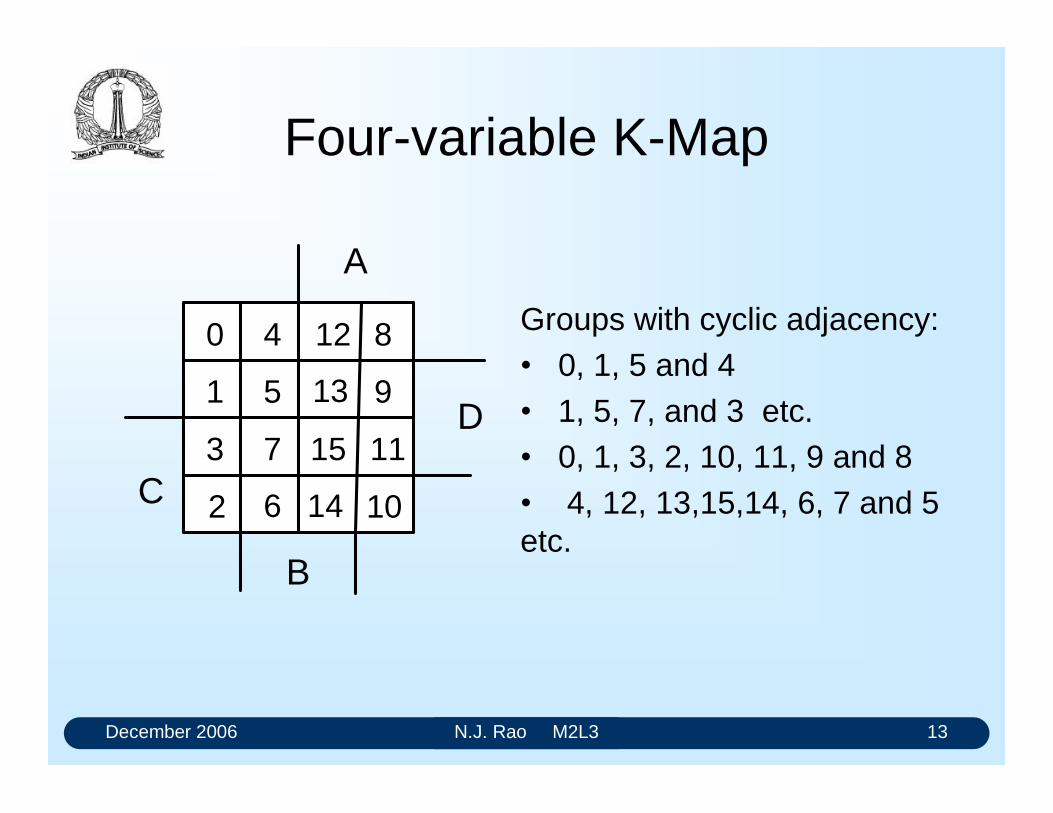
December 2006 N.J. Rao M2L3 13
Four-variable K-Map
0
1
2
3
4
5
6
7
8
9
10
11
12
13
14
15
A
B
C
D
Groups with cyclic adjacency: 0, 1, 5 and 4 1, 5, 7, and 3 etc. 0, 1, 3, 2, 10, 11, 9 and 8 4, 12, 13,15,14, 6, 7 and 5 etc.
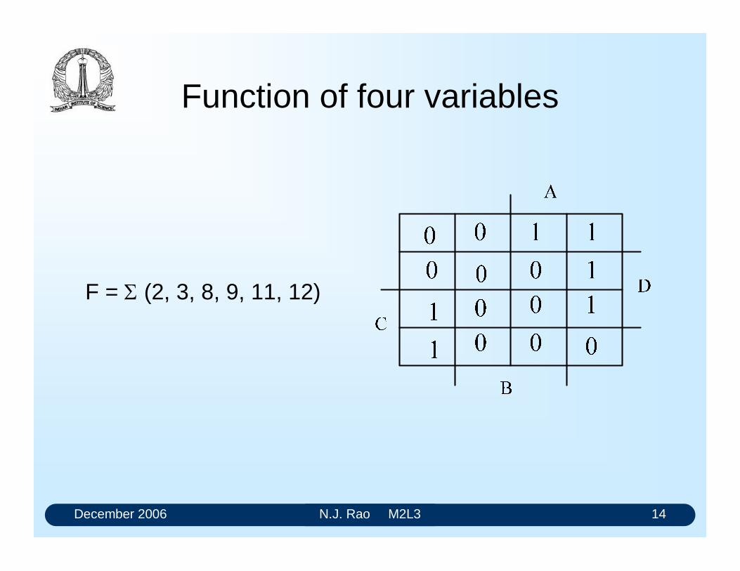
December 2006 N.J. Rao M2L3 14
Function of four variables
F = (2, 3, 8, 9, 11, 12)
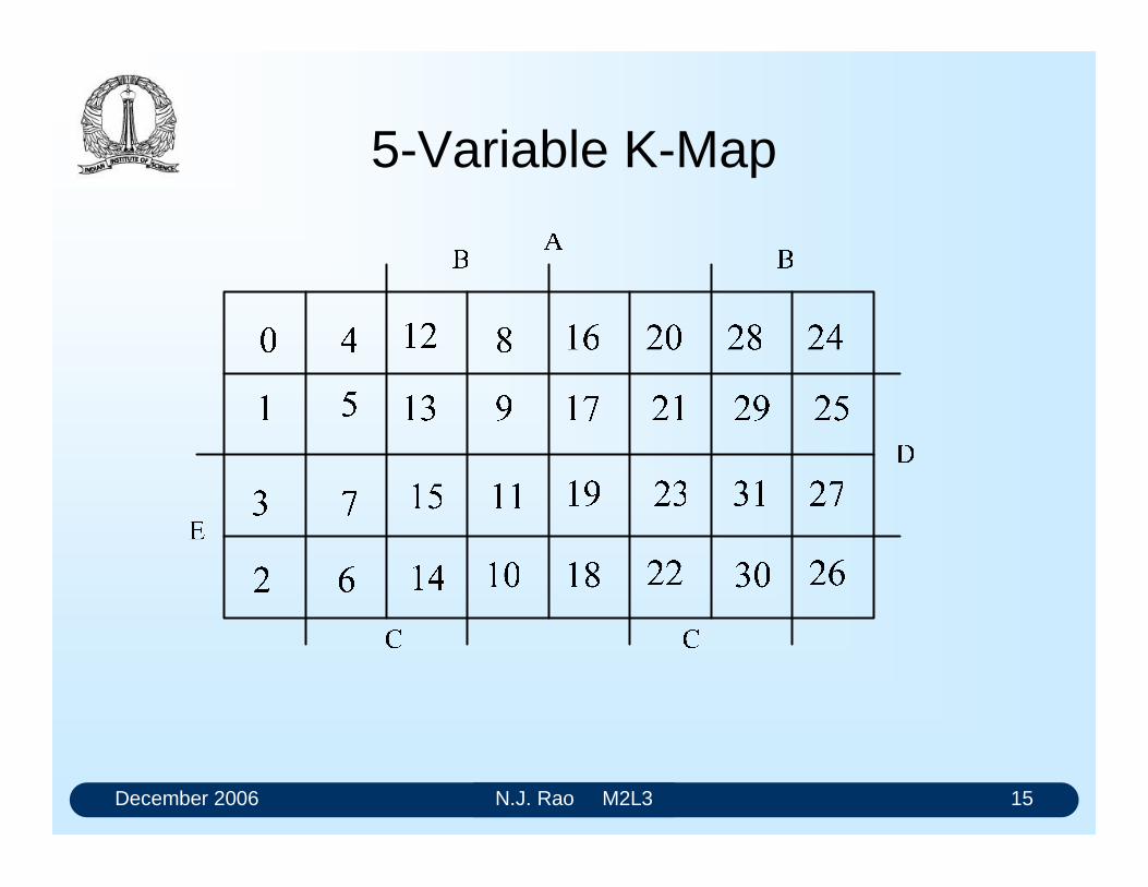
December 2006 N.J. Rao M2L3 15
5-Variable K-Map
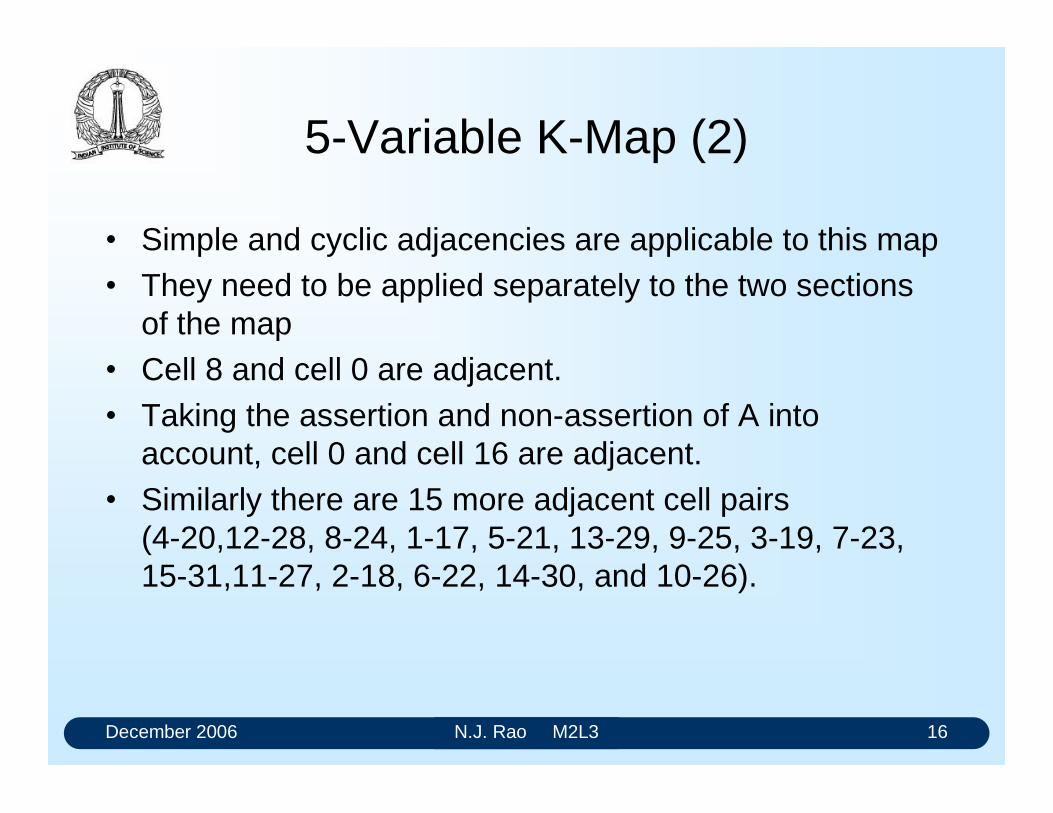
December 2006 N.J. Rao M2L3 16
5-Variable K-Map (2)
Simple and cyclic adjacencies are applicable to this map They need to be applied separately to the two sections
of the map Cell 8 and cell 0 are adjacent. Taking the assertion and non-assertion of A into
account, cell 0 and cell 16 are adjacent. Similarly there are 15 more adjacent cell pairs
(4-20,12-28, 8-24, 1-17, 5-21, 13-29, 9-25, 3-19, 7-23, 15-31,11-27, 2-18, 6-22, 14-30, and 10-26).
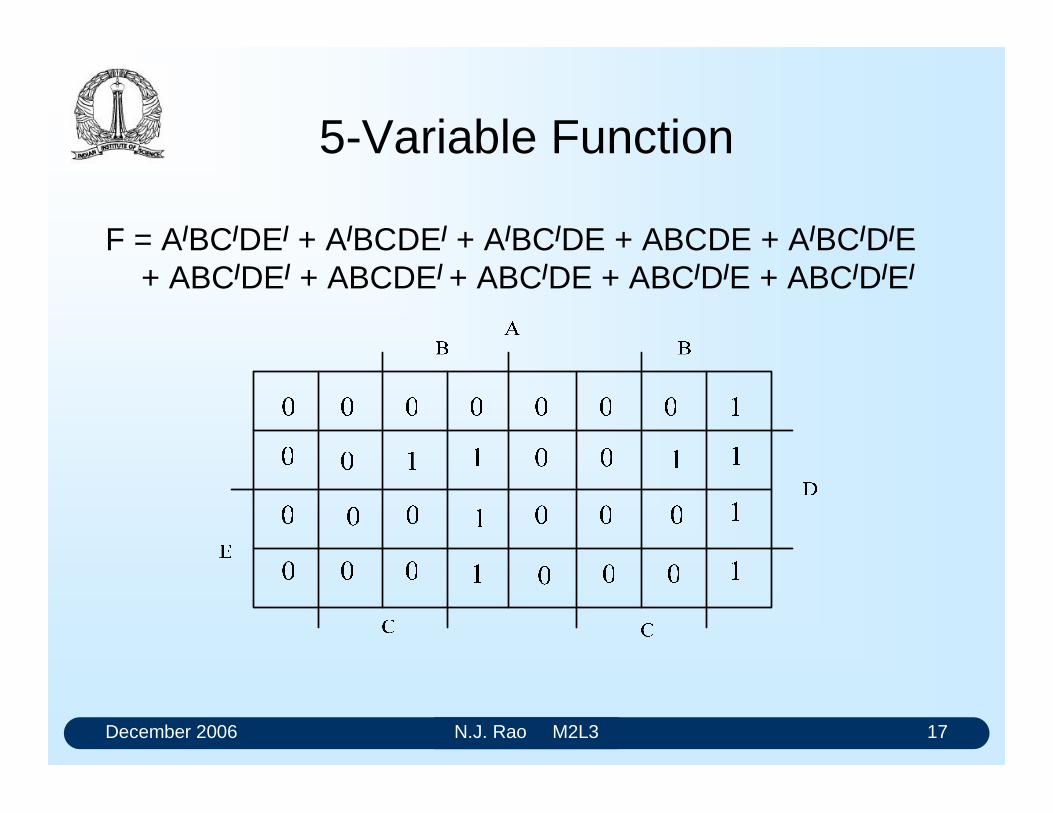
December 2006 N.J. Rao M2L3 17
5-Variable Function
F = A/BC/DE/ + A/BCDE/ + A/BC/DE + ABCDE + A/BC/D/E + ABC/DE/ + ABCDE/ + ABC/DE + ABC/D/E + ABC/D/E/
December 2006 N.J. Rao M2L3 18
K-Map Properties
Karnaugh Map's main feature is to convert logic adjacency into positional adjacency
Every K-map has 2n cells corresponding to 2n
minterms Combinations are arranged in a special order so as to
keep the equivalence of logic adjacency to positional adjacency
There are three kinds of positional adjacency, namely simple, cyclic and symmetric
December 2006 N.J. Rao M2L3 19
Function not in canonical POS form
If the Boolean function is available in the canonical SOP form, a "1" is entered in all those cells representing the minterms of the expression, and "0" in all the other cells
If it is not available in the canonical form, convert the non-canonical form into canonical SOP form
Convert the function into the standard SOP form and directly prepare the K-map.
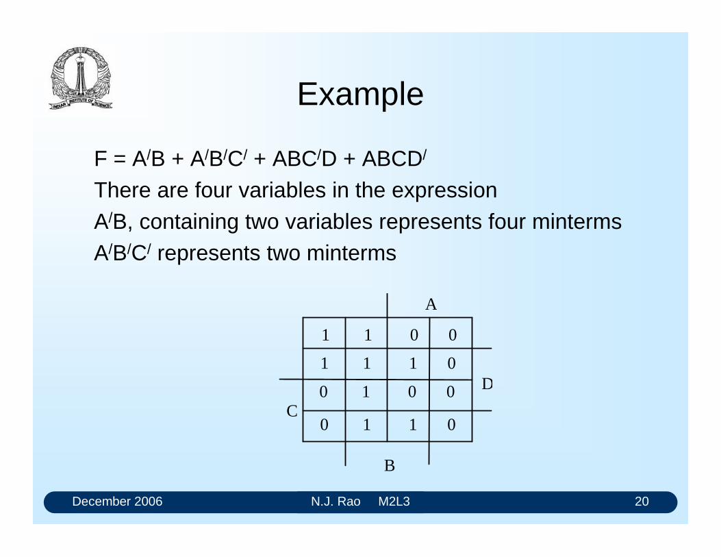
December 2006 N.J. Rao M2L3 20
Example
A
D
B
C
1 1 0 0
1 1 1 0
0 1 0 0
0 1 1 0
F = A/B + A/B/C/ + ABC/D + ABCD/
There are four variables in the expression A/B, containing two variables represents four mintermsA/B/C/ represents two minterms
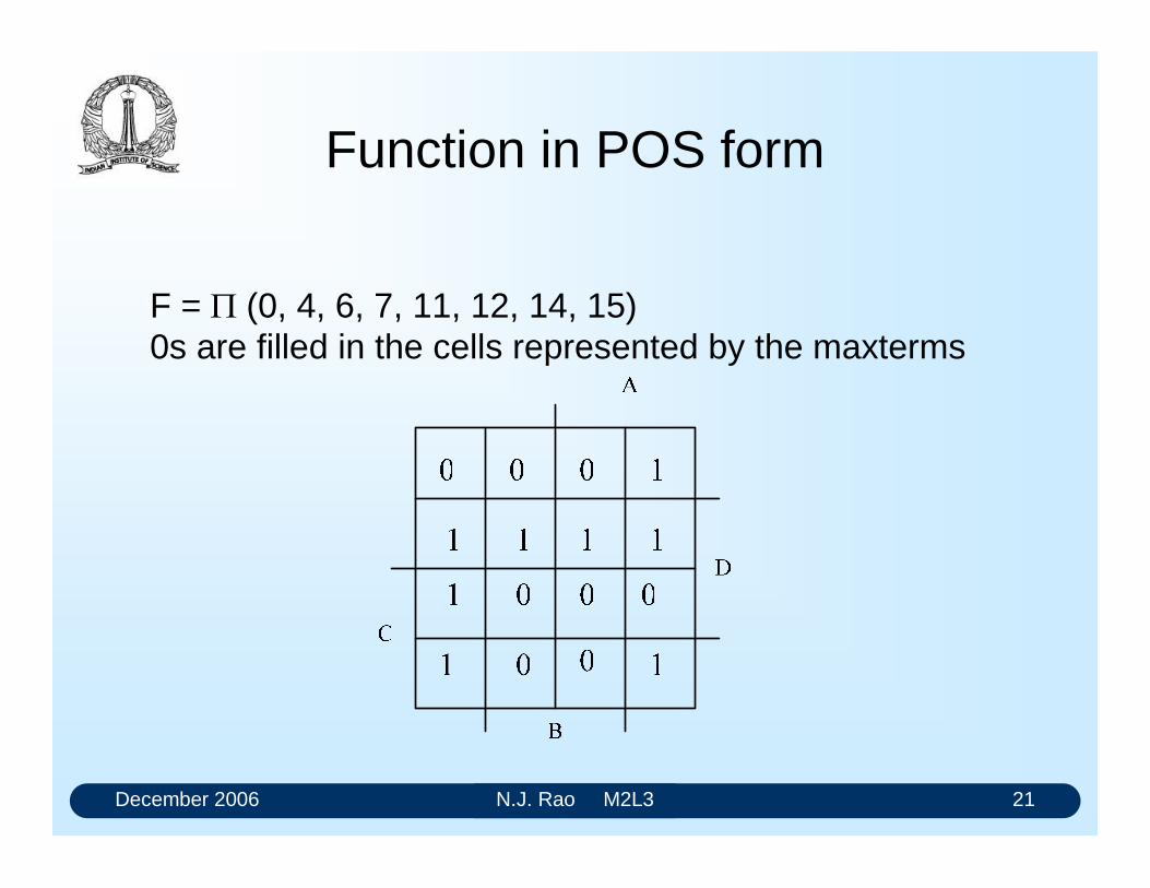
December 2006 N.J. Rao M2L3 21
Function in POS form
F = (0, 4, 6, 7, 11, 12, 14, 15)0s are filled in the cells represented by the maxterms
December 2006 N.J. Rao M2L3 22
Function in standard POS form
Initially convert the standard POS form of the expression into its canonical form, and enter 0s in the cells representing the maxterms
Enter 0s directly into the map by observing the sum terms one after the other
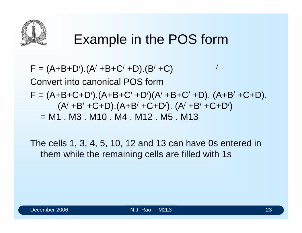
December 2006 N.J. Rao M2L3 23
Example in the POS form
F = (A+B+D/).(A/ +B+C/ +D).(B/ +C) /
Convert into canonical POS formF = (A+B+C+D/).(A+B+C/ +D/)(A/ +B+C/ +D). (A+B/ +C+D).
(A/ +B/ +C+D).(A+B/ +C+D/). (A/ +B/ +C+D/) = M1 . M3 . M10 . M4 . M12 . M5 . M13
The cells 1, 3, 4, 5, 10, 12 and 13 can have 0s entered in them while the remaining cells are filled with 1s
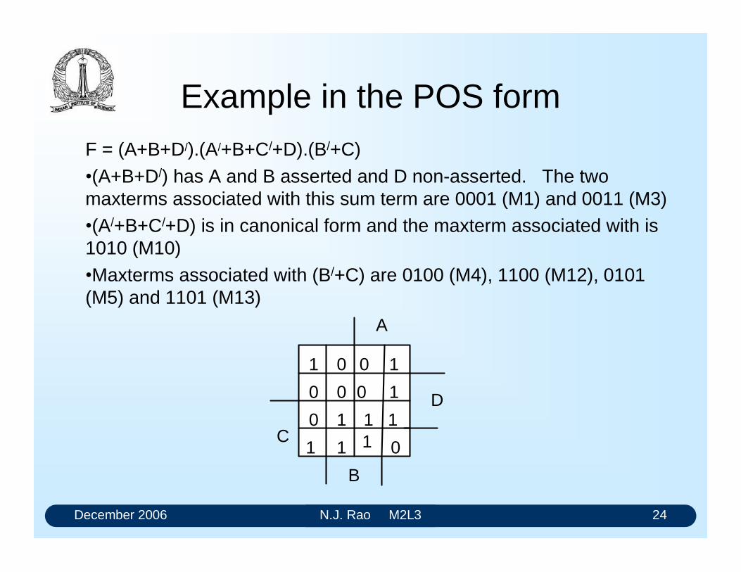
December 2006 N.J. Rao M2L3 24
Example in the POS formF = (A+B+D/).(A/+B+C/+D).(B/+C)(A+B+D/) has A and B asserted and D non-asserted. The two maxterms associated with this sum term are 0001 (M1) and 0011 (M3) (A/+B+C/+D) is in canonical form and the maxterm associated with is 1010 (M10) Maxterms associated with (B/+C) are 0100 (M4), 1100 (M12), 0101 (M5) and 1101 (M13)
1
0
1
0
0
0
1
1
1
1
0
1
0
0
11
A
B
C
D
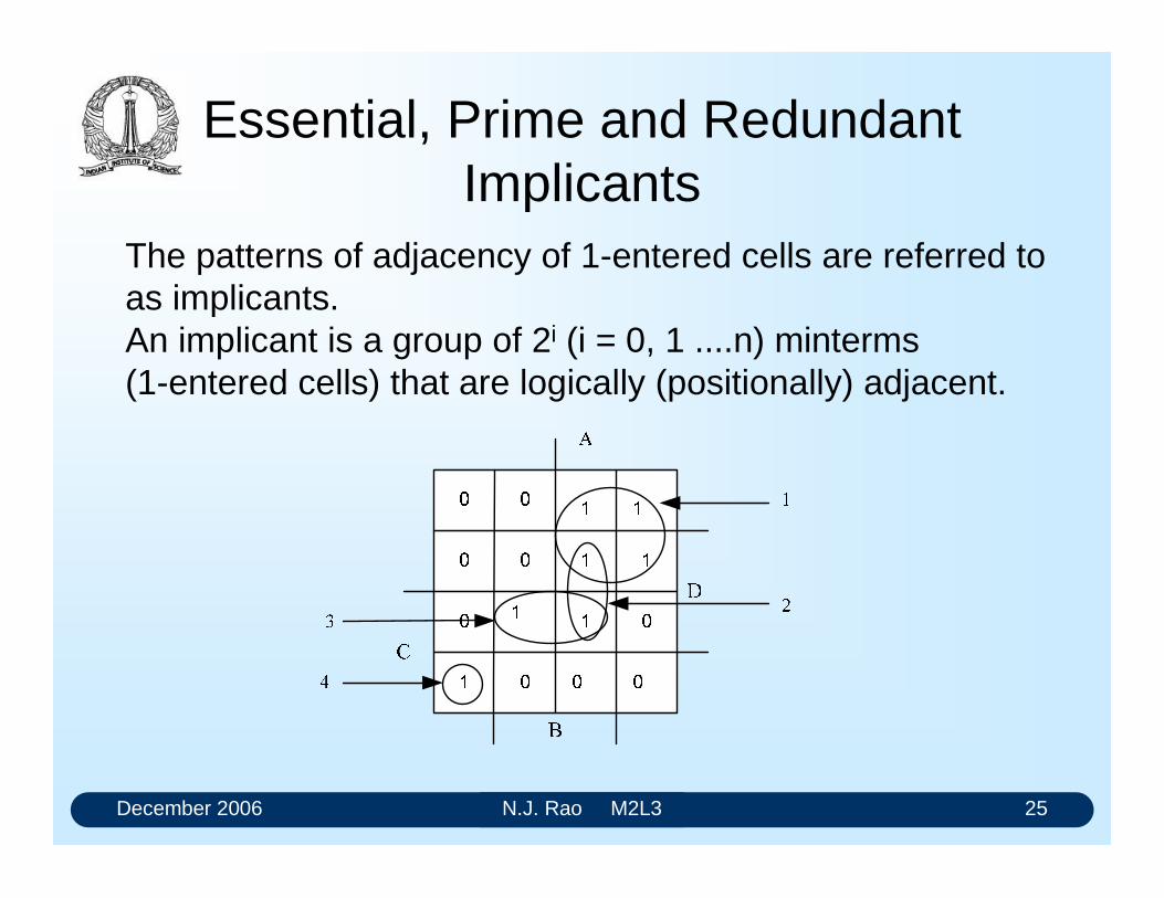
December 2006 N.J. Rao M2L3 25
Essential, Prime and Redundant Implicants
The patterns of adjacency of 1-entered cells are referred to as implicants. An implicant is a group of 2i (i = 0, 1 ....n) minterms(1-entered cells) that are logically (positionally) adjacent.
December 2006 N.J. Rao M2L3 26
Implicants and Product Terms
An implicant represents a product term Implicant 1 represents the product term AC/
Implicant 2 represents ABD Implicant 3 represents BCD Implicant 4 represents A/B/CD/
Smaller the number of implicants the smaller the number of product terms in the simplified Boolean expression.
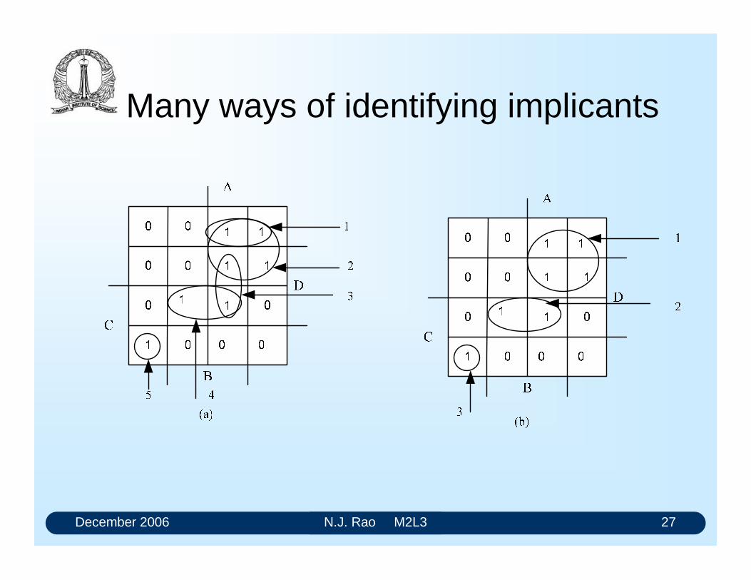
December 2006 N.J. Rao M2L3 27
Many ways of identifying implicants
December 2006 N.J. Rao M2L3 28
Implicants with properties
A prime implicant is one that is not a subset of any other implicant
A prime implicant which includes a 1-entered cell that is not included in any other prime implicant is called an essential prime implicant.
A redundant implicant is one in which all the 1-entered cells are covered by other implicants
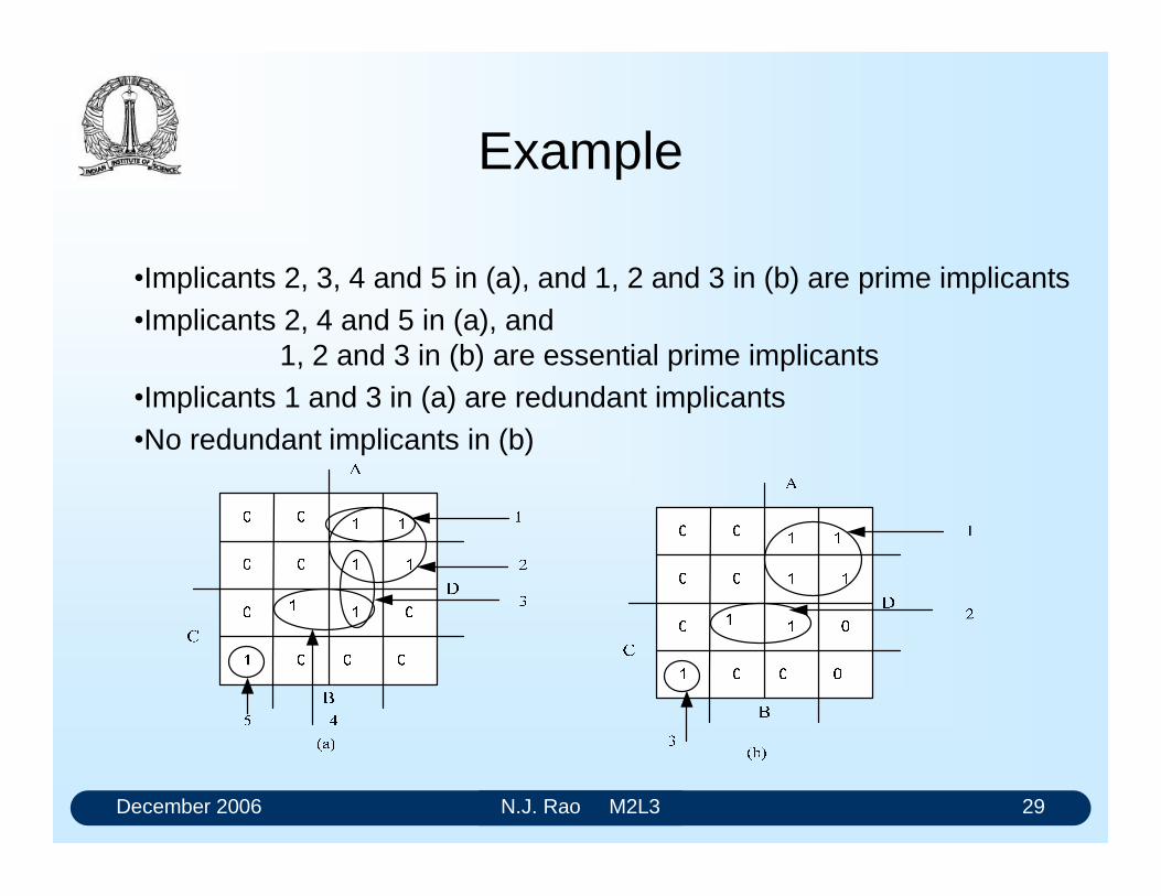
December 2006 N.J. Rao M2L3 29
Example
Implicants 2, 3, 4 and 5 in (a), and 1, 2 and 3 in (b) are prime implicantsImplicants 2, 4 and 5 in (a), and
1, 2 and 3 in (b) are essential prime implicantsImplicants 1 and 3 in (a) are redundant implicantsNo redundant implicants in (b)
December 2006 N.J. Rao M2L3 30
K-map minimisation
Find the smallest set of prime implicants that includes all the essential prime implicants
If there is a choice, the simpler prime implicantshould be chosen.
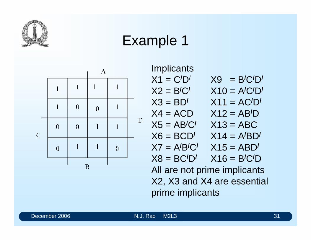
December 2006 N.J. Rao M2L3 31
Example 1
ImplicantsX1 = C/D/ X9 = B/C/D/
X2 = B/C/ X10 = A/C/D/
X3 = BD/ X11 = AC/D/
X4 = ACD X12 = AB/DX5 = AB/C/ X13 = ABCX6 = BCD/ X14 = A/BD/
X7 = A/B/C/ X15 = ABD/
X8 = BC/D/ X16 = B/C/DAll are not prime implicantsX2, X3 and X4 are essential prime implicants
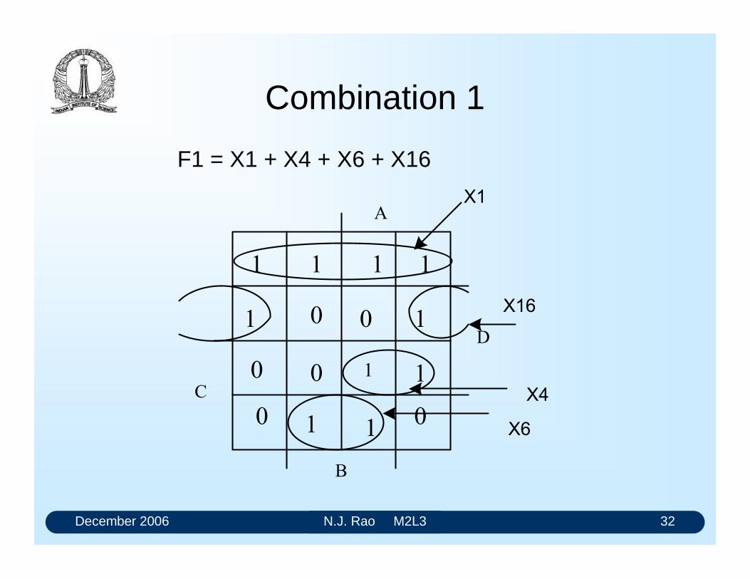
December 2006 N.J. Rao M2L3 32
Combination 1
F1 = X1 + X4 + X6 + X16
$
%
'
&
;
;
;
;
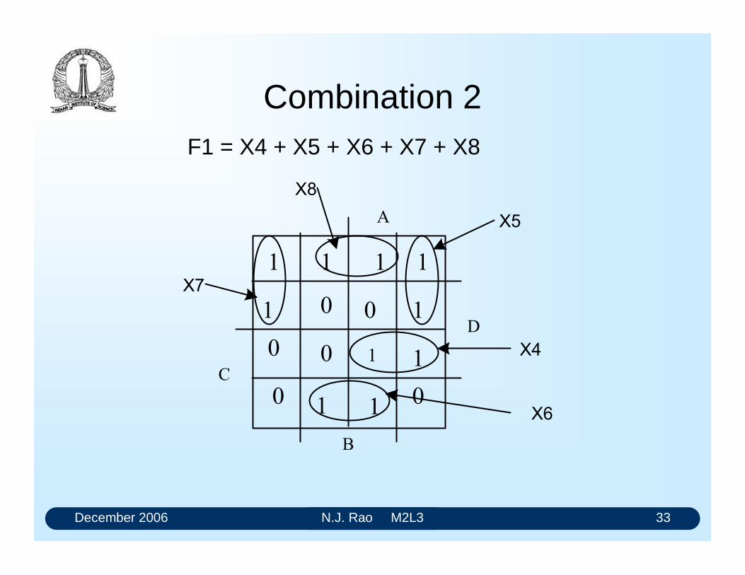
December 2006 N.J. Rao M2L3 33
Combination 2
$
%
'
&
;
;
;
;
;
F1 = X4 + X5 + X6 + X7 + X8
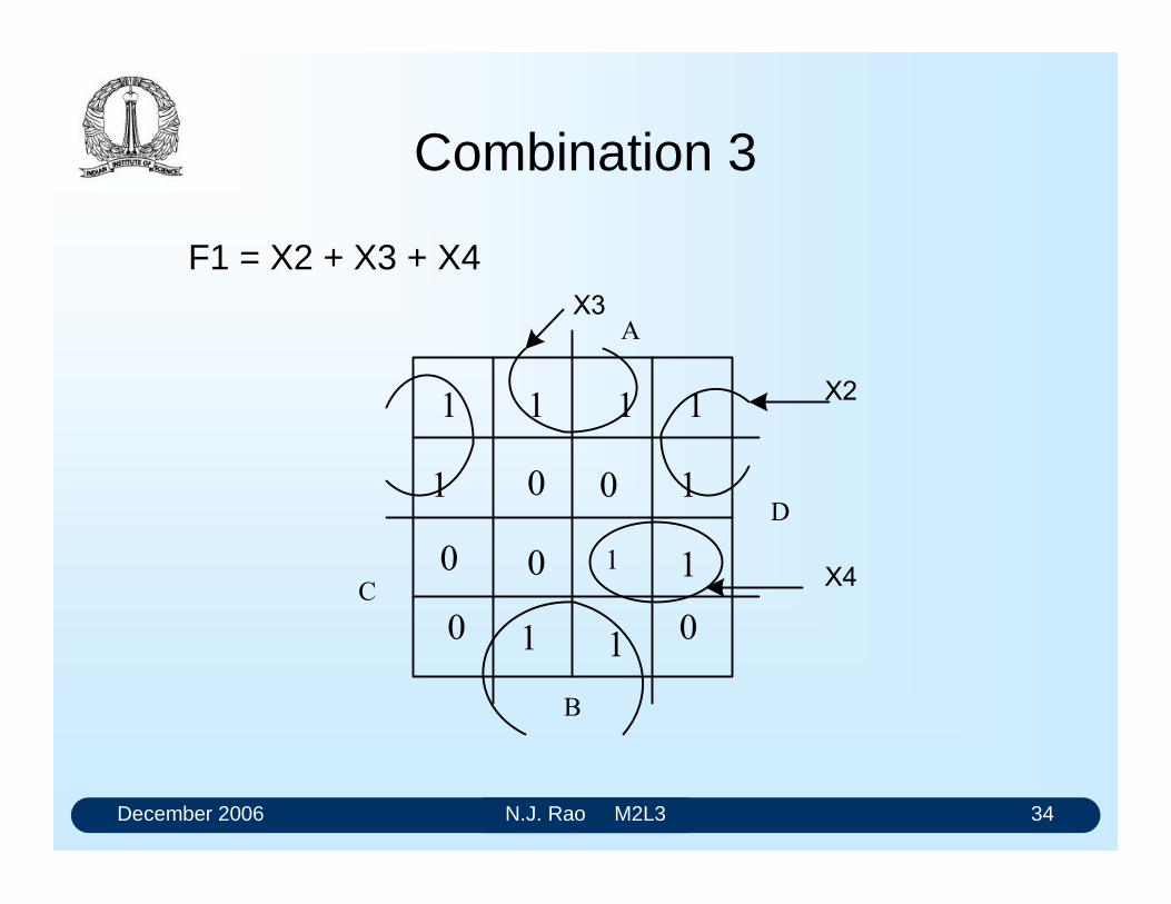
December 2006 N.J. Rao M2L3 34
Combination 3
$
%
'
&
;
;
;
F1 = X2 + X3 + X4
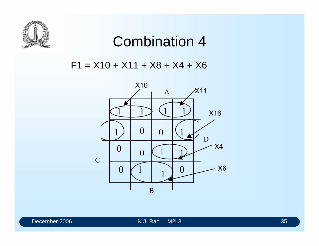
December 2006 N.J. Rao M2L3 35
Combination 4
F1 = X10 + X11 + X8 + X4 + X6
$
%
'
&
;;
;
;
;
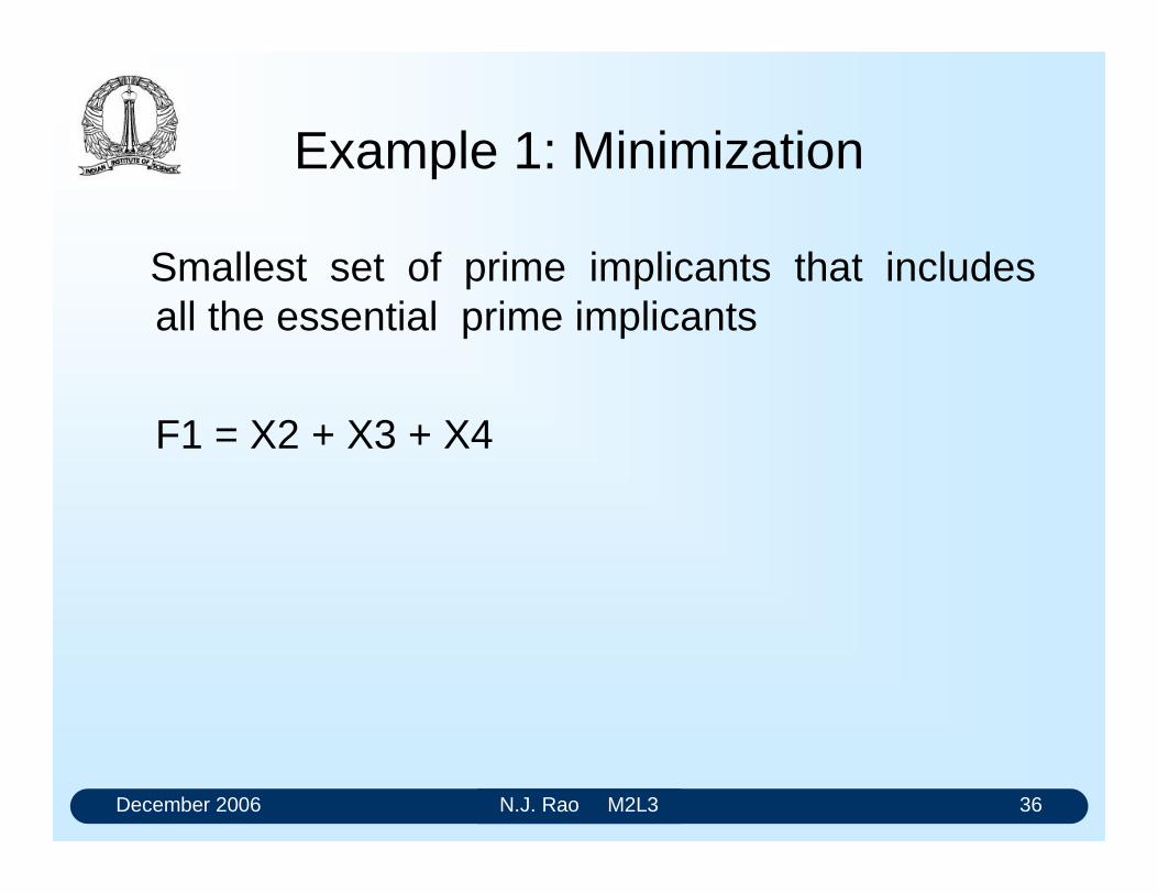
December 2006 N.J. Rao M2L3 36
Example 1: Minimization
Smallest set of prime implicants that includes all the essential prime implicants
F1 = X2 + X3 + X4
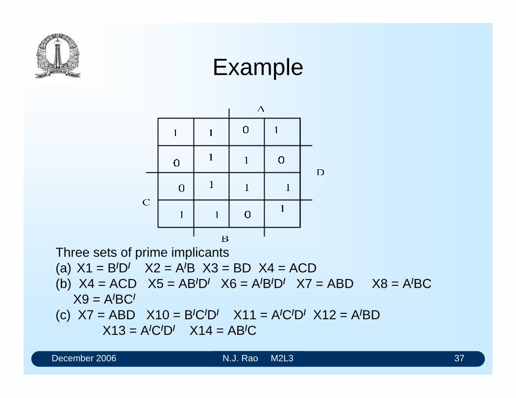
December 2006 N.J. Rao M2L3 37
Example
Three sets of prime implicants(a) X1 = B/D/ X2 = A/B X3 = BD X4 = ACD(b) X4 = ACD X5 = AB/D/ X6 = A/B/D/ X7 = ABD X8 = A/BC
X9 = A/BC/
(c) X7 = ABD X10 = B/C/D/ X11 = A/C/D/ X12 = A/BD X13 = A/C/D/ X14 = AB/C
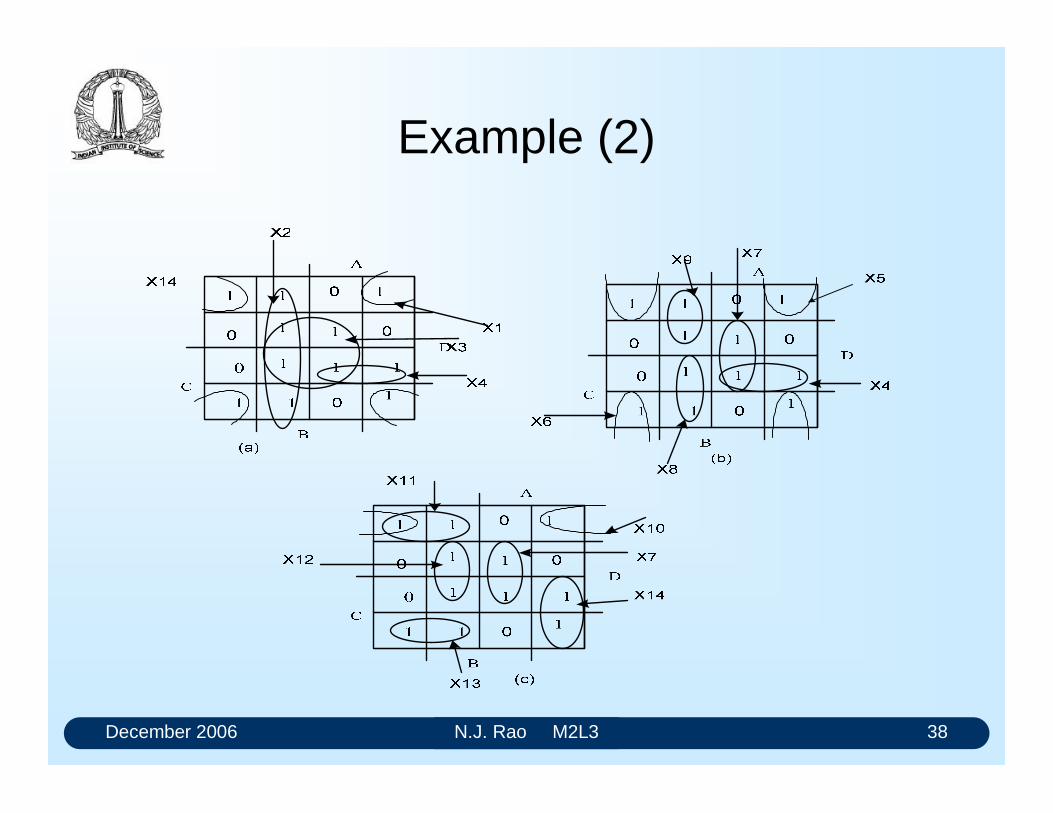
December 2006 N.J. Rao M2L3 38
Example (2)
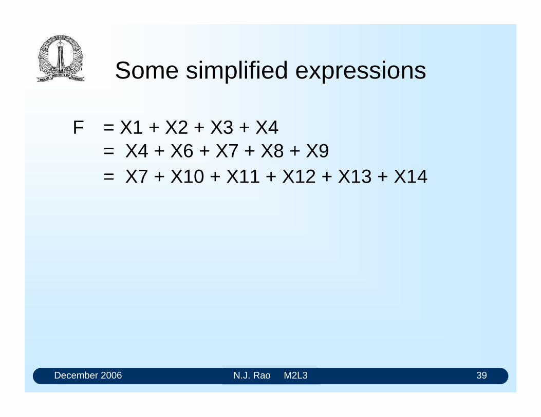
December 2006 N.J. Rao M2L3 39
Some simplified expressions
F = X1 + X2 + X3 + X4 = X4 + X6 + X7 + X8 + X9 = X7 + X10 + X11 + X12 + X13 + X14
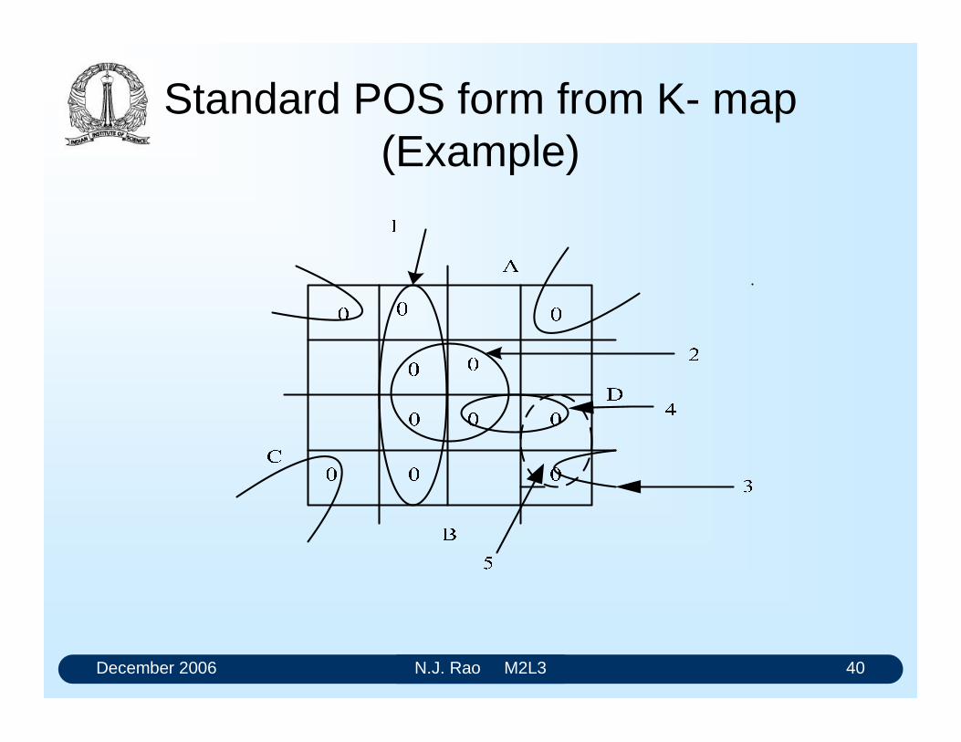
December 2006 N.J. Rao M2L3 40
Standard POS form from K- map (Example)
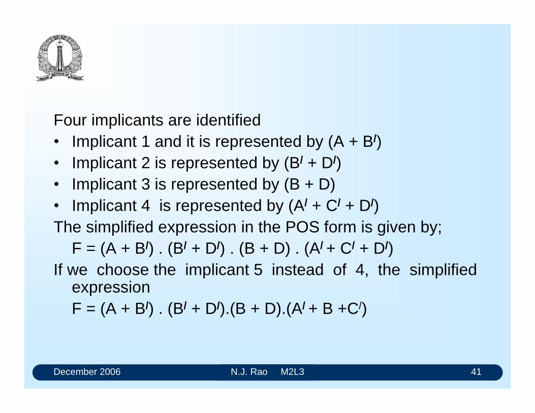
December 2006 N.J. Rao M2L3 41
Four implicants are identified Implicant 1 and it is represented by (A + B/) Implicant 2 is represented by (B/ + D/) Implicant 3 is represented by (B + D) Implicant 4 is represented by (A/ + C/ + D/)The simplified expression in the POS form is given by;
F = (A + B/) . (B/ + D/) . (B + D) . (A/ + C/ + D/) If we choose the implicant 5 instead of 4, the simplified
expression F = (A + B/) . (B/ + D/).(B + D).(A/ + B +C/)
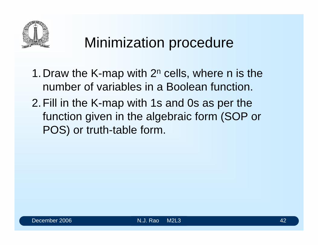
December 2006 N.J. Rao M2L3 42
Minimization procedure
1.Draw the K-map with 2n cells, where n is the number of variables in a Boolean function.
2.Fill in the K-map with 1s and 0s as per the function given in the algebraic form (SOP or POS) or truth-table form.
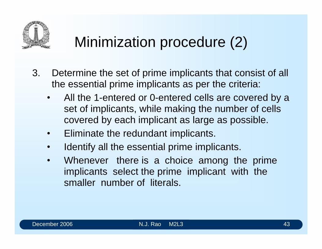
December 2006 N.J. Rao M2L3 43
Minimization procedure (2)
3. Determine the set of prime implicants that consist of all the essential prime implicants as per the criteria: All the 1-entered or 0-entered cells are covered by a
set of implicants, while making the number of cells covered by each implicant as large as possible.
Eliminate the redundant implicants. Identify all the essential prime implicants. Whenever there is a choice among the prime
implicants select the prime implicant with the smaller number of literals.
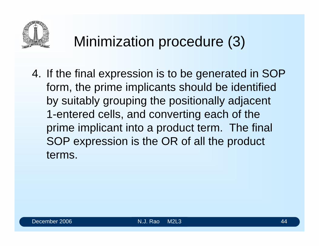
December 2006 N.J. Rao M2L3 44
Minimization procedure (3)
4. If the final expression is to be generated in SOP form, the prime implicants should be identified by suitably grouping the positionally adjacent 1-entered cells, and converting each of the prime implicant into a product term. The final SOP expression is the OR of all the product terms.
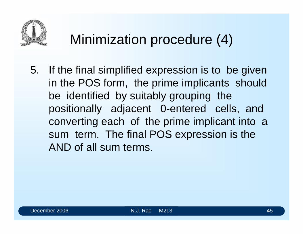
December 2006 N.J. Rao M2L3 45
Minimization procedure (4)
5. If the final simplified expression is to be given in the POS form, the prime implicants should be identified by suitably grouping the positionally adjacent 0-entered cells, and converting each of the prime implicant into a sum term. The final POS expression is the AND of all sum terms.
December 2006 N.J. Rao M2L3 46
Incompletely specified functions
All Boolean functions are not always completely specifiedConsider the BCD decoder, Only 10 outputs are decoded from 16 possible input
combinations The six invalid combinations of the inputs never occur We dont-care what the output is for any of these
combinations that should never occur These dont-care situations can be used advantageously in
generating a simpler Boolean expression Such dont-care combinations of the variables are
represented by an "X" in the appropriate cell of the K-map
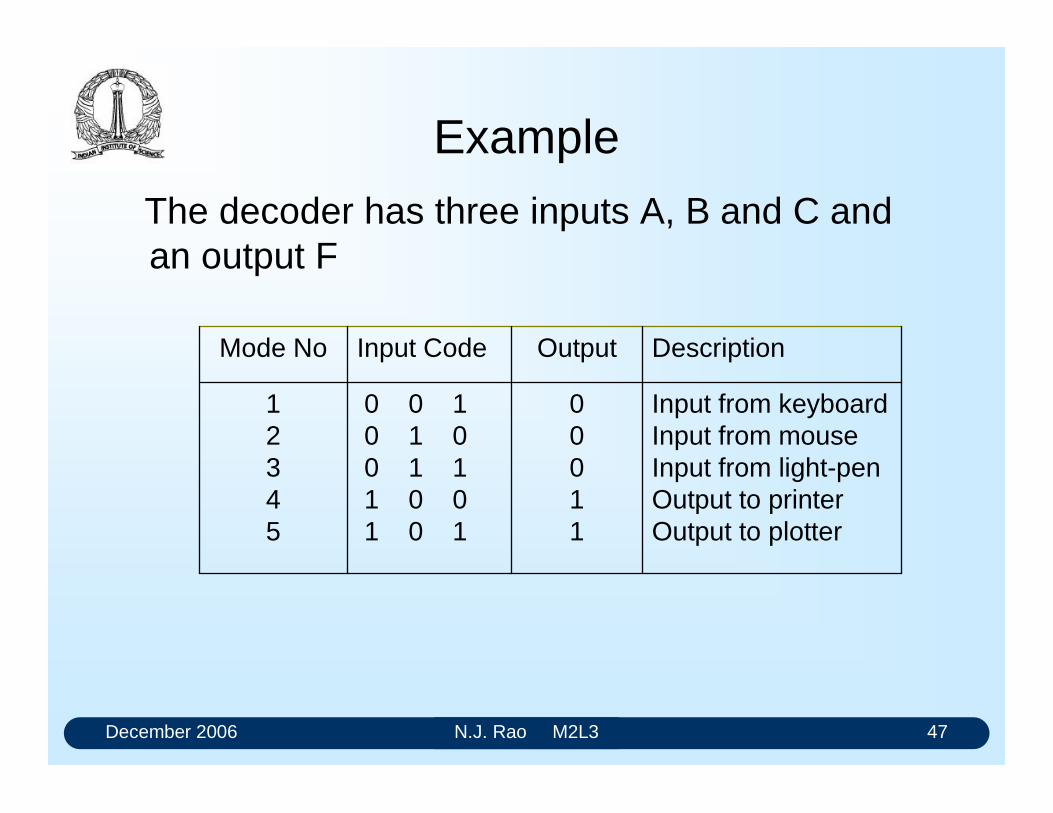
December 2006 N.J. Rao M2L3 47
Example
The decoder has three inputs A, B and C and an output F
Input from keyboardInput from mouseInput from light-penOutput to printerOutput to plotter
00011
0 0 10 1 00 1 11 0 01 0 1
12345
DescriptionOutputInput CodeMode No
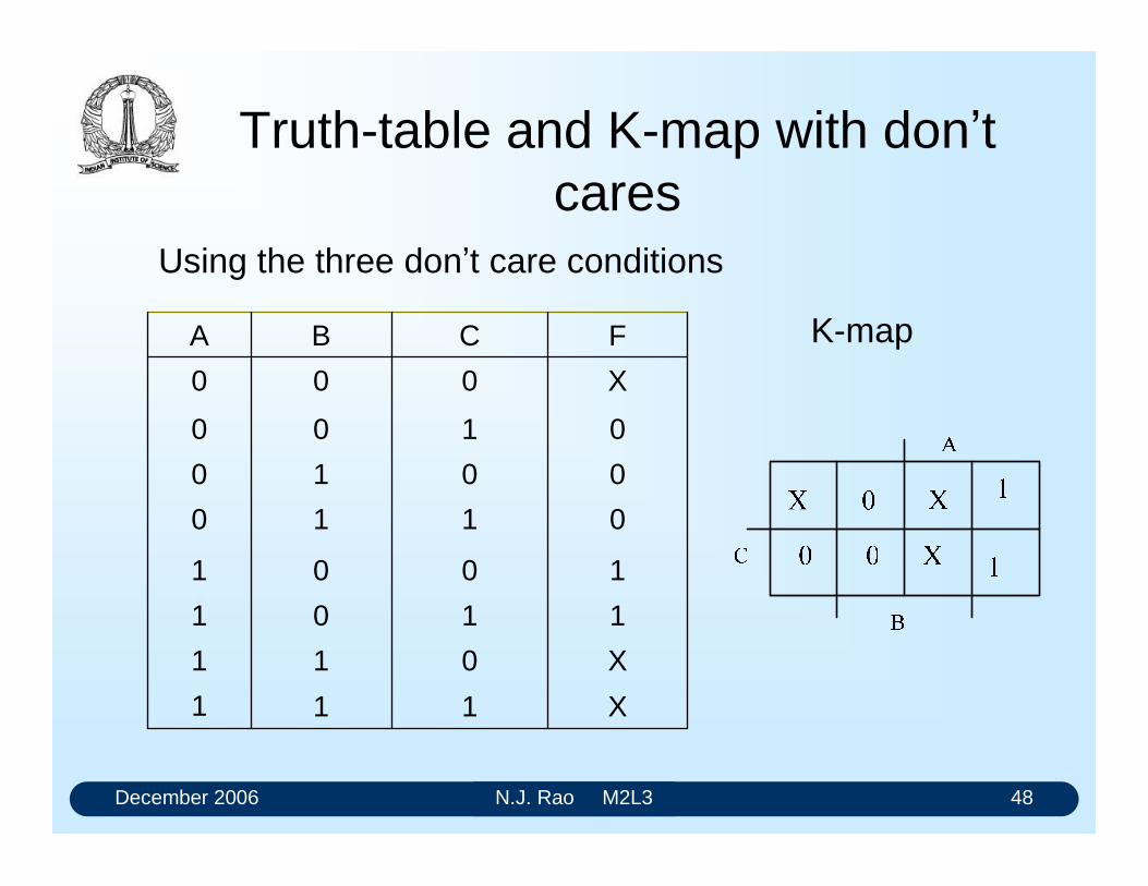
December 2006 N.J. Rao M2L3 48
Truth-table and K-map with dont cares
X11
X011
1
1101
1001
0110
0010
0100
X000
FCBA
Using the three dont care conditions
K-map
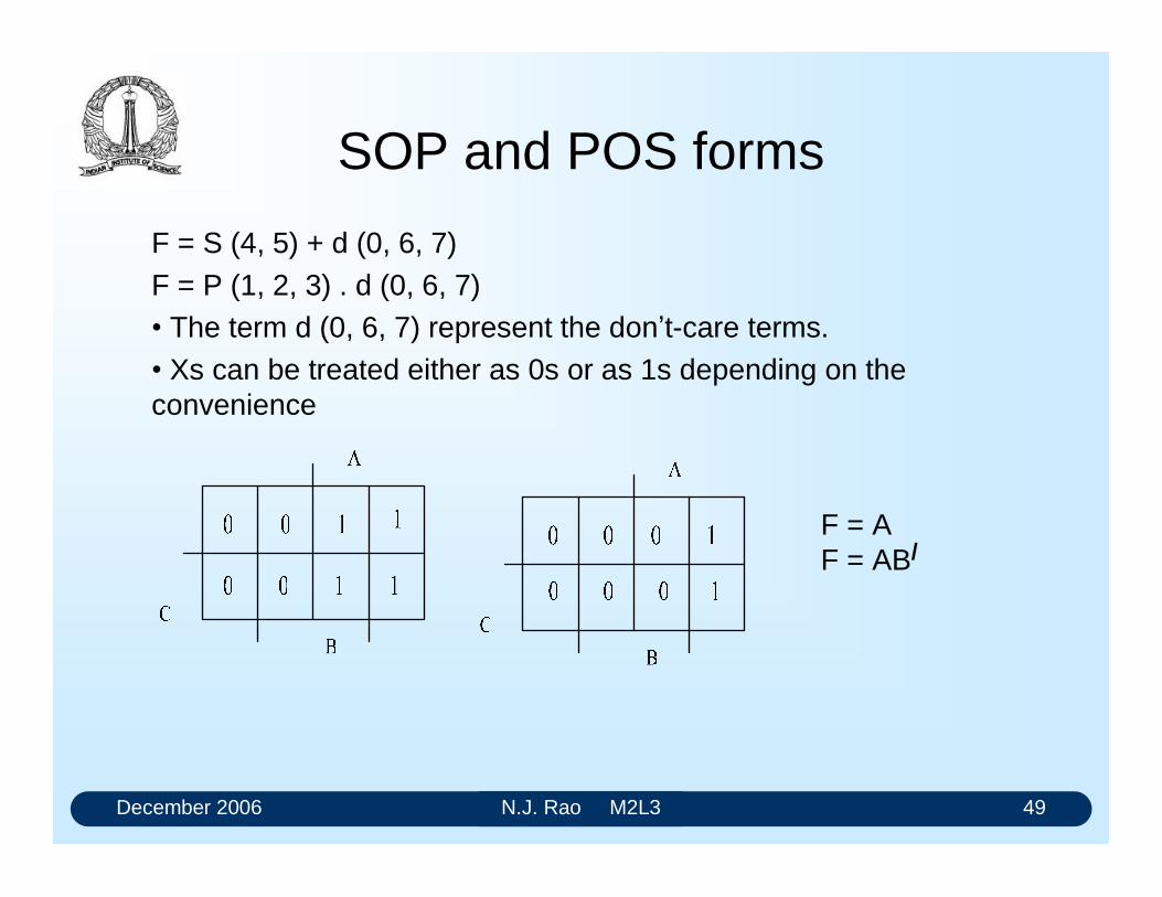
December 2006 N.J. Rao M2L3 49
SOP and POS forms
F = S (4, 5) + d (0, 6, 7) F = P (1, 2, 3) . d (0, 6, 7) The term d (0, 6, 7) represent the dont-care terms. Xs can be treated either as 0s or as 1s depending on the convenience
F = A F = AB/
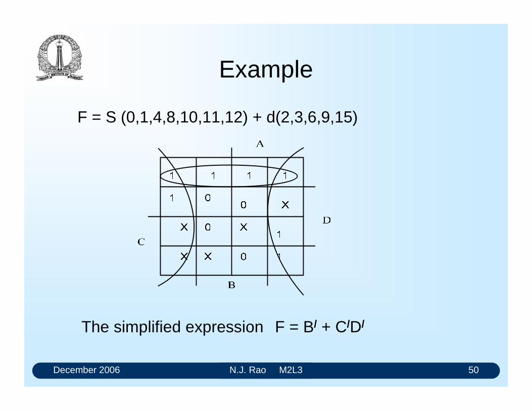
December 2006 N.J. Rao M2L3 50
Example
F = S (0,1,4,8,10,11,12) + d(2,3,6,9,15)
The simplified expression F = B/ + C/D/
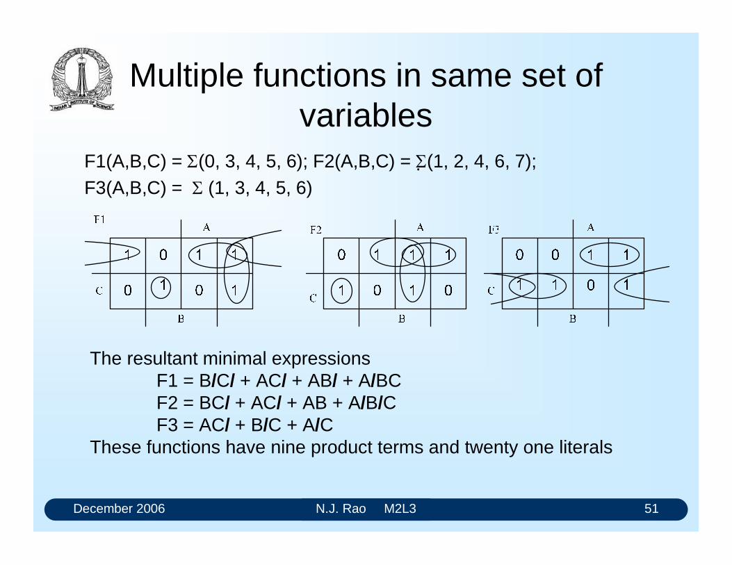
December 2006 N.J. Rao M2L3 51
Multiple functions in same set of variables
F1(A,B,C) = (0, 3, 4, 5, 6); F2(A,B,C) = (1, 2, 4, 6, 7); F3(A,B,C) = (1, 3, 4, 5, 6)
The resultant minimal expressionsF1 = B/C/ + AC/ + AB/ + A/BC F2 = BC/ + AC/ + AB + A/B/C F3 = AC/ + B/C + A/C
These functions have nine product terms and twenty one literals
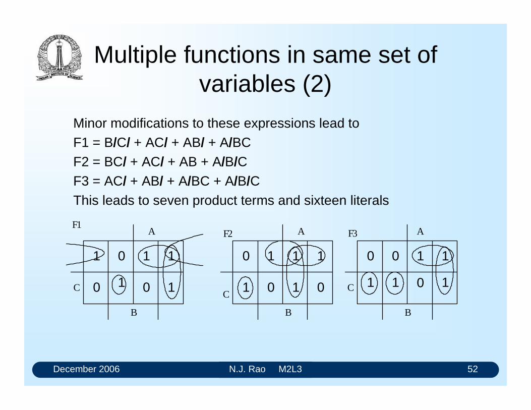
December 2006 N.J. Rao M2L3 52
Multiple functions in same set of variables (2)
Minor modifications to these expressions lead to F1 = B/C/ + AC/ + AB/ + A/BC F2 = BC/ + AC/ + AB + A/B/C F3 = AC/ + AB/ + A/BC + A/B/C This leads to seven product terms and sixteen literals
F1A
C
B
1
0 1
1
1
10
0
F2
1 1 1
1 10
0
0
A
B
C
F3
1 1
1 1 1
0 0
0
A
B
C
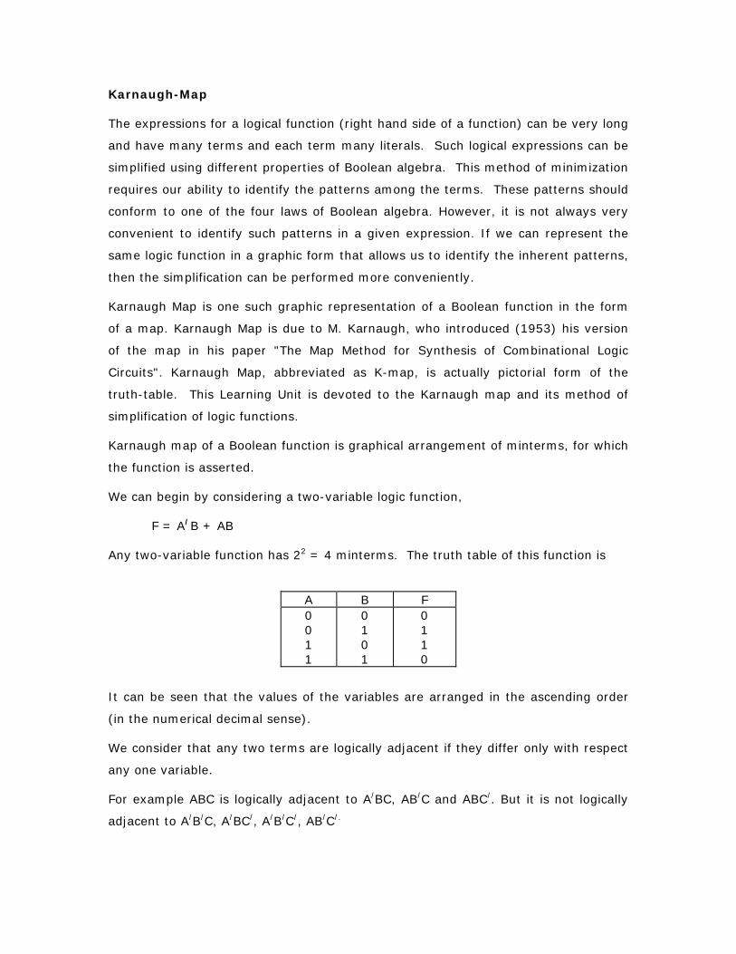
Karnaugh-Map
The expressions for a logical function (right hand side of a function) can be very long
and have many terms and each term many literals. Such logical expressions can be
simplified using different properties of Boolean algebra. This method of minimization
requires our ability to identify the patterns among the terms. These patterns should
conform to one of the four laws of Boolean algebra. However, it is not always very
convenient to identify such patterns in a given expression. If we can represent the
same logic function in a graphic form that allows us to identify the inherent patterns,
then the simplification can be performed more conveniently.
Karnaugh Map is one such graphic representation of a Boolean function in the form
of a map. Karnaugh Map is due to M. Karnaugh, who introduced (1953) his version
of the map in his paper "The Map Method for Synthesis of Combinational Logic
Circuits". Karnaugh Map, abbreviated as K-map, is actually pictorial form of the
truth-table. This Learning Unit is devoted to the Karnaugh map and its method of
simplification of logic functions.
Karnaugh map of a Boolean function is graphical arrangement of minterms, for which
the function is asserted.
We can begin by considering a two-variable logic function,
F = A/B + AB
Any two-variable function has 22 = 4 minterms. The truth table of this function is
A B F 0 0 1 1
0 1 0 1
0 1 1 0
It can be seen that the values of the variables are arranged in the ascending order
(in the numerical decimal sense).
We consider that any two terms are logically adjacent if they differ only with respect
any one variable.
For example ABC is logically adjacent to A/BC, AB/C and ABC/. But it is not logically
adjacent to A/B/C, A/BC/, A/B/C/, AB/C/.
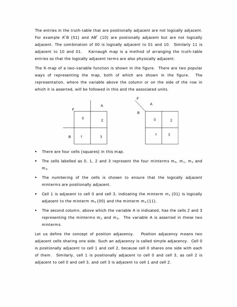
The entries in the truth-table that are positionally adjacent are not logically adjacent.
For example A/B (01) and AB/ (10) are postionally adjacent but are not logically
adjacent. The combination of 00 is logically adjacent to 01 and 10. Similarly 11 is
adjacent to 10 and 01. Karnaugh map is a method of arranging the truth-table
entries so that the logically adjacent terms are also physically adjacent.
The K-map of a two-variable function is shown in the figure. There are two popular
ways of representing the map, both of which are shown in the figure. The
representation, where the variable above the column or on the side of the row in
which it is asserted, will be followed in this and the associated units.
There are four cells (squares) in this map.
The cells labelled as 0, 1, 2 and 3 represent the four minterms m0, m1, m2 and
m3.
The numbering of the cells is chosen to ensure that the logically adjacent
minterms are positionally adjacent.
Cell 1 is adjacent to cell 0 and cell 3, indicating the minterm m1 (01) is logically
adjacent to the minterm m0 (00) and the minterm m3 (11).
The second column, above which the variable A is indicated, has the cells 2 and 3
representing the minterms m2 and m3. The variable A is asserted in these two
minterms.
Let us define the concept of position adjacency. Position adjacency means two
adjacent cells sharing one side. Such an adjacency is called simple adjacency. Cell 0
is positionally adjacent to cell 1 and cell 2, because cell 0 shares one side with each
of them. Similarly, cell 1 is positionally adjacent to cell 0 and cell 3, as cell 2 is
adjacent to cell 0 and cell 3, and cell 3 is adjacent to cell 1 and cell 2.

There are other kinds of positional adjacencies, which become relevant when the
number of variables is more than 3. We will explore them at a later time.
The main feature of the K-map is that by merely looking at the position of a cell, it is
possible to find immediately all the logically adjacent combinations in a function.
The function F = (A/B + AB) can now be incorporated into the K-map by entering "1"
in cells represented by the minterms for which the function is asserted. A "0" is
entered in all other cells. K-map for the function F is
You will notice that the two cells in which "1" is entered are not positionally adjacent.
Therefore, they are not logically adjacent.
Consider another function of two variables.
F = A/B + AB
The K-map for this function is
You will notice that the cells in which "1" is entered are positionally adjacent and
hence are logically adjacent.
Three-Variable Karnaugh Map:
K-map for three variables will have 23 = 8 cells as shown in the figure.
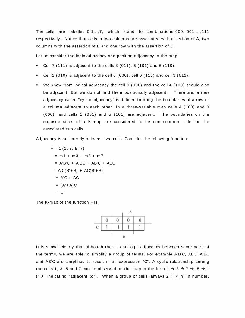
The cells are labelled 0,1,..,7, which stand for combinations 000, 001,...,111
respectively. Notice that cells in two columns are associated with assertion of A, two
columns with the assertion of B and one row with the assertion of C.
Let us consider the logic adjacency and position adjacency in the map.
Cell 7 (111) is adjacent to the cells 3 (011), 5 (101) and 6 (110).
Cell 2 (010) is adjacent to the cell 0 (000), cell 6 (110) and cell 3 (011).
We know from logical adjacency the cell 0 (000) and the cell 4 (100) should also
be adjacent. But we do not find them positionally adjacent. Therefore, a new
adjacency called "cyclic adjacency" is defined to bring the boundaries of a row or
a column adjacent to each other. In a three-variable map cells 4 (100) and 0
(000), and cells 1 (001) and 5 (101) are adjacent. The boundaries on the
opposite sides of a K-map are considered to be one common side for the
associated two cells.
Adjacency is not merely between two cells. Consider the following function:
F = Σ (1, 3, 5, 7)
= m1 + m3 + m5 + m7
= A'B'C + A'BC + AB'C + ABC
= A'C(B'+B) + AC(B'+B)
= A'C + AC
= (A'+A)C
= C
The K-map of the function F is
It is shown clearly that although there is no logic adjacency between some pairs of
the terms, we are able to simplify a group of terms. For example A/B/C, ABC, A/BC
and AB/C are simplified to result in an expression "C". A cyclic relationship among
the cells 1, 3, 5 and 7 can be observed on the map in the form 1 3 7 5 1
(" " indicating "adjacent to"). When a group of cells, always 2i (i < n) in number,
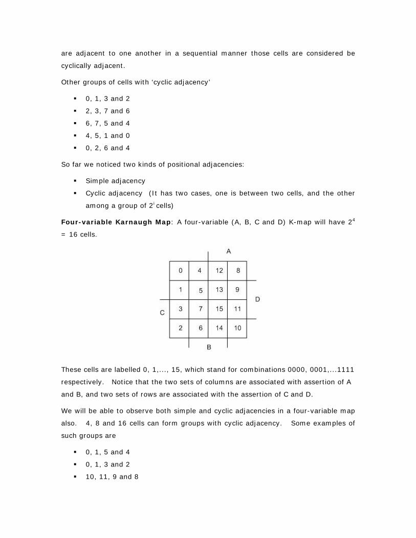
are adjacent to one another in a sequential manner those cells are considered be
cyclically adjacent.
Other groups of cells with ‘cyclic adjacency’
0, 1, 3 and 2
2, 3, 7 and 6
6, 7, 5 and 4
4, 5, 1 and 0
0, 2, 6 and 4
So far we noticed two kinds of positional adjacencies:
Simple adjacency
Cyclic adjacency (It has two cases, one is between two cells, and the other
among a group of 2i cells)
Four-variable Karnaugh Map: A four-variable (A, B, C and D) K-map will have 24
= 16 cells.
These cells are labelled 0, 1,..., 15, which stand for combinations 0000, 0001,...1111
respectively. Notice that the two sets of columns are associated with assertion of A
and B, and two sets of rows are associated with the assertion of C and D.
We will be able to observe both simple and cyclic adjacencies in a four-variable map
also. 4, 8 and 16 cells can form groups with cyclic adjacency. Some examples of
such groups are
0, 1, 5 and 4
0, 1, 3 and 2
10, 11, 9 and 8
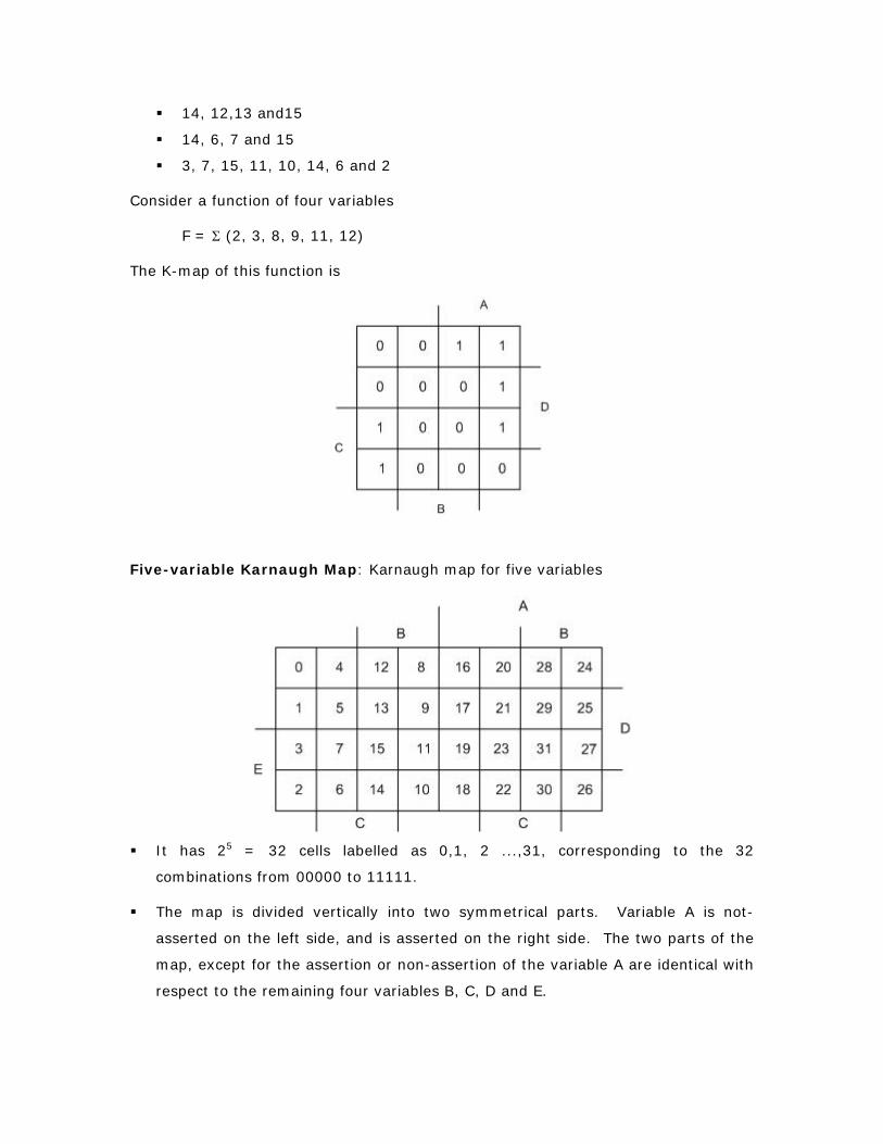
14, 12,13 and15
14, 6, 7 and 15
3, 7, 15, 11, 10, 14, 6 and 2
Consider a function of four variables
F = Σ (2, 3, 8, 9, 11, 12)
The K-map of this function is
Five-variable Karnaugh Map: Karnaugh map for five variables
It has 25 = 32 cells labelled as 0,1, 2 ...,31, corresponding to the 32
combinations from 00000 to 11111.
The map is divided vertically into two symmetrical parts. Variable A is not-
asserted on the left side, and is asserted on the right side. The two parts of the
map, except for the assertion or non-assertion of the variable A are identical with
respect to the remaining four variables B, C, D and E.
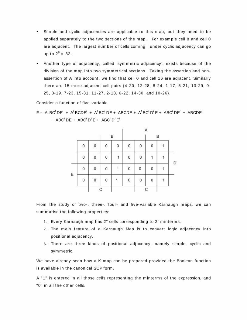
Simple and cyclic adjacencies are applicable to this map, but they need to be
applied separately to the two sections of the map. For example cell 8 and cell 0
are adjacent. The largest number of cells coming under cyclic adjacency can go
up to 25 = 32.
Another type of adjacency, called ‘symmetric adjacency’, exists because of the
division of the map into two symmetrical sections. Taking the assertion and non-
assertion of A into account, we find that cell 0 and cell 16 are adjacent. Similarly
there are 15 more adjacent cell pairs (4-20, 12-28, 8-24, 1-17, 5-21, 13-29, 9-
25, 3-19, 7-23, 15-31, 11-27, 2-18, 6-22, 14-30, and 10-26).
Consider a function of five-variable
F = A/BC/DE/ + A/BCDE/ + A/BC/DE + ABCDE + A/BC/D/E + ABC/DE/ + ABCDE/
+ ABC/DE + ABC/D/E + ABC/D/E/
From the study of two-, three-, four- and five-variable Karnaugh maps, we can
summarise the following properties:
1. Every Karnaugh map has 2n cells corresponding to 2n minterms.
2. The main feature of a Karnaugh Map is to convert logic adjacency into
positional adjacency.
3. There are three kinds of positional adjacency, namely simple, cyclic and
symmetric.
We have already seen how a K-map can be prepared provided the Boolean function
is available in the canonical SOP form.
A "1" is entered in all those cells representing the minterms of the expression, and
"0" in all the other cells.
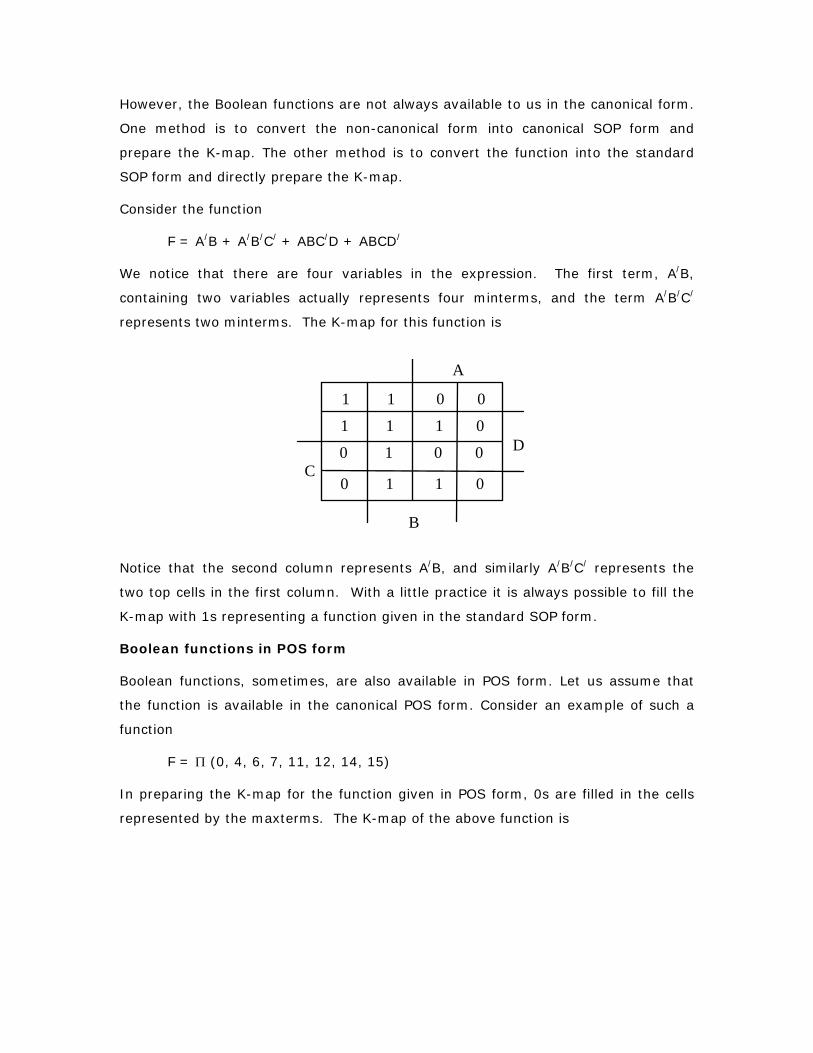
However, the Boolean functions are not always available to us in the canonical form.
One method is to convert the non-canonical form into canonical SOP form and
prepare the K-map. The other method is to convert the function into the standard
SOP form and directly prepare the K-map.
Consider the function
F = A/B + A/B/C/ + ABC/D + ABCD/
We notice that there are four variables in the expression. The first term, A/B,
containing two variables actually represents four minterms, and the term A/B/C/
represents two minterms. The K-map for this function is
A
D
B
C
1 1 0 0
1 1 1 0
0 1 0 0
0 1 1 0
Notice that the second column represents A/B, and similarly A/B/C/ represents the
two top cells in the first column. With a little practice it is always possible to fill the
K-map with 1s representing a function given in the standard SOP form.
Boolean functions in POS form
Boolean functions, sometimes, are also available in POS form. Let us assume that
the function is available in the canonical POS form. Consider an example of such a
function
F = Π (0, 4, 6, 7, 11, 12, 14, 15)
In preparing the K-map for the function given in POS form, 0s are filled in the cells
represented by the maxterms. The K-map of the above function is
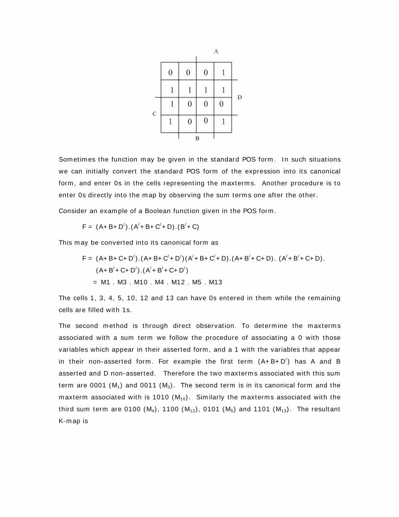
Sometimes the function may be given in the standard POS form. In such situations
we can initially convert the standard POS form of the expression into its canonical
form, and enter 0s in the cells representing the maxterms. Another procedure is to
enter 0s directly into the map by observing the sum terms one after the other.
Consider an example of a Boolean function given in the POS form.
F = (A+B+D/).(A/+B+C/+D).(B/+C)
This may be converted into its canonical form as
F = (A+B+C+D/).(A+B+C/+D/)(A/+B+C/+D).(A+B/+C+D). (A/+B/+C+D).
(A+B/+C+D/).(A/+B/+C+D/)
= M1 . M3 . M10 . M4 . M12 . M5 . M13
The cells 1, 3, 4, 5, 10, 12 and 13 can have 0s entered in them while the remaining
cells are filled with 1s.
The second method is through direct observation. To determine the maxterms
associated with a sum term we follow the procedure of associating a 0 with those
variables which appear in their asserted form, and a 1 with the variables that appear
in their non-asserted form. For example the first term (A+B+D/) has A and B
asserted and D non-asserted. Therefore the two maxterms associated with this sum
term are 0001 (M1) and 0011 (M3). The second term is in its canonical form and the
maxterm associated with is 1010 (M10). Similarly the maxterms associated with the
third sum term are 0100 (M4), 1100 (M12), 0101 (M5) and 1101 (M13). The resultant
K-map is
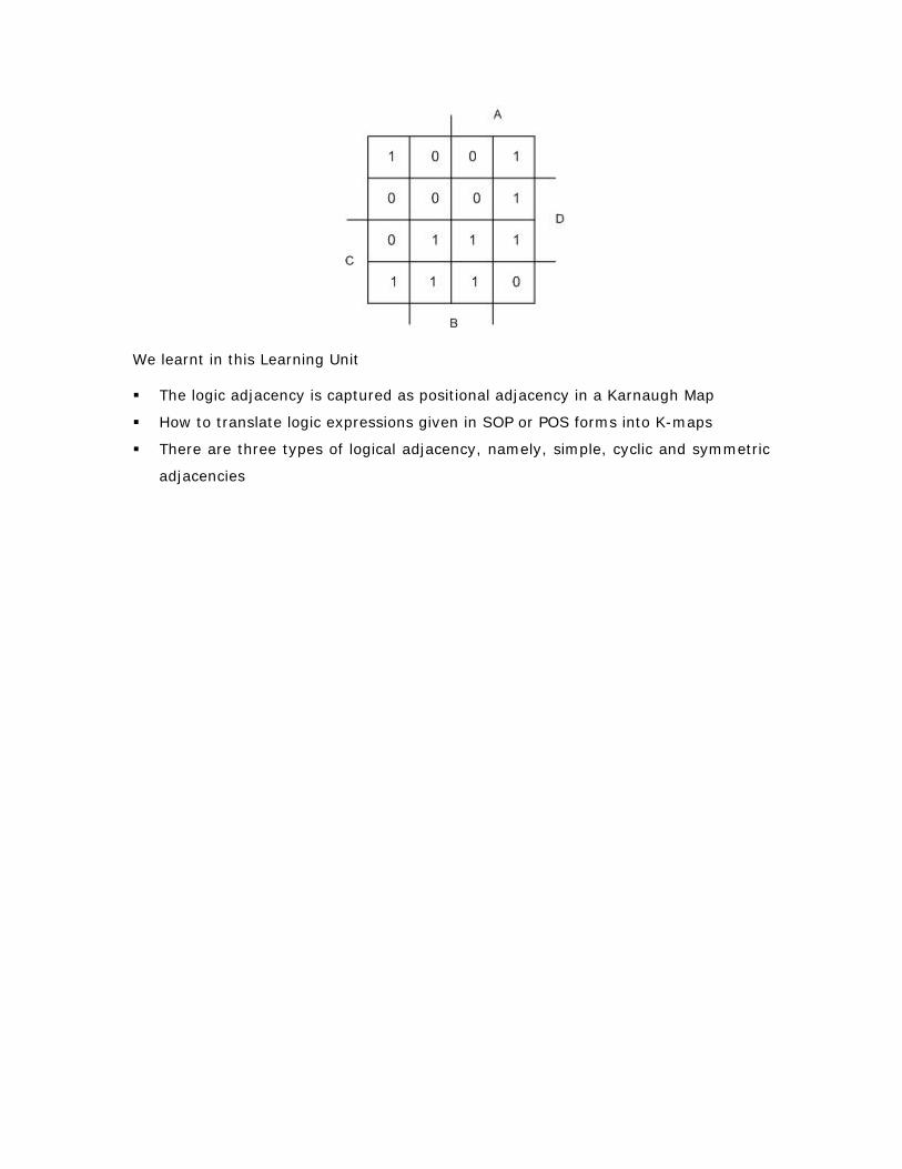
We learnt in this Learning Unit
The logic adjacency is captured as positional adjacency in a Karnaugh Map
How to translate logic expressions given in SOP or POS forms into K-maps
There are three types of logical adjacency, namely, simple, cyclic and symmetric
adjacencies
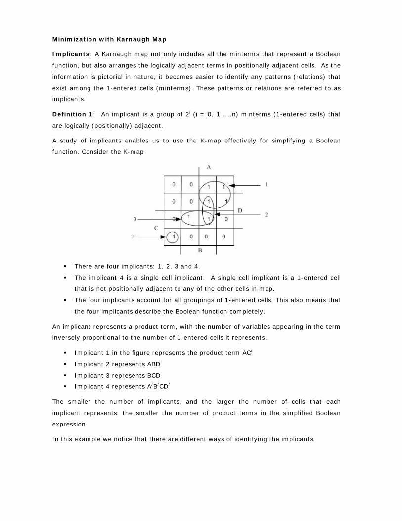
Minimization with Karnaugh Map
Implicants: A Karnaugh map not only includes all the minterms that represent a Boolean
function, but also arranges the logically adjacent terms in positionally adjacent cells. As the
information is pictorial in nature, it becomes easier to identify any patterns (relations) that
exist among the 1-entered cells (minterms). These patterns or relations are referred to as
implicants.
Definition 1: An implicant is a group of 2i (i = 0, 1 ....n) minterms (1-entered cells) that
are logically (positionally) adjacent.
A study of implicants enables us to use the K-map effectively for simplifying a Boolean
function. Consider the K-map
There are four implicants: 1, 2, 3 and 4.
The implicant 4 is a single cell implicant. A single cell implicant is a 1-entered cell
that is not positionally adjacent to any of the other cells in map.
The four implicants account for all groupings of 1-entered cells. This also means that
the four implicants describe the Boolean function completely.
An implicant represents a product term, with the number of variables appearing in the term
inversely proportional to the number of 1-entered cells it represents.
Implicant 1 in the figure represents the product term AC/
Implicant 2 represents ABD
Implicant 3 represents BCD
Implicant 4 represents A/B/CD/
The smaller the number of implicants, and the larger the number of cells that each
implicant represents, the smaller the number of product terms in the simplified Boolean
expression.
In this example we notice that there are different ways of identifying the implicants.
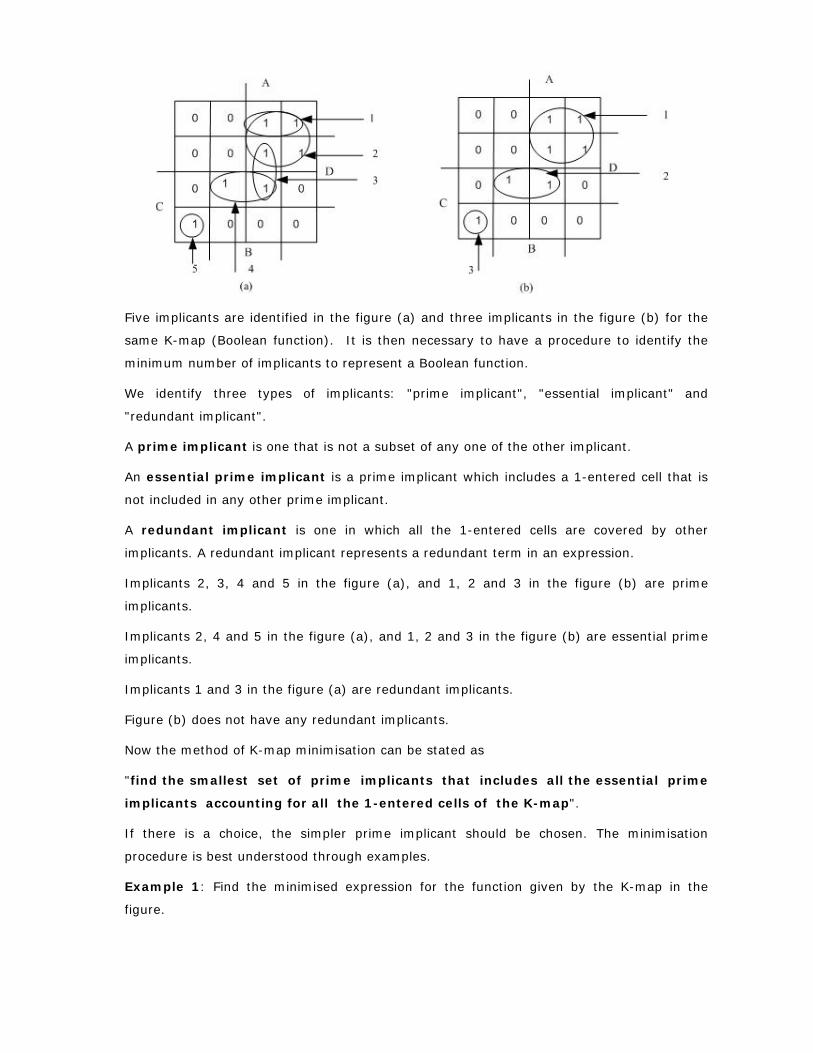
Five implicants are identified in the figure (a) and three implicants in the figure (b) for the
same K-map (Boolean function). It is then necessary to have a procedure to identify the
minimum number of implicants to represent a Boolean function.
We identify three types of implicants: "prime implicant", "essential implicant" and
"redundant implicant".
A prime implicant is one that is not a subset of any one of the other implicant.
An essential prime implicant is a prime implicant which includes a 1-entered cell that is
not included in any other prime implicant.
A redundant implicant is one in which all the 1-entered cells are covered by other
implicants. A redundant implicant represents a redundant term in an expression.
Implicants 2, 3, 4 and 5 in the figure (a), and 1, 2 and 3 in the figure (b) are prime
implicants.
Implicants 2, 4 and 5 in the figure (a), and 1, 2 and 3 in the figure (b) are essential prime
implicants.
Implicants 1 and 3 in the figure (a) are redundant implicants.
Figure (b) does not have any redundant implicants.
Now the method of K-map minimisation can be stated as
"find the smallest set of prime implicants that includes all the essential prime
implicants accounting for all the 1-entered cells of the K-map".
If there is a choice, the simpler prime implicant should be chosen. The minimisation
procedure is best understood through examples.
Example 1: Find the minimised expression for the function given by the K-map in the
figure.
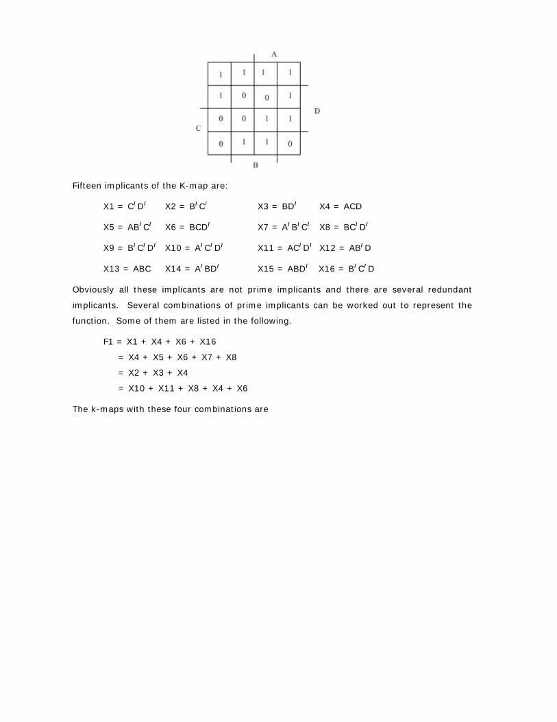
Fifteen implicants of the K-map are:
X1 = C/D/ X2 = B/C/ X3 = BD/ X4 = ACD
X5 = AB/C/ X6 = BCD/ X7 = A/B/C/ X8 = BC/D/
X9 = B/C/D/ X10 = A/C/D/ X11 = AC/D/ X12 = AB/D
X13 = ABC X14 = A/BD/ X15 = ABD/ X16 = B/C/D
Obviously all these implicants are not prime implicants and there are several redundant
implicants. Several combinations of prime implicants can be worked out to represent the
function. Some of them are listed in the following.
F1 = X1 + X4 + X6 + X16
= X4 + X5 + X6 + X7 + X8
= X2 + X3 + X4
= X10 + X11 + X8 + X4 + X6
The k-maps with these four combinations are
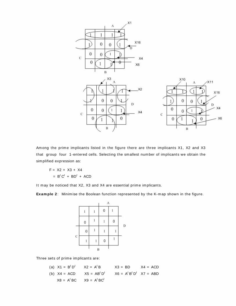
Among the prime implicants listed in the figure there are three implicants X1, X2 and X3
that group four 1-entered cells. Selecting the smallest number of implicants we obtain the
simplified expression as:
F = X2 + X3 + X4
= B/C/ + BD/ + ACD
It may be noticed that X2, X3 and X4 are essential prime implicants.
Example 2: Minimise the Boolean function represented by the K-map shown in the figure.
Three sets of prime implicants are:
(a) X1 = B/D/ X2 = A/B X3 = BD X4 = ACD
(b) X4 = ACD X5 = AB/D/ X6 = A/B/D/ X7 = ABD
X8 = A/BC X9 = A/BC/
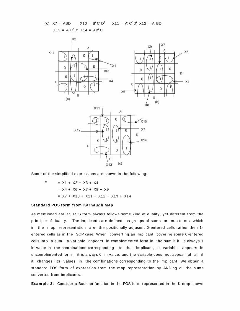
(c) X7 = ABD X10 = B/C/D/ X11 = A/C/D/ X12 = A/BD
X13 = A/C/D/ X14 = AB/C
Some of the simplified expressions are shown in the following:
F = X1 + X2 + X3 + X4
= X4 + X6 + X7 + X8 + X9
= X7 + X10 + X11 + X12 + X13 + X14
Standard POS form from Karnaugh Map
As mentioned earlier, POS form always follows some kind of duality, yet different from the
principle of duality. The implicants are defined as groups of sums or maxterms which
in the map representation are the positionally adjacent 0-entered cells rather then 1-
entered cells as in the SOP case. When converting an implicant covering some 0-entered
cells into a sum, a variable appears in complemented form in the sum if it is always 1
in value in the combinations corresponding to that implicant, a variable appears in
uncomplimented form if it is always 0 in value, and the variable does not appear at all if
it changes its values in the combinations corresponding to the implicant. We obtain a
standard POS form of expression from the map representation by ANDing all the sums
converted from implicants.
Example 3: Consider a Boolean function in the POS form represented in the K-map shown

in the figure
Initially four implicants are identified (1, 2, 3 and 4).
Implicant 1: B is asserted and A is not-asserted in all the cells of implicant 1, where as
the variables C and D change their values from 0 to 1. It is represented by the sum
term (A + B/).
Implicant 2: It is represented by the sum term (B/ + D/).
Implicant 3: It is represented by (B + D).
Implicant 4: It is represented by (A/ + C/ + D/).
The simplified expression in the POS form is given by;
F = (A + B/) . (B/ + D/) . (B + D) . (A/ + C/ + D/)
If we choose the implicant 5 (shown by the dotted line in the figure 19) instead of 4,
the simplified expression gets modified as:
F = (A + B/) . (B/ + D/).(B + D).(A/ + B +C'/)
We may summarise the procedure for minimization of a Boolean function through a K-map
as follows:
1. Draw the K-map with 2n cells, where n is the number of variables in a Boolean function.
2. Fill in the K-map with 1s and 0s as per the function given in the algebraic form (SOP or
POS) or truth-table form.
3. Determine the set of prime implicants that consist of all the essential prime implicants
as per the following criteria:
All the 1-entered or 0-entered cells are covered by the set of implicants, while
making the number of cells covered by each implicant as large as possible.
Eliminate the redundant implicants.
Identify all the essential prime implicants.
Whenever there is a choice among the prime implicants select the prime
implicant with the smaller number of literals.
4. If the final expression is to be generated in SOP form, the prime implicants should be
identified by suitably grouping the positionally adjacent 1-entered cells, and converting
each of the prime implicant into a product term. The final SOP expression is the OR of
the identified product terms.
5. If the final simplified expression is to be given in the POS form, the prime implicants
should be identified by suitably grouping the positionally adjacent 0-entered
cells, and converting each of the prime implicant into a sum term. The final POS
expression is the AND of the identified sum terms.
Simplification of Incompletely Specified Functions
So far we assumed that the Boolean functions are always completely specified, which
means a given function assumes strictly a specific value, 1 or 0, for each of its 2n
input combinations. This, however, is not always the case.
Consider the example is the BCD decoders
The ten outputs are decoded from sixteen possible input combinations produced by
four inputs representing BCD codes.
An encoding scheme chooses ten valid codes.
Irrespective of the encoding scheme there are always six combinations of the inputs
that would be considered as invalid codes.
If the input unit to the BCD decoder works in a functionally correct way, then the six
invalid combinations of the inputs should never occur.
In such a case, it does not matter what the output of the decoder is for these six
combinations. As we do not mind what the values of the outputs are in such situations, we
call them "don’t-care" situations. These don’t-care situations can be used advantageously in
generating a simpler Boolean expression than without taking that advantage.
Such don’t-care combinations of the variables are represented by an "X" in the appropriate
cell of the K-map.
Example: This example shows how an incompletely specified function can be represented
in truth-table, Karnaugh map and canonical forms.
The decoder has three inputs A, B and C representing three bit codes and an output F. Out
of the 23 = 8 possible combinations of the inputs, only five are described and hence
constitute the valid codes. F is not specified for the remaining three input codes, namely,
000, 110 and 111.
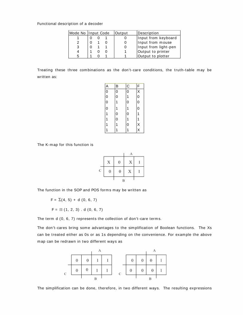
Functional description of a decoder
Mode No Input Code Output Description 1 2 3 4 5
0 0 1 0 1 0 0 1 1 1 0 0 1 0 1
0 0 0 1 1
Input from keyboard Input from mouse Input from light-pen Output to printer Output to plotter
Treating these three combinations as the don’t-care conditions, the truth-table may be
written as:
A B C F 0 0 0 X 0 0 1 0 0 1 0 0
0 1 1 0 1 0 0 1 1 0 1 1 1 1 0 X 1 1 1 X
The K-map for this function is
The function in the SOP and POS forms may be written as
F = Σ(4, 5) + d (0, 6, 7)
F = Π (1, 2, 3) . d (0, 6, 7)
The term d (0, 6, 7) represents the collection of don’t-care terms.
The don’t-cares bring some advantages to the simplification of Boolean functions. The Xs
can be treated either as 0s or as 1s depending on the convenience. For example the above
map can be redrawn in two different ways as
The simplification can be done, therefore, in two different ways. The resulting expressions
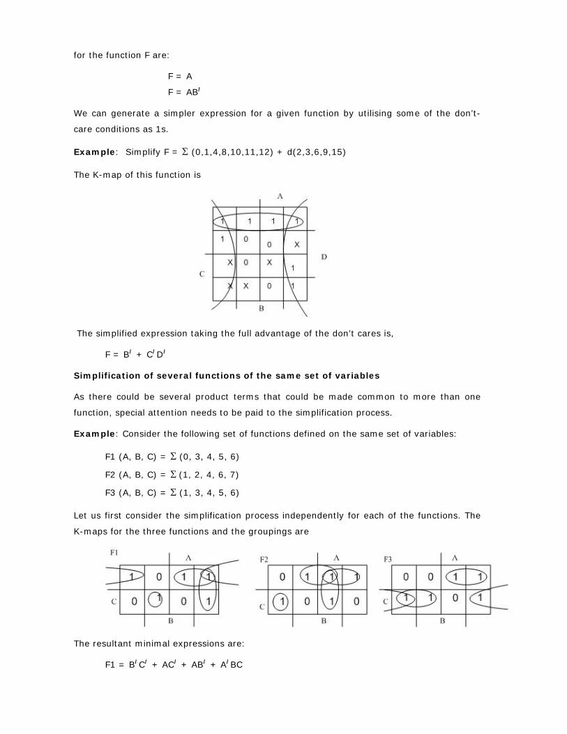
for the function F are:
F = A
F = AB/
We can generate a simpler expression for a given function by utilising some of the don’t-
care conditions as 1s.
Example: Simplify F = Σ (0,1,4,8,10,11,12) + d(2,3,6,9,15)
The K-map of this function is
The simplified expression taking the full advantage of the don’t cares is,
F = B/ + C/D/
Simplification of several functions of the same set of variables
As there could be several product terms that could be made common to more than one
function, special attention needs to be paid to the simplification process.
Example: Consider the following set of functions defined on the same set of variables:
F1 (A, B, C) = Σ (0, 3, 4, 5, 6)
F2 (A, B, C) = Σ (1, 2, 4, 6, 7)
F3 (A, B, C) = Σ (1, 3, 4, 5, 6)
Let us first consider the simplification process independently for each of the functions. The
K-maps for the three functions and the groupings are
The resultant minimal expressions are:
F1 = B/C/ + AC/ + AB/ + A/BC
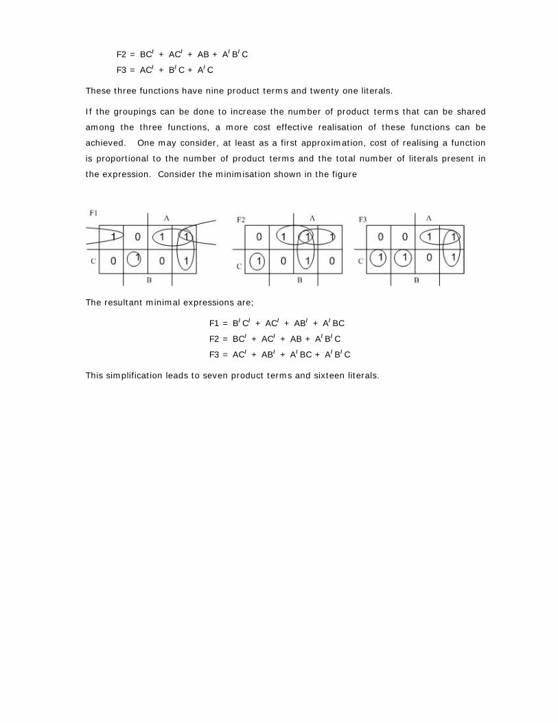
F2 = BC/ + AC/ + AB + A/B/C
F3 = AC/ + B/C + A/C
These three functions have nine product terms and twenty one literals.
If the groupings can be done to increase the number of product terms that can be shared
among the three functions, a more cost effective realisation of these functions can be
achieved. One may consider, at least as a first approximation, cost of realising a function
is proportional to the number of product terms and the total number of literals present in
the expression. Consider the minimisation shown in the figure
The resultant minimal expressions are;
F1 = B/C/ + AC/ + AB/ + A/BC
F2 = BC/ + AC/ + AB + A/B/C
F3 = AC/ + AB/ + A/BC + A/B/C
This simplification leads to seven product terms and sixteen literals.
Digital Electronics Module 2: Quine-McCluskey Method
N.J. RaoIndian Institute of Science
id5097289 pdfMachine by Broadgun Software - a great PDF writer! - a great PDF creator! - http://www.pdfmachine.com http://www.broadgun.com
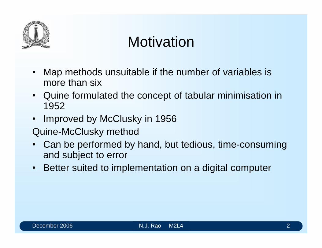
December 2006 N.J. Rao M2L4 2
Motivation
Map methods unsuitable if the number of variables is more than six
Quine formulated the concept of tabular minimisation in 1952
Improved by McClusky in 1956Quine-McClusky method Can be performed by hand, but tedious, time-consuming
and subject to error Better suited to implementation on a digital computer
December 2006 N.J. Rao M2L4 3
Principle of Quine-McCusky Method
Quine-McClusky method is a two stage simplification process Step 1: Prime implicants are generated by a special
tabulation processStep 2: A minimal set of implicants is determined
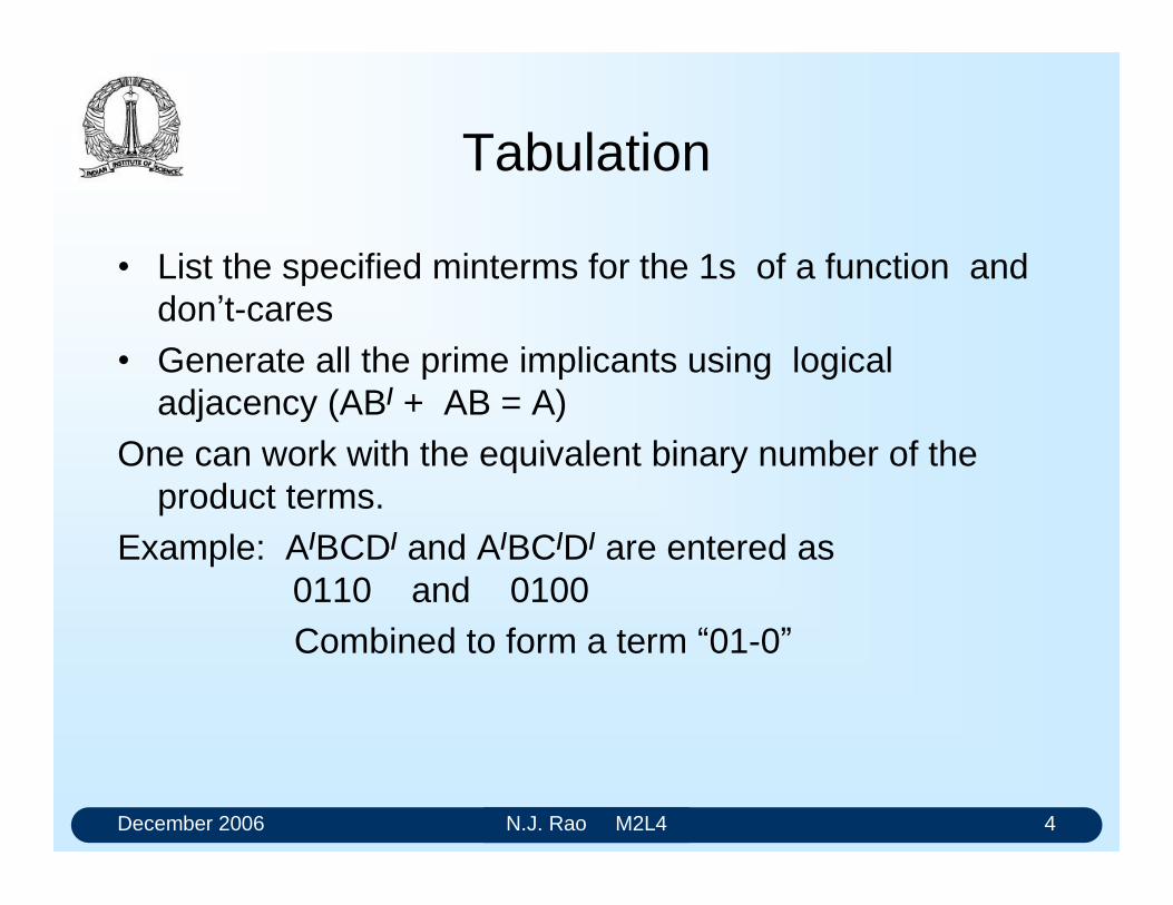
December 2006 N.J. Rao M2L4 4
Tabulation
List the specified minterms for the 1s of a function and dont-cares
Generate all the prime implicants using logical adjacency (AB/ + AB = A)
One can work with the equivalent binary number of the product terms.
Example: A/BCD/ and A/BC/D/ are entered as 0110 and 0100Combined to form a term 01-0
December 2006 N.J. Rao M2L4 5
Creation of Prime Implicant Table
Selected prime implicants are combined and arranged in a table
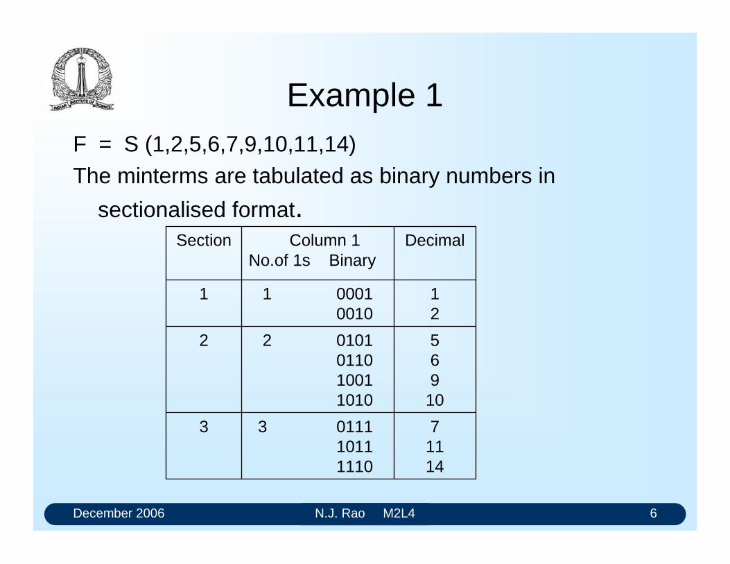
December 2006 N.J. Rao M2L4 6
Example 1F = S (1,2,5,6,7,9,10,11,14) The minterms are tabulated as binary numbers in
sectionalised format.
71114
3 011110111110
3
569
10
2 0101011010011010
2
12
1 00010010
1
DecimalColumn 1No.of 1s Binary
Section
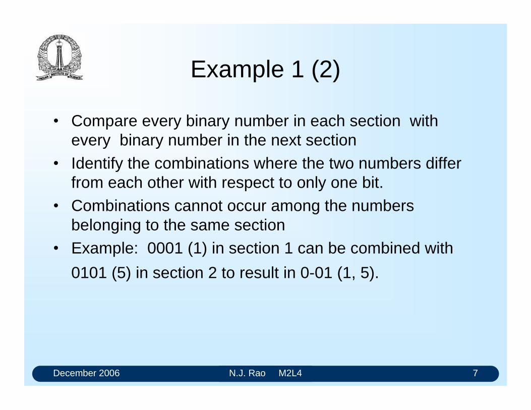
December 2006 N.J. Rao M2L4 7
Example 1 (2)
Compare every binary number in each section with every binary number in the next section
Identify the combinations where the two numbers differ from each other with respect to only one bit.
Combinations cannot occur among the numbers belonging to the same section
Example: 0001 (1) in section 1 can be combined with
0101 (5) in section 2 to result in 0-01 (1, 5).
December 2006 N.J. Rao M2L4 8
Example 1 (3)
The results of such combinations are entered into another column
The paired entries are checked off The entries of one section in the second column can
again be combined together with entries in the next section
Continue this process
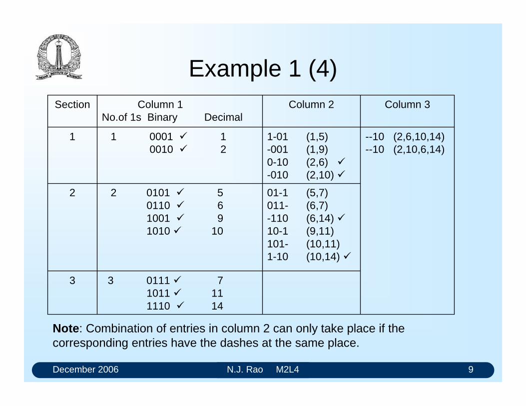
December 2006 N.J. Rao M2L4 9
Example 1 (4)
3 0111 71011 111110 14
3
01-1 (5,7)011- (6,7)-110 (6,14) 10-1 (9,11)101- (10,11) 1-10 (10,14)
2 0101 50110 61001 9 1010 10
2
--10 (2,6,10,14)--10 (2,10,6,14)
1-01 (1,5)-001 (1,9)0-10 (2,6) -010 (2,10)
1 0001 10010 2
1
Column 3Column 2Column 1No.of 1s Binary Decimal
Section
Note: Combination of entries in column 2 can only take place if the corresponding entries have the dashes at the same place.
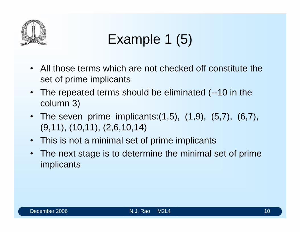
December 2006 N.J. Rao M2L4 10
Example 1 (5)
All those terms which are not checked off constitute the set of prime implicants
The repeated terms should be eliminated (--10 in the column 3)
The seven prime implicants:(1,5), (1,9), (5,7), (6,7), (9,11), (10,11), (2,6,10,14)
This is not a minimal set of prime implicants The next stage is to determine the minimal set of prime
implicants
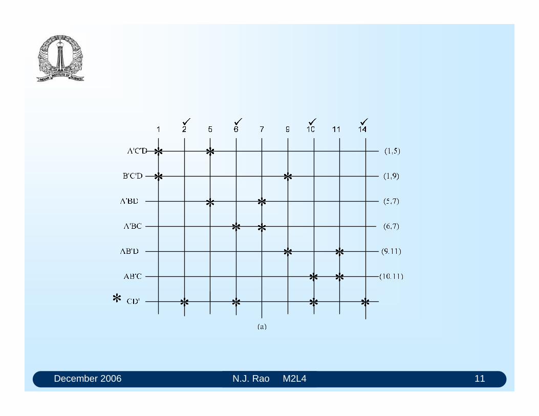
December 2006 N.J. Rao M2L4 11
December 2006 N.J. Rao M2L4 12
Selection of minimal set of implicants
Determine essential prime implicants These are the minterms not covered by any other prime
implicant Identified by columns that have only one asterisk Columns 2 and 14 have only one asterisk each The associated row, CD/, is an essential prime implicant. CD/ is selected as a member of the minimal set (mark it by an
asterisk) Remove the corresponding columns, 2, 6, 10, 14, from the prime
implicant table
A new table is prepared.
December 2006 N.J. Rao M2L4 13
Selection of minimal set of implicants (2)
December 2006 N.J. Rao M2L4 14
Dominating Prime Implicants
Identified by the rows that have more asterisks than others
Choose Row A/BD Includes the minterm 7, which is the only one included in
the row represented by A/BC A/BD is dominant implicant over A/BC A/BC can be eliminated Mark A/BD by an asterisk Check off the columns 5 and 7
December 2006 N.J. Rao M2L4 15
Dominating Prime Implicants (2)
Choose AB/D Dominates over the row AB/C Mark the row AB/D by an asterisk Eliminate the row AB/C Check off columns 9 and 11
Select A/C/D Dominates over B/C/D. B/C/D also dominates over A/C/D Either B/C/D or A/C/D can be chosen as the dominant
prime implicant
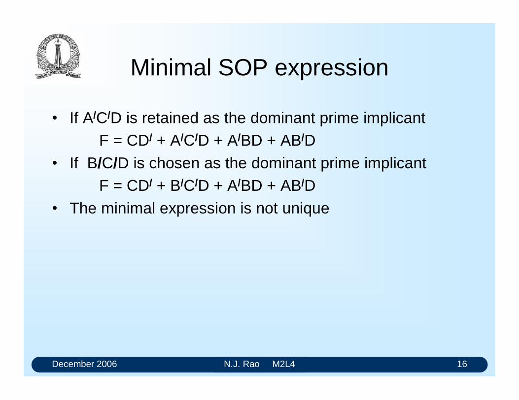
December 2006 N.J. Rao M2L4 16
Minimal SOP expression
If A/C/D is retained as the dominant prime implicantF = CD/ + A/C/D + A/BD + AB/D
If B/C/D is chosen as the dominant prime implicantF = CD/ + B/C/D + A/BD + AB/D
The minimal expression is not unique
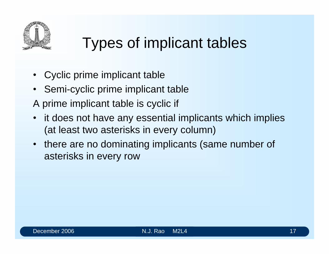
December 2006 N.J. Rao M2L4 17
Types of implicant tables
Cyclic prime implicant table Semi-cyclic prime implicant tableA prime implicant table is cyclic if it does not have any essential implicants which implies
(at least two asterisks in every column) there are no dominating implicants (same number of
asterisks in every row
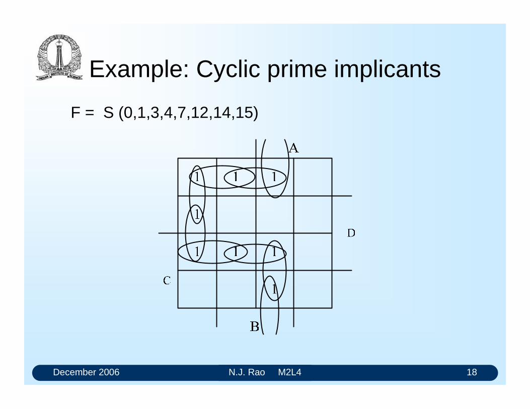
December 2006 N.J. Rao M2L4 18
Example: Cyclic prime implicants
F = S (0,1,3,4,7,12,14,15)
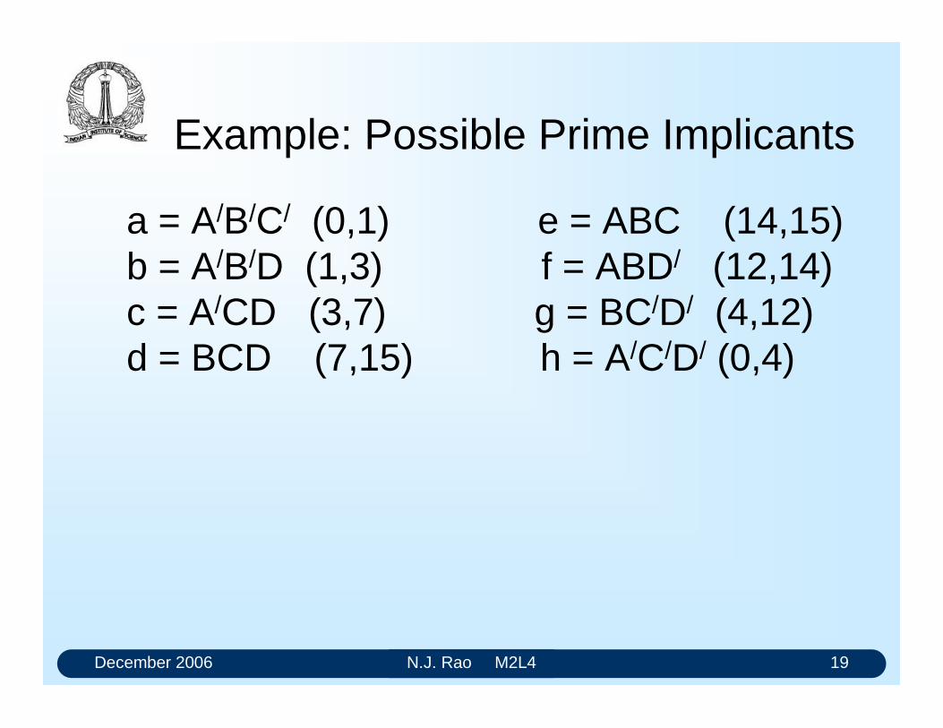
December 2006 N.J. Rao M2L4 19
Example: Possible Prime Implicants
a = A/B/C/ (0,1) e = ABC (14,15) b = A/B/D (1,3) f = ABD/ (12,14) c = A/CD (3,7) g = BC/D/ (4,12) d = BCD (7,15) h = A/C/D/ (0,4)
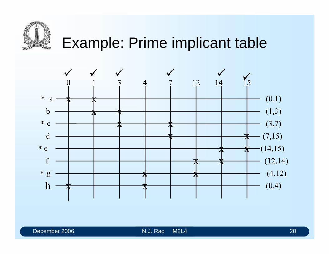
December 2006 N.J. Rao M2L4 20
Example: Prime implicant table
December 2006 N.J. Rao M2L4 21
Process of simplification
All columns have two asterisks There are no essential prime implicants. Choose any one of the prime implicants to start with Start with prime implicant a (mark with asterisk) Delete corresponding columns, 0 and 1 Row c becomes dominant over row b, delete row b Delete columns 3 and 7 Row e dominates row d, and row d can be eliminated Delete columns 14 and 15 Choose row g it covers the remaining asterisks
associated with rows h and f
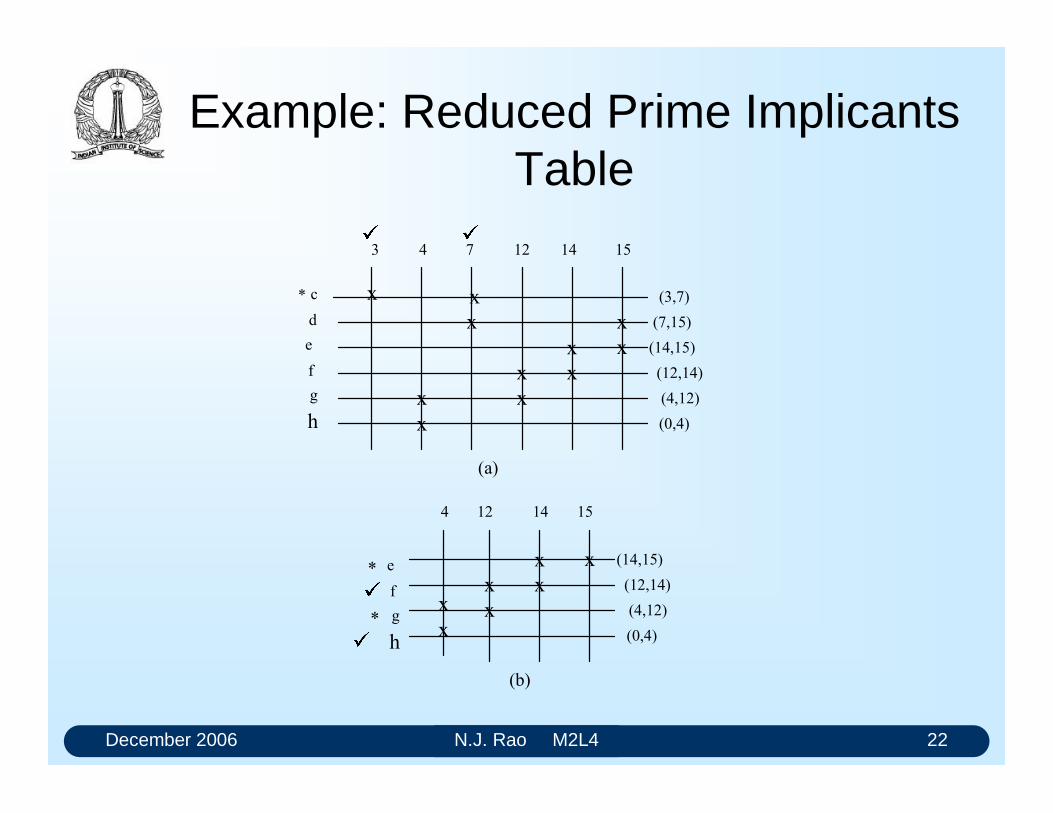
December 2006 N.J. Rao M2L4 22
Example: Reduced Prime ImplicantsTable
F
G
H
I
J
K
[ [
[[
[[
[[
[[
[
D
H
I
J
K
[ [
[[
[[
[
E
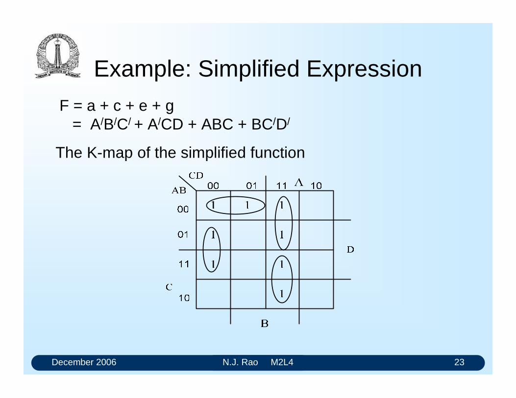
December 2006 N.J. Rao M2L4 23
Example: Simplified Expression
F = a + c + e + g = A/B/C/ + A/CD + ABC + BC/D/
The K-map of the simplified function
December 2006 N.J. Rao M2L4 24
Semi-cyclic prime implicant table
The number of minterms covered by each prime implicant is identical in cyclic function
Not necessarily true in a semi-cyclic function
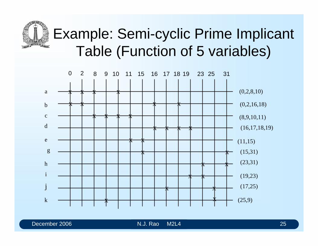
December 2006 N.J. Rao M2L4 25
Example: Semi-cyclic Prime ImplicantTable (Function of 5 variables)
x
(0,2,8,10)
(0,2,16,18)
(8,9,10,11)
(16,17,18,19)
(11,15)
(15,31)
(23,31)
(19,23)
(17,25)
(25,9)
x
a
b
c
e
d
g
h
i
j
k
0 2 8 9 10 11 15 16 17 18 19 23 25 31
x
x x x x
x x
x x x x
x x x x
xx
x x
xx
x x
x x
x
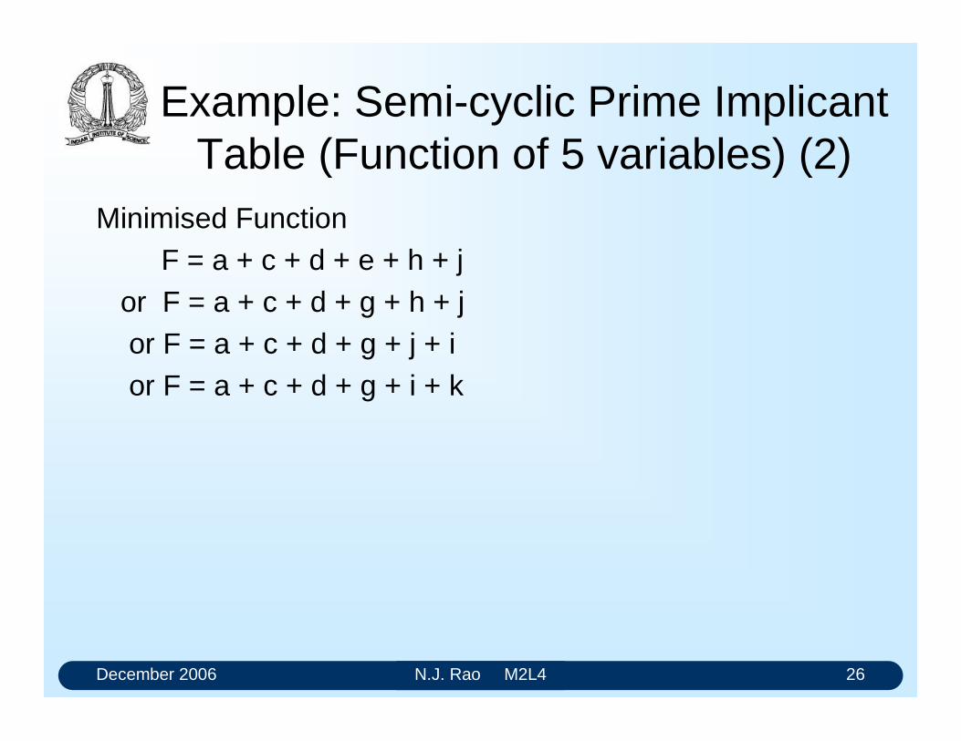
December 2006 N.J. Rao M2L4 26
Example: Semi-cyclic Prime ImplicantTable (Function of 5 variables) (2)
Minimised FunctionF = a + c + d + e + h + j
or F = a + c + d + g + h + j or F = a + c + d + g + j + i or F = a + c + d + g + i + k
December 2006 N.J. Rao M2L4 27
Simplification of Incompletely Specified Functions
Do the initial tabulation including the dont-cares Construct the prime implicant table Columns associated with dont-cares need not be
included Further simplification is similar to that for completely
specified functions
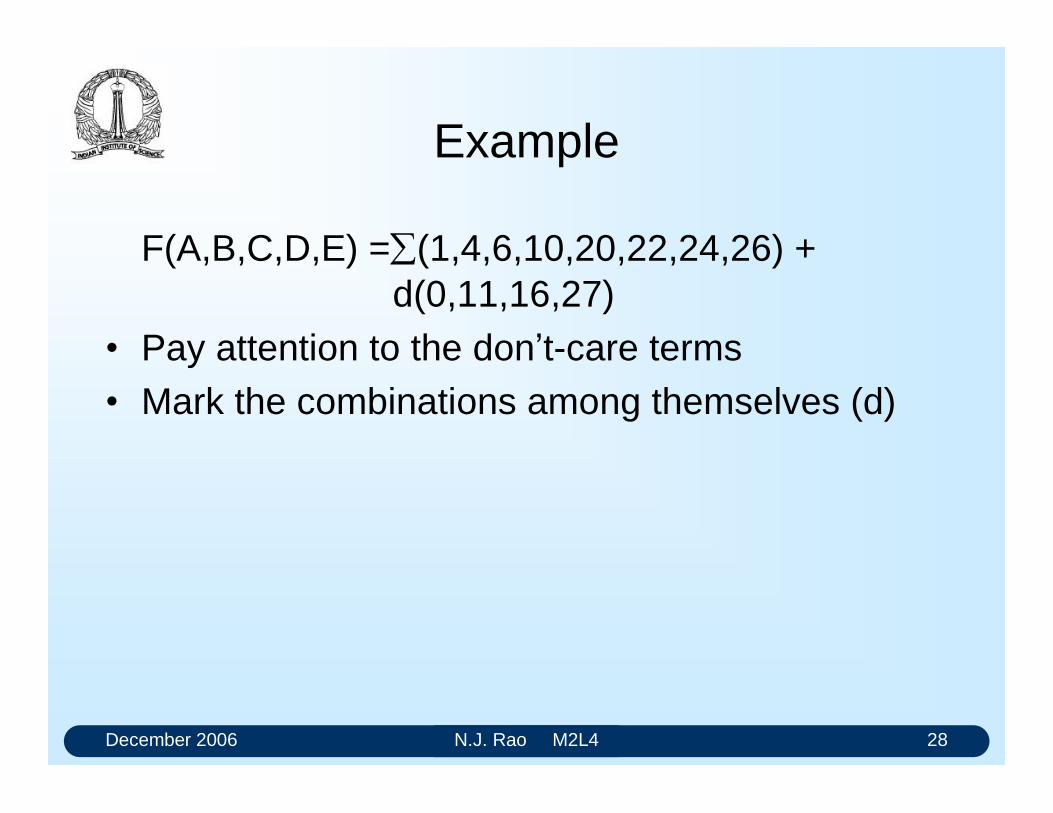
December 2006 N.J. Rao M2L4 28
Example
F(A,B,C,D,E) =(1,4,6,10,20,22,24,26) + d(0,11,16,27)
Pay attention to the dont-care terms Mark the combinations among themselves (d)
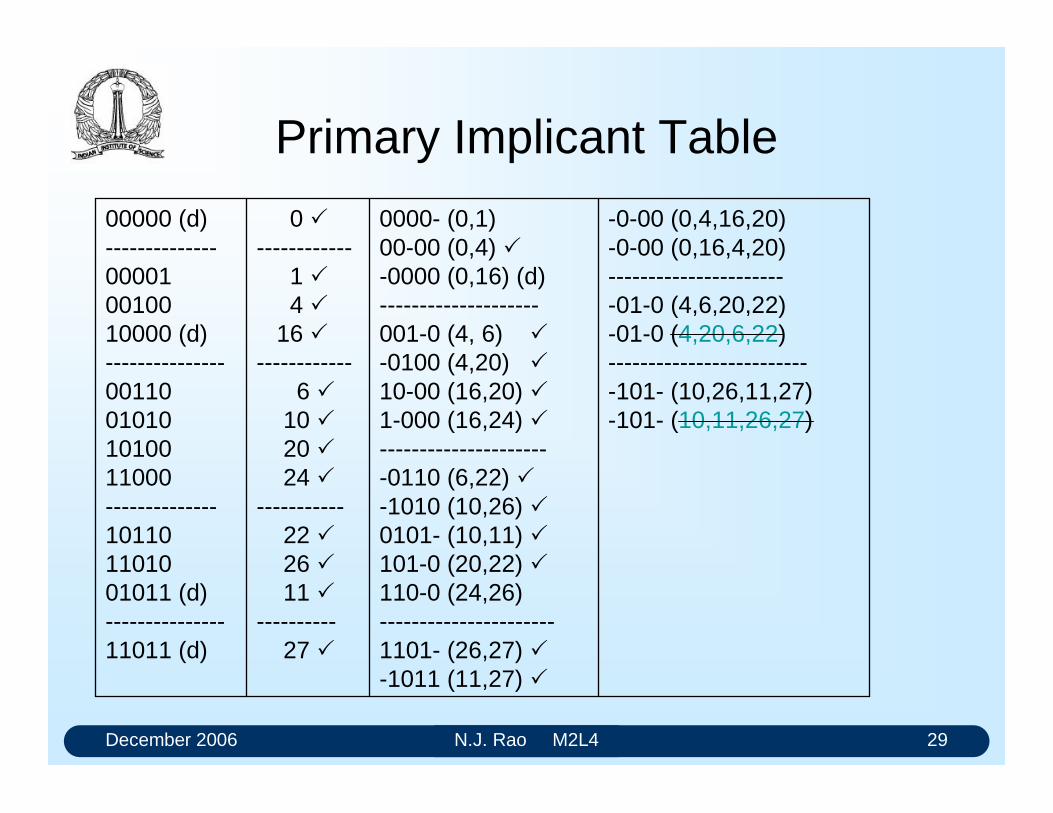
December 2006 N.J. Rao M2L4 29
Primary Implicant Table
-0-00 (0,4,16,20)-0-00 (0,16,4,20)-----------------------01-0 (4,6,20,22)-01-0 (4,20,6,22)--------------------------101- (10,26,11,27)-101- (10,11,26,27)
0000- (0,1)00-00 (0,4) -0000 (0,16) (d)--------------------001-0 (4, 6) -0100 (4,20) 10-00 (16,20) 1-000 (16,24) ----------------------0110 (6,22) -1010 (10,26) 0101- (10,11) 101-0 (20,22) 110-0 (24,26)----------------------1101- (26,27) -1011 (11,27)
0 ------------
1 4
16 ------------
6 10 20 24
-----------22 26 11
----------27
00000 (d)--------------000010010010000 (d)---------------00110010101010011000--------------101101101001011 (d)---------------11011 (d)
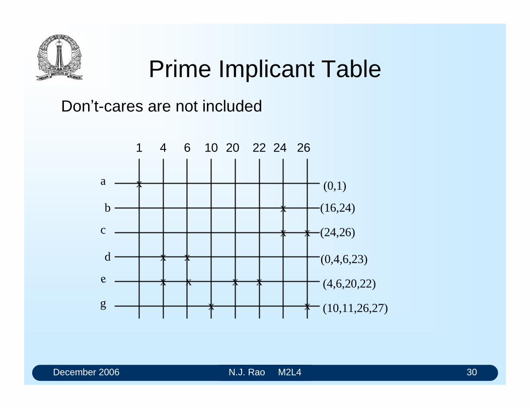
December 2006 N.J. Rao M2L4 30
Prime Implicant Table
a
b
c
d
e
g
x
(0,1)
(16,24)
(24,26)
(0,4,6,23)
(4,6,20,22)
(10,11,26,27)
1 4 6 10 20 22 24 26
x
x x
x x
x x x x
x x
Dont-cares are not included
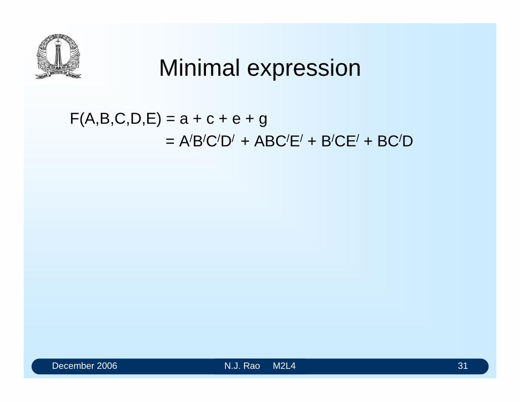
December 2006 N.J. Rao M2L4 31
Minimal expression
F(A,B,C,D,E) = a + c + e + g = A/B/C/D/ + ABC/E/ + B/CE/ + BC/D
Quine-McCluskey Method of Minimization
Karnaugh Map provides a good method of minimizing a logic function. However, it depends
on our ability to observe appropriate patterns and identify the necessary implicants. If the
number of variables increases beyond five, K-map or its variant Variable Entered Map can
become very messy and there is every possibility of committing a mistake. What we
require is a method that is more suitable for implementation on a computer, even if it is
inconvenient for paper-and-pencil procedures. The concept of tabular minimisation was
originally formulated by Quine in 1952. This method was later improved upon by
McClusky in 1956, hence the name Quine-McClusky.
This Learning Unit is concerned with the Quine-McClusky method of minimisation. This
method is tedious, time-consuming and subject to error when performed by hand. But it is
better suited to implementation on a digital computer.
Principle of Quine-McClusky Method
The Quine-McClusky method is a two stage simplification process.
Generate prime implicants of the given Boolean function by a special tabulation
process.
Determine the minimal set of implicants is determined from the set of implicants
generated in the first stage.
The tabulation process starts with a listing of the specified minterms for the 1s (or 0s)
of a function and don’t-cares (the unspecified minterms) in a particular format. All the
prime implicants are generated from them using the simple logical adjacency theorem,
namely, AB/ + AB = A. The main feature of this stage is that we work with the equivalent
binary number of the product terms. For example in a four variable case, the minterms
A/BCD/ and A/BC/D/ are entered as 0110 and 0100. As the two logically adjacent
minterms A/BCD/ and A/BC/D/ can be combined to form a product term A/BD/,the two
binary terms 0110 and 0100 are combined to form a term represented as "01-0", where ‘-‘
(dash) indicates the position where the combination took place.
Stage two involves creating a prime implicant table. This table provides a means of
identifying, by a special procedure, the smallest number of prime implicants that represents
the original Boolean function. The selected prime implicants are combined to form the
simplified expression in the SOP form. While we confine our discussion to the creation of
minimal SOP expression of a Boolean function in the canonical form, it is easy to
extend the procedure to functions that are given in the standard or any other forms.
Generation of Prime Implicants
The process of generating prime implicants is best presented through an example.
Example 1: F = Σ (1,2,5,6,7,9,10,11,14)
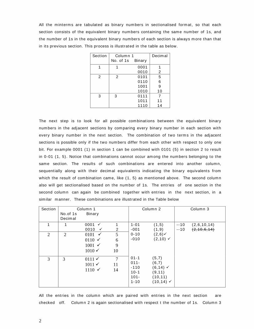
2
All the minterms are tabulated as binary numbers in sectionalised format, so that each
section consists of the equivalent binary numbers containing the same number of 1s, and
the number of 1s in the equivalent binary numbers of each section is always more than that
in its previous section. This process is illustrated in the table as below.
Section Column 1 No. of 1s Binary
Decimal
1 1 0001 0010
1 2
2 2 0101 0110 1001 1010
5 6 9 10
3 3 0111 1011 1110
7 11 14
The next step is to look for all possible combinations between the equivalent binary
numbers in the adjacent sections by comparing every binary number in each section with
every binary number in the next section. The combination of two terms in the adjacent
sections is possible only if the two numbers differ from each other with respect to only one
bit. For example 0001 (1) in section 1 can be combined with 0101 (5) in section 2 to result
in 0-01 (1, 5). Notice that combinations cannot occur among the numbers belonging to the
same section. The results of such combinations are entered into another column,
sequentially along with their decimal equivalents indicating the binary equivalents from
which the result of combination came, like (1, 5) as mentioned above. The second column
also will get sectionalised based on the number of 1s. The entries of one section in the
second column can again be combined together with entries in the next section, in a
similar manner. These combinations are illustrated in the Table below
Section Column 1 No.of 1s Binary Decimal
Column 2 Column 3
1 1 0001 1 0010 2
2 2 0101 5 0110 6 1001 9 1010 10
3 3 0111 7 1011 11 1110 14
1-01 (1,5) -001 (1,9) 0-10 (2,6) -010 (2,10) 01-1 (5,7) 011- (6,7) -110 (6,14) 10-1 (9,11) 101- (10,11) 1-10 (10,14)
--10 (2,6,10,14) --10 (2,10,6,14)
All the entries in the column which are paired with entries in the next section are
checked off. Column 2 is again sectionalised with respect t the number of 1s. Column 3
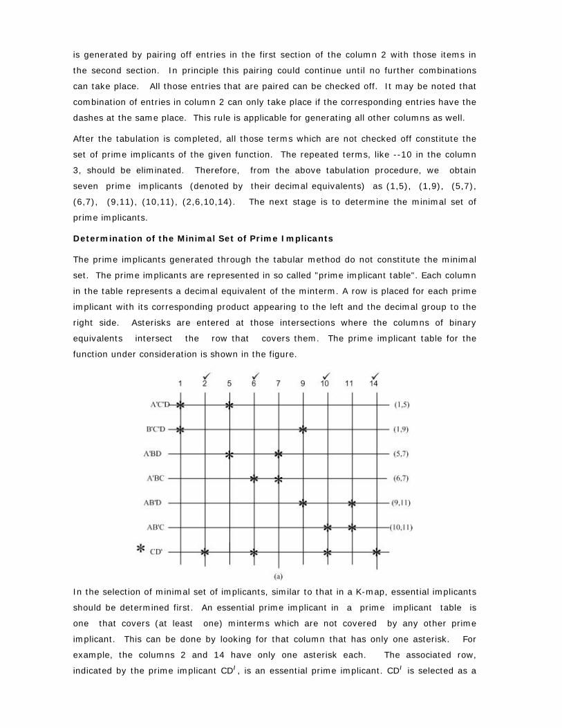
is generated by pairing off entries in the first section of the column 2 with those items in
the second section. In principle this pairing could continue until no further combinations
can take place. All those entries that are paired can be checked off. It may be noted that
combination of entries in column 2 can only take place if the corresponding entries have the
dashes at the same place. This rule is applicable for generating all other columns as well.
After the tabulation is completed, all those terms which are not checked off constitute the
set of prime implicants of the given function. The repeated terms, like --10 in the column
3, should be eliminated. Therefore, from the above tabulation procedure, we obtain
seven prime implicants (denoted by their decimal equivalents) as (1,5), (1,9), (5,7),
(6,7), (9,11), (10,11), (2,6,10,14). The next stage is to determine the minimal set of
prime implicants.
Determination of the Minimal Set of Prime Implicants
The prime implicants generated through the tabular method do not constitute the minimal
set. The prime implicants are represented in so called "prime implicant table". Each column
in the table represents a decimal equivalent of the minterm. A row is placed for each prime
implicant with its corresponding product appearing to the left and the decimal group to the
right side. Asterisks are entered at those intersections where the columns of binary
equivalents intersect the row that covers them. The prime implicant table for the
function under consideration is shown in the figure.
In the selection of minimal set of implicants, similar to that in a K-map, essential implicants
should be determined first. An essential prime implicant in a prime implicant table is
one that covers (at least one) minterms which are not covered by any other prime
implicant. This can be done by looking for that column that has only one asterisk. For
example, the columns 2 and 14 have only one asterisk each. The associated row,
indicated by the prime implicant CD/, is an essential prime implicant. CD/ is selected as a
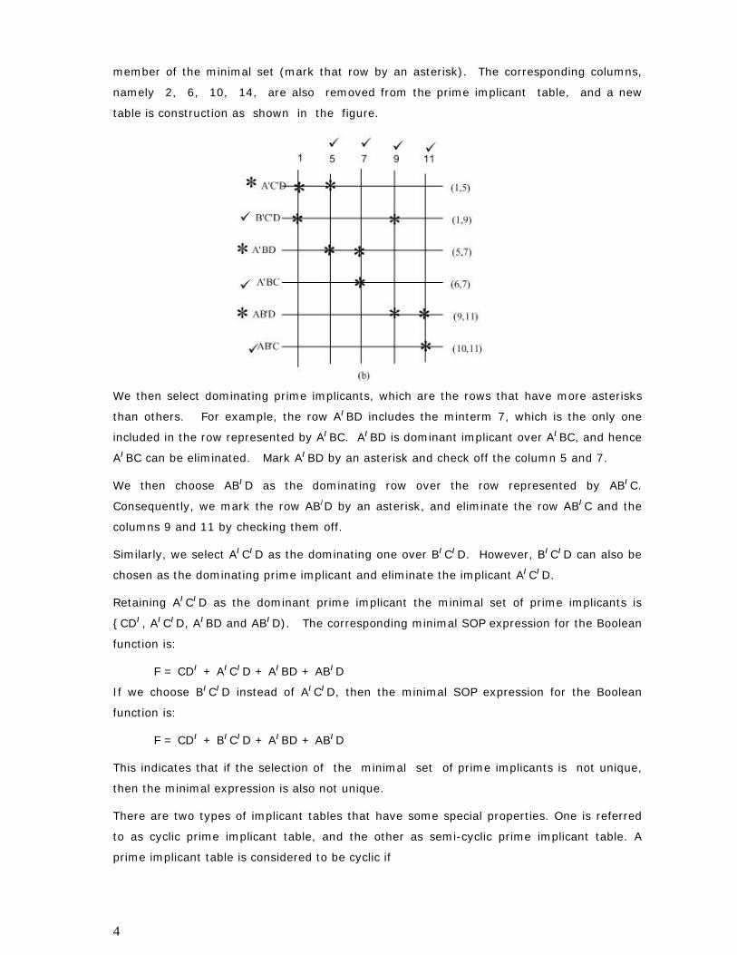
4
member of the minimal set (mark that row by an asterisk). The corresponding columns,
namely 2, 6, 10, 14, are also removed from the prime implicant table, and a new
table is construction as shown in the figure.
We then select dominating prime implicants, which are the rows that have more asterisks
than others. For example, the row A/BD includes the minterm 7, which is the only one
included in the row represented by A/BC. A/BD is dominant implicant over A/BC, and hence
A/BC can be eliminated. Mark A/BD by an asterisk and check off the column 5 and 7.
We then choose AB/D as the dominating row over the row represented by AB/C.
Consequently, we mark the row AB/D by an asterisk, and eliminate the row AB/C and the
columns 9 and 11 by checking them off.
Similarly, we select A/C/D as the dominating one over B/C/D. However, B/C/D can also be
chosen as the dominating prime implicant and eliminate the implicant A/C/D.
Retaining A/C/D as the dominant prime implicant the minimal set of prime implicants is
CD/, A/C/D, A/BD and AB/D). The corresponding minimal SOP expression for the Boolean
function is:
F = CD/ + A/C/D + A/BD + AB/D
If we choose B/C/D instead of A/C/D, then the minimal SOP expression for the Boolean
function is:
F = CD/ + B/C/D + A/BD + AB/D
This indicates that if the selection of the minimal set of prime implicants is not unique,
then the minimal expression is also not unique.
There are two types of implicant tables that have some special properties. One is referred
to as cyclic prime implicant table, and the other as semi-cyclic prime implicant table. A
prime implicant table is considered to be cyclic if
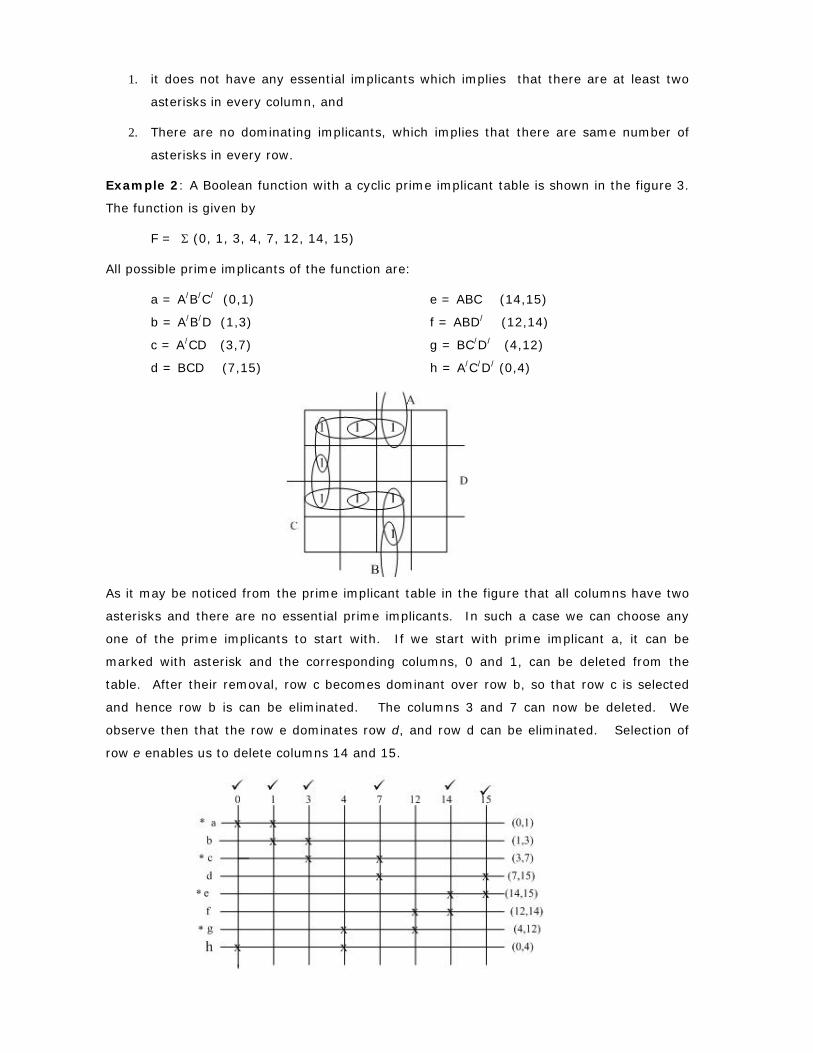
1. it does not have any essential implicants which implies that there are at least two
asterisks in every column, and
2. There are no dominating implicants, which implies that there are same number of
asterisks in every row.
Example 2: A Boolean function with a cyclic prime implicant table is shown in the figure 3.
The function is given by
F = Σ (0, 1, 3, 4, 7, 12, 14, 15)
All possible prime implicants of the function are:
a = A/B/C/ (0,1) e = ABC (14,15)
b = A/B/D (1,3) f = ABD/ (12,14)
c = A/CD (3,7) g = BC/D/ (4,12)
d = BCD (7,15) h = A/C/D/ (0,4)
As it may be noticed from the prime implicant table in the figure that all columns have two
asterisks and there are no essential prime implicants. In such a case we can choose any
one of the prime implicants to start with. If we start with prime implicant a, it can be
marked with asterisk and the corresponding columns, 0 and 1, can be deleted from the
table. After their removal, row c becomes dominant over row b, so that row c is selected
and hence row b is can be eliminated. The columns 3 and 7 can now be deleted. We
observe then that the row e dominates row d, and row d can be eliminated. Selection of
row e enables us to delete columns 14 and 15.
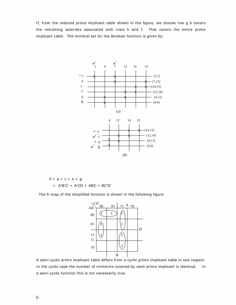
6
If, from the reduced prime implicant table shown in the figure, we choose row g it covers
the remaining asterisks associated with rows h and f. That covers the entire prime
implicant table. The minimal set for the Boolean function is given by:
F = a + c + e + g
= A'B'C' + A'CD + ABC + BC'D'
The K-map of the simplified function is shown in the following figure
A semi-cyclic prime implicant table differs from a cyclic prime implicant table in one respect.
In the cyclic case the number of minterms covered by each prime implicant is identical. In
a semi-cyclic function this is not necessarily true.
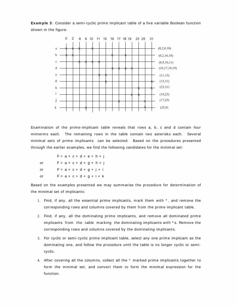
Example 3: Consider a semi-cyclic prime implicant table of a five variable Boolean function
shown in the figure.
Examination of the prime-implicant table reveals that rows a, b, c and d contain four
minterms each. The remaining rows in the table contain two asterisks each. Several
minimal sets of prime implicants can be selected. Based on the procedures presented
through the earlier examples, we find the following candidates for the minimal set:
F = a + c + d + e + h + j
or F = a + c + d + g + h + j
or F = a + c + d + g + j + i
or F = a + c + d + g + i + k
Based on the examples presented we may summarise the procedure for determination of
the minimal set of implicants:
1. Find, if any, all the essential prime implicants, mark them with *, and remove the
corresponding rows and columns covered by them from the prime implicant table.
2. Find, if any, all the dominating prime implicants, and remove all dominated prime
implicants from the table marking the dominating implicants with *s. Remove the
corresponding rows and columns covered by the dominating implicants.
3. For cyclic or semi-cyclic prime implicant table, select any one prime implicant as the
dominating one, and follow the procedure until the table is no longer cyclic or semi-
cyclic.
4. After covering all the columns, collect all the * marked prime implicants together to
form the minimal set, and convert them to form the minimal expression for the
function.
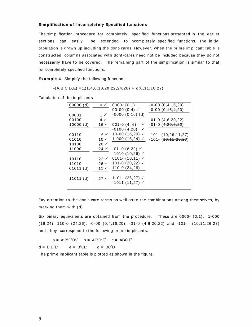
8
Simplification of Incompletely Specified functions
The simplification procedure for completely specified functions presented in the earlier
sections can easily be extended to incompletely specified functions. The initial
tabulation is drawn up including the dont-cares. However, when the prime implicant table is
constructed, columns associated with dont-cares need not be included because they do not
necessarily have to be covered. The remaining part of the simplification is similar to that
for completely specified functions.
Example 4: Simplify the following function:
F(A,B,C,D,E) =∑(1,4,6,10,20,22,24,26) + d(0,11,16,27)
Tabulation of the implicants
00000 (d) 00001 00100 10000 (d) 00110 01010 10100 11000 10110 11010 01011 (d) 11011 (d)
0 1 4 16 6 10 20 24 22 26 11 27
0000- (0,1) 00-00 (0,4) -0000 (0,16) (d) 001-0 (4, 6) -0100 (4,20) 10-00 (16,20) 1-000 (16,24) -0110 (6,22) -1010 (10,26) 0101- (10,11) 101-0 (20,22) 110-0 (24,26) 1101- (26,27) -1011 (11,27)
-0-00 (0,4,16,20) -0-00 (0,16,4,20) -01-0 (4,6,20,22) -01-0 (4,20,6,22) -101- (10,26,11,27) -101- (10,11,26,27)
Pay attention to the don’t-care terms as well as to the combinations among themselves, by
marking them with (d).
Six binary equivalents are obtained from the procedure. These are 0000- (0,1), 1-000
(16,24), 110-0 (24,26), -0-00 (0,4,16,20), -01-0 (4,6,20,22) and -101- (10,11,26,27)
and they correspond to the following prime implicants:
a = A/B/C/D// b = AC/D/E/ c = ABC/E/
d = B/D/E/ e = B/CE/ g = BC/D The prime implicant table is plotted as shown in the figure.
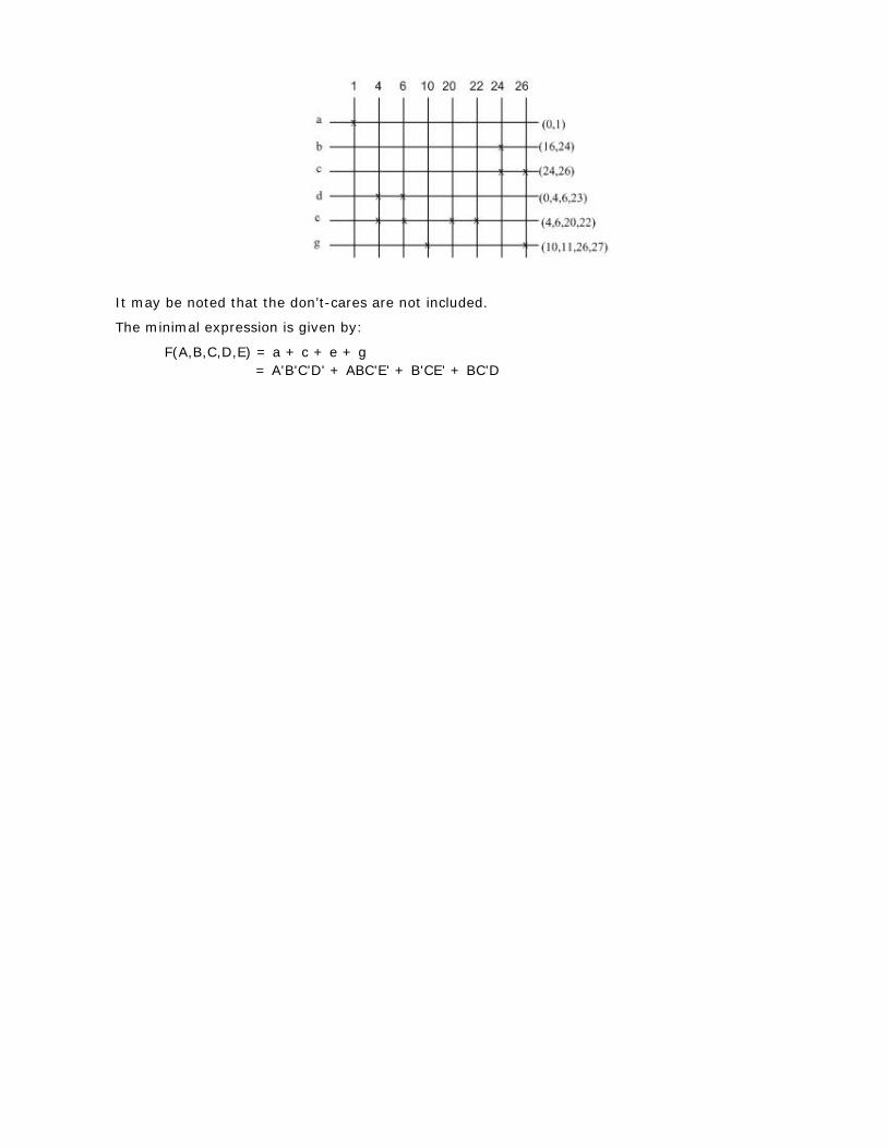
It may be noted that the don’t-cares are not included. The minimal expression is given by:
F(A,B,C,D,E) = a + c + e + g = A'B'C'D' + ABC'E' + B'CE' + BC'D

Digital Electronics Module 3Logic Families: Introduction
N.J. RaoIndian Institute of Science
id7733189 pdfMachine by Broadgun Software - a great PDF writer! - a great PDF creator! - http://www.pdfmachine.com http://www.broadgun.com
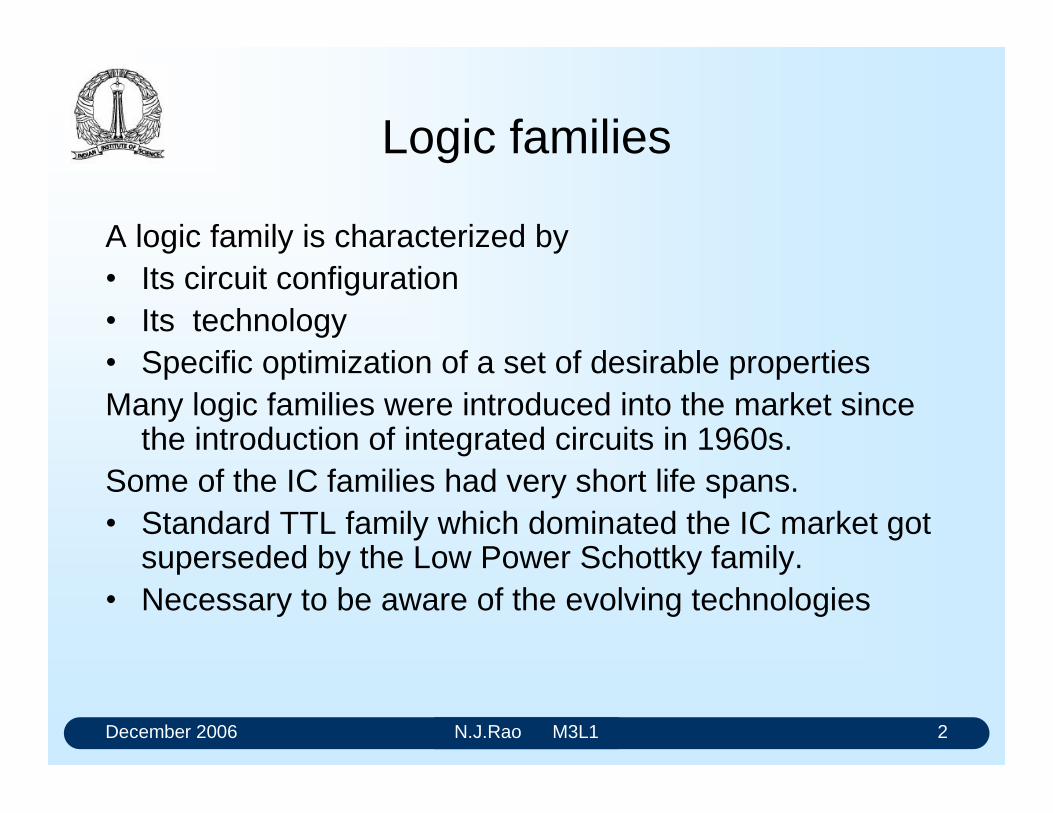
December 2006 N.J.Rao M3L1 2
Logic families
A logic family is characterized by Its circuit configuration Its technology Specific optimization of a set of desirable properties Many logic families were introduced into the market since
the introduction of integrated circuits in 1960s. Some of the IC families had very short life spans. Standard TTL family which dominated the IC market got
superseded by the Low Power Schottky family. Necessary to be aware of the evolving technologies
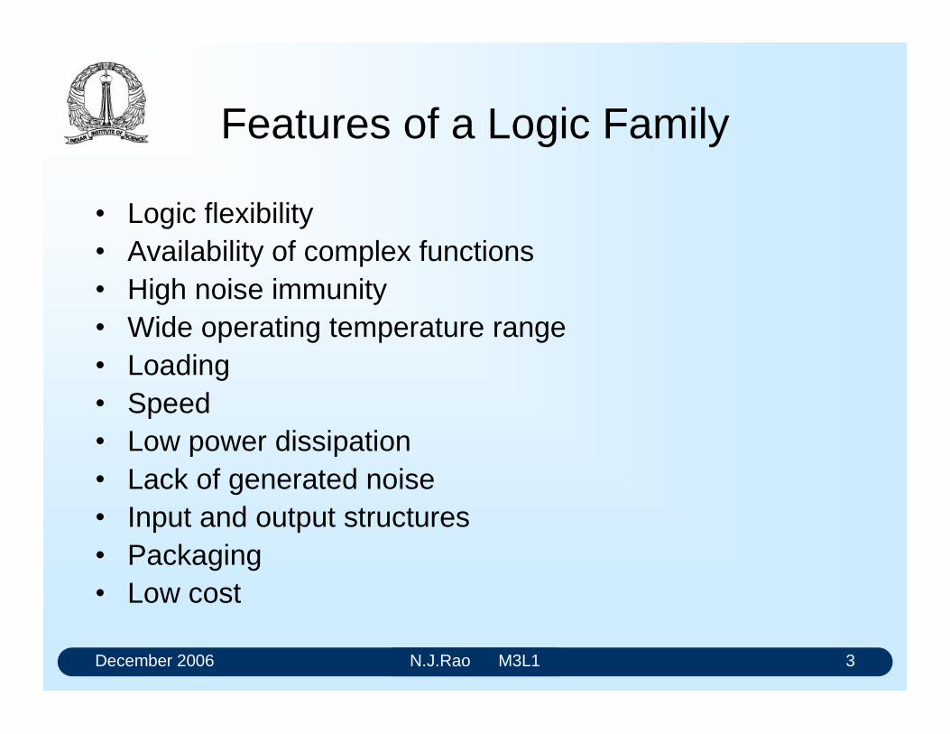
December 2006 N.J.Rao M3L1 3
Features of a Logic Family
Logic flexibility Availability of complex functions High noise immunity Wide operating temperature range Loading Speed Low power dissipation Lack of generated noise Input and output structures Packaging Low cost
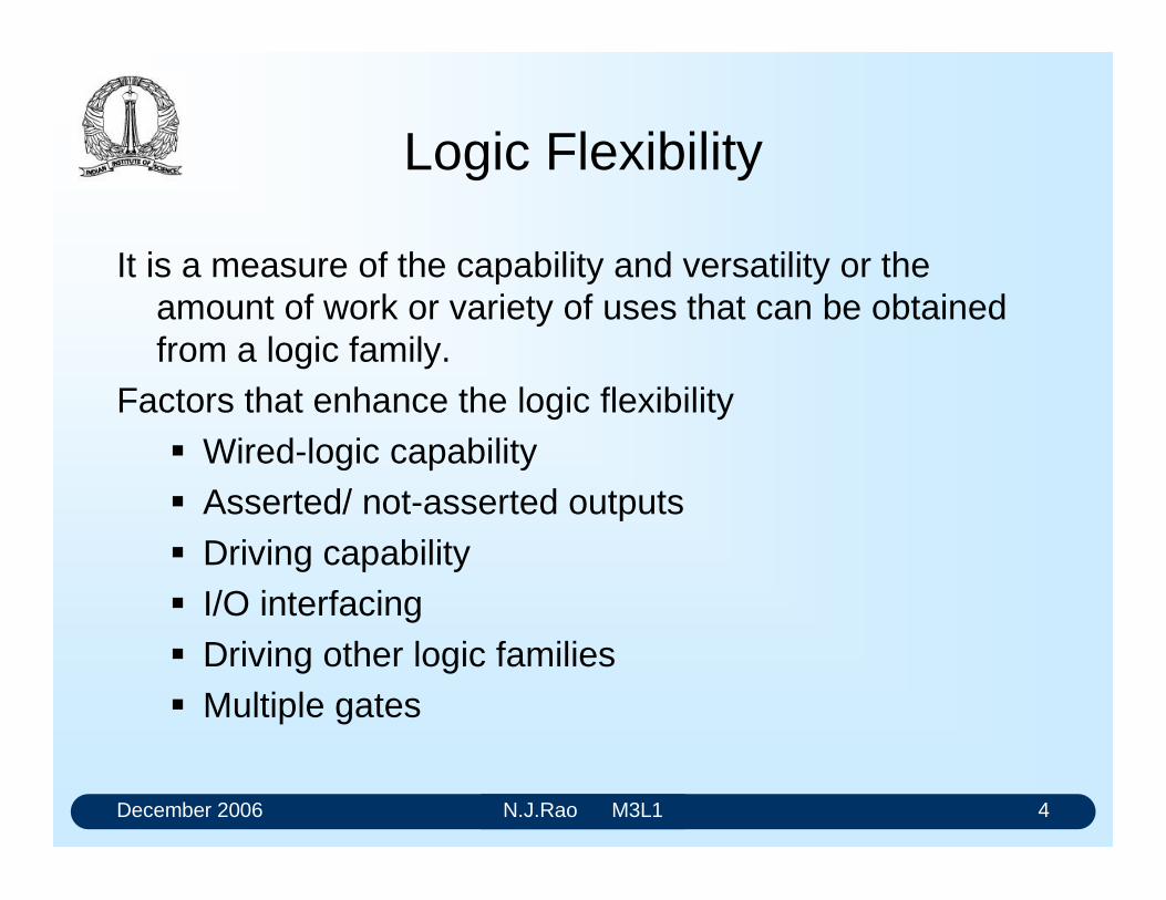
December 2006 N.J.Rao M3L1 4
Logic Flexibility
It is a measure of the capability and versatility or the amount of work or variety of uses that can be obtained from a logic family.
Factors that enhance the logic flexibility Wired-logic capability Asserted/ not-asserted outputs Driving capability I/O interfacing Driving other logic families Multiple gates
December 2006 N.J.Rao M3L1 5
Complex Functions
A complex function represents a grouping of basic gates requiring a relatively high level of integration.
As complexity increases, the number of input/output pins also increases - but usually at a decreasing rate.
High pin count gives the benefit of decreasing assembly costs per gate while increasing the reliability per gate.
The complexity is also measured in terms of gates per chip.
December 2006 N.J.Rao M3L1 6
Noise Immunity
High immunity to noise is desired to prevent the occurrence of false logic signals in a system.
Common sources of noise: Variations of the dc supply voltage, Ground noise Excessive coupling between signal leads Magnetically coupled voltages from adjacent lines, External sources (relays, circuit breakers, and power line
transients) Radiated signals
December 2006 N.J.Rao M3L1 7
Measures of Noise Immunity
Voltage noise immunity (noise margin) is the amount of voltage that can be added algebraically to the worst-case output level before a worst-case gate tied to that output will begin to switch.
Noise immunity is specified in terms of millivolts or volts
December 2006 N.J.Rao M3L1 8
DC Noise Margin
It is a measure of its noise immunity, a gates ability to withstand dc input signal variations. VIL: Low level input voltage VIH: High level input voltage VOL: Low level output voltage VOH High level output voltage
Voltage levels associated with logic High and logic Low levels are not single values but a band of values.
December 2006 N.J.Rao M3L1 9
DC Noise Margin (2)
A gate may accept an input signal in the range of 0.0 V to 0.8 V as logic Low while it produces at its output a Low voltage of 0.4 V under worst loading and voltage supply conditions.
DC margin is considered to be 0.4 V (0.8 - 0.4 = 0.4 V) The dc noise margins are defined as
Low level dc noise margin: VILmax- VOLmax
High level dc noise margin: VOHmin - VIHmin
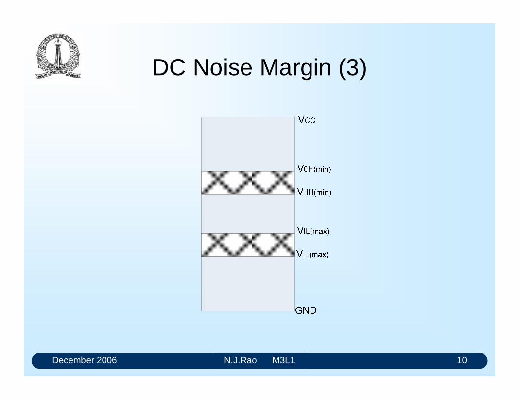
December 2006 N.J.Rao M3L1 10
DC Noise Margin (3)
December 2006 N.J.Rao M3L1 11
AC Noise Margin
It refers to the immunity of a gate to noise of very short durations.
Amplitude and duration of the noise signals become important.
The noise signal must contain enough energy to effect a change in the state of the circuit.
AC noise margins are higher than dc noise margins.
December 2006 N.J.Rao M3L1 12
AC Noise Margin (2)
The ability of a logic element to operate in a noisy environment depends on
Built-in operating margins Time required for the device to react The ease with which a noise voltage is developed

December 2006 N.J.Rao M3L1 13
Operating Temperature Range
For commercial and industrial needs, temperatures usually range from 0o or -30o C to 55o, 70o or 85o C
The military has an universal requirement for operability from -55o C to 125o C.
Advantages of a wide temperature specification are offset by the increased cost
December 2006 N.J.Rao M3L1 14
Loading
The output of a logic gate may be connected to the inputs of several other similar gates
The fan out of a gate is the maximum number of inputs of the same IC family that the gate can drive while maintaining its output levels within specified limits.
December 2006 N.J.Rao M3L1 15
Loading
The input and output loading parameters are normalized, with regard to TTL devices
1 TTL Unit Load (U.L.) = 40 A in the High state (Logic 1)1 TTL Unit Load (U.L.) = -1.6 mA in the Low state (Logic 0)
The output of 74LS00 will sink 8.0 mA in Low state and source 400 A in the High state.
The normalized output Low drive factor is: (8.0/1.6) = 5 U.L.
Output High drive factor is: (400 A/40 A) = 10 U.L.
December 2006 N.J.Rao M3L1 16
Speed
The shorter the propagation delay, the higher the speed of the circuit
Propagation delay of a gate:time interval between the application of an input pulse and the occurrence of the resulting output pulse.
December 2006 N.J.Rao M3L1 17
Propagation Delays
Two propagation delays associated with a logic gate:tPHL: The time between a specified reference point on the input pulse and a corresponding reference point on the output pulse, with the output changing from the High level to the Low level.tPLH: The time between specified reference point on the input pulse and a corresponding reference point on the output pulse, with the output changing from the Low level to the High level.
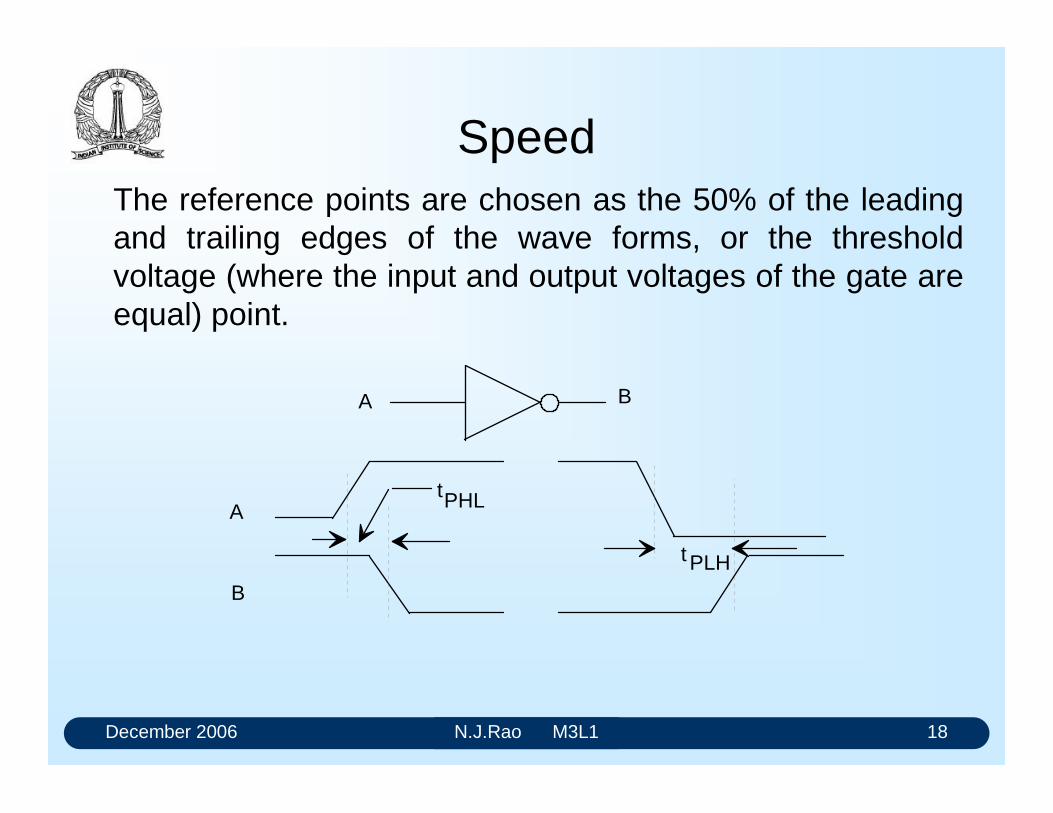
December 2006 N.J.Rao M3L1 18
SpeedThe reference points are chosen as the 50% of the leading and trailing edges of the wave forms, or the threshold voltage (where the input and output voltages of the gate are equal) point.
A B
A
B
tPHL
t PLH
December 2006 N.J.Rao M3L1 19
Power Dissipation
Low power dissipation is desired in large systems as it leads to
Lower cooling costs Lower power supply and distribution costs, Reduction in mechanical design problems Decrease in power dissipation on a per-gate basis with
higher integration levels
December 2006 N.J.Rao M3L1 20
Steady state dissipation
DC supply voltage VCC x Average supply current ICC
Value of ICC for a Low gate output is higher than for a High output
Manufacturer's data sheet usually specifies both these values as ICCL and ICCH.
The average ICC is then determined based on a 50% duty cycle operation of the gate
December 2006 N.J.Rao M3L1 21
Dissipation during transitions
The supply current drawn is generally very different during the transition times
More number of active devices come into operation, and parasitic capacitors will have to be charged and discharged.
Power dissipation increases linearly as a function of the frequency of switching.
December 2006 N.J.Rao M3L1 22
Dissipation during transitions (2)
Speed-power product (SPP) is specified by the manufacturer
SSP is specified in terms of pico Joules (symbolized by pJ)
SPP of a 74HC CMOS gate at 100 KHz is SPP = (8ns) x (0.17 mW) = 1.36 pJ.
December 2006 N.J.Rao M3L1 23
Generated Noise
Switching transients either on power line or signal line can be very serious sources of noise.
Care has to be taken to design the power, ground and signal interconnections.
All the power supply leads in a system must be bypassed.
Supply distribution is less expensive if the circuits generate less noise.
December 2006 N.J.Rao M3L1 24
Input and output structures
Effective interfacing both at the input and output are needed
Interfacing at the input requires facility To accept different voltage levels for the two logic states To accept signals with rise and fall times very different
from those of the signals associated with that logic family At the output we require Larger current driving capability Facility to increase the voltages associated with the two
logic levels Ability to tie the outputs of gates to have wired logic
operations
December 2006 N.J.Rao M3L1 25
Interfacing at the inputs and outputs
Interfacing the slow varying signals is achieved through Schmitt triggers.
Voltage levels of the output signals can be increased by providing open-collector configurations. Open-collector configurations also permit us to achieve wired-logic operations
The outputs of gates can be tied together by having tristate outputs.
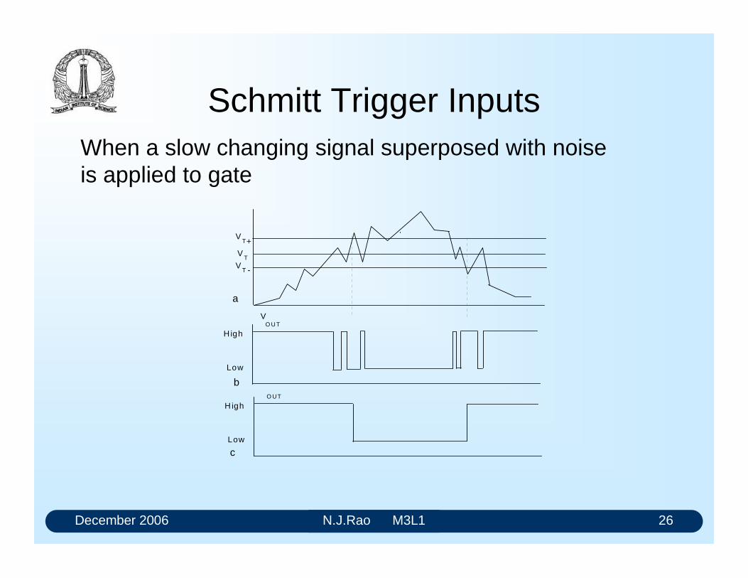
December 2006 N.J.Rao M3L1 26
Schmitt Trigger InputsWhen a slow changing signal superposed with noise is applied to gate
VT
V
VT
VT
+
-
O U T
High
Low
a
bO UT
H igh
Low
c
December 2006 N.J.Rao M3L1 27
Three-State Outputs
Logic outputs have two normal states; Low and High It is desirable to have another electrical state in which
the output of the circuit offers very high impedance, high-impedance, Hi-z or floating state
In this state, the circuit is effectively disconnected at its output, except for a small leakage current.
Three states: logic 0, logic 1, and Hi-z. An output with three possible states is called tri-state
output.
December 2006 N.J.Rao M3L1 28
Three-State Outputs (2)
Devices with three state outputs, should have an extra input, called as output enable (OE) for placing a device in low-impedance or high-impedance states.
The outputs of devices which can have three states can be tied together, to create a three-state bus.
The control circuitry must enable that at any given time only one output is enabled while all other outputs are kept in high-z state.
December 2006 N.J.Rao M3L1 29
Open-Collector (or Drain) Outputs
An IC device has a pull-up resistor at its output transistor Such circuits prevent us from tying the outputs of two
such devices together. If the internal pull-up elements are removed, then it allows
one to tie up the outputs of more than one device together
connect external pull-up resistor to increase the output voltage swing.
Devices with open-collector (open-drain) outputs are very useful for
Creating wired logic operations, or Interfacing loads which are incompatible with the
electrical characteristics of the logic family.
December 2006 N.J.Rao M3L1 30
Packaging
Initially most of the digital ICs were made available in dual-in-line packages (DIP).
Commercial ICs come in plastic DIPs Ceramic DIPs are used for operation over a larger
temperature range Increasing integrations lead to a wide range of chip level
packages
December 2006 N.J.Rao M3L1 31
Cost
Often the most important one, is the cost of a logic family. It is not sufficient to compare the cost of logic families at gate level.The total system cost is decided by
Cost of ICs Cost printed wiring board on which the ICs are mounted Assembly of circuit board Programming the programmable devices etc.
Procurement Testing Power supply Documentation Storage

PROPERTIES OF A LOGIC FAMILY
Since the introduction of integrated circuits in 1960s, many logic families were
introduced into the market. Each logic family is characterised by
a circuit configuration
a particular semiconductor technology
a specific optimisation of a set of desirable properties
Some of the IC families had very short life spans. With continuously changing
technologies, ICs that were quite popular suddenly become unattractive and
uneconomical. For example Standard TTL family which dominated the IC market
for a long period got superseded by the Low Power Schottky family. A digital
designer should not only have a good knowledge of the existing digital families but
should also be aware of the trends as well. The major requirements and the
desirable features of a logic family are:
Logic flexibility
Availability of complex functions
High noise immunity
Wide operating temperature range
Loading
Speed
Low power dissipation
Lack of generated noise
Input and output structures
Packaging
Low cost
Logic Flexibility
Logic flexibility is a measure of the capability and versatility or the amount of work
or variety of uses that can be obtained from a logic family, in other words, it is a
measure of the utility of a logic family in meeting various system needs. Factors
that enhance the logic flexibility are wired-logic capability, asserted/not-asserted
outputs, line driving capability, indicator driving, I/O interfacing, driving other logic
families and multiple gates.
Wired logic refers to the capability of tying the outputs of gates together to perform
additional logic without extra hardware and components. Frequently, asserted/not-
asserted versions of a variable are required in a logic system. If the logic family has
gates with not-asserted outputs, use of inverters can be avoided. If the circuits can
drive non-standard loads such as long signal lines, lamps and indicator tubes,
additional discrete circuits can be avoided. The gate count can be minimised in a
digital system if AND, NAND, OR, NOR and EX-OR gates are all available in the
family. The logic families currently popular, namely TTL, CMOS and to a limited
extent ECL, in the market have similar logic flexibility, and as such this factor does
not constitute a deciding issue in selecting a logic family.
Complex Function
A complex function may be described as a grouping of basic gates requiring a
relatively high level of integration. As complexity increases, the number of
input/output pins also increases - but usually at a decreasing rate. Gate-to-pin
ratios that normally increase with complexity give the benefit of decreasing assembly
costs per gate while increasing the reliability per gate. The complexity is also
measured, at present, by the number of gates that can be offered in a
programmable logic device or programmable gate array.
Noise Immunity
In order to prevent the occurrence of false logic signals in a system, high immunity
to noise is desired. Common sources of noise in digital circuits are
Variations of the dc supply voltage
Ground noise
Excessive coupling between signal leads
Magnetically coupled voltages from adjacent lines
External sources such as relays, circuit breakers, and power line transients
If the noise immunity is higher, the number of precautions required to prevent the
false logic signals will also be less. This becomes an important advantage in those
areas, such as in industrial logic control systems that are subject to high noise levels.
At present with increasing use of electronic control systems even in household
appliances, the ambient noise levels at homes have significantly risen. Voltage noise
immunity, or noise margin, is normally specified in terms of millivolts or volts. The
noise immunity is specified as the amount of voltage that can be added algebraically
to the worst-case output level before a worst-case gate tied to that output will begin
to switch.

DC Noise Margin: The dc noise margin of a logic gate is a measure of its noise
immunity, a gate’s ability to withstand dc input signal variations. The term dc noise
margin applies to noise voltages of relatively long duration compared to the gate’s
response times. The dc noise margin is defined in terms of the following voltage
levels associated with a gate;
VIL: Low level input voltage
VIH: High level input voltage
VOL: Low level output voltage
VOH: High level output voltage
Voltage levels associated with logic High and logic Low levels are not single values
but a band of values.
For example, a gate may accept an input signal in the range of 0.0 V to 0.8 V as
logic Low while it produces at its output a Low voltage of 0.4 V under worst loading
and voltage supply conditions.
In such a situation 0.4 V (0.8 - 0.4 = 0.4 V) is considered to be the dc noise margin.
When the output of one gate is connected to the input of another gate, as the output
is limited to 0.4 V even if a noise voltage up to 0.4 is superimposed on it, the second
gate would accept it as logic Low signal.
The dc noise margins are defined as
Low level dc noise margin: VILmax- VOLmax
High level dc noise margin: VOHmin - VIHmin
The noise margins and the voltage levels associated with the gates can be graphically shown as in the figure.
V0H(min)
V IH(min)
VCC
VIL(max)
VIL(max)
GND
AC Noise Margin: The term ac noise margin refers to the noise immunity of a gate
to noise of very short durations. In short duration noise, both the amplitude and
duration of the noise signals become important. The noise signal must contain
enough energy to effect a change in the state of the circuit. Therefore, the ac noise
margins are considerably higher than dc noise margins.
The ability of a logic element to operate in a noisy environment involves more than
the dc and ac noise margins. To be a problem, an externally generated noise pulse
must be received into the system and cause malfunction. The noise voltage must be
introduced into the circuit by radiated or coupled means. The amount of noise power
required to develop a given voltage is strictly a function of the circuit impedances.
Noise power must be transferred from the noise source with some arbitrary
impedance, through a coupling to the impedance of the circuit under consideration.
The ability to operate in a noisy environment is, then, an interaction of the built-in
operating margins, the time required for the device to react, and the ease with which
a noise voltage is developed. Therefore, the noise rejection capabilities of a logic
family represent a combination of a number of circuit parameters.
Operating Temperature Range
A wide operating range is always desired and is often a design requirement.
For commercial and industrial needs, temperatures usually range from 0o C or -30o C
to 55o C, 70o C or 85o C.
The military has a universal requirement for operability from -55o C to 125o C.
In most cases a logic line specified from -55o C to 125o C will exhibit better
characteristics at room temperature conditions than a line specified by commercial
requirements. It means performance of a logic circuit with regard to fan out, noise
immunity and tolerance to power supply variations is usually better, since the circuits
must still be within specifications even when the inherent degradation due to
temperature extremes occurs. The advantages of a wide temperature specification
are often offset by the increased cost.
Loading
In digital systems many digital ICs are interconnected to perform different functions.
The output of a logic gate may be connected to the inputs of several other similar
gates so the load on the driving gate becomes an important factor. The fan-out of a
gate is the maximum number of inputs of ICs from the same IC family that the gate

can drive while maintaining its output levels within specified limits. In other words,
the fan-out specifies the maximum loading that a given gate is capable of handling.
The input and output loading parameters are generally normalised, with regard to
TTL devices, to the following values.
1 TTL Unit Load (U.L.) = 40 µA in the High state (Logic “1”)
1 TTL Unit Load (U.L.) = -1.6 mA in the Low state (Logic “0”)
For example the output of 74LS00 will sink 8.0 mA in Low state and source 400 µA in the High state.
The normalised output Low drive factor is:
(8.0/1.6) = 5 U.L.
The output High drive factor is:
(400/40) = 10 U.L. Speed
Propagation delay is a very important characteristic of logic circuits because it limits
the speed (frequency) at which they can operate. The shorter the propagation
delay, the higher the speed of the circuit.
The propagation delay of a gate is basically the time interval between the application
of an input pulse and the occurrence of the resulting output pulse.
There are two propagation delays associated with a logic gate:
1. tPHL: The time between a specified reference point on the input pulse and a
corresponding reference point on the output pulse, with the output changing
from the High level to the Low level.
2. tPLH: The time between specified reference point on the input pulse and a
corresponding reference point on the output pulse, with the output changing
from the Low level to the High level.
The reference points on the wave forms with respect to which the time delays are
measured can be chosen as
The 50% of the leading and trailing edges of the wave forms
or
The threshold voltage (where the input and output voltages of the gate are equal)
point.
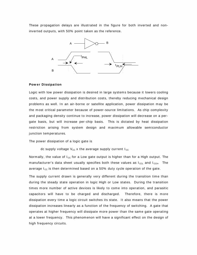
These propagation delays are illustrated in the figure for both inverted and non-
inverted outputs, with 50% point taken as the reference.
Power Dissipation
Logic with low power dissipation is desired in large systems because it lowers cooling
costs, and power supply and distribution costs, thereby reducing mechanical design
problems as well. In an air-borne or satellite application, power dissipation may be
the most critical parameter because of power-source limitations. As chip complexity
and packaging density continue to increase, power dissipation will decrease on a per-
gate basis, but will increase per-chip basis. This is dictated by heat dissipation
restriction arising from system design and maximum allowable semiconductor
junction temperatures.
The power dissipation of a logic gate is
dc supply voltage VCC x the average supply current ICC
Normally, the value of ICC for a Low gate output is higher than for a High output. The
manufacturer's data sheet usually specifies both these values as ICCL and ICCH. The
average ICC is then determined based on a 50% duty cycle operation of the gate.
The supply current drawn is generally very different during the transition time than
during the steady state operation in logic High or Low states. During the transition
times more number of active devices is likely to come into operation, and parasitic
capacitors will have to be charged and discharged. Therefore, there is more
dissipation every time a logic circuit switches its state. It also means that the power
dissipation increases linearly as a function of the frequency of switching. A gate that
operates at higher frequency will dissipate more power than the same gate operating
at a lower frequency. This phenomenon will have a significant effect on the design of
high frequency circuits.
A B
A
B
tPHL
t PLH

In view of this another parameter known as speed-power product (SPP) is specified
by the manufacturer as a measure of the performance of a logic circuit based on the
product of the propagation delay time with the power dissipation at a specified
frequency.
The speed-power product is specified in terms of pico Joules, symbolised by pJ.
For example, the SPP of a 74HC CMOS gate at 100 KHz is
SPP = (8ns) x (0.17 mW) = 1.36 pJ.
Generated Noise
The switching transients either on power line or signal line can be very serious
sources of noise. They can conduct and radiate through different channels and
influence the functioning of the near by circuits or systems. Therefore, the lack of
generated noise is an important requirement of a logic family. When the switching
noise is significant, special care has to be taken to design the power, ground and
signal interconnections.
All the power supply leads in a system must be bypassed.
Power supply and ground distribution has to be carefully designed.
Supply distribution is less expensive if the logic family generates minimal noise.
Also, the maximum line lengths in the back plane and wiring on the printed wiring
board are functions of cross talk generated by the logic family. A logic family that
draws constant current in both logic Low and High states, and does not change
supply current when switching states will generate less noise.
Input and output Structures
A logic family should provide features for effective interfacing both at the input and
output. Interfacing at the input requires facility to accept different voltage levels for
the two logic states, and to accept signals with rise and fall times very different from
those of the signals associated with that logic family. At the output we require larger
current driving capability, facility to increase the voltages associated with the two
logic levels, and the ability to tie the outputs of gates to have wired logic operations.
Interfacing the slow varying signals (signals with rise and fall times greater than one
microsecond) is achieved through Schmitt triggers. Voltage levels of the output
signals can be increased by providing open-collector (or open-drain) configurations.
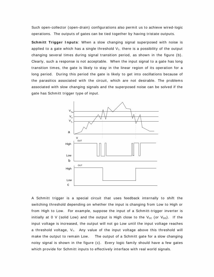
Such open-collector (open-drain) configurations also permit us to achieve wired-logic
operations. The outputs of gates can be tied together by having tristate outputs.
Schmitt Trigger Inputs: When a slow changing signal superposed with noise is
applied to a gate which has a single threshold VT, there is a possibility of the output
changing several times during signal transition period, as shown in the figure (b).
Clearly, such a response is not acceptable. When the input signal to a gate has long
transition times, the gate is likely to stay in the linear region of its operation for a
long period. During this period the gate is likely to get into oscillations because of
the parasitics associated with the circuit, which are not desirable. The problems
associated with slow changing signals and the superposed noise can be solved if the
gate has Schmitt trigger type of input.
VT
V
VT
VT
+
-
OUTHigh
Low
a
bOUT
High
Low
c
A Schmitt trigger is a special circuit that uses feedback internally to shift the
switching threshold depending on whether the input is changing from Low to High or
from High to Low. For example, suppose the input of a Schmitt-trigger inverter is
initially at 0 V (solid Low) and the output is High close to the VCC (or VDD). If the
input voltage is increased, the output will not go Low until the input voltage reaches
a threshold voltage, VT. Any value of the input voltage above this threshold will
make the output to remain Low. The output of a Schmitt gate for a slow changing
noisy signal is shown in the figure (c). Every logic family should have a few gates
which provide for Schmitt inputs to effectively interface with real world signals.
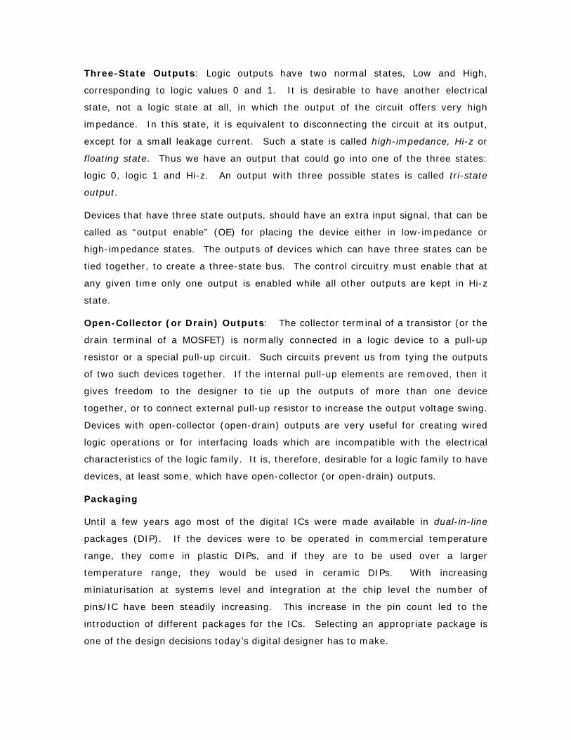
Three-State Outputs: Logic outputs have two normal states, Low and High,
corresponding to logic values 0 and 1. It is desirable to have another electrical
state, not a logic state at all, in which the output of the circuit offers very high
impedance. In this state, it is equivalent to disconnecting the circuit at its output,
except for a small leakage current. Such a state is called high-impedance, Hi-z or
floating state. Thus we have an output that could go into one of the three states:
logic 0, logic 1 and Hi-z. An output with three possible states is called tri-state
output.
Devices that have three state outputs, should have an extra input signal, that can be
called as “output enable” (OE) for placing the device either in low-impedance or
high-impedance states. The outputs of devices which can have three states can be
tied together, to create a three-state bus. The control circuitry must enable that at
any given time only one output is enabled while all other outputs are kept in Hi-z
state.
Open-Collector (or Drain) Outputs: The collector terminal of a transistor (or the
drain terminal of a MOSFET) is normally connected in a logic device to a pull-up
resistor or a special pull-up circuit. Such circuits prevent us from tying the outputs
of two such devices together. If the internal pull-up elements are removed, then it
gives freedom to the designer to tie up the outputs of more than one device
together, or to connect external pull-up resistor to increase the output voltage swing.
Devices with open-collector (open-drain) outputs are very useful for creating wired
logic operations or for interfacing loads which are incompatible with the electrical
characteristics of the logic family. It is, therefore, desirable for a logic family to have
devices, at least some, which have open-collector (or open-drain) outputs.
Packaging
Until a few years ago most of the digital ICs were made available in dual-in-line
packages (DIP). If the devices were to be operated in commercial temperature
range, they come in plastic DIPs, and if they are to be used over a larger
temperature range, they would be used in ceramic DIPs. With increasing
miniaturisation at systems level and integration at the chip level the number of
pins/IC have been steadily increasing. This increase in the pin count led to the
introduction of different packages for the ICs. Selecting an appropriate package is
one of the design decisions today’s digital designer has to make.

Cost
The last consideration, and often the most important one, is the cost of a given logic
family. The first approximate cost comparison can be obtained by pricing a common
function such as a dual four-input or quad two-input gate. But the cost of a few
types of gates alone can not indicate the cost of the total system. The total system
cost is decided not only by the cost of ICs but also by the cost of
printed wiring board on which the ICs are mounted
assembly of circuit board
testing
programming the programmable devices
power supply
documentation
procurement
storage
etc.
In many instances the cost of ICs could become a less important component of the
total cost of the system.
Concluding Note
The question that arises after considering all the desirable features of a logic family
is “why not design a family that best meets these needs and then mass produce it
and drive the costs down?” Unfortunately, this can not be achieved as there is no
universal logic family that a does a good job of meeting all the previously stated
needs. Silicon technology, though better understood and studied than any other
solid-state technology, still has its own limitations. Besides, the demand for higher
and higher performance specifications continues to grow.
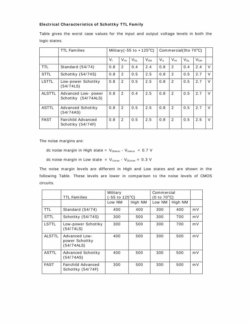
Electrical Characteristics of Schottky TTL Family
Table gives the worst case values for the input and output voltage levels in both the
logic states.
TTL Families Military(-55 to +125oC) Commercial(0to 70oC)
VI VIH VOL VOH VIL VIH VOL VOH
TTL Standard (54/74) 0.8 2 0.4 2.4 0.8 2 0.4 2.4 V
STTL Schottky (54/74S) 0.8 2 0.5 2.5 0.8 2 0.5 2.7 V
LSTTL Low-power Schottky (54/74LS)
0.8 2 0.5 2.5 0.8 2 0.5 2.7 V
ALSTTL
Advanced Low- power Schottky (54/74ALS)
0.8 2 0.4 2.5 0.8 2 0.5 2.7 V
ASTTL Advanced Schottky (54/74AS)
0.8 2 0.5 2.5 0.8 2 0.5 2.7 V
FAST Fairchild Advanced Schottky (54/74F)
0.8 2 0.5 2.5 0.8 2 0.5 2.5 V
The noise margins are:
dc noise margin in High state = VOHmin - VIHmin = 0.7 V
dc noise margin in Low state = VILmax - VOLmax = 0.3 V
The noise margin levels are different in High and Low states and are shown in the
following Table. These levels are lower in comparison to the noise levels of CMOS
circuits.
TTL Families
Military (-55 to 125oC)
Commercial (0 to 70oC)
Low NM High NM Low NM High NM
TTL Standard (54/74) 400 400 300 400 mV
STTL Schottky (54/74S) 300 500 300 700 mV
LSTTL Low-power Schottky (54/74LS)
300 500 300 700 mV
ALSTTL
Advanced Low- power Schottky (54/74ALS)
400 500 300 500 mV
ASTTL Advanced Schottky (54/74AS)
400 500 300 500 mV
FAST Fairchild Advanced Schottky (54/74F)
300 500 300 500 mV
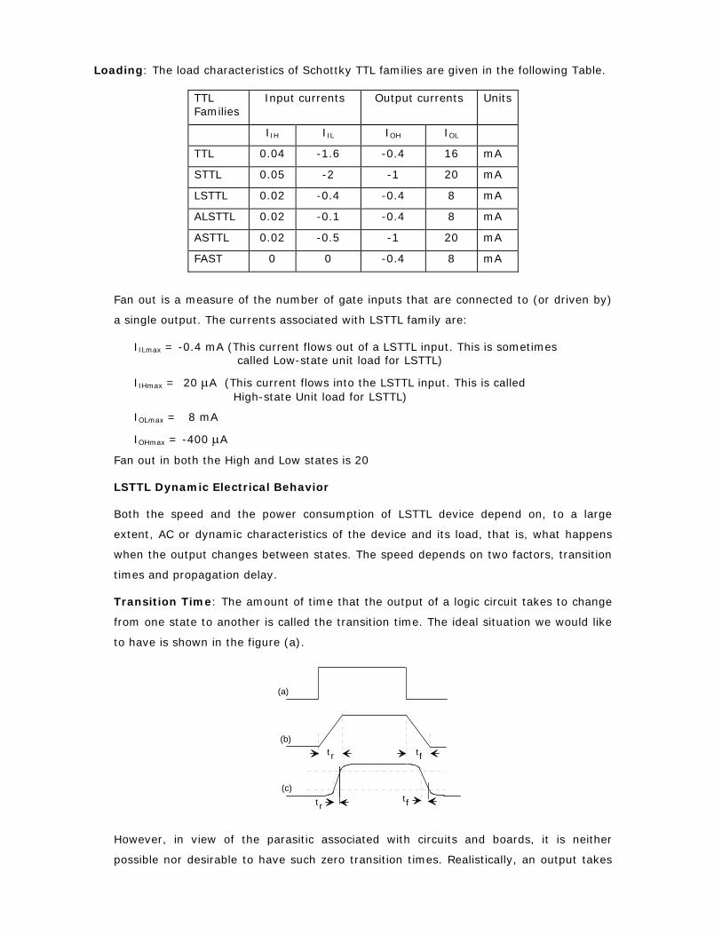
Loading: The load characteristics of Schottky TTL families are given in the following Table.
TTL Families
Input currents Output currents Units
IIH IIL IOH IOL
TTL 0.04 -1.6 -0.4 16 mA
STTL 0.05 -2 -1 20 mA
LSTTL 0.02 -0.4 -0.4 8 mA
ALSTTL 0.02 -0.1 -0.4 8 mA
ASTTL 0.02 -0.5 -1 20 mA
FAST 0 0 -0.4 8 mA
Fan out is a measure of the number of gate inputs that are connected to (or driven by)
a single output. The currents associated with LSTTL family are:
IILmax = -0.4 mA (This current flows out of a LSTTL input. This is sometimes called Low-state unit load for LSTTL)
IIHmax = 20 µA (This current flows into the LSTTL input. This is called High-state Unit load for LSTTL)
IOLmax = 8 mA
IOHmax = -400 µA
Fan out in both the High and Low states is 20
LSTTL Dynamic Electrical Behavior
Both the speed and the power consumption of LSTTL device depend on, to a large
extent, AC or dynamic characteristics of the device and its load, that is, what happens
when the output changes between states. The speed depends on two factors, transition
times and propagation delay.
Transition Time: The amount of time that the output of a logic circuit takes to change
from one state to another is called the transition time. The ideal situation we would like
to have is shown in the figure (a).
t f
t r t f
t r
(a)
(b)
(c)
However, in view of the parasitic associated with circuits and boards, it is neither
possible nor desirable to have such zero transition times. Realistically, an output takes
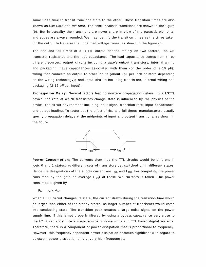
some finite time to transit from one state to the other. These transition times are also
known as rise time and fall time. The semi-idealistic transitions are shown in the figure
(b). But in actuality the transitions are never sharp in view of the parasitic elements,
and edges are always rounded. We may identify the transition times as the times taken
for the output to traverse the undefined voltage zones, as shown in the figure (c).
The rise and fall times of a LSTTL output depend mainly on two factors, the ON
transistor resistance and the load capacitance. The load capacitance comes from three
different sources: output circuits including a gate’s output transistors, internal wiring
and packaging, have capacitances associated with them (of the order of 2-10 pF);
wiring that connects an output to other inputs (about 1pF per inch or more depending
on the wiring technology); and input circuits including transistors, internal wiring and
packaging (2-15 pF per input).
Propagation Delay: Several factors lead to nonzero propagation delays. In a LSTTL
device, the rate at which transistors change state is influenced by the physics of the
device, the circuit environment including input-signal transition rate, input capacitance,
and output loading. To factor out the effect of rise and fall times, manufacturers usually
specify propagation delays at the midpoints of input and output transitions, as shown in
the figure.
tPHL tPLH
Power Consumption: The currents drawn by the TTL circuits would be different in
logic 0 and 1 states, as different sets of transistors get switched on in different states.
Hence the designations of the supply current are ICCL and ICCH. For computing the power
consumed by the gate an average (ICC) of these two currents is taken. The power
consumed is given by
PD = ICC x VCC
When a TTL circuit changes its state, the current drawn during the transition time would
be larger than either of the steady states, as larger number of transistors would come
into conducting state. The transition peak creates a large noise signal on the power
supply line. If this is not properly filtered by using a bypass capacitance very close to
the IC, it can constitute a major source of noise signals in TTL based digital systems.
Therefore, there is a component of power dissipation that is proportional to frequency.
However, this frequency dependent power dissipation becomes significant with regard to
quiescent power dissipation only at very high frequencies.
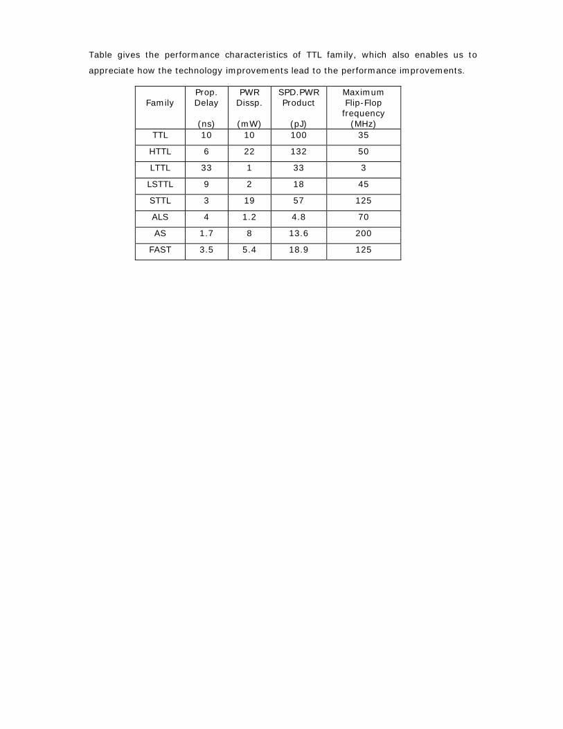
Table gives the performance characteristics of TTL family, which also enables us to
appreciate how the technology improvements lead to the performance improvements.
Family
Prop. Delay
(ns)
PWR Dissp.
(mW)
SPD.PWR Product
(pJ)
Maximum Flip-Flop frequency
(MHz) TTL 10 10 100 35
HTTL 6 22 132 50
LTTL 33 1 33 3
LSTTL 9 2 18 45
STTL 3 19 57 125
ALS 4 1.2 4.8 70
AS 1.7 8 13.6 200
FAST 3.5 5.4 18.9 125

Digital Electronics Module 3: TTL Family
N.J. RaoIndian Institute of Science
id8344719 pdfMachine by Broadgun Software - a great PDF writer! - a great PDF creator! - http://www.pdfmachine.com http://www.broadgun.com
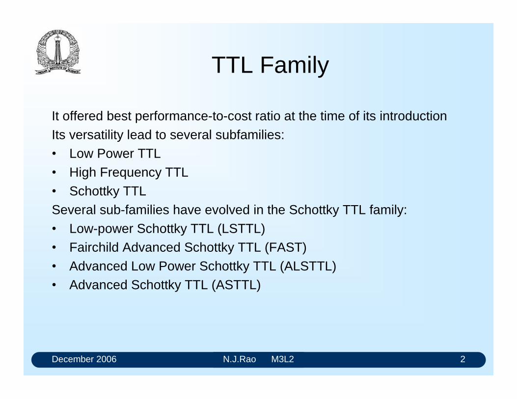
December 2006 N.J.Rao M3L2 2
TTL Family
It offered best performance-to-cost ratio at the time of its introduction Its versatility lead to several subfamilies: Low Power TTL High Frequency TTL Schottky TTLSeveral sub-families have evolved in the Schottky TTL family: Low-power Schottky TTL (LSTTL) Fairchild Advanced Schottky TTL (FAST) Advanced Low Power Schottky TTL (ALSTTL) Advanced Schottky TTL (ASTTL)
December 2006 N.J.Rao M3L2 3
Bipolar logic families
Use semiconductor diodes and bipolar junction transistor as the basic building blocks
Simplest bipolar logic elements use diodes and resistorsto perform logic operation (diode logic)
Many TTL logic gates use diode logic internally, and boost their output drive capability using transistorcircuits.
Some TTL gates use parallel configurations of
transistors to perform logic functions.
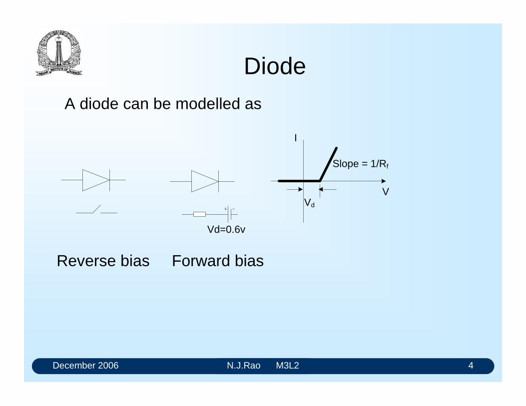
December 2006 N.J.Rao M3L2 4
Diode
A diode can be modelled as
Slope = 1/Rf
V
I
Vd
Vd=0.6v
Reverse bias Forward bias
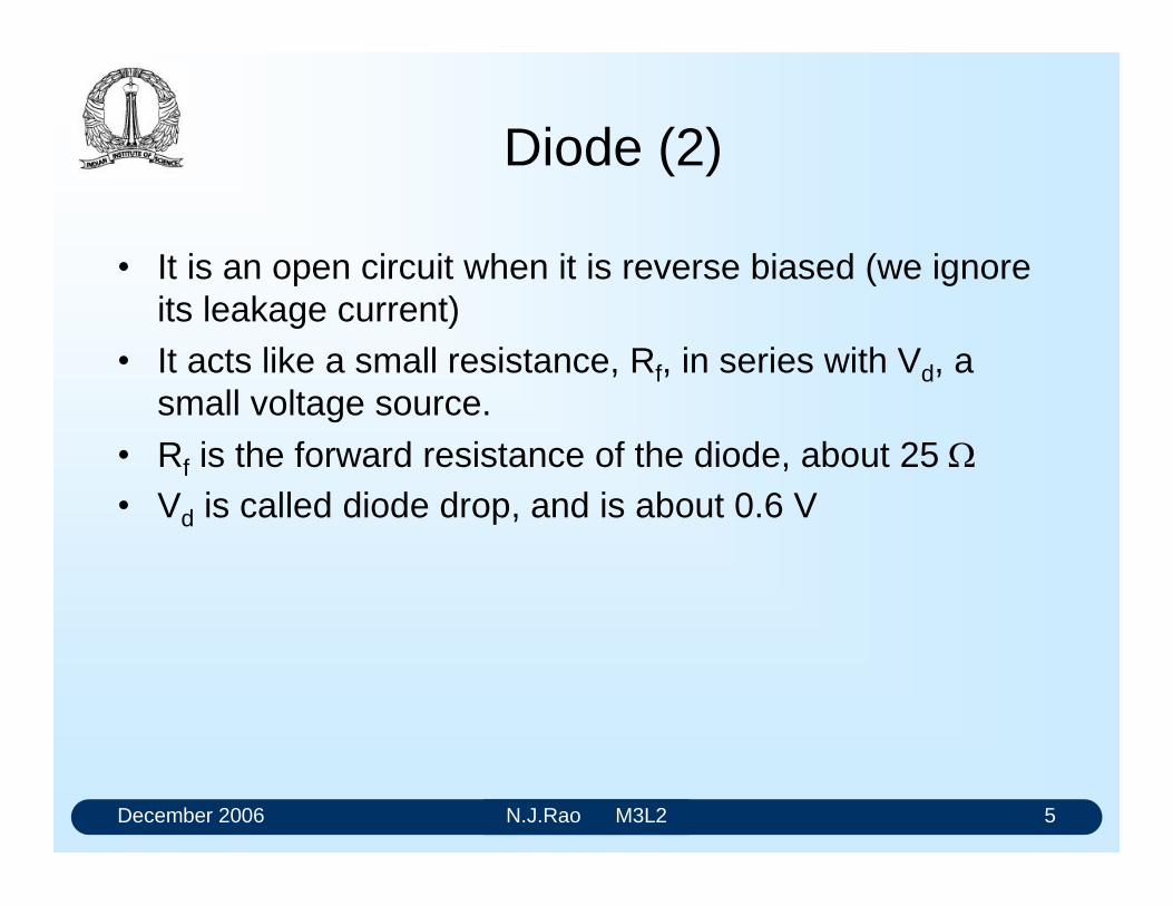
December 2006 N.J.Rao M3L2 5
Diode (2)
It is an open circuit when it is reverse biased (we ignore its leakage current)
It acts like a small resistance, Rf, in series with Vd, a small voltage source.
Rf is the forward resistance of the diode, about 25 Vd is called diode drop, and is about 0.6 V
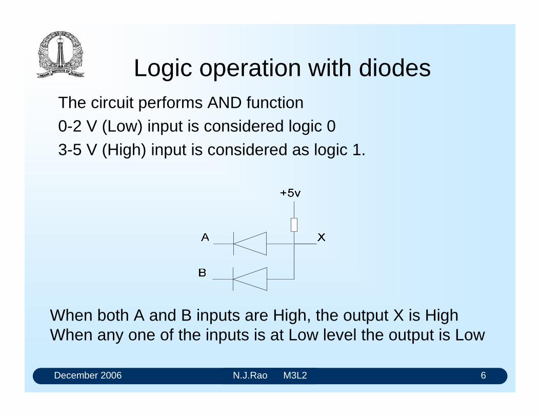
December 2006 N.J.Rao M3L2 6
Logic operation with diodesThe circuit performs AND function 0-2 V (Low) input is considered logic 0 3-5 V (High) input is considered as logic 1.
When both A and B inputs are High, the output X is High When any one of the inputs is at Low level the output is Low
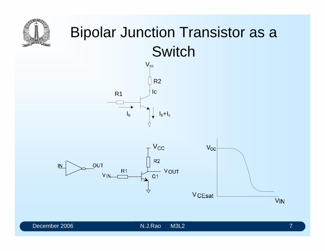
December 2006 N.J.Rao M3L2 7
Bipolar Junction Transistor as a Switch
Vcc
R1
R2
Ib
Ic
Ib+Ic
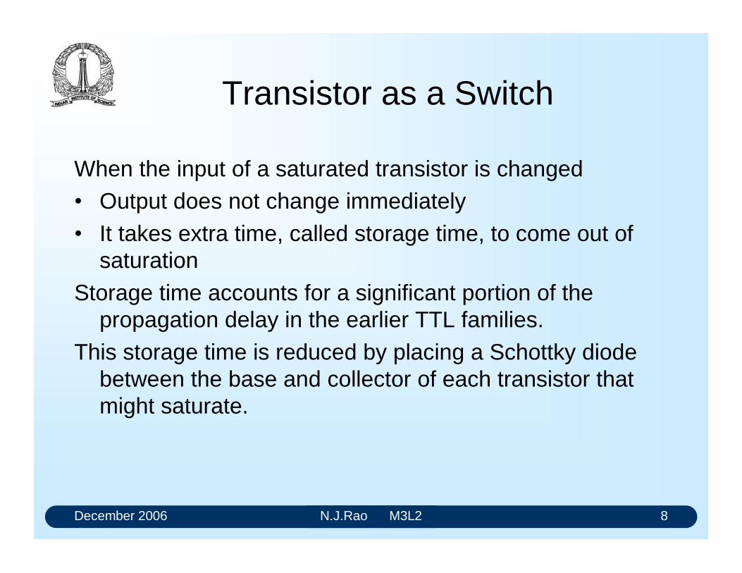
December 2006 N.J.Rao M3L2 8
Transistor as a Switch
When the input of a saturated transistor is changed Output does not change immediately It takes extra time, called storage time, to come out of
saturation Storage time accounts for a significant portion of the
propagation delay in the earlier TTL families. This storage time is reduced by placing a Schottky diode
between the base and collector of each transistor that might saturate.

December 2006 N.J.Rao M3L2 9
Schottky Barrier Diode
Forward current- voltage characteristics differences between the SBD and p-njunction
It is a rectifying metal-semiconductor contact formed between a metal and highly doped N semiconductor.
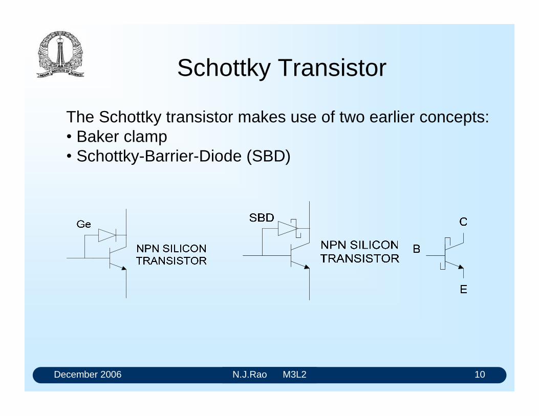
December 2006 N.J.Rao M3L2 10
Schottky Transistor
The Schottky transistor makes use of two earlier concepts: Baker clamp Schottky-Barrier-Diode (SBD)
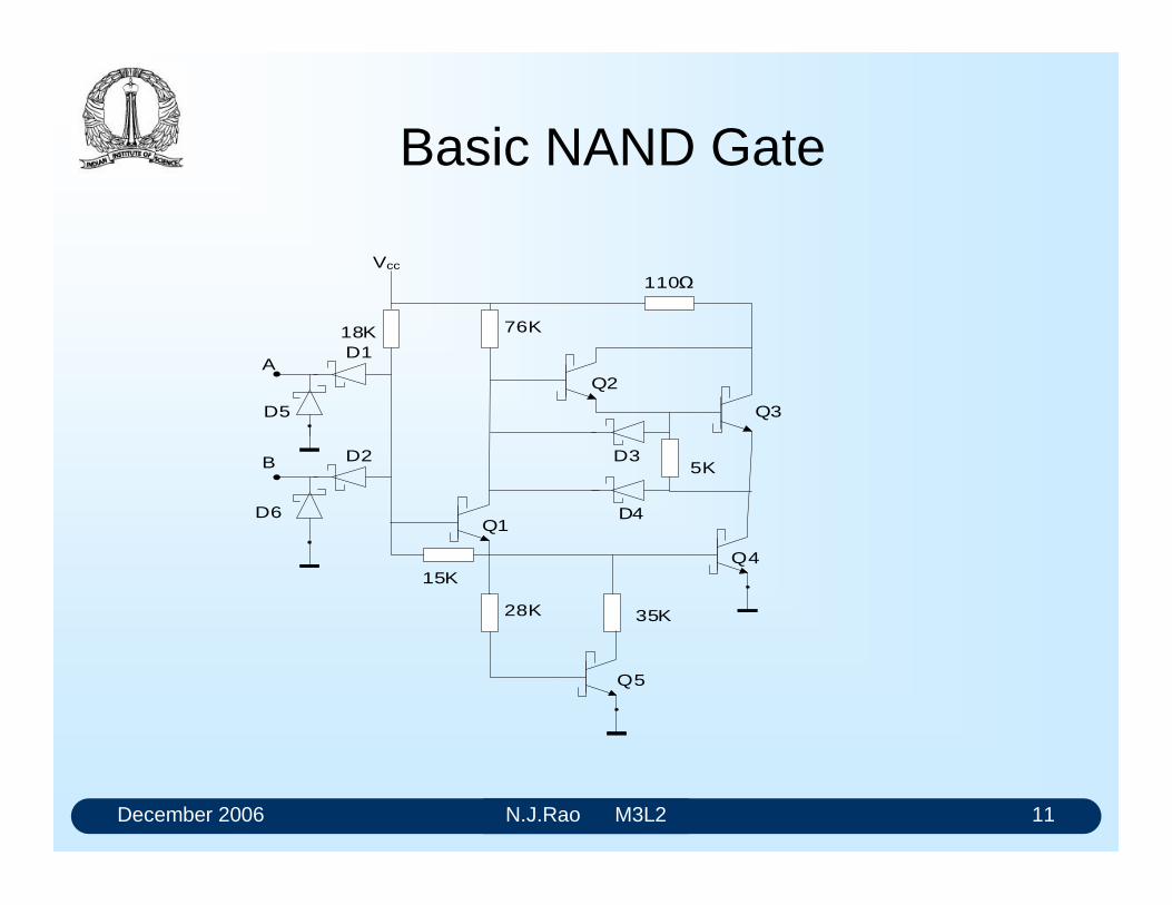
December 2006 N.J.Rao M3L2 11
Basic NAND Gate
A
B D2
D1
D5
D6
D3
D4
Q3
Q4
Q5
Q2
Q1
15K
5K
35K28K
18K 76K
110ΩVcc
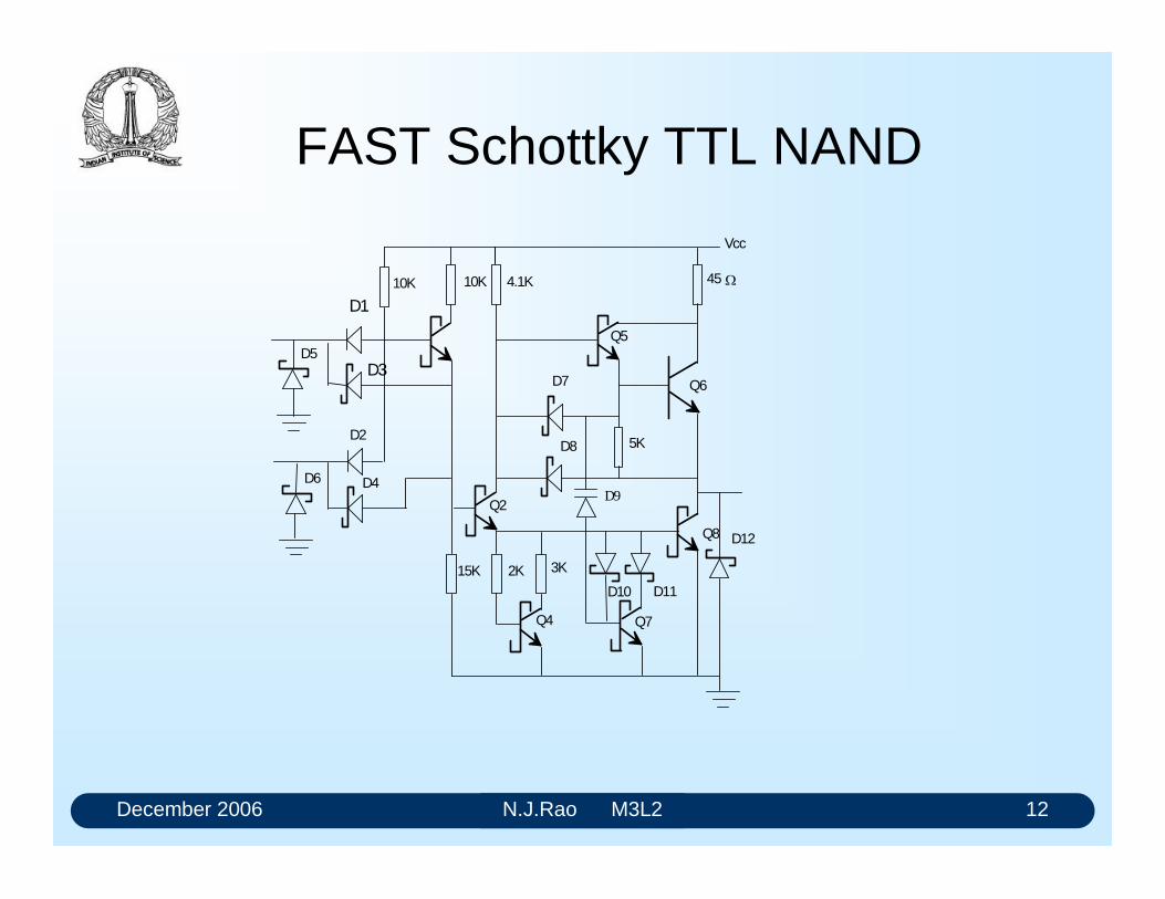
December 2006 N.J.Rao M3L2 12
FAST Schottky TTL NAND
D4
D2
D6
D5
10K 10K 4.1K 45
Q6
Q5
D7
D8
Q2
15K 2K 3K
D10 D11
Q7Q4
D12
5K
Vcc
D9
Q8
D1
D3

December 2006 N.J.Rao M3L2 13
75-80% power reduction compared to standard SchottkyTTL
20-40% improvement in the circuit performance using MOSAIC process
A flatter power/frequency curve Higher fan out
FAST devices provide
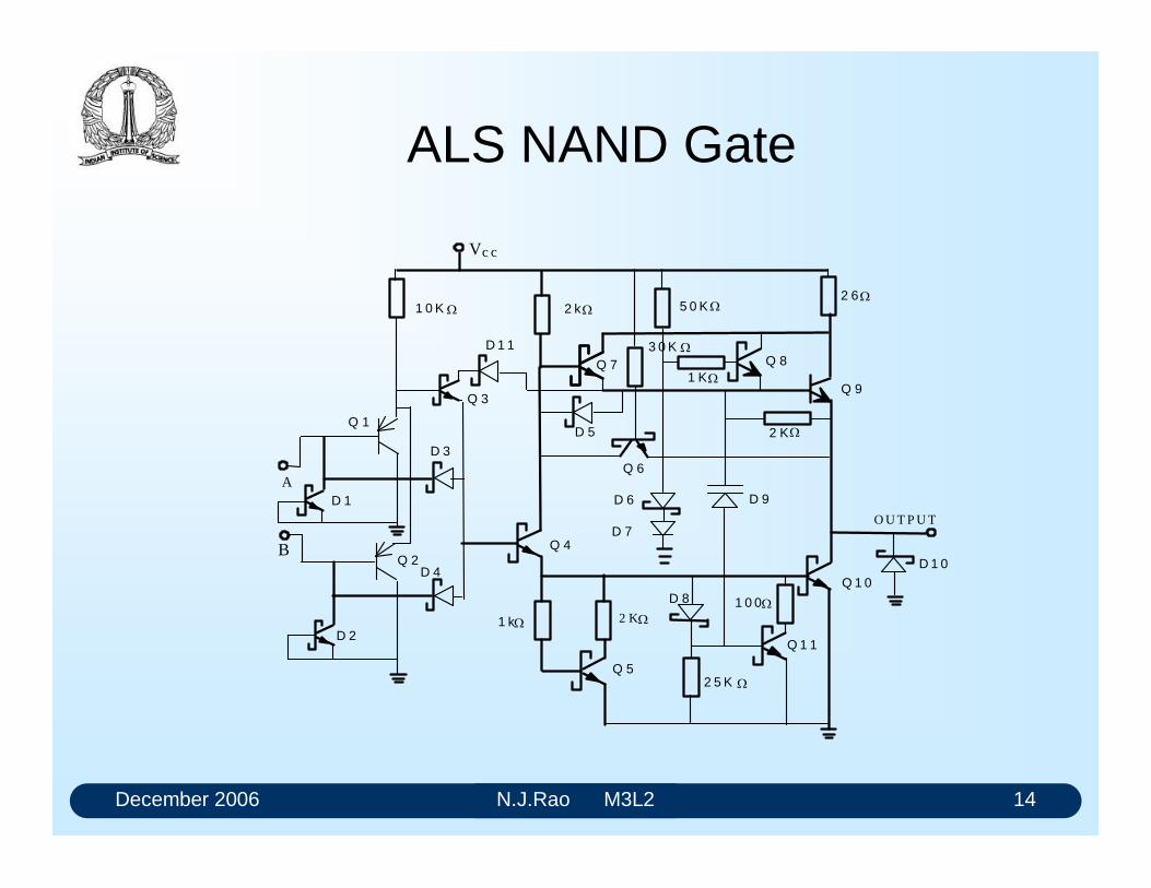
December 2006 N.J.Rao M3L2 14
ALS NAND Gate
2 K
A
Vc c
O U T P U T
B
D 1
D 3
D 4
D 2
Q 2Q 4
Q 3
Q 1
Q 9
Q 5
Q 7
D 8
2 5 K
Q 1 1
1 0 0
D 9
D 7
D 6
Q 6
D 5
3 0 K
2 K
D 1 1
5 0 K2 6
Q 81 K
Q 1 0
D 1 0
2 k
1 k
1 0 K
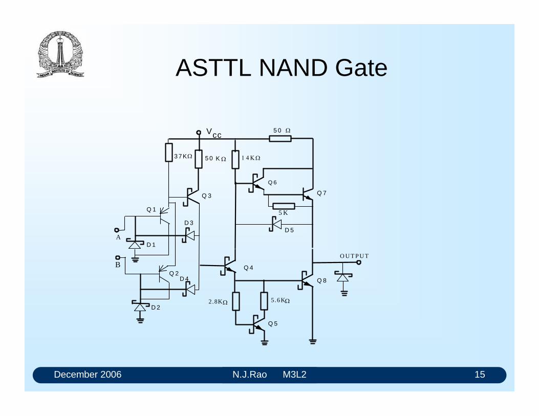
December 2006 N.J.Rao M3L2 15
ASTTL NAND Gate
5 .6 K2.8K
A
5 K
O U T P U T
B
5 0
5 0 K
Q 6
3 7K
D 1
D 5D 3
D 4
D 2
Q 2Q 4
Q 3
Q 1
Q 7
Q 8
Q 5
Vcc
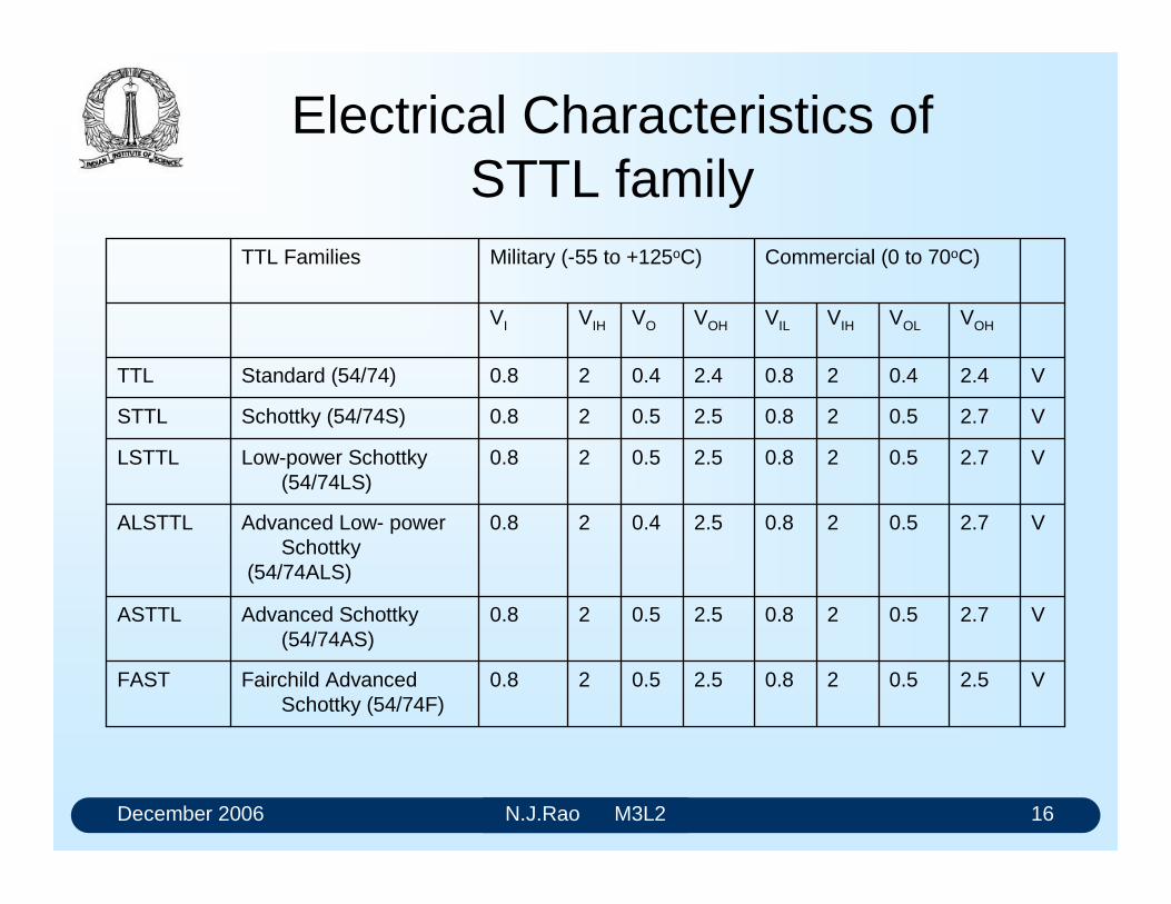
December 2006 N.J.Rao M3L2 16
Electrical Characteristics of STTL family
V2.50.520.82.50.520.8Fairchild Advanced Schottky (54/74F)
FAST
V2.70.520.82.50.520.8Advanced Schottky(54/74AS)
ASTTL
V2.70.520.82.50.420.8Advanced Low- power Schottky
(54/74ALS)
ALSTTL
V2.70.520.82.50.520.8Low-power Schottky(54/74LS)
LSTTL
V2.70.520.82.50.520.8Schottky (54/74S)STTL
V2.40.420.82.40.420.8Standard (54/74)TTL
VOHVOLVIHVILVOHVOVIHVI
Commercial (0 to 70oC)Military (-55 to +125oC)TTL Families
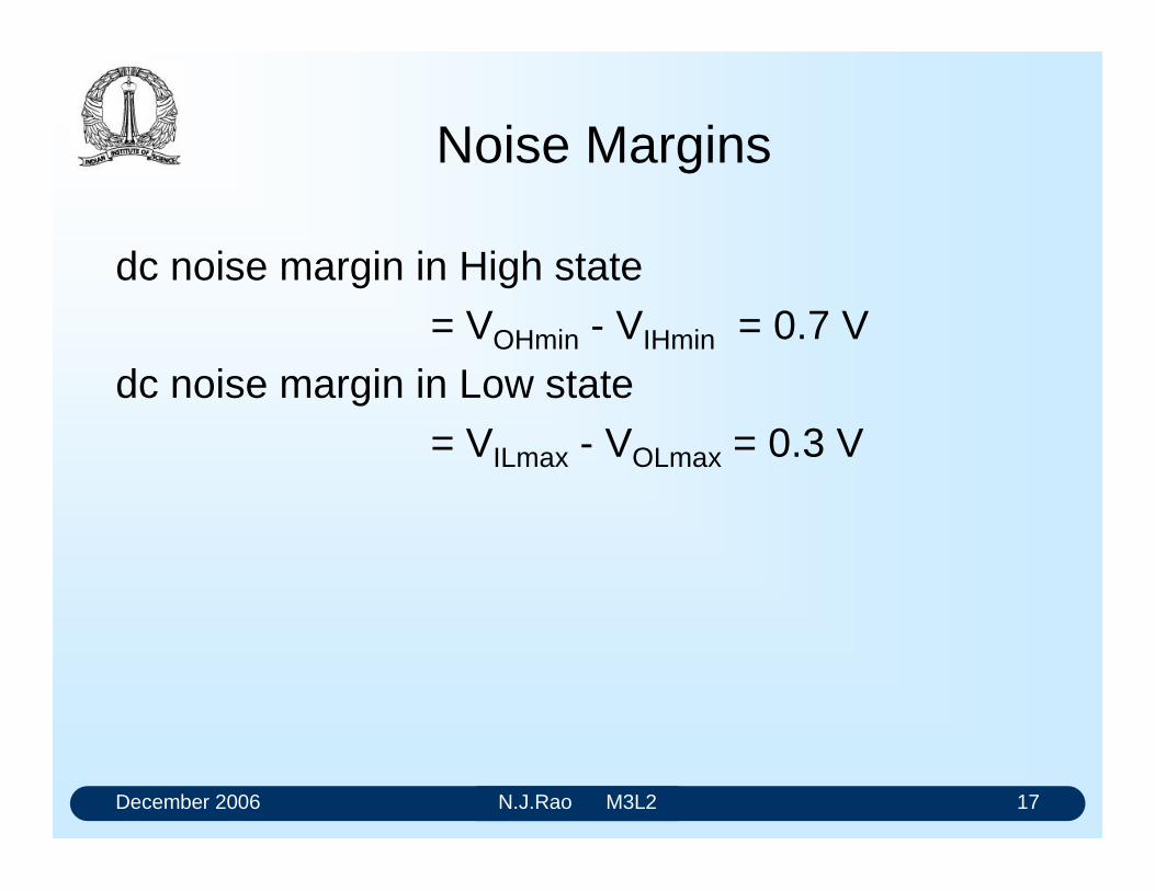
December 2006 N.J.Rao M3L2 17
Noise Margins
dc noise margin in High state
= VOHmin - VIHmin = 0.7 Vdc noise margin in Low state
= VILmax - VOLmax = 0.3 V
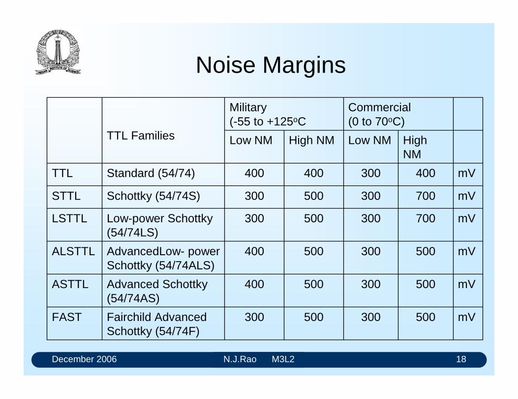
December 2006 N.J.Rao M3L2 18
Noise Margins
mV500300500300Fairchild Advanced Schottky (54/74F)
FAST
mV500300500400Advanced Schottky(54/74AS)
ASTTL
mV500300500400AdvancedLow- power Schottky (54/74ALS)
ALSTTL
mV700300500300Low-power Schottky(54/74LS)
LSTTL
mV700300500300Schottky (54/74S)STTL
mV400300400400Standard (54/74)TTL
High NM
Low NMHigh NMLow NM
Commercial (0 to 70oC)
Military (-55 to +125oC
TTL Families
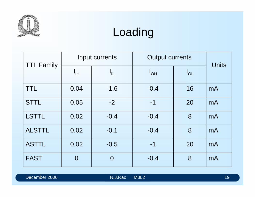
December 2006 N.J.Rao M3L2 19
Loading
mA8-0.400FAST
mA20-1-0.50.02ASTTL
mA8-0.4-0.10.02ALSTTL
mA8-0.4-0.40.02LSTTL
mA20-1-20.05STTL
mA16-0.4-1.60.04TTL
IOLIOHIILIIHUnits
Output currentsInput currentsTTL Family
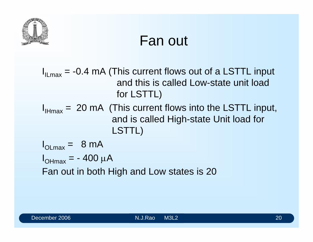
December 2006 N.J.Rao M3L2 20
Fan out
IILmax = -0.4 mA (This current flows out of a LSTTL input and this is called Low-state unit load for LSTTL)
IIHmax = 20 mA (This current flows into the LSTTL input,and is called High-state Unit load for LSTTL)
IOLmax = 8 mA
IOHmax = - 400 AFan out in both High and Low states is 20
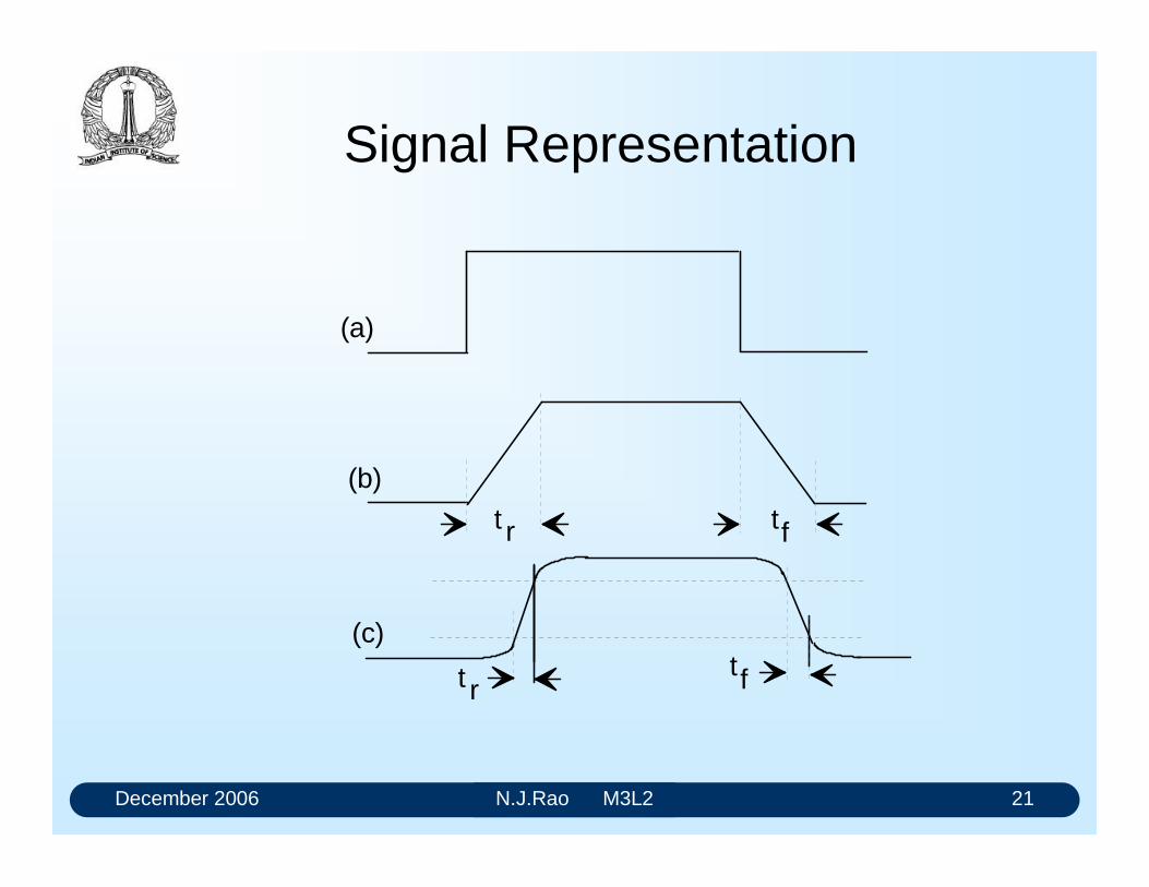
December 2006 N.J.Rao M3L2 21
Signal Representation
t f
t r tf
t r
(a)
(b)
(c)
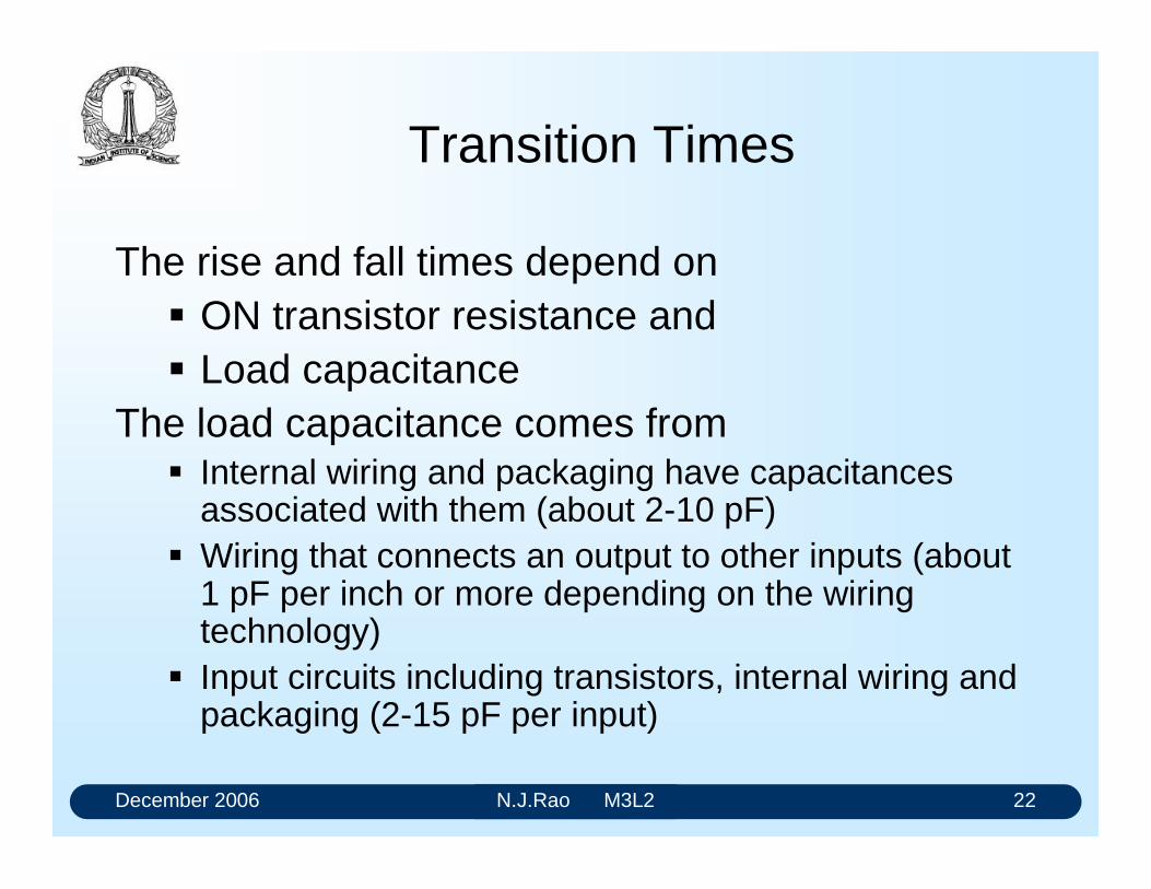
December 2006 N.J.Rao M3L2 22
Transition Times
The rise and fall times depend on ON transistor resistance and Load capacitance
The load capacitance comes from Internal wiring and packaging have capacitances
associated with them (about 2-10 pF) Wiring that connects an output to other inputs (about
1 pF per inch or more depending on the wiring technology)
Input circuits including transistors, internal wiring and packaging (2-15 pF per input)
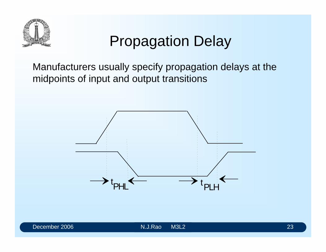
December 2006 N.J.Rao M3L2 23
Propagation Delay
Manufacturers usually specify propagation delays at the midpoints of input and output transitions
tPHL tPLH
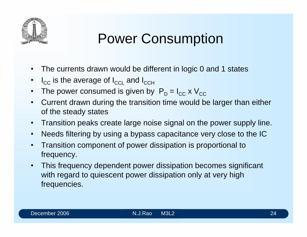
December 2006 N.J.Rao M3L2 24
Power Consumption
The currents drawn would be different in logic 0 and 1 states ICC is the average of ICCL and ICCH
The power consumed is given by PD = ICC x VCC
Current drawn during the transition time would be larger than either of the steady states
Transition peaks create large noise signal on the power supply line. Needs filtering by using a bypass capacitance very close to the IC Transition component of power dissipation is proportional to
frequency. This frequency dependent power dissipation becomes significant
with regard to quiescent power dissipation only at very high frequencies.
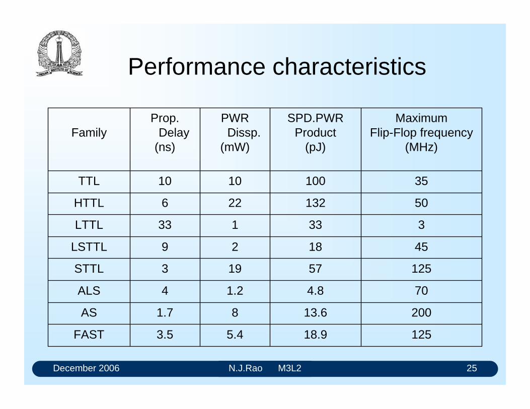
December 2006 N.J.Rao M3L2 25
Performance characteristics
12518.95.43.5FAST
20013.681.7AS
704.81.24ALS
12557193STTL
451829LSTTL
333133LTTL
50132226HTTL
351001010TTL
Maximum Flip-Flop frequency
(MHz)
SPD.PWRProduct
(pJ)
PWR Dissp.
(mW)
Prop. Delay
(ns)Family
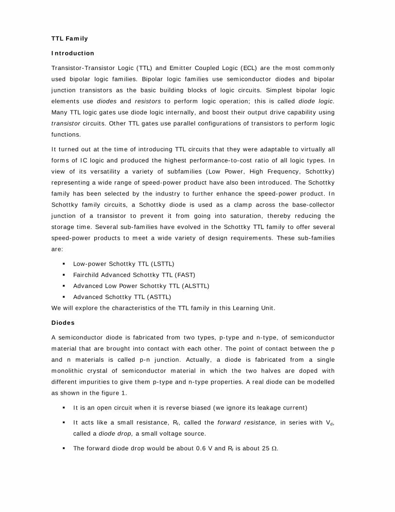
TTL Family
Introduction
Transistor-Transistor Logic (TTL) and Emitter Coupled Logic (ECL) are the most commonly
used bipolar logic families. Bipolar logic families use semiconductor diodes and bipolar
junction transistors as the basic building blocks of logic circuits. Simplest bipolar logic
elements use diodes and resistors to perform logic operation; this is called diode logic.
Many TTL logic gates use diode logic internally, and boost their output drive capability using
transistor circuits. Other TTL gates use parallel configurations of transistors to perform logic
functions.
It turned out at the time of introducing TTL circuits that they were adaptable to virtually all
forms of IC logic and produced the highest performance-to-cost ratio of all logic types. In
view of its versatility a variety of subfamilies (Low Power, High Frequency, Schottky)
representing a wide range of speed-power product have also been introduced. The Schottky
family has been selected by the industry to further enhance the speed-power product. In
Schottky family circuits, a Schottky diode is used as a clamp across the base-collector
junction of a transistor to prevent it from going into saturation, thereby reducing the
storage time. Several sub-families have evolved in the Schottky TTL family to offer several
speed-power products to meet a wide variety of design requirements. These sub-families
are:
Low-power Schottky TTL (LSTTL)
Fairchild Advanced Schottky TTL (FAST)
Advanced Low Power Schottky TTL (ALSTTL)
Advanced Schottky TTL (ASTTL)
We will explore the characteristics of the TTL family in this Learning Unit.
Diodes
A semiconductor diode is fabricated from two types, p-type and n-type, of semiconductor
material that are brought into contact with each other. The point of contact between the p
and n materials is called p-n junction. Actually, a diode is fabricated from a single
monolithic crystal of semiconductor material in which the two halves are doped with
different impurities to give them p-type and n-type properties. A real diode can be modelled
as shown in the figure 1.
It is an open circuit when it is reverse biased (we ignore its leakage current)
It acts like a small resistance, Rf, called the forward resistance, in series with Vd,
called a diode drop, a small voltage source.
The forward diode drop would be about 0.6 V and Rf is about 25 Ω.
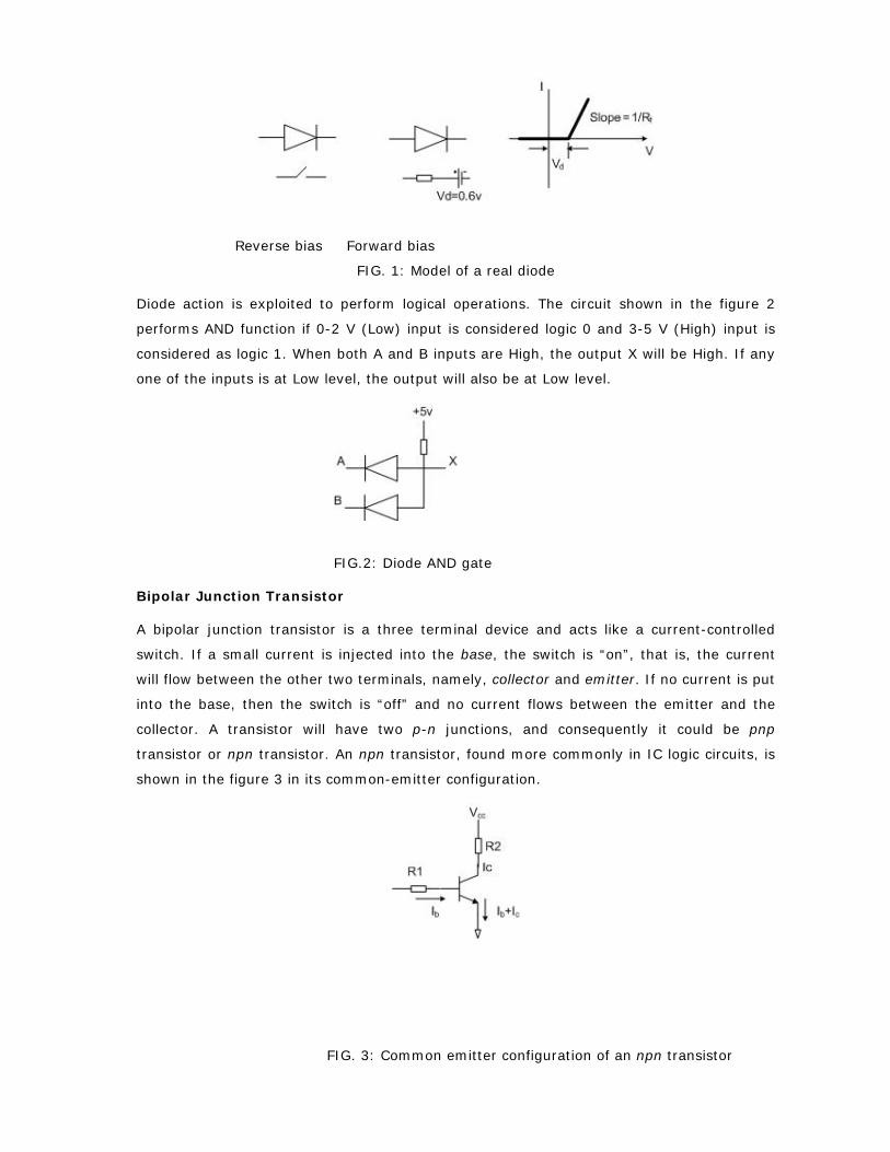
Reverse bias Forward bias
FIG. 1: Model of a real diode
Diode action is exploited to perform logical operations. The circuit shown in the figure 2
performs AND function if 0-2 V (Low) input is considered logic 0 and 3-5 V (High) input is
considered as logic 1. When both A and B inputs are High, the output X will be High. If any
one of the inputs is at Low level, the output will also be at Low level.
FIG.2: Diode AND gate
Bipolar Junction Transistor
A bipolar junction transistor is a three terminal device and acts like a current-controlled
switch. If a small current is injected into the base, the switch is “on”, that is, the current
will flow between the other two terminals, namely, collector and emitter. If no current is put
into the base, then the switch is “off” and no current flows between the emitter and the
collector. A transistor will have two p-n junctions, and consequently it could be pnp
transistor or npn transistor. An npn transistor, found more commonly in IC logic circuits, is
shown in the figure 3 in its common-emitter configuration.
FIG. 3: Common emitter configuration of an npn transistor
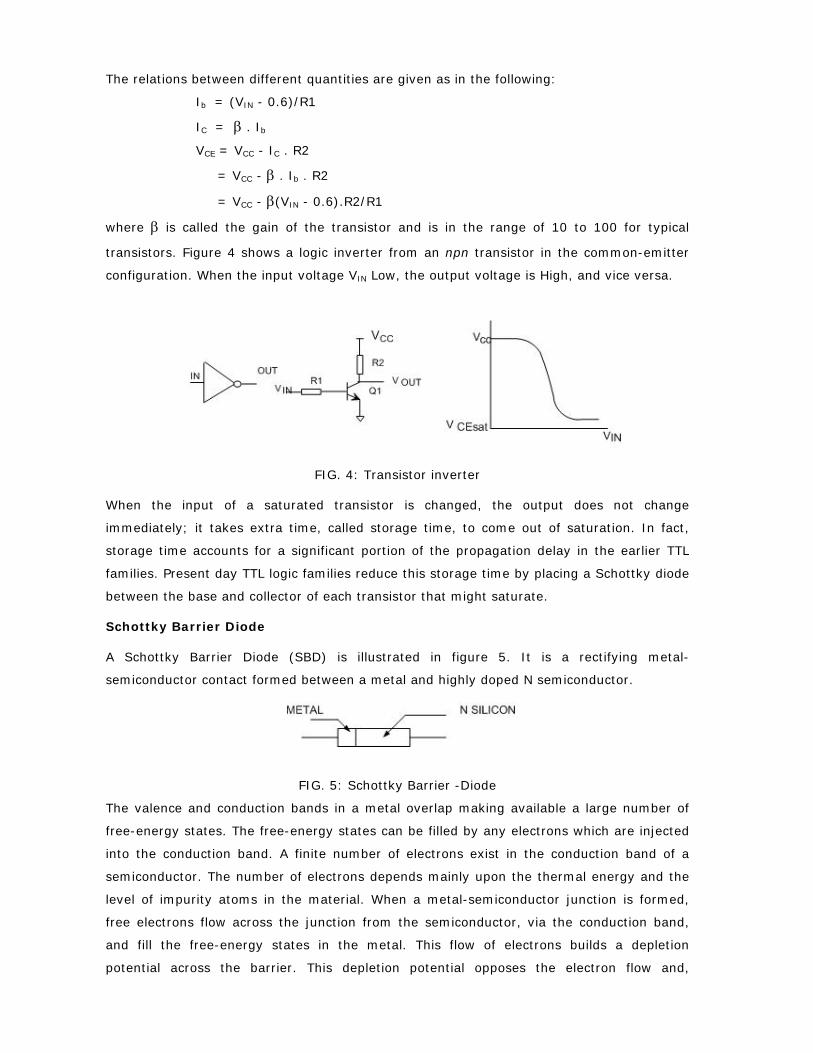
The relations between different quantities are given as in the following:
Ib = (VIN - 0.6)/R1
IC = β . Ib
VCE = VCC - IC . R2
= VCC - β . Ib . R2
= VCC - β(VIN - 0.6).R2/R1
where β is called the gain of the transistor and is in the range of 10 to 100 for typical
transistors. Figure 4 shows a logic inverter from an npn transistor in the common-emitter
configuration. When the input voltage VIN Low, the output voltage is High, and vice versa.
FIG. 4: Transistor inverter
When the input of a saturated transistor is changed, the output does not change
immediately; it takes extra time, called storage time, to come out of saturation. In fact,
storage time accounts for a significant portion of the propagation delay in the earlier TTL
families. Present day TTL logic families reduce this storage time by placing a Schottky diode
between the base and collector of each transistor that might saturate.
Schottky Barrier Diode
A Schottky Barrier Diode (SBD) is illustrated in figure 5. It is a rectifying metal-
semiconductor contact formed between a metal and highly doped N semiconductor.
FIG. 5: Schottky Barrier -Diode
The valence and conduction bands in a metal overlap making available a large number of
free-energy states. The free-energy states can be filled by any electrons which are injected
into the conduction band. A finite number of electrons exist in the conduction band of a
semiconductor. The number of electrons depends mainly upon the thermal energy and the
level of impurity atoms in the material. When a metal-semiconductor junction is formed,
free electrons flow across the junction from the semiconductor, via the conduction band,
and fill the free-energy states in the metal. This flow of electrons builds a depletion
potential across the barrier. This depletion potential opposes the electron flow and,
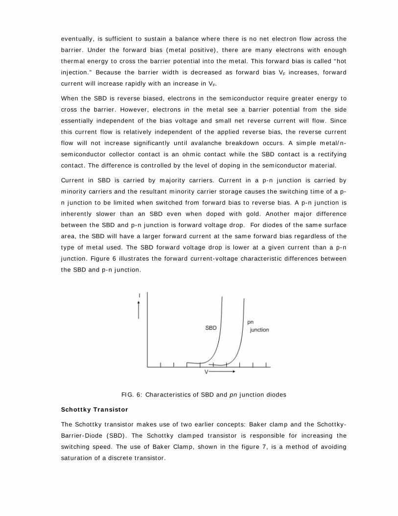
eventually, is sufficient to sustain a balance where there is no net electron flow across the
barrier. Under the forward bias (metal positive), there are many electrons with enough
thermal energy to cross the barrier potential into the metal. This forward bias is called “hot
injection.” Because the barrier width is decreased as forward bias VF increases, forward
current will increase rapidly with an increase in VF.
When the SBD is reverse biased, electrons in the semiconductor require greater energy to
cross the barrier. However, electrons in the metal see a barrier potential from the side
essentially independent of the bias voltage and small net reverse current will flow. Since
this current flow is relatively independent of the applied reverse bias, the reverse current
flow will not increase significantly until avalanche breakdown occurs. A simple metal/n-
semiconductor collector contact is an ohmic contact while the SBD contact is a rectifying
contact. The difference is controlled by the level of doping in the semiconductor material.
Current in SBD is carried by majority carriers. Current in a p-n junction is carried by
minority carriers and the resultant minority carrier storage causes the switching time of a p-
n junction to be limited when switched from forward bias to reverse bias. A p-n junction is
inherently slower than an SBD even when doped with gold. Another major difference
between the SBD and p-n junction is forward voltage drop. For diodes of the same surface
area, the SBD will have a larger forward current at the same forward bias regardless of the
type of metal used. The SBD forward voltage drop is lower at a given current than a p-n
junction. Figure 6 illustrates the forward current-voltage characteristic differences between
the SBD and p-n junction.
FIG. 6: Characteristics of SBD and pn junction diodes
Schottky Transistor
The Schottky transistor makes use of two earlier concepts: Baker clamp and the Schottky-
Barrier-Diode (SBD). The Schottky clamped transistor is responsible for increasing the
switching speed. The use of Baker Clamp, shown in the figure 7, is a method of avoiding
saturation of a discrete transistor.
FIG. 7: Baker Clamp
The germanium diode forward voltage is 0.3 V to 0.4 V as compared to 0.7 V for the base-
emitter junction silicon diode. When the transistor is turned on, base current drives the
transistor toward saturation. The collector voltage drops, the germanium diode begins to
conduct forward current, and excess base drive is diverted from the base-collector junction
of the transistor. This causes the transistor to be held out of deep saturation, the excess
base charge not stored, and the turn-off time to be dramatically reduced. However, a
germanium diode cannot be incorporated into a monolithic silicon integrated circuit.
Therefore, the germanium diode must be replaced with a silicon diode which has a lower
forward voltage drop than the base-collector junction of the transistor. A normal p-n diode
will not meet this requirement. An SBD can be used to meet the requirement as shown in
the figure 8.
FIG.8: The Schottky-Clamped Transistor
The SBD meets the requirements of a silicon diode which will clamp a silicon npn transistor
out of saturation.
BASIC NAND GATE
The familiarization with a logic family is acquired, in general, through understanding the
circuit features of a NAND gate. The circuit diagram of a two-input LSTTL NAND gate,
74LS00, is shown in the figure 9.
D1 and D2 along with 18 KΩ resistor perform the AND function. Diodes D3 and D4 do
nothing in normal operation, but limit undesirable negative excursions on the inputs to a
signal diode drop. Such negative excursions may occur on High-to-Low input transitions as
a result of transmission-line effects. Transistor Q1 serves as an inverter, so the output at its
collector represents the NAND function. It also, along with its resistors, forms a phase
splitter that controls the output stage. The output state has two transistors, Q3 and Q4,
only one of which is on at any time. The TTL output state is sometimes called a totem-pole
output. Q2 and Q5 provide active pull-up and pull-down to the High and Low states,
respectively. Transistor Q5 regulates current flow into the base of Q4 and aids in turning Q4
off rapidly. Transistors Q3 and Q2 constitute a Darlington driver, with Q3 not being
permitted to saturate. The network consisting of Schottky diodes D3 and D4 and a 5 KΩ
resistor is connected to the output and aids in charging and discharging load capacitance
when Q3 and Q4 are changing states. Transistor Q4 conducts when the output is in Low
state.
FIG. 9: Low Power Schottky NAND (74LS00)
The FAST Schottky TTL family provides a 75-80% power reduction compared to standard
Schottky TTL and yet offers 20-40% improved circuit performance over the standard
Schottky due to the MOSAIC process. Also, FAST circuits contain additional circuitry to
provide a flatter power/frequency curve. The input configuration of FAST uses a lower input
current which translates into higher fan-out. The NAND gate of FAST family is shown in the
figure 10.
The F00 input configuration utilises a p-n diodes (D1 and D2) rather than pnp-transistor.
The p-n diode offers a much smaller capacitance and results in much better ac noise
immunity at the expense of increased input
current
FIG. 10: FAST NAND (74F00)
Figure 11 shows one gate in 74ALS00A quad 2-input NAND gate parallel-connected pnp
transistors Q1 and Q2 are used at the input. These transistors reduce the current flow, IR,
when the inputs are low and thus increase fan out. If inputs A, B, or both are low, then the
respective pnp transistors turn on because their emitters are then more positive than their
bases. If at least one of the inputs is low, the corresponding pnp transistor conducts,
making the base of Q3 low and keeping Q3 off. If both the inputs A and B are high, both
switches are open and Q3 turns on. Q3 drives Q4 (by emitter follower action), and Q4
drives the output totem pole. Schottky diodes D3, D4 and D5 are used to speed the
switching and do not affect the logic. Note that the output and the inputs have Schottky
protective diodes. Figure 12 shows one gate in 74AS00 gate.
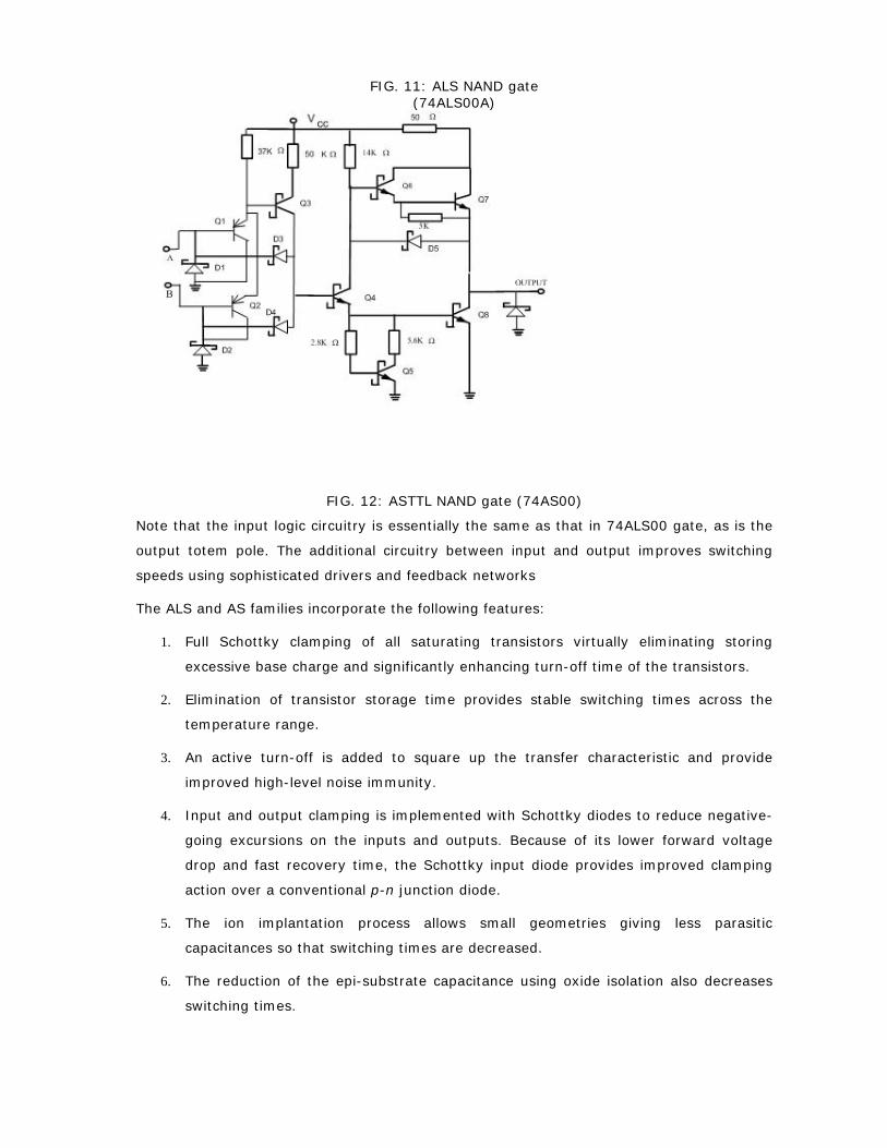
FIG. 11: ALS NAND gate (74ALS00A)
FIG. 12: ASTTL NAND gate (74AS00)
Note that the input logic circuitry is essentially the same as that in 74ALS00 gate, as is the
output totem pole. The additional circuitry between input and output improves switching
speeds using sophisticated drivers and feedback networks
The ALS and AS families incorporate the following features:
1. Full Schottky clamping of all saturating transistors virtually eliminating storing
excessive base charge and significantly enhancing turn-off time of the transistors.
2. Elimination of transistor storage time provides stable switching times across the
temperature range.
3. An active turn-off is added to square up the transfer characteristic and provide
improved high-level noise immunity.
4. Input and output clamping is implemented with Schottky diodes to reduce negative-
going excursions on the inputs and outputs. Because of its lower forward voltage
drop and fast recovery time, the Schottky input diode provides improved clamping
action over a conventional p-n junction diode.
5. The ion implantation process allows small geometries giving less parasitic
capacitances so that switching times are decreased.
6. The reduction of the epi-substrate capacitance using oxide isolation also decreases
switching times.
Digital Electronics Module 3: CMOS Family
N.J. RaoIndian Institute of Science
id9126783 pdfMachine by Broadgun Software - a great PDF writer! - a great PDF creator! - http://www.pdfmachine.com http://www.broadgun.com

December 2006 N.J.Rao M3L3 2
CMOS Family
CMOS has often been called the ideal technology. It has Low power dissipation High noise immunity to power supply noise Symmetric switching characteristics Large supply voltage tolerance

December 2006 N.J.Rao M3L3 3
CMOS Family
Reducing power requirements leads to Reduction in the cost of power supplies Simplifies power distribution Possible elimination of cooling fans A denser PCB Ultimately lower cost of the system
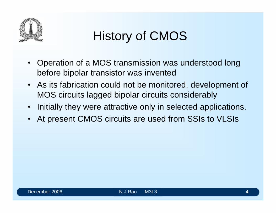
December 2006 N.J.Rao M3L3 4
History of CMOS
Operation of a MOS transmission was understood long before bipolar transistor was invented
As its fabrication could not be monitored, development of MOS circuits lagged bipolar circuits considerably
Initially they were attractive only in selected applications. At present CMOS circuits are used from SSIs to VLSIs
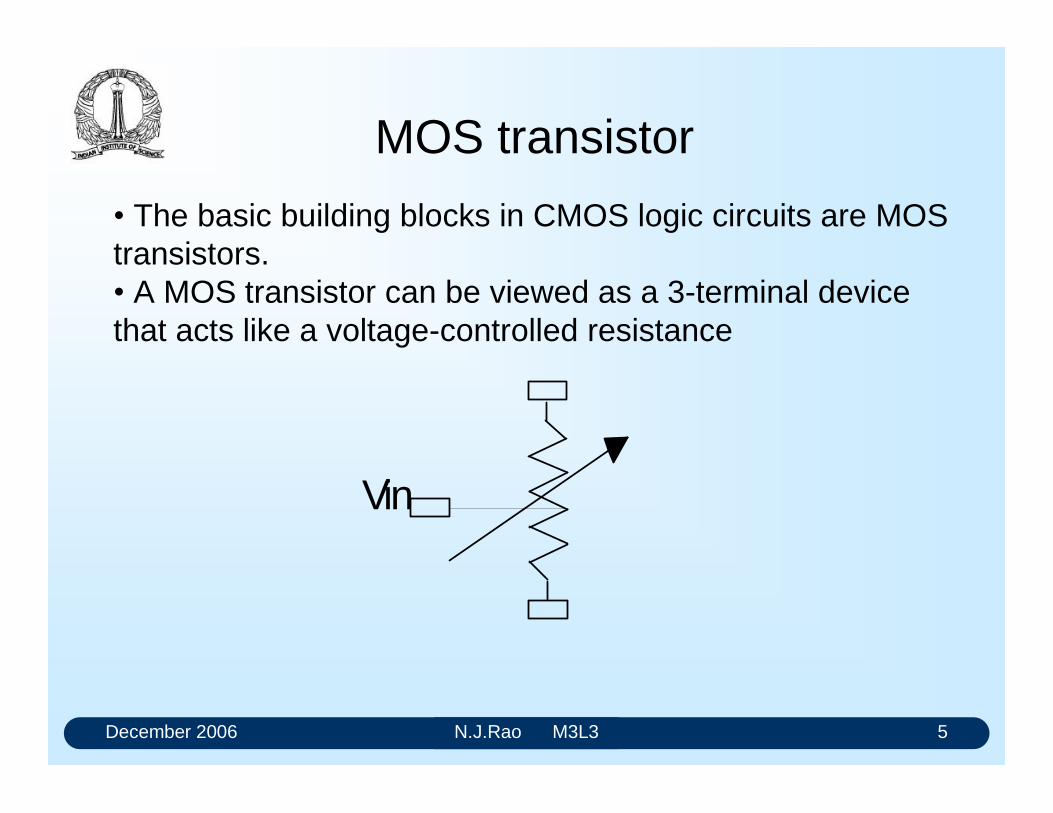
December 2006 N.J.Rao M3L3 5
MOS transistor
The basic building blocks in CMOS logic circuits are MOS transistors. A MOS transistor can be viewed as a 3-terminal device that acts like a voltage-controlled resistance
Vin
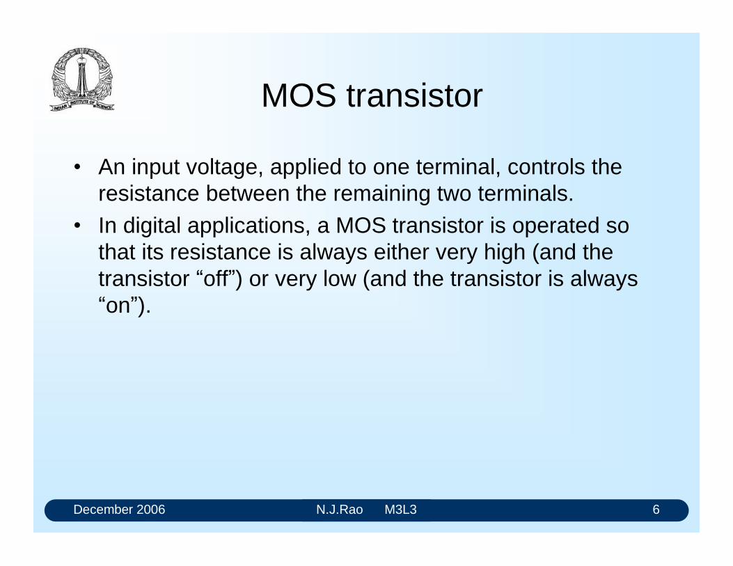
December 2006 N.J.Rao M3L3 6
MOS transistor
An input voltage, applied to one terminal, controls the resistance between the remaining two terminals.
In digital applications, a MOS transistor is operated so that its resistance is always either very high (and the transistor off) or very low (and the transistor is always on).
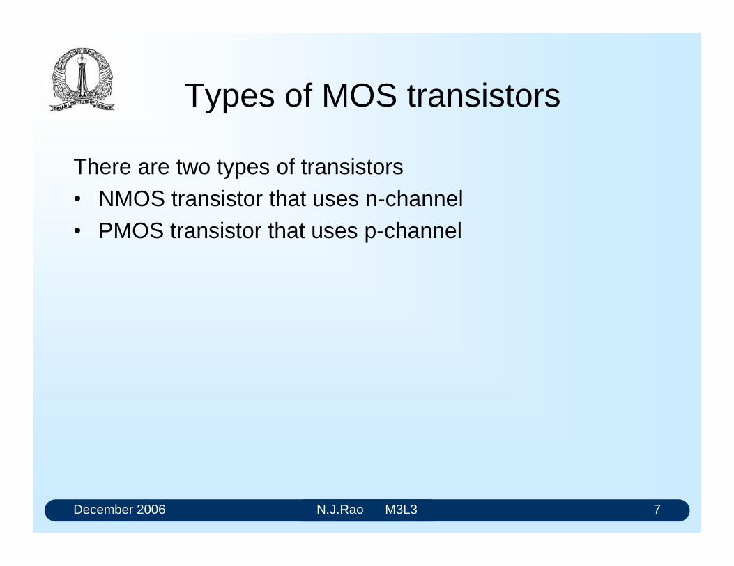
December 2006 N.J.Rao M3L3 7
Types of MOS transistors
There are two types of transistors NMOS transistor that uses n-channel PMOS transistor that uses p-channel
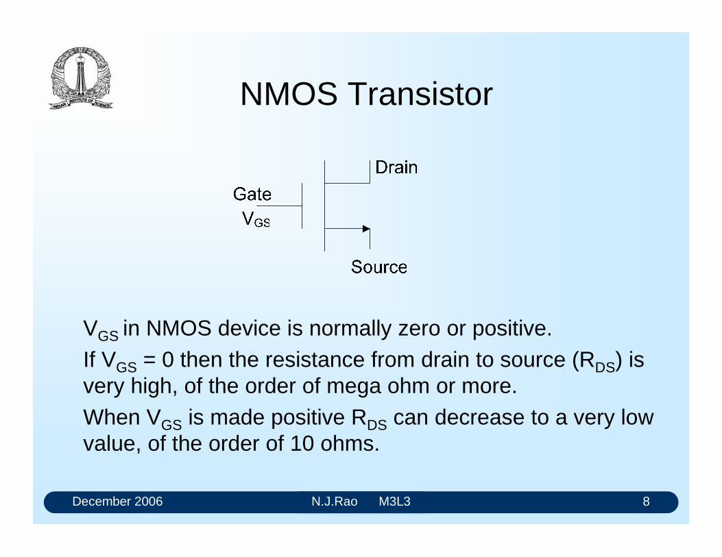
December 2006 N.J.Rao M3L3 8
NMOS Transistor
VGS in NMOS device is normally zero or positive. If VGS = 0 then the resistance from drain to source (RDS) is very high, of the order of mega ohm or more. When VGS is made positive RDS can decrease to a very low value, of the order of 10 ohms.
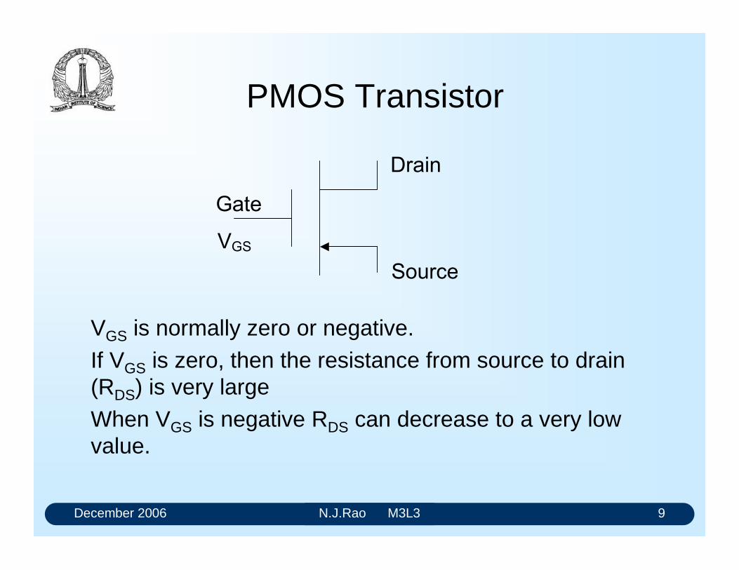
December 2006 N.J.Rao M3L3 9
PMOS Transistor
VGS is normally zero or negative. If VGS is zero, then the resistance from source to drain (RDS) is very largeWhen VGS is negative RDS can decrease to a very low value.
*DWH
'UDLQ
9*6
6RXUFH
December 2006 N.J.Rao M3L3 10
Gate of a MOS transistor
It has very high impedance Gate is separated from the source and drain by an
insulating material with a very high resistance. Gate voltage creates an electric field that enhances or
retards the flow of current between source and drain. This is the field effect in a MOSFET.
The high resistance between the gate and the other terminals keeps the gate current to values lower than a microampere irrespective of the gate voltage.
December 2006 N.J.Rao M3L3 11
Gate of a MOS transistor (2)
The gate current is called leakage current. The gate of a MOS transistor is capacitively coupled to
the source and drain. In high speed circuits, the power needed to charge and
discharge these capacitances on each input signal transition accounts for a non trivial portion of a circuits power consumption.
December 2006 N.J.Rao M3L3 12
Basic CMOS Inverter circuit
NMOS and PMOS transistors are used together in a complementary way to form CMOS logic
The power supply voltage VDD, typically is in the range of 2- 6 V, and is most often set at 5.0 V for compatibility with TTL circuits.
December 2006 N.J.Rao M3L3 13
Basic CMOS Inverter circuit (2)
0VOnOff5.0
5VOffOn0.0
VOUT
Q2Q1VIN
When VIN is at 0.0 V, the lower n-channel MOSFET Q1 is OFF since its VGS is 0, but the upper p-channel MOSFET Q2 is ON since its VGS
would be -5.0 VVOUT at the output terminal would be +5.0 V. Similarly when VIN is at 5.0 Q1 will be ON presenting a small resistance, while Q2 will be OFF presenting a large resistance. VOUT would be 0 V
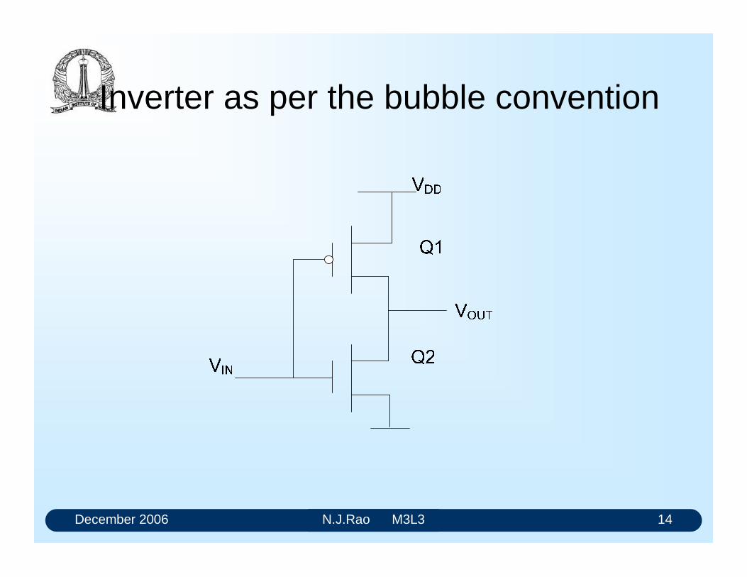
December 2006 N.J.Rao M3L3 14
Inverter as per the bubble convention
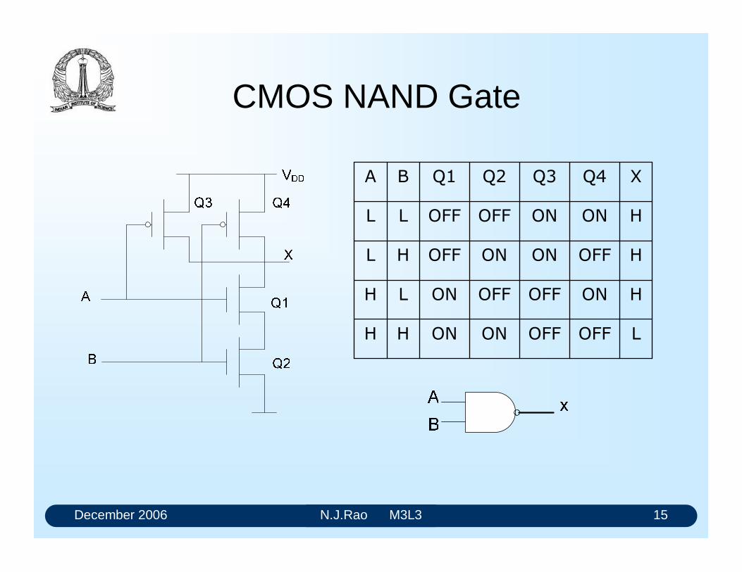
December 2006 N.J.Rao M3L3 15
CMOS NAND Gate
LOFFOFFONONHH
HONOFFOFFONLH
HOFFONONOFFHL
HONONOFFOFFLL
XQ4Q3Q2Q1BA
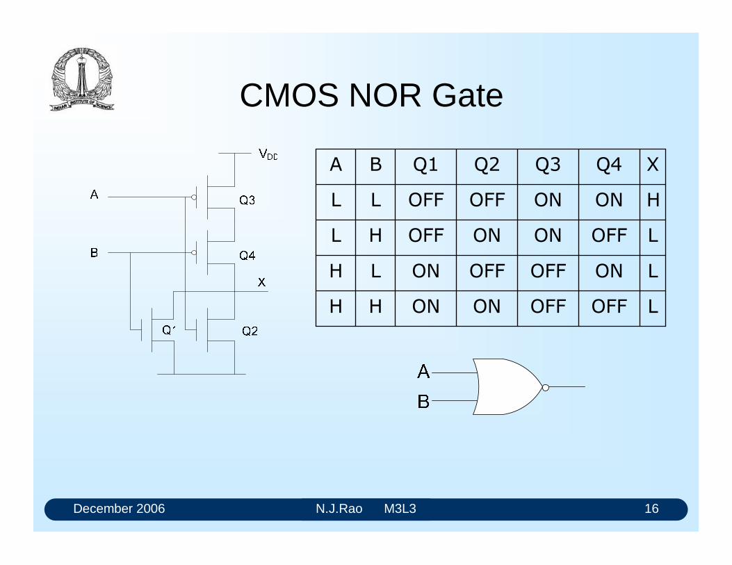
December 2006 N.J.Rao M3L3 16
CMOS NOR Gate
LOFFOFFONONHH
LONOFFOFFONLH
LOFFONONOFFHL
HONONOFFOFFLL
XQ4Q3Q2Q1BA
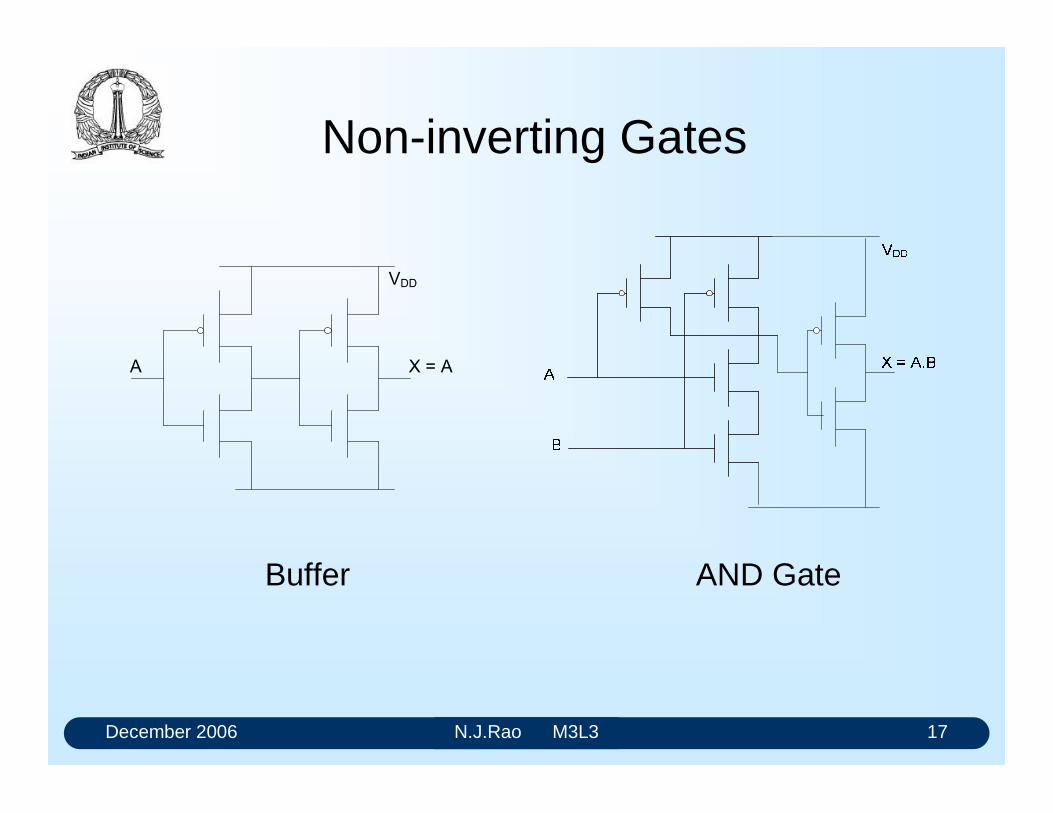
December 2006 N.J.Rao M3L3 17
Non-inverting Gates
$ ; $
9''
Buffer AND Gate
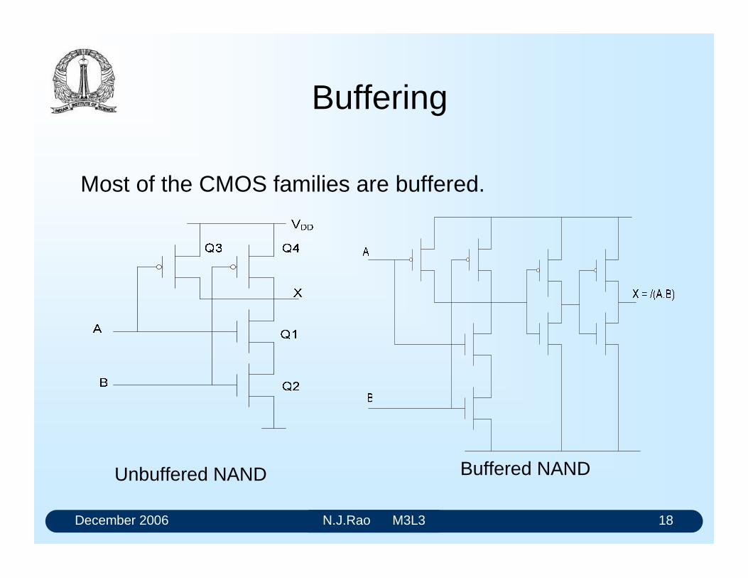
December 2006 N.J.Rao M3L3 18
Buffering
Unbuffered NAND
Most of the CMOS families are buffered.
Buffered NAND
December 2006 N.J.Rao M3L3 19
Advantages of buffering
Output characteristics of all devices are more easily made identical.
Multistage gates will have better noise immunity due to their higher gain caused by having several stages from input to output.
Output impedance of buffered gates is unaffected by input conditions
December 2006 N.J.Rao M3L3 20
Advantages of buffering (2)
Single stage gates implemented would require large transistors due to the large output drive requirements.
Large devices would have a large input capacitance associated with them. This would affect the speed of circuits driving into an unbuffered gate, especially when driving large fan outs.
Buffered gates have small input transistors and correspondingly small input capacitance.
Internal stages are much faster than the output stage and speed lost by buffering is relatively small.
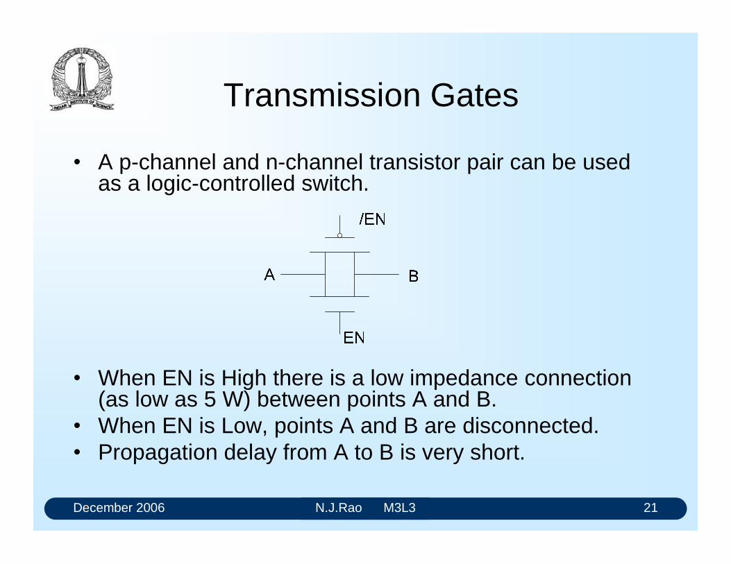
December 2006 N.J.Rao M3L3 21
Transmission Gates
A p-channel and n-channel transistor pair can be used as a logic-controlled switch.
When EN is High there is a low impedance connection (as low as 5 W) between points A and B.
When EN is Low, points A and B are disconnected. Propagation delay from A to B is very short.
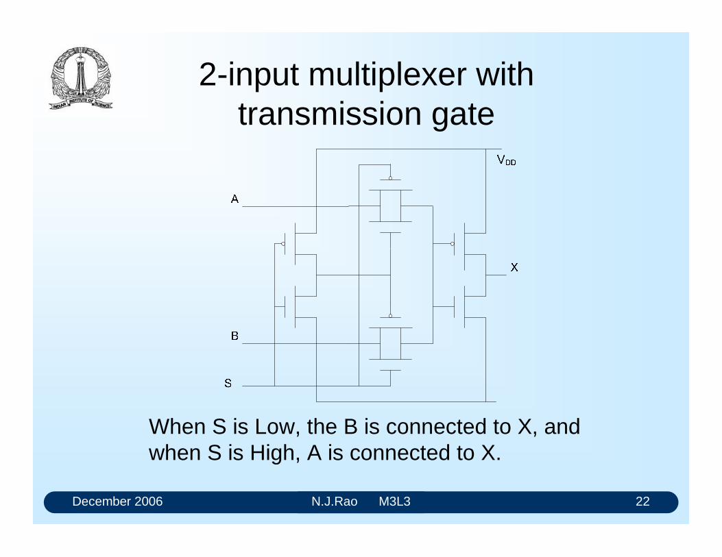
December 2006 N.J.Rao M3L3 22
2-input multiplexer with transmission gate
When S is Low, the B is connected to X, and when S is High, A is connected to X.
December 2006 N.J.Rao M3L3 23
CMOS Input and Output Structures
CMOS family offers a Hex inverter with Schmitt inputs (74HC14).
It offers a hysterisis of 1.5 V when operated at 5 V.
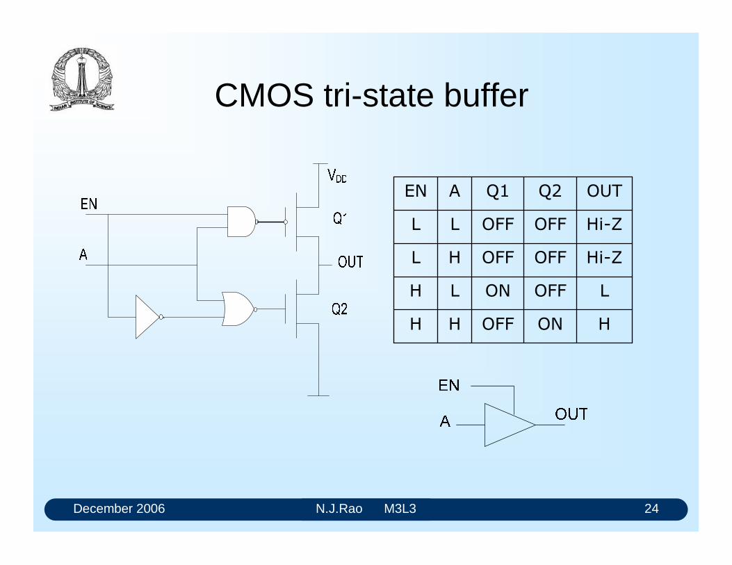
December 2006 N.J.Rao M3L3 24
CMOS tri-state buffer
HONOFFHH
LOFFONLH
Hi-ZOFFOFFHL
Hi-ZOFFOFFLL
OUTQ2Q1AEN
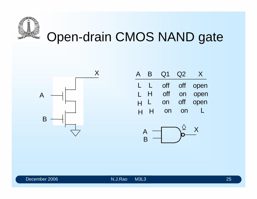
December 2006 N.J.Rao M3L3 25
Open-drain CMOS NAND gate
A
B
X A B Q1 Q2 X
L L L H H
H L on off open
H
off off open off on open
on on L
A B
X
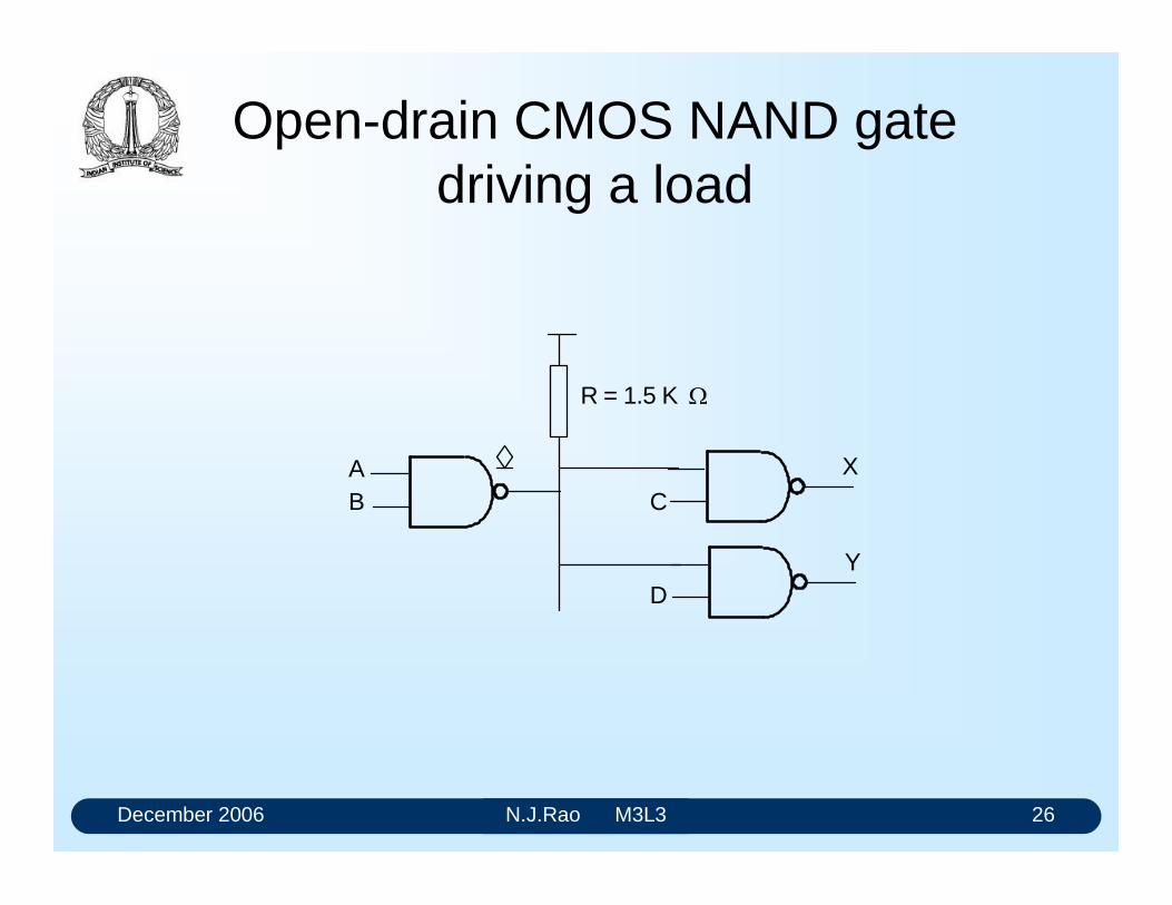
December 2006 N.J.Rao M3L3 26
Open-drain CMOS NAND gate driving a load
AB C
D
X
Y
R = 1.5 K
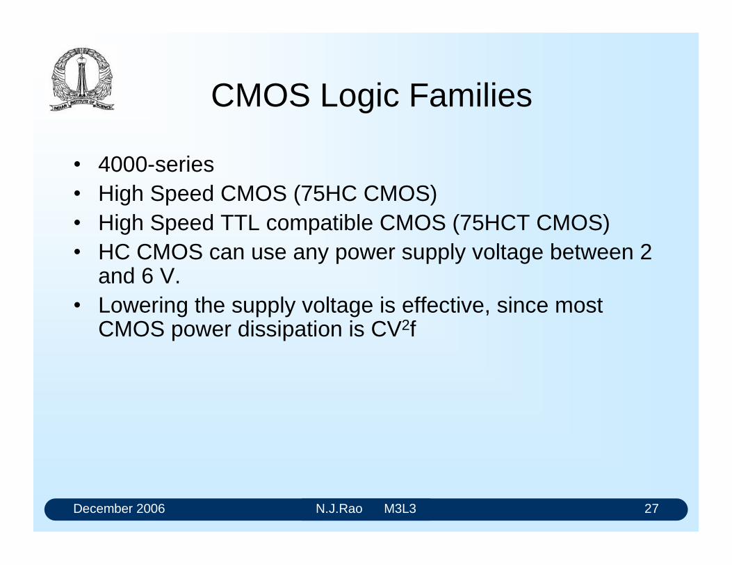
December 2006 N.J.Rao M3L3 27
CMOS Logic Families
4000-series High Speed CMOS (75HC CMOS) High Speed TTL compatible CMOS (75HCT CMOS) HC CMOS can use any power supply voltage between 2
and 6 V. Lowering the supply voltage is effective, since most
CMOS power dissipation is CV2f
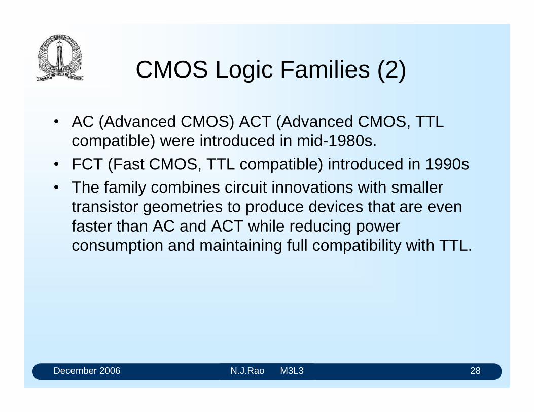
December 2006 N.J.Rao M3L3 28
CMOS Logic Families (2)
AC (Advanced CMOS) ACT (Advanced CMOS, TTL compatible) were introduced in mid-1980s.
FCT (Fast CMOS, TTL compatible) introduced in 1990s The family combines circuit innovations with smaller
transistor geometries to produce devices that are even faster than AC and ACT while reducing power consumption and maintaining full compatibility with TTL.

December 2006 N.J.Rao M3L3 29
Subfamilies of FCT CMOS
FCT-T and FCT2-T These families represent a technology crossover point
that occurred when the performance achieved using CMOS technology matched that of bipolar technology, and typically one third the power.
Both the logic families are TTL compatible
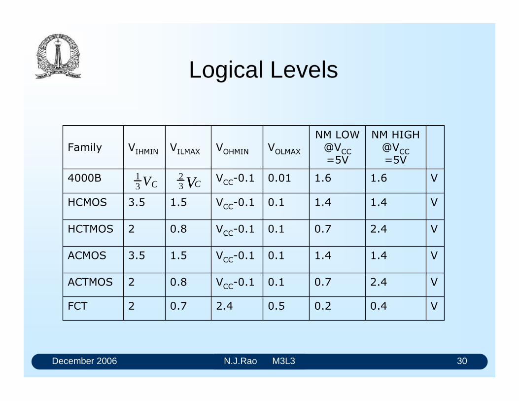
December 2006 N.J.Rao M3L3 30
Logical Levels
2 3 V C13 VC
V0.40.20.52.40.72FCT
V2.40.70.1VCC
-0.10.82ACTMOS
V1.41.40.1VCC
-0.11.53.5ACMOS
V2.40.70.1VCC
-0.10.82HCTMOS
V1.41.40.1VCC
-0.11.53.5HCMOS
V1.61.60.01VCC
-0.14000B
NM HIGH
@VCC
=5V
NM LOW
@VCC
=5V
VOLMAX
VOHMIN
VILMAX
VIHMIN
Family
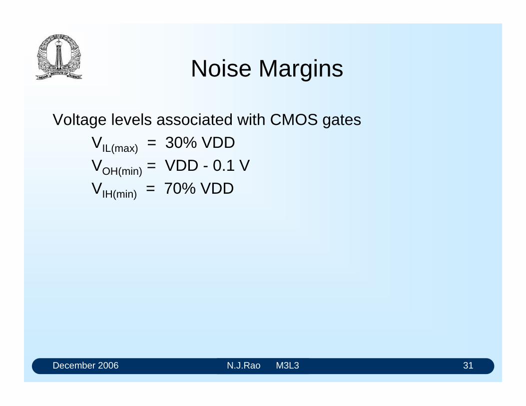
December 2006 N.J.Rao M3L3 31
Noise Margins
Voltage levels associated with CMOS gates VIL(max) = 30% VDDVOH(min) = VDD - 0.1 VVIH(min) = 70% VDD
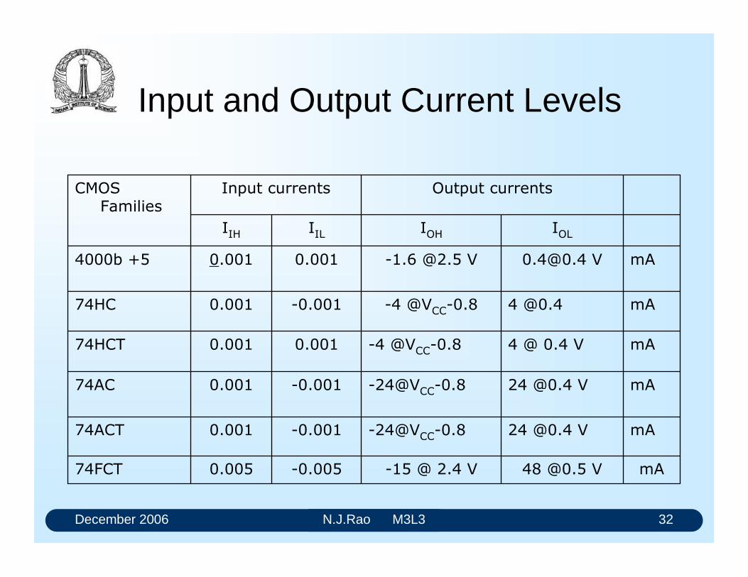
December 2006 N.J.Rao M3L3 32
Input and Output Current Levels
mA48 @0.5 V-15 @ 2.4 V-0.0050.00574FCT
mA24 @0.4 V-24@VCC
-0.8-0.0010.00174ACT
mA24 @0.4 V-24@VCC
-0.8-0.0010.00174AC
mA4 @ 0.4 V-4 @VCC
-0.80.0010.00174HCT
mA4 @0.4-4 @VCC
-0.8-0.0010.00174HC
[email protected] V-1.6 @2.5 V0.0010.0014000b +5
IOL
IOH
IIL
IIH
Output currentsInput currentsCMOS
Families
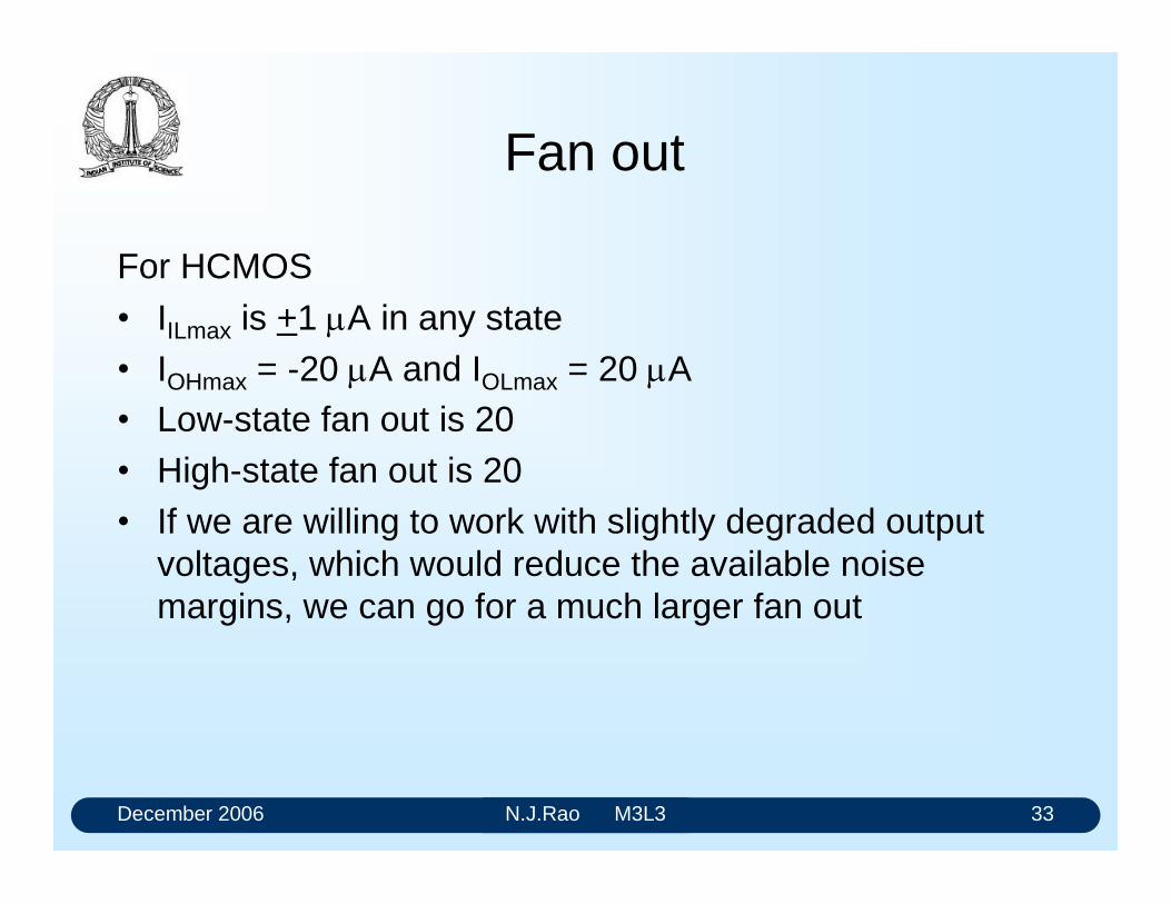
December 2006 N.J.Rao M3L3 33
Fan out
For HCMOS
IILmax is +1 A in any state IOHmax = -20 A and IOLmax = 20 A Low-state fan out is 20 High-state fan out is 20 If we are willing to work with slightly degraded output
voltages, which would reduce the available noise margins, we can go for a much larger fan out
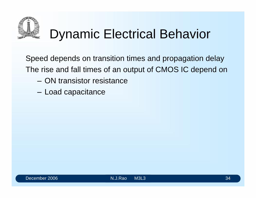
December 2006 N.J.Rao M3L3 34
Dynamic Electrical Behavior
Speed depends on transition times and propagation delayThe rise and fall times of an output of CMOS IC depend on ON transistor resistance Load capacitance
December 2006 N.J.Rao M3L3 35
Dynamic Electrical Behavior (2)
Load capacitance comes from Output circuits including a gates output transistors Internal wiring and packaging, have capacitances
associated with them (of the order of 2-10 pF) Wiring that connects an output to other inputs (about 1pF
per inch or more depending on the wiring technology) Input circuits including transistors, internal wiring and
packaging (2-15 pF per input).
December 2006 N.J.Rao M3L3 36
Dynamic Electrical Behavior (3)
OFF transistor resistance would be about 1 M, ON resistance of p-channel transistor would be of the
order of 200 ON resistance of n-channel resistance would be about
100 We can compute the rise and fall times from the
equivalent circuits.
December 2006 N.J.Rao M3L3 37
Propagation Delay
In a CMOS device, the rate at which transistors change state is influenced by
Physics of the device Circuit environment including input-signal transition rate,
input capacitance, and output loading
December 2006 N.J.Rao M3L3 38
Speed Characteristics
605.8 (138)FCTMOS
458ACTMOS
458.5ACMOS
2524HCTMOS
2522HCMOS
51604000B
Flip-Flop frequency
(MHz)
Prop. Delay
(ns)
Family
Device outputs in AC and ACT families have very fast rise and fall times. Input signals should have rise and fall times of 3.0 ns (400 ns for HC and HCT devices) and signal swing of 0V to 3.0V for ACT devices or 0V to VDD for AC devices.
December 2006 N.J.Rao M3L3 39
Power Consumption
A CMOS circuit consumes significant power only during transition
Sources of dynamic power dissipation Partial short-circuiting of the CMOS output structure Capacitive load (CL) on the output
December 2006 N.J.Rao M3L3 40
Partial short-circuiting
The amount of power consumed during transition depends on the value of VDD
the frequency of output transitions Equivalent dissipation capacitance CPD as given by the
manufacturerPT = CPD . V2
DD. f
CPD for a gate of HCMOS is about 24 pF
December 2006 N.J.Rao M3L3 41
Dissipation due to capacitive loading
During Low-to-High transition, current passes through the p-channel transistor to charge the load capacitance.
During High-to-Low transition, current flows through the n-channel transistor to discharge the load capacitor.
During the transitions the voltage across the capacitor changes by VDD.
For each pulse there would be two transitions.
December 2006 N.J.Rao M3L3 42
Dissipation due to capacitive loading (2)
As the currents are passing through the transistors, and capacitor itself would not be dissipating any power, the power dissipated due to the capacitive load is
2L L DDP = C .V .f
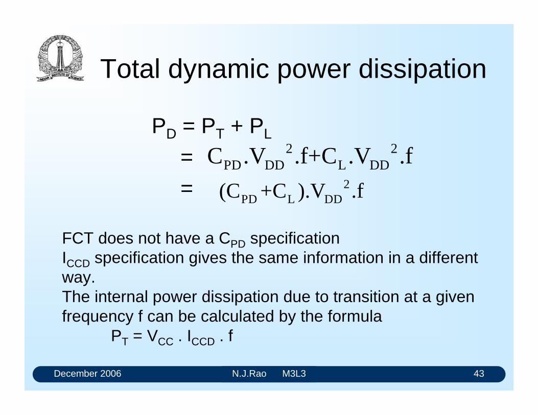
December 2006 N.J.Rao M3L3 43
Total dynamic power dissipation
PD = PT + PL
==
2 2PD DD L DDC .V .f+C .V .f
2PD L DD(C +C ).V .f
FCT does not have a CPD specificationICCD specification gives the same information in a different way. The internal power dissipation due to transition at a given frequency f can be calculated by the formula
PT = VCC . ICCD . f
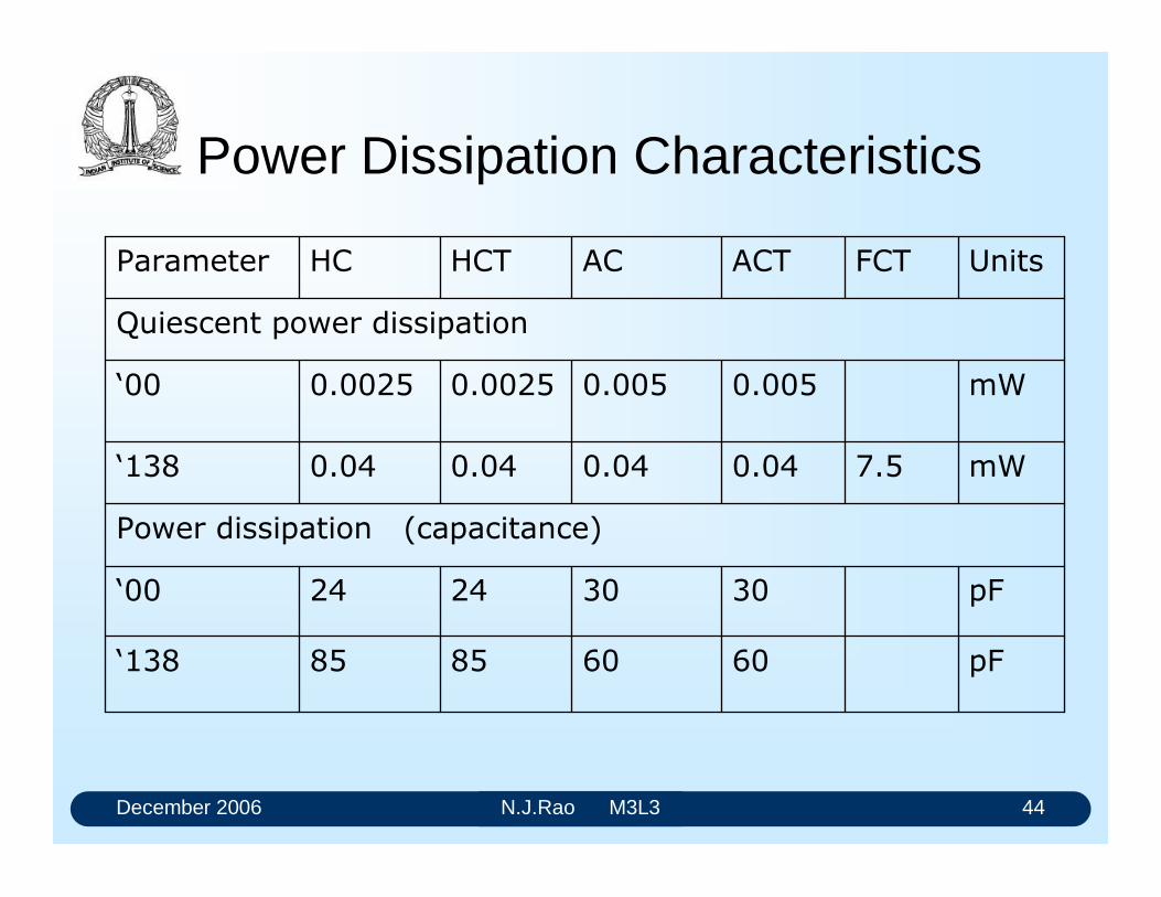
December 2006 N.J.Rao M3L3 44
Power Dissipation Characteristics
pF60608585138
pF3030242400
Power dissipation (capacitance)
mW7.50.040.040.040.04138
mW0.0050.0050.00250.002500
Quiescent power dissipation
UnitsFCTACTACHCTHCParameter
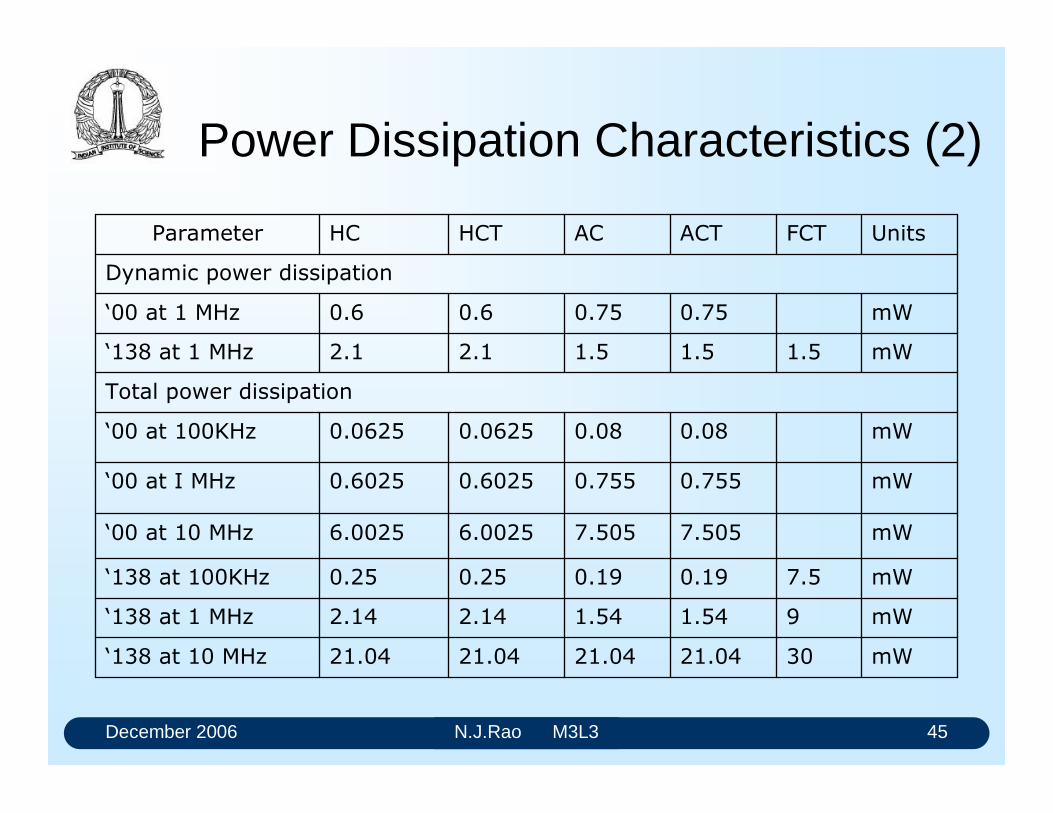
December 2006 N.J.Rao M3L3 45
Power Dissipation Characteristics (2)
mW3021.0421.0421.0421.04138 at 10 MHz
mW91.541.542.142.14138 at 1 MHz
mW7.50.190.190.250.25138 at 100KHz
mW7.5057.5056.00256.002500 at 10 MHz
mW0.7550.7550.60250.602500 at I MHz
mW0.080.080.06250.062500 at 100KHz
Total power dissipation
mW1.51.51.52.12.1138 at 1 MHz
mW0.750.750.60.600 at 1 MHz
Dynamic power dissipation
UnitsFCTACTACHCTHCParameter
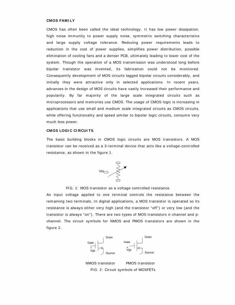
CMOS FAMILY
CMOS has often been called the ideal technology. It has low power dissipation,
high noise immunity to power supply noise, symmetric switching characteristics
and large supply voltage tolerance. Reducing power requirements leads to
reduction in the cost of power supplies, simplifies power distribution, possible
elimination of cooling fans and a denser PCB, ultimately leading to lower cost of the
system. Though the operation of a MOS transmission was understood long before
bipolar transistor was invented, its fabrication could not be monitored.
Consequently development of MOS circuits lagged bipolar circuits considerably, and
initially they were attractive only in selected applications. In recent years,
advances in the design of MOS circuits have vastly increased their performance and
popularity. By far majority of the large scale integrated circuits such as
microprocessors and memories use CMOS. The usage of CMOS logic is increasing in
applications that use small and medium scale integrated circuits as CMOS circuits,
while offering functionality and speed similar to bipolar logic circuits, consume very
much less power.
CMOS LOGIC CIRCUITS
The basic building blocks in CMOS logic circuits are MOS transistors. A MOS
transistor can be received as a 3-terminal device that acts like a voltage-controlled
resistance, as shown in the figure 1.
Vin
FIG. 1: MOS transistor as a voltage controlled resistance
An input voltage applied to one terminal controls the resistance between the
remaining two terminals. In digital applications, a MOS transistor is operated so its
resistance is always either very high (and the transistor “off”) or very low (and the
transistor is always “on”). There are two types of MOS transistors n-channel and p-
channel. The circuit symbols for NMOS and PMOS transistors are shown in the
figure 2.
Drain
Source
Gate Gate
+ +
_- _-Vgs Vgs
Drain
Source
NMOS transistor PMOS transistor
FIG. 2: Circuit symbols of MOSFETs
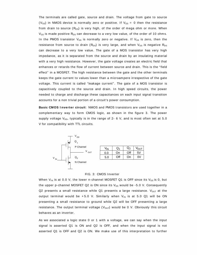
The terminals are called gate, source and drain. The voltage from gate to source
(VGS) in NMOS device is normally zero or positive. If VGS = 0 then the resistance
from drain to source (RDS) is very high, of the order of mega ohm or more. When
VGS is made positive RDS can decrease to a very low value, of the order of 10 ohms.
In the PMOS transistor VGS is normally zero or negative. If VGS is zero, then the
resistance from source to drain (RDS) is very large, and when VGS is negative RDS
can decrease to a very low value. The gate of a MOS transistor has very high
impedance, as it is separated from the source and drain by an insulating material
with a very high resistance. However, the gate voltage creates an electric field that
enhances or retards the flow of current between source and drain. This is the “field
effect” in a MOSFET. The high resistance between the gate and the other terminals
keeps the gate current to values lower than a microampere irrespective of the gate
voltage. This current is called “leakage current”. The gate of a MOS transistor is
capacitively coupled to the source and drain. In high speed circuits, the power
needed to charge and discharge these capacitances on each input signal transition
accounts for a non trivial portion of a circuit’s power consumption.
Basic CMOS Inverter circuit: NMOS and PMOS transistors are used together in a
complementary way to form CMOS logic, as shown in the figure 3. The power
supply voltage VDD, typically is in the range of 2- 6 V, and is most often set at 5.0
V for compatibility with TTL circuits.
V DD
V
V
P Channel
N Channel
Q
Q
1
2IN
OUT 0.05.0
Q Q VOnOff
OffOn
5V0V
VIN 1 2 OUT
FIG. 3: CMOS Inverter
When VIN is at 0.0 V, the lower n-channel MOSFET Q1 is OFF since its VGS is 0, but
the upper p-channel MOSFET Q2 is ON since its VGS would be -5.0 V. Consequently
Q2 presents a small resistance while Q1 presents a large resistance. VOUT at the
output terminal would be +5.0 V. Similarly when VIN is at 5.0 Q1 will be ON
presenting a small resistance to ground while Q2 will be OFF presenting a large
resistance. The output terminal voltage (VOUT) would be 0 V. Obviously this circuit
behaves as an inverter.
As we associated a logic state 0 or 1 with a voltage, we can say when the input
signal is asserted Q1 is ON and Q2 is OFF, and when the input signal is not
asserted Q1 is OFF and Q2 is ON. We make use of this interpretation to further
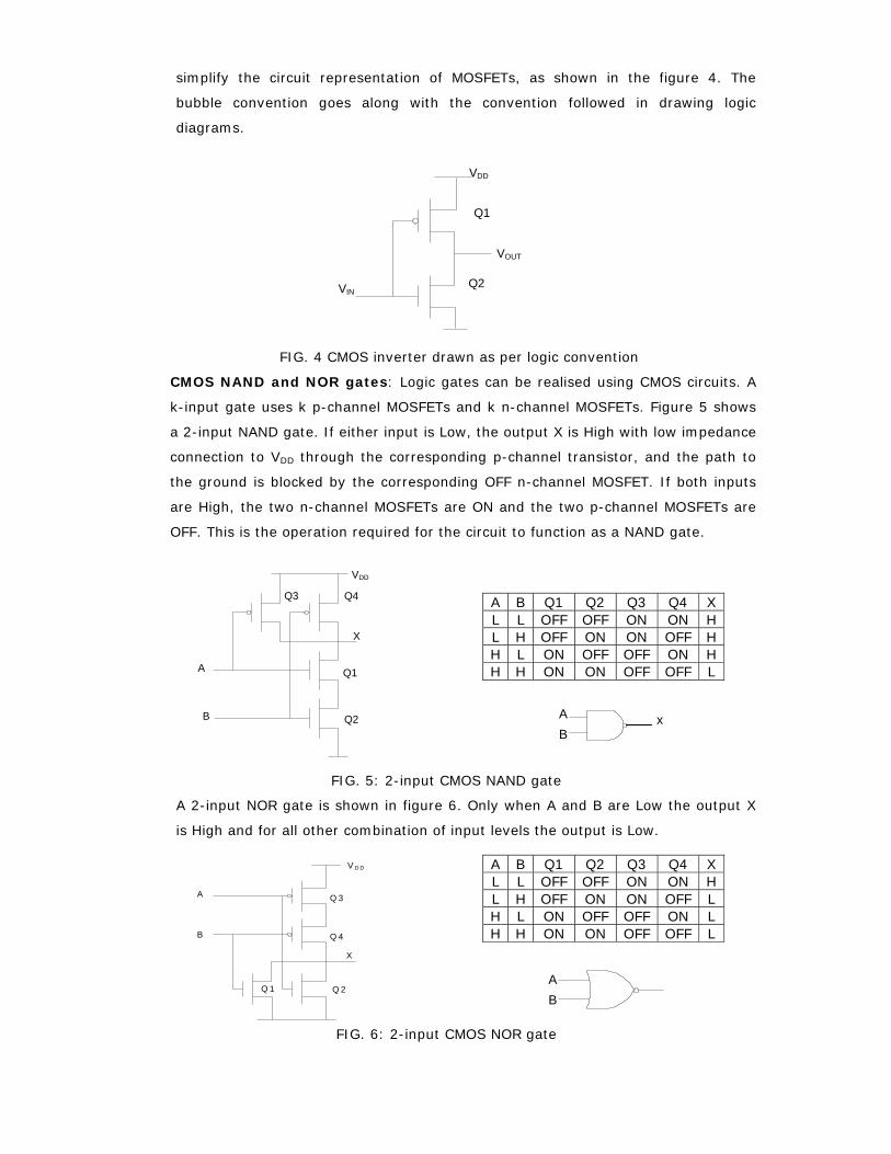
simplify the circuit representation of MOSFETs, as shown in the figure 4. The
bubble convention goes along with the convention followed in drawing logic
diagrams.
Q1
Q2
VDD
VIN
VOUT
FIG. 4 CMOS inverter drawn as per logic convention
CMOS NAND and NOR gates: Logic gates can be realised using CMOS circuits. A
k-input gate uses k p-channel MOSFETs and k n-channel MOSFETs. Figure 5 shows
a 2-input NAND gate. If either input is Low, the output X is High with low impedance
connection to VDD through the corresponding p-channel transistor, and the path to
the ground is blocked by the corresponding OFF n-channel MOSFET. If both inputs
are High, the two n-channel MOSFETs are ON and the two p-channel MOSFETs are
OFF. This is the operation required for the circuit to function as a NAND gate.
A B Q1 Q2 Q3 Q4 X L L OFF OFF ON ON H L H OFF ON ON OFF H H L ON OFF OFF ON H H H ON ON OFF OFF L
FIG. 5: 2-input CMOS NAND gate
A 2-input NOR gate is shown in figure 6. Only when A and B are Low the output X
is High and for all other combination of input levels the output is Low.
A B Q1 Q2 Q3 Q4 X L L OFF OFF ON ON H L H OFF ON ON OFF L H L ON OFF OFF ON L H H ON ON OFF OFF L
FIG. 6: 2-input CMOS NOR gate
X
VDD
Q2
Q1
Q4Q3
A
B AB
x
A
B
X
V D D
Q 2Q 1
Q 3
Q 4
BA
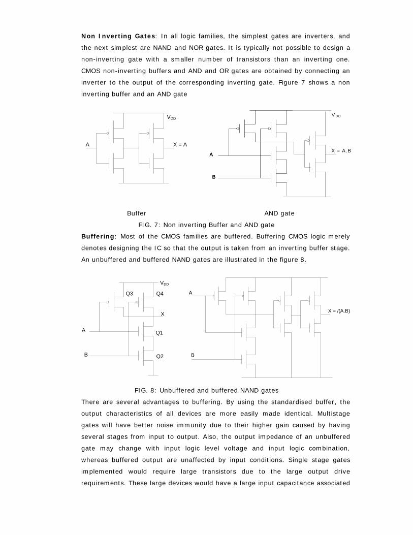
Non Inverting Gates: In all logic families, the simplest gates are inverters, and
the next simplest are NAND and NOR gates. It is typically not possible to design a
non-inverting gate with a smaller number of transistors than an inverting one.
CMOS non-inverting buffers and AND and OR gates are obtained by connecting an
inverter to the output of the corresponding inverting gate. Figure 7 shows a non
inverting buffer and an AND gate
Buffer AND gate
FIG. 7: Non inverting Buffer and AND gate
Buffering: Most of the CMOS families are buffered. Buffering CMOS logic merely
denotes designing the IC so that the output is taken from an inverting buffer stage.
An unbuffered and buffered NAND gates are illustrated in the figure 8.
FIG. 8: Unbuffered and buffered NAND gates
There are several advantages to buffering. By using the standardised buffer, the
output characteristics of all devices are more easily made identical. Multistage
gates will have better noise immunity due to their higher gain caused by having
several stages from input to output. Also, the output impedance of an unbuffered
gate may change with input logic level voltage and input logic combination,
whereas buffered output are unaffected by input conditions. Single stage gates
implemented would require large transistors due to the large output drive
requirements. These large devices would have a large input capacitance associated
A X = A
VDD
A
B
V DD
A
B
X = A.B
X
VDD
Q2
Q1
Q4Q3
A
B
A
B
X = /(A.B)
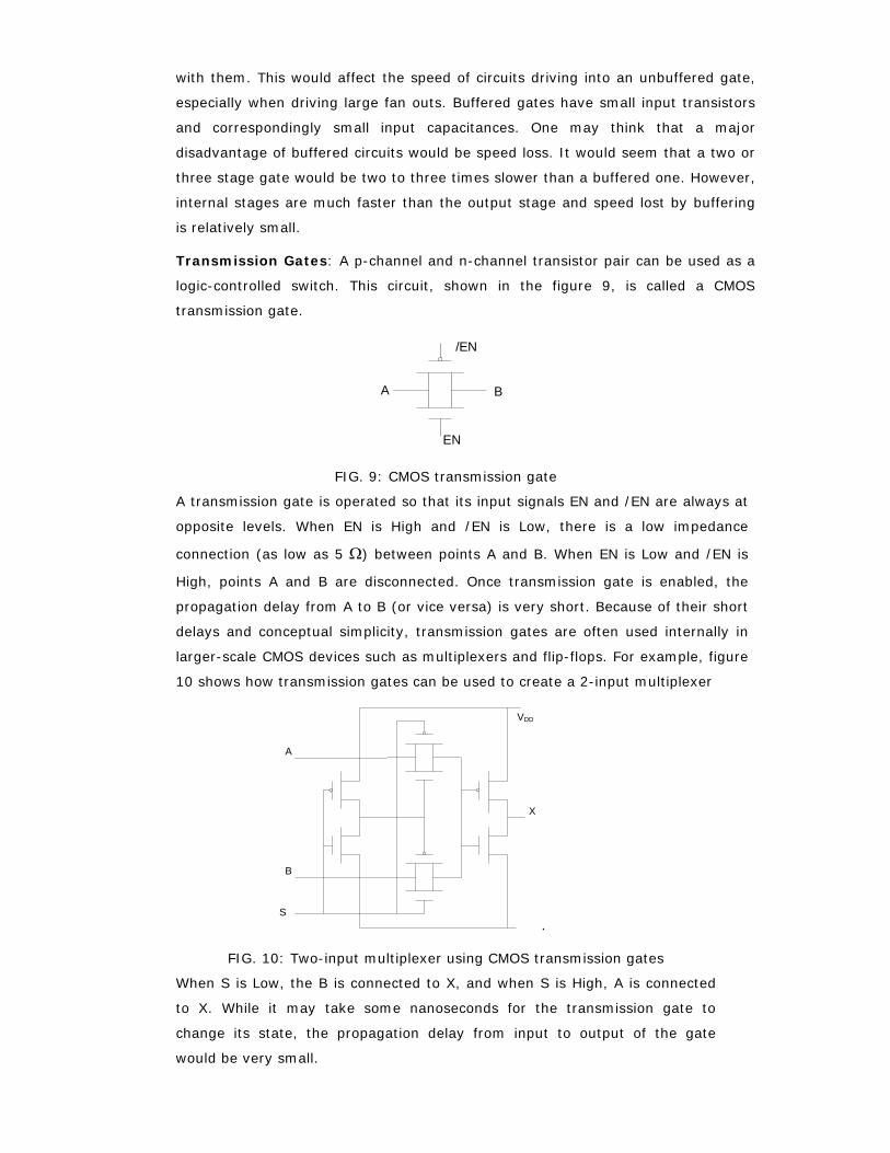
with them. This would affect the speed of circuits driving into an unbuffered gate,
especially when driving large fan outs. Buffered gates have small input transistors
and correspondingly small input capacitances. One may think that a major
disadvantage of buffered circuits would be speed loss. It would seem that a two or
three stage gate would be two to three times slower than a buffered one. However,
internal stages are much faster than the output stage and speed lost by buffering
is relatively small.
Transmission Gates: A p-channel and n-channel transistor pair can be used as a
logic-controlled switch. This circuit, shown in the figure 9, is called a CMOS
transmission gate.
/EN
EN
A B
FIG. 9: CMOS transmission gate
A transmission gate is operated so that its input signals EN and /EN are always at
opposite levels. When EN is High and /EN is Low, there is a low impedance
connection (as low as 5 Ω) between points A and B. When EN is Low and /EN is
High, points A and B are disconnected. Once transmission gate is enabled, the
propagation delay from A to B (or vice versa) is very short. Because of their short
delays and conceptual simplicity, transmission gates are often used internally in
larger-scale CMOS devices such as multiplexers and flip-flops. For example, figure
10 shows how transmission gates can be used to create a 2-input multiplexer
A
B
S
X
VDD
.
FIG. 10: Two-input multiplexer using CMOS transmission gates
When S is Low, the B is connected to X, and when S is High, A is connected
to X. While it may take some nanoseconds for the transmission gate to
change its state, the propagation delay from input to output of the gate
would be very small.
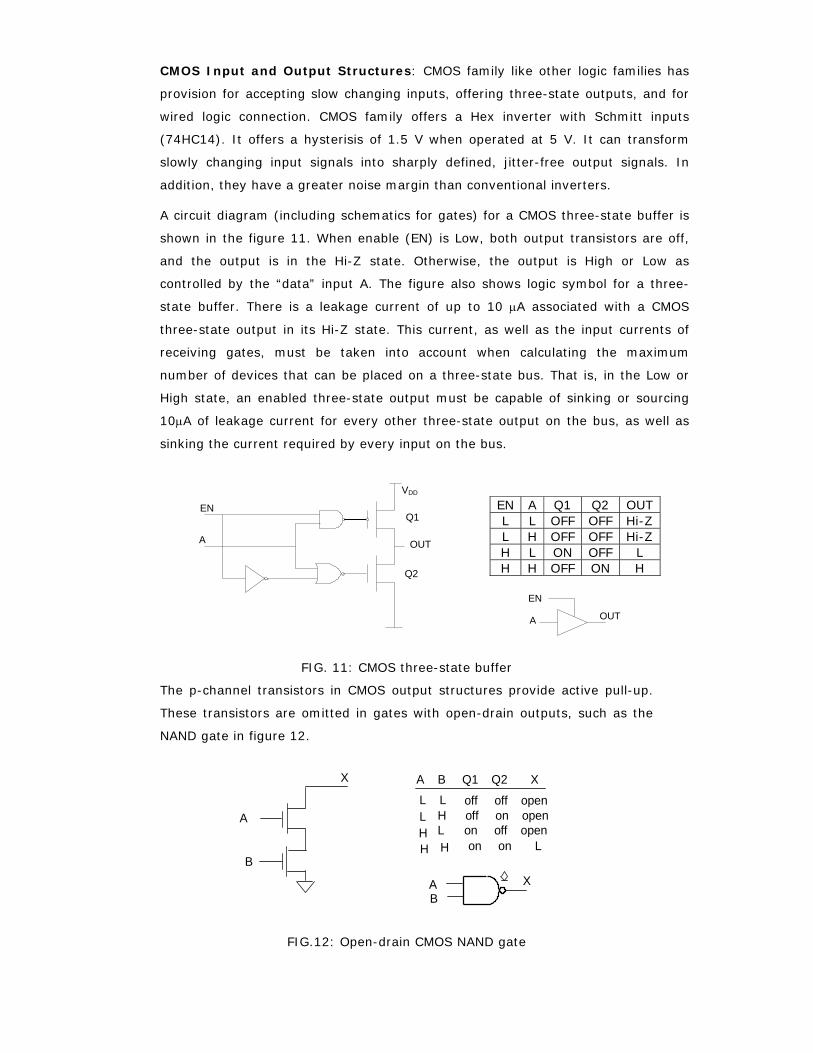
CMOS Input and Output Structures: CMOS family like other logic families has
provision for accepting slow changing inputs, offering three-state outputs, and for
wired logic connection. CMOS family offers a Hex inverter with Schmitt inputs
(74HC14). It offers a hysterisis of 1.5 V when operated at 5 V. It can transform
slowly changing input signals into sharply defined, jitter-free output signals. In
addition, they have a greater noise margin than conventional inverters.
A circuit diagram (including schematics for gates) for a CMOS three-state buffer is
shown in the figure 11. When enable (EN) is Low, both output transistors are off,
and the output is in the Hi-Z state. Otherwise, the output is High or Low as
controlled by the “data” input A. The figure also shows logic symbol for a three-
state buffer. There is a leakage current of up to 10 µA associated with a CMOS
three-state output in its Hi-Z state. This current, as well as the input currents of
receiving gates, must be taken into account when calculating the maximum
number of devices that can be placed on a three-state bus. That is, in the Low or
High state, an enabled three-state output must be capable of sinking or sourcing
10µA of leakage current for every other three-state output on the bus, as well as
sinking the current required by every input on the bus.
EN A Q1 Q2 OUT L L OFF OFF Hi-Z L H OFF OFF Hi-Z H L ON OFF L H H OFF ON H
FIG. 11: CMOS three-state buffer
The p-channel transistors in CMOS output structures provide active pull-up.
These transistors are omitted in gates with open-drain outputs, such as the
NAND gate in figure 12.
A
B
X A B Q1 Q2 XL LLHH
H L on off open
H
off off open off on open
on on L
AB
X
FIG.12: Open-drain CMOS NAND gate
VDD
OUT
EN
A
Q1
Q2
EN
A OUT
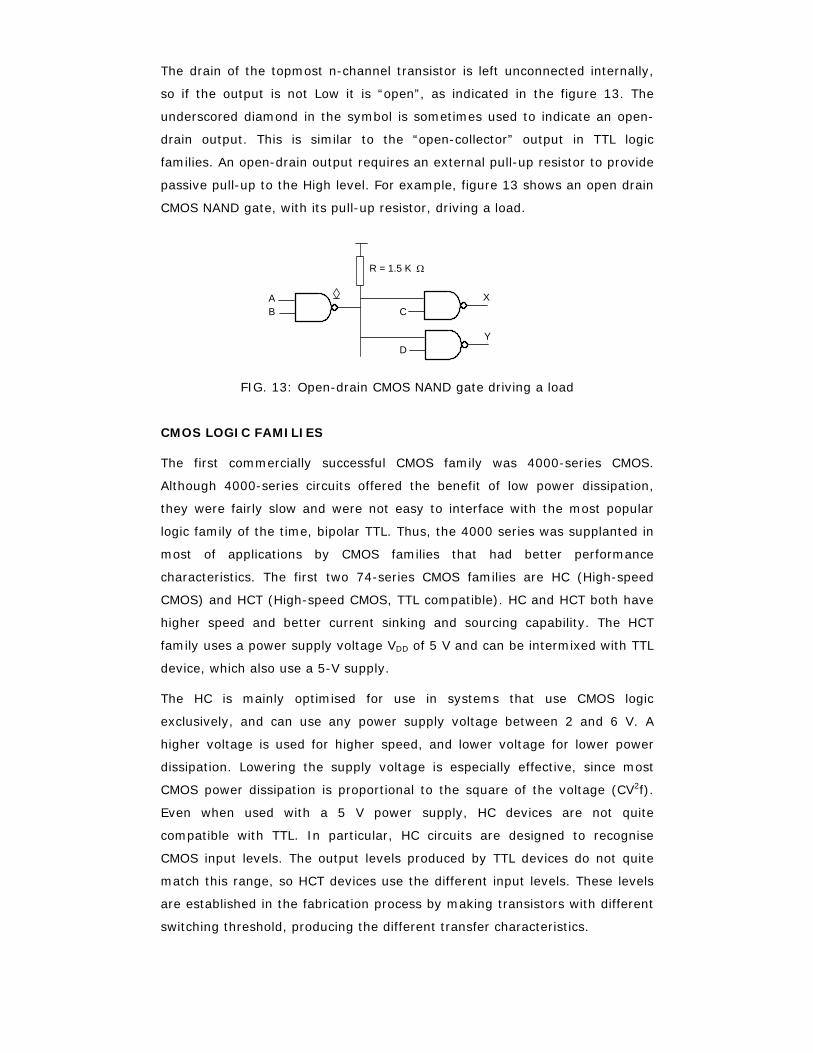
The drain of the topmost n-channel transistor is left unconnected internally,
so if the output is not Low it is “open”, as indicated in the figure 13. The
underscored diamond in the symbol is sometimes used to indicate an open-
drain output. This is similar to the “open-collector” output in TTL logic
families. An open-drain output requires an external pull-up resistor to provide
passive pull-up to the High level. For example, figure 13 shows an open drain
CMOS NAND gate, with its pull-up resistor, driving a load.
AB C
D
X
Y
R = 1.5 K Ω
FIG. 13: Open-drain CMOS NAND gate driving a load
CMOS LOGIC FAMILIES
The first commercially successful CMOS family was 4000-series CMOS.
Although 4000-series circuits offered the benefit of low power dissipation,
they were fairly slow and were not easy to interface with the most popular
logic family of the time, bipolar TTL. Thus, the 4000 series was supplanted in
most of applications by CMOS families that had better performance
characteristics. The first two 74-series CMOS families are HC (High-speed
CMOS) and HCT (High-speed CMOS, TTL compatible). HC and HCT both have
higher speed and better current sinking and sourcing capability. The HCT
family uses a power supply voltage VDD of 5 V and can be intermixed with TTL
device, which also use a 5-V supply.
The HC is mainly optimised for use in systems that use CMOS logic
exclusively, and can use any power supply voltage between 2 and 6 V. A
higher voltage is used for higher speed, and lower voltage for lower power
dissipation. Lowering the supply voltage is especially effective, since most
CMOS power dissipation is proportional to the square of the voltage (CV2f).
Even when used with a 5 V power supply, HC devices are not quite
compatible with TTL. In particular, HC circuits are designed to recognise
CMOS input levels. The output levels produced by TTL devices do not quite
match this range, so HCT devices use the different input levels. These levels
are established in the fabrication process by making transistors with different
switching threshold, producing the different transfer characteristics.
Two more CMOS families, known as AC (Advanced CMOS) and ACT
(Advanced CMOS, TTL compatible) were introduced in mid-1980s. These
families are fast, comparable to ALSTTL, and they can source or sink more
current than most of the TTL circuits can. Like HC and HCT, the AC and ACT
families differ only in the input levels that they recognise; their output
characteristics are the same. Also like HC/HCT, AC/ACT outputs have
symmetric output drive.
In the early 1990s, yet another CMOS family was launched. The FCT (Fast
CMOS, TTL compatible) family combines circuit innovations with smaller
transistor geometries to produce devices that are even faster than AC and
ACT while reducing power consumption and maintaining full compatibility
with TTL. There are two subfamilies, FCT-T and FCT2-T. These families
represent a “technology crossover point” that occurred when the performance
achieved using CMOS technology matched that of bipolar technology, and
typically one third the power. Both the logic families are TTL compatible,
which means that they conform to the industry-standard TTL voltage levels
and threshold point (1.5 V), and operate from a 5 Volt VCC power source. All
inputs are designed to have a hysterisis of 200 mV (low-to-high threshold of
1.6 V and high-to-low threshold of 1.4V). This hysteresis increases both the
static and dynamic noise immunity, as well as reducing the sensitivity to
noise superimposed on slowly rising or falling inputs. Individual logic gates
are not manufactured in the FCT families. Just about the simplest FCT logic
element is a 74FCT138/74FCT138T decoder, which has six inputs, eight
outputs and contains the equivalent of about twelve 4-input gates internally
ELECTRICAL BEHAVIOUR OF CMOS CIRCUITS
This section presents the electrical characteristics of CMOS families. The
electrical characteristics refer to DC noise margins, fan out, speed, power
consumption, noise, electrical discharge, open drain outputs and three state
outputs.
Logical Levels and Noise Margins: The generated voltage levels given by
the manufacturing data sheet for HCMOS circuits operating at VDD = 5 V, are
given in the Table 1. The input parameters are mainly determined by the
switching threshold of the two transistors, while the output parameters are
determined by the ON resistance of the transistors. These parameters apply
when the device inputs and outputs are connected only to other CMOS
devices. The dc voltage levels and noise margins of CMOS families are given
in the Table 1.
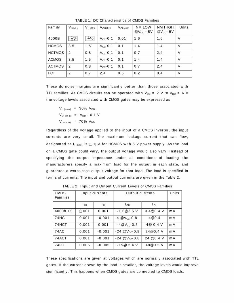
TABLE 1: DC Characteristics of CMOS Families
Family VIHMIN VILMAX VOHMIN VOLMAX NM LOW @VCC =5V
NM HIGH @VCC=5V
Units
4000B 2 3 V C 13 VC VCC-0.1 0.01 1.6 1.6 V
HCMOS 3.5 1.5 VCC-0.1 0.1 1.4 1.4 V
HCTMOS 2 0.8 VCC-0.1 0.1 0.7 2.4 V
ACMOS 3.5 1.5 VCC-0.1 0.1 1.4 1.4 V
ACTMOS 2 0.8 VCC-0.1 0.1 0.7 2.4 V
FCT 2 0.7 2.4 0.5 0.2 0.4 V
These dc noise margins are significantly better than those associated with
TTL families. As CMOS circuits can be operated with VDD = 2 V to VDD = 6 V
the voltage levels associated with CMOS gates may be expressed as
VIL(max) = 30% VDD
VOH(min) = VDD - 0.1 V
VIH(min) = 70% VDD
Regardless of the voltage applied to the input of a CMOS inverter, the input
currents are very small. The maximum leakage current that can flow,
designated as II max, is + 1µA for HCMOS with 5 V power supply. As the load
on a CMOS gate could vary, the output voltage would also vary. Instead of
specifying the output impedance under all conditions of loading the
manufacturers specify a maximum load for the output in each state, and
guarantee a worst-case output voltage for that load. The load is specified in
terms of currents. The input and output currents are given in the Table 2.
TABLE 2: Input and Output Current Levels of CMOS Families
CMOS Families
Input currents Output currents Units
IIH IIL IOH IOL
4000b +5 0.001 0.001 [email protected] V [email protected] V mA
74HC 0.001 -0.001 -4 @VCC-0.8 [email protected] mA
74HCT 0.001 0.001 [email protected] 4@ 0.4 V mA
74AC 0.001 -0.001 -24 @VCC-0.8 [email protected] V mA
74ACT 0.001 -0.001 -24 @VCC-0.8 24 @0.4 V mA
74FCT 0.005 -0.005 -15@ 2.4 V [email protected] V mA
These specifications are given at voltages which are normally associated with TTL
gates. If the current drawn by the load is smaller, the voltage levels would improve
significantly. This happens when CMOS gates are connected to CMOS loads.
It is important to note that in a CMOS circuit the output structure by itself
consumes very little current in either state, High or Low. In either state, one of the
transistors is in the high impedance OFF state. When no load is connected the only
current that flows through the transistors is their leakage current. With a load,
however, current flows through both the load and the ON transistor, and power is
consumed in both.
Fan out: The fan out of a logic gate is the number of inputs that the gate can drive
without exceeding its worst-case loading specifications. The fan out depends not
only on the characteristics of the output, but also on the inputs that it is driving.
When a HCMOS gate is driving HCMOS gates, we note that IILmax is +1 µA in any
state, and IOHmax = -20 µA and IOLmax = 20 µA. Therefore, the Low-state fan out is
20 and High-state fan out is 20 for HCMOS gates. However, if we are willing to
work with slightly degraded output voltages, which would reduce the available
noise margins, we can go for IOHmax and IOLmax of 4.0 mA. This would mean that an
HCMOS gate can drive as many as 4000 HCMOS gates. But in actuality this would
not be true, as the currents we are considering are only the steady state currents
and not the transition currents. The actual fan out under degraded load conditions
would be far less than 4000. During the transitions, the CMOS output must charge
or discharge the capacitance associated with the inputs that it derives. If this
capacitance is too large, the transition from Low to High (or vice versa) may be too
slow causing improper system operation.
CMOS DYNAMIC ELECTRICAL BEHAVIOUR
Both the speed and the power consumption of CMOS devices depend on to a large
extent on AC or dynamic characteristics of the device and its load, that is, what
happens when the output changes between states. The speed depends on two
factors, transition times and propagation delay.
The rise and fall times of an output of CMOS IC depend mainly on two factors, the
ON transistor resistance and the load capacitance. The load capacitance comes
from three different sources: output circuits including a gate’s output transistors,
internal wiring and packaging, have capacitances associated with them (of the
order of 2-10 pF); wiring that connects an output to other inputs (about 1pF per
inch or more depending on the wiring technology); and input circuits including
transistors, internal wiring and packaging (2-15 pF per input). The OFF transistor
resistance would be about 1 MΩ, the ON resistance of p-channel transistor would
be of the order of 200 Ω, and the ON resistance of n-channel resistance would be
about 100 Ω. We can compute the rise and fall times from the equivalent circuits.
Several factors lead to nonzero propagation delays. In a CMOS device, the rate at
which transistors change state is influenced both by the semiconductor physics of
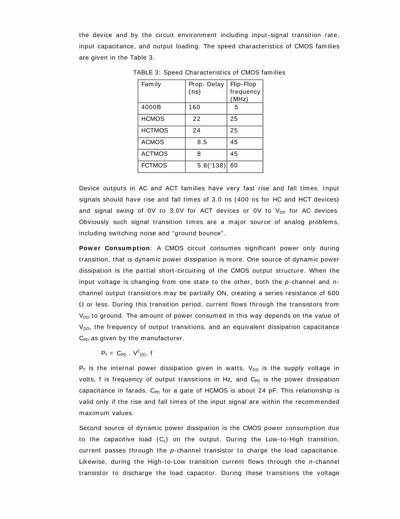
the device and by the circuit environment including input-signal transition rate,
input capacitance, and output loading. The speed characteristics of CMOS families
are given in the Table 3.
TABLE 3: Speed Characteristics of CMOS families
Family Prop. Delay (ns)
Flip-Flop frequency (MHz)
4000B 160 5
HCMOS 22 25
HCTMOS 24 25
ACMOS 8.5 45
ACTMOS 8 45
FCTMOS 5.8(‘138) 60
Device outputs in AC and ACT families have very fast rise and fall times. Input
signals should have rise and fall times of 3.0 ns (400 ns for HC and HCT devices)
and signal swing of 0V to 3.0V for ACT devices or 0V to VDD for AC devices.
Obviously such signal transition times are a major source of analog problems,
including switching noise and “ground bounce”.
Power Consumption: A CMOS circuit consumes significant power only during
transition, that is dynamic power dissipation is more. One source of dynamic power
dissipation is the partial short-circuiting of the CMOS output structure. When the
input voltage is changing from one state to the other, both the p-channel and n-
channel output transistors may be partially ON, creating a series resistance of 600
Ω or less. During this transition period, current flows through the transistors from
VDD to ground. The amount of power consumed in this way depends on the value of
VDD, the frequency of output transitions, and an equivalent dissipation capacitance
CPD as given by the manufacturer.
PT = CPD . V2DD. f
PT is the internal power dissipation given in watts, VDD is the supply voltage in
volts, f is frequency of output transitions in Hz, and CPD is the power dissipation
capacitance in farads. CPD for a gate of HCMOS is about 24 pF. This relationship is
valid only if the rise and fall times of the input signal are within the recommended
maximum values.
Second source of dynamic power dissipation is the CMOS power consumption due
to the capacitive load (CL) on the output. During the Low-to-High transition,
current passes through the p-channel transistor to charge the load capacitance.
Likewise, during the High-to-Low transition current flows through the n-channel
transistor to discharge the load capacitor. During these transitions the voltage
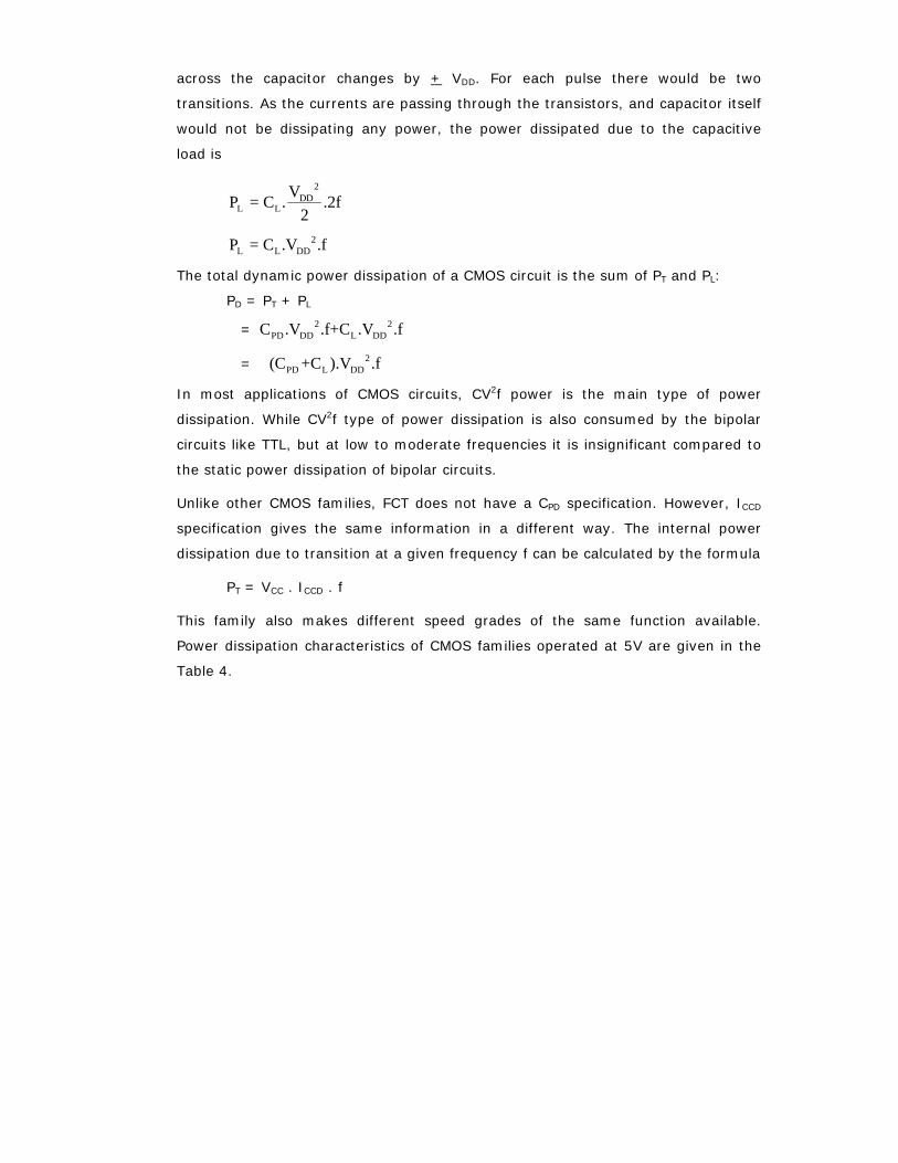
across the capacitor changes by + VDD. For each pulse there would be two
transitions. As the currents are passing through the transistors, and capacitor itself
would not be dissipating any power, the power dissipated due to the capacitive
load is
2
DDL L
VP = C . .2f2
2L L DDP = C .V .f
The total dynamic power dissipation of a CMOS circuit is the sum of PT and PL:
PD = PT + PL
= 2 2PD DD L DDC .V .f+C .V .f
= 2PD L DD(C +C ).V .f
In most applications of CMOS circuits, CV2f power is the main type of power
dissipation. While CV2f type of power dissipation is also consumed by the bipolar
circuits like TTL, but at low to moderate frequencies it is insignificant compared to
the static power dissipation of bipolar circuits.
Unlike other CMOS families, FCT does not have a CPD specification. However, ICCD
specification gives the same information in a different way. The internal power
dissipation due to transition at a given frequency f can be calculated by the formula
PT = VCC . ICCD . f
This family also makes different speed grades of the same function available.
Power dissipation characteristics of CMOS families operated at 5V are given in the
Table 4.
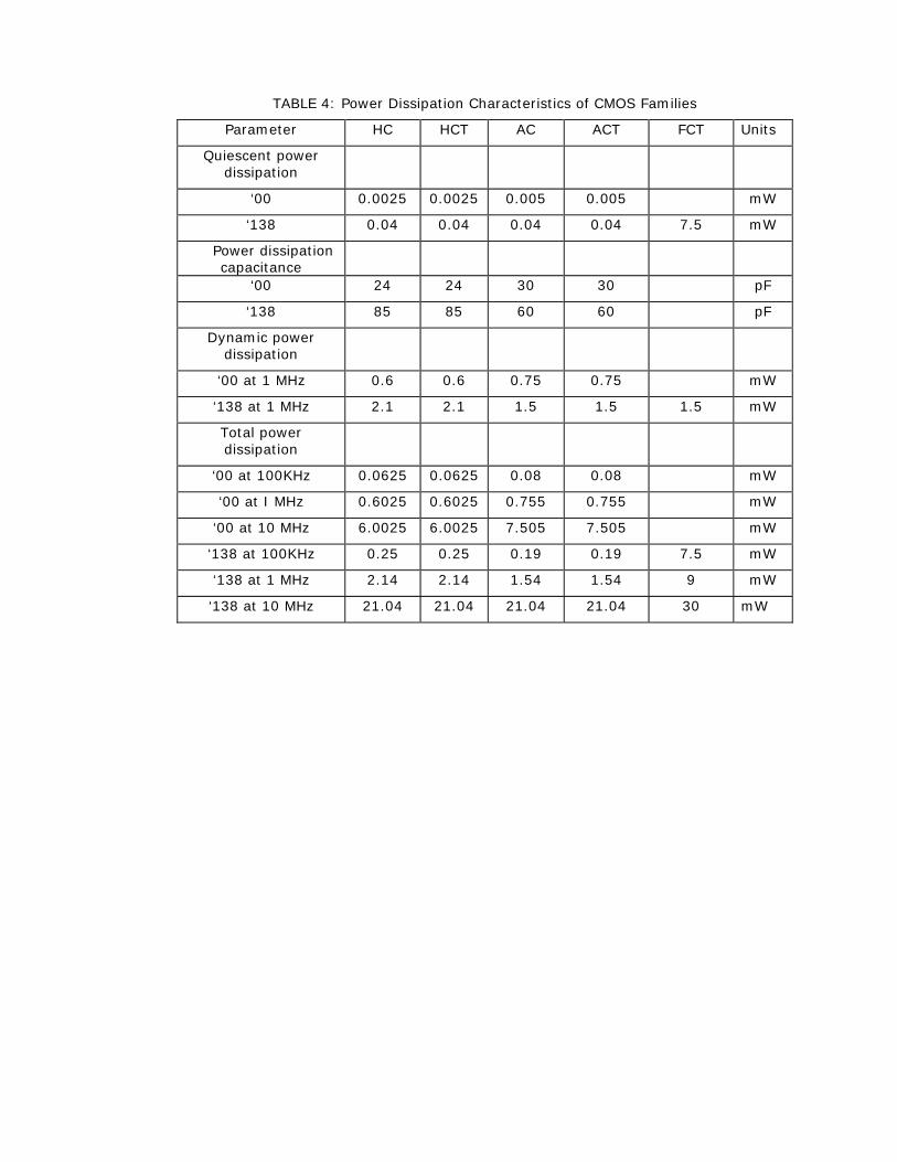
TABLE 4: Power Dissipation Characteristics of CMOS Families
Parameter HC HCT AC ACT FCT Units
Quiescent power dissipation
‘00 0.0025 0.0025 0.005 0.005 mW
‘138 0.04 0.04 0.04 0.04 7.5 mW
Power dissipation capacitance
‘00 24 24 30 30 pF
‘138 85 85 60 60 pF
Dynamic power dissipation
‘00 at 1 MHz 0.6 0.6 0.75 0.75 mW
‘138 at 1 MHz 2.1 2.1 1.5 1.5 1.5 mW
Total power dissipation
‘00 at 100KHz 0.0625 0.0625 0.08 0.08 mW
‘00 at I MHz 0.6025 0.6025 0.755 0.755 mW
‘00 at 10 MHz 6.0025 6.0025 7.505 7.505 mW
‘138 at 100KHz 0.25 0.25 0.19 0.19 7.5 mW
‘138 at 1 MHz 2.14 2.14 1.54 1.54 9 mW
‘138 at 10 MHz 21.04 21.04 21.04 21.04 30 mW

Digital Electronics Module 3: ECL Family
N.J. RaoIndian Institute of Science
id9619281 pdfMachine by Broadgun Software - a great PDF writer! - a great PDF creator! - http://www.pdfmachine.com http://www.broadgun.com
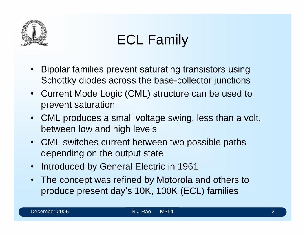
December 2006 N.J.Rao M3L4 2
ECL Family
Bipolar families prevent saturating transistors using Schottky diodes across the base-collector junctions
Current Mode Logic (CML) structure can be used to prevent saturation
CML produces a small voltage swing, less than a volt, between low and high levels
CML switches current between two possible paths depending on the output state
Introduced by General Electric in 1961 The concept was refined by Motorola and others to
produce present days 10K, 100K (ECL) families
December 2006 N.J.Rao M3L4 3
ECL Family (2)
They offer propagation delays as short as 1 ns They are not as popular as TTL and CMOS mainly
because they consume too much power High power consumption has made the design of ECL
super computers, such as CRAY as a challenge in cooling technology
ECL has poor power-speed product, does not provide a high level of integration
ECL signals have fast edge rates requiring design for special transmission line effects
ECL circuits are not directly compatible with TTL and CMOS
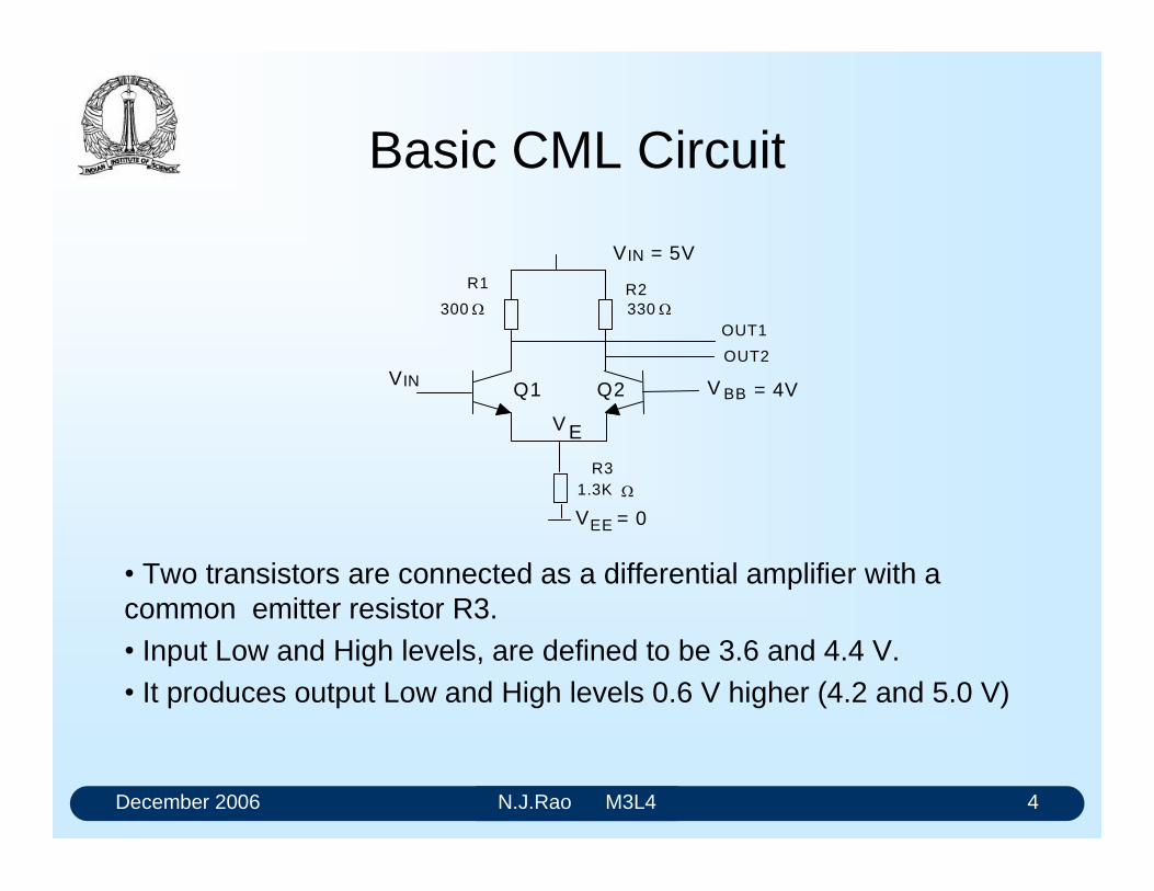
December 2006 N.J.Rao M3L4 4
Basic CML Circuit
V
R2330
R1
300
Q1 Q2 VV
V
R31.3K
OUT1
OUT2
IN
INBB
E
VEE = 0
= 5V
= 4V
Two transistors are connected as a differential amplifier with a common emitter resistor R3. Input Low and High levels, are defined to be 3.6 and 4.4 V. It produces output Low and High levels 0.6 V higher (4.2 and 5.0 V)
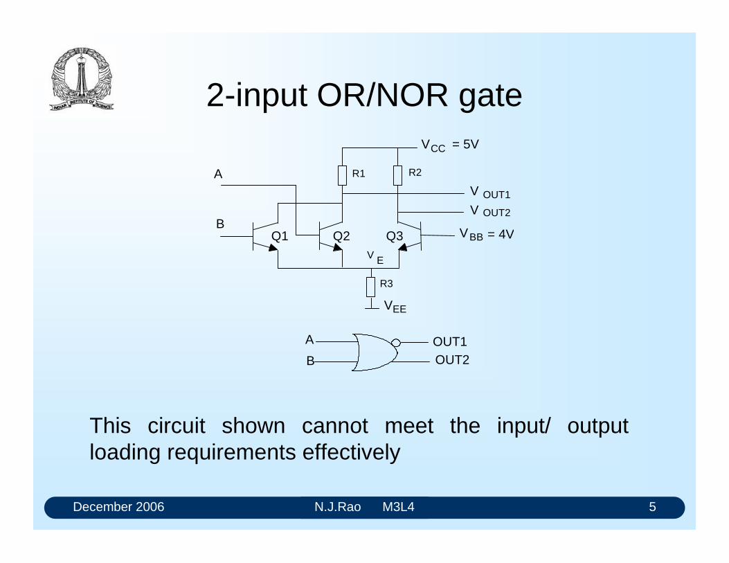
December 2006 N.J.Rao M3L4 5
2-input OR/NOR gate
Q1 Q2 V
V
R3
EE
BB
V E
= 4VQ3
V
V
V
A
B
R1 R2
OUT2
OUT1
CC = 5V
A
B
OUT1OUT2
This circuit shown cannot meet the input/ output loading requirements effectively
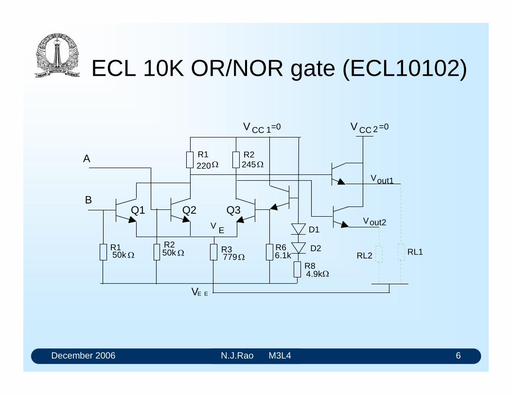
December 2006 N.J.Rao M3L4 6
ECL 10K OR/NOR gate (ECL10102)
Q1 Q2
V
R3
E E
V E
Q3
A
B
R1 R2
V CC 1=0
D1
D2
R84.9k
V CC 2=0
R66.1k77950k
R2R150k
245220
RL1RL2
Vout1
Vout2
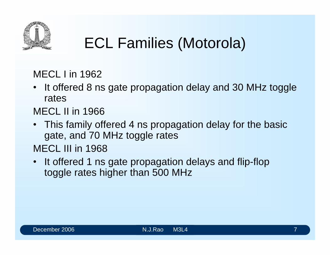
December 2006 N.J.Rao M3L4 7
ECL Families (Motorola)
MECL I in 1962 It offered 8 ns gate propagation delay and 30 MHz toggle
ratesMECL II in 1966 This family offered 4 ns propagation delay for the basic
gate, and 70 MHz toggle rates MECL III in 1968 It offered 1 ns gate propagation delays and flip-flop
toggle rates higher than 500 MHz
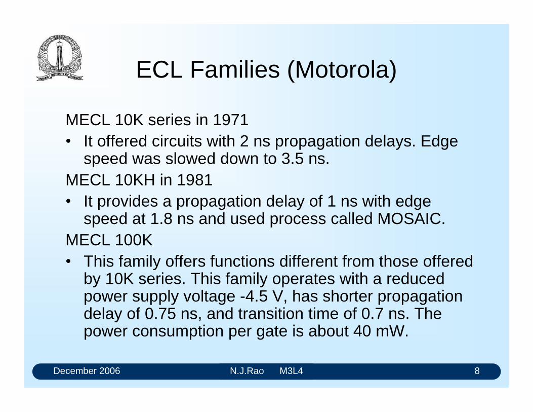
December 2006 N.J.Rao M3L4 8
ECL Families (Motorola)
MECL 10K series in 1971 It offered circuits with 2 ns propagation delays. Edge
speed was slowed down to 3.5 ns.MECL 10KH in 1981 It provides a propagation delay of 1 ns with edge
speed at 1.8 ns and used process called MOSAIC. MECL 100K This family offers functions different from those offered
by 10K series. This family operates with a reduced power supply voltage -4.5 V, has shorter propagation delay of 0.75 ns, and transition time of 0.7 ns. The power consumption per gate is about 40 mW.

December 2006 N.J.Rao M3L4 9
Subfamilies of MECL 10K
10100 and 10500 series (propagation delay of 2 ns, edge speed of 3.5 ns and flip-flop toggle rate of 160 MHz)
10200 and 10600 series (propagation delay of 1.5 ns, edge speed of 2.5 ns and flip-flop toggle rate of 250 MHz)
10800 series (propagation delay of 1 - 2.5 ns and edge speed of 3.5 ns)
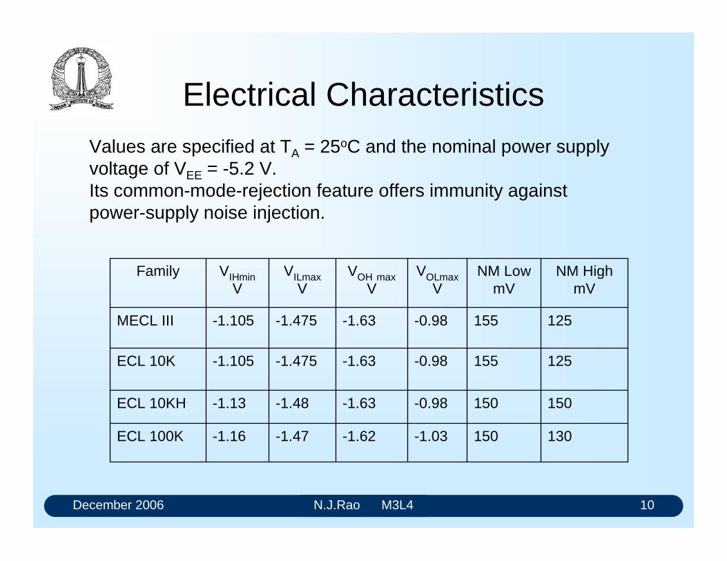
December 2006 N.J.Rao M3L4 10
Electrical CharacteristicsValues are specified at TA = 25oC and the nominal power supply voltage of VEE = -5.2 V. Its common-mode-rejection feature offers immunity against power-supply noise injection.
130150-1.03-1.62-1.47-1.16ECL 100K
150150-0.98-1.63-1.48-1.13ECL 10KH
125155-0.98-1.63-1.475-1.105ECL 10K
125155-0.98-1.63-1.475-1.105MECL III
NM HighmV
NM LowmV
VOLmaxV
VOH maxV
VILmaxV
VIHminV
Family
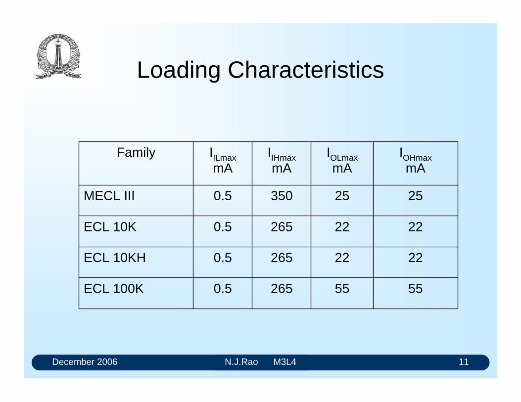
December 2006 N.J.Rao M3L4 11
Loading Characteristics
55552650.5ECL 100K
22222650.5ECL 10KH
22222650.5ECL 10K
25253500.5MECL III
IOHmaxmA
IOLmaxmA
IIHmaxmA
IILmaxmA
Family
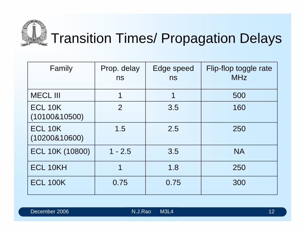
December 2006 N.J.Rao M3L4 12
Transition Times/ Propagation Delays
3000.750.75ECL 100K
2501.81ECL 10KH
NA3.51 - 2.5ECL 10K (10800)
2502.51.5ECL 10K(10200&10600)
1603.52ECL 10K(10100&10500)
50011MECL III
Flip-flop toggle rateMHz
Edge speedns
Prop. delayns
Family
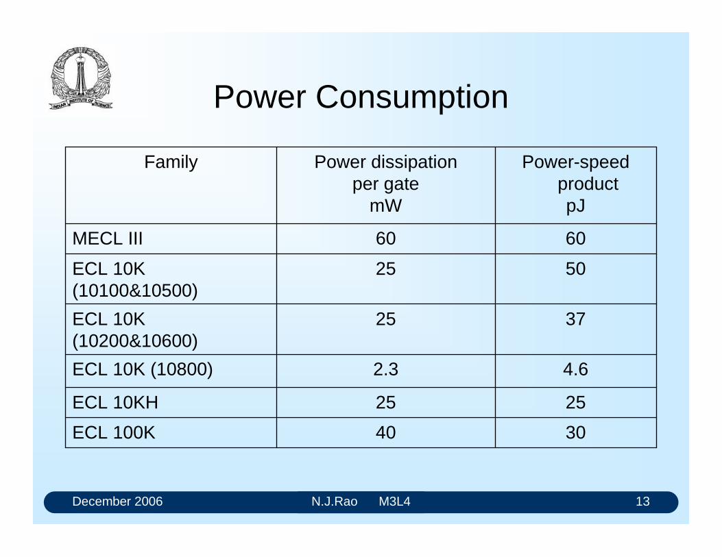
December 2006 N.J.Rao M3L4 13
Power Consumption
3040ECL 100K
2525ECL 10KH
4.62.3ECL 10K (10800)
3725ECL 10K(10200&10600)
5025ECL 10K(10100&10500)
6060MECL III
Power-speed productpJ
Power dissipation per gate
mW
Family
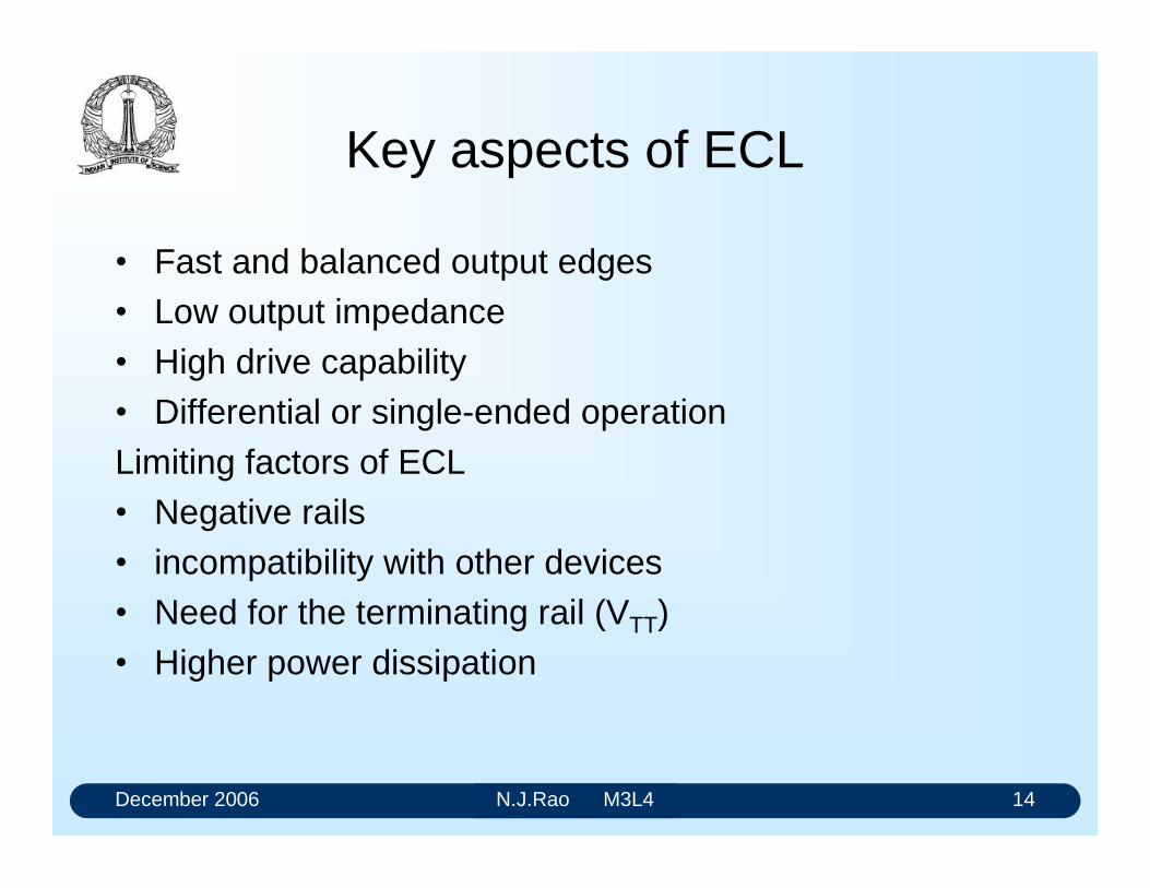
December 2006 N.J.Rao M3L4 14
Key aspects of ECL
Fast and balanced output edges Low output impedance High drive capability Differential or single-ended operationLimiting factors of ECL Negative rails incompatibility with other devices Need for the terminating rail (VTT) Higher power dissipation
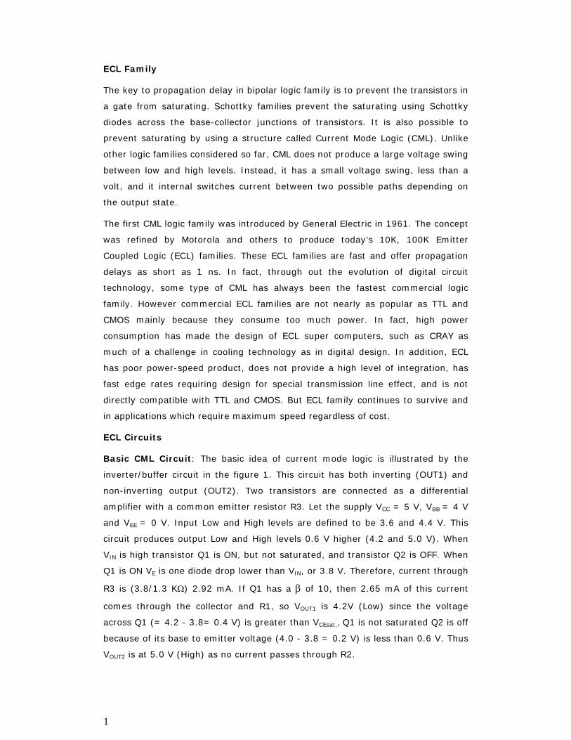
1
ECL Family
The key to propagation delay in bipolar logic family is to prevent the transistors in
a gate from saturating. Schottky families prevent the saturating using Schottky
diodes across the base-collector junctions of transistors. It is also possible to
prevent saturating by using a structure called Current Mode Logic (CML). Unlike
other logic families considered so far, CML does not produce a large voltage swing
between low and high levels. Instead, it has a small voltage swing, less than a
volt, and it internal switches current between two possible paths depending on
the output state.
The first CML logic family was introduced by General Electric in 1961. The concept
was refined by Motorola and others to produce today’s 10K, 100K Emitter
Coupled Logic (ECL) families. These ECL families are fast and offer propagation
delays as short as 1 ns. In fact, through out the evolution of digital circuit
technology, some type of CML has always been the fastest commercial logic
family. However commercial ECL families are not nearly as popular as TTL and
CMOS mainly because they consume too much power. In fact, high power
consumption has made the design of ECL super computers, such as CRAY as
much of a challenge in cooling technology as in digital design. In addition, ECL
has poor power-speed product, does not provide a high level of integration, has
fast edge rates requiring design for special transmission line effect, and is not
directly compatible with TTL and CMOS. But ECL family continues to survive and
in applications which require maximum speed regardless of cost.
ECL Circuits
Basic CML Circuit: The basic idea of current mode logic is illustrated by the
inverter/buffer circuit in the figure 1. This circuit has both inverting (OUT1) and
non-inverting output (OUT2). Two transistors are connected as a differential
amplifier with a common emitter resistor R3. Let the supply VCC = 5 V, VBB = 4 V
and VEE = 0 V. Input Low and High levels are defined to be 3.6 and 4.4 V. This
circuit produces output Low and High levels 0.6 V higher (4.2 and 5.0 V). When
VIN is high transistor Q1 is ON, but not saturated, and transistor Q2 is OFF. When
Q1 is ON VE is one diode drop lower than VIN, or 3.8 V. Therefore, current through
R3 is (3.8/1.3 KΩ) 2.92 mA. If Q1 has a β of 10, then 2.65 mA of this current
comes through the collector and R1, so VOUT1 is 4.2V (Low) since the voltage
across Q1 (= 4.2 - 3.8= 0.4 V) is greater than VCEsat,, Q1 is not saturated Q2 is off
because of its base to emitter voltage (4.0 - 3.8 = 0.2 V) is less than 0.6 V. Thus
VOUT2 is at 5.0 V (High) as no current passes through R2.
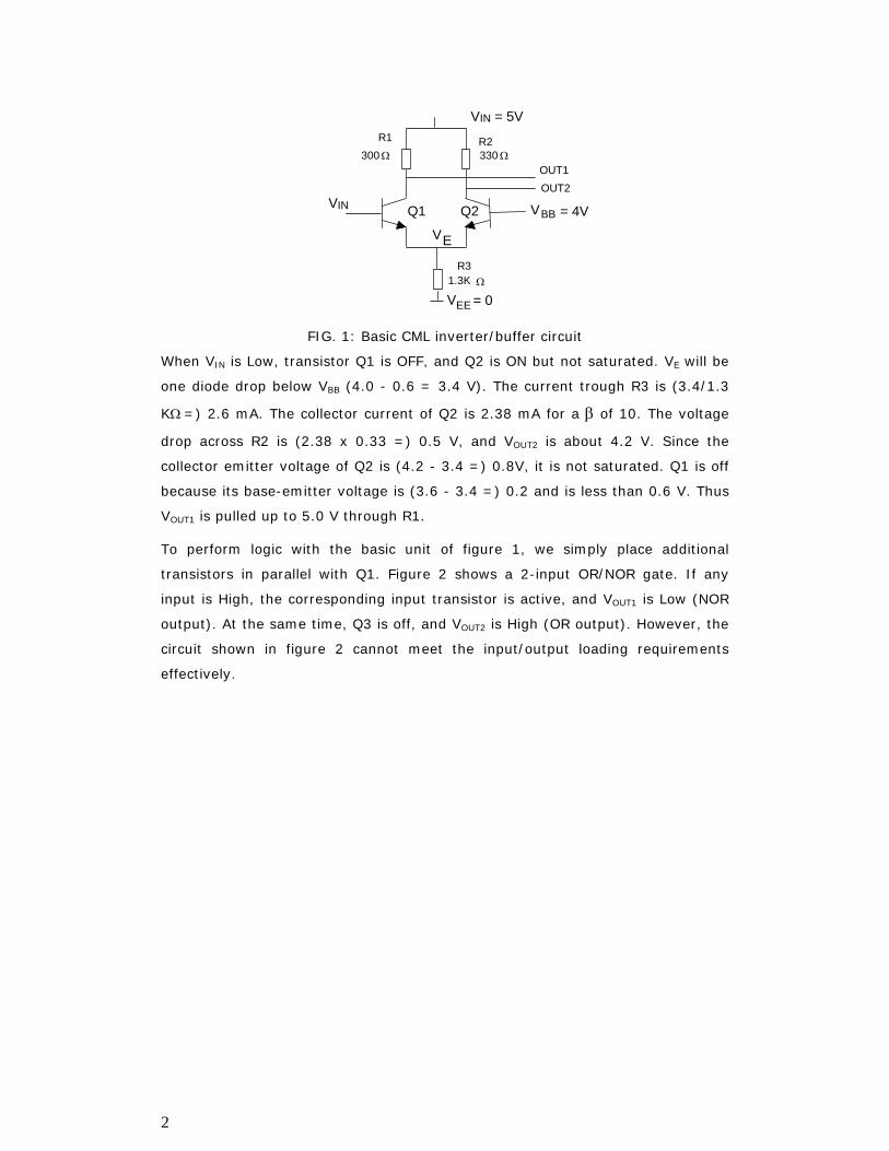
2
V
R2330
R1300
Q1 Q2 VV
V
R31.3K
Ω
Ω
ΩOUT1OUT2
IN
INBB
E
VEE = 0
= 5V
= 4V
FIG. 1: Basic CML inverter/buffer circuit
When VIN is Low, transistor Q1 is OFF, and Q2 is ON but not saturated. VE will be
one diode drop below VBB (4.0 - 0.6 = 3.4 V). The current trough R3 is (3.4/1.3
KΩ =) 2.6 mA. The collector current of Q2 is 2.38 mA for a β of 10. The voltage
drop across R2 is (2.38 x 0.33 =) 0.5 V, and VOUT2 is about 4.2 V. Since the
collector emitter voltage of Q2 is (4.2 - 3.4 =) 0.8V, it is not saturated. Q1 is off
because its base-emitter voltage is (3.6 - 3.4 =) 0.2 and is less than 0.6 V. Thus
VOUT1 is pulled up to 5.0 V through R1.
To perform logic with the basic unit of figure 1, we simply place additional
transistors in parallel with Q1. Figure 2 shows a 2-input OR/NOR gate. If any
input is High, the corresponding input transistor is active, and VOUT1 is Low (NOR
output). At the same time, Q3 is off, and VOUT2 is High (OR output). However, the
circuit shown in figure 2 cannot meet the input/output loading requirements
effectively.
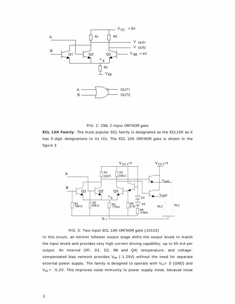
3
FIG. 2: CML 2-input OR/NOR gate
ECL 10K Family: The most popular ECL family is designated as the ECL10K as it
has 5-digit designations to its ICs. The ECL 10K OR/NOR gate is shown in the
figure 3
Q1 Q2
V
R3
E E
V E
Q3
A
B
R1 R2
V CC 1=0
D1
D2
R84.9k
V CC 2=0
R66.1k77950k
R2R150k Ω ΩΩ
Ω
245220 Ω Ω
RL1RL2
Vout1
Vout2
FIG. 3: Two-input ECL 10K OR/NOR gate (10102)
In this circuit, an emitter follower output stage shifts the output levels to match
the input levels and provides very high current driving capability, up to 50 mA per
output. An internal (R7, D1, D2, R8 and Q4) temperature, and voltage-
compensated bias network provides VBB (-1.29V) without the need for separate
external power supply. The family is designed to operate with VCC= 0 (GND) and
VEE = -5.2V. This improves noise immunity to power supply noise, because noise
4
on VEE is a “common mode” signal that is rejected by the input structure’s
differential amplifier.
A pull down resistor on each input ensures that of the input is left unconnected, it
is treated as Low. The emitter-follower outputs used in ECL 10K require external
pull-down resistors as shown in the figure. This is because of the fast
transmission times (typically 2ns). The short transmission times require special
attention as any interconnection longer than a few centimetres must be treated
as a transmission line. By removing the internal pull-down resistor, the designer
can now select a resistor that satisfies the pull-down requirements as well as
transmission line termination requirements. The simplest terminator for short
connections is to use a resistor in the range of 270 Ω to 2 KΩ.
ECL SUBFAMILIES
Motorola has offered MECL circuits in five logic families: MECL I, MECL II, MECL
III, MECL 10000 (MECL 10K), and MECL 10H000 (MECL 10KH). The MECL I family
was introduced in 1962, offering 8 ns gate propagation delay and 30 MHz toggle
rates. This was the highest performance from any logic family at that time.
However, this family required a separate bias driver package to be connected to
each logic function. The ten pin packages used by this family limited the number
of gates per package and the number of gate inputs. MECL II was introduced in
1966. This family offered 4 ns propagation delay for the basic gate, and 70 MHz
toggle rates. MECL II circuits have a temperature compensated bias driver
internal to the circuits, which simplifies circuit interconnections.
MECL III was introduced in 1968. They offered 1 ns gate propagation delays and
flip-flop toggle rates higher than 500 MHz. The 1 ns rise and fall times required a
transmission line environment for all but the smallest systems. For this reason, all
circuit outputs are designed to drive transmission lines and all output logic levels
are specified when driving 50-ohm loads. For the first time with MECL, internal
input pull down resistors are included with the circuits to eliminate the need to tie
unused inputs to VEE..
Motorola introduced MECL 10K series in 1971 with 2 ns propagation delays. In
order to make the circuits comparatively easy to use, edge speed was slowed
down to 3.5 ns. Subsequently, the basic MECL 10K series has been expanded by
a subset of devices with even greater speed. These subfamilies are 10100 and
10500 series (propagation delay of 2 ns, edge speed of 3.5 ns and flip-flop toggle
rate of 160 MHz), 10200 and 10600 series (propagation delay of 1.5 ns, edge

5
speed of 2.5 ns and flip-flop toggle rate of 250 MHz), and 10800 LSI family
(propagation delay of 1 - 2.5 ns and edge speed of 3.5 ns)
MECL 10KH family was introduced in 1981. This family provides a propagation
delay of 1 ns with edge speed at 1.8 ns. These speeds, which were attained with
no increase in power over MECL 10K, are due to both advanced circuit design
techniques and new oxide isolated process called MOSAIC. To enhance the
existing systems, many of the MECL 10KH devices are pin-out/functional
duplications of the MECL 10K family. Also, MECL 10K/10KH are provided with
logic levels that are completely compatible with MECL III. Another important
feature of MECL 10K/10KH is the significant power reduction over both MECL III
and the older MECL II. Because of the power reductions and advanced circuit
design techniques, the MECL 10KH family has many new functions not available
with the other families.
The latest entrant to the ECL family is ECL 100K, having 6-digit part numbers.
This family offers functions, in general, different from those offered by 10K series.
This family operates with a reduced power supply voltage -4.5 V, has shorter
propagation delay of 0.75 ns, and transition time of 0.7 ns. However, the power
consumption per gate is about 40 mW.
ELECTRICAL CHARACTERISTICS OF ECL FAMILY
The input and output levels, and noise margins of ECL gates are given in the
Table 1. These values are specified at TA = 25oC and the nominal power supply
voltage of VEE = -5.2 V.
TABLE 1: Voltage levels and noise margins of ECL family ICs
The noise margin levels are slightly different in High and Low states. This
specification by itself does not give complete picture regarding the noise
immunity of a system built with a particular set of circuits. In general, noise
immunity involves line impedances, circuit output impedances, and propagation
delay in addition to noise-margin specifications.
Family VIHmin V
VILmax V
VOH max V
VOLmax V
NM Low mV
NM High mV
MECL III -1.105 -1.475 -1.63 -0.98 155 125
ECL 10K -1.105 -1.475 -1.63 -0.98 155 125
ECL 10KH -1.13 -1.48 -1.63 -0.98 150 150
ECL 100K -1.16 -1.47 -1.62 -1.03 150 130
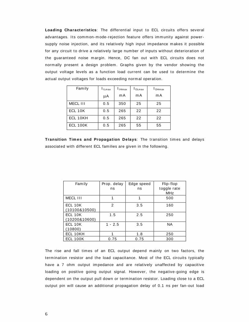
6
Loading Characteristics: The differential input to ECL circuits offers several
advantages. Its common-mode-rejection feature offers immunity against power-
supply noise injection, and its relatively high input impedance makes it possible
for any circuit to drive a relatively large number of inputs without deterioration of
the guaranteed noise margin. Hence, DC fan out with ECL circuits does not
normally present a design problem. Graphs given by the vendor showing the
output voltage levels as a function load current can be used to determine the
actual output voltages for loads exceeding normal operation.
Family IILmax
µA
IIHmax
mA
IOLmax
mA
IOHmax
mA
MECL III 0.5 350 25 25
ECL 10K 0.5 265 22 22
ECL 10KH 0.5 265 22 22
ECL 100K 0.5 265 55 55
Transition Times and Propagation Delays: The transition times and delays
associated with different ECL families are given in the following.
Family Prop. delay ns
Edge speed ns
Flip-flop toggle rate
MHz MECL III 1 1 500
ECL 10K (10100&10500)
2 3.5 160
ECL 10K (10200&10600)
1.5 2.5 250
ECL 10K (10800)
1 - 2.5 3.5 NA
ECL 10KH 1 1.8 250 ECL 100K 0.75 0.75 300
The rise and fall times of an ECL output depend mainly on two factors, the
termination resistor and the load capacitance. Most of the ECL circuits typically
have a 7 ohm output impedance and are relatively unaffected by capacitive
loading on positive going output signal. However, the negative-going edge is
dependent on the output pull down or termination resistor. Loading close to a ECL
output pin will cause an additional propagation delay of 0.1 ns per fan-out load
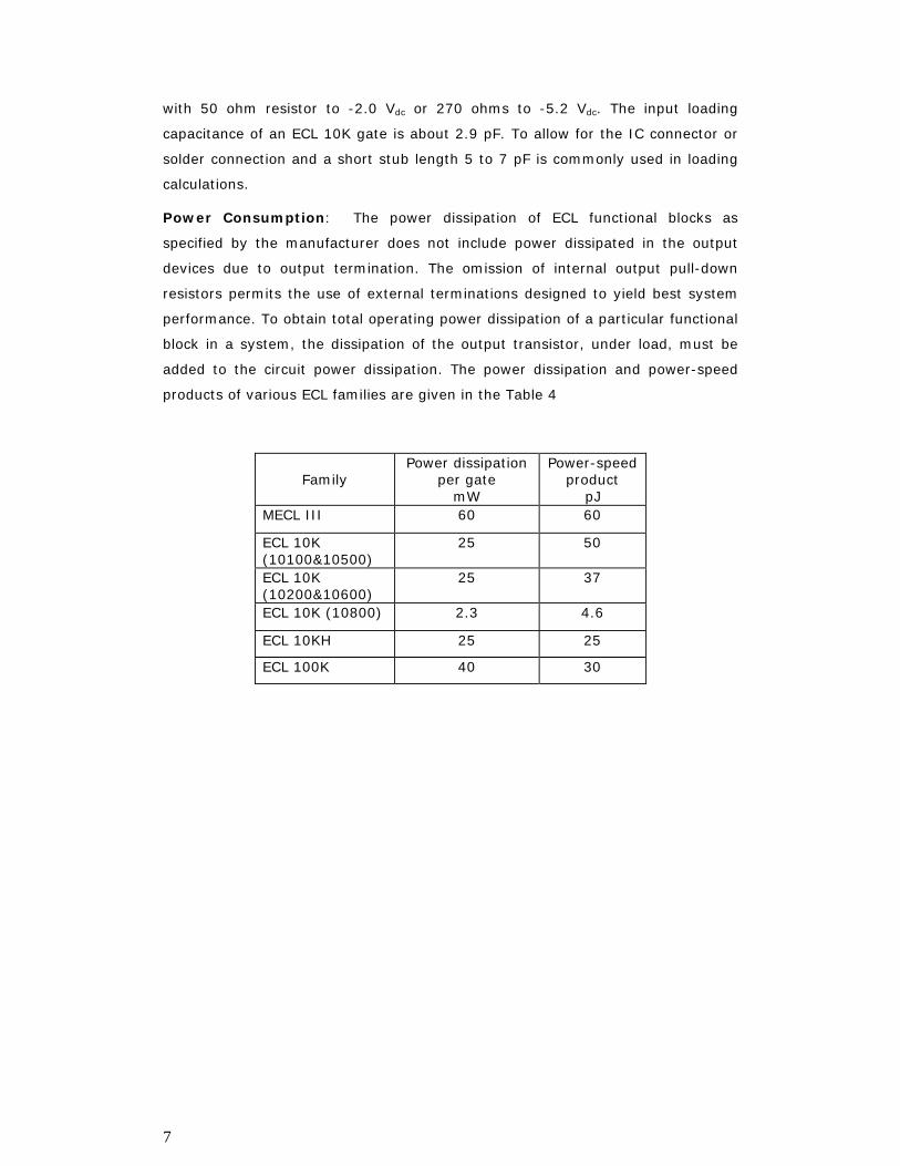
7
with 50 ohm resistor to -2.0 Vdc or 270 ohms to -5.2 Vdc. The input loading
capacitance of an ECL 10K gate is about 2.9 pF. To allow for the IC connector or
solder connection and a short stub length 5 to 7 pF is commonly used in loading
calculations.
Power Consumption: The power dissipation of ECL functional blocks as
specified by the manufacturer does not include power dissipated in the output
devices due to output termination. The omission of internal output pull-down
resistors permits the use of external terminations designed to yield best system
performance. To obtain total operating power dissipation of a particular functional
block in a system, the dissipation of the output transistor, under load, must be
added to the circuit power dissipation. The power dissipation and power-speed
products of various ECL families are given in the Table 4
Family
Power dissipation per gate
mW
Power-speed product
pJ MECL III 60 60
ECL 10K (10100&10500)
25 50
ECL 10K (10200&10600)
25 37
ECL 10K (10800) 2.3 4.6
ECL 10KH 25 25
ECL 100K 40 30
Digital Electronics Module 4: Combinational Circuits:
An Introduction
N.J. RaoIndian Institute of Science
id1254774 pdfMachine by Broadgun Software - a great PDF writer! - a great PDF creator! - http://www.pdfmachine.com http://www.broadgun.com
December 2006 N.J.Rao M4L1 2
We are familiar with
How to express a verbal logical statement as a logical expression
How to simplify a given logical expression using a variety of tools
How to pictorially represent a logical function in terms of basic logic functions like AND, OR etc.
How to perform a logical function using electronic circuits when the binary variables are presented by voltage levels
December 2006 N.J.Rao M4L1 3
Digital electronic circuits
Classified as:
Combinational Circuits Sequential Circuits
December 2006 N.J.Rao M4L1 4
Combinational circuits
The output can be expressed as a logical expression in terms of the input variables
The present value of the output is dependent only on the present values of the inputs
All logical expressions consist of logical operations AND, OR and NOT.
Any logical expression can be realized using these three types of electronic gates.
December 2006 N.J.Rao M4L1 5
Sequential Circuits
In a sequential circuit the outputs depend on
The present inputs The sequence of all the past inputs
December 2006 N.J.Rao M4L1 6
Early era of digital design
logic gates
were built with discrete devices were expensive consumed considerable power occupied significant amount of space on the printed
circuit board. minimisation of the number of gates was one of the
major design objectives

December 2006 N.J.Rao M4L1 7
Present day semiconductor technology
The integration levels are very high The delay times are very low and coming down all the
time Power consumed by them has been coming down. Minimization of printed circuit board area is the major
design objective
December 2006 N.J.Rao M4L1 8
Traditional minimisation methods
Can help in locating problems like hazards and racing
December 2006 N.J.Rao M4L1 9
Combinational SSI, MSI and LSIs
Gates Multiplexers Demultiplexers Arithmetic Units Encoders and Code Converters Comparators Multipliers Programmable Logic Devices (PLDs)
December 2006 N.J.Rao M4L1 10
Hardware aspects: Electrical Parameters
propagation delays power consumption supply voltage levels currents tolerances (voltages and currents) loading margins (noise)
December 2006 N.J.Rao M4L1 11
Hardware aspects: Mechanical Parameters
Foot print Type of package Pin pitch (distance between two adjacent pins) Thermal resistance
December 2006 N.J.Rao M4L1 12
Present day context of combinational circuits
Interfacing (propagation delay should be minimum) The number of ICs of SSI and MSI level to be
considerably restricted
December 2006 N.J.Rao M4L1 13
Learning Objectives
Analyse and design combinational circuits using commercially available ICs belonging to LSTTL and HCMOS/HCTMOS families
Resolve issues related to interfacing Learn to use Polarized Mnemonic Conventions
Polarized Mnemonic Convention
December 2006 N.J.Rao M4L1 15
Learning objectives
Explain the polarized mnemonic conventions of IEEE for representing logic variables and signals used in combinational circuits.
Implement different logic functions with different logic gates.
Explain the method of representing Mode signals and binary data unambiguously.
State the advantages of polarized mnemonic convention.
December 2006 N.J.Rao M4L1 16
Standard Convention
Polarised Mnemonic Convention and logic symbology as per IEEE Std. 91/ ANSI Y32.14
The standard convention has two components: logic notation including signal designation, symbols for digital functional units, available as SSI and
MSI packages
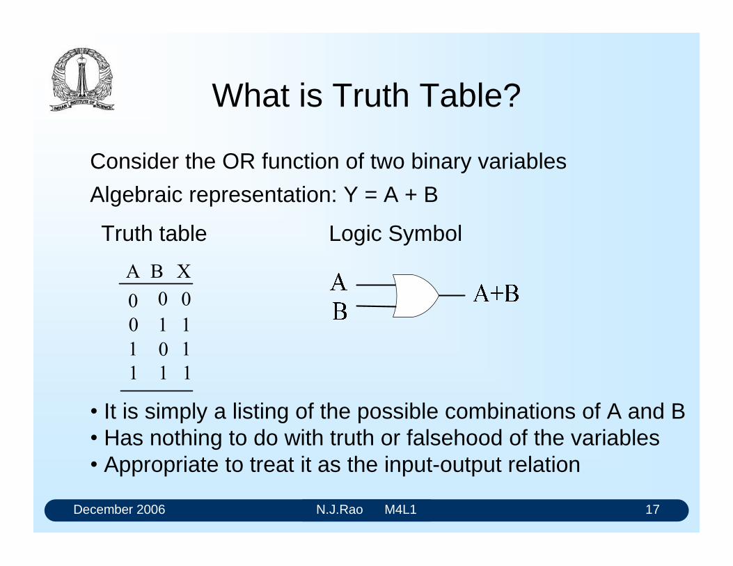
December 2006 N.J.Rao M4L1 17
What is Truth Table?
$ % ;
Consider the OR function of two binary variables
Algebraic representation: Y = A + B
Truth table Logic Symbol
It is simply a listing of the possible combinations of A and B Has nothing to do with truth or falsehood of the variables Appropriate to treat it as the input-output relation
December 2006 N.J.Rao M4L1 18
Logic variables represent Action
Examples of digital signals: START, LOAD, CLEAR etc. These are indicative of actions to be performed We do not establish Truth or Falsehood of something It is appropriate to say when the signal LOAD is Asserted, the intended action
of loading takes place Asserted/ Not Asserted qualification is more
appropriate
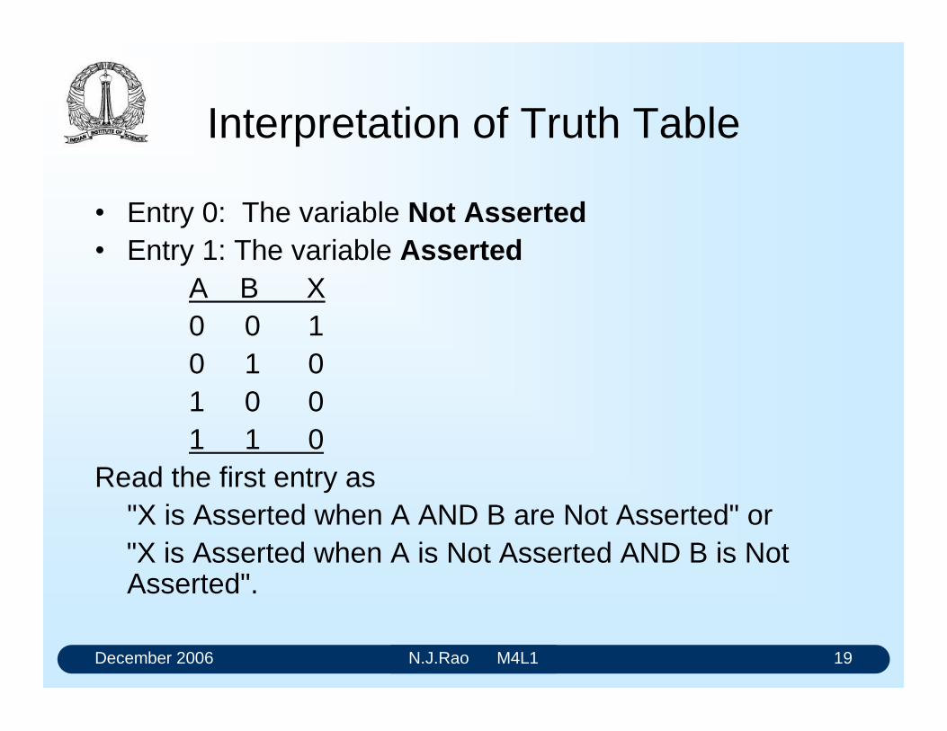
December 2006 N.J.Rao M4L1 19
Interpretation of Truth Table
Entry 0: The variable Not Asserted Entry 1: The variable Asserted
A B X 0 0 1 0 1 0 1 0 0 1 1 0
Read the first entry as "X is Asserted when A AND B are Not Asserted" or "X is Asserted when A is Not Asserted AND B is Not Asserted".
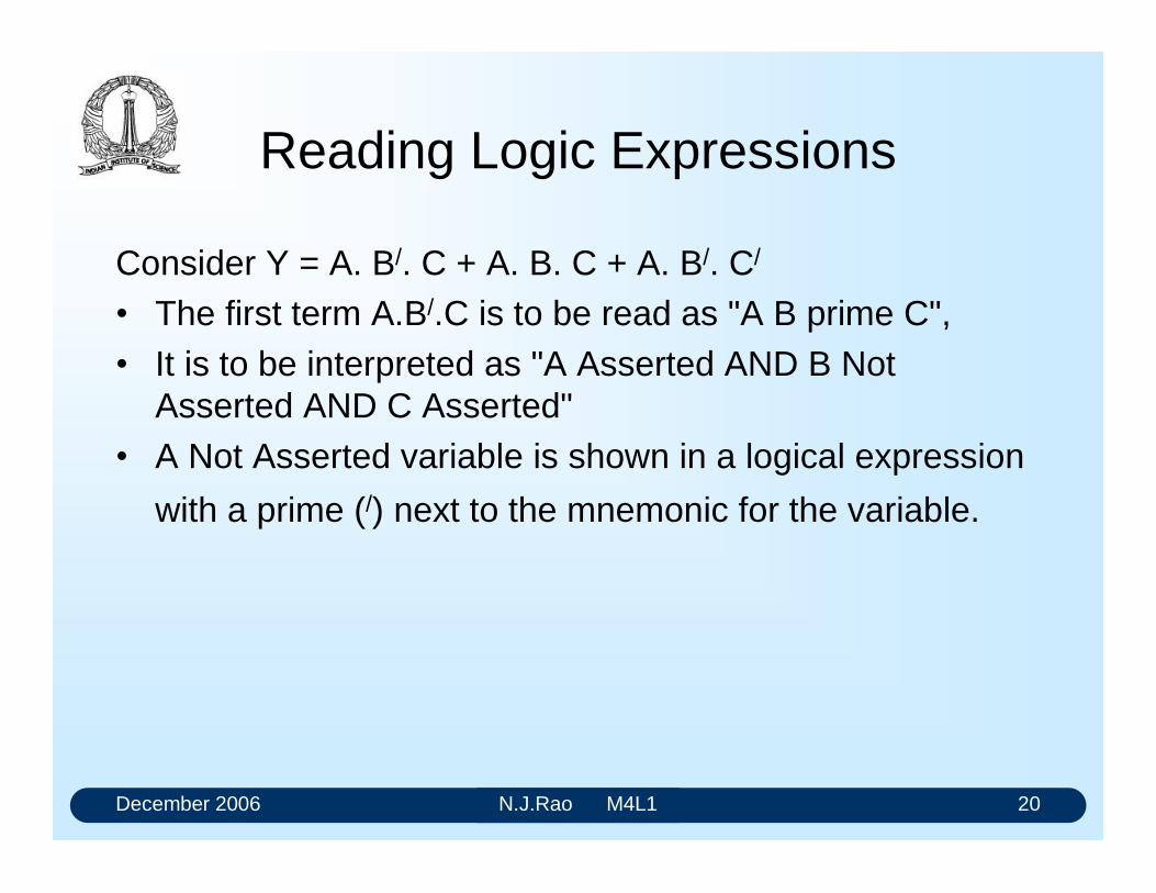
December 2006 N.J.Rao M4L1 20
Reading Logic Expressions
Consider Y = A. B/. C + A. B. C + A. B/. C/
The first term A.B/.C is to be read as "A B prime C", It is to be interpreted as "A Asserted AND B Not
Asserted AND C Asserted" A Not Asserted variable is shown in a logical expression
with a prime (/) next to the mnemonic for the variable.
December 2006 N.J.Rao M4L1 21
Electronic Circuits and Logic Functions
Electronic circuits are used to implement logic functions Currents and voltages are associated with these circuits Assertion and Not Assertion are associated with voltages Need to have a convention to associate voltages with
logic variables
December 2006 N.J.Rao M4L1 22
Signal Convention
The voltage levels associated with logic variables are not of a single value
Normally a band of few hundred milli volts or even a few volts are associated with a logic state
The more positive of the two voltage levels (voltage ranges) is designated as High Voltage (H)
The less positive of the two is designated as Low Voltage (L)
The intended action can take place at either of the voltage level
This choice can be given to the designer
December 2006 N.J.Rao M4L1 23
Signal Convention(2)
Asserted High Signal It is Asserted when the voltage level is High (H) and Not
Asserted when the voltage level is Low (L) Asserted Low Signal It is Asserted when its voltage level is Low (L) and Not
Asserted when the voltage level is High (H)
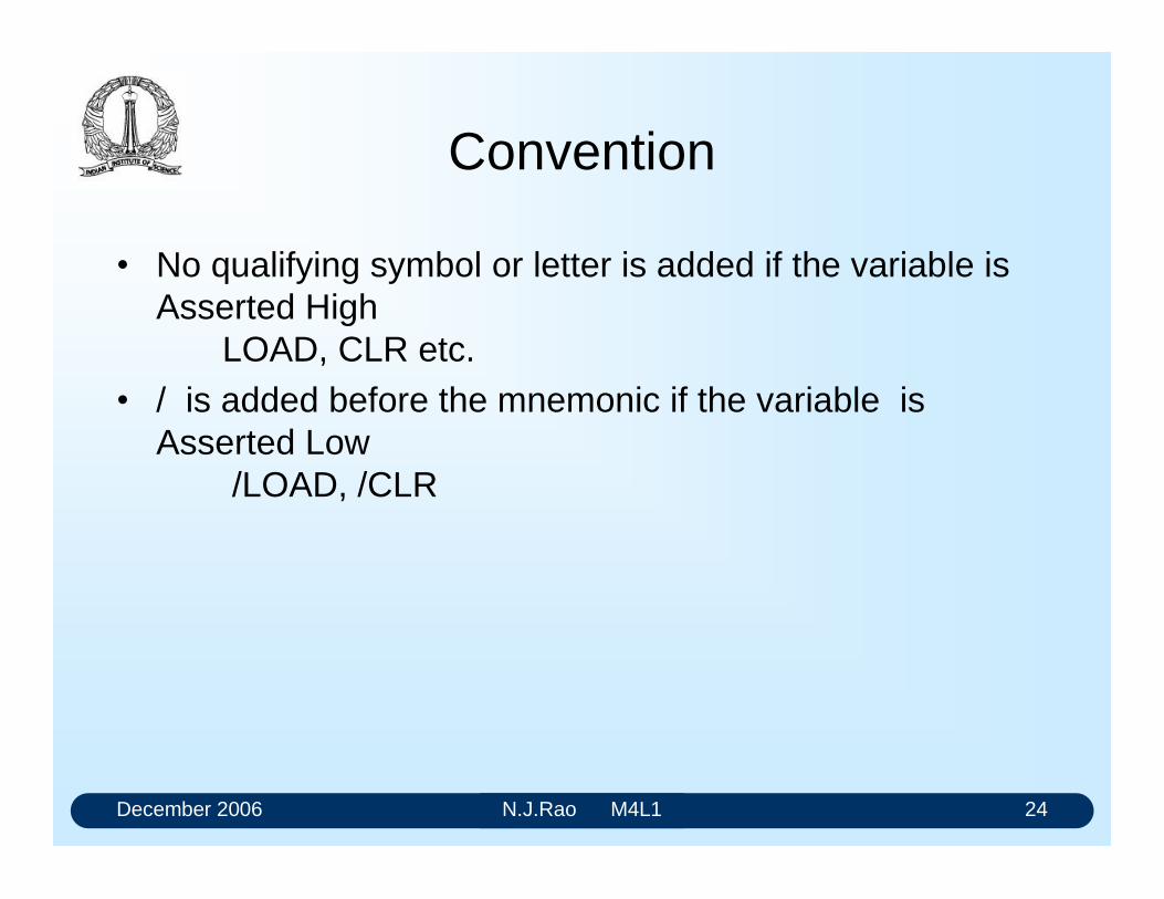
December 2006 N.J.Rao M4L1 24
Convention
No qualifying symbol or letter is added if the variable is Asserted High
LOAD, CLR etc. / is added before the mnemonic if the variable is
Asserted Low/LOAD, /CLR
December 2006 N.J.Rao M4L1 25
Logic Gates
Refer to physical electronic units that generate output voltage levels in a well-defined relationship to the input voltage levels
A given gate may perform a variety of logical functions
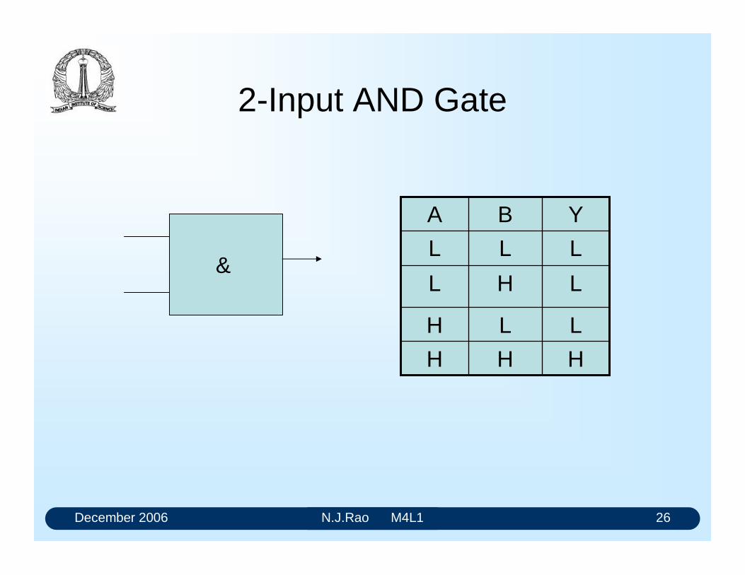
December 2006 N.J.Rao M4L1 26
2-Input AND Gate
HHH
LLH
LHL
LLL
YBA
&

December 2006 N.J.Rao M4L1 27
AND Gate with AH variables
111
001
010
000
YBA
The Truth-Table gets modified as
X is Asserted only when A AND B are Asserted This AND gate performs AND operation on the two input variableswhich are Asserted High to produce an output that is Asserted High

December 2006 N.J.Rao M4L1 28
AND Gate with AL variables
000
110
101
111
/Y/B/A
The Truth-Table gets modified as
/Y is Asserted when /A is Asserted OR /B is Asserted This AND gate performs OR operation on the two input variables which are Asserted Low to produce an output that is Asserted Low
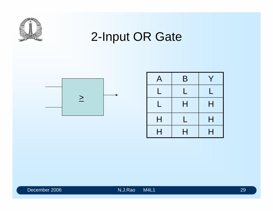
December 2006 N.J.Rao M4L1 29
2-Input OR Gate
HHH
HLH
HHL
LLL
YBA
>

December 2006 N.J.Rao M4L1 30
OR Gate with AH variables
111
101
110
000
YBA
The Truth-Table gets modified as
X is Asserted only when A OR B are Asserted This OR gate performs OR operation on the two input variables which are Asserted High to produce an output that is Asserted High
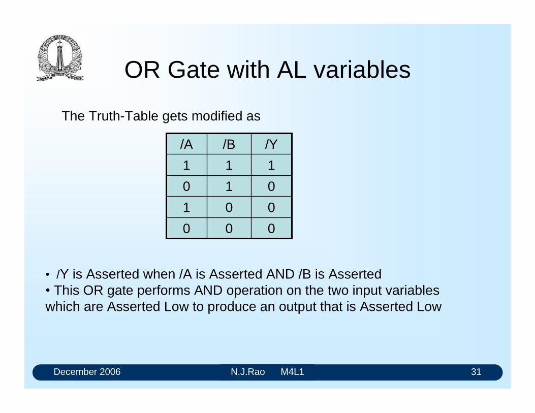
December 2006 N.J.Rao M4L1 31
OR Gate with AL variables
000
001
010
111
/Y/B/A
The Truth-Table gets modified as
/Y is Asserted when /A is Asserted AND /B is Asserted This OR gate performs AND operation on the two input variables which are Asserted Low to produce an output that is Asserted Low
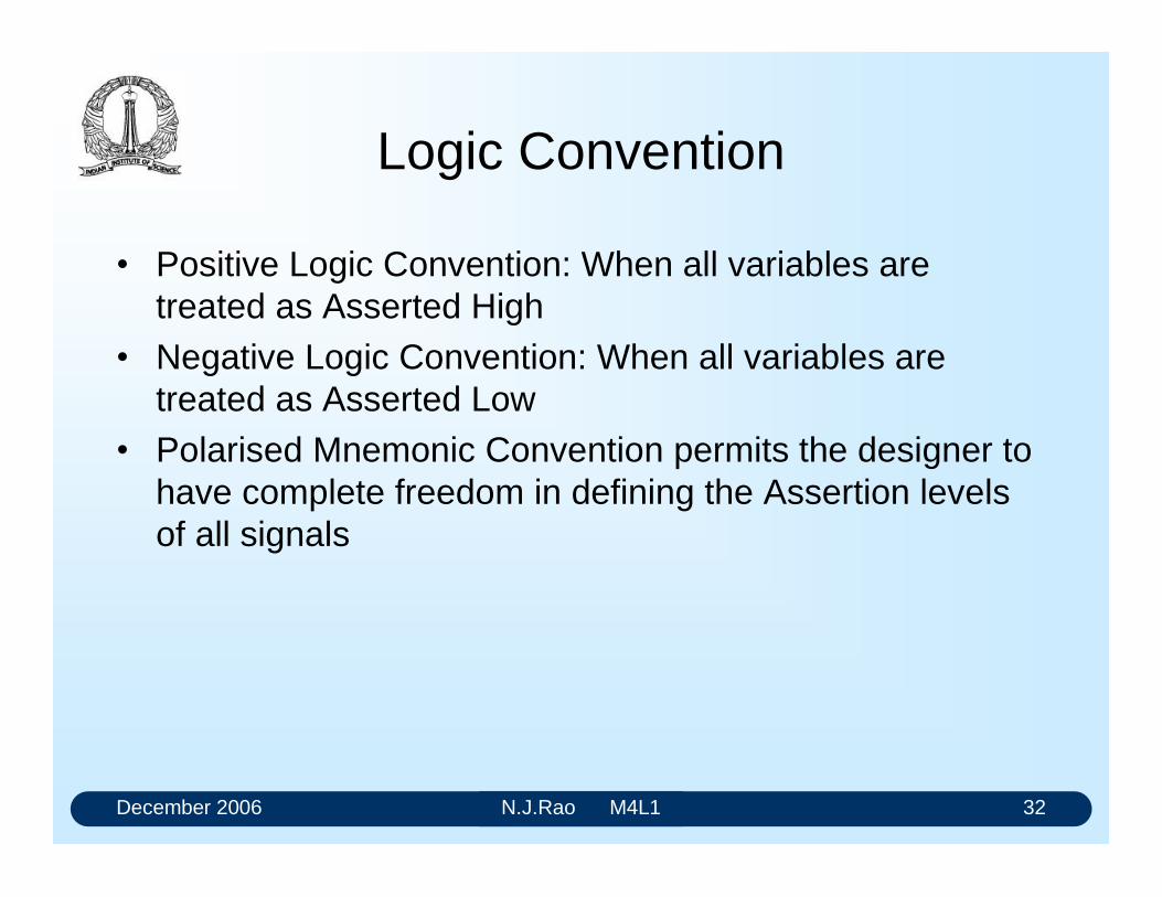
December 2006 N.J.Rao M4L1 32
Logic Convention
Positive Logic Convention: When all variables are treated as Asserted High
Negative Logic Convention: When all variables are treated as Asserted Low
Polarised Mnemonic Convention permits the designer to have complete freedom in defining the Assertion levels of all signals

December 2006 N.J.Rao M4L1 33
Negation/Polarity Indicator
As per the IEEE Standard "o" (bubble) or a (small triangle) is used as a negation/polarity indicator
We use the bubble to represent polarity
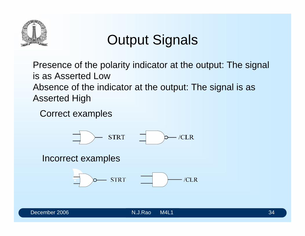
December 2006 N.J.Rao M4L1 34
Output Signals
Incorrect examples
Presence of the polarity indicator at the output: The signal is as Asserted LowAbsence of the indicator at the output: The signal is as Asserted High
Correct examples
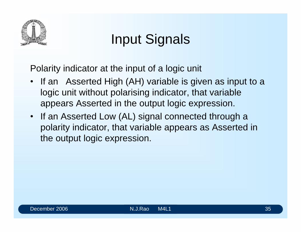
December 2006 N.J.Rao M4L1 35
Input Signals
Polarity indicator at the input of a logic unit If an Asserted High (AH) variable is given as input to a
logic unit without polarising indicator, that variable appears Asserted in the output logic expression.
If an Asserted Low (AL) signal connected through a polarity indicator, that variable appears as Asserted in the output logic expression.
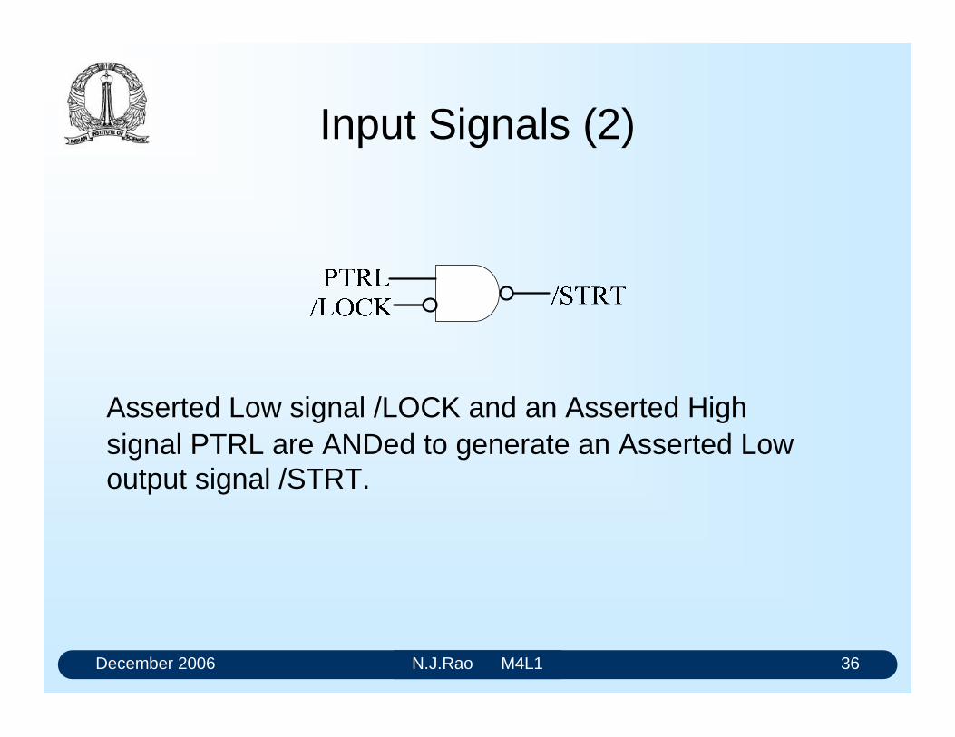
December 2006 N.J.Rao M4L1 36
Input Signals (2)
Asserted Low signal /LOCK and an Asserted High signal PTRL are ANDed to generate an Asserted Low output signal /STRT.
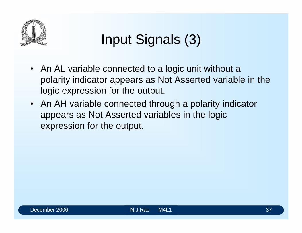
December 2006 N.J.Rao M4L1 37
Input Signals (3)
An AL variable connected to a logic unit without a polarity indicator appears as Not Asserted variable in the logic expression for the output.
An AH variable connected through a polarity indicator appears as Not Asserted variables in the logic expression for the output.
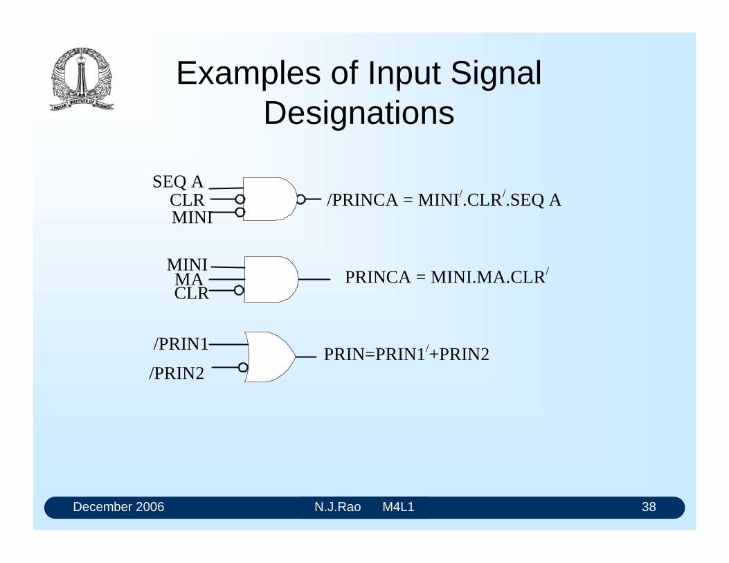
December 2006 N.J.Rao M4L1 38
Examples of Input Signal Designations
/PRINCA = MINI/.CLR/.SEQ ACLRSEQ A
MINI
PRINCA = MINI.MA.CLR/
MINIMACLR
/PRIN1
/PRIN2PRIN=PRIN1/+PRIN2
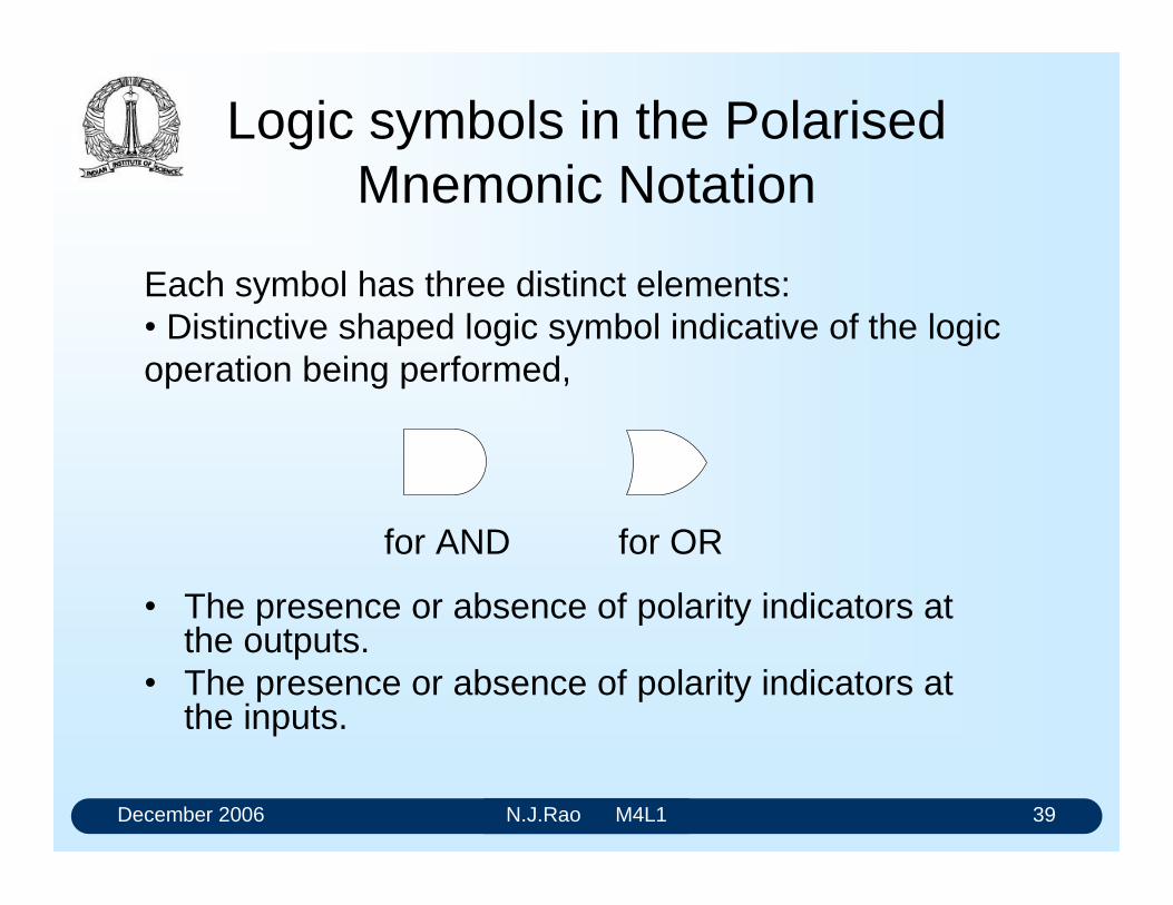
December 2006 N.J.Rao M4L1 39
Logic symbols in the Polarised Mnemonic Notation
The presence or absence of polarity indicators at the outputs.
The presence or absence of polarity indicators at the inputs.
Each symbol has three distinct elements: Distinctive shaped logic symbol indicative of the logic operation being performed,
for AND for OR
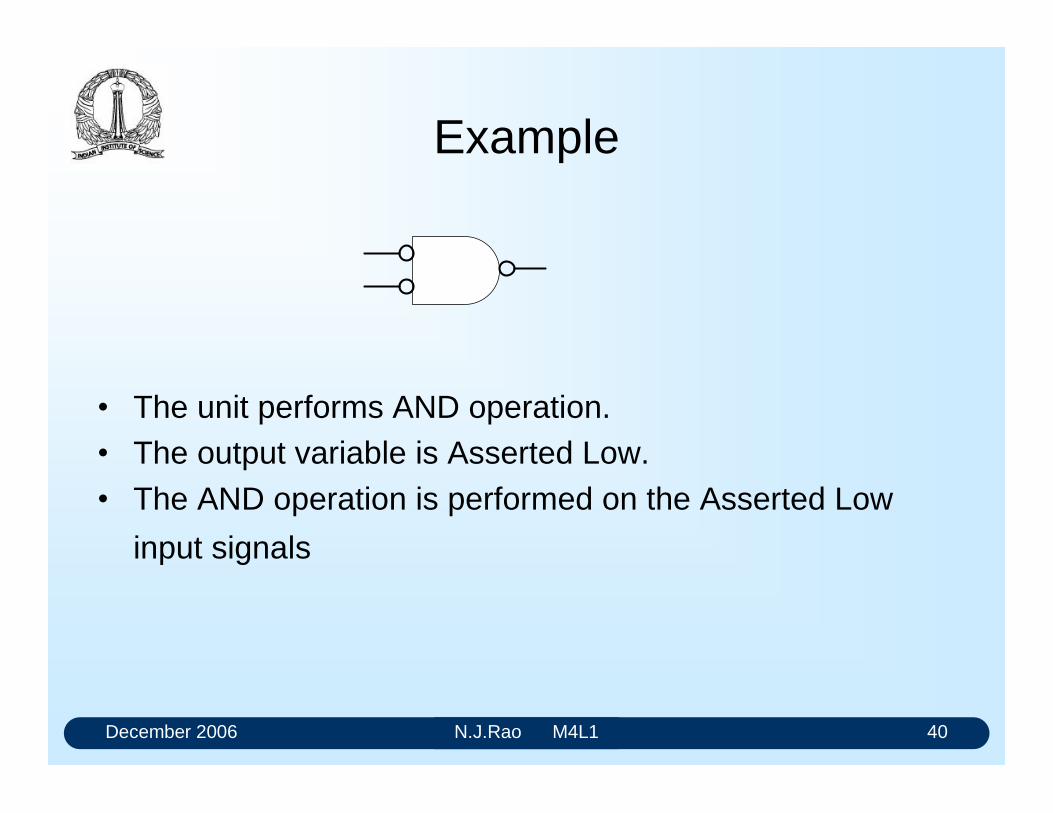
December 2006 N.J.Rao M4L1 40
Example
The unit performs AND operation. The output variable is Asserted Low. The AND operation is performed on the Asserted Low
input signals
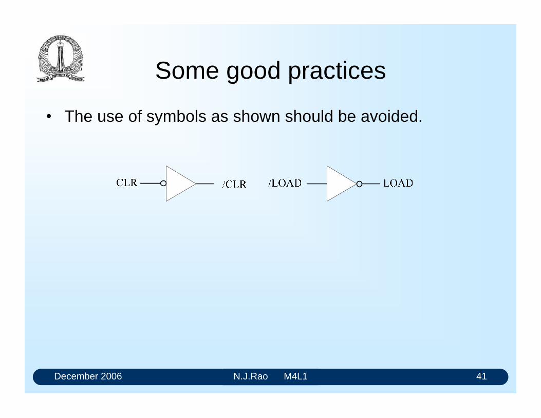
December 2006 N.J.Rao M4L1 41
Some good practices
The use of symbols as shown should be avoided.
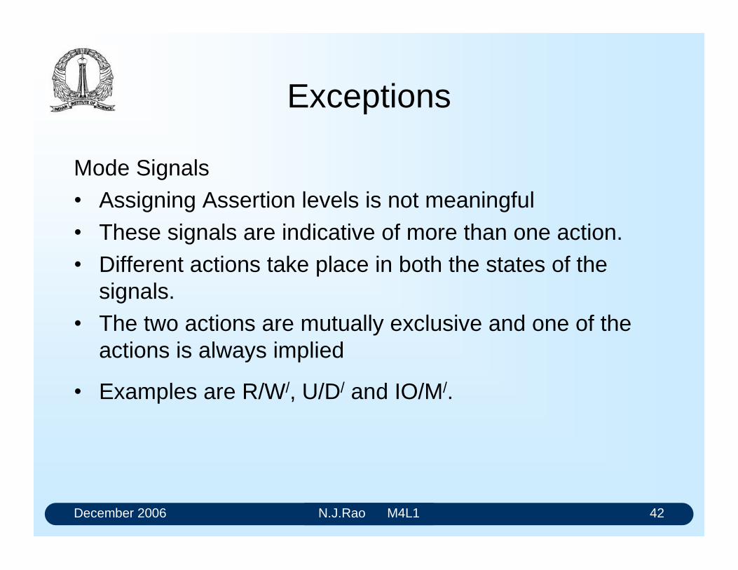
December 2006 N.J.Rao M4L1 42
Exceptions
Mode Signals Assigning Assertion levels is not meaningful These signals are indicative of more than one action. Different actions take place in both the states of the
signals. The two actions are mutually exclusive and one of the
actions is always implied
Examples are R/W/, U/D/ and IO/M/.
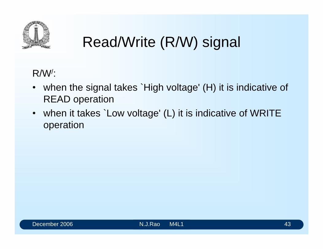
December 2006 N.J.Rao M4L1 43
Read/Write (R/W) signal
R/W/: when the signal takes `High voltage' (H) it is indicative of
READ operation when it takes `Low voltage' (L) it is indicative of WRITE
operation
December 2006 N.J.Rao M4L1 44
Binary Data
We can not use Asserted or Not Asserted conventions with binary data
Data line will either convey a numerical value of 0 or 1. A data line, designated with mnemonics like DBIT-4 When it takes High voltage it is considered having a
numerical value of 1 When it takes Low voltage it is considered having a
numerical value of `0'.
December 2006 N.J.Rao M4L1 45
Unused Inputs
All inputs of an IC may not be utilized Unused inputs will have to be tied at known states. In a 3-input OR gate that is used only as a 2-input OR
gate, the unused input should be kept in Not Asserted state.
A high voltage input is shown by the letter H and a low voltage input is shown by the letter L.
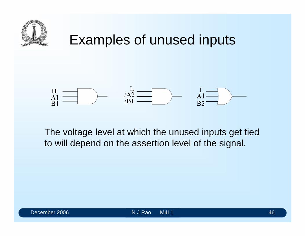
December 2006 N.J.Rao M4L1 46
Examples of unused inputs
The voltage level at which the unused inputs get tied to will depend on the assertion level of the signal.
COMBINATIONAL CIRCUITS
INTRODUCTION
We explored in the earlier learning units
• How to express a verbal logical statement as a logical expression
• How to simplify a given logical expression using a variety of tools
• How to pictorially represent a logical function in terms of basic logic functions like AND, OR etc.
• How to perform a logical function using electronic circuits when the binary variables are presented by voltage levels
An electronic circuit can perform a logical function in extremely short periods of time (time taken from the application of inputs to the appearance of outputs). These periods are of the order of nanoseconds. We mainly use electronic circuits to perform logic functions because of their high speeds.
The electronic circuits that perform logical functions are seen under two broad categories:
o Combinational
o Sequential
The output of a combinational circuit can be expressed as a logical expression in terms of the input variables. The present value of the output of a combinational circuit is dependent only on the present values of the inputs.
The logical expressions mainly consist of logical operations AND, OR and NOT. Therefore, it is possible to physically realise any logical expression using these three types of electronic gates.
In the early era of digital design “logic gates” built with discrete devices, were expensive, consumed considerable power and occupied significant amount of space on the printed circuit board on which these devices were mounted. In those early days the minimisation of the number of gates was one of the major design objectives of Logic and Switching Theory. The semiconductor technology, however, made these gates available in IC packages that occupy very little space and at very low costs. As the technologies improved
• The delay times associated with the logical devices have been coming down
• Power consumed by them has been coming down.
• More and more logic functions are getting integrated into a single package.
This has drastically reduced the number of ICs needed to realise a given function. But the proportional cost of the printed circuit board on which these devices were getting assembled has been increasing. Therefore, one of the main objectives of the present day combinational circuit design is to reduce the printed circuit board area needed for the logic circuits. This implies reduction of the number of IC packages used rather than the number of gates.
Because of these changes in technologies, the design and minimisation methods evolved by the traditional Logic and Switching Theory are not that relevant. It may not be necessary to master the finer aspects of these methods, but a good working knowledge of these methods is still needed to analyse and design combinational circuits, even as per the new criteria. Besides minimisation, these methods can

greatly help in locating problems like hazards and racing, which are mainly the consequence of variations in the electrical characteristics of the physical devices used.
Combinational integrated circuits are available in a wide functional and complexity range in SSI, MSI and LSI packages. These may be classified as:
• Gates
• Multiplexers
• Demultiplexers
• Arithmetic Units
• Encoders and code converters
• Comparators
• Multipliers
• Programmable Logic Devices (PLDs)
A digital designer must get himself thoroughly familiar with the functional and hardware aspects of these combinational ICs. The hardware aspects relate to electrical parameters
• propagation delays
• power consumption
• supply voltage levels
• currents
• tolerances (noise, voltages and currents)
• loading
Mechanical parameters are also important. These include
• foot print
• type of package
• pin pitch (distance between two adjacent pins)
• thermal resistance
The design of any digital circuit is not merely limited to the functional aspects. For example the combinational circuits find applications, in the context of the present day microprocessors, mainly for the interfacing applications. In such applications the propagation delay should be made minimum. The designer will have to use less number of levels of gating and choose the appropriate logic family. With the real estate at the printed circuit board level becoming more and more expensive the number of ICs of SSI and MSI level have to be considerably restricted.
In this module you will mainly learn to analyze and design combination circuits using commercially available Gates, Arithmetic Units, Multiplexers, and Demultiplexers belonging to both LSTTL and HCMOS/HCTMOS families. The issues related to interfacing between circuits belonging to different logic families, as well as interfacing with external world are also addressed.
As there are two logic states and two voltage levels to represent them electrically, communication among digital designers can become very confusing if well-accepted
conventions do not exist. IEEE evolved standards for Logic Convention and Dependency Notation for Medium Scale Integrated Circuits. While these conventions and notations have limited utility when working with the present day PLDs and FPGAs, it is advantageous to adhere to them whenever it is possible.
Initially we will clarify issues related to logic and signal conventions, and then proceed to designing a variety of combinational circuits.
The objectives of this learning unit are
• Explain the polarized mnemonic conventions of IEEE for representing logic variables and signals used in combinational circuits.
• Implement different logic functions with different logic gates.
• Explain the method of representing ‘mode’ signals and binary data unambiguously.
• State the advantages of polarized mnemonic convention.
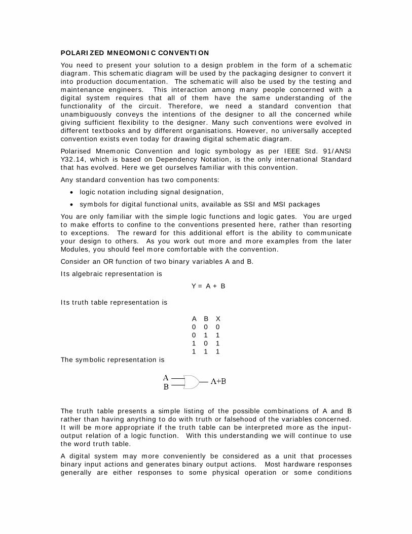
POLARIZED MNEOMONIC CONVENTION
You need to present your solution to a design problem in the form of a schematic diagram. This schematic diagram will be used by the packaging designer to convert it into production documentation. The schematic will also be used by the testing and maintenance engineers. This interaction among many people concerned with a digital system requires that all of them have the same understanding of the functionality of the circuit. Therefore, we need a standard convention that unambiguously conveys the intentions of the designer to all the concerned while giving sufficient flexibility to the designer. Many such conventions were evolved in different textbooks and by different organisations. However, no universally accepted convention exists even today for drawing digital schematic diagram.
Polarised Mnemonic Convention and logic symbology as per IEEE Std. 91/ANSI Y32.14, which is based on Dependency Notation, is the only international Standard that has evolved. Here we get ourselves familiar with this convention.
Any standard convention has two components:
• logic notation including signal designation,
• symbols for digital functional units, available as SSI and MSI packages
You are only familiar with the simple logic functions and logic gates. You are urged to make efforts to confine to the conventions presented here, rather than resorting to exceptions. The reward for this additional effort is the ability to communicate your design to others. As you work out more and more examples from the later Modules, you should feel more comfortable with the convention.
Consider an OR function of two binary variables A and B.
Its algebraic representation is
Y = A + B
Its truth table representation is
A B X 0 0 0 0 1 1 1 0 1 1 1 1
The symbolic representation is
The truth table presents a simple listing of the possible combinations of A and B rather than having anything to do with truth or falsehood of the variables concerned. It will be more appropriate if the truth table can be interpreted more as the input-output relation of a logic function. With this understanding we will continue to use the word truth table.
A digital system may more conveniently be considered as a unit that processes binary input actions and generates binary output actions. Most hardware responses generally are either responses to some physical operation or some conditions
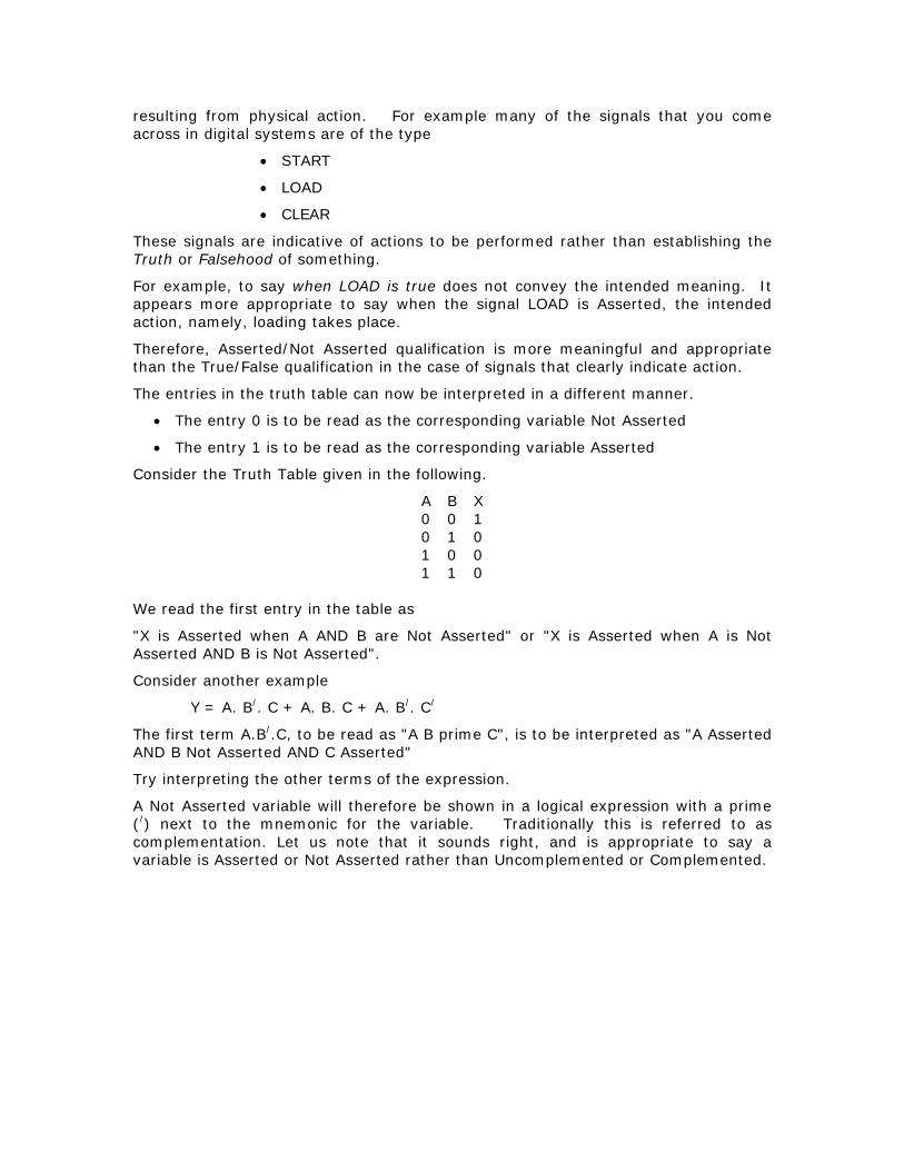
resulting from physical action. For example many of the signals that you come across in digital systems are of the type
• START
• LOAD
• CLEAR
These signals are indicative of actions to be performed rather than establishing the Truth or Falsehood of something.
For example, to say when LOAD is true does not convey the intended meaning. It appears more appropriate to say when the signal LOAD is Asserted, the intended action, namely, loading takes place.
Therefore, Asserted/Not Asserted qualification is more meaningful and appropriate than the True/False qualification in the case of signals that clearly indicate action.
The entries in the truth table can now be interpreted in a different manner.
• The entry 0 is to be read as the corresponding variable Not Asserted
• The entry 1 is to be read as the corresponding variable Asserted
Consider the Truth Table given in the following.
A B X 0 0 1 0 1 0 1 0 0 1 1 0
We read the first entry in the table as
"X is Asserted when A AND B are Not Asserted" or "X is Asserted when A is Not Asserted AND B is Not Asserted".
Consider another example
Y = A. B/. C + A. B. C + A. B/. C/
The first term A.B/.C, to be read as "A B prime C", is to be interpreted as "A Asserted AND B Not Asserted AND C Asserted"
Try interpreting the other terms of the expression.
A Not Asserted variable will therefore be shown in a logical expression with a prime (/) next to the mnemonic for the variable. Traditionally this is referred to as complementation. Let us note that it sounds right, and is appropriate to say a variable is Asserted or Not Asserted rather than Uncomplemented or Complemented.
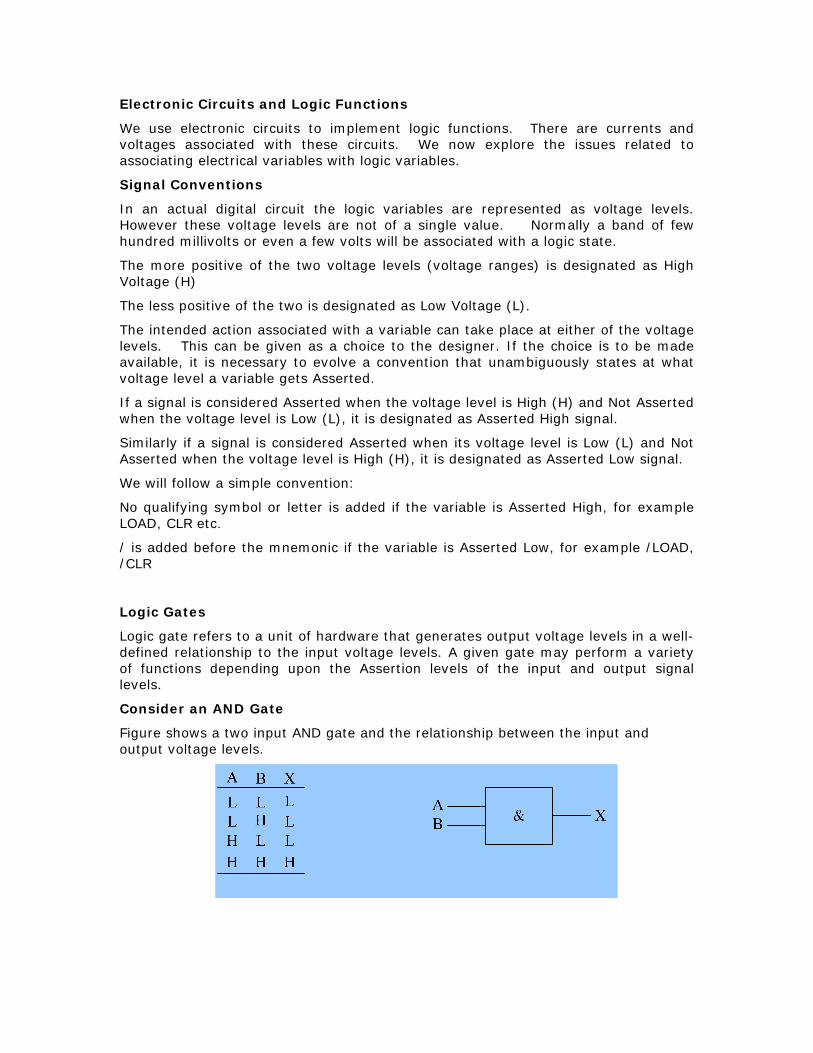
Electronic Circuits and Logic Functions
We use electronic circuits to implement logic functions. There are currents and voltages associated with these circuits. We now explore the issues related to associating electrical variables with logic variables.
Signal Conventions
In an actual digital circuit the logic variables are represented as voltage levels. However these voltage levels are not of a single value. Normally a band of few hundred millivolts or even a few volts will be associated with a logic state.
The more positive of the two voltage levels (voltage ranges) is designated as High Voltage (H)
The less positive of the two is designated as Low Voltage (L).
The intended action associated with a variable can take place at either of the voltage levels. This can be given as a choice to the designer. If the choice is to be made available, it is necessary to evolve a convention that unambiguously states at what voltage level a variable gets Asserted.
If a signal is considered Asserted when the voltage level is High (H) and Not Asserted when the voltage level is Low (L), it is designated as Asserted High signal.
Similarly if a signal is considered Asserted when its voltage level is Low (L) and Not Asserted when the voltage level is High (H), it is designated as Asserted Low signal.
We will follow a simple convention:
No qualifying symbol or letter is added if the variable is Asserted High, for example LOAD, CLR etc.
/ is added before the mnemonic if the variable is Asserted Low, for example /LOAD, /CLR
Logic Gates
Logic gate refers to a unit of hardware that generates output voltage levels in a well-defined relationship to the input voltage levels. A given gate may perform a variety of functions depending upon the Assertion levels of the input and output signal levels.
Consider an AND Gate
Figure shows a two input AND gate and the relationship between the input and output voltage levels.
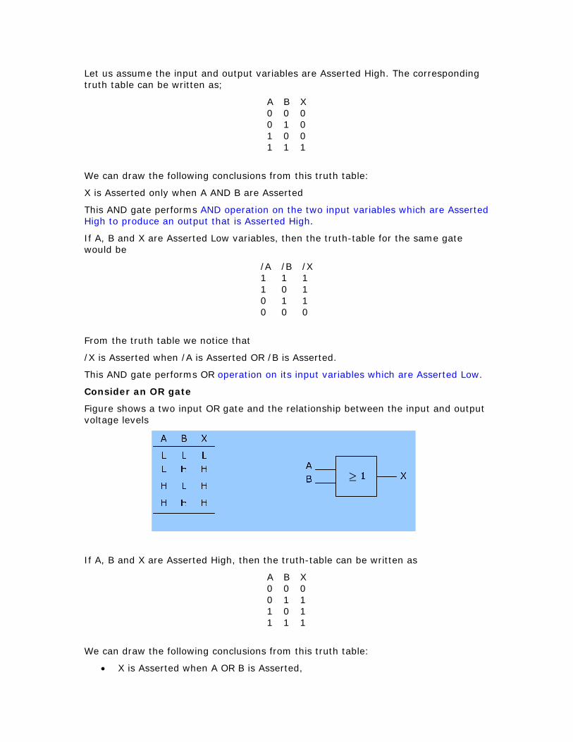
Let us assume the input and output variables are Asserted High. The corresponding truth table can be written as;
A B X 0 0 0 0 1 0 1 0 0 1 1 1
We can draw the following conclusions from this truth table:
X is Asserted only when A AND B are Asserted
This AND gate performs AND operation on the two input variables which are Asserted High to produce an output that is Asserted High.
If A, B and X are Asserted Low variables, then the truth-table for the same gate would be
/A /B /X 1 1 1 1 0 1 0 1 1 0 0 0
From the truth table we notice that
/X is Asserted when /A is Asserted OR /B is Asserted.
This AND gate performs OR operation on its input variables which are Asserted Low.
Consider an OR gate
Figure shows a two input OR gate and the relationship between the input and output voltage levels
≥
If A, B and X are Asserted High, then the truth-table can be written as
A B X 0 0 0 0 1 1 1 0 1 1 1 1
We can draw the following conclusions from this truth table:
• X is Asserted when A OR B is Asserted,
• This gate performs OR operation on the Asserted High variables.
When the variables A, B and X are Asserted Low, the Truth Table can be written as
/A /B /X 1 1 1 1 0 0 0 1 0 0 0 0
/X is Asserted only when /A AND /B are Asserted
This gate performs AND operation on Asserted Low variables.
In a similar manner each one of the available hardware gates can be used to perform more than one logic operation. From these two examples it is clear that the name given to the hardware gate corresponds to the function it performs on Asserted High inputs to generate an Asserted High output.
Exercises:
1. Find out the function performed by a 2-input NAND gate if its input and output variables are Asserted High?
2. Find out the function performed by a 2-input NAND gate if its input and output variables are Asserted Low?
3. Find out the function performed by a 2-input NAND gate if its input variables are Asserted High and its output variable is Asserted Low?
4. Find out the function performed by a 2-input NOR gate if its input and output variables are Asserted High?
5. Find out the function performed by a 2-input NOR gate if its input and output variables are Asserted Low?
6. Find out the function performed by a 2-input NOR gate if its input variables are Asserted High and its output variable is Asserted Low?
7. Find out the function performed by a 2-input Ex-NOR gate if its input and output variables are Asserted High?
8. Find out the function performed by a 2-input EX-NOR gate if its input and output variables are Asserted Low?
9. Find out the function performed by a 2-input NOR gate if one of its input variables is Asserted High and the other is Asserted Low, and its output variable is Asserted High?
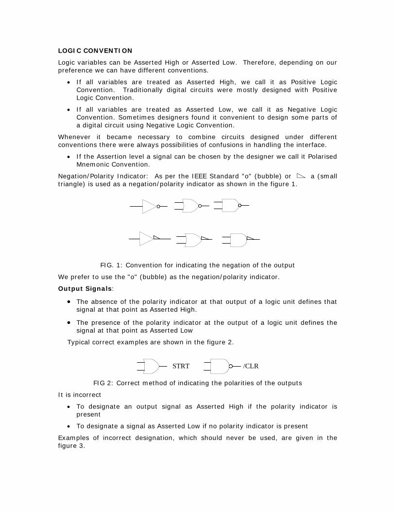
LOGIC CONVENTION
Logic variables can be Asserted High or Asserted Low. Therefore, depending on our preference we can have different conventions.
• If all variables are treated as Asserted High, we call it as Positive Logic Convention. Traditionally digital circuits were mostly designed with Positive Logic Convention.
• If all variables are treated as Asserted Low, we call it as Negative Logic Convention. Sometimes designers found it convenient to design some parts of a digital circuit using Negative Logic Convention.
Whenever it became necessary to combine circuits designed under different conventions there were always possibilities of confusions in handling the interface.
• If the Assertion level a signal can be chosen by the designer we call it Polarised Mnemonic Convention.
Negation/Polarity Indicator: As per the IEEE Standard "o" (bubble) or a (small triangle) is used as a negation/polarity indicator as shown in the figure 1.
FIG. 1: Convention for indicating the negation of the output
We prefer to use the "o" (bubble) as the negation/polarity indicator.
Output Signals:
• The absence of the polarity indicator at that output of a logic unit defines that signal at that point as Asserted High.
• The presence of the polarity indicator at the output of a logic unit defines the signal at that point as Asserted Low
Typical correct examples are shown in the figure 2.
/CLRSTRT
FIG 2: Correct method of indicating the polarities of the outputs
It is incorrect
• To designate an output signal as Asserted High if the polarity indicator is present
• To designate a signal as Asserted Low if no polarity indicator is present
Examples of incorrect designation, which should never be used, are given in the figure 3.
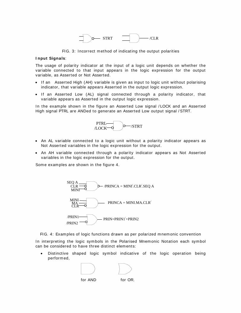
/CLRSTRT
FIG. 3: Incorrect method of indicating the output polarities
Input Signals:
The usage of polarity indicator at the input of a logic unit depends on whether the variable connected to that input appears in the logic expression for the output variable, as Asserted or Not Asserted.
• If an Asserted High (AH) variable is given as input to logic unit without polarising indicator, that variable appears Asserted in the output logic expression.
• If an Asserted Low (AL) signal connected through a polarity indicator, that variable appears as Asserted in the output logic expression.
In the example shown in the figure an Asserted Low signal /LOCK and an Asserted High signal PTRL are ANDed to generate an Asserted Low output signal /STRT.
/STRT/LOCKPTRL
• An AL variable connected to a logic unit without a polarity indicator appears as Not Asserted variables in the logic expression for the output.
• An AH variable connected through a polarity indicator appears as Not Asserted variables in the logic expression for the output.
Some examples are shown in the figure 4.
/PRINCA = MINI/.CLR/.SEQ ACLRSEQ A
MINI
PRINCA = MINI.MA.CLR/
MINIMACLR
/PRIN1/PRIN2
PRIN=PRIN1/+PRIN2
FIG. 4: Examples of logic functions drawn as per polarized mnemonic convention
In interpreting the logic symbols in the Polarised Mnemonic Notation each symbol can be considered to have three distinct elements:
• Distinctive shaped logic symbol indicative of the logic operation being performed,
for AND for OR.
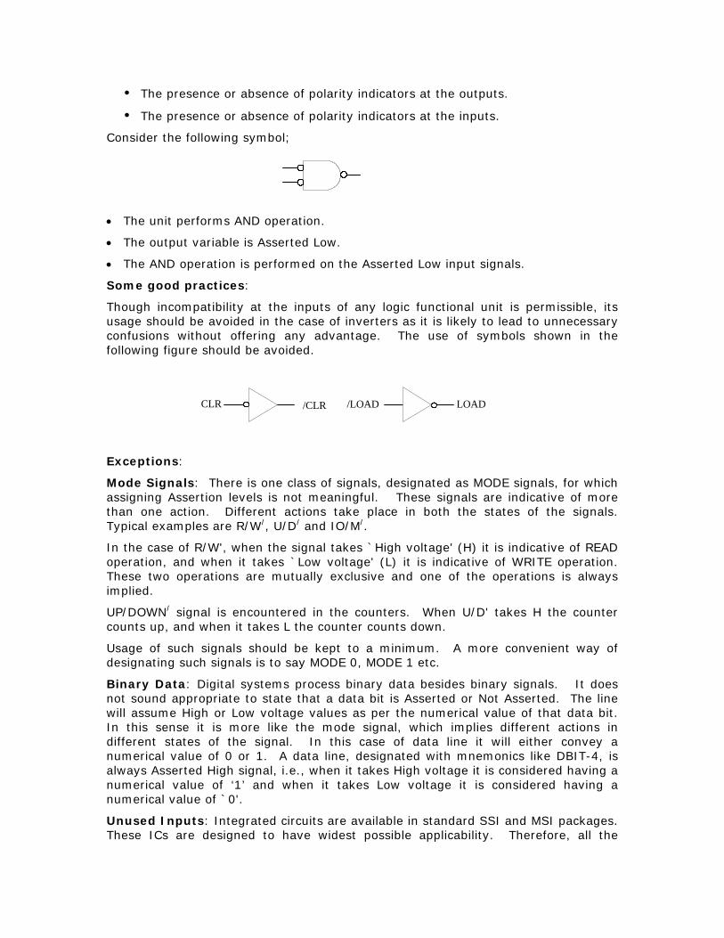
The presence or absence of polarity indicators at the outputs.
The presence or absence of polarity indicators at the inputs.
Consider the following symbol;
• The unit performs AND operation.
• The output variable is Asserted Low.
• The AND operation is performed on the Asserted Low input signals.
Some good practices:
Though incompatibility at the inputs of any logic functional unit is permissible, its usage should be avoided in the case of inverters as it is likely to lead to unnecessary confusions without offering any advantage. The use of symbols shown in the following figure should be avoided.
CLR /CLR /LOAD LOAD
Exceptions:
Mode Signals: There is one class of signals, designated as MODE signals, for which assigning Assertion levels is not meaningful. These signals are indicative of more than one action. Different actions take place in both the states of the signals. Typical examples are R/W/, U/D/ and IO/M/.
In the case of R/W', when the signal takes `High voltage' (H) it is indicative of READ operation, and when it takes `Low voltage' (L) it is indicative of WRITE operation. These two operations are mutually exclusive and one of the operations is always implied.
UP/DOWN/ signal is encountered in the counters. When U/D' takes H the counter counts up, and when it takes L the counter counts down.
Usage of such signals should be kept to a minimum. A more convenient way of designating such signals is to say MODE 0, MODE 1 etc.
Binary Data: Digital systems process binary data besides binary signals. It does not sound appropriate to state that a data bit is Asserted or Not Asserted. The line will assume High or Low voltage values as per the numerical value of that data bit. In this sense it is more like the mode signal, which implies different actions in different states of the signal. In this case of data line it will either convey a numerical value of 0 or 1. A data line, designated with mnemonics like DBIT-4, is always Asserted High signal, i.e., when it takes High voltage it is considered having a numerical value of ‘1’ and when it takes Low voltage it is considered having a numerical value of `0'.
Unused Inputs: Integrated circuits are available in standard SSI and MSI packages. These ICs are designed to have widest possible applicability. Therefore, all the
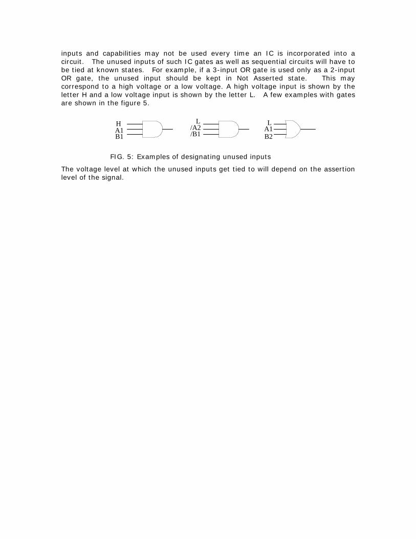
inputs and capabilities may not be used every time an IC is incorporated into a circuit. The unused inputs of such IC gates as well as sequential circuits will have to be tied at known states. For example, if a 3-input OR gate is used only as a 2-input OR gate, the unused input should be kept in Not Asserted state. This may correspond to a high voltage or a low voltage. A high voltage input is shown by the letter H and a low voltage input is shown by the letter L. A few examples with gates are shown in the figure 5.
LA1B2
L/A2/B1
HA1B1
FIG. 5: Examples of designating unused inputs
The voltage level at which the unused inputs get tied to will depend on the assertion level of the signal.

Digital Electronics Module 4: Combinational Circuits:
Logic Functions
N.J. RaoIndian Institute of Science
id1795722 pdfMachine by Broadgun Software - a great PDF writer! - a great PDF creator! - http://www.pdfmachine.com http://www.broadgun.com
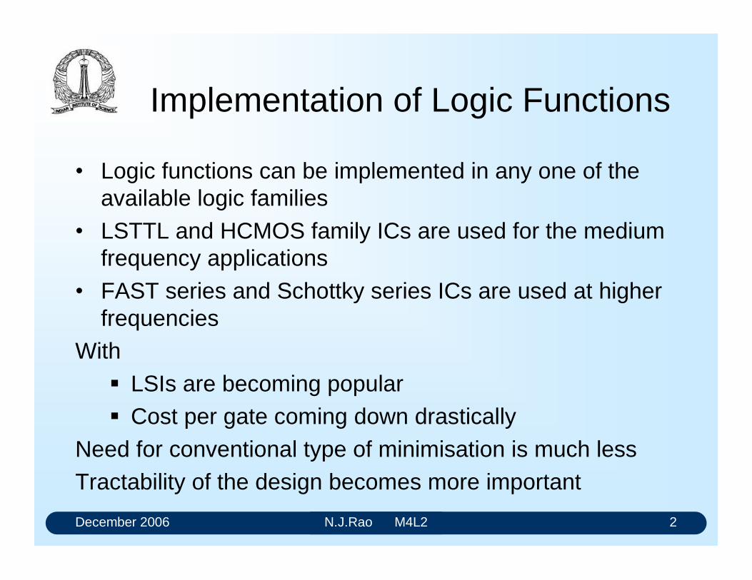
December 2006 N.J.Rao M4L2 2
Implementation of Logic Functions
Logic functions can be implemented in any one of the available logic families
LSTTL and HCMOS family ICs are used for the medium frequency applications
FAST series and Schottky series ICs are used at higher frequencies
With LSIs are becoming popular Cost per gate coming down drastically
Need for conventional type of minimisation is much lessTractability of the design becomes more important
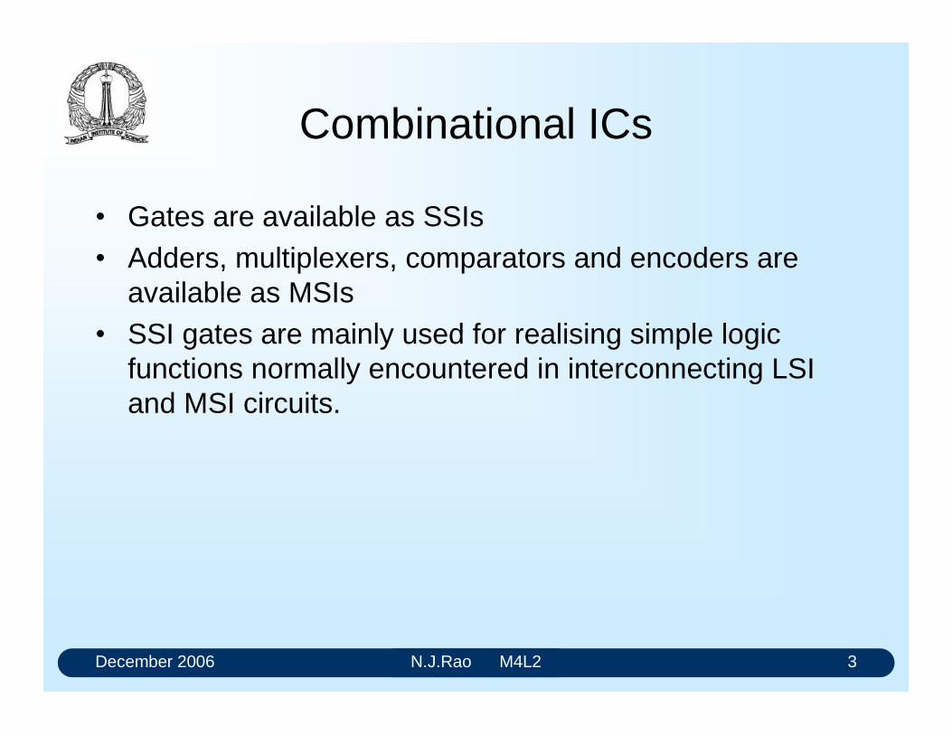
December 2006 N.J.Rao M4L2 3
Combinational ICs
Gates are available as SSIs Adders, multiplexers, comparators and encoders are
available as MSIs SSI gates are mainly used for realising simple logic
functions normally encountered in interconnecting LSI and MSI circuits.
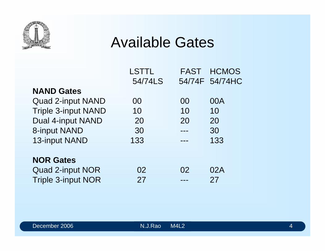
December 2006 N.J.Rao M4L2 4
Available Gates
LSTTL FAST HCMOS 54/74LS 54/74F 54/74HC
NAND GatesQuad 2-input NAND 00 00 00A Triple 3-input NAND 10 10 10Dual 4-input NAND 20 20 208-input NAND 30 --- 30 13-input NAND 133 --- 133
NOR GatesQuad 2-input NOR 02 02 02A Triple 3-input NOR 27 --- 27
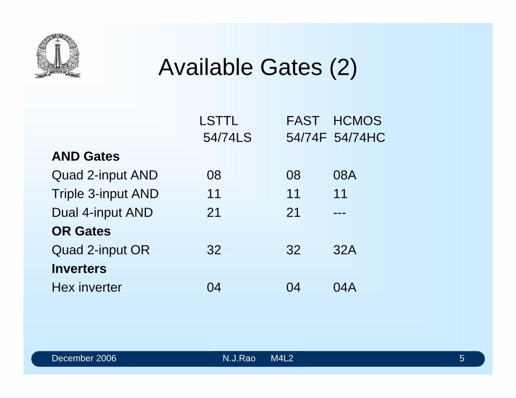
December 2006 N.J.Rao M4L2 5
Available Gates (2)
LSTTL FAST HCMOS 54/74LS 54/74F 54/74HC
AND Gates Quad 2-input AND 08 08 08A Triple 3-input AND 11 11 11Dual 4-input AND 21 21 ---OR GatesQuad 2-input OR 32 32 32A Inverters Hex inverter 04 04 04A
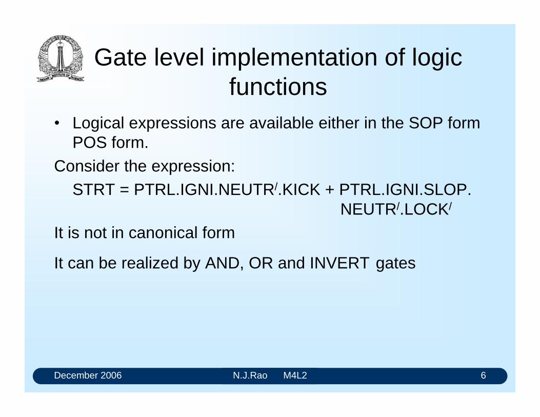
December 2006 N.J.Rao M4L2 6
Gate level implementation of logic functions
Logical expressions are available either in the SOP form POS form.
Consider the expression:STRT = PTRL.IGNI.NEUTR/.KICK + PTRL.IGNI.SLOP.
NEUTR/.LOCK/
It is not in canonical form
It can be realized by AND, OR and INVERT gates
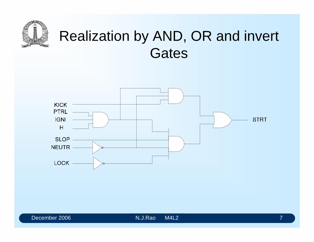
December 2006 N.J.Rao M4L2 7
Realization by AND, OR and invert Gates
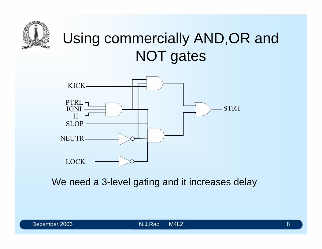
December 2006 N.J.Rao M4L2 8
Using commercially AND,OR and NOT gates
1(875
,*1,375/
/2&.
6/23
.,&.
6757+
We need a 3-level gating and it increases delay
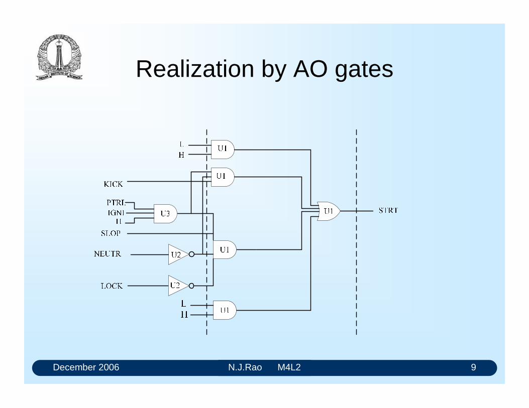
December 2006 N.J.Rao M4L2 9
Realization by AO gates
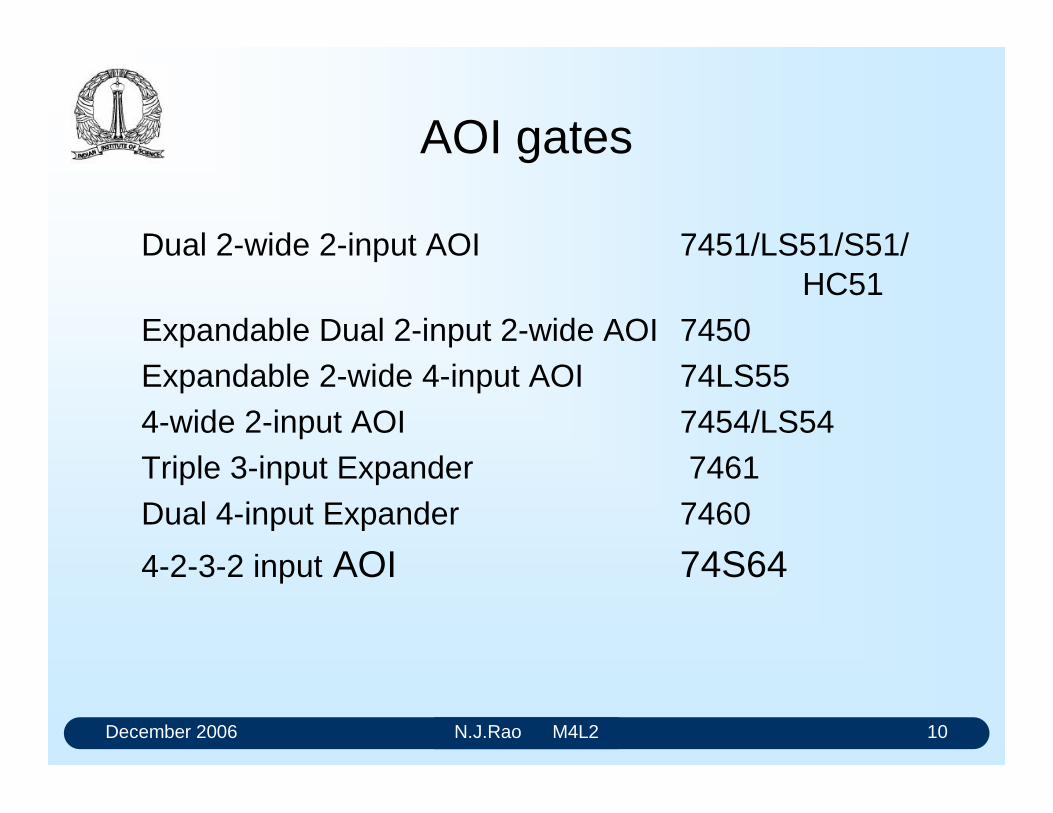
December 2006 N.J.Rao M4L2 10
AOI gates
Dual 2-wide 2-input AOI 7451/LS51/S51/ HC51
Expandable Dual 2-input 2-wide AOI 7450 Expandable 2-wide 4-input AOI 74LS554-wide 2-input AOI 7454/LS54Triple 3-input Expander 7461Dual 4-input Expander 7460
4-2-3-2 input AOI 74S64
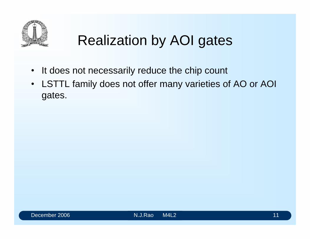
December 2006 N.J.Rao M4L2 11
Realization by AOI gates
It does not necessarily reduce the chip count LSTTL family does not offer many varieties of AO or AOI
gates.
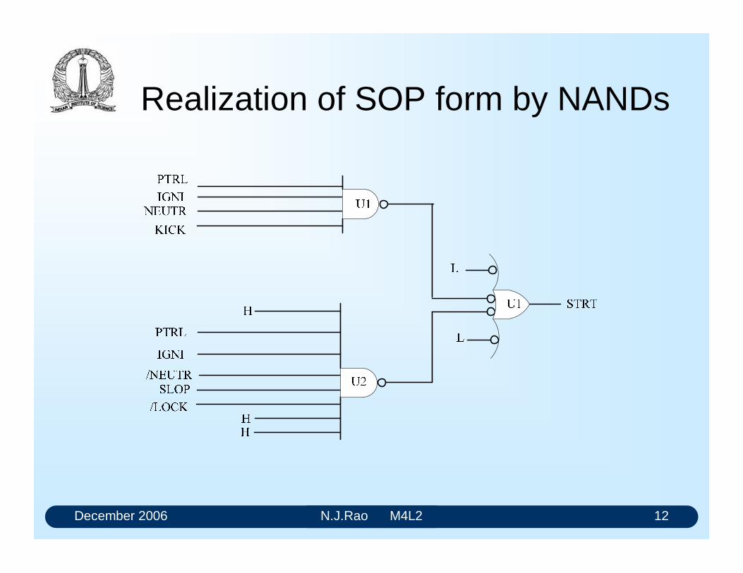
December 2006 N.J.Rao M4L2 12
Realization of SOP form by NANDs
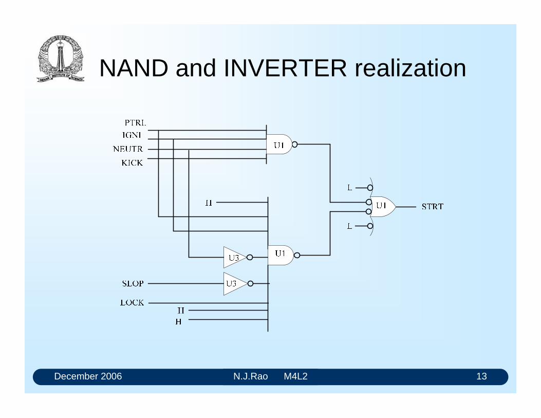
December 2006 N.J.Rao M4L2 13
NAND and INVERTER realization
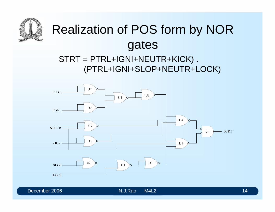
December 2006 N.J.Rao M4L2 14
Realization of POS form by NOR gates
STRT = PTRL+IGNI+NEUTR+KICK) . (PTRL+IGNI+SLOP+NEUTR+LOCK)
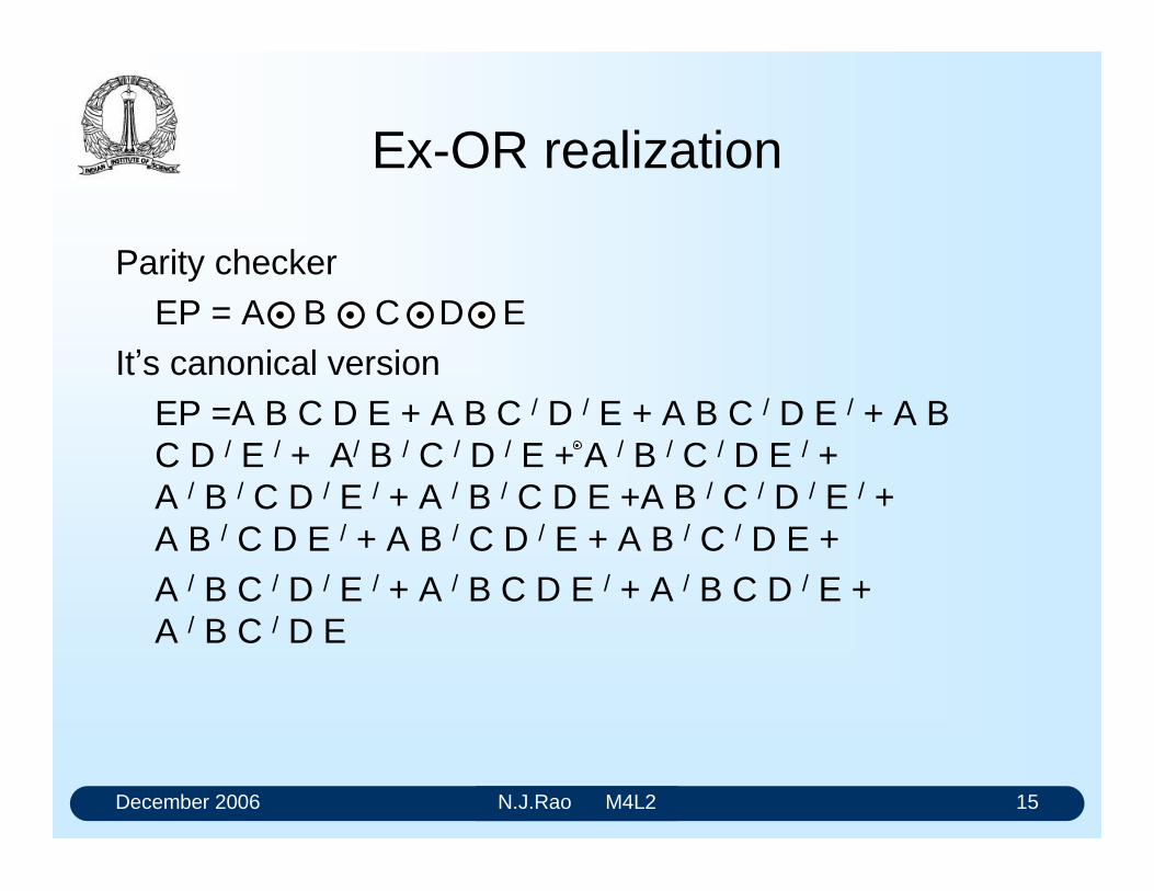
December 2006 N.J.Rao M4L2 15
Ex-OR realization
Parity checkerEP = A B C D E
Its canonical versionEP =A B C D E + A B C / D / E + A B C / D E / + A B C D / E / + A/ B / C / D / E + A / B / C / D E / + A / B / C D / E / + A / B / C D E +A B / C / D / E / + A B / C D E / + A B / C D / E + A B / C / D E +A / B C / D / E / + A / B C D E / + A / B C D / E + A / B C / D E
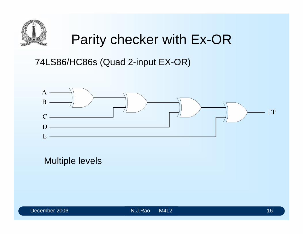
December 2006 N.J.Rao M4L2 16
Parity checker with Ex-OR
74LS86/HC86s (Quad 2-input EX-OR)
Multiple levels
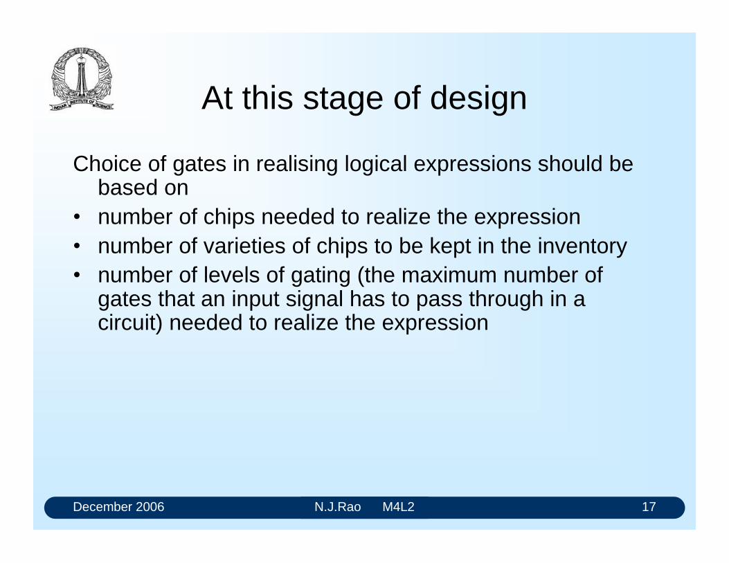
December 2006 N.J.Rao M4L2 17
At this stage of design
Choice of gates in realising logical expressions should be based on
number of chips needed to realize the expression number of varieties of chips to be kept in the inventory number of levels of gating (the maximum number of
gates that an input signal has to pass through in a circuit) needed to realize the expression
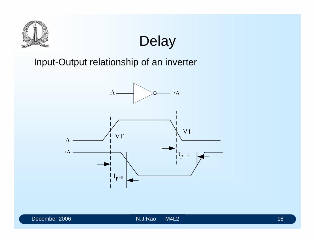
December 2006 N.J.Rao M4L2 18
DelayInput-Output relationship of an inverter
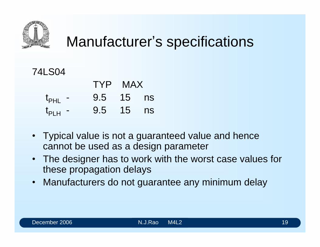
December 2006 N.J.Rao M4L2 19
Manufacturers specifications
74LS04 TYP MAX
tPHL - 9.5 15 nstPLH - 9.5 15 ns
Typical value is not a guaranteed value and hence cannot be used as a design parameter
The designer has to work with the worst case values for these propagation delays
Manufacturers do not guarantee any minimum delay
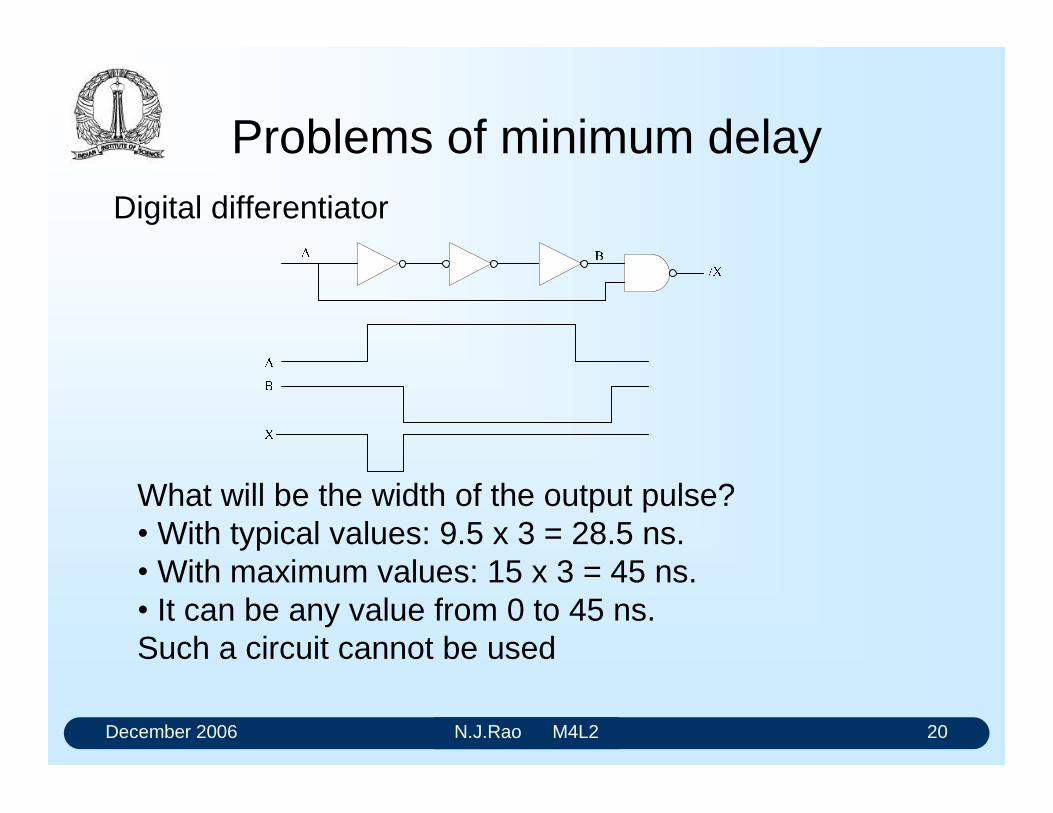
December 2006 N.J.Rao M4L2 20
Problems of minimum delayDigital differentiator
What will be the width of the output pulse? With typical values: 9.5 x 3 = 28.5 ns. With maximum values: 15 x 3 = 45 ns. It can be any value from 0 to 45 ns. Such a circuit cannot be used
December 2006 N.J.Rao M4L2 21
Delays and different realizations
Expression in SOP form can be realized By 2-level gating if the variables are available in their
Asserted High and Asserted Low versions By 3-level gating if the variables are not available in their
Asserted High and Asserted Low versionsIn all other forms the delay is likely to be more
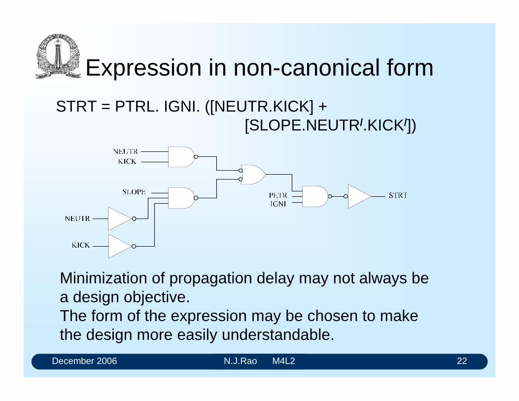
December 2006 N.J.Rao M4L2 22
Expression in non-canonical form
STRT = PTRL. IGNI. ([NEUTR.KICK] + [SLOPE.NEUTR/.KICK/])
Minimization of propagation delay may not always be a design objective. The form of the expression may be chosen to make the design more easily understandable.
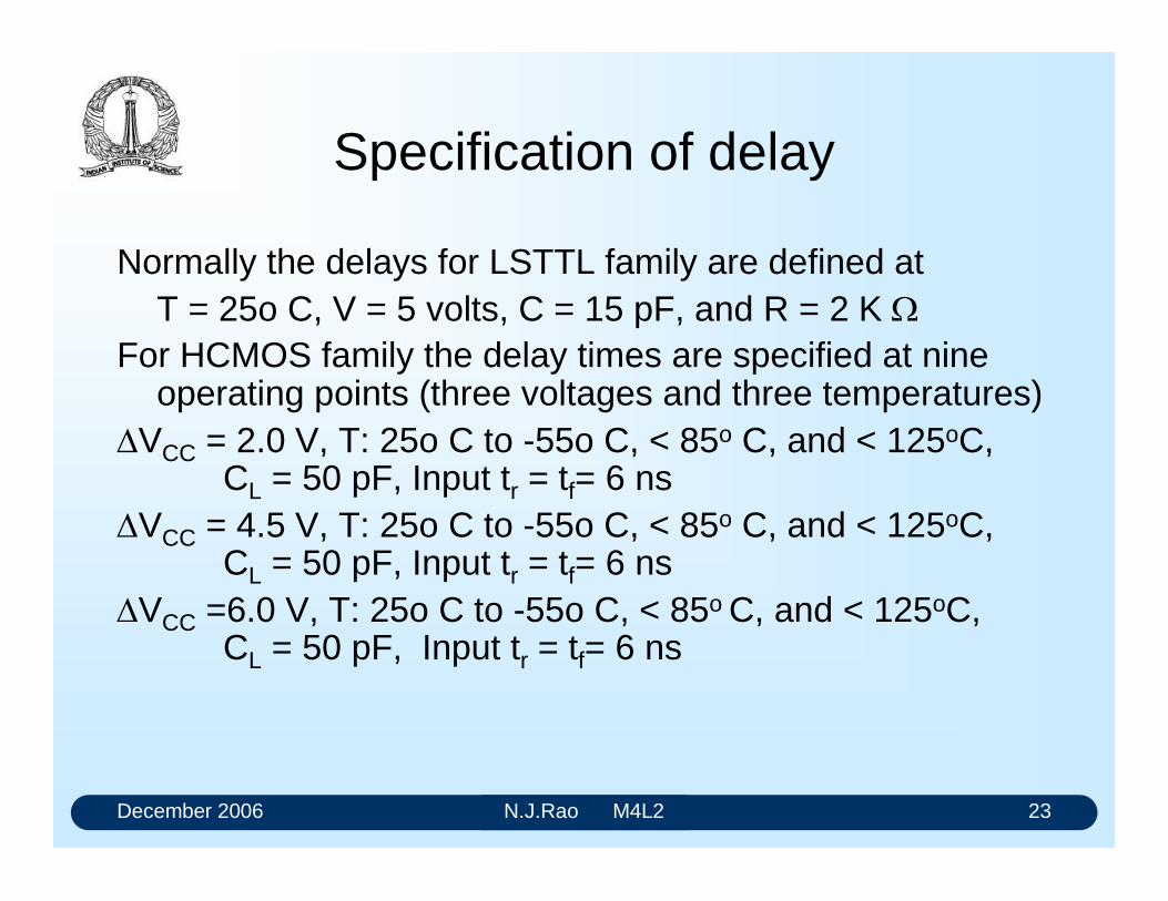
December 2006 N.J.Rao M4L2 23
Specification of delay
Normally the delays for LSTTL family are defined at T = 25o C, V = 5 volts, C = 15 pF, and R = 2 K
For HCMOS family the delay times are specified at nine operating points (three voltages and three temperatures)
VCC = 2.0 V, T: 25o C to -55o C, < 85o C, and < 125oC, CL = 50 pF, Input tr = tf= 6 ns
VCC = 4.5 V, T: 25o C to -55o C, < 85o C, and < 125oC, CL = 50 pF, Input tr = tf= 6 ns
VCC =6.0 V, T: 25o C to -55o C, < 85o C, and < 125oC, CL = 50 pF, Input tr = tf= 6 ns
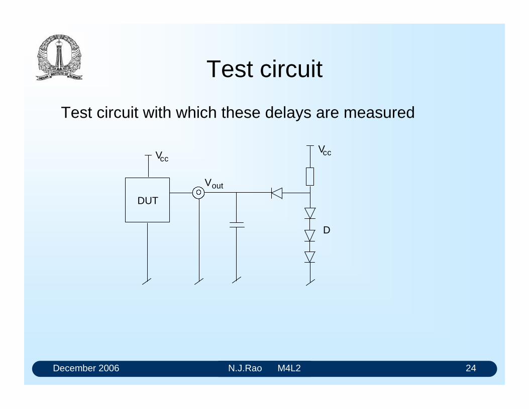
December 2006 N.J.Rao M4L2 24
Test circuit
Test circuit with which these delays are measured
VccVcc
Vout
D
DUT
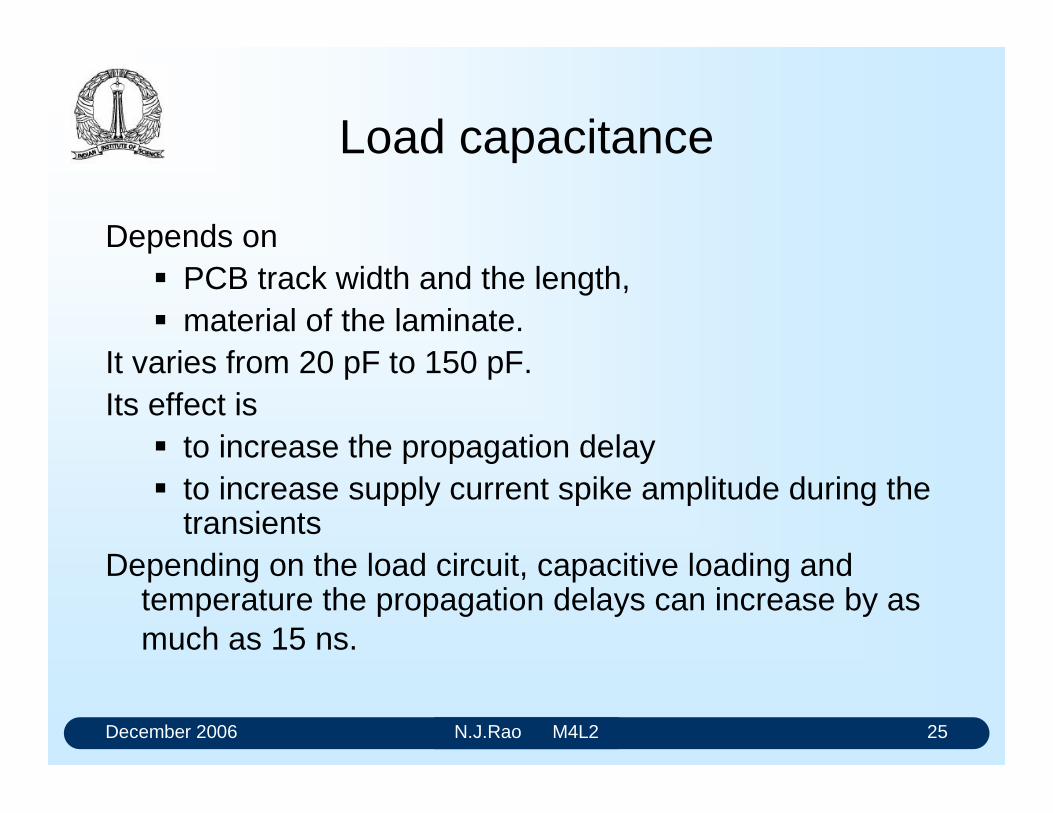
December 2006 N.J.Rao M4L2 25
Load capacitance
Depends on PCB track width and the length, material of the laminate.
It varies from 20 pF to 150 pF. Its effect is
to increase the propagation delay to increase supply current spike amplitude during the
transientsDepending on the load circuit, capacitive loading and
temperature the propagation delays can increase by as much as 15 ns.
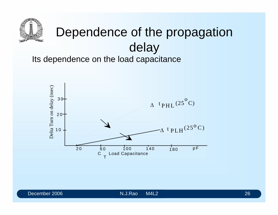
December 2006 N.J.Rao M4L2 26
Dependence of the propagation delay
Its dependence on the load capacitance
2 0 6 0 100 1 40 1 80 p F
1 0
2 0
3 0
C Load CapacitanceT
t
t P H L
P L H (25o
(25 C)o
Del
ta T
urn
on d
elay
(ns
ec)
C )
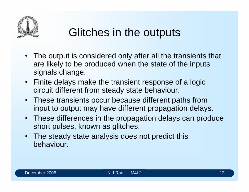
December 2006 N.J.Rao M4L2 27
Glitches in the outputs
The output is considered only after all the transients that are likely to be produced when the state of the inputs signals change.
Finite delays make the transient response of a logic circuit different from steady state behaviour.
These transients occur because different paths from input to output may have different propagation delays.
These differences in the propagation delays can produce short pulses, known as glitches.
The steady state analysis does not predict this behaviour.
December 2006 N.J.Rao M4L2 28
Hazard
A hazard is said to exist when a circuit has the possibility of generating a glitch.
The actual occurrence of the glitch and its pulse width depend on the exact delays associated with the actual devices used in the circuit.
Designer has no control over this parameter It is necessary to design that avoids the occurrence of
glitches. One simple method is not to look at the outputs until they
settle down to their final value.
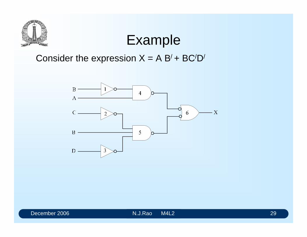
December 2006 N.J.Rao M4L2 29
ExampleConsider the expression X = A B/ + BC/D/
December 2006 N.J.Rao M4L2 30
Detection of hazard
Hazard is caused by the propagation delay associated with the gate-1 Let A and B be Asserted and C and D are Not-asserrted. When B changes from its Asserted state to its Not-asserted state with
the other variables remaining the same the output should remain in its Asserted state.
When B changes from 1-to-0 the output of the gate-5 changes from 1-to-0.
The output of the gate-4 should change from 0-to-1 at the same time. But the delay associated with the gate-1 makes this transition of the
gate-4 output to happen a little later than that of gate-5. This can cause brief transition of X from 1-to-0 and then from 0-to-1
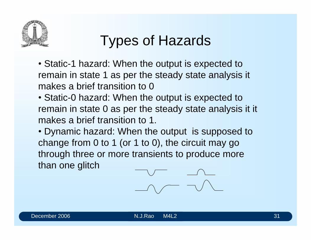
December 2006 N.J.Rao M4L2 31
Types of Hazards
Static-1 hazard: When the output is expected to remain in state 1 as per the steady state analysis it makes a brief transition to 0 Static-0 hazard: When the output is expected to remain in state 0 as per the steady state analysis it itmakes a brief transition to 1. Dynamic hazard: When the output is supposed to change from 0 to 1 (or 1 to 0), the circuit may go through three or more transients to produce more than one glitch
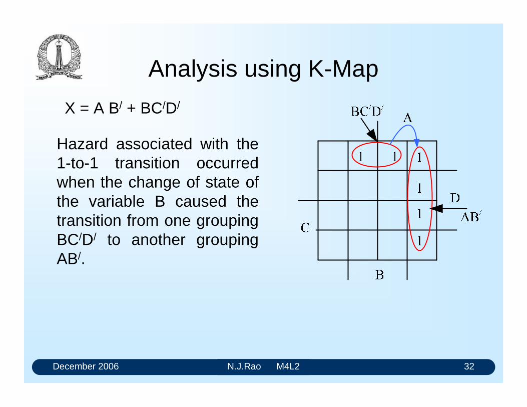
December 2006 N.J.Rao M4L2 32
Analysis using K-Map
X = A B/ + BC/D/
Hazard associated with the 1-to-1 transition occurred when the change of state of the variable B caused the transition from one grouping BC/D/ to another grouping AB/.
December 2006 N.J.Rao M4L2 33
Detection of other hazards
It is more difficult to detect the other three transitions. One result from Logic and Switching Theory states that a
two level gate implementation of a logical expression will be hazard free for all transitions of the output if it is free from the hazard associated with 1-to-1 transition.
When the input variables change in such manner as to cause a transition from one grouping to another grouping, the 1-to-1 transition can occur
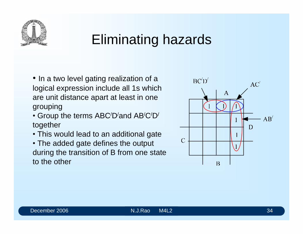
December 2006 N.J.Rao M4L2 34
Eliminating hazards
In a two level gating realization of a logical expression include all 1s which are unit distance apart at least in one grouping Group the terms ABC/D/and AB/C/D/
together This would lead to an additional gate The added gate defines the output during the transition of B from one state to the other
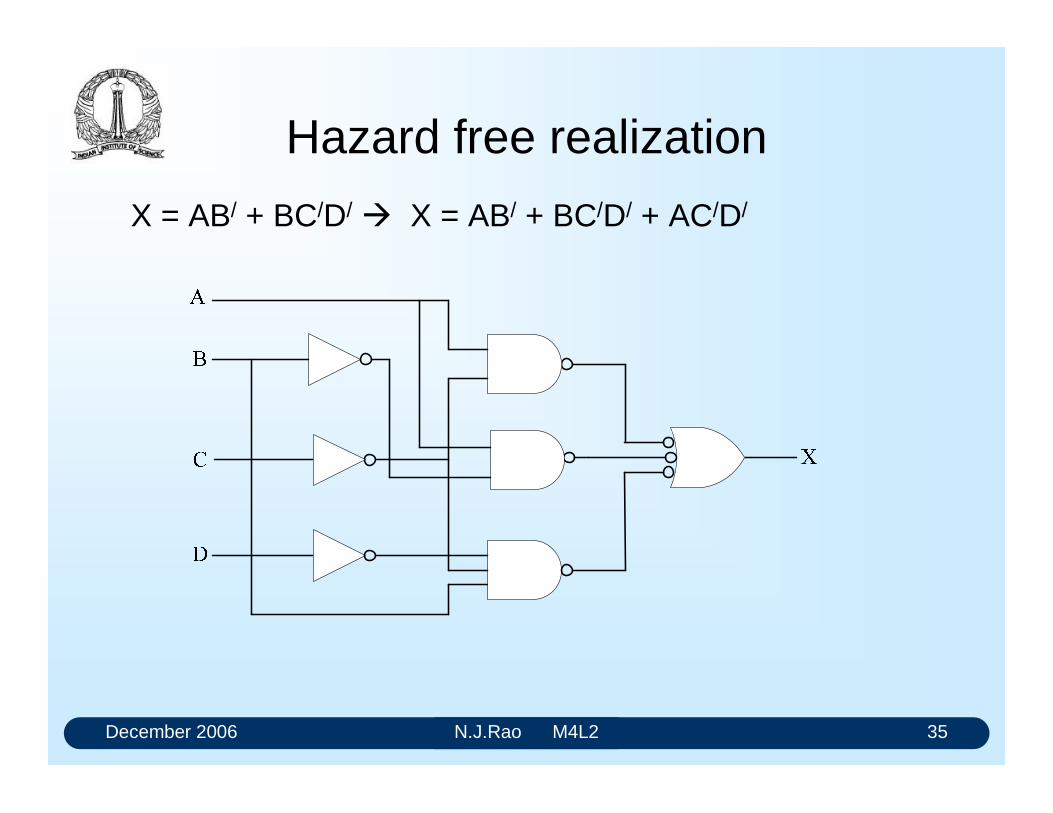
December 2006 N.J.Rao M4L2 35
Hazard free realization
X = AB/ + BC/D/ X = AB/ + BC/D/ + AC/D/
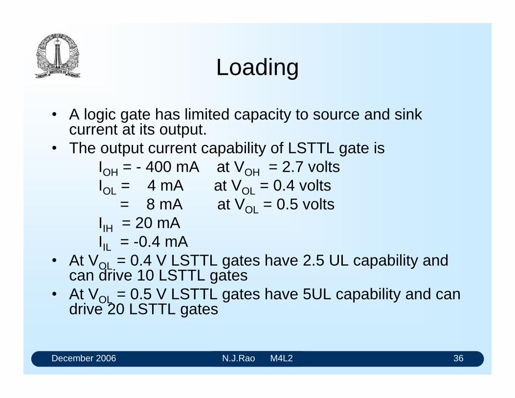
December 2006 N.J.Rao M4L2 36
Loading
A logic gate has limited capacity to source and sink current at its output.
The output current capability of LSTTL gate isIOH = - 400 mA at VOH = 2.7 voltsIOL = 4 mA at VOL = 0.4 volts
= 8 mA at VOL = 0.5 voltsIIH = 20 mAIIL = -0.4 mA
At VOL = 0.4 V LSTTL gates have 2.5 UL capability and can drive 10 LSTTL gates
At VOL = 0.5 V LSTTL gates have 5UL capability and can drive 20 LSTTL gates
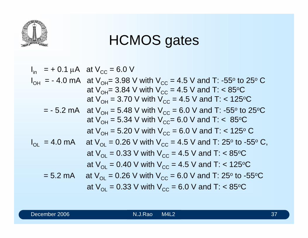
December 2006 N.J.Rao M4L2 37
HCMOS gates
Iin = + 0.1 A at VCC = 6.0 V IOH = - 4.0 mA at VOH= 3.98 V with VCC = 4.5 V and T: -55o to 25o C
at VOH= 3.84 V with VCC = 4.5 V and T: < 85oC at VOH = 3.70 V with VCC = 4.5 V and T: < 125oC
= - 5.2 mA at VOH = 5.48 V with VCC = 6.0 V and T: -55o to 25oC at VOH = 5.34 V with VCC= 6.0 V and T: < 85oCat VOH = 5.20 V with VCC = 6.0 V and T: < 125o C
IOL = 4.0 mA at VOL = 0.26 V with VCC = 4.5 V and T: 25o to -55o C, at VOL = 0.33 V with VCC = 4.5 V and T: < 85oC at VOL = 0.40 V with VCC = 4.5 V and T: < 125oC
= 5.2 mA at VOL = 0.26 V with VCC = 6.0 V and T: 25o to -55oC at VOL = 0.33 V with VCC = 6.0 V and T: < 85oC
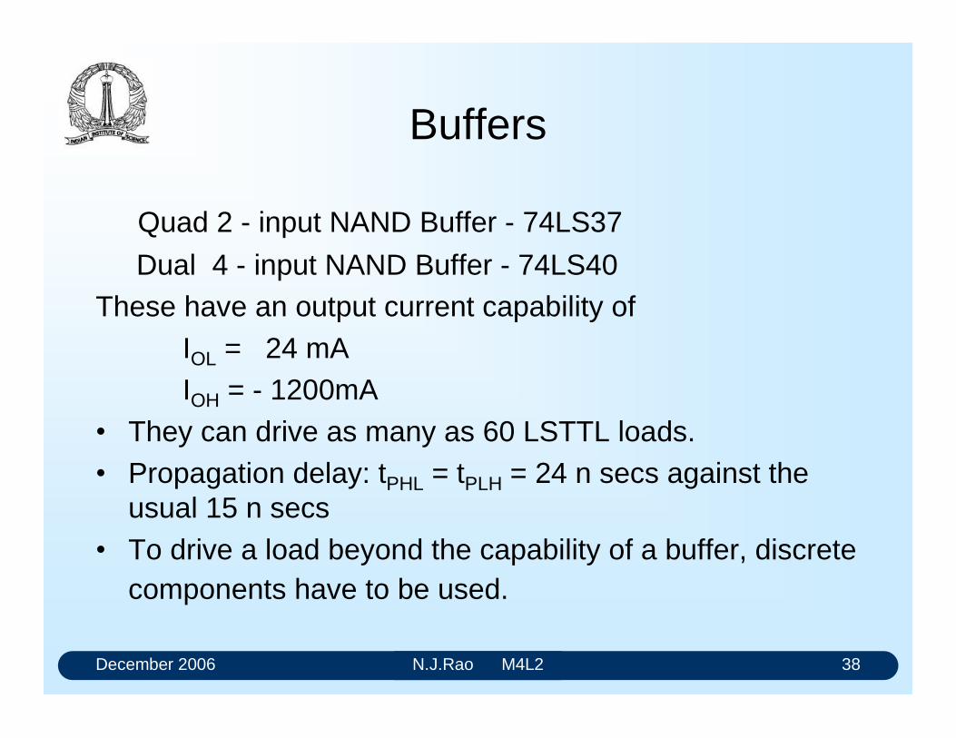
December 2006 N.J.Rao M4L2 38
Buffers
Quad 2 - input NAND Buffer - 74LS37
Dual 4 - input NAND Buffer - 74LS40These have an output current capability of
IOL = 24 mAIOH = - 1200mA
They can drive as many as 60 LSTTL loads. Propagation delay: tPHL = tPLH = 24 n secs against the
usual 15 n secs To drive a load beyond the capability of a buffer, discrete
components have to be used.
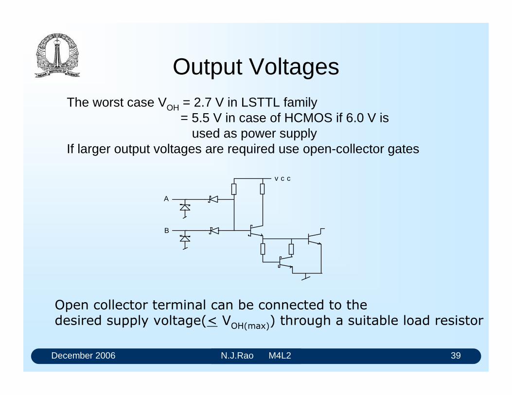
December 2006 N.J.Rao M4L2 39
Output VoltagesThe worst case VOH = 2.7 V in LSTTL family
= 5.5 V in case of HCMOS if 6.0 V isused as power supply
If larger output voltages are required use open-collector gates
A
B
v c c
Open collector terminal can be connected to the
desired supply voltage(< VOH(max)
) through a suitable load resistor
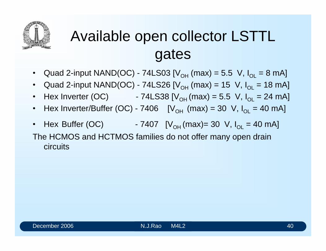
December 2006 N.J.Rao M4L2 40
Available open collector LSTTL gates
Quad 2-input NAND(OC) - 74LS03 [VOH (max) = 5.5 V, IOL = 8 mA] Quad 2-input NAND(OC) - 74LS26 [VOH (max) = 15 V, IOL = 18 mA] Hex Inverter (OC) - 74LS38 [VOH (max) = 5.5 V, IOL = 24 mA] Hex Inverter/Buffer (OC) - 7406 [VOH (max) = 30 V, IOL = 40 mA]
Hex Buffer (OC) - 7407 [VOH (max)= 30 V, IOL = 40 mA]
The HCMOS and HCTMOS families do not offer many open drain circuits
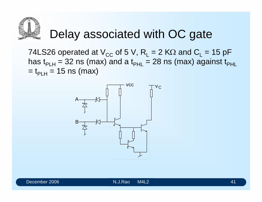
December 2006 N.J.Rao M4L2 41
Delay associated with OC gate74LS26 operated at VCC of 5 V, RL = 2 K and CL = 15 pFhas tPLH = 32 ns (max) and a tPHL = 28 ns (max) against tPHL= tPLH = 15 ns (max)
A
B
vcc vC
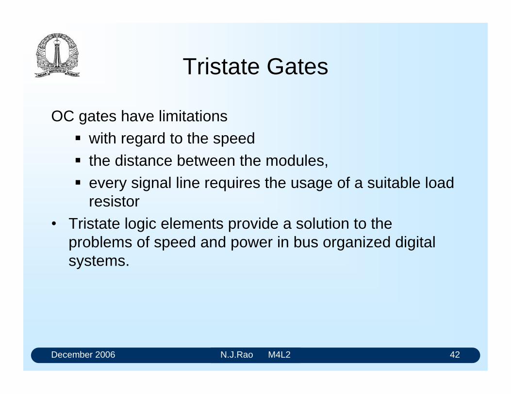
December 2006 N.J.Rao M4L2 42
Tristate Gates
OC gates have limitations with regard to the speed the distance between the modules, every signal line requires the usage of a suitable load
resistor Tristate logic elements provide a solution to the
problems of speed and power in bus organized digital systems.
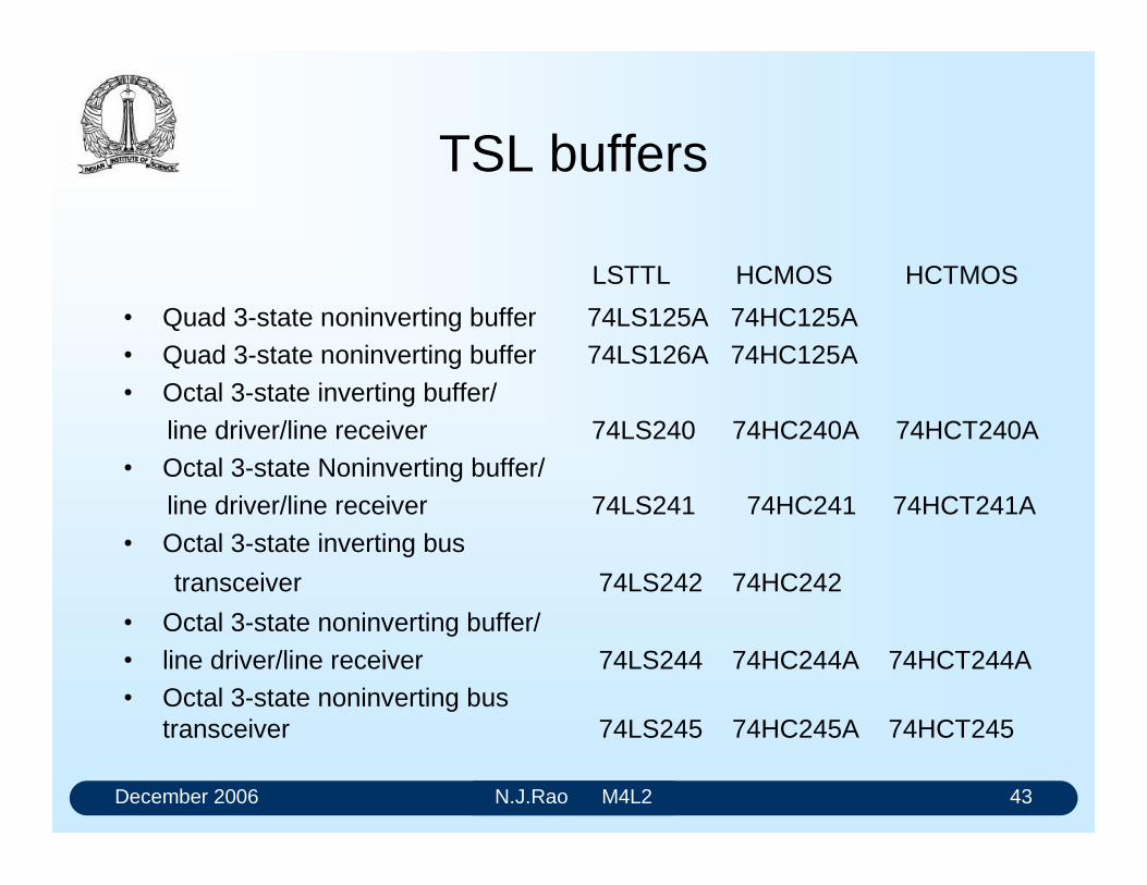
December 2006 N.J.Rao M4L2 43
TSL buffers
LSTTL HCMOS HCTMOS
Quad 3-state noninverting buffer 74LS125A 74HC125A Quad 3-state noninverting buffer 74LS126A 74HC125A
Octal 3-state inverting buffer/
line driver/line receiver 74LS240 74HC240A 74HCT240A Octal 3-state Noninverting buffer/
line driver/line receiver 74LS241 74HC241 74HCT241A
Octal 3-state inverting bus
transceiver 74LS242 74HC242
Octal 3-state noninverting buffer/
line driver/line receiver 74LS244 74HC244A 74HCT244A Octal 3-state noninverting bus
transceiver 74LS245 74HC245A 74HCT245
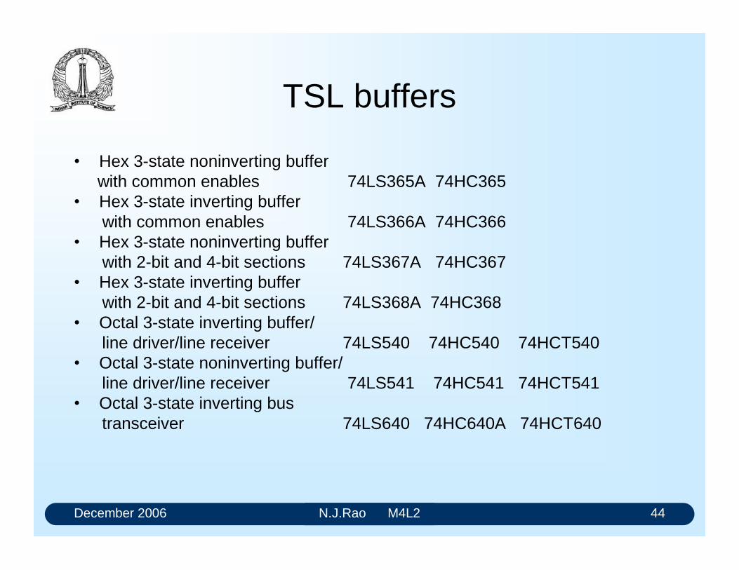
December 2006 N.J.Rao M4L2 44
TSL buffers
Hex 3-state noninverting buffer with common enables 74LS365A 74HC365
Hex 3-state inverting buffer with common enables 74LS366A 74HC366
Hex 3-state noninverting buffer with 2-bit and 4-bit sections 74LS367A 74HC367
Hex 3-state inverting buffer with 2-bit and 4-bit sections 74LS368A 74HC368
Octal 3-state inverting buffer/ line driver/line receiver 74LS540 74HC540 74HCT540
Octal 3-state noninverting buffer/ line driver/line receiver 74LS541 74HC541 74HCT541
Octal 3-state inverting bus transceiver 74LS640 74HC640A 74HCT640
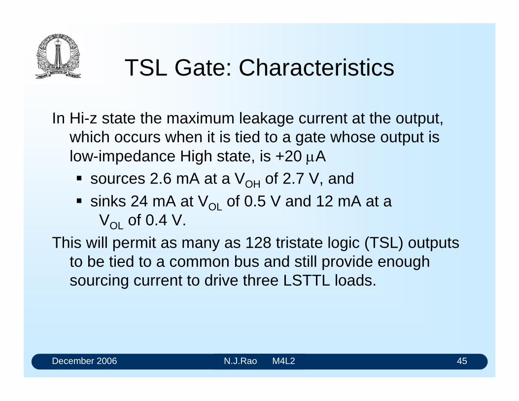
December 2006 N.J.Rao M4L2 45
TSL Gate: Characteristics
In Hi-z state the maximum leakage current at the output, which occurs when it is tied to a gate whose output is low-impedance High state, is +20 A sources 2.6 mA at a VOH of 2.7 V, and sinks 24 mA at VOL of 0.5 V and 12 mA at a
VOL of 0.4 V.This will permit as many as 128 tristate logic (TSL) outputs
to be tied to a common bus and still provide enough sourcing current to drive three LSTTL loads.
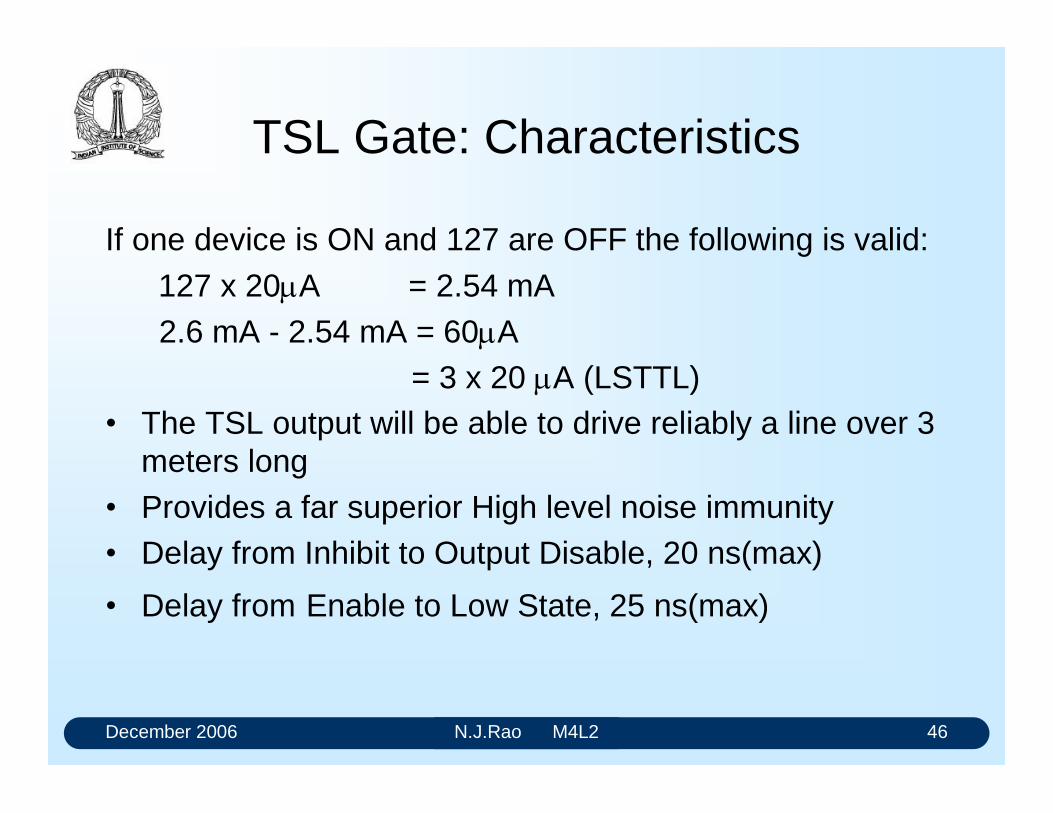
December 2006 N.J.Rao M4L2 46
TSL Gate: Characteristics
If one device is ON and 127 are OFF the following is valid:
127 x 20A = 2.54 mA2.6 mA - 2.54 mA = 60A
= 3 x 20 A (LSTTL) The TSL output will be able to drive reliably a line over 3
meters long Provides a far superior High level noise immunity Delay from Inhibit to Output Disable, 20 ns(max)
Delay from Enable to Low State, 25 ns(max)

INTRODUCTION
Logic functions that represent combinational functions can be implemented as hardware in any one of the several logic families that are commercially available. The logic families that are widely used for the medium frequency (up to about 25 MHz) applications are
LSTTL
HCMOS
Higher frequency requirements are met by
FAST series
Schottky series
74LSTTL ICs are designed to operate over the commercial temperature range, namely, from 0oC to 70oC.
54LS TTL ICs are functionally and pin-to-pin compatible with 74LS units, but operate over the Military temperature range, namely, -55oC to +125oC.
HCMOS family ICs are also available in the same temperature range.
Before the advent of the microprocessors and programmable LSI combinational circuits (PROMs, PLAs and PALs) digital designers had to be content with gates to realise complex combinational circuits. It was, therefore, necessary to simplify the expressions to reduce the number of gates or the number of ICs. When the number of variables was smaller, designers used Karnaugh Maps or Variable Entered Karnaugh Maps (VEM). When the variables were large in number it was necessary to use computer based minimisation techniques.
With LSI combinational circuits becoming popular and the cost per gate coming down drastically, the need for conventional type of minimisation is much less, the tractability of the design became more important. The given logical expressions can now be implemented, however complex they are, using programmable combinational LSI circuits, and keep the chip count low.
Certain standard combinational functions like adders, multiplexers, comparators and encoders are available in MSI packages. Therefore, realisation of these commonly encountered combinational functions need not be done by gates. In view of the availability of certain standard MSI and LSI circuits the SSI gates are mainly used for realising simple logic functions normally encountered in interconnecting LSI and MSI circuits. Design with these gates, therefore, is done predominantly on an intuitive basis, and occasionally using K-Maps or VEMs.
Gates available in the 74 series of LS and HCMOS/HCTMOS families are listed in the following.
LSTTL FAST HCMOS HCTMOS 54/74LS 54/74F 54/74HC 54/74HCT NAND Gates Quad 2-input NAND 00 00 00A --- Triple 3-input NAND 10 10 10 --- Dual 4-input NAND 20 20 20 --- 8-input NAND 30 --- 30 --- 13-input NAND 133 --- 133 ---
NOR Gates
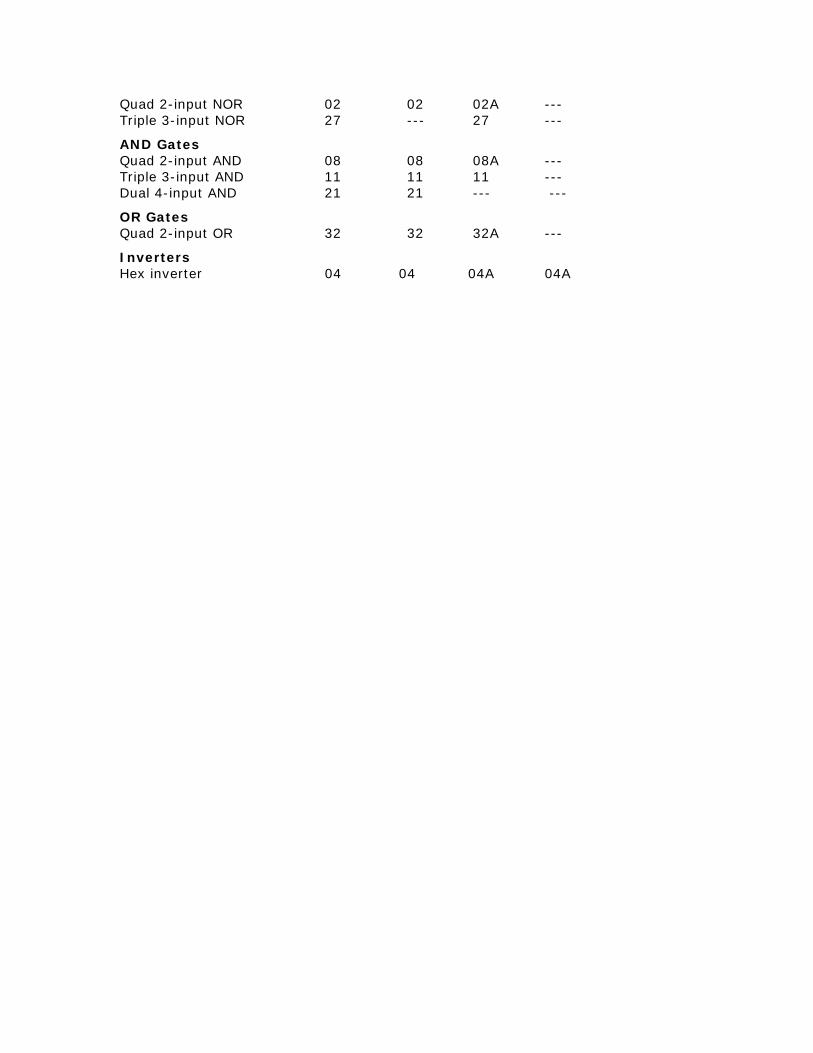
Quad 2-input NOR 02 02 02A --- Triple 3-input NOR 27 --- 27 ---
AND Gates Quad 2-input AND 08 08 08A --- Triple 3-input AND 11 11 11 --- Dual 4-input AND 21 21 --- ---
OR Gates Quad 2-input OR 32 32 32A ---
Inverters Hex inverter 04 04 04A 04A
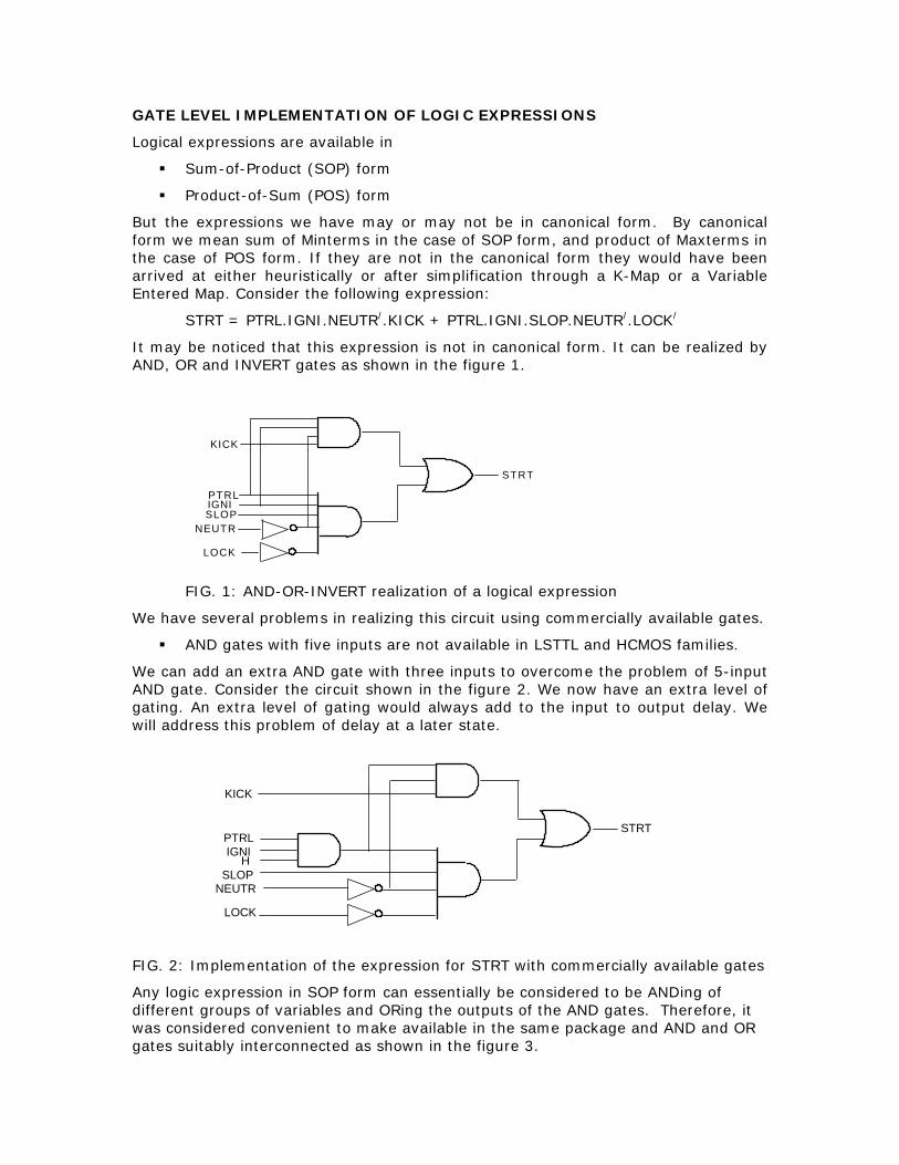
GATE LEVEL IMPLEMENTATION OF LOGIC EXPRESSIONS
Logical expressions are available in
Sum-of-Product (SOP) form
Product-of-Sum (POS) form
But the expressions we have may or may not be in canonical form. By canonical form we mean sum of Minterms in the case of SOP form, and product of Maxterms in the case of POS form. If they are not in the canonical form they would have been arrived at either heuristically or after simplification through a K-Map or a Variable Entered Map. Consider the following expression:
STRT = PTRL.IGNI.NEUTR/.KICK + PTRL.IGNI.SLOP.NEUTR/.LOCK/
It may be noticed that this expression is not in canonical form. It can be realized by AND, OR and INVERT gates as shown in the figure 1.
KICK
PTRLIGNISLOP
NEUTR
LOCK
STRT
FIG. 1: AND-OR-INVERT realization of a logical expression
We have several problems in realizing this circuit using commercially available gates.
AND gates with five inputs are not available in LSTTL and HCMOS families.
We can add an extra AND gate with three inputs to overcome the problem of 5-input AND gate. Consider the circuit shown in the figure 2. We now have an extra level of gating. An extra level of gating would always add to the input to output delay. We will address this problem of delay at a later state.
FIG. 2: Implementation of the expression for STRT with commercially available gates
Any logic expression in SOP form can essentially be considered to be ANDing of different groups of variables and ORing the outputs of the AND gates. Therefore, it was considered convenient to make available in the same package and AND and OR gates suitably interconnected as shown in the figure 3.
KICK
PTRLIGNI
SLOPNEUTR
LOCK
STRT
H
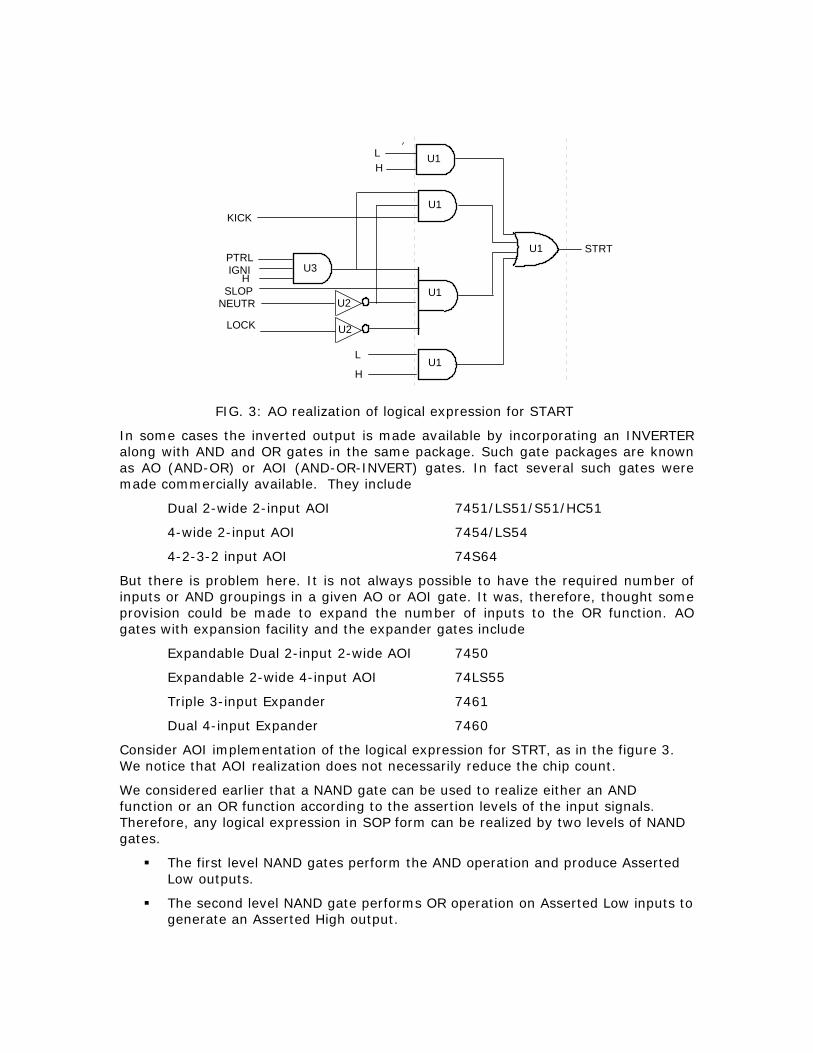
KICK
PTRLIGNI
SLOPNEUTR
LOCK
STRT
H
L
H
LH
U1
U1
U1
U1
U1
U2
U2
U3
FIG. 3: AO realization of logical expression for START
In some cases the inverted output is made available by incorporating an INVERTER along with AND and OR gates in the same package. Such gate packages are known as AO (AND-OR) or AOI (AND-OR-INVERT) gates. In fact several such gates were made commercially available. They include
Dual 2-wide 2-input AOI 7451/LS51/S51/HC51
4-wide 2-input AOI 7454/LS54
4-2-3-2 input AOI 74S64
But there is problem here. It is not always possible to have the required number of inputs or AND groupings in a given AO or AOI gate. It was, therefore, thought some provision could be made to expand the number of inputs to the OR function. AO gates with expansion facility and the expander gates include
Expandable Dual 2-input 2-wide AOI 7450
Expandable 2-wide 4-input AOI 74LS55
Triple 3-input Expander 7461
Dual 4-input Expander 7460
Consider AOI implementation of the logical expression for STRT, as in the figure 3. We notice that AOI realization does not necessarily reduce the chip count.
We considered earlier that a NAND gate can be used to realize either an AND function or an OR function according to the assertion levels of the input signals. Therefore, any logical expression in SOP form can be realized by two levels of NAND gates.
The first level NAND gates perform the AND operation and produce Asserted Low outputs.
The second level NAND gate performs OR operation on Asserted Low inputs to generate an Asserted High output.
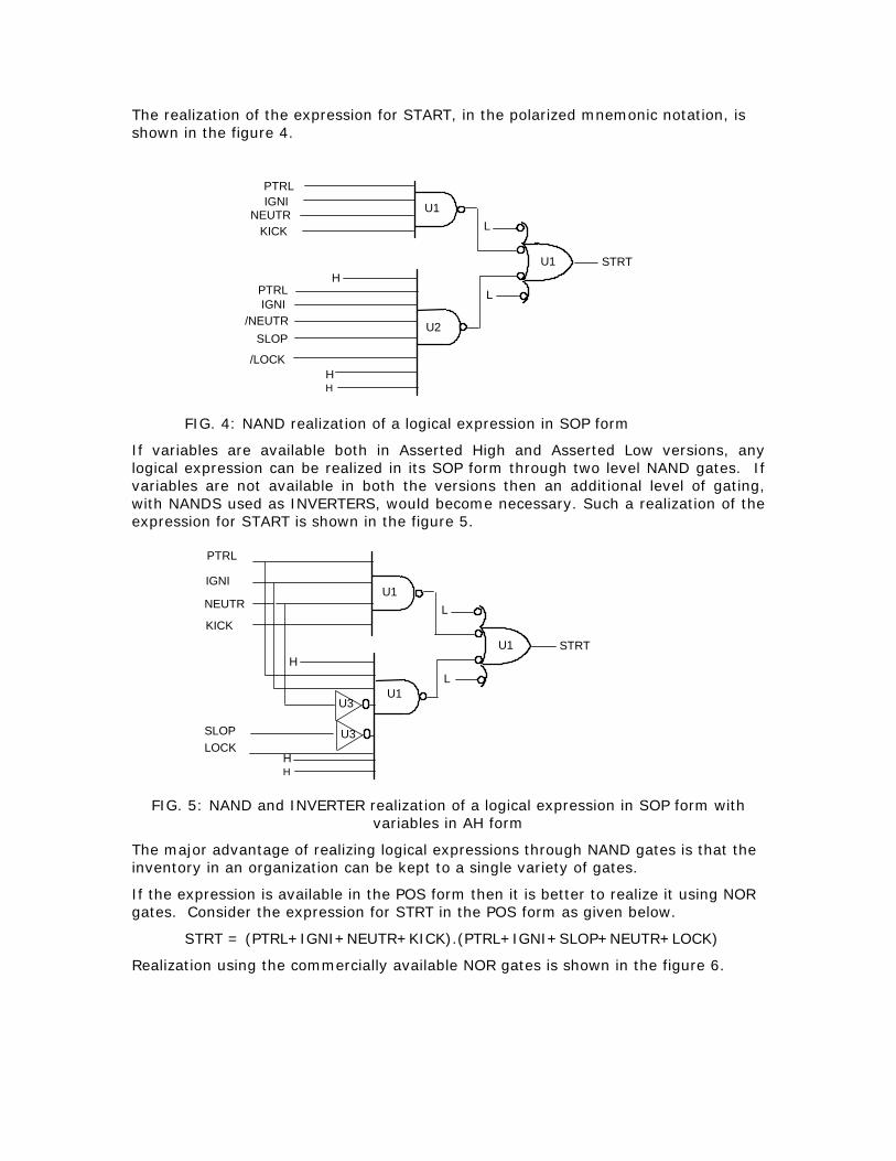
The realization of the expression for START, in the polarized mnemonic notation, is shown in the figure 4.
STRTU1
U2
IGNINEUTR
H
U1L
L
KICK
HH
SLOP
/LOCK
PTRL
/NEUTRIGNIPTRL
FIG. 4: NAND realization of a logical expression in SOP form
If variables are available both in Asserted High and Asserted Low versions, any logical expression can be realized in its SOP form through two level NAND gates. If variables are not available in both the versions then an additional level of gating, with NANDS used as INVERTERS, would become necessary. Such a realization of the expression for START is shown in the figure 5.
STRTU1
U1
IGNI
NEUTR
H
U1
U3
U3
L
L
KICK
HH
SLOPLOCK
PTRL
FIG. 5: NAND and INVERTER realization of a logical expression in SOP form with variables in AH form
The major advantage of realizing logical expressions through NAND gates is that the inventory in an organization can be kept to a single variety of gates.
If the expression is available in the POS form then it is better to realize it using NOR gates. Consider the expression for STRT in the POS form as given below.
STRT = (PTRL+IGNI+NEUTR+KICK).(PTRL+IGNI+SLOP+NEUTR+LOCK)
Realization using the commercially available NOR gates is shown in the figure 6.
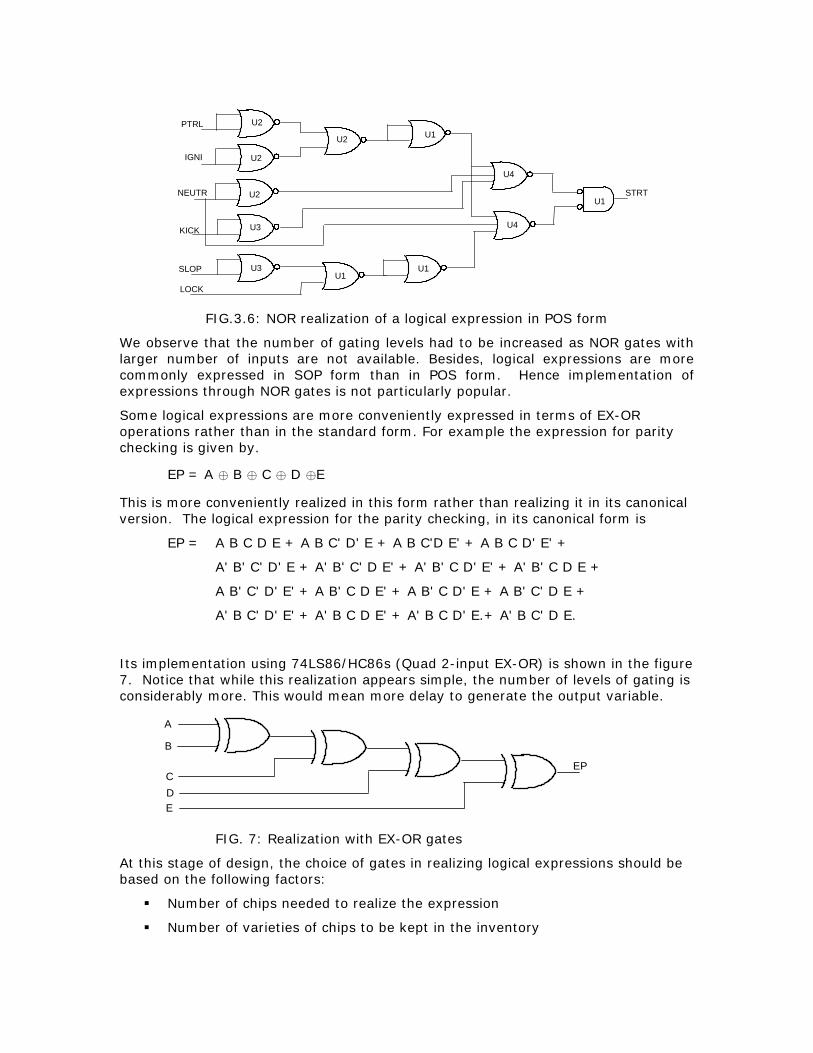
U1STRT
U4
U4
U1U1
U3
U3
U2
U2
U2
U2 U1PTRL
IGNI
NEUTR
KICK
SLOP
LOCK
FIG.3.6: NOR realization of a logical expression in POS form
We observe that the number of gating levels had to be increased as NOR gates with larger number of inputs are not available. Besides, logical expressions are more commonly expressed in SOP form than in POS form. Hence implementation of expressions through NOR gates is not particularly popular.
Some logical expressions are more conveniently expressed in terms of EX-OR operations rather than in the standard form. For example the expression for parity checking is given by.
EP = A ⊕ B ⊕ C ⊕ D ⊕E
This is more conveniently realized in this form rather than realizing it in its canonical version. The logical expression for the parity checking, in its canonical form is
EP = A B C D E + A B C' D' E + A B C'D E' + A B C D' E' +
A' B' C' D' E + A' B' C' D E' + A' B' C D' E' + A' B' C D E +
A B' C' D' E' + A B' C D E' + A B' C D' E + A B' C' D E +
A' B C' D' E' + A' B C D E' + A' B C D' E.+ A' B C' D E.
Its implementation using 74LS86/HC86s (Quad 2-input EX-OR) is shown in the figure 7. Notice that while this realization appears simple, the number of levels of gating is considerably more. This would mean more delay to generate the output variable.
A
B
CDE
EP
FIG. 7: Realization with EX-OR gates
At this stage of design, the choice of gates in realizing logical expressions should be based on the following factors:
Number of chips needed to realize the expression
Number of varieties of chips to be kept in the inventory

Number of levels of gating (the maximum number of gates that an input signal has to pass through in a circuit)
Each expression may lead to the usage of a unique combination of gates in minimizing the chip count. In such a case one has to keep all the available gates in the inventory. However, if one wishes to minimize the inventory it is more convenient to limit the realization of logical expressions to NANDs and INVERTERs. This is particularly advantageous as the expressions are more commonly available in the SOP form. The number of levels of gating depends on the number of variables, the form in which the variables are available and the fan-in of the available gates, which in turn determines the delay in generating the output.
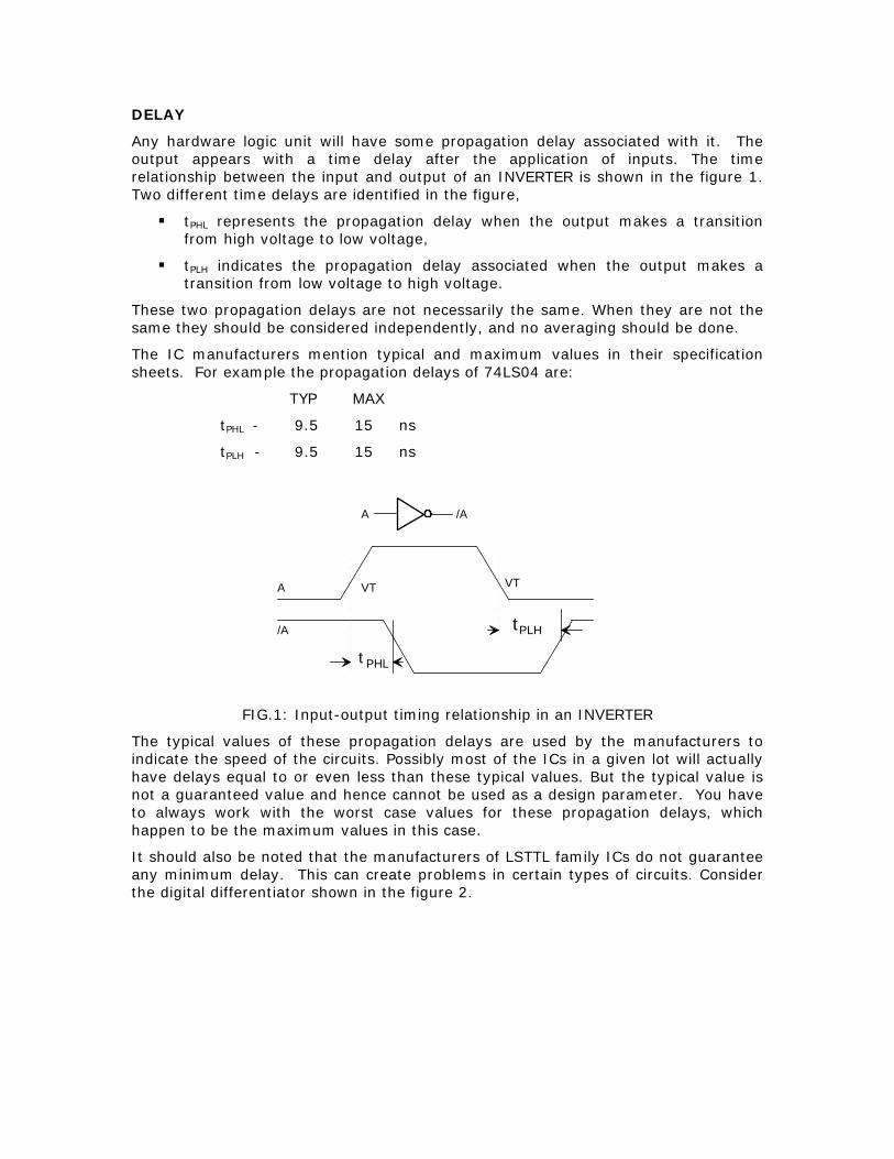
DELAY
Any hardware logic unit will have some propagation delay associated with it. The output appears with a time delay after the application of inputs. The time relationship between the input and output of an INVERTER is shown in the figure 1. Two different time delays are identified in the figure,
tPHL represents the propagation delay when the output makes a transition from high voltage to low voltage,
tPLH indicates the propagation delay associated when the output makes a transition from low voltage to high voltage.
These two propagation delays are not necessarily the same. When they are not the same they should be considered independently, and no averaging should be done.
The IC manufacturers mention typical and maximum values in their specification sheets. For example the propagation delays of 74LS04 are:
TYP MAX
tPHL - 9.5 15 ns
tPLH - 9.5 15 ns
A /A
VT
/A
A
PLHt
t PHL
VT
FIG.1: Input-output timing relationship in an INVERTER
The typical values of these propagation delays are used by the manufacturers to indicate the speed of the circuits. Possibly most of the ICs in a given lot will actually have delays equal to or even less than these typical values. But the typical value is not a guaranteed value and hence cannot be used as a design parameter. You have to always work with the worst case values for these propagation delays, which happen to be the maximum values in this case.
It should also be noted that the manufacturers of LSTTL family ICs do not guarantee any minimum delay. This can create problems in certain types of circuits. Consider the digital differentiator shown in the figure 2.
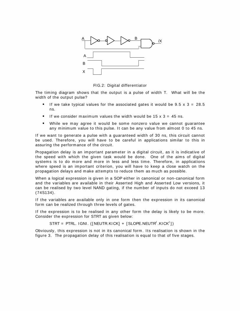
/XA B
A
B
X
FIG.2: Digital differentiator
The timing diagram shows that the output is a pulse of width T. What will be the width of the output pulse?
If we take typical values for the associated gates it would be 9.5 x 3 = 28.5 ns.
If we consider maximum values the width would be 15 x 3 = 45 ns.
While we may agree it would be some nonzero value we cannot guarantee any minimum value to this pulse. It can be any value from almost 0 to 45 ns.
If we want to generate a pulse with a guaranteed width of 30 ns, this circuit cannot be used. Therefore, you will have to be careful in applications similar to this in assuring the performance of the circuit.
Propagation delay is an important parameter in a digital circuit, as it is indicative of the speed with which the given task would be done. One of the aims of digital systems is to do more and more in less and less time. Therefore, in applications where speed is an important criterion, you will have to keep a close watch on the propagation delays and make attempts to reduce them as much as possible.
When a logical expression is given in a SOP either in canonical or non-canonical form and the variables are available in their Asserted High and Asserted Low versions, it can be realised by two level NAND gating, if the number of inputs do not exceed 13 (74S134).
If the variables are available only in one form then the expression in its canonical form can be realized through three levels of gates.
If the expression is to be realised in any other form the delay is likely to be more. Consider the expression for STRT as given below:
STRT = PTRL. IGNI. ([NEUTR.KICK] + [SLOPE.NEUTR/.KICK/])
Obviously, this expression is not in its canonical form. Its realisation is shown in the figure 3. The propagation delay of this realisation is equal to that of five stages.
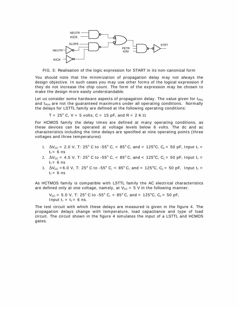
NEUTR
SLOPE
NEUTRPETRIGNI
STRT
KICK
KICK
FIG. 3: Realisation of the logic expression for START in its non-canonical form
You should note that the minimization of propagation delay may not always the design objective. In such cases you may use other forms of the logical expression if they do not increase the chip count. The form of the expression may be chosen to make the design more easily understandable.
Let us consider some hardware aspects of propagation delay. The value given for tPHL and tPLH are not the guaranteed maximums under all operating conditions. Normally the delays for LSTTL family are defined at the following operating conditions:
T = 25o C, V = 5 volts, C = 15 pF, and R = 2 K Ω
For HCMOS family the delay times are defined at many operating conditions, as these devices can be operated at voltage levels below 6 volts. The dc and ac characteristics including the time delays are specified at nine operating points (three voltages and three temperatures)
1. ∆VCC = 2.0 V, T: 25o C to -55o C, < 85o C, and < 125oC, CL = 50 pF, Input tr = tf = 6 ns
2. ∆VCC = 4.5 V, T: 25o C to -55o C, < 85o C, and < 125oC, CL = 50 pF, Input tr = tf = 6 ns
3. ∆VCC =6.0 V, T: 25o C to -55o C, < 85o C, and < 125oC, CL = 50 pF, Input tr = tf = 6 ns
As HCTMOS family is compatible with LSTTL family the AC electrical characteristics are defined only at one voltage, namely, at VCC = 5 V in the following manner.
VCC = 5.0 V, T: 25o C to -55o C, < 85o C, and < 125oC, CL = 50 pF, Input tr = tf = 6 ns.
The test circuit with which these delays are measured is given in the figure 4. The propagation delays change with temperature, load capacitance and type of load circuit. The circuit shown in the figure 4 simulates the input of a LSTTL and HCMOS gates.
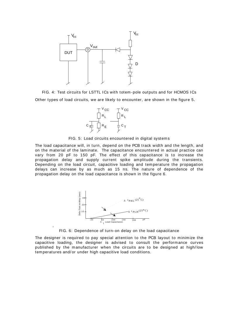
VccVcc
Vout
D
DUT
FIG. 4: Test circuits for LSTTL ICs with totem-pole outputs and for HCMOS ICs
Other types of load circuits, we are likely to encounter, are shown in the figure 5.
R
V V
R
RC T E
LL
C T
CCCC
FIG. 5: Load circuits encountered in digital systems
The load capacitance will, in turn, depend on the PCB track width and the length, and on the material of the laminate. The capacitance encountered in actual practice can vary from 20 pF to 150 pF. The effect of this capacitance is to increase the propagation delay and supply current spike amplitude during the transients. Depending on the load circuit, capacitive loading and temperature the propagation delays can increase by as much as 15 ns. The nature of dependence of the propagation delay on the load capacitance is shown in the figure 6.
. 2 0 6 0 10 0 1 40 18 0 p F
1 0
2 0
3 0
C Load CapacitanceT
∆
t
t P H L
P L H (25o
(25 C)o
Del
ta T
urn
on d
elay
(nse
c)
∆ C )
FIG. 6: Dependence of turn-on delay on the load capacitance
The designer is required to pay special attention to the PCB layout to minimize the capacitive loading, the designer is advised to consult the performance curves published by the manufacturer when the circuits are to be designed at high/low temperatures and/or under high capacitive load conditions.
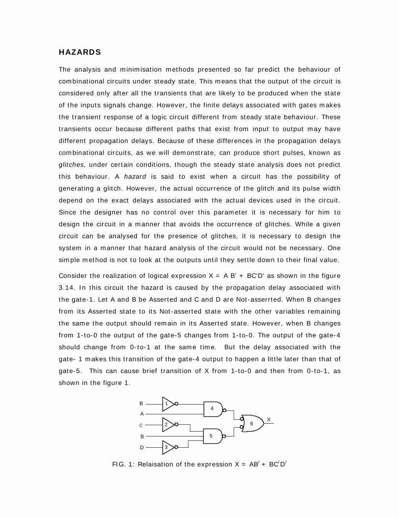
HAZARDS
The analysis and minimisation methods presented so far predict the behaviour of
combinational circuits under steady state. This means that the output of the circuit is
considered only after all the transients that are likely to be produced when the state
of the inputs signals change. However, the finite delays associated with gates makes
the transient response of a logic circuit different from steady state behaviour. These
transients occur because different paths that exist from input to output may have
different propagation delays. Because of these differences in the propagation delays
combinational circuits, as we will demonstrate, can produce short pulses, known as
glitches, under certain conditions, though the steady state analysis does not predict
this behaviour. A hazard is said to exist when a circuit has the possibility of
generating a glitch. However, the actual occurrence of the glitch and its pulse width
depend on the exact delays associated with the actual devices used in the circuit.
Since the designer has no control over this parameter it is necessary for him to
design the circuit in a manner that avoids the occurrence of glitches. While a given
circuit can be analysed for the presence of glitches, it is necessary to design the
system in a manner that hazard analysis of the circuit would not be necessary. One
simple method is not to look at the outputs until they settle down to their final value.
Consider the realization of logical expression X = A B' + BC'D' as shown in the figure
3.14. In this circuit the hazard is caused by the propagation delay associated with
the gate-1. Let A and B be Asserted and C and D are Not-asserrted. When B changes
from its Asserted state to its Not-asserted state with the other variables remaining
the same the output should remain in its Asserted state. However, when B changes
from 1-to-0 the output of the gate-5 changes from 1-to-0. The output of the gate-4
should change from 0-to-1 at the same time. But the delay associated with the
gate- 1 makes this transition of the gate-4 output to happen a little later than that of
gate-5. This can cause brief transition of X from 1-to-0 and then from 0-to-1, as
shown in the figure 1.
A
B
B
C
D
X
1
2
3
4
5
6
FIG. 1: Relaisation of the expression X = AB/ + BC/D/
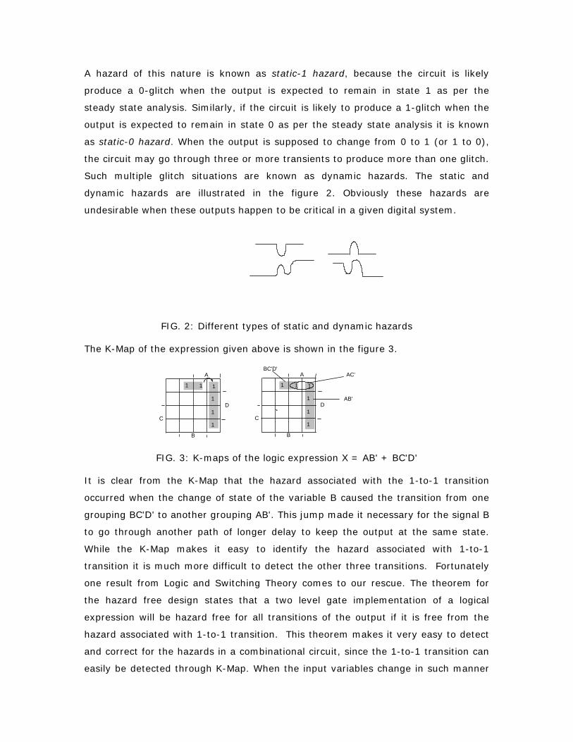
A hazard of this nature is known as static-1 hazard, because the circuit is likely
produce a 0-glitch when the output is expected to remain in state 1 as per the
steady state analysis. Similarly, if the circuit is likely to produce a 1-glitch when the
output is expected to remain in state 0 as per the steady state analysis it is known
as static-0 hazard. When the output is supposed to change from 0 to 1 (or 1 to 0),
the circuit may go through three or more transients to produce more than one glitch.
Such multiple glitch situations are known as dynamic hazards. The static and
dynamic hazards are illustrated in the figure 2. Obviously these hazards are
undesirable when these outputs happen to be critical in a given digital system.
FIG. 2: Different types of static and dynamic hazards
The K-Map of the expression given above is shown in the figure 3.
1 1 1
1
1
1
A
B
C
D
1 1 1
1
1
1
A
B
C
D
AC' BC'D'
AB'
FIG. 3: K-maps of the logic expression X = AB' + BC'D'
It is clear from the K-Map that the hazard associated with the 1-to-1 transition
occurred when the change of state of the variable B caused the transition from one
grouping BC'D' to another grouping AB'. This jump made it necessary for the signal B
to go through another path of longer delay to keep the output at the same state.
While the K-Map makes it easy to identify the hazard associated with 1-to-1
transition it is much more difficult to detect the other three transitions. Fortunately
one result from Logic and Switching Theory comes to our rescue. The theorem for
the hazard free design states that a two level gate implementation of a logical
expression will be hazard free for all transitions of the output if it is free from the
hazard associated with 1-to-1 transition. This theorem makes it very easy to detect
and correct for the hazards in a combinational circuit, since the 1-to-1 transition can
easily be detected through K-Map. When the input variables change in such manner
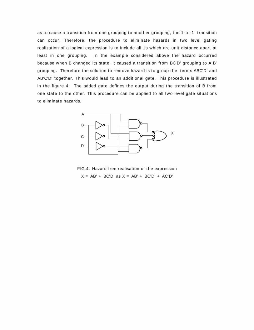
as to cause a transition from one grouping to another grouping, the 1-to-1 transition
can occur. Therefore, the procedure to eliminate hazards in two level gating
realization of a logical expression is to include all 1s which are unit distance apart at
least in one grouping. In the example considered above the hazard occurred
because when B changed its state, it caused a transition from BC'D' grouping to A B'
grouping. Therefore the solution to remove hazard is to group the terms ABC'D' and
AB'C'D' together. This would lead to an additional gate. This procedure is illustrated
in the figure 4. The added gate defines the output during the transition of B from
one state to the other. This procedure can be applied to all two level gate situations
to eliminate hazards.
A
B
C
D
X
FIG.4: Hazard free realisation of the expression
X = AB' + BC'D' as X = AB' + BC'D' + AC'D'
LOADING
A logic gate has limited capacity to source and sink current at its output. As the
output of a gate is likely to be connected to more than one similar gate, the designer
has to ensure that the driving unit has the necessary current capability. The loading
in the case of digital circuits, built with TTL integrated circuits, is defined in terms of
Unit Loads (UL). One UL is defined as that of the input of Std.TTL gate. This is given
by,
IIL : Input LOW Current (The current flowing out of an input when a
specified LOW level voltage is applied to that input)
= -1.6 mA (with VCC at Maximum and VI = 0.4 volts)
IIH : Input HIGH Current (The current flowing into an input when a specified
HIGH level voltage is applied to that input)
= 40µA (with VCC at Maximum and VI = 2.4 volts)
A Std. TTL gate has a fanout of 10 ULs. This is equivalent to,
IOL : Output LOW Current (The current flowing into an output which is in the
LOW state)
= 16 mA (with VCC and VIH at Minimum and VOL = 0.4 volts)
IOH - Output HIGH Current (The current flowing out of an output which is in
HIGH state)
= - 400 µA(with VCC at Minimum, VIL at Maximum and VOH = 2.4 volts)
The output current capability of LSTTL gate is
IOH = - 400 µA at VOH = 2.7 volts
IOL = 4 mA at VOL = 0.4 volts
= 8 mA at VOL = 0.5 volts
If the LOW state output VOL is to be maintained at 0.4 volts LSTTL gates have 2.5 UL
capability, and if VOL can be tolerated at 0.5 volts it can support 5 ULs. However, it is
unlikely that we need to drive Std.TTL gates. The LSTTL gate has the input
characteristics as given below:
IIH = 20 µA at VI = 2.7 volts
IIL = -0.4 mA at VI = 2.7 volts

Therefore, an LSTTL gate can drive 10 LSTTL gates with VOL of 0.4 volts and 20
LSTTL gates with a VOL of 0.5 volts. The loading on an LSTTL gate, that is, the
number of other LSTTL gates that can be connected to it, should be kept within these
limits. If these limits are exceeded, initially the logic voltage levels deteriorate from
the specified values, and subsequently the gate would be damaged due to the
excessive power consumption.
The input and output current specifications of a HCMOS gate are given by;
Iin = + 0.1 µA at VCC = 6.0 V at T: 25o C to -55oC,
= + 1.0 µA at VCC = 6.0 V at T: < 85o C
= + 1.0 µA at VCC = 6.0 V at T: < 125o C
IOH = - 4.0 mA at VOH = 3.98 V with VCC = 4.5 V and T: -55o to 25o C
at VOH = 3.84 V with VCC = 4.5 V and T: < 85oC
at VOH = 3.70 V with VCC = 4.5 V and T: < 125oC
= - 5.2 mA at VOH = 5.48 V with VCC = 6.0 V and T: -55o to 25o C
at VOH = 5.34 V with VCC = 6.0 V and T: < 85oC
at VOH = 5.20 V with VCC = 6.0 V and T: < 125o C
IOL = 4.0 mA at VOL = 0.26 V with VCC = 4.5 V and T: 25o to -55o C,
at VOL = 0.33 V with VCC = 4.5 V and T: < 85oC
at VOL = 0.40 V with VCC = 4.5 V and T: < 125oC
= 5.2 mA at VOL = 0.26 V with VCC = 6.0 V and T: 25o to -55o C
at VOL = 0.33 V with VCC = 6.0 V and T: < 85oC
at VOL = 0.40 V with VCC = 6.0 V and T: < 125oC
As it can be seen the designer has to consider a wide range of operating conditions
to take loading effects into consideration when working with HCMOS family circuits.
For the HCTMOS family ICs the currents specified at VCC = 4.5 V need only to be
considered.
There may arise certain occasions, like a clock source driving many units and setting
up LOW(L) and HIGH (H) voltage levels to be connected to unused inputs, wherein it
may become necessary to provide more drive capability than the standard values. In
such cases buffers have to be used. The available buffers in LSTTL family are;

Quad 2 - input NAND Buffer - 74LS37
Dual 4 - input NAND Buffer - 74LS40
These have an output current capability of
IOL = 24 mA
IOH = - 1200µA
They have the capacity to drive as many as 60 LSTTL loads. There is a small price to
be paid in terms of increased propagation delay (tPHL = tPLH = 24 n secs against the
usual 15 n secs) for this enhanced drive capability. This increased time delay should
not normally make any difference as these buffers are unlikely to be used for
implementing logic expressions. There are no similar buffers available in the HCMOS
and HCTMOS families. When we are required to drive a load even beyond the
capability of a buffer, discrete components have to be used.
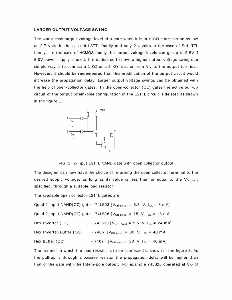
LARGER OUTPUT VOLTAGE SWING
The worst case output voltage level of a gate when it is in HIGH state can be as low
as 2.7 volts in the case of LSTTL family and only 2.4 volts in the case of Std. TTL
family. In the case of HCMOS family the output voltage levels can go up to 5.5V if
6.0V power supply is used. If it is desired to have a higher output voltage swing one
simple way is to connect a 1 KΩ or a 2 KΩ resistor from VCC to the output terminal.
However, it should be remembered that this modification of the output circuit would
increase the propagation delay. Larger output voltage swings can be obtained with
the help of open-collector gates. In the open-collector (OC) gates the active pull-up
circuit of the output totem-pole configuration in the LSTTL circuit is deleted as shown
in the figure 1.
A
B
vcc
FIG. 1: 2-input LSTTL NAND gate with open collector output
The designer can now have the choice of returning the open collector terminal to the
desired supply voltage, as long as its value is less than or equal to the VOH(max)
specified, through a suitable load resistor.
The available open collector LSTTL gates are:
Quad 2-input NAND(OC) gate - 74LS03 [VOH (max) = 5.5 V, IOL = 8 mA]
Quad 2-input NAND(OC) gate - 74LS26 [VOH (max) = 15 V, IOL = 18 mA]
Hex Inverter (OC) - 74LS38 [VOH (max) = 5.5 V, IOL = 24 mA]
Hex Inverter/Buffer (OC) - 7406 [VOH (max) = 30 V, IOL = 40 mA]
Hex Buffer (OC) - 7407 [VOH (max)= 30 V, IOL = 40 mA]
The manner in which the load resistor is to be connected is shown in the figure 2. As
the pull-up is through a passive resistor the propagation delay will be higher than
that of the gate with the totem-pole output. For example 74LS26 operated at VCC of
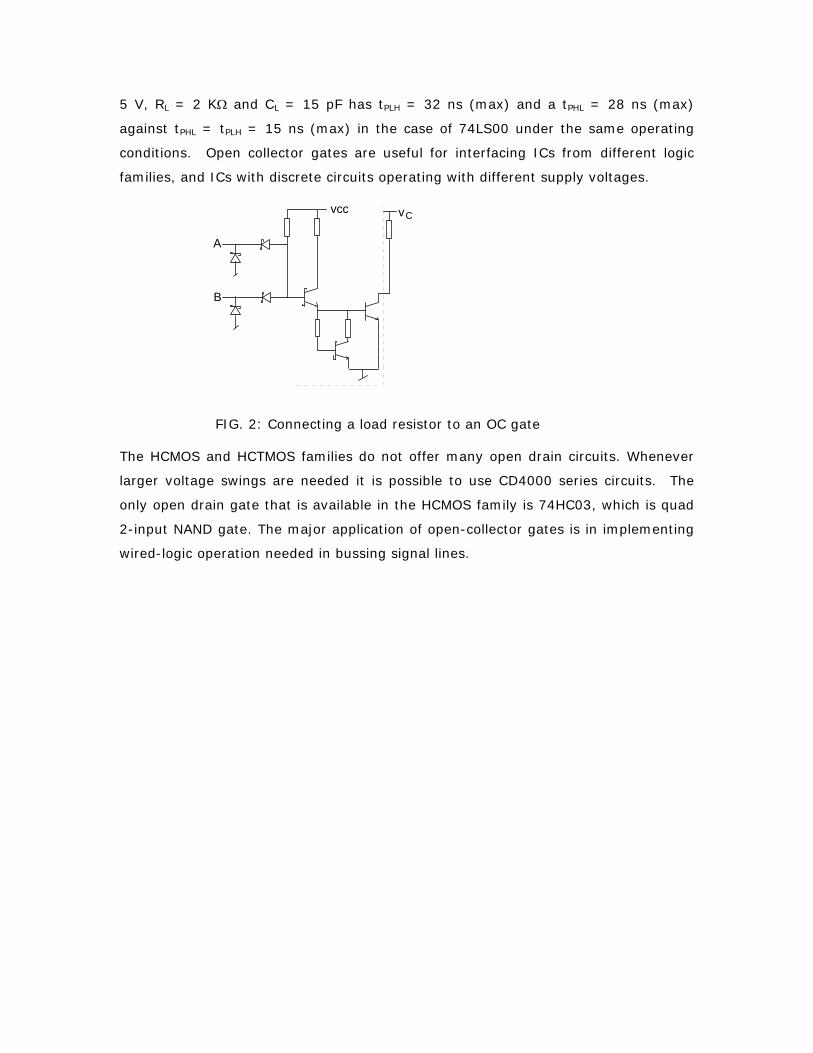
5 V, RL = 2 KΩ and CL = 15 pF has tPLH = 32 ns (max) and a tPHL = 28 ns (max)
against tPHL = tPLH = 15 ns (max) in the case of 74LS00 under the same operating
conditions. Open collector gates are useful for interfacing ICs from different logic
families, and ICs with discrete circuits operating with different supply voltages.
A
B
vcc vC
FIG. 2: Connecting a load resistor to an OC gate
The HCMOS and HCTMOS families do not offer many open drain circuits. Whenever
larger voltage swings are needed it is possible to use CD4000 series circuits. The
only open drain gate that is available in the HCMOS family is 74HC03, which is quad
2-input NAND gate. The major application of open-collector gates is in implementing
wired-logic operation needed in bussing signal lines.
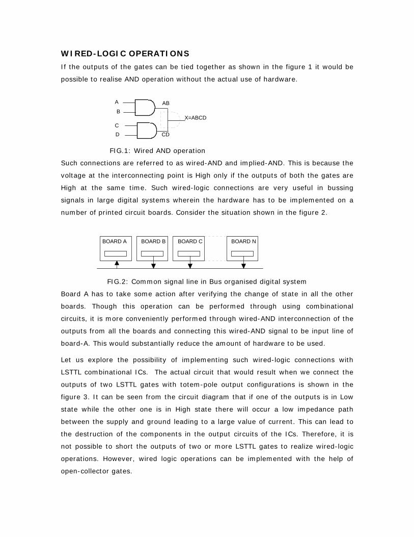
WIRED-LOGIC OPERATIONS
If the outputs of the gates can be tied together as shown in the figure 1 it would be
possible to realise AND operation without the actual use of hardware.
A
B
CD
AB
CD
X=ABCD
FIG.1: Wired AND operation
Such connections are referred to as wired-AND and implied-AND. This is because the
voltage at the interconnecting point is High only if the outputs of both the gates are
High at the same time. Such wired-logic connections are very useful in bussing
signals in large digital systems wherein the hardware has to be implemented on a
number of printed circuit boards. Consider the situation shown in the figure 2.
BOARD A BOARD B BOARD C BOARD N
FIG.2: Common signal line in Bus organised digital system
Board A has to take some action after verifying the change of state in all the other
boards. Though this operation can be performed through using combinational
circuits, it is more conveniently performed through wired-AND interconnection of the
outputs from all the boards and connecting this wired-AND signal to be input line of
board-A. This would substantially reduce the amount of hardware to be used.
Let us explore the possibility of implementing such wired-logic connections with
LSTTL combinational ICs. The actual circuit that would result when we connect the
outputs of two LSTTL gates with totem-pole output configurations is shown in the
figure 3. It can be seen from the circuit diagram that if one of the outputs is in Low
state while the other one is in High state there will occur a low impedance path
between the supply and ground leading to a large value of current. This can lead to
the destruction of the components in the output circuits of the ICs. Therefore, it is
not possible to short the outputs of two or more LSTTL gates to realize wired-logic
operations. However, wired logic operations can be implemented with the help of
open-collector gates.
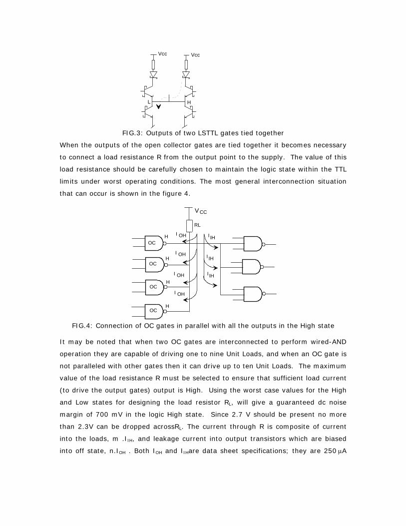
HL
VccVcc
FIG.3: Outputs of two LSTTL gates tied together
When the outputs of the open collector gates are tied together it becomes necessary
to connect a load resistance R from the output point to the supply. The value of this
load resistance should be carefully chosen to maintain the logic state within the TTL
limits under worst operating conditions. The most general interconnection situation
that can occur is shown in the figure 4.
OC
OC
OC
OC
H
H
H
H
RL
I IH
I IH
I IH
I OH
I OH
I OH
I OH
V CC
FIG.4: Connection of OC gates in parallel with all the outputs in the High state
It may be noted that when two OC gates are interconnected to perform wired-AND
operation they are capable of driving one to nine Unit Loads, and when an OC gate is
not paralleled with other gates then it can drive up to ten Unit Loads. The maximum
value of the load resistance R must be selected to ensure that sufficient load current
(to drive the output gates) output is High. Using the worst case values for the High
and Low states for designing the load resistor RL, will give a guaranteed dc noise
margin of 700 mV in the logic High state. Since 2.7 V should be present no more
than 2.3V can be dropped acrossRL. The current through R is composite of current
into the loads, m .IIH, and leakage current into output transistors which are biased
into off state, n.IOH . Both IOH and IIHare data sheet specifications; they are 250 µA
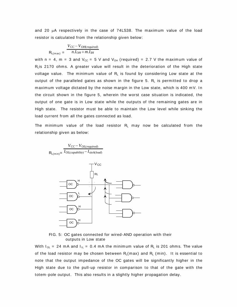
and 20 µA respectively in the case of 74LS38. The maximum value of the load
resistor is calculated from the relationship given below:
RL(max) =
VCC − VOH(required)
n.IOH + m.IIH
with n = 4, m = 3 and VCC = 5 V and VOH (required) = 2.7 V the maximum value of
RLis 2170 ohms. A greater value will result in the deterioration of the High state
voltage value. The minimum value of RL is found by considering Low state at the
output of the paralleled gates as shown in the figure 5. RL is permitted to drop a
maximum voltage dictated by the noise margin in the Low state, which is 400 mV. In
the circuit shown in the figure 5, wherein the worst case situation is indicated, the
output of one gate is in Low state while the outputs of the remaining gates are in
High state. The resistor must be able to maintain the Low level while sinking the
load current from all the gates connected as load.
The minimum value of the load resistor RL may now be calculated from the
relationship given as below:
RL(min)=
VCC − VOL(required)
IOL(capability) − Isink(load)
OC
OC
OC
OC
H
L
H
H
RL
V CC
FIG. 5: OC gates connected for wired-AND operation with their outputs in Low state
With IOL = 24 mA and IIL = 0.4 mA the minimum value of RL is 201 ohms. The value
of the load resistor may be chosen between RL(max) and RL (min). It is essential to
note that the output impedance of the OC gates will be significantly higher in the
High state due to the pull-up resistor in comparison to that of the gate with the
totem-pole output. This also results in a slightly higher propagation delay.
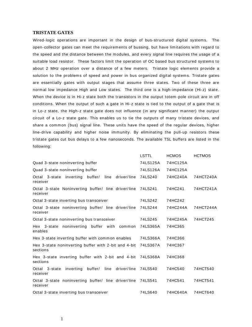
1
TRISTATE GATES Wired-logic operations are important in the design of bus-structured digital systems. The
open-collector gates can meet the requirements of bussing, but have limitations with regard to
the speed and the distance between the modules, and every signal line requires the usage of a
suitable load resistor. These factors limit the operation of OC based bus structured systems to
about 2 MHz operation over a distance of a few meters. Tristate logic elements provide a
solution to the problems of speed and power in bus organized digital systems. Tristate gates
are essentially gates with output stages that assume three states. Two of these three are
normal low impedance High and Low states. The third one is a high-impedance (Hi-z) state.
When the device is in Hi-z state both the transistors in the output totem-pole circuit are in off
conditions. When the output of such a gate in Hi-z state is tied to the output of a gate that is
in Lo-z state, the High-z state gate does not influence (in any significant manner) the output
circuit of a Lo-z state gate. This enables us to tie the outputs of many tristate devices, and
share a common (bus) signal line. These units have the speed of the regular devices, higher
line-drive capability and higher noise immunity. By eliminating the pull-up resistors these
tristate gates cut bus delays to a few nanoseconds. The available TSL buffers are listed in the
following:
LSTTL HCMOS HCTMOS
Quad 3-state noninverting buffer 74LS125A 74HC125A
Quad 3-state noninverting buffer 74LS126A 74HC125A
Octal 3-state inverting buffer/ line driver/line receiver
74LS240 74HC240A 74HCT240A
Octal 3-state Noninverting buffer/ line driver/line receiver
74LS241 74HC241 74HCT241A
Octal 3-state inverting bus transceiver 74LS242 74HC242
Octal 3-state noninverting buffer/ line driver/line receiver
74LS244 74HC244A 74HCT244A
Octal 3-state noninverting bus transceiver 74LS245 74HC245A 74HCT245
Hex 3-state noninverting buffer with common enables
74LS365A 74HC365
Hex 3-state inverting buffer with common enables 74LS366A 74HC366
Hex 3-state noninverting buffer with 2-bit and 4-bit sections
74LS367A 74HC367
Hex 3-state inverting buffer with 2-bit and 4-bit sections
74LS368A 74HC368
Octal 3-state inverting buffer/ line driver/line receiver
74LS540 74HC540 74HCT540
Octal 3-state noninverting buffer/ line driver/line receiver
74LS541 74HC541 74HCT541
Octal 3-state inverting bus transceiver 74LS640 74HC640A 74HCT640
2
When the output of an LSTTL tristate gate is in Hi-z state the maximum leakage current at the
output, which occurs when it is tied to a gate whose output is low-impedance High state, is
+20 µA (into the output terminal). When the device is placed in its low impedance state it has
all the desirable properties of the usual LSTTL gate. Another important factor in driving a bus
line is the current capability in sinking and sourcing. For this reason the output stage of a
tristate gate is designed to source 2.6 mA at a VOH of 2.7 V, and sink 24 mA at VOL of 0.5 V
and 12 mA at a VOL of 0.4 V. This is 6.5 times more sourcing capability than a LSTTL gate.
This will permit as many as 128 tristate logic (TSL) outputs to be tied to a common bus and
still provide enough sourcing current to drive three LSTTL loads. If one device is ON and 127
are OFF the following is valid:
127 x 20µA = 2.54 mA 2.6 mA - 2.54 mA = 60µA = 3 x 20 µA (LSTTL)
The device that is ON, therefore, is capable of maintaining LSTTL speeds while driving the bus.
Another advantage of the high current sourcing feature is that the LSTTL gate with 400 µA
maximum sourcing capability can only drive about 25 to 35 cms of line before the noise
problems become prohibitive. The TSL output will be able to drive reliably a line over 3 meters
long. The greater sourcing capability also provides a far superior High level noise immunity
that is better than the usual LSTTL devices. TSL gates are designed in such a way that the
delay from Inhibit to Output Disable, 20 ns(max), is less than the delay from Enable to Low
State, 25 ns(max). Therefore, the device that is disabled off the line is removed before the
device that is being enabled into Low state is brought on to the bus. This prevents the
occurrence of heavy currents during the transients from Hi-Z state to Low-Z state and vice-
versa. In addition the output state is designed to take care of shorted conditions between two
TSL gates. Even if two devices are simultaneously switched on, the pull down transistors are
designed to withstand as much as 40 mA. But long before it reaches that limit the transistors
begin to come out of saturation.
At present many of the combinational and sequential MSI circuits are available commercially
with tristate outputs. This option makes the usage of these ICs very convenient.
Digital Electronics Module 4: Combinational Circuits:
Multiplexers
N.J. RaoIndian Institute of Science
id1993476 pdfMachine by Broadgun Software - a great PDF writer! - a great PDF creator! - http://www.pdfmachine.com http://www.broadgun.com
December 2006 N.J.Rao M4L3 2
Multiplexers
A multiplexer is a combinational circuit that gates one out of its several inputs to a single output.
It is also called a data selector. The input selected for connection to the output is
controlled by a set of SELECT inputs.
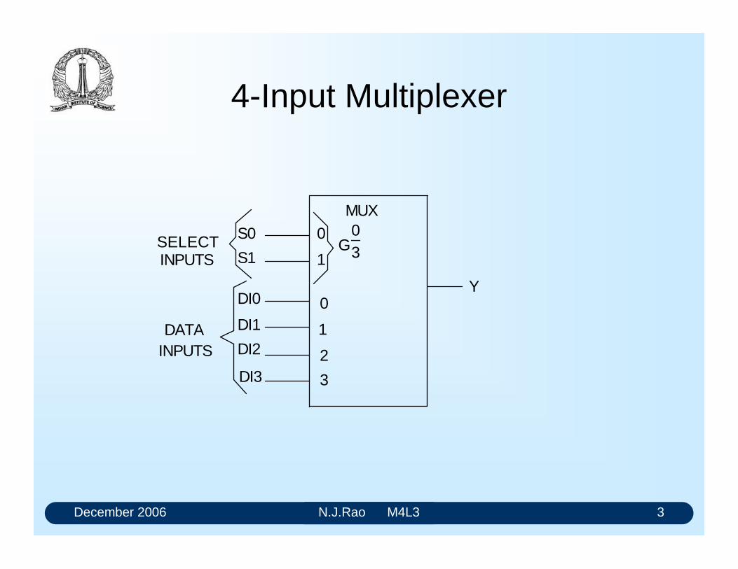
December 2006 N.J.Rao M4L3 3
4-Input Multiplexer
MUX
0
1
0
1
2
3
S0
S1
DI0
DI1
DI2
DI3
G0_3
Y
SELECTINPUTS
DATAINPUTS
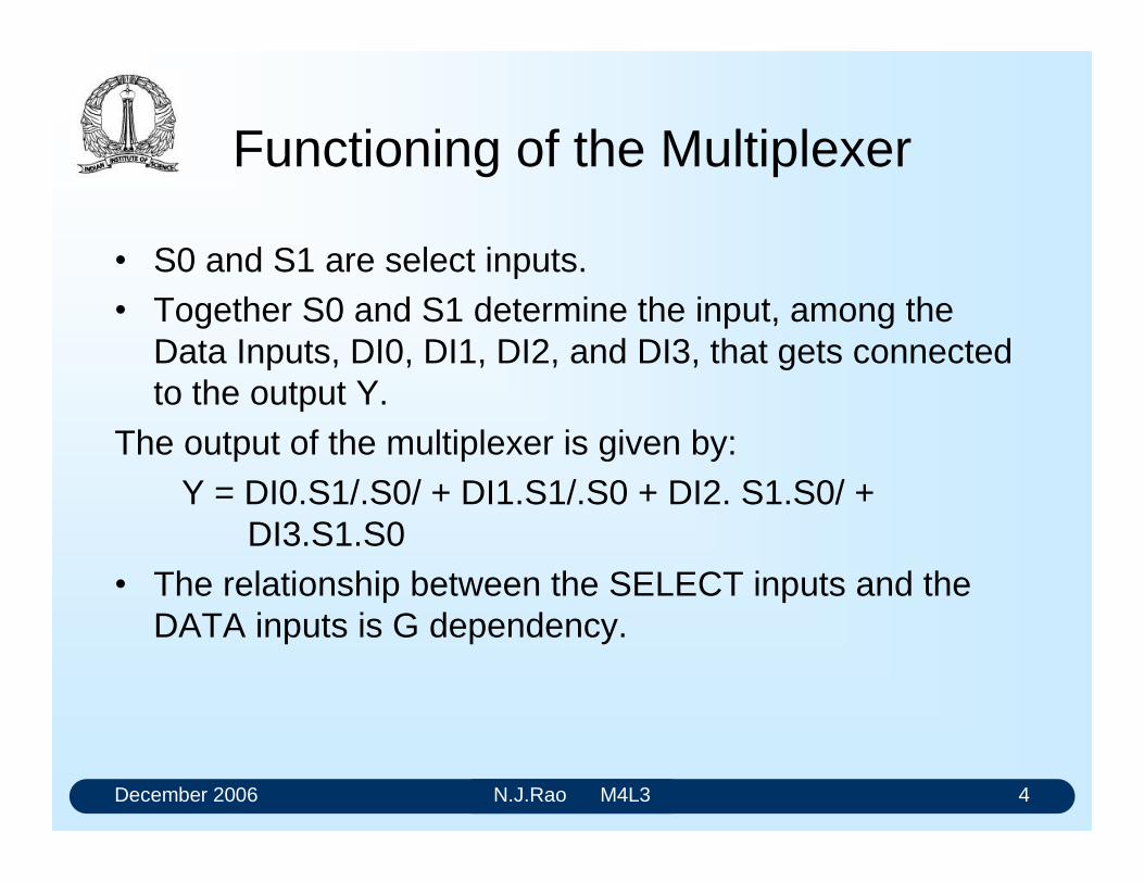
December 2006 N.J.Rao M4L3 4
Functioning of the Multiplexer
S0 and S1 are select inputs. Together S0 and S1 determine the input, among the
Data Inputs, DI0, DI1, DI2, and DI3, that gets connected to the output Y.
The output of the multiplexer is given by: Y = DI0.S1/.S0/ + DI1.S1/.S0 + DI2. S1.S0/ +
DI3.S1.S0 The relationship between the SELECT inputs and the
DATA inputs is G dependency.
December 2006 N.J.Rao M4L3 5
Parameters of concern
The main parameters of concern to us are: Number of inputs Nature of outputs Propagation delay
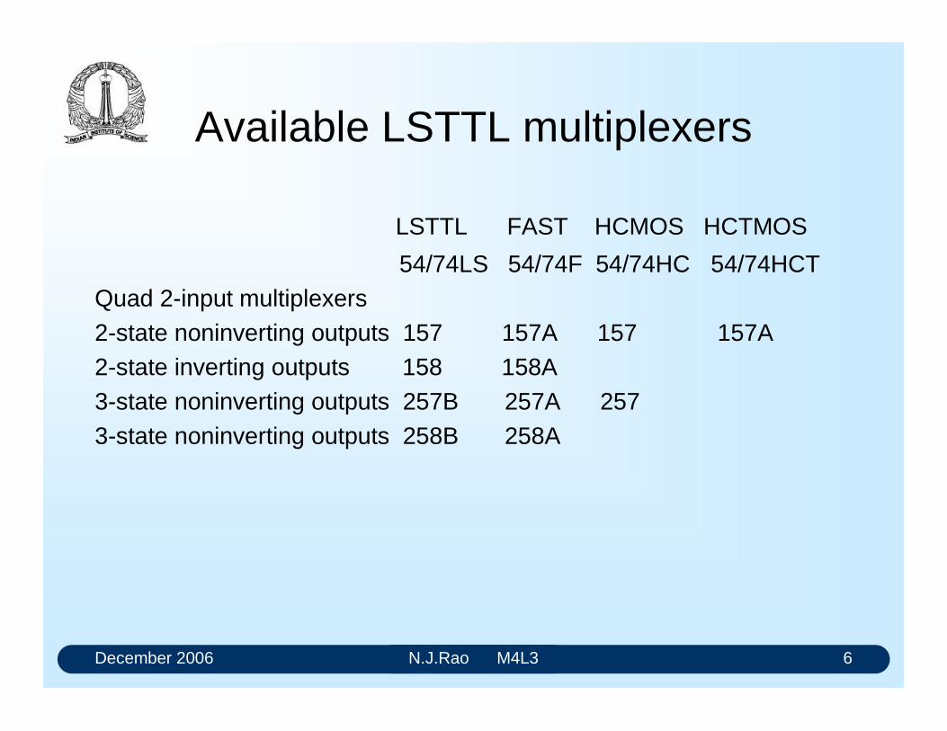
December 2006 N.J.Rao M4L3 6
Available LSTTL multiplexers
LSTTL FAST HCMOS HCTMOS
54/74LS 54/74F 54/74HC 54/74HCTQuad 2-input multiplexers 2-state noninverting outputs 157 157A 157 157A 2-state inverting outputs 158 158A3-state noninverting outputs 257B 257A 2573-state noninverting outputs 258B 258A
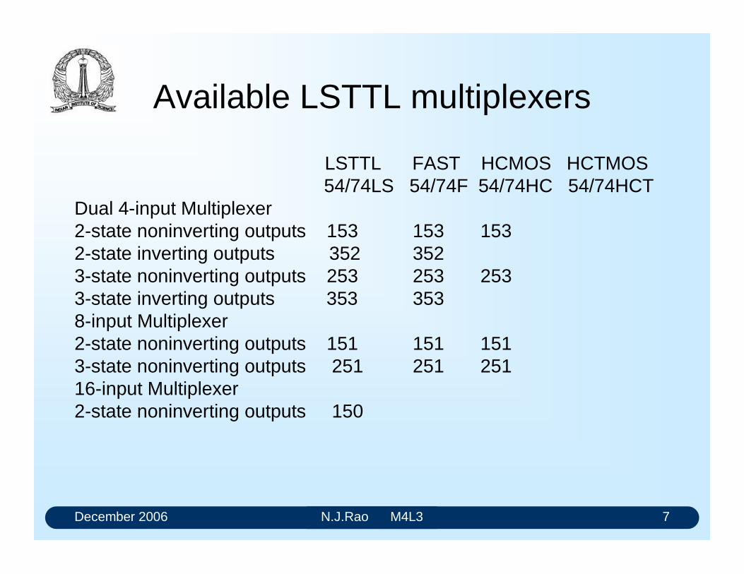
December 2006 N.J.Rao M4L3 7
Available LSTTL multiplexers
LSTTL FAST HCMOS HCTMOS 54/74LS 54/74F 54/74HC 54/74HCT
Dual 4-input Multiplexer2-state noninverting outputs 153 153 1532-state inverting outputs 352 3523-state noninverting outputs 253 253 2533-state inverting outputs 353 3538-input Multiplexer 2-state noninverting outputs 151 151 1513-state noninverting outputs 251 251 25116-input Multiplexer 2-state noninverting outputs 150
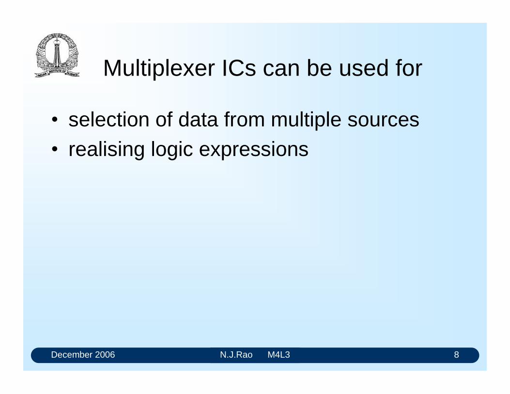
December 2006 N.J.Rao M4L3 8
Multiplexer ICs can be used for
selection of data from multiple sources realising logic expressions
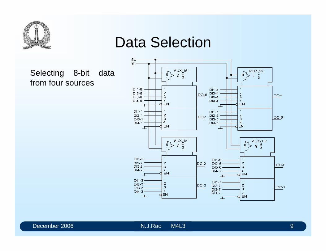
December 2006 N.J.Rao M4L3 9
Data Selection
Selecting 8-bit data from four sources
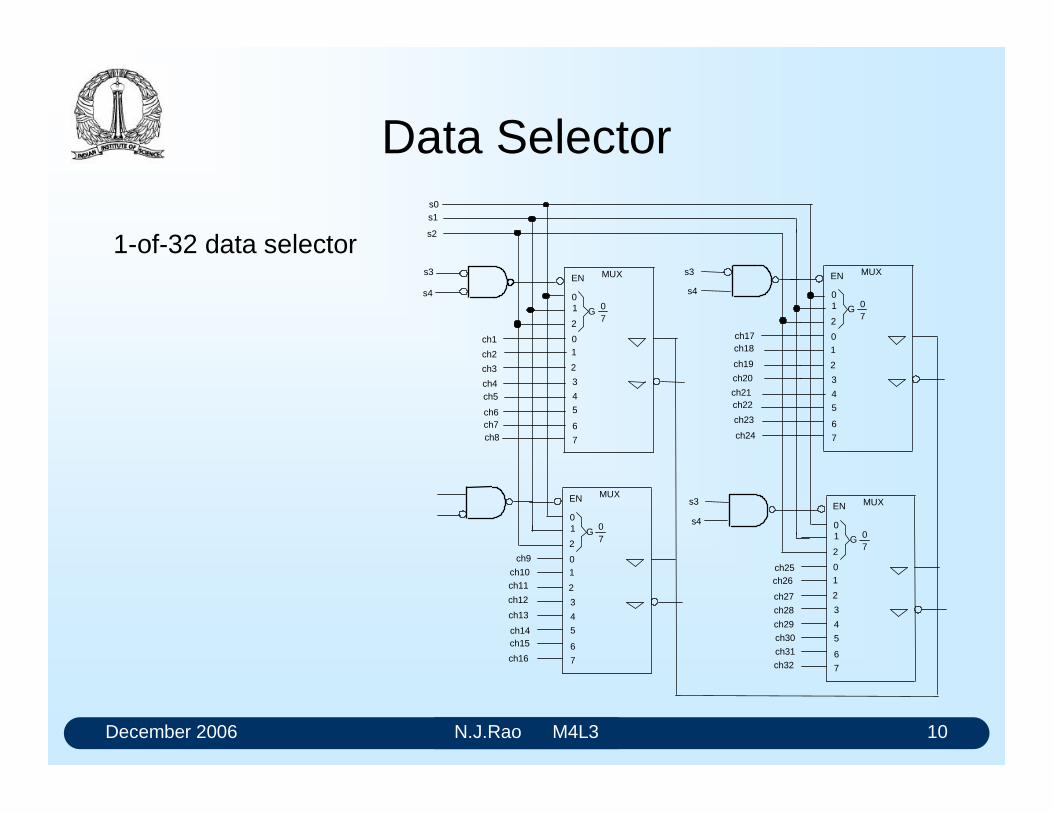
December 2006 N.J.Rao M4L3 10
Data Selector
EN
01
2
1
2
3
4
5
6
7
0
G 07
MUX EN
01
2
1
2
3
4
5
6
7
0
G 07
MUX
EN
01
2
1
2
3
4
5
6
7
0
G 07
MUXEN
01
2
1
2
3
4
5
6
7
0
G 07
MUX
ch9
ch10ch11
ch12
ch13
ch14ch15
ch16
ch25ch26
ch27
ch28
ch29
ch30
ch31
ch32
s3
s4
ch17ch18
ch19
ch20
ch21ch22
ch23
ch24
ch1
ch2
ch3
ch4ch5
ch6ch7ch8
s3
s4
s0s1
s2
s3
s4
1-of-32 data selector
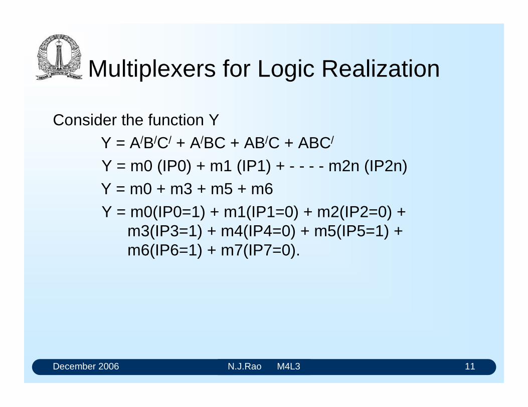
December 2006 N.J.Rao M4L3 11
Multiplexers for Logic Realization
Consider the function YY = A/B/C/ + A/BC + AB/C + ABC/
Y = m0 (IP0) + m1 (IP1) + - - - - m2n (IP2n)Y = m0 + m3 + m5 + m6Y = m0(IP0=1) + m1(IP1=0) + m2(IP2=0) +
m3(IP3=1) + m4(IP4=0) + m5(IP5=1) + m6(IP6=1) + m7(IP7=0).
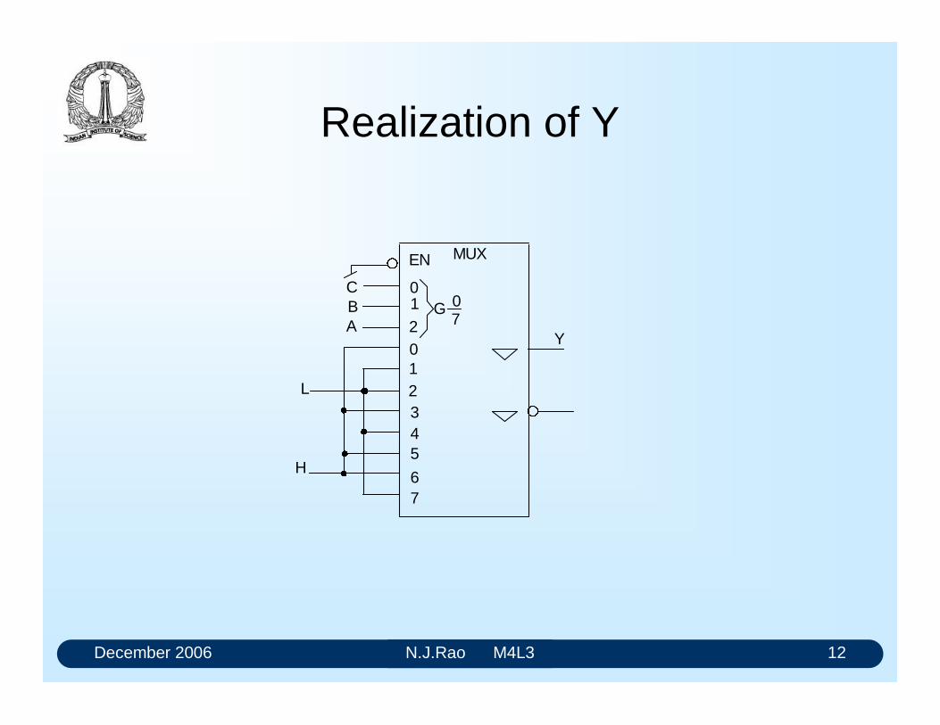
December 2006 N.J.Rao M4L3 12
Realization of Y
EN
012
12345
67
0
G 07
MUX
CBA
L
H
Y
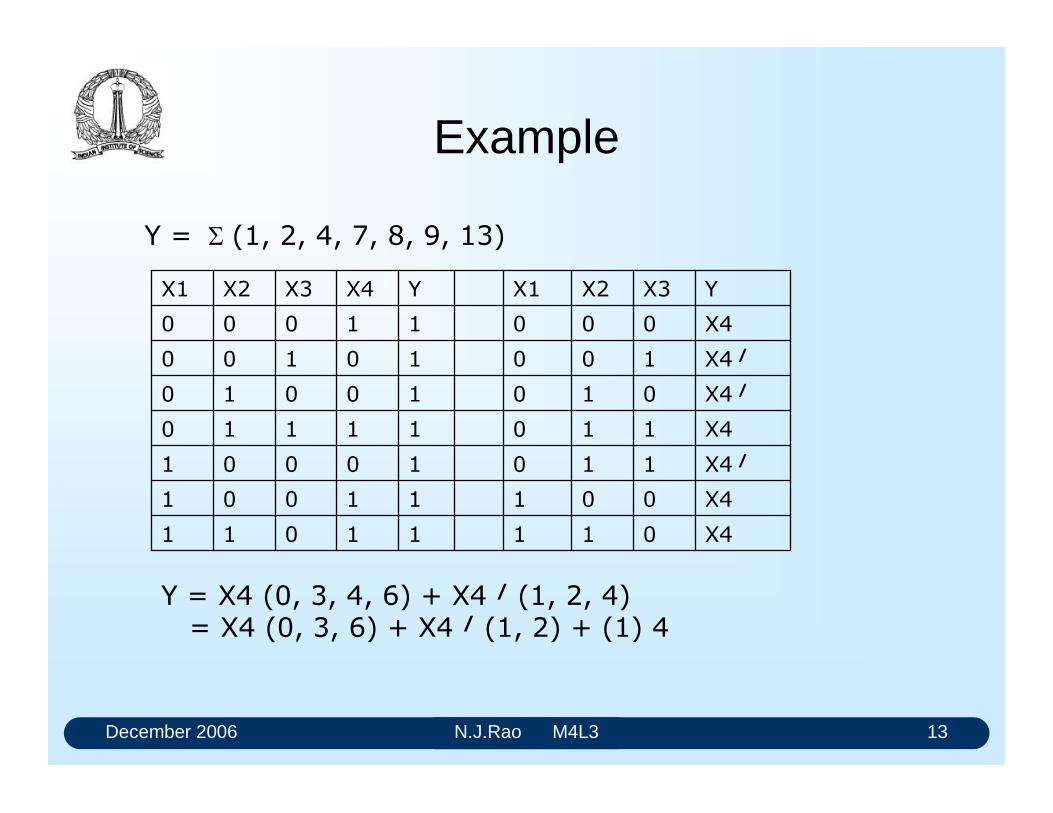
December 2006 N.J.Rao M4L3 13
Example
Y = (1, 2, 4, 7, 8, 9, 13)
X401111011
X400111001
X4 /11010001
X411011110
X4 /01010010
X4 /10010100
X400011000
YX3X2X1YX4X3X2X1
Y = X4 (0, 3, 4, 6) + X4 / (1, 2, 4)
= X4 (0, 3, 6) + X4 / (1, 2) + (1) 4
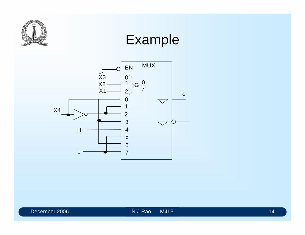
December 2006 N.J.Rao M4L3 14
Example
EN
012
12345
67
0
G 07
MUX
Y
X4
X3X2X1
L
H
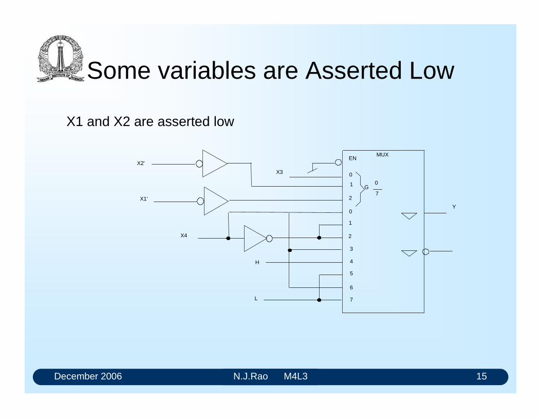
December 2006 N.J.Rao M4L3 15
Some variables are Asserted Low
EN
0
1
2
1
2
3
4
5
6
7
0
G0
7
MUX
Y
X3
X2'
X1'
X4
H
L
X1 and X2 are asserted low
MULTIPLEXERS
A multiplexer is a combinational circuit that gates one out of its several inputs to a
single output. As it selects one out of many inputs, it is also called a “data selector”.
The input selected for connection to the output is controlled by a set of SELECT
inputs. A typical 4-input multiplexer is illustrated in the figure 1.
MUX01
0123
S0S1
DI0DI1DI2
DI3
G0_3
Y
SELECTINPUTS
DATAINPUTS
FIG. 1: Schematic of a 4-input multiplexer
S0 and S1 are select inputs. Together S0 and S1 determine the input, among the
Data Inputs, DI0, DI1, DI2, and DI3, that gets connected to the output Y.
The output of the multiplexer is given by:
Y = DI0.S1/.S0/ + DI1.S1/.S0 + DI2. S1.S0/ + DI3.S1.S0
Notice that the relationship between the SELECT inputs and the DATA inputs is G
dependency.
The main parameters of concern to us are:
Number of inputs
Nature of outputs
Propagation delay
The choice on the number of inputs enables us to select the appropriate multiplexer,
to minimize the number of ICs needed to implement a given logic function.
For example, if data is to be selected from two 16-bit sources, it is more convenient
to use 2-input multiplexers, than 4-input or 8-input multiplexers.
Some additional features:
Higher drive capability of a multiplexer enables the designer to save on
buffers and the consequent delay in certain situations.
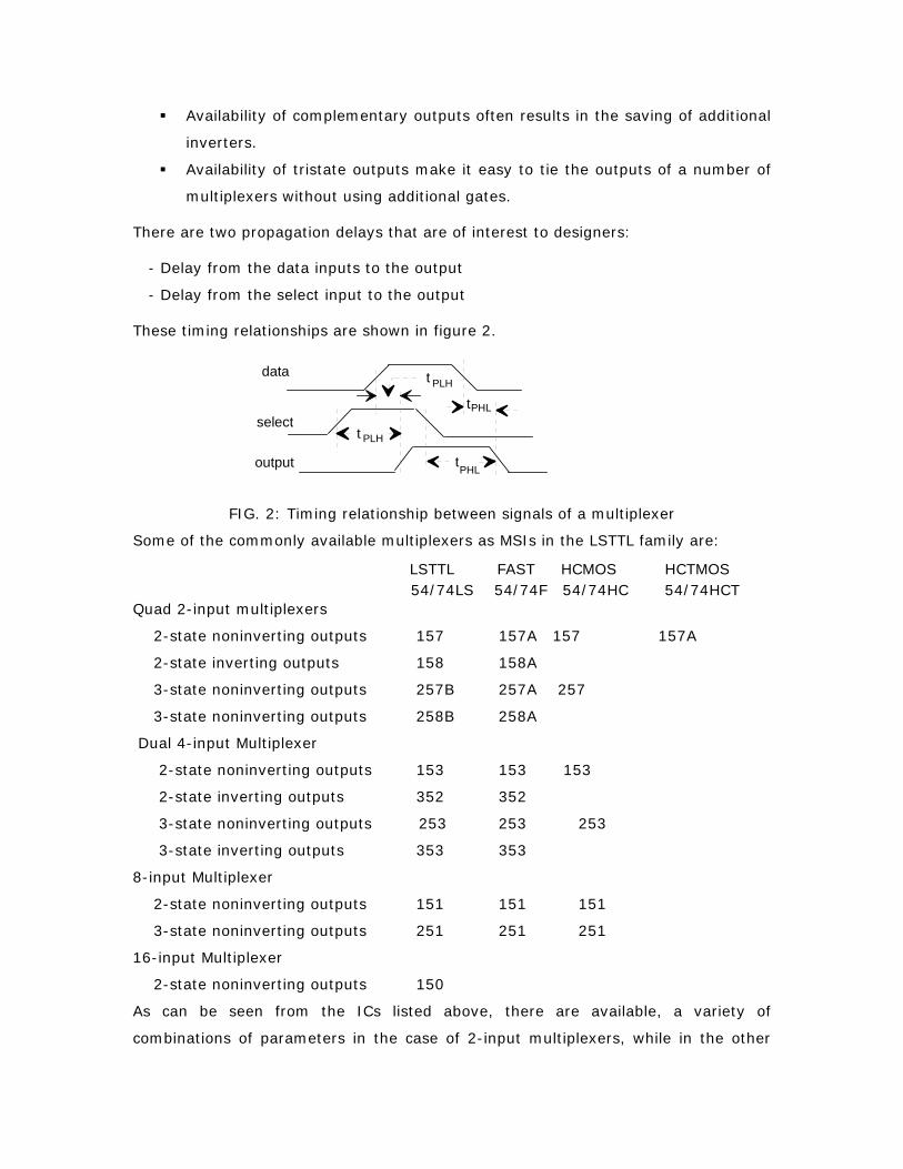
Availability of complementary outputs often results in the saving of additional
inverters.
Availability of tristate outputs make it easy to tie the outputs of a number of
multiplexers without using additional gates.
There are two propagation delays that are of interest to designers:
- Delay from the data inputs to the output
- Delay from the select input to the output
These timing relationships are shown in figure 2.
t PLH
t
PLHt
tPHL
PHLtoutput
select
data
FIG. 2: Timing relationship between signals of a multiplexer
Some of the commonly available multiplexers as MSIs in the LSTTL family are:
LSTTL FAST HCMOS HCTMOS 54/74LS 54/74F 54/74HC 54/74HCT Quad 2-input multiplexers
2-state noninverting outputs 157 157A 157 157A
2-state inverting outputs 158 158A
3-state noninverting outputs 257B 257A 257
3-state noninverting outputs 258B 258A
Dual 4-input Multiplexer
2-state noninverting outputs 153 153 153
2-state inverting outputs 352 352
3-state noninverting outputs 253 253 253
3-state inverting outputs 353 353
8-input Multiplexer
2-state noninverting outputs 151 151 151
3-state noninverting outputs 251 251 251
16-input Multiplexer
2-state noninverting outputs 150
As can be seen from the ICs listed above, there are available, a variety of
combinations of parameters in the case of 2-input multiplexers, while in the other
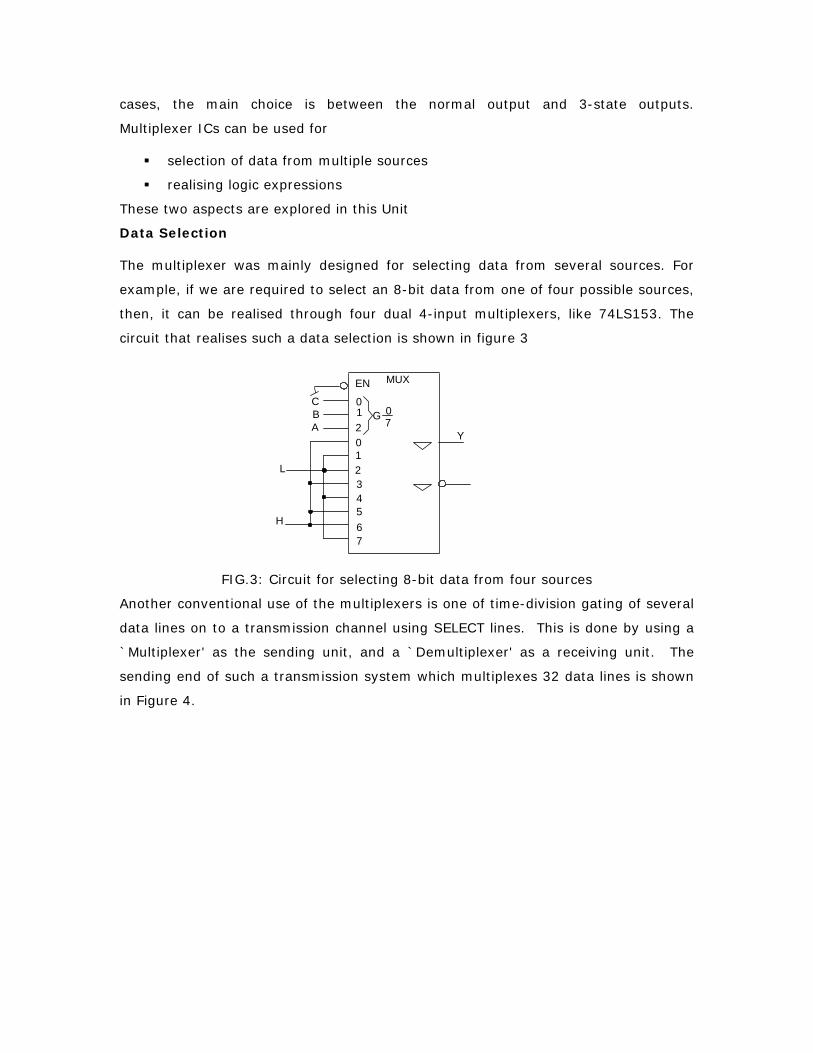
cases, the main choice is between the normal output and 3-state outputs.
Multiplexer ICs can be used for
selection of data from multiple sources
realising logic expressions
These two aspects are explored in this Unit
Data Selection
The multiplexer was mainly designed for selecting data from several sources. For
example, if we are required to select an 8-bit data from one of four possible sources,
then, it can be realised through four dual 4-input multiplexers, like 74LS153. The
circuit that realises such a data selection is shown in figure 3
EN
012
1234567
0
G 07
MUX
CBA
L
H
Y
FIG.3: Circuit for selecting 8-bit data from four sources
Another conventional use of the multiplexers is one of time-division gating of several
data lines on to a transmission channel using SELECT lines. This is done by using a
`Multiplexer' as the sending unit, and a `Demultiplexer' as a receiving unit. The
sending end of such a transmission system which multiplexes 32 data lines is shown
in Figure 4.
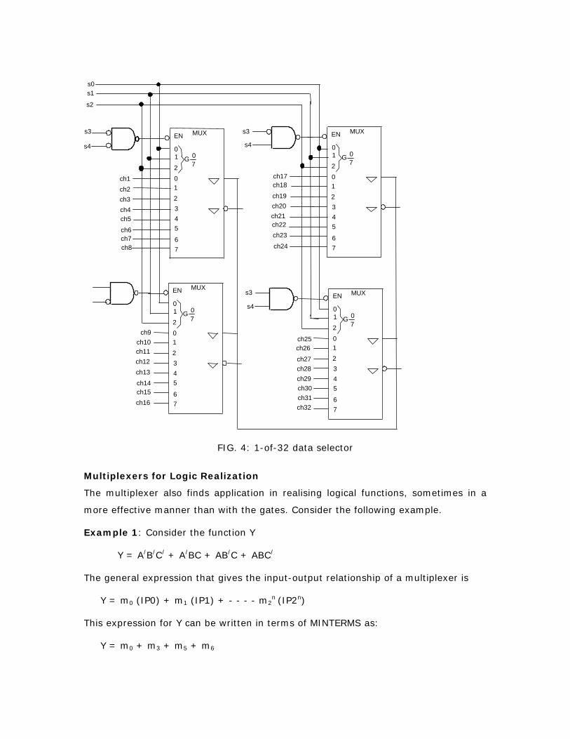
FIG. 4: 1-of-32 data selector
Multiplexers for Logic Realization
The multiplexer also finds application in realising logical functions, sometimes in a
more effective manner than with the gates. Consider the following example.
Example 1: Consider the function Y
Y = A/B/C/ + A/BC + AB/C + ABC/
The general expression that gives the input-output relationship of a multiplexer is
Y = m0 (IP0) + m1 (IP1) + - - - - m2n (IP2n)
This expression for Y can be written in terms of MINTERMS as:
Y = m0 + m3 + m5 + m6
EN 01
2
12345
67
0
G 07
MUX EN
01
2
12345
67
0
G 07
MUX
EN
012
12345
67
0
G 07
MUXEN
012
12345
67
0
G 07
MUX
ch9ch10ch11 ch12 ch13 ch14 ch15ch16
ch25ch26
ch27ch28ch29ch30ch31ch32
s3
s4
ch17ch18
ch19ch20ch21ch22ch23
ch24
ch1 ch2 ch3 ch4ch5 ch6 ch7 ch8
s3
s4
s0 s1 s2
s3 s4
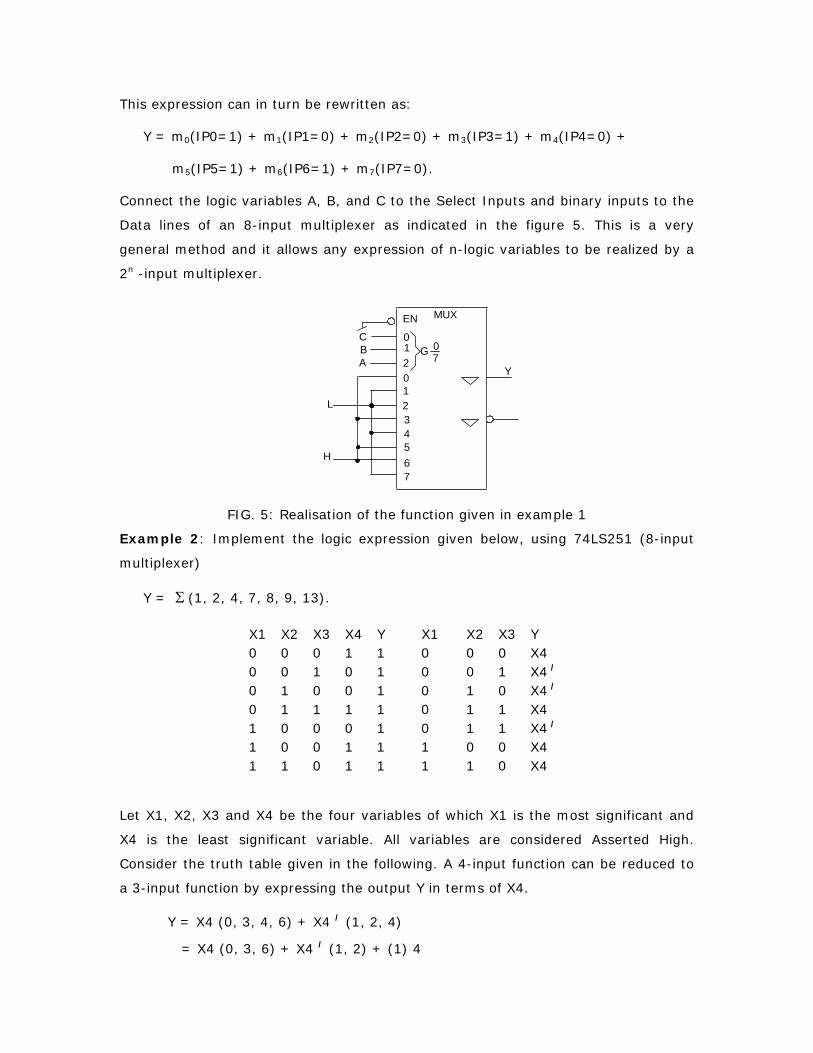
This expression can in turn be rewritten as:
Y = m0(IP0=1) + m1(IP1=0) + m2(IP2=0) + m3(IP3=1) + m4(IP4=0) +
m5(IP5=1) + m6(IP6=1) + m7(IP7=0).
Connect the logic variables A, B, and C to the Select Inputs and binary inputs to the
Data lines of an 8-input multiplexer as indicated in the figure 5. This is a very
general method and it allows any expression of n-logic variables to be realized by a
2n -input multiplexer.
EN
012
1234567
0
G 07
MUX
CBA
L
H
Y
FIG. 5: Realisation of the function given in example 1
Example 2: Implement the logic expression given below, using 74LS251 (8-input
multiplexer)
Y = Σ (1, 2, 4, 7, 8, 9, 13).
X1 X2 X3 X4 Y X1 X2 X3 Y 0 0 0 1 1 0 0 0 X4 0 0 1 0 1 0 0 1 X4 / 0 1 0 0 1 0 1 0 X4 / 0 1 1 1 1 0 1 1 X4 1 0 0 0 1 0 1 1 X4 / 1 0 0 1 1 1 0 0 X4 1 1 0 1 1 1 1 0 X4
Let X1, X2, X3 and X4 be the four variables of which X1 is the most significant and
X4 is the least significant variable. All variables are considered Asserted High.
Consider the truth table given in the following. A 4-input function can be reduced to
a 3-input function by expressing the output Y in terms of X4.
Y = X4 (0, 3, 4, 6) + X4 / (1, 2, 4)
= X4 (0, 3, 6) + X4 / (1, 2) + (1) 4
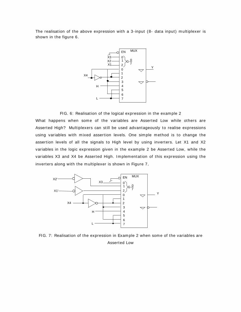
The realisation of the above expression with a 3-input (8- data input) multiplexer is shown in the figure 6.
EN
012
1234567
0
G 07
MUX
Y
X4
X3X2X1
L
H
FIG. 6: Realisation of the logical expression in the example 2
What happens when some of the variables are Asserted Low while others are
Asserted High? Multiplexers can still be used advantageously to realise expressions
using variables with mixed assertion levels. One simple method is to change the
assertion levels of all the signals to High level by using inverters. Let X1 and X2
variables in the logic expression given in the example 2 be Asserted Low, while the
variables X3 and X4 be Asserted High. Implementation of this expression using the
inverters along with the multiplexer is shown in Figure 7.
FIG. 7: Realisation of the expression in Example 2 when some of the variables are
Asserted Low
EN
012
1234567
0
G 07
MUX
Y
X3X2'
X1'
X4
H
L
Digital Electronics Module 4: Combinational Circuits:
Demultiplexers
N.J. RaoIndian Institute of Science
id2152024 pdfMachine by Broadgun Software - a great PDF writer! - a great PDF creator! - http://www.pdfmachine.com http://www.broadgun.com
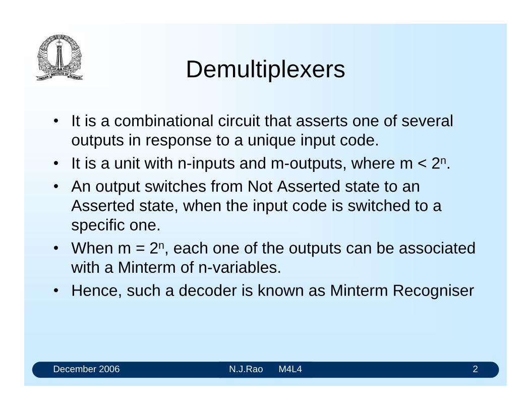
December 2006 N.J.Rao M4L4 2
Demultiplexers
It is a combinational circuit that asserts one of several outputs in response to a unique input code.
It is a unit with n-inputs and m-outputs, where m < 2n. An output switches from Not Asserted state to an
Asserted state, when the input code is switched to a specific one.
When m = 2n, each one of the outputs can be associated with a Minterm of n-variables.
Hence, such a decoder is known as Minterm Recogniser
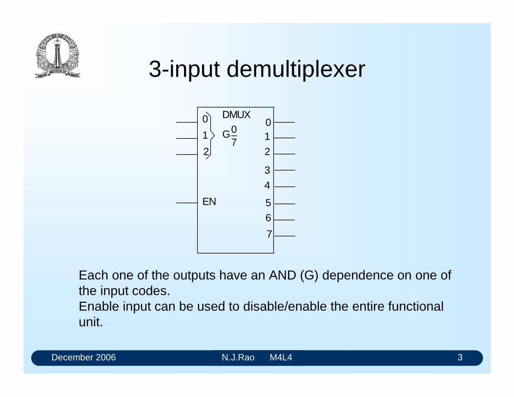
December 2006 N.J.Rao M4L4 3
3-input demultiplexer
0
1
2
EN
01
3
4
5
6
7
2
G07_
DMUX
Each one of the outputs have an AND (G) dependence on one of the input codes.Enable input can be used to disable/enable the entire functionalunit.
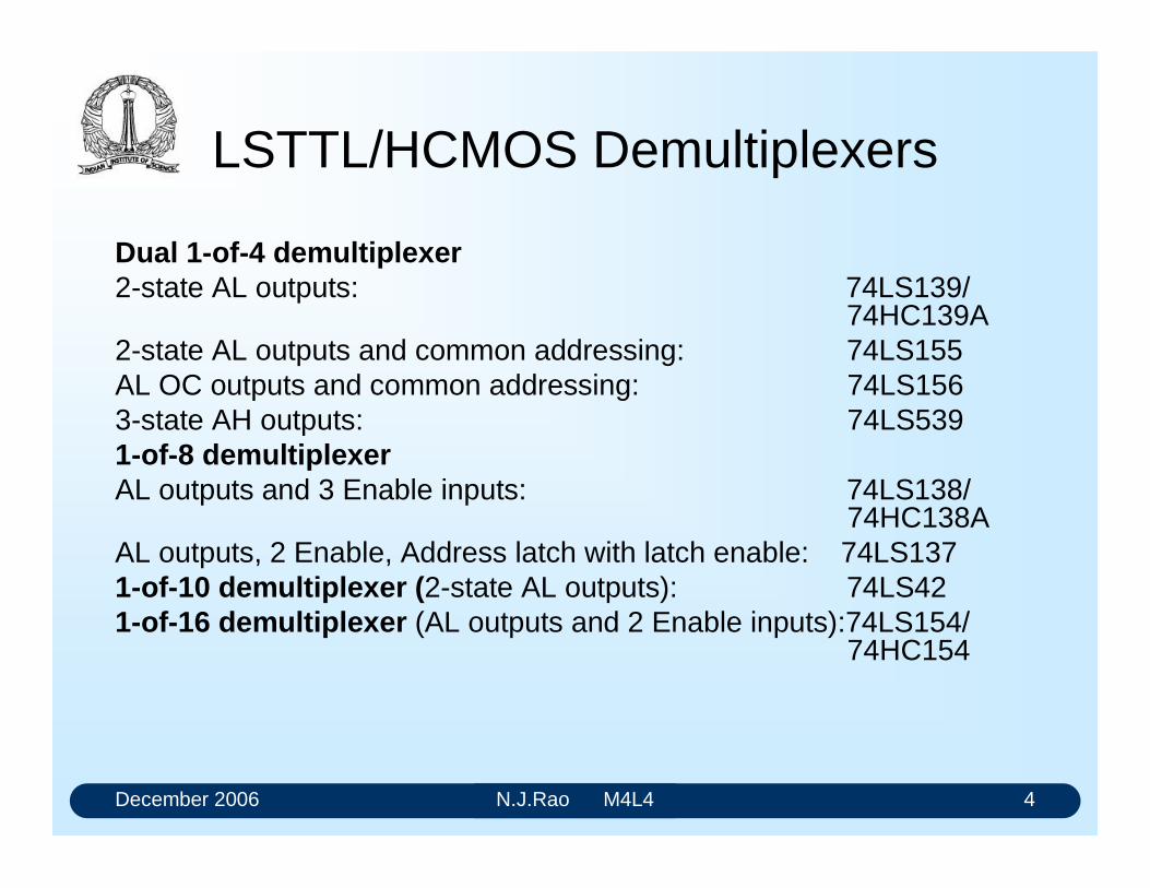
December 2006 N.J.Rao M4L4 4
LSTTL/HCMOS Demultiplexers
Dual 1-of-4 demultiplexer2-state AL outputs: 74LS139/
74HC139A2-state AL outputs and common addressing: 74LS155 AL OC outputs and common addressing: 74LS156 3-state AH outputs: 74LS539 1-of-8 demultiplexerAL outputs and 3 Enable inputs: 74LS138/
74HC138A AL outputs, 2 Enable, Address latch with latch enable: 74LS137 1-of-10 demultiplexer (2-state AL outputs): 74LS42 1-of-16 demultiplexer (AL outputs and 2 Enable inputs):74LS154/
74HC154
December 2006 N.J.Rao M4L4 5
Uses of a demultiplexer
Demultiplexing
Realisation of logic functions
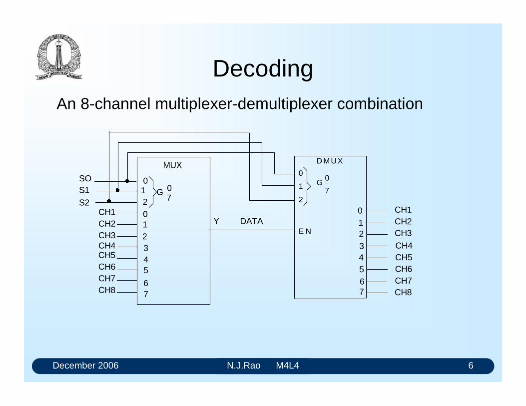
December 2006 N.J.Rao M4L4 6
Decoding An 8-channel multiplexer-demultiplexer combination
0
1
2
E N
G0
7
_
D M U X
01234567
012
12345
67
0
G 07
MUX
Y DATA
SOS1S2
CH1CH2CH3CH4CH5CH6CH7CH8
CH1CH2CH3CH4CH5CH6CH7CH8
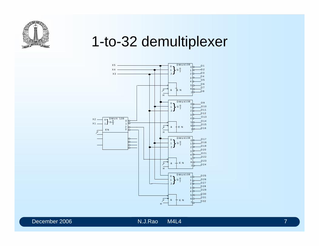
December 2006 N.J.Rao M4L4 7
1-to-32 demultiplexer0
1
2
E N
01
34
5
6
7
2
G 07_
D M U X
&
H
1 3 8
O 1
O 2
O 3
O 4
O 5
O 6
O 7
O 8
0
1
2
E N
01
3
4
5
6
7
2
G 07_
D M U X
&
H
1 3 8
O 9
O 1 0
O 1 1
O 1 2
O 1 3
O 1 4
O 1 5
O 1 6
0
1
2
E N
01
3
4
5
6
7
2
G 07_
D M U X
&
H
1 3 8
O 1 7O 1 8
O 1 9
O 2 0
O 2 1
O 2 2
O 2 3
O 2 4
0
1
2
E N
01
3
4
5
6
7
2
G 07_
D M U X
&
H
1 3 8
O 2 5
O 2 6
O 2 7
O 2 8
O 2 9
O 3 0
O 3 1
O 3 2
E N
0
1 G_03
0123
D M U X '1 3 9X 2
X 1
X 5
X 4
X 3
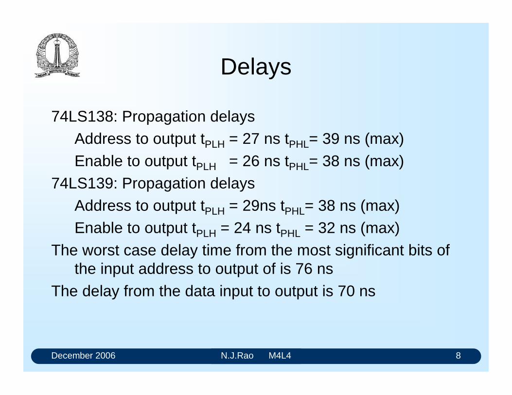
December 2006 N.J.Rao M4L4 8
Delays
74LS138: Propagation delays Address to output tPLH = 27 ns tPHL= 39 ns (max)Enable to output tPLH = 26 ns tPHL= 38 ns (max)
74LS139: Propagation delays Address to output tPLH = 29ns tPHL= 38 ns (max)Enable to output tPLH = 24 ns tPHL = 32 ns (max)
The worst case delay time from the most significant bits of the input address to output of is 76 ns
The delay from the data input to output is 70 ns
December 2006 N.J.Rao M4L4 9
Realization of Logic functions
Demultiplexer is essentially a Minterms generator Do the necessary ORing of the required Minterms to
realize the logic expression. One demultiplexer which generates all the Minterms, and
a number of OR gates can realize multiple logic expressions of the same set of variables
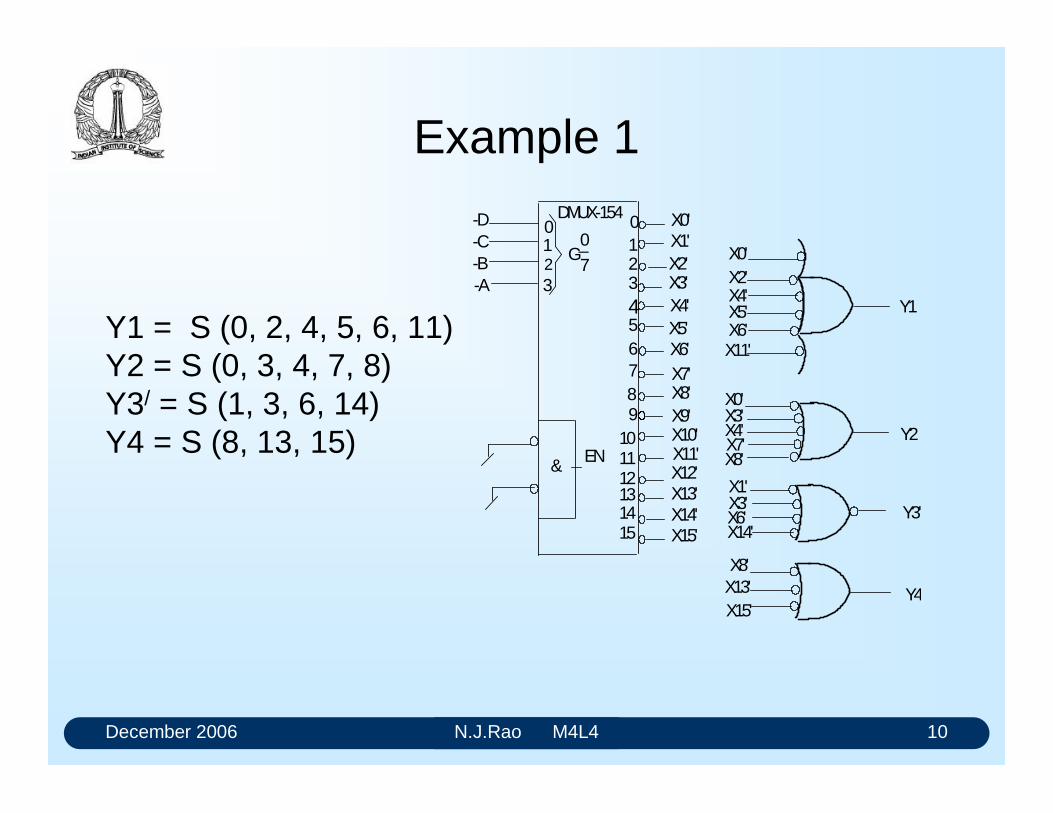
December 2006 N.J.Rao M4L4 10
Example 1
Y1 = S (0, 2, 4, 5, 6, 11)Y2 = S (0, 3, 4, 7, 8)Y3/ = S (1, 3, 6, 14)Y4 = S (8, 13, 15)
X0'X1'X2'X3'X4'X5'X6'X7'X8'X9'X10'X11'X12'X13'X14'X15'
0123456789
101112131415
&
DMUX-1540123
-D-C-B-A
G0_7
X0'X2'X4'X5'X6'X11'
X0'X3'X4'X7'X8'
X1'X3'X6'X14'
X8'X13'X15'
Y1
Y2
Y3'
Y4
EN
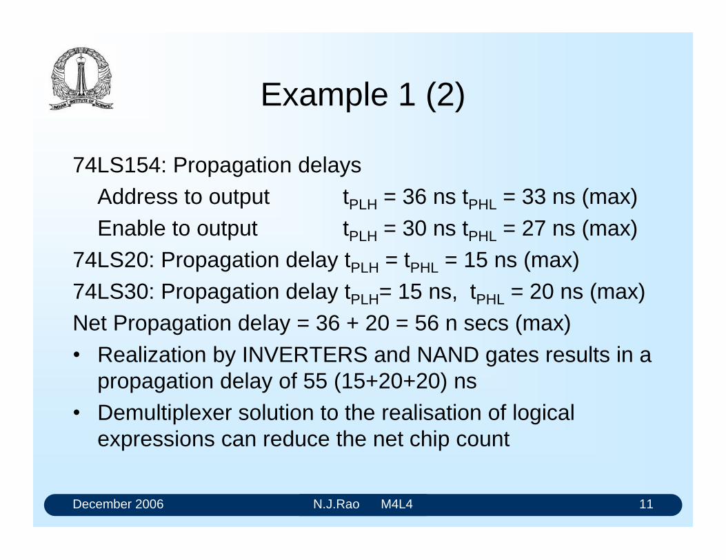
December 2006 N.J.Rao M4L4 11
Example 1 (2)
74LS154: Propagation delays Address to output tPLH = 36 ns tPHL = 33 ns (max)Enable to output tPLH = 30 ns tPHL = 27 ns (max)
74LS20: Propagation delay tPLH = tPHL = 15 ns (max)74LS30: Propagation delay tPLH= 15 ns, tPHL = 20 ns (max)Net Propagation delay = 36 + 20 = 56 n secs (max) Realization by INVERTERS and NAND gates results in a
propagation delay of 55 (15+20+20) ns Demultiplexer solution to the realisation of logical
expressions can reduce the net chip count
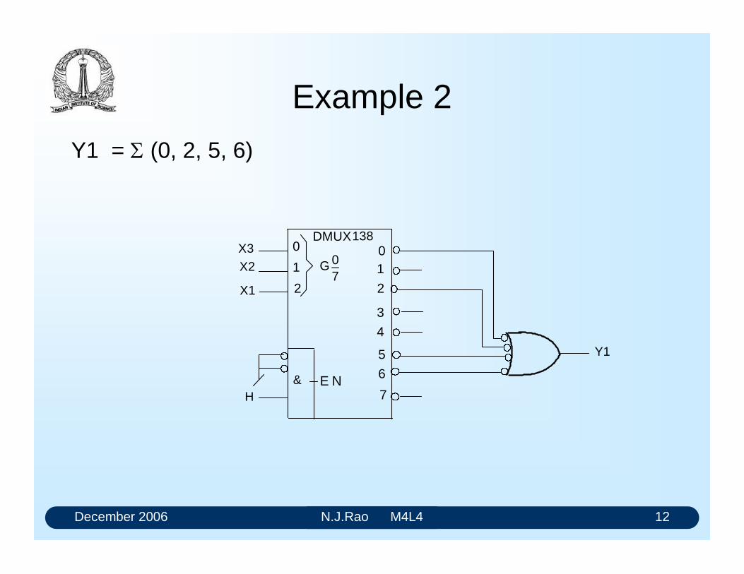
December 2006 N.J.Rao M4L4 12
Example 2
Y1 = (0, 2, 5, 6)
0
1
2
E N
01
3
4
5
6
7
2
G 07_
DMUX
&
X3
X2
H
138
Y1
X1
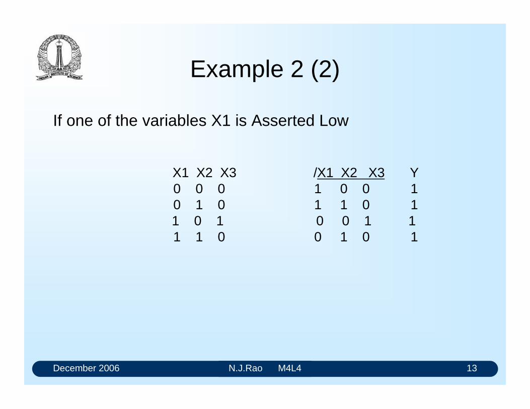
December 2006 N.J.Rao M4L4 13
Example 2 (2)
If one of the variables X1 is Asserted Low
X1 X2 X3 /X1 X2 X3 Y0 0 0 1 0 0 10 1 0 1 1 0 11 0 1 0 0 1 11 1 0 0 1 0 1
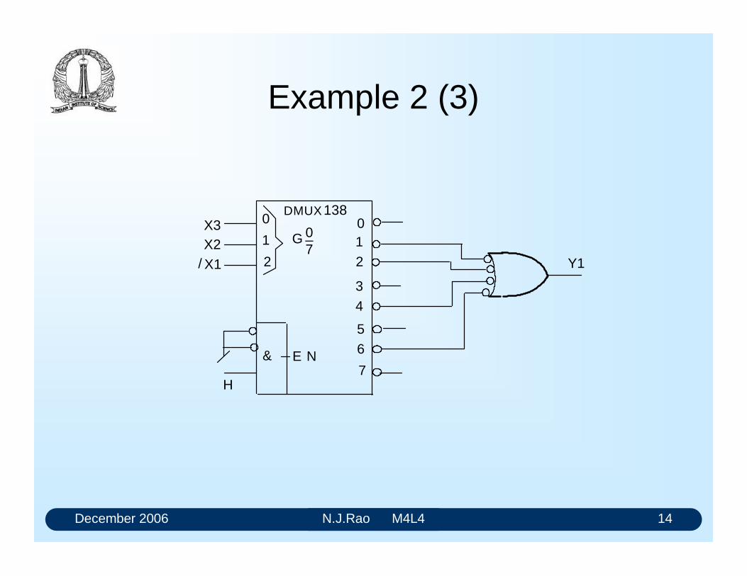
December 2006 N.J.Rao M4L4 14
Example 2 (3)
0
1
2
E N
01
3
4
5
6
7
2
G 07_
DMUX
&
X3X2
H
138
X1 Y1/
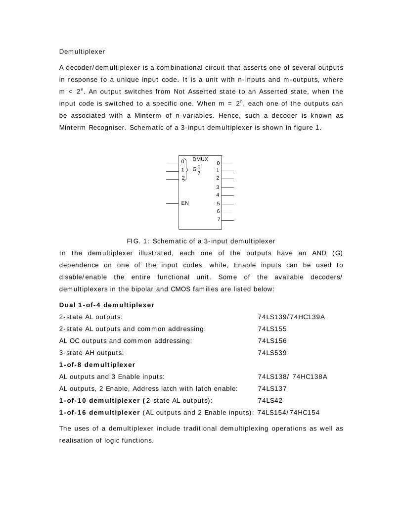
Demultiplexer
A decoder/demultiplexer is a combinational circuit that asserts one of several outputs
in response to a unique input code. It is a unit with n-inputs and m-outputs, where
m < 2n. An output switches from Not Asserted state to an Asserted state, when the
input code is switched to a specific one. When m = 2n, each one of the outputs can
be associated with a Minterm of n-variables. Hence, such a decoder is known as
Minterm Recogniser. Schematic of a 3-input demultiplexer is shown in figure 1.
012
EN
01
34
567
2
G 07_
DMUX
FIG. 1: Schematic of a 3-input demultiplexer
In the demultiplexer illustrated, each one of the outputs have an AND (G)
dependence on one of the input codes, while, Enable inputs can be used to
disable/enable the entire functional unit. Some of the available decoders/
demultiplexers in the bipolar and CMOS families are listed below:
Dual 1-of-4 demultiplexer
2-state AL outputs: 74LS139/74HC139A
2-state AL outputs and common addressing: 74LS155
AL OC outputs and common addressing: 74LS156
3-state AH outputs: 74LS539
1-of-8 demultiplexer
AL outputs and 3 Enable inputs: 74LS138/ 74HC138A
AL outputs, 2 Enable, Address latch with latch enable: 74LS137
1-of-10 demultiplexer (2-state AL outputs): 74LS42
1-of-16 demultiplexer (AL outputs and 2 Enable inputs): 74LS154/74HC154
The uses of a demultiplexer include traditional demultiplexing operations as well as
realisation of logic functions.
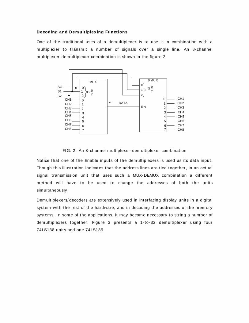
Decoding and Demultiplexing Functions
One of the traditional uses of a demultiplexer is to use it in combination with a
multiplexer to transmit a number of signals over a single line. An 8-channel
multiplexer-demultiplexer combination is shown in the figure 2.
FIG. 2: An 8-channel multiplexer-demultiplexer combination
Notice that one of the Enable inputs of the demultiplexers is used as its data input.
Though this illustration indicates that the address lines are tied together, in an actual
signal transmission unit that uses such a MUX-DEMUX combination a different
method will have to be used to change the addresses of both the units
simultaneously.
Demultiplexers/decoders are extensively used in interfacing display units in a digital
system with the rest of the hardware, and in decoding the addresses of the memory
systems. In some of the applications, it may become necessary to string a number of
demultiplexers together. Figure 3 presents a 1-to-32 demultiplexer using four
74LS138 units and one 74LS139.
0
1
2
E N
G 07_
D M U X
01234567
012
1234567
0
G 07
MUX
Y DATA
SOS1S2
CH1CH2CH3CH4CH5CH6CH7CH8
CH1CH2CH3CH4CH5CH6CH7CH8
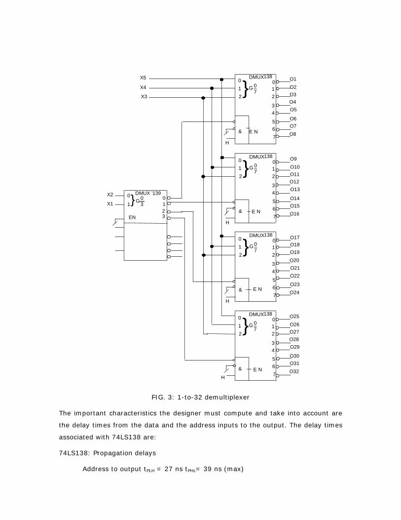
FIG. 3: 1-to-32 demultiplexer
The important characteristics the designer must compute and take into account are
the delay times from the data and the address inputs to the output. The delay times
associated with 74LS138 are:
74LS138: Propagation delays
Address to output tPLH = 27 ns tPHL= 39 ns (max)
012
E N
01
34
567
2
G 07_
DMUX
&
H
138
O1O2O3O4O5
O6O7O8
012
E N
01
34
567
2
G 07_
DMUX
&
H
138
O9O10O11O12O13
O14O15O16
012
E N
01
34
567
2
G 07_
DMUX
&
H
138
O17O18O19O20O21O22
O23O24
012
E N
01
34
567
2
G 07_
DMUX
&
H
138
O25O26O27O28O29
O30O31O32
EN
0
1G_03
0123
DMUX '139X2
X1
X5
X4
X3
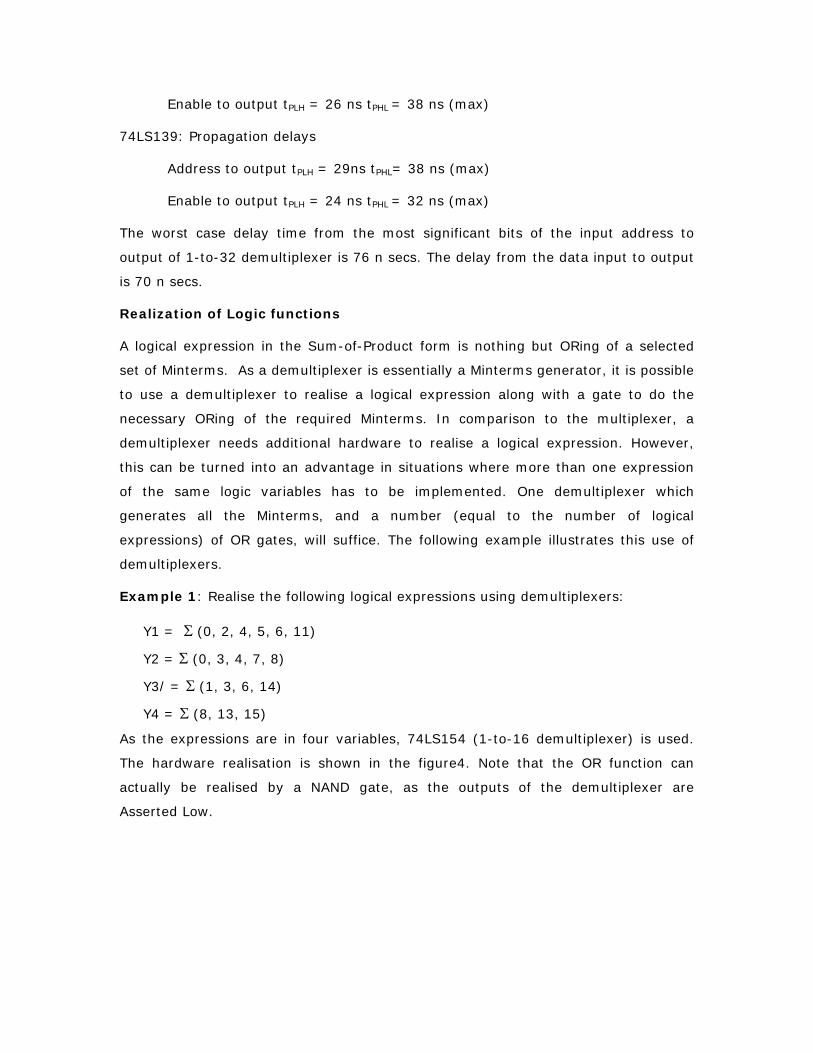
Enable to output tPLH = 26 ns tPHL = 38 ns (max)
74LS139: Propagation delays
Address to output tPLH = 29ns tPHL= 38 ns (max)
Enable to output tPLH = 24 ns tPHL = 32 ns (max)
The worst case delay time from the most significant bits of the input address to
output of 1-to-32 demultiplexer is 76 n secs. The delay from the data input to output
is 70 n secs.
Realization of Logic functions
A logical expression in the Sum-of-Product form is nothing but ORing of a selected
set of Minterms. As a demultiplexer is essentially a Minterms generator, it is possible
to use a demultiplexer to realise a logical expression along with a gate to do the
necessary ORing of the required Minterms. In comparison to the multiplexer, a
demultiplexer needs additional hardware to realise a logical expression. However,
this can be turned into an advantage in situations where more than one expression
of the same logic variables has to be implemented. One demultiplexer which
generates all the Minterms, and a number (equal to the number of logical
expressions) of OR gates, will suffice. The following example illustrates this use of
demultiplexers.
Example 1: Realise the following logical expressions using demultiplexers:
Y1 = Σ (0, 2, 4, 5, 6, 11)
Y2 = Σ (0, 3, 4, 7, 8)
Y3/ = Σ (1, 3, 6, 14)
Y4 = Σ (8, 13, 15)
As the expressions are in four variables, 74LS154 (1-to-16 demultiplexer) is used.
The hardware realisation is shown in the figure4. Note that the OR function can
actually be realised by a NAND gate, as the outputs of the demultiplexer are
Asserted Low.
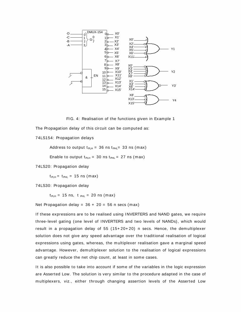
X0'X1'X2'X3'X4'X5'X6'X7'X8'X9'X10'X11'X12'X13'X14'X15'
0123456789
101112131415
&
DMUX-1540123
-D-C-B-A
G0_7 X0'
X2'X4'X5'X6'
X11'
X0'X3'X4'X7'X8'X1'X3'X6'X14'
X8'X13'X15'
Y1
Y2
Y3'
Y4
EN
FIG. 4: Realisation of the functions given in Example 1
The Propagation delay of this circuit can be computed as:
74LS154: Propagation delays
Address to output tPLH = 36 ns tPHL= 33 ns (max)
Enable to output tPLH = 30 ns tPHL = 27 ns (max)
74LS20: Propagation delay
tPLH = tPHL = 15 ns (max)
74LS30: Propagation delay
tPLH = 15 ns, t PHL = 20 ns (max)
Net Propagation delay = 36 + 20 = 56 n secs (max)
If these expressions are to be realised using INVERTERS and NAND gates, we require
three-level gating (one level of INVERTERS and two levels of NANDs), which would
result in a propagation delay of 55 (15+20+20) n secs. Hence, the demultiplexer
solution does not give any speed advantage over the traditional realisation of logical
expressions using gates, whereas, the multiplexer realisation gave a marginal speed
advantage. However, demultiplexer solution to the realisation of logical expressions
can greatly reduce the net chip count, at least in some cases.
It is also possible to take into account if some of the variables in the logic expression
are Asserted Low. The solution is very similar to the procedure adapted in the case of
multiplexers, viz., either through changing assertion levels of the Asserted Low
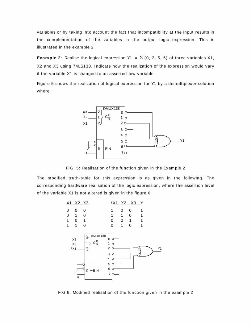
variables or by taking into account the fact that incompatibility at the input results in
the complementation of the variables in the output logic expression. This is
illustrated in the example 2
Example 2: Realise the logical expression Y1 = Σ (0, 2, 5, 6) of three variables X1,
X2 and X3 using 74LS138. Indicate how the realization of the expression would vary
if the variable X1 is changed to an asserted-low variable
Figure 5 shows the realization of logical expression for Y1 by a demultiplexer solution
where.
FIG. 5: Realisation of the function given in the Example 2
The modified truth-table for this expression is as given in the following. The
corresponding hardware realisation of the logic expression, where the assertion level
of the variable X1 is not altered is given in the figure 6.
X1 X2 X3 /X1 X2 X3 Y
0 0 0 1 0 0 1 0 1 0 1 1 0 1 1 0 1 0 0 1 1 1 1 0 0 1 0 1
FIG.6: Modified realisation of the function given in the example 2
012
E N
01
34
567
2
G 07_
DMUX
&
X3X2
H
138
Y1
X1
012
E N
01
34
567
2
G 07_
DMUX
&
X3X2
H
138
X1 Y1/
Digital Electronics Module 4: Combinational Circuits:
Addition
N.J. RaoIndian Institute of Science
id2363959 pdfMachine by Broadgun Software - a great PDF writer! - a great PDF creator! - http://www.pdfmachine.com http://www.broadgun.com
December 2006 N.J.Rao M4L5 2
Addition
Addition is the most fundamental arithmetic operation. All the other arithmetic operations can be expressed in
terms of addition. It is desirable for a digital designer to be familiar with the
realisation of simple arithmetic functions using combinational circuits.
Many of these conventions and procedures are carried over to the software level while designing with LSIs.
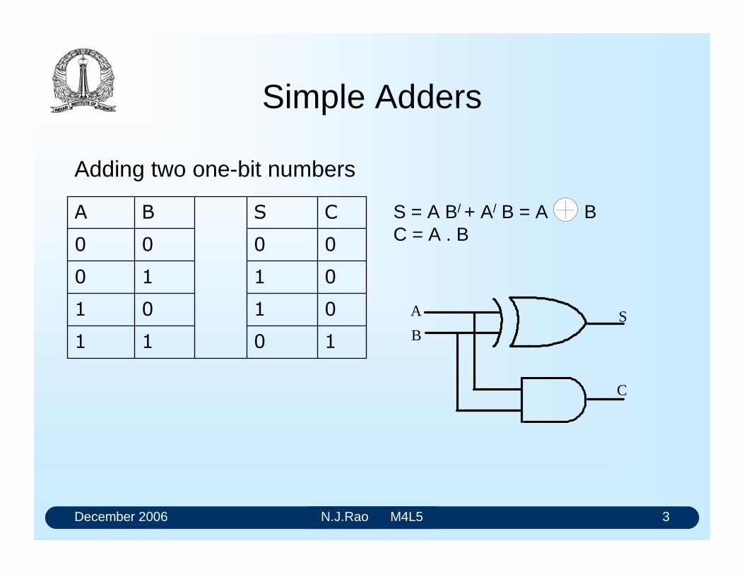
December 2006 N.J.Rao M4L5 3
Simple Adders
Adding two one-bit numbers
1011
0101
0110
0000
CSBA S = A B/ + A/ B = A B C = A . B
A
BS
C
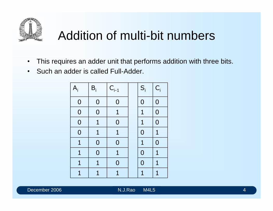
December 2006 N.J.Rao M4L5 4
Addition of multi-bit numbers
This requires an adder unit that performs addition with three bits. Such an adder is called Full-Adder.
11111
10011
10101
01001
10110
01010
01100
00000
CiSiCi-1BiAi
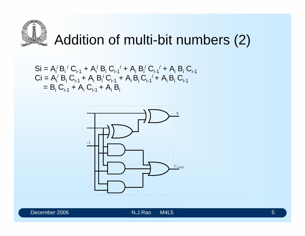
December 2006 N.J.Rao M4L5 5
Addition of multi-bit numbers (2)
Si = Ai/ Bi
/ Ci-1 + Ai/ Bi Ci-1
/ + Ai Bi/ Ci-1
/ + Ai Bi Ci-1
Ci = Ai/ Bi Ci-1 + Ai Bi
/ Ci-1 + Ai Bi Ci-1/ + Ai Bi Ci-1
= Bi Ci-1 + Ai Ci-1 + Ai Bi
S
C o u t
i-1
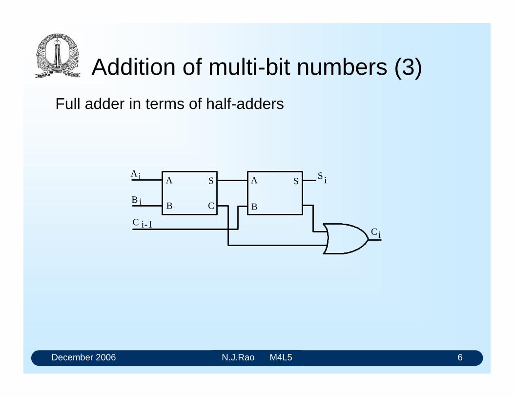
December 2006 N.J.Rao M4L5 6
Addition of multi-bit numbers (3)
Full adder in terms of half-adders
B i
Ai
C i-1
A
B
S
C
A
B
SSi
Ci
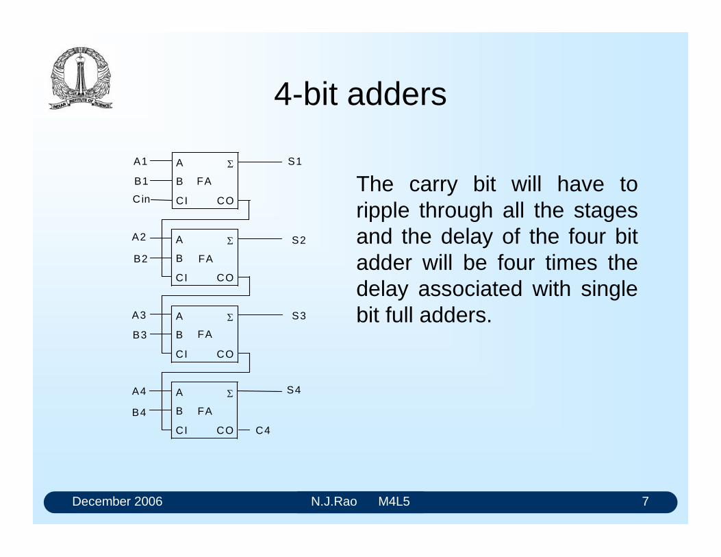
December 2006 N.J.Rao M4L5 7
4-bit adders
CO CI
B
A
CO CI
B
A
CO CI
B
A
CO CI
B
A
A1
B1
Cin
A2
B2
A3
B3
S1
S2
S3
S4
C4
A4
B4 FA
FA
FA
FA The carry bit will have to ripple through all the stages and the delay of the four bit adder will be four times the delay associated with single bit full adders.
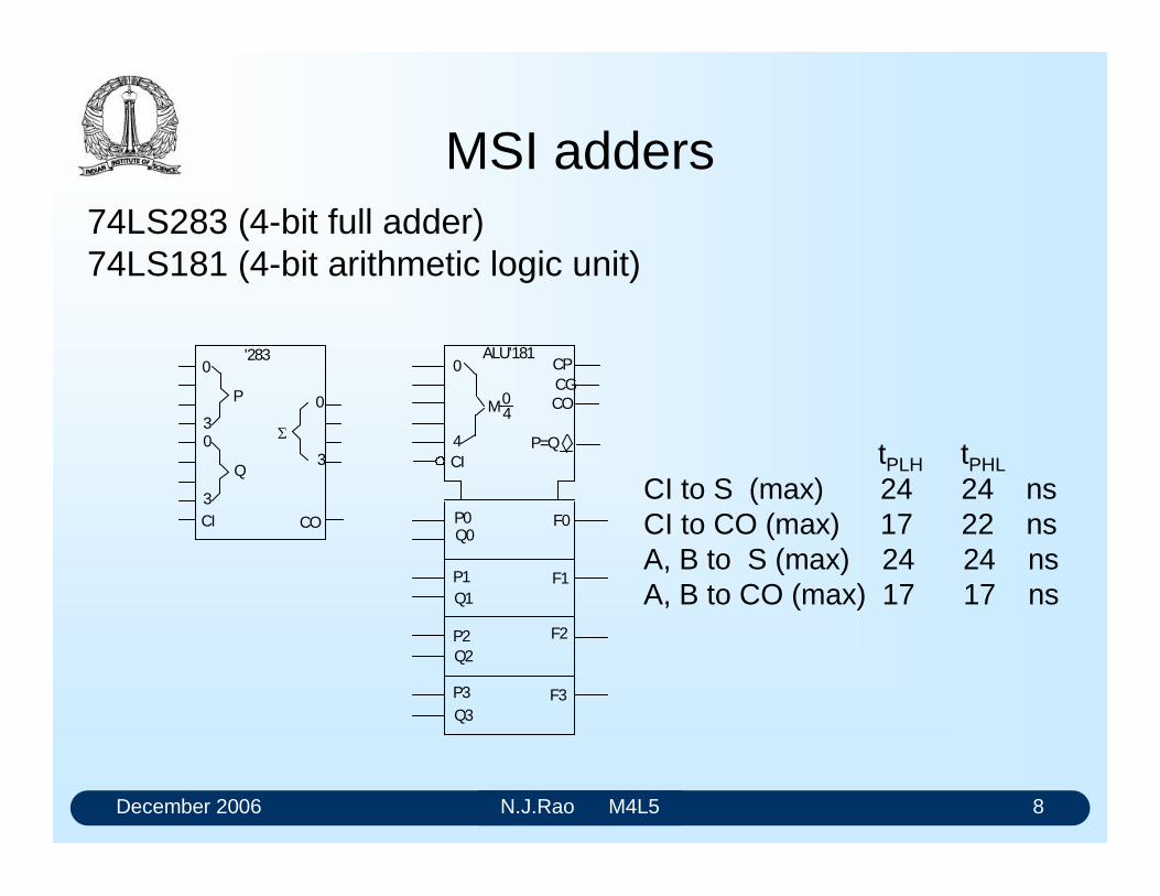
December 2006 N.J.Rao M4L5 8
MSI adders74LS283 (4-bit full adder) 74LS181 (4-bit arithmetic logic unit)
P0Q0
F0
P1Q1
F1
P2Q2
P3Q3
F2
F3
0
4
M04
CPCGCO
P=QCI
ALU'181
CI CO
'2830
30
3
0
3
P
Q
tPLH tPHL
CI to S (max) 24 24 ns CI to CO (max) 17 22 ns A, B to S (max) 24 24 ns A, B to CO (max) 17 17 ns
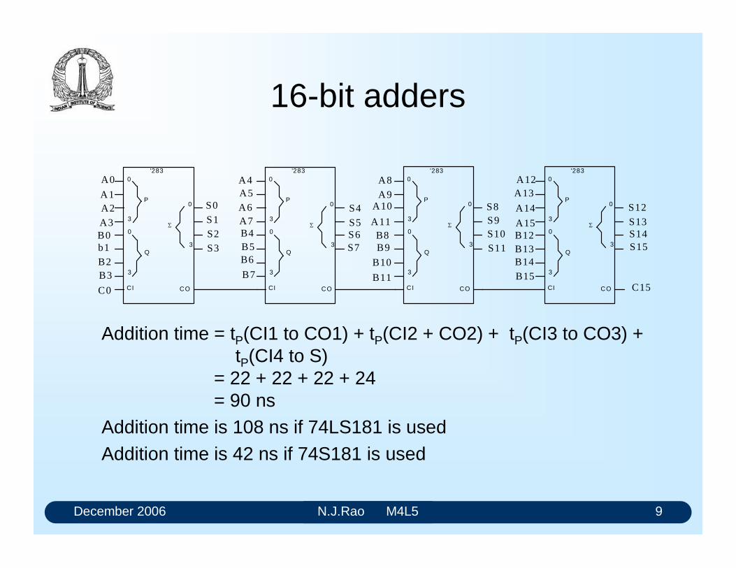
December 2006 N.J.Rao M4L5 9
16-bit adders
CI CO
'2830
3
0
3
0
3
P
Q
CI CO
'2830
3
0
3
0
3
P
Q
CI CO
'2830
3
0
3
0
3
P
Q
CI CO
'2830
3
0
3
0
3
P
Q
S0
S1S2S3
S4
S5S6S7
S8S9S10S11
S12
S13S14S15
C15C0
A0
A1A2
A3B0b1B2B3
A4A5A6A7B4B5B6
B7
A9A10
A11B8B9
B10
B11
A8 A12A13
A14
A15B12B13B14
B15
Addition time = tP(CI1 to CO1) + tP(CI2 + CO2) + tP(CI3 to CO3) + tP(CI4 to S)
= 22 + 22 + 22 + 24 = 90 ns
Addition time is 108 ns if 74LS181 is usedAddition time is 42 ns if 74S181 is used
December 2006 N.J.Rao M4L5 10
Limitations of 4-bit adders
Internal circuitry of the 4-bit adders is optimised to provide minimum delay
The carry bit has to ripple from one group of bits to the next group in the case of 16-bit, 32-bit and 64-bit adders
This will increase the addition time significantly. Add extra circuitry that can determine the final carry bit
without waiting for it to ripple through all the stages. Such an arrangement is called Carry Look Ahead
feature.
December 2006 N.J.Rao M4L5 11
Carry Look Ahead
Carry Generator, Gi = Ai Bi
Carry Propagator, Pi = Ai + Bi C1 = A0 B0+ C0 (A0 + B0) = G0 + C0 P0C2 = A1 B1 + C1 (A1 + B1)
= G1 + C1 P1 = G1 + P1 G0 + P1 P0 C0 C3 = A2 B2 + C2 (A2 + B2) = G2 + C2 P2
= G2 + P2 G1 + P2 P1 G0 + P2 P1 P0 C0 C4 = A3 B3 + C3 (A3 + B3) = G3 + C3 P3
= G3 + P3 G2 + P3 P2 G1 + P3 P2 P1 G0 + P3 P2 P1 P0 C0
December 2006 N.J.Rao M4L5 12
Carry Look Ahead (2)
74LS283 incorporates this feature to minimise the associated delay.
74LS182, called Carry Look Ahead Generator, can accept these group-carry signals from the four ALUs to generate final carry bit in the case of 16-bit addition
If 64-bit adder is to be built, a second level carry look ahead generator, taking the group carry signals from each group of 16 bits, will have to be used.
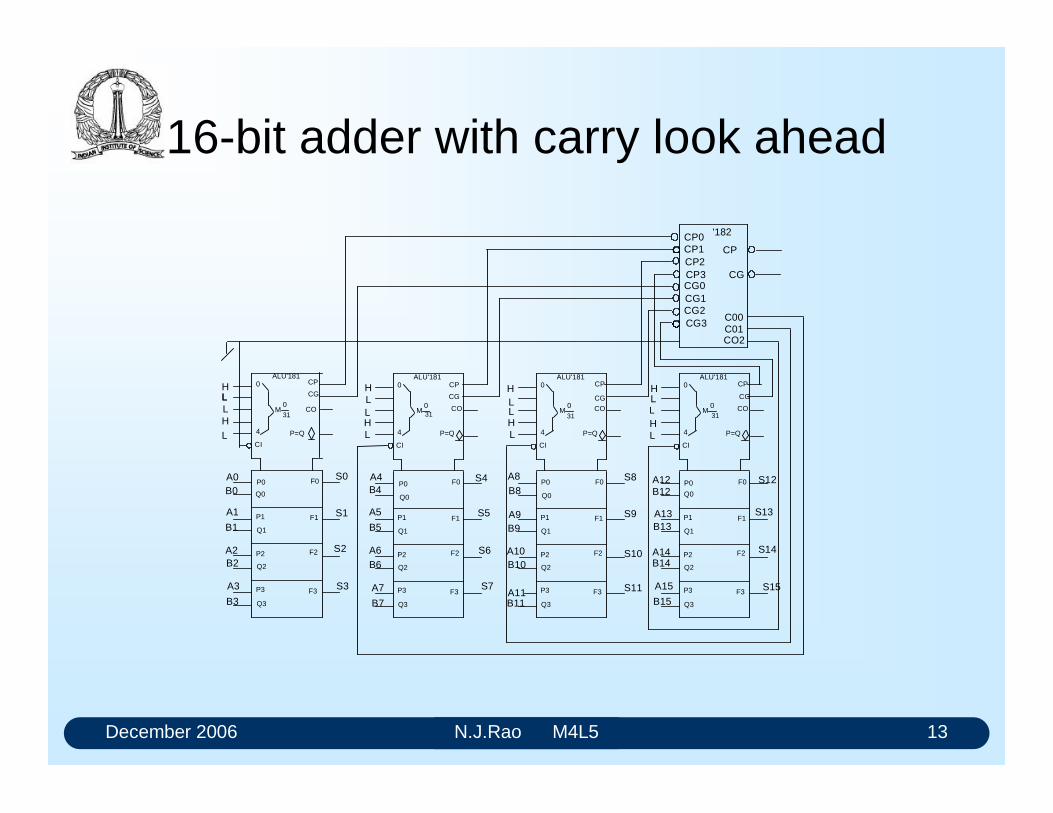
December 2006 N.J.Rao M4L5 13
16-bit adder with carry look ahead
P0
Q0
F0
P1
Q1
F1
P2
Q2
P3
Q3
F2
F3
0
4
M0
CP
CG
CO
P=Q
CI
ALU'181
P0
Q0
F0
P1
Q1
F1
P2
Q2
P3
Q3
F2
F3
0
4
M0
CP
CG
CO
P=Q
CI
ALU'181
P0
Q0
F0
P1
Q1
F1
P2
Q2
P3
Q3
F2
F3
0
4
M0
CP
CGCO
P=Q
CI
ALU'181
P0
Q0
F0
P1
Q1
F1
P2
Q2
P3
Q3
F2
F3
0
4
M0
CP
CG
CO
P=Q
CI
ALU'181
HLLHL
H
HH
HLL
L
LLL
L
H
H
LL
L
A8
A9
A10
A11
A12
A13
A14
B12
B13
B14B10
B9
B8A4B4
A5
B5
A6B6
A7
B7 B11
A15
B15
A0B0
A1
B1
A2B2
A3
B3
S0
S1
S2
S3
S4
S5
S6
S7
S8
S9
S10
S11
S12
S13
S14
S15
CP0CP1CP2CP3CG0CG1CG2CG3
CP
CG
C00C01CO2
'182
31313131

December 2006 N.J.Rao M4L5 14
Subtraction
Normally subtraction is performed by changing the sign of subtrahend and adding it to the minuend.
Ways of representing the signed numbers: sign-magnitude ones complement twos complement forms BCD representations
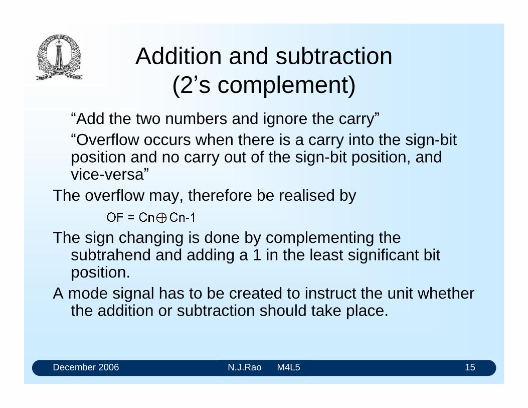
December 2006 N.J.Rao M4L5 15
Addition and subtraction (2s complement)
Add the two numbers and ignore the carryOverflow occurs when there is a carry into the sign-bit position and no carry out of the sign-bit position, and vice-versa
The overflow may, therefore be realised by
The sign changing is done by complementing the subtrahend and adding a 1 in the least significant bit position.
A mode signal has to be created to instruct the unit whether the addition or subtraction should take place.
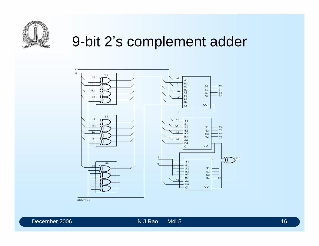
December 2006 N.J.Rao M4L5 16
9-bit 2s complement adder
CI CO
A1B1A2B2A3B3A4B4
S1S2S3S4
CI CO
A1B1A2B2A3B3A4B4
S1S2S3S4
CI CO
A1B1A2B2A3B3A4B4
S1S2S3S4
'86
'86
OF1
0
'86
ADD'/SUB
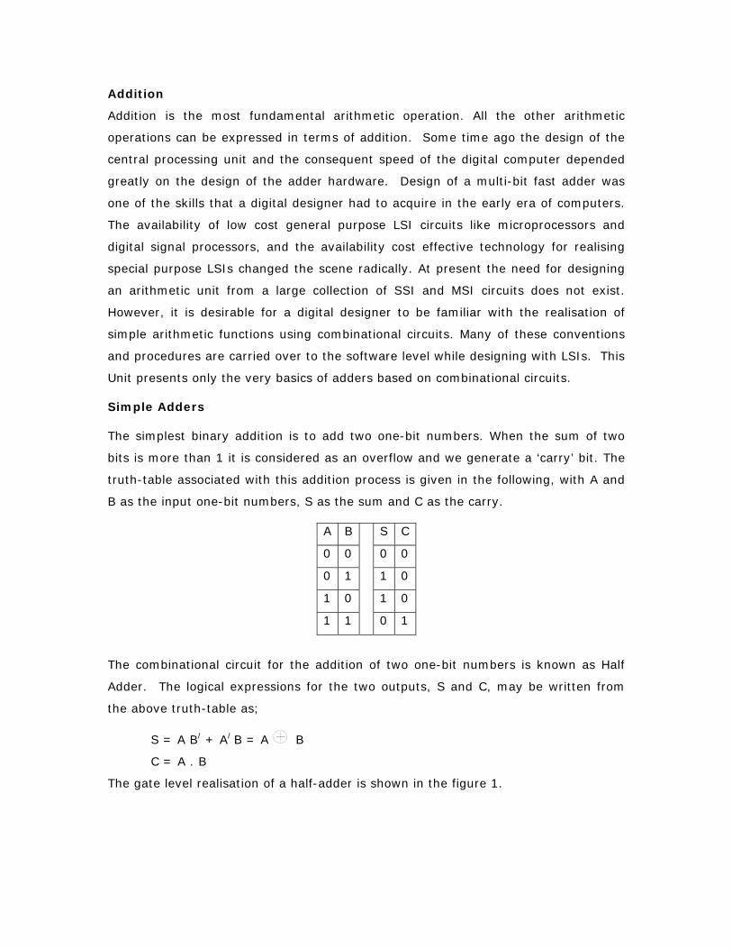
Addition
Addition is the most fundamental arithmetic operation. All the other arithmetic
operations can be expressed in terms of addition. Some time ago the design of the
central processing unit and the consequent speed of the digital computer depended
greatly on the design of the adder hardware. Design of a multi-bit fast adder was
one of the skills that a digital designer had to acquire in the early era of computers.
The availability of low cost general purpose LSI circuits like microprocessors and
digital signal processors, and the availability cost effective technology for realising
special purpose LSIs changed the scene radically. At present the need for designing
an arithmetic unit from a large collection of SSI and MSI circuits does not exist.
However, it is desirable for a digital designer to be familiar with the realisation of
simple arithmetic functions using combinational circuits. Many of these conventions
and procedures are carried over to the software level while designing with LSIs. This
Unit presents only the very basics of adders based on combinational circuits.
Simple Adders
The simplest binary addition is to add two one-bit numbers. When the sum of two
bits is more than 1 it is considered as an overflow and we generate a ‘carry’ bit. The
truth-table associated with this addition process is given in the following, with A and
B as the input one-bit numbers, S as the sum and C as the carry.
A B S C
0 0 0 0
0 1 1 0
1 0 1 0
1 1
0 1
The combinational circuit for the addition of two one-bit numbers is known as Half
Adder. The logical expressions for the two outputs, S and C, may be written from
the above truth-table as;
S = A B/ + A/ B = A B
C = A . B
The gate level realisation of a half-adder is shown in the figure 1.
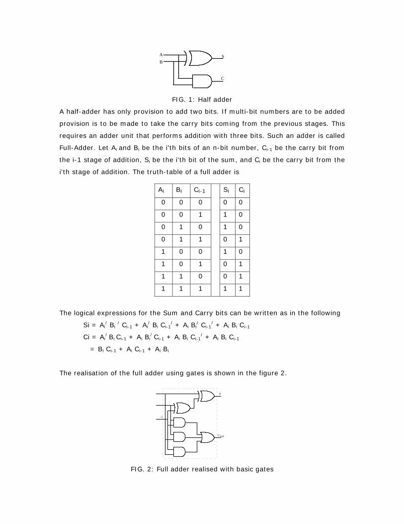
AB
S
C
FIG. 1: Half adder
A half-adder has only provision to add two bits. If multi-bit numbers are to be added
provision is to be made to take the carry bits coming from the previous stages. This
requires an adder unit that performs addition with three bits. Such an adder is called
Full-Adder. Let Ai and Bi be the i'th bits of an n-bit number, Ci-1 be the carry bit from
the i-1 stage of addition, Si be the i'th bit of the sum, and Ci be the carry bit from the
i'th stage of addition. The truth-table of a full adder is
Ai Bi Ci-1 Si Ci
0 0 0 0 0
0 0 1 1 0
0 1 0 1 0
0 1 1 0 1
1 0 0 1 0
1 0 1 0 1
1 1 0 0 1
1 1 1
1 1
The logical expressions for the Sum and Carry bits can be written as in the following
Si = Ai/ Bi / Ci-1 + Ai
/ Bi Ci-1/ + Ai Bi
/ Ci-1/ + Ai Bi Ci-1
Ci = Ai/ Bi Ci-1 + Ai Bi
/ Ci-1 + Ai Bi Ci-1/ + Ai Bi Ci-1
= Bi Ci-1 + Ai Ci-1 + Ai Bi
The realisation of the full adder using gates is shown in the figure 2.
FIG. 2: Full adder realised with basic gates
S
Cout
-1
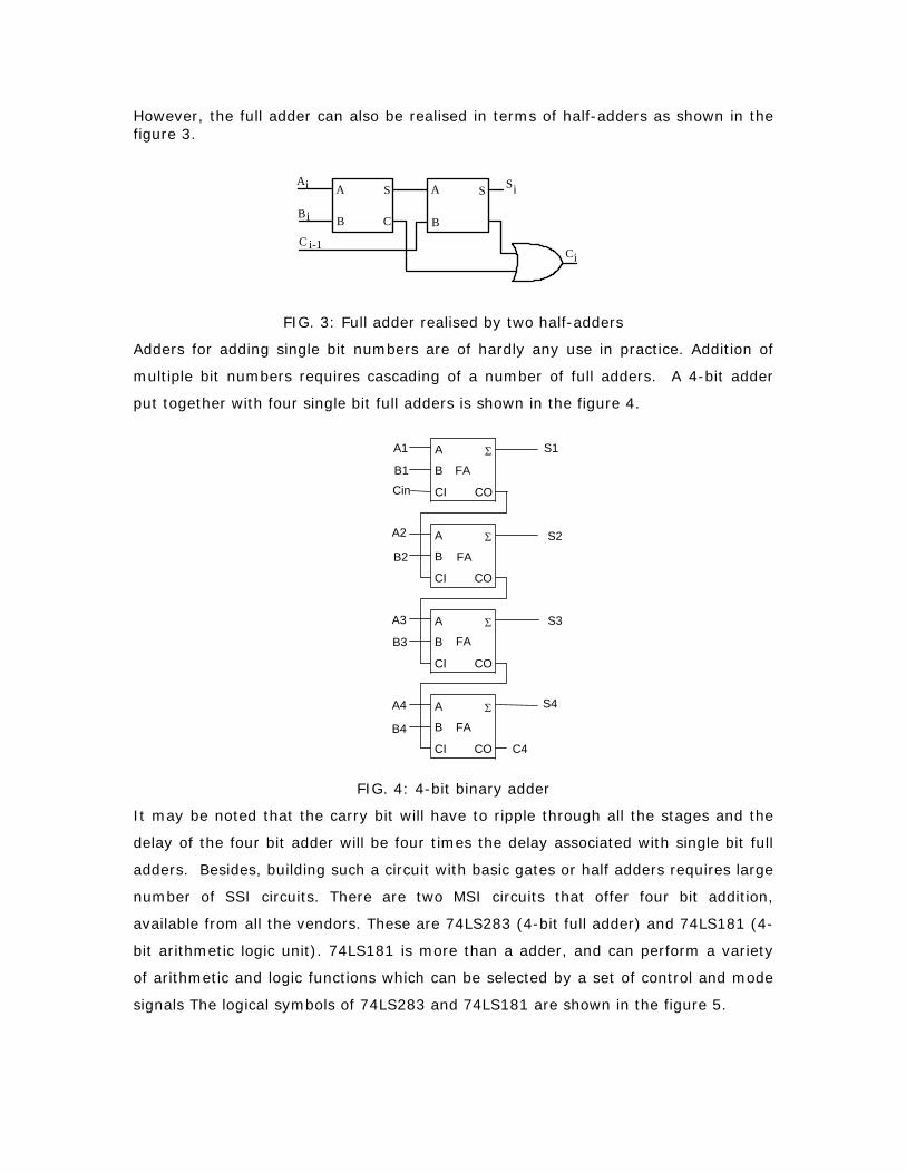
However, the full adder can also be realised in terms of half-adders as shown in the figure 3.
FIG. 3: Full adder realised by two half-adders
Adders for adding single bit numbers are of hardly any use in practice. Addition of
multiple bit numbers requires cascading of a number of full adders. A 4-bit adder
put together with four single bit full adders is shown in the figure 4.
FIG. 4: 4-bit binary adder
It may be noted that the carry bit will have to ripple through all the stages and the
delay of the four bit adder will be four times the delay associated with single bit full
adders. Besides, building such a circuit with basic gates or half adders requires large
number of SSI circuits. There are two MSI circuits that offer four bit addition,
available from all the vendors. These are 74LS283 (4-bit full adder) and 74LS181 (4-
bit arithmetic logic unit). 74LS181 is more than a adder, and can perform a variety
of arithmetic and logic functions which can be selected by a set of control and mode
signals The logical symbols of 74LS283 and 74LS181 are shown in the figure 5.
Bi
Ai
C i-1
A
B
S
C
A
B
S Si
Ci
Σ
CO CI
B
A
Σ
CO CI
B
A
Σ
CO CI
B
A
Σ
CO CI
B
A
A1
B1
Cin
A2
B2
A3
B3
S1
S2
S3
S4
C4
A4
B4 FA
FA
FA
FA
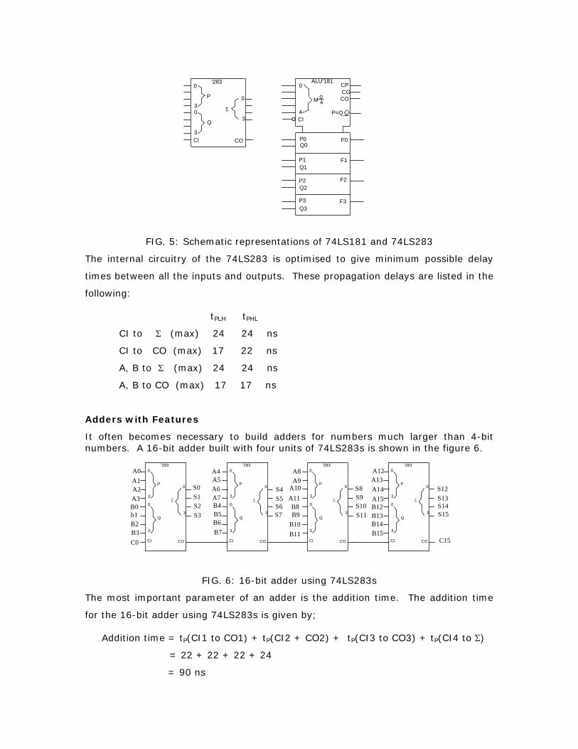
P0Q0
F0
P1Q1
F1
P2Q2
P3Q3
F2
F3
0
4
M 04
CPCGCO
P=QCI
ALU'181
CI CO
'2830
30
3
0
3
P
Q
Σ
FIG. 5: Schematic representations of 74LS181 and 74LS283
The internal circuitry of the 74LS283 is optimised to give minimum possible delay
times between all the inputs and outputs. These propagation delays are listed in the
following:
tPLH tPHL
CI to Σ (max) 24 24 ns
CI to CO (max) 17 22 ns
A, B to Σ (max) 24 24 ns
A, B to CO (max) 17 17 ns
Adders with Features
It often becomes necessary to build adders for numbers much larger than 4-bit numbers. A 16-bit adder built with four units of 74LS283s is shown in the figure 6.
CI CO
'2830
3
0
3
0
3
P
Q
Σ
CI CO
'2830
3
0
3
0
3
P
Q
Σ
CI CO
'2830
3
0
3
0
3
P
Q
Σ
CI CO
'2830
3
0
3
0
3
P
Q
Σ
S0S1S2S3
S4S5S6S7
S8S9S10S11
S12S13S14S15
C15C0
A0A1A2A3B0b1B2B3
A4A5A6A7B4B5B6B7
A9A10A11B8B9
B10B11
A8 A12A13A14A15B12B13B14B15
FIG. 6: 16-bit adder using 74LS283s
The most important parameter of an adder is the addition time. The addition time
for the 16-bit adder using 74LS283s is given by;
Addition time = tP(CI1 to CO1) + tP(CI2 + CO2) + tP(CI3 to CO3) + tP(CI4 to Σ)
= 22 + 22 + 22 + 24
= 90 ns

If 74LS283 is replaced by 74LS181 the delay time will be slightly larger, as the
circuitry within this unit is more complex. The net addition time for a 16-bit adder
will be 108 ns. If a faster unit like 74S181 is used the addition time gets reduced to
42 ns.
While the internal circuitry of the available adder units is optimised to provide
minimum delay for the addition of 4-bit numbers, the carry bit has to ripple from one
group of bits to the next group in the case of a 16-bit adder. When the addition
involves numbers that are 32-bit or 64-bit long, the carry bit will have to ripple
through 8 and 16 stages of adders respectively. This will increase the addition time
significantly. One method of reducing the addition time is to add extra circuitry that
enables the determination of the final carry bit without waiting for it to ripple through
all the stages. Such an arrangement is called Carry Look Ahead feature. This is
based on deciding independently whether a particular stage in addition generates a
carry bit or merely propagates the carry bit coming from the previous stage. Let Ai
and Bi be the two i'th bits of multi-bit numbers A and B respectively. A carry bit is
generated from this stage to the next one, whether there is a carry bit from the
previous stage or not, if both bits are 1s. The carry bit from the previous stage is
propagated to the next stage if one of the bits or both of them are 1s. These two
functions, namely carry generate and carry propagate, can be defined as;
Carry Generator, Gi = Ai Bi
Carry Propagator, Pi = Ai + Bi
Let, in a 4-bit adder, CI be the carry bit into the first stage and C1, C2, C3 and C4 be
the carry bits from the four stages of addition. G0, G1, G2 and G3 are the carry
generates and P0, P1, P2 and P3 are the carry propagates from the four stages of
addition of the 4-bit adder. Then the relationships can be stated as below:
C1 = A0 B0+ C0 (A0 + B0) = G0 + C0 P0
C2 = A1 B1 + C1 (A1 + B1) = G1 + C1 P1 = G1 + P1 G0 + P1 P0 C0
C3 = A2 B2 + C2 (A2 + B2) = G2 + C2 P2
= G2 + P2 G1 + P2 P1 G0 + P2 P1 P0 C0
C4 = A3 B3 + C3 (A3 + B3) = G3 + C3 P3
= G3 + P3 G2 + P3 P2 G1 + P3 P2 P1 G0 + P3 P2 P1 P0 C0
C4 can, therefore, be generated independently of C1, C2, and C3 as P and G
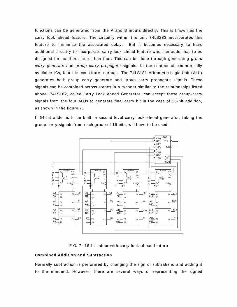
functions can be generated from the A and B inputs directly. This is known as the
carry look ahead feature. The circuitry within the unit 74LS283 incorporates this
feature to minimise the associated delay. But it becomes necessary to have
additional circuitry to incorporate carry look ahead feature when an adder has to be
designed for numbers more than four. This can be done through generating group
carry generate and group carry propagate signals. In the context of commercially
available ICs, four bits constitute a group. The 74LS181 Arithmetic Logic Unit (ALU)
generates both group carry generate and group carry propagate signals. These
signals can be combined across stages in a manner similar to the relationships listed
above. 74LS182, called Carry Look Ahead Generator, can accept these group-carry
signals from the four ALUs to generate final carry bit in the case of 16-bit addition,
as shown in the figure 7.
If 64-bit adder is to be built, a second level carry look ahead generator, taking the
group carry signals from each group of 16 bits, will have to be used.
P0Q0
F0
P1
Q1
F1
P2
Q2
P3
Q3
F2
F3
0
4
M0
CPCG
CO
P=QCI
ALU'181
P0
Q0
F0
P1
Q1
F1
P2
Q2
P3
Q3
F2
F3
0
4
M0
CPCGCO
P=Q
CI
ALU'181
P0
Q0
F0
P1
Q1
F1
P2
Q2
P3
Q3
F2
F3
0
4
M0
CP
CGCO
P=Q
CI
ALU'181
P0Q0
F0
P1
Q1
F1
P2
Q2
P3
Q3
F2
F3
0
4
M0
CP
CGCO
P=Q
CI
ALU'181
HLLHL
H
HH
HLL
L
LLL
L
H
H
LL
L
A8
A9
A10
A11
A12
A13
A14
B12
B13
B14B10
B9
B8A4B4
A5B5
A6B6
A7B7 B11
A15B15
A0B0
A1B1
A2B2
A3B3
S0
S1
S2
S3
S4
S5
S6
S7
S8
S9
S10
S11
S12
S13
S14
S15
CP0CP1CP2CP3CG0CG1CG2CG3
CP
CG
C00C01CO2
'182
31313131
FIG. 7: 16-bit adder with carry look-ahead feature
Combined Addition and Subtraction
Normally subtraction is performed by changing the sign of subtrahend and adding it
to the minuend. However, there are several ways of representing the signed
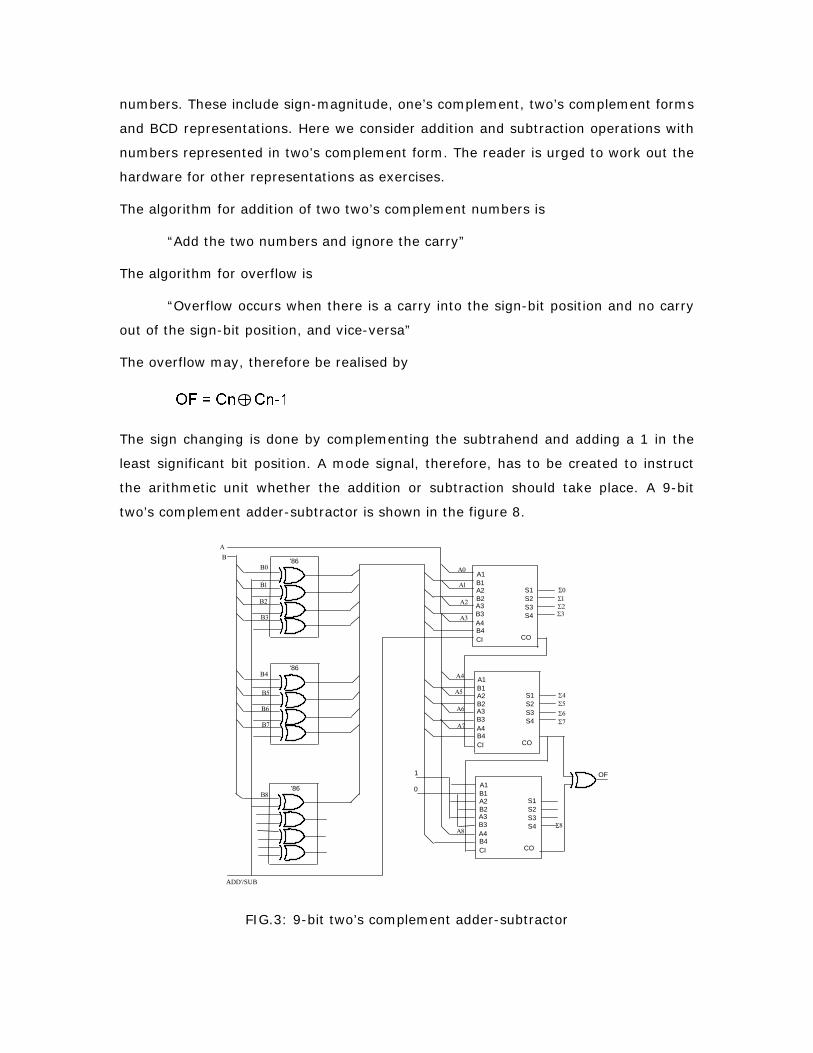
numbers. These include sign-magnitude, one’s complement, two’s complement forms
and BCD representations. Here we consider addition and subtraction operations with
numbers represented in two’s complement form. The reader is urged to work out the
hardware for other representations as exercises.
The algorithm for addition of two two’s complement numbers is
“Add the two numbers and ignore the carry”
The algorithm for overflow is
“Overflow occurs when there is a carry into the sign-bit position and no carry
out of the sign-bit position, and vice-versa”
The overflow may, therefore be realised by
The sign changing is done by complementing the subtrahend and adding a 1 in the
least significant bit position. A mode signal, therefore, has to be created to instruct
the arithmetic unit whether the addition or subtraction should take place. A 9-bit
two’s complement adder-subtractor is shown in the figure 8.
CI CO
A1B1A2B2A3B3A4B4
S1S2S3S4
CI CO
A1B1A2B2A3B3A4B4
S1S2S3S4
CI CO
A1B1A2B2A3B3A4B4
S1S2S3S4
'86
'86
OF1
0
Σ0Σ1Σ2Σ3
Σ5Σ4
Σ6Σ7
Σ8
Β8
Β7
Β6
Β5
Β4
Β0
Β1
Β2
Β3
ΒΑ
Α0
Α1
Α2
Α3
Α4
Α5
Α6
Α7
Α8
'86
ADD'/SUB
FIG.3: 9-bit two’s complement adder-subtractor
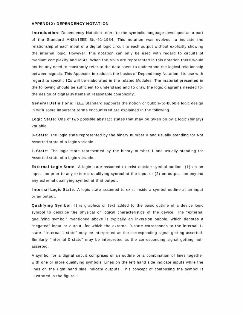
APPENDIX: DEPENDENCY NOTATION
Introduction: Dependency Notation refers to the symbolic language developed as a part
of the Standard ANSI/IEEE Std-91-1984. This notation was evolved to indicate the
relationship of each input of a digital logic circuit to each output without explicitly showing
the internal logic. However, this notation can only be used with regard to circuits of
medium complexity and MSIs. When the MSIs are represented in this notation there would
not be any need to constantly refer to the data sheet to understand the logical relationship
between signals. This Appexdix introduces the basics of Dependency Notation. Its use with
regard to specific ICs will be elaborated in the related Modules. The material presented in
the following should be sufficient to understand and to draw the logic diagrams needed for
the design of digital systems of reasonable complexity.
General Definitions: IEEE Standard supports the notion of bubble-to-bubble logic design
in with some important terms encountered are explained in the following.
Logic State: One of two possible abstract states that may be taken on by a logic (binary)
variable.
0-State: The logic state represented by the binary number 0 and usually standing for Not
Asserted state of a logic variable.
1-State: The logic state represented by the binary number 1 and usually standing for
Asserted state of a logic variable.
External Logic State: A logic state assumed to exist outside symbol outline; (1) on an
input line prior to any external qualifying symbol at the input or (2) on output line beyond
any external qualifying symbol at that output.
Internal Logic State: A logic state assumed to exist inside a symbol outline at an input
or an output.
Qualifying Symbol: It is graphics or text added to the basic outline of a device logic
symbol to describe the physical or logical characteristics of the device. The “external
qualifying symbol” mentioned above is typically an inversion bubble, which denotes a
“negated” input or output, for which the external 0-state corresponds to the internal 1-
state. “Internal 1-state” may be interpreted as the corresponding signal getting asserted.
Similarly “internal 0-state” may be interpreted as the corresponding signal getting not-
asserted.
A symbol for a digital circuit comprises of an outline or a combination of lines together
with one or more qualifying symbols. Lines on the left hand side indicate inputs while the
lines on the right hand side indicate outputs. This concept of composing the symbol is
illustrated in the figure 1.
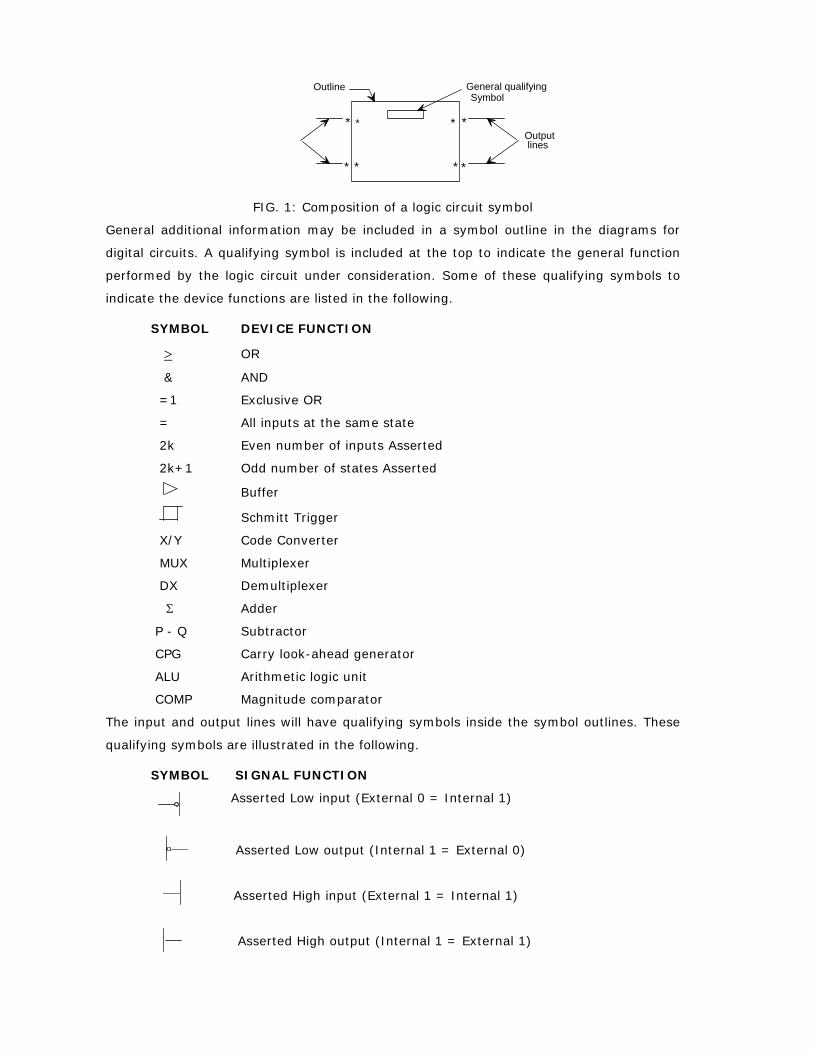
*
**
* *
**
*
General qualifying Symbol
Outputlines
Outline
FIG. 1: Composition of a logic circuit symbol
General additional information may be included in a symbol outline in the diagrams for
digital circuits. A qualifying symbol is included at the top to indicate the general function
performed by the logic circuit under consideration. Some of these qualifying symbols to
indicate the device functions are listed in the following.
SYMBOL DEVICE FUNCTION
> OR
& AND
=1 Exclusive OR
= All inputs at the same state
2k Even number of inputs Asserted
2k+1 Odd number of states Asserted
Buffer
Schmitt Trigger
X/Y Code Converter
MUX Multiplexer
DX Demultiplexer
Σ Adder
P - Q Subtractor
CPG Carry look-ahead generator
ALU Arithmetic logic unit
COMP Magnitude comparator
The input and output lines will have qualifying symbols inside the symbol outlines. These
qualifying symbols are illustrated in the following.
SYMBOL SIGNAL FUNCTION
Asserted Low input (External 0 = Internal 1)
Asserted Low output (Internal 1 = External 0)
Asserted High input (External 1 = Internal 1)
Asserted High output (Internal 1 = External 1)
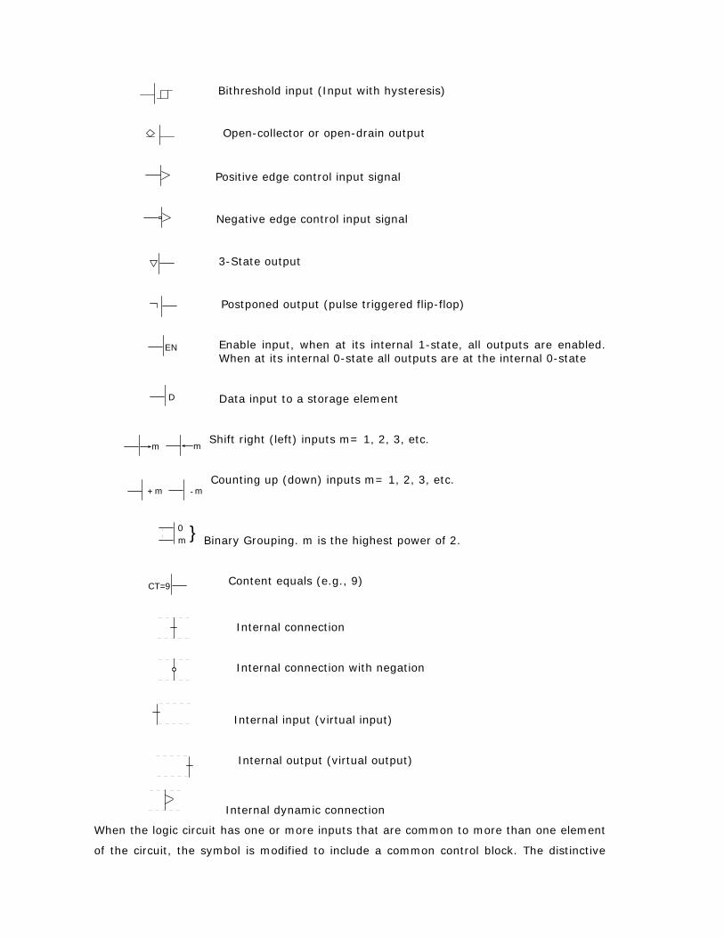
Bithreshold input (Input with hysteresis)
Open-collector or open-drain output
Positive edge control input signal
Negative edge control input signal
3-State output
Postponed output (pulse triggered flip-flop)
Enable input, when at its internal 1-state, all outputs are enabled. When at its internal 0-state all outputs are at the internal 0-state
Data input to a storage element
Shift right (left) inputs m= 1, 2, 3, etc.
Counting up (down) inputs m= 1, 2, 3, etc.
Binary Grouping. m is the highest power of 2.
Content equals (e.g., 9)
Internal connection
Internal connection with negation
Internal input (virtual input)
Internal output (virtual output)
Internal dynamic connection
When the logic circuit has one or more inputs that are common to more than one element
of the circuit, the symbol is modified to include a common control block. The distinctive
EN
m m
m m+ -
0m
CT=9
D
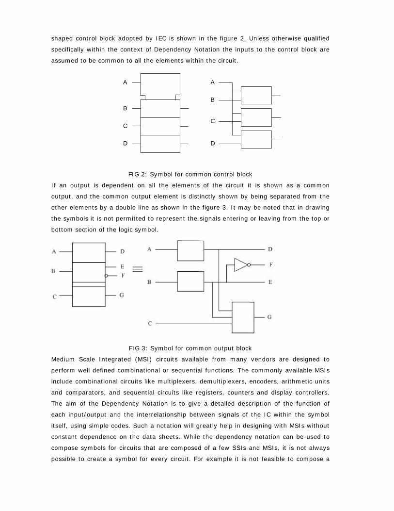
shaped control block adopted by IEC is shown in the figure 2. Unless otherwise qualified
specifically within the context of Dependency Notation the inputs to the control block are
assumed to be common to all the elements within the circuit.
A
B
C
D
A
B
C
D
FIG 2: Symbol for common control block
If an output is dependent on all the elements of the circuit it is shown as a common
output, and the common output element is distinctly shown by being separated from the
other elements by a double line as shown in the figure 3. It may be noted that in drawing
the symbols it is not permitted to represent the signals entering or leaving from the top or
bottom section of the logic symbol.
FIG 3: Symbol for common output block
Medium Scale Integrated (MSI) circuits available from many vendors are designed to
perform well defined combinational or sequential functions. The commonly available MSIs
include combinational circuits like multiplexers, demultiplexers, encoders, arithmetic units
and comparators, and sequential circuits like registers, counters and display controllers.
The aim of the Dependency Notation is to give a detailed description of the function of
each input/output and the interrelationship between signals of the IC within the symbol
itself, using simple codes. Such a notation will greatly help in designing with MSIs without
constant dependence on the data sheets. While the dependency notation can be used to
compose symbols for circuits that are composed of a few SSIs and MSIs, it is not always
possible to create a symbol for every circuit. For example it is not feasible to compose a
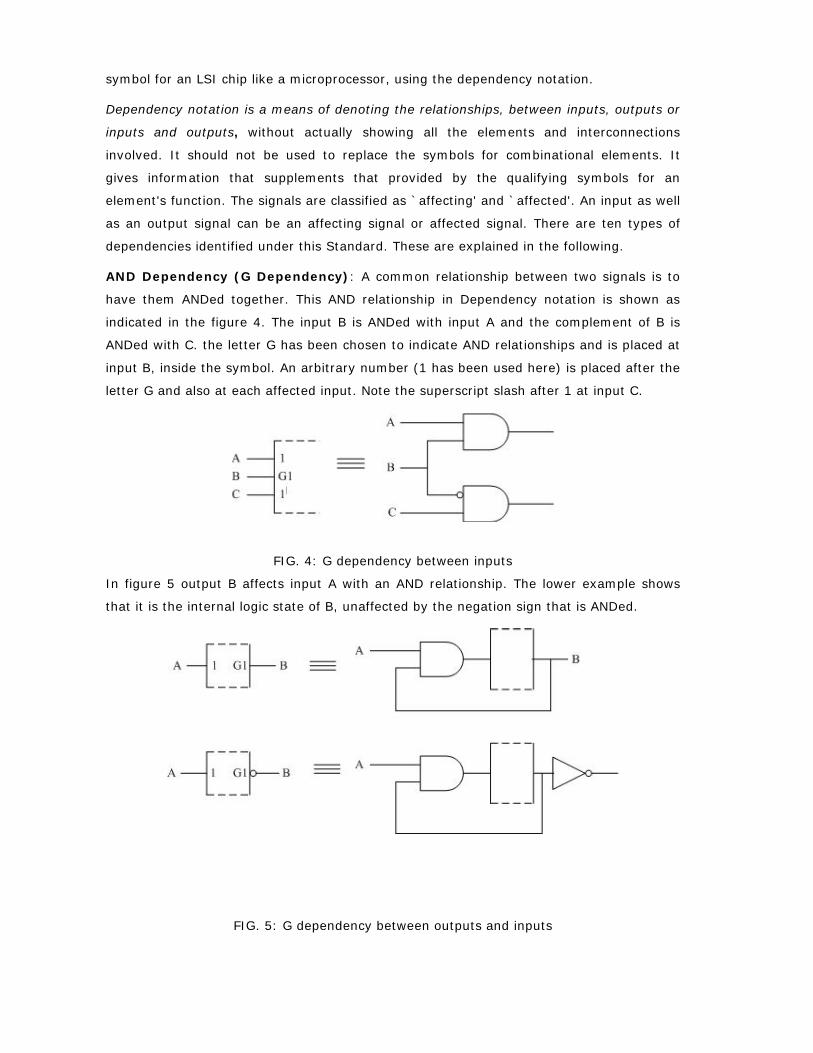
symbol for an LSI chip like a microprocessor, using the dependency notation.
Dependency notation is a means of denoting the relationships, between inputs, outputs or
inputs and outputs, without actually showing all the elements and interconnections
involved. It should not be used to replace the symbols for combinational elements. It
gives information that supplements that provided by the qualifying symbols for an
element's function. The signals are classified as `affecting' and `affected'. An input as well
as an output signal can be an affecting signal or affected signal. There are ten types of
dependencies identified under this Standard. These are explained in the following.
AND Dependency (G Dependency): A common relationship between two signals is to
have them ANDed together. This AND relationship in Dependency notation is shown as
indicated in the figure 4. The input B is ANDed with input A and the complement of B is
ANDed with C. the letter G has been chosen to indicate AND relationships and is placed at
input B, inside the symbol. An arbitrary number (1 has been used here) is placed after the
letter G and also at each affected input. Note the superscript slash after 1 at input C.
FIG. 4: G dependency between inputs
In figure 5 output B affects input A with an AND relationship. The lower example shows
that it is the internal logic state of B, unaffected by the negation sign that is ANDed.
FIG. 5: G dependency between outputs and inputs
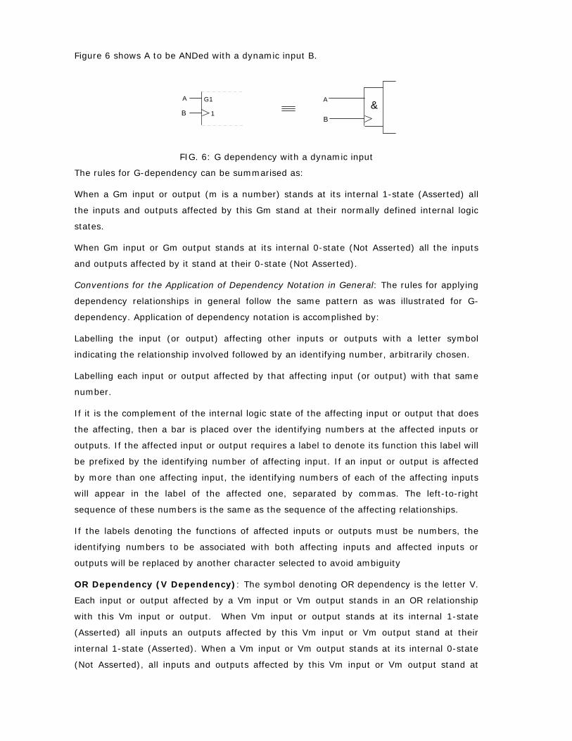
Figure 6 shows A to be ANDed with a dynamic input B.
FIG. 6: G dependency with a dynamic input
The rules for G-dependency can be summarised as:
When a Gm input or output (m is a number) stands at its internal 1-state (Asserted) all
the inputs and outputs affected by this Gm stand at their normally defined internal logic
states.
When Gm input or Gm output stands at its internal 0-state (Not Asserted) all the inputs
and outputs affected by it stand at their 0-state (Not Asserted).
Conventions for the Application of Dependency Notation in General: The rules for applying
dependency relationships in general follow the same pattern as was illustrated for G-
dependency. Application of dependency notation is accomplished by:
Labelling the input (or output) affecting other inputs or outputs with a letter symbol
indicating the relationship involved followed by an identifying number, arbitrarily chosen.
Labelling each input or output affected by that affecting input (or output) with that same
number.
If it is the complement of the internal logic state of the affecting input or output that does
the affecting, then a bar is placed over the identifying numbers at the affected inputs or
outputs. If the affected input or output requires a label to denote its function this label will
be prefixed by the identifying number of affecting input. If an input or output is affected
by more than one affecting input, the identifying numbers of each of the affecting inputs
will appear in the label of the affected one, separated by commas. The left-to-right
sequence of these numbers is the same as the sequence of the affecting relationships.
If the labels denoting the functions of affected inputs or outputs must be numbers, the
identifying numbers to be associated with both affecting inputs and affected inputs or
outputs will be replaced by another character selected to avoid ambiguity
OR Dependency (V Dependency): The symbol denoting OR dependency is the letter V.
Each input or output affected by a Vm input or Vm output stands in an OR relationship
with this Vm input or output. When Vm input or output stands at its internal 1-state
(Asserted) all inputs an outputs affected by this Vm input or Vm output stand at their
internal 1-state (Asserted). When a Vm input or Vm output stands at its internal 0-state
(Not Asserted), all inputs and outputs affected by this Vm input or Vm output stand at
1
G1A A
BB
&
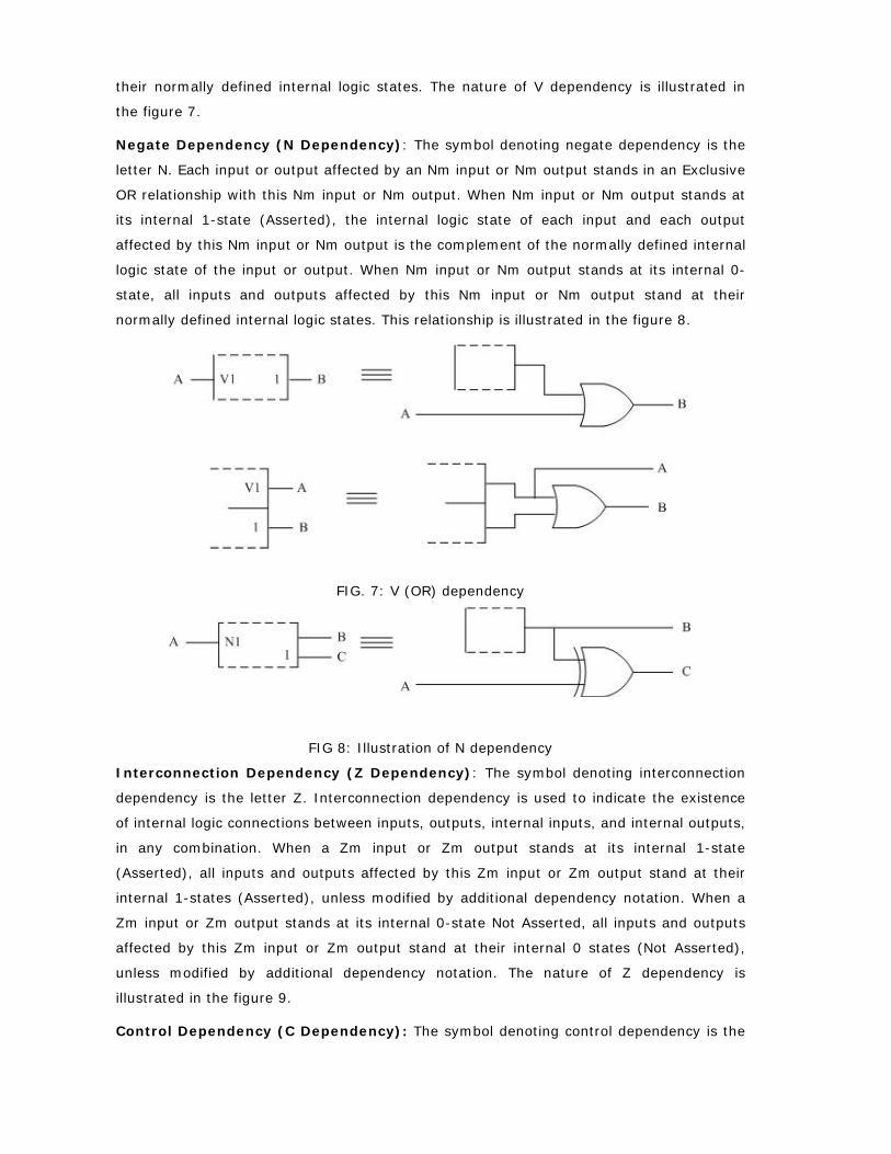
their normally defined internal logic states. The nature of V dependency is illustrated in
the figure 7.
Negate Dependency (N Dependency): The symbol denoting negate dependency is the
letter N. Each input or output affected by an Nm input or Nm output stands in an Exclusive
OR relationship with this Nm input or Nm output. When Nm input or Nm output stands at
its internal 1-state (Asserted), the internal logic state of each input and each output
affected by this Nm input or Nm output is the complement of the normally defined internal
logic state of the input or output. When Nm input or Nm output stands at its internal 0-
state, all inputs and outputs affected by this Nm input or Nm output stand at their
normally defined internal logic states. This relationship is illustrated in the figure 8.
FIG. 7: V (OR) dependency
FIG 8: Illustration of N dependency
Interconnection Dependency (Z Dependency): The symbol denoting interconnection
dependency is the letter Z. Interconnection dependency is used to indicate the existence
of internal logic connections between inputs, outputs, internal inputs, and internal outputs,
in any combination. When a Zm input or Zm output stands at its internal 1-state
(Asserted), all inputs and outputs affected by this Zm input or Zm output stand at their
internal 1-states (Asserted), unless modified by additional dependency notation. When a
Zm input or Zm output stands at its internal 0-state Not Asserted, all inputs and outputs
affected by this Zm input or Zm output stand at their internal 0 states (Not Asserted),
unless modified by additional dependency notation. The nature of Z dependency is
illustrated in the figure 9.
Control Dependency (C Dependency): The symbol denoting control dependency is the
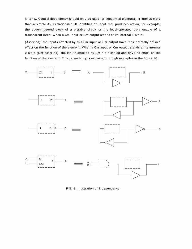
letter C. Control dependency should only be used for sequential elements. It implies more
than a simple AND relationship. It identifies an input that produces action, for example,
the edge-triggered clock of a bistable circuit or the level-operated data enable of a
transparent latch. When a Cm input or Cm output stands at its internal 1-state
(Asserted), the inputs affected by this Cm input or Cm output have their normally defined
effect on the function of the element. When a Cm input or Cm output stands at its internal
0-state (Not asserted), the inputs affected by Cm are disabled and have no effect on the
function of the element. This dependency is explained through examples in the figure 10.
FIG. 9: Illustration of Z dependency
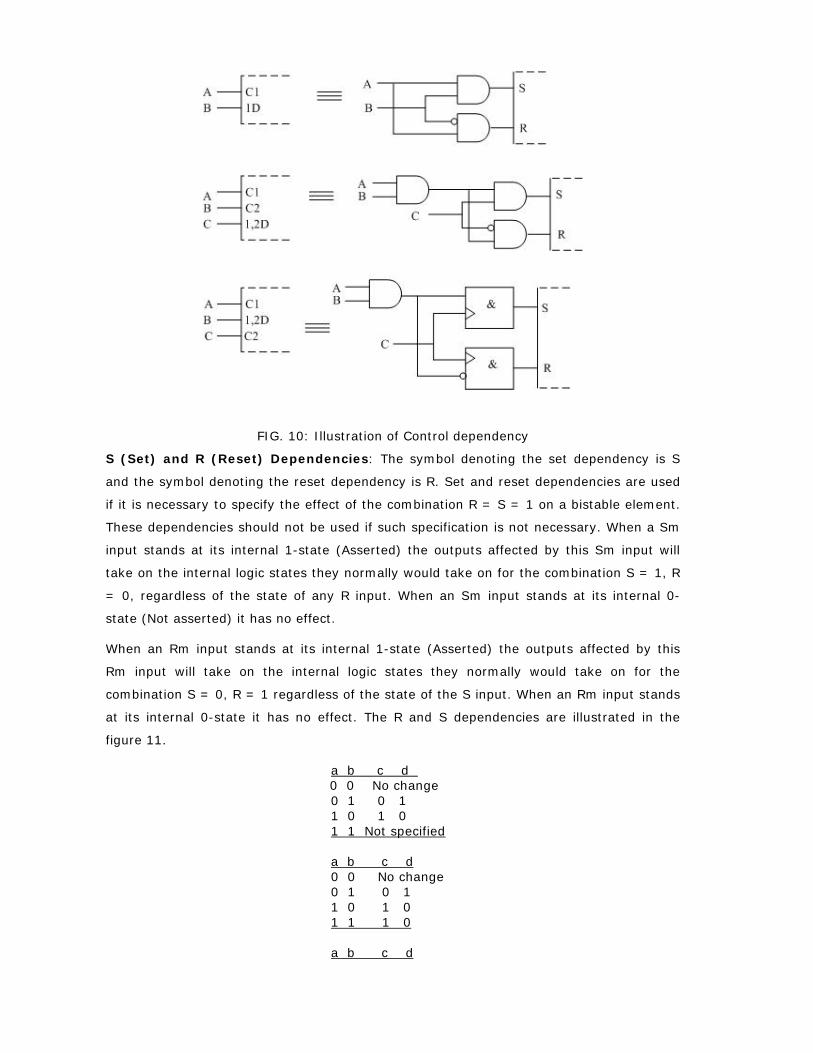
FIG. 10: Illustration of Control dependency
S (Set) and R (Reset) Dependencies: The symbol denoting the set dependency is S
and the symbol denoting the reset dependency is R. Set and reset dependencies are used
if it is necessary to specify the effect of the combination R = S = 1 on a bistable element.
These dependencies should not be used if such specification is not necessary. When a Sm
input stands at its internal 1-state (Asserted) the outputs affected by this Sm input will
take on the internal logic states they normally would take on for the combination S = 1, R
= 0, regardless of the state of any R input. When an Sm input stands at its internal 0-
state (Not asserted) it has no effect.
When an Rm input stands at its internal 1-state (Asserted) the outputs affected by this
Rm input will take on the internal logic states they normally would take on for the
combination S = 0, R = 1 regardless of the state of the S input. When an Rm input stands
at its internal 0-state it has no effect. The R and S dependencies are illustrated in the
figure 11.
a b c d 0 0 No change 0 1 0 1 1 0 1 0 1 1 Not specified a b c d 0 0 No change
0 1 0 1 1 0 1 0 1 1 1 0 a b c d
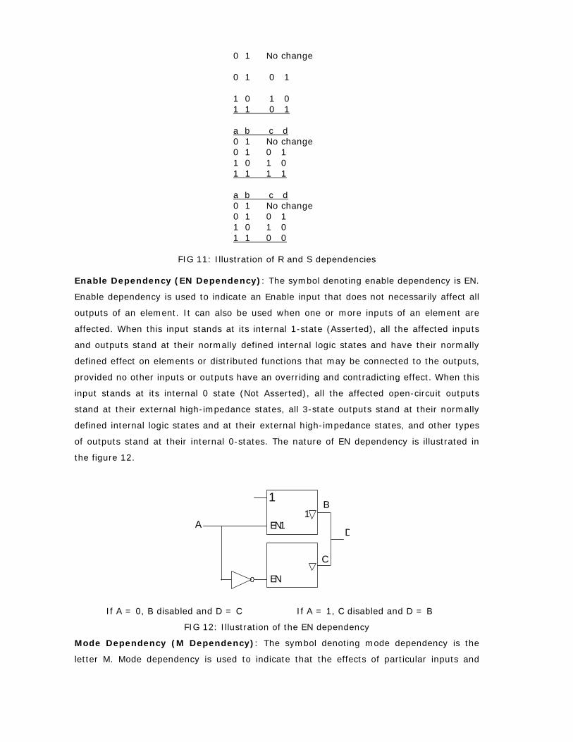
0 1 No change
0 1 0 1
1 0 1 0 1 1 0 1
a b c d
0 1 No change 0 1 0 1 1 0 1 0 1 1 1 1
a b c d 0 1 No change 0 1 0 1 1 0 1 0 1 1 0 0
FIG 11: Illustration of R and S dependencies
Enable Dependency (EN Dependency): The symbol denoting enable dependency is EN.
Enable dependency is used to indicate an Enable input that does not necessarily affect all
outputs of an element. It can also be used when one or more inputs of an element are
affected. When this input stands at its internal 1-state (Asserted), all the affected inputs
and outputs stand at their normally defined internal logic states and have their normally
defined effect on elements or distributed functions that may be connected to the outputs,
provided no other inputs or outputs have an overriding and contradicting effect. When this
input stands at its internal 0 state (Not Asserted), all the affected open-circuit outputs
stand at their external high-impedance states, all 3-state outputs stand at their normally
defined internal logic states and at their external high-impedance states, and other types
of outputs stand at their internal 0-states. The nature of EN dependency is illustrated in
the figure 12.
1
EN1
EN
AD
1B
C
If A = 0, B disabled and D = C If A = 1, C disabled and D = B
FIG 12: Illustration of the EN dependency
Mode Dependency (M Dependency): The symbol denoting mode dependency is the
letter M. Mode dependency is used to indicate that the effects of particular inputs and
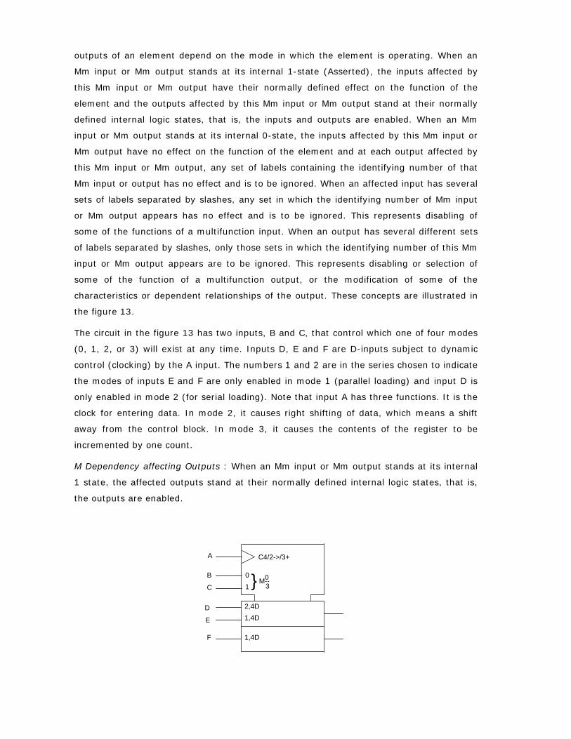
outputs of an element depend on the mode in which the element is operating. When an
Mm input or Mm output stands at its internal 1-state (Asserted), the inputs affected by
this Mm input or Mm output have their normally defined effect on the function of the
element and the outputs affected by this Mm input or Mm output stand at their normally
defined internal logic states, that is, the inputs and outputs are enabled. When an Mm
input or Mm output stands at its internal 0-state, the inputs affected by this Mm input or
Mm output have no effect on the function of the element and at each output affected by
this Mm input or Mm output, any set of labels containing the identifying number of that
Mm input or output has no effect and is to be ignored. When an affected input has several
sets of labels separated by slashes, any set in which the identifying number of Mm input
or Mm output appears has no effect and is to be ignored. This represents disabling of
some of the functions of a multifunction input. When an output has several different sets
of labels separated by slashes, only those sets in which the identifying number of this Mm
input or Mm output appears are to be ignored. This represents disabling or selection of
some of the function of a multifunction output, or the modification of some of the
characteristics or dependent relationships of the output. These concepts are illustrated in
the figure 13.
The circuit in the figure 13 has two inputs, B and C, that control which one of four modes
(0, 1, 2, or 3) will exist at any time. Inputs D, E and F are D-inputs subject to dynamic
control (clocking) by the A input. The numbers 1 and 2 are in the series chosen to indicate
the modes of inputs E and F are only enabled in mode 1 (parallel loading) and input D is
only enabled in mode 2 (for serial loading). Note that input A has three functions. It is the
clock for entering data. In mode 2, it causes right shifting of data, which means a shift
away from the control block. In mode 3, it causes the contents of the register to be
incremented by one count.
M Dependency affecting Outputs : When an Mm input or Mm output stands at its internal
1 state, the affected outputs stand at their normally defined internal logic states, that is,
the outputs are enabled.
C4/2->/3+
01 M--0
3
2,4D1,4D
1,4D
A
B
C
D
E
F
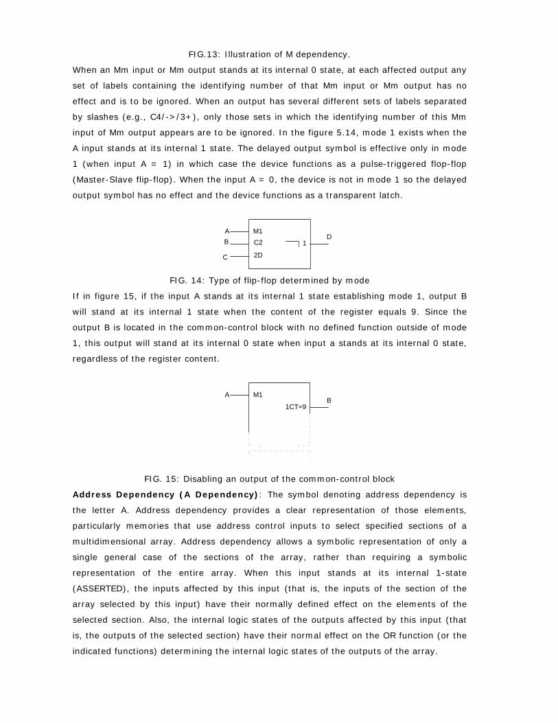
FIG.13: Illustration of M dependency.
When an Mm input or Mm output stands at its internal 0 state, at each affected output any
set of labels containing the identifying number of that Mm input or Mm output has no
effect and is to be ignored. When an output has several different sets of labels separated
by slashes (e.g., C4/->/3+), only those sets in which the identifying number of this Mm
input of Mm output appears are to be ignored. In the figure 5.14, mode 1 exists when the
A input stands at its internal 1 state. The delayed output symbol is effective only in mode
1 (when input A = 1) in which case the device functions as a pulse-triggered flop-flop
(Master-Slave flip-flop). When the input A = 0, the device is not in mode 1 so the delayed
output symbol has no effect and the device functions as a transparent latch.
1
M1C2
2D
AB
C
D
FIG. 14: Type of flip-flop determined by mode
If in figure 15, if the input A stands at its internal 1 state establishing mode 1, output B
will stand at its internal 1 state when the content of the register equals 9. Since the
output B is located in the common-control block with no defined function outside of mode
1, this output will stand at its internal 0 state when input a stands at its internal 0 state,
regardless of the register content.
M1AB
1CT=9
FIG. 15: Disabling an output of the common-control block
Address Dependency (A Dependency): The symbol denoting address dependency is
the letter A. Address dependency provides a clear representation of those elements,
particularly memories that use address control inputs to select specified sections of a
multidimensional array. Address dependency allows a symbolic representation of only a
single general case of the sections of the array, rather than requiring a symbolic
representation of the entire array. When this input stands at its internal 1-state
(ASSERTED), the inputs affected by this input (that is, the inputs of the section of the
array selected by this input) have their normally defined effect on the elements of the
selected section. Also, the internal logic states of the outputs affected by this input (that
is, the outputs of the selected section) have their normal effect on the OR function (or the
indicated functions) determining the internal logic states of the outputs of the array.
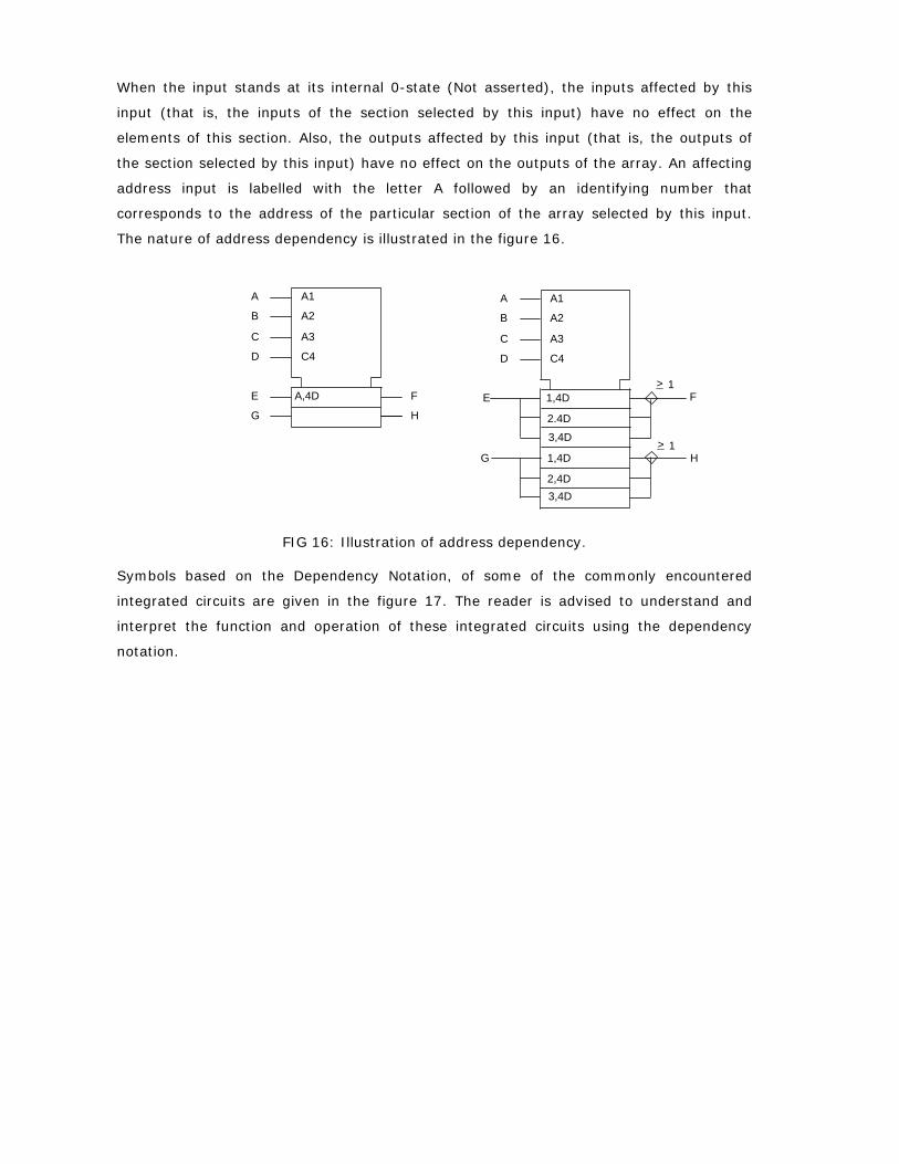
When the input stands at its internal 0-state (Not asserted), the inputs affected by this
input (that is, the inputs of the section selected by this input) have no effect on the
elements of this section. Also, the outputs affected by this input (that is, the outputs of
the section selected by this input) have no effect on the outputs of the array. An affecting
address input is labelled with the letter A followed by an identifying number that
corresponds to the address of the particular section of the array selected by this input.
The nature of address dependency is illustrated in the figure 16.
A
B
C
D
A1
A2
A3
C4
A
B
C
D
A1
A2
A3
C4
A,4DE
G
F
H1,4D
2.4D
3,4D
1,4D
2,4D3,4D
E
G
F
H
> 1
> 1
FIG 16: Illustration of address dependency. Symbols based on the Dependency Notation, of some of the commonly encountered
integrated circuits are given in the figure 17. The reader is advised to understand and
interpret the function and operation of these integrated circuits using the dependency
notation.
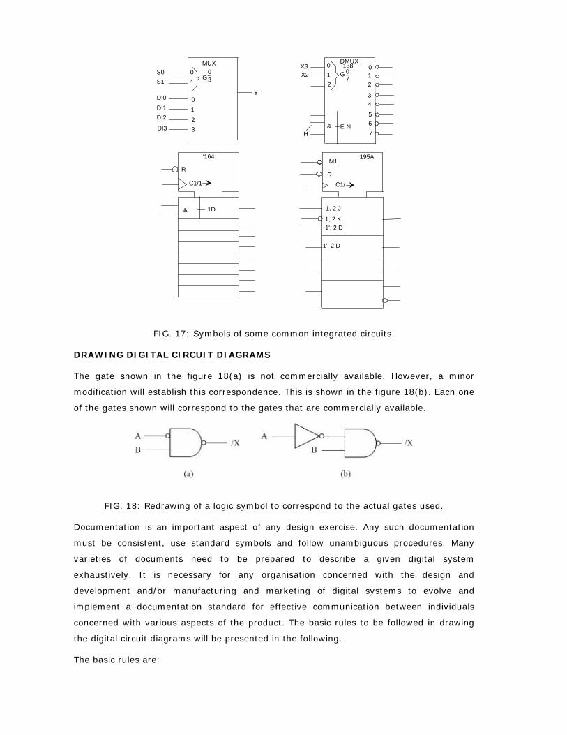
012
E N
01
34
567
2
G 07_
DMUX
&
X3X2
H
1380
G_3
MUX01
0123
S0S1
DI0DI1DI2
DI3
Y
'164
R
C1/1
& 1D
RC1/
195AM1
1, 2 J
1, 2 K1', 2 D
1', 2 D
FIG. 17: Symbols of some common integrated circuits. DRAWING DIGITAL CIRCUIT DIAGRAMS
The gate shown in the figure 18(a) is not commercially available. However, a minor
modification will establish this correspondence. This is shown in the figure 18(b). Each one
of the gates shown will correspond to the gates that are commercially available.
FIG. 18: Redrawing of a logic symbol to correspond to the actual gates used.
Documentation is an important aspect of any design exercise. Any such documentation
must be consistent, use standard symbols and follow unambiguous procedures. Many
varieties of documents need to be prepared to describe a given digital system
exhaustively. It is necessary for any organisation concerned with the design and
development and/or manufacturing and marketing of digital systems to evolve and
implement a documentation standard for effective communication between individuals
concerned with various aspects of the product. The basic rules to be followed in drawing
the digital circuit diagrams will be presented in the following.
The basic rules are:

All signals flow from left to right. In case of any deviation from this convention the
direction must be indicated by an arrow. Such a need may arise when there is
requirement to feed the output of a circuit module to the input of circuit module
which is otherwise upstream from the signal flow point of view.
External inputs should enter the left hand side of the diagram. Outputs from the
circuit should be shown in the right hand side.
Use polarised mnemonic notation and all the standard symbols thereof.
Use dependency notation to represent any MSI and LSI circuits.
All signals should have properly defined mnemonics with their assertion levels
indicated.
All gates represented in the circuit diagram must correspond to the actual
hardware elements used. But the choice of operator symbol (NAND, NOR, OR,
EXOR ETC.) for gates must be indicative of the function they perform.
Each operator symbol should be given a number to correspond with the actual IC
used. These are designated as U1, U2 etc. A particular number, say U2, may be
given to more than one logic operator as an IC may have more than one functional
element.
The pin numbers corresponding to the specific IC used should be shown near the
inputs or the outputs of the logic operator, or outside the symbol outline in the
case of MSIs and LSIs.
The specific ICs used along with their pin numbers for VCC and GND (VBB) should be
shown at a convenient place on the circuit diagram.
If the circuit diagram is large and is to be drawn on a large sheet, zonal co-
ordinates should be incorporated.
If a discontinuity is to be introduced in a signal line, its destination or source, if
needed in terms of zonal coordinates, should be indicated at the discontinuity.
Consider the circuit diagram shown in the figure19. It is redrawn as per the rules stated
above and shown in the figure 20.
FIG. 19: Example of a combination circuit
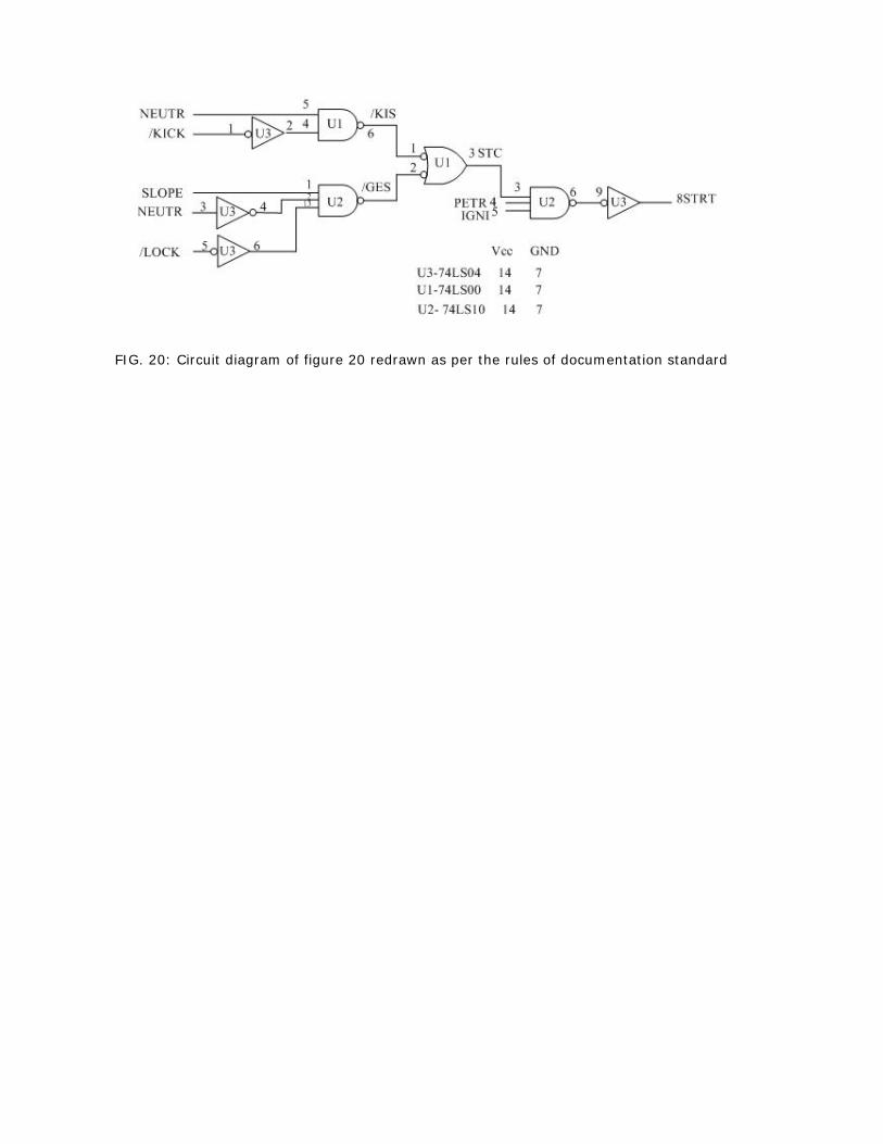
FIG. 20: Circuit diagram of figure 20 redrawn as per the rules of documentation standard
Related Documents