Digital Signal Processor TMS320LF2407 TMS320LF2407 Sarath S Nair Assistant Professor Amrita University www.technologyfuturae.com

Welcome message from author
This document is posted to help you gain knowledge. Please leave a comment to let me know what you think about it! Share it to your friends and learn new things together.
Transcript
Digital Signal
Processor
TMS320LF2407TMS320LF2407
Sarath S Nair
Assistant Professor
Amrita University
www.technologyfuturae.com
www.technologyfuturae.com
www.technologyfuturae.com
www.technologyfuturae.com
www.technologyfuturae.com
www.technologyfuturae.com
www.technologyfuturae.com
www.technologyfuturae.com
www.technologyfuturae.com
www.technologyfuturae.com
www.technologyfuturae.com
www.technologyfuturae.com
www.technologyfuturae.com
www.technologyfuturae.com
www.technologyfuturae.com
www.technologyfuturae.com
www.technologyfuturae.com
www.technologyfuturae.com
www.technologyfuturae.com
www.technologyfuturae.com
www.technologyfuturae.com
www.technologyfuturae.com
www.technologyfuturae.com
www.technologyfuturae.com
www.technologyfuturae.com
www.technologyfuturae.com
www.technologyfuturae.com
www.technologyfuturae.com
www.technologyfuturae.com
www.technologyfuturae.com
www.technologyfuturae.com
www.technologyfuturae.com
www.technologyfuturae.com
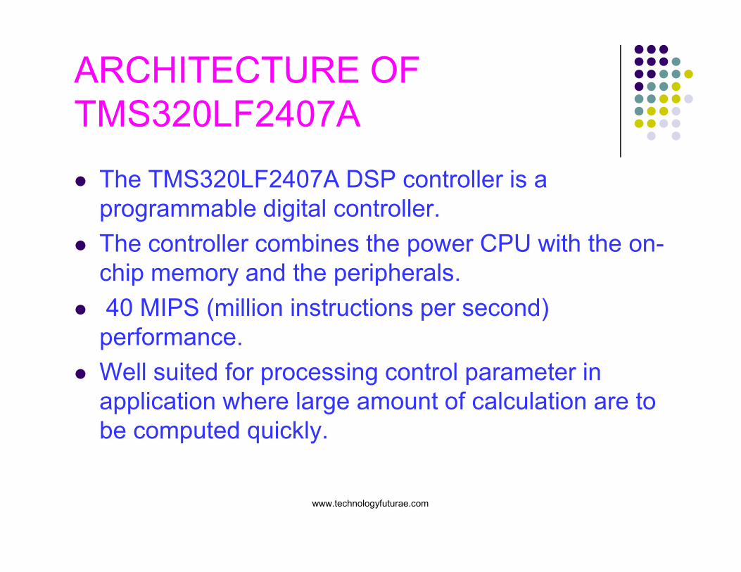
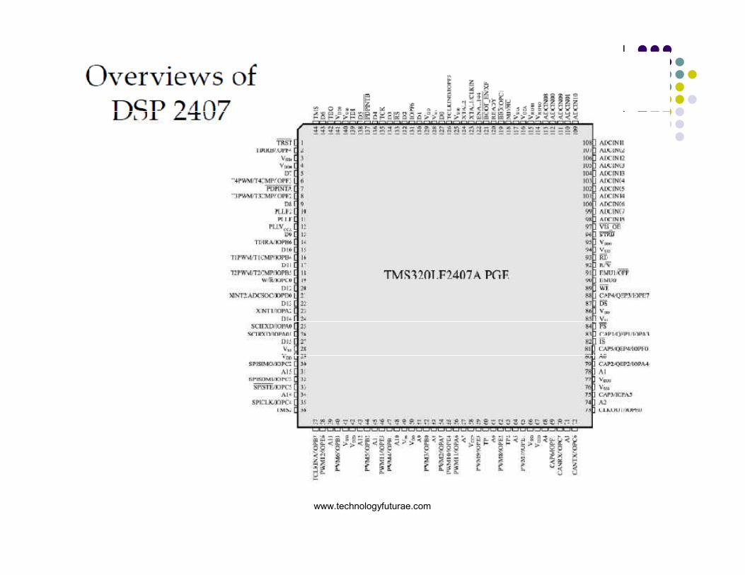
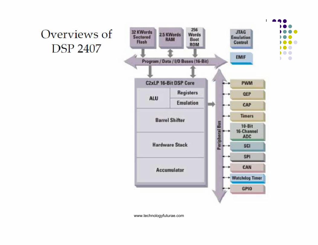
ARCHITECTURE OF
TMS320LF2407A
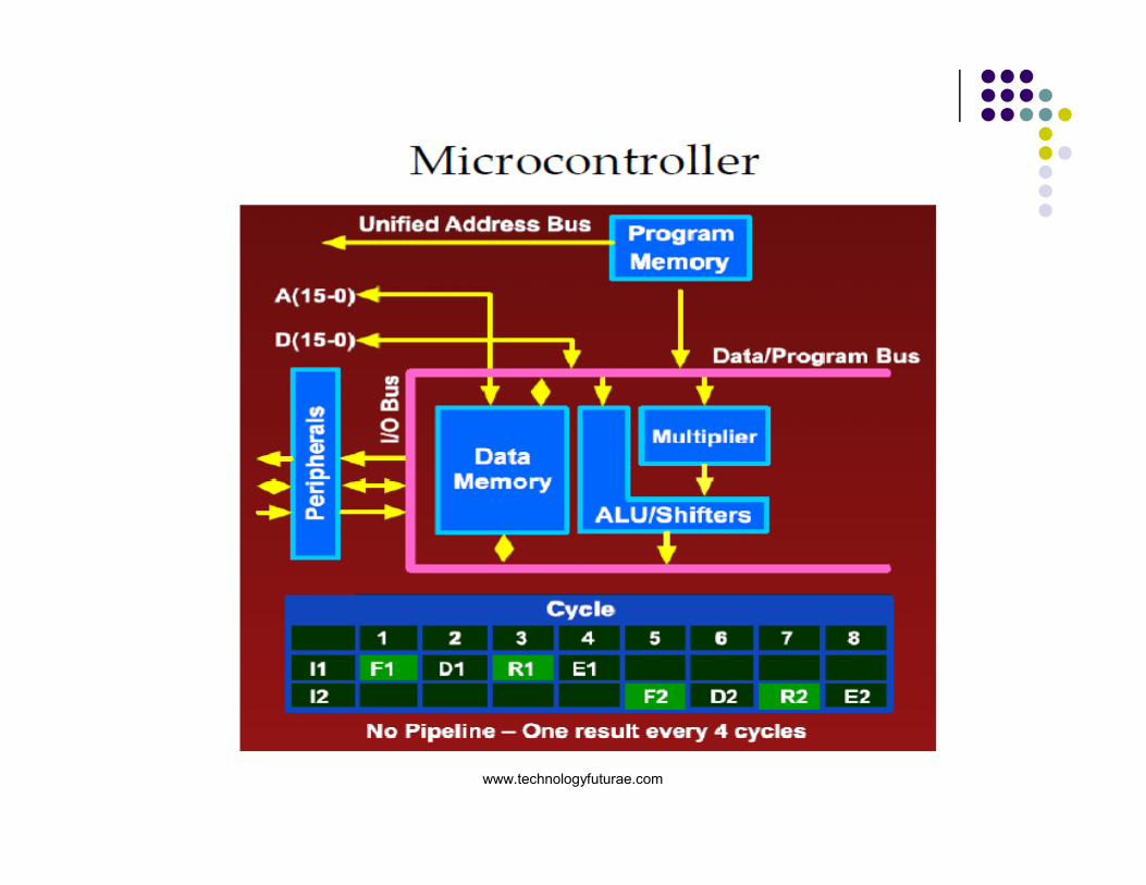
� The TMS320LF2407A DSP controller is a
programmable digital controller.
� The controller combines the power CPU with the on-
chip memory and the peripherals.
� 40 MIPS (million instructions per second)
performance.
� Well suited for processing control parameter in
application where large amount of calculation are to
be computed quickly.
www.technologyfuturae.com
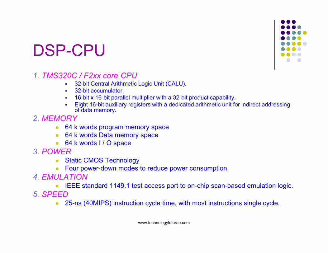
DSP-CPU
1. TMS320C / F2xx core CPU� 32-bit Central Arithmetic Logic Unit (CALU).
� 32-bit accumulator.
� 16-bit x 16-bit parallel multiplier with a 32-bit product capability.
� Eight 16-bit auxiliary registers with a dedicated arithmetic unit for indirect addressing of data memory.
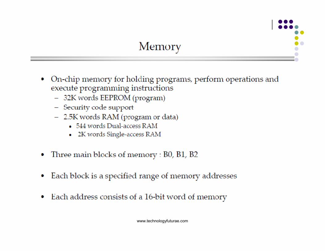
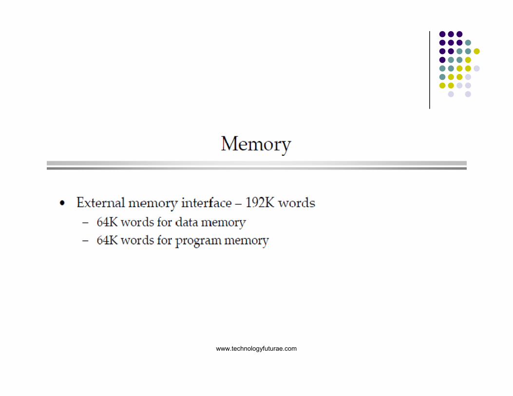
2. MEMORY� 64 k words program memory space� 64 k words program memory space
� 64 k words Data memory space
� 64 k words I / O space
3. POWER� Static CMOS Technology
� Four power-down modes to reduce power consumption.
4. EMULATION� IEEE standard 1149.1 test access port to on-chip scan-based emulation logic.
5. SPEED� 25-ns (40MIPS) instruction cycle time, with most instructions single cycle.
www.technologyfuturae.com
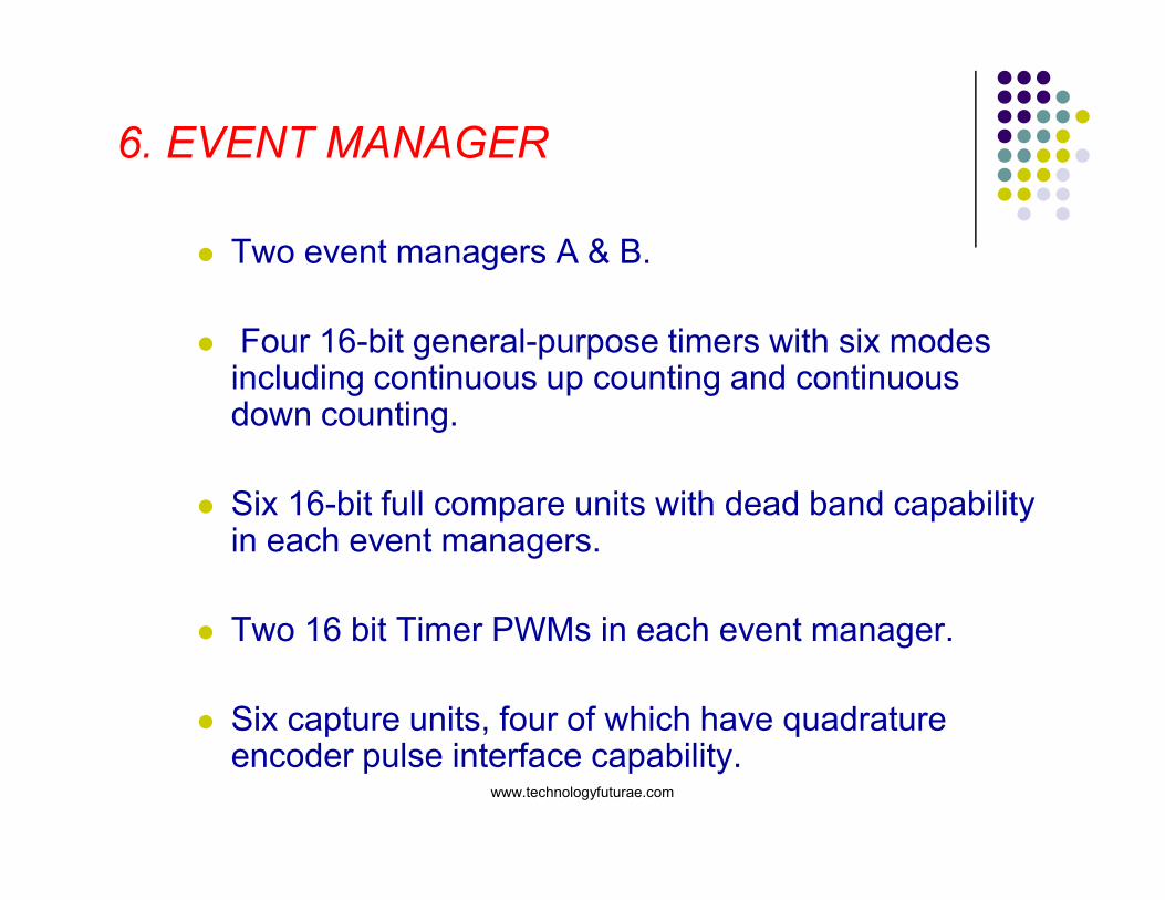
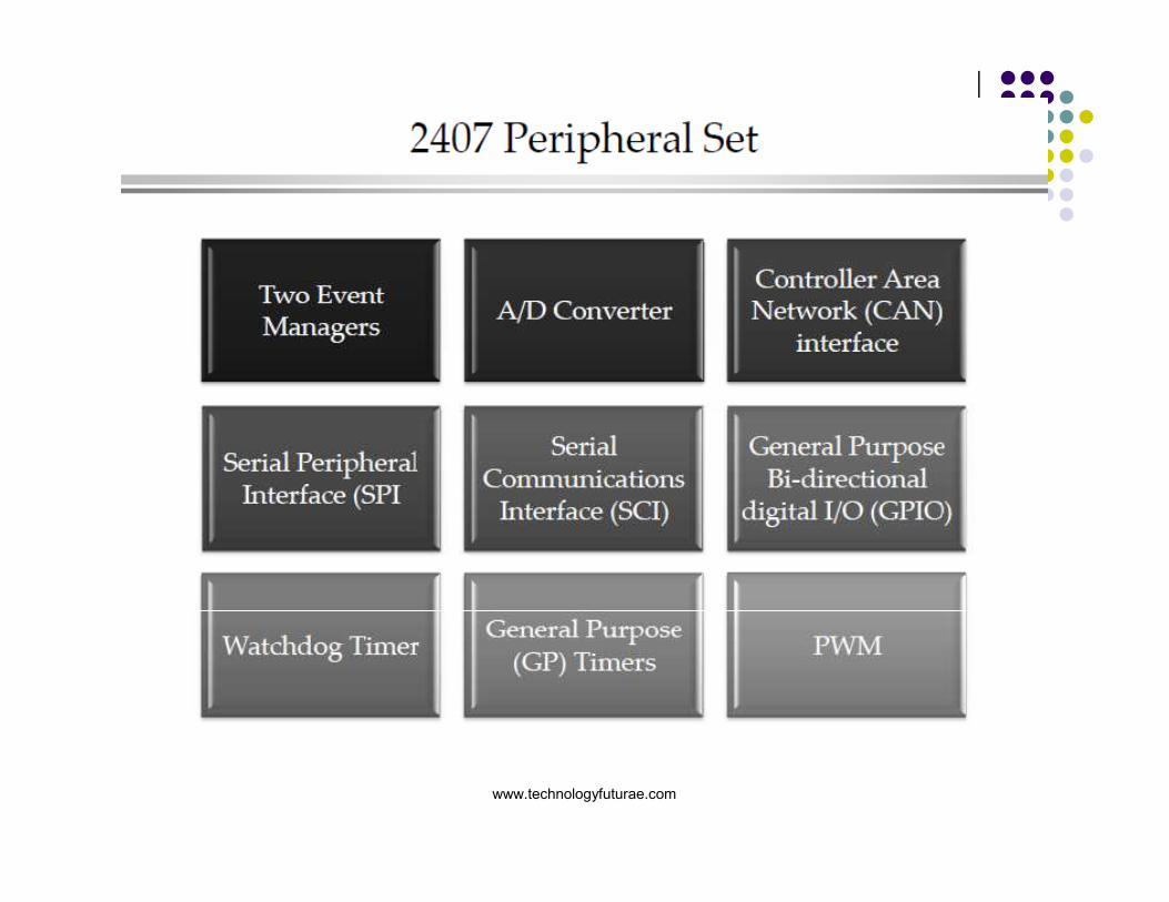
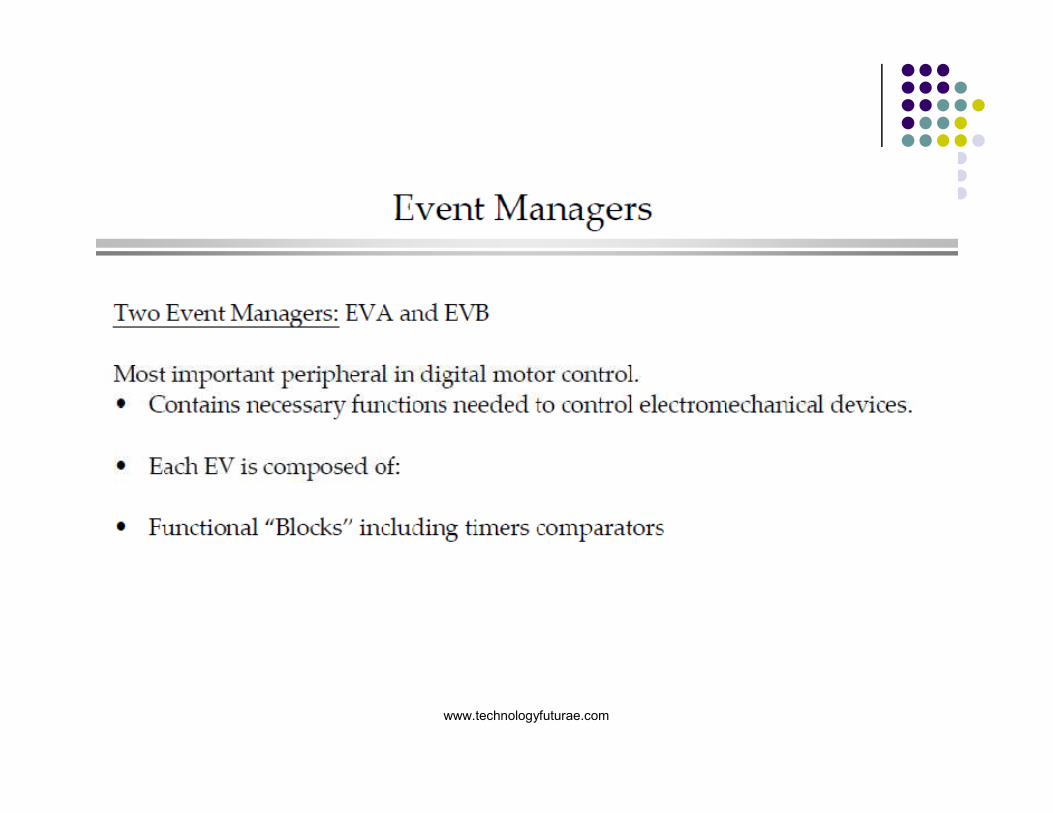
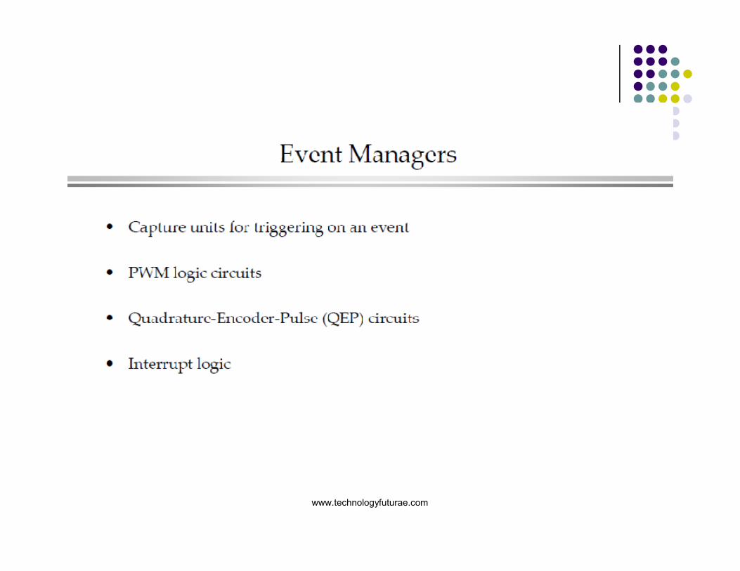
6. EVENT MANAGER
� Two event managers A & B.
� Four 16-bit general-purpose timers with six modes including continuous up counting and continuous down counting.
� Six 16-bit full compare units with dead band capability in each event managers.
� Two 16 bit Timer PWMs in each event manager.
� Six capture units, four of which have quadrature encoder pulse interface capability.
www.technologyfuturae.com
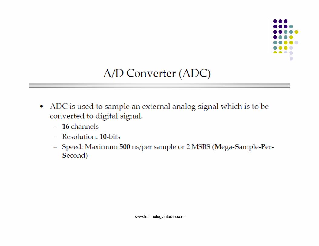
7. DUAL 10-BIT ANALOG-TO-DIGITAL CONVERTER (ADC)
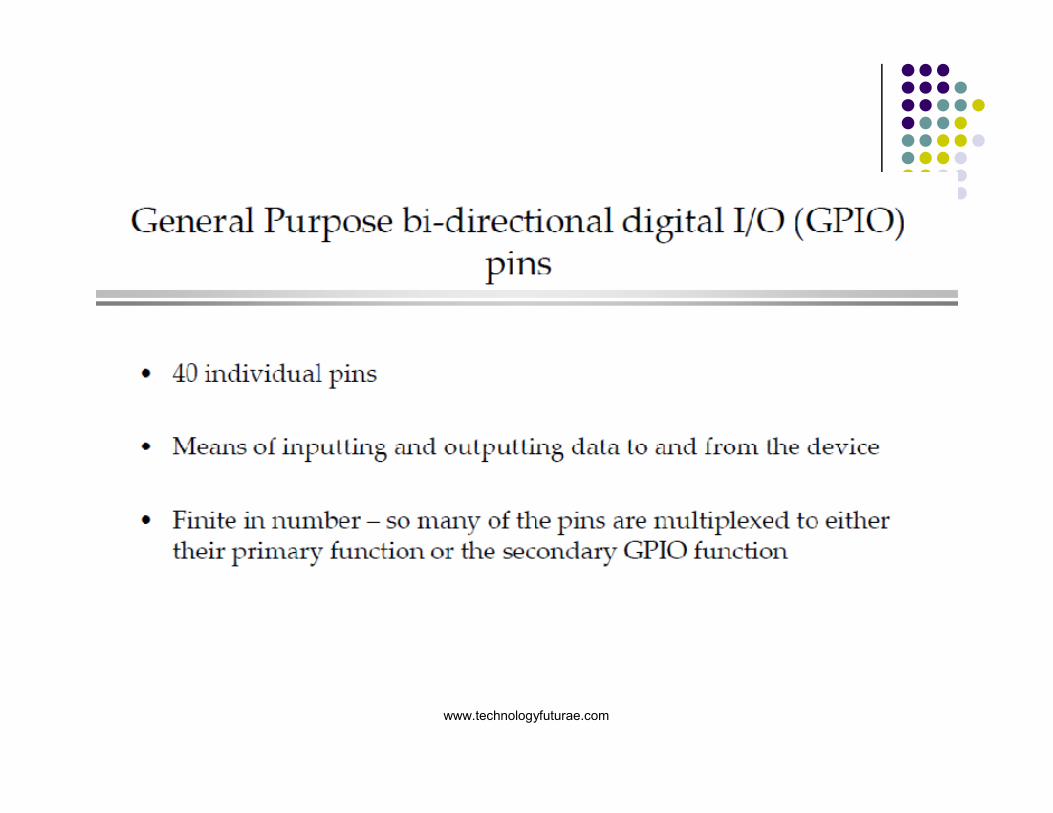
8. 40 INDIVIDUALLY PROGRAMMABLE, MULTIPLEXED I/O PINS.
9. PHASE-LOCKED LOOP (PLL) BASED CLOCK MODULE.
10. WATCHDOG (WD) TIMER MODULE WITH REAL-TIME
INTERRUPT (RTI)
11. SERIAL COMMUNICATION INTERFACE (SCI)11. SERIAL COMMUNICATION INTERFACE (SCI)
12. SERIAL PERIPHERAL INTERFACE
www.technologyfuturae.com
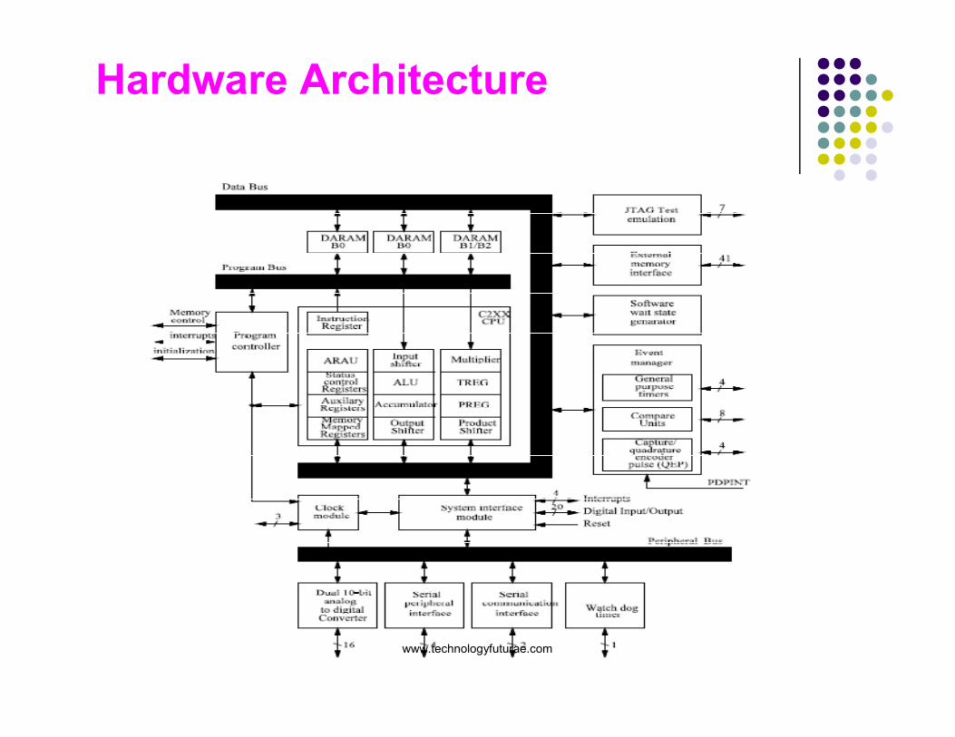
Hardware Architecture
www.technologyfuturae.com
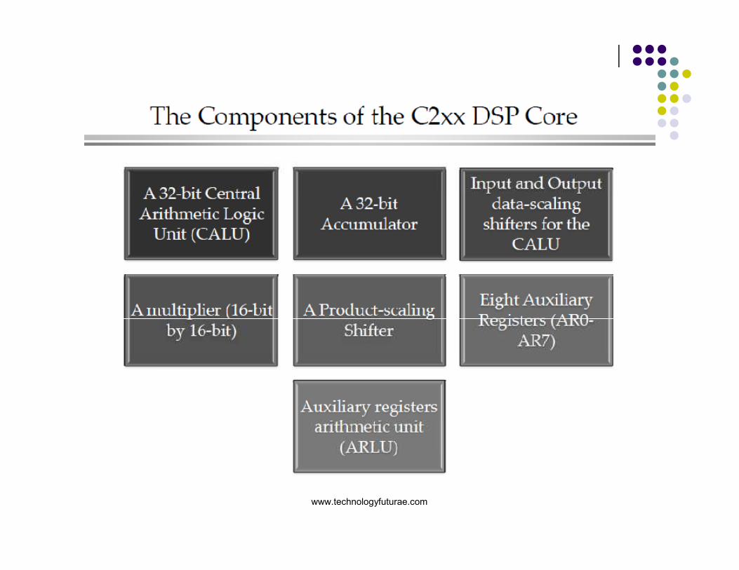
1.C2xx DSP CORE
� The C2xx DSP core is a16-bit fixed point processor
The components of C2xx DSP core:
� i. Central Arithmetic Logic Unit (CALU)� i. Central Arithmetic Logic Unit (CALU)
� ii. Accumulator
� iii. Data scaling shifters
� iv. Multiplier
� v. Product scaling shifters
� vi. Auxiliary register and auxiliary register arithmetic unit
(ARAU)
www.technologyfuturae.com
i. Central Arithmetic Logic Unit (CALU)
� The DSP core performs 2's-complement arithmetic using the 32-bit CALU.
� The CALU can perform Boolean operations.
ii 32-BIT Accumulator
� The accumulator stores the output from the CALU and provides an input to the CALU.
� Performs shift and rotate operations. Its word length is 32-bit.
� The accumulator is divided into a high-order word (bits 31 through 16) and a low-order word (bits15 through 0).
www.technologyfuturae.com
iii. Shifters- 3, 32 bit shifters
� Shifters allow for scaling, bit extraction, extended arithmetic, and overflow-prevention operations.
� Input data-scaling shifter (input shifter) –
� This shifter left-shifts 16-bit input data by 0 to 16 bits to align the data to the 32-bit input of the CALU.
� Output data-scaling shifter (output shifter) –� Output data-scaling shifter (output shifter) –
� This shifter left-shifts data from the accumulator by 0 to 7 bits before the output is stored to data memory. The content of the accumulator remain unchanged.
� Product - scaling shifter (product shifter) –
� The product register (PREG) receives the output of the multiplier.
www.technologyfuturae.com
iv 16 x 16 Bit Parallel Multiplier
� The multiplier performs a 16-bit two’s complement multiplication with a 32-bit result in a single instruction cycle.
� The multiplier consists of three units:
1. T-Register - temporarily stores the multiplicand
2. P-Register- stores the 32-bit product.
3. multiplier array
v. Auxiliary Register Arithmetic Unit (ARAU) and Auxiliary RegistersAuxiliary Registers
� ARAU generates data memory addresses during indirect addressing
� Eight auxiliary registers (AR0 through AR7) support the ARAU
� It can be loaded with a 16-bit value from data memory or directly from an instruction.
www.technologyfuturae.com
2. EVENT MANAGER (EV)
� There are two identical Event Managers
(EVA and EVB) on TMS320LF2407A.i. Interrupt logic
ii. Two general purpose timersii. Two general purpose timers
iii. Three compare units
iv. Three capture units
v. Quadrature encoder pulse circuit
www.technologyfuturae.com
i. Interrupt Logic
� Arranged into three groups (A, B, C ) and each group has its own mask and flag register
ii. GP Timer
� A General purpose timer is configured to count up, down or continuously up and down.
� Each EV has two GP timers. Timer1 & 2 for EVA and Timer3 & 4 for � Each EV has two GP timers. Timer1 & 2 for EVA and Timer3 & 4 for EVB.
iii. Compare Unit
� A PWM signal can also be generated using compare unit
� Their functions are identical to GP Timer compare units.
� Six PWM ouputs per EV
www.technologyfuturae.com
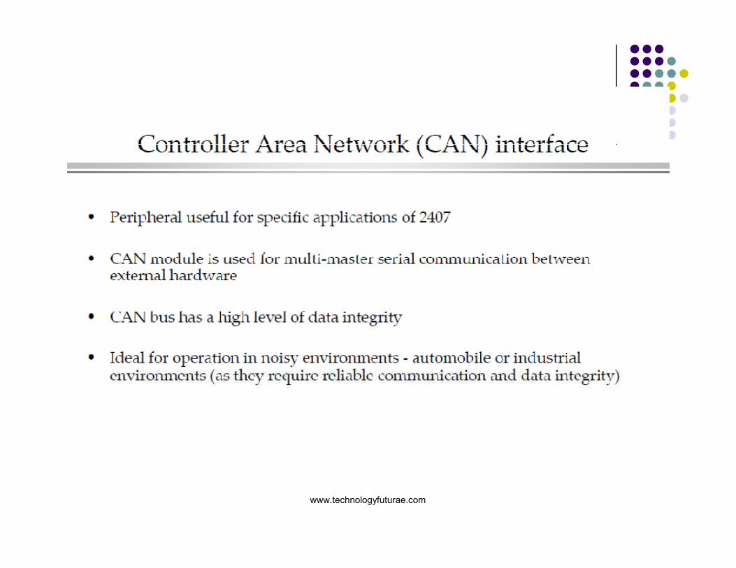
3. CONTROLLER AREA NETWORK
The CAN module is used for multi-master serial communication between external hardware.
� The CAN bus has a high level of data integrity
� Ideal for operation in noisy environment
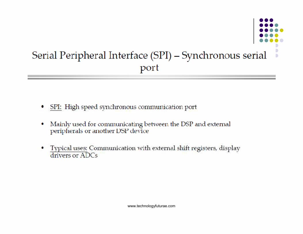
4. SERIAL PERIPHERAL INTERFACE4. SERIAL PERIPHERAL INTERFACE
The SPI is a high speed synchronous serial input / output port
� SPI is mainly used for communication between DSP and external
peripherals or another DSP device.
� Allow a serial bit stream of program length to be shifted in and out of
device at a programmed bit transfer rate.www.technologyfuturae.com
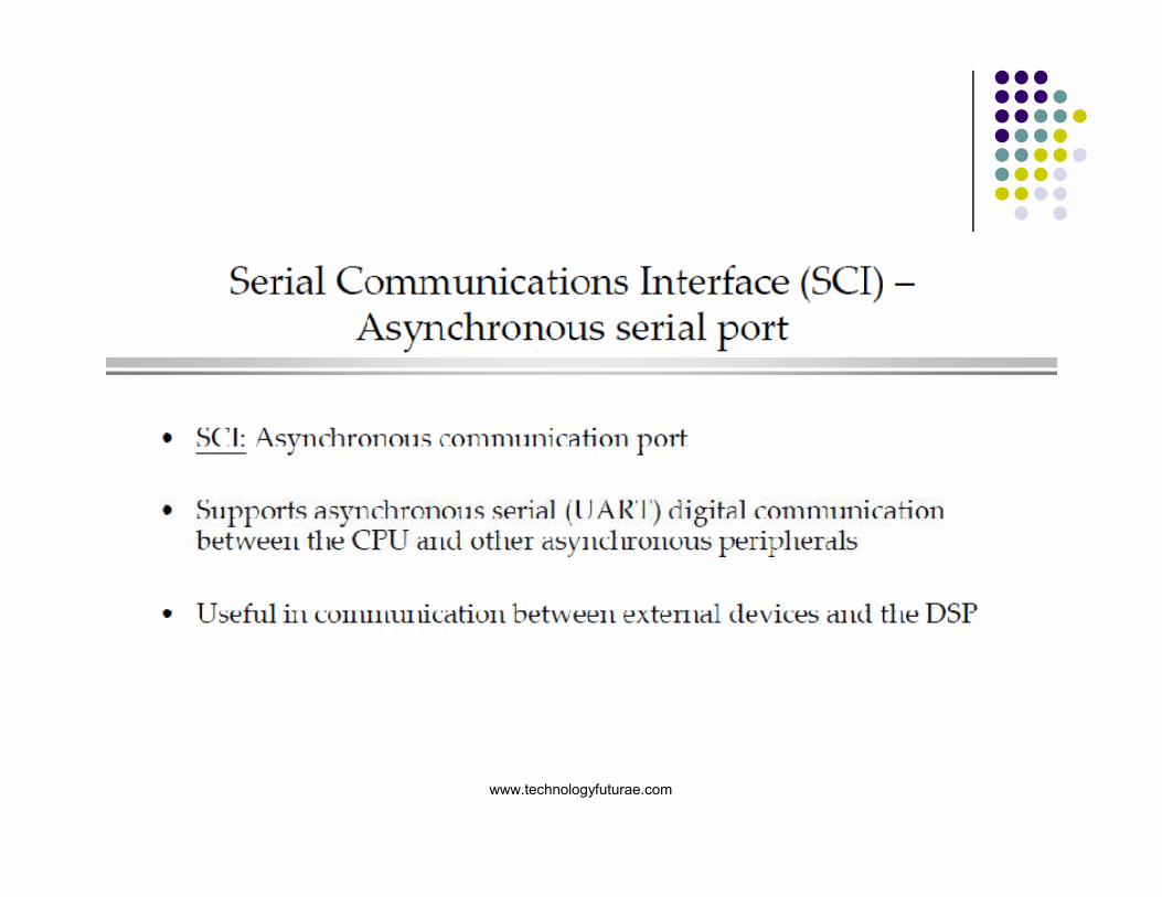
5. SERIAL COMMUNICATION INTERFACE
� Supports asynchronous serial digital communication
� Communication between external device and CPU.
� The SCI transmits and receives serial data one bit at a time at programmable bit rate.
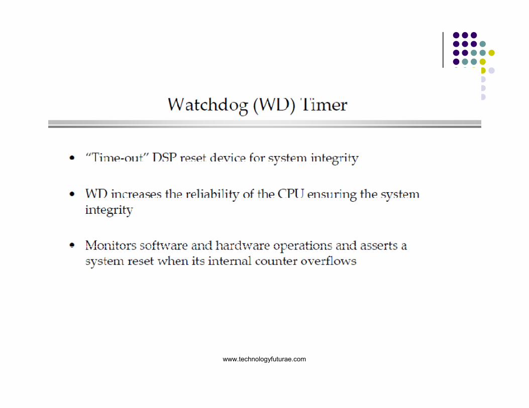
6. WATCH DOG TIMER (WD)
� The WD timer will count for specific amount of time.
� When the software enters into endless loop or CPU is disrupted, the
WD timer will reset the DSP
www.technologyfuturae.com
7. PHASE LOCKED LOOP CLOCK MODULE (PLL)
� Input clock multiplier that allows the user to control the input clock frequency to DSP processor.
� Multiplication factor ranges from 0.5x to 4x that of external clock signal.
� The default value of PLL is 0.5x.
� 10 bit ADC
� Stores results in 16 bit registers
� The 10 MSB's are ADC result & LSB's are filled with zero
� Value in resultant register is simply right shifted by six places.
8. ANALOG TO DIGITAL CONVERTER
www.technologyfuturae.com
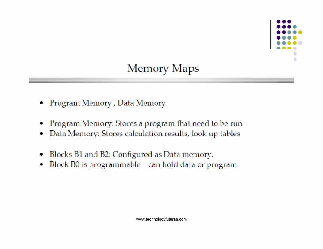
MEMORY MAPPING
� i. Program Memory
� ii. Data Memory
� iii. I/O space
www.technologyfuturae.com
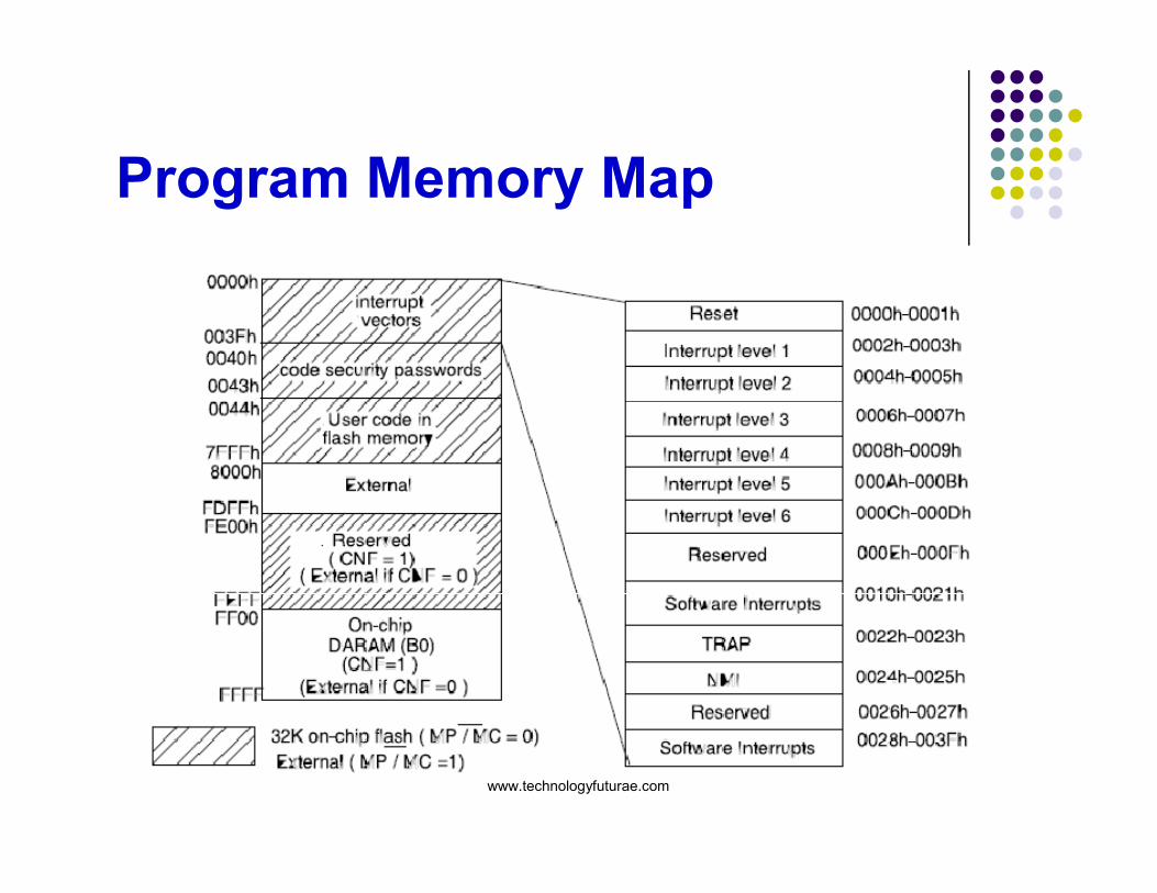
Program Memory Map
www.technologyfuturae.com
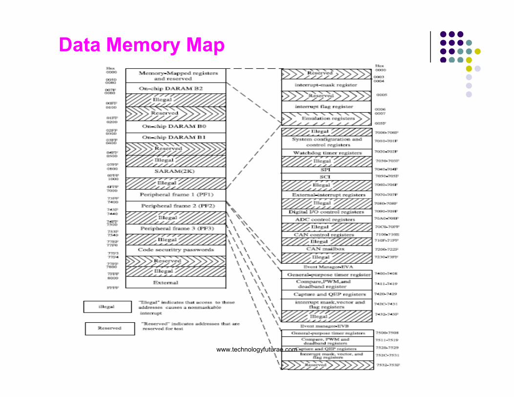
Data Memory Map
www.technologyfuturae.com
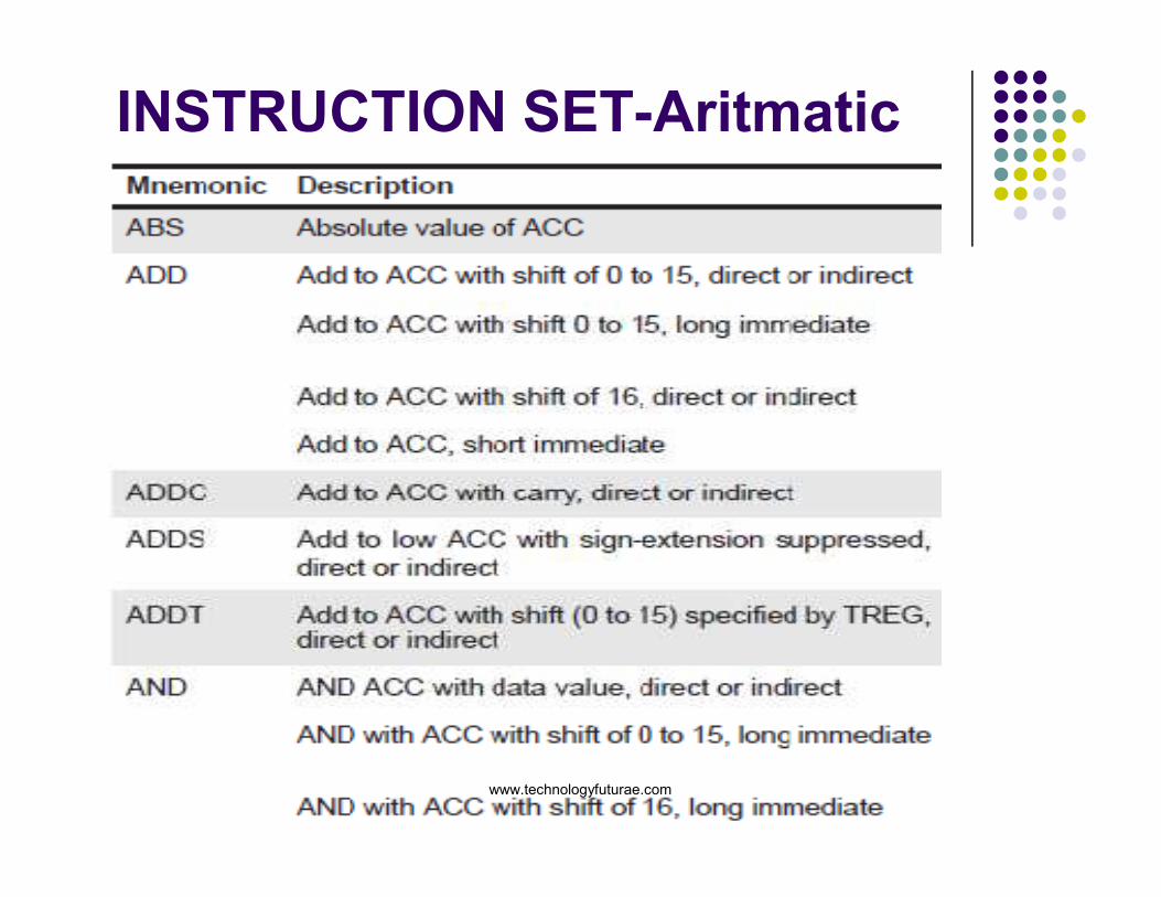
INSTRUCTION SET-Aritmatic
www.technologyfuturae.com
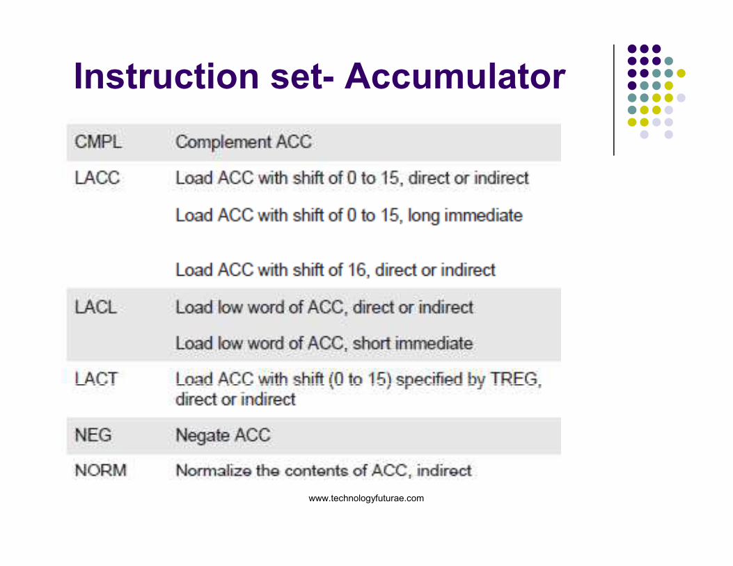
Instruction set- Accumulator
www.technologyfuturae.com
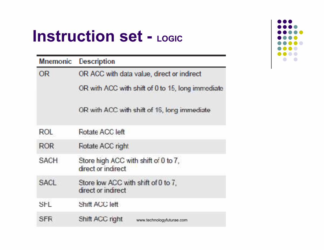
Instruction set - LOGIC
www.technologyfuturae.com
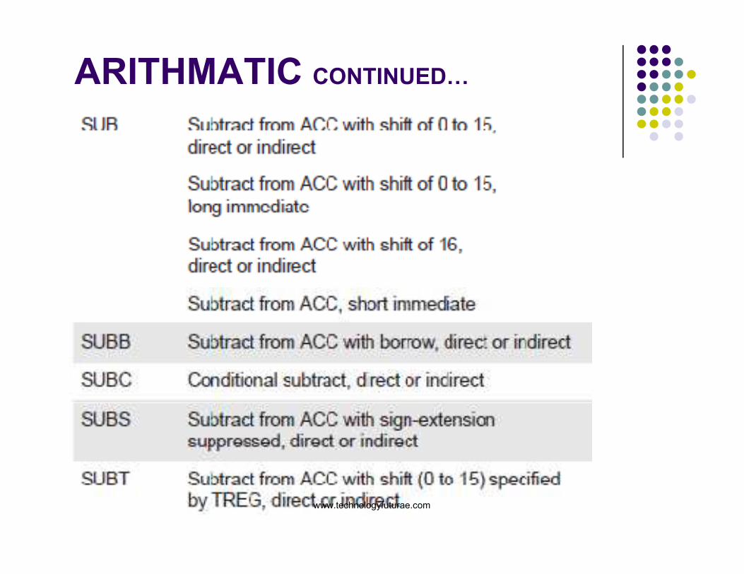
ARITHMATIC CONTINUED…
www.technologyfuturae.com
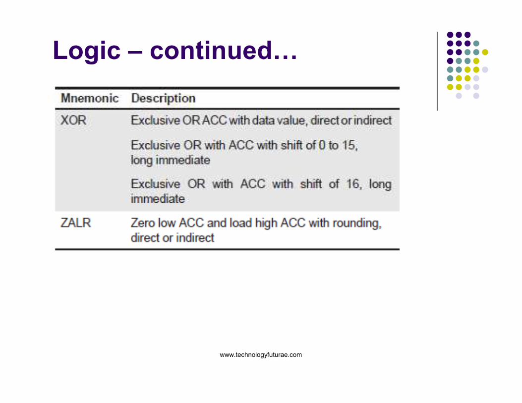
Logic – continued…
www.technologyfuturae.com
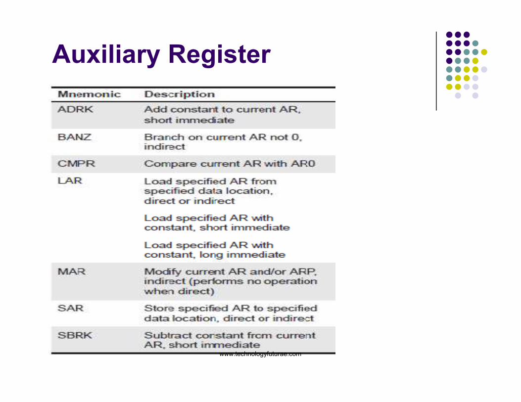
Auxiliary Register
www.technologyfuturae.com
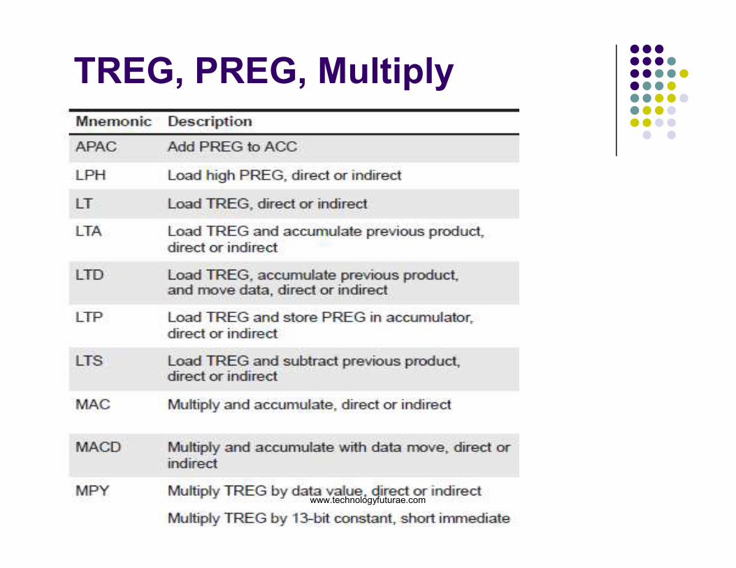
TREG, PREG, Multiply
www.technologyfuturae.com
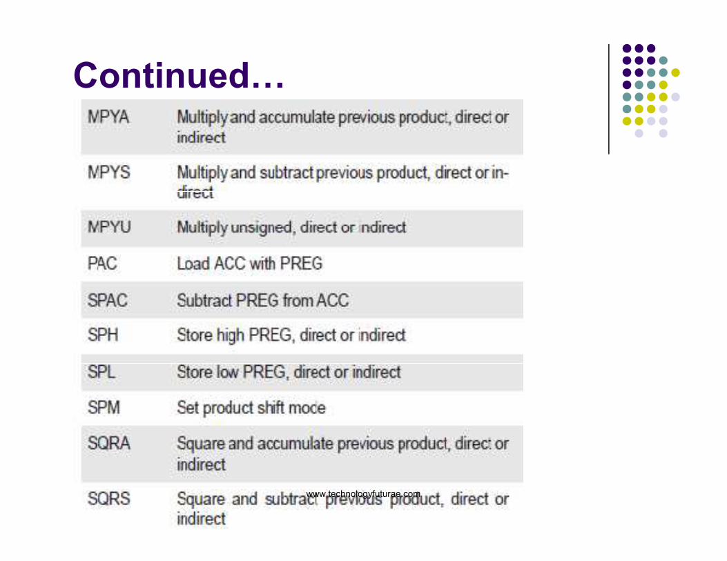
Continued…
www.technologyfuturae.com
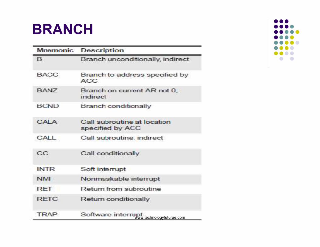
BRANCH
www.technologyfuturae.com
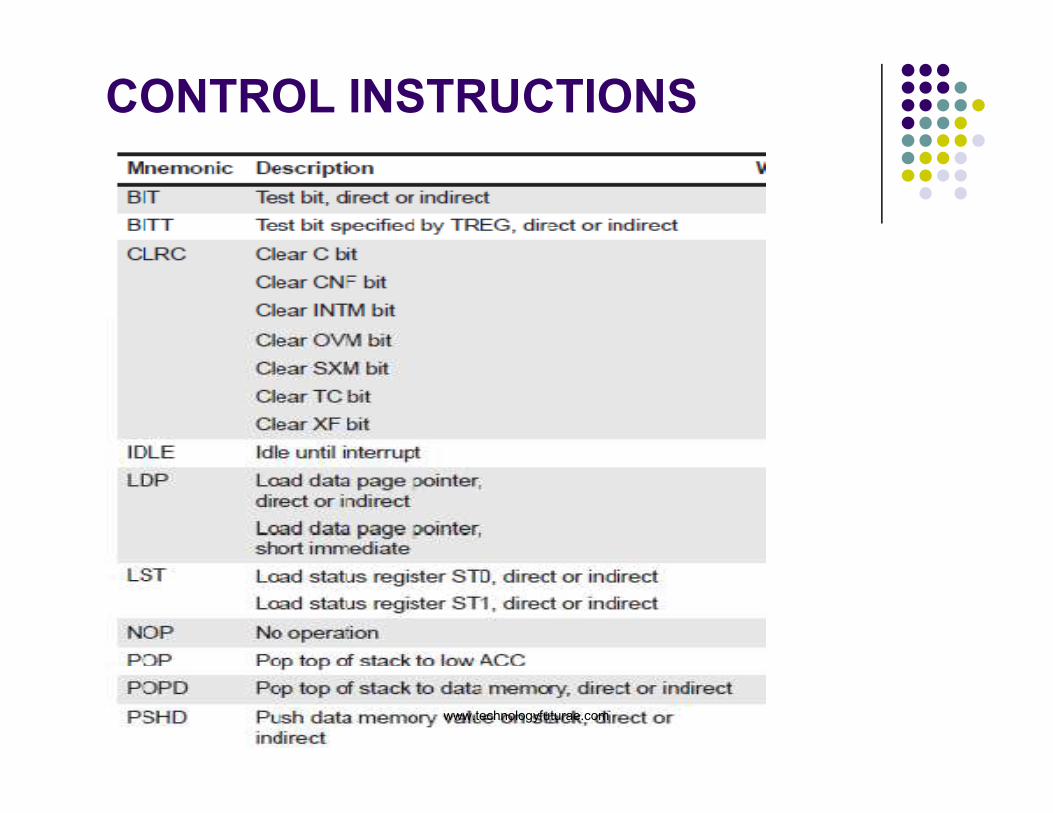
CONTROL INSTRUCTIONS
www.technologyfuturae.com
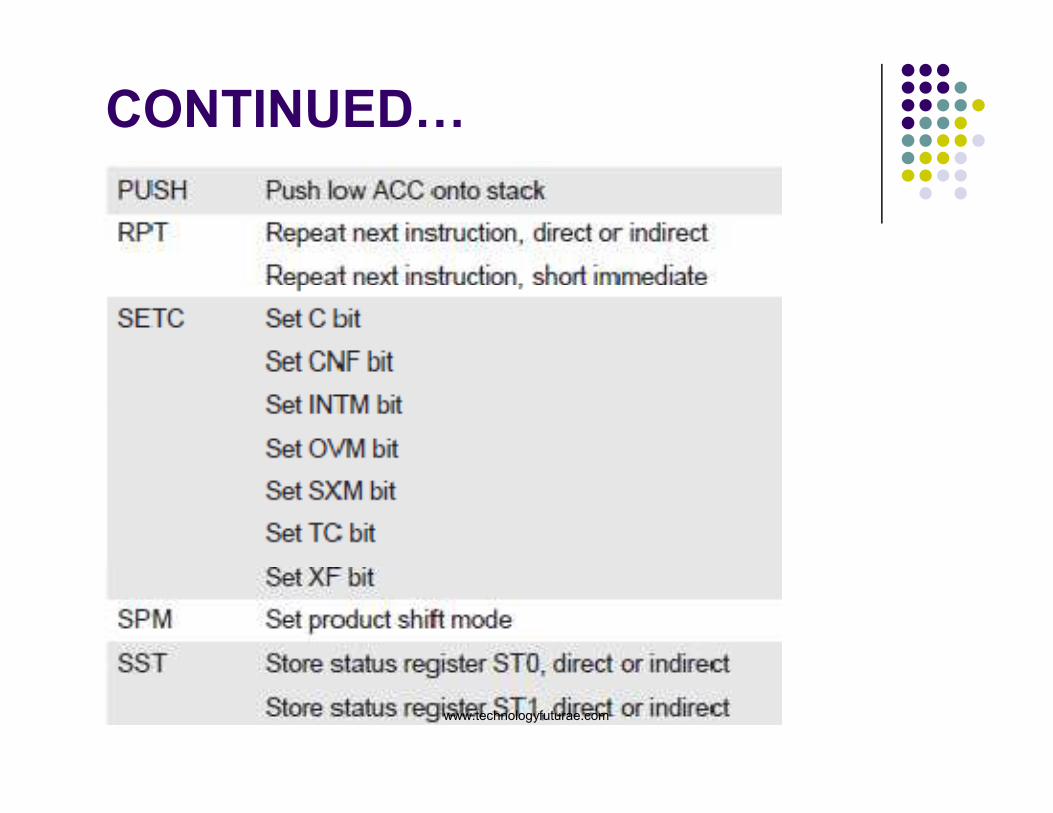
CONTINUED…
www.technologyfuturae.com
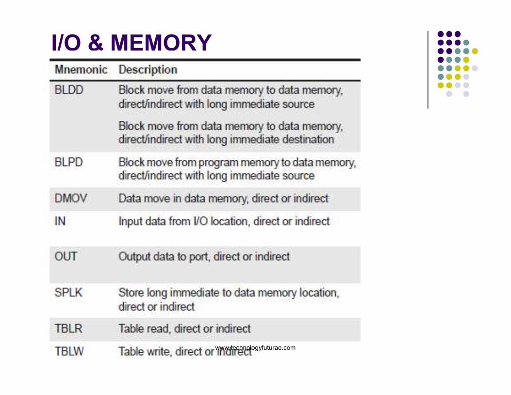
I/O & MEMORY
www.technologyfuturae.com
SYSTEM REGISTERS
www.technologyfuturae.com
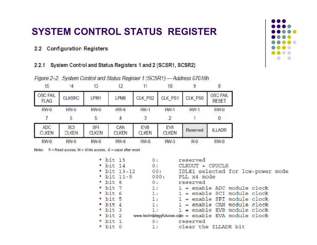
SYSTEM CONTROL STATUS REGISTER
www.technologyfuturae.com
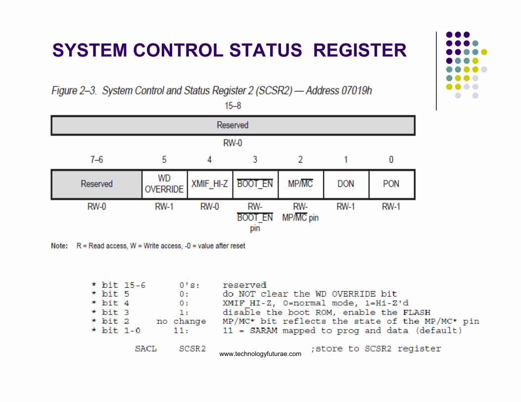
SYSTEM CONTROL STATUS REGISTER
www.technologyfuturae.com
ADC CONTROL REGISTER
www.technologyfuturae.com
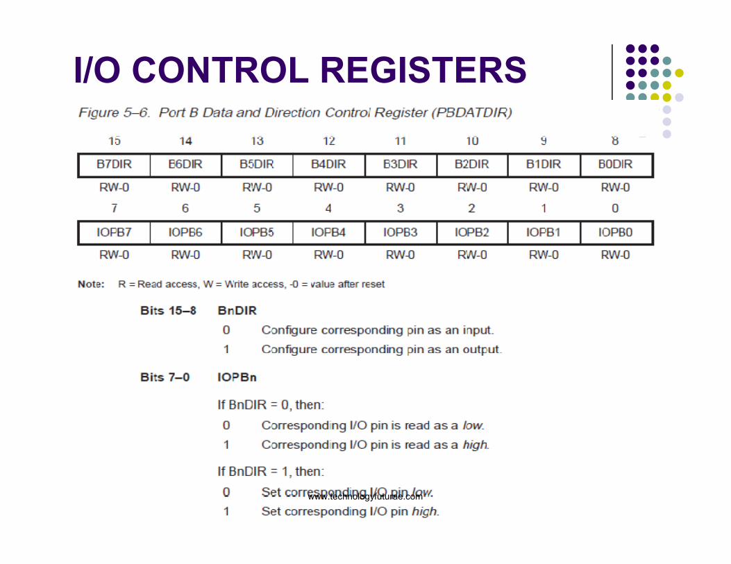
I/O CONTROL REGISTERS
www.technologyfuturae.com

REGISTER
ADDRESSES
www.technologyfuturae.com
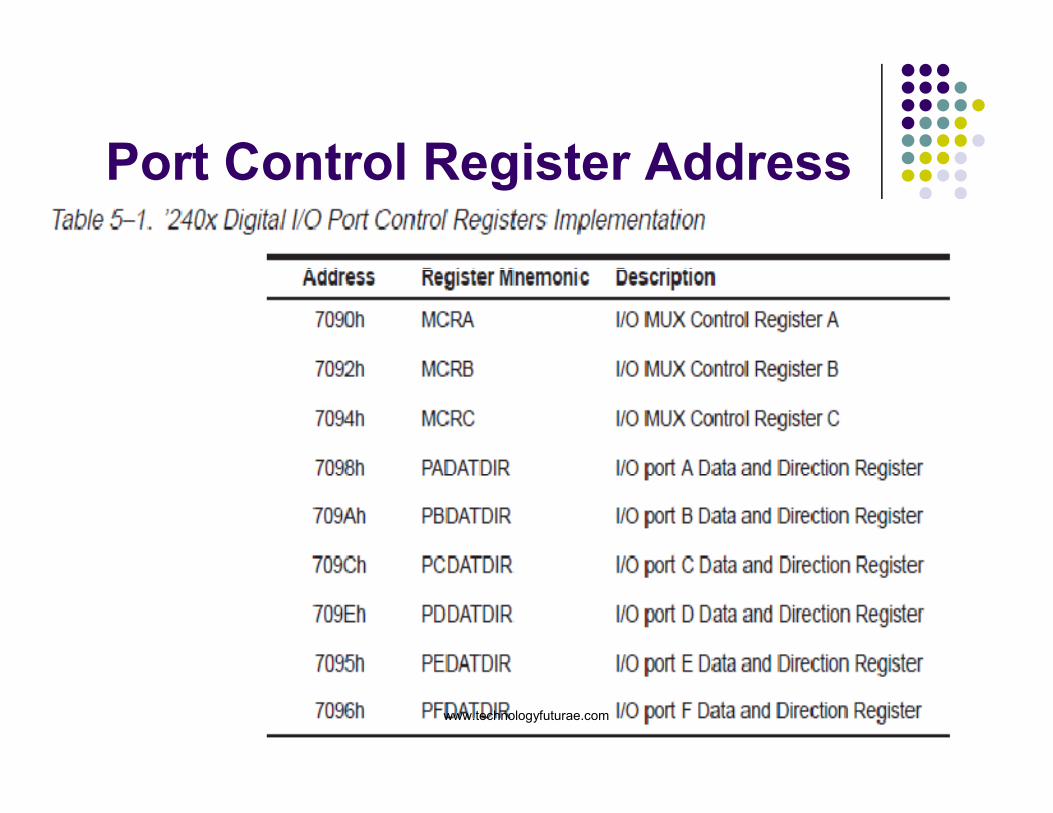
Port Control Register Address
www.technologyfuturae.com
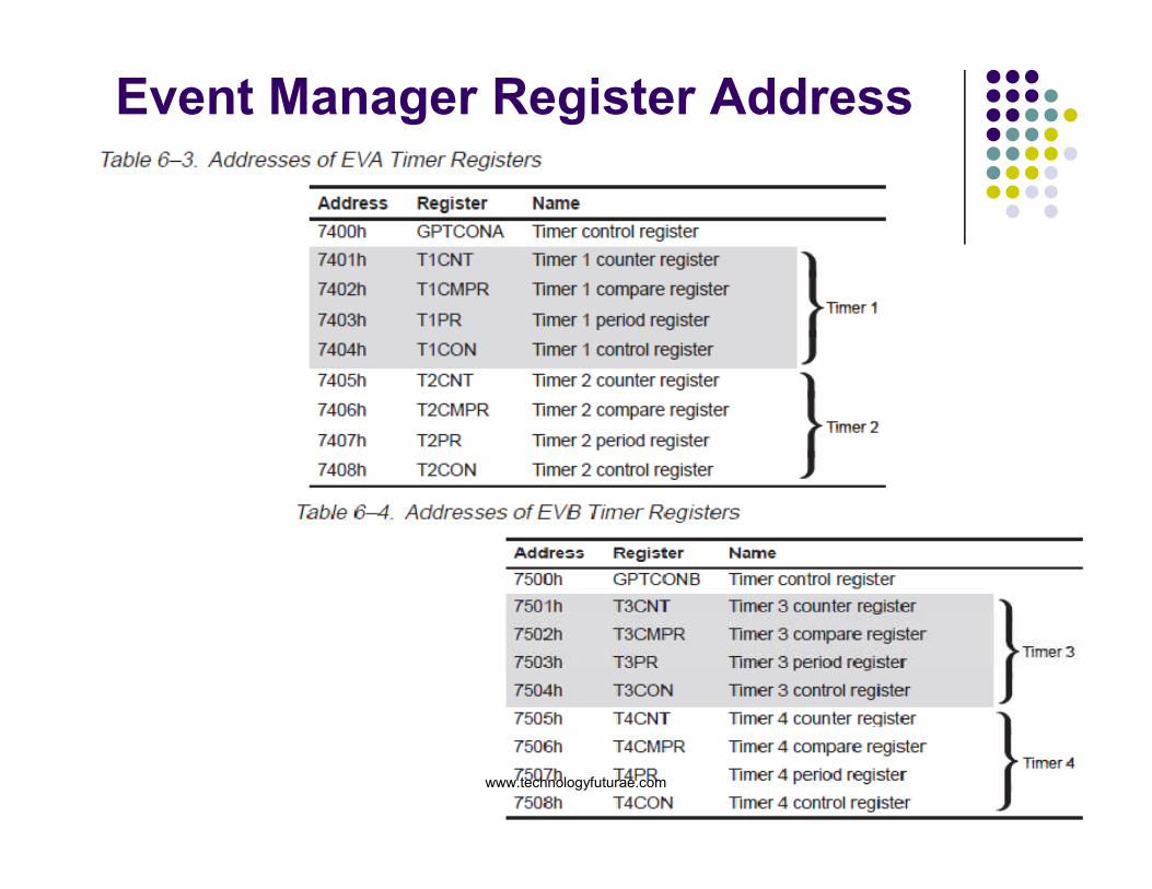
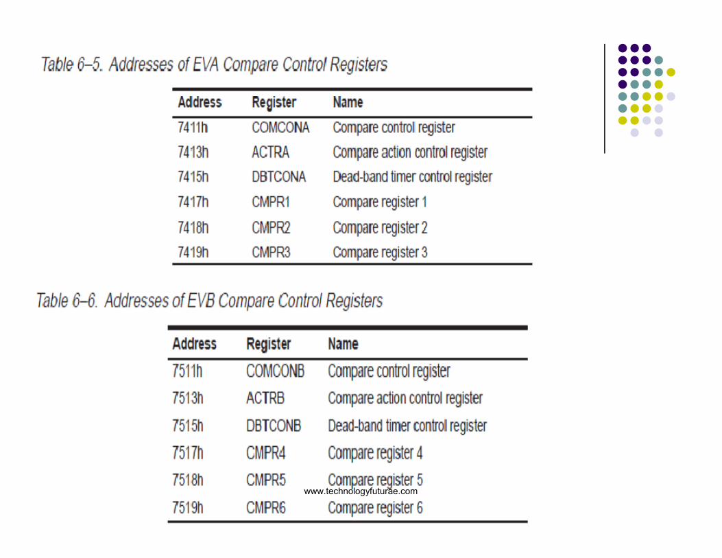
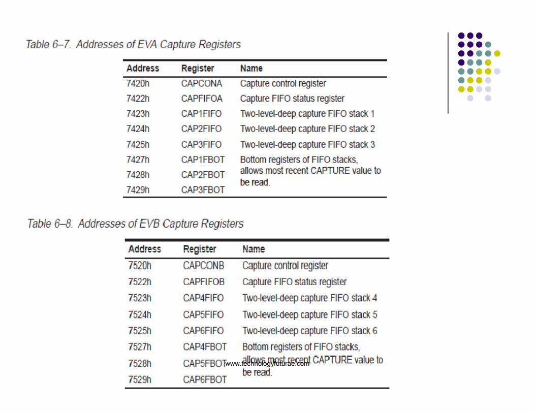
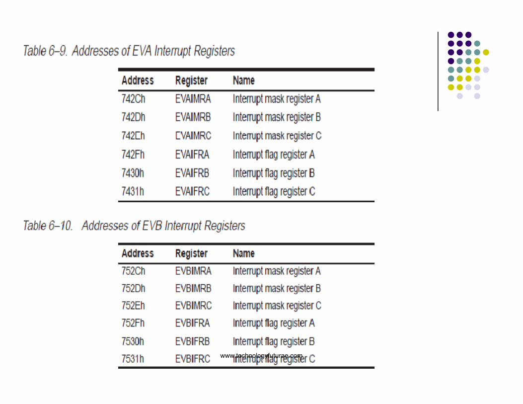
Event Manager Register Address
www.technologyfuturae.com
www.technologyfuturae.com
www.technologyfuturae.com
www.technologyfuturae.com

Initialization
Steps before writing programsSteps before writing programs
www.technologyfuturae.com
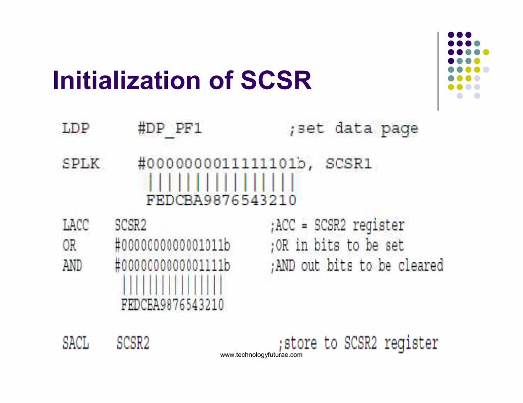
Initialization of SCSR
www.technologyfuturae.com
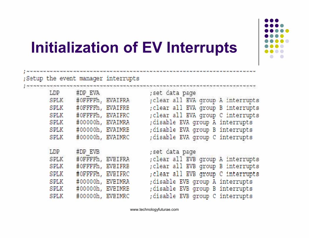
Initialization of EV Interrupts
www.technologyfuturae.com
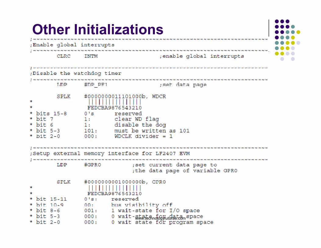
Other Initializations
www.technologyfuturae.com
DSP Programming
www.technologyfuturae.com
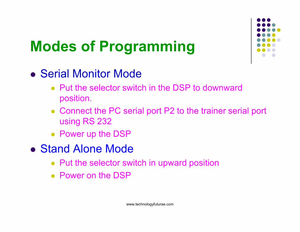
Modes of Programming
� Serial Monitor Mode� Put the selector switch in the DSP to downward
position.
� Connect the PC serial port P2 to the trainer serial port
using RS 232
� Power up the DSP
� Stand Alone Mode� Put the selector switch in upward position
� Power on the DSP
www.technologyfuturae.com
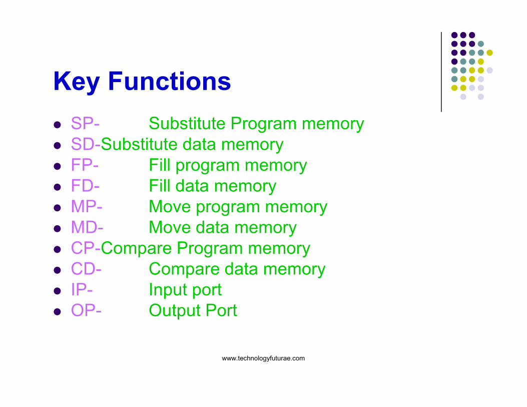
Key Functions
� SP- Substitute Program memory
� SD-Substitute data memory
� FP- Fill program memory
� FD- Fill data memory
� MP- Move program memory� MP- Move program memory
� MD- Move data memory
� CP-Compare Program memory
� CD- Compare data memory
� IP- Input port
� OP- Output Port
www.technologyfuturae.com
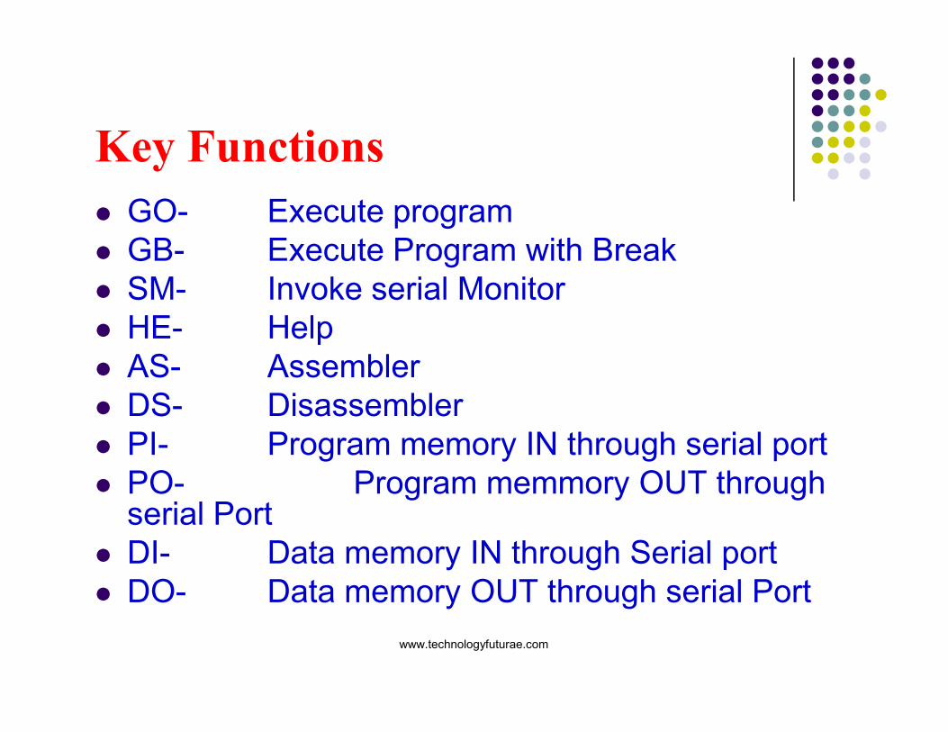
Key Functions
� GO- Execute program
� GB- Execute Program with Break
� SM- Invoke serial Monitor
� HE- Help
� AS- Assembler� AS- Assembler
� DS- Disassembler
� PI- Program memory IN through serial port
� PO- Program memmory OUT through serial Port
� DI- Data memory IN through Serial port
� DO- Data memory OUT through serial Port
www.technologyfuturae.com
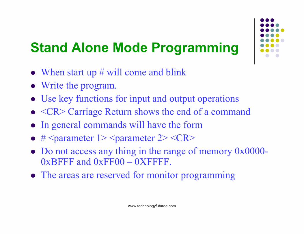
Stand Alone Mode Programming
� When start up # will come and blink
� Write the program.
� Use key functions for input and output operations
� <CR> Carriage Return shows the end of a command
� In general commands will have the form
� # <parameter 1> <parameter 2> <CR>
� Do not access any thing in the range of memory 0x0000-0xBFFF and 0xFF00 – 0XFFFF.
� The areas are reserved for monitor programming
www.technologyfuturae.com
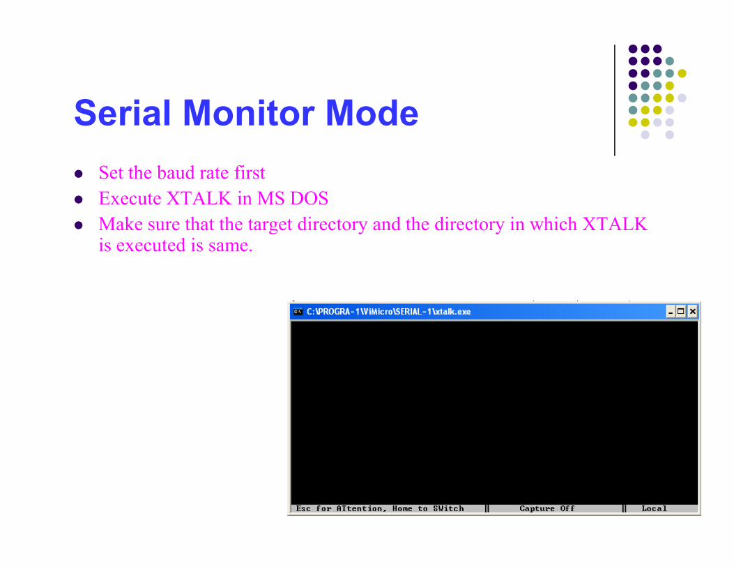
Serial Monitor Mode
� Set the baud rate first
� Execute XTALK in MS DOS
� Make sure that the target directory and the directory in which XTALK is executed is same.
www.technologyfuturae.com
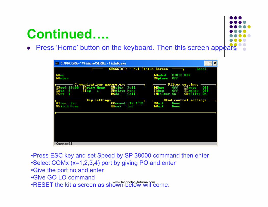
Continued….� Press ‘Home’ button on the keyboard. Then this screen appears
•Press ESC key and set Speed by SP 38000 command then enter
•Select COMx (x=1,2,3,4) port by giving PO and enter
•Give the port no and enter
•Give GO LO command
•RESET the kit a screen as shown below will come.www.technologyfuturae.com
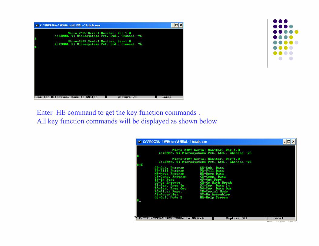
Enter HE command to get the key function commands .
All key function commands will be displayed as shown belowAll key function commands will be displayed as shown below
www.technologyfuturae.com
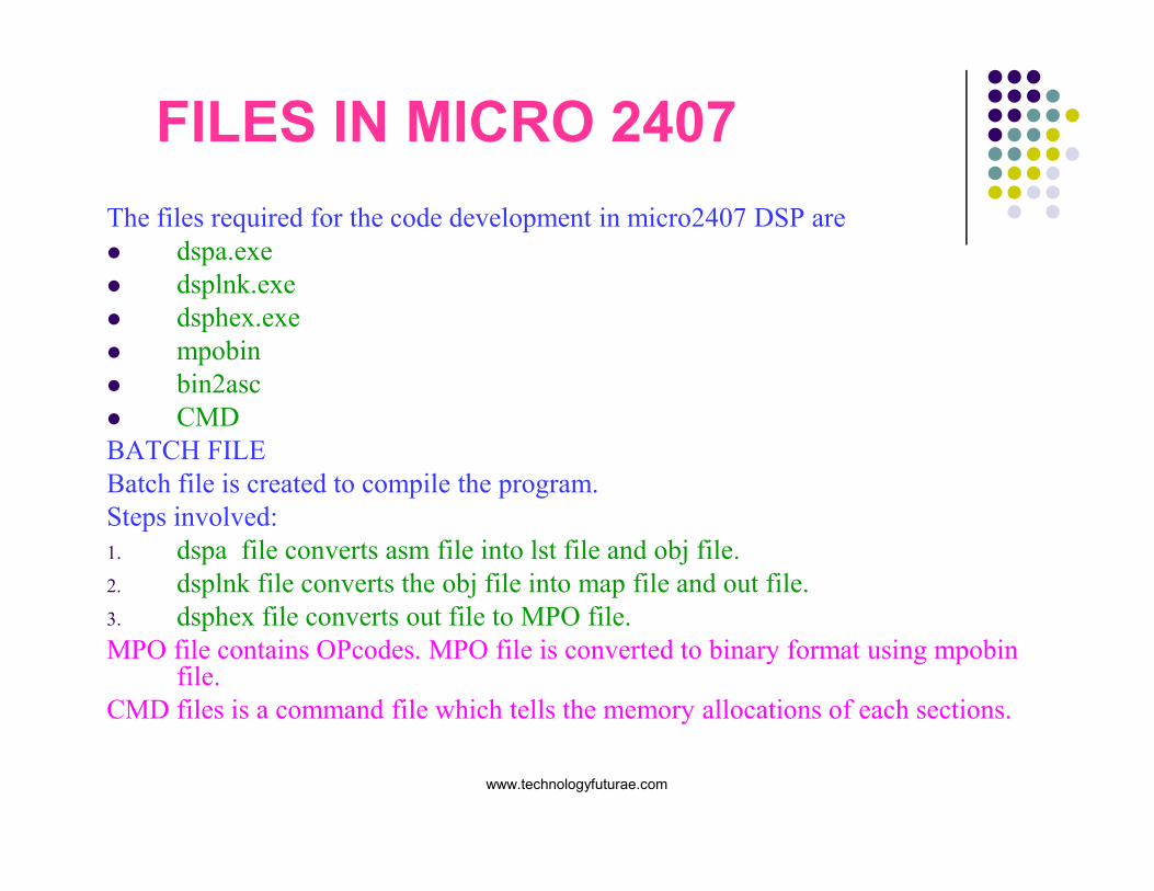
FILES IN MICRO 2407
The files required for the code development in micro2407 DSP are
� dspa.exe
� dsplnk.exe
� dsphex.exe
� mpobin
� bin2asc
� CMD
BATCH FILEBATCH FILE
Batch file is created to compile the program.
Steps involved:
1. dspa file converts asm file into lst file and obj file.
2. dsplnk file converts the obj file into map file and out file.
3. dsphex file converts out file to MPO file.
MPO file contains OPcodes. MPO file is converted to binary format using mpobin file.
CMD files is a command file which tells the memory allocations of each sections.
www.technologyfuturae.com
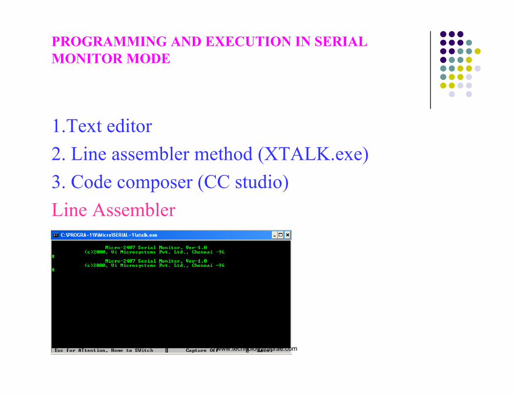
PROGRAMMING AND EXECUTION IN SERIAL
MONITOR MODE
1.Text editor
2. Line assembler method (XTALK.exe)
3. Code composer (CC studio)
Line Assembler
www.technologyfuturae.com
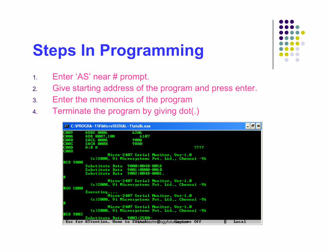
Steps In Programming
1. Enter ‘AS’ near # prompt.
2. Give starting address of the program and press enter.
3. Enter the mnemonics of the program
4. Terminate the program by giving dot(.)
www.technologyfuturae.com
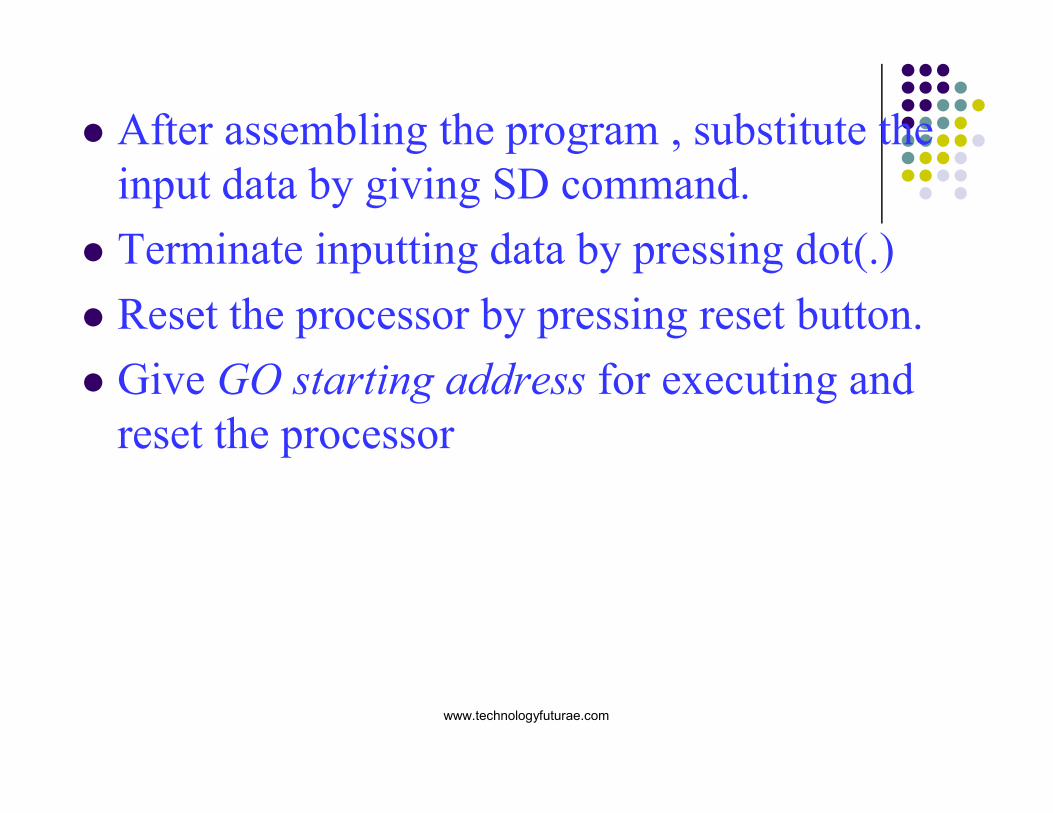
� After assembling the program , substitute the
input data by giving SD command.
� Terminate inputting data by pressing dot(.)
� Reset the processor by pressing reset button.
� Give GO starting address for executing and
reset the processor
www.technologyfuturae.com
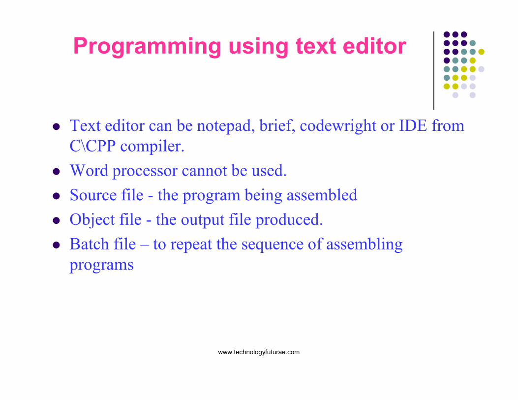
� Text editor can be notepad, brief, codewright or IDE from
C\CPP compiler.
� Word processor cannot be used.
� Source file - the program being assembled
Programming using text editor
� Source file - the program being assembled
� Object file - the output file produced.
� Batch file – to repeat the sequence of assembling
programs
www.technologyfuturae.com
DSP PROGRAMMING
EXAMPLESEXAMPLES
www.technologyfuturae.com
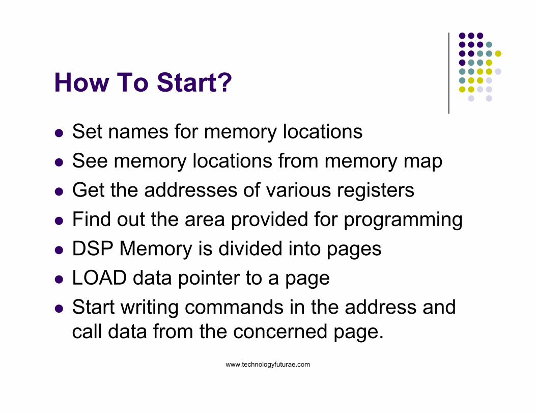
How To Start?
� Set names for memory locations
� See memory locations from memory map
� Get the addresses of various registers
� Find out the area provided for programming
� DSP Memory is divided into pages
� LOAD data pointer to a page
� Start writing commands in the address and
call data from the concerned page.
www.technologyfuturae.com
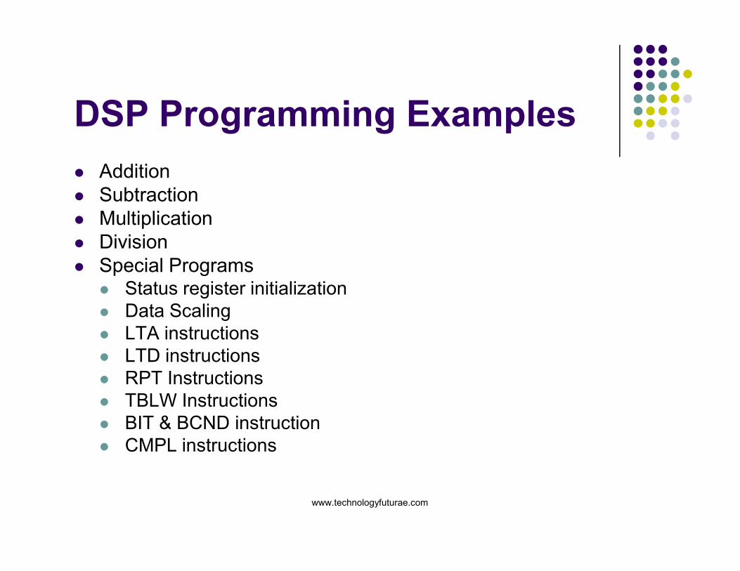
DSP Programming Examples
� Addition
� Subtraction
� Multiplication
� Division
� Special Programs� Status register initialization� Status register initialization
� Data Scaling
� LTA instructions
� LTD instructions
� RPT Instructions
� TBLW Instructions
� BIT & BCND instruction
� CMPL instructions
www.technologyfuturae.com
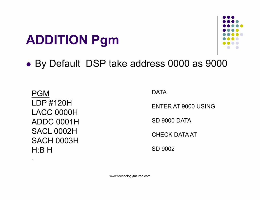
ADDITION Pgm
� By Default DSP take address 0000 as 9000
PGM
LDP #120H
DATA
LDP #120H
LACC 0000H
ADDC 0001H
SACL 0002H
SACH 0003H
H:B H.
ENTER AT 9000 USING
SD 9000 DATA
CHECK DATA AT
SD 9002
www.technologyfuturae.com
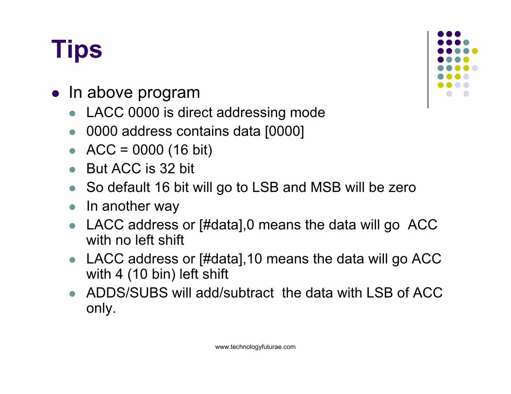
Tips
� In above program� LACC 0000 is direct addressing mode
� 0000 address contains data [0000]
� ACC = 0000 (16 bit)
� But ACC is 32 bit
� So default 16 bit will go to LSB and MSB will be zero
� In another way
� LACC address or [#data],0 means the data will go ACC with no left shift
� LACC address or [#data],10 means the data will go ACC with 4 (10 bin) left shift
� ADDS/SUBS will add/subtract the data with LSB of ACC only.
www.technologyfuturae.com
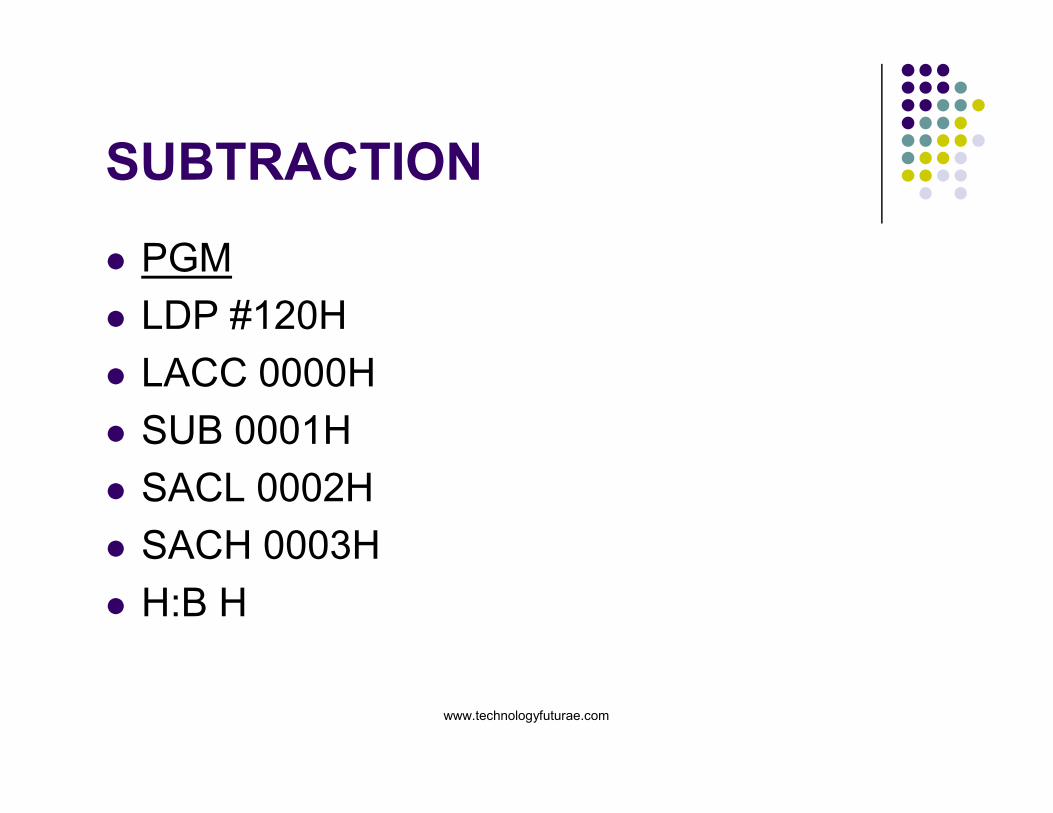
SUBTRACTION
� PGM
� LDP #120H
� LACC 0000H
� SUB 0001H
� SACL 0002H
� SACH 0003H
� H:B H
www.technologyfuturae.com
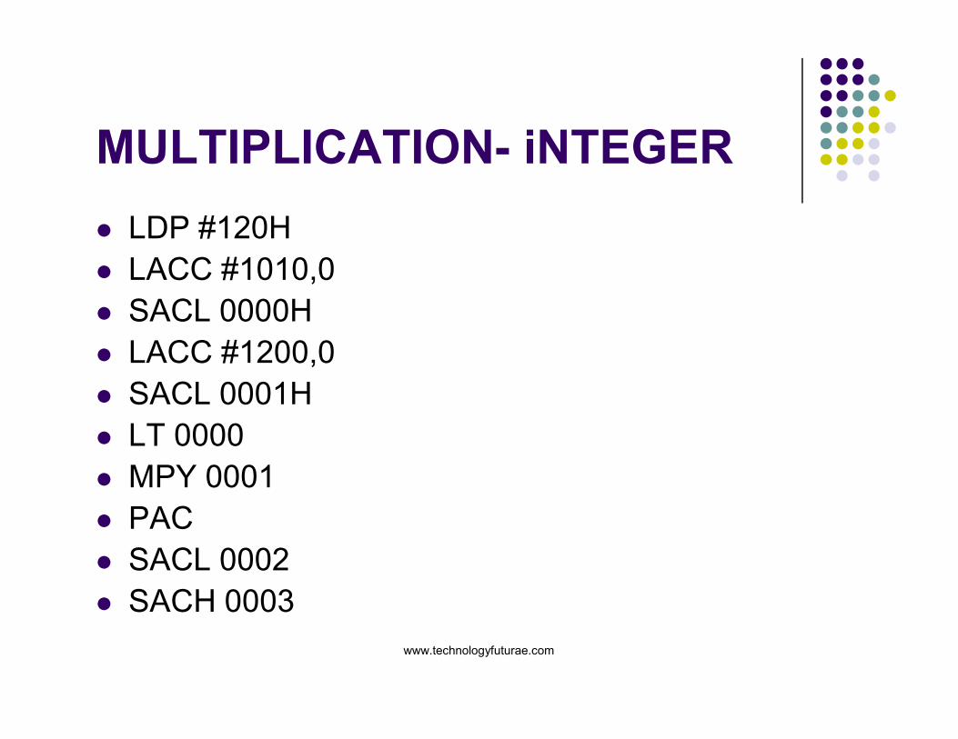
MULTIPLICATION- iNTEGER
� LDP #120H
� LACC #1010,0
� SACL 0000H
� LACC #1200,0
� SACL 0001H
� LT 0000
� MPY 0001
� PAC
� SACL 0002
� SACH 0003
www.technologyfuturae.com
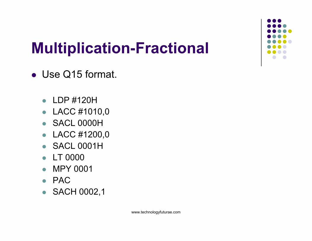
Multiplication-Fractional
� Use Q15 format.
� LDP #120H
� LACC #1010,0
� SACL 0000H� SACL 0000H
� LACC #1200,0
� SACL 0001H
� LT 0000
� MPY 0001
� PAC
� SACH 0002,1
www.technologyfuturae.com
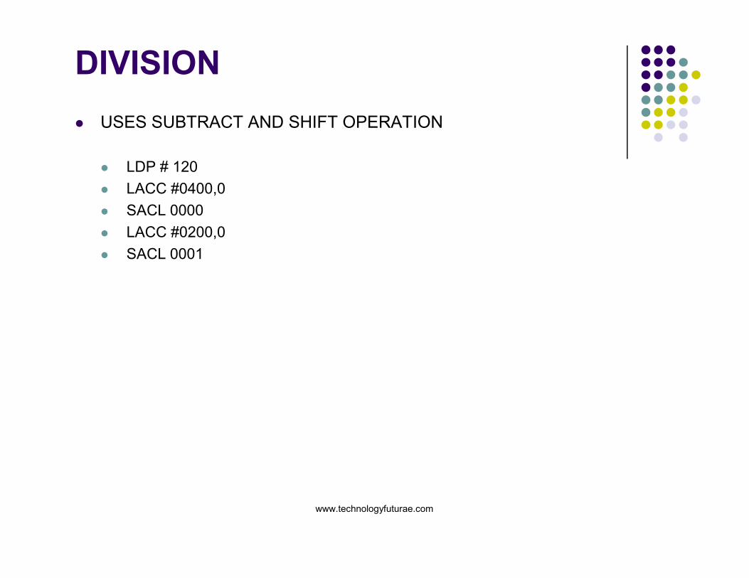
DIVISION
� USES SUBTRACT AND SHIFT OPERATION
� LDP # 120
� LACC #0400,0
� SACL 0000
� LACC #0200,0
� SACL 0001
www.technologyfuturae.com
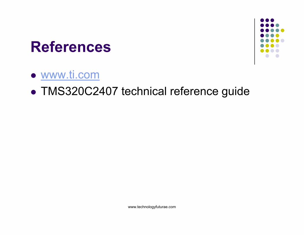
References
� www.ti.com
� TMS320C2407 technical reference guide
www.technologyfuturae.com

THANK YOU
For more technical reviews For more technical reviews
log on to
www.technologyfuturae.com
www.technologyfuturae.com
Related Documents