Digital RF Synthesizer: DC to 135 MHz Todd P. Meyrath 1 Florian Schreck Atom Optics Laboratory Center for Nonlinear Dynamics University of Texas at Austin c 2004 April 16, 2004 revised August 10, 2005 See disclaimer 2 Here, we give a design for a Direct Digital Synthesis (DDS) device to produce Radio Frequency (RF) signals between DC and 135MHz. The design centers around an AD9852 from Analog Devices (but will also accommodate an AD9854). This design is partially based on that of the evaluation board available from Analog Devices but contains circuits relevant to our laboratory electronics implementation and control system and a redesigned output filter. The digital interface given in this design is relatively simple and can be interfaced with a microprocessor or with the system described on our website george.ph.utexas.edu/ control. The PCB layout is located there also, it is a layout design using the software from pcb123. See notes on our website with regard to version. Digital Side: The digital inputs consist of a 24-bit bus and a strobe bit. The first 16- bits we identify as the data bus and the next 8 as the address bus. This address bus is intended to address many boards, each with a local address set by DIP switches. In the case of this DDS device, the 16-bit ‘data bus’ is broken up into various parts as discussed below. The address bus uses the first 2 bits (first 4 addresses) to determine the strobe function on the board. The higher 6-bits of the address bus are the board select. If they do not match the address set by the DIP switches then the strobe is rejected and the board does not accept the data. Only when this address matches does the strobe bit cause the 16-bit data bus to be latched. 1 Please send comments, questions, corrections, insults to [email protected] 2 Disclaimer: The author provides this and other designs on the web as a courtesy. There is no guarantee on this or any other designs presented, use at your own risk. The author also comments that the suggested parts used are not an endorsement of any manufacturer or distributer. 1

Welcome message from author
This document is posted to help you gain knowledge. Please leave a comment to let me know what you think about it! Share it to your friends and learn new things together.
Transcript
Digital RF Synthesizer:
DC to 135 MHz
Todd P. Meyrath1
Florian Schreck
Atom Optics Laboratory
Center for Nonlinear Dynamics
University of Texas at Austin
c© 2004
April 16, 2004
revised August 10, 2005
See disclaimer2
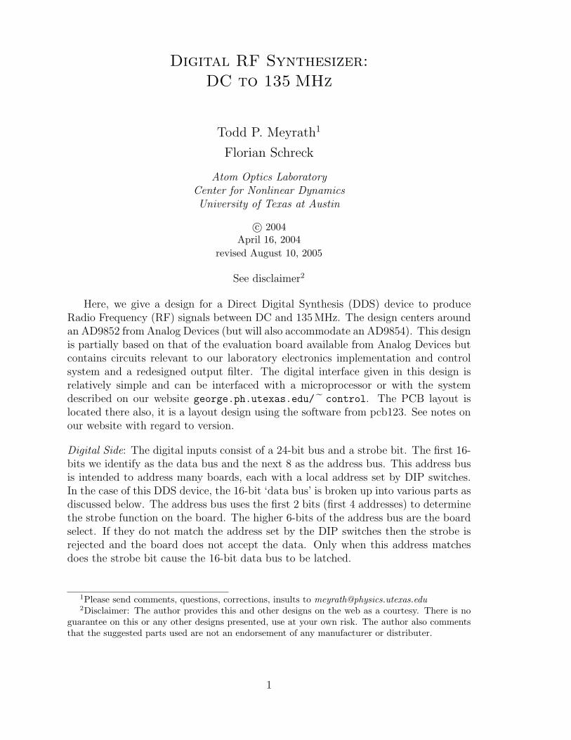
Here, we give a design for a Direct Digital Synthesis (DDS) device to produceRadio Frequency (RF) signals between DC and 135 MHz. The design centers aroundan AD9852 from Analog Devices (but will also accommodate an AD9854). This designis partially based on that of the evaluation board available from Analog Devices butcontains circuits relevant to our laboratory electronics implementation and controlsystem and a redesigned output filter. The digital interface given in this design isrelatively simple and can be interfaced with a microprocessor or with the systemdescribed on our website george.ph.utexas.edu/˜ control. The PCB layout islocated there also, it is a layout design using the software from pcb123. See notes onour website with regard to version.
Digital Side: The digital inputs consist of a 24-bit bus and a strobe bit. The first 16-bits we identify as the data bus and the next 8 as the address bus. This address busis intended to address many boards, each with a local address set by DIP switches.In the case of this DDS device, the 16-bit ‘data bus’ is broken up into various parts asdiscussed below. The address bus uses the first 2 bits (first 4 addresses) to determinethe strobe function on the board. The higher 6-bits of the address bus are the boardselect. If they do not match the address set by the DIP switches then the strobe isrejected and the board does not accept the data. Only when this address matchesdoes the strobe bit cause the 16-bit data bus to be latched.
1Please send comments, questions, corrections, insults to [email protected]: The author provides this and other designs on the web as a courtesy. There is no
guarantee on this or any other designs presented, use at your own risk. The author also comments
that the suggested parts used are not an endorsement of any manufacturer or distributer.
1

49
502
1 3
4
5
6
7
8
9
10
11
12
13
14
15
16
17
18
19
20
21
22
23
24
25
26
27
28
29
30
31
32
33
34
35
36
37
38
39
40
41
42
43
44
45
46
47
48
16-bit data bus
8-bit address bus
strobe bit
ground line
LSB MSB LSB MSB
odd 1 to 31
odd 33 to 47
49
even 2 to 50
Figure 1: Pin configuration for 50-pin connector.
8-bit address bus
A1 A0 Option number Strobe bit function0 0 Option 0 Latch 16-bit data bus, Master Reset0 1 Option 1 Latch 16-bit data bus, Load data into DDS buffer1 0 Option 2 Latch 16-bit data bus, Update output register
-or- Load data and Update output (see version 2.0 note below)1 1 Option 3 Latch 16-bit data bus only
A7 to A2 must match DIP switch settings.DIP switches: ON=0 OFF=1.
Generally, Option 0, for the master reset is called after power-up of the device.
Programming the DDS: Programming the DDS generally requires several loads ofdata. The 16-bit data bus is broken up by function as in the table here:
16-bit data bus
D0 (LSB) to D5 Programming register address in DDSD6 FSK/BPSK/Hold functionsD7 Shaped Keying function
D8 to D15 (MSB) 8-bit data for referenced programming register
Programming generally consists of multiple loads of data D0 to D5 and D8 to D15 inparallel using address Option 1 to load the DDS registers in the desired locations withthe desired values. Then Option 2 is used for an update of the output register in whichthe DDS uses the previous loaded values to determine the new output characteristics.In the case of Option 2, the D values are unimportant. This is just sending the strobeto the update output. D6 and D7 are used for the named functions above with theaddress Option 3 or are instead triggered by the external BNC option, see below.
With D0 to D5 as a 6-bit register address location in the DDS, there are 64memory locations in the DDS (all of which are not used), each 8-bit wide, which maybe updated with the Option 1 load method. The address meanings are given in TableIV on page 26 of the AD9852 data sheet. Information on the modes of operation of thedevice is also given on the data sheet, see pages 15 to 26 for a description. We do notreproduce this information here. Just as a summary, this very impressive device can
2

operate in the following modes: Single-tone, Frequency Shift Keying (FSK), RampedFSK, Frequency Chirp, and Binary Phase Shift Keying (BPSK).
Clock Options: The internal PLL clock multiplier of the DDS may be set to anyinteger between 4 and 20 or not used. This design is intended to run at the maximumfrequency of the DDS of 300 MHz. The clock for the DDS can be setup in one of 3ways. One is to use a crystal (Y1) on the PCB, the clock multiplier must be used andset to ×6 in the case that the 50 MHz crystal suggested on the parts list is used, also,C53 and R19 should be omitted and W15 included, see below. The second option isto use a single ended external clock which enters on the BNC J5, in this case W15 isnot used. In this case, the input clock is converted to a differential ECL type by U8.The third option is to use a differential ECL type clock input with BNCs J9 and J10.
Analog Side: Aside from the output options (see below), the analog side consistsprincipally of a pair of filters. The AD9852 has two high speed outputs. Output 1is the RF (cosine) output and Output 2 is an arbitrary ‘control’ DAC. The AD9854which is pin-for-pin compatible has a quadrature RF for Output 2. The filter in thisdesign is a 9th Order 135 MHz Low Pass Elliptic Filter. Which gives a very fast dropoff after 135 MHz, below 60 dB stopband begins just above 150 MHz which is theNyquist frequency. The conceptual schematic is shown in Figure 2 and the frequencytransfer function in Figure 3.
Output Options: The output BNCs are J1 to J4 and J6. The ‘normal’ output setup islabeled (1a) and (1b) in the jumper table below. In this case the two RF (cosine andcontrol) outputs are pass the filters and exit through J1 and J2. Another possibility isto obtain a filtered differential pair for the cosine output on J1 and J2, this is labelled2 on the jumper table. This also has a special case which can use the DDS’s internalcomparator to produce an agile digital clock output (J6). And naturally, there is anoption for an unfiltered output, whereas the user may add a different filter after theoutput of the device for desired results.
FSK, BPSK, Hold, Shaped Keying Options: The AD9852 device has a number ofextra options for various modulation methods. These are described in detail on thedatasheet. This design has the options of having these triggered on the programmingbus (slower) or externally (faster). The necessary jumpers are discussed in the tablebelow.
Jumper Options: There are a number of options that may be enabled or disabled bysoldering on jumpers labelled W on the schematic and the board. These jumpers areacutally 0 Ω resistors in a 1206 surface mount package.
3

27nH 47nH 68nH 82nH
39pF 22pF 10pF 3.3pF
7.7pF* 28pF* 34pF* 40pF* 25.5pF*
+
-
50Ω
50Ω
Figure 2: 9th Order 135 MHz Low Pass Elliptic Filter. This filter gives a very fastdrop off after 135 MHz, below 60 dB stopband begins just above 150 MHz. Resonancesoccur for the LC modes at 155.1 MHz, 156.5 MHz, 193.0 MHz, and 306.0 MHz. Thestarred capacitors to the ground include estimated stray capacitance due to boardlayout of 2.1 pF, 1 pF, 1 pF, 1 pF, and 3.5 pF left to right, respectively. These valueswere estimated from pad area at the nodes. Errors in these capacitances principallyaffect ripple in both the pass band and stop band. Note that the capacitor valuesgiven on the circuit diagram at the end are those of the 1206 chip capacitors whichare to be attached to the PCB and are all of standard available values. The chipcapacitors and inductors also have some small error, generally order 5% or less whichcan have an effect on the filter transfer characteristics. The inductors used (see partslist) all have a tiny stray capacitance (order 0.3 pF) which adds to that of its parallelcapacitor. The theoretical transfer function is plotted in Figure 3.
Option Jumpers to connect Jumpers to omit Other components
Clocks: W6, W7, W15, W16, W17(1) Crystal - Y1 W15, W16, W17 W6, W7 omit C53 and R19(2) Single ended input - J5 W16, W17 W15, W6, W7(3) Differential input - J9, J10 W6, W7 W16, W17Outputs: W3-W5, W8-W13(1a) Filtered RF 1 - J2 W9, W12 W8, W5, W13 R12 should be 25 Ω
single ended(1b) Filtered RF 2 - J1 W4, W10 W3, W5, W11
single ended(2) Filtered RF 1 - J1, J2 W5, W9, W10, W12 W3, W4, W8, W11, W13 R12 should be 50 Ω
differential(3a) Unfiltered RF 1 - J4 W8 W9, W12, W13 R12 should be 25 Ω(3b) Unfiltered RF 2 - J3 W3 W4, W5, W10, W11(4) Comparator Output - J6 W5, W9, W11, W13 W3, W4, W8, W10, W12 R12 should be 50 ΩFSK/BPSK/HOLD Input: W2, W18(1) From control bus - D6 W2 W18(2) External - J8 W18 W2Shaped Keying Input: W1, W19(1) From control bus - D7 W1 W19(2) External - J7 W19 W1
4

50.0M 100.0M 150.0M 200.0M 250.0M 300.0M 350.0M
-120
-100
-80
-60
-40
-20
0
Mag
nit
ude
(dB
)
Frequency (Hz)
Figure 3: Filter Transfer Function. Theoretical — SPICE plot.
Version 2.0 modifications:(1) Addition of the inverter before pin 21 of the DDS, to correct the loading
problem. Version 1.0 boards use an inverter on a small auxiliary PCB with jumpers.(2) Addition of the option of sending the update output strobe (pin 20) on the
same bus cycle as the load data. In this case, with lower address bits of 01 onlythe load data is sent for filling the DDS registers, and for 10 load data and updateoutput is sent with a time lag between them. To have this option enabled use W22and W25 with the additional delay line, omit W23 and W24. To use in the original(version 1.0) configuration, use W23 and W24, omit W22, W25, R23, and C57. If itis preferred to use the internal output update signal, then one may omit both W24and W25.
(3) Modification of the pads on the bottom of the board for the possibility ofclamping the PCB to the box directly below the DDS chip. This also includes theaddition of 2-56 through holes near the DDS. Appropriate modification to the box wasalso made. The holes below the DDS and the voltage regulators were made smallerand more numerous. This requires the use of solder paste rather than any drip soldermethod from the back. These modifications were done to address the overheatingconcern of the version 1.0 board and seem to have worked well.
(4) Addition of another single ended clock input on the back of the board and box
5

labeled J5A and R19A. This is used as a replacement for J5 and R19. One must putin W26 for this option to be used, omit W26 if using the side clock port.
Comments and Improvement Possibilities:Comment on digital side speed: Although the DDS device digital side may be
updated at rate of order 100 MHz, the HC type devices used on the digital sidelimit the speed to about a quarter of this. However, before this limit, one may finda limit with the ribbon connector and layout. Typically, we operate much slower(order 500 kHz). For some options, such as the FSK, BPSK, Hold, and ShapedKeying functions, there is an available BNC to directly drive these functions withan external source at full speed. For very high speed operation, a slightly modifieddesign involving a high speed FIFO memory located right next to the DDS mightbe appropriate for a next generation device. TI and Cypress Semi. have many suchappropriate memory ICs. In the case of operating at higher frequencies, the delay linefor the strobe signal would have to be appropriately modified or removed all together.The various gates between pin 12 of U2 and the strobe inputs of U1 likely producesufficient delay for the data to settle before strobing.
This design is relatively rudimentary and could likely be specialized for othertasks, such as involving a VCO and PLL type system to produce higher frequencies.
Comment: all options on this design have not been tested.
Soldering Method: We used solder paste (Kester water based solder paste, KE1512-ND from Digikey electronics). The solder paste is applied to the pins and the thebackplane of the DDS IC. We also used the solder paste on the voltage regulators.For the solder reflow, we used a standard toaster oven and brought the temperatureto about 220oC. Note: the DDS is a moisture sensitive device, so we first baked itout at about 120oC for several hours. See the website:http://www.seattlerobotics.org/encoder/200006/oven art.htm
for amateur solder paste ideas. The original version required us to fill in the largerholes prior to soldering the ICs. In this version, we simply apply solder paste to thelarge solder pads and pins for both the DDS and the voltage regulators and did thebaking on a steel plate so the solder did not drip out of the holes.
We would like to thank the Kirk Madison boys at UBC for useful discussions onthis topic and our co-worker Gabriel Price for constructing most of the synthesizersrunning our experiment.
6

PartsQu. Label Part # Manufacturer/Description1 U1 AD9852ASQ Analog Devices / Complete DDS 80-LQFP pkg.2 U2, U12 SN74HC14D Texas Inst. / Hex schmitt-trigger inverters, 14-SOIC pkg.1 U3 SN74HC688D Texas Inst. / 8-Bit Mag. Comp., 20-SOIC wide pkg.1 U4 CD74HC08M Texas Inst. / Quad 2-input AND gate, 14-SOIC pkg.2 U5,U6 CD74HC573M Texas Inst. / 8-bit Bus Latch, 20-SOIC wide pkg.1 U7 SN74HC139D Texas Inst. / 2T04 Decoder 16-SOIC pkg.1 U8 MC100LVEL16D ON Semi. / ECL Reciever, 8-SOIC pkg.3 U9,U10,U11 TPS78633KTTT Texas Inst. / 3.3V wide band regulator, DDPAK-5.4 C1,C2,C15,C16 39pF cap, 1206 pkg.2 C3,C4,C17,C18 22pF cap, 1206 pkg.2 C5,C6 10pF cap, 1206 pkg.2 C7,C8 3.3pF cap, 1206 pkg.2 C9,C10 5.6pF cap, 1206 pkg.2 C11,C12 27pF cap, 1206 pkg.2 C13,C14 33pF cap, 1206 pkg.5 C29-
C31,C52,C5310nF cap, 1206 pkg.
1 C55, C57 120pF cap, 1206 pkg.1 C19 T491X477K006AS Kemet / SMD Tant Cap 6.3V 470µF ‘X’ pkg.6 C20-C25 T491B106K006AS Kemet / SMD Tant Cap 6.3V 10µF ‘B’ pkg.13 C26-C28,C43-
C51,C560.1 µF cap, 1206 pkg.
11 C32-C41,C54 † 0.1 µF cap, 0603 pkg.2 L1,L2 KQ1008LTE27NJ KOA Speer / 27nH 5%, 1008 pkg.2 L3,L4 KQ1008LTE47NJ KOA Speer / 47nH 5%, 1008 pkg.2 L5,L6 KQ1008LTE68NG KOA Speer / 68nH 2%, 1008 pkg.2 L7,L8 KQ1008LTE82NG KOA Speer / 82nH 2%, 1008 pkg.† These capacitors are not labelled on the PCB, they are the small pads near U1.
7

PartsQu. Label Part # Manufacturer/Description1 R1, R23 1.0 kΩ 1260 pkg resistor.6 R2-R7 10 kΩ 1260 pkg resistor.1 R8 3.9 kΩ 1260 pkg resistor.1 R9 1.3 kΩ 1260 pkg resistor.2 R10,R12 24.9 Ω 1% 1260 pkg resistor.8 R11,R13,R14,
R17-R19,R21,R22
49.9 Ω 1% 1260 pkg resistor.
2 R15,R16 100 Ω 1260 pkg resistor.1 R20 2 kΩ 1260 pkg resistor.? W1-W26 0 Ω (jumper) 1260 pkg resistor.1 S1 SDA06H1KD ITT Ind. 6 pos top slide DIP switch, 12-DIP pkg.10 J1-J10, J5A 31-203-RFX Amphenol RF / Panel mount BNC receptacle1 J11 1-103308-0 AMP, Tyco Elect. / 50 pos. header.1 J12 70543-0002 Molex / 3 pin vertical header power conn.1 50-57-9403 Molex / 3 pin mate housing.
16-02-0102 Molex / female crimp pins.1 Y1 †† XOSM-573 Vishay Dale / 50 MHz clock oscillator
Quantity is per board, label is on the PCB, part # is manufacturer number. Most parts obtainedfrom www.mouser.com, www.digikey.com, or www.alliedelec.com. ††Crystal oscillator is optional, ifused, the internal PLL clock multiplier of the DDS must be used and set to ×6, also, C53 and R19should be omitted, see text.
8

Figure 4: Version 2.0 Board (in a modified Version 1.0 box). This board uses thefilter option for the RF output, the unfiltered for the control DAC output, and clockinput on the rear.
9

DIGITAL RADIO FREQUENCY SYNTHESIZER
Todd MeyrathCNLD, Atom OpticsUniv of TexasJuly 2005
SN74
HC
688D
8-B
it C
ompa
rato
r
strobe
A=B
19
+3.3V10kΩ
out
DIP Switchlocal addressset
8 BitAddressBus
LSB
MSB
16 BitDataBus
CD
74H
C57
3M8-
Bit
Bus
Lat
chC
D74
HC
573M
8-B
it B
us L
atch
LE
LE
OE
OE
1/6
SN74
HC
142
11
468
1715
13
3579
1816
1412
E1
11
11
23456789
1918171615141312
1918171615141312
23456789
1, 10
1, 10
U2
S1
Direct RF output frequency range: DC to 135MHz
Based on AD9852 from Analog Devices.
SN74HC139D
2-Bit AddressDecoder
32
4567
1,8
1kΩ
120pF1/6 SN74HC14D
1/6 SN74HC14D~100ns delay line
A5-A0
D7-D0
12345678
141516171819
2930
FSK/BPSK/HoldShaped Keying
71 21 20
22
70
MasterReset
Load datainto IO buffer
Update(output)Registers
+3.3V
Read from IO Buffer (disabled)
Parallel Input selected
11,12,26,27,28,33,34,39,40,41,45,46,47,53,59,62,66,67,72,75,76,77,78
9,10,23,24,25,31,32,37,38,44,50,54,60,65,73,74,79,80
AD9852Complete-DDSAnalog Devices
A1A2A3A4A5A6A7
A0
Address for board set with DIP switchesA7..A2 A1 A0, lowest bits give functionAdditional Strobe Bit:address: function: A1 A0 0 0 Master Reset 0 1 Load Data to buffer 1 0 Update output register (W22) -or- Load Data and Update output (W23) 1 1 no additional strobe
A0A1
Digital Side:
13,35,57,58,63 NC
1/2 SN74HC14D
3/4 CD74HC08M
0Ω Optional short:0Ω resistor 1206 package
0Ω0Ω
U2
U3
R2 to R7
U7
U4
U2
U1
U5
U6
U2R1
W1 W2
W
C55
13
12 11 10 9 8
5
6
1 2
3
4 5
6
1213
11
D0
D7
D8
D15
LSB
MSB
20
10
20
20
15, 16
Version 2.0
0Ω
1/6 SN74HC14U12
1213
3
4
0Ω 0Ω
1/4 CD74HC08M
U41089
1kΩ
120pF1/6 SN74HC14D
1/6 SN74HC14D~100ns delay line
U12
U12R23
C57
11 10 9 8
1
2
0Ω
W24
W23
W22
W25

AD9852Complete-DDSAnalog Devices
+3.3V
0.01µF
1.3kΩ
61
PLLFilter
64
Single-ended/DifferentialClock InputSelect
56Max PowerOutput Set
3.9kΩ
+3.3V0.1µF55DAC Bypass
0Ω
51 25Ω
52
50Ω
0Ω
0Ω
IOUT2
IOUT2B
or 25Ω50Ω
49IOUT1B
50Ω
IOUT1 48
0Ω
Analog Side:
0Ω
0Ω
0Ω
0Ω
100Ω
100Ω
42
43Comparator VIN-
Comparator VIN+CompVOUT
36
0Ω0Ω
50Ω50Ω
29 30
FSK/BPSK/HOLD
ShapedKeying
Crystal
+3.3V
0Ω
MC100LVEL16
54
8
2
3
7
6
0Ω
0Ω
50Ω50Ω
CLK
CLKB
69
68
Clock:
2kΩ
0.01µF
J1
J2
J4
J6
J7J8
J9
J10
9th Order 135MHz Low Pass Elliptic Filter
C18C16
R9
R8
C15R10
R11
W3W4
W5
W8 W9
W10
W11
W12
W13
W15
W16
W17
W18 W19
R12R14
R15
R16R17R18
R20
R21 R22
C17
C1
C2
C3
C4
C5
C6
C7
C8
C9
C10
C11
C12
C13
C14
L1
L2
L3
L4
L5
L6
U1
U8
Y1
C52
C53
C54
9th Order 135MHz Low Pass Elliptic Filter
27nH 47nH 68nH 82nH
39pF 22pF 10pF 3.3pF
5.6pF 27pF 33pF 39pF 22pF
27nH 47nH 68nH 82nH
39pF 22pF 10pF 3.3pF
L7
L8J3
0Ω
0Ω
0Ω
W6
W7
5.6pF 27pF 33pF 39pF 22pF
Note: C9-C18 are values of the 1206 capacitors, filter parameters must include stray capacitance on the PCB, see documentation
50Ω
J5
R1950Ω
J5A
R19A
0Ω
W26

Supply Regulator and Bypass circuits:
+5V
GND
470µF 6V
TPS786333.3V Regulator1
2
3
4
5IN
OUTEN
GND
Bypass
+3.3V
U9
10µF
10µF 0.1µF
0.01µF
TPS786333.3V Regulator1
2
3
4
5IN
OUTEN
GND
Bypass
+3.3V
U10
10µF
10µF 0.1µF
0.01µF
TPS786333.3V Regulator1
2
3
4
5IN
OUTEN
GND
Bypass
+3.3V
U11
10µF
10µF 0.1µF
0.01µF
Analog SidePower toAD9852
Digital SidePower toAD9852
Other DigitalIC Power
+3.3V
Bypass Capactors:
0.1µF
on each supply pin for all ICs
U1: C32-C42U2: C43U3: C44U4: C45U5: C46U6: C47U7: C48U8: C49U12: C56
Y1: C51
C19 C20
C21
C22
C23
C24
C25
C26
C27
C28
C30
C31
C29

Box for Digital RF Synthesizer (Version 2)
Material: Aluminum, all parts
Todd MeyrathAtom Optics LabUniv of Texas1-0883
Drawing's scale 1:1
Part: Quantity: (per assembly)
Center Piece 1
Top Plate 1
Header Cover 1
Brackets 2
1:5

Part:Amphenol31-203-RFX
For hole pattern, see dimensioned drawing
BNC RecptacleHole patterns labeled 1 to 11 are for BNC Recptacles some are optional. Please include the circled:1 2 3 4 5 6 7 8 9 10 11
Others are to be omitted.
Center Piece
2-56 tapto 0.15"
4-40 tapto 0.15"
Tap depths not critical
Eight inner corners: max radius of curvature: 0.2" (not critical)
Okay for holes to pierce into inner shelf
(12)
5
6
7
8
9
10
1 23 4
11
0-80 tapto 0.15" (2)
(24: 12 from the top, 12 from the bottom)

Hole Pattern for BNC Receptacle:
Ø .453"
.5"
.25"
.5".25"
4-40 tap through or to 0.2" (4 each)
Center Piece
Critical Dimension +/-0.005
3.5"
.11"
.6"1.36"
2.11"2.875"
5.8"
.11" 1.5"
3"
.11"
2.6"
2.835"
.455"
1.61"
.15"
.15"
.45"
.45"
.75"
2.25"
.475"
.625"
.125"
.35".5"
.47"

Center Piece
.075"1.175"
.35"
2.55"
3.325"
5.725"
.075"
1"1.75"
2.5"
3.15"
3.425"
1.895"
2.675"
5.45"
2.32"
2.305"
.945"
2.42"
1.487"
2.9"
4.312"

Top Plate2-56 clearance, counter sunk from top, round hex-head
4-40 tap through
Eight inner corners: max radius of curvature: 0.075" (not critical)
Slits are through cuts for connection headers

Top Plate
.125"
5.8"
3.5"
.075"
1.487"
2.9"
5.725"
.075"1.75"
3.425"
.192"
3.342"
.417".767"
.317" 3.217" .417"
.867"
.936"1.406"
.642"
4.312"

Header Cover
Hole: 4-40 clearance, counter sunk from top
3.4"
.5".25"
.2"
.125"
.25"3.15"
.075"
Bracket
1"
.375"
.35".8"
.2" .35" .5"
.125"
.625".75"
Related Documents