UNIVERSITY OF CALIFORNIA Los Angeles Digital Linearization and Wideband Measurements in Optical Links A dissertation submitted in partial satisfaction of the requirements for the degree Doctor of Philosophy in Electrical Engineering by Daniel Wai Chuen Lam 2014

Welcome message from author
This document is posted to help you gain knowledge. Please leave a comment to let me know what you think about it! Share it to your friends and learn new things together.
Transcript
UNIVERSITY OF CALIFORNIA
Los Angeles
Digital Linearization and
Wideband Measurements
in Optical Links
A dissertation submitted in partial satisfaction of the
requirements for the degree Doctor of Philosophy
in Electrical Engineering
by
Daniel Wai Chuen Lam
2014

© Copyright by
Daniel Wai Chuen Lam
2014
ii
ABSTRACT OF THE DISSERTATION
Digital Linearization and
Wideband Measurements
in Optical Links
by
Daniel Wai Chuen Lam
Doctor of Philosophy in Electrical Engineering
University of California, Los Angeles, 2014
Professor Bahram Jalali, Co-Chair
Professor Asad M. Madni, Co-Chair
Optical fiber networks have been in use for many decades to transport large amounts of data
across long distances. Internet traffic grows at an exponential rate and demand for increased
bandwidth and faster data rates is higher than ever. Radio frequency over fiber is used for a
plethora of applications such as providing wireless access to remote and rural areas, phased array
radars, and cable television to name a few. As signals are transmitted over longer distances,
nonlinearities are incurred which degrades the performance and sensitivity of the link. Moreover
as the data rates increase, it becomes a challenge to measure and monitor the signal integrity.
This dissertation will cover two main topics: digital broadband linearization and
performing wideband high speed measurements using time-stretch technology. Over the last few
iii
years there has been considerable interest in reducing the intermodulation distortions in optical
links. The intermodulation distortions are caused by the nonlinear transfer function of the optical
link. To reduce the nonlinearities, linearization of the optical link is performed. A novel digital
post-processing algorithm has been developed to suppress nonlinearities and increase the
dynamic range of the link. Digital broadband linearization algorithm has been implemented and
demonstrated a record 120 dB.Hz2/3
Spurious Free Dynamic Range (SFDR) over 6 GHz of
bandwidth and is shown to suppress third order intermodulation products by 35 dB. By reducing
the nonlinearities and improving SFDR, we have increased the sensitivity of the receiver.
Afterwards, simulation of the real-time implementation of the digital broadband linearization
algorithm onto a field-programmable gate array was performed by designing the architecture and
translating the code into Verilog HDL. Simulations on collected data show comparable results in
both Matlab and iSim which were used to evaluate the performance.
In the second part of this dissertation, two applications using time-stretch are
demonstrated: ultra-wideband instantaneous frequency estimation and high speed signal analysis
measurements. By combining time-stretch technology and windowing and quadratic
interpolation, ultra-wideband frequency measurements with improved frequency estimation are
demonstrated. Moreover, multiple signal measurements are performed, and the frequency
resolution can be tuned to measure signals close together. Lastly, time-stretch is used for
measuring high speed signal integrity parameters such as bit error rate, jitter, and rise and fall
times by taking advantage of the high sampling throughput and the ability to generate and
analyze eye diagrams. In addition, we were able to integrate this technology into a test-bed for
aggregate optical networks and use it for an optical performance monitoring application.
iv
The dissertation of Daniel Wai-Chuen Lam is approved.
Carlos Portera-Cailliau
Asad M. Madni, Committee Co-chair
Bahram Jalali, Committee Co-chair
University of California, Los Angeles
2014

v
For my family
And for all those who persevere and strive for their dreams…
vi
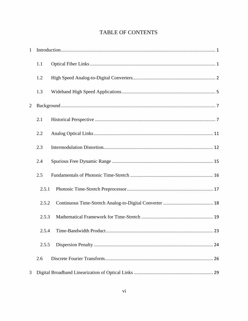
TABLE OF CONTENTS
1 Introduction ............................................................................................................................... 1
1.1 Optical Fiber Links ....................................................................................................... 1
1.2 High Speed Analog-to-Digital Converters .................................................................... 2
1.3 Wideband High Speed Applications ............................................................................. 5
2 Background ............................................................................................................................... 7
2.1 Historical Perspective ................................................................................................... 7
2.2 Analog Optical Links .................................................................................................. 11
2.3 Intermodulation Distortion.......................................................................................... 12
2.4 Spurious Free Dynamic Range ................................................................................... 15
2.5 Fundamentals of Photonic Time-Stretch .................................................................... 16
2.5.1 Photonic Time-Stretch Preprocessor....................................................................... 17
2.5.2 Continuous Time-Stretch Analog-to-Digital Converter ......................................... 18
2.5.3 Mathematical Framework for Time-Stretch ........................................................... 19
2.5.4 Time-Bandwidth Product ........................................................................................ 23
2.5.5 Dispersion Penalty .................................................................................................. 24
2.6 Discrete Fourier Transform......................................................................................... 26
3 Digital Broadband Linearization of Optical Links ................................................................. 29
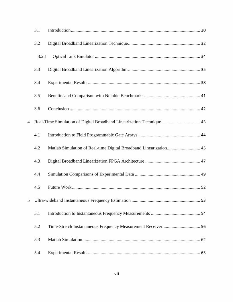
vii
3.1 Introduction ................................................................................................................. 30
3.2 Digital Broadband Linearization Technique ............................................................... 32
3.2.1 Optical Link Emulator ............................................................................................ 34
3.3 Digital Broadband Linearization Algorithm ............................................................... 35
3.4 Experimental Results .................................................................................................. 38
3.5 Benefits and Comparison with Notable Benchmarks ................................................. 41
3.6 Conclusion .................................................................................................................. 42
4 Real-Time Simulation of Digital Broadband Linearization Technique .................................. 43
4.1 Introduction to Field Programmable Gate Arrays ...................................................... 44
4.2 Matlab Simulation of Real-time Digital Broadband Linearization............................. 45
4.3 Digital Broadband Linearization FPGA Architecture ................................................ 47
4.4 Simulation Comparisons of Experimental Data ......................................................... 49
4.5 Future Work ................................................................................................................ 52
5 Ultra-wideband Instantaneous Frequency Estimation ............................................................ 53
5.1 Introduction to Instantaneous Frequency Measurements ........................................... 54
5.2 Time-Stretch Instantaneous Frequency Measurement Receiver................................. 56
5.3 Matlab Simulation ....................................................................................................... 62
5.4 Experimental Results .................................................................................................. 63
viii
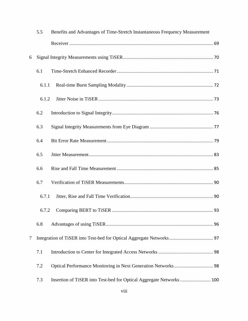
5.5 Benefits and Advantages of Time-Stretch Instantaneous Frequency Measurement
Receiver ...................................................................................................................... 69
6 Signal Integrity Measurements using TiSER .......................................................................... 70
6.1 Time-Stretch Enhanced Recorder ............................................................................... 71
6.1.1 Real-time Burst Sampling Modality ....................................................................... 72
6.1.2 Jitter Noise in TiSER .............................................................................................. 73
6.2 Introduction to Signal Integrity ................................................................................... 76
6.3 Signal Integrity Measurements from Eye Diagram .................................................... 77
6.4 Bit Error Rate Measurement ....................................................................................... 79
6.5 Jitter Measurement ...................................................................................................... 83
6.6 Rise and Fall Time Measurement ............................................................................... 85
6.7 Verification of TiSER Measurements ......................................................................... 90
6.7.1 Jitter, Rise and Fall Time Verification .................................................................... 90
6.7.2 Comparing BERT to TiSER ................................................................................... 93
6.8 Advantages of using TiSER ........................................................................................ 96
7 Integration of TiSER into Test-bed for Optical Aggregate Networks .................................... 97
7.1 Introduction to Center for Integrated Access Networks ............................................. 98
7.2 Optical Performance Monitoring in Next Generation Networks ................................ 98
7.3 Insertion of TiSER into Test-bed for Optical Aggregate Networks ......................... 100
ix
7.4 Optical Performance Monitoring using TiSER......................................................... 104
7.5 Conclusions ............................................................................................................... 106
8 Concluding Remarks ............................................................................................................. 107
9 Appendix A: Real-time Simulation of Digital Broadband Linearization Technique ........... 109
9.1 Digital Broadband Linearization Technique Architecture ........................................ 109
9.1.1 Detailed Architecture ............................................................................................ 110
9.1.2 Normalization Block ............................................................................................. 111
9.1.3 Buffer Block.......................................................................................................... 113
9.1.4 System Emulator Block ........................................................................................ 115
9.1.5 Y Axis Shift Block ................................................................................................ 115
9.1.6 Multiply and Accumulate Block ........................................................................... 116
10 Appendix B: Extracting Data from TiSER ........................................................................... 118
10.1 Overlaying Pulses from TiSER ................................................................................. 118
11 References ............................................................................................................................. 120
x
LIST OF FIGURES
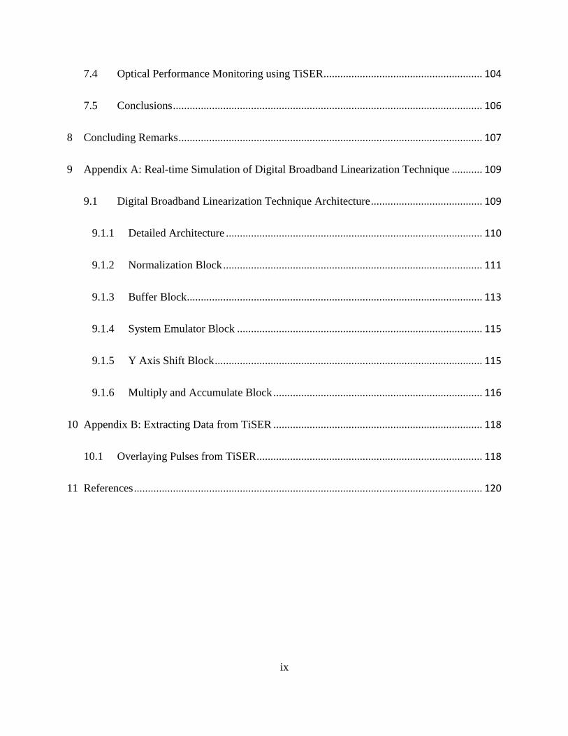
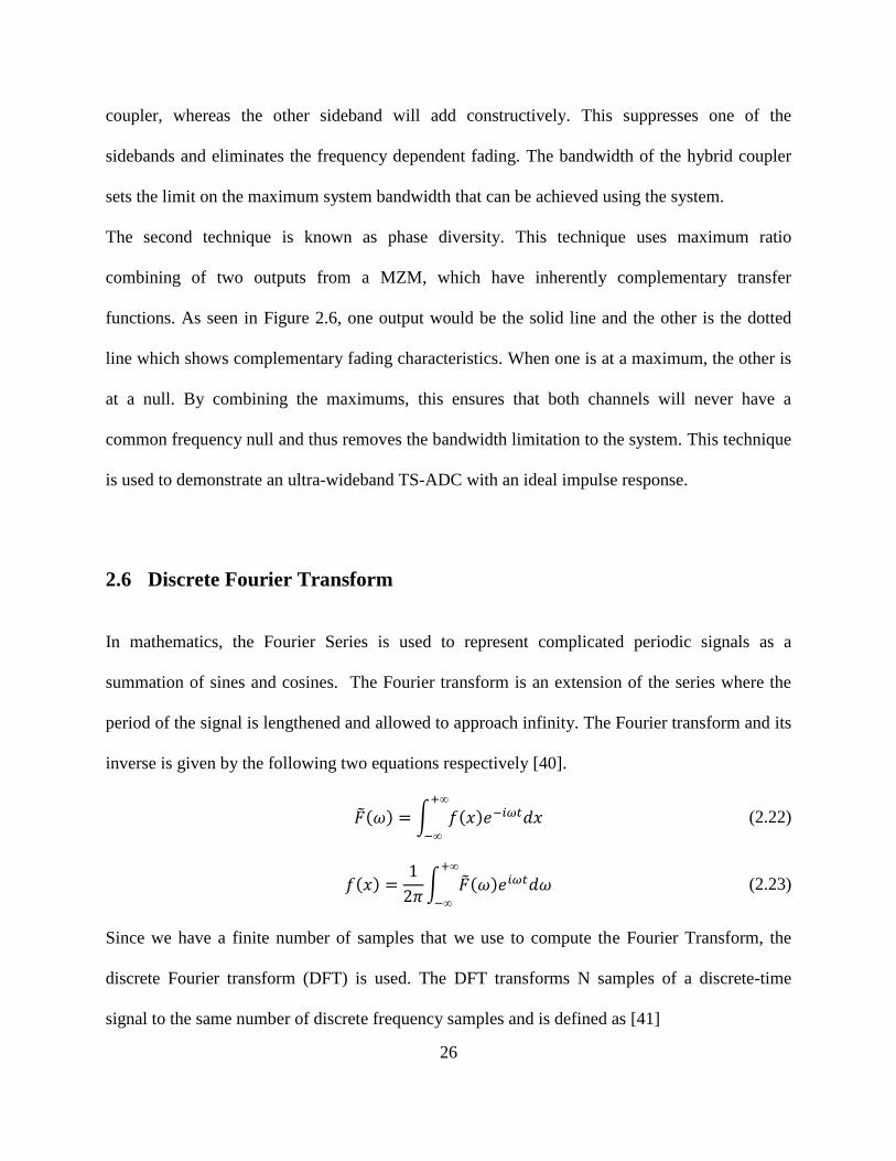
Figure 1.1. Resolution of state-of-the-art electronic ADCs versus input bandwidth [8]. The
TS-ADC is able to demonstrate 7.2 ENOB over 10 GHz of bandwidth [13] which
shows photonics can help in overcoming current bandwidth limitations. .................... 5
Figure 2.1. Schematic of a typical intensity-modulation direct-detection analog optical link
[32]. ............................................................................................................................. 11
Figure 2.2. Spectrum of the intermodulation products generated by nonlinearities in a system
[35]. ............................................................................................................................. 14
Figure 2.3. Measuring the spurious free dynamic range from a two tone test. ............................. 16
Figure 2.4. Basic operating principle of time-stretch [12]. ........................................................... 17
Figure 2.5. Continuous time-stretch ADC diagram for stretch factor of four [12]. ...................... 19
Figure 2.6. Dispersion penalty curves in a conventional optical link and for a photonic time-
stretch ADC (solid line). By mitigating the dispersion penalty, we get a flat
response (wide dotted lines) [12]. ............................................................................... 25
Figure 3.1. Schematic of a typical intensity-modulation direct-detection analog optical link
[43]. ............................................................................................................................. 30
Figure 3.2. Digital broadband linearization technique is a single stage post-processing
algorithm used to linear optical links [60]. ................................................................. 34
Figure 3.3. Optical link transfer function emulator used in the digital broadband linearization
algorithm. .................................................................................................................... 35
xi
Figure 3.4. The digital broadband linearization algorithm is able to suppress nonlinearities in
several stages [32]. ...................................................................................................... 36
Figure 3.5. The gain coefficients used in the digital broadband linearization algorithm
follows the coefficients from Pascal's triangle. .......................................................... 37
Figure 3.6. Third-order intermodulation product suppression is observed. (a) Prior to digital
broadband linearization we have two third order tones. (b) After digital broadband
linearization we observe 35 dB of third-order suppression. ....................................... 39
Figure 3.7. Output power versus input power for two different frequency sets. (a)
Fundamental tones at 1 and 1.1 GHz, resulting in third-order intermodulation
distortions at 900 MHz and 1.2 GHz. (b) Fundamental tones at 6 and 6.1 GHz,
resulting in third-order intermodulation distortions at 5.9 and 6.2 GHz [32]. ............ 40
Figure 4.1. Simulink Model of the broadband linearization algorithm. ....................................... 46
Figure 4.2. Simulink simulation results showing about 18 dB of improvement from a single
stage. ........................................................................................................................... 47
Figure 4.3. Block diagram of a single stage of the broadband linearization algorithm. It can
be expanded to multiple stages. .................................................................................. 48
Figure 4.4. Matlab (top) and Verilog (bottom) simulation of real data show IMD3
suppression of about 17 dB. The blue curve shows the spectrum before digital
broadband linearization (uncorrected) and the red curve shows the spectrum after
digital broadband linearization (corrected). ................................................................ 51
Figure 5.1. Block diagram of a traditional instantaneous frequency measurement system [72]. . 55
Figure 5.2. Time-Stretch IFM Receiver block diagram [80]. ....................................................... 58
xii
Figure 5.3 Dispersion penalty behavior in the Time-stretch IFM. ............................................... 60
Figure 5.4. By using quadratic interpolation, the true peak frequency and amplitude can be
found [81].................................................................................................................... 61
Figure 5.5. TS-IFM frequency estimation simulation which shows using quadratic
interpolation significantly reduces the frequency error [80]....................................... 62
Figure 5.6. A single frequency tone was swept from 5 GHz to 45 GHz. ..................................... 64
Figure 5.7. Estimated frequency error of 97 MHz rms is achieved using the TS-IFM receiver. . 64
Figure 5.8. Dual tones input at 10 GHz and 30 GHz. TS-IFM estimated the frequency of the
tones to be at 9.96 GHz and 30.01 GHz. .................................................................... 65
Figure 5.9. Plots 5.9(a)-(c) depicts how changing the first dispersive fiber allows for tuning
of frequency resolution. .............................................................................................. 67
Figure 5.10. TS-IFM can resolve two tones close together and with similar amplitudes
simultaneously which is a challenge for current IFM receivers. ................................ 68
Figure 5.11. Dual tones input at 8 GHz and 9 GHz with high and low amplitudes. The system
was able to resolve these two signals and correct for signal frequency. ..................... 68
Figure 6.1. Block diagram of time-stretch enhanced recorder [80]. ............................................. 71
Figure 6.2. Different sampling techniques are shown. (a) An equivalent-time oscilloscope
samples signals at very slow rates and can reproduce signals only of repetitive
nature. (b) A real-time digitizer samples signals continuously but has limited
bandwidth. (c) TiSER can capture very high bandwidth signal segments in real-
time and quickly reproduce them on equivalent time scales [89]. .............................. 73
Figure 6.3. Small amount of jitter in a fast signal can result in large voltage errors [12]. ........... 74
xiii
Figure 6.4. Sampling stretched fast signal reduces amplitude jitter [12]. ..................................... 74
Figure 6.5. By recompressing the signal to the original timescale, the sampling jitter is
reduced [12]. ............................................................................................................... 75
Figure 6.6. Real-time burst sampling modality using TiSER allows for rapid generation of
eye diagrams for signal integrity analysis [89]. .......................................................... 78
Figure 6.7. Eye diagram with areas of statistical measurements for bit error rate, jitter, and
rise and fall times. ....................................................................................................... 79
Figure 6.8. The probability distribution functions used to estimate BER from an eye diagram.
The overlap region determines the BER [94]. ............................................................ 81
Figure 6.9. Histogram of a rising edge and the sample taken from the center to determine the
jitter. ............................................................................................................................ 84
Figure 6.10. Comparison of the temporal resolution for TiSER with stretch factor 50 and 50
GSample/s real-time digitizer capture of the rising (top) and falling (bottom)
edges of a 12.5 Gbps data stream in a single burst. TiSER can capture about 20
data points whereas a real-time digitizer can only get 2-4 along the edge. ................ 86
Figure 6.11. Starting from an eye diagram, the rising and falling edges can be separated. ......... 88
Figure 6.12. The determination of the '0' and '1' levels. ............................................................... 88
Figure 6.13. The rise time for a rising edge is the time between the purple lines. ....................... 89
Figure 6.14. The fall time for a falling edge is the time between the purple lines. ...................... 89
Figure 6.15. Eye diagram generated by using data from Tektronix real-time oscilloscope and
how the rising and falling edges are separated. .......................................................... 91
Figure 6.16. Histogram of the rising edge of a PRBS signal using a Tektronix oscilloscope. ..... 91
xiv
Figure 6.17. Histogram of the falling edge of a PRBS signal using a Tektronix oscilloscope. .... 92
Figure 6.18. Histogram of the rising edge of a PRBS signal using TiSER. ................................. 92
Figure 6.19. Histogram of the falling edge of a PRBS signal using TiSER. ................................ 93
Figure 6.20. The experimental set up used for measuring BER with a BERT and the addition
of a noise generator in the signal path. ....................................................................... 94
Figure 6.21. To measure the BER, noise was combined with the signal until a certain BER
value was obtained (top). The addition of noise degraded the eye (middle) and we
can estimate the BER using TiSER (bottom). ............................................................ 95
Figure 7.1. The SDN plane that receives feedback from the OPM layers for dynamic network
control. ...................................................................................................................... 101
Figure 7.2. The CIAN box architecture where TiSER is inserted into the OPM layer. A
wavelength selective switch drops an optical channel to TiSER to monitor. ........... 102
Figure 7.3. Set up of TiSER at CIAN TOAN. ............................................................................ 103
Figure 7.4. CIAN TOAN collaborative effort simulated ability to compensate for
impairments in next generation optical communication networks. .......................... 103
Figure 7.5. (Left) TiSER generated eye diagram and (right) sampling oscilloscope generated
eyes for the 10 Gbit/s video UDP packets with stretch factor of 50. TiSER is able
to generate eyes in 27 as opposed to many seconds or minutes using the
sampling oscilloscope [99]. ...................................................................................... 105
Figure 9.1. Block diagram of the architecture for digital broadband linearization technique. ... 109
Figure 9.2. The four input channels of the ADQ108 with the order of the samples along with
the size of each sample in bits................................................................................... 110
xv
Figure 9.3. The bit size inputs to each block of the architecture. ............................................... 111
Figure 9.4. Normalization block diagram. This shows how every 128 sample points are
normalized at a time. ................................................................................................. 112
Figure 9.5. Verification in simulation of the normalization block. It can be seen that the
signal is normalized as shown by the plot on the right. ............................................ 113
Figure 9.6. Buffer block diagram where 32 sample points are stored and shifted to each
buffer level at each clock cycle. ................................................................................ 114
Figure 9.7. Determining the number of buffer levels by lining up the data points. .................... 114
Figure 9.8. The block diagram for the system emulator. ............................................................ 115
Figure 9.9. Block diagram for the Y-shifter block. This block finds the max and min values
in a data set and shifts all the values by the median value. ....................................... 116
Figure 9.10. Multiply and accumulate block that combines the two data paths and produces
the corrected output................................................................................................... 117
Figure 10.1. Aligned pulses from TiSER and the pulse envelope (blue). .................................. 119
xvi
LIST OF TABLES
Table 2-1. Symbols used in time-stretch ADC mathematical framework [12]. ........................... 20
Table 3-1. Benchmark comparisons of the digital technique with other broadband
linearization techniques [32], [52]-[54], [64]. ............................................................ 42
Table 5-1. Tuning TS-IFM for bandwidth and resolution ............................................................ 67
Table 6-1. TiSER and Tektronix oscilloscope measurement comparisons. ................................. 90
xvii
ACKNOWLEDGMENTS
This degree would not be possible without the encouragement, support, and mentoring by many
individuals. First, I would like to thank both of my advisors, Professor Bahram Jalali and
Professor Asad Madni, for giving me the opportunity to study under them and work on really
interesting and cutting edge projects. Both have been great supportive advisors who have pushed
me and guided me to new heights as a professional. I am extremely grateful and appreciative of
the time they spent and the advice they have shared with me over the years. I could not be any
luckier to study under two world renowned professors and am proud to be their student.
I thank Professor Bahram Jalali for accepting me into his group and giving me an
opportunity to pursue my degree at UCLA. Over the years, he has been a great support to me
academically and professionally and has provided me with many opportunities to expand my
knowledge and develop my skills through various projects. He has also taught me to always look
for business opportunities. Two things I take away are that we should always be flexible in our
approach to problems just like how time isn't always rigid and that "there is no free lunch."
I thank Professor Asad Madni for his desire to mentor me. His passion, energy, drive, and
knowledge has helped me grow leaps and bounds. His dedication for his students is evident in
the time he spends with us and how he pushes us to succeed. Under his tutelage, I have learned
so much and to always continue learning and find ways to continually improve the world around
me. I am grateful and appreciative of his insight and feedback for this body of work would not
have been as successful without them.
I would like to thank Professor Oscar Stafsudd, Professor Frank Chang, and Professor
Carlos Portera-Cailliau for taking the time to serve on my committee and providing me feedback.

xviii
I want to thank my lab mates who I have gotten to know and became great friends with
over the years. They have helped me through useful discussions and for spending long hours in
the lab with me. Without them, my time at UCLA would not have been as exciting or enjoyable.
I especially want to thank Dr. Ali Fard, Dr. Peter DeVore, Dr. Brandon Buckley, and Cejo
Konuparamban Lonappan. Getting to know these gentlemen in and out of the lab has been a
blessing to me, and I will cherish the times we have spent together.
I am grateful to Northrop Grumman Aerospace Systems for giving me the opportunity to
pursue a higher degree through their fellowship program. Without their support and funding, this
would not have been possible.
I thank all my mentors and teachers throughout my life and during my career. Be it a
small piece of advice or just taking the time to teach me, all these experiences have shaped me
into the person I am today. I especially want to thank Professor Galina Khitrova and the late
Professor Hyatt Gibbs for giving me my first opportunity to work in an optical lab and helping
me find my passion for optics.
I am grateful for my friends who have given me moral support throughout these many
years.
Most importantly, I want to thank my entire family. Their love, support, and
encouragement gave me the strength to keep persevering to complete this degree. They
celebrated my accomplishments with me and stood by me when I was discouraged. I especially
thank my parents for providing me with so many opportunities in life and instilling in me the
value of a good education. Thank you for always being there for me.
xix
VITA
2011-2014 Graduate Student Researcher
Department of Electrical Engineering
University of California, Los Angeles
Los Angeles, California, USA
2009-Present Engineer
Northrop Grumman Aerospace Systems
El Segundo, California, USA
2008-2009 Master of Science in Electrical Engineering
Stanford University
Stanford, California, USA
2008 Engineering Intern
Northrop Grumman Space Technologies
Redondo Beach, California, USA
2007 Engineering Intern
Raytheon Space and Airborne Systems
El Segundo, California, USA
2005-2008 Undergraduate Research Assistant
The University of Arizona
College of Optical Sciences
Tucson, Arizona, USA
2004-2008 Bachelor of Science in Optical Sciences and Engineering with Honors
Minors in Electrical Engineering and Mathematics, Magna Cum Laude
The University of Arizona
Tucson, Arizona, USA
AWARDS
2010 Northrop Grumman Aerospace Systems Fellowship
2004-2008 Raytheon Scholars Program
2004-2008 Dean’s List (GPA 3.5-3.999) and Dean’s List with Distinction (GPA 4.0)
2004-2008 UA Provost Scholarship
2004-2008 UA Spirit of Discovery Award
xx
PUBLICATIONS AND PRESENTATIONS
D.Lam, C. K. Lonappan, B. Buckley, A. M. Madni, and B. Jalali, “Real-time Optical
Performance Monitoring using Time-Stretch Technology,” CIAN lecture series, Sept 2014.
D.Lam, B. W. Buckley, C. K. Lonappan, A. M. Madni, and B. Jalali, "Ultra-wideband
Instantaneous Frequency Estimation," (To be published).
C. K. Lonappan, B. Buckley, J. Adam, D. Lam, A. M. Madni, and B. Jalali, “Time-Stretch
Accelerated Processor for Real-time, In-service, Signal Analysis,” IEEE Conference on Signal
and Information Processing, December 3-5, 2014 (Accepted).
C. K. Lonappan, D. Lam, B. Buckley, P.T.S. DeVore, D. Borlaug, A. M. Madni, B. Jalali, M.
Chitgarha, A. Almaiman, A. E. Willner, M. Wang, A. Ahsan, B. Birand, G. Zussman, K.
Bergman, W. Mo, M. Yang, A. Gautham, S. Albanna, J. Wissinger, D. Kilper, “Optical
Performance Monitoring for Agile Optical Networks,” Poster presentation at Center for
Integrated Access Networks (CIAN) Site Visit, May 2014.
C. K. Lonappan, D. Lam, P.T.S. DeVore, D. Borlaug, B. W. Buckley, A. M. Madni, and B.
Jalali, “Photonic Time-Stretch for Real-time In-service Performance Monitoring of Next
Generation Optical Networks,” Poster presentation for CIAN Industrial Affiliates Board meeting,
2014.
P. DeVore, D. Lam, C. Kim, and B. Jalali, "Boosting Electrooptic Modulators for Optical
Communications," in Frontiers in Optics 2013, I. Kang, D. Reitze, N. Alic, and D. Hagan, eds.,
OSA Technical Digest (online) (Optical Society of America, 2013), paper FW48.
D. Lam, A. Fard, B. Buckley, and B. Jalali, "Digital broadband linearization of optical links,"
Optics Letters, 38, 446-448 (2013).
D. Lam, A. Fard, and B. Jalali, "Digital broadband linearization of analog optical links," IEEE
Photonics Conference, 23-27 Sept. 2012.
J. Hendrickson, B. C. Richards, J. Sweet, S. Mosor, C. Christenson, D. Lam, G. Khitrova, H. M.
Gibbs, T. Yoshie, A. Scherer, O. B. Shchekin, and D. G. Deppe, "Quantum dot photonic-crystal-
slab nanocavities: quality factors and lasing", Phys. Rev. B 72, 193303 (2005).
1
1 Introduction
Chapter 1
Introduction
1.1 Optical Fiber Links
Optical fiber networks have been used for many decades to transport large amounts of data
across long distances. These networks help connect the world and bring wireless access to
remote locations cheaply. Radio frequency over fiber is an enabling technology used for an array
of applications such as providing wireless access to remote and rural areas, phased array radars,
and cable television to name a few. Using optical links provides significant advantages over
current coaxial cables [1]-[3]. Optical links have much lower attenuation than other media. Using
optical fibers allows transmission of signals further, thereby reducing the number of repeaters
along the way. The optical fiber link has lower complexity, typically a link just consists of an
optical to electrical converter, amplifiers, and an antenna. This means that we could create a
central location and connect all the antennas to this station which simplifies the overall
architecture. Additionally, having a simpler architecture reduces cost since there will be reduced
power consumption and lower cost to the infrastructure. Moreover, fiber optics can support
speeds that are greater than those available today, and they can handle faster speeds offered by
2
future generations. This means that they do not need to be upgraded as frequently which also
saves on cost [1]-[4].
With increased demand for wireless access points, many locations need to be connected
to these fiber links. There is a need for transporting data to farther remote areas or areas
inaccessible via wireless. As signals are transmitted over longer distances, the optical links begin
to suffer from nonlinearities and distortion that degrade the performance of the link [1]. These
distortions, known as intermodulation distortion products, can produce crosstalk in the link
which causes interference for signals in other bands. These eventually degrade the entire optical
link performance and limit the data rate and distance of signal propagation. Chapter 3 presents a
digital post-processing algorithm that is capable of reducing nonlinearities and increasing the
spurious free dynamic range of an optical link. This is an improvement over current techniques
because it is a post-processing technique which does not require additional hardware and can be
implemented onto a real-time system. Previous techniques, by contrast, require additional
hardware and can only reduce the nonlinearities in a limited bandwidth. Additionally, this
algorithm regenerates the nonlinearities which obviates the need for excessive bandwidth.
1.2 High Speed Analog-to-Digital Converters
Internet traffic continues to grow at an exponential rate, and next generation networks need to be
able to handle the increasing bandwidth every year. According to Cisco [5], the annual global IP
traffic will surpass the zettabyte threshold in 2016. Over the past five years, global IP traffic has
grown fivefold and is expected to grow threefold in the next five years. Most of the growth has
been fueled by the explosion of social media, online gaming, video streaming, and cloud storage.
Furthermore, metro traffic is expected to surpass long-haul traffic by 2015 and will account for
3
more than 62 percent of total IP traffic by 2018 [5]. This large growth in metro traffic is due in
part to content delivery services which bypass the long-haul links and deliver their content
directly to regional and metro networks. These content delivery services are expected to carry
over half of the Internet traffic by 2018 [5].
As the number of users and demand for content increases, the data rate continues to
increase in order to meet demand. However, due to high speed signals, it becomes increasing
difficult and challenging for engineers to develop electronic hardware capable of supporting
these speeds. There has been a lot of development over the past two decades on developing
technology to send more data through optical fibers. For example, the data rate is increased
through different optical techniques like optical time division multiplexing or using denser
wavelengths. Research is ongoing on making the optical components, such as the electro-optic
modulators faster. Next generation modulators have demonstrated the ability to achieve speeds
of over 100 GHz [6].
On the receiving end, there is a need for high speed analog-to-digital converters (ADC) to
convert this information into digital format. Walden has taken a survey of different high speed
digitizers and shown that as the bandwidth increases, the resolution decreases [7],[8]. This is
because as the bandwidth of the digitizer increases, the amount of noise increases as well thereby
lowering the signal to noise ratio. Several architectures have been developed to increase the
speed of the digitizers, such as interleaving multiple ADCs. However, the main issue with this
architecture is the timing and ability to interleave the data. A small timing error during the
interleaving process can create timing errors in the final data resulting in jitter [9]. Additionally,
these high speed ADCs comprised of several interleaved ADCs are large rack mount units that
consume a considerable amount of energy.
4
Using time-stretch technology, we can perform high speed measurements and reduce the
size and energy consumption of the system. The time-stretch concept was first demonstrated in
1998 [10] and has since been used for an array of applications. One application is the time-
stretch analog-to-digital converter (TS-ADC) [11],[12]. The unique advantage of this technology
is that it can slow down ultrafast signals in time and allow a slower, higher resolution ADC to
sample the signal. By using a slower ADC for sampling, we can maintain a higher resolution as
opposed to using a faster ADC with lower effective number of bits (ENOB) [11],[12]. For
example, a 40 GHz signal would appear as a 2 GHz signal with a stretch factor of 20. By using
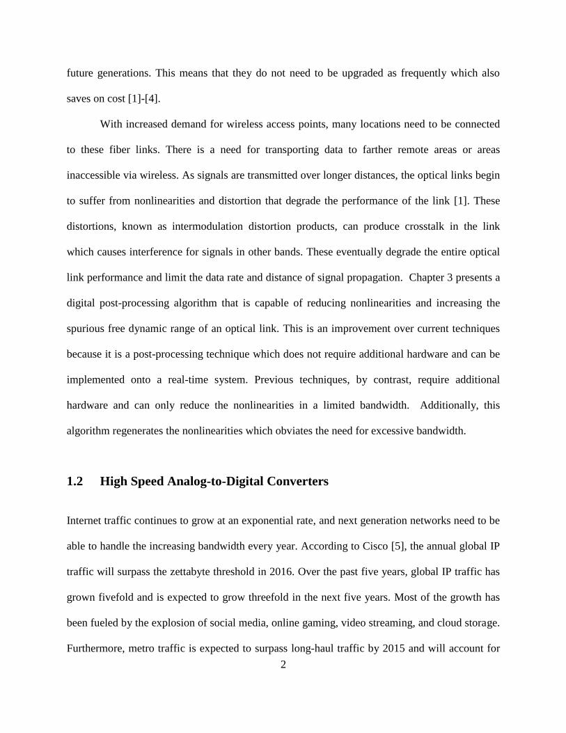
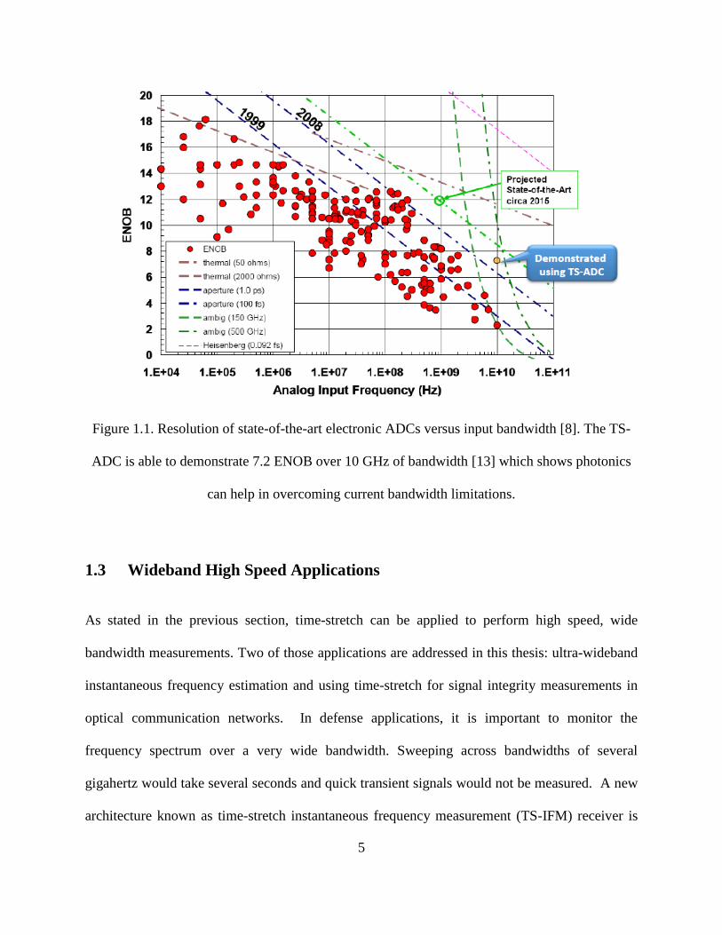
this technique, the TS-ADC is able to break past the Walden curve shown in Figure 1.1 and set a
record 7.2 ENOB over 10 GHz of bandwidth [13].
Time-stretch has been used to capture ultrafast signals. In one demonstration, a 95 GHz
tone was sampled at an effective sampling rate of 10 Terasamples/second [14]. By expanding
this technology into two-dimensions, ultrafast images can be captured. A new type of bright-field
camera known as time-stretch microscopy [15] has demonstrated imaging of cells with record
shutter speed and throughput leading to detection of rare breast cancer cells in blood with one-in-
a-million sensitivity [16]. Used for single-shot real-time spectroscopy, the time stretch
technology led to the discovery of optical rogue waves, bright and random flashes of white light
that result from complex nonlinear interactions in optical fibers [17]. Time-stretch also led to the
development of a fluorescence imager with record imaging speeds [18].
5
Figure 1.1. Resolution of state-of-the-art electronic ADCs versus input bandwidth [8]. The TS-
ADC is able to demonstrate 7.2 ENOB over 10 GHz of bandwidth [13] which shows photonics
can help in overcoming current bandwidth limitations.
1.3 Wideband High Speed Applications
As stated in the previous section, time-stretch can be applied to perform high speed, wide
bandwidth measurements. Two of those applications are addressed in this thesis: ultra-wideband
instantaneous frequency estimation and using time-stretch for signal integrity measurements in
optical communication networks. In defense applications, it is important to monitor the
frequency spectrum over a very wide bandwidth. Sweeping across bandwidths of several
gigahertz would take several seconds and quick transient signals would not be measured. A new
architecture known as time-stretch instantaneous frequency measurement (TS-IFM) receiver is
6
introduced that can overcome some of the limitations of current IFMs. The TS-IFM can estimate
multiple frequencies with improved accuracy in a wide bandwidth with fast sweep times. The
improved frequency estimation is performed by windowing the time domain data and performing
quadratic interpolation in the frequency domain [19]. Wideband single tone frequency estimation
across 40 GHz of bandwidth has been demonstrated and this can be extended to multiple
frequency estimation as well. The TS-IFM is discussed in detail in Chapter 5.
Time-stretch technology can also be used for high speed signal integrity measurements
for optical networks. Using the time-stretch enhanced recorder (TiSER) and a field
programmable gate array (FPGA) for real-time processing, fast signals can be captured with high
fidelity due to TiSER's high temporal resolution. Chapter 6 describes how we can use time-
stretch to capture rising and falling edges which provides more data points than a conventional
Tektronix 50 GSa/s real-time oscilloscope. Due to TiSER's high sampling throughput and by
overlapping the recorded signals, eye diagrams can be generated. A major development, which
will not be discussed in detail in this thesis, is TiSER's ability to generate eye diagrams in real-
time which allows for rapid analysis of the eye for bit error rate, rise time, fall time, and jitter
measurements. This information can immediately be used to provide feedback to a software
defined network (SDN). Chapter 6 describes how the eye diagram is analyzed to extract the bit
error rate, rise and fall times, and jitter. Chapter 7 discusses how TiSER was integrated into the
Center for Integrated Access Networks Test-bed for Optical Aggregate Networks. In this test-
bed, TiSER acts as an optical performance monitor for a SDN which is able to perform
measurements and analyze the eye diagram in order to determine the health of the optical
network. Depending on the information provided by TiSER, real-time adjustments can be made
by the SDN control plane to optimize network performance.
7
2 Background
Chapter 2
Background
Many of the topics discussed in this thesis involve performing high speed measurements using
optical fiber links. This chapter presents some of the fundamental concepts so that the reader is
able to gain a better appreciation of the work presented later in this thesis and to gain an
appreciation of the challenges faced and the approach used in solving those problems.
2.1 Historical Perspective
Fiber optic systems are ubiquitous in modern society and the demand for high speed internet
continues to grow. Fiber optic networks have stimulated the development of cities, promoted
economic growth, and connected people around the world. Communication systems transmit
information from one place to another, whether separated by a few kilometers or by great
transoceanic distances. Optical communication systems use light to transmit information by
modulating information onto a high carrier frequency.
8
The precursor to the fiber optic link, called the photophone, was developed in 1880 by
Alexander Graham Bell and his assistant Charles Sumner Tainter [20]-[22]. The device allowed
for the transmission of sound on a beam of light. Using the photophone, the first wireless voice
transmission was made some 213 meters apart, and this was different than the telephone because
it required the modulation of light instead of modulated voltage carried over a conductive wire
circuit. Bell deemed it his greatest invention, but the photophone would not be very practical
until advances in lasers and optical fiber technology permitted the secure transport of light. Until
1950, the main issue with realizing optical waves as a carrier was there was neither a coherent
optical source nor a suitable transmission medium for transporting light.
Optical communications was realized when the laser was invented which solved the
coherent optical source issue. However, there was no low attenuation medium as the glass fibers
during this time had losses around 1000 dB/km [22]-[24]. The concept for developing low loss
fibers was possible from the proposal of Charles K. Kao and George Hockman in 1966 when
they showed that losses in existing glass was due to contaminants and that these could potentially
be removed [25]. It was not until the 1970's that the optical fiber was successfully invented by
Corning Glass Works researchers Robert Maurer, Donald Keck, and Peter Schultz (patent no.
3,711,262) [26] with low enough attenuation and the development of the GaAs semiconductor
laser that optical fiber technology became practical. Afterwards, development on lasers and
fiber-optic communications started and continued to develop at a rapid pace.
The first fiber-optic communication systems operated around 0.8 m with a bit rate of 45
Mbps with repeater spacing of up to 10 km. It was found in the 1970's that the repeater distances
can be increased by shifting the wavelength to 1.3 m. In the 1980's, the second generation of
fiber-optic communication was developed and operated in the 1.3 m window and used
9
InGaAsP semiconductor lasers. The bit rate of early systems was limited to below 100 Mbps
because of dispersion in multimode fibers, but this limitation was overcome with the
development of the single mode fiber. One of the issues during this time period was having
practical connectors capable of working with the newly developed single mode fiber. Towards
the end of the decade, commercial systems were able to operate at bit rates up to 1.7 Gbps and
repeater spacing of 50 km [23],[24].
The third generation fiber systems operated at 1.55 m and fibers at this time had losses
of about 0.2 dB/km. Many of these improvements are due to the discovery of Indium gallium
arsenide (InGaAs) and the InGaAs photodiode. It was during this time that the dispersion
problems experienced in optical systems could be reduced by using dispersion shifted fibers that
had minimum dispersion near 1.55 m. The third generation systems were able to operate at
speeds of 2.5 Gbps with repeater spacings in excess of 100 km [22]. The fourth generation
systems used optical amplification to increase the distance between repeaters and began using
wavelength division multiplexing (WDM) to increase data capacity. The development of the
erbium doped fiber amplifier (EDFA) was a major breakthrough as these optical amplifiers could
compensate for losses in the fiber system and reduce the number of repeaters required. This
resulted in a revolution that resulted in the doubling of system capacity every six months. By
2006, a bit-rate of 14 Tbps was achieved over a 160 km line [23],[24].
The fifth generation of fiber optic communications is concerned with extending the
wavelength range of the WDM in order to increase the wavelength range the system can operate.
This has led to the wavelength windows known as C, L, and S bands. C is for the conventional
band in the range from 1.53-1.57 m, and the window was extended for long and short
wavelengths on either side resulting in L and S bands, respectively. Also a new kind of fiber
10
known as dry fiber had been developed with very little loss that led to optical systems able to
support thousands of WDM channels. Also the fifth generation systems tried to increase the bit
rate within these WDM channels by using optical solitons as pulses. Optical solitons are pulses
that preserve their pulse shape during propagation by counteracting the effect of dispersion
through the fiber nonlinearity [22].
Today, much of the development is focused on creating a "smart" mesh grid network.
With increased content delivery services, fiber optics are no longer just used for long haul
networks and are being used for metropolitan networks. These networks need to be able to
quickly adapt to any impairment and adapt to large volumes of traffic. The invention of the
colorless, distortionless, contentionless reconfigurable optical add drop multiplexer (CDC-
ROADM) will be revolutionary in making networks more agile and robust [27],[28]. In the past,
sending data required a direct link from transmitter to receiver. With the CDC-ROADM, it can
act as an optical switch and can send the data in any direction and on a new wavelength
[27],[28]. The ability to instantly switch wavelengths and directions provides much greater
flexibility for a network and allows it to send information quickly. There is also focus on making
next generation networks more robust by using a control plane that can monitor and rapidly
adapt to impairments. Repairs on modern optical communication systems are very time
consuming and can bring an entire network down for hours or days. By being able to monitor a
network continuously, a "smart" network can allocate resources to where traffic is heaviest and
identify where problems may occur before it happens [29]. If a disaster occurs, then the network
can immediately use these optical switches and redirect traffic to minimize network connectivity
loss.
11
2.2 Analog Optical Links
Analog optical links, also referred to as Radio over Fiber (RoF), is a technology where light is
modulated by a radio frequency signal and transmitted over an optical fiber link [1]. RoF is used
for multiple purposes such as cable television, phased arrays, networks, and military radar
applications. The most common usage is to facilitate wireless access because of its ability to
transport signals over long distances and reach areas where wireless cannot penetrate.
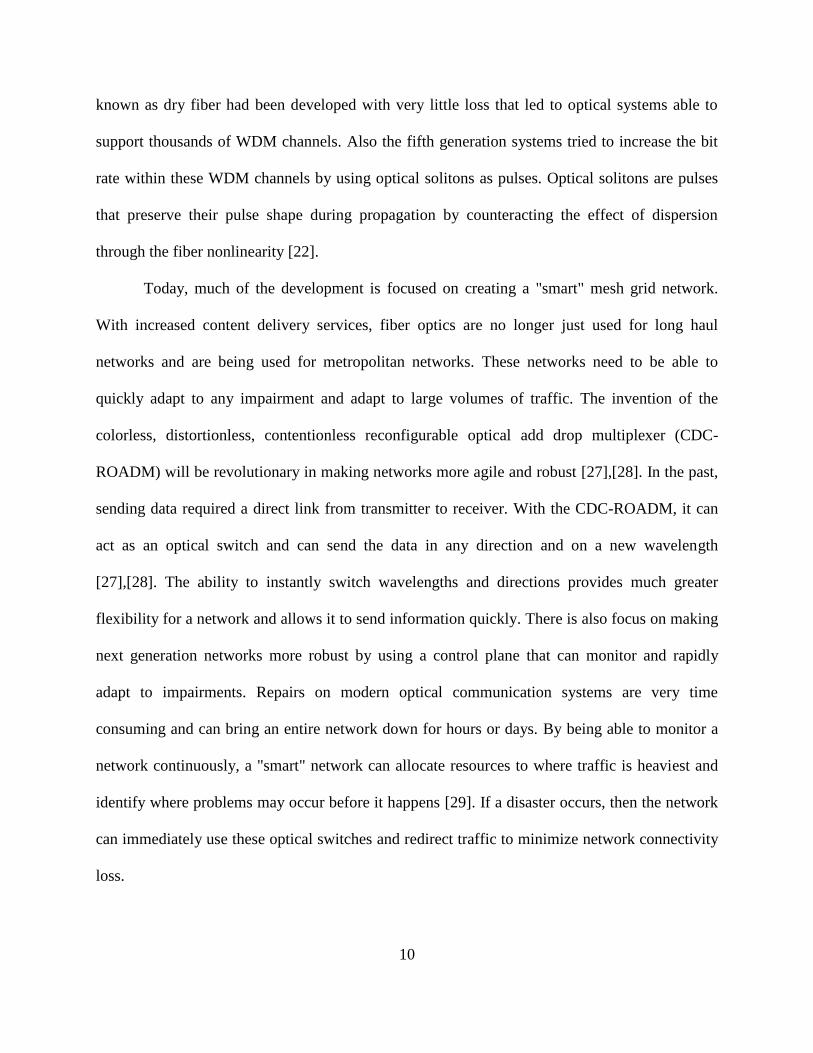
Analog optical links are comprised of three main parts: a transmitter, transmission
medium, and a receiver [30],[31]. The basic transmitter consists of a laser and a modulator where
the laser acts as a carrier and the signal we want to send is modulated via a modulator onto the
carrier signal. The optical fiber acts as the transmission medium. The signal from the transmitter
is transported along the optical fiber. At the receiver, the transmitted signal is detected using
detectors. This will allow us to demodulate and recover the signal. A schematic of an optical link
is shown in Figure 2.1 [32].
Figure 2.1. Schematic of a typical intensity-modulation direct-detection analog optical link [32].
There are several advantages of using an optical link to send radio signals [1]. An optical
link has low loss and is able to send signals across a longer distance with less power compared to
a copper coaxial cable. The cost to manufacture and maintain optical fibers is cheaper than
12
copper. In addition, photonic devices are capable of very high speeds and inherently have a large
bandwidth. This makes them suitable for future generations and device upgrades for years to
come as we have not yet reached those speeds. Also optical fiber is bit rate and protocol
independent, hence it can be used in current and future technologies. The optical fiber is immune
to electromagnetic interference, so other electrical signals and lightning strikes will not affect its
performance. Furthermore, fibers can be deployed to “dead zones,” secluded areas where
wireless signals cannot access easily such as in large buildings, tunnels, and rural areas. By
deploying RoF, we can reach these areas and set up wireless access points [3],[4].
2.3 Intermodulation Distortion
One of the problems when sending signals in an optical fiber for long distances is the generation
of intermodulation distortions (IMD). IMD is the amplitude modulation of signals containing
two or more different frequencies in a system with nonlinearities. It is an important metric of
linearity for a wide range of RF devices and components. Good IMD performance is essential in
many applications because interference from other signals can pollute the spectrum and create
crosstalk [33].
IMD measurement begins with a two tone test where a two-tone signal is injected into a
device under test [33]. For instance, a signal with two tones at frequencies 1 and 2 and with
amplitudes V1 and V2 respectively described by equation 2.1 is input to a device under test.
(2.1)
Most RF components have a degree of nonlinearity and for weakly nonlinear systems, the output
can be given by the Taylor series power expansion:
13
(2.2)
For systems with strong nonlinearities, the nonlinearities can be described by the Volterra Series.
In a perfectly linear device, the output signal will only be represented by just the first term in
equation 2.2 and produce two tones at the exact same frequencies as the input signal. A single
tone signal will produce harmonic distortions which are additional frequency components that
appear at integer multiples of the input frequency. A two tone signal will produce both harmonic
distortion and intermodulation distortions [33],[34]. For this scenario frequency components
appear not just at harmonic frequencies of the two original input frequencies, but also at the sum
and difference of those frequencies and at integer multiples of those sum and difference
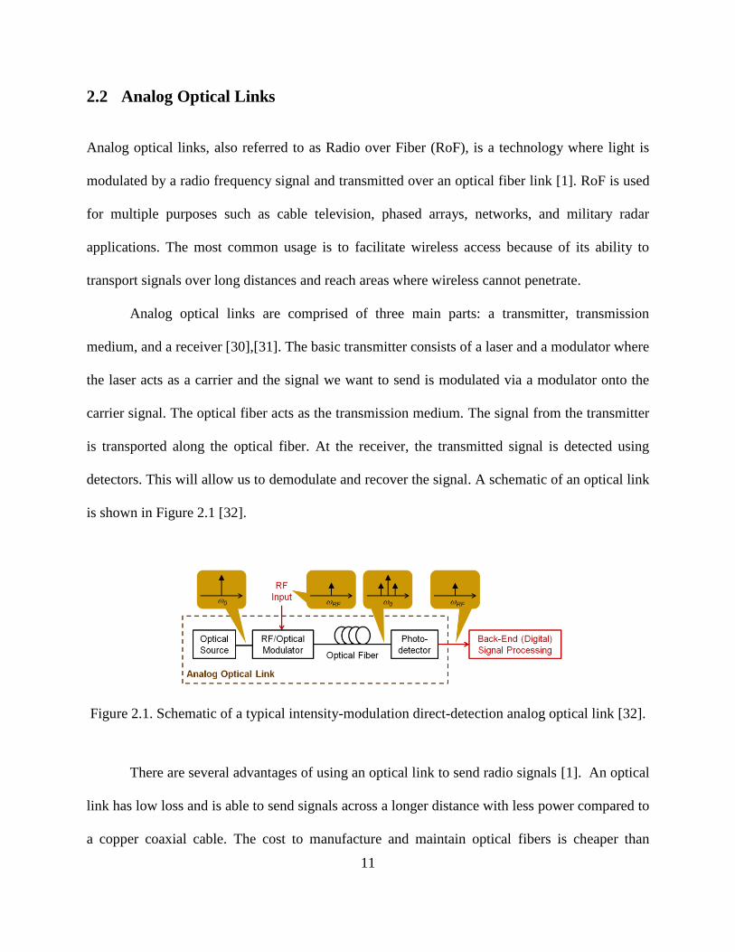
frequencies. Figure 2.2 below illustrates these generated intermodulation products and their
frequency locations [35].
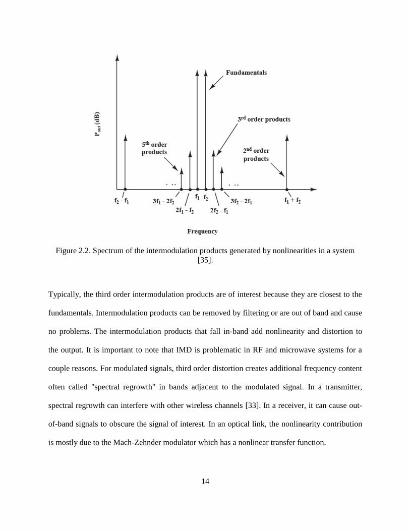
14
Figure 2.2. Spectrum of the intermodulation products generated by nonlinearities in a system
[35].
Typically, the third order intermodulation products are of interest because they are closest to the
fundamentals. Intermodulation products can be removed by filtering or are out of band and cause
no problems. The intermodulation products that fall in-band add nonlinearity and distortion to
the output. It is important to note that IMD is problematic in RF and microwave systems for a
couple reasons. For modulated signals, third order distortion creates additional frequency content
often called "spectral regrowth" in bands adjacent to the modulated signal. In a transmitter,
spectral regrowth can interfere with other wireless channels [33]. In a receiver, it can cause out-
of-band signals to obscure the signal of interest. In an optical link, the nonlinearity contribution
is mostly due to the Mach-Zehnder modulator which has a nonlinear transfer function.
15
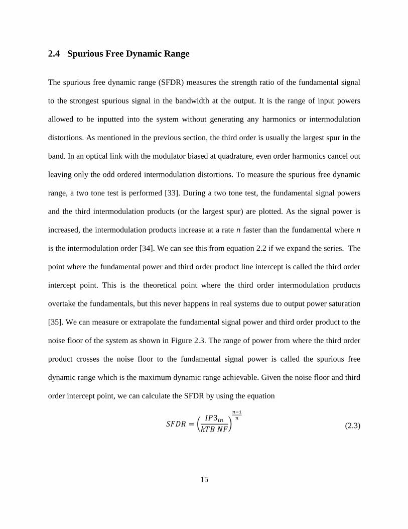
2.4 Spurious Free Dynamic Range
The spurious free dynamic range (SFDR) measures the strength ratio of the fundamental signal
to the strongest spurious signal in the bandwidth at the output. It is the range of input powers
allowed to be inputted into the system without generating any harmonics or intermodulation
distortions. As mentioned in the previous section, the third order is usually the largest spur in the
band. In an optical link with the modulator biased at quadrature, even order harmonics cancel out
leaving only the odd ordered intermodulation distortions. To measure the spurious free dynamic
range, a two tone test is performed [33]. During a two tone test, the fundamental signal powers
and the third intermodulation products (or the largest spur) are plotted. As the signal power is
increased, the intermodulation products increase at a rate n faster than the fundamental where n
is the intermodulation order [34]. We can see this from equation 2.2 if we expand the series. The
point where the fundamental power and third order product line intercept is called the third order
intercept point. This is the theoretical point where the third order intermodulation products
overtake the fundamentals, but this never happens in real systems due to output power saturation
[35]. We can measure or extrapolate the fundamental signal power and third order product to the
noise floor of the system as shown in Figure 2.3. The range of power from where the third order
product crosses the noise floor to the fundamental signal power is called the spurious free
dynamic range which is the maximum dynamic range achievable. Given the noise floor and third
order intercept point, we can calculate the SFDR by using the equation
(2.3)
16
Figure 2.3. Measuring the spurious free dynamic range from a two tone test.
2.5 Fundamentals of Photonic Time-Stretch
In the second part of this thesis, time-stretch enhanced recorder (TiSER) is used for ultra-
wideband frequency estimation and for high speed measurement applications. In this section, the
fundamentals of photonic time-stretch are discussed. First, I will give a brief overview of the
photonic time-stretch preprocessor from a systems perspective, discuss briefly how the time-
stretch analog-to-digital converter can be implemented into continuous time, and then go through
the mathematical framework of time-stretch. Lastly, I will discuss about the time-bandwidth
product and how dispersion penalty can limit the bandwidth of the time-stretch system.
However, dispersion penalty is not a fundamental limitation and can be mitigated using several
techniques.
17
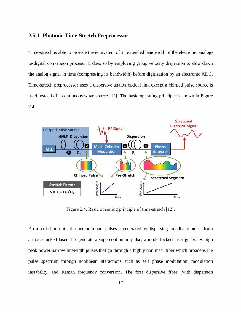
2.5.1 Photonic Time-Stretch Preprocessor
Time-stretch is able to provide the equivalent of an extended bandwidth of the electronic analog-
to-digital conversion process. It does so by employing group velocity dispersion to slow down
the analog signal in time (compressing its bandwidth) before digitization by an electronic ADC.
Time-stretch preprocessor uses a dispersive analog optical link except a chirped pulse source is
used instead of a continuous wave source [12]. The basic operating principle is shown in Figure
2.4.
Figure 2.4. Basic operating principle of time-stretch [12].
A train of short optical supercontinuum pulses is generated by dispersing broadband pulses from
a mode locked laser. To generate a supercontinuum pulse, a mode locked laser generates high
peak power narrow linewidth pulses that go through a highly nonlinear fiber which broadens the
pulse spectrum through nonlinear interactions such as self phase modulation, modulation
instability, and Raman frequency conversion. The first dispersive fiber (with dispersion
18
parameter D1 and length L1) chirps the pulse using group velocity dispersion (GVD) which is the
phenomenon that the velocity of light is dependent on the wavelength or frequency in a
transparent medium. In an optical fiber, frequencies travel at different velocities which will
spread the pulse. This creates a chirped optical pulse and results in a way to perform wavelength
to time mapping. At the Mach-Zehnder electro-optic modulator, the analog input signal is
intensity modulated onto these chirped pulses. This maps a particular wavelength to the
modulated RF signal. The pre-stretched segment is then propagated through a second dispersive
fiber (with dispersion parameter D2 and length L2) which stretches out the segment even more.
Finally the segment is converted to the electrical domain using a photodetector. The stretch
factor for the system describes the factor the signal has been stretched or how much the signal
bandwidth has been compressed. The time stretch factor is given by,
(2.4)
If the dispersion parameters are the same, we can represent the stretch factor as a function of
their lengths,
(2.5)
2.5.2 Continuous Time-Stretch Analog-to-Digital Converter
This system can be extended for continuous operation by using a train of supercontinuum pulses
to stretch the signal and dividing the signal into multiple segments [11],[12]. The continuous
time-stretch system with stretch factor of four is depicted in Figure 2.5 [12]. The input RF signal
19
is split into multiple segments and divided by a wavelength division multiplexer and each
segment is stretched in time and digitized. The resulting four segments can then be digitally
recombined by stitching the segments back together. The capture time would be the length of all
the segments added together. However for longer stretch factors, we would need the same
number of ADCs as the stretch factor. A continuous time-stretch version of this was
demonstrated by Aerospace Corporation and discussed in [36], [37]. Unlike a traditional time-
interleaved ADC array, the analog signal that each ADC sees is below its Nyquist bandwidth.
Since the signal at the input of each digitizer is slowed to below Nyquist bandwidth, each
digitizer is able to capture the full input signal. This is different than a conventional sample-
interleaved ADC in which the signal at the digitizer is above its Nyquist rate [12].
Figure 2.5. Continuous time-stretch ADC diagram for stretch factor of four [12].
2.5.3 Mathematical Framework for Time-Stretch
In this section, mathematical framework for time-stretch is provided [11], [12]. Since time-
stretch uses a modified optical link, understanding the nature of the carrier wave and modulation
20
sidebands and what happens to them as they propagate through the system is required. The
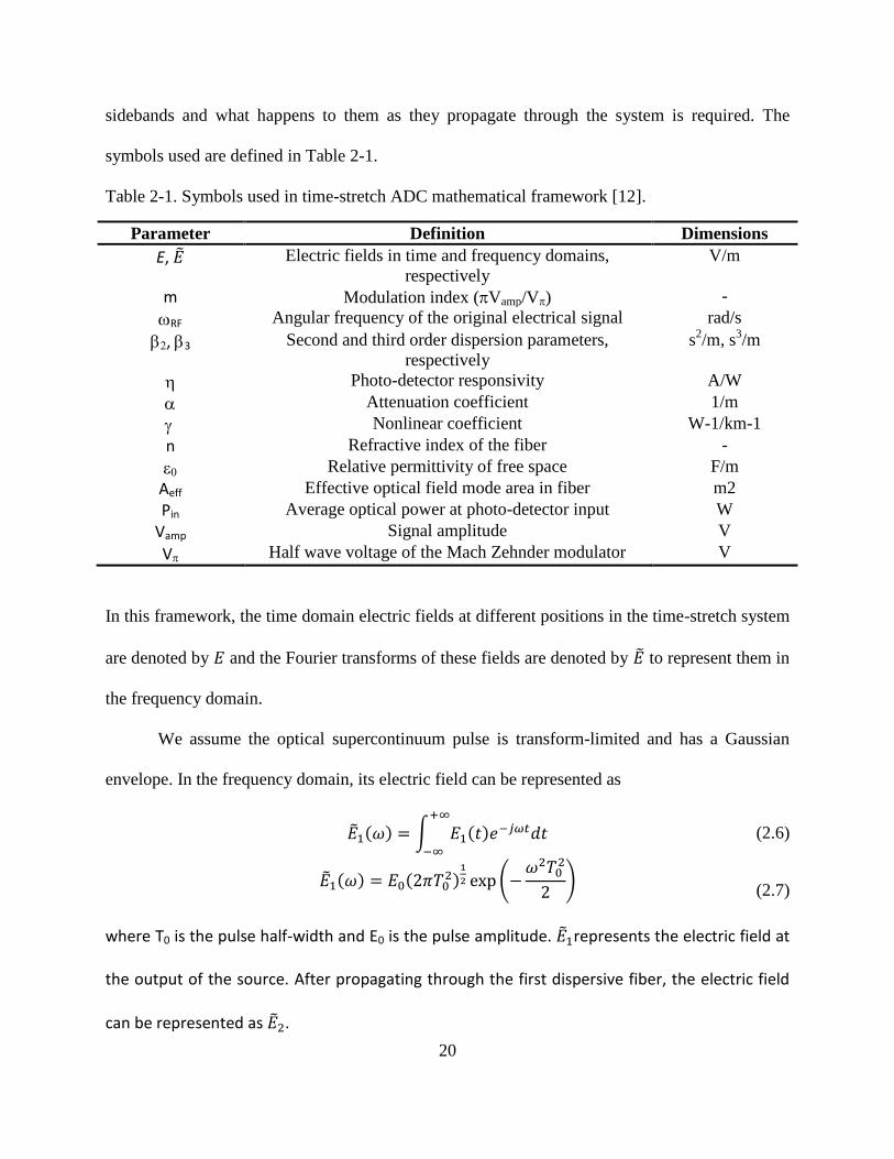
symbols used are defined in Table 2-1.
Table 2-1. Symbols used in time-stretch ADC mathematical framework [12].
Parameter Definition Dimensions
E, Electric fields in time and frequency domains,
respectively
V/m
m Modulation index (Vamp/V) -
RF Angular frequency of the original electrical signal rad/s
, 3 Second and third order dispersion parameters,
respectively
s2/m, s
3/m
Photo-detector responsivity A/W
Attenuation coefficient 1/m
Nonlinear coefficient W-1/km-1
n Refractive index of the fiber -
Relative permittivity of free space F/m
Aeff Effective optical field mode area in fiber m2
Pin Average optical power at photo-detector input W
Vamp Signal amplitude V
V Half wave voltage of the Mach Zehnder modulator V
In this framework, the time domain electric fields at different positions in the time-stretch system
are denoted by and the Fourier transforms of these fields are denoted by to represent them in
the frequency domain.
We assume the optical supercontinuum pulse is transform-limited and has a Gaussian
envelope. In the frequency domain, its electric field can be represented as
(2.6)
(2.7)
where T0 is the pulse half-width and E0 is the pulse amplitude. represents the electric field at
the output of the source. After propagating through the first dispersive fiber, the electric field
can be represented as .
21
(2.8)
Here both the linear group velocity dispersion term 2 and its dispersion slope 3 are included.
To simplify the mathematics in this section, the 3 term is ignored. Non-quadratic phase shifts
caused by 3 of GVD elements and elsewhere in the signal path cause time warping in the
stretched signal. represents the signal before the modulator. Assuming a push-pull Mach-
Zehnder modulator biased at quadrature point and after modulation by a sinusoidal RF signal of
angular frequency RF, the field can be represented as
(2.9a)
where m is the modulation index. Equivalently, the field after the MZM can be represented as
E3(t).
(2.9b)
Next we can do a Taylor series expansion of the term (m/2) where the second and
higher order terms are ignored if we assume a linear approximation. This linear approximation
leads to a double sideband-modulated chirped carrier,
(2.10)
with frequency-domain representation of this field given by
(2.11)
This field then propagates through the second GVD element and the resulting electric field is,
(2.12)
22
Once again, we ignore the 3 term for simplicity which gives the field at the photo-detector.
(2.13a)
(2.13b)
For wideband supercontinuum pulses (ie. that have slow frequency
dependent variations, we can approximate
. We also
define the dispersion-induced phase as where and the
envelope function is defined as
. (2.14)
We can then rewrite 2.14 as
(2.15)
which gives time-domain representation as
. (2.16)
The photocurrent at the photo-detector without a modulated signal is given by,
. (2.17)
Therefore, the output current with RF modulation is
23
(2.18)
For small values of m (i.e. m << 1), the m2 component can be ignored, and envelop modulation
can be removed to give the current with just the signal.
(2.19)
From the output current, this output signal has a frequency of for the input signal
frequency , which implies that the frequency (and the bandwidth) are compressed or that the
signal is stretched in time by a factor of S.
2.5.4 Time-Bandwidth Product
The photonic time-stretch system could be described by the following three parameters: the
stretch factor, time aperture, and RF bandwidth [11]. The stretch factor as mentioned previously
is the factor in which the RF signal is stretched in time or the factor its bandwidth is compressed.
The time aperture is defined as the pulse width after the first dispersive fiber, equivalent to the
amount of time that each pulse captures data: where is the
optical bandwidth. Ideally, it is desirable to maximize the time aperture, however there are
tradeoffs. To increase the time aperture while maintaining a constant stretch factor, one would
simply increase L1. However a larger L1 would increase the dispersion penalty and reduce the
overall RF bandwidth. Thus one cannot only use the time aperture or just the bandwidth to assess
the performance. The time-bandwidth product is identified as a metric to evaluate the overall
performance and is defined as . For a dual sideband modulated system, the
TBP is given as
24
(2.20)
2.5.5 Dispersion Penalty
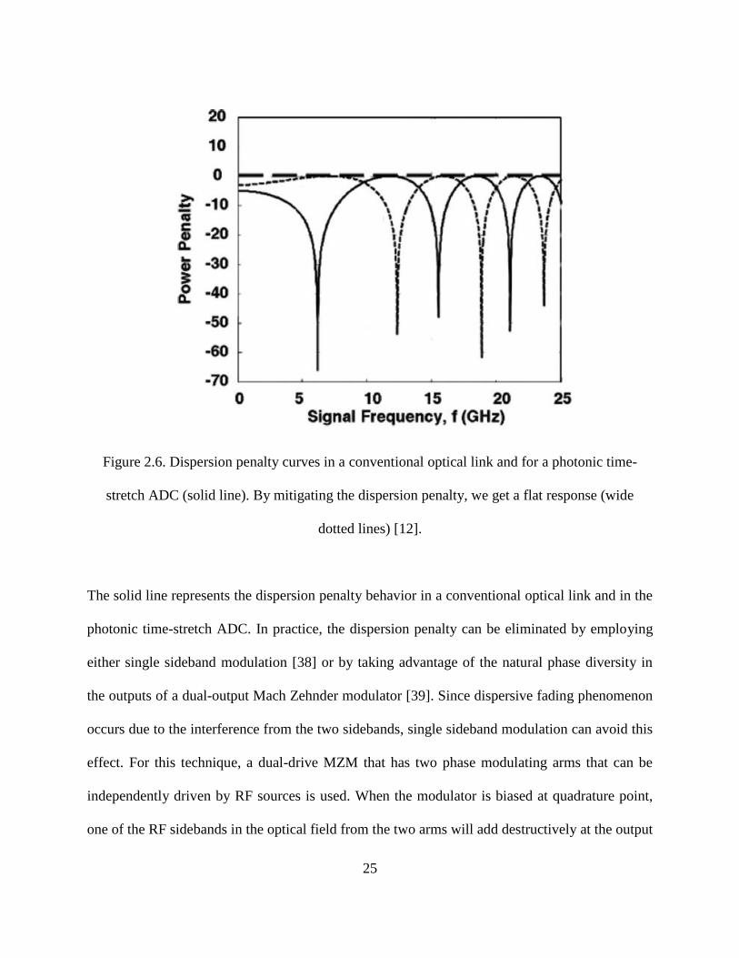
The frequency dependent phase term results in nulls in the frequency response. The
modulator produces upper and lower sidebands of the RF signal in the optical spectrum at
frequencies of optical ± RF. In the absence of dispersion, these sidebands beat with the optical
carrier at the photo-detector to reproduce a copy of the signal. Since dispersion is present, the
upper and lower sidebands slip in phase with each other and interfere at the photo-receiver,
creating nulls at certain frequencies when the two sidebands are 180 degrees out of phase. This
produces a periodic fading characteristic versus frequency shown by Figure 2.6 [12]. For a
double sideband modulated signal with dispersion parameter 2, second dispersive fiber length
L2, and angular frequency RF, the transfer function is given by
. (2.21)
This equation is similar to an optical link if it were dispersed by fiber of length L2/S. The fiber is
not shorter, but the frequency of the signal has been decreased due to the stretching. This causes
the total dispersion induced phase to be reduced. However, dispersion penalty can limit the total
bandwidth of the time-stretched signal and acts as a low pass filter. The 3 dB RF bandwidth in
equal to
which is valid for M >> 1.
25
Figure 2.6. Dispersion penalty curves in a conventional optical link and for a photonic time-
stretch ADC (solid line). By mitigating the dispersion penalty, we get a flat response (wide
dotted lines) [12].
The solid line represents the dispersion penalty behavior in a conventional optical link and in the
photonic time-stretch ADC. In practice, the dispersion penalty can be eliminated by employing
either single sideband modulation [38] or by taking advantage of the natural phase diversity in
the outputs of a dual-output Mach Zehnder modulator [39]. Since dispersive fading phenomenon
occurs due to the interference from the two sidebands, single sideband modulation can avoid this
effect. For this technique, a dual-drive MZM that has two phase modulating arms that can be
independently driven by RF sources is used. When the modulator is biased at quadrature point,
one of the RF sidebands in the optical field from the two arms will add destructively at the output
26
coupler, whereas the other sideband will add constructively. This suppresses one of the
sidebands and eliminates the frequency dependent fading. The bandwidth of the hybrid coupler
sets the limit on the maximum system bandwidth that can be achieved using the system.
The second technique is known as phase diversity. This technique uses maximum ratio
combining of two outputs from a MZM, which have inherently complementary transfer
functions. As seen in Figure 2.6, one output would be the solid line and the other is the dotted
line which shows complementary fading characteristics. When one is at a maximum, the other is
at a null. By combining the maximums, this ensures that both channels will never have a
common frequency null and thus removes the bandwidth limitation to the system. This technique
is used to demonstrate an ultra-wideband TS-ADC with an ideal impulse response.
2.6 Discrete Fourier Transform
In mathematics, the Fourier Series is used to represent complicated periodic signals as a
summation of sines and cosines. The Fourier transform is an extension of the series where the
period of the signal is lengthened and allowed to approach infinity. The Fourier transform and its
inverse is given by the following two equations respectively [40].
(2.22)
(2.23)
Since we have a finite number of samples that we use to compute the Fourier Transform, the
discrete Fourier transform (DFT) is used. The DFT transforms N samples of a discrete-time
signal to the same number of discrete frequency samples and is defined as [41]
27
(2.24)
The DFT is invertible by the inverse discrete Fourier transform given by
(2.25)
The theoretical frequency resolution limit, the smallest resolvable frequency resolution, is given
by
(2.26)
where is the sampling frequency, T is collection time, and N is number of samples [41]. With
a longer collection time, the frequency resolution limit becomes finer. To increase the frequency
resolution, we could either decrease the sampling frequency, , or increase the number of
samples N. Decreasing is usually not practical because that would decrease the range of
frequencies that can be measured. Typically the number of samples N is increased by taking a
longer measurement. Many times, zero-padding is used to extend the number of points or to
make the number of points a power of 2 making it easier for the computer to compute the DFT.
However, despite zero-padding increases the frequency resolution by extending the number of
points for the DFT, it does not add any additional information. It only interpolates the frequency
spectrum [41]. The smallest resolvable frequency resolution is still determined by the inverse of
the collection time. When resolving two frequencies placed close together, these frequencies
need to be spaced apart greater than the minimum frequency resolution. For the time-stretch
system, this collection time is the length of the chirped pulse after the first dispersive element
which we defined as the time aperture.
28
For amplitude measurements, the accuracy of the amplitudes is limited by the resolution
of the frequency bins. The energy of the frequency components when computed by the DFT will
fit into frequency bins. For one frequency the energy might fit into a bin while for another
frequency the energy could be detected by multiple bins and could spread into adjacent bins.
This frequency spreading is known as spectral leakage. Spectral leakage occurs mainly due to
arbitrary sampling of signals. Instead of having pre-determined starting and ending times to
capture an integer number of cycles, arbitrary starting and ending times capture a non-integer
number of cycles with abrupt starting and ending edges. This causes the peak in the frequency-
domain to broaden and spread into adjacent frequency bins. This might give the false error after
performing a DFT for two signals that appear to not be equal in amplitude despite they are due to
the spreading of the energy. This peak magnitude error due to insufficient frequency sampling is
known as scalloping loss [41].
Windowing the signal can help to reduce spectral leakage and also affect the ability to
resolve two signals close together. By windowing [42], a weighting function can be applied
across the captured signal so that the edges are close to zero and the center of the signal where
the cycles are complete and amplitude is maximized is close to "1." Depending on the window
used, the peak could broaden due to the frequency response. For resolving two tones close
together, a rectangular window is best since the peak is sharpest, however it has the most
scalloping. When using other windows, the spreading of the peak energy could cover two tones
close together. In general, the type of window used should be application specific.
29
3 Digital Broadband Linearization of Optical Links
Chapter 3
Digital Broadband Linearization of
Optical Links
This chapter is an expanded version of two published manuscripts [32],[42] where we present a
digital post-processing linearization technique to efficiently suppress dynamic distortions added
to a wideband signal in an analog optical link. This technique achieves up to 35-dB suppression
of intermodulation distortions over multi-octaves of signal bandwidth. In contrast to
conventional linearization methods, it does not require excessive analog bandwidth for
performing digital correction. This is made possible by re-generating undesired distortions from
the captured output, and subtracting it from the distorted digitized signal. Moreover, we
experimentally demonstrate record spurious-free dynamic range of 120 dB.Hz2/3
over 6-GHz
electrical signal bandwidth. While our digital broadband linearization technique advances state-
of-the-art optical links, it can also be applied to other nonlinear dynamic systems.
30
3.1 Introduction
Analog optical links have become extremely useful platforms over the past decades for
transmitting and/or routing analog radio frequency (RF) signals over long distances. Due to
wide-bandwidth and low-loss characteristics of optical fibers, analog optical links [44] have
attracted a broad range of applications, from RF antenna remoting and beam forming for phased-
array radars [45], [46] to cable television (CATV) [45]-[48]. In such applications, the optical link
must meet stringent performance requirements in terms of dynamic range, gain, bandwidth, and
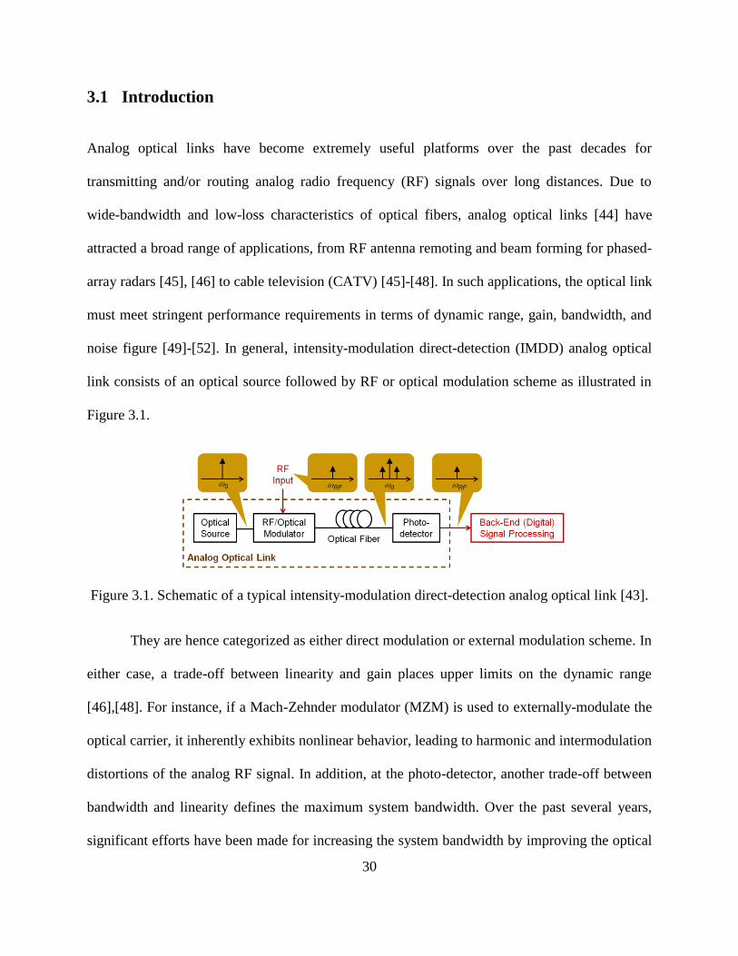
noise figure [49]-[52]. In general, intensity-modulation direct-detection (IMDD) analog optical
link consists of an optical source followed by RF or optical modulation scheme as illustrated in
Figure 3.1.
Figure 3.1. Schematic of a typical intensity-modulation direct-detection analog optical link [43].
They are hence categorized as either direct modulation or external modulation scheme. In
either case, a trade-off between linearity and gain places upper limits on the dynamic range
[46],[48]. For instance, if a Mach-Zehnder modulator (MZM) is used to externally-modulate the
optical carrier, it inherently exhibits nonlinear behavior, leading to harmonic and intermodulation
distortions of the analog RF signal. In addition, at the photo-detector, another trade-off between
bandwidth and linearity defines the maximum system bandwidth. Over the past several years,
significant efforts have been made for increasing the system bandwidth by improving the optical
31
components, while maintaining linearity and dynamic range. A sub-octave analog optical link
has been developed through pioneer work by Betts, et al [52]. This technique that is capable of
achieving a spurious-free dynamic range (SFDR) of 132 dB over 1-Hz bandwidth relies on a
linearized modulator, consisting of two standard Mach-Zehnder modulators in series. Later, a
broadband linearized modulator for frequencies up to 2.5 GHz was demonstrated by Ackerman
[53], achieving a dynamic range of 122 dB.Hz4/5
over 1-Hz bandwidth. Another technique that
achieves a highly linear link was recently demonstrated by Chou, et al [54]. Their approach is
based on coherent detection with feedback and is capable of achieving an SFDR of up to 124.3
dB.Hz2/3
over 160 kHz of bandwidth. Finally, several techniques based on adaptive pre-distortion
and post-distortion linearizers have been previously developed in our early work [55]-[57]. In
case of pre-distortion linearizer [55], [56], adaptive complementary-metal-oxide-semiconductor
(CMOS) circuits are designed to predict the distortions added by the optical link and to generate
distortions that are equal but opposite in phase from the undesired components. Another
approach is to perform post-distortion correction optically [57], which uses a spatial light
modulator (SLM) and a feedback loop to optically generate the out-of-phase distortions, and
hence it suppresses the optical nonlinearities. Unfortunately, while these approaches are effective
for distortion suppression up to 20 dB, their operation bandwidth is limited to the bandwidth of
the linearizer circuits. Another effort made by Karim and Devenport [58] was able to reduce the
noise figure, and hence it was able to achieve an SFDR of 121 dB over 1 Hz, yet it requires 500
mW optical power at the photo-receiver. In work done by Juodawlkis, et al. [59], they were able
to reduce distortions by reversing the MZM transfer function and improving the linearity of the
modulator, yet they were unable to compensate for long fiber lengths and memory effects.

32
Clearly, all aforementioned methods are not able to obtain high dynamic range (>120 dB) and
large (multi-octave) operation bandwidth at a moderate photocurrent simultaneously.
Here we propose and demonstrate an efficient digital post-processing linearization
technique that is performed after photo-detection to suppress the intermodulation distortions by
more than 31 dB over multi-octave bandwidth of analog signal. Our technique essentially
estimates the input signal to the well-known nonlinear system (e.g., analog optical link) from the
observed output. It can be also implemented on digital signal processing (DSP) units and/or field
programmable gate arrays (FPGA) to perform real-time correction of the analog RF signal
transmitted through an analog optical link. Moreover, it is compatible with the state-of-the-art
sub-octave optical link and can be exploited at the back end to further improve their
performance. We also report a record SFDR of more than 120 dB.Hz2/3
across 6-GHz bandwidth
(with only 1 mA of photocurrent) that has been achieved using the proposed digital linearization
technique. A simplified implementation of digital broadband linearization was previously
demonstrated by us [60]. It was shown that this technique is able to suppress the distortions by
more than 15 dB in a photonic time-stretch analog-to-digital converter.
3.2 Digital Broadband Linearization Technique
All analog systems exhibit some nonlinear behavior which limits their dynamic range. The
magnitude of the output does not follow the input which results in distortion of the signal. This
nonlinear behavior can be memory-less or dynamic. Memory-less nonlinearity is frequency-
independent, resulting in a direct mapping between instantaneous magnitudes of the input signal
to their outputs. For dynamic or memory behavior, nonlinearities depend on the input signal over
a period of time instead of a single time instance. In an optical link, the spurious free dynamic
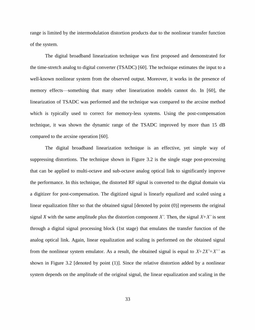
33
range is limited by the intermodulation distortion products due to the nonlinear transfer function
of the system.
The digital broadband linearization technique was first proposed and demonstrated for
the time-stretch analog to digital converter (TSADC) [60]. The technique estimates the input to a
well-known nonlinear system from the observed output. Moreover, it works in the presence of
memory effects—something that many other linearization models cannot do. In [60], the
linearization of TSADC was performed and the technique was compared to the arcsine method
which is typically used to correct for memory-less systems. Using the post-compensation
technique, it was shown the dynamic range of the TSADC improved by more than 15 dB
compared to the arcsine operation [60].
The digital broadband linearization technique is an effective, yet simple way of
suppressing distortions. The technique shown in Figure 3.2 is the single stage post-processing
that can be applied to multi-octave and sub-octave analog optical link to significantly improve
the performance. In this technique, the distorted RF signal is converted to the digital domain via
a digitizer for post-compensation. The digitized signal is linearly equalized and scaled using a
linear equalization filter so that the obtained signal [denoted by point (0)] represents the original
signal X with the same amplitude plus the distortion component X’. Then, the signal X+X’ is sent
through a digital signal processing block (1st stage) that emulates the transfer function of the
analog optical link. Again, linear equalization and scaling is performed on the obtained signal
from the nonlinear system emulator. As a result, the obtained signal is equal to X+2X’+X’’ as
shown in Figure 3.2 [denoted by point (1)]. Since the relative distortion added by a nonlinear
system depends on the amplitude of the original signal, the linear equalization and scaling in the
34
first step is necessary to provide the same signal amplitude (albeit with a small additive
distortion).
Figure 3.2. Digital broadband linearization technique is a single stage post-processing algorithm
used to linear optical links [60].
3.2.1 Optical Link Emulator
For the digital broadband linearization technique to be effective, the transfer function of the
system must be well modeled and understood. A typical optical link is comprised of a continuous
wave (CW) source, a modulator, fiber, and a photodetector (PD). For our model used in the
algorithm, we used an ideal laser with center wavelength of 1550 nm, push-pull Mach-Zehnder
intensity modulator, standard single mode fiber (SMF), and an ideal PD. The carrier signal is
generated by the CW source with electric field . The RF signal is given by and is
intensity modulated using the MZM onto the carrier. The transfer function of the MZM is known
and is given by
(3.1)
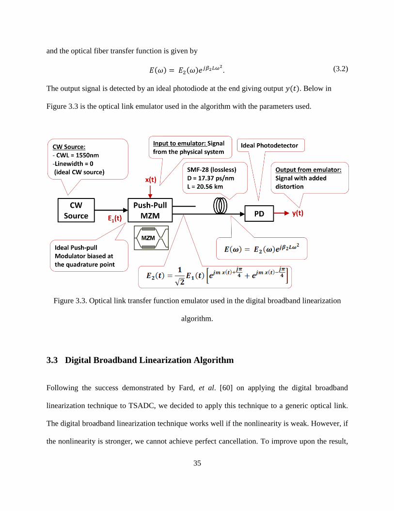
35
and the optical fiber transfer function is given by
. (3.2)
The output signal is detected by an ideal photodiode at the end giving output . Below in
Figure 3.3 is the optical link emulator used in the algorithm with the parameters used.
Figure 3.3. Optical link transfer function emulator used in the digital broadband linearization
algorithm.
3.3 Digital Broadband Linearization Algorithm
Following the success demonstrated by Fard, et al. [60] on applying the digital broadband
linearization technique to TSADC, we decided to apply this technique to a generic optical link.
The digital broadband linearization technique works well if the nonlinearity is weak. However, if
the nonlinearity is stronger, we cannot achieve perfect cancellation. To improve upon the result,
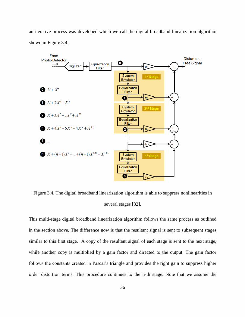
36
an iterative process was developed which we call the digital broadband linearization algorithm
shown in Figure 3.4.
Figure 3.4. The digital broadband linearization algorithm is able to suppress nonlinearities in
several stages [32].
This multi-stage digital broadband linearization algorithm follows the same process as outlined
in the section above. The difference now is that the resultant signal is sent to subsequent stages
similar to this first stage. A copy of the resultant signal of each stage is sent to the next stage,
while another copy is multiplied by a gain factor and directed to the output. The gain factor
follows the constants created in Pascal’s triangle and provides the right gain to suppress higher
order distortion terms. This procedure continues to the n-th stage. Note that we assume the
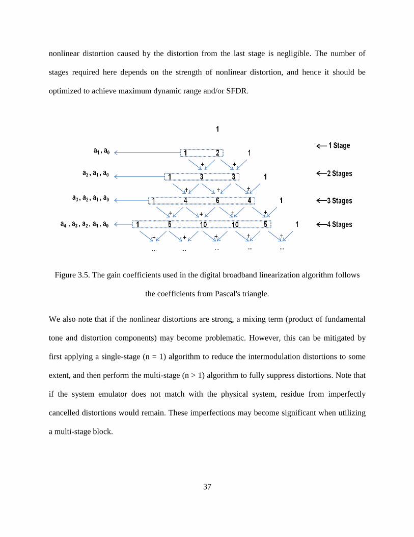
37
nonlinear distortion caused by the distortion from the last stage is negligible. The number of
stages required here depends on the strength of nonlinear distortion, and hence it should be
optimized to achieve maximum dynamic range and/or SFDR.
Figure 3.5. The gain coefficients used in the digital broadband linearization algorithm follows
the coefficients from Pascal's triangle.
We also note that if the nonlinear distortions are strong, a mixing term (product of fundamental
tone and distortion components) may become problematic. However, this can be mitigated by
first applying a single-stage (n = 1) algorithm to reduce the intermodulation distortions to some
extent, and then perform the multi-stage (n > 1) algorithm to fully suppress distortions. Note that
if the system emulator does not match with the physical system, residue from imperfectly
cancelled distortions would remain. These imperfections may become significant when utilizing
a multi-stage block.
38
3.4 Experimental Results To evaluate the performance of our algorithm, we built a link consisting of a continuous-wave
laser, a standard LiNbO3 Mach-Zehnder modulator (MZM), and ~20-km single-mode fiber. The
long SMF-28 emulates a practical application, where the radio frequency signal is captured in a
remote site. This is particularly important because in presence of dispersion, the nonlinear
distortions become dynamic (i.e., with memory effect), which results in significant frequency-
dependent nonlinear distortions. Finally, the modulated optical signal is detected by a PIN
photodiode with a responsivity of 0.85 A/W. The photo-current was found to be 1 mA. Hence,
our system exhibits ~ -22 dB of gain from input to output (without pre- and/or post-
amplification). The resultant signal is digitized using a commercial digitizer with sampling rate
of 50 GSamples/s and analog bandwidth of 16 GHz. The optical power was set so that the
photocurrent is at 1mA. We then performed a two-tone test by coupling two input RF tones, f1
and f2, into the RF input port of the MZM. To minimize the 2nd-order distortion, the modulator
is biased at quadrature. In order to measure the SDFR, we performed the two-tone measurement
with different analog signal power levels for different frequencies up to 6 GHz. By cascading
two single-stage blocks before the 4-stage block, we are able to suppress the third-order
intermodulation distortions to some extent, and to avoid any additional distortions while
propagating through the 4-stage block. Additionally, we checked the dispersion power penalty to
ensure the 3rd-order distortion was not in a null when making the measurements.
Figure 3.7a and Figure 3.7b show output power versus input power for the fundamental
input frequencies at 1 and 1.1 GHz and also at 6 and 6.1 GHz, respectively. As evident from
these two plots, our digital broadband linearization technique achieves an SFDR of 120 dB.Hz2/3
over 6-GHz bandwidth at 1mA of photocurrent. In addition, the fiber length of 20 km used in the
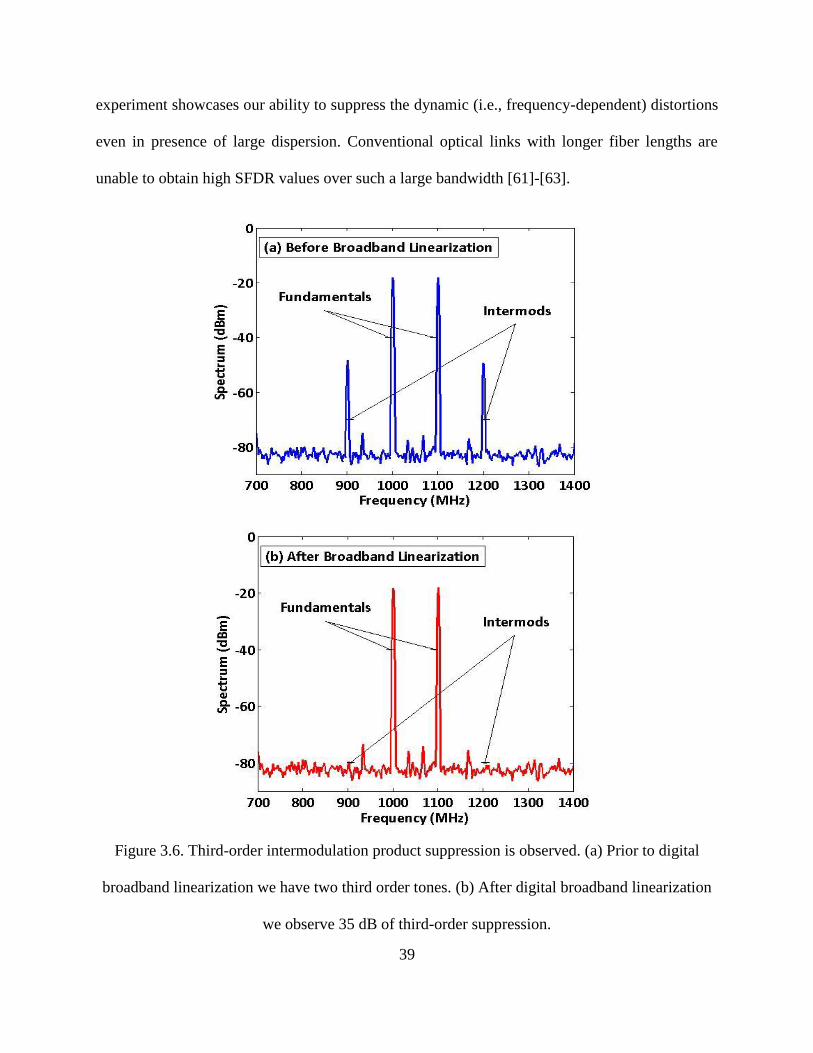
39
experiment showcases our ability to suppress the dynamic (i.e., frequency-dependent) distortions
even in presence of large dispersion. Conventional optical links with longer fiber lengths are
unable to obtain high SFDR values over such a large bandwidth [61]-[63].
Figure 3.6. Third-order intermodulation product suppression is observed. (a) Prior to digital
broadband linearization we have two third order tones. (b) After digital broadband linearization
we observe 35 dB of third-order suppression.
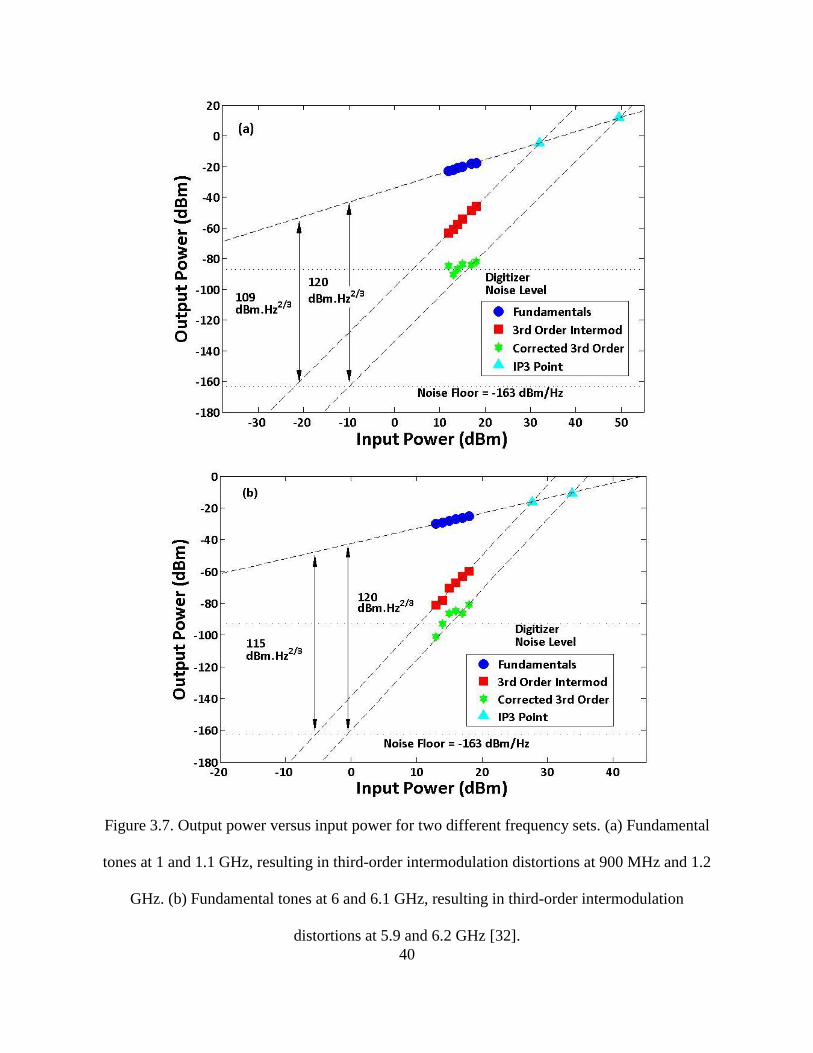
40
Figure 3.7. Output power versus input power for two different frequency sets. (a) Fundamental
tones at 1 and 1.1 GHz, resulting in third-order intermodulation distortions at 900 MHz and 1.2
GHz. (b) Fundamental tones at 6 and 6.1 GHz, resulting in third-order intermodulation
distortions at 5.9 and 6.2 GHz [32].
41
Since our technique is performed in digital domain, it is imperative to evaluate the impact of
digitizer noise (i.e., quantization noise) on the performance of the broadband linearization
technique. In order to do so, we calculated the signal to noise ratio (SNR) at the input before and
after the algorithm. The input signal is already digitized by the system so it includes quantization
noise prior to using the algorithm. We observed that across the 6 GHz bandwidth, we had an
average SNR degradation of 0.5 dB. This is due to the algorithm being designed to mitigate
nonlinear distortions and not uncorrelated white noise. Generally, the amount of noise not taken
into account by the emulator may increase as we propagate through several stages of the
algorithm.
3.5 Benefits and Comparison with Notable Benchmarks
Furthermore, our broadband linearization method is a digital technique, which means no
additional hardware is required. It also works with time-domain representations of the RF signal,
making it hardware friendly for real-time implementations. It hence can be implemented using
field programmable gate arrays (FPGAs), which are capable of handling high data rates and
performing complex algorithms on the data. Moreover, as opposed to conventional digital
correction techniques, our presented technique performs distortion correction by re-generating
the distortion components in digital domain, and subtracts them from the captured signal. Hence,
it only requires digitization of fundamental frequency components, which obviates need for
capturing excessive analog bandwidth at the electronic back-end. In other methods, the other
frequency components over a wide bandwidth need to be captured. In the table below we show a
table which compares some notable benchmarks of optical links with the largest SFDR. As we
can see, we are able to achieve 120 dB.Hz2/3
over 6 GHz of analog bandwidth while also using an
average photocurrent of 1 mA which is typical of standard links.
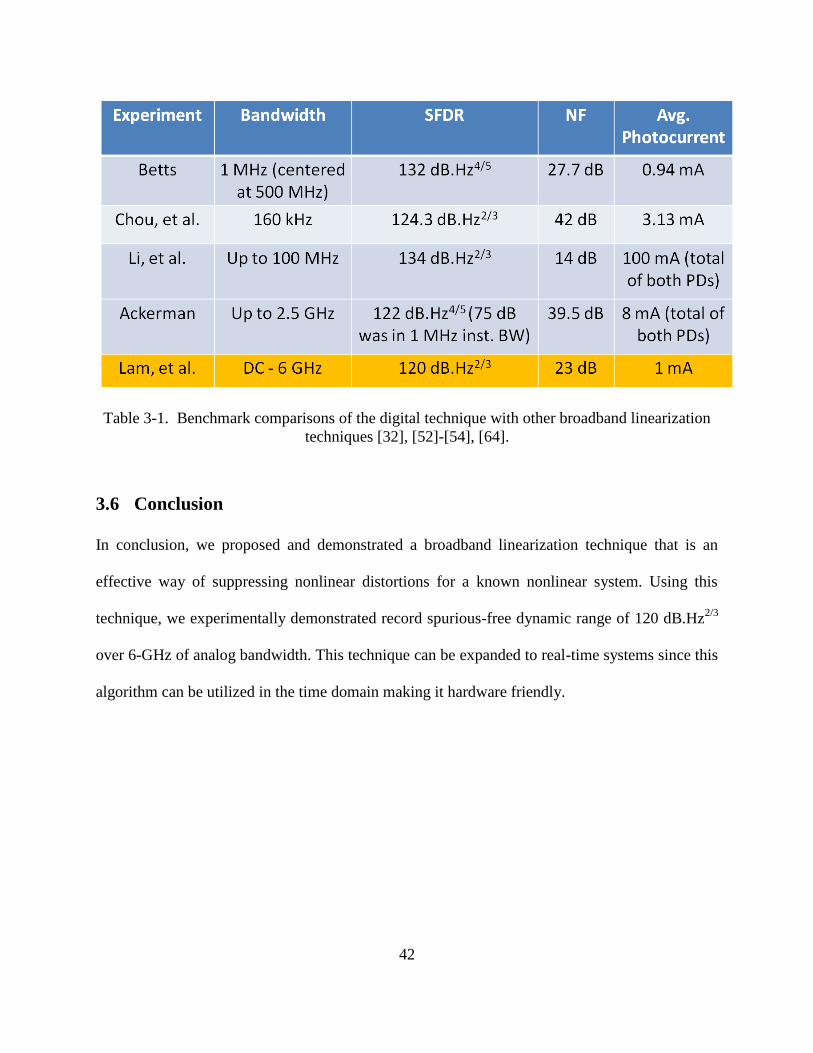
42
Table 3-1. Benchmark comparisons of the digital technique with other broadband linearization
techniques [32], [52]-[54], [64].
3.6 Conclusion
In conclusion, we proposed and demonstrated a broadband linearization technique that is an
effective way of suppressing nonlinear distortions for a known nonlinear system. Using this
technique, we experimentally demonstrated record spurious-free dynamic range of 120 dB.Hz2/3
over 6-GHz of analog bandwidth. This technique can be expanded to real-time systems since this
algorithm can be utilized in the time domain making it hardware friendly.
43
4 Real-Time Simulation of Digital Broadband Linearization Technique
Chapter 4
Real-Time Simulation of Digital Broadband
Linearization Technique
In the previous chapter, a digital post-processing linearization technique was demonstrated to
efficiently suppress dynamic distortions added to a wideband signal in an analog optical link. To
make this algorithm useful in a real-world application, the technique needs to be implemented
onto a field-programmable gate array (FPGA) which allows for fast computation and real-time
correction of these distortions. This chapter will discuss the aspects of implementing a real-time
system and discuss the architecture required to implement the digital broadband linearization
algorithm onto a FPGA. A Matlab simulation of the real-time implementation of this technique
was developed, and the FPGA implementation was done using Verilog, a hardware description
language. The performance of this algorithm was simulated in iSim and compared to a Matlab
simulation of the real-time implementation. The two simulations show similar performance in
suppressing third order intermodulation distortions by about 17 dB.
44
4.1 Introduction to Field Programmable Gate Arrays
The FPGA has been an important and ubiquitous device since its invention in 1985. It has been
slowly incorporated into essentially every facet of technology that requires real-time application
or fast computation. Many applications today take advantage of the power of the FPGA such as
aerospace and defense systems, audio and broadcasting equipment, medical imaging devices,
wireless communications, and video and image processing hardware, and medical to name a few
[65]. The FPGA is a programmable semiconductor device that is based around a matrix of
configurable logic blocks connected through programmable interconnects [65]. These are
different from application specific integrated circuits (ASICs) where the device is custom built
for a particular design, FPGAs can be programmed to a desired application or functionality.
The true power behind this device is in its computation power and its ability to process
large amounts of data in parallel. Its millions of logic gates allow it to implement complex
computations, and it can be reprogrammed if required for another application. FPGAs allow
designers to change their designs very late in the design cycle–even after the end product has
been manufactured and deployed in the field. In addition, Xilinx FPGAs allow for field upgrades
to be completed remotely, eliminating the costs associated with re-designing or manually
updating electronic systems [65]. As FPGAs evolve and are developed, many now have
embedded processors transforming these devices into systems on a chip [66].
As the FPGA continues to increase in popularity, one of the many challenges application
engineers face is programming in Register Transfer Level (RTL) despite many are experienced
in higher level languages [67]. Many companies have attempted to ease this transition by writing
hybrid programs in which a higher level language can be translated into RTL. However, the
hardware description language (HDL) produced usually is inefficient compared to writing it
45
strictly in RTL. Companies such as Xilinx and Mathworks have started addressing this issue by
developing user-friendly methods, such as interactive graphical user interfaces, for designing
logic blocks and linking them together in order to make it easier for beginners to learn FPGA
development and make it more efficient for advanced developers. By utilizing Matlab Simulink
and Xilinx’s System Generator, one can design a circuit in Simulink and export the logic block
using Mathwork’s HDL Coder [68]. This will generate the RTL that can be exported to FPGA.
4.2 Matlab Simulation of Real-time Digital Broadband Linearization
Before implementing onto a FPGA, a model for the single stage broadband linearization
algorithm was designed and implemented in Matlab. As shown in Figure 4.1 in the blue box, a
model of the optical link was generated and the green box highlights the part coded onto the
FPGA. In this model, two sine wave generators set at approximately 1 GHz and 1.1 GHz were
used and combined to form a modulated signal. These two frequencies were chosen to be
consistent with the offline Matlab demonstration of the digital broadband linearization code. The
combined signal was sent through the system emulator to simulate sending the original signal
through the optical link and to add the nonlinearities generated as the signal propagates. The
resultant signal is then sent through a simulation of the FPGA programmed with the digital
broadband linearization algorithm shown in the green box. Inside the FPGA, the signal is sent
through a copy of the system emulator, and then coefficients are multiplied against the digitized
signal and the resultant signal from the emulator. The corrected signal is obtained by summing
the two signals, and its performance can be evaluated by viewing the spectrum.
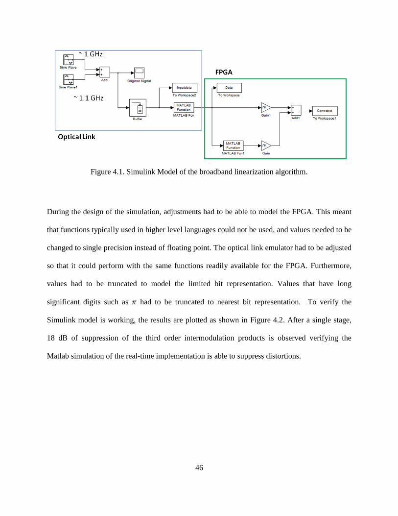
46
Figure 4.1. Simulink Model of the broadband linearization algorithm.
During the design of the simulation, adjustments had to be able to model the FPGA. This meant
that functions typically used in higher level languages could not be used, and values needed to be
changed to single precision instead of floating point. The optical link emulator had to be adjusted
so that it could perform with the same functions readily available for the FPGA. Furthermore,
values had to be truncated to model the limited bit representation. Values that have long
significant digits such as had to be truncated to nearest bit representation. To verify the
Simulink model is working, the results are plotted as shown in Figure 4.2. After a single stage,
18 dB of suppression of the third order intermodulation products is observed verifying the
Matlab simulation of the real-time implementation is able to suppress distortions.
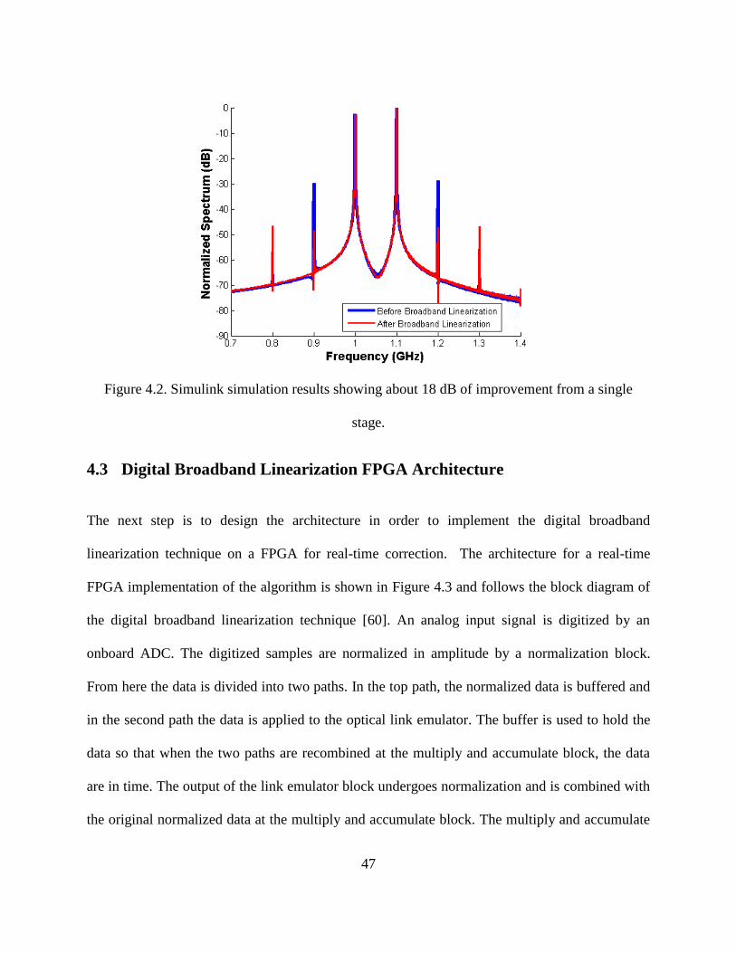
47
Figure 4.2. Simulink simulation results showing about 18 dB of improvement from a single
stage.
4.3 Digital Broadband Linearization FPGA Architecture
The next step is to design the architecture in order to implement the digital broadband
linearization technique on a FPGA for real-time correction. The architecture for a real-time
FPGA implementation of the algorithm is shown in Figure 4.3 and follows the block diagram of
the digital broadband linearization technique [60]. An analog input signal is digitized by an
onboard ADC. The digitized samples are normalized in amplitude by a normalization block.
From here the data is divided into two paths. In the top path, the normalized data is buffered and
in the second path the data is applied to the optical link emulator. The buffer is used to hold the
data so that when the two paths are recombined at the multiply and accumulate block, the data
are in time. The output of the link emulator block undergoes normalization and is combined with
the original normalized data at the multiply and accumulate block. The multiply and accumulate
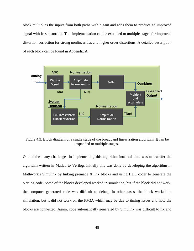
48
block multiplies the inputs from both paths with a gain and adds them to produce an improved
signal with less distortion. This implementation can be extended to multiple stages for improved
distortion correction for strong nonlinearities and higher order distortions. A detailed description
of each block can be found in Appendix A.
Figure 4.3. Block diagram of a single stage of the broadband linearization algorithm. It can be
expanded to multiple stages.
One of the many challenges in implementing this algorithm into real-time was to transfer the
algorithm written in Matlab to Verilog. Initially this was done by developing the algorithm in
Mathwork's Simulink by linking premade Xilinx blocks and using HDL coder to generate the
Verilog code. Some of the blocks developed worked in simulation, but if the block did not work,
the computer generated code was difficult to debug. In other cases, the block worked in
simulation, but it did not work on the FPGA which may be due to timing issues and how the
blocks are connected. Again, code automatically generated by Simulink was difficult to fix and
49
debug. In the end, the entire architecture was written in Verilog for simplicity and making it
easier to debug and more efficient with less extraneous code from the HDL coder.
4.4 Simulation Comparisons of Experimental Data
In order to demonstrate a highly linear optical link using our digital broadband linearization
technique, an externally-modulated direct-detection optical link was built with a FPGA at the
output to digitize the signal. The link uses a continuous-wave laser (Orbits Lightwave Inc.),
which provides 7-mW of low-noise optical power at 1.55 m. The optical signal is directed to a
Lithium-Niobate Mach-Zehnder modulator (EO Space EO modulator), where the optical signal
is intensity modulated by the radio frequency analog signal. To minimize even-ordered
distortions, the electro-optic modulator is biased at the quadrature point. The resultant optical
signal is then transmitted through 20.56-km of standard single-mode fiber (SMF-28). The long
SMF-28 emulates a practical application, where the radio frequency signal is transmitted and
received in a remote site. This is particularly important because in presence of dispersion, the
nonlinear distortions become dynamic (i.e., with memory effect), which results in significant
frequency-dependent nonlinear distortions. Finally, the modulated optical signal is detected by a
PIN photodiode (Optilab, LR-12-AM) with a responsivity of 0.85 A/W. The photo-current was
found to be 1mA. Hence, our system exhibits ~22 dB of gain from input to output (without pre-
and/or post-amplification). The resultant signal is digitized and will undergo signal processing
using a commercial FPGA (SP Devices ADQ108).
In this evaluation, the FPGA digitized the signal and the output collected will serve as the
input to both the Matlab and Verilog simulations to test how well the algorithm works with real
50
data. A two-tone signal with fundamental frequencies at 1 and 1.1 GHz was inputted to the link.
This gives the third order intermodulation distortion products at 0.9 and 1.2 GHz. The output file
from the FPGA was inserted into the Matlab and Verilog simulations to (1) verify that the
Matlab and Verilog codes were similar and (2) demonstrate third-order intermodulation
distortion product suppression. After plotting the spectrum, it is evident that the performance of
the two is very similar. Both spectrums shown in Figure 4.4 look similar, and they both show
about 17 dB of third order intermodulation distortion product suppression.
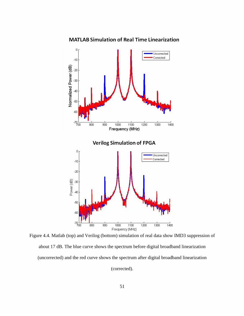
51
Figure 4.4. Matlab (top) and Verilog (bottom) simulation of real data show IMD3 suppression of
about 17 dB. The blue curve shows the spectrum before digital broadband linearization
(uncorrected) and the red curve shows the spectrum after digital broadband linearization
(corrected).
52
4.5 Future Work
The digital broadband linearization technique is shown to work on a FPGA simulator and
matches with the Matlab simulation results. Despite the simulation was written in Verilog and
able to compute the corrected output, actual implementation on FPGA hardware proved very
difficult and hard to debug. There were internal timing issues that are beyond the expertise of the
author and several blocks were unable to function, notably the normalization block. There is
interest in pursuing a joint venture with an outside vendor for implementing the digital
broadband linearization algorithm on a FPGA for real-time demonstration through the Office for
Naval Contracts small business innovation research program. Additionally the multi-stage
version of this algorithm can be implemented. By being able to use the algorithm in real-time,
this makes the technique much more useful for real-time correction to improve the dynamic
range of the optical link.
53
5 Ultra-wideband Instantaneous Frequency Estimation
Chapter 5
Ultra-wideband Instantaneous Frequency
Estimation
Determining the instantaneous frequency of a signal is required for many applications ranging
from radio astronomy to military equipment. Unfortunately, the scan rate over a wideband
spectrum is often too long compared to the time scale of the frequencies of interest. A time-
stretched instantaneous frequency measurement receiver is presented which is capable of
simultaneous measurement of multiple frequencies and amplitudes across an ultra-wide
instantaneous bandwidth. The high effective sampling throughput of the system provides high
temporal resolution of the signal, and frequency and amplitude estimation capability is improved
through signal processing. This system has the flexibility to be modified to adjust its
instantaneous bandwidth and frequency resolution. It also has an ultra-fast sweep time and
reduced hardware complexity compared to other instantaneous frequency measurement systems.
54
5.1 Introduction to Instantaneous Frequency Measurements
Instantaneous frequency measurement (IFM) receiver has been an increasingly important tool for
measuring radio-frequency (RF) signals over a wide bandwidth. It is used to measure RF
frequency, amplitude, pulse width, and time of arrival for a plethora of applications such as radar
threat detection, electronic warfare, and signal intelligence [69]-[70]. A wideband IFM receiver
offers the high probability of intercept over wide instantaneous RF bandwidths, high dynamic
ranges, good sensitivity and high frequency measurement accuracy. Currently IFM receivers are
limited in performance mainly by their ability to only measure single frequencies at a time, and
have limited bandwidths with very slow sweep times across enormous bandwidths. Additional
channels would be required to expand the bandwidth which would increase hardware
complexity. The time-stretch instantaneous frequency measurement receiver (TS-IFM) is able to
overcome these challenges and provide a solution capable of ultra-fast sweeping across
enormous bandwidths to perform measurements on transient signals. Today’s spectrally cluttered
environments demand a system that can perform measurements across wider bandwidths and
also detect frequencies of interest quickly and efficiently.
Traditional IFMs use microwave interferometers and make use of hybrid couplers, power
dividers, and delay lines to perform measurements [71]. The basic measurement technology
consists of a microwave correlator to measure an unknown signal [70]. A traditional IFM, shown
in Figure 5.1, will split the incoming signal into two paths and delay one path by a time with
respect to the other along with a 90 degree phase shift. Subsequently the ratio of the two paths is
taken and then an arc-tangent operation is performed to determine the input frequency of the
received signal.
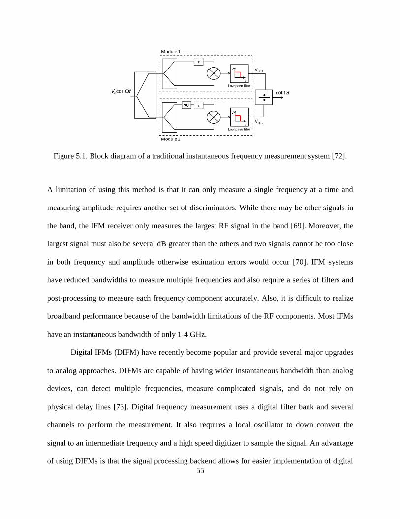
55
Figure 5.1. Block diagram of a traditional instantaneous frequency measurement system [72].
A limitation of using this method is that it can only measure a single frequency at a time and
measuring amplitude requires another set of discriminators. While there may be other signals in
the band, the IFM receiver only measures the largest RF signal in the band [69]. Moreover, the
largest signal must also be several dB greater than the others and two signals cannot be too close
in both frequency and amplitude otherwise estimation errors would occur [70]. IFM systems
have reduced bandwidths to measure multiple frequencies and also require a series of filters and
post-processing to measure each frequency component accurately. Also, it is difficult to realize
broadband performance because of the bandwidth limitations of the RF components. Most IFMs
have an instantaneous bandwidth of only 1-4 GHz.
Digital IFMs (DIFM) have recently become popular and provide several major upgrades
to analog approaches. DIFMs are capable of having wider instantaneous bandwidth than analog
devices, can detect multiple frequencies, measure complicated signals, and do not rely on
physical delay lines [73]. Digital frequency measurement uses a digital filter bank and several
channels to perform the measurement. It also requires a local oscillator to down convert the
signal to an intermediate frequency and a high speed digitizer to sample the signal. An advantage
of using DIFMs is that the signal processing backend allows for easier implementation of digital
56
delays and typically several delays have to be implemented for performing more accurate
measurements. DIFMs require several successive stages where each stage determines a
frequency using a correlator [74]. Errors can occur when the frequency is close to the time delay
hence to avoid this problem, different time delays are utilized [75]. The necessity of this method
requiring multiple stages to accurately measure a frequency makes it computationally intensive.
DIFM performance is also limited by the sampling rate and resolution of the analog to digital
converter (ADC), jitter in the electronics, and quantization errors.
Recently, there has been work on employing photonic devices to perform IFM exploiting
the inherent wide bandwidth. Many photonic systems using correlation methods to measure a
single frequency have been demonstrated [76]. Various research groups have achieved multiple
frequency measurements by mixing nonlinear terms [77], utilizing multiple optical delay
channels [78], and using frequency to time mapping [79]. While these techniques can perform
frequency measurements, they are incapable of measuring both frequency and amplitude without
requiring additional hardware. Furthermore, their frequency resolutions are not narrow enough
and are typically on the order of several gigahertz.
5.2 Time-Stretch Instantaneous Frequency Measurement Receiver
We propose the time-stretch IFM receiver that is capable of rapidly measuring multiple signals
simultaneously (within hardware and software constraints) over an ultra-wide bandwidth. Time-
stretching compresses the signal bandwidth which allows for rapid spectral sweeps across an
enormous bandwidth to be digitized using slower analog to digital converters. The TS-IFM
captures a segment of real-time data on which we can apply Fast Fourier Transform (FFT) to
analyze in the spectral domain. This allows us to perform multiple frequency and amplitude
57
measurements over an ultra-wide bandwidth. The frequency resolution for the system is limited
by the short capture window and the number of points used for the FFT. However, the capture
time window can be adjusted which allows for frequency resolution tuning. The accuracy of
frequency estimates is further improved by windowing the sampled signal data and performing
quadratic interpolation on the signal peaks in the frequency domain [19]. In this section, we
demonstrate TS-IFM frequency detection capabilities by performing frequency measurements
across a wide bandwidth and simultaneous multiple frequency measurements without requiring
additional hardware or cascading filter designs. The time-stretch IFM is the union of time-stretch
enhanced recorder (TiSER) and digital signal processing that performs windowing on time
domain sampled data and frequency interpolation on the signal peaks. The combination of the
two allows for a high resolution, wideband, low power instantaneous frequency measurement
receiver.
The front-end of the time-stretch IFM is TiSER, shown in Figure 5.2, which uses time-
stretch to capture ultrafast signals [11],[12]. Using this system we are able to take an ultrafast RF
input signal and stretch it in time which then allows a slower ADC to digitize the signal with
high fidelity in real-time. In the system, a short optical super-continuum (i.e. broadband) pulse is
chirped by propagating through dispersive fiber which performs a frequency to time mapping as
indicated by the rainbow pulses in Figure 5.2. The RF input signal is intensity modulated onto
the chirped optical pulse using an electro-optic modulator. This modulated pulse is sent through
a second dispersive fiber which linearly stretches out the signal in time, compressing its analog
bandwidth. The amount of stretching is defined as M = 1+D2/D1 where M is the stretch factor
and D1 and D2 are the dispersions of the two dispersive fibers. The stretch factor is the factor by
which we compress the signal bandwidth. At the backend of TiSER is an ADC which digitizes
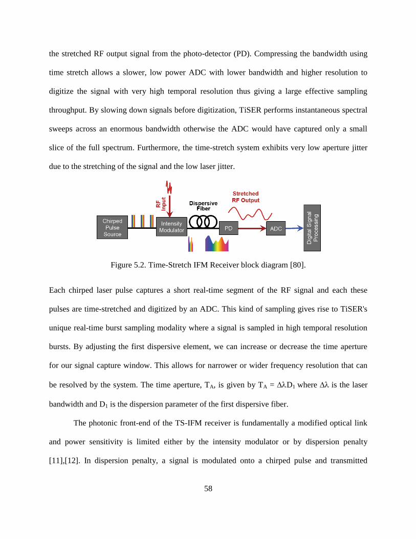
58
the stretched RF output signal from the photo-detector (PD). Compressing the bandwidth using
time stretch allows a slower, low power ADC with lower bandwidth and higher resolution to
digitize the signal with very high temporal resolution thus giving a large effective sampling
throughput. By slowing down signals before digitization, TiSER performs instantaneous spectral
sweeps across an enormous bandwidth otherwise the ADC would have captured only a small
slice of the full spectrum. Furthermore, the time-stretch system exhibits very low aperture jitter
due to the stretching of the signal and the low laser jitter.
Figure 5.2. Time-Stretch IFM Receiver block diagram [80].
Each chirped laser pulse captures a short real-time segment of the RF signal and each these
pulses are time-stretched and digitized by an ADC. This kind of sampling gives rise to TiSER's
unique real-time burst sampling modality where a signal is sampled in high temporal resolution
bursts. By adjusting the first dispersive element, we can increase or decrease the time aperture
for our signal capture window. This allows for narrower or wider frequency resolution that can
be resolved by the system. The time aperture, TA, is given by TA = D1 where is the laser
bandwidth and D1 is the dispersion parameter of the first dispersive fiber.
The photonic front-end of the TS-IFM receiver is fundamentally a modified optical link
and power sensitivity is limited either by the intensity modulator or by dispersion penalty
[11],[12]. In dispersion penalty, a signal is modulated onto a chirped pulse and transmitted
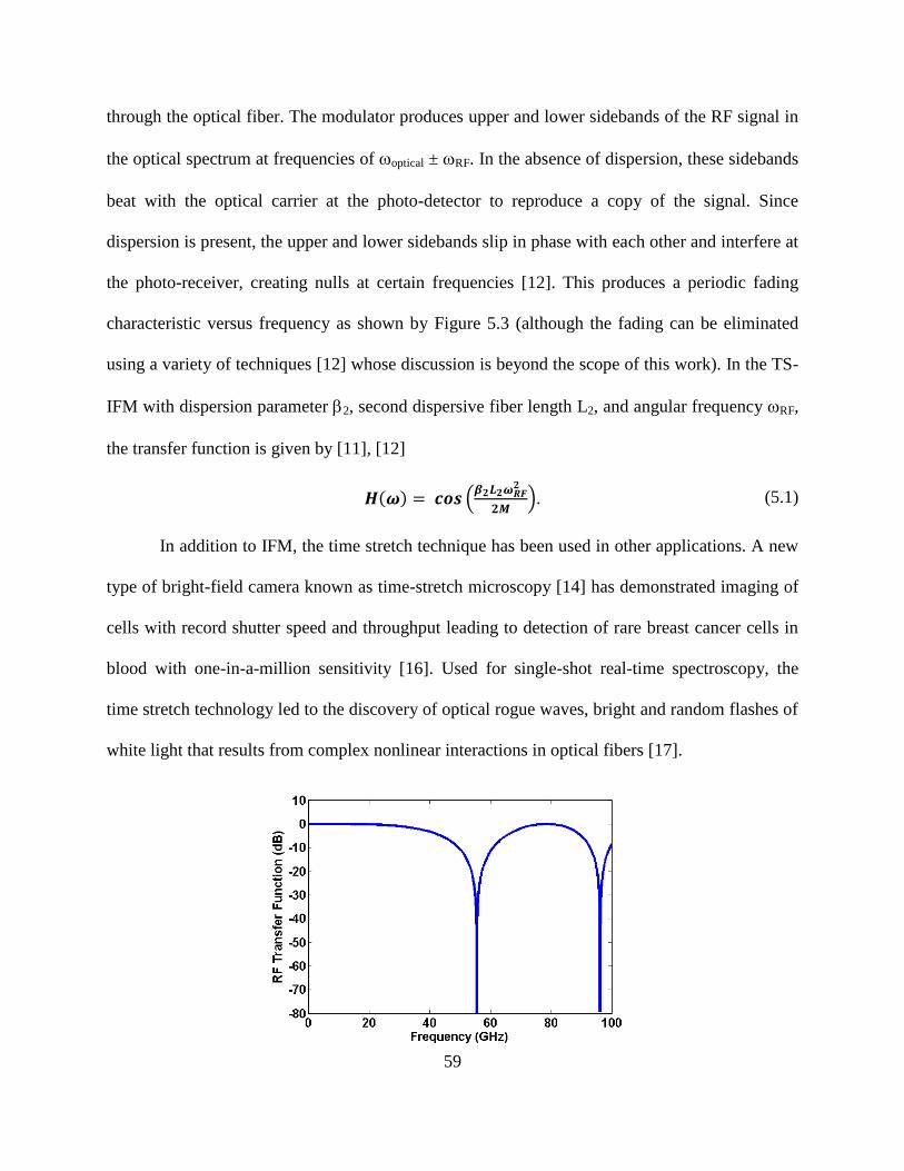
59
through the optical fiber. The modulator produces upper and lower sidebands of the RF signal in
the optical spectrum at frequencies of optical ± RF. In the absence of dispersion, these sidebands
beat with the optical carrier at the photo-detector to reproduce a copy of the signal. Since
dispersion is present, the upper and lower sidebands slip in phase with each other and interfere at
the photo-receiver, creating nulls at certain frequencies [12]. This produces a periodic fading
characteristic versus frequency as shown by Figure 5.3 (although the fading can be eliminated
using a variety of techniques [12] whose discussion is beyond the scope of this work). In the TS-
IFM with dispersion parameter 2, second dispersive fiber length L2, and angular frequency RF,
the transfer function is given by [11], [12]
. (5.1)
In addition to IFM, the time stretch technique has been used in other applications. A new
type of bright-field camera known as time-stretch microscopy [14] has demonstrated imaging of
cells with record shutter speed and throughput leading to detection of rare breast cancer cells in
blood with one-in-a-million sensitivity [16]. Used for single-shot real-time spectroscopy, the
time stretch technology led to the discovery of optical rogue waves, bright and random flashes of
white light that results from complex nonlinear interactions in optical fibers [17].
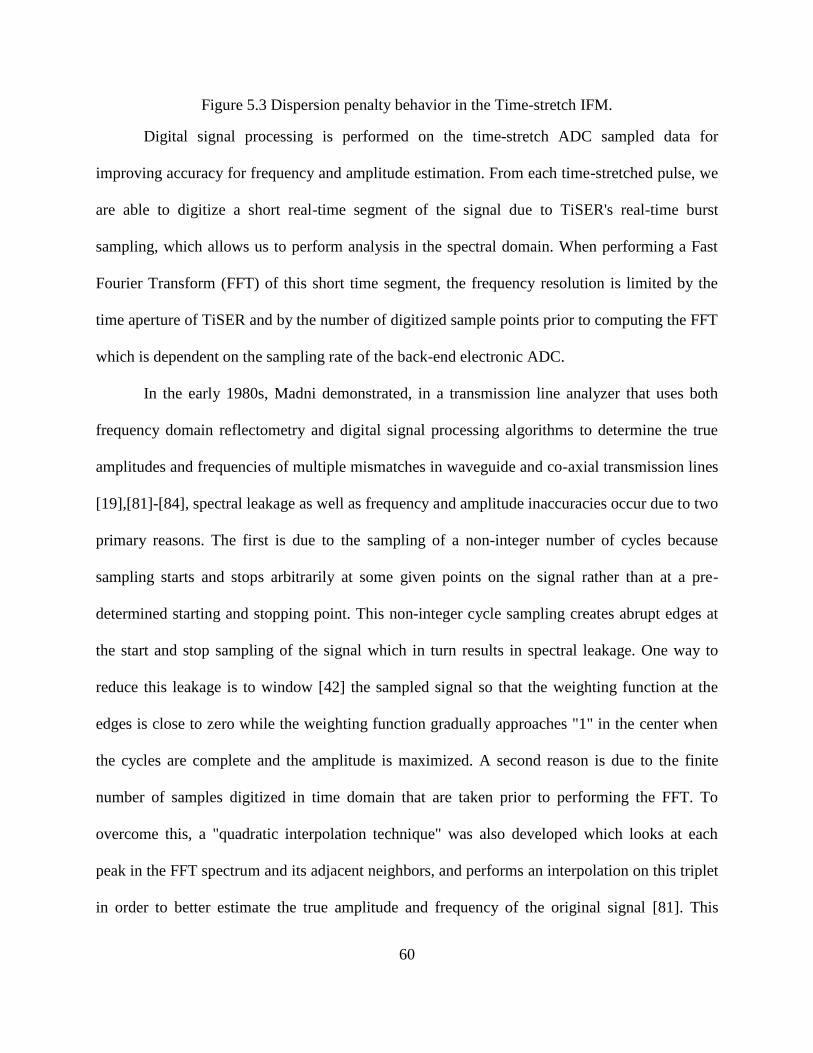
60
Figure 5.3 Dispersion penalty behavior in the Time-stretch IFM.
Digital signal processing is performed on the time-stretch ADC sampled data for
improving accuracy for frequency and amplitude estimation. From each time-stretched pulse, we
are able to digitize a short real-time segment of the signal due to TiSER's real-time burst
sampling, which allows us to perform analysis in the spectral domain. When performing a Fast
Fourier Transform (FFT) of this short time segment, the frequency resolution is limited by the
time aperture of TiSER and by the number of digitized sample points prior to computing the FFT
which is dependent on the sampling rate of the back-end electronic ADC.
In the early 1980s, Madni demonstrated, in a transmission line analyzer that uses both
frequency domain reflectometry and digital signal processing algorithms to determine the true
amplitudes and frequencies of multiple mismatches in waveguide and co-axial transmission lines
[19],[81]-[84], spectral leakage as well as frequency and amplitude inaccuracies occur due to two
primary reasons. The first is due to the sampling of a non-integer number of cycles because
sampling starts and stops arbitrarily at some given points on the signal rather than at a pre-
determined starting and stopping point. This non-integer cycle sampling creates abrupt edges at
the start and stop sampling of the signal which in turn results in spectral leakage. One way to
reduce this leakage is to window [42] the sampled signal so that the weighting function at the
edges is close to zero while the weighting function gradually approaches "1" in the center when
the cycles are complete and the amplitude is maximized. A second reason is due to the finite
number of samples digitized in time domain that are taken prior to performing the FFT. To
overcome this, a "quadratic interpolation technique" was also developed which looks at each
peak in the FFT spectrum and its adjacent neighbors, and performs an interpolation on this triplet
in order to better estimate the true amplitude and frequency of the original signal [81]. This
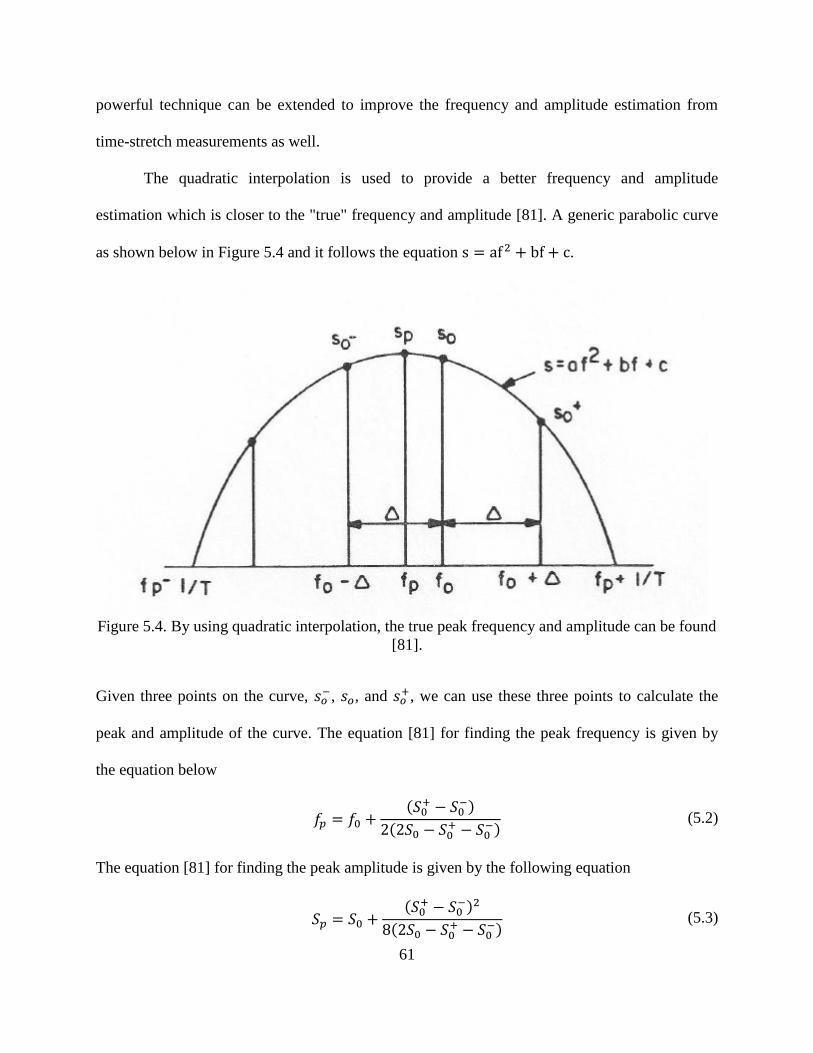
61
powerful technique can be extended to improve the frequency and amplitude estimation from
time-stretch measurements as well.
The quadratic interpolation is used to provide a better frequency and amplitude
estimation which is closer to the "true" frequency and amplitude [81]. A generic parabolic curve
as shown below in Figure 5.4 and it follows the equation .
Figure 5.4. By using quadratic interpolation, the true peak frequency and amplitude can be found
[81].
Given three points on the curve, , , and
, we can use these three points to calculate the
peak and amplitude of the curve. The equation [81] for finding the peak frequency is given by
the equation below
(5.2)
The equation [81] for finding the peak amplitude is given by the following equation
(5.3)
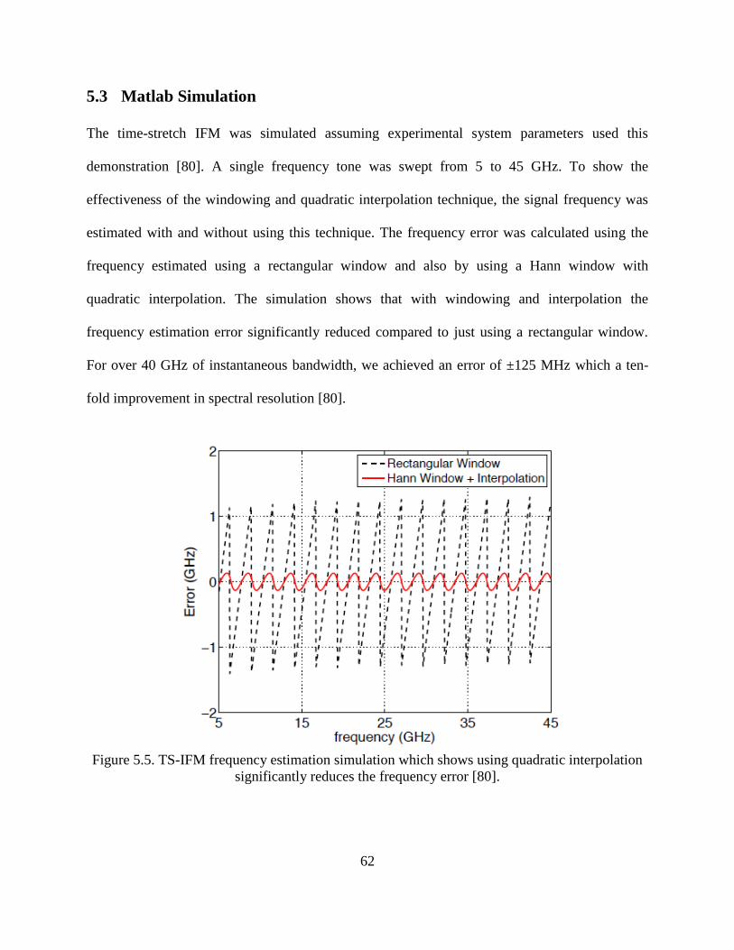
62
5.3 Matlab Simulation
The time-stretch IFM was simulated assuming experimental system parameters used this
demonstration [80]. A single frequency tone was swept from 5 to 45 GHz. To show the
effectiveness of the windowing and quadratic interpolation technique, the signal frequency was
estimated with and without using this technique. The frequency error was calculated using the
frequency estimated using a rectangular window and also by using a Hann window with
quadratic interpolation. The simulation shows that with windowing and interpolation the
frequency estimation error significantly reduced compared to just using a rectangular window.
For over 40 GHz of instantaneous bandwidth, we achieved an error of ±125 MHz which a ten-
fold improvement in spectral resolution [80].
Figure 5.5. TS-IFM frequency estimation simulation which shows using quadratic interpolation
significantly reduces the frequency error [80].
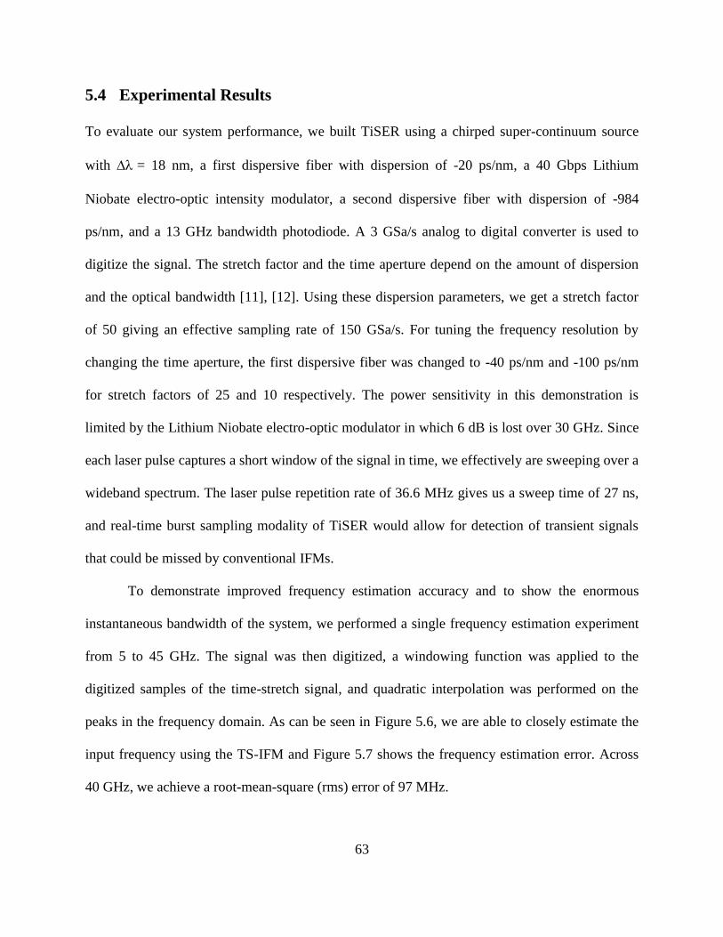
63
5.4 Experimental Results
To evaluate our system performance, we built TiSER using a chirped super-continuum source
with = 18 nm, a first dispersive fiber with dispersion of -20 ps/nm, a 40 Gbps Lithium
Niobate electro-optic intensity modulator, a second dispersive fiber with dispersion of -984
ps/nm, and a 13 GHz bandwidth photodiode. A 3 GSa/s analog to digital converter is used to
digitize the signal. The stretch factor and the time aperture depend on the amount of dispersion
and the optical bandwidth [11], [12]. Using these dispersion parameters, we get a stretch factor
of 50 giving an effective sampling rate of 150 GSa/s. For tuning the frequency resolution by
changing the time aperture, the first dispersive fiber was changed to -40 ps/nm and -100 ps/nm
for stretch factors of 25 and 10 respectively. The power sensitivity in this demonstration is
limited by the Lithium Niobate electro-optic modulator in which 6 dB is lost over 30 GHz. Since
each laser pulse captures a short window of the signal in time, we effectively are sweeping over a
wideband spectrum. The laser pulse repetition rate of 36.6 MHz gives us a sweep time of 27 ns,
and real-time burst sampling modality of TiSER would allow for detection of transient signals
that could be missed by conventional IFMs.
To demonstrate improved frequency estimation accuracy and to show the enormous
instantaneous bandwidth of the system, we performed a single frequency estimation experiment
from 5 to 45 GHz. The signal was then digitized, a windowing function was applied to the
digitized samples of the time-stretch signal, and quadratic interpolation was performed on the
peaks in the frequency domain. As can be seen in Figure 5.6, we are able to closely estimate the
input frequency using the TS-IFM and Figure 5.7 shows the frequency estimation error. Across
40 GHz, we achieve a root-mean-square (rms) error of 97 MHz.
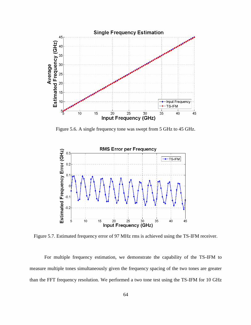
64
Figure 5.6. A single frequency tone was swept from 5 GHz to 45 GHz.
Figure 5.7. Estimated frequency error of 97 MHz rms is achieved using the TS-IFM receiver.
For multiple frequency estimation, we demonstrate the capability of the TS-IFM to
measure multiple tones simultaneously given the frequency spacing of the two tones are greater
than the FFT frequency resolution. We performed a two tone test using the TS-IFM for 10 GHz
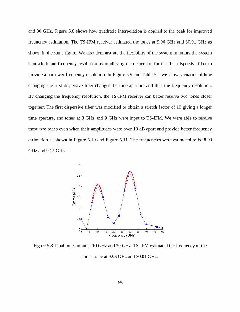
65
and 30 GHz. Figure 5.8 shows how quadratic interpolation is applied to the peak for improved
frequency estimation. The TS-IFM receiver estimated the tones at 9.96 GHz and 30.01 GHz as
shown in the same figure. We also demonstrate the flexibility of the system in tuning the system
bandwidth and frequency resolution by modifying the dispersion for the first dispersive fiber to
provide a narrower frequency resolution. In Figure 5.9 and Table 5-1 we show scenarios of how
changing the first dispersive fiber changes the time aperture and thus the frequency resolution.
By changing the frequency resolution, the TS-IFM receiver can better resolve two tones closer
together. The first dispersive fiber was modified to obtain a stretch factor of 10 giving a longer
time aperture, and tones at 8 GHz and 9 GHz were input to TS-IFM. We were able to resolve
these two tones even when their amplitudes were over 10 dB apart and provide better frequency
estimation as shown in Figure 5.10 and Figure 5.11. The frequencies were estimated to be 8.09
GHz and 9.15 GHz.
Figure 5.8. Dual tones input at 10 GHz and 30 GHz. TS-IFM estimated the frequency of the
tones to be at 9.96 GHz and 30.01 GHz.
66
(a)
(b)
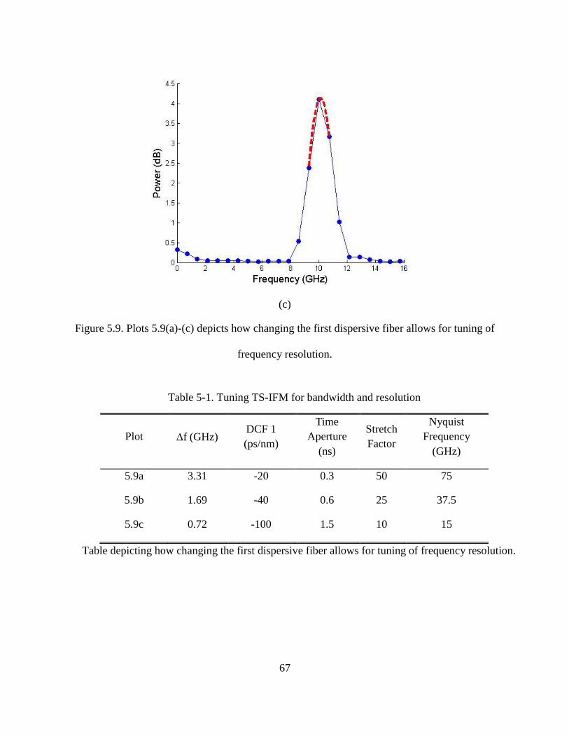
67
(c)
Figure 5.9. Plots 5.9(a)-(c) depicts how changing the first dispersive fiber allows for tuning of
frequency resolution.
Table 5-1. Tuning TS-IFM for bandwidth and resolution
Plot f (GHz) DCF 1
(ps/nm)
Time
Aperture
(ns)
Stretch
Factor
Nyquist
Frequency
(GHz)
5.9a 3.31 -20 0.3 50 75
5.9b 1.69 -40 0.6 25 37.5
5.9c 0.72 -100 1.5 10 15
Table depicting how changing the first dispersive fiber allows for tuning of frequency resolution.
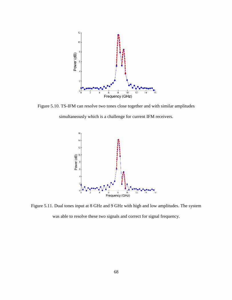
68
Figure 5.10. TS-IFM can resolve two tones close together and with similar amplitudes
simultaneously which is a challenge for current IFM receivers.
Figure 5.11. Dual tones input at 8 GHz and 9 GHz with high and low amplitudes. The system
was able to resolve these two signals and correct for signal frequency.
69
5.5 Benefits and Advantages of Time-Stretch Instantaneous Frequency
Measurement Receiver
Time-stretch IFM receiver has several key advantages compared to commercial systems [86]-
[88]. TS-IFM has the ability to perform frequency measurements across an ultra-wide
instantaneous bandwidth with increased accuracy through windowing and quadratic
interpolation. The fast sweep time allows for rapid spectral measurements across enormous
bandwidths. Additionally, multiple frequencies can be estimated simultaneously without any
additional filtering or cascading stages whereas current commercial systems do not have this
capability. This makes the TS-IFM receiver very effective in spectrally cluttered environments
and for quickly detecting transient signals. Moreover, the effective sampling throughput of TS-
IFM receiver is significantly higher allowing it to capture signals with high temporal resolution
due to its real-time burst sampling and uses less power than high speed ADCs with similar
throughput thus reducing the electronic hardware complexity and cost. The TS-IFM can be
implemented in real-time using field programmable gate arrays and could be used as a wideband
cueing receiver for finer resolution systems. Further work can be done by calibrating the system
for amplitude measurements and by implementing continuous time-stretch architecture to take
longer collection times for better frequency resolution.
70
6 Signal Integrity Measurements using TiSER
Chapter 6
Signal Integrity Measurements using TiSER
As electronic circuits and data speeds in communications continue to increase, the demand for
high bandwidth digitizers have become paramount. It becomes more difficult to measure the
integrity of the signal. By using time-stretch to slow down the signals, we are able to measure
these high speed signals with higher fidelity. In this chapter, our approach to perform signal
integrity measurements using time-stretch is presented. A discussion on the advantages of
TiSER's unique real-time burst sampling modality and low system jitter will be given.
Afterwards, we present how the signal integrity parameters are measured using TiSER and how
these results match with commercial instruments. By matching with calibrated equipment results,
we demonstrate TiSER can be used as a high speed measurement device.
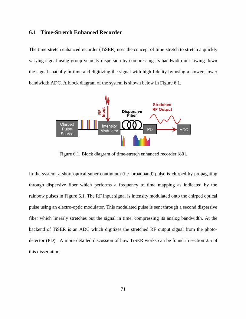
71
6.1 Time-Stretch Enhanced Recorder
The time-stretch enhanced recorder (TiSER) uses the concept of time-stretch to stretch a quickly
varying signal using group velocity dispersion by compressing its bandwidth or slowing down
the signal spatially in time and digitizing the signal with high fidelity by using a slower, lower
bandwidth ADC. A block diagram of the system is shown below in Figure 6.1.
Figure 6.1. Block diagram of time-stretch enhanced recorder [80].
In the system, a short optical super-continuum (i.e. broadband) pulse is chirped by propagating
through dispersive fiber which performs a frequency to time mapping as indicated by the
rainbow pulses in Figure 6.1. The RF input signal is intensity modulated onto the chirped optical
pulse using an electro-optic modulator. This modulated pulse is sent through a second dispersive
fiber which linearly stretches out the signal in time, compressing its analog bandwidth. At the
backend of TiSER is an ADC which digitizes the stretched RF output signal from the photo-
detector (PD). A more detailed discussion of how TiSER works can be found in section 2.5 of
this dissertation.
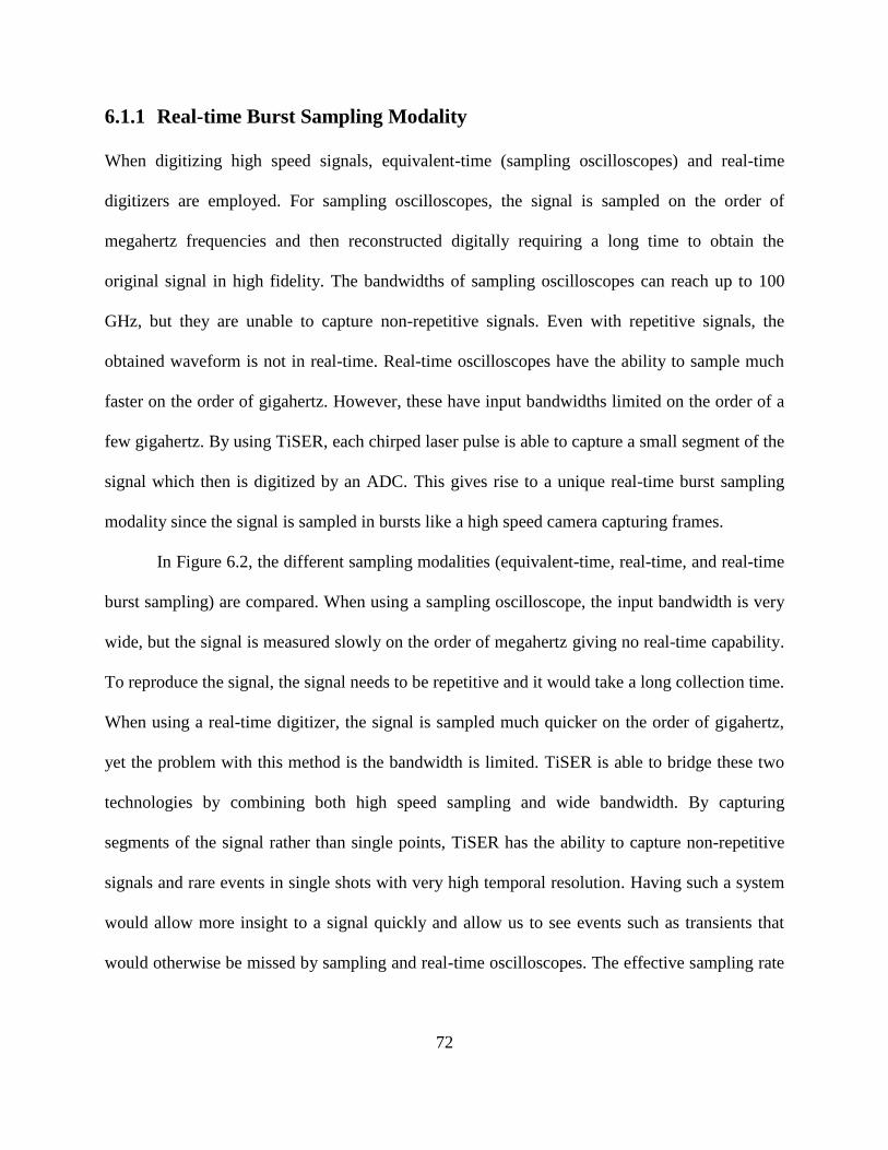
72
6.1.1 Real-time Burst Sampling Modality
When digitizing high speed signals, equivalent-time (sampling oscilloscopes) and real-time
digitizers are employed. For sampling oscilloscopes, the signal is sampled on the order of
megahertz frequencies and then reconstructed digitally requiring a long time to obtain the
original signal in high fidelity. The bandwidths of sampling oscilloscopes can reach up to 100
GHz, but they are unable to capture non-repetitive signals. Even with repetitive signals, the
obtained waveform is not in real-time. Real-time oscilloscopes have the ability to sample much
faster on the order of gigahertz. However, these have input bandwidths limited on the order of a
few gigahertz. By using TiSER, each chirped laser pulse is able to capture a small segment of the
signal which then is digitized by an ADC. This gives rise to a unique real-time burst sampling
modality since the signal is sampled in bursts like a high speed camera capturing frames.
In Figure 6.2, the different sampling modalities (equivalent-time, real-time, and real-time
burst sampling) are compared. When using a sampling oscilloscope, the input bandwidth is very
wide, but the signal is measured slowly on the order of megahertz giving no real-time capability.
To reproduce the signal, the signal needs to be repetitive and it would take a long collection time.
When using a real-time digitizer, the signal is sampled much quicker on the order of gigahertz,
yet the problem with this method is the bandwidth is limited. TiSER is able to bridge these two
technologies by combining both high speed sampling and wide bandwidth. By capturing
segments of the signal rather than single points, TiSER has the ability to capture non-repetitive
signals and rare events in single shots with very high temporal resolution. Having such a system
would allow more insight to a signal quickly and allow us to see events such as transients that
would otherwise be missed by sampling and real-time oscilloscopes. The effective sampling rate
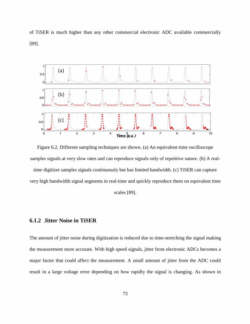
73
of TiSER is much higher than any other commercial electronic ADC available commercially
[89].
Figure 6.2. Different sampling techniques are shown. (a) An equivalent-time oscilloscope
samples signals at very slow rates and can reproduce signals only of repetitive nature. (b) A real-
time digitizer samples signals continuously but has limited bandwidth. (c) TiSER can capture
very high bandwidth signal segments in real-time and quickly reproduce them on equivalent time
scales [89].
6.1.2 Jitter Noise in TiSER
The amount of jitter noise during digitization is reduced due to time-stretching the signal making
the measurement more accurate. With high speed signals, jitter from electronic ADCs becomes a
major factor that could affect the measurement. A small amount of jitter from the ADC could
result in a large voltage error depending on how rapidly the signal is changing. As shown in
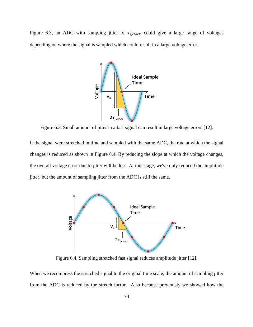
74
Figure 6.3, an ADC with sampling jitter of could give a large range of voltages
depending on where the signal is sampled which could result in a large voltage error.
Figure 6.3. Small amount of jitter in a fast signal can result in large voltage errors [12].
If the signal were stretched in time and sampled with the same ADC, the rate at which the signal
changes is reduced as shown in Figure 6.4. By reducing the slope at which the voltage changes,
the overall voltage error due to jitter will be less. At this stage, we've only reduced the amplitude
jitter, but the amount of sampling jitter from the ADC is still the same.
Figure 6.4. Sampling stretched fast signal reduces amplitude jitter [12].
When we recompress the stretched signal to the original time scale, the amount of sampling jitter
from the ADC is reduced by the stretch factor. Also because previously we showed how the
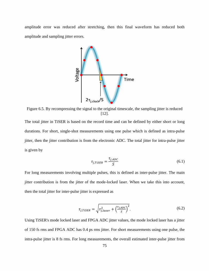
75
amplitude error was reduced after stretching, then this final waveform has reduced both
amplitude and sampling jitter errors.
Figure 6.5. By recompressing the signal to the original timescale, the sampling jitter is reduced
[12].
The total jitter in TiSER is based on the record time and can be defined by either short or long
durations. For short, single-shot measurements using one pulse which is defined as intra-pulse
jitter, then the jitter contribution is from the electronic ADC. The total jitter for intra-pulse jitter
is given by
(6.1)
For long measurements involving multiple pulses, this is defined as inter-pulse jitter. The main
jitter contribution is from the jitter of the mode-locked laser. When we take this into account,
then the total jitter for inter-pulse jitter is expressed as
. (6.2)
Using TiSER's mode locked laser and FPGA ADC jitter values, the mode locked laser has a jitter
of 150 fs rms and FPGA ADC has 0.4 ps rms jitter. For short measurements using one pulse, the
intra-pulse jitter is 8 fs rms. For long measurements, the overall estimated inter-pulse jitter from
76
TiSER is about 150 fs rms. Therefore, TiSER has very low jitter which is important when
measuring signal integrity parameters such as jitter. These values are very short compared to the
jitter we are trying to measure which may be on the order of picoseconds. This allows us to use
TiSER to measure the jitter of other signals since our jitter is lower than conventional standards
and other hardware. Time-stretch is able to reduce the amount of jitter noise contributed by
electronic ADCs in the measurement.
6.2 Introduction to Signal Integrity
In high speed measurements, signal integrity is a significant issue and is posing increasing
challenges to design engineers. Signal integrity is a set of measurements that determines the
timing and quality of an electrical signal [90]. More importantly, does the signal reach its
destination when it is supposed to and is it in good condition? In the past, digital transmission
speeds were on the order of megahertz and there were fewer issues at such low speeds. With
accelerating data rates, higher frequencies are used which push the limits of electronics and
increase design complexity. Faster switches and detectors are required to detect the signal
received. As the frequency increases and thus the required bandwidth, a variety of variables such
as transmission-line effects, impedance mismatches, ringing, and crosstalk can hamper the
performance and thus the signal integrity of a high speed link. As technology continues to
evolve, it makes it more difficult for system developers to design completed, unimpaired signals
in digital systems. Ultimately, systems are judged on their ability to pass bits faithfully and
without error [91]. In this section, we concentrate on measuring signal characteristics that could
affect signal integrity namely jitter, rise time, fall time, and bit error rate since those are of
interest to high speed communications.
77
6.3 Signal Integrity Measurements from Eye Diagram
The eye diagram is a very successful way of quickly and intuitively assessing the quality of
signals in high speed transmissions. The eye diagram is generated by superimposing every
possible combination of 1's and 0's from segments of long data streams [92]. The edges of the bit
sequences are timed according to a master clock and after a period of time, the resulting image
would appear like an eye. Ideally, the eye diagram would appear like a rectangular box. In
reality, communication systems are imperfect and thus the pattern appears eye shaped. The eye
diagram shows parametric information about the signal such as any impairment in the
communication system that would distort the signal and cause the recovery circuit to read the
wrong bit value. Common measurements using of characterizing an eye diagram is to measure
the rise times, fall times, jitter, overshoots present, bit error rate, and any other numerical
descriptions of eye behavior [91].
By taking advantage of TiSER's real-time burst sampling, we can capture long segments
of data that would otherwise not be able to be captured by sampling oscilloscopes or real-time
oscilloscopes. This gives us more information about the signal at that instance than over several
repetitions which would not give us a real-time advantage. Moreover, these longer segments can
help us gain important insight into a signal and capture transients and overshoots that may occur.
Below in Figure 6.6, we can see how the real-time burst sampling can be used to generate eye
diagrams by superimposing the captured data streams on top of each other. We can also see that
by capturing long segments, transient effects can be observed that would otherwise be missed by
the other oscilloscopes. TiSER also allows us to generate eye diagrams in a fraction of the time
that it would take a regular sampling oscilloscope.
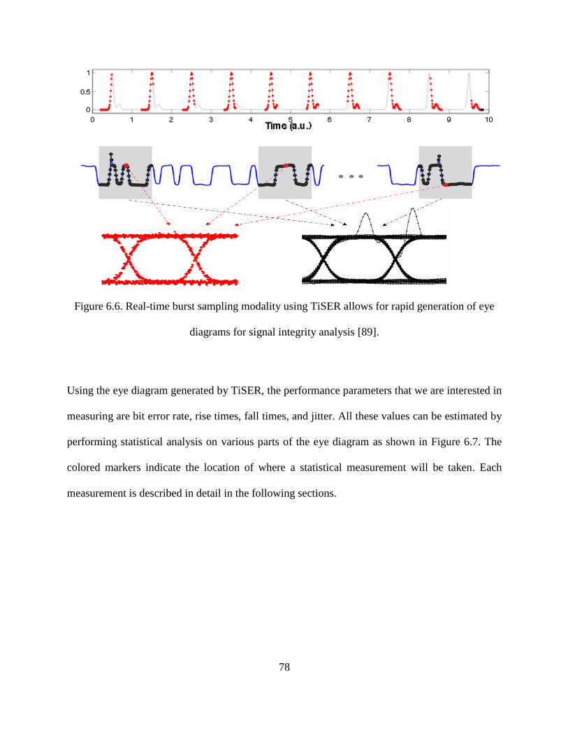
78
Figure 6.6. Real-time burst sampling modality using TiSER allows for rapid generation of eye
diagrams for signal integrity analysis [89].
Using the eye diagram generated by TiSER, the performance parameters that we are interested in
measuring are bit error rate, rise times, fall times, and jitter. All these values can be estimated by
performing statistical analysis on various parts of the eye diagram as shown in Figure 6.7. The
colored markers indicate the location of where a statistical measurement will be taken. Each
measurement is described in detail in the following sections.
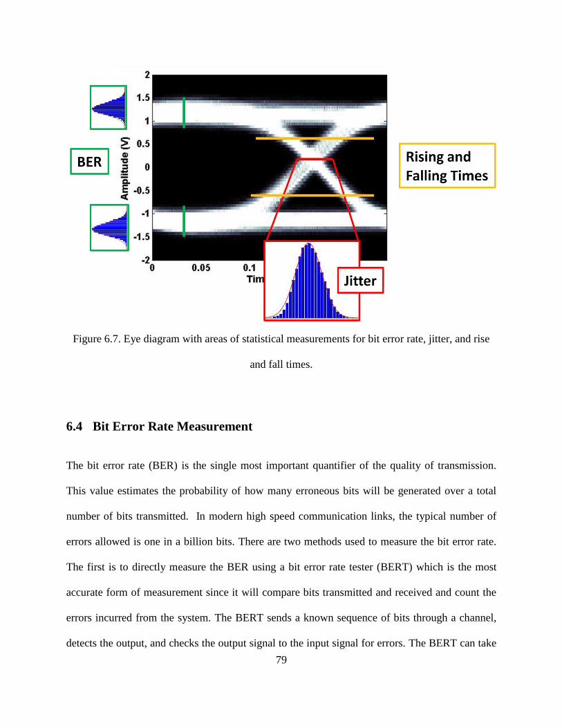
79
Figure 6.7. Eye diagram with areas of statistical measurements for bit error rate, jitter, and rise
and fall times.
6.4 Bit Error Rate Measurement
The bit error rate (BER) is the single most important quantifier of the quality of transmission.
This value estimates the probability of how many erroneous bits will be generated over a total
number of bits transmitted. In modern high speed communication links, the typical number of
errors allowed is one in a billion bits. There are two methods used to measure the bit error rate.
The first is to directly measure the BER using a bit error rate tester (BERT) which is the most
accurate form of measurement since it will compare bits transmitted and received and count the
errors incurred from the system. The BERT sends a known sequence of bits through a channel,
detects the output, and checks the output signal to the input signal for errors. The BERT can take
80
on the order of minutes to many hours to measure the BER depending on the data rate and what
BER value is desired. However when there are multiple channels needing to be measured, this
method becomes impractical due to the amount of time required to do a measurement. For
example, when requiring a BER of 1x10-15
a minimum measurement time of 27 hours is required
at 10 Gb/s data rate for just a single channel to get to a 95% confidence level. When using this
method, the BER is given by the following equation [23], [93]:
(6.3)
The second method is using the quality factor, or “Q factor”, to estimate the BER [93].
The Q factor involves generating an eye diagram and estimating the BER from the eye opening
by Gaussian fit approximations which is much faster than using a BERT for measuring low BER
values of 10-12
to 10-15
. This method is uses the signal-to-noise ratio (SNR) in a digital signal and
assumes normal noise distribution to estimate the BER. In a digital receiver, a decision circuit
decides whether an incoming binary signal is at a logical 0 or 1 level by sampling the received
signal and comparing the sample value to a threshold value. In a noise free system, the received
signal would have only two states. However due to additive noise and nonlinear distortions
caused by the transmission medium or equipment, the received signal levels can vary. This
means the sampled receive signal must be regarded as a random variable with probability
distributions and for the probability of detecting a 0 or 1 respectively. It is in
the overlapping regions where the BER is determined [93].
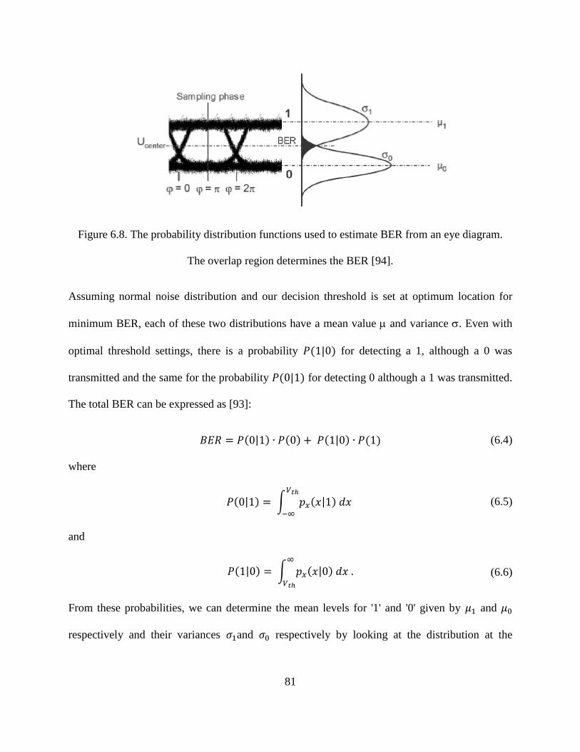
81
Figure 6.8. The probability distribution functions used to estimate BER from an eye diagram.
The overlap region determines the BER [94].
Assuming normal noise distribution and our decision threshold is set at optimum location for
minimum BER, each of these two distributions have a mean value and variance . Even with
optimal threshold settings, there is a probability for detecting a 1, although a 0 was
transmitted and the same for the probability for detecting 0 although a 1 was transmitted.
The total BER can be expressed as [93]:
(6.4)
where
(6.5)
and
(6.6)
From these probabilities, we can determine the mean levels for '1' and '0' given by and
respectively and their variances and respectively by looking at the distribution at the
82
sampling point. If we take the mean value and variances, we can determine the Q value defined
by [23]
(6.7)
and the BER can be estimated using the following equation [23]
(6.8)
From equation 6.8 we observe that as the SNR degrades, resulting in a lower Q value,
then the BER will be a higher value and is thus worse in performance. As the SNR increases
giving a higher Q, then the BER will be lower resulting in better performance. As the data rate
increases and assuming constant optical power in the system, the BER will worsen since the
signal to noise ratio decreases with faster data rate [94]. With faster data rates, we require
increased bandwidth to measure the signal and this adds more noise. To get the same BER value,
we would need to increase the transmitter power to improve SNR. Visually in the eye diagram,
we would expect the eye opening to shrink and thus the BER will get worse with decreasing
SNR. As the SNR is decreasing, then the noise grows which will make the eye narrow. This will
increase the likelihood of getting erroneous bits which results in more bit errors. If we were to
draw an eye mask over the opening of the eye, the edge of the mask is where we can move our
decision circuit sampling point to obtain a particular BER. The size of the mask would
correspond to a particular BER. As we move the sample point closer to the edge of the eye, the
probability of errors would increase thus resulting in a worse BER.
Time is not a factor when performing a Q factor measurement because the timing circuits
used for eye diagram generation have very little jitter. The jitter in these circuits must follow
conventional standards and thus the jitter will be very low as the signal is usually resampled by a
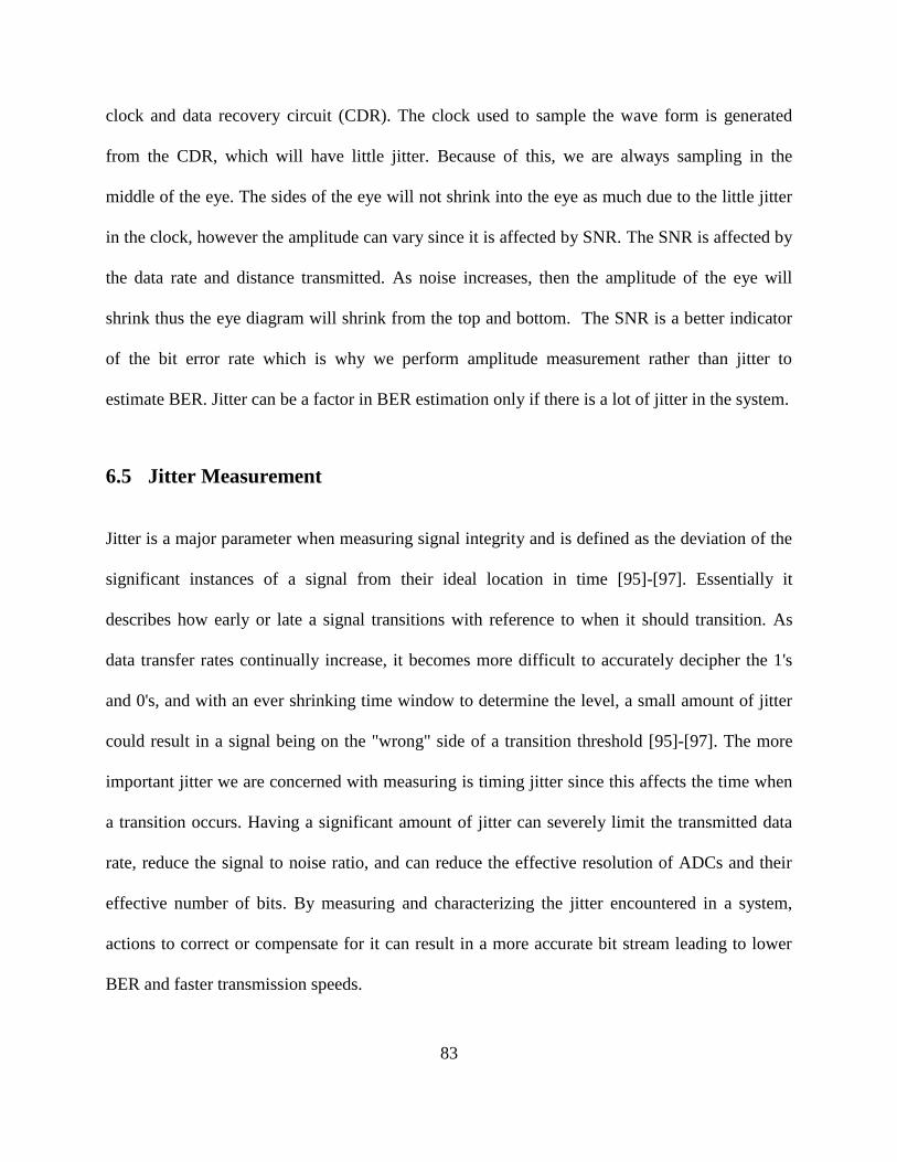
83
clock and data recovery circuit (CDR). The clock used to sample the wave form is generated
from the CDR, which will have little jitter. Because of this, we are always sampling in the
middle of the eye. The sides of the eye will not shrink into the eye as much due to the little jitter
in the clock, however the amplitude can vary since it is affected by SNR. The SNR is affected by
the data rate and distance transmitted. As noise increases, then the amplitude of the eye will
shrink thus the eye diagram will shrink from the top and bottom. The SNR is a better indicator
of the bit error rate which is why we perform amplitude measurement rather than jitter to
estimate BER. Jitter can be a factor in BER estimation only if there is a lot of jitter in the system.
6.5 Jitter Measurement
Jitter is a major parameter when measuring signal integrity and is defined as the deviation of the
significant instances of a signal from their ideal location in time [95]-[97]. Essentially it
describes how early or late a signal transitions with reference to when it should transition. As
data transfer rates continually increase, it becomes more difficult to accurately decipher the 1's
and 0's, and with an ever shrinking time window to determine the level, a small amount of jitter
could result in a signal being on the "wrong" side of a transition threshold [95]-[97]. The more
important jitter we are concerned with measuring is timing jitter since this affects the time when
a transition occurs. Having a significant amount of jitter can severely limit the transmitted data
rate, reduce the signal to noise ratio, and can reduce the effective resolution of ADCs and their
effective number of bits. By measuring and characterizing the jitter encountered in a system,
actions to correct or compensate for it can result in a more accurate bit stream leading to lower
BER and faster transmission speeds.
84
To estimate the jitter in the system, a histogram of the eye diagram is generated. In this
code, the jitter is assumed to be due to random noise and thus follows a Gaussian distribution.
From the eye diagram histogram, a one pixel wide sample of the crossing point of the eye
diagram at the sampling threshold is plotted. Afterwards, a Gaussian curve fit is performed on
the histogram data, and the resultant jitter will be approximately twice the variance. This
measurement can also be done to determine the jitter in a rising edge or falling edge as well as
shown in Figure 6.9.
Figure 6.9. Histogram of a rising edge and the sample taken from the center to determine the
jitter.
85
6.6 Rise and Fall Time Measurement
The rise and fall times describe the transition time of a signal from a low value to high value or
high value to low value respectively. In high speed optical electronics, the rise and fall times
measure the ability of a circuit to respond to fast input signals. The rise and fall times are defined
as the time for the response to rise from x% to y% of its final value [98]. In analog signals,
typically it is the time the signal takes to rise from 10% to 90%.
Using TiSER's burst sampling, a rising and falling edge can be captured with higher
temporal resolution in a single burst. Figure 6.10 shows the performance difference between a
real-time oscilloscope and TiSER in a single burst. By capturing a segment, we can get better
resolution on the transition edges. Using a 50 GSamples/s Tektronix oscilloscope, we can get at
best 2-4 points along the edge of a 12.5 Gbps signal. In comparison using TiSER, we can get
approximately 20 points on the edge. If we were to take several of these rising edge
measurements, we can get a more accurate measurement of the rising and falling edges. We can
also measure any transient effects as the signal rises and falls.
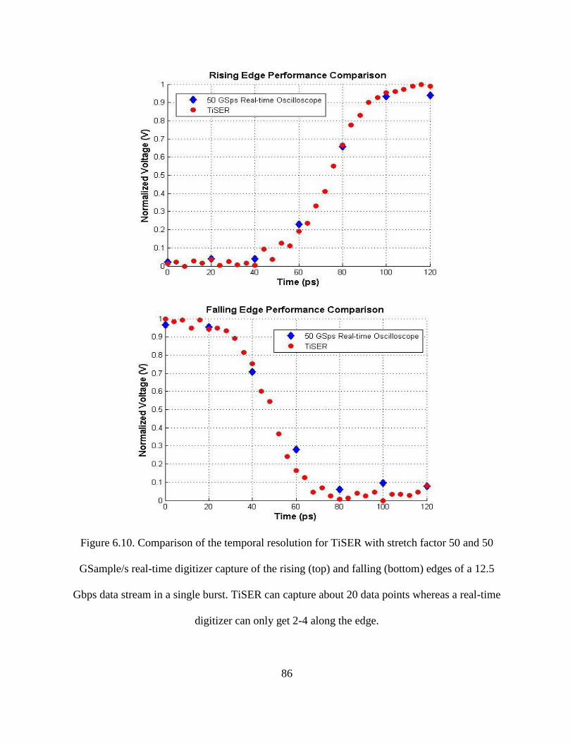
86
Figure 6.10. Comparison of the temporal resolution for TiSER with stretch factor 50 and 50
GSample/s real-time digitizer capture of the rising (top) and falling (bottom) edges of a 12.5
Gbps data stream in a single burst. TiSER can capture about 20 data points whereas a real-time
digitizer can only get 2-4 along the edge.
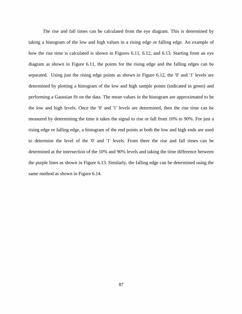
87
The rise and fall times can be calculated from the eye diagram. This is determined by
taking a histogram of the low and high values in a rising edge or falling edge. An example of
how the rise time is calculated is shown in Figures 6.11, 6.12, and 6.13. Starting from an eye
diagram as shown in Figure 6.11, the points for the rising edge and the falling edges can be
separated. Using just the rising edge points as shown in Figure 6.12, the '0' and '1' levels are
determined by plotting a histogram of the low and high sample points (indicated in green) and
performing a Gaussian fit on the data. The mean values in the histogram are approximated to be
the low and high levels. Once the '0' and '1' levels are determined, then the rise time can be
measured by determining the time it takes the signal to rise or fall from 10% to 90%. For just a
rising edge or falling edge, a histogram of the end points at both the low and high ends are used
to determine the level of the '0' and '1' levels. From there the rise and fall times can be
determined at the intersection of the 10% and 90% levels and taking the time difference between
the purple lines as shown in Figure 6.13. Similarly, the falling edge can be determined using the
same method as shown in Figure 6.14.
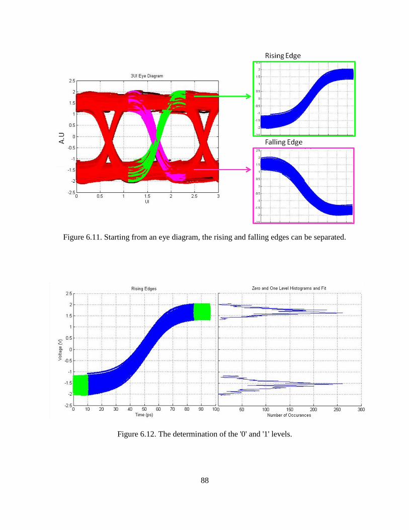
88
Figure 6.11. Starting from an eye diagram, the rising and falling edges can be separated.
Figure 6.12. The determination of the '0' and '1' levels.
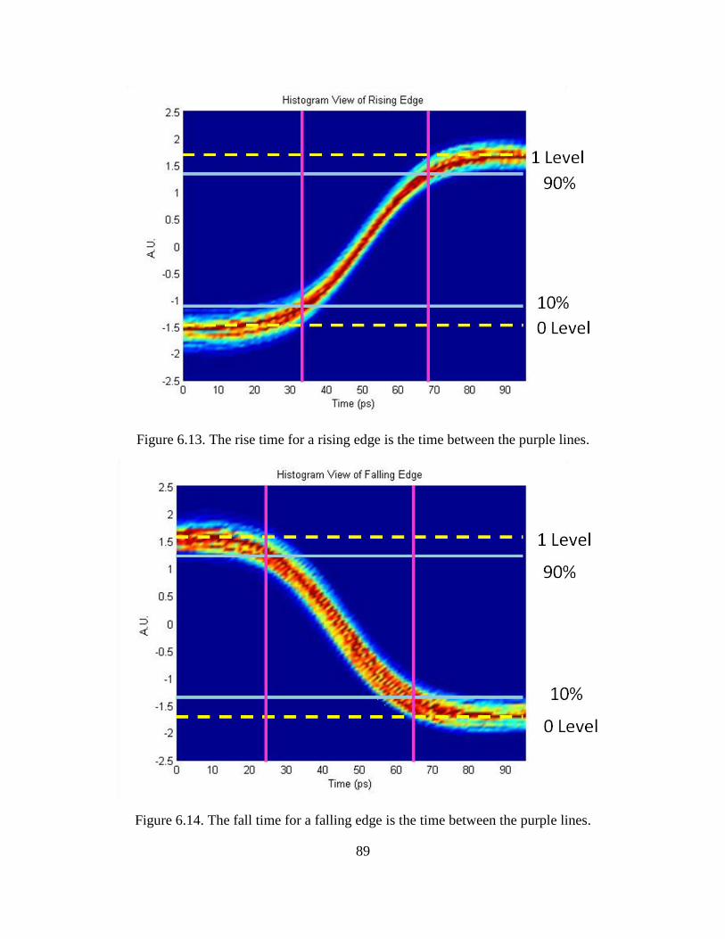
89
Figure 6.13. The rise time for a rising edge is the time between the purple lines.
Figure 6.14. The fall time for a falling edge is the time between the purple lines.
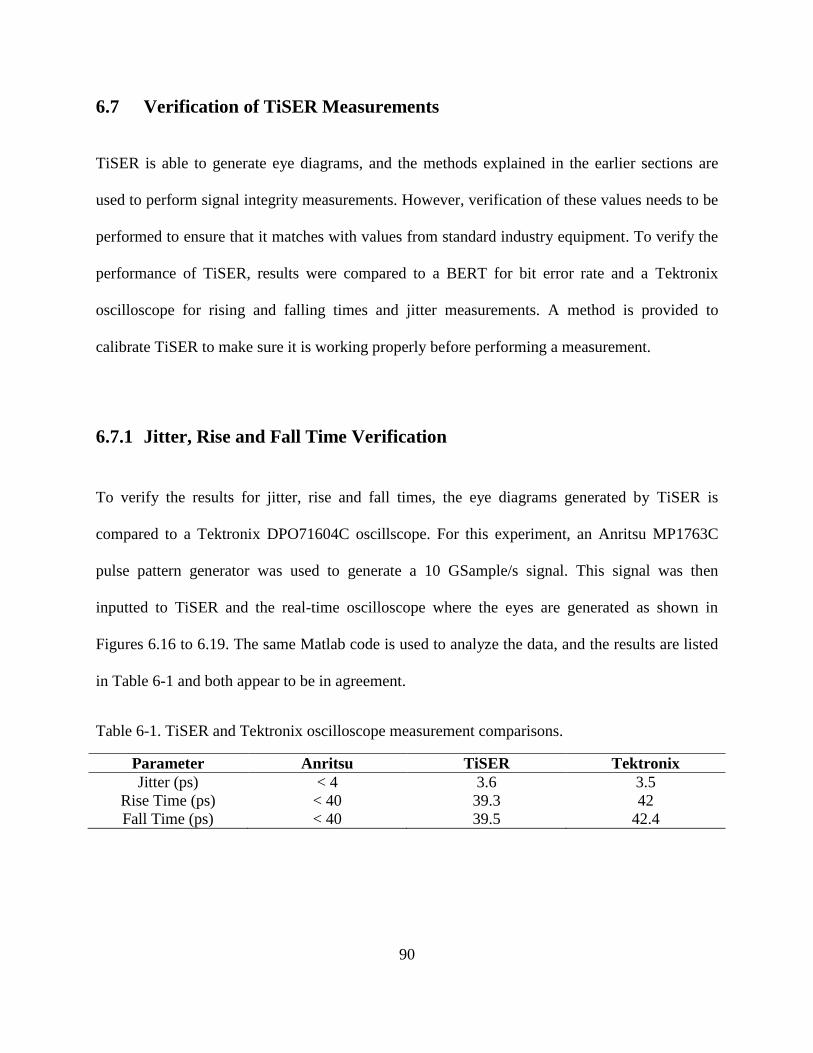
90
6.7 Verification of TiSER Measurements
TiSER is able to generate eye diagrams, and the methods explained in the earlier sections are
used to perform signal integrity measurements. However, verification of these values needs to be
performed to ensure that it matches with values from standard industry equipment. To verify the
performance of TiSER, results were compared to a BERT for bit error rate and a Tektronix
oscilloscope for rising and falling times and jitter measurements. A method is provided to
calibrate TiSER to make sure it is working properly before performing a measurement.
6.7.1 Jitter, Rise and Fall Time Verification
To verify the results for jitter, rise and fall times, the eye diagrams generated by TiSER is
compared to a Tektronix DPO71604C oscillscope. For this experiment, an Anritsu MP1763C
pulse pattern generator was used to generate a 10 GSample/s signal. This signal was then
inputted to TiSER and the real-time oscilloscope where the eyes are generated as shown in
Figures 6.16 to 6.19. The same Matlab code is used to analyze the data, and the results are listed
in Table 6-1 and both appear to be in agreement.
Table 6-1. TiSER and Tektronix oscilloscope measurement comparisons.
Parameter Anritsu TiSER Tektronix
Jitter (ps) < 4 3.6 3.5
Rise Time (ps) < 40 39.3 42
Fall Time (ps) < 40 39.5 42.4
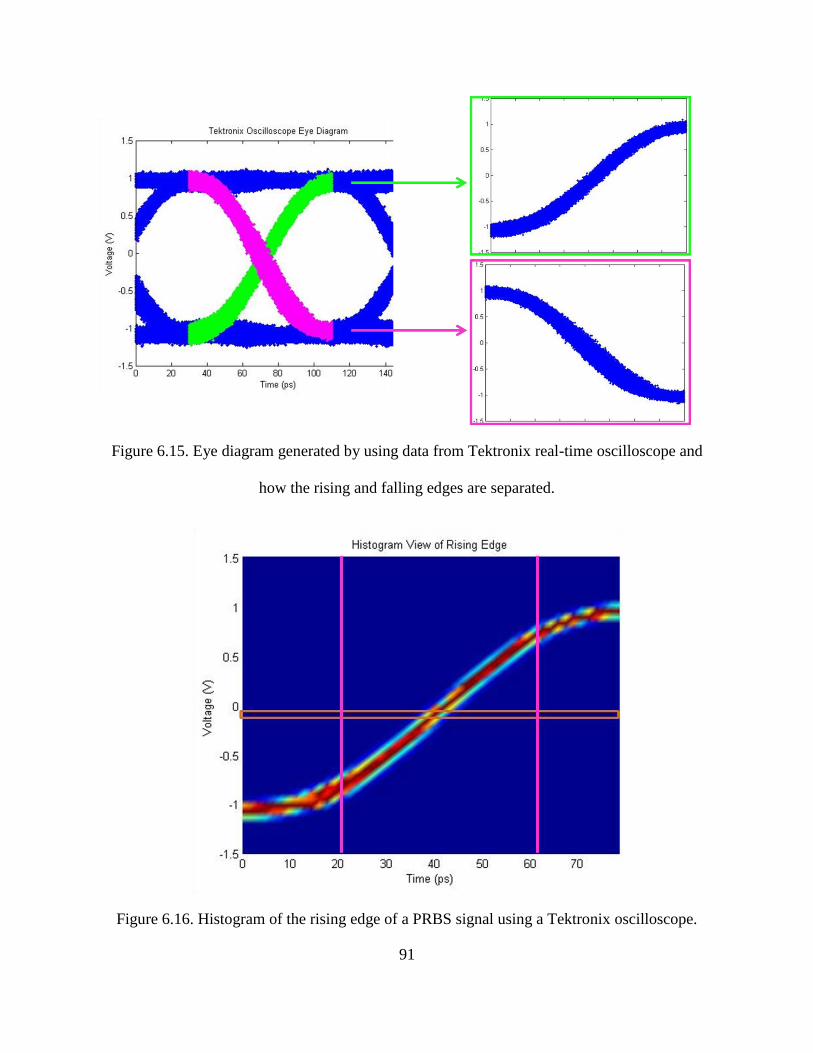
91
Figure 6.15. Eye diagram generated by using data from Tektronix real-time oscilloscope and
how the rising and falling edges are separated.
Figure 6.16. Histogram of the rising edge of a PRBS signal using a Tektronix oscilloscope.
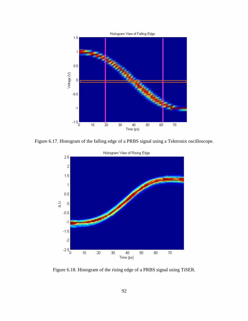
92
Figure 6.17. Histogram of the falling edge of a PRBS signal using a Tektronix oscilloscope.
Figure 6.18. Histogram of the rising edge of a PRBS signal using TiSER.
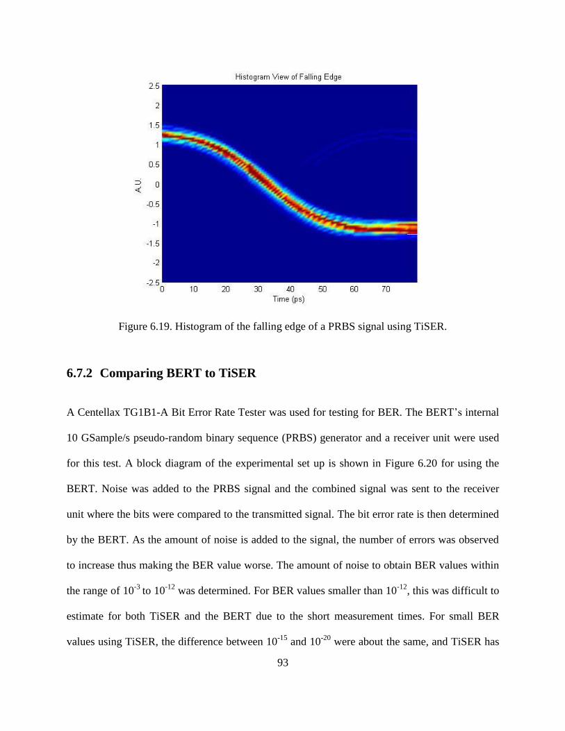
93
Figure 6.19. Histogram of the falling edge of a PRBS signal using TiSER.
6.7.2 Comparing BERT to TiSER
A Centellax TG1B1-A Bit Error Rate Tester was used for testing for BER. The BERT’s internal
10 GSample/s pseudo-random binary sequence (PRBS) generator and a receiver unit were used
for this test. A block diagram of the experimental set up is shown in Figure 6.20 for using the
BERT. Noise was added to the PRBS signal and the combined signal was sent to the receiver
unit where the bits were compared to the transmitted signal. The bit error rate is then determined
by the BERT. As the amount of noise is added to the signal, the number of errors was observed
to increase thus making the BER value worse. The amount of noise to obtain BER values within
the range of 10-3
to 10-12
was determined. For BER values smaller than 10-12
, this was difficult to
estimate for both TiSER and the BERT due to the short measurement times. For small BER
values using TiSER, the difference between 10-15
and 10-20
were about the same, and TiSER has
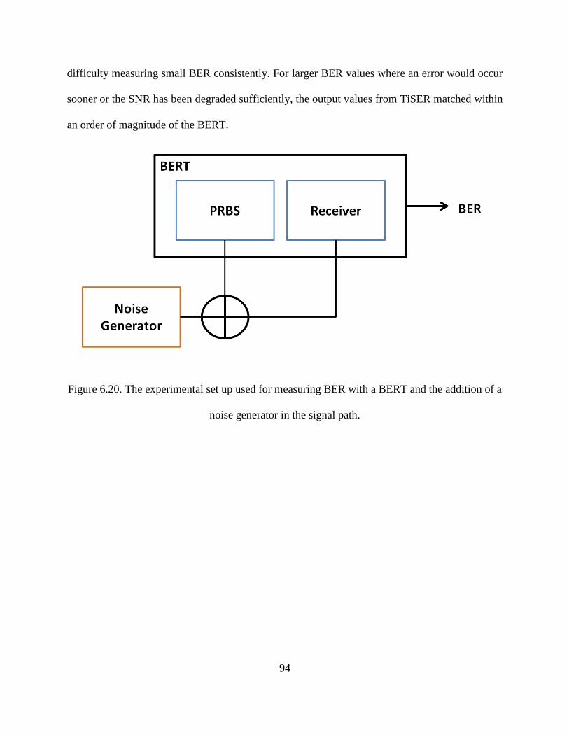
94
difficulty measuring small BER consistently. For larger BER values where an error would occur
sooner or the SNR has been degraded sufficiently, the output values from TiSER matched within
an order of magnitude of the BERT.
Figure 6.20. The experimental set up used for measuring BER with a BERT and the addition of a
noise generator in the signal path.
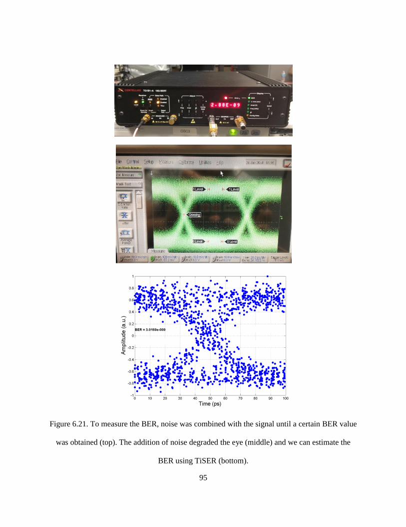
95
Figure 6.21. To measure the BER, noise was combined with the signal until a certain BER value
was obtained (top). The addition of noise degraded the eye (middle) and we can estimate the
BER using TiSER (bottom).
96
6.8 Advantages of using TiSER
TiSER can be used for signal integrity measurements and has been verified by comparing the
performance to commercial measurement equipment. TiSER provides several advantages over
similar instruments. The high effective sampling rate and temporal resolution allows TiSER to
generate eye diagrams much quicker and with these tools, TiSER can be used to quickly analyze
an eye diagram and measure the rise and fall times, jitter, and bit error rate. The high temporal
resolution gives TiSER the capability to capture rare events and transients and time traces of data
bits which are impossible to capture with a conventional sampling oscilloscope. For electronic
ADCs that can achieve comparable sampling speeds as TiSER, TiSER has a much larger input
bandwidth and requires far less power due to its use of photonics.
97
7 Integration of TiSER into Test-bed for Optical Aggregate Networks
Chapter 7
Integration of TiSER into Test-bed for Optical
Aggregate Networks
In the previous chapter, analysis tools were developed to evaluate signal integrity parameters and
estimate the bit error rate from eye diagrams generated by TiSER offline. A time-stretch
accelerated processor [99] was achieved which allowed for the generation of eye diagrams in
real-time using TiSER. This new capability allowed for rapid eye diagram generation and
analysis which is beneficial for monitoring next generation optical networks. This new
instrument, known as real-time TiSER, was integrated into an optical test-bed studying aggregate
optical networks at the University of Arizona where it was used as an optical performance
monitor. In this multi-university collaborative effort consisting of the University of Arizona,
University of California Los Angeles, Columbia University, University of Southern California,
and Cornell University, we set out to build and demonstrate an aggregate optical network. TiSER
would serve as an optical performance monitor and provide real-time feedback to a software
defined network (SDN) control plane which is used to optimize optical network performance.
Using real-time TiSER, amplified stimulated emission and self phase modulation effects were
98
observed. Moreover, real-time TiSER was used to demonstrate for the first time real-time, in-
service monitoring of a commercial platform [99].
7.1 Introduction to Center for Integrated Access Networks
The collaboration effort was funded by the National Science Foundation Center for Integrated
Access Networks (CIAN) Engineering Research Center (ERC). CIAN is a multi-institutional
research effort consisting of the University of Arizona (Lead), University of California at Los
Angeles, University of California at San Diego, University of California at Berkeley, University
of Southern California, Columbia University, Norfolk State University, and Tuskegee
University. The vision of CIAN is to create transformative technologies for optical access
networks where virtually any application requiring any resource can be seamlessly and
efficiently aggregated and interfaced with existing and future core networks in a cost-effective
manner. Analogous to the evolution over decades of today's computer laptop using massive
integration of discrete electronic components, the CIAN vision would lead to the creation of the
PC equivalent of the optical access network by employing optoelectronic integration to enable
affordable and flexible access to any type of service, including delivery of data rates approaching
10 Gigabits/sec to a broad population base anywhere and at any time [100].
7.2 Optical Performance Monitoring in Next Generation Networks
One of the main issues in modern communication systems is the time to repair when
impairments are present. This would result in shutting down portions of the optical network to
debug, repair, and then verify that the fix worked which could take hours to days. In the event of
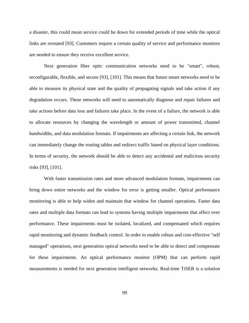
99
a disaster, this could mean service could be down for extended periods of time while the optical
links are rerouted [93]. Customers require a certain quality of service and performance monitors
are needed to ensure they receive excellent service.
Next generation fiber optic communication networks need to be "smart", robust,
reconfigurable, flexible, and secure [93], [101]. This means that future smart networks need to be
able to measure its physical state and the quality of propagating signals and take action if any
degradation occurs. These networks will need to automatically diagnose and repair failures and
take actions before data loss and failures take place. In the event of a failure, the network is able
to allocate resources by changing the wavelength or amount of power transmitted, channel
bandwidths, and data modulation formats. If impairments are affecting a certain link, the network
can immediately change the routing tables and redirect traffic based on physical layer conditions.
In terms of security, the network should be able to detect any accidental and malicious security
risks [93], [101].
With faster transmission rates and more advanced modulation formats, impairments can
bring down entire networks and the window for error is getting smaller. Optical performance
monitoring is able to help widen and maintain that window for channel operations. Faster data
rates and multiple data formats can lead to systems having multiple impairments that affect over
performance. These impairments must be isolated, localized, and compensated which requires
rapid monitoring and dynamic feedback control. In order to enable robust and cost-effective "self
managed" operations, next generation optical networks need to be able to detect and compensate
for these impairments. An optical performance monitor (OPM) that can perform rapid
measurements is needed for next generation intelligent networks. Real-time TiSER is a solution
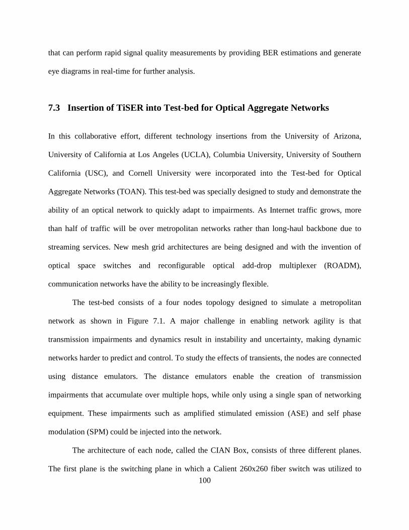
100
that can perform rapid signal quality measurements by providing BER estimations and generate
eye diagrams in real-time for further analysis.
7.3 Insertion of TiSER into Test-bed for Optical Aggregate Networks
In this collaborative effort, different technology insertions from the University of Arizona,
University of California at Los Angeles (UCLA), Columbia University, University of Southern
California (USC), and Cornell University were incorporated into the Test-bed for Optical
Aggregate Networks (TOAN). This test-bed was specially designed to study and demonstrate the
ability of an optical network to quickly adapt to impairments. As Internet traffic grows, more
than half of traffic will be over metropolitan networks rather than long-haul backbone due to
streaming services. New mesh grid architectures are being designed and with the invention of
optical space switches and reconfigurable optical add-drop multiplexer (ROADM),
communication networks have the ability to be increasingly flexible.
The test-bed consists of a four nodes topology designed to simulate a metropolitan
network as shown in Figure 7.1. A major challenge in enabling network agility is that
transmission impairments and dynamics result in instability and uncertainty, making dynamic
networks harder to predict and control. To study the effects of transients, the nodes are connected
using distance emulators. The distance emulators enable the creation of transmission
impairments that accumulate over multiple hops, while only using a single span of networking
equipment. These impairments such as amplified stimulated emission (ASE) and self phase
modulation (SPM) could be injected into the network.
The architecture of each node, called the CIAN Box, consists of three different planes.
The first plane is the switching plane in which a Calient 260x260 fiber switch was utilized to
101
build a colorless, contentionless, and directionless ROADM architecture. This is the most
flexible way to allow the network to switch wavelengths quickly. However, the CDC ROADM
architecture is not enough to enable dynamic reconfiguration capabilities, and the OPM plane is
used to monitor the quality of the signals.
To monitor the optical performance of the network, two complementary methods were
employed. The first method was a real-time optical signal to noise ratio (OSNR) monitor using
delay line interferometry developed by USC. This monitor performed measurements on the
OSNR which gave coarse measurements of the optical signal, but nothing about the electric
signal. The second method was using TiSER developed by UCLA. TiSER is able to perform
finer measurements and provide more detailed information such as BER, jitter, and rise and fall
times about the electric signal. TiSER was able to send the BER via XMPP to a SDN controller.
This SDN controller is able to make decisions and make any necessary adjustments to the
network based on the information provided.
Figure 7.1. The SDN plane that receives feedback from the OPM layers for dynamic network
control.
102
Figure 7.2. The CIAN box architecture where TiSER is inserted into the OPM layer. A
wavelength selective switch drops an optical channel to TiSER to monitor.
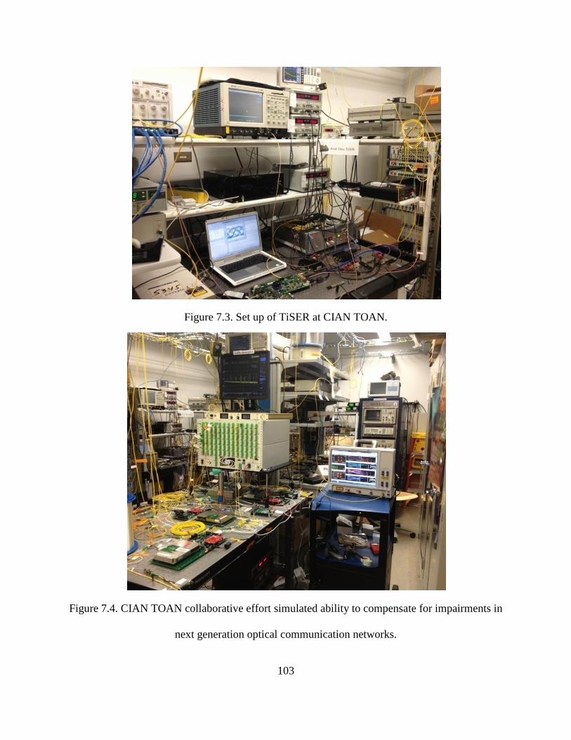
103
Figure 7.3. Set up of TiSER at CIAN TOAN.
Figure 7.4. CIAN TOAN collaborative effort simulated ability to compensate for impairments in
next generation optical communication networks.
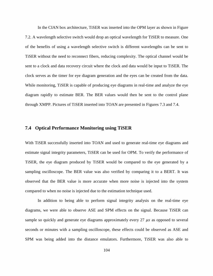
104
In the CIAN box architecture, TiSER was inserted into the OPM layer as shown in Figure
7.2. A wavelength selective switch would drop an optical wavelength for TiSER to measure. One
of the benefits of using a wavelength selective switch is different wavelengths can be sent to
TiSER without the need to reconnect fibers, reducing complexity. The optical channel would be
sent to a clock and data recovery circuit where the clock and data would be input to TiSER. The
clock serves as the timer for eye diagram generation and the eyes can be created from the data.
While monitoring, TiSER is capable of producing eye diagrams in real-time and analyze the eye
diagram rapidly to estimate BER. The BER values would then be sent to the control plane
through XMPP. Pictures of TiSER inserted into TOAN are presented in Figures 7.3 and 7.4.
7.4 Optical Performance Monitoring using TiSER
With TiSER successfully inserted into TOAN and used to generate real-time eye diagrams and
estimate signal integrity parameters, TiSER can be used for OPM. To verify the performance of
TiSER, the eye diagram produced by TiSER would be compared to the eye generated by a
sampling oscilloscope. The BER value was also verified by comparing it to a BERT. It was
observed that the BER value is more accurate when more noise is injected into the system
compared to when no noise is injected due to the estimation technique used.
In addition to being able to perform signal integrity analysis on the real-time eye
diagrams, we were able to observe ASE and SPM effects on the signal. Because TiSER can
sample so quickly and generate eye diagrams approximately every 27 as opposed to several
seconds or minutes with a sampling oscilloscope, these effects could be observed as ASE and
SPM was being added into the distance emulators. Furthermore, TiSER was also able to
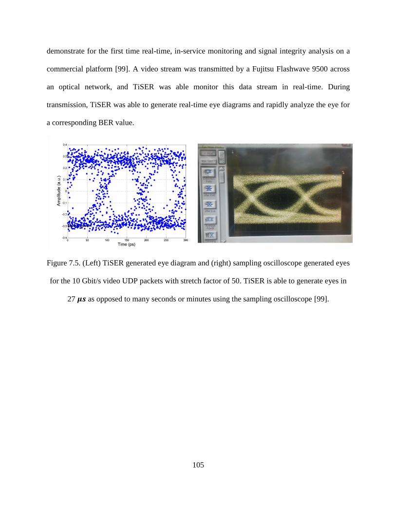
105
demonstrate for the first time real-time, in-service monitoring and signal integrity analysis on a
commercial platform [99]. A video stream was transmitted by a Fujitsu Flashwave 9500 across
an optical network, and TiSER was able monitor this data stream in real-time. During
transmission, TiSER was able to generate real-time eye diagrams and rapidly analyze the eye for
a corresponding BER value.
Figure 7.5. (Left) TiSER generated eye diagram and (right) sampling oscilloscope generated eyes
for the 10 Gbit/s video UDP packets with stretch factor of 50. TiSER is able to generate eyes in
27 as opposed to many seconds or minutes using the sampling oscilloscope [99].
106
7.5 Conclusions
Next generation optical networks need real-time OPM that can relay information about the health
of the network quickly, and TiSER is a solution that can be used. TiSER can be used to monitor
the signal integrity along the transmission line, provide feedback to optimize optical devices or
along the transmission line, and the rapid feedback will enable system management to detect
optical link failures. This section has highlighted many features in TiSER that make it an
attractive platform for OPM applications. These include real-time eye diagram generation and
analysis, the ability to capture time-traces whereas sampling oscilloscopes cannot, and the ability
to capture transients with its high temporal resolution that would otherwise be missed by
conventional electronic digitizers.
107
8 Concluding Remarks
Chapter 8
Concluding Remarks
Several new developments have been presented that improve the linearity of optical links and
enable high speed measurements on ultra-fast signals. A digital broadband linearization
algorithm is developed and used to linearize optical links by reducing intermodulation products
and experimentally demonstrating a record 120 dB.Hz2/3
SFDR across 6 GHz of bandwidth. This
algorithm, currently realized for offline processing, could be implemented into real-time. The
architecture for the real-time implementation of this algorithm on a FPGA was designed, and a
Matlab simulation of the real-time implementation matches well with the Verilog simulation
showing proof of concept.
An ultra-wideband instantaneous frequency estimator termed time-stretch instantaneous
frequency measurement receiver (TS-IFM) was demonstrated. By combining both time-stretch
and windowing and quadratic interpolation, the TS-IFM capable of rapidly sweeping across
ultra-wide bandwidths and measuring the frequency of signals with higher accuracy was
achieved. Moreover, the TS-IFM has the capability to measure multiple frequencies
simultaneously whereas current IFM can only measure one signal at a time as long as it is within
108
hardware and software capabilities. The TS-IFM is able to improve on many weaknesses
exhibited by many current IFM receivers.
Lastly, results were presented from experiments highlighting the impact of TiSER in
telecommunication applications. TiSER is capable of analyzing eye diagrams and performing
rapid signal integrity measurements of high speed signals. TiSER is able to quickly measure rise
and fall times, bit error rate, and jitter, and it can be expanded to measure other performance
parameters are well. The analysis program was integrated into the backend of real-time TiSER
and was used during our collaboration effort when TiSER was inserted into CIAN TOAN. From
our collaboration, we demonstrated that TiSER can be used as an optical performance monitor
for next generation agile networks.
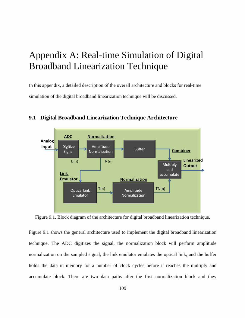
109
9 Appendix A: Real-time Simulation of Digital Broadband Linearization
Technique
Appendix A: Real-time Simulation of Digital
Broadband Linearization Technique
In this appendix, a detailed description of the overall architecture and blocks for real-time
simulation of the digital broadband linearization technique will be discussed.
9.1 Digital Broadband Linearization Technique Architecture
Figure 9.1. Block diagram of the architecture for digital broadband linearization technique.
Figure 9.1 shows the general architecture used to implement the digital broadband linearization
technique. The ADC digitizes the signal, the normalization block will perform amplitude
normalization on the sampled signal, the link emulator emulates the optical link, and the buffer
holds the data in memory for a number of clock cycles before it reaches the multiply and
accumulate block. There are two data paths after the first normalization block and they
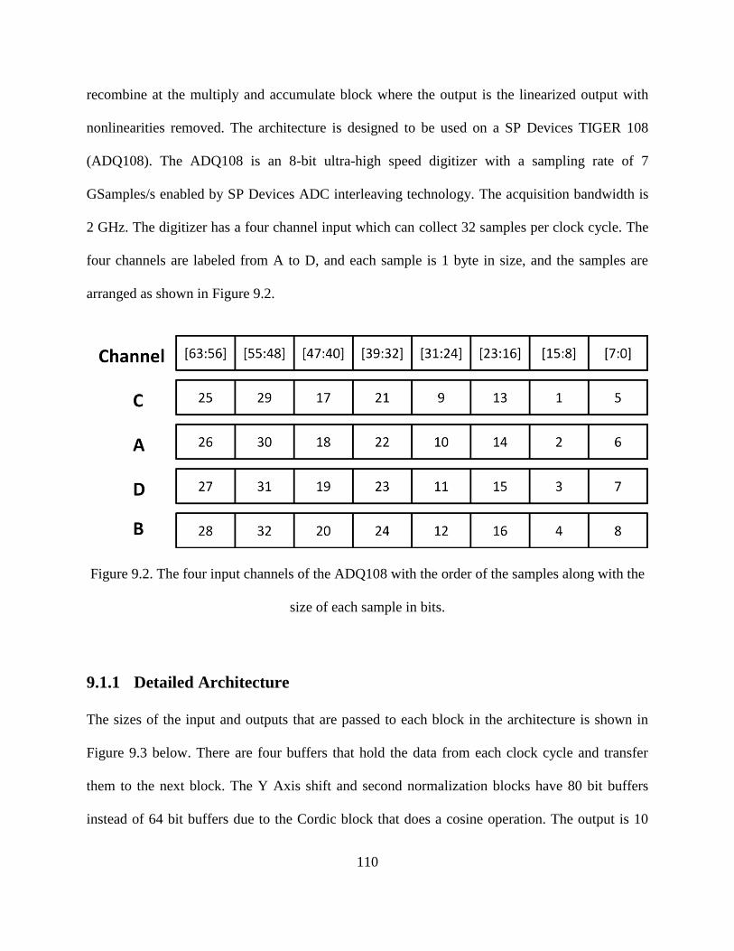
110
recombine at the multiply and accumulate block where the output is the linearized output with
nonlinearities removed. The architecture is designed to be used on a SP Devices TIGER 108
(ADQ108). The ADQ108 is an 8-bit ultra-high speed digitizer with a sampling rate of 7
GSamples/s enabled by SP Devices ADC interleaving technology. The acquisition bandwidth is
2 GHz. The digitizer has a four channel input which can collect 32 samples per clock cycle. The
four channels are labeled from A to D, and each sample is 1 byte in size, and the samples are
arranged as shown in Figure 9.2.
Figure 9.2. The four input channels of the ADQ108 with the order of the samples along with the
size of each sample in bits.
9.1.1 Detailed Architecture
The sizes of the input and outputs that are passed to each block in the architecture is shown in
Figure 9.3 below. There are four buffers that hold the data from each clock cycle and transfer
them to the next block. The Y Axis shift and second normalization blocks have 80 bit buffers
instead of 64 bit buffers due to the Cordic block that does a cosine operation. The output is 10
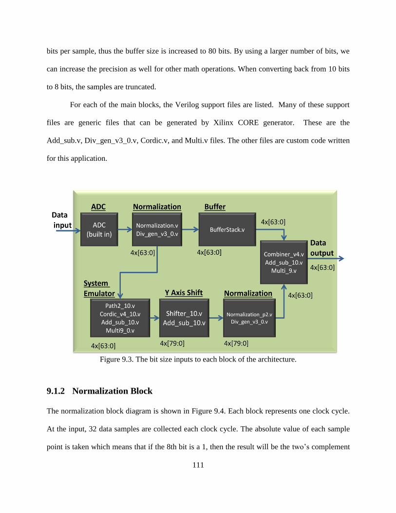
111
bits per sample, thus the buffer size is increased to 80 bits. By using a larger number of bits, we
can increase the precision as well for other math operations. When converting back from 10 bits
to 8 bits, the samples are truncated.
For each of the main blocks, the Verilog support files are listed. Many of these support
files are generic files that can be generated by Xilinx CORE generator. These are the
Add_sub.v, Div_gen_v3_0.v, Cordic.v, and Multi.v files. The other files are custom code written
for this application.
Figure 9.3. The bit size inputs to each block of the architecture.
9.1.2 Normalization Block
The normalization block diagram is shown in Figure 9.4. Each block represents one clock cycle.
At the input, 32 data samples are collected each clock cycle. The absolute value of each sample
point is taken which means that if the 8th bit is a 1, then the result will be the two’s complement
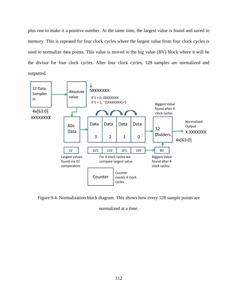
112
plus one to make it a positive number. At the same time, the largest value is found and saved to
memory. This is repeated for four clock cycles where the largest value from four clock cycles is
used to normalize data points. This value is moved to the big value (BV) block where it will be
the divisor for four clock cycles. After four clock cycles, 128 samples are normalized and
outputted.
Figure 9.4. Normalization block diagram. This shows how every 128 sample points are
normalized at a time.
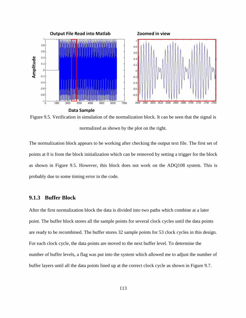
113
Figure 9.5. Verification in simulation of the normalization block. It can be seen that the signal is
normalized as shown by the plot on the right.
The normalization block appears to be working after checking the output text file. The first set of
points at 0 is from the block initialization which can be removed by setting a trigger for the block
as shown in Figure 9.5. However, this block does not work on the ADQ108 system. This is
probably due to some timing error in the code.
9.1.3 Buffer Block
After the first normalization block the data is divided into two paths which combine at a later
point. The buffer block stores all the sample points for several clock cycles until the data points
are ready to be recombined. The buffer stores 32 sample points for 53 clock cycles in this design.
For each clock cycle, the data points are moved to the next buffer level. To determine the
number of buffer levels, a flag was put into the system which allowed me to adjust the number of
buffer layers until all the data points lined up at the correct clock cycle as shown in Figure 9.7.
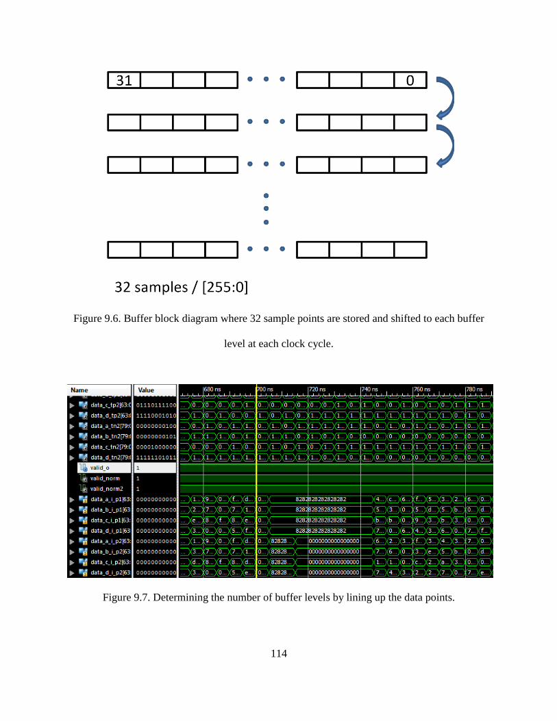
114
Figure 9.6. Buffer block diagram where 32 sample points are stored and shifted to each buffer
level at each clock cycle.
Figure 9.7. Determining the number of buffer levels by lining up the data points.
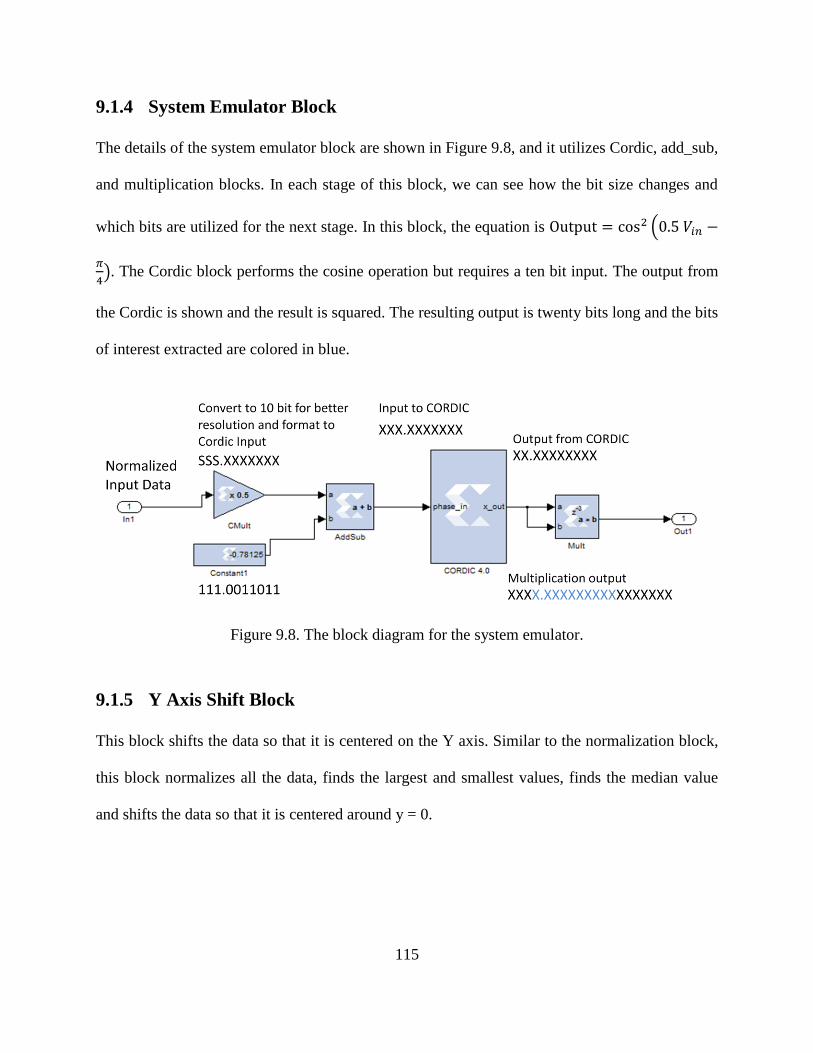
115
9.1.4 System Emulator Block
The details of the system emulator block are shown in Figure 9.8, and it utilizes Cordic, add_sub,
and multiplication blocks. In each stage of this block, we can see how the bit size changes and
which bits are utilized for the next stage. In this block, the equation is
. The Cordic block performs the cosine operation but requires a ten bit input. The output from
the Cordic is shown and the result is squared. The resulting output is twenty bits long and the bits
of interest extracted are colored in blue.
Figure 9.8. The block diagram for the system emulator.
9.1.5 Y Axis Shift Block
This block shifts the data so that it is centered on the Y axis. Similar to the normalization block,
this block normalizes all the data, finds the largest and smallest values, finds the median value
and shifts the data so that it is centered around y = 0.
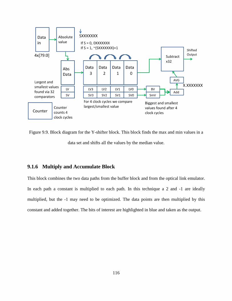
116
Figure 9.9. Block diagram for the Y-shifter block. This block finds the max and min values in a
data set and shifts all the values by the median value.
9.1.6 Multiply and Accumulate Block
This block combines the two data paths from the buffer block and from the optical link emulator.
In each path a constant is multiplied to each path. In this technique a 2 and -1 are ideally
multiplied, but the -1 may need to be optimized. The data points are then multiplied by this
constant and added together. The bits of interest are highlighted in blue and taken as the output.
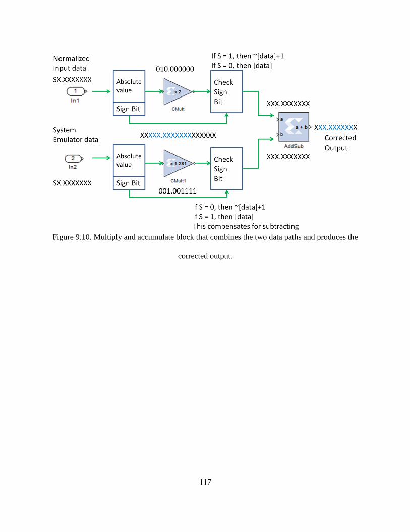
117
Figure 9.10. Multiply and accumulate block that combines the two data paths and produces the
corrected output.
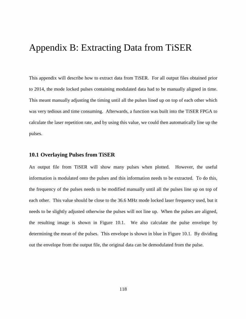
118
10 Appendix B: Extracting Data from TiSER
Appendix B: Extracting Data from TiSER
This appendix will describe how to extract data from TiSER. For all output files obtained prior
to 2014, the mode locked pulses containing modulated data had to be manually aligned in time.
This meant manually adjusting the timing until all the pulses lined up on top of each other which
was very tedious and time consuming. Afterwards, a function was built into the TiSER FPGA to
calculate the laser repetition rate, and by using this value, we could then automatically line up the
pulses.
10.1 Overlaying Pulses from TiSER
An output file from TiSER will show many pulses when plotted. However, the useful
information is modulated onto the pulses and this information needs to be extracted. To do this,
the frequency of the pulses needs to be modified manually until all the pulses line up on top of
each other. This value should be close to the 36.6 MHz mode locked laser frequency used, but it
needs to be slightly adjusted otherwise the pulses will not line up. When the pulses are aligned,
the resulting image is shown in Figure 10.1. We also calculate the pulse envelope by
determining the mean of the pulses. This envelope is shown in blue in Figure 10.1. By dividing
out the envelope from the output file, the original data can be demodulated from the pulse.
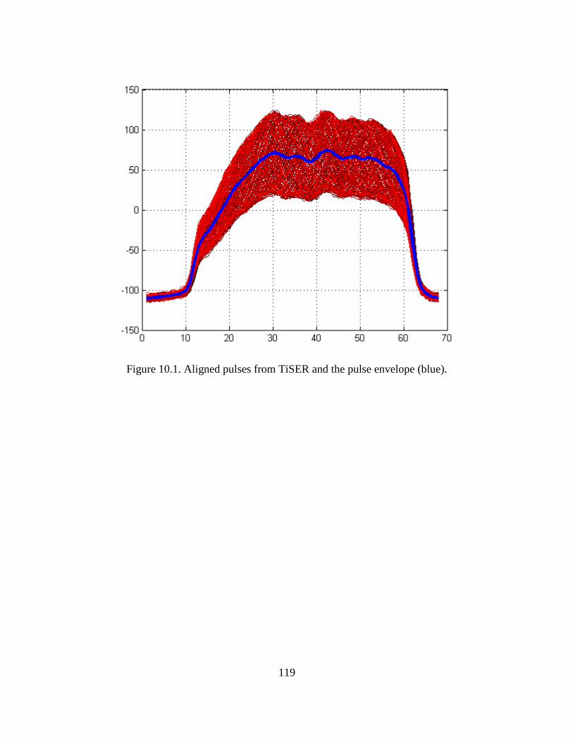
119
Figure 10.1. Aligned pulses from TiSER and the pulse envelope (blue).
120
11 References
References
[1] A. M. Zin, M. S Bongsu, S. M. Idrus, and N. Zulkifli, "An Overview of Radio-over-Fiber
Network Technology," IEEE Conference on Photonics, pp.1-3, March 26, 2010.
[2] X. Fernando, "Radio over Fiber- An Optical Technique for Wireless Access" IEEE
Comm. Soc., Oct 16, 2009. [Online].
http://cms.comsoc.org/SiteGen/Uploads/Public/Docs_Globecom_2009/XavierROFT16.p
df. [Accessed Oct 30, 2014].
[3] D. Opatic, "Radio over Fiber Technology for Wireless Access," Ericsson Nikola Tesla
d.d., [Online]. http://www.ericsson.com/hr/etk/dogadjanja/mipro_2009/12_1112_F.pdf.
[Accessed Oct 10, 2014].
[4] H. Kim, "Radio-over-Fiber Technology for Wireless Communication Services", Samsung
Electronics, 2005. [Online].
http://www.tspd.com.tw/images/fbfiles/files/ROF_for_wireless_comm_Hoon_Kim_.pdf.
[Accessed Oct 12, 2014].
[5] Cisco, "Cisco Visual Networking Index: Forecast and Methodology, 2013–2018", Cisco,
June 10, 2014. [Online]. http://www.cisco.com/c/en/us/solutions/collateral/service-
provider/ip-ngn-ip-next-generation-network/white_paper_c11-481360.html. [Accessed
Oct 10, 2014].
121
[6] L. Alloatti, et al., “100 GHz Silicon-Organic Hybrid Modulator,” Light Sci. Appl., vol. 3,
p.e173, 2014. DOI:10.1038/lsa.2014.54
[7] R. H. Walden, "Analog-to-digital converter survey and analysis," Selected Areas in
Communications, IEEE Journal on, vol.17, no.4, pp.539-550, Apr 1999.
[8] R. Walden, “Analog-to-digital conversion in the early twenty-first century,” in Wiley
Encyclopedia of Computer Science and Engineering (Wiley, 2008), pp. 126–138.
[9] N. Gray, "Interleaving ADCs for Higher Sampling Rates", Texas Instruments, 2011.
[Online]. http://www.ti.com/lit/wp/snaa111/snaa111.pdf. [Accessed Oct 13, 2014].
[10] A. S. Bhushan, F. Coppinger, and B. Jalali, “Time-stretched analogue-to-digital
conversion," Electronics Letters vol. 34, no. 9, pp. 839–841, April 1998.
[11] Y. Han and B. Jalali, “Photonic Time-Stretched Analog-to-Digital Converter:
Fundamental Concepts and Practical Considerations," Journal of Lightwave Technology,
Vol. 21, Issue 12, pp. 3085–3103, Dec. 2003.
[12] A. Fard, S. Gupta, and B. Jalali, "Photonic time-stretch digitizer and its extension to real-
time spectroscopy and imaging," Laser & Photonics Reviews vol. 7, no. 2, pp. 207-263,
March 2013.
[13] S. Gupta and B. Jalali, “Time-warp correction and calibration in photonic time-stretch
analog-to-digital converter," Optics Letters vol. 33, no. 22, 2674–2676, 2008.
[14] J. Chou, O. Boyraz, D. Solli, and B. Jalali, "Femtosecond real-time single-shot digitizer",
Appl. Phys. Lett., vol. 91, no. 16, pp.161105-1 -161105-3 2007.
[15] K. Goda, et al., "Serial time-encoded amplified imaging for real-time observation of fast
dynamic phenomena," Nature, vol. 458, pp. 1145-1149. Apr. 2009.
122
[16] K. Goda, et al., "High-throughput single-microparticle imaging flow analyzer," Proc.
Natl. Acad. Sci. USA, vol. 109, pp. 11630-11635. Jun. 2012.
[17] D. R. Solli, et al., "Optical rogue waves," Nature, vol. 450, pp. 1054-1057, Dec 2007.
[18] E. Diebold, et al., "Digitally synthesized beat frequency multiplexing for submillisecond
fluorescence microscopy," Nature Photonics, vol. 7, no. 10, pp. 806-810 2013.
[19] Asad M. Madni and E. J. Nyiri, "Fast Fourier Transform and Digital Filtering Solution to
Transmission Line Analysis" 1982 Military MicrowavesConference, 1982.
[20] M. K. Carson. Alexander Graham Bell: Giving Voice To The World. Sterling
Biographies. New York: Sterling Publishing. 2007, pp. 76–78.
[21] A. G. Bell, "On the Production and Reproduction of Sound by Light". Am. Jour. of Sci.,
vol. Series 3, Vol. 20, no. 118, pp. 305–324. Oct. 1880.
[22] J. Hecht, City of Light, 1999 : Oxford Univ. Press.
[23] G. P. Agrawal, Fiber Optic Communication Systems, 2002 : Wiley.
[24] J. Hayes, Fiber Optics Technician's Handbook, 2006 : Delmar Publishers.
[25] C. K. Kao and G. Hockham, "Dielectric fiber surface waveguides for optical
frequencies", Proc. IEE, vol. 113, pp.1151 -1158 1966.
[26] V. Alwayn. "Fiber-Optic Technologies – A Brief History of Fiber-Optic
Communications". Cisco Press. Apr. 23, 2004. [Online].
http://www.ciscopress.com/articles/article.asp?p=170740. [Accessed Oct 14, 2014].
[27] Transmode, "Transmode's Flexible Optical Network," Transmode, 2014. [Online].
http://www.transmode.com/en/technologies/flexible-optical-networks. [Accessed Oct 14,
2014].
123
[28] S. Perrin, "The need for next generation ROADM networks," Heavy Reading, White
Paper, Sep. 2012.
[29] D. C. Kilper, et al., "Optical Performance Monitoring", IEEE/OSA J. Lightwave Tech.,
vol. 22, no. 1, pp.294 -304 2004.
[30] G. C. Valley, "Photonic analog-to-digital converters", Opt. Exp., vol. 15, no. 5,
pp.1955 -1982 2007.
[31] C. H. Cox, III, Analog Optical Links, 2004: Cambridge University Press.
[32] D. Lam, A. M. Fard, B. Buckley, and B. Jalali, "Digital broadband linearization of optical
links", Opt. Lett., vol. 38, no. 4, pp.446-448 2013.
[33] D. Hall, "Understanding intermodulation distortion measurements," National
Instruments, Oct 9, 2013. [Online].
http://electronicdesign.com/communications/understanding-intermodulation-distortion-
measurements. [Accessed Oct 15, 2014].
[34] C. Henn, "Intermodulation Distortion (IMD)," Burr-Brown, Apr. 1993. [Online].
http://www.ti.com/lit/an/sboa077/sboa077.pdf. [Accessed Oct 15, 2014].
[35] B. Jasper, "IP3 (3rd Order Intercept)," TestEdge, [Online]. testedgeinc.com. [Accessed
2012].
[36] G. C. Valley, G. A. Sefler, J. Chou, and B. Jalali, "Continuous time realization of time-
stretch ADC", Dig. Tech. Papers Microw. Photon., pp.1-3 2006.
[37] J. Chou, G. A. Sefler, J. Conway, G. C. Valley, and B. Jalali, "4-channel continuous-time
77 GSa/s ADC using photonic bandwidth compression", Proc. IEEE Int. Top. Meet.
Microw. Photon., pp.54 -57 2007.
124
[38] Y. Han, O. Boyraz, and B. Jalali, "Ultrawide-band photonic time-stretch A/D converter
employing phase diversity", J. Lightw. Technol., vol. 53, no. 4, pp.1404 -1408 2005.
[39] A. Tarighat, S. Gupta, A. H. Sayed, and B. Jalali, "Two-Dimensional Spatio-Temporal
Signal Processing for Dispersion Compensation in Time-Stretched ADC," J. Lightwave
Technol. 25, 1580-1587 (2007).
[40] R. N. Bracewell, The Fourier Transform and Its Applications (3rd ed.), 2000: McGraw-
Hill.
[41] D. L. Jones, "Spectrum Analysis using the Discrete Fourier Transform," OpenTax-CNX
module, 2014. [Online]. http://cnx.org/contents/e23c86ab-f737-49e3-9e6a-
f47172e3f688@6/Spectrum_Analysis_Using_the_Di. [Accessed Oct 16, 2014].
[42] F. J. Harris, "On the use of windows for harmonic analysis with the DFT", Proc. IEEE,
vol. 66, pp. 51-83 1978.
[43] D. Lam, A. Fard and B. Jalali, "Digital broadband linearization of analog optical links",
Proc. IEEE Photon. Conf., pp.370-371 2012.
[44] J. Capmany and D. Novak, "Microwave photonics combines two worlds", Nat. Photon.,
vol. 1, pp.319 -330 2007.
[45] A. J. Seeds, "Microwave photonics", IEEE Trans. Microw. Theory Tech., vol. 50, no. 3,
pp.877 -887 2002.
[46] W.S. Chang, RF Photonic Technology in Optical Fiber Links, 2002: Cambridge Univ.
Press.
[47] T. E. Darcie and G. E. Bodeep "Lightwave subcarrier CATV transmission systems",
IEEE Trans. Microwave Theory Tech., vol. 38, pp.524 -533 1990.
125
[48] C. H. Cox, "Gain and noise figure in analogue fiber-optic links", Inst. Elec. Eng. Proc.
J., vol. 139, no. 4, pp.238 -242 1992.
[49] C. Cox III, E. Ackerman, R. Helkey, and G. Betts, "Techniques and performance of
intensity modulation direct detection analog optical links", IEEE Trans. Microwave
Theory Tech., vol. 45, pp.1375 -1383 1997.
[50] C. H. Cox III, E. I. Ackerman, G. E. Betts, and J. L. Prince, "Limits on the performance
of RF-over-fiber links and their impact on device design", IEEE Trans. Microw. Theory
Tech., vol. 54, no. 2, pp.906 -919 2006.
[51] Y. Takahashi, K. Nagano, and Y. Takasaki, "Optical receiver for VHF multichannel
video transmission", IEEE J. Sel. Areas Commun., vol. 8, no. 7, pp.1382 -1386 1990.
[52] G. Betts, "Linearized modulator for suboctave-bandpass optical analog links", IEEE
Trans. Microwave Theory Tech., vol. 42, pp.2642 -2649 1994.
[53] E. I. Ackerman, "Broad-band linearization of a Mach Zehnder electro-optic modulator",
IEEE Trans. Microw. Theory Tech., vol. 47, no. 12, pp.2271 -2279 1999.
[54] H. F. Chou, A. Ramaswamy, D. Zibar, L. A. Johansson, J. E. Bowers, M. Rodwell, and
L. A. Coldren, "High-linearity coherent receiver with feedback", IEEE Photon. Technol.
Lett., vol. 19, no. 12, pp.940 -942 2007.
[55] R. Sadhwani and B. Jalali, "Adaptive CMOS predistortion linearizer for fiber-optic
links", J. Lightw. Technol., vol. 21, no. 12, pp.3180 -3193 2003.
[56] A. R. Shah and B. Jalali, "Adaptive equalisation for broadband predistortion linearisation
of optical transmitters", Proc. IEEE—Optoelectron., vol. 152, pp.16 -32 2005.
[57] J. Chou, et al. "Adaptive optical post distortion linearization," Optics Express, vol. 13,
no. 15, pp. 5711-5718, July 2005.
126
[58] A. Karim and J. Devenport, "Noise figure reduction in externally modulated analog fiber-
optic links", IEEE Photon. Technol. Lett., vol. 19, no. 5, pp.312 -314 2007.
[59] P. Juodawlkis, J. Twitchell, G. Betts, J. Hargreaves, R. Younger, J. Wasserman, F.
O’Donnell, K. Ray, and R. Williamson, “Optically Sampled Analog-to-Digital
Converters,” IEEE Trans. Microw. Theory Tech., vol. 49, no. 10, pp.1840 -1853 2001.
[60] A. Fard, S. Gupta, and B. Jalali, "Digital broadband linearization technique and its
application to photonic time-stretch analog-to-digital converter," Opt. Lett. , vol. 36, pp.
1077-1079, Mar. 2011.
[61] A. Lab Systems LTD., "AFL-500 Analog Fiber Optic Link," 2006. [Online].
http://www.lab-systems.com/products/fib-opt/afl500/index.html. [Accessed Dec 2012].
[62] Photonic Systems, Inc., "PSI-1600-10L Series," 2011. [Online].
http://www.photonicsinc.com/1600_10L_series.html. [Accessed Dec 2012].
[63] Optical Zonu, "RF over Fiber Optic Link," 2013. [Online].
http://www.opticalzonu.com/rfofproducts/standalone/oz1606. [Accessed Dec 2012].
[64] Y. Li and P. Herczfeld., "Coherent PM Optical Link Employing ACP-PPLL," J.
Lightwave Technol., vol. 27, no. 9, pp. 1086-1094 2009.
[65] Xilinx, "What is a FPGA?" 2014. [Online]. http://www.xilinx.com/fpga/index.htm.
[Accessed Oct 20, 2014].
[66] Altera, "FPGAs," 2014. [Online]. http://www.altera.com/products/fpga.html. [Accessed
Oct 20, 2014].
[67] Z. Que et al, "Implementing Medical CT algorithms on stand-alone FPGA based systems
using an efficient workflow with SysGen and Simulink," 10th International IEEE
Conference on Computer and Information Technology (CIT), pp.2391-2396, 2010.
127
[68] Mathworks, "FPGA Design and Codesign," 2014. [Online].
http://www.mathworks.com/fpga-design/simulink-with-xilinx-system-generator-for-
dsp.html. [Accessed Oct 20, 2014].
[69] W. B. Sullivan, “Instantaneous Frequency Measurement Receivers for Maritime Patrol,”
Jour. of Electronic Defense, vol. 25, no. 10, pp. 55, Oct. 2002.
[70] W. B. Sullivan, “Simultaneous Signal Errors in Wideband IFM Receivers,” Microw.
Jour., vol. 38, no. 9, Sept. 1995.
[71] H. Gruchala and M. Czyzewski, "The instantaneous frequency measurement receiver in
the complex electromagnetic environment," MIKON-2004., Warsaw, Poland, 2004, pp.
155-158.
[72] H. Emami, et al., "Amplitude independent RF instantaneous frequency measurement
system using photonic Hilbert transform," Opt. Exp., vol. 16, no. 18, pp. 13707-13710.
Sept. 2008.
[73] PK Avionics GmbH, "Digital receiver technology for RWR, ESM and ELINT
applications." March 1, 2014. [Online]. www.pk-avionics.ch/ppt/ghz.pdf. [Accessed Oct
30, 01 .
[74] Fields, T.W.; Sharpin, D.L.; Tsui, J.B., "Digital channelized IFM receiver," Microwave
Symposium Digest, 1994., IEEE MTT-S International , vol., no., pp.1667,1670 vol.3, 23-
27 May 1994.
[75] Elisra Electronic Systems Ltd., Microwave Division, "A Digital Instantaneous Frequency
Measurement Receiver," Microwave Journal. 1 Mar. 2014. [Online].
http://www.microwavejournal.com/articles/4772-a-digital-instantaneous-frequency-
measurement-receiver. [Accessed Jul 20, 2014].
128
[76] N. Sarkhosh , H. Emami , L. Bui and A. Mitchell, "Reduced cost photonic instantaneous
frequency measurement system", IEEE Photon. Technol. Lett., vol. 20, no. 18, pp.1521
-1523 2009.
[77] N. Sarkhosh, H. Emami, L. Bui, and A. Mitchell, "Microwave photonic instantaneous
frequency measurement with simultaneous parallel operation within a single optical
fiber", Proc. IEEE IMS, pp.368 -372 2010.
[78] X. Zou, et al., "Photonic approach for multiple-frequency-component measurement using
spectrally sliced incoherent source," Opt. Lett., vol. 35, no. 3, pp. 438-440, Feb. 2010.
[79] L.V.T. Nguyen, "Microwave Photonic Technique for Frequency Measurement of
Simultaneous Signals," IEEE Photonics Tech. Lett., vol.21, no.10, pp.642-644, May
2009.
[80] B. Buckley, “Ultra-high Throughput Real-time Instruments for Capturing Fast Signals
and Rare Events,” Ph.D. dissertation, Univ. of Ca., Los Angeles, Los Angeles, CA, 013.
[81] Asad M. Madni, “Frequency domain reflectometry and digital signal processing solution
to transmission lines/antenna systems analysis," Ph.D. dissertation, Cal. Coast. Univ.,
Santa Ana, CA, 1987.
[82] Asad M. Madni and Z. Hornoch, "Microprocessor Based Fault Finder Pinpoints
Transmission Line Faults Within Inches…and Within Minutes," Microwave Journal, Intl
Ed., vol. 24, no. 11, pp. 49 - 57, Nov. 1981.
[83] Asad M. Madni and R. B. Windle, "Microprocessor Based Hardware and Digital Signal
Processing Algorithm Provide a State-Of-The-Art Approach to Transmission
Line/Antenna Systems Analysis," Proc. 1982 IEEE EMC- S Intl, 1982.
129
[84] Asad M. Madni and L. A. Wan, "Digital Signal Processing Techniques for Transmission
Lines/Antenna Systems Analysis," Proc. AMTA, pp. 10.1-10.8, Sept. 1983.
[85] VOPcz, "IFM-Broadband Receiver with Instantaneous Frequency Measurement," 12
Mar. 2014. [Online]. http://www.vop.cz. [Accessed Mar. 2014].
[86] Wide Band Systems, Inc., "Wide Band Products: Instantaneous Frequency Measurement
Receiver Systems (IFM)," 12 Mar. 2014, [Online].
http://www.widebandsystems.com/ifm.html. [Accessed Mar. 2014].
[87] Mercury Systems, "Frequency Measurement", 12 Mar. 2014. [Online].
http://www.mrcy.com/products/microwave-rf/frequency-measurement/. [Accessed Mar
2014].
[88] Rockwell Collins, "IFMR-6070 Instantaneous Frequency Measurement Receiver," 12
Mar. 2014. [Online].
https://www.rockwellcollins.com/sitecore/content/Data/Products/EW_and_Intelligence/S
IGINT/IFMR-6070_Instantaneous_Frequency_Measurement_Receiver.aspx. [Accessed
Mar. 2014].
[89] S. Gupta and B. Jalali, "Time stretch enhanced recording scope," Appl. Phys. Lett., vol.
94, no. 4, pp. 041 105-041 105-3, Jan. 2009
[90] R. Y. Chen, "Chapter 14: Signal Integrity," [Online].
http://www.csee.umbc.edu/csee/research/vlsi/reports/si_chapter.pdf. [Accessed Oct
2014].
[91] Tektronix, "Anatomy of an eye diagram," Nov. 22, 2013. [Online].
http://www.tek.com/application-note/anatomy-eye-diagram. [Accessed Mar 2014].
130
[92] D. Behera, S. Varshney, S. Srivastava, and S. Tiwari. "Eye Diagram Basics: Reading and
applying eye diagrams," Freescale Semiconductor. Dec. 16, 2011. [Online].
http://www.edn.com/design/test-and-measurement/4389368/Eye-Diagram-Basics-
Reading-and-applying-eye-diagrams. [Accessed Mar 2014].
[93] C.C.K. Chan, Optical Performance Monitoring: Adv Tech for Next-Gen Photonic
Networks, 2010: Academic Press.
[94] K. Willox, "Q Factor: The Wrong Answer for Service Providers and NEMs," Agilent
Technologies. Apr. 25, 2013. [Online]. http://cp.literature.agilent.com/litweb/pdf/5988-
8925EN.pdf. [Accessed Oct. 2014].
[95] J. Hancock, "Jitter--Understanding it, Measuring it, Eliminating it Part 1: Jitter
Fundamentals" High Frequency Electronics, Apr. 2004. [Online].
http://www.highfrequencyelectronics.com/Apr04/HFE0404_Hancock.pdf. [Accessed Feb
2014].
[96] National Instruments, "Understanding and Characterizing Timing Jitter", National
Instruments. Apr. 17, 2013. [Online]. http://www.ni.com/white-paper/14227/en/.
[Accessed Feb 2014].
[97] Agilent Technologies, "Understanding Jitter and Wander Measurements and Standards,"
Agilent Technologies. Feb. 1, 2013. [Online].
http://cp.literature.agilent.com/litweb/pdf/5988-6254EN.pdf. [Accessed Oct 2014].
[98] W. S. Levine, The control handbook, 1996: CRC Press, p. 1548.
[99] C. K. Lonappan, B. Buckley, J. Adam, D. Lam, A. M. Madni, and B. Jalali, “Time-
Stretch Accelerated Processor for Real-time, In-service, Signal Analysis,” IEEE
Conference on Signal and Information Processing, December 3-5, 2014.
131
[100] Center for Integrated Access Networks, "Center for Integrated Access Networks," 2014.
[Online]. http://cian-erc.org/. [Accessed Oct 2014].
[101] Z. Q. Pan, C. Y. Yu, and A. E. Willner, "Optical performance monitoring for the next
generation optical communication networks", Opt. Fiber Technol., vol. 16, pp.20 -45
2010.
Related Documents