Short Course On Phase-Locked Loops and Their Applications Day 4, AM Lecture Digital Frequency Synthesizers Michael Perrott August 14, 2008 Copyright © 2008 by Michael H. Perrott All rights reserved.

Welcome message from author
This document is posted to help you gain knowledge. Please leave a comment to let me know what you think about it! Share it to your friends and learn new things together.
Transcript
Short Course On Phase-Locked Loops and Their Applications
Day 4, AM Lecture
Digital Frequency Synthesizers
Michael PerrottAugust 14, 2008
Copyright © 2008 by Michael H. PerrottAll rights reserved.
2M.H. Perrott
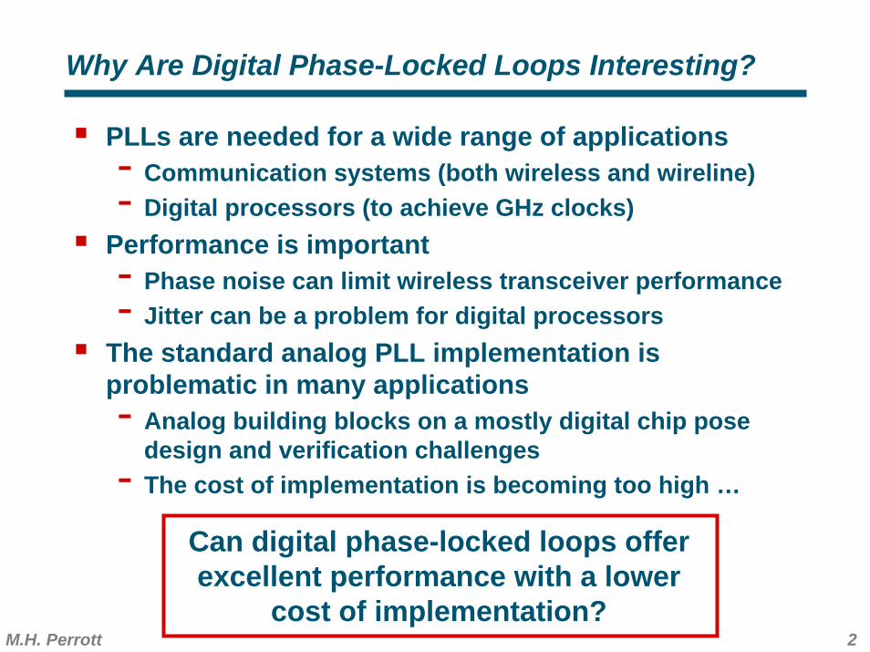
Why Are Digital Phase-Locked Loops Interesting?
PLLs are needed for a wide range of applications- Communication systems (both wireless and wireline)- Digital processors (to achieve GHz clocks)
Performance is important- Phase noise can limit wireless transceiver performance- Jitter can be a problem for digital processors
The standard analog PLL implementation is problematic in many applications- Analog building blocks on a mostly digital chip pose
design and verification challenges- The cost of implementation is becoming too high …
Can digital phase-locked loops offer excellent performance with a lower
cost of implementation?
3M.H. Perrott
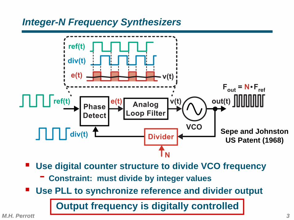
Integer-N Frequency Synthesizers
Use digital counter structure to divide VCO frequency- Constraint: must divide by integer values
Use PLL to synchronize reference and divider output
Sepe and JohnstonUS Patent (1968)
Output frequency is digitally controlled
e(t) v(t) out(t)ref(t) Analog
Loop FilterPhase
Detect
VCO
ref(t)
div(t)
e(t) v(t)
Divider
N
Fout = N Fref
div(t)
4M.H. Perrott
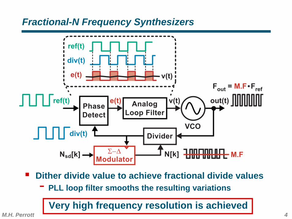
Fractional-N Frequency Synthesizers
Dither divide value to achieve fractional divide values- PLL loop filter smooths the resulting variations
Very high frequency resolution is achieved
e(t) v(t) out(t)ref(t) Analog
Loop FilterPhase
Detect
VCO
Divider
N[k]
Fout = M.F Fref
div(t)
Nsd[k] Σ−Δ
ModulatorM.F
ref(t)
div(t)
e(t) v(t)
5M.H. Perrott
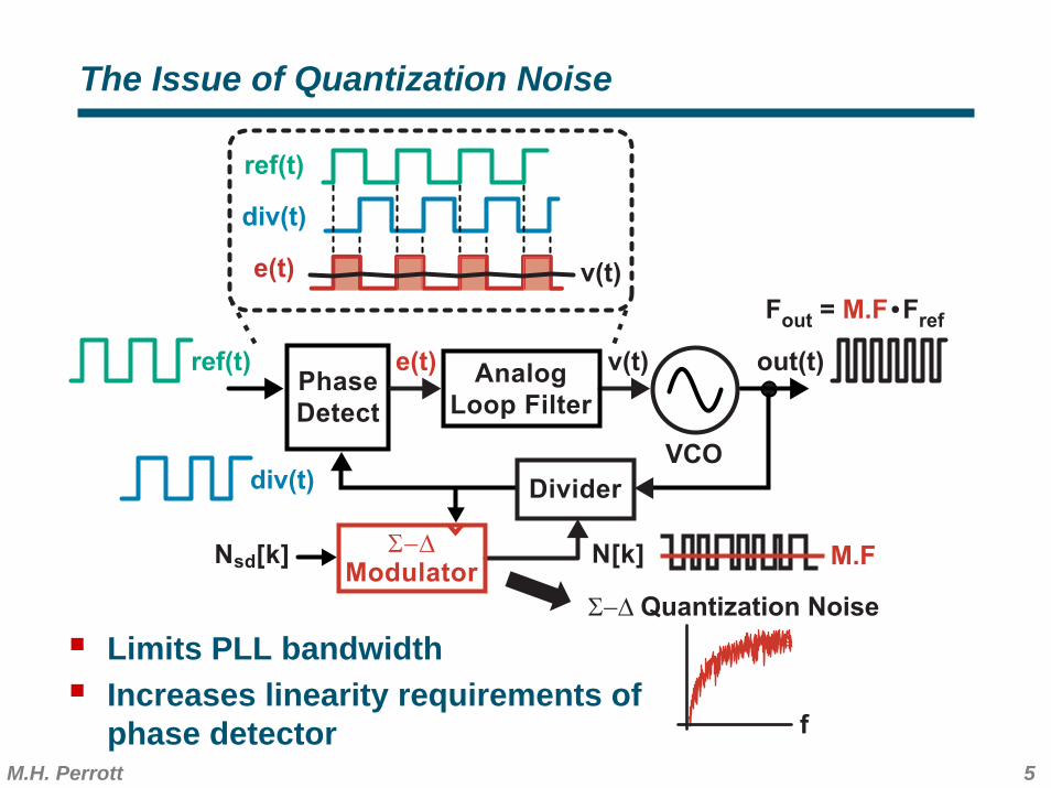
The Issue of Quantization Noise
Limits PLL bandwidthIncreases linearity requirements of phase detector
e(t) v(t) out(t)ref(t) Analog
Loop FilterPhase
Detect
VCO
Divider
N[k]
Fout = M.F Fref
div(t)
Nsd[k] Σ−Δ
ModulatorM.F
ref(t)
div(t)
e(t) v(t)
f
Σ−Δ Quantization Noise

Striving for a Better PLL Implementation
7M.H. Perrott
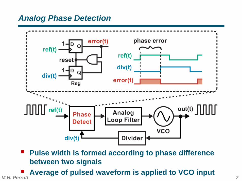
Analog Phase Detection
Pulse width is formed according to phase difference between two signalsAverage of pulsed waveform is applied to VCO input
out(t)ref(t) Analog
Loop FilterPhase
Detect
VCO
Reg
D Q
ref(t)
div(t)
phase errorD Q
reset
1
1
ref(t)
error(t)
div(t)
error(t)
Dividerdiv(t)
8M.H. Perrott
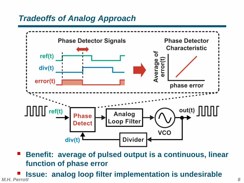
Tradeoffs of Analog Approach
Benefit: average of pulsed output is a continuous, linear function of phase errorIssue: analog loop filter implementation is undesirable
ref(t)
div(t)
error(t)
Phase Detector
Characteristic
Phase Detector Signals
out(t)Analog
Loop FilterPhase
Detect
VCO
phase error
Av
era
ge
of
err
or(
t)
Divider
ref(t)
div(t)
9M.H. Perrott
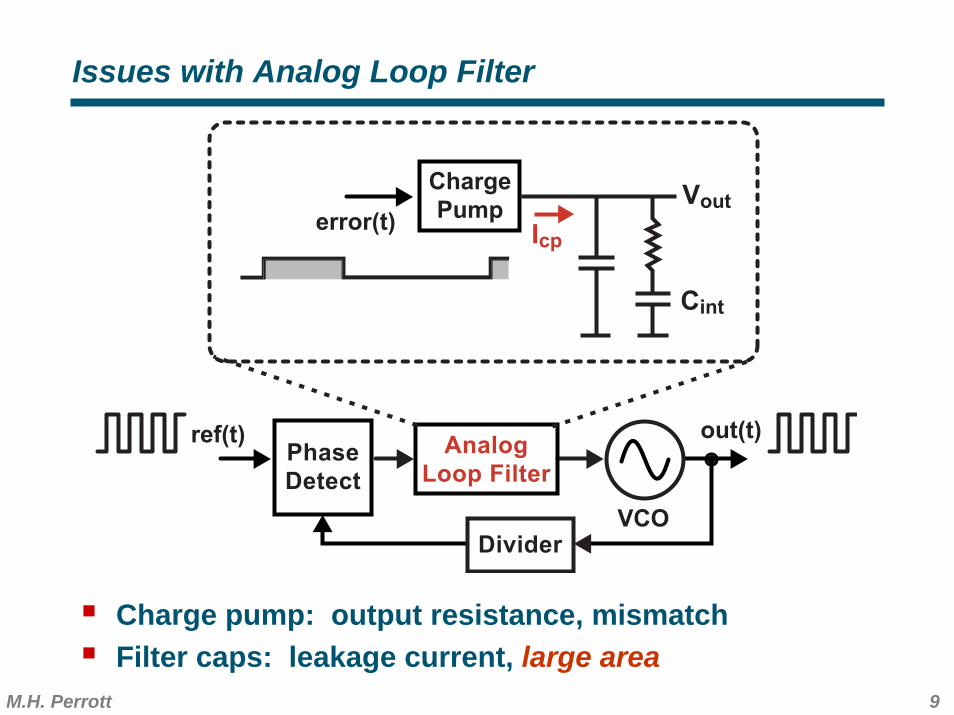
Issues with Analog Loop Filter
Charge pump: output resistance, mismatchFilter caps: leakage current, large area
out(t)ref(t) Analog
Loop FilterPhase
Detect
VCO
error(t)Icp
VoutCharge
Pump
Cint
Divider
10M.H. Perrott
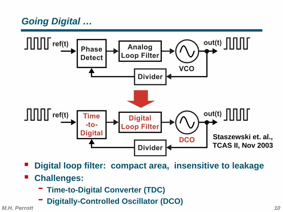
Going Digital …
Digital loop filter: compact area, insensitive to leakageChallenges: - Time-to-Digital Converter (TDC)- Digitally-Controlled Oscillator (DCO)
Staszewski et. al.,TCAS II, Nov 2003
out(t)ref(t) Analog
Loop FilterPhase
Detect
VCO
Time
-to-
Digital
out(t)ref(t) Digital
Loop Filter
DCO
Divider
Divider
Time-to-Digital Conversion
12M.H. Perrott
Time
-to-
Digital
out(t)ref(t) Digital
Loop Filter
DCO
div(t)
Reg
D Q
Delay
Reg
D Q
Reg
D Q
Delay Delay
ref(t)
e[k]
Dividerdiv(t)
ref(t)
div(t)
e[k]
1
1
1
0
0
Delay
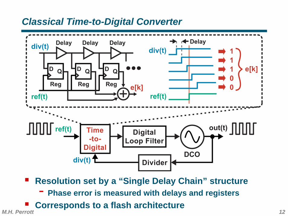
Classical Time-to-Digital Converter
Resolution set by a “Single Delay Chain” structure- Phase error is measured with delays and registers
Corresponds to a flash architecture
13M.H. Perrott
Time
-to-
Digital
out(t)ref(t) Digital
Loop Filter
DCODividerdiv(t)
ref(t)
div(t)
e[k]
1
1
1
0
0
Phase Detector
Characteristic
phase error
de
tec
tor
ou
tpu
t
Delay varies due to mismatch
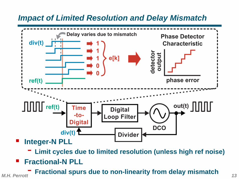
Impact of Limited Resolution and Delay Mismatch
Integer-N PLL- Limit cycles due to limited resolution (unless high ref noise)
Fractional-N PLL- Fractional spurs due to non-linearity from delay mismatch
14M.H. Perrott
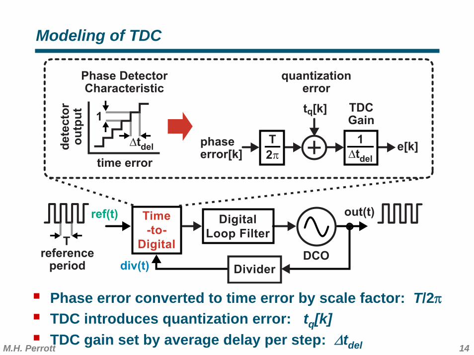
Modeling of TDC
Phase error converted to time error by scale factor: T/2πTDC introduces quantization error: tq[k]TDC gain set by average delay per step: Δtdel
Time
-to-
Digital
out(t)ref(t) Digital
Loop Filter
DCO
quantizationerror
phaseerror[k]
e[k]
Phase DetectorCharacteristic
time error
de
tec
tor
ou
tpu
t
T
2π
tq[k]
Dividerdiv(t)reference
period
T
TDCGain
1
Δtdel
Δtdel
1
How Do We Improve Performance?
Two Key Issues:• TDC resolution• Mismatch
16M.H. Perrott
div(t)
Reg
D Q
Delay
Reg
D Q
Reg
D Q
Delay Delay
ref(t)
e[k]
ref(t)
div(t)
e[k]
1
1
1
0
0
Delay
div(t)
Reg
D Q
Delay
Reg
D Q
Reg
D Q
Delay Delay
ref(t)
e[k]Delay2 Delay2 Delay2
div(t)
Delay
ref(t)
Delay2
e[k]
1
1
1
0
0
Vernier
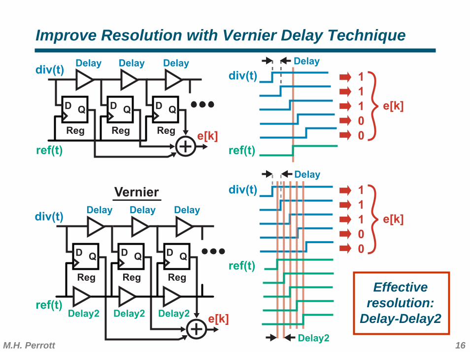
Improve Resolution with Vernier Delay Technique
Effective resolution:
Delay-Delay2
17M.H. Perrott
div(t)
Reg
D Q
Delay
Reg
D Q
Reg
D Q
Delay Delay
ref(t)
e[k]Delay2 Delay2 Delay2
div(t)
Delay
ref(t)
Delay2
e[k]
1
1
1
0
0
Vernier
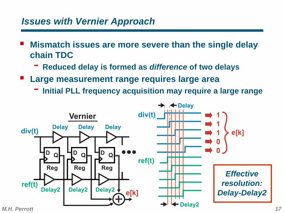
Issues with Vernier Approach
Mismatch issues are more severe than the single delay chain TDC- Reduced delay is formed as difference of two delays
Large measurement range requires large area- Initial PLL frequency acquisition may require a large range
Effective resolution:
Delay-Delay2
18M.H. Perrott
Vernier
div(t)
ref(t)
Coarsee[k]
Delay Delay Delay
Delay2 Delay2 Delay2
Delay Delay Delay
Reg
D Q
Reg
D Q
Reg
D Q
Reg
D Q
Reg
D Q
Reg
D Q
Logic
Mux
Finee[k]
Single Delay Chain
Delay
Delay - Delay2
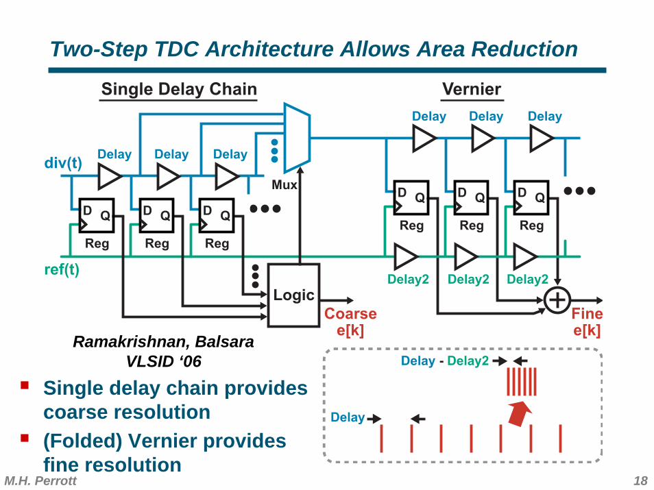
Two-Step TDC Architecture Allows Area Reduction
Single delay chain provides coarse resolution(Folded) Vernier provides fine resolution
Ramakrishnan, BalsaraVLSID ‘06
19M.H. Perrott
Single Delay Chain
div(t)
ref(t)
Coarsee[k]
Delay Delay DelayDelay Delay Delay
Reg
D Q
Reg
D Q
Reg
D Q
Reg
D Q
Reg
D Q
Reg
D Q
Logic
Mux
Finee[k]
Single Delay Chain
Delay
Delay
Time
Amplifier
Amplificationof Time
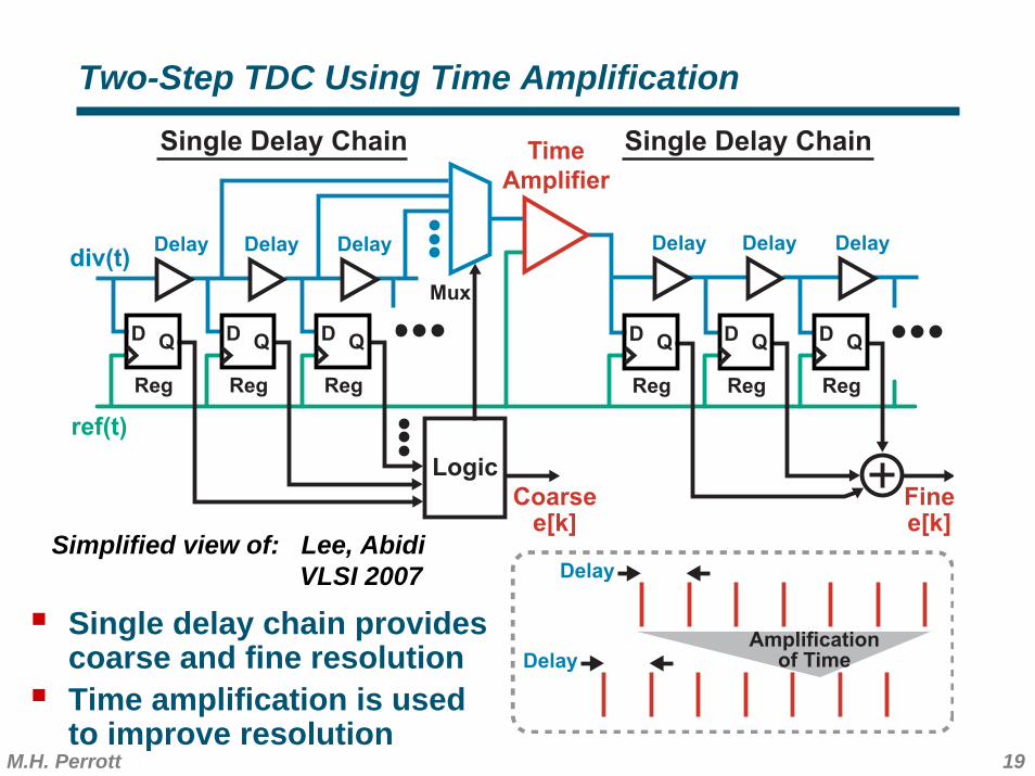
Single delay chain provides coarse and fine resolutionTime amplification is used to improve resolution
Simplified view of: Lee, AbidiVLSI 2007
Two-Step TDC Using Time Amplification
20M.H. Perrott
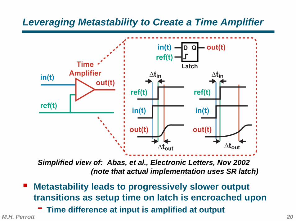
Leveraging Metastability to Create a Time Amplifier
Metastability leads to progressively slower output transitions as setup time on latch is encroached upon- Time difference at input is amplified at output
Simplified view of: Abas, et al., Electronic Letters, Nov 2002(note that actual implementation uses SR latch)
Time
AmplifierLatch
D Qin(t)
ref(t)
out(t)
ref(t)
in(t)
out(t)
ref(t)
in(t)
out(t)
ref(t)
Δtin Δtin
Δtout Δtout
in(t)out(t)
21M.H. Perrott
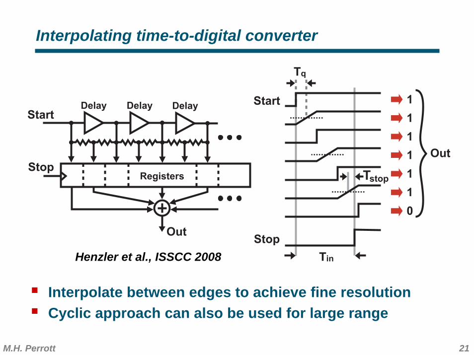
Interpolating time-to-digital converter
Interpolate between edges to achieve fine resolutionCyclic approach can also be used for large range
Tstop
Start
Stop
Tq
Tin
1
1
1
1
1
Out
Stop
StartDelayDelayDelay
Registers
Out
1
0
Henzler et al., ISSCC 2008
22M.H. Perrott
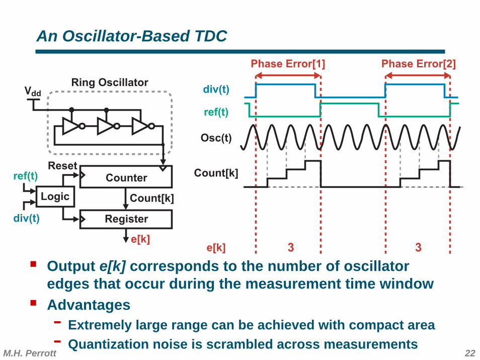
Ring OscillatorVdd
Counter
Register
Reset
Count[k]
e[k]
Osc(t)
e[k]
ref(t)
div(t)
Phase Error[1] Phase Error[2]
Logic
div(t)
ref(t)
Count[k]
3 3
An Oscillator-Based TDC
Output e[k] corresponds to the number of oscillator edges that occur during the measurement time windowAdvantages- Extremely large range can be achieved with compact area- Quantization noise is scrambled across measurements
23M.H. Perrott
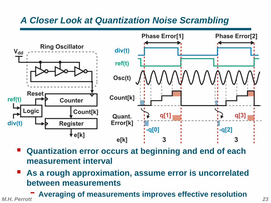
Ring OscillatorVdd
Counter
Register
Reset
Count[k]
e[k]
Osc(t)
e[k]
ref(t)
div(t)
Phase Error[1] Phase Error[2]
Logic
div(t)
ref(t)
Count[k]
3 3
Quant.Error[k]
q[1] q[3]
-q[0] -q[2]
A Closer Look at Quantization Noise Scrambling
Quantization error occurs at beginning and end of each measurement intervalAs a rough approximation, assume error is uncorrelated between measurements- Averaging of measurements improves effective resolution
24M.H. Perrott
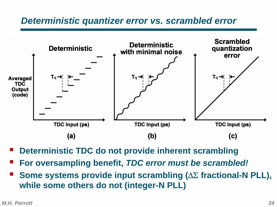
Deterministic quantizer error vs. scrambled error
Deterministic TDC do not provide inherent scramblingFor oversampling benefit, TDC error must be scrambled!Some systems provide input scrambling (ΔΣ fractional-N PLL), while some others do not (integer-N PLL)

Proposed GRO TDC Structure
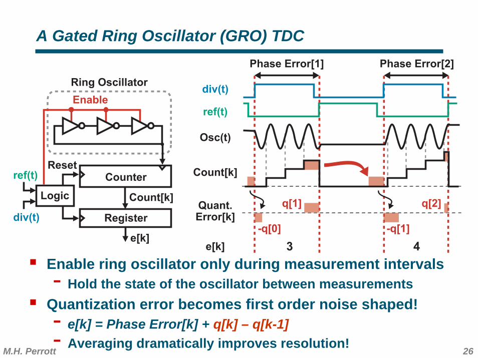
26M.H. Perrott
Ring Oscillator
Counter
Register
Reset
Count[k]
e[k]
Osc(t)
e[k]
ref(t)
div(t)
Phase Error[1] Phase Error[2]
Logic
div(t)
ref(t)
Count[k]
3 4
Quant.Error[k]
q[1] q[2]
-q[0] -q[1]
Enable
A Gated Ring Oscillator (GRO) TDC
Enable ring oscillator only during measurement intervals- Hold the state of the oscillator between measurements
Quantization error becomes first order noise shaped!- e[k] = Phase Error[k] + q[k] – q[k-1]- Averaging dramatically improves resolution!
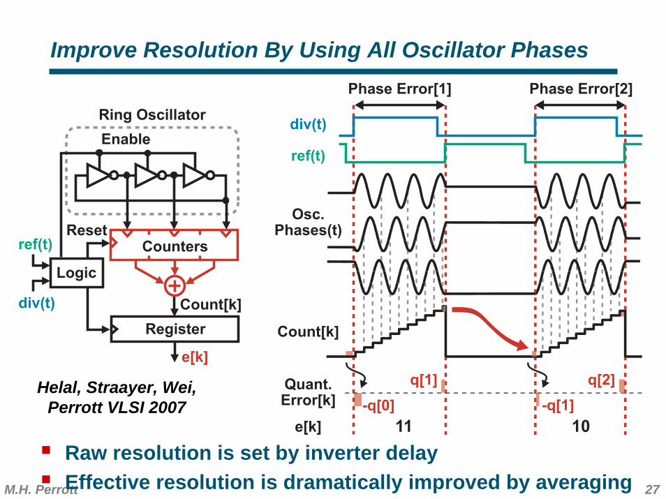
27M.H. Perrott
Ring Oscillator
Register
Reset
Count[k]
e[k]
ref(t)
div(t)
Logic
Enable
Osc.Phases(t)
Count[k]
e[k] 11 10
Quant.Error[k]
q[1] q[2]
-q[1]
Phase Error[1] Phase Error[2]
div(t)
ref(t)
-q[0]
Counters
Raw resolution is set by inverter delayEffective resolution is dramatically improved by averaging
Helal, Straayer, Wei, Perrott VLSI 2007
Improve Resolution By Using All Oscillator Phases
28M.H. Perrott
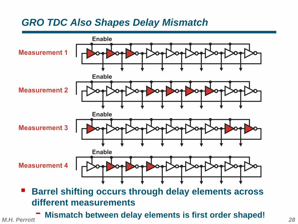
GRO TDC Also Shapes Delay Mismatch
Barrel shifting occurs through delay elements across different measurements- Mismatch between delay elements is first order shaped!
Enable
Enable
Enable
Enable
Measurement 1
Measurement 2
Measurement 3
Measurement 4
29M.H. Perrott
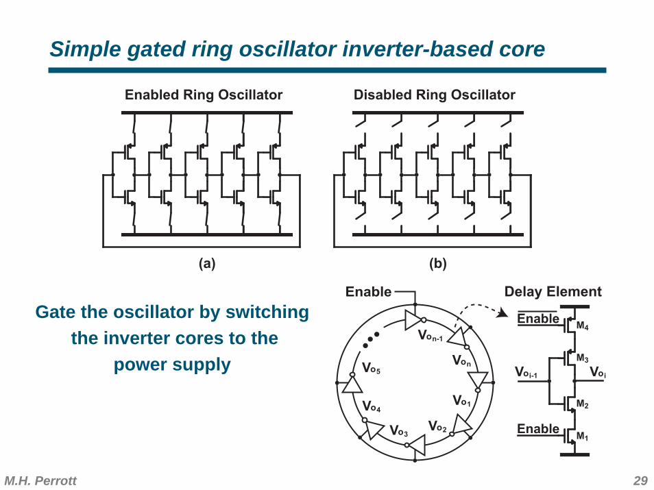
Simple gated ring oscillator inverter-based core
Enabled Ring Oscillator Disabled Ring Oscillator
(a) (b)
Gate the oscillator by switchingthe inverter cores to the
power supply
Enable
Enable
Enable
VoiVoi-1
Delay Element
Vo4Vo1
Von
Vo2Vo3
Vo5
M4
M3
M2
M1
Von-1
30M.H. Perrott
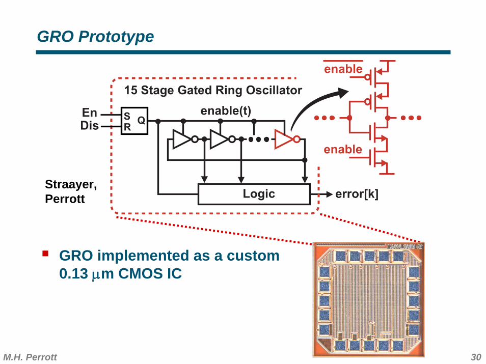
GRO Prototype
GRO implemented as a custom 0.13 μm CMOS IC
Straayer,Perrott
15 Stage Gated Ring Oscillator
enable(t)EnDis
Logic error[k]
enable
enable
S QR
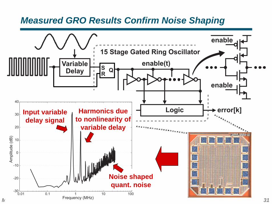
31M.H. Perrott
enable
enable
15 Stage Gated Ring Oscillator
enable(t)
Logic
S QR
error[k]
VariableDelay
Measured GRO Results Confirm Noise Shaping
0.01 0.1 1 10 100-30
-20
-10
0
10
20
30
40
Frequency (MHz)
Am
plit
ud
e (
dB
)
Noise shapedquant. noise
Harmonics dueto nonlinearity of
variable delay
Input variabledelay signal
32M.H. Perrott
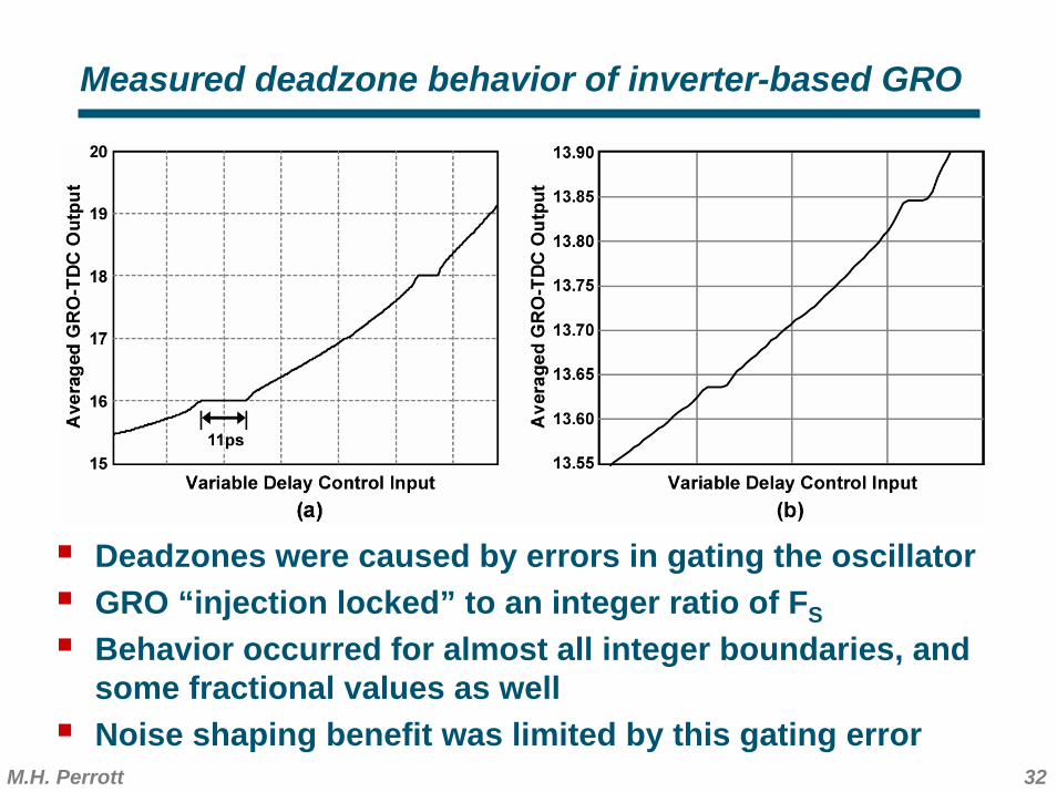
Measured deadzone behavior of inverter-based GRO
Deadzones were caused by errors in gating the oscillatorGRO “injection locked” to an integer ratio of FSBehavior occurred for almost all integer boundaries, and some fractional values as wellNoise shaping benefit was limited by this gating error

33M.H. Perrott
The issue of gating non-idealities…
GRO Phase
Enable
Orig
inal p
hase traje
ctory
Orig
inal p
hase + Tdis
able
Actual p
hase
TinTdisable
Tskew
Oscillator does not stop and start instantlyActual phase trajectory deviates from ideal trajectory by a time defined as “Tskew”
34M.H. Perrott
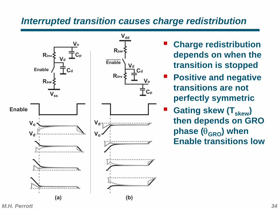
Interrupted transition causes charge redistribution
Enable
Vd
Vo
Vss
Vd
Vo
(a) (b)
Vo
Enable
Vo
Vdd
Cp
Cd
Cp
Cd
Rinv
Rinv
Rsw
Enable
Rsw
Vd
Vd
Charge redistribution depends on when the transition is stoppedPositive and negative transitions are not perfectly symmetricGating skew (Tskew) then depends on GRO phase (θGRO) when Enable transitions low
35M.H. Perrott
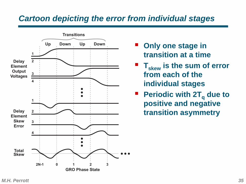
Cartoon depicting the error from individual stages
Only one stage in transition at a timeTskew is the sum of error from each of the individual stagesPeriodic with 2Tq due to positive and negative transition asymmetry
GRO Phase State
Delay
Element
Output
Voltages
2N-1 0 1 2
Delay
Element
Skew
Error
1
2
4
3
1
2
3
4
3
TotalSkew
Up Down Up Down
Transitions
36M.H. Perrott
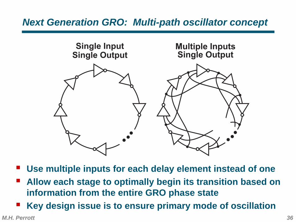
Next Generation GRO: Multi-path oscillator concept
Use multiple inputs for each delay element instead of oneAllow each stage to optimally begin its transition based on information from the entire GRO phase state Key design issue is to ensure primary mode of oscillation
Single InputSingle Output
Multiple InputsSingle Output
37M.H. Perrott
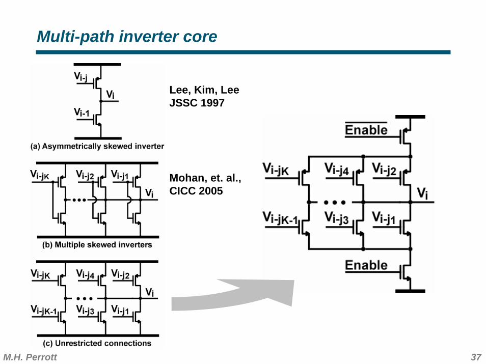
Multi-path inverter core
Lee, Kim, LeeJSSC 1997
Mohan, et. al., CICC 2005
38M.H. Perrott
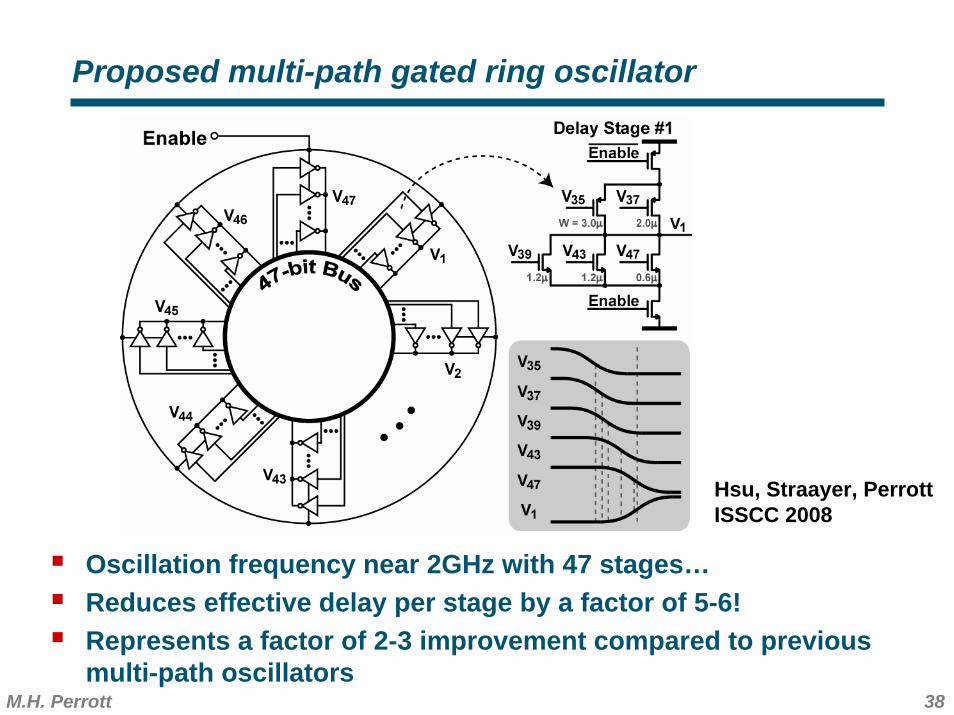
Proposed multi-path gated ring oscillator
Oscillation frequency near 2GHz with 47 stages…Reduces effective delay per stage by a factor of 5-6! Represents a factor of 2-3 improvement compared to previous multi-path oscillators
Hsu, Straayer, Perrott ISSCC 2008
39M.H. Perrott
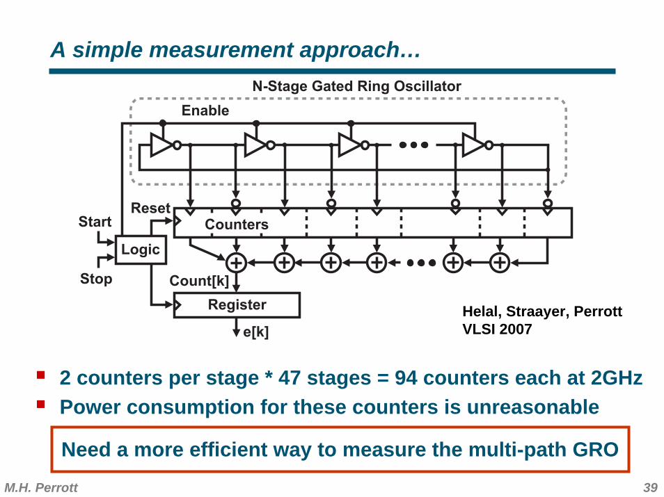
A simple measurement approach…
2 counters per stage * 47 stages = 94 counters each at 2GHz Power consumption for these counters is unreasonable
Need a more efficient way to measure the multi-path GRO
N-Stage Gated Ring Oscillator
ResetStart
Stop
Logic
Register
Count[k]
e[k]
Counters
Enable
Helal, Straayer, Perrott VLSI 2007
40M.H. Perrott
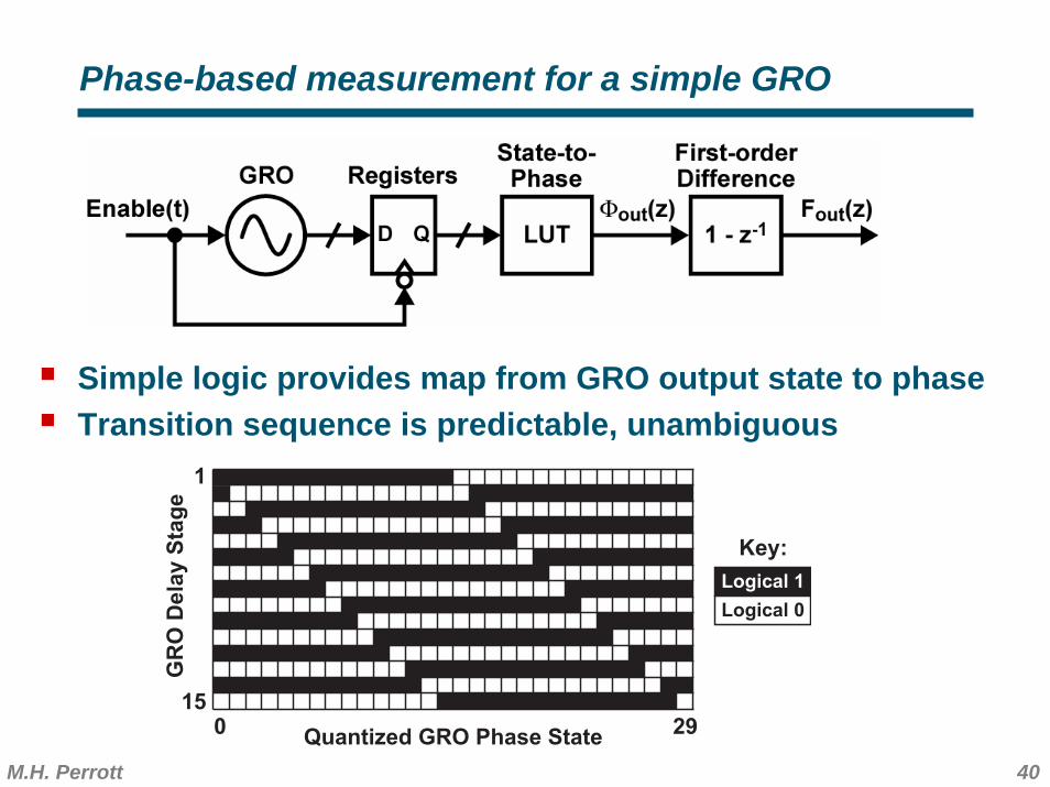
Phase-based measurement for a simple GRO
1
15
GR
O D
ela
y S
tag
e
Quantized GRO Phase State0 29
Logical 1
Logical 0
Key:
Simple logic provides map from GRO output state to phaseTransition sequence is predictable, unambiguous
41M.H. Perrott
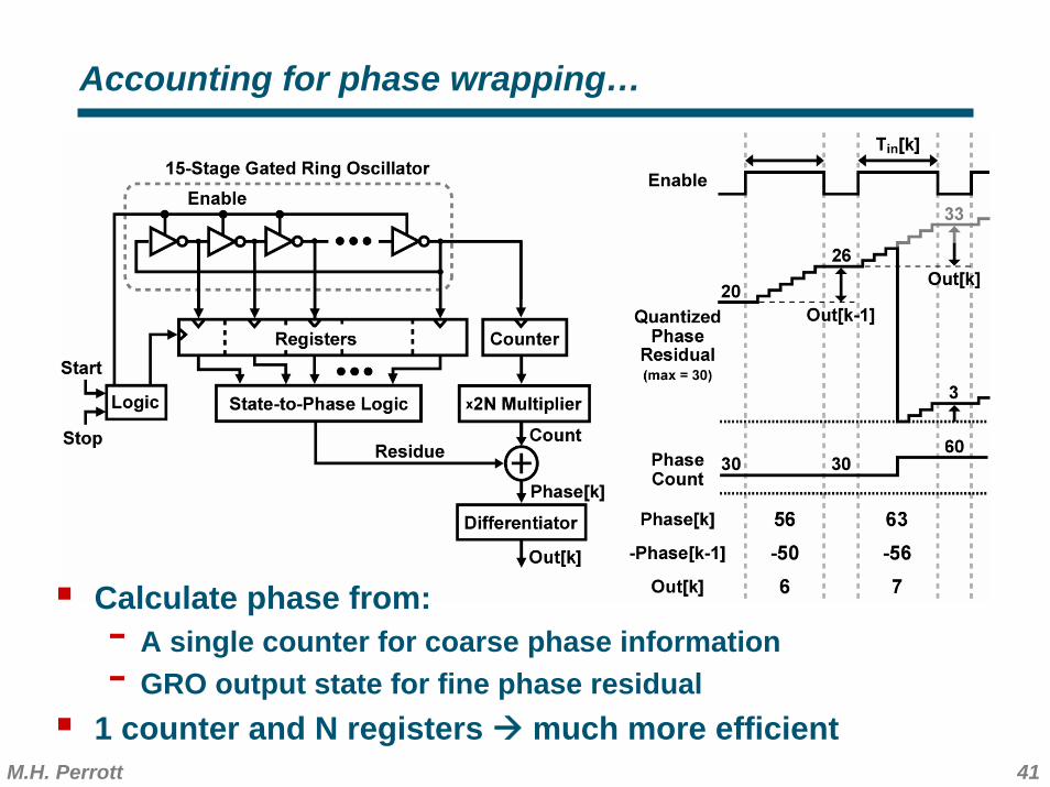
Accounting for phase wrapping…
Calculate phase from:- A single counter for coarse phase information- GRO output state for fine phase residual
1 counter and N registers much more efficient
42M.H. Perrott
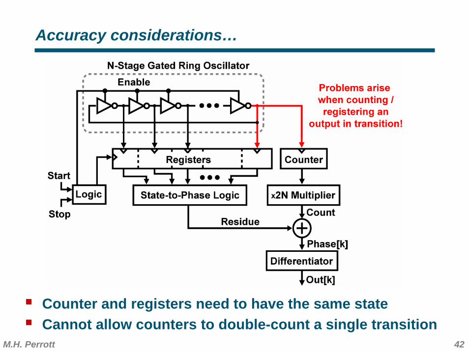
Accuracy considerations…
Counter and registers need to have the same stateCannot allow counters to double-count a single transition
43M.H. Perrott
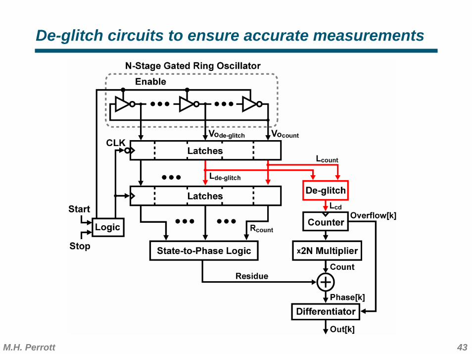
De-glitch circuits to ensure accurate measurements
44M.H. Perrott
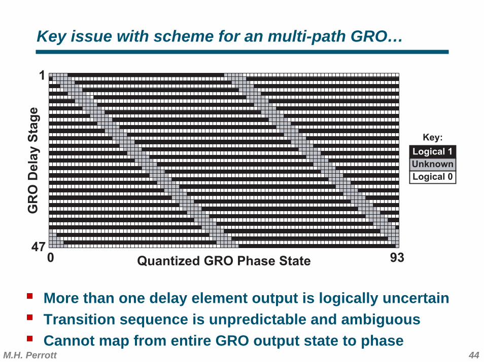
Key issue with scheme for an multi-path GRO…
More than one delay element output is logically uncertainTransition sequence is unpredictable and ambiguousCannot map from entire GRO output state to phase
1
47
GR
O D
ela
y S
tag
e
Quantized GRO Phase State0 93
Logical 1
Logical 0
Unknown
Key:
45M.H. Perrott
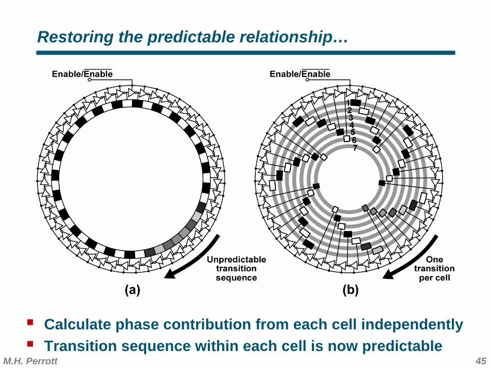
Restoring the predictable relationship…
Calculate phase contribution from each cell independentlyTransition sequence within each cell is now predictable
46M.H. Perrott
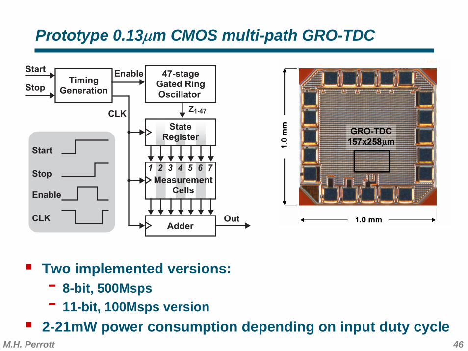
Prototype 0.13μm CMOS multi-path GRO-TDC
Timing
Generation
Out
Enable 47-stage
Gated Ring
Oscillator
State
Register
Start
Stop
Adder
Z1-47
Measurement
Cells
Start
Stop
Enable
CLK
CLK
1 72 3 4 5 6
Two implemented versions:- 8-bit, 500Msps- 11-bit, 100Msps version
2-21mW power consumption depending on input duty cycle
47M.H. Perrott
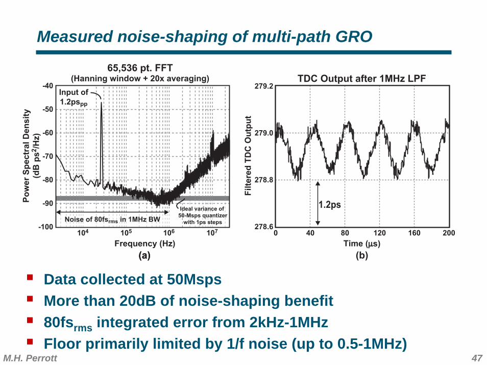
Measured noise-shaping of multi-path GRO
Data collected at 50MspsMore than 20dB of noise-shaping benefit80fsrms integrated error from 2kHz-1MHzFloor primarily limited by 1/f noise (up to 0.5-1MHz)
104 105 106 107
Frequency (Hz)
-100
-90
-80
-70
-60
-50
-40
Po
wer
Sp
ectr
al D
en
sit
y
(dB
ps
2/H
z)
65,536 pt. FFT(Hanning window + 20x averaging)
278.6
278.8
279.0
279.2TDC Output after 1MHz LPF
Filte
red
TD
C O
utp
ut
Time (µµs)
0 40 80 120 160 200
Noise of 80fsrms in 1MHz BW
Input of
1.2pspp
Ideal variance of
50-Msps quantizer
with 1ps steps
1.2ps
(a)(a) (b)
48M.H. Perrott
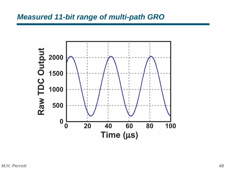
Measured 11-bit range of multi-path GRO
Ra
w T
DC
Ou
tpu
t
Time (µµs)
0
500
1000
1500
2000
0 20 40 60 80 100
49M.H. Perrott
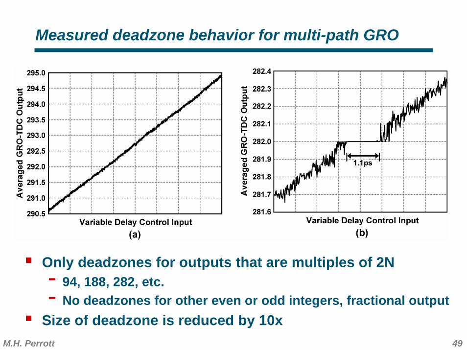
Measured deadzone behavior for multi-path GRO
Only deadzones for outputs that are multiples of 2N- 94, 188, 282, etc.- No deadzones for other even or odd integers, fractional output
Size of deadzone is reduced by 10x
50M.H. Perrott
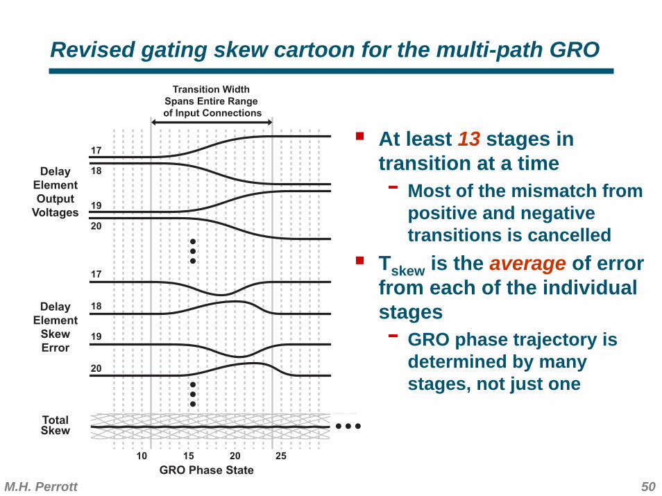
Revised gating skew cartoon for the multi-path GRO
GRO Phase State
Transition Width
Spans Entire Range
of Input Connections
Delay
Element
Output
Voltages
10 15
Delay
Element
Skew
Error
17
18
20
19
17
18
19
20
20 25
TotalSkew
At least 13 stages in transition at a time- Most of the mismatch from
positive and negative transitions is cancelled
Tskew is the average of error from each of the individual stages- GRO phase trajectory is
determined by many stages, not just one
51M.H. Perrott
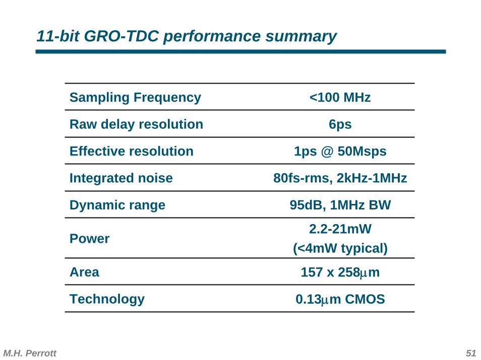
11-bit GRO-TDC performance summary
Sampling Frequency <100 MHz
Raw delay resolution 6ps
Effective resolution 1ps @ 50Msps
Integrated noise 80fs-rms, 2kHz-1MHz
Dynamic range 95dB, 1MHz BW
Power2.2-21mW
(<4mW typical)
Area 157 x 258μm
Technology 0.13μm CMOS
52M.H. Perrott
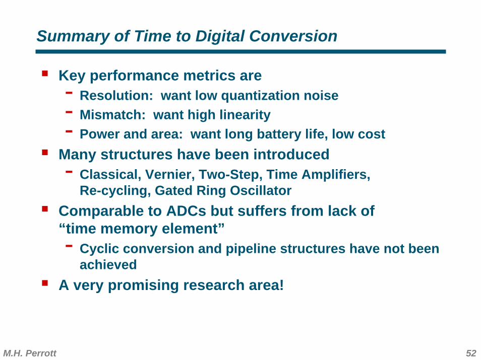
Summary of Time to Digital Conversion
Key performance metrics are- Resolution: want low quantization noise- Mismatch: want high linearity- Power and area: want long battery life, low cost
Many structures have been introduced- Classical, Vernier, Two-Step, Time Amplifiers,
Re-cycling, Gated Ring OscillatorComparable to ADCs but suffers from lack of “time memory element”- Cyclic conversion and pipeline structures have not been
achievedA very promising research area!
Digitally-Controlled Oscillators
54M.H. Perrott
Time
-to-
Digital
out(t)ref(t) Digital
Loop Filter
DCODividerdiv(t)
Va
rac
tor
Va
rac
tor
Analog
Control
DAC
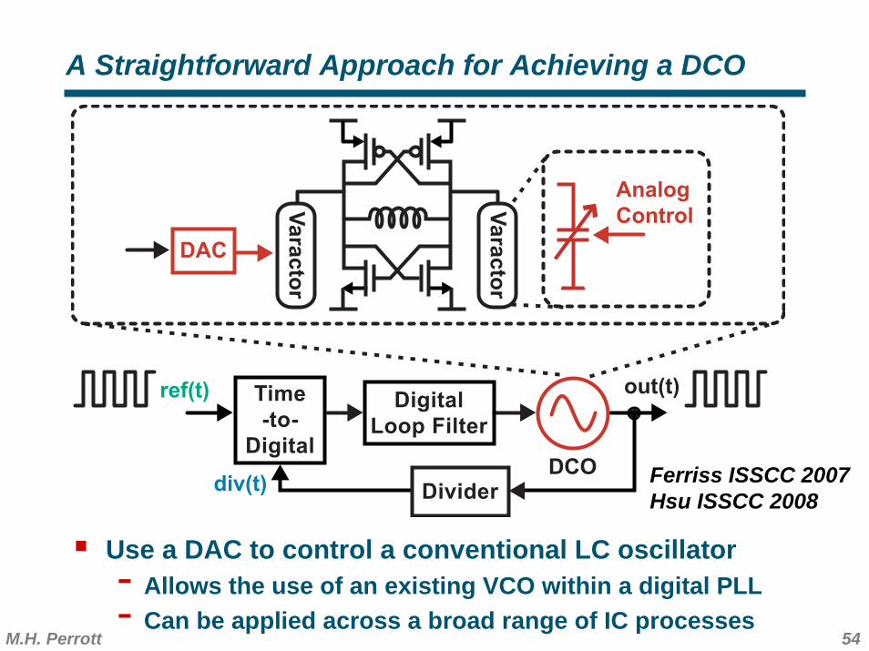
A Straightforward Approach for Achieving a DCO
Use a DAC to control a conventional LC oscillator- Allows the use of an existing VCO within a digital PLL- Can be applied across a broad range of IC processes
Ferriss ISSCC 2007Hsu ISSCC 2008
55M.H. Perrott
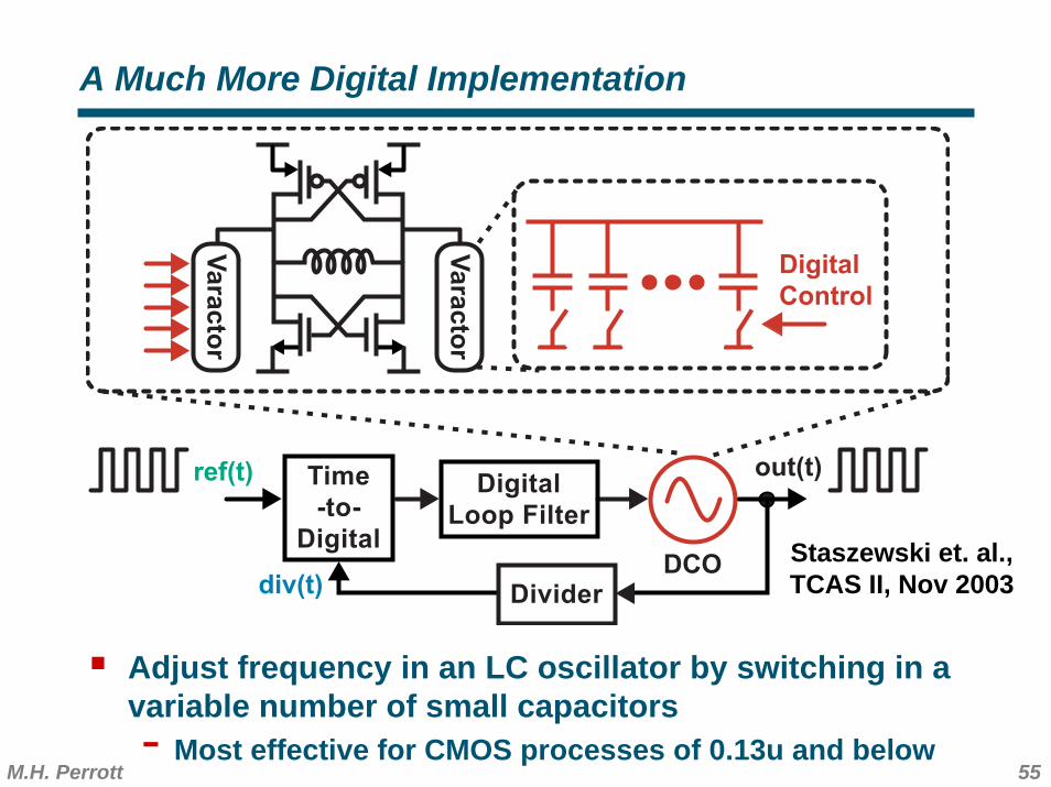
A Much More Digital Implementation
Adjust frequency in an LC oscillator by switching in a variable number of small capacitors- Most effective for CMOS processes of 0.13u and below
Staszewski et. al.,TCAS II, Nov 2003
Time
-to-
Digital
out(t)ref(t) Digital
Loop Filter
DCODividerdiv(t)
Va
rac
tor
Va
rac
tor
Digital
Control
56M.H. Perrott
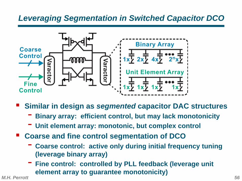
Leveraging Segmentation in Switched Capacitor DCO
Similar in design as segmented capacitor DAC structures- Binary array: efficient control, but may lack monotonicity- Unit element array: monotonic, but complex control
Coarse and fine control segmentation of DCO- Coarse control: active only during initial frequency tuning
(leverage binary array)- Fine control: controlled by PLL feedback (leverage unit
element array to guarantee monotonicity)
Va
rac
tor
Va
rac
tor
1x 2x 4x 2nx
1x 1x 1x 1x
Binary Array
Unit Element Array
CoarseControl
FineControl
57M.H. Perrott
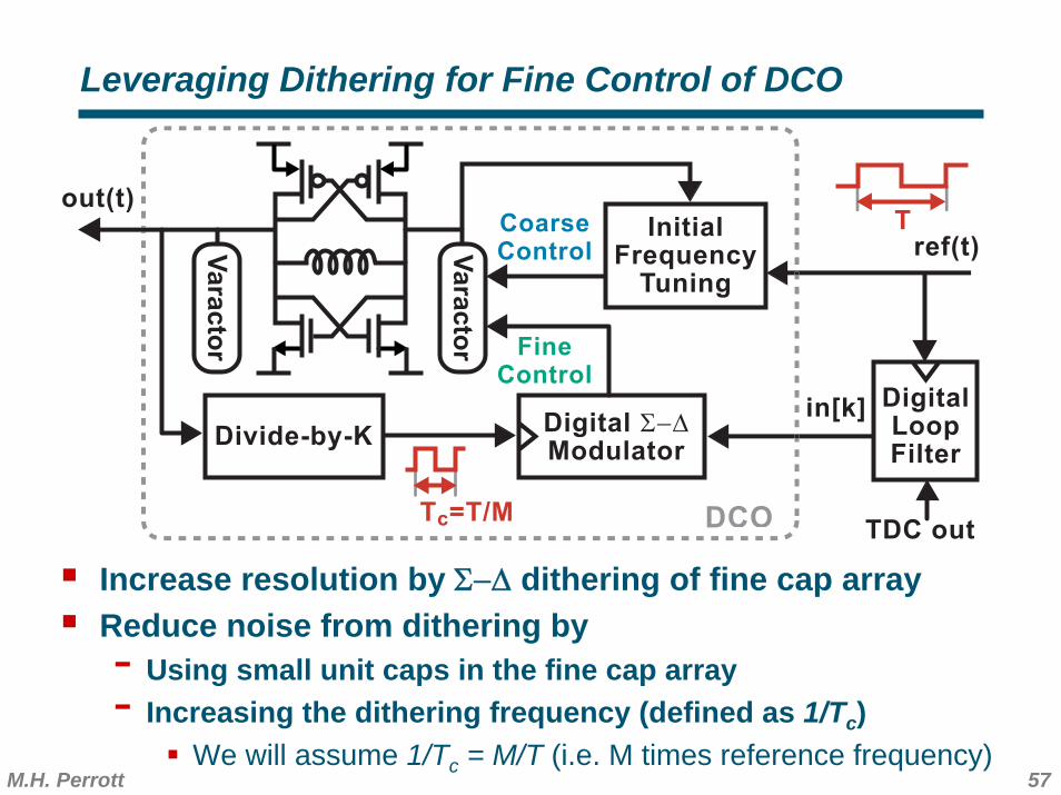
Leveraging Dithering for Fine Control of DCO
Increase resolution by Σ−Δ dithering of fine cap arrayReduce noise from dithering by- Using small unit caps in the fine cap array- Increasing the dithering frequency (defined as 1/Tc)
We will assume 1/Tc = M/T (i.e. M times reference frequency)
Va
rac
tor
Va
rac
tor
CoarseControl
FineControl
InitialFrequency
Tuning
T
Divide-by-K
Tc=T/M
Digital Σ−Δ
Modulator
in[k] DigitalLoopFilter
ref(t)
out(t)
TDC outDCO
58M.H. Perrott
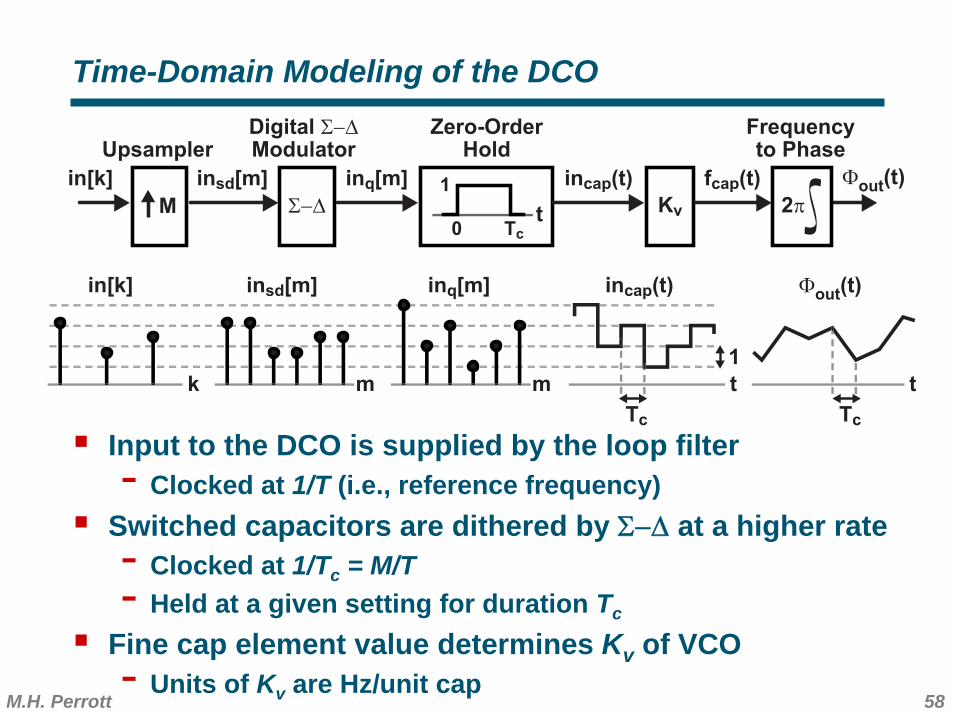
Time-Domain Modeling of the DCO
Input to the DCO is supplied by the loop filter- Clocked at 1/T (i.e., reference frequency)
Switched capacitors are dithered by Σ−Δ at a higher rate- Clocked at 1/Tc = M/T- Held at a given setting for duration Tc
Fine cap element value determines Kv of VCO- Units of Kv are Hz/unit cap
Digital Σ−Δ
Modulator
in[k]
Zero-OrderHold
tTc
1
0
m m
inq[m]
t
Tc
1
Kv
Frequencyto Phase
incap(t) Φout(t)
in[k] inq[m] incap(t)
t
Tc
Φout(t)
2π
fcap(t)
Σ−Δ
insd[m]
M
Upsampler
k
insd[m]
59M.H. Perrott
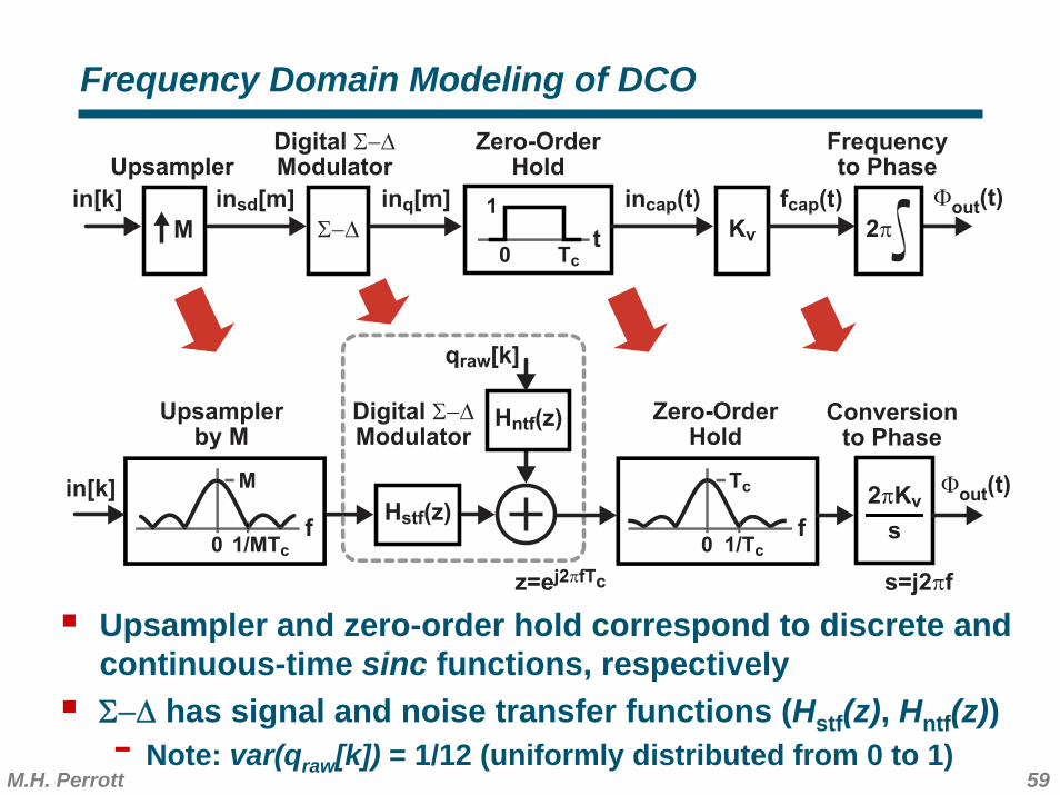
Frequency Domain Modeling of DCO
Upsampler and zero-order hold correspond to discrete and continuous-time sinc functions, respectivelyΣ−Δ has signal and noise transfer functions (Hstf(z), Hntf(z))- Note: var(qraw[k]) = 1/12 (uniformly distributed from 0 to 1)
f1/Tc
Tc
0
Zero-OrderHold
Digital Σ−Δ
Modulator
in[k]
Zero-OrderHold
tTc
1
0
inq[m]
Kv
Frequencyto Phase
incap(t) Φout(t)
2π
fcap(t)
Σ−Δ
insd[m]
M
Upsampler
f1/MTc
M
0
Upsamplerby M
Hntf(z)
Hstf(z)in[k]
Conversionto Phase
2πKv
s
s=j2πfz=ej2πfTc
Digital Σ−Δ
Modulator
Φout(t)
qraw[k]
60M.H. Perrott
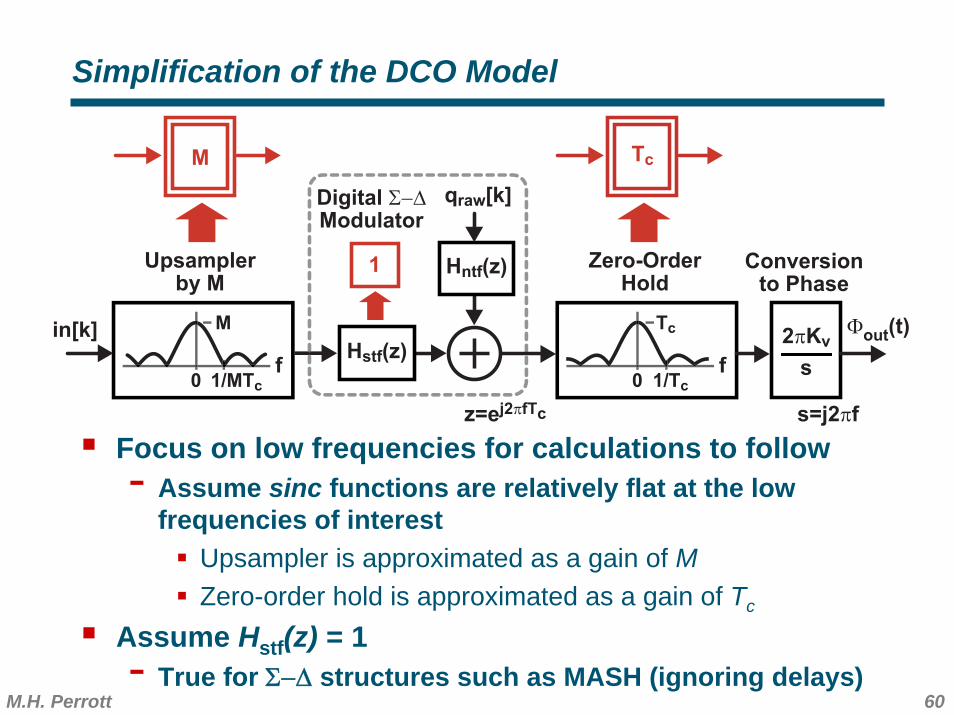
Simplification of the DCO Model
Focus on low frequencies for calculations to follow- Assume sinc functions are relatively flat at the low
frequencies of interestUpsampler is approximated as a gain of MZero-order hold is approximated as a gain of Tc
Assume Hstf(z) = 1- True for Σ−Δ structures such as MASH (ignoring delays)
f1/Tc
Tc
0
Zero-OrderHold
f1/MTc
M
0
Upsamplerby M
Hntf(z)
Hstf(z)in[k]
Conversionto Phase
2πKv
s
s=j2πfz=ej2πfTc
Digital Σ−Δ
Modulator
Φout(t)
TcM
1
qraw[k]
61M.H. Perrott
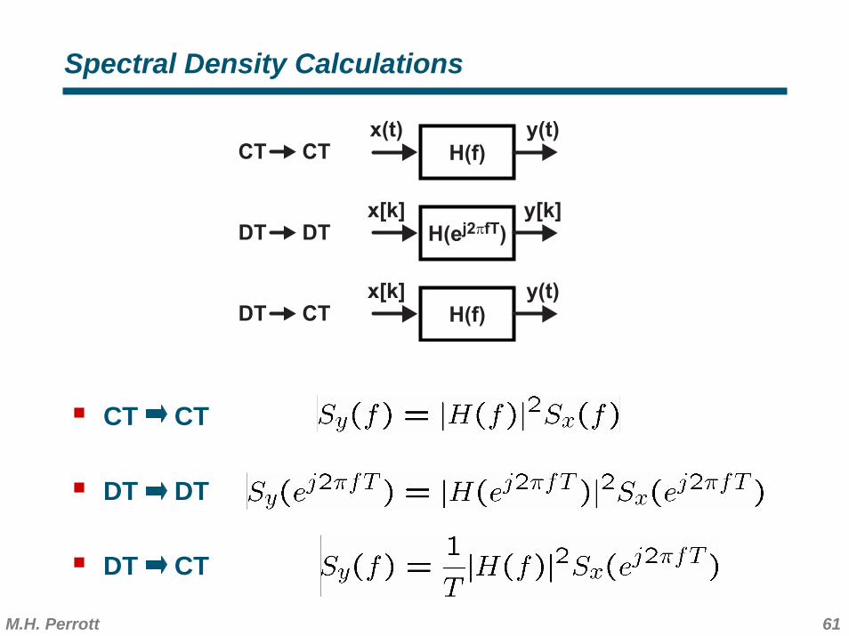
Spectral Density Calculations
CT CT
DT DT
DT CT
CT CT
x[k]H(f)
y(t)
x[k]H(ej2πfT)
y[k]
x(t)H(f)
y(t)
DT DT
DT CT
62M.H. Perrott
Hntf(z)z=ej2πfTc
TcM2πKv
s
s=j2πf
in[k]
qraw[k]
Φout(t)
q[k]
PhaseNoise
ff
QuantizationNoise
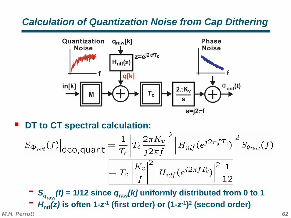
Calculation of Quantization Noise from Cap Dithering
DT to CT spectral calculation:
- Sqraw(f) = 1/12 since qraw[k] uniformly distributed from 0 to 1
- Hntf(z) is often 1-z-1 (first order) or (1-z-1)2 (second order)
63M.H. Perrott
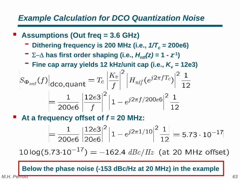
Example Calculation for DCO Quantization Noise
At a frequency offset of f = 20 MHz:
Assumptions (Out freq = 3.6 GHz)- Dithering frequency is 200 MHz (i.e., 1/Tc = 200e6)- Σ−Δ has first order shaping (i.e., Hntf(z) = 1 - z-1)- Fine cap array yields 12 kHz/unit cap (i.e., Kv = 12e3)
Below the phase noise (-153 dBc/Hz at 20 MHz) in the example
64M.H. Perrott
Hntf(z)z=ej2πfTc
TcM2πKv
s
s=j2πf
in[k]
qraw[k]
Φout(t)
q[k]
PhaseNoise
ff
QuantizationNoise
T2πKv
s
s=j2πf
Φout(t)in[k]
DT-CTΦn(t)
DCO-ReferredNoise
SΦn(f)
f
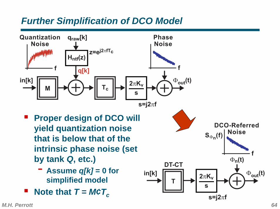
Further Simplification of DCO Model
Proper design of DCO will yield quantization noise that is below that of the intrinsic phase noise (set by tank Q, etc.)- Assume q[k] = 0 for
simplified modelNote that T = M¢Tc
65M.H. Perrott
f
Stq(ej2πfT)
TDC-referredNoise
e[k]T
2π
tq[k] TDCGain
1
Δtdel
Φref[k]
H(z)
LoopFilter
2πKv
s
Φn(t)
1
T
T
1
N
DT-CT
CT-DT
Φdiv[k]
Φout(t)
TDC DCO
Divider
SΦn(f)
-20 dB/dec
f
DCO-referredNoise
z=ej2πfT s=j2πf
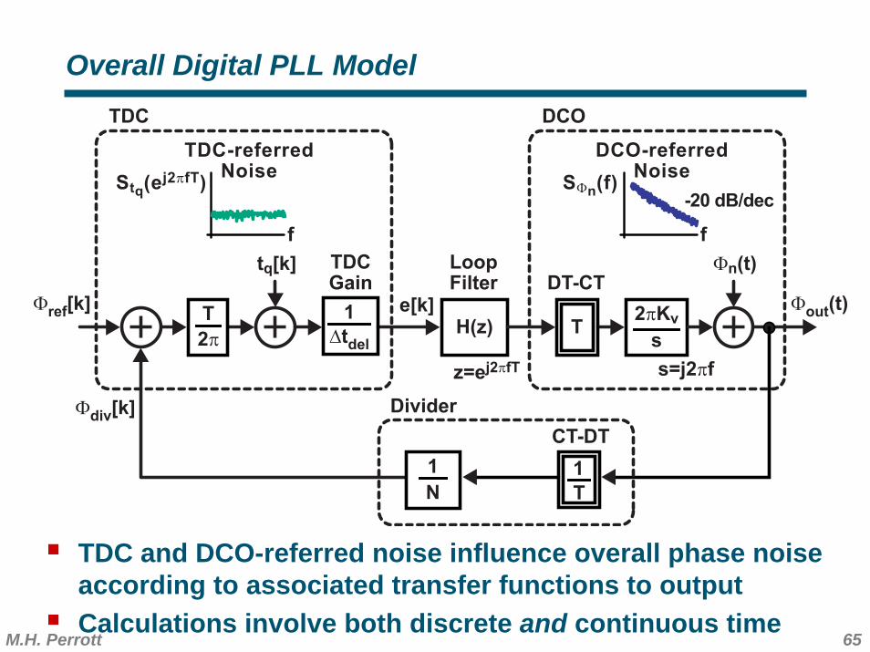
Overall Digital PLL Model
TDC and DCO-referred noise influence overall phase noise according to associated transfer functions to outputCalculations involve both discrete and continuous time
66M.H. Perrott
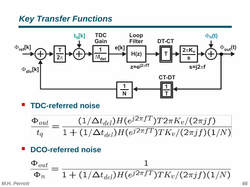
Key Transfer Functions
TDC-referred noise
DCO-referred noise
e[k]T
2π
tq[k] TDCGain
1
Δtdel
Φref[k]
H(z)
LoopFilter
2πKv
s
Φn(t)
1
T
T
1
N
DT-CT
CT-DT
Φdiv[k]
Φout(t)
z=ej2πfT s=j2πf
67M.H. Perrott
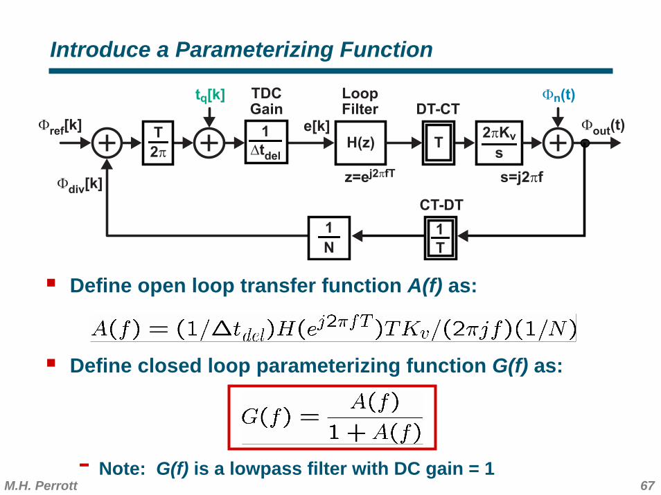
Define open loop transfer function A(f) as:
Define closed loop parameterizing function G(f) as:
- Note: G(f) is a lowpass filter with DC gain = 1
Introduce a Parameterizing Function
e[k]T
2π
tq[k] TDCGain
1
Δtdel
Φref[k]
H(z)
LoopFilter
2πKv
s
Φn(t)
1
T
T
1
N
DT-CT
CT-DT
Φdiv[k]
Φout(t)
z=ej2πfT s=j2πf
68M.H. Perrott
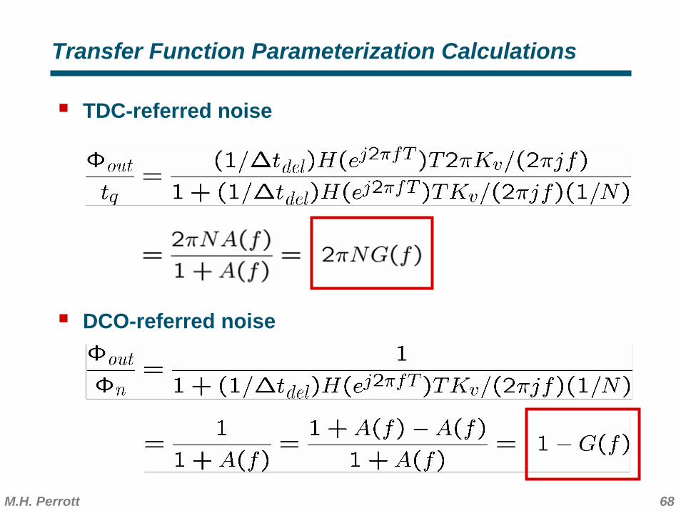
Transfer Function Parameterization Calculations
TDC-referred noise
DCO-referred noise
69M.H. Perrott
e[k]T
2π
tq[k] TDCGain
1
Δtdel
Φref[k]
H(z)
LoopFilter
2πKv
s
Φn(t)
1
T
T
1
N
DT-CT
CT-DT
Φdiv[k]
Φout(t)
z=ej2πfT s=j2πf
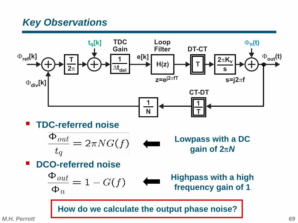
Key Observations
TDC-referred noiseLowpass with a DC
gain of 2πN
Highpass with a highfrequency gain of 1
DCO-referred noise
How do we calculate the output phase noise?
70M.H. Perrott
fofo2πN G(f) 1-G(f)
SΦn(f)
-20 dB/dec
f
DCO-referredNoise
f
TDC-referredNoise
tq[k] Φn(t)
Φout(t)
Stq(ej2πfT)
f
dBc/Hz
fo
G(f)2πNT1 2
Stq(ej2πfT)
SΦn(f)G(f)1-
2
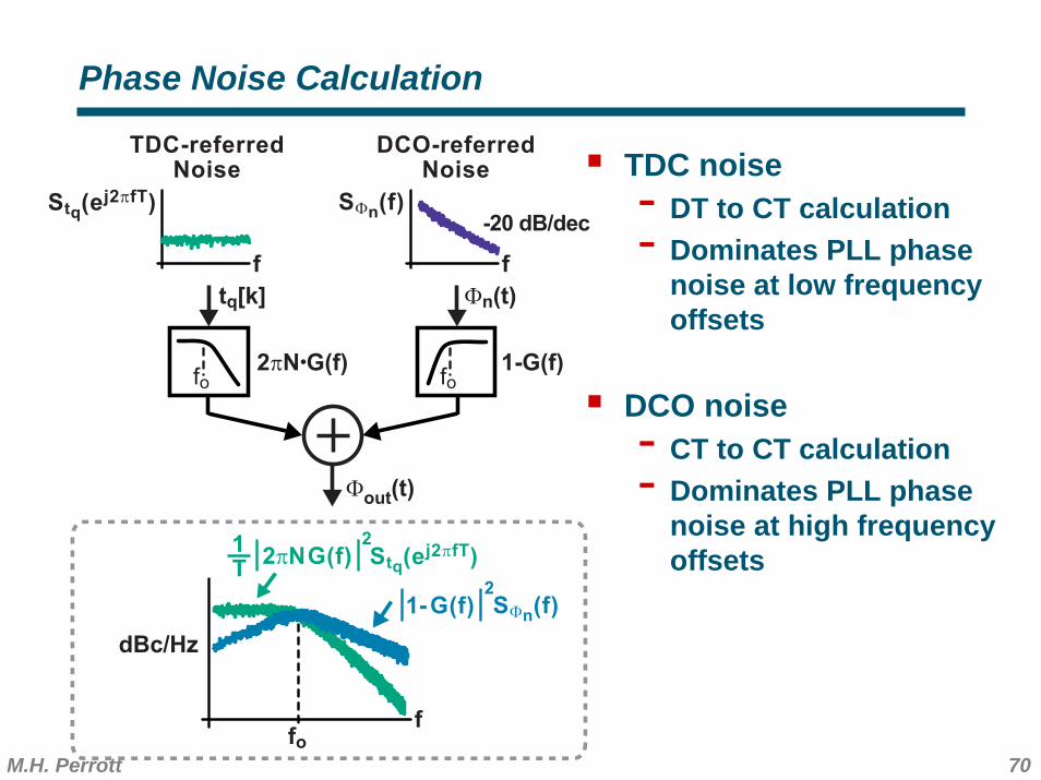
Phase Noise Calculation
TDC noise- DT to CT calculation- Dominates PLL phase
noise at low frequency offsets
DCO noise- CT to CT calculation- Dominates PLL phase
noise at high frequency offsets
71M.H. Perrott
fofo2πN G(f) 1-G(f)
SΦn(f)
-20 dB/dec
f
DCO-referredNoise
f
TDC-referredNoise
tq[k] Φn(t)
Φout(t)
f
dBc/Hz
Stq(ej2πfT)
f
dBc/Hz
fofo
Low PLL Bandwidth High PLL Bandwidth
DCONoise
TDCNoise
TDCNoise DCO
Noise
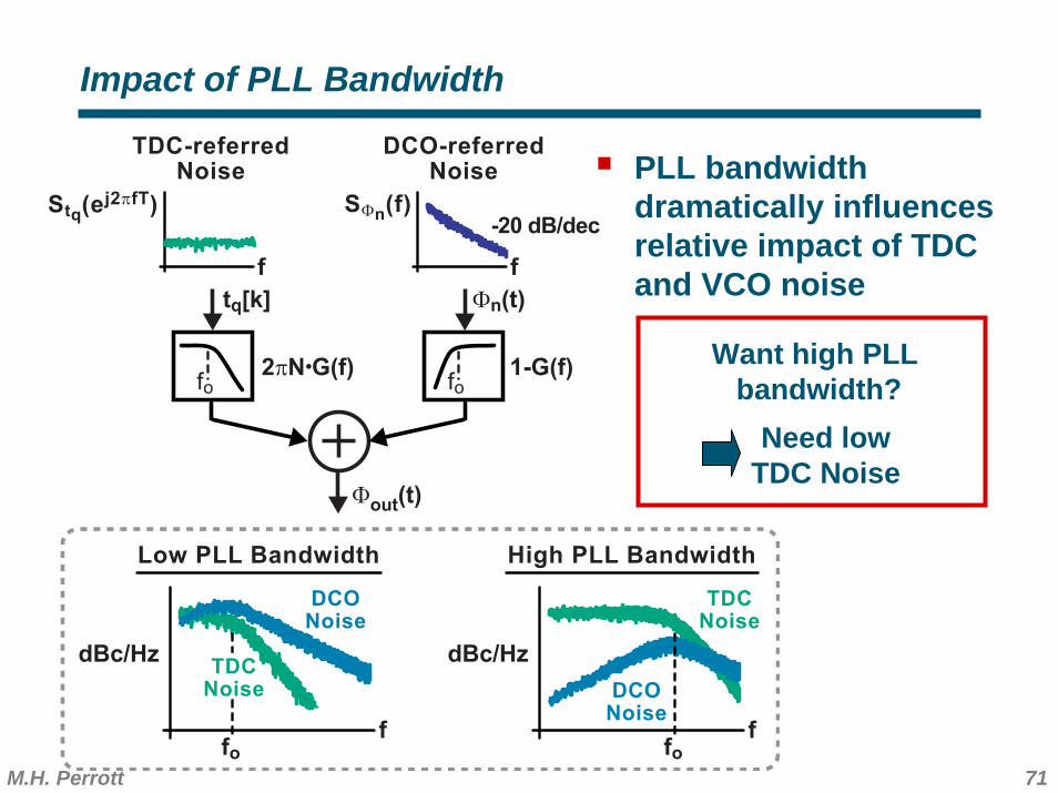
PLL bandwidth dramatically influences relative impact of TDC and VCO noise
Want high PLL bandwidth?
Impact of PLL Bandwidth
Need lowTDC Noise

System Level Design
73M.H. Perrott
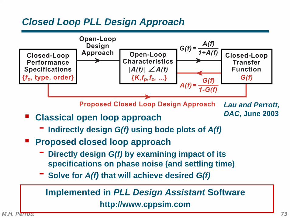
Closed Loop PLL Design Approach
Classical open loop approach- Indirectly design G(f) using bode plots of A(f)
Proposed closed loop approach- Directly design G(f) by examining impact of its
specifications on phase noise (and settling time)- Solve for A(f) that will achieve desired G(f)
Implemented in PLL Design Assistant Software
Lau and Perrott, DAC, June 2003
Closed-LoopPerformance
Specifications
G(f)A(f)
1+A(f)=
A(f)G(f)
1-G(f)=
|A(f)| A(f)
{K,fp,fz, ...}
Open-LoopCharacteristics
Closed-LoopTransferFunction
G(f)
Open-LoopDesign
Approach
{fo, type, order}
Proposed Closed Loop Design Approach
http://www.cppsim.com
74M.H. Perrott
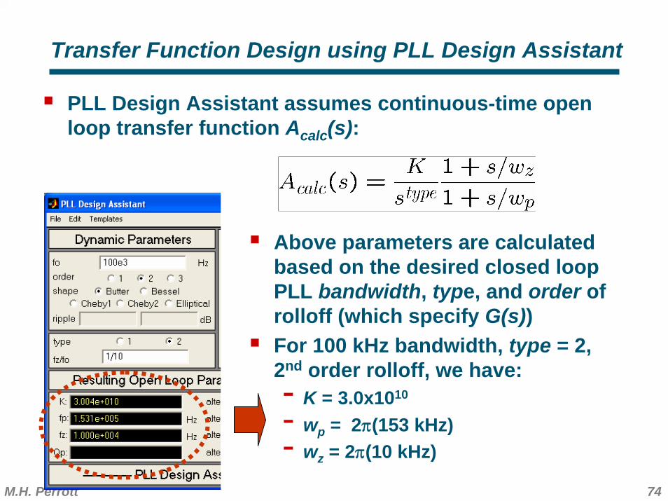
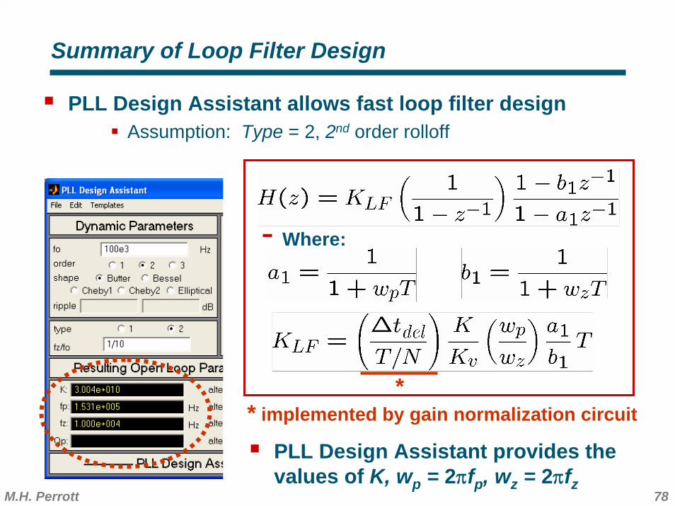
Transfer Function Design using PLL Design Assistant
PLL Design Assistant assumes continuous-time open loop transfer function Acalc(s):
Above parameters are calculated based on the desired closed loop PLL bandwidth, type, and order of rolloff (which specify G(s))For 100 kHz bandwidth, type = 2, 2nd order rolloff, we have:- K = 3.0x10¹⁰
- wp = 2π(153 kHz)- wz = 2π(10 kHz)
75M.H. Perrott
e[k]T
2π
tq[k] TDCGain
1
Δtdel
Φref[k]
LoopFilter
2πKv
s
Φn(t)
1
T
T
1
N
DT-CT
CT-DTΦdiv[k]
Φout(t)
z=esT s=j2πf
H(z)
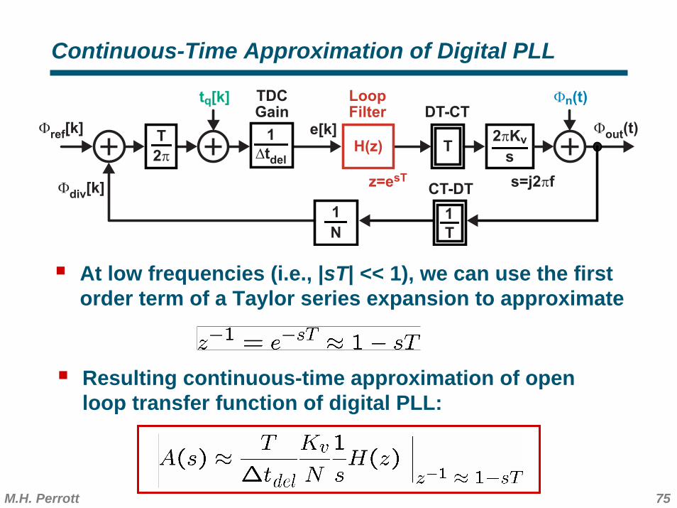
Continuous-Time Approximation of Digital PLL
Resulting continuous-time approximation of open loop transfer function of digital PLL:
At low frequencies (i.e., |sT| << 1), we can use the first order term of a Taylor series expansion to approximate
76M.H. Perrott
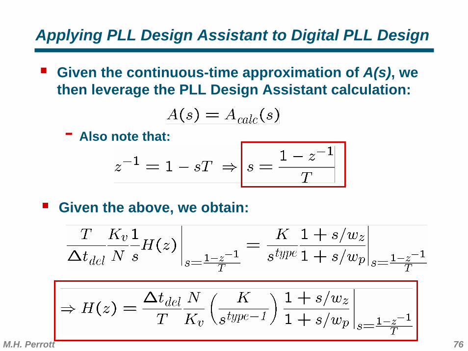
Applying PLL Design Assistant to Digital PLL Design
Given the continuous-time approximation of A(s), we then leverage the PLL Design Assistant calculation:
- Also note that:
Given the above, we obtain:
77M.H. Perrott
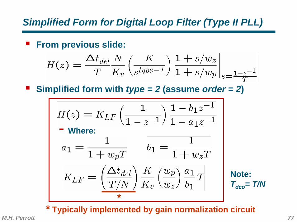
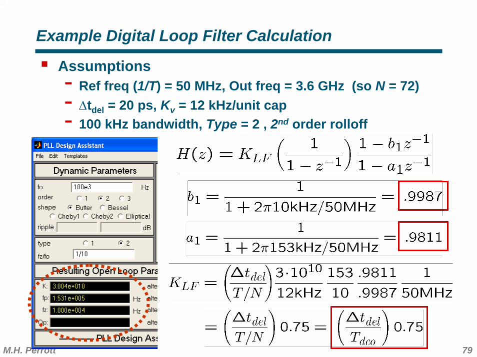
Simplified form with type = 2 (assume order = 2)
Simplified Form for Digital Loop Filter (Type II PLL)
From previous slide:
- Where:
* Typically implemented by gain normalization circuit*
Note:Tdco= T/N
78M.H. Perrott
Summary of Loop Filter Design
PLL Design Assistant allows fast loop filter designAssumption: Type = 2, 2nd order rolloff
- Where:
PLL Design Assistant provides the values of K, wp = 2πfp, wz = 2πfz
* implemented by gain normalization circuit*
79M.H. Perrott
Example Digital Loop Filter Calculation
Assumptions- Ref freq (1/T) = 50 MHz, Out freq = 3.6 GHz (so N = 72)- Δtdel = 20 ps, Kv = 12 kHz/unit cap- 100 kHz bandwidth, Type = 2 , 2nd order rolloff
Overall PLL Noise Analysis
81M.H. Perrott
f
Stq(ej2πfT) Δtdel
12
2
thermalnoise
1/fnoise
div(t)
Reg
D Q
Reg
D Q
Reg
D Q
ref(t)
e[k]
Δtdel Δtdel Δtdel
timeerror[k]
e[k]
tq[k] TDCGain
1
Δtdel
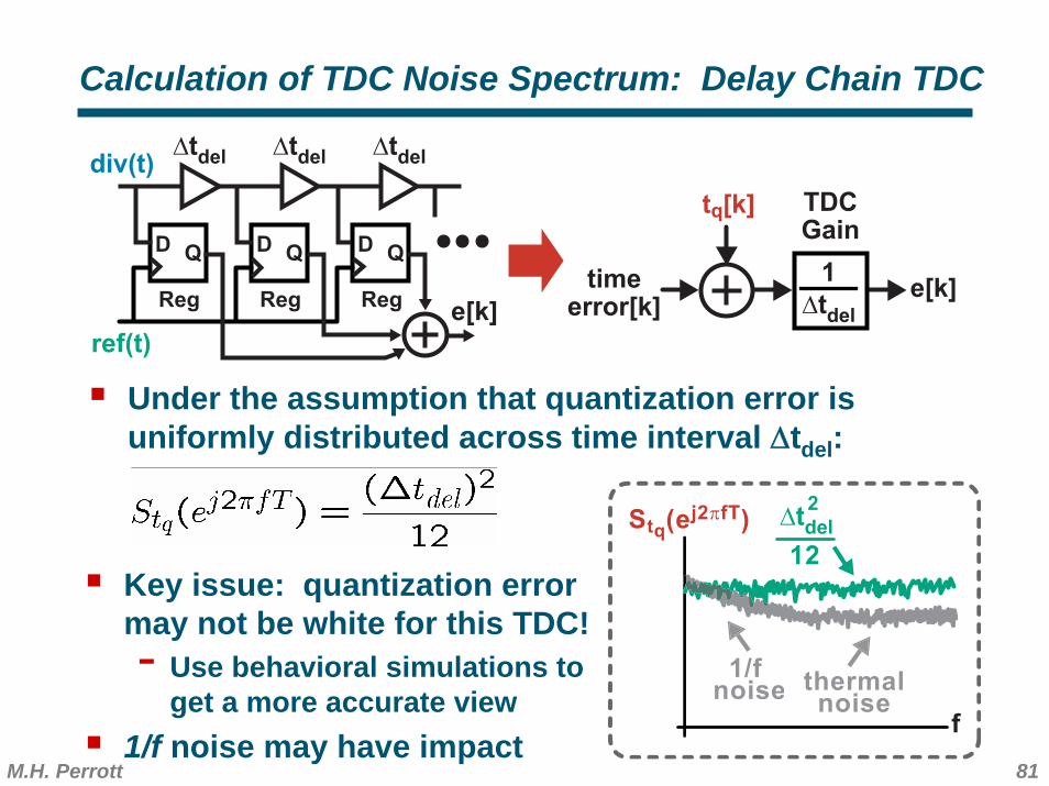
Calculation of TDC Noise Spectrum: Delay Chain TDC
Under the assumption that quantization error is uniformly distributed across time interval Δtdel:
Key issue: quantization error may not be white for this TDC!- Use behavioral simulations to
get a more accurate view1/f noise may have impact
82M.H. Perrott
f
Stq(ej2πfT)
thermalnoise
1/fnoise
Δtdel
12
22
1-ej2πfT
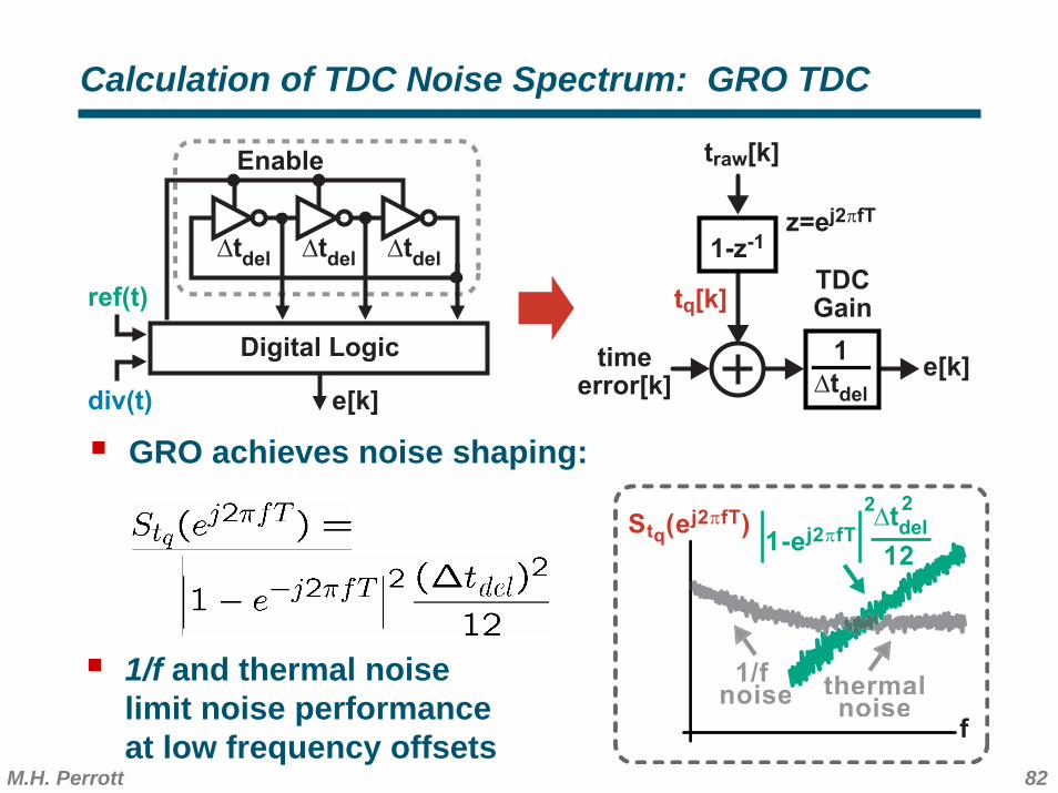
Calculation of TDC Noise Spectrum: GRO TDC
GRO achieves noise shaping:
1/f and thermal noise limit noise performance at low frequency offsets
e[k]
ref(t)
div(t)
Digital Logic
Enable
ΔtdelΔtdelΔtdel
timeerror[k]
e[k]
tq[k]TDCGain
1
Δtdel
1-z-1
traw[k]
z=ej2πfT
83M.H. Perrott
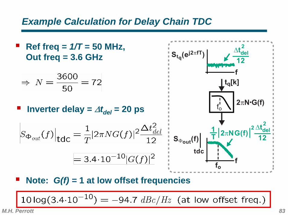
Example Calculation for Delay Chain TDC
Note: G(f) = 1 at low offset frequencies
Ref freq = 1/T = 50 MHz, Out freq = 3.6 GHz
Inverter delay = Δtdel = 20 ps
fo
fo2πN G(f)
f
tq[k]
f
G(f)2πNT1 2 Δtdel
12
2
Δtdel
12
2
Stq(ej2πfT)
SΦout(f)
tdc
84M.H. Perrott
Hntf(z)z=ej2πfTc
TcM2πKv
s
s=j2πf
in[k]
qraw[k]
Φout(t)
q[k]
PhaseNoise
ff
QuantizationNoise
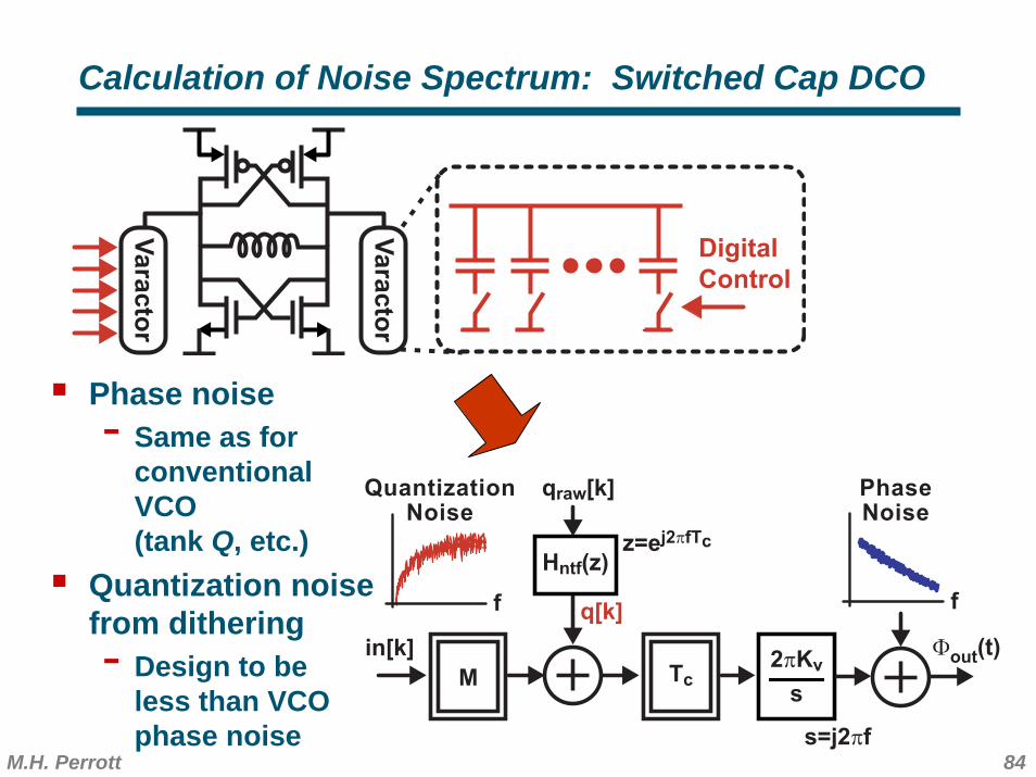
Phase noise- Same as for
conventional VCO (tank Q, etc.)
Quantization noise from dithering- Design to be
less than VCO phase noise
Calculation of Noise Spectrum: Switched Cap DCO
Va
rac
tor
Va
rac
tor
Digital
Control
85M.H. Perrott
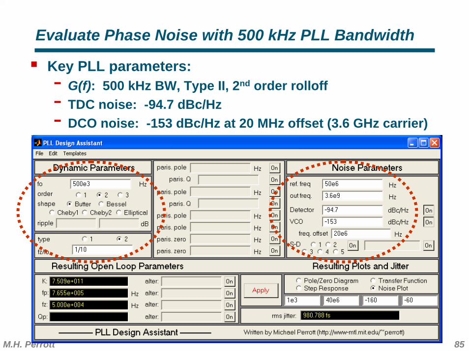
Evaluate Phase Noise with 500 kHz PLL Bandwidth
Key PLL parameters:- G(f): 500 kHz BW, Type II, 2nd order rolloff- TDC noise: -94.7 dBc/Hz- DCO noise: -153 dBc/Hz at 20 MHz offset (3.6 GHz carrier)
86M.H. Perrott
103
104
105
106
107
-160
-150
-140
-130
-120
-110
-100
-90
-80
-70
-60Output Phase Noise of Synthesizer
Frequency Offset (Hz)
L(f
) (d
Bc/H
z)
Detector NoiseVCO Noise Total Noise
GSM Mask(Referenced to
3.6 GHz carrier)
DCO Noise
TDC Noise
Overall PLLPhase Noise
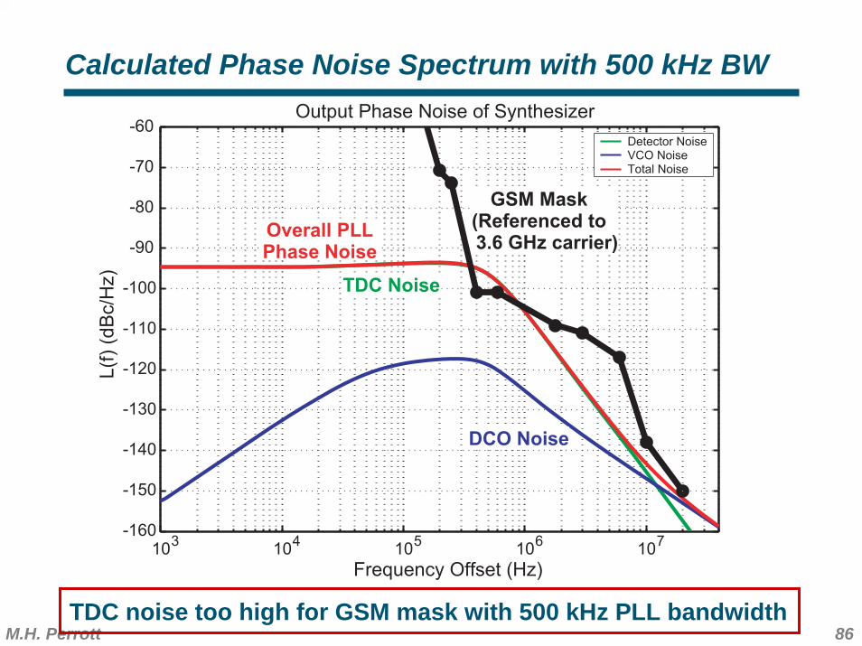
Calculated Phase Noise Spectrum with 500 kHz BW
TDC noise too high for GSM mask with 500 kHz PLL bandwidth
87M.H. Perrott
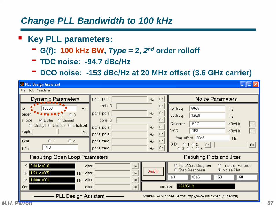
Change PLL Bandwidth to 100 kHz
Key PLL parameters:- G(f): 100 kHz BW, Type = 2, 2nd order rolloff- TDC noise: -94.7 dBc/Hz- DCO noise: -153 dBc/Hz at 20 MHz offset (3.6 GHz carrier)
88M.H. Perrott
103
104
105
106
107
-160
-150
-140
-130
-120
-110
-100
-90
-80
-70
-60Output Phase Noise of Synthesizer
Frequency Offset (Hz)
L(f
) (d
Bc/H
z)
Detector NoiseVCO Noise Total Noise
GSM Mask(Referenced to
3.6 GHz carrier)
DCO Noise
TDC Noise
Overall PLLPhase Noise
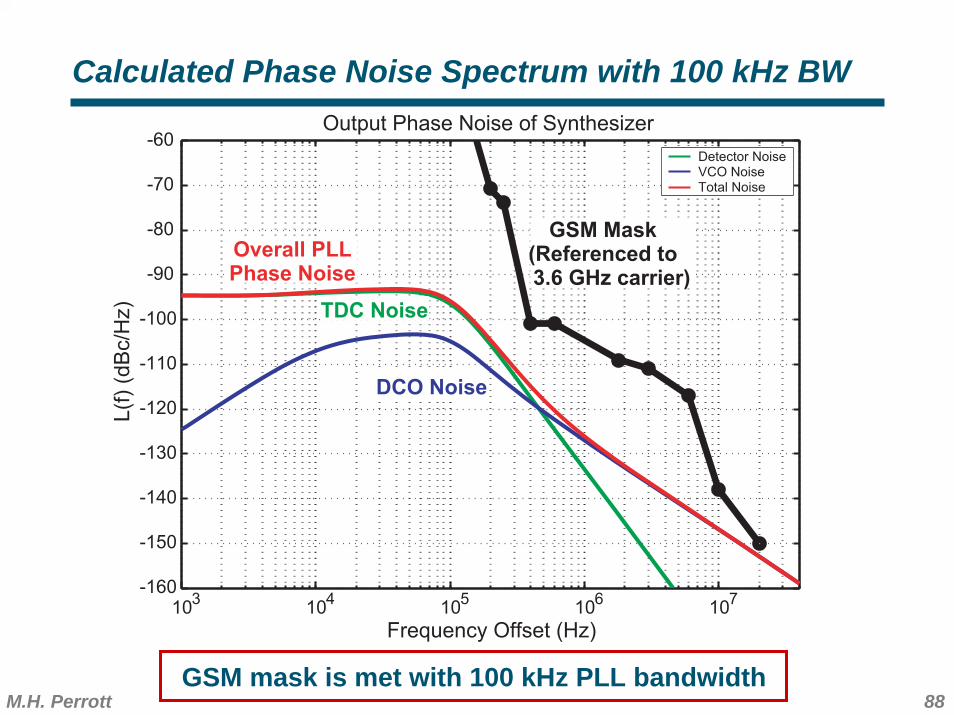
Calculated Phase Noise Spectrum with 100 kHz BW
GSM mask is met with 100 kHz PLL bandwidth
Digital Fractional-N Synthesis
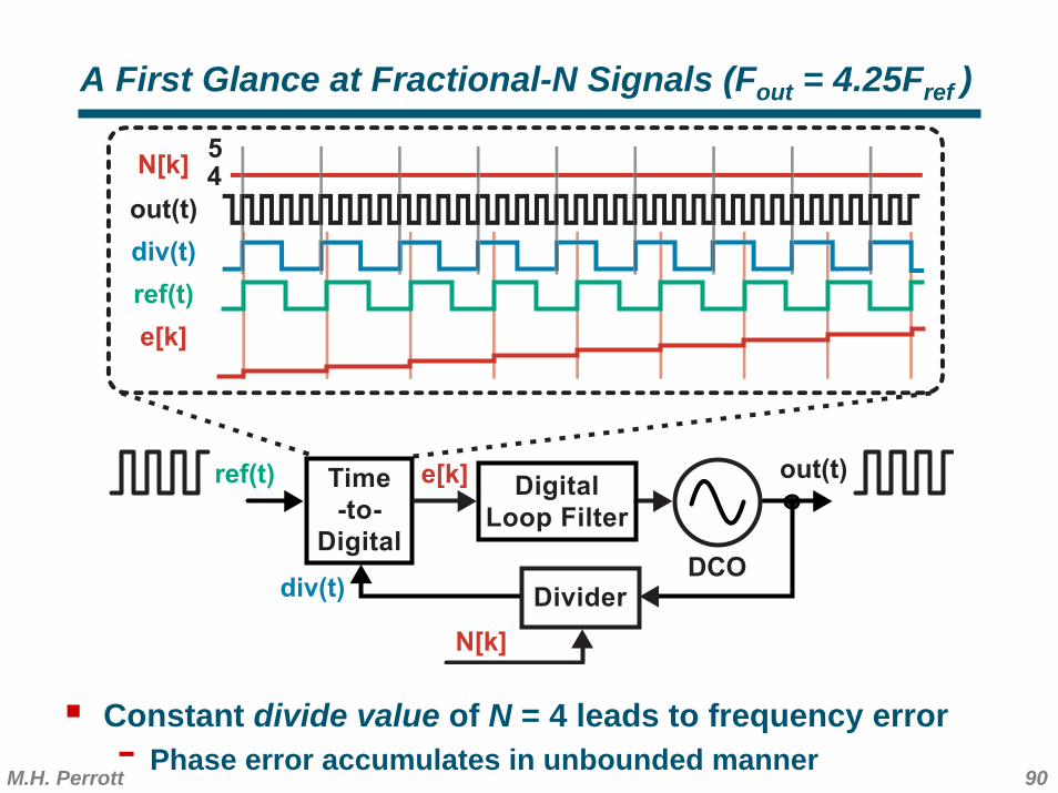
90M.H. Perrott
Time
-to-
Digital
out(t)ref(t) Digital
Loop Filter
DCODividerdiv(t)
e[k]
N[k]
N[k] 45
out(t)
div(t)
ref(t)
e[k]
Constant divide value of N = 4 leads to frequency error- Phase error accumulates in unbounded manner
A First Glance at Fractional-N Signals (Fout = 4.25Fref )
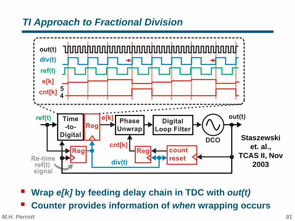
91M.H. Perrott
Time
-to-
Digital
out(t)ref(t)Digital
Loop Filter
DCO
div(t)
cnt[k]
out(t)
ref(t)
e[k]
45
Reg countcnt[k]
resetRe-timeref(t) signal
Reg
e[k]
div(t)
Phase
Unwrap
Reg
TI Approach to Fractional Division
Wrap e[k] by feeding delay chain in TDC with out(t)Counter provides information of when wrapping occurs
Staszewskiet. al.,
TCAS II, Nov 2003
92M.H. Perrott
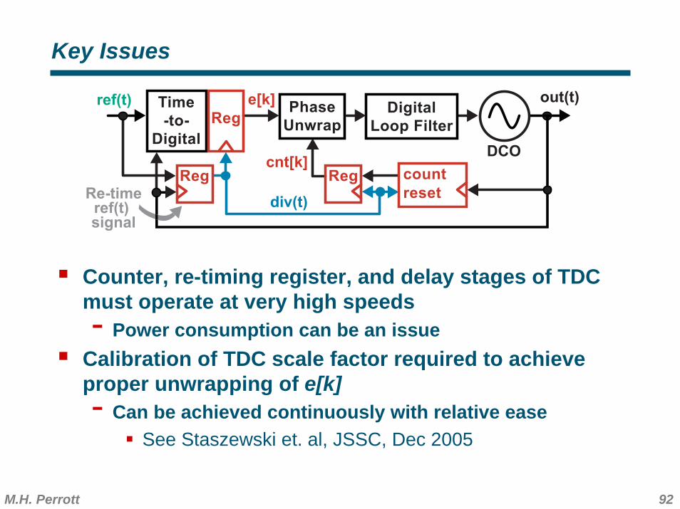
Key Issues
Counter, re-timing register, and delay stages of TDC must operate at very high speeds- Power consumption can be an issue
Calibration of TDC scale factor required to achieve proper unwrapping of e[k]- Can be achieved continuously with relative ease
See Staszewski et. al, JSSC, Dec 2005
Time
-to-
Digital
out(t)ref(t)Digital
Loop Filter
DCO
div(t)
Reg countcnt[k]
resetRe-timeref(t) signal
Reg
e[k]Phase
Unwrap
Reg
93M.H. Perrott
Accum4.25
Time
-to-
Digital
out(t)ref(t) Digital
Loop Filter
DCODividerdiv(t)
e[k]
N[k]
N[k] 45
out(t)
div(t)
ref(t)
e[k]
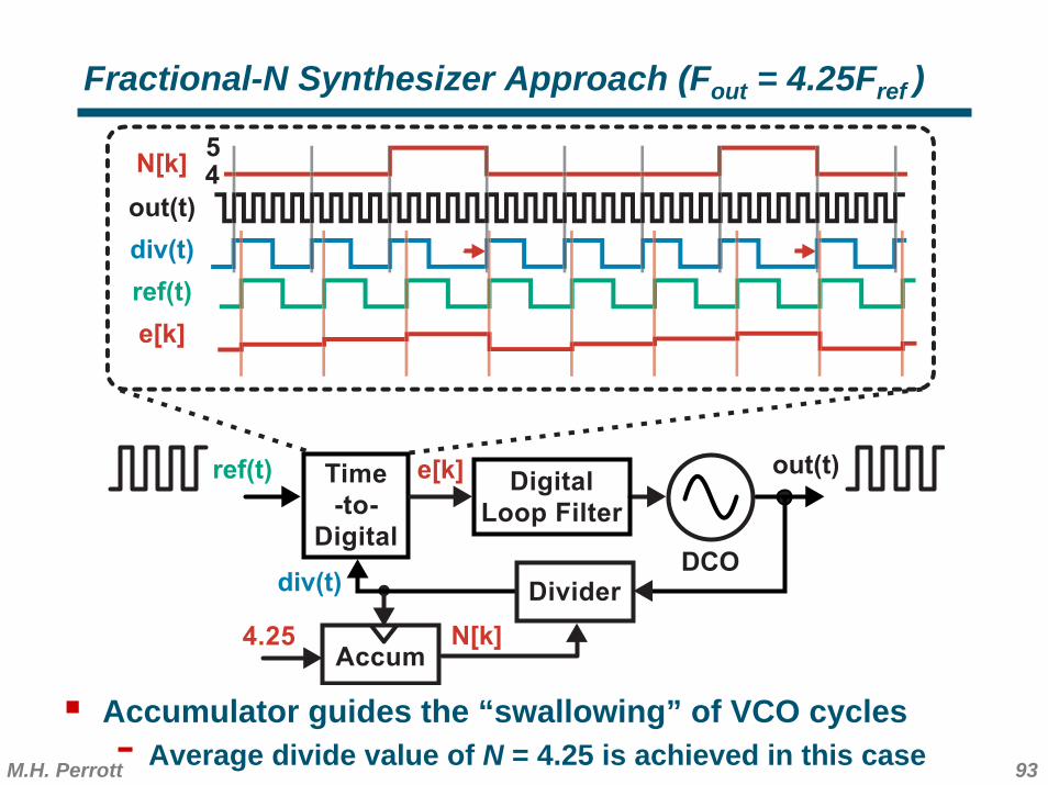
Fractional-N Synthesizer Approach (Fout = 4.25Fref )
Accumulator guides the “swallowing” of VCO cycles- Average divide value of N = 4.25 is achieved in this case
94M.H. Perrott
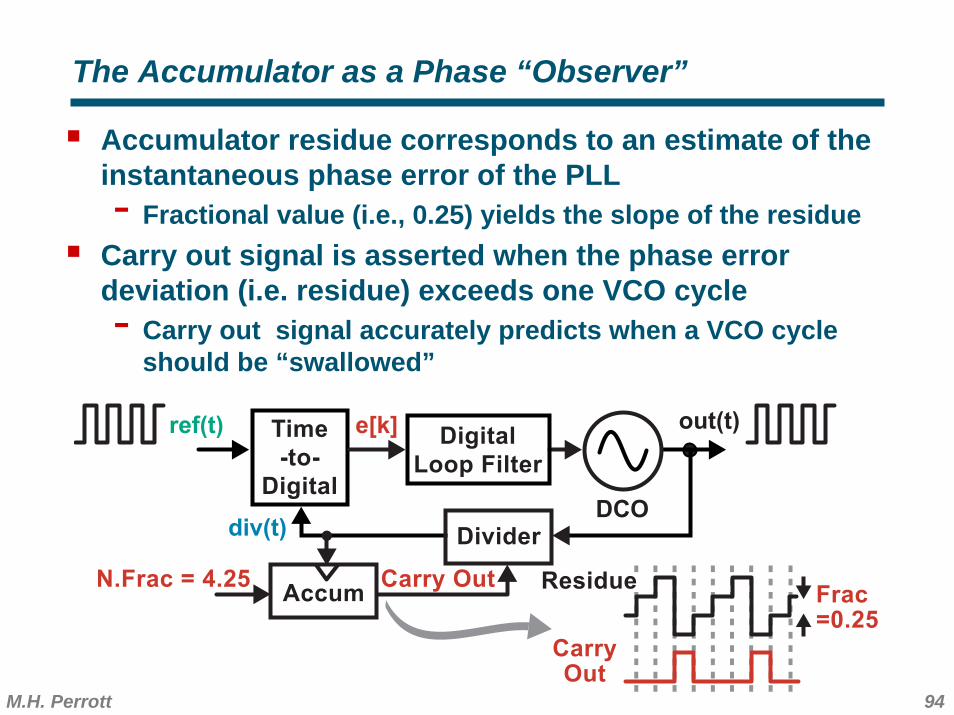
The Accumulator as a Phase “Observer”
Accumulator residue corresponds to an estimate of the instantaneous phase error of the PLL- Fractional value (i.e., 0.25) yields the slope of the residue
Carry out signal is asserted when the phase error deviation (i.e. residue) exceeds one VCO cycle- Carry out signal accurately predicts when a VCO cycle
should be “swallowed”
Time
-to-
Digital
out(t)ref(t) Digital
Loop Filter
DCODividerdiv(t)
e[k]
AccumN.Frac = 4.25 Residue
CarryOut
Frac=0.25
Carry Out
95M.H. Perrott
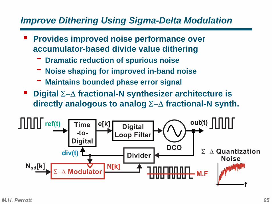
Improve Dithering Using Sigma-Delta Modulation
Provides improved noise performance over accumulator-based divide value dithering- Dramatic reduction of spurious noise- Noise shaping for improved in-band noise- Maintains bounded phase error signal
Digital Σ−Δ fractional-N synthesizer architecture is directly analogous to analog Σ−Δ fractional-N synth.
Time
-to-
Digital
out(t)ref(t) Digital
Loop Filter
DCODividerdiv(t)
e[k]
N[k]Σ−Δ Modulator M.F
Nsd[k]
f
Σ−Δ QuantizationNoise
96M.H. Perrott
f
Stq(ej2πfT)
TDC-referredNoise
e[k]T
2π
tq[k] TDCGain
1
Δtdel
Φref[k]
H(z)
LoopFilter
2πKv
s
Φn(t)
1
T
T
1
Nnom
DT-CT
CT-DTΦdiv[k]
Φout(t)
TDC DCO
Divider
SΦn(f)
-20 dB/dec
f
DCO-referredNoise
z=ej2πfT s=j2πf
2π
1-z-1
z-1
z=ej2πfT
n[k]
f
Sq(ej2πfT)
Σ−Δ QuantizationNoise
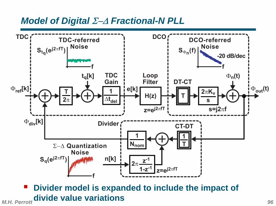
Model of Digital Σ−Δ Fractional-N PLL
Divider model is expanded to include the impact of divide value variations
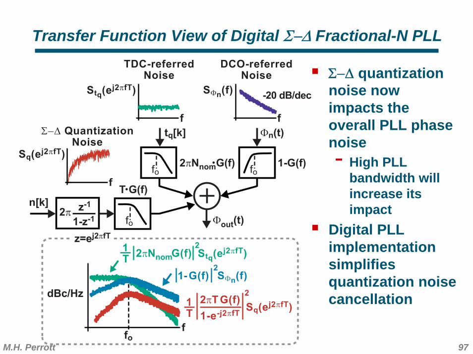
97M.H. Perrott
fofo2πNnomG(f) 1-G(f)
SΦn(f)
-20 dB/dec
f
DCO-referredNoise
f
TDC-referredNoise
tq[k] Φn(t)
Φout(t)
Stq(ej2πfT)
f
dBc/Hz
fo
G(f)2πNnomT1 2
Stq(ej2πfT)
SΦn(f)G(f)1-
2
fo
T G(f)f
Sq(ej2πfT)
Σ−Δ QuantizationNoise
2π
1-z-1
z-1n[k]
z=ej2πfT
G(f)2πT
T1
2
Sq(ej2πfT)1-e-j2πfT
Transfer Function View of Digital Σ−Δ Fractional-N PLL
Σ−Δ quantization noise now impacts the overall PLL phase noise- High PLL
bandwidth will increase its impact
Digital PLL implementation simplifies quantization noise cancellation
98M.H. Perrott
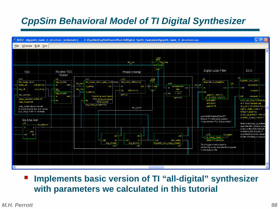
CppSim Behavioral Model of TI Digital Synthesizer
Implements basic version of TI “all-digital” synthesizer with parameters we calculated in this tutorial
99M.H. Perrott
103
104
105
106
107
-160
-150
-140
-130
-120
-110
-100
-90
-80
-70
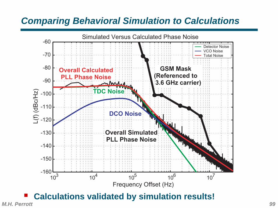
-60Simulated Versus Calculated Phase Noise
Frequency Offset (Hz)
L(f
) (d
Bc/H
z)
Detector NoiseVCO Noise Total Noise
GSM Mask(Referenced to
3.6 GHz carrier)
DCO Noise
TDC Noise
Overall CalculatedPLL Phase Noise
Overall SimulatedPLL Phase Noise
Comparing Behavioral Simulation to Calculations
Calculations validated by simulation results!
100M.H. Perrott
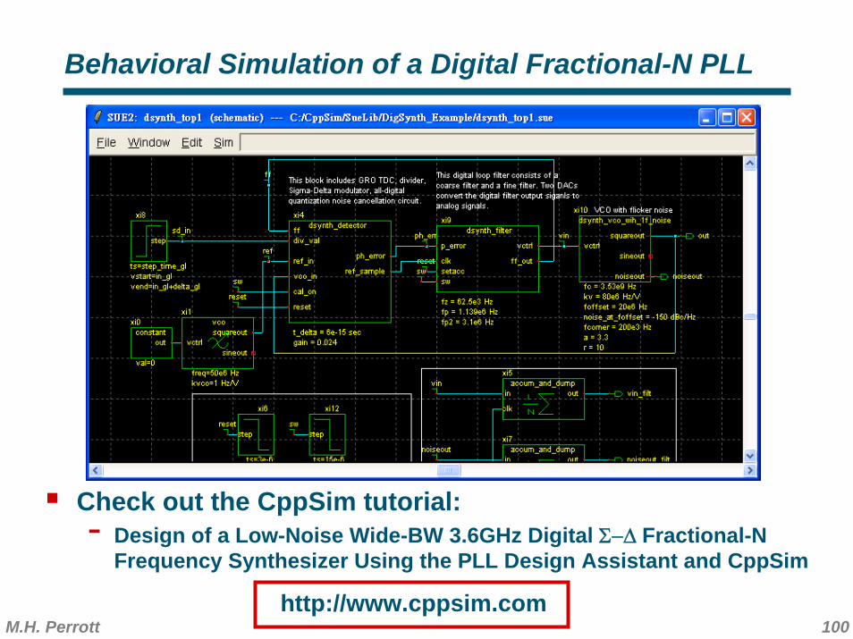
Behavioral Simulation of a Digital Fractional-N PLL
Check out the CppSim tutorial:- Design of a Low-Noise Wide-BW 3.6GHz Digital Σ−Δ Fractional-N
Frequency Synthesizer Using the PLL Design Assistant and CppSim
http://www.cppsim.com
101M.H. Perrott
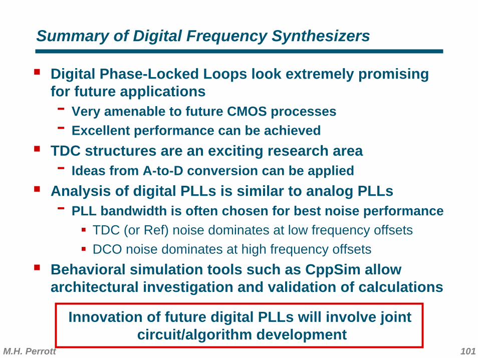
Summary of Digital Frequency Synthesizers
Digital Phase-Locked Loops look extremely promising for future applications- Very amenable to future CMOS processes- Excellent performance can be achieved
TDC structures are an exciting research area- Ideas from A-to-D conversion can be applied
Analysis of digital PLLs is similar to analog PLLs- PLL bandwidth is often chosen for best noise performance
TDC (or Ref) noise dominates at low frequency offsetsDCO noise dominates at high frequency offsets
Behavioral simulation tools such as CppSim allow architectural investigation and validation of calculations
Innovation of future digital PLLs will involve joint circuit/algorithm development
Related Documents


