Introductory Concepts 1. Digital representations of numerical values of quantities may BEST be described as having characteristics: a. that are difficult to interpret because they are continuously changing. b. that vary constantly over a continuous range of values. c. that vary in constant and direct proportion to the values they represent. d. that vary in discrete steps in proportion to the values they represent. 2. Which of the following is not an analog device? a. Thermocouple b. Current flow in a circuit c. Light switch d. Audio microphone 3. Which of the following statements does NOT describe an advantage of digital technology? a. The values may vary over a continuous range. b. The circuits are less affected by noise. c. The operation can be programmed. d. Information storage is easy. 4. How many binary bits are necessary to represent 748 different numbers? a. 9 b. 7 c. 10 d. 8 5. The parallel transmission of digital data: a. is much slower than the serial transmission of data. b. requires only one signal line between sender and receiver. c. requires as many signal lines between sender and receiver as there are data bits. d. is less expensive than the serial method of data transmission. 6. Any number with an exponent of zero is equal to: a. zero. b. one. c. that number. d. ten. 7. Any number with an exponent of one is equal to: a. zero. b. one. c. two. d. that number. 8. How many unique symbols are used in the decimal number system? a. One

Welcome message from author
This document is posted to help you gain knowledge. Please leave a comment to let me know what you think about it! Share it to your friends and learn new things together.
Transcript
Introductory Concepts
1. Digital representations of numerical values of quantities may BEST be described as having characteristics:
a. that are difficult to interpret because they are continuously changing. b. that vary constantly over a continuous range of values. c. that vary in constant and direct proportion to the
values they represent.
d. that vary in discrete steps in proportion to the values they represent.
2. Which of the following is not an analog device? a. Thermocouple b. Current flow in a circuit c. Light switch d. Audio microphone
3. Which of the following statements does NOT describe an advantage of digital technology? a. The values may vary over a continuous range. b. The circuits are less affected by noise. c. The operation can be programmed. d. Information storage is easy.
4. How many binary bits are necessary to represent 748 different numbers? a. 9 b. 7 c. 10 d. 8
5. The parallel transmission of digital data: a. is much slower than the serial transmission of data. b. requires only one signal line between sender and receiver.
c. requires as many signal lines between sender and receiver as there are data bits.
d. is less expensive than the serial method of data transmission.
6. Any number with an exponent of zero is equal to: a. zero.
b. one. c. that number.
d. ten.
7. Any number with an exponent of one is equal to: a. zero. b. one. c. two. d. that number.
8. How many unique symbols are used in the decimal number system?
a. One b. Nine c. Ten d. Unlimited
9. What are the symbols used to represent digits in the binary number system? a. 0,1 b. 0,1,2 c. 0 through 8 d. 1,2
10. What is the binary representation of 2-3? a. 0000.0010 b. 0000.0100
c. 0000.0011 d. 0011.1000
11. Convert the fractional binary number 0001.0010 to decimal. a. 1.40

b. 1.125 c. 1.20 d. 1.80
12. Convert the fractional binary number 0000.1010 to decimal. a. 0.625 b. 0.50 c. 0.55 d. 0.10
13. Convert the fractional binary number 10010.0100 to decimal. a. 24.50 b. 18.25 c. 18.40 d. 16.25
14. Convert the fractional decimal number 6.75 to binary. a. 0111.1100 b. 0110.1010 c. 0110.1100 d. 0110.0110
15. Give the decimal value of binary 10010. a. 610 b. 910 c. 1810 d. 2010
16. Give the decimal value of binary 10000110. a. 13410 b. 14410 c. 11010 d. 12610
17. Digital signals transmitted on a single conductor (and a ground) must be transmitted in:
a. slow speed. b. parallel.
c. analog. d. serial.
18. Serial format means digital signals are: a. sent over many conductors simultaneously. b. sent over one conductor sequentially.
c. sent in groups of eight signals. d. sent in binary coded decimal.
19. Parallel format means that: a. each digital signal has its own conductor. b. several digital signals are sent on each conductor. c. both binary and hexadecimal can be used. d. no clock is needed.
20. Which format requires fewer conductors? a. Parallel b. Serial c. Both are the same d. Cannot tell
21. Which format can send several bits of information faster? a. Parallel b. Serial c. Both are the same d. Cannot tell
22. What is the decimal value of 2-1? a. 0.5 b. 0.25 c. 0.05 d. 0.1
23. What is the decimal value of 23 ? a. 2 b. 4 c. 6 d. 8
24. What is one relative disadvantage of serial transfer?
a. It requires too many conductors. b. Its interconnect system is complex. c. It is slow. d. It can only be used over very short distances.
25. What kind of logic device or circuit is used to store information? a. Counter b. Register c. Inverter d. Buffer
26. What is an analog-to-digital converter? a. It makes digital signals. b. It takes analog signals and puts them in digital format. c. It allows the use of digital signals in everyday life. d. It stores information on a CD.
27. What is a digital-to-analog converter? a. It takes the digital information from a CD and converts it to audio.
b. It allows the use of cheaper analog techniques, which are always simpler.
c. It stores digital data on a hard drive. d. It converts direct current to alternating current.
28. What has happened to the advances in digital technologies over the past three decades? a. Slowed down considerably b. Continued to increase, but at a decreasing rate c. Made excellent progress d. Nothing short of phenomenal 29. In the decimal numbering system, what is the MSD? a. The middle digit of a stream of numbers b. The digit to the right of the decimal point c. The last digit on the right d. The digit with the most weight
30. What is the typical invalid voltage for a binary signal? a. 0.7–2.8 volts
b. 0.8–3 volts c. 0.8–2 volts d. 0.7–2.5 volts
Number Systems and Codes
1. Which of the following is the primary advantage of using the BCD code instead of straight binary coding?
a. Fewer bits are required to represent a decimal number with the BCD code.
b. The relative ease of converting to and from decimal. c. BCD codes are easily converted to hexadecimal codes.

d. BCD codes are easily converted to straight binary codes.
2. How many BCD code bits and how many straight binary bits would be required to represent the decimal number 643? a. 12 BCD, 12 binary b. 12 BCD, 10 binary c. 12 BCD, 9 binary d. 16 BCD, 9 binary
3. When using the repeated division by 2 method of converting from decimal to binary, one must write the first remainder as the: a. MSB
b. MSB, providing the following sequence of remainders are written in descending order until the final remainder is achieved.
c. LSB d. LSB, providing the final remainder is used to replace the original LSB, which is then moved to the MSB position.
4. Select one of the following statements that best describes the parity method of error detection.
a. Parity checking is best suited for detecting single-bit errors in transmitted codes.
b. Parity checking is not suitable for detecting single-bit errors in transmitted codes.
c. Parity checking is capable of detecting and correcting errors in transmitted codes.
d. Parity checking is best suited for detecting double-bit errors that occur during the transmission of codes from one location to another.
5. Alphanumeric codes should include as a minimum: a. the capacity to represent the alphabet upper and
lowercase characters and the decimal numbers in a straight binary format.
b. the capacity to code all possible decimal numbers in a direct octal representation of BCD codes.
c. the alphabet upper and lowercase letters, the decimal digits, the 7 punctuation marks, and other characters or symbols.
d. the ability to represent decimal numbers greater than 128-10th in a straight binary format.
6. Which of the following is an invalid BCD code? a. 0011
b. 1101 c. 0101 d. 1001
7. Convert 59.7210 to BCD. a. 111011 b. 01011001.01110010 c. 1110.11 d. 0101100101110010
8. Which of the following is the most widely used code for computer input and output? a. Gray b. ASCII c. Parity d. EBCDIC
9. Convert 5278 to binary. a. 343 b. 011100111 c. 101010111 d. 111010101
10. Convert 11001010001101012 to hexadecimal. a. 121035 b. CA35 c. 53AC1 d. 530121
11. Convert 8B3F16 to binary. a. 35647

b. 011010 c. 1011001111100011 d. 1000101100111111
12. Convert 45710 to octal. a. 711 b. 2C7 c. 811 d. 88.8
13. Convert 17318 to decimal. a. 216.4 b. 985 c. 3D9 d. 1123
14. How many binary digits are required to count to 10010? a. 7 b. 2 c. 3 d. 100
15. What decimal number does 25 represent? a. 10 b. 31 c. 25 d. 32 16. Convert decimal 64 to binary. a. 01010010 b. 01000000 c. 00110110 d. 0100100017. Convert decimal 213 to binary. a. 11001101 b. 11010101 c. 01111001 d. 11100011
18. The base of the octal system is: a. Eight. b. Seven.
c. Ten. d. Two.
19. Convert binary 1001 to octal. a. 98 b. 118 c. 1018 d. 108
20. Convert binary 01001110 to octal. a. 1068 b. 1078 c. 768 d. 1168
21. Convert octal 701 to binary. a. 11000001 b. 1000111 c. 111000100 d. 111000001
22. Convert octal 16 to decimal. a. 1410 b. 1610 c. 1010 d. 2010
23. Convert binary 11001111 to hexadecimal. a. 8F16 b. CE16 c. DF16 d. CF16
24. Convert binary 111111110010 to hexadecimal. a. EE216 b. FF216 c. 2FE16 d. FD216
25. Convert hexadecimal C0B to binary. a. 110000001011
b. 110000001001 c. 110000001100 d. 110100001011
26. Which is the longest: bit, byte, nibble, word? a. Bit b. Byte c. Nibble d. Word
27. Which is not a word size? a. 64 b. 28 c. 16 d. 8
28. How many bits are in an ASCII character? a. 16 b. 8 c. 7 d. 4
29. When using even parity, where is the parity bit placed? a. Before the MSB b. After the LSB c. In the parity word d. After the odd parity bit
30. If a typical PC uses a 20-bit address code, what is the most RAM the CPU can address? a. 20 GB b. 10 GB c. 1 GB d. 580MB
Describing Logic Circuits
1. The format used to present the logic output for the various combinations of logic inputs to a gate is called a(n): [Hint] a. Truth Table. b. input logic function. c. Boolean constant. d. Boolean variable.
2. The logic gate that will have HIGH or "1" at its output when any one of its inputs is HIGH is a(n): [Hint] a. NOR gate b. OR gate c. AND gate d. NOT operation
3. Which of the following equations would accurately describe a 4-input OR gate when A = 1, B = 1, C = 0 and D = 0? [Hint]

a. 1 + 1 + 0 + 0 = 1 b. 1 + 1 + 0 + 0 = 01 c. 1 + 1 + 0 + 0 = 0 d. 1 + 1 + 0 + 0 = 00
4. A NAND gate has: [Hint] a. active low inputs and an active high output. b. active low inputs and an active low output. c. active high inputs and an active high output. d. active high inputs and an active low output.
5. A small circle on the output of a logic gate is used to represent the: [Hint] a. Comparator operation. b. OR operation. c. NOT operation. d. AND operation.
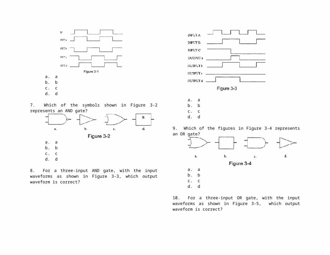
6. Which timing diagram shown in Figure 3-1 is correct for an inverter?
a. a b. b c. c d. d
7. Which of the symbols shown in Figure 3-2 represents an AND gate?
a. a b. b c. c d. d
8. For a three-input AND gate, with the input waveforms as shown in Figure 3-3, which output waveform is correct?
a. a b. b c. c d. d
9. Which of the figures in Figure 3-4 represents an OR gate?
a. a b. b c. c

d. d
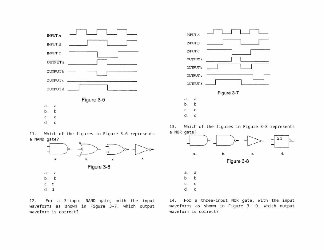
10. For a three-input OR gate, with the input waveforms as shown in Figure 3-5, which output waveform is correct?
a. a b. b c. c d. d
11. Which of the figures in Figure 3-6 represents a NAND gate?
a. a b. b
c. c d. d
12. For a 3-input NAND gate, with the input waveforms as shown in Figure 3-7, which output waveform is correct?
a. a b. b c. c d. d
13. Which of the figures in Figure 3-8 represents a NOR gate?
a. a b. b c. c d. d
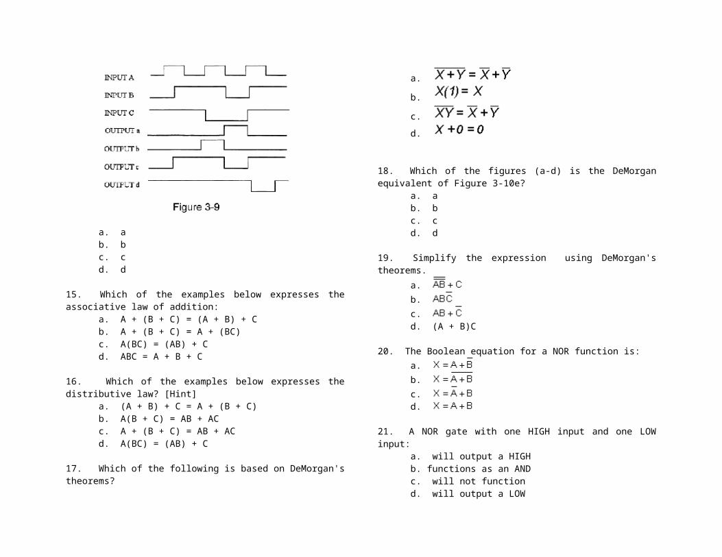
14. For a three-input NOR gate, with the input waveforms as shown in Figure 3- 9, which output waveform is correct?
a. a b. b c. c d. d
15. Which of the examples below expresses the associative law of addition: a. A + (B + C) = (A + B) + C b. A + (B + C) = A + (BC) c. A(BC) = (AB) + C d. ABC = A + B + C
16. Which of the examples below expresses the distributive law? [Hint] a. (A + B) + C = A + (B + C) b. A(B + C) = AB + AC c. A + (B + C) = AB + AC d. A(BC) = (AB) + C
17. Which of the following is based on DeMorgan's theorems?
a.
b.
c.
d.
18. Which of the figures (a-d) is the DeMorgan equivalent of Figure 3-10e? a. a b. b c. c d. d
19. Simplify the expression using DeMorgan's theorems.
a.
b.
c. d. (A + B)C
20. The Boolean equation for a NOR function is:
a.
b.
c. d.
21. A NOR gate with one HIGH input and one LOW input: a. will output a HIGH b. functions as an AND c. will not function d. will output a LOW
22. Which logic gate does this truth table describe?
a. AND b. OR
c. NAND d. NOR
23. Which step in this reduction process is using DeMorgan's theorem?
a. STEP 1 b. STEP 2 c. STEP 3 d. STEP 4
24. An OR gate with inverted inputs functions as: a. an AND. b. a NAND. c. a NOR. d. an inverter.
25. Which of the figures in Figure 3-11 (a-d), is equivalent to Figure 3-11(e)?
a. a b. b c. c d. d
26. Which is not an HDL suited for programming simple programmable devices? a. VHSIC b. CUPL c. ABEL d. PALASM
27. The special software application that translates from HDL into a grid of 1's and 0's, which can be loaded into a PLD, is called a: a. formatter. b. compiler. c. programmable wiring. d. CPU.
28. In VHDL, the mode of a port does not define: a. an input. b. an output. c. both an input and an output. d. the TYPE of the bit.
29. What is the basic difference between AHDL and VHDL? [Hint] a. ADHL is used in all PLD's. b. VHDL is used in all PLD's. c. ADHL is proprietary.
d. VHDL is proprietary.
30. How are the statements between BEGIN and END not evaluated in VHDL? a. Constantly b. Simultaneously c. Concurrently d. Sequentially
Combinational Logic Circuits
1. The implementation of simplified sum-of-products expressions may be easily implemented into actual logic
circuits using all universal ________ gates with little or no increase in circuit complexity.
a. AND/ORb. NANDc. NORd. OR/AND
2. Each "1" entry in a K-map square represents: a. a HIGH for each input Truth Table condition that
produces a HIGH output.b. a HIGH output on the Truth Table for all LOW
input combinations.c. a LOW output for all possible HIGH input
conditions.d. a DON'T CARE condition for all possible input
Truth Table combinations. 3. Which of the following statements accurately represents the two BEST methods of logic circuit simplification?
a. Boolean algebra and Karnaugh mapping b. Karnaugh mapping and circuit waveform
analysisc. Actual circuit trial and error evaluation and
waveform analysisd. Boolean algebra and actual circuit trial and error
evaluation
4. Looping on a K-map always results in the elimination of: a. variables within the loop that appear only in their
complemented form. b. variables that remain unchanged within the loop.c. variables within the loop that appear in both
complemented and uncomplemented form.d. variables within the loop that appear only in their
uncomplemented form.
5. As a technician you are confronted with a TTL circuit board containing dozens of IC chips. You have taken several readings at numerous IC chips, but the readings are inconclusive because of their erratic nature. Of the possible
faults listed, select the one that most probably is causing the problem.
a. A defective IC chip that is drawing excessive current from the power supply
b. A solar bridge between the inputs on the first IC chip on the board
c. An open connection between the inputs on the first IC chip on the board
d. A defective output IC chip that has an internal open to Vcc
6. Which of the following expressions is in the sum-of-products form?
a. (A + B)(C + D) b. (AB)(CD)c. AB(CD)d. AB + CD
7. Which of the following is an important feature of the sum-of-products form of expressions?
a. All logic circuits are reduced to nothing more than simple AND and OR gates.
b. The delay times are greatly reduced over other forms.
b. No signal must pass through more than two gates,
c. not including inverters. d. The maximum number of gates that any signal
must pass through is reduced by a factor of two.
8. Which of the following expressions is in the product-of-sums form? a. (A + B)(C + D) b. (AB)(CD) c. AB(CD)
d. AB + CD 9. Solve the network in Figure 4-1 for X.

a. A + BC + D b. ((A + B)C) + D c. D(A + B + C) d. (AC + BC)D
10. A logic probe is placed on the output of a gate and the display indicator is dim. A pulser is used on each of the input terminals, but the output indication does not change. What is wrong? a. The output of the gate appears to be open.
b. The dim indication on the logic probe indicates that the supply voltage is probably low.
c. The dim indication is a result of a bad ground connection on the logic probe. d. The gate may be a tri-state device.
11. For a two-input XNOR gate, with the input waveforms as shown in Figure 4-2, which output waveform is correct?
a. a b. b
c. c d. d 12. Which of the figures shown in Figure 4-3 represents the exclusive-NOR gate?
a. a b. b c. c d. d
13. Which statement below best describes a Karnaugh map? a. A Karnaugh map can be used to replace Boolean rules.
b. The Karnaugh map eliminates the need for using NAND and NOR gates.
c. Variable complements can be eliminated by using Karnaugh maps.
d. Karnaugh maps provide a cookbook approach to simplifying Boolean expressions.
14. Which of the circuits in Figure 4-4 (a-d) is equivalent to Figure 4-4 (e)?
a. a b. b
c. c d. d
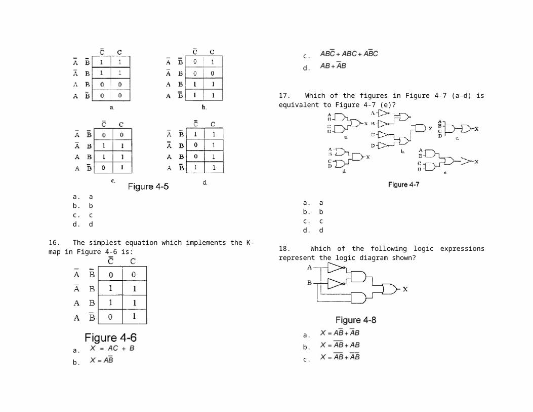
15. Which of the K-maps in Figure 4-5 represents the expression X = AC + BC + B?
a. a b. b c. c d. d
16. The simplest equation which implements the K-map in Figure 4-6 is:
a.
b.
c.
d.
17. Which of the figures in Figure 4-7 (a-d) is equivalent to Figure 4-7 (e)?
a. a b. b c. c d. d
18. Which of the following logic expressions represent the logic diagram shown?

a.
b.
c.
d.
19. What type of logic circuit is represented by the figure shown in Question 18?
a. XOR b. XNOR c. XAND d. XNAND
21. Which of the following combinations cannot be combined into K-map groups? a. Corners in the same row b. Corners in the same column c. Diagonal corners d. Overlapping combinations 21. Which of the circuits in Figure 4-9 (a-d) is the sum-of-products implementation of Figure 4-9(e)?
a. a b. b c. c d. d
22. Based on the indications of probe A in Figure 4-10, what is wrong, if anything, with the circuit?
a. The logic probe is unable to determine the state of the circuit at that point and is blinking to alert the technician to the problem.
b. The output appears to be shorted to Vcc, but is being pulsed by the pulser.

c. The output appears to be LOW, but is being pulsed by the pulser. d. Nothing appears to be wrong at that point.
23. What is the indication of a short to ground in the output of a driving gate? a. Only the output of the defective gate is affected. b. There is a signal loss to all load gates. c. The node may be stuck in either the HIGH or LOW state. d. The affected node will be stuck in the HIGH state.
24. What is the indication of a short on the input of a load gate? a. Only the output of the defective gate is affected. b. There is a signal loss to all gates on the node. c. The affected node will be stuck in the LOW state. d. Both b and c are correct.
25. An output gate is connected to four input gates; the circuit does not function. Preliminary tests with the DMM indicate that the power is applied; scope tests show that the primary input gate has a pulsing signal, while the interconnecting node has no signal. The four load gates are all on different ICs. Which instrument will best help isolate the problem? a. Current tracer b. Logic probe c. Oscilloscope d. Logic analyzer
26. The design concept of using building blocks of circuits in a PLD program is called a(n): a. hierarchical design. b. architectural design. c. digital design. d. verilog.
27. What will a design engineer do after he/she is satisfied that the design will work? a. Put it in a flow chart b. Program a chip and test it c. Give the design to a technician to verify the design d. Perform a vector test
28. In HDL, LITERALS is/are: a. digital systems. b. scalars. c. binary coded decimals. d. a numbering system.
29. In VHDL, macrofunctions is/are: a. digital circuits. b. analog circuits. c. a set of bit vectors. d. preprogrammed TTL devices.
30. In VHDL, concatenating is: a. selecting a signal assignment. b. a secondary point. c. connecting in order to form a bit vector. d. a group of sequential statements.
Flip-Flops and Related Devices 1. A "D" flip-flop utilizing a PGT clock is in the CLEAR state. Which of the following input actions will cause it to change states? a. CLK = NGT, D = 0 b. CLK = PGT, D = 0 c. CLOCK NGT, D = 1 d. CLOCK PGT, D = 1 e. Both a and c
2. Which statement BEST describes the operation of a negative-edge-triggered D flip-flop?
a. The logic level at the D input is transferred to Q on NGT of CLK.
b. The Q output is ALWAYS identical to the CLK input if
the D input is HIGH. c. The Q output is ALWAYS identical to the D input when CLK = PGT. d. The Q output is ALWAYS identical to the D input.
3. The circuit that is primarily responsible for certain flip-flops to be designated as edge-triggered is the: a. edge-detection circuit. b. NOR latch. c. NAND latch. d. pulse-steering circuit.
4. As a general rule for stable flip-flop triggering, the clock pulse rise and fall times must be: a. very long. b. very short. c. at a maximum value to enable the input control signals to stabilize. d. of no consequence as long as the levels are within the determinate range of value.
5. Determine the output frequency for a frequency division circuit that contains twelve flip-flops with an input clock frequency of 20.48MHz. a. 10.24 kHz b. 5kHz c. 30.24kHz d. 15kHz
6. An active-HIGH input S-C latch has a 1 on the S input and a 0 on the C input. What state is the latch in?
a.
b.
c.
d. 7. What is one disadvantage of an S-C flip-flop? a. It has no Enable input. b. It has an invalid state. c. It has no CLOCK input. d. It has only a single output. 8. Which of the following is correct for a clocked D latch? a. The output toggles if one of the inputs is held high. b. Q output follows the input D when the ENABLE is high. c. Only one of the inputs can be high at a time. d. The output complement follows the input when enabled.
9. Edge-triggered flip-flops must have: a. very fast response times. b. at least two inputs to handle rising and falling edges. c. a pulse transition detector. d. active-low inputs and complemented outputs.
10. What is the significance of the J and K terminals on the J-K flip-flop? a. There is no known significance in their designations.
c. The J represents "jump," which is how the Q output reacts whenever the clock goes high and the J input is also high.
d. The letters represent the initials of Johnson and King, the co-inventors of the J-K flip-flop.
d. All of the other letters of the alphabet are already in use.

11. If both inputs of an S-C flip-flop are low, what will happen when the clock goes high? a. An invalid state will exist. b. No change will occur in the output. c. The output will toggle. d. The output will reset.
12. Which of the following best describes the action of pulse-triggered FF's? a. The clock and the S-C inputs must be pulse shaped. b. The data is entered on the leading edge of the clock, and transferred out on the trailing edge of the clock. c. A pulse on the clock transfers data from input to output. d. The synchronous inputs must be pulsed.
13. Which of the following is a disadvantage of the S-C master-slave flip-flop? a. The outputs do not change when both inputs are low. b. There is no complementary output. c. Data can only be entered on the leading edge of the clock. d. An invalid output state exists if both inputs are high.
14. Which of the following is not generally associated with flip-flops? a. Hold time b. Propagation delay time c. Interval time d. Set-up time
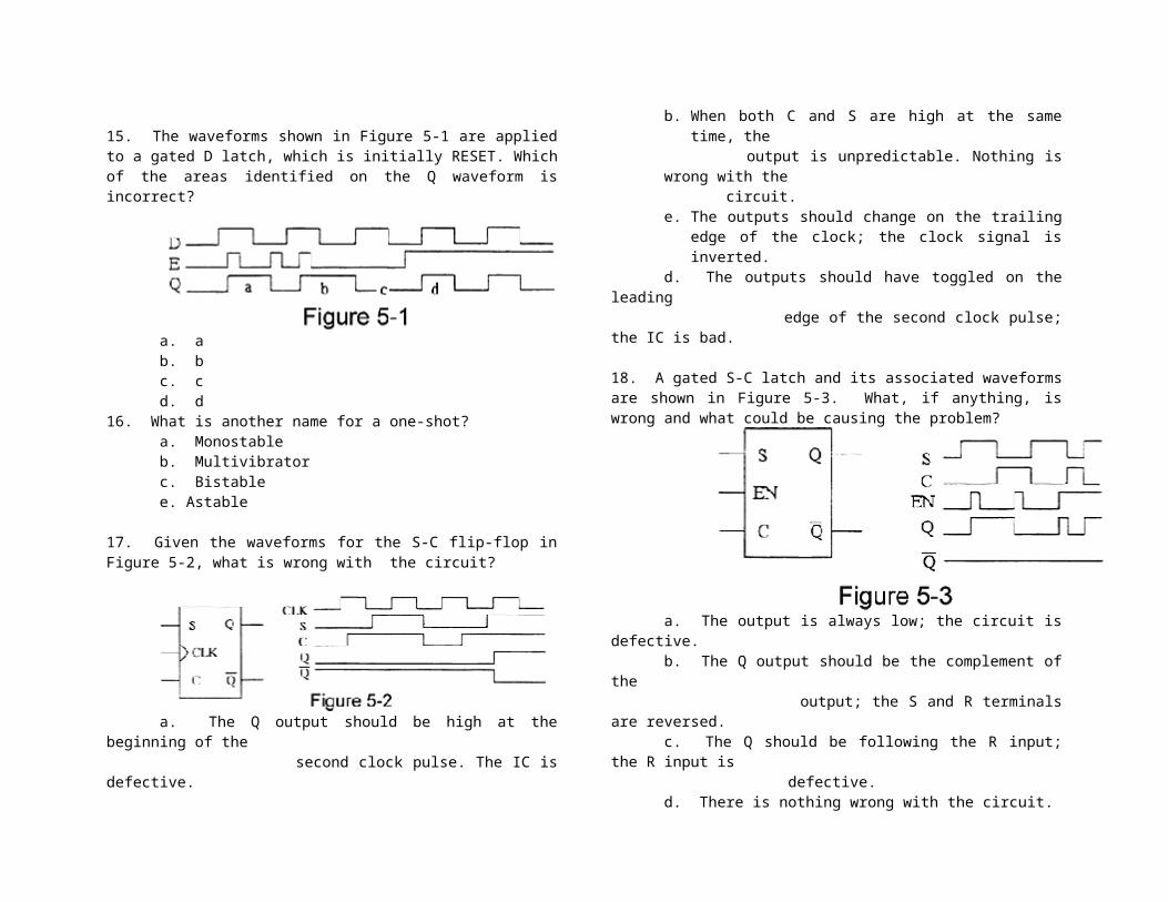
15. The waveforms shown in Figure 5-1 are applied to a gated D latch, which is initially RESET. Which of the areas identified on the Q waveform is incorrect?
a. a b. b c. c d. d 16. What is another name for a one-shot? a. Monostable b. Multivibrator c. Bistable
e. Astable
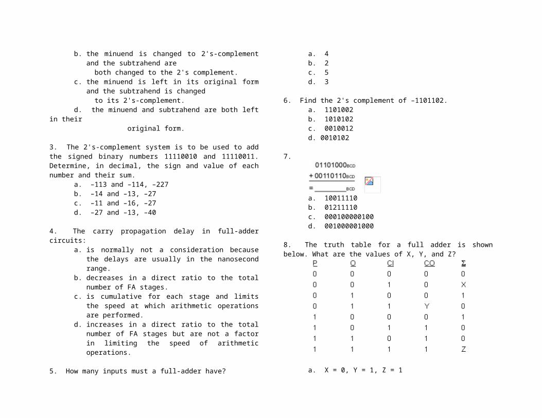
17. Given the waveforms for the S-C flip-flop in Figure 5-2, what is wrong with the circuit?
a. The Q output should be high at the beginning of the second clock pulse. The IC is defective.
b. When both C and S are high at the same time, the
output is unpredictable. Nothing is wrong with the circuit. e. The outputs should change on the trailing edge of
the clock; the clock signal is inverted. d. The outputs should have toggled on the leading edge of the second clock pulse; the IC is bad.

18. A gated S-C latch and its associated waveforms are shown in Figure 5-3. What, if anything, is wrong and what could be causing the problem?
a. The output is always low; the circuit is defective. b. The Q output should be the complement of the output; the S and R terminals are reversed. c. The Q should be following the R input; the R input is defective. d. There is nothing wrong with the circuit.
19. Determine which of the output waveforms is correct for the master-slave D flip-flop shown in Figure 5-4.
a. Qa b. Qb c. Qc d. Qd
20. The 7472 AND-gated master-slave J-K flip-flop is shown in Figure 5-5 with a timing diagram. Examine the output waveform and determine what might be wrong with the
circuit. The Q output is initially LOW and the PRESET and CLEAR are high. Determine whether or not a problem exists, and if so, what could be causing the problem.
a. The output is correct; no problem exists. b. The output is incorrect; J1 is a constant HIGH. c. The output is incorrect; K3 is a constant LOW. d. The output is incorrect; Q is shorted to Vcc.
21. A push-button switch is used to input data to a register. The output of the register is erratic. What could be causing the problem? a. The power supply is probably noisy. b. The switch contacts are bouncing. c. The socket contacts on the register IC are corroded.
f. The register IC is intermittent and failure is imminent.
22. The circuit in Figure 5-6 fails to function; the inputs are checked with a logic probe and the following indications are obtained: C, J1, J2, J3, K1, K2, and K3 are pulsing. Q and CLR are HIGH. Q and PRE are LOW. What could be causing the problem?

a. There is no problem. b. The CLOCK should be held HIGH. c. The PRE is stuck LOW. d. The CLR is stuck HIGH.
23. A positive edge-triggered J-K flip-flop is used to produce a two-phase clock. However, when the circuit is operated it produces erratic results. Close examination with a scope reveals the presence of glitches. What causes the glitches, and how might the problem be corrected?
a. The PRESET and CLEAR terminals may have been left floating; they should be properly terminated if not being used.
b. The problem is caused by a race condition between the J and K inputs; an inverter should be inserted in one of the terminals to correct the problem.
c. A race condition exists between the Q and Q outputs to the AND gate; the AND gate should be replaced with a NAND gate.
d. A race condition exists between the CLOCK and the outputs of the flip-flop feeding the AND gate; replace the flip-flop with a negative edge-triggered J-K flip-flop.
24. Four positive edge-triggered D flip-flops are used to store a 4-bit binary number as shown in Figure 5-7. Determine if the circuit is functioning properly, and if not, what might be wrong.
a. The circuit is functioning properly. b. Q2 is incorrect; the flip-flop is probably bad.
c. The input to flip-flop 3 (D2) is probably wrong; check the source of D2.
d. A bad connection probably exists between FF-3 and FF-4, causing FF-3 not to reset.
25. A 555 timer is connected for astable operation as shown in Figure 5-8 along with the output waveform. It is determined that the duty cycle should be 0.5. What steps need to be taken to correct the duty cycle, while maintaining the same output frequency?
a. Increase the value of C. b. Increase Vcc and decrease RL.

c. Decrease R1 and R2. d. Decrease R1 and increase R2. 26. In VHDL, in which declaration section is a COMPONENT declared? a. Architecture b. Library c. Entity d. Port map
27. In VHDL, how many inputs will a primitive JK flip-flop have? a. 2 b. 3 c. 4 d. 5
28. Which is not an Altera Primitive port identifier? a. clk b. ena c. clr d. prn
29. In VHDL, how is each instance of a component addressed? a. A name followed by a colon and the name of the library primitive b. A name followed by a semi-colon and the component type c. A name followed by the library being used d. A name followed by the component library number
30. Which is not a real advantage of HDL? a. Using higher levels of abstraction b. Tailoring components to exactly fit the needs of the project c. The use of graphical tools d. Both 1 and 2
Digital Arithmetic: Operations and Circuits
1. The MOST commonly used system for representing signed binary numbers is the: a. 2's-complement system. b. 1's-complement system. c. 10's-complement system. d. Sign-magnitude system.
2. When performing subtraction by addition in the 2's-complement system:
a. the minuend and the subtrahend are both changed to the 2's-
complement. b. the minuend is changed to 2's-complement and
the subtrahend are both changed to the 2's complement. c. the minuend is left in its original form and the
subtrahend is changed to its 2's-complement.
d. the minuend and subtrahend are both left in their original form.
3. The 2's-complement system is to be used to add the signed binary numbers 11110010 and 11110011. Determine, in decimal, the sign and value of each number and their sum. a. –113 and –114, –227 b. –14 and –13, –27 c. –11 and –16, –27 d. –27 and –13, –40
4. The carry propagation delay in full-adder circuits:a. is normally not a consideration because the
delays are usually in the nanosecond range. b. decreases in a direct ratio to the total number of
FA stages. c. is cumulative for each stage and limits the speed
at which arithmetic operations are performed.
d. increases in a direct ratio to the total number of FA stages but are not a factor in limiting the speed of arithmetic operations.
5. How many inputs must a full-adder have? a. 4 b. 2 c. 5 d. 3
6. Find the 2's complement of –1101102. a. 1101002 b. 1010102 c. 0010012
d. 0010102
7.
a. 10011110 b. 01211110 c. 000100000100 d. 001000001000
8. The truth table for a full adder is shown below. What are the values of X, Y, and Z?
a. X = 0, Y = 1, Z = 1 b. X = 1, Y = 1, Z = 1 c. X = 1, Y = 0, Z = 1 d. X = 0, Y = 0, Z = 1
9. Which of the statements below best describes Figure 6-1?
a. Half-carry adder; Sum = 0, Carry = 1 b. Half-carry adder; Sum = 1, Carry = 0 c. Full-carry adder; Sum = 1, Carry = 0 d. Full-carry adder; Sum = 1, Carry = 1
10. What is the major difference between half-adders and full-adders?

a. Nothing basically; full-adders are made up of two half-adders. b. Full-adders can handle double digit numbers. c. Full-adders have a carry input capability. d. Half-adders can only handle single digit numbers.
11. What is the correct output of the adder in Figure 6-2, with the output in the order:
a. 10111 b. 11101 c. 01101 d. 10011 12. What is one disadvantage of the ripple-carry adder? a. The interconnections are more complex. b. More stages are required to a full-adder. c. It is slow due to propagation time. d. All of the above are correct.
13. Which of the following is correct for full-adders? a. Full-adders have the capability of directly adding decimal numbers. b. Full-adders are used to make half-adders.
e. Full adders are limited to two inputs since there are only two binary digits.
d. In a parallel full-adder, the first stage may be a half- adder.
14. For a 4 bit parallel adder, if the carry-in is connected to a logical high, the result is:
a. the same as if the carry-in is tied low since the least significant carry-in is ignored.
b. that carry-out will always be high. c. a one will be added to the final result. d. the carry-out is ignored.
15. Using 4-bit adders to create a 16-bit adder: a. requires 16 adders. b. requires 4 adders. c. requires the carry out of the less significant adder to be connected to the carry in of the next significant adder. d. Both b and c.
16. What distinguishes the look-ahead-carry adder? a. It is slower than the ripple-carry adder. b. It is easier to implement logically than a full-adder. c. It is faster than a ripple-carry adder. d. It requires advance knowledge of the final answer.
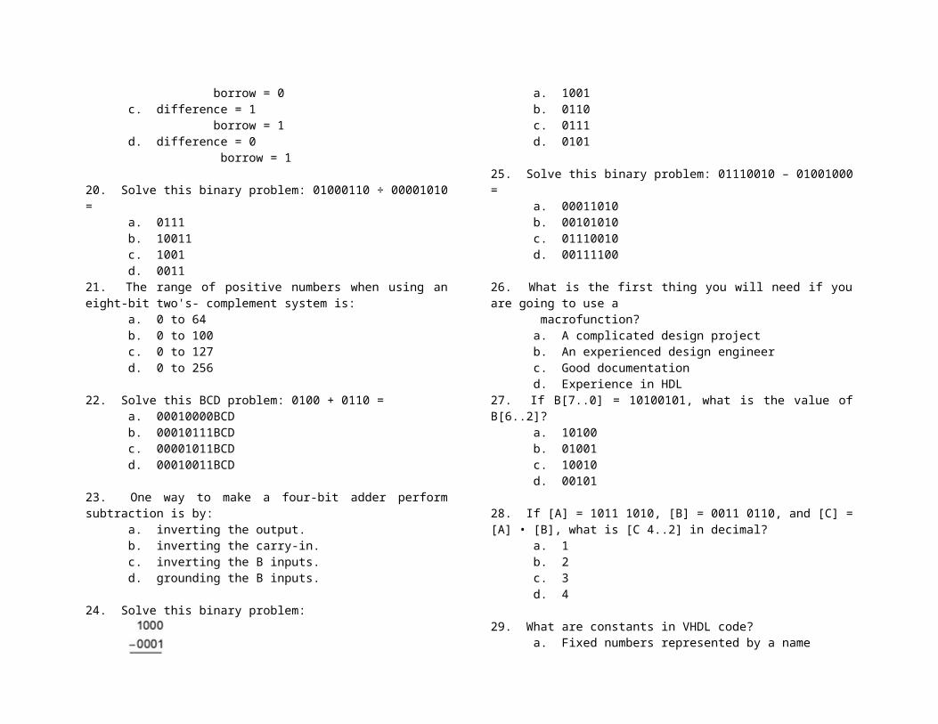
17. What is wrong, if anything, with the circuit in Figure 6-3 based on the logic analyzer display accompanying the circuit?

a. The CO terminal is shorted to ground. b. The S1 output is shorted to Vcc. c. The P1 input is not being added into the total. d. Nothing is wrong; the circuit is functioning correctly.
18. Solve this binary problem:
a. 11001001 b. 10010000 c. 01101110 d. 01110110
19. The binary subtraction 0 – 0 = a. difference = 0 borrow = 0 b. difference = 1 borrow = 0 c. difference = 1 borrow = 1 d. difference = 0 borrow = 1
20. Solve this binary problem: 01000110 ÷ 00001010 = a. 0111
b. 10011 c. 1001 d. 0011 21. The range of positive numbers when using an eight-bit two's- complement system is: a. 0 to 64 b. 0 to 100 c. 0 to 127 d. 0 to 256
22. Solve this BCD problem: 0100 + 0110 = a. 00010000BCD b. 00010111BCD c. 00001011BCD d. 00010011BCD
23. One way to make a four-bit adder perform subtraction is by: a. inverting the output. b. inverting the carry-in. c. inverting the B inputs. d. grounding the B inputs.
24. Solve this binary problem:
a. 1001 b. 0110 c. 0111 d. 0101
25. Solve this binary problem: 01110010 – 01001000 = a. 00011010 b. 00101010 c. 01110010 d. 00111100
26. What is the first thing you will need if you are going to use a macrofunction?

a. A complicated design project b. An experienced design engineer c. Good documentation d. Experience in HDL 27. If B[7..0] = 10100101, what is the value of B[6..2]? a. 10100 b. 01001 c. 10010 d. 00101
28. If [A] = 1011 1010, [B] = 0011 0110, and [C] = [A] • [B], what is [C 4..2] in decimal? a. 1 b. 2 c. 3 d. 4
29. What are constants in VHDL code? a. Fixed numbers represented by a name b. Fixed variables used in functions c. Fixed number types d. Constants do not exist in VHDL code.
30. In VHDL, what is a GENERATE statement? a. The start statement of a program b. Not used in VHDL or ADHL c. A way to get the computer to generate a program from a circuit diagram
e. A way to tell the compiler to replicate several components
Counters and Registers Multiple Choice
1. Which of the following groups of logic devices would be the minimum required for a MOD-64 synchronous counter? [Hint] a. Five flip-flops, three AND gates b. Seven flip-flops, five AND gates c. Four flip-flops, ten AND gates d. Six flip-flops, four AND gates
2. Synchronous (parallel) counters eliminate the delay problems encountered with asynchronous (ripple) counters because the: [Hint] a. Input clock pulses are applied only to the first and last stage. b. input clock pulses are applied only to the last stage. c. input clock pulses are applied simultaneously to each stage. d. input clock pulses are not used to activate any of the counter stages.
3. How many AND gates would be required to completely decode ALL the states of a MOD 64 counter, and how many inputs must each AND gate have? [Hint] a. 128 gates, 6 inputs to each gate b. 64 gates, 5 inputs to each gate c. 64 gates, 6 inputs to each gate d. 128 gates, 5 inputs to each gate
4. A MOD 12 and a MOD 10 counter are cascaded. Determine the output frequency if the input clock frequency is 60MHz. [Hint] a. 500kHz b. 1,500kHz c. 6MHz d. 5MHz
5. To operate correctly, starting a ring counter requires: [Hint] a. clearing one flip-flop and presetting all others. b. clearing all the flip-flops. c. presetting one flip-flop and clearing all others. d. presetting all the flip-flops.
6. Which of the following statements are true? [Hint] a. Asynchronous events do not occur at the same time. b. Asynchronous events are controlled by a clock. c. Synchronous events do not need a clock to control
them. d. Only asynchronous events need a control clock.
7. How many flip-flops are required to construct a decade counter? [Hint] a. 10 b. 8 c. 5 d. 4
8. What function will the counter shown in Figure 7-1 be performing during period "B" on the timing diagram?
a. Counting up b. Counting down c. Inhibited d. Loading
9. What decimal value is required to produce an output at "X" in Figure 7-2?
a. 1 b. 1 or 4 c. 2 d. 5
10. The circuit in Figure 7-3 has no output on Q1 when examined with an oscilloscope. All J-K inputs are HIGH, the CLK signal is present, and the Q0 is toggling. The C input of FF1 is a constant LOW. What could be causing the problem?
a. The Q0 output should be connected to the J input

of FF1. b. The output of FFO may be shorted to ground. c. The input of FF1 may be shorted to ground. d. Either b or c could be correct.
11. Which of the following procedures could be used to check the parallel loading feature of a counter? [Hint]
a. Preset the LOAD inputs, set the CLR to its active level, and check to see that the Q outputs match the values preset into the LOAD inputs.
b. Apply LOWs to the parallel DATA inputs, pulse the CLK input, and check for LOWs on all the Q outputs.
c. Apply HIGHs to all the DATA inputs, pulse the CLK and CLR inputs, and check to be sure that the Q outputs are all LOW.
d. Apply HIGHs to all the Q terminals, pulse the CLK, and check to see if the DATA terminals now match the Q outputs.
12. A four-channel scope is used to check the counter in Figure 7-4. Are the displayed waveforms correct?
a. Yes b. No
13. How many data bits can be stored in the register shown in Figure 7-5?
a. 5 b. 32 c. 31 d. 4
14. After 10 clock cycles, and assuming that the DATA input had returned to 0 following the storage sequence, what values would be stored in Q4, Q3, Q2, Q1, Q0 of the register in Figure 7-5. a. 0,1,0,1,1 b. 1,1,0,1,0 c. 1,0,1,0,1 d. 0,0,0,0,0
15. What type of register is shown in Figure 7-6?
a. Parallel-in parallel-out register
b. Serial-in parallel-out register c. Serial/parallel-in parallel-out register d. Parallel-access shift register
16. Referring to Figure 7-6, at point "X" on the timing diagram, what action will take place? a. The outputs will all go LOW. b. The inputs will be disabled. c. All inputs and outputs will be reset to LOW. d. Only the CLK will be disabled during this time, preventing any transfer of data between inputs and outputs.
17. Referring to Figure 7-6, what action takes place during the interval labeled "Y"? a. Parallel data transfer takes place. b. Parallel data is shifted through the register. c. Serial data is being shifted through the register. d. Clock pulses are being toggled through the register.
18. What type of device is shown in Figure 7-7?
a. 4-bit bidirectional universal shift register b. Parallel-in parallel-out shift register with bidirectional data flow c. 2-way parallel-in serial-out bidirectional register d. 2-bit serial-in 4-bit parallel-out bidirectional shift register
19. Referring to Figure 7-7, what action takes place at point "V" on the timing diagram? a. Data is loaded into the register from the parallel inputs.
b. The parallel inputs are inhibited; i.e., prevented from loading into the register.
c. The serial inputs are loaded into the register.
d. The outputs are cleared; set to LOW.
20. Referring to Figure 7-7, what action takes place at point "W" on the timing diagram? a. Data is loaded into the register from the parallel inputs.
c. The parallel inputs are inhibited; i.e., prevented from loading into the register.
c. The serial inputs are loaded into the register. d. The outputs are cleared; set to LOW. 21. Which of the following is a type of shift register counter? a. Decade b. Binary c. Ring d. BCD
22. What function does the CTR DIV 8 circuit perform in Figure 7-8?
a. It divides the clock frequency down to match the frequency of the serial data in.
b. The divide-by-8 counter is triggered by the control flip-flop and clock, which then allows the data output register to begin storing the input data. Once all 8 data bits are stored in the data
output register, the data output register and the divide-by-8 counter trigger the one-shot. The one-shot then begins the process all over again.
c. The divide-by-8 counter is used to verify that the parity bit is attached to the input data string.
d. It keeps track of the eight data bits, triggering the transfer of the data through the output register and the one-shot, which then resets the control flip-flop and divide-by-8 counter.
23. Referring to Figure 7-9, at which point is the serial data transferred to the parallel output?
a. W b. X c. Y
d. Z
24. Referring to Figure 7-9, what causes the Control FF to reset after D7?
a. Once the data cycle is initiated by the Start bit, the one-shot produces an output pulse equal to the duration of the eight data bits. Once the eight data bits have been transferred to the data input register, the falling edge of the one-shot pulse resets the Control FF to start the sequence all over again.
b. After counting the eight data bits, the divide-by-8 counter produces an output on its active-low CLR line to reset the Control FF.
c. After counting eight clock pulses equivalent to eight data periods, the terminal count of the divide-by-8 counter and the clock trigger the one-shot, which in turn resets the Control FF and divide-by-8 circuits to begin the sequence all over again. Simultaneously the data is transferred through the output register.
d. When the data output register is full, it produces an output on its C terminal that triggers the one-shot, which in turn resets the Control FF.
25. The circuit in Figure 7-10 fails to produce data output: the individual flip- flops are checked with a logic probe and pulser, and each checks OK. What could be causing the problem?
a. The data output line may be grounded. b. One of the clock input lines may be open.c. One of the interconnect lines between two stages
may have a solder bridge to ground.
f. One of the flip-flops may have a solder bridge between its input and Vcc.
26. The Altera library LPM counter does not: a. count up and down. b. perform synchronous parallel load. c. do asynchronous clear. d. do synchronous cascading.
27. In an HDL ring counter, many invalid states are included in the programming by: a. using a case statement. b. using an elsif statement. c. including them under others. d. the ser_in line.
28. How can a digital one-shot be implemented using HDL? a. By using a resistor and a capacitor b. By applying the concept of a counter c. By using a library function d. By applying a level trigger
29. For a one-shot application, how can HDL code be used to make a circuit respond once to each positive transition on its trigger input? a. By using a counter b. By using an active clock c. By using an immediate reload d. By using edge trapping
30. In a VHDL retriggerable edge-triggered one-shot, which condition will not exist when a clock edge occurs? [Hint] a. A trigger edge has occurred and we must load the counter. b. The counter is zero and we need to keep it at zero. c. The shift register is reset. d. The counter is not zero and we need to count down by one.
Integrated-Circuit Logic Families
1. The bipolar TTL logic family that was developed to increase switching speed by preventing transistor saturation is: a. emitter-coupled logic (ECL). b. current-mode logic (CML). c. transistor-transistor logic (TTL). d. Both a and c.
2. Generally, the voltage measured at an unused TTL input would typically be measured between: a. 1.4 to 1.8v. b. 0 to 5v. c. 0 to 1.8v. d. 0.8 to 5v.
3. The IEEE/ANSI notation of an internal underlined diamond denotes: a. totem-pole outputs. b. open-collector outputs. c. quadrature amplifiers. d. tri-state buffers.
4. A "floating" TTL input may be defined as: a. unused input that is tied to Vcc through a 1k ohm resistor. b. unused input that is tied to used inputs. c. unused input that is tied to the ground. d. unused input that is not connected.
5. Logic circuits that are designated as buffers, drivers, or buffer/drivers are designed to have: a. a greater current/voltage capability than an ordinary logic circuit. b. greater input current/voltage capability than an ordinary logic circuit. c. a smaller output current/voltage capability than an ordinary logic.
d. greater input and output current/voltage capability
than an ordinary logic circuit.
6. Why is the fan-out of CMOS gates frequency dependent? a. Each CMOS input gate has a specific propagation
time and this limits the number of different gates that can be connected to the output of a CMOS gate.
b. When the frequency reaches the critical value, the gate will only be capable of delivering 70% of the normal output voltage and consequently the output power will be one-half of normal; this defines the upper operating frequency.
c. The higher the number of gates attached to the output, the more frequently they will have to be serviced, thus reducing the frequency at which each will be serviced with an input signal.
d. The input gates of the FETs are predominantly capacitive, and as the signal frequency increases the capacitive loading also increases, thereby limiting the number of loads that may be attached to the output of the driving gate.
7. Which of the following will not normally be found on a data sheet? a. Minimum HIGH level output voltage b. Maximum LOW level output voltage c. Minimum LOW level output voltage d. Maximum HIGH level input current
8. What are the major differences between the 5400 and 7400 series of ICS?
a. The 5400 series are military grade and require tighter supply voltages and temperatures.
b. The 5400 series are military grade and allow for a wider range of supply voltages and temperatures.
c. The 7400 series are an improvement over the original
5400s. d. The 7400 series was originally developed by Texas Instruments. The 5400 series was brought out by National Semiconductors after TI's patents expired, as a second supply source.
9. Refer to Figure 8-1. Which of the following describes the operation of the circuit?
a. A LOW input turns Q1 and Q3 on; Q2 and Q4 are off. b. A LOW input turns Q1 and Q4 off; Q2 and Q3 are on. c. A HIGH input turns Q1, Q2, and Q3 off, and Q4 is on. d. A HIGH input turns Q1, Q2, and Q4 on; Q3 is off.
10. Refer to Figure 8-1. What type of output arrangement is being used for the output? a. Complementary-symmetry b. Push-pull c. Quasi push-pull d. Totem-Pole
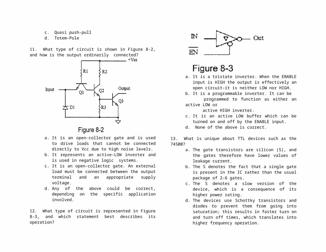
11. What type of circuit is shown in Figure 8-2, and how is the output ordinarily connected?
a. It is an open-collector gate and is used to drive loads that cannot be connected directly to Vcc due to high noise levels.
b. It represents an active-LOW inverter and is used in negative logic systems.
c. It is an open-collector gate. An external load must be connected between the output terminal and an appropriate supply voltage.
d. Any of the above could be correct, depending on the specific application involved.
12. What type of circuit is represented in Figure 8-3, and which statement best describes its operation?

a. It is a tristate inverter. When the ENABLE input is HIGH the output is effectively an open circuit-it is neither LOW nor HIGH.
b. It is a programmable inverter. It can be programmed to function as either an active LOW or active HIGH inverter. c. It is an active LOW buffer which can be turned on
and off by the ENABLE input. d. None of the above is correct.
13. What is unique about TTL devices such as the 74S00? a. The gate transistors are silicon (S), and the gates
therefore have lower values of leakage current. b. The S denotes the fact that a single gate is
present in the IC rather than the usual package of 2-6 gates.
c. The S denotes a slow version of the device, which is a consequence of its higher power rating.
d. The devices use Schottky transistors and diodes to prevent them from going into saturation; this results in faster turn on and turn off times, which translates into higher frequency operation.
14. Refer to Figure 8-4. What type of device is shown and what input levels are required to turn the LED off?
a. The device is an open-collector AND gate and
requires both inputs to be HIGH in order to turn the LED off.
b. The device is a Schottky AND gate and requires only one low input to turn the LED off.
c. The device is an open-collector AND gate and requires only one low input to turn the LED off.
d. The device is a Schottky open-collector AND gate and requires a low on both inputs to turn the LED off.
15. What type of logic circuit is shown in Figure 8-5 and what logic function is being performed?
a. It is an NMOS AND gate. b. It is a CMOS AND gate. c. It is a CMOS NOR gate. d. It is a PMOS NAND gate. 16. What type of circuit is shown in Figure 8-6 and which statement best describes its operation?
a. It is a two-input CMOS AND gate with open drain.
b. It is a two-input CMOS buffer with tristate output. c. It is a CMOS inverter with tristate output. d. It is a hybrid TTL-CMOS inverter with FET totem-pole output.
17. Which of the following statements apply to CMOS devices? a. The devices should not be inserted into circuits with the power on.
c. All tools, test equipment, and metal workbenches should be tied to earth ground.
d. The devices should be stored and shipped in antistatic tubes or conductive foam.
d. All of the above are correct.
18. Which of the following logic families has the highest noise margin? a. TTL b. LS TTL c. CMOS d. HCMOS
19. Which of the following logic families has the highest maximum clock frequency? a. S-TTL b. AS-TTL c. HS-TTL d. HCMOS 20. Which of the following logic families has the shortest propagation delay? a. S-TTL b. AS-TTL c. HS-TTL d. HCMOS
21. What must be done to interface CMOS to TTL? a. A dropping resistor must be used on the CMOS 12V supply to reduce it to 5V for the TTL.

b. As long as the CMOS supply voltage is 5V, they can be interfaced; however, the fan-out of the CMOS is limited to two TTL gates.
c. A 5V Zener diode must be placed across the inputs of the TTL gates in order to protect them from the higher output voltages of the CMOS gates.
d. The two series cannot be interfaced without the use of special interface buffers designed for that purpose, such as the open-collector buffers.
22. What must be done to interface TTL to CMOS? a. A dropping resistor must be used on the CMOS 12V supply to reduce it to 5V for the TTL.
b. As long as the CMOS supply voltage is 5V, they can be interfaced; however, the fan-out of the TTL is limited to five CMOS gates.
c. A 5V Zener diode must be placed across the inputs of the TTL gates in order to protect them from the higher output voltages of the CMOS gates.
d. A pull-up resistor must be used between the TTL output-CMOS input node and Vcc; the value of RP will depend on the number of CMOS gates connected to the node.
23. What does ECL stand for? a. It stands for electron-coupled logic; all of the
devices used within the gates are N-type transistors.
b. It stands for emitter-coupled logic; all of the inputs are coupled into the device through the emitters of the input transistors.
c. It stands for emitter-coupled logic; all of the emitters of the input transistors are connected together and each transistor functions as an emitter follower.
d. It stands for energy-coupled logic; the input energy is amplified by the input transistors and
allows the device to deliver higher output currents.
24. Which of the following summarizes the important features of ECL? [Hint]
a. Low noise margin, low output voltage swing, negative voltage operation, fast, and high power consumption
b. Good noise immunity, negative logic, high frequency capability, low power dissipation, and short propagation time
c. Slow propagation time, high frequency response, low power consumption, and high output voltage swings
d. Poor noise immunity, positive supply voltage operation, good low frequency operation, and low power
25. Which of the logic families listed below allows the highest operating frequency? a. 74AS b. ECL c. HCMOS d. 54S
26. A logic signal experiences a delay in going through a circuit. The two propagation delay times are defined as: a. tPLH and tPHL. b. tDLH and tDHL. c. tHPL and tlph. d. tLDH and tHDL.
27. What causes low-power Schottky TTL to use less power than the 74XX series TTL? a. The Schottky-clamped transistor b. Nothing. The 74XX series uses less power. c. A larger value resistor d. Using NAND gates

28. Whenever a totem-pole TTL output goes from LOW to HIGH, a high-amplitude current spike is drawn from the Vcc supply. How is this effect corrected to a digital circuit? a. By connecting a radio-frequency capacitor from Vcc to ground. b. By using a switching power supply c. By connecting a capacitor from Vout to ground d. By connecting a large resistor from Vcc to Vout
29. What is the increase in switching speed between 74LS series TTL and 74HC/HCT (High-Speed CMOS)? a. 5 b. 10 c. 50 d. 100
30. What is the static charge that can be stored by your body as you walk across a carpet? a. 300 volts b. 3,000 volts c. 30,000 volts d. Over 30,000 volts
MSI Logic Circuits
1. A 16-input multiplexer is to be used to perform parallel-to-serial data conversion. Which of the following counters would be required to provide the data select inputs? a. MOD 8 b. MOD 16 c. MOD 4 d. MOD 2
2. The IEEE/ANSI symbol for a decoder has the internal designation bcd/dec. This means the decoder is a:
a. decimal to binary coded decimal decoder with ten inputs and four outputs.
b. binary coded decimal to decimal decoder with ten inputs and four outputs.
c. decimal to binary coded decimal decoder with four inputs and ten outputs.
d. binary coded decimal to decimal decoder with four inputs and ten outputs.
3. Multiplexing of digital signals is usually required when: a. moving data internally within a microprocessor.
b. moving data between memory and storage registers in a microprocessor.
c. moving data over long distance transmission lines. d. Both a and b.
4. One can safely state that the output lines for a demultiplexer are under the direct control of the: a. input data select lines. b. the internal AND gates. c. the internal OR gate. d. Input data line.
5. What is the purpose of a decoder's inputs? a. To allow the decoder to respond to the inputs to
activate the correct output gate. b. To disable the decoder outputs so that all outputs will be inactive. c. To disable the inputs and activate all outputs. d. Both a and c.
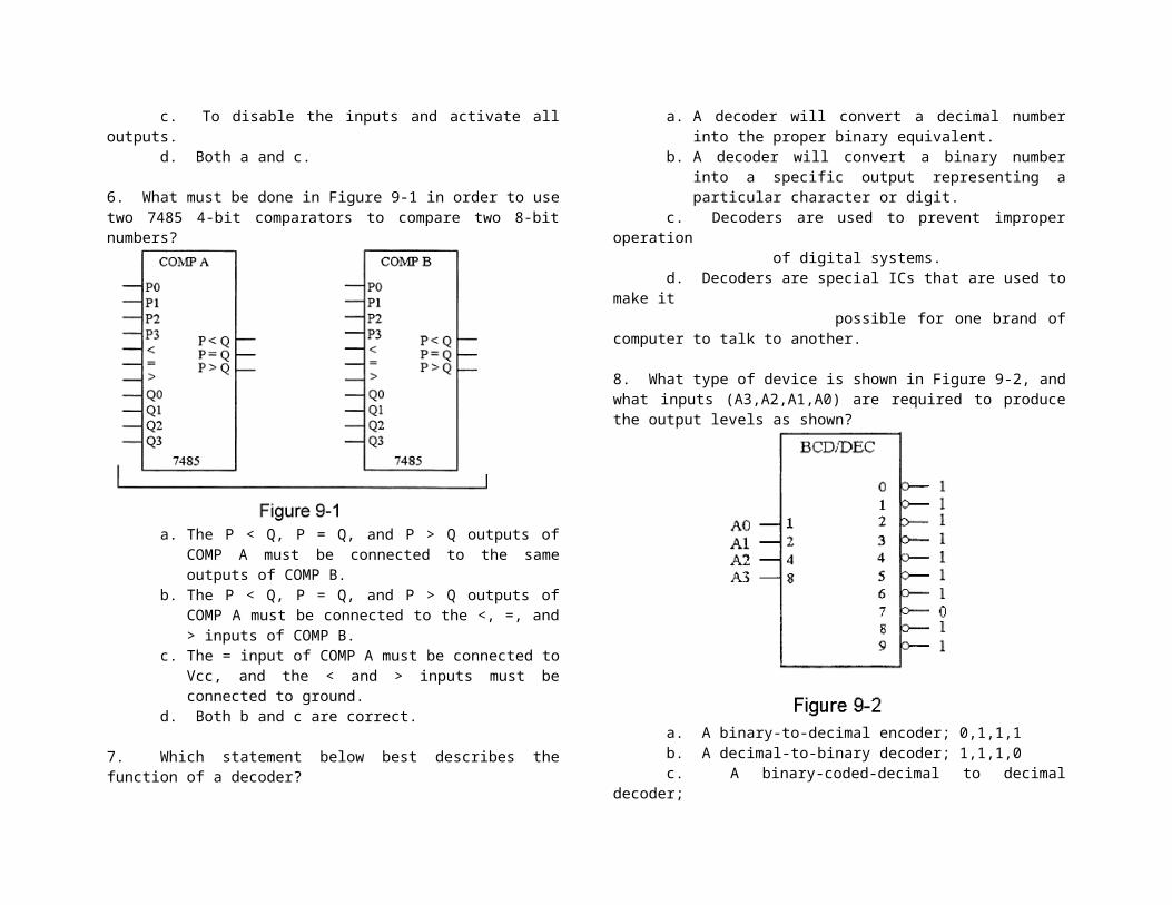
6. What must be done in Figure 9-1 in order to use two 7485 4-bit comparators to compare two 8-bit numbers?
a. The P < Q, P = Q, and P > Q outputs of COMP A
must be connected to the same outputs of COMP B.
b. The P < Q, P = Q, and P > Q outputs of COMP A must be connected to the <, =, and > inputs of COMP B.
c. The = input of COMP A must be connected to Vcc, and the < and > inputs must be connected to ground.
d. Both b and c are correct.
7. Which statement below best describes the function of a decoder?
a. A decoder will convert a decimal number into the proper binary equivalent.
b. A decoder will convert a binary number into a specific output representing a particular character or digit.
c. Decoders are used to prevent improper operation of digital systems. d. Decoders are special ICs that are used to make it possible for one brand of computer to talk to another.
8. What type of device is shown in Figure 9-2, and what inputs (A3,A2,A1,A0) are required to produce the output levels as shown?
a. A binary-to-decimal encoder; 0,1,1,1 b. A decimal-to-binary decoder; 1,1,1,0 c. A binary-coded-decimal to decimal decoder; 0,1,1,1 d. A decimal to binary-coded-decimal encoder; 1,1,1,0
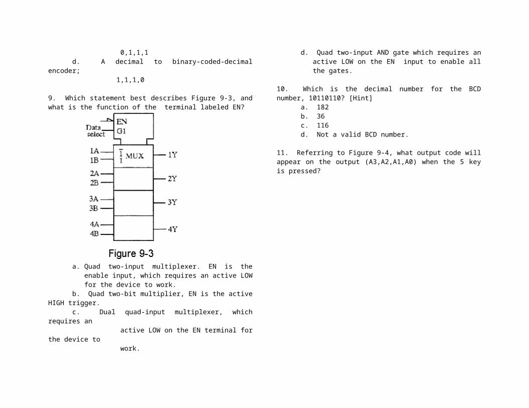
9. Which statement best describes Figure 9-3, and what is the function of the terminal labeled EN?

a. Quad two-input multiplexer. EN is the enable input, which requires an active LOW for the device to work.
b. Quad two-bit multiplier, EN is the active HIGH trigger. c. Dual quad-input multiplexer, which requires an active LOW on the EN terminal for the device to work.
d. Quad two-input AND gate which requires an active LOW on the EN input to enable all the gates.
10. Which is the decimal number for the BCD number, 10110110? [Hint] a. 182 b. 36 c. 116 d. Not a valid BCD number.
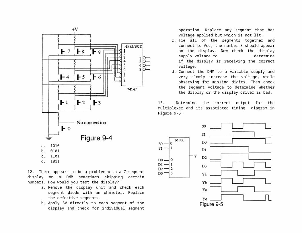
11. Referring to Figure 9-4, what output code will appear on the output (A3,A2,A1,A0) when the 5 key is pressed?
a. 1010 b. 0101 c. 1101 d. 1011
12. There appears to be a problem with a 7-segment display on a DMM sometimes skipping certain numbers. How would you test the display?
a. Remove the display unit and check each segment diode with an ohmmeter. Replace the defective segments.
b. Apply 5V directly to each segment of the display and check for individual segment operation. Replace any segment that has voltage applied but which is not lit.
c. Tie all of the segments together and connect to Vcc; the number 8 should appear on the display. Now check the display supply voltage to determine if the display is receiving the correct voltage.
d. Connect the DMM to a variable supply and very slowly increase the voltage, while observing for missing digits. Then check the segment voltage to determine whether the display or the display driver is bad.
13. Determine the correct output for the multiplexer and its associated timing diagram in Figure 9-5.
a. Ya b. Yb c. Yc d. Yd
14. A breadboard-circuit design using a BCD-to-decimal decoder has a problem wherein the operation of the
system is erratic. The technician uses his scope to examine the waveforms throughout the system and doesn't really see any problems. While he's scratching his head, what helpful advice can you offer him as to what might be wrong and what to do to correct the problem? a. The decoder is thermally intermittent; replace it.
b. There is probably a bad connection on the wire wrap proto- board; recheck the wiring.
c. Glitches are probably the culprit; strobe the decoder. d. Either a or b is correct.
15. Refer to the display multiplexer in Figure 9-6. The MSD display is blank, while the LSD seems to be OK. The input and output lines to the 74157 and 7449 are checked with a scope and can be seen changing levels. The A input on the 74139 also changes; however, the 0 output on the 74139 is always LOW and the 1 output is always HIGH. The B and EN inputs on the 74139 are always LOW. What could cause the problem and what should be done to correct it?

a. The 74139 is defective; replace it. b. The EN pin on the 74139 could have a bad connection; check the connection. c. Either a or b could be correct; try b first. d. The MSD display is bad; replace it.
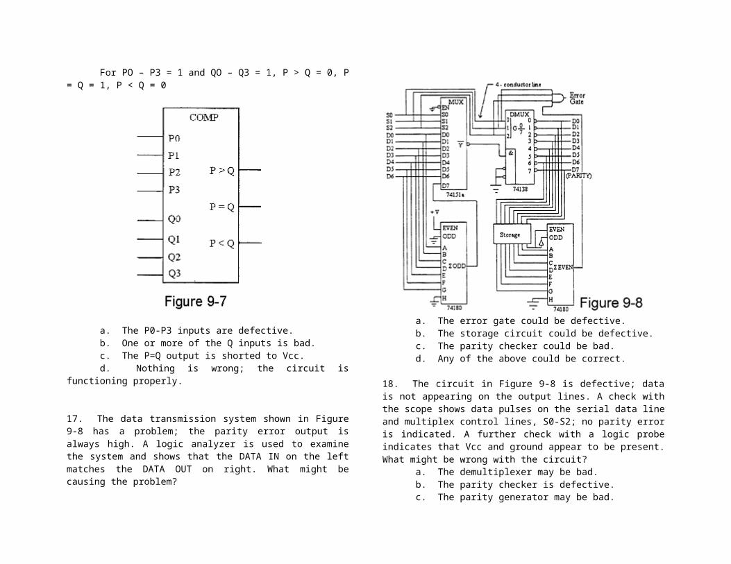
16. It is suspected that the comparator in Figure 9-7 has a problem. The inputs are activated in the table shown below and the corresponding outputs noted. What is most likely wrong with the circuit?
For PO – P3 = 1 and QO – Q3 = 0, P > Q = 1, P = Q = 1, P < Q = 0
For PO – P3 = 0 and QO – Q3 = 1, P > Q = 0, P = Q = 1, P < Q = 1
For PO – P3 = 1 and QO – Q3 = 1, P > Q = 0, P = Q = 1, P < Q = 0
a. The P0-P3 inputs are defective. b. One or more of the Q inputs is bad. c. The P=Q output is shorted to Vcc.
d. Nothing is wrong; the circuit is functioning properly.
17. The data transmission system shown in Figure 9-8 has a problem; the parity error output is always high. A logic analyzer is used to examine the system and shows that the DATA IN on the left matches the DATA OUT on right. What might be causing the problem?
a. The error gate could be defective. b. The storage circuit could be defective. c. The parity checker could be bad. d. Any of the above could be correct.
18. The circuit in Figure 9-8 is defective; data is not appearing on the output lines. A check with the scope shows data pulses on the serial data line and multiplex control lines, S0-S2; no parity error is indicated. A further check

with a logic probe indicates that Vcc and ground appear to be present. What might be wrong with the circuit? a. The demultiplexer may be bad. b. The parity checker is defective. c. The parity generator may be bad. d. Both b and c could be correct.
19. Refer to the keyboard encoder in Figure 9-9(a). Sometimes when the 5 key is pressed, the system attached to the keypad does not respond. The 5 input on the 74147 is monitored with a digital storage scope while repeatedly pressing the 5 key, and the waveform in Figure 9-9(b) is obtained; the P above the trace indicates the points at which the technician pressed the key. What is most likely wrong with the circuit?
a. The switches on the 5 key are intermittent; the contacts need to be cleaned or the switch replaced.
b. The pull-up resistor connected to the 5 key is bad and should be replaced.
c. The common ground connection at the bottom of the 0 key has a bad solder connection; repair the connection.
d. The 74147 is intermittent, possibly due to high temperature, and should be replaced.
20. Refer to Figure 9-10. The logic function generator being implemented with the multiplexer in this circuit produces a constant LOW on the output. The ABC inputs are checked and appear to be pulsing; also, the 0-7 and EN inputs are checked with the scope and all appear to be at OV. A check with the DMM confirms that power is on. What is the problem, and what should be done to correct it?
a. The output is shorted to Vcc; replace the IC. b. The scope's vertical input is in the AC mode and the common connection for the 0,2,3 and 5 inputs is bad. Set the scope's vertical input mode to DC, and repair the bad solder connection. c. Power has not been applied to the circuit; apply

power. d. The output is shorted to ground; replace the IC.
21. The BCD/DEC decoder shown in Figure 9-11(a) is examined with a logic analyzer and the results are shown in the waveforms in Figure 9-11(b). What, if anything, is wrong with the circuit?
a. The "2" output is shorted to Vcc. b. The A1 input is internally open. c. The A1 input node is internally stuck LOW. d. Nothing is wrong with the circuit.
22. For the input values (A0-A3, B0-B3, Data Select = 1) given for Figure 9-12, what will be indicated on the displays?
a. A = 0, B = 5 b. A = 5, B = 0 c. A = 6, B = 0 d. A = 0, B = 6
23. What are the outputs of a 7485 four-bit magnitude comparator when the inputs are A = 1001 and B = 1010?
a.
b.

c.
d.
24. Output 5 of a 74138 octal decoder is selected when it is enabled by a data input of:
a.
b.
c.
d. 25. How is the number one (1) indicated on the outputs of a 7447 BCD-to- seven-segment code converter? a. Segment a is active. b. Segment b is active. c. Segments a and b are active. d. Segments b and c are active.
26. What VHDL techniques are used to describe a priority encoder? a. Integer outputs and priority coding
b. Signal outputs and priority coding e. Tristate outputs and priority codingf. Variables and priority coding
27. What is an important attribute of the conditional signal assignment statement? a. Its tristate outputs b. Its sequential evaluation c. Its use of library components d. Its fast activation times 28. What is the HDL key issue in the design of the MUX and DEMUX? a. Having the MUX and DEMUX part of the library b. Using the case statement in the process c. Describing the functions d. Assigning signals under certain conditions
29. Why are control inputs included in an HDL magnitude comparator? a. For cascading the chips b. For control signal input c. For signal control d. For internal interconnections
30. In an AHDL BCD to binary code converter, how is multiplication by 10 accomplished? a. By using the shifting of bits b. By using the library multiplication function c. By using integer types d. By using the multiplication operator
Digital System Projects Using HDL
1. When designing an HDL digital system, which is the worst mistake one can make? a. Conclude that a fundamental block works perfectly b. Fail to provide proper documentation c. Add blocks of code prior to testing them
d. Overlook a possible VARIABLE
2. What must a stepper motor HDL application include? a. Variables and processes b. Types and bits c, Counters and decoders d. Sequencers and multiplexers
3. In a full-step sequence involving two flip-flops driving four coils of a stepper motor, how far will the stepper motor step? a. 90° b. 45° c. 30° d. 15°
4. In an HDL application of a stepper motor, after an up/down counter is built what is done next? a. Build the sequencer b. Test it on a simulator c. Test the decoder d. Design an intermediate integer variable
5. In an HDL stepper motor design, why is there more than one mode? a. To change the speed of the stepper motor b. To change the direction of the stepper motor c. To direct drive the stepper motor d. All the above
6. Why should a real hardware functional test be performed on the HDL stepper motor design? a. To check the speed of the software b. To check the current levels in the motor c. To check the voltage levels of the real outputs d. To provide a fully operational system
7. What does the major block of an HDL code emulation of a keypad include? a. A sequencer b. A clock
c. A multiplexer d. A ring counter
8. What does the ring counter in the HDL keypad application do when a key is pressed? a. Count to find the row b. Freeze c. Count to find the column d. Start the D flip-flop
9. In the keypad application, what does the preset state of the ring counter define? a. The proper output of the column encoder b. The NANDing of the rows c. The NANDing of the columns d. The proper output of the row encoder
10. In the keypad application, what does the data signal define? a. The row and column encoded data b. The ring encoded data c. The freeze locator data d. The ring counter data
11. In the keypad application, when all columns are high, the ring counter is enabled and counting and dav is low, what is the status of the d outputs? a. On b. Off c. Hi-Z d. 1011
12. In the keypad application, just after the 4ms mark the simulation imitates the release of the key by changing the column value back to F hex, which causes the d output to go into its Hi-Z state. On the next rising clock edge, what happens to dav? a. It goes high. b. It goes low. c. It goes to Hi-Z. d. It goes to 1111H.
13. In a digital clock application, the basic frequency must be divided down to: a. 1 Hz. b. 60 Hz. c. 100 Hz. d. 1000 Hz.
14. In the digital clock project, what type of counter is used to count to 59 seconds? a. MOD-60 b. MOD-6 c. BCD d. BCD followed by a MOD-6
15. In the digital clock project, what is the frequency of the MOD-6 counter in the minutes section? a. 1 pulse per minute b. 6 pulses per minute c. 10 pulses per minute d. 1 pulse per hour
16. In the digital clock project, the purpose of the frequency prescalar is to: a. find the basic frequency. b. transform a 60pps input to a 1pps timing signal. c. prevent the clock from exceeding 12:59:59. d. allow the BCD display to have a value from 00–59.
17. List 3 basic blocks in the digital clock project. a. MOD-60, MOD-12 counters b. MOD-5, MOD-10, MOD-12 counters c. MOD-60, MOD-10 counters d. MOD-6, MOD-12, and MOD-10 counters
18. What are two ways to remember the current state of a counter in VHDL? a. With FUNCTIONS and PROCESS b. With counters and timers c. With SIGNAL and VARIABLE d. With bit types
19. In the digital clock project, when does the PM indicator go high? a. Never b. Going from 11:59:59 to 12:00:00 c. Going from 12:59:59 to 01:00:00 d. On the falling edge of the clock after enable goes high
20. In a frequency counter, what happens at high frequencies when the sampling interval is too long? a. The counter works fine b. The counter undercounts the frequency c. The measurement is less precise d. The counter overflows
21. How is the output frequency related to the sampling interval of a frequency counter? a. Directly with the sampling interval b. Inversely with the sampling interval c. More precision with longer sampling interval d. Less precision with longer sampling interval
22. Which is not a major block of a HDL frequency counter? a. Display register b. Decoder/display c. Timing and control unit d. Bit shifter
23. The accuracy of the frequency counter depends on the: a. system clock frequency. b. number of displayed digits. c. sampling rate. d. display update rate.
24. In the frequency counter, what is the function of the Schmitt trigger circuit? [Hint] a. To reduce input noise b. To condition the input signal c. To convert non-square waveforms
d. To provide a usable signal to the display unit
25. In the frequency counter, when is the new count stored in the display register? a. After disabling the counter b. When the count buffer is full c. After the sample interval is set d. When the timing and control block has put it there
26. For the frequency counter, which is not a control signal from the control and timing block? a. Clear b. Enable c. Reset d. Store
27. In the frequency counter, if the clock generator produces a 100 kHz system clock signal, how many decade counters are required to measure 1 Hz? a. 6 b. 5 c. 4 d. 3
28. Which is not a step that should be followed in project management? a. Overall definition b. System documentation c. Synthesis and testing d. System integration
29. Which is not a step in strategic planning for HDL development? a. There must be a way to test each piece. b. Each block must fit together to make up the whole system. c. The names of each input and output must be known. d. The exact operation of each block must be thoroughly defined and understood.
30. Which is not a step used to define the scope of an HDL project? a. Are the inputs and outputs active high or active low? b. A clear vision of how to make each block work c. What are the speed requirements? d. How many bits of data are needed?
Interfacing with the Analog World
1. A certain digital-to-analog converter has a step size of 0.25V and a full-scale output of 7.75V. Determine the percent of resolution and the number of input binary bite. a. 31%, 4 bits b. 3.23%, 4 bits c. 31%, 5 bits d. 3.23, 5 bits
2. An actuator is usually a device that: a. converts analog data to meaningful digital data. b. controls a physical variable.
c. stores digital data and then processes that data according to a set of specified instructions.
d. converts a physical variable to an electrical variable.
3. When comparing the conversions from digital-to-analog and analog-to-digital, the A/D conversion is generally: a. less complicated but more time consuming than the D/A conversion. b. more complicated and more time consuming than the D/A conversion. c. less complicated and less time consuming than the D/A conversion. d. more complicated but less time consuming than the D/A conversion.

4. The quantization error in an analog-to-digital converter can be reduced by: a. increasing the number of bits in the counter and DAC.
b. decreasing the number of bits in the counter and increasing the number of bits in the DAC.
c. increasing the number of bits in the counter and decreasing the number of bits in the DAC.
d. decreasing the number of bits in the counter and DAC.
5. Two principal advantages of the Dual-Slope ADC are its: a. high speed and low cost. b. high sensitivity to noise and low cost. c. low sensitivity to noise and high speed. d. low sensitivity to noise and low cost. 6. An analog quantity varies from 0-7V and is input to a 6-bit A/D converter. What analog value is represented by each step on the digital output? a. 0.111V b. 1.17V c. 0.109V d. 0.857V
7. What function is performed by the block labeled X in Figure 11-1?
a. analog-to-digital conversion b. digital-to-analog conversion c. audio ON/OFF control d. power supply for the audio amplifier
8. What is the major advantage of the R/2R ladder DAC as compared to a binary-weighted-input DAC? a. It has fewer parts for the same number of inputs. b. It is much easier to analyze its operation. c. It uses only two different resistor values.
d. The virtual ground is eliminated and the circuit is therefore easier to understand and troubleshoot.
9. What is the resolution of a D/A converter? a. It is the reciprocal of the number of discrete steps in the D/A output.
b. It is the comparison between the actual output of the converter and its expected output.
c. It is the deviation between the ideal straight-line output and the actual output of the converter.
d. It is the ability to resolve between forward and reverse steps when sequenced over its entire range of inputs.
10. What is the resolution, in percent, of a 12-bit DAC? a. 8.33 b. 0.049 c. 0.000488 d. 0.083
11. A 4-bit stairstep-ramp A/D converter has a clock frequency of 100kHz and maximum input voltage of 10V. a. The maximum number of samples per second will be 6250. b. The maximum sample rate will be 100,000 samples/second. c. The minimum sample rate will be 6250 samples/second. d. The minimum sample rate will be 100,000 samples/second.
12. What is the main disadvantage of the stairstep-ramp A/D converter?
a. The counter must count up from zero at the beginning of each conversion sequence, and the conversion time will vary depending on the input voltage.
b. It requires a counter. c. It requires a precision clock in order for the conversion to be reliable. d. All of the above are correct.
13. Which of the following describes the basic operation of a single-slope A/D converter.
a. The input voltage is used to set the frequency of a voltage-controlled oscillator (VCO). The VCO quits changing frequency when the input voltage stabilizes. The frequency of the VCO, which is proportional to the analog input voltage, is measured and is displayed on the digital display as a voltage reading.
b. A ramp generator is used to enable a counter through a comparator. When the ramp voltage equals the input voltage the counter is latched
and then reset. The counter reading is proportional to the input voltage since the ramp is changing at a constant V/second rate.
c. A ramp voltage and analog input voltage are applied to a comparator. As the input voltage causes the integrating capacitor to charge, it will at some point equal the ramp voltage. The ramp voltage is measured and displayed on the digital panel meter.
d. Any of the above could be correct, depending on the specific type of A/D converter involved.
14. One disadvantage of the tracking A/D converter is: a. that it requires two counters-one for up and one for down.
b. that the binary output will oscillate between two binary states when the analog input is constant.
c. the need for an accurate clock reference for the counter. d. the need for a latch and its associated control circuit.
15. The basic approach to testing D/A converters is to: a. apply a sequence of binary codes covering the
full range of the input to the input while observing the output on an oscilloscope. The output should consist of a linear stairstep ramp.
b. single-step the device through its full input range while checking the output with a DMM.
c. check the output with zero input and then full input. The output of the converter should extend from zero to its maximum value. If so, then everything in between can be assumed to be operating properly.
d. apply the correct input to the analog terminal and then check to see if the proper binary code exists on the digital inputs.

16. Referring to Figure 11-2, what appears to be wrong, if anything, with the output of the D/A converter?
a. The input signal is probably noisy. b. There appears to be some nonlinearity in the scope display. c. The converter has a nonmonotonic output error. d. It appears that certain input codes are incorrect; double- check the input coding.
17. Referring to Figure 11-3, what appears to be wrong, if anything, with the D/A converter and what should be done to correct the problem?
a. There is nothing wrong with the converter. b. There is an offset error; if no provision is made for adjusting the offset, the op amp may need to be changed. c. There is a nonlinearity error; the op amp must be changed. d. The power supply voltage appears to be too high; adjust the power supply to the correct value.
18. A test system using the GPIB is being used to monitor a potentially dangerous crash test from a distance of 200 feet. The engineer decides to have you fabricate a special cable, rather that ordering one, since all the materials are on hand and the tests are already behind schedule. When the tests are run, the test system is erratic and the data is almost useless. What has gone wrong? [Hint]
a. The engineer is probably not using the correct data format for the specific instruments being used to collect the data.
b. The GPIB cable is too long; a bus extender should be used.

c. The cable should be shielded and properly grounded. d. The tests themselves probably produced extraneous signals which confused the instruments, resulting in unusable data.
19. Referring to Figure 11-4, what should the display on the scope look like if the A/D converter is working properly?
a. It should be a circular Lissajous pattern resulting from the simultaneous application of ramps to the vertical and horizontal inputs of the oscilloscope.
b. The pattern should be a straight line across the screen due to the equal but opposite voltages being applied to the scope inputs.
c. A uniform stairstep pattern should be displayed. d. The scope should display a sequential binary count with the LSB being on the left and the MSB on the right side of the display.
20. Which of the statements below best describes the basic operation of a dual-slope A/D converter? a. The input voltage is used to set the frequency of a
voltage-controlled oscillator (VCO). The VCO quits changing frequency when the input voltage stabilizes. The frequency of the VCO, which is proportional to the analog input voltage, is measured and is displayed on the digital display as a voltage reading. b. A ramp generator is used to enable a counter through a comparator. When the ramp voltage equals the input voltage, the counter is latched and then reset. The counter reading is proportional to the input voltage since the ramp is changing at a constant V/second rate.
c. A ramp voltage and analog input voltage are applied to a comparator. As the input voltage causes the integrating capacitor to charge, it will at some point equal the ramp voltage. The ramp voltage is measured and displayed on the digital panel meter.
d. Two ramps are generated: one by the input voltage and the other by a reference voltage. The input voltage ramp charges the integrating capacitor, while the reference voltage discharges the capacitor and enables the counter until the capacitor is discharged, at which time the counter value is loaded into the output latches.
21. What is the linearity of a D/A converter? a. It is the reciprocal of the number of discrete steps in the D/A output.
b. It is the comparison between the actual output of the converter and
its expected output. c. The ability to resolve between forward and reverse steps when sequenced over its entire range of inputs. d. It is the deviation between the ideal straight-line

output and the actual output of the converter.
22. What is the accuracy of a D/A converter? a. It is the reciprocal of the number of discrete steps in the D/A output. b. It is the comparison between the actual output of the converter and its expected output. c. The ability to resolve between forward and reverse steps when sequenced over its entire range of inputs. d. It is the deviation between the ideal straight-line output and the actual output of the converter.
23. Which of the equations below expresses the voltage gain relationship for an operational amplifier? a. Vout = Vin/Av b. Vout/Vin = Rout/Rin c. Vin/Vout = Rout/Rin d. Vout/Vin = -Rf/Rin
24. Which of the following characterizes an analog quantity? a. Discrete levels represent changes in a quantity. b. Its values follow a logarithmic response curve. c. Can be described with a finite number of steps. d. Has a continuous set of values over a given range.
25. An analog-to-digital converter has a four-bit output. How many analog values can it represent? a. 4 b. 1/4 c. 16 d. 0.0625
26. What is the conversion time of a flash converter? a. 20 s b. 10 s c. 1 s
d. The conversion takes place continuously.
27. What is the speed of the up/down digital-ramp ADC (tracking ADC)? a. 20 s b. 10 s c. 1 s d. Relatively slow
28. What is the purpose of a sample-and-hold circuit? a. To keep temporary memory b. To hold a voltage constant so an ADC has time to produce an output c. To hold a voltage constant so a DAC has time to produce an output d. To hold data after a multiplexer has selected an output
29. What is the acquisition time of the AD1154 sample-and-hold IC? a. 1.5 s b. 2.5 s c. 3.5 s d. 4.5 s
30. What circuitry is on an ADC0808 IC? a. A multiplexer b. An ADC c. A 3-bit select input code d. All the above
Memory Devices 1. Which of the following are normally used to initialize a computer system's hardware? [Hint] a. Bootstrap memory b. Volatile memory c. External mass memory d. Static memory
2. The reason the data outputs of most ROM ICs are tri-state outputs is to: a. allow for three separate data input lines. b. allow the bidirectional flow of data between the bus lines and the ROM registers. c. permit the connection of many ROM chips to a common data bus. d. isolate the registers from the data bus during read operations.
3. Suppose that a certain semiconductor memory chip has a capacity of 8k x 8. How many bytes could be stored in this device? a. 8,000 b. 64,000 c. 65,536 d. 8,192
4. When a RAM module passes the checkerboard test it is: a. able to read and write only 1s. b. faulty. c. probably good. d. able to read and write only 0s.
5. The check sum method of testing a ROM: a. indicates if the data in more than one memory location is incorrect. b. provides a means for locating and correcting data errors in specific memory location. c. allows data errors to be pinpointed to a specific memory location. d. simply indicates that the contents of the ROM are incorrect.
6. Eight bits of digital data are normally referred to as a: a. group. b. byte. c. word. d. cell.
7. Which of the following describes the action of storing a bit of data in a mask ROM?
a. A 1 is stored in a bipolar cell by opening the base connection to the address line.
b. A 0 is stored in a bipolar cell by shorting the base connection to the address line.
c. A 1 is stored by connecting the gate of a MOS cell to the address line. d. A 0 is stored by connecting the gate of a MOS cell to the address line.
8. Which of the following is NOT a type of memory? a. RAM b. ROM c. FPROM d. EEPROM
9. For the circuit of Figure 12-1, what is the bit length of the output data word?

a. 3 b. 4 c. 8 d. 32 10. For the circuit shown in Figure 12-1, what memory location is being addressed? a. 10111 b. 249 c. 5 d. 157
11. What is the major difference between SRAM and DRAM? a. DRAMs must be periodically refreshed. b. SRAMs can hold data via a static charge, even with power off. c. The only difference is the terminal from which the data is removed- from the FET Drain or Source. d. Dynamic RAMs are always active; Static RAMs must reset between data read/write cycles.
12. What is the significance of the inverted triangles on the outputs of the device in Figure 12-2?
a. They represent inverters and mean that the outputs are active-LOW. b. They represent buffers and mean that the outputs can drive 40TTL loads, instead of the normal 10. c. It means that the outputs will only be active if a change has occurred at that memory location since the last read/write cycle. d. The outputs are tri-stated.
13. For the circuit shown in Figure 12-2, which of the following is correct? a. The number 5 is being written to the memory at address location 203. b. The chip has not been enabled, since the EN terminal is 0; therefore nothing will be written to the chip and the output is tri-stated. c. Decimal 10 is being written into memory location 211. d. The read/write line is LOW; therefore decimal 5 is

being stored at memory location 211.
14. Which of the following best describes EPROMs? a. EPROMs can only be programmed once. b. EPROMs can be erased by UV. c. EPROMs can be erased by shorting all inputs to the ground. d. All of the above are correct.
15. How can UV erasable PROMs be recognized? a. By the small window on the chip b. They will have a small violet dot next to the #1 pin. c. They can be identified by the fact that their part number always starts with a "U", such as in U12. d. They are not readily identifiable, since they must always be kept under a small cover.
16. What is the meaning of RAM, and what is its primary role?
a. Readily Available Memory; it is the first level of memory used by the computer in all of its operations.
b. Random Access Memory; it is memory that can be reached by any sub-system within a computer, and at any time.
c. Random Access Memory; it is the memory that is used for short-term temporary data storage within the computer.
d. Resettable Automatic Memory; it is memory that can be used and then automatically reset, or cleared, after being read from or written to.
17. Which of the following is one of the basic characteristics of DRAMs? a. DRAMs must have a constantly changing input. b. DRAMs must be periodically refreshed in order to be able to retain data.
c. DRAMs have a broader "dynamic" storage range than other types of memories.
d. DRAMs are simpler devices than other types of memories.
18. Which of the following faults will the checkerboard pattern test for in RAM? [Hint] a. Short between adjacent cells b. Ability to store both 0s and 1s c. Dynamically introduced errors between cells d. Checks all of the above
19. The device shown in Figure 12-3 is checked with a logic probe and the output is HIGH.
a. The device is working properly. b. For the input conditions shown the output should be LOW; the input is shorted to ground. c. For the input conditions shown the output should be neither HIGH nor LOW; the device is shorted to Vcc. d. The device is probably alright; the problem is most likely caused by the stage connected to the output of the device.

20. Refer to Figure 12-4. The outputs (Q0-Q3) of the memory are always LOW. The address lines (A0-A7) are checked with a logic probe and all are indicating pulse activity, except for A3 which shows a constant HIGH, and A7 which shows a constant LOW; the select lines, are checked and shows pulse activity, while indicates a constant HIGH. What is wrong, and how can the memory be tested to determine whether it is defective or if the external circuitry is defective?
a. It appears that one of the inputs to the active-
LOW select AND gate may be stuck high for some reason; take both select lines LOW and check for pulse activity on the outputs, Q0-Q3. If the outputs now respond, the problem is most likely in the program or circuitry driving the select lines.
b. The problem appears to be in the two address lines that never change levels; the problem is probably in the program driving the memory address bus.
c. The output buffers are probably defective since they are all tied together; the common input line
is most likely stuck LOW. Change the output buffer IC.
d. Since no data appears to be getting through to the output buffers, the problem may be in the X decoder; change the X decoder IC.
21. The RAM circuit shown in Figure 12-5 is suspected of being bad. A check with a logic probe shows pulse activity on all of the address lines and data inputs. The / and inputs are forced HIGH and the data output lines are checked with the logic probe. Q0, Q2, and Q3 show a dim indication on the logic probe; Q1 indicates a HIGH level on the logic probe. What, if anything, is wrong with the circuit?
a. The Q0, Q2, and Q3 output lines are open; the chip is defective. b. The Q1 line appears to be shorted to Vcc; replace the chip. c. The outputs should only be active when the / line is held LOW, so the circuit is behaving normally
considering the fact that the line is HIGH. d. The EN input should be forced HIGH and the
outputs rechecked; if they are still giving the same indications as before, then the three outputs are definitely open and the IC will have to be replaced.
22. A 64 Mbyte SIMM is installed into a system but when a memory test is executed, the SIMM is detected as a 32 Mbyte device. What is a possible cause? [Hint] a. The memory module was not installed properly. b. The voltage on the memory module is incorrect. c. The most significant address line is stuck high or low. d. The address decoder on the SIMM is faulty. 23. Refer to Figures 12-6a and 12-6b. A logic analyzer is used to check the circuit in Figure 12-6a and displays the waveforms shown in Figure 12-6b. The actual analyzer display shows all four data outputs, Q0-Q3. The analyzer's cursor is placed at position X and all four of the data output lines show a LOW level output. What is wrong, if anything, with the circuit?
a. Nothing is wrong, according to the display. The outputs are in the open state and should show zero output voltage.
b. The circuit is in the READ mode and the outputs, Q0- Q3, should reflect the contents of the memory at that address. The chip is defective; replace the chip.
d. The circuit is in the mode and should be writing the
contents of the selected address to Q0-Q3. d. The Q0-Q3 lines can be either LOW or HIGH, since the chip is in the tri-state mode in which case their level is unpredictable.
24. How many address bits are needed to select all memory locations in the 2118 16K X 1 RAM? a. 8 b. 10 c. 14 d. 16
25. To which pin on the RAM chip does the address decoder connect in order to signal which memory chip is being accessed? a. the address input b. the output enable c. the chip enable d. the data input
26. What is the computer main memory? a. Hard drive and RAM b. CDROM and hard drive c. RAM and ROM d. CMOS and hard drive
27. What are the typical values of tOE? a. 10 to 20 ns for bipolar b. 25 to 100 ns for NMOS c. 12 to 50 ns for CMOS d. All the above
28. What is a major disadvantage of RAM?

a. Its access speed b. Matrix size is too big c. It is volatile. d. High power consumption
29. In a DRAM, what is the state of R/W during a read operation? a. Low b. High c. Hi-Z d. None of the above
30. Typically, how often is DRAM refreshed? a. 2 to 8 ms b. 4 to 16 ms c. 8 to 16 s d. 1 to 2 s
Programmable Logic Device Architectures
1. What is the defining difference between microprocessor/DSP systems and other digital systems? a. The digital system follows a programmed sequence of instructions that the designer specified. b. The microprocessor follows a programmed sequence of instructions that the designer specified. c. The digital system is faster. d. The microprocessor/DSP is faster.
2. Why have PLDs taken over so much of the market? a. One PLD does the work of many ICs. b. The PLDs are cheaper. c. Less power is required. d. All the above
3. Which is a major digital system category? a. Standard logic devices b. ASICs c. Microprocessor/DSP devices
d. All the above
4. What is the major downfall of microprocessor/DSP systems? a. Speed—they are too fast b. Speed—they are too slow c. Too much flexibility d. Not enough flexibility
5. ASIC stands for: a. advanced speed integrated circuit. b. advanced standard integrated circuit. c. application specific integrated circuit. d. application speedy integrated circuit.
6. MPGA stands for: a. mass produced gated array. b. Morgan-Phillips gated array. c. memory programmed ROM. d. mask programmed ROM.
7. When did the first PLD appear? a. More than 10 years ago b. More than 20 years ago c. More than 30 years ago d. More than 40 years ago
8. What is an OTP device? a. Optical transporting port b. Octal transmitting pixel c. Operational topical portable d. One time programmable
9. What programmable technology is used in FPGA devices? a. SRAM b. FLASH c. Antifuse d. All the above
10. What does a dot mean when placed on a PLD circuit diagram

a. A point that is programmable b. A point that can not change c. An intersection of logic blocks d. An input or output point
11. What is PROM? a. SPLD b. QPLD c. HPLD d. PLD
12. Which is not a type of PLD? a. SPLD b. HPLD c. CPLD d. FPGA
13. FPLA is: a. a nonmemory programmable device. b. a programmable AND array. c. a programmable OR array. d. All the above
14. A PAL16L8 has: a. 10 inputs and 8 outputs. b. 8 inputs and 8 outputs. c. 16 inputs and 16 outputs. d. 16 inputs and 8 outputs.
15. The GAL16V8 has: a. 16 dedicated inputs. b. 8 special function pins. c. 8 pins that are used as inputs or outputs. d. All the above
16. Now many times can a GAL be erased and reprogrammed? a. 0 b. At least 100 c. At least 1000 d. Over 10,000
17. What gives a GAL its flexibility? a. Its speed b. Its reprogrammable EPROM c. Its large size logic arrays d. Its programmable OLMCs
18. Which is not a part of a GAL16V8's OLMC? a. TSMUX b. OMUX c. FMUX d. PSMUX
19. In an OLMC, where does the FMUX signal go? a. OMUX b. D flip-flop c. Matrix d. PAL
20. Which is a mode of operation of the GAL16V8? a. Simple mode b. Complex Mode c. Registered mode d. All the above
21. What is the input/output pin configuration of the GAL22V10? a. 10 output pins and 12 input pins b. 2 special purpose pins c. 8 pins that are either inputs or outputs d. All the above
22. What can the ispGAL22V10 do that the GAL16V8 can not? a. It has an extra large array. b. It is in-system programmable. c. It has twice the special function pins. d. All the above
23. What is an EPM7128S? a. An Altera MAX7000S CPLD

b. An Altera UP2 c. A DeVry eSOC d. A BSR PL DT-2
24. How many macrocells are in a MAX700S LAB? a. 8 b. 16 c. 32 d. 64
25. What is the status of a tristate output buffer on a MAX7000S family device? a. It is permanently enabled or disabled. b. It is controlled by one of the two global output enable pins. c. It is controlled by other inputs or functions generated by other macrocells. d. All the above
26. How many product terms can a MAX+Plus II compiler borrow from adjacent macrocells in the same LAB? a. 0 b. 5 c. 10 d. 20
27. What does the Altera FLEX10K PLD use in place of AND and OR arrays? a. Nothing, it uses AND and OR arrays. b. Look up tables c. SRAM-based memory d. HPLD architecture
28. How many combinations are handled in a LUT? a. 4 b. 8 c. 16 d. 32
29. In a FLEX10K, what two outputs will the LE produce?
a. The LAB and the fast track b. ON and OFF c. Hi-Z and ON d. Hi-Z and OFF 30. How many pins are in an EDF10K70 package? a. 70 b. 140 c. 240 d. 532
Related Documents


