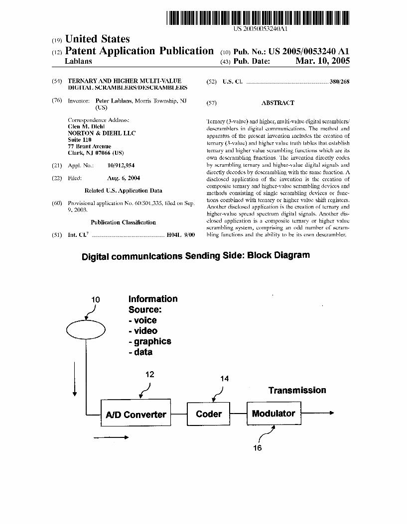
US 20050053240A1 (19) United States (12) Patent Application Publication (10) Pub. No.: US 2005/0053240 A1 Lablans (43) Pub. Date: Mar. 10, 2005 (54) (76) (21) (22) (60) (51) TERNARY AND HIGHER MULTI-VALUE DIGITAL SCRAMBLERS/DESCRAMBLERS Inventor: Peter Lablans, Morris Township, NJ (US) Correspondence Address: Glen M. Diehl NORTON & DIEHL LLC Suite 110 77 Brant Avenue Clark, NJ 07066 (US) Appl. No.: 10/912,954 Filed: Aug. 6, 2004 Related US. Application Data Provisional application No. 60/501,335, ?led on Sep. 9, 2003. Publication Classi?cation Int. Cl.7 ..................................................... .. H04L 9/00 (52) Us. 01. ............................................................ .. 380/268 (57) ABSTRACT Ternary (3-value) and higher, multi-value digital scramblers/ descramblers in digital communications. The method and apparatus of the present invention includes the creation of ternary (3-value) and higher value truth tables that establish ternary and higher value scrambling functions Which are its oWn descrambling functions. The invention directly codes by scrambling ternary and higher-value digital signals and directly decodes by descrambling With the same function. A disclosed application of the invention is the creation of composite ternary and higher-value scrambling devices and methods consisting of single scrambling devices or func tions combined With ternary or higher value shift registers. Another disclosed application is the creation of ternary and higher-value spread spectrum digital signals. Another dis closed application is a composite ternary or higher value scrambling system, comprising an odd number of scram bling functions and the ability to be its oWn descrambler. Digital communications Sending Side: Block Diagram Information Source: - voice - video - graphics - data 10 12 / AID Converter 14 / Coder Transmission Modulator K) 16

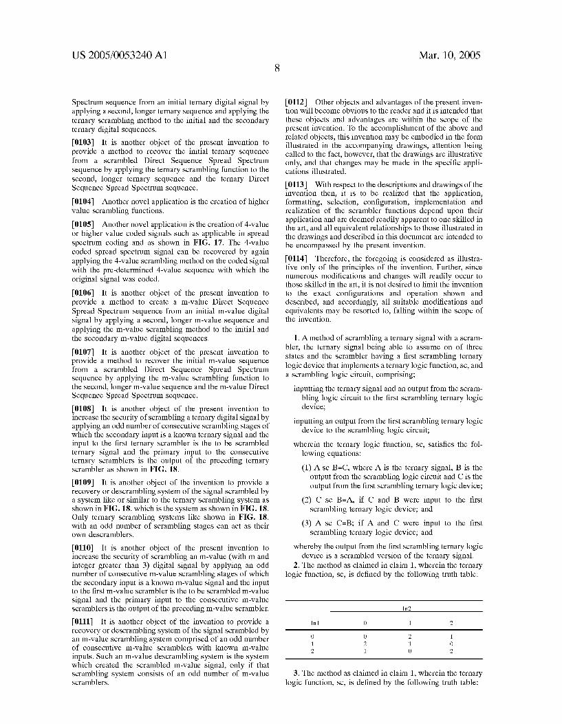
Welcome message from author
This document is posted to help you gain knowledge. Please leave a comment to let me know what you think about it! Share it to your friends and learn new things together.
Transcript
US 20050053240A1
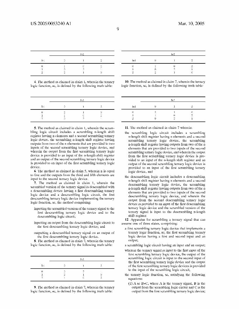
(19) United States (12) Patent Application Publication (10) Pub. No.: US 2005/0053240 A1
Lablans (43) Pub. Date: Mar. 10, 2005
(54)
(76)
(21)
(22)
(60)
(51)
TERNARY AND HIGHER MULTI-VALUE DIGITAL SCRAMBLERS/DESCRAMBLERS
Inventor: Peter Lablans, Morris Township, NJ (US)
Correspondence Address: Glen M. Diehl NORTON & DIEHL LLC Suite 110 77 Brant Avenue Clark, NJ 07066 (US)
Appl. No.: 10/912,954
Filed: Aug. 6, 2004
Related US. Application Data
Provisional application No. 60/501,335, ?led on Sep. 9, 2003.
Publication Classi?cation
Int. Cl.7 ..................................................... .. H04L 9/00
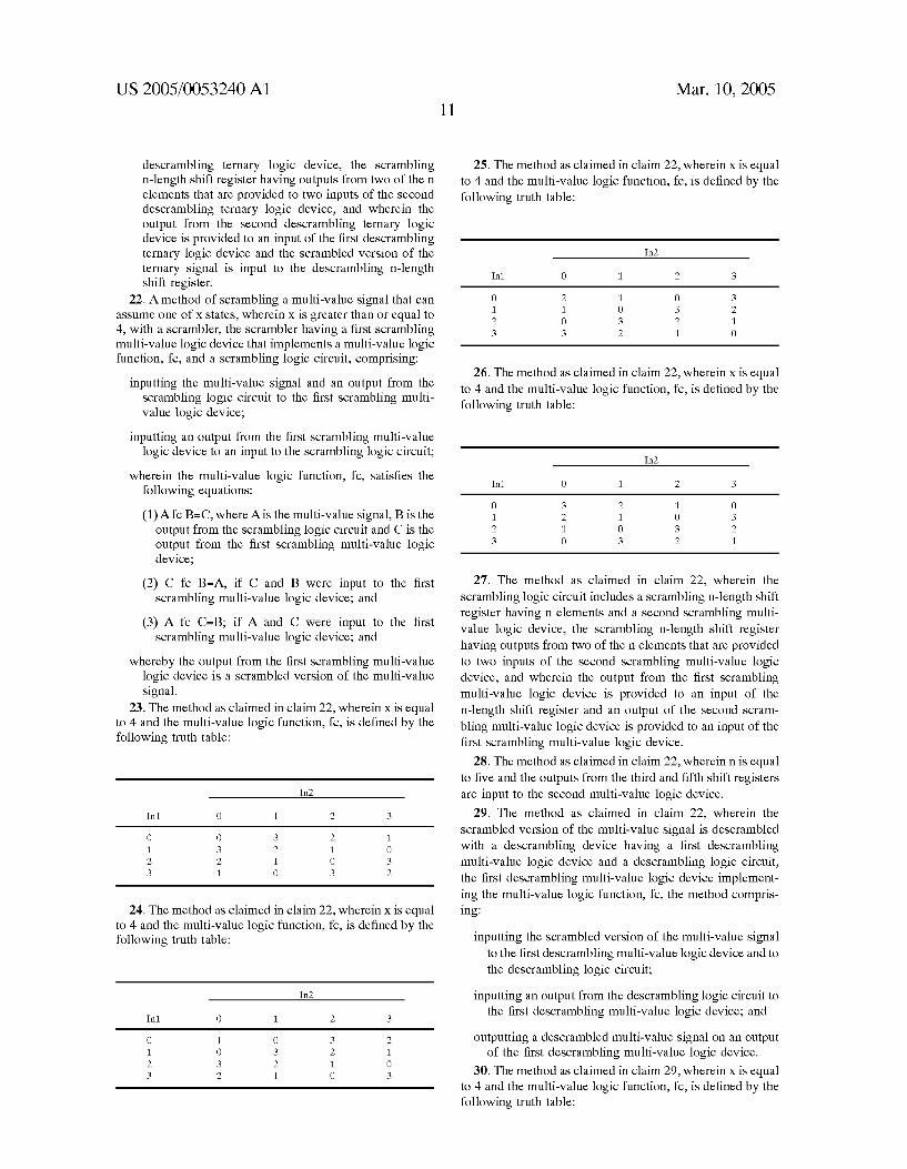
(52) Us. 01. ............................................................ .. 380/268
(57) ABSTRACT
Ternary (3-value) and higher, multi-value digital scramblers/ descramblers in digital communications. The method and apparatus of the present invention includes the creation of ternary (3-value) and higher value truth tables that establish ternary and higher value scrambling functions Which are its oWn descrambling functions. The invention directly codes by scrambling ternary and higher-value digital signals and directly decodes by descrambling With the same function. A disclosed application of the invention is the creation of composite ternary and higher-value scrambling devices and methods consisting of single scrambling devices or func tions combined With ternary or higher value shift registers. Another disclosed application is the creation of ternary and higher-value spread spectrum digital signals. Another dis closed application is a composite ternary or higher value scrambling system, comprising an odd number of scram bling functions and the ability to be its oWn descrambler.
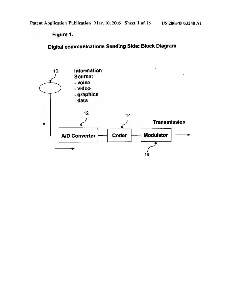
Digital communications Sending Side: Block Diagram
Information Source: - voice
- video
- graphics
- data
10
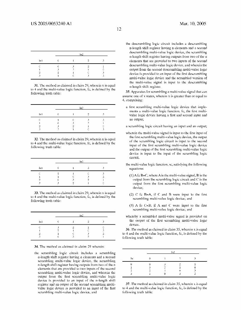
12
/ AID Converter
14
/ Coder
Transmission
Modulator
K) 16
Patent Application Publication Mar. 10, 2005 Sheet 1 0f 18
Figure 1.
US 2005/0053240 A1
Digital communications Sending Side: Block Diagram
10 Information Source: - voice
- video
- graphics
- data
12
/ AID Converter
14
Coder
Transmission
Modulator ——-—>
/ 16

Patent Application Publication Mar. 10, 2005 Sheet 2 0f 18 US 2005/0053240 A1
Figure 2. Digital communications Receiving Side: Block Diagram
Information Target:
- voice O - video
- graphics t‘
- data
Receiving
———-+‘ Demodulator Decoder D/A Converter
/ / / 17 18 2Q

Patent Application Publication Mar. 10, 2005 Sheet 3 0f 18 US 2005/0053240 A1
Figure 3.
The Exclusive Or or Modulo-Z adder as scrambling and descrambling function.
A In formula:
' ' ' *} C c ->A # B —-———> B But also:
B A -->C #5 B
\ ¢ 0 1 and
Patent Application Publication Mar. 10, 2005 Sheet 4 0f 18 US 2005/0053240 A1
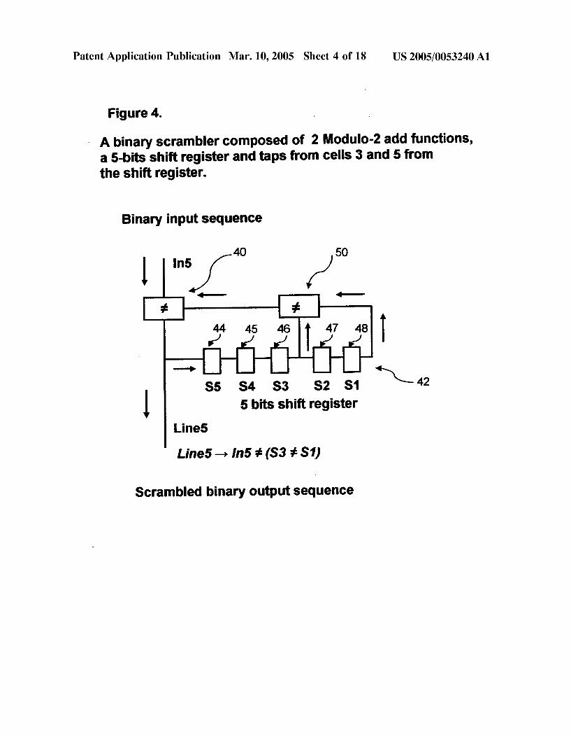
Figure 4.
~ A binary scrambler composed of 2 Modulo-2 add functions, a 5-bits shift register and taps from cells 3 and 5 from the shift register.
Binary input sequence
40 ln5 50
‘i
¢ ¢ ‘
44 45 46147 481 £14 /
s5 s4 s3 s2 s1 1 5 bits shift register
Line5
Line5 —-> In5 #5 (S3 9* S1)
Scrambled binary output sequence

Patent Application Publication Mar. 10, 2005 Sheet 5 0f 18 US 2005/0053240 A1
Figure 5.
A binary descrambler composed of a 5-bit shift register, taps from cells 3 and 5 and two Modulo-Z adder functions.
Scrambled input
Line5
5-bits shift register
‘l
Descrambled output
Patent Application Publication Mar. 10, 2005 Sheet 6 0f 18 US 2005/0053240 A1
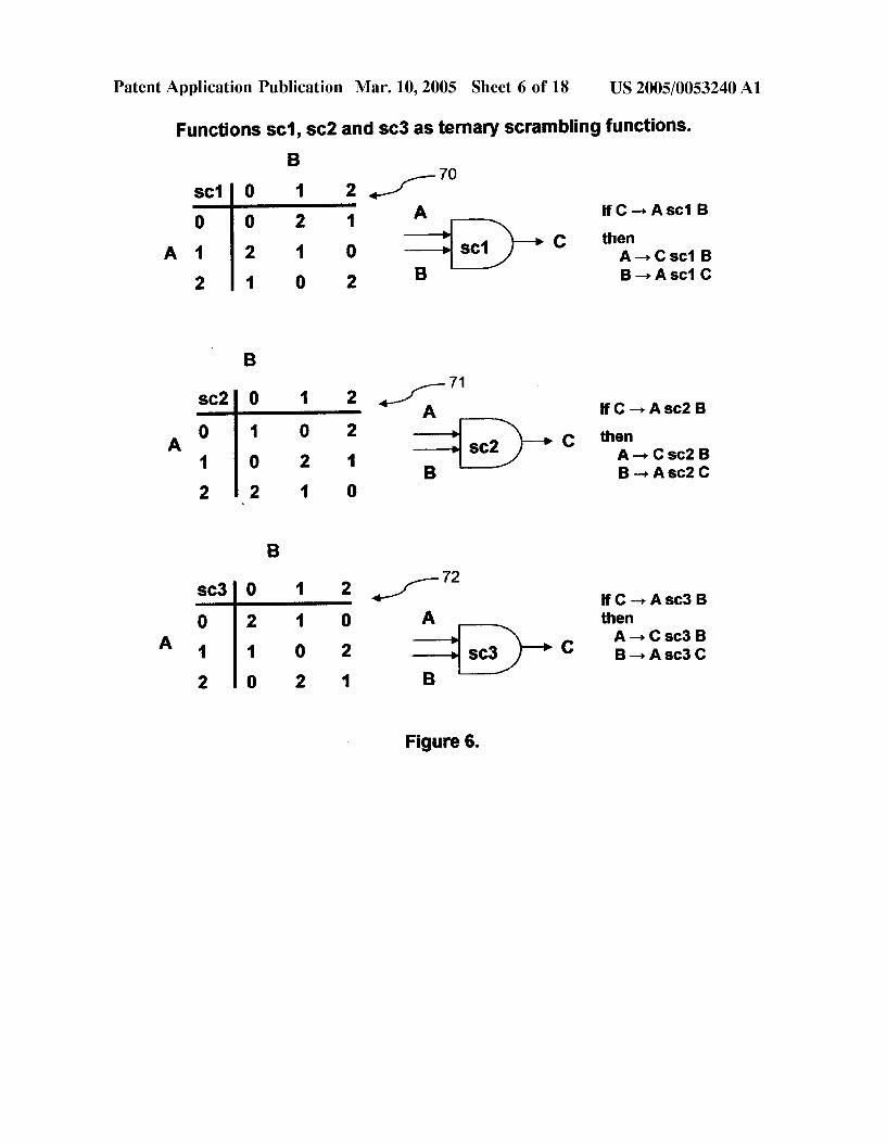
Functions sc1, $02 and sc3 as ternary scrambling functions.
B
ifC->Asc1 B
——> c then 0 ’ “1 A _’ c sc1 B
2 B B->Asc1C
0
0 0
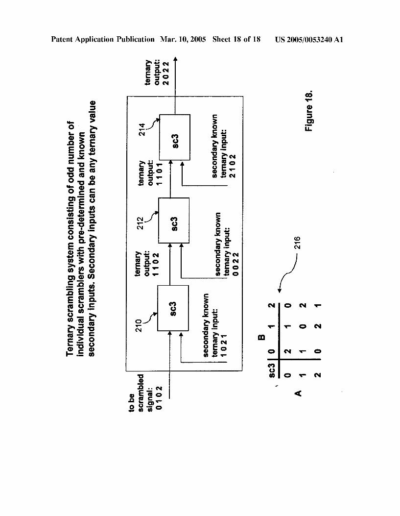
2
1 O-LN-a A >
then A—+C$C2B B-rASCZC
sc2 c
ifC-,Asc3B then A—>Csc3B B-+Asc3C
Figure 6.
Patent Application Publication Mar. 10, 2005 Sheet 7 0f 18 US 2005/0053240 A1
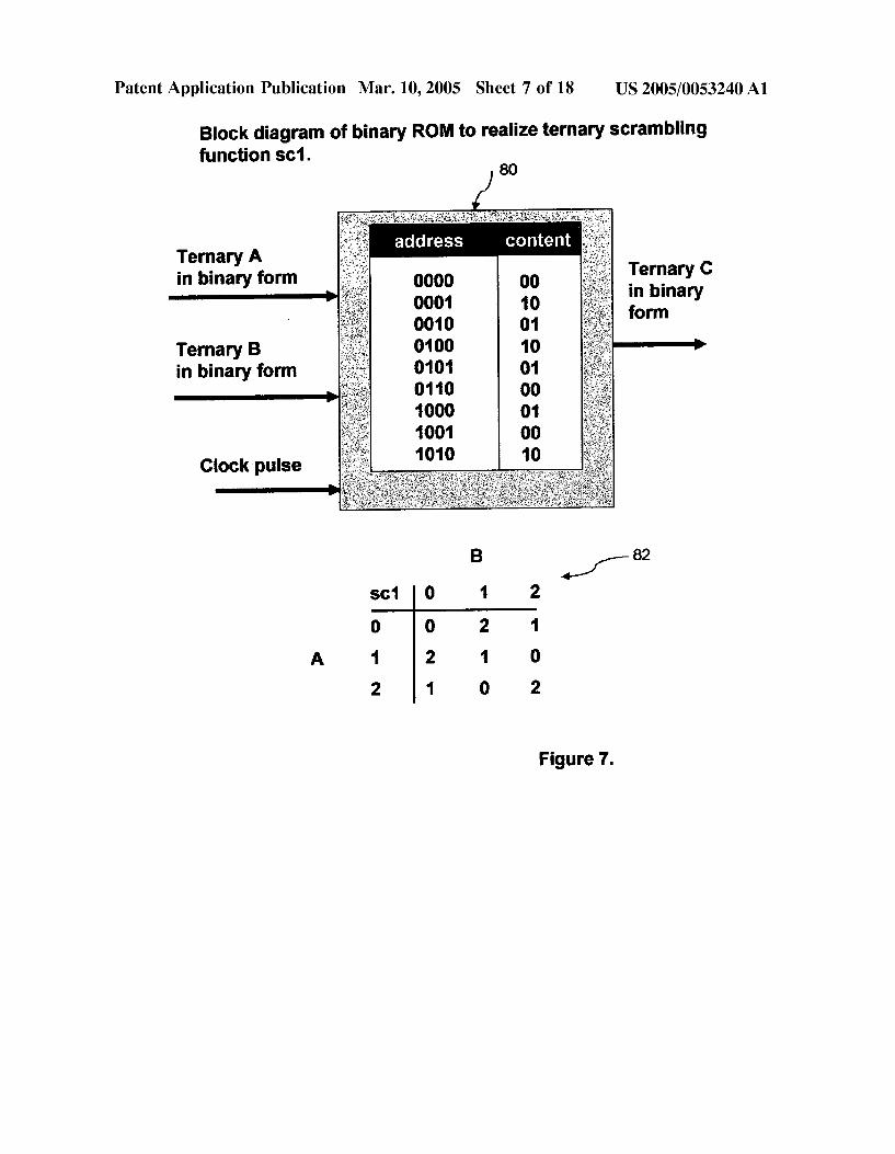
Block diagram of binary ROM to realize ternary scrambling function sc1.
'/ 80
address content Ternary A in binary form Ternary C
in binary form
in binary fonn
Clock pulse
Figure 7.
Patent Application Publication Mar. 10, 2005 Sheet 8 0f 18 US 2005/0053240 A1
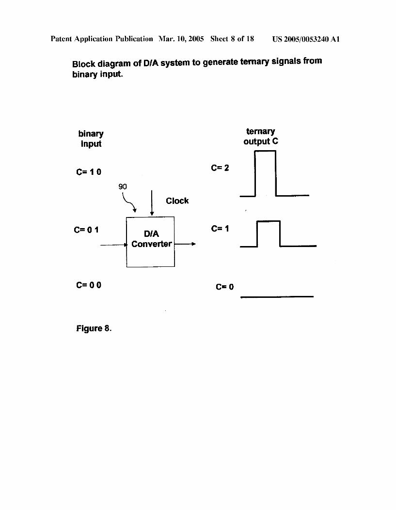
Block diagram of DIA system to generate ternary signals from binary input.
binary ternary input output C
c= 1 0 , = 2
90
\ l Clock C= 0 1 DIA = 1
-_-w Converter --—>
C= 0 0 c: 0
Figure 8.
Patent Application Publication Mar. 10, 2005 Sheet 9 0f 18 US 2005/0053240 A1
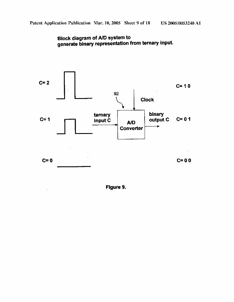
Block diagram of AID system to generate binary representation from ternary input.
= 2 C= 1 0
92
\ Clock _ ternary binary - 1 input c AID output 0 c= o 1
———————>
Converter ’
= o I c= o 0
Figure 9.
Patent Application Publication Mar. 10, 2005 Sheet 10 0f 18 US 2005/0053240 A1
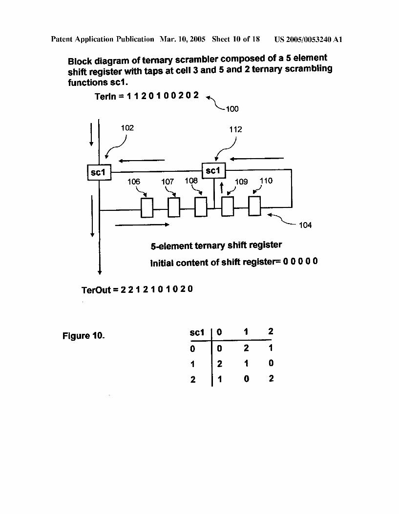
Block diagram of ternary scrambler composed of a 5 element shift register with taps at cell 3 and 5 and 2 ternary scrambling functions sc1.
Terln=1120100202 \ 100
1 102 112
sc1 sc1 106 107 108 T 109 110 \. a .1
5-element ternary shift register
Initial content of shift registeF 0 0 0 0 0
TerOut=2212101020
Figure 10. sc1 | 0 1 2 0 0 2 1
1 2 1 0
2 1 0 2
Patent Application Publication Mar. 10, 2005 Sheet 11 0f 18 US 2005/0053240 A1
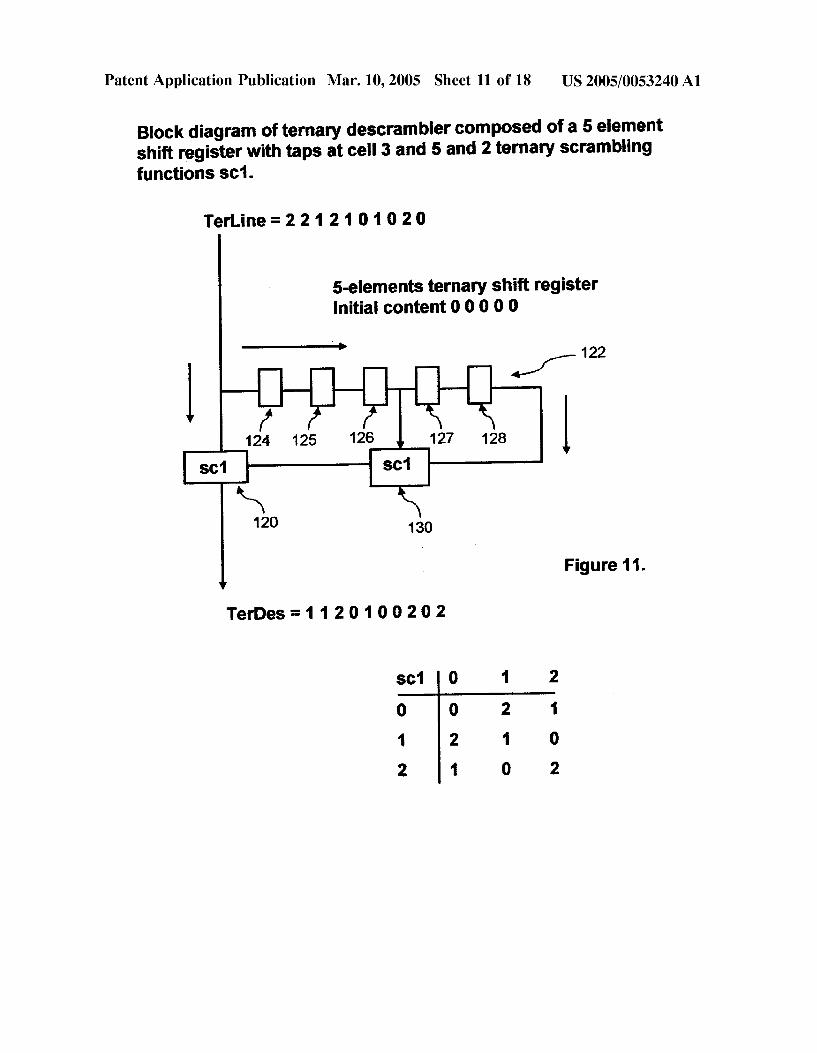
Block diagram of ternary descrambler composed of a 5 element shift register with taps at cell 3 and 5 and 2 ternary scrambling functions sc1.
TerLine=2212101020
5-elements ternary shift register Initial content 0 0 0 0 0
1 / 124 125 125 v 127 128 1
$121 $01
120 130
Figure11.
TerDes=1120100202
Patent Application Publication Mar. 10, 2005 Sheet 12 0f 18 US 2005/0053240 A1
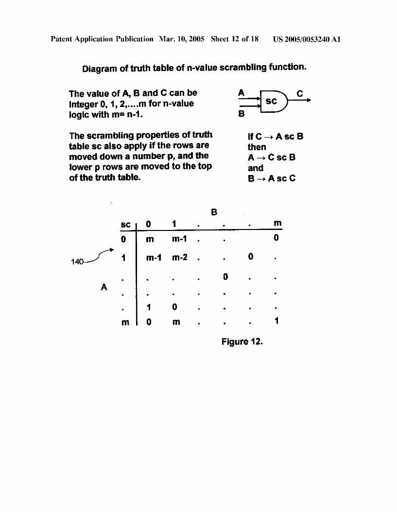
Diagram of truth table of n-value scrambling function.
The value of A, B and C can be A ‘ c
Integer 0, 1, 2,....m for n-value _D—' '86 B logic with m= n-1.
The scrambling properties of truth |f C _, A 5c 3 table sc also apply if the rows are then moved down a number p,eand the A _> C so B lower p rows are moved to the top and of the truth table. B _-> A sc C
B .
sc 0 1 . . . m
0 m m-1 . . 0
1 '“'1 m": I I o
0 A
_1 0 m 0 m 1
Figure 12.
Patent Application Publication Mar. 10, 2005 Sheet 13 0f 18 US 2005/0053240 A1
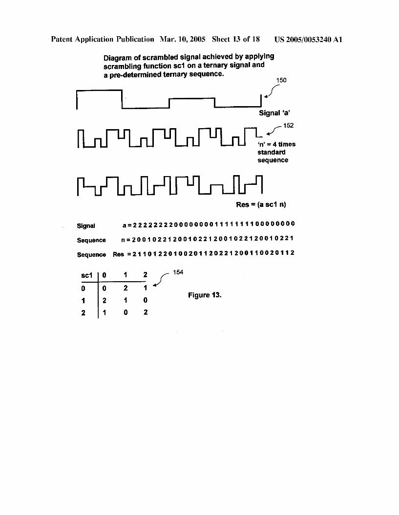
Diagram of scrambled signal achieved by applying scrambling function sc1 on a ternary signal and a pre-determined ternary sequence.
150
|-———l |/ Signal ‘a’
MW/m ‘n’ =4times standard sequence
W Res = (a sc1 n)
Signal a=22222222000000001111111100000000
Sequence n=20010221200102212001022120010221
Sequence Res =21101220100201120221200110020112
/ 154
Figure 13.
0
0
2
1
Patent Application Publication Mar. 10, 2005 Sheet 14 0f 18 US 2005/0053240 A1
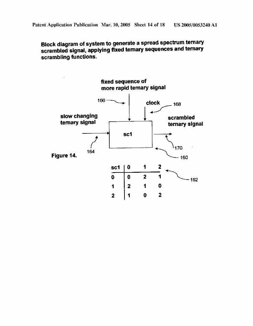
Block diagram of system to generate a spread spectrum ternary scrambled signal, applying ?xed temary sequences and ternary scrambling functions.
?xed sequence of more rapid ternary signal
166 \ clock 168
slow changing l _ scrambled
ternary 3'9'"ll ternary signal -———* $01 ———>
. \170 Figure 14. 164 \ 160

Patent Application Publication Mar. 10, 2005 Sheet 15 0f 18 US 2005/0053240 A1
Block diagram of system to recover a signal from a spread spectrum ternary scrambled signal, applying ?xed ternary sequences and ternary scrambling function.
?xed sequence of more rapid ternary signal
186 \ clock 188
scrambled 1 f recovered ternary signal “ ternary signal
7' sc1 Figure 14. 184
Figure 15.

Patent Application Publication Mar. 10, 2005 Sheet 17 0f 18 US 2005/0053240 A1
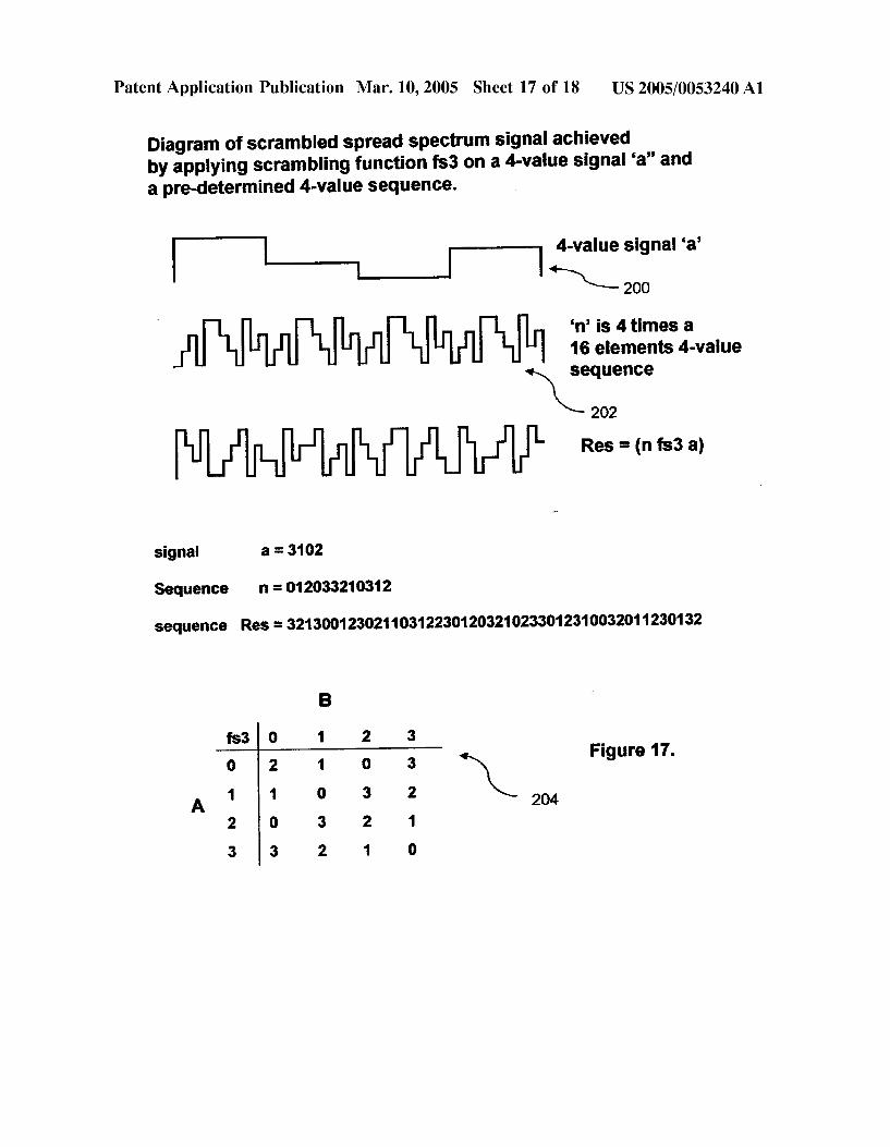
Diagram of scrambled spread spectrum signal achieved by applying scrambling function fs3 on a 4-value signal ‘a” and a pre-determined 4-value sequence.
4-value signal ‘a’ I _l____‘ \ 200
i ‘n’ is 4 times a
16 elements 4-value
<\sequence 202
signal a = 3102
Sequence n = 012033210312
sequence Res = 321 3001 230211 03122301 20321 023301 231 003201 1 2301 32
B
fs3 o 1 2 3
o 2 1 o 3 \ Flgure 17. A 1 1 0 3 2 204
2 0 3 2 1
3 3 2 1 0
US 2005/0053240 A1
TERNARY AND HIGHER MULTI-VALUE DIGITAL SCRAMBLERS/DESCRAMBLERS
STATEMENT OF RELATED CASES
[0001] This application claims the bene?t of US. Provi sional Patent Application No. 60/501,335, ?led on Sep. 9, 2003, the entirety of Which is hereby incorporated by reference into this document.
BACKGROUND OF THE INVENTION
[0002] The present invention relates to telecommunica tions of digital signals. In particular, the present invention relates to coding a digital signal and decoding of the coded digital signal Without error and loss of information.
[0003] Digital coding is applied Widely for the transmis sion of signals over optical, cable, radio connections and other transmission media. Coding is applied to transmitted signals for several reasons. For eXample, coding helps retain the quality of the digitally coded signal after transmission. It can also hide the content of the coded message or signal. Coding can also protect the coded message against interfer ence or jamming, and can increase the capacity of the transmission medium to alloW the medium to handle a greater number of messages or signals.
[0004] More particularly, the present invention relates to the area of ternary and higher, multi-value digital scrambling methods and apparatus as Well as descrambling methods and apparatus. The method and apparatus of the present inven tion Which applies methods that generate digital sequences Which are the coded form of digital message to be trans mitted or Which form a substantial basis for creating coded messages.
[0005] Typical digital transmission systems have transmit ters and receivers. The original message to be transmitted can be any type of signal, such as voice, video, teXt or any other data format. The signal is digitiZed, coded and then modulated to be transmitted over the transmission medium. At the receiving end, the signal is demodulated, decoded and then applied to some device to re-constitute the original message format.
[0006] The digitiZed message has been generally repre sented in binary (or 2-value) format. This means that the signal provided to the coder is a binary signal and the signal provided to the decoder is also a binary signal.
[0007] There are different Ways to implement binary cod ing and decoding. In the prior art, a Well established Way to code a binary message is by applying a binary scrambler. A binary scrambler is an electronic device or an eXecuted method that has as its input a series or sequence of binary digits, Which Will be guided through a ?nite length shift register or a computer program that acts as such. The content of pre-established cells of the shift register Will be tapped and connected to an element that Will conduct a speci?c binary operation on tWo binary elements. In the prior art, this operation is overWhelmingly Modulo-2 addition. The result of the Modulo-2 addition can be fed back into the shift register, fed into a neXt Modulo-2 addition or being sent to the modulation stage of the transmission.
[0008] If the input to a binary scrambler is a sequence of binary digits, the output of a binary scrambler is also a series
Mar. 10, 2005
or sequence of binary digits. The input and output of a scrambler are .in general and preferably dissimilar. The dissimilarity of the input and the output sequences depends on the input sequence, the length of the shift register, the number and place of taps and applied Modulo-2 add opera tions and initial content of the shift register.
[0009] The descrambler has as its input the output of the scrambler. The descrambler reverses the operation of the scrambler and can recover, Without mistakes, the original uncoded digital message that formed the input to the scram bler.
[0010] The common element in all binary scramblers and descramblers are the binary Modulo-2 additions. The binary logical operation is also knoWn under its binary logic designation: Exclusive OR or XOR or #.
[0011] Scramblers and descramblers are currently binary methods or devices that are composed of binary XOR functions. Binary XOR functions have the property of Modulo-2 addition. Modulo-2 addition is identical to Modulo-2 subtraction. In general, a binary signal is scrambled by adding it to another knoWn binary signal under Modulo-2 rules. The original binary signal can be recovered from the scrambled signal by Modulo-2 subtraction of the knoWn binary signal from the scrambled signal. Because Modulo-2 addition and Modulo-2 subtraction are both rep resented by the binary logic XOR function, binary scram bling and descrambling take place by the same binary logic function. While Modulo-2 addition is identical to Modulo-2 subtraction, that identity is not true for Modulo-3 and higher Modulo-n addition and subtraction. It is apparent to the inventor that the more fundamental description of identical scrambling/descrambling functions is that tWo binary inputs Aand B generate a binary output C. If A and C are the inputs to the function, the output B is generated. Or if B and C are the inputs to the function, A is generated as the output. Binary scrambling functions can also be applied in binary Direct Sequence Spread Spectrum coding Where an initial binary digital sequence is combined With a secondary, binary sequence With substantially more digits through a binary scrambling function.
[0012] In many cases it Would be bene?cial, either to the performance, quality or capacity of the telecommunication system to transmit modulated digital signals that represent higher value digits. For instance a cable system may transmit 3-value or ternary signals to balance the Direct Current component of the signals in the transmission system. These ternary signals can assume one of three states. The use of multi-value (greater than 2) signals also can increase the capacity (in information rate, or number of users) of a communication system. Nevertheless, many systems limit themselves to operating in a binary fashion. This is because of the availability and pervasiveness of binary technology and the lack of ternary and higher multi-value methods and technologies.
[0013] The availability of ternary (or 3-value) methods (even if eXecuted in binary fashion) Would greatly improve the performance of digital systems. Signal coding is an eXample of an area that Would be greatly improved by the use of ternary or multi-value scrambling techniques. Also, as higher value scramblers have a greater number of scram bling functions, the application of ternary and higher value scramblers can make a spread-spectrum signal much harder


Related Documents