NOTICE • PORTIONS OF THIS REPORT ABEj ; » has been reproduced from the best available copy to permit the broadest '. possible availability. DIGEST OF TECHNICAL PAPERS 2nd IEEE International Pulsed Power Conference SouthPark Inn Lubbock, Texas June 12-14, 1979 CONF-790622— DE85 000613 Editors A. H. Guenther Air Force Weapons Laboratory Chairman, Technical Program Committee M. Kristiansen Dept. of Electrical Engineering Texas Tech University Conference Chairman 2nd IEEE Pulsed Power Conference Joint Sponsors: South Plains Section IEEE, Air Force Aero Propulsion Laboratory, Air Force Office of Scientific Research, Electronics Technology and Devices Laboratory, U. S. Army, Naval Surface Weapons Center, Office of Naval Research, Office of Laser Fusion, Office of Fusion Energy. "The views and conclusions contained in this document are those of the authors and should not be interpreted as necessarily representing the official policies or endorsements, either expressedor implied, of the South Plains Section IEEE, Air Force Aero Propulsion Laboratory, Air Force Office of Scientific Research, Electronics Technology and Devices Laboratory, U.S. Army, Naval Surface Weapons Center. Office of Nat/al Research, Office of Laser 'usicn, Office of Fusion Energy, or the U.S. Government." Library of Congress Catalog Card Number 79-90330 IEEE Catalog Number 79CHI505-7 _ _ DISTRIBUTION OF THIS DOCUMENT IS UNUM1E0

Welcome message from author
This document is posted to help you gain knowledge. Please leave a comment to let me know what you think about it! Share it to your friends and learn new things together.
Transcript
NOTICE• PORTIONS OF THIS REPORT ABEj; » has been reproduced from the best
available copy to permit the broadest'. possible availability.
DIGEST OF TECHNICAL PAPERS2nd IEEE International Pulsed Power Conference
SouthPark InnLubbock, Texas
June 12-14, 1979
CONF-790622—
DE85 000613
Editors
A. H. GuentherAir Force Weapons LaboratoryChairman, Technical Program
Committee
M. KristiansenDept. of Electrical EngineeringTexas Tech UniversityConference Chairman
2nd IEEE Pulsed Power Conference Joint Sponsors: South Plains Section IEEE, Air ForceAero Propulsion Laboratory, Air Force Office of Scientific Research, ElectronicsTechnology and Devices Laboratory, U. S. Army, Naval Surface Weapons Center, Officeof Naval Research, Office of Laser Fusion, Office of Fusion Energy.
"The views and conclusions contained in this document are those of the authors and should not be interpretedas necessarily representing the official policies or endorsements, either expressed or implied, of the SouthPlains Section IEEE, Air Force Aero Propulsion Laboratory, Air Force Office of Scientific Research, ElectronicsTechnology and Devices Laboratory, U.S. Army, Naval Surface Weapons Center. Office of Nat/al Research,Office of Laser 'usicn, Office of Fusion Energy, or the U.S. Government."
Library of Congress Catalog Card Number 79-90330IEEE Catalog Number 79CHI505-7
_ _DISTRIBUTION OF THIS DOCUMENT IS UNUM1E0

PREFACE
Pulsed power in a l l i t s varied meanings i s showing no sign of aba te -
ment in a c t i v i t y . I t i s becoming a technology of increas ing importance
in numerous new and novel app l i ca t i ons , growing from i t s we l l - e s t ab l i shed
base in energy and defense r e l a t ed research and development. One ind ica -
t ion of i t s v i t a l i t y i s t h i s Digest of Technical Papers for the 2nd IEEE
I n t e r n a t i o n a l Pulsed Power Conference. The organizers were counseled by
msny tha t there would not be enough mater ia l tha t could be covered a t
t h i s meeting nor would there be a su f f i c i en t d i v e r s i t y of i n t e r e s t . How-
ever , from our f i r s t such conference during November 1976, held in Lub-
bock as we l l , we have recorded a f i f t y percent increase in attendance to
almost 300., with well over 100 inv i t ed and contr ibuted p re sen t a t i ons .
There were twenty-five at tendees from 10 foreign countr ies including Bel-
gium, Canada, Denmark, England, France, I s r a e l , Japan, Poland, the USSR,
and West Germany.
As a r e s u l t of t h i s growth and with the real izat ion, tha t th i s con-
ference serves as the p r inc ipa l forum for the exchange of information in
the highly spec ia l ized and unique f i e ld of pulsed power technology, sev-
e r a l act ions and events have taken place. F i r s t , the present technical
program committee, which adequately insures tha t the i n t e r e s t s of the
p r i n c i p a l players in the f i e ld wi l l be served, have been designated a
permanent standing committee to organize and maintain t h i s conference
s e r i e s . Secondly, we have agreed to hold t h i s meeting b i e n n i a l l y , a l t e r -
nat ing with the well-known Modulator Symposium. I t i s our present i n t en -
t ion t ha t the 3rd IEEE In te rna t iona l Pulsed Power Conference w i l l be held
in Albuquerque, NM during 1981 with Art Guenther of the Air Force Weapons
Laboratory as Conference Chairman and Tom Martin of Sandia Labora tor ies ,
ii

Albuquerque, as Chairman of the Technical Program Committee.
One interesting sidelight of this years meeting was a contest to
select a conference symbol which could be used with al l future meetings
and correspondence. We wished the symbol to be easily recognized and to
uniquely depict pulse power. To our pleasant surprise almost fifty en-
tries were received and from these the Technical Program Committee selec-
ted the symbol shown on the t i t l e page of these proceedings. The winner
was Capt. Charles W. Schubert, Jr. of the U.S. Air Force Flight Dynamics
Laboratory, Wright-Patterson AFB, Ohio. He received a Texas Instruments
TI-59 fully programmable calculator graciously donated by the manufac-
turer. Congratulations to Capt. Schubert and many thanks to TI.
Our conference had the distinct honor of being able to recognize the
many contributions of Mr. Peter Haas to the development of pulse power
technology in the United States. Mr. Haas recently retired from his posi-
tion as Deputy Director for Science and Technology, Defense Nuclear Agency,
after a distinguished career in the Federal Civil Service. We al l recog-
nize that he has not really retired but just entered into another role and
we can count on his continued vigorous and outspoken support for further
development in pulsed power technology.
Besides the excellent technical content and Texas hospitality, the
meeting could not have transpired without the sponsorships of several
key organizations. Thus we would like to cr.ll your special attention to
the following sponsors:
The Air Force Aero Propulsion Laboratory
The Air Force Office of Scientific Research
The Electronics Technology and DevicesLaboratory, U.S. Army
The Naval Surface Weapons Center and
iii

The Office of Naval Research; all of
The Department of Defense, and from the Department of Energy;
The Office of Laser Fusion and the Office of Fusion Energy.
The Conference was most effectively organized locally by the Depart-
ment of Electrical Engineering, Texas Tech University under Dr. Russell H.
Seacat, Chairman, and the South Plains Section of IEEE, Lewis Thomas,
SecttonPresident, with Travis Simpson, Martha Smith, and Deanya Wood of
the Texas Tech EE Department, as Local Chairman, Conference Secretary,
and Secretarial Assistant, respectively. To all of these people go our
deepest appreciation and a hardy "well-done"!
To those who worked so diligently on the organization and preparation
of the 2nd IEEE-PPC, may we add our sincere appreciation and thanks. See
you in Albuquerque in '81.
A. H. Guenther M. KristiansenAir Force Weapons Lab. Texas Tech UniversityChairman, Tech. Program Committee Conference Chairman
IV

Presentationat
Award LuncheonJune 13, 1979
SPECIAL AWARD
Peter HaasDefense Nuclear Agency
Retired
"For many contributions to a strong and vigorous pulse power program throughsound management, steadfast conviction and farsighted technical acumen".
2nd International IEEE Pulsed Power Conference
Technical Program Committee
A. H. Guenther, ChairmanAir Force Weapons Lib.Kirtland AFBAlbuquerque, NM 87117
T. R. BurkesTexas Tech Univ.Dspt. of Elect. Eng.Lubbock, TX 79409
J. FarberDefense Nuclear AgencyWashington, DC 20305
R. FitchMaxwell Labs.Precipco, Inc.9244 Balboa Ave,San Diego, CA 92123
W. GagnonLawrence Livermore Lab.P.O. Box 808Livermore, CA 94550
A. S. Gilmour, Jr.State Univ. of. New York/Buffalo4232 Ridge Lea Rd.Amherst, NY 87545
R. GullicksonAFOSR/NP, Boiling AFBWashington, DC 20332
E. KempLos Alamos Scientific Lab.P.O. Box 1663Los Alamos, NM 87545
T. M;.rtinSandra Lab.Dept. 4250Albuquerque, NM 87113
M. F. RoseNaval Surface Weapons CenterCode F-404Dahlgren, VA 22448
S. SchneiderU.S. Army Electronics Technologyand Devices Lab.
Ft. Monmouth, NJ 07703
I. SmithIan Smith, Inc.3115 Gibbons Dr.Alameda, CA 94501
P. TurchiNaval Research Lab.Code 6770Washington, DC 20375
R. L. VergaAir Force Aero Propulsion Lab.PODWright-Patterson AFB, OH 45433
Local Organization Committee
Travis L. SimpsonLocal ChairmanTexas T;jch Univ.
Martha SmithConference SecretaryTexas Tech Univ.
Deanya WoodSecretarial AssistantTexas Tech Univ.
vi

2nd IEEE International Pulsed Powar ConferenceSouth Park Inn, Lubbock, Toxss
Niva(o Room Altec Room Bronz> Room Mayan Room OWwMONDAY. June 116:00 p.m.-10:00 p.m.
TUESDAY. June 128:00 a.m.- 5:00 p.m.9:00 a.m.- 9:30 a.m.9:30 a.m.-11:00 a.m.
11:00 a.m.-i 1:20 a.m.11:20 a.m.-12:20 p.m.
12:20 p.m.- 1:45 p.m.1:45 p.m.- 3:15 p.m.
3:15 p.m.- 3:35 p.m.3:35 p.m.- 5:05 p.m.6:00 p.m.- 8:00 p.m.
WEDNESDAY, June 138:00 a.m.- 5:00 p.m.9:00 a.m.-10:30 a.m.
10:30 a.m.-10:50 a.m.10:50 a.m.-12:05 p.m.-
12:05 p.m.- 2:00 p.m.
2:00 p.m.- 3:15 p.m.
3:15 p.m.- 3:35 p.m.3:35 p.m.- 5:05 p.m.
THURSDAY, Juno 143:00 a.m.-i0:30 a.m.
10:30 a.m.-iO:50 a.m.10:50 a.m.-12:05 p.m.12:05 p.m.- 1:30 p.tn.1:30 p.m.- 3:00 p.m.
3:00 p.m.- 5:30 p.m.
Registration
Registration
Registration
Opsninq SessionPlenary Session 1
I-Electron and IonDiodes
IV-BreakdownMechanisms
Vll-Switching 1
Plenary Session II
X-Switching II
Xlll-Switchmg III
XVI-Switching IV
Plenary Session III
XlX-Switching V
XXII-Post DeadlinePapers (SeeBulletin Board)
Il-MagneticComponents
V-Novel Applications
Vlll-Accelerators 1
Xl-Applica'ions 1
XIV-E!ectro-MechanicalEnergy StorageSystems )
XVII-Electro-MechanicaiEnergy StorageSystems II
XX-Applications II
Ill-Power Conditioning 1
Vl-Power Conditioning II
IX-Power Conditioning III
Xll-lnductive indCapacitive EnergyStorage Systems I
XV-lnductive andCapacitive EnergyStorage Systems II
XVlll-Oiagnostics andMiscellaneous
XXI-Vacuum Power Flow
i
Coffee-Patio
Lunch
Coffee-Patio
Cocktail Party Patio(Hosted by IEEESouth Plains Sect.;
Coffee-Patio
ConferenceLuncheon- Patio
Coffee-Patio
Coffee-Patio
Lunch
Tours of PulsedPower. Plasma,and Laser ResearchFacilities atTexas Tech Univ
Library of Congress Catalog Card N'umber 79-90330
IEEE Catalog Number 79CH15O5-7
vli

TABLE OF
Plenary Session I:
Chairman: A. H. Guenther,Air Force Weapons Lab.
Pl.l Overview of Inertial ConfinementFusion (Invited)G. Canavan 1
PI.2 Pulsed Power for Fusion (Invited)
T. H. McuUln . 3
PI.3 Pulsed High-Curreit Electron Tech-nology (Invited)G. A. tiuyoutA 9
Plenary Session II:
Chairman: A. Kolb,Maxwell Lab.
P2.1 New Hydrogen Thyratrons for Ad-vanced High Power Switching(Invited)V. TuAnqtuAt, R. CcvuAti, S.FfUzdman, S. Me/iz, R. Plants.,M. tzlnhafidt 17
P2.2 Accelerator Module of "Angara-5"(Iavited)S. I/. BaAe.nkov, 0. A. Goaev, Ju. A.l&tomin, Ju. I/. Koba, G. M.--'LaAma.rU.zova, A. M. Pabecknikov,8. P. Pnvcktv, 0. P. PtcheAAkti,A, S. PeAJUn, L. I. Rvdakov, I/. P.SmOinov, V. I. ChoAvanAkov, I. R.Jampot'i>\uJl 25
P2.3 Review and Status of Antares(Invited)J. JanAzn 31
Plenary Session III:
Chairman: E. Abramyan, Institute ofHigh Temperatures, USSR
P3>1 Electromagnetic Guns, Launchersand Reaction Engines (Invited)H. Koim, K. Tina, F. WUUam,?. Uonge.au 42
P3.2 The Near and Long Term Pulse PowerRequirements for Laser Driven In-ertial Confinement Fusion (Invited)W. L. Gagnon, E. K. TnzytdQ,R. ?Uch 49
viii
CONTENTS
Session I: Electron and Ion Diodes
Chairman: R. Detweiler, AF
Office of ScientificResearch
1.1 Repetitively Pulsed Electron BeamDiode Lifetime and StabilityM. T. Buttftam 61
1.2 Voltage Distribution and Currentin a Cylindrical RelativisticDiodeH. ft/. HavuA 65
1.3 Simulations of Intense Relativis-tic Electron Beam Generation byFoilless DiodesM. E. JonaA, L. E. Thode. 68
1.4 Ion Beam Generation Through aMoving Plasma BoundaryM. VmbinAki, P. K. John 72
Session II: Magnetic Components
Chairman: K.. Freytag,Lawrence Livermore Lab.
1.1 Fundamental Limitations and DesignConsiderations for CompensatedPulsed Alternators (Invited)K. M. ToV-, W. F. WeJLdoin, M. V.VKIQCL, W. L. %-Lh.d, H. H. Woodion,H. G. RylandeA 76
2.2 Use of Transformers in ProducingHigh Power Output from HomopolarGeneratorsW. H. Lupton, R. V. Fold, H. B.LLyidifwrn, I . M. ViAkov-vt&ky, V.Contz 83
2.3 Design of Pulse Transformers forPFL Charging
G. J. Rohweln 87
Session III: Power Conditioning I
Chairman: R. Fontana, Air ForceInstitute of Technology
3.1 Pulse Sharpening in Ferrite Trans-mission LinesM. Wzinex 91

3.2 High Power Pulse Modeling of Co-axial T7.-ansmission LinesJ . P. O'Loughtin 96
3.3 Light Activated 10 kV Low JitterPulserJ . V. GalbnauXh 100
3.4 Command Charge Using SaturableInductors5. Black, T. R. BuAkeA 102
Session IV: Breakdown Mechanisms
Chairman: R. Fitch,Maxwell Lab.
4.1 Investigations of Fast InsulatorSurface Flashover (Invited)J . E. Thompson, J . Lin, K.Hlkk&lion, M. IOU6tlan6zn 106
4.2 Breakdown in Small, Flowing GasSpark GapsW. K. Ccviy, 3K.., V. V. LLndbiAg,J . W. Rlct 114
4.3 Electron Densities in Laser-Trig-gered Spark Gap DischargesR. J. Cfimlzy, P. F. Isl-llttami,M. A. Gand&uen, A. Wcut&on . . . .119
4.4 Electrical Breakdown in Waterin the Microsecond RegimeV. B. Fe.n.nman, R. GHlpAhovun. . . .122
4.5 Pulsed Electron Field EmissionFrom Prepared ConductorsG. B. TnjXTiiA 127
Session V: Novel Applications
Chairman: J. Farber,Defense Nuclear Agency
5.1 Investigation Into TriggeringLightning with a Pulsed LaserC. W. SdmxbznZ, In.., J. R.Uppwt 132
5.2 Long ARC Simulated LightningAttachment Testing Using a 150 kWTesla CoilR. K. Golka 136
5.3 High Density Z-Pinch Pulse-Power Supply System01. C. Manually, I. A. Jonei,S. SlnqzA 142
5.4 The Design of Solenoids forGenerating High MagneticFieldsP. ByAzewikX. 148
5.5 Analysis of a DistributedPulse Power System Usinga Circuit Analysis Code
L 0. Hoe.it 149
5.6 Determination of Line VoltageIn Self-Magnetically InsulatedFlowsC. US. tAmdzl, 3K. , 3. P.VanV^v znd&i, G. W. Ku&wo. . . . .153
Session VI: Power Conditioning II
Chairman: T. R. Burkes,Texas Tech University
6.1 Versatile High Energy CapacitorDischarge SystemV. N. Ma/itin 157
6.2 A 130 kV Low Impedance Multi-ple Output Trigger GeneratorA. H. Biu>hnM and C. 8. Vobblz,A. P. tOu.ck.huhn 161
6.3 Low-Impedance, Coaxial-TypeMarx Generator with a Quasi-Rectangular Output Waveform(Invited)M. Qba,ia, y. Sakcuto, C. H.Lee, T. Hashimoto, T.
165
6.4 The Design Approach to aHigh-Voltage Burst Generator(Invited)V. 8. CumnuMgi, H. G. ^Hammon, 111 172
Session VII: Switching I
Chairman: 3. Bernstein,Physics International
ii:

7.1 High Pressure Surface SparkGaps
W. J. Saujzant, A. J. Alcock,K. E. Leopold 179
7.2 Parallel Combinations of Pire-Ionized, Low Jitter Spark Gapsill. A. F-itzAimmoni and L. Ro-iocha. 184
7.3 A Streamer Model for High VoltageUater SwitchesF. J. Sazama, V. L. Ktnyon, 111 .187
7.4 Low Prepulse, High Power DensityWater Dielectric SwitchingV. J . Johnion, J . P. VariOzve.nde/i,T. H. sAaxtin. 191
7.5 Contacts for Pulsed High Current;Design and Test
P. W-ildl 195
7.6 The Early Counterpulse TechniqueApplied to Vacuum InterruptersR. W. WaM-zn 198
Session VIII: Accelerators
Chairman: 1. Smith,Ian Smith, Inc.
8.1 Development of High Current Elec-tron Pulse Accelerators (Invited)E. Abiamyan, G. V. KulzAhov . . .202
8.2 Status of the Upgraded Versionof the NRL Gamble II Pulse PowerGeneratorJ . R. BolteA, J. K. BuAton, J . V.Shlpman, In. 205
8.4 Emittance Measurements on FieldEmitter Diodes
S. Kulkz, R. UhaAa 209
8.5 On the Development of a Repeti-tively Pulsed Electron 3eam SystemG. A. Ifilpoti 214
Session IX: Power Conditioning III
Chairman: R. Verga, Air ForceAero Propulsion Lab.
9.1 Development of High Repetition-Rate Pulse Power GeneratorsR. J. Sojka, G- K. SJjncox . . . .217
x
9.2 Frozen-Wave Hertzian Generators:Theory and ApplicationsM. L. Toiclvi, M. F. Ro-ie, L. F.ZlnehaAt, R. J. GtiipihoveA. . . .221
9.3 A 500 kV Rep-Rate Marx Gener-ator (Invited)
J. Shannon 226
9.4 A High Current Pulser for Ex-periment #225, "Neutrino Elec-tron Elastic Scattering,"C. Vatton, G. Kxaime., W. J.
232
9.5 KrF Laser-Triggered SF, SparkGap for Low-Jitter TimingW. K. Rapapofvt, J. Goldhan.,J. R. MuAAxy, M. V'AddaAlo . . .236
Session X: Switching II
Chairman: R. Wasneski, NavalAir Systems Command
10.1 Effects of Surrounding Med-ium on the Performance of Ex-ploding Aluminum Foil FusesI. L. BeAgeA. 237
10.2 High Power, Very Long PulseTesting of a 200 KV TetrodeRegulation TubeJ. Stablzy, 8. Gn.ay 242
10.3 Withdrawn
10.4 Very Fast, High Peak PowerPlanar Triode Amplifiers forDriving Optical GatesW. L. Gagnon, S. J. Davit.M. M. Houiland .246
10.5 Vacuum Arc Switched InverterTests at 2.5 MVAR. W. tUtteA, A. 5. G-LbnouA,JfL. .250
Session XI: Applications I
Chairman: J. Jansen, Los AlamosScientific Labs
11.1 300-kJ, 200-kA Marx Module forAntaresK. S. Rlzpz, J. Jan&en, J.lfe^i 254

11.2 A Large-Area Cold-Cathode Grid-Controlled Electron Gun forAntaresmi. R. ScaAleXt, K. R. kn.dn.em,H. Jamzn .261
11.3 The Antares Laser Power AmplifierR. V. Stlnn, G. F. RoM, C.SllvzAnail 265
11.4 A Double-Sided Electron BeamGenerator for KrF Laser ExcitationL. SchlUt 269
11.5 Electric Discharge Characteristicsof Cable PFN Used as a PumpR. R. BuutcheA, S. H. GuA.baxa.vii .273
Session XII: Inductive and CapacitiveEnergy Storage Systems I
Chairman: K. Whitham,Lawrence Livennore Labs
12.1 Trident—A Megavc r tfulse Gener-ator Using Inductive Energy Stor-age (Invited)V. Zowtt, R. V. Void, W. H.Lupton, I . M. VJjtkovAtAky . . .276
12.2 Inductive Storage—Prospects forHigh Power GenerationJ . K. Buuiton, V. Conte., R. V. ToKd,W. H. Lupton, V. E. Sdkwwi, I . M.
kk 284
12.3 Considerations for InductivelyDriven Plasma Implosions (Invited)V. L. Smith, R. P. He.Yid&ra>on,R. E. RtUnoviky 287
Session XIII: Switching I I I
Cha irman: E. Kunhardt,Texas Tech University
13.1 High Repetition Rate MiniatureTriggered Spark SwitchM. F. Roiz, M. T. Glancy . . . .295
13.2 Surface Aging in High RepetitionRate Spark Switches with Aluminumand Brass ElectrodesM. T. Glancy, M. F. Ro^e . . . .301
13.3 Spark Gap Erosion ResultsR. Pe£t, V. oJtxeJtt, T. R. Bififeea. 308
13.4 Long-Life High-Repetition-RateTriggered Spark GapH. Wcution 313
13.5 Testing of a 100 kV, 100 HZ,Rep-Rate Gas SwitchA. Ramu&r J. Skannon 320
Session XIV: Electro-MechanicalEnergy StorageSystems I
Chairman: P. Turchi, NavalResearch Lab.
14.1 Rebuilding the Five MegaJouleHomopolar Machine at the Uni-versity of TexasK. M. Talk, J. H. GvJULy, R. C.Zotticinka, M. Bn.e.nnan, W. I.Bifid, W. F. Weldon, H. G.RylandeA, H. H. Wood&on 325
14.2 Computer Based ElectricalAnalysis of Homopolar Genera-tor Driven, Bitter Plate Stor-age Inductors with Radial Cur-rent DiffusionV. J . T. UatjhaJUL, H. G.RylandeA, W. F. (Ueldon, H. H.Woodion 330
14.3 Testing and Analysis of a FastDischarge Homopolar Machine(FDX) (Invited)T. M. BuZlcon, M. V. Vnlqa,J . H. Gully, H. G. RylandeA,K. M. Tolk, ft/. F. Wztdon,H. H. Woodion, R. louiaJika . . . . 333
14.4 Pulsar: An Inductive PulsePower SourceE. C. CnaAz, W. P. BuookA, M.Cowan 343 *
Session XV: Inductive and Capaci-tive Energy StorageSystems II
Chairman: R. Ford, NavalResearch Lab.
xi

15.1 Preliminary Inductive EnergyTransfer ExperimentsR. P. Vnnd&uon, V. L. Smith,R. E. R&inavAky 347
15.2 Application of PFN Capacitors inHigh Power SystemsR. V. PankeA 351
15.3 Withdrawn
15.4 Safety Grounding Switches in LargeExperiments; General Consider-ations and the TEXT ApplicationP. Wildi 355
15.5 Inductance and Resistance Charac-teristics of Single-Site Untrigger-ed Water Switches in Water Trans-fer Capacitor CircuitsP. W. Spence., V. G. Chzn, G.T-iux.zi.QA., H. Calvin 359
Session XVI: Switching IV
Chairman: S. Schneider, U.S. ArmyElectronics Technologyand Devices Lab.
16.1 Hollow-Anode Multigap Thyratrons(Invited)H. Mznovon, C. V. Umlz 363
16.2 High Frequency Thyratron Evalu-ationG. Hill, T. P.. BankoM 364
16.3 Repetitive Electron Beam Con-trolled SwitchingR. F. fixmlax, V. Conte., I. M.Vitkovi&ky 368
16.4 Orientation Independent IgnitronR. J . HaJivzy, J . R. Baylza. . ,372
16.5 Stabilization of Metal-Oxide BulkSwitching Devices with DiffusedBi Contacts8. lalzvic, M. Shoga, M. Gvibhi,S. Uvy 376
Session XVII: Electro-MechanicalEnergy Storage Sys-tems II
Chairman: W. L. Gagnon,Lawrence Livermore Labs
xii
17.1 Magnetic Optimization for PulsedEnergy ConversionW. K. Tuck&fi, W. P. &wok&, R. E.Wilcox, W. V. Mcw.fccenw.cz, E. C.Zwms. 381
17.2 Design of the Armature Windings ofa Compensated Pulsed AlternatorEngineering PrototypeJ. H. Gully, W. L. Bind, H. G.RylandeA, ft/. F. Waldon, H. H.Woodion, T. M. Bullion 385
17.3 The Mechanical Design of a Compen-sated Pulsed Alternator PrototypeM. Bn.e.manr W. L. Bixu, J. H.GuUy, M. L. Spann, K. M. Talk,W. F. W&ldon, H. G. RylandeA, K. M.Talk, W. F. Wzldon, H. H. Oloodion.392
17.4 The Design, Assembly, and Test-ing of a Desk Model CompensatedPulsed AlternatorM. Vichot, 01. L. Bifid, M.Bn.e.nnan, M. V. Vfiiga., J . H.Gully, H. G. RylandeA, K. U.Talk, W. F. (tieldon, H. H.Itloodion 398
17.5 A Compressed Magnetic Field Gener-ator Systems ModelJ. E. GoveA 402
17.6 Application of Subsystem Sum-mary Algorithms for High PowerSystem StudiesF. C. BAOckhuAAt 406
Session XVIII: Diagnostics andMiscellaneous
Chairman: C. J. Jouys, Atomic EnergyCommission, France
18.1 A Computerized Measuring Sys-tem for Nanosecond RisetimePulsed AcceleratorsV. PzLUnzn, S. K&hby, P.Gillie, K. Miztizn, P.Spznce. 410
18=2 Withdrawn
18.3 A 33-GVA Interrupter Test Facil-ityW. M. Pateoni, E. M. Honig,R. W. WcVOizn 414

18.4 Analysis of the MultiphaseInductor-Converter BridgeM. Ek&anl, R. I. KuAtom,R. E. ftijCL 419
18.5 Distributed Parameter Model ofthe Trestle PulserT. H. Lehman, R. L. Hatckini,R. TlbheA 425
18.6 Compton Scattering of Photonsfrom Electrons in MagneticallyInsulated Transmission LinesK. L. BtouizA, J. P.Va.nVe.ve.ndeA. 429
Session XIX: Switching V
Chairman: M. F. Rose, NavalSurface Weapons Center
19.1 Simulation of Inductive and Elec-tromagnetic Effects Associatedwith Single and Multi ChannelTriggered Spark GapsS. Lzvlmon, E. E. KunkaAdt, M.YjuMtia.me.vi, A. H. GazntheA . . .433
19.2 An Electron-Beam Triggered SparkGapK. McDonald, M. Nwtcn, E. E.Kunhandt, M. KAsUtianizn, A. H.GazntheA 437
19.3 Low Jitter Lastir Triggered SparkGap Using Fiber OpticL. L. Hcut&leld, H. C. HcvijeA, M.KnAMtlame.n, A. H. GuzntheA, K. H.Sckonbach 442
19.4 A 3 MV Low Jitter Triggered GasSwitchV. 8. Cummlng*, H. G.Hammon, 111 446
19.5 Characterization of High Power GasSwitch Failure MechanismsE. E. Molting 450
Session XX: Applications II
Chairman: W. Baker, Air ForceWeapons Lab
20.1 Balanced, Parallel Operation ofFlashlampsB. M. CaAdeA, B. T. MeAAitt. . . .454
20.2 Applying a Compensated PulsedAlternator to a Flashlamp Loadfor Nova8. M. CaAdeA, 3. T.MwUtt 459
20.3 Applying a Compensated PulsedAlternator to a Flashlamp Load forNova—Part IIW. L. Bifid, V. J. T. MaijhaZl,Of. F. Weldon, H. G. RylandeA,H. H. Wcodbon 463
20.4 A Compact 5 x ID12 Amp/Sec Rail-gun Pulser for a Laser PlasmaShutterL. P. Bradley, E. L. Onkam,I. F. StouveA* 467
20.5 Fast Rising Transient Heavy Cur-rent Spark Damage to ElectrodesA. WcutAon 471
Session XXI: Vacuum Power Flow
Chairman: T. H. Martin,Sandia Labs
21.1 Influence of Nonuniform Exter-nal Magnetic Fields and Anode-Cathode Shaping on MagneticInsulation in Coaxial Trans-mission LinesM. A. Uo&tAom 475
21.2 MITL—A2-D Code to InvestigateElectron Flow Through Son-Uniform Field Region of Mag-netically Insulated Trans-mission LinesE. 1. Neaci, J. P.VariDevendefi. 479
21.3 Magnetic Insulation in Short Co-axial Vacuum StructuresM. S. ViCapua, T. S. Sullivan . . 483
21.4 A Low Inductance 2 MV Tubey. G. Chen, K. MaAkima., J.Bzn&ond 487
21.5 Withdrawn
xiii
Pl.l
INVITEE
OVERVIEF OF IKERTIAI COKPIKEMENT FUSION
Gregory E. Canavar
Office of Inertial FusionU.S. Department of EnergyGermantown, MD 20767
Abstract
Progress and plans for the U.S. program in inertial
confinement fusion are reviewed with emphasis on
the pulsed power aspects of pellet driver techno-
logy. The program has grown in five years from
early experiments at the sub-terawatt level to con-
struction of large facilities capable of peak pow-
er on target of about 100 TW. Driver technology
options have broadened from glass and CO, lasers
to short wavelength lasers, electron and light ion
beans, and high energy heavy ion accelerators. Ex-
cept for the heavy ion drivers, near term emphasis
has been placed on single-shot systems to establish
scientific feasibility at greatly reduced cost com-
pared to rep-rate facilities. However, as theJTO-
gram develops attention must be given fcc components
and subsystems necessary for reliable rep-rated
operation.
P I . 2
INVITED
POT.SED POWER FOR FUSION*
T. H. MAHTIN
Pulsed Power Systems Dept., Sandia LaboratoriesAlbuquerque, New Mexico 87185
Abstract
Research conducted In support of the pulsed
power approach to fusion has resulted in the cre-
ation of an extendable accelerator technology that
could be used at levels up to 100 TW and 30 HJ.
These types of accelerators are efficient (about
30 to 50 percent) and for ion outputs in the 1 to
3 MJ range they may provide an approach to econo-
mically feasible 200 MW electric power reactor.
Repetitive pulsing of the pulsed power system fora
>10 3hot lifetimes must be solved along with ion
beam concentration, bunching, and dr i f t ing.
Summary
In this paper we first describe Sandia's
nodular pulsed power approach and provide projec-
tions concerning future accelerators.
Second, the technology for repetitively
pulsed (rep rate) accelerators is outlined. Recent
ancouraging results at 10 to 10 shots were
obcained which could lead to reliable, long life
systems.
Third, a reactor scenario is presented which
uses the unique capabilities of the efficient
pulsed power systems and plasma channel transport
of the particles to provide a small, economically
feasib: » system.
Introduction
Pulsed oower accelerators originated at the
Atomic Weapons Research Establishment (AWRE) during
1962-64 in a group directed by J. C. Martin. The
first applications were flash radiography and
transient radiation affects studies and the field
has diversified rapidly into several areas. Some
jf :he present applications are plasma compression.
intense e-beam generation, intense light and heavy
ion beam generation, electro-magnetic pulse testing,
lightning simulation, and laser excitation. Poten-
tially, the largest economic impact of pulsed power
could be in electrical power generation by inertial
confinement fusion where the relatively high effi-
ciency of pulse power drivers make them the optimum
of the various methods considered.
The basis of pulsed power technology is the
ability to store and switch large quantities of
energy and power economically. The technology eci'
compasses Marx generators, compressed field genera-
tors, high voltage pulse transformers, triggered
and ^triggered switching, pulse forming lines,
vacuum insulation, magnetically insulated lines and
beam forming diodes. Presently, currents to 3 MA14
rising at 4 x 10 amps/second and voltages rising
at 4 x 10 V/second have been achieved. The
accelerator for particle beam fusion research at
Sandia Laboratories utilizes many of these new
techniques.
The Sandia fusion accelerator operating se-
quence begins with a Marx generator wheire energy
storage capacitors are charged in parallel and dis-
charged in series. Since voltage breakdown limits
in liquids are determined partially by pulse length,
short charge times are important throughout the
accelerator and low inductance is desirable. The
energy, flows from the Marx into the intermediate
store capacitor. A gas insulated triggered switch
is then actuated to transfer the intermediate store
capacitor energy to the water insulated pulse
forming line (PFL). Untriggered switching in the
?FL then provides many current carrying channels
for low inductance and launches a 50 ns electrical
pulse cowards Che vacuum insulator. After passage
through the vacuum insulator, one of the most in-
ductive components in the accelerator, the power
par unit area is increased during transport
through oattiecically insulated transmission lines
to the diodes. The energy ir. the electromagnetic
wave is then converted to a particle beam by a
diode and guided to Che target by a magnetized
plasma column which prevents beam dispersion. Many
beams are formed and then are overlapped on the
target to provide farther power concentration.
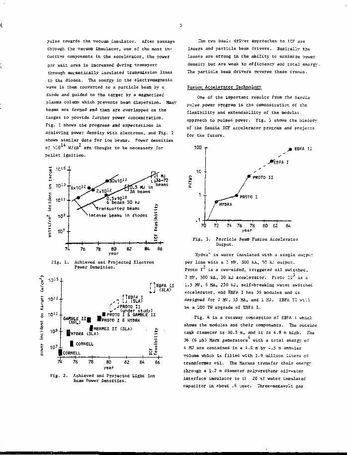
Fig. 1 shows the progress and expectations in
achieving power density with electrons, and Fig. 2
shows similar data for ion beams. Power densities14 2
of VL0 W/cm are thought to be necessary for
pellet ignition.
1C15
1013
1011
10s
107
'6X101
transported beams £
^intense beams in diodes ••;
74 76 78 80 82year
84 36
E'ig. 1. Achieved and Projected ElectronPower Densities.
1015.-
2 109--
HEBFA II[_j (SLA)
HEBFA I,*. LJ (SLA)
GAMBLE
: J PROTO iiv (under study)
• PROTO I S GAMBLE II•PROTO I
§ HERMES II (SLA)HYDRA (SLA)
1 D 7 i I CORNELL
JcORNELL
76 78 80year
82 86
Fig. 2. Achieved and Projected Light IonBeam Power Densities.
The two basic driver approaches to ICF are
lasers and particle bean drivers. Basically the
lasers are strong in the ability to maximize power
density but are weak in efficiency and tocal energy.
The particle beam drivers reverse these trends.
Fusion Accelerator Technology
One of the important results from the Sandis
pulse power program is the demonstration of the
flexibility and extendability of the modular
approach to pulsed power. Fig. 3 shows the history
of the Sandia ICF accelerator program and projects
for the future.
100
10 ••
EBFA II
74 76 7Byear
Fig. 3. Particle Bean Fusion AcceleratorOutput.
Hydra is water insulated with a single output
per line with a 1 MV, 500 kA, 50 kJ output.
Proco I" is a two-sided, triggered oil switched,
2 MV, 500 kA, 20 kj accelerator. Proto II is a
1.5 MV, 6 MA, 250 kJ, self-breaking water switched
accelerator, and EBFA I has 36 modules and is
designed for 2 MV, 15 MA, and 1 MJ. EBFA II will
be a 100 TW upgrade of EBFA I.
Fig. 4 is a cutaway conception of EBFA I which
shows the modules and their components. The outside
tank diameter is 30.5 m, and it is 4.8 m high. The
36 (6 un) Marx generators with a total energy of
4 MJ are contained i n a 4 . S m b y « . 5 n annular
volume which is filled with 1.9 million liters of
transformer oil. The Marxes transfer their energy
through a 1.2 m diameter polyurethane oil-wacer
interface insulator to tt 20 nf water insulated
capacitor in about .6 usec. Three-megavolt gas
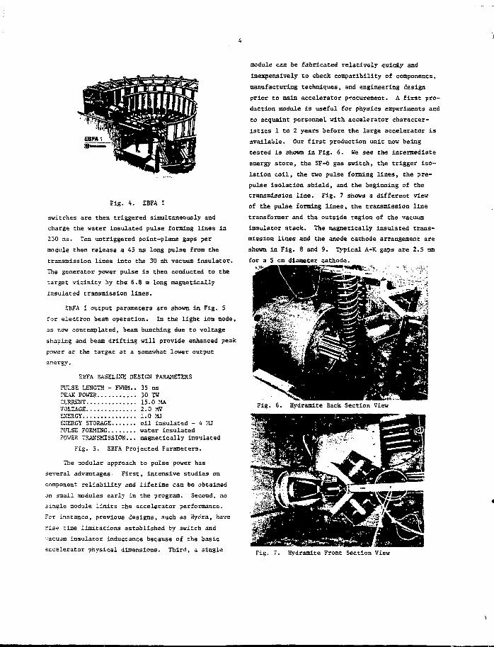
Fig. 4. EBFA I
switches are then triggered simultaneously and
charge the water insulated pulse forming lines in
230 ns. Ten untriggered point-plane gaps per
nodule then release a 45 ns long pulse from the
transmission lines into the 30 nh vacuum insulator.
The generator power pulse is then conducted to the
target vicinity by the 6.8 m long magnetically
insulated transmission lines.
EBFA I output parameters are shown in Fig. 5
for electron beam operation. In the light ion mode,
as now contemplated, beam bunching due to voltage
shaping and beam drifting will provide enhanced peak
power at the target at a somewhat lower output
energy.
EBFA BASELINE DESIGN PARAMETERS
PULSE LENGTH - FWHM.. 35 nsPEAK POWER 30 TWCURRENT 15.0 MAVOLTAGE 2.0 MVENERGY 1.0 MJEIERGY STORAGE oil insulated - 4 MJPULSE FORMING water insulatedPOWER TRANSMISSION... magnetically insulated
Fig. 5. EBFA Projected Parameters.
The nodular approach to pulse power has
several advantages: First, intensive studies on
component reliability and lifetime can be obtained
on small modules early in the program. Second, no
single module limits the accelerator performance.
Fcr instance, previous designs, such as Hyrira, have
rise cine limitations established by switch and
vacuum insulator inductance because of the basic
accelerator physical dimensions. Third, a single
module can be fabricated relatively quicfty and
inexpensively to check compatibility of components,
manufacturing techniques, and engineering design
prior to main accelerator procurement. A first pro-
duction module is useful for physics experiments and
to acquaint personnel with accelerator character-
istics 1 to 2 years before the large accelerator is
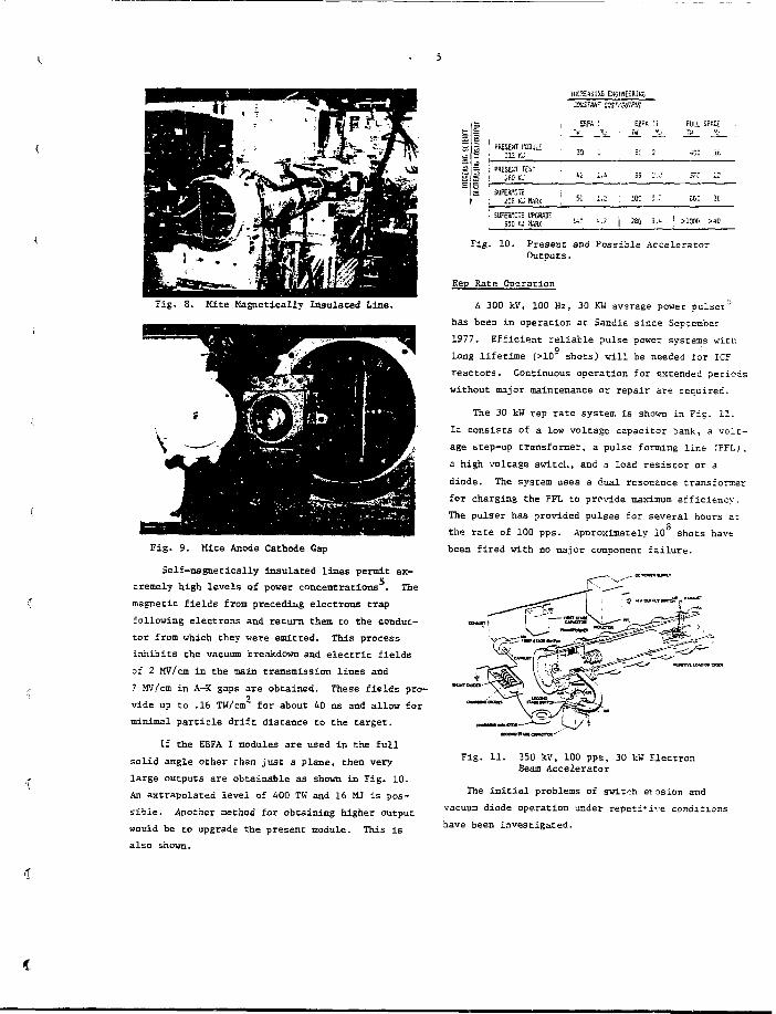
available. Our first production unit now being
tested is shown in Fig. 6. We see the intermediate
energy store, the SF-6 gas switch, the trigger iso~
lation coil, the two pulse forming lines, the pre-
pulse isolation shield, and the beginning of the
transmission line. Fig. 7 shows a different view
of the pulse forming lines, the transmission line
transformer and the outside region of the vacuum
insulator stack. The magnetically insulated trans-
mission lines and the anode cathode arrangement are
shown in Fig. 8 and 9. Typical A-K gaps are 2.5 ran
for a 5 cm diameter cathode.
Fig. 6. Hydramite Back Section View
Fig. Hydramite Front Section View
ItiCEASM ESGHIEERilK
Fig. 8. Mite Magnetically Insulated Line.
Fig. 9. Kite Anode Cathode Gap
Self-magnetically insulated lines permit ex-
tremely high levels of power concentrations . The
magnetic fields from preceding electrons trap
following electrons and return them to the conduc-
tor from which they were emitted. This process
inhibits the vacuum breakdown and electric fields
of 2 MV/cm in the main transmission lines and
7 MV/cm in A-K gaps are obtained. These fields pro-
vide up to .16 TW/cm for about 40 ns and allow for
minimal particle drift distance to the target.
If the EBFA I modules are used in the full
solid angle other than just a plane, then very
large outputs are obtainable as shown in Fig. 10.
An extrapolated level of 400 TW and 16 MJ is pos-
sible. Another aethod for obtaining higher output
would be to upgrade the present module. This is
also shown.
§
BIX
PRESENT HODUuUl U
PRESENT TESTjso a
SUPBHIIL<!OS KJ WRX
SUFEK1I7E UPGRADE530 KJ I1ARX
EEF»TB
S3
«
50.
« r c:si/3ur?s;
6C 2
i.a 35 : . :
1.2 ; :oc ; . :
•-7 | 280 ?.*•
: Fua SPffi
SOD I t
57C 2
60C 2:
' >I000 >10
Fig. 10. Present and Possible AcceleratorOutputs.
Rep Rate Operation
A 300 kV, 100 Hz, 30 KK avarage power pulsei5
has been in operation at Sandia since September
1977. Efficient reliable pulse power systems withq
long lifetime (>10 shots) will be needed for ICF
reactors. Continuous operation for extended periods
without major maintenance or repair are required.
The 30 kW rep rate system is shown in Fig. 11.
It consists of a low voltage capacitor bank, a volt-
age step-up transformer, a pulse fonaing line (PFL;,
a high voltage switcl., and a load resistor or a
diode. The system uses a dual resonance transformer
for charging the PFL to provide maximum efficiency.
The pulser has provided pulses for several hours at
the rate of 100 pps. Apnroximately 10 shots have
been fired with no major component failure.
Fig. 11. 350 kV, 100 pps, 30 kW ElectronBeam Accelerator
The initial problems of switch erosion and
vacuum diode operation under repetitive conditions
have been investigated.
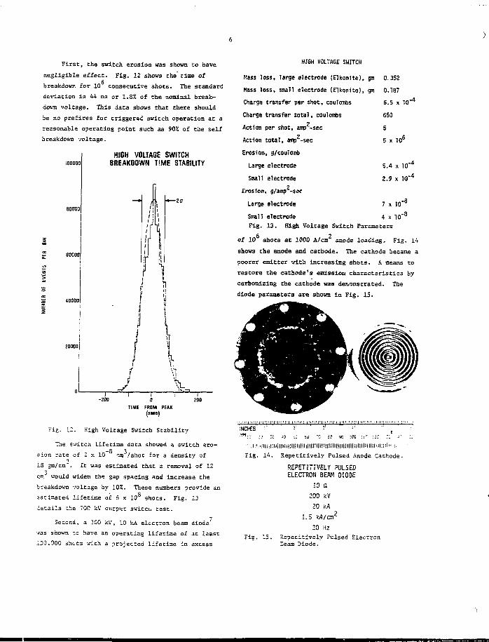
First, the switch erosion was shown to have
negligible effect. Fig. 12 shows the" time of
breakdown for 10 consecutive shots. The standard
deviation is 44 ns or 1.8% of the nominal break-
down voltage. This data shows that there should
be no prefires for triggered switch operation at a
reasonable operating point such as 902 of the self
breakdown voltage.
HIGH VOLTAGE SWITCHBREAKDOWN TIME STABILITY
80000
600 0C
40000
-200
TIME FROM PEAK
Fig. 12. High Voltage Switch Stabi l i ty
The switch Lifetime data showed a switch sro-
5ion rate of 2 x 10 cm /shot for a density of
18 gm/cm . It was estimated that a renoval of 12
cm would widen the gap spacing and increase the
breakdown voltage by 10%. These numbers provide an
estimated lifetime of 5 x 10 shots. Fig. 13
detai ls the 70C kV output switcu t e s t .
Second, a 2C0 k.V, 10 kA electron beam diode'•vas shown to have an operating lifetime of i t least150.000 shots with a projected lifetime in excess
HIGH VOLTAGE SWITCH
Hass loss, large electrode (Elkonite), gm 0.352
Mass loss, small electrode (Elkonite), gm 0.187
Charge transfer per shot, coulombs 6.5 x 10"*
Charge transfer total, coulombs 6S0
Action per shot, antp'-sec 5
Action total, ampE-sec 5 x 10⁶
Erosion, g/coulomb
Large electrode 5.4 x 10"*
Small electrode 2.9 x 10"4
Erosion, g/amp -sac
Large electrode 7 x 10"8
Small electrode 4 x 10"3
Fig. 13. High Voltage Switch Parameters
of 10 shots at 1000 A/cm anode loading. Fig. 14shows the anode and cathode. The cathode became a
poorer emitter with increasing shots. A means to
restore the cathode's eoissiou characteristics bycarbonizing the cathode was demonstrated. The
diode parameters are shown in Fig. 15.
INCHES
Fig. 14. Repetitively Pulsed Anode Cathode.
REPETITIVELY PULSEDELECTRON BEAM DIODE
10 a200 kV20 kA
1.5 k/Vcn2
30 HzFig. 15. Repetitively Pulsed Electron
Learn Diode.
Power Reactor Concept
One possible 200 MWe reactor system is shown
in Fig. 16 ' . The energy storage section con-
cains the primary energy store, either capacitive
or inductive. The energy is compressed and pulse
shaped as previously outlined and then transmitted
through the containment wall up to the reactor
chamber by magnetically insulated power flow
lines.
.•'•ft
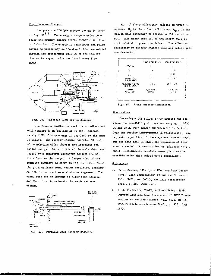
Fig. 16. Particle Beam Driven Reactor.
The reactor chamber is small (2 m radius) and
will contain 60 MJ/pellets at 10 pps. Approxi-
mately 2 MJ of bean energy is supplied to the gain
30 pellet. The reactor chamber contains 50 torr
of neon-helium which absorbs and moderates the
pellet energy. Laser initiated channels which are
heated by a capactive discharge conduct the par-
ticle beam to the target. A larger view of the
beamline geometry is shown in Fig. 17. This shows
the guiding laser beam, vacuum insulator, contain-
ment wall, and dual vane window arrangement. The
vanes open for an instant to allow beam passage
and then close to maintain the anode cathode
vacuum.
! M Vj INSULATOR ' . t v !
SlMKG£nouiM«SII /MH>VACUUM TT-»NSMIS5ION LINE
DIODE GAP , [ 1
AffBtURE V*h£
Fig. IS shows efficiency affects on power re-actors. N_ is the driver efficiencv, 0 . is the
1> ' "nun
pellet gain necessary to provide a 75% useful out-
put. This means that 257; of the energy will be
recircuiated to power the driver. The effect of
efficiency on reactor chamber size and pellet gair.
are dramatic.
Wf. £HERGV CTOPEEr j ori TARGET)
Fig. 18. Power Reactor Comparison
Conclusions
The modular ICF pulsed power concept has pro-
vided the possibility for systems ranging to 1000
TK and 30 MJ with modest improvements in techno-
logy and further improvements in reliability. The
rep rate capability of these systems appeals good,
but the data base is small and expansion of this
area is needed. A reactor design indicates that a
small, economically feasible power plant may be
possible using this pulsed power technology.
References
1. T. H. Martin, "The Hydra Electron Beam Gener-
ator," IEEE Transactions on Nuclear Science.
Vol. NS-20, No. 3-ID3, Particle Accelerator
Conf., p. 289, June 1973.
2. K. R. Prestwich, "HARP, A Short Pulse, High
Current Electron Beam Accelerator," IEEE Trans-
actions on Nuclear Science, Vol. NS22, No. 3,
1975 Particle Accelerator Conf., p. 975, June
1975.
, yGUIDINGJtS!R BEAM
Fig. 17. Particle Beam Reactor Beamline

3. I, H. Hartin, J. P. yanDevender, D. L. Johnson,
D. H. McDaniel, M. Aker, "PSOTO II - A Short
Pulse Water Insulated Accelerator," Inter-
national Topical Conf. on Electron Beam
Research & Technology, Albuquerque, NM, Vol. 1,
p. 450, November 3-5, 1973.
4. D. L. Johnson, "Initial PROTO II Pulsed Power
Tests," Proceedings International Pulsed Power
Conf., Paper IE2-1, Texas Tech University,
November 9-11, 1976.
5. J. P. VsnDevender, "Self-Magnetically Insula-
ted Power Flow," Proceedings of IEEE 2nd
Int&imational Pulsed Power Conf., Lubbock,
Texas, June 12-14, 1979.
6. M. T. Buttram, G. J. Rohwein, "Operation of a
300 kV, 100 Hz, 30 kW Average Power Pulser,"
13th Pulse Power Modulator Symposium, Buffalo,
NY, June 20-22, 1978.
7. M. T. Buttram, "Operation of a Repetitively
Pulsed 300 kV, 10 kA Electron Beam Diode,"
IEEE Transactions on Nuclear Science, 1979
Particle Accelerator Conf., June 1979.
8. D. L. Cook, M. A. Sweeney, "Design of a Com-
pact Particle Beam Driven Inertial Confinement
Fusion Reactor," Proceedings of ANS 3rd Topi-
cal Meeting on the Technology of Controlled
N'uclear Fusion, Santa Fe, NM, "lay 1978.
9. D. L. Cook, I!. A. Sweeney, "Critical Environ-
mental Considerations for Particle Beam Driven
ICF Reactor Materials, Journal of Nuclear
Materials, to be published, 1979.
•'This vork vas supported by the U. S. Departmentof Energy under Contract DE-AC04-76-DP00789.
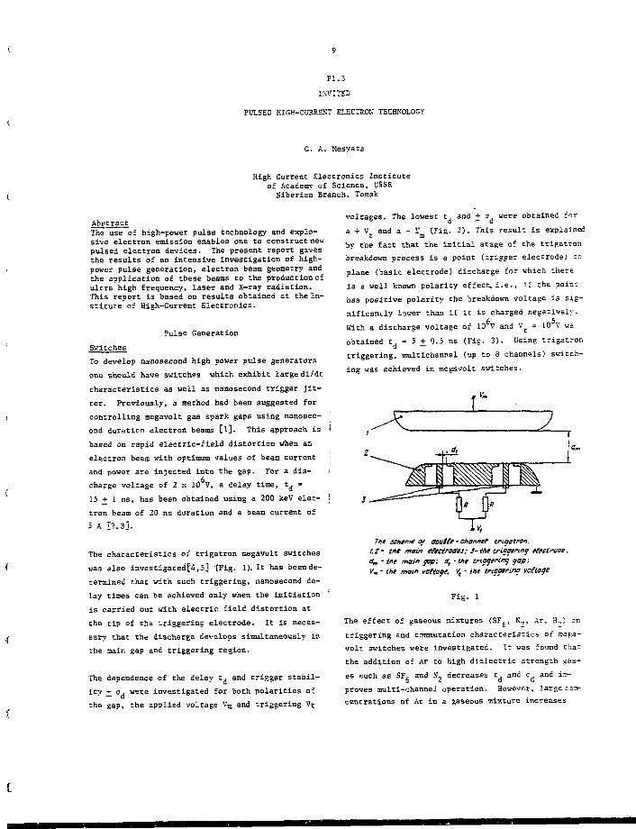
PI.3
INVITED
PULSED KIGH-CUXRENT ELECTRON TECHNOLOGY
G. A. Mesyats
High Current Electronics Instituteof Academy of Science, USSRSiberian Branch, Tomsk
AbstractThe use of high-power pulse technology and explo-sive electron emission enables one to construct newpulsed electron devices. The present report givesthe results of an intensive investigation of high-power pulse generation, electron beam geometry andChe application of these beams to the production ofultra high frequency, laser and X-ray radiation.This report is based on results obtained at the Jn-sticure of High-Current Electronics.
Pulse Generation
Switches
To develop nanosecond high power pulse generators
one should have switches which exhibit large di/dt
characteristics as well as nanosecond trigger jit-
ter. Previously, a method had been suggested for
controlling megavolt gas spark gaps using nanosec-
ond duration electron beams [!•]. This approach is I
based on rapid electric-field distortion vhen an
electron beam with optimum values of beam current
and power are injected into the gap. For a dis- =
charge voltage of 2 x 10 V, a delay time, trf -
15 + 1 ns, has been obtained using a 200 keV elec- !
tron beam of 20 ns duration and a beam current of
5 A [2,3].
The characteristics of trigatron megavolt switches
was also investigated^,5] XTig. 1). It has been de-
termined that with such triggering, nanosecond de-
lay times can be achieved only when the initiation
is carried out with electric field distortion at
the tip of the Lriggering electrode. It is neces-
sary that the discharge develops simultaneously in
the main gap and triggering region.
voltages. The lowest t and + Jd were obtained for
a + V and a - 1" tFig. 2). This result is explainedt m
by the fact that the initial stage of the trip.atron
breakdown process is a point (trigger electrode; to
plane (basic electrode) discharge for which there
is a well known polarity effect, i.e., if the point
has positive polarity the breakdown voltage is sig-
nificantly lower than if it is charged negatively.
With a discharge voltage of 10 V and V"c = 10 V wa
obtained L. - 5 •>• 0.5 ns (Fie. 3). Using trigatrona —
triggering, multichannel (up to 8 channels) switch-
ing was achieved in mcgavolt switches.
The dependence of the delay t^ and trigger stabil-
itv + o , were investigated for both polarities of* — d
the gap, the applied voltage Vm and triggering Vt
The scheme of ctoutte - channet triyotron.1,2- (he main eUctrae/ts; 3--the iriasennf tfKtraae.dm - the main mp; d, -the tnaaering pap;K» - i*e main votlafr, Vt • the trieprw voltage.
Fig . 1
The effect of gaseous mixtures (SF,, N,,, Ar, Ho) onc — -
triggering and commutation characteristics of raeea-
volt switches were investigated. It was found that
the addition of Ar to high dielectric strength gas-
es such as SF, and N, decreases t^ and c^ and im-
proves multi-channel operation. However, large con-
centrations of Ar in a gaseous mixture increases
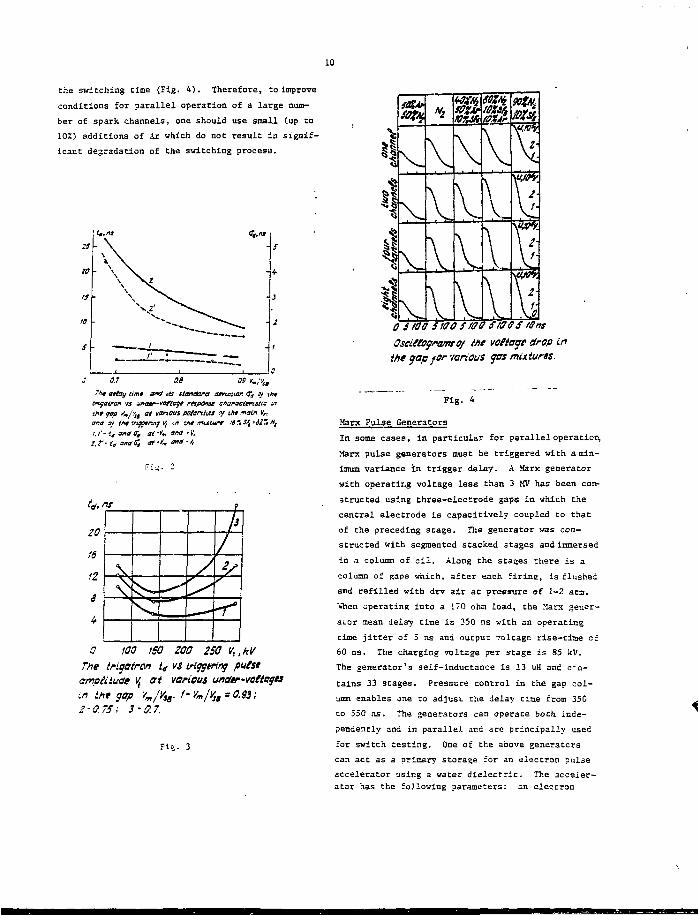
10
che switching time (Fig. 4 ) . Therefore, to improve
conditions for parallel operation of a large num-
ber of spark channels, one should use small (up to
10%) additions of Ar which do noC result in signif-
icant degradation of the switching process.
<#."*
o.7 asTti* attay limt ana its stanaara arrtation Ca y tht
tnaainn vs jnair-wftae* response characteristic u*the cap **/'.'sg at various petanhu ty Utt main v^ana Ol the friqcirwf Vt i/r s/it mixture !9TtSft*dtT* 'V;t. /'- i, atta (T, at -fm ana • <l,
!,?• ti unaC,, at -«; ««* -*
//
20
IS
12
0 100 ISO ZOO 250 Vt,kVThe triqatron i< vs trotting pulseamplitude Vt at various u n d tin tht ?ap ym/ysg. f-vm/vss=0.93;2-0.7S; 3-0.7.
Fig. 3
\
I-
z-
0 i100 S tOO S100 StOOS fans
Oscitfopram-o/ Me votiage strop in
the gap for various gas mixtures.
Fig. 4
Marx Pulse Generators
In some cases, in particular for parallel operation,
Marx pulse generators must be triggered with a min-
imum variance in trigger delay. A Marx generator
with operating voltage less than 3 MV has been con-
structed using three-electrode gaps in which the
central electrode is capacitively coupled to that
of the preceding stage. The generator was con-
structed with segmented stacked stages and immersed
in a column of cil. Along the stages there is a
column of saps which, after each Siring, is flushed
and refilled with drv air at pressure of 1-2 acs.
Vheu operating into a 170 ohm load, the Marx gener-
aLor mean delay time is 350 ns with an operating
time jitter of 5 ns and output voltage rise-tiiae cf
60 ns. The charging voltage per stage is 85 kV.
The generator's self-inductance is 13 UH and con-
tains 33 stages. Pressure control in the gap col-
umn enables one to adjust the delay time from 350
to 550 ns. The generators can operate both, inde-
pendently and in parallel and are principally used
for switch testing. One of the above generators
can act as a primary storage for an electron pulse
accelerator using a water dielectric. The acceler-
ator has che following parameters: an electron
II
beam voltage up to I MV, beam current - up to 30C
kA, pulse-duration of the electron current is 70ns
Through a controlled commutator a single storage
line of 39 ohm impedance is discharged through a
coaxial transformer of 2.3 ohm impedance. The
electron beam is forced in the diode, containing a
disk insulator. The interelectrode spacing dbeing
of the order of 1 cm, ratio R/d "- 1 (E • radius
of cathode). TJsing the accelerator, we have in-
vestigated the regimes of electron - beam geometry
in diodes with a large value of \>/y. To analyze
the plasma generated in the diode, laser scattering
off plasma electrons and interferometry are used.
Due to the very low jitter in the operation of t>e
Marx generator and gap, good coincidence of elec-
tron current pulse and laser diagnostic devices
was achieved in the accelerator.
A calculation for the "Module" installation indi-
cates one can achieve a congressional speed of 10'
temperatures of 1 keV.
Fig.
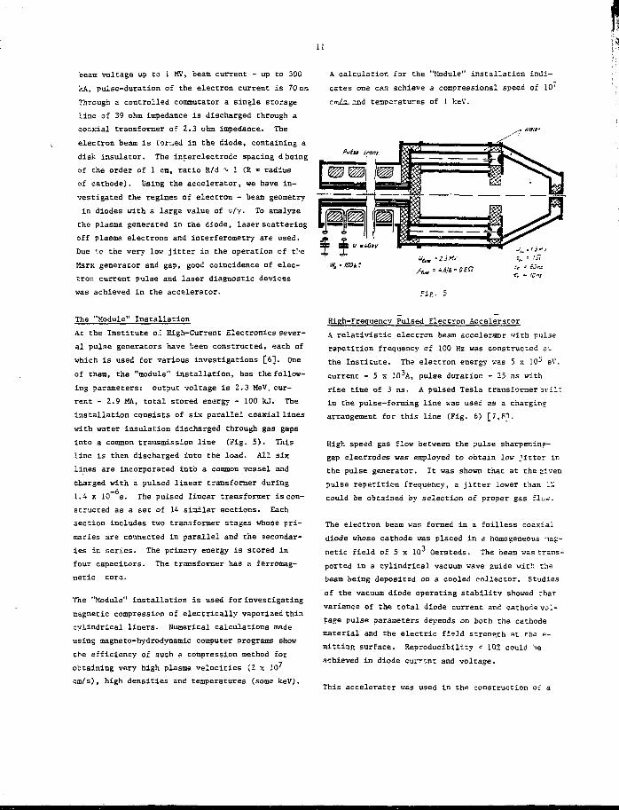
The "Module" Installation
At the Institute of High-Current Electronics sever-
al pulse generators have been constructed, each of
which is used for various investigations £6]. One
of them, the "module" installation, has the follow-
ing parameters: output voltage is 2.3 MeV, cur-
rent - 2.9 MA, total stored energy - 100 kj. The
installation consists of six parallel coaxial lines
with water insulation discharged through gas gaps
into a common transmission line (Fig. 5). This
line is then discharged into the load. All six
lines are incorporated into a common vessel and
charged with a pulsed linear transformer during
1.4 x I0~°s. The pulsed linear transformer is con-
structed as a set of 14 similar sections. Each
section includes two transformer stages whose pri-
maries are connected in parallel and the secondar-
ies in series. The primary energy is stored in
four capacitors. The transformer has a ferromag-
netic core.
The "Module" installation is used for investigating
magnetic compression of electrically vaporized thin
cylindrical liners. Numerical calculations made
using magneto-hydrodynamic computer programs show
the efficiency of such a compression method for
obtaining very high plasma velocities (2 x 10⁷
cm/s), high densities and temperatures (some keV).
High-Frequency Pulsed Electron Accelerator
A relativistic electron beam accelerdor with pulse
repetition frequency of 100 Hz was constructed aL
the Institute. The electron energy was 5 x 10-" eV,
current - 5 x 10 A, pulse duration - 25 ns with
rise time of 3 ns. A pulsed Tesla transformer built
in the pulse-forming line was used as a charging
arrangement for this line (Fig. 6) [7,PI.
High speed gas flow between the pulse sharpeninp-
gap electrodes was employed to obtain low jitter in
the pulse generator. It was shown that at the given
pulse repetition frequency, a jitter lower than 17,
could be obtained by selection of proper gas flo».
The electron beam was formed in a foilless coaxial
diode whose cathode was placed in a homogeneous nag-
netic field of 5 x 10 Oersteds. The beam was trans-
ported in a cylindrical vacuum wave guide with the
beam being deposited on a cooled collector. Studies
of the vacuum diode operating stability showed that
variance of the total diode current and cathode vol-
tage pulse parameters depends on both the cathode
material and the electric field strength at cha e-
mitting surface. Reproducibility < 102 could be
achieved in diode current and voltage.
This accelerator was used in the construction oi a
12
high-power M2 + A r laser (efficiency -* 1.5%) [9],
and for constructing a pulsed 100 Mf microwave radi-
ition generator (prf - 50 Hz, efficiency "- 10%)
Cio].
Processes in Accelerator Diodes
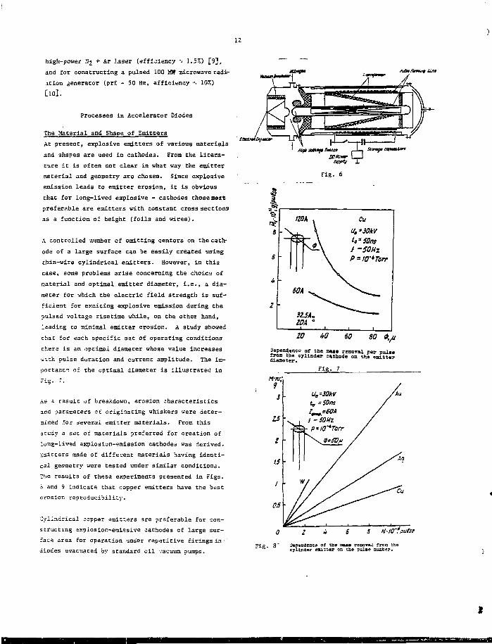
The Malarial and Shape of Emitters
At present, explosive emitters of various materials
and shapes are used in cathodes. From the litera-
ture it is often not clear in what way the emitter
material and geometry are chosen. Since explosive
emission Iead3 to emitter erosion, it is obvious
that for long-lived explosive - cathodes those mast
preferable are emitters with constant cross sections
as a function of height (foils and wires).
A controlled number of emitting centers on the cath-
ode of a large surface can be easily created using
thin-wire cylindrical emitters. However, in this
case, some problems arise concerning the choice of
naterial and optimal emitter diameter, i.e., a dia-
meter for which the electric field strength is suf-
ficient for exciting explosive emission during the
pulsed voltage risetime while, on the other hand,
leading to minimal emitter erosion. A study showed
that for each specific set of operating conditions
there is an optimal diameter whose value increases
with pulse duration and current amplitude. The im-
portance of the optimal diameter is illustrated in
Fig. 7.
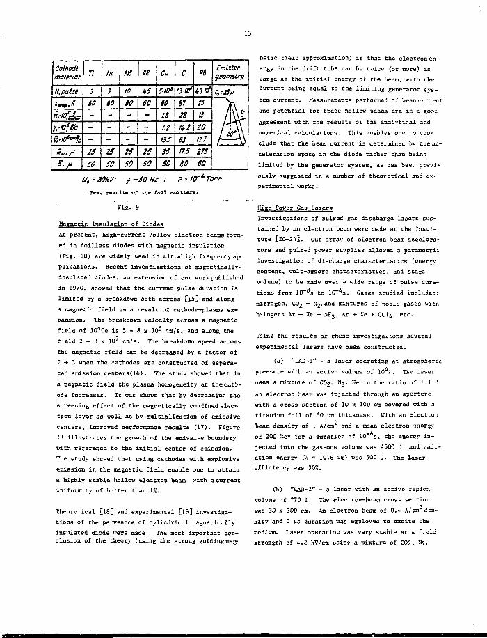
As a result of breakdown, erosion characteristics
and parameters ot originating whiskers were deter-
mined .for several emitter materials. From this
study a sot of materials preferred for creation of
long-lived explosion-emission cathodes was derived.
Imitters made of different materials having identi-
cal geometry ware tested under similar conditions.
The results of these experiments presented in Figs.
i and 9 indicate that copper emitters have the best
erosior. reoroducibility.
Cylindrical copper emitters are preferable for con-
structing expiosior.-emissive cathodes cf large sur-
face area for operation under repetitive firings in -
diodes evacuated by standard oil vacuum pumps.
ZO
Dependence of tha 3ui removal per pulsefrom the cylinder cathode on th» ealtte?disaster.
Fig. 7
rj.» 3" Dependence of the mass remor*! from the~ & cylinder emitter on the pulse nuaber.
13
Caihoaematerial
N, pulse
r,-ioft/c
Vf<Otcmfc
Ti
3
SO
-
-
-
25SO
Ni
3
60
-
-
-
2550
NS
to60-
-
-
25SO
ne
45
so---25SO
Cu
S-IO'
60
1.6
l.Z
as3550
C
a-to*87
28H.2S3US80
Pi
«-0*25
ti
20
m27S
SO
Emitterqiometri/
r<,'2Sr
h\u
r
Uo - 30kV; f -50 HZ ; P - V* Torr
Tea-: results at the foil emitter*.
Fig. 9
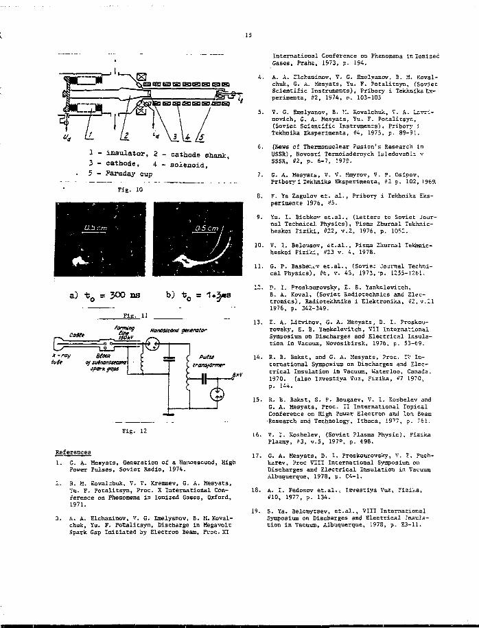
Magnetic Insulation of Diodes
At present, high-current hollow electron beams form-
ed in foilless diodes with magnetic insulation
(Fig. 10) are widely used in ultrahigh frequency ap-
plications. Recent investigations of magnetically-
insulated diodes, an extension of our work published
in 1970, showed that the current pulse duration is
limited by a breakdown both across £i-5j and along
a magnetic field as a result of cathode-plasma ex-
pansion. The breakdown velocity across a magnetic
field of 1040e is 5 - 8 x 10⁵ C B / S , and along the
field 2 - 3 x 10' cm/s. The breakdown speed across
the magnetic field can be decreased by a factor of
2 ->• 3 when the cathodes are constructed of separa-
ted emission centers(16). The study showed that in
a magnetic field the plasma homogeneity at the cath-
ode increases. It was shown that by decreasing the
screening effect of the magnetically confined elec-
tron layer as well as by multiplication of emissive
centers, improved performance results (17). Figure
11 illustrates the growth of the emissive boundary
with reference to the initial center of emission.
The study shewed that using cathodes with explosive
emission in the magnetic field enable one to attain
a highly stable hollow electron beam with a current
uniformity of better than 1%.
Theoretical [18] and experimental [19] investiga-
tions of the perveance of cylindrical magnetically
insulated diode were made. The most important con-clusion of the theory (using the strong guiding mag-
netic field approximation) is tha: the electron en-
ergy in the drift tube can be twice (or more) as
large as the initial energy of the bean, with the
current being equal to the limiting generator sys-
tem current. Measurements performed of bean current
and potential for these hollow beams are in a good
agreement with the results of the analytical and
numerical calculations. This enables one to con-
clude that the beam current is determined by the ac-
celeration space in the diode rather than being
limited by the generator system, as has been previ-
ously suggested in a number of theoretical and ex-
perimental works.
High Power Gas Lasers
Investigations of pulsed gas discharge lasers sus-
tained by an electron bean were made at the Insti-
tute X-0—24]. Our array of electron-beam accelera-
tors and puls=d power supplies allowed a parametric
investigation of discharge characteristics (energy
content, volt-ampere characteristics, and stage
volume) to be made over a wide range of pulse dura-
tions from 10~°s to 10 s. Gases studied included:
nitrogen, CO2 + N2. and mixtures of noble gases with
halogens Ar + Xe + NF3, Ar + Xe + CCI4, etc.
Using the results of these investigations several
experimental lasers have been constructed.
(a) "LAD-1" - a laser operating at atmospheric
pressure with an active volume of 10*2. The laser
uses a mixture of CO2: N7: He in the ratio of 1:1:1
An electron beam was injected through an aperture
with a cross section of 10 x 100 ca covered with a
titanium foil of 50 urn thickness. Kith an electron
beam density of 1 A/cm' and a mean electron energy
of 200 keV for a duration of 10"6s, the energy in-
jected into the gaseous volume was 4500 J, and radi-
ation energy (\ = 10.6 um) was 500 J. The laser
efficiency was 30%.
(b) "LAD-2" - a laser with an active region
volume of 270 1. The electron-bean cross section
was 30 x 300 co. An electron beam of 0.4 A/cm" den-
sity and 2 us duration was employed to excite the
medium. Laser operation was very stable at a field
strength of 4.2 kV/cm usinp a mixture of C02, N2,
14
and He. The power source was a capacitor bank of
15 nF capacitance charged to 125 kV voltage. The
laser output was 7.5 kj, an efficiency of 26Z.
(c) A tunable CO2 laser covering the range of
9 to 11 va at 6 atm pressure of CO2: N2 « 1:1. A
smooth tuning was obtained over Che aforementioned
spectral range. Individual E and P branch lines
were easily identifiable over a range of 86 caT^.
Spectral frequency scanning was accomplished by
use of a diffraction grating. The output energy
density of this tunable radiation was 5 J/cmz at
the line center with 1 50" modulation in between
lines. Pulse duration was 40 ns.
(d) Several eiximer lasers are being investi-
gated which are excited by both an electron beam
and a sustained electric discharge. Using the e-
beam o-Tited mixture Ar + Xe + CCI4, XeCl molecule
radiation (\ - 308 nm) with a radiation power of
10 J/l and an efficiency of 37. was obtained.
A discharge supported by a 50 nsec e-beam enables
one co excite XeF and XeCl to output power of 105
'.J/cm3 with pulse duration 2 x 10"8s.
nificantly [25]. be were able to construct a mini-
ature X-ray tube of 10 mm diameter, powered through
a section of coaxial cable (7.5 mm external diameter
and 30 cm in length). The power supply was a nano-
second generator from the X-ray device fHR-2d (Fig.
12) which charged a subnanosecond pulse forming line
over 3 - 5 na, providing a high over-voltage on
the sharpening gap. Pulse duration was limited with
a crowbar switch.
Measurements, made using a magnetic analyzer, of the
electron energies in the tube, showed that when
charging the pulse rorming line to 150 kV for a
pulse duration "v 0.5 ns, the voltage in the tube was
80 - 100 kV. Output was limited by line and sharp-
ening gap losses. The ma-r^mum radiation dose (80mR
per pulse at the distance of 1 cm from the anode)
was achieved with an anode-cathode distance of 0.2
mm. Bowever, in some cases, holes of 0.1 - 0.15 on
diameter were produced in the 0.1 mm thickness tung-
sten anode. Increasing the pap to 0.5 mm decreased
the dose to 25 mR/pulse, but provided a prolonged
operation of the tube and anode. Results did not
depend on pressure variation in the tube over the
range of 10"1 to 10"3 torr.
Powerful Nano- and Subnanosecond X-ray Pulses
A series of a pulsed X-ray machines with radiation
energy from 90 to 600 keV was developed and manu-
factured in the USSR for flaw detection in materi-
als. The use of nanosecond pulse generators and
X-cay Cubes based on explosive emission permitted
che reduction in overall size. Further decreases
in the nanosecond X-ray emitter sizes is limited by
che non-reproducible breakdown characteristics and
by che value of the anode-cathode gap in the vacu-
um X-ray tube.
investigations of vacuum diodes in the subnanosec-
cmd range showed that with pulse duration shorter
':han I as che interelectrode gap value can be de-
creased co 0.1 - 0.2 mm without danger of its
Hhorticg by a cathode flare plasma. The current
density ac che anode can be raised ca 10° A/cm"
'.jichouc che use of special focusing devices, and
che cube vacuum insulator sizes can decrease sig-
In this regime the electric-field strength at the
inner conductor of the coaxial cable is 1 MV/cm;
therefore, its lifetime is limited to 10^ pulses, at
which time the cable is replaced. It should be
noted that the impedance of a cable insulation
breakdown (single-channel) is so high that it does
not in fact influence the dose value. A halving of
the dose per pulse was observed only with the ap-
pearance of 5 to 6 breakdown channels.
The dose value and small size of the cube focus _ ,'.
make it very useful for flaw detection of ia .:.,, * .
goods with both narrow and long cavities.
15
63 IS
1 - insulator, 2 - cathode shank,
3 - cathode, 4 - solenoid,
5 - Faraday cup
Fig. 10
a) to = 300 ns b)
Fig. 11
CateeNanosecond gtntrator
x -ray BlocktuSt of sutnanostana
spark gaps \
Fig. 12
References
1. G. A. Mesyats, Generation of a Nanosecond, HighPower Pulses, Soviet Radio, 1974.
I. B. M. Koval^huk, V. V. Kremnev, G. A. Mesyats,Yu. F. Potalitsyn, Proc. X International Con-ference on Phenomena in Ionized Gases, Oxford,1971.
3. A. A. Elchaninov, V. G. Emelyanov, B. M. Koval-chuk, Yu. F. Potalitsyn, Discharge in MegavoltSpark Gap Initiated by Electron Beam, Proc. XI
International Conference on Phenomena in IonizedGases, Prahs, 1973, p. 194.
4. A. A. Jlchaninov, V. G. Emelyanov, B. >i. Koval-chuk, G. A. Mesyats, Yu. F. Potalitsyn, (SovietScientific Instruments), Pribory i Tekhnika Ex-perimenta, ill, 1974, r. 103-105
5. V. G. Emelyanov, B. V.. Kovalchuk, V. k. Lavri-novich, G. A. Mesyats, Yu. F. Potalitsyn,(Soviet Scientific Instruments), Pribory iTekhnika Eksperimenta, #4, 1975, p. 89-91.
6. (News of Thermonuclear Fusion's Research inUSSR), Novosti Termoiadernych Isledovanii vSSSR, #2, p. 6-7, 1979.
7. G. A. Mesyats, V. V. Hmyrov, V. P. Osipov,Pribory i Tekhnika Eksperimenta, #2 p. 102, 1969.
8. F. Ya Zagulov et. al., Pribory i Iekhnika Eks-perimente 1976, '.'5.
9. Yu. I. Bicbkov et.al., (Letters to Soviet Jour-nal Technical Physics), Pisma Zhurnal Tekhnic-heskoi Fiziki, #22, v.2, 1976, p. 1052.
10. V. I. Belousov, st.al., Pisma Zhurnal lekanic-heskoi Fiziki, 423 v. 4, 1978.
11. G. P. Basher.L.-v et.al., (Soviet Journal Techni-cal Physics), #6, v. 43, 1973, "p. 1255-1261.
12. P. I. Proskourovsky, E. B. Yankelevitch,B. A. Koval, (Soviet aadiotechnics and Elec-tronics), Radiotekhnika i Elektronika, #2,v.ll1976, p. 342-349.
13. E. A. Litvinov, G. A. Mesyats, D. I. Proskou-rovsky, E. B. Yankelevitch, VII InternationalSymposium on Discharges and Electrical Insula-tion in Vacuum, Novosibirsk, 1976, p. 55-69.
14. R. B. Bakst, and G. A. Mesyats, Proc. IV In-ternational Symposium on Discharges and Elec-trical Insulation in Vacuum, Waterloo, Canada.1970. (also Izvestiya Vuz, Fizika, 1>7 1970,p. 144.
15. R. B. Bakst, S. P. Bougaev, V. I. Koshelev andG. A. Mesyats, Proc. II International TopicalConference on High Power Electron and Ion Beam•Research and Technology, Ithaca, 1977, p. 761.
16. V. I. Koshelev, (Soviet Plasma Physic), FizikaPlazmy, #3, v.5, 197?, p. 698.
17. G. A. Mesyats, D. I. Proskourovsky, V. F. Puch-karev, Proc VIII International Symposium onDischarges and Electrical Insulation in VacuumAlbuquerque, 1978, p. C4-1.
18. A. I. Fedosov et.al,.. Izvestiya Vuz, Fizika,#10, 1977, p. 134.
19. S. Ya. Beloaytsev, et.al., VIII InternationalSymposium on Discharges and Electrical Insula-tion in Vacuum, Albuquerque, 1978, p. E3-11.
16
20. Yu.I. Bychkov, Yu.D. Korolev, G. A. Mesyats,(Soviet Physic's Sews), Uspekhi FizicheskikhNauk, #3, v. 126, 1978, p. 451-477.
21. S. P. Bougaer, ec.al., Pisma Zhurnal Tekhnich-eskoi Fiziki, #10,v. 1, 197S, p. 492-496.
22. Yu.I. Bychkov, et.al., (letters to Sov. Jour-nal Tehn. Phys.), Plsma Zhuraal TekhnicheskolFiziki, #5, v. 2, 1976, p.212-216.
23. Tu.I. Bychkov, et.al., (Soviet Sew Academy ofSciences USSR) #14, v. 1, 1975.
24. G. A. Mesyats, Plsraa Zhurnal TektinicheskoiFiziki, 014, v. 1, 1975.
25. G. A. Mesyats, V. G. Shpak, Pisma ZhurnalTekhnicheskoi Fiziki, v. 3, 1977, p. 708.
17
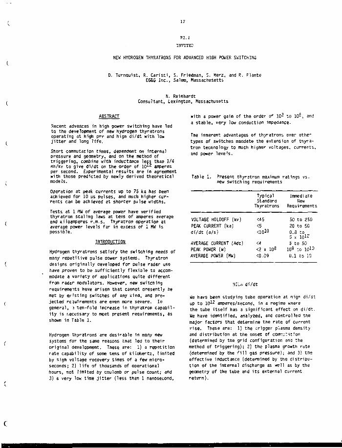
P2.1
INVITED
NEW HYDROSEN THYRATRONS FOR ADVANCED HIGH POWER SWITChING
D. Turnquist, R. Caristi, S. Friedman, S. Merz, and R. PlanteEGSG Inc., Salem, Massachusetts
N. ReinhardtConsultant, Lexington, Massachusetts
ABSTRACT
Recent advances in high power switching have ledto the development of new hydrogen thyratronsoperating at high prr and high di/dt with lowjitter and long life.
Short commutation times, dependent on internalpressure and geometry, and on the method oftriggering, combine with inductance less than 2/4nh/kv to give di/dt on the order of 1 0 ^ amperesper second. Experimental results are in agreementwith those predicted by newly derived theoreticalmodels.
Operation at peak currents up to 75 ka has beenachieved for 10 us pulses, and much higher cur-rents can be achieved at shorter pulse widths.
Tests at 1 MW of average power have verifiedthyratron scaling laws at tens of amperes averageand kiloamperes r.m.s. Thyratron operation ataverage power levels far in excess of 1 MW ispossible.
INTRODUCTION
Hydrogen thyratrons satisfy the switching needs ofmany repetitive pulse power systems. Thyratrondesigns originally developed for pulse radar usehave proven to be sufficiently flexible to accom-modate a variety of applications quite differentfrom radar modulators. However, new switchingrequirements have arisen that cannot presently bemet by existing switches of any kind, and pro-jected requirements are even more severe. Ingeneral, i ten-fold increase in thyratron capabil-ity is r.ecessary to meet present requirements, asshown in Table 1.
Hydrogen thyratrons are desirable in many newsystems for the same reasons that led to theiroriginal development. These are: 1) a repatitionrate capability of some tens of kilohertz, limitedby high voltage recovery times of a few micro-seconds; 2) life of thousands of operationalhours, not limited by coulomb or pulse count; and3) a very low time jitter (less than 1 nanosecond,
with a power gain of the order of 10^ to 10=, anda stable, very low conduction impedance.
The inherent advantages of thyratrons over othertypes of switches mandate the extension of thyra-tron tecnnology to much higher voltages, currents,and power levels.
Table 1. Present thyratron maximum ratings vs.new switching requirements
VOLTAGE HOLDOFF (kv )
PEAK CURRENT ( ka )
di/dt (a/s)
AVERAGE CURRENT (Adc)
PEAK POWER (W)
AVERAGE POWER (MW)
T y p i c a lStandard
Thy ra t rons
<45<5<ioi°
<t<2 x 10⁸
<0.09
ImmediateNew
Requirements
50 to 25020 to 500.8 to „5 x lO 1 '5 to 50
10.9 to 1010
0.1 to 10
HICo di/dt
We have been studying tube operation at hign di/dtup to 10^2 amperes/second, in a regime wherethe tube itself has a significant effect on di/dt.We have identified, analyzed, and controlled themajor factors that determine the rate of currentrise. These are: 1) the trigger plasma densityand distribution at the onset of competition(determined by the grid configuration and themethod of triggering); 2) the plasma growth rate(determined by the fill gas pressure); and 3) theeffective inductance (determined by the distribu-tion of the internal discharge as well as by thegeometry of the tube and its external currentreturn).
18
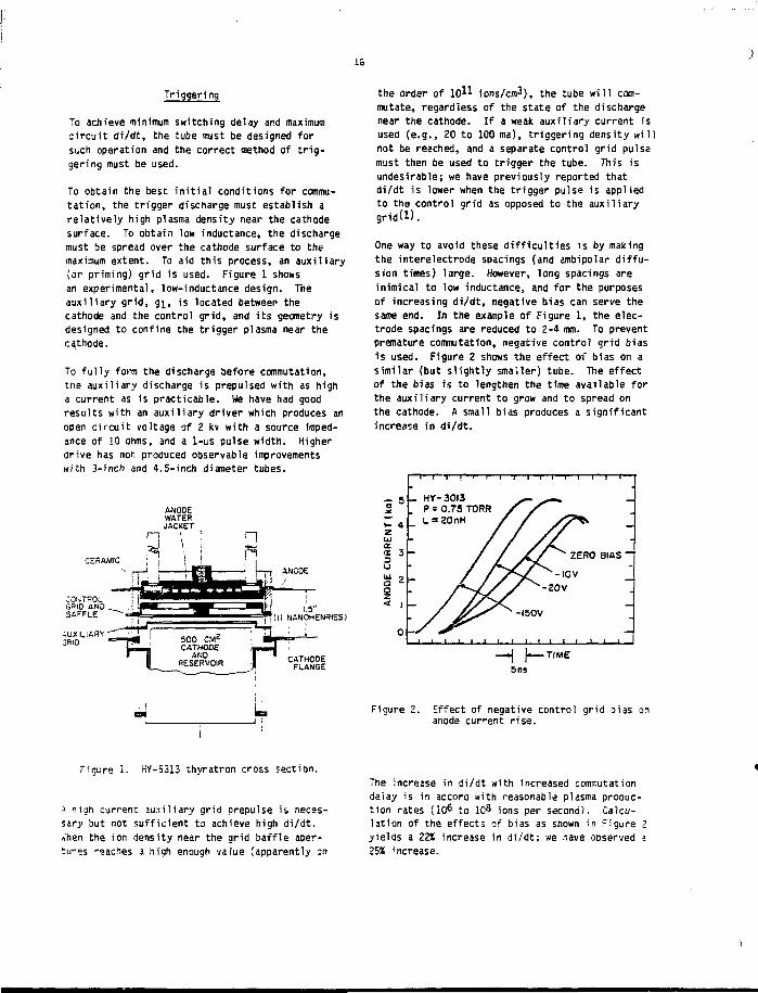
Triggering
To achieve minimum switching delay and maximumcircuit di/dt, the tube mast be designed forsuch operation and the correct method of trig-gering must be used.
To obtain the best initial conditions for commu-tation, the trigger discharge must establish arelatively high plasma density near the cathodesurface. To obtain low inductance, the dischargemust be spread over the cathode surface to themaximum extent. To aid this process, an auxiliary(or priming) grid is used. Figure 1 showsan experimental, low-inductance design. Theauxiliary grid, gx, is located between thecathode and the control grid, and its geometry isdesigned to confine the trigger plasma near thecathode.
To fully form the discharge before commutation,tne auxiliary discharge is prepulsed with as higha current as is practicable. We have had goodresults with an auxiliary driver which produces anopen circuit voltage of 2 kv with a source imped-ance of 10 ohms, and a 1-us pulse width. Higherdrive has not produced observable improvementswith 3-inch and 4.5-inch diameter tubes.
CERAMIC
1.5( I I NANOHENRIES)
AUXILIARY3R1O
the order of 1 0 ^ ions/cm^), the tube will com-mutate, regardless of the state of the dischargenear the cathode. If a weak auxiliary current isused (e.g., 20 to 100 ma), triggering density willnot be reached, and a separate control grid pulsemust then be used to trigger the tube. This isundesirable; we have previously reported thatdi/dt is lower when the trigger pulse is appliedto the control grid as opposed to the auxiliarygridU).
One way to avoid these difficulties is by makingthe intereiectrode spacings (and ambipolar diffu-sion times) large. However, long spacings areinimical to low inductance, and far the purposesof increasing di/dt, negative bias can serve thesame end. In the example of Figure 1, the elec-trode spacings are reduced to 2-4 mm. To preventpremature commutation, negative control grid biasis used. Figure 2 shows the effect of bias on asimilar (but slightly smaller) tube. The effectof the bias is to lengthen the time available forthe auxiliary current to grow and to spread onthe cathode. A small bias produces a significantincrease in di/dt.
a 5 _ HY-3OI3P = 0.75 TORR
zua:
uUJaa2
4 -
3 -
0 -
ZERO BIAS
-I50V
5 ns
Fiaure 2. Effect of negative control grid bias onanode current rise.
Figure i. HY-5313 thyratron cross section.
A nigh currant auxiliary grid prepulse is necas-sary but not sufficient to achieve high di/dt.* e n the ion density near the grid baffle aper-tures i-aaches a high enough value (apparently on
The increase in di/dt with increased commutationdeiay is in accoro with reasonable plasma proauc-tion rates (I06 to 1C8 ions per second). Calcu-lation of the effects of bias as shown in Figure 2yields a 22* increase in di/dt: we have ODserved a25% increase.
19
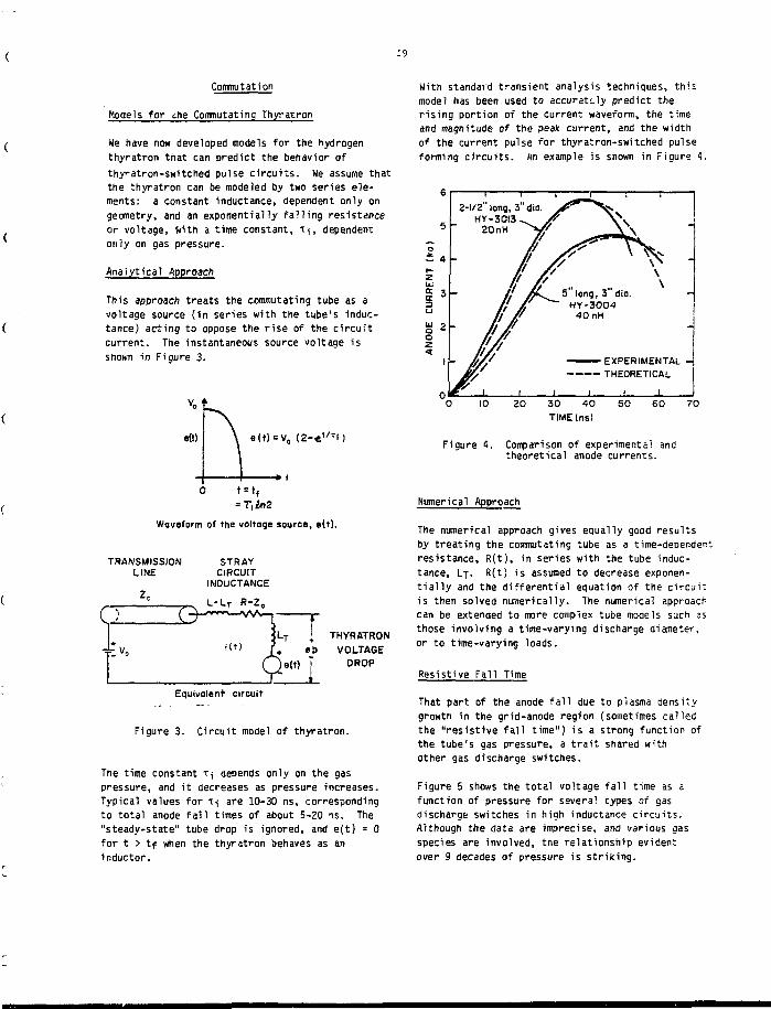
Commutation
Models for che Commutating Thyratron
We have now developed models for the hydrogenthyratron that can predict the behavior ofthyratron-switched pulse circuits. We assume thatthe thyratron can be modeled by two serias ele-ments: a constant inductance, dependent only ongeometry, and an exponentially falling resistanceor voltage, With a time constant, ti, dependentonly on gas pressure.
Analytical Approach
This approach treats the commutating tube as avoltage source (in series with the tube's induc-tance) acting to oppose the rise of the circuitcurrent. The instantaneous source voltage isshown in Figure 3.
V. *
0 t = tf
Waveform of the voltage source, e(t).
TRANSMISSION STRAYLINE CIRCUIT
INDUCTANCE
THYRATRON• eb VOLTAGE
DROP
Equivalent circuit
Figure 3. Circuit model of thyratron.
The time constant T, depends only on the gaspressure, and it decreases as pressure increases.Typical values for T-J are 10-30 ns, correspondingto total anode fall times of about 5-20 ns. The"steady-state" tube drop is ignored, and e(t) - 0for t > tf when the thyratron behaves as aninductor.
With standard transient analysis techniques, thismodel has been used to accurately predict therising portion of the current waveform, the timeand magnitude of the peak current, and the widthof the current pulse for thyratron-switched pulseforming circuits. An example is shown in Figure 4.
2-1/2" long, 3"dia.
EXPERIMENTAL -THEORETICAL
10 30 40 50 60TIME Ins)
70
Figure 4. Comparison of experimental andtheoretical anode currents.
Numerical Approach
The numerical approach gives equally good resultsby treating the commutating tube as a time-dependentresistance, R(t), in series with the tube induc-tance, Lj. R(t) is assumed to decrease exponen-tially and the differential equation of the circuitis then solved numerically. The numerical approachcan be extended to more complex tube models such asthose involving a time-varying discharge diameter,or to time-varying loads.
Resistive Fall Time
That part of the anode fall due to plasma densitygrowth in the grid-anode region (sometimes calledthe "resistive fall time") is a strong function ofthe tube's gas pressure, a trait shared withother gas discharge switches.
Figure 5 shows the total voltage fall time as afunction of pressure for several types of gasdischarge switches in high inductance circuits.Although the data are imprecise, and various oasspecies are involved, the relationship evidentover 9 decades of pressure is striking.
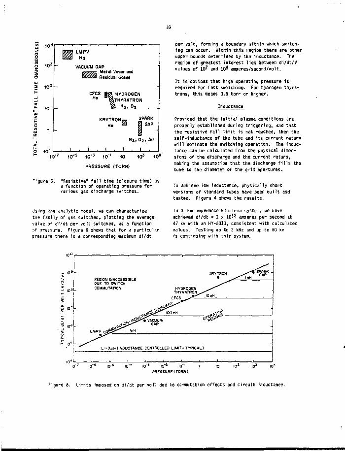
1 0 4
§uUiCO
o
IU
I -B>COIII
o
1 -
10'10"
LMPV
Hg
VACUUM GAPg ^ j A Metal Vapor andB2&2a Residual Gases
CFCSHe
I HYDROGENSTHYRATRON^ H a, 0 2
10"
PRESSURE {TORRJ
F'gure 5. "Resistive" fall time (closure time) asa function of operating pressure forvarious gas discharge switches.
Using the analytic model, we can characterizethe family of gas switches, plotting the averagevalue of di/dt per volt switched, as a functionof pressure. Figure 6 shows that for a particularpressure there is a corresponding maximum di/dt
per volt, forming a boundary within which switch-ing can occur. Within this region there are otherupper bounds determined by the inductance. Theregion of greatest, interest lies between di/dt/Vvalues of \<P and 10& amperes/second/volt.
It is obvious that high operating pressure isrequired for fast switching. For hydrogen thyra-trons, this means 0.6 torr or higher.
Inductance
Provided that the initial plasma conditions areproperly established during triggering, and thatthe resistive fall limit is not reached, then theself-inductance of the tube and its current returnwill dominate the switching operation. The induc-tance can be calculated from the physical dimen-sions of the discharge and the current return,making the assumption that the discharge fills thetube to the diameter of the grid apertures.
To achieve low inductance, physically shortversions of standard tubes have been built andtested. Figure 4 shows the results.
In a low impedance Blumlein system, we haveachieved di/dt = 1 x 10*2 amperes per second at47 kv with an HY-5313, consistent with calculatedvalues. Testing up to 2 kHz and up to SO kvis continuing with this system.
HEG10N INACCESSIBLEOUE TO SWITCHCOMMUTATION
= i0uH (INDUCTANCE CONTROLLED LIMIT-TYPICAL)
10"' 10"° I0"a 10 I0'3 10 10'PRESSURE(TOUR!
IOZ I03 10*
Figure 5. Limits Imposed on di/dt per volt due to commutation effects and circuit inductance.
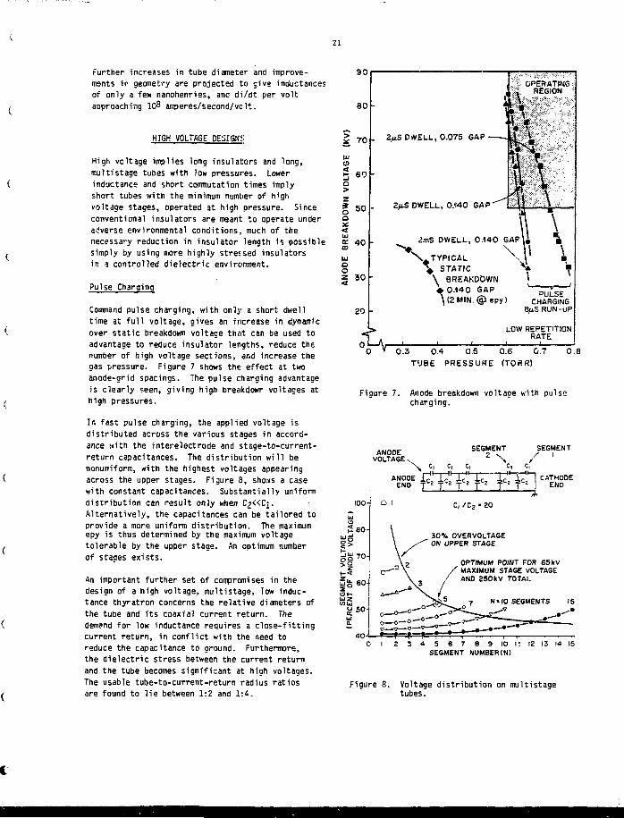
21
Further increases in tube diameter and improve-ments in geometry are projected to give inductancesof only a few nanohenries, and di/dt per voltapproaching 10^ amperes/second/volt.
HIGH VOLTAGE DESIGNS
High voltage implies long insulators and long,multistage tubes with low pressures. Lowerinductance and short commutation times implyshort tubes with the minimum number of highvoltage stages, operated at high pressure. Sinceconventional insulators are meant, to operate underadverse environmental conditions, much of thenecessary reduction in insulator length is possiblesimply by using more highly stressed insulatorsin u controlled dielectric environment.
Pulse Charging
Command pulse charging, with only a short dwelltime at full voltage, gives an increase in dynamicover static breakdown voltage that can be used toadvantage to reduce insulator lengths, reduce thenumber of high voltage sections, and increase thegas pressure. Figure 7 shows the effect at twoanode-grid spacings. The pulse charging advantageis clearly seen, giving high breakdowr voltages athigh pressures.
In fast pulse charging, the applied voltage isdistributed across the various stages in accord-ance with the interelectrode and stEge-to-current-return capacitances. The distribution will benonuniform, with the highest voltages appearingacross the upper stages. Figure 8, shows a casewith constant capacitances. Substantially uniformdistribution can result only when C2«C|.Alternatively, the capacitances can be tailored toprovide a more uniform distribution. The maximumepy is thus determined by the maximum voltagetolerable by the upper stage. An optimum numberof stages exists.
An important further set of compromises in thedesign of a high voltage, multistage, low induc-tance thyratron concerns the relative diameters ofthe tube and its coaxial current return. Thedemand for low inductance requires a close-fittingcurrent return, in conflict with the need toreduce the capacitance to ground. Furthermore,the dielectric stress between the current returnand the tube becomes significant at high voltages.The usable tube-to-current-return radius ratiosare found to lie between 1:2 and 1:4.
BO
ooz<
70
6 0
SO
40
30
. ZftS DWELL, 0.075 GAP
20
2/iS DWELL, 0.140 SAP
2mS DWELL, 0.140 GAP
\ :
TYPICALSTATIC
\ BREAKDOWN+ 0.140 GAP\(2MIN. @epy)
LOW REPETITIONRATE
0.3 0.4 0 5 0.6 C.7 0.8TUBE PRESSURE (TORR)
Figure 7. Anode breakdown voltage with pulseCharging.
ANOOEVOLTAGE ^
END
s
c, c.
EGMEIv
rCz :
T
C,
H
SEGMENT
/ '
r1""] CATHODE2 1 END
C, / C ? - 20
3 0 % OVERVOLTAGEON UPPER STAGE
OPTIMUM POINT FOR 65kVMAXIMUM STAGE VOLTAGEAND Z50kV TOTAL
0 1 2 3 4 5 6 7 B 9 10 I! 12 13 14 15SEGMENT NUMBER (N)
Figure 8. Voltage distribution on multistagetubes.
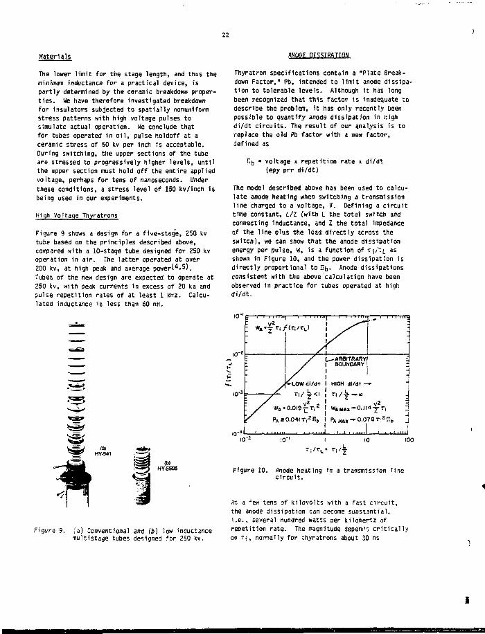
22
Materials ANODE DISSIPATION
The lower limit for the stage length, and thus theminimum inductance for a practical device, ispartly determined by the ceramic breakdown proper-ties. We have therefore investigated breakdownfor insulators subjected to spatially nonuniformstress patterns with high voltage pulses tosimulate actual operation. We conclude thatfor tubes operated in oil, pulse holdoff at aceramic stress of 50 kv per inch is acceptable.During switching, the upper sections of the tubeare stressed to progressively higher levels, untilthe upper section must hold off the entire appliedvoltage, perhaps for tens of nanoseconds. Underthese conditions, a stress level of 150 kv/inch isbeing used in our experiments.
High Voltage Thyratrons
Figure 9 shows a design for a five-stage, 250 kvtube based on the principles described above,compared with a 10-stage tube designed for 250 kvoperation in air. The latter operated at over200 kv, at high peak and average power(*'5).Tubes of the new design are expected to operate at250 kv, with peak currents in excess of 20 ka andpulse repetition rates of at least 1 kHz. Calcu-lated inductance is less than 60 nH.
*=*
l.=s.j (a)^ ^ HY-541
HY-5505
Thyratron specifications contain a "Plate Break-down Factor," Pb, intended to limit anode dissipa-tion to tolerable levels. Although it has longbeen recognized that this factor is inadequate todescribe the problem, it has only recently beenpossible to quantify anode dissipation in highdi/dt circuits. The result of our analysis is toreplace the old Pb factor with a new factor,defined as
Iljj •> voltage x repetition rate x di/dt(epy prr di/dt)
The model described above has been used to calcu-late anode heating when switching a transmissionline charged to a voltage, V. Defining a circuittime constant, L/Z (with I the total switch andconnecting inductance, and Z the total impedanceof the line plus the load directly across theswitch), we can show that the anode dissipationenergy per pulse, W, is a function of TJ/T|_ asshown in Figure 10, and the power dissipation isdirectly proportional to n D. Anode dissipationsconsistent with the above calculation have beenobserved in practice for tubes operated at highdi/dt.
Figure 9. (a) Conventional and (b) low inductancemultistage tubes designed for 250 kv.
IO
Figure 10. Anode heating in a transmission linecircuit.
At a few tens of kilovolts with a fast circuit,the anode dissipation can become substantial,i.e., several hundred watts per kilohertz ofrepetition rate. The magnitude depend', criticallyon Ti, normally for thyratrons about 30 ns
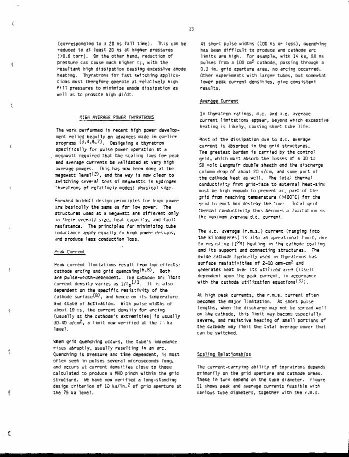
23
(corresponding to a 20 ns fall time). This can bereduced to at least 20 ns at higher pressures(>0.6 torr). On the other hand, reduction ofpressure can cause much higher T,, with theresultant high dissipation causing excessive anodeheating. Thyratrons for fast switching applica-tions must therefore operate at relatively highfill pressures to minimize anode dissipation aswell as to promote high di/dt.
HIGH A'/ERAGE POWER THYRATROKS
The work performed in recent high power develop-ment relied heavily on advances made in earlierprograms (3,4,6,7), Designing a thyratronspecifically for pulse power operation at a
. megawatt required that the scaling laws for peakand average currents be validated at very highaverage powers. This has now been done at themegawatt level(2), and the way is now clear toswitching several tens of megawatts in hydrogenthyratrons of relatively modest physical size.
Forward holdoff design principles for high powerare basically the same as for low power. Thestructures used at a megawatt are different onlyin their overall size, heat capacity, and faultresistance. The principles for minimizing tubeinductance apply equally to high power designs,and produce less conduction loss.
Peak Current
Peak current limitations result from two effects:cathode arcing and grid quenching(6»8). Bothare pulse-width-dependent. The cathode arc limitcurrent density varies as 1/tp^^. it i5 alsodependent on the specific resistivity of thecathode surfaced), and hence on its temperatureand state of activation. With pulse widths ofabout 10 us, the current density for arcing(usually at the cathode's extremities) is usually30-40 a/cm2, a limit now verified at the 7', kalevel.
When grid quenching occurs, the tube's impedancerises abruptly, usually resulting in an arc.Quenching is pressure and time dependent, is mostoften seen in pulses several microseconds long,and occurs at current densities close to thosecalculated to produce a HHD pinch within the gridstructure. We have now verified a long-standingdesign criterion of 10 ka/in.2 of grid aperture atthe 75 ka level.
At short pulse widths (100 ns or less), quenchinghas been difficult to produce and cathode arclimits are high. For example, with 14 ka, 50 nspulses from a 100 cm? cathode, passing through a0.3 in. grid aperture area, no arcing occurred.Other experiments with larger tubes, but somewhatlower peak current densities, give consistentresults.
Average Current
In thyratron ratings, d.c. and a.c. averagecurrent limitations appear, beyond which excessiveheating is likely, causing short tube life.
Most of the dissipation due to d.c. averagecurrent is absorbed in the grid structures.The greatest burden is carried by the controlgrid, which must absorb the losses of a 30 to50 volt Langmuir double sheath and the dischargecolumn drop of about 20 v/cm, and some part ofthe cathode heat as well. The totai thermalconductivity from grid-face to external heat-sinkmust be high enough to prevent arv part of thegrid from reaching temperature (>400°C) for thegrid to emit and destroy the tuDe. Total gridthermal conductivity thus becomes a limitation onthe maximum average d.c. current.
The a.c. average (r.m.s.) current (ranging intothe kiloamperes) is also an operational limit, dueto resistive (I^R) heating in the cathode coatingand its support and connecting structures. Theoxide cathode typically used in thyratrons hassurface resistivities of 2-10 ohm-cm' andgenerates heat over its utilized area (itselfdependent upon the peak current, in accordancewith the cathode utilization equations'3)).
At high peak currents, the r.m.s. current oftenbecomes the major limitation. At short pulselengths, when the discharge may not be spread wellon the cathode, this limit may become especiallysevere, and resistive heating of small portions ofthe cathode may limit the total average power thatcan be switched.
Scaling Relationships
The current-carrying ability of thyratrons dependsprimarily on the grid aperture and cathode areas.These in turn depend on the tube diameter. Figure11 shows peak and average currents feasible withvarious tube diameters, together with the r.m.s.
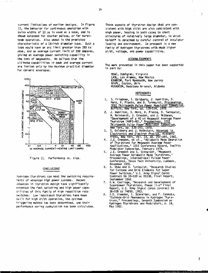
24
current limitations of earlier designs. In Figure11, the behavior for continuous operation withpulse widths of 10 us is used as a base, and isshown extended for shorter pulses, or for burst-mode operation. Also shown is the predictedcharacteristic of a 16-inch diameter tube. Such atube would have an arc limit greater than 350 kapeak, and an average current limit of 200 amperes,giving an average power switching capability inthe tens of megawatts. We believe that theultimate capabilities in peak and average currentare limited only by the maximum practical diameterfor ceramic envelopes.
lOOOr \
4001- \
O.I0.1 0.4 I 4 10 40 100 400
dc AVERAGE CURRENT-HEATING UMIT(AUPS)
Figure 11. Performance vs. size.
CONCLUSIONS
Hydrogen thyratrons can meet the switching require-ments of advanced high power systems. Recentadvances in thyratron design have significantlyextended the fast switching and high power capa-bilities of this family of high repetition rateswitches. Low inductance thyratrons have beenbuilt for high di/dt operation, the optimumtriggering method has been determined, and theirperformance during commutation has been calculated.
Those aspects of thyratron design that are con-sistent with high di/dt are also consistent withhigh power, leading in both cases to shortstructures of relatively large diameter, in whichholdoff is obtained by careful control of insulatorloading and environment. In prospect is a newfamily of hydrogen thyratrons with much higherdi/dt, voltage, and power capabilities.
ACKNOWLEDGMENTS
The work presented in this paper has been supportedin part by:
NSWC, Oahlgren, VirginiaLASL, Los Alamos, New MexicoERADCOM, Fort Monmouth, New JerseyAFAPL, Dayton, OhioMIRADCOM, Redstone Arsenal, Alabama
REFERENCES
1. S. Friedman, S. Goldberg, J. Hamilton, S.Merz, R. Plante, and D. Turnquist, Proceedings,IEEE Thirteenth Pulse Power Modulator S^poslum,Buffalo, New York, pp. 129-134, 1978.
Z. J. Hamilton, S. Merz, R. Plante, D. Turnquist,N. Reinhardt, J. Creedon, and J. McGowan,"Development of a 40 kV Megawatt Average PowerThyratron (HAPS-40)," Proceedinqst IEEEThirteenth Pulse Power Modulator Symposium,New York, pp. 135-143, 1978.
3. S. Goldberg and J. Rothstein, Advances inElectronics and Electron Physics, AcademicPress, New York, Vol. 14, pp. 207-264, 1961.
4. J.E. Creedon, et al., "Adiabatic Mode Operationof Thyratrons for Megawatt Average PowerApplications," IEEE Conference Record, TwelfthModulator Symposium, February 1976.
5. J.E. Creedon and S. Schneider, "MegawattAverage Power Adiabatic Mode Thyratrons,"Proceedings, International Pulsed PowerConference, Texas Tech University, Lubbock,November 1976.
6. A. Shea and D. Turnquist, "Research Studiesfor Cathode and Grid Elements for SuperPower Switchas," U.S. Army Sianal CorpsContract DA 39-039 sc 85338, Final Report,September 1962.
7. A.W. Coolidge, "Research and Development ofSuperpower Thyratrons, Phase II-o" FinalReport, U.S. Army Signal Corps Contract DA36-039 sc 74850, 1963.
3. J.E. Creedon, S. Schneider, and F. Cannata,"Cathode-Grid Phenomena in Hydrogen Thyra-trons," Proceedings, Seventh Symposium onHydrogen Thyratrons and Modulators, p. 16,May 1962.
25
P2.2
INVITED
ACCELERATOR MODULE OF "ANGARA - 5"
S.7. Basenkov, O.A. Gusev, Ju.A. Istomin, Ju.V. Koba, G.M. Latcsnizoi'aA.K. Pasechnikov, B.P. Pevchev, O.P. Pecherskii, A.S. Perlin
L.I. F.udakov, V.P. Smirnov, V.I. Chetvertkov, I.R. Jampol'skii
I.V. Kurchatov Institute of Atomic EnergyMoscow USSR
Abstract
Features and design principles of the inertial con-
finement fusion multi-module "Angara-5" accelerator
are considered.
The computed output parameters of an individual
module are as follows:
V >2MeV; I » 0.8 MA Tk = 90ns; W - 112 kj
The predicted output was compared with the pulse-
shaping line mock-up measurements. According to
these measurements the end-on section contributes
21 per cent of the total pulse-shaping line capaci-
tance. The end-on section capacitance was accounted
for in computations via transmission line sections
with appropriate impedance values. The reasonable
choice of the pulse-shaping equivalent circuit was
confirmed by experimental data and were in good
agreement with calculations based on system design
features.
AKGARA - 3. GENERAL DESIGN
The 10 - 10 s pulsed Relatlvistic Electron Beam
(REB) inertial confinement program fl] has recently
received new impetus due to the development of 10-
100 TH accelerators [2,3]. Target heating requir-
ments limit the diode voltage tD 2 - 4 MV such that
specific accelerators should have a low output iro-7 8
pedance and generate currents of 10 - 10 A.
The problems of developing a 100 TW.O.l Ohm accel-
erator were analyzed in 1974 [2]. The multi-module
type accelerator was found to present many advan-
tages . The total independence of modules and
module groups allows the opportunity for prelimi-
nary module development and test. It ensures over-
all facility safety in case one of the modules brea'.3
down. The facility shall consist of several tens of
identical modules such that it will be possible to
utilise already well developed 1-2 Ohm output ac-
celerator technology. The omission of one or a rev-
modules would result in an insignificant total
power decrease. So, in principle, experiments
should not be interrupted during repair and main-
tainence operations. These considerations have
caused the multi-module design of "Angara - 5" de-
veloped by the I.V. Kurchatov Institute of Atonic
Energy and the D.V. Efremov Institute of Electro-
Physical Apparatus.
The Angara-5 accelerator is designed for target
heating experiments using 48 REB generator modules.
The latter are located around the explosion chamber
in a two-floor structure with 24 modules on each
floor. The total beam energy is 4.B SI. The half-
width beam duration is 90 ns. The total beam cur-
rent is up to 40 MA with diode voltages up to Z MV.
Fig. 1 shows the general accelerator lay-out. Ther?
is a 6 m diameter explosion chamber in the center.
Tvo possible ways of transporting the PEB enerpy to
the central target surface inside the chamber are
being considered. The first is based upon vacuum
transmission lines, "hich may be disc-shaped. The
REB energy is transported along these disc-shaped
lines towards the diode in which the external tar-
Bet shell represents the anode. The required 10
W/cm energy flux along the line can be achieved at
aaZ • 4MV/cm average field inside the line which is
feasible due to the magnetic self-insulation [<i].
An alternative transport scheme would involve the
production of an inertially confined relativistic
26
electron sheath, the beam being injected into the
sheath making use of external cusp magnetic fields
[5].
ternally triggered. Transverse resistive couplings
are provided to improve the switching range of the
central condenser array.
The beam energy arrives at the explosion chamber
along magnetic self-insulation vacuum lines having
a 30 en diamecer and 3.5 m length. The line length
is determined by the high-voltage diode insulator
size (assuming a 60 kV/cm permissible surface elec-
tric field). The electric field in '.he vacuum line
is 2 MV/cm. The vacuum line imped.-.nce was calcu-
lated according Co the Brillouin electron flow in
the gap [6,7].
The high-voltage diodes are connected to pulse-
shaping Blumlein lines via water-insulated transmis-
sion lines. The transmission line diameter is 1.2m,
its length being 5 tn due to the Marx generator size.
The 2.5 m diameter water-filled Blumlein line has a
60 ns electric length (L » U ) and a 2 Ohm output
impedance. The Marx generator tank has a 3.2 m
diameter and transformer oil is used as insulation
in the Marx generator.
"ANGARA - 5" EXPERIMENTAL MODULE
Lee us consider in more detail the "Angara-5" ac-
celerator module. In order to lower the volcage
gradients along che dielectric diaphragms and across
the swicch gaps as well as to improve the operacion
reliability, it was decided to use a Bl:unlein type
pulse-shaping line. This choice has resulted in a
larger module diameter and somewhat more sophisti-
cated design. Fig. 2. presents a cross-section of
an experimental "ANGAKA-5" module, "his module has
been assembled at the 1.7. Kurchatov ~.Z.
The Marx generator 1 consists of three parallel
circuits. Each circuit consists of 14 stages.
Each stage contains four 0.4 uF, 100 kV condensers
connected in a parallel-series configuration and
•lr-e charged up to •*• 89 kV. The stages are placed
inside 2.4 3 diameter voltage-grading rings. Marx
generacor switching is achieved with field distor-
:ion =uitch-gaps pressurized with SF, at "- 2 kg/cm".
As che condensers are tighcly packed with a result-
ing bad stray capacicance racio, :he gaps are ex-
The Marx generator parameters are the following:
85.7 nF capacitance, 2.67 iW peak voltage, 305 kJ
scored energy. Fig. 3 shows the assembled Marr/
generator outside its container.
The Blumlein line 7 i3 charged via two conductors
3. The conductors pass through section 4, separat-
ing the Marx generator from the line. The dielec-
tric diaphragm electric fields are computed to be
up to 90 kV/cm. In order to use the volume of che
line in che optimum .manner che wave impedances of
che outer and inner lines were chosen different,
namely 0.82 and 1.36 Ohm. The intermediate elec-
rode thickness and end-on curvature radii were
chosen in accordance with compuced admissible elec-
tric fields in water. The computations were based
upop. che following relations [6] for fields 30% be-
low the breakdown limit .,.
E, - —nr; £-*r MV/cm: E - , ,,'—s~ST MV/cmcl/3 J3.06erf eff
1/3 0.06eff eff
The internal electrode diameter is 149 cm and the
intermediate electrode thickness ia 14.5 cm. This
high electrode-diameter over line-length ratio re-
sults in considerable edp j contribution co che co-
cal line capacitance. Mock-up measurements indicate
that the end-on sections contribute 21 per cent of
the 76.5 nF total line capacitance. The inner line
and outer line capacitances are 30 nF and 46 aF res-
lectively. The inner line is chareed via conductor
5 which servas to inductively Hecouple both lines,
•"he line is switched with 1(1 gas-filled triggered
switches 6 located at the inner line edge. The his-h-
volcase crisgering pulses are supplied via 10 cables
passing inside che conductor 5.
Prepulse is suppressed by a multi-channel gas-fill-
ed spark gap 8 following che 30 r.F capacitance line
section. The capacitance across che spark sap is
63 pF. The spark gap is followed by a 4.9 m lene
water transmission line 9 which serves as a crar.s-
former. The 50 nH inductance high-voltage diode
10 is of quasi-planar shape. The diode is followed
bv a magnetically self"insulated vacuum line 11.
Computations oi line charging and switching vere
performed to estimate the pulse shape, the effi-
ciency of energy transport from the Marx generator
to the load and the prepulse levelf the latter
being of importance for normal vacuum line and
diode operation. The SF- filled switch spark chan-
nel resistance was computed according the Bragin-
skii formula [9]KP
I I dt
(2)
The vacuum line load was assumed to correspond to
the minimal magnetic self-insulation current in the
flux limited regime at II = 2 MV. The validity of
the latter assumption follows from the practically
linear dependence upor voltage for rJ > 0.5 OT.
Fig. 4 presents the charging/switching scheme tak-
ing into consideration the above-cited module para-
meters. The charging computation tE.l-.-o into ac-
count the condenser resistivity which was calculat-
ed from the attenuation decrement near the lower
self-frequency of the circuit of K.g. 4.
The Marx generator-to-line energy transfer efficien-
cy was found to be up to 73%. The charging line
voltage is 2.4. MV. The voltage across the prepulse
spark gap is 200 kV. The diode prepulse is plotted
versus time in Fig. 5. The diode prepulse magni-
tude "u 200 V is low enough to allow the use of short
inter-electrode gaps.
The effect of edge sections was accounted for in
the calculations by introducing special line sec-
tions. Fig. 6 presents the computational section-
ing of the Blumlein line. The effective line length
was found from the relation
e =(3)
with p representing the wave impedance of the line.
The resistance and inductance of the Blumlein line
s,jark gaps were computed according to the Bragin-
skii formula. The number of spark channels in each
spark gap was varied in the calculations. The COE-
puted pulse shape of Fig. 7 was compared with line
mock-up measurements. The mock-up switching re-
sistivity was chosen equal to that of spark gaps
100 ns after triggering. The good agreement between
computation and measurement has corroborated the
reasonable choice of the pulse-shaping scheme. The
main result of computations are pulst lengths up
to 90 ns and pulse power modification due to edge
capacitance eff.ects.
Fig. 8 presents the computed pulse shape and diode
energy deposition for a 50 nH diode inductance.
Calculations show that the channel number should ex-
ceed 5 - 6 to limit losses in the spark gaps. A
further channel number increase does not substanti-
ally improve the pulse parameters.
So the " Angara-5 " module should be able to aro-
duce a U » 2 Ml1, I = 0.8 MA, T. « 90 ns. total ener-
sy per pulse (for t <_ 110 ns) Is 102 kj for a con-
stant ft, * 2.5 Ohm inroedance. The Marx generator -
to-beam energy transfer efficiency is 33 per cent.
References
1. L. I. Rudakov, S. A. Samarskii., VI European Conf.on Controlled Nuclear Fusion and Plasmas Physics.Moscow 2,487 (1973).
2. E. P. Velikhov, V. A. Glukhikh, 0. A. Gusev,G. K. Latmanizova, S. L. Nedoseev, 0. B. Ovchin-nikov, A. M. Passechaikov, 0. P. Pecherskii,L. I. Rudakov, M. P. Svin'in, V. P. Smirnov,V. I. Chetvertkov, "Angara - 5 accelerator com-plex". Preprint D-0301, NIIEFA, Leningrad, 1976,(In Russian).
3. G. Yonas et al,7th Conf. on Plasma Physics andControlled Thermonuclear Research. CN-37-X3,Insbruck, Austria, 23-30 Aug., 1978.
4. E. I. Baranchikov, A. V. Gordeev, V. D. Koroiev,V. P. Smirnov. Zh.E.T.F. 75_, 2102. 1978 (InRussian).
5. E. I. Baranchikov, A. V. Gordeev, Ju. V. Koba,V. D. Koroiev, V. i. Penkina, L. I. Rudakov.V. P. Smirnov, A. D. Sukhov, E. Z. Tarumov. In-tern. Topical Conf. on Electron Beam Researchand Technology. November 3-5, 1975, Albuquerauev. 1,248, Sand. 76-5122, 1976.
6. E. I. Baranchikov et al. Reports to the Ail-tiaonConference on Thermonuclear Reactor EngineeringProblems, 2., Leningrad, NIIEFA Edition, 1977(In Russian).
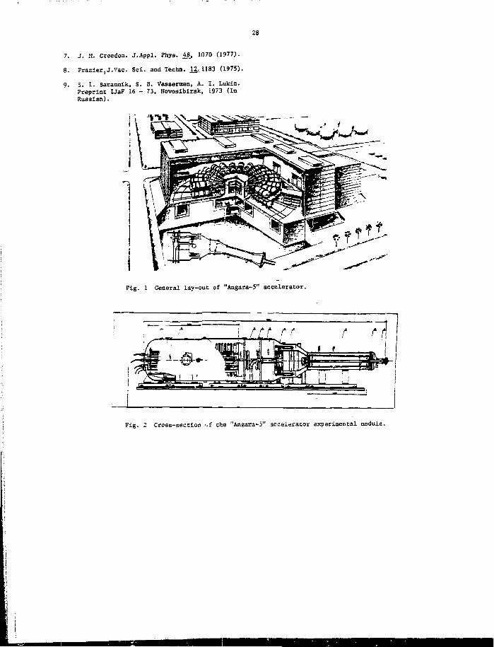
28
7. J. M. Creedon. J.Appl. Phys. 48, 1070 (1977).
8. Frazier,J.Vac. Sci. and Techn. 12- 1183 (1975).
g. 3. I. Barannik, S. B. Vassennan, A. I. Lukin.Preprint IJaF 16 - 73, Novosibirsk, 1973 (InRussian).
Fig. 1 General lay-out of "Angara-5" accelerator.
Fig. 2 Cross-section >jf Che "Angara-5" accelerator experimental nodule.
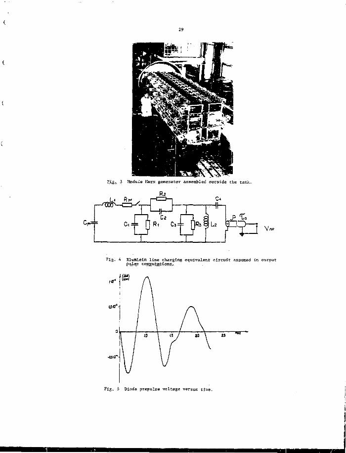
29
Fig.. 3 Module Marx generator assembled outside the tank.
7ig. 4 Blumlein line charging equivalent circuit assumed in outputpulse comaati
-as-sr
Fig. 5 Diode prepulse voltage versus time.
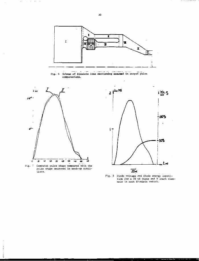
30
Fig. 6 Scheme of Blumlein line sectioning assumed in output pulse
computations.
Fig. 7 Computed pulse shape compared with thepulse shape xeasured in mock-up condi-tions.
Tig. 8 Diode voltage and diode energy deposi-tion for a 30 nK diode and 9 spark, chan-nels in each BJ.usU.ein switch.
31
P2.3
INVITED
REVIEW AND STATUS OF ANTARES*
Jorg oansen
University of California, LosLos Alamos.
Abstt actThe laser fusion effort at the Los Alamos
Scientific Laboratory (LASL) has evolved from
early experiments with an electron-beam-con-
troiled large-aperture COj laser to the massive
engineering task of designing and building a
100-kJ laser fusion machine.
The design of Antares is based on the design
of its predecessors. It builds upon technology
which was developed or advanced during the design
and construction of earlier machines. On one
hand it is dictated by the requirements for the
output, i.e., energy on target; on the other hand
it is limited by existing technology or reason-
able extensions thereof. Reliability and main-
tainability play important roles in the design
considerations.
Introduction
The goal of the Laser Fusion program is to
achieve inertia'ly confined fusion for commercial
and military applications. The high-power,
short-pulse COj laser developed at LASL lends
itself very well to this task because of the
high efficiency and capability to operate at
high repetition rates. The 100-kJ Antares
laser, the fourth step in the LASL development,
is designed to provide this laser power for
scientific breakeven experiments in J.984. This
paper gives a brief overview of the evolution,
design, and construction of Antares as a
background for a number of detailed papers
presented e'sewhere at this conference.
•Work performed under the auspices of the U.S.
Department of Energy
Alamos Scientific LaboratoryNH 87545
Evolution
As we are gradually getting more used to the
idea of very large C02 fusion lasers Antares be-
comes more tractable in its enormous size anc
complexity. Less than a decade ago the concept
of such a large machine would have been unthink-
able. However, development took place at a fast
pace and what seemed to be an unlikely adventure
then is now rapidly becoming a reality. The ev-
olution began, with the departure from the double-
discharge laser.
The double-discharge laser is the kind of de-
vice upon which one would not hesitate to base
the construction of a large reliable gas laser
facility. It is simple, rugged, inexpensive, and
easy to operate and maintain. Unfortunately, the
laser energy output and the maximum aperture of a
single cavity are relatively small. The size is
limited by a gap-pressure product of about 20-cm-
atmospheres compared to about 75-cm-atmospheres
for an electron-beam sustained CO^ laser. By
way of comparison, the Lumonics 620 can generate
a short pulse of <100 J with an aperture of
10 x 10 cm. Translated into the energy require-
ment of 100 kJ for Antares, this would mean a
system of 1000 beams and cavities. Such a large
number of components and subsystems makes the
facility reliability almost automatically
questionable.
One way to overcome this problem and provide
for a stable, large-aperture discharge is to feed
an externally generated electron beam into the
cavity. In this way, the generation of ionizing
electrons and the control of their energy and
density is separated from the parameters of the
cavity. To build and operate such an electron-
beam controlled COj laser was successfully
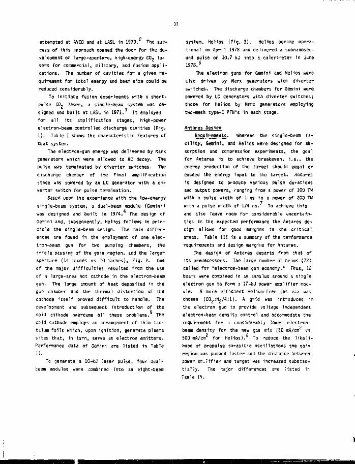
32
attemptsd at AVCO and at LASL in 1970. The suc-cess of this approach opened the door for the de-velopment of large-aperture, high-energy COj la-sers for commercial, military, and fusion appli-cations. The number of cavities for a given re-quirement for total energy and beam size could bereduced considerably.
To initiate fusion experiments with a short-pulse C02 laser, a single-beam system was de-signed and built at LASL in 1971.3 It employedfor all its amplification stages, high-powerelectron-beam controlled discharge cavities (Fig.1). Table I shows the characteristic features ofthat system.
The electron-gun energy was delivered by Marxgenerators wnich were allowed to RC decay. Thepulse was terminated by diverter switches. Thedischarge chamber of the final amplificationstage was powered by an LC generator with a di-verter switch for pulse termination.
Based upon the experience with the low-energysingle-beam system, a dual-beam module (Gemini)was designed and built in 1974. The design ofGemini and, subsequently, Helios follows in prin-ciple the single-beam design. The main differ-ences are found in the employment of one elec-t-on-faeam gun for two pumping chambers, thetriple passing of the gain region, and the largeraperture (14 inches vs 10 inches), Fig. 2. Oneof the major difficulties resulted from the useof a large-area hot cathode in the electron-beamgun. The large amount of heat deposited in thegun chamber and the thermal distortion of thecathode itself proved difficult to handle. Thedevelopment and subsequent introduction of thecold cathode overcame all these problems. Thecold cathode employs an arrangement of thin tan-talum foils which, upon ignition, generate plasmasites that, in turn, serve as electron emitters.Performance data of Gemini are listed in TableII.
To generate a 10-kJ laser pulse, four dual-beam radules were combined into an eight-beam
system, Helios (rig. 3). Helios became opera-tional in April 1978 and delivered a subnanosec-ond pulse of 10.7 kJ into a calorimeter in June1978.6
The electron guns for Gemini and Helios werealso driven by Marx generators with diverterswitches. The discharge chambers for Gemini werepowered by LC generators with diverter switches;those for Helios by Marx generators employingtwo-mesh type-C PFN's in each stage.
Antares DesignRequirements. Whereas the single-beam fa-
cility, Gemini, and Helios were designed for ab-sorption and compression experiments, the goalfor Antares is to achieve breakeven, i.e., theenergy production of the target should equal orexceed the energy input to the target. Antaresis designed to produce various pulse durationsand output powers, ranging from a power of 100 TWwith a pulse width of 1 ns to a power of 200 TWwith a pulse width of 1/4 ns. To achieve thisand also leave room for considerable uncertain-ties ir, the expected performance the Antares de-sign allows for good margins in the criticalareas. Table III is a summary of the performancerequirements and design margins for Antares.
The design of Antares departs from that ofits predecessors. The large number of beams (72)called for "electron-beam gun economy." Thus, 12beams were combined in an annulus around a singleelectron gun to form a 17-kJ power amplifier mod-ule. A more efficient Helium-free gas mix waschosen (COjiNj^:!). A grid was introduced inthe electron gun to provide voltage independentelectron-beam density control and accommodate therequirement for a considerably lower electron-beam density for the new gas mix (50 mA/cm' vs500 mA/cm2 for Helios).6 To -educe the likeli-hood of prepulse parasitic oscillations the gainregion was pumped faster and the distance betweenpower air,lifier and target was increased substan-tially. The ™jor differences are listed inTable IV.

33
TABLE I
CHARACTERISTIC FEATURES OF THE SINGLE-BEAK SYSTEM
Parameter
Electron Beam
Energy
Current
Current Density
GasPressure
Electric Field
Current
Current Density
Gain (P-20)
J/liter-atm
gn(J)EcEfficiency ,° *
Staqes 1 and 2
120 kV
100 A
0.12 A/cm2
600 torr
4.3 kV/cm-atm
5000 A
6.3 A/cm2
0.051 cm"1
15C
Stage 3
155 kV
500 A
0.60 A/cm2
1800 torr
3.8 kV/cm-atm
16000 A
20 A/cm2
0.049 cm"1
150
Stage 4
250 kV
1500 A
0.27 A/urn2
1400 torr
3.5 kV/cm-atm
50000 A
9 A/cm2
0.03 on"1
55
3.2X(x 1/5;
TABLE I I
PERFORMANCE DATA OF A HELIOS DUAL-BEAM MODULE
Optical Design (each beam)
Aperture
Gain Length
Operating Pressure
Gas Mixture
Gain
Energy Output
Electrical Design
Discharge Voltage
Discharge Current
Pulse Length
Energy
Electron-Beam Voltage
electron-Beam Current Density
Pulse Length
Emitter
34-cm diameter
200 cm
1800 torr
l/4:l:3/N2:C02:He
4S/cm (P-20, 10 um)
1250 J
300 kV
100 kA
3 ps
150 J/l-atm
250 kV
0.3 A/cm2
5.0 us
0.013-cm-thick Ta fio i l

34
TABLE III
ANTARES SPECIFICATIONS
100 kJ at Target X-ns pulse
50 kJ at Target 0.25-ns pulse
Power Amplifier Parameter
Mixture
Pressure
(g0 - «)«.Electrical Store
Optical Aperture
MAJOR
Chanqe
Design PointC02:N2/4:l
1800 torr
6.0
5.4 MJ
60,500 cm2
TABLE IV
DIFFERENCES BETWEEN ANTARES ANO HELIOS
Antares vs Helios
Design Margin
25X (2250 torr)
25S (7.5)
25* (7.2 MJ)
13%
Reason
Longer distance between
power amplifier and target
200 ft 20 ft Longer buildup time of
prepulse parasitics
Faster pumping to peak
gain
1.5 us 3 us Shorter time available for
build-up of parasitic oscil-
lation, higher efficiency
Different gas mix in
power amplifier
C02:N2 C02:N2:He4:1 4:1:12
Higher efficiency,no helium handling
Annular arrangement ofcavities around e-gun
Empioymen1" of currentcontrol grid in e-gun
Larger exit window diameter
Number of cavities per gun12 2
E-beam current density50 mA/cm2 0.5 A/cm2
18" 16"
Fewer guns, large annular
optics, fewer beams
Different gas mix requires
lower e-beam density,
better density control
Availability of larger
salt windows
Higher
Higher
discharge voltage
e-gun voltage
550
500
kV
kV
330
300
kV
kV
Gas mix with higher impedance
Gas mix with higher density
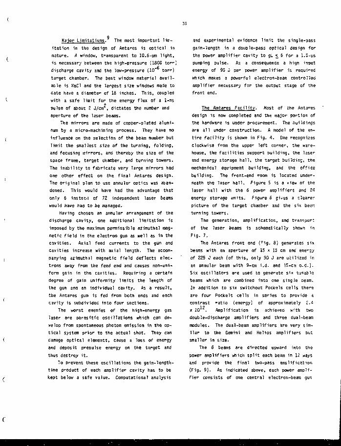
35
Major Limitations. The most important lim-
itation in the design of Antares is optical in
nature. A window, transparent to 10.6-vm light,
is necessary between the high-pressure (1800 torr)
discharge cavity and the low-pressure (10" torr)
target chamber. The best window material avail-
able is NaC7 and the largest size windows made to
date have a diameter of 18 inches. This, coupled
with a safe limit for the energy flux of a 1-ns
pulse of about 2 J/cm , dictates the number and
aperture of the laser beams.
The mirrors are made of copper-plated alumi-
num by a micro-machining process. They have no
influence on the selection of the beam number but
limit the smallest size of the turning, folding,
and focusing mirrors, and thereby the size of the
space frame, target chamber, and turning towers.
The inability to fabricate very Targe mirrors had
one other effect on the final Antares design.
The original plan to use annular optics was aban-
doned. This would have had the advantage that
only 6 instesJ of 72 independent lassr beams
would have haa to be managed.
Having chosen an annular arrangement of the
discharge cavity, one additional limitation is
imposed by the maximum permissible azimuthal mag-
netic field in the electron gun as well as in the
cavities. Axial feed currents to the gun and
cavities increase with axial length. The accom-
panying azimuthal magnetic field deflects elec-
trons away from the feed end and causes non-uni-
form gain in the cavities. Requiring a certain
degree of gain uniformity limits the length of
the gun and an individual cavity. As a result,
the Antares gun is fed from both ends and each
cavity is subdivided into four sections.
The worst enemies of the high-energy gas
laser are parasitic oscillations which can de-
velop from spontaneous photon emission in the op-
tical system prior to the actual shot. They can
damage optical elements, cause a loss of energy
and deposit prepulse energy on the target and
thus destroy it.
To prevent these oscillations the gain-length-
time product of each amplifier cavity has to be
kept below a safe value. Computational analysis
and experimental evidence limit the single-pass
gain-length in a double-pass optical design for
the power amplifier cavity to gi. < 6 for a 1.5-ys
pumping pulse. As a consequence a high input
energy of 90 0 per power amplifier is required
which makes a powerful electron-beam controlled
amplifier necessary for the output stage of the
front end.
The Antares Facility. Most of the Antares
design is now completed and the major portion of
the hardware is under procurement. The buildings
are all under construction. A model of the en-
tire facility is shown in Fig. 4. One recognizes
clockwise from the upper left corner, the ware-
house, the facilities support building, the laser
and energy storage hall, the target building, the
mechanical equipment building, and ths office
building. The front-end room is located under-
neath the laser hall. Figure 5 is a view of the
laser hall with the 6 power amplifiers and 24
energy storage units. Figure 6 gives a clearer
picture of the target chamber and the six beam
turning towers.
The generation, amplification, and transport
of the laser beams is schematically shown in
Fig. 7.
The Antares front end (Fig. 8) generates six
beams with an aperture of 15 x IS cm and energy
of 225 J each (of this, only 90 J are utilized in
an annular beam with 9-cm i.d. and 15-cm o.d.).
Six oscillators are used to generate six tunable
beams which are combined into one single beam.
In addition to six switchout Pockels cells there
are four Pockels cells in series to provide a
contrast ratio (energy) of approximately Z.4
x 10 . Amplification is achieved with two
double-discharge amplifiers and three dual-beam
modules. The dual-beam amplifiers are very sim-
ilar to the Gemini and Helios amplifiers but
smaller in size.
The 6 beams are directed upward into the
power amplifiers which split each beam in 12 ways
and provide the final two-pass amplification
(Fig. 9). As indicated above, each power ampli-
fier consists of one central electron-beam gur,
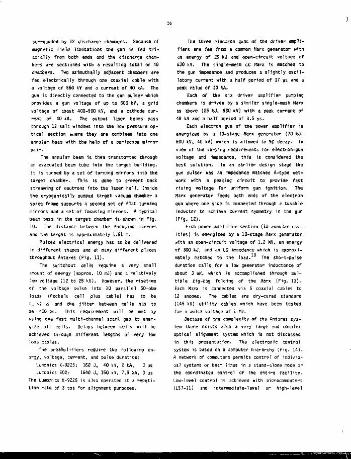
36
surrounded by 12 discharge chambers. Because ofmagnetic fieJd limitations the gun is fed tri-axially from both ends and the discharge cham-bers are sectioned with a resulting total of 48chambers. Two azimuthally adjacent chambers arefed electrically through one coaxial cable witha voltage of 550 kV and a current of 40 kA. Thegun is directly connected to the gun pulser whichprovides a gun voltage of up to 600 kV, a gridvoltage of about 400-500 kV, and a cathode cur-rent of 40 JcA. The output laser beams passthrough 12 salt windows into the low pressure op-tical section w.iere they are combined into oneannular beam with the help of a periscope mirrorpair.
The annular beam is then transported throughan evacuated beam tube into the target building.It is turned by a set of turning mirrors into thetarget chamber. This is done to prevent backstreaming of neutrons into the laser hall. Insidethe cryogenically pumped target vacuum chamber aspace frame supports a second set of flat turningmirrors and a set of focusing mirrors. A typicalbeam pass in the target chamber is shown in Fig.10. The distance between the focusing mirrorsand the target is approximately 1.61 m.
Pulsed electrical energy has to be deliveredin different shapes and at many different placesthroughout Antares (Fig. 11).
The switchout cells require a very smallamount of energy (approx. 10 mJ) and a relativelylow voltage (12 to 25 kV). However, the risetimeof the voltage pulse into 10 parallel 50-ohmloads (Pockels cell plus cable) has to betr •.; u$ and the jitter between cells has totie <50 ps. This requirement will be met byusing one fast multi-channel spark gap to ener-gize all cells. Delays between cells will beachieved through different lengths of very lowloss cables.
The sreamplifiers require the following en-ergy, voltage, current, and pulse duration:
Lumonics K-9225: 160 J, 40 fcV. Z kA, 3 ysLumonics 602: 1640 0, 150 kV, 7.5 kA, 3 us
The Lumonics K-9225 is also operated at a repeti-tion rate of 3 DPS for alignment purposes.
The three electron guns of the driver ampli-fiers are fed from a common Marx generator withan energy of 25 kJ and open-circuit voltage of630 kV. The single-mesh L.C Marx is matched tothe gun impedance and produces a slightly oscil-latory current with a half period of 17 us and apeak value of 10 kA.
Each of the six driver amplifier pumpingchambers is driven by a similar single-mesh Marxas above (25 kJ, 630 kV) with a peak current of48 kA and a half period of 3.5 us.
Each electron gun of the power amplifier isenergized by a 10-stage Marx generator (70 k«j,600 kV, 40 kA) which is allowed to RC decay. Inview of the varying requirements for electron-gunvoltage and impedance, this is considered thebest solution. In an earlier design stage thegun pulser was an impedance matched A-type net-work with a peaking circuit to provide fastrising voltage for uniform gun ignition. TheMarx generator feeds both ends of the elextrongun where one side is connected through a tunableinductor to achieve current symmetry in the gun(Fig. 12).
Each power amplifier section (12 annular cav-ities) is energized by a 10-stage Marx generatorwith an open-circuit voltage of 1.2 MV, an energyof 300 kJ, and an LC impedance which is approxi-mately matched to the load. The short-pulseduration calls for a low generator inductance ofabout 3 yH, which is accomplished through mul-tiple zig-zag folding of the Marx (Fig. 13).Each Marx is connected via 6 coaxial cables to12 anodes. The cables are dry-cured standard(145 kV) utility cables which have been testedfor a pulse voltage of 1 MV.
Because of the complexity of the Antares sys-tem there exists also a very large and complexoptical alignment system which is not discussedin this presentation. The electronic controlsystem is based on a computer hierarchy (Fig. 14).A network of computers permits control of individ-ual systems or beam lines in a stand-alone node orthe coordinated control of the entire facility.Low-level control is achieved with microcomputers(LSJ-ll) and intermediate-level or high-level

37
control with minicomputers (PDP-11/34, 60 and 70).To avoid the typical problems of transient inter-ference in a high pulsed electro-magnetic environ-ment all computers and computer interfaces areheavily shielded and all sijnal transmission takesplace via fiber optic cables. A typical fiber-optic link is shown in Fig. 15. It consists of asignal generator (Pearson current transformer},an electro-optic converter, the fiber-optic cable,and an opto-electric converter.
Status of the flntares Construction. The An-tares schedule (Fig. 16) as part of the overallinertia! confinement fusion plan foresees that theAntares facility will become operational and readyfor target experiments in the spring of 1984.
As a first step towards this goal the firstbeam line (of six) will be completed and checkedout in the fall of 1981. The major milestones inthis effort are:• Power amplifier and
energy storage system installed April '80• Electrical and small-signal August '80
tests complete• Single-beam front-end ready November '80• Single-sector energy extraction February '81• 12 sector energy extraction April '81• 17 kj/l ns pulse centered October '81
and focused
All Antares buildings are now fully enclosedand internal work is progressing. Figure 17shows the target hall with its 6-ft-thick wallsand 5-ft-thick ceiling. The laser hall and thefront-end room will be available for joint occu-pancy in August 1979. It is presently antici-pated that all buildings will be complete andready for occupancy by LASL in December 1979.
Most of the components and systems develop-ment and 752 of the design are complete. Allmajor hardware for the first beamline has beenprocured and will begin to arrive at LASL inJune. A pumping chamber section is shown inFig. 18. The output amplifier for the front endwill be tested at LASL starting in July. Theperformance test of the first energy storage unit
will begin in July. Half of the control compo-nents network is on hand and is being used forsoftware development. The electron-beam gun(Fig. 19) will be assembled and readied for testin August. Installation of the gigantic targetvacuum system (beam tubes and chamber) will beginin August.
References1. W. T. Leland, "Design Engineering of Large
High-Pressure Gas Laser Amplifiers," SPIH,Vol. 138, Advances in Laser Technology,pp. 39-45 (1978).
2. C. Fenstermacher, et al. Bull. Am. Phys. Soc.16, 12 (1971);Daugherty, et al, Bull. Am. Phys. Soc. 17,399 (1972).
3. T. F. Stratton, "C02 Short Pulse LaserTechnology," in High-power Gas Lasers, 1975,E. R. Pike, Ed. (The Institute of Physics,London, England, 1976), pp. 284-311.
4. S. Singer, J. S. Parker, M. 0. Nutter, "ColdCathode Electron Guns in the LASL High-PowerShort-Pulse COj Laser Program," Int. Top.Conference on Electron-Beam R&D, pp. 274-292,Nov. 3-6, 1S75, Albuquerque, NM.
5. G. V. Loda, 0. A. Meskar, "RepetitivelyPulsed Electron-Beam Generators," Int. Top.Conference on Electron-8eam Research andDevelopment, pp. 252-272, Nov. 3-6, 1975,Albuquerque, NM.
6. J. Ladish, "Helios, a ZC-TW CO, Laser Fu-sion Facility," Laser '79 Opto-ElectronicsConference, Munich, Germany, July 2-6, 1979.
7. T. F. Sfatton, et al, "The LASL 100-leJ CO-Laser for ICF Research: Antares," in Iner-tia! Confinement Fusion Technical Pigest,Proc. Topical Meeting on Inertia! Confine-ment Fusion, San Diego, California, February7-9, 1978 (Optical Society of America, Wash-ington, DC, 1977), paper TuC7.
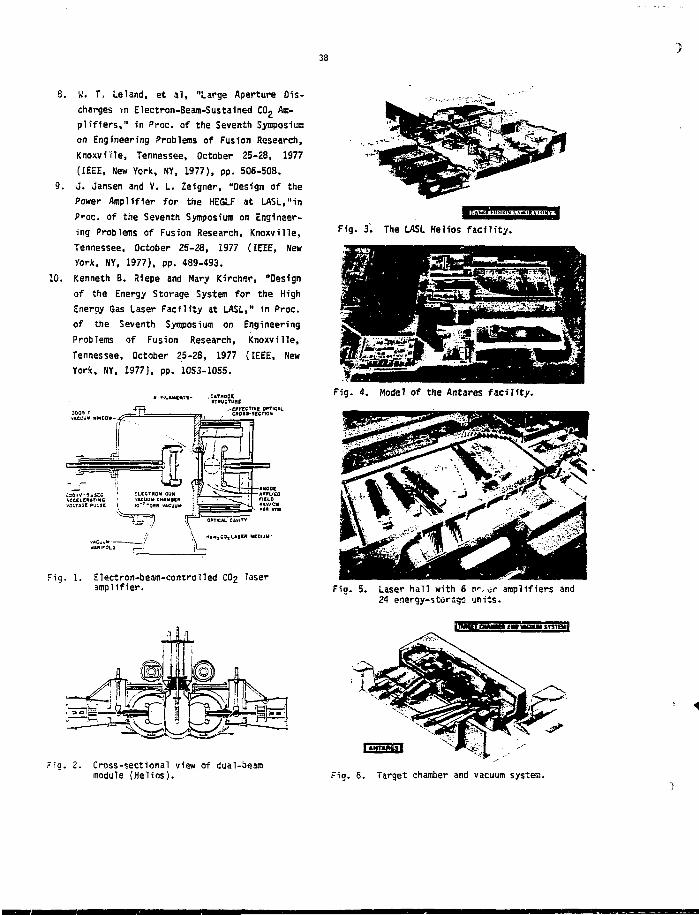
38
10.
W. T, Leland, et al, "Large Aperture Dis-
charges <n Electron-Beam-Sustained C02 Am-
plifiers," in Proc. of the Seventh Symposium
on Engineering Problems of Fusion Research,
Knoxviile, Tennessee, October 25-28, 1977
(IEEE, New York, NY, 1977), pp. 506-508.
J. Jansen and V. L. Zeigner, "Oesign of the
Power Amplifier for the HEGLF at LASL,"in
Proc. of the Seventh Symposium on Engineer-
ing Problems of Fusion Research, Knoxvilie,
Tennessee, October 25-28, 1977 (IEEE, New
York, NY, 1977), pp. 489-493.
Kenneth B. Riepe and Mary Kircher, "Design
of the Energy Storage System for the High
Energy Gas Laser Facility at LASL," in Proc.
of the Seventh Symposium on Engineering
Problems of Fusion Research, Knoxville,
Tennessee, October 25-28, 1977 (IEEE, New
York, NY, 1977), pp. 1053-1055.
IL*«I»TS~ - "TMOOI
Fig. 1. Electron-beam-controlled CO2 laseramplifier.
Fig. 3'. The LASL Helios facility.
Fig. 4. Model of the Antares facility.
Fig. 5. Laser hall with 6 t", ir amplifiers and24 energy-storags units.
Fig. 2. Cross-sectional view of dual-beammodule (Helios). Fig. 6. Target chamber and vacuum system.
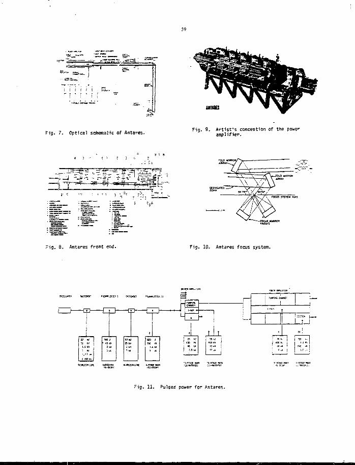
39
Fig. 7. Optical schematic of Antares.Fig. 9. Artist's conception of the power
amplifier.
FOCUS SYSTEM AXIS
:sri'E—s-
Fig. 8. Antares front end. F7g. 10- Antares focus system.
•ItCT W*L,rlt*
OSCULATOB iMlTOOtT *REJW*LtFTEE I MITCKOUT PREMTLlFlEK I I
40 kV2 kM
(
25 U630 W
4B t *3-5 UI
f !
IS kJSB tv
10 kA
" * • *
I
Fig. 11. Pulsed power for Antares.
40
Fig. 12. Symetric feeding of the electron-beamgun to reduce the azimuthal magneticfield.
Fig, 13. Low-inductance Marx configuration.
PDPII/M imtU
at-:'TIIIIMSI
(aits
Fig. i4. Antares control system implementation.
Fig. 15. Fiber-optic signal transmission link.
FTTT I Tm mi I f fBT fTII FTji; I f t M IFTM»9.7» ! SS.DM tloJM »IZ.OM j *'aQB I *fl.0W j jl.3M |
I VwnTJl lgTMt /
tiflf a y
sruSt»»WLCIi8 •' I 'i . n t !
i i i
! ! !
<rl*t-f tltULl IHU
I r » ,;:. I I I
Fig. 16. Antares sumiary schedule.
rig. 17. Facility construction, target buildingin foreground.
41
Fig. 18. Pumping chamber sections in production.Fig. 19. One of four sections of the electron-
beam-gun vacuum shell.
42
P3.1
INVITED
ELECTROMAGNETIC GUNS., LAUNCHERS AND REACTION ENGINES
Henry Kolm, Kevin Fine, Fred Williams and Peter Mongeau
Massachusetts Institute of Technology
Francis Bitter National Magnet Laboratory**
Cambridge, Massachusetts, 02139
Abstract
Recent advances in energy storage, switching andmagnet technology make electromagnetic accelerationa viable alternative to chemical propulsion for cer-tain tasks, and a means to perform other tasks notpreviously feasible. Launchers of interest includethe dc railgun driven by energy stored inertially ina homopolar generator and transferred through aswitching inductor, and the opposite extreme, thesynchronous mass driver energized by a high voltagealternator through an oscillating coil-capacitorcircuit. A number of hybrid variants between thesetwo extremes are also promising. A novel systemdescribed here is the momentum transformer whichtransfers momentum from a massive chemically drivenarmature to a much lighter, higher velocity projec-tile by magnetic flux compression. Potential appli-cations include the acceleration of gram-size par-ticles for hypervelocity research and for use as re-action engines in space transport; high velocity ar-tillery; stretcher-size tactical, supply and medicalevacuation vehicles; the launching of space cargoor nuclear waste in one-ton packets using off-peakelectric power.
Background
.Magnetic guns and launchers have received period-
ic attention for many years, and several large sys-
tems have actually been built. The "ace that none of
these evolved into a practical device reflects large-
ly the immaturity of required support technology and
iac:< of coordinated follow-up programs. The most
recent survey of the field was made by the Naval
'•/eaoons Laboratory in 1972, and the report contains
all significant prior references .
Since 1972 considerable attention has been devo-
ted to linear electric motors in the context of air
cushion and magnetically levitated high speed trains;
an extensive review published in 1975 contains over
ltd references'. Most early efforts utilized linear
Induction motors (LIMs) which do not lend themselves
to high acceleration. There evolved one concept,
nowever, the linear synchronous motor (LSM) first
proposed by Powell and Oanby and ultimately imple-4
mented by Kelm and Thornton at MIT; it is synthe-
tically synchronized and is capable of very high
acceleration, efficiency and speed. G.K.O'Neill of
Princeton University proposed using the LSM for
launching lunar raw materials into very precise or-
bits to permit interception at a space manufacturing
site , thus re-inventing a concept first proposed by
Arthur C. Clarke6 in 1950. O'Neill and Kolm devel-
oped the "mass driver" as part of two NASA-AMES sum-
mer studies in 1976 and 1977, and a group of students
constructed the first demonstration model at MIT.
It was exhibited at the 1977 Princeton Symposium ono
Space Manufacturing and also on the occasion of the
first flight of the orbiter Enterprise in August 77.
A second, more sophisticated mass driver is presently
under construction at Princeton and MIT, with supp-
ort from NASA-Lewis^.
Another significant effort was made recently
by Marshall and Barber who used the world's larg-
est homopolar generator at the Australian National
University in Canberra to power a series of experi-
mental dc railguns. Their spectacular success might
not have been of much practical interest, had it not
been accompanied by eayally spectacular progress in
the design of practical pulse-rated homopolar gener-
ators by Woodson. We I don and others at the Universi-
ty of Texas in Austin . The group also invented a
new inertial energy storage device, the "compensated
alternator", or "compulsator" . There has also
been a great deal of other work in the area of ener-
gy storage in relation to requirements for ohmic
* Study supported by C.S.Army Armament Researchand Development Command, Dover HJ, under AROSrant No. DRAG 29-73-G-O147.
** Laboratory supported by the national Science
Foundation.

43
hsiatir.g of plasmas in toroidal fusion experiments,
l^isei—induced fusion, particle beam weapons research
and laser weapons research. Much of this work is
directly applicable to accelerators. Equally appli-
cable is work done in the development of large,
high-intensity magnet coils, superconducting as well
as normal, for MHD power generation and for solid
state research. The MIT National Magnet Laboratory
is a center of expertise in this area . Related
work which is doubly applicable is the development
of large superconducting ragnet systems for induc-1 15
tive energy storage at Los Alamos and Sandia .
In March 1977 Dr. Harry Fair, head of the Pro-
pulsion Technology Branch of the Army Research and
Development Command in Dover, N.J.. inquired whether
any of the MIT Magneplane or Mass Driver work might
have ordnance applications. It was immediately ob-
vious that the potential applications and related
concepts and technologies spanned such a vast range
as to require a nationally coordinated effort. Peter
Kemmey and Ted Gora of ARRADCOM were assigned to
the task of coordinating the effort within DOD, and
the present authors were funded to conduct a prelim-
inary study. In addition, we have assembled an inter-
agency steering committee and a technical advisory
panel to ensure liaison with other centers of exper-
tise.
Electromagnetic Accelerator Concepts
We are concerned here with linear motors which
are capable of very high acceleration. This exclu-
des at the outset the sizeable literature of linear
motors developed over the years for a variety of
purposes, including traverse curtain rods, conveyor
belts, solid waste separation, liquid metal pumps,
high speed ground transportation, and even certain
attempted launch devices. We shall characterize
the features and limitations of our basic arsenal of
accelerator concepts.
The Classic Railqun
The classic railgun is the simplest and also the
most high perfected accelerator. It consists of two
parallel rails connected to a source of dc current,
the projectile consisting of a short-circuit slide
propelled between the rails by the Lorentz force
F » BLl/2 newton, where B is the magnetic field in-
tensity between the rails in tesla, L is the length
of Chs current path through the slide, or rhe gap
between rails ;n meters, and I is the current in am-
peres. The factor of 1/2 accounts for the fact that
the field is B behind the slide but zero in front of
it, the average being B/2.
The classic railgun has been studied extensively
by Brast and Sawle of MB Associates in the mid-sixties
under NASA contract , and more recently by Marshall
and Barber using the world's largest homopolar gen-
erator at the Australian National University in Can-
ber-a; it is capable of storing 500 MJ. Railguns
can operate in two distinct modes. In the metallic
conduction mode, current flows through the sliding
projectile itself, and this mode has been demonstra-
ted to a performance level of about 1 kg mass and
2,000 g (20,000 m/s 1 acceleration by the switching
gun used in the Canberra installation to feed tne main
gun. Marshall and Barber found that if the ratlgun
is driven very hard, a plasma arc tends to bypass the
projectile, leaving it behind. By using a non-conduc-
ting lexan projectile and confining the arc behind it
they were able to achieve a performance level of 16
gram accelerated at 250,000 g along a 3 m barrel to a
final velocity of 5.9 km/s. As railguns are extrapol-
ated to large projectile sizes, the distinction brush
conduction mode and plasma mode is likely to vanish:
brush conduction will be supplemented by arc conduc-
tion as the limit of brush current is exceeded. The
practical limit of railgun performance in regard to
projectile size, acceleration, length and velocity
will have to be explored by progressive refinement of
material and engineering details, as in the case of
any new technology. The Canberra work has provided
sufficient information to justify the first attempt18
in this direction. Westinghouse, with support from
DKRPA, will construct a practical railgun system in-
cluding the first pulse-rated homopolar generator de-
signed with attention to overall weight. The objec-
tive is to demonstrate feasibility of accelerating a
0.33 kg (.73 pound) projectile to a velocity of 3 km/s
(3.8 ft/s), corresponding to a muzzle energy of i.5 MJ.
To a oreat extent, the practical limit of rail
guns will depend on acceptable cost and service li'e.
The problems relate to mechanical containment of tne
percussive expansion force which tends to blow the
rails apart, the electromagnetic analog of barrel
44
pressure in a chemical gun, with the important diff-
erence that the rail gun maintains more or less con-
stant pressure throughout the acceleration. Instead
of chemical corrosion, there is the destructive eff-
ect of high brush current density and the related
metai vapor arc. The body of knowledge available
from the study of brushes and circuit breakers does
not extend to the current densities and velocities
in question.
In addition to these limits, the classic railgun
also faces certain fundamental limits which are not
related to acceleration, but to maximum possible
length or maximum muzzle velocity. As a railgun is
lengthened, the resistance and inductance of the
rails eventually absorb a dominant fraction of the
energy. The effect is seen to begin at about five
meters in the Canberra tests. Increasing velocity
also causes an increasing back-emf. Current will
continue to flow, even if this emf exceeds the out-
put voltage of the homopolar generator, because the
intermediate storage inductor acts as a current
source. However, there is a practical limit to the
voltage which can be stood off by the gap between
rails, and this scales about linearly with size.
Thus there are two fundamental effects which limit
the amount of energy that can be transferred to the
projectile, regardless of how much is available.
Another shortcoming of the railgun is its inherent
Inefficiency. An appreciable amount of energy is
contained in the rail inductance at the instant the
projectile leaves, and this energy must be absorbed
by a muzzle blast suppressor. A fraction might con-
ceivable be returned to the homopolar generator.
There are several means for circumventing the limit-
ations of the classic railgun.
The Augmented Rail gun
The magnetic field between t:.e rail* can be aug-
mented by supplementary current which does not flow
through the sliding brushes. This current can be
carried by separate conductors flanking the rails
(which must be farther from the projectile), or it
;an be added to the rail current itself by simply
terminating the rails with a load resistor or induc-
tor at the muzzle to carry a fraction of the current.
The raiis themselves will obviously contribute more
field than auxiliary rails located farther away, but
the use of superconducting auxiliary rails might be
expedient in some applications. It should be noted
that railgun fields are much higher than the critical
fields of superconductors. Augmentation has the ob-
vious effect of reducing the amount of current flowing
through the brushes and the projectile, and thereby
the necessary conductor mass which must be accelera-
ted.
It should also be noted that the augmenting
field is twice as effective as the rail field itself.
The augmenting field prevails in front of the projec-
tile as well as behind it, thereby eliminating the
factor of 1/2 In the Lorentz force expression. This
fact is important inasmuch as it reduces to one half
the rail bursting force which must be contained for a
given acceleration.
Augmentation therefore ameliorates both the brush
current density limitation and the bursting force con-
tainment limitation of classic railguns.
The Segmented Railgun
The length limitation imposed by rail resistance
and rail unductance can b; circumvented by simply sub-
dividing a long railgun into short segments, each fed
by an independent local energy source. This will of
course involve certain commutation problems as the
projectile transitions between segments, but will per-
mit using part of the energy stored in each segment
to energize the subsequent segment. The segmented
railgun seems promising for launching large masses
such as aircraft at low acceleration. In very long
launchers, the use of multiple independent energy
supplies will have other advantages as well.
Mass Drwars
As mentioned in the introduction, the mass driver
is a direct adaptation of the linear synchronous no-
tor first conceived and developed as the MIT Megne-
plane system in 1970-75 , a high-speed magnetically
levitated train. The mass driver can be planar or
axial depending on requirements. The axial configui—
ation permits higher efficiency and is therefore
preferred for high acceleration, while the planar con-
figuration will accommodate payloads which need not
be cylindrical and may have any arbitrary shape.
In both cases, the payload is carried by a re-
useable vehicle, called the bucket, which is provided
with two superconducting coils carrying a persistent

current and guided without contact by repulsive eddy
currents induced by the bucket motion in an aluminum
guideway. The bucket is propelled by a series of
drive coils which are pulsed in synchronism as the
bucket passes by. The bucket operatss like a surf-
board riding the forward crest of a magnetic travel-
ling wave, the wave being generated by the drive
coils and synchronized by position sensors. Buckets
can be launched at repetition rates of 10 per second.
Each bucket releases its payioad at a precise speed,
is decelerated, and then returns to the starting
point on a return track to be reloaded and relaunched
Mass drivers can operate in the "push-only" mode
as in the case of Mass Driver One, or in the pull-
push mode of Mass Driver Two, now under construction,
in which each drive coil undergoes a complete sinus-
oidal oscillation by being connected synchronously
to a supply capacitor line. By tuning this cycle
to the effectiv e wavelength of the bucket it is
possible to achieve energy transfer efficiencies,
electric-to-mechanical, of better than 90 percent.
We should add that the bucket-to-payload ratio is
about unity, and that about half the bucket energy
is recoverable by regenerative braking.
For all practical purposes, mass drivers have no
velocity limit and no length limit. Acceleration has
been limited thus far by the current and voltage ca-
pacity of the SCRs used for switching. Using shelf
components, Mass Driver Two should achieve 500 to
1,000 g. If the SCR limitation is removed, by using
ignitrons, spark gaps, or direct contact switching,
performance will be limited by mechanical ar.d thermal
failure of the drive coils. Some preliminary calcu-
lations bsised on a four inch caliber mass driver
using aluminum bucket coils and copper drive coils
suggest an acceleration limit between 100,000 and
250,000 g. This is comparable to rail gun performance.
However, the failure mode of drive coils under fast
pulse conditions is a very complex subject requiring
experimental study.
All previous mass driver designs are based on a
bucket coil current density of 25 kA/cm of cable,
achieved in an operational model of the MIT iuagne-
plane. Superconductors should withstand up to four
times this current density at the low field intensity
and stored energy involved. It should also be point-
ed out that mass drivers do not necessarilyiequire
superconducting bucket coils. For periods of the
order of 0.i second it is actually possible to main-
tain higher current densities in normal conductors.
Maximum performance mass drivers are therefore likely
to utilize aluminum bucket coils, possibly precoolec
to liquid nitrogen temperature, fed by sliding brush-
es, and drive coils triggered by physical contact.
Of course this would eliminate the non-contac: advan-
tages.
A unique feature of mass drivers bears emphasis:
. although they are energized by capacitors, the cost-
liest, heaviest and bulkiest energy store known, each
capacitor is used hundreds or thousands of times dur-
ing each launch cycle by being connected to many drive
coils through feeder lines. This permits the use of
an efficient but slower intermediate energy store,
such as a compuisator or MHD generator.
The Helical Rail gun
The railgun is in essence a single-turn motor.
A multi-turn railgun would reduce the rail current
and the brush current by a factor equal to the numbs--
of turns. It therefore seems worth-while to study
a "helical railgun". In this hybrid device, the two
rails are surrounded by a simple helical barrel, and
the projectile or re-useable carrier is also helical.
The projectile is energized continuously by two Drush-
es sliding along the rails, and two or more additional
brushes on the projectile serve to energize and cornmu-
tate several windings of the helical barrel directly
in front of and/or behind the projectile. The heli-
cal railgun is in fact a cross between the railgun
and the mass driver.
Superconducting Slingshots
Accelerators based on mechanical energy storage
have not been used since the day of the bow and medie-
val catapult, with the exception of naval aircraft
launching. Mechanical energy storage devices are bulky,
heavy, and slow to release their energy. The advent
of practical superconducting magnets provides a gooc
mechanical storage mechanism, the ".uagnetic slingshot'.'
Consider a short superconducting solenoid which
is free to slide inside a long one. The travelling
solenoid will be either attracted to or reoelled from
the center : .' the long solenoid, depending on the
direction of relative magnetization. Either configur-
46
ation can serve as an electromagnetic slingshot.
In the attractive configuration, the travel I ing"sol-
enoid can serve as a payload-carrying shuttle bucket.
Released at the breach end of the barrel coil, it
will accelerate to the center, where it will release
its payload at maximum velocity, come to rest at the
muzzle, and then return empty to a position short
of its release point, from where it can be returned
to the release point by mechanical force, possibly
by a thermal cycle. This oscillation is inherently
loss-less, except for possible eddy currents induced
in nearby metal.
In the repulsive configuration, the travelling
solenoid will be moved by mechanical force from the
breach to a point just beyond the center of the
barrel. When released, it will be expelled from the
muzzle as parr, of the projectile. Velocities up to
several hundred m/s are attainable by slingshots.
The Superconducting Quench Gun
By successively quenching a line of adjacent
coaxial superconducting coils forming a gun barrel,
it is possible to generate a wave of magnetic field
gradient travelling at any desired speed. A travel-
ling superconducting coil can be made to ride this
wave like a surfboard. The device in fact repre-
sents a mass driver or linear synchronous motor in
which Che propulsion energy is stored directly in
the drive coils.
Impulse Accelerators
A brass washer placed on top of a vertically
oriented pulsed field coil is driven upward, acceler-
ated by eddy currents which tend to be 180° out of
phase with the inducing field pulse. The resulting
iiroulse has been used commercially since 1962 for
metal forming operations, for instance for swaging
cerminal fittings around aircraft control cables.
The process has certain applications for accelera-
tion. It can be made into a synchronous induction
xotor whose performance is limited by the thermal
inertia of the sliding member.
The Momentum Transformer
A novel concept described here for the first
time is what we shall call the "momentum transformer'.1
It makes use of a so-called "flux concentrator",
first studied by How I and at MIT Lincoln Laboratory
in I96019 A flux concentrator is simply a conduc-
ting cylinder with a funnelled bore, and at least one
radial slot extending from the Inside to the outside
surface. The cylinder is surrounded by a pulsed field
winding, preferably imbedded in a helical groove to
minimize hoop stresses. A fast pulsed current in the
winding induces an opposite Image current in the out-
er surface of theecylinder. Duo to the radial slot,
this induced current is forced to return along the
inner perimeter of the cylinder, thereby generating
a magnetic field in the funnelled bore. All of the
magnetic flux which would have filled the pulsed field
winding in the absence of the concentrator is thus
compressed into the central bore, resulting in a field
intensity which is higher than it would have been
by about the outside-to-inside cross section ratio.
The device was used at MIT for high field research
and also for industrial metal forming. In 1965,
Chapman used a flux concentrator with a tapered
bore for accelerating milligram metal spheres to
hypervelocities. Using a first stage explosive
flux compressor, Chapman managed to reach peak fields
in excess of 7 megagauss, starting with an initial
field jf only kO kilogauss.
The momentum transformer proposed here uses a
flux concentrator as the armature or sabot in a chem-
ically driven conventional gun. The bore of this
sabot is occupied by a much smaller projectile, for
instance a rod-shaped armor penetrator. Tha muzzle
end of the gun is a pulsed field winding imbedded in
a helical groove, which is excited with a current
pulse sufficiently slow to penetrate the barrel and
fill the bore with magnetic flux. When the sabot
enters this flux region so rapidly that the effective
penetration depth of the field is small, it compress-
es the flux into its inner bore, decelerates drastic-
ally, and expels the projectile contained in its bore
at a much higher velocity. ThQ device should have very
little recoil because the muzzle coil acts like a
muzzle brake, transferring much of the sabot momentum
to the barrel. The process can be multi-staged with
a series of nesting sabots.
Application to Hvpervelocity Research
The acceleration of milligram to grm size Del lets
to hypervelocities, i.e., 10 to 100 km/s, already has
a literature of three decades. Research areas include
nicrometeorite impact studies, equation-of-state re-
search, terminal ballistics, etc, A new application
of current interest involves the achievement of fus-
ion by pellet impact at several hundred km/s.
High Velocity Artillery
Projectiles in the range of ten grams to a kilo-
gram accelerated to 3 to 10 or 20 km/s have foresee-
able applications. The destruction of missiles in
space, where mass is at a premium is one obvious use.
Another is the possible interception of incoming
rounds by ships and armored vehicles. This requires
small projectiles travelling at speeds much greater
than the incoming round, capable of detonating, de-
forming, or just deflecting them. Plasma-driven
railguns already have the required capacility on a
laboratory basis. If incoming round interception can
be accomplished with good reliability, it will make
armored vehicles as obsolete as knights on horseback.
An armor penetrator fired at 3 km/s, twice pre-
sent speed, needs only to be about one fifth the size
to inflict equal damage. If in addition it can be
'Spelled with available diese! fuel, tanks can be
given five times present capability with drastically
reduced vulnerability. We are dealing here with en-
ergy pulses in the 1 to 3 HJ range, supplied by the
primary propulsion engine of the tank.
Stretcher-Size Logistic Supply gr.d Medical
Evacuation Vehicle
It is an irony of modern tactical warfare that
an armored advance can be supported with many tons
per minute of artillery, but not by a single gallon
of fuel or pound of food. Helicopters and parachutes
are too vulnerable for battlefield use, and the chem-
ical gun does not lend itself to logistic supply
applications. Electromagnetic launchers can fill
this need.
A 300 pound stretcher or supply module can be
launched from a 100-foot, truck-mounted ramp to 100
mph at 3-3 9 acceleration, using only 0.1A MJ of en-
ergy. It could easily be guided to a soft landing
by microwave or conventional ILS type guidance sys-
tem located at the destination point. The vehicle
would operate at high speed, low trajectory, be rela-
tively invulnerable and weather-independent, and sig-
nificantly less expensive and fuel-consumptive than
a helicopter. It could be built using available
technology.
Light Plane Launchers
It is interesting to study the generation of
STOL aircraft which could be designed by eliminating
the requirement of inordinate take-off thrust from op-
board engines.
Space Vehicle Launcher
The application of mass drivers for lunar launch-
ing and for use as reaction engines in oraital trans-
fer has already been studied extensively . However,
the possibility of electromagnetic earth-based launch-
ing, proposed by science fiction writers since the
forties, has never before been considered seriously.
On the basis of computer software developed by NASA
in connection with the Venus lander , it appears
quite practical.
A telephone-pole shaped vehicle 8 inches in dia-
meter and 20 feet in length, weighing 1.5 tonnes,
accelerated to 20 km/s at sea level would traverse
the 8 km atmosphere in half a second, emerging az 16
km/s, which is enough velocity to escape the sc'ar
system. It would lose 3 to 6 percent of its mass by
ablation of a carbon shield. Initial projectile ener-
gy would be 300 x 10 J, one third of which would be
lost in traversing the atmosphere.
The launch energy may seem formidable, but it
amounts to only 83 MW-hrs, which represents several
minutes of output by a large metropolitan utility
plart. The required launcher would be 20 km long at
1,000 g acceleration; it wouiri be only 2 km long, less
than a small airport runway, at 10,000 g, which should
be easily attainable. Such a launcher couid be in-
stalled on a hillside, or in a vertical hole maoe by
an oversize rotary well drilling rig.
One potential application is the disposal of nuc-
lear waste. 2,000 tons of waste will be generated
between 1980 jnd 2000. This waste could be launched
out of the solar system by using off-peak power from
a utility plant at a cost corresponding to only 2
cents per kw-hr of generated power which produced the
waste. Considering that the average cost of power
during the period will be 22 cents per kw-hr, this
waste disposal cost is very low.
Conclusions
Rotary motors have not yet approached the con-
ceptual or practical limits of their potential, even
after a century of intensive evolution. Fundamcr.-al

48
innovation still occurs under the stimulation of new
technology and new needs.
Linear motors have not been pursued to anywhere
near a comparable degree, although an appreciable
literature sxists. Linear motors might be on the
threshholti of an evolution comparable to the evolu-
tion of rotary motors. The above survey indicates
that there is no shortage of new concepts or uses.
What makes this field exciting is the advent of new
pulsed energy sources, and the challenging fact that
a motor of zero curvature is virtually free of all
Fundamental limitations on size, acceleration and
velocity.
References
1. Albert F. Riedl III, "Preliminary Investigationof an Electromagnetic! Gun", NHL Technical MoteNo. TH-E-10/72, July 1972, Naval Weapons Labora-tory, Dahlgren VA, 22448.
2. R.D.Thornton, "Magnetic Levitation and Propulsion1975", IEEE Trans, on Magnetics, Vol. MAG-11,No. 4, July 1975.
3. J.R.Powell and G.T.Danby, "The Linear Synchron-ous Motor and High Speed Ground Transport", 6thInternational Engergy Conversion Engineering Con-ference, Boston, MR, 1971.
4. H.H.Kolm and S.O.Thornton, "The Magneplane: Gui-ded Electromagnetic Flight", proc. 1972 AppliedSuperconductivity Conf., Annapolis.
5. 3.K.O'Neill, "The Colonization of Space", Phys-ics Today, Vol 27 Mo. 9 Sep 1974, pp. 32-40.
6. A.C.Clarke, "Electromagnetic Launching as a MajorContribution to Space Flight", JBIS, Vol. 9 No. 6IIov. 19S0.
7. The 1976 NASA-AMES OAST Summer Study on SpaceManufacturing with non-terrestrial Materials,published by AIAA as Progress in Astronautics andAeronautics, Space-Based Manufacturing from Mon-Terrestrial MateriaJs, Series Vol. 57, editor:M. Sumnerfield.
W.Arnold, S.Bowen, S.Cohen, K.Fine, D.KaplanH.Kolm, M.Kolm, J.Newman, G.K.O'Neill and W.Snow,"rtess Drivers", parts I, II and III, Proc. of theI9"7 MASA-AMES Summer Study:"Space Resources andSpace Settlements" NASA, SP-428, 1979, U.S.Govt.Printing office.
G.K.O'Neill and H.H.Xolm, "Mass Driver for LunarTransport and as a Reaction Engine", Jour, of theAstron. Sciences, Vol. 15, No. 4, Jan-Mar 197S.
3..<-O'Neill, "High Frontier", Astron. and Aaron.Mar. 1978, special issue on space industrializa-tion.
5. H.H.Koin, "3asic Mass Driver Reference Design"X.Fir.e "Basic M D Construction and Testing",3.K.O':ieill, "S4 D Reaction engine as Shuttleupper Stage", F.Chilton, "MD Theory and History",Proc. of the Third Princeton-AIAA 3ymp. on SpaceManufacturing, 1977, published by che AIAA.
9. U.Kula, K.Fine, P.Mongeau, F.Williams, W.Snow,G.K.O'Neill: three papers on Mass Driver Twoto appear in the Proceedings of the 4th PrincetonAIAA Symposium on Space Manufacturing, 1979, tobe published by the AIAA in late 1979.
10. S.C.Ra3hleigh and R.A.Marshall, "ElectromagneticAcceleration of Macxoparticles and a HypervelocityAcc-lerator", dissertation 1972, Dept. Engr. Phys.Australian Natl. tJniv., Canberra.
11. w.F.Weldon et al., "The Design, Fabrication andTesting of a S HI Homopolar Motor-Generator",Intematl. Conf. on Energy Storage, Compressionand Switching, Torino, Italy, Nov. 1974.
M.D.Origa et al, "Fundamental Limitations andTopological Considerations for Fast DischargingKoncpolar Machines", IEEE Trans, on Plasma Scien,Dec. 1975.
12. W.L.Gagnon at al, editors, "Compensated PulsedAlternator", Lawrence Livermore Lab., July 1978.
13. MUT Francis Sitter Natl. Magnet Lab, Annual Rep.July 1977 - June 1978", Cambridge MA, 02139;see also various technical reports.
14. J.D.Lindsay and D.M.Weldon, "Loss Measurements inSuperconducting Magnetic Energy Storage Coils",Report LA-6790-MS, Los Alamos Scien. Lab, LosAlamos MM May 1977.
15. M.Cowan et al., "Pulsar - a Flux Compression Stagefor Coal-Fired Power Plants", Proc. 6th Internatl.Cryogenic Engr. Conf., Grenoble, Franca, May 76,Published by IPC Science and Technology Press Ltd.Guildford, Surrey, England.
16. S.A.Nasar and I.3oldea, "Linear Motion ElectridMachines", Wiley, NY, 1976.
17. D.E.Brast and D.R.Sawle, "Feasibility Study forDevelopment of a Hypervelocity Gun", Final ReportNASA Contract NAS 8-11204, May 1965.
18. John Mole, Westinghouse Research Lab., PittsburghPA 15235, personal communication.
19. B.Howland and S.Foner, "Flux Concentrators", HighMagnetic Fields, H.Kolm, editor, Wiley NY, 1962.
20. R.I.Chapman, "Field Compression Accelerators",Proc. Conf. on Megagauss Field Generation by Sxplo-sives, Frascati, Italy, Sep. 1965 (Euratoml
21. Dr. Chul parK, NASA-AMES Research Center, MoffettField, CA, 94035; personal communication.
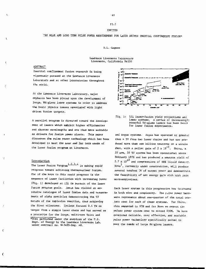
49
P3.2
INVITED
THE NEAR AND LONG TEEM PULSE POWER REQUIREMENT FOR LASER DRIVEN INERTIA! CONFINEMENT FUSION*
W.L. Gagnon
Lawrence Livermore LaboratoryLivennore, California 94550
ABSTRACT
Inertial confinement fusion research is being
vigorously pursued at the Lawrence Livermore
Laboratory and at other laboratories throughout
the world.
At the Lawrence Livennore Laboratory, major
emphasis has been placed upon the development of
large, Nd:glass laser systems in order to address
the basic physics issues associated with light
driven fusion targets.
A parallel program is directed toward the develop-
ment of lasers which exhibit higher efficiencies
and shorter wavelengths and are thus more suitable
as drivers for fusion power plants. This paper
discusses the pulse power technology which has been
developed to meet the near and far term needs of
the laser fusion program at Livermore.
Introduction
The Laser Fusion Program *"' ' is making rapid
progress toward achieving thermonuclear fusion.
One of the keys to this rapid progress is the
sequence of laser facilities with increasing power
(Fig. 1) developed at LLL in pursuit of the laser
fusion program goals. Janus has yielded an ex-
tensive catalogue of laser fusion data and ntasure-
raents of alpha particles demonstrating the IS
nature of the implosion reaction, thus achieving
the firs: milestone. Cyclops focused 0.6 TW on
target from a single laser chain and has served as
a prototype for the large, multi-arm Shiva and
*Work performed under the auspices of the U.S.Dept. of Energy by the Lawrence Livermore Lab.under contract no. W-7405-Eng. 48.
Fig. 1: LLL laser-fusion yield projections andlaser systems. A series of increasinglypowerful Nd:glass lasers has been builtfor laser fusion experiments.
and Argus systems. Argus has operated at greater
than 4 TW from two laser chains and has now pro-
duced more than one billion neutrons on a single
shot, with a pellet gain of 2 x IO~D. Shiva, a
20 arm, 20 TW system has been operational since
February 1978 and has produced a neutron yield of
2.7 x 10 and compressions of 50X liquid density.
Nova , currently under construction, will produce
several hundred TK of output power and demonstrate
the feasibility of net energy gain with high gain
microexplosions.
Each laser system in this progression has increased
in both size and complexity. The False power hard-
ware represents 3bout one-quarter of the total pro-
ject cost for each of these systems. For Shiva,
this anounted to S7M and for Nova we expect the
pulser power system cost to exceed S30M. We have
developed reliable, cost effective, and scalable
pulse power technology specifically suited to
meet the needs of large Nd:glass lasers.
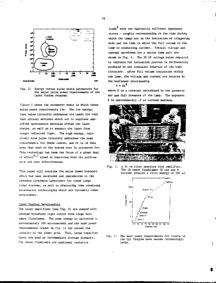
50
Fig. 2: Energy versus pulse width parameters forthe major pulse power requirements of thelaser fusion program.
Figure I shows the parameter space in which these
pulse power requirements lie. The low energy,
fast pulse circuitry addresses the needs for very
fast optical switches which act to suppress amp-
lified spontaneous emission within the laser
chains, as well as to protect the laser from
target reflected light. The high energy, rela-
tively slow pulse circuitry addresses the pump
requirements for these lasers, and it is in this
area chat most of the system cost is accounted for.
This technology has been the focus of a great deal
of effort ' aimed at improving both its perform-
ance and cost effectiveness.
This paper will describe the pulse power hardware
which has been developed and implemented at the
Lawrence Livernore Laboratory for these large
laser systems, as well as discussing some promising
alternative technologies which are currently under
develooment.
loads with two distinctly different impedance
states - roughly corresponding to the time during
which the lamps are in the ionization or triggering
mods and the time at which the full volume of the
lamp is conducting current. Typical voltage and
current waveforms for a aeries lamp pair are
shown in Fig. 5. The 35 kV voltage pulse required
to initiate the lonization process is deliberately
produced by the transient behavior of the bank
circuitry. After full volume ionization within
the lamp, the voltage and current are related by
the nonlinear relationship
V - KIB
where K is a constant determined by the geometry
and gas fill pressure of the lamp. The exponent
B is approximately .5 at current maximum.
Fig. 3: A 34 cm clear aperture disk amplifier.The 16 xenon flashlamps (8 top and 8bottom) require a total energy of 300 kj.
rElierqv MJ
Laser Pumping Reouirecent3
The laser amplifiers (see Fig. 3) are pumped with
intense broadband light output from large bore
xenon flashlamps. The pump energy is delivered ii
approximately 500 microseconds and the peak power
requirements (shown in Fig. i) far exceed the
capacity of Che power grid. Thus, large capacitor
banks are used as intermediate storage elements.
The :cenon flashlamps are nonlinear resistive
Fig. 1:
10 t-
f
' Cyclops
75 76 ?7 78 79 80 81 82 93Calendar vw i
The peak power requirements for lasers inche LLL Program have become increasinglylarge.
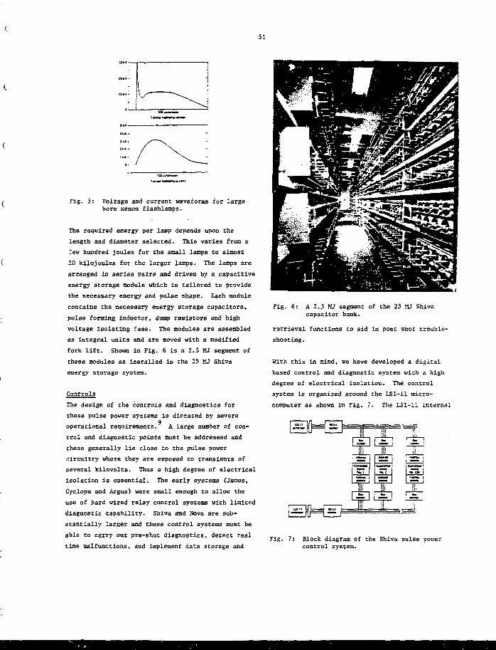
51
Fig. 5: Voltage and current waveforms for largebore xenon flashlamps.
The required energy per lamp depends upon the
length and diameter selected. This varies from a
.lev hundred joules for the small lamps to almost
20 kilojoules for the larger lamps. The lamps are
arranged in series pairs and driven by a capacitive
energy storage module which is tailored to provide
the necessary energy and pulse shape. Each module
contains the necessary energy storage capacitors,
pulse forming inductor, dump resistors and high
voltage isolating fuse. The modules are assembled
as integral units and are moved with a modified
fork lift. Shown in Fig. 6 is a 2.5 MJ segment of
these modules as installed in the 25 MJ Shiva
energy storage system.
Controls
The design of the controls and diagnostics for
these pulse power systems is dictated by severe9
operational requirements. A large number of con-
trol and diagnostic points must be addressed and
these generally lie close to tha pulse power
circuitry where they are exposed to transients of
several kilovolts. Thus a high degree of electrical
isolation is essential. The early systems (Janus,
Cyclops and Argus) uere small enough to allow the
use of hard wired relay control systems with limited
diagnostic capability. Shiva and Nova are sub-
stantially larger and these control systems must be
able to carry out pre-shot diagnostics, detect real
time malfunctions, and implement data storage and
Fig. 6: A2.5HJ segment of the 25 MJ Shivacapacitor bank.
ratrieval functions to aid in post shot trouble-
shooting.
With this in mind, we have developed a digital
based control and diagnostic system with a high
degree of electrical isolation. The control
system is organized around the LS1-11 micro-
computer as shown in Fig. 7. The LSI-11 internal
Fig. 7: Block diagram of the Shiva pulse pouercontrol system.
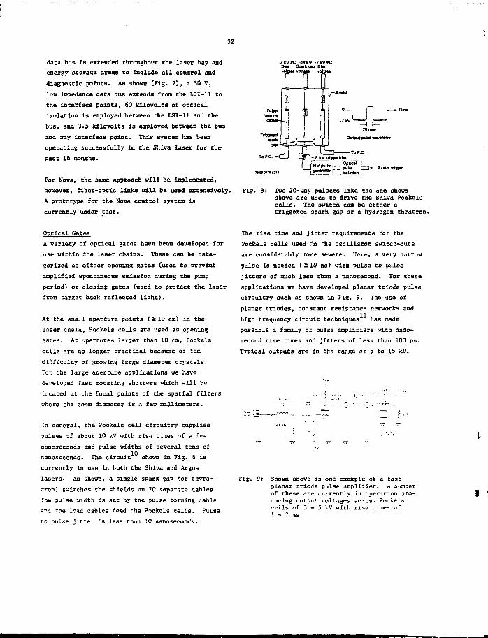
52
data, bus is extended throughout the laser bay and
energy storage areas to include all control and
diagnostic points. As shown (Fig. 7), a 30 V,
low impedance data bus extends from the LSI-11 to
the interface points, 60 kilovolts of optical
isolation is employed between the LSI-11 and the
bus, and 3.5 kilovolts is employed between the bus
and any interface point. This system has been
operating successfully in the Shiva laser for the
past IS months.
For Nova, the same approach will be implemented,
however, fiber-optic links will be used extensively.
A prototype for the Nova control system is
currently under test.
-7WPC ]«kV -7WPCSiM Spakgw Biaxunpvoli
Tri&ml
Fig. 8: Two 20-way pulsers like the one shownabove are used to drive the Shiva Pockelscells. The switch can be either atriggered spark gap or a hydrogen thratron.
Optical Gates
A variety of optical gates have been developed for
use within the laser chains. These can be cata-
gorized as either opening gates (used to prevent
amplified spontaneous emission during the pump
period) or closing gates (used to protect the laser
from target back reflected light).
At the small aperture points (£10 cm) in Che
laser chain, Pockels cells are used as opening
gates. At apertures larger than 10 cm, Fockels
cells are no longer practical because of ;he
difficulty of growing large diameter crystals.
For the large aperture applications we have
developed fast rotating shutters which will be
located at che focal points of the spatial filters
where the beam diameter is a few millimeters.
The rise time and jitter requirements for the
Pockels cells used in "he oscillator switch-outs
are considerably more severe. Here, a very narrow
pulse is needed (£ 10 ns) with pulse to pulse
jitters of much less than a nanosecond. For these
applications we have developed planar triode pulse
circuitry such as shown in Fig. 9. The use of
planar triodes, constant resistance networks and
high frequency circuit techniques has made
possible a family of pulse amplifiers with nano-
second rise times and jitters of less than 100 ps.
Typical outputs are in Ch3 range of 5 Co 15 kV.
In general, the Pockels cell circuitry supplies
pulses of about 10 kV with rise times of a few
nanoseconds and pulse widths of several tens of
nanoseconds. The circuit shown in Fig. 8 is
currently in use in both the Shiva and Argus
lasers. As shown, a single spark gap (or thyra-
cron) switches che shields on 20 separate cables.
The pulse width is set by the pulse forming cable
and che load cables feed the Pockels cells. Pulse
co pulse jitter is less Chan 10 nanoseconds.
Fig. 9: Shown above is one example of a fascplanar criode pulse amplifier. A numberof these are currently in operation pro-ducing output voltages across Pockeiscells of 3 - 5 kV with rise times of1 - : ns.
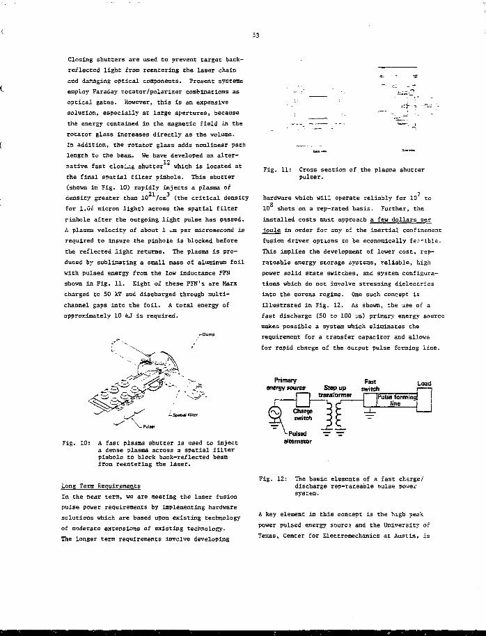
Closing shutters are used to prevent target back-
rezlected light from reentering the laser chain
and damaging optical components. Present systems
employ Faraday rotator/polarizer combinations as
optical gates. However, this is an expensive
solution, especially at large apertures, because
the energy contained in the magnetic field in the
rotator glass increases directly as the volume.
In addition, the rotator glass adds nonlinear path
length to the beam. We have developed an alter-
native fast closing shutter * which is located at
the final spatial filter pinhole. This shutter
(shown in Fig. 10) rapidly injects a plasma of21 3
density greater than 10 /cm (the critical density
for 1.06 micron light) across the spatial filter
rinhole after the outgoing light pulse has passed.
A plasma velocity of about 1 cm per microsecond is
required to insure the pinhole is blocked before
the reflected light returns. The plasma is pro-
duced by sublimating a saall mass of aluminum foil
v±th pulsed energy from the low inductance PFN
shown in Fig. 11. Eight of these PFN's are Marx
charged to 50 kV and discharged through multi-
channel gaps into the foil. A total energy of
approximately 10 kJ is required.
Fig. 10: A fast plasma shutter is used to injecta dense plasma across a spatial filterpinhole to block back-reflected beamfrom reentering the laser.
Long Term Requirements
In the near term, we are meeting the laser fusion
pulse power requirements by implementing hardware
solutions which are based upon existing technology
of moderate extensions of existing technology.
The longer term requirements involve developing
Fig. 11: Cross section of the plasma shutterpulser.
hardware which will operate reliably for 10' to
10 shots on a rep-rated basis. Further, the
installed costs must approach a few dollars per
.joule in order for any of the inertial confinement
fusion driver options to be economically fe^-ible.
This implies the development of lower cost, rep-
rateable energy storage systems, reliable, high
power solid state switches, and system configura-
tions which do not involve stressing dielectrics
into the corona regime. One such concept is
illustrated in Fig. 12. As shown, the use of a
fast discharge (50 to 100 us) primary energy source
makes possible a system which eliminates the
requirement for a transfer capacitor and allows
for rapid charge of the output pulse forming line.
Primaryenergy sou res Load
-PuiJBd — —alternator
Fig. 12: The basic elements of a fast charge/discharge rep-rateable oulse powefsvstem.
A key element in this concept is the high peek
power pulsed energy source and the University of
Texas, Center tor Electromechanics at Austin, is
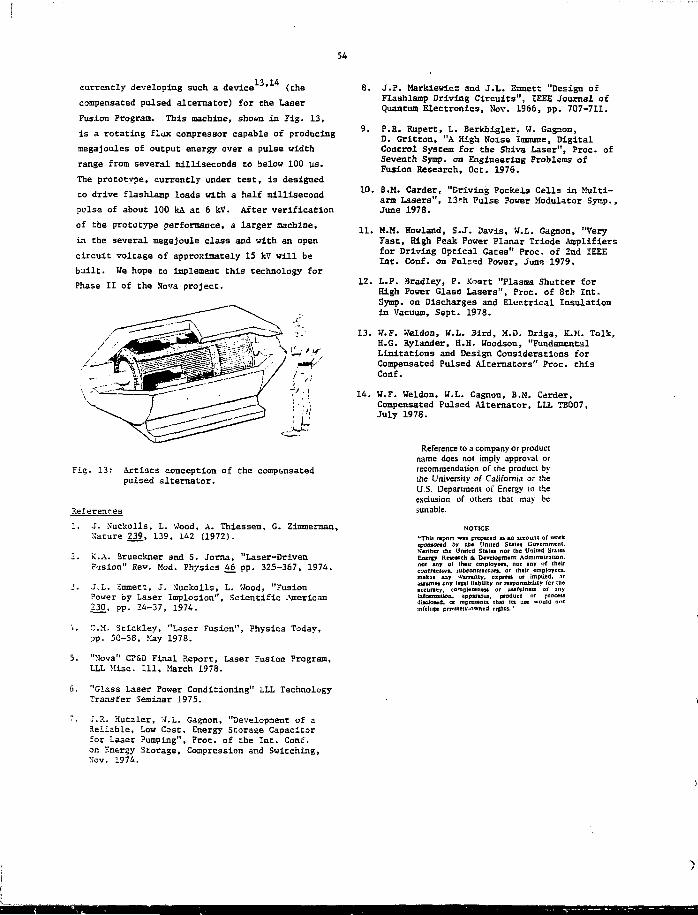
54
13 14currently developing such a device * (the
compensated pulsed alternator) for the Laser
Fusion Program. This machine, shown in Fig. 13,
is a rotating flax compressor capable of producing
megajoules of output energy over a pulse width
range from several milliseconds to below 100 us.
The prototype, currently under test, is designed
to drive flashlamp loads with a half millisecond
pulse of about 100 kA at 6 kV. After verification
of the prototype performance, a larger machine,
in the several megajoule class and with an open
circuit voltage of approximately IS kV will be
built. We hope to implement this technology for
Phase II of the Nova project.
Fig. 13: Artists conception of the compensatedpulsed alternator.
References
J. Kuckolls, L. Wood, A. Thiessen, G. Zimmerman,Mature £39, 139, 142 (1972).
K.A. 3rueckner and S. Jorna, "Laser-DrivenFusion" Rev. Mod. Physics 46 pp. 325-367, 1974.
J.L. Emmett, J. Nuckolls, L. Hood, "FusionPower by Laser Implosion", Scientific American230, pp. 24-37, 1974.
CM. Stickley, "Laser Fusion", Physics Today,?p. 50-58, May 1978.
"Nova" CP&D Final Report, Laser Fusion Program,LLL Misc. Ill, March 1978.
"Glass Laser Power Conditioning" LLL TechnologyTransfer Seminar 1975.
J.R. Hutzler, W.L. Gagnon, "Development of aReliable, Low Cost, Energy Storage Capacitortor Laser Pumping", Proc. of the Int. Coru.on Enfergy Storage, Compression and Switching,Nov. 1974.
3. J.P. Markiewicz and J.L. Emmett "Design ofFlashlamp Driving Circuits", IEEE Journal ofQuantum Electronics, Nov. 1966, pp. 707-711.
9. P.R. Rupert, L. Berkbigler, W. Gagnon,D. Gritton, "A High Noise Immune, DigitalControl System for the Shiva Laser", Proc. ofSeventh Symp. on Engineering Problems ofFusion Research, Oct. 1976.
10. B.M. Carder, "Driving Pockels Cells in Multi-ana Lasers", 13r-h Pulse Power Modulator Symp.,June 1978.
11. M.M. Howland, S.J. Davis, W.L. Gagnon, "VeryFast, High Peak Power Planar Triode Amplifiersfor Driving Optical Gates" Proc. of 2nd IEEEInt. Conf. on Pulsed Power, June 1979.
12. L.P. Sradley, P. Koert "Plasma Shutter forHigh Power Glass Lasers", Proc. of 8tb Int.Symp. on Discharges and Electrical Insulationin Vacuum, Sept. 1978.
13. W.F. Weldon, W.L. Bird, M.D. Driga, K.M. Tolk,H.G. Rylander, H.H. Woodson, "FundamentalLimitations and Design Considerations forCompensated Pulsed Alternators" Proc. thisConf.
14. W.F. Weldon, W.L. Gagnon, B.M. Carder,Compensated Pulsed Alternator, LLL TB007,July 1978.
Reference to a company or productname does not imply approval orrecommendation of the product bythe University of California or theU.S. Department of Energy to theexclusion of others that may besuitable.
NOTICE"This report was prepared as an account of worfcsponsored br tfct United Stales Government.Neither tlia United Statas nor the United statesEnergy Research &. Development Administration,nor any of their employees, nor any of theircontractor*, subcontractors, or their employees,makes any warranty, express or implied, Jrassumes any lefjJ liability or responsibility for theaccuracy, completeness or usefulness of anyinformation, apparatus, product or processdisclosed, or represents that its use would nntmfrinfe privately-owned rights."
55
?3.3
INVITED
Self-Magnetically Insulated Power Flow*
J. P. VanDevender
Sandia Laboratories, Albuquerque, New Mexico 87185
Abstract
Electromagnetic power transport through self-magnetically insulated vacuum transmission lineshas bees developed into a useful and reliabletechnology. A power density of 160 TW/m hasbeen transported at ~ 100 percent efficiency oversix meters. The theoretical understanding of powerflow through lines of constant cross section hasprogressed through analytical theory and 2-D elec-tromagnetic particle simulations. However, workneeds to be done on the effects of line transitionsin which the cross section changes in the directionof power flow. The major features of our presentunderstanding will be reviewed and some promisinghypotheses now under investigation will bepresented.
Introduction
High current particle beam accelerators forInertial Confinement Fusion must produce approxi-mately 30 to 100 TW of power and deliver it to theanode/cathode (A-K) gap at ~ 1 meter from thetarget. The limiting factor^ on acceleratorpower has been the allowable power flow through theinterface between vacuum and the liquid dielectricsin the pulse forming network. Several authorshave proposed using many separate vacuum interfacesin parallel and transporting the power to the A-Kgap through self-magnetically insulated transmis-sion lines (MITL). In ICF accelerators, the20-40 ns pulse width is less than or equal to thetwo way transit time through the vacuum line.Consequently, the power transport must be madeefficient without the benefit of choosing anoptimum load impedance to improve magnetic insula-tion. Self-magnetic insulation in these circum-stances is called the long line or short pulseproblem and has been the object of major researchand development efforts in the EBFA acceleratorprogram at Sandia Laboratories and the Angara Vprogram at Kurchatov Laboratory.
Experiments on the long line problem at severallaboratories '' showed net power transportefficiencies of ~ 60 percent through six to tenmeter long lines with negative inner conductors.The efficiency dropped to ~ 40 percent with thepositive inner conductor required for light ionacceleration.
*This work was supported by the U.S. Dept. ofEnergy, under Contract DE-AC04-76-DP00789.
Later experiments on the Mite accelerator, whichis one module of EBFA, revealed several lossmechanisms. When these mechanisms were avoided byredesigning the input into the MITL, the powertransport improved to ~ 100 percent with a negativsinner conductor. The results have been interpretedas a set of criteria for efficient self-aagneticinsulation. Positive polarity operation wasnot attempted at that time. In a subsequent setof experiments, which will be briefly discussedat the end of this paper, an injector convolutethat operated at ~ 100 percent efficiency in eiztierpolarity was developed and adopted for EBFA I.
In all of these experiments the most intrinsic losswas associated with the transition from the weaklystressed vacuum insulator to the highly stressedmagnetically insulated transmission line. Much ofour recent power flow research has been directedtowards elucidating the physics of chat lossmechanism. In this paper the basic phenomenaassociated with long self-magnetically insulatedpower transport will be reviewed, the elements ofour working hypothesis on the effects of convoluteswill be presented, and the Implications of thehypothesis on bi-polarity input convolutes will bediscussed.
Self-Magnetic Insulation in Vacuum Feed Lines ofUniform Cross Section
The self-magnetically insulated flow in a long MITLis established in the following steps as indicatedin Fig. la-Id. When a voltage is applied to cheparallel plate transmission line of impedance ZQ,a TEM wave propagates down the line as shown inFig. la. When the electric field in the Unereaches 25 to 40 MV/m, explosive emission occurson the cathode and a cathode plasma forms. A coat-ing of carbon that is ~ 2 x 10 m thick with asurface resistivity of ~ 10 H/sq facilitates theformation of a spatially uniform cathode plasma.The plasma becomes a space charge limited source ofelectrons which are initially accelerated across thegap by the electric field, as shown in Fig. 1b.When the magnetic field from the displacement cur-rent density "tf and the electron loss current densityT, becomes sufficiently large, the electrons behindthat point are prevented from reaching the anodeand are magnetically insulated as shown in Fig. lc.Since the conductance is greater than zero in theloss regjon, the region of loss propagates at avelocity' -10,13-16 l e s s t h a n c » 3 x io
8 m/s.Behind the lossy front, the pulse propagates at c.
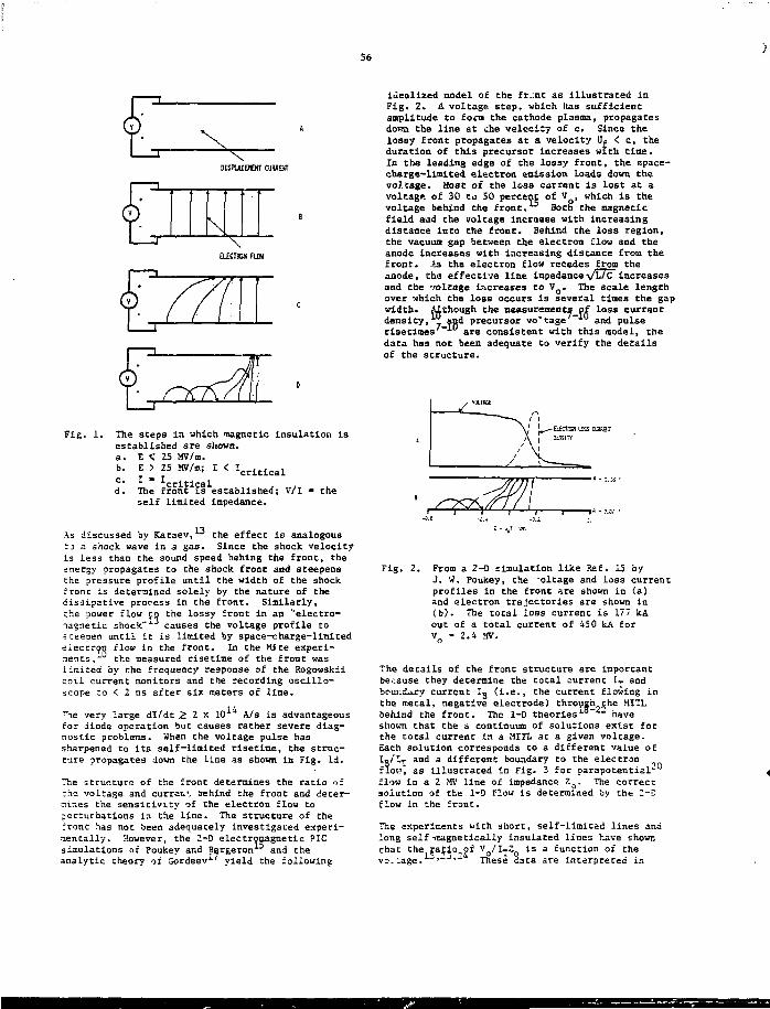
56
DISPUCEHENT CURJKT
Fig. 1. The seeps in which magnetic insulation isestablished are shown.
a. E < 25 MV/m.b. E > 25 MV/m; I < I,
d.1 * ^critical
'•critical
The front is established; 171
self limited impedance.the
As discussed by Kataev,^ the effect is analogoust j s shock wave in a gas. Since the shock velocityis less than Che sound speed behing the front, theenergy propagates to the shock front and steepensche pressure profile until the width of the shockfront; is determined solely by the nature of thedissipative process in Che front. Similarly,the power flow po Che lossy front in an "electro-magnetic shock" causes the voltage profile tosteepen until Ic is limited by space-charge-limitedaleccron flow in che front. In Che Mite experi-raenCG, che measured risetime of the front waslimited by the frequency response of the Rogouskiicoil current monitors and che recording oscillo-scope co < 2 ns after six meters of line.
~ne very large dl/dt Z 2 x 10* A/s is advantageoustor diode operation but causes rather severe diag-nostic problems. When the voltage pulse hassharpened to it3 self-limited risetime, the struc-ture propagates down the line as shown in Fig. Id.
The structure of the front determines the racio ofthe voltage and currer;-. oehind che fronc and decer-aines che sensitivicy of the electron flow toperturbations in the line. The structure of thefronc has not been adequately investigated experi-mentally. However, the 2-D electromagnetic PICsimulations of Poukey and Bergeron and theanalytic theory of Gordeev1-' yield che following
idealized model of the front as illustrated inFig. 2. & voltage step, which has sufficientamplitude to form the cathode plasma, propagatesdorei Che line at che velocity of c. Since thelossy front propagates at a velocity U* < c, theduration of this precursor increases with d m e .In the leading edge of the lossy front, the space-charge-limited electron emission loads down thevoltage. Host of the leas current is lost at avoleage of 30 to 50 percent of V which is thevoltage behind the front. Both che magneticfield and the voltage increase with Increasingdistance into the front. Behind the loss region,the vacuum gap between the electron flow and cheanode increases with increasing distance from thefront, .is the electron flow recedes from theanode, the effective line impedanceVL/C increasesand che voltage increases to V Q. The scale lengthover which the loss occurs is several times the gapwidth. Although che measurements of loss currentdensity, !: and precursor vo'tage and pulserisetlmes are consistent with this model, thedata has not been adequate to verify the decailsof the structure.
•ElfCTHM UXS CLMSIT
Fig. 2. From a 2-D simulation like Ref. 15 by
J. W. Poukey, the "oltage and loss currencprofiles in the fronc are shown in (a)and electron trajectories are shown in(b). The total loss currenc is 177 kAout of a total current of 450 kA forV_ - 2.4 MV.
The details of the front structure are importantbecause they determine che Cotal currenc I~ andboundary currenc I s (i.e., the current flowing inthe metal, negative electrode) through the MITLbehind the front. The 1-D theories haveshown that the a continuum of solutions exist forthe total current in a MITL at a given voltage.Each solution corresponds to a different value ofIo/Lj. and a different boundary to che electronflot-t as illustrated in Fig. 3 for parapotentialflow in a 2 MV line of impedance Z Q. The correctsolution of the 1-D flow is determined by the 2-Dflow in che front.
20
The experimencs wich short, self-limiced lines andlong self -nagnecically insulated lines have shownthat che ratio.of v 0/Lj2 Q is a function of chevD_:age. '~J'" These data are incerpreted in
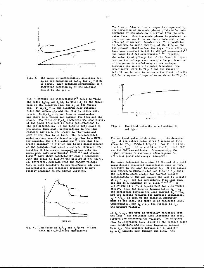
Fig. 3. The range of parapotential solutions forI T as are function of Lj./IB for VQ - 2 MVis shown. Each solution corresponds to adifferent position Xg of the electronsheath in the gap D.
Fig. 4 through the parapotential model to yieldthe ratio IB/IT and X /dQ in which Xe is the thick-ness of the electron rlow and d is the vacuumgap. If Xg/d « 1, the electron flow entirelyfills the vacuum gap and the flow is called satu-rated. If Xe/d0 < 1, the flow is unsaturatedand there is a vacuum gap between the flow and theanode. The ratio of Xe/dQ indicates the sensitivityof the power transport to snail perturbations inthe gap separation. If the flow is very close tothe anode, then small perturbations in the linegeometry may cause the sheath to fluctuate andpart of the flow to be lost. The parapotentialmodel nay not exactly describe the flow in a MITL,for example, the 2-D simulations show that thesheath boundary is diffuse and is not discontinuousas the parapotential model requires. However, thelocation of the sheath boundary agrees with themodel and, both experiments ' ' and simula-tions have shown sufficiently good a agreementwith the model to justify the utility of the model.We, therefore, conclude that the higher v'oltageMITL is less sensitive to gap tolerances and lineperturbations, and efficient transport is morereadily achieved at the higher voltages.
The loss problem at low voltages is compounded bythe formation oz an anode plasma produced by bom-bardment of the anode by electrons from the satu-rated flow. When the anode plasma is produced, anion loss current flows to the cathode and is noteffected by magnetic insulatior.. This conditionis followed by rapid shorting of the line as thetwo plasmas expand across the gap. These effectshave been observed in 200 to 400 keV experiments"'but .lever in 2 MeV experiments. Finally,the velocity of propagation of the front is deper.-dent on the voltage and, hence, a larger fractionof the pulse is eroded away at low voltage.Although the velocity is pulse dependent, theexperimental data in Fig. 4 and the theory inRef. 14 can be used to estimate the front velocitySfC for a square voltage pulse as shown in Fig. 5.
Fig. 4. The ratio of IT/IB and XE/D vs, V fromdata in st'lf-limited experiments.
Fig. 5. The front velocity as a function ofvoltage.
For an input pulse of duration i n, the duration7 of the output pulse aTter L meters of linewould be (Tin -hJ/«fc)(l/if-l). For rin - 40 r.s,L » 6 m, 7 t « 10 ns acd 34 ns for V » 0.2 MaVand 2.0 MeV respectively. Consequently, thehigher voltage is extremely advantageous forefficient power and energy transport.
The power delivered to a .load at the end or a self-magnetically insulated transmission line is verysensitive to the load impedance Z, . If the vacuumwave impedance without electron flow is ZQ, thenthe electron space charge and current densitydistribution in the gap causes the line to operateat Z^ » ZQ. For all conditions, <X j,s ],ess thanone and is a function of voltage. ' " • * At0.5 MV and at 2 MV, a equals 0.35 and 0.63 respec-tively. When the line is terminated in ZL > Z,the difference between the load current 1^ = V/Z^and the current required for magnetic insulation,lj « V/Zj, is lost to the positive conductornext to the load, and there is no reflected wave.Consequently, for Z, > Z^, the voltage is VQ,the matched voltagaf
If Z, < Z^, the wave is partially reflected fromthe load. The reflected wave increases the totalcurrent and decreases the voltage. The electronflow is compressed much closer to the cathode undersuch conditions and the line impedance becomesZ2 ~ Zo" ^ e l50un'lary between Z » Zj and Z =Z, » Z travels back through the line. The
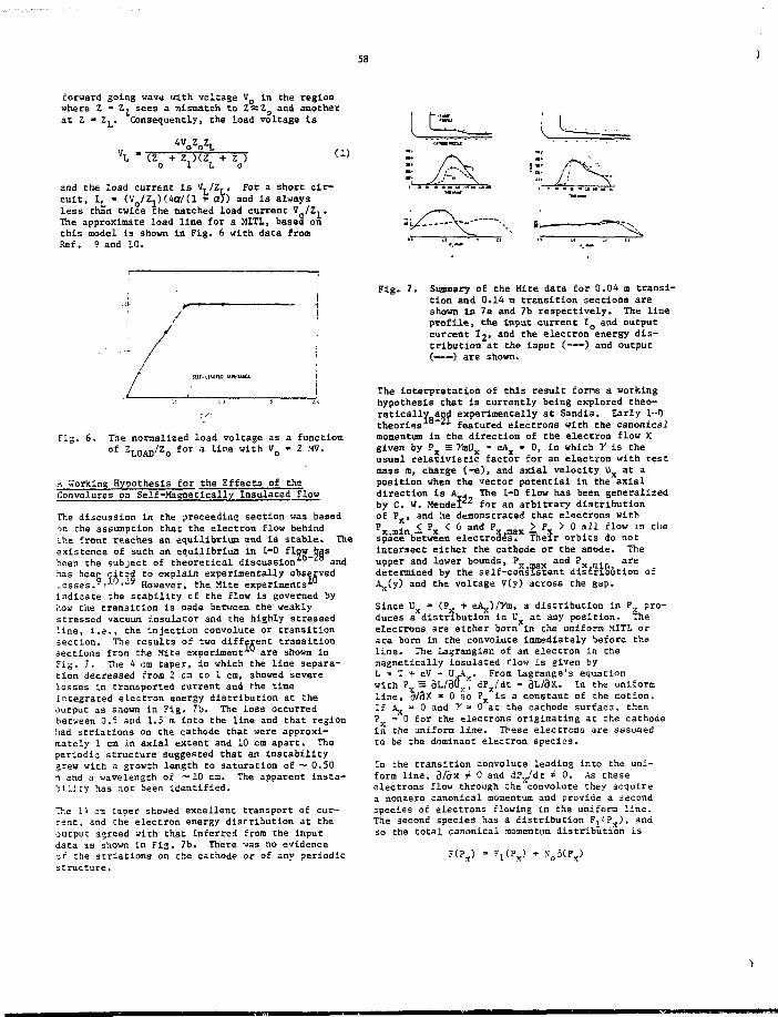
58
forward going wave with voltage VQ in the region^ sees a mismatch to Z«Z Q and anotherConsequently, the load voltage is
whereat Z Z^.
(Z Z,)(ZT1 L(1)
and Che load current is V./Z.. For a short cir-cuit, IL - (Vo/Z1)(Aa/(l * aj) and is alwaysless Chan twice the matched load current Vg/Z^.The approximate load line for a MITL, based onthis model Is shown in Fig. 6 with data fromRef. 9 and 10.
tz..
Fig. 7. Summary of the Mite data for 0.04 m transi-tion and 0.14 m trcnsition sections areshown In 7a and 7b respectively. The lineprofile, the input current IQ and outputcurrent I2. and the electron energy dis-tribution at the input ( ) and output( ) are shown.
SEU-UMITMIMMOAMCI
Fig. 6. The normalized load voltage as a function/ line with VQ - 2 MV.
A Working Hypothesis for the Effects of theConvolutes on Self-Magnetically Insulated Flow
The discussion in the preceeding section was basedon the assumption that the electron flow behindthe front reaches an equilibrium and is stable. Theexistence of such an equilibrium in 1-D fl»V hasbeen the subject of theoretical discussion andhas been cited to explain experimentally observedlosses.9>J-9>-9 However, the Mite experiments10
indicate the stability cE the clow is governed byhow the transition is made between the weaklystressed vacuum insulator and the highly stressedline, i.e., the injection convolute or transitionsection. The results of two different transitionsections from the Mice experiment are shown inFig. 7. The 4 cm taper, in which the line separa-tion decreased from 2 cm to 1 cm, showed severelosses in transported current and fhe timeintegrated electron energy distribution at theoutput as snown in Fig. 7b. The loss occurredbetween 0.5 and 1.5 m into the line and that regionhad striations on the cathode that were approxi-mately 1 cm in axial extent and 10 cm apart. Theperiodic structure suggested that an instabilitygrew with a growth length to saturation of — 0.50n and a wavelength of ~10 cm. The apparent insta-bility has not been identified.
The li c:3 caper showed excellent transport of cur-rent, and the electron energy disrribution at theoutput agreed with that inferred from the inputdata as shown in Fig. 7b. There 'Jas no evidenceof ;he striations on the cathode or of any periodicstructure.
The interpretation of this result fonts a workinghypothesis that is currently being explored theo-retically and experimentally at Sandia. Early 1--Dtheories1 21 featured electrons with the canonicalmomentum in the direction of the electron flow Xgiven by Px = y<sUx - eAx » 0, in which Y is theusual relatlvistic factor for an electron with testmags m, charge (-e), and axial velocity Ux at aposition when the vector potential in the'axialdirection is A . The 1-D flow has been generalizedby C. W. Mendel22 for an arbitrary distributionof P , and he demonstrated that electrons withPx,min < px < V n d px,max > px > ° « " « » " la cl'espace between electrodes. Their orbits do notintersect either the cathode or the anode. Theupper and lower bounds, Px and ?x . aredetermined by the self-consistent distribution of
and the voltage V(y) across the gap.
Since Ux » (Px + eA^/Vm, a distribution in ?x pro-duces a distribution in Ux at any position. Theelectrons are etcher born in the uniform MITL orare born in the convolute immediately before theline. The Lagrangiar. of an electron in themagnetically insulated flow is given byL - T + eV - UA. From Lagrange's equationwith P = oL/dVy', dPx/dt - 3W3X. In the uniformline, o/3X » 0 so Px is a constant of the motion.If AJJ • 0 and y =• 0 at che cathode surface, thenP ='0 for the electrons originating at the cathodein the uniform line. These electrons are assumedto be the dominant electron species.
In the transition convolute leading ir.to the uni-form line, 9/ox r 0 and dP^'dt + 0. As theseelectrons flow through the*convolute they acquirea nonzero canonical momentum and provide a secondspecies of electrons flowing in che uniform line.The second species has a distribution F,f?x), andso the total canonical momentum distribution is
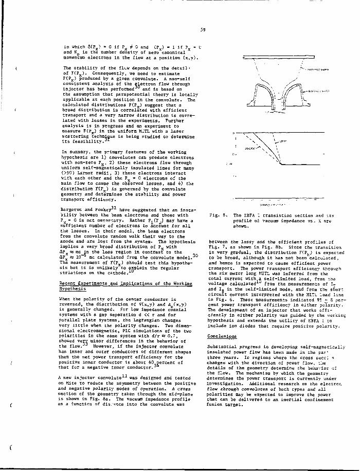
59
in which 6(PX) » 0 it Px # 0 and (Px) « 1 if Px = Cand No is the number density of zero canonicalmomentum electrons in the flow at a position (x,y).
The stability of the fli w depends on the detail••of F(PX). Consequently, we need to estimateF(PX) produced by a given convolute. A non-selfconsistent analysis of the electron flow throughinjector has baen performed and is based onthe assumption that parapotential theory is locallyapplicable at each position in the convolute. Thecalculated distributions F(PX) suggest that abroad distribution is correlated with efficienttransport and a very narrow distribution is corre-lated with losses in the experiments. Furtheranalysis is in progress and an experiment tomeasure F(PX) in the uniform MiTL with a laserscattering technique is being studied to determineIts feasibility.31
In summary, the primary features of the workinghypothesis are 1) convolutes can produce electronswith non-zero Px, 2) these electrons flow throughuniform self-magnetically insulated lines for many(>50) Lannor radii, 3) these electrons interactwith each other and the Px - 0 electrons of themain flow to cause the observed losses, and 4) thedistribution F(PX) is governed by the convolutegeometry and determines the stability and powertransport efficiency.
Bergeron and Poukejr have suggested that an insta-bility between the beam electrons and those withPx =• 0 is net necessary. Rather F^CI^J may have asufficient number of electrons to account for allthe losses. In their model, the beam electronsfrom the convolute random walk their way to theanode and are lost from the system. The hypothesisimplies a very broad distribution of P with
t«: me ias 10~°
n the loss region in contrast to thex as 10~° me calculated from the convolute model.
The measurement of F(PX) should test this hypothe-sis but it is unlikely to explain the regularstriations on the cathode.
Recent Experiments and Implications of the WorkingHypothesis
When the polarity of the center conductor isreversed, the distribution of V(x,y) and A (x,y)is generally changed. For low impedance coaxialsystems with a gap separation d « r and forparallel plate systems, the Lagrangian changesvery little when the polarity changes. Two dimen-sional electromagnetic, PIC simulations of the twopolarities in the same system with d/r « 0.7,showed verv minor differences in the behavior ofthe flow. However, if the Injector convolutehas inner and outer conductors of different shapesthen the net power transport efficiency for thepositive inner conductor is about 60 percent ofthat for a negative inner conductor.3
A new injector convolute was designed and testedon Mite to reduce the asymmetry between the positiveand negative polarity modes of operation. A crosssection of the geometry taken through the mid-planeis shown in Fig. 8a. The vacuum impedance profileas a function of dis.=nce into the convolute was
Fig. 8. The EBFA I transistior. section and itsprofile of vacuum impedance vs. X areshown.
between the lossy and the efficient profiles ofFig. 7, as shown in Fig. 8b. Since the transitionis very gradual, the distribution F(PX) is expectedto be broad, although it has not been'calculated,and hence is expected to cause efficient powertransport. The power transport efficiency throughthe six meter long MITL was inferred from thetotal current with a self-limited load, from thevoltage calculated1 from the measurements of I,.and Ig in the self-limited mode, and from the shortcircuit current interpreted with the MITL load linein Fig. 6. These measurements indicated 9 5 + 8 per-cent power transport efficiency in either polarity.The development of an injector that works effi-ciently in either polarity was guided by the workinghypothesis and extends the utility of EBFA 1 toinclude ion diodes that require positive polarity.
Conclusions
Substantial progress in developing self-magneticallyinsulated power flow has been made in the pap'three years. ID regions where the cross sect: nchanges with the direction of power flow, the'details of the geometry determine the behavior ofthe flow. The mechanism by which the geometrydetermines the power transport is currently underinvestigation. Additional research on the electronflow through convolutes of both types and allpolarities may be expected to improve the powerthat can be delivered to an inertial confinementfusion target.
60
References
1. J. P. VanDevender and D. H. McDaniel, Proc. 8thInc'l. Conf. on Discharges and Electrical Insu-lation in Vacuum, Albuq., SM, E-l (Sept. 5-/,1978).
2. T. H. Martin, IEEE Trans. Sud. Sci., NS-20,289 (1973).
3. Z. P. Velikov, V. A. Glukhilcy, 0. A. Gusev,G. M. Latmanizova, S. L. Nedoseev,0. B. Ovchinnikov, A. M. Pasechnikov,0. P. Percherskii, L. I. Rudakov, M. B. Svin'in,V. P. Smirnov and V. I. Chetvertkov, "ANGARA-5"Accelerator, NIIEFA Preprint D-0301, Leningrad,USSR (1976).
4. I. D. Smith, lat'l. Topical Conf. on Electron3eam Res. and Tech., Albuq., NM, Vol. I, p.472(Nov. 3-5, 1975).
5. R. G. Little, W. R. Seal and J. R. UgJura. sameas Ref. 4, p. 508.
6. T. H. Martin, D. L. Johnson and D. H. hrDaniel,Proc. of 2nd Topical Conf. on High PowerElectron and Ion Beam Res. and Terh.. O--.ellUniv., Ithaca, NY, 307 (1977).
7. I. D. Smith, P. D'A. Champney and J. M. Creedon,IEEE Pulsed Power Conf., Lubbock, TX (1976).
3. E. I. Baranchikov, A. V. Gordeev, V. D. Korolevand V. P. Smirnov, Sov. Phys.-Tech. Phys. £,42 (1977).
9. >!. DiCapua and E. G. Pelllnen, J. Appl. Phys..50, (1979).
10. J. ?. VanDevender, J. Appl. Phys. 5p_, No. 6(June 1979).
LI. J. ?. VanDevender and E. L. Neau, Sardia LabsElectron 3eam Fusion Progress Report, April1978-December 1978, Albuq., SM, (1979).
L2. Q. A. Mesyats and D. I. Proskurovskii, JETPLett. JL3,' 4 (1971).
13. I. G. Kataev, Electromagnetic Shock Waves (inRussian), Sov. Radio, Moscow (1963); (in English)Iliffe Books, Ltd. London (1966).
14. !C. 3. Bergeron, J. Appl. Phys. 48, 3065 (1977).
15. J. V. Poukey and K. D. Bergeron, Appl. Phys.Lett. 2?., 8 (1978).
16. E. I. Branchikov, A. V. Gordeev, Yu. V. Koba,V. a. Korolev, V. S. Pen'kina, L. I. Rudakov,V. ?. Smirnov, A. 0. Sukhov, E. Z. Tarumov andYu. L. 3akshaev, 6th IAEA Conf. Plasma Phys.Cont. Therraonuclear Reactions, 3erchtesgaden,(1976).
17. A. V. Gordeev, Sov. Phys.-Tech. Phys. 23_, 991(1978).
18. R. V. Lovelace and E. Ott, Phys. Fluids 37,1263 (1974).
19. A. Ron, A. A. Mondelli and N. Roscoker, IEEETrans. Plasma Sci. PS-1, 85 (1973).
20. J. M. Creedon, J. Appl. Phys. 46_, 2946 (1975)and J. M. Creedon, J. Appl. Phys. 48, 1070(1977).
21. V. S. Veronin and A. I. Lebedev, Sov. Phys.-Tech. Phys. 18_, 1627 (1974).
22. C. W. Mandel, Accepted for publication in J.Appl. Phys. 50, !lo. 7, (July 1979).
23. S. Shope, J. W. Poukey, K. D. Bergeron,D.H.McDanlel, A.Jdbepfer and J.P.VanDevender,J. Appl. Phys. 49, 3675 (1978).
24. A. A. Kolomenskii, E. G. Krastelev andB. N. Yablokov, Sov. Phys.-Tech. Phys. 3, 247(1977).
25. V. P. Smirnov, private communication (1978).
26. K. D. Bergeron, Phys. Fluids 2_0_, 688 (1977).
27. A. V. Gordeev, Sov. Terh. Phys. Lett. 3 , 323(1977).
28. K. 0. Bergeron, "A Slipping Stream Instabilityfor Magnetically Insulated Electron Flow",RS4241/1005, Sandia Laboratories, Albuq., NM(1978).
29. M. DiCapua, D. G. Pellinen, P. D'A. Champneyand D. 'd. McDaniel, sane as Ref. 6, p.781.
30. E. L. tfeau and J. P. VanDevender, IEEE 2ndInt'l. Pulsed Power Conf., Lubbock, TX (1979).
31. K. L. Brower and J. P. VanDevender, same asRef. 30.
32. K. D. Bergeron and J. W. Poukey, Accepted forPublication J. Appl. Phys. 50_ (1979).
33. J. W. Poukey, Private Communication.
34. n. DiCapua and D. G. Pellinen, Physics Int'l.Final Report, PIFR-^009, San Leandro, CA(Oct. 1978).
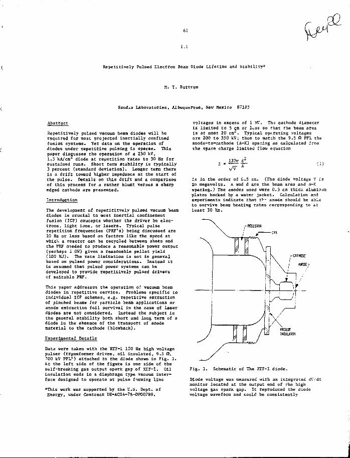
61
1.1
Repetitively Pulsed Electron Bean Diode Lifetime and Stability*
M. T. Buttram
Sandia Laboratories, Albuquerque, New Mexico 87185
Abstract
Repetitively pulsed vacuum beam diodes will berequired for most projected inertially confinedfusion systems. Yet data on the operation ofdiodes under repetitive pulsing is sparse. Thispaper discusses the operation of a 250 kV,1.5 kA/cm2 diode at repetition rates to 30 Hz forsustained runs. Short term stability is typically3 percent (standard deviation). Longer term thereis a drift toward higher impedance at the start ofthe pulse. Details on this drift and a comparisonof this process for a rather blunt versus a sharpedged cathode are presented.
Introduction
The development of repetltlcvely pulsed vacuum beamdiodes is crucial to most inertial confinementfusion (ICF) concepts whether the driver be elec-trons, light ions, or lasers. Typical pulserepetition frequencies (PRF's) being discussed are10 Hz or less based on factors like the speed atuhich a reactor can be recycled between shots andthe FRF needed to produce a reasonable power output(perhaps 1 GW) given a reasonable pellet yield(100 MJ). The rate limitation is not in generalbased on pulsed power considerations. Instead itis assumed that pulsed power systems can bedeveloped to provide repetitively pulsed driversof suitable PRF.
This paper addresses the operation of vacuum beamdiodes in repetitive service. Problems specific toindividual ICF schemes, e.g. repetitive extractionof pinched beams for particle beam applications oranode extraction foil survival in the case of laserdiodes are not considered. Instead the subject isthe general stability both short and long term of adiode in the absence of the transport of anodematerial to the cathode (blowback).
Experimental Details
Data were taken with the RTF-I 100 Hz high voltagepulser (transformer driven, oil insulated, 9.5 n,700 kV PFL1) attached to the diode shown in Fig. 1.At the left side of the figure is one side of theself-breaking gas output spark gap of H.TF-I. Oilinsulation ends in a diaphragm type vacuum inter-face designed to operate at pulse forming line
*This work was supported by the U.S. Dept. ofEnergy, under Contract DE-AC04-76-DP0078S.
voltages in excess of 1 MV. Tha cathode diameteris limited to 5 cm or l^ss so that the beam areaIs at most 20 cm2. Typical operating voltagesare 200 to 350 kV; thus to matih the 9.5 fi PFL theanode-to-cathode (A-K) spacing as calculated fromthe space charge limited flow equation
(i)
is in the order of C.5 en. (The diode voltage V isin megavolts. A and d are the beam area and A-Kspacing.) The anodes used were 0.3 cm thick aluminumplates backed by a water jacket. Calculation andexperiments indicate that tl"~ anode should be ableto survive beam beating rates corresponding to atleast 30 Hz.
,- RESISTOR
VACIW!INSUWTOH
Fig. 1. Schematic of The RTF-I diode.
Diode voltage was measured with an integrated dv/dtmonitor located at the output end of rhe highvoltage gas spark gap. It reproduced the diodevoltage waveform and could be consistently
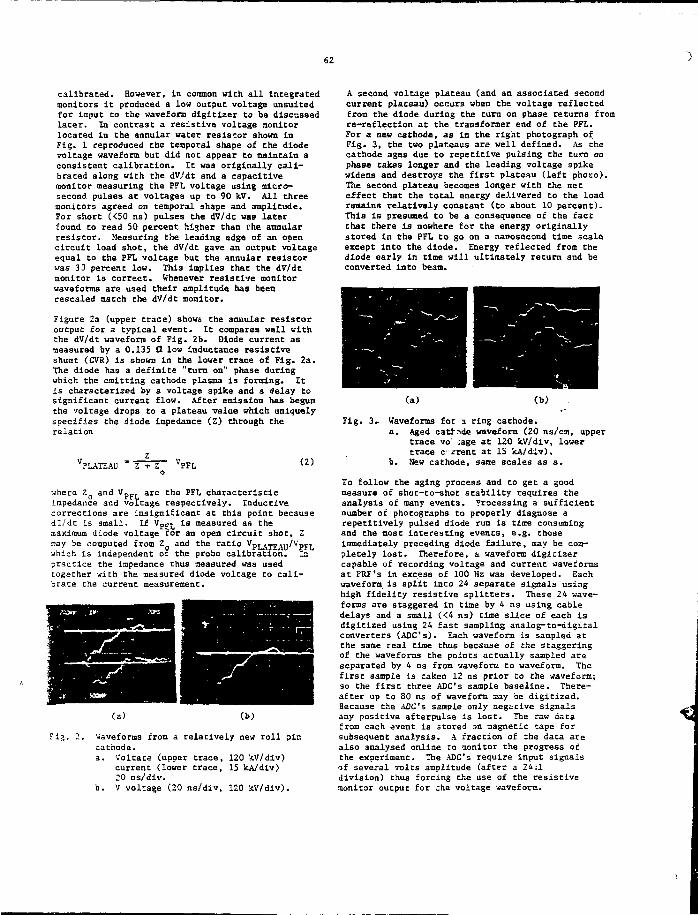
62
calibrated. However, In common with all Integratedmonitors It produced a low output voltage unsultedfor Input to the waveforn digitizer to be discussedlater. In contrast a resistive voltage monitorlocated in the annular water resistor shown inFig. 1 reproduced the temporal shape of the diodevoltage waveform but did not appear to maintain aconsistent calibration. It was originally call-braced along with the dV/dt and a capacitivemonitor measuring the PFL voltage using micro-second pulses at voltages up to 90 fcV. All threemonitors agreed on temporal shape and amplitude.For short (<50 ns) pulses the dV/dt was laterfound to read 50 percent, higher than the annularresistor. Measuring the leading edge of an opencircuit load shot, the dV/dt gave an output voltageequal to the PFL voltage but the annular realscorwas 33 percent low. This implies that the dV/dtmonitor is correct. Whenever resistive monitorwaveforms are used their amplitude has beenrescaled match the dV/dt monitor.
Figure 2a (upper trace) shows the annular resistoroutput for a typical event. It compares well withthe dV/dt waveform of Fig. 2b. Diode current asmeasured by a 0.135 II low Inductance resistiveshunt (CVR) is shown in the lower trace of Fig. 2a.The diode has a definite "turn on" phase duringwhich the emitting cathode plasma is forming. Itis characterized by a voltage spike and a delay tosignificant current flow. After emission lias begunthe voltage drops to a plateau value which uniquelyspecifies Che diode impedance (Z) through therelation
PLATEAU VPFL (2)
where ZQ and V p F, are the PFL characteristicimpedance and voltage respectively. Inductivecorrections are insignificant at this point becausedl/dc is small. If Vp?I_ is measured as themaximum diode voltage for an open circuit shoe, Zaay be computed from Z and the ratio ^ P I ^ T E A U ^ P F Lwhich is independent of the probe calibration. lapractice the impedance thus measured was usedtogether vith the measured diode voltage to cali-brate the current measurement.
Fig. 2. Waveforms from a relatively new roll pincathode.
a. Voltate (upper trace, 120 kV/div)current (lower trace, 15 kA/div)20 ns/div.
b. V voltage (20 ns/div, 120 kV/div).
A second voltage plateau (and an associated secondcurrent plateau) occurs when the voltage reflectedfrom the diode during the turn on phase returns fromre-reflection at the transformer end of the PFL.For a new cathode, as in Che right photograph ofFig. 3, the two plateaus are well defined. As thecathode ages due to repetitive pulsing the turn onphase takes longer and the leading voltage spikewidens and destroys the first plateau (left photo).The second plateau becomes longer wich Che neteffect that the total energy delivered to the loadremains relatively constant (to about 10 percent).This is presumed to be a consequence of the factchat there is nowhere for the energy originallystored In the PFL to go on a nanosecond time scaleexcept Into che diode. Energy reflected from Chediode early in time will ultimately return and beconverted Into beam.
Fig. 3- Waveforms for a ring cathode.
a. Aged catr-ide waveform (20 ns/cm, uppertrace vo ;age at 120 kV/div, lowertrace c rrent at 15 kA/div).
b. New cathode, same scales as a.
To follow the aging process and to get a goodmeasure of shot-to-shoc stability requires theanalysis of many events. Processing a sufficientnumber of photographs to properly diagnose arepetitively pulsed diode run is time consumingand the most interesting events, e.g. thoseImmediately preceding diode failure, may be com-pletely lost. Therefore, a waveform digitizercapable of recording voltage and current waveformsat PRF's In excess of 100 Hz was developed. Eachwaveform is split into 24 separate signals usinghigh fidelity resistive splitters. These 24 wave-forms are staggered in time by 4 ns using cabledelays and a small (<4 ns) cine slice of each isdigitized using 24 fast sampling analog-to-digitalconverters (ADC's). Each waveform is sampled atthe same real time thus because of the staggeringof the waveforms the points actually sampled areseparated by 4 ns from waveform to waveform. Thefirst sample is taken 12 ns prior to the waveform;so the first three ADC's sample baseline. There-after up to 30 ns of waveform may be digitized.Because the ADC's sample only negative signalsany positive afterpulse is lost. The raw datafrom each event is stored on magnetic tape forsubsequent analysis. A fraction of rhe data arealso analysed online to monitor the progress ofthe experiment. The ADC's require inpuc signalsof several volts amplitude (after a 24:1division) thus forcing the use of the resistivemonitor output for che voltage waveform.
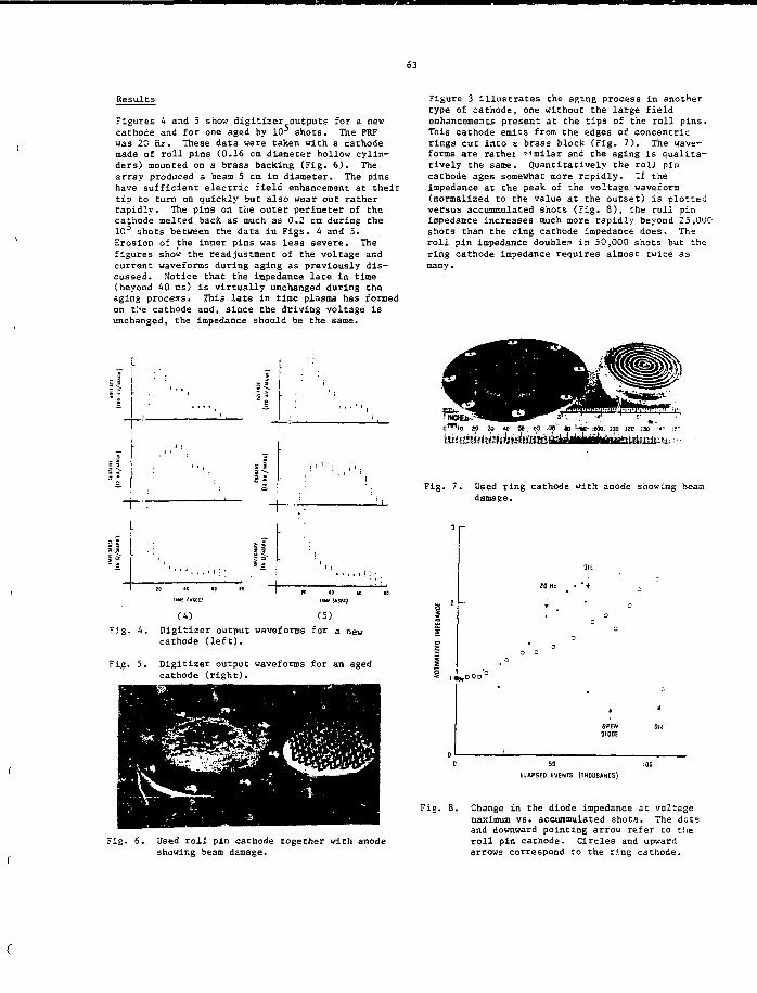
63
Results
Figures 4 and 5 show digitizer outputs for a newcathode and for one aged by 10 shots. The PRFwas 20 Kz. These data were taken with a cathodemade of roll pins (0.16 cm diameter hollow cylin-ders) mounted on a brass backing (Fig. 6). Thearray produced a beam 5 cm in diameter. The pinshave sufficient electric field enhancement at theirtip to turn on quickly but also wear out ratherrapidly. The pins on the outer perimeter of thecathode melted back as much as 0.2 cm during thelO3 shots between the data in Figs. A and 5.Erosion of the inner pins was less severe. Thefigures show the readjustment of the voltage andcurrent waveforms during aging as previously dis-cussed. Notice that the impedance late in time(beyond 40 ns) is virtually unchanged during theaging process. This late in time plasma has formedon t>e cathode and, since the driving voltage isunchanged, the impedance should be the same.
isIS
;o «o ID ID
tiut I <ticc!ID <D ID
(4) (5)
Fig. 4. Digitizer output waveforms for a newcathode (left).
Fig. 5. Digitizer output waveforms for an agedcathode (right).'
Figure 3 illustrates the aging process in anothertype of cathode, one without the large fieldenhancements present at the tips of the roll pins.This cathode emits from the edges of concentricrings cut into a brass block (Fig. 7). The wave-forms are rathet ^milar and the aging is qualita-tively the same. Quantitatively the roll pincathode ages somewhat more rapidly. If theimpedance at the peak of the voltage waveform(normalized to the value at the outset) is plottedversus accummulated shots (Fig. 8), the roll pinimpedance increases much more rapidly beyond 25,000shots than the ring cathode impedance does. Theroll pin impedance double.0 in 50,000 shots but thering cathode impedance requires almost twice asmany.
Fig. 7. Used ring cathode with anode showing beamdamage.
3IL
JO Hi • ' •
OPfNDIODE
Fig. 6. Used roll pin cathode together with anodeshowing beam damage.
El»PSEO EVENTS (THOUSANDS)
Fig. 8. Change in the diode impedance at voltagemaximum vs. accummulated shots. The dotsand downward pointing arrow refer to theroll pin cathode. Circles and upwardarrows correspond to the r?.ng cathode.
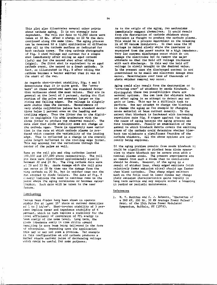
64
This plot also Illustrates several other pointsabout cathode aging. It is not strongly ratedependent. The roll pin data to 45,000 shots weretaken ac 10 Hz. After a change to 20 Hz the datacontinued along the same line. The aging processcan be reversed by a light application of diffusionpump oil to the cathode surface as indicated forboth cathode types. The ring cathode photographsof Fig. 3 show voltage and current for a singleshot immediately after oiling an aged cathode(left) and for the second shot after oiling(right). The first shot is equivalent to an agedcathode event, the second to a fresh cathode. Infact, as illustrated in Fig. 8 after oiling thecathode becomes a better emitter than it was atChe start of the run.
As regards shot-to-shot Gtability, Fig. 4 and 5demonstrate that it 1? quite good. The "errorbars" on those waveforms mark one standard devia-tion variances about the mean values. They are ingeneral at the level of 3 percent, during tha flatportion of the pulse and somewhat larger on therising and falling edges. The voltage is slightlystore stable than the current. Measurements ofvery stable calibration pulses have standard devia-tions below 1 percent even on the leading andtrailing edges. Thus the jitter due to the digiti-zer is negligible (it adds quadrature with thediode jitter to produce the observed result). Thedata show that diode stability does not change asthe cathode ages. There is apparently some varia-tion in the rate at which cathode plasma is pro-duced which creates the variability of the leadingedge. This is reflected in a change in the overallpulse length reflected In the trailing edge jitter.This may account for the variations through thecenter of the pulse as well.
Runs on the roll pin and ring cathodes lasted100,000 and 157,000 shots respectively. The rollpin data were distributed approximately eiuallybetween 10 and 20 Hz. The ring cathode data wereac 20 and 30 Hz. Anode damage with the roll pins••as worse at 20 Hz than was the damage from thering cathode ac 30 Hz, but in neither case was therun stopped by diode failure. The data of Fig. 8clearly indicate the need Co continue runs to thepoint where the aging terminates or becomes catas-trophic. Such data will be taken In the nearfuture.
Conclusions
Vacuum beam diodes have been shown Co operacestably for at l^ast 10° shots at current densitiesof 1 to 2 kA/ctn". Shot-to-shot stability of 3 per-cent implies power and impedance stability of 4percent, which in turn implies a stability for thetotal efficiency of conversion of PFL energy Cobeam anergy of che same level. Long term, thediode impedance early in time drifts upwardresulting tn aore beam being delivered in the form->i jfterpulse. Depending upon Che applicationthis aay or may not pose a problem. For examplein this configuration an old cathode produces arather square current pulse of decreasing voltagewhich could be useful for some purposes.
As to the origin of the aging, two mechanismsimmediately suggest themselves. It could resultfrom the destruction of cathode whiskers whoseexplosion is thought to produce the cathode plasma.This would be a process equivalent to the breakingin of DC vacuum insulators. In that case the DCvoltage is raised slowly while the insulator isseparated from the power source by a high impedance.Very low current discharges occur which do notdamage the electrodes but do remove the majorwhiskers so that the hold off voltage increaseswith each discharge. In this way the hold offvoltage is slowly brought to the desired value,la the present case the discharged current is notcoostrained to be small and electrode damage doesoccur. Nevertheless over tens of thousands ofshots whisker removal may occur.
Aging could also result from the destruction or"covering over" of whiskers by anode blowback. Todistinguish these two possibilities there areseveral options. One can look for whiskers beforeand after aging in an attempt to detect any netgain or loss. This may be a difficult task toperform. One may attempt to change the blowbackto change the aging as for example by changinganode material or beam current density. To theextent that blowback is increased with increasingrepetition rate Fig. 8 argues against its beingthe cause of aging because the aging process wasrate Independent. Finally an examination of theextent to which blowback debris covers the emittingareas of the cathode could determine whether blow-back can eliminate a significant fraction of thecathode whiskers. All the above options are cur-rently being explored.
If Che aging problem results from anode blowback itcould be significant to pinched beam diode opera-tion in where blowback may be severe even with anominal plasma anode. The present experiments areso remote from such a diode that no conclusionsshould be drawn. However, if the aging is aresult of whisker loss, sharp edged emitters (withrelatively fewer emission sices) should age fasterthan blunt cathodes. Thus sharp edged emitterssuch as the foils used in laser diodes may changetheir emission characteristics quite rapidly inlong term service and may require either a breakingin period or periodic maintenance.
References
1. H. T. Buttram and G. J. Kohwein, "Operation ofa 300 kV, 100 Hz, 30 KW Average Power Pulser",Proc. of the 13th Pulse Power ModulatorSymposium, Buffalo, NY (1973).
65
VOLTAGE DISTHIBUTION AMD CURRENT IN A CYLINDRICAL BELATIVISTIC DIODE
IS". W. Harris
Ion Physics Company
Burlington, Massachusetts
Abstract and hence tabulation is not practicable for voltages
in excess of 200 kV. Consequently a simple pro-
gram in BASIC was written for a timeshare com-
puter to solve cases of interest. This is appended.
Fig. 2 shows a typical result, the perveance fall-
ing by 43% as the voltage is raised to 1 0 MV. The
cathode/anode diameter ratio was 5 in thiE case.
The voltage distribution and current in a space
charge limited cylindrical diode are calculated by
means of a simple computer program. Relativistic
formulation is used, and the results are applicable
up to the limit of significant beam pinch. The
accuracy is 0. lTo.
Method of Calculation
Introduction
This paper describes the calculation of current
density and voltage distribution in cylindrical
electron guns working iD the megavolt region. The
current is assumed to be space charge limited.
The cathode in this example is larger than, and
concentric with, the anode. The companion case,
anode radius greater than cathode radius, is very
similar. The current is assumed radial, and
magnetic effects have been ignored. The geome-
try is shown in Fig. 1, the Pierce electrodes pro-
ducing the same radial electric field distribution
outside the beam as the space charge produces in-
side the beam.
The units are MKS. Consider a unit lengthd me-
ter), with the cathode surface at a radius R and
the anode at a radius R,. Let the intervening dis-
tance be divided up into a number of equal parts.
If each tube or shell has a very small radial width
D, we can take the space charge in it as essentially
uniform.
The first step is to place a small arbitrary voltase
across the first shell. The current is calculated
from the plane parallel diode approximation
4ir e(2R -D)V" '
9D~
Even at low voltages, where relativistic correc-
tions car be neglected, solution of this problem is
not simple and the results are usually given in a
tabular, rather than an analytic form ' . At very
high voltage, the perveance is a function of voltage
This current is the same for all shells. The field
on the inside surface of the first shell is E=4V '3D
as shown by Langmuir , The average voltage in
the next shell is calculated by extrapolation,
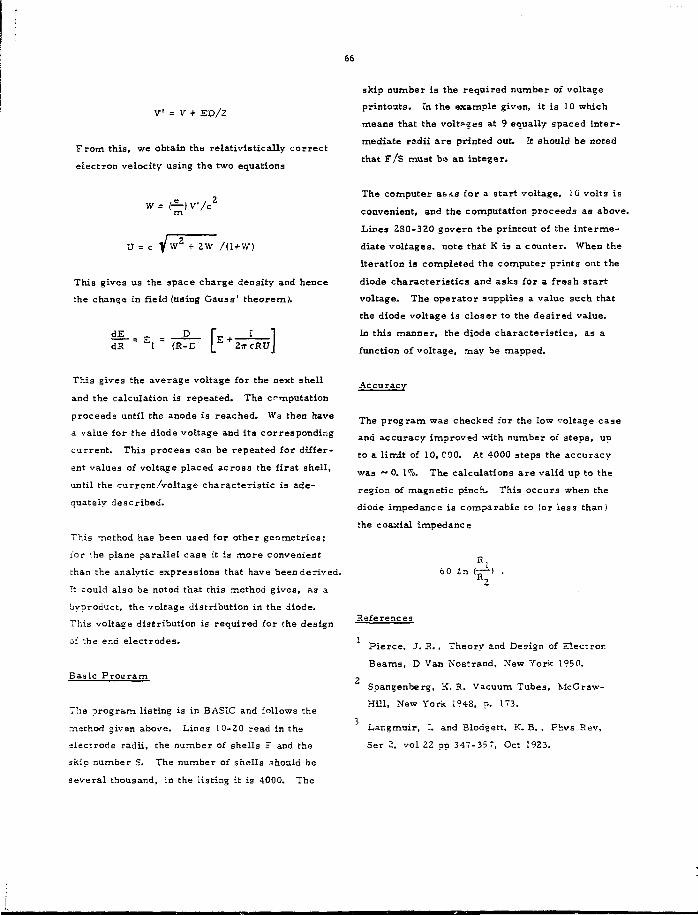
66
V = V + ED/2
From this, we obtain the relativistically correct
electron velocity using the two equations
W= (— )V'/cZ
m
u = c yw 2 + 2W /(i+w)
This gives us the space charge density and hence
the change in field (using Gauss' theorem).
dH 1 (R-D
This gives the average voltage for the next shell
and the calculation is repeated. The computation
proceeds until the anode is reached. Wa then have
a value for the diode voltage and its corresponding
current. This process can be repeated for differ-
ent values of voltage placed across the first shell,
until the current/voltage characteristic is ade-
quately described.
This method has been used for other geometries:
for the plane parallel case it is more convenient
than the analytic expressions that have been derived.
It could also be noted that this method gives, as a
byproduct, the voltage distribution in the diode.
This voltage distribution is required for the design
of -he end electrodes.
Basic Program
The program listing is in BASIC and follows the
method given above. Lines 10-20 read in the
electrode radii, the number of shells F and the
skip number S. The number of shells should be
several thousand, in the listing it is 4000. The
skip number is the required number of voltage
printouts. In the example given, it is 10 which
means that the voltages at 9 equally spaced inter-
mediate radii are printed out. It should be noted
that F/S must ba an integer.
The computer aBits for a start voltage, 10 volts is
convenient, and the computation proceeds as above.
Lines 280-320 govern the printout of the interme-
diate voltages, note that K is a counter. When the
iteration is completed the computer prints out the
diode characteristics and asks for a fresh start
voltage. The operator supplies a value such that
the diode voltage is closer to the desired value.
In this manner, the diode characteristics, as a
function of voltage, may be mapped.
The program was checked for the low voltage case
and accuracy improved with number of steps, up
to a limit of 10, COO. At 4000 steps the accuracy
was ~ 0. 17o. The calculations are valid up to the
region of magnetic pinch. This occurs when the
diode impedance is comparable to (or less than)
the coaxial impedance
60 in (-—) .R2
Referenc es
i
Pierce, J. R., Theory and Design of ElectronBeams, D Van Nostrand, New York 1950.
Spangenberg, K. R. Vacuum Tubes, McGraw-
Hill, New York 1948, p. 173.
Lacgmuir, I. and Blodgett, K. B. , Phvs Rev,
Ser 2, vol 22 pp 347-35 T, Oct 1923.
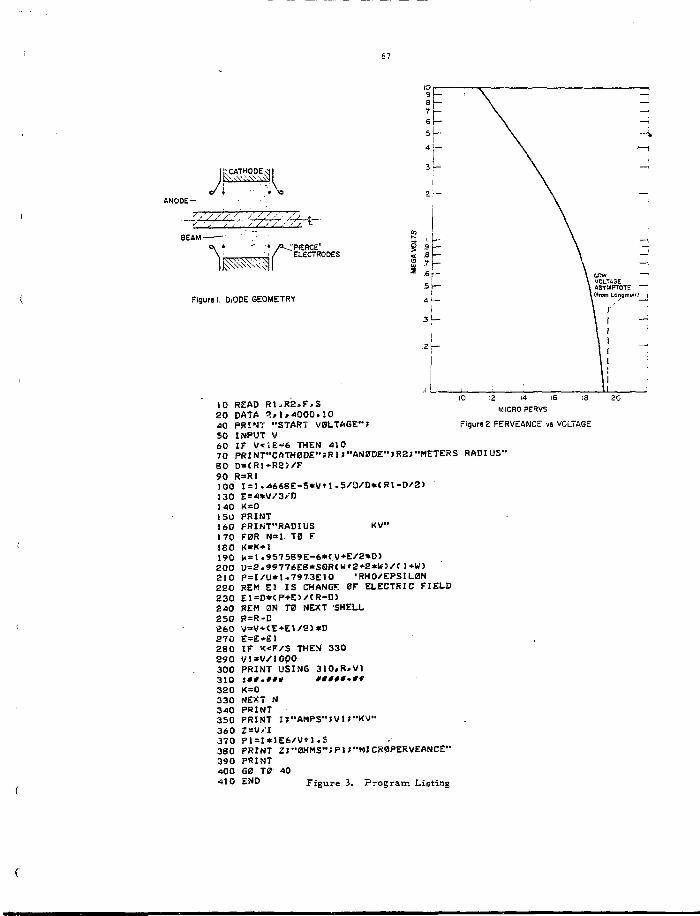
101—
f6 I—
I t CATHODE^ I
3EAM-
ELECTRODES
5 1 I—g .9 1-
« shS 7 h
Si-Figure I. DiODE GEOMETRY
,L10 READ RUR2»F>S20 DATA 9*1/4000.1010 PRINT "START V0tTftGE"J
50 INPUT V60 IF V«i£-6 THEN 41070 PRINT"CflTHCDE"JRl/"AN0DE"JR2J"METERS RADIUS80 D"CRI-R8J/F90 R=RI100 1 = 1 .JI668E-S*Uf 1 .5/D/D*(RI-D/2>130 E=-0*V/3/O140 K=0150 PRINT160 FRINT"RADIUS KV"170 F0R N=l. T0 F180 K»Kf!190 1«=1.957589E-6*<V*E/2*D)200 U=2.99776E8*S0R(Wr2*2*WJ/C1*WJ210 P=I/U*l-7973EJ0 'RHO/EPSIL0N220 REM El IS CHANGE 0F ELECTRIC FIELD230 E1=D*CP+E)/CR-D>240 REM 0N T0 NEXT SHELL250 f?=R-D260 V=V*<E+E1/2>*D270 E=E*E1280 IF K<F/S THEN 330290 Vl*V/!OpO300 PRINT USIN6 310.R/V1310 !##.##* #####.##320 K=0330 NEXT N340 PRINT350 PRINT U"AMPS"JVI)'W'360 Z=y/I370 P1=I*1E6/V»1.S380 PRINT Z;"0HMS"JP1J"MICR0PERVEANCE"390 PRINT400 G0 T0 40410 END
10 12 14 16 18MICRO PERVS
Figure 2 PERVEANCE vs VCLTAGE
Figure 3. Program Listing
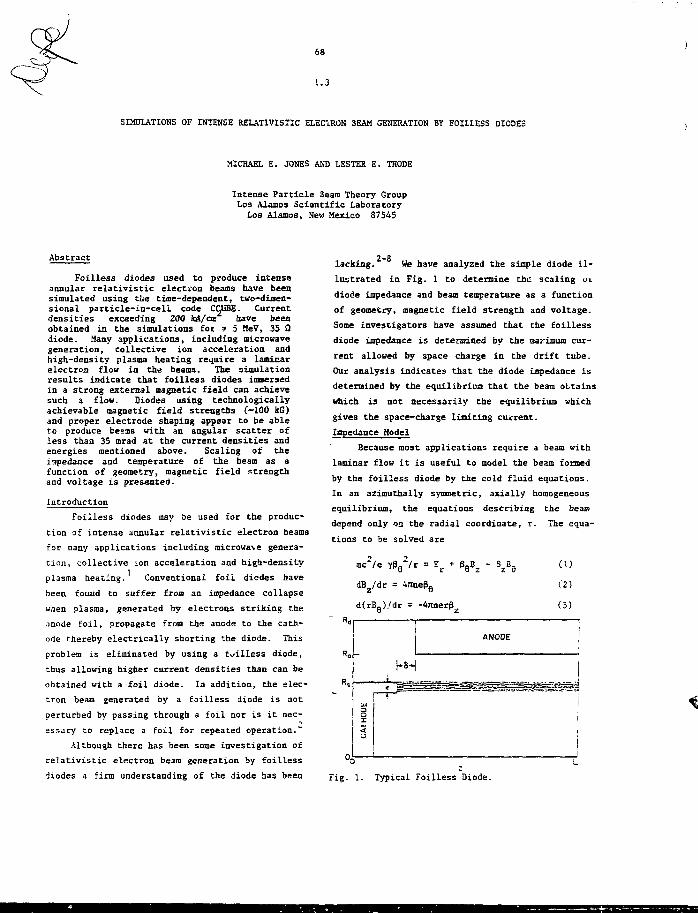
68
1.3
SIMULATIONS OF INTENSE RELAT1VISTIC ELECTRON BEAM GENERATION BY FOIIXESS DIODES
MICHAEL E. JONES AND LESTER E. THODE
Intense Particle Beam Theory GroupLos Alamos Scientific LaboratoryLos Alamos, New Mexico 87545
Abstract
Foilless diodes used to produce intenseannular relativistic electron beams have beensimulated using the time-dependent, two-dimen-sional particle-in-cell code CCUBE. Currentdensities exceeding 200 kA/ar have beenobtained in the simulations for ? S MeV, 35 Qdiode. Many applications, including microwavegeneration, collective ion acceleration andhigh-density plasma heating require a laminarelectron flow in the beams. The simulationresults indicate that foilless diodes imnersedin a strong external magnetic field can achievesuch a flow. Diodes using technologicallyachievable magnetic field strengths (-100 kG)and proper electrode shaping appear to be ableto produce be^ms with an angular scatter ofless than 35 mrad at the current densities andenergies mentioned above. Scaling of theimpedance and temperature of the beam as afunction of geometry, magnetic field strengthand voltage is presented.
Introduction
Foilless diodes may be used for the produc-
tion of intense annular relativistic electron beams
for many applications including microwave genera-
tion, collective ion acceleration and high-density
plasma heating. Conventional foil diodes have
been found to suffer from an impedance collapse
when plasma, generated by electrons striking the
anode foil, propagate from the anode to the cath-
ode thereby electrically shorting the diode. This
problem is eliminated by using a foilless diode,
thus allowing higher current densities than can be
obtained with a foil diode. In addition, the elec-
tron beam generated by a foilless diode is not
perturbed by passing through a foil nor is it nec-
essary to replace a foil for repeated operation."
Although there has been some investigation of
relativistic electron beam generation by foilless
diodes a firm understanding of the diode has been
2-8
lacking. We have analyzed the simple diode il-
lustrated in Fig. 1 to determine the scaling m
diode impedance and beam temperature as a function
of geometry, magnetic field strength and voltage.
Some investigators have assumed that the foilless
diode impedance is determined by the maximum cur-
rent allowed by space charge in the drift tube.
Our analysis indicates that the diode impedance is
determined by the equilibrium that the beam obtains
which is not necessarily the equilibrium which
gives the space-charge limiting current.
Impedance Model
Because most applications require a beam with
laminar flow it is useful to model the beam formed
by the foilless diode by the cold fluid equations.
In an azimuthally symmetric, axially homogeneous
equilibrium, the equations describing the beam
depend only on the radial coordinate, r. The equa-
tions to be solved are
mc2/e
Fig. 1. Typical Foilless Diode.
69
= -4nner (4j
vhere m and e are the mass and charge of the elec-
tron. The only nonzero fluid variables are the
density c and the axial and azimuthal fluid veloc-
ities 8^ and B~ (divioed by the speed of light c).
The nonzero fluid variables are the radial elec-
tric field E^, the azimuthal magnetic field Bfi, and
the axial nagnetic field B . The relativistic
factor is denoted by Y- Because the cathode is an
equipotentiai surface, conservation of energy
assumes the following form:
2dy/dr = -eEr/nc (5)
Because there are only fiva equations and six
unknowns another condition must be specified. A
condition which leads to ai. analytically tractable
solution of the equilibrium equations and which
becomes increasingly better satisfied at largerg
energies, is to choose Pz to be independent of r.
Defining the following quantities y.. = (1 - p )
and y = y/y. i aa equation for y can be found
whose solution is given in terms of elliptic Jacobio
functions. The total beam current v, measured in
units of me /e is given by this model as
v= l(ru(6)
where y is y evaluated at the outside edge of
the beam.R , and a is an arbitrary constant. De-
fining IU s eB (E )/mc we find
and In R /R. = F($,k)/(a* +0 1
C8)
where R. is the inside beam radius, <]> = Cos (y )
and k = a/(a + I)"4 and F(<p,k) is the incomplete
elliptic integral of the second kind.
In addition to Eqs. (6)-(8), we require that
the total energy of the electrons, kinetic and
potential, be equal to the potential drop between
the anode and cathode. Thus,
In R /Ra o (9)
where R is the anode radius (see Fig. 1). Thea
relativistic factor that the electrons would have
upon reaching the anode is denoted by y . Voronin,
et al. have used these equations and additional
assumptions to find the space-charge limited cur-
rent as a function of magnetic field. However,
there is no a priori reason to assume that the
beam produced by the diode will be launched into an
equilibrium which will transmit the maximum current.
If the applied external magnetic field pene-
trates the cathode then conservation of canonical
acgular momentum takes the form:
(y0
(Hou.co/c - R2 U(./Boc)/2 (10)
2where ui = eE_/cm and Eg is the applied magnetic
field. The cau-.ie radius is denoted by R^. If
in addition we assume that the laminar electron
flow is along the self-consistent magnetic field
lines, then the flux between the axis and the outer
edge of the beam is equal to the applied flux be-
tween the axis and the cathode radius. On the time
scale of most experiments, the magnetic field pro-
duced by the beam cannot diffuse through the anode
wall. Therefore, the flus between the outer edge
of the beam and the anode will be equal to the
applied flux between the cathode and anode. These
conditions may be written as
= 2 V1and - R2) = (12)
Equations (6)-(12) form a complete set of equa-
tions which can be solved (numerically) to determine
the impedance of the foilless diode. In order to
insure laminar flow, it is necessary to apply a
large external magnetic field. Therefore a useful
approximation can be obtained by taking the infinite
magnetic field limit. One then finds that the beam
becomes infinitesimally thin with radius R and that
the beam approaches a nonrovating equilibrium. The
diode impedance in this limit becomes
Z = 15(y -1){[Y /(1+4 In R /R )}2-l)'h 0. (13)3 3 3 C
should be noted that this formula is invalid
for low voltage, probably owing to our assumption
of P being independent of r.
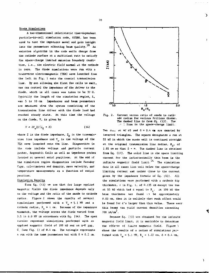
70
Diode Simulations
A two-dimensional relativistic time-dependent
particle-in-cell simulation code, CCUBE, has beea
used to test the impedance model and gain insight
into the parameters affecting beam quality. An
emission algorithm in the code emits charge from
the cathode surface at a sufficient rate to satisfy
the space-charge limited emission boundary condi-
tion, i.e., the electric field normal at the cathode
is zero. The diode simulations were run with a
transverse electromagnetic (TEH) wave launched from
the left in Fig. 1 onto the coaxial transmission
line. By not allowing tbe first few ceils to emit,
one can control the impedance of the driver to the
diode, which in all cases was taken to be 37 Q.
Typically the length of the simulation region, L,
was 5 to 10 ens. Impedances and bean parameters
are measured wt-n the system consisting of the
transmission line driver with the diode load had
reached steady state. At this time the voltage
on the diode, V, is given by
220
V = ZVvZ/(Z0 * Z) (14)
where Z is the diode impedance, Z- is the transmis-
sion line impedance and V is the voltage of the
TEM wave launched onto the line. Diagnostics in
the code include voltage and particle current
probes, Rogowskii Coils as well as impedance probes
located at several axial positions. At the end of
the simulation region diagnostics include Faraday
Cups, calorimeters and density, Man velocity, and
temperature measurements as a function of radial
position.
Simulation Results
From Eq. (13) we see that tor large applied
magnetic fields the diode impedance depends only
on the voltage and the ratio of the anode to cathode
radius. Figure 2 saowa the results of several
simulations performed with a V = 5.1 MV and a
cathode radius, 3 = 1 cm. Because of the impedance
mismatch, the voltage across the diode varied from
3.5 to 6.0 MV in accordance with Eq. (14). The open
circles represent simulations performed with an
applied magnetic field of 100 kG and an A-K gap,
5, (see Fig. [) of 0.4 cm. The triangle represents
a run with the same parameters but with 6 = 0.2 cm.
Fig. 2.
Two
Current versus ratio of anode to cath-ode radius for various foillcss diodes.The dashed liae is from £q. (13). The
• 1 line is the space-charge limit.
<m 4C t9 and 5 = 0.4 are denoted by
inverted triangles. The square designates a run at
55 kG in which the auode wall is continued straight
at the original transmission line radius, R,, of
1.85 cm so that 5 -» ». The dashed line is obtained
from Eq. (13). The solid line is the space limiting
current for the iofinitesimally thin beam in the14
infinite magnetic field limit. The simulation
data in all cases lies well below the space-charge
limiting current and rather close to the current
given by the impedance formula of Eq. (13). .411
the simulations were performed with a cathode tip
thickness, s in Fig. 1, of 0.135 cm except tee run
at 55 kG which had £ equal to R^. .it 100 StG the
beam thickness was cound ii be approximately
0.03 cm, thus it is unlikely that much effect would
be found for e's larger than this value. These very
thin beams can yield current densities exceeding
700 kA/cm2.
Because Eq. (13) vas obtained for the infinite
magnetic field limit, it is desirable to determine
the affects of finite magnetic field. Figure ~i
shows the results of a series of simulations per-
formed with V = 5.1 !W, R = 1.27 cm, 6 = 0.4 cm.
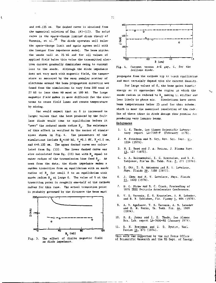
and £=0.135 cm. The dashed curve is obtained from
the numerical solution of Eqs. (6)-(12). The solid
curve is the space-charge limited diode theory of
Voronin, et al. The diode operates well below
the space-charge limit and again agrees well with
the laminar flow impedance model. The beam striken
the anode wall at 25 kG and for all values of
applied field below this value the transmitted elec-
tron current gradually diminishes owing to current
loss to the anode. Although the diode impedance
does not vary much with magnetic field, the temper-
ature as measured by the mean annular scatter of
electrons around the beam propagation direction was
found from the simulations to vary from 200 mrad at
27 kG to less than 60 mrad at 100 kG. The large
magnetic field makes it more difficult for the elec-
trons to cross field lines and create temperature
by mixing.
One would expect that as 6 is increased to
larger values that the beam produced by the foil-
less diode would come to equilibrium before it
"sees" the reduced anode radius R . The existencea
of this effect is verified by the series of simula-
tions shown in Fig. 4. The parameters of the
simulations include B =100 kG, V =5.1 MV, B =1.5 cm,
and £=0.135 cm. The upper dashed curve was calcu-
lated from Eq. (13). The lower dashed curve was
also calculated from Eq. (13) but with R equal to
outer radius of the transmission line feed R,. Asd
seen from the data, the diode impedance makes a
sudden transition from an equilibrium with an anode
radius of R for small 5 to an equilibrium with
anode radius R. at large 6. The value of 6 at the
transition point is roughtly one-half of the cathode
radius for this case. The actual transition point
is probably governed by the distance the beam must
20Or
75;
S (cm)Fig. 4. Current versus A-K gap, c, for the
foilless diode.
propagate from the cathode tip to x*ach equilibrium
and must certainly depend upon the current density.
For large values of 6, the beam gains kinetic
energy as it approaches the region in which the
anode radius is reduced to R making i:. stiffer anda
less likely to phase mix. Simulations have shown
beam temperatures below 25 <jrad for this scheme,
which is near the numerical resolution of the codf:.
Use of these Ldezs in diode design show promise tor
producing very laminar beams.
References1. L. E. Thode, Los Alamos Scientific Labora-
tory report LA-7169-P (February 1W8).
2. H. Friedman and M. Ury, Rev. Sci. Ins".. 4;,1334 (1970).
3. M. E. Read and J. A. Nation, J. Plasma Phys.13, 127 (1975).
4. A. A. Kolomenskii, E. G. Krastelev, aud B. N.Yablokov, Pis'ma Zh. Tekh. Fiz. 2, 271 (1976).
5. E. Ott, T. M. Antonsen and R. V. Lovelace,Phys. Fluids 20, 3180 (1977).
6. J. Chen and R. V. Lovelace, Phys. Fluids21, 1623 (1978).
7. D. C. Straw and H. C. Clark, Proceeding of1979 IEEE Particle Accelerator Conference.
8. V. S. Voronin. E. G. Krastelev, A. N. Lebeder,and B. N. Yablokov, Fiz. Plazmy 4, 604 (1978).
9. A. V. Agafonov. V. S. Voronin, A. N. Lebedevand K. N. Pazin, Zh. Tekh. Fiz. 44. 1909(1974).
10. a. £• Jones and L. E. Thode. Los .AlamosSci. Lab. report LA-7600-MS (January 1979).
11. E. N. Brejzman and C. D. Ryutjv, Sucl.Fusion 14, 873 (1974).
Fig. 3. The effect of finite magnetic fieldon diode impedance.
This work was supported by the Air Force Officeof Scientific Research and the US Dept. of Energy.
72
1.4
ION BEAM GENERATION THROUGH A MOVING PLASMA BOUNDARY
!J. Dembinski and P.K. John
Dept. of Physics, The University of Western Ontario
London, Canada N6A 3K7
Abstract
It Is shown that ion currents extracted from a
moving plasma can be increased by a factor of
T- v/c_ (v-plasma flow velocity, c -ion acoustic
speed) as compared with a stationary plasma of the
same density and temperature. A conical 9-pinch
gun is used to accelerate plasma with density n
^ 1012 cm"3 to velocity v 107 cm/s. Total
currents "V/ 100 A of 10-20 keV ions were obtained
from an 3 an diameter extraction system.
Introduction
Recent interest in high current ion and electron
sources has been primarily due to their potential
use in fusion related studies. Fast development
of neutral beam injectors for plasira heating re-
sulted in construction of high current ion
sources"*"' capable of delivering up to 100 A
currents of 10-40 iceV energy in quasi—steady or
pulsed operation. In these sources increase of
extracted ion current can be achieved by increase
of piasna density or temperature. In the source
inscribed here the increase of the extracted
current results from the use of a moving plasma as
chc source of ions. The advantage of this ap-
proach lies in the relative ease of plasma accel-
eration to high velocities in comparison with
generation of a sufficiently dense plasma and
leacing it to sufficient temperature - especially
in Large diameter systems. Furthermore with high
velocity injection of the ions into the extraction
jap, che space charge limited current determined
On leave from Institute of Fundamental
Technological Research, Warsaw, Poland
by Child-Langmuir lav increases thus allowing ex-
traction of higher ion currents. This effect is
especially significant in the case of low extrac-
tion voltages and high p.isma velocities. A
limitation of this type of ion source is Chat it is
a pulsed source with pulse duration limited by
plasma lifetime.
In the conventional method of ion current genera-
tion, the current per unit area collected by a
negative electrode in a plasma is given by the Bong-4
formula which for T » T, gives J. » 0.4ne xt e l a
(2kT /M.) where T and T are the electron and ion
temperatures, n is the electron density and M. is
the ion mass. The current collected is thus
proportional to the ion acoustic speed c , the
speed at which the ions enter the sheath surrounding
the electrode. However if the plasma were moving
at a speed v » c , in the collisionless case of
A » R (where A <.s the collision length and R is
the radius of the electrode) the current density
collected by a cylindrical probe transverse co the
flow direction would be given^ by Jv » nev. The
current for a given plasma is now limited only bv
the attainable flow velocity provided it is less
than th«". space charge United current determined
by extraction system geometry and voltage. Thus ic
should be possible to extract ion currents much
larger Chan the saturation ion current predicted
by che 3ohm theory. A pair of closely spaced
transparent electrodes can be used to extract :he
beam from cha moving plasma. If the first electrode
of the extraction system is charged highly positive
with respect to the plasma potential, che plasma
73
on reaching the electrode would attain this applied
potential. The electric field E in the space
between the electrodes lets the gap play the role
or an artificial sheath while an ion beam emerges
through the second electrode. Since the ions
enter the sheath at the flow velocicy v, the ex-
tracted current would be given by J * nev, at an
energy defined by the applied potential.
Experiment
The experimental setup is shown in figure 1. The
plasma was produced in a pyrex pipe of diameter
10 cm by a conical 8-pinch system (coil length 20
an, angle 15°). A low inductance 0.75 uF capacitor
charged up to 40 kV was discharged into the coil.
The ringing period of the discharge was 2.5 usec.
The extraction system consisted of a pair of
stainless steel grid electrodes of diameter 8 cm
and mesh size 1.8 x 1.8 mm. The electrodes had
spherical shapes of radius of curvature 9.5 cm
each for beam focussing purpose and spacing between
the two was variable is the range 1 to 5 mm.
Variable voltages ± U were supplied to the ex-
traction gap by a 0.75 uF capacitor. The voltage
V was monitored by a potential divider and a low
inductance shunt measured the current I in theg
gap. The extracted beam was incident on a thin
stainless steel collector disc. A low inductance
shunt measured the current I in the beam and a
calibrated thermistor T attached to the disc was
used to measure the energy in the incident beam.
Hydrogen was let into the system through a fast
pulse-gas valve. This reduced the probability of
early breakdown in the extraction gap. Triggering
of the 3-pinch was timed such that the plasma was
produced just as the pressure front reached the
far end of the 6-pinch coil. Typical operating
pressure was "\> 1 alorx. Two cylindrical electro-
static probes mounted at right angles to each
other were used to measure simultaneously the
density. temperature and plasma flow velocity.
The microvave system (A » 3 cm) was used to
monitor plasma density.
Results
Measurements of the plasma parameters near the
extraction electrodes were mail*3 by the two cylin-
drical Langauir probes, one parallel and the other
perpendicular to the Flasma flow. Temperature and
density were obtained from the characteristics of
the parallel probe. Current to the probe is not
affected by the plasma flow since *._3 effect is
negligible in our case. Plasma flow velocity v
was determined from the ratio of ion saturation
currents of the two probes. The ratio (i;;/ii) =
0.4(A.i/A|)(c /v) where ii> and i, refer to ioni i ^ s M j^
saturation currents in the parallel and perpendic-
ular probes and A(| and A; are the effective
collecting areas of the probes. The plasma para-
meters at 6-pinch voltages in the range 20+10 kV
were: n » (2.5*9) x 1 0 " cm"5, T = 4*8 eV,
v =• (1*3) x 10' cm/S. ion acoustic speed for such
plasma parameters is i 3 x 10s cm/s.
In order to obtain the value of the extracted
current I. from the current I measured at the
collector, secondary electron emission from the
surface had to be taken into account. The meas-
ured current I - I± (1 + a) where a is the effective
secondary emission coefficient for the collector
surface. Simultaneous measurements of I and E, the
energy deposited on calibrated collector disc,
enabled determination of a which under our operating
conditions was (1.1 1 C.2).
Figure 2 shows a typical set of oscilloscope traces
for a 6-pinch charging voltage of 35 kV and ex-
traction gap voltage of 16 kV. For the signal shown
in figure 2b the ion beam current corrected fcr
secondary emission gives a value I_. = (95 t 15)A,
the error arising from the uncertainty in the neas-
ured value of a. The extracted current increases
rapidly with increasing density and is terminated
by electrical breakdown in the accelerating gap.
The total current Ii \ 100 A corresponds to current
density " 2A/cm: which is larger than the space
charge limited current (j ^ 1.2A/cm: for I" = 15
kV and gap separation d = 3 mm). It suggests that
processes occurring in the extraction gap result in
change of j . Emission of secondary electrons
from the second electrode of the extraction gap can
considerably change potential distribution thus

leading to the decrease of effective gap spacing.
Recently published results show that at high ion
current densities (> 1.1 A/ca2) complex processes
occur in the gap resulting In an Increase in the
effective secondary emission coefficient which
causes additional neutralization of space charge.
Figure 3 shows a comparison of the extracted ion
beam current density J. with the expected current
J ^ nev calculated from the measured values of n
and v as a function of 8-pin.ch voltage U_. Also
shown is che Bohm current J_ calculated from theB
measured values of n and T . It is seen that J,
and J follow the saoe curve and show a steep
increase with 6-pinch voltage, while the Bohm
current stays a relatively Insensitive function
of che voltage. In our range of observations the
ratio (J /JB) rises co "\< 10 which is primarily
due to the increase of v with 8-pinch voltage.
Quality of beam focussing was tested by using
variable diameter collectors which could be moved
along the axis of the system. Beam size which is
S cm at che grids was found co be leas than 1 cm
at che focus. Beam diameter was measured from
burn marks on exposed polaroid paper. Diameter
of che focal spot so measured was i 7 mm.
Position of che beam focus coincided with che
geometric focus of che electrodes. Size of the
focal spot suggests rather high value for beam
calccaiice which we accribute mainly co che imper-
fections of che eleccrode shaping. A transverse
componenc ox velocicy of che injected particles
could also have contributed co che emictance.
of large diameter ion beams. For 30 cm diameter
extraction system it would give total ion currents
in the range of 1 fcA at presently observed current
densities. Further increase of plasma density and
velocity can theoretically increase extractable
current density provided that difficult problem of
suppressing voltage breakdown in the gap can be
resolved by possible use of magnetic insulation.
Further study of processes occurring in the gap is
needed for better understanding and possible
increase of extractable currents.
References
1. A.T. Forrester, D.M. Goebel and J.T. Crow,
Appl. Phys. Lett. 33, 11 (1978).
2. K.W. Ehlers et al, J. Vac. Sci. Technol. 10,
9 (1573).
3. 8. T.fuipaecher and K.R. MacKenzxe, Rev. Sci.
Instrum. 44, 726 (1973).
4. D. Bohm, E.H.S. Burhop and K.S.W. Massey in
"The Characteristics of Electrical Discharges
in Magnetic Fields" (Ed. by A. Guthrie and
R.K. Hakerling, McGraw Hill, New York 1949).
5. W.A. Clayden In Rarefied Gas Dynamics (Ed.
J.A. Laurman Academic Press 1963) Vol. II,
p. 435.
6. S.D. Hester, A.A. Sonin in Rarefied Gas
Dynamics (Ed. L. Trilling and H. rfachman,
Academic Press 1969) Vol. II, p. 1659.
7. 7.M. Antonov, L.B. Gevorkian, A.G. Ponomarenko,
Zh. Tech. Phys. Letters 4-, 995 (1978).
Conclusion
t'se of a moving plasaa as a source of ions can
incraase extracted currents as compared to a
stationary plasma with che same parameters. Ion
beams with cocal currents "* 100 A corresponding
co current density 2A/cm2 were extracted over the
3 cm diamecer cwo-electrode extraction system.
Processes occurring in che extraction gap (second-
ary electron emission) lead Co an increase or
extracted currenc density above che limit 3et by
the Child-Langmuir law. The syscem described here
seems to be particularly suitable for generation
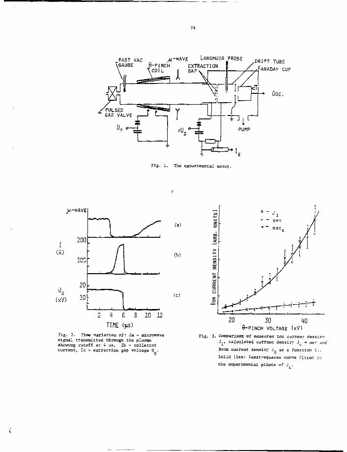
73
FAST VAC LANGMUIR PROBEDRIFT TUBE
/ ,FARAn/lV CUP
Osc.
Fig. 1. The experimental setup.
JJ--WAVE
I(A)
(KV)
fa)
Cb)
(c)
2 4 6 8 ID 12
TIME (ys)
Fig. 2. Time variation of: 2a - microwavesignal transmitted through the plasmashowing cutoff at 4 vs. 2b - collectorcurrent, 2c - extraction gap voltage U .
20 50 409-PINCH VOLTAGE [KV ]
Fig. 3. Comparison of measured ior. current densitv
J^. calculated current density J_ = nev and
Bohm current density J_ as a function U..
Solid line: least-squares curve fitted to
the experimental points of J. .
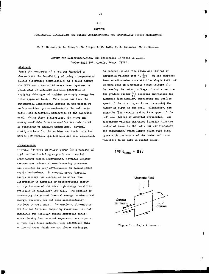
76
2.1
INVITED
FUNDAMENTAL LIMITATIONS AND DESIGN CONSIDERATIONS FOE COMPENSATED PULSED ALTERNATORS
W. F. tfeldon, W. I. Bird, M. D. Driga, K. M. Tolk, H. G. Sylander, H. H. Woodson
Center for Electrooechanics, The University of Texas at Austin
Taylor Hall 167, Austin, Texas 78712
Abstract
Since the beginning of a project intended to
demonstrate the feasibility of using a compensated
pulsed alternator (compulsator) as a power supply
tor NOVA and other solid state laser systems, a
great deal of interest has been generated in
applying this type of machine to supply energy for
ocher types of loads. This paper outlines the
fundamental limitations imposed on the design of
such a machine by the mechanical, thermal, mag-
netic, and electrical properties of the materials
used. Using these limitations, the power and
energy available from the machine are calculated
as functions of machine dimensions. Several
configurations for the machine and their relative
merits tor various applications are also discussed.
Introduction
Recently interest in pulsed power for a variety of
applications including magnetic and inertial
confinement fusion experiments, advanced weapons
systems and industrial manufacturing processes
r.as resulted in many developments in pulsed power
supply technology. In several areas inertial
energy storage has emerged as an attractive
alternative to magnetic or electrostatic energy
storage because of the very high energy densities
available at relatively low cosi:. The problea of
converting the stored inertial energy to electrical
energy, however, h..-s not been satisfactorily
•.resolved in nost case. . Conventional alternators
are Limited in powar output by their own internal
impedance and although puised homopolar gener-
ators, having low internal impedanca, are capaDle
of very high power outputs, they accomplish this
at low voltages vhich 3re not always desirable.
In essence, pulse rise times are limited by
inductive voltage drop (L •£?>• In its simplest
form an alternator consists of a single turn coil
of wire spun ic s. magnetic field (Figure 1).
Increasing the output voltage of such a machine
(to produce faster -r—) requires increasing the
magnetic flux density, increasing the surface
speed of the rotating coil, or increasing the
number of turns in the coil. Ultimately, the
magnetic flux density and surface speed of the
coil are limited by material properties. The
alternator voltaga increases linearly with' the
number of turns in the coil, but unfortunately
the inductance, which limits pulse rise time,
rises with the square of the number of turns
resulting in no gain in output power.
max = Bjv
Rotation
Figure 1: Simple Alternator
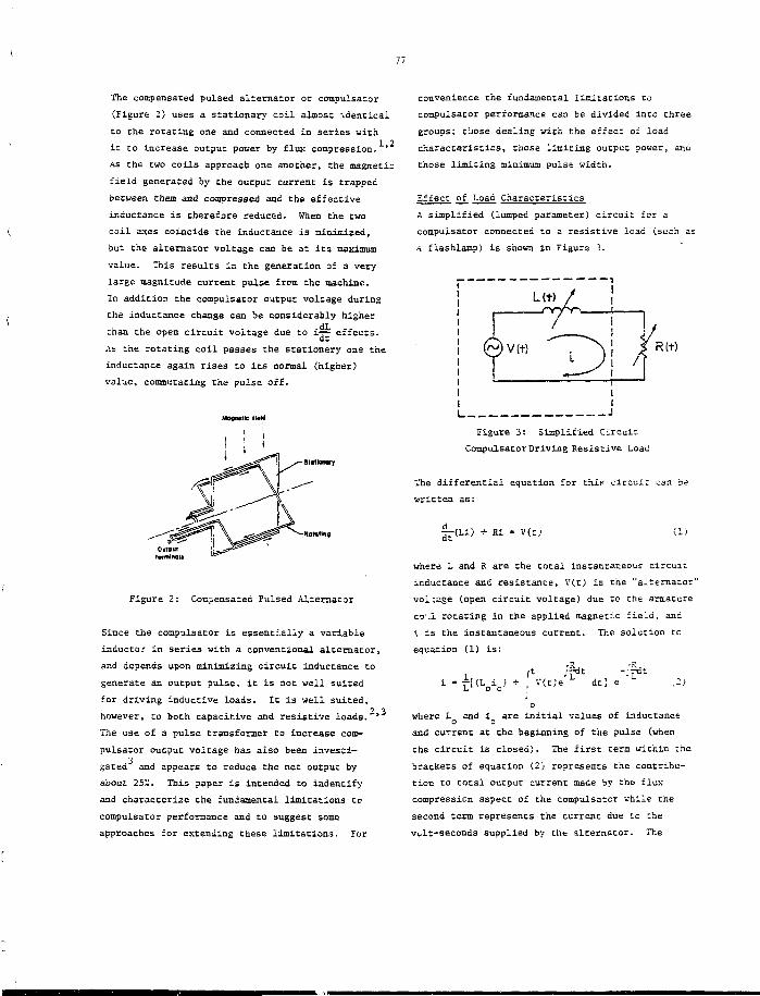
The compensated pulsed alternator or compulsator
(Figure 2) uses a stationary coil almost identical
to the rotating one and connected in series with
it to increase output power by flux compression. '*
As the two coils approach one another, the magnetic
field generated by the output current is trapped
between them and compressed and the effective
inductance is therefore reduced. When the two
coil axes coincide the inductance is minimized,
but tha alternator voltage can be at its maximum
value. This results in the generation of a very
large magnitude current pulse from the machine.
In addition the compulsator output voltage during
the inductance change can be considerably higher
than the open circuit voltage due to i-r— effects.
As the rotating coil passes the stationary one the
inductance again rises to its normal (higher)
value, commutating the pulse off.
Rotating
Figure 2: Compensated Pulsed Alternator
Since the compulsator is essentially a variable
inductor in series with a conventional alternator,
and depends upon minimizing circuit inductance to
generate an output pulse, it is not well suited
for driving inductive loads. It is veil suited,
however, Co both capacir.ive and resistive loads.
The use of a pulse transformer to increase com-
pulsator output voltage has also been investi-
gated and appears to reduce the net output by
about 25;;. This paper is intended to indentify
and characterize the fundamental limitations to
coinpulsator performance and to suggest some
approaches for extending these llmitationis. For
2,3
convenience the rundamental limitations to
compuisator performance can be divided into three
groups; t:iose dealing with Che effec; of load
characteristics, those limiting output power, and
those limiting minimum pulse width.
Effect of Load Characteristics
A simplified (lumped parameter) circuit for a
compulsator connected to a resistive load (such as
a flashlamp) is shown in Figure 3.
Figure 3: Simplified Circuit
Compulsator Driving Resistive Load
The differential equation for this circuit can be
written as:
dt(Li) + Ri - V(t) (1)
where L and R are the total instantaneous circuit
inductance and resistance, V(t) is the "alternator
vol:age (open circuit voltage) due to the armature
co1.1 rotating in the applied magnetic field, and
\ is the instantaneous current. The solution to
equation (1) is:
dtj e ,2.)
where L and i are initial values of inductanceo o
and current at the beginning of the pulse (when
the circuit is closed). The first term within the
brackets of equation (2) represents the contribu-
tion to total output current made by the flux
compression aspect of the compulsator while the
second term represents the current due to the
vult-seconds supplied by the alternator. The
78
first term primarily affeccs Che shape of Che
output pulse while the second term determines the
energy delivered co che load. For a wide range of
resiscive load cases investigated Che compulsacor
has been found Co reduce Che basic alternator half
cycle pulse width by a faccor of about 8.
For a capacitive load such as a transfer capacitor
the basic circuic is shown in Figure 4 and Che
differential equation for the circuit is:
V(t) (3)
^ c
Figure 4: Simplified Circuit
Compulsator Driving Capacitive Load
Although the analytical solucion of this second
order iif f erential equation is quit.' tumbersome
it can be solved numerically and the energy
delivered Co a capacitive load by a compulsacor
has been shown to be
(I v(c)dc)"
2L (4)sin
vnere L . is che niinimum '.local circuic inductancem m
and -. is a riur-erically decermined conscanc which
has been found co be around 0.5 for most cases of
inceresc. For the capacicive load case the
compulsacor has been found to compress the basic
alternator '.ialf cycle pulse width by a factor ofJ.OOUC •*.
'-imitations to Peak Output Power
It is apparent from equations (Z) and (•+) that checcmpulsator's primary advancage, in terns of high
output power, over che conventional alternator
comes from flux compression* or more specifically,
from the interaction of che discharge currenc with
che inductance variation. This in turn implies
Chat che inductance variation must be maximized
and since che maximum inductance in the uncompen-
saced position is relatively insensitive co
machine variables, really requires that che
minimum inductance in Che compensated position be
reduced as much as possible. This requirement
suggests che use of radially chin air gap windings
distributed uniformly over the rotor surface
rather Chan salienC pole windings or even distri-
buted windings in slots since the slot teeth
increase the winding inductance. A significant
limitation to peak output power comes then from
the conflict between che requirement for minimum
radial air gap between the rocor and stater
windings in order co minimize L . and che dielec-mxn
eric strength of the air gap insulation on the
windings. The inductance variacion is given by
(—) for an iron cored machine (unsaturaced) and8 T- e
by —(1 + a) for an air cored machine where - is
che conductor widch per pole and g is che radial
air gap between conductors, so that the sensitivity
of machine performance Co this air gap limicacion
is readily apparent.
k second limicacion on oucpuc power imposed by
this air gap winding concerns the shear strengch
of che insulacion syscem used Co bond the stator
and rocor windings to the atator and rotor struc-
tures. The interaction between the compulsator
discharge current and the radial component of the
magnetic field in the air gap due to that current
causes a tangential force on the conductors which
slows the rotor, converting stored inertial energy
to electrical energy. This force results in a
tangential shear stress on the insulation bond
between the conductors and the rotor or scacor.
This radial magnetic field component whicn depends
upon the time and position history of the currents
as well as the permeability and eddy currents in
the surrounding structure nas been calculated for
several cases using a transient, nonlinear, finite
element isagnecic field mapping code developed by
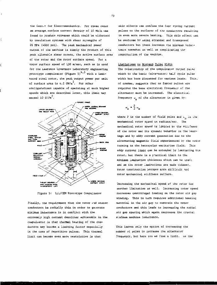
the Center for Electromechani.es. For these cases
an average, surface current density of 10 MA/m was
found to produce stresses which could be withstood
by insulation systems with shear strengths of
2S MPa (4000 psi). The peak mechanical power
output of the machine is simply the product of this
peak allowable shear stress, the active surface area
of the rotor and the rotor surface speed. For a
rotor surface speed of 150 m/sec, such as is used
for the Lawrence Livennore Laboratory engineering4 5
prototype compulsator (Figure 5) * with a lami-
nated steel rotor, the peak output power per unit
of surface area is 4.2 GW/m . For other
configurations capable of operating at much higher
speeds which are described later, this limit may
exceed 10 GVI/m".roitoue raute
UMIK tflUSHCt -\v
AND MUSH HIM* \^y
4MMMA1. K M M C
TMRUST KARINBHOU1INC WITH
HTOROSTATIC LIFT
Figure 5: LLL/CEM Prototype Compulsator
Finally, the requirement that the rotor t<nd stator
conductors be radially thin in order to generate
minimum inductance is in conflict with the
extremely high current densities achievable in the
compulsator in that thermal heating of the con-
ductors may become a limiting factor especially
in the case of repetitive pulses. This thermal
limit can become even more restrictive in that
skin effects can confine the fast rising current
pulses to the surfaces of the conductors resulting
in even more severe heating. This skin effect car.
be overcome by using stranded and transposed
conductors but these increase the minimum induc-
tance somewhat as well as complicating Lhe
construction of the machine.
Limitations tj> Minimum Pulse Width
The relationship of the compulsator output pulse
width to the basic (alternator) half cycle pulse
width has been discussed for various loads. This,
of course, suggests that as faster pulses are
required the base electrical frequency of the
alternator must be increased. The electrical
frequency LU of the alternator is given by:
Pid = ~ ue 2 m
where P is the number of field poles and in is zhe
mechanical rotor speed in radians/sec. The
mechanical rotor speed is limited by the stiffness
of the rotor and its dynamic behavior in the bear-
ings and by eddy current generation due to the
alternating magnetic field experinenced by the rotor
turning in the hetropolar excitation field. This
eddy current limit can be extended by laminating the
rotor, but there is a practical limit Co che
minimuo lamination thickness which can be used;
and as the rotor laminations are made thinner,
rotor construction becomes more difficult and
rotor mechanical stiffness suffers.
Increasing the mechanical speed of the rotor has
another limitation as well. Increasing rotor speed
increases centrifugal loading on the rotor air gap
winding. This in turn requires additional banding
material in the air gap to restrain the rotor
conductors and this leads to increasing the radial
air gap spacing which again increases the crucial
ir Inimum machine inductance.
This leaves only the option of increasing the
number of poles to increase the alternator
frequency, but here too we find a limit. As the
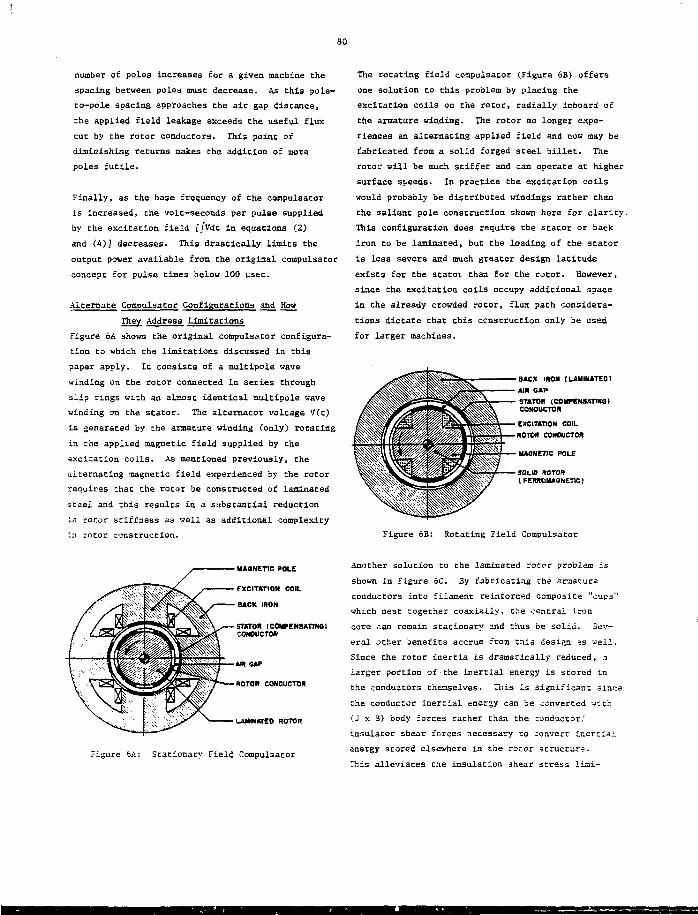
80
number of poles Increases for a given machine che
spacing between poles must decrease. As thia pole-
to-pole spacing approaches the air gap distance,
the applied field leakage exceeds the useful flux
cut by the rotor conductors. This point of
diminishing returns snakes che addition of more
poles futile.
Finally, as the base frequency of the compulsator
is increased, che volt-seconds per pulae supplied
by the excitation field [JVdt in equaclons (2)
and (i)] decreases. This drastically limits the
output power available from the original compulsator
concept for pulse times below 100 psec.
Alternate Compulaator Configurations and How
They Address Limitations
Figure 6A shows the original compulsator configura-
tion to which che limitations discussed in this
paper apply. It consists of a mulCipole wave
winding on the rotor connected in series through
slip rings with an almost identical multipole wave
winding on the stator. Hie alternator voltage '/(t)
is generated by che armature winding (only) rotating
in che applied magnetic field supplied by che
excitation coils. As mentioned previously, the
alternating magnetic field experienced by the rotor
requires that che rotor be constructed of laminated
steei and chis results in a substantial reduction
in rocor stiffness as well as additional complexity
in rotor construction.
The rotating field coapulsator (Figure 6B) offers
one solution to this problem by placing the
excitacion coils on the rotor, radially inboard of
the armature winding. The rotor no longer expe-
riences an alternating applied field and now may be
fabricated from a solid forged steel billet. The
rotor will be much stiffer and can operate at higher
surface steeds. In practice che excitation coils
would probably be distributed windings rather Chan
the salient pole construction shown here for clarity.
This configuration does require the stator or back
iron to be laminated, but the loading of the stator
is less severe and much greater design latitude
exists for the statoi than for the rotor. However,
since che excitation coils occupy additional space
in the already crowded rotor, flux path considera-
tions dictate that this construction only be used
for larger machines.
BACX IRON (LAMINATED)
AIR GAP
STATOR (COUPENSATINSICONDUCTOR
EXCITATION COIL
ROTO* CONDUCTOR
MAGNETIC POLE
SOLID ftOTO*(FERROMAGNETIC!
Figure 6B: Rotating Field Compulsator
MASNET1C POLE
FXCITATION COIL
SACK IRON
STATOR (COMPENSATING)CONDUCTOR
AM SAP
ROTOR CCaOUCTOR
LAMINATEO ROTOR
Figure 6A: Stationary Field Compulsator
Another solution to the laminaced roct?r problem is
shown in Figure 6C. By fabricating che armature
conductors into filament reinforced composite "cups"
which nest together coaxiaily, che central iron
core can remain stationary and thus be solid. Sev-
eral other benefits accrue from chis design as well.
Since the rotor inertia is dramatically reduced, a
larger portion of-che irertial energy is stored in
the conductors themselves. This is significant since
che conductor inercial energy can be converted wich
(J x 3) body forces rather than che conductor.'
insulator shear forces necessary to convert inertia!
anergy scored elsewhere in che rotor structure.
This alleviates che insulation shear stress lioi-
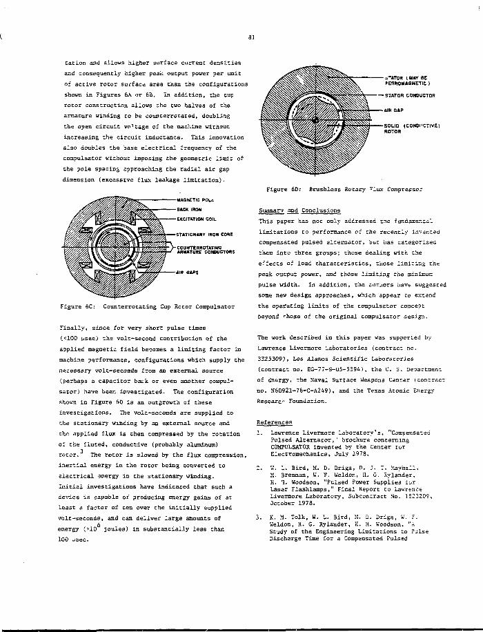
cation and allows higher surface current densities
and consequently higher peak output power per unit
of active rotor surface area than the configurations
shown in Figures 6A or 6B. In addition, the cup
rotor construction allows the two halves of the
armature winding to be counterrecaced, doubling
the open circuit voltage of the machine without
increasing the circuit inductance. This innovation
also doubles the base electrical frequency of the
compuisator without imposing the geometric limit of
the pole spaciD& approaching the radial air gap
dimension (excessive flux leakage limitation).
'MAGNETIC POLc
BACK IRON
EXCITATION COIL
STATIONARY IRON CONE
COUNTERROTATINGARMATURE CONDUCTORS
AIR SAPS
Figure 6C: Counterrotating Cup Rotor Compulsator
Finally, since for very short pulse times
(<100 usec) the volt-second contribution of the
applied magnetic field becomes a limiting factor in
machine performance, configurations which supply the
necessary volt-seconds from an external source
(perhaps a capacitor back or even another compul-
sator) have beer, investigated. The configuration
shown in Figure 6D is an outgrowth of these
investigations. The volt-seconds are supplied to
the stationary winding by an external source and
the applied flux is then compressed by the rotation
of the fluted, conductive (probably aluminum)
rotor. The rotor is slowed by the flux compression,
inertlal energy in the rotor being converted to
electrical energy in the stationary winding.
Initial investigations have indicated that such a
device is capable of producing energy gains of at
least a factor of ten over the initially supplied
volt-seconds, and can deliver large amounts of
energy (>10 joules) in substantially less than
100 usec.
S-ATOR (MAY BEFEnROMAQNETIC )
STATOR CONDUCTOR
AIR GAP
SOLID (CONDUCTIVE)ROTOR
Figure 6D: Srushless Rotary rlux Compressor
Summary and Conclusions
This paper has not only addressed tne fundamental
limitations to performance of the recently invented
compensated pulsed alternator, but has categorized
them into three groups; chose dealing with the
effects of load characteristics, those limiting the
peak output power, and those Uniting the ainimuc:
pulse width. In addition, the authors have suggested
some new design approaches, which appear co extend
the operating limits of the compulsator concept
beyond ""hose of the original corapulsator design.
The work described in this paper was supported by
Lawrence Livermore Laboratories (contract no.
3325309), Los Alamos Scientific Laboratories
(contract no. EG-77-S-O5-5594), the L". S. Department
of energy, the Naval Surface Weapons Center (contract
no. N60921-7S-C-A249), and the Texas Atomic Energy
Research Foundation.
References
1. Lawrence Livermore Laboratory's, "CompensatedPulsed Alternator, ' brochure concerningCOMPULSATOR invented by the Center forElectromechanlcs, July 1978.
2. •»•. L. Bird, M. D. Driga, D. J. 7. Mayhall,M. Brennan, K. F. Weldor., a. G. Rylander,H. 'I. Woodson, "Pulsed Power Supplies forLaser Flashlamps," Final Report to LawrenceLivermore Laboratory, Subcontract So. 1823209,October 1978.
3. K. M. Tolk, H. L. Bird, H. D. Driga, W. F.Weldon, H. G. Rylander, P.. H. Koodson, "AStudy of the Engineering Limitations to PulseDischarge Time for a Compensated Pulsed
82
Alternator," Final Report to Los AlamosS ien-cifig Laboratories, Order No. N68-0899H-1, May 1979.
4. J. H. Gully, W. L. Bird, M. D. Driga, H. G.Rylander, K. M. Tolk, W. F. Weldon, H. H.Ucadson, "Design of the Armature Windings ofa Compensated Pulsed Alternator EngineeringPrototype," 2nd IEEE International PulsedPower Conference, Texas Tech University,Lubbock, Texas, June 12-14, 1979.
5. M. Brennan, W. L. Bird, J. H. Gully, M. L.Spann, K. M. Tolk, W. F. Weldon, H. G. Rylander,H. H, Woodson, "The Mechanical Design of aCompensated Pulsed .-'.Itamator Prototype,"Za.d IEEE International Pulsed Power Conference,Texas Tech University, Lubboclc, Texas,June 12-14, 1979.
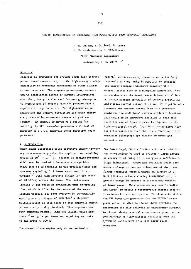
S3
USE OF TRANSFORMERS IK PRODUCING HIGH POWER OUTPUT FROX HOMOPCLAK GENERATORS
W. E. Lupton, R. D. Ford, D. Conte
H. B. Lindstrom, I. M. Vitkovitsky
Naval Research Laboratory
Washington, D. C. 20375
Abstract
Analysis is presented for systems using high current
pulse transformers to exploit the high energy storage
capability of homopolar generators or other limited
current sources. The stepped-up secondary current
can be established either by current interruption
when the primary is also used for energy storage o-
by commutation of current into the primary from a
separate storage inductor. For high-power pulse
generators the primary insulation and power supply
are protected by subsequent crowbarring of the
primary. An example is given of a design for
matching the NKL homopolar generator with 1.46 mH
inductor to a 1--:H, megavolt level inductive pulse
generator.
I. Introduction
Fuise power generators using inductive energy storage
may have economic promise for applications requiring
powers of 10 - 10 W. Studies of opening switches
which must be used with inductive storage have
shown that it is possible to use carefully made and
operated exploding foil fuses as current inter-1 2
rupters with high electric fields (of the order
of 20 kV/cm) across the fuse. The limitations
imposed b*-' the ratio of conduction time to opening
time, which is fixed by the nature of the vapor-
isation process, has been overcome by sequentially
opening several stages of switches with power
multiplication at each stage so that megavolt output
pulses are typically obtained. This approach has
been extended recently with the TRIDENT pulse gen-
erator using larger fuses and requiring currents
of the order of 500 kA.
The advent of the explosively driven mechanical
switch , which can carry these currents for long
intervals of time, make it possible ro energize
the energy storage inductance directly with a
current source such as a homopolar generator. One
in existence at the Naval Research Laboratory"' has
an energy storage capability of several megajoules
and typical current output of 40 kA. To significantly
increase the current output from this generator
would require additional current-collector brushes.
This would be an expensive addition in this case
since the use of fiber brusnes is required by the
high rotational speed. This is an exaggerated case
but illustrates the fact that the current output of
homopolar generators are limited by brush and
contact area.
Any power supply with a limited current c lability
can nevertneless be used to deliver a large amount
of energy by allowing it to energize a sufficien-ly
large inductance. Subsequent switching which pro-
duces a change in current allows use of the trans-
former principle where a change in current in a
multiple—turn primary winding is accompanied by a
greater change in current in a secondary winding
of fewer turns. This procedure was used by Walker
and Early to obtain a hundred-fold current step-up
in an inductive storage system. The desire to utilize
the NRL homopolar generator for the TRIDENT high-
power pulser studies mentioned above provides the
motivation for this analysis of transformer systems.
In circuit design special attention is given to the
consequences of high-voltages resulting when the
system is used a part of a high-power pulse
generator.
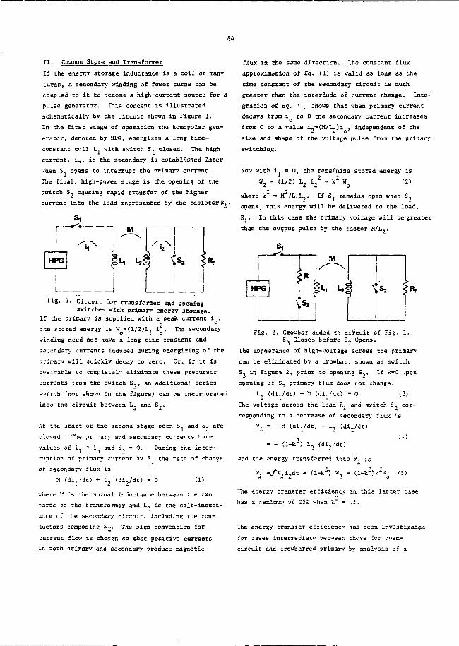
II. Common Score and Transformer
If the energy storage inductance is 3 coll of many
turns, a secondary winding of fewer turns can be
coupled to it to become a high-current source for a
pulse generator. This concept is illustrated
schematically by the circuit shown in Figure 1.
In the first stage of operation the homopolar gen-
erator, denoted by HPG, energizes a long tine—
constant coil L^ with switch Sj closed. The high
current, i,, in the secondary is established later
when S opens to interrupt the primary current.
The final, high-power stage is the opening of the
switch S., causing rapid transfer of the higher
current into the load represented by the resistor R,.
Fig. 1. Circuit for transformer and openingswitches with primary energy storage.
If the primary is supplied with a peak currenc i ,
the stored energy is W °»(1/2)L, i . The secondaryo 1 0
winding need not have a long time constant and
.secondary currents induced during energizing of the
primary will quickly decay to zero, Or, if it is
desirable Co completely eliminate these precursor
currents from the switch S?, an additional series
switch (not shown in the figure) can be incorporated
into che circuit between L, and S.;.
At the start of the second stage both 5. and S, are
closed. The primary and secondary currents have
values of 1, = i and i, • 0. During Che inter-
ruption of primary current by ST the rate of change
of secondary flux is
M (di,/dt) + L, (di,/dt) - 0 (1)
where M is che nucual inductance between the cwo
parts 3i che transformer and L_ is che self-inducc-
3r.ce of che secondary circuit, including che con-
ductors composing So. The sign convention for
current flow is chosen so chat positive currents
in both primary and secondary produce magnetic
flux in the same direction. The constant flux
approximation of Eq. (1) is valid as long as the
time constant of the secondary circuit is much
greater than the interlude of current change. Inte-
gration of Eq. ''. .shows that when primary current
decays from i to 0 the secondary current increases0
from 0 to a value ij-WL.,)! , independent of the
size and shape of the voltage pulse from the primary
switching.
Now with i, » 0, the remaining stored energy is
tf2 - (1/2) L, i 22 = k2
W Q (2)
where k" - M/L.L,. If 5, remains open when S,
opens, this energy will be delivered to the load,
R,. In this case the primary voltage will be greater
than the output pulse by the factor M/L,.
Fig. 2. Crowbar added to circuit of Fig. 1.S, Closes before S, Opens.
The appearance of high-voltage across the primary
can be eliminated by a crowbar, shewn as switch
S, in Figure 2, prior co opening S-,. If R«0 upon
opening of S, primary flux does not changa:
(dlL/dt) + M (di,/dt) - 0 (3)
The voltage across che load R. and switch S, cor-
responding co a decrease of secondary flux is
V. =• - M (dit/dt) - L, (di,/dt)
= - Cl-k2) L, (di,/dt)
and the energy transferred into R. is
(5)
The energy transfer efficiency in this latter case
has a -aximum of 252 when k" • .5.
The energy transfer efficiency has been investieatea
for cases intermediate between those for oper.-
circuit and crowbarred primary by analysis c-f a
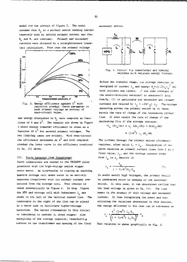
85
model for the circuit of Figure 2. The model
assumes that S is a perfect switch opening instan-
taneously with no initial primary current and that
R. and R, are constant. Primary and secondary
currents were obtained by a straightforward trans-
ient calculation. Frora then the primary voltage
secondary switch.
02 0.4 0-6TRANSFORMER COUPUNG. k
1.0
Fig. 3. Energy efficiency against k withresistive crowbar. Curve parameter ispeak primary voltage as percent ofopen-circuit value.
and energy dissipated in R, were computed as func-2 *tions of R and k . The results are shown in Figure
3 where energy transfer efficiency is shown as a
function of k for several primary voltages. The
two limiting cases are evident. With open-circuit
the efficiency increases as k and with complete
crowbar the lower curve is the efficiency predicted
by Eq. (5) above.
III. Stcre Separate from Transformer
Short connections are needed to the TRIDENT pulse
generator with its high-voltage switch stages
under water. An alternative to placing an existing
massive storage coil under water is an entirely
separate transformer with its primary current com-
murated from the storage coil. This concept is
shown schematically in Figure 4. In that figure
the HPG and storage coil with inductance L are
shown to the left of the vertical dashed line. The
components to the right of the line can be placed
in a water tank to facilitate higher-voltage
operation. The device represented by this circuit
is considered to operate iii three stages: slow
energizing of the storage inductor, transferring
current to the transformer and opening of the final
HPG
M
Fig. it. Circui- fur transformer and openingswitches wizh separate energy storage.
Before the transfer stage, cue storage inductor is
energized by current i and energv W =il'2)L i ' ando °- c- o c
both switches are closed. If the time constant of
the short-circuited secondary is adequately long
then Eq. (1) is applicable and secondary and primary
currents are related by i, - -(M/L,) i,. The voitage
appearing across the primary switch as it opens
equals the rate of change of the increasing primary
flux. It also equals the rate of change of the
decreasing flux of the storage inductor.
- L Q (dis/dt) - L, (dij/dr) ->• S(di,/dt)
- (1-k2) Lj di,/dt
The current through the primary switch ultimate!'.-
vanishes, after which i = i_. Integration of the
above equation as primary current rises fron 0 to a
final value, i,, and the storage current drops
from iQ to i results in
1 - Cl-k-)L,/L1 o
To avoid unduly high voltages, the primary should
be crowbarred prior to opening of the secondary
switch. In this case, it was determined earlier char
the load voltage is given by Eq. (i). The load
power is the product of this voltage and secondary
current. By time integrating the power and sub-
stituting the relations determined in this section,
the energy delivered to the loac can be expressed as
M.
This relation is shown graphically in Fig. 5.
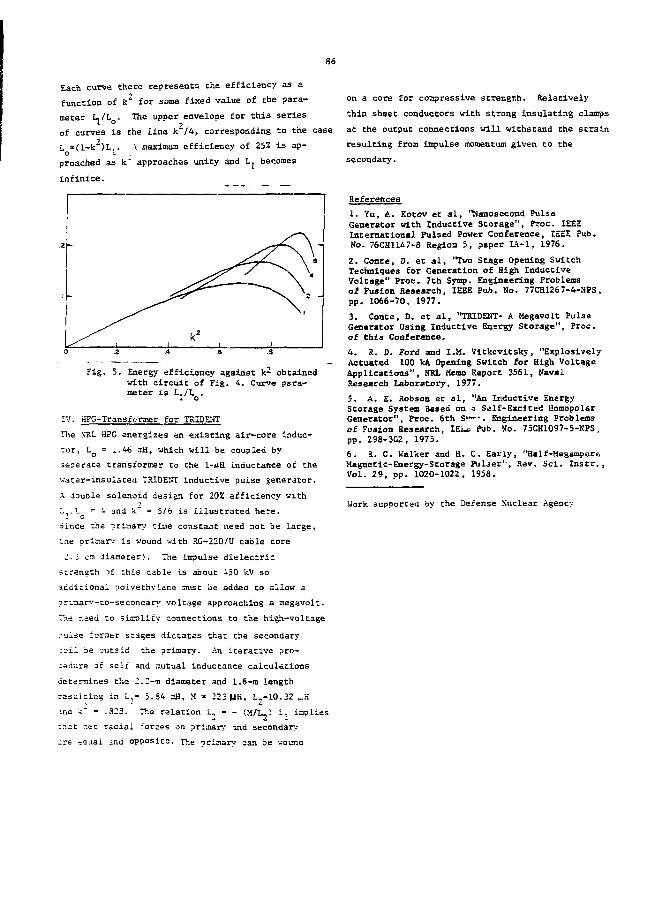
86
Each curve there represents the efficiency as a
function of k2 for some fixed value of the para- on a core for coapressive strength. Relatively
meter L./L . The upper envelope for this series thin sheet conductors with strong insulating clamps
of curves is the line k2/4, corresponding to the case at the output connections will withstand the strain
L »(l-k2)L . A maximum efficiency of 25% is ap- resulting from impulse momentum given to theo 1proached as k" approaches unity and Lj becomes secondary.
infinite.
Fig. 5. Energy efficiency against k2 obtainedwith circuit of Fig. 4. Curve para-meter is L,/L .
1 o
IV. ttPG-Transfcrmer for TRIDENT
The NRL HPG energizes an existing air-core induc-
-or, LQ = i.46 3iH, which will be coupled by
seaerace transformer to the 1-MH inductance of the
vacer-insulated TRIDENT inductive pulse generator.
A double solenoid design for 20% efficiency with
-,.!. - '- and k~ = 5/6 is illustrated here.
Since che primary time constant nead not be large,
:ne primary is vound vith RC-220/U cable core
J.3 cni diameter). The impulse dielectric
strength oi ;his cable is about 450 kV so
additional polyethylene :nust be added to allow a
primary-to-secondary volcage approaching a megavolt.
The naed co simplify connections to the high-voltage
puise former stages dictates that the secondary
coil be autsid the primary. An iterative pro-
cedure ot self and mutual inductance calculations
determines the 2.2-m diameter and 1.6-m length
rssuicing in L,- 5.34 aH, M » 223 |iH, L,-10.32 .a
ma '&' = .328. The relation in = - (M/L,) i, implies
that r.ez raaial forces on primary' and secondary
re -=auai and opposite. The nrimarv can be vound
References
1. Vu, &.. Kotov et al, "Nanosecond PulseGenerator with Inductive Storage", Proc. IEEEInternational Pulsed Power Conference, IEEE Pub.No. 76CH1147-8 Region 5, paper IA-1, 1976.
2. Conte, 0. et al, "Two Stage Opening SwitchTechniques for Generation of High InductiveVoltage" Proc. 7th Symp. Engineering Problemsof Fusion Research, IEEE Pub. No. 77CH1267-4-NPS,pp. 1066-70, 1977.
3. Conte, D. et al, "TBIDENT- A Megavolt PulseGenerator Using Inductive Energy Storage", Proc.of this Conference.
4. R. D. Ford and I.M. Vitkovitsky, "ExplosivelyActuated 100 kA Opening Switch for High VoltageApplications", NRL Memo Report 3561, NavalResearch Laboratory, 1977.
5. A. E. Robson et al, "An Inductive EnergyStorage System Based on a .Self-Excited HomopolarGenerator", Proc. 6th S"~-. Engineering Problemsof Fusion Research, IEi.ii Pub. No. 75CH1097-5-KPS,pp. 298-3C2, 1975.
6. R. C. Walker and B. C. Early, "Half-MegampereMagnetic-Energy-Storage Pulaer'', Rev. Sci. Instr.,Vol. 29, pp. 1020-1022, 1958.
Work supported by the Defense Nuclear Agency
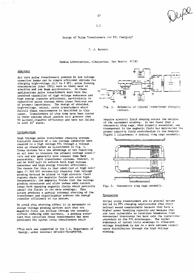
87
2.3
Design of Pulse Transformers for PFL Charging*
"• J . Rohwein
Sandia Laboratories, Albuquerque. New Mexico S71S5
Abstract
Air core pulse transformers powered by iow voltagecapacitor banks can be sinple efficient systems forcharging high-voltage (0.5 to 3 MV), pulse formingtransmission lines (PFL) such as those used inelectron and ion bean accalerators. In theseapplications pulse transformers must have thecombined capability of high voltage endurance andhigh energy transfer efficiency, particularly inrepetitive pulse systems where these features areof primary importance. The design of shielded,high—voltage, spiral, strip transformers whichfulfill these requirements is described in thispaper. Transformers of this type have been testedin three systems which jperate wi;h greater than90 percent transfer efficiency and have not failedin over 10 shots.
Introduction
High voltage pulse transformer charging systemstypically consist of a low voltage capacitor bankcoupled to a high voltage PFL through a voltagestep up transformer as illustrated in Fig. 1.These systems have the advantage of not requiringan oil tank to insulate the primary storage capaci-tors and are generally more compact than Marxgenerators. With transformer systems, however, itcan be difficult to achieve both high voltageendurance and high energy transfer efficiency.The reason for this is that operation at high volt-ages (> 500 kV) necessarily requires that voltagegrading devices be placed in high electric fieldregions where the magnetic fields are also high.Consequently, the magnetic fields link the voltagegrading structures and often induce eddy currentloops with opposing magnetic fields which partiallycancel the fields in the main windings. Thisaction produces a partial internal shorting of thetransformer and significantly reduces the energytransfer efficiency of the system.
To avoid this shorting effect it is necessary todesign voltage grading devices such that themagnetic field can diffuse through the assemblywithout inducing eddy currents. A grading struc-ture that satisfies these requirements has beendeveloped for spiral strip transformers which
*This work was supported by the U.S. Department ofEnergy, under Contract DE-AC04-76-DP00789.
Fig. I. Schematic of typical transformer chargingcircui t.
require electric field shaping across the marginsof the secondary winding. It was found that aconcentric ring cage, when properly assembled, -.-astransparent to the magnetic field but maintained cnproper electric field distribution in the margins.Figure 2 illustrates- a typical ring cage assembly.
vjOQ
Fig. 2. Concentric ring cage assembly.
Discussion
Sprial strip transformers are in general bettersui-ed to PFL charging applications than theirhelical wound counterparts because they have ahigher power handling capacity and because theyare less vulnerable to incerturn breakdown fromnanosecond transients fed back into the transformersecondary by the PFL discharges. The higherendurance of sprial strip windings to transientvoltage breakdown is due to a more optimum capaci-tance distribution through the high voltagewinding.
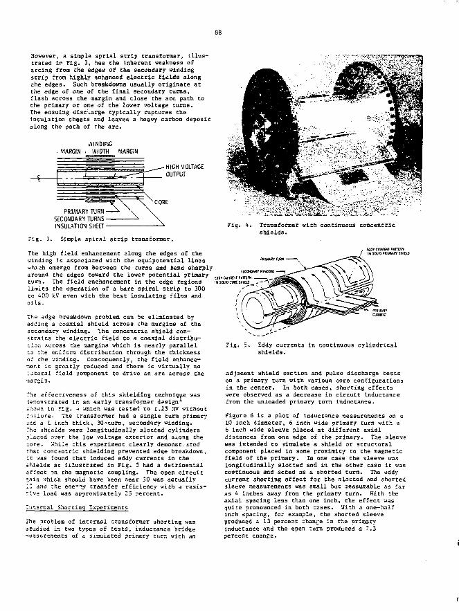
88
However, a simple sprial strip transformer, Illus-trated in Fig. 3, has the inherent weakness ofarcing from the edges of the secondary windingstrip from highly enhanced electric fields alongthe edges. Such breakdowns usually originate atthe edge of one of the final secondary turns,flash across the margin and close the arc path tothe primary or one of che lower voltage turns.The ensuing discharge typically ruptures theinsulation sheets and leaves a heavy carbon depositalong Che path of Mie arc.
WINDING. MARGIN i WJDTH MARGIN
HIGH VOLTAGEOUTPUT
COREPRIMARY TURN-
SECONDARY TURNS-INSULATION SHEET- Fig. 4. Transformer with continuous concentric
shields.Fig. 3. Simple spiral strip transformer.
The high field enhancement along the edges of thewinding is associated with the equipotential lineswhich emerge from between the turns and bend sharplyaround che edges toward the lower potential primaryturn. The field enchancement in the edge regionslimits Che operation of a bare spiral strip to 300to 400 kV even with che best insulating films andoils.
The edge breakdown problem can be eliminated byadding a coaxial shield across che margins of thesecondary winding. Ihe concentric shield con-strains che electric field Co a coaxial distribu-cion across che margins which is nearly parallelca the uniform distribution through the thicknessor che winding. Consequently, che field enhance-ment is greaciy reduced and there is virtually noliteral field component Co drive an arc across themargin.
The effecciveness ol this shielding cechnique wasiejionstraced in an early transformer designshown in Fig. 4 which was testeri' to 1.25 MV wichoucfailure. The transformer had a single turn primaryand a 1 inch thick, 30-turn, secondary winding.The shields were longitudinally slotted cylindersplaced over the low volcage exterior and sj.ong thecore. While this experiment clearly demonst. itedthat concentric shielding prevented edge breakdown,It was found that induced eddy currents in cheshields as illustrated in Fig. 5 had a detrimentalaffect on the magnetic coupling. The open circuitgain which should have been near 30 was actually12 and the ene~v? transfer efficiency with a resis-tive load was approximately 25 percent.
Internal Shorting Experiments
The problem of internal cransformer shorting wasstudied in two types of tests, inductance bridge-neasuraraents or a simulated primary c u m wich an
i £SDt CURRENT PjlTTSSf/ I I SOLID PRIMARY SHIELD
SECCKOARY WIMOING
CODY CURRENT P«m.°N
IN SO.I0 COS SHIttf l ~
Fig. 5. Eddy currents in continuous cylindricalshields.
adjacent shield section and pulse discharge Cescson a primary turn with various core configurationsin che center. In both cases, shorting effectswere observed as a decrease in circuit inductancefrom the unloaded primary turn inductance.
Figure 6 is a plot of inductance measurements on a10 inch diameter, 6 inch wide primary turn with a6 inch wide sleeve placed at different axialdistances from one edge of the primary. The sleevewas intended to 'simulate a shield or structuralcomponent placed in some proximity to the magneticfield of the primary. In one case the sleeve waslongitudinally slotted and in the other case it wascontinuous and acted as a shorted turn. The eddycurrent shorting effect for the slotted and shortedsleeve measurements was small but measurable as faras 4 inches away from the primary turn. With cheaxial spacing less Chan one inch, che effect wasquite pronounced in both cases. With a one-halfinch spacing, for example, the shorted sleeveproduced a 13 percent change in the primaryinductance and the open C u m produced a 7.3percent cnange.
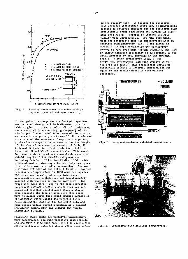
89
£ 220
I 2
DISTANCE FROM EDGE OF PRIMARY, INCHES
Fig. 6, Primary inductance variation with anadjacent shorted and open turn.
In the pulse discharge tests a 14.5 (if capacitorwas witched through a 4 inch diameter by '• inchwide single turn primary coil. Circ<.'- inductancewas determined from the ringing frequency of thedischarge. The unloaded inductance of the circuit(no core in the primary coil) was 98 nH. A slottedcore tube of the same axial length as the primaryproduced no change in inductance but as the lengthof the slotted tube was increased to 8 inch, 12inch and 14 inch the circuit inductance fell to76 nH, 65 nH and 53 nH, respectively. This resultindicated a shorting effect strongly dependent onshield length. Other shield configurationsincluding screens, foils, longitudinal rods, etc.produced similar shorting effects* Only two typesof shields snowed virtually no shorting. One wasa slotted cylinder of resistive film with a surfaceresistance of approximately 1000 ohms per square.The other was an array of rings interspacedapproximately one eighth inch and longitudinallyaligned with the =xis of the primary turn. Therings were made with a gap in the hoop directionto prevent circumferential current flow and wereconnected together electrically along a singleline opposite the line of gaps such that therewere no closed loops that could conduct current inthe assembly which linked the magnetic field.Pulse discharge tests on the resistive film andring shield models showed a maximum of 3 percentinductance change with and without the shieldassemblies in place.
Following these tests two prototype transformerswere constructed, one with resistive film shieldsand one with a ring type core shield in combinationwith a continuous external shield which also served
as the primary turn. In testing the resistivefilm shielded transformer there were ho measureabieeffects of internal shorting but the resistive filmconsistently broke down along the surface at volt-ages over 500 kV. Efforts to improve the file,quality were unsuccessful. The ring core nodelwith the continuous case was incorporated into anelectron beam generator <Fig. 7) and tested to600 kV. In this application the transformerproved to have good high voltage endurance but withan energy transfer efficiency of 52 percent, iz wasstill affected by eddy currents ir. the externalshield. A third transformer (Fig, 8) was,there ore, constructed with ring shields on boththe c-re and case. This transformer showed nomeasurable effects of internal shorting and wasequal to the earlier model in high voltageendurance•
-TRANSFORMER pVOLTAGEPROBE
Fig. 7. Ring and cylinder shielded transformer.
Fig. S. Concentric ring shielded transformer.
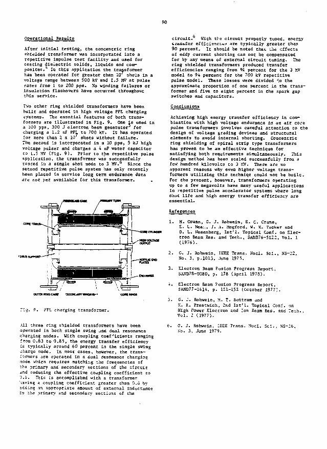
90
Operational Results
After initial testing, the concentric ringshielded transformer was incorporated into arepetitive impulse test facility and used fortesting dielectric solids, liquids and com-posites. * In this application the transformerhas been operated for greater than 10 shois In avoltage range between 500 kV and 1.5 MV at pulserates from 1 to 200 ppa. So winding failures orinsulation flashovers have occurred throughoutthis service.
Two other ring shielded transformers have beenbuilt and operated In high voltage PFL chargingsystems. The essntlal features of both trans-formers are illustrated in Fig. 9. One is used ina 100 pps, 300 J electron beam generator forcharging a 1.2 nF PFL to 700 kV. It has operatedfor more than 2 x 10 shots without failure.The second Is Incorporated in a 10 pps, 5 kj highvoltage pulser and charges a 4 nF water capacitorto 1.5 MV (Fig. 9). Prior to the repetitive pulseapplication, the transformer was successfullytested in a single shot mode to 3 MV.° Since thesecond repetitive pulse system has only recentlybeen placed in service long tern endurance dataare not yet available for this transformer.
ouimmacue szcauinr
Fl>. 9. PFL charging transformer.
All three ri:ig shielded transformers have beenoperated in both single swing and dual resonancecharging modes. With coupling coefficients rangingfrom 0.83 to 0.85, the energy transfer efficiencyis typically around 60 percent in the single swingcharge node. In most cases, however, the trans-formers are operated in a dual resonance charging.tode vhich requires matching the frequencies of:he primary and secondary sections of the circuitand reducing Che effective coupling coefficient tol.i. This is accomplished with a transformer'laving a coupling coefficient greater than 0.5 by-adding an appropriate amount of external inductance:o ;he prioary and secondary sections of the
circuit. With ths circuit properly tuned, energytransfer efficiencies are typically greater than90 percent. It should be noted thac the effectsof eddy current shorting can not be compensatedfor by any means of external circuit tuning. Thering shielded transformers produced transferefficiencies ranging from 91 percent for the 3 MVmodel to 94 percent for the 700 tcV repetitivepulse model. These losses were divided \n theapproximate proportion of one percent in the trans-former and five to eight percent in the spark gapswitches and capacitors.
Conclusions
Achieving high energy transfer efficiency in com-bination with high voltage endurance In an air corepulse transformers involves careful attention to thedesign of voltage grading devices and structuralelements to avoid internal snorting. Concentricring shielding of spiral strip type transformershas proven to be an effective technique forsatisfying both requirements simultaneously. Thisdesign method has been scaled successfully from afew hundred fcilovolts to 3 MV. There are noapparent reasons why even higher voltage trans-formers utilizing this techniqe could not be built.For the present, however, transformers operatingup to a few megavolts have many useful applicationsin repetitive pulse accelerator systems where longshot life and high energy transfer efficiency areessential.
References
1. M. Cowan, G. J. Rohwein, E. C. Crane,E. L. Nea.., J. A. Mogford, U. K. Tucker andD. L. Wesenberg, Int'l. Topical Conf. on Elec-tron Beam Res. and Tech., SAHD76-5122, Vol. 1(1976).
2. G. J. Rohwein, IEEE Trans. Sucl. Sci., NS-22,No. 3, p.1013, June 1975.
3. Electron Beam Fusion Progress Report,SAND78-0080, p. 178 (April 197S).
4. Electron Beam Fusion Progress Report,SAND77-1U4, p. 131-152 (October 1977).
5. G. J. Rohwein, M. T. 3uttram andK. R. Prestwich, 2nd lat'l. Topical Conf. onHigh Power Electron and Ion Beam Res. and Tech.,Vol. 2 (1977).
6. C-. J. Rohwein, IEEE Trans. Sucl. Sci., NS-26,No. 3, June 1979.
91
3.1
PULSE SHARPENING IK FERRITE TRANSMISSION LINES
Maurice Weir.er
Electronics Technology and Devices LaboratoryUSA Electronics R&D Command
Fort Monmouth, New Jersey 07703
Abstract
Pulse sharpening effects in ferrite transmissionlines may be used Co obtain kV pulses with nsrisetime. The exact description of the sharp-ening effect requires complex shock waveanalysis1. In this paper an approximate butuseful physical model is discussed. The ferriteis treated as a lossy but linear transmissionline from which equivalent design results areobtained. In many instances the nonlineareffects present are confined to a region whichis small compared to the total transmissionlength, which makes the linear approximationmore plausible. Preliminary experimentalresults, based on a 130 cm long line, are inaccord with the predictions of the model.
Introduction
In recent years an increasing need has arisenfor kV pulsers with ns risetimes. In the areaof pulsers for ma wave tubes, for example,extremely narrow pulse widths (< 5 ns) aredesired for improved resolution. At the sametime pulse repetion rates as high as 20 kHz,with pulse voltage and current amplitudes up to15 kV and 1000 A, respectively, are required.These simultaneous requirements place tremendousburde-s on the switch, which is the key elementin the design of fuch a pulser. Switches nowavailable do not simultaneously satisfy the rise-time, FRR, and power requirements. For examplespark gaps satisfy the risetime and peak powerrequirements, but are unable to satisfy the PRRrequirement.
A promising solution to the switch problem isthe use of a slower risetime switch in combina-tion with a ferrite pulse sharpener. The incor-poration of a ferrite pulse sharpener into thedischarge circuit has the advantage of simulta-neously providing fast risetime, large PER, andlarge peak power levels. There are disadvan-tages, however, and these are added circuit
complexity and bulk, as well as lowered circuitefficiency caused by the need for bias current.Nevertheless the ferrite pulse sharpener haspotential in an area where there are fewtechnological alternatives.
In recent years the bulk of the scientificliterature on ferrite pulse sharpeners hasappeared in the USSR. In particular, the workby Kataev emphasized the shock wave aspects ofthe wave propagating in the ferrite. Exactanalysis has indicated the formation of shockwaves under a variety of conditions, ana suchwaves are important in the interpretation ofpulse sharpening effects.
In this report an elementary model for thepulse sharpening effect is presented, whereinthe ferrite is treated as a lossy but lineartransmission line. A simplifying feature isintroduced with the idea of a spin saturationfront, which travels along the length of theferrite. The shock wave nature of the problemis pointed out, but emphasis is placed onsimple and useful solutions which are possiblewithout explicitly solving the shock waveproblem.
Outline of Model
We consider a ferrite transmission line which isuniformly magnetized in the direction transverseto the direction of propagation (Fig. ! ) • Atransmission line without ferrite, with imped-ance Z , is connected to the input terminals ofthe ferrite. A pulse with risetime TR is inci-dent upon the ferrite. The polarity of themagnetic field of the pulse is opposite to thatof the magnetization. As a consequence thepulse will see a large RF impedance; consistingof an inductance, as well as a resistive compo-nent caused by dissipation in the ferrite. Forthe most part the signal will be reflected,although a substantial percentage of the inci-dent energy will propagate into the ferrite.The region close to the start of the ferriteline will not continually appear as a largeimpedance, however. Eventually this portion ofthe ferrite will suddenly reach saturation.When this happens the large impedance willsuddenly decrease to the saturated impedance,
92
Z , which by design is chosen equal to ZQ, Cheinput impedance. As shown in Fig. 1, this proc-ess continues, so that a "spin saturation front"propagates along the length of the ferrite. Thevelocity of this front will increase as thepulse amplitude is increased. The ferrite lineis designed such that, vh<ai the front reachesthe end of the ferrite line (i.e., the entirelength of the ferrite is completely magnetizedin the opposite direction) the pulse is near orat its plateau value. This will occur at t •TR ignoring transit cime effects, i.e., assum-ing the velocity In Che saturated region ismuch larger than the velocity of the spin satu-racion front.
The advance of the spin saturation front must bedistinguished from the region of magnetic fieldpropagating beyond the spin saturation front.Such field penetration arises from the inherentdelay which exists between the onset of themagnetic field and Che Cine needed for thespins ;o change direction. The field penetra-tion is confined to a "propagation width,"Fig. 2. In this region the magnetizationchanges continuously between the two appositelysaturated states. At the spin saturation frontche magnetization is aligned with the incidentmagnetic field, and the changeover to the lowersaturation Impedance is Imminent. AC the farend of the propagation width the field signal hfhas just arrived and Che magnetization is stillsaturated and opposite to that of the field.The field is also shown as terminating abruptlyat the end of the propagation width. This sim-plifies the model but in fact dispersion effects,which result from the presence of loss in thetransmission line, will tend to cause the fieldto decrease more gradually.
As implied in Fig. 2 the field propagating be-yond the spin reversal front will be dampened,resulting from the dissipation which accompaniesche rotation of Che spins. The propagationwidth, as well as che amount of damping, willvary, depending on the ferrite loading and nu-merous other parameters. In most cases thefield penetration will be small, on che order ofa fev centimeters, compared to the toCal lengthof the ferrice line which is cypically one-eter long. The relatively small region Cowhich che propagation is confined makes plausi-ble certain simplifications in the descriptionof pulse sharpening, without resorting Codetailed shock wave analysis.
Anaivsis of Model
For concreteness we consider a coaxial trans-mission line in which che ferrite fills the en-tire space between inner and outer conductors.The analysis may be easily extended Co cHe casewhere the line is partially filled vich ferrite,ir. which we have concentric dielectric and fer-rice sleeves. It is also assumed the ferritetransmission Line is connected to a load Z L
while the input is connected Co another lineof impedance Zo (Fig. 3).
In che saturated region of the line the ferritehas an inductance per unit length (Ls) and a ca-pacitance per unit length (Cs). Ls, C3, and Zs
are given by standard expressions for the coaxialline.
When the ferrite magnetization is not alignedwith the incident magnetic field, che ferritewill appear as a large ispedance relative co thesaturated impedance. When this happens most ofChe input energy will be reflected although asignificant percentage of the energy will betransmitted into the ferrite. In order to ascer-tain the degree of reflection, one must calculatethe electrical parameters associated with theferrite line, LF, Cj., P_ (Fig. 3).
The transmission line parameters are a functionof the physical mechanisms by which the magneti-zation aligns itself with the magnetic field, hj.The mechanism which appears to prevail is theGilbert form of the Landau Lifschitz equationfrom which the time dependence of the magneti-zation ls given by (gaussian units)
„ 2'2M
dt «;
(1)
where i^ is the magnetization along the appliedfield, Ms is the saturation magnetization and S isthe switching constant. I/sing the approximationgiven by Gyorgy^ the switching time To, for Mj Cogo from -M3 to + Ms, is given by
(2)
Thus To is inversely proportional to the magneticfield. Using Eqs. (1). (2), and the circuit ofFig. 3, calculation of the network parameters If,Cj, gives
32 T*(d-a) M=Lf " , — ^- X10-' —
7
1 h.m f
32 _ a 2 , j.
-no
(3)
(4)
where d and a are the outer and inner radii of cheferrite, respectively, and fen is the mean magneticlength. In all equations the magnetization, mag-netic field, and S are given in gaussian units.All other quantities are in MKS.
In calculating L£ and Reusing Eq. (1), we haveassumed the time averaged quantity for M ^ i.e.,Mz " 0 . In a sense this amounts to treating cheentire propagacion width as che load seen by cheincident wave, since Mj varies from +MS Co -M. inche -egion. Intuitively this appears Co be a"reasonable assumption since this length is usuallysmall compared to che Cocal ferrite length and isalso small, or at least comparable, to the wave-lengths corresponding to the frequencies present
in the incident wave.
The final network parameter needed to describethe high Impedance ferrite is the capacitance perunits length Cr. No calculation is required herehowever since we have assumed that che magneticproperties are uncoupled from the dielectricproperties. Thus C. will be unchanged from thesaturated capacitance Cs.
Once the network components Lj, Rp, and Ce areknown, one may calculate various transmissionline properties such as the impedance Z-. chereflection coefficient T, the propagation con-stant Yj. and other quantities, using steadystate transmission line expressions with fre-quency u. The phase velocity v is obtainedfrom u)/6. where Sf is the imaginary part of v«.Another important velocity is that of the spinsaturation front, v^, which is obtained by relat-ing the energy delivered by the pulse to the en-ergy needed to redirect the spins contained ir.the propagation width, Lo. The propagationwidth is defined by I • v T . A second impor-tant xength is La « l/a<. vnerects is tfcs realrt of Y Wh I < L b lpart of Y -. When I.
I Ssubstantial
ation occurs. When La > Lo the loss is small.When the pulse is introduced at the start of theline the propagation width will be relativelylarge since the field in the ferrite is small.As the pulse increases in amplitude v^ will in-crease and the spin saturation front will catchup with the propagation front. The residualfield penetration at the end of the line willhave a time duration of TQ, given by Eq. (2),which represents the risetime limitation.
Model Approximations
In order to obtain mathematically tractable re-sults several approximations have been made. Themore important of these will be discussed briefly.
An important approximation is the neglect ofshock waves. In the propagation region it wasshown that the permeability is inversely pro-portional to the signal level. The lower permea-bility region near the spin saturation front thussupports a faster wave compared to the higherpermeability near the end of the propagation re-gion. As a result the faster waves will catch upwith the slower waves, compressing the propaga-tion region. A knowledge of such waves may bederived from the nonlinear differential equationswhich apply.
A second approximation is the application of thesteady state solution to deal with a problemwhich is transient in nature, i.e., we are deal-ing with a pulse rather than the case of a singlefrequency. Further, the line is lossy and thusdispersion effects will occur. Laplacian tech-niques may be applied to solve such a problem,although the details are cumbersome. Althoughthe transient calculation is not done here, onecan surmise the dispersion effects at least bvexamining various frequencies, to, such that 0} £ OJCwhere u = 2ir /T . Since we are interested inthe fas? risetime response, our Interest will becentered on the higher frequencies since these
frequencies are responsible for the fast rise-tine. In addition one muse take into accountpulse broadening which results from notion ofspin saturation front relative to the propagationin the saturated region.
Another approximation has to do with che tine de-pendence of the magnetization expressed in Eq.(l).Time average values of Le have been utilized, andtheir effect on the solution should be examined.Also the time change ic magnetization slows downconsiderably near extremes V^ • + K . This willimpact on the sharpness of the spin saturationrront, resulting in a front which has a profilerather than one in which the change is abrupt.
Another important approximation is the neglect cfmagnetic fielc accumulation in the propagationregion, arising from earlier portions of the pulserisetime. In this analysis it is assumed h. issolely a function of the field incident -n thesaturation front and prior fields are ignored.Taking field accumulation into account affectsthe calculation of T as well as the networkparameters L., R_.
r IComputational Basttlts
Computation of several important quantities,based on the model, is given in Fig. •*•• In orderto obtain numerical results it is assumed thefrequency, OJ, is g.ven by 2^/Tn where T_ is thedelay time, i.e., the time needed for tne spinsaturation front to transverse the ferrite. It i=assumed the pulse reaches its plateau value themoment it emerges from the ferrite. If transittime effects are ignored T = TR.
Fig. 4 shows how vf, v and T change during thepulse risetime incident on the spin saturationfront. It is assumed voltage incident on thefront, V, has a ramp like dependence, reaching amaximum of 6X10^ volts at t • 70 ns. As antici-pated both vc and v increase with signal level,although v_ levels off because of the resistivelosses. To decreases rapidly with voltage. Thisis expected since che signal strength becomeslarge in the propagation width, and this in turnreduces T . The value of TQ at t = 70 ns is ^2.0 ns, which represents the residual risetimeemerging from the ferrite line. LQ is approxi-mately 5 cm as it emerges frctn the ferrite.
The length of the ferrite line L, is found by in-tegrating v . With the present model L- shouldbe approximately equal to the integral of v ,denoted by L . This ignores corrections arisingfrom the propagation width, which effectively in-creases L. In the cafe of Fig. 4, for exampleLf is 101 cm while L is 90 cm.
Experimental Results
A 130 cm long coaxial ferrite line was constructedand tested. The magnetic material is magnesiumferrite, supplied by Trans-Tech, type TTI-3000.The saturation magnetization (4uHs) is 3000 gauss,with a remanent induction of 2000 gauss and a co-ercive force of 0.85 Ca. The ferrite is composedof sleeves each 1.25 cm long, with an OD of 0.5 cmand an ID of 0.25 cm.
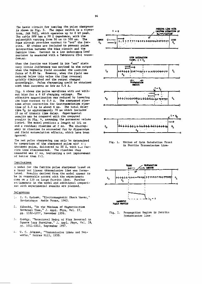
94
The basic circuit for testing the pulse sharpeneris shown in Fig. 5. The input switch is a tfcyra-cron, JAN 7621, which operates up to 8 kV peak.The cable PFN has a 50 £2 impedance, with thepulsevidth varying from 50 ns to 300 as. Thebias circuit provides current to "set" the fer-rite. RF cnokes are included to prevent pulseInteraction between the bias circuit and theferrite line. Current in a low inductance loadresistor is measured with a Tektronix CT-1 trans-former.
When the ferrite was biased In its "set" statevery little difference wa3 noticed in the outputwhen the magnetic field exceeded the coerciveforce of 0.85 Oe. However, when the field wasreduced below this value the flux reversalquickly diminished and the output changedaccordingly. Fulse sharpening could be obtainedwith bias currents as low as 0.4 A.
Fig. 6 shows the pulse waveforms with and with-out bias for a 6 kV charging voltage. Theeffective magnetization was reduced by loweringthe bias current to 0.4 A. The sharpened rise-time after correction for instrumentation rise-tfcae of 2.5 ns is about 6 as. The total delaytime TQ is approximately 70 ns which Includes35 ns of transit time delay. Experimentalresults may be compared with the computedresults in Fig. 4, assuming the parameter valueslisted. The model predicts a length of 101 cmand a residual risetime of 2 ns. The discrep-ancy in risetime is accounted for by dispersionand field accumulation effects, which V«ave beenignored.
The net pulse sharpening can only be determinedby comparison of the sharpenad pulse vit^ ti oincident pulse, delivered to 50 52, with t..s fer-rite line disconnected. The risetime thusmeasured was 15 ns, indicating a net improvementof better than 2:1.
t -o79SXTX LDV VTXH
wmom BOtcnm or
» n urautioanan. t - tt
20
h
a
S i i
musution
z» : :
2 J - " ' • • — a
Fig. 1. Motion of Spin Saturation Frontin Ferrite Transmission Line-
Conclusions
A model for che ferrite pulse sharpener based ona lossy but linear transmission line was formu-lated. Results derived from the model appear tobe in reasonable accord with the experimentsdone on a 130 cm large fercite line. Furtherrefinements in the model and additional compari-son with experimental results are planned.
References
TKKt
I. G. Kataev, "Electromagnetic Shock Haves,"Soviecskoye Radio Press, 1963.
Kikuchi, "On the Minimum of MagnetizationReversal Time," J. Appl. Phys, Vol. 27,pp. 1352-1357, November 1956.
Gyorgy, "Rotational Model of Flux Reversal inSquare Loop Ferrites," J. Appl. Phys, Vol. 28,pp. 1011-1015, September 1957.
W. C. Johnson, "Transmission Lines and Net-works," McGraw Hill, 1950.
s- nuttcuiim
71ZU) PMJfiLZ
Fig. 2. Propagation Region in FerriteTransmission Line.
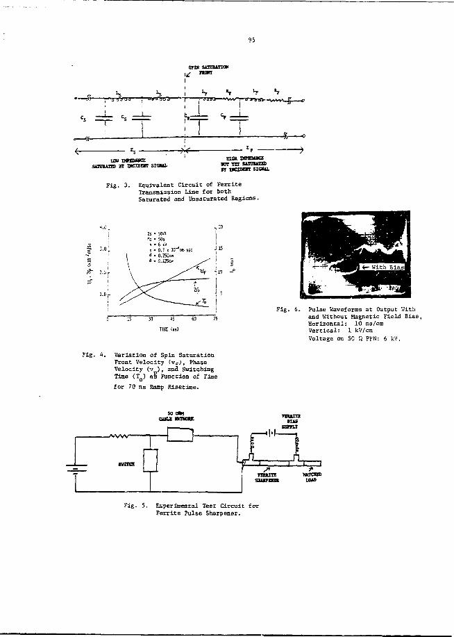
95
r JJ
i- s, L L-i- c.1
—0
LOU mnxmia:SAIDXA1D ZT mCXDEVt S tQUL
Hica mnuuKZSOT TIT SUDUIBIIT n c m n SIOUL
Pig. 3. Equivalent Circuit of Ferri teTransmission Line for bothSaturated and Unsaturated Regions.
2.0 r
30 45
TIffi (KS!
Fig. 6. Pulse Waveforms at Output Withand Without Magnetic Field Bias,Horizontal: 10 ns/cmVertical: 1 kV/cmVoltage on 50 Q PFS: 6 kV.
Fig. A. Variation of Spin SaturationFront Velocity (v-J, PhaseVelocity (v ) , and SwitchingTine (T ) a l Function of Time
for 70 ns Samp Risetime.
Fig. 5. Experimental Test Circuit forFerri te Pulse Sharpener.
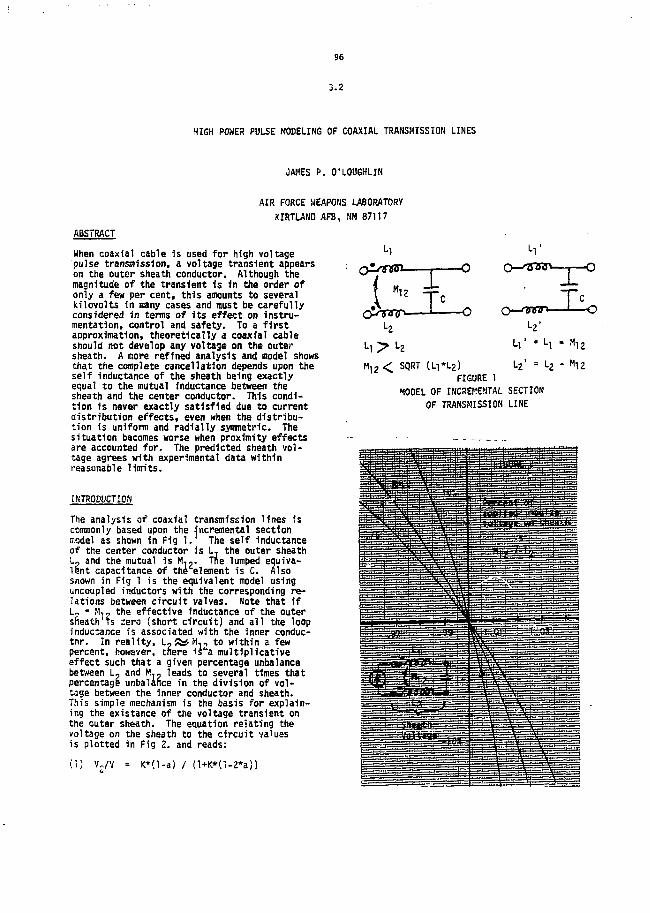
96
3.2
HIGH POWER PULSE MODELING OF COAXIAL TRANSMISSION LINES
JAMES P. O'LOUGHLIN
AIR FORCE WEAPONS LABORATORY
KIRTLAND AFB, NM 87117
ABSTRACT
When coaxial cable Is used for high voltagepulse transmission, a voltage transient appearson the outer sheath conductor. Although themagnitude of the transient Is in the order ofonly a few per cent, this amounts to severalkilovolts in many cases and must be carefullyconsidered in terms of its effect on instru-mentation, control and safety. To a firstapproximation, theoretically a coaxial cableshould not develop any voltage on the outersheath. A more refined analysis and model showsthat the complete cancellation depends upon theself inductance of the sheath being exactlyequal to the mutual inductance between thesheath and the center conductor. This condi-tion is never exactly satisfied due to currentdistribution effects, even when the distribu-tion 1s uniform and radially symmetric. Thesituation becomes worse when proximity effectsare accounted for. The predicted sheath vol-tage agrees with experimental data withinreasonable limits.
INTRODUCTION
The analysis of coaxial transmission lines iscommonly based upon the incremental sectionir.odei as shown in Fig 1. The self inductanceof the center conductor is L, the outer sheathL, and the mutual is M,-. Tne lumped equiva-lent capacitance of the element is C. Alsoshown in Fig 1 is the equivalent model usinguncoupled inductors with the corresponding re-lations between circuit valves. Note that ifLn = M-JJ the effective inductance of the outersfieath ts zero (short circuit) and all the loopinductance is associated with the inner conduc-tnr. In reality, L 2{^M,, to within a fewpercent, however, tnere is^a multiplicativeeffect such that a given percentage unbalancebetween L, and M,- leads to several times thatpercentage unbalance in the division of vol-tage between the inner conductor and sheath.This simple mechanism is the basis for explain-ing the existance of the voltage transient onthe outer sheath. The equation relating thevoltage on the sheath to the circuit valuesis plotted in Fig 2. and reads:
(1) Vn/V = K*(l-a) / (1+K*(l-2*a))
1-1'
O—'•ffoTH—-j—O
<y-nrvn—'—o
= L
SQRT
FIGURE 1
MOOEL OF INCREMENTAL SECTION
OF TRANSMISSION LINE
• 1 *
4 -'12
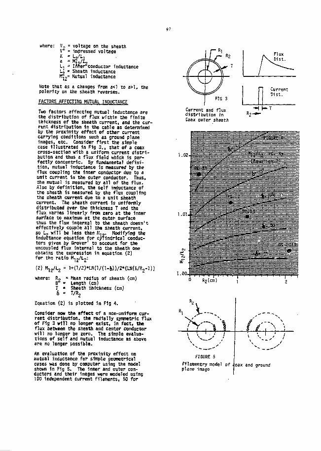
where: V2 = voltage on the sheathV = impressed voltageK ' L2/Ll
her conductor inductanceSheath inductanceMutual inductance
Note that as a changes from a<l to a>l, thepolarity on the sheath reverses.
FACTORS AFFECTING MUTUAL INDUCTANCE
Two factors affecting mutual inductance arethe distribution of flux within the finitethickness of the sheath current, and the cur-rent distribution 1n the cable as determinedby the proximity effect of other currentcarrying conditions such as ground planeimages, etc. Consider first the simplecase illustrated 1n Fig 3., that of a coaxcross-section with a uniform current distri-bution and thus a flux field which 1s per-fectly concentric. By fundamental defini-tion, mutual inductance 1s measured by theflux coupling the inner conductor due to aunit current in the outer conductor. Thus,the mutual is measured by all of the flux.Also by definition, the self inductance ofthe sheath 1s measured by the flux couplingthe sheath current due to a unit sheathcurrent. The sheath current is uniformlydistributed over the thickness T and theflux varies linearly from zero at the innersurface to maximum at the outer surfacethus the flux internal to the sheath doesn'teffectively couple all the sheath current,so L2 will be less than M12. Modifying theinductance equation for cylindrical conduc-tors given by Grover to account for theuncoupled flux internal to the sheath oneobtains the expression in equation (2)for the ratio H12/L2:
(2) H12/L2 = l+(V2)*LN(l/(l-6))/2*(LN(B/R2-l))
where: R» = Mean radius of sheath (an)B = Length (cm)T = Sheath thickness (cm)6 • T/R2
Equation (2) 1s plotted in Fig 4.
Consider now the effect of a non-uniform cur-rent distribution, the radially symmetric fluxof Fig 3 will no longer exist, in fact, theflux between the sheath and center conductorwill no longer be zero. The simple evalua-tions of self and mutual inductance as aboveare no longer possible.
An evaluation of the proximity effect onmutual inductance for simple geometricalcases was done by computer using the modelshown in Fig 5. The Inner and outer con-ductors and their Images were modeled using100 Independent current filaments, SO for
FIG 3
Current and fluxdistribution inCoax outer sheath
0-H r*
CurrentDist.
1.02
1.01.
1.00R2(cm)
\
V /^ ^FIGURE 5
Filamentry model of ,plane image
V \ /' /
oax and ground
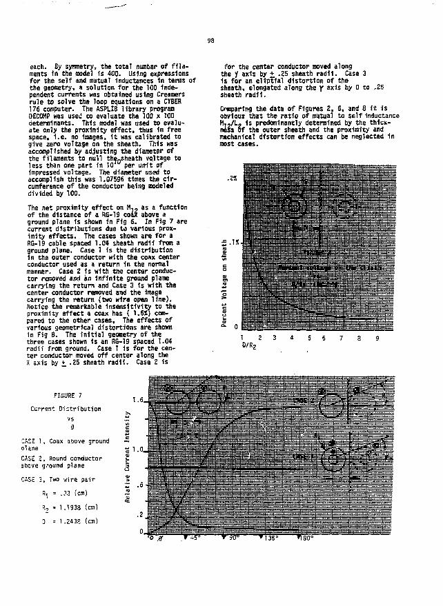
98
each. By symmetry, the total number of fila-ments in the model 1s 400. Using expressionsfor the self and mutual Inductances 1n terms ofthe geometry, a solution for the 100 Inde-pendent currents was obtained using Creamersrule to solve the loop equations on a CYBER176 computer. The ASPLIB library programOECOHP was use>2 co evaluate the 100 x 100determinants. This model was used to evalu-ate only the proximity effect, thus In freespace. I.e. no images, 1t was calibrated togive zero voltage on the sheath. This wasaccomplished by adjusting the diameter ofthe filaments to null the.sheath voltage toless than one part in 10 per unit ofimpressed voltage. The diameter used toaccomplish this was 1.07596 times the cir-cumference of the conductor being modeleddivided by 100.
The net proximity effect on M-., as a functionof the distance of a RG-19 coaX above aground plane is shown in Fig 6. In Fig 7 arecurrent distributions due to various prox-imity effects. The cases shown are for aRG-19 cable spaced 1.04 sheath radii from aground plane. Case 1 is the distributionin ths outer conductor with the coax centerconductor used as a return in the normalmanner. Case 2 is with the center conduc-tor renoved and an Infinite ground planecarrying the return and Case 3 is with thecenter conductor removed and the imagecarrying the return (two wire open line).Notice the remarkable Insensitivity to theproximity effect a coax has { 1.5%) com-pared to the other cases, The effects ofvarious geometrical distortions are shownin Fig 8. The initial geometry of thethree cases shown is an RG-19 spaced 1.04radii from ground. Case 1 is for the cen-ter conductor moved off center along theX axis by + .25 sheath radii. Case 2 is
for the center conductor moved alongthe y axis by + .25 sheath radii. Case 3is for an eliptial distortion of thesheath, elongated along the y a x i s b> c t 0 -25
sheath radii.
Comparing the data of Figures 2, 6, and 8 it isobvious that the ratio of mutual to self inductanceM 1 7/U Is predominantly determined by the thicn-neSs of the outer sheath and the proximity andmechanical distortion effects can be neglected inmost cases.
.22
FIGURE 7
Current Distribution
vs
1
CASE 1, Coax above groundplane
CASE 2, Round conductorabove ground plane
CASE 3, Two wire pair
3, = .33 (cm)
% = 1 .1938 (cm)
D = 1 .243E (cm)
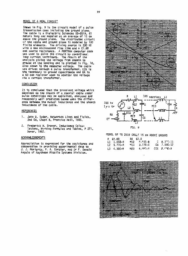
99
MODEL OF A REAL CIRCUIT
Shown in Fig. 9 is the circuit model of a pulsetransmission coax including the ground plane.The cable is a Dielectric Sciences DS-2019, 61meters long and modeled at an average of 15 cmabove the ground plane. The distributed circuitof ths cable and ground plane is modeled by 100finite elements. The driving source is 330 KVwith a one microsecond rise time and a 27.68own source resistance. A FORTRAN computer codswas used to solve the circuit by coventionalloop current techniques. The result of theanalysis giving the voltage from sheath toground at the sending end is plotted in Fig. 10,also shown is the measured voltage. The cablewas driven through a pulse transformer. CCG isthe secondary to ground capacitance and RA isa 60 onm resistor used to monitor the voltagevia a current transformer.
CONCLUSION
It is concluded that the transient voltage whichdevelops on the sheath of a coaxial cable underpulse conditions may be explained, analyzed andreasonably well predicted, based upon the differ-ence between the mutual inductance and the sheathinductance of the cable.
REFERENCES
1. John D. Ryder, Networkds Lines and Fields,2nd Ed, Chapt 6, Prentice Hall, 1955.
2. Frederick W. Grover, Inductance Calcu-lations, Working Formulas and Tables, P 271,Dover, 1962.
ACKNOWLEDGEMENTS
Appreciation is expressed for the assistance andcooperation in providing experimental data toJ. J. Moriarty, P. A. Corbier, and Dr F. DonaldAngelo of Raytheon Missile Systems Division.
CT
FIG. 9
MODEL OF DS 2019 CAtLE 15 cm ABOVE GROUNDR 22.68 RA 60.0Ll 1.65E-8 M12 R.13E-8 C 9.3"M1L2 5.77E-8 '113 3.23E-8 CG 7.93E-12L3 4.30E-8 MZ3 4.OS?-3 CCG 2.""E-S
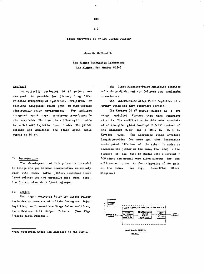
100
3.3
LIGHT ACTIVATED 10 KV LOB JITTER PDLSES*
John D. Galbralth
Los Alamoa Scientific Laboratory
Los Alamos, New Mexico 87545
ABSTRACT
An optically activated 10 kV pulser was
designed to provide low jitter, long life,
reliable triggering of lgnitrons, trlgatron, or
midplane triggered spark gaps in high voltage
electrically noisy environments' For midplane
triggered spark gaps, a step-up transformer is
also required- The input to a fibre optic cable
Is a 9.5 watt injection laaer diode* The pulser
detects and amplifies the fibre optic cable
output to 10 1;V.
I. Introduction
The development of this pulser is Intended
to bridge the gap between inexpensive, relatively
slow rise time, large jitter, sometimes short
lived pulsers and the expensive fa3t rise time,
low jitter, also short lived pulsers.
The Light Detector-Pulse Amplifier consists
of a photo diode, emitter follower and avalanche
transistor-
The Intermediate Stage Pulse Amplifier is a
twenty stage SCR Marx generator circuit.
The Krytron 10 kV output pulser Is a two
stage modified Krytron tube Marx generator
circuit. The modification to this tube consists
of an elongated glass envelope - 2.25" instead of
the standard 0.85" for a KH-4 £. G. & G.
Krytron tube. The increased glass envelope
length provides for more gas thus increasing
anticipated lifetime of the tube* In order to
decrease the jitter of the tube, the keep alive
element of the tube is pulsed with a current =
100 times the normal keep alive current for one
millisecond prior to the triggering of the grid
of the tube. (See Fig. 2-Modified Block
Diagram.)
II. Design
The Light Activated 10 kV Low Jitter Pulser
basic design consists of a Light Detector- Pulse
Amplifier, an Intermediate Stage Pulse Amplifier,
and a Krytron 10 kV Output Pulser. (See Fig.
i-Basic Block Diagram.)
*Wori performed under :he auspices of the BSDOE.
; UCHT ACTIVATED tCIW L W JITTER WL3CT -
t*^tJ UCHT I
OCTECTORl, H H I E
BA3C SLOCK DIACKAU
ncu»E 1
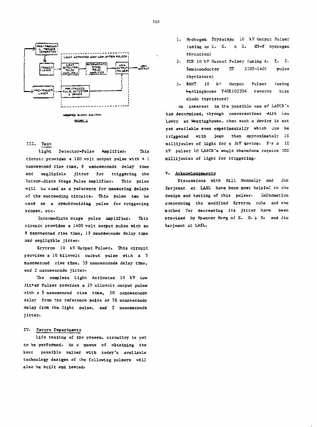
101
' LIGHT ACTIVATES WM LOW JITTCH PULSER
UCHTHWCER I t DETECT©*'
I
I PWE-THlCCCR— 4 PUL5E O£TCCTO«
1 B*tVER
nCOWE 2
III. Test
Light Detector-Pulse Amplifier. This
circuit provides a 120 volt output pulse with « 1
nanosecond rise time* 8 nanoseconds delay time
and negligible jitter for triggering the
Interr^diate Stage Pulse Amplifier. This pulse
will be used as a reference for measuring delays
of the succeeding circuits. This pulse can be
used as a synchronizing pulse for triggering
scopes, etc
Intermediate stage pulse amplifier. This
circuit provides a 1400 volt output pulse with an
8 nanosecond rise time, 15 nanoseconds delay time
and negligible Jitter.
Krytron 10 kV Output Pulser. This circuit
provides a 10 kilovolt output pulse with a 5
nanosecond rise time, 35 nanoseconds delay time,
and 2 nanoseconds jitter*
The complete Light Activated 10 kV Low
Jitt-er Pulser provides a 10 kilovolt output pulse
with a 5 nanosecond rise time, 50 nanoseconds
delay from the reference pulse or 58 nanoseconds
delay iron the light pulse, and 2 nanoseconds
jitter.
1. Hydrogen Thyratron 10 kV Output Puiser
(using an E. G. a G. HY-8 hydrogen
thyratron)
2. SCR 10 V.V Outnut Pulser (using A. E. I.
Semiconductor ITT 2105-1401 pulse
thyristors)
3. RBDT 10 kV Output Pulser (using
Viestinghouse T40R102204 reverse bias
diode thyristors)
An interest in the possible use of LASCR's
has determined, through conversations with Lou
Lowry at Westlnghouse, that such a device is not
yet available even experimentally vhlch can be
triggered with less than approximately 10
millijoules of light for a ikV device. For a 10
kV pulser 10 LASCR's would therefore require 100
millijoules of light for triggering-
Discussions with Bill Nunnally and Jin
Sarjeant at LASL have been most helpful in the
design and testing of this pulser. Information
concerning the modified Krytron tube sod the
method for decreasing its Jitter have been
provided by Spencer Merg of E. G. & G. and Jim
Sarjeant at LASL.
IV. Future Experiments
Life testing of the present circuitry is yet
to be performed. As a means of obtaining the
best possible pulser with today's available
technology designs of the following pulsers will
also be built and tested.
102
3.4
COMMAND CHARGE USING SATURABLE INDUCTORS
Susan Black and T. R. Burkes
High Voltage/Pulse Power LaboratoryTexas Tech University E. E. Dept.
Lubbock, Texas 79409
Abstract
Line-type pulsers operating at rep-rates greaterthan a fev kilohertz require special circuits to in-sure proper operation of the switch. Specifically,thyratrons and other closing switches require a"grace period" of several microseconds or more be-fore anode voltage is reapplied; this delay allowsrecovery and prevents reclosure of the thyratron.One method of achieving the required delay time isby ui.ing a slightly mismatched PFN and slower-than-resonanc charging. However, repetition rates ofline-type modulators are limited by Che character-istics of resonant charging. In order to increaserep-rates, these characteristics may be modified byusing a saturable reactor as a charging inductor.
This paper describes design considerations and lab-oratory performance of saturable Inductors used toresonately charge an energy storage network up to25 kV with a delay as much aa 16.5 microseconds.
Introduction
iHe required time delay or grace period for swicch
recovery may be achieved with a command charge
scheme; however, the required circuitry is usually
complicated and expensive. A comparatively simple
and inexpensive mechod of achieving this charging
delay is through slower than resonant charging. TIE
iaior disadvantage of this method is the limitation
o: rep-rates co a narrow range by the characteris-
tics ot inductive charging. This rep-rate restric-
tion raay be reduced by using a saturable inductor
as a charging inductor. The major disadvantage of
using saturable inductors in inductive charging nec-
vorl<s is *hac their operating characteristics are
-.-oicaee dependent.
A ssturable inductor utilizes the non-Linearity of
:he hysteresis curve -f ferromagnetic materials.
Initially, che inductor operates in the high perme-
ability region of the B-H curve. This provides a
high inductive, low energy transfer period (delay
in main charging cycle) allowing adequate recovery
time for the closing switch. Upon saturation, che
inductor core operates in the low permeability re-
gior of the 3-H curve producing a low inductance
which results in a relatively fast energy transfer.
At the end of che charging cycle, the core resets
to the initial conditions and the cycle repeats.
To obtain a sharp break between the saturated and
unsaturaced states of the saturable inductor, it is
desirable to have the B-H characteristic of the
core as square as possible. This provides high in-
itial permeability frcr the charging delay and a low
saturated permeability for fast charging (high rep-
rates) . In order to achieve high rep-rates, a lo«
saturated inductance is required. Sine; che satu-
rated inductance is inversely proportional to the
square of the saturable flux density, a large satu-
rated flux density results in a low saturated in-
ductance. For efficient energy transfer, hystere-
sis losses should be as low as possible. To mini-
mize this loss while maintaining o high saturation
flux density, a low coercive force is desired.
A typical iine-type modulator is shown in Figure la,
with the saturable inductor used as the charging
inductor. The charging time for resonant charging
with a linear inductor, as seen in Figure lb, is
determined by the charging inductor and the capaci-
tance of the pulse forming network (PFS):
r = -v LC (1)
To prevent reciosure ?f :he Train discharge swicch.
T should be sufficiently large that a thrashold vol-
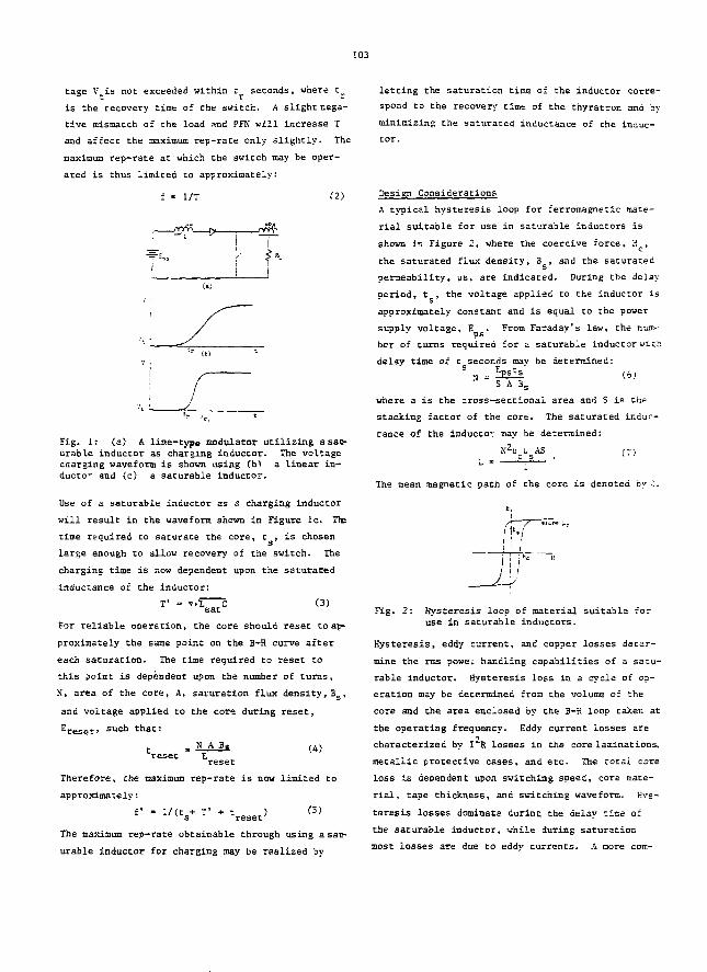
103
cage V is not exceeded within t seconds, where t_
is the recovery time of the switch. A slight nega-
tive mismatch of the load and PFN will increase T
and affect Che maximum rep-rate only slightly. The
maximum rep-rate at which the switch may be oper-
ated is thus limited to approximately:
1/T (2)
Fig. i: (a) A line-type modulator utilizing a sac-urable induccor as charging inductor. The voltagecharging waveform is shown using (b) a linear in-ductor and (c) a saturable inductor.
Use of a saturable induccor as a charging inductor
will result in the waveform shown in Figure 1c. The
time required to saturate the core, t , is chosen
large enough to allow recovery of the switch. The
charging time is now dependent upon the saturated
inductance of the inductor:
T' (3)
For reliable operation, Che core should resec to ap-
proximately the same point on the B-H curve after
each saturation. The time required to reset to
this point is dependent upon the number of turns,
N, area of the core, A, saturation flux density, Bs,
and voltage applied to the core during reset,
Ereset' s u c h that:
creset " E
reset
Therefore, che maximum rep-rate is now limited to
approximately:
f - l/(t + T1 + t ) (5)
The maximum rep-rate obtainable through using a sat-
urable inductor for charging may be realized by
letting the saturation time of the inductor corre-
spond to the recovery time of the thyratron and by
minimizing the saturated inductance of the induc-
tor.
Design Considerations
A typical hysteresis loop for ferromagnetic mace-
rial suitable for use in sacurable inductors is
shown in Figure 2, where the coercive force, a ,
the saturated flux density, B , and the saturated
permeability, us, are indicated. During the delsy
period, t , the voltage applied to the inductor is
approximately constant and is equal to the power
supply voltage, E . From Faraday's law, the num-
ber of turns required for a saturable inductor with
delay time of t seconds may be determined:
N (6)S A 3S
where a is the cross-sectional area and S is the
stacking factor of the core. The saturated induc-
tance of the inductor mav be determined:
P u AS0 S
(7)
The mean magnetic path of the core is denoted by '•
Fig. 2: Hysteresis loop of material suitable foruse in saturable inductors.
Hysteresis, eddy current, and copper losses deter-
mine the rms powe* handling capabilities of a satu-
rable inductor. Hysteresis loss in a cycle of op-
eration may be determined from the volume of the
core and the area enclosed by the B-H loop taken at
the operating frequency. Eddy current losses are
characterized by I R losses in the core laminations,
metallic protective cases, and etc. The total core
loss is dependent upon switching speed, core mace-
rial, cape chickness, and switching waveform. Hys-
teresis losses dominate during the delay time of
the saturable inductor, while during saturation
most losses are due to eddy currents. A more com-
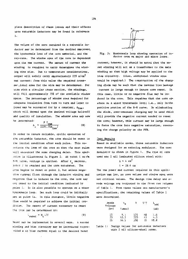
104
plete description of these losses and their effects
upon saturable inductors may be found in reference
1.
The volume of Che core required in a saturable in-
ductor may be determined from the desired rms power,
the hysteresis loss of the core material, and the
rep-rate. The window area of the core is dependent
upon the ras current. The amount of current the
winding is required to carry determines the wind-
ing wire size. Due to temperature considerations,
copper will safely carry approximately 235 A/cm^
rms current; from this value the required cross-
ser.ional area for the wire may be determined. For
wxre with a circular cross section, the windings,
will fill approximately 75% of the available window
space. The percentage of window area required for
adequate insulation from turn to turn and layer to
layer may be accounted for by a constant, A^ns,
which will depend upon the desired voltage hold-off
and quality of insulation. The window area may now
be determined:.V I
235 C75A. )xns
(8)
In order to insure reliable, cyclic operation of
Che saturable inductor, the core should be reset Co
che initial condition after each pulse. This re-
orients the iron of che core so that the next pulse
will encuunter the same charging delay. This oper-
jcion is illustrated in Figure 3. At point I on the
3-H curve, voltage is applied. After t seconds,
point 2 is reached and the core saturates. The
cere begins Co reset ac point 3, but unless nega-
tive current flows through the inductor winding and
negative flux is induced in che core, che core may
aoc resec co che inicial condition indicated by
tjoinc 1. It ig also possible Co operate on a minor
hysceres is loop. One such loop could be initially
sec ac point la. In this instance, little negative
flux would be required to achieve the initial con-
dition. The amount of current necessary Co reset
che core nay be determined by:
i = H i/:t >'9)reset c
^esec may be implemented in several ways. A second
winding jnd bias circuitry may be introduced to pro-
vided a dc bias current equal Co the desired resec
Fig. 3: Hysteresis loop showing operation of in-ductor core on major and minor loops.
current; however, it should be noted that the re-
set winding will act as a transformer to che main
winding so that high voltage may be applied to the
bias circuitry. (Also, additional window area
would bs required.) The construction of the charg-
ing diode may be such that che reverse bias leakage
current is large enough to insure core reset. In
this case, little or no negative flux may be in-
duced in the core. This requires that the core op-
erate on a minor hysteresis loop; i.e., only in the
positive portion of the B-H curve. By eliminating
the diode, over-resonant charging may be used which
will provide the negative current needed Co reset
che core; however, this current may be large enough
to force che core into negative saturation, revers-
ing the charge polarity on the PFS.
Test Results
Based on available cores, three saturable inductors
were designed for an exiscing modulator. The test
modulator is shown in Figure 4. The cype of core
used was 2 mil laminated silicon steel with:
A = 4 cm"
I =• 28.6 cm
The rms power and current required in this appli-
cation was low, so core volume and window area were
not critical values. The design time delay and a-
node volcage are indicaced in che first two columns
of Table 1. From chese values and manufacturer's
specifications, che remaining values of Table 1
were determined.
Anode cs
Voltage(kv) (usec)
S V/Tsac
(mH)
15 9.4 125 50 1.520 12.5 220 45 4.325 16.5 350 35 10.3
Table 1: Design values for sacurable inductorswith 2 mil silicon-ateel cores.
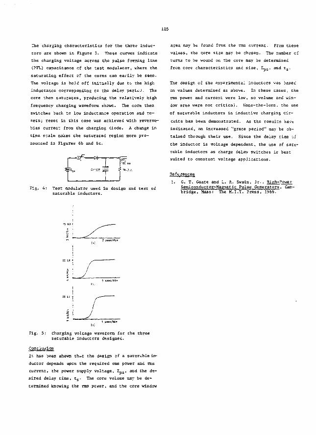
105
The charging characteristics for the three induc-
tors are shown in Figure 5. These curves indicate
the charging voltage across the pulse forming line
(PFL) capacitance of the test modulator, where the
saturating effect cf the cores can earily be seen.
The voltage is held off initially due to the high
inductance corresponding to the delay pericj. The
core then saturates, producing the relatively high
frequency charging waveform shown. The core then
switches back to low inductance operation and re-
sets; reset in this case was achieved with reverse-
bias current from the charging diode. A change in
time scale aakes the saturated region more pro-
nounced in Figures 6b and 6c.
rr<aF- T
Fig. 4: Test modulator used in design and test ofsaturable inductors.
area may be found from the ras current. From these
values, the core size may be chosen. The number of
turns to be wound on the core may be determined
from core characteristics anc size, L~s, and ts.
The design of the experimental inductors vas based
on values determined as above. In these cases, the
rms power and current were low, so volume and win-
dow area were not critical. Kone-the-less. the use
of saturable inductors in inductive charging cir-
cuits has been demonstrated. As the results have
indicated, an increased "grace period" :nay be ob-
tained through their use. Since the delay time cf
the inductor is voltage dependent, the use of satu-
rable inductors as charge delay switches is best
suited to constant voltage applications.
References
L. G. T. Goate and L. R. Swain, Jr.. High-PowerSemiconductor-Magnetic Pulse Generators, Cam-bridge, Mass: The M.I.T. Press, 1966.
Fig. 5: Charging voltage wavetonn for the threesaturable inductors designed.
Conclusion
It has been shown that the design of a satur^ble in-
ductor depends upon the required rms power and ras
current, the power supply voltage, EpS» and the de-
sired delay time, ts. The core volume may be de-
termined knowing the rms power, and the core window
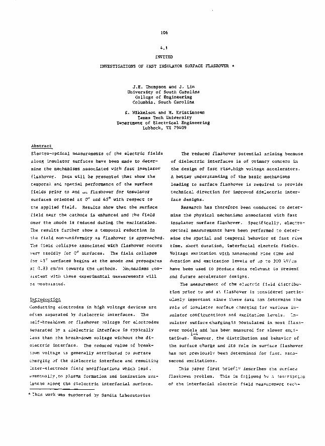
106
4.1
INVITED
INVESTIGATIONS OF FAST INSULATOR SURFACE FLASHOVER *
J.E. Thompson and J. LinUniversity of South Carolina
College of EngineeringColumbia, South Carolina
K. Kikkelson and M. KristiansenTexas Tech University
Department of Electrical EngineeringLubbock, TX 79409
Abstract
Electro-optical measurements of the electric fields
along insulator surfaces have been made to deter-
mine the mechanisms associated with fast insulator
tlashover. Data will be presented that show the
temporal and spatial performance of the surface
fields prior to and dL flashover for insulator
surfaces oriented at 0° and 45° with respect to
the applied field. Results show that the surface
field near the cathode is enhanced and the field
near the anode is reduced during the excitataion.
The results further shov a temporal reduction in
the field non-uniformity as flashover is approached.
The tield collapse associated with flashover occurs
very rapidly for 0° surfaces. The field collapse
for 45° surfaces begins at the anode and propagates
at 0.33 cm/ns towards the cachode. Mechanisms con-
sistent with these experimental measurements will
be postulated.
Introduction
Conducting electrodes in high voltage devices are
often separated by dielectric interfaces. The
self-breakdown or flashover voltage for electrodes
separated by a aielectric interface is typically
Less than the break-down voltage without the di-
electric interface. The reduced value of break-
down voltage is generally attributed to surface
charging of the dielectric interface and resulting
inter—slectrode field modifications which lead ,
eventually,to plasma formation and ionization ava-
lancne along the dielectric interfacial surface.
The reduced flashover potential arising because
of dielectric interfaces is of primary concern in
the design of fast rise,high voltage accelerators.
A better understanding of the basic mechanisms
leading to surface flashover is required to provide
technical direction for improved dielectric inter-
face designs.
Research has therefore been conducted to deter-
mine the physical mechanisms associated with fast
insulator surface flashover. Specifically, electro-
optical measurements have been performed to deter-
mine the spatial and temporal behavior of fast rise
time, short duration, interfacial electric fields.
Voltage excitation with nanosecond rise time and
duration and excitation levels of jp to 300 kWcm
have been used to produce data relevant to present
and future accelerator designs.
The measurement of the electric fieid distribu-
tion prior to and at flashover is considered partic-
ularly important since these data can determine the
role of insulator surface charging for various in-
sulator configurations and excitation levels. In-
sulator surface charging is postulated in nost flash-
over models and has beer measured for slower exci-1-4
tatious. However, the distribution and behavior of
the surface charge and its role in surface flashover
has not previously been determined for fast, nano-
second excitations.
this paper first briefly describes the surface
flashovei problem. This is followed bv a iescripticn
of the interfacial electric fieid measurement tech-
* This work was supported by Sandia Laboratories
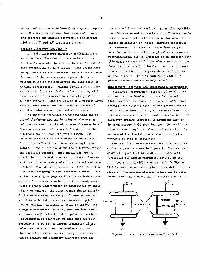
107
nique used and the experimental arrangement requir-
ed. Results obtained are then presented, showing
the temporal and spatial behavior of the surface
fields for 0° and 45° insulator shapes.
Surface Flashover Description
.'. maple electrode-insulator configuration in
which surface flashover occurs consists of two
electrodes separated by a solid insulator. The en-
tire arrangement is in a vacuum. This arrangement
is applicable to many practical devices and is used
for most of the measurements reported here. A
voltage pulse is applied across the electrodes in
typical applications. Voltage levels above a cer-
tain value, for a particular pu^se duration, will
cause an arc or flashover to occur along the in-
sulator surface. This arc occurs at a voltage level
that is much lower than the arcing potential of
the electrodes without the dielectric spacer.
The physical mechanism associated with the ob-
served flashover and the lowering of the arcing
voltage has been postulated by several researchers.
Electrons are emitted by small "whiskers" on the
electrode surface near the triple point. The
emission mechanism is field emission due to the
field intensification at these microscopic sharp
points. Some of the field emitted electrons strike
the insulator surface. Most insulators have a
coefficient of secondary emission greater than one
such that more secondary electrons are emitted from
insulator than striking primaries. This results in
a positive charging of the insulator surface. This
surface charging propagates from the cathode to the
anode. The process continues until a steady-state
surface charge distribution is established or until
flashover occurs. The steady-state charge distri-
bution exists when the energy of returned second-
cathode and insulator surface. It is also possible
chat for nanosecond excitations, the flashover mech-
anisms operate extremely fast such that other mech-
anisms ir. addition to surface charging contribute
to flashover. The field at the cathode triple
junction could reach high enough values to cause a
microdischarge, due to explosion of an emission site.
This could release sufficient electrons and photons
from the cathode anc/or insulator surface to caust
impact ionization of the gas molecules on the in-
sulator surface. This in turn could lead t s
plasma streamer and ultimately breakdown.
Measurement Tecrtique and Experimental Arrangement
Flashover, according to postulated models, re-
quires that the insulator surface be charged by
field emitted electrons. The surface charge ther.
enhances the electric field in the cathode region
near the insulator, causing increased cathode field
emission, avalanche, and ultimately breakdown. The
flashover process therefore is dependent UDOT. ar.
inter-electrode field modification. The modifica-
tions to the interfacial electric fields along t'n«
surface of the insulator were electro-optically
measured in this investigation.
Electric field measurements were made usinu test
cell arrangements shown in Figure 1. The test cell
shown in Figure l(a) is constructed using a KDP
(potassium-dihydrogen-phosphate) crystal as the
insulator material while the test cell in Figure
K b ) is constructed using nylon surrounded by nitro-
benzene. The surface electric fields can be deter-
mined by optically measuring the Pockels effect: in
aries is such that the energy dependent coeffici-2-5
ent of secondary emission is equal to unity. The
charge distribution, however, does not have time
to attain equilibrium for short pulse excitations.
The occurence of flashover in this case has been
postulated to be due to impact ionization of gas
molecules desorbed from the insulator surface.
The ionization and molecular desorption are both
due to primary and secondary electrons from the
Vacuum
(a) (b)
Figure 1. KDP and Nitrobenzene Test Cell.
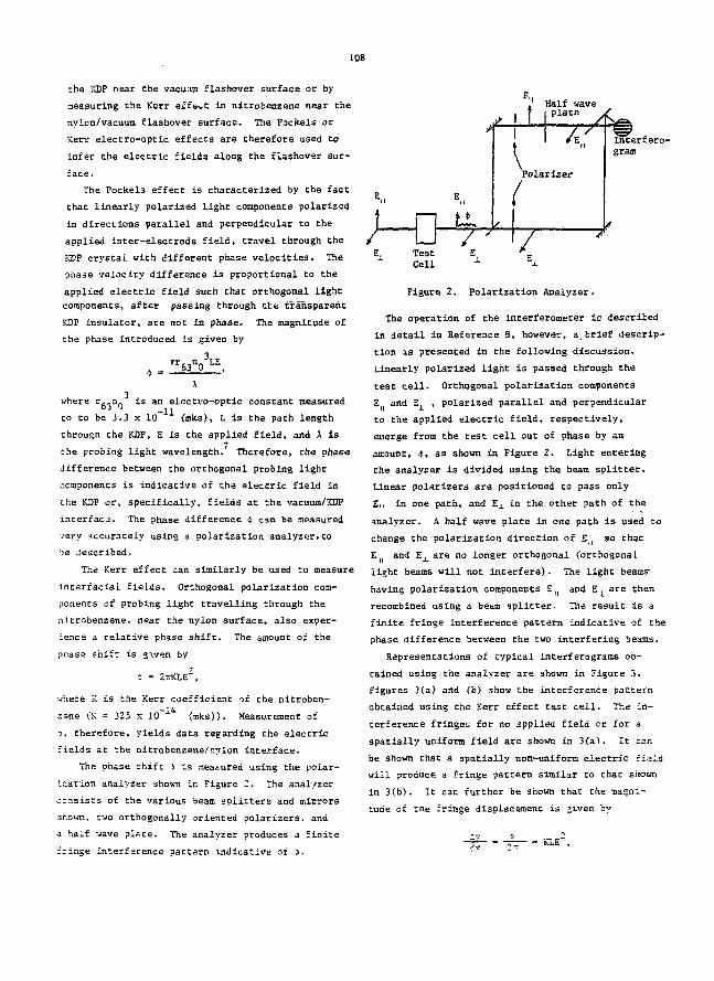
108
the KDP near the vacu:im flashover surface or by
neasuring the Kerr efft>.t in nitrobenzene near the
nylon/vacuum flashover surface. The Pockels or
Kerr electro-optic effects are therefore used to
infer the electric fields along the flashover sur-
face.
The Pockels effect is characterized by the fact
that linearly polarized light components polarized
in directions parallel and perpendicular to the
applied inter-electrode field, travel through the
KDP crystal with different phase velocities. The
phase velocity difference is proportional to the
applied electric field such that orthogonal light
components, after passing through the transparent
KDP insulator, are not in phase. The magnitude of
the phase introduced is given by
where r-_nn is an electro-optic constant measured3 -11
to to be J.3 x 10 (mks), L is the path length
through the KDF, £ is the applied field, and \ is
the probing light wavelength.' Therefore, the phase
difference between the orthogonal probing light
components is indicative of the electric field in
the KDP or, specifically, fields at the vacuum/XDP
interface. The phase difference « can be measured
very accurately using a polarization analyzer,to
be described.
The Kerr effect can similarly be used to measure
interracial fields. Orthogonal polarization com-
ponents of probing light travelling through the
nitrobenzene, near the nylon surface, also exper-
ience a relative phase shift. The amount of the
pr.ase shift is given by
i = 2irKI.E",
•.mere :< is the Kerr coefficient of the nitroben-—14
zene (K =• 325 x 10 (mks)). Measurement of
j, therefore, yields data regarding the electric
fields at *he nitrobenzene/nylon interface.
The phase shift i is measured using the polar-
isation analyzer shown in Figure 2. The analyzer
consists of the various beam splitters and mirrors
shown, two orthogonally oriented polarizers, and
a half wave piste. The analyzer produces a finite
fringe interference pattern indicative of j.
Figure 2. Polarization Analyzer.
The operation of the interferometer i£ described
in detail in Reference 3, however, a_brief descrip-
tion is presented in the following discussion.
Linearly polarized light is passed through the
test cell. Orthogonal polarization components
E and E}_ , polarized parallel and perpendicular
to the applied electric field, respectively,
emerge from the test cell out of phase by an
amount, <f>, as shown in Figure 2. Light entering
the analyser is divided using the beam splitter.
Linear polarizers are positioned to pass only
E,, in one path, and E x in the other path of the
analyzer. A half wave plate in one path is used to
change the polarization direction of EM so that
E and Ej_ are no longer orthogonal (orthogonal
light beams will not interfere). The light beans-
having polarization components £ |( and E^ are then
recombined using a beam splitter. The result is a
finite fringe interference patteim indicative of the
phase difference between the two interfering beams.
Representations of typical interferograms ob-
tained using the analyzer are shown in Figure 3.
Figures 3(a) and (b) show the interference pattern
obtained using the Kerr effect test cell. The in-
terference fringes for no applied field or for a
spatially uniform field are shown in 3(a~>. It can
be shown that a spatially non-uniform electric field
will produce a fringe pattern similar to that shown
in 3(b). It can further be shown that the magni-
tude of the fringe displacement is *iven by
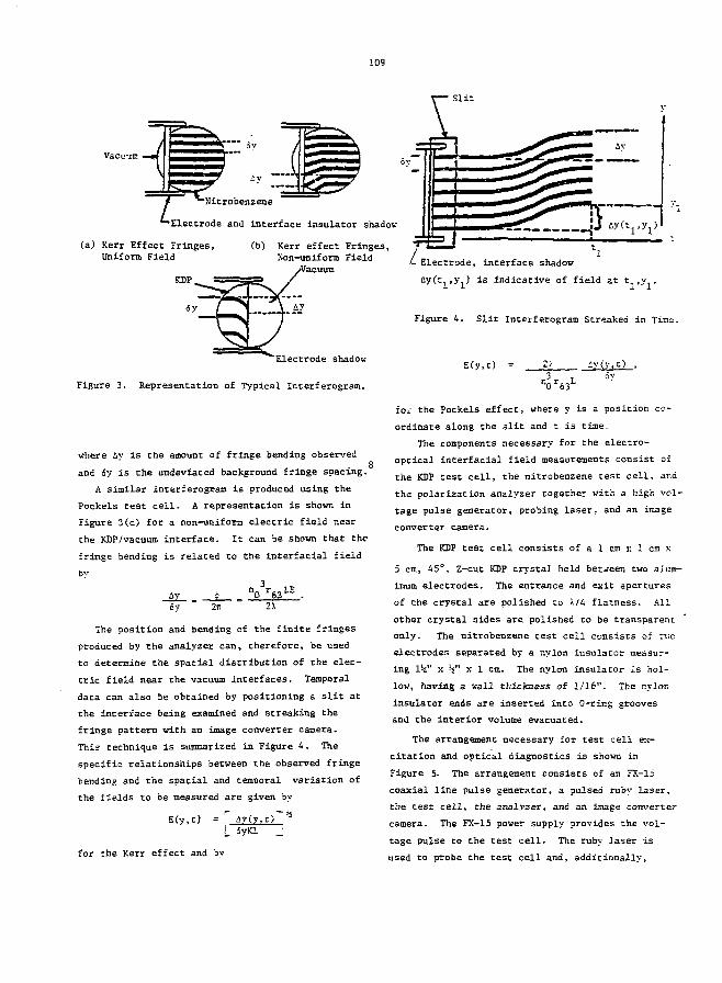
109
• Slit
6v
Electrode and interface insulator shadow
(a) Kerr Effect Fringes, (b) Kerr effect Fringes,Uniform Field F l 6 U I- Electrode,
"Electrode shadow
Figure 3. Representation of Typical Interferogram.
where Ay is the amount of fringe bending observed
and ay is the undeviated background fringe spacing.
A similar interferogratn is produced using the
Pockels test cell. A representation is shown in
Figure 3(c) for a non-uniform electric field near
the KDP/vacuum interface. It can be shown that the
fringe bending is related to the interfacial field
bv
-SZ-,6y
-_£_2ir
n0 r63 LE
The position and bending of the finite fringes
produced by the analyzer can, therefore, be used
to determine the spatial distribution of the elec-
tric field near the vacuum interfaces. Temporal
data can also be obtained by positioning a slit at
the interface being examined and streaking the
fringe pattern with an image converter camera.
This technique is summarized in Figure 4. The
specific relationships between the observed fringe
bending and the spatial and temporal variation of
the fields to be measured are given by
E(y,t) = ay(y.t)~hl_ SyKL _
interface shadow
for the Kerr effect and by
is indicative of field at t, ,y
Figure A. Slit Interferogram Streaked in Tins.
E(y.t) =
for the Pockels effect, where y is a position co-
ordinate along the slit and t is tine.
The components necessary for the electro-
optical interfacial field measurements consist of
the KDP test cell, the nitrobenzene test cell, and
the polarization analyzer together with a high vol-
tage pulse generator, probing laser, and an image
converter camera.
The KDP teat cell consists of a 1 cm r. 1 cm x
5 cm, 45°, Z-cut KDP crystal held between two alum-
inum electrodes. The entrance and exit apertures
of Che crystal are polished to \IU flatness. All
other crystal sides are polished to be transparent
only. The nitrobenzene test cell consists of two
electrodes separated by a nylon insulator measur-
ing IV x 5" x 1 cm. The nylon insulator is hol-
low, having a wall thickness of 1/16". The nylon
insulator ends are inserted into 0-ring grooves
and the interior volume evacuated.
The arrangement necessary for test cell ex-
citation and optical diagnostics is shown in
Figure 5. The arrangement consists of an FX-15
coaxial line pulse generator, a pulsed ruby laser,
the test cell, the analyzer, and an image converter
camera. The FX-15 power supply provides the vol-
tage pulse to the test cell. The ruby laser is
used to probe the test cell and, additionally,
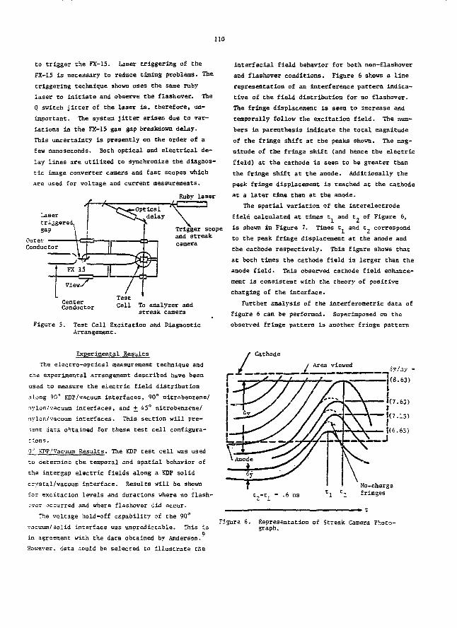
no
to trigger the FX-15. Laser triggering of the
FX-15 is necessary to reduce timing problems. The
triggering technique shown uses the same ruby
laser to initiate and observe the flashover. The
Q switch jitter of the laser is, therefore, un-
important. The systea jitter arises due to var-
iations in the FX-15 gas gap breakdown delay.
This uncertainty is presently on the order of a
few nanoseconds. Both optical and electrical de-
lay lines are utilized to synchronize the diagnos-
tic image converter camera and fast scopes which
are used for voltage and current measurements.
Ruby laser
OuterConductor
Trigger scopeand streak
CenterConductor
TestCell To analyzer and
streak camera
Figure 5. Test Cell Excitation and DiagnosticArrangement.
interfacial field behavior for both non-flashover
and flashover conditions. Figure 6 shows a line
representation of an interference pattern indica-
tive of the field distribution for no flashover.
The fringe displacement is seen to increase and
temporally follow the excitation field. The num-
bers in parenthesis indicate the total magnitude
of the fringe shift at the peaks shown. The mag-
nitude of the fringe shift (and hence the electric
field) at the cathode is seen to be greater than
the fringe shift at the anode. Additionally the
peak fringe displacement is reached at the cathode
at a later time than at the anode.
The spatial variation of the interelectrode
field calculated at times t.. and t of Figure 6,
is shown in Figure 7. Times t and t_ correspond
to the peak fringe displacement at the anode and
the cathode respectively. This figure shows that
at both times the cathode field is larger than the
anode field. This observed cathode field enhance-
ment is consistent with the theory of positive
charging of the interface.
Further analysis of the interferonetric data of
Figure 6 can be performed. Superimposed on the
observed fringe pattern is another fringe pattern
Experimental Results
The electro-optical measurement technique and
che experimental arrangement described have been
used to measure the electric field distribution
along 90° KDP/vacuum interfaces, 90° nitrobenzene/
avion/vacuum interfaces, and + 45° nitrobenzene/
nylon/vacuum interfaces. This section will pre-
sent data obtained for these test cell configura-
tions.
0' XPP.'Vacuum Results. The KDP test cell was used
to determine the temporal and spatial behavior of
the intergap electric fields along a KDP solid
crystal/vacuum interface. Results will be shown
for excitacion levels and durations where no flash-
:ver occurred and where flashover did occur.
The voltage hold-off capability of the 90°
vacuum/solid interface was unpredictable. This IsQ
in agreement with the data obtained by Anderson.'
However, data could be selected to illustrate the
Cathode
ly/Ay =
(8.63)
(7.63)
1(7.13)
1(6.63)
No-chargafringes
Figure 6. Representationgraph.
of Streak Camera Photo-
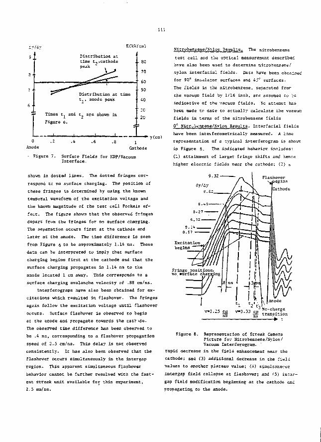
Ill
E(kV/cm)
, . 80
70
6 • •
«T Times
Figure 6.
Distribution at timetj, anode peak
and t are shown in
i
60
50
40
20
. 20
0
Anode
.2 .6 .8• y(cn1
Figure 7. Surface Fields for KDP/VacuumInterface.
shown in dotted lines. The dotted fringes cor-
respond to no surface charging. The position of
these fringes is determined by using the known
temporal waveform of the excitation voltage and
the known magnitude of the test cell Fockeis ef-
fect. The figure shows that the observed fringes
depart from the fringes for no surface charging.
The separation occurs first at the cathode and
later at the anode. The time difference is seen
from Figure 6 to be approximately 1.14 ns. These
data can be interpreted to imply that surface
charging begins first at the cathode and that the
surface charging propagates in 1.14 ns to the
anode located 1 cm away. This corresponds to a
surface charging avalanche velocity of .88 cm/ns.
Ititerf erograms have also been obtained for ex-
citations which resulted in flashover. The fringes
again follow the excitation voltage until flashover
occurs. Surface flashover is observed to begin
at the anode and propagate towards the cathode.
The observed time difference has been observed to
be .4 ns, corresponding to a flashover propagation
speed of 2.5 co/ns. This delay is not observed
consistently. It has also been observed that the
flasbover occurs simultaneously in the intergap
region. This apparent simultaneous flashover
behavior cannot be further resolved with the fast-
est streak unit available for this experiment,
2.5 mn/ns.
Nitrobenzene/Nylon Results. The nitrobenzene
test cell and the optical measurement describee
h;?ve also been used to determine nitrobenzene/
nylon interfacial fields. Data have been obtained
for 90° insulator surfaces and 45° surfaces.
The fields in the nitrobenzene, separated fror
the vacuum field by 1/16 inch, are assumed to be
indicative of the vacuum fields. No attempt has
been made to date to actually calculate the vacuum
fields in terms of the nitrobenzene fields
0 c Nitr^berizene/Nvlon Results. Interfacial fields
have been inteiferometrically measured. A line
representation of a typical irterferogran is shnwn
in Figure 8. The indicated behavior includes:
(1) attainment of larger fringe shifts and hence
higher electric fields near the cathode; (2) a
9.32
6yJe.8i.
Excitationbegins
Fringe positions,no surface charging
v»l.25 cmns
-3.33 ^~ transition
'•+• t
Figure 8. Representation of Streak Camera
Picture for Nitrobenzene/Nylon/
Vacuum Interferogram. '
rapid decrease in the field enhancement near the
cathode; and (3) additional decrease in the field
values to another plateau value; (4) simultaneous
intergap field collapse at flashover; and (5) intar-
gap field modification beginning at the cathode and
propagating to the anode.
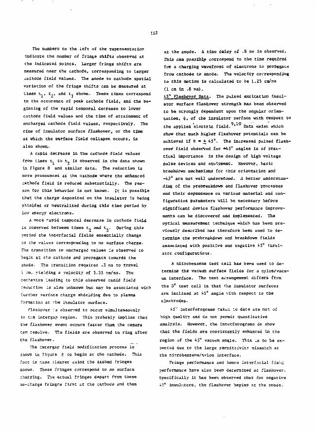
112
The numbers to the left of the representation
indicate the number of fringe shifts observed at
che indicated points. Larger fringe shifts are
measured near the cathode, corresponding to larger
cathode field values. The anode to cathode spatial
variation of the fringe shifts can be measured at
times t , t., and t, shown. These times correspond
to the occurence of peak cathode field, and the be-
ginning of the rapid temporal decrease to lower
cathode field values and the time of attainment of
uncharged cathode field values, respectively. The
time of insulator surface flaahover, or the time
at which the surface field collapse occurs, is
also shown.
A rapid decrease in the cathode field values
from times t^ to t- is observed in the data shown
in Figure 8 and similar data. The reduction is
more pronounced at the cathode where the enhanced
cathode field is reduced substantially. The rea-
son for this behavior is not known. It is possible
chat Che charge deposited on the insulator is being
shielded or neutralized during this time period by
low energy electrons.
A more *-apid temporal decrease in cathode field
is observed between times t, and t . During this
period the interracial fields essentially change
co che values corresponding Co no surface charge.
The transition to uncharged values is observed to
begin at che cathode and propagate towards the
anode. The transition requires .3 ns to travel
L en, yielding a velocity of 3.33 cm/ns. The
mechanism leading Co this observed rapid field
reduction is also unknown but may be associated with
further surface charge shielding due to plasma
tarnation at che insulator surface.
elashover :s observed to occur simultaneously
in tne intergap region. This probably implies that
che flashover event occurs faster than the camera
can resolve. The fields are observed to ring after
che flashover.
The intergap field modification process is
shown in ~i?ure 8 Co begin at the cathode. This
face is ade clearer using the dashed fringes
shown. These fringes correspond to no surface
charging. The actual fringes depart from these
ao-cb.arge fringes first at che cathode and then
at the anode. A. time deiay of .8 ns is observed.
This can possibly correspond to the time required
for a charging vavefront of electrons to propagate
from cathode to anode. The velocity corresponding
to this motion is calculated to be 1.25 cm/ns
(1 cm in .8 ns).
45" Flashover Data. The pulsed excitation insul-
ator surface flashover strength has been observed
to be strongly dependent upon the angular orien-
tation, 9, of che insulator surface with respect to9 10
the applied electric field. ' Data exist which
show that much higher flashover potentials can be
achieved if 6 • + 45°. The increased pulsed flash-
over field observed for +45° angles is of prac-
tical importance in the design of high voltage
pulse devices and equipment. However, basic
breakdown mechanisms for this orientation and
-45° are not well understood. A better understan-
ding of the prebreakdown and flashover processes
and their dependence on various material and con-
figuration parameters will be necessary before
significant device flashover performance improve-
ments can be discovered and implemented. The
optical measurement technique which has been pre-
viously described has therefore been used to de-
termine the prebreakdown and breakdown fields
associated with positive ana negative 45° insul-
ator configurations.
A nitrobenzene test cell has been used co de-
termine the vacuum surface fields for a nylon/vacu-
um interface. The test arrangement differs from
the 0" test cell in that the insulator surfaces
are inclined at 45° angle with respect to the
electrodes.
45° interferograms cakur. to date are not of
high quality and do not permit quantitative
analysis. However, the interferograms do show
that the fields are consistantly enhanced in che
region of che 45° vacuum angle. This _s to be ex-
pected due co the large permittivity mismatch at
che nitrobenzene/nylon interface.
Fringe performance and hence intarfacial field
performance have also been determined at flashover.
Specifically it has been observed that for negative
43° insulators, the flashover begins at the anode.

113
The flashover Is observed to propagate from anode
LO cathode (1 cm; in 1.2 ns, corresponding to a
velocity of .83 cm/as.
Summary
Electro-optical measurements have been made and
have determined the temporal and spatial distribu-
tion of nanosecond electric fields along vacuum/
solid interfaces. The results indicate that cathode
field enhancement and cathode initiated flashover
are important for 0° insulator surfaces. The data
have determined several performance features for 0°
surfaces which have not been observed prior to this
work. The features include (1) cathode field en-
hancement ; (2) the cathode field enhancement occurs
first at the cathode (a field enhancement propaga-
tion velocity has been calculated); (3) the inter-
gap field enhancement is reduced in two steps. The
first step is slower than the second. The second
reduction essentially reduces the Intergap fields
to the uncharged insulator surface values. The
velocity of propagation of this effect has been
measured; (4) Flashover most often begins simul-
taneously between electrodes. However, anode
initiated flashovers have been observed. The ve-
locity of the anode initiated flashover field
collapse has been measured.
Results obtained for 45° insulator surfaces are
presently inconclusive and should be considered pre-
liminary . The results do show, however: (1) Fields
near the vacuum 45° angle are enhanced, probably
because of the permitivity mismatch resulting from
the electro-optic fluid; and (2) Flashover has
been observed to occur first at the anode for neg-
ative 45° surfaces and propagate towards the cath-
ode at a velocity of .83 cm/ns.
References
1. M. Boersche, et. al., "Surface DischargesAcross Insulators in Vacuum," Zeitsc-ifi furAngewandte Physik. la, pp. 51S (1963;.
2. C.K. de Tourrel et. al., "Mechanism of SurfaceCharging of High Voltage Insulators in Vacuum,"IEEE Transactions on Electrical Insxlation,El-6. 17 (1973).
3. T.S. Sudarshan and J.D. Cross. "DC FieldModifications Produced by Solid InsulatorsBridging a Uniform Vacuum Gap," IEEE Trans-actions on Electrical Insulation, £X-8, 112,(1973).
4. J.P. Brainard and D. Jensen, "Electron Ava-lanche and Surface Charging on Alumina Insul-ators During Pulsed High Voltage Stresses,"J. Appl. Phys. Al, 3260 (1976).
5. T.S. Sudarshan, et. al., "Prebreakdown Pro-cesses Associated with Surface Flashover ofSolid Insulators in Vacuum," IEEE Trans, orElectrical Insulation, EI-12, 20C, C1977;.
6. R.A. Anderson and J.P. Srainard, "SurfaceFlashover Model Based on Electron-SimulatedDesorption," 8th Int. Symp. on Discharges andElectrical Insulation in Vacuum, Alburquerque,September 1978.
7. I.P. Kaminow and E.H. Turner, Applied Optics._5,1612-1617, (1966).
8. J.E. Thompson et. al., "Optical Measurementof High Electric and Magnetic Fields," IEEETrans, of Instrum. and Measurement, Z5_, 1(1976). "
9. R.A. Anderson, "Surface Flashover Measure-ments on Conical Insulators Suggesting Pos-sible Design Improvements," Sand la Lab.Report i; SAKD F5066F.
10. A. Watson, J. of A?vl. Phys., 3£_, 2019 f 1967)
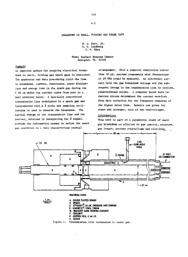
114
4.2
BREAKDOWN IS SMALL, FLOWISG GAS SPARK GAPS
W. K. Cary, J r .D. D. Lindberg
J. H. Rice
Naval SurfaceDahlgren,
Summary
An Improved method for studying electrical break-
down in small, flowing gas spark gaps is described.
The apparatus and data processing yield the time
to breakdown, current, resistance, power dissipa-
tion and energy loss in the spark gap during the
4 nS in which the current rises from zero to a.
near constant value. A specially constructed
transmission line terninated in a spark gap and
instrumented with a B probe and sampling oscil-
loscope is used to observe the breakdown. The
initial charge on the transmission line and the
current, obtained by integrating the B signal,
provide the information needed to define the spark
gap operation in a well characterized coaxial
Weapons CenterVA. 22448
arrangement. With a temporal resolution better
than 50 pS, current components with frequencies
to 10 GHz could be measured. An electronic cir-
cuit held the gap breakdown voltage and the sub-
sequent charge in the transmission line to precise,
predetermined values. A computer based data re-
duction system determined the current waveform
from data corrected for the frequency response of
the signal delay line. Results are given for
argon and nitrogen, each at two overvoltages.
Introduction
This work is part of a parametric study of small
gap breakdown as effected by gas species, pressure,
gap length, percent overvoltage and electrode^
SO cm-
HI VOLTGR CONNECTOR
i
1.27 cm
MATERIAL CODE:
A - SILVER PLATED BRASSB-BRASS %D • STYCASTr'36 DK. EMERSON AND CUMINGE - ELKOBITE1* 10W3. CM&WM . MACOtrS) OOW CORNING CERAMICT TEFLO*S>P - COPPER PIPE, 2 cm I.D.S • SILVER
Figure 1. Transmission l ine terminated by spark gap.
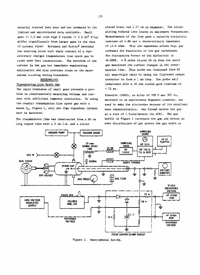
115
material started last year and was prompted by the
limited and uncorrelated data available. Small
gaps (> 2.5 mm) with high E fields (> 2 x 10s V/cm)
differ significantly from larger gaps in the rate
of current risel. Sorensen and Ristic^ provided
the starting point with their concept of a rep-
etitively charged transmission line spark gap to
study very fast transistions. The waveform of the
current in the gap has immediate engineering
application and also provides clues to the mech-
anisms occuring during breakdown.
METHODOLOGY
Transmission Line Spark Gap
Tne rapid breakdown of small gaps presents a pro-
blem in simultaneously measuring voltage and cur-
rent with sufficient temporal resolution. By using
the coaxial transmission line spark gap with a
known Zo, Figure 1, only the time dependent current
must be measured.
The transmission line was constructed from a 60 en
long copper pipe with a 2 cm I.D. and a silver
plated brass rod 1.27 cm in diameter. The silver
plating reduced line losses at microwave frequencies.
Measurements of the line gave a relative dielectric
constant of 4.86 and a characteristic impedance
of 12.0 ohms. This low impedance allows high gap
currents for resolution of low gap resistance.
The dissipation factor of the dielectric is
<0.0008. A B probe placed 10 cm from the spark
gap monitored the current changes in the trans-
mission line. This probe was fashioned from 35
m-n semi-rigid cable by using the flattened center
conductor to form a 1 mm loop. The probs self
inductance with a 50 ohm system gave risetime of
< 25 ps.
Elkonite (10W3), an alloy of 70% W and 30% Cu,
machined to an approximate Rogowski countour, was
used to make the electrodes because of its excellent
wear characteristics. Gas flowed across the gap
at a rate of 1 liter/minute (to ATM). The gas
baffle in Figure 1 surrounds the gap and forces an
even distribution of gas across the gap width as
SAMPLINGSCOPE
HP 1S1A
HP 1B11AT.B. & VERT
X
y
HP XVPLOTTER
_J
oJ-K-
L_ Iz I
REFERENCEVOLTAGE
FU1.SE CHARGE CLAMP CIRCUIT
Figure 2. Experimental Set-Up.
116
we\l as preserving the line Zo across thi3 region.
The flow rate was chosen so that at least 2 changes
of gas took place between arcs. The arcs then
occurred in a gas relatively free from residue
and were highly repeatable. The adjustable
electrode which allows gap size up to 0.5 mm is
electrically shorted to the outer shell through
a silver foil sliding contact placed less than
3 am from the spark gap (Figure 1). The length
of chis short circuit thus is less than 1/5 of
a wavelength at 10 GHz.
Charging Circuit
The sampling techniques to monitor the 3 signal
require that the line be charged to precisely the
same voltage each time for minimum amplitude
jitter. The high voltage pulse ganerator and the
electronic voltage clamping circuit shown in
Figure 2 held voltage variations to less than
1.57.. The rise time of the charging pulse must be
fast: enough to prevent the gap from breaking down
before the clamp voltage is reached. Generally,
risecimes of about 1 microsecond are satisfactory,
but when gap overvoltages greater than 250-300%
are used, faster charging pulses are needed. A
digital voltmeter monitors the clamp voltage and
a specially built, pulse compensated voltage probe
with a oscilloscope records the charging pulse
vaveforra. This also gives a measure of the time
between application of voltage and breakdown to
ailow a statistical analysis of the time to break-
down.
Procedure
The spark gap and transmission line were charac-
terized by determining the gap capacitance, the
characteristic impedance (Zo) of the line and the
autual impedance of the line and B probe. The gap
capa .itance is in parallel with the line and the
line capacitance adds with that of the gap.
In jrder to determine Zo, the velocity of propaga-
tion was measured with an Ikor pulse generator and
c~-o Tektronix sampling heads. Four points along
Che transmission line were accessible and were
paired for three measurements. Time domain re-
rlec trorae r.ry was also used. The mean of these
measurements gave a value of 45% the velocity of
light with a standard deviation of less than 6%
for a Zo of 12.0 ohms. The 3 probe constant was
determined from measurements with argon at 50 psia
and a 50 micrometer gap while assuming a low gap
resistance when the di/dt= 0.
Gas species, pressure, flow rate and gap length
are selected and the static breakdown voltage
measured. The clamp voltage is set based on a
percent overvoltage of the static breakdown voltage.
The pulse generator voltage is set approximately
50% above the clamp voltage to ensure a fast
charging pulse risetime. Pulse repetition rates
of 33 to 100 Hz were selected as needed to produce
stable oscilloscope traces. The system is run
several minutes to condition the electrodes before
the charging voltage and the B signal are re-
corded. When gas species is changed, the gap is
dissassembled, cleaned., and the electrodes polished
and flushed with the new gas. The gap measure -
ments stablize after 2-3 minutes of operation.
Significant electrode erosion or coating have not
been noted during runs with argon and nitrogen.
Data Reduction
The sampling oscilloscope measuring the B signal
drives an X-Y plotter to record the data. These
waveforms are digitized and stored in a computer.
The computer smoothes the data, reconstructs the
signal at the input to the delay line, solves the
circuit equations for the gap resistance, power
dissapated and energy lost, and plots these as a
function of time. The delay line, which acts as
a r.ime invariant low pass filter, distorts the
signal. The computer program finds the Fourier
transform of the signal, multiplies it by the in-
verse Fourier transform. The current in the trans-
mission line is simply I(t) = —/vg(t) dt, where
vB(t) is the B signal and k is the mutual induct-
ance between the B probe and the transmission line.
The time varying resistance of the gap is given^
by
R(t) = — 2 —
Where 70 is the breakdown voltage,
C is the gap capacitance and it can be
seen, that as I(t) gets large an accurate measure
117
of Vo becomes more important for accurate results.
Power and energy are directly available from the
current and resistance.
Results
The time dependence of gap resistance and instan-
taneous power for argon at two E/P ratios is
shown in Figures 3-6. For comparison, the time
functions of instantaneous gap power for nitrogen
at two E/P ratios is given in Figures 7 and 8.
Table 1 is a summary of some of the parameters
for the four runs. The gap resistance curves fit
the relationship
R(t) - at"m
with a and m listed in the table.
The very high electric field in the gap makes it
operate in an unusual regime. After the electrodes
are conditioned, with electric fields greater
than 10" V/m, cause its explosion of cathode
microtips ' and create runaway electrons from
the avalanche that generate X-rays -. Thus in
this regime, breakdown is very rapid and does not
follow breakdown in gaps with lower fields- . An
example of this can be seen in Figures 3 and 4,
where at constant pd the rate of gap resistances
fall increases when the charge voltage decreases.
SPBRV U>V PP.BWIETtP.Si
veax> 1917 cap icwcrw.itii.s**.*
STBT1C veBK-l2&t CDS PRESS.PSIO> 5 1 . f
tOVtP.r01.TB 52 CRS FL&H. t-K)ff> !•!>
REStSTRNCE RCT)
T.rmCfNRNDSCCQNDS)
58 . f
RRGON iorcswi.1" inRESISTRNCE RCT)
T.TJBECJBHOSECDKKI
Figure 4. (Run 2)
- *
*
:
t • \ RRGON] \ POWER
r A; ; \ •
\
1 ! ' '
. !
1 ' ',
j : ' ; ;1 ': ; .
VBSKB
\
N\
(
IB17 GDC LENCrk.fl.E-^.C
TIME IX SECONDS CJC10-" )
Figure 5. (Run 1)
f POHERi
i l l '
• ! i :
I • :
' : •
SPDRK SCP DOKQ"ETEa5.
VBBl. 2S*7 «B» l t * I S I I . . m L « - * . f
S T O T : : V B B I C « I Z 4 I S D S o n E E t . o s i t . st.i
S ^ ^ ^ I D W O U * )B2 SB* Ft,DM.L-KlNe ; . B
~ ^ — ^ _ _
: .' ' • — •
Figure 3. (Run 1)
t.12 1.16 I.ZB
TIKE IN SECONDS CK10-")
Figure 6. (Run 2)
118
NIT: POWER
SPUR* SUP PMOMCTCDSI
YlflK* 1917 CBP LEKCTU.HILS-2.1
IDVERVOLT- 52 t3S rLQtt.L-HINu I . I
•>.!• *. ft. I.IB I.12 1.16 t.ZI ».Z* 1.21
TIME IN SECONOS CXtfl-«)
NIT; POWER
SCMK CAP DOBOHCTtaSi
VBRKB 2547 CflP IEH6TM.KILS.2.B
srnnc vBRf- i j i f vn dness.psio* 2S. i
taVERVOLTa 112 MS FLOU.l-MIM 1.1
i :
i/ ; ;
Bigiire 8- <RunI I
|.!2 f. 16 C.2I
TIME IN 3ECQNQS ai0-» 1
Hun [f
1
:
•1
S u
Arjfon
Argon
Nltrogan
Nitrogen
a
2.4
4.A
1.7
6 . 6
3
.766
.547
.545
.iai
Cap Flald
t 10»
18.9
25.1
37.7
50.1
730
970
2920
3S7O
Mm GapEnsrgy
(BJ)
.111
.285
.155
.316
PeakPover
(W>
69
129
70
128
10-901CurrencRlascloR
(PS)
170
155
150
150
pd(ma-corr)
263
263
65.3
65.B
References
i . Kassel, S.; Hendricks, C. D.; Soviet Be3earch
xnd development of High-Power Tap Saitahes,
R-1333-A.RPA, January 1974.
1. Sorensen, T. P.; Rist ic , V. M.; Ries Time am
Zim'S-Depender.t Svark-Gav Resistance in
r.izrsgsn and Helium, J. Appl. Phys., Vol. ui.
No. 1, January 1977.
•?• Cjr;.-, 'A. K., J r . ; Massie, J . A. ; ri.ue Resolved
Resistance During Spark. Izp 3veakdown, Proc.,
Second P u l s e d Power C o n f . , May 1 9 7 8 .
-.. M e s y a t s , <i. A . ; B y c h k o v , Y u . I . ; Kremnev , V . V . ;
Pulsed llanoeeaovd Zleetvio Discharges m Tiises,
Soviec Physics - Technical Physics, Vol 16, So.
3, 1972.
5. Mesyats, G. A.; Bychkov, Yu. I . ; I skol 'dsk i i ,
A. I . ; Nanosecond Formation Time of Discharges
in SlwFt Air Gaps, Soviet Physics - Technical
Physics, Vol. 13, No. 3, 1969.
119
4.3
ELECTRON DENSITIES IN LASER-TRIGGERED SPARK GAP DISCHARGES
R. J. Crumley, P. F. Williams, M. A. Gundersen and h. Watson
Dept. Elect. Eng., Texas Tech Univ.
Lubbock, Texas 79409
Abstract
The results of experiments designed co measure
electron densities from measurements of Stark
broadened spectral profiles in laser-triggered
discharges in hydrogen are reported. Temporally
and spatially resolved data have been obtained
both during and after the arc for discharges in
hydrogen. Evidence of a Shockwave is presented,
consistent with the observations of other
investigators.
Introduction
Laser-triggered spark gaps offer a number of
important advantages in applications requiring
switching of high voltage at high currents with
low jitter in the switch closure time. In such
gaps the triggering laser is focussed onto one
electrode, usually entering the gap through a
small bole in the opposite electrode and passing
along the gap axis. Even though the gap voltage
is held at a value significantly below the static
breakdown value, the laser induces the gap to
break down completely after only a short delay.
Study of the basic processes responsible for the
breakdown phenomena are of considerable interest,
not only because of the direct practical value of
such studies, but also because of the critical
role space charge-induced fields must play in the
initial breakdown.
Ue report the results of studies undertaken to
determine the electron density in a laser-
triggered hydrogen arc. Electron densities were
determined from the measured full widths of the
Stark-broadened atomic linewidth using the
relation
Ke • C(N£,T) iS3/2
vhere Ng is the electron density, AS is the full
Stark width, and C(N ,T) is a coefficient weakl:-
dependent upon N and temperature. Time-resolved
data have been obtained both during and after che
arc for discharges in hydrogen, and spatially-
resolved data have been obtained for times
corresponding to the beginning and end of the arc.
The experimental arrangement is shown in figure 1.
an.' consists of a spark gap enclosed in a cell
which is evacuated and then backfilled to the
desired pressure with hydrogen. The aluminum
electrodes have a constant field profile, and a
voltage less than the static breakdown voltage is
impressed across them using a coaxial cable
system, charged through a large resistor by a
regulated power supply. The length of the cable
is such that, when the load is properly matched to
the transmission line, laser-triggering of the gap
results in a clean current pulse of about 1 usec.
duration. A nitrogen laser pulse, = 5 mj. in
10 nsec, enters the gap axially through a 2 inn.
hole in one electrode and is focussed onto the
other electrode, triggering the gap. The emission
from the discharge exits the cell through a
window transverse to the gap axis, and is
spectrally-dispersed with a 0.5 m. spectrogrsph.
An optical multichannel analyzer is used to detect
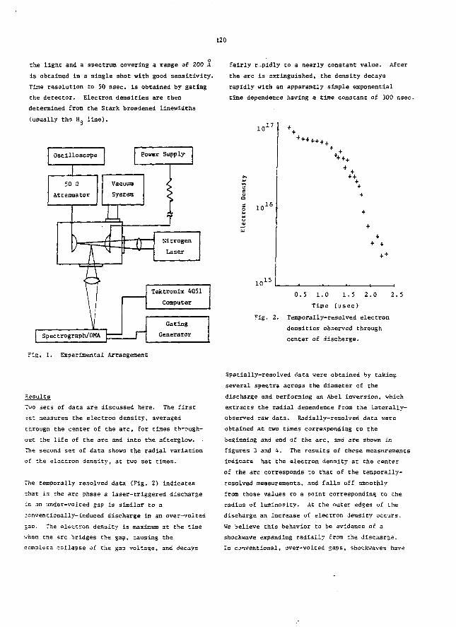
120
othe light and a spectrum covering a range of 200 A
is obtained in a single shot with good sensitivity-
Time resolution to 50 nsec. is obtained by gating
the detector. Electron densities are then
determined from the Stark broadened linewidths
(usually tha H3 line).
Oscilloscope Power Supply
50 S2
Attenuator
Vacuum
System
XT
Spectrograph/OKA
Tektronix 4051
Computer
Fig, I. Experimental Arrangement
Results
Two sees of data are discussed here. The first
set measures the electron density, averaged
through the center of the arc, for times through-
out the life of the arc and into the afterglow.
The second set of data shows the radial variation
of the electron density, at two set times.
The temporally resolved data (Fig. 2) indicates
chat in the arc phase a laser-triggered discharge
in an under-voiced gap is similar to a
conventionally-induced discharge in an over-voited
Sap. The electron density is maximum at the time
when the arc bridges the gap, causing the
complete collapse of the gap voltage, and decays
fairly r.-pidly to a nearly constant value. After
the arc is extinguished, the density decays
rapidly with an apparently simple exponential
time dependence having a time constant of 300 nsec.
1017
o 1016
1015
+4
0.5 1.0 1.5 2.0 2.5
Time (usec)
Fig. 2. Temporally-resolved electron
densities observed through
center of discharge.
Spatially-resolved data were obtained by taking
several spectra across the diameter of the
discharge and Derforming an Abel inversion, which
extracts the radial dependence from the laterally-
observed raw data. Radially-rasolved data were
obtained at two times corresponding to the
beginning and end of the arc, and are shown in
figures 3 and 4. The results of these measurements
indicate hat the electron density at the center
of the arc corresponds to that of the temporally-
resolved measurements, and falls off smoothly
from chose values to a point corresponding to the
radius of luminosity. At the outer edges of the
discharge an increase of electron density occurs.
We believe this behavior to be evidence of a
Shockwave expanding radially from the discharge.
In conventional, over-voited saps, Shockwaves have
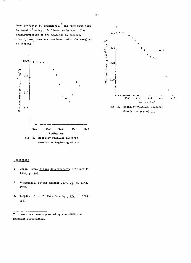
121
been predicted by Braginskii,1* and have been seen
by Koppitz using a Schlieren technique. The
characteristics of the increase in electron
density seen here are consistent with the results
of Koppitz.
10.0
7.5
1 5-0
0.1 0.70.3 0.5
Radius (mm)
Fig. 3. Radially-resolved electron
density at beginning of arc.
0.9
i
4.01-
3.0
I 2-°
1.0
0.5 1.0 1.5 2.0
Radius (am)
Fig. 4. Radially-resolved electron
densicy at end of arc.
References
1. Griem, Hans, Plasma 5pectroscopy, McGraw-Hill,
1964, p. 305.
2. Braginskii, Soviet Physics JETP, 3±, p. 1548,
1958.
3. Koppitz, Jorn, Z. Naturforschg., 22a, p. 1D89,
1967.
This work has been supported by the AF0SR and
Research Corporation.
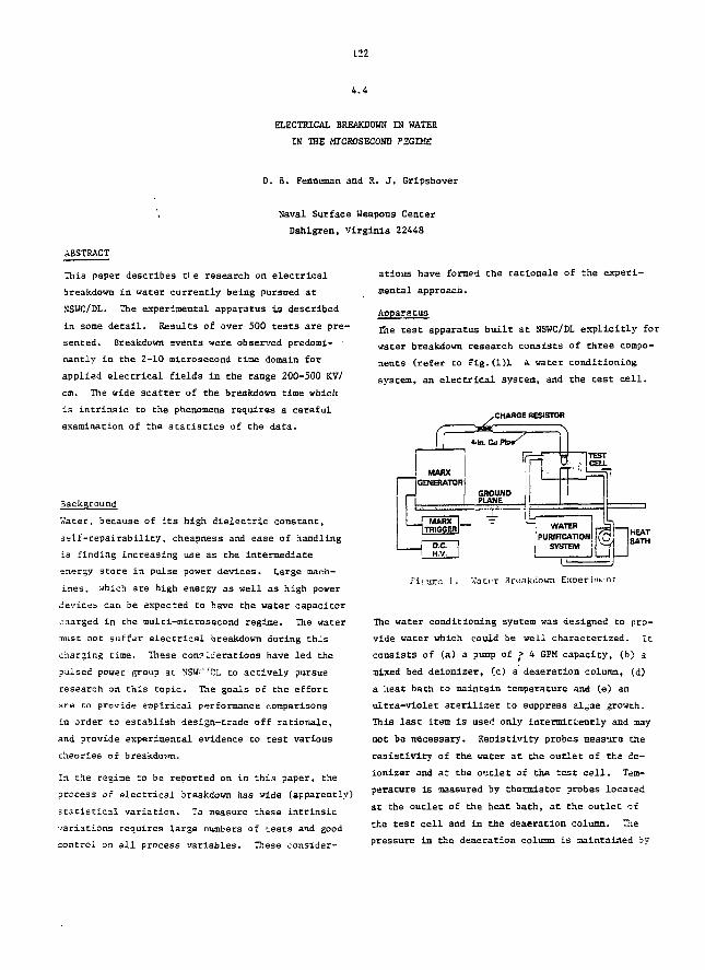
122
4.4
ELECTRICAL BREAKDOWN IN HATER
IN THE MICROSECOND P2GME
D. B. Fenneman and R. J. Gripshover
Naval Surface Weapons Center
Dahlgren, Virginia 22448
ABSTRACT
This paper describes tfe research on electrical
breakdown in water currently being pursued at
NSHC/DL. The experimental apparatus is described
in some detail. Results of over 500 tests are pre-
sented. Breakdown events were observed predomi- •
nancly in the 2-10 microsecond time domain for
applied electrical fields in the range 200-500 KV/
cm. The wide scatter of the breakdown time which
is intrinsic to the phenomena requires a careful
examination of the statistics of the data.
Background
Water, because of its high dielectric constant,
self-repairability, cheapness and ease of handling
ts finding increasing use as the intermediate
energy store in pulse power devices. Large mach-
ines, which are high energy as well as high power
devices can be expected to have the water capacitor
charged in che multi-microsecond regime. The water
lust not suffer electrical breakdown during this
charging time. These considerations have led the
puised power group at. N'SW 'DL to actively pursue
research on this topic. The goals of the effort
are to provide empirical performance comparisons
in order to establish design-trade off rationale,
and provide experimental evidence to test various
theories of breakdovm.
In che regime to be reported on in this paper, Che
process of electrical breakdown has wide (apparently)
statistical variation. To measure these intrinsic
variations requires large numbers of tests and good
control on all process variables. These consider-
ations have formed the rationale of the experi-
mental approach.
Apparatus
The test apparatus built at NSWC/DL explicitly for
water breakdown research consists of three compo-
nents (refer to Fig.(1)X A water conditioning
system, an electrical system, and the cest cell.
CHARGE RESISTOR
Firuro 1. Water Breakdown Experim.nr
The water conditioning system was designed to pro-
vide water which could be well characterized. It
consists of (a) a pump of > 4 GPM capacity, (b) a
mixed bed deionizer, (c) a deaeration column, (d)
a heat bath to maintain temperature and (e) an
ultra-violec sterilizer to suppress al=ae growth.
This last Item is used only intermittently and niay
not be necessary. Reoistivlty probes measure the
resistivity of the water at the outlet of the de-
ionizer and at the outlet of the test cell. Tem-
perature is measured by thermistor probes located
at the outlet of the heat bath, at the outlet of
the test cell and in the deaeration col man. The
pressure in the deaeration column Is maintained by
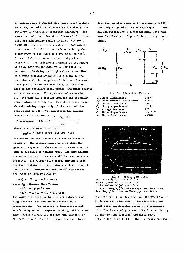
123
a vacuum pump, protected from water vapcr fouling
by a trap cooled by an alcohol-dry ice slurry, the
pressure is measured by a mercury manometer. The
water is conditioned for about 3 hours before test-
ing, and continually during r.esting. All told,
about 40 gallons of treated water are continually
circulated. It takes about an hour to bring the
resistivity of the water to above 18 Mn-cm (25°C)
from the Z-3 MS-cm value the water degrades to
overnight. The resistivity obtained in the system
is at or near the ultimate value for water and
success in obtaining such high values is ascribed
to flawing continually above 2.5 GPM and to the
fact that with the exception of the test electrodes,
the copper coils of the heat bath, and the small
area of che stainless steel probes, the water touches
no metal or glass. All pipes and valves are hard
?VC, the pump has a nitrile impeller and the deaer-
ation column is plexlglas. Deaeration takes longer
than deiocizing, especially if the test cell has
been opened to air. At equilibrium the percent
deaeration is computed asP -
Z Deaeration - 100 x ( 1 )760
where: p » pressure in column, Corr
PH -(T) - water vapor pressure, torr
The circuit of the electrical system is shown in
Figure 2. The voltage source is a 10 3tage Marx
generator capable of 500 KV maximum, whose erection
time is a couple of hundred nsec. The Marx charges
the water test cell through a 4000f! copper sulphate
resistor. The voltage also bleeds through a Marx
internal resistance of approximately 9008. Circuit
inductance is unimportant and the voltage across
the water is closely given by
V(t) - .71 Vo (e<"lt - e«>2t)
where Vo » Erected Marx Voltage
-1/">1 - RmCm- 20 usec
-l/")2 - Rc(Cw + Cs) - 2.0 usec
The voltage is measured by a copper sulphate divi-
ding resistor, the current is measured by a
Rogowski coil. The observed voltage and current
waveforms agree with computer modeling (which takes
into account temperature and gap size effects) to
the resol' .ion of the oscilloscope traces. Break-
dewn time is also measured by counting a 100 MHz
clock signal gated by the voltage signal. These
all are recorded on a Tektronix Model 7844 Dual
Bean Oscilloscope. Figure 3 shows a sample test
trace.
C s ^
J i
Fig. 2. Electrical Circuit
CM, Marx Capacitance 22nFtill, Marx Internal Resistance 9003Ls, Stray Inductance 4uHCs, Stray Capacitance .lnFRe, Charge Resistor 4KS2CH, Water Capacitance .4-.5nFSty, Water Resistance >300K$i
Fig 3. Sample Data TraceTcp Curve V(t)> 1 CM - 41.7 KVBottom Curve i(t) 1 CM « 20 AAt Breakdown V(t)-*O and i(t)->-
V0.exp (-RnCmO/Bc since capacitor is shorted.Starting glitch due to Marx gap transients.
The test cell is a plexiglas box 20"x20"xl4" which
holds the test electrodes. The electrodes are
tough pitch electrolytic copper in a hemisphere
(R = l:l)-plane configuration. The final surfacing
is done by sand blasting with glass beads
(Blastolite, size Bl-10). This surfacing technique
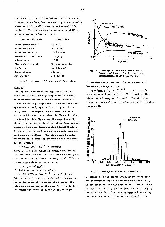
124
Is chosen, not out of any belief that it produces
a superior surface, but because It produces a well-
characterized, easily restored and reproducible
surface. The gap spacing is measured to .001" by
a cachetometer before each shot.
Process Variable
Water Temperature
Water Flow Bate
Water Resistivity
Pressure in Test Cell
% Deaeracion
Electrode Material
Surfacing
Stressed Area
Gap Spacing
Condition
19 +2°C
> 2.2 GPM
> 18 MB-cm
1.3 ps ig
> 95Z
Electrolytic Cu.
Sandblasted
300 mm2
2.8-6.4 mm
Table 1. Summary of Experimental Conditions
Results
For any real apparatus the applied field is a
function of time, consequently there is a built
in dependence of field at breakdown to time of
breakdown for any single test. Further, any real
apparatus can only spaa a finite region of the
S-t plane. The region investigated in this work
is bounded by the curves shown in Figure 4. Also
displayed in this figure are the experimentally
observed point pairs (EMAX' cb) where Effax is the
maximum field experienced before breakdown and tfe
is the time at which breakdown occurred, measured
from onset of voltage. The touchstone of water
breakdown field-tioe experiments is the relation
due to Martin1:
M " EMAX <<*
Here, to is a time parameter usually defined as
che time when the applied field exceeds some given
fraction of its maximum value (e.g., 50%, 63%). A
linear regression- on the relation
tb - t0 + (a/Etftx^
yielded from the data the values
:•! - .562 (MV/cm)-(ysec)1/'3; to » 0.53 us'ec
This value of M is close to the value .6 usually
quoted cor uniformly stressed electrodes. The
value to corresponds to che time E(t) =• 0.28 EUAX.
The regression curve is also plotted in Figure 4.
'
.REGRESSION
_OS>2
t (ft MC}
Fig. 4. Breakdown Time vs Maxlmm Field -Summary of Data. The dots are theexperimental paints
To examine the properties of M as a measure of
breakdown, the quantities
»i - EM & X i (tbt - .53)1 / 3 i - 1.....294
were computed from the data. The result is dis-
played as a histogram. Figure 5. The histogram
shows the mean and mode are close to the regression
value of M.
UJ50
[30
•20
2iof-a3
MEAN* .55HO=.07»
0L4- ,-rn-iH k0.3 0.4 0.5 0.6 0.7 0.8 0.9
M. (MV/cm) • ifi see)1'3
Fig 5. Histogram of Martin's Relation
A criticism of the regression analysis stems from
the observation that the standard deviation of t(,
is not constant over the population. This is shown
in Figure 6. This graph was generated by arranging
the data in order of increasing EJJ^ and computing
the means and standard deviations of tb for all
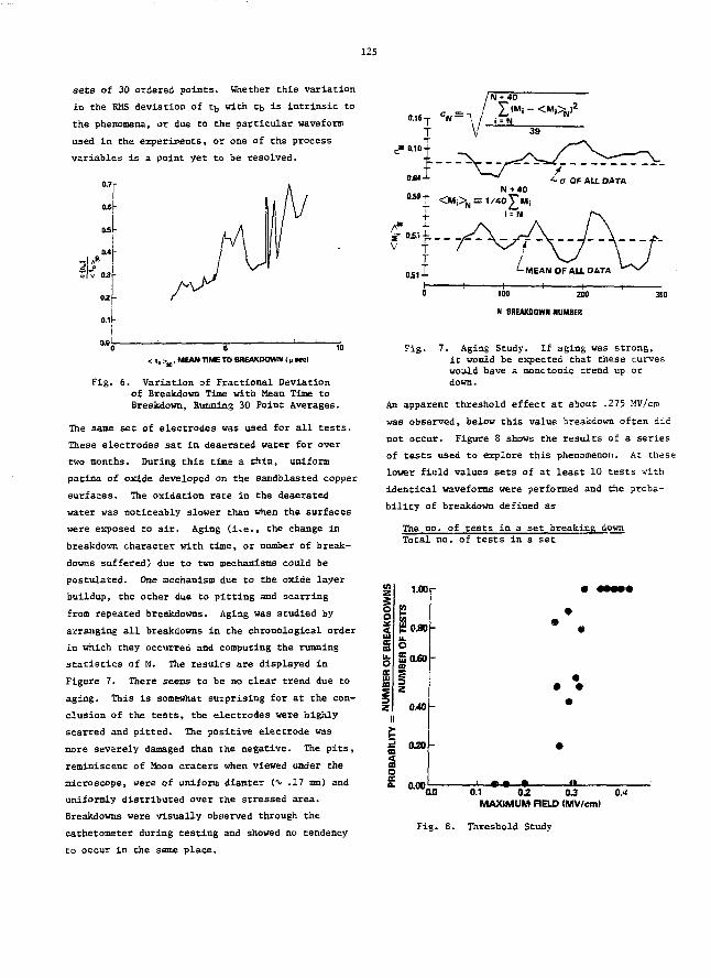
125
sets of 30 ordered points. Whether this variation
in the EMS deviation of tfc with tb is intrinsic to
the phenomena, or due to the particular waveform
used in the experiments, or one of the process
variables is a point yet to be resolved.
0.6J-
CLE
1X4
03
02
0.1 -
jO.OL , , , _ ; • , ft
<t -> .MEAN TIME TO BREAKDOWN (n MCI
Fig. 6. Variation of Fractional Deviationof Breakdown Time with Mean Time toBreakdown, Running 30 Point Averages.
The same set of electrodes was used for all tests.
These electrodes sat in deaerated water for over
two months. During this time a thin, uniform
patina of oxide developed on the sandblasted copper
surfaces. The oxidation rate in the deaerated
water was noticeably slower than when the surfaces
were exposed to air. Aging (i.e., the change in
breakdown character with time, or number of break-
downs suffered) due to two mechanisms could be
postulated. One mechanism due to the oxide layer
buildup, the other due to pitting and scarring
from repeated breakdowns. Aging was studied by
arranging all breakdowns in the chronological order
in which they occurred and computing the running
statistics of M. The results are displayed in
Figure 7. There seems to be no clear trend due to
aging. This is somewhat surprising for at the con-
clusion of the tests, the electrodes were highly
scarred and pitted. The positive electrode was
more sevarely damaged than the negative. The pits,
reminiscent of Moon craters when viewed under the
microscope, were of uniform diamter (i* .17 mm) and
uniformly distributed over the stressed area.
Breakdowns were visually observed through the
cathetometeT during testing and showed no tendency
to occur in the same place.
IUI-1- <- MEAN OF ALL DATA
0 100 200 300
H BREAKDOWN NUMBER
Fig. 7. Aging Study. If aging was strong,it would be expected that these curveEwould have a monctonic trend up ordown.
An apparent threshold effect at about .275 MV/cn
was observed, below this value breakdown often did
not occur. Figure 8 shows the results of a series
of tests used to explore this phenomenon. At these
lower field values sets of at least 10 tests with
identical waveforms were performed and the proba-
bility of breakdown defined as
The no. of tests in a set breaking downTotal no. of tests in a set
1.00
(fiaaou.O5 0.60
0.40-
0.000.0 0.1 02 0.3 0.4
MAXIMUM FIELD (MV/cml
Fig. 8. Threshold Study
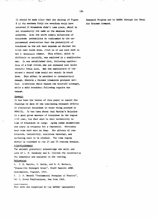
126
It should be made clear chat the abcissa of Figure
8 Is the man-innim field the waveform would have
achieved if breakdown didn't take place, which is
not necessarily the same as the maximum field
achieved. Also the above simple definition of
breakdown probability is confounded by the ex-
perimental observation that the probability of
breakdown on the nth test depends on whether the
n-lst test broke down, »hich is to say each test is
not a Bernoulli chance. This effect, which is
difficult to quantify, was explored in a qualitative
way. It was established that, following applica-
tion of a high stress, the low stressed test would
probably break down. But the application of low
stress a second time would not result in break
down. This effect is ascribed to transistitory
damage, wherein a violent breakdown produces sur-
face crnditions which weaken the hold-off strength,
while a mild breakdown following repairs the
damage.
Summary
It has been the intent of this paper to report the
findings to date of the continuing research efforts
on electrical breakdown in water being pursued at
NSWC/DL. It has been shown that Martin's Relation
is a good gross measure of breakdown in the region
2-10 ysec, but that shot to shot variability in
cime of breakdown is large. Aging seems unimportant
and there is evidence for a threshold. Obviously
much aore work must be done. The effects of tem-
perature, resistivity, electrode material, and
surfacing need to be studied. The time regime
should be extended to the 20 and 30 usecond domains.
Acknowledgement
The authors gratefully acknowledge the skill and
care of L. W. Hardesty and K. Chllton who constructed
the apparatus and assisted in the testing.
References
1. J. C. Martin, I. Smith, and H. G. Herbe7.-t,
"Dielectric Strength Motes", Staff Reports AWRE,
Aldermaston, England, 1965.
2. D. a. Menzel "Fundamental Formulas of Physics",
'.'al 1, Dover Publications, Sew York 1960.
Research Program and by DARPA through the Saval
Air Systems Command.
Fhis work was supported by the MAVSWC Independent
127
PULSED ELECTRON FIELD EMISSION FROM PREPARED CONDUCTORS*
G. B. Frazier
Physics International Company2700 Merced Street
San Leandro, California 94577
Abstract
The electron emission characteristics of metal
cathodes subjected to pulsed electric fields in the
absence of insulating magnetic fields has bsen in-
vestigated experimentally> Uniform electric fields
in the range of 0.2-0.8 MV/cm were applied to
50 en surfaces under vacuum in single pulses of
' 60 as duration at a voltage of * 0.5 MV. Bare
metals and metals coated with dielectric materials
were studied. Results show that bare metals with
freshly prepared surfaces can withstand fields of
5 300 kv/cm for 2 40 us without significant emis-
sion. Emission-induced discharges degrade the sur-
faces such that full space-charge-lizaited current
densities (100-250 A/cm2 for this experiment) are
obtained at fields as low as 200 kV/cm on subse-
quent pulses. In the case of coated surfaces, it
was found that dielectrics could occasionally sup-
press emission completely up to * 300-400 kV/cm,
and unlike bare metals, could partially suppress
emission after having passed significant current at
fields up to 0.6 MV/cm.
Introduction
Electron emission from surfaces subjected to
high electric fields in a vacuum is an important
consideration in a wide variety of pulsed paver ap-
plications. The phenomenon has been extensively
investigated for the dc case. Early work1 provided
valuable insight into basic emission and vacuum
breakdown processes, but with the advent of high-
voltage, high-current, pulsed electron acceler-
ators, it became necessary to investigate the
phenomenon on a submicrosecond time scale. Some
work was done on this problem in the late sixties2
•Work partially supported by the LawrenceLivermore Laboratory.
as part of the development program for the AURORA
generator, and more recently by Milton4 using bare
stainless steel cathodes. The data reported here
are the result of a limited, empirical study of the
phenomenon under a specific set of pulse and elec-
trode conditions.
The experiment was conducted to investigate
the feasibility of rising dielectric coatings to
suppress emission. Investigation of coatings under
pulsed conditions was considered particularly im-
portant for advanced, high-power laser exciters
because such devices typically do not produce the
large, self-generated magnetic fields used to insu-
late structures in low impedance accelerators.5'6
Description of Experiment
The expsrimental apparatus (Figure 1) consist-
ed of a 38-cm-diameter aluminum vacuum chamber con-
taining a sample holder and current collector
assembly. The samples were 23-cnt-diameter by
6.35-mm-thick disks which were held in place by a
radiused clamp ring. The holder was attached to
the negative output electrode of a Physics Inter-
national Oompany PULSERAD 225-W, which produces a
72 kJ, 60 ns pulse at 5.3 ft when configured as an
REBA.
The experimental parameters are given in
Table 1. The basic experimental approach was to
install prepared samples, then fire the 225-W at
the •.* 530 kv outp'it level using a variety of
sp&cings to achieve different peak electric field
magnitudes. The general pattern for each sample
was from low to high values of field. Mast samples
were initially stressed to 200-250 kv/cm (2.5-2.0
cm spacing), then subjected to gradually increased
fields for successive shots. "Op-and-down" scans
were often used to investigate degradation effects.
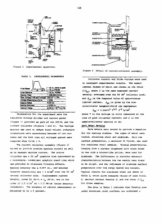
128
CARSON GUARD RING
Figure 1 Experimental apparatus.
TABLE 1, EXPERIMENTAL PARAMETERS
PuinShipa V . (~ 50 nl, width a pMk120 m \ ~ 75 nSiuFWHM
PUIM Rimim*ElMtrieFitMPMk Voiugt (140 ihot i t > w lVolage Mwunmeit EirarSpKingRingaSwans AccuracyVacuum Rang*
- 2 0 m. 10-90%-200800 kV/cm532 kV -t 7.3*±5.0%0-25 cm10.001 in.2.0*0 X 10"4 mm Hg
Diagnostics for the experiment were the
rasistive voltage divider and current probe
(Figure 1) provided aa part of the 225-W, and the
current collector {Figures 1 and 2). The voltage
monitor was used to deduce field values; inductive
corrections were unnecessary because of low cur-
rents and the fact that ail voltages quoted were
.•naasured when di/dt =• 0.
The current collector assembly (Figure 2)
served to provide precise spacing control as well
as to measure emitted current. The active
collector was a 50 cm graphite disk surrounded by
a concentric, re-entrant graphite guard ring which
was provided to eliminate fringing effects•
Spacing accuracy was t 0.001 in., and minimum
•iecector sensitivity was ^ 3 fl/cm over the 50 3n2
central collector area. Displacement current
density, given by 3D/3t » eQ 3E/at, was on the
order a£ i.5 A/cm" at i. 0.5 MV/cin (below detector
-hreshold). The accuracy of current measurement is
estimated to be i S percent.
Figure 2 Detail of currant collector assembly.
Collector current and diode voltage were used
to interpret experimental results. The exper-
imental figure of merit was chosen as the ratio
J/JLC, where J is the peak measured current
density, averaged over the 50 cm2 collector area,
and JLC is the computed value of space-charge
limited current. JLC is given by the non-
relativiatic Iangmuir-Child law expression
JLC - 2.34x10³ 7 3 / 2 d"2 A/cm2
where V 13 the voltage in volts (measured at the
time of peak collector currentJ and d is the
sample-collector spacing in cm.
Bare Metal Results
Bare metals were tested to provide a baseline
for the coating studies. Two types of metal were
tested, stainless steel and aluminum. Only one
surface preparation, a machined 32 finish, was used
for stainless steel samples. Several preparations,
ranging from a surface roughened with glass beads
to one with a mirror-like polish, were used for
aluminum. The differences in electron emission
characteristics between the two metals were found
to be slight, and the influence of alaminud surface
preparation over the range tested was minimal.
Typical results for stainless steel are shown in
Table 2, which gives measured values of mean field,
S, emitted current density J, and the ratio J/J^_
for three samples.
The data in Table 3 indicate that freshly pre-
pared stainless steel surfaces can withstand a
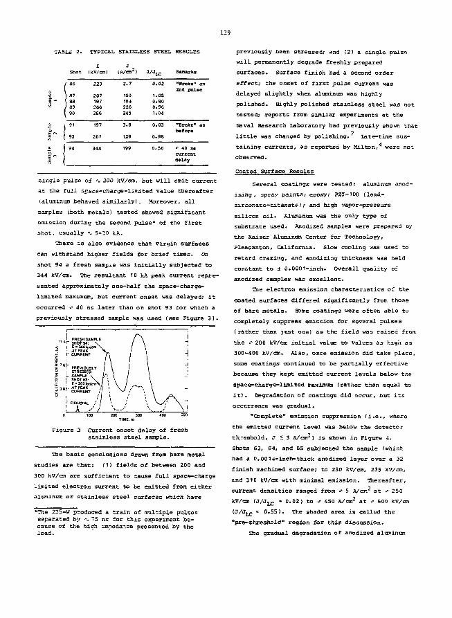
129
TABLE 2. TYPICAL STAINLESS STEEL RESULTS
Shot (kV/cnl (Vcnr)
s —
207
197
266
266
150
104
226
245
0.02
1.05
0.80
0.96
1.04
"Broke" on
2nd pulse
a
prV.
V
iJ<
91
93
94
197
201
344
3.8
129
199
0.
0.
0.
03
96
50
"Broke" as
before
' « 0 in
current
delay
single pulse of 200 kV/cm, but will emit current
at the full space-charge-limited value thereafter
(aluminum behaved similarly). Moreover, all
samples (both metals) tested showed significant
emission during the second pulse* of the first
shot, usually -\. 5-10 kA.
There is also evidence that virgin surfaces
can withstand higher fields for brief times. On
shot 94 a fresh sample was initially subjected to
344 kV/cm. The resultant 10 kA peak current repre-
sented approximately one-half the space—charge-
limited maximum, but current onset was delayed; it
occurred <r 40 as later than on shot 93 for which a
previously stressed sample was used (see Figure 3).
FRESH SAMPLE~ SHOT 94:
E-3UfcWcfliAT PEAKCURRENT
7.6J-
I
PHEVIOUSLVSTRESSEDSAMPLE
Figure 3 Current onset delay of freshstainless steel sample.
The basic conclusions drawn from bare metal
studies are that: n ) fields of between 200 and
300 kV/cm are sufficient to cause full space-charge
limited electron current to be emitted from either
aluminum or stainless steel surfaces which have
•The 225-w produced a train of multiple pulsesseparated by i_, 75 ns for this experiment be-cause of the high impedance presented by theload.
previously been stressed; and (2) a single puls«
will permanently degrade freshly prepared
surfaces. Surface finish had a second order
effect; the onset of first pulse current was
delayed slightly when aluminum was highly
polished. Highly polished stainless steel was not
tested; reports from similar experiments at the
Naval Research laboratory had previously shown that
little was changed by polishing. Late-time sus-
taining currents, as reported by Milton, were not
obs&rved.
Coated Surface Results
Several coatings were tested: aluminum anod-
izing, spray paints; epoxy; PZT-100 (lead-
zirconare-titanate),- and high vapor-pressure
silicon oil. Aluminum was the only type of
substrate used. Anodized samples were prepared by
the Kaiser Aluminum Center for Technology,
Fleasanton, California. Slow cooling was used to
retard crazing, and anodizing thickness was held
constant to ± 0.0001-inch. Overall quality of
anodized samples was excellent.
The electron emission characteristics of the
coated surfaces differed significantly from those
of bare metals. Some coatings were often able tc
completely suppress emission for several pulses
(rather than Just one) EB the field was raised from
the ./- 200 kV/cm initial value to values as high as
300-400 KV/cm. Also, once emission did take place,
some coatings continued to be partially effective
because they kept emitted current levels below the
space-charge-limited maximum (rather than equal to
it). Degradation of coatings did occur, but its
occurrence was gradual.
"Complete" emission suppression (i.e., where
the emitted current level was below the detector
threshold, J < 3 A/cm2) is shown in Figure 4.
Shots 63, 64, and 65 subjected the sample (which
had a 0.001^-inch-thick anodized layer over a 32
finish machined surface) to 230 kV/cm, 235 kv/an,
and 310 kV/cm with minimal emission. Thereafter,
current densities ranged from * 5 A/CE 2 at ^250
kV/cm (J/JLC * 0.02) to 450 A/cm2 at 500 kv/cro
(J/Jj^ = 0.55). The shaded area is called the
"pre-thxeshold" region for this discussion.
The gradual degradation of anodized aluminum
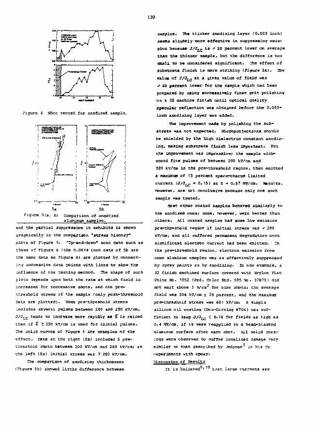
130
Figure 4 Shot record for anoaized sample.
5a 5b
Figure 5 (a, b) Comparison of ar.odized
aluminum samples.
and the partial suppression it exhibits is shown
graphically in the comparison "stress history*
plots of Figure 5. "Dp-and-down" scan data such as
those of Figure 4 (the 0.0014 inch data of 5b are
the same data as Figure 4) are plotted by connect-
ing successive data points with lines to show the
influence of the testing method. The shape of such
plots depends upon both the rate at which field is
increased for successive shots, and the pre-
threshold stress of "-.he sample (only past-threshold
data are plotted), when pre-threshold stress
includes several pulses between 200 and 250 kV/cmr
J/JLC tends to increase more rapidly as E is raised
-han if E > 250 kv/cm is used for initial pulses.
The solid curves of Figure 5 are examples of the
etiect. Data at the right (5b) included 5 pre-
threshold shots between 200 kv/cm and 260 .Wcm; at
the left (Sa) initial stress was 4 260 kV/cra.
The comparison of anodizing thicknesses
(Figure 5b) showed little difference between
samples* The thicker anodizing layer (0.003 inch)
seems slightly more effective in suppressing emis-
sion because J/JLC As </> 20 percent lower on average
than the thinner sample, but the difference is too
small to b« considered significant. The effect of
substrate finish is more striking (Figure 5a). The
value of J/J,c at a given value of field was
s 40 percent lower for the sample which had been
prepared by using successively finer grit polishing
on a 32 machine finish until optical quality
specular reflection was obtained before the 0.003-
inch anodizing layer was added.
The improvement made by polishing the sub-
strate was not expected. Microprojections should
be shielded by the high dielectric constant anodiz-
ing, making substrate finish lesa important. But
the improvement was impressive; the sample with-
stood five pulses of between 290 kv/cm and
320 kV/cm in the pre-threshold region, then emitted
a maximum of 15 percent space-charge limited
current (J/J^ - 0. 15) at E =• 0.57 MV/cm. Results,
however, are not conclusive because only one such
sample was tested.
.Most other coated samples behaved similarly to
the anodized ones; some, however, were better than
others* All coated samples had some low emission
pre-threshold region if initial stress was J- 200
kV/aa, and all suffered permanent degradation once
significant electron current had been emitted. In
the pre-threshold region, electron emission from
some aluminum samples was as effectively suppressed
by spray paints as by anodizing. 3h one example, a
32 finish machined surface covered with Krylon Flat
White Ito. 10S2 (Fed. Color Std. 595 No. 37875) did
not emit above 3 A/cm for nine shots; the average
field was 304 kv/cm ± 20 percent, and the maximum
pre-threshold stress was 401 kv/cm. A simple
3ilicon oil coating (Dow-Coming #704) was suf-
ficient to keep J/J^; •? 0.16 for fields as high as
0.4 MV/ca, if it were reapplied to a bead-b.lasted
aluminum surface after each shot. All solid coat-
ings were observed to suffer localized damage very
similar co that described by JedynaJc5 ixt his -ic
experiments with epoxy.
Siscu3sian of Results
It is believed ' that large currents are
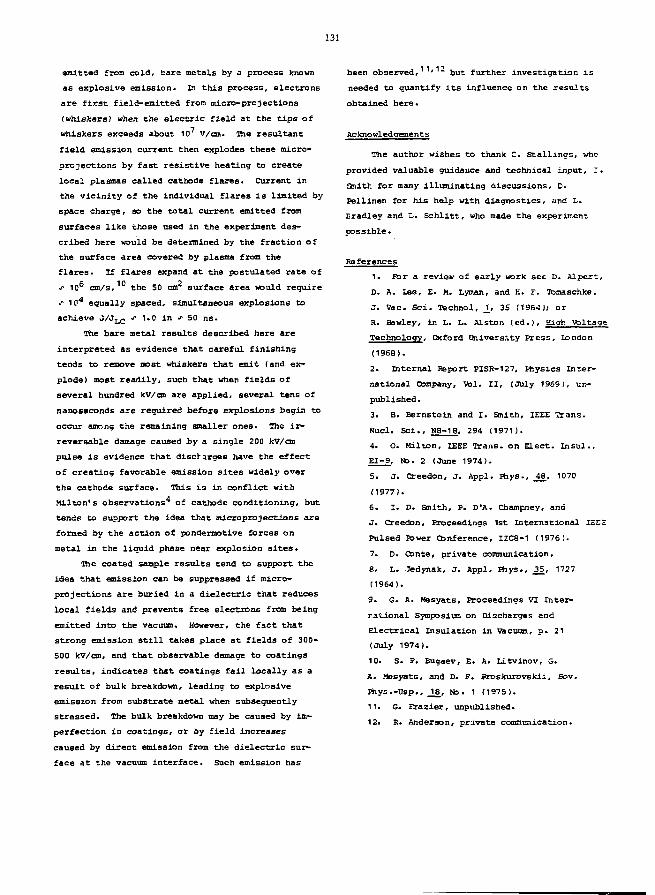
131
emitted from cold, bare metals by a process known
as explosive emission. In this process, electrons
are first field-emitted from micro-projections
(whiskers) when the electric field at the tips of
whiskers exceeds about 10 v/cm. The resultant
field emission current then explodes these micro-
projections by fast resistive heating to create
local plasmas called cathode flares. Current in
the vicinity of the individual flares is limited by
space charge, so the total current emitted from
surfaces like those used in the experiment des-
cribed here would be determined by the fraction of
the surface area covered by plasma from the
flares. If flares expand at the postulated rate of
s 106 cm/s, the SO cur surface area would require
*/* 10 equally spaced, simultaneous explosions to
achieve J/JLC * 1.0 in * 50 ns.
The bare metal results described here are
interpreted as evidence that careful finishing
tends to remove most whiskers that emit (and ex-
plode) most readily, such that when fields of
several hundred kv/cm are applied, several tens of
nanoseconds are required before explosions begin to
occur among the remaining smaller ones. The ir-
reversable damage caused by a single 200 kv/cm
pulse is evidence that discharges have the effect
of creating favorable emission sites widely over
the cathode surface. This is in conflict with
Milton's observations of cathode conditioning, but
tends to support the idea that microprojections are
formed by the action of pondermotive forces on
metal in the liquid phase near explosion sites.
The coated sample results tend to support the
idea that emission can be suppressed if micro-
projections are buried in a dielectric that reduces
local fields and prevents free electrons from being
emitted into the vacuum. However, the fact that
strong emission still takes place at fields of 300-
500 kv/cm, and that observable damage to coatings
results, indicates that coatings fail locally as a
result of bulk breakdown, leading to explosive
emission from substrate metal when subsequently
stressed. The bulk breakdown may be caused by im-
perfection in coatings, or by field increases
caused by direct emission from the dielectric sur-
face at the vacuum interface. Such emission has
been observed, ' but further investigation is
needed to quantify its influence on the results
obtained here.
Acknowledgements
The author wishes to thank C. stallings, who
provided valuable guidance and technical input, I.
Snith for many illuminating discussions, D.
Pellinen for his help with diagnostics, and L.
Eradley and L. Schlitt, who made the experiment
possible.
References
1. For a review of early work see D. Alpert,
0. A. Lee, E. M. Lyman, and H. F. Tomaschke,
J. Vac. Sci. Technol, _1_> 35 C196-D; or
R. Bawley, in L. L. Alston (ed.). High Voltage
Technology, Qcford University Press, Iondon
(1968).
2. Internal Report PISR-127, Physics Inter-
national Company, Vol. II, (July 1969), un-
published.
3. B. Bernstein and I. Smith, IEEE Trans.
Nucl. Sci., NS-1S. 294 (1971).
4. O. Hilton, IEEE Trans, on Elect. Insul.,
EI-9, Ito. 2 (June 1974).
5. J. Creedon, J. Appl. Phys., _48, 1070
(1977).
6. I. O. Smith, P. D*A. Champney, and
J. Creedon, Proceedings 1st International IEEE
Pulsed Power Conference, IIC8-1 (1976).
7. D. Conte, private communication.
8. L. Jedynak, J. Appl. Phys., _35_, 1727
(1964).
9. G. A. Mesyats, Proceedings VI Inter-
national Symposium on Discharges and
Electrical Insulation in Vacuum, p. 21
(July 1974).
10. S. P. Bugaev, E. A. Litvinov, G.
A. Mesyats, and D. F. Proskurovskii, Sov.
Phys.-Usp., _1<3, Ib. 1 (1975).
11. G. Frazier, unpublished.12. R. Anderson, private communication.
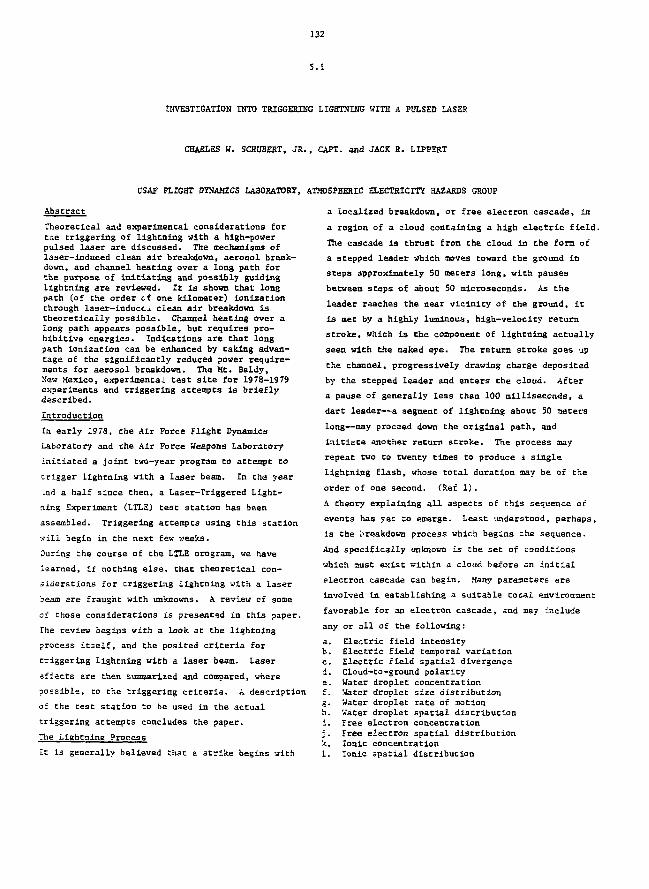
132
5.1
INVESTIGATION INTO TRIGGEBIHG LIGHTNING WITH A PULSED LASER
CHARLES W. SCHITBERT, JR., CAPT. and JACK R. LIPPERT
USAF FLIGHT DYNAMICS LABORATORY, ATMOSPHERIC ELECTRICITY HAZARDS GROUP
Abstract
Theoretical and experimental considerations fortne triggering of lightning with a high-powerpulsed laser are discussed. The mechanisms oflaser-Induced clean air breakdown, aerosol break-do wn, and channel heating over a long path forthe purpose of initiating and possibly guidinglightning are reviewed. It is shown that longpath (of the order cf one kilometer) ionizationthrough laser-induces clean air breakdown istheoretically possible. Channel heating over along path appears possible, but requires pro-hibitive energies. Indications are that longpath ionization can be enhanced by taking advan-tage of the significantly reduced power require-ments for aerosol breakdown. The Mt. BalJy,Mew Mexico, experimental test site for 1978-1979experiments and triggering attempts is brieflydescribed.
Introduction
In early 1978, the Air Force Flight Dynamics
Laboratory and che Air Force Weapons Laboratory
initiated a joint two-year program to attempt to
trigger lightning with a laser beam. In the year
»nd a half since then, a Laser-Triggered Light-
ning Experiment (LTLE) test station has been
assembled. Triggering attempts using this station
vili begin in the next few weeks.
During Che course of the LTLE orogram, we have
learned, if nothing else, that theoretical con-
siderations for triggering lightning with a laser
ieao are fraught with unknowns. A review of some
of those considerations is presented in this paper.
The review begins with a look at the lightning
process it3elf, and the posited criteria for
triggering lightning with a laser beam. Laser
effects are then summarized and compared, where
possible, to the triggering criteria. A description
of the test station to be used in the actual
triggering attempts concludes the paper.
The Lightning Process
It is generally believed that a strike begins with
a localized breakdown, or free electron cascade, in
a region of a cloud containing a high electric field.
The cascade is thrust from the cloud in the form of
a stepped leader which moves toward the ground in
steps approximately 50 meters long, with pauses
between steps of about 50 microseconds. As the
leader reaches the near vicinity of the ground, it
is met by a highly luminous, high-velocity return
stroke, which is the component of lightning actually
seen with the naked eye. The return stroke goes up
the channel, progressively drawing charge deposited
by the stepped leader and enters the cloud. After
a pause of generally less than 100 milliseconds, a
dart leader—a segment of lightning about 50 meters
long—may procaed down the original path, and
initiate another return stroke. The process may
repeat two to twenty tides to produce a single
lightning flash, whose total duration may be of the
order of one second. (Hef 1).
A theory explaining all aspects of this sequence of
events has yet tD emerge. Least understood, perhaps,
is the breakdown process which begins Che sequence.
And specifically unknown is the set of conditions
which oust exist within a cloud before an initial
electron cascade can begin. Many parameters are
involved in establishing a suitable total environment
favorable for an electron cascade, and may include
any or all of the following:
a. Electric field intensityb. Electric field temporal variationc. Electric field spatial divergenced. Cloud-to-ground polaritye. Hater droplet concentrationf. Water droplet size distribution
Mater droplet rate of motionWater droplet spatial distributionFree electron concentrationFree electron spatial distributionIonic concentrationIonic spatial distribution

133
u. Ionic specie typen. Ionic race of motiono. Particulate concentrationp. Particulate spatial distributionq. Particulate size distributionr. Farticulate specie types. Particulate rate of motiont. Ice crystal concentrationu. Ice crystal size and shape distributionv. Ice crystal spatial distributionw. Ice crystal rate o£ motionx. Temperaturey. Relative humidity
z. Atmospheric pressure
It is generally assumed that the electric field
intensity is the predominant factor in natural
lightning Initiation, However, other factors could
be of equal importance. Of particular significance,
we feel, are parameters involving relatively rapid
change over time, such as the motion of water
droplets, ions, ice crystals and participates; and
temporal variations in the electric field. The
single most important changing parameter is
difficult to identify and may vary from discharge.
Thus, in one case, a bulk motion of charge carriers
may initiate a cascade by permitting the electric
field intensity in some locality to build to the
air breakdown threshold level. In another case,
the electric field may remain constant, with
threshold conditions reached because of a changing
distribution of wind-blown water droplets within a
local region of a cloud. Conditions which exist
in active thunderstorms are not well known, and
the initial phase of the lightning discharge is
not well understood. Consequently, a numerical
estimate of the degree, speed and spatial extent
of parameter change within a cloud which is
required for the initiation of natural lightning
cannot be made.
Triggering Criteria
The triggering of lightning with a laser beam may
be accomplished by at least three approaches:
(1) by generating an ionized path over the entire
earth-to-ground distance, (2) by producing a
rarefied column of air from the ground to a cloud,
or (3) by heating and ionizing some local region
near or within a cloud. In the first and second
approaches, the slm is to short-circuit the cloud
charge to the ground, either by providing a
partially-conductive path or by lowering the earth-
to-cloud dielectric constant. In the third approach,
the hope is to upset the electrical balance within
a cloud by altering one or more of the environmental
parameters which were listed earlier.
To establish criteria for triggering b7 using the
earth-to-cloud ionized path method, natural
lightning data can be used. Since a stepped leader
is sufficiently conductive to maintain subsequent
lightning components, a laser-generated ionized
column with similar characteristics should be able
to discharge'a cloud. Electron densities within a
lightning stepped leader are nor known with certainty9 in
but have been estimated as being about 10 to 10
electrons per cubic centimeter. (Ref 1, 2). The
time required for a stepped leader to go from the
cloud to the ground is about 10 seconds, and the
time required for a return stroke to go from the
ground to the cloud over the stepped leader path is
approximately 10 seconds. Consequently, if
lightning can be triggered by generating an artifi-
cial lightning component with a laser the criteria9 10
for the triggering would be 10 to 10 electrons
per cubic centimeter in a channel about 1 kilometer
long, with a persistence time of approximately
10~ to 10 seconds.
The results of spark gap experiments performed by
Koopman and Saum can be used to estimate upper limit
criteria for triggering lightning using the rarefield
channel method. Koopman and Saum found in 1972 that
sparks could be guided from one highly charged
electrode to another by heating a path between the
electrodes with a laser beam (Ref 3). According
to their computations, the air density along the
beam was reduced to about 64* ambient value for the
triggerings.
Criteria for triggering lightning by ionizing a
local region in or near a thundercloud cannot, at
this point in time, be established. Too little is
known about natural lightning initiation to
ascertain the type and extent of disturbance which
would be needed for an artificial triggering.
Laser Effects
To determine the likelihood of triggering lightning
with a laser, it is *• -essary to first examine the
effects of a las. ti the atmosphere. A
sufficiently intent beam can produce three
effects of interest: .hermal heating, (2) clear,
air breakdown, and (3) aerosol (particulate) break-
down. All three effects will occur simultaneously
if the laser beam is extremely intense. However,
specific effects may be emphasized by a careful
selection of laser beam and optical parameters.

134
Thermal Heating
The effect of primacy Interest la thermal heating
by a laser beam Is the rarefaction, via thermal
expansion, of air along the beam channel, the
mechanical energy required to lower the density
of air alont. a column of length z and radius r
to a fraction F •.' ambient value is, from
pressure-balance considerations2 ^ i - 1} (1)E - j (Tr2z)
where T. and n, ate the ambient air temperature
and density, and k in the Boltzman constant.
Using a typical value for kT. and for n, of-21 19 -3
4 x 10 joules and 2.5 x 10 cm , respectively;
the energy required to rarefy a column of air
one kilometer long and one centimeter in radius
to 64% ambient value is about 26,000 joules.
Even greater laser energies would be required,
since only a fraction of the energy from the
laser is converted to termal heating. Thus,
the triggering of lightning with a long path
of laser-rarefied air does not appear to be a
viable approach.
Clean Air Breakdown
Laser-induced clean air breakdown is a non-linear
process in which laser-heated electrons undergo
a cascade of ionizing collisions with atoms.
Unless the laser flux Intensity exceeds a certain
threshold level, which for the CO laser is
3 x 10 W/cm~, various atomic loss processes
will inhibit the cascade. When the threshold
for cascade is reached, however, free electron
densities rise rapidly to near full first-stage-
ionizacion levels. A detailed theoretical
analysis of long path clean air breakdown has
been made in The Laser Lightning Rod System: A
Feasibility S tudy, by an author of this paper
(Ref 4). The analysis Indicates that electron
densities meecing or exceeding Che criterion
for triggering lightning can be generated over
a path a kilometer or so in length through the
clean air breakdown mechanism. However, the
production of such a pathway would require laser
flux intensities on the order of gigawatts/cm
(for CO. radiation), over a laser aperture tens
of centimeters in radius. These requirements
are beyond Che capability of lasers currently
available.
Aerosol Breakdown
Aerosol breakdown occurs as Che result of the
heating and vaporization of participate matter
in the atmosphere. The laser flux required to
Initiate aerosol breakdown Is dependent upon
particle size, but can be as much as 10U times
less than the flux required for clean air break-
down. An analytical model for aerosol breakdown
over a long path has not yet been developed.
However, small scale laboratory experiments per-
formed as a part of Che LTLE effort indicate that
a clean air breakdown bead can be lengthened by
at least a factor of seven by introducing parti-
culates Into the beam path. Additional
experimentation will be necessary to determine if
a path of ionizatlon can be further elongated by
optimizing focusing parameters.
Laser Effects S'"™"»ry
Significant ionization or rarefaction of air
over the entire earth-to-cloud distance appears
unlikely with the energy-limited lasers available
today. Aerosol breakdown offers some promise of
ionizacion path elongation, but further study of
the process is needed before conclusions can be
drawn.
The generation of a limited disturbance in or
near a thundercloud remains a viable option for
triggering attempts. A laser beam can change air
temperature, air pressure, free electron distri-
bution, ion distribution, electric field intensity,
water droplet concentration, particulate size
distribution, and ice crystal concentration,all
in times the order of microseconds. Whether
lightning can be triggered by a laser beam will
depend on Che effect, yet unknown, of rapidly
changing chese parameters over a limited spatial
range. Lightning has been triggered In the pasc
by relatively small disturbances—in-flight
aircraft, water plumes, and rocket-launched wires,
so the outlook is not discouraging.
LTLE Test Station Description
A diagram of the test station to be used in the
actual triggering attempts is shown in Figure 1.
135
The lasers to be used are housed in a 35-foot
expandable-side van which will be deployed to
the cop of Mt. Baldy, near Soccorro, Sew Mexico.
The Mt. Baldy test site was chosen primarily
because of the near-daily occurrence of thunder-
storms in the local area during the summer
months.
The primary laser to be used in the triggering
attempts is a pulsed CO, unit with a design
output of 400 joules in a one-to-two micro-
second pulse. The CO, beam will be supplemented
wit: the output of a 15 joule Nd-Glass laser
having a pulse length of about 30nanoseconds.
The beams will be focused by an on-axis Casse-
grain telescope comprised of a 60 centimeter
diameter copper-plated aluminum primary mirror,
and a 20-centimeter diameter secondary mirror,
both on adjustable mounts. Deflection of the
beam upward will be accomplished by a 76-centimeter
diameter copper-plated hon-aycomb titanium turn-
ing flat. A 60-foot aluminum trestle tower
adjacent to the beam path will serve as a ter-
minus for any lightning which may be triggered.
The optical system is designed for diffraction-
limited operation at distances ranging from
100 to 1000 meters. Various focal ranges will
be employed during the course of the experiment.
Control units, data storage equipment, and per-
sonnel will be housed in a separate van adjacent
to the laser van. Both vans are of sheet metal
construction and are grounded, providing Faraday-
cage protection for personnel. Data acquisition
equipment will include a current-sensing system
on the lightning strike tower, electric and
magnetic field antennae, a motion picture camera
and a videocassette system. Triggering attempts
will be made over a month and a half period
beginning in early July, 1979.
References
1. Uman, M.A., Lightning, New York: McGraw-Hill
Book Co., 1969.
2. Klingbeil, P.., and C.A. Tidman, "Theory and
Computer Model of the Lightning Stepped Leader ,"
Journal of Geophysical Research, 79:865-869,
(February 20, 1974).
3. Samm, K.A. and D.W. Koopman, "Discharges
Guided by Laser-Induced Rarification Channels," The
Physics of Fluids, 15:2077-2079 (November, 1972).
4. The Laser Lightning Rod System: A Feasibility
Study, AFFDL-TR-78-60, Wright Patterson Air Force
Base: AFSC, June, 1978.
Groundatf UoMntng SWtoTowv-
Figure 1.
LAMB TRKKERED LIGHTNING EXPERIMENTREMOTE SITE SET-UP

136
LONG ARC SIMULATED LIGHTNING ATTACHMENT TESTING USING A 150 KW TESLA COIL
ROBERT K. GOLXA
Project Tesla, Wendover AFB, Utah 34083In conjunction with Air Force Flight Dynamics Laboratory,
Wright-Patterson Air Force Base
Abstract
Recent advances in direct lightning striketesting have been in Lightning attachmenttest techniques and generator cjvelopmentusing a very large Tesla Coil (51 feetwide). Breakthroughs in simulated light-ning attachment to small scale replicaaircraft models which can be adapted tofull size operational aircraft have beenmade in the past year. New high voltagelong arc generator developments have suc-ceeded in producing voltages in excess of15 million volts and arc lengths in excessof U0 feet. The shortest path from the
discharge arc electrode to the model ex-tremity using the long arc does notgovern the attachment points to the testspecimen as it does when a short arc isused to conduct simulated lightningtesting. The system just described mayalso have application as an ultr.i-highmega-volt source for particle beamweaponry.
Introduction
The purpose of the program was to evaluaterhe Tesla Coil as a laboratory tool forlightning effects research on aircraft.The ability of a Tesla Coil to generatehigh voltage pulses at high rep rates re-sults in the capability to create artifi-cial, lightning-like streamering and Longelectrical discharge arcs and makes it adesirable alternative to the high voltageimpulse generators currently in use.Another characteristic of a Tesla Coil isthat many long arcs can be generated overa very short time period. These TeslaCoil characteristics are highly desirablein lightning effects research using fullscale (e.g. an actual aircraft) testspecimens.
The primary objective of the program wasto evaluate the Tesla Coil as a long arcsource for lightning attachment studies.Secondary objectives of the program wereto investigate methods for measuring theoutput characteristics of the Tesla Coiland the attachment characteristics of anAdvanced Design Composite Aircraft (ADCA)
model.
Background
At the present time the lightning suscep-tibility of aircraft is investigated usinghigh voltage impulse generators. In atypical test involving streamering, thedirect effects due to arc'ng are deter-mined by discharging the venerator in alocalized area of an aircraft in such amanner that streamering is induced with-out arc attachment to the aircraft. Thepresence of streamering is indicative of apossible ignition source for combustiblevapors. The procedure is repeated untiltotal aircraft coverage is attained. Longarc attachment tests are conducted toverify the primary zones and to identifysecondary attachment zones. For thesetests the probe of a high voltage impulsegenerator is positioned to generate a longarc that attaches to the test specimen.The test is repeated a number of times withthe probe at different orientations withrespect to the test specimen to eliminatethe possibility of biasing the attachmentpoint and to simulate lightning flashesapproaching from various directions. Thisis a time consuming procedure because ofthe set-up time and the charging time ofimpulse generators.
In contrast to the existing method, a TeslaCoil streamering test requires one set-upto identify the total streamering charac-teristics of a test specimen. Also, thehigh frequency nature of the Tesla Coilcan generate many long arcs, of somewhatrandom lengths and paths (reducing testset-up bias).
Attachment Evaluation
The Advanced Design Composite aircraft(ADCA) model used for the attainment evalu-ation was designed and nuilt by GruinmanAerospace for the Advanced CompositeStructures ADP, Structural Mechanics Divi-sion, Air Force Flight Dynamics Laboratory,Wright-Patterson Air Force Base. Light-ning attachment tests to the ADCA modelwere subcontracted to Lightning TransientResearch Institute (LTR1) initially. The
LINETRANSFORMER
rBREAK WHEEL 8 Ft.
mm.
-51 Ff..
a Ft.
J
/7\
-18 Ft.
SECONDARY- 2G TURNS
PRIMARY- I TURN
Fig I. Schematic Diagram of Golltci Apparatus of Wondovor
138
Electromagnetic Hazards Group obtainedthe model after the initial attachmenttests. The model was taken to Wendover,Utah to the Associates 12 million voltTesla Facility for further attachmentstudies. An F-4 model was also taken andused as a preliminary test set-up model.
The Tesla Coil test was conducted to eval-uate its use as a long arc source forattachment studies. Data was taken withthe model in three configurations andvarious positions. Data was obtained forcomparison to that obtained during LTR2long arc attachment tests.
FIGURE Typical Primary CircuitCurrent Measurement UsingPearson Current Transformer
Vertical Scale: 1200 Amps/Div.Horizontal Scale: 200 us/Div.
Measurement of Tesla Coil Characteristics
Some of the physical characteristics of rheTesla Coil that were of interest were theresonant frequencies of the primary andsecondary circuits, the rise and decaytimes, commutation rate, and input currentarid output current values. The Tesla Coilcircuit of Golka Associates is diagramedin Figure 1 and its equivalent circuit ispresented in Figure 2.
The current in the primary circuit wasmeasured with e Pearson, model 301 currentmonitoring transformer (CT). A typicalcurrent measurement is depicted in the os-cillogram of Figure 3. The highest cur-rent measured was 3240 amperes.
The output voltage was determined to aver-age about 10 megavolts. Higher voltageshave been observed on different occasions,the highest being 25 megavolts. Thesemeasurements were made with capacitordivider techniques. The risetime of theoutput voltage was measured to be about5 microseconds. The risetime of the out-put voltage is important to determine po-tential arc length. The risetime canaffect voltage needed to break down agiven air gap. 50 KC is the ringing fre-quency of the secondary/extra coil combin-ation. 30 KC is the primary oscillatoryfrequency, the primary and secondary fre-quencies being pulled together somewhatdue to high mutual coupling. This tech-nique being used to prevent circulatingcurrents between primary and secondary
TESLA COIL
150 KW To OscilloscopeLl=Primary of Power
TransformerL2=Secondary of W*=Secondary of Tesla
Power Transformer Coil SystemL3=Primary of Tesla L5=Extra Coil of
Coil Svstem Tesla Coil System
Cl=Primary CircuitCharging Capactor
C2=DistributedCapacitance ofExtra Coil
FIGURE 2: Equivalent Circuit of Golka Associates Tesla Coil
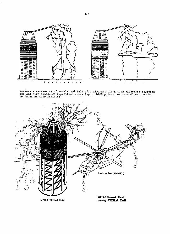
139
I I I I I i I I i !
Various arrangements of models and full size aircraft along with electrode position-ing and high discharge repetition rates (up to 4200 pulses per second) can now beachieved at this facility.
Helicopter <HH- 53)
Golka TESLA CoilAttachment Testusing TESLA Coil
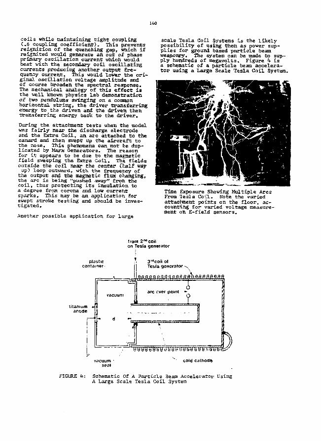
140
coils while naintaining tight coupling(.6 coupling coefficient). This preventsreignition of the quenching gap, which ifreignited would generate an out of phaseprimary oscillation current which wouldbeat with the secondary coil oscillatingcurrents producing another output fre-quency current. This would lower the ori-ginal oscillation voltage amplitude andof course broaden the spectral response.The mechanical analogy of this effect isthe well known physics lab demonstrationof two pendulums swinging on a commonhorizontal string, tha driver transferringenergy to the driven and the driven thentransferring energy back to the driver.
During the attachment tests when the modelwas fairly near the discharge electrodeand the Extra Coil, an arc attached to thecanard and then swept up the aircraft tothe nose. This phenomena can not fce dup-licated by Marx Generators. The reasonfor it appears to be due to the magneticfield sweeping the Extra Coil. The, fieldsoutside the coil near the center (tialf wayup) loop outward, with tne frequency of
the output and the magnetic flux changing,the arc is being "pushed away" from thecoil, thus protecting its insulation toa degree from corona and low currentsparks. This may be an application forswept stroke testing and should be inves-tigated.
Another possible application for large
scale Tesla Coil Systems is the likelypossibility of using them as power sup-plies for ground based particle beamweaponry. The system can be made to sup-ply hundreds of tnegavolts. Figure k isa schematic of a particle beam accelera-tor using a Large Scale Tesla Coil System.
Time Exposure Showing Multiple ArcsFrom Tesla Coil. Note the variedattachment points on the floor, ac-counting for varied voLtage measure-ment on E-field sensors.
from 2nd coilon Tesla generator
cold cathodft
FIGURE Schematic Of A Particle 3eam Accelerator UsingA Large Scale Tesla Coil System
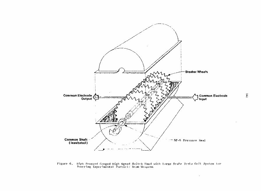
Breaker Wheels
Common ElectrodeOutput
Common Shaft(insultated)
Common ElectrodeInput
— S F - 6 P r e s s u r e S e a l
I ' i g u r e 6 . lli.pl> P o w e r e d (Ringed High S p e e d S w i t c h Used w i t h l , ; i rge S c i l e Tviln C o i l S y s t e m l o rP o w e r i n R E x p e r i m e n t a l P a r t i c - l c lipym W<uipoi>s
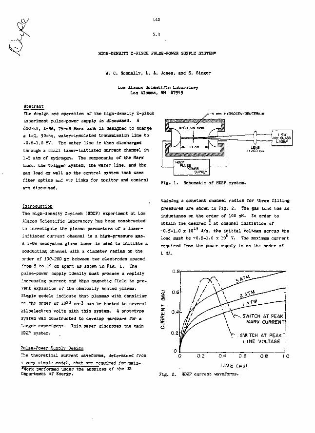
142
5.3
HIGH-DENSITY Z-PINCH PULSE-POWER SUPPLY SYSTEM*
W. C. Nunnally, L. A. Jones, and S. Singer
Los Alamos Scientific LaboratoryLos Alanos, UM 875«5
Abstract
The design and operation of the high-density Z-pinch
experiment pulse-power supply is discussed. A
600-kV, 1-MA, 75-nH Marx bank is designed to charge
a 1-Sl, 90-ns, water-insulated transmission line to
-0.6-1.0 MV. The water line is then discharged
through a 3mall laser-initiated current channel in
1-5 atm of hydrogen. The components of the Marx
bank, the trigger system, the water line, and the
gas load as well as the control system that uses
fiber optics aud =>lr Iink3 for monitor and control
are discussed.
Introduction
The high-density Z-plnch (HDZP) experiment at Los
Alamos Scientific Laboratory has been constructed
to investigate the plasma parameters of a laser-
initiated current channel in a high-pressure gas.
A 1-GW necdymium glass laser is used to initiate a
conducting channel with a diameter radius on the
order of 100-200 vim between two electrodes spaced
from 5 to 10 cm apart as shewn in Fig. 1. The
pulse-power supply ideally oust produce a rapidly
increasing current and thus magnetic field to pre-
vent expansion of the ohmically heated plasma.
Sisple models indicate that plasmas with densities'
on the order of 1020 0Br3 c a n b e heated to several
kiloelectron volts with this system. A prototype
system was constructed to develop hardware for a
larger experiment. Thia paper discusses the main
HDZP system.
Pulse-Power Supply Design
The theoretical current waveforms, determined from
a very 3impie nodel, that are required for main-
•Work performed under the auspices of the US
Department of Energy.
, 1 - 5 otm HYOROGEN/DEUTERIUM
§ L _ * WO *"<> diom. ^ ^ 1
V4-H— - J - 1 1
HP— (™—io cm—"t —"t§3
HOZPPULSE
POWERSUPPLY
MLENS
f=200 cm
1 GWNd: GLASS
LdSER
Fig. 1. Schematic of HDZP system.
taining a constant channel radius for three filling
pressures are shown in Fig. 2. The gas load has an
inductance on the order of 100 nH. In order to
obtain the desired I at channel initiation of
-0.5-1.0 x 10¹³ A/s, the initial voltage across the
load oust be -0.5-1.0 x 10 V. The maxiaium current
required from the power supply is on the order of
1 MA.
IUJIo
u.o
0.6
0.4
0.2
0
w
\*\
\ * ^ . SWITCH AT PEAK"MARX CURRENT
V SWITCH AT PEAK "JLINE VOLTAGE
!O O.2 0.4 0.6
TIME2. HDZP current waveforms.
0.8 1.0
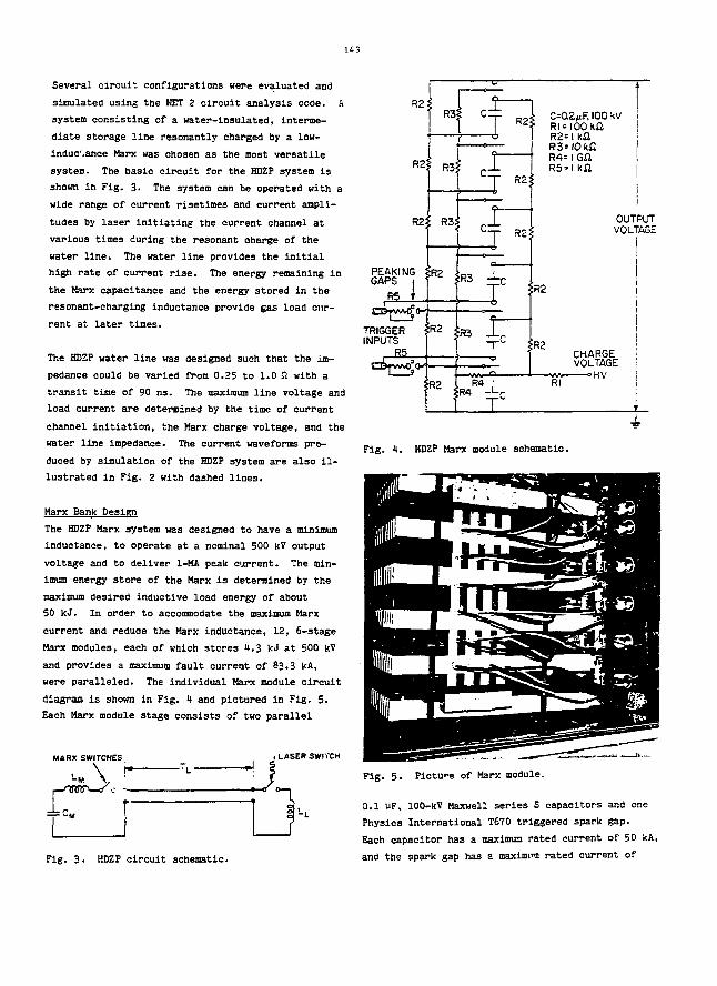
143
Several circuit configurations were evaluated and
simulated using the NET 2 circuit analysis code. A
system consisting of a water-insulated, interme-
diate storage line resonantly charged by a low-
inductance Marx was chosen as the most versatile
system. The basic circuit for the HDZP system is
shown in Fig. 3. The system can be operated with a
wide range of current risetimes and current ampli-
tudes by laser initiating the current channel at
various times during the resonant charge of the
water line. The water line provides the initial
high rate of current rise. The energy remaining in
the Marx capacitance and the energy stored in the
resonant-charging inductance provide gas load cur-
rent at later times.
The HDZP water line was designed such that the im-
pedance could be varied from 0.25 to 1.0 ft with a
transit time of 90 ns. The maximum line voltage and
load current are determined by the time of current
channel initiation, the Marx charge voltage, and the
water line impedance. The current waveforms pro-
duced by simulation of the HDZP system are also il-
lustrated in Fig. 2 with dashed lines.
Marx Bank Design
The HDZP Marx system was designed to have a minimum
inductance, to operate at a nominal 500 kV output
voltage and to deliver 1-MA peak current. The min-
imum energy store of the Marx is determined by the
maximum desired inductive load energy of about
50 kJ. In order to accommodate the maximum Marx
current and reduce the Marx inductance, 12, 6-stage
Marx modules, each of which stores 4.3 kJ at 500 kV
and provides a maximum fault current of 83.3 kA,
were paralleled. The individual Marx module circuit
diagram is shown in Fig. 4 and pictured in Fig. 5.
Each Marx module stage consists of two parallel
R2
MORX SWITCHES
I—TnriK-</ c -~
XIU,
LASER SWITCH
R3=!0k£lR4= I Gil
__i_ | R5=lkflJ R2
C=Q2u.F, 100 kV iRI=IOOkQ i
OUTPUTVOLTAGE
Rl
CHARGE |VOLTAGE i
H V I
Fig. 4. HDZP Marx module schematic.
Fig. 3. HDZP circuit schematic.
Fig. 5. Picture of Marx module.
0.1 UF, 100-kV Maxwell series S capacitors and one
Physics International T670 triggered spark gap.
Each capacitor has a maximum rated current of 50 kA,
and the spark gap has a maxim™ rated current of
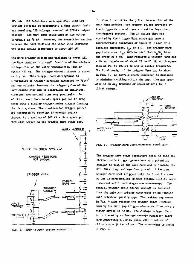
144
100 k&. The capacitors were specified with 50$
voltage reversal to acccnnodate a Marx output fault
and resulting 75* voltage reversal at 500-kV output
voltage. The Marx bank inductance at the output
terminals is 75 nH. However, the transition section
between the Marx bank and the water line increases
the total series inductance to about 250 nH.
The Marx trigger system was designed to ereet all
the Marx modules in a small fraction of tile minimum
voltage rise on the water transmission line or
within -20 ns. The trigger circuit chosen is shown
in Fig. 6. This trigger Marx arrangement is
a variation of trigger circuits suggested by Fitch
and was selected because the trigger pulse- of the
Marx (nodule gaps can be controlled in amplitude,
risetime, and arrival cime very precisely- In
addition, each Marx module spark gap can be trig-
gered with a similar trigger pulse without loading
the Marx system. The simultaneous trigger pulses
are generated by shorting 12 coaxial cables
charged to a maximum of 100 kV with a spark gap
-.hat also serves as the trigger Marx stage gap.
MARX MODULE
NURX TRIGGER SYSTEM
CHARGE RESISTORSNOT SHOWN
TRIGGER MARX
INPUTTRIGGER
In order to minimize the jitter in erection of the
main Marx modules, the trigger pulses provided by
the trigger Marx must have a risetime less than
the desired scatter. The 12 cables that are
shorted by the trigger Marx stage gap have a
characteristic impedance of about 36 H each or a
parallel impedance, Z , of 3 ft. The trigger Marx
gap Inductance, U,, must be such that L_/Z is on
the order of 5 ns. This requires a trigger Marx gap
with an inductance of about 15 to 20 nH, which oper-
ates at 85- to 100-kY dc and is easily triggered.
The final design of the trigger Marx gap is shown
in Fig. 7. An acrylic sheet insulator is designed
to minimize tracking within the gap. The gap oper-
ates at an SF, pressure of about 60 psig for a
100-kV charge.
Fig. 6. HDZP trigger system schematic.
Fig. 7. Trigger Marx low-inductance spark gap.
The trigger Marx stage capacitors serve to bias the
shorted cable trigger generators at a potential
similar to that of the main Marx and to isolate the
main Marx stage voltage from ground. A 2-stage
trigger Marx that triggers only the first 2 stages
of the 12 Marx modules is used because initial tests
indicated additional 3tages are unnecessary. The
coaxial trigger cable charge voltage is isolated
from the main gap trigger electrodes by an "inside-
out" trigatron peaking gap. The peaking gap shown
in Fig. 6 also reduces the trigger pulse risetime
seen by the main gap trigger electrode <7 ns with a
jittar spread of <2 ns. The 2-stage trigger Marx
is initiated by an 8-stage ceramic capacitor niere-
Marx generating a 20O-kV pulse with risetime of
<20 as and a jitter <2 ns. The micro-Marx is shown
in Fig. 9.
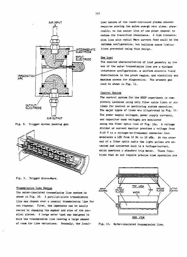
145
AIR INPUT
INTERMEDIATEELECTRODE
INPUTELECTRODE
OUTPUTELECTRODE
AIR OUTPUT
Fig. 8. Trigger system peaking gap.
Fig. 9. Trigger micro-Marx.
Transmission Line Design
The water-insulated transmission line system is
shown in Fig. 10. A parallel-plate transmission
line was chosen over a coaxial transmission line for
two reasons. First, the inpedanee oan be easily
varied by changing the number and size of the par-
allel plates. A large water tank was designed to
hold the transmission line leaving a large amount
of room for line variations. Secondly, the local-
ized nature of the laser-initiated plasma channel
requires storing the pulse energy very close, phys-
ically, to the center line of the pinch channel to
reduce the transition inductance. A disk transmis-
sion line with radial Marx current feed would be the
optimum configuration, but building space limita-
tions prevented using this design.
The desired characteristics of load geometry at the
end of the water transmission line are a minimum
inductance configuration, a uniform.electric field
distribution in the pinch region, and visibility and
maximum access for diagnostics. The present gas
load is shown in Fig. 11.
Control System
The control system for the HDZP experiment is com-
pletely isolated using only fiber optic links or air
links for control or monitoring system operation.
The major types of links are illustrated in Fig. 12.
The power supply voltages, power supply currents,
and capacitor bank voltages are monitored
using the fiber optic link of Fig. 12a. A voltage
divider or current monitor provides a voltage from
0-10 V to a voltage-to-frequeney converter that
modulates a LED from 10 Hz to 10 kHz. At the other
end of a fiber optic cable the light pulses are de-
tected and converted back to a voltage/current,
which operates a standard trip meter. Those func-
tions that do not require precise time operation are
Fig. 10. Water-insulated transmission line.
146
WATER DIELECTRIC
HIGH VOLTAGEELECTRODE
SEAM DUMP
NEUTRAL GAS
INSULATOR
METEROR
CONTROLSYSTEM
1 1FREQUENCY
TOVOLTAGECONVERTER
DETECTOR
•"3.FIBER J
3 WAYAM SOLENOID
3 WAY
AIR SOLENOIOPOLY T U M I G '
(el
Fig. 12. HDZP control systems.
LrAOt SWITCH-r
)LY TUBING'
—AIR CTUNDCfl
HIGH VQLTAGCSWITCH
TO CONTROL SYSTEM
F i g . 11 . HDZP gas load chamber. Fig. 13. HDZP interlock system.
implemented using compressed air, one example of
which is shown in Fig. 12b. The high-voltage dunp
and safety switches are also actuated U3ing air
links as illustrated in Fig. 12e. The interlock
3yatems are structured as shown in Fig. 13. Each
location or function requiring an interlock was de-
signed to provide closure of contacts, energizing a
high-intensity lamp. The resulting light i3 con-
ducted to the main control panel through a fiber
cptic cable where a phototransistor pulls in a relay
if the high-intensity lamp is energized. This
method is very simple and has been extremely reli-
able. It is fail safe in that a malfunction pre-
vents relay closure and inhibits system operationl
The trigger system also uses fiber optic links from
the time delay system in the screen room to various
systems to be initiated. The trigger link system
is diagrammed in Fig. it. The basic timing system
consists of a multichannel digital time delay unit
that determines the timing sequence of the experi-
ment. The time delay output signals energize in-
jection laser pulsers, which produce 900-nm light
pulses that are conducted to the various systems in
the HDZP experiment through fiber optic cable. The
receiver-pulse generators shown in Fig. It produce
electrical pulses at voltages from 5 to 900 V with
10 ns rlsetimes and various pulse lengths and
shapes. The Jitter of this type of trigger link
systen is less than ±1 ns. The system is extremely
insensitive to the large amount of EMI present *\:d
the location of the fiber optic cable in the exper-
iment is thus not critical.
System Operation
System operation is initiated by charging the Marx
bank and charging the trigger Marx such that they
reach the desired voltage simultaneously in about
30 s. The control system monitors bank voltages and
sends a fiber optic trigger pulse into ths 3creer
room after disconnecting the power supplies. The
digital tine delay system then energizes the appro-
priate systems in the proper sequence. The main
Marx is erected to pulse charge the water line in
about 200-600 ns. At the desired load voltage the
glass laser initiates the HDZP current channel and
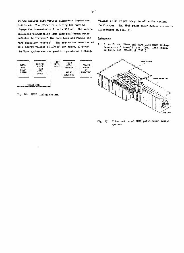
at the desired time various diagnostic lasers are
initiated. The Jitter is erecting the Marx to
charge the transmission line is ±10 ns. The water-
insulated transmission line uses self-break water
switches to "crowbar" the Marx bank and reduce the
Marx capacitor reversal. The system has been tested
to a charge voltage of 100 kV per stage, although
the Marx system was designed to operate at a charge
voltage of 85 kV per stage to allow for various
fault modes. The HDZP pulse-power supply system is
illustrated in Fig. 15.
R. A. Fiteh, "Marx and Marx-Like High-VoltageGenerators," Maxwell Labs, Inc., IEEE Trans,on Nuoi. Sci. NS-18, t (1971).
Fig. It. HDZP timing system.
Fig. 15. Illustration of HDZP pulse-power supplysystem.
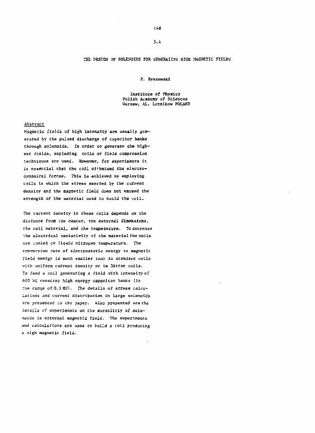
148
5.4
THE DESIGN OF SOLENOIDS FOR GENERATING HIGH MAGNETIC FIELDS
P. Byszewski
Institute of PhysicsPolish Academy of SciencesWarsaw, AL. Lotnlfcow POLAND
Abstract
Magnetic fields of high intensity are usually gen-
erated by the pulsed discharge of capacitor banks
through solenoids. In order to generate the high-
est fields, exploding coils or field compression
techniques are used. However, for experiments it
is essential that Che coil withstand the electro-
dynamical forces. This is achieved by employing
coils in which the stress exerted by the current
density and the magnetic field does not exceed the
strength of the material used to build the coil.
The current density in these coils depends un the
distance from the center, the external dimensions,
che coil material, and the temperature. To decrease
The electrical resistivity of the material the coils
are cooled to liquid nitrogen temperature. The
conversion rate of electrostatic energy to magnetic
field energy is much smaller thar. in standard coils
with uniform current density or in Bitter coils.
To feed a coil generating a field vith intensity of
600 kG reauires high energy capacitor banks (in
che range of0.5RJ). The details of stress calcu-
lacions and current distribution in large solenoids
are presented in che paper. Also presented are the
details of experiments on the durablitiy of sole-
noids in external magnetic field. The experiments
and calculations are used to build a coil producing
a high magnetic field.
149
5.5
ANALYSIS OF A DISTRIBUTED PULSE POWER SYSTEM USING ACIRCUIT ANALYSIS CODE
LOTHAB 0. HOEFT
AIR FORCE WEAPONS LABORATORY, KIRTLAND AFB, NM 87117 ANDTHE BDM CORPORATION, ALBUQUERQUE, NM 87106
Abstract.
A sophisticated computer code (SCEPTRE),
used to analyze electronic circuits, was used to
evaluate the performance of a large flash X-ray
machine. This device was considered to be a
transmission line whose impedance varied with
position. This distributed system was modeled
by lumped paratnet-r sections with time constants
of 1 ns. The model was used to interpret vol-
tage, current, and radiation measurements in
terms of diode performance. The effects of tube
impedance, diode model, switch behavior, and
potential geometric modifications were deter-
mined. The principal conclusions were that,
since radiation output depends strongly on
voltage, diode impedance was much more important
than the other parameters, and the charge vol-
tage must be accurately known.
analysis codes such as SCEPTRE, NET-II, etc..
the pulse power system designer has a nei- and
powerful analysis tool for predicting the per-
formance of pulse power devices. Conceptually,
the pulse power system is modelled with lumped
parameter transmission line sections ir. which
the time delay per section is small compared to
the time constant of interest in the system.
This concept implies that the pulse power system
can be represented by a one-dimensional struc-
ture; that is, effects due to a change in direc-
tion of the electromagnetic wave are ignored.
This paper presents the methodology used to
construct such a model for 2 large DC-charged,
flash x-ray machine. The u.'.e of this model to
interpret measured waveforms and evaluate pos-
sible modifications is described. Finally, the
principal conclusions reached by this analysis
are presented.
INTRODUCTION MODEL DEVELOPMENT
The prediction of overall performance of
complex pulse power devices is required for
achieving optimum design, identifying problems
that arise during operation, and for evaluating
proposed modifications. Rather simple analysis
techniques may be used if the transit times of
the structure are small compared to the rise
time or pulse length. However, in most cases,
the rise time/pulse length is comparable to the
transit time of the structure and/or its dis-
continuities. Such systems have been treated as
a series of transmission lines with capacitances
added at the discontinuities . Such techniques
are tedious and lack credibility if the struc-
ture is complex. With the advent oi network
Figure 1 shows a cross-sectional view of
the flash x-ray machine. The energy is stored
in a 33-foot long high pressure gas insulated
transmission line ( Z = 42 ohms). This line oro
coaxial capacitor is charged to approximately 10
Megavolts by a van de Graaff generator. A 2-foot
I MFT
MUMURETANK
GRADEDINSULATOR DIODE
CHAROINOCOLUMN
COAXIAL UNE
SWITCH
; RAILROAD FLATCAB
Figure 1. Crossection of FlashX-Ray Machine
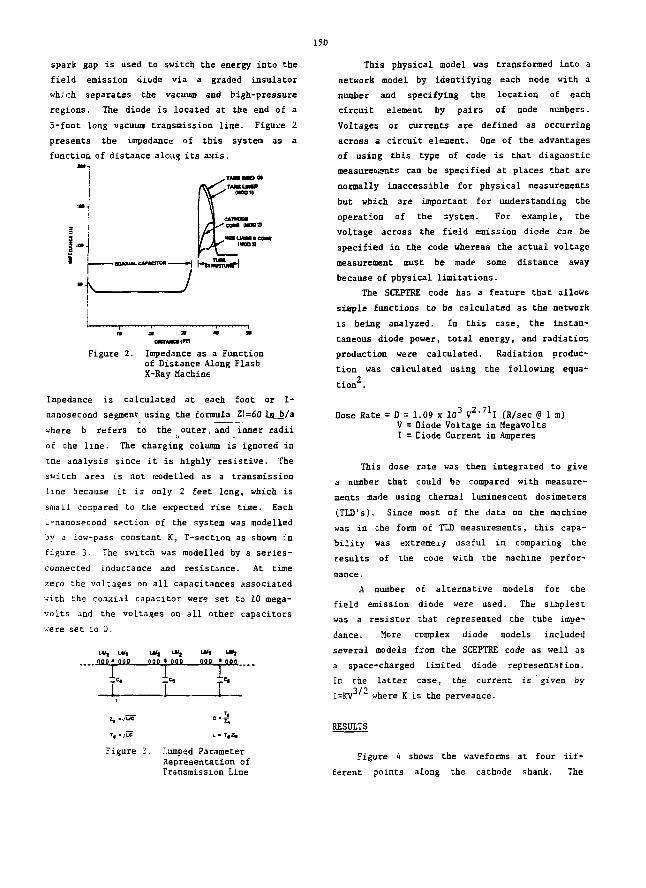
150
spark gap is used to switch the energy into the
field emission ciiude via a graded insulator
which separates the vacuum and high-pressure
regions. The diode is located at the end of a
5-foot long vacuum transmission line. Figure 2
presents the impedance of this system as a
function of distance along its axis.
"1
-)
Figure 2. Impedance as a Functionof Distance Along FlashX-Ray Machine
Impedance is calculated at each foot or 1-
nanosecond segment using the formula Z!=60 In b/a
where b refers to the outer, and inner radii
of the line. The charging column is ignored in
tne analysis since it is highly resistive. The
switch area is not modelled as a transmission
Line because it is only 2 feet long, which is
small compared to the expected rise time. Each
1-nanosecond section of the system was modelled
by ,3 low-pass constant K, T-section as shown in
figure 3. The switch was modelled by a series-
connected inductance and resistance. At time
zero the voltages on all capacitances associated
"-'ith the coaxial capacitor were set to 10 mega-
'.•olts jnd the voltages on all other capacitors
were set ~-o 0.
<ioo« aoo ooo i ooo
1. X.ooo ' ono
°m%,
This physical model was transformed into a
network model by identifying each node with a
number and specifying the location of each
circuit element by pairs of node numbers.
Voltages or currents are defined as occurring
across a circuit element. One of the advantages
of using this type of code is that diagnostic
measurements can be specified at places that are
normally inaccessible for physical measurements
but which are important for understanding the
operation of the system. For example, the
voltage across the field emission diode can be
specified in the code whereas the actual voltage
measurement must be made some distance away
because of physical limitations.
The SCEPTRE code has a feature that allows
simple functions to be calculated as the network
is being analyzed. In this case, the instan-
taneous diode power, total energy, and radiation
production were calculated. Radiation produc-
tion was calculated using the following equa-
tion .
Dose Rate = D = 1.09 x 10³ V 2' 7 1I (8/sec S i m )V = Diode Voltage in MegavoltsI = Ciode Current in Amperes
This dose rate was then integrated to give
a number that could bs compared with measure-
ments made using thermal luminescent dosimeters
(TLD's). Since most of the data on the machine
was in the form of TID measurements, this capa-
bility was extremei./ useful in comparing the
results of the code with the machine perfor-
mance .
A number of alternative models for the
field emission diode were used. The simplest
was a resistor tbat represented the tube impe-
dance. More complex diode models included
several models from the SCEPTRE code as well as
a space-charged limited diode representation.
In the latter case, the current is given by
I=KV where K is the perveance.
RESULTS
Figure 3. Lumpad ParameterRepresentation ofTransmission Line
Figure i shows the waveforms at four dif-
ferent points along the cathode shank. The
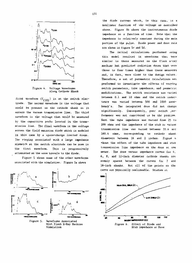
151
100 200TMEbal
Figure 4. Voltage WaveformsAlong Cathode Shank
first waveform (V"--,) is at the switch elec-
trode. The second waveform is the voltage that
would be present on the cathode shank as it
enters the vacuum transmission line. The third
waveform is the voltage that would be measured
by the capacitive probe located in the trans-
mission line. The final waveform is the voltage
across the field emission diode which is modeled
in this case by a space-charge limited diode.
The ringing associated with a large impedance
mismatch at the switch electrode can be seen in
the first waveform. This is progressively
attenuated as the wave travels to the diode.
Figure 5 shows some of the other waveforms
associated with the simulation. Figure 5a shows
\\
is,w.p
the diode current which, in this case, is a
nonlinear function of the voltage as described
above. Figure 5b shows the instantaneous diode
impedance as a function of time. Note that the
impedance is relatively constant during the main
portion of the pulse. Diode power and dose rate
are shown in figure 5c and 5d.
The initial calculations performed using
this model resulted in waveforms thaL were
similar to those measured on the flash x-ray
machine but predicted radiation doses that were
three to four times higher than those measured
and, in fact, were close to the design values.
Therefore, a set of parametric calculations was.
performed to investigate the effects of varying
switch parameters, tube impedance, and geometric
modifications. The switch resistance was varied
between 0.1 and 10 ohms and the switch induc-
tance was varied between 500 and 1000 nano-
henry's. The integrated dose did not change
significantly. Consequently, poor switch per-
formance was not considered LO be the problem.
Next the tube impedance was varied from 25 to
200 ohms and the impedance of the stub or vacuum
transmission line was varied between 35.6 and
160.4 ohms, corresponding to cathode shank
diameters between 16 and 2 inches. Figure t>
shows the effect of the tube impedance and stub
transmission line impedance on the dose at one
meter. The dose versus impedance curves for 4,
6, 8, and 12-inch diameter cathode shanks are
evenly spaced between the curves for 2 and
16-inch shanks. Not all of the points on the
curve are physically realizeable. Studies at
Figure 5. Waveforms AssociatedWith Flash X-Ray MachineSimulation
QIOOE IMPEDANCE U 2 ]100 T10
Figure 6. Effect of Diode andStub Impedance or Dose
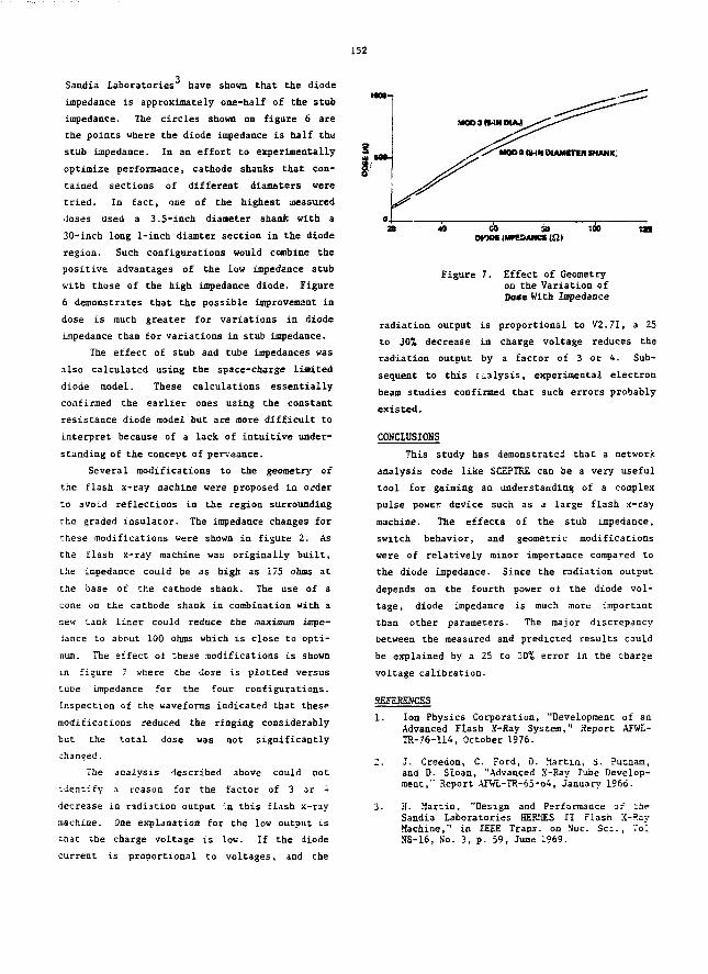
152
Sandia Laboratories have shown that the diode
impedance is approximately one-half of the stub
impedance. The circles shown on figure 6 are
the points where the diode impedance is half the
stub impedance. In an effort to experimentally
optimize performance, cathode shanks that con-
tained sections of different diameters were
tried. In fact, one of the highest measured
doses used a 3.5-inch diameter shank with a
30-inch long 1-inch diamter section in the diode
region. Such configurations would combine the
positive advantages of the low impedance stub
with those of the high impedance diode. Figure
6 demonstrates that the possible improvement in
dose is much greater for variations in diode
impedance than for variations in stub impedance.
The effect of stub and tube impedances was
also calculated using the space-charge limited
diode model. These calculations essentially
confirmed the earlier ones using the constant
resistance diode model but are more difficult to
interpret because of a lack of intuitive under-
standing of the concept of perveance.
Several modifications to the geometry of
the flash x-ray machine were proposed in order
to avoid reflections in the region surrounding
the graded insulator. The impedance changes for
these modifications were shown in figure 2. As
the flash x-ray machine was originally built,
the impedance could be as high as 175 ohms at
the base of the cathode shank. The use of a
cone on the cathode shank in combination with a
sew tank Liner could reduce the maximum iinpe-
tance to about 100 ohms which is close to opti-
mum. The effect of these modifications is shown
in figure ? where the dose is plotted versus
tut>e impedance for the four configurations.
Inspection of the waveforms indicated that thes*»
modifications reduced the ringing considerably
but the total dose was not significantly
changed.
The analysis described above could not
identify s reason for the factor of 3 or i
decrease in radiation output :.n this flash x-ray
machine. Oae explanation for the low output is
that the charge voltage is low. If the diode
current is proportional to voltages, and the
OVJOt IMKSANC* K?)
Figure 7. Effect of Geometryon the Variation ofDo»e With Impedance
radiation output is proportional to V2.7I, a 25
to 30% decrease in charge voltage reduces the
radiation output by a factor of 3 or 4. Sub-
sequent to this c^alysis, experimental electron
beam studies confirmed that such errors probably
existed.
CONCLUSIONS
This study has demonstrated that a network
analysis code like SCEFTKE can be a very useful
tool for gaining an understanding of a complex
pulse power device such as a large flash x-ray
machine. The effects of the stub impedance,
switch behavior, and geometric modifications
were of relatively minor importance compared to
the diode impedance. Since the radiation output
depends on the fourth power of the diode vol-
tage, diode impedance is much more important
than other parameters. The major discrepancy
between the measured and predicted results could
be explained by a 25 to 30% error in the charge
voltage calibration.
REFERENCES
1. Ion Physics Corporation, "Development of anAdvanced Flash X-Ray System," Report AFWL-TR-76-114, October 1976.
Z. J. Creedon, C. Ford, D. Martin, S. Putnam,and D. Sloan, "Advanced X-Ray Tube Develop-ment," Report AFWL-TR-65-t>4, January 1966.
3. H. Martin, "Design and Performance of theSandia Laboratories HERMES II Flash X-SayMachine," in IEEE Trans, on .Nuc. Sci., VolSS-16, No. 3, p. 59, June 1969.
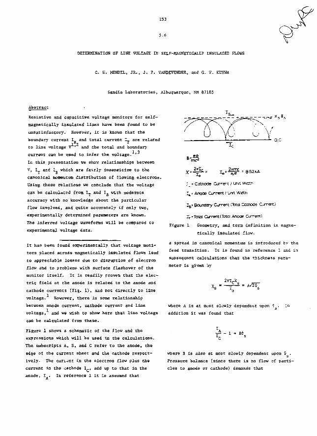
153
5.6
DETERMINATION OF LINE VOLTAGE IK SELF-MAGNETICALLY INSULATED FLOWS
C. W. MENDEL, JR., J. P. VANDEVENDER, ar.d G. W. KUSWA
Sandia Laboratories, Albuquerque, KM 87185
Abstract
Resistive and capacitive voltage monitors for self-
magnetic ally insulated lines have been found to be
unsatisfaccory. However, it is known that the
boundary current I_ and total current I™ are related
to line voltage v ' and the total and boundary
current can be used to infer the voltage. '
In this presentation we show relationships between
V, I and I which are fairly insensitive to the
canonical momentum distribution of flowing electrons.
Using these relations we conclude that the voltage
can be calculated from Lj. and Ig with moderate
accuracy with no knowledge about the particular
flow involved, and quite accurately if only two,
experimentally determined parameters are known.
The inferred voltage waveforms will be compared to
experimental voltage data.
It has been found experimentally that voltage moni-
tors placed across magnetically insulated flows lead
to appreciable losses due to disruption of electron
flow and to problems with surface flashover of the
monitor itself. It is readily proven that the elec-
tric field at the anode is related to the anode and
cathode currents (Fig. 1), aad not directly to line
voltage. However, there is some relationship
between anode current, cathode current and line
voltage, and we wish to show here that line voltage
can be calculated from these.
Figure 1 shows a schematic of the flow and the
expressions which will be used in the calculations.
The subscripts A, S, and C refer to the anode, the
edge of the current sheet and the cathode respect-
ively. The cuncnt in the electron flow plus the
current in the cathode I , add up to that in the
anode, I . In reference 1 it is assumed that
8.52KA
I - = Catnode Current / Unit Wtctr
Z^- Anode Current / Unit Wotn
Z%* Bounoary Current (Total Catnode Current)
IT-Total Current (Totol Anode Current)
F.igure 1 Geometry, and term definition in magne-
tically insulated flow.
a spread in canonical momentum is introduced by the
feed transition. It is found in reference 1 and in
suDsequent calculations that the thickness para-
meter is given by
where A is at most slcwly dependent upon C . In
addition it was found that
where B is also at most slowly dependent upon i .
Pressure balance (since there is no flow of parti-
cles to anode or cathode) demands that
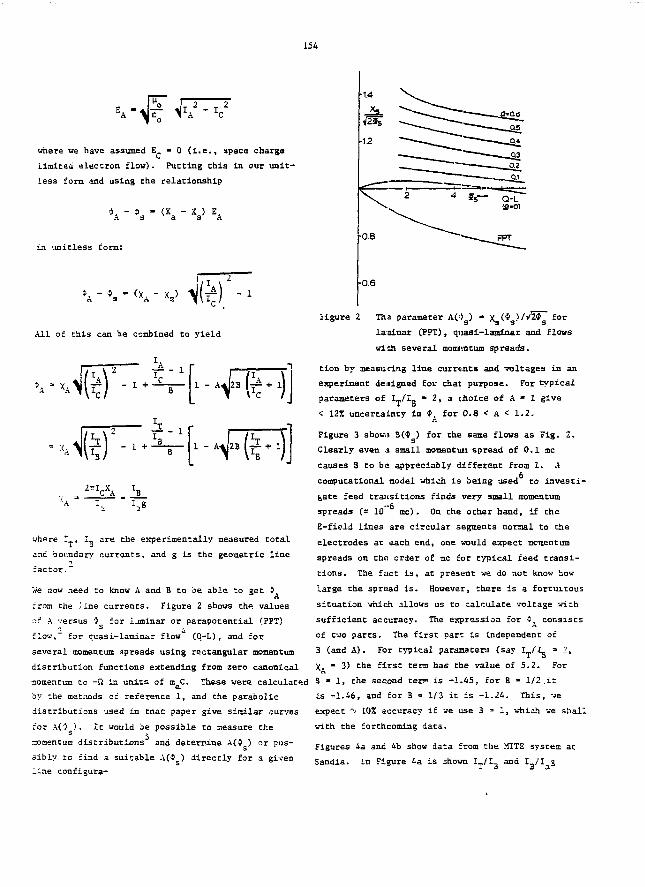
154
K-4t K'h*
where we have assumed E_ " 0 (i.e., space charge
limited electron flow). Putting this in our unit-
less form and using the relationship
*A " 's " (Xa " V h
in unitless form:
- x.) ^(ij
All of this can be combined to yield
where I , I are the experimentally measured total
and boundary currents, and g is the geometric line
factor.~
We now need to know A and B to be able to get $
from the jine currents. Figure 2 shows the values
of A versus i for ljminar or parapotencial (PPT)
flow, for quasi-laminar flow (Q-L), and for
several momentum spreads using rectangular momentum
distribution functions extending from zero canonical
momentum Co -ft i-n units of m C. These were calculated
by -he methods of reference 1, and the parabolic
distributions used in thac paper give similar curves
for A O ). It would be possible to aeasure thes j
:nomentuni distributions and determine AC**1 ) or pos-
sibly to find a suitable A(4 ) directly for a given
line configura-
Figure 2 Tha parameter A('> ) • x ff >//24 for
laiinar (PPT), quasi-laminar and flows
with several momentum spreads.
tion by measuring line currents and voltages in an
experiment designed for that purpose. For typical
parameters of IT/Ig " 2, a cihoice of A - 1 give
< 12X uncertainty in *A for 0.8 < A < 1.2.
Figure 3 shown B(t ) for the same flows as Fig. 2.
Clearly even i small momentuii spread of 0.1 me
causes 8 to ba appreciably different from 1. A
computational model which is being used to investi-
gate feed transitions finds very small momentum
spreads (= 10 me). On the other hand, if the
E-field lines are circular segments normal to the
electrodes at each end, one would expect momentum
spreads on thn order of me for typical feed transi-
tions. The fact is, at present we do not know how
large the spread is. However, there is a fortuitous
situation vhich allows us to calculate voltage with
sufficient accuracy. The expression for i consists
of two parts. The first part is independent of
B (and A). For typical parameters (say ^/Ij = ->
X. - 3) the first term has the value of 5.2. For
S • 1, Che second cerr? is -1.45, for B * 1/2 .it
is -1.46, and for B • 1/3 it is -1.24. This, ve
expect "J 10% accuracy if we use 3 - 1 , which we shall
with the forthcoming data.
Figures 4a and &b show data from the MTTE system at
Sandia. In Figure 4a is shown I_/I, and I /I 31 J O jL
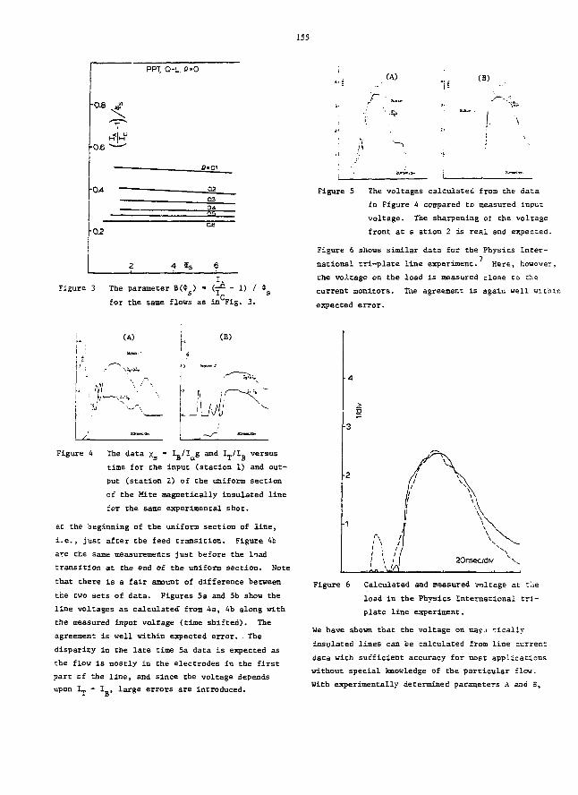
155
-0.8 ^
•0.6 " - ^
•0A
•0.2
2
PPT, Q-L
4
0=0
C-C1
Q3
Q6
S5 6
(A) (B)
•"•A
Figure 3 The parameter B (•)»(•==- 1) / tCfor the same flows as in Fig. 3.
r
Figure 5 The voltages calculated from the data
in Figure 4 compared to measured input
voltage. The sharpening of the voltage
front at s ation 2 is real and expected.
Figure 6 shows similar data for the Physics Inter-
national tri-plate line experiment. Here, however,
uhe voltage on the load is measured close to the
current monitors. The agreement is again well within
expected error.
(A)
\ r
(B)
Figure 4 The data x * ^B^ 1 S and I—/I- versus
time for the input (station 1) and out-
put (station 2) of the uniform section
of the Mite magnetically insulated line
for the same experimental shot.
at the beginning of the uniform section of line,
i.e., just after the feed transition. Figure 4b
are the same measurements just before the ^ad
transition at the end of the uniform section. Note
that there is a fair amount of difference between
the two sets of data. Figures 5a and 5b show the
line voltages as calculated from 4a, 4b along with
the measured input voltage (time shifted). The
agreement is well within expected error. . The
disparity in the late time 5a data is expected as
the flow is mostly in the electrodes in the first
part of the line, and since the voltage depends
upon I,, - I3> large errors are introduced.
•3
Figure 6 Calculated and measured voltage az the
load in the Physics International tri-
plate line experiment.
We have shown that the voltage on mag.i Tically
insulated lines can be calculated from line current
data with sufficient accuracy for most applications
without special knowledge of the particular flow.
With experimentally determined parameters A and E,

156
additional accuracy may be available. Ibis allevi-
ates the loss problems previously seen with, traas-
iine voltage monitors.
References
1. C. W. Mendel, J. Appl. Phya., July 1979.
2. J. Creedon, J. Appl. Phys., 46_, 2946 (1976).
3. J. P. VanDevender, J. Appl. Phys., June 1979.
4. R. V. Lovelace and Edward Ott, Phys. of Fluids,
2£, 688 (1977). A. Bon, A. A. Hondelli, and
N. Rostoker, IEEE Trans, on Plasma 3d.,
PSI-1. 85 (1973).
5. K. L. Brower and J. P. VanDevender, 2nd Int'l.
Conf. on Pulsed Power, Lulbick, TX (June 1979).
6. E. L. Neau and J. P. VcoDivai-iar, 2nd Int'l.
Conf. on Pulsed Power- Lub^oek, TX (June 1979).
7. M. DiCapua and D. G. Pellir."u, Physics Int'l.
Report PIFR-1009, Oaz. ,378.
This work was supported by the U. S. Department of
energy, under Contract 0E-ACO4-76-DPOO789.
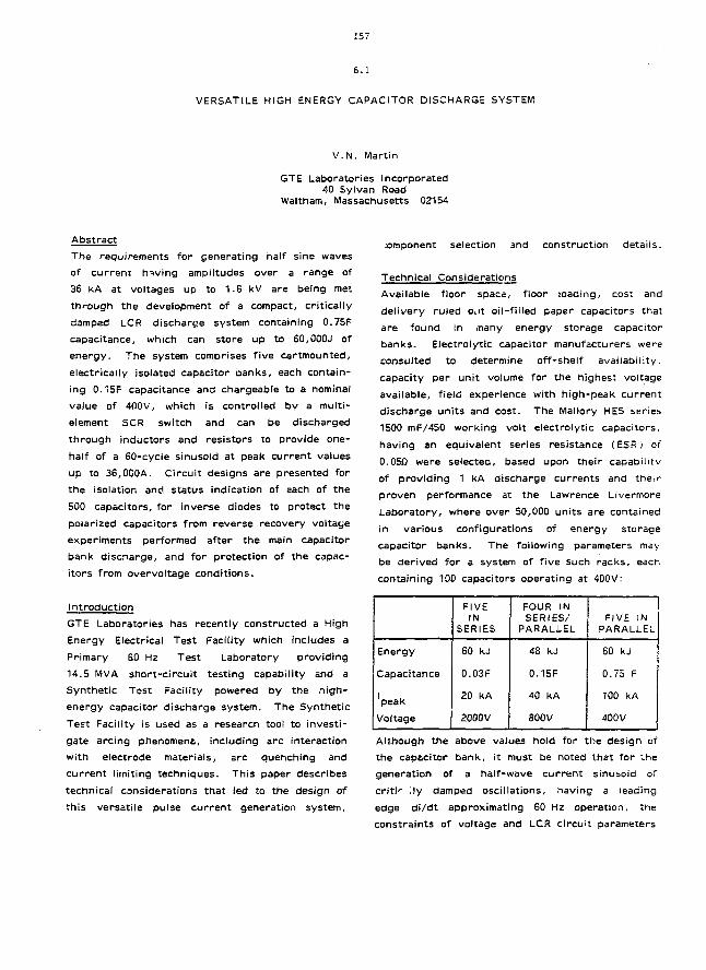
157
6.1
VERSATILE HIGH ENERGY CAPACITOR DISCHARGE SYSTEM
V.N. Martin
GTE Laboratories Incorporated40 Sylvan Road
Waltham, Massachusetts 02154
AbstractThe requirements for generating half sine wavesof current having amplitudes over a range of36 kA at voltages up to 1-6 kV are being metthrough the development of a compact, criticallydamped LCR discharge system containing 0.75Fcapacitance, which can store up to 60,000J ofenergy. The system comprises five cartmounted,electrically isolated capacitor banks, each contain-ing 0.15F capacitance and chargeable to a nominalvalue of 400V, which is controlled by a multi-element SCR switch and can be dischargedthrough inductors and resistors to provide one-half of a 60-cycle sinusoid at peak current valuesup to 36,00OA. Circuit designs are presented forthe isolation and status indication of each of the500 capacitors, for inverse diodes to protect thepolarized capacitors from reverse recovery voltageexperiments performed after the main capacitorbank discharge, and for protection of the capac-itors from overvoltage conditions.
IntroductionGTE Laboratories has recently constructed a HighEnergy Electrical Test Facility which includes aPrimary 60 Hz Test Laboratory providing14.5 MVA short-circuit testing capability and aSynthetic Test Facility powered by the high-energy capacitor discharge system. The SyntheticTest Facility is used as a research tool to investi-gate arcing phenomena, including arc interactionwith electrode materials, arc quenching andcurrent limiting techniques. This paper describestechnical considerations that led to the design ofthis versatile pulse current generation system,
/.omponent selection and construction details.
Technical ConsiderationsAvailable floor space, floor loading, cost anddelivery ruled OM oil-filled paper capacitors thatare found in many energy storage capacitorbanks. Electrolytic capacitor manufacturers wereconsulted to determine off-shelf availability,capacity per unit volume for the highest voltageavailable, field experience with high-peak currentdischarge units and cost. The Mallory HES series1500 mF/450 working volt electrolytic capacitors,having an equivalent series resistance (ESR) of0.05fl were selected, based upon their capabihtvof providing 1 kA discharge currents and theirproven performance at the Lawrence LivermoreLaboratory, where over 50,000 units are containedin various configurations of energy storagecapacitor banks. The following parameters maybe derived for a system of five such racks, eachcontaining 100 capacitors operating at 400V:
Energy
Capacitance
'peak
Voltage
FIVEIN
SERIES
60 kJ
0.03F
20 kA
2000V
FOUR INSERIES/
PARALLEL
48 kJ
0.15F
40 kA
800V
FIVE INPARALLEL
60 kJ
0.75 F
100 kA
400V
Although the above values hold for the design ofthe capacitor bank, it must be noted that for thegeneration of a half-wave current sinusoid ofcriti'" ;iy damped oscillations, having a leadingedge di/dt approximating 60 Hz operation, theconstraints of voltage and LCR circuit parameters
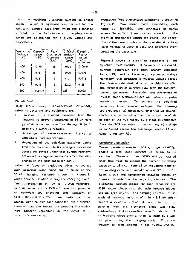
158
limit the resulting discharge current as shown
below. A set of equations was derived for .the
critically damped case from which the discharge
current, rritical inductance and damping resis-
tance are detarmined for a given voltage and
capacitance:
OperatingVoltage
(V)
400
400
400
800
1600
Capaci-tance
(F)
0.75
0.6
0.3
0.15
0.0375
PeakDischargeCurrent
(kA)
4S
36
18
18
9
CriticalInduc-tance(MH)
16.4
20.5
41.1
82.2
328
DampingResis-tance(0)
0.0046
0.0061
0.012
0.25
0.098
Circuit DesignMajor circuit design considerations influencingsafety to personnel and equipment are:1. Isolation of a shorted capacitor from' the
network to prevent discharge of 99 or moreparallel-connected capacitors through it (withpossibly disastrous results).
2. Protaction of series-connected banks ofcapacitors from overvoltage.
3. Protection of the polarized capacitor banksfrom the reverse polarity voltages impressedacross the device under-test during recovery(reverse) voltage experiments after the dis-charge of the main capacitor bank.
Individual fuses or exploding wires to protecteach capacitor were ruled out in favor of the10 kQ charging resistors shown in Figure 1,which provide isolation during the charging cycle.The superposition of 100 to 10,000(2 resistors,each in series with -• 1500 mF capacitor, providesan equivlent RC charging time constant of(400 + 100) x 0.15 = 75s. An individual dis-charge diode couples each capacitor into a commonexternal load and blocks the possible interactionfrom adjacent capacitors in the event of acapacitor's short-circuit.
Protection from overvoltage conditions is shown inFigure 2. Two zener diode assemblies, eachrated at 180V/350W, are connected in seriesacross the output of each capacitor rack. In theevent of unbalances within the racks, the opera-tion of the zener diodes in the operational rack(s)limits voltage to 360V to 385V and prevents over-stressing the capacitors.
Figure 3 shows a simplified schematic of theSynthetic Test Facility. It consists of a forward-current generator (the high energy capacitorbank, Cl) and a low-energy recovery voltagegenerator that produces a reverse voltage acrossthe device-under-test at a controllable time afterthe termination of current flow from the forward-current generator. Protection and awareness ofinverse diode techniques are well known in puisemodulator design. To protect the polarizedcapacitors from reverse voltages, the followingare provided: a) three parallel-connected 1N3295Rdiodes are connected across the output terminalsof each of the five racks, b) a diode is connectedfrom the SCR cathodas to ground, and c) a diodeis connected across the discharge reactor LI anddamping resistor R2.
Component Selection
Three paral lei-connected SCR's, type NL-602L,enable a total peak current of 18 kA to beswitched. Three additional SCR's will be installedlater this year to extend the current switchingcapacity to 36 kA. Four 82 yH inductors made of3/0 welding cable are pancake wound (20 in. I.O.,32 in. O.D.) and sandwiched between sheets ofplywood provide the discharge inductances. Thedischarge isolation diodes for each capacitor are60S3 epoxy diodes and the main inverse diodesare GE type A197P. The damping resistor, R2,ismade of various lengths of 1 in x 8.9 mi) thickTophet-A resistive ribbon. A neon pilot light inparallel with the discharge diode will glowcontinuously if its respective capacitor shorts. Ifan isolating diode shorts, then its neon bulb willnot glow during the charging cycle. Thus the"health" of each element in the system can be
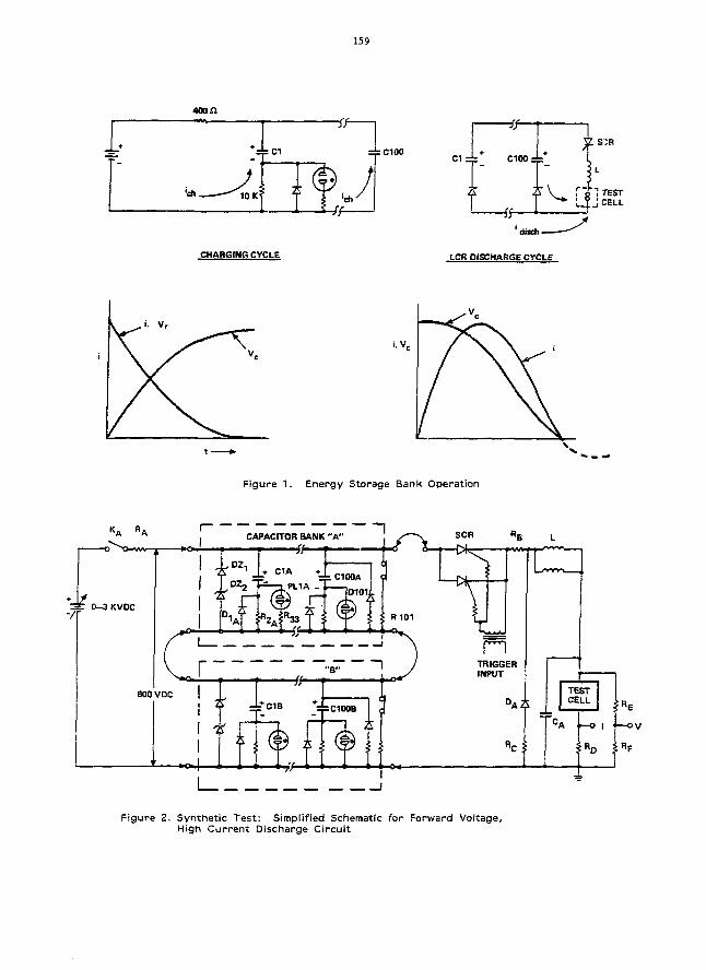
159
400 ft
iciooSCR
ci i cioo =J=
CHARGING CYCLE LCR OISCHARGE CYCLE
Figure 1. Energy Storage Bank Operation
*v € 0-3 KVDC
B L
800 VDC
^=C1WB
Figure 2. Synthetic TeEt: Simplified Schematic for Forward Voltage,High Current Discharge Circuit
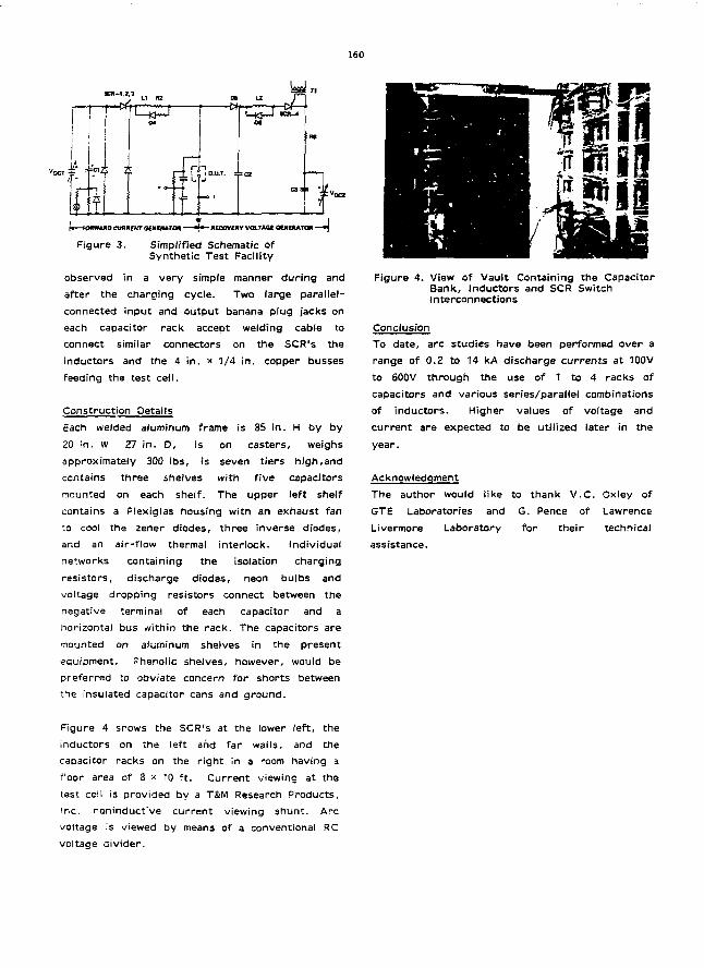
160
Figure 3. Simplified Schematic ofSynthetic Test Facility
observed in a very simple manner during andafter the charging cycle. Two large parallel-connected input and output banana plug jacks oneach capacitor rack accept welding cable toconnect similar connectors on the SCR's theinductors and the 4 in. x 1/4 in. copper bussesfeeding the test cell.
Construction Details
Each welded aluminum frame is 85 in. H by by20 in. W 27 in. D, is on casters, weighsapproximately 300 lbs, is seven tiers high,andcontains three shelves with five capacitorsmounted on each shelf. The upper left shelfcontains a Plexiglas housing with an exhaust fanto cool the zener diodes, three inverse diodes,and an air-flow thermal interlock. Individualnetworks containing the isolation chargingresistors, discharge diodes, neon bulbs andvoltage dropping resistors connect between thenegative terminal of each capacitor and ahorizontal bus within the rack. The capacitors areciounted on aluminum shelves in the presentequipment. Phenolic shelves, however, would bepreferred to obviate concern for shorts betweenthe insulated capacitor cans and ground.
Figure 4. View of Vault Containing the CapacitorBank, Inductors and SCR SwitchInterconnections
ConclusionTo date, arc studies have been performed over arange of 0.2 to 14 kA discharge currents at 100Vto 600V through the use of 1 to 4 racks ofcapacitors and various series/parallel combinationsof inductors. Higher values of voltage andcurrent are expected to be utilized later in theyear.
Acknowledgment
The author would like to thank V.C. Oxley ofGTE Laboratories and G. Pence of LawrenceLivermore Laboratory for their technicalassistance.
Figure 4 snows the SCR's at the lower left, theinductors on the left and far walls, and thecapacitor racks on the right in a room having afloor area of 3 x 10 ft . Current viewing at thetest cell is provided by a T&M Research Products,!nc. noninduct^ve current viewing shunt. Arcvoltage is viewed by means of a conventional RCvoltage divider.
161
6.2
130 kV Low Impedance Multiple Output Trigger Generator
A. H. Bushnell, C. B.,Dobbie, A. P. Krickhuhn
Maxwell Laboratories, Inc.8835 Balboa Avenue, San Diego, California 92123
Abstract
A unique low impedance trigger generator has
been developed which can generate 130 kV pulses
having 22 ns risetime in four 50 ohm output
cables. This generator uses a multichannel
rail-gap switch to discharge a group of low
inductance capacitors which are charged to
150 kV into the output cables. The performance
of the circuit was analyzed using a computer
and successfully predicted the behavior of the
circuit. Time jitter between input trigger
and output pulse is less than 2 ns (one stand-
ard deviation). The unit is immersed in oil
in its own metal housing.
Introduction
High voltage trigger generators are used extensively
to trigger various types of switching devices
including spark gap switches. Typically, trigger
generators for these applications range in output
voltage from 10 kV to 500 W with risctises varying
from less than 10 ns to several hundred ns.
We will start with a brief description of trlgge:r
systems and then present a detailed description of
a recently developed trigger system.
Trigger generators can be divided invo several
classes as listed below:
a. Charged cables
b. Single stage charged capacitors
c. Multiple stage charged capacitors
d. Pulse transformer
Each of these classes will be discussed and a
particular design of a new single-stage charged
capacitor class will be described in detail.
Charged Cable
As shown in Figure 1, a charged cable trigger
generator consists of a length of cable which is
electrically charged to some potential V Q by a
power supply. When switch Sj is closed, pulse
travels along the cable from S1 to the output end.
'When the voltage puJ.se reaches the end of the cabl
the open circuit output voltage changes by -2V Q.
Risetime of the output pulse is determined by
switch inductance and cable impedance. Charged
..cable systems are probably the least complex and
simplest type of trigger generator to build, but
they suffer from problems of cable life as a result
of the dc charge potential and 100% voltage reversal
This class of generator is often built with multiple
charged cables feeding multiple loads but switched
by a single switch. Also, as shown in Figure 1, a dc
blocking capacitor can be used in those applications
which do not permit the dc potential to be applied to
the output load. Time jitter values less than 5 ns
can be obtained with this class of generator.
Single-Stage Charged Capacitor
Figure 2 shows a single-stage charged capacitor
trigger generator. In this case, the initial poten-
tial V Q is stored on the capacitor C and discharged
into the output cable by switch S_. The open circuit
output voltage at the load end of the cable is 2 V .o
The charged capacitor generator offers advantages
over the charged cable type since there is no dc
charge potential on the cable nor is the cable
subjected to voltage reversal. It is somewhat more
difficult to obtain as fast a .isetime from charged
capacitor units as from charged cable units because
of the added inductance of the capacitor and associ-
ated buswork. Time jitter values of less than 5 ns
are obtained with this class of generator. Both of
162
these classes are capable of driving many cables and
therefore are useful in systems which require many
output triggers.
Multiple-Stage Charged Capacitors
The maximum output trigger anplitude of the single-
stage charged capacitor class ii typically limited
by the maximum voltage rating of the switch S ^ In
those applications vhlch require output trigger
potentials greater than can be obtained with a
single capacitor-switch combination, Marx type
trigger generators are usad. A Marx generator
consists of a group of capacitors charged in parallel
and discharged in series; thereby multiplying the
power supply b> the number of capacitors. Spark
gaps are normally used to switch Marx type
trigger generators. Figure 3 shows a schematic
diagram of a typical Marx generator. Typical Mars
generators operate at potentials of 50 to 100 kV per
stage and are often used to supply as much as 1 to
2 MV output poten.j.als.
Risetlme is determined by the inductance per stage
and the load Impedance. This class of generator
tends to have somewhat higher so -rce impedance than
che two discussed above. As a consequence, Marx
type trigger generators are usually used where they
can be mounted in close proximity to and directly
connected Co the load, thus avoiding coaxial cables
which would degrade rlsetlme and limit the output
potential. A properly designed Marx generator will
typically have time jitter in the 10 as region.
Fulse Transformer
In addition to the Marx generator approach just
described, another method of obtaining large trigger
potentials is to use a pulse transformer. As shown
in Figure 4, che potential to which C is charged
,'V ) is stepped up by the turns-ratio of che trans-
former (N) so that the open-circuit output potential
is SV .o
Pulse transformer trigger generators provide a
relatively high impedance trigger source at low cost.
This type generator uses a switch (i.e., cold cathode
switch tube, chyratron, etc.) to discharge a capaci-
ZCT into the primary of a pulse transformer. Use of
:his type unit is limited to situations where slower
risetime and high irapedance is acceptable. Because
of the high source impedance, this type of generator
is not used to drive coaxial cable. Therefore, the
trigger generator must be placed adjacent Co the
unit being triggered.
130 kV Low Impedance Multiple Outauc Trigger Generacor
We have recently built a trigger generator of the
single-stage charged capacitor type which can gener-
ate 130 ! ? pulses having 22 ns 10-90% risetime in
four SO ohm output cables. Nine of these generators
will be used In a single system to provide 36 simul-
taneous 130 kV output triggers. A unique requirement
of this application is that each on-put cable has a
oear-zero impedance short which appear- at the output
end of the cable early in che pulse. This system has
been designed to withstand the voltage and current
transients which result and still provide long
trouble-free life.
A schematic diagram of one of these trigger
generators is shown in Figure 5. A group of four
60 nF capacitors. In a series, parallel combination
are connected to the 4 output cables by a. low-
inductance rail gap switch. Four capacitors are
charged by an approximately constant current power
supply via an Isolation resistor to ISO kV. An
inductor is used to reference the output size of
the rail gap to ground for dc biasing. A two-
resistor divider biases the trigger rail in che
switch to V/3. An RC network couples the external
trigger generator to che rail gap and provides dc
isolation from the bias voltage. The rail gap is
triggered by a Maxwell Catalog iJumber 40151, 100 kV
trigger generator which is of the switched capacitor
variety. This triggf.r generacor provides che fasc-
riFing pulse (>5 kV/ns) required for a rail gap Co
operace in a multichannel mode. Nine outpuc cables
from che 50151 trigger generator are used to trigger
the nine separate capacitor discharge units
simultaneously.
The MLI 40151 trigger generator provides a 100 >.V,
fast-rising trigger pulse co che rail gap. This
causes che rail gap co close in che aiultichannel
mode. The four capacitors Chen discharge through
che rail gap inco the 12.3 ohm load of cha four
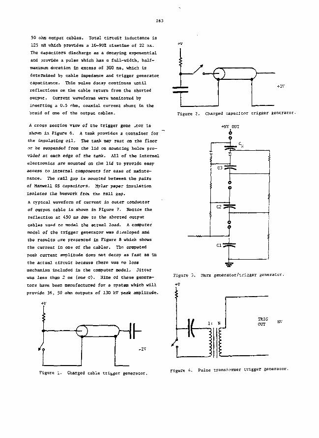
163
50 ohm output cables. Total circuit inductance is
125 nH which provides a 10-90% risetime of 22 ns.
The capacitors discharge as a decaying exponential
and provide a pulse which has a full-width, half-
maximum duration in excess of 300 ns, which is
determined by cable impedance and trigger generator
capacitance. This pulse dacay continues until
reflections on the cable return from the shorted
output. Current waveforms were monitored by
inserting a 0.5 ohm, coaxial current shunt in the
braid of one of the output cables.
A cross section viev of the trigger gene ..tor is
shown in Figure 6. A tank provides a container for
the insulating oil. The tank may rest on the floor
^r be suspended from the lid on mounting holes pro-
vided at each edge of the tank. All of the internal
electronics are mounted on the lid to provide easy
access to internal components for ease of mainte-
nance. The rail gap is mounted between the pairs
of Maxwell SS capacitors. Mylar paper insulation
isolates the buswork froa the rail gap.
A typical waveform of current in outer conductor
of output cable is shown in Figure 7. Notice the
reflection at 450 ns due to the shorted output
cables used to model the actual load. A computer
model of the trigger generator was developed and
the results tire presented in Figure 8 which shows
the current in one of the cables. The computed
peak current amplitude does not decay as fast as in
the actual circuit because there was no loss
mechanism included in the computer model. Jitter
was less than 2 ns (one o"). Nine of these genera-
tors have been manufactured for a system which will
provide 36, 50 ohm outputs of 130 kV peak amplitude.
€1-IV
Figure 2. Charged capacitor trigger generator.
+NV OUT
Figure 3. Marx generator/trigger generator.
KV
Figure 1. Charged cable trigger generator.Figure 4. Pulse transformer trigger generator.
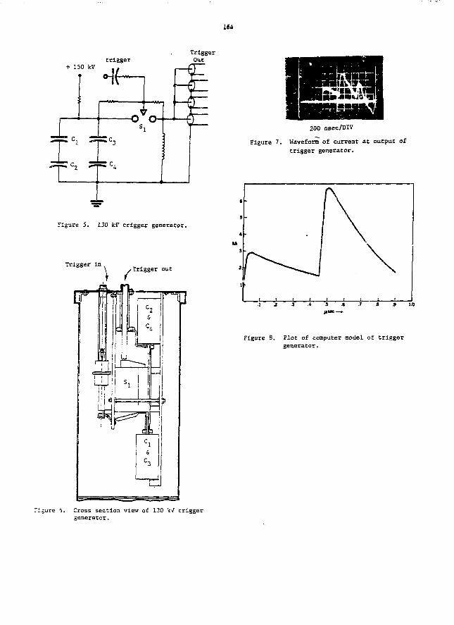
164
triggerTriggerOut
;
0 kV
- c 2 5=
t
S l
Figure 5. 130 kv trigger generator.
Trigger in
200 nsec/DIV
Figure 7. Waveform of current at output of
trigger generator.
Figure 8. Plot of computer model of triggergenerator.
i. Cross section view of 130 W triggergenerator.
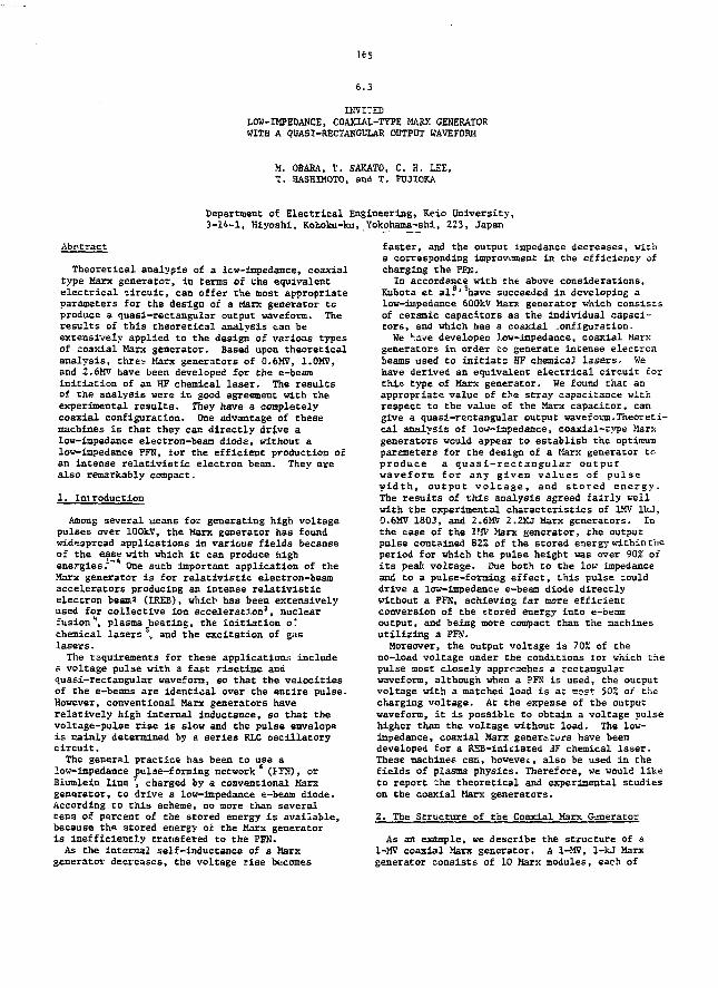
165
6.3
IKVITEDLOW-IMPEDANCE, COAXIAL-TYPE MARX GENERATORWITH A QUASI-RECTANGULAR OUTPUT WAVEFOBM
M. OBARA, Y. SAKATO, C. H. LEE,T. HASHIMOTO, and T. FUJIOKA
Department of Electrical Engineering, Keio University,3-14-1, Hiyoshi, Kohoku-ku, Yokohama-shi, 223, Japan
Abstract
Theoretical analysis of a low-impedance, coaxialtype Marx generator, in terms of the equivalentelectrical circuit, can offer the most appropriateparameters for the design of a Man; generator toproduce a quasi-rectangular output waveform. Theresults of this theoretical analysis can beextensively applied to the design of varioas typesof coaxial Marx generator. Based upon theoreticalanalysis, threa Marx generators of 0.6MV, 1.0MV,and 2.6MV have been developed for the e-beaminitiation of an HF chemical laser. The resultsof the analysis were in good agreement with theexperimental results. They have a completelycoaxial configuration. One advantage of thesemachines is that they can directly drive alow-impedance electron-beam dioda, without alow-impedance PFN, tor the efficient production ofan intense relativistic electron beam. They arealso remarkably compact.
1. Introduction
Among several means for generating high voltagepulses over lOOkV, the Marx generator has foundwidespread applications in various fields becanseof the ease with which it can produce highenergies.~" One such important application of theMarx generator is for relativistic electron-beamaccelerators producing an intense relativiEticelectron beams (IREB), which has been extensivelyused for collective ion acceleration3, nuclearfusion •", plasma heating, the initiation o:chemical lasers S» and the excitation of gaslasers.
The requirements for these applications includea voltage pulse with a fast risetime andquasi-rectangular waveform, so that the velocitiesof the e-beams are identical over the entire pulse.However, conventional Marx generators haverelatively high internal inductance, so that thevoltage-pulse rise is slow and the pulse envelopeis mainly determined by a series RLC oscillatorycircuit.
The general practice has been to use alow-impedance pulse-forming network 6 (JFN), orEiumlein line ', charged by a conventional Marxgenerator, to drive a low-impedance e-beam diode.According to this scheme, no more than severaltens of percent of the stored energy is available,because the. stored energy or the Marx generatoris inefficiently transfered to the PPH.
As the internal self-inductance of a Marxgenerator decreases, the voltage rise becomes
faster, and the output impedance decreases, witha corresponding improvement in the efficiency ofcharging the PR;.In accordance with the above considerations,
Kubota et al?'shave succeeded in developing alow-impedance 600kv Marx generator which consistsof ceramic capacitors as the individual capaci-tors, and which has a coaxial .onfiguration.We have developed low-ijnpedance, coaxial Marx
generators in order Cc generate intense electronbeams used to initiate HF chemical lasers. Hehave derived an equivalent electrical circuit forthis type of Marx generator. We found that anappropriate value of Che stray capacitance withrespect to the value of the Marx capacitor, cangive a quasi-rectangular output waveform.Theoreti-cal analysis of low-impedance, coaxial-type Marxgenerators would appear to establish the optimumparameters for the design of a Marx generator toproduce a quasi-rectangular outputwaveform for any given values of pulsewidth, output voltage, and stored energy.The results of this analysis agreed fairly wellwith the experimental characteristics of 1MV lkJ,0.6MV 180J, and 2.6MV 2.2KJ Marx generators. Inthe case of the 1!SV Marx generator, the outputpulse contained 82% of the stored energy within theperiod for which the pulse height was over 90% ofits peak voltage. Cue both to the low impedanceand to a pulse-forming effect, this pulse coulddrive a low-impedance e-beam diode directlywithout a FFN, achieving far more efficientconversion of the stored energy into e-beamoutput, and being more compact than the machinesutilizing a PFN.Moreover, the output voltage is 70% of the
no-load voltage under the conditions for which thepulse most closely approaches a rectangularwaveform, although when a PFN is used, the outputvoltage with a matched load is at E?sf 50% of thecharging voltage. At the expense of the outputwaveform, it is possible to obtain a voltage pulsehigher than the voltage without load. The low-impedance, coaxial Marx genexziors have beendeveloped for a R5B-iuiciated iF chemical laser.These machines can, however, also be used in thefields of plasma physics. Therefore, we would liketo report the theoretical and experimental studieson the coaxial Marx generators.
2. The Structure of the Coaxial Marx Generator
As an example, we describe the structure of a1-MV coaxial Marx generator. A 1-MV, 1-kJ Marxgenerator consists of 10 Marx modules, each of
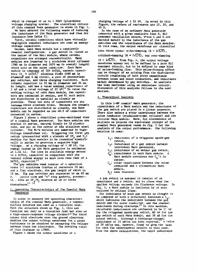
166
which is charged at up to ± 50kV (plus-minusvoltage charging system). The electrical circuitof this coaxial Marx generator is shown in Fig. 1.
He have adopted the following means of reducingthe inductance of the Marx generator and thus itsImpedance (see Table I ) .
First, ceramic capacitors which have virtuallynegligible residual inductance are used as energystorage capacitors.
Second, each Marx module has a completelycoaxial configuration. A gap switch is placed atthe center of the Mar.c module, where ceramiccapacitors are arranged concentrically. Marxmodules are inserted in a stainless steel cylinder(560 mm in diameter and 2670 mm in overall length)which acts as the outer conductor. Each Marxmodule is composed of 324 SrTiO. ceramic capaci-tors (£ * 1450)1,0 aluminum disEs (460 ma indiameter and 6 mm thick), a pair of pressurizedgap switches, and three charging resistors. Eachceramic capacitor is 35 am in diameter and 24 mmin length, and has a rated nominal capacitance of1 nF and a rated voltage of 25 kV." To raise theworking voltage of each Marx module, two capaci-tors are connected in series, and 81 such pairsare distributed in parallel as closely aspossible. These two sets of capacitors are putbetween three aluminum disks. Because the ceramiccapacitors are distributed so closely, one Marsmodule can be regarded as two 40.5 nF capacitorsconnected in series.
Figure 2 shows a simplified cross-sectional viewof a coaxial Marx generator. Ten Marx modules arestacked in series, secured firaXy by 10 plasticrods, and pu- at the center of the stainless steelcylinder. The Marx modules are imoersed in high-voltage transformer oil. Triggering the first gapswitch (pressurized with a mixture of SFfi and N 7)enables the Marx modules to be connected electri-cally in series to generate a negative highvoltage. At a charging voltage of ± 50 kV, theenergy stored in the Marx generator is estimatedat 1.01 kj. The loss in available energy storedin a SrTiO.-, capacicor in comparison with thenominal stored energy is much less than that of aBaTiO. capacitor.10
TheJgap switches used consist of a sphericalbrass (-) electrode (radius or curvature 20 mm)and a flat electrode, the gap length of which isIS mm. The gap switches are separated by an 60 ano. ' lucite tube and "o" ring gaskets, pressur-izi. . with an SF./N, mixture at up to three
atmospheres.
3. Operating Characteristics of the Coaxial Marx
Generator
In order to measure the operating charaeter«-lstics of the coaxial Marx generator, a copper-sulfate solution was used as a resistive load.With the structure shown in Fig. 3, this canfunction not only as a resistive load but also asa high-speed-response voltage divider.' 3 The thirdcopper disk electrode near the ground electrodeenables the output voltage waveforms for a givenresistance to be obtained by measuring the voltagebetween these two electrodes. The dividing ratioof this resistor is 1/800.
Figure i shows the output waveforms at a
charging voltage of ± 25 kV. As noted in thisfigure, the values of resistance are 12, 30, and40 a.
In the case of an ordinary Marx generatorconnectad with a given resistive load R, RLCresonant oscillation occurs, w^ere L and C aredecided mainly by the inductance of the gapswitches and the capacitance of the Marx modules.In this case, the output waveforms arr classified
into three types: ur_Jer-damping (R < 2/L/C),
critical-damping (R - 2/L/C), and over-damping
(R > 2/L/C). From Fig. 4, the output voltagewaveforms appear not to be defined by a pure ?XCresonant circuit, but to be defined by some kindof pulse-forming line. This pulse-fonaing effectcan be thought of as arising from the distributedcircuit consisting of both stray capacitancebetween Inner and outer conductors, and inductancemainly determined by gap switches. An analysishas been performed using an equivalent circuit.Discussion of this analysis follows in the nextsection.
4. Theoretical Analysis
Is this 1-HV coaxia1. Marx generator, thecapacitance of a Marx module and the inductance ofthe gap switch are placed in a linear sequence.There also exists a stray capacitance between theouter conductor (stainless-steel cylinder) and thecircular Marx module. Here, for convenience ofatalysis we propose the equivalent circuit of thecoaxial Marx generator snown in Fig. 5 for theanalysis of the output performance. The followingnotation is used:
c ;
inductance of a triggered spark-gapswitch,inductance of a gap switch betweenindividual Marx generator,inductance of aa output gap switch,
capacitance in each Marx module. A
Marx module container two C 's inseries.stTay capacitance between the outer
conductor and a cylindrical Marxmodule,load resistor.
A gap switch is assumed to consist of aninductance and a switch, and to close when theapplied voltagt exceeds its flashover voltage. InFig. 5, a Marx module is indicated by an areaenclosed by oblique lines.
the Inductance of each gap switch is thought tobe composed of both a structural inductance L ,which indicates the inductance between the gapswitch and the outer conductor, and the channelinductance during discharge.* In this machine,structural.inductances are estimated to be 37 iBfor the triggered spark-gap switch, 65 nfl for thegap switch of each Marx module, and 38 nH for theoutput switch. Although a discharge-channelinductance of 15 nH/cra has been reported,1" a valueof 28 oH/cm was, however, found to give the bestfit with the experimental results in this case.From the above calculations, the total inductance
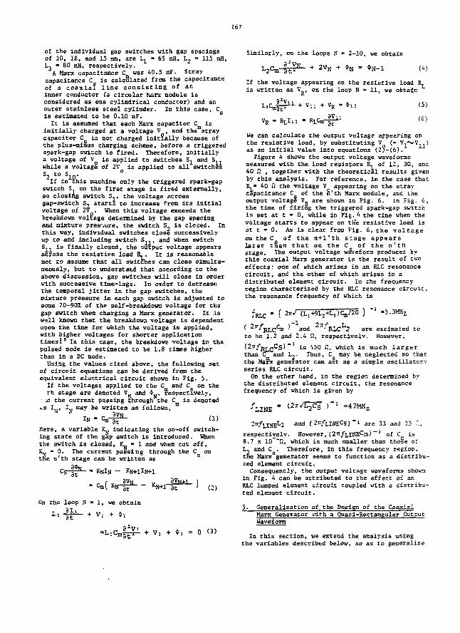
167
of the individual gap switches with gap spacingsof 10, 18, and 15 mm, are Lx - 65 nH, L2 - 115 nH,L, " 80 nH, respectively.
A Marx capacitance C was 40.5 nF. Straycapacitance C is calculated from the capacitanceof a coaxial line consisting of aninner conductor (a circular Marx module isconsidered as one cylindrical conductor) and anouter stainless steel cylinder. In this case, Cis estimated to be 0.10 nF. s
It is assumed that each Marx capacitor C isinitially charged at a voltage V , and themstraycapacitor Cg is not charged initially because ofthe plus-minus charging scheme, before a triggeredspark-gap switch is fired. Therefore, initiallya voltage of VQ is applied to switches S^ and S.^while a voltage of 2V is applied to all switchesS2 to Sjp. °If in this machine only the triggered spark-gap
switch S on the first stage is fired externally,so closing switch S^, the voltage acrossgap-switch S, starts to increase from its Initialvoltage of 2t? . When this voltage exceeds thebreakdown voltage determined by the gap spacingand mixture pressure, the switch S, is closed. Inthis way, individual switches close successivelyup to and including switch S... and when switchS-. is finally closed, the output voltage appearsacross the resistive load R,. It is reasonablenot to assume that all switches can close simulta-neously, but to understand that according to theabove discussion, gap switches will close in orderwith successive time-lags. In order to decreasethe temporal jitter in the gap switches, themixture pressure in each gap switch is adjusted tosome 70-90% of the self-breakdown voltage for thegap switch when charging a Marx generator. It .iswell known that the breakdown voltage is dependentupon the time for which the voltage is applied,with higher voltages for shorter applicationtimes!5 In this case, the breakdown voltage in thepulsed mode is estimated to be 1.8 times higherthan in a DC mode.
Using the values cited above, the following setof circuit equations can be derived from theequivalent electrical circuit shown in Fig. 5.
If the voltages applied to the C and C on therh stage are denoted V and •„, respectively,id the current passing through the C^ is denotedI , 1^ may be written as follows,
(1)
Here, a variable IC indicating the on-off switch-ing state of the gap switch is introduced. Whenthe switch is closed, K _» 1 and when cut off,Iw - 0. The current passing through the C onthe n'th stage can be written as
(2)
Similarly, on the loops N - 2-10, we obtain
2VN + *H = *H-1 (4)
On the loop N » 1, we obtain
it -IT1- + v, + $I
is written as V , on the loop N = 11, we obtainIf the voltage appearing on the resistive load R,
»io (5)
ft V 1 - / £ \
VR » Ri , In " RLC°' 3C '
We can calculate the output voltage appearing onthe resistive load, by substituting V (= V,~v,, )as an initial value into equations (Zj-(6).x
Figure 4 shows the output voltage waveformsmeasured with the load resistors R_ of 12, 30, and40 ft , together with the theoretical results givenby this analysis. For reference, in the case thatR, • 40 fl r.he voltage V appearing on the straycapacitance Cs of the n'th Marx module, and theoutput voltage VR are shown in Fig. 6. In Fig. 6,the time of firing the triggered spark-gap switchis set at t • 0, while in Fig.4 the time when thevoltage starts to appear on th"e resistive load isat t • 0. As is clear from Fig. 6, the voltageon the C of the n+l'th stage appearslater tnan that on the C of the n'thstage. The output voltage waveform produced bythis coaxial Marx generator is the result of twoeffects: one of which arises in an RLC resonancecircuit, and the other of which arises in adistributed element circuit. In the frequencyregion characterized by the RLC resonance circuit.the resonance frequency of which is
fHLC - ( 27r/ ai+9L:,+L3)Co/20 J -3.3MHZ
( •* R L C ^ an<* J E&C 2 are estimated toto be 1.2 and 2.4 S2, respectively. However,
(2n/jjr j,Cs) ~ is '<50 ii, which is much largerthan C and L-* Thus, C may be neglected so thatthe Marx generator can act as a simple oscillator-.-series RLC circuit.On the other hand, in the region determined by
the distributed element circuit, the resonancefrequency of which is given by
1 =47MHZ
2TTfLINEL2 and ( 217/tINECs) " 1 are 33 and 33 .".,
respectively. However, [2TfiXSZcm) ~l of C is8.7 x 10~ Jl, which is much smaller than those ofL, and C . Therefore, in this frequency region,tEe MarxSgenerator seems to function as a distribu-ted element circuit.Consequently, the output voltage waveforms shown
in Fig. 4 can be attributed to the effect of anRLC lumped element circuit coupled with a distribu-ted element circuit.
+ V, + *j = 0 (3)
5. Generalization of the Design of the CoaxialMarx Generator with a Quasi-Rectangular OutputWaveform
In this section, we extend the analysis usingthe variables described below, so as to generalize
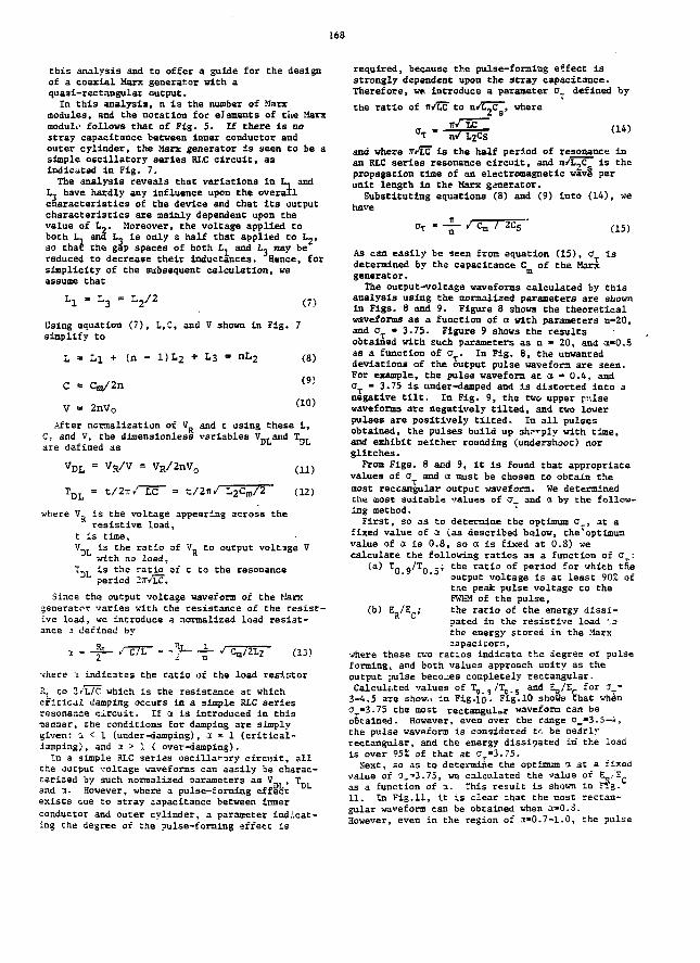
163
this analysis and to offer a guide for the designof a coaxial Marx generator with aquasi-rectangular output.
In this analysis, n ia the number of Marxmodules, and the notation for eJamenta of the Marxmodulo follows that of Fig. 5. If there is nostray capacitance between inner conductor andouter cylinder, the Mara generator is seen to be asimple oscillatory series RI.C circuit, aaindicated in Fig. 7.
The analysis reveals that variations in L. andL, have hardly any influence upon the overallcharacteristics of the device and that its outputcharacteristics are mainly dependent upon Chevalue of L«. Moreover, the voltage applied toboth U and L ? is only a half that applied to L2,so that the gap spaces of both L, and L, nay bereduced to decrease their inductances. Hence, forsimplicity of the subsequent calculation, weassume that
Ll - L3 = V 2
Using equation (7), L,C, and V shown in Fig. 7
simplify to
(7)
L = Li + (n - 1)L 2 + L3 = nL 2
C = Cm/211
V 2nV0
(8)
(9)
(10)
After normalization of VR and t using these L,C, and V, the dimensionless variables V and T_.are defined as
(11)
L 2C m/2 (12)= t / 2 r / LC =
where V is che voltage appearing across Cheresistive load,
t is time,V is the ratio of V to output voltage V
with no load,T_, is the ratio of t Co the resonance'DL period 2JT/LC.
Since the output voltage waveform of the Marxgenerator varies with the resistance of the resist-ive load, we introduce a normalized load resist-ance x defined by
D» 1(13)
•••here 2 indicates the ratio of the load resistor
R^ co 2/L/C which is che resistance at whichcritical damping occurs in a simple RLC seriesresonacce circuit. If a is introduced in thismanner, che conditions for damping are simplygiven: 1 < 1 (under-damping), a - 1 (critical-damping) , and 2 > 1 ( over-damping).
In a simple 3LC series oscillai-ory circuit, allthe output volcage waveforms can easily be charac-terized by such normalized oarameters as V , Tand a. However, where a pulse-forming effectexists due to stray capacitance between innerconductor and outer cylinder, a parameter indicat-ing the degree of the pulse-forming effect is
required, because the pulse-formiag effect isstrongly dependent upon the stray capacitance.Therefore, we introduce a parameter 0 defined by
the ratio of irvEJf to where
! n/ L2CS(14)
and where iT'Tc is the half period of resonance inan RLC series resonance circuit, and n/L9C is thepropagation time of an electromagnetic wave perunit length in the Marx generator.
Substituting equations (3) and (9) into (14), wehave
' -=- ' c m / 2 CS (15)
As can easily be seen from equation (15), a isdetermined by the capacitance C of the Marxgenerator. m
The output-voltage waveforms calculated by thisanalysis using the normalized parameters are shownin Figs. 8 and 9. Figure 8 shows the theoreticalwaveforms as a function of a with parameters n-20,and crT • 3.75. Figure 9 shows the resultsobtained with such parameters as n » 20, and a-O.Sas a function of c . In Fig. 8, the unwanteddeviations of the output pulse waveform are seen.For example, the pulse waveform at a - 0.4, andO T - 3.75 is under-damped and is distorted into anegative tilt. In Fig. 9, the two upper pulsewaveforms are negatively tilted, and two lowerpulses are positively tilted. In all pulsesobtained, the pulses build up sh?»ply with time,and exhibit neither rounding (undershoot) norglitches.
From Figs. 8 and 9, it is found that appropriatevalues of a^ and a must be chosen to obtain themost rectangular output waveform. He determinedthe tuosc suitable values of (7 and ot by the follow-ing method.
First, so as to determine the optimum c_, at afixed value of a (as described below, the'optimumvalue of a is 0.8, so a is fixed at 0.8) wecalculate the following ratios as a function of C_:
(a) T Q 9/T Q .; the ratio of period for which cfieoutput voltage is at least 90" ofthe peak pulse voltage to theFBHM of the pulse,
(b) E /E ; the ratio of the energy dissi-pated in the resistive load '.jthe energy stored in the Marxcapacitors,
where these two ratios indicate che degree of pulseforming, and both values approach unity as theoutput pulse becomes completely rectangular.Calculated values of T8.,/T,,.5 and / E - for j_«3-4.5 are show,, in Fig.iQ. Fig. 10 shows Chat whenJT»3.75 the most rectangular waveform can beobtained. However, even over the range 0^-3.5-4,the pulse waveform is considered tr, be nearlyrectangular, and the energy dissipated in the loadis over 95? of that at <JT=3.75.
Sext, so as to determine the optimum a at a fixedvalue of 3^=3.75, we calculated the value of E .< E^as a function of 3. This resulc is shown in Fz.g.11. In Fig.11, ic is clear thac the most rectan-gular waveform can be obtained when 2-0.S.'dowever, even in the region of i»0.7-1.0, the pulse
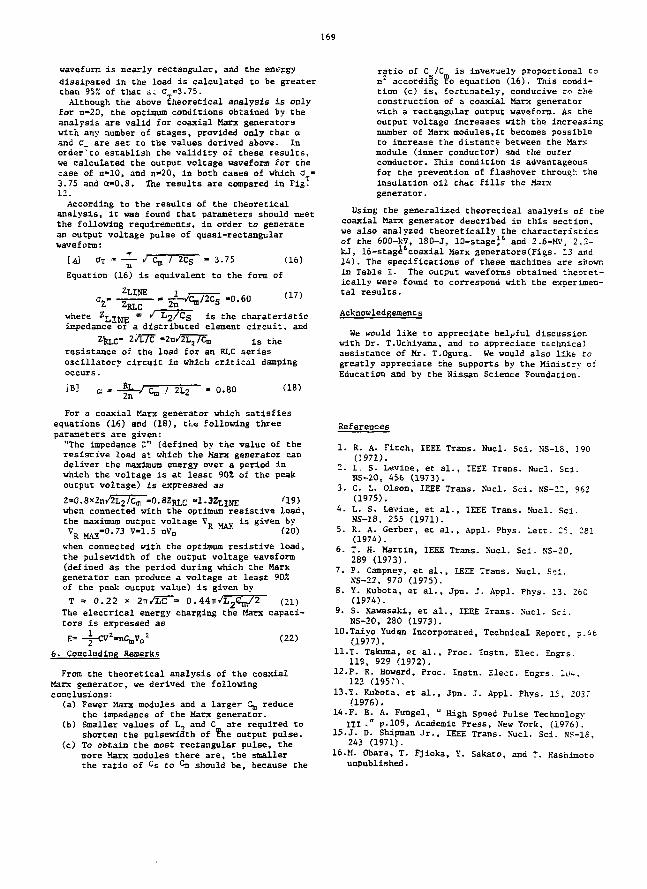
169
waveform is nearly rectangular, and the energydissipated in the load is calculated to be greaterthan 95% of that a- a =3.75.
Although the above theoretical analysis is onlyfor n=20, the optimum conditions obtained by theanalysis are valid for coaxial Marx generatorswith any number of stages, provided only that aand c_ are set to the values derived above. Inorder1to establish the validity of these results,we calculated the output voltage waveform for thecase of n"10, and n=20, in both cases of which 0_=3.75 and a«0.8. The results are compared in Fig'12.According to the results of the theoretical
analysis, it was found that parameters should meetthe following requirements, in order to generatean output voltage pulse of quasi-rectangularwaveform:
[A] oT - -£- / Cj, / 2CS - 3.75 (16)
Equation (16) is equivalent to the form of
ZI-INE i ;_ ... . ,„ (i7)/2CS -0.60
ZRLCwhere ^LTfjE = ^ ^*2./*~S is che charateristicimpedance~oi a distributed element circuit, and
^&I.C* 2vL/C *2n/2L, /Cm j_s theresistance of the load for an RLC seriesoscillatory circuit in which critical dampingoccurs.
ratio of C /C is inversely proportional ton' according to equation (16). This condi-tion (c) is, fortunately, conducive to theconstruction of a coaxial Marx generatorwith a rectangular output waveform. As theoutput voltage increases with the increasingnumber of Marx modules.it becomes possibleto increase the distance between the Marxmodule (inner conductor) and the outerconductor. This condition is advantageousfor the prevention of flashover through theinsulation oil that fills the Marxgenerator.
Using the generalized theoretical analysis of thecoaxial Marx generator described in this section,we also analyzed theoretically the characteristicsof the 600-kV, 180-J, 10-stagei6 and 2.6-MV, 2.2-kJ, 16-stage6coaxial Marx generators(Figs. 13 and14). The specifications of these machines are shownin Table I. The output waveforms obtained theoret-ically were found to correspond with the experimen-tal results.
Acknowledgements
We would like to appreciate helpful discussionwith Dr. T.Uchiyama, and to appreciate technicalassistance of Mr. T.Ogura. We would also like togreatly appreciate the supports by the Ministry ofEducation and by the Nissan Science Foundation.
0.80 (18)
For a coaxial Marx generator which satisfiesequations (16) and (18), the following threeparameters are given:
"The impedance Z" (defined by the value of theresistive load at which the }£arx generator candeliver the maximum energy over a period inwhich the voltage is at least 90% of the peakoutput voltage) is expressed as
Z»0.8x2n/2L2/Cm -O.SZR^C - 1 . 3 Z L I N E '19)
when connected with the optimum resistive load,the maximum output voltage V is given byVR JJ^-0.73 V-1.5 nVo
R "** (20)
when connected with the optimum resistive load,the pulsewidth of the output voltage waveform(defined as the period during which the Marxgenerator can produce a voltage at least 90%of the peak output value) is given by
T = 0.22 x 2TI/LC = 0.44it L 2S m/2 (21)The electrical energy charging the Marx capaci-tors is expressed as
(22)
6. Concluding Remarks
From the theoretical analysis of the coaxialMarx generator, we derived the followingconclusions:
(a) Fewer Marx modules and a larger Cj, reducethe impedance of the Marx generator.
(b) Smaller values of L, and C are required toshorten the pulsewiSth of ftie output pulse.
(c) To obtain the most rectangular pulse, themore Marx modules there are, the smallerthe ratio of C s to Cm should be, because the
References
1. R. A. Fitch, IEEE Trans. Nucl. Sci. NS-18, 190(1971).
2. L. S. Levine, et al., IEEE Trans. Nucl. Sci.NS-20, 456 (1973).
3. C. L. Olson, IEEE Trans. Nucl. Sci. NS-22. 962(1975).
4. L. S. Le-v-ine, et al., IEEE Trans. Nucl. Sci.NS-lS, 255 (1971).
5. R. A. Gerber, et al., Appl. Phys. Lett. 25 281(1974).
6. T. H. Martin, IEEE Trans. .Nucl. Sci- NS-20289 (1973).
7. P. Campney, et al., IEEE Trans. Nucl. S^i.NS-22, 970 (1975).
8. Y. Kubota, at al., Jpn. J. Appl. Phys. 13. 260(1974).
9. S. Kawasaki, et al., IEEE Trans. Nucl. Sci.NS-20, 280 (1973).
lO.Taiyo Yuden Incorporated, Technical Report, p.46(1977).
11.T. Takuma, et al., Proc. Instn. Elec. Engrs.119, 929 (1972).
12.P. R. Howard, Proc. Instn. Elect. Engrs. 104.123 (19571.
13.Y. Kubota, et al., Jpn. J. Appl. Phys. 15, 2037(1976).
14.F. B. A. Fungel, " High Speed Pulse TechnologyIII ." p-109, Academic Press, New York, (1976).
15.J. D. Shipman Jr., IEEE Trans. Nucl. Sci. NS-18243 (1971).
16.M. Obara, T. Fjioka, Y. Sakato, and T. Hashimotounpublished.
170
' Cm ! ClOwmm
-50i.v» »TMOI
Fig.1 Electrical circuit of thecoaxial-type, 10-stageMarx generator (lHV.IkJ).
Fig.4 Comparison of theoretical andexperimental results of outputvoltage waveform at a chargingyoltage of ±25 kV.
i:.if, rime[SUMC STAMBS SISB.
nit WKna nm CTUIOI
T ig.2 Simplified cross-sectional view of acoaxial-type, 10-stage Marx generator.Not to scale.
JTl
-ig.3 Cross-sectional view of a CL1SO4-solution resistive load, (connec-ted with a Marx generator). Not toscale.
S. b C x C S U . Cm Cm
Fig.5 Equivalent electrical circuit of a coaxial-type,10-stage Marx generator.
Fig.6 Theoretical voltagewaveforms appeared onn'th Marx module witha 40n resistive load.
I . t
KVL
200Tim»insoO
1. J
1—OTP—^—->
i-ig.7 Simplified electricalequivalent circuit ofa Marx generator.
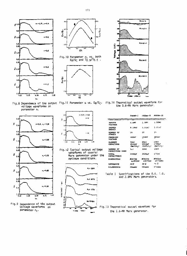
171
0.0
0.8
£0.4
Fig.10 Parameter aT vs. bothER/EC and T0.9/T0.5 •
0.25 D.50 0.75 1.00
I M
4M
Ml
i 3
I(A
ll •»•!
> ° :
m
HI
IN
•M
HI
Rl*3CJ
ill:::i ::::::•:• ::£S>.
R u : 3 B 0
RIS150Q
Tim* tnarsj .«_•
Fig.8 Dependence of the outputvoltage waveforms onparameter a.
Fig.ll Parameter a vs. ER/EC- Fig.14 Theoretical output waveform forthe 0.6-MV Marx generator.
f-JJO
• -O.8, .,-3.00
"i.m o.is o.so 0.75 '•"IK.
Fig.9 Dependence of tfie outputvoltage waveforms onparameter oT.
=.«
' \ —10
r\_-•
•
O.CC 0 25 D.50 3.75 1..T0IBL
Fig.i2 Typical output voltagewaveforms of coaxialMarx generator under theoptimum conditions.
OUTPUTVOLTAGE
STOREDENERGY
NUMBER OFSTAGES
CHARGINGVOLTAGE
ELSffiKTCAPACITOR
KUMBEE 0 ?CAPACITORS USED
TOTALCAPACITANCE
DIMENSIONS
IMPEDANCE
PULSEMIDTH
KREBA-I
0.6MV
O.lBkj
10
*€OJcV
30kV2500pF(B*TiO3;
u-:IDOOpF
WJmxI455inm
30Q
20n*ec
JCHEBA-II
1.0HV
l . O l k J
10
•50JtV
25 JtVlOOOpF(SrTiOj)3240
2025pF
0560mmx2670rnm
38 C
6Bn»ec
KREBA-2E
2.56W.1
2 . 2 1 K J
16
+80kV
<0kV2700pr{BaTiDjJ1024
6 75CF
^56 Omnix4740mr
<7nsec
Table I Specifications of the 0.6, 1.0,and 2.6HV Marx generators.
— ) ^ ~ ^ ^\r Fig. 13 Theoretical output waveform forTIME • tin> __ the 2.6-HV Marx generator.
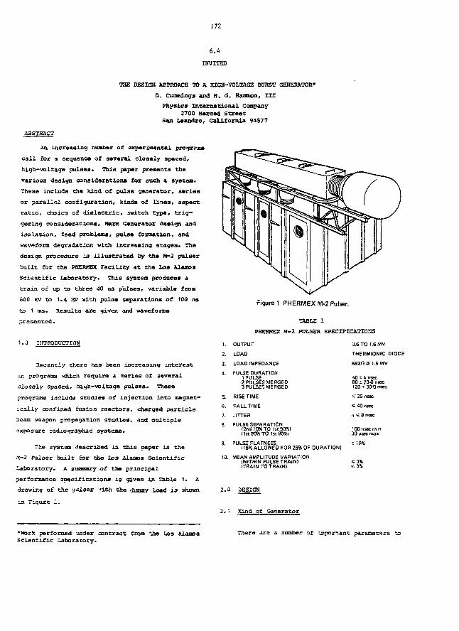
172
6.4
INVITED
THE DESIGN APPROACH TO A HIGH-VOLTAGE BURST GENERATOR*
D. Cunning's and H. G» Hamton, III
Physics International Company
2700 Merced StreetSan Laandro, California 94577
ABSTRACT
An increasing number of experimental programs
call for a sequence of several closely spaced,
high-voltage pulses. This paper presents the
various design considerations for such a system.
These include the kind of pulse generator, series
or parallel configuration, kinds of Vines, aspect
ratio, choics of dielectric, switch type, trig-
gering considerations, Marx Generator design and
isolation, feed problems, pulse formation, and
waveform degradation with increasing stages. The
design procedure is illustrated by the M-2 pulser
built for the PHERMEX Facility at the Los Alamos
Scientific laboratory. This system produces a
train of up to three 40 ns pulses, variable from
600 kv to 1.4 MV with pulse separations of too ns
to 1 tns. Results are given and waveforms
presented.
1.0 INTRODUCTION
Recently there has been increasing interest
JLJI programs which require a 3eries of several
closely spaced, high-voltage pulses. These
programs include studies of injection into magnet-
ically confined fusion reactors, charged particle
beam weapon propagation studies, and multiple
exposure radiographic systems.
The system described in this paper is the
.M-2 Pulser built for the las Alanos Scientific
laboratory, A summary of the principal
performance specifications is given in Table 1. A
drawing of the polser »ith the dmnay load is shown
in Figure 1.
Figure 1 PHEHMEX M-2 Pulser.
TABLE 1
PHERMEX M-2 POLSER SPECIFICATIONS
1.
2.
3.
4.
5.
6.
7.
9.
OUTPUT
LOAD
LOAD IMPEDANCE
PULSE DURATION1 PULSE2 PULSES MERGED3 PULSED MEHGED
RISE TIME
FALL TIME
JITTER
PULSE SEPARATION!2niilO%TO tst90%l(1st90%TOTst90%l
0.6 TO I .SMV
THERMIONIC DIODE
40? 4 nsec80 z 2 0 4 nsec!20*3CH)nsec
< 25 nsec
< 40 nsec
9. PULSE FLATNESS115* ALLOWED FOR 25% OF OURATIONI
10. MEAN AMPLITUDE VAHIATION(WITHIN PULSE TRAIN)(TRAIN TO TRAINI
2.0 DESIGN
2," Kind of Generator
•Work performed under contract from the los AlamosScientific Laboratory.
There are a number 3f iaporiant parameters to

173
be considered in selecting the design of the
generator:
a) Poise duration
b) Voltage
c) Impedance
d) Waveform requirements
e) Number of pulses
f) Pulse separation
g) Jitter
The first parameter forces the basic decision
of whether to use distributed or lumped elements,
the latter becoming feasible and often desirable
above a pulse length in the range of 100-300 ns.
For short pulses, the choice is narrowed dawn to
either a simple pulse line or a Blumlein circuit.
2.2 Configuration
For high repetition rates (> 10 kHz] and high
average power, a single repetitive pulser in burst
mode will not meet the requirement. Consequently,
there are two alternative general approaches -to
the configuration:
1. Independent Parallel ftolsers* This configur-
ation would be quite useful if nanosecond,
megavolt, terawatt diodes w&re available. One
might consider direct connection with pulsers of
ZQ, ZQ/2, ZQ/4, etc., with twice the energy for
~each successive pulser. However* without
isolation, the second pulse wuld have a tail of
V/2, v/4 , etc., and the third pulse a tail of
3V/4, 9V/16, etc. Isolation with a series im-
pedance could be used to reduce the tail, but the
energy penalty becomes enormous.
2. Independent Tandem Pulsers* In this approach
pulses after the first must pass through a series
of switches r leading to waveform degradation. In
addition, no line and is available for the input
energy feed. Eiowever, these problems have
solutions and the tandem configuration was
chosen, a Blunlein circuit cannot be used,
and the choice becomes a simple pulse line
configuration selected for the M-2 pulser
(see Figure 2) .
Figure 2 PHERMEX M-2 Pulser-schematic design.
2.3 Choice of Dielectric
The following factors influence the choxce of
dielectric:
a) Dielectric strength
b} Desired impedance
c) Pulse length
d) Space available
e) Aspect ratio of line
f) losses and dispersion
The choice becomes primarily a tradeoff
between high icpedance for short risetune and load
damping, and low impedance for short length to f i t
the limited space available.
The load was to be a coaxial vacuum-insulated
thermionic diode with a nominal line impedance of
€0 ohB6 with an end capacitance of 115 pF and beam
loading of 682 ohms. The resulting resonant
circuit has a series impedance of about T! ohms.
With trivial beam loading ~iifc primary damping must
cone fi-xn the line and load impedances in
parall'.l, or ZQ/2. For a slight overshoot, this
v»•>.... leads to the goal of ZQ « 2ZUOHD " 7 4 o h m s -
In a simplified model of a switched line, the
10-90% rise-time is given by tr - 1.1 Lsw/Zo. For
2Q - 74 ohms, this Mould also give an excellent
risetine with the estimated switch inductance of
160 nB 'single arc channel).
Oil would have been desirable since i t could
readily give iapedances in the range of 30 to
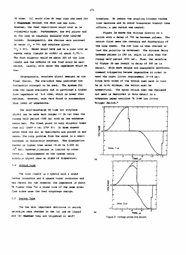
174
50 ohms* Oil would alao do away with the need for
a diaphragtt between the Marx and the line.
However, the feed capacitance would tend to be
relatively high. Furthermore, the M-2 pulser had
to fit into an existing facility vitb limited
length. Consequently, the choices were narrowed
to water («r " 78) and ethylene glycol
( Sf » 41). Water would have led to a line with an
aspect ratio (length to width) of about 0.75:1.
The feed diameter teuld be about 20% of the line
length and the effects of the feed would be max-
imized. Lastly, with water the iapedanca would be
low.
Consequently, ethylene glycol emerged as the
final choice. The available data indicated the
dielectric strength to be good. The system fit
into the space available and it permitted a higher
line Impedance of "6.5 ohms, which is lover than
optimum. However, ways were found to accommodate
this level of impedances.
The self-discharge RC time for ethylene
glycol can be made ouch longer ( 36 us) than the
nngup half period (500 ns) with an ion exchange
resin bed. The flash point is only slightly lower
than oil (240» F vs. 275» F). It does absorb
water from the air so desiccants are placed in air
vents. The only problem from the water is a small
increase in dielectric constant. The dissipation
factor is higher than water (0.45 vs 0.005 at
108 Hz); however,risetinm is limited by other
factc.^^. Measurements on the systea using
ethyliuua glycol show no signs of dispersion.
2.4 Hybrid Line
The Line itself is a hybrid with a round
center conductor and a square outer conductor and
was chosen for two reasons: the impedance is about
5% higher than 'or a round line of the sane sizer
flat sides ease the feed diaphragm design.
2.5 Switch Type
The mo aost important decisions in switch
selection were whether to use (a) gas or liquid
and (b) whether they are triggered or self-
breaking. To reduce the coupling between tandem
line sections and to avoid transverse transit time
effects, a gas switch was needed.
Figure 3* shows the voltage history on a
switch with a delay of 700 ns between pulses. The
3vitch first sees the charging and discharging of
the line ahead. Its own line is then charged so
that the polarity is reversed. The minimum delay
between pulses is 180 ns, which is less than the
ringup half period (500 ns). Thus, the waveform
of Figure 3b can result (a delay of 300 ns is
shorn). With such unique and changeable waveforms,
command triggering became imperative in order to
aeet the tight jitter requirement (c < 8 ns).
Since both sides of the switch must each in turn
be at nJ-ih voltage, the switch must be
symmetrical. The epoxy switch that was designed
and used is described in more detail in a
companion paper entitled "A 3-HV low Jitter
Trigger Switch."
1
Delay -7 us
I 1 ' I !
1 1 1 1 1 1 i
\
v
-
1.6 .8TIME. ia
/
\\
\•\
_ Delay .3 us
> i t i
-
M
1 "T
II—
-]
tb> TIME.;;*
Figure 3 Voltage across line switch.
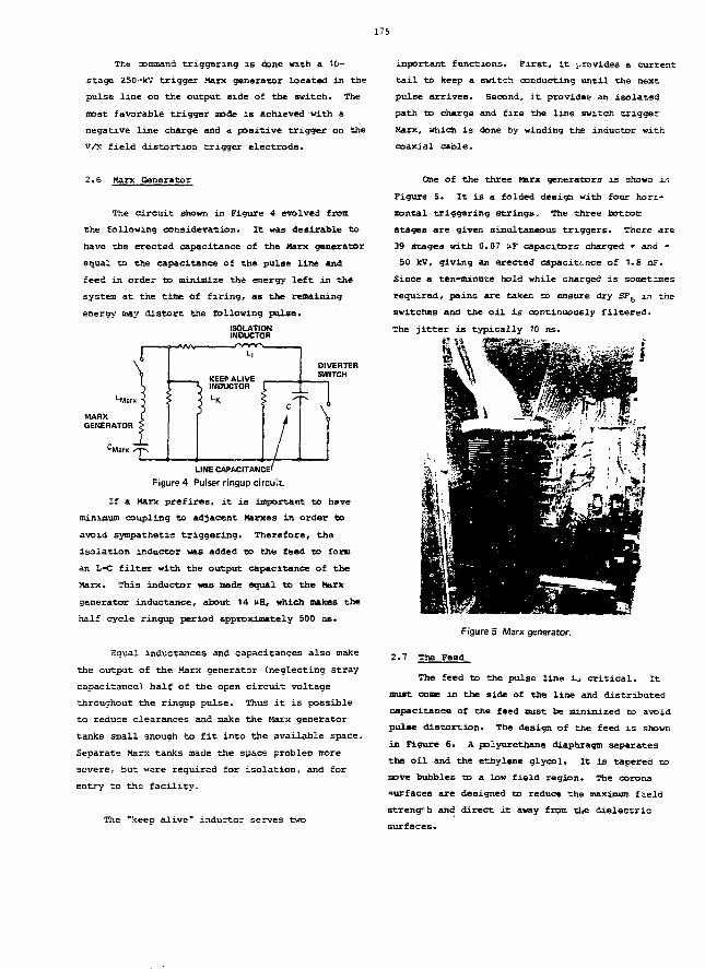
175
The command triggering is done with a 10-
ftage 250~kV trigger Marx generator located in the
pulse line on the output Bide of the switch* The
most favorable trigger mode is achieved with a
negative line charge and a positive trigger on the
V/N field distortion trigger electrode.
important functions. First* it provides a current
tail to keep a switch conducting until the next
pulse arrives. Second, it provides an isolated
path to charge and fire the line switch trigger
Marx, which is done by winding the inductor with
coaxial cable.
2.6 Marx Generator
The circuit shown in Figure 4 evolved from
the following consideration. It was desirable to
have the erected capacitance of the Marx generator
equal to the capacitance of the pulse line and
feed in order to minimize the energy left in the
system at the time of firing, as the remaining
energy may distort the following pulse.
LINE CAPACITANCE'
Figure 4 Pulser ringup circuit.
If a Marx prefires, it is important to have
minimum coupling to adjacent Marxes in order to
avoid sympathetic triggering. Therefore, the
isolation inductor was added to the feed to form
an L-C filter with the output capacitance of the
Marx. This inductor was made equal to the Marx
generator inductance, about 14 UH, which makes the
half cycle ringup period approximately 500 ns.
Equal inductances and capacitances also make
the output of the Marx generator (neglecting stray
capacitance) half of the open circuit voltage
throughout the ringup pulse. Thus it is possible
to reduce clearances and make the Marx generator
tanks small enough to fit into the available space.
Separate Marx tanks made the space problem more
severe,. but were required for isolation, and for
entry to the facility.
The "keep alive" inductor serves two
One of the three Marx generators is shown in
Figure 5. It is a folded deBign with four hori-
zontal triggering strings. The three bottom
stages are given simultaneous triggers. There are
39 stages with 0.07 nF capacitors charged • and -
50 kV, giving an erected capacitance of 1.8 nF.
Since a ten-minute hold while charged is sometimes
required, pains are taken to ensure dry SFg in the
switches and the oil is continuously filtered.
The jitter is typically 10 ns.
Figure 5 Marx generator.
2.7 The Feed
The feed to the pulse line io critical. It
must cone in the side of the line and distributed
capacitance of the feed must be minimized to avoid
pulse distortion. The design of the feed is shown
in Figure 6. A polyurethane diaphragm separates
the oil and the ethylene glycol. It is tapered to
move bubbles to a low field region. The corona
surfaces are designed to reduce the maximum field
streng* h and direct it away from the dielectric
surfaces.
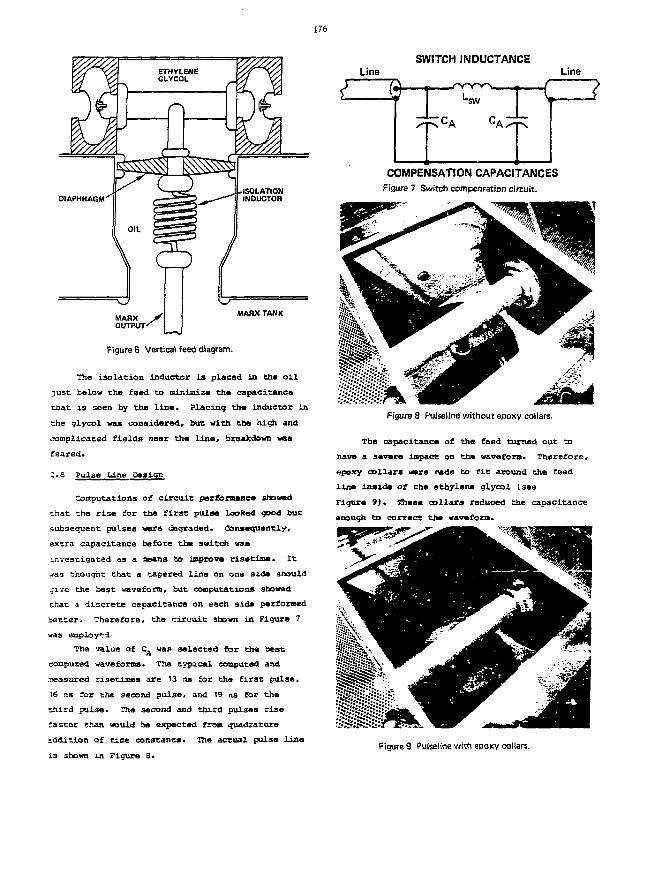
176
SWITCH INDUCTANCELine Line
MAHX yniiTPirr/ ,
MARX TANK
OUTPUT'
Figure 6 Vertical feed diagram.
The isolation inductor is placed in the oil
just below the feed to minimize the capacitance
that is seen by the line. Placing the inductor in
Che glycol was considered, but with the high and
complicated fields near the line, breakdown was
feared.
2.8 Pulse Ldne aesiqn
Computations of circuit performance showed
that the rise for the first pulse looked good but
subsequent pulses were degraded. Consequently,
extra capacitance before the switch was
investigated as a aeans to improve risetime. It
was thought that a tapered line on ona side should
give the best waveform, but computations showed
chat a discrete capacitance on each side performed
better. Therefore, the circuit shown in Figure 7
was employed.
The value of Cft was selected for the best
computed waveforms. The typical computed and
measured risetises are 13 as for the first pulse,
16 .is for the second pulse, and 19 ns for the
third pul3e. The second and third pulses rise
faster than would be expected from quadrature
addition of time constants. The actual pulse line
i3 shown in Figure 8.
usw
;CA
COMPENSATION CAPACITANCES
Figure 7 Switch compensation circuit.
Figure 8 Pulseline without epoxy collars.
The capacitance of the feed turned out to
have a severe impact on th« waveform. Therefore,
epoxy collars were nade to fit around the feed
line inside of the ethylene glycol (see
Figure 9 ) . These collars reduced the capacitance
enough to correct the waveform.
Figure 9 Pulseline with epoxv collars.
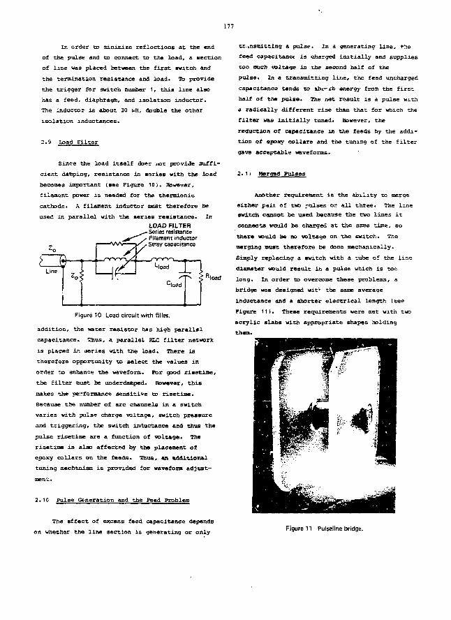
177
In order to minimize reflections at the end
of the pulse and to connect to the load, a section
of line was placed between the first switch and
the termination resistance and load. To provide
the trigger for switch number 1, this line also
has a feed, diaphragm, and isolation inductor.
The inductor is about 30 uH, double the othar
isolation inductances.
2.9 load Filter
Since the load itself doe? m e provide suffi-
cient damping, resistance in «sries with the load
becomes important (see Figure 10). However,
filament power is needed for the thermionic
cathode* A filament inductor must therefore be
used in parallel with the aeries resistance. In
LOAD FILTER- Series resistance- Filament inductorStray capacitance
Rload
Figure 10 Load circuit with filler.
addition, the water resistor has high parallel
capacitance. Thus, a parallel KLC filter network
is placed ir. aeries with the load. There is
therefore opportunity to select the values in
order tx> enhance the waveform, for good risetime,
the filter must be underdamped. However, this
makes the performance sensitive to risetime.
Because the number of arc channels in a switch
varies with pulse charge voltage, switch pressure
and triggering, the switch inductance and thus the
pulse risetime are a function of voltage. The
risetime is also affected by the placement of
epoxy collars on the feeds. Thus, an additional
tuning mechanism is provided for waveform adjust-
ment.
2.10 Pulse Generation and the Feed Problem
The effect of excenti feed capacitance depends
on whethar the line section is generating or only
transmitting a pulse. In a generating line, the
feed capacitance is charged initially and supplies
too nuch voltage in the second half of the
pulse. In a transmitting line, the feed uncharged
•capacitance tends to abt^rb energy from the first
half of the pulse. The net result is a pulse with
a radically different rise than that for which the
filter was initially tuned. However, the
reduction of capacitance in the feeds by the addi-
tion of epoxy collars and the tuning of the filter
gave acceptable waveforms.
2.11 Merged Pulses
Another requirement is the ability to merge
either pair of two ulsen or all three. The line
switch cannot be used because the two lines it
connects valid be charged at the same time, so
there would be no voltage on the switch. The
merging must therefore be done mechanically.
Simply replacing a switch with a tube of the line
diameter would result in a pulse which is toe
long. In order to overcome these problems, &
bridge was designed witv the same average
inductance and a shorter electrical length (see
Pigure 11). These requirements were met with two
acrylic slabs with appropriate shapes holding
them.
Figure 11 Pulseline bridge.
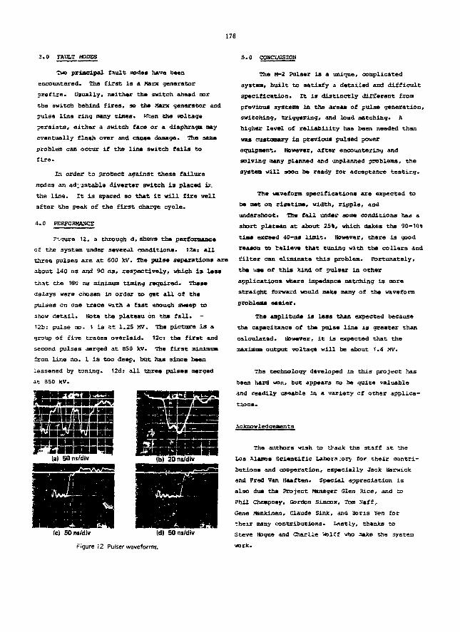
178
3.0 FAULT MODES
Two principal fault modes have been
encountered. The first ia a Marx generator
prefire. Usually, neither the switch ahead nor
the switch behind fires, so the Marx generator and
pulse line ring many times, when the voltage
persists, either a switch face or a diaphrag* nay
eventually flash over and cause damage. The 3aaa
problem can occur if the line switch fails to
fire.
In order to protect against these failure
modes an ad;jstable diverter switch is placed ii.
the line. It is spaced so that it will fire wall
after the peak of the first charge cycle.
4.0 PERFOBMASCE
?iqure 12, a through d, shews the performance
of the system under several conditions* 12a: all
three pulses are at 600 W . The pulse separation* are
about 140 ns and 90 as, respectively, which is less
that the 183 na minimum timing required. These
delays were chosen in order to get all of the
pulses on one trace with a fast enough sweep to
show detail. Note the plateau on the fall. -
12b: pulse no. 1 is ?.t 1.25 MV. The picture is a
group of five traces overlaid. 12c: the first and
second pulses jierged at 350 lev. The first minima
from line no. 1 is too deep, but has since been
lessened by tuning. 12d: all three pulses merged
at 350 kV.
(c) 50ns/div (d) 50ns/div
figure 12 Pulser waveforms.
S.O CONCLUSION
The M-2 Pulser is a unique, complicated
systen, built to satisfy a detailed and difficult
specification. It is distinctly different from
previous systems ia the areas of pulse generation,
switching, triggering, and load matching. A
higher level of reliability has been needed than
was customary in previous pulsed power
equipment. However, after encountering and
solving many planned and unplanned problems, the
system will soon be ready tor acceptance testing.
The waveform specifications are expected to
be met on risetime, width, ripple, and
undershoot. The fall under some conditions has a
short plateau at about 25%, which makes the 90-10*
time exceed 40-ns limit. However, there is good
reason to believe that tuning with the collars and
filter can eliminate this problem. Fortunately,
the use of this kind of pulser in other
applications where impedance matching is more
straight forward would make many of the waveform
problems easier.
The amplitude is less than expected because
the capacitance of the pulse line ia greater than
calculated. However, it is expected that the
output voltage will be about 1.4 MV.
The technology developed in this project has
been hard won, but appears to be quite valuable
and readily useable in a variety of other applica-
tions.
Acknowledgements
The authors wish to thank the staff at the
Los Alamos Scientific Labors :or> for their contri-
butions and cooperation, especially Jack Harwick
and Fred Van Haaften. Special appreciation i s
also due the Project Manager Glen Sice, and to
Phil Cbaapney, Gordon simcox, Tom Naff,
Gene Msnkinen, Claude Sink, and Boris Yen for
their many contributions. Lastly, thanks to
Steve Hague and Charlie Vtolff *«'ho aake the system
work.
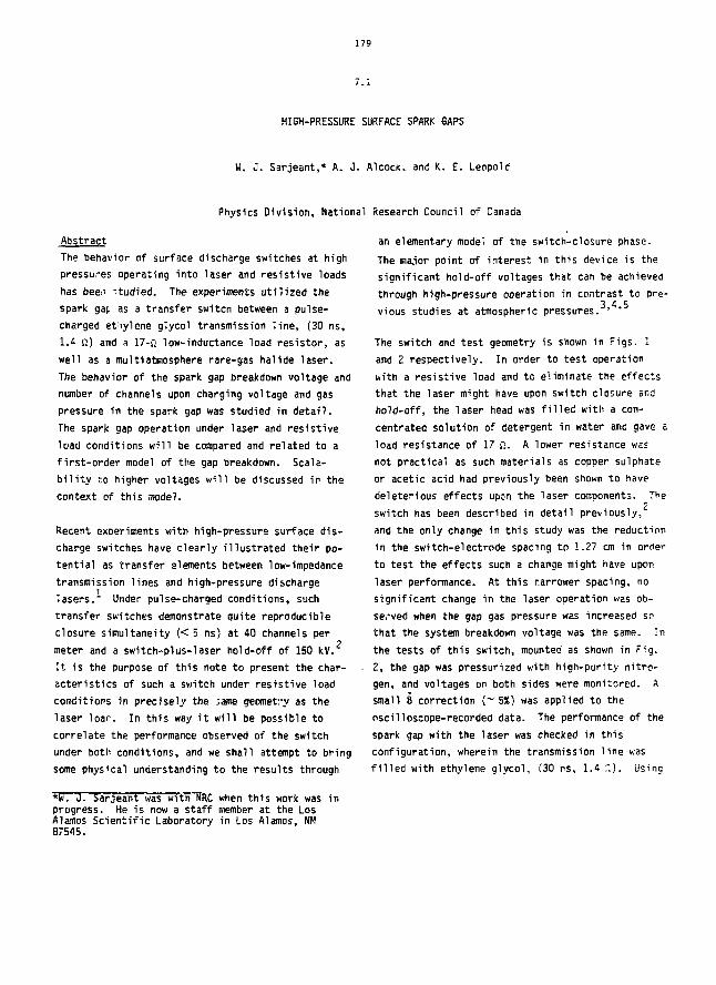
179
7.1
HIGH-PRESSURE SURFACE SPARK GAPS
W. 0. Sarjeant,* A. J. Alcoctc, and K. E. Leopold
Physics Division, National Research Council of Canada
AbstractThe behavior of surface discharge switches at highpressures operating into laser and resistive loadshas been "tudied. The experiments utilized thespark gat as a transfer switcn between a pulse-charged ethylene glycol transmission line, (30 ns,1.4 fi) and a 17-n low-inductance load resistor, aswell as a multiatmosphere rare-gas halide laser.The behavior of the spark gap breakdown voltage andnumber of channels upon charging voltage and gaspressure in the spark gap was studied in detail.The spark gap operation under laser and resistiveload conditions will be compared and related to afirst-order model of the gap breakdown. Scala-bility to higher voltages will be discussed in thecontext of this model.
Recent experiments with high-pressure surface dis-charge switches have clearly illustrated their po-tential as transfer elements between low-impedancetransmission lines and high-pressure dischargelasers. Under pulse-charged conditions, suchtransfer switches demonstrate quite reproducibleclosure simultaneity (< 5 ns) at 40 channels per
2meter and a switch-plus-laser hold-off of 150 kV.It is the purpose of this note to present the char-acteristics of such a switch under resistive loadconditions in precisely the same geometry as thelaser loar. In this way it will be possible tocorrelate the performance observed of the switchunder both conditions, and we shall attempt to bringsome physical understanding to the results through
an elementary model of the switch-closure phase.The major point of interest in this device is thesignificant hold-off voltages that can be achievedthrough high-pressure operation in contrast to pre-
3 4 5vious studies at atmospheric pressures. ' '
The switch and test geometry is shown in Figs. 1and 2 respectively. In order to test operationwith a resistive load and to eliminate the effectsthat the laser might have upon switch closure andhold-off, the laser head was filled with a con-centrated solution of detergent in water and gave aload resistance of 17 n. A lower resistance wasnot practical as such materials as copper sulphateor acetic acid had previously been shown to havedeleterious effects upon the laser components. Theswitch has been described in detail previously/and the only change in this study was the reductionin the switch-electrode spacing to 1.27 cm in orcie>-to test the effects such a change might have uponlaser performance. At this narrower spacing, nosignificant change in the laser operation was ob-served when the gap gas pressure was increased sothat the system breakdown voltage was the same. Inthe tests of this switch, mounted as shown in Fig.2, the gap was pressurized with high-purity nitro-gen, and voltages on both sides were monitored. Asmall 8 correction (~ 5%) was applied to theoscilloscope-recorded data. The performance of thespark gap with the laser was checked in thisconfiguration, wherein the transmission line wasfilled with ethylene glycol, f30 ns, 1.4 ."). Using
*W. J. Sarjeant was withTJRC when this work was inprogress. He is now a staff member at the LosAlamos Scientific Laboratory in Los Alamos, NM87545.
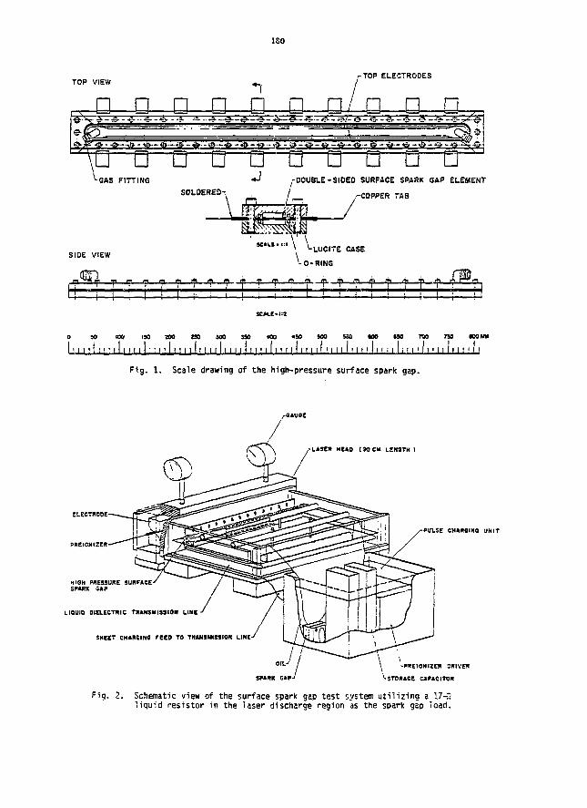
ISO
TOP VIEW-TOP ELECTRODES
n n nJy - -J. .-a . .
n n G n />.
n n-m-.O-ja
n '••* • © • •
\u u^-GAS FITTING
U U U LJ U U U USOL0ERED-.
SIDE VIEW
,-D0U8LE-SI0ED SURFACE SPARK GAP ELEMENT
/-COPPER TAB
LLUCITE CASE
'-0-3ING
•?-?--M- -3—i-
0 so n o n a o a x o a o i o i a s f l o a n i i i m r s o aaomi1 I I I I I I ! I [ I I I I I I • : I I I I 1 I I I I ! I I I I I I I I I I I I I I ' I I I I I I I I I I I I I I I M I I I I I I i I I ' I I 1 ! I I I I I I ! !
Fig. 1, Scale drawing of the high-pressure surface spark gap.
ELECTRODE'
PREICNIZER
USED HCAO (90 CM LENGTH )
PULSE CHUHOINO UNIT
HIGH PKES3UKE SURFACESPMK GAP
LIQUID DIELECTRIC TRANSMISSION LINE
SHEET CHARGING FEED TO TRANSMISSION LINE
\ ^PKEIONIZER SRIVE*
^-STORAGE CAPACITOR
Fig. 2. Schematic view of the surface spark gap test system utilizing a 17-2liquid resistor in the laser discharge region as the spark gap load.
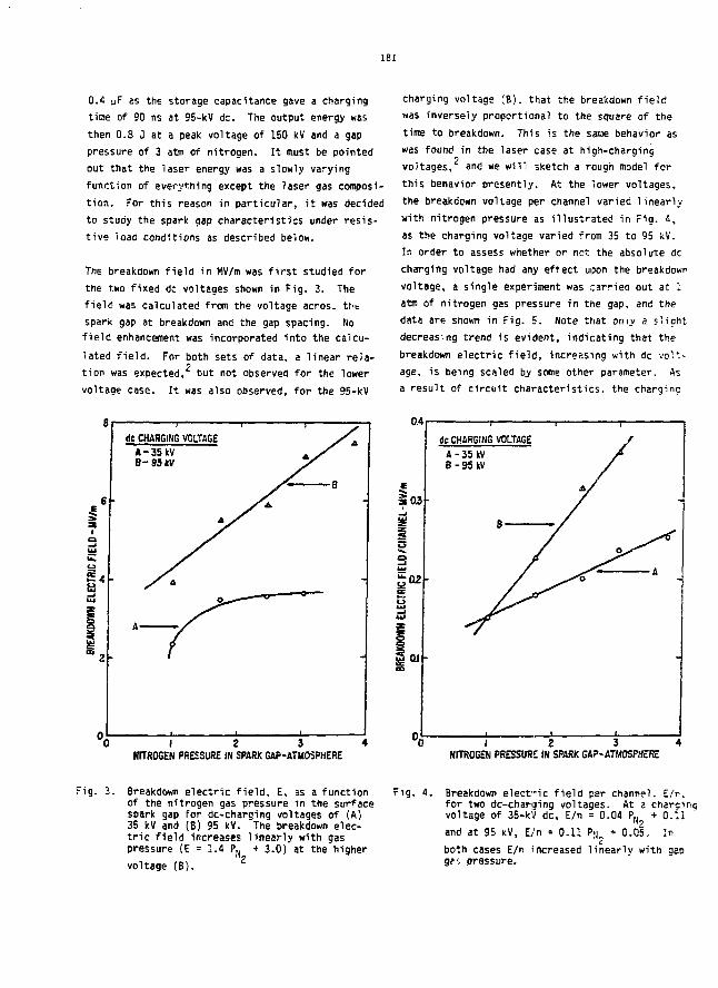
181
0.4 iiF as the storage capacitance gave a charging
time of 90 ns at 95-kV dc. The output energy was
then 0.8 0 at a peak voltage of 150 kV and a gap
pressure of 3 atm of nitrogen. It must be pointed
out that the laser energy was a slowly varying
function of everything except the laser gas composi-
tion. For this reason in particular, it was decided
to study the spark gap characteristics under resis-
tive load conditions as described below.
The breakdown field in MV/m was first studied for
the two fixed dc voltages shown in Fig. 3. The
field was calculated from the voltage acros. tt>t
spark gap at breakdown and the gap spacing. No
field enhancement was incorporated into the calcu-
lated field. For both sets of data, a linear rela-
tion was expected, but not observed for the lower
voltage case. It was also observed, for the 95-kV
charging voltage (B). that the breakdown field
was inversely proportional to the square of the
time to breakdown. This is the same behavior as
was found in the laser case at high-charging
voltages, and we will sketch a rough model for
this behavior presently. At the lower voltages,
the breakdown voHage per channel varied linearly
with nitrogen pressure as illustrated in Fig. «,
as the charging voltage varied from 35 to 95 *V.
In order to assess whether or not the absolute dc
charging voltage had any eftect upon the breakdown
voltage, a single experiment was carried out at 1
atm of nitrogen gas pressure in the gap, and the
data are shown in Fig. 5. Note that oniy a slight
decreasing trend is evident, indicating that the
breakdown electric field, increasing with dc volt-
age, is being scaled by some other parameter. As
a result of circuit characteristics, the charging
dc CHARGING VOLTAGEA-35WB-95W
0.4
f.
•02
I Of
dc CHARGING VOLTAGEA - 35 kVB-95kV
1 2 3 4NITROGEN PRESSURE IN SPARK GAP-ATMOSPHERE
1 2 3 4NITROGEN PRESSURE IN SPARK GAP-ATMOSPHERE
Fig . 3. Breakdown e l e c t r i c f i e l d , E, as a functionof the nitrogen gas pressure in the surfacespark gap for dc-charging voltages of (A)35 kV and (B) 95 kV. The breakdown elec-t r i c f i e l d increases l i n e a r l y with gaspressure (E = 1.4 PN + 3.0) at the higher
voltage (B).
Fig. 4. Breakdown electHc field par channel. E/n,for two dc-charoing voltages. At a charainavoltage of 35-kV dc, E/n = 0.04 PN + 0.11
and at 95 kV, E/n = 0.11 P-j + 0.05. In
both cases E/t> increased linearly with gapg?s pressure.
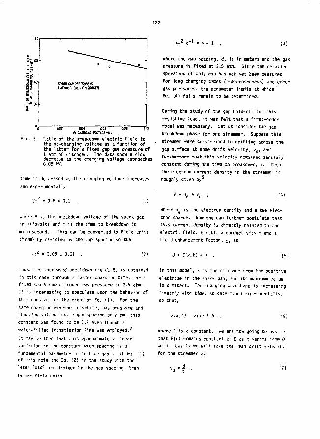
182
80 r
II?4Oill1*4
SMRKMPPSrSUREISI ATMQSMiflE f f NITROGEN
0.02 ocu aoslie BttRCJW YM.K5E-MV
acs OJO
Fig. 5. Ratio of the breakdown electric field tothe dc-charging voltage as a function ofthe latter for a fixed gap gas pressure of1 atm of nitrogen. The data show a slowdecrease as the charging voltage approaches0.09 MV.
time is decreased as the charging voltage increases
and experimentally
VT- 0.6 s 0.1
where V is the breakdown voltage of the spark gap
in Irilovolts and r is the time to breakdown in
microseconds. This can be converted to field units
(MV/m) by dividing by the gap spacing so that
-.2 = 0.05 t 0.01 (2)
Thus, the increased breakdown field, E, is obtained
in this case through a faster charging time, for a
f'xe<l spark gap nitrogen gas pressure of 2.S atra.
It is interesting to speculate upon the behavior of
this constant on the right of Eq. (1). For the
same charging waveform risetime, gas pressure and
charging voltage but a gap spacing of 2 cm, this
constant was found to be 1.2 even though a
water-filled transmission line was employed.'
It "nay be then that this approximately linear
variation in the constant with spacing is a
fundamental parameter in surface gaps. If Ea. 11)
of this note and Eg. (2) in the study with the
"aser load^ are dividea by the gap spacing, then
in the field units
£ T 2 d"1 = 4 ± 1 (3)
where the gap spacing, d, is in meters and the gas
pressure is fixed at 2.5 atm. Since the detailed
operation of this gap has not yet been measurpd
for long charging times (~ microseconds) and other
gas pressures, the parameter limits at which
Eq. (4) fails remain to be determined.
During the study of the gap hold-off for this
resistive load, it was felt that a first-order
model was necessary. Let us consider the gap
breakdown phase for one streamer. Suppose this
streamer were constrained to drifting across the
gap surface at some drift velocity, vd, and
furthermore that this velocity remained sensibly
constant during the time to breakdown, T. Then
the electron current density in the streamer is
roughly given by
J = ne e (4)
where ng is the electron density and e tite elec-
tron charge. New one can further postulate that
this current density i» directly related to the
electric field, E(x,t), a conductivity z and a
field enhancement factor, 2> as
J = Efx.t) 3 = . (5;
In this model, x is the distance from the positive
electrode in the spark gap, and its maximum value
is d meters. The charging waveshape is increasing
linearly with time, as determined experimentally,
so that,
- I X , i . / ~ i-\ ••5)
where A is a constant. We are now going to assume
that E(x) remains constant at E as x varirs f-om 0
to d. Lastly we will take the mean drift velocity
for the streamer as
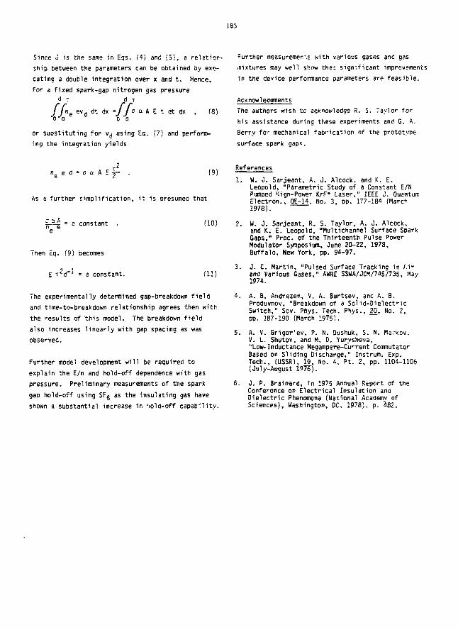
183
Since 0 is the same in Eqs. (4) and (5), a relation-
ship between the parameters can be obtained by exe-
cuting a double integration over x and t. Hence,
for a fixed spark-gap nitrogen gas pressure<1 - d T
y / n e evd dt dx =j j c a A E t dt dx , (8)0 0 0 0
or substituting for vd using Eq. (7) and perform-
ing the integration yields
Further measurements with various gases and gas
inixtures may well show that significant improvements
in the device performance parameters are feasible.
Acknowledgments
The authors wish to acknowledge R. S. Taylor for
his assistance during these experiments and G. A.
Berry for mechanical fabrication of the prototyoe
surface spark gap*.
e d = o a A,2
(9)
As a further simplification, it is presumed that
£-2-2 = a constant
Then Eq. (9) becomes
E f-d"1 - a constant.
(10)
Ul)
The experimentally determined gap-breakdown field
and time-to-breakdown relationship agrees then with
the results of this model. The breakdown field
also increases linearly with gap spacing as was
observed.
Further model development will be required to
explain the E/n and hold-off dependence with gas
pressure. Preliminary measurements of the spark
gap hold-off using SFg as the insulating gas have
shown a substantial increase in hold-off capab-lity.
References
1. W. 0. Sarjeant, A. J. Alcock, and K. E.Leopold, "Parametric Study of a Constant E/NPumped High-Power KrF* Laser," IEEE J. QuantumElectron., QE-14. No. 3, pp. 177-184 (Marc*1978).
2. H. J. Sarjeant, R. S. Taylor, A. J. Alcock,and K. E. Leopold, "Multichannel Surface SDarkGaps," Proc. of the Thirteenth Pulse PowerModulator Symposium, June 20-22, 1978,Buffalo, New York, pp. 94-97.
3. J. C. Martin, "Pulsed Surface Tracking in l,ir
and Various Gases," AWRE SSWA/JCM/745/735, May1974.
4. A. B. Andrezen, V. A. Burtsev, and A. B.Produvnov, "Breakdown of a Solid-Dielect-icSwitch," Sov. Phys. Tech. Phys., 20, No. 2,pp. 187-190 (March 1975).
5. A. V. Grigor'ev, P. N. Dushuk, S. N. Ma.-kov.V. L. Shutov, and M. D. Yurysheva,"Low-Inductance Megampere-Current CommutatorBased on Sliding Discharge," Instrum. Exp.Tech., (USSR), 19, No. 4. Pt. 2, pp. 1104-1106(July-August l°TS).
6. J. P. Brainard, in 1975 Annual Report of theConference on Electrical Insulation andDielectric Phenomona (National Acaaemy ofSciences), Washington, DC. 1978). p. 482.
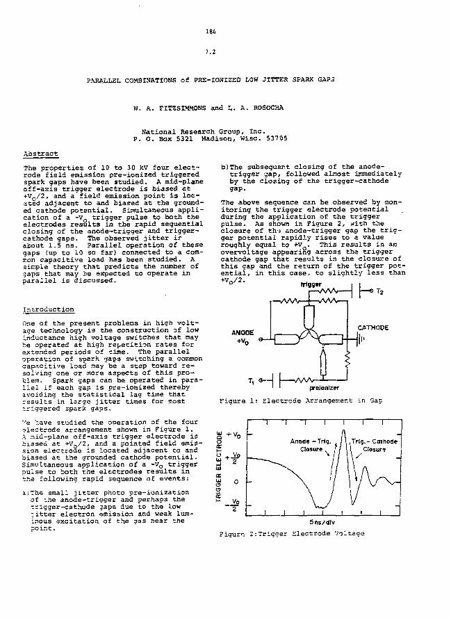
184
7.2
PARALLEL COMBINATIONS of PRE-IONIZED LOW JITTER SPARK GAPo
W. A. FIT2SI.MMONS and L. A. ROSOCHA
National Research Group, Inc.P. O. Box 5321 Madison, Wise. 53705
Abstract
The properties of 10 to 30 kV four elect-rode field emission pre-ionized triggeredspark gaps have been studied. A mid-planeoff-axis trigger electrode is biased at+Vo/2, and a field emission point is loc-ated adjacent to and biased at the ground-ed cathode potential. Simultaneous appli-cation of a -VQ trigger pulse to both theelectrodes results in the rapid sequentialclosing of the anode-trigger and trigger-cathode gaps. The observed jitter isabout 1.5 ns. Parallel operation of thesegaps (up to 10 so far) connected to a com-mon capacitive load has been studied. Asimple" theory that predicts the number ofsaps that may be expected to operate inoaraliel is discussed.
Introduction
One of the present problems in high volt-age technology is the construction of lowinductance high voltage switches that maybe operated at high repetition rates forextended periods of time. The paralleloperation of spark gaps switching a commoncapacitive load may be a step toward re-solving one or more aspects of this pro-blem. Spark gaps can be operated in para-llel if each gap is pre-ionized therebyavoiding the statistical lag time thatresults in large jitter times for mosttriggered spark gaps.
'•'e have studied the operation of the fourelectrode arrangement shown in Figure 1.A mid-plane off-axis trigger electrode isbiased at +V /2, and a pointed field emis-sion electroae is located adjacent to andbiased at the grounded cathode potential.Simultaneous application of a -Vo triggerpulse to both the electrodes results inthe following rapid sequence of events:
a)The small jitter photo pre-ionizationof the anode-trigger and perhaps thetrigger-cathode japs due to the low;. itter electron emission and weak lum-inous excitation of the gas near the20 int.
b)The subsequent closing of the anode-trigger gap, followed almost immediatelyby the closing of the trigger-cathodegap.
The above sequence can be observed by mon-itoring the trigger electrode potentialduring the application of the triggerpulse. As shown in Figure 2, with theclosure of th/s anode-trigger gap the trig-ger potential rapidly rises to a valueroughly equal to +vo- This results in anovervoltage appearing across the triggercathode gap that results in the closure ofthis gap and the return of the trigger pot-ential, in this case, to sliahtly less than
,rlgg.r
ANODE
T, <3—\ v W Vprcionizer
Figure 1: Electrode Arrangement in Gap
+ VOAnode -Trig. / \ (Trig.- Cathode
Closure. * Closure
5ns/dlv
igure 2:Trigger Electrode Voltage
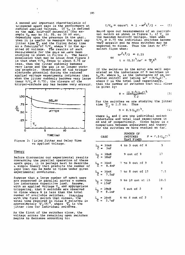
185
A second and important characteristic oftriggered spark gaps is the performance atreduced applied voltage. If Vo is definedas the muz. hold-off potential (for ex-ample Vo may be 10, 20, or 30 kV etc,depending upon the pressure in the gap),then it is useful to measure the spark gapjitter time TTj and the firing delay timeas a function of V/V where V is the ap-plied DC voltage. The results of suchmeasurements for the gsf-s we nave beenstudying is shown in Ficure 3. The basicconclusion that may be drawn from Figure 3is that when v/vo drops to about 0.75 orless, then the jitter suddenly becomesvery large and the gap is no longer work-ing properly. Observation of the triggerelectrode potential during the reducedapplied voltage experiments indicates thatwhen the jitter suddenly becomes very large
« 075) f h
/2 -- (1)
(near V/Voy y
0.75), the closure of theotrigger-cathode gap has become very erratic.
TIME(ns)
Figure 3: Firing Jitter and Delay Timevs Applied Voltage.
Before discussing our experimental resultsconcerning the parallel operation of thesespark gaps, it is perhaps best to describe& simple theory that predicts the number ofgaps that can be made to close under givenexperimental conditions.
Suppose that a large number of spark gapsare connected in parallel across a commonlow inductance capacitive load. Assume,with an applied voltage V Q and appropriatetriggering, that N switches are observedto close where N is less than the totalnumber of available switches. Startingwith the first switch that closes, thetotal time required to close N switches isapproximately T j (N) , where "TL is thejitter time for individual switches.
As the first of the switches close, thevoltage across the remaining open switchesbegins to decrease according to:
Baeod upon our measurements of an individ-ual switch as shown in Figure 3, if VQ isthe maximum hold-off voltage, then whenV/Vo a 0.75 the individual switches becomevery erratic and no more switches may beexpected to close. Thus the last or Ktr-switch fires when:
ur2t2/2 » 0.25
t =
If the switches in the array are well sep-arated so the inductance of N switches isL_/N, where L is the inductance of an, is-olated switch, and taking US' =(N/LOC)'
5,where C is the total load capacitance,then the number of switches that will closeis given by:
M = (O-5)'5(I.r,C)35 (3)
For the switches we are studying the jittertime 2f as 1.5 ns. Thus
N = 0.5 (LQC)* 5, (4 I
where L_ and C are the individual switchinductance and total load capacitance ir.nH and nF respectively. Given below is acomparison between experiment and theoryfor the switches we have studied so far.
CASENUMBER OFSWITCHES N =THAT FIRED
L o = 30nH 4 to 5 out of 6C = 3nF
L o = 30nHC = 38nF
Lo = 30nHC = 8.4nF
L o = 30nHC = 7.5nF
L, = 30nHC = 15nF
i = 39nH8 = 8.1nF
9 out of 9 17
7 to 8 out of 9 S
7 to 8 out of 15 7.5
9 to 10 out of 15 10.5
5 out of 5 9
L = 39nH A to 5 out Of 58 = 2.7nF
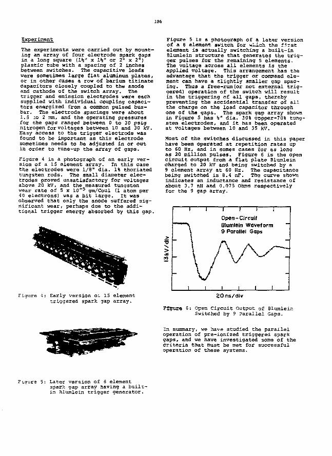
186
Experiment
The experiments were carried out by mount-ing an array of four electrode spark gapsin a long square (IV x 1%" or 2" x 2")plastic tube with a spacing of 2 inchesbetween switches. The capacitive loadswere sometimes large flat aluminum plates,or in other cases a row of barium titinatecapacitors closely coupled to the anodeand cathode of the switch array. Thetrigger and emission electrodes were eachsupplied with individual coupling capaci-tors energized from a common pulsed bus-bar. The electrode spacings were about1.5 M 2 mm, and the operating pressuresfor the gaps ranged between 0 to 30 psignitrogen for voltages between 10 and 30 kV.Easy access to the trigger electrode wasfound to be important as this electrodesometimes needs to be adjusted in or outin order to tune-up the array of gaps.
Figure 4 is a photograph of an early ver-sion of a 15 element array. In this casethe electrodes were 1/8" dia. 1% thoriatedtungsten rods. The small diameter elec-trodes proved unsatisfactory for voltagesabove 20 kV, and the measured tungstenwear rate of 5 x 10~5 gm/Coul (1 atom per4 0 electrons) was a bit large. It wasobserved that only the anode suffered sig-nificant wear, perhaps due to the addi-tional trigger energy absorbed by this gap.
Figure 4: Early version oi IS elementtriggered spark gap array.
Figure 5 is a photograph of a later versionof a 6 element switch for wliich the firstelement is actually switching a built-inBlumlein structure that generates the trig-ger pulses for the remaining 5 elements.The voltage across all elements is theapplied voltage. This arrangement has theadvantage that the trigger or command ele-ment can have a slightly smaller gap spac-ing. Thus a free-run(or not external trig-gered) operation of the switch will resultin the triggering nf all gaps, therebypreventing the accidential transfer of allthe charge on the load capacitor throughone of the gaps. The spark gap array shownin Figure 5 has h" dia." 30% copper-70% tung-sten electrodes, and it has been operatedat voltages between 10 and 35 kV.
Most of the switches discussed in this paperhave been operated at repetition rates upto 60 Hz, and in somes cases for as longas 20 million pulses. Figure 6 is the opencircuit output from a flat plate Blumleincharged to 20 kV and being switched by a9 clement array at 60 Hz. The capacitancebeing switched is 8.4 nF. Ths curve shownindicates an inductance and resistance ofabout 3.7 nH and 0.075 Ohms respectivelyfor the 9 gap array.
I i I TOpen-CircuitBlumlein Waveform9 Parallel Gaps
I I2Ons/div
6: Open Circuit Output of BlumleinSwitched by 9 Parallel Gaps.
In summary, we have studied the paralleloperation of pre-ionized triggered sparkgaps, and we have investigated some of thecriteria that must be met for successfuloperation of these systems.
Figure 5: Later version of. 6 elementspark gap array having a built-in Blumlein trigger generator.
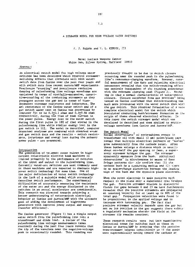
187
A STREAMER MODEL FOR HIGH VOLTAGE WATER SWITCHES
F. J. SAZAMA and V. L. KENYON, III
Naval Surface Weapons CenterWhite Oak, Silver Spring, Maryland 20910
Abstract
An eleccrical switch model for high voltage waterswitches has been developed which predicts streamer-switching effects that correlate well with water-switch data from Casino over the past four years andwith switch data from recent Aurora/AMP experiments.Preclosure "rounding" and postclosure resistivedamping of pulseforming line voltage waveforms areexplained in terms of spatially-extensive, eapaci-tive-coupling of the conducting streamers as theypropagate across the gap and in terms of time-dependent streamer resistance and inductance. Thearc resistance of the Casino water switch and of agac switch under test on Casino was determined bycomputer fit to be 0.5+0.1 ohms and 0.3+0.06 ohmsrespectively, during the time of peak current inthe power pulse. Energy lost in the water switchduring the first pulse is 18% of that stored in thepulseforming line while similar energy lost in thegas switch is 11%. The model is described, computertransient analyses are compared with observed waterand gas switch data and the results - switch resist-ance, inductance and energy loss during the primarypower pulse - are presented.
IntroductionThe generation of teiawatt power pulses in high-current relativistic electron beam machines islimited primarily by the performance of switchesat the input and output to the pulseforming line.Currently water-arc switches are most commonly usedir. these machines and are expected to dominate high-power switch technology for some time. One ofthe major deficiencies of water switch technologyis the lack of a suitable model which accuratelydescribes switch performance. The experimentaldifficulties of accurately measuring the resistanceof the water arc and the energy dissipated in theswitches in an actual accelerator are considerable.This research was directed towards achieving abetter understanding of water-switch electricalbehavior at Casino and Aurora/AMP with the ultimategoal of aiding the development of high-powergenerators with improved power output and energy-transfer efficiency.
The Casino generator (Figure 1) has a single outputwater switch from the pulseforming line into atransformer and diode load. A review of thepulseforming line voltage measurements takenroutinely during the past four years reveals thatthe tip of the waveform near the negative-voltagepeak is occasionally rounded. This rounding was
previously thought to be due to switch closureoccurring near the rounded peak in the pulseformingline's resonance-charging waveform. However, care-ful measurement of the Marx and pulseline electricalparameters revealed that the switch-rounding effectwas entirely independent of the rounding associatedwith the resonant charging peak (Figure 2). Round-ing is thus a normal characteristic of water-switchclosure. Closure waveforms from gas switches'"" beingtested on Casino confirmed that switch-rounding wasmuch more pronounced with the water switch than withthe gas switch. This prompted formulation of a morecomplete electrical model for the switch whichpostulated conducting bush/streamer formation as theorigin of these observed electrical effects. Inthis paper tne switch streamer model which vasdeveloped is described and then applied to switch-voltage waveforms from Casino and Aurora/AMP.
The Switch Model 2
Recent observations of prebreakdown events intransformer oil with small (2 mm) point/plane gapsreveal that multiple electrical pathways or "bushes"grow subsonically from the cathode point. Afterthese bushes enlarge a distance which is usuallyabout one—half the gap spacing or less, a super-sonic streamer bridges the gap. The streamerapparently emanates from the bush. Additionalobservations^ iii nitrobenzene by means of Kerrfringe patterns dir^ -tly confirm that (1) thecathode bush is a conducting medium and (2) thereis no space-charge distortion between the leadingedge of the bush and the opposite plane electrode.
When the point electrode is made positive withrespect to the plane only a supersonic tree bridgesthe gap. Positive streamer studies in dielectricfluids for gaps between 6 and 25 mm have furthermorerevealed that the positive streamers are propagatedat constant velocity for at least up to 90% of thetotal gap. Propagation velocities were found tobe proportional to the applied voltage and todecrease with increasing gap. The fact thatpositive streamer velocity depends upon the gap butnot on its position in the gap suggests there existsa regulatory mechanism whereby the field at thestreamer tip remains constant.
These research results were put into quantitativeelectrical terms for switches such as those onCasino or Aurora/AMP by positing that the positivetree—streamer behaves capacitively as if the anodewere supersonically moving toward the cathode at
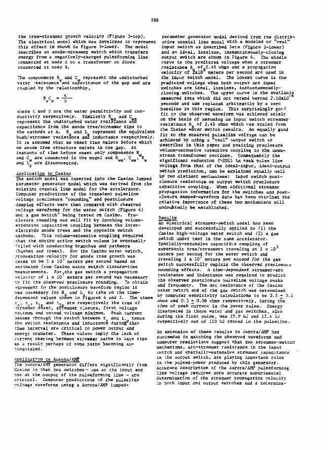
las
the tree-streamer growth velocity (Figure 3-top).The electrical model which was developed to representthis effect is shown in Figure 3-lower. The medaldescribes an anode-streamer switch which transfersenergy from a negatively-charged pulseforming lineconnected at node A to a transformer or diodeconnected at node B.
The components it and C represent the undisturbedwater resistance and capacitance of the gap and arecoupled by the relationship,
where E and o are the water permittivity and con-ductivity respectively. Similarly R and Crepresent the undisturbed water resistance arilcapacitance from the anode tree/streamer tips tothe cathode at A. E and L represent the equivalentbush/streamer resistance ant inductance respectively.It is assumed that an onset time exists before whichno anode tree structure exists in the gap. Atinstants of time before onset only components Rand C are connected in the model and R , C , Rand I." are disconnected.
Application to CasinoThe switch model was inserted into the Casino lumpedparameter generator model which was derived from theexisting coaxial line model for the accelerator.Computer predictions of the transient pulselinevoltage preclosure "rounding" and postclosuredamping effects were then compared with observedvolcage waveforms for the water switch (Figure 4)and a gas switch being tested on Casino. Pre-closure rounding was well fit by invoking volume-extensive capacitive coupling between the inter-electrode anode trees and the opposite switchcathode. This volume-extensive coupling requiredchat the entire active switch volume be eventuallyfilled with conducting branches and pathways(bushes and trees). For the Casino water switch,prooagarion velocicv for anode tree growth wastaken to be 5 x 10 meters per second based onestimates from Casino water switch closure-timexeasurements. For7the gas switch a propagationvelocity of 1 x 10 meters per second was necessaryco fie che observed preclosure rounding. To obtainagreement in the pcstclosure waveform region itwas necessary for R and L co take on the time-dependent values shown in Figures 4 and 5. The times£ , c , t.. and tn are respectively the time ofscreamer onset, streamer closure, first voltagemaximum and 3econd voltage minimum. Peak currentpasses through the switch between t and t1 hencethe switch resistance and inductance during''thattime interval are critical to power output andenergy transfer. These values imply the lack ofcurrent sharing between streamer paths in late timeas a result perhaps of some paths becoming ex-tinguished.
Application to Aurora/AMPThe Aurora/AMP generator differs significantly fromCasino in that two switches- one at the input andone at the output of the pulseforming line - arecritical. Computer predictions of the pulselinevoltage waveforms using a Aurora/AMP lumped-
parameter generator model derived from the distrib-utive coaxial line model with a modeled or "real"input switch as described here (Figure 2-lower)and an ideal, lossless, instantaneously-closingoutput switch are shown in Figure 6. The middlecurve is the predicted voltage when a streamerresistance R of,2.45 ohms and a propagationvelocity of 2x10 meters per second are used inthe input switch model. The lowest curve is thepredicted voltage when both output and inputswitches are ideal, lossless, instantaneously-closing switches. The upper curve is the availablemeasured data which did net extend beyond 2.10x10"seconds and was replaced arbitrarily by a zerobaseline in this region. This surprisingly goodfit to the observed waveform was achieved solelyon the basis of assuming an input switch streamerresistance R of 2.45 ohms which vas scaled fromthe Casino water switch results. An equally goodfit to the observed pulseline voltage can beachieved by using a "real" output switch asdescribed in this paper and positing preclosurevolume-extensive capactive coupling to the down-stream transformer sections. Consequently thesignificant reduction ( 202) in peak pulse linevoltage from that of the Ideal-inpuc, ideal-outputswitch prediction, can be explained equally wellby tvo distinct mechanisms: input switch post-closure resistar.ee or output switch preclosurecapacitive coupling. When additional streamerpropagation information for the switches and post-closure damped-waveform data has been obtained therelative importance of these two mechanisns willundoubtedly be established.
ResultsAn electrical streamer-switch model has beendeveloped and successfully applied to (1) theCasino high-voltage water switch and (2) a gasswitch under test in the some accelerator.Spatially-extensive capacitive coupling ofsupersonic tree/streamers traveling at 5 x 10J
meters per second for the water switch andtraveling 1 x 10 meters per second for the gasswitch successfully explain the observed preclosuiirounding effects. A time-dependent 3treamer-arcresistance and inductance was required to predictthe observed postclosure pulseline voltage peaksand frequency. The arc resistance of the Casinowater switch and of the gas switch was determinedby computer sensitivity calculations to be 0.5 + 0.1ohms and 0.3 + 0.06 ohms respectively, during thetime of peak current in the power pulse. Energydissipated in these water and gas switches, alsoduring the first pulse, was 19.9 kj and 12.4 kJrespectively out of 110 kj stored in che pulseline.
An extension of these results to Aurora/AMP hassucceeded in matching the observed waveforms andcomputer predictions suggest that two streamer-switchmechanisms, arc-streamer resistance in the inputtwitch and spatially-extensive streamer capacitancein che output switch, are playing important rolesin che pulsed-power produced by this generator.Accurate description of the Aurora/AMP pulseformingline voltage requires more accurate experimentaldetermination of the streamer propagation velocityin both input and output switches and a datermina-
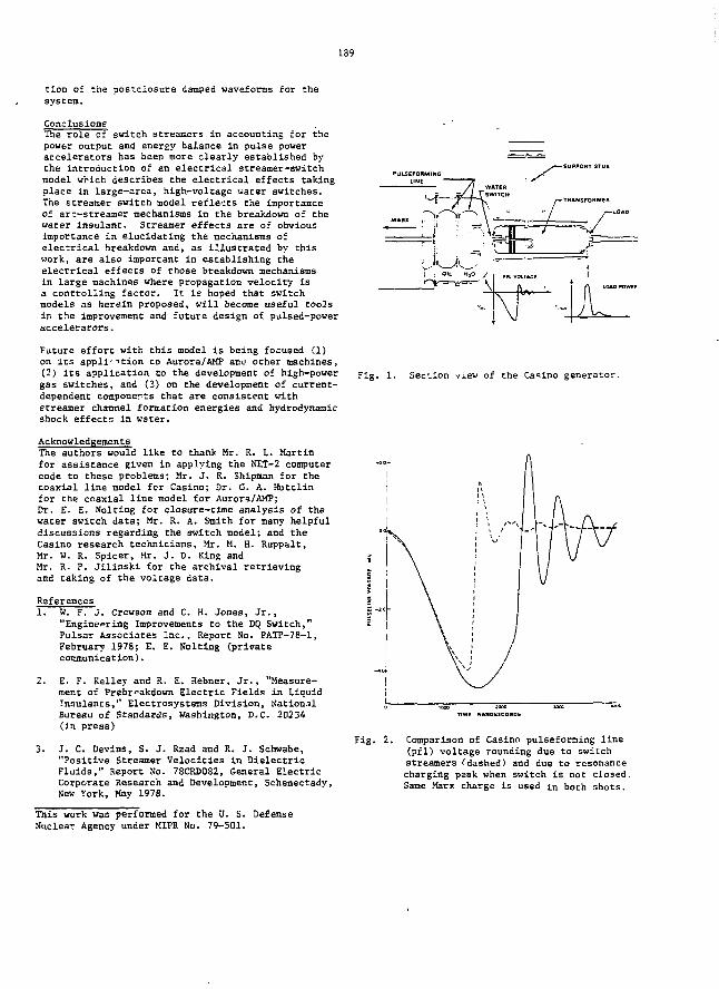
189
tion of the postclosure damped waveforms for thesystem.
ConclusionsThe role of switch streamers in accounting for thepower output and energy balance in pulse poweraccelerators has been more clearly established bythe introduction of an electrical streamer-switchmodel which describes the electrical effects takingplace in largs-area, high-voltage water switches.The streamer switch model reflects the importanceof arc-streamer mechanisms in the breakdown of thewater insulant. Streamer effects are of obviousimportance in elucidating the mechanisms ofelectrical breakdown and, as illustrated by thiswork, are also important in establishing theelectrical effects of those breakdown mechanismsin large machines where propagation velocity isa controlling factor. It is hoped that switchmodels as herein proposed, will become useful toolsin the improvement and future design of pulsed-poweraccelerators.
Future effort with this model is being focused (1)on its applirition to Aurora/AMP and other machines,(2) its application to the development of high-powergas switches, and (3) on the development of current-dependent components that are consistent withstreamer channel formation energies and hydrodynamicshock effects in water.
AcknowledgementsThe authors would like to thank Mr. R. L. Martinfor assistance given in applying the NF.T-2 computercode to these problems; Mr. J. R. Shipman for thecoaxial line model fcr Casino; Dr. G. A. Huttlinfor the coaxial line model for Aurora/AMP;Dr. E. E. Nolting for closure-time analysis of thewater switch data; Mr. R. A. Smith for many helpfuldiscussions regarding the switch model; and theCasino research technicians, Mr. M. H. Ruppalt,Mr. W. R. Spicer, Mr. J. D. King andMr. R. P. Jilinski for the archival retrievingand taking of the voltage data.
References1. W. F. J. Crewson and C. H. Jones, Jr.,
"Engineering Improvements to the DQ Switch,"Pulsar Associates Inc., Report No. PATP-78-1,February 1978; E. E. Nolting (privatecommunication).
2. E. F. Kelley and R. E. Hebner, Jr., "Measure-ment of Prebr^akdown Electric Fields in LiquidInsulants," Electrosystems Division, NationalBureau of Standards, Washington, D.C. 20234(in press)
3. J. C. Devins, S. J. Rzad and R. J. Schwabe,"Positive Streamer Velocities in DielectricFluids," Report No. 78CRD082, General ElectricCorporate Research and Development, Schenectady,New York, May 1978.
PULSEFORMINGLINE
SUPPORT STUB
Fig. 1. Section view of the Casino generator.
TIMC «*MOEICONDB
Fig. 2. Comparison of Casino pulseforning line(pfl) voltage rounding due to switchstreamers (dashed) and due to resonancecharging peak when switch is not closed.Same Marx charge is used in both shots.
This work was performed for the U. S. DefenseNuclear Agency under MIPR No. 79-501.
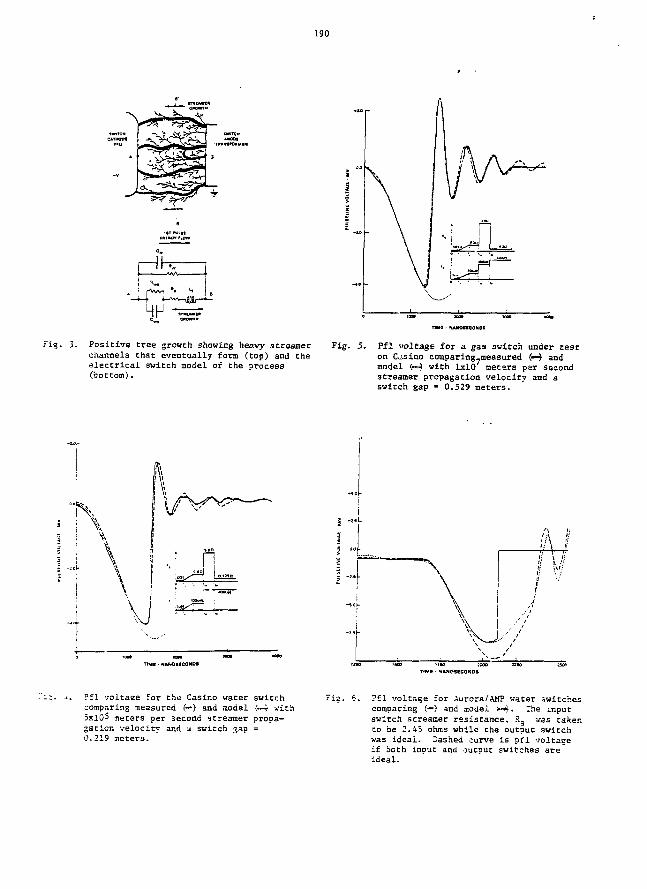
190
I I XTHUMtft
Fig. 3. Positive tree growth showing heavy streamerchannels that eventually form (top) and theelectrical svitch model of the process(bottom).
1AMOHCONOI
Fig. 5. Pfl voltage for a gas switch under teston Casino comparing-measured (* andmodel <r»3 with 1x10 metars per secondstreamer propagation velocity and aswitch gap - 0.529 meters.
'\ I-I :l I:'.'V
1:
i?f
Ii
\
\\
1-n1!
• NAUOIICONDI
Pfl voltaee for che Casino water switchcomparing measured (—) and model (•—» vith5x105 meters per second streamer propa-gation velocity and a switch gap =0.219 meters.
Fig. 6. Pfl voltage for Aurora/AMP water switchescomparing (—) and model (*'*$. The inputswitch screamer resistance, S. was taker,to be 2.45 ohms while the output switchwas ideal. Dashed curve is pfl voltageif both input and output switches areideal.
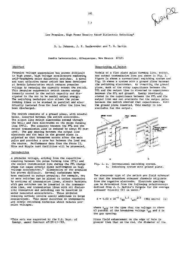
191
T.i
Low Prepulse, High Power Density Water Dielectric Switching*
D. L. Johnson, J. P. VanDevender and T. H. Martin
Sandia Laboratories, Albuquerque, New Mexico 8718 3
Abstract
Prepulse voltage suppression has proven difficultin high power, high voltage accelerators employingself-breakdown water dielectric switches. A noveland cost effective water switch has been developedat Sandia Laboratories which reduces prepulsevoltage by reducing the capacity across the switch.This prepulse suppression switch causes energyformerly stored in the switch capacity and dis-sipated in the arc to be useful output energy.The switching technique also allows the pulseforming lines to be stacked in parallel and elec-trically isolated from the load after the line haobeen discharged.
The switch consists of a ground plane, with severalholes, inserted between the switch electrodes.The output line switch electrodes extend throughthe holes and face electrodes on the pulse formingline (PFL). The capacity between the PFL and theoutput transmission line is reduced by about 80 per-cent. The gap spacing between the output lineelectrode and the hole in the ground plane isadjusted so that breakdown occurs after the mainpulse and provides a crow bar between the load andthe source. Performance data from the Proto II,Mite and Ripple teBt facilities will be presented.
Introduction
A prepulse voltage, arising from the capacitivecoupling between the pulse forming line (FFL) andthe output transmission line during the PFL chargephase can cause erratic diode performance on highvoltage accelerators. Elimination of the prepulsehas proven difficult. Several techniques havebeen employed to reduce prepulse; for example, twoor more switches can be placed in series separatedby sections of transmission lines, plastic barrierswith gas switches can be inserted in the transmis-sion line, and transmission lines with oil dielec-tric insulation and switching can be inserted inwater insulated accelerators. These prepulsereducing methods involve costly additions to largeaccelerators. This paper describes an inexpensiveand sinple switching technique which reduces pre-pulse voltages.
*This work was supported by the U.S. Dept. ofEnergy, under Contract AT(29-l)-789.
Description of Switch
Models of a flat plate pulse forming line, switch,and output transmission line are shown in Fig. 1.Figure la shows a conventional switching system andFig. 1b shows a system with a ground plane betweenthe switching electrodes. By inserting the groundplane, much of the stray capacitance between thePFL and the output line is diverted to capacitancebetween the PFL and ground. Energy previouslystored in the capacitance between the PFL and theoutput line was not available for the output pulsebecause the switch shorted that capacitance. Withthe ground plane inserted, this energy is nowavailable for the output.
,Wtit FMM1RC
Fig. 1. a. Convensional switching system.b. Switching system with ground plane.
The electrode tips of the switch are field enhancedso that the breakdown streamer channels originatefrom the negative electrode. Electrode spacingscan be determined from the following relationshipsderived from J. C. Martin's formula for the averagestreamer velocity (U) in water.
d - 4.02 x 10"4 V 1.1BD ceff
2/3 (MKS units) (1)
where tgf£ is the time that the voltage is above63 percent of the breakdown voltage VgD and d isthe gap spacing.
Since field enhancement on the edge of hole isgreater than that on the rod, the diameter of the
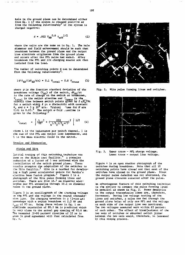
192
hole In the ground plane can be determined eitherfrom Eq. 1 If the system Is charged positive orfrom the following relationship if the system ischarged negative:
.022 V, 0.6BD C6ff
1/2(2)
where the units are the same as in Eq. 1. The holediameter and field enhancement should be such thatbreakdown between the ground plane and the outputline electrode originates from the ground planeand occurs after the PFL pulse had ended. Afterbreakdown the PFL and its charging source are r.heaisolated from the load.
The number of switching points S can be determinedfrom the following relationship3:
2<7VBD/CdVBD/dt) - 0 .1 0.8 (3)
where <T is the fraction standard deviation of thebreakdown voltage (V^p) of the switch, dVBt)/dtis the rate of charge on Che switch at breakdown,
Fig. 2. Mite pulse forming lines and switches.
and " t r a n 8gi
Is thetotal t r a n 8
transit time between switch points given by I ^for a switch width i in a dielectric with constanter and c • 3 x 10° m/s. Typical T.ues for <T are0.01 to 0.03. The switch e-fold -isetime isgiven by the following:
total1/2
(4)
where L is the Inductance per switch channel, 2 isthe sum of the FFL and output line impedances, andE is the mean electric field in the switch.
Results and Discussion
Ripple and Mite
Initial testing of this switching technique wasdone en the Sipple test facility. A prepulsereduction of a rsctor of 5 was achieved with theinstallation of the switch ground plane. Theseresults prompted the adaptation of the switches tothe Mlta facility. Mite is a testbed for develop-ing a high power accelerator aodule for Sandia'selectron beam fusion program.3 Figure 2 is aphotograph of the Mite pulse forming lines andswitches. There are five 12.7 mm diameter elec-trodes per PFL extending through 10.2 cm diameterholes in Che ground plane.
Figure 3 is an oscillograph of the charging voltage3d Che PFL and the voltage in the output transmis-sion line. The charging waveform is a (1-cos wt)waveshape vith a switch breakdown ?t 2.3 MV and~n£f of 90 as. tTsing these values in Eq. 1 anelectrode separation of 80.3 am is predicted whichis very close to the actual gap spacing of 82.6 mm.Tha measured 10-90 percent risetime of 22 ns isalso in good agreement with that calculated fromZq. i.
Fig. 3. Opper trace - PFL charge voltage.Lower trace - output line voltage.
Figure A is an open shutter photograph of theswitches during breakdown. Note that all 10switching points tiave closed and that most of theswitches have closed to the ground plane. Sincethe output pulse duration was not shortened, theground plane closures occurred after the pulse.
An advantageous feature of this switching techniqueis the ability to connect the pulse forming linesin parallel as shewn in Fig. 2. Power densitiesin the output transmission lines are, therefore,increased. During low voltage Cesting of thelines and switches, a pulse was fed through thesground plane hole* of only one PFL and the volcageon each side of die output line was aonitored.The two voltages measured were within 85 percentof each other. The effect of Disadjustment of chetwo sets of switches or abnormal switch jitterbetween the two sets would, therefore, be lessenedby this mixing process.
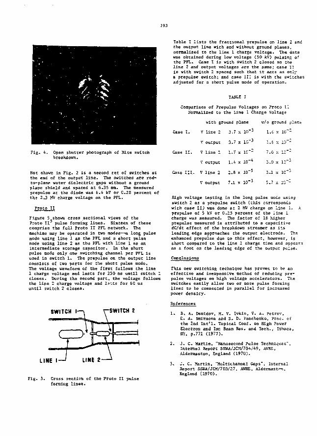
293
Fig. 4. Open shutter photograph of Mite switchbreakdown•
Not shown in Fig. 2 is a second set of switches atthe end of the output line. The switches are rod-to-plane water dielectric gaps without a groundplane shield and spaced at 6.35 mm. The measuredprepulse at the diode was 6.4 kV or 0.28 percent ofthe 2.3 MV charge voltage on the PFL.
Proto II
Figure 5 shows cross sectional views of theProto II pulse forming lines. Sixteen of thesecomprise the full Proto II PFL network. Themachine may be operated in two modes—a long pulsemode using line 1 as the PFL and a short pulsenode using line 2 as the PFL with line 1 as anintermediate storage capacitor. In the shortpulse mode only one switching channel per PFL isused in switch 1. The prepulse on the output lineconsists of two parts for the short pulse mode.The voltage waveform of the first follows the line1 charge voltage and lasts for 250 ns until switch 1closes. During the second part, the voltage followsthe line 2 charge voltage and Is^ts for 60 nsuntil switch 2 closes.
SWITCH I r-SWITCH 2
LINE I- LINE 2
Fig. 5. Cross section of the Proto II pulseforming lines.
Table I lists the fractional prepulse on line 2 andthe output line with and without ground planes,normalized to the line 1 charge voltage. The datawas obtained during low voltage (50 kV> pulsing ofthe PFL. Case I is with switch 2 closed so theline 2 and output voltages are the sane; case IIis with switch 2 spaced such that it acts as onlya prepulse switch; and case III is with the switchesadjusted for a short pulse node of operation.
TABLE I
Comparison of Prepulse Voltages on Proto IINormalized to the line i Charge Voltage
Case I.
with ground plane
V line 2 3.7 x 10'-3
-3V output 3.7 x 1C
Case II. V line 2 1.7 x 1G~2
V output 1.4 x 1C"4
Case III. V line 2 2.8 x 10"5
w/o ground plane
1.6 x 1C"2
1.6 x 1CT:
7.0 s 1C":
3.0 x ID"3
*3
V output 7.1 x 10,-3
3.1 x 1C
5.7 x "-Z~~
High voltage testing in the long pulse mode usingswitch 2 as a prepulse switch (this correspondswith case II) was done at 2 MV charge on line 1. Aprepulse of 5 kV or 0.25 percent of the line 1charge was measured. The factor of 18 higherprepulse measured is attributed to a capacitivedC/dt effect of the breakdown streamer as itsleading edge approaches the output electrode. Theenhanced prepulse due to this effect, however, isshort compared to the line 1 charge time and appearsas a foot on the leading edge of the output pulse.
Conclusions
This new switching technique has proven to be aneffective and inexpensive method of reducing pre-pulse voltages on high voltage accelerators. Theswitches easily allow two or more pulse forminglines to be connected in parallel for increasedpower density.
References
1. B. A. Demidov, M. V. Ivkin, V. A. Petrov,E. A. Sniraova and S. D. Fanchenko, Proc. ofthe 2nd Int'l. Topical Conf. on High PowerElectron and Ion Beam Res. and Tech., Ithaca,NY, p.771 (1977).
2. J. C. Martin, "Nanosecond Pulse Techniques",Internal Report SSWA/JCM/704/49, AWRE, 'Aldermaston, England (1970).
3. J. C. Martin, "Multichannel Gaps", InternalHeport SSWA/JCM/703/27, AWRE, Aldermast^n,England (1970).
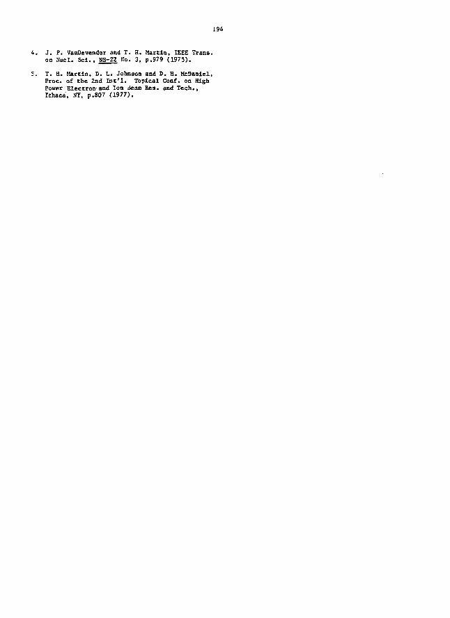
194
4. J. P. VanDevender and T. H. Martin, IEEE Trans,on Nucl. Sci., NS-22 No. 3, p.979 (1975).
5. T. H. Martin, D. L. Johnson and 0. H. McDanlel,Proc. of the 2nd Iiit'l. Topical Conf. on HighPower Electron-aad Ion <Jeam Res. and Tech.,Ithaca, XY, p.807 (1977).
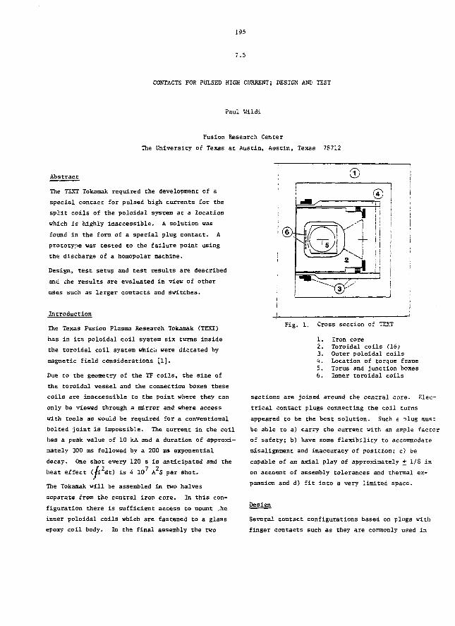
195
7.5
CONTACTS FOR PULSED HIGH CURRENT; DESIGN AND TEST
Paul Wildi
Fusion Research Center
The University of Texas at Austin, Austin, Texas 78712
Abstract
The TEXT Tokamak required the development of a
special contact for pulsed high currents for the
split coils of the poloidal system at a location
which is highly inaccessible. A solution was
found in the form of a special plug contact. A
prototype was tested to the failure point using
the discharge of a homopolar machine.
Design, test setup and test results are described
and die results are evaluated in view of other
uses such as larger contacts and switches.
Introduction
The Texas Fusion Plasma Research Tokamak (TEXT)
has in its poloidal coil system six turns Inside
the toroidal coil system which were dictated by
magnetic field considerations [1].
Due to the geometry of the TF coils, the size of
the toroidal vessel and the connection boxes these
coils are inaccessible to the point where they can
only be viewed through a mirror and where access
with tools as would be required for a conventional
bolted joint is impossible. The current in the coil
has a peak value of 10 kA and a duration of approxi-
mately 300 ms followed by a 200 ms exponential
decay. One shot every 120 s is anticipated and the
heat effect (/i2dt) is 4 107 A2S per shot.
The Tokamak will be assembled in two halves
separate from the central iron core. In this con-
figuration there is sufficient access to mount .he
inner poloidal coils which are fastened to a glass
eFoxy coil body. In the final assembly the two
Fig. 1. Cross section of TEXT
1. Iron core2. Toroidal coils (16)3. Outer poloidal coils4. Location of torque frame5. Torus and junction boxes6. Inner toroidal coils
sections are joined around the central core. Elec-
trical contact plugs connecting the coil turns
appeared to be the best solution. Such a plug must
be able to a) carry the current with an ample factor
of safety; b) have some flexibility to accommodate
misalignment and inaccuracy of position; c) be
capable of an axial play of approximately + 1/S in
on account of assembly tolerances and thermal ex-
pansion and d) fit into a very limited space.
Several contact configurations based on plugs with
finger contacts such as they are commonly used in
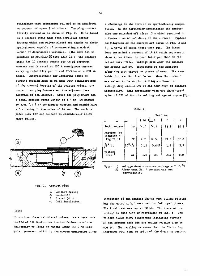
196
switchgear were considered bu; had to be abandoned
on account of space limitations. The plug contact
finally arrived as is shown in Fig. 2. It is based
on a contact strip made from beryllium copper
louvers which are silver plated and thanks to their
springiness, capable of accommodating a modest
amount of dimensional variance. (The material in
question is MULTXLAM® type LAI/.25.) The contact
strip has 10 contact points per in of apparent
contact and is rated at 350 A continuous current
carrying capability per in and 17.3 kA on a 200 ms
basis. Interpolations for different times of
current loading have to be made with consideration
of the thermal inertia of the contact points, the
current carrying louvers and the adjacent base
material of the contact. Since the plug shown has
a total contact strip length of 5.4 in, it should
be good for 2 kA continuous current acd should have
a 3 s rating in the order of 44 kA. The antici-
pated duty for our contact is considerably below
these values.
(3)
a discharge in the form of an aperiodically damped
pulse. In the particular experiments the excita-
tion was switched off after .5 s which resulted in
a faster than normal decay of the current. Typical
oscillograms of the current are shown in Fig. 3 and
4. A toril of seven tests were run. The first
four tests had a current of 14 kA which represents
about three times the heat input per shot of the
actual duty cycle. Voltage drop over the contact
was around 200 mV. Inspection of the contacts
after the test showed no craces of wear. The sane
holds for test No. 4 at 34 kA. When the current
was raised to 54 kA the oscillogram showed a
voltage drop around 450 mV and some sign of contact
instability. This correlates with the theoretical
value of 370 mV for the melting voltage of copoer[2].
TABLE 1
Peak current
HeatinglocationFigure
/i 2dt
Voltagedrop *
CatA-1)
kA
°C
loVs
mV
1
14
2
0
to 4
p2
.11
120
Test
S
34.4
12.S
0.645
300
No.
6
S3
29
1
9
0
6
450
7
80.1
67.0
3.5
800
Note: 1) Voltage drop = contact voltage * 2.10 i2) After test No. 7 contact was not
serviceable.
Fig. 2. Contact Plug
1.2.
3.
Contact springConductorBrazed jointCoil insulation
To confirm these calculated values, tests were con-
ducted at the Center for Electro-Mechanics of the
University of Texas at Austin using the 5 MJ homo-
polar generacor which in the chosen connection gives
Inspection of the contact showed very slis'nt pitting,
but the material had retained its full springiness.
The final test was run at 80 kA. The trace of the
voltaga in this test is reproduced in Fig. 5. The
voltage shows heavy fluttering indicating burning
on the contact spot and the median voltage drop is
800 aV. The oscillogram shows that the fluttering
increases with time in spite of the decaying current
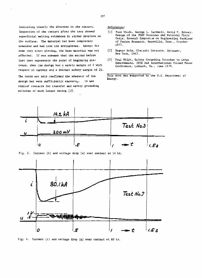
197
indicating clearly the distress in the contact.
Inspection of the contact after the test showed
superficial melting evidenced by silver droplets on
the surface. The material had been completely
annealed and had lost its springiness. Except for
some very nlnor pitting, the base material was not
affected. If one assumes that the second before
last test represents the point of beginning dis-
tress, then the design has a safety margin of 5 with
respect to current and a thermal safety margin of 25.
The tests not only confirmed the adequacy of the
design but were sufficiently encoura^- to use
similar contacts for transfer and safety grounding
switches of much larger rating [3].
References:
[1] Paul Kiidi, George L. Cardwell, David F. Brower.Design of the TEXT Toroidal and Poloidal FieldCoils, Seventh Symposium on Engineering Problemsof Fusion Research, Knoxville, Tenn., October1977.
[2] Ragnar Holm, Electric Contacts, Springer,New York, 1967.
[3] Paul Wildi, Safety Grounding Switches in LargeExperiments, IEEE 2nd International Pulsed PowerConference, Lubbock, Tx., June 1979.
This work was supported by the U.S. Departmen: ofEnergy.
0 .5* /
Fig. 3. Current (i) and voltage drop (u) over contact at 14 kA.
i.Ss
0 KS /
Fig. 4. Current (i) and voltage drop (u) over contact at 80 kA.
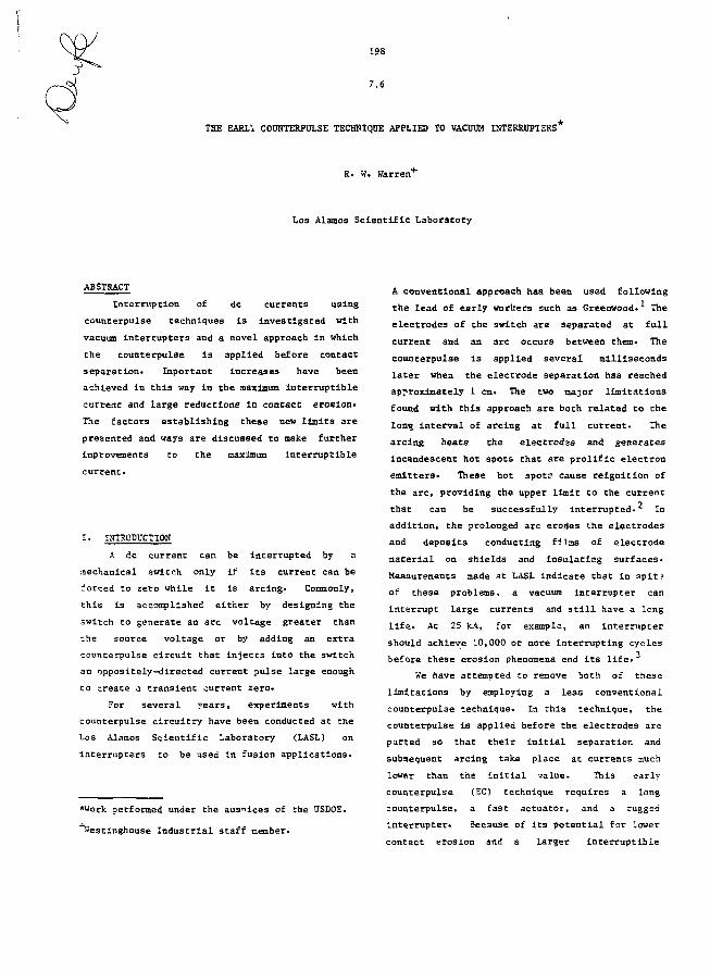
198
7 . 6
THE EARL'i COUNTERPULSE TECHNIQUE APPLIED TO VACUUM INTERRUPTERS*
R. W. Warren"1"
Los Alamos Scientific Laboratory
ABSTRACT
Interruption of dc currents using
counterpulse techniques is investigated with
vacuum interrupters and a novel approach in which
the counterpulse is applied before contact
separation. Important increases have been
achieved in this vay in the maximum interruptible
current and large reductions In contact erosion*
The factors establishing these new limits are
presented and ways are discussed to make further
Improvements Co the maximum interruptible
current*
I. INTRODUCTION
A dc current can be interrupted by a
mechanical switch only if Its current can be
forced to zero while it Is arcing" Commonly,
chis is accomplished either by designing the
switch to generate an arc voltage greater than
the source voltage or by adding an extra
counterpulse circuit that injects into the switch
an oppositely-directed current pulse large enough
co create a transient current zero*
For several years, experiments with
counterpulse circuitry have been conducted at the
Los Alamos Scientific Laboratory (LASL) on
interrupters to be used in fusion applications*
*Work performed under the auspices of the USDOE.
~*«estinghouse Industrial staff member*
A conventional approach has been used following
the lead of early workers such as Greenwood* The
electrodes of the switch are separated at full
current and an arc occurs between them* The
counterpulse is applied several milliseconds
later when the electrode separation has reached
approximately 1 cm* The two major limitations
found with this approach are both related to the
long interval of arcing at full current* The
arcing heats the electrodas and generates
Incandescent hot spots that are prolific electron
emitters* These hot spot? cause reignitlon of
the arc, providing the upper limit to the current
that can be successfully Interrupted* In
addition, the prolonged arc erodes the electrodes
and deposits conducting f^)as of electrode
material on shields and insulating surfaces.
Measurements made at LASL Indicate that in spit?
of these problems, a vacuum Interrupter can
interrupt large currents and still have a lcng
life. At 25 kA, for example, an interrupter
should achieve 10,000 or more interrupting cycles
before these erosion phenomena end its life*
We have attempted to remove both of these
limitations by employing a less conventional
counterpulse technique* In this technique, the
counterpulse is applied before the electrodes are
parted so that their initial separation and
subsequent arcing take place at currents auch
lower than the initial value* This early
counterpulse (EC) technique requires a long
counterpulse, a cast actuator, and a rugged
interrupter* 3ecause of its potential for lower
contact erosion and a larger interruptible
199
current, the EC technique has attracted other
investigators. An air-blast interrupter to be
used with the tokamak JET and a spaclal SF^
switch" used with the Crossed Field Tube are
examples of such developments* Vacuum
interrupters have advantages relative Co these
other types primarily because of the lower
erosion expected for the contacts and the
resulting longer life*
II. THE EARLY COUNTERPIILSE TECHNIQUE
The circuit, discussed in detail elsewhere,
used ir. the tests is shown in Fig* 1* Energy
storage capacitor Cj in conjunction with switches
S, and S2 and inductor Lj establish a slowly
decaying current, I, in VI, the interrupter under
test. The counterpulse is fired by closing
switch S3 which connects capacitor bank C^ to VI.
This generates the desired reverse-current pulse*
i»2, a saturable reactor, helps to shape the
reverse-current pulse so that the switch current
is close to zero for a long time. El is used as
a final dump resistor for the energy initially
stored in C* and C-, and is connected by S^ after
the interruption phenomenon is completed*
Figure 2 shows schematically, the behavior
of the current flowing through VI. At time tQ
the counterpulse is initiated. At tj the current
in the switch passes through zero for the second
time and interruption may occur* At t2 the
capacitor Cj and the saturable reactor L£ have
exhausted their charge and flux so that the
counterpulse ends. For the EC technique to
succeed, VI must open its contacts between t0 and
tj. With this timing an arc will start and burn
at low current and interrupt as the current
passes through zero at tt*
There are two obvious problems with the EC
technique which must be overcome and which have
become the main focus of these investigations*
The first is the difficulty of opening the
interrupter in the short interval between tg and
t| in the face of jitter from various sources*
The second is the rapid development of the
recovery voltage at a time when the arc has
barely extinguished and the electrodes have
barely separated* The possibility of reignition
of the arc at this time is high but can be
reduced by several measures.
1. A high-average velocity of separation of
the electrodes*
2. A large saturable reactor and counterpulse
bank.
3* A snubber circuit (an RC series
combination) placed across VI.
The actuator used in these tests was made by Ross
Engineering Co. It is operated by two repulsion
coils, one stationary and one connected to the
moving electrode of the interrupter. The coils
are energized by a 300 uF capacitor bank charged
to 2 to 5 kV. The peak coil current is several
tens of kiloamperes. The actuator was designed
to maximize the acceleration of the moving
electrode. Accelerations of 10 cm/sec*" have
been achieved. The saturable reactor is composed
of 133 separate 4~mil tape-wound cores, each
threaded by a 4-0 electrical cable. Each of the
cores has a flux ratirg of 0*008 Wb for a total
of about 1 Wb* Because cf the gap-less
tape-wound construction of these cores, their
unsaturated inductance is very large.
The counterpulse bank is unusually large.
We used 360 kJ of capacitance connected in
different ways to provide either 1.8 * 10"3 F at
20 kV or 0.45 " 10"3 F at 40 kV.
III. RESIILTS
The first experiments were performed with a
standard 7-in- interrupter,^ with an actuator
acceleration of 0.3 * 106 cm/sec2, and a
counterpulse bank of 1.8 * 10"^ F. This
arrangement gives the longest possible
counterpulse and potentially the largest
Interruptible current- The modest acceleration
was chosen to avoid possible stress-induced
problems with the actuator or interrupter. With
conventional counterpulse techniques, such an
arrangement would have given a naxtnutc
200
lnterruptlble current of 21 kA, relatively
Independent of recovery voltage.
The experiment proceeded by gradually
raising I, the current to be Interrupted, and at
each current level by varying t^, the interrupter
opening time, over Its full range, from tg to C^.
The experiments were continued with currents up
Co 35 kA at 25 kV, the limit of the test
facilities, with no failures of any kind* A
striking observation concerned the visual
appearance of the switch during interruption*
With conventional counterpulse techniques, the
ceramic envelope lights up brightly due to the
enclosed arc* Wlth 2C techniques, no light could
be se>a. This is consistent with Che reduction
oC the arcing current by a factor of 300 and
arcing time by a factor of 10 produced by EC.
To increase the electrical stresses on the
interrupter the value of Cj was reduced to
0.45 * 10"3 F. This change increased the
recovery voltage by a factor of two and decreased
Che Interval tj-tg for opening the Interrupter by
a factor of two* Under these conditions
reignitions were occasionally observed when t^-t3
was snail, that Is, much less than 100 us* The
major aew effects observed vere a marked Increase
In the Jitter observed in the opening time and a
consistent shift of che average opening cime as
the current increased. These effects combined to
make it difficult Co time the switch's opening to
occur between t0 and tj. This effect set a
naxlmum lnterrupcible current of about 20 kA.
To Investigate this limit, we substituted
three different &-ln. Interrupters for the
original one keeping C 2 -0.45 * 10"3 T. With
conventional techniques these switches could
incerrupc 6, 6, and 8 kA, respectively. With the
EC technique their limits were increased by a
factor of 2 Co 2.5, as determined, again, by the
onset of marked jitter in the opening time and
tcs shift to later times.
Careful neasureoents Identified cwo sources
of che jitter and shift. One was the tendency of
the electrodes to pop apart at high currents.
This shows up as a voltage Jump before t0-
The second problem was of a related kind.
The "openiag" of the switch occurs when the
molten bridge which forms between the electrodes
ruptures. The lifetime of the bridge depends
upon the details of current magnitude, contact
pressure, etc*, In a complex way.
The effect of chese phenomena is to reduce
the range of counterpulse settings within which
an EC Interruption can be achieved. The range is
reduced to zero for currents slightly above
i9 kA, consistent with the findings that 20 kA is
the largest current we can successfully
interrupt.
IV. LIFE TESTS
To test the erosion reduction expected of
the EC technique, a 4-in. interrupter was
subjected to over 1000 Interruption cycles at
10 kA. The interrupter was disassembled and the
contacts examined after these wholly successful
interruptions. The contacts were found to be in
near-new condition, che surface markings being
caused largely by contact rubbing. We estimate a
reduction in erosion brought about by the EC
technique of more than one hundred.
V. CONCLUSIOH
The anticipated features of the EC technique
were reduced electrode erosion and increased
current racings. Substantially Increased ratings
have been realized in these experiments, and the
reduction in erosion Is very large. The
components and techniques used to achieve these
improvements are available, convenient to use,
and relatively reliable.
The new current limit does not appear to be
a basic property of che switches but is instead
associated with the actuator, in particular ulth
the force with which the electrodes are held
closed. Fucure work will attempt to raise the
currenc limit further by employing higher closing
forces.
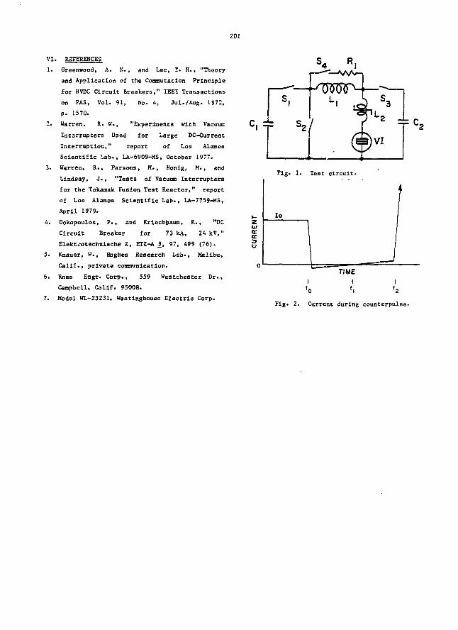
202
VI. REFERENCES
1. Greenwood, A. N., and Lee, T. H.f "Theory
and Application of the Commutation Principle
for HVDC Circuit Breakers," IEEE Transactions
on PAS, Vol. 91, No. 4, Jul./Aug. 1972,
p. 1570.
2. Warren, R. W., "Experiments with Vacuum
Interrupters Used for Large DC-Current
Interruption," report of Los Alamos
Scientific Lab., LA-6909-MS, October 1977.
3. Warren, R., Parsons, M., Honig, M., and
Lindsay, J., "Tests of Vacuum Interrupters
for the Tokamak Fusion Test Reactor," report
of Los Alamos Scientific Lab., LA-7759-MS,
April 1979.
4. Dokopoulos, P., and Krlechbaum, K., "DC
Circuit Breaker for 73 kA, 24 kV,"
Elekti-otechnische Z, E T 2 ^ 1, 97, 499 (76).
5. Knauer, W., Hughes Research Lab., Malibu,
Calif., private communication.
6. R O S E Engr. Corp., 559 Westchester Dr.,
Campbell, Calif. 95008.
7. Model WL-23231, Westinghouse Electric Corp.
C, =fc
Fig. 1. Test circuit.
=t= c.
I
'0 'I *Z
Fig. 2. Current during counterpulse-
202
8.1
INVITEDDEVELOPMENT OF HIGH CURRENT ELECTRON PULSE ACCELERATORS
AT THE INSTITUTE OF HIGH TEMPERATURES
E. A. Abramyan, C. D. Kuleshov
Institute of High Temperatures, USSR Academy of SdsncesKorovinskoe ChausaeeMoscow, 127412, USSR
Abstract
A short analysis of the problems encountered in theacceleration of long (10~* sec and longer) pulsed,relativistic electron beams (REB) is given. A des-cription of clie parameters of the experimental fa-cilities developed to study these long-pulaed beamsis presented, as well.
Over the last 15 years, the power in nanosecondduration electron accelerators has increased by morethan 3 orders of magnitude and the energy contentof these beams has reached several MJ. It is knownthat in accelerators of this type the electric fieldgradient in the acceleration r^ion approaches 0.5MV'cm. Thfe length of the applied pulse is Haltedby the breakdown development time. The rapid devel-opment of nanosecond accelerators has benefited fromthe unique characteristics of cold cathodes, i.e.the high emission density achievable in short pulses(up to I04 A/cm2) and their capability to retaingood emission characteristicsafter arcing or vacuumrupture.
Electron beams of short duration satisfy quite anumber of REB applications, particularly with re-spect to heating of a substance Co thermonucleartemperatures in experimental installations forinertially confined fusion. However, to solve othertasks it is necessary to increase the beam life timeand make the operation more stable. Examples ofother applications are SHF generators, i.e. oscilla-ting relativistic beams; and collective accelerationof ions Ll ]• The further development of severalkiloampere REB's with duration of 10"* - 10"3 sec,and continuous beams in the future, will make itpossible to start experimental research concerningthe problem of energy transfer over large distancesby means of electron beams. [2].
One of the main directions of research on REB con-ducted at our institute is related to finding waysto create long-pulsed electron beams with currentsof the order of 1 kA at an energy of 1 MeV. Theprogram is limed at studying new energy transfercechniaues.
Peculiarities of the Generation of Long-Pulsed In-tensive REE's
It is common knowledge that the current density in
accelerating gaps is limited by the perveaace of
the system and the emitting capability of the cath-
ode. The accelerating fields in existing long-
pulsed and continuous accelerators is about 0.02 -
0.05 MV/cm, considerably less than for nanosecond
duration acceleration. In this case the current
density of the beams to be accelerated is no greater
than several amps per cm**. Some increase of per-
veance of the accelerating system can be achieved
by the installation, between the cathode and anode,
of many intermediate electrodes at appropriate po-
tentials as well as by space charge neutralization.
One approach to the problem of intensive long-pulsed
REB generation is to increase the gradient of the
accelerating electric fieid, another the compression
(focusing) of the beam to much higher densities Chan
the initial low values. In order to make the re-
quired improvements it is necessary to combine both
methods.
The capability of present, existing cathodes - e.g.
lanthanum boride, iridium cerium, overheated cung-
sten, etc. - makes It possible Co achieve current
densities of the order of 10' A/cm^ in pulses of
L0 sec and longer. The primary cask is Co in-
crease Che perveance of che accelerating gaps to
such values as to provide higher currents.
The comparatively slow progress in improving the
voltage hold-off characteristics of non-segmenued
high voltage vacuum gaps makes it impossible ZD
guarantee Che emission of current at high energy in
systems similar to electron guns employing compres-
sion. It is more appropriate Co develop acceier-
acing devices constructed with njany electrodes and
203
many separated parallel beams In tbe sane diode.
In particular, a considerable Improvement in elec-
rical strength of the accelerating tube can be ex-
pected wich the electrode spacing reduced to 10 -
100 um. It is known that micron vacuum gaps and
layers of solid insulation can resist static elec-
tric fields of more than 1 MV/cm. The problem is
to obtain satisfactory electric field intensities
in many-layer structures containing many channels
u r electron acceleration, lo achieve this goal it
is necessary to provide for stable and uniform dis-
tribution of voltages over intermediate electrodes
and, furthermore, to reduce to the utmost the num-
ber of elecrrons lost to the electrodes of the tube
by, for instance, the application of a longitudinal
magnetic field. The fabrication of such jystems
are cf great importance as well.
Energy Recycling - One of the Key Problems in Devel-opment of Experimental Installations With long-Pulsed REB's
The development of high voltage generators to feed
long-pulsed several kA, MeV beams presents no major
obstacle. For this purpose we can use inductive
storage, Marx generators, or transformers. The en-
ergy content of beams that can be employed in the
earlier stages of research will probably not exceed
106 - 107J.
As far as the high voltage generators used in ex-
perimental installations, which are designed for
flexible operation of the accelerating and focusing
systems and for beam transfer, are concerned, their
cost could be considerably reduced if one could re-
cover the electron beam energy. In an Installation
of this kind the collector of the decelerating de-
vice is connected electrically to the cathode, re-
sulting in a closed circuit with the stream of fast
electrons beine an integral segment of the total
current flow [33. Since a complete deceleration of
the electron beam is essentially impossible, there
is a small potential difference between the cathode
and the collector (Au is usually on the order of
several percent of the anode voltage tT, which is
maintained by the power source).
If AU is relatively small compared to the accele-
rating potential, then power and current losses,
AI, in the beam of accelerated electrons will also
be small. The beam power IE can exceed many times
the total of the component sources:
IU»UAI + IAU
and the effective energy content of the Dean can ex-
ceed the energy accumulated in both power sources.
Experimental Facilities For Research, Generation,Transfer and Deceleration of LonR-Pulsed Relativ-JBtic Beams
To study the processes of generation and recovery
of long-pulsed electron beams a test facility was
developed at our institute which could generate
electron beams with the following parameters: elec-
tron energy 0.5 MeV, beam current 100 A, pulse length
100 visec. A Marx generator with the correct pulse
shape 13J to obtain a constant accelerating voltage
during the main part of the pulse was constructed.
The accelerating device is of two types; a simple
diode and a segmented one. The accelerator design
makes it possible to conduct studies of other options
of beam forming systems, e.g. compact multichannel
acceleration tubes with small segmented sections
and the combination of beams in a drift region.
In this system, the electron beam energy recovery
device is mounted inside the same vacuum chamber ar
the accelerator. The research program using this
test facility includes the studies of the optimum
conditions for reverse transformation of the kinetic
energy of the electron beam into electromagnetic
field energy. The recovered energy is then feJ to
the accalerating system input. In this manner the
beam power and pulse length can be increased consid-
erably. The range of experimental research work
conduc.ee . — the test facility can of course be ex-
panded .
The test "facility is a model of a more powerful in-
stallation which is under development at the present
time. The design parameters of this new installa:ion
are; energy 1 MeV, current 10^ - ID4 A, pulse length
10 Lsec, the pulse length in the recycling mode
• -lOOusec. The installation includes a IOmeter
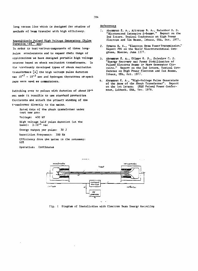
204
long vacuum line which is designed for studies of
methods of beam transfer with high efficiency.
Repetitively Pulsed High Voltage Generators (PulseDuration %10~** sec)
In order to test various components of these long-
pulse accelerators and to expand their range of
applications we have designed portable high voltage
sources based on shock excitation transformers. In
the -reviously developed types of shock excitation
transformers [4] the high voltage pulse duration
References
1.
was 10 sec and hydrogen thyratrons o? spark
gaps were used as commutators.
Switching over to pulses with duration of about 10-4
sec made it possible to use standard production
thyristors and attach the primary winding of the
transformer directly to the mains.
Rated data of the shock transformer undertest now are:
Voltage: 400 kV
High voltage half pulse, duration (at thebase): 3-10"4 sec
Energy output per pulse: 30 J
Repetition Frequency: 300 Hz
Efficiency from the mains Co the consumer:50%
Operation: Continuous
Abramyan E. A., Altarcop B. A., Kuleshov G. D."Microsecond Incensive E-beams." Report on the2nd Intern. Topical Conference on High PowerElectron and Ion Beans, Ithaca, USA, Oct. 1977.
2. Symons R. S., "Electron Beam Power Transmission.Report #94 on the World. Electrotechnical Con-gress, Moscow, June 1377.
3. Abramyan E. A., Efimov E. N., Kuleshov G. D."Energy Recovery and Power Stabilization ofPulsed Electron Beams in Marx Generator Cir-cuits." Report on the 2nd Intern. Topical Con-ference on High Power Electron and Ion Beams,Ithaca, USA, Oct. 1977.
4. Abramyan E. A., "High-Voltage Pulse Generatorsof Che Base of the Shock Transformer". Reporton the 1st Intern. IEEE Pulsed Power Confer-ence, Lubboek, USA, 'tov. 1976.
leeuaeretaz
Fig. 1 Diagram of Installation with Electron 3eam Energy Recycling
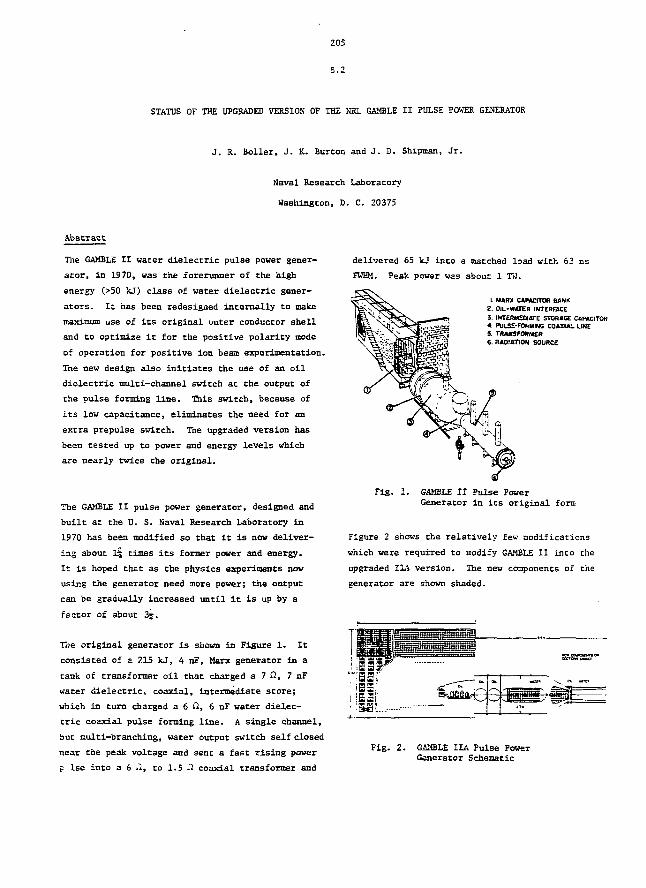
205
STATUS OF THE UPGRADED VERSION OF THE NRL GAMBLE II PULSE POWER GENERATOR
J. R. Boiler, J. K. Burton and J. D. Shipman, Jr.
Naval Research Laboratory
Washington, D. C. 20375
Abstract
The GAMBLE II water dielectric pulse power gener-
ator, in 1970, was the forerunner of the high
energy (>50 kj) class of water dielectric gener-
ators. It has been redesigned internally to make
maxinum use of its original uucer conductor shell
and to optimize it for the positive polarity mode
of operation for positive ion beam experimentation.
The new design also initiates the use of an oil
dielectric multi-channel switch at the output of
the pulse forming line. This switch, because of
its low capacitance, eliminates the need for an
extra prepulse switch. The upgraded version has
been tested up to power and energy levels which
are nearly twice the original.
The GAMBLE II pulse power generator, designed and
built at the U. S. Naval Research Laboratory in
1970 has been modified so that it is now deliver-
ing about l| times its former power and energy.
It is hoped that as the physics experiments now
using the generator need more power; the output
can be gradually increased until it is up by a
factor of about 3f.
The original generator is shown in Figure 1. It
consisted of a 213 kJ, 4 nF, Hani generator in a
tank of transformer oil that charged a 7 0., 7 nF
water dielectric, coaxial, intermediate store;
which in turn charged a 6 Cl, 6 nF water dielec-
tric coaxial pulse forming line. A single channel,
but multi-branching, water output switch self closed
near the peak voltage and sent a fast rising power
p Ise into a 6 hi, to 1.5 £1 coaxial transformer and
delivered 65 kj into a matched load with 63 ns
FWEM. Peak power was about 1 TO.
L MARX CAMCTTOR BANKZ. OIL-WATER INTERFACE3. INTERMEDIATE STGRACE CAPACITOR* PULSE-FOftMING COAXIAL LINEi TRANSFORMER6. RADIATION SOURCE
Fig. 1. GAMBLE II Pulse PowerGenerator in its original form
Figure 2 shows the relatively few modifications
which were required to modify GAMBLE II into the
upgraded ILA version. The new components of the
generator are shown shaded.
Fig. 2. GfflffiLE IIA Pulse PowerGenerator Schematic
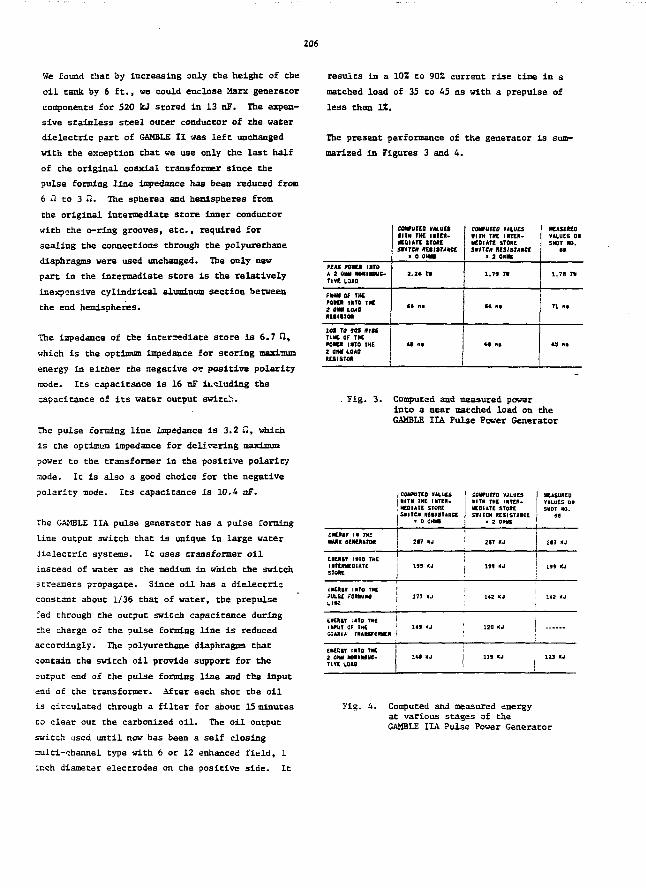
206
We found that by increasing only the height of the
oil tank by 6 ft., we could enclose Marx generator
components for 520 kJ stored in 13 nF. The expen-
sive stainless steel outer conductor of the water
dielectric part of GAMBLE II was left unchanged
with the exception that we use only the last half
of the original coaxial transformer since the
pulse forming line impedance has been reduced from
6 to 3 H. The spheres and hemispheres from
the original intermediate store Inner conductor
with the o-ring grooves, etc., required for
sealing the connections through the polyurethane
diaphragms were used unchanged. The only nev
part in the intermediate score is the relatively
inexpensive cylindrical aluminum section between
che end hemispheres.
The impedance of the intermediate store is 6.7 Q,
which is the optimum impedance for storing nmrlTmim
energy in either the negative or positive polarity
mode. Its capacitance is 16 nF iueluding the
capacitance of its water output switch.
The pulse forming line impedance is 3.2 .1, which
is che optimum impedance for delivering maTrtmiira
power Co the transformer in the positive polarity
node. Ic is also a good choice for the negative
polarity mode. Its capacitance is 10.A nF.
The GAMBLE I LA pulse generator has a pulse forming
line output switch that is unique in large water
dielectric systems. It uses transformer oil
instead of water as the medium in which Che switch
screamers propagate. Since oil has a dielectric
conscanc about 1/36 that of water, the prepulse
fed through Che output switch capacitance during
che charge of Che pulse forming line is reduced
accordingly. The polyurethane diaphragms that
contain the switch oil provide support for the
output end of the pulse forming line and the input
and of che transformer. After each shot the oil
is circulated through a filter for about 15 minutes
co clear out the carbonized oil. The oil output
switch used until now has been a self closing
sulti-channel type with 6 or 12 enhanced field, 1
inch diameter electrodes on che positive side. It
results in a 10% to 90S current rise time in a
matched load of 35 to 45 ns with a prepulse of
less than 12.
The present performance of the generator is sum-
marized in Figures 3 and 4.
KM K K I 1110l i o n K»muc.TIVC DIDIVHt OF THEpottn mo T «t am UMO
ict ra tea maTIME OF THEPOKR IITO THE2 aw LOWIESISTM
comma vM.ua•ITH THC l« I t«-• 0 1 Art STME
stiren naitrtKc• 0 OHM
2.24 T>
C4 na
48 fta
cmrurco invts•ITH THE l« I t« -WDInTC STOKESWITCH HBISTMCt
• 1 OKaS
1.7J T l
84 na
4S ns
UtJSUKO•M.UES OKSHOT NO.
t$
i.7« r«
71 na
49 na
Fig. 3. Computed and measured powerinto a near matched load on theGAMBLE IIA Pulse Power Generator
J C0WU7£D VALUES I COHPUTCO VALUESj l l T M THC INTER. KITH THE IMTEJU! MEDIATE STOflF. ICOIATE STORE
SV1TCM JKvSISTlDCE SWITCH KESrSTANCE• 0 0HW 1 * 2 0HW
MEASUREDVALUES 01SHOT MO.
EMUttr 1 * THE•MX QEMIUrOR
CKftlT ItttO THEINTCmCOiATESTORE
tRCXir IITO THC?vist fojunM
ERERIT INTO THEIMfUT OF THECOAXIA TRANSFORMER
EMCIT 1HT0 THE2 OHM W M I H H C -Tire LOAD
217 HJ
199 KJ
177 KJ
1*9 KJ
I t * XJ
26T XJ
| 199 KJ
1*2 KJ
1 120 KJ
267 XJ
199 XJ
142 KJ
123 KJ
Fig. 4. Computed and measured energyat various stages of cheGAMBLE IIA Pulse Power Generator
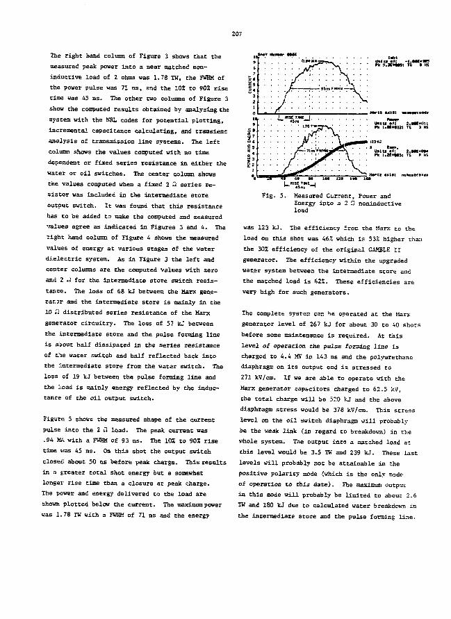
207
The right hand column of Figure 3 shows that the
measured peak power into a near matched non-
inductive load of 2 ohms was 1.78 TK, the FWHM of
the power pulse was 71 ns, and the 10% to 902 rise
time was 45 ns. The other two columns of Figure 3
show the computed results obtained by analyzing the
system with the NKL codes for potential plotting,
incremental capacitance calculating, and transient
analysis of transmission line systems. The left
column shows the values computed with no time
dependent or fixed series resistance in either the
water or oil switches. The center column shows
the values computed when a fixed 2 ft series re-
sistor was included in the intermediate store
output switch. It was found that this resistance
has to be added to make the computed and measured
values agree as indicated in Figures 3 and 4. The
light hand column of Figure 4 shows the measured
values of energy at various stages of the water
dielectric system. As in Figure 3 the left and
center columns are the computed values with zero
and 2 iJ for the intermediate store switch resis-
tance. The loss of 68 kJ between the Marx gene-
rator and the intermediate store is mainly in the
10 ii distributed series resistance of the Mane
generator circuitry. The loss of 57 kJ between
the intermediate store and the pulse forming line
is about half dissipated in the series resistance
of tile water switch and half reflected back into
the Intermediate store from the watar switch. The
loss of 19 kJ between the pulse forming line and
the load is mainly energy reflected by the induc-
tance of the oil output switch.
Figuro 5 shows the measured shape of the current
pulse into the 2 il load. The peak current was
.94 MA with a FWHM of 93 ns. The 10X to 902 rise
time was 45 ns. On this shot the output switch
closed about 50 ns before peak charge. This results
in a greater total shot energy but a somewhat:
longer rise time than a closure at peak charge.
The power and energy delivered to the load are
shown plotted below the current. The maximum power
was 1.78 TW with a FWHM of 71 ns and the energy
u*lu •*: -i.i
ttartx txtwi MMHcceiMf
Uftlti •#! 2.ttE«HlPt. 1.K*«I2I T£ 3 MS
123 KJJ E M » .
UBtts a«! 2.ME*IM4Pk 1.2E*M5l TS » HS
Fig. 5. Measured Current, Power andEnergy into a 2 0 noninductiveload
was 123 kJ. The efficiency from the Marx to the
load on this shot was 462 which is 53% higher than
the 30% efficiency of the originiJ. GAMBLE II
generator. The efficiency within the upgraded
water system between the intermediate store and
the matched load is 62%. These efficiencies are
very high for such generators.
The complete systec can be operated at the Marx
generator level of 267 kJ for about 30 to 40 shots
before some maintenance is required. At this
level of operation the pulse forming line is
charged to 4.4 MV in 143 ns and the polyurethane
diaphragm on its output end is stressed to
271 kV/cra. If we are able to operate with the
Marx generator capacitors charged to 62.5 kV,
the total charge will be 520 kJ and the above
diaphragm stress would be 378 kV/cm. This stress
level on the oil switch diaphragm will probably
be the weak link (in regard to breakdown) in the
whole system. The output into a matched load at
this level would be 3.5 TW and 239 kJ. These last
levels will probably not be attainable in the
positive polarity mode {which is the only mode
of operation to this date). The m^vi pn output
in this mode will probably be limited to about 2.6
TW and 180 kJ due to calculated water breakdown in
the intermediate store and the pulse forming line.

206
Our design goal in the upgrade was to get as much
power and energy out of the water dielectric
system as possible without Increasing its outer
dimensions and we believe we will achieve this.
At least, we are certain that the GAMBLE II
generator has shed its conservative label.
The original GAMBLE II generator waa funded by toe
Defense Nuclear Agency. The upgrade was funded by
Che Oflice of Naval Research and the capacitors
for the Marx generator were furnished by the
Sandia Laboratories.
209
EMITTANCE MEASUREMENTS ON FIELD EMITTER DIODES '
Bernhard Kulke and Ronald Kihara
University of CaliforniaLawrence Liverroore Laboratory
P. 0. Box 808, Livermore, CA. 94550
ABSTRACT
On the basis of time-integrated emittancemeasurements, several different types of fieldemitter diodes were investigated at 1-3 kA,1 MeV. The experimental parameters were thecathode type, the anode mesh texture, the diodespacing and voltage, and the level of coili-mation of the emerging beam. Over a widerange, the emi'cance was found to be propor-tional to the level of collimation. With thediode spacing left fixed, the emittance wasfound to be essentially independent of thediode voltage and current.
The lowest emittances (30-40 mr-cm at400 A) were obtained with a foil-type cathodein a ball-over-plane configuration.
INTRODUCTIONThe flash x-ray (FXR) linear induction
accelerator at Lawrence Livermore Laboratory,currently being designed, requires an injectedelectron beam of 2-4 kA at 1.5-2 MeV. In orderto maximize the forward radiation dose producedby a beam of given diameter, it is essential tominimize the emittance. Field emitter diodesare well suited for flash x-rey applications,but measurements to date of their beam qualityhave largely been confined to determining theangular divergence of high current beams in the
1 2region very close to the anode * . Measure-ments on a beam that was coliimated and trans-ported over some distance have been reported bythe ERA group at Lawrence Berkeley Labo-ratory (LBL) who utilized a field emitter diodeas the injector to a 4 MeV induction LINAC.
The proposed FXR electron source is modeledlargely after the LBL injector. Thus, in orderto confirm and expand on the earlier LBL re-sults, the LBL field emitter diode gun wasbrought to LLL and reactivated for furtheremittance measurements.
APPARATUS AND EXPERIMENTAL PROCEDUREAs shown in Figure 1, the diode proper con-
sists of a ball-over-plane or similar configu-ration with the planar anode formed by tungstenmesh. The electron beam traverses the anodemesh and is focused by a thin lens solenoidthat in conjunction with two collimator aper-tures downstream from the anode, acts as avariable beam scraper. Downstream from thesecond collimator is mounted a pinhole maskwith a square array of 1 mm dia pinholes on5 mm centers, and this in turn is followed by ascintillator screen carrying a layer of P-llphosphor.
The diode voltage is generated by five in-duction modules that are effectively connectedin series by the movable cathode stem linkingthem. This allows convenient adjustment of theanode-cathode spacing. Each module is aferrite-cored 1:1 pulse transformer, with thesingle turn primary driven from a nominal250 kV, 56 ohm, 40 ns Blunrtein, and thesecondary being formed by the cathode stem.Figure 2 shows some typical pulse shapes. Motethat the width of the beam current pulse isnarrower after collimation.
To calculate the emittance, the scinfil-lator image (Figure 3) typically was firstscanned with a densitometer. The center ofeach image spot then was used to measure the

210
angular divergence of each oeamlet from thestraight-through position. A second angle,calculated from the FWHM of the image spot,represents the growth in diameter of the beam-let over the 115 mm drift distance. The corre-sponding phase plane representation of any onebeamlet was then drawn, and finally, the emit-tance was calculated as 1/ir times the area ofthe figure circumscribing the entire phaseplane plot.
The diodes investigated here employed anumber of different cathodes, with the best one(Cl) consisting of a 50 mm dia., approximatelyspherical, polished stain!ess steel ball with asmall, flush mounted button insert carrying a7 ,im dia. tantalum foil spiral. This was anearlier LBL design. Cathode C2 used a flat,graphite emitter button. Two other cathodegeometries employed a graphite rod and aspherical-cap graphite button, respectively.Cathode C3 was a 100 mm dia., polished, stain-iess steel pancake carrying the 7 ram dia.emitter button of Cl.
The experimental anodes consisted of tung-sten mesh stretched across a 76 mm dia. circu-lar aperture facing the cathode. They included:
Al. Woven mesh, 0.025 rrni dia., in a0.6 x 1.8 ram array.
A2. Etched mesh, 16 lines/cm,0.036 mm thick x 0.061 mm wide.
A3. Etched mesh, 24 lines/cm,0.025 mm thick x 0.05 mm wide.
EXPERIMENTAL RESULTSThe lowest emittances were obtained with
the Cl cathode, i.e., a simple ball-over-planeconfiguration, using a foil emitter. The othercathodes all tended to produce scintillatorimages that were poorly defined, and clearly-epresented beams with greater emittance. Themeasurements discussed in the following there-fore concern only cathode Cl.
The degree of collimation was controlledthroughout by varying the solenoid lens fieldstrength. For diode Cl-Al, Figure 4 shows thevariation of the emittance vs the collimatedbeam current with the A-K spacing as the para-
meter. The nearly linear relationship betweenthe collimated beam fraction and the emittanceleads one to conclude that for a beam that isalready severely collimated, the remaining beamcurrent is quite uniformly distributed in phasespace. A further reduction ir beam currentthus corresponds linearly to a similar re-duction in phase space area, or emittance.
'The function of the planar anode mesh is tosupport a strong electrostatic field at thespherical cathode while at the same timeallowing the beam electrons to pass throughwith minimum interception or perturbation totheir trajectories. The perturbing effect oftha anode mesh can be modeled by consideringeach open square as a miniature electrostaticlens, with the focal length given byf = 4U/{E2 - E ^ , where U = anodepotential, referred to the cathode, and E^and Eg represent the electric field on thecathode side and on the downstream side,respectively. For the typical case, Eg = 0,the lens is diverging, and the divergence halfangle will be proportional to the meshspacing. Thus, one clearly does well to usethe minimum mesh spacing that is consistentwith good beam transmission.
In Figure 5 we have plotted the measuredemittance variation with current for diodeC1-A2 which used the 16 i/cm, etched tungstenmesh. It is seen that the tighter, etchedanode mesh does produce somewhat lower emit-tance beams than the woven mesh of Figure 4.Also, there appears to be a definite minimum ofenittance reached near 30 mr-cm. Furthermeasurements indicated that there wasnothing to be gained in going from 16 to 24lines/cm (etched) while there was visibleimprovement in going from 10 lines/cm (woven)to IS lines/cm (etched).
In an attempt to gain some insight on theeffect of beam voltage variations, the diodepotential was changed in three steps, from680 kV to 970 kV. The results are shown inFigure 6, and clearly, no systematic variationof the emittance with the diooe potential is
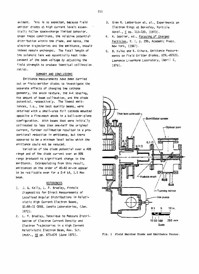
211
evident. This is as expected, because field
emitter diodes at high current levels essen-
tially follow space-charge limited behavior.
Under these conditions, the relative potential
distribution within the diode, and hence, the
electron trajectories and the emittance, should
indeed remain unchanged. The focal length of
the solenoid lens was essentially kept inde-
pendent of the beam voltage by adjusting the
field strength to produce identical collimation
ratios.
SUMMARY AND CONCLUSIONS
tmittance measurements have been carried
out on field-emitter diodes to investigate the
separate effects of changing the cathode
geometry, the anode texture, the A-K spacing,
trie amount of beam collimation, and the diode
potential, respectively. The lowest emit-
tances, i.e., the best quality beams, were
obtained with a small-area foil cathode mounted
opposite a fine-mesh anode in a ball-over-plane
configuration. With beams that were initially
collimated to less than one-half the original
current, further collimation resulted in a pro-
portional reduction in emittance, but there
appeared to be a minimum level below which the
emittance could not be reduced.
Variation of the diode potential over a 40%
range and of the diode current over an 80%
range produced ro significant change in the
emittance. Extrapolating from this result,
emittances on the order of 40-60 mr-an appear
to be realizable even for a 2-4 kA, 1.5 Mev
beam.
REFERENCES
1. 0. G. Kelly, L. P. Bradley, Pinhole
Diagnostics for Direct Measurements of
Localized Angular Distributions in Relati-
vistic High Current Electron Beams,
SC-RR-7Z 0058, Sandia Laboratories, (Jan.
1972).
2. L. P. Bradley, Technique to Measure Distri-
bution of Electron Current Density and
Electron Trajectories in a High Current
Relativistic Electron Beam, Rev. Sci.
Instr., 48 pp. 673-576 (June 1975).
3. Glen R. Lambertson et. al., Experiments on
Electron Rings at Berkeley, Particle
Accel., J_ pp. 113-120, (1973).
4. A. Septier, ed., Focusing of Charged
Particles, V. I, p. 296, Academic Press,
New York, (1967).
5. 8. Kulke and R. Kihara, Emittance Measure-
ments on Field Emitter Diodes, UCRL-82533,
Lawrence Livermore Laboratory, (April 5,
1979).
Thin lens solenoid—
/ ' ^-Scrntillator screen
10 50 100 250 mm
Scale
Fig. 1 field Emitter Diode and Emittance Tester.
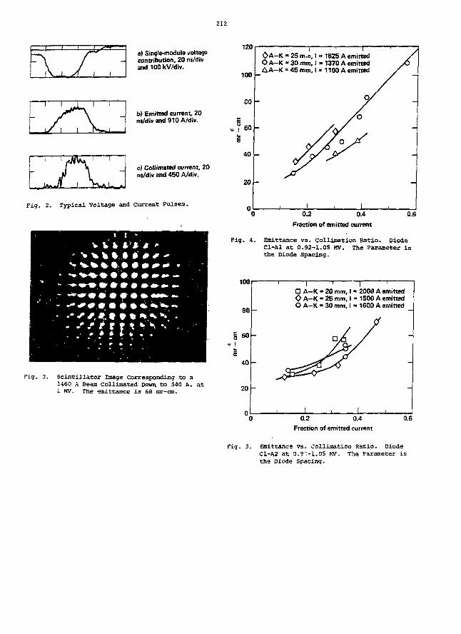
212
a) Single-module voltagecontribution, 20 ns/divand 100 kV/div.
b) Emitted current 20ns/div and 910 A/div.
c) Collimated current, 20ns/div and 450 A/div.
Fig. 2. Typical Voltage and Current Pulses.
Fig. 3. Scintillator Image Corresponding to a1460 A Beam Collimated Sown to 540 A, at1 MV. The emittance i s 68 oar-cm.
O A - K = 25 m.n. I » 182S A emittedO A-K « 30 mm, I - 1370 A emittedA A - K « 45 mm. I » 1100 A emitted
Fig. 4.
0.2 0.4
Fraction of emitted current
Emittance vs. Collimstion Ratio. DiodeCl-Al at 0.92-1.OS MV. The Parameter isthe Diode Spacing.
100
30
60
40
20
\ ' r ^D A-K =• 20 mm, I " 2000 A emitted0 A-K - 25 mm, I = 1500 A emittedO A-K - 30 mm, I » 1600 A emitted
0.2 0.4Fraction of emitted current
0.6
Fig. 5. Emittance vs. Collimation Ratio. DiodeC1-A2 at 0.9">1.05 MV. The Parameter isthe Diode Spacing.
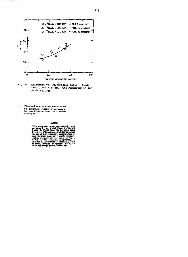
213
100 r-
30 1-
60
0 - VDiotte = 680 KV, 1 = 820 A emittedA VDiode = 820 KV, I = 1180 A emittedO VOiode = 970 KV, I * 7500 A emitted
0.2 0.4
Fraction of emitted current
0.6
Fig. 6. Smittance vs. Collimation Ratio. DiodeC1-A2, A-K = 30 ntn. The Parameter is theDiode Voltage.
"Work performed under the auspice* of theU.S. Department of Energy- by the LawrenceLivennorc Laborator1 under contract numberW.7405-ENG-48."
NOTICE
"This report was prepared as an account of worksponsored by the United States Government.Neither tbe United States nor the United StatesDepantnent of Energy, nor any of their employees,nor any of thor contractors, subcontractors, ortheir employees, makes any warranty, exptesi orimplied, or asiumei any legal liability or respon-sibility for tbe accuracy, completeness orusefulness of any information, apparatus, productor process dudosed. or represents that its usewould not infringe privately-owned rights."

214
8.5
ON THE DEVELOPMENT OF A REPETITIVELY PULSED ELECTRON BEAM SYSTEM
Gary A. Tripoli
Ion Physics Company
Burlington, Massachusetts
Abstract
A pulsed electron beam system - - PEBS-III - - has
beendeveloped at Ion Physics Company to generate2
an electron beam of 200 keV, 4 A / c m , 2. 5 cm X
75 cm, 1. 3 lisec, at high repetition ra tes . That
system incorporates a gas-insulated PFN Marx
generator in Guillerain C network configuration to
drive a cold-cathode electron gun. System perfor-
mance corresponded to computer simulation of VI
waveforms versus genera to r -paramete r and
impedance-collapse variat ions. The effort demon-
strated the usability of a PFN for energization of
long-pulse repetitively pulsed electron guns.
Introduction
With ever increasing power levels in electron beam
technology, there is need for increased efficiency
in energy t ransfer through the various associated
pulse power subsystems. Design considerations
for a repetitively pulsed electron gun a re such
that nominally rectangular electron beam
voltage-current pulses are therefore required. A
system which generates such a pulsed electron
beam - PEBS-HI - shown in Figure 1 is described
with regard to its theoretical design and actual
operating pa ramete r s .
Theoretical Design
For purposes of generating a nominally rectangular
electron beam current pulse, the PEBS-HI pulse
generator was designed as a two-section Guillemin
C pulse forming network(PFN). Figure 2a shows
the basic network in which L. and C. a re normal -
ized capacitors and inductors, the actual values of
which a re determined by multiplying the L. by Z T
and the C. by T / Z , where T is pulsewidth and Z is
load impedance. Discharge of initially charged
C. through L. into Z produces a parabolic r i se and
decay voltage pulse across Z as shown in Figure
2b.
By separating the C. and L. into a se r ies of a
capacitors and n inductors each with value nC. and
L./n respectively, the 2-section Guillemin C net-
work takes the form of two paral lel inductive
n-stage Marx generators . Utilization of common
inter-jtage switches between the two sections
assures simultaneous erection of the two Marxes .
A schematic of the PFN Marx, less tr iggering
circuitry, is shown in Figure 3.
Because actual generator capacitor and inductor
values a re dependent on load impedance as well as
pulsewidth, a model was developed for the electron
gun which constitutes the Z of the PFN.
A cold cathode electron gun with space charge
limited flow is characterized by the relat ion:
j = k V 3 / 2 ( d - u t f 2 ,
where j = current density (A/cm"), V = gun voltaee

215
(V), d = AK gap(cm), u = plasma, propagation veloc-
ity(cm/sec), t = time(sec) and k = 2. 335 x 10" .
With consideration of required electron energy and
current density, there follows the value, A, of the
AK gap. An estimate of beam spread of 1. 5 d to
2 d within the diode along with Ijam length require-
ments gives effective beam area. In such way
total gun current with knowr. gun voltage leads to
gun impedance.
An initial approximation, then, for the PEBS-HI
gun impedance was Z = 56. 3(1-2. 7 x 10 t) . A
computer circuit analysis program, ITHAC, used
to evaluate V and I waveforms for generator para-
meters of L, = 17 uH, L, = 18 (iK, C, = 8. 5 nF,
C_, = . 9 nF, and Z as above produced simulation?
shown in Figure 4.
Pulse Generator
The PEBS-ni pulse generator comprises two
parallel ten-stage inductive Marx generators in
Guillemin C configuration with common triggered
spark gaps as shown in Figure 1. All components
including generator capacitors, generator induc-
tors, charging inductors, spark gaps, and associ-
ated trigger circuitry are gas insulated by common
location within the main pressure vessel. As
shown, access to components is afforded by their
positioning atop a support platform which is canti-
levered from the main pressure vessel endplate.
Generator capacitors and inductors were designed
so as to permit matching the PFN to the time vary-
ing electron gun impedance. Specifically, the sec-
ond section capacitors were of multisection con-
rtructiott to allow ~ 20% variation for risetime
considerations. The generator inductors were of
multiturn expandable/compressible construction to
allow ~ 50% variation for pulsewidth considerations.
Interstage charging of the PFN Marx capacitor
banks is by means of charging inductors so as to
virtually eliminate the power loss associated with
resistive charging. Ordinary magnet wire was
wound on an acrylic cylindrical support to form
each charging inductor.
Triggered mid-plane spark gaps comprising
elkonite and brass electrodes were incorporated
as interstage switches. Positioning of these
switches within the main pressure vessel presented
each switch with a large volume of gaseous dielec-
tric, afforded UV illumination among gaps, and
provided easy access for adjustment purposes.
During sustained PEBS-III operation into a dummv
load these ten switches each passed > 5 mC per
pulse at 55 kV, 5 kA peak, 1. 3 usec, 20 pps.
Electron Gun
The PEBS-HI electron beam output of 4 A/cm
over 2. 5 cm x 75 cm was generated by an electron
gun with cathode comprising three 12 pm thick
tantalum foil blades positioned on a stainless
steel focus electrode and blade support structure.
A customer-supplied stainless steel water-cooled
hibachi supported a 50 um thick aluminum anode foil.
System Performance and Conclusions
Overall system performance is illustrated in
Figure 5 which shows a gun current pulse com-
pared with a dummy load current pulse. Close
agreement between the two actual waveforms as
well as the computer generated waveform can be
seen. Beam current and gun (shank' current with
and without focus electrode are illustrated in
Figure 6. As shown, the focus electrode increases
beam current, reduces gun current, and increases
gun impedance as expected.
Development of the PEBS-IH has demonstrated the
effectiveness of incorporating pulse forming net-
works for energization of repetitively pulsed
electros guns. Such utilization serves to improve
efficiency as required by large scale systems.
216
F i g u r e 1. P E B S - I I I P U L S E D ELECTRON BEAM SYSTEM
-00 1
TFigure 2a.
Guillemin C Network
Figure 2b. T
Output Voltage Waveforn.
i ' * > .
Figure 3.PFN Marx
Network
Figure 4. Computer Simulation withTime-Varying Load
Dummy Load Electron Gun
Figure 5. Shank Current Traces5kA/div, lu sec/div
|O O 1J C F !I U F 1
SShank Current Beam Curre.nt
5kA/div, , 5» aec/div . 5fcA/div, . 5u sec/div
Figure 6- Effect of Focus Electrode

217
9.1
DEVELOPMENT OF HIGH REPETITION-BATE PDLSED POWER GENERATORS
R. J. Sojka and G. K. Simcox
Physics International Company2700 Merced Street
San Leandro, California 94577
Abstract
The design and development of high
repetition-rate, (>1 kHz) pulsed power generators
are discussed and a set of chosen assign
approaches presented* The ensuing technical
approaches for the pulse forming network, PFH
(twitching, and PEN charging modulators are
described- Xey elements of the system are the
deionized-water, fast-energy store, and a flowing
air spark gap switch, both capable of operation at
higher than a 1 kHz repetition frequency. Based
on this design and development effort, the
technical issues of high repetition rate pulsed
power systems are discussed, and recommendations
are offered for further study and development of
dielectrics, spark gap switches, and high power
modulators.
Introduction
In recent years. Physics International (PI)
has invested in the study and development of repe-
titively pulsed power systems* Some emphasis has
been given to the generation of short, nanosecond
regime pulses into Xov-iapedance loads at
repetition rates in excess of 1 kHz.
The water-insulated pulse forming line and
spark gap were used for the critical final energy
store and switch. At the outset, there were very
fev data to support this choice, but there were
reasons to expect that the' outstanding character-
istics of water as a dielectric and the spark gap
as a switch in single pulse systems could be re-
tained to an adequate extent for repetitive oper-
ation.
As a result of this choice, the immediate
issues to consider were:
•The special treatments for water under
repetitive stresses and the assignment of
suitable design stresses
•The electrical and mechanical design of a
spark gap switch for maximum repetitive
operation and adequate life
For the entire system, there were many issues of
great significance for high repetition rate oper-
ations:
•Prine power
•Pulse forning line charge control
•Capacitor and component life
•Trigger generators
• Heat transport
•High average power dummy load
•Gas and water flows
To develop the major switch and dielectric
technologies, satisfactory solutions for all these
issues, and uore, had to be found*
This paper gives a short description of this
work and treats the Important topic of spark gap
switch performance in more detail.
The Experimental Arrangement
A schematic of the switch test bed is showr.
in Figure 1. The pulse forming line had a
Blumlein configuration with an output impedance of
2.0 ohms. This line is shown as two 12.3 nF
capacitors, storing a total of 31 joules at 50 kv
LUMPED EQUrw*LE^
Figure 1 Electrical schematic switch and Blumlein PFL test circuit.
charge* The Blumlein was erected by the mid-plane
apark gap switch under teat* An output peaking
apark gap switch of similar main electrode
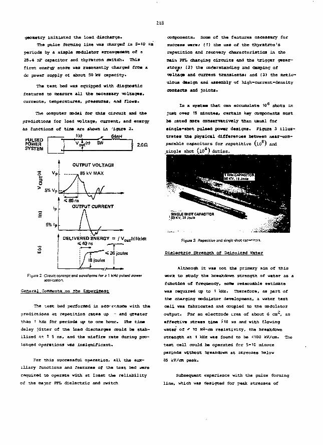
218
geometry initiated the Load discharge.
The pulse forming lisa was charged in 5-10 us
periods by a simple modulator arrangement of a
25.4 nP capacitor and thyratron switch* This
first energy store was resonantly charged ffroa a
dc power supply ot about SO kw capacity.
The test bed was equipped with diagnostic
features to measure all the necessary voltages,
currents, temperatures, pressures, and flows.
The computer model for this circuit and the
predictions for load voltage, current/ and energy
as functions of time are shown in 'lgure 2.
PULSEDPOWERSYSTEM
lit) 64nH
SW 2.012
OUTPUT VOLTAGE
E>
5% V,
5% Ip
, , \ /< 86ri3
OUTPUT CURRENT
DELIVERED ENERGY s / V t(t)l(t)dt<40ns
Figure 2 Circuit concept and waveforms for a I kHr pulsed powerapplication.
General Comments on the Experiment
The test bed performed in accrrcance with thepredictions at repetition rates up - and greaterthan t kHz for periods up to one hour. The tijnedelay j i t ter of the load discharges could be stab-il ized at i S ns, and the misfire rate during pro-longed operations was insignificant.
For this successful operation, a l l the aux-il iary functions and features of the test bed wererequired to operate with at laast the rel iabil i tyof the major PFL dielectric and switch
components. Some of the features necessary forsuccess were: (1) the use of the thyratron'srepetition and recovery characteristics in themain PFL charging circuits and the trigger gener-ators; (2) the understanding and damping ofvoltage and current transients) and (3) the metic-ulous design and assembly of high-current-densitycontacts and joints .
In a syatasi that can accumulate 10 s shots injust a m 15 minutes, certain key components mustbe rated nore conservatively than usual forsingle-shot pulsed power designs. Figure 3 i l l u s -trates the physical differences between near-com-parable capacitors for repetitive (lO ) andsingle shot (lO4) duties.
SINGLE SHOT CAPACITOR50 KV. 31 Joule
Figure 3 Repetitive and single shot capwr'tors.
Dielectric Strength of Peionized Water
Although i t was not the primary aim of thiswork to study the breakdown strength of water as afunction of frequency, some reasonable estimatewas required up to 1 kHz. Therefore, as part ofthe charging modulator development, a water testce l l was fabricated and coupled to the nodulatoroutput. For an electrode crea of about 6 cm*, aneffective stress time >10 us and with flowingwater of * 10 Hd-cm resist ivity, the breakdownstrength at 1 kHz was found to be <100 kV/cm. Thetest cel l could be operated for 5-10 aiinHteperiods without breakdown at stresses below35 jcV/cm peak.
Subsequent experience with the pulse forming
line, which was designed for peak stresses of
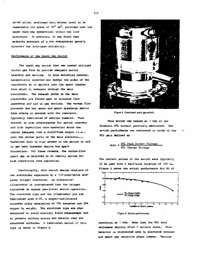
219
80-85 kv/cm, confirmed this stress level to bereasonable for areas of 10 cm , provided that thewater flow was symmetrical within the linestructure. In addition, i t was found thatmoderate pressure of a few atmospheres greatlyenhanced the long-term reliabiity.
Performance of the Spark Gap Switch
The spark gap switch that was tested utilizedvortex gas flow to provide adequate switchrecovery and cooling. In this switching concept,tangentially injected air sweeps the sides of theinsulators as i t spirals into the spark chamberfrom which i t exhausts through the sainelectrodes. The exhaust ports in the rainelectrodes axe flared open to minimize flowimpedance and aid in gas cooling. The vortex flowprevents the hot gases and spark discharge debrisfrom coming in contact with the insulator,typically fabricated of acrylic plastic . Thisconcept i s also advantageous for switch recoveryand high repetition rate operation since thedebris exhausts into a field-free region ( i . e . ,into the center ports of the main electrode*.,.Turbulent flow is also needed in the switch to aidin gas heat transfer during the sparkdischarges. For these reasons, the vortex-flowspark gap is believed to be ideally suited forhigh repetition rate operation.
Electrically, this switch design consists oftwo electrodes separated by a 1/2-inch-thick Bid-plane trigger electrode. An ultravioletilluminator is incorporated into the triggerelectrode to ensure low-jitter switch operation.The electrode tips and the illuminator pin arefabricated with K-2S, a copper-infiltratedtungsten alloy consisting of 75$ tungsten and 25%copper by weight. She electrode tips are alsocontoured to avoid electric field enhaacewnt andto promote uniform arcing and erosion over theelectrode surfaces. A fabricated switch oS thistype -is shown in Figure 4.
Figure 4 Fabricated spark gap switch.
This switch was tested at 1 kHz in the
Blumlein PFL circuit previosly mentioned. The
•witch performance was evaluated in terms of the
PFL gain defined as
Gain, PFL Peak Output Voltage
PFL Charge Voltage
The current pulses in the switch were typically
22 kA peak with a half-sine duration of 100 as.
Figure 5 snows the switch performance for 50 kV
NUMBER DP SHOTS, miltom
Figure 5 Switch performance.
operation at 1 kHz. Dote that the PEL gaindecreases rapidly after 7 million shots. Thisbehavior i s attributed both to electrode erosionand spark gap resistive phase losses. Various
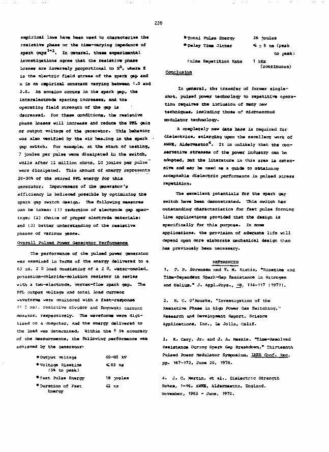
220
empirical I n n have b m used to characterize the
reai.sti.va phaaa or the time-varying impedance of
spark gaps . In ganaral, thasa experimental
investigations agree that: the raaiative phaaa
losses axa invarsaly proportional to E n, where Z
la the electric field atraaa of the spark gap and
n is an empirical constant varying between 1.0 and
2.0. As erosion occurs in the spark gap, the
interelectrode spacing increase*, and the
operating field strength of the gap la
decreased. For these conditions, the resistive
phase losses will Increase and reduce the FKL gala
or output voltage of the generator. Thia behavior
was also verified by the air heaclng in the spark •
gap switch. For example, at the start of testing,
7 joules per pulse were dissipated In the switch,
while after 11 million shots, 10 joules per pulse
were dissipated. This amount of energy represents
20-30% of the stored PPL energy for this
generator. Improvement of the generator's
efficiency is believed possible by optimizing the
spark gap switch design. The following measures
can be taken: (1) reduction of electrode gap spac—
ings; (2) choice of proper electrode materials;
and (3) better understanding of the resistive
passes of various gases.
Overall Pulsed Power Generator Performance
The performance of the pulsed power generator
was examined in terms of the energy delivered to a
63 nti, 2 3 load consisting of a 2 n, water-cooled,
potassxum-chloride-solutlon resistor in series
with a tuo-electrode, vortex-flow spark gap. The
?FL output voltage and total load current
waveforms were aonitored with a fast-response
(< 5 ns) , resistive divider and Rogowski current
monitor, respectively* The waveforms were digi-
tized on a computer, and the energy delivered to
the load was determined. Within the ± 5% accuracy
of the measurements, the following performance was
achieved by the generator:
•Total Pulse Energy
•Delay Tine Jitter
• Output voltage
eVoltage Risetiae(5* to peak)
•Fast Pulse Energy
• Duration of PastEnergy
80-85 kV
<SS3 ns
18 joules
42 ns
26 joules
< ± 5 ns (peak
to paak)
Repetition Rate 1 kHz
(continuous)
Conclusion
In general, th/» transfer of former single-
shot, pulsed power technology to repetitive opera-
tion requires the inclusion of many new
techniques, including those of microsecond
modulator technology.
A completely new data base is required for
dielectrics, enlarging upon the excellent work of
AWRs, Aldermaston4. It is unlikely that the con-
servative stresses of the power industry can be
adopted, but the literature in this area is exten-
sive and may be used as a guide to obtaining
acceptable dielectric performance in pulsed ar.resa
repetition.
The excellent potentials for the spark gap
switch have been denonstrated. This switch has
outstanding characteristics for fast pul3e forming
line applications provided that the design is
specifically for this purpose. In some
applications, the provision of adequate life will
depend upon more elaborate mechanical design than
has previously been necessary.
BEPEREHCES
1. T. P. Sorensen iind V. H. Rlstic, "Risetiae and
Time-Dependent Spark-Gap Resistance in Nitrogen
and Helium," J. Appl.Phys., ^8., 114-117 (1977).
2. R. C. O'Rourke, "Investigation of the
Resistive Phase in High Power Sas Switching,"
Research and Development Report, Science
Applications, Inc., La Jo lla, Calif.
3. K. Cary, Jr. ami J. A. Maszie, "Time—Resolved
Resistance During Spark Sap Breakdown," Thirteenth
Pulsed Power Modulator Symposium, IEEE Conf. Rec.
pp. 167-172, June 20, 1978.
4. J. C. Martin, et al.. Dielectric Strength
Motes, 1—16, AWKE, Aldermaston, England,
November, 1965 - June, 1970.
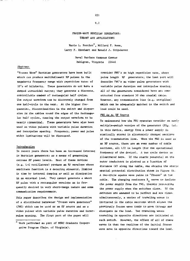
221
9.2
FROZEN-WAVE HERTZIAN GENERATORS:
THEORY AND APPLICATIONS
Marie L. Forcier+, Millard F. Rose,
Larry F. Itinehart and Ronald J. Gripshover
Haval Surface Weapons Center
Dahlgren, Virginia 22446
Abstract.
"Frozen Wave" Hertzian generators have been built
which can produce multikilowatt RF pulses in the
megahertz frequency range with repetition rates of
10's of kilohertz. These generators do not have a
damped sinusoidal output; they generate a discrete,
controllable number of rectangular half cycles.
The output waveform can be discretely changed from
one half-cycle to the next. At the higher fre-
quencies., discontinuities in the switch and disper-
sion in the cables round the edges of the rectangu-
lar half cycles, causLng the output waveform to be
nearly sinusoidal. Tiese generators have also been
used as video pulsers with variable pulse duration
and interpulse spacing. Frequency, power and pulse
width limitations will be discussed.
Introduction
In recetit years there has been an increased interest
in Hertzian generators as a means of generating
extreme RF power levels. Most of these devices
(e.g. L-C oscillators) produce an RF envelope whose
amplitude function is a decaying sinusoid, limited
in time by internal damping as well as dissipation
in an esitemal load. They cannot generate a short
RF pulse with a rectangular envelope as is fre-
quently desired in very short-range radars and some
communication requirements.
This paper describes the design and implementation
of a distributed parameter "frozen wave generator"
(FWG) vliich can be used as an RF source and as a
video ptilser with variable pulse duration and inter-
pulse spacing. The first part of the paper will
Work performed as part of HSHC Graduate Cooper-
ative Program (Dniv. of Virginia).
consider FWG's as high repetition rate, short
pulse length RF generators; the last part will
describe FWG's as video pulse generators with
variable pulse duration and interpulse spacing.
All of the generators considered here aze con-
structed froa: standard 50 oho coaxial cable.
However, any transmission line (e.g. stripline)
which can be adequately matched to the switch and
load could be used.
FWG As An RF Source
To understand how the FWG operates consider an early
multiple-switch version of the generator (Fig. la).
In this device, energy from a power supply is
statically stored in alternately charged sections
of the transmission line. When the FWG is used as
an RF source, there are an even number of cable
sections, all X/2 in length (for the operational
frequency of the device). A two cycle device is
illustrated here. If the static potential on the
outer conductors is plotted as a function of
distance (d) along the cable, one obtains the static
spatial potential distribution shown in Figure lb.
A two-cycle square wave pulse is "frozen" in the
cable. The charging resistors R serve to isolate
the power supply from the FWG, thereby protecting
the power supply when the switches close. If che
switches are assumed to be perfect and are closet
simultaneously, a series of traveling waves is
initiated in the cable sections which allows the
previously frozen wave train to move through and
dissipate in the load. Two traveling waves
traveling in opposite directions are initiated at
each switch. HowevfiT, the effect of alL of these
waves is that two replicas of the initial frozen
wave move in opposite directions toward the load.
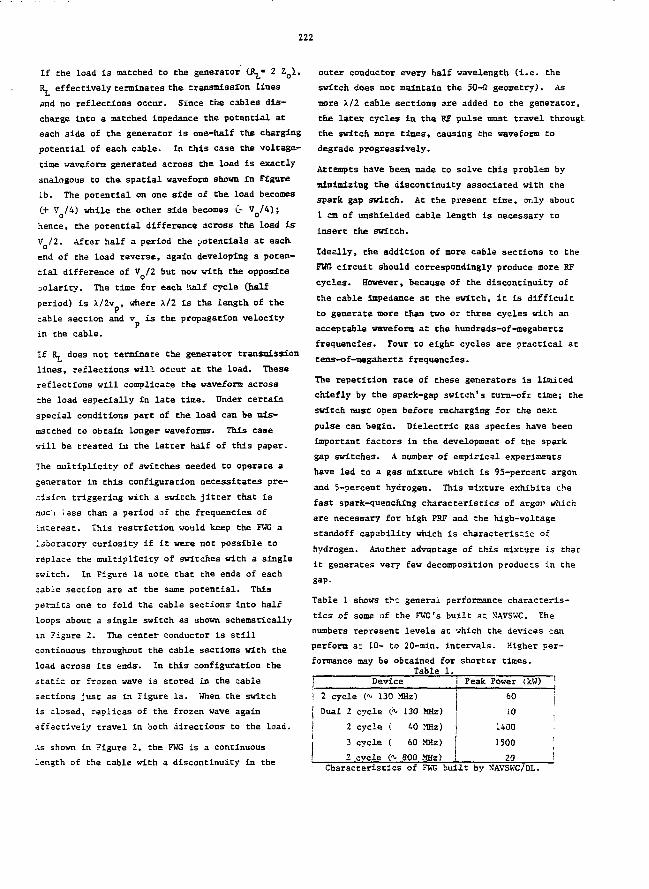
222
If che load is matched to the generator (R^- 2 ZQ\,
R, effectively terminates the transmission lines
and no reflections occur. Since tfcie cables dis-
charge into a matched impedance the potential at
each side of the generator la one-half the charging
potential of each, cable. In this case the voltage-
time waveform generated across the load is exactly
analogous to the spatial waveform shown in Figure
lb. The potential on one side of the load becomes
(+ Vo/4) while the other side becomes C- V0/*l;
hence, the potential difference across the load is
V /2. After half a period the potentials at each
end of the load reverse, again developing a poten-
tial difference of VQ/2 but now with, the opposite
aolarity. The time for each half cycle (half
period) is X/2v , where A/2 is the length of the
cable section and v is the propagation velocity
in the cable.
If R, does not terminate the generator transmission
lines, reflections will occur at the load. These
reflections will complicate the waveform across
the load especially In late time. Under certain
special conditions part of the load can be mis-
matched to obtain longer waveforms. This case
will be treated in the latter half of this paper.
The multiplicity of switches needed to operate a
generator in this configuration necessitates pre-
cision triggering with a switch, jitter that is
ouch less Chan a period of the frequencies of
interest. This restriction would keep the FWG a
laboratory curiosity If It were not possible to
replace the multiplicity of switches with a single
switch. In Figure la note that the ends of each
cable section are at the same potential. This
pennies one to fold the cable seccions Into half
loops about a single switch as shown schematically
in Figure 2. The center conductor is still
continuous throughout the cable sections with the
load across its ends'. In this configuration the
static or frozen wave is stored in the cable
sections just as in Figure la. When the switch
is closed, replicas of che frozen wave again
affectively travel in both directions to the load.
As shown In Figure 2, the FWG is a continuous
length of the cable with a discontinuity in the
outer conductor every half wavelength (i.e. the
switch does not maintain the 50-fl geometry). As
more A/2 cable sections are added to the generator,
the later cycles In the RF pulse must travel through
che switch more times, causing the waveform to
degrade progressively.
Attempts have been made to solve this problem by
minimizing the discontinuity associated with the
spark gap switch. At the present time, only about
1 cm of unshielded cable length is necessary to
insert the switch.
Ideally, the addition of more cable sections to the
FW3 circuit should correspondingly produce more RF
cycles. However, because of the discontinuity of
the cable impedance at the switch, it is difficult
to generate more than two or three cycles with an
acceptable waveform at the hundreds-of-megahertz
frequencies. Four to eight cycles are practical at
tens-of-megahertz frequencies.
The repetition rate of these generators is limited
chiefly by the spark-gap switch's turn-ofr time; the
switch oust open before recharging for the next
pulse can begin. Dielectric gas species have been
Important factors in the development of the spark
gap switches. A number of empirical experiments
have led to a gas mixture which is 95-percsnt argon
and 5-percent hydrogen. This mixture exhibits iihe
fast spark-quenching characteristics of argor> which
are necessary for high PRF and the high-voltage
standoff capability which is characteristic of
hydrogen. Another advantage of this mixture is chac
it generates very few decomposition products in che
gap.
Table 1 shows the general performance characteris-
tics of some of the FKG's built at XAVSKC. The
numbers represent levels at which the devices can
perform a- 10- to 20-min. intervals. Higher per-
formance may be obtained for shorter times.Table 1.
Device Peak Power (.kW)
! 2 cycle (y 130 MHz)
j Dual 2 cycle (y 130 MHz)
i 2 cycle ( UQ MHz)
3 cycle ( 60 MHz)
2 evele <y 800 MHz)
60
10
U00
1500
20Characteristics of FWG built by SAVSWC/DL.
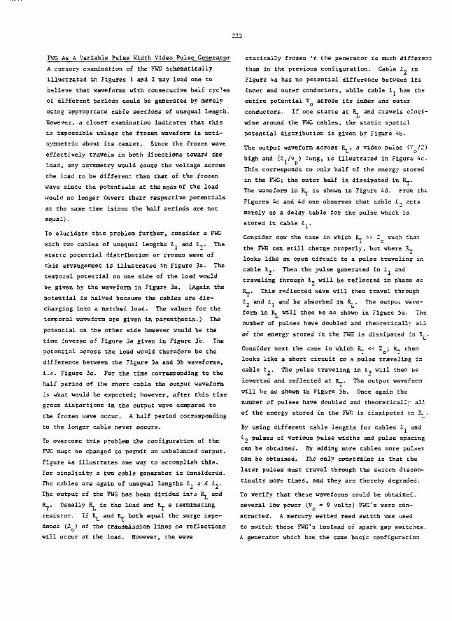
223
FWG As A Variable Pulse Width Video Pulse Generator
A cursory examination of the FHG schematically
illustrated in Figures 1 and 2 may lead one to
believe that waveforms with consecutive half cycles
of different periods could be generated by merely
using appropriate cable sections of unequal length.
However, a closer examination indicates that this
is impossible unless the frozen waveform is anti-
symmetric about its center. Since the frozen wave
effectively travels in both directions toward the
load, any asymmetry would cause the voltage across
the load to be different than that of the frozen
wave since the potentials at the ends of the load
would no longer invert their respective potentials
at the same time (since the half periods are not
equal).
To elucidate this problem further, consider a FWG
with two cables of unequal lengths J., and £,. The
static potential distribution or frozen wave of
this arrangement is illustrated in Figure 3a. The
temporal potential on one side of the load would
be given by the waveform in Figure 3a. (Again the
potential is halved because the cables Te dis-
charging into a matched load. The values for the
temporal waveform are given in parenthesis.) The
potential on the other side however would be the
time inverse of Figure 3a given in Figure 3b. The
potential across the load would therefore be the
difference between the Figure 3a and 3b waveforms,
i.e. Figure 3c. For the time corresponding to the
half period of the short cable the output waveform
is what would be expected; however, after this time
gross distortions in the output wave compared to
the frozen wave occur. A half period corresponding
to the longer cable never occurs.
To overcome this problem the configuration of the
FWG must be changed to permit an unbalanced output.
Figure 4a illustrates one way to accomplish this.
For simplicity a two cable generator is considered.
The cables are again of unequal lengths 8., s-.d i -
The output of the FWG has been divided inro R, and
IL,. Usually IL is the load and R_ a terminating
resistor. If R^ and R^ both equal the surge impe-
dance (,Zo) of the transmission lines no reflections
will occur at the load. However, the wave
statically frozen -'n the generator is much different
than in the previous configuration. Cable 1_ in
Figure 4a has no potential difference between its
inner and outer conductors, while cable I. has the
entire potential V Q across its inner and outer
conductors. If one starts at IL and travels clock-
wise around the FWG cables, the static spatial
potential distribution is given by Figure 4b.
The output waveform across E,, a video pulse (V /2)
high and 01 /v ) long, is illustrated in Figure 4c.
This corresponds to only half of the energy stored
in the FWG; the outer half is dissipated in R_.
The waveform in R . is shown in Figure 4d. From the
Figures 4c and 4d one observes that cable £, acts
merely as a delay cable for the pulse which is
stored in cable , ,
Consider now the case in which R_ >> Z such thatI o
the FWG can still charge properly, but where R_
looks like an open circuit to a pulse traveling in
cable £7. Then the pulse generated in 1. and
traveling through I, will be reflected in phase at
R_. This reflected wave will then travel through
Z, and Zj and be absorbed in R, . The outpui. wave-
form in Py will then be as shown in Figure 5a. The
number of pulses have doubled and theoretically all
of the energy stored in the FWG is dissipated in R. .
Consider next the case in which R^ << Z ; ilj then
looks like a short circuit to a pulse traveling in
cable £_. The pulse traveling in Z, will then be
inverted and reflected at R^. The output waveforn
will be as shown in Figure 5b. Once again the
number of pulses have doubled and theoretically all
of the energy stored in the FWG is dissipated in R. .
By using different cable lengths for cables 1, and
£•2 pulses of various pulse widths and pulse spacing
can be obtained. By adding more cables more pulses
can be obtained. Ihe only constraint is that the
later pulses must travel through the switch discon-
tinuity more times, and they are thereby degraded.
To verify that these waveforms could be obtained,
several low power (V - 9 volts) FWG's were con-
structed. A mercury wetted reed switch was used
to switch these FWG's instead of spark gap switches.
A generator which has the same basic configuration
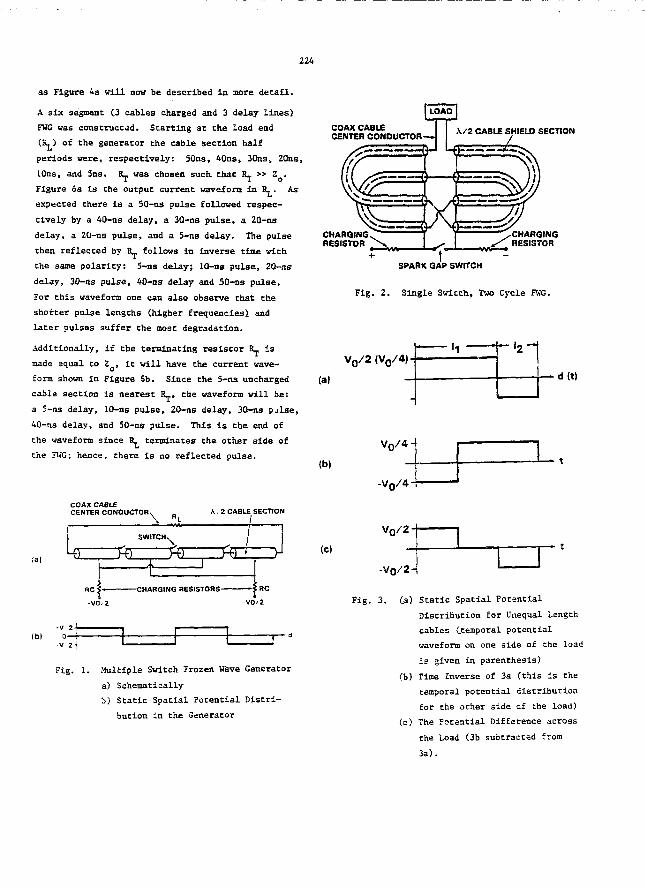
224
as Figure 4a will not? ba described in more detail.
A six segment C3 cables charged and 3 delay lines)
FUG was constructed. Starting at the load end
(Rj) of the generator the cable section half
periods were, respectively: 50ns, 40ns, 30ns, 20ns,
LOns, and Sns. R_ vas chosen such, that B_ » Z .
Figure 6a is the output current waveform in S,. As
expected there is a SO-ns pulse followed respec-
tively by a 40-ns delay, a 30-ns pulse, a 20-ns
delay, a 20-ns pulse, and a 5-ns delay. The pulse
then reflected by %^ follows in inverse time with,
the same polarity: 5-ns delay; 10-ns pulse, 20-ns-
delay, 30-ns pulse, 40-ns delay and 50-ns pulse.
For this waveform one can also observe that the
shorter pulse lengths (higher frequencies! and
later pulses suffer the most degradation.
Additionally, if che terminating resistor Rj is
nade equal to ZQ, it will have the current wave-
form shown In Figure 6b. Since the 5-ns uncharged
cable section is nearest R_, the waveform will be:
a 5-ns delay, 10-ns pulse, 20-ns delay, 30-ns pjlse,
40-ns delay, and 50-ns pulse. This is the end of
the waveform since R^ terminates the other side of
the FUG; hence, there Is no reflected pulse.
COAX CABLECENTER CONDUCTOR
\
A. 2 CABLE SECTION
-V 2+.o—r
•V 2 \
Fig. 1. Multiple Switch Frozen Wave Generator
a) Schematically
b) Static Spatial Potential Distri-
bution in the Generator
COAX CABLECENTER CONDUCTOR
^<=ABLE SHIELD SECT.ON
..CHARGINGj / \ RESISTOR
SPARK GAP SWITCH
Fig. 2. Single Switch, Two Cycle FWG.
V0/2<V0/4>
(a) •d(t)
V0/4-
(b)
(c)
-V0/4
V0/2
-VQ/2-I
Fig. 3. (a) Static Spatial Potential
Distribution for Unequal Length
cables (temporal potential
waveform on one side of the load
is given in parenthesis)
(b) Time Inverse of 3a (this is the
temporal potential distribution
for the other side of the load)
(c) The Potential Difference across
the Load (3b subtracted from
3a).
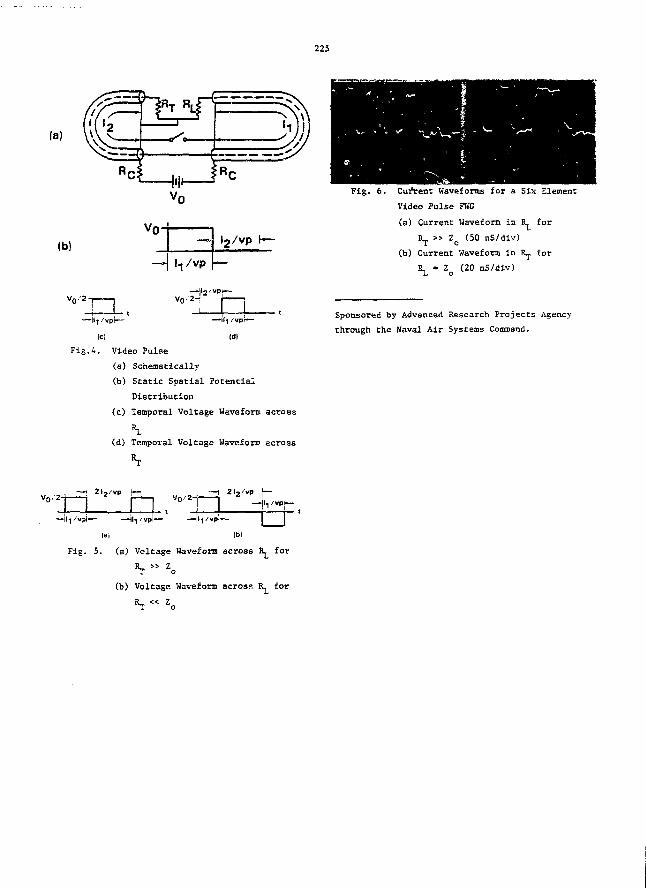
225
(b)v0- —-I ^/vp
1.,/vp P-
Fig. 6. Current Waveforms for a Six Element
Video Pulse FWG
(a) Current Waveform in IL tor
Rj, » ZQ (50 nS/div)
Cb) Current Waveform in R_ for
\ ~ Zo (20 nS/div)
pn—llj'vpi—
ICI
Fig.4. Vid
(a)
(b)
(c)
(d)
—111 /vpt—
Id)
eo Pulpe
Schematically
Stat ic Spatial Potential
Distribution
Tetnporal Voltage Waveform across
hTemporal Voltage Waveform across
K
Sponsored by Advanced Research Projects Agency
through the Naval Air Systems Command.
1 I I I 1 -j'l^p—ll<]/vpi— —ll^/vpl— —Ili/vpi— I I
laj Ibl
Fig. 5. (a) Voltage Waveform across R. for
(b) Voltage Waveform across R, for
*r<K zo
226
9.3
INVITED '
A 500 kV REP-RATE MARX GENERATOR
J. SHANNON
Maxwell Laboratories, Inc.
8835 Balboa Avenue, San Diego, California 92123
Abstract
An efficient PFN/Marx generator was constructed
for generating high average power electron beams
The generator consists of cen 100 kV PFN stages
connected in a Marx configuration. The Marx genera-
tor employs purged gas switches. The nominal
operating parameters are:
Voltage 500 kV
Current 10 kA
Pulse Duration 1 usec
Rep-Rate to 100 Hz
Average Power to 500 kW
This paper discusses the Marx charging power condi-
tioning and the operation of the generator into
resistive and electron beam loads.
Introduction
Electron beams have been used for some time in gas
lasers either as a source of ionization or as the
primary pumping mechanism. The extension of the
gas laser technology to high average power requires
the development of repetitively pulsed electron
beams. In the direct pumped schemes, efficiency is
c£ prime consideration. This limits the type of
technology which can be used, especially at higher
voltages and power. The work reported on in this
paper is aided at developing technology priiaarily
for tha direct pumped application.
Since a Marx generator is an inherently efficient
circuit for generating high voltage, it is an
attractive approach :o high average power, high
voltage systems. The availability1 of proven
100 kV rep-rate switch designs at the start of the
present program allowed the design to proceed with
a minimum of switch development. By incorporating
a pulse-forming network (PFN) into the Marx design,
the system was made efficient with an output suit-
able to the electron beam load.
The goal of the program is to develop the tech-
nology for scaling to larger systems, both in the
areas of the power supply and the electron beam
loads. Toward this end, a 500 kV device is large
enough to ensure that scaling can be demonstrated.
In the present paper, the Marx generator and
associated power conditioning will be primarily
discussed.
Marx Generator Design Considerations
Initially, the Marx generator was used as a single-
shot device in a cold cathode development program.
Two circuits were considered in the design of the
PFN/Marx generator; a Guillemin Type A voltage fed
network (shown in Figure 1A) and a standard 5-section
PFN as shown in Figure lb. Both circuits have real-
istic values for components in terms of available
capacitors and values of Inductors.
After initial consideration, it was decided that the
PFN/Marx approach was more suited to the present
application. There were basically two reasons for
this; first, calculations indicated that, for the
present parameters, the PFN/Marx circuit would have
a slightly faster risetime than a Guillemin Type A
network with a single resonant circuit. The rnairj-
facture of several values of rep-rate capacitors for
use in resonant circuits was considered impractical
227
Kith che then existing budget. Second, at the
inception of this program, the impedance collapse
in cold cathode guns was a major issue as concerns
efficient energy transfer. In the PFN/Marx approach,
it is more straightforward to taper the impedance
profile of the transmission line to compensate for
a collapsing impedance.
The output parameters of the generator were chosen
to be:
Voltage
Current
Pulse Length
.510
T.1
MVkA
Usec
Current Density ^10 A/cm2
These values give an impedance of 50 ohms for the
generator. Because of the availability of 100 kV
switches and rep-rate capacitors, s 10—scage Marx/
PFN was decided upon.
A practical number of meshes in the PFHs is five.
The PFN was made 10% longer in an attempt to get
longer flat top on the pulse. Based on these con-
siderations, the PFNs had the zero order design
parameters of 5 ohms impedance and an electrical
length of .55 usec.
A circuit diagram of the Marx generator is shown in
Figure 2 and in outline in Figure 3. The switches
and PFN stages are oil insulated and suspended by
nylon straps in an oil enclosure. This design makes
modifications such as changing the PFN inductors,
relatively simple. After initial operation in the
single-shot mode, the switches shown in Figure 3
were replaced by rep-rata switches and the gas
purge lines installed.
To simplify Che circuit, only the first two switches
were triggered. The remaining eight gaps were two
electrode switches and were closed by the erection
wave in the Marx generator. To ensure reliable
operation of the Marx generator, the stray capaci-
tance to ground of the positive side of tha third
switch (the first two electrode gap) WES enhanced
by extending the ground plane between the second
and third stage. This increases the over voltage
of the first two electrode gap. For the Marx to
erect reliably, it was necessary to install an
auxiliary irradiating pin in each gap. Because
of the efficiency requirements, inductors are used
to charge the PFN stages. The charging inductors
oust be large enough so that only a small fraction
of the energy is lost during the pulse and small
enough so that the Marx stages can be charged
uniformly. For the 2500 UH values used here, only
"ilZ of the energy is lost in the inductors during
the pulse and the 40 mK inductor in the intermediate
store still dominates the charging.
Marx Charging Supply Design Considerations
It has been found that for reliable spark gap opera-
tion at rep-rate, a "grace" period is necessary
before reapplying the voltage. Alternately the
voltage can be reapplied so slowly that restrike
will not occur. The fault mode that causes most
concern is a spark gap "lock-on" where the primary-
supply is connected to the gap. This sometimes
causes the arc to walk out of the gap and onto the
insulator causing severe damage. Because of this
concern, it was decided that the Marx charging
should have two stages to decouple the Marx from
the primary power supply.
The Marx charging circuit is shown in Figure A. To
initiate the sequence, S. is closed and the inter-
mediate capacitor is charged through diode D . After
S, has recovered, S., is closed and the Marx is
charged and fired at the peak of the charging wave-
form. The switches S^ and S, are closed by
superimposing a fast trigger pulse on the gap
causing breakdown. It was found necessary here to
have an auxiliary UV irradiator to make these gaps
operate reliably.
The resistor R^ is used to control the voltage on
C-. This approach was adopted because of budgetary
constraints and the desire to use proven power
supply available at a somewhat higher voltage than
necessary (manufactured by Electro Engineering
Works). A variable voltage transformer in the pri-
mary of the supply would eliminate the need for
such a large resistance. At this stage, overall
efficiency is not an issue and it is more economi-
cal to throw away some power.

228
Resistive Load Teats
The PFH/Marx generator was tested into a dummy load
and into various types of cold cathode emitters.
Typical output waveforms are shown in Figure 5 for
single-shot operation into an electron beam load.
For this case, the voltage risetime is .1 psec and
the pulse width is -.9 ysec. The Marx has been
tested at charge voltages from 50 kV to 100 kV and
found to have an operating range a factor of approx-
imately 2 in absolute pressure for a given voltage.
The usual operating point for the Marx is 2/3 of
the selfbreak voltage.
A limited amount of testing under rep-rate condi-
tions was done into a resistive load at the > utput
of the Marx generator. The purpose of these tests
was mainly to test out the various subsystems. The
volume of the liquid load resistor limited the
number of pulses per run to 50. A typical output
is shown in Figure 6 with a nominal SO ohm load on
the Marx. The Marx charging voltage and the output
voltage are shown in the figure. The measured
peak output voltage of 450 kV agrees well with half
the open circuit voltage of 480 kV.
At the present operating parameters, the Marx
generator has a one Sigma jitter of -30 nsec.
This can probably be improved by reducing the
pressure, but no systematic study of this has been
attempted.
Electron Beam Tests
Experiments on various cold cathode emitters have
been carried out. Typical output wavefonas are
shown in Figure 7. There are 50 and 100 consecutive
shots in the 5 Hz and 20 Hz cases shown. The
cathode in this case is a graphite felt cathode
at a current density of M.0 A/cm2. This cathode
structure has been tested up to 50 Hz in short
(5 sec) runs. The rep-rate ia limited at present
by outgassing in the diode and work is continuing
in this area.
The output of the generator with an electron beam
load is 500-600 kV and '••10 kA. The nonlinear nature
of the Child's low load tends to distort the pulse
somewhat, but the width (FWHM) of the power pulse
is M. psec which agrees with the calculated value.
For the waveforms shown in the figure, the calcu-
lated energy is 5.5 kJ per pulse compared to 5.9 kj
stored in the intermediate storage capacitor. This
gives a Marx efficiency of >90%, although the values
are the same within the accuracy of the measurements.
At 50 Hz operation, the average power is 275 kW into
the electron beam.
Switch Performance
There ar"> four switch operating conditions in the
sy3tem: two in the Marx charging supply and two in
the Mane generator. All the switches use dry air
and are fed by a gas blow-down system. Only a
limited amount of work has been done to explore the
operating range of the various switches and the gas
flow is much more than adequate based on previous
work.
The switches S, and S_ in the Marx charging supply
are identical to those described previously.1 The
same switch without the nested electrodes was used
in the upper eight stages of the Marx generator
(Mj). Three electrode switches (M.) were used in
the first two stages. All the switches except S,
had a grace period of >5 msec before reapplication
of the voltage. The recovery of S in Figure 4 was
controlled by the diode. The operating parameters
of the switches are shown in Table 1.
During the rep-rate operation consisting of "-10*
shots to date, no Mary prefires have been observed
for the present operating conditions. A few pre-
fires of switches S1 and S,, have occurred but were
traceable to trigger generator malfunctions. The
present operating values of the switches is ade-
quate for reliable operation.
Acknowledgement
The author would like to acknowledge the signifi-
cant contributions by J. DeVoss to the design and
construction of the major subsystems and by L.
Houghton to the construction and operation of the
facility. Acknowledgement must also be given to
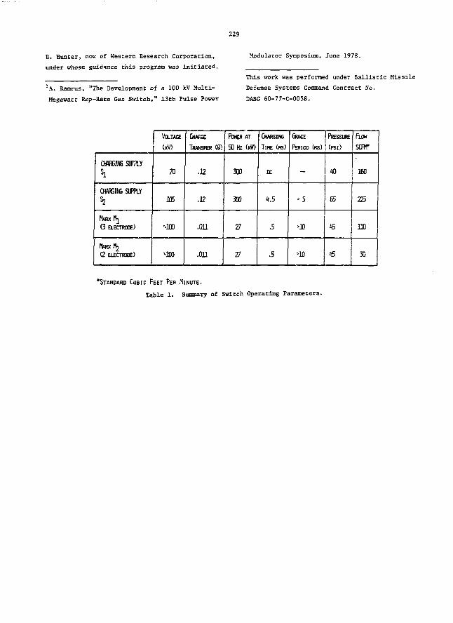
229
R. Hunter, now of Western Research Corporacicm,
under whose guidance this program was initiated.
!A. Ramrus, "The Development of a 100 kV Multi-
Megawatt Rep-Hate Gas Switch," 13th Pulse Power
Modulator Synposium, June 1973.
This work was performed under Ballistic Missile
Defense Systems Command Contract No.
DASG 60-77-C-0058.
CHARGING SUPPLYhCHARGING SFPLY
C aEORore)
(2 ELECTRODE)
VOLTAGE
(KV)
70
105
•qoo
•IDO
CHARGE
TRANSFER (Q)
.12
.12
.QU
.011
POWER AT
50 Kz (KW)
300
3D0
27
27
CHARGING
TIKE (MS)
BC
1.5
.5
.5
GRACE
PERIOD CMS)
-
> 5
>ID
>10
PRESSURE
(PSI)
40
65
«
15
FLOW
SCHf
160
225
110
30
"STANDARD CUBIC FEET PER MINUTE.
Table 1. Summary of Switch Operating Parameters.
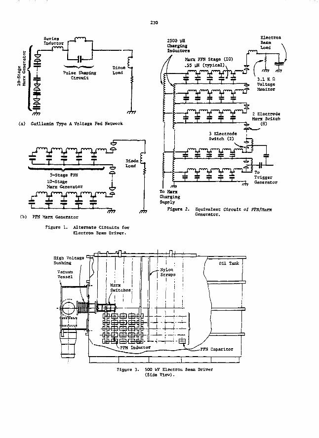
230
ttn
(a) Guilleain Type A Voltage Fed Network
T T T T T
5-Stage PFN
10-StageMarx Generator
DiodejLoad
T T(b) PFN Marx Generator
Figure 1. Alternate Circuits forElectron Beam Driver.
2S00 uHChargingInductors
ElectronBeanLoad
Marx PFN Stage (10).55 uH (typical).
1
T T T T T
T T T
VoltageMonitor
2 ElectrodeMarx Switch
(8)
u3 ElectrodeSwitch (2)
ToTriggerGenerator
To MarxChargingSupply
Figure 2. Equivalent Gircuit of PFN/MarxGenerator,
High Voltage 'Bushing Oil Tank
PFN Capacitor
Figure 3. 500 kV Electron Beam Driver(Side View).
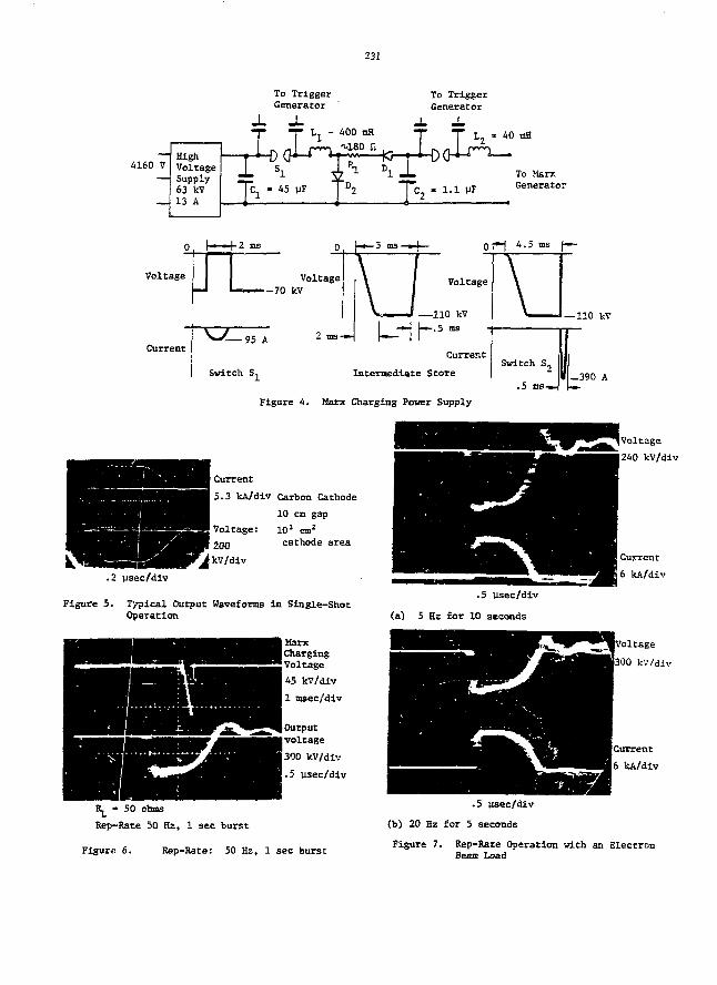
231
4160 VHighVoltageSupply63 kV13 A
To TriggerGenerator
-L JL- 400
45 yF j D2
To TriggerGenerator
T L > 4040 mH
1.1 PF
To MarxGenerator
Voltage
o, H-5
Voltage-70 kV
Current-95 A
Switch S, Intermediate Store
Figure 4. Marx Charging Power Supply
Current
5.3 kA/div Carbon Cathode
10 cm gap
Voltage: 103 cm2
2oo cathode area
kV/div
.5 ms-i
.2 psec/div
Figure 5. Typical Output Waveforms in Single-ShotOperation
.5 usec/div
(a) 5 Hz for 10 seconds
— 110 kV
-390 A
Voltage
240 kV/div
MarxChargingVoltage
45 kV/div
Outputvoltage
300 kV/div
.5 usec/div
.5 usec/div
(b) 20 Hz for 5 seconds
50 ohms
Rep-Rate 50 Hz, 1 sec burst
Current
6 kA/div
•oltage
|300 kv'/div
Figure 6. Rep-Rate: 50 Hz, 1 sec burst
Current
6 kA/div
Figure 7. Rep-Rate Operation with an ElectronBeam Load
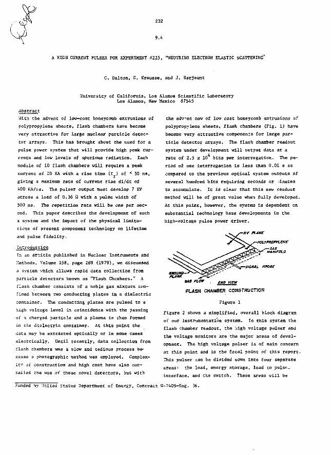
232
9.4
A HIGH CURRENT PULSER FOR EXPERIMENT #225, "NEUTRINO ELECTRON ELASTIC SCATTERING
C. Dalton, G. Krausse, and J. Sarjeant
Universtcy of California, LosLos Alamos, New
Abstract
With the advent of low-cost honeycomb extrusions of
polypropylene sheets, flash chambers have become
very attractive for large nuclear particle detec-
tor arrays. This has brought about the need for a
pulse power system that will provide high peak cur-
rents and low levels of spurious radiation. Each
module of 10 flash chambers will require a peak
current of 20 KA with a rise time (T ) of < 50 na,
giving a maximum rate of current rise di/dt of
400 KA/us. The pulser output must develop 7 KV
across a load of 0.36 fi with a pulse width of
500 ns. The repetition rate will be one per aec-
ond. This paper describes the development of such
a system and the impact of the physical limita-
tions of present component technology on lifetime
and pulse fidelity.
Introduction
In Jn article published in Nuclear Instruments and
Methods, Volume 158, page 289 (1979), we discussed
a system which allows rapid data collection from
particle detectors known as "Flash Chambers." A
flash chamber consists of a noble gas mixture con-
fined between two conducting plates in a dielectric
container. The conducting plates are pulsed to a
high voltage level in coincidence with the passing
or a charged particle and a plasma i3 chen formed
in the dielectric container. At this point the
data may be extracted optically or in some cases
electrically. Until recently, data collection from
flash chambers was a slow and tedious process be-
cause a photographic method was employed. Complex-
ity of construction and high cost have also cur-
tailed the use of these novel detectors, but with
Alamos Scientific LaboratoryMexico 87545
the advint now of low cost honeycomb extrusions of
polypropylene sheets, flash chambers (Fig. 1) have
become very attractive components for large par-
ticle detector arrays. The flash chamber readout
system under development will output data at a
rate of 2.5 x 10 bits per interrogation. The pe-
riod of one interrogation is less than 0.01 s as
compared to the previous optical system outputs of
several hundred bits requiring seconds or minutes
to accumulate. It is clear that this new readout
method will be of great value whea fully developed.
At this point, however, the system is dependent on
substantial technology base developments in the
high—voltage pulse power driver.
•SIS/Ml. P*OBE
«** nar , eN0 VIEW
FLASH CHAMBER CONSrRUCTION
Figure 1
Figure 2 shows a simplified, overall block diagram
of our instrumentation system. In this system the
flash chamber readout, the high voltage pulser and
the voltage monitors are the major areas of devel-
opment. The high voltage pulser is of main concern
at this point and is the focal point of this report.
This pulser can be divided down into four separate
areas: the ioad, energy storage, load to puls^-
interface, and the switch. These areas will be
Funded by 'Jr.ited States Department of Energy, Contract W-7405-Eng. 36.
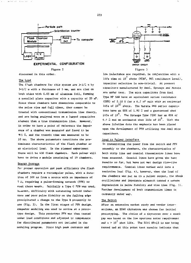
233
-Particle path^Scintilloiion counter
Flash ChamberModule !
ii
Logic j —H.V.
Pulser
Readout
—•-To computer
EXPERIMENTAL CONFIGURATION
Figure 2
discussed in this order.
The Load
The flash chambers for this system are 3-1/2 m by
3-1/2 m with a thickness of 5 mm, and are clad on
both sides vith 0.05 ram of aluminum foil, forming
a parallel plate capacitor with a capacity of 20 nF.
Since these chambers have dimensions comparable to
the pulse rise and fall times, they cannot be
treated with conventional transmission line theory,
and are being analyzed more as a lumped capacitive
element than a true transmission line. However,
in order to have a point of reference the imped-
ance of a chamber was measured and found to be
~5 Q, and the transit time was measured to be
10 ns. The above parameters constitute the pre-
dominant characteristics of the flash chamber as
an electrical load. In the planned experiment
there will be 450 flash chambers. Each pulser will
have to drive a module consisting of 10 chambers.
Energy Storage
For proper operation and peak efficiency the flash
chambers require a rectangular pulse, with a dura-
tion of 500 ns from a source with an impedance of
5 it, requiring a pulse-forming network (PFN) to
ir.aet these needs. Initially a Type C PFN was used,
however, difficulty with saturating toroid induc-
tors and poor pulse fidelity on the falling edge
precipitated a change to the Type B presently in
use (Fig. 3). In the first stages of PFN design,
computer modeling was used to arrive at a proto-
type design. This prototype PFN was then tested
under load conditions and adjusted to compensate
for distributed parameters not included in the
modeling program. Since high peak currents and
low inductance are required, in conjunction with a
life time of 10 shots (MTBF, 90% confidence level),
capacitor selection is non-trivial. At present
capacitors manufactured by Axel, Sprauge and Murata
are under test. The mica capacitors from Axel
Type MP 5AK have an equivalent series resistance
(ESR) of 2.10 S for a 6.5 nF unit vith an estimated
life of 10 shots. The Murata DHS series capaci-
tors have an ESR of 1.90 12 and a guaranteed shot
life of 10 . The Sprauge Type 720C has an ESR of
6.4 71 and an estimated shot life of 10 . With the
above lifetime data the emphasis has been placed
upon the development of PFN utilizing the Axel mica
capacitors.
Load to Pulser Interface
In transmitting the power from the switch and PFK
assembly co the chambers, the characteristics of
both strip line and coaxial transmission lines have
been assessed. Coaxial lines have given the best
results so far, but have not met design rise-tine
requirements. Coaxial lines worked well into a
resistive load (Fig. A), however, when the load of
the chambers was put on to a pulser output, the shock
oscillations and impedance mismatch caused a severe
degradation in pulse fidelity and rise time (Fig. 5';.
Further development of both transmission lines is
currently under way.
The Switch
After an extensive market study and vendor inter-
actions, an EG&G thyratron was chosen for initial
prototyping. The choice of a thyratron over a spark
gap was based on the low spurious noise requirement
and a > 10 shot life. The EG&G HY-13 is now being
tested and at this point test results indicate that
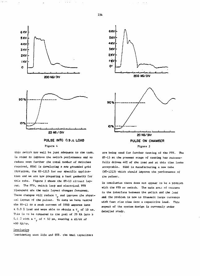
234
200NS/DIV 200 NS/01V
90%
10%
20 MS/01V
PULSE INTO 0.9 yi LOAD
Figure 4
this switch may well be just adequate to the task.
In order to improve the switch performance and so
reduce sven further the total number of switches
required, EGSG is developing a new grounded grid
thyratron, the HY-1313 for our specific applica-
tion and we are now preparing a test geometry for
this tube. Figure 3 shows the HY-13 circuit lay-
cut. The PFN, switch loop and electrical PFN
placement are che main layout changes foreseen.
These changes will reduce T and improve the physi-
cal layout of the pulser. To date we have tested
the HY-13 to a peak current of 5500 amperes into
a 0.9 2 load and were able to obtain a T of 10 ns.
This is to be compared to the goal of 20 KA into a
0.4 n with a : r of < 50 ns, meaning a di/dt of
400 KA/us.
Conclusion
Considering shot life and ESR, the Axel capacitors
90%
10%
SONS/01V
PULSE ON CHAMBER
Figure 5
are being used for further testing of the PFN. The
ffif-13 at the present stage of testing has success-
fully driven 40% of the load and at this time looks
acceptable. EG&G is manufacturing a new tube
(HY-1313) which should improve the performance of
the pulser.
In conclusion there does not appear to be a problem
with the PFN or switch. The main area of concern
is the interface between the switch and the load
and the problem is how to transmit large currents
with fast rise time into a capacitive load. This
aspect of che system design is currently under
detailed study.

235
References
1. C. Dalton and G. Krausse, Nucl. Inst. and 3. D. Turnquist et al., EG&G Application NoteMeth. 158, ;!89 (1979). H5005A-1.
2. S. FrieJman et al., "Multi-Gigawatt Hydrogen A. E. Iverson, ''Electromagnetic Short: Lines,"Thyracrons vlth Nano-Second Rise Times," Los Alamos Scientific Laboratory, to be pub-Modulator Symp., 3ufialo, NY, 1979. lished.
236
9 . 5
KrF LASER-TRIGGERED SF, SPABK GAP FOR L0W-JITTE3. THONGa
W. R. Rapoport, J. Goldhar, J. R. Murray, and M. D'Addario
Lawrence Livermore LaboratoryUniversity of CaliforniaLlvertnore, CA 94550
Abstract
An SF, spark gap operated at field stresses of 60-
180 kV/co cam be triggered with subnanosecond jit-
ter by volume breakdown In SF, induced by as little
as 10 aJ in 15 ns of KrF laser radiation.
Work performed under the auspices of the V. S. De-
partment of Energy by the Lawrence Livermore Labo-
ratory under contract number W-7405-ENG-48.
23?
10.1
EFFECTS OF SURROISTDING MEDIUM ON THE
PERFORMANCE OF EXPLODING ALUMINUM FOIL FUSES
T. L. Berger
Maval Surface Weapons Center
Dahlgren, Virginia 22448
Abstract
Flat aluminum foil fuses were exploded electri-
cally by discharging a capacitor bank into a series
combination inductance (•>. 600 nH) and fuse. The
2.54 s 2.54 x 0.0023 cm foils were exploded in a
sealed chamber. The time to burst and fuse
voltage characteristics were investigated as a
function of the fuse environment. Results are
given for foils exploded in various gases and
liquids.
Introduction
Electrically exploded conductors are useful in a
wide variety of pulsed power applications. Fast
foil current breakers have boen used to sharpen
current pulses from capacitor banks and from
explosive magnetic flux compression geaerator-4—7
transforms systems . In addition, fuses have
been used as the high speed elements for multiple
stage switching in inductive energy storage
Exploding conductors have also been used to launch
hypervelocity projectiles
Despite a wide variety of experimental work, there
remains much that is not understood about the
electrical explosion of conductors. Edge effects
which lead to breakdown, for example, are not well
understood. It seems reasonable that breakdown at
the edges of the foil is due to corona discharge
and explosions due to irregularities which are
introduced when the foil is cut. There is some
evidence, however, that there nay be mechanises
other than corona discharge which lead to edge
breakdown . The effect of volume changes is also
not well understood. Although electrical conduc-
tivity is known to be relatively sensitive to
volume changes, a constant volume approximation is
generally used in order to avor.d difficult hydro-
dynamic calculations . Finally, we mention the
effects of the surrounding medium on fuse charac-
teristics. It is not clear, for example, what the
characteristics of the surrounding medium should
be in order to best inhibit electrical breakdown.
On the one hand, it is suggested that the surround-
ing medium should confine the metal vapor in order
to inhibit collisionally induced ionization and
subsequent breakdown . On the other hand, it ha=
been suggested that heat transfer and chemical
reactions with the surrounding medium can inhibit
electrical breakdown
The purpose of this work is to attempt to gain, a
better understanding of the effects of the fuse
environment on fuse performance. In this paper
we report the results of measurements of the time
to burst and peak hold off voltage for aluminum
foils exploded in various gases and liquids.
Experimental Details
Flat aluminum foils 2.54 x 2.54 x 0.0023 cm were
exploded by discharging a capacitor bank into an
inductance in series with the aluminum foil.
The capacitor bank is a low inductance bank with
ignitron switches. The nominal charging voltage
is 20 kV, the capacitance is 98 uF, and the induc-
tance is 80 nH. The maximum bank current is
about 600 kA.
238
The capacitor bank ia coupled Into a parallel
plate transmission line by 15 coaxial cables. The
total inductance of the system is 620 nH.
Fuse current was measured with a low inductance
current viewing resistor. Fuse voltage was
measured with a resistive divider.
Experimental Results and Discussion
Figure 1 is a typical example of current and voltage
waveforms obtained In this work.. Fig. 1 shows that
there are a number of well defined stages in the
discharge of the capacitor bank through the foil.
For approximately the first 6 microseconds of the
discharge, the fuse voltage changes very little.
The foil resistance also changes very little and
Che current is not far from what is obtained in
the case of zero resistance. At t = 6 micro-
seconds, there is an abrupt change in the slope of
the voltage curve. At this time, a solid to
liquid phase transition is in progress. At t - 8
microseconds, there is .a veij sharp change In the
slope of the voltage curve. At this time, a
liquid to vapor phase transition is In progress
and fuse resistance is rapidly increasing. After
ioouc 200 nanoseconds, however, the fuse resistance
begins to decrease very rapidly presumably due to
lonization and breakdown of the metallic vapor.
Figure 2 is a plot of the time to burst as a
function of capacitor bank voltage for foils
exploded in air. Time to burst Is defined as" the
time to peak voltage measured from the point where
the current departs from Its initial value of zero.
The solid line in rig. 2 was plotted according to
the theory of Hasionnier et al . According to this
theory, the Joule heat power is equal to the rate
of change of the internal energy of the foil. This
leads Co Che equation
'12v 2
TS 2
where
C- \ sin
de,
— 1 -
C, =• bank capcitance
VQ » Initial bank voltage
S « cross sectional area of the foil
oi - angular frequency of sinusoidal current
Y » mass density of foil
p - resistivity of foil
e - internal energy per unit mass
T - initial foil temperature
T - foil temperature at vaporization
The quantity a can be calculated from handbook
tables and has the value a • 2.2 x 10¹⁶ for alumi-
num . This value of a corresponds to slow adiabatic
heating at atmospheric pressure. The numerical
factor k. takes into account the rapid heating1 i
encountered In exploding foils. Masionnier et al
suggest
1 < kj < 3.
Using the measured value of en and other known values
of physical parameters, Eq. (1) was solved numeri-
cally. The solid line shown in Fig. 2 was obtained
with k, » 2.2. The fit is seen to be quite good.
Time to burst as a function of capacitor bank
voltage was also measured for foils exploded in
distilled water and In aluminum oxide powder.
Within the limits of experimental uncertainty, the
results (not given in this paper) are the sane as
those obtained for foils exploded in air. He have
also measured the time to burst for foils exploded
In various gases and liquids. The results are
given in Table I. These results show that the
cime to burst is not sensitive to changes in Che
surrounding medium. Since Che chermal conduccivicy
is much greater for wacer Chan air, it seems
reasonable chat more energy and hence more cime
would be required to obtain a given resistance
change of Che foil in water than in air. According
Co Burtsev et al , changing the relative resistance
of the foil by a factor of 20 requires 4.5 kj/g in '
water and 3.2 kJ/g in air. We have not observed
this effect possibly because the natural frequency
of our system is smaller by about a factor of 2.
Our results, however, do agree with those of Salge
et al9.
We now consider the niaxittrum standoff electric field
measurements. These measurements were made for

239
foils exploded in various gases at pressures
ranging from 0-200 psig and in various liquids
over the density range 0.9 - 3.1 g/cm3. This was
done in order to test the assumption of two models:
the vaporization wave model and the heat transfer-
chemical reaction model
According to the vaporization wave hypothesis, a
vaporization wave propagates inward fron the con-
ductor surface. Ahead of the wave, the material
remains in the conducting state while behind the
wave, the material is in a vaporized insulating
state. If the vapor cloud Is free to expand, mean
free path effects should eventually lead to ioni-
zation and breakdown in the vapor. This has been
observed . Breakdown should be inhibited by
increasing the density of the surrounding medium.
Figure 3 is a plot of the maximum standoff electric
field as a function of density for foils exploded
in a 50?. S, 50% 0- gas mixture. This plot shows
that the electric field does indeed increase with
density in accordance with the vaporization wave
theory. The same effect was observed for the other
two gases used as shown in Table I. The peak
electric field was very nearly the same in all the
liquids except for transformer oil.
We now consider the heat transfer-chemical reac-
tion model. Conte et al have used this model to
explain their results for aluminum foils exploded
in water. An exothermic chemical reaction between
the foil and water Is thought to occur. The extra
heat drives the fuse toward higher resistance and
more rapid explosion. Foils exploded in H,0_
exhibited higher holdoff voltage than foils
exploded la H,0 presumably because 02 is more
chemically active than H_0.
In this investigation, we have searched for
chemical reactions in gases and liquids. Accord-
ing to Table I, the maximum electric field for the
gases tends to decrease with increasing oxygen
concentration. The peak electric field was the
same for HjO as for the more cheidcally active
HnQ2. Thus, the results of this work provide no
support for the chemical reaction model. We do
not reject this model, however, because we have
not investigated other factors which may be impor-
tant such as time to burst, foil dimensions, and
rate of energy transfer.
It is interesting that at the same density, the
peak electric field is greater for helium than for
the other gases. This effect may be due to vapor
cloud cooling since helium has a relatively high
thermal conductivity.
Conclusions
In conclusion, this work indicates that time Co
burst is largely independent of the surrounding
medium. We have also found no evidence that chemi-
cal reactions affect fuse performance. We have
found some indication chat heat transfer to the
surrounding medium-may inhibij breakdown. Finally,
we have found that the hold off voltage increases
with gas density in the pressure range 0-200 psi
but there Is a weak dependence on gas species.
References
1. C. Masionnier, J. H. Linhart, and C. Gourlau.
Rev. Sci. Instr. 17, 1380 (1966).
2. H. C. Early and F. J. Martin, Rev. Sci. Instr.
36, 1000 (1965).
3. J. N. Di Marco and L. C. Burkhardt, J. Appl.
Phys. &1_, 3894 (1970).
4. Ye.I. Azarkevich et al, Zhurnal Tekhnicheskoy
Fiziki 46_, 1957 (1976).
5. A. I. Pavlovskly, V. A. Vasyukov, and A. S.
Russkov, Zhurnal Tekhnicheskoy Fiziki, Pis'ma
v Redaktsiyu 3_> 789 (1977).
6. C M . Fowler, Private Communication.
7. B. Antoni, Y. Landure', and C. Nazet, in
Energy Storage. Compression, and Switching,
W. H. Bostick, V. Nardi, and 0. S. F. Zucker
Eds. (Plenum Press, New York, 1976), p. 481.
8. E. K. SchaU, Nature Phys. Sci. 231., 111 (1971).
9. J. Salge, U. Braunsberger, and V. Schwartz, in
Energy Storage. Compression, and Switching,
W. H. Botstick, V. Nardi, and 0. S. F. Zucker,
Eds. (Plenum Press, New York, 1976), p. 477.
10. V. E. Scherrer and P. I. Richards, Svma_.
Hypervelocitv Impact. 4th, Elgin AFB, Florida
(April 1960).
11. W. H. Clark et al, Svmp. Hvpervelocitv Impact,
7th, Tampa, Florida (Nov. 1964).
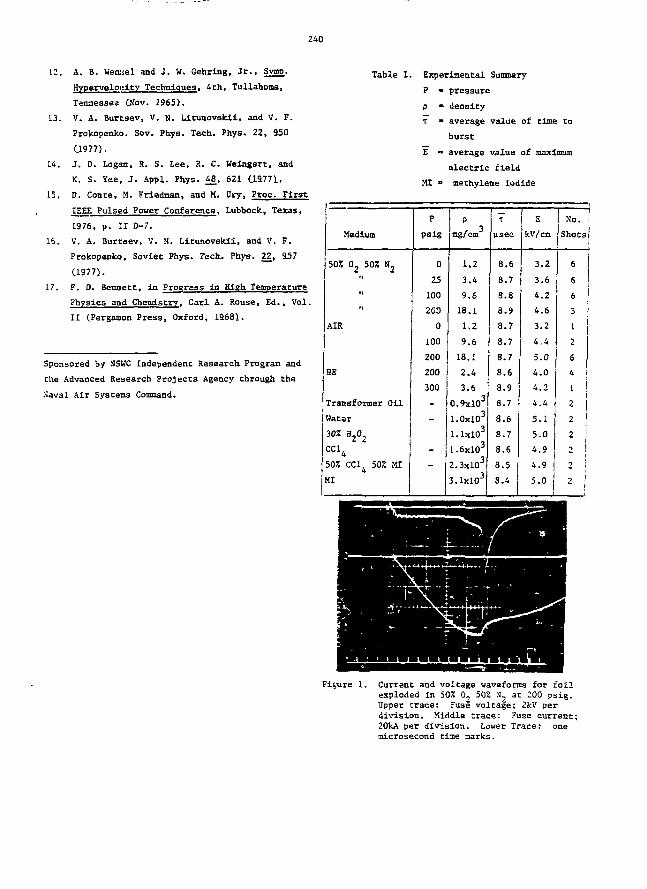
240
12. A. B. Wensel and J. W. Gehxing, Jr., Symp.
Hypervelocity Techniques, 4th, Tullahoma,
Tennessee (Nov. 1965),
13. V. A. Burtsev, V. N. Ldtunovskii, and V. F.
Prokopenko. Sov. Phys. Tech.. Phys. 22, 9-50
(.1977).
14. J. D. Logan, R. S. Lee, R. C. Weingart, and
K. S. Yee, J. Appl. Phys. 48, 621 U5771.
15. D. Conte, M. Friedman, and M. Dry, Proc. First
IEEE Pulsed Power Conference, Lubbock, Texas,
1976, p. II D-7.
16. V. A. Burtsev, V. S. Litunovskli, and V. F.
Prokopenko, Soviet Phys. Tech, Phys. 22, 957
C1977).
17. F. D. Bennetc, in Progress in High Temperature
Physics and Chemistry. Carl A. Rouse, Ed., Vol.
II (Pergamon Press, Oxford, 11681.
Sponsored by HSWC Independent Research Program and
the Advanced Research Projects Agency through the
Naval Air Systems Command.
Table I. Experimental Summary
P " pressure
p « density
x - average value of time to
burst
E =• average value of maximum
electric field
MI » methylene iodide
Medium
50% 02 50Z N2
AIR
HE
Transformer Oil
Hater
302 H20,
cci4
50% CC14 507. MI
MI
P
psig
0
25
100
20D
0
100
200
200
300
-
-
-
-
P
mg/cm
1.2
3.4
9.6
18.1
1.2
9.6
18.1
2.4
3.6
0.9xl03
l.OxlO3
l.lxlO3
l.6xlO3
2.3xlO3
3.1X10³
T
usec
8.6
8.7
8.8
8.9
8.7
8.7
8.7
8.6
3.9
8.7
8.6
8.7
8.6
8.5
3.4
E
kV/cm
3.2
3.6
4.2
4.6
3.2
4.4
5.0
4.0
4.2
4.4
5.1
5.0
4.9
4.9
5.0
No.
Shots
6
6
6
3
1
2
6
4
1
22
2
2 jt
Figure 1. Current and voltage waveforms for foilexploded in 50% 0, 50% S, at 200 psig.Upper trace: Fuse voltage; 2kV perdivision. Xiddle trace: Fuse current;20kA per division. Lower Trace: onemicrosecond time narks.
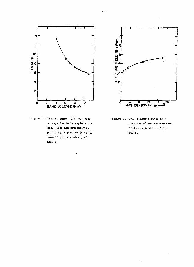
241
2 4 6 8 10BANK VOLTAGE IN kV
0 4 8 12 16 20GAS DENSITY IN tng/cm3
Figure 2. Time to burst (TTB) vs. bank
voltage for foils exploded in
air. Dots are experimental
points and the curve is dravn
according to the theory of
Ref. 1.
Figure 3. Peak electric field as a
function of gas density for
foils exploded in 50X 0,
50% N7.
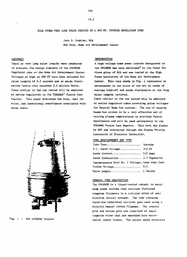
242
10.2
HIGH POWER VERY LONG PULSE TESTING OF A 200 KV. TETRODE REGULATION TUBE
Jere 0. Scabley, RCA
Bob Gray, Rome Air Development Center
ABSTRACT
Tests at very long pulse lengths were conducted
Co evaluate the design concepts of the S94000E
regulator tube at the Rome Air Development Center.
Voltages as high as 200 KV have been switched for
pulse lengths of 0.5 seconds and at anode dissi-
pation levels that exceeded 2.0 million Watts.
Tubes similar to the one tested will be employed
as series regulators in the TOKAMAK1 Fusion Test
Reactor. This paper discusses the tube, test re-
sults, and operational experiences associated with
those tests.
"ig. 1 - RCA S94000E Tetrode
INTRODUCTION
A high voltage beam power tetrode designated as
the S94000E has been developed^ by the Power De-
vices group of RCA and was tested at the High
Power Laboratory of the Rome Air Development
Center. This tube shown in Fig. 1 represents an
advancement in the state of the art in terms of
voltage hold-off and anode dissipation at the long
pulse lengths Involved.
Tubes similar to the one tested will be employed
as series regulator tubes providing pulse voltages
for Neutral Beam Ion sources. The use of neutral
beams has proven to be a very effective way of
raising plasma temperatures in previous Fusion
experiments and will be used extensively in the
TOKAMAK Fusion Test Reactor. This work was funded
by DOE and contracted through the Plasma Phvsics
Laboratory of Princeton University.
TUBE REQUIREMENTS FOR TFTR
Tube Type Tetrode
D.C. Anode Voltage 2P0 KV
Anode Current 125 Amps
Anode Dissipation 2.0 Megawatts
Instantaneous Grid So. 1 Voltage..Less than Zero
Screen Voltage D.C.
Pulse Length 1 Second
GEHERAL TUBE DESCRIPTION
The S94000E is a liquid-cooled ceramic to metal
beam power tetrode that utilises thoriated
tungsten filaments in a circular array of unit
electron optical systems. The cube contains
sixty-six individual electron guns each using a
directly heated ribbon filament. The control
grid and screen grid are comprised of small
-ungsten wires that are embedded into uater-
cooled copper blocks. The unique anode structure
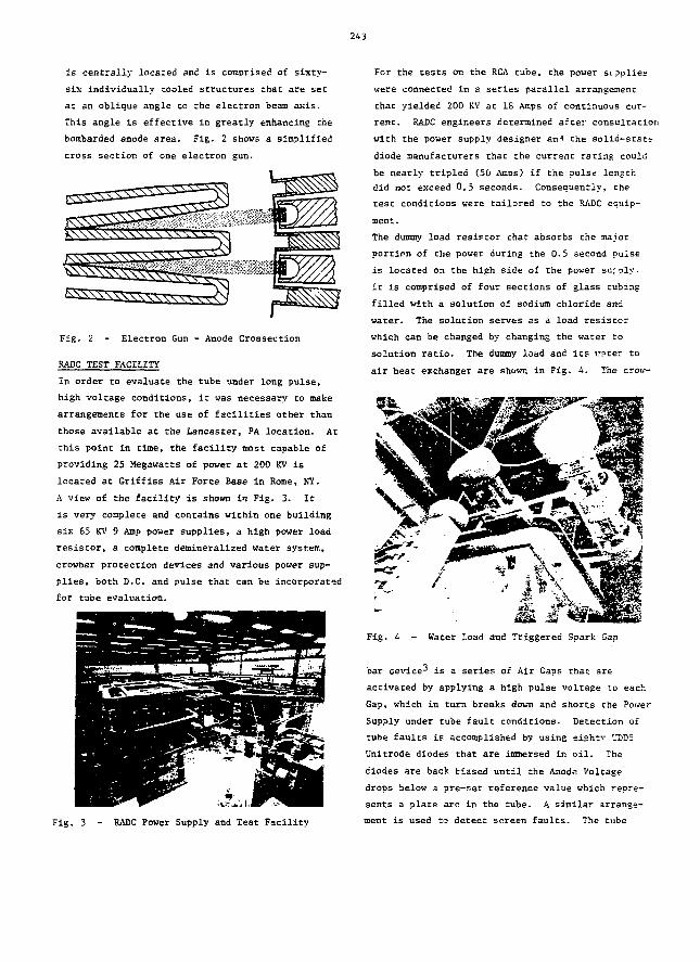
243
is centrally located and is comprised of sixty-
six individually cooled structures that are set
at an oblique angle to the electron beam axis.
This angle is effective in greatly enhancing the
bombarded anode area. Fig. 2 shows a simplified
cross section of one electron gun.
Fig. 2 - Electron Gun - Anode Crossection
RADC TEST FACILITY
In order to evaluate the tube under long pulse,
high voltage conditions, it was necessary to make
arrangements for the use of facilities other than
those available at the Lancaster, PA location. At
this point in time, the facility most capable of
providing 25 Megawatts of power at 200 KV is
located at Griffiss Air Force Base in Rome, NY.
A view of the facility is shown in Fig. 3. It
is very complete and contains within one building
six 65 KV 9 Amp power supplies, a high power load
resistor, a complete demineralized water system,
crowbar protection devices and various power sup-
plies, both D.C. and pulse that can be incorporated
for tube evaluation.
For the tests on the RCA tube, the power supplies
were connected in a series parallel arrangement
that yielded 200 KV at 18 AKDS of continuous cur-
rent. RADC engineers determined after consultation
with the power supply designer an"1 the solid-state
diode manufacturers that the current rating could
be nearly tripled (50 Amps) if the pulse length
did not exceed 0.5 seconds. Consequently, the
test conditions were tailored to the RADC equip-
ment.
The dummy load resistor chat absorbs the major
portirn of the power during the 0.5 second pulse
is located on the high side of the power sur ply.
It is comprised of four sections of glass tubing
filled with a solution of sodium chloride and
water. The solution serves as a load resistor
which can be changed by changing the water ro
solution ratio. The dummy load and its rater to
air heat exchanger are shown in Fig. 4. The crow-
Fig. 3 - RADC Power Supply and Test Facility
Fig. 4 - Water Load and Triggered Spark Gap
bar device- is a series of Air Gaps that are
activated by applying a high pulse voltage to each
Gap, which in turn breaks down and shorts the Power
Supply under tube fault conditions. Detection of
tube faults is accomplished by using eighty UDD5
Unitrode diodes that are immersed in oil. The
diodes are back biased until the Anode Voltage
drops below a pre-set reference value which repre-
sents a plate arc in the tube. A similar arrange-
ment is used to detect screen faults. The tube
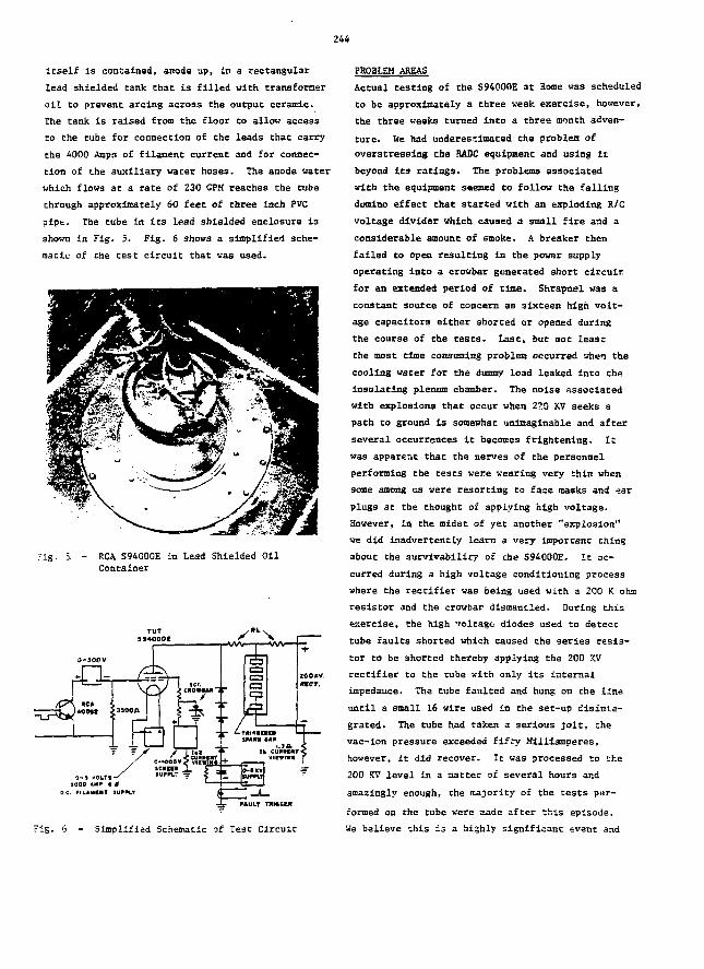
244
itself 13 contained, anode up, in a rectangular
lead shielded tank that is filled with transformer
oil to prevent arcing across the output ceramic,
the tank is raised from the floor to allow access
to Che tube for connection of the leads that carry
the 4000 Amps of filament current and for connec-
tion of the auxiliary water hoses. The anode water
which flows at a rate of 230 GFM reaches the cube
through approximately 60 feet of three inch PVC
pipt. The cube in its lead shielded enclosure is
shown in Fig. 5. Fig. 6 shows a simplified sche-
matic of the test circuit that was used.
"ig. 5. - RCA S94000E in Lead Shielded OilContainer
0 - » VOLT*90OO AM* t
D.C. FILAMtKT 3UPW.Y
•ir «""-T -rente*
Fig. 6 - Simplified Schematic of Test Circuit
PROBLEM AREAS
Actual testing of the S94O0OE at Rome was scheduled
Co be approximately a three week exercise, however,
the three weeks turned into a three month adven-
ture. We had underestimated the problem of
overstressing the RADC equipment and using it
beyond its racings. The problems associated
with the equipment seemed to follow the falling
domino effect that started with an exploding R/C
voltage divider which caused a small fire and a
considerable amount of smoke. A breaker then
failed to open resulting in the power supply
operating into a crowbar generated short circuit
for an extended period of time. Shrapnel was a
constant source of concern as sixteen high volt-
age capacitors either shorted or opened during
the course of the tests. Last, but not least
Che most time consuming problem occurred when the
cooling water for che dummy load leaked into the
insulating plenum chamber. The noise associated
with explosions that occur when 220 KV seeks a
path to ground is somewhat unimaginable and after
several occurrences it becomes frightening. It
was apparent that the nerves of the personnel
performing the tests were wearing very thin when
some among us were resorting Co face masks and ear
plugs at the Chought of applying high voltage.
However, in the midst of yet another "explosion"
we did inadvertently learn a very important thing
about che survivabiliry of che S94000E. It oc-
curred during a high voltage conditioning process
vhere the rectifier was being used with a 200 K ohm
resistor and the crowbar dismantled. During this
exercise, the high voltage diodes used to detect
tube faults shorted which caused Che series resis-
tor to be shorted thereby applying the 200 KV
rectifier to the tube with only its internal
impedance. The tube faulted and hung on che line
until a small 16 wire used in the set-up disinte-
grated. The tube had taken a serious jolt, the
vac-ion pressure exceeded fifty Hiiliamperes,
however, it did recover. Ic was processed to Che
200 KV level in a matter of several hours and
amazingly enough, the majority of che tests per-
formed on the cube were aade after this episode.
We believe this is a highly significant event and
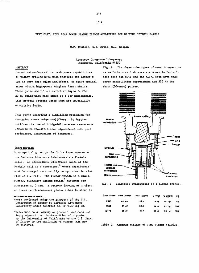
246
10.4
VERY FAST, HIGH PEAK POWER PLANAR TRIODE AMPLIFIERS FOR DRIVING OPTICAL GATES*
M.M. Howland, S.J. Davis, W.L. Gagnon
Laurence Livermore LaboratoryLivenaore, California 94550
ABSTRACT
Recent extensions of the peak power capabilities
of planar criodes have made possible the letter's
use as very fast pulse amplifiers, to drive optical
gates within high-power Nd:glass laser chains.
These pulse amplifiers switch voltages In the
20 kV range with rise tines of a few nanoseconds,
into crystal optical gates that are essentially
capacitive loads.
This paper describes a simplified procedure for
designing these pulse amplifiers. It further
outlines the use of bridged-T constant resistance
networks l:o transform load capacitance into pure
resistance, independent of frequency.
Introduction
Many optical gates in the Shiva laser system at
che Lawrence Livermore Laboratory are Pockels
cells. An approximate electrical model of the
Pockels cell is a capacitor, whose capacitance
must be charged very quickly to optimize the rise
time of Che cell. The planar triode is a small,
rugged, microwave vacuum triode designed for
operation co 3 GHz. A cutaway drawing of a class
of these centineter-wave planar tubes is shown in
"Work performed under the auspices of the U.S.Department of Energy by Lawrence LivermoreLaboratory under contract no. W-7405-Eng-48.
"Reference co a company or product name does notimply approval or recommendation of a productby the University of California or the U.S. Dept.of Energy t:o the exclusion of others chat maybe suitable.
Fig. 1. The three tube types of most interest co
u3 as Pockels cell drivers are shown in Table 1.
Note that the 8941 and the X2172 both have peak
power capabilities approaching the 500 kW for
short (50-nsec) pulses.
insulation
Fig. 1: Electrode arrangement of a planar triode.
mic Tvo»t Ptra VoUn
8940 4.5 kV
8941 15 kV
x2172 25 kV
Mix. Currant C Input C Output Mu
3SA 18 pf 0.11 pf 65
38 A 14 pf 0.11 pf 200
38 A 16 pf 0.2 pf 500
Table 1. Maximum ratings of some planar triodes.
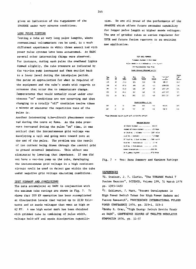
245
gives an indication of the ruggedness of the
S94000E under very adverse conditions.
LONG PULSE TESTING
Testing a tube at very long pulse lengths, where
conventional voltameters can be used, is a much
different experience to which those associated with
power pulse systems have been accustomed. At RADC
several other interesting things were observed.
For instance, during each pulse the overhead lights
dimmed slightly, the tube pressure as indicated by
the vac-ion pump increased and then settled back
to a lower level during the interpulse period.
One gains an appreciation for what is required of
the equipment and the tube's anode with regards to
stresses that occur due to temperature change.
Temperatures that would normally occur under con-
tinuous "on" conditions are now occurring and then
changing to a totally "off" condition twelve times
a minute or whatever the repetition rate of the
pulse is.
Another interesting ti-be-circuit phenomenon occur-
red during the tests at Rome. As the tube pres-
sure increased during the pulse "on" time, it was
noticed that the instantaneous grid voltage was
developing a tail and going more toward zero at
the end of the pulse. The problem was the result
of ion current being drawn through the control grid
to ground external impedance. This effect was
eliminated by lowering that impedance. If one did
not have a vac-ion pump on the tube, developing
the instantaneous grid voltage in a high resistant
circuit could be used to detect gas within the tube
under negative grid voltage operating conditions.
TEST SUMMARY AMD COHCLPSIONS
The data accumulated at RADC in conjunction with
the maximum tube ratings are shovn in Fig. 7. It
shows that 200 KV operation has been accomplished
at dissipation levels that varied up to 2150 Kilo-
watts and at anode voltages that went as high as
62 KV. A new high water mark has been obtained
with gridded tube in combining of pulse width,
voltage hold-off and anode dissipation capabili-
ties. We are all proud of the performance of the
S94000E which offers future extended capability
for longer pulse length at higher anode voltages.
The use of gridded tubes as series regulator for
TFTR and future fusion reactors is an exciting
new application.
TEST WTA S1WU0-
r i l a n e r t OuiBi ' . • 4300 JWcw
Pulw Leno-Ji • 0.5 SeoCTda a : J Kir r*i.-sit.*
200 Hiczooacords Ki»o Ttn>
Anccif Ceraaic Xirapfwi i.-. Oil
PCPd "-JitS Volte VOlu . J
^ " . j 52C 31P -3D 30C 3(
47.0 ^90 J1C -i'j 1S00/22C
^j.O SOC j lP -IT i.400 Ifif.
46.C 60( 51C -ri ii5C.'2W
so.; 590 :ic -is :£3i pis:
Anode Ccntnic if. Air
» pressure durira pulse and mterpulsc p
X 71tte Voltsae 230 KV
Pulsed X Piste current iZS taps
DC Grid tta. : -^ I tsoe leoti Volts
Crul tfc- .' Current *.5 AK»
37 Srid ?«. ; Si«s VsJuae 1000 Voits
Grid NO. i Dissipation 1? RV
Srin No. I Dissipation 10 K<
Anode Dissipst isn 2000 Kk
X FUseant Current 4700 taps
Fig. 7 - Test Data Summary and Maxlmi«ni Ratings
REFERENCES
k>. Steiner, J. T. Clarke, "The T0KAMAK Model T
Fusion Reactor", SCIENCE, Volume 199, 31 March 1978
pp. 1395-1403
2j. Eshleman, J, Mark, "Recent Development in
High Power Switch Tubes for High Power Radars and
Fusion Research", PSOCEEDINGS INTERNATIONAL PULSED
POWER C0NFEKENCE 1976, pp. IC5-1, IC5-5
3uobby R. Gray, "High Energy Switch Device Scudy
at RADC", CONFERENCE RECORD OF TWELFTH MODULATOR
SYMPOSIUM 1976, pp. 51-57
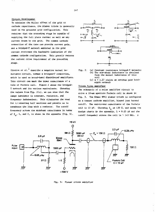
24?
Circuit Development
To minimize the Miller effect of the grid to
cathode capacitance, the planar triode is generally
used in the grounded grid configuration. This
requires that the preceding stage be capable of
supplying the full plate current as well as any
current drawn by the grid. The common cathode
connection of the tube can provide current gain,
and a bridged-T network employed in the grid
circuit overcomes the bandwidth limitation of the
common cathode configuration. This greatly reduces
the current drive requirement of the preceding
stage.
Ginzton et al.J describe a negative mutual in-
ductance circuit, termed a bridged-T connection,
which is used on broad-band distributed amplifiers.
This circuit can mask the input capacitance of a
tube or PocUels cell. Figure 2 shows the bridged-
T network and its various equivalents. Choosing
the values from Fig. 2(c), we can show that the
image impedance is constant, resistive, and
frequency independent. This eliminates the need
for terminating half sections and permits us to
terminate the line with a resistor. The cutoff
frequency across the midshunt capacitance in terms
of Z , L, and C, is shown in the appendix (Fig. 6).o
+9kV
Fig. 2: (a) Constant resistance bridged-T networks(b) The mid-shunt inductance is obtained
from the mutual inductance of thiscoil
(c) m - 1.27 yields an optimum gain band-width network
Triode Pulse Amplifier
The schematic of a pulse amplifier circuit to
drive a 10-nm aperture Pockels cell is shown in
Fig. 3. The Eimac 8941 planar triode is configured
as a common cathode amplifier, biased just beyond
cutoff. The end-to-end capacitance of the Pockels
cell is 15 pF. Choosing Z Q as 130 Si, and using the
design charts in the appendix, L » 0.25 yH and the
cutoff frequency across the tell is "- 145 MHz. A
2.3 pF
3.0 pFEimac
5M n > 3800 pF ~ Zn = 130 n< 30 kV
77T
0.25 MHy
130 a
I Pockels CellC = 15pF
-100 V
Fig. 3: Planar triode amplifier
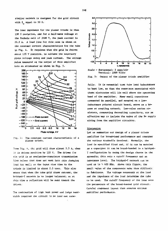
248
similar network is designed for the grid circuit
with Z equal to 50 ft.
The load impedance for the planar criode is then
130 ft resistive, and for a half-wave voltage at
the Pockels cell of 3500 V, the peak current is
26.9 A. A load line for this case is shoun on
the constant current characteristics for the tube
in Fig. 4. It requires that the grid be driven
about 135 V positive, to achieve the necessary
plate voltage swing and peak current. The voltage
pulse measured at the output of this amplifier
into an attenuator as shown la Fig. 5.
2001 ,
2.0 4.0 6.0 8.0 10
Plate voltage, kV
Fig. The constant current characteristic of aplanar triode.
7rom "i?. '-, the grid will draw almost 5.5 A, when
it is driven positive by 135 V. The driver for
the ?rid is an avalanche-transistor transmission
lir.e pulser that does not work into chis changing
Load too well; so the input rise time to the
triode is limited to about 2.5 nsec. This also
means that when the tube grid draws current, the
bridged-T network is no Longer balanced; so at
this time a reflection will be sent toward the
driver.
The combination of high oeak power and large band-
width requires the circuit to be laid out care-
-0.5
Scale - Horizontal: 5 nsec/div
Vertical: 1000 7/div
Fig. 5: Output of the planar triode amplifier
fully. It is essential tliat tube lead inductances
be kept low, so that the resonance associated with
these electrodes will lie well above the operating
band cf the amplifier. Many small capacitors
connected In parallel, and mounted on a low-
inductance printed circuit board, serve as a by-
pass or coupling network. Low-value series re-
sistors, connecting decoupling capacitors, are an
effective way to isolate the modes of the B+ supply
wiring from the amplifier circuitry.
Discussion
Let us summarize our design of a planar triode
amplifier for broad-band performance and consider
the various tradeoffs involved. Normally, the
load is specified first and, if it can be modeled
as a capacitor it can be broad-banded in a bridged-
T configuration by using the design charts in the
appendix; this sets a cutoff frequency and an
impedance level. The bridged-T network can be
used up to "' 400 MHz. Above this figure, the
small value of the components make them difficult
to fabricate. The voltage necessary at the load
and the impedance of the load determine the tube
to be used. The cutoff frequency of the ioad sees
the parameters of the broad-banded grid circuit.
Careful component layout then assures optimum
amplifier performance.

249
We have used the techniques presented here to
design a pulse amplifier for driving a 10-mm
Pockels cell. The amplifier performed as predicted.
Its output characteristics are: 3600 V into 130 fi
with 2.5-nsec rise time, 3-tiBec fall time, and
pulse width of 8-9 nsec. The Jitter is less than
100 psec.
Of the various lumped-constant lines for the anode
and grid circuits studied by Ginzten et al. . the
bridged-T network provides the highest-gain band-
width product. For a given gain, the bridged-T
line provides about twice the bandwidth of the
constant-K line.
He obtain the midshunt inductance from the mutual
coupling between the two halves of the coil, as
shown in Fig. 2(b). If we choose m Co be 1.27,,
the inductance to the midpoint of the coil must
be 40.3% of the total coil inductance.
By using the equation2 2
r • r n ,,HL 9r+10£ u H
where n is the number of turns, and SL and r are
the length and radius of the coil, respectively,
the correct coupling results when the length of the
coil is 1.35 times the coil's diameter.
10
Fraquiliey, t, (MHz)
Fig. 6: Design chart for bridged-" network ofFig. 3.
10 E
0X1
Fig. 7: Design chart of inductance for bridged-Tnetwork of Fig. 3.
The output voltage, taken across capacitor C in
Fig. 2(c), has a cutoff frequency
and the characteristic impedance
Figure 6 is a design chart for the bridged-T con-
stant resistance network of Fig. 2(c), with the
values of L and C plotted as functions of Z ando
~,. Figure 7 is a design chart for the inductor
in this network.
"This repon was prepared as in account of untilesponsored by ihe United Sutei Government.Neither the United Steles nor the United StilesEnergy Research & Development Administration,nor sny of their employees, nor iny of theircontractors, subcontractors, or their employees,mikes iny warranty, express or implied, orassumes any lerel liebtilry Of rejpoiujbilily for theaccuracy, eompleieneu or usefulness of myinformation, ipptritus. product or processdisclosed, or represents that ils use would notinfringe privately-owned richis."
References
1. L.L. Steinmetz, T.W. Pouliot, and B.C. Johnson.Applied Optics 12, 1468 (1973).
2. Electronics Engineers Handbook, D.G. Fink, ed.(McGraw-Hill, 1975), pp. 9-23 to 9-28.
3. E.L. Ginzton, W.E. Hewlett, J.H. Jasberg, andJ.D. Noe, "Distributed Amplification", inProc. IKE, 956, (August 1948).
4. W.L. Gagnon and B.H. Smith, "Simplified DesignTechniques for Distributed Power Amplifiers",Natl. Particle Accelerator Conf• (Feb. 1969).Also published as UCEL 18491, LawrenceLivermore Laboratory, Livermore, California.
250
10.5
VACUUM ARC SWITCHED INVERTER TESTS
AT 2.5 MVA*
RICHA3D ». MILLER and A. S. GILMOOR, JR.
Department of Electrical Engineering
Laboratory for Power and Environmental Studies
State University of New York at Buffalo
ABSTRACT A mathematical analysis of the unloaded
vacuum arc switch (VAS) inverter is undartaken; a
key element in chls analysis is the assumption of a
constant volcage drop of 50 volt3 across each VAS
while it is cr ctxng. From this analysis a con-
scant VAS-volcat;i -aodel is developed to explain the
VAS inverter operation. A comparison of data ob-
caineri from laboratory tests of the inverter is
made with data obtained from this model, and agree-
ment Is found to be within 10? for up to 15 alter-
nations.
INTRODUCTION High-frequency, high-power inverter
circuits employing vacuum arc switches (VAS's) as
che switching elements have been under development
at che Scate University of New York at Buffalo
(SUNYAB) for some time (1 - 7). The circuit used
in chis development is che series inverter shown
in Figure 1. Several cests have been conducted on
che inverter (3); using the results of these tests,
a model of che inverter was developed as is describ-
ed in che following paragraphs.
INVEgTER CIRCUIT ANALYSIS The operation of the in-
verter circuit shown in Figure 1 has been described
(6). In earlier work (1) the voltage drop across
the VAS was measured and found to be nearly constant
over a wide range of conducting currents. This
characteristic suggests a constant V ,„ model for the
VAS. Taking this characteristic into account, the
capacitor voltages during the conduction of VAS, can
be shown to be (4)
C
+ v,. (1)
~°1£ [-a, BinCu, t)-», cos On., t) ]
FIGURE 1. Series Vacuum Arc Switched Inverter.
*This work was sponsored by cha Air Force Aero-
propulsion Laboratory, Wright-Patterson AFB,
Ohio.
and
+ "vAS^ (2)
" c +c VVAS ~VC f—1 I in
, sin(u). O-r^cos (u, t) ]i ± i a_]
(3)
231
BCKTwhere a1 - - g p
i "Mr -°i2-find
CT l "
C2 +C1 C3
all of for which
n -0, 2, 4,
The equations for the capacitor voltages have a sim-
ilar form for the conduction of VAS, (4). Now, the
initial-final conditions between alternations take
the following type of form:
and
- vfitl.3Nwhere m • 2k+l,
n - 2k,
and k is the inverter output cycle mmber,
k - 0, 1, 2, 3, •••.
as the bright positive and negative peaks. This
oscillograph suggests an approach to comparing
data from the model with data from the test. The
waveform in this oscillograph has a definite envel-
ope; this envelope provides a good picture of the
operation of the entire circuit, since, as the model
equations show, an intercependence exists between
all of the parameters of the circuit. Therefore, if
the equations are obtained for the capacitor voltage
envelopes, this form of the model will provide a
basis for comparing the model with the data from ti«e
laboratory. The equations thus obtained are (4),
for the positive peaks,
And
°i n
"l 3 ul
again where
n - 0, 2, 4. 6, •••.
For the negative peaks, the equations become
(6)
Equations (1) - (3), together with the initial-final
conditions, comprise the Constant-V Model. A
comparison will now be made between data obtained
from this model and data obtained in the laboratory.
APPLYING THE MODEL Figure 2 shows an oscillograph
of v (t) obtained while the Inverter was operating.
In this particular test, the VAS's were pulsed alt-
ernately at a 1.04 kHz rate. The L-C combination
of the circuit was resonant at 9303 Hz, so the trans-
ition time between the two polarities indicated on
the oscillograph was about 54 usec. This left a de-
lay of 0.9 msec before the next VAS was fired.
This 0.9 msec delay appears in the oscillograph
2 [-o,8in(ui,t)-tu,co»(u,t)]+ •= i * *• i
"2
Cl U2
C2 V * * [ VAS2 C3 U2
C7)
a2t [-o2sin (u,t )-
(8)
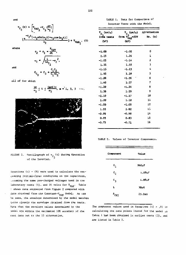
252
and
."VHJ + (9)
where
and
a l l of for which
S-S:
«
FIGURE 2. Oscillograph of v (t) during Operation
of che Inverter.
zquaticns (4) - (9) were used Co calculate the suc-
ceeding initial-final conditions on che capacitors,
-turning che same pre-cherged voltages used in che
laboratory tests (4), and 50 volts for V,VAS" Table
1 shows data extracted from Figure 2 compared with
data obtained from che Constant-V,.,_ Model. As canVAS
be seen, che envelope determined by che model matches
quite closely che envelope obtained from Che tests.
Note that che envelope values determined by che
.-aodei are within the estimated 10% accuracy of the
cast data out to che 15 alternation.
TABLE 1. Data for Comparison of
Inverter Tests with the Model.
V (nir/u)
from easts
(kV)
-1.00
1.25-1.05
1.35
-1.15
1.40
-1.20
1.40
-1.20
1.30
-1.10
1.20
-1.00
1.10
-0.90
0.95
-0.75
v («./„:from V^g-501
(kV)
-1.00
1.26
-1.14
1.35
-1.23
1.39
-1.26 •
1.37
-1.24
1.29
-1.17
LIB
-1.05
1.02
-0.90
0.83
-0.71
) Alternation
1/ No. (n)
0
1
2
3
4
5
6
7
8
9
10
11
12
15
14
15
16
TABLE 2. Values of Inverter Components.
Component Value
C,
C3
L
"CXT
960uF
4.89uF
4.89uF
30uH
23.2mn
The component values used in Equations (4)
calculating che data points listed for the
Table 1 had been obtained in earlier tests
are listed in Table 2.
model m
(3), and
253
CONCLUSIONS For che VAS operating in a series res-
onant inverter, the use of a Conscant-V Model to
represent the dynamic characteristics of the VAS is
a valid approximation for high power (2 - 2.5 MVA'r
operation, further tests are therefore warranted
at other operating power levels.
REFERENCES
1. A. S. Gilmour, Jr., and D. L. Lockwood, "Vacuum
Arc Inverter Switch Development Program", Proc.
IEEE 1975 Naecon, pp281-288, June 1975
2. A. S. Gilmour, Jr., and D. C. Hopkins, "Recent
Results of Vacuum Arc Switched Multi-Megawatt
Inverter Tests", Proc. IEEE International Pul-
sed Power Conference, Texas Tech University,
Lubbock, Texas, November 1976
3. D. C. Hopkins, "Construction and Energy Loss of
a Vacuum Arc Switched Series Inverter", MSEE
Thesis, State University of New York at Buffalo,
Amherst, NY, February 1978
4. R. N. Miller, "Vacuum Arc Switched Inverters",
PhD Dissertation, State University of New York
at Buffalo, Amherst, M, February 1979
5. R. N. Miller, R. E. Dollinger, and A. S. Gilmour,
Jr., "High Repetition Rate, High Power Pulse
Tests of Vacuum Arc Switches", Proc. IEEE Pulse
Power Modulator Symposium, State University of
Nev York at Buffalo, Amhersc, NY, June 1978
6. R. N. Miller, sz_ _al, "A Multi-Megawatt, Vacuum
Arc Switched Inverter for Airborne Applications",
Proc. IEEE Pulse Power Modulatoi Symposium,
State University of New York at Buffalo, Am-
herst, NY 1978
7. R. N. Miller, P. T. Glinski, rind A. S. Gilmour,
Jr., "A Facility for Testing High Power DC, AC,
or Pulsed Devices", Proc. IEEE International
Pulse Power Conference, Te;tas Tech University,
Lubbock, Texas, November 1976
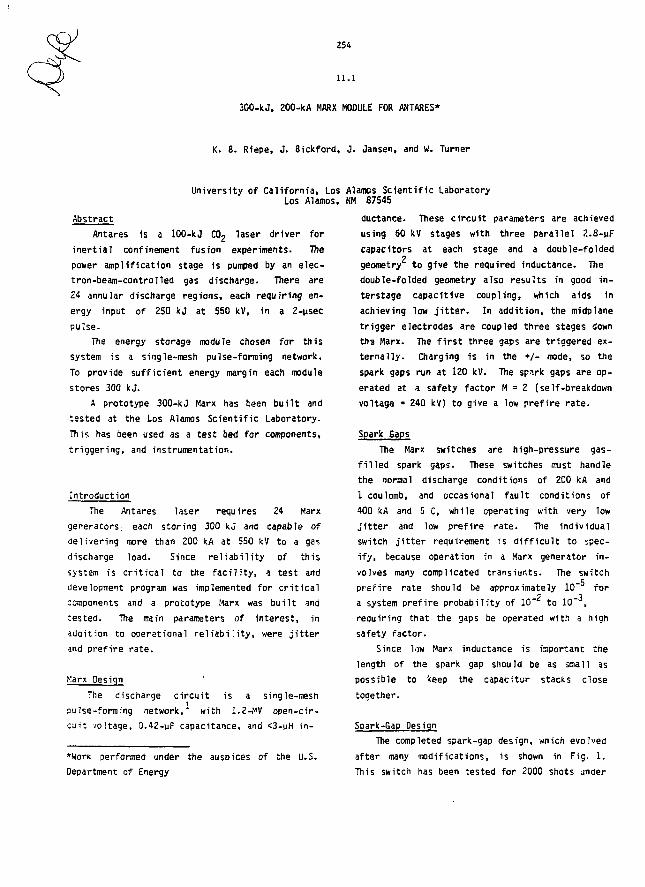
254
11.1
300-kJ, 200-kA MARX MODULE FOR ANTARES*
K. B. Riepe, J. Bickford, J. Jansen, and W. Turner
University of California, LosLos Alamos,
Abstract
Antares is a 100-kJ C02 laser driver for
inertia! confinement fusion experiments. The
power amplification stage is pumped by an elec-
tron-beam-controlled gas discharge. There are
24 annular discharge regions, each requiring en-
ergy input of 250 kj at 550 kV, in a 2-usec
pulse.
The energy storage module chosen for this
system is a single-mesh pulse-forming network.
To provide sufficient energy margin each module
stores 300 kj.
A prototype 300-kJ Marx has been built and
tested at the Los Alamos Scientific Laboratory.
This has been used as a test bed for components,
triggering, and instrumentation.
Introduction
The Antares later requires 24 Marx
generators: each storing 300 kj and capable of
delivering more than 200 kA at 550 kV to a gas
discharge load. Since reliability of this
system is critical to the facility, a test and
development program was implemented for critical
components and a prototype Marx was built and
tested. The main parameters of interest, in
addition to operational reliability, were jitter
and prefire rate.
Marx Design
The discharge circuit is a single-meshI
pulse-forming network," with 1.2-MV open-cir-
cuit voltage, 0.42-uF capacitance, and <3-»H in-
*WorK performed under the auspices of the U.S.
Department of Energy
Alamos Scientific LaboratoryNM 87545
ductance. These circuit parameters are achieved
using 60 kV stages with three parallel ?..8-uF
capacitors at each stage and a double-folded2
geometry to give the required inductance. The
double-folded geometry also results in good in-
terstage capacitive coupling, which aids in
achieving low jitter. In addition, the midplane
trigger electrodes are coupled three stages down
tbi Marx. The first three gaps are triggered ex-
ternally. Charging is in the +/- mode, so the
spark gaps run at 120 kV. The spirk gaps are op-
erated at a safety factor M = 2 (self-breakdown
voltage » 240 kV) to give a low prefire rate.
Spark Gaps
The Marx switches are high-pressure gas-
filled spark gaps. These switches must handle
the normal discharge conditions of 200 kA and
i coulomb, and occasional fault conditions of
400 kA and 5 C, while operating with very low
jitter and low prefire rate. The individual
switch jitter requirement is difficult to spec-
ify, because operation in a Marx generator in-
volves many complicated transients. The switch
prefire rate should be approximately 10" for
a system prefire probability of 10~* to 10" ,
requiring that the gaps be operated with a high
safety factor.
Since low Marx inductance is important the
length of the spark gap should be as small as
possible to keep the capacitur stacks close
together.
Spark-Gap Design
The completed spark-gap design, wnich evolved
after many modifications, is shown in Fig. 1.
This switch has been tested for 2000 shots under
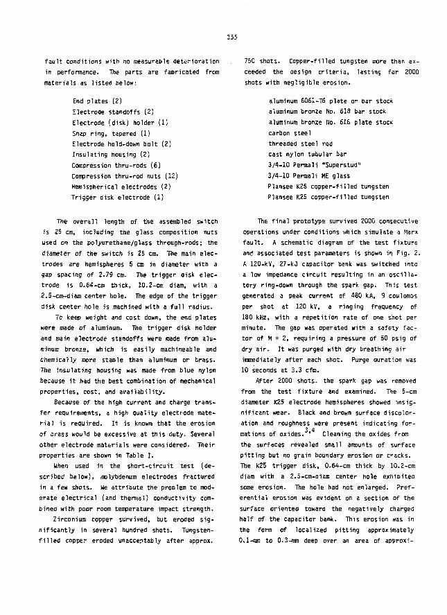
255
fault conditions with no measurable deterioration
in performance. The parts are fabricated from
materials as listed below:
End plates (2)
Electrode standoffs (2)
Electrode (disk) holder (1)
Snap ring, tapered (1)
Electrode hold-down bolt (2)
Insulating housing (2)
Compression thru-rods (6)
Compression thru-rod nuts (12)
Hemispherical electrodes (2)
Trigger disk electrode (1)
750 shots. Copper-filled tungsten more than ex-
ceeded the design criteria, lasting for 2000
shots with negligible erosion.
aluminum 6061-T6 plate or bar stock
aluminum bronze No. 618 bar stock
aluminum bronze Mo. 616 plate stock
carbon steel
threaded steel rod
cast nylon tubular bar
3/4-10 Permali "Superstud"
3/4-10 Permali HE glass
Plansee K25 copper-filled tungsten
Plansee K25 copper-filled tungsten
The overall length of the assembled switch
is 25 cm, including the glass composition nuts
used on the polyurethane/glass through-rods; the
diameter of the switch is 25 cm. The main elec-
trodes are hemispheres 5 cm in diameter with a
gap spacing of 2.79 cm. The trigger disk elec-
trode is 0.64-cm thick, 10.2-cm diam, with a
2.5-cm-diam center hole. The edge of the trigger
disk center hole is machined with a full radius.
To keep weight and cost down, the end plates
were made of aluminum. The trigger disk holder
and main electrode standoffs were made from alu-
minum bronze, which is easily machineable and
chemically more stable than aluminum or brass.
The insulating housing was made from blue nylon
because it had the best combination of mechanical
properties, cost, and availability.
Because of the high current and charge trans-
fer requirements, a high quality electrode mate-
rial is required. It is known that the erosion
of brass would be excessive at this duty. Several
other electrode materials were considered. Their
properties are shown in Table I.
When used in the short-circuit test (de-
scribed below), inolybdenum electrodes fractured
in a few shots. We attribute the problem to mod-
erate electrical (and thermal) conductivity com-
bined with poor room temperature impact strength.
Zirconium copper survived, but eroded sig-
nificantly in several hundred shots. Tungsten-
filled copper eroded unacceptably after approx.
The final prototype survived 2000 consecutive
operations under conditions which simulate a Marx
fault. A schematic diagram of the test fixture
anc! associated test parameters is shown in Fig. 2.
A 120-kV, 27-kO capacitor bank was switched into
a low impedance circuit resulting in an oscilla-
tory ring-down through the spark gap. This test
generated a peak current of 480 It A, 9 coulombs
per shot at 120 kv, a ringing frequency of
180 kHz, with a repetition rate of one shot per
minute. The gap was operated with a safety fac-
tor of M = 2, requiring a pressure of 50 psig of
dry air. It was purged with dry breathing air
immediately after each shot. Purge duration was
10 seconds at 3.3 cfm.
After 2000 shots, the spark gap was removed
from the test fixture and examined. The 5-cm
diameter K25 electrode hemispheres showed insig-
nificant wear. Black and brown surface discolor-
ation and roughness were present indicating for-3 4
nations of oxides. * Cleaning the oxides from
the surfaces revealed small amounts of surface
pitting but no grain boundary erosion or cracks.
The K25 trigger disk, 0.64-cm thick by 10.2-cm
diam with a 2.5-cm-diam center hole exhibited
some erosion. Tne hole had not enlarged. Pref-
erential erosion was evident on a section of the
surface oriented toward the negatively charged
half of the capacitor bank. This erosion was in
the form of localized pitting approximately
0.1-nm to 0.3-nin deep over an area of approxi-
256
Metal
Molybdenum
Zirconium Copper
Tungsten-filledcopper matrix
Copper-filledtungstan matrix
irately 1 cm near the hole edgediscoloration and roughness were present as onthe hemispheres.
The interior surfaces of the nylon insulatorwere discolored, glazed and rough, but no cracks,burns, or electrical tracking were in evidence.It appeared as though heat had glazed the nylon,short wavelength radiation had discolored it, andhot, nonconducting metal oxides had splatteredand coated the surfaces. Blue-colored powder(probably zinc oxide) had settled by gravity onthe lower halves of each insulator. At the con-clusion of the 2000-shot test, the dielectricstrength of the nylon surface was still suffi-cient to hold off 120 kV for three minutes at agas pressure of 30 psig (M = 1.2). This test wasrepeated three times with several full-powershots between the three-minute holding periods.
The switch was tested for jitter at differentoperating voltages and pressures with a 0.25-ohmCJSO^ resistor installed to simulate actual oper-ating conditions. A 500-ohm, CuSC^ resistor wasinserted in series with the trigger electrode tosimulate circuit values in the Marx generator.The test arrangement is shown in Figs. 3 and 4,and the test results are shown in Figs. 5-11.The trigger voltage amplitude and waveform (Fig.5) was held constant for all jitter measurements.The time spread is on the order of 10 ns. Theaffect of trigger amplitude on jitter is shownin Figs. 11 and 12. A Hewlett-Packard 5370-ATime Interval Counter corroborated the oscillo-scope data.
METALS
ElectricalConductivity
Fair
Excellent
Good
Good
le same oxide
TABLE IINVESTIGATED
PropertyHigh Temp.Strength
Excellent
Poor
Poor
Excellent
Resistors
Room TemperatureImpact Strength
Very Poor
Good
Poor
Poor
Most Marx generators have used liquid resis-tors for stage charging isolation and triggercoupling. Me felt that liquid resistors wouldnot provide the reliability required in thislarge system. Some type of solid resistor waspreferred. We tested two types, wire-wound andCarborundum type AS. The test consisted of dis-charging a 170-uF capacitor at voltages up to11 kV (10 kj) into the resistor. The resistorswere first soaked in transformer oil. The wire-wound resistors were Dale 225 W, 100 ohm. Theyfailed at 1/2 kj, by melting of the coating. TheCarborundum resistors were type 889 AS (12 in.long, 1 in. diam). They failed at 3 kj by chip-ping of the material. These are rated by themanufacturer at 35 kj when operated in air. Wethen tested some resistors which were coatedwith epoxy by the manufacturer to keep oil outof the resistor body. These were run up to10 kj, the limit of our test facility, withoutfailure. This provided an adequate safety mar-gin for use in the Marx generator.
Marx TestingA prototype Marx was built and tested to de-
termine operating reliability, jitter, and pre-fire rate. Secause the resistor development pro-gram was still in progress when the Marx wasbuilt, liquid resistors were used initially.
Jitter was measured using an HP-5j7OA timecounter. The start signal was taken from thefirst stage of trigger amplification, a PATCOPT-70. The remainder of the trigger system con-
25?
sists of a PATCO TG-55 (Krytron switched spiral
line) and a three-stage trigger Marx with 120-kV
output, driving three 50-ohro cables, 30 ft long.
The stop signal for the counter comes from ao
shielded single-turn 8 probe placed in the Marxtank. Because of severe noise problems, this was
coupled through an analog fiber-optic system.
The system rms jitter with liquid charging
and trigger resistors was 12 ns. With solid
charging resistors and liquid coupling resistors,
the jitter was 14 ns, and with all solid resis-
tors, jitter was 15.5 ns. All jitter measure-
ments are after 500 to 800 shots at full energy.
A set of shots was 20 to 30. The liquid resis-
tors were mounted directly to the capacitor bus-
bars. When the change was made to solid charg-
ing resistors, all the resistors were mounted on
a board outside the Marx with wires going to the
bus-bars. The increased inductance of this path
may account for the increased jitter of the Marx.
The prefire rate has been on the order of
0.01. This seems excessive, considering that the
spark gaps are run with a safety factor M « 2,
and that the electrodes feel very smooth after
running at full energy. Self-breakdown voltage
vs pressure curves were run on new and used {500-
shot) gaps. These showed only a few percent dif-
ference. Experiments are continuing using in-
creased air flow through the gaps 2nd 50-um mesh
filters on the air line to each gap.
References
1. Kenneth B. Riepe and Hansjorg Jansen, "Pulsed
Power Systems for the LASL High Energy Gas
Laser Facility," IEEE International Pulsed
Power Conference, Lubbock, TX, Nov. 1976,
IEEE Publication No. 76CH1147-8 REG 5.
2. Kenneth B. Riepe and Mary J. Kircher, "Design
of the Energy Storage System for the High
Energy Gas Laser Facility at LASL," Seventh
Symposium on Engineering Problems of Fusion
Research, Knoxville, TN, Oct. 1977, IEEE
Publication No. 77CH1267-4-NPS.
3. G. N. Glasoe and J. If. Lebacqz, Pulse Gen-
erators, (Dover Publications, Inc., New York,
NY, 1965), p. 280.
4. Z. E. Gruber and R. Suess, "Investigation of
the Erosion Phenomenon in High Current, High
Pressure Gas Discharges," Institute for
Plasmaphysik, Garching bei Hunchen, IPP 4/72
(December 1969).
Fig. 1. Tne tested spark-gap design.
TRIGGERPULSE
TOTAtSCRIES
I.
SPARK GAP -
ZD <LJc h j
lOarf
Ilpaal)V tusld.ott
ij par aha:
E»r r awtabad1 t.v^ern*Ropot.lios, rax*
• 4SZkA• lzotv
• 27tr
• lUkHs
Fig. 2. Worst-case fault- test parameters.
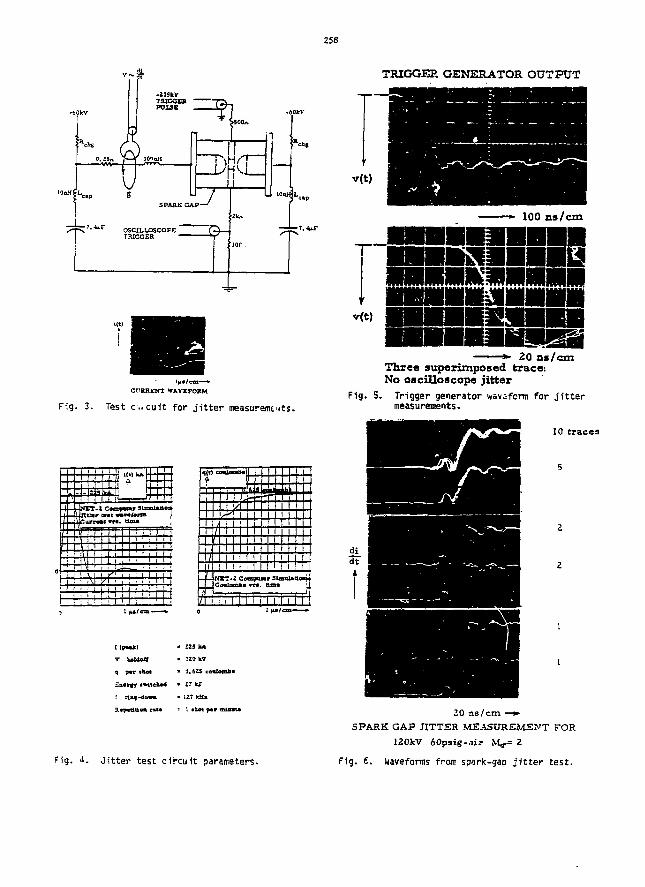
256
TRIGGER GENERATOR OUTPUT
CtTKRENT WAVErORM
Fig. 3. Test c . cu i t for j i t te r measurements.
i\T
WXT-2Htsrnr
L_
1 \
b
cenit
Y
MBei
fV«nr9Io
i
H
rih-
1
1
J-
J1
-1-4
-1
- j
.it
7
-
y
\ i
!
i
1Lft•frT1 I
1l
11 i 1
i • t
i
L
i ;
N t T - 2 Compotar SLmnUHoB^Coaiomaa vr*. Oral ^
i i i i i 11
L(pwfc)
y frnv sbflt
- a w l t e h # -
• 223 HA
> 3.6JS coalamb*
• zrw
Rapotltlim rum 3 1 ibot p*r misnu
v(t)
* 20 ns /cmThree superimposed trace:No oscilloscope jitter
Fig. S. Trigger generator wavifonu for j i t t e rmeasurements.
10 traces
Fig. 4. Jitter test circuit parameters.
20 as/cm —••SPARK GAP JITTER MEASUREMENT FOR
120kV 60psig-air M^= 2
Fig. 6. Waveforms from spark-gap j i t t e r test.
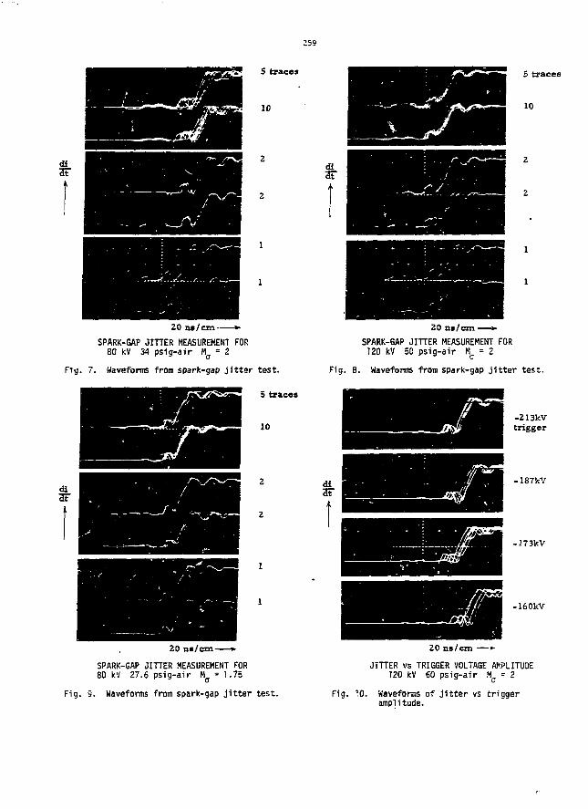
259
di
5 traces
10
20 ni/cm-
SPARK-GAP JITTER MEASUREMENT FOR80 kV 34 ps i g -a i r Mg = 2
F ig . 7. Waveforms from spark-gap j i t t e r t e s t .
5 traces
10
20 ns/cm »•
SPARK-GAP JITTER MEASUREMENT FOR80 kV 27.6 ps ig -a i r MQ = 1.75
Fig . 9. Waveforms from spark-gap j i t t e r t e s t .
5 traces
10
20 ns /cm *•
SPARK-GAP JITTER MEASUREMENT FOR120 kV 50 ps i g -a i r Ma = 2
Fig. 8. Waveforms from spark-gap j i t t e r t e s t .
-213kVtrigger
-187kV
-173kV
-160kV
20 ns/cm -
JITTER vs TRIGGER VOLTAGE AMPLITUDE120 kV 60 ps ig -a i r Mo = 2
Fig. 10. Waveforms o f j i t t e r vs t r i gge ramplitude.
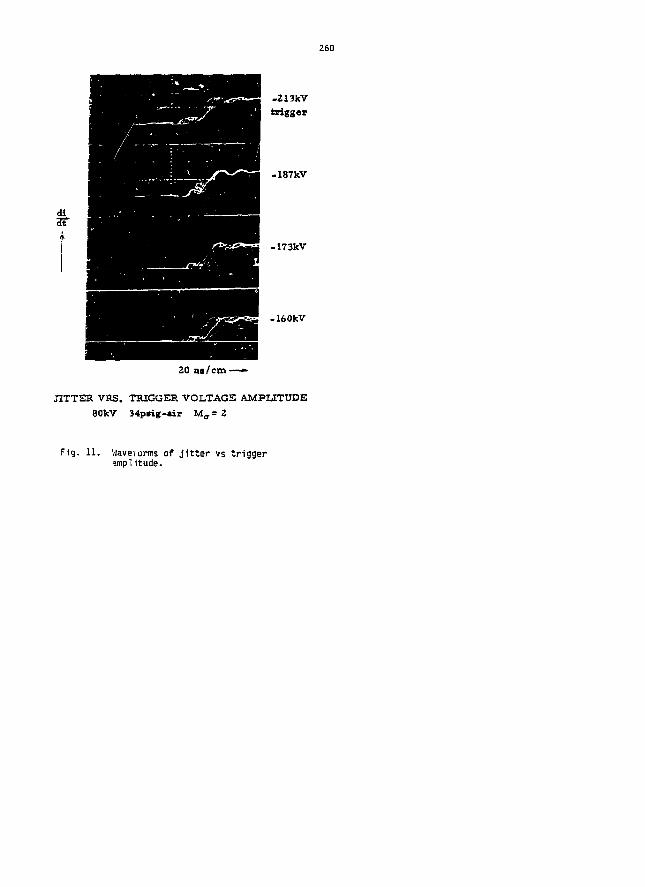
260
di3T
-213kVtrigger
-187kV
-173kV
-160kV
20 ns/cm—•
JITTER VRS. TRIGGER VOLTAGS AMPLITUDE80kV 34p«ig-air M,= 2
Fig. 11. Waveforms of jitter vs triggeramplitude.
261
11.2
A LARGE-AREA COLD-CATHODE GRID-CONTROLLED ELECTRO!. GUN FOR ANTARES*
W. R- Scarlett, K. R. Andrews, H. Jansen
University of California, LosLos Alamos,
Abstract
The CO2 laser amplifiers used in the Antares
inertia! confinement fusion project requira
large-area radial beams of high-energy electrons
to ionize the laser medium before the main dis-
charge pulse is applied. We have designed a
grid-controlled, cold-cathode electron gun with
a cylindrical anode having a window area of
9.3mZ. A full diameter, 1/4 length prototype of
the Antares gun has been built and tested. The
design details of the Antares electron gun will
be presented as well as test results from the
prototype. Techniques used for the prevention
and control of emission and breakdown from the
grid will also be discussed.
Alamos Scientific LaboratoryNM 87545
The electron-gun design is governed by sev-
eral constraints. First, the electrons must have
sufficient energy to penetrate the electron-gun
window and the gas volume of laser gas between
the windows and the power amplifier anode. Per
the range of operating pressures being corsidere(i
for Antares, electrons having energy between 4G&
and 550 keV are required.
The second requirement is that the electron
gun deliver a beam having uniform current density
between 50 and 100 mA/cr/ and lasting for 5 us.
This current density produces the required imped-
ance in the gas for the main discharqe.
A third constraint is that the spacing be-
tween anode and cathode must be sufficient to
prevent vacuum breakdown.
Introduction
The Antares laser fusion system at the Los
Alamos Scientific Laboratory (LASL) is designed
to deliver up to 100 kj of energy to a target in
a 1-ns pulse. A low energy, short pulse of CO2
laser light is split into six beams, each of
which is then amplified in a laser power
amplifier.
The annular pumped volume of each power am-
plifier is ionized by a radial beam of high-
energy eiectrons produced in a central electron
gun. Details of other aspects of the power am-
plifier and the Antares project are given else-
where in these proceedings.
IK - 14.68 x 10-° V, -
Antares Electron-Gun Design
The solution to these constraints chosen for
Antares is a cold-cathode, grid-control led elec-
tron gun having a cylindrical geometry as snown
in Fig.I. The cathode consists of 48 blaoes of
12.7-urn-thick tantalum foil, each 0.76-m long,
arranged in 12 rows of 4- blades, 1 blaae opposite
the center of each window. An- alternate design
being considered is a spark cathode designed by
G. Loda of Systems, ^icianxe and Software vS ;
of Kayward, California.
The grid, consisting of an 80S transmitting
stainless steel mesh, is self-biased fc, current
flowing from the grid through a resistor to
around. The space charqed limited current, I..,1for this geometry is given by:
3/2 V (1)

262
whereVj. is the cathode voltageT is the grid transparencyR is the grid resistance£ is the length of the cathoder is the radius of the grid
and S is a function of rq/rcicathode radius.
There are 48 windows in each electron gun,each 0.76 in x 0,25 m in size. Each window con-sists of a hibachi support structure covered bya window of 0.050-mm-thick titanium foil gluedto a Q.9-mm-thick stainless steel rip-stop grid.The grid prevents damage to the interior of theelectron gun in case of window failure by limit-ing ths size of the rupture and thus the rate ofrise of the internal pressure.
There are several advantages of the grid-controlled electron gun over the simpler diodegeometry. First, the gun current can be con-trolled independently of the gun voltage andcathode-anode spacing. A diode electron gunmeeting the Antares requirements would either beuneconomically large or would produce consider-ably more current than desired for ionizing thegas. Higher currents lead to shortened cathodeand window lifetimes. The lower current of thegrid-controlled gun also reduces the size of thehigh-voltage pulser required and reduces magneticaffects on the electron beam.
A second advantage is tne current stabiliza-tion produced by the self-biased grid. This sta-bilizing effect certainly r—:urs for an idealgrid which does not show secondary emission. Butit is also true that as long ss the number ofsecondary electrons emitted from the grid surfacefor each primary incident is less than 1.0 thegrid acts to stabilize the gun.
Prototype ResultsIn order to evaluate many aspects of the An-
tares design, a prototype power amplifier wasconstructed. Design details and initial measure-ments whch confirmed the Antares assign concept
have been reported by Leland. After those testswere completed, it was decided to make a seriesof measurements to more fully cheractsrize theelectron gun.
One problem which was addressed is thj con-trol of vacuum breakdown. In the measurementsreported by Leland the cathode was shorted by acrowbar gap after 3 us. Even under these condi-tions, occasional cases of runaway cathode cur-rent were observed. Ouring the period of thesemeasurements, the silicon-based diffusion pumpoil (Dow Corning 704) was deliberately allowedto backstream into the electron gun in order tosuppress secondary emission from the grid. Inthis case the operation of the electron gun wasin general agreement with the predictions of thespace charge equation.
One of the goals of the present investigationwas to eliminate the crowbar gap, thus simplify-ing the electron.gun pulser and improving its re-liability. The electron gun must thus be capableof holding off the high voltage for a longerperiod of time without breakdown.
At the beginning of the present set of meas-urements the diffusion pump was drained, cleanedand refilled with a carbon-based pump oil iCon-voil 20). Once again, the pump oil was allowedto backstream into the electron gun. Two resultsware observed after this change. First, both thefrequency and -everity of breakdown increased.Upon later disassembly of the gun, several burnspots were seen on the cathode, grid, and anode.The second result was observation of anomalousgrid current measurements, though th= cathodecurrent agreed with that preaicted by Eq. (I).
We next disassembled the gun, carefullycleaned each part with solvent, and reassembledit, taking care to maintain cleanliness. Thevacuum system was operated with a liquid M2 coldtrap and a larger backing pump to prevent oilbackstreaaiing. Other changes included the addi-tion of corona rings to the cathooe asssmoly toshield areas of unwanted field enhancement.
The roost significant improvement made by thisinvestigation has been the development of a gridconditioning technique consisting of first shorting
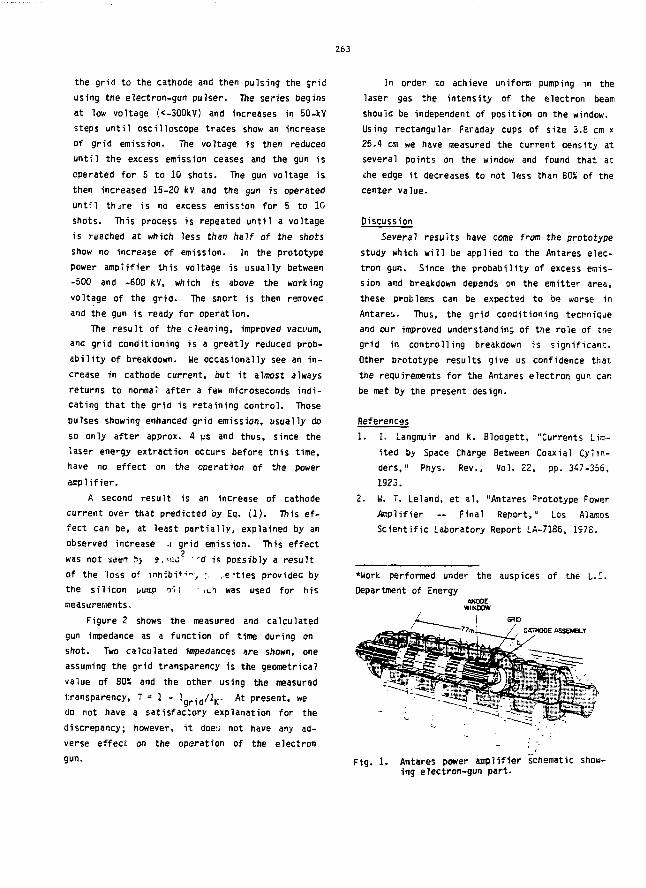
263
the grid to the cathode and then pulsing the grid
using the electron-gun puJser. The series begins
at low voltage (<-300kV) and increases in 5O-kV
steps until oscilloscope traces show an increase
of grid emission. The voltage is then reduced
until the excess emission ceases and the gun is
operated for 5 to 10 shots. The gun voltage is
then increased 15-20 kV and the gun is operated
until th^re is no excess emission for 5 to 10
shots. This process is repeated until a voltage
is reached at which less than half of the shots
show no increase of emission. In the prototype
power amplifier this voltage is usually between
-500 and -600 kV, which is above the working
voltage of the grid. The short is then removed
and the gun is ready for operation.
The result of the cleaning, improved vacuum,
and grid conditioning is a greatly reduced prob-
ability of breakdown. Me occasionally see an in-
crease in cathode current, but it almost always
returns to normal after a few microseconds indi-
cating that the grid is retaining control. Those
pulses showing enhanced grid emission, usually do
so only after approx. 4 JJS and thus, since the
laser energy extraction occurs before this time,
have no effect on the operation of the power
amplifier.
A second result is an increase of cathode
current over that predicted by Eq. (1). This ef-
fect can be, at least partially, explained by an
observed increase .1 grid emission. This effect
was not sden h> 2. <nJ rd is possibly a result
of the loss of inhibit-i-j ;. . .•e.-ties provided by
the silicon pump o-i! .(.h was used for his
measurements.
Figure 2 shows the measured and calculated
gun impedance as a function of time during on
shot. Two calculated impedances are shown, one
assuming the grid transparency is the geometrical
value of 80S and the other using the measured
transparency, T = 1 - Jgrid/IK- At present, we
do not have a satisfactory explanation for the
discrepancy; however, it does not have any ad-
verse effect on the operation of the electron
gun.
In order to achieve uniform pumping in the
laser gas the intensity of the electron beam
should be independent of position on the window.
Using rectangular Faraday cups of size 3.8 cm x
25.4 era we have measured the current density at
several points on the window and found that at
che edge it decreases to not less than 80S of tne
center value.
Discussion
Several results have come from the prototype
study which will be applied to the Antares elec-
tron gun. Since the probability of excess emis-
sion and breakdown depends on the emitter area,
these problems can be expected to be worse in
Antares,. Thus, the grid conditioning technique
and our improved understanding of the role of the
grid in controlling breakdown is significant.
Other prototype results give us confidence that
the requirements for the Antares electron gun car,
be met by the present design.
References
1. I. Langmuir and K. Blodgett, "Currents Lim-
ited by Space Charge Between Coaxial Cylin-
ders," Phys. Rev., Vol. 22, pp. 347-356,
1923.
2. W. T. Leland, et al, "Antares Prototype Power
Amplifier — Final Report," Los Alamos
Scientific Laboratory Report LA-7186, 1978.
*Work performed under the auspices of the 1.5.
Department of Energy
CATHODE ASSEMBLY
Fig. 1. Antares power amplifier schematic show-ing electron-gun part.
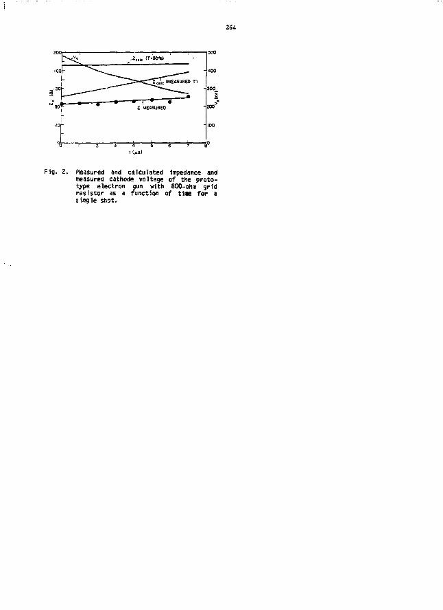
264
Fig. 2. Measured and calculated Impedance andmeasured cathode voltage of the proto-type electron gun with 8C0-ohm gridresistor as a function of time for asingle shot.
265
11.3
THE ANTARES LASER POWER AMPl IFIER*
R. D. Stine, G. F. Ross, C. Silver-nail
University of California, LosLos Alamos,
Abstract
The overall design of the Antares laser power
amplifier is discussed. The power amplifier is
the last stage of amplification in the 100-kJ
Antares laser. In the power amplifier a single,
cylindrical, grid-controlled cold-cathode, elec-
tron gun is surrounded by 12 large-aperture CO^
electron-beam sustained laser discharge sectors.
Each power amplifier will deliver 28 kj end the
six modules used in Antares will produce the re-
quired 100 kj for delivery to the target. A
large-scale interaction between optical, mechan-
ical, and electrical disciplines is required to
meet the design objectives. Significant compo-
nent advances required by the power amplifier
design are discussed.
Introduction
The Antares laser is under construction at
the Los Alamos Scientific Laboratory (LASL).
This is a large (100-kJ) C02 laser for the iner-
tial confinement fusion program. The power am-
plifier (Figs. 1 and 2) is the last stage of
amplification in the optical chain. A cylindri-
cal cold-cathode, grid-controlled electron gun is
utilized to ionize the laser gas in the annulus
surrounding the gun. Each power amplifier oper-
ates at 1800 torr of l:4::N2:C02 laser gas and
requires approximately 1 KJ of stored electrical
energy at an operating voltage of 550 kV. An
input light energy of less than 100 J is ampli-
fied in two passes through the power amplifier
to an output energy of 18 kj. Six power ampli-
*Work performed under the auspices of the U.S.
Department of Energy
Alamos Scientific LaboratoryNM 87545
fiers operating in parallel are required to pro-
duce the 100-kJ output for the fusion targets.
This paper discusses features of tne cower
amplifier optical, mechanical, and electrical
design, and their problem areas a'id solutions.
Optical Design
A 15-cm-diameter annular input beam with an
energy of less than 100 J is delivered to each
power amplifier from the driver amplifier in the
front end. It passes into the vacuum section
through a 22-cm-diameter salt window. Tnis input
beam is divided by a central polyhedron beam
splitter into 12 segments which are" directed
radially outward. Each of the 12 beams is re-
flected to a three-mirror corner cube which is
used to adjust individual path lengths to obtain
pulse synchronization. From the corner cube the
light passes to a focus mirror then through a
spatial filter. The beam enters .the pressure
vessel section through a 12.7-cm-diameter salt
window, then through a group of four relay mir-
rors to the first amplifying section. The ap-
proximately 2.5-cm trapezoidal beam makes a first
diverging pass through the four pumpeo regions
to the back-reflector mirror where it is re-
flected for a second, near-coilimated, pass
through the amplifying sections. At the output
of the pressure vessel the beam is transmitted
through a 45-cra-diameter salt window to the two
mirror periscope sections. Because of the racial
geometry of the power amplifier, each amplifying
sector, and therefore each beam, is a segment of
an annulus. The periscope compresses the radius
of the annular 12-sector beam array exiting the
power amplifier to reduce the dimensions required
downstream in the turning and target chambers.
266
The power amplifier design is primarily dic-2
tated by optical requirements. The damage
threshold for the transmitting windows limits the2
flux to about 2 J/cm average energy density
for the nanosecond pulses. This average density
provides an allowance for hot spots due to dif-
fraction and non-uniform gain. The window damage
limitation combined with state-of-the-art limits
on window size means that the laser must exit
through multiple output windows. For Antares
this results in 12 windows per power amplifier,
or 72 total output windows in the system.
An intensive development program at Harshaw
Chemical Company, funded by LASL, has produced
optical grade salt windows up to 45-cm diameter.
The windows are 8.9-cm thick to withstand the
3-atmosphere pressure differential. Each window
is mounted between two Viton 0-rings to provide
a positive seal for both the 3-atmospheres pres-
sure operating condition and the 0.1-torr vacuum
when the laser gas is exchanged.
Another development program, at the Y-12
Plant of the Union Carbide Corp. in Oak Ridge,
Tennessee, has produced the large mirrors used
in the power amplifier (Fig. 3). Over 200 of
these large mirrors are used in the power ampli-
fiers. These mirrors utilize an aluminum sub-
stra'ce plated with a 1-nm-thick copper coating.
The optical surface is produced by single-point
aUmnd-turnipj (SPOT). Both flats and weak
spherical mirrors are produced for the power am-
plifier. This technology provides an optical
-'inisn on odd-shaped mirrors at a reasonable cost
as well .* resulting in a higher damage threshold
than conventionally polished mirrors.
Antiparasitic coatings such as LiF and Fe^O.
have been developed which are highly absorptive
at 10.6 iim. Tnese coatings will be used within
the power amplifier to help eliminate harmful
parasitics. Provision has been made in the power
amplifier design for a saturable absorber cell to
farther reauce oarasitics if necessary.
Mechanical
sure vessel must operate at 3 atmospheres with a
1.65-m opening at one end for the electron gun
and 12 openings, each 45 cm in diameter at the
other end for the salt windows. Finite element
analysis was utilized in the design of these com-
plex elements to ensure adequate safety factors.
The material is ASTM 516 Grade 70 pressure vessel
carbon steel and was chosen because of good per-
formance, dimensional stability, and low cost.
The electron-gun vacuum vessel is also made
from ASTM 516 steel. This unit (Fig. 2) is
1.65 m in diameter and 7.7 m long. The vessel
wall is penetrated by 48 openings for the elec-
tron beams. Each electron window opening is
75 cm by 25 cm with 0.8-cm wide hibachi ribs
spaced on 6.3-cm centers down the length for win-
dow and shell support. The vdcuum vessel is con-
structed from four finish machined cylinders each
1.65 m in diameter, 1.9 m long, with a 5-cm-thick
wall. These cylinders are joined together using
pulse-arc welding to give very low weld distor-
tion, thus requiring no further machining after
the welding.
The hibachi window openings are covered with
2-mil-thick titanium foil wnich allows the elec-
tron-beam to pass through and also provides the
vacuum seal. The foil is attached to a punched-
metal backing grid to form a rip-stop which pre-
vents catastrophic window failure. Inserting and
removing the electron gun posed a difficult mech-
anical problem. The solution was to develop
special-shaped air bearings to fit the small
space allowed, yet provide a reliable method for
sliding the gun in and out of the pressure vessel
with a minimum of force.
Electrical
A number of difficult irechanical assemblies
are required in the power amplifier. The pres-
The derivation of the power amplifier elec-
trical parameters has been discussed previously.
The electrical problems in the power amplifier
involve the anooe, anode bushings, high-voltage
cable, and the electron-gun design, including gun
support bushings and electrical feed.
The high-voltage cables connect the gas
pulser energy storage to the power amplifier.
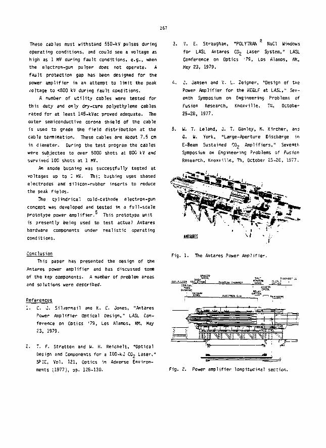
267
These cables must withstand 550-kV pulses during
operating conditions, and could see a voltage as
high as 1 MV during fault conditions, e.g., when
the electron-gun pulser does not operate. A
fault protection gap has been designed for the
power amplifier in an attempt to limit the peak
voltage to <800 kV during fault conditions.
A number of utility cables were tested for
this duty and only dry-cure polyethylene cables
rated for at least 145-kVac proved adequate. The
outer semiconductive corona shield of the cable
is used to grade the field distribution at the
cable termination. These cables are about 7.5 cm
in diameter. During the test program the cables
were subjected to over 6000 shots at 800 kV and
survived 100 shots at 1 MV.
An anode bushing was successfully tested at
voltages up to 1 MV. Thi: bushing uses shaped
electrodes and silicon-rubber inserts to reduce
the peak fields.
The cylindrical cold-cathode electron-gun
concept was developed and tested in a full-scale
prototype power amplifier. This prototype unit
is presently being used to test actual Antares
hardware components under realistic operating
conditions.
Conclusion
This paper has presented the design of the
Antares power amplifier and has discussed some
of the key components. A number of problem areas
and solutions were described.
References
1. C. J. Silvernail and K. C. Jones, "Antares
Power Amplifier Optical Design," LASL Con-
ference on Optics '79, Los Alamos, NM, May
23, 1979.
Z. T. r. Stratton and W. K. Reichelt, "Optical
Design and Components for a 100-kJ COj Laser,"
SPIE, Vol. 121, Optics in Adverse Environ-
ments (1977), pp. 128-130.
3. V. E. Straughan, "POLYTRAN KaCl Windows
for LASL Antares CC2 Laser System," LASL
Conference on Optics '7S, Los Alamos, HH,
May 23, 1979.
4. J. Jansen and V. L. Zeigner, "Design of the
Power Amplifier for the HEGLF at LASL," Sev-
enth Symposium on Engineering Problems of
Fusion Research, Knoxville, Tf«, Octobe1-
25-28, 1977.
5. W. T. Leland, J. T. Ganley, K. Kircher, and
G. W. York, "Large-Aperture Discharge in
E-Beam Sustained C02 Amplifiers," Seventh
Symposium on Engineering Problems of Fusion
Research, Knoxville, TN, October 25-28, 1977.
ANTARES
Fig. 1. The Antares Power Amplifier.
Fig. 2. Power amplifier longitudinal section.
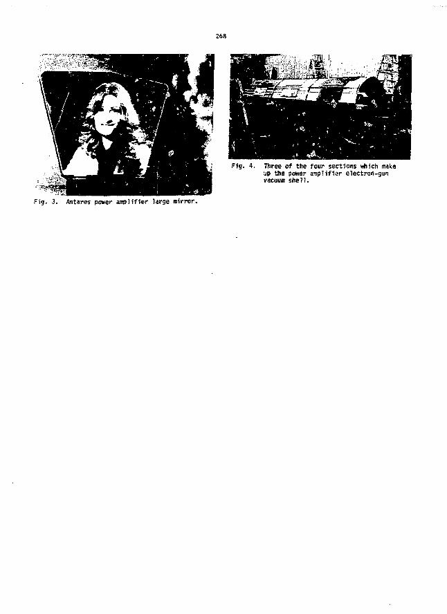
268
Ffg. Three of the four sections which makesjp the power amplifier electron-gunvacuum shell.
Fig. 3. Antares power amplifier large mirror.
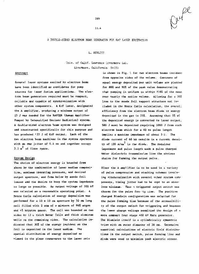
269
11.4
A DOUBLE-SIDED ELECTHOH BEAM GENERATOR FOB Kr? LASHE EXCITATION
L. SCELITT
Abstract
Several, laser systems excited by electron beam
have been identified as candidates for pump
sources for laser fusion applications. The elec-
tron bean generators required must be compact,
reliable and capable of synchronization with
other system components. A KrF laser, designated
the A amplifier, producing a minimum output of
25 J was needed for the RAPIER (Raman Amplifier
Pumped by Intensified Exciner Radiation) system.
A double-sided electron beam system was designed
and constructed specifically for this purpose and
has produced >35 J of KrF output. Each of the
tvo electron beam machines in the system operates
vith an rms jitter of 0.4 ns and together occupy2
3.5 m of floor space.
System Design
The choice of electron energy is bounded from
above by the combination of laser medium composi-
tion, maximum operating pressure, and desired
output aperture, and from below by anode foil
losses and the desire to keep the system impedance
as large as possible. An output voltage of 300 kV
was selected as a reasonable operating point. A
Monte Carlo calculation of energy deposition was
performed for a 10 x 10 cm aperture by 50 cm long
cell filled with 2 atm of a mixture of 96Z argon
and 4% krypton gases. The cell was bounded on two
sides by 13 u thick Havar foils and thick aluminum
walls on the remaining sides. The calculation in-
dicated that 30J of the energy incident on the
foil is deposited in the laser medium. The
spatial distribution of energy deposited as
viewed in the plane transverse to the laser axis
Univ. of Calif. Lawrence Livermore Lac.
Livennore, California 9^550
is shown in Fig. 1 for two electron beams incident
from opposite sides of the volume. Contours of
equal energy deposited per unit volume are plotted
for 807 and 902 of the peak value demonstrating
that pumping is uniform to vithin -10% o£ the mean
over nearly the entire volume. Allowing for a 20™
loss to the anode foil support structure not in-
cluded in the Monte Carlo calculation, the overall
efficiency from the electron beam diode to energy
deposited in the gas is 25*. Assuming that 5Z of
the deposited energy is converted to laser output,
500 J must be deposited requiring 1000 J from each
electron beam which for a 60 ns pulse length
implies a machine impedance of about 5 2 . The
diode current of 60 kA results in a current densi-
ty of 120 A/cm in the diode. The required
impedance and pulse length made a pulse charged
water dielectric transmission line the obvious
choice for forming the output pulse.
Since the A amplifier is to be used in a variety
of pulse compression and stacking schemes involv-
ing synchronization with several other system com-
ponents, timing jitter had to be tept to an abso-
lute minimum. Thus i triggered jutput switch was
chosen for the pulse fore ng line. The positive
charged Blumlein configuration was selected for
the pulse forming line because of the accessibili-
ty of the output switch for triggering and because
the lower charge voltage permitted the design of a
more compact four stage 400 kV Marx generator.
The Blumlein itself is a cylindrically symmetric
triax with an outer diameter of 36 cm. Extensive
numerical calculations of electric field distribu-
tions in the output switch, pulse forming line and
diode were used to minimize peak electric stress.
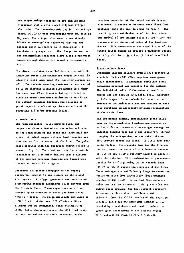
270
The output switch consists of two annular main
electrodes with a disc shaped midplane trigger
electrode. The interelectrode gap is 1 cm and op-
erates at 300 kV when pressurized with 100 paig of
SFg gas. The trigger electrode is resistively
biased at one-half the charge voltage and Che
trigger pulss is coupled to i; through an oil-
insulated ring capacitor. The charge current to
the intermediate conductor flows along a rod which
passes through this entire assembly as shown in
Fig. 2.
The diode insulator is a flat lucite disc with the
inner and outer line conductors shaped so that the
electric field Lines meet the insulator surface at
45°. The cathode mounting hardware is constructed
of 15 cm diameter aluminum pipe housed in a cham-
ber made from 22 cm diameter tubing in orde- to
minimize diode inductance estimated to be <30 nh.
The cathode mounting hardware was polished to
permit operation without spurious emission at the
resulting 115 kV/cm electric fields.
BLumlein Tests
The Marx generator, pulse forming line, and
output switch were tested and characterized prior
to the completion of Che diode and laser cell de-
signs. A radial copper sulfate load resistor was
constructed for the output of the line. The pulse
shape obtained with the triggered output switch is
shown in Fig. 3. The risetime indie"es a switch
inductance of 12 nh which implies that a minimum
of two current carrying channels are formed when
the output switch is triggered.
Obtaining low jitter operation of the output
switch was crucial to the success of the A ampli-
fier system. A trigger generator was constructed
r:rw barium titanate capacitors pulse charged from
Khe aiu.'nlein Marx. These capacitors were dis-
charged by an over-volted spark gap into a 4 m
long 50 3 cable. The pulse amplitude delivered to
a 50 ?. Load resistor was -150 kV with a 10 ns
risetime and an exponential decay giving 50 ns
FWHM. After characterization the 50 a load resis-
tor was removed and the cable connected to the
coupling capacitor of the output switch trigger
electrode. A series of 20 shots were fired (one
prefired) with the results shown in Fig. 4. The
resulting standard deviation of the time between
the arrival of the trigger pulse at the switch and
the arrival of the output pulse at the load was
0.4 ns. This demonstrated the capabilities of the
output switch though at present a different scheme
is being used to trigger the system as described
below.
Electron Beam Tests
Obtaining uniform emission from a cold cathode in
electric fields <200 kV/cm requires some gross
field enhancement. A hexagonal stainless steel
honeycomb material was selected for the cathode.
The individual cells of the material are 3 mm
across and are made of 75 u thick foil. Electron
pinhole images of the cathode indicate that an
average of 3-4 emission sites are created at each
cell resulting in acceptably uniform illumination
of the anode plane.
The tvo nested coaxial transmission lines which
make up the A amplifier Blumlein are charged in
series with the innermost line charged through an
inductor located near the diode insulator. During
charging the voltage drop across this inductor
also appears ACTOSS the diode. To limit this pre-
pulse voltage, the charging time for che line was
set at 1 usec, the value of this inductor reduced
Co ^1.5 uh and a 100 a resistor placed in parallel
with the inductor. This combination of parameters
results in a voltage swing on the cathode from
+35 kV to -20 kV during the charging of the line.
These voltages are sufficiently large to cause un-
wanted emission from excessively field enhanced
regions of the diode. To control this emission
which can lead to a shorted diode by the time the
output pul3e arrives, the foil support structure
is covered with an aluminized Kapton foil to
shield it from zhe +35 kV portion of the prepulse
alectric field and the honeycomb cathode is sur-
rounded by a stainless steel band to reduce the
large field enhancement at the cathode corner.
This combination shown in Fig. 5 eliminates
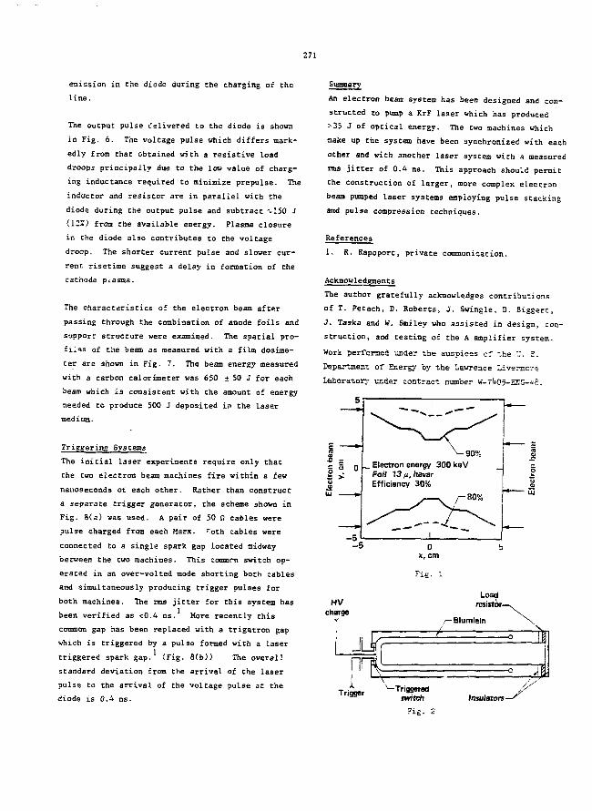
271
emission in the diode during the charging of the
line.
The output pulse delivered to the diode is shown
in Fig. 6. The voltage pulse which differs mark-
edly from that obtained with a resistive load
droops principally due to the low value of charg-
ing inductance required to minimize prepulse. The
inductor and resistor are in parallel with the
diode during the output pulse and subtract t!50 J
(122) from the available energy. Plasma closure
in the diode also contributes to the voltage
droop. The shorter current pulse and slower cur-
rent risetime suggest a delay in formation of the
cathode plasma.
The characteristics of the electron beam after
passing through the combination of anode foils and
support structure were examined. The spatial pro-
files of the beam as measured with a film dosime-
ter are shown in Fig. 7. The beam energy measured
with a carbon calorimeter was 650 ± 50 J for each
beam which is consistent with the amount of energy
needed to produce 500 J deposited in. the laser
medium.
Triggering Systems
The initial laser experiments require only that
the two electron beam machines fire within a few
nanoseconds of each other. Rather than construct
a separate trigger generator, the scheme shown in
Fig. 8(a) was used. A pair of 50 S! cables were
pulse charged from each Marx. F.oth cables were
connected to a single spark gap located midway
between the two machines. This eommrn switch op-
erated in an over-volted mode shorting both cables
and simultaneously producing trigger pulses for
both machines. The rms jitter for this system has
been verified as <0.4 ns. More recently this
common gap has been replaced with a trigatron gap
which is triggered by a pulse formed with a laser
triggered spark gap. (Fig. 8(b)) The overall
standard deviation from the arrival of the laser
pulse to the arrival of the voltage pulse at the
diode is 0.4 ns.
An electron beam system has been designed and con-
structed to pump a KrF laser which has produced
>35 J of optical energy. The two machines which
make up the system have been synchronized with each
other and with another laser system with a measured
rms jitter of 0.4 ns. This approach should permit
the construction of larger, more complex electron
beam pumped laser systems employing pulse stacking
and pulse compression techniques.
References
1. R. Rapoport, private communication.
Acknowledgments
The author gratefully acknowledges contributions
of T. Petach, D. Roberts, j. Swingle, D. Biggert,
J. Taska and V. Smiley who assisted in design, con-
struction, and testing of the A amplifier system.
Work performed under the auspices of the TJ. £.
Department of Energy by the Lawrence Livsrjsoys
Laboratory under contract number W-7liQ5-EHG-'jfi.
u
- 5
HVcharge
_ Electron energy 300 keVFoil 13 M. havarEfficiency 30%
0X, cm
Loadresistor-
-Blumlein/
n\—?
1 ^ 'ItTrigger -Triggered
switch
Fig. 2
Insulators -
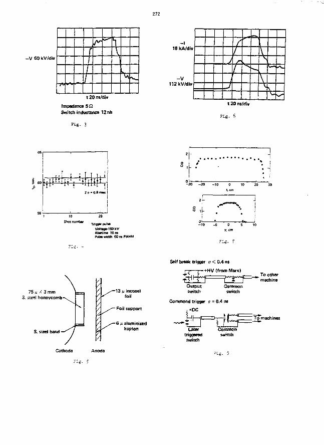
272
- V 60 kV/div
/
. /
i
\
\
120 ns/div
Impedance 5 f lSwitch inductance 12 nh
?ig. 3
-118 kA/div
- V112kV/div
J
1
J
c11
\
120 nj/div
Fig. 6
2 o • 0.6 m«c
10
Shot numbtr
RtMtinM 10 mPulH writh SO in FWHM
-30 -20 -10 10 20 30
- 1 0 - 5 0 5 10
Y. cm
f-S-
75 M X 3 mmS. steel honeycomb-
S. steel band
Cathode Anode
13 M inconelfoil
Foil support
6 n aluminizedkapton
Seif break triggor a < 0.4 ns
r-T—-j—+HV (from Marx)
Outputswitch
Command triQQar
,+OC
LasertrtQijeiodswitch
Commonswitch
a = 0.4 ns
—>-j—? i_^_ii ..
Commonswitch
_^_ To othermachine
~ To machines
7H. 5
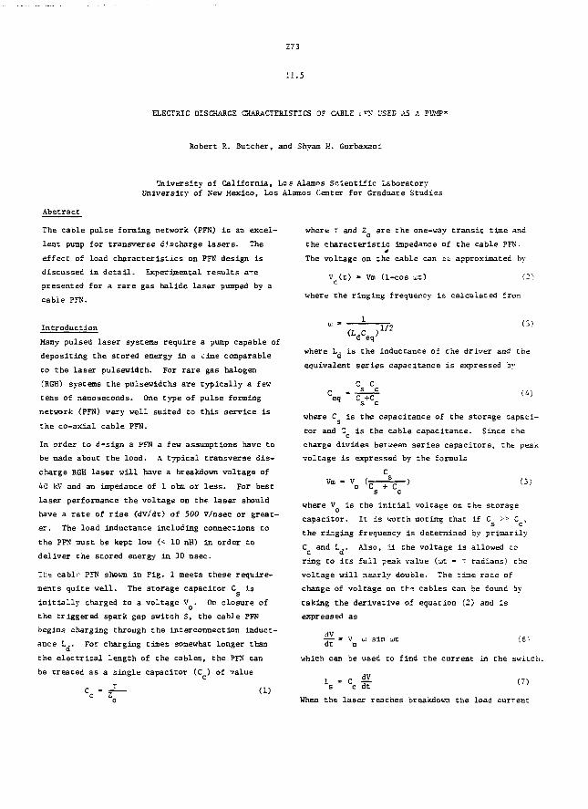
273
11.5
ELECTRIC DISCHARGE CHAEACTERISTICS OF CABLE i TT USED AS A PUMP*
Robert R. Butcher, and Shyam H. Gurbaxani
University of California, Los Alamos Scientific LaboratoryUniversity of New- Mexico, Los Alamos Center for Graduate Studies
Abstract
The cable pulse forming network (PFN) is an excel-
lent pump for transverse discharge lasers . The
effect of load character is t ics on PFN design is
discussed in de ta i l . Experimental resu l t s are
presented for a rare gas halide laser pumped by a
cable PFN.
Introduction
Many pulsed laser systems require a pump capable of
depositing the stored energy in a iiime comparable
to the laser pulsewidth. For rare gas halogen
(RGH) systems the pulsewidths are typically a few
tens of nanoseconds. One type of pulse forming
network (PFN) very well suited to this service i s
the co-axial cable PFN.
In order to design a PFN a few assumptions have to
be made about the load. A typical transverse d i s -
charge RGH laser will have a breakdown voltage of
40 kV and an impedance of 1 oho. or less . For best
laser performance the voltage on the laser should
have a ra te of r i s e (dV/dt> of 500 V/nsec or great-
er. The load inductance Including connections to
the PFN must be kept low (< 10 nH) in order to
deliver the stored energy in 30 nsec.
The cabls- PFN shown in Fig. 1 meets these require-
ments quite well. The storage capacitor C is
i n i t i a l l y charged to a voltage V . On closure of
the triggered spark gap switch S, the cable PFN
begins charging through the interconnection induct-
ance L.. For charging times somewhat longer than
the e lec t r ica l length of the cables, the PFN can
be treated as a single capacitor (C ) of value
where 7 and Z are the one-way t r a n s i t time and
the c h a r a c t e r i s t i c impedance of the cable PFN.
The vol tage on the cable can Dfc approximated by
V ( t ) • Vm (1-cos ^ t ) (2
where the r inging frequency i s calculated fron
1
<LdCeq>1/2
(3)
where L. is the inductance of the driver and chea
equivalent series capacitance is expressed b<-
C Ceq C +C (4)
where C_ is the capacitance of the storage capaci-
tor and Z is the cable capacitance. Since the
charge divides between series capacitors, the peak
voltage is expressed by the formula
C-) (5)Vm V (
C + C
where V is the initial voltage on the storage
capacitor. It is worth noting that if C » C ,
the ringing frequency is determined by primarily
C and L,. Also, ii the voltage is allowed to
ring to its full peak value (ut = ~ radians) the
voltage will nearly double. The rime rate of
change of voltage on th? cables can be found by
taking the derivative of equation (2) and is
expressed as
dt u: sin ajt (6 '•
which can be used to find the current in the switch.
r- dV , , v
When the laser reaches breakdown the load current
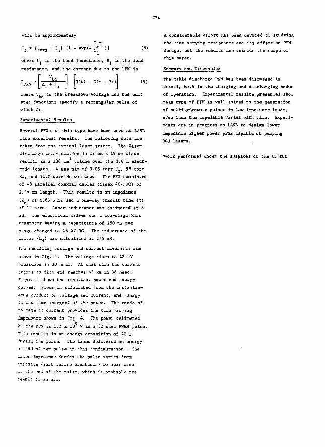
274
will be approximately
(8)
where L1 is the load inductance, R. is the load
resistance, and the current due to the PFN is
where V. - is the breakdown voltage and the unit
step functions specify a rectangular pulse of
width 2T.
Experimental Results
Several PFNs of this type have been used at LASL
with excellent results. The following data are
t.iken from one typical laser system. The laser
discharge crocs section is 12 mm x 19 mm which
results in a 138 cm volume over the 0.6 in elect-
rode length. A gas mix of 3.05 torr F,, 35 torr
Kr, and 3150 torr He was used. The PFN consisted
of 48 parallel coaxial cables (Essex 40/; 00) of
2.44 mm length. This results in an impedance
(Z ) of 0.63 ohms and a one-way transit time (x)
of 15 nsec. Laser inductance was estimated at 8
nH. The electrical driver was 2 two-stage Marx
generator having a capacitance of 150 nF per
stage charged to 48 kV DC. The inductance of the
drivar (L ) was calculated at 275 nH.
a
The resulting voltage and current waveforms are
shown in Fig. 2. The voltage rises co 42 kV
breakdown in 30 nsec. At that time the current
begins co flow and reaches 62 kA in 36 nsec.
"igure 3 shows Che resultant power and energy
curves. Power is calculated from the instantan-
eous product of voltage and current, and nergy
is rhe time Integral of the power. The ratio of
volcage co current provides the cime varying
impedance shown in Fig. •+. The powei delivered
by the ?FS is 1.3 x 10⁹ W in a 32 nsec FWHM pulse.
This results in an energy deposition of 40 J
during the pulse. The laser delivered an energy
or 530 raj per pulse in this configuration. The
laser impedance during che pulse varies from
infinite (just before breakdown) Co near zero
3L che end of che pulse, vhich is probably che
resulc of an arc.
A considerable effort has been devoted to studying
the time varying resistance and its effect on PFN
design, but the results are outside the scope of
this paper.
Summary and Discr.asion
The cable discharge PFN has been discussed in
detail, both in the charging and discharging modes
of operation. Experimental results presented show
this type or PFN is well suited to the generation
of multi-gigawatt pulses in low impedance loads,
even when the impedance varies with time. Experi-
ments are in progress as LASL to design lower
impedance higher power pFNs capable of pumping
RGH lasers.
*Uork performed under the auspices of the US DOE
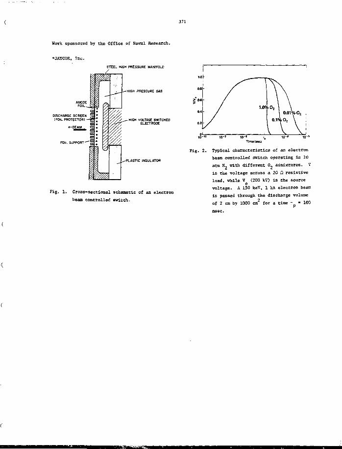
371
Work sponsored by the Office of Naval Research.
*JAYCOR, Inc.
STEEL HIGH PRESSURE MANIFOLD
ANODEFOIL..
DISCHARGE SCREEN(FOIL PROTECTOR) -
FOIL SUPPORT-
il1 "c •c •a •= •c .c .e .e •c .^§
y.
4'6y.
i| |
yy0^///'yV/yw
HIGH PRESSURE GAS
HIGH VOLTAGE SWITCHEDELECTRODE
PLASTIC INSULATOR
Fig. 1. Cross-sectional schematic of an electron
bean controlled switch.
1.0*0, \ \
\ 0.01% Oj
0.1% O2
10-'
Fig. 2. Typical characteristics of an electron
beam controlled switch operating in 10
arm N, with different 0^ admixtures. V
is the voltage across a 20 Q resistive
load, while V (200 kV) is the sourceo
voltage. A 150 keV, 1 kA electron beam
is passed through the discharge volume
of 2 cm by 1000 cm for a time T " 100
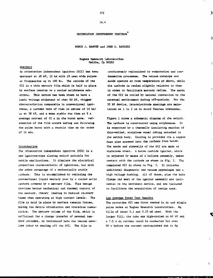
372
16.4
ORIENTATION INDEPENDENT IGNITRON*
ROBIN J. HARVET and JOHN R. BAYLESS
Hughes Research LaboratoriesMalibu, CA 90265
Abstract
An orientation independent ignitron (Oil) haa been
operated at -JO kV, 15 kA with 10 ysec wide pulses
ac frequencies up to 100 Hz. The cathode of the
Oil is a thin mercury film which is held in place
by surface tension on a cooled molybdenum sub-
strate. This device has been shown to have a
basic voltage withstand of over 60 kV, trigger
characteristics comparable to conventional igni-
trons, a current rate of rise In excess of 10 kA/
us at 30 kV, and a mean stable run time at 8 A
average current of 22 3 in the burst mode, ref-
ormation of the film occurs during and following
Che pulse burse with a recycle time on tiir order
of 10 min.
Introduction
The orientation independent lgnitron (Oil) is a
new ignitron-cype closing switch suitable for
nobile applications. It displays Che electrical
properties characteristic of ignitrons, but vith
che added advantage of a mechanically stable
cathode. This is accomplished by replacing the
conventional liquid mercury pool by a cooled solid
cathode covered by a mercury film. This design
provides better mechanical and thermal control of
the mercury, thereb: leading to reduced recovery
times when operating at high current levels. The
film is held in place by surface tension forces,
making Che device orientation and vibration insen-
sitive. The mercury volume of the film, which is
sufficient for a charge cransfer of several hun-
dred coulombs, is introduced into the vacuum enve-
lope prior Co sealing off Che Oil. The film is
continuously replenished by evaporation and con-
densation processes. Th« vacuum envelope and
anoda operate at room temperature or above, while
the cathode is cooled slightly relative to Chen
in order co facilitate mercury reflux. The anode
of the Oil is cooled by natural convection to the
external enviromaent during off-periods. For the
30 W device, incerelectrode spacings are main-
tained at 1 to 2 cm to avoid Faschen breakdown.
Figure 1 shows a schematic diagram of the switch.
The cathode Is constructed using molybdenum. It
Is supported by a thermally Insulating section of
thin-walled, stainless steel tubing attached to
the switch body. Cooling is provided via a copper
heat pipe screwed into the cathode from below.
The anode and sidewalls of the Oil are made of
stainless steel. A boron carbide igniter, vhich
is adjusted by means of a bellows assembly, makes
contact vith the cathode as shown in Fig. 2. The
completed Oil is shown in Fig. 3. It includes
additional diagnostic and vacuum appendages and a
high voltage bushing. All of these, plus che xain
flange and most of che igniter assembly are inci-
dental Co the intrinsic device, and are included
to facilitate the acquisition of design data.
Low Average Power Test Results
The prototype Oil was first tested in dc and single
pulse modes at Hughes Research Laboratories. Hg
fills of about 0.1 and 0.25 n£ used. With che
larger fill, the tube was high-potted to 60 kV and
a 7.5 A dc current could be conducted for over
90 s before the current extinguished due to Eg

373
evaporation from Che carhode. In the single pulse
mode, the anode fall time was observed to vary
with the anode voltage, changing from 1 us at 250 V
to 0.15 us at 30 kV. However, the Hg film on the
cathode was thick enough to show signs of droplet
formation.
Ths smaller Hg ffi.ll was chosen Co eliminate any
potential problem with droplet formation. The
associated dc conduction time was limited to about
60 s at 7.5 A. During a 60 s dc run, the mercury
vapor pressure varied from 0.6 to 6 mTorr depend-
ing on the cathode temperature as expected from
vapor pressure data. An increase in the jitter
and increasingly erratic anode fall behavior are
also more evident with the lower Hg fill.
High Average Power Test Results
The Oil vas tested at the ERADCOM High Power Test
Facility at Ft. Honmouth starting with the circuit
shown in Fig. 4. The circuit was calibrated using
a HAPS 40 Thyratron. A comparison of the pulse
current waveforms for these two devices show
little difference at the sane voltage except for
the larger jitter of the Oil. A typical current
waveform generated at 30 kV is shown in Fig. 5.
Figure 6 shows a typical overlay of all pulses
•ccurring during a 20 second rue of the Oil at
50 Hz. The variation in timing is found Co average
about ± 1 vis. The charging inductor was reduced
to 1.5 H to achieve a 120 Hz effective recharge
rate and the device ran at up to 100 Hz without
notifiable difficulty in voltage recovery; refer
to Fig. 7.
The cathode was cooled using ice water during
these runs at high power. The energy dissipated
at the cathode was measured thermally to be about
1 to 2 J/pulse or an equivalent voltage drop of
5 to 10 V at the cathode The anode dissipation
was probably somewhat higher.
a high cathode temperature (y 60 C) leu to Paschen
breakdown. The introduction of inpurlcy gasses had
no noticeable affect on the tube behavior below the
Paschen limit.
The run tioe before tube instabilities become exces-
sive is shown in Fig. 8. The total charge transfer
is proportional to the product of the frequency and
the run time. Evidently, Hg vapor reflux makes up
a significant contribution to the Bg film volume.
during a time on the order of 0.03 s since the
charge transfer at 30 Hz is nearly double that at
100 Hz.
During the course of these experiments, the tube
was physically rotated by 180° with no d?»-Rct2.ble
change in operation. Also, the end of line clipper
was removed without noticeable change In the tube
reliability.
Summary
Table I outlines the developmental goals and the
te»t results actually achieved. Obviously, most
of the goals have been reached with this first
prototype model of an orientation independent: igni-
tron, thereby making PU ignitron-type switch
available for airborne or mobile applications for
the first tine.
Acknowledgements
The authors are indebted to Mr. John Creedon who
facilitated the high power tests ae EHADCOH, to
Mr. Janes O'Loughlin (AFWt) and Dr. Wilfried 0.
Eckhardt (HRL) for technical discussions, and co
Mr. Robert W. Holly (HEL) for engineering support.
*This work supported by U.S. Air Force Weapons
Laboratory, Klrtland, AFB, Ontract No. N60921-76-
C-0138 through the Haval Surface Weapons Center,
Dahlgren, Virginia.
The anode temperature excursions were typically
30°C for a run of 1000 pulses. A high anode
temperature did not affect the tube behavior, but
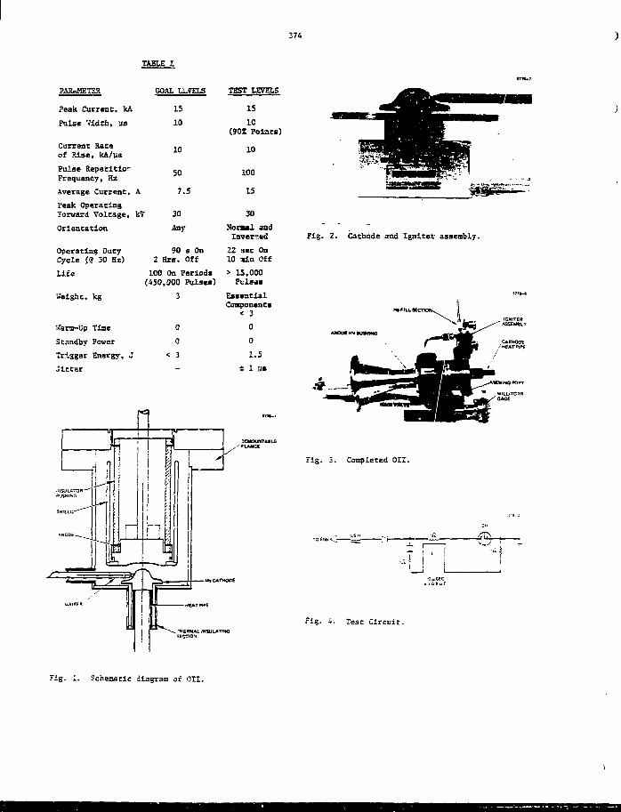
TABLE I
374
PARAMETER
Peak Current, kA
Pulse Vldth, Us
Current Hateof Rise, kA/us
Pulse RepetitiorFrequency, Hz
Average Current,
I'eak OperatingForward Voltage,
Orientation
Operating DutyCycle C9 50 Hz)
Life
Weight, kg
Warm-Up Time
Standby Power
Trigger Energy, J
Jitter
GOAL U.VELS
15
10
10
50
A 7.5
k.7 30
Any
90 s On2 HTB. Off
100 On Periods(150,000 Pulses)
3
0
0
< 3
TEST LEVELS
IS
10(90S Foiacs)
10
XOO
15
30
Normal andInverv.wi
22 sec On10 ain Off
> 15,000Pulses
EssentialComponents
< 3
0
0
1.3
± 1 us
Fig. 2. Cathode and Igniter assembly.
Fig. 3. Completed Oil.
II. >
Fig. 4. Test Circuit.
Fig. 1. Schematic diagram of Oil,
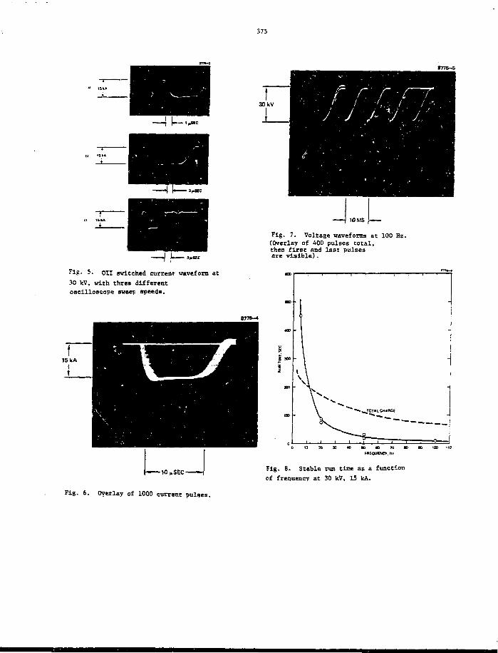
375
Fig. 5. oil switched current waveform at
30 kV, with three different
oscilloscope sweep speeds.
30 kV
8T7S-4
y y-y~y;//
——) 10 MS |——
Fig. 7. Voltage waveforms at 100 Hz.(Overlay of 400 pulses total,then first and last pulsesare visible).
!
.\\\
\ V •*
^ — % ~
-
]1
-
-
« 80 m 70
FREQUENCY. Ht
•> 10 IX no
Fig. 8. Stable run time as a function
of frequency at 30 kV, 15 kA.
Fig. 6. Overlay of 1000 current pulses.
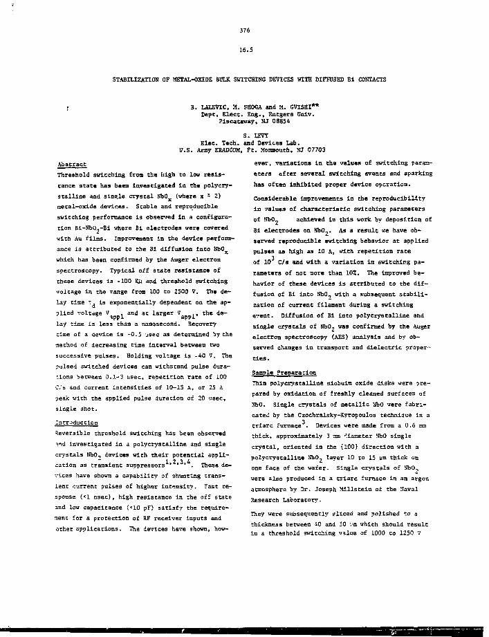
376
16.5
STABILIZATION OF METAL-OXIDE BULK SWITCHING DEVICES WITH DIFFUSED Bi CONTACTS
B. LALEVIC, M. SHOGA and M. GVISHI**Depc. Elect. Eng., Rutgers Univ.
Plscataway, NJ 08854
S. LEVY
Elec. Tech. and Devices Lab.
U.S. Army ERADCOM, Ft. Monmouth, NJ C7703
Abstract
Threshold switching from the high to low resis-
tance state has been investigated in the polyery-
stalline and single crystal NbO (where x : 2)
necal-oxide devices. Stable and reproducible
switching performance is observed in a configura-
tion Bl-NbO.-Bi where Bi electrodes were covered
with Au films. Improvement in the device perform-
ance is attributed to the 31 diffusion into NbO^
which has been confirmed by the Auger electron
spectroscopy. Typical off state resistance of
these devices is -100 KM and threshold switching
voltage in the range from 100 to 2500 V. The de-
lay time T^ is exponentially dependent on the ap-
plied voltage V , and at larger V ,, the de-
ippl = appl*
lay time is less than a nanosecond. Recovery
clme of a device is -0.5 'jsec as determined by the
method of decreasing time interval between two
successive pulses. Holding voltage is -40 V, The
pulsed switched devices can withstand pulse dura-
tions between 0.1-3 usec, repetition rate of 100
C's and current intensities of 10-15 A, or 25 A
peak with the applied pulse duration of 20 usec,
single shot.
Introduction
Reversible threshold switching has been observed
'.id investigated in a poly crystalline and single
crystals NbO., devices with their potential appli-
cation as transient suppressors ' ' ' . These de-
vices have shown a capability of shunting trans-
ient current pulses of higher intensity. Fast re-
sponse (<1 nsec), high resistance in the off state
and low capacitance (<10 pF) satisfy the require-
ment for a protection of RF receiver Inputs and
other applications. The devices have shown, how-
ever, variations In the values of switching param-
eters after several switching avents and sparking
has often inhibited proper device operation.
Considerable Improvements in the reproducibility
In values of characteristic switching parameters
of SbO, achieved in this work by deposition of
Bi electrodes on NbO-. As a result we have ob-
served reproducible switching behavior at applied
pulses as high as 10 A, with repetition rate
of 10 C/s and with a variation in switching pa-
rameters of not more than 10*. The improved be-
havior of these devices is attributed to the dif-
fusion of BI into HbO, with a subsequent stabili-
zation of current filament during a switching
event. Diffusion of BI into polycrystalline and
single crystals of NbO- was confirmed by the Auger
electron spectroscopy (AES) analysis and by ob-
served changes in transport and dielectric proper-
ties.
Sample Preparation
Thin polycrystalline niobuim oxide disks were pre-
pared by oxidation of freshly cleaned surfaces of
NbO. Single crystals of metallic HbO were fabri-
cated by the Czochralsky-iCyropoulos technique in a
triarc furnace . Devices were made from a 0,6 mm
thick, approximately 3 am diameter NbO single
crystal, oriented in the {100} direction with a
polycrystalline NbO, layer 10 to 15 um thick on
one face of the wafer. Single crystals of MbO?
were also produced in a triarc furnace in an argon
atmosphere by Dr. Joseph Millstein of the Naval
Research Laboratory.
They were subsequently sliced and polished to a
thickness between 40 and SO i>m which should result
in a threshold switching value of 1000 to 1250 V
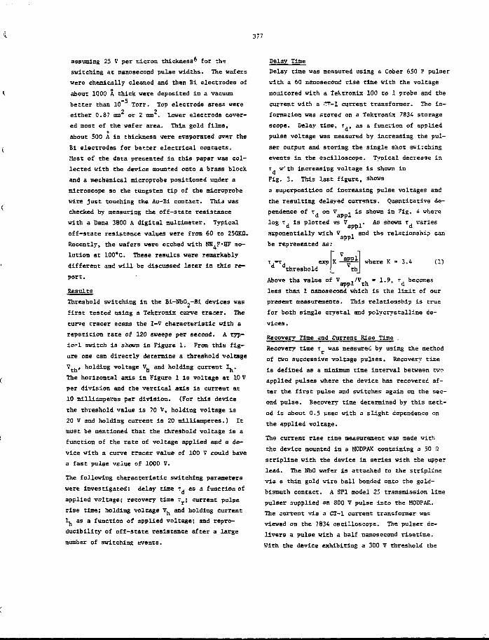
377
assuming 25 V per nicron thickness^ for th«
switching at nanosecond pulse widths. The wafers
were chemically cleaned and then Bi electrodes of
about 1000 A thick were deposited in a vacuum
better than 10 Torr. Top electrode areas were
either 0.87 ma or 2 nm . Lower electrode cover-
ed most of the wafer area. Thin gold films,
about 500 A in thickness vere evaporated over the
Bi electrodes for better electrical contacts.
Most of the data presented in this paper was col-
lected with the device moun-ed onto a brass block
and a mechanical mlcroprobe positioned under a
microscope so the tungsten tip of the microprobe
wire Just touching the Au-Bi contact. This was
checked by measuring the off-state resistance
with a Dana 3800 A digital multimeter. Typical
off-state resistance values were from 60 to 250KQ.
Recently, the wafers were etched with NH.F'HF 30-
lution at 100°C. These results were remarkably
different and will be discussed later in this re-
port.
Results
Threshold switching in the Bi-tJbO2-Bl devices was
first tested using a Tektronix curve tracer. The
curve tracer scans the 1-V characteristic with a
repetition rate of 120 sweeps per second. A typ-
ical switch is shown in Figure 1. From this fig-
ure one can directly determine a threshold voltage
V . , holding voltage V^ and holding current I. .
The horizontal axis in Figure 1 is voltage at 10 V
per division and the vertical axis is current at
10 milliamperes per division. (For this device
the threshold value is 70 V, holding voltage is
20 V and holding current is 20 milllamperes.} It
must be mentioned that the threshold voltage is a
function of the rate of voltage applied and a de-
vice with a curve tracer value of 100 V could have
a fast pulse value of 1000 V.
The following characteristic switching parameters
were investigated: delay time T , as a function of
applied voltage; recovery time T .; current pulse
rise time; holding voltage V^ and holding current
L as a function of applied voltage; and repro-
ducibility of off-state resistance after a large
number of switching events.
Delay Time
Delay time was measured using a Cober 650 F pulser
with a 60 nanosecond rise cine with the voltage
monitored with a Tektronix 100 to 1 probe and the
current with a ^T-l current transformer. The in-
formation was stored on a Tektronix 7834 storage
scope. Delay time, T , as a function of applied
pulse voltage was measured by increasing the pul-
ser output and storing the single shot switching
events in the oscilloscope. Typical decrease in
T w: th increasing voltage is shown in
Fig. I. This last figure, shows
a superposition of increasing pulse voltages and
the resulting delayed currents. Quantitative de-
pendence of i; on V , is shown in Fig. 4 where
d appl
log T , is plotted vs V ,. As shown T *.'ariesa appx d
azponentially with
be represented as:
azponentially with V and the relationship can
d 'dthresholdexp K where K = 3.4 (1)
1.9, T, becomesd
Above the value of V ....appl th
less than 1 nanosecond which is the limit of our
present measurements. This relationship is true
for both single crystal and polycrystalline de-
vices .
Recovery Time and Current Rise Time .
Recovery time T was measured by using the method
of two successive voltage pulses. Recovery time
is defined as a minimum time interval between two
applied pulses where the device has recovered af-
ter the first pulse and switches again on the sec-
ond pulse. Recovery time determined by this meth-
od is about 0.5 usec with a slight dependence on
the applied voltage.
The current rise time measurement was made with
the device mounted in a MODPAK containing a 50 a
stripline with the device in series with the upper
lead. The NbO wafer is attached to the stripline
via a thin gold wire ball bonded onto the gold-
bismuth contact. A SP1 model 25 transmission line
pulser supplied an 800 V pulse into the MODPAK.
The current via a CT-1 current transformer was
viewed on the 7834 oscilloscope. The pulser de-
livers a pulse with a half nanosecond risetlme.
With the device exhibiting a 300 V threshold the
378
current risetime vas leas than 0.8 nanoseconds
for a current of 25 A.
adding Voltage and Current
Holding voltage Vh and holding Current L were
read out directly from the switching pulse trace.
It was found that V^ exhibits a slow dependence on
V ^ in che range from Vft to 2000 V. Typically
Vh varied from 20 to 40 7 and holding current 1^
between 1 and 5 A (for the same range of applied
voltage pulses).
Off-State Resistance
Figure 2 shows the voltage waveform (top trace)
and current (bottom trace) for a single crystal
device at the beginning of teat. It displayed an
initial threshold voltage of 1400 7 and an off-
state resistance prior to switching of 227 kfl.
The voltage sensitivity in this photo was 200 V
per snail division and the current was 1 A per
small division. Pulse width was 0.3 usec. The
device was switched into a matched load. After
the first 2 K switching events the threshold drop-
ped to 900 V with 121 kfi off-state resistance. It
was then pulsed at 10 3z. After 24 K pulses with
che applied pulse voltage varying from threshold
to 2200 V there was no discernible change in off-
scate resistance. Some sparking was observed un-
derneath the tungsten tip of the mlcroprobe after
a few thousand pulses. Sparking was erratic and
at che end of 10,000 pulses the off-state resis-
cance had dropped below 100,000 fi. The test was
terminated after 40,000 pulses at which time Fig.
6 vas recorded. Here che voltage is SO V per
small division and the current 1 A per small divi-
sion. The off-state resistance was 37 kfl. Lift-
Ing che cungsten tip uncovered a deep eroded pit
caused by poor contact between tip and device.
Transport and Dielectric Properties
The next figure, Fig. 5a, shows a Schottky plot of
log I/T2 vs V1/2/T. Prior Co switching the 31-
XbO.,-31 device shows a Schotcky barrier to exist.
.\fcer switching Fig. 5b shows th'. barrier is gone
and che log I vs log V plot shows the device
whether single crystal or polycrystalline, to be
space-charge limited. The next figure. Fig. 6a,
shows the C-f dependence which again exhibited the
characteristic capacitance associated with a
Schot*k7 barrier being eliminated by switching.
Last in this series is Fig. 6b which shows the In-
crease in the dc component contribution to ac con-
ductivity upon switching.
Discussion
Stability and reproducibility of the characteris-
tic switching parameters of Bi-NbO.-Bi devices as
compared, to Au (or Al)-NbO2-Au (or Al) devices are
attributed to the Bi diffusion into polycrystalline
and single crystal BbOj. The dlffunion of Bi la
NbO, has been confirmed by the Auger electron spec-
troscopy measurements and shown in Fig. Sa. Bi
diffusion 300 A deep ia single crystal of NbO.
was measured. Further Bi diffusion
is enhanced by the application of voltage pulses
as shown in Fig. 5b. Diffusion of Bi under the in-
fluence of applied field is responsible for the ob-
served lowering of R .. resistance after the re-
ox E
peated switching applications. Comparison of de-
vices with Bi or Au electrodes shews the following
dif ferences in the transport and dielectric proper-
ties caused by the Bi diffusion: change from Schot-
tky barrier to apace charge conduction mechanism,
decrease ia thermal activation energy, increase in
dc component contribution to ac conductivity and
change in C-f and C-V dependences.
The relative insensitivity of a on the electrodeon
area would tend to indicate a formation of a stable
high current density path along the region doped
with Bi.
Based on che above observation one can assume Lu-
ca's switching model of filling the recombination
centers and subsequent collapse of the high resis-
tance state. The critical current density for
switching to low resistance state is given in that
model by:
where T^ is che time required co fill recombinacion
ce-nters, ND is the density of recombination centers
and L is Co be of the thickness of NbO,, i.e. -10
um, one obtains for J the value of 7.7x10 ass/2 ft
cm , while the measured value is J « 1.8x10 amp/2 c r
cm which represents a fair agreement.
379
Etched Sample
The etched device shows another improvement over
the unetched sample. Figure 8 shows the I-V
taken from the Tektrnnix curve tracer. (The
voltage is now 20 V per division and current still
10 milliamps per division.)
Notice the disappearance of the holding current.
The switched device returns to the origin now.
This information is new and has not been analyzed
as yet. A device consisting of a single crystal
sample etched, ball-bonded and mounted in the HOIK
FAK was pulsed 15 A with no change in any of its
characteristics for over 400 pulses. At 26 A the
device showed a slight reduction in off-state re-
sistance. On the second or third shot the gold
bond lifted off the samples. However there was no
evidence of damage to the NbO, wafer.
In conclusion, Bi-NbO -Bi etched devices have
shown a satisfactory performance as suppressors
of high transient currents needed to protect RF
inputs.
In conclusion, Bi-NbO,-Bi devices have shown a
satisfactory performance as suppressors of the
high intensity current transients.
References
1. G. K. Gaule, P. LaPlante, S. Levy and S. Sch-
neider, "Pulse Sharpening with Metal-Qjd.de
Bulk Switching Devices," Pruc. of the Int.
Pulse Power Conf., 78CH1147-of Rep. 5, PIC-6,
Nov. 1976.
2. G. K. Gaule and P. LaFlante, "Metal Oxide Sub-
nanosecond Suppressors," 25th El. Coup. Cnnf.
(IEEE) Washington, DC, pp. 390-394, Hay 1975.
3. S. H. Shin, T. Halpern and P. Raccah, "High
Speed, High-Current Field Switching NbO2,"
J. Appl. Phys., Vol. 48, pp. 3150-3153, July
19 ?7.
4. G. R. Gaule, P. LaPlance, S. Levy and S. Sch-
neider, "Metal-Oxide Devices for Rapid Cur-
rent Switching," Int. Elec. Device Mtg., Wash-
ington, DC, pp. 279-281, Dec. 1976.
5. I. Lucas, "Switching Mechanism in Amorphous
Semiconductors," J. Non-Crystalline Solids,
Vol. 8, p. 293, 1972.
6. L. M. Levinson, H. R. Philipp, G. A. Slack,
"Protective Coaxial Switching Devices," GE Re-
search and Development Center Final Report
Contract ECOM: 76-1331-F, Oct. 1977, p. 85.
•Research supported by the Army Research Office**0n leave of absence from the Israeli Ministryof Defense
***Here we have assumed T<J to be equal to the ob-served delay time
Fig. 1. Switching in Bi-HbO,-Bl devices taken
by Tektronix curve tracer, horizontalscale 10 V/Div. vertical scale 10 mA/Div.
Fig. 2. Initial pulse switching and switchingcharacteristics after 4xlO4 pulses,a) Initial voltage pulse, b) Initialcurrent pulse, c) Voltage and currentpulse after the application of 4x10^pulses at the repetition rate of 10 Hz.Time scale 200 ns/Div.
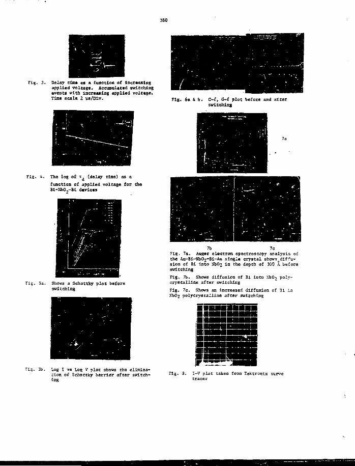
380
Fig. 3. Delay time as a function of increasingapplied voltage. Accumulated switchingevents vith increasing applied voltage.Time scale 2 ua/Div. 6a & b. C-f, Of plot before and after
switching
7a
Fig. The log of T (delay time) as aafunction of applied voltage for theBi-NbO2-3i devices
5a. Shows a Schottky plot beforeswitching
7b 7cFig. 7a. Auger electron spectroscopy analysis ofthe Au-Bi-NbC^-Bi-Au single crystal shows^difru-sion of Bi into Nb<>2 in the depth of 300 A beforeswitchingFig. 7b. Shows diffusion of Bi into NbO? poly-crystalline after switching
Fig. 7c. Shows an increased diffusion of 31 inNbO? polycrystalline after switching
5b. Log I vs Log V plot shows Che elimina-tion of Schoctky barrier after switch-ing
rig. 3. I-V plot taken from TektroniK curvetracer
381
17.1
MAGNET OPTIMIZATION. FOR PULSED ENERGY CONVERSION*
W. K. TUCKER, E. C. CSARE, and W. P. BROOKSSandia Laboratories, Albuquerque, New Mexico 87185
R. E. WILCOX and H. D. MARKIEWICZIntermagnetics General, Guilderland, New York
Abstract
A flux compression generator called PULSAR is
being developed to meet power requirements for
future fusion reactors. Key components of the
generator are superconducting magnet, generator
coil of normal conductor, and an armature, either
a metallic conductor or plasma. Chemical energy
1- used to increase the mutual inductance between
the armture and nested generator coil and super-
conducting magnet. Flux compression occurs and
electrical energy is transferred to a load induct-
ance. This paper will present the results of a
study that was conducted to design a suitable
superconducting magnet for the PULSAR device.
1-5Introduction
A pulsed energy generator, PULSAR,* " is being
developed to meet energy requirements of future
fusion research. The primary components of the
generator, illustrated in Figure 1, are a super-
conducting magnet, a generator coil of normal
NORMAL COIL-
EXPANDINGAIJUJE
STCELTUK
COIL (SUPERCONDUCTOR!
Fig. 1. PULSAR Generator
conductor, and an aluminum armature. The super-
conducting magnet supplies the initial flux to the
bore of the nested generator coil. The load, con-
nected in series vith the generator coll, is not
Inductively coupled to the remainder of the system.
The armture is nested inside the generator coil
bore and is initially loosely coupled to the gen-
erator coil. Additional components are required
for structural support of the generator coil and
shielding of the superconducting magnet.
Chemical energy is used to impart an initial veloc-
ity to the armature causing the armature to expand
in the bore of the generator. Mutual inductance
of the generator coil and armature increases, con-
verting kinetic energy of the armature to electri-
cal energy in the load. During the energy pulse,
currents are generated in the various components
resulting in forces on these elements. The super-
conducting magnet unless properly designed may
quench when subjected to these conditions. The
results of a study conducted to optimize the mag-
net for a fixed load energy output from a PULSAR
generator operated with a metallic armature are
presented in this paper.
System Analysis
Figure 2 shows a simplified circuit diagram for
PULSAB. Additieaal circuits are required to model
SUKRtMOUCTIHC MMXT CIRCUITC D C U T O K COIL CIRCUIT
IILOADI
*This work was supported by the U.S. Department ofEnergy, under Contract AT(29-l)-789. Fig. 2. Circuits Used to Model PULSAR
382
structural and shielding components. The super-
conducting magnet and generator coil may be modeled
as a single circuit since each is wound to control
current distribution. All other components are
modeled by dividing each component into radial and
axial pieces Co account for radial diffusion and
axial drift of current. Each piece has self-
inductance, resistance, and mutual inductances to
all other circuits. Since the armature is expand-
ing, its self-inductance, resistance, and all mu-
cual inductances to the armature are functions of
armature position. The forces acting on the arma-
ture are calculated, summed, and the resulting
motion determined. Initial conditions for the sys-
tem are the superconducting magnet current, the
mass, Initial position and velocity of the arma-
ture, and the electrical properties of all compo-
nents.
Two computer codes, PULSRAD and CYLSEG, have been
written to solve the equations which describe PUL-
SAR performance. Although similar, each has dis-
tinct advantages in certain areas, and both have
been used for this work.
The PULSRAD code will solve 10 3ets of circuits of
unequal length each with uniform axial current
density. PULSRAD is not capable cf using divided
components. The CYLSEG code will solve 4 sets of
circuits of unequal length, two with uniform axial
current density and ewo capable of being divided
bath axially and radially. Additionally, PULSRAD
has two modes of solution; flux equations and volt-
age equations. The flux solution uses conservation
of flux and gives results that are lossless upper
limits of a PULSAR device. The voitage node of
PULSRAD uses summation of voltage equations and
gives results that are in close agreement with ex-
periment. CYLSEG operates in exactly the sane
manner as PULSHAD voltage mode.
Parameter Study
A small scale PULSAR device Oi.0 kJ output) has
been in operation for several years. To determine
magnet characteristics for larger PULSAR systems a
10 VJ output was selected as standard. The flux
•ode of PULSRAD code was used to size various
aystarns to produce the standard output. Two prin-
cipal constraints are readily apparent: (1) it Is
desirable to use well-known superconducting mater-
ials; therefore, the magnetic field density of the
magnet should be limited to 5T or less; (2) struc-
tures become increasingly hard to build if pulsed
fields of 20T are repeatedly applied, therefore,
the axial field at the generator wall should be
limited to 20T or less.
Four Pulsar systems, listed in Table I, were de-
signed to meet the 10 HJ output requirement. A
preliminary evaluation of System 1 establiJhed that
excessively high fields and energies would be pro-
duced and a detailed design was not completed.
Systems 2, 3, and 4 are comparable in terms of
energy and field. System 4, will of course, have
a larger cryostat, which will be more expensive.
Savings will be evident in the amount of supercon-
ductor required In System 4.
Magnet Design
The magnets of Systems 2, 3, and 4 were design by
Intermagnetics General Corf, Guilderland, MY. Key
factors considered were shielding against the tran-
sient field, conductor design, winding design, cry-
ostat design, and cost.
A number of diffe>—-t shielding position alterna-
tives are availab_<s. Referring to Figure 3, shields
of copper or aluminum could be used with placement
either Inside the warm bore, in the vacuum space
or on the actual winding form. Analysis of the var-
ious materials and possible locations resulted in
O.D. ofGenerator
\0.3. ofMagnet
I WindingForm
\\warm BoreTube
Fig. 3. Possible Shield Locations
placing the shield between the magnet winding form
and warm bore. This location has several advantages:
(1) the shield serves as a heat shield, (2) heat in-
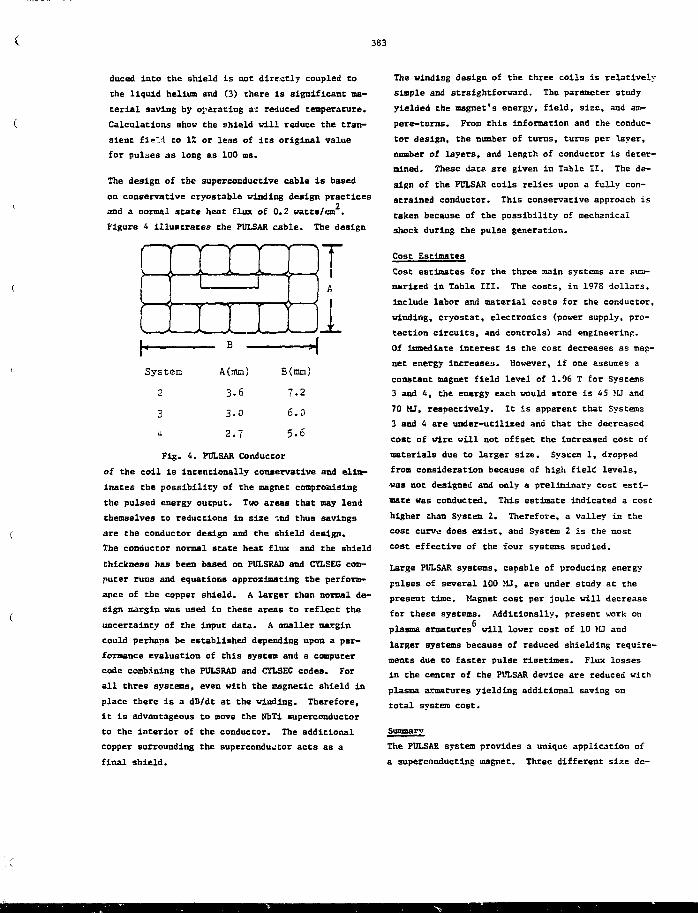
383
duced into the shield is not directly coupled to
the liquid helium and (3) there is significant ma-
terial saving by operating ac reduced temperature.
Calculations show the shield will reduce the tran-
sient fie?.i to IX or less of Its original value
for pulses as long as 100 us.
the design of the superconductive cable is based
on conservative cryostable winding design practices
and a normal state heat flux of 0.2 vatts/cn .
Figure 4 illustrates the PULSAR cable. The design
T
11System A(nun)
3.6
3-0
2 . 7
13(mm)
7.2
6.0
5.6
Fig. 4. PULSAR Conductor
of the coil is intentionally conservative and elim-
inates the possibility of the magnet compromising
the pulsed energy output. Tuo areas that may lend
themselves to reductions in size -aid thus savings
are the conductor design and the shield design.
The conductor normal state heat flux and the shield
thickness has been based on FUL5RAD and CYLSEG com-
puter runs and equations approximating the perform-
ance of the copper shield. A larger than normal de-
sign oargin was used in these areas to reflect the
uncertainty of the input data. A smaller margin
could perhaps be established depending upon a per-
formance evaluation of this system and a computer
code combining the PULSRAD and CYLSEG codes. For
all three systems, even with the magnetic shield in
place there is a dB/dt at the winding. Therefore,
it is advantageous to move the NbTl superconductor
to the interior of the conductor. The additional
copper surrounding the superconductor acts as a
final shield.
The winding design of the three coils is relatively
simple and straightforward. The parameter study
yielded the magnet's energy, field, size, and am-
pere—turns. From this information and the conduc-
tor design, the number of turns, turns per layer,
number of layers, and length of conductor is deter-
mined. These data are given in Table II. The de-
sign of the PULSAR colls relies upon a fully con-
strained conductor. This conservative approach is
taken because of the possibility of mechanical
shock during the pulse generation.
Cost Estimates
Cost estimates for the three main systems are sum-
marized in Table III. The costs, in 1978 dollars,
include labor and material costs for the conductor,
winding, cryostat, electronics (power supply, pro-
tection circuits, and controls) and engineering.
Of immediate interest is the cost decreases as mag-
net energy increases. However, if one assumes a
constant magnet field level of 1.96 T for Systems
3 and 4, the energy each would store is 45 ?IJ and
70 MJ, respectively. It is apparent that Systems
3 and 4 are under-utilized and that the decreased
cost of wire will not offset the increased cost of
materials due to larger size. System 1, dropped
from consideration because of high field levels,
was not designed and only a preliminary cost esti-
mate was conducted. This estimate indicated a cost
higher than System 2. Therefore, a valley in the
cost curve does exist, and System 2 is the most
cost effective of the four systems studied.
Large PULSAR systems, capable of producing energy
pulses of several 100 MJ, are under study at the
present time. Magnet cost per joule will decrease
for these systems. Additionally, present uork on
plasma armatures will lower cost of 10 MJ and
larger systems because of reduced shielding require-
ments due to faster pulse risetimes. Flux losses
in the center of the PULSAR device are reduced with
plasma armatures yielding additional saving on
total Systran cost.
Summary
The PULSAR system provides a unique application of
a superconducting magnet. Three different size de-
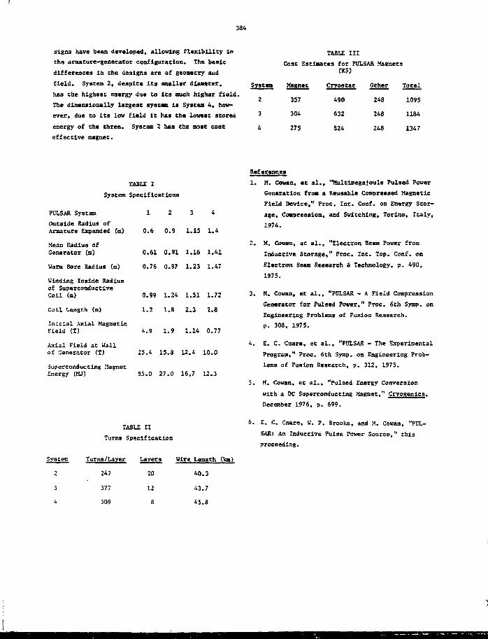
384
signs have been developed, allowing flexibility in
Che araature-generator configuration. The basic
differences in the designs are of geometry and
field. System 2, despite its snallar diaacter,
has Che highest energy due Co its ouch highar field.
The dioensionally largest system is System 4, how-
ever, due Co Its low field it has the lowest stored
energy of Che three. System 2 has the most cost
effective magnet.
TABLE III
Cost Estimates for PULSAR Magnets(K$)
System
2
3
4
Magnet
357
304
275
Cryostat
490
632
324
Other
248
248
248
Total
1095
1184
1347
System
PULSAR System
Outside Radius ofArmature Expanded (a)
Mean Radius ofGenerator (m)
Harm Bore Radius (m)
TABLE I
Specifications
1
0.6
0.61
0.76
2
0.9
0.91
0.97
1
1
1
3
.15
.16
.23
1
1
1
4
.4
.41
.47
Winding Inside Radiusof SuperconductiveCoil (m)
Coil length (m)
Initial Axial MagneticField (T)
Axial Field at Wailof Generator (T)
Superconducting !lagnetEnergy (MJ)
0.99 1.24 1.51 1.72
1.2 1.8 2.3 2.8
4.9 1.9 1.14 0.77
25.4 15.8 12.4 10.0
85.0 27.0 16.7 12.3
TABLE II
Turns Specification
Turns/Layer Layers Hire Length (km)
247 20 40.3
377 12 43.7
509 8 45.3
References
1. M. Cowan, et si., "Multimegajoule Pulsed Power
Generation from a Reusable Compressed Magnetic
Field Device," Proc, Int. Conf. on Energy Stor-
age, Compression, and Switching, Torino, Italy,
1974.
2. M. Cowan, et al., "Electron Beam Power from
Inductive Storage," Froc. Int. Top. Cone, on
Electron Bsan Research & Technology, p. 490,
1975.
3. M. Cowan, et al., "PULSAR - A Field Compression
Generator for Pulsed Power," Proc. 6th Symp. on
Engineering Problems of Fusion Research.
p. 308, 1975.
4. E. C. Cnare, et al., "PULSAR - The Experimental
Program," Proc. 6th Symp. on Engineering Prob-
lems of Fusion Research, p. 312, 1975.
5. M. Cowan, et al., "Pulsed Energy Conversion
with a DC Superconducting Magnet," Cryogenics.
December 1976, p. 699.
6. E. C. Cnare, H. P. Brooks, and M. Cowan, "PUL-
SAR: An Inductive Pulse Power Source," this
proceeding.
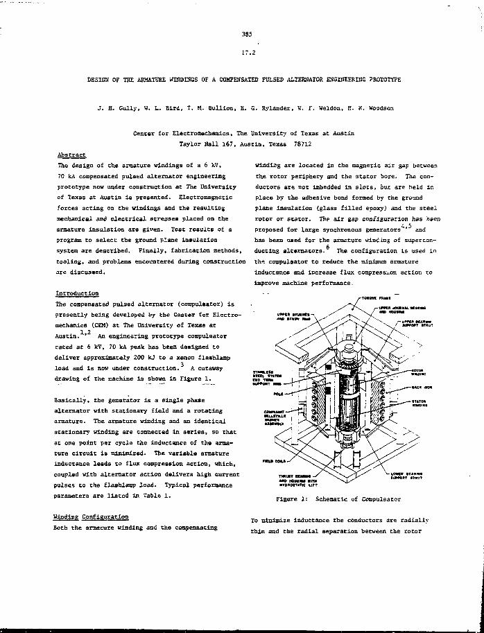
385
17.2
DESIGN OF THE ARMATURE WINDINGS OF A COMPENSATED PULSED ALTERNATOR ENGINEERING PROTOTYPE
J. H. Gully, W. L. Bird, T. M. Bullion, H. G. Rylander, W. F. Weldoa, E. H. Woodson
Center for Electromachanics, The University of Texas at Austin
Taylor Hall 167, Austin, Texas 78712
Abstract
The design of the armature windings of a 6 kV,
70 kA compensated pulsed alternator engineering
prototype now under construction at The University
of Texas at Austin is presented. Electromagnetic
forces acting on the windings and the resulting
mechanical and electrical stresses placed on the
armature insulation are given. Test results of a
program to select the ground plane insulation
system are described. Finally, fabrication methods,
winding ara located in the magnetic air gap between
the rotor periphery and the stator bore. The con-
ductors are not imbedded in slots, but are held ir.
place by the adhesive bond formed by the ground
plane insulation (glass filled epoxy) and the steel
rotor or stator. The air gap configuration has been
proposed for large synchronous generators"" and
has been used for the armature winding of supercon-
ducting alternators. The configuration is used in
tooling, and problems encountered during construction the compulsator to reduce the minimum armature
are discussed.
Introduction
The compensated pulsed alternator (compulsator) is
presently being developed by the Center for Electro-
mechanics (CEM) at The University of Texas at
Austin. ' An engineering prototype compulsator
rated at 6 kV, 70 kA peak has been designed to
deliver approximately 200 U to a xenon flashlamp
load and is now under construction. A cutaway
drawing of the machine is shown in Figure 1.
Basically, the generator is a single phase
alternator with stationary field and a rotating
armature. The armature winding and an identical
stationary winding are connected in series, so that
at one point per cycle the inductance of the arma-
ture circuit is minimized. The variable armature
inductance leads to flux compression action, which,
coupled with alternator action delivers high current
pulses to the flashlamp load. Typical performance
parameters are listed in Table 1.
Winding Configuration
Both the araature winding and the compensating
inductance and increase flux compression action to
improve machine performance,
TOROWC wuml
nunMOWIM mm
HTDHOITATie UFT
Figure 1: Schematic of Compulsator
To minimize inductance the conductors are radially
thin and the radial separation between the rotor
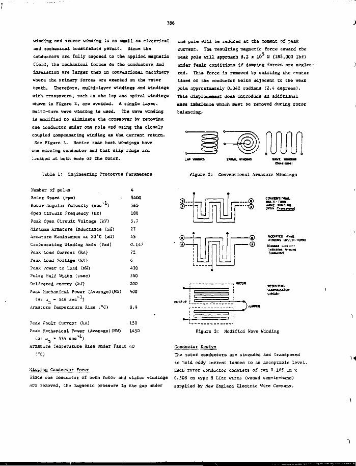
386
winding and scator winding is as snail as electrical
and mechanical constraints permit. Since the
conductors are fully exposed to the applied magnetic
field, the mechanical forces on the conductors and
insulation are larger Chan in conventional machinery
where the primary forces are exarted on the rotor
teeth. Therefore, multi-layer windings and windings
with crossovers, such as the lap and spiral windings
shown in Figure 2, are avoided. A single layer,
multi-turn wave winding is used. The wava winding
is modified to eliminate the crossover by removing
one conductor under one pole and using the closely
coupled compensating winding as the current return.
See Figure 3. Notice that both windings have
one missing conductor and that slip rings are
Located at both ends of the rotor.
Table 1: Engineering Prototype Parameters
one pole will be reduced at the moment of peak
current. The resulting magnetic force toward the
weak poX« will approach 8.2 x 10⁵ N (185,000 lbf)
under fault conditions if damping forces are neglec-
tsd. TIii» force is removed by shifting the center
lines of the conductor belts adjacent to the weak
pole approximately 0.042 radians (2.4 degrees).
This displacement does introduce an additional
moss imbalance which oust be removed during rotor
balancing.
SKKAL WINOWO WAVE WIWUM
figure 2: Conventional Armature Windings
e" )
Number of poles
Rocor Speed (rpm)
Rotor Angular Velocity (see" )
Open Circuit Frequency (Hz)
Peak Open Circuit Voltage (kV)
Minimum Armature Inductance (uH)
Armature Resistance at 20°C (mil)
Compensating Winding Axis (rad)
Peak Load Current (kA)
Peak Load Voltage (kV)
Peak Power to Load (MW)
Pulse Half Width (usec)
Delivered energy (kJ)
Peak Mechanical Power (Average)(MW)
(at J - 548 sec"1)
Armature Temperature Rise (°C)
4
5400
565
180
5.7
27
45
0.147
72
6
430
560
200
500
3.9
Peak Fault Current (kA) 150
Peak Mechanical Power (Average)(MW) 1450
(at u) - 534 sec~ )31
Armature Temperature Rise 'Jnder Fault 40
Missing Conductor Force
Since one conductor of both rotor and stator windings
are removed, the magnetic pressure in the gap under
t=
• ®
OUTPUT
|
J
CONVCMTiniUI.MUCH-TWINW E WINOINaIWItft CtMtmvr»)
MODIFIED WAVEWINOINa (MULTI-TURN)
IQolln* UnaInaleatn MiningCaKoaor)
RESULTINGCOMMLSATORCIIKMT
Figure 3: Modified Wave Winding
Conductor Design
The rotor conductors are stranded and transposed
co hold eddy current losses to an acceptable levei.
Each rotor conductor consists of ten 0.165 cm x
0.508 cm type 8 Lits wires (wound ten-in-hand)
supplied by New England Electric Wire Company.
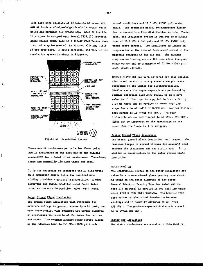
387
Each Litz wire consists of 12 bundles of seven #30
AWG AP Bondeze (Fhelps-Dodga) bondable magnet vires
which arc stranded six around one. Each of the ten
Lit2 wires is wrapped with Hexcel F159/120 pre-preg
glass filled epoxy tape in a linear wrap rather than
J. spiral wrap because of the ml Til mum slitting width
of pre-preg tape. A cross-sectional end view of the
insulation system is shown in Figure 4.
GROUND PLANEINSULATION
CONDUCTIVE^SURFACE100 ft/SO.
12 I 7 I 30 AWGTYPE 8 LITZCONDUCTOR
TURN TO TURN —INSULATION
GROUND PLANEINSULATION
KAPTON AIR GAPINSULATION
PRE-TEMSIOHEDGLASS FIBERBANDING
• ' ROTOR /
1 STRANDNO. 30 « K
Figure 4: Insulation System
There are 12 conductors per pole for three polas
and 11 conductors on one pole due to the missing
conductors for a total of 47 conductors. Therefore,
there are nominally 120 LItz wires per pole.
It is not necessary to transpose the 10 Litz wires
in a conductor bundle since the modified wave
winding provides a natural transposition. A wire
occupying the inside position under south poles
occupies the outside position under north pules.
Rotor Ground Plane Insulation
The ground plane insulation must withstand the
armature voltage to ground, nominally 6 kV peak, but
most importantly, must transmit the torque required
to decelerate the inertia of the rotor laminations
and shaft. Ihe maximum average shear stress placed
on the adhesive bond is 7.1 MPa (1030 psi) under
normal conditions and 17.3 HPa (2500 psi) under
fault. The estimated stress concentration factor
due to non-uniform flux distribution is. 1.5. There-
fore, the insulation system is subject to a cyclic
load of 10.6 MPa (1540 pBi) and 26 MPa (3780 psi)
under short circuit. The insulation is loaded in
compression at the time of peak shear stress by the
magnetic pressure in the air gap. The maximum
compressive loading occurs 100 usec after the peak
shear stress and is a maximum of 33 MPa (4000 psi)
under short circuit.
Hexcel F159/1581 has been selected for this applica-
tion based on static rotary shear strength tests
performed by the Center for Electromechanics.
Similar tests for copper/epoxy bonds perforned by
Grumman Aerospace also show Hexcel to be a good
selection. The tape is supplied in 5 cm width by
0.24 mo thick and is applied in seven half lap
wraps for a total build of 0.338 cm. Nominal dielec-
tric stress is 18 UV/cm (45 VPM). The peak
dielectric stress anticipated is 30 kv/cpi (76 VPM),
which can be impressed on the insulation in the
event that the lamps fail to trigger.
Stator Ground Plane Insulation
The statoi ground plane insulation must transmit the
reaction torque to ground through the adhesive bond
between the Insulation and the stator bore. It is
similar in construction to the rotor ground plane
insulation.
Rotor Banding
The centrifugal forces on the rotor conductors are
taken by a pre-tensioned glass banding tape which
is wound on the outer diameter of the rotor.
General Electric Banding Tape No. 76843 (60 end
tape 1.9 cm wide) is applied in two half lap wraps
under 2200 N (500 lbf) tension. The banding tape
also serves as electrical insulation between
windings and is normally stressed at 20 kV/cm
(51 VPM). The ""Him expected dielectric stress
is 33 kV/cm (85 VPM).
Stator Gap Insulation
The stator conductors are wound on a thin 0.64 mm
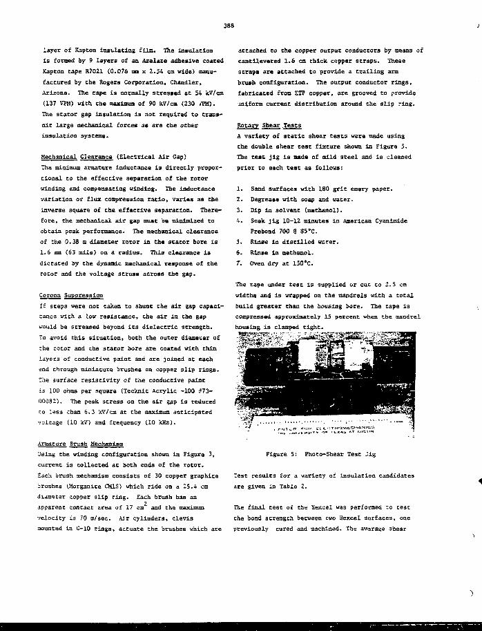
388
layer of Kapton insulating film. The insulation
is formed by 9 layers of an Azelace adhesive coated
Kapcon tape R7021 (0.076 ma x. 2.54 ca wide) manu-
factured by the Rogers Corporation, Chandler,
Arizona. The tape is normally stressed at 54 kV/cm
(137 VPM) with the maximum of 90 kV/ca (230 /PM).
The stator gap insulation is not required to trans-
ait large mechanical forces as are the other
insulation systems.
Mechanical C3 earance (Electrical Air Gap)
The minimum armature inductance is directly propor-
tional to the effective separation of the rotor
winding and compensating winding. The inductance
variation or flux compression ratio, varies as the
inverse square of the effective separation. There-
fore, the mechanical air gap must be minimized to
obtain peak performance. The mechanical clearance
of the 0.38 m diameter rotor in the stator bore is
1.6 ma (63 mils) on a radius. This clearance is
dictated by the dynamic mechanical response of the
rotor and the voltage stress across the gap.
Corona Suppression
If steps were not taken to shunt the air gap capaci-
tance with a low resistance, the air in the gap
would be stressed beyond its dielectric strength.
To avoid this situation, both the outer diameter of
the rotor and the stator bore are coatad with thin
layers of conductive paint and are joined at each
end through miniature brushes on copper slip rings.
The surface resistivity of the conductive paint
is 1D0 ohms per square (Tecknit Acrylic -100 #73-
00082). The peak stress on the air gap is reduced
to Less chan 6.3 kV/cm at the maximum anticipated
voltage (10 kV) and frequency (10 kHz).
Armature Brush Mechanism
Using the winding configuration shown in Figure 3,
current is collected at both ends of the rotor.
£ach brush mechanism consists of 30 copper graphite
brushes (Morganite CM1S) which ride on a 25.4 cm
diameter copper slip ring. Each brush has an
apparent contact area of 17 cm and the mai"t mum
velocity is 70 a/sec. Adr cylinders, clevis
mounted in G—10 rings, actuate the brushes which are
attached to the copper output conductors by means of
cantilevered 1.6 cm thick capper straps. These
straps are attached to provide a trailing arm
brush configuration. The output conductor rings,
fabricated from STP copper, are grooved to provide
uniform current distribution around the slip ring.
Rotary Shear Teats
A variety of static shear tests were made using
the double shear test fixture shown in Figure 5.
The test jig is Bade of mild steel and is cleaned
prior to each test as follows:
1. Sand surfaces with 130 grit emery paper.
2. Degrease with soap and water.
3. Dip in solvent (methanol).
4. Soak jig 10-12 minutes in American Cyanimide
Prebond 700 @ 85 °C.
5. Rinse in distilled vscer.
6. Rinse in methanol.
T. Oven dry at 150°C.
The tape under test is supplied or cut to 2.5 cm
widths and ia wrapped on the mandrels with a total
build greater chan the housing bore. The tape is
compressed approximately 15 percent when the niandrel
housing is clamped tight.
Figure 5: Photo-Shear Tesc Jig
Test results for a variety of Insulation candidates
are given in Table 2.
The final test of Che Hexcel was performed to test
the bond strength between two Hexcel surfaces, one
previously cured and machined. The average shear
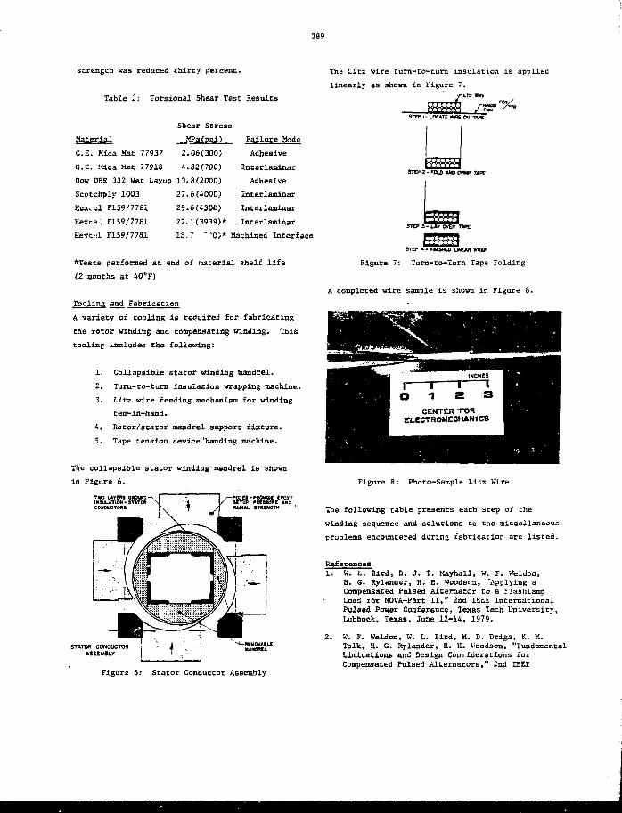
389
strength was reduced thirty percent.
table 2: Torsional Shear Test Results
Shear Stress
Material MPa(psi) Failure Mode
G.E. Mica Mat 77937 2.06(300) Adhesive
G.E. Mica Mat 7791S 4.82(700) Interlaminar
Dow DEE 332 Wet Layup 13.8(2000) Adhesive
Scotchply 1003 27.6(4000) Interlaminar
Hexvel F159/7781 29.6(4300) Interlaminar
Hexce,. F159/7781 27.1(3939)* Interlaminar
Hexed F159/7781 18.7 "'0)* Machined Interface
*Tests performed at end of material shelf life
(2 months at 40°F)
Tooling and Fabrication
A variety of tooling is required for fabricating
the rotor winding and compensating winding. This
tooling .includes the following:
1. Collapsible stator winding mandrel.
2. Turn-to-turn insulation wrapping machine..
3. Litz wire feeding mechanism for winding
cen-in-hand.
4. Rotor/stator mandrel support fixture,
5. Tape tension devicp,'banding machine.
The collapsible stator winding mandrel is shown
in Figure 6.
The Litz wire turn-to-tum insulation is applied
linearly as shown in Figure 7.
TWO LAYERS 0R0UND—.INSULATION 'CONDUCTORS
ma PROVIDE epcwrSETUP PRESUME AND
!AL 9TMN0TH
STATOR CON0UCTORASSEMBLY
ST£T> | . LOCATE WfiE ON TARE
STEP 2 - FOLD AND
STEP 3 - LAY OVER TAPE
STEP 4 - FM3 IC0 LINEAR W U P
Figure 7: Turn-to-Turn Tape Folding
A completed wire sample is shown in Figure 8.
CENTER FORELECTROMECHANtCS
Figure 6: Stator Conductor Assembly
Figure 8: Photo-Sample Litz Wire
The following table presents each step of the
winding sequence and solutions to the miscellaneous
problems encountered during fabrication are listed.
References1. W. L. Bird, D. J. T. Mayhall, W. F. Weldon,
E. G. Rylander, H. E. Woodscn, "Applying aCompensated Pulsed Alternator to a FlashlampLoad for NOVA-Part II," 2nd IEEE InternationalPulsed Power Conference, Texas Tech University,Lubbock, Texas, June 12-14, 1979.
2. W. F. Weldon, W. L. Bird, M. D. Driga, K. M.Tolk, H. G. Rylander, H. E. Voodson, "FundamentalLimitations and Design Considerations forCompensated Pulsed Alternators," 2nd IEEE

390
Table 3: Fabrication of Compensating Winding,
Problems and Solutions
Procedure Solution
Fabricate air gap
winding spacers
Insulating material, compound angle
at end turns prevents conventional machining
Laminated structure out of
0.8 m G-10 sheets using
EPON 828 epoxy. Grind shape
by hand.
Wrap Hexcel F159/72O
turn—to—cum insulation
Epoxy flows at room temperature causing Cape
to stretch and epoxy to coat jig rollers.
Move process to refrigerated
room at 10°C
Wrap Kapton stator air Kapton shifts during cure cycle. Laminated
gap insulation on winding G-10 spacers warp
mandrel. 3ond G-10 spacers
in position
Cure in two steps. use
disposable heat shrink '.ape
to control Kapton diameter.
3ond G-10 spacers with
Hexcel resin. Hold spacers
in place with both hose
clamps and shrink film.
Wind Litz wire ten in hand Wires must move independently. Must hold in
place as rotate horizontally
Made Jigs to locate each
bundle of 10 wires with
respect to spacers. Use
inner tubes to hold wires
in place.
Wrap Hexcei F159/1581
ground plane insulation
Voids must be filled to prevent air bubbles Paint on epoxy before wrapping
Clamp poles around mandrel Voids or wrinkles in tape after 10% compression Built jigs to ^ocate 4 poie
causes stress concentration pieces. Each piece rocaced
into place rather than
sliding at interface.
Caring jf insulation systen Large structure/no available oven Bonded nichrome element
resistors to heat plates
with thermon heat transfer
cement. Strapped resistors
to poles and bore of stator
mandrel.
391
International Pulsed Power Conference, TexasTech University, Lubbock, Texas, June 12-14,1979.
3. 3. Carder, "Applying a Compensated PulsedAlternator to a Flashlamp Load for NOVA-Part I,"2nd IEEE International Pulsed Power Conference,Texas Tech University, Lubbock, Texas.
4. E. Spconer, "Fully Slotless Turbogenerators,"Proceedings, IEE Vol. 120, No. 12, December1973, pp. 1507-1518.
5. E. J. Davies, "Airgap Windings tor large Turbo-generators," Proceedings, IEE Vol. 118, No. 3/4,March/April 1971, pp. 529-535.
6. J. Kirtley, Jr., "Design and Construction of anArmature for an Alternator With a SuperconductionField Winding," Doctoral Dissertation, Massachu-setts Institute of Technology, Boston, Mass.,Ausgust, 1971.
7. C. Burke, "Coil Integrity Insulation MechanicalScreening Interim Test Report," RDAC 11.B.4-2,K^port No. EP-D-016 to Princeton Plasma PhysicsLaboratory, Grumman Aerospace Corp., December 13,1977.
Acknowledgments
This work vas performed under Lawrence Livermore
Laboratory Purchase Order No. 3325309 with suoport
of the U. S. Department of Enfcrey and the Texas
Atomic Energy Research Foundation.
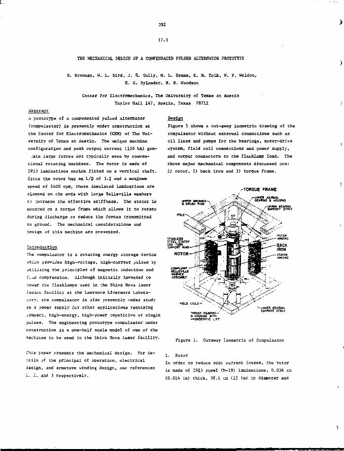
392
17.3
THE MECHANICAL DESIGN OF A COMPENSATED PULSED ALTERNATOR PROTOTYPE
Design
Figure I shows a cut-away isometric drawing of the
compulsator without external connections such as
oil lines and pumps for the bearings, mocor-drive
system, field coil connections and power supply,
and output connectors to the flaahlamp load. The
three major mechanical components discussed are:
1) rotor, 2) back iron and 3) torque frame.
rTORQUE FRAME
M. Brennan, W. L. Bird, J". 8. Gully, M. L. Spann, K. M. Tolk, W. F. Weldon,
H. G. Rylander, H. H. Woodson
Center for Electromechanics, The University of Texas at Austin
Taylor Hall 167, Austin, Texas 78712
Abstract
A prototype of a compensated pulsed alternator
(coopulsator) la presently under construction at
the Canter for Electromechanics (CEM) of The Uni-
versity of Texas at Austin. The unique machine
configuration and peak output current (150 kA) gen-
-ate large farces not typically seen by conven-
tional rotating machines. The rotor is made of
2913 laminations shrink fitted on a vertical shaft.
Since the rotor has an L/D of 3.2 and a maximum
speed of 5400 rpm, these insulated laminations are
clamped on the ends with large Belleville washers
to increase the effective stiffness. The stator is
mounted on a torque frame which allows it to rotate
during discharge to reduce Che forces transmitted
to ground. The mechanical considerations and
design of this machine are presented.
Introduction
The compulsator is a rotating energy storage device
vhich provides high-voltage, high-current pulses by
utilizing the principles of magnetic induction and
flax compression. Although initially Invented to
power che flashlamps used In the Shiva Uova laser
fusion facility at the Lawrence Livermore Labora-
CDry, the compulsator is also presently under study
as a power supply for other applications requiring
compact, high-energy, high-power repetitive or single
pulses. The engineering prototype compulsator under
construction is a one-half scale model of one of the
machines to be used in the Shiva Nova laser facility.
This paper presents the mechanical design. For de-
cails of the principal of operation, electrical
design, and armature winding design, see references
i, 2. and 3 respectively.
THRUST BEARING-a HOUSING WITHHYOTOSTATIC LIFT
LOWER 8ESRINGSUPPORT STRUT
Figure 1. Cutaway Isometric of Compulsator
1. Rotor
In order to reduce eddy current losses, the rotor
is made of 2913 steel (M-19) laminations, 0.036 cm
(0.014 in) thick, 38.1 cm (15 in.) in diameter and
395
Figure 4. Rotor and Back Iron
The inverse of the slope of the curve in Figure 3
can be considered an effective Young's Modulus,
E .., of the stack, of laminations in compression.
Using the data obtained on the final unloading in
Figure 3b, E e f f- 1.88 x 10¹⁰ MPa (2.72 x 10⁶ psi).
Although what is actually desired is the flezural
modulus, it could not be measured and the above
E „, should be sufficient for the dynamic calcula-
tions.
A discrete, lumped mass model of the rotor-bearing-
support system (see Figure 5) was performed using
a CDC 6600 computer to solve for the complex eigen-
vectors and complex eigenvalues. The torque frame,
bearing supports, bearings (including damping), and
rotor are included in the model. The first rotor
critical is calculated to be 621 rad/sec, 10% above
maximum operating speed.
The radial bearings for the machine are tilting pad,
oil lubricated, hydrodynamic bearings made by Kings-
bury, Inc. A special design feature incorporated
into the bearing is spherical buttons on the back
of the pads which allot; for axial misalignment or
cocking of the shaft. Each bearing is instrumented
with a resistance temperature detector (RTD)
embedded in the babbit to monitor pad temperatures.
The thrust bearing is a two sided, self aligning,
tilting pad, hydrodynamic bearing made by Kingsbury,
Inc. Each side is instrumented with a RTD and the
loaded side has irwo load cells to measure steady
state and dynamic loads.
Since this is an experimental machine and will be
started and stopped many times, a high pressure oil
inlet at the end of the shaft is used to lift the
machine off the thrust bearing pads at zero speed
to avoid excessive wear of the pads. This will
only be used during start up.
Y/?y/y/yy/y//y/yyy//yyyyyy/yy/yyy77//Yy77y,KJJ - TOROUE rwre sriFness • 6.W x m N/H
1^3 • BEARING auPKRT STlFTItSS ' 1 . 2 9 X I D 9 H/H
*2 • BEARING STIFFNESS - WRIED
Cj - BEARING OWING - VARIED
E ^ • EFFarre Youc's KmiE o» arm - VARIED
K,, - BDTtR ST1FINESS; INCUDES SHEAR DEFLECTION;
0E7EWB.T I K K E ^ - VARIED
1 ^ " N B E I I C SWING STIFFNESS - 3 . 9 7 X 1D^ N/B
« . - HASS OF ROTOR - 1 . 0 9 X H r KG
^ , • N U S OF BACK IKM • 9 . 0 7 X 10^ KG
t ^ " MASS OF BEARING HOUSING - 2 3 0 KG
.-'igure 5. Lumped Mass Dynamic Model
2. Back Iron
During a discharge, the back iron must withstand
two forces generated from J X B forces and flux
depression. These forces appear as a torque and
an internal pressure applied at the inner diameter
of the back iron where che stator conductors are
located (see Figure 6). The back iron is designed
to withstand these forces under steady state con-
ditions for a peak fault current of 150 kA although
396
this peak current only exists instantaneously duringthe pulse.
mourns FMXI' ?MU.T woe. 5400 KM, ISO «»IT > PEAK USCWMOe TOHflUC - 2.7 I 10* M-M
"m ' »MK MAOMTIC P « M U M • SOT " • • <30OO«*t
Figure 5. Back Iron
The reaction torque of 2.70 x 10 N-ra (1.99 x 10
rrc-lb) ar.a internal pressure of 20.7 MPa (3000 psi)
muse be sustained with ao relative movement of the
pieces. The stator conductor is epoxied Co Che
inner diameter of the back iron and any slippage
of a Dack iron member could initiate a crack in the
epoxy. The ideal geometry for these forces would
be a cylindrical vessel, but a casting could not be
obtained in time. An irregular octagonal structure
:aade of 16.5 cm (6,5 iiO plate as seen in Figure 6
evolved with the sides interlocked with closely
coleranced keys and slots. This allowed for most
of Che load to be taken by the keys in shear.
Another significant design feature of the back iron
and poles is that they do not extend the length of
the rotor. If this had been done, the axial forces
on the end turns at each end of the rotor from the
applied field and the current in the conductors
would be very large and any asymmetry in the field
wouid pull the rotor to one end and overload the
thrust bearing. Therefore, the back iron only
extends the active length of the conductors and the
stator end turns arc supported by stainless seeel
rings bolted Co the esd of the poles. Figure 7
shews the back iron supported in Che torque frame.
Figure 7. Back Iron In Torque Frame
3. Torque Frame
the torque frame is a structure designed to support
the compulsacor and allow a slight rotacion of the
back iron during a discharge (see Figures 1,5 and
7). By allowing the back iron to rotate, the total
peak load transferred to Che torque frame as a
result of the discharge torque is reduced from
6.82 x 10,,4
(1.53 x 10⁶ lb) to 1.15 x 10⁵N (2.56 x
10 lb). As the back iron rotaces, it compresses
Belleville washers against I beams which form. Che
structure of the torque frame. The springs are
essentially serving as force attenuators. There are
two sets of Belleville washers being compressed at
each of the four corners of the torque frame located
at a radius of 79.4 cm (31.3 in) from the center of
the compulsator. The back iron is allowed to rotate
0.00733 radians, compressing the Belleville springs
0.382 cm (0.23 in). The torque frame is constructed
of eight I beans (6112.5), two per corner, which are
connected at the cop and botton by a square formed
from rectangular tubing. In addition to resisting
the discharge torque, the frame must support the
mass of the compulsator, approximately 9.07 x 10 k.g.
Acknowledgements
This work is supported by the U.S. Department of
Energy, Lawrence Livermore Laboratories (Purchase
Order 3325309), and the Texas Atomic Energy Research
Foundation.
393
shrink fitted on to an AISI 4340 steel shaft heat
treated to Rc 34. Because Che nominal shaft diam-
eter of 9.65 cm (3.8 itO is insufficient to keep
the first rotor critical above the maximum operat-
ing speed of 5400 rpm, it is necessary to compress
the laminations in order to increase the effective
flexural modulus of the rotor, hence the rotor
stiffness. The rotor cannot be allowed to pass
through a critical because hyBteritic losses from
sliding of the lamination interfaces would result
in a rotor instability . The lamination preload
is applied with two (one per end) large, titanium
Belleville washers, 6.03 cm (2.375 in) thick and
38.1 cm (15 in} in diameter. Because of the Belle-
ville washer configuration, the preload of 2.67x10 N
(600,000 1b) preferentially loads the outside diam-
eter of the laminations il though the washer will be
flattened to partially load the inner diameter also.
The required preload was not arbitrarily selected,
but resulted from a series of tests performed on
sample stacks of laminations. The two guiding
design criteria were the interlaminar resistance
and effective modulus versus load. With increasing
load, the effective flexural modulus of the stack
of laminations increases as the interlaminar resis-
tance decreases.
The desired lamination core plating, C-5, could not
be obtained on the schedule required for construc-
tion of the prototype. The plating received, C-0,
was unacceptable and required that an interlaminar
insulation be applied that could take the high
loads. The first type of insulation tested was
Sterling U-87/PS, an air dry varnish.
Figure 2 shows the measured overall resistance
versus load of two separate stacks of laminations.
The bottom curve is the test results of a stack of
1000 varnished laminations. Even as the load was
held steady, the resistance continued to drop and
at 1.33 x 10⁶N (300,000 lb), ueasured 162 ohms.
This was unacceptable since a value of 782 ohms
was desired in order to keep the eddy current losses
at an acceptable level.
LOW • 1O' (It)
-500 CONVERSION COATED LAMINATiONS
1000 VARNISHED LAMINATIONS
1.0 '-5 2.0 i^> 5.0 3J
LOAD • 10* (N)
Figure Z. Resistance vs Load
The next insulation tested and finally used was a
military refinish concentrate made by Atlanta
Cutlery. It is a chemical conversion coating which
phosphatizes the surface. The varnish previously
applied was baked off the laminations before the
chemical conversion coating was applied. The resis-
tance versus load of a stack of 500 coated lamina-
tions is also shown in Figure 2 and at 3.11 x 10 S
(700,000 lb) measured 9,040 ohms, over an order of
magnitude above the design goal of 391 ohms. Note
that even as the load was fluctuated, the resistance
remained relatively stable and repaatable. The
resistance did register lower after the load was
decreased than when the load was initially applied.
This is probably due to an increasing number of
small asperities breaking through the insulation as
the load is increased and then remaining in contact
with the adjacent lamination as the load is de-
creased.
During the same test with the chemical conversion
coated laminations, the amount of axial compression
versus load was measured and is shown in Figure 3a.
When the stack is initially compressed, the total
deflection is significant. This is a result of the
air being squeezed out from between each lamination.
394
small asperities being flattened, and any warpage
in the lamination being flattened. When the same
stack is then compressed a second time, even after
sitting unloaded for one day, the total deflection
is considerably less. The interesting fact is that
the slope of the curve as the load is decreased is
the same, indicating that after the stack is loaded,
its mechanical characteristics are repeatable.
Figure 3b is an enlarged section of the first load-
ing curve and shows some other interesting facts.
LOAD • 1 0 s (Ik)
i 8.03
* 3.90
/
'.2 t.S 2.0 i.* t^U3A0 ' * 5* (Nl
EnfarganMflf
. Figure 3b
LOAD t 103 (Ib)
SM atmt Efllv|i«Mir-7
First Loosing
Sacond Loading i-" i
I.OAD i 10* INI
Figure 3a
Deflection vc Load
First note that as the stack is brought to full
load, at two points the load is reduced and the
stack still shows an increase in deflection. This
was noticed in other tests rat presented here and
is due co che amount of time the stack is allowed
co sin at load before the deflection measurement is
xade. If the load is held steady, the stack will
continue to compress for many minutes. It is
suspected this time element is a result of the air
being squeezed out from between the laminations.
Another important fact is that after the stack stops
creeping and the load is fluctuated, the stack does
HOC load and unload along the same curve, indicating
some hysteresis in the stack.
Since the resistance remained high for all the loads
tested, the level of load to be used is determined
by mechanical limitations. The Belleville washers,
which apply the preload, are held in place with two
large nuts which also serve as the bearing journals.
These nuts will be tightened using a stud tensioner
loaned to CEM by the DuFont chemical processing
plant in Victoria, Texas. The device works by
stretching the stud (in our case, the shaft) and
then "hand tightening" the nut down against the
Belleville washer. The device has a 3.56 x 10⁶S
(300,000 lb) pulling capacity which produces the
maximum stresses the modified 60° stub-tooth Acme
threads and shaft can take. Due to relaxation in
the threads as the load is transferred from the
stud tensioner to the nut, the resulting preloa.l
will be less although the minimum desired is
2.67 x 10⁶K (600,000 lb).
Clamped up sections of laminations 22.9 cm (9 in)
long were bored with a taper of 6.86 x 10 ca
(0.0027 inj on the diameter and the shaft then
ground to match. After the application of the lami-
nation insulation, the inner bore of the laminations
were aligned for the shrink fit by pulling one lami-
nacion at a time up against two small ground shafts
glued together and inserted down the bore. The
entire stack was then clamped as tightly aa possible
without affecting che bore alignment. The alignment
was checked by lowering the shaft in at room temper-
ature until the tapers matched. The final hrink
fit was done by chilling the shaft in liquid nitro-
gen and ther. dropping it into the laminations.
Figure i is a picture of the rotor with the Belle-
ville washers and nuts in place and the back iron
in the background.
397
References
1. W. F. Weldon, W. L. Bird, M. D. Driga, K. M.Tolk, H. G. Rylander, and H. H. Woodson,"Fundamental limitations and Design Considera-tions for Compensated Pulsed Alternators,"2nd International IEEE Pulsed Power Conference,Jt:ne 12-14, 1979, Texas lech University,Lubbock, Texas.
2. W. L. Bird, D. J. T. Mayhall, W. F. Weldon,H. G. Rylander, and H. H. Woodson, "Applyinga Compensated Pulsed Alternator to a FlashlampLoad for NOVA-Part II," 2nd International IEEEPulsed Power Conference, June 12-14, 1979,Texas Tech University, Lubbock. Texas.
3. J. H. Gully, W. L. Bird, M. D. Driga, H. G.Rylander, K. M. Tolk, W, F. Heldon, and H. a.Woodson, "Design of the Armature Windings of aCompensated Pulsed Alternator EngineeringPrototype," 2nd International IEEE pulsedPower Conference, June 12-14, 1979, TexasTech University, Lubbock, Texas.
4. R. G. Loewy and V. J. Piarulli, Dynamics ofRotating Shafts. Washington, D.C.: Havy Publi-cation and Printing Service Office, 1969,pp. 31-34.
398
17.4
THE DESIGN, ASSEMBLY, AHD TESTING OF A DESK MODEL COMPENSATED PULSED ALTERNATOR
M. A. Pichot, W. L. Bird, M. Brannaa, M. D. Driga, J. H. Golly
H. G. Ry lander, K. M. To Ik, H. F. Weldon, H. H. Soodsou
Cencer for Electromechanica, The University of Texas at Austin
Taylor Kail 167, Austin, Texas 78712
Abstract
The Center for Electromechanics (CEM) at The Uni-
versity of Texas Is currently involved in the
design, fabrication, and testing of a prototype
compensated pulsed alternator (compulsator). This
machine, a new concept in pulsed power technology,
utilizes the principles of magnetic induction and
Design Philosophy
The desk model compulsator, intended as a portable
demonstration device, is designed to operate from
a 120 Vac wall outlet. The motoring system and
inductance of the rotating coil, reducing it to a
small fraction of its normal value. At this
Instant, a very intense pulse is generated; after
the pulse, Che inductance again rises to its ori-2
ginal value.
flux compression to convert rotational energy
directly into electrical energy.
The subject of this paper is a one-fifth scale
version of the CEM prototype. This desk, model com-
pulsator is a portable demonstration machine
designed to operate in the same fashion as the full
scale model.
Introduction
The compulsator was invented to reduce the large
volume and high costs associated with large pulsed
power sources. Because of the machine's unique
characteristics, it is able to produce the high-
voltage, high-current pulses of capacitors in a
3ore compact and economical form.
Although the compulsator offers volume and cost
savings at high power levels, the advantages become
less prominent as the size of the power source is
reduced, Because or tliis, the desk model compulsator
is not intended to compete with other power sources
in its output range, but rather to demonstrate the
' operation of larger compulsators.
?rinciple of Operation
The design feature that makes the compulsator unique
is a. stationary coil almost identical to the rotating
winding. When the two coils are in their closest
proximity, the stationary coil counteracts the
magnetic circuit of the machine are sized accord-
ingly.
Rotor
The rotor consists of 6.99 cm outer diaaeter ring-
type laminations shrunk fit onto a 2.54 cm diameter
stainless steel shaft. In audition to the shrink
fit, the laminations are compressed axiaily by
stainless steel nuts on each end of the shaft.
Attached to the O.D. of the laminations, the rotating
coil is wound in a serpentine like shape (Figure
1). The coil conductors are stranded and trans-
posed (Litz) wire used to reduce the losses associa-
ted with skin and proximity effects. The shaft is
supported both radially and axially by ball-bearing
units press fitted onto each of ics ends.
The limiting speed of Che machine is determined by
the rotor's first critical frequency. For a worst
case assumption, the shaft alone is assumed to
provide the rotor's stiffness (additional stiffness
is expected from the compressed laminations). The
resulting rotor stiffness is 3.713 x 10 :it/m. The
ball bearings are supported by an aluminum structure
bolted to Che compulsator's outer housing (back
iron); the bearing support stiffness in its weakest
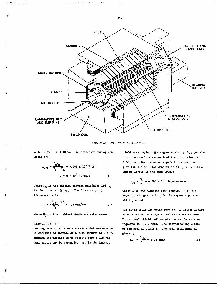
399
POLE
BACKIRON
BRUSH HOLDER
BRUSH
ROTOR SHAFT
LAMINATION NUTAND SLIP RING
BALL BEARINGFLANGE UNIT
BEARINGSUPPORT
COMPENSATINGSTATOR COIL
ROTOR COIL
FIELD COIL
Figure 1: Desk Model Cc-apulsator
mode i s 9.19 x 10 Nt/m. The effective spring con-
stant i s :
Keff 1 0
(2.038 x 10⁴ lb / ia . ) (1)
where K^ is the bearing support stiffness and iC
is the rotor stiffness. The first critical
frequency is then:
ux - (-§~> - 738 rad/sec (2)
where M_ is the combined shaft and rotor mass.
Magnetic Circuit
The magnetic circuit of the desk model corapulsator
is designed to operate at a flux density of 1.5 T.
Because the machine is to operate from a 120 Vac
wall outlet and be portable, this is the highest
field attainable. The magnetic air gap between the
rotor laminations and each of the four poles is
0.511 cm. The number of ampere-turns required to
give the desired flux density in the gap is (assum-
ing no losses in the back iron):
N, » —^ « 6.096 x 10 Ampere-turns
where B is the magnetic flux density, g is the
magnetic air gap, and u is the magnetic perme-
ability of air.
The field coils are wound from Mo. 13 copper magnet
wire in a conical shape around the poles (Figure 1).
For a single field coil of 462 turns, the current
required is 13.19 Amps. The corresponding length
of the coil is 302.3 m. The coil resistance is
given by:PL,
R f c "'fc 2.03 ohms (3)
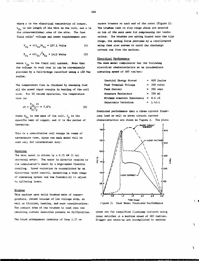
400
where p is the electrical resistivity of copper,
L_ is the length of the wire ia the coil, and A is
the cross-sectional area of the wire. The four
field coils' voltage and power requirements are:
V£(. 107.1 Volts
P f c • 4(i £ c) R f c * 1413 Watts
(4)
(5)
where i. is the field coil current. Note that
the voltage is such that it can be conveniently
provided by a full-bridge rectifier using a 120 Vac
outlet.
The temperature rise is obtained by assuming that
all the power input results in heating of the coil
wire. For 60 second operation, the temperature
rise is:
P f c A t
MfcCo7.8°C (6)
where M. is the mass of the coil, C is thefc p
specific heat of copper, and At is ths period of
operation.
This is a conservative coil design in terms of
temperature rise, since the desk, model will be
used only for iatennittant duty.
Mocoring
The desk model is driven by a 0.7S k.H (1 hp)
universal motor. The noCor is directly coupled to
the compulsator's shaft by a high-speed flexible
coupling. Speed variation is accomplished by an
electronic speed control, permitting a wide range
of operating speeds and the flexibility to adjust
za differing loads.
Brushes
This machine uses solid brushes made of copper-
graphite, chosen because of low voltage drop, as
well as friction, heating, and wear considerations.
The contact area of the brushes is such that the
resulting current densities present no difficulties.
The brush arrangement consists of four 1.27 cm
square brushes at each end of the rctor (Figure 1).
The brushes ride on slip rings which are mounted
on Cop of the nucs used for compressing the lamin-
ations. The brushes are spring loaded onto the slip
rings, the spring force provided by a cantilevered
strap that also serves to carry the discharge
current ouc from Che machine.
Electrical Performance
The desk model compulsator has the following
electrical characteristics at an intermediate
operating 3p««d of 565 rad/sec:
Inertial Energy Stored - 600 joules
Peak Terminal Voltage - 200 volts
Peak Current - 500 amps
Armature Resistance • 320 mfi
Minimum Armature Inductance - 8.6 uH
Inductance Variation * 1.45:1
Predicted performance into a three circuit flash-
lamp load as well as short circuit current
characteristics are shown in Figure 2. The plots
TIME (mticl
rigure 2: Desk Model Predicted Performance
shown are for simplified ilashlamp circuits using
ideal switches at a machine speed of 565 rad/sec.
Trigger and start-up are accomplished by methods
401
discussed in reference 3.
The curves indicate little flux compression effect
in the desk model. This is a consequence of scaling
down from the larger diameter machine; that is,
fjux compression improves with the increase in
Machine diameter.
Additional information concerning fundamental
limitations and load applications of compulsators can
be found in references 3, 4, and 5.
Fabrication and Assembly
Fabrication and assembly of the desk model are now
underway at The University of Texas.
The shaft was machined from type 304 stainless steel
bar stock. Ring laminations were purchased from
Arnold Engineering Co.; the inside diametar of the
laminations was bored to the 2.54 cm shaft diameter,
and the laminations were shrunk onto the shaft.
The back iron and pole assembly was manufactured
from cold-rolled steel plates. The 1.905 cm thick
back iron plates were assembled to form a 21.59 cm
square structure 20.96 cm long. Four 3.81 cm pole
plates were then fastened to the inside of the
back iron structure.
The field coils will be wound from No. 13 magnet wire
around each of the four poles. Epoxy is to be
applied to the coils after each layer of wire is
wound, so that the field coils form spool-type units.
In addition, the coils can be removed from the poles
should repairs become necessary.
Additional preparations for the desk model will
include winding both the rotor and compensating
stator coils, fabricating the brush set-up, and
manufacturing the bearing supports.
a) experimentally verifying the basic machine
constants,
b) comparison of actual machine performance
to predicted values,
c) attempting to minimize the various sources
of mechanical and electrical losses, and
d) determining machine efficiency in various
modes of operation.
The desk model compulaator research project is
funded by Lawrence Livermore Laboratory, the
U. S. Department of Energy, and the Texas Atomic
Energy Research Foundation.
References
1. Lawrence Livermore Laboratory's, "CompensatedPulsed Alternator," brochure concerning thecompulsator invented by the Center forElectromechanics, July 1978.
2. K. F. Weldon, H. G. Rylander, H. H. Woodson,"Invention from Research," DISCOVERY: Researchand Scholarship at The University of Texas atAustin, Volume III, Number 2, December 1978.
3. B. M. Carder, "Applying a Compensated PulsedAlternator to a Flachlamp Load for NOVA-Part I,2nd IEEE International Pulsed Power Conference,Texas Tech University, Lubbock, Texas, June12-14, 1979.
4. W. F. Weldon, W. L. Bird, M. D. Driga, K. M.Tolk, H. G. Rylandar, H. H. Woodson, "Fund-amental Limitations and Design Considerationsfor Compensated Pulsed Alternators," 2nd IEEEInternational Pulsed Power Conference, TexasTech University, Lubbock, Texas, June 12-14,1979.
5. H. L. Bird, D. J. T. Mayhall, M. F. Weldon,H. G. Rylander, H. H Woodson, "Applying aCompensated Pulsed Alternator to a FlashlampLoad for NOVA-Part II," 2nd IEEE InternationalPulsed Power Conference, Texas Tech University,Lubbock, Texas, June 12-14, 1979.
Testing
After assembly has been completed, the desk model
compulsator will be thoroughly tasted. Some of the
testing program's objectives will include:
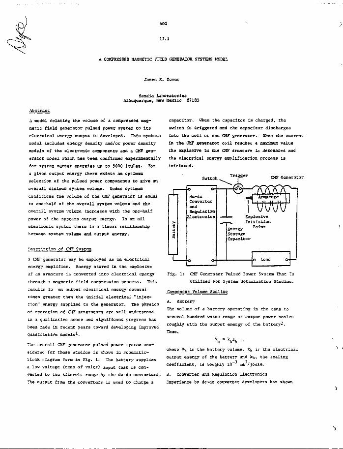
402
17.5
A COMPRESSED MAGNETIC FIELD GENERATOR SYSTEMS MODEL
James E. Gover
Sandia LaboratoriesAlbuquerque, New Mexico 67185
Abstract
A model relating the volume of a compressed mag-
netic field generator pulsed power system to its
electrical energy output is developed. This systems
model includes energy density and/or power density
models of the electronic components and a CMF gen-
erator model which has been confirmed experimentally
for system output energies up to 5000 joules. For
a given output energy there exists an optimum
selection of the pulsed power components to give an
overall minimum system volume. Under optimum
conditions the volume of the CMF generator is equal
to one-half of the overall system volume and the
overall system volume increases with the one-half
power of the systems output energy. In an all
electronic system there is a linear relationship
between system volume and output energy.
Descriation of CMF System
A CMF generator may be employed as an electrical
energy amplifier. Energy stored in the explosive
of an armature is converted into electrical energy
through a magnetic field compression process. This
-esults in an output electrical energy several
times greater than the initial electrical "injec-
tion" energy supplied Co the generator. The physics
of operation of CMF generators are veil understood
in a qualitative sense and significant progress has
been made in recent years toward developing Improved
quantitative models1.
The overall CMF generator pulsed power system con-
sidered for these studies is shown in schematic-
block diagram form in Fig. 1. The battery supplies
a low voltage (tens of volts) input that is con-
verted to the kilovolt range by the dc-dc converters.
The output from the converters is used to charge a
capacitor. When the capacitor is charged, the
switch is triggered and the capacitor discharges
into the coil of the CMF generator. When the current
in the CMF generator coil reaches a maximum value
the explosive in the CMF armature is detonated and
the electrical energy amplification process is
initiated.
SwitchTrigger CMF Generator
dc-dcConverterandRegulationElectronics
EnergyStorageCapacitor
Load
Fig. 1: CMF Generator Pulsed Power System That Is
Utilized For System Optimization Studies.
Component Volume Scaling
A. Battery
The volume of a battery operating in the cens to
several hundred watts range of output power scales
roughly with the oucput energy of the battery^.
Thus,
Vb"Vb 'where Vi, is the battery volume, E^ if the electrical
output energy of the battery and kb> the scaling
coefficient, is roughly 10 cm /joule.
B. Converter and Regulation Electronics
Experience by dc-dc converter developers has shown
403
that dc-dc converter volume scales linearly with
output power, or
e r '
where V is the volume of the dc—dc converter and
regulation electronics, E is the output electrical
energy of the converters, T is the time required to
charge the energy storage capacitor and k is the
scaling coefficient . A significant range of values
of 1^ may be obtained depending upon regulation and
reliability requirements, technology choices and
operating life. For these studies the range
_ 3 35 *— < k < 20 S —watt - e - watt
is selected.
The efficiency of dc-dc converters may range from
20% to 90% depending upon the type of converter
design. An efficiency factor, ( , is defined such
that
capacitor to maintain this reliability over a broad
temperature range and maintaining a high pulse life
results in values for k of 0.06 joules/cm for dry
mylar and mica paper capacitors. It has been
demonstrated that the energy density of mylar energy
storage capacitors may increase to values as high as
0.3 joule/cm by flooding the mylar with Fluorinert.
Refinement of this design method could result in
energy storage capacitors whose energy density is
as high as 1 joule/cm without diminishing reli-
ability, temperature range or pulse life capabili-L
ties . Hence,
16 cm /joule >_ k^ > 3 cm /joule
with potential for obtaining k - 1 cm /joule.
D. Switch and CMF Coil Resistance Losses
When the switch is triggered and the energy storage
capacitor is discharged into the CMF generator coil,
energy is lost to joule heating in the switch and
coil. Hence,
C. Energy Storage Capacitor
Once one chooses the dielectric material of a
capacitor, as upper limit is obtained for the maxi-
mum electric field at which the capacitor may be
operated, i.e., the breakdown field of the dielec-
tric. The permittivity is also fixed. Thus an
upper limit is obtained for the energy density of a
capacitor. In practice, capacitors are operated
at electric field values much less than the break-
down strength of tha dielectric. One accepted
practice is to determine the average breakdown
voltage and the standard deviation of the breakdown
voltage of a large number of capacitors and limit
the operation of the capacitor to voltages that are
four standard deviations below the average break-
down voltage. This operational practice results in
capacitors that are extremely reliable; however,
their energy density is much less than that suggested
by the breakdown field of the dielectrl--.
We model the capacitor volume as
Vc " kcEe
where V is the capacitor volume and k is the
scaling coefficient. Employing the high reliability
design approach as outlined above, designing the
Eig ' <sEe
where E. is the initial magnetic field energy in
the generator and t is the electric field to
magnetic field conversion efficiency. For tnost
cases of practical interest
0.9 >_ € >_ 0.7 .
E. CMF Generator
We have found by empirical methods that helical CMF
generators have an energy gain per unit volume that
is independent of their volume . That is
Eigk vg g
where E is the output electrical energy of the
generator, V is the generator volume and k is the
generator scaling constant. This model was arrived
at by observing data obtained from several generator
designs whose output energy ranged from 50 joules to
5000 joules. Validity of the model above 5000 joules
output energy cannot be claimed because of lack of
experimental data. Furthermore, it is clear that
at values of output energy in the megajoule region
this scaling is not valid because the electrical
output of the generator would exceed the energy
stored in the armature's explosive.
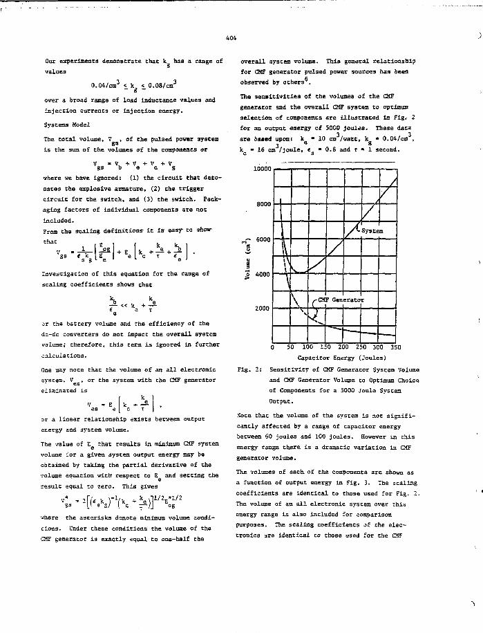
404
Our experiments demonstrate that k has a range of
values
0.04/cm3 < k < 0.08/cm3
over a broad range of load Inductance values and
injection currents or injection energy.
Systems Model
The total volume, V , of the pulsed power system
is the sum of che volumes of the components or
Vgs
V. + V + V + Vb e c g
where we have ignored: (1) the circuit that deto-
nates the explosive armature, (2) the trigger
circuit for the switch, and (3) che switch. Pack-
aging faccors of individual components are not
included.
From the scaling definitions- it is- easy to show
that
Investigation of this equation for the range of
scaling coefficients shows that
or the battery volume and rhe efficiency of the
dc-dc converters do not impact the overall system
volume; therefore, this term is ignored in further
calculations.
One may note that the volume of an all electronic
system, V , o
eliminated is
system, V , or the system with the CMF generator
es e
or a linear relationship exists between output
energy and system volume.
The value of E that results in nrin-timim CMF system
volume tor a given system output energy may be
obtained by caking che partial derivative of the
volume aquation with- respect Co E and setting the
result equal to zero. This gives
vhere che asterisks denote minimum volume condi-
tions. Under these conditions the volume of the
CMF generacor is exactly equal to one-half che
overall system volume. This general relationship
for CHF generator pulsed power sources has been
observed by others .
The sensitivities of Che volumes of the CKF
generator and the overall CMF system Co optimum
selection of components are illustrated in Fig. 2
for an output energy of 5000 joules. These data3 3
are ba«ed upon: k • 10 cm /watt, k • 0.04/cm ,3
k • 16 cm /joule, « • 0.8 and T » 1 second.
1IX
I
\
\
y
/-CM
/
? Gen
/ •
erato
— .-
/
/
Syste
r
m
10000
8000
~ 6000s
o 4000
2000
50 100 150 200 250 300 350
Capacitor Energy (Joules)
Fig. 2: Sensitivity of CMF Generator System Volume
and CMF Generator Volume to Optimum Choice
of Components for a 5000 Joule System
Output.
Note that the volume of the system is not signifi-
cantly affected by a range of capacitor energy
between 60 joules and 100 joules. However in this
energy range there is a dramatic variation in CMF
generator volume.
The volumes of each, of che components are shown as
a function of output energy in Tig. 3. The scaling
coefficients are identical to those used for Fig. 2.
The volume of an all electronic system over this
energy range is also included for comparison
purposes. The scaling coefficients of the elec-
tronics are identical to chose used for the CMF
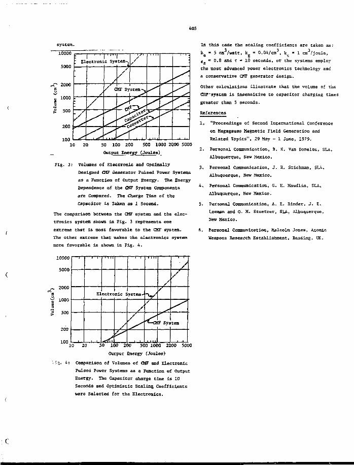
405
system.
10010 20 SO 100 200 500 X000 2000 5000
Output Energy (Joules)
Fig. 3: Volumes of Electronic and Optimally
Designed Off Generator Pulsed Power Systems
as a Function of Output Energy. The Energy
Dependence of the Off System Components
are Compared. The Charge Tine of the
Capacitor is Taken as 1 Second.
The comparison between the CHF system and the elec-
tronics system shown in Fig. 3 represents one
extreme chat is most favorable to the CHF system.
The other extreme that makes the electronics system
more favorable is shown in Fig. A.
10000
5000
„, 2000E
X 100°|
!g 500
200100
Electronic !
/
ystem- _ 4
/
A <*•
F Syi
/
/
tea
10 20 500050 100 200 500 1000 2000
Output Energy (Joules-)
Comparison of Volumes of CMF and Electronic
Pulsed Power Systems as a Function of Output
Energy. The Capacitor charge time is 10
Seconds and Optimistic Scaling Coefficients
were Selected for the Electronics.
In this case the scaling coefficients are taken as:
ke - 5 cm3/watt, k - 0.04/cm3, k_ » 1 cm3/joule,
£ =0.8 and T « 10 seconds, or the systems employ
the most advanced power electronics technology and
a conservative CHF generator design.
Other calculations illustrate that the volume of the
CMF-system is insensitive to capacitor charging times
greater than 5 seconds.
References
1. "Proceedings of Second International Conference
on Hegagauss Magnetic Field Generation and
Related Topics", 29 May - 1 June, 1979.
2. Personal Communication, B. H. Vac Domelen, SLA,
Albuquerque, New Mexico.
3. Personal Communication, J. H. Stichman, SLA,
Albuquerque, Hew Mexico.
4. Personal Communication, G. H. Maudlin, SLA,
Albuquerque, New Mexico.
5. Personal Communication, A. E. Binder, J. E.
Leeman and 0. M. Stuetzer, SLA, Albuquerque,
New Mexico.
6. Personal Communication, Malcolm Jones, Atomic
Weapons Research Establishment, Reading, UK.
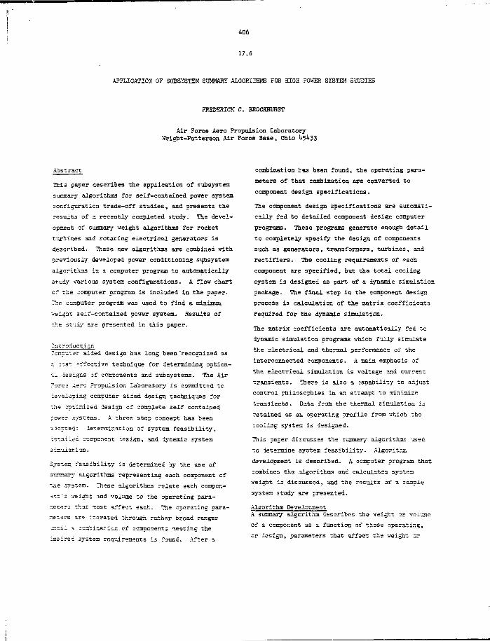
406
17.6
APPLICATION OF SUBSYSTEM SUMMARY ALGORITHMS FOR HIGH POWER SYSTEM SiTOIES
FREDERICK C. BHOCKHURST
Air Force Aero Propulsion LaboratoryWright-Patter3on Air Force Base, Ohio U5U33
Abstract
This paper describes the application of subsystem
summary algorithms for self-contained power system
configuration trade-off studies, and presents the
results of a recently completed study. The devel-
opment of summary weight algorithms for rocket
turbines and rotating electrical generators is
described. These new algorithms are combined with
previously developed power conditioning subsystem
algorithms in a computer program to automatically
study various system configurations. A fjow chart
of the computer program is included in the paper.
The computer program was used to find a minimum
weight self-contained power system. Results of
the study are presented in this paper.
Zntroductlcn
?snputer aided design has long been 'recognized as
a :cst effective technique for determining option-
al designs of components and subsystems. The Air
?csrc? Aero Propulsion Laboratory is committed to
ieveloping computer aided design techniques for
-he optimized design of complete self contained
power systens. A three step concept has been
adopted: ietermination of system feasibility,
ietaiied component design, and dynamic system
3 inflation.
System feasibility is determined by the use of
summary algorithms representing each component of
tne system. These algorithms relate each compon-
ent ' 2 veiigit and volume to the operating para-
meters that most affect each. The operating para-
~iet=rs are iterated through rather broad ranges
—ti- 3. ;cnbinati^n of components meeting the
iesired system requirements is found. After a
combination fcas been found, the operating para-
meters of that combination are converted to
component design specifications.
The component design specifications are automati-
cally fed to detailed component design computer
programs. These programs generate enough detail
to completely specify the design of components
such as generators, transformers, turbines, and
rectifiers. The cooling requirements of each
component are specified, but the total cooling
system is designed as part of a dynamic simulation
package. The final step in the component design
process is calculation of the matrix coefficients
required for the dynamic simulation.
The matrix coefficients are automatically fed tc
dynamic simulation programs which full}- simulate
the electrical and thermal performance of the
interconnected components. A main emphasis of
the electrical simulation is voltage and current
transients. There is also a capability to adjust
control philosophies in an attempt to aiaiaize
transients. Data from the thermal simulation is
retained as au operating profile from which the
cooling system is designed.
This paper discusses the summary algorithms used
to determine system feasibility. Algorithm
development is described. A computer program that
combines the algorithms and calculates system
weight i3 discussed, and the results of a sample
system study are presented.
Algorithm Development
A summary algorithm describes the weight ^r volume
of a component as a function of those operating,
or design, parameters that affect the weight or
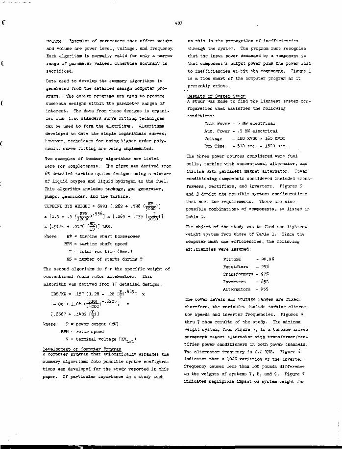
407
volume. Examples of parameters that affect weight
and volume are power level, voltage, and frequency.
Each algorithm is normally valid for only a narrow
range of parameter values, otherwise accuracy is
sacrificed.
Data used to develop the summary algorithms is
generated from the detailed design computer pro-
grams. The desigr programs are used to produce
numerous designs vithin the parameter rarges of
interest. The data from these designs is organi-
zed such t.:&t standard curve fitting techniques
can be used to form the algori tlnif. Algorithms
developed to date use simple logarithmic curves;
hccver, techniques for using higher order poly-
nomial curve fitting are being implemented.
Ivo examples of summary algorithms are listed
here for completeness. The first was derived from
65 detailed turbine systen designs using a mixture
of liquid oxygen and liquid hydrogen as the fuel.
This algorithm includes tankage, gas generator,
punps, gearboxes, and the turbine.
TOTBIUE SYS WEIGHT = 6991 [.262 + .738 (rjjg-) 3
1- " -5
{—)x [.9S2U + .0176 {—)] L3S.
Where: HP = turbine sbai't horsepower
RPM = turbine shaft speed
T = to t a l run time 'Sec.)
NS = number of s t a r t s during T
The second algorithm is f s r the specific weight of
conventional round rotor a l ternators . This
algorithm was derived from 77 detailed designs.
LBS/KW = .157 11.28 - .28 (^)'kk9] x
[ -06 • 1.06
[.8567 + .H»33 ( | ) ]
Where: P = power output (MW)
RPM = rotor speed
V = terminal voltage (KVL ^)
Development of Computer Program
A computer program that automatically arranges the
summary algorithms into possible system configura-
tions was developed for the study reported in th is
paper. Of part icular importance in a study such
as this is the propagation of inefficiencies
through the system. The program must recognize
that the input power demanded by a component is
that component's output power plus the power lost
to inefficiencies wiUrin the component. Figure 1
is a flow chart of the computer program as it
presently exists.
Results of System Study
A study was made to find the ligntest system :cn-
figuration that satisfies the following
conditions:
Main Power - 5 MM electrical
Aux. Power - -5 MW electrical
Voltage - 100 KVBC - loO KVDC
Run Time - 500 sec. - 1500 sec.
The three power sources considered were fuel
cells, turbine with conventional alternator, ar.d
turbine with permanent magnet alternator. Power
conditioning components considered included trans-
formers, rectifiers, and inverters. Figures 2
and 3 depict the possible system? configurations
that meet the requirements. There are nine
possible combinations of components, as listed in
Tahle 1.
The object of the study was to find the lightest
veight system from those of Table 1. Since "he
computer must use efficiencies, the following
efficiencies were assumed:
Filters - 99-9?
Rectifiers - 95%
Transformers - 972
Inverters - 35*
Alternators - 95?
The power levels and voltage ranges are fixed;
therefore, the variables include turbine alterna-
tor speeds and inverter frequencies. Figures i
thru 7 show results of the study. The minimum
weight system, from Figure 5, is a turbine driven
permanent magnet alternator with transformer/rec-
tifier power conditioners in both power channels.
The alternator frequency is 2.2 KHZ. Figure 6
indicates that a 100? variation of the inverter
frequency causes less than 100 pounds difference
in the weights of systems 7, 8, and 9. Figure T
indicates negligible impact on system weight for
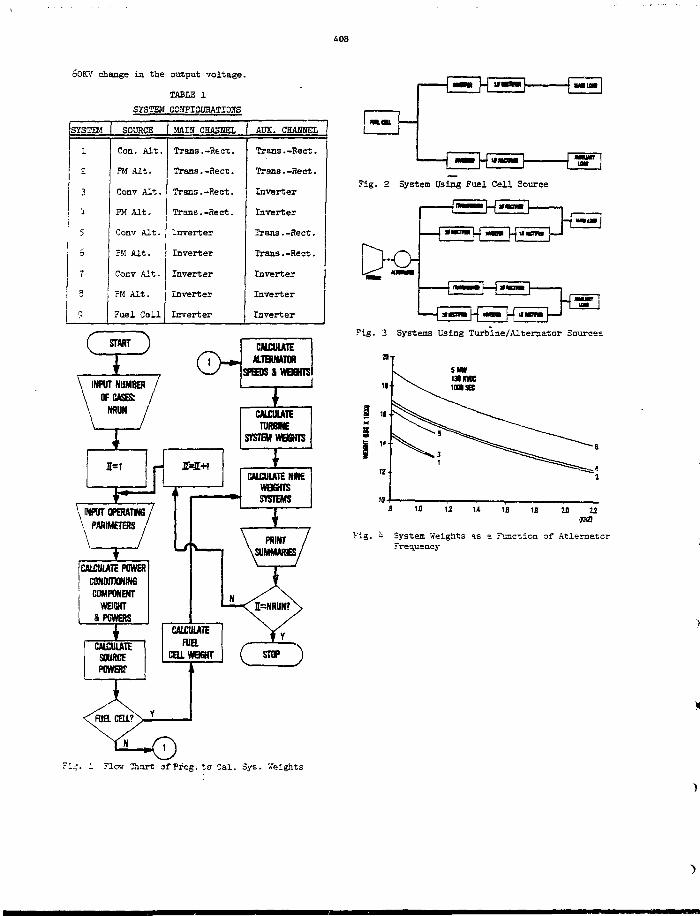
408
60KV changs in t h e ou tpu t v o l t a g e .
TABLE 1
STSTEM
1
2
3
6
7
a
o
SYSTEM
[ SOUECE
Con. A l t .
m Alt.
Conv Alt.
PM Alt.
Conv Alt.
?M Alt.
Conv Alt.
?M Alt.
Fuel Cell
CCHFISURATJOJfS
i MAIN CHAHUEL
T r a n s . - H e c t .
T rans . - S e c t .
T r a n s . - S e c t .
T r a n s . - H e c t .
Inverter
Inverter
Inverter
Inverter
Inverter
ADX. CHANNEL
T r a n s . - E e e t .
T r a n s . - H e e t .
Inverter
Inverter
Trans.-Rect.
Trans.-Hect.
Inverter
Inverter
Inverter
CALCUUTEM.TBWATOR
SPEEDS I WEIGHTS
CALCULATETURBINE
SYSTEM WEIGHTS
1=1 rJ
INPUT O P E R A T H G /
\ PARAMETERS /
CALCULATE POWER
COMPONENTWBGHT
4 POWERS
•CALCULATE
SOURCEPOWER?
•^FUEL cairN.
/ \
CALCULATE
nleiCELLWBSHT
Y
1
•CALCULATE NME
WBGHTSSYSTEMS
\ .
\ PRINT /XSUMMARIES/
( STOP )
F i j . I Flow Siart of Frog, to '^al. Sys. Weights
Fig. 2 System Using Fuel Cell Source
Fig. 3 Systems Using Turbine/Alternator Sources
tm13>KWC
Fig. U System Weights as a F'^nction of AtlematorFrequency
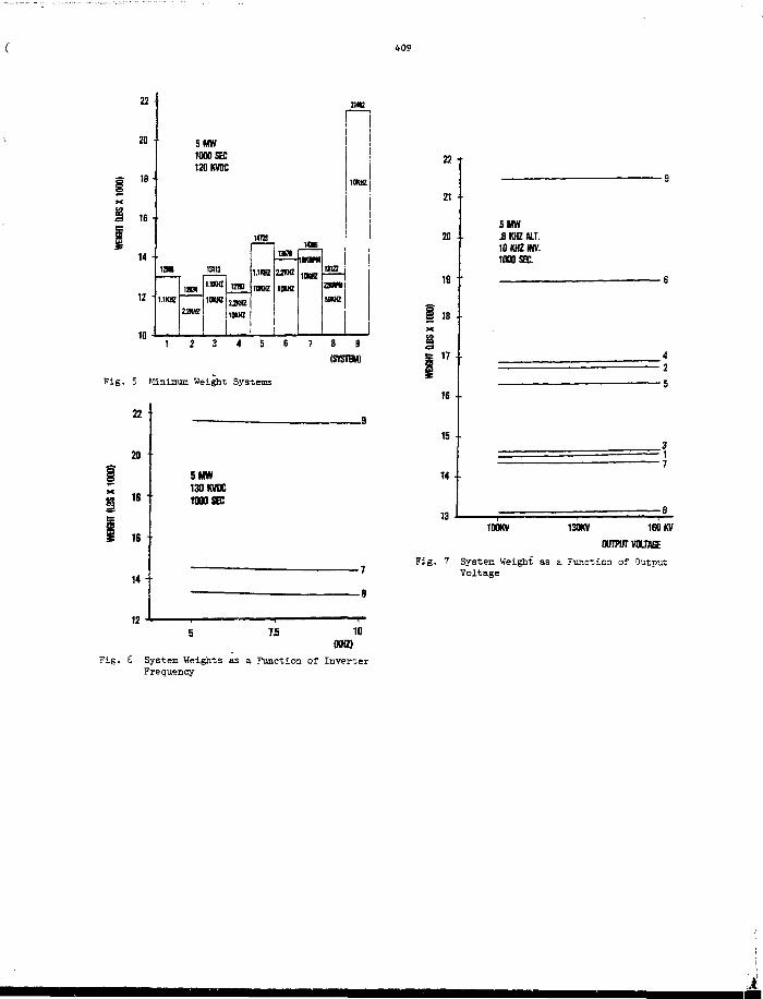
409
22
20
18 -
16 -
14 •
n •
taa
Lima
SMW1000 SEC120KVDC
13113
1 »
22CKZ
1.11(10
1DUIZ
121B
220E1WHZ
147B
1.1KHZ
iona
an
Una
1BWZ
BIB
10WC
2MB
IKK
3 4 5 6
Fig. 5 Minimum Weight Systems
(SVSTBI)
22
20
IS
16
14 -
5MW130KVDC1000 SEC
9
u
21
20
16
18
17
16
15
14
11 •
5MWS KHZ ALT.10KHZWV.1000 SEC.
42
3
7
8
100KV 130KV 160 KV
OUTPUT VOLTAS
Fig. T System Weight as a Function of OutcutVoltage
10
Fig. 6 System Weights as a Function of InverterFrequency
4 1 0
1 8 . 1
A COMPUTERIZED MEASURING SYSTEM FOR tRNOSECOND RISETIME PULSED ACCELERATORS*
D. Pellinen, S. Ashby, P. Giilis, K. Nielson and P. Spence
Physics International Company2700 Merced Street
San Leandro, California 94577
Abstract
We have developed a new computerized
diagnostic system for high voltage, high current
pulsers. This diagnostic system uses electronic
circuits connected to nanosecond response
transducers to meat ure machine performance at
critical points. The voltage outputs of these
circuits are converted to digital form and
directly read by a computer. The major advantages
of this system are cost effectiveness and greater
accuracy than commonly used oscilloscope or
transient analyzer systems in applications where
it is not necessary to record full analog
diagnostic waveforms. Operation is fully
computerized and requires a minimum number of
personnel; the system is scalable to very large
multi-module generators.
Historically, pulsed accelerators have been
diagnosed by placing a sensor in an accelerator,
connecting the sensor to a cathode ray
oscilloscope by a coaxial cable, and photographing
one resulting waveform. The data were reduced by
measuring key amplitudes or times, or by manually
digitizing the photograph. Although computerized
digitizers and waveform analyzers were an improve-
ment, they basically were 3till the same as oscil-
loscopes, but . aad ^ut digitally. These methods
were adequate when pulsers consisted of only a few
modules with single switches. The current trend
is coward very large pulsers with multiple
switches or toward machines with many
rnodules. ' ' On these never machines the
requirements for synchronous operation are con-
siderably more severe, and the number of channels
for diagnostics must be far greater than
•Work supported by Defense Nuclear Agency.
previously used. The use of oscilloscopes or
transient analyzers would be very costly on these
large system and would provide an unmanageable
mountain of data to analyze.
For these reasons, we have developed a new
computerized diagnostic system for the pulser
modules on one 3uch large system, the modular
breosstrahlun? 3ource (MBS). This diagnostic
system uses eiactronic circuits to measure machine
performance at critical points. The voltage
outputs of these circuits are converted to digital
form and directly read by a computer. The major
advantages of this system are:
1. A single data channel can bs completely
implemented for about $300 compared with
~ S20 K for a transient analyzer.
2. The system is more accurate than an
oscilloscope or transient analyzer.
3. Operation is fully computerized and re-
quires a minimum number of personnel to
operate.
4. The system is scalable to very large
multi-module generators.
The approach used was to locate areas where
problems could occur in the MBS modules and piace
appropriate nanosecond response transducers, such
as voltage and current sensors, at these
locations. These sensors are connected to
circuits that will record and hold the parameter
we are measuring, such as time, a peajc amplitude,
or an integral of a voltage. The data are
converted to digital form, read, and processed by
a digital computer.
He assembled a prototype system of this sort

413
REFERENCES
1. T. H. Martin, D. L. Johnson, and D. H.
McDaniel, Proceedings of the 2nd Internat ional
Topical Conference on High Power Electron and Ion
Beam Research and Technology, laboratory o£ Plasma
S t u d i e s , Cornell Univers i ty , I thaca , N.Y., 807-15
(1977) .
2 . s . Yonas, S c i e n t i f i c American, 239, 50 (1978-).
3 . T. H. Martin, e t a l . . Proceedings of the 2nd
IEEE Internat iona l PuZsed ftover Conference,
Lubbock, Texas, June 1979.
4 . The Standards for CAMAC are defined by the
fo l lowing Standards, IEEE Standards Of f i ce ,
New York.
IEEE Standard 583-197S
IEEE Standard 595-1976
IEEE Standard 596-1976
IEEE Standard 6B3-1976
414
18.3
A 33-GVA INTERRUPTER TEST FACILITY*
W. M. Parsons, E. M» Honig, «nd R. H. Warren*
Los Alamos Scientific Laboratory
ABSTRACT
The use of commercial ac circuit breakers
for dc switching operations requires that they be
evaluated to determine their dc limitations' Two
2.4-GVA facilities have been constructed and used
for this purpose at LASL during the last several
years. In response to the increased demands on
switching technology, a 33-GVA facility has been
constructed. Novel features incorporated into
this facility Include (I) separate capacltlve and
cryogenic inductive energy storage systems, (2)
fiber-optic controls and optically-coupled data
links, and (3) dig'.tal data acquisition systems*
Facility decalls and planned testa on an
experimental rod-array vacuum Intertupter arc
presented.
INTRODUCTION
Since 1975 the Los Alamos Scientific
Laboratory (LASL) has been conducting experiments
vlth commerical ac circuit breakers to determine
their direct-current ratings for potential
application in various fusion devices. '
Particular attention has been paid to the vacuum
intertupter due to its low cost, mechanical
simplicity, and its ruggedness. Because of these
advantages, fusion experiments such as Alcator,
TFTR, and Doublet III utilize vacuum intertupters
in their switching systems. Interrupters used In
boch TFTR and Doublet III require current
interruption in the 25 kA to 30 -kA range with as-
sociated recovery voltages of 20 kV to 25 kV.
Preliminary designs for larger devices •"c)- as
ETF indicar« "Vat a trend towards higher currents
may be economical if low-cost switching systems
exist that can satisfy the interruption require-
ments. For this reason a facility has been con-
structed at LASL which is capable of evaluating
circuit breakers for application in the next
generation of fusion experiments.
PgESEKT TEST FACILITIES
In addition to the facility discussed in
this paper, two smaller facilities are presently
used for intertupter testing.3 These facilities
are essentially identical and are rated at
2.4 GVA each. They can be connected in parallel
for high-curreot tests, or operated independently
for tests up to 40 kA. The new 33-GVA facility
will be capable of tests as high as 280 kA. A
summary of the facilities ratings is given in
Table I.
TABLE I.
SUMMARY OF FACILITIES RATINGS
Peak powerStored energy (kJ)Rated current (kA)Max. recovery voltage (kV)Completion date
2.44504060
1975
2.44504060
1977
33.62250280120
1979
+Industrial Staff Member for (festiughouaeResearch LaboratoryWork performed under the auspices of the U.S.Department of Energy
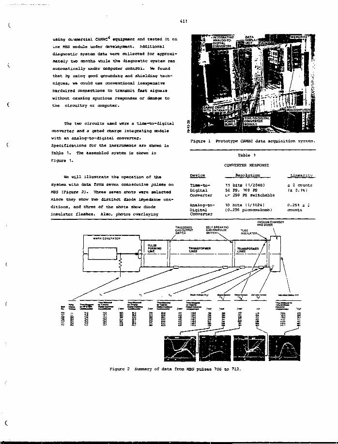
411
using ctmmercial CAHAC equipment and tested it on
Lne MBS nodule under development* Additional
diagnostic system data were collected for approxi-
mately two months while the diagnostic system ran
automatically under computer control. We found
that by using good grounding and shielding tech-
niques* we could use conventional Inexpensive
hardwired connections to transmit fast signals
without causing spurious responses or damage to
the circuitry or computer.
The two circuits used were a time-to-digital
converter and a gated charge integrating module
with an analog-to-digital converter.
Specifications for the instruments aro shown in
Table 1. The assembled system is shown in
Figure 1.
He will illustrate the operation of the
system with data from seven consecutive pulses on
MBS (Figure 2 ) . These seven shots were selected
since they show two distinct diode impedance con-
ditions, and three of the shots show diode
insulator flashes. Also, photos overlaying
Figure 1 Prototype CAMAC data acquisition system.
Table 1
CONVERTER BESPONSE
Device
Time-to-DigitalConverter
Analog-to-OigitalConverter
Resolution
11 bits (1/2048)SO PS, 100 PSor 250 PS switchable
10 bits (1/1024)(0 • 256 pioocoulomb)
Linearity
± 2 counts(± 0.1%)
0.25% icounts
TRIGGEREDGAS OUTPUTSWITCH
SELF BREAKINGGAS PREPULSESWITCH N
Figure 2 Summary of data from MBS pulses 706 to 712.
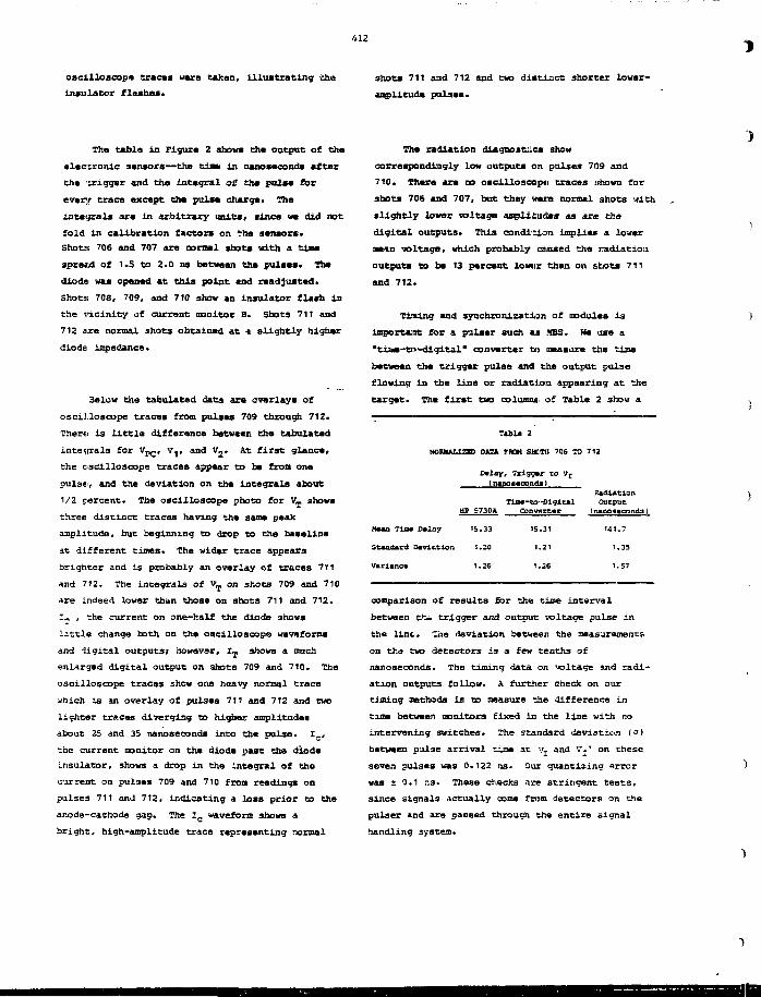
412
oscilloscope traces were t&ken, illustrating the
Insulator flashes.
shots 711 and 712 and two distinct: shorter lower-
amplitud* pulses.
The table in Figure 2 shovrs the output of the
electronic sensors—the tin* In nanoseconds after
the trigger and the integral of. the pulse for
every trace except the pulse charget The
inteijrals are in arbitrary units, since we did not
fold in calibration factors on the seniors.
Shot:! 706 and 707 are normal shots with a time
spread of 1.5 to 2.0 ns between the pulses. The
diodei was opened at this point and readjusted.
Shots; 70S, 709, and 710 show an insulator flash In
the vicinity of current monitor B. Shots 711 and
712 are normal shots obtained at a slightly higher
diode impedance.
Below the tabulated data are overlays of
oscilloscope traces from pulses 709 through 712.
T h e m is little difference between the tabulated
inte<rrals for Vpc> V,, and v 2. At first glance,
the oscilloscope traces appear to be from one
pulse, and the deviation on the integrals about
1/2 percent. The oscilloscope photo for 7 T shows
three distinct traces having the same peak
amplitude, but beginning to drop to the baseline
at different times. The wider trace appears
brighter and is probably an overlay of traces 711
and 712. The integrals of v^, on shots 709 and 710
are indeed lower thin those on shots 711 and 712.
!„ , the current on one-half the diode shows
little change both on the oscilloscope waveforms
and digital outputs; however, t— shows a much
enlarged digital output on shots 709 and 710. The
oscilloscope traces shew one heavy normal trace
which is an overlay of pulses 711 and 712 and two
lighter traces diverging to higher amplitudes
about 25 and 35 nanoseconds into the pulse.••<:•
the current monitor on the diode past the diode
insulator, shows a. drop in the integral of the
current on pulses 709 and 710 from readings on
pulses 711 and 712, indicating a loss prior to the
anode-cathode gap. The I c waveform shows a
bright, high-amplitude trace representing normal
The radiation diagnostics show
correspondingly low outputs on pulses 709 and
710. Inhere are no oscilloscope traces shown for
shots 706 and 707, but they warn normal shot3 with
sl ight ly lower voltage amplitudes as are the
digital outputs. This condition implies a lower
mean voltage, which probably caused the radiation
outputs to be 13 percent lowtir than on shots 711
and 712.
Tilling and synchronization of nodules i s
important for a pulser such as MBS. We use a
"tilae-to-digital" converter to measure the time
between the trigger pul3e and the output pulse
flowing in the line or radiation appearing at this
target. The f irs t two columns of Table 2 show a
Tabla 2
NOKHALXZID DATA FDCH SHOTS 706 TO 712
Dalay, Tri?g»r co Vr
Maaa ?1M
Standard
varianc*
I DmXay
Oaviaeion
HP S730A
15.33
1.20
1.26
Tloa-to-OlgitalConvartar
15.31
1.21
1.26
RadiationOucput
(nanosacondill
141.7
1.35
1.57
comparison of results for the time interval
between th^ trigger and output voltage pulse in
the l ine. The deviation between the measurements
on tha two detectors is a few tenths of
nanoseconds. The timing data on -voltage and radi-
ation outputs follow. A further check on our
timing methods i s to aeasure the difference in
time between monitors fixed in the line with no
intervening switches. The standard deviation (a)
between pulse arrival time at Vj and V.' on these
seven pulses was 0.122 ns. Our quantizing ?rror
was ± 0.1 ns. These checks are stringent teats,
since signals actually come from detectors on the
pulser and are passed through the entire signal
handling system.
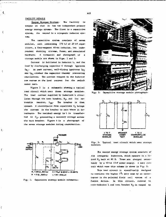
415
FACILITY DETAILS
Energy Storage Systems. The facility is
unique in that it has two independent primary
energy storage syterns. The first is a capacitlve
system, the second is a cryogenic inductor sys-
tem.
The capacitive system consists of seven
modules, each containing Z70 kJ of 20 kV capa-
citors, a four-segment 60-kA inductor, two inde-
pendent shorting systems, fuses, and associated
hardware. A schematic and photograph of a
storage module are shown in Figs. 1 and 2.
Current is initiated in inductor L, and the
load by discharging capacitor C through ignitron
Igj. At peak current, self-firing lgnitrons Ig2
and Ig3 crowbar Che capacitor thereby preventing
oscillation. The current trapped In the inductor
now serves as the load current for the switch
under test*
Figure 3 is a schematic showing a typical
test circuit which uses these storage nodules*
The load current supplied by Inductors L clrcu~
lates through the test breaker, B T, and its sa-
turable reactor, L S R. The breaker is then
opened* A counterpulse from capacitors C 2 brings
the current in the breaker to zero where it in-
terrupts* The residual energy in L is transfer-
red to C,, generating a recovery voltage across
the teat breaker. Figure 4 is a photograph of
the seven storage modules during construction*
TRIGSER
R, •lOOJJ.SCOkJR '13 fl, 300 kJ
I IB UNITS
Fig* 2- Capacitive storage module photograph*
S, L
Cli
Fig. 1. Capacitive storage module schematic*
I TO 7 BREAKER I TO 6STORAGE UNDER COUNTERPULSEMODULES TEST MOOULES
Fig* 3. Typical test circuit which uses storagemodules*
The second energy storage system consists of
six cryogenic inductors, which operate in a li-
quid Nj bath at SC K. Miese are charged exter-
nally by a 40-kA 12-V power supply. A test cir-
cuit which uses this scheme is shown in Fig. 5.
This test circuit :Ls specifically designedo
to simulate the higher Z t duty seen by an inter-
tupter in the poloidal field coil system of a
fusion device. In this circuit, current in
cryo-inductor L and test breaker B^ is ramped up
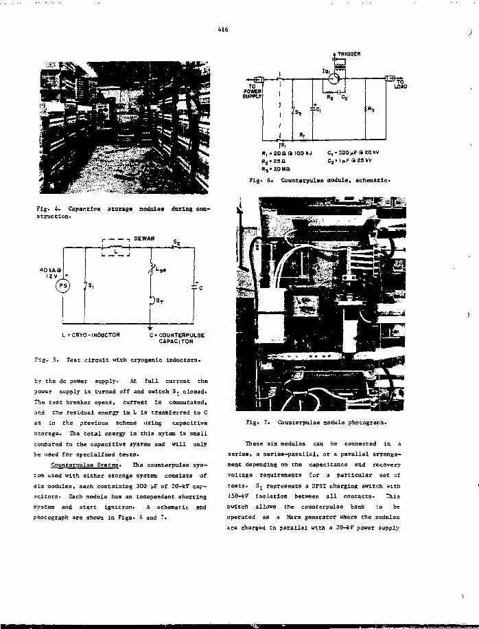
416
l TRIGGER
Fig. 4. Capar.ttve storage modules during con-
struction.
, DEWAR
T C
C•COUNTERPULSECAPACITOR
U »CRYO-INDUCTOR
Fig. 5. Test circuit with cryogenic Inductors*
by the dc power supply- At full current the
power supply Is turned off and switch S^ closed*
The test breaker opens. current Is commutated,
and the residual energy in L is transferred to C
as in the previous scheme using capacitive
storage* The total energy in this syten is small
compared Co the capacitive system and will only
be used for specialized tests*
Counterpulse System* The couaterpulse sys-
tem used with either storage system consists of
six modules, each containing 300 uF of 2O-kV cap-
acitors. Each module has an independent shorting
system and start ignltron* A schematic and
photograph are shown in Figs* 6 and 7.
TOPOWERSUPPLY
1' 1
111
11
f
Si "
O Ir
LOAO
R, « 2 o a a IOO kj c, •l
Fig* 6. Counterpulse module, schematic*
Fig. 7. Counterpulse module photograph.
These six modules can be connected in a
series, a series-parallel, or a parallel arrange-
ment depending on the capacitance and recovery
voltage . requirements for a particular set of
tests* S^ represents a DPST charging switch .Hth
150-kF isolation between all contacts. This
switch allows the counterpulse bank to be
operated as a Marx generator where the modules
are charged in parallel with a 20-fcV power supply
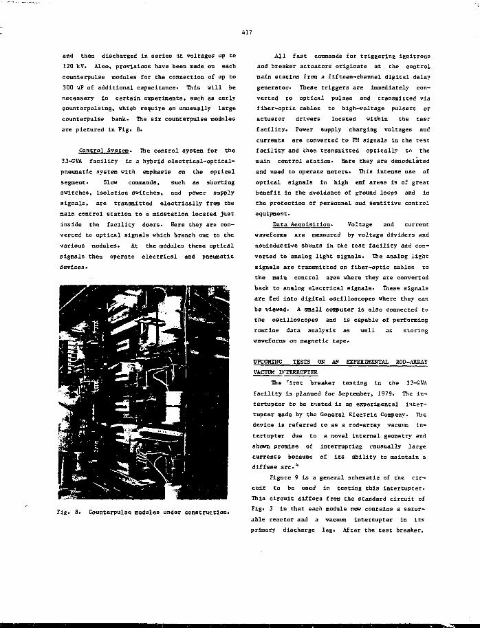
417
and then discharged in series at voltages up to
120 kV. Also, provisions have been made on each
counterpulse nodules for the connection of up to
300 uF of additional capacitance- This will be
necessary in certain experiments, such as early
counterpulsing, which require an unusually large
counterpulse bank* The six counterpulse modules
are pictured in Fig. 8.
Control System* The control system for the
33-GVA facility is a hybrid electrical-optical-
pneumatic system with emphasis on the optical
segment* Slow commands, such as shorting
switches, Isolation switches, and power supply
signals, are transmitted electrically from the
main control station to a midstation located just
inside the facility doors• Here they are con-
verted to optical signals which branch out to the
various modules* At the modules these optical
signals then operate electrical and pneumatic
devices*
Fig* 8* Counterpulse modules under construction*
All fast commands for triggering ignitrons
and breaker actuators originate at the control
main station from a fifteen-channel digital delay
generator* These triggers are immediately con-
verted to optical pulses and transmitted via
fiber-optic cables to high-voltage pulsers or
actuator drivers located within the test
facility. Power supply charging voltages and
currents are converted to FM signals in the test
facility and *chen transmitted optically to the
main control station* Here they are demodulated
and uaed to operate meters* This intense use of
optical signals in high emf areas is of great
benefit in the avoidance of ground loops and in
the protection of personnel aud sentitive control
equipment*
Data Acquisition* Voltage and current
waveforms are measured by voltage dividers and
nooinductive shunts in the test facility and con-
verted to analog light signals* The analog light
signals are transmitted on fiber-optic cables to
the main control area where they are converted
back to analog electrical signals* These signals
are fed into digital oscilloscopes where they can
be viewed. A small computer Is also connected to
the oscilloscopes and is capable of performing
routine data analysis as well as storing
waveforms on magnetic tape.
PPCOMIHG TESTS OH AN ggPERIMEHTAI. ROD-AKRAY
VACUUM IFTERRPPTER
The 'iret breaker testing in the 33-GVA
facility is planned for September, 1979* The in-
tertupter to be tested is an experimental inter-
tupter made by the General Electric Company. The
device is referred to as a rod-array vacuum in-
tertupter due to a novel internal geometry and
shown promise of interrupting unusually large
currents because of Its ability to maintain a
diffuse arc.1*
Figure 9 is a general schematic of the cir-
cuit to be used in testing this interrupter.
This circuit differs from the standard circuit of
Fig* 3 in that each module now contains a satur-
able reactor and a vacuum intertupter in its
primary discharge leg. After the test breaker,
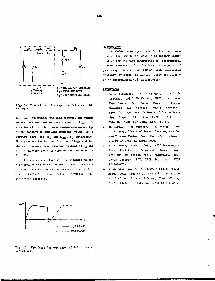
418
I TO 7STORAGEMODULES
Bt> ISOLATION BREAKER
. B T-TEST BREAKER
C, > COUNTERPULSE BANK
Fig. 9. Test circuit for experimental G.S. in—
tertupter.
B^p has Interrupted the load current, the energy
in the load coil and saturable reactor, L g R 1, is
transferred to the counterpulse capacitor, C 2.
At the instant of complete transfer, which is a
currant zero for Bj and L S R 1, Bj Interrupts.
This prevents further oscillation of LgRj and C2,
thereby holding the recovery voltage on Cj and
B,.. A waveform for this type of cesc Is shown in
Fig. 10.
The recovery voltage Mill be maintain on the
cast breaker for 50 to 100 ms. This simulates
intended use in tokamak systems and insures that
the intertupter has fully recovered its
dielectric strength.
CONCLUSIONS
A 33-<5VA intertupter teat facility has been
constructed which is capable of testing inter-
tupters for the next generaciion of experimental
fusion devices* The facility is capable of
producing currents of 280 kA with associated
recovery voltages of 120 kV. Tests are planned
on an experimental G#E. intertupter*
REFERENCES
1. C. E. Swannack, R- A. Haarman, J. D. G.
Lindsay, and D. M. Weldon, "HVDC Intet^apter
Experiments for Large Magnetic Energy
Transfer and Storage (HETS) Systems,"
Proc- 6th Symp. Eng. Problems of Fusion Res.,
San Diego, CA, Nov. 18-21, 1975; IEEE
Pub. No. 75CH 1097-5 NPS, 662, (1976).
2. R. Warren, M. Parsons, E. Eonig, and
J. Lindsayt "Tests of Vacuum Interrupters for
the Tolcamak Fusion Test Reactor," Informal
report LA-7759-MS, April 1979.
3. E. «. Bonig, "Dual 30-kA, HVDC Interrupter
Test Facility", Pvoc. 7th Symp. Eng.
Problems of Fusion Res., Kaoxville, TK.,
35-28 October 1977; IEEE Pub. Ho. 77CH
1267-4-NPS.
4. J. A. Rich and C. P. Coudy, "Diffuse Vacuum
Arcs," Cocf. Records of IEEE 1977 Iternation-
al Conf. on Plasma Science, Troy, NY, May
23-25, 1977; IEEE Pub. No. 77CH 1205-4-SPS.
I.V
— CURRENT
• - VOLTAGE
Fig. 1C. Waveforms for experimental G.E. inter-
tupter test.

TM MbrMtUd miwKrrvt tm fa
uiM. contract No. W-31-IOHNO-tt.Awydinfftv. UwU.fi-
ttdiai*. w*tvnorodwa tM publimd <orm a* tub
eunrNMtien. of «lo» 0Hwn to «> n . forU.S.
419
18.4
ANALYSIS OF THE MULTIPHASE INDUCTOR-CONVERTER BRIDGE*
Mehrdad Ehsani,+ -Robert L. Kustom, and Raymond E. Fuja
Abstract
Analytical derivations are presented for inductor-
converter bridge (tCB) circuits in which energy is
transferred from a storage inductor to a load
inductor with solid state bridges. These
derivations provide complete analytical circuit
solution In contrast to previously available
numerical (non-analytical) procedures. The
analysis is based on two parallel methods: (1)
Fourier expansion of the inverter waveforms and
(2) a novel method based on the inherent waveforms
of Che ICB, labeled square functions. Our
analytical values of power flow, inductor
currents, and voltages compare favorably with the
results of a three-phase ICB experiment at Argonne
National Laboratory.
Introduction
The inductor-converter bridge (ICB) is a solid
stats dc-ac-dc converter system for reversible
energy transfer between two inductors. This
system is especially suitable for pulsed power
supply applications greater than several hundred
megawatts and durations from a fraction of a
second to many seconds. Two such applications are
the superconductive equilibrium field coils of the
projected tokamak fusion power reactors and
superconductive magnets to be used in future
particle accelerators.
The ICB system is inherently efficient, control-
lable in real time and allows isolation of large
Argonne National Laboratory
Argonne, Illinois 60439
pulsed reactive loads from the power grid. Thus,
only the average system losses are drawn from the
grid.
"fc'ork supporte by the U.S. Department of Energy.
tAlso at the University of Wisconsin.
Operation of the ICB Circuit
Detailed operation of the ICB may be found in
references 1 and 2. Figure 1 shows a three-phase
ICB where the storage and the load coil is
represented by Lg and L^, respectively. At a
typical instant during the energy transfer, dc
currents ig and iL will be flowing in the storage
and load coils, respectively. The SCR's of the
left hand side (storage side) are fired in the
normal Graetz bridge sequence: S j SJJ, S j SL&,
SL2 SL6> SL2 SL4> SL3 SL4' SL3 SL5! SL1 SL5-
The SCR's of the right-hand side (load side)
follow the same sequence but nay be out of step
with respect to the storage side. The direction
and the level of power flour is determined by the
relative timing between the source and the load
bridge switching sequences such that a load bridge
lead will cause power flow into the load and vice
versa. The Y-connected capacitors in the middle
serve as the intermediate energy store between the
storage and load coils and they provide the
reverse voltages to commutate the inductor
circuits from one SCR to the next. Thus, no
external counterpulse circuit is needed.
Only a very snail fraction of each coil energy is
extracted in each bridge cycle. Therefore, by
varying the relative timing between the source and
load switching sequences and/or the frequency of
operation, very fine control over the rate of
energy transfer can be achieved. The functional
dependence of the power on the relative timing
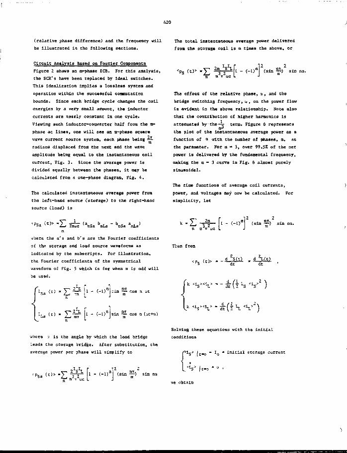
420
(relative phase difference) and the frequency
be illustrated in the following sections.
The total instantaneous average power delivered
from the storage coil is a times the above, or
Circuit Analysis Based on Fourier Components
Figure 2 shows an nr-phase ICB. For this analysis,
the SCR's have been replaced by ideal switches.
This idealization implies a lossless system and
operation within the successful commutation
bounds. Since each bridge cycle changes the coil
energies by a very sosll aoount, the inductor
currents are nearly constant in one cycle.
Viewing such inductor-converter half from the la-
phase ac lines, one will see an m-phase square
wave current source system, each phase being —
radians displaced from the next and the wave
amplitude being equal to the instantaneous coil
current, Fig. 3. Since the average power is
divided equally between the phases, it may be
calculated from a one-phase diagram, Fig. 4.
The calculated instantaneous average power from
the left-hand source (storage) to the right-hand
source (load) is
bnLa " bnSa
where Che a's and b's are the Fourier coefficients
or Che storage and load source waveforms as
indicated by Che subscripts. For illustration,
Che Fourier coefficients of the symmetrical
waveform of Fig. 5 which is for when m is odd will
be used.
*<:„ (t) - ^f |1 - (-in sin SI cos n at
(t) - V * l i [l - <-L)n stn 2L cos n (ut+o.)
where J. is che angle by which the load bridge
leads Che storage bridge. After substitution, Che
average power per phase will simplify to
-'PS. < c ) >
——) sin na.
The effect of the relative phase, a, and the
bridge switching frequency, u , on the power flow
is evident In the above relationship. Note also
that the contribution of higher harmonics is
attenuated by the—s- term. Figure 6 represents
the plot of the instantaneous average power as a
function of a with the number of phases, m, as
the parameter. For m « 3, over 99.5Z of the net
power is delivered by the fundamental frequency,
making the m - 3 curve in Fig. 6 almost purely
sinusoidal.
The time functions of average coil currents,
power, and voltages may now be calculated. For
simplicity, let
Then
'11n
from
n
2m3 2
TT CiJC
- (-l)n (sin 21)
= PS (t)> dt
Solving these equations with the initial
conditions
o - IQ • initial storage current
— ) sin na
we obtain
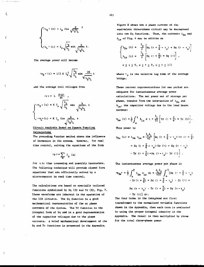
421
(t) - !„ h- sin
The average power will become
<ps>(t) - 1/2 K lo2 i j f s in
Figure 8 shows how a phase current of the
equivalent three-phase circuit may be decomposed
into two Sq functions. Thus, the currents iga and
i L a of Fig. i may be written as
-j- q (T + \ - xo> + Sq (T - to>]
o * t < T, o < T < T, o < i < 1/2
where T Q is the relative lag time of the storage
bridge.
and the average coil voltages from
•«vs>(O - K I 0 J^f sin
_<v L>(t) - K IQ Cos
Circuit Analysis Based on Square Function
Calculations
The preceding Fourier method shows the influence
of harmonics in the system. However, for real
time control, solving the equations of the form
(a)
These current representations for one period are
adequate for instantaneous average power
calculations. The net power out of storage per
phaae, results from the interaction of i S a and
vLa' c h e capacitor voltage due to the load phase
current:
vLa
This power is
• is. vLa - -|<r Is" •6- V-Tr (T+i>
+ Sq (T + i - T )-Tr (T) + Sq (T - T )DO O
• Tr (T +f)+Sq (T-TQ)- Tr (T) j .
for a is time consuming and possibly inaccurate.
The following technique will provide closed form
equations that are efficiently solved by a
microcomputer in real time control.
The calculations are based on specially tailored
functions symbolized by Sq (X) and Tr (X), Fig. 7.
These waveforms are inherent in the operation of
the ICB circuits. The Sq function is a good
mathematical representation of the ac phase
currents of the system. The Tr function is the
integral form of Sq and is a good representation
of the capacitor voltages due to the phase
currents. A brief mathematical development of the
Sq and Tr functions is presented in the Appendix.
The instantaneous average power per phase is
[Sq (T + f - To)
• Tr (T + ) + Sq (T + | - rQ) • Tr (7) +
Sq (T - To) • Tr (T + p + Sq (T - tQ)
• Tr (T)] dr.
The four terms in the integrand are first
transformed to the normalized variable functions
shown in the Appendix, then each term is evaluated
by using the proper integral identity in the
Appendix. The result is then multiplied by three
for the total three-phase power

422
PSa >
<vL> (t) - 224.4 cos 0.S609 t
<ps> (t) - 11218 sin 1.1218 t
T !„
where yg " - ^ " gjjB is the normalized lag cime of
the storage bridge relative to the load bridge and
che frequency is represented by the period T.
This ls the closed form of the <p> vs a curve for
ai « 3 In Fig. 6. The time functions of the
average coil currents, power and voltages may be
calculated as before. The only difference being
chac K ( Y Q ) is in closed form.
Expressing the actual circuit wavefonss
analytically, allows other useful calculations
such as the actual capacitor voltages throughout
the transfer cycle, the study of commutation
throughout the cycle, and the actual coil voltages
and instantaneous currents, without resorting to
numerical procedures.
Comparison with Test Results
A aodel three-phase ICB has been built and tested
at Argonne National Laboratory. This system uses
two identical superconducting coils capable of
stcring 125 kJ at 250 A, as Che storage and load
inductor-;. Other system parameters are:
Ls - Lj_ - 4 H, Io - 100 A
C « I0~4 F, o - 90°
••> = 4084 rad/s
The system equations are derived from subscitution
of these parameters and m » 3 inco che time
functions shown in che Fourier analysis section:
<is> (t) - 100 cos 0.5609 c A
<iL> (c) - 100 sin 0.5609 t A
cvs> (.-) - 224.4 sin 0.5609 t V
A plot of these equations appears in Fig. 9.
Figure 10 shows the average coil voltages and
currents obtained experimentally. Good agreement
exists between the analytical and the experimental
results. Note, however, that the experimental
initial storage current ls somewhat higher than
the final load current. This ls due co the losses
in the system which ls neglected in this analysis,
but may be incorporated in the differential
equations leading to the average time functions.
Conclusions
The behavior of the multiphase inductor-converter
bridges have been studied by two analytical
techniques. The conventional Fourier technique
produces the average circuit power, currents, and
voltages as a function of time. It also shows the
effect of the existing harmonics in the circuit
behavior. The square function technique ls
particularly devised for Che ICB and other SCR
circuits in which rectangular waveforms appear.
The identities defined on the special functions
Sq (20 and Tr (X) operate directly on Che circuic
waveforms. Thus, much more information about
instantaneous behavior of the circuit is available
for analysis, system design, and che development
of real time control algorithms. Preliminary
tests with open loop microcomputer control have
been conducted with satisfactory results. The
development of an optimal closed loop control
algorithm ls currently in progress.
Appendix
The Sq function is defined as -he sum of unit step
functions as follows,
Sq (Y+Yo) 2 u (Y) - 2 u (Y - i + YQ> + 2
u (Y - 1 + Y j - u (y_ - 1) ,
O i l £ — » 0 < v s I.o 2

423
The Tr function is defined as the integral value
of the Sq functions,
Tr (Y+Y0) & f Sq (5 + Y )
Y U - 2 (Y - J + To)
u (Y - J + Yo) + 2 (Y - 1 + YQ)
u (Y - 1 + Yo) - (Y ~ 1) u (Y - 1)
The following integral is extensively used in
calculating the average power flow in the circuits
of interest. Therefore, it will be stated as an
identity which may be directly verified,
/ :[Sq (Y +
-r 0 < t < T
'Tr (t + t ) - / Sq (a + t ) de,
where Y - £ and Y0 - - ^ .
Substitution of y and Y0 in the above integral
will give
Tr ( t + t 0 ) - T f Sq U + Yo)
T [Tr (Y + Yo)3 = t u (t) - 2
( t - | + t o ) U ( t - f + t o )
+ 2 (t - T + tQ) u (t - T + tQ)
- (t - T) u (t - T).
For time base calculations, these functions may be
used.
Tr (Y + Y2)] dY
* . . < * .
*i-
2'
The following identities will also be of
considerable value
sq (Y- YO) - " S<I W V
Tr ( Y " Y0> " " Tr IY + d/2-Yo) 1. ° ; Yo i I
which may be verified by direct substitution.
Note tliat by using these identities, we can easily
evaluate the above integral for any combination of
leading and lagging functions.
The above Sq and Tr functions have been defined
for a period equal to 1. For periods other than
1, the argument should be multiplied by the
appropriate constant:
Sq (t + tQ ) - Sq (Y + v ) ,0 < t < T , 0 <
0 < Y S 1, 0 < YO < j
References
' , R. L. Kustom et al., "The Use of Multiphase
Inductor-Converter Bridges as Actively
Controlled Power Supplies for Tokamak Coils,"
Argonne National Laboratory Report
AHL/FPP/TM-78 (April 11, 1977).
2. H. A. Peterson et al., "Superconductive
Inductor-Converter Units for Pulsed Power
Loads," Proceedings of International
Conference on Energy Storage, Compression and
Switching, Asti-Torino, Italy (November
1974).
3. M. Ehsani, R. L. Kustom, "Analysis of the
Multiphase Inductor-Converter Bridge,"
Argonne National Laboratory Report
AHL/FPP/TM-114 (August 1978).
4. M. Ehsani, R. L. Kustom, "Square Function
Analysis of the Inductor-Converter Bridge,"
Argonne National Laboratory Report
AHL/FPP/TM-118 (March 1979).
5. N. Mohan, B. A. Peterson, "Superconductive
Inductor Storage and Converters for Pulsed
Power Loads,11 Proceedings of the
Intel-national Pulsed Power Conference,
Lubbock, TX (November 1976).
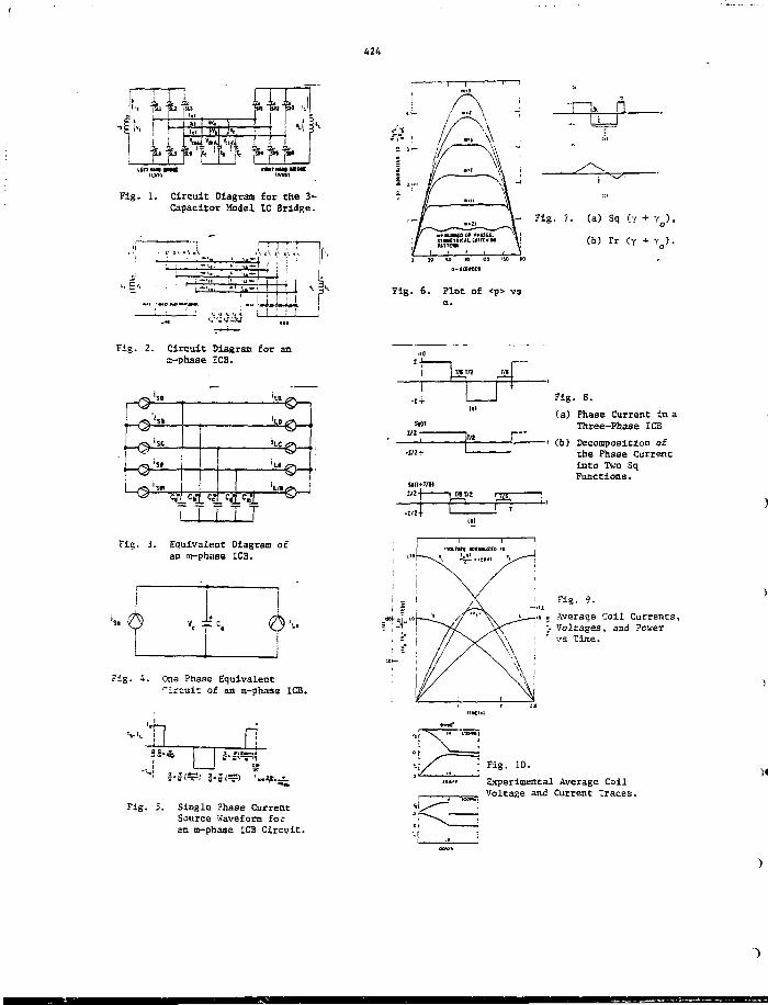
424
f
Fig. 1. Circuit Diagram for the 3-Capacitor Model IC Bridge.
§'•... a w .
1
' " " ' I ! ' ' ' i f *
( ;
. - . . . - ' ' , . .
r
A
n
Fig. ?. (a) Sq (Y + Yo),
(b) Tr (Y + Yn).10 SO M 'ID ISO <0
Fig. 6. Plot of <p> V3
Fig. 2. Circuit Diagram for ana-phase ICB.
*€>—
i i i i L iTT TT T
-IJ
0
T
1/2 H
-I/J+
Fig. 8.(a) Phase Current in a
Three-Phase IC3(b) Decomposition of
the Phase Currentinto Two SqFunctions.
?ig. 3. Equivalent Diagram ofan ni-phase IC3.
Fig. 4. One Phase Equivalent'"irouit of an m-phase ICB.
Fig. 9.
..a . Average Coil Currents,: > Voltages, and Power! ' vs Time.
c tl
ji
Fig. 5. Single Phase CurrentSource Waveform foran m-phase ICB Circuit.
Fig. 10.
Experimental Average CoilVoltage and Current Traces.
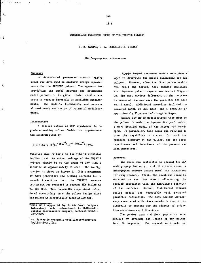
425
IB.5
DISTRIBUTED PARAMETER MODEL OF THE TRESTLE PULSER*
T. H. LEffilAN, R. L. HUTCHINS, R. FISHER+
BDH Corporation, Albuquerque
Abstract
A distributed parameter circuit analog
model was developed to evaluate design improve-
ments for the TRESTLE pulser. The approach for
specifying the model network and estimating
model parameters is given. Model results are
snoun to compare favorably to available measure-
ments. The model's flexibility and economy
allowed ready evaluation of potential modifica-
tions .
Introduction
A desired output of EMP simulators is to
produce working volume fields that approximate
the waveform given by
E = 5.25 10*(e-4*l°l>t-e-4.76xl0ot) v/m
Applying this criteria to the TRESTLE simulator
implies that the output voltage of the TRESTLE
pulsers should be on the order of 5MV with a
risetime of approximately 10 nsec. The config-
uration is shown in Figure 1. This arrangement
of Marx generators and peaking circuits has a
smooth transition into the TRESTLE antenna
system and was required to support TEM fields up
to 100 MHz. This bandwidth requirement intro-
duced uncertainty into the pulser design since
the pulser is electrically large at 100 MHz.
-This work supported by the Air Force WeaponsLaboratory under subcontract to McDonnell-Douglas Astronautics Company, Contract F29601-73-C-0090
Mr. Fisher is currently with ElectroMagneticsApplications, Inc.
Simple lumped parameter models were devel-
oped to determine the design parameters for the
pulsers. However, after the first pulser module
was built and tested, test results indicated
that improved pulser response was desired (Figure
2). The most obvious difference is the increase
in measured risetime over the predicted (25 nsec
vs. 8 nsec). Additional anomolies included the
measured notch at 225 nsec. and a prepulse of
approximately 30 percent of charge voltage.
Before any major modifications were made to
the pulser in order to improve its performance,
a more detailed model of the pulser was devel-
oped. In particular, this model was required to
have the capability to account for both the
extended geometry of the pulser, and the stray
capacitance and inductance of the peakers and
Marx generators.
Approach
The model was restricted to account for TEM
mode propagation only. With this restriction, a
distributed network analog model was attractive
for many reasons. First, the solutions could be
obtained in the time domain alleviating the
problem associated with the non-linear behavior
of the switches. Second, distributed network
analog models are compatible with measured
parameter estimation. The most serious defici-
ency associated with these models is that it is
difficult to account for the effects of radia-
tion resistance and diffraction.
The peaker arms and Marx generators were
modeled by dividing the length of the pulser
into 16 segments. The segment unit cell is
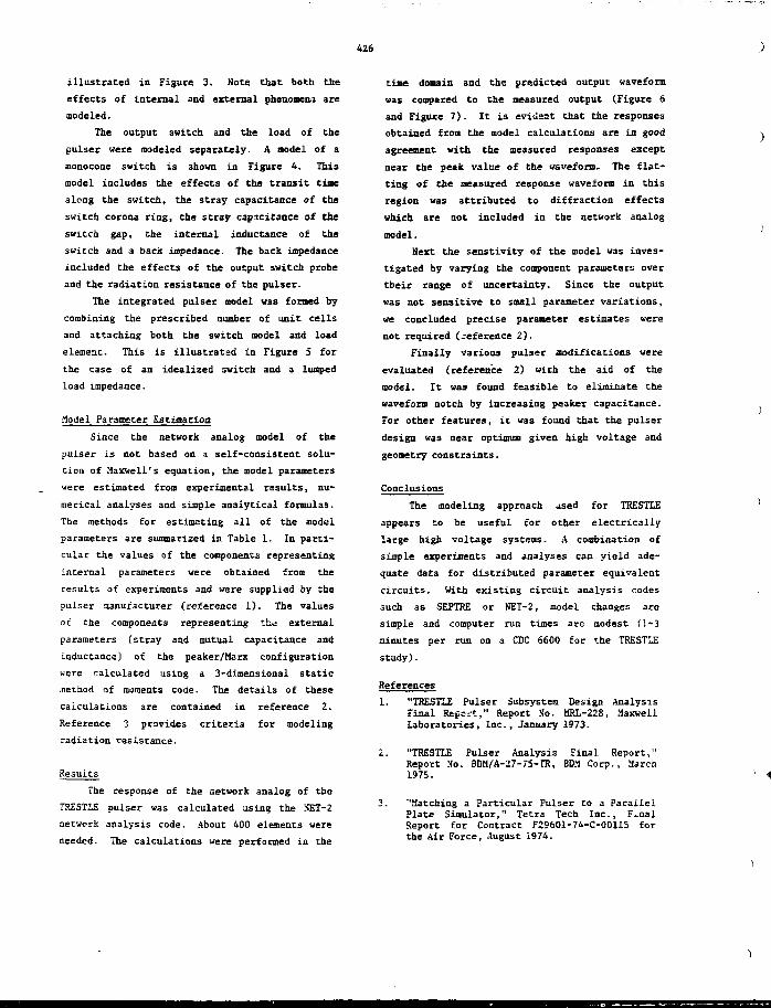
426
illustrated in Figure 3. Note that both the
effects of internal and external phenomena are
modeled.
The output switch and the load of the
pulser were modeled separately. A model of a
moaocone switch is shown in Figure 4. This
model includes the effects of the transit time
along the switch, the stray capacitance of the
switch corona ring, the stray capacitance of the
switch gap, the internal inductance of the
switch and a back impedance. The back impedance
included the effects of the output switch probe
and the radiation resistance of the pulser.
The integrated pulser model was formed by
combining the prescribed number of unit cells
and attaching both the switch model and load
element. This is illustrated in Figure 5 for
the case of an idealized switch and a lumped
load impedance.
Model Parameter Estimation
Since the network analog model of the
pulser is not based on a self-consistent solu-
tion of Maxwell's equation, the model parameters
were estimated from experimental results, nu-
merical analyses and simple analytical formulas.
The methods for estimating all of the model
parameters are summarized in Table 1. In parti-
cular the values of the components representing
internal parameters were obtained from the
results of experiments and were supplied by the
pulser manufacturer (reference 1). The values
of the components representing thj external
parameters (stray and mutual capacitance and
inductance) of the peaker/Marx configuration
were calculated using a 3-dimensional static
.nethod of moments code. The details of these
calculations are contained in reference 2.
Reference 3 provides criteria for modeling
radiation resistance.
Results
The response of the cetwork analog of the
TRESTLE pulser was calculated using the 5IET-2
network analysis code. About 400 elements were
needed. The calculations were performed in the
time domain and the predicted output waveform
was compared to the measured output (Figure 6
and Figure 7). It is evident that the responses
obtained froa the model calculations are in good
agreement with the measured responses except
near the peak value of the waveform. The flat-
ting of the measured response waveform in this
region was attributed to diffraction effects
which are not included in the network analog
model.
Next the senstivity of the model was inves-
tigated by varying the component parameters over
tbeir range of uncertainty. Since the output
was not sensitive to snail parameter variations,
we concluded precise parameter estimates were
not required (reference 2).
Finally various pulser modifications were
evaluated (reference 2) with the aid of the
model. It was found feasible to eliminate the
waveform notch by increasing peaker capacitance.
For other features, it was found that the pulser
design was near optimum given high voltage and
geometry constraints.
Conclusions
The modeling approach used for TRESTLE
appears to be useful for other electrically
large high voltage systems. A combination of
simple experiments and analyses can yield ade-
quate data for distributed parameter equivalent
circuits. With existing circuit analysis codes
such as SEPTRE or SET-2, model changes are
simple and computer run times are modest (1-3
minutes per run on a CDC 6600 for the TRESTLE
study).
References
1. "TRESTLE Pulser Subsystem Design AnalysisFinal Regci-t," Report No. MRL-228, MaxwellLaboratories, Inc., January 1973.
2. "TRESTLE Pulser Analysis Final Report,"Report No. BDM/A-27-75-rR, BDM Corp., March1975.
3. "Matching a Particular Pulser to a ParallelPlate Simulator," Tetra Tech Inc., F^nalReport for Contract F29601-74-C-00115 forthe Air Force, August 1974.
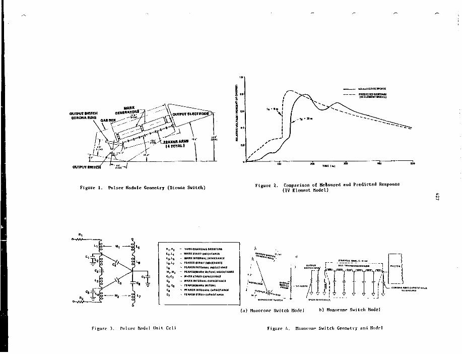
0U1TUT SWITCH O«MMI«p™.
"
' / V-1 / \ "- —> « • • - 1 / N S"
, , .„ • I I I
100
MEASURED RESPONSE
PREDICIEO REWONtt(II-ELEUCNT MOOEU
• " " " \
ada 400 M
Figure 1. Pulser Hodule Geometry (Bicone Switch)Figure 2. Comparison of Me&sured and Predicted Response
(IV Element Model)
TMARK CttARQtNQ REIIIT0R1
MARK STRAY INDUCTANCE
MARX INTERNAL INDUCTANCE
id STRAY INOUCIANCE
IF) INTERNAL INDUCTANCE
in/MARK MUTUAL INDUCTANCE
ITRAV CAPACITANCE
(R/MARX MUTUAL
• PFAKER INTERNAL CAPACITANCE
- PEAKERITRAY CAPACITANCE
1
(a) Houorone Switch Model b) Monocone Switch Model
Figure 3. Pulser Model Unit Cell Figure A. Moiiornr.p Swi tcti Geometry and Ho
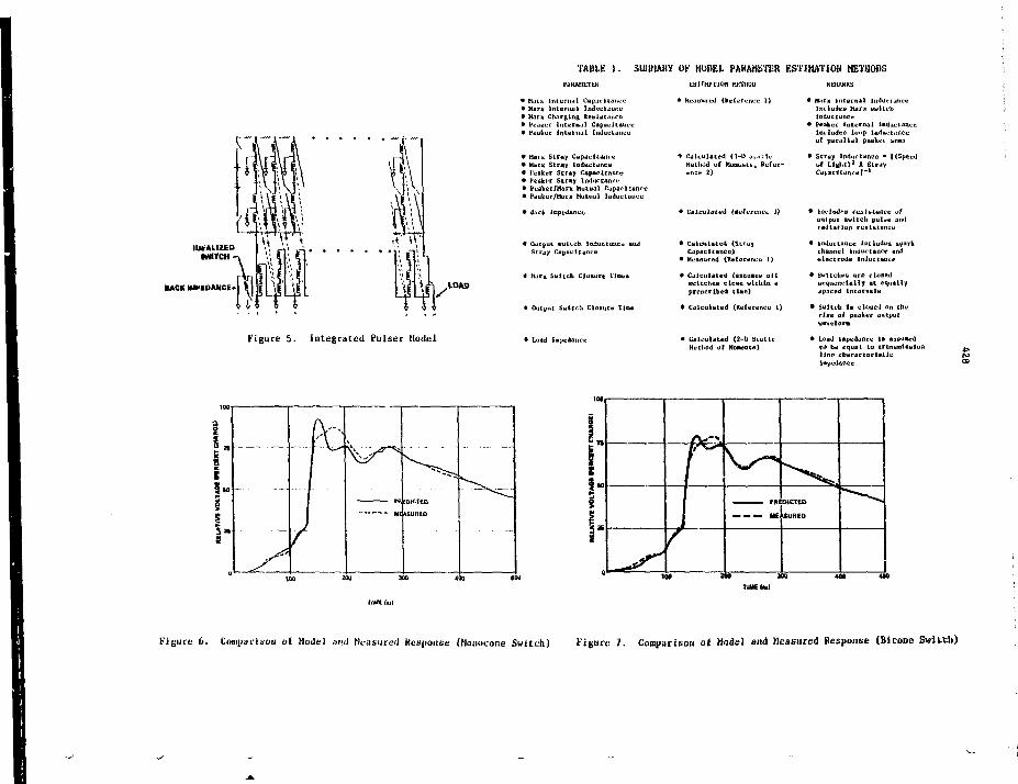
TABLE J. SUMMARY 0¥ MODEL PARAMETER ESTIMATION METHODS
•ACK UIPEOAMCE
I'itRAMLTKK
Haix I n i t rim I CapacitanceHuTM Internal InductanceHarx Charging RealytancePeantir In turn J ! Capacitancefeufeer Internal Inductance
Harx Stray CapacitanceHam Str«y InductancePeaker Stray Capucitunct:Weaker Stray tnductancu
• Peaker/Harn Mutual CapacUanc<• Peaker/Karx Hutuul Inductance
• tlacfc Impudunctt
V Output suticli Iniluctancu andStray CapaL-ltanre
* Output Switch Clauure Ha»
HtV IION HKTIIUU
urud (keferunte
• CultruUted <3-U Huthod of MomtntGence 2)
• Calculated
* Calculated (StrayCapacitance)
* Measured (Reference 1)
* Calculated (as&uaet* all
switches clcBe within a
prescribed t U e )
* Calculated (Reference 1)
RbHAKKS
• Harx i n t e r n a l InducrancuIncludes Harx owlt tbInductance
• Peuker I n t e r n a l lnduciancuIncludes loup Inductancuof p a r a l l e l peaker j r»a
• Stray Inductance - ((Speedat L i g h t ) 2 X StrayCapacf cancel*"'
1 Includes ceui*tttnwoutput switch pul^
Figure 5. Integrated Pulser Model
* Inductance Includes upurkchannel Inductance andfclectrade Induetance
• Switches arc closedHuquL-nclally at equallyspaced Intervals
* Switch Is cloaed on therJse af peafcdr outputwaveFora
• Load lapedunce Is antmacdco be equal to tranualasluline characterlatlt
Figure 6. Coin|»aiisoii of Model ami Measured Kes|ioiis<; (Homicone Switch) Figure 7. Comparison ot Model and Measured Response (Bicone Swilth)
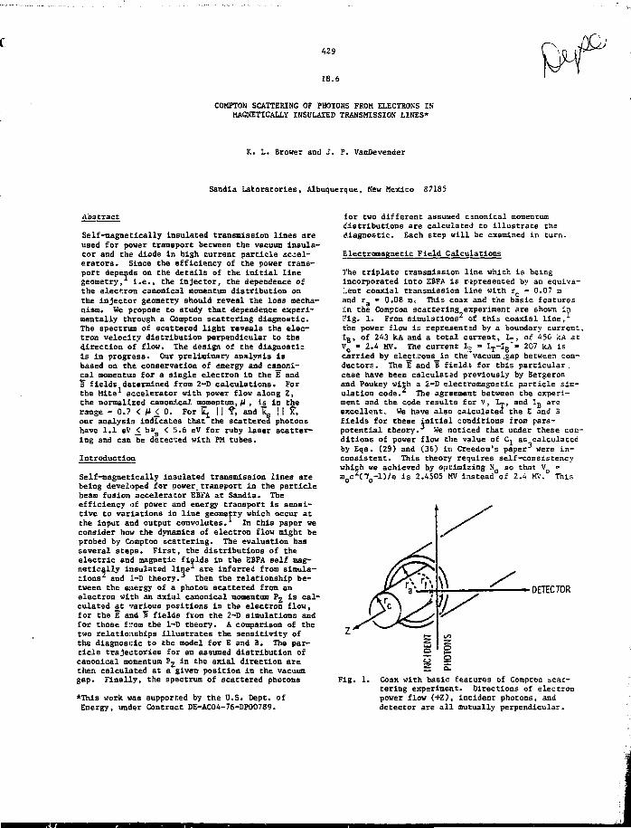
429
18.6
COMPTON SCATTERING OF PHOTONS FROM ELECTRONS ISMAGNETICALLY INSULATED TRANSMISSION LINES*
K. L. Brower and J. P. VanDevender
Sandla Laboratories, Albuquerque, New Mexico 87195
Abstract
Self-magnetically insulated transmission lines areused for power transport between the vacuum insula-tor and the diode in high current particle accel-erators. Since the efficiency of the power trans-port depends on the details of the Initial linegeometry, I.e., the Injector, the dependence ofChe electron canonical momentum distribution onthe injector geometry should reveal the loss mecha-nism. He propose to study that dependence experi-mentally through a Compton scattering diagnostic.The spectrum of scattered light reveals the elec-tron velocity distribution perpendicular to Chedirection of flow. The design of the diagnosticis in progress. Our preliminary analysis isbased on the conservation of energy and canoni-cal aomentus for a single electron in the E* andif fields determined from 2-D calculations. Forthe Mite accelerator with power flow along Z,the normalized canonical momentum, fi , is in therange - 0.7 < H< 0. For kj 11 % and k ! I £,our analysis indicates that the scattered photonshave 1.1 eV £ hvs < 5.6 eV for ruby laser scatter-ing and can be detected with PM tubes.
Introduction
Self-magnetically insulated transmission lines arebeing developed for power transport in the particlebeam fusion accelerator EB'FA at Sandia. Theefficiency of power and energy transport is sensi-tive to variations in line geometry which occur atthe input and output convolutes. In this paper weconsider how the dynamics of electron flow might beprobed by Compton scattering. The evaluation hasseveral steps. First, the distributions of theelectricnetictions*
tween the energy of a photon scattered from anelectron with an axial canonical momentum Pz is cal-culated at various positions in the electron flow,for the E and 5 fields from the 2-D simulations andfor those from the 1-D theory. A comparison of thetwo relationships illustrates the sensitivity ofthe diagnostic to the model for E and 3. The par-ticle trajectories for an assumed distribution ofcanonical momentum F^ in the axial direction arethen calculated at a given position in the vacuumgap. Finally, the spectrum of scattered photons
*Thi3 work was supported by the U.S. Dept. ofEnergy, under Contract DE-AC04-76-DP00789.
for two different assumed canonical momencumdistributions are calculated to illustrate thediagnostic. Each step will be examined in turn.
Electromagnetic Field Calculations
The triplate transmission line which is beingincorporated into EBFA is represented by an equiva-lent coaxial transmission line with rc » 0.07 mand ra » 0.08 m. This coax and the basic features±n the Compton scattering experiment are shown inFig. 1. From simulations2 of this coaxial line,the power flow is represented by a boundary current,tj, of 243 kA and a total current, Lj, of 450 kA atVo - 2.4 MV. The current I, - ^-Ig - 207 kA iscarried by electrons_in the"vacuum .gap between con-ductors. The E and B fields for this particular ,case have been calculated previously by Bergeronand Poukey with a 2-D electromagnetic particle sim-ulation code. The agreement between the experi-ment and the code results for V, I—, and In areexcellent. We have also calculated the Z and Bfields for these initial conditions from para-pocentlal theory. We noticed that under these con-ditions of power flow the value of C-, as calculatedby Eqs. (29) and (36) in Creedon's paper were in-consistent. This theory requires self-consistencywhich we achieved by optimizing N so that VQ =moc
2(7o-l)/e is 2.4505 MV instead of 2.4 MV. This
DETECTOR
Fig. 1. Coax with basic features of Compton scat-tering experiment. Directions of electronpower flow (+Z), incident photons, anddetector are all mutually perpendicular.
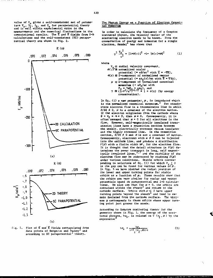
430
value of V gives a self-consistent set of parame-
ters V . LJ., and Z for parapotential theoryand ls'uell within experimental error In themeasurements and the numerical fluctuations la thecomputational results. The E and B fields from 2-Dcalculations and the self-consistent (SC) parapo-tencial theory are shown in Fig. 2.
The Photon Energy as a Function of Electron Canoni-cal Moaentm
In order to calculate the frequency of a Comptonscattered photon, the velocity vector of thescattering electron needs to be known. From theconservation of energy and momentum for a singleelectron, Mendel has shown that
.070 .072 .074 .076
-100
-200
-300
T
.078—r—
.080 -1- [a(r)+/up (1)
\^__2D CALCULATION
PARAPOTENTIAL
(a)
.070
2D THEORY
SC PARAPOTENTIAL
(b)
Fig. 2. Plot of C and IT fields extrapolated fromdata points of Bergeron and ?Qukey" andaccording to SC parapotentialJ theory.
whereV = radial velocity component,
0<r)'= normalized scalar _potential (- e0/mc with E - -Vt)),
o(r) = Z-conponenc of normalized vectorpotential (- eAgCrt/mc with ~$ - 7XA),
II s Z-component of normalized canonicalmomeatuB (m e?*r/ac with
y S (I-V'/c2)"1'2 - 1 + 0(r) (by enconservation).
energy
In Eq. (1) a new parameter, (I, is introduced whichis the normalized canonical momentum. For steady-state electron flow in a transmission line in whichd/dZ ? 0, ft is a constant of the electron motion.If the electron originates from the cathode wheretf - 1Z » a - 0, then U - 0. Consequently, it isoften assumed that It • 0 for all electrons in theflow. However, self-magnetically insulated trans-mission lines have a transition section betweenthe weakly, electrically stressed vacuum insulatorand the highly stressed line. Is the transitionsection, d/dz i4 0 and It is not a constant of motion.Consequently, electrons with U f 0 can be injectedinto the uniform line, and produce a distributionF(*i) with a finite width W, for the electron flow.It is thought that the detail structure in F(/i) de-termines the power transport In long, self magnet-ically Insulated lines,0' and the stability of theelectron flow may be understood by studying F(JJ)under various conditions. Stable orbits corres-ponding to solutions of Eq. (1) for which Vr > 0In the gap can be found for various values of ju .In Fig. 3 we have plotted the radial position ofche lower and upper turning points for stableorbits as a function of it. These results show thatthe orbits are very similar far scalar and vectorpotentials based on parapotential and 2-D calcula-tions. We also see that for u - 0, the orbits arecontained within che sheath3 and return to thecathode surface. Orbits wlth/i-< 0 have upperturning points beyond Che sheath and tend to re-main isolated from the cathode surface. The mini-mum it corresponds to those orbits whose upper turn-ing point just grazes the anode.
According to Compton scattering theory tor thegeometry shown in Fig. 1, the energy of the scat-tered photons, hi»s> Is related to V (r« , It ) by cheexpression
(2)
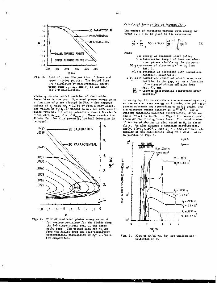
431
-SC PARAPOTENTIAL
- PARAPOTENTIAL
2D CALCULATION
LOWER TURNING POINTS
UPPER TURNING POINTS-
.070 .072 .074 .076 .078 .080
R (m)
Fig. 3. Plot of fi vs. the position of lower andupper turning points. The dotted linewas calculated by parapotentiai theoryusing same Ig, IT, and VQ as was usedfor 2-D calculation.
where r is the radial position of the incidentlaser beam in the gap. Scattered photon energies asa function of u are plotted in Fig. 4 for variousvalues of r. with hi^ • 1.786 eV from a ruby laser.The values of V_(rj ,11) needed in Eq. (2) were deter-mined from Eq. (1) using potentials from 2-D calcula-tions with These results in-dicate that for this geometfyT'optical detection isrequired.
Calculated Spectra for an Assumed t(A0.
The number of scattered photons with energy be-tween E, E + dE is given by the expression
Jdndn (3)
whereU= energy of incident laser pulse,L s interaction length of beam and elec-
tron plasma visible to the detector.D(r«) s number of electrons/m3 at r« from
Bef. 2. x
F(Ji) = fraction of electrons with normalizedcanonical momentum it,
G(rj ,E) £ normalized canonical momentum at someposition in the gap, r., as a functionof scattered photon energies (seeFig. 4), andCompton differential scattering crosssection.
do
-.7 -.6 -.5 -4 -.3 -.2 -.1 0
Fig. 4. Plot of scattered photon energies vs.nfor various positions for the fields fromthe 2-D computations and, UI the laserprobe beam. The dotted line has hvs(U)from the fields from the self-consistentparapotentiai calculation at r»» 0.0725 mfor comparison.
In using Eq. (3) to calculate the scattered spectra,we assume the laser energy is 1 joule, the collectorsystem subtends one sterradian of |°lid angle, andthe electron number density is 10 m~3. For auniform canonical momentum distribution, dN'/dE ver-sus E ("h»g) is plotted in Fig. 5 for several posi-tions of the probing laser beam. Tbe total numberof scattered photons is also noted as N in theseplots. We also assumed a Gaussian distribution,exp(-0.5(P-/y/«*/)2), with Vo - 0 and 4J* - 0.1; theresults of the calculation using this distributionis plotted in Fig. 6.
J!ED
5 105
SHIFT'SHIFT R| _ . „ „ „ ,
=i.mo5
R| = .0715
N p= 1.4 X10⁵
hv (eVI
Fig. 5. Plot of dN/dE vs. h»s for uniform dis-tribution in P.
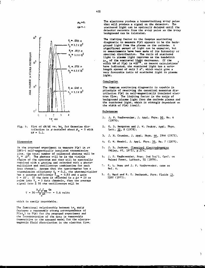
432
i io5
a
3
| U)4
103
0
'.
1
- 1A
—
n—/T\\T\i
i i1 2 3
eVI
R,.
-v- v
R,=
V
pv
.0705 m
3.2X10 5
.0715 m
3.0X1.05
.0735 <n
6.0X10 4
.0745 m
5.3X1O3
Fig. 6. Plot of dN/dE vs. hvg fcr Gaussian dis-tribution in V centered about IX - 0 with6*r » 0.1.
Discussion
In the proposed experiment to measure F(jM) in anEBFA-I self-tnagnetically insulated transmissionline, the total number of collected photons will beX = 10°. The photons will be in the visibleregion of the spectrum and they will be spectrallyresolved uith a grating and recorded with a photo-multiplier and oscilloscope combination for eachdata channel. Assume that the spectrometer has atransmission efficiency f, « 0.2, the photomultlplierhas a qunatum efficiency t - 0.03 and a gainG • 10' . If the data is recorded in a At » 10 T13pulse Into Ne - 5 data channels, then the averagesignal Into a 50 ohm oscilloscope will be
The electrons produce a bremsstrahlung x-ray pulsethat Mill produce a signal on the detector. Thescattered light can be optically delayed until thedetector recovers from the x-ray pulse so the x-raybackground can be tolerated.
The Halting factor to the Compton scatteringdiagnostic to measure F(/J) appears to be Che back-ground light from the plasma on the cathode. Asignificant anount of light can be expected, butno measurements have been made of its Intensity orspectral distribution. The ratio of scatteredlight to platoa light improves as the bandwidthivs of the scattered light decreases. If thewidth ill of FOl) la =10 , as recent calculations'have indicated, the scattered light has a wave-length sprsad of only 3 A", which would give avery favorable ratio of scattered light to plasmalight.
Conclusion
The Compton scattering diagnostic is capable inprinciple of resolving the canonical momentum dis-tribution F O O in self-nagnetically insulated elec-tron flow. The limiting factor is the ratio ofbackground plasma light froa the cathode plasma andthe scattered light, which is strongly dependent onthe width of F(UJ itself.
References
1. J. P. VanDevender, J. Appl. Phys. 50, No. 6(1979).
2. K. D. Bergeron and J. W. Poukey, Appl. Fiiys.Lett. 32, 8 (1978).
3. J. M. Creedon, J. Appl. Phys. 4£, 2946 (1975).
4. C. W. Mendel, J. Appl. Phys. 50, So. 7 (1979).
5. J. D. Jackson, Classical Electrodynamics(Wiley, NY, 1975), p.574.
6. J. P. VanDevencler, Proc. 2nd Int'l. Conf. onPulsed Power, Lubbock, TX (1979).
7. E. L. Neau and J. P. VanDevender, same as
Ref. 6.
3. G. Ward and R. E. Pechacek, Phys. Fluids 15_,2202 (1972).
50-Vsfpm Ge
0.6 volts
which is easily recordable.
The functional relationship between hi> and ^features a reasonably strong correspondence ofF(hKs) to FOJ) for the proposed experiment andthe interpretation of the data is reasonablyinsensitive to the assumed model for the electro-magnetic field distribution in the electron flow.
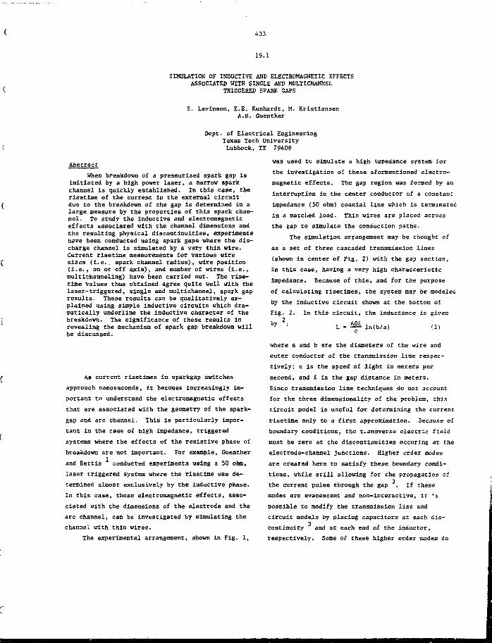
433
19.1
SIMULATION OF INDUCTIVE AND ELECTROMAGNETIC EFFECTSASSOCIATED WITH SINGLE AND MULTICHANNEL
TRIGGERED SPABK GAPS
S. Levinson, E.E. Kunhardt, M. KristiansenA.K. Guenther
Dept. of Electrical EngineeringTexas Tech UniversityLubbock, TX 79409
Abstract
When breakdown of a pressurized spark gap isinitiated by a high power laser, a narrow sparkchannel is quickly established. In this case, Cherisetime of the current in the external circuitdue to the breakdown of the gap is determined in alarge measure by the properties of this spark chan-nel. To study the inductive and electromagneticeffects associated with the channel dimensions andthe resulting physical discontinuities, experimentshave been conducted using spark gaps where the dis-charge channel is simulated by a very thin wire.Current risetime measurements for various wiresizes (i.e.. spark channel radius), wire position(i.e., on or off axis), and number of wires (i.e.,multichanneling) have been carried out. The rise-time values thus obtained agree quite well with thelaser-triggered, single and multichannel, spark gapresults. These results can be qualitatively ex-plained using simple inductive circuits which dra-matically underline the Inductive character of thebreakdown. The significance of these results inrevealing the mechanism of spark gap breakdown willbe discussed.
As current rlsetimes in sparkgap switches
approach nanoseconds, it becomes increasingly im-
portant to understand the electromagnetic effects
that are associated with the geometry of the spark-
gap and arc channel. This is particularly impor-
tant in the case of high impedance, triggered
systems where the effects of the resistive phase of
breakdown are not important. For example, Guenther
and Bettis conducted experiments using a 50 ohm,
laser triggered system where the risetime was de-
termined almost exclusively by the inductive phase.
In this case, those electromagnetic effects, asso-
ciated with the dimensions of the electrode and the
arc channel, can be investigated by simulating the
channel with thin wires.
The experimental arrangement, shown in Fig. 1,
was used to simulate a high Impedance system for
the investigation of these aformentioned electro-
magnetic effects. The gap region was formed by an
interruption in the center conductor of a constant
impedance (50 ohm) coaxial line which is terminated
in a matched load. Thin wires are placed across
the gap to simulate the conduction paths.
The simulation arrangement may be thought of
as a set of three cascaded transmission lines
(shown in center of Fig. 2) with the gap section,
in this case, having a very high characteristic
impedance. Because of this, and for the purpose
of calculating risetimes, the system may be modelec
by the inductive circuit shown at the bottom of
In this circuit, the inductance is given
602
Fig. 2.
b y 2 :ln(b/a) (1)
where a and b are the diameters of the wire and
outer conductor of the transmission line respec-
tively; c is the speed of light in meters per
second, and I is the gap distance in meters.
Since transmission line techniques do not account
for the three dimensionality of the problem, this
circuit model is useful for determining the current
risetime only to a first approximation. Because of
boundary conditions, the t*ansverse electric field
must be zero at the discontinuities occuring at the
electrode—channel junctions. Higher order modes
are created here to satisfy these boundary condi-
tions, while still allowing for the propagation of
the current pulse through the gap . If these
modes are evanescent and non-interactive, it -s
possible to modify the transmission lisa and
circuit models by placing capacitors at each dis-
continuity and at each end of the inductor,
respectively. Some of these higher order modes do
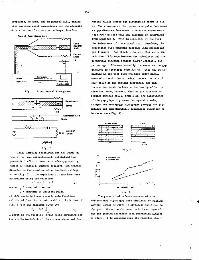
434
propagace, however, and in general Hill, making
this modified model unacepcable for Che accurate
determination of current or voltage risetime.
Taporaa Tronimmion Line'WV-?
Fig. I Experimental Arrangement
V////A
z.
50fl
—Wi—
z, z
L
- vvv
I l i
fj
| -
EipwifflMitol
S«t-up
ranjmiulon Lin*
odal
Inductor
Fig. 2
LTsing sampling techniques and the setup in
Fig. 1, we have experimentally determined the
geometrical effects associated with gap spacing,
nuaber of channels, channel position, and channel
diameter on the risetime of an incident voltage
pulse (Fig. 3). The experimental rxsetimes were
decennined using the relation:
(2)
where T = observed risetimeo
T^ i risetime of incident pulse
:.'e have compared these results with risetimes
calculated from the circuit model at the bottom of
Fig. 2 vith the risetime given by:
A graph of the risetime (after being corrected for
the finite bandwidth of the current shunt and in-
cident pulse) versus gap distance is shown in Fig.
4. The risetime of the transmitted pulse decreases
as gap distance decreases in both the experimental
case and the case uh^n the risecime is determined
from equation 3. This is explained by the fact
the inductance of the channel and, therefore, the
associated time constant decrease with decreasing
gap distance. One should also note that while the
relative difference between the calculated and ex-
perimental risetime remains fairly constant, the
percentage difference actually increases as the gap
distance is decreased from 3.3 cm. This may be ex-
plained by the fact that the high order modes,
created at each discontinuity, interact more with
each other as the spacing decreases, and this
interaction tends to have an increasing effect on
risecioe. note, however, that as gap distance is
reduced further still, from 2 cm, the capacitance
of the gap plays a greater but opposite role,
causing the percentage difference between the cal-
culated and experimentally determined risetimes to
decrease (see Fig. 4).
I1
1
j
!\ I .
: 71 ;i ;
(~ : •
• • / ! i
i ' 1 I i
: i 1 '•
l
— b ^' : ( '1 I •
i ! 1 j 1
: ' ' . L_!
Fig. 3
SAP DISTANCE <Cffil
Fig. 4
The geometrical effects associated with
multichannel discharges were simulated by placing
various number oi wires at different positions in
the gap. Since the characteristic inductance of
the gap section decreases vith increasing numbers
of wires, it is expected that the risetime should
435
decrease also. Ihij decrease Is particularly
acute between rise times associated with one and
two wire channels (see Figs. 5 and 7 ) .
a.0]
1.5-j
Z j
X Experimental Datao Calculated Data
Wires Va" From Gap CenterV From Gap Center- Wires
S2<r
0 I 2 3 4 5 6
•# OF WIRES (.01" DIAMETER)
Fig. 5
As the number of wires increases, the elec-
tromagnetic field distribution more accurately
approximates that of a larger diameter wire. It
then follows that large numbers of wires placed
at the edge of the gap have an associated rise-
time that is smaller than the case when the same
number of wires are placed closer to the axis of
the gap since the associated inductance of the
"effective" large diameter channel is smaller.
Similarly it follows that the experimental rise-
tiae should more closely match the rise time
calculated from equation 3 since the "effective"
large diameter wire produces less of a discon-
tinuity to the transverse electromagnetic fields
of the incident pulse, than the smallei "effec-
tive" diameter wire. This is verified by the
graph in Fig. 5.
Finally the effects of channel thickness on
risetloe were determined by varying the diameter
of che wires used to simulate the channel. Again,
since the characteristic inductance of the gap
section associated with the thicker wires is less
than that associated with thinner wires, it is
expected tbat risetimes should also be less. This
is shown in the plot of risetime versus channel
diameter in Fig. 6. Note that the difference
between calculated and experimentally determined
risetimes tends to become smaller as ch» thickness
of the channel is increased. This decrease is due
to two reasons. First, less high order modes are
generated in the gap section when thicker wires
are used, hence shorter risetimes for the experi-
mental case. Secondly, as wire thickness begins
to approach the diameter of the center conductor
of the main line, we no longer have the necessary
condition that the impedance of the gap be much
greater than the impedance of the Hain line render-
ing tht risetimes calculated from the inductor
model too large for the very large diameter wires
that we tested.
X Experimental Datao Calculated Dota
I5H
UQ-i
0.5-1
0 .01 .! :.O
CHANNEL THICKNESS (In)
Fig. 6
The importance of these effects in high in-
pedance triggered systems, may be further ascer-
tained by comparing the results obtained in our
simulation with the data obtained by Guenther and
Bettis using the laser trigger system mentioned
previously. They studied the rdsetime of single
and dual channel sparkgaps triggered by one or Lwo
laser beams focused on the cathode. A risetime of
2 ns for a single channel and 1.12 ns for dual
channels were obtained in their experiment. This
is a 44% difference between the two cases. Figure
7 shows a comparison between photographs of
oscilloscope traces when one and two .01 inch dia-
meter wires are used to simulate the arc channels.
We have a 34£ difference between the risetimes cf
the single and dual wire cases. Considering that
fhe discontinuities in their experiment are more
abrupt, (i.e. the cutoff frequency for the higher
order modes in their experiment was 200 MHz, where-
as in ours it was 600 A ), the results compared
favorable. Moreover, note that the increase in
the risetime for the single channel case is con-
sistent with our explanation.
436
! 1 1 1- 1 1
/ : i ' 1 ! i ,
J< • i l ' i :
' j' ! ' i !: i ! 1
Fig. 7
It is apparent from these results that in
nanosecond regimes, current risetime is strongly
dependent on the geometry of Che spark gap and
arc channel system. If minimization of current
risetime is to be achieved, reduction in the
electromagnetic discontinuities must be consider-
ed. One way to accomplish this is by multi-
channelling. From our results, the most desirable
condition, for this case, is the simultaneous
creation of either two or four channels at Che
outer edges of the spark gap. Considering the
problems of simultaneously producing four channels,
it seems that the percentage reduction using two
channels may render this case to be the most
praccical.
Work supported by AFOSR under Grant tfATOSR-76-3124..
1. Guenther, A.H. and Bettis, J.R., J. Phys. D:Appl. Phys. 1, 1577-1613, 1978
2. Metzger, George and Jean-Paul Vabre,Transmission Lines with Pulse Excitation.131-138, Academic Press, 1969.
n. Vhinnery, J.R. and Jamieson, H.W., Proc.I.R.E., 32, pp. 98-114, 1944.
437
19.2
AN ELECTRON-BEAM-TRIGGERHD SPARK GAP
K. McDonald, M. Newton, E. E. Kunhatdt, and M. KristiansenDept. of Electrical Engineering, Texas Tech University
Lubbock, Texas 79409
A. H. GuentherAir Force Weapons Laboratory
Kirtland AFB, NM 87117 "
Abstract
Studies on the triggering of a high-voltage, gaa-
insulated spark gap by an electron beam have been
conducted. Risetimes of approximately 2.5 ns and
subnanosecond ., 1 uter have been obtained for 3 cm
gaps with gap voltages as low as 50% of the self-
breakdown voltage (variable to 1 MV). The switch
delay (including the diode) was 50 ns. The work-
ing media were N_, and mixtures of N'2 and Ar, and
of N. and SF, ac pressures of 1-3 atm. Open
shutter photographs show that the discharge is
broad in cross-section.
Voltage, current, and jitter measurements have
been made for a wide range of gap conditions and
electron-bean parameters. Variations in the
character of the discharge have been inferred
using streak and open shutter photography.
Correlation between electron beam width, beam
energy, discharge channel width, current risetime,
delay, and jitter are discussed.
Introduction
Several current high priority research efforts
such as fusion, the production of high energy-
particle beams, and the simulation of environments
associated with nuclear weapons detonations,
require the generation of very high voltage, high
peak power pulses. One of the principle pre-
requisites to achieving this objective is the
Work supported by AFOSR under Grant No.
AFOSR-75-3124
development of switches that will allov fast
transfer of energy from an energy storage system
to the load or transducer. We are currently
engaged in a research program designed to improve
the physical understanding of switching processes
for the subsequent development of an advanced, low
inductance, fast rise time, command fired spark
gap switch, capable of operating at very high
voltages (MV). Encouraging results toward this
goal have been achieved by laser triggered
switching (LTS), and by e-beam triggered
switching ' (EBTS). This paper discusses an
investigation into e-beam initiated breakdown
which laads to the formation of a volume discharge
(proportional to the cross-sectional area of the
injected beam), which helns reduce electrode ero-
sion and switch inductance.
The Experimental Arrangement
The experiment consists of an energy storage
element, a gas Insulated, pressurized spark gap,
and a source of energetic electrons. (Fig. 1).
The energy storage element and the spark gap are
both contained within the high pressure vessel of
the Ion Physics Corporation FX-15 (Fig 2). The
energy storage element is a Van tie Graaff charged
co-axial line. It is capable of producing a 1 MV
rectangular pulse of ipproximately 10 ns FWHM
duration. The spark gap is formed by an inter-
ruption in the center conductor of the line. The
stainless steel electrodes have a Bruce profile
and are 21.5 en in diameter. The high pressure in-
438
sulating gas also serves as the dielectric for
the co-axial line. The electron beam is generated
by a. cold cathode, field enmission vacuum diode,
which is located behind the grounded electrode.
It is actually placed inside the inner conductor
of the output co-axial line, so as to introduce
the e-beam axially through a 1" diameter aperaeure
in the center of the electrode. In order to
-.aincain a uniform field distribution in the gap
and to protect the foil from the discharge, the
aperature was covered with a stainless steel mesh
(0.050"). The diode4 (Fig. 3), designed and built
at Texas Tech University, utilises a spiral groved
graphite cathode, and a thin foil anode. Graphics
was chosen because of its fast "turn on" pro-
parties3. The diode was designed to have an
impedance of 70 ft to natch that of the driving
generator. This generator is a 25 3tage modified
Marx pulse forming network (Heds pulser) . It
combines the voltage multiplicative feature of the
standard Marx circuit with the pulse shaping
characteristics of a lumped parameter network.
The sequence of events in the experiment is as
follows: The Marx erects to give an output wave-
form characterized by a 250 fcV tra-azoidal pulse
of 30 ns FWHM duration with a 4 ns risetime. This
pulse propagates down a 70 tt, oil-filled, co-axial
transmission line and appears across the anode-
cathode gap of che diode. The diode emits, through
a 1 mil. citaminan foil, a 1.5 kA, 200 keV burst
of electrons with a 0-502 risetiae of 1.5 ns and
a duration of 15 ns. This pulsed beam of elec-
crons travels chrough 1.5 cm of che high pressure
^as before it enters the spark gap. The insulat-
ing jas is ionized by electron impact, resulting
in the subsequent formation of an ionized conduc-
tion path and che collapse of the voltage across
che gap. The charged co-axial lice of the FX-15
discharges, and the resulting wave propagates down
a 50 H, oil-filled output transmission line, which
is cerminaced in a matching A1C1. water resistor.
The outer conductor of che Marx Generator to
dicde transmission line also serves as the inner
conductor for che FX-15 output transmission line.
Experimental Approach
The characteristics of the spark gap breakdown
investigated '*ere: (1) the risetime of the trans-
mitted voltage pulse, (2) the switch delay and
Jitter, and (3) the spatial character of the
breakdown. The diagnostics used were open shutter
and streak photography to record the character of
the discharge, and a capacitive divider probe
(fl-), located in the FX-15 output transmission
line, to monitor the voltage pulse generated at
breakdown.
he parameters that we varied during the course of
our Investigation include: (1) The gap polarity
(depending on how the Van de Graaff was charged,
the target electrode was either positive or nega-
tive. When charged positive the injected e-beam
was accelerated hy the initial electric field in
the gap, and for the target electrode negative the
beam waa decelerated), (2) the gap voltage V (V
waa varied between 50% and 98% of the self-break-
down voltage which raiiged from 75 kV to 4O0kV>,(2)
gas pressure (1-3 aoa), (4) the type of gas (N2>
mixtures of M- and Ar, and mixtures of N» and
SF,), (5) the e-beam diameter (1.2S cm and 2.50
cm), and (6) the e-beam energy (150 keV to 250
keV).
Results
The pulse risetime was observed to vary with the
beam energy and ranged from 2.5 to 3 ns. The
larger value was obtained for a beam energy of 150
keV and V - 100 kV or, 50% V S B . The jitter was
found to be virtually identical throughout the
range of our investigation. Fig. 4a is representa-
tive of all jitter measurements. There are 15
separate, superimposed traces of che voltage pulse
as monitored by the capacitive probe (C^), and
displayed on a Tektronix 51? oscilloscope. The
scope was triggered with the signal from the 3
probe (B ) located on the diode transmission line.
The sweep speed was 2 ns/div, thus, the resolution
ts approximately 0.2 ns and the jitter can be seen
to be no greater than chis amount. These traces
correspond to breakdown of a 3.2 cm gap in N., at
3 atm. The gap voltage was V =• 235 kV or 94Z •/,,_.
The self-breakdown voltage was 250 kV. The craces
in Fig. 4b are further examples of the excellent
jitter characteristics. With all other parameters
identical to chose given above, the beam was
439
injected when V = 130 kV or 52% V._. Again, theg OI>
jitter vas below the capabilities of our resolu-
tion. These two experiments were conducted for
positive and negative polarities, yielding identi-
cal results. The delay was obtained from t±gw:e
5 (a-e), where the B signal from the diode trans-
mission line is delayed to appear after the FX-15
voltage pulse. The delay time was measured to be
52 ns in pure K , which is consistent with pre-3vious studies . The figure also demonstrates
that (for these low voltages and pressures) the
delay was invariant to both the pressure and the
gap voltage (as a function of the self-breakdown
voltage). We should also note that these results
were obtained with a DC charged gap; one would
expect the performance to be better for a pulse
charged gap.
The character of the gas discharge for e~beam
initiated breakdown was determined from open
shutter photographs. This is shown in Fig. 6a
when the target electrode was charged positive
and in Fig 6b for z negative charged electrode.
These two photographs are representative of the
spatial character of the discharges observed
throughout the range of our investigation. For
the same polarity, the light intensity varied as
we changed experimental characteristics. For dif-
ferent polarities, the character of the light
emission are different, indicating that there is
probably a difference in the breakdown processes.
Note that for both cases, t>ie breakdown takes the
form of a volume discharge. No localized spark
channels were seen.
Fig. 7 demonstrates the variation of the discharge
as a function of the e-beam diameter. Note that
the volume of the discharge is proportional to the
cross-sectional area of the injected beam.
Fig. 8 depicts the variation in the dimensions of
che discharge cross-section as a function of the
energy of the injected beam. The light intensity
is seen to be significantly increased when a more
energetic beam is introduced into the gap. To
investigate the significance of this observation,
voltage pulses for varying e-beam energy were
recorded (Fig. 9). The amplitude of the pulse is
also observed to be a function of the beam energy.
These results indicate that the degree of ioniza-
tion in the discharge plasma, hence the resistivity
varies with the beam energy. The voltage drop
across the gap is, therefore, a function of the
e-beam energy.
Streak photographs of the discharge are shown ir.
Fig. 10. Again, we can observe a difference
between the cases of positive and negative target
electrodes in the gap. Preliminary analysis indi-
cate that the early emission of light corresponds
to the actual breakdown (the time duration is the
same as the voltage pulse), and the second emission
is the result of the recombination process.
Further analysis of these observations are presently
being made.
Conclusions
The results obtained in this series of experiments
oxj e-beam triggered switching are summarized as
follows: (1) fast risetime (2.5 ns). (2) low
jitter (less than 0.2 ns for V > 50% VgB>, and
(3) volume discharge. The characteristics make
e-beam triggered switches highly desirable for
many applications.
The risetimes of the self-breakdown and the trig-
gered voltage pulses were virtually identical, as
demonstrated by the superimposed traces shown in
figure 11. This is *ue to the fact that the pulse
risetimes were generator limited rather than spark
gap limited.
The demonstrated low jitter (particularly when
operated at voltages well below the self-breakdown
voltage), is one of the most significant contribu-
tions of this work. Small jitter is crucial to
the successful operation of any pulse power system,
however, it becomes extremely critical in any
scheme that utilizes the simultaneous discharge of
parallel pulse forming lines into a common load.
Prefires can be virtually eliminated, due to the
ability of the switch to function reliability at
low voltage levels. The diode and, therefore,
the switch has a very good single shot reliability,
which eliminates most misfires.
The EBTS breakdown was observed to take the form
of a volume discharge (proportional to tha size of
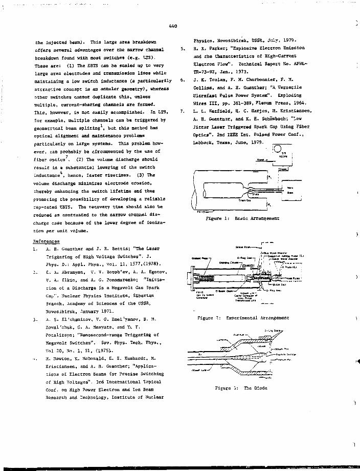
440
the Injected beam). This large area breakdown
offers several advantages over the narrow channel
breakdown found tflch most switches (e.g. ITS).
These are: (1) The ZBTS caa be scaled up to very
large area electrodes and transmission lines while
maintaining a low switch inductance (a particularity
attrac'-ive concept is an annular geometry), whereas
other switches cannot duplicate thi3, unless
multiple, current-sharing channels are formed.
This, however, is not easily accomplished. In LTS,
for example, multiple channels can be triggered by
geometrical beam split ing , but. this method has
optical alignment and maintenance problems
particularly on large systems. This problem how-
ever, can probably be circumvented by the use of
fiber optics . (2) The volume discharge should
result In a substantial lowering of the switch
inductance , hence, faster risetiaes. (3) The
volume discharge minimizes electrode erosion,
thereby enhancing the switch lifetime and thus
promoting the possibility of developing a reliable
rep-rated EBTS. The recovery time should also be
reduced as contrasted to the narrow channel dis-
charge case because of the lower degree of ioniza-
cion per unit volume.
References
1. A. H. Guenther and J. R. Bettis; "The Laser
Triggering of High Voltage Switches". J.
Phys. D.: Appl. Phys., Vol. 11, 1577,(1978).
2. E. A. Abramyan, V. V. Borob'ev, A. A. Egorov,
V. A. Elkin, and A. G. Ponomarenko; "Initia-
tion of a Discharge In a Megavolt Gas Spark
Gat,''. Huclear Physics Institute, Siberian
3ranch, Academy of Sciences of the USSR,
Sovosibirsk, January 1971.
3. A. S. El'chaninov, V. G. Emel'yanov, B. M.
Koval'ohuk, G. A. Mesyats, and YL F.
Potalitsyn; "Nanosecond-range Triggering of
Megavolt Switches". Sov. Phys. Tech. Phys.,
V'ol 20, So. 1, 51, U975}.
M. Mewton, K. McDonald, E. E. Kunhardt, M.
Krlstiansen, and A. H. Guenther; "Applica-
tions of Electron Beams for Precise Switching
or High Voltages". 3rd International Topical
Conf. on High Power Electron and Ion Beam
Research and Technology, Institute of Nuclear
Physics, Novosibirsk, USSR, July, 1979.
5. R. K. Parker; "Explosive Electron Emission
and the Characteristics of High-Current
Electron Flow". Technical Report No. AFWL-
TR-73-92, Jan., 3.973.
6. J. K. Trolan, F. M. Charbonnier, F. M.
Collins, and A. H. Guentlier; "A Versatile
UltrafaBt Pulse Power System". Exploding
Mires III, pp. 361-389, Plenum Press, 1964.
7. L. L. Hatfield, H. C. Harjes, H. Kristiansen,
A. H. Guentasr, and K. H. Schonbach; "-ow
Jittar Laser Triggered Spark Gap Using Fiber
Optics". 2nd IEEE Int. Pulsed Power Conf.,
Lubbock, Texas, June, 1979.
• om
Figure 1: Basic Arrangement
Figure I: Experimental Arrangement
Figure 3: The Diode
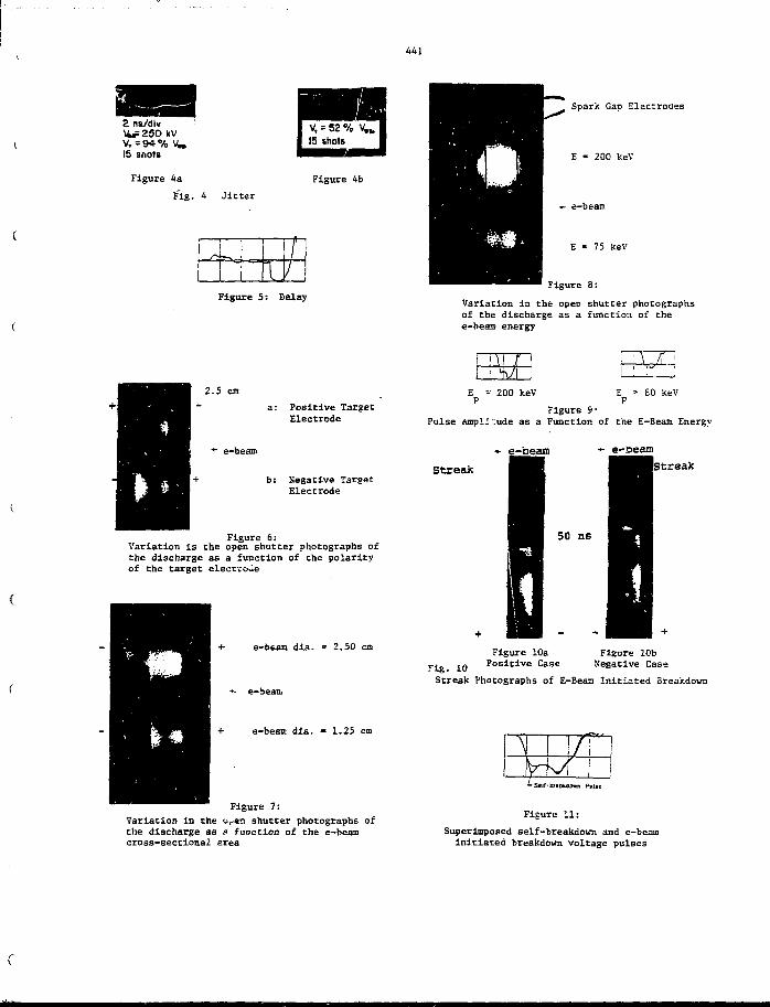
441
2 ns/divW 250 kVV, = 94 % \i.IS shots
Figure 4a
Fig. 4 Jitter
Figure 4b
I ,rp/
Figure 5: Belay
Spark Gap Electrodes
E - 200 keV
i- e-beam
E - 75 keV
Figure 8:
Variation in the open shutter photographsof the discharge as a function of thee-beam energy
2.5 cm
*• e-beam
b:
Positive TargetElectrode
Negative TargetElectrode
Figure 6:Variation is the open shutter photographs ofthe discharge as a function of the polarityof the target electroue
+ e-beam dia. » 2.50 cm
•*- e-beam
+ e-beam dia. » 1.25 cm
Figure 7:
Variation in the orer. shutter photographs ofthe discharge as a function of the e-beamcross-sectional area
I ! :u
E = 200 keV E = 80 kevP
Figure 9-Pulse Ampli:ude as a Function of the E-Beam Energy
• e-beam — e-oeam
Streak
50 ns
itreak
Figure 10aPositive Case
Figure 10bNegative CaseFig. 10
Streak Photographs of E-Beam Initiated Breakdown
Figure 11:
Superimposed self-breakdown and e-beaicinitiated breakdown voltage pulses
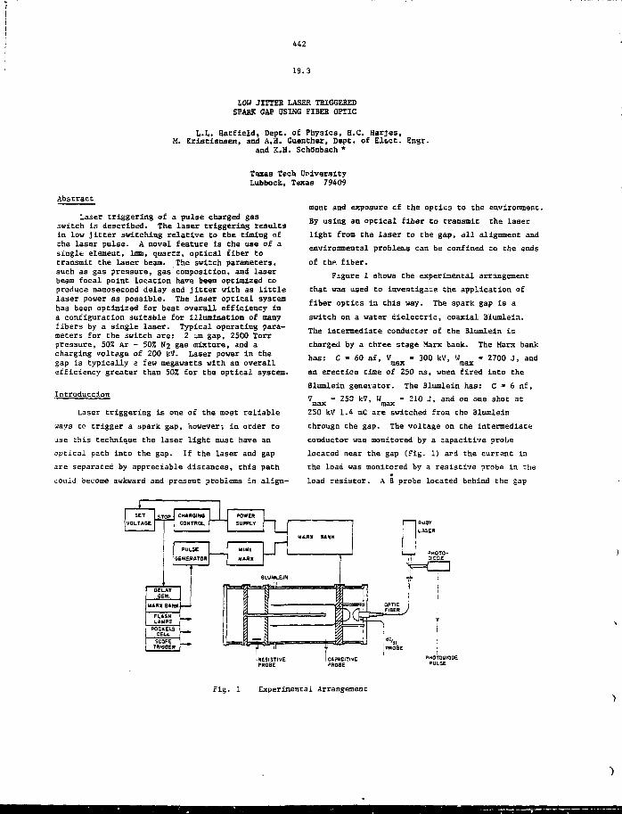
442
19.3
LOW JITTER LASER TRIGGEREDSPARK GAP USING FIBER OPTIC
L.L. Hatfield, Dept. of Physics, H.C. Harjes,M. Kristiansen, and A.3. Guenther, Dept. of Elect. Engr.
and K.H. SchBnbach *
Texas Tech UniversityLubbock, Texas 79409
Abstract
Laser triggering of a pulse charged gasswitch is described. The laser triggering resultsin low jitter switching relative to the timing ofche laser pulse. A novel feature is the use of asingle element, Iran, quartz, optical fiber Cotransmit che laser beam. The switch parameters,such as gas pressure, gas composition, and laserbeam focal point location have been optimized toproduce nanosecond delay and jitter with as littlelaser power as possible. The laser optical systemhas been optimized for best overall efficiency ina configuration suitable for illumination of manyfibers by a single laser. Typical operating para-meters for the switch are: 2 sm gap, 2500 Torrpressure, 50% Ar - 50Z N2 gas mixture, and acharging voltage of 200 kV. Laser power in thegap is typically a few megawatts with an overallefficiency greater than 50Z for the optical system.
Introduction
Laser triggering is one of the most reliable
ways Co trigger a spark gap, however; in order to
use this technique the laser light must have an
optical path into the gap. If the laser and gap
are separated by appreciable distances, this path
couid become awkward and present problems in align-
ment and exposure cf the optics to the environment.
By using an optical fiber to transmit the laser
light from the laser to the gap, all alignment and
environmental problems can be confined to the ends
of the. fiber.
Figure 1 shows the experimental arrangement
that was used to investigate the application of
fiber optics in this way. The spark gap is a
switch on a water dielectric, coaxial Blumlein.
The intermediate conductor of the Blumlein is
charged by a three stage Marx bank. The Marx bank
has: C - 60 nf, V 300 ktf, W • 2700 J, andmax
an erection time of 250 ns, vhen fired into the
Blumlein generator. The 31umlein has: C • 6 nf.
250 kV, W 210 J, and on one shot atmax """T "max250 kV 1.4 mC are switched from che Blumlein
through the gap. The voltage on the intermediate
conductor was monitored by a capacitive probe
located near the gap (Fig. 1) ard the currant in
the load was monitored by a resistive probe in che
load resistor. A B probe located behind the gap
CAPACITIVEPROBE
PMOTOOIODEPULSE
Fig. 1 Experimental Arrangement
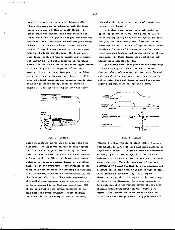
443
was used to monitor the gap breakdown, while a
photodiode was used to determine both the laser
pulse shape and the time of laser firing. By
using these two signals, the delay between the
laser entry into the gap and the gap breakdown was
measured. The laser light entered the gap through
a hole in the cachode and was focused onto the
anode. Figure 2 shows Che optics that were used
between the laser and the gap. The fiber was a
step index, single strand of quartz with a numeri-
cal aperture of .22 and a diameter of one milli-
meter. On the output end of the fiber light exists
with a divergence full angle of 18° at the e"
points. Since the light diverges from the fiber,
an uncoated quartz lens was positioned to c o m -
ma te this light while another uncoated quartz lens
focused the light onto the anode as shown in
Figure 2. The light was coupled into the fiber
otherwise the output divergence angle would in-
crease significantly.
A typical laser pulse had a half width of
15 ns, an energy of 72 mj, peak power of 4.3 MK.
After passing through the optical system and into
the gap, the laser energy was 45 mJ and the peak
power was 2.6 MK. The optical system had a trans-
mission efficiency of 61X despite the fact that
three uncoated lenses, each representing an 8% loss
were used. If tbese lenses were coated the effi-
ciency would increase to 78%.
The timing which took place in the experiment
is shown in Fig. 3. After the Marx bank was
charged, the flashlamps on the laser were flashed
and then the Marx hank was fired. Approximately
150 ns later the laser pulse entered the gap and
after a certain delay the gap broke down.
PHOT0O1ODEOUTPUT
Fig. 2 Optics
using an uncoated quartz lens to reduce the beam
diameter. The light was allowed to pass through
the focus and diverge before entering the fiber.
This was done so that the light would not come to
a focus inside the fiber. At laser power levels
which do not produce surface damage on the fiber,
there was no air breakdown. Flat surfaces on the
fiber ends were obtained by stripping the cladding
back, scratching the quartz circumferencially, and
then breaking the fiber. When ends prepared by
this method were examined under a microscope, the
surfaces appeared to be flat and smooth over 90%
of the area with a flaw always appearing on the
edge where the break finished. After breaking
the fiber, it was necessary to reclad the ends,
Fig. 3 Timing
Figures 4-6 show results obtained with a 2 cm gap
pressurized to 2700 Torr with different mixtures of
Argon and Nitrogen. The graphs show the dependence
of delay upon the percentage of self-breakdown
voltage which appears across the gap when the laser
enters the gap. The self-breakdown voltage was
determined by firing thsj Marx into the Elumlein and
allowing the voltage across the gap to rise steadily
until breakdown occurred (Fig. 7a). Figure 4
shows two curves which correspond to di-^erent ways
of charging the Blumlein. Curve A corresponds to
data obtained when the voltage across the gap rose
steadily until triggering occured. Curve E of
Figure 4 and Figures 5-6 corresponds to data ob-
tained when the voltage across the gap leveled off
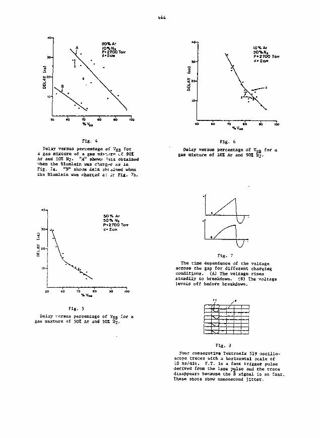
444
90% A.10% N,P«2700Torrd«2cffl
TO
%vMSO » TO 10 90 100
Ftg. 4
Delay versus percentage of Vgg fora gas mixture of a gas mi>~nre cf 902Ar and 10£ N2- "A" showa <nta obtained•rtien the Blumlein was charged as inFig. 7a. "3" sho'.ra data obtained whancha Blumlein was charged a-, ir Fig. 7b.
Fig.. 6
Delay versus percentage of 7 S B for agas mixture of 10Z Ar and 90% N2-
50% Ar50% N«P»27OQTorrd« 2cm
Fig. 7
The time dependence of the voltageacross the gap for different chargingconditions. (A) The voltage risessteadily to breakdown. (B) The voltagelevels off before breakdown.
Fig. 5
Delay versus percentage of Vgg forgas mixture of 50% Ar and 50% N2-
[
/ i
I•
Fig. 3
Four consecutive Tektronix 519 oscillo-scope traces with a horizontal scale of10 ns/div. F.T. is a fast trigger pulsederived from the lase pulse and the tracedisappears because che B signal is so fast.These shots show nanosecond jitter.
445
before triggering (Fig. 7b). Figure 4b shows that References
in a gas mixture of 90S Argon and I K Nitrogen the ^ G u e n C h e r ] A H a n d 3 e t £ i S i J R j 1 9 7 g f j p h y s
delay ranged from 3 to 11 ns as the percentage of D. Appi_ p h y s ^ 1577.16i3_
V ranged from 70 to 50. In 50S Argon and 502
Nitrogen, the delay ranged from 5 to 29 ns while
the percentage of V__ ranged from 75 to 55 (Fig.SB
5). In 10% Argon and 90% Nitrogen, the delay
ranged from 5 to 33 ns while the percentage of
V ranged from 93 to 68. These graphs also show
that under the same charging conditions the delay
at a certain percentage of V__ decreases as the91)
concentration of Argon goes up. Figures 5 and 6
also show breakpoints at approximately 15 ns which
is the laser pulse width. Once the laser turns
off, the delay increases at a faster rate as thepercentage of \' decreases. Figure 3 shows four
Sc
shots in 10% Argon and 90% Nitrogen at 857. VgB
which demonstrate nanosecond jitter.
In the curves shown, all the data were ob-
tained with the laser focused on the anode;
however, when. the focus was moved to the center
of the gap, no significant change in results was
observed. This observation can be explained by
noting that an image of the fiber appeared at the
anode because the fiber was not a point source of
light. Under such conditions the spot size on
either side of the focal plane changes slowly.
Therefore the power density on the surface of the
anode did not decrease enough to make a signifi-
cant difference in triggering when the focus was
moved to the center of the gap.
Conclusion
The results in Figures 4-6 demonstrate the same
Characteristics of laser triggering as presented
by Guenther and Bettis , thus proving that it is
possible to laser trigger a spark gap through an
optical fiber and obtain low delay and jitter.
The fact that the location of the focal spot is
not critical (not true in the work of Guenther
and Bettis) is probably due to the beam divergence
introduced by the fiber.
* On leave from Technische Hochschule Darmstadt,
FKG.
446
19.4
A 3-Mtf LOW-JITTER TRIGGERED G&S SWITCH*
Abstract
Physics International Company has designed, built,
and tested a 3 MV, low jitter, triggered gas
switch. The switch operates in a 16.5 Q coasial
pulse line. The system design requires thai: the
pulse line switches perform the difficult task of
first folding off a reverse pulse charge, than
of holding off the forward pulse charge, then,
finally, of triggering on comand. The trigger
for the switch is generated by a trigger Marx
placed within the output pulse liae. The remain-
der of the triggering circuit includes a trigger
isolation gap. A tf/N-type trigger electrode is
situated within the main gap. To date, the
switch has been shown to hold voltage and trig-
ger reliably for pulse charges from 0.9 MP to
2.5 MV. The rms jitter of the switch firing
time is less than 6 ns. At an operating
voltage or 2.5 MV, the switch transfers a charge
it up to 0.1 coulomb per shot, with a peak
current of 80 kA.
Introduction
Physics International has designed, built and
tested a 3 MV, low-jitter, triggered gas switch.
Figure 1 shows the major components o£ the switch
and how they are assembled. In tests, including
more than 5000 shots in the M-2 pulser built for
the PHERMEC facility at Los A l a u s Scientific
Laboratory, the switch lias met all design expec-
tations. In operation, the switch sees a
(1 - cos nit) pulse charge, with the voltage rising
from zero to peak In 450 ns. He have operated the
switch with pulse charges from slightly under 1 MV
to approximately 2.5 MV. Over the entire trigger-
ing range, the total system jitter, including that
D.B. CEMMINGS and H.G. HAMWON, III
Physics International Company2700 Merced Street
San Laandro, California 94577
Figure 1 Line switch schematic.
of the triggering circuit, is less than 3 ns.
Assuming the jitter of the switch adds In quadra-
Cure to that of its triggering system, the switch
jitter alcniu is less than 6 ns. The self-break
curve of the switch (Figure 2) shows chat the
3000
40 SO 120 160SWITCH PRESSURE, pn ablokra
Figure 2 Self-break voltage versus pressure.
* Work performed under contract from Los Alamos Scientific Laboratory.

447
switch can be expected to operate well to its
design level of about 3 MV. The M-2 pulser as
a whole Is limited to about 2.8 MV, preventing our
testing the switch to its design limit.
The basic switch design requirements were imposed
by the customer's specifications for the M-2
pulser in which the switch was to operate.
The pulser specifications of interest are listed
in Table 1, and the overall configuration of the
pulser designed to meet the specifications is
shown schematically In Figure 3. Each of the
TABLE 1
System Requirements for the M-2 Pulser
1.
2.
3.
5.
6.
7.
Output
Pulse Duration
1 pulse
2 pulses merged
3 pulsed merged
Risetime
Jitter
Pulse Separation
Reliability
Maintenance
0.6 to 1.5 IK
40 ± 4 ns
120£3° ns< 25 ns
G < 8 nsISO ns minimum30 Us mHTiimim
> 90Z of shots goodin all respects
Not more frequent thanevery 1000 shots
system specifications has its effect on the final
choice of a switch design. For example, the out-
put voltage specification defines the voltage
range over which the switch must operate. The
operating range impacts the choice of the switch
electrode gap, the gas pressure range for the
switch, the type of gas to be used, the shape of
the switch housing, etc. The risetime specifi-
cation defines the minimum .Twitch Inductance
and thus puts restrictions on switch length and
geometry as well as on the switch gap and
triggering scheme. (A pulse sharpening switch
close to the load would be no mean feat, since
we have three pulses in series, each of which
must meet the risetime specification.)
SSt /GCNtftATOft /IBPKVATAOE ' KCE'ALIVE
INDUCTORS
Figure 3 PHERMEX M-2 Pulser—schematic diagram.
Design Particulars
The design criteria for the primary elements of
a high voltage switch are deeply interrelated,
making it totally impossible to complete the de-
sign of any one switch component without first
knowing how the rest of the switch Is to be
constructed. Switch design is, therefore, a
fundamentally iterative process. For clarity in
presentation, however, the design of individual
switch elements will be discussed, as much as
possible, as independent activities.
The obvious place to begin is the criterion which
forced the choice of a gas rather than a liquid
switch. Stringent specifications on pulse shape,
prepulse, and jitter require that each pulse line
be electrically isolated from the adjacent pulse
lines. This requirement means that the switch
capacitance must be small compared to the pulse
line capacitance. This can best be accomplished
by assuring that the dielectric constant of the
switch volume is well below that of the pulse
line insulator. For our ethylene glycol insulated
pulse line, we chose to make gas switches with
housings machined from individual epoxy castings.
The capacitance with which the switch couples the
pulse lines 1B roughly 5 x 10 fd, small compared
to the pulse line capacitance of 2 x 10 fd.
The configuration of the system, with the line
switches separating adjacent pulse lines, imposes
another Important restriction on switch design
(Figure 3). The complexities associated with
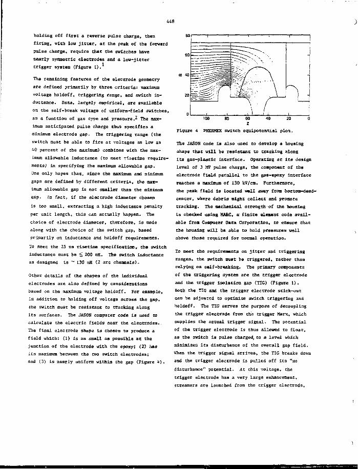
443
holding off first a reverse pulse charge, then
firing, with low jitter, ac the peak of the forward
pulse charge, require that the switches have
nearly symmetric electrodes and a low-jitter
trigger system (Figure 1 ) .
The remaining features of the electrode geometry
are defined primarily by three criteria: maximum
voltage holdoff, triggering range, and switch in-
ductance. Daca, largely empirical, are available
on the self-break voltage of uniform-field switches,
as a function of gas type and pressureP- The max-
imum anticipated pulse charge thus specifies a
minimum electrode gap. The triggering range (the
switch must be able to fire at voltages as low as
40 percent of the maximum) combines with the max-
imum allowable inductance (to meet risetime require-
ments) in specifying Che aaxljaum allowable gap.
One only hopes chat, since the maximum and minimum
gaps are defined by different criteria, the max-
imum allowable gap is not smaller than the minimum
gap. In fact, if the electrode diameter chosen
is too small, extracting a high inductance penalty
per unit length, this can actually happen. The
choice of electrode diameter, therefore, is made
along with the choice of Che switch gap, based
primarily on inductance and holdoff requirements.
To meet the 25 ns risetime specification, the switch
inductance must be < 200 nfl. The switch inductance
as designed is ~ 130 nH (2 arc channels).
Other details of the shapes of the individual
electrodes are also defined by considerations
based on Che maximum voltage holdoff. For example,
in addition to holding off voltage across the gap,
che switch must be resistant to tracking along
its surfaces. The JASON computer code is used to
calculate Che electric fields near the electrodes.
The final electrode shape is chosen to produce a
field which: (1) is as small as possible at the
junction of the electrode with the epoxy; (2) has
its maximum between the two 3witch electrodes;
and (3) is nearly uniform within the gap (Figure 4 ) .
80 r
60
S 40
20
n
"—-
Ef lS i l
—____
^•r# ; ' .C> x > > ." ' \
• * \ - / -
, \
/
-
-
i
J100 30 60
z20
Figure 4 PHERMEX switch equipotential plot.
The JASON code Is also used to develop a housing
shape that will be resistant to tracking along
its gas-plastic interface. Operating at Its design
level of 3 M7 pulse charge, the component of the
electrode field parallel to the gas-epoxy interface
reaches a mpirinium of 130 kV/cn. Furthermore,
the peak field is located well away from botton-dead-
center, where debris might collect and promote
tracking. The mechanical strength of the housing
is checked using MARC, a- finite element code avail-
able from Computer Data Corporation, to ensure that
the housing will be able to hold pressures wsll
above those required for normal operation.
To meet the requirements on jitter and triggering
ranges, the switch must be triggered, rather than
relying on self-breaking. The primary components
of the triggering system are the trigger electrode
and the trigger isolation gap (TIG) (Figure 1).
Both the TIG and the trigger electrode stick-out
can be adjusted to optimize switch triggering and
hoidoff. The TIG serves the purpose of decoupling
the trigger electrode from the trigger Marx, which
supplies the actual trigger signal. The potential
of the trigger electrode is thus allowed to float,
as the switch is pulse charged, to a level which
minimizes its disturbance of the overall gap field.
When the trigger signal arrives, the TIG breaks down
and the trigger electrode is pulled off its "no
disturbance" potential. AC this voltage, the
trigger electrode has a very large enhancement,
streamers are launched from the trigger electrode,
449
and the switch gap breaks down. The interval
required for this switch to trigger is reproducible
to within less than 6 ns for a given pulse charge.
Several primarily mechanical features of Che switch
are of interest. The switch contains two isolated
pressure volumes, one for the main gap and trigger
electrode, the other for the TIG. This feature is
necessary as the TIG and the main gap are switches
of different enhancements and see different voltage
histories. The switches thus cannot be expected to
track each other. Customer specifications require
that a two-person crew can remove a switch and re-
place it with a spare in not more than 4 hours.
The threaded stainless steel thrust nets, indicated
in Figure 1, seal the switch and make the electrical
connections to the adjacent pulse lines. The sim-
Dlicity of this attachment scheme allows rapid
switch replacement without jeopardizing the voltage
holding characteristics of the switch or of the
pulse lines, both of which are highly stressed at
full voltage.
Conclusions
The 3 MV switch, designed for use in the M-2 pulser,
has performed well for more than 5000 system shots.
Though the switches carry peak currents as high as
SO kA and transfer as much as 0.1 coulomb per shot,
we have seen negligible electrode wear to date.
The jitter, holdoff, triggering range, and induct-
ance of the switch are well within the design
limits. It may be possible to use the switch with-
out significant design changes in other high volt-
age systems. Furthermore, the success of this
switch design provides information that will be
of assistance in the design of other high volt-
age switches. Switch operating characteristics
are summarized in Table 2.
TABLE 2
Switch Parameters and Characteristics
Operating Range:
Trigger Voltage:
Pressure Range:
Main Electrode Gap:
External Dimensions:
Peak Field (gas-epoxyinterface):
Switch Inductance:
~ 900 kV to ~ 3 MV
~ 250 kV pulse
to 175 psig <SF6)
7 cm
36 inch diameter20 inches thick
130 kV/cm at 3.0 MV
- 130 nH
Acknowledgements
The authors wish to thank the staff at Los Alamos
Scientific Laboratory for their contributions and
cooperation, especially Jack Harvick and Fred
Van Haaften. Special appreciation is also due
the project manager,Glen Rice,and to Phil Champ-
ney, Gordon Simcox, Tom Naff, and Steve Hogue
for their many contributions.
References
1. For a more complete discussion of this prob-
lem and of the system as a whole, see: D.E.
Cuamings and H.G. Bammon.III, "The Design
Approach to a High-Voltage Burst Generator,"
Proceedings of the 2nd IEEE International
Pulsed Povi : Conference, Lubbock, Texas,
June 1979.
2. See for example, D. Legg, "Insulation
Applied to Circuit Breakers," Power Circuit
Breakers Theory and Design. C.H. Flurscheim, ed.
(Peter Peregrinus, Ltd., Hertsfordshire, Eng-
land) International Scholarly Book Services,Inc.
Forest Grove, Oregon, 1975.
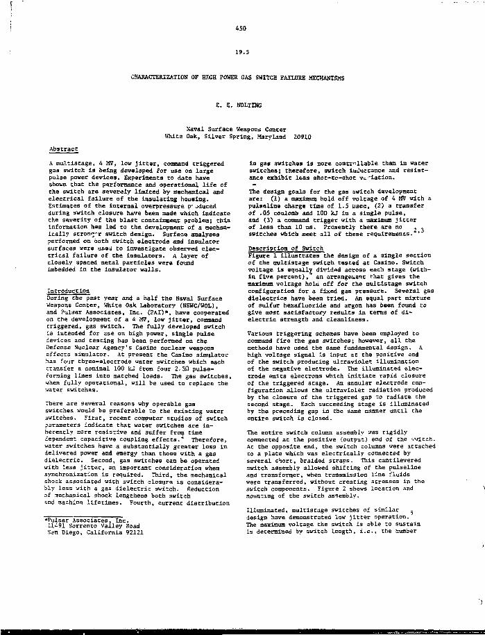
450
19.5
CHARACTERIZATION OF HIGH POWER GAS SWITCH FAILURE MECHANISMS
E. E. NOLTING
Naval Surface Weapons CenterWhite Oak, Silver Spring, Maryland 20910
Abstract
A multistage, 4 MV, low jitter, command triggeredgas switch is being developed for use on largepulse power devices. Experiments to date haveshown that the perfonsance and operational life ofthe switch are severely limited by mechanical andelectrical failure of the insulating housing.Estimates of the internal overpressure p- jducedduring switch closure have been made which indicatethe severity of the blast containment problem; thisinformation has led to the development of a mechan-ically stron^r switch design. Surface analysesperformed on both switch electrode and insulatorsurfaces were used to investigate observed elec-trical failure of the insulators. A layer ofclosely spaced metal particles were foundimbedded in the insulator walls.
IntroductionDuring the past year and a half the Naval SurfaceWeapons Center, White Oak Laboratory (NSWC/WOL),and Pulsar Associates, Inc. (PAI)*, have cooperatedon the development of a 4 M7, low jitter, commandtriggered, gas switch. The fully developed switchis intended for use on high power, single pulsedevices and testing has been performed on theDefense Nuclear Agency's Casino nuclear weaponseffects simulator. At present the Casino simulatorhas four three-electrode water switches which eachtransfer a nominal 100 kj from four 2, 5ft pulse-rorning lines into matched loads. The gas switches,when fully operational, will be used to replace thewater switches.
There are several reasons why operable gasswitches would be preferable to the existing waterswitches. First, recent computer studies of switchparameters indicate that water switches are in-herently more resistive and suffer from timedependent capacitive coupling effects. Therefore,water switches have a substantially greater loss indelivered power and energy than those with a gasdielectric. Second, gas switches can be operatedwith less jitter, an important consideration whensynchronization is required. Third, the mechanicalshock associated with switch closure is considera-bly less with a gas dielectric switch. Reductionof mechanical shock lengthens both switchand machins lifetimes. Fourth, current distribution
*Pulsar Associates, Inc.11491 Sorrento Valley RoadSsn Diego, California 92121
in gas switches is more controllable than in waterswitches; therefore, switch iuductance and resist-ance exhibit Ie3s shot-to-shot V
The design goals for the gas switch developmentare: CD a maximum hold off voltage of 4 m with apulseline charge time of 1.5 Msec, (2) a transferof .05 coulomb and 100 kj in a single pulse,and (3) a command trigger with a maximum jitterof less than 10 ns. Presently there are no ,switches which meet all of these requirements. *
Description of SwitchFigure 1 illustrates the design of a single sectionof the multistage switch tested at Casino. Switchvoltage is equally divided across each stage (with-in five percent),"* an arrangement that gives themaximum voltage hold off for the multistage switchconfiguration for a fia-ed gas pressure. Several gasdielectrics have been tried. An equal part mixtureof sulfur hexafluoride and argon has been found togive most satisfactory results in terms of di-electric strength and cleanliness.
Various triggering schemes have been employed tocommand fire the gas switches; however, all themethods have used the same fundamental design. Ahigh voltage signal ts input at the positive endof the switch producing ultraviolet illuminationof the negative electrode. The illuminated elec-trode emits electrons which initiate rapid closureof the triggered stage. An annular electrode con-figuration allows the ultraviolet radiation producedby the closure of the triggered gap to radiate thesecond stage. Each succeeding stage is illuminatedby the preceding gap in the same manner until theentire switch is closed.
The entire switch column assembly was rigidlyconnected at the positive (output) end of the switch.At the opposite end, the switch columns were attachedto a plate which was electrically connected byseveral short, braided straps. This cantileveredswitch assembly allowed shifting of the pulselineand transformer, when transmission line fluidswere transferred, without creating stresses in theswitch components. Figure 2 shows location andmounting of the switch assembly.
Illuminated, multistage switches of similar -design have demonstrated low jitter operation.The maximum voltage the switch is able to sustainis determined by switch length, i.e., the number
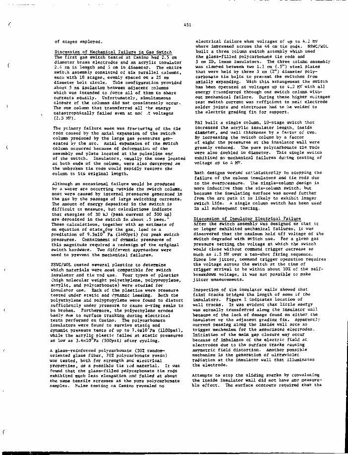
451
of stages employed.
Discussion of Mechanical Failure in Gas SwitchThe first gas switch tested at Casino had 2.5 cmdiameter brass electrodes and an acrylic Insulator2.4 cm in length and 5 cm in diameter. The entireswitr.h assembly consisted of six parallel columns,each with 18 stages, evenly spaced on a 25 cmdiameter bolt circle. This configuration providedabout 5 ns isolation between adjacent columnswhich was intended to force all of them to sharecurrents equally. Unfortunately, simultaneousclosure of the columns did not consistently occur.The one column that transferred all "he energycatastrophically tailed even at moc -t voltages(2.5 MV).
The primary failure mode was fracturing of the tierods caused by the axial expansion of the switchcolumn produced by the large gas press-ares gen-erated by the arc. Axial expansion of the switchcolumn occurred because of deformation of theassembly end plate located at the pulseline endof the switch. Insulators, usually the ones locatedat both ends of the column, were also destroyed asthe unbroken tie rods would rapidly restore thecolumn to its original length.
Although an occasional failure would be producedby a water arc occurring outside the switch column,most were caused by internal pressures generated inthe gas by the passage of large switching currents.The amount of energy deposited in the switch isdifficult to measure, but calculations indicatethat energies of 30 kj (peak current of 500 kA)are deposited in the switch in about .5 Msec.These calculations, together with an estimate ofan equation of state,for the gas, lead to aprediction of 9.5x10 Fa (1400psi) for peak switchpressures. Containment of dynamic pressures ofthis magnitude required a redesign of the originalswitch hardware. Two different approaches wereused to prevent the mechanical failures.
NSWC/WOL tested several plastics to determinewhich materials were most compatible for switchInsulator and tie rod use. Four types of plastics(high molecular weight polyethylene, polypropylene,acrylic, and polycarbonate) were studied forinsulator use. Each of the plastics were pressuretested under static and dynamic loading. Both thepolyethylene and polypropylene were found to distortsufficiently under pressure to cause o-ring seals tobe broken. Furthermore, the polyethylene erodedbadly due to surface tracking during electricaltests performed on Casino. The polycarbonateinsulators were found to survive static anddynamic pressure tests of up to 7.4x10 Pa (UOOpsi),while the acrylic plastic failed at static pressuresas low as 3.4x10 Pa (500psi) after cycling.
A glaGS-reinforced polycarbonate (30% random-oriented glass fiber, 70% polycarbonate resin)was tested, both for strength and electricalproperties, as a possible tie lod material. It wasfound that the glass-filled polycarbonate tie rodsexhibited much less elongation and failed at aboutthe same tensile stresses as the pure polycarbonatesamples. Pulse testing on Casino revealed no
electrical failure when voltages of up to 4.2 MVwhere Impressed acroSB the 46 cm tie rods. NSWC/WOLbuilt a three column switch assembly which usedthe glass-filled polycarbonate tie rods and5 cm ID, lexan insulators. The three column assemblywas clamped between two 1.3 cm (.5") steel platesthat were held by three 5 cm (211) diameter poly-carbonate tie bolts to prevent the switches fromaxially expanding. With this arrangement the switchhas been operated at voltages up to 4.2 MV with allenergy transferred through one switch column with-out mechanical failure. During these higher voltagestest switch current was sufficient to melt electrodesolder joints and electrodes had to I>e welded tothe electric grading fin for support.
PAI built a single column, 10-stage switch thatincreased the acrylic insulator length, insidediameter, and wall thickness by a factor of two.By increasing the switch colume by a factorof eight the pressures at the insulator wall weregreatly reduced. The pure polycarbonate tie rodswere also doubled in diameter. This single switchexhibited no mechanical failures during testing ofvoltage up to 4 MV.
Both designs worked satisfactorily in stopping thefailure of the coluan insulators and tie rods dueto the overpressure. The single-column design ismore inductive than the six-column switch, butbecause the insulating surface was moved furtherfrom the arc path it is likely to exhibit longerswitch life. A single column switch has been usedin all subsequent testing.
Discussion of Insulator Electrical FailureAfter the switch assembly was designed so that itnc longer exhibited mechanical failures, it wasdiscovered that the maximum hold off voltage of theswitch degraded with switch use. For a given gaspressure setting the voltage at which the switchwould close without command trigger decrease asmuch as 1.5 MV over a ten-shot firing sequence.Since low jitter, command trigger operation requiresthe voltage across the switch at the time oftrigger arrival to be within about 10* of the self-breakdown voltage, it was not possible co makejitter measurements.
Inspection of the insulator walls showed thatfaint tracks bridged the length of some of theinsulators. Figure 1 indicates location ofwall tracks. It was evident that little energywas actually transferred along the insulator wallbecause of the lack of damage found on either theinsulator or the adjacent grading fin. Apparentlycurrent passing along the inside wall acts astrigger mechanism for the associated electrodes.Initiation of the main gap closure may occurbecause of imbalance of the electric field atelectrodes due to the surface tracks causingasymetric field distortion. Another possiblemechanism is the generation of ultravioletradiation at the insulator wall that illuminatesthe electrode.
Attempts to stop the sliding sparks by cocvolutingthe inside insulator wail did not have any measura-ble effect. The surface contours required that the
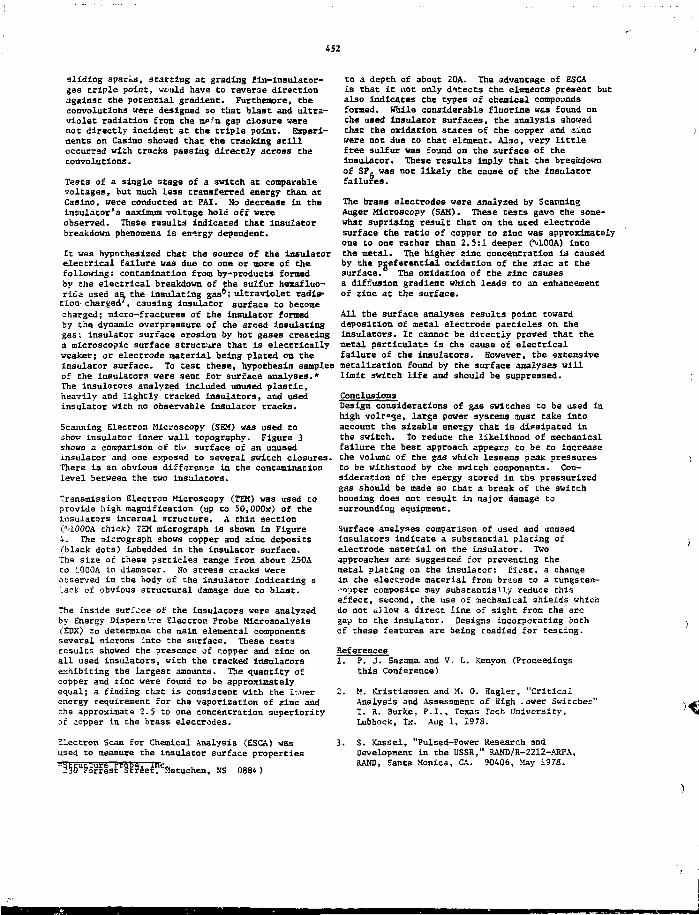
4S2
sliding sparks, starting at grading fin-insulator-gas triple point, would have Co reverse directionagainst che potential gradient. Furtheoore, theconvolutions were designed so that blast and ultra-violet radiation from the mp~n gap closure werenot directly incident at the triple point. Experi-ments on Casino showed that the tracking scilloccurred with tracks passing directly across theconvolutions.
Tests of a single stage of a 3witch at comparablevoltages, but much less transferred energy than atCasino, were conducted at FAX. Ho decrease in theinsulator's maximum voltage hold off vereobserved. These results indicated that insulatorbreakdown phenomena is energy dependent.
It was hypothesized chat the source of the insulatorelectrical failure vas due to one or more of thefollowing: contamination from by-products formedby the electrical breakdown of the sulfur hexafluo-rid« used aa the insulating gas°; ultraviolet radia-tion charged', causing insulator surface to becomecharged; micro-fractures of the insulator formedby the dynamic overpressure of che arced insulatinggas; insulator surface erosion by hot gases creatinga microscopic surface structure that is electricallyweaker; or electrode material being plated on theinsulator surface, to test these, hypothesin samplesof the Insulators were sent for surface analyses.*the insulators analyzed included unused plastic,heavily and lightly tracked insulators, and usedinsulator with no observable insulator tracks.
Scanning Electron Microscopy (SEM) was used toshow insulator inner wall topography. Figure 3shows a comparison of tin. surface of an unusedinsulator and one exposed Co several switch closures.There is an obvious difference in the contaminationlevel between the two insulators.
Transmission Electron Microscopy (TEM) was used toprovide high magnification (up to 50,000x) of theinsulators internal structure. A thin sectionC^IOOOA chick) TEM micrograph is shown in Figure4. The aicrograph shows copper and zinc deposits(black dots) Imbedded in the insulator surface.The size of these particles range from about 250ACo LOOOA in diameter. No stress cracks wereobserved in the body of che insulator indicating alack of obvious structural damage due to blast.
The inside surface of the insulators were analyzedby Energy Dispersire Electron Probe Microanalysis(EDX) Co determine the main elemental componentsseveral microns into the surface. These testsresults showed the presence of copper and zinc onall used insulators, with the tracked insulatorsexhibiting the largest amounts. The quantity ofcopper and sine were found to be approximatelyequal; a finding chat is consistent with the lowerenergy requirement for che vaporization of zinc andche approximate 2.5 to one concentration superiorityoi copper in che brass electrodes.
Electron Scan for Chemical Analysis (ESCA) wasused to measure the insulator surface properties
to a depth of about 20A. The advantage of ESCAis that it not only detects the elements present butalso indicates the types of chemical compoundsformed. While considerable fluorine was found onthe used insulator surfaces, the analysis showedchat the oxidation states of the copper and zincwere not due to that element. Also, very littlefree sulfur was found on the surface of theinsulator. These results imply that the breakdownof SF, was not likely the cause of the insulatorfailures.
The brass electrodes were analyzed by ScanningAuger Microscopy (SAM). These tests gave the some-what suprising result that on the used electrodesurface che ratio of copper to zinc was approximatelyone to one rather than 2.5:1 deeper (M.0OA) intothe metal. The higher zinc concentration is causedby the preferential oxidation of the zinc ac chesurface. The oxidation of the zinc causesa diffusion gradient which leads to an enhancementof zinc at the surface.
All the surface analyses results point towarddeposition of metal electrode particles on theinsulators. It cannot be directly proved that themetal particulate is the cause of electricalfailure of the insulators. However, the extensivemetalization found by the surface analyses willlimit switch life and should be suppressed.
ConclusionsDesign considerations of gas switches to be used inhigh volfge, large power systems oust take intoaccount the sizable energy that is dissipated inche switch. To reduce che likelihood of mechanicalfailure the best approach appears Co be to increaseche volume of the gas which lessens peak pressuresto be withstood by che switch components. Con-sideration of the energy stored in the pressurizedgas should be made so that a break of che switchhousing does not result in major damage tosurrounding equipment.
Surface analyses comparison of used and unusedinsulators indicate a substantial plating ofelectrode material on che insulator. Twoapproaches are- suggested for preventing themetal plating on che insulator: first, a changein che electrode material from brass co a tungsten-•"o' per composite may substantially reduce chiseffect, second, che use of mechanical shields whichdo not allow a direct line of sight from the arcgay Co che insulator. Designs incorporating bothof these features are being readied for testing.
References
1. F. J. Sazama and 7. L. Kenyon (Proceedingsthis Conference)
2. K. Kristian3en and M. 0. Hagler, "CricicalAnalysis and Assessment of ffigh -ower Switches"T. R. Burke, P.I., Texas Tech University,Lubbock, Tx. Aug 1, 1978.
15BuF§SisEr§??eet°Caetuchen, HS 0B8O
3. S. Kassel, "Pulsed-Power Research andDevelopment in the USSR," HAND/R-2212-ARPA,RAND, Santa Monica, CA. 90406, May 1978.
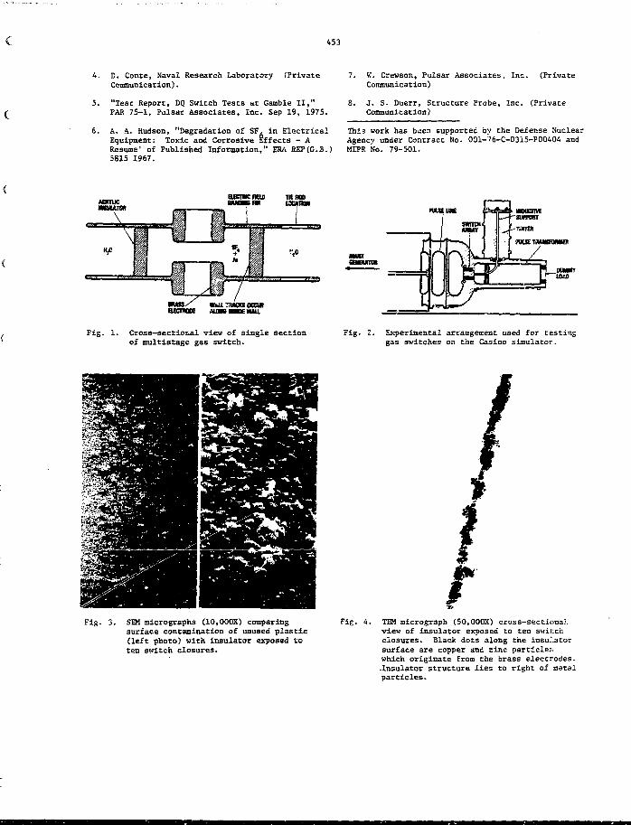
453
4.
5.
6.
D. Conte, Naval Research LaboratoryCommunication).
(Private
"Test Report, DQ Switch Tests at Gamble II,"PAR 75-1, Pulsar Associates, Inc. Sep 19, 1975.
A. A. Hudson, "Degradation of SF, in ElectricalEquipment: Toxic and Corrosive Effects - AResume' of Published Information," ERA REPfG.B.)5B15 1967.
7.
8.
K. Crewson, Pulsar Associates, Inc.Communication)
(Private
J. S. Duerr, Structure Probe, Inc. (PrivateCommunication)
This work has been supported by the Defense NuclearAgency under Contract No. 001-76-C-0315-P00404 andMIPR No. 79-501.
Fig. 1. Cross-sectio&al view of single sectionof multistage gas switch.
Fig. 2. Experimental arrangement used for testinggas switches on the Casino simulator.
Fig. 3. SEM micrographs (10.000X) comparingsurface contamination of unused plastic(left photo) with insulator exposed toten switch closures.
Fig. 4. TEM micrograph (50.000X) cross-sectiona.1.view of insulator exposed to ten swir.chclosures. Black dots along the insulatorsurface are copper and zinc particleswhich originate from the brass electrodes..Insulator structure lies to right of metalparticles.
454
20.1
BALANCED, PARALLEL OPERATION OF FLASHLAMPS*
B.M. Carder, B.T. Merritt
Lawrence Liveimore Laboratory
Llvermore, California 94550
ABSTRACT
A new energy store, the Compensated Pulsed
Alternator (CFA), promises to be a cost effective
substitute for capacitors to drive flashlamps that
pump large Nd:glass lasers. Because the CFA is
large and discrete, it will be necessary that it
drive many parallel flashlamp circuits, presenting
a problem in equal current distribution. Current
division to x 20% between parallel flashlamps has
been achieved, but this is marginal for laser
pumping. A method is presented here that provides
equal current sharing to about 1%, and it includes
fused protection against short circuit faults. The
method was tested with eight parallel circuits,
including both open-circuit and short-circttit fault
tests.
Introduction
The new Mova solid state laser will require an
energy storage system of at least 100 HJ size to
drive the 5 tc 10 thousand flashlamps that will
pump the glass. This type of distributed load is
normally driven with an equally distributed energy
store - namely a capacitor bank of many modules.
Alternative stores co capacitors, such as the
compensated pulsed alternator, at., only practical
in large single sizea, however, so the requirement
exists to learn how to drive many parallel flash-
lamps .
Flashlamps are nonlinear resistive loads with a
resistance that decreases as the current through
them increases. Equal current sharing will there-
fore not necessarily be achieved when the lamps are
operated in parallel. Xnall has demonstrated
parallel operation of 16 flashlamp circuits with
equal current sharing to within 20X, provided all
lamps are properly preionized. In this paper, we
report upon a simple method using inductors with
reacting mutuals in each lamp circuit, that pro-
vides parallel current sharing within about one
percent. The method requires no special pre-
ionlzation circuitry: lamp triggering is
accomplished with the LC ringup between the
inductor and the lamp cable capacitance.
Summary of Results
>n experimental system was constructed in which
eighi: parallel flashlaop circuits, were driven
by a single 200 kj, 20 kV capacitor bank. Each
circuit comprised two series 44-inch long, 15-mm
bore, xenon filled flashlamps, a fuse, and an
inductor. With an Inductance of 112 uH In each
circuit, equal current division Co about 4* was
achieved. , When inductors were stacked together
so that the mutuals subtracted, they became
balancing reactors. With this arrangement, current
division within measurement error ("" 17.) was
achieved and the effective series inductance in
each circuit dropped to about IS UH.
Open circuit testa were also made- When one of
the flashlamps was disconnected, the remaining
seven circuits shared the full bank energy, and
balancing was achieved as before.
The worst-case unbalance occurs when a flashlamp
breaks and the circuit becomes shorted. This case
was simulated with a deliberate short in place of
the lamp. With a 112 uH inductor in each circuit,
the currents in the seven normal circuits balanced
well, but the current in the shorted circuit rose
at three times the nominal value until the fuse
455
burst. The energy dissipated by the fused shorted
circuit was about 1.5 to 3 times the normal value
depending on the fuse size.
fuses protecting the capacitors were 700 A/1.5 msec
and the output fuses were 5000 A/1.5 msec or
7000 A/1.5 msec depending upon the test performed.
Parallel flashlamp operation has therefore been
demonstrated. Series inductances work well but
balancing reactors provide the moat uniform
current sharing. If a flashlamp fails to fire,
the remaining lamps share its energy. In a laser
amplifier this would be advantageous, since the
pumping efficiency would then remain virtually
unchanged. A shorted circuit can be protected
adequately with a fuse. It will reduce the energy
delivered to the other lamps by up to three times
its normal share. In a large system, however,
this amount of energy loss would be insignificant.
Test Configuration
The test circuit schematic is shown in Fig. 1.
Each of the eight circuits comprised eight
parallel 14.5 uF capacitors; however, all eight
circuits were connected together 3t the charge
resistors (Point A in Fig. 1) as shown, effective-
ly forming a single 928 UF capacitor bank.
Fig. 1: Test Circuit Schematic
Circuit performance was monitored by measuring
cutrents via four Pearson #301X probes and re-
cording these waveforms on a Tektronix 5441
oscilloscope with a four channel input. These
current probes are useable tu 50 kA. Photographs
' of scope traces were taken to preserve the data.
Procedure
The first test demonstrating parallel operation
used a 450 uH pulse shaping inductor in each
circuit. The inductor's value was halved twice:
first to 225 and then to 112 uH. For each in-
ductor value a number of shots were taken at
voltages ranging from 16 to 22 kV. In order to
vi«cs all eight flashlaxpp currents on a single
shot, two circuits were strung through each
Pearson probe. Then each waveform was the sum of
two currents.
Special cases of one circuit open and one circuit
shorted were investigated. To simulate a shorted
flashlamp circuit, one series pair of lamps was
replaced by a hard wire short. Open circuits
were simulated by opening one circuit at point "B",
Fig. 1. Open circuit tests were performed with
112 ufi inductors, and with Intial charge voltages
of 16 to 18 kV. Short circuit tests were performed
with two sizes of output fuses (5000 A and 7000 A)
and with 112 UH inductors at an initial capacitor
charge voltage of 16 kV. A short circuit test was
also performed at 20 kV with a 5000 A fuse output
and 112 uH inductors.
During the experiment, the pulse shaping inductors
were varied from 45C uH to 112 uH. For the final
phase of testing, these inductors were placed in
parallel by additionally connecting the eight
circuits together between the inductors and out-
put fuses (Point B in Fig. 1). For this case
balancing reactors of 15 uH were inserted
directly at the flashlamps. The sparkgaps pro-
tecting the inductors were set at 40 kV. The
The pulse shaping inductors were then connected
together by paralleling the circuits at point 3,
Fig. 1. The test circuit then comprised one large
capacitor (928 uF), one inductor (14 uH), and
eight parallel flashlamp circuits. Balancing
reactors were used in each flashlamp circuit.
These were nominally 44 uH pancake inductors that
were stacked together in alternate fashion so that
adjacent mutuals subtracted. Two of these
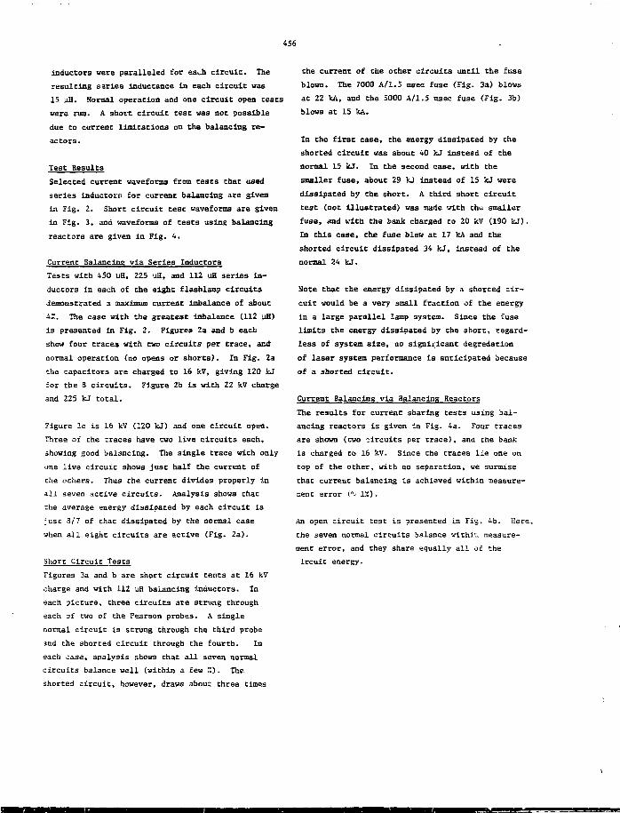
456
inductors were paralleled for each circuit. The
resulting saries inductance in each circuit was
15 uH. Normal operation and one circuit open treats
were run. A short circuit test was not possible
due Co current limitations on the balancing re-
actors.
Test Results
Selected current waveforms from teats that used
series inductors for current balancing are given
in Fig. 2. Short circuit test waveforms are given
in Fig. 3, and waveforms of tests using balancing
reactors are given in Fig. 4.
Current Balancing via Series Inductors
Tests with 450 uH, 225 uH, and 112 uH series in-
ductors in each of the eight flashlamp circuits
demonstrated a maximum current Imbalance of about
iZ. The case with the greatest imbalance (112 uH)
is presented in Fig. 2. Figures 2a and b each
show four traces with two circuits per trace, and
normal operation (no opens or shorts). In Fig. 2a
the capacitors are charged to 16 kV, giving 120 kJ
for the 8 circuits. Figure 2b is with 22 kV charge
and 225 kJ total.
Figure 2c is 16 kV (120 kJ) and one circuit open.
Three of the traces have two live circuits each,
showing good balancing. The single trace with only
one live circuit shows just half the current of
che others. Thus the current divides properly in
all seven active circuits. Analysis shows that
che average energy dissipated by each circuit is
just 3/7 of chat dissipated by the normal case
when all eight circuits are active (Fig. 2a).
Short Circuit Tests
Figures 3a and b are short circuit ceot3 at 16 kV
charge and with 112 uH balancing inductors. In
each picture, three circuits are strung through
each of two of: che Pearson probes. A single
normal circuit is strung through the third proba
and the shorted circuit through the fourth. In
each case, analysis shows that all seven normal
circuits balance well (within a few °). The
shorted circuit, however, draws about three times
the current of the other circuits until the fuse
blows. The 7000 A/1.5 msec fuse (Fig. 3a) blows
at 22 kA, and the 5000 A/1.5 msec fuse (Fig. 3b)
blows at 15 kA.
In the fir3t case, the energy dissipated by the
shorted circuit was about 40 kJ instead of the
normal 13 kJ. In the second case, with the
smaller fuse, about 29 kJ instead of 15 kJ were
dissipated by the short. A third short circuit
test (not illuscrated) was made with the smaller
fuse, and with the bank charged to 20 kV (190 kJ).
In this case, che fuse blew at 17 kA and the
shorted circuit dissipated 34 kJ, instead of the
normal 24 kJ.
Note that the energy dissipated by a shorted cir-
cuit would be a very small fraction of che energy
in a large parallel lamp system. Since the fuse
limits the energy dissipated by the short, regard-
less of system size, no significant degredation
of laser system performance is anticipated because
of a shorted circuit.
Current Balancing via Balancing Reactors
The results for current sharing tests using bal-
ancing reactors is given in Fig. 4a. Four traces
are shown (two circuits per trace), and the bank
is charged to 16 kV. Since the traces lie one on
top of the other, with no separation, we surmise
that current balancing is achieved within measure-
ment srror ( 1%).
An open circuit cest is presented In Fig. 4b. Here,
che seven normal circuits balance withir. measure-
ment error, and they share equally all of che
ircuic energy.
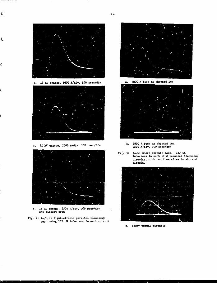
€ 457
a. 15 kV charge, 100C A/div, 100 usec/div a. 7000 A fuse in shorted leg
b. 22 kV charge, 2500 A/div, 100 usec/divb. 5000 A fuse in shorted leg
2500 A/div, 100 usec/div
Fig. 3: (a,b) Short circuit test. 112 uHinductors in each of 8 parallel flashlampcircuits, with two fuse sizes in shortedcircuit.
c. 16 kV charge, 2500 A/div, 100 usec/divone circuit open
Fig. 2: (a,b,c) Eight-circuit parallel flashlamptest using 112 uH inductors ID each circuit
a. Eight normal circuits
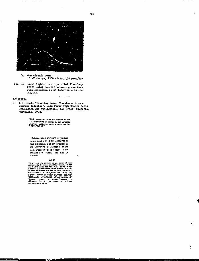
458
b. One circuit o?«n16 kV charge, 2300 A/dlv, 100 us«c/div
Fig. 4: (a,b) Eight-circuit parallel flashlamptests using current balancing reactorswith effective IS uH inductance in eachcircuit.
Reference
1. E.K. Inall "Powering Laser Flashlamps from aStorage Inductor", High Power High Energy FalseProduction and Application, AHU Press, Canberra,Australia, 1978.
"Work performed under the juapicee of theU.S. Oeptttmefli of Eiwigy by the LawrenceLivermore Laboratory under contract numberW-74O5-ENG-48."
Reference to a company or productname docs not imply approval orrecommendation of the product byihe University of California or theU.S. Department of Energy to theexclusion or others that may besuitable.
NOTICE"Thrj report wta prepared as an jccouiu of workipanwred br ibt United SUtet Govemnunt. N«ilhirme UmMd SUMS nor ihi Uctittd S u m EnergyReMtrch b Oerslopnent Admintmtion. nor uiyof thtir employen, nor iny or thtir coniracton.subcontractor!, or tAvir emplorcn. nuJtn anywarranty, expraat or imptica. or auuron anv Ugalliability or response. 4ity for tht accuracy,comphmnra 07 uufuln?* of avy information,ippanlut. product or procau diacloitd. orreprawna that iu use would not infrine*privataiy-ownid rjehts."
459
20.2
APPLYING A COMPENSATED PULSED ALTERNATOR TO A FLASHLAMP LOAD FOR NOVA*
B.M. Carder, E.T. Merritt
Lawrence Livermore LaboratoryLivermore, California 94550
ABSTRACT
The Compensated Pulsed Alternator (CPA) is a large
rotating machine that will convert mechanical,
rotationally stored energy into a single electri-
cal impulse of very high power. It is being op-
timized for driving flashlamps in the very large
Nova Nd:glass laser system. The machine is a
rotary flux compression device, and for maxim™
performance, it requires start-up current. We
report upon a circuit that will provide this
current and that will aiso assist in triggering
the flashlamps. This circuit has been tested with
a 200 kJ capacitor bank and it is nov being tested
with a small 200 kJ CPA. Large Nova-size machines
will require output energies in excess of 5 KJ.
We also present empirically tested formulae that
will assist in matching the Nova flaahlamp load to
any given size CPA machine.
Introduc tlon
The Compensated Pulsed Alternator (Compulsator) is
a very large rotary energy store that is a candi-
date source for driving chc 5 to 10 thousand flash-
lamps that will pump the Nova laser. It is pre-
sently under development by the University of Texas
at Austin (UT) and the Lawrence Livermore Labora-
tory (LLL). In the final (Nova) version, the
machine will deliver a pulsed output energy of 5
to 20 MJ in about a half millisecond time with a
peak voltage of about 13 kV. The order of a 100 HJ
total energy will be needed for the Nova flashlamps.
At present, a small 200 kJ Compulsator is starting
through a comprehensive test program at UT. The
magnetics, mechanics and electrical characteristics
of the machine are to be determined, and the
machine will be used for driving 16 parallel flash-
lamps in an LLL laser amplifier head. The test
data for the small machine will be used in the
design of the large Nova-size machines.
In this paper, we report upon the circuit that will
couple the 200 kJ Compulsator to its 16-flashlanp
load. A similar circuit will be used for each
Nova Compulsator, where hundreds of lamps will be
driven by a single machine. These circuits pro-
vide start-up current for the Compulsator as well
as providing triggering to all of the parallel
flashlamp circuits.
Matching the Compulsator to the flashlamp load is
another important task in this program. Empirical
data have been collected for the large Nova flash-
lamps that enable us to characterize this type of
load over a broad range of operating conditions.
Briefly, we find that the energy W delivered to a
flashlamp is given by, W fK i3/2lt (Eq. 1), where
*Work performed under the auspices of the U.S.Dept. of Energy by the Lawrence LivermoreLaboratory under contract no. W-7405-Eng-48.
i is the peak current through the lamp and it is the
time for full-width at half-maximum (FWHM) of the
current pulse. The factor f is a unitless current
waveshape form factor chat has a range of values
from 0.8 to 1.02. For the Compulsator waveshape,
f is very nearly unity (± 2X). The parameter K has
been found to be constant within two percent over
a broad range of energies and pulse durations. It
is defined by K » V/VT, where V is the voltage
across the flashlamp and i is the current through
it. Thus the flashlamp resistance is
E - V/i - K/VT. (2)
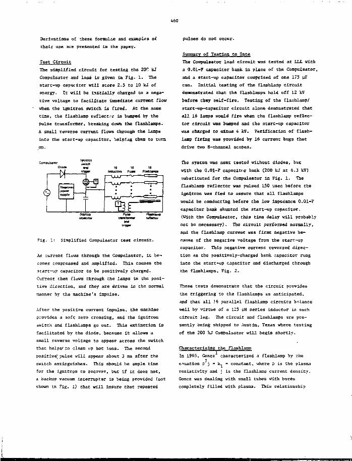
460
Derivations of these formulae and examples of
their use are presented in the paper.
Test Circuit
The sinplified circuit for testing the 20H kJ
Compulsator and load is given in Fig. 1. the
start-up capacitor will score 2.5 to 10 kJ of
energy. It will be initially charged to a nega-
tive voltage to facilitate immediate current flow
when the ignitron switch is fired. At Che same
time, the flashlamp reflect-r is bumped by the
pulse transformer, breaking down the flashlamps.
A small reverse current flows through the lamps
into the start-up capacitor, helping them to turn
on.
pulses do not occur.
of Testing to Date
The Compulsafor load circuit was tested at T.T.I, with
a 0.01-F capacitor bank in place of the Compuisator,
and a start-up capacitor comprised of one 173 US
can. Initial testing of the flashlamp circuit
demonstrated that the flashlamps hold off 12 kV
before they aeif-fire. Testing of the flashlamp/
start-up-capacitor circuit alone demonstrated that
all 16 lamps would fire when tha flashlamp reflec-
tor circuit was bumped and the start-up capacitor
was charged Co minus 4 kV. Verification of flash-
lamp firing was provided by 16 current bugs that
drive two B-channel scopes.
Fig. 1: Simplified Compulsator test circuit.
As current flows through the Compulsator, it b«-
comes compressed and amplified. This causes the
3tart-up capacitor to be positively charged.
Current then flows through the lamps in the posi-
tive direction, and chey are driven in the normal
manner by the machine's impulse.
After the positive current impulse, the machine
provides a soft zero crossing, and the ignitron
switch and flashlamps go out. This extinction is
facilitated by the diode, because it allows a
small reverse voltage to appear across the switch
chat helps/.to clean up hot ions. The second
positive; pulse will appear about 3 ms after the
switch extinguishes. This should be ample time
for the ignitron to recover, but if it does not,
a backup vacuum interrupter is being provided (not
shown in Fig. 1) that will insure that repeated
The system was next tested without diodes, but
with the 0.01-F capacitcr bank (200 kJ at 6.3 kV)
substituted for the Compulsator in Fig. 1. The
flashlamp reflector was pulsed 150 ysec before the
ignitron was fled to assure that all flashlamps
would be conducting before the low impedance 0.01-F
capacitor bank shunted the start-up capacitor.
(.With Che Compulsator, this time delay will probably
not be necessary). The circuit performed normally,
and the flashlamp current was first negative be-
cause of the negative voltage from the scarr-up
capacitor. This negative current reversed direc-
tion as the positively-charged bank capacitor rung
into the start-up capacitor and discharged through
the flashlamps. Fig. 2.
These tests demonstrate that the circuit provides
the triggering to the flashlamps as anticipated,
and that all 16 parallel flashlamp circuits balance
well by virtue of a 125 uH series inductor in each
circuit leg. The circuit and flashlamps are pre-
sently being shipped to Austin, Texas where testing
of the 200 kJ Compulsator will begin shortly.
Characterizing the Flaahlamn
In 1965, Goncz characterized a flashlamp by the
equation D"j " k, » constant, where D is the plasma
resistivity and j is the flashlanp currenc density.
Goncz was dealing with small tubes with bores
completely filled with plasma. This relationsbip
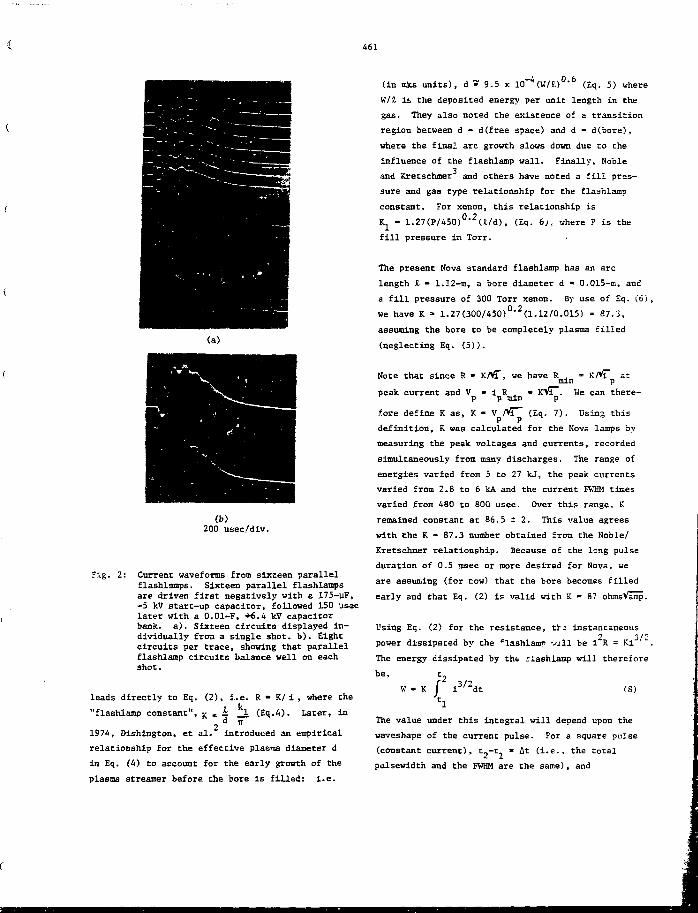
461
(b)200 usec/div.
Fig. 2: Current waveforms from sixteen parallelflashlamps. Sixteen parallel flashlampsare driven first negatively with a 175-uF,-5 kV atart-up capacitor, followed 150 usaclater with a Q.01-F, +6.4 kV capacitorbank. a). Sixteen circuits displayed in-dividually from a single shot, b). Eightcircuits per trace, showing that parallelflashlamp circuits balance well on eachshot.
leads directly to Eq. (2), i.e. R - K/ i , where the
"flashlamp constant", R « — _1 CEq.4). Later, in
1974, Dishington, et al." introduced an empirical
relationship for the effective plas*na diameter d
in Eq. (4) to account for the early growth of the
plasoa streamer before the bore is filled: i.e.
(in mks units), d = 9.5 x 10 (W/SL) (Eq. 5) where
W/£ is, the deposited energy per unit length in the
gas. They also noted the existence of a transition
region between d - d(free space) and d - d(bore),
where the final arc growth slows down due to the
influence of the flashlamp wall. Finally, Noble
and Xretschmer and others have noted a fill pres-
sure and gas type relationship for the flaahlamp
constant. For xenon, this relationship is
Kx - 1.27(P/450)0-2W/d), (Eq. 6), where P is the
fill pressure in Torr.
The present Nova standard flashlamp has an arc
length I - 1.12-m, a bore diameter d • 0.015-m, and
a fill pressure of 300 Torr xenon. By use of Eq. (6),
we have K =• 1.27(300/450)0-2(1.12/0.015) - 87.3,
assuming the bore to be completely plasma filled
(neglecting Eq. (5)).
Note that since R » K/>ff", we have R . K/5min p
peak current and V • i R , • KVi". We can there-p p ain p
fore define K as, K - V P/i~ (Eq. 7). Using thisP P
definition, K was calculated for the Nova lamps by
measuring the peak voltages and currents, recorded
simultaneously from many discharges. The range of
energies varied from 5 to 27 kJ, the peak currents
varied from 2.8 to 6 kA and the current FWHM times
varied from 480 to 800 usec. Over this range, K
remained constant at 86.5 i 2. This value agrees
with Che K = 87.3 number obtained from the Noble/
Kretschmer relationship. Because of the long pulse
duration of 0.5 msec or more desired for Nova, we
are assuming (for tow) that the bore becomes filled
early and that Eq. (2) is valid with K = 87 ohmsVamp.
Using Eq. C2) for the resistance, tre instantaneous3/2
power dissipated by the *lashlaim> v j l l be i~R = Ki
The energy dissipated by the .clashlamp will therefor*
be, t 2
W • K J i3/2dt (8)
The value under this integral will depend upon the
waveshape of the current pulse. For a square pulse
(constant current), t.-t « At (i.e., the total
pulsewidth and the FHBM are the same), and
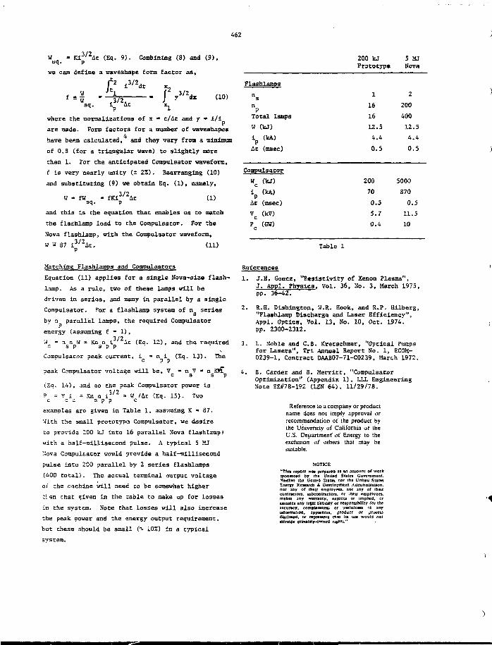
462
sq.Ki3/2At (Eq. 9). Combining (8) and (9),
we can define a waveshape form factor as,
^"1 3/2
3/2,
sq.dx
t/&t and y * I/I
(10)
where che normalizations of x
are made. Form factors for a number of waveshapes
have been calculated, and they vary from a minimum
of 0.3 (for a triangular wave) to slightly more
Chan 1. For the anticipated Compulsator waveform,
f is very nearly unity (± 2%). Rearranging (10)
and substituting (9) we obtain Eq. (1), namely,
W - fWsq.
(1)
and this is the equation that enables us Co match
the flaihlamp load to the Compulsator. For the
Nova flashlamp, with the Compulsator waveform,
(11)W 3 87 i3/2At.
Flashlanps
Total lamps
i
At
(kJ)
(kA)
(msec)
Compulsacor
W
At
V
P
(kJ)
(kA)
(msec)
(kV)
(GW)
200 kJPrototype
1
16
16
12.5
4.4
0.5
5 MJHova
2
200
400
12.5
4.4
0.5
200 5000
70 870
0.5 0.5
5.7 11.5
0.4 10
Table 1
Matching Flashlampa and Compulaators
Equation (11) applies for a single Nova-size flash-
lamp. As a rule, two of these lamps vill be
driven in series, and many in parallel by a single
Compulsator. For a flashlamp system of n 3eries
by n parallel lamps, the required CcmpulsatorP
energy (assuming £ " 1),1/2
w =• n n M - Kn n i it (Ea. 12), and the requiredc s p s p p •
Compulsacor peak current, i • n 1 (Eq. 13). The
peak Compulsator voltage will be, V ™ n V * n BSx
(Eq. 14), and so che peak Compulsator power is.3/2V i
c cKn n i
s p pWWAt (Eq. 15). Two
examples are given in Table 1, assuming K * 87.
With the small prototypes Compulsator, we desire
Co provide 200 kJ into 16 parallel Nova flashlamp?
with a half-millisecond pulse. A typical 5 MJ
Mova Compul&ator would provide a half-millisecond
pulse into 200 parallel by 2 series flashlamps
(400 total). The actual terminal output voltage
of che machine will need co be somewhat higher
ti 3ti chat »iven in che cable to make up for losses
tn che system. Mote chat losses vill also increase
che peak power and che energy output requirement,
but these should be small (i< 10%) in a cypical
svstem.
References
1. J.H. Goncz, "Resistivity of Xenon Plasma",J. Appl. Physics, Vol. 36, Ho. 3, March 1975,pp. 36-42.
2. R.H. Dishington, W.R. Hook, and R.P. Hilberg,"Flashlamp Discharge and Laser Efficiency",Appl. Optics, Vol. 13, No. 10, Oct. 1974.pp. 2300-2312.
3. L. Noble and C.B. Kretschmer, "Optical Pumpsfor Lasers", Tri Annual Report No. 1, ECOM-0239-1, Contract DAAB07-71-C0239, March 1972.
4. B. Carder and B. Merritt, "CompulsatorOptimization" (Appendix 1), LLL EngineeringNote EE078-192 (LEN 64), 11/29/78.
Reference to a company or productname does not imply approval orrecominendation of the product bythe University of California or theU.S. Department of Energy to theexclusion of others thai may besuitable.
NOTICE"Thb report w » prepared u ui account or worksponsored by (he United State! Government.Neither ttaa United States nor tho United StatesEnergy Research & Development Administration,nor any oi their employees, not any of thencontractors, subcontractors, or ;heir employees,makes any warranty, express or implied, orassumes any legal liability or rtsyoasibilllY for theaccuracy, completeness or usefulness of anyinformation, appsrttus. product or process•Usclosed, or represents that its use would ao!infringe prmfeJir'OMmed rights."
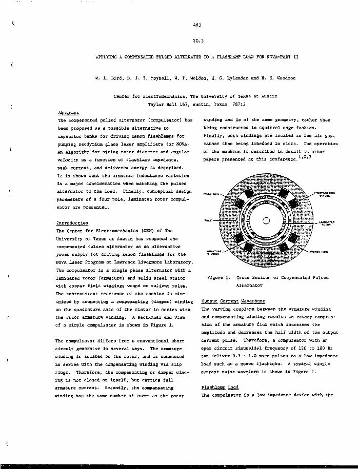
463
20.3
APPLYING A COMPENSATED PULSED ALTERNATOR TO A FLASHLAMP LOAD FOR NOVA-PART II
W. L. Bird, D. J. T. Mayhall, W. F. Weldon, H. G. Rylander and H. H. Woodson
winding and is of Che same geometry, rather than
being constructed in squirrel cage fashion.
Finally, both windings are located in the air gap,
rather than being imbedded in slots. The operation
of che machine is described in detail in other1 ° 3papers presented at this conference. '"'
Center for Electromechanics, The University of Texas at Austin
Taylor Hall 167, Austin, Texas 78712
Abstract
The compensated pulsed alternator (compulsator) has
been proposed as a possible alternative to
capacitor banks for driving xenon flashlamps for
pumping neodymium glass laser amplifiers for NOVA.
An algorithm for sizing rotor diameter and angular
velocity as a function of flashlamp impedance,
peak current, and delivered energy As described.
It is shown that the armature inductance variation
is a major consideration when matching the pulsed
alternator to the load. Finally, conceptual design
parameters of a four pole, laminated rotor compul-
sator are presented.
Introduction
The Center for Electromechanics (CEM) of The
University of Texas at Austin has proposed che
compensated pulsed alternator as an alternative
power supply for driving xenon flashlamps for the
NOVA Laser Program at Lawrence Livennore Laboratory,
The compulsator is a single phase alternator with a
laminated rotor (armature) and solid steel stator
with copper field windings wound on salient poles.
The subtransient reactance of the machine is min-
imized by connecting a compensating (damper) winding
on the quadrature axis of the stator in series with
the rotor armature winding. A sectional end view
of a simple compulsacor is shown in Figure 1.
The compulsator differs from a conventional short
circuit generator in several ways. The armature
winding is located on the rotor, and is connected
in series with the compensating winding via slip
rings. Therefore, the compensating or damper wind-
ing is not closed on itself, but carries full
armature current. Secondly, the compensating
winding has the same number of Curns as the rotor
Figure 1: Cross Section of Compensated Pulsed
Alternator
Output Current Waveshape
The varying coupling between the armature winding
and compensating winding results in rotary compres-
sion of the armature flux which increases che
amplitude and decreases the half width of the output
current pulse. Therefore, a compulsator with an
open circuit sinusoidal frequency of 120 to 180 H2
can deliver 0.5 - 1.0 msec pulses to a low impedance
load such as a xenon flashtube. A typical single
current pulse waveform is shown in Figure 2.
Flashlamp Load
The compulsator is a low impedance device with the
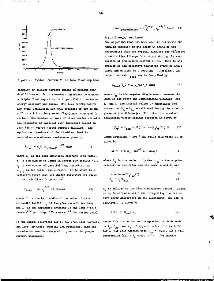
464
i^. n* u
Figure 2: Typical Current: Pulse Inco Flashlastp Load
capacity co deliver current pulses of several hun-
dred kiloamps. It ia therefore necessary to connect
multiple flashiamp circuits in parailal to maximize
energy delivery per pulse. One lamp configuration
now being considered for NOVA consists of two IS ma
x 20 mm x 112 cm long xenon flaahlaops connected in
series. One hundred or more of these series circuits
are connected in parallel with inductors placed in
each leg Co insure proper current division. The
equivalent impedance of the flashlamp load is
modeled as a nonlinear resistance given fay
5. . - n K (n i, . ) " 1 / 2 ohmsload s o p load (1)
where fC is the lamp impedance constant (one lamp),
n is the number of lamps in series per circuit (2),
a Is the number of parallel lamp circuits, and
i. . is che tocal load current. It is shoun in axoaa
companion paper chac the energy delivered per pulse
to each flashlamp is given by
compulsator
Rotor Diameter and Speed
One algorithm that has been used to determine the
angular velocity of che rotor is based on the
observation that for typical circuits che effective
armature flux linkage is constant during the main
portion of Che output current pulse. That is che
product of Che effective transient armature induc-
tance and current is a constant. Therefore, the
output current i. , may be described by
(4)
where 6 is the angular displacement between chem
axes of the rotor and compensating windings, and
L and i are initial values ^f inductance ando ocurrent at 6
m8 established during the startupmo
phase of che discharge. The effective armature
inductance versus angular position is given by
L ( V " Lmin
Using Equations 4 and 5 the pulse half width it is
given by
At - (4/N u ) cos"1 U - a/A. )P m jc
(6)
where N is che number of poles, <•) is the angularp ID
velocity of the rocor and che ceras a and A. are
a «• 1-cosfN a 12)p mo •7)
(3)
Lapp fK i AC joulesop (2)
where It is the half width of che pulse, f is a
waveshape factor, 1 is che peak current per lamp,
and K is che impedance constant of the lamp (-87.51/2 1/2
ohm-amp " per lamp, 175 ohm-amp for series pair).
A, is defined as che flux compression factor. Again,
using Equations 4 and 5 and integrating the resis-
tive power dissipated in che flashlamps, the LHS of
Equation 3 is given by
(9!
If the energy delivered per pulse, peak lamp current, where S is a constant of incegration which depends
and lamp impedance constant are specified, then the on N^, 5 ^ , and A. . A cypical value of S is 0.253
compuisacor must be designed to provide che proper for a four pole macnine wich 9 ^ = -0.294 and a flux
current waveshape. compression factor A. equal to 14. The angular
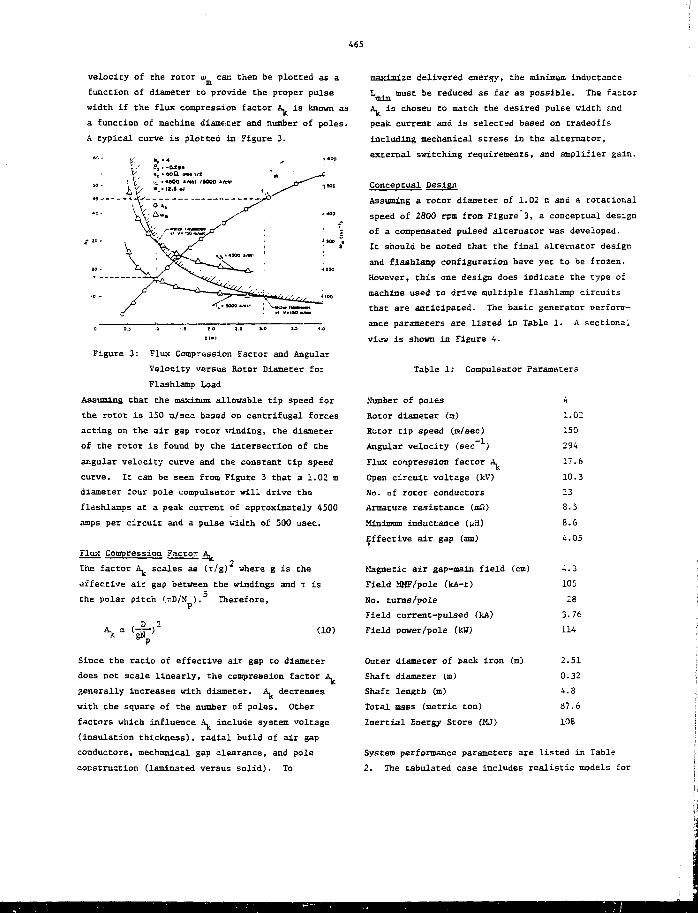
465
velocity of the rotor u car. then be plotted as am
function of diameter to provide the proper pulse
width if the flux compression factor A. is known as
a function of machine diameter and number of poles.
A typical curve is plotted in Figure 3.
Figure 3: Flux Compression Factor and Angular
Velocity versus Rotor Diameter foz
Flashlamp Load
Assuming that the mavimiiTii allowable tip speed for
the rotor is 150 m/sec based on centrifugal forces
acting on the air gap rotor winding, the diameter
of the rotor is found by the intersection of the
angular velocity curve and the constant tip speed
curve. It can be seen from Figure 3 that a 1.02 m
diameter four pole compulsatcr will drive the
flashlamps at a peak current of approximately 4500
amps per circuit and a pulse width of 500 usec.
Flux Compression Factor A,2
The factor ^ scales as (t/g) where g is the
effective air gap between the windings and T is
the polar pitch <>D/N ) . 3 Therefore,P
(10)
maximize delivered energy, the minimum inductance
L . must be reduced as far as possible. The factormin
A. is chosen to match the desired pulse width ;.nd
peak current and is selected based on tradeoffs
including mechanical stress in the alternator,
external switching requirements, and amplifier gain.
Conceptual Design
Assuming a rocor diameter of 1.02 m and a rotational
speed of 2600 rpm from Figure 3, a conceptual design
of a compensated pulsed alternator was developed.
It should be noted that the final alternator design
and flashlamp configuration have yet to be frozen.
However, this one design does indicate the type of
machine used to drive multiple flashlamp circuits
that are anticipated. The basic generator perform-
ance parameters are listed in Table 1. A sectional
viaw is shown in Figure 4.
Table 1: Compulsator Parameters
Number of poles 4
Rotor diameter On) 1.02
Rotor tip speed (m/sec) 150
Angular velocity (sec ) 294
Flux compression factor A 17.6
Open circuit voltage (kV) 10.3
No. of rotor conductors 23
Armature resistance (m£2) 8.5
Minimum inductance (»H) 8.6
Effective air gap (ma) 4.05
Magnetic air gap-main field (cm) 4.3
Field MMF/pole (kA-t) 105
No. turns/pole 28
Field current-pulsed (kA) 3.76
Field power/pole (kW) 114
Since the ratio of effective air gap to diameter
does not scale linearly, the compression factor A.
generally increases with diameter. A, decreases
with the square of the number of poles. Other
factors which influence A. include system voltage
(insulation thickness), radial build of air gap
conductors, mechanical gap clearance, and pole
construction (laminated versus solid). To
Outer diameter of back iron (m) 2.51
Shaft diameter (m) 0.32
Shaft length (u) 4.8
Total mass (metric ton) 87.6
Inertial Energy Store (MJ) 108
System performance parameters are listed in Table
2. The tabulated case includes realistic models for
466
Che ignltron switches. Includes the growth of the
plasma diameter from startup to full bore, and
utilizes capacicive assist startup as described in4
the companion paper.
ROTOR-'
Figure i: Cross Section of Conceptual Compensated
Pulsed Alternator Power Supply for NOVA
Table 2: System Performance Parameters
Peak lamp voltage (kV)
Peak current (kA)
No. lamp circuits
Energy delivered (MJ)
?ulse half width (asec)
10.9 (12.5)*
774 (963)
198
4.52 (6.2)
510 (510)
•'Numbers in parentheses for +3ir/64 radian phase •
shiit of compensating winding past quadrature axis.
NoLe that the delivered energy is increased if the
axis of the compensating winding is shifted so that
the point of minimum inductance lags the point of
maximum open circuit voltage. The increased
delivered energy must be weighted against increased
localized shear stress on the adhesive bond between
the air gap winding and che surface of the rotor.
However, the 3^/64 phase shift should be satisfac-
tory mechanically.
alternator matched to a specific flashlamp load
typical of the lamp characteristics anticipated for
NOVA has been presented. Final selection o£ the
flashlamp load and alternator parameters are yet to
be made, however, pending results of an engineering
prototype test program.
Acknowledgements
The authors wish to thank Mr. Bernard Merritt- Law-
rence Livermore Laboratory, for his invaluable
assistance in performing the computer circuit
analysis for the complete discharge cir~'.:it.
This work was performed under Lawrence Liveraore
Laboratory Subcontract Ho. 1823209 with support of
the U. S. Department of Energy and the Texas Atomic
Energy Research Foundation.
References
1. W. F. Weldon, W. L. Bird, M. D. Driga, K. M.Tolk, H. G. Rylander, H. H. Woodson, "Funda-mental Limitations and Design Considerationsfor Compensated Pulsed Alternators," 2nd IEEEInternational Pulsed Power Conference, TexasTech University, Lubbock, Texas, June 12-14,1979.
2. J. H. Gully, H. L. Bird, M. D. Driga, H. G.Rylander, K.. M. Tolk, ff. F. Weldon, H. a.Woodson, "Design of the Armature Windings of aCompensated Pulsed Alternator EngineeringPrototype," 2nd IEEE International Pulsed PowerConference, Texas Tech University, Lubbock,Texas, June 12-14, 1979.
3. M. Brennan, W. '... Bird, J. H. Gully, M. L. Spann,K. M. Tolk, W. F. Weldon, H. G. Rylander, H. H.Woodson, "The Mechanical Design of a CompensatedPulsed Alternator Prototype," 2nd IEEE Interna-tional Pulsed Power Conference, Texas Tech Uni-versity, Lubbock, Texas, June 12-14, 1979.
4. B. Carder, "Applying a compensated PulsedAlternator to a Flashlamp Load for NOVA-PartI," 2ad IEEE International Pulsed PowerConference, Texas Tech University, Lubbock,Texas, June 12-14, 1979.
5. W. L. 3ird, M. D. Driga, D. J. T. Mayhall,M. Brennan, W. F. Weldon, H. G. Rylander,H. H. Woodson, "Pulsed Power Supplies for LaserFlashlamps," Final Report for Lawrence LiveraoreLaboratory, Subcontract So. 1323209, October1978.
The conceptual design of a compensated pulsed
275
Figure !. Schematic of Cable PFN
LaserHead
-0.
Power vs Time
0
5 11
j
" \
\\i
i
100
Time f-sec)200
80
<
^ 60
o
3 40
20
Voltage vs time
100Time (nsec)
Discharge Current vs Time
200
IOC 200
Time (nsec)Figure 2. Laser Voltage and Current
45
30
15
-15
Energy Deposited vs Time
0 100 200
Time {nsec)Figure 3. Instaneous Pover and Energy
Deposited
•£ 4
St 1
-1
Discharge Impedance vs Time
0 100 2(10Time (nsec)
Figure 4. Tine Varying Impedance of Laser
275
12.1
INVITED
TRIDENT - A MEGAVOLT PDLSE GENERATOR USING IHDUCTIVE ENERGY STORAGE
D. Conte, R. D. Ford, W. B. Luptoa, I. M. Vitkovitsky
Naval Research Laboratory
Washington, D.C. 20375
Abstract
A megavolt level pulse generator, TRIDENT, has been
constructed utilizing an inductive store as the
primary pulse forming device. The 2.5 UH coaxial
storage inductor can be energized with up to 500 kA
obtained from a 500 kJ, 60 kV capacitor bank.
Current interruption is accomplished using a three
stage opening switch comprised of an explosively
actuated switch in parallel with foil and wire fuses.
The generator has been operated at the 410 kA charge
level (702 energy) to produce 700 kV pulses with
risetimes of 150 nsec. Energy has been deposited
into a 7.5 n resistive load at a rate of 5 x 10 H.
Operation with optimized fuse dimensions and at full
charge is anticipated to approach negavolt outputs
at powers of 10 U. Future experiments include
utilizing a homopolar generator as the current 3ource.
Introduction
The development of high power pulse generators using
capacitive energy storage has achieved levels of tens
of cerawatts at energies of a few megajoules. '" The
:iext generation of experiments to be performed using
pulse power technology will require energies of
several tens of megajoules. The combination of size,
complexity, cost, and, in some cases, limitation of
electrical parameters of such machines is prohib-
itive. In anticipation of this requirement, NRL
has undertaken a program to develop compact induc-
tive energy storage pulse generators which utilize
inertial energy stores, i.e. homopolar generators,
as the primary energy 9ource.
As recognized in every previous experiment applying
inductive energy storage, the major component problem
is the opening switch. Our approach to this problem
has been to begin with those types of switches which
have exhibited the most promising characteristics
(e.g. opening times, high current capabilities,
rapid high hold-off recovery, low loss, etc.) with
respect to the present state of technology. The
results of this work indicated that an effective
opening switch could be designed by paralleling ex-
plosively actuated switches with foil and wire fuses.
As a demonstration of this switching scheme, che
'TRIDENT pulse generator was designed and fabricated.
The goals of this experimental pulse generator were
to demonstrate megavolt capabilities at 500 kA current
level? with 100 nsec risetimes while delivering a few
tens of kilojoules to a resistive load. The remain-
der of this paper describes the switching scheme, the
design of the pulser, operation to dace, and future
experimental plans.
Three Stage Opening Switch
The three stage opening switch vas developed espe-
cially to be compatible with the slow risetimes
(seconds) typical of homopolar generators, but yet
retain the fast rpening potential (10's of nsecs)
of wire fuses. A schematic diagram of che three
stage switch circuit is shown in Fig. 1. The first
stage of this switch is an explosively actuated
switch. This switch has been described in detail
elsewhere, ' Briefly, it consists of a thick wall
aluminum tube which acts as a current conductor.
Sharp edged rings (cutters) and full radiused rings
(benders) are alternately placed around the tube and
spaced using polyethylene insulators. A length of
primer cord is placed along the axis of the tube and
277
miTCHmc SECTION
'antomt SLOW WME LOADJ SWITCH nnc Miuer
Fig. I. Schematic diagram of the TRZDENT inductive
storage pulse generator.
che tube is then filled with paraffin. Detonation
of the primer cord by en exploding bridgewire deton-
ator forces che paraffin against the tube which is
then severed circumferentially by the cutting rings
and folded around the bending rings. For operation
in water, the region immediately adjacent to the
bending rings is filled with styrofoao to exclude
che water and thus provide a compressible medium into
which the severed aluminum rings can be driven. Each
gap generates an arc voltage of 200-700 V, depending
on the current carried, with a risetine of approxi-
mately 20 wsec (opening time). The outstanding
characteristic of this switch is its low loss in che
conducting state. This feature allows the storage
indue.or to be charged at relatively slow rates.
Its slow opening time and relatively low resistance
in che open state are the reasons that succeeding
stages are required for high voltage, fast puise
applications. If this switch is to be operated in
high voltage applications, current must be cemmu-
tated away from the switch for a time period of
40-50 usec before any high voltage is applied.
During this interval the switch has recovered to a
hold-off level of 10 kV/em.
Commutation for this interval has been accomplished
with fuse elements chosen with appropriate cross
sections. The majority of our work has employed
wacer tamped aluminum foil fuses for this element.
Fuses with this duration time to explosion generate
maximum voltages of 6 kv per cm length of fuse.
Current interruption times for these fuses range
from 3 to 5 -isec. These times are sti?l too slow
for many applications and, in order to achieve the
high voltages, the mass of che fuse material to be
vaporized accounts for a significant amount of sys-
tem energy.
The 300 nsec risetime, high voltage pulses can be
generatca by commutating the current fron the foil
with another fuse element with a small cross section
designed to explode in the microsecond time range.
These fast fuses can generate self-field stresses
approaching 20 kV/cn without restrike. Most of che
work at NRL has employed vire fuses for this element.
Copper wires have been used over aluminum wires
mainly because of the fragile nature oi aluminum
wires. Ideally, wires of minimum mass should be
used, however, the actual cross section necessary
is dependent on che recovery characteristic of the
slower preceding foil fuse. A small scale ej."peri-
ment conducted at the 10 kA level using a two stage
foil and wire fuse arrangement has produced che foil
fuse recovery characteristic shown in Fig. Z. The
two curves were for commutation out of the foil in
the 3 and 4 kV/cm self stress range because at lower-
fields the fuse is not completely vaporized and at
higher fields unnecessary energy dissipation occurs.
The significant feature of this data is that after
2 ysec of comnutation the foil fuse can withstand
electric fields of 20 to 25 kV/cm wirhout rescrike.
The reason for the decrease in the recovery charac-
teristic at times out to 10 ysec is not understood,
FUSE RECOVERr CHARACTERISTIC
Fig.
TIME (/iMtCi
2. Foil fuse high voltage recovery charac-
teristic.
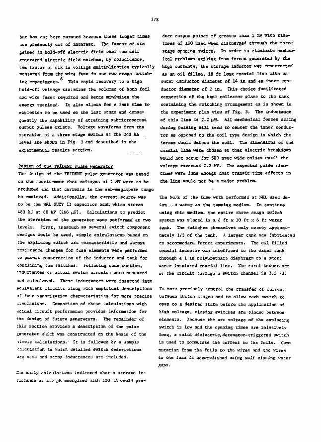
278
but has not been pursued because these longer tines
are presently not of interest. The factor of 3ix
gained lu hold-off electric field over the self
generated electric field matches, by coincidence,
the factor of six in voltage multiplication typically
measured from the wire fuse ifl our two stage switch-
ing experiments. Tills rapid recovery to a high
hold-off voltage misinlzcs the volumes of both foil
and ulre fuses required and hence minifflii.es the
energy required. It alao allows for a fa»t tine to
explosion to be used on the last stage and conse-
quently the capability of attaining submicrosecond
output pulses exists. Voltage waveforms from the
operation of a three stage switch at the 340 kA
level are shown in Fig, 7 and described in the
experimental results section.
Design of tha TRIDENT Pulse Generator
The design of the TRIDENT pulse generator was based
on the requirement that voltages of 1 iff were Co be
produced and that currents la the sub-megampere range
be employed. Additionally, the current source was
to be the NRL SUZ7 II capacitor bank which scores
480 kJ at 60 kV (266 ^ F ) . Calculations to predict
the operation of the generator were performed at rwo
levels. First, inasmuch as several switch component
designs would be used, simple calculations based on
cbe exploding switch arc characteristic and abrupt
resistance changes for fuse elements were performed
co permit construction of the inductor and tank for
containing the switches. Following construction,
inductances of actual switch circuits were measured
and calculated. These Inductances were inserted into
equivalent circuits along with empirical 'descriptions
of fuse vaporization characteristics for more precise
simulations. Comparison of these calculations with
actual circuit performance provides information for
the design of future generators. The remainder of
this section provides a description of the pulse
generator which was constructed on the basis cf the
sinpie calculations.' It is followed by a sample,
calculation in vhich detailed switch descriptions
are used and stray inductances are included.
The early calculations indicated that a storage in-
ductance of 2.5 ,jH energized with 500 kA would pro-
duce output puises of greater than 1 MV with rise-
tives of 100 csec when discharged through the three
stage opining switch. In order to eliminate mechan-
ical problems arising from forces generated by the
high currents, the storage Inductor was constructed
as an oil filled, 18 ft long coaxial line with an
outer conductor diameter of 14 In and an inner con-
ductor diameter of 2 in. This choice facilitated
connection of the bank collector plate to the tank
containing the switching arrangement as is shown in
the experiment plan view of Fig. 3. The inductance
of this line is 2.2 nH. All mechanical forces acting
during pulsing will tend to center the inner conduc-
tor as opposed to the coil type design in which the
forces would deform the coll. The dimensions of the
coaxial line were chosen so that electric breakdown
would not occur for S00 nsec wide pulses until the
voltage exceeded 2.2 MV. The expected pulse rise-
times were long enough that transit time effects in
the line would not be a major problem.
The bulk of the fuse work performed at NRL used de-
ion .... d water as the tamping medium. To continue
using this mediua, the entire three stage switch
system was placed in a 6 ft x 10 ft x 6 ft water
tank. The switches themselves only occupy approxi-
mately 1/3 of the tank. A larger tank was fabricated
to accommodate future experiments. The oil filled
coaxial inductor was interfaced to the water tank
through a 1 in polyurethac^ diaphragm to a short
water insulated coaxial line. The total Inductance
of the circuit chrough a switch channel is 3.5 -H.
To more precisely control the transfer of current
between switch stages and to allow each switch to
open to a desired state before the application of
high voltage, closing switches are placed between
elements. Because the arc voltage of the exploding
switch is low and the opening times are relatively
long, a solid dielectric, detonator-triggered switch
is used co commutate the current to the foils. Con-
nutation from the foils to the wires and the wires
to the load is accomplished using self closing vater
gaps.
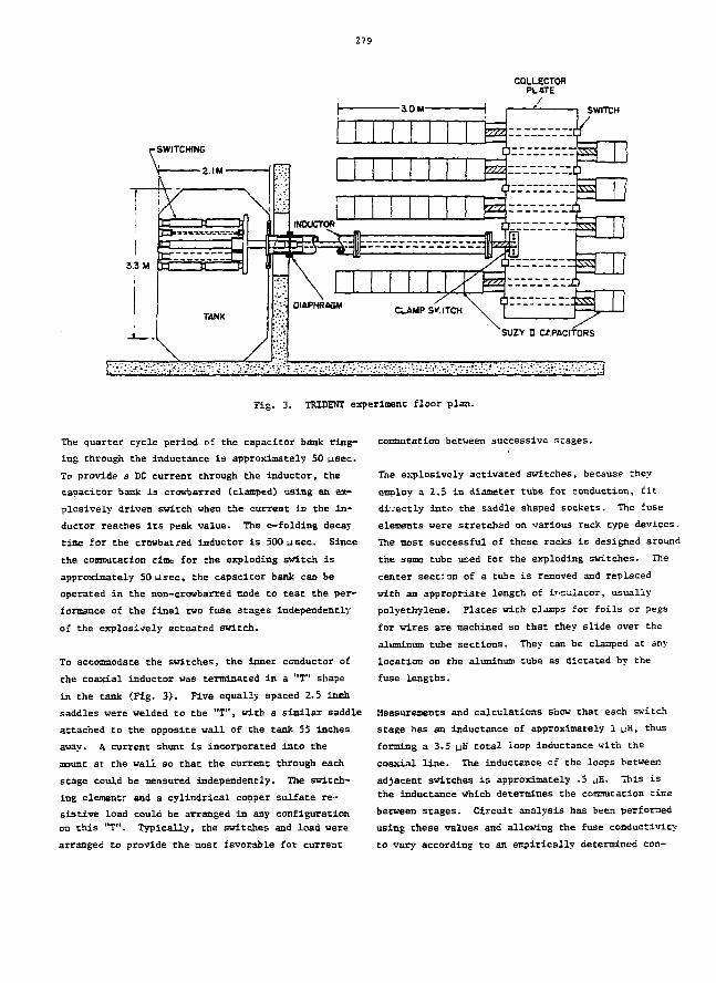
279
r-SWITCHING
SWITCH
Fig. 3. TRIDEHT experiment floor plan.
The quarter cycle period cf the capacitor bank ring-
ing through the inductance is approximately SO usec.
To provide a DC current through the inductor, the
capacitor bank is crowbarred (clamped) using an ex-
plosively driven switch when the current in the in-
ductor reaches its peak value. The e-folding decay
time for the crowbaired inductor is 500 usec. Since
the commutation time for the exploding switch is
approximately 50 usec, the capacitor bank can be
operated in the non-crowbarred mode to test the per-
formance of the final two fuse stages independently
of the explosively actuated switch.
To accommodate the switches, the inner conductor of
the coaxial inductor was terminated in a "T" shape
in the tank (Fig. 3). Five equally spaced 2.5 inch
saddles were welded to the "T", with a similar saddle
attached to the opposite wall of the tank 55 inches
away. A current shunt is incorporated into the
mount at the wall so that the current through each
stage could be measured independently. The switch-
ing elementr and a cylindrical copper sulfate re-
sistive load could be arranged in any configuration
on this "T". Typically, the switches and load were
arranged to provide the most favorable for current
commutation between successive stages.
The explosively activated switches, because they
employ a 2.5 in diameter tube for conduction, fit
dl.-ectly into the saddle shaped sockets. The fuse
elements were stretched on various rack type devices.
The most successful of these racks is designed around
the same tube used for the exploding switches. The
center sectj on of a tube is removed and replaced
with an appropriate length of insulator, usually
polyethylene. Plates with clomps for foils or pegs
for wires are machined so that they slide over the
aluminum tube sections. They can be clamped at any
location on the aluminum tube as dictated by the
fuse lengths.
Measurements and calculations snow that each switch
stage has an inductance of approximately 1 i H, thus
forming a 3.5 uH total ioop inductance with the
coaxial 11TH*- The inductance of the loops between
adjacent switches is approximately .5 uH. This is
the inductance which determines the commutation time
between stages. Circuit analysis has been performed
using these values and allowing the fuse conductivity
to vary according to an empirically determined con-
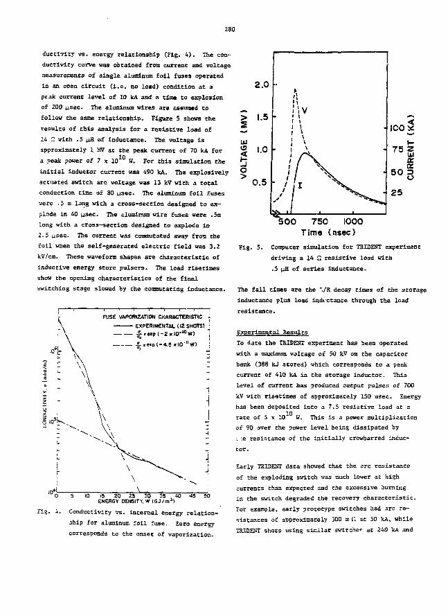
280
ductivity vs. energy relationship (Fig. 4). The con-
ductivity curve was obtained from current and voltage
raeasureoents of single aluminum foil fuses operated
in an open circuit (i.e. no load) condition at a
peak current level of 10 kA and a time to explosion
of 200 _:sec. The aluminum wires are assumed to
follow the same relationship. Figure S shows the
results of this analysis for a resistive load of
14 £ with .5 y.H of inductance. The voltage is
approximately 1 W at the peak current of 70 kA for
a peak power of 7 x 10 W. For this simulation the
initial inductor current was 490 kA. The explosively
actuated switch arc voltage was 13 kV with a total
conduction time uf SO usec. The aluminum foil fuses
were .5 m long with a cross-section designed to ex-
plode in 40 |isec. The aluminum wire fuses were .5m
long with a cross-section designed to explode in
2.5 usec. The current was commutated away from the
foil when the self-generated electric field was 3.2
kv/cm. These waveform shapes are characteristic of
inductive energy store pulsers. The load risetimes
show the opening characteristics of the final
switching stage slowed by the commutating inductance.
FUSE VAPORIZATION CHARACTERISTIC
EXPERIMENTAL (IE SHOTS)
10 15 20 25 30 35 40 45 50ENERGY DENSITY. W IGJ/m3)
rig. A. Conductivity vs. internal energy relation-
3hip for aluminum foil fuse. Zero energy
corresponds to the onset of vaporization.
500 750 1000Tims (nsec)
Fig. 5. Computer simulation for TRIDENT experiaent
driving a 14 £3 resistive load with
.5 nH of series inductance.
The fall times are the ',/R decay times of the scorage
inductance plus load indictance through the load
resistance.
Experimental Results
To date the TRIDENT experiment has been operated
with a maximum voltage of 50 kV on the capacitor
bank (388 kJ stored) which corresponds to a peak
current of 410 kA in the storage inductor. This
level of current has produced output pulses of 700
kV with risetimes of approximately 150 nsec. Energy
has been deposited into a 7.5 resistive load at a10
rate of 5 x 10* W. This is a power multiplication
of 90 over the power level being dissipated by
i le resistance of the initially crowbarred induc-
tor.
Early TRIDENT data showed that the arc resistance
of the exploding switch was nuch lower at high
currents than expected and Che excessive burning
in the switch degraded the recovery characteristic.
For example, early prototype switches had arc re-
sistances of approximately 300 m Q at 50 kA, while
TRIDENT shots using sioilar switches at 240 kA and
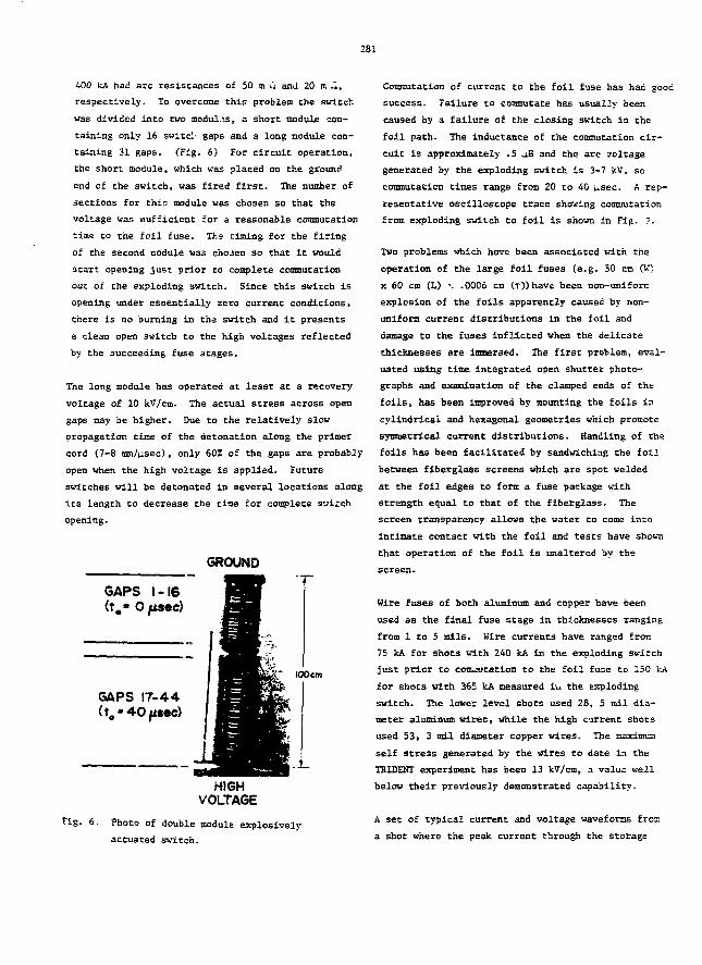
281
400 kA had arc resistances of 50 in u and 20 m «,
respectively. To overcome this problem the switch
was divided into two modules, a short module con-
taining only 16 switcl- gaps and a long module con-
taining 31 gaps. (Fig. 6) For circuit operation,
the short module, which was placed on the ground
end of the switch, was fired first. The number of
sections for this module was chosen so that the
voltage was sufficient for a reasonable commutation
time to the foil fuse. Tha timing for the firing
of the second module was chosen so that it would
start opening just prior to complete commutation
out of the exploding switch. Since this switch is
opening under essentially zero current conditions,
there is no burning in the switch and it presents
a clean open switch to the high voltages reflected
by the succeeding fuse stages.
The long module has operated at least at a recovery
voltage of 10 kV/cm. The actual stress across open
gaps may be higher. Due to the relatively slow
propagation time of the detonation along the primer
cord (7-8 mra/usec), only 602 of the gaps are probably
open when the high voltage is applied. Future
switches will be detonated in several locations along
its length to decrease the time for complete switch
opening.
GROUND
100cm
HIGHVOLTAGE
Fig. 6. Photo of double module explosively
actuated switch.
Commutation of current to the foil fuse has had good
success. Failure to corcmutate has usually been
caused by a failure of the closing switch in the
foil path. The inductance of the commutation cir-
cuit is approximately .5 4H and che arc voltage
generated by the exploding switch is 3-7 kV, so
commutation times range from 20 to 40 usec. A rep-
resentative oscilloscope trace shoving commutation
from exploding switch to foii is shown in Fig. ?.
Two problems which have been associated with the
operation of the large foil fuses (e.g. 50 cm 00
X 60 cm (L) -. .0006 cm (T))have been non-uniform
explosion of the foils apparently caused by non-
uniform current distributions in the foil and
damage to the fuses inflicted vhen the delicate
thicknesses are immersed. The first problem, eval-
uated using time integrated open shutter photo-
graphs and examination of the damped ends of the
foils, has been improved by mounting the foils in
cylindrical and hexagonal geometries which promote
symmetrical current distributions. Handling of the
foils has been facilitated by sandwiching the foil
between fiberglass screens which are spot welded
at the foil edges to form a fuse package with
strength equal to that of the fiberglass. The
screen transparency allows the water to come into
intimate contact with the foil and tests have shown
that operation of the foil is unaltered by the
screen.
Wire fuses of both aluminum and copper have been
used as the final fuse stage in thicknesses ranging
from 1 to 5 mils. Wire currents have ranged from
75 kA for shots with 240 kA in the exploding switch
just prior to confutation to the foil fuse to 150 kA
for shots with 365 kA measured iu the exploding
switch. The lower level shots used 28, 5 mil dia-
meter aluminum wires, while the high current shots
used 53, 3 mil diameter copper wires. The maximum
self stress generated by the wires to date in the
TRIDENT experiment has been 13 kV/cm, 3 valu; well
below their previously demonstrated capability.
A set of typical current and voltage waveforms fron:
a shot where the peak current through the storage
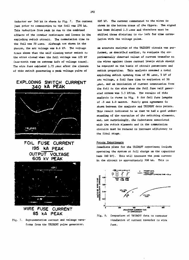
282
inductor wa,* 340 kA is shown in Fig. ?. The current
just prior to commutation to the foil was 270 kA.
This reduction from peak is due to the combined
effects of the erowbtr resistance and losses in the
exploding switch circuit. The commutation time to
the foil vas 20 usec. Although not shown in the
photos, Che arc voltage was 6.6 kV. The voltage
trace shows that the self closing water switch to
the wires closed when the foil voltage was 125 kV
(saw-tooth ramp on extreme left of voltage trace).
The wire fuse exploded 1.75 usec after the closure
of this switch generating a peak voltage pulse of
EXPLODING SWITCH CURRENT3 4 0 kA PEAK
FOIL FUSE CURRENT195 kA PEAK
OUTPUT VOLTAGE605 kV PEAK
fig.
WIRE FUSE CURRENT85 kA PEAK
Representative current and voltage wave-
forms from the TRIDENT pulse generator.
605 kV. The current commutated to the wires is
shown in the bottom trace of the figure. The signal
has been delayed 1,5 usec and therefore must be
shifted three divisions to tin- left for time corre-
lation with the voltage pulse.
An accurate analysis of the TRIDENT circuit was per-
formed, as described earlier, to evaluate Che ex-
perimentally observed values of current transfer to
the wires against chose current levels which should
be expected on the basis of circuit parameters and
switch properties. This analysis assumed a total
exploding switch opening time of 80 Msec, 5 kV of
arc voltage, a foil fuse time to explosion of SO
ysec, and an initiation of current commutation from
the foil to Che wire when the foil fuse self gener-
ated stress was 3.3 kV/cm. The results of this
analysis is ?tanm in Fig. 8 for foil fuse lengths
of .5 and 1.0 meters. Fairly good agreement is
shown between the analysis and TRIDENT data points.
This result indicated Co us chat we had a good under-
standing of Che operation of the switching elements,
and, not surprisingly, the inductance associated
with the switch elements and in Che commutation
circuits must be reduced to increase efficiency Co
the final stage.
Future Experiments
Immediate plans for the TRIDENT experiment include
operating the system at full charge on the capacitor
bank (60 kV). This will increase the peak current
in the circuit to approximately 500 kA. This is
300 W0 300INDUCTOR CURRfNT IkAl
AT SWITCH-OUT
BOO
Fig. S. Comparison of TRIDENT data to computer
simulation of current transfer to wire
fuse.

283
expected to generate output pulses of over 800 kV.
In order Co attain this level, a folded version of
the exploding switch will be employed whicb will
have a higher voltage hold-off capability with a
very small change in the circuit inductance. Addi-
tionally, a falsework arrangement has been proposed
to reduce the inductance of the switches and commu-
tation circuits. This modification to improve energy
cransfer to the wires aioag with optimized switching
between stages should produce output pulses
approaching the desired goal of 1 MV.
Later in the year, the TRIDENT switching tank will
be connected to the NRL homopolar generator for
operation at 600 kA with an initial stored energy
of 1 MJ. This will provide the first demonstration
of a complete, compact, high energy inductive storage
pulser with an inertial energy store as the primary
source•
Following the hoTBopolar generator tests, a demonstra-
tion of pulse charging the capacitance of a 1 MV,
moderate energy pulse forming line is planned.
Reference
1. T. H. Martin and K. R. Prestwich, "EBFA, A
Twenty Terawatt Election Beam Accelerator",
Energy Storage, Compression, and Switching
Edited by W. H. Bostick, V. Nardi, and 0. S. F.
Zucker, Plenum Press, New York, 1976. pp. 57-
62; G. Yonas, "Fusion Power with Particle Beams",
Scientific American, Vol. 239, No. 5, Nov. 1978.
pp. 50-61.
6.
B. Bernstein and I. Smith. "Aurora, An Electron
Beam Accelerator", IEEE Transactions on Nuclear
Science, Vol. 20, 1973. p. 294.
H. H. Woodson, H. G. Rylander, W. F. Ueldon,
"Pulsed Power from Inertial Storage with Homo-
polar Machines for Conversion", Proceedings of
First IEEE International Pulsed Power Conference,
IEEE Cat. No. 76H1147-8 REG-5, Lubbock, Texas,
Nov. 1976.
A. E. Robson, R. E. Lanham, W. H. Luptor., T. J.
01Cornell, P. J. Turchi and W. L. Warnick,
"An Inductive Energy Storage System Based On A
Self-Excited Homopolar Generator", Proceedings
of the Sixth Symposium on Engineering Problems
of Fusion Research, IEEE Cat. No. 75CH 1097-5-NPS
(1976). p. 298.
R. D. Foru and I. M. Vitkovitsky, "Explosively
Actuated 100 kA Opening Switch for High Voltage
Applications", NR1 Memo T-eport 3561, July 1977.
D. Conte, R. D. Ford, W. H. Lupton and I. M.
Vitkovitsky, " Two Stage Opening Switch Techni-
ques for Generation of High Inductive Voltage",
Proceedings of Seventh Symposium of Engineering
Problems of Fusion Research, IEEE Cat. No.
77CH1267-4-NPS (1977). p. 1066.
W. B. Lupton, R. D. Ford, D. Conte,
H. B. Lindstrom and I. M. Vitkovitsky "Use of
Transformers in Producing High Power Output from
Homopolar Generators", proceedings of this con-
ference.
This work was sponsored by the Defense Nuclear
Agency.
284
12.2
INDUCTIVE STORAGE - PROSPECTS FOR HIGH POWER GENERATION
J. K. Burton, D. Conce, 3.. D. Ford
W. H. Lupton, V. E. Scherrer, I. M. Vitkovitsky
Naval Research Laboratory
Washington, D. C. 20375
Ab3tract
Recent progress in the development of key elements
of high power inductive storage systems makes it
possible Co generate high power pulses using energy
storage systems (other than explosive generators)
chit include single-pulse inductive systems, hybrids
(iiductor/pulse line and inductive devices for
steepening of the capacitor output') as well as
inductive systems for generation of high power
pulse trains.
Prospects for further development of opening
switches and storage systems suggest potential
near-tern payoff. Improvements based on such de-
velopments can be expected to impact system effi-
ciency, compactness and operational convenience.
Introduction
Magnetic storage of energy for applications, re-
quiring large amounts of energy, is preferable to
capacitive storage because of its characteristicallyo 3
high energy density, some 10 Co 10 times higher
than electrostatic energy storage. S. A. ^asar and
H. H. Woodson have surveyed the methods of energy
storage for pulse power applications, concluding
in 1975 chat inductive storage has great potential,
buc chat ic has not been used extensively in the
past. Specifically, the problem of opening switches
is indicated, with the prediction chat high current,
high voltage opening switches will evolve froo power
circuit breaker technology.
This paper discusses the status of opening switches
and their relation to development of large inductive
storage systems designed for loads requiring high
power input, and for systems with specialized output,
such as pulse trains with short pulse-to-pulse
separation. Prospective development of one new
type of opening switch, a plasma switch, is also
discussed to illustrate further possibilities for
improved performance of these systems, including
repetitive capabilities.
Opening Switches
Tha requirements imposed on the opening switches in
Inductive storage systems, i.e. high resistance of
the opened state, high inductive electric field,
high restrike voltage with the attendant rapid re-
covery rate and fast opening time were discussed in
Kef. 4 in relation to Che circuit parameters. It
can be seen from the analysis of the energy transport
from the inductor, L , co the load that the above_tfitcho
characteristics strongly influence the pulser's effi-
ciency. Thi3 is because the efficiency of transfer
from one switching stage Co a succeeding one (as is
necessary to do in systems with large power
ficacion factors ) is given by
where W/W is Che ratio of energy transferred co the
next stage (characterized by resistance, R, and in-
ductance L) to the stored energy3. The magnitude
of the effect can be estimated from W/W by noting
that the inductance L of the next stage is always
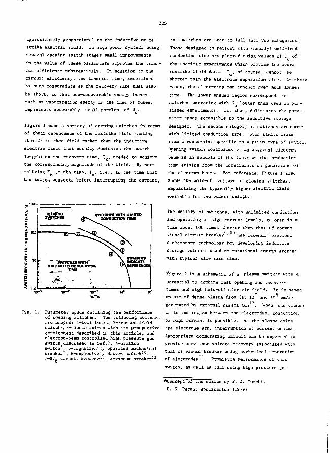
285
approximately proportional to the inductive or re-
strike electric field. In high power systems using
several opening switch stages small improvements
in the value of these parameters improves the trans-
fer efficiency substantially. In addition to the
circuir efficiency, the transfer time, determined
by such constraints as the recovery rate must also
be short, so that non-recoverable energy losses ,
such as vaporization energy ir the case of fuses,
represents acceptably small portion of W .
Figure 1 maps 2 variety of opening switches in terms
of their dependance of the restrike field (noting
that it is that field rather than the inductive
electric field that usually dominates the switch
length) on the recovery time, T , needed to achieve
the corresponding magnitude of the field. By nor-
malizing Tp uo the time, T , i.e., to the time that
rt o
the switch conducts before interrupting the current.
_ 1000
§ ISO
SWITCHES WITH LIMITEDCONDUCTION TIME
10-*
Fig. 1. Parameter space outlining the performanceof opening switches. The following switchesare mapped: 1-foil fuses, 2-crossed fieldswitch6, 3-plasma switch with, its prospectivedevelopment described in this article, andelectron-beam controlled high pressure gasswitch discussed in ref.7, 4-erosionswitch3, 5-magnetically operated mechanicalbreaker3, 6-explosively driven switch10,7-SF, circuit breaker^, S-vacuum breaker^2,o
the switches are seen to tall into two categories.
Those designed to perform with (nearly) unlimited
conduction time are plotted using values of T ofo
the specific experiments which provide the aboverestrike field data. T , of course, cannot be
o
shorter than the electrode separation time. In these
cases, the electrcdes cac conduct over much longer
time. The lower shaded region corresponds to
switches operating with T longer than used in pub-
lished experiments. It, thus, delineates the para-
meter space accessible to the inductive storage
designer. The second category of switches are those
with limited conduction time. Such limits arise
from a constraint specific to a given type of switch.
Opening switch controlled by an external electron
beam is an exaraple of the limit on the conduction
time arising from the constraints or. generation of
the electron beams. For reference. Figure 1 also
shows the hold-off voltage of closina switches,
emphasizing the typically higher electric field
available for the pulser design.
The ability of switches, with unlimited conduction
and operating at high current levels, to open in a
time about 100 times shorter than that of conven-9 10tional circuit breaker ' has recently provided
a necessary technology for developing inductive
storage pulsers based on rotational energy storage
with typical slow rise time.
Figure 2 is a schematic of a plasma switch* with d
potential to combine fast opening and recovery
times and high hold-off electric field. Ic is based7 R
on use of dense plasma flow (at 10 and T> cra/s)
generated by external plasma gun . When the plasma
is in the region between the electrodes, conduction
of high current is possible. As the plasma exits
the electrode gap, interruption of current ensues.
Appropriate commutating circuit can be expected to
provide very fast voltage recovery associated with
that of vacuum breaker using mechanical separation
of electrodes ". Promising performance of this
switch, as well as that using high pressure gas
*Concept o± the switcn By V. J. Turchi,
U. S. Patent Application (1979)
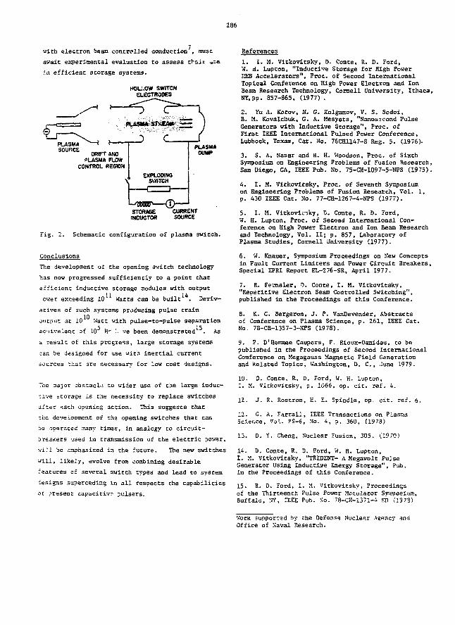
236
with electron beam controlled conduction', must
await experimental evaluation to assess their us
in efficient storage systems.
HOLI-OW SWITCHELECTROOES
S 0 U R C E MFTANOPLASMA FLOW
CONTROL REGION
Fig. 2. Schematic configuration of plasma switch.
Conclusions
The development of the opening switch technology
has now progressed sufficiently to a point that
efficient inductive storage modules with output' 1 14
ewer exceeding 10* Watts can be built . Deriv-
atives of such systems producing pulse train
•,10jutput at 10 Matt with pulse-to-pulse separation
equivalent of 10 H- '. ;ve been demonstrated . As
a result of this progxess, large storage systems
can be designed for use with inertial current
sources that are necessary for low cost designs.
The major obstacle to wider use of the large induc-
tive storage is the necessity to replace switches
after each opening action. This suggests that
-he development of the opening swicches that can
be operated .ttany times, in analogy Co circuit-
breakers 'jsed in transmission of che electric power,
vill be emphasised in the future. The new switches
will, likely, evolve from combining desirable
features of several switch types and lead to system
designs superceding in all respects the capabilities
of present capacitiv? pulsers.
References
1. I. M, Vitkovitsky, D. Conce, R. D. Ford,W. d. Lupton, "Inductive Storage for High PowerEEB Accelerators", Proc. of Second InternationalTopical Conference on High Power Electron and IonBeam Research Technology, Cornell University, Ithaca,NY,pp. 857-865, (1977) .
2. Yu A. Kotov, H. G. Xolganov, V. S. Sedoi,B. M. Kovalchuk, G. A. Mesyats, "Nanosecond PulseGenerators with Inductive Storage", Proc. ofFirst IEEE International Pulsed Power Conference,Lubbock, Texas, Cat. So. 76CH1147-8 Reg. 5. (1976).
3. S. A. Nasar and a. H. Hoodson, Proc. of SixthSymposium on Engineering Problems of Fusion Research,San Diego, CA, IEEE Pub. No. 75-CH-1097-5-NPS (1975).
4. I. M. Vickoviesky, Proc. of Seventh Symposiumon Engineering Problems of Fusion Research, Vol. 1,p. 430 IEEE Cat. No. 77-CH-1267-4-NPS (1977).
5. I. M. Vitkoviu-sky, D. Conte, R. D. Ford,H. H. Lupton, Proc. of Second International Con-ference on High Power Electron and Ion Beam Researchand Technology, Vol. II; p. 857, Laboratory ofPlasma Studies, Cornell University (1977).
6. W. Knauer, Symposium Proceedings on New Conceptsin Fault Current Limiters and Power Circuit 3reakers,Special EPRI Report EL-276-SR, April 1977.
7. R. Femsler, D. Conte, I. M. Vitkovitsky,"Repetitive Electron Beam Controlled Switching",published in the Proceedings of this Conference.
8. K. C. Bergeron, J. P. VanDevender, Abstractsot Conference on Plasma Science, p. 261, IEEE Cat.No. 78-CH-1357-3-NPS (1978).
9. P. D'Hommee Caupers, F. Rloux-Damidau, to bepublished in the Proceedings of Second InternationalConference on Megagauss Magnetic Field Generationand Related Topics, Washington, D. C., June 1979.
10. D. Conte, R. D. Ford, W. H. Lupton,I. M. Vitkovicsky, p. 1066, op. ciz. ref. 4.
11. J. R. Rostron, H. E. Spindle, op, cit. ref. 6.
12. G. A. Farrall, IEEE Transactions on PlasnaScience, Vol.. PS-6, No. 4, p. 360, (1978)
13. D. Y. Cheng, Nuclear Fusion, 305. (1970)
14. D. Conte, R. D. Ford, W. H. Lupton,I. M. Vitkovitsky, "TRIDENT- A Megavolt PulseGenerator Using Inductive Energy Storage", Pub.in the Proceedings of this Conference.
15. R. D. Ford, I. M. Vitkovitsky, Proceedingsof the Thirteenth Pulse Power Maculator Symposium,Buffalo, NY, IEEE Pub. So. 78-CH-1371-4 ED '.I1378)
Work supported by the Defense Nuclear Agency andOffice of Naval Research.
287
12.3
INVITED
CONSIDERATIONS FOE INDUCTIVELY DRIVES PLASMA IMPLOSIONS
D.L. SMITH, R.P. HENDERSON, and R.E. REINOVSICV
Air Force Weapons LaboratoryKirtland AFB, Hew Mexico
Absitract
Inductive pulse forming techniques appropriate for
th<3 driving of imploding plasmas have been explored
with special attention given to a suitable opening
switch. Parametric investigations of circuit models
indicate ttuu imploding load performance is rela-
tively independent of opening switch parameters.
Extrapolation of existing experimental and computer
simulated data leads to conceptual design criteria
for a fused necal foil opening switch which will
bi; implemented on a 1.9 MJ system. The inductive
system compares favorably with the direct capaci-
tor driven systea in terms of kinetic energy with
the definite advantage of shorter time scales on
which the energy is delivered to the implosion.
introduction
The Air Force Weapons Laboratory is investigating
plasma implosion techniques as a desirable method
for generating a very high energy density plasma
suitable for use as an intense X-ray Source . Under
the SHIVA program experiments have been conducted
in which a plasma formed from a thin freestanding,
cylindrical metal or plastic film is driven to high
velocities (> 20cm/usec) by a high current from a
1.1 J5J, 1.3 jis capacitor bank. Proper choice of
gaometry and mass of the imploding plasma allow
good (25-30%) coupling of electrical to kinetic
energy and have efficient heating of the pinched
plasma. Radiation outputs of 180 kj (16% total
efficiency) at powers in excess of 1.5 TN have been
observed. Future experiments call for the delivery
of much larger amounts of electrical energy (15-
30 MJ), and Implosion dynamics suggest that shorter
implosion times (30Cns) would be advantageous. To
meet these requirements energy storage systems of
conventional design would be exceedingly large andexpensive. An attractive alternative technology
aay be conceptually developed using inductivei 3
(mag'etic) energv conditioning techniques"'4
coupled with inertial primary energy storage .
The inertial primary store is essentially present
technology. Therefore, the purpose of this work is
to explore the potential applicability o£ inductive
pulse forming techniques in the driving of implod-
ing plasma loads. Special attention is paid to the
development of a suitable opening switch. In this
paper the inductively driver, pl&saa implosion sys-
tems will be explored analytically and computa-
tionally through circuit models. The performance
of currently available opening switches will be
compared against the requirements developed in the
analysis to assess the near term prospects for
applying inductive techniques to large systems.
Simple Analysis
The circuit shown in Fig. 1 consists of a dc charged
capacitor bank (C) discharging through a storage
inductor (L » L. . + L ) and a closed switchs oatLl- ext
(Sj) that opens at peak current (I ) to transfer
the energy through switch S, to the load of ir.itial
inductance L . The load inductance increases sub-o
sequent to the initiation of current interruption
thus corresponding to the implosion of the SHIVA
load (L(t) - L + 4L(t)). The initially open switch
(S,) isolates the load from the system until switch-
ing time (t ). The final load inductance is
L » L + AL whereo
i L =
The parameter a is the height of the cylindrical
foil, while R and R. are the initial and finalo r
cylinder radii respectively. Convergence ratios
(R /R ) of 12-14 are common and the shorter tinec z
scale implosion is expected to lead to a convergence
Z88
of 20. Several assumptions are employed in the
simplest analysis. The final resistance of the
opening switch is assumed to be large compared to
the final L of che load Co prevent significant
sharing of current through the switch. If the im-
ploding cylinder radius and velocity are r(t) and
v(c), one can write
It is also assumed that the resistance rises
quickly, In other words that the switching time
is much less than the implosion time.
At peak current and for the short energy transfer
times of interest the bank voltage and the amount
by uhich the charge on C can change is near zero,
hence for Che analysis the capacitor element can be
represented by a short circuit. Assuming conserva-
tion of magnetic flux, tha energy stored in L and
L immediately after t iso ' s
LIT > s _ (3)
where E (" sL I 2) is the energy stored in L
prior co t . The energy dissipated in the rising
switch resistance must be
LQ («)
~sw L + L *bs o
according to conservation of energy. To minimizethe switch dissipation L must be as low as possi-ble (L <<L ). After the implosion the approximate
o senergy stored in L , L , and AL is
ratio and che foil height. For the SHIVA system
values of L below 3-5 nH are unrealistic, whileo
AL can range from 6 to 24 nH, and reaching very
high efficiency will be difficult. Given practical
constraints upon L and AL, the value of L re-
mains A S one parsaeCer which can be adjusted. In-
tuitively, if I. is chosen to be very small, a
large amount of energy is lost in the switching
operation, if it is chosen to be large the energy
transfer to the load suffers. To find the optimum
choice of L one can take dr, /dL and set the re-
sult equal to zero. This results in a criterion on
L , namely:
+ L AL .o (7)
Clearly for the case of Che static load,' AL - 0,
Eq. (7) gives L » L . Thus, the familiar static
result is recovered, and as expected, from Eq. (3)
and Eq. (4) Z^ - E » 50% E . Plotting n. as a
function of L for an implosion where AL * 12 nH
shows that the efficiency of coupling inductive to
kinetic energy goes through a maximum at the pre-
dicted optimum L and chat the optimum is broad and
relatively insensitive to small variations in L .
For one class of opening switches, namely electri-
cally exploded conductors, the operation of Che
switch is determined by the energy, (and to some
extent power history) dissipated in Che switch.
Therefore it is useful to characterize che circuit
performance in terms of the energy dissipated in
the switch given by Eq. (4). Figure 2 is a plot of
the minimum dissipation fraction defined as
L + Ls o
It Eo (5)
The kinetic energy coupled to the plasma shell dur-
ing the iaplosicn is just the difference E.-E,,
and a kinetic efficiency can be defined as
it '(6)
if 1 '-<L . If LL>>h_ efficiency approaching tinity
can be realized. Thus, in general, to get mosc of
Che scored energy into kinetic energy and maximize
efficiency reouires L <<L «AL. Unfortunately Los o
is typically fixed by consideration of power flow
in che Load and I'L is fixed by the convergence
L + L 's o(8)
When Ls is chosen by Eq. (7), Eq. (8) indicates
chat 6 is only a weak function of AL. For small ±L
che curve approaches 50% as expecced for a static
load. The significance of 6 is that it represents
Che minimum amount of energy that will be dissipa-
ced when the switch opens (at least 25% for prac-
tical cases), regardless of che characteriscics or
relative time of che operations of switches 3. and
5,. Conversely it is che minimum energy available
co use Co actuate a dissipation driven switch. The
cesiptation Is co develop a switch ^hich "requires"
289
very littly energy. Figure 2 indicates that, for
example, for typical SHIVA parameters L • 5 nH
and 1L - 12 nH, almost 40% of che energy goes into
the switch regardless of how clever the design. On
the other hand, since dissipatively operated cur-
rent interrupting switches may require more than
the minimum energy given by 6, the fraction f of
the inductively stored energy remaining after
switching chat is coupled to kinetic energy is also
a relevant parameter. Using Eq. (3) and (5)
E. L + Lf = k e/E, - 1 - ,- \ , ° Ay . (9)L + L + AL '
s o
Figure 3 is a plot of the coupling fraction f. The
plot shows that for realistic values of 3 nH< L <r o
5- nil and for AL » 12 nH approximately half of the
energy remaining after switching is coupled to ki-
netic energy yielding for these parameters an over-
all n of 302. From this simple analysis, a few
design criteria emerge:
i) Minimize L , as much as possible,o
ii) Maximize AL,
iii) Choose L ss «/L 2 + L AL ,s f o o
iv) Determine the dissipated switch energy.
Numerical Results
In this section, the numerical solution to a cir-
cuit similar to that in Fig. 1 is discussed.
Values were chosen for circuit elements which cor-
respond to parameters of the SHIVA-I1 capacitor
bank system. The 267 uF capacitor is charged to
120 kV storing 1.9 HJ. The load is modeled as a
time varying resistance, having the same form as
Eq. (2), in series with a time varying inductance
expressed by
v hLft) ' ~r In (R/r(t)). (10)
The radii of the return conductor (chamber) and of
che imploding foil are represented by R and r(t),
respectively. The initial foil radius was chosen at
5 cm and the height at 2 cm by stability arguments.
The return conductor radius was chosen at 17.3 cai
to give an initial value for the L of 5 nH, which
corresponds to L « 5 nH in the analytic model. Theo
assumption of 20:1 conversion leads to a minimum
radius of 2.5 mm; a final value L. of 17 nH; and a
AL of 12 nH. Thus from L and AL a value of the
storage inductance is chosen from Eq. (7) to be
9.2 nH. The series output switch is modeled as a
time varying resistor whose value is 1 megohm prior
to switching cime t and changes to 0.1 miliiohm in
5 ns sub..~qyent to t . The current interrupting
switch is a resistance (R..) which is varied as a
problem variable. The opening switch inductance if
typically taker, as less than 1 nH but will depend
on the switch geometry. The fuse inductance was
included in the bank side of the circuit rather
than in the fuse branch because, wit:, the coaxial
SHIVA arrangement, L_ stores magnetic energ" that
is available to the load when switching occurs. The
circuit was subjected to numerical analysis using
a circuit solving code for a variety of R profiles
and time scales and for a variety of switch tiir.es
t .
s
Terminal Resistance
Assuming all the stored energy is transferred to
the inductors, the coupled kinetic energy should be
570 kj (30S kinetic efficiency). Choosing 33 cm/us
final velocity and allowing a 2.5 xm final radius
the foil mass and final £ should be 10"- kg and
0.5 ft. The constant flux analysis implied that the
final value of R should be much greater than 0.5 f:
to assure that most of the current is flowing in
the load. To model the situation a linear ramp re-
sistance profile was chosen (since other shapes
effected only a few percent variation in the kinetic
energy), changing R from the initial resistance
(R.. a 0) at t1 = 2.46 us (time of peak current) to
a final terminal resistance (£„). The switch dura-
tion (At) was taken as 100 ns i:o assure that it <<t. , and R, was varied from 3D mf. to 5 -~.. The timeimp t
at which the output switch closed (t ), was a cons-
tant at 2.465 us. Figure 4 shows a plot of the ki-
netic energy coupled to the isrplodlng foi_ and the
final velocity of the foil when it had collapsed to
290
a radius of 2.5 mi as a function of Rf, the final
switch resistance. As anticipated the kinetic en-
ergy coupled at lower values of R- is lower than
that observed at higher values. Perhaps surprising
is the fact that when K, •>< L peak nearly 902 of
the kinetic energy predicted by the flux model is
observed coupled in the numerical solution. But
when R drops more than an order of magnitude
to 30 mi! the kinetic efficiency decreases only
moderately to 62Z of the efficiency predicted by
the flux model. This relatively moderate impact
of reducing R. can be motivated by referring to
Fig. 5 where the dissipatlve impedance (RLD) and
R. (t) ars plotted a3 functions of time for the case
where R, « 30 mil. The plot shows that the dissi-
pative part of the load impedance RLD rises rapidly
at the very end of the implosion, and even for very
modest values of R., RLD is less than R. for about
90? of the implosion time. Although it is also
true that most of the kinetic energy is coupled
Late in the implosion, it must be noted that once
R- interrupts the current and "charges'* the load
inductance, the time scale (L/IL) for current to
transfer back to R^ is much longer than the 30-60
us for which Che load impedance is higher than R,.
Coupling to L is independent of R. until late in
"he implosion, and most of the necessary energy
has been loaded into L (which has increased to
almosc L. + AL before L overtakes R..). Figure 4
O £
also exhibits a fall off of n above approximately
0.5 u. This result is perhaps more surprising than
the relative moderate fall off at low R,. At larger
values of R. excessive energy is dissipated in the
fuse during opening time thus leaving Less energy
in the magnetic circuit to drive the Implosion and
thereby explaining lower overall efficiency. The
conclusion is that, for implosion parameters dis-
cussed and for values of 3.P that are greater than
Che initial L of the load (a few milliohms) but
not much greater than the final L (one-half ohm),
performance seems to be predicted by the simple
modeL within about 20%. Thus the criteria results
with 1 « a. "» L . .o r pinch.
Output Switch Closure Time
It -..-as observed chat earlier "closing times" (t )
of the series output switch R resulted in improved
efficiency and decreased dissipation of large values
of R.. In fact the kinetic energy approaches the
570 kJ flux model value. Presumably when R is very
large (i.e., R£ is large and At is fixed), the time
scale of current transfer is seriously effected by
the R- closing time and thus results in larger dis-
dipation in IL. Closing the output switch late in
the interruption may be expected to result in ex-
cessive ensrgy dissipation in the fuse and hence
lower kinetic efficiency. On the other hand, clo-
sure of the output switch too early may be expected
to result in lower voltages across the load and
hence lower initial I, and perhaps result in longer
implosion time for a given load. Fortunately, from
a practical point of view, the earliest possible
closure time (after start of interruption time)
appears moat promising according to both the effi-
ciency and implosion time. The 5 ns value of R,
used to generate the data In Fig. 4 is more repre-
sentative of practical multi-channel switches than
is the less than 1 ns value required to achieve
flux model efficiency. The implication is that a
"low jitter" output switch is required if large
values of R_ are achieved by the fuse. Figure 6
shows a plot of kinetic energy and implosion time
as functions of output switch time for a case where
R_ equals 500 mfl. The Implosion mass was 1 x in~5kg,
and the switch opening time (At) was 100 ns. For
reference, the fuse resistance profile is also
sketched. The figure shows that both kinetic energy
and Implosion time are sensitive to switch closure
time. As expected kinetic energy drops and implosion
time increases with later closing times. The Implo-
sion time shows a tendency to flatten out for clo-
sure times near the start of the interruption
(2.46 JS).
Opening Time
The simple flux model presumes that the implosion
is carried out in two stepa. First a current inter-
ruption occurs, Chen an implosion phase occurs. The
energy transfer is calculated on the assumption that
L(t) does not change during the interruption phase
(i.e., a static load). The numerical analysis shows
that for time scales of about 3/4 of the implosion
cime the opening switch is seeing a constant L(t)
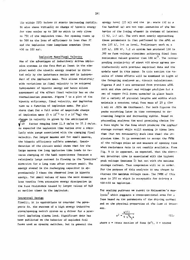
291
(to within 257.) before it starts increasing rapidly.
It also shows virtually no change of kinetic energy
for time scales up to 300 ns which is very close
to 75% of the implosion time. For opening times up
to 500 ns the loss of efficiency is less than SX
and the implosion time lengthens somewhat (from
450 to 550 ns).
Implosion Mass/Final Velocity
One of the advantages of inductively driven implo-
sion systems is the fact that at least in the sim-
plest model the kinetic energy coupled is dicta-
ted only by the inductance ratios and is indepen-
dent of the implosion mass. This allows relatively
wide variations in final velocity to be achieved
independent of kinetic energy and hence allows
assessment of the effect final velocity has on the
thermalization process. Figure 7 is a plot of the
kinetic efficiency, final velocity, and implosion
time as a function of implosion mass. The plot
shows that for a full order of magnitude change
of implosion mass (5 x 10"5 to 5 x 10~6kg) the
change in velocity is given by the anticipated
* 10 factor ranging from 11.9 cm/us to 37.3 cm/us.
As expected the implosion time varies over a simi-
larly wide range associated with the changing final
velocity. For larger masses and for small masses,
the kinetic efficiency suffers somewhat. Consi-
deration of the circuit model shows that for the
large masses the long implosion time leads to re-
verse charging of the bank capacitance (because a
relatively large current is flowing in the "positive"
direction for a long time after current peak). The
energy scored in the recharging capacitor is ap-
proximately 3 times the observed loss in kinetic
energy. For small values of mass the more dramatic
loss results from excessive energy dissipation in
the fuse resistance caused by larger values of RID
at earlier times in the implosion.
Conceptual Design
Finally, it is appropriate tcf consider the pros-
pects fo. the success of a high energy inductive
store/opening switch system as a driver for a prac-
tical Imploding plasma load. Significant data has
been published on the behavior of exploded foil
fuses used as opening switches, but in general the
energy level (25 kJ) and the ic > scale (10 to a
few hundred us) are not repr ..tentative of the be-
havior of the fusing element in systems of interest
(2 MJ, 1-2 us). The work most nearly approaching
these parameters is that performed by the AFVL at
the 200 kJ, 3-4 us level. Preliminary work or. a
100 kJ, 100 kV, 1.2 us system has produced 150 to
200 ns fuse voltage risetimes achieving final fuse
resistance values greater than 160 mf. . The corres-
ponding resistivity of about 400 m&-cm agrees sa-
tisfactorily with previous empirical data and the
models used in this paper. In this section the re-
sults of these efforts will be examined in light of
the foregoing analyses aE- circuit calculations.
Figures 8 and 9 are extracted from previous AFWL
work and show current and voltage profiles for a
set of copper foil fuses quenched in glass beads
for a variety of physical lengths and widths which
maintain a constant total fuse mass of 25 g (for
1 mil or .0254 mm thickness). For both figures the
peaks occurring later in time correspond to de-
creasing lengths and increasing widths. Based on
prtceeding analyses the most promising choice for
a fuse might be the fuse which produces the highest
storage current while still opening in times less
than (but not necessarily much less than) the im-
plosion time. It is convenient to accept the FHHM
of the voltage pulse as one measure of opening time
when resistance data is not readily available. From
Fig. 9 it is apparent, as expected, that the short-
est interrupt time is associated with the highest
peak voltage (maximum I) but not with the maximum
storage current. Thus compromise will be in order.
For the purpose of this analysis it was chosen to
discuss the maximum voltage case. The FWHM of this
case is 370 ns which is acceptable for driving a
400-450 ns Implosion.
For scaling purposes we resort to Maisonnier's ana-n
lysis which suggests a cross-sectional area for a
fuse based on the parameters cf the driving current
and on the physical properties of the fuse of inter-
est.
where s • cross section of fuse (m2), a = stored
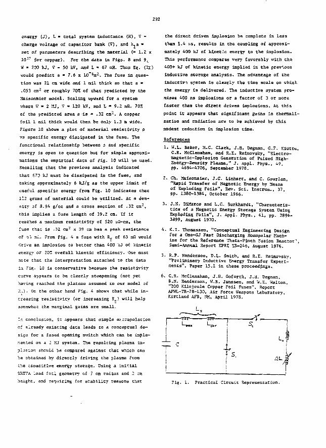
292
energy (J), L • total system inductance (H), V -
charge voltage of capacitor bank (V), and k a -
set of parameters describing the material (» 1.2 x
1017 for copper). For the data in Figs. 8 and 9,
H - 200 fcj, V - 50 kV, and L - 67 nH. Thus Eq. (U)
would predict s » 7.6 x 10 6m*-. The fuse in ques-
tion was 21 cm wide and 1 oil thick so that s *
.053 cm2 or roughly 7051 of that predicted by the
Maisonnier model. Scaling upward for a system
where W • 2 til, V - 120 kV, and L - 9.2 nH. 70Z
of the predicted area s is « .32 cm2. A copper
foil 1 mil thick would then be only 1.3 m wide.
Figure 10 shows a plot of material resistivity p
vs specific energy dissipated in the fuse. The
functional relationship between p and specific
energy is open to question but for simple approxi-
mations Che empirical data of rig. 10 will be used.
Recalling chat the previous analysis Indicated
chat 670 fcJ must be dissipated in the fuse, and
caking approximately 6 kJ/g as the upper limit of
useful specific energy from Fig. 10 indicates that
112 grams of material could be utilized. At a den-
sity of 8.94 g/cc and a cross section of .32 ca2,
this Implies a fuse length of 39.2 cm. If it
reaches a maximum resistivity of 520 u£2-cm, the
fuse that is .32 cm2 x 39 cm has a peak resistance
of b3 mf.. From Fig. 4 a fuse with Rf of 63 mii would
drive an implosion Co better Chan 400 kJ of kinetic
energy ar 20^ overall kinetic efficiency. One must
rate that Che interpretation attached to the daca
in Tig. 10 is conservative because the resistivity
curve appears Co be cleerly steepening (not yet
having reached the plateau assumed in our model of
R.). On che ochax hand Fig. 4 shows chac while in-
creasing resistivity (or increasing Rc) will help
sonewhac Che marginal gains are small.
Ir. conclusion, it appears that simple ej.zrapolacion
cf already exiscing data leads to a conceptual de-
sign for a fused opening switch which can be imple-
mented on a 2 MJ syscem. The resulting plasma im-
plosior. should be compared against that which can
be obtained by directly driving Che plasma from
cV-.e capacicive energy storage. Using a initial
SHIVA load foil geometry of 7 cm radius and 2 ca
height, and requiring cor stability reasons chat
the direct driven implosion be complete in less
than 1.4 vs, results in the coupling of approxi-
mately 400 kJ of klnet-'.c energy to the implosion.
This performance compares very favorably with the
400+ kJ of kinetic energy implied in the previous
Inductive storage analysis. The advantage of the
inductive system is clearly the time scale on which
the energy is delivered. The inductive system pro-
mises 400 ns implosions or a factor of 3 or more
faster Chan the direct driven implosions. At this
point it appears that significant gains in themali-
zation and radiation are to be achieved by this
modest reduction in implosion time.
References
1. W.L. Baker, M.C. Clark, J.H. Degnan, G.F. Xiuttu,C.S. HcClenahan, and R.E. Retnovsky, "Electro-magnetic-Implosion Generation of Pulsed High-Energy-Density Plasma," J. Appl. Phys., 49,pp. 4694-4706, September 1978.
2. Ch. Maisonnier, J.G. Linhart, and C. Gourlan,"Rapid Transfer of Magnetic Energy by Meansof Exploding Foils", Rev. Sci. Instriim., 37,pp. 1380-1384, October 1966.
3. J.S. DiMarco and L.C. Burkhardt, "Characteris-tics of a Magnetic Energy Storage System UsingExploding Foils", J. Appl. Phys., 41, pp. 3894-3399, August 1970.
4. K.I. Thomassen, "Conceptual Engineering Designfor a One-GJ Fast Discharging Homopolar Mach-ine for Che Reference Theta-Pinch Fusion Reactor',Semi-Annual Report EPRI SR-246, August 1976.
5. R.P. Henderson, D.L. Smith, and R.E. Reinovsky,"Preliminary Inductive Energy Transfer Experi-ments", Paper 15.1 in these proceedings^
6. C.R. McClenahan, J.H. Goforth, J.a. Degnan,B.M. Henderson, W.R. Janssen, and W.E. Walton,"200 Kilojoule Copper Foil Fuses", ReportAFWL-TR-78-130, Air force Weapons Laboratory,Kirtland AF3, MM, April 1978.
Fig. I. Practical Circuit Representation.
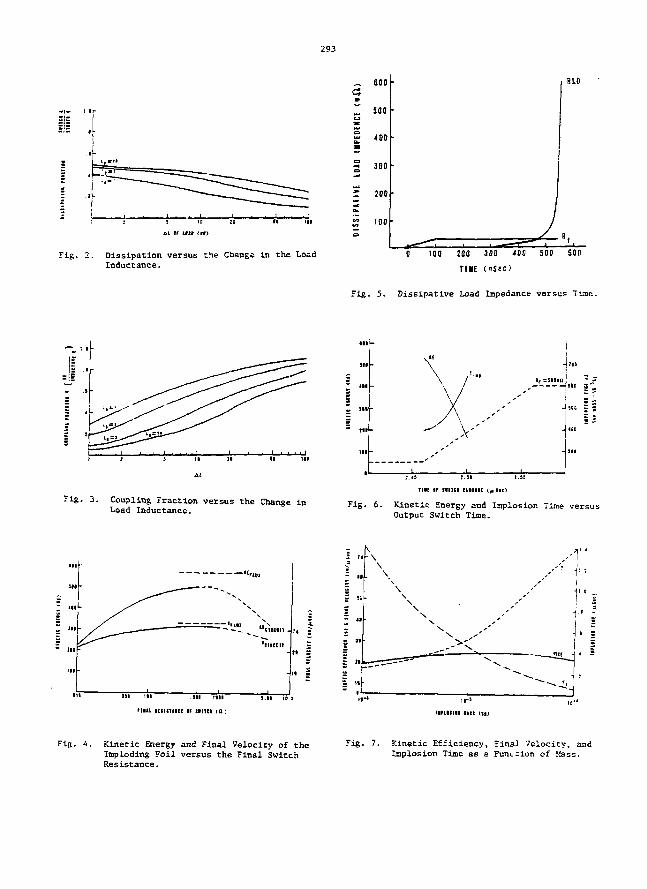
293
at if uit <«>
Fig. 2. Dissipation versus the Change in the LoadInductance.
u J
uuUS
600
SCO
400
300
'00
0 100 200 300 4Qt> S00 SOU
TIKE (nSec)
Fig. 5. Dissipative Load Impedance versus Tine.
it in
sZ mh
-L
so =sSi
Fig. 3. Coupling Fraction versus the Change inLoad Inductance.
THE ir IltlBI CLttllE (Mti«)
Fig. 6. Kinetic Energy and Implosion Time versusOutput Switch Time.
- n\-\
rim lEitmiEt IF »nti in)
Fig. A. Kinetic Energy and Final Velocity of theImploding Foil versus the Final SwitchResistance.
Fig. 7. Kinetic Efficiency, Final Velocity, andImplosion Time as a Function of Mass.
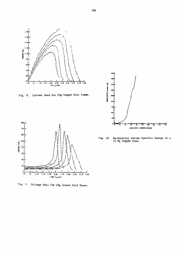
294
; l.ia
' , • . • . V ,v\ V ,.ca .r. i.4o j.ia Z.EO i.sa *.jo *.9O S.BD S.JO I.DI
Fig. 8. Current Data for 25g Copper Foil Fuses.
s ™-
s -•-
Fig. 10. Resistivity verstis Specific Energy in a
25.9g Copper Fuse.
Voltage Data for 2Sg Copper Foil Fuses.
295
13.1
HIGH REPETITION RATE MINIATURE TRIGGERED
SPARK SWITCH
M. F. Rose and M. T. Glancy
Naval Surface Weapons Center
Dahlgren, Virginia 22448
Abstract
A miniature triggered spark switch designed to
operate at high repetition rates has been con-
structed. The device, along with associated
trigger circuitry, has been incorporated into a
simple L-C generator which produces an oscilla-
tory discharge at a frequency of 150 MHz. The
switch is operated in the pressure range 760
torr - 2.6 x 10 torr using commercial dry
nitrogen as the working gas. Both brass and
aluminum electrodes were investigated for re-
petition frequencies as" high as 20 kHz and for
gas flow rates as high as 8 cm /sec. The effect
of repetition rate on switch jitter and switch
breakdown voltage is presented and discussed in
terms of gas pressure and flow rate.
Introduction
High repetition rate switching in the region
greater than 10 kHz can be accomplished by
thyratrons, and in some cases, vacuum gaps.
Unfortunately, these techniques often suffer from
jitter or inductance problems. A quenching spark
gap, however, appears to be one of the simplest
and most efficient devices for this purpose, if
fast turn on and low losses are desirable. The
general idea of a quenching switch is one which
has a large (> 10) A/d ratio and additionally, a
small value of d. The quenching action is based
upon the fact that small plasma volumes can
maintain good electrical conductivity in the small
gap spacing very soon after initiation of the
switch process. After the driving potential has
been removed, the small plasma volume can quickly
recover. Excess thermal energy associated with
the gap dissipation can be transferred to the
switch electrode surfaces or blown from the system
with sufficient gas flow. It is difficult, however,
to provide an adequate trigger mechanism to take
advantage of the high repetition rate in applica-
tions "Th..u"« demand precision pulse spacing. Singlt
stage switcin- of this type have gap spacings no
more than a few mils which make it difficult co
design and implement a "third electrode" trigger
of the trigatron type. The purpose of this paper
is to describe the operating characteristics of a
simple, high repetition rate, quenching spark
switch, under gas flow, when configured as part of
a small hertzian generator of the type described
1 °by Moran and by others in chis conference".Experimental
Figure 1 shows a cross-sectional view of the oscil-
lator and the switch. The device has circular
symmetry and is held together using several nylon
bolts. The pressure collar is made of plexiglass
and is sealed to the switch electrodes via o-rings.
The electrodes are 1.02 cm in diameter, givint an
A/d ratio of approximately 50. In addition, the
electrodes are removable for examination of wear
and other electrode effects^. For our experiments,
we have investigated both brass and aluminum
electrodes with 6 mils gap spacing.
The electrodes are provided with a gas inlet
immediately in the center of one of the switch
electrodes and gas flow outlet holes located
around the periphery of the other electrode.
Figure 2 shows a schematic of the gas flow and
pressurization scheme. While we realize that the
configuration is probably not optimum from a gas
dynamic point of view, it offers nrlrHnrnm inductance,
a desirable characteristic for our application.
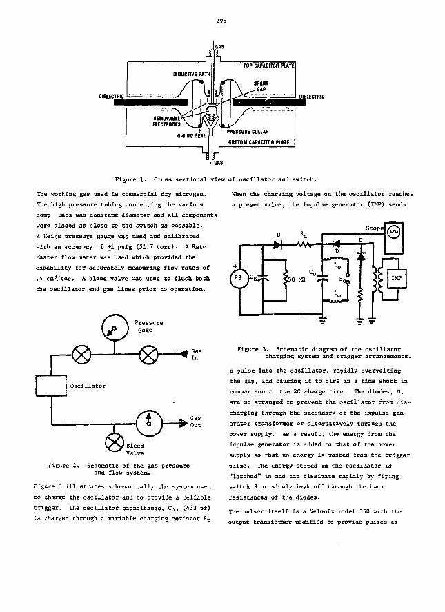
296
DIELECTRIC DIELECTRIC
PRESSURE COLUR
BOTTOM CAPACITOR PLATE
\ GAS
Figure 1. Cross sectional view of oscillator and switch.
The working gas used is commercial dry nitrogen.
The high pressure tubing connecting the various
comp jnts was constant diameter and all components
jere placed as close Co Che switch as possible.
A Heiss pressure gauge was used and calibrated
with an accuracy of +1 psig (51.7 torr). A Rate
Master flow meter was used which provided the
capability for accurately measuring flow rates of
.4 cnv'sec. A bleed valve was used to flush both
che oscillator and gas lines prior to operacion.
PressureGage
<&—«£"
Figure 2. Schematic of the gas pressureand flow system.
Figure 3 illustrates schemacically Che system used
zo charge Che oscillator and to provide a reliable
trigger. The oscillator capacitance, Co, (433 pf)
is charged through a variable charging resistor S^.
When the charging voltage on the oscillator reaches
a preset value, the impulse generator (IMP) sends
Scope!
Figure 3. Schematic diagram of the oscillacorcharging system and trigger arrangements.
a pulse into the oscillator, rapidly overvolting
Che gap, and causing it to fire in a time short in
comparison Co the RC charge cine. The diodes, D,
are so arranged Co prevent che oscillator from dis-
charging through che secondary of the impulse gen-
erator transformer or alternatively through che
power supply. As a resulc, che energy from che
impulse generator is added Co Chat of che power
supply so that no energy is wasted from the trigger
pulse. The energy stored in che oscillacor is
"latched" in and can dissipate rapidly by firing
switch S or slowly leak off through the back
resistances of che diodes.
The pulser itself is a Velonix :nodel 350 with the
output transformer modified to provide pulses as
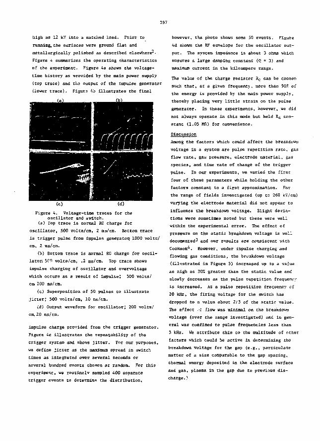
297
high as 12 kV into a Hatched load. Prior to
running, the surfaces were ground flat and
metallurgically polished as described elsewhere- •
Figure 4 summarizes Che operating characteristics
of the experiment. Figure 4a shows the voltage-
time history as provided by the main power supply
(top trace) and the output of the impulse generator
(lower trace). Figurs 'to illustrates the final
Figure 4. Voltage-time traces for theoscillator and switch.
(a) Top trace is normal RC charge for
oscillator, 500 volts/cm, 2 ms/cm. Bottom trace
is trigger pulse from impulse generator; 1000 volts/
cm, 2 ms/cm.
(b) Bottom trace is normal RC charge for oscil-
lator, 5C0 volts/cm, .2 ms/cm. Top trace shows
impulse charging of oscillator and overvoltage
which occurs as a result of impulse; 500 volts/
cm 200 ns/cm.
(c) Superposition of 50 pulses to illustrate
jitter; 500 volts/cm, 10 ns/cm.
(d) Output waveform for oscillator; 200 volts/
cm, 20 as/cm.
impulse charge provided from the trigger generator.
Figure 4c illustrates the repeatability of the
trigger system and shows jitrer. For our purposes,
we define jitter as the maximum spread in switch
times as integrated over several seconds or
several hundred events chosen at random. For this
experiment, we routinelv sampled 400 separate
trigger events to determine the distribution.
however, the photo shows some 50 events. Figure
4d shows the RF envelope for the oscillator out-
put. The system impedance is about 3 ohms which
ensures a large damping constant (Q = 3) and
maximum current in the kiloampere range.
The value of the charge resistor Rc can be chosen
such that, at a given frequency, more than 90X of
the energy is provided by the main power supply,
thereby placing very little strain on the pulse
generator. In these experiments, however, we did
not always operate in this mode but held Rc con-
stant (1.05 Mfi) for convenience.
Discussion
Among the factors which could affect Che breakdown
voltage in a system are pulse repetition rate, gas
flow rate, gas pressure, electrode material, gas
species, and time rate of change of the trigger
pulse. In our experiments, we varied the first
four of these parameters while holding the other
factors constant to a first approximation. For
the range of fields investigated (up to 260 kV/cm)
varying the electTode material did not appear to
influence the breakdown voltage. Slight devia-
tions were sometimes noted but these were well
within the experimental error. The effect of
pressure on the static breakdown voltage is well
documented^ and our results are consistent with
Cookson*. However, under impulse charging and
flowing gas conditions, the breakdown voltage
(illustrated in Figure 5) increased up to a value
as high as 30% greater than the static value and
slowly decreases as the pulse repetition frequency
is increased. At a pulse repetition frequency of
20 kHz, the firing voltage for the switch has
dropped to a value about 2/3 of the static value.
The effect .£ flow was minimal on the breakdown
voltage (over the range investigated) and in gen-
eral was confined to pulse frequencies less than
3 kHz. We attribute this to the multitude of other
factors which could be active in determining the
breakdown voltage for the gap (e.g., particulate
matter of a size comparable to the gap spacing,
thermal energy deposited in the electrode surface
and gas, plasma in the gap due to previous dis-
charge . >
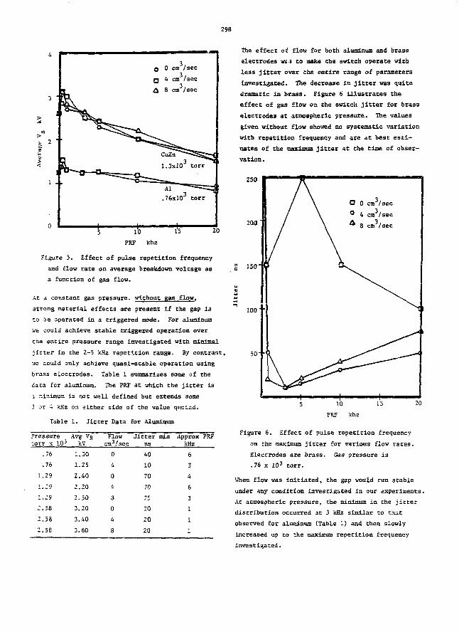
298
1 .
O 0 cm /sec
Q 4 cm /sec
8 cm /sec
.76x10 torr
15 20
PRF khz
Figure 5. Effect of pulse repetition frequency
and flow rate on average breakdown voltage as
a function of gas flow.
At a constant gas pressure, without gas flow,
strong material effects are present If the gap is
to be operated in a triggered mode. For aluminum
we could achieve stable triggered operation over
the entire pressure range investigated with m-ln-tinai
jitter in the 2-5 kHz repetition range. By contrast,
we could only achieve quasi-stable operation using
brass electrodes. Table 1 summarizes some of the
data for aluminum. The PRF at which the jitter is
i minimum is not well defined but extends some
3 or A kHz on either side of the value quoted.
Table 1. Jitter Data for Aluminum
Pressure Avg Vg Flow Jitter min Approx PRF3 3/10 icV kHz
.76
.76
1.29
1.-9
1.29
2.5S
2.53
2.58
1.301.25
2.40
2.20
2.50
3.20
3.40
3.60
0
4
0
3
0
4
8
40
10
70
70
75
20
20
20
6
3
4
6
3
1
1
The effect of flow for both aluminum and brass
electrodes wtj to make the switch operate with
less jitter over the entire range of parameters
investigated. The decrease in jitter was quite
dramatic in brass. Figure 6 illustrates the
effect of gas flow on the switch jitter for brass
electrodes at atmospheric pressure. The values
given without flow showed no systematic variation
with repetition frequency and are <it best esti-
mates of the maximum jitter at the time of obser-
vation.
2S0
200
150
100
50-
O 0 cm /sec0 4 cm3/sec
8 cm3/sec
20
Figure 6. Effect of pulse repetition frequency
on the maximum jitter for various flow rates.
Electrodes are brass. Gas pressure is
.76 x 103 torr.
When flow was initiated, the gap would run stable
under any condition investigated in our experiments.
At atmospheric pressure, the nritrlmmn in the jitter
distribution occurred at 3 kHz similar to that
observed for aluminum (Table 1) and then slowly
increased up to the maximum repetition frequency
investigated.
299
The effect of pressure is equally dramatic fcr
constant flow rate. The trends are similar for
aluminum and brass but differ considerably in
absolute magnitude. Figure 7 illustrates the
effect of repetition frequency on jitter using
brass electrodes for several pressures. The flow
rate was held constant at 8 cm3/sec. The increase
in jitter at higher repetition rates is probably
associated with the increased surface damage,
larger volume; of plasma still in the gap, and
electrode heating effects which enhance field
emission. The minimum jitter occurs at lower pulse
repetition frequencies as the pressure increases.
It has been shown that the diameter of the "spark
discharge" increases with pressure^, if we assume
that this diameter defines the amount of plasma
associated with a particular event, we can readily
estimate the plasma volume associated with the
switch at any given gas flow rate and repetition
rate. This number is approximately constant at
3.4 +.1 x 10- 6cm 3 for the data shown in Figure 7.
Slim',1 ;,r results were also obtained for aluminum.
400
300
200- I
100'
Figure 8 illustrates a typical distribution of
switch firings normalized with respect to the
maximum in the number of switch evencs at a specific
triggering time after the impulse was applied.
These data were taken at a flow rate of 8 emVsec,
PRF of 5 kHz, and atmospheric pressure. The curves
represents some 400 individual events, taken at
random, over a period of several minutes. The
distribution for brass electrodes is approximately
Gaussian and the extrema agree well with the maximum
jitter as observed directly from the oscilloscope.
The results for aluminum were complicated, and we
attribute this to local defects such as that shown
in Figure 9 which eventually grow to such an extent
that the gap is effectively shorted out. We did no-
observe similar failure in brass although running
times of several hours were sometimes involved. In
general, aluminum failed after some 45 minutes with
a drastic increase in jitter and a decrease in
breakdown voltage and in all cases a localized
damage area was observed.
1.001 •
-20
Time ns
Figure 7. Effect of pulse repetition frequency
on maximum switch jitter for constant flow
rate (8 cm3/sec) for various pressures.
Figure 8. Jitter distribution in brass and
aluminum, pressure 760 torr, flow rate
8 cm3/sec, pulse repetition frequency 5 kHz.
300
p. 254-259, 1978.
2. M. T. Glancy aai M. F. Rose, "Surface Aging
in High Repetition Rate Spatt Switches with
Aluminum and Brass Electrodes", Proceedings
of Che Second IEEE International Pulsed Power
Conference, 1979.
3. J. D. Cobine, Gaseous Conductors, p. 163, 1958.
4. A. H. Cookson, "Electrical Breakdown for
Uniform Fields in Compressed Gases", Proc.
IEEE, Vol. 117, p. 269-280, Jan. 1970.
Figure 9. Failure zone on aluminim
electrode surface.
Simple spark switches can be 3iade to operate in
a triggered node for frequencies as high as 20
kHz with a maximum of 30% decrease in the break-
down voltage. In so far as we Investigated,
there is very little effect of materials on the
average breakdown voltage of the switch. There
are, however, large material effects associated
'•rich switch jitter which are probably due to sur-
face chemistry and contamination of the working
gas by particulate matter, blown from the surfaces.
Introduction of gas flow greatly enhances sta-
bility and often results in orders of magnitude
reduction in switch jitter. The effects of gas
pressure are primarily to increase jitter at
higher repetition frequencies and to decrease and
better define the repetition frequency at which
Che minimum in jitter occurs.
Acknowledgement
This work was supported in part by the Defense
Advance Projects Research Agency through Che Naval
Air Systems Command. We wish to thank C. E.
Comford for assistance during Che course of these
experiments.
References
1. 5. L. Movan, "High Repetition Sate L-C
Oscillator", IEEE Conference Record of
Thirteenth Pulse Power Modulator Symposium,
301
13.2
SURFACE AGING IN HIGH REPETITION RATE
SPARK SWITCHES WITH ALUMINUM AND BRASS ELECTRODES
M. T. Glancy and M. F. Rose
Naval Surface Weapons Center
Dahlgren, Virginia 22448Abstract
The surface aging o:f the electrodes of miniature
spark switches (A/d i> 50) is explored using
commercial dry nitrogen as the working gas. Both
brass and aluminum electrodes were investigated
for aging characteristics using a constant gas
flow rate of 8 cm /sec. The gas pressure was
varied froo 760 torr-5200 torr. The switches were
constructed as an integral part of a riiniacure
L-C oscillator which has a ringing frequency of
approximately 150 MHz. The aging process was
halted at intervals ranging from one to several
thousand discharges and the electrode surface
examined with a scanning electron microscope.
Introduction
The problems of electrode wear are relevant to many
applications involving high-speed switching such
as the relay systems used in telecommunications.
Previous work in this area has identified several
mechanisms which govern the dynamics of the forma-
tion and subsequent growth of spark induced
damage . In addition, high repetition rate, pulsed
power systems are being constructed which employ
spark switches that oust carry orders of magnitude
greater current and energy. These systems may use
different gases, electrode materials, gas pressures,
and gas flow rates to minimize erosion and resis-
tive losses while maximizing switch lifetimes and
maintaining acceptable operating parameters.
Common to all of these devices are the fast tran-
sient currents which can produce discharges exhib-
iting glov and arc characteristics. Several
investigators have explored the effect of electrode
-2.3surface coatings ' and crystallographic orienta-
tion on breakdowns in gases. It has been shown
that even thin (' 10 cm) coatings can greatly
alter the breakdown characteristics. In systems
demanding high average power, surface heating can
easily induce chemical reactions between the working
gas and electrode material. These reactions alter
the switch characteristics by forming brittle
compounds which can flake off the metal surface
affecting breakdown voltage and jitter.
In our laboratory, we are currently experimenting
with small hertzian generators which must operate
continuously for long periods of time at pulse
repetition rates of 10's of kilohertz. In another
paper in this conference by Rose and Glancy ,
switches were desc'ii.T'i which were part of a simple
oscillator with a ringing frequency of approximately
ISO MHz. By employing gas flow, it is possible to
operate these devices at high repetition rates (up
to 30 kHz) for long periods of time. The total
energy expenditure may be hundreds of kilojoules.
It is the purpose of this paper to explore the
surface aging phenomenon and wear characteristics
of switches of this type.
Experimental Procedure
The basic oscillator has been described by Moraa .
Our only modification to this design was to provide
for symmetric gas flow and removable electrodes.
In Figure 1, the basic oscillator has capacitance
(CQ> of 433 pf and inductance (21, ) of 4.3 nH.
These values correspond to characteristic oscilla-
tor impedance of approximately 3 ohms. The
oscillator is fitted with a pressure collar and
flow system capable of flow rates as high as 80
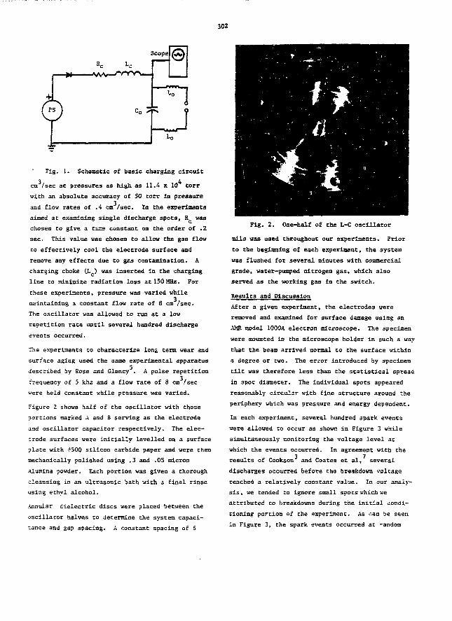
302
Scope |
•M^gj^M
Fig. 1. Schematic of basic charging circuit
3 4
cm /sec at pressures as high as 11.4 X 10 torr
with an absolute accuracy of 50 torr in pressure
and flow rates of .4 cm /sec. In the experiments
aimed at examining single discharge spots, R was
chosen to give a ti=s constant on the order of .2
sec. This value was chosen to allow the gas flov
to effectively cool the electrode surface and
remove any effects due to ges contamination. A
charging choke CLC) was inserted in the charging
line to minimize radiation loss at 150 MHz. For
these experiments, pressure was varied while
maintaining a constant flow rate of 8 cm /sec.
The oscillator was allowed to run at a low
repetition rate until several hundred discharge
events occurred.
The experiments to characterize lonj term wear and
surface aging used the same experimental apparatus
described by Rose snd Glancy . A pulse repetition
frequency of 5 khz and a flow rate of 8 cm /sec
were held constant while pressure was varied.
Figure 2 shows half of Che oscillator with those
portions marked A and B serving as the electrode
and oscillator capacitor respectively. The elec-
trode surfaces were initially levelled on a surface
plate with '.'500 silicon carbide paper and were then
mechanically polished using .3 and .05 micron
alumina powder. Each portion was given a thorough
cleansing in an ultrasonic bath with a final rinse
using ethyl alcohol.
Annular dielectric discs were placed between the
oscillator halves to determine the system capaci-
tance and gap spacing. A constant spacing of 5
Fig. 2. One-half of the L-C oscillator
mils was used throughout our experiments. Prior
to the beginning of each experiment, the system
was flushed for several minutes with commercial
grade, water-pumped nitrogen gas, which also
served as the working gas in the switch.
Results and Discussion
After a given experiment, the electrodes were
removed and examined for surface damage using an
AMR model 1000A electron microscope. The specimen
were mounted in the microscope holder in such a way
that the beam arrived normal to the surface within
a degree or two. The error introduced by specimen
tilt was therefore less than the statistical spread
in spot diameter. The individual spots appeared
reasonably circular with fine structure around the
periphery which was pressure and energy dependent.
In each experiment, several hundred spark events
were allowed to occur as shown in Figure 3 while
simultaneously monitoring the voltage level at
which the events occurred. In agreement with the
results of Cookson and Coates et al, several
discharges occurred before the breakdown voltage
reached a relatively constant value. In our analy-
sis, we tended to ignore small spots which we
attributed to breakdowns during the initial condi-
tioning portion of the experiment. As can be seen
in Figure 3, the spark events occurred at "-andom
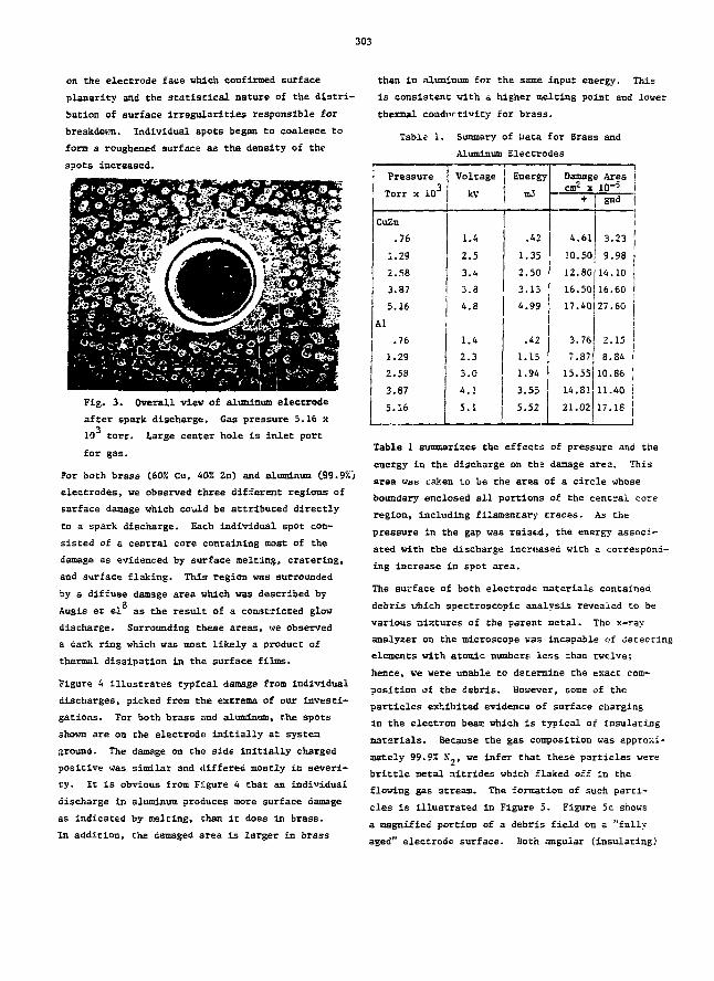
303
an Che electrode face which confirmed surface
planarity and the statistical nature of the distri-
bution of surface irregularities responsible for
breakdown. Individual spots began Co coalesce to
form a roughened surface as the density of the
spots increased.
Fig. 3. Overall view of aluminum electrode
after spark discharge. Gas pressure 5.16 x
10 torr. Large center hole is inlet port
for gas.
For both brass (60% Cu, 40% Zn) and aluminum C99.9ZJ
electrodes, we observed three different regions of
surface damage which could be attributed directly
Co a spark discharge. Each individual spot con-
sisted of a central core containing most of the
damage as evidenced by surface melting, crateringf
and surface flaking. This region was surrounded
by a diffuse damage area which was described byQ
Augis et el as the result of a constricted glow
discharge. Surrounding these areas* we observed
a dark ring which was most likely a product of
thermal dissipation in the surface films.
Figure 4 illustrates typical damage from individual
discharges, picked from the extrema of our investi-
gations. For both brass and ai'irrrfn'.n, the spots
shown are on the electrode initially at system
ground. The damage on the side initially charged
positive was similar and differed mostly in severi-
ty. It is obvious £rom Figure 4 that an individual
discharge in aluminum produces more surface damage
as indicated by melting, :han it does in brass.
In addition, the damaged area is larger in brass
than in aluminum for the same input energy. This
is consistent with a higher melting point and lower
thermal conductivity cor brass.
Table 1. Summary of Data for Brass and
Aluminum Electrodes
Pressure
Torr x 103
CuZn
.76
1.29
2.58
3.87
5.16
Al
.76
1.29
2.58
3.87
5.16
Voltage
kv
1.4
2.5
3.4
3.8
4.8
1.4
2.3
3.0
4.1
5.1
Energy
mJ
.42
1.35
2.50
3.13
4.99
.42
1.15
1.94
3.55
5.52
Damage Areacm2 x 10"5
+
4.6i
10.50
12.80
16.50
17.40
3.76
7.87
15.55
14.81
21.02
gnd
3.23
9.98
14.10
16.60
27.60
i
2.15 |
8.84
10.86
11.40 i
17.18I
Table 1 summarizes the effects of pressure and the
energy in the discharge on the damage area. This
area was taken to be the area of a circle whose
boundary enclosed all portions of the central core
region, including filamentary traces. As the
pressure in the gap was raised, the energy associ-
ated with the discharge increased with a correspond-
ing increase in spot area.
The surface of both electrode materials contained
debris which spectroscopic analysis revealed to be
various mixtures of the parent metal. The x-ray
analyzer on the microscope was incapable of detecting
elements with atomic numbers less than twelve;
hence, we were unable to determine the exact com-
position of the debris. However, some of the
particles exhibited evidence of surface charging
in the electron beam which is typical of insulating
materials. Because the gas composition was approxi-
mately 99.9% N,, we infer that these particles were
brittle metal nitrides which flaked off in the
flowing gas: stream. The formation of such parti-
cles is illustrated in Figure 5. Figure 5c shows
a magnified portion of a debris field on a "fully
aged" electrode surface. Doth angular (insulating)
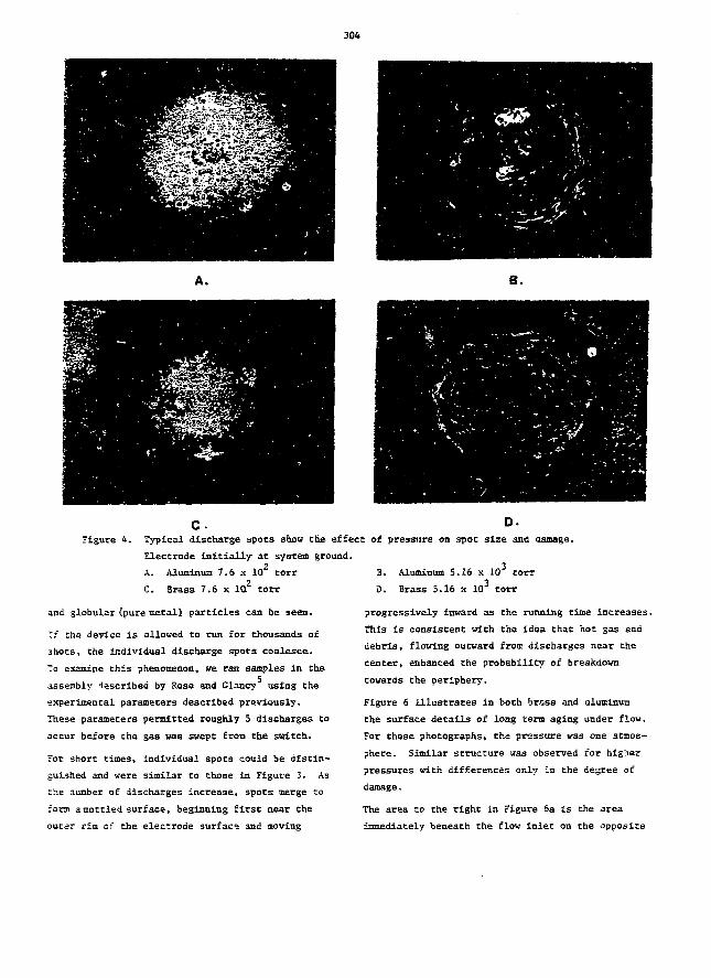
304
A. B.
C. D-Figure 4. Typical discharge spots show the effect of pressure on spot size and damage.
Electrode initially at system ground.2
Aluminum 7.6 x 10 torrn2C. Brass 7.6 x 10. torr
and globular (pure metal) particles can be seen.
If Che device is allowed to run for thousands of
shots, the individual discharge spots coalesce.
To examine this phenomenon, we ran samples in the
assembly described by Rose and Glancy using the
experimental parameters described previously.
These parameters permitted roughly 5 discharges to
occur before che gas was swept from Che switch.
For short times, individual spots could be distin-
guished and were similar to chose In Figure 3. As
the number of discharges increase, spots merge to
form a mottled surface, beginning first near the
outer ria cf the electrode surface aad moving
B. Aluminum 5.16 x 10 torr
D. Brass 5.16 x 10 torr
progressively inward as the running time increases,
this is consistent with the idea that hot gas and
debris, flowing outward from discharges near the
center, enhanced the probability of breakdown
towards the periphery.
Figure 6 illustrates in both br&ss and aluminum
the surface details of long term aging under flow.
For these photographs, the pressure was one atmos-
phere. Similar structure was observed for higher
pressures with differences only in the degree of
damage.
The area to the right in Figure 6a is the area
Immediately beneath the flow inlet on the opposite
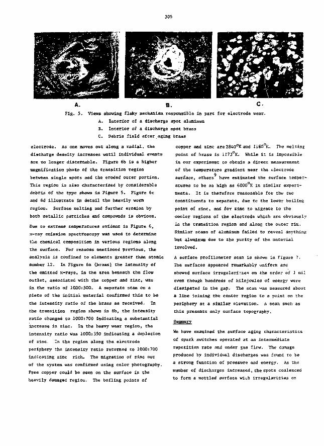
305
A. B.Fig. 5. Views shotting flaky mechanism responsible in part for electrode vear.
A. Interior of a discbarge spot aluminum
B. Interior of a discharge spot brass
C. Debris field after aging brass
copper and zinc are2840°Kand 1163°K. The melting
point of brass is 1173°K. While it is impossible
in our experiment to obtain a direct measurement
electrode. As one moves out along a radial, the
discharge density increases until individual events
are no longer discernable. Figure 6b is a higher
magnification photo of the transition region
between single spots and the eroded outer portion.
This region is also characterized by considerable
debris of Che type shown is Figure 5. Figure 6c
and 6d illustrate in detail the heavily worn
region. Surface melting and further erosion by
both metallic particles and compounds is obvious.
Due to extreme temperatures evident in Figure 6,
x-ray emission spectroscopy was used to determine
the chemical composition in various regions along
the surface. For reasons mentioned previous, the
analysis is confined to elements greater than atomic
number 12. In Figure 6a (brass) the intensity of
the emitted x-rays, in the area beneath the flow
outlet, associated with the copper and zinc, was
in the ratio of 1000:500. A separate scan on a
piece of the initial material confirmed this to be
the intensity ratio of the brass as received. In
the transition region shown in 6h, the intensity
ratio changed to 1000:700 indicating a substantial
increase in zinc. In the heavy wear region, the
intensity ratio was 1000:350 indicating a depletion
of zinc. In the region along the electrode
periphery the intensity ratio returned to 1000:700
indicating zinc rich. The migration of zinc out
of the system was confirmed using color photography.
Free copper could be seen on the surface in the
heavily damaged region. The boiling points of
of the temperature gradient near the electrodeq
surface, others have estimated the surface temper-
atures to be as high as 6000°K in similar experi-
ments. It is therefore reasonable for the two
constituents to separate, due to the lower boiling
point of zinc, and for zinc to migrate to the
cooler regions of the electrode which are obviously
ia the transition region and along the outer rim.
Similar scans of aluminum failed to reveal anything
but aluminum due to the purity of the material
involved.
A surface profilometer scan is shown in Figure 7.
The surfaces appeared remarkably uniform and
showed surface irregular! r.ies on the order oi 1 mil
even though hundreds of kilojoules of energy were
dissipated in the gap. The scan ••'as measured about
a line joining the center region to a point on the
periphery at a similar elevation. A scan such as
this presents only surface topography.
We have examined the surface aging characteristics
of spark switches operated at an intermediate
repetition rate and under gas flow. The damage
produced by individual discharges was found to be
a strong function of pressure and energy. As the
number of discharges increased, the spots coalesced
to form a mottled surface with irregularities on
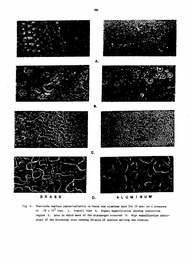
306
B.
C.
B R A S S 0. A L U M I N U M
"ig. 6. Electrode surface characteristics in brass and aluminum aged for 20 min. at a pressure
of .76 x 10 torr. A. Overall view 3. Higher magnification showing transition
region C. Area in which most of the discharges occurred D. High magnification photo-
graph of the discharge area showing details of surface melting and erosion.
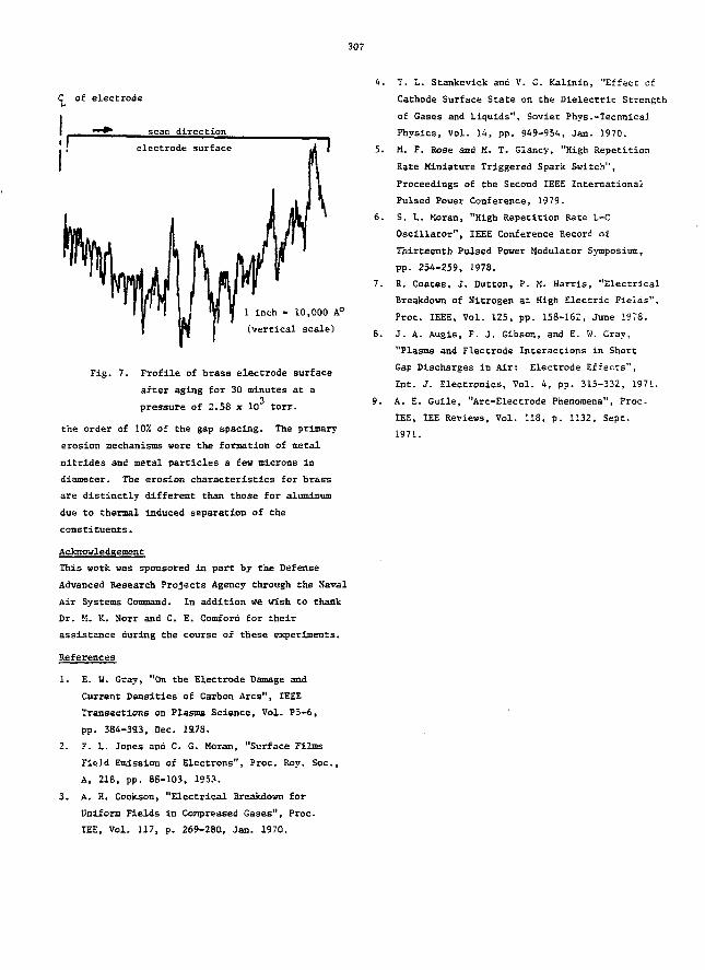
307
of electrode
scan direction
electrode surface
1 inch - 10,000 A0
(vertical scale)
Fig. 7. Frofile of brass electrode surface
after aging for 30 minutes at a
pressure of 2.58 x 10 torr.
the order of 10% of the gap spacing. The primary
erosion mechanisms were the formation of metal
nitrides and metal particles a feu microns in
diameter. The erosion characteristics for brass
are distinctly different than those for aluminum
due to thermal induced separation of the
constituents.
Acknowledgement
This work was sponsored in part by the Defense
Advanced Research Projects Agency through the Naval
Air Systems Command. In addition we wish to thank
Dr. K. K. Norr and C. E. Comford for their
assistance during the course of these experiments.
References
1. E. W. Gray, "On the Electrode Damage and
Current Densities of Carbon Arcs", IEEE
Transactions on Plasma Science, Vol. F5-6,
pp. 384-323, Dec. 19.78.
2. F. L. Jones and C. G. Moran, "Surface Films
Field Emission of Electrons", Proc. Roy. Soc,
A, 218, pp. 88-103, 1953.
3. A. H. Cookson, "Electrical Breakdown for
Uniform Fields in Conpressed Gases", Proc.
IEE, Vol. 117, p. 269-280, Jan. 1970.
8.
". L. Stankevick and V. G. Kalinin, "Effect of
Cathode Surface State on the Dielectric Strength
of Gases and Liquids", Soviet Phys.-Technical
Physics, Vol. 14, pp. 949-954, Jan. 1970.
M. F. Rose and M. T. Glancy, "High Repetition
Rate Miniature Triggered Spark Switch",
Proceedings of the Second IEEE International
Pulsed Power Conference, 1979.
S. L. Moran, "High Repetition Rate L-C
Oscillator", IEEE Conference Record of
Thirteenth Pulsed Power Modulator Symposium,
pp. 254-259, 1978.
R. Coates, J. Dutton, P. M. Harris, "Electrical
Breakdown of Nitrogen at High Electric Fields",
Proc. IEEE, Vol. 125, pp. 158-162, June 1978.
J. A. Augis, F. J. Gibson, and E. W. Gray,
"Plasma and Flectrode Interactions in Short
Gap Discharges in Air: Electrode Effects",
Int. J. Electronics, Vol. 4, pp. 315-332, 1971.
A. E. Guile, "Arc-Electrode Phenomena", Proc.
IEE, IEE Reviews, Vol. 118, p. 1132, Sept.
1971.
303
13.3
SPABK GAP EROSION RESULTS
R. Peer, D. Barrett, and T. R. Burke3
Texas Tech UniversityHigh Voltage/Pulsed Power Laboratory
Lubbock, Texas 79409
Abstract
The erosion characteristics of a spark gap withparallel~plan2 electrodes are determined at atmos-pheric and vacuum pressures. Erosion as a loss ofelectrode material i s measured in a range from 200to 1000 amperes. The severity of electrode erosionis found to be related to spot formation, switchingrates, melting point of the electrode, pressure,arid gap length. Erosion values for a pulsed cur-rent are given for aluminum, brass, and carbon.
IntroductionThe major limiting factor of spark gap lifetime i susually related, in one way or the other, to theerosion characteristics of the material used in thegap. Very l i t t l e information is available on ero-sion of electrode material under repetitive pulseoperation. The primary objective of this researchis Co gather data in an effort to determine thecharacteristics of electrode erosion under rep-raced, square pulse operation. The tests were con-ducted at both atmospheric (760 torr) and low(<50u) pressure and for peak currents of 200 to1000 amperes. The rep-rates used for these testswere 10 and 50 pulses per second (pps). The mate-rials studied were aluminum, brass, and carbon.The test gap was over-volted by a square pulse,so that anode and cathode were well defined (noringing discharge) .
It was found that spot formation, melting point ofthe material, rep-rate, pressure, and gap lengthafracted electrode erosion. At low currents, thecathode undergoes a destructive process while Cheanode is not significantly affected. As the cur-rent i s increased, a transition occurs in which theanode begins to erode. At high current, both cath-ode and anode erosion i s measureable. Electrodes
constructed of material with low melting points pep-form best at low currents while high melting pointmaterials perform beat at higher currents.
Te3t CircuitThe spark gap i s triggered by over-voicing the gap.The circuit i s shown in Figure 1. The output ofthe pulse generator consists of a well-defined rec-tangular pulse so that the anode and cathode areeasily identified. The pulse i s 20 microsecondslong and has a rise and fal l time of less than 1microsecond. A Type E pulse forming network isused to shape the pulse and has a characteristicimpedance of 12 ohms.
A thyratron is used to switch the voltage across thetest gap. When the gap breaks dotm, the major por-tion of the energy stored in the pulse forming net-work i s dissipated in a copper sulfate solution re-sistor. When high current tests are conducted, a2:1 transformer is inserted in the circuit as shownin Figure 2. This test circuit i s capable of oper-ation up to 500 pps and peak currents of 2,5 k i lo-amps using the step down transformer.
-P.F./'-
Figure 1: Spark gap test circuit.
P.F.H.
ir.±' ~ — ' ' '
Figure 2: Spark gap test circuitvith pulse transformer.
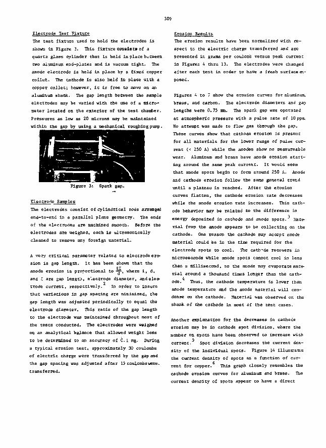
309
Electrode Test Fixture
The tes t fixture used to hold the electrodes is
shown In Figure 3. This fixture consists of a
quartz glass cylinder that i s held in place between
two aluminum end-plates and is vacuum t ight . The
anode electrode i s held is place by a fixed copper
co l le t . The cathode i s also held in place with a
copper col le t ; however, i t i s free to oove on an
aluminum shank. The gap length between the sample
electrodes may be varied with the use of a micro-
meter located on the exterior of the tes t chamber.
Pressures as low as 20 microns may be maintained
within the gap by using a mechanical roughing pump.
Figure 3: Spark gap-
Electrode Samples
The electrodes consist of cylindrical rods arrange!
end-to-end in a para l le l plane geometry. The ends
of the electrodes are machined smooth. Before the
electrodes are weighed, each is ultraaonically
cleaned to remove any foreign material .
A very c r i t i c a l parameter related to electrode ero-
sion i s gap length. I t has been shown that the
anode erosion is proportional to —p, where I, d,
and I are gap length, electrode diameter, and elec-
trode current, respectively. In order to insure
that variations in gap spacing are minimized, the
gap length was adjusted periodically to equal the
electrode diameter. This rat io of the gap length
to the electrode was maintained throughout most of
the tes ts conducted. The electrodes were weighed
on an analytical balance that allowed weight loss
to be determined to an accuracy of C.I mg. During
a typical erosion tes t , approximately 30 coulombs
of e lec t r i c charge were transferred by the gap and
the gap spacing was adjusted after 15 coulombs were,
transferred.
Erosion ResultsThe erosion results have been normalized with re-
spect to the e lec t r ic charge transferred and are
presented in grams per coulomb versus peak current
in Figures A thru 13. The electrodes were changed
after each tes t in order to have a fresh surface ex-
posed.
Figures 4 to 7 show the erosion curves for aluminum
brass, and carbon. The electrode diameters and gap
lengths were 0.75 mm. The spark gap was operated
at atmospheric pressure with a pulse rate of 10 pps.
No attempt was made to flow gas through the gap.
These curves show that cathode erosion is present
for a l l materials for the lower range of pulse cur-
rent (< 250 A) while the anodes show no measureable
wear. Aluminum and brass have anode erosion s t a r t -
ing around the same peak current. I t would seem
that anode spots begin to form around 250 A. Anode
and cathode erosion follow the sane general trend
unt i l a plateau is reached. After the erosion
curves f la t ten , the cathode erosion rate decreases
while the anode erosion rate increases. This cath-
ode behavior may be related to the difference in
energy deposited in cathode and anode spots. Mate-
r i a l from the anode appears to be collecting on the
cathode. One reason the cathode may accept anode
material could be in the time required for the
electrode spots to cool. The cath'de recovers in
microseconds while anode spots cannot cool in less
than a millisecond, so the anode may evaporate mate-
r i a l around a thousand times longer than the cath-
ode. Thus, the cathode temperature i s lower than
anode temperature and the anode material will con-
dense on the cathode. Material was observed on the
shank of the cathode in most of the test cases.
Another explanation for the decreases in cathode
erosion may be in cathode spot division, where the
number on spots have been observed to increase with
current. Spot division decreases the current den-
s i ty of the individual spots. Figure 14 illustrates
the current density of spots as a function of cur-
rent for copper. This graph closely resembles the
cathode erosion curves for aluminum and brass. The
current density of spots appear to have a direct
310
bearing on electrode erosion.
Carbon has an interesting erosion curve In that
the cathode erosion race is constant for all val-
ues of current Investigated. The anode does not
show any measurable wear. Further study is re-
quired to define the conditions for anode erosion.
The melting points of the electrode materials are
a factor on cathode erosion at different pulse
currents. Figure 7 compares the cathode erosion
curves for aluminum, brass, and carbon. Alumi-
num has the lowest melting point of the materials
tested and performs best at currents up to 500 A.
Carbon, which has the highest melting point, erodes
almost twice as much as aluminum In this region.
After 500 A, the brass cathode shows better ero-
sion resistance than aluminum. Hie cast results
for carbon (Figure 6) shows no measurable anode
wear and illustrates the desirability of a high
neIcing point material for the anode electrode.
Figures 8 thru 13 compare the erosion characteris-
tics of brass at atmospheric and vacuum pressures
along with different rep rates and gap lengths.
The electrode diameters and gap lengths were
changed to determine the erosion dependence on gap
length and electrode diameter. Comparing Figure 5
to Figure 8, it Is seen that the erosion rate for
brass is increased by a factor of ten when the gap
Length and electrode diameter are Increased (from
= 10 gm/cb at a gap length and electrode diameter-4
of 0.75 M to = 10 gal do at a gap spacing and
electrode diameter o£ 2.5 mm). The gap length was
adjusced to 1.0 ma with an electrode diameter of
-.5 mm and the erosion results are displayed in
Figure 12. The rate of erosion is dramatically
decreased (from = 10 gm/cb at a gap length and
electrode diameter of 2.5 mm to = 10 gm/cb at a
gap length of 1.0 mm and an electrode diameter of
2.5 nan). In order to verify these findings, a
paper insert was placed in the test chamber to
collect ejected electrode material. Visual obser-
vation indicated that collected material was less
jt a gap length of 1.0 am than at a gap length of
2.5 mm for the same total coulombs transferred.
It is not known whether the destructive electrode
processes of an arc are diminished as gap length is
decreased or that the electrodes simply collect
more ejected material. Gap length and electrode
diameter play an important part in electrode ero-
sion; and, iy maximizing electrode diameter and
minimizing gap length, the rate of erosion can be
reduced.
The pulse repetition rate ac which the test gap is
switched has pronounced affect on cathode erosion.
Referring to Figure 13, it is seen that the maxi-
mum cathode erosion point is shifted from e. ?ea!c
current of 300 A at 10 pps to a peak current of
300 A at 50 pps. This shift of the cathode ero-
sion curve may be explained by tha fact that more
energy per unit time is deposited at the cathode at
50 pps than at 10 pps, and the average cathode
temperature increases so that the condensation of
anode material decreases. For constant pps, the
cathode erosion of brass shows little difference
between atmospheric and vacuum pressures and is as-
sumed to be the same. The erosion race at the
anode is relatively unaffected by different pulse
repetition rates.
Operation of a spark gap at vacuum or lou pressure
has an adverse affect on the erosion rate of the
anode. The pressure in the gap was adjusted to op-
erate below the Faschen minimum for all tests con-
ducted at lou pressure (see Reference 7). Compar-
ing Figure 8 to Figure 10, it is seen that there is
an anode erosion null for vacuum at a peak current
of 700 A with a pulse repetition rate of 10 pps.
The same is true for che anode at vacuum with a rep
rate of 50 pps, except Che anode null occurs at a
peak current of 850 A (Figure 11).
Figure 9 shows a reduction of anode erosion at at-
mospheric pressure with a rep rate of 50 pps; how-
ever, it is not nearly as great as che anode ero-
sion decrease at vacuum pressure. Erosion rates at
low pressure require more investigation to explain
the decrease of anode erosion.
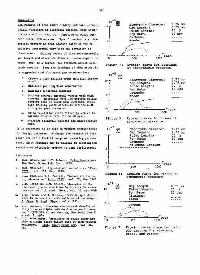
311
Conclusion
The results of this study clearly indicate a consid-
erable variation of electrode erosion, both innag-
nltude and character, as a J-jr-ction of pulse cur-
rent below 1000 amperes. Spot formation is an itr-
portant process in that erosion rates of the re-
spective electrodes vary with the formation of
these spots. Melting paints of electrode materials,
gap length and electrode diameter, pulse repetition
rates, and, to a degree, gap pressure affect elec-
trode erosion. From the findings of this study, it
is suggested that for spark gap construction:
1. Choose a high meeting point material for theanode.
2. Minimize gap length or separation.
3. Maximize electrode diameter.
4. Optimum cathode material varies with peakcurrent. Materials with low melting pointsperform best at lower peak currents, whilehigh melting point materials perform bestat higher peak currents.
5. Pulse repetition rates primarily affect thecathode erosion rate (10 to 50 pps).
6. Pressure primarily affects the anode erosionrate.
it is necessary to be able to predict evosion rates
for design purposes. Although the results of this
paper are for a limited range of operating parame-
ters, these findings may be helpful in reducing the
severity of electrode erosion in some applications
References
1. G.N. Glasoe and J.V. Lebacqz, Pulse Generators,New fork, Dover Pub. Inc., 1948.
2. G.R. Mitchell, 'High-current vacuun arcs.' Proc.IEEF., vol. 117, Dec. 1970.
3. J.A. Rich and G.A. Farrall, 'Vacuum arc recov-ery phenomena.' Proc. IEEE.. vol. 52, Nov. 1964
A. W.D. Davis and K.C. Miller, 'Analysis of theelectrode products emitted by dc arcs in a vac-uum ambient.' 3_. Appl. Phys., vol. 40, Apr. 1969.
5. B.E. Djakov and R. Holmes, 'Cathode spot divi-sion in vacuum arcs with solid metal cathodes.'3_. Phys. p_: Appl. Phys., vol 4 1971.
6. J.E. Daalder, 'Diameter and current density ofsingle and multiple cathode discharges in vac-uum. ' IEEE PES Winter Meeting, New York, Jan.27- Fab. 1, 1974
7. M.J. Schonhuber, 'Breakdown of gases below pas-chen minimum: basic design data of high-voltageequipment.' IEEE. TRASS POWER APP., vol. 88,Feb.
10,- Electrode Diameter:Gap Length:Pulse Length:Rep Ra_f=--.Cathode:Anode:
0.75 mm0.75 mm20 S10 pps
10"5
10 j-
10-5
10
Figure 6:
10'
10
500 1000
Figure 4: Erosion curve for aluminumat atmosoheric pressure.
Electrode DiameterGap Length:Pulse Length:Rep Rate:Cathode:Anode
0 .75 mm0.75 mm20 S10 DDS
•jpn 1000
Figure 5: Erosion curve for brass atatmosoeric oressure.
Electrode Diameter: 0.75 mmGap Length: 0. 7 5 mr.Pulse Length: 20 SRep Rate: 10 ppsCathode:No Anode Erosion
500 1000Sea*
Erosion curve for carbon atatmosperic pressure.
Gap Length:Pulse Length:Rep Rate:Aluminum:Brass:
0. 75 mm20 S10 DPS
Carbon:
.1.
590 1000peak
Figure 7: Erosion curve comparinn cath-ode erosion for aluminum,brass, and carbon.
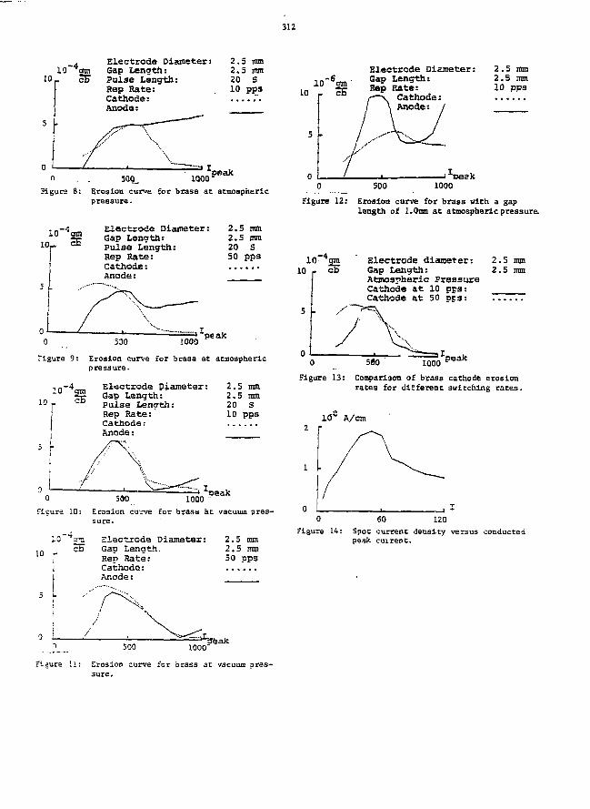
312
10~4gm10 „ aS
Electrode Diameter:Gap Length:Pulse Length:Rep Rate:Cathode:Anode:
2*5 mm2.5 mm20 S10 pps
'•peakn . _ 500_ 1Q00
Figure 8: Erosion curve for brass at atmospheric
10~4gn>10- =fc
pressure.
Electrode Diameter:Gap Length:Pulse Length:Rep Rate:Cathode:Anode:
2.5 mm2.5 mm20 S50 pps
500 1000peak
Figure 9: Erosion curve for brass at atmosphericpressure.
10
,n-4 Electrode Diameter: 2.5 mmlu S" Gap Length: 2.5 mm
Pulse Lencrth:Rep Rate:Cathode:Anode:
20 S10 pps
540'"oeak
1000 -Figure 10: Erosion curve for brass at vacuum pres-
sure.
1 0 " * 5 3 Electrode Diameter: 2.5 mmcF Gap Length. 2 .5 mm
T Rep Sate : 50 pps1 Cathode:1 Anode:
10"6gnT10 - cb
Electrode Diameter:GapRep
Length:Rate:Cathode t
\ Anode: /
2.52.S10
mmmmpps
. . . - • ' •
, 1 .oeajc500 1000
Figure 12: Erosion curve for brass with a gaplength of 1.0mm at atmospheric pressure
10~4gni. cb
Electrode diameter: 2.5 mmGap Length: 2.5 mmAtmospheric FressureCathode at 10 pps:Cathode at 50 pjs:
peak1000Figure 13: Comparison of brass cathode erosion
rates for different switching rates.
10" A/cm2 r
60 120Figure 14: Spot current density versus conducted
peak current.
0 L500 1000'
Figure li: Erosion curve for brass at vacuum pres-sure.
313
13.4
LONG-LIFE HIGH-REPETITION-EATE TRIGGERED SPARK GAP
HAROLD WATSON
AiResearch Manufacturing Company of California
Torrance, California
Abstract
A forced-air-blown triggered spark gap (TSG) switch
system capable of high repetitioc rates on a con-
tinuous basis as veil as a TSG comparative study is
described. The system consists of two TSG's, each
discharging its own 30-ohm pulse cable into a common
load. The svstec was operated at 30 kv, 1 kHz, for
39 x 10& shots with erosion r^tes of approximately
60 mg/amp-hour• Each TSG discharged 0.423 Joules
in 60 nsec (fWHM) per pulse. The switching losses
were about 28 percent of the stored cable energy.
Calculations indicate this can reduce to 14 percent
by optimizing the TSG design and surrounding air
channel insulation for a more uniform E-field.
Test results indicate a multielement assembly capa-
ble of switching 50 'ka or more 40- to 100-nsec
pulses at 1 kHz from 50 kv for 500 x 106 shots
without gap adjustment is feasible with this con-
cept. The work was partially supported by the U.S.
Energy Research and Development Administration under
Contract No. EN-77-C-04-4048.
Introduction
The objective was to develop TSG's Chat would work
in a small-scale multielement spark* gap switch
system to show the feasibility of a much larger
switch system. A full-scale system is to furnish
pulse pcwer to a KrF laser. The specifications are
shown in Table 1.
TABLE 1
TRIGGERED SPARK GAP SYSTEM PERFORMANCE SPECIFICATION
Voltage
Current
Duration
Frequency
50
50
kv
ka
SI00 nsec
2:1 kHz
Life
Jitter
Di/dt
Inductance
Closure time
>5 x 10 8 shots
£10 nsec
2xlO'amp/usec
S.0 oh
£20 nsec
•The words sparks and arcs are used interchangeably.
Complete system studies for a switch system that
will meet these requirements are described in the
final report on this contract (Ref. 1). Spark gap
switches have been used for many years for a variety
of switching applications. Many types have been
developed, each with its particular good feature,
but none that would meet all the requirements of
Table 1. In these contemporary systems, the power
being switched Is not as high as many high-powered
systems; however, the requirement of switching up
to 50 ka and less than 100 nsec pulses, with low
jitter at 1 kHz with a switch life of 5xlO8 pulses,
is a relatively new requi ernest that has received
little attention. The requirement of long life
dictates that the closure di/dt and charge per shot
per switch must be low, which means that many swit-
ches are needed for the 500x10* shots, and thus it
follows that they should be small so the final
assembly Is not unacceptable.- large. The system
study indicated the closure time requirement of
20 nsec could be realized with small TSG's oper-
ating at 1 atm of air. A higher pressure will
decrease the closure time but it will also derrease
the gap spacing, which will make it more difficult
to realize che 500 x 10* shot life requirement. For
example, if the gap spacing increases X percent for
5 cm, it will increase 2XJT percent for 2.5 era, all
else being equal.
This paper is limited to describing the development
of the TSG's in a small-scale pulser to demonstrate
the feasibility of the large multielement switch
system. The merits of various basic spark gap
switches are described as they relate to this appli-
cation. Small size, low switching losses, and low
erosion rateB of the electrodes and trigger were the
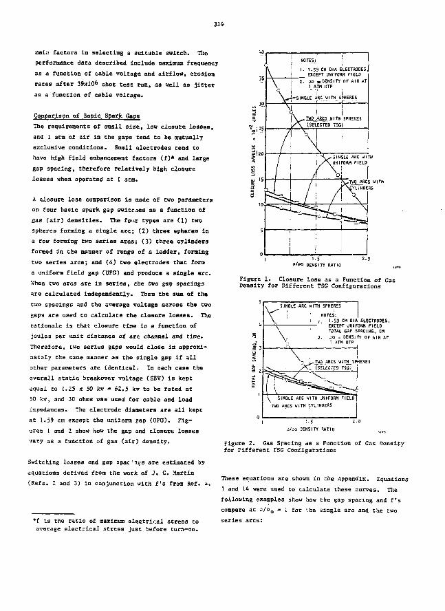
314
aiait! factors in selecting a suitable switch. The
performance data described include maximum frequency
as a function of cable voltage and airflow, erosion
rates after 39x106 shot test run, as well as jitter
as a function of cable voltage*
Comparison of Basic Spark Gaps
The requirements of small size, low closure losses,
and 1 atm of air in the gaps tend to be mutually
exclusive conditions. Small electrodes tend to
have high field enhancement factors (f)* and large
gap spacing, therefore relatively high closure
losses when operated at I atm.
A closure loss comparison is made of two parameters
on four basic spark gap switches as a function of
gas (air) densities. The four types are (1) two
spheres forming a single arc; (2) three spheres in
a row forming two series arcs; (3) three cylinders
formed in Che manner of rungs of a ladder, forming
two series arcs; and (4) two electrodes that form
a uniform field gap (UFG) and produce a single arc.
When two arcs are in series, the two gap spacings
are calculated independently. Then the sum of the
two spacings and the average voltage across the two
gaps are used to calculate the closure losses. The
rationale is that closure time Is a function of
joules per unit distance of arc channel and time.
Therefore, two series gaps would close in approxi-
mately the same manner as the single gap if all
other parameters are identical. In each case the
overall static breakover voltage (SBV) is kept
equal to 1.25 x 50 kv - 62.5 kv to be rated at
50 kv, and 30 ohms was used for cable and load
impedances. The electrode diameters are all kept
at 1.59 cm except the unitorm gap (UFG). Fig-
ures 1 and 2 show how the gap and closure losses
vary as a function of gas (air) density.
Switching lasses and gap spac'ngs are estimated by
equations derived from the work of J. C. Martin
(Refs. 2 and 3) in conjunction with f's from Ref. i.
I 1 . 1 . 5 9 CH DIA ELECTRODES
EXCEPT UNIFORM F IELO
2 . po . D E N S I T Y OF A I R AT
1 ATH IITP
\ .TWO ABCS MITH SPHERES/ \ (SELECTED TSG)
I.S Z.3p/po DENSITY RATIO , „
Figure 1. Closure Loss as a Function of GasDensity for Different TSG Configurations
5
I 3
SINGLE ARC UITH SPHERES
NOTES:I 1 . 5 9 CH OIA ELECTRDOES,
EXCEPT UMIFORH F I E L DTOTAL GAP SPACING. CM
2 . 3 0 • DENSITY OF AIR ATI ATH NTP
TW) ARCS WITH SPHERES
(SZUC7ZD TSG) '
SINGLE ARC WITH UNIFORM FIELD
TWO ARCS UITH CYLINDERS
t :.$ 2-0
a/oo DENSITY RATIO
Figure 2. Gas Spacing is a Function of Gas Densityfor Tifferent TSG Configurations
*f Is the ratio of maximum electrical stress to
average electrical stress just before turn-on.
These equations are shown in the Appendix. Equations
1 and 14 were used to calculate these curves. The
following examples show how the gap spacing and f's
compare at = / % » 1 for nhe single arc and the two
series arcs:
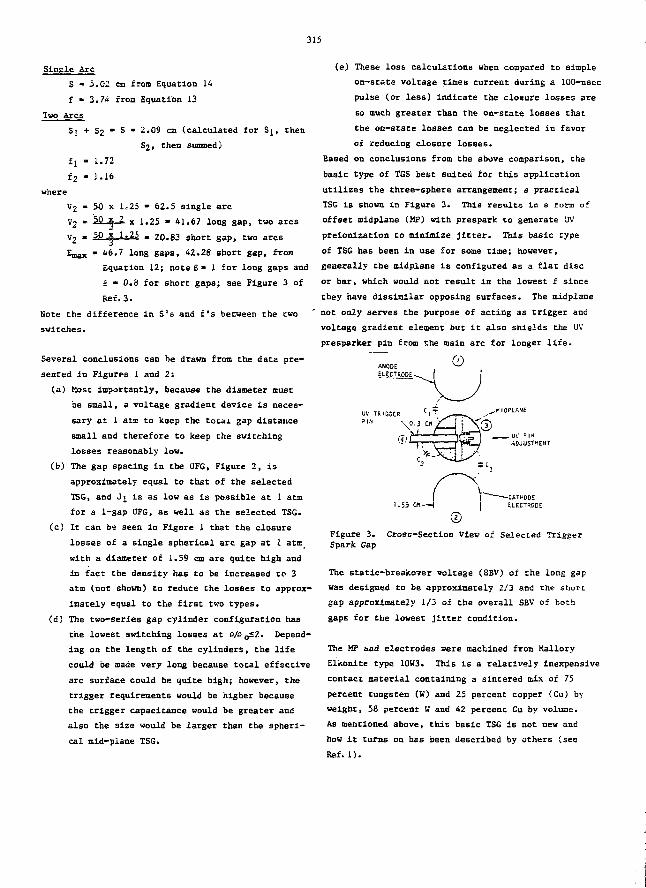
315
Single Arc
S " 5.0; cm from Equation 14
f • 3.74 from Equation 13
Two Arcs
si + S2 " s " 2'09 ^ (calculated for Sj, then
Si, then summed)
fj - 1.72
f2 - 1.16
where
V2 - 50 x 1=25 - 62.5 single arc
V2 » 5Q. ff i- x 1.25 - 41.67 long gap, two arcs
20.83 short gap, two arcs
^6.7 long gaps, 42.28 short gap, fros
Equation 12; note 6*1 for long gaps and
= - 0.8 for short gap6; see Figure 3 of
Ref.3.
Note the difference in S's and t's between the ewo
swlcches.
Several conclusions can be drawn from the data pre-
sented in Figures 1 and 2:
(a) Most importantly, because the diameter must
be small, a voltage gradient device is neces-
sary at 1 atm to keep the total gap distance
small and therefore to keep the switching
losses reasonably low.
(b) The gap spacing in the UFG, Figure 2, is
approximately equal to that of the selected
TSG, and Jj is as low as is possible at 1 atm
for a 1-gap UFG, as well as the selected TSG.
(c) It can be seen in Figure 1 that the closure
losses of a single spherical arc gap at 1 atm
with a diameter of 1.59 cm are quite high and
in fact the density has to be increased to 3
atm (not shown) to reduce the losses to approx-
imately equal to the first two types.
(d) The two'serles gap cylinder configuration has
the lowest switching losses at O/PQ£2. Depend-
ing on the length of the cylinders, the life
could be made very long because total effective
arc surface could be quite high; however, the
trigger requirements would be higher because
the trigger capacitance would be greater and
also the size would be larger than the spheri-
cal mid-plane TSG.
(e) These loss calculations when compared to simple
on-state voltage times current during a 100-nsec
pulse (or less) indicate the closure losses are
so much greater than the on-state losses that
the on-state losses can be neglected in favor
of reducing closure losses.
Based on conclusions from the above comparison, the
basic type of TGS best suited for this application
utilizes the three-sphere arrangement; a practical
TSG is shown In Figure 3. This results in a form of
offset oidplane (MP) with prespark Co generate UV
preionization to minimize jitter. This basic type
of TSG has been in use for some time; however,
generally the mldplane is configured as a flat disc
or bar, which would not result in the lowest f since
they have dissimilar opposing surfaces. The midplane
not only serves the purpose of acting as trigger and
voltage gradient element but it also shields the UV
presparker pin from the main arc for longer life.
Figure 3. Cross-Section View of Selected TriggerSpark Gap
The static-breakover voltage (SBV) of the long gap
was designed to be approximately 2/3 and the short
gap approximately 1/3 of the overall SBV of both
gaps for the lowest jitter condition.
The HP =nd electrodes were machined from Mallory
Elkonlte type 10W3. This is a relatively inexpensive
contact material containing a sintered mix of 75
percent tungsten (U) and 25 percent copper (Cu) by
weight, 56 percent W and 42 percent Cu by volume.
As mentioned above, this basic TSG is not new and
how it turns on has been described by others (see
Ref. 1).
316
Setup and Test Results
The pulser test bed consisted of two of Che newly
developed TSG's, each discharging its own 30<4-ohsi
pulse cable Into a common load; a dc resonant
charger was used Co chfirge the cables In 67 usec;
this plus an additional irargin of 83 usec allowed
850 usec for the TSG's to recover at 1 kHz. Due
to higher than expected core losses in the trigger
pulse transformers, the overall rise tine of the
trigger pulse was ouch longer than expected. Despite
this, the jitter was in the range of 3 to 4 nsec
peak to peak, which suggests jitter in the range
of 1 nsec could be expected with adequate trigger
generator redesign*
Figure 4 shows a side view of the TSG used for
case in the air channel. One TSG is mounted 12
inches above the other in the same air stream.
Note there is an opening for air to circulate
through the MP r.o clear out prespark generated
hoc gas and dust particles.
Figure 5 shows Che air velocity as measured right
on top of the air channel. The fixture was
originally designed for two TSG's side-by-side
but because of arcovecs between th« '.wo TSG's,
one was renoved. This left a large space in which
much of the air could flow. Though this decreased
Che air to the remaining TSG, the 1 kHz goal wan
reached; however, it does suggejt that with the
proper air flow the pulse rate could be higher.
Figure 6 show a side view picture of Che TSG
and load assembly. The TSG's were operating at
1 kHz when Che picture was taken.
SPOT WHERE A TSGWAS REMOVED WKG ELECTRODE
UV PIN ADJUSTMENTSCREW
VELOCITIES IN LINEART-T PER MlN
SHORT ELECTRODE
Figure 5. Airflow Pattern Over Top of Air Ducc
Figure i. Side View of TEG in Test Fixture Figure 6. Switch Assembly and Load
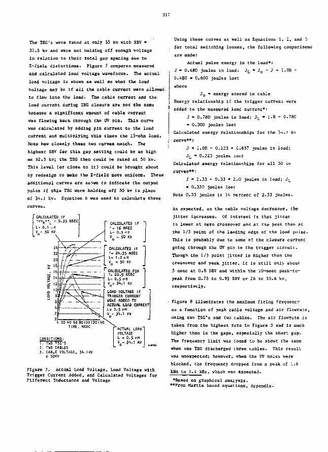
317
The TSG's were rated at only 35 kv with SBV -
37.5 !tv and were not holding off enough voltage
in relation to their total gap spacing due to
E-field distortions. Figure 7 compares measured
and calculated load voltage waveforms. The actual
load voltage is shown as well as what the load
voltage may be if all the cable current were allowed
to flow into the load. The cable current and the
load current during TSG closure are not the same
because a significant amount of cable current
was flowing back through the UV pin. This curve
was calculated by adding pin current to the load
current and multiplying this times the 15-ohm load.
Note how closely these two curves match* The
highest SBV for this gap setting could be as high
as 62.5 kv; the TSG then could be rated at 50 kv.
This level (or close to it) could be brought about
by redesign to make the E-field more uniform. Three
additional curves are sniws to Indicate the output
pulse if this TSG were holding off 50 kv in place
of 34.1 kv. Equation 6 was used to calculate these
curves.
fCALCULATED IFT = V T L = 5 . 3 5 NSECL= 0.1 uHV > 50 KV
CALCULATED IFT - 16 MSECL= 0 . 5 ^ HV = 50 KV
o
CALCULATED IF-=. 2 4 . 3 5 NSECL= 1 .0 KH
50 KV
' CALCULATED FORT = 2 0 . 9 NSECL-- 0 .5 MHv =. 3 4 . ; KV
LOAD VOLTAGE I FTRIGGER CURRENTWEKE ADDED TOACTUAL LOAD CURRENTL= 0 . 5 UN
4 . 1 KV
ACTUAL LOADV0LTA3EL = 0 . 5 HHV = 3 4 . 1 KV
CONDITIONS:1 . TWO TSG'S2 . TWO CABLES3. CABLE VOLTAGE, 34.1KV
t, 5OKV
Figure 7. Actual Load Voltage, Load Voltage withTrigger Current Added, and Calculated Voltages forPifferer.t Inductance and Voltage
Using these curves as well as Equations 1, 2, and 3
for total switching losses, the following comparisons
are made:
Actual pulse energy in the load*:
J - 0.480 joules in load: JL - Jo - J - 1.08 -
0.480 » 0.600 joules lost
where
Jo * energy stored in cable
Energy relationship if the trigger current were
added to the measured load current*:
J - 0.780 joules in load; JL - 1.8 - 0.780
» 0.300 joules lost
Calculated energy relationships for the 34.1 kv
j curve**:
I J - 1.08 - 0.223 - 0.857 joules in load;
JL - 0.223 joules lost
Calculated energy relationships for all 50 kv
curves**:
J - 2.33 - 0.33 - 2.0 joules in load; JL
- 0.330 joules lost
Note 0.33 joules is 14 percent of 2.33 joules.
As expected, as the cable voltage decreases, the
jitter increases. Of interest is that jitter
is lower at zero crossover and at the peak than at
the 1/3 point of the leading edge of the load pulse.
This is probably due to some of the closure current
going through the TJV pin to the trigger circuit.
Though the 1/3 point jitter is higher than the
crossover and peak jitter, it is still only about
3 nsec at 0.8 SBV and within the 10-nsec peak-to-
peak from 0.75 to 0.95 SBV or 26 to 35.6 kv,
respectively.
• Figure 8 illustrates the maximum firing frequency
as a function of peak cable voltage and air flovrate,
using two TSG's and two cables. The air flowrate is
taken from the highest rtite in Figure 5 and is much
higher than in the gaps, especially the short gap.
The frequency limit was found to be about the same
when one TSG discharged three cables. This result
was unexpected; however, when the UV holes were
blocked, the frequency dropped from a peak of 1.6
kHz to 1.1 kHz. which was] expected.
*Based on graphical analysis.**From Martin based equations, Appendix.
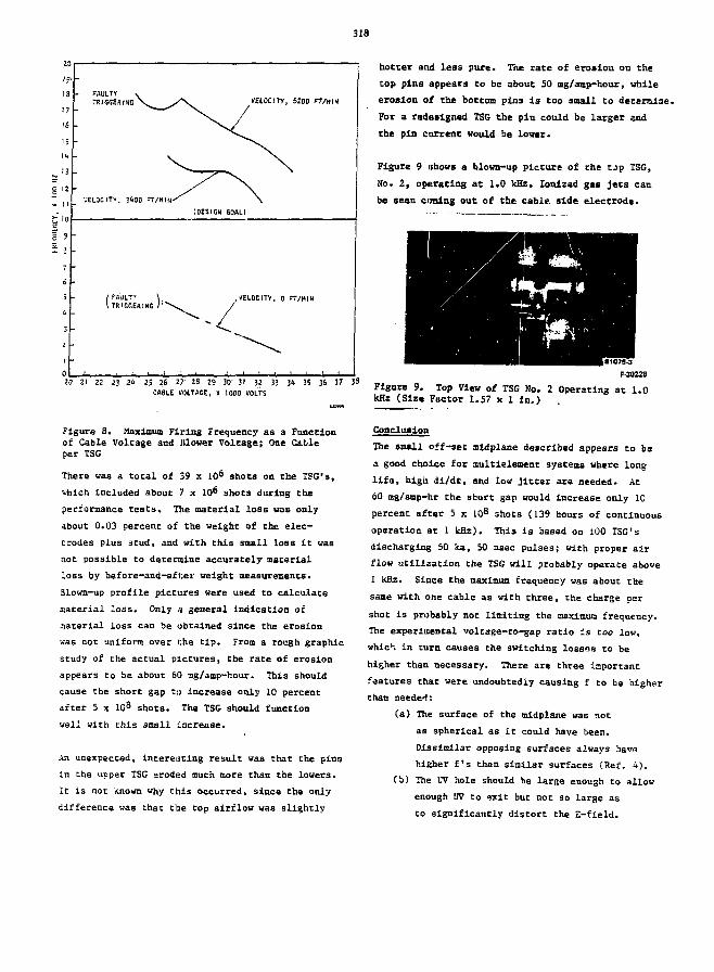
318
FAULTYTRIGGERING
VELOCITY, J4OO FT/MIH
VELOCITY, 6200 FT/HIN
(DESIGN GOAL)
VELOCITY, 0 FT/HIN
Figure 8. Maximum Firing Frequency as a Functionof Cable Voltage and Blower Voltage; One Cableper TSG
There was a total of 39 x 106 3hots on the TSG's,
which included about 7 x 10& shots during the
performance tests. The material loss was only
about 0.03 percent of the weight of the elec-
trodes plus stud, and with this small loss it was
not possible to determine accurately material
loss by before-and-after weight measurements.
Blown-up profile pictures were used to calculate
material loss. Only a general indication of
material loss can be obtained since the erosion
vas not uniform over i:he tip. From a rough graphic
study of the actual pictures, the rate of erosion
appears to be about 60 mg/amp-hour. This should
cause the short gap to increase only 10 percent
afcer 5 x 10⁸ shots. The TSG should function
veil with this small Increase.
An unexpected. Interesting result was that the pins
in the upper TSG eroded much more than the lowers.
It is not ttnown why this occurred, since the only
difference was that the top airflow was slightly
hotter and less pure. The race of erosion on the
top pins appears Co be about 50 mg/amp-hour, while
erosion of the bottom pln3 Is too small to determine.
For a redesigned XSG the pin could be larger and
the pin current would be lower.
Figure 9 dhows a blown-up picture of the tjp TSG,
Ho. 2, operating at 1.0 kHz. Ionized gas jets can
be seen cooing out of the cable side electrode.
33
F-30228
•kHz (Size Factor 1.57 x 1 in.)
Conclusion
The small off-set midplane described appears to be
a good choice for multielement systems where long
life, hlgii di/dt, and low jitter are needed. At
60 mg/amp-hr the short gap would increase only 10
percent after 5 x 10⁸ shots (139 hours of continuous
operation at 1 kHi). This is based on 100 TSG's
discharging 50 ka, 50 nsec pulses; with proper air
flow utilization the TSG will probably operate above
1 kHz. Since the maximum frequency was about the
same with one cable as with three, the charge per
shot is probably not limiting the maximum frequency.
The experimental voltage-to-gap ratio is too low,
which in turn causes the switching losses to be
higher than necessary. There are three inportant
features that were undoubtedly causing f to be higher
than needed:
(a) The surface of the midplane was not
as spherical as it could have been.
Dissimilar opposing surfaces always have
higher f's than similar surfaces (Ref. 4).
(b) The UV hole should be large enough to allow
enough UV to exit but not so large as
to significantly distort the E-field.

31S
The present hole Is 1/8 In., which is
probably larger than needed,
(c) The dividers and nonsymmetrieal surrounding
structure distorts the E-field.
By proper redesign the closure losses will be
reduced; however, the lowest possible figure appears
to be 14 percent of the available energy. The pres-
sure could be increased to lower the closure losses;
however, this may decrease the life since the per-
cent of increase In the now smaller gap spacing
would be greater. Also, any air filter will allow
some dust particles through. How much filtering is
needed to keep prefire at a minimum Is uncertain.
The premise that two gaps could be operated in the
same air stream if the air has around 10 msec between
gaps to recover its dielectric strength has been
shown.
References
1. "Multielement Spark Gap Switch System," Final
Report on Contract No. EN-72-C-04-4048 for U.S.
Energy Research and Development Administration.
2. Pulsed Electrical Power Circuit and Electro-
magnetic System Design Notes 4-1, Volume I,
Note 4, AFWL-TR-73-166.
3. Pulsed Electrical Power Dielectric Strength
Notes 5-1, Note 16, AFWL-TR-73-167.
4. High-Voltage Technology, edited by L. L. Alston,
Gxford University Press A68, Page 7.
APPENDIX
Switching losses are estimated in three steps from
0 to 2.2T, from 2.2T to T 0, and from x0 to t0 in the
following manner:
2.2T ,
I. J2 s /vtltdt - 0,4 V o
2 T R / R (closure losses)!
I~o To i
3. J3
C-o - 2.2t)
tp
f Z£J Ctt" 2
0.11)
4.
5.
6.
7.
8.
9.
10.
11.
12.
13.
14.
15.whert
Vt - Vo - Vx - 1TR, drop across gap
L iidt
Z + (Ref. 2)
T R + T L , e—folding time of current pulse(Ref. 2)
- • 8 8 , (0/Po)l/2 x 10"? secEl/3 E 4 / 3
(accurate within 20%) (Eef. 2.)
- L/R (Ref. 2)
^ax/f in units of 10 kV (Ref. 3)
- 24.5p + 6.7 /p7r^7 (Ref. 3)
f - KjS/r + K2 (for f > 0.37) (Ref. 4)r
S - rg2K2 (from combining EquacionsrEmax-v2Kl 13 and 15)
V, S B V in kV (Ref. 3)
2. J2
VtItdt + / VcItdi:
2.2T 2.2T
-2T O/T _ T /T
£ - e2
+ 0.105J +
J - energy lost in joules
Vo - cable voltage at to+, v
L - effective series inductance, h
Z - source Impedance, 30 ohms per cable
R " load resistance, 15 ohms for two TSG's and
two cables
Po - density of air at 1 atm NTP
P - density of air in gap
Kj - 0.13 for cylinders, 0.46 for spheres (Ref. 4)
K2 - 1.06 for cylinders, 0.83 for spheres (Ref. <O
r - radius of electrodes in cm
reff - 0.23r for cylinders, 0.115r for spheres
(Ref. 4)
e - function of S/r, slight modifier (Ref. 4)
Vc - on-state voltage, 50 v assumed
T O - cable pulse duration, both ways, nsec
tp« duration of pulse at base, nsec
I * peak pulse current
SBV - static breakover voltage
P • pressure, atm
S « gap spacing, cm
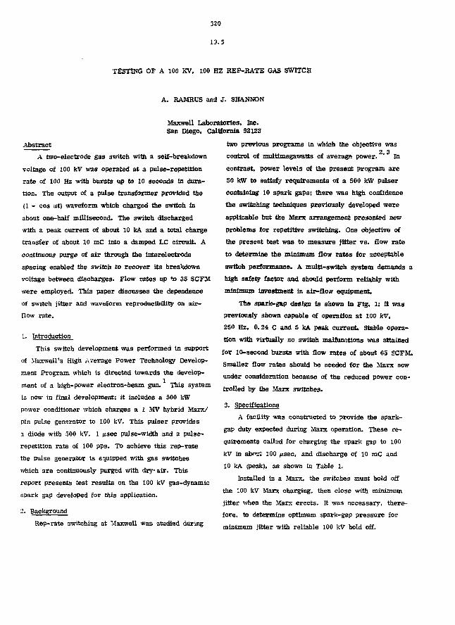
320
13.5
TESTING OF A 100 KV, 100 HZ REP-HATE GAS SWITCH
A. RAMBUS and J. SHANNON
Maxwell Laboratories, Inc.San Diego, California 92123
Abstract
A two-electrode gas switch with a self-breakdown
voltage of 100 kV was operated at a pulse-repetition
rate of 100 Hz with bursts up to 10 seconds in dura-
tion. The output of a pulse transformer provided the
(1 - cos iut) waveform which charged the switch in
about one-half millisecond. The switch discharged
with a peak current of about 10 kA and a total charge
transfer of about 10 mC into a damped LC circuit. A
continuous* purge of air through the interelectrode
spacing enabled the switch to recover its breakdown
voltage between discharges. Flow rates up to 35 SCFM
were employed. This paper discusses the dependence
of switch jitter and waveform reproduclbility on air-
flow rate.
1. Introduction
This switch development was performed in support
of Maxwell's High Average Power Technology Develop-
ment Program which is directed towards the develop-
ment of a high-power electron-beam gun. This system
is now in final development; it includes a 500 irtV
power conditioner which charges a 1 MV hybrid Marx/
pfn pulse generator to 100 kV. This pulser provides
a diode with 500 kV, 1 jisec pulse-width and a pules-
repetition rate of 100 pps. To achieve this rep-rate
the pulse generator is equipped with gas switches
which are continuously purged with dry air. This
report presents test results on the 100 kV gas-dynamic
spark gap developed for this application.
2. Background
Rep-rate switching at Maxwell was studied during
two previous programs in which the objective was
control of multtmegawatts of average power. ' In
contrast, power levels of the present program are
SO kW to satisfy requirements of a 500 kW pulser
containing 10 spark gaps; there was high confidence
the switching techniques previously developed were
applicable but the Marx arrangement presented new
problems for repetitive switching. One objective of
the present test was to measure jitter vs. flow rate
to determine the minimum flow rates for acceptable
switch performance. A multi-switch system demands a
high safety factor and should perform reliably with
minimum investment in air-flow equipment.
The spark-gap design is shown in Fig. 1; it was
previously shown capable of operation at 100 kV,
250 Hz, 0.24 C and 5 kA peak current. Stable opera-
tion with virtually no switch malfunctions was attained
for 10-second bursts with flow rates of about 65 SCFM.
Smaller flow rates should be needed for the Marx now
under consideration because of the reduced power con-
trolled by the Marx switches.
3. Specifications
A facility was constructed to provide the spark-
gap duty expected during Marx operation. These re-
quirements callad for charging the spark gap to 100
kV in about 100 psec, and discharge of 10 mC and
10 kA (peak), as shown in Table 1.
Installed in a Marx, the switches must hold off
the 100 kV Marx charging, then close with minimum
jitter when the Marx erects. It was necessary, there-
fore, to determine optimum spark-gap pressure for
minimum jitter with reliable 100 kV hold off.

321
4. Setup
4.1 Test Circuit
The test facility consisted of a primary charging
circuit, a 1:12 step-up transformer, and an output
circuit containing the switch under test. The power
source was a 3-phase transformer which reduced
power company 12 kV AC to 4160 V (rms). The 3-
phase was then rectified in a 6-rectifier bridge.
Fig. 2 shows the main circuit elements. When
the ignitron is triggered, the primary capacitor, C
resonantly charges through the 13 mH inductor to about
8 kV with a 1 msec transfer time. A thyrairon (Eng.
Elec. CX 1154) controls the discharge of Cj into the
transformer. A diode and resistor is connected across
the thyratron to allow reverse current to bypass fee
thyratron and to reset the transformer core while pre-
venting damaging current reversal through the thyra-
tron.
The transformer was a foil and mylar winding
around an iron core with Hie primary and secondary
insulated from one another and from ground permitting
the primary to be charged with the secondary grounded.
C and the thyratron had one end grounded to eliminate
the need for an isolated heater supply.
The output circuit containing the switch had the
required inductance and resistance to ring the current
through the switch to conduct 10 mC, although C_ con-
tained only 2.2 mC. The 3 ^ damping resistance was
chosen for a circuit-Q of about three. The switch
circuit inductance was about 1.5 itR to attain the
10 kA (peak) at 100 kV.
4.2 Diagnostics
(1) Voltage Probes
Uesistive voltage dividers tapped-off the voltage
on C, and Co. The probe on C capacitor indicated
switch breakdown voltage. Data from these probes was
stored on an Ampex tape recorder which operates at
high tape speeds. The magnetic record is then played
back at a slow speed and recorded on a multi-channel
chart recorder. With this technique every pulse
in a burst can be analyzed although at the relatively
low frequency bandwidth of - 20 kHz. The C charge
voltage was also recorded on an oscillograph.
(2) Current Probe
A Pearson current probe monitored switch
current. The rep-rate waveforms were recorded on
magnetic tape and were superimposed on an oscillo-
scope. Fluctuation in the amplitude of this current
measured on the oscillograph indicated the jitter in
breakdown voltage since this peak current is propor-
tional to breakdown voltage. The trace width after a
typical 100-shot run indicated the total spread in peak
current*
(3) Air Pressure and Flow
Flow was determined by measurement of pressure
in a pitot tube placed downstream from the switch. A
Magnahelic gauge measured this pressure. The pitot
tube was located in a straight section of 2-7/6" dia-
meter PVC pipe about ten feet from the switch and
three feet from the end of the pipe which exhausted
into the atmosphere. Calculation of mass Son- rate
from measured flow velocity of 500 ft. per minute
yielded 10 SCFM.
5. Results
5.1 Switch Hold-off Voltage vs. Pressure
An irradiation gap (Fig. 1) was provided in the
aluminum flange attached to one of the switch electrodes.
In this way the arc site on the nested-pair electrode
was illuminated with UV from the irradiation source.
In theBe experiments the TJV source was a <-park plug
which fires perpendicular to the plug axis, and has an
unimpeded optical path to the arc site on the nested-
pair axis.
The breakdown probability vs. switch pressure is
shown in Fig. 3. This data was obtained by recording
the number of switch closures which occurred in a one-
second, 100-shot burst, and the ratio of successful
switch closures to 100 switch charges was plotted.
Fig. 4 shows a typical magnetic-tape record with a
missing C_ recharge which occurred when the switch

322
failed to fire.
The relation between breakdown probability and
pressure enables the switch to be operated in a Marx
by pre-setting switch pressure at the value where this
probability is zero. For example, for negative polarity
on the nested pair, a pressure of 40 psig (and flow
rate of 500 ft/min) is suitable.
5.2 Switch Jitter
Jitter was estimated by computing the ratio of the
total spread in the peak switch current to the average
peak switch current in a given 100-shot burst. A
typical set of 100 superimposed voltage and current
waveforms is shown in Figure Sa in which total spread
is 12% of average peak current.
Switch polarity had an influence on jitter. Best
jitter was obtained when negative polarity was applied
to the nested-pair electrode and when that electrode
was irradiated.
For either positive or negative polarity when
irradiation was absent the first switch charge had an
abnormally high peak current indicating increased
breakdown strength. Occasionally the first applied
waveform did not breakdown the switch. After the
first breakdown subsequent waveform? had lower
amplitude and low jitter.
The percentage spreads in Table 2 do not include
the first few anomalous charging waveforms for non-
irradiation cases. \t they did, those values would have
substantially higher spreads.
3. 3 Conclusions
Based on these results, when employing this
switch in a rep-rated Marx, it is important to employ
irradiation. Also, the switch operates more reliably
and with consistently low jitter when the irradiated
electrode is charged negatively. (Thi3 is not too sur-
prising since the negative electrode provides the initiat-
ing electrons when illuminated with UV.) Regardless of
polarity the non-irradiated switch has a first-pulse
breakdown strength which exceeds that of the irradiated
switch. This is believed caused by a stagnation region
of plasma at the arc site of the nested pair which
reduces breakdown strength and provides irradiation.
This volume may not purge completely preventing the
switch from recovering its full breakdown strength,
once the first breakdown occurs. The ratio of the first
to the average breakdown voltage was variable; average
20% below that of the first value was not uncommon.
Surprisingly, anomalous first-pulse charging wave-
forms did not occur when the irradiated electrode was
charged positively. Probably reflection of UV from the
positive to the negative electrode caused the necessary
Initiating electrons. Also, for many tests, jitter was
comparable to mat of negative polarity, although not
as consistent from burst to burst.
Acknowledgements
The authors wish to extend our thank3 to Mr.
James DeVoss for his extensive contributions to the
design, test, and data analysis throughout this program.
Also, our thanks to Mr. Larry Houghton for the
capable engineering MIJ technical support he provided.
Bibliography
1. J. Shannon, "A 500 kV Rep-rate Marx Generator".2nd International Pulse-Power Conference, June1979, Lubbock, Texa3.
2. R. W. Clark, "A Simulation Approach to HighAverage Power Repetitively Pulsed Switch Testing",IEEE Transactions on Industrial Electrical andControl Ind., Vol. EC 1-23, No. 1, February 1976.
3. A. Ramrus, "Development of a 100 kV Multimega-watt Rep-Rate Gas Switch", Thirteenth Pulse-Power Modulator Symposium, June 1978.
This work was performed under Ballistic MissileDefense System Command Contract No. DASG60-77-C-0058.
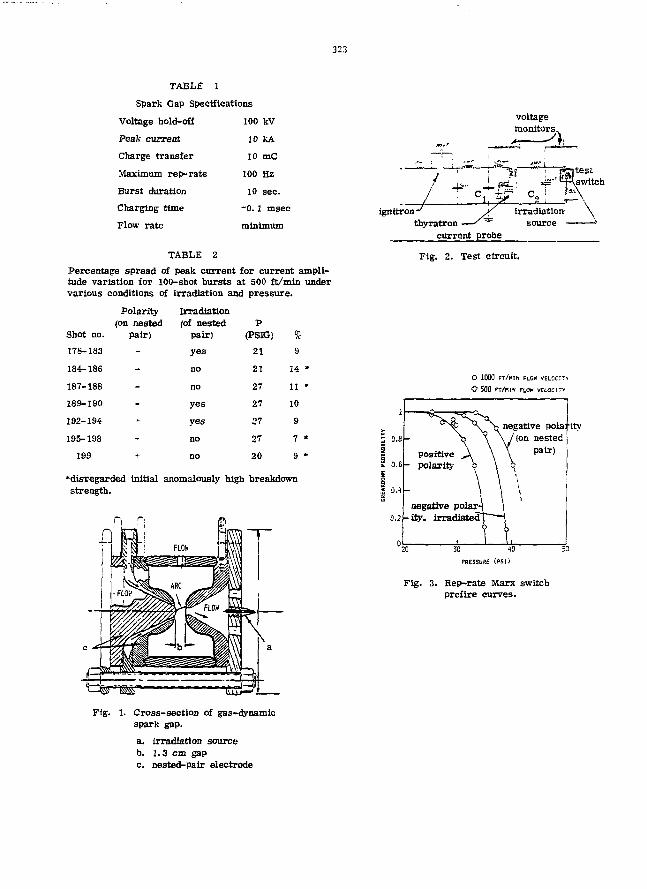
323
TABL£ 1
Spark Gap Specifications
Voltage hold-off
Peak current
Charge transfer
Maximum rep-rate
Burst duration
Charging time
Flow rate
100 kV
10 kA
10 mC
100 Hz
10 sec.
•0.1 msec
minimum
TABLE 2
Percentage spread of peak current for current ampli-tude variation for 100-shot bursts at 500 ft/min undervarious conditions of irradiation and pressure.
Shot no.
178-183
184-186
187-188
189-190
192-194
195-198
199
Polarity(on nested
pair)
-
-
-
-
-
Irradiation(of nested
pair)
yes
no
no
y e s
y e s
no
no
P(PSIG)
21
21
27
27
27
27
20
%
9
14 "
11 *
10
9
7 *
9 •
"disregarded initial anomalously high breakdownstrength.
Fig. l. Cross-section of gas-dynamicspark gap.
a. irradiation sourceb. 1.3 cm gapc. nested-Pair electrode
voltagemonitors.
ignitron-' j /thyratron — ' ^
current probe
irradiation- \source *•
Fig. 2. Test circuit.
O 1000 FT/HIN FLOW VELOCITY
O 500 PT/HI« FLOW VELOCTTV
2 0.8
1 0.6
I 0.110
0.2
0
positive- polarity
-
negative f\
)olar--t ty. irradiated^"
V negative pola:
\ /(on nestedi y pair)
\ •\ \J '1,
itv
PRESSURE <PSI>
Fig. 3. Rep-rate Marx switchprefire curves.
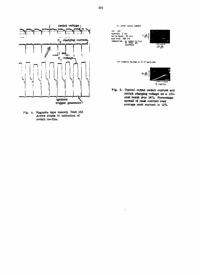
324
J switch voltage- U J ZUTP
11 i
n, !
! Is
H1
i
—•
S
ignitrontrigger generator)nerator)
Fig. 4. Magnetic tape record. Test 153Arrow points to indication ofswitch no-fire.
P«F: 100DURATIQM: i ; £C
SHITCH PRgSS: Z9 PSIG
FLOW MTE: S25 P/M
IRRADIATION: RC CHARGE ON PLUGTO IRflAO. » E S .ELECTRODE
) CHAftQING VOLTAGE ON 2 2 flF CAPACITOR
Fig. 5. typical output switch current andswitch charging voltage on a 100-shot burst (tun 167). Percentagespread of peak current overaverage peak current is 12%.
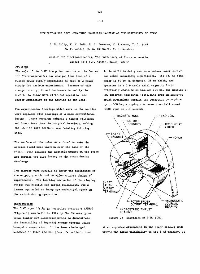
325
14.1
REBUILDING THE FIVE MEGAJOULE HOMOPOLAR MACHINE AT THE UNIVERSITY OF TEXAS
J. K. Gully, K. K. Toik. R. C. Zowarka, >I. Brennar., '«'. L. Bird
K. F. Weldon, H. G. Rylander, K. H. Woodsoa
Center for Electromechanics, The
Taylor Hall 167, Aus
Abstract
The role of che 5 MJ homopolar machine at the Center
for Elecnromechaui.es has changed from that of a
pulsed power supply experiment to that of a power
supply for various experiments. Because of this
change in duty, it was necessary to modify the
machine to allow more efficient operation and
easier connection of the machine to the load.
The experimental bearings which were on the machine
were replaced with bearings of a more conventional
design. These bearings exhibit a higher stiffness
and lower loss than the original bearings, making
the machine more reliable and reducing motoring
time.
The surface of the poles were faced to zuake the
applied field more uniform over the face of the
rotor. This reduced the magnetic moment on the rotor
and reduced the side forces on the rotor during
discharge.
The busbars were rebuilt to lower the resistance of
the output circuit and to allow quicker change of
experiments. The latching mechanism of the closing
switch was rebuilt for better reliability and a
damper was added to lower the mechanical shock on
the switch during operation.
Introduction
The 5 MJ slow discharge homopolar generator (SDHG)
(Figure 1) was built in 1974 by The Onivtrsity of
Texas Center for Electromechanics to demonstrate
the feasibility of inertial energy storage using
homopolar conversion. It has been discharged
hundreds of rimes and has proven so reliable that
University of Texas at Austin
itin, Texas 78712
it is still in daily use as a pulsed power supply
£or other laboratory experiments. Its 730 kg steel
rotor is 61 ctn in diameter, 28 cm thick, and
operates in a 1.6 tesla axial magnetic field.
Originally designed to produce 165 kA, the machine's
low internal impedance (resulting from an improved
brush mechanism) permits the generator to produce
up to 560 kA, stopping the rotor from half speed
(2800 rpm) in 0.7 seconds.
V- MAGNETIC YOKE
\ \— ROTOR\ BRUSHES
- FIELD COIL
CONDUCTIVELINER
ROTOR
SHAFTBRUSHOUTPUTTERMINAL-
HYDROSTATICJOURNALBEARING
• ROTOR BRUSHOUTPUT TERMINAL
•HYDROSTATIC THRUSTBEARING
Figure 1: Schematic of 5 MJ SDEG.
After r e l a t e d discharges in the short c ircui t mode
proved the basic r e l i ab i l i t y of the 5 MJ machine, i t

326
was connected to various loads In order to study
such machine parameters as voltage, current, pulse
rise time and discharge time. Three major series of
laboratory experiments have been conducted that
involve operational testing of the machine as a
pulsed power supply.
ing bearing interface surface speed is much higher
than in conventional rotating machines.
Desirable bearing design features include:
1) Very low losses (reduce motoring tine).
1) Discharging into the fast discharge experi-
ment (FDX) field coll (inductive store)
to obtain maniirmm currant in the coil.
2) Full 3tiffness at zero speeds. (Bearing
loads in homopolar generators are as large
at zero speed as at full speed.)
2) Discharging into the FDX field coil
(inductive store) while controlling the
shape of the current pulse by controlling
the field excitation of the 5 MI machine.
3) Pulsed resistance welding of 2" mild steel
pipe."
Season for Rebuild
After completing these experiments, misalignment and
out-of-roundness of the experimental hydrostatic
bearings installed two and one-half yaars before
resulted in an inability of the 5 MJ homopolar
machine to be motored to speed with full field. A
4" stainless steel pipe resistance welding program
would soon require many high level discharges.
Therefore, to addresa the bearing problem and observe
rhe internal condition of the generator after some
tvo years of operational testing, the decision was
nade to redesign the bearings, disassemble the
machine and upgrade the overall performance.
Attention was paid to making the machine as reliable
as possible, reflecting the change from its
previous experimental status.
Searings
Homopolar machines have stringent bearing require-
ments. A large diameter rotor shaft i3 required
for a disc type homopolar generator, since the shaft
is used as a conductor and the larger diameter
lowers -he resistance. (For the 5 MJ machine,
resistance of its five-inch shaft is about one-third
of the total machine resistance.) 3ecause the shaft
is larger in diameter than would normally be used
on a rotor of the same size and weight, the result-
3) Electrical insulation (to prevent arcing
during a discharge and eliminate circulat-
ing currents in the bearings).
Of the three types of bearings, rolling element
(unacceptable due to high magnetic fields in the
bearing location), hydrodynamic (unacceptable because
of zero load capacity at zero speed) and hydrostatic,
only the hydrostatic bearing can be designed to
achieve all of these goals.
Two configurations of hydrostatic bearings had been
tested before the rebuild. Originally, a set of
stainless steel bearings, which were not insulated
from the bearing housing, were used. Although
they functioned satisfactorily at the original
design currents, during a high-level discharge the
shaft arced to the bearings, causing pitting of the
shaft and bearings. Bearings made of G-9 melamine
(a nonconductive, fiberglass-reinforced material)
replaced the stainless steel bearings. These
bearings functioned for over two years, but thermal
creep ultimately resulted in bearing misalignment
and loss of stiffness which necessitated that the
machine be run at reduced field levels. Friction
and I R losses would cause the shaft to expand, b. ;
the melamine bearings (which have a very low modulus)
were prevented from expanding because they were
confined by the stainless steel bearing housing.
This resulted in reduced clearance in the bearing
which increased shaft heating further reducing
bearing clearance and resulting in rubbing between
the shaft and bearing. In addition, the bearing
housings were misaligned and out-of-round, causing
the bearings to be oval-shaped and misaligned.
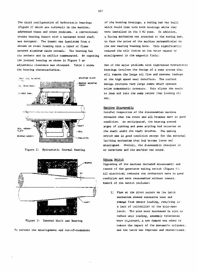
327
The third configuration of hydrostatic bearings
(Figure 2) which are currently in the machine,
addressed these and other problems. A conventional
bronre bearing insert with a hardened steel shaft
was designed. The insert was insulated from a
shrunk on steel housing with a layer of flame
sprayed aluminum oxide ceramic. The bearing has
six pockets and is orifice compensated. By capering
the journal bearing as shown in Figure 3 an
adjustable clearance was obtained. Table 1 shows
Che bearing characteristics.
MOUNTING PLATE
BEARING MOUNTING
Figure 2: Hydrostatic Journal Bearing
of the bearing housings, a boring bar was built
which would line bore both housings while they
were installed in the 5 MJ yoke. In addition,
a facing mechanism was attached to the boring bar,
to face the poles of the machine perpendicular to
the new bearing housing bore. This significantly
reduced the tilt forces on the rotor caused by
misalignment in the magnetic field.
One of the major problems with high-speed hydrostatic
bearings involves the design of a sump system thar
will remove the large oil flow and prevent leakage
at the high speed seal interface. The current
design provides very large sumps which operate
below atmospheric pressure. This allows the seals
to leak air into the suap rather than leaking oil
out.
Machine Disassembly
Careful inspection of the disassembled machine
revealed that the rotor and all brushes were, in good
condition. As anticipated, the bearing showed
signs of rubbing and some pitting had occurred on
the shaft under the shaft brushes. The making
switch was in good condition except for the external
latching mechanism that had become loose and
misaligned. Overall, the disassembly resulted in
no surprises and the machine was sound.
Fisure 3: Tapered Shaft and Bearing
To correct the misalignment and out-of-roundness
Making Switch
Upgrading of the machine Included disassembly and
rework of the generator making switch (Figure £).
A H electrical contacts and conductors were in good
condition and were reassembled without rework.
Rework of the switch included:
1) Pins at the pivot points on the latch
mechanism showed excessive wear and
damage from impact loading, resulting in
a lack of reliability of the hold-open
latch. The pins were increased in size to
reduce unit loading, assembly tolerances
were tightened, a new damper was added to
reduce the impact of the pneumatic cylinder,
and the latch was reground and repositioned.
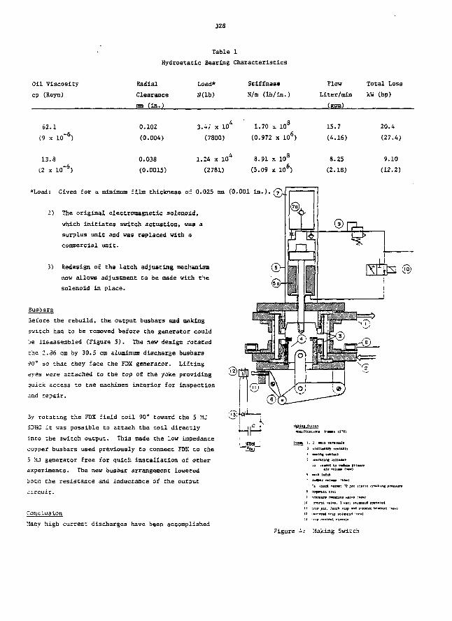
328
Table 1
Hydrostatic Bearing Characteristics
Oil Viscosity
cp (Reyn)
Radial
Clearance
an (in.)
Load*
N(lb)
Stiffness
N/m (Ib/in.)
Flow
Liter/min
(f?pm)
15.7
(4.16)
8.25
(2.18)
Total Loss
kW (hp)
20.4
(27.4)
9.10
(12.2)
62.1
{9 x 10~6)
13.8
(2 x 10"6)
0.102
(0.004)
0.038
(0.0015)
3.4/ x 10
(7800)
1.24 x 10⁴
(2781)
1.70 x. 10
(0.972 x 10⁵)
8.91 x 10⁸
(5.09 x 10 )
*Load: Given for a ltHn-tunim film thickness ol: 0.025 mm (0.001 in.).
2) The original electromagnetic solenoid,
which Initiates switch actuation, was a
surplus unit and was replaced with a
commercial unit.
3) Redesign or the latch adjusting mechanism
now allows adjustment to be made with the
solenoid in place.
Busbars
3efore the rebuild, the output busbars and making
switch had to be removed before the generatoi: could
be disassembled (Figure 5 ) . The new design rotated
the 2.66 cm by 30.5 cm aluminum discharge busbars
90° so thac they face the FDX generator. Lifting
eyes were attached to the top of the yoke providing
quick access to the machines interior for inspection
and repair.
3y rotating the FDX field coil 90° toward the 5 MJ
SDHG it was possible to attach the coil directly
into the switch output. This made Che low impedance
copper busbars used previously to connect FDX to the
5 MJ generator free for quick installation o£ other
experiments. The new busbar arrangement lowered
boch che resistance and inductance of the output
circuit.
Conclusion
Many high current discharges have been accomplishedFigure
II ;rtp pin. Jatch «iop and iII iw>r3««d trip iol«noid nc
Making Switch
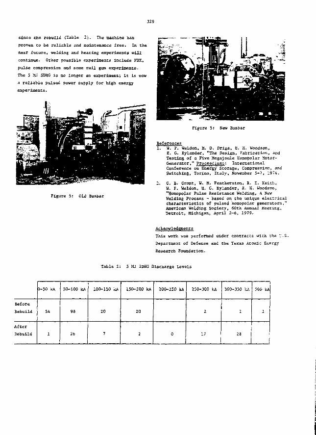
329
since che rebuild (Table 2). The machine has
proven to be reliable and maintenance free. In the
near future, welding and heating experiments will
continue. Other possible experiments include FDX,
pulse compression and some rail gun experiments.
The 5 MJ SDHG is no longer an experiment; it is now
a reliable pulsed power supply for high energy
experiments•
Figure 5: Old Busbar
Figure 5: New Busbar
References1. U. F. Weldon, M. D. Driga, H. H. Woodson,
H. G. Rylander, "The Design, Fabrication, andTesting of a Five Megajoule Homopolar Motor-Generator," Proceedings: InternationalConference on Energy Storage, Compression, andSwitching, Torino, Italy, November 5-7, 1974.
2. G. B. Grant, W. M. Featherston, R. E. Keith,H. F. Weldon, H. G. Ry.lander, H. H. Woodson,"Homopolar Pulse Resistance Welding, A NewWelding Process - based on the unique electricalcharacteristics of pulsed homopolar generators,"American Welding Society, 60th Annual Meeting,Detroit, Michigan, April 2-6, 1979.
Acknowledgments
This work was performed under contracts with the U.S.
Department of Defense and the Texas Atomic Energy
Research Foundation-
Table 2: 5 MJ SDHG Discharge Levels
Before
Rebuild
After
Rebuild
3-50 kA
54
1
50-100 kA
98
26
100-150
20
7
kA 150-200
20
2
kA 200-250
0
kA 250-300
2
17
kA 300-350 kA
1
28
560 kA
1

330
14.2
COMPUTER BAKED ELECTRICAL ANALYSIS OF HOKOPOLAR GENERATORDRIVEIt, BITTER PLATE STOBAGE ESKJCTORS WITH
RADIAL CUHBENT DIFFUSION
D.J.T. Mayhall"1", H.G. Bylander, W.F. Weldon,.and H.H. Uijodson
Center for ElectromeehanicsThe University of Texas at Austin
Austin, Texae 78712
Abstract
Maxwell's equations are solved for the opera-tional admittance in the magnetic quasi-staticapproximation for nonmagnetic cylindrical coilswith aximuthal currents and axial magneticfields. An infinite series, Bessel functionsolution is obtained and solved for coppercoils with given radial dimensions. Coil turnsnumbers and lengths are design parameters. Amultiple branch, shunt network coil model withseries resistances and inductances is derived.The UT CEH 5 MJ horaopolar generator is modeledwith a torque-speed equation Including brushand seal drag torques. The brush conta-.t volt-age drop is modeled versus surface speed andbrush current. Transmission system resistancesand inductances are included. Effective depthsof current penetration, effective coil resist-ances and inductances, and peak temperaturesare calculated versus time. Coil currents andvoltages are obtained, as are system energystorages and dissipations. Peak current timesand system discharge times are determined.Slightly underdamped configurations are found.
Admittance Solutions for Model Cylindrical CoilsSquare Bitter plate coils with eccentric boresare approximated with a cylindrical, axisyrame-cric model. The operational admittance approachof Mocanu [ij accounts for radial current diffu-sion. The coil model is shown in Figure 1. The:coil length is lc; its thickness is b-a. The Hfield is purely axial; the E field purelyazimuthal. Displacement current effects areneglected.
The boundary conditions for the LaPlace trans-form fields are Hzfr) » constant, 0ir*a, and?cHCr)*d£ « I(p), where the contour c is shownin Figure 1, I(p) is the transform current, andp is the transform variable. For nonmagneticcoil material. Maxwell's equations give
i &('£)• A-« 2-VPwhere y0 = -t~ x 10~" H/m and J is the coil con-ductivity. A solution to aq. (1) is
AJ Mqr) ->- BY (jqr) (2)
where J and Y are Bessel functions of the firstand second kind, j - v1-!, and A and B are con-stants. The E field is
(3)
The transform voltage across the coil terminalsis taken as
- I8(b)2TTb (4)
The operational admittance is Y(p) - I(p)/V(p).
Application of the boundary conditions and use ofthe residue theorem [2] gives the temporal admit-tance as
y(t) Z A. e"Bi£
1(5)
^ J aasi2[Vasia)Vasib)-Vasia>Vasi»]
sis i
a ) Jo ( a *»]+2b
/ o3. • a . /u ai si / o
The a . are the roots of the equation
a s i [ Tn
( a s i a ) J l ( a s i b ) - J o ( a s i a ) T l ( a s i b ) ]
lb)-J, (a^.)Y, (as±b)] =
(6)
"]
(7)
(S)
Solutions for Particular Coil DimensionsThe roots of eq. (8) are solved for a - 0.3048m(12 in) and b - 0.508m (20 in) with routines
+Presently at Lawrence Livermore Laboratory,' Livermore, CA 94550

33i
MMBSJfJ, MMBSJ1, MMBSYN, ZREAL1, and ZRIAL2 ofthe International Mathematical and StatisticalLibrary (TMSI.). The first 4 roots arey ()3.127309270 a"*,11.98715946 a"1,
7.401705666 a-1,16.64197700 a"l. and
ulated for LC c o
c » 5.800 x 10⁷ (fi-mj-i. The first 4 v.ilues ofA are 6.466691304 x 10&, 9.924480604 x 105,2.509179152 x 106, 1.441670278 x 10⁶. 'Those ofB are 1.444322999, 8.090703477, 21.22041)119,40.90086543.
Shunt Equivalent Circuit for the CoilWhen eq. (5) is transformed and variable coillengths lc and multiple coil turns of number N T
are allowed, the operational admittance may bewritten
i-i Ri L i p i-iL Ai = h
c
-1(9)
The coil may be thus represeuted by the :lnfinitebranch, shunt network shown at the right side ofFigure 2. Each branch consists of a resistanceR^ and an inductance Lj in series. The propernumber of branches n is determined by tr:.al.
Model for the nT-CEM 5MJ Homopolar GeneratorThe UT-CEM 5MJ homopclar generator is shown onthe left side of Figure 2. Its voltage Vfl -0}<j>/277, where w is the generator angular fre-quency and 4> is the magnetic flux. The gener-ator internal resistance Rg is taken as 13.1yfland the internal inductance LJJ as 0.5yH. Thetorque equation for the generator coast downmcde is
i f --,1^21, -Tfer-Ts (10)
where I is the rotor rotational inertia, ij. isthe series current, T D r is the brush drag torque,and T s is the seal drag torque. Bearing lossesare ignored. T^r is taken as 446 m—nt: Ts as13.6 m-nr.
The brush voltage drop resistance RDr, whichvaries with brush current and generator speed,is approximated by
with the rotor brush voltage coefficient given by
v , j 0.74, a)<88.6 rad/sec ( 1 2 )
™ I 0.676 + 7.27 X 10~4<i), u)>88.6 rad/sec
and the shaft brush voltage coefficient given by
| 0.74, (D<425 rad/sec
The estimated resistance of the bus system isi9.9uft; the estimated inductance is 0.3uH.
Effective Parameters for the CoilAn effective coil resistance is defr.ned as
_•? n 2K i Z R_. i , »here i. is the currentf. " i_ Z R_. i , »here i.
ri the i h_ branch. An effective coil inductance
_-> n ,is defined as L .c - i_ I L. i ". The current
i*l
density is approximated by j(r,t) = i_K (rL in
(I
(1 + ~ — ) ) , wh»re deff is the effective depth
of current penetration. rhe temperature rise atr • a for ETP copper is taken as
aemax = 5 - " X
I 0.676 + 1.51 X 10~4u, co>425 rad/sec(13)
Solution of Circuit Equations for an Example CoilThe circuit equations for Figure 2 are integratedin time on a CDC 6600 computer. Example resultsare given for a 12 turn, 72 plate co:ll (6 plates/turn) of length 0.1534m, p..at> thickness 2.13 x10~3ii, and zero thickness insulation. Resistanceincrease with temperature is neglected. The gen~erator has an initial spe«d of 584 rad/sec and anInitial voltage of 42V. Jourteen branches areused for the coil network.
Generator speed and current are shown in Figure 3,along with the coil voltage and the temperaturerise at the inner radius of the 0.1524m thick neckof the real coil. The rotor kinetic energy, coilinductive energy, system resistive dissipatedenergy, and drag friction dissipated energy areshovn in Figure 4. The effective coil resistance,inductance and depth of current penetration areshown in Figure 5. The series current is slightlyunderdatnped. The peak current of 120.6 kA occursat 0.855 sec; the peak coiL energy of 0.814 MJoccurs at 0.908 sec. The generator reversesdirection at 3.64 sec; the current reverses at4.57 sec.
AcknowledgementsThanks are due to W. L. Bird, M. Brennan,G. Cardwell, M. D. Driga, K. M. Tolk, P. Wildi,and R. Zaworka for their most kind help.
This work was supported by the U. S. Departmentof Energy and the Texa6 Atomic Energy ResearchFoundation.
References|Tj C.I. Mocanu, "The Equivalent Schemes of Cvlin-drical Conductors At Transient Skin Effect," 71TP 667-PWR, IEEE Summer Meeting and Inc. Svmp. onHij.h Power Testing, pp. 8S4-852, July 18-23, 1971.
332
[2] J. C. Jaeger, "III. Magnetic Screening byHollow Circular Cylinders," Phil. Mag. Z£,pp. 18-31, 1940.
-t
I — , - ^ ; - >II
•
i
i*
•—a
H t
< r
!fcIJ
CONTOUK OFiNTBSHATON
3 — 0
FIG. 1 -CYLINOSICAL COIL MOOS.
SMJ HOMOPaLAR TKAKSM1SS1ON3ENEMT0H 3UJ
STOHAGC INDUCTOR
eauiv. O R C U I T TOR S M T HOMOPOIJU? GENERATOR
AND STDRAiiE INDUCTOR W/RADIAL CURRENTOIFFUSION.
J 3
1-IME - SECONOS
FIG. 3 - MACHINE SPEEO, CURRENT, COIL VOLTAGE
AND PEAK COIL TEMP RISE Vs TIME
MJ
(•
5 .
2 .
I*
XT
•31 f \ / \
7/ A \
k j
EFft 11.
7 -
313-
M
• 6
'5
• 3
1
TIME - SEC0N03
FI8. 4 - SYSTtM ENER3Y STORAGE ANODISSIPATION V> TIME
Latt-HENRVSUf.-OHie
- t - •+•2 J 4 5 6
TIME - SECONDS
FIB. 5 - VARIATION OF EFFECTIVE COILPARAMETERS WITH TIME.
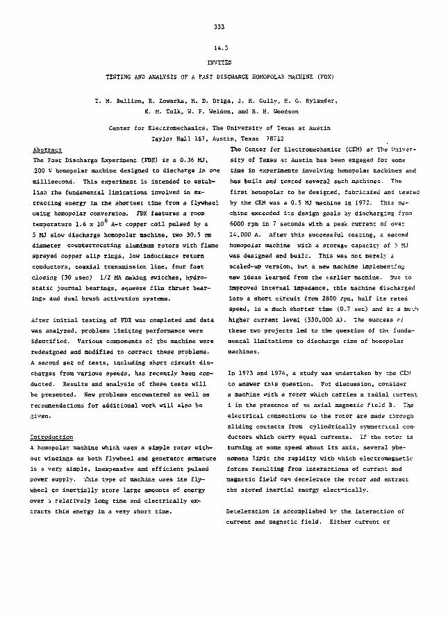
333
14.3
INVITED
TESTING AND ANALYSIS OF A FAST DISCHARGE HOMOPOLAR MACHINE (FDX)
T. M. Bullion, R. Zowarka, M. D. Driga, J. K. Gully, H. G. Rylander,
K. M. Tolk, K. F. Weldon, and H. H. Woodson
Center for Electromechanics, Tlie University of Texas at Austin
Taylor Hall 167, Austin, Texas 78T12
The Center for Electromechanics (CEM) at The Univer-
sity of Texas at Austin has been engaged for some
time in experiments involving homopolar machines and
has built and tested several such machines. The
first homopolar to be designed, fabricated and tested
by the CEM was a 0.5 MJ machine in 1972. This ma-
chine exceeded its design goals by discharging from
6000 rpm in 7 seconds with a peak current of over
14,000 A. After this successful testing, a second
homopolar machine with a storage capacity of 5 MJ
was designed and built. This was not merely a
scaled-up version, hut a new machine implementing
new ideas learned from the earlier machine. Due to
Improved internal impedance, this machine discharged
into a short circuit from 2800 rpm, half its rated
speed, in a much shorter time (0.7 sec) and at a mu-h
higher current level (550,000 A). The success c-i
these two projects led to the question of the funda-
mental limitations to discharge time of homopolar
machines.
Abstract
The Fast Discharge Experiment (FDX) is a 0.36 MJ,
200 V homopolar machine designed to discharge in one
millisecond. This experiment is intended to estab-
lish the fundamental limitations involved in ex-
tracting energy in the shortest time from a flywheel
using homopolar conversion. FOX features a room
temperature 1.6 x 10 A-t copper coil pulsed by a
5 MJ slow discharge homopolar machine, two 30.5 cm
diameter counterrccating aluminum rotors with flame
sprayed copper slip rings, low inductance return
conductors, coaxial transmission line, four fast
closing (30 usec) 1/2 MA making switches, hydro-
static journal bearings, squeeze film thrust bear-
ings and dual brush actlvacion systems.
After initial testing of FDX was completed and data
was analyzed, problems limiting performance were
identified. Various components of the machine were
redesigned and modified to correct these problems.
A second set of tests, including short circuit dis-
charges from various speeds, has recently been con-
ducted. Results and analysis of these tests will
be presented. New problems encountered as well as
recommendations for additional work will also be
given.
Introduction
A homopolar machine which uses a simple rotor with-
out windings as both flywheel and generator armature
is a very simple, inexpensive and efficient pulsed
power supply. This type of machine uses its fly-
wheel to inertially store large amounts of energy
over \ relatively long time and electrically ex-
tracts this energy in a very short time.
In 1973 and 1974, a study was undertaken by the CEN
to answer this question. For discussion, consider
a machine »ith a rotor which carries a radial current
i in the presence of an axial magnetic field 3. The
electrical connections to the rotor are made through
sliding contacts from cyllndrically symmetrical con-
ductors which carry equal currents. If the rotor is
turning at some speed about its axis, several phe-
nomena limit the rapidity with which electromagnetic
forces resulting from interactions of current and
magnetic field can decelerate the rctor and extract
the stored inertial energy electrically.
Deceleration is accomplished by the interaction of
current and magnetic field. Either current or
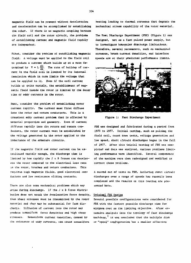
334
magnetic field can be present without deceleration
and deceleration can be accomplished by establishing
the other. If there is no magnetic coupling between
the field coil and the rotor circuit, the problems
of establishing current and magnetic field rapidly
are independent.
First, consider the problem of establishing magnetic
field, A voltage must be applied to the field coil
to produce a current which builds up at a rate de-
termined by V - L -j—. The rate of buildup of cur-
rent in the field coil is limited by its internal
insulation which in turn limits the voltage that
can be applied to it. Even if the coil current
builds uv quite rapidly, the establishment of mag-
netic field inside the rotor is limited by the decay
time of eddy currents in the rotor.
Next, consider the problem of establishing rotor
current rapidly- The current must first diffuse
into the rotor and return conductors. This is a
transient eddy current problem that is affected by
material properties and geometry. Even if current
diffuses rapidly into the rotors and return con-
ductors, the rotor current must be established by
the voltage generated in the rotor applied to the
inductance of the armature circuits.
If che magnetic field and rotor current can be es-
tablished rapidly enough, the discharge time is
limited by how rapidly che J x B forces can deceler-
ate :he rotor compared to the electrical loss rate
in the rotor, brushes and return conductors. This
requires high magnetic fields, good electrical con-
ductors and low resistance sliding contacts.
There are also some mechanical problems which may
arise during discharge. If the J x B force distri-
bution does not match the deceleration force density,
Chen shear stresses must be transmitted by the rotor
material and they may be substantial for fast dis-
charge. Diffusion of current into the rotor may
produce nonuniform force densities and high shear
stresses. Nonuniforn current densities, caused by
the existence of eddy currents, can cause nonuniform
heating leading to thermal stresses that degrade the
mechanical stress capability of the rotor material.
The Fast Discharge Experiment (FDX) (Figure 1) was
designed, not as a fast pulsed power supply, but
to investigate homopolar discharge limitations.
Therefore, several parameters, such as mechanical
stresses, brush current densities, and interface
speeds are at their predicted performance limits.
Figure 1: Fast Discharge Experiment
FDX was designed and fabricated during a period from
1975 to 1977. Initial testing, such as pulsing the
field coil, coast down tests, voltage generation and
low speed, short circuit discharges began in the fall
of 1977. After this initial testing of FDX was com-
pleted and data was analyzed, various problems limit-
ing performance were identified. Several components
of the machine were then redesigned and modified to
correct these problems.
A second set of tests on FDX, including short circuit
discharges over a range of speeds has recently been
completed and the results of this testing are pre-
sented here.
Original FDX Design
Several possible configurations were considered for
FDX with the fastest possible discharge cime for
minimum cost as the limiting objective. After ex-
tensive analysis into the topology of fast discharge
machines, it was concluded that the multiple disk
or "spool1* configuration has a smaller effective
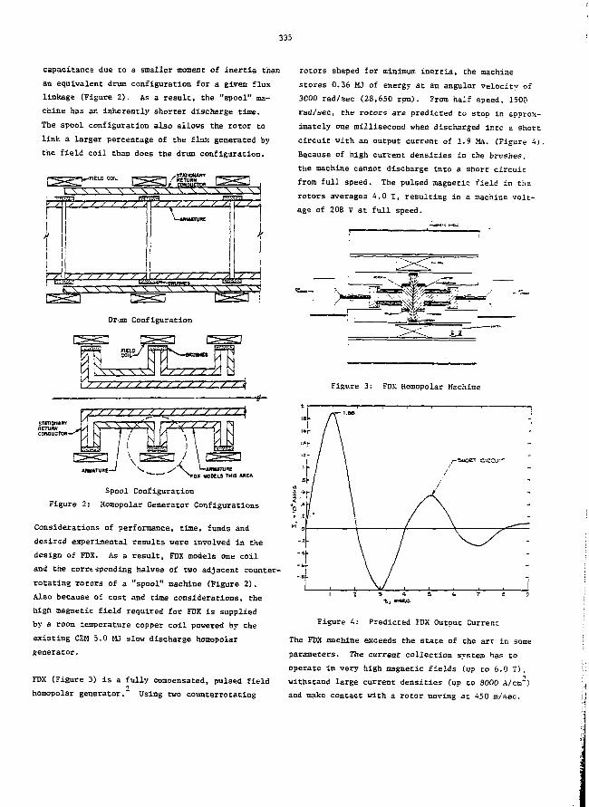
335
capacitance due to a smaller moment of inertia than
an equivalent drum configuration for a given flux
linkage (Figure 2). As a result, the "spool" ma-
chine has an inherently shorter discharge time.
The spool configuration also allows the rotor to
link a larger percentage of the flux generated by
the field coil than does the drum configuration.
7-y
\-UWTUK
Drum Configuration
ITUHEHODELS THIS » « E «
Spool Configuration
Figure 2: Homopolar Generator Configurations
Considerations of performance, time, funds and
desired experimental results were involved in the
design of FDX. As a result, FDX models one coil
and the corrtspending halves of two adjacent counter-
rotating rotors of a "spool" machine (Figure 2).
Also because of cost and time considerations, the
high magnetic field required for FDX is supplied
by a room temperature copper coil powered by the
existing CEM 5.0 MJ slow discharge homopolar
generator.
FDX (Figure 3) is a fully compensated, pulsed field
homopolar generator." Using two counterrotating
rotors shaped for minimum inertia, the machine
stores 0.36 MJ of energy at an angular velocity of
3C00 rad/sec (28,650 rpm). From half speed, 1500
rad/sec, the rotors are predicted to stop in approx-
imately one millisecond when discharged into a short
circuit with an output current of 1.9 MA. (Figure A).
Because of high current densities in the brushes,
the machine cannot discharge into a short circuit
from full speed. The pulsed magnetic field in the
rotors averages 4.0 T, resulting in a machine volt-
age of 208 V at full speed.
Figure 3: FDX Homopolar Machine
T a e
Figure A: Predicted FDX Output Current
The FDX machine exceeds the state of the art in some
parameters. The current collection system has to
operate in very high magnetic fields (up to 6.0 T),
withstand large current densities (up to 8000 A/ca~)
and make contact with a rotor moving at 650 m/sec.
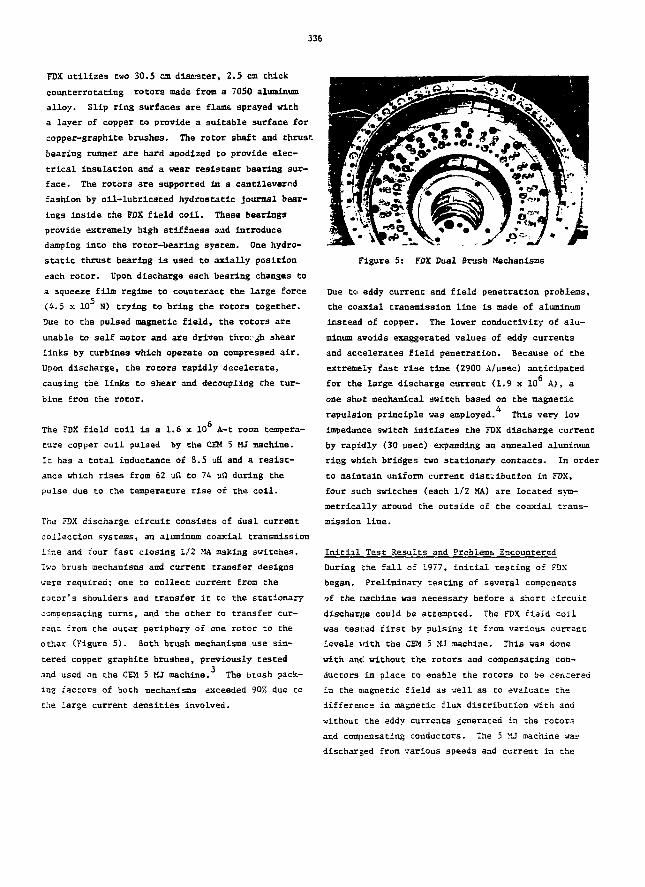
336
FDX utilizes two 30.5 cm diameter, 2.5 cm thick
counterroeating rotors made from a 7050 aluminum
alloy. Slip ring surfaces are flame, sprayed with
a layer of copper to provide a suitable surface for
copper-graphite brushes. The rotor shaft and thrust-
bearing runner are hard anodized to provide elec-
trical insulation and a wear resistant bearing sur-
face. The rotors are supported in a cantilevered
fashion by oil-lubricated hydrostatic journal bear-
ings inside the FDX field coil. These bearings
provide extremely high stiffness aad introduce
damping into the rotor-bearing system. One hydro-
static thrust bearing is used to axially position
each rotor. Upon discharge each bearing changes to
a squeeze film regime to counteract the large force
(4.5 x 10 M) trying to bring the rotors together.
Due to the pulsed magnetic field, the rotors are
unable Co self motor and are driven thro, h shear
links by turbines which operate on compressed air.
Upon discharge, the rotors rapidly decelerate,
causing the links to shear and decoupling the tur-
bine from the rotor.
The FDX field coil is a 1.6 x 10 A-t room tempera-
ture copper coil pulsed by the CEM 5 MJ machine.
It has a total inductance of 8.5 uH and a resist-
ance which rises from 62 uQ to 74 ufl during the
pulse due to the temperature rise of the coil.
The FDX discharge circuit consists of dual current
collection systems, an aluminum coaxial transmission
line and four fast closing 1/2 MA making switches.
Two brush mechanisms and current transfer designs
were required; one zo collect current from the
rotor's shoulders and transfer it Co the stationary
compensating turns, and the other to transfer cur-
rent from the outer periphery of one rotor to che
other (Figure 5). Both brush mechanisms use sin-
tered copper graphite brushes, previously tested
and used on che CEM 5 MJ machine. The btush pack-
ing factors of both mechanisms exceeded 90% due CD
che large current densities involved.
Figure 5: FOX Dual Brush Mechanisms
Due to eddy current and field penetration problems,
the coaxial transmission line is made of aluminum
Instead of copper. The lower conductivity of alu-
minum avoids exaggerated values of eddy currents
and accelerates field penetration. Because of the
extremely fast rise time (2900 A/usee) anticipated
for the large discharge current (1.9 x 10 A), a
one shot mechanical switch based on the magnetic4
repulsion principle was employed. This very low
impedance switch initiaces the FDX discharge current
by rapidly (30 usec) expanding an annealed aluminum
ring which bridges two stationary contacts. In order
to maintain uniform current distribution in FDX,
four such switches (each 1/2 MA) are located sym-
metrically around che outside of the coaxial trans-
mission line.
Initial Test Results and Problems Encountered
During the fall of 1977, initial cescing of FDX
began. Preliminary testing of several components
of the Daciilne was necessary before a short circuit
discharge could be attempted. The FDX field coil
was tested first by pulsing ic from various current
levels with Che CEM 5 JU Jiachine. This was done
with and without the rotors and compensating con-
ductors in place Co enable the rotors to be centered
in the magnetic field as veil as co evaluate che
difference in magnetic flux distribution with and
without the eddy currents generated in the rocors
and compensating conductors. The 5 MJ machine was
discharged from various speeds and current in che
337
coil and magnetic field was recorded. This measured
field very closely matched the field calculated
previously.
The two brush mechanisms were tested individually
and together by activating the brush mechanisms in
various combinations. The objective of these tests
was to wear In Che brushes, determine how long each
mechanism cook to activate and v?rify predicted
brush losses. From 7000 rpm, the rotors stopped
from brush losses approximately 0.4 sec after both
brush mechanisms were seated. This rapid decelera-
tion was expected from predicted brush losses.
Voltage generation teats were performed on FDX oy
exciting the field coil and activating both brush
mechanisms with the rotors spinning. Machine volt-
age and movement of the rotors as a result of the
magnetic field were monitored.
After these tests were complete, four short circuit
discharge tests were performed. On one of these
tests, the 5 MJ machine generated 140,000 A into
the FDX field coil, producing an average magnetic
field of 2.4 T inside the bore of the coil. From
2500 rpm, the rotors stopped in 20 milliseconds and
the machine generated approximately 60,000 A, The
FDX machine voltage was 19 V. While this was the
fastest discharge of a homopolar machine to date,
the time was still an order of magnitude greater
than the predicted results. Also, on other tests,
it became apparent that current could not be main-
tained at speeds over 2500 rpm. This was due
largely to brush bounce, either electromagnetic or
dynamic in nature. Because of a very fast current
rise before breaking up, a one millisecond discharge
still seemed feasible if brush contact could be
maintained. Therefore, an extensive rework of FDX
began late in 1977.
The internal resistance of FDX was higher than ex-
pected because of a high resistance, bolted joint in
the return conductor. If FDX was to discharge in
one millisecond this resistance would have to be
decreased.
Another problem with FDX which affected predicted
performance was insufficient air supply to the cur-
bines which motor the machine. If the specified
15,000 rpm was to be reached, larger air lines and
more air inlets to each turbine would have to be
used.
Upon dismantling the machine, several other problems
were noted. The surfaces of the outer rotor slip
rings as well as the rotor brushes showed signs of
arcing but the rotor was not sariously pitted. This
indicated that the suspected brush bounce was occur-
ring in the rotor brush mechanism. Also, there was
considerable oil in the rotor cavity, indicating
that the inside bearing seals were noc functioning
properly. Further examination and testing using
displacement transducers showed that the rotors
ran out approximately 0.015 cm. This could he one
cause of brush bounce.
In general, all components of FDX except those noted
above were in good shape. Therefore, to make FDX
perform as predicted, a complete redesign and re-
build of these components was needed. Coinciding
with the FDX rebuild, was a rebuild of the CEM 5 MJ
machine to increase its performance.
FDX Rebuild
FDX has an 8.3 cm diameter shaft which rotates at
speeds up to 15,000 rpm. This gives a very high
interface speed for a aydrostatic bearing. Because
of this high shaft surface speed and the roughness
of the hard anodized shaft on which they rubbed, the
original lip seals used in FDX wore out rapidly.
Also, the oil sump in the inner bearing scavenge
system was slightly pressurized due to line restric-
tions and dynamic effects of oil flowing out of the
bearing pocket. These two problems combined to allow
oil leakage into the rotor cavity. The oil sump and
lip seal were redesigned to prevent this. For an
oil scavenge system to work correctly, a vacuum must
be maintained to assure that air will flow by the
seal into the sump. Flow should be laminar at che
sump inlet and large return lines and manifolds
should be used to assure th"t return -low is not
338
restricted. The FDX scavenge system was rebuilt Co
Increase the cross sectional area of Che scavenge
by adding two larger (1.9 cm) return passages. Also
a dam and small reservoir were added to the sump.
The dam serves to force oil away from the rotating
shaft and Into the reservoir Co keep oil off Che
shaft, reducing turbulence. To avoid excessive
horsepower losses, low loss seals had been used on
FDX. After a search for a suitable lip seal, only
one was found which could perform at Che necessary
high speeds with low losses. This was a Mather U p
seal. Sue to the roughness of the hard anodized
shaft, it was necessary to shrink fit a 4340 steel
sleeve on the rotor seal shoulder (Figure 6).
Because this ring was hardened and ground, it pro-
vided a suitable surface for the seal to run on.
/-KMIM
MATHER UP SEAL
*AH0EWD a -GROUNO SLEEVE —
Figure 6: Mather Lip Seal and Rebuilt Sump
Current collection systems have always been diffi-
cult in horaopolar machines because of high magnetic
fields, large current densities and high surface
velocities. While most brush mechanisms transfer
current from a rotor to a stationary conductor, the
FDX rotor brush mechanism transfers current from
one rotor to another spinning in the opposite di-
rection. So brush in use before FDX had been run
at comparable speeds or current, densities. There-
fore a somewhat unique brush mechanism was required.
The original FDX rotor brush mechanism didn't vork
properly for several reasons. 3ecau.<3 the rotors
were each about 0.025 cm out of round, a single
brush could not follow both surfaces. Because the
brushes were not supported close enough to the rotor
surface, a substantial moment was applied to the
brushes causing them to bind in their holders. The
polymer diaphragm used to actuate the brushes was
not sufficiently stiff to prevent brush bounce and
it leaked due to tears in mounting holes and reac-
tion with the oil which had leaked into the rotor
cavity.
The rotor brush mechanism was redesigned to solve
these problems as well as to implement some new
Ideas. The rotor slip ring surfaces were machined
to very close tolerances to assure that they were
round and the same diameter. They were then bal-
anced in the bearings so the total runout was less
than 0.003 cm. This small runout makes it easier
for a brush to follow the rotor. The rebuilt brush
mechanism consists of 120, 0.64 cm wide sintered
copper graphite brushes supported on each end by
slotted fiberglass reinforced epoxy rings (Figure 7).
The brushes are activated by an air pulse behind
a cast polyurethane diaphragm and retracted by two
compression springs per brush (Figure 8).
Figure 7: FDX Rotor Brushes and Suppor. Rings
More brushes are used on the rebuilt mechanism than
on the original mechanism £120 vs 36) because of the
theory on the current carrying ability of brushes,
chat discrete points of contact rather Chan total
surface area of contact is important. According
to this theory, number of points of contact is in-
dependent of amount of surface area. Because the
brushes are supported over their entire height in
339
a slot, applied moment and tendency to bind are
reduced. The new diaphragm is much st.tffer and
tougher Chan the old one, maKing higher actuation
pressure and greater downforce possible.
-SUPPORT RING
-DIAPHNAOM SUPPORT BINSAIR PRESSURE -
URETHANEDIAPHRAGM'
RETURN SPRING-
COUKTERROTATINGROTORS
Figure 8: FDX Rotor Brush Mechanisn
The high resistance bolted joint in the return con-
ductors of FDX was eliminated on the rebuild. This
was accomplished by welding the compensating turn
to rhe outer coaxial transmission line (Figures 9
and 10). This served to decrease the internal
resistance of FDX, allowing a faster discharge.
Second FDX Discharge Tests
After the rebuild of FDX was completed, a second set
of tests was performed beginning in fall 1978. Be-
fore attempting a short circuit discharge, it was
necessary to test the rebuilt components as well as
verify that all other components were still function-
ing properly. The rotor brush mechanism was activated
with both rotors spinning, to wear in the brushes
and tc determine the time required for the brushes
to seat. Since the rotor brush mechanism required
longer to seat than the shoulder brush mechanism,
the two solenoids controlling them were put on dif-
ferent electrical circuits to allow the two brush
mechanisms to activate simultaneously. The Mather
lip seal and rebuilt sump and return lines were also
tested with the rotor spinning at high speed. No
leaks were evident and higher rotor speeds were
possible due to the lower losses of the new seal.
After the performance of the other components was
verified, several short circuit discharges were per-
formed with varying rotor speed and field.
COMPENSATINGTURN
>r-RETURNCONDUCTOR
• HIGH RESISTANCEBOLTED JOINT -LOW RESISTANCE
WELDED JOINT
Figure 9: Current Transmission LineBolted vs Welded Joint
Figure 10: Welded Joint
The testing program called for a high speed, high
field first discharge after careful evaluation and
testing of the rebuilt components. It was desired
to produce a one millisecond discharge from a re-
spectable energy store. Initial discharges produced
a choppy 240,000 A discharge and stopped the rotor?
in 20 msec. The energy store was then lowered in
an attempt to attain the fastest known discharge of
a homopolar machine. This was achieved on December
21, 1978 when oscillograms showed a continuous short
circuit current output of 90,000 A that stopped the
rotors in 5 msec. Results of that test allowed
calculation of bulk circuit parameters as well as
in depth analysis of machine performance and identi-
fication of problem areas.

340
Two Important pieces of instrumentation were added
in Che FOX rebuild: a high resistance shoulder
brush and a split and insulated rotor brush
(Figure 11). This separated the terminal voltage
into useful components and allowed analysis of Che
machine's internal operation. Up until the ninth
run, discharge current had not been continuous
during Che complete discharge cycle. Calculated
bulk circuit parameters from erratic data were
unreliable. The shoulder brush drop 2-1 was con-
tinuous in early runs but the brush drop from 3-1
was choppy and followed Che current nonuniformity.
A discharge from lower speed with high volume
accumulators plumbed Co Che rocor brushes produced
:he first continuous current waveform.
Machine Parameters
(The rotors as referred to as Rocor 1 and Rotor 2).
Rotor Speeds
rmi - 188.5 sec (1800 rpm)
ru2 - 167.5 sec (1600 rpm)
Energy Stored
k k I2Iu>- - 2 (.0446KI88.5)2 + 2(.0446) (167.5)2
» 1.418 ScJ
5.3V experimental
.177 V-sec
.177 Wb
•-r(0.023-.0058) - 3.23Produced by 223,000 A discharge of 5 MJhomopolar into FDX AIR BORE FIEIJ) COIL
V- = 2IT = 4.72 V
Current
3 t = .00095 I
Capacitance
C;
C
peak
p - 56.2 F
28.1 F
90,700 experimental
Resistance
Rocors
There is very little rotor speed
variation between t»0 and tpea^y23t-0~ - V23cpeak 5.3-4
- 90,700
-6
• 14.3 s 10"5 fl
Shoulder brashes
.9R - peak 90,700 - 9.9 x 10 a
Switches
Voltage drop across 4 switches in parallel
at t p e a k - .626 V.
The currents in the switches are measured
with hall probes that sense the eo coia-
t-onent of flux in Che coaxial switch.
.626 ,Rgwl - 24800 - 25 x 10 fl
.62617100 - 36 x 10 0
.626Rsw3 - 30500 - 20.5 x 10
.62bvh ' 18300 - 34.2 x 20
R » 6.85 x 10"6 a
5.33 - .62690700
51.8 x 10
Inductance
Slope of current rise
8 -£-2.66 x 10 sec experimental
v13C=0~ - 7 : 3pQt 2.3
L23 slope
3.6 x 10~9 H
V12C-O~ - V12c-o"r
2.66 x 10a
2.3= 2.66 xslope
8.6 x I0"9 H
n-9 „ (Reference 4)
341
Bulk Circuit
COAX
SHOULDER BRUSHES
51.8 x 10 ft
6.85 x 10"* ft
5 x 10"* H
" 'It 10
8.6 x 10"* H
9.9 x 10"" ft
8.6 x 10"* H
RT.-6
28.1 F
* 107 x 10
= 39.4 x 10"9 H
DampingCoefficient
107 x 10.-6
" 2 / 39.4 x 10 9 ' X-43
28.1
R2cIn L 2.09\ - 2716-332
. 00088
Even in the continuous current discharge the rotor
instrumentation brush unseated at 0.8 msec into the
discharge and reseated at 3.2 msec. Total discharge
current never went to zero. This indicates th3t the
current repulsion between flow in the brush and out-
put coax is aiding the down force on the rotor
brushes. The decay of the current waveform shortly
after current peak did not follow the R-C decay
predicted from bulk parameters. The resistance
change occurred because full brush seating was not
maintained. Also it can be concluded that the force
causing brush bounce is either mechanical or eddy
current related because the rotor instrumentation
brush which does not carry current also bouncad.
.Therefore current constriction and brush melting can
be eliminated as causes of bounce. The engineering
solution will probablv be the separation of the rotor
brushes into two independent rotor tracking mecha-
nisms. Also if expanded flux plots in the rotor
brush area show an eddy current force, brush laaiina-
tion may also be considered. The present mechanism
functioned well enough to provide the 5 msec dis-
charge from low energy store which explored ths fun-
damental limitation. New mechanisms will make fast
discharge homopolars viable pulsed power supplies..
SPLIT-INSULATEDROTOR BRUSH
iIGH RESISTANCEINSTRUMENTATION
Figure 11: FBX Instrumentation
Conclusions
Even though a one millisecond discharge of FDX was
not achieved, further testing is warranted due co
the very fast current rise times seen in the second
set of tests. Since the main problem with FDX is
current breakup due to the bouncing of rotor brushes,
the configuration of this mechanism must be changed
to allow it to continuously transfer current between
the two counterrotating rotors. Experience from
both FDX rotor brush mechanisms has shown that this
cannot be done successfully by using a single brush
bridging both rotors. A separate brush mechanism
should therefore be used on eaci. rotor with a flex-
ible, current-carrying strap joining rbe two. Also,
because controlling the speeds of the two rotors by
342
manually controlling air flow is difficult, a cir-
cuit should be designed to synchronize the rotor
speeds.
The 5 millisecond discharge achieved by FDX is the
fastest discharge ever for a homopolar machine.
Stll'.. the fast current rise times demonstrate that
a shorter discharge time is possible. A second
generation fast discharge machine would be very
similar to FDX with two significant changes. Two
separate rotor brush mechanisms, as explained above,
woulr be used to transfer current between the two
rotors. A steady state superconducting field coil
would replace the present pulsed field coil t:o pro-
vide the necessary high field. This superconducting
coil would allow higher fields if necessary, enable
che uniformity of the field to be controlled and
allow the rotors to self motor. Also because the
field would be steady state, the return conductors
could be made of copper rather than aluminum, thus
decreasing the resistance of the machine and in-
creasing the output current.
4. P. Wildi, "A Fast Metallic Contact ClosingSwitch for the FDX Experiment," Seminar onEnergy Storage, Compression and Switchingat the Australia- Sfaeiooal University, CanberraAustralia and the University of Sydney, Sydney,Australia, November 13-21, 1977.
Acknowledgements
This work was performed under contracts to the
U.S. Department of Energy (DOE), the Electric
Power Research Institute (EPRI) and the Texas
Atomic Energy Research Foundation (TAERF).
References
1. M. D. Driga, S. A. Sasar, H. G. Rylander, W. F.Weldon and H. H. Woodson, "Fundamental Limi-tations and Topological Considerations forFast Discharge Homopolar Machines," IEEETransactions of Plasma Science, Vol. PS 3,Mo. 4, December 1975, pp 209-215.
2. J. H. Gully, M. D. Driga. B. Grant, H. G.Rylander, K. M. Tolk, W. F. Weldon, andH. H. Woodson, "One Millisecond Discharge TimeHomopolar Machine (FDX)", presented at the IEEEInternational Pulsed Power Conference, Lubbock,Texas, November 9-11, 1976.
1. M. Srennan, Z. Eliezer, W. F. Weldon, H. G.Sylander, and H. H. Hoodson, "The Testing ofSliding Electrical Contacts for HomopolarGeneracors," IEEE Transactions on ComponentsHybrids and Manufacturing Technology, Vol.CHMT-2, Mo. 1. March 1979.
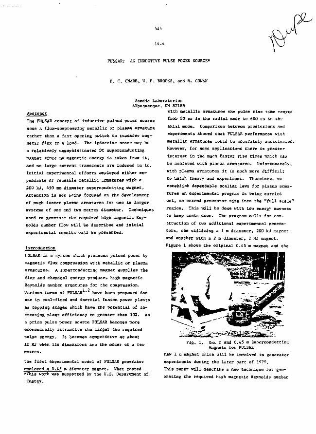
343
14.4
PULSAR: AN INDUCTIVE PULSE POWER SOURCE*
E. C. CNARE, W. P. BROOKS, and M. COWAN
Abstract
The PULSAR concept of inductive pulsed power source
uses & flux-compressing metallic or plasma armature
rather than a fast opening switch to transfer mag-
netic flux to a load. The inductive store may be
a relatively unsophisticated DC superconducting
magnet since no magnetic energy is taken from it,
and no large current transients are induced in it.
Initial experimental efforts employed either ex-
pendable or reusable metallic ^matures with a
200 kJ, 430 mm diameter superconducting magnet.
Attention is now being focused on the development
of much faster plasma armatures for use in larger
systems of one and two metres diameter. Techniques
used to generate the required high magnetic Rey-
nolds number flow will be described and initial
experimental results will be presented.
Introduction
Saudis LaboratoriesAlbuquerque, NM 87185
with metallic armatures the pulse rise time ranged
fros 80 us in the radial mode to 600 us in the
axial mode. Comparison between predictions and
experiments showed that PULSAR performance with
metallic armatures could be accurately anticipated.
However, for some applications there is greater
Interest in the much faster rise times which can
be achieved vith plasma armatures. Unfortunately,
with plasma armatures it is much more difficult
to match theory and experiment. Therefore, to
establish dependable scaling laws for plasma arma-
tures an experimental program is being carried
out, to extend generator size into the "full scaie"
region. This will be done with low energy maenets
to keep costs down. The program calls for con-
struction of two additional experimental genera-
tors, one utilizing a i m diameter, 200 kJ magnet
and another with a 2 o diameter, 2 MJ magnst.
Figure 1 shows the original 0.45 n magnet and the
PULSAR is a system which produces pulsed power by
magnetic flux compression with metallic or plasma
armatures. A superconducting magnet supplies the
flux and chemical energy produces high magnetic
Reynolds number armatures for the compression.
Various forms of PULSAR * have been proposed for
use in coal-fired and inercial fusion power plants
as topping stages which have the potential of in-
creasing plant efficiency to greater than SOX, As
a prime pulse power source PULSAR becomes more
economically attractive the larger the required
pulse energy. It becomes competitive at about
10 MJ when its dimensions are the order of a few
metres.
The first experimental model of PULSAR generator
employed a 0.45 o diameter magnet. Wher. tested*This work was supported by the U.S. Department of
Energy.
Fig. 1. One m and 0.45 m SuperconductingMagnets for PULSAR
new 1 m magnet which will be involved in generator
experiments during the later part of 1"7O.
This paper will describe a new technique for gen-
erating the required high magnetic Reynolds number
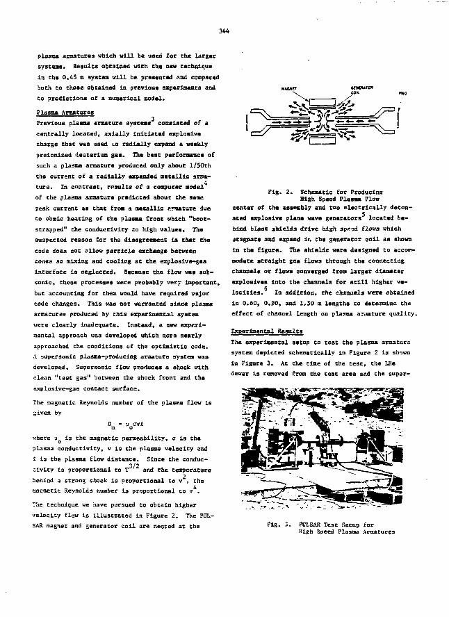
344
plasma armatures which will be used for the larger
systems. Results obtained with the new technique
in the 0.45 m systea will be presented nod compared
both to those obtained in previous experiments and
to predictions of a numerical model.
Plasma Armatures
Previous plasma armature syseens consisted of a
centrally located, axially initiated explosive
charge that was used LO radially expand a weakly
preionized deuterium gas. The best performance of
such a plasma armature produced only about 1/SOth
Che current of a radially expanded metallic arsa-
ture. In contrast, results of a computer aodel
of the plasma armature predicted about the sane
peak current as that from a metallic ?.mature due
to ohmic heating of the plasma front which "boot-
strapped" the conductivity to high values. The
suspected reason for the disagreement is that the
code does not allow particle exchange between
zones so mixing and cooling at the explosive-gas
interface is neglected. Because the flow wee sub-
sonic, these processes were probably very Important,
but accounting for them would have required trrjor
code changes. This was not warranted since plasna
armatures produced by this experimental system
were clearly inadequate. Instead, a new experi-
mental approach was developed which more nearly
approached Che conditions of the optimistic code.
•\ supersonic plasma-producing araature system was
developed. Supersonic flow produces a shock with
clean "test gas" between the shock front and the
explosive-gas contact surface.
The magnetic Reynolds number of the plasma flow is
given by
R - u cvtR o
•--here u Is the magnetic permeability, a is the
plasma conductivity, v is the plasma velocity and
£ is the plasma flow distance. Since the conduc-
tivity ts proportional to T and the temparature
behind a strong shock is proportional to v , the
aai;necic Reynolds number 13 proportional co v .
the technique we have pursued to obtain higher
velocity flow is Illustrated in Figure 2. The PUL-
SAR magnet and generator coil are nested at the
Pig. 2. Schematic for ProducingHigh Speed Plasma Flow
center of the assembly and two electrically deton-
ated explosive plane wave generators located be-
hind blast shields drive high apfsd flows which
stagnate and expand ii. Che generator coil as shown
in the figure. The shields were designed to accom-
modate straight gas flows through the connecting
channels or flows converged from larger diameter
explosives into the channels for still higher ve-
locities. In addition, the channels were obtained
in 0.60, 0.90, and 1.50 m lengths to determine the
effect of channel length on plasma artosture quality.
Experimental Results
The experimental setup to rest the plasma armature
system depicted schematically in Figure 2 is shown
in Figure 3. At the time of the test, the LHe
dewar is removed from the test area and the super-
Fig. 3. PtftSAR Test Setup forHigh Speed Plasma Armatures
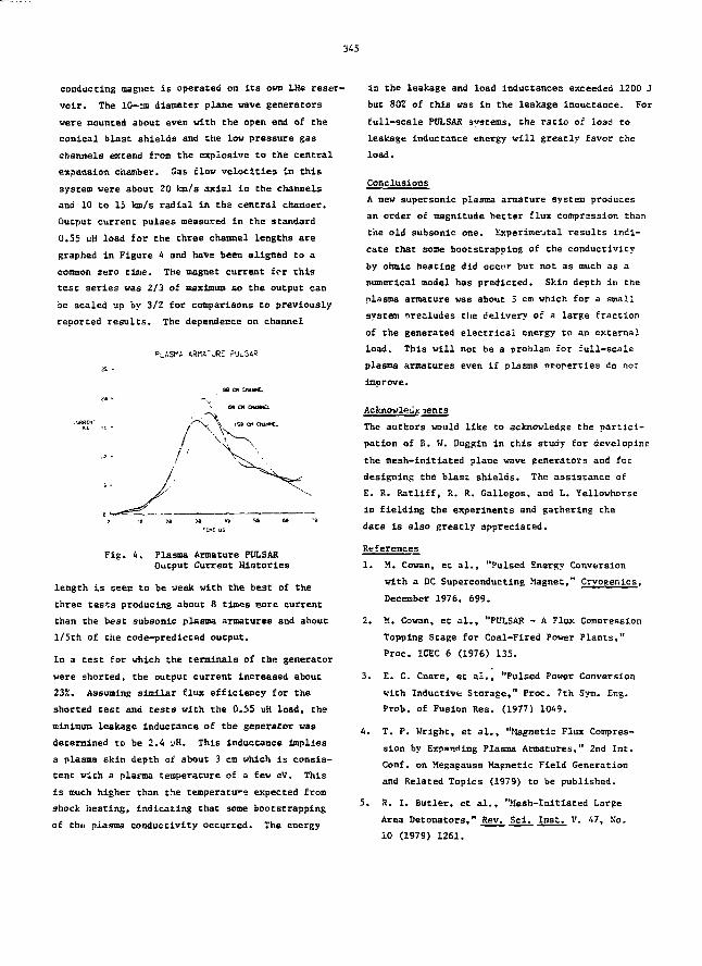
345
conducting magnet is operated on Its own LHe reser-
voir. The 10-cm diameter plane wave generators
vrere mounted about even with the open end of the
conical blast shields and the low pressure gas
channels extend from the explosive to the central
expansion chamber. Gas flow velocities in this
system vere about 20 ko/s axial in the channels
and 10 to 15 km/s radial in tha central chamber.
Output current pulses measured in the standard
0.55 uH load for the three channel lengths are
graphed in Figure 4 and have been aligned to a
common zero time. The magnet current fc-r this
test series vas 2/3 of maximum so the output can
be scaled up by 3/2 for comparisons to previously
reported results. The dependence on channel
°;.ASPA ARMA'URi PUL34R
Fig. 4. Plasma Armature PULSAROutput Current Histories
length is seen to be weak with the best of the
three tests producing about 8 tines more current
than the best subsonic plasma armatures and about
l/5th of the code-predicted output.
In a test for which the terminals of the generator
were shorted, the output current increased about
232. Assuming similar flux efficiency for the
shorted test and tests with the 0.55 uH load, the
minimum leakage inductance of the generator vas
determined to be 2.4 uH. This inductance implies
a plasma skin depth of about 3 cm which Is consis-
tent with a planoa temperature of a feu eV. This
is much higher than the temperature expected from
shock heating, indicating that some bootstrapping
or the plasma conductivity occurred. The energy
in the leakage and load Inductances exceeded 1200 J
but 802 of this was in the leakage inouctance. For
full-scale PULSAR systems, the ratio of load to
leakage inductance energy will greatly favor the
load.
Conclusions
A new supersonic plasma armature system produces
an order of magnitude better flux compression than
the old subsonic one. Experimental results indi-
cate that some bootstrapping of the conductivity
by ohmic heating did occur but not as much as a
numerical model has predicted. Skin depth in the
plasma armature was about 3 cm which for a small
system precludes the delivery of a large fraction
of the generated electrical energy to an external
load. This will not be a problsn for full-scale
plasma armatures even if plasma properties do not
improve.
lents
The authors would like to acknowledge the partici-
pation of E. H. Duggln in this scudy for developinc
the mesh-initiated plane wave generators and for
designing the blast shields. The assistance of
E. R. Ratliff, R. R. Gallegos, and L. Yellowhorse
in fielding the experiments and gathering the
data Is also greatly appreciated.
References
1. M. Cowan, et al., "Pulsed Energy Conversion
with a DC Superconducting Magnet," Cryogenics,
December 1976, 699.
2. M. Cowan, et al., "PULSAR - A Flux Compression
Topping Stage for Coal—Fired Power Plants,"
Proc. ICEC 6 (1976) 135.
3. E. C. Cnare, et al., "Pulsed Power Conversion
with Inductive Storage," Proc. 7th Sym. Eng.
Prob. of Fusion Res. (1977) 1049.
4. T. P. Wright, et al., "Magnetic Flux Compres-
sion by Expanding Plasma Armatures," 2nd Int.
Conf. on Megagauss Magnetic Field Generation
and Related Topics (1979) to be published.
5. R. I. Butler, et al., "Mesh-Initiated Large
Area Detonators," Rev. Sci. Inst. V. 47, So.
10 (1979) 1261.

346
6. H. Cowan and D. A. Freiwald, "Strongly Ion-
izing High Explodv* Shocks," Proe. 7th Int.
Shock Tube Syapoaiua (1969) 432.
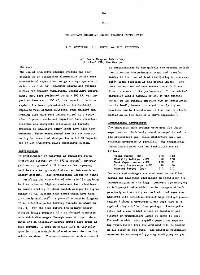
347
15.1
PRELIMINARY INDUCTIVE ENERGY TRANSFER EXPERIMENTS
R.P. HENDERSOK, D.L. SMITH, and R.E. REINOVSKY
Air Force Weapons LaboratoryKirtland AFB, New Mexico
Abstract
The use of inductive storage systems has been
studied as an attractive alternative to the more
conventional capacitive energy storage systems to
drive a cylindrical imploding plasma and produce
X-rays for nuclear simulation. Preliminary experi-
ments have been conducted using a 200 kJ, 4us ca-
pacitor bank and a 100 kJ, lus capacitor bank to
explore the basic performance of electrically
exploded foil opening switches. Peak voltage arid
opening time have been characterized as a func-
tion of quench media and capacitor bank risetime.
Risetime and energetic efficiency of current
transfer to inductive dummy loads have also been
measured. These experimental results are contri-
buting to conceptual designs for a 1.9 MJ capaci-
tor driven inductive pulse shortening system.
Introduction
In anticipation of applying an inductive pulse
shortening circuit to the SHIVA system , investi-
gations using metal foil fuses as fast opening
switches are being conducted on two intermediate
energy systems. This experimental effort is aimed
at verifying the operation of electrically exploded
foil switches at high currents and fast risecioes
to permit scaling of these switch designs to higher
energy (2 MJ) systems than those which have been2
previously explored . A general schematic diagram
of an inductive pulse forming circuit is shown in
Fig. 1. For the near future the primary energy
storage device consists of a dc charged capacitor
bank which discharges through some storage induc-
tance and an initially closed switch that opens at
peak current. A load in series with an initially
open isolation switch is placed across the opening
switch as shown. The performance of such a circuit
is characterized by how quickly th-s opening switch
can interrupt the pTimary current and transfer
energy to the load without dissipating an unaccep-
tably large fraction of the stored energy. The
peak current and voltage across the switch are
also a measure of its performance. For a matched
inductive load a maximum of 25* of the initial
energy lu the storage inductor can be transferred
to the load ; however, a significantly higher
fraction can be transferred if the load is dissi-
pative as in the case of a SHIVA implosion .
Experimental Arrangement
Two capacitor bank systems were used for these
experiments. Both banks are discharged by multi-
ple pressurized gas, field distortion rail gap
switches connected in parallel. The operational
characteristics of the two facilities are as
follows:
Total Energy (kJ)Charging Voltage (kV)Bank Capacitance (pF)Primary Inductance (nE)Quarter Period (us)
Currents and voltages are monitored on oscillo-
scopes and transient digitizers to facilitate the
interpretation of the data. Currents are measured
with Rogowski belts which can be integrated both
passively and actively as desired. Voltages are
measured with resistive divider high voltage probes.
Figure 2 shows a cross-sectional edge view of a
typical single folded fuse package. Rectangular
metal foils are folded around an insulator and
clamped to transmission lines at oppor'te ends.
The medium which must rapidly quench t.ic expand-
ing vapor/liquid from the exploded foil is packed
on all sides of the fuse. The criteria originally
reported by Maisonnier placing conditions on the
20050158363.7
11010022261.2
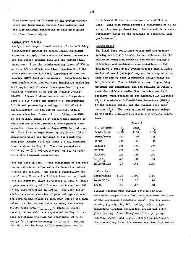
343
fuse cross section In terms of the system capaci-
tance and Inductance, Initial bank voltage, and
Che fuse material properties is used as a guide
for these fuse designs.
Simple Fuse Results
Analytic and computational models of the switching
requirements imposed by future imploding plasma
experiments imply that the two relevant parameters
are the switch opening time and the switch final
impedance. From the models opening times of 350 ns
or less are required, and final impedances of the
same order as the H 3 final impedance of the im-
ploding SHIVA load are necessary. Experiments have
been conducted on the two test facilities employing
both copper and aluminum fuses quenched In glass
beads of diameter 62 to 105 urn ("Elast-O-Lite"
BT-12). Figure 3 shows currer.t and voltage data
from * 1 mil (.0254 mm) coppir fv.s ; interrupting
1.5 MA and generating a voltage -)i 220 kV (4.4
multiplication) on the 200 '.cj facility with a
current risetiae of about 3 vs. faking the FWHM
of the voltage pulse as an approximate measure of
Che risetime of the impedance, the temporal com-
pression (time of peak voltage/LTHM) ia just over
10. Data from an experiment on the faster 100 kJ
experiment which was designed to interrupt the
same peak current (1.5 MA) using a 1 mil aluminum
fuse is shown in Fig. 4. The fuse generates a
270 kV pulse (3.3 multiplication) of 120 ns width
for a 12,5 temporal compression.
From the data in Fig. 4, the resistance of the fuse
can be calculated after suitable Inductive calcu-
lations are applied. And hence a resistivity for
c.ne 40 cm x 20 cm x 1 mil thick fuse can be found.
This resistivity, which is plotted in Fig. 5, shows
a peak resistivity of 2.5 mil-cm, with the last 90%
of che rise occurring in 100 ns. The peak resis-
tivity occurs at che time of peak voltage and when
the current has fallen to less than 20J of its peak
value. As che current falls to zero, the resis-
civitv found from V t/I takes on videlycorrected '
varying values which are suppressed in Fig. 5. At
peak resistance the fuse has dissipated 70 kj of
energy for a specific energy of 13 kJ/g. Scaling
chis data to the large (2 MJ) experiment results
in a fuse 0.87 cm2 in cross section and 21.4 ex
long. This fuse would produce a resistance of 60 mti
at similar energy densities. Such a switch Is very
attractive based on the concepts of projected load
performance
Quench Media
The final fuse resistance values and the corres-
ponding resistivities seem to be influenced by the
choice of quenching media in the switch package 3.
Electrical and mechanical considerations in the
design of a full scale system suggest that a large
cumber of small packages may not be acceptable and
that the use of thin (preferably solid) media may
be preferred. Thus a limited survey of quenching
material was conducted, and the results in Table I
rank the different media (for one aluminum foil
geometry) with respect to the maximum fuse voltages
(V ) , the minimum full-width-half-raaximum (FWHM )
of the voltage spike, and the highest peak fuse
current (I ). The combination of material refersP
to the media used outside/inside the hairpin foldedfuse.
4.0 us Bank Vp
Beads/ Beads 1.00
Beads/Mylar .97
BI/BI .95
AFB/AFB .86
FC/PVC . 79
PVC/PVC . 59
LN2/LN., .45
Mylar/Mylar .28
1.0 us Bank
Beads/Beads 1.00 1.00
Beads/Mylar .55
BI/BI .35
Similar studies with similar results for near-
Maisonnier copper fuses (no load) have been performed
at the Los Alamos Scientific Labs . For the above
results 31, AF3, FC, PVC, and LN7 refer to R19
fiberglass building insulation, acoustical fiber-
glass batting, fine fiberglass cloth, polyvinyl
chloride sheets, and liquid nitrogen respectively.
The conclusions from this survey are chat foil switch
Table I
FWHM,
1.00
.99
.71
.71
.78
.56
.91
.45
1.00
.86
.67
P1.00
.98
.92
.99
-
.92
.99
1.00
1.00
.90
.90
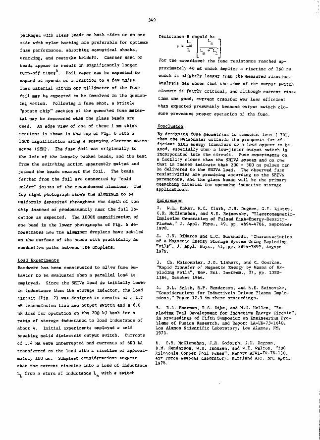
349
packages with glass beads on both sides or on one
side with mylar backing are preferable for optimum
f-jse performance, absorbing acoustical shocks,
tracking, and restrike holdoff. Coarser sand or
beads appear to result in significantly longer
turn-off times - Foil vapor can be expected to
expand at speeds of a fraction to a few tun/us.
Thus material within one millimeter of the fuse
foil may be expected to be involved in the quench-
ing f.ction. Following a fuse shot, a brittle
"potato chip" section of the quenched fuse mater-
ial may be recovered when the glass beads are
used. An edge view of one of these 1 mm thick
sections is shown in the top of Fig. 6 with a
100X magnification using a scanning electron micro-
scope (SEM). The fuse foil was origionally to
the left of the loosely packed beads, and the heat
from the switching action apparently melted and
joined the beads nearest the foil. The beads
farther from the foil are connected by "cold
solder" joints of the recondensefi aluminum. The
top right photograph shows the aluminum to be
uniformly deposited throughout the depth of the
chip Instead of predominantly near the foil lo-
cation as expected. The 1000X magnification of
one bead in the lower photographs of Fig. 6 de-
monstrates how the aluminum droplets have settled
on the surface of the beads with practically no
conductive paths between the droplets.
Load Experiments
Hardware has been constructed to allow fuse be-
havior to be evaluated when a parallel load is
employed. Since the SHIVA load is Initially lower
in inductance than the storage inductor, the load
circuit (Fig. 7) was designed to consist of a 2.2
nH transmission line and output switch and a 6.0
nH load for operation on the 200 kJ bank for a
ratio of storage Inductance to load inductance of
about 4. Initial experiments employed a self
breaking solid dielectric output switch. Currents
of 1.4 MA were interrupted and currents of 600 kA
transferred to the load with a risetime of approxi-
mately 100 ns. Simplest considerations sugsest
that the current risetime into a load of inductance
I- from a store of inductance Lg with a switch
resistance B should be
\[Jfor the experiment Che fuse resistance reached ap-
proximately 40 mC which Implies a risetiae of 160 ns
which is slightly longer than the measured risetiae.
Analysis has shown that the time of the output switch
closure is fairly critical, and although current rise-
time was good, current transfer was less efficient
than expected presumably because output switch clo-
sure prevented proper operation of the fuse.
Conclusion
By designing fuse geometries to somewhat less ( 70'; Ithan the Maisonnier criteria the prospects for ef-ficient high energy transfers to a load appear to begood, especially whei' a low-jitter output switch Isincorporated into the circuit. Fuse experiments ona facility slower than the SHIVA system and on onethat is faster indicate that 200 - 300 ns pulses canbe delivered to the SHIVA load. The observed fuseresistivities are promising according to the SHIVAparameters, and the glass beads will be the primaryquenching material for upcoming inductive storageapplications.
Ref erences
1. W.L. Baker, M.C. Clark, J.H. Degnan, G.F. Kiuttu,C.R. McClenahan, and R.E. Reinovsky, "Electromagnetic-Implosion Generation of Pulsed High-Energy-Density-Plasma," J. Appl. Phys., 49, pp. 4694-4706, September1978.
2. J.N. DIMarco and L.C. Burkhardt, "Characteristicsof a Magnetic Energy Storage System Using ExplodingFoils", J. Appl. Phys., 41, pp. 3894-3899, August1970.
3. Ch. Maisonnier, J.G. Linhart, and C. Gourlan,"Rapid Transfer of Magnetic Energy by Means of Ex-ploding Foils", Rev. Sci. Instrum., 37, pp. 1380-1384, October 1966.
4. D.L. Smith, R.P. Henderson, and R.E. Reinovsky,"Considerations for Inductively Driven Plasma Imp'.o-sions," Paper 12.3 in these proceedings.
5. R.A. Haarman, R.S. Dike, and M.J. Hollen, "Ex-ploding Foil Development for Inductive Energy Circuit",in proceedings of Fifth Symposium on Engineering Pro-blems of Fusion Research, and Report LA-UR-73-1610,Los Alamos Scientific Laboratory, Los Alamos, KM,1973.
6. C.R. McClenahan, J.H. Gofoith, J.H. Degnan,S.M. Henderson, W.R. Janssen, and W.E. Walton, "200Kilojoule Copper Foil Fuses", Report AFWL-TR-78-130,Air Force Weapons Laboratory, Kirtland AFB, NM, April1978.
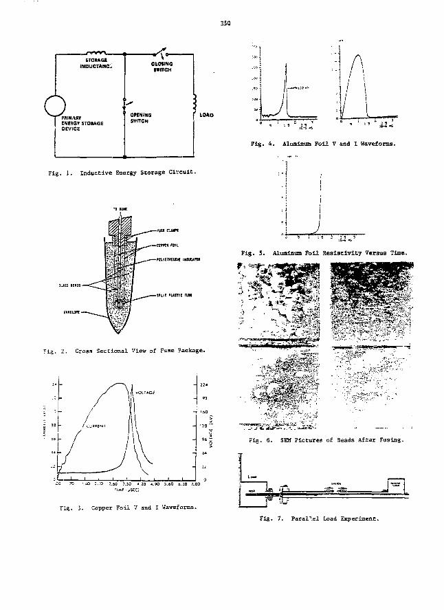
350
JTOKAGlINDUCTANCE
6PltlMARTENEnQT STORAGEDEVICE
CLOSINGSO ITCH
OPENINGSWITCH
LOAD
Fig. 1. Inductive Energy Storage CIvcult.
:.J
Fig. 4. Aluminum Foil V and I Waveforms.
snir FUSTIC TUK
Fig. 2. Cross Sectional View of Fuse Package.
- -J•t. V
70 '.JO :.:0 2.60 3.50 4.20 A.90 5.60 a. 30 7,00
Fig. 3. Copper Foil 7 and I Waveforms.
1I Z 2 3 1
Fig. 5. Aluminum Foil Resistivity Versus Time.
rig. 6. SEM Pictures of 3eads After Fusing.
Fig. 7. Parallel Load Experiment.

351
15.:
APPLICATION OF PFN CAPACITORS IS HIGH POWER SYSTEMS
ROBERT D. PARKER
Hughes Aircraft Company, Culver City, California
Abstract
The application of lightweight reliablecapacitors in a mobile energy store is dis-cussed. The relationship of system designparameters to capacitor size and life is dis-played. Electric fields and weights of a21 J/lb and a 77 J/lfa pulse discharge capacitordesign are given. Estimates of future near-term development are made.
INTRODUCTION
In the vast majority of aerospace applications, thecapacitor may be successfully treated by circuitand system engineers as a black box containing anessentially ideal passive circuit element. Capaci-tors are normally applied well within their ratings,and are designed extremely conservatively, even forhigh voltage applications. Recently, however, anew class of mobile pulsed-power systems hasemerged. In these systems, a capacitative energystore may comprise a substantial fraction of theweight and volume of the entire system. Becauseof the "black box" design approach, systen param-eters are often selected without a clear understand-ing of their combined effect on the weight, life,and reliability of the energy storage capacitors.Since a major design goal in a mobile system is toreduce system size and weight, designs are some-times produced for which no appropriate capacitorsare available, or in which non-ideal capacitorsmust be used in a make—do situation, resulting ingenerally unsatisfactory component performance.
The designer is hampered by the total lack of allbut rudimentary data on the application of the com-ponent, often because no testing has been done bymanufacturers or published in the literature. Themanufacturing processes themselves are poorly con-trolled, resulting in high part-to-part non-uniformity as well as lot-to-lot non-uniformity.Finally, except for measurements of capacitanceand dissipation factor, no industry or militaryspecifications or standards exist for the measure-ment of various parameters important to pulse dis-charge application.
This paper discusses the application of largecapacitors in high power pulse forming networks.The impact of system parameters such as pulsewidth, pulse rise time and repetition rate uponthe weight, life, and reliability of the energy
store is discussed. The problem of application inhostile environments is examined. Present experi-mental results are reviewed, and projections ofachievable weight and volume for mobile energystore are made.
APPLICATION
Many system level parameters affe.ct the applica-tion of pulse-discharge capacitors in a reliablemobile energy store. These are:
• Pulse width and shape
• Load impedance
• Pulse repetition rate
• Charge voltage and waveshape
• Burst duty cycle
• Load match
• Thermal impedance of mount
• Available cooling
• Operational temperature range
• Air pressure/altitude
• Air quality-contaminants
Each of these impacts electrical and thermal fail-ure mechanisms. In the sections below, eachparameter is discussed and its effects displayed.The motive here is to show how to make the oper-ating environment less severe; a less severeenvironment allows smaller, lighter, more reliablecapacitors.
PULSE WIDTH AND SHAPE
These two parameters determine the frequency spec-trum and relative magnitude of the discharge cur-rents for each PFN capacitor. For a system whereall other parameters remain the same, a shorteroutput pulse results in a larger amount of powerdissipated, and therefore a higher operating temp-erature and shorter life. Similarly, a given pulsewidth with faster rise time requires more PFN sec-tions, and this has the same effect as a shorterpulse.
It is easy to show, for a given energy storage, thatthe power dissipation is linear in 1/T, where T isthe output pulse width. This ignores the fact thatdissipation factor is not constant with frequency,
352
but normally this is not as large an effect, andmust be worked ouc for each insulating system.The pulse rise time will be approximately 2T/(2H+1),where N is the number of PFN sections. As the num-ber of sections increases for a given energy, thefrequency dependence of dissipation factor (or ESR)will generally cause the power dissipation coincrease.
LOAD IMPEDANCE
Low impedance Ioad3 are more difficult to drivebecause they require high currents. Real problemsarise only if capacitor currencs above about 20 kAare necessary, because of the extreme mechanicalforces.
PULSE REPETITION RATE
The pulse widen and shape determine the powerdissipated In che capacitor for each pulse. Thepulse repetition rate determines the power dissi-pated per unit time during the pulse burst:
burst pulsex PPJt
This, in turn, is linearly related to che internaltemperature and thus to capacitor life.
CHARGE VOLTAGE AKD WAVESHAPE
Very high charging voltages cause an increase inweight, because additional Interconnections andinsulation between case and capacitor element arerequired. Various curves have been presented. Onerule of thumb is 5 percent weight increase 20 to30 kV, 10 :o 15 percent increase in the 30 to 40 kVrange, and at least 20 percent increase above 40 kV.3ecause very high voltage capacitors require addi-tional series sections and therefore additionalinterconnections, overall reliability is lower.
Charge waveshape effects the capacitor dissipationduring the charging cycle. Surprisingly, systemshave been designed for which the dissipation duringcharge was as large as the dissipation during dis-charge, and since designers normally neglect chargedissipation, such systems normally burn up. Somedielectric systems used in energy storage capacitorshave very high dissipation factors at normal chargefrequencies. Ic is wise to utilize as much of theinterpulse spacing as possible co charge the store,since power dissipation increases as the peak cur-rent increases.
BURST DUTY CYCLE
A capacitor of average dimensions ( 5 x 5 x 7 in.)or larger has a long thermal time constant, becauseeven with heavy foil, the capacitor element has anexcremely poor chermal diffusivity. Tine constantsare in the range of several hours. Therefore, theburst duty cycle determines che highest servicetemperature seen during a given mission. Sincethe time constant is so large, variation of burstlength and spacing on a scale much smaller than thetiisa constant has little effect on the temperature,provided the energy transferred remains the same.
LOAD MATCH
It is normally possible to match the energyscore co the load within a few percent,even for loads which exhibit complex time-dependent transfer characteristics. Failure tomatch the load results in a large voltage rever-sal. This drastically shortens component life.The system level result is shorter-lived,extremely heavy components, with weights beingbetween 2 and 5 times as large as what would havebeen possible with a matched load.
PASSIVE THERMAL CONSIDERATIONS
The thermal impedance of the counting and theavailable cooling determine the temperature riseduring a series of bursts over a time longer thanan hour. It is important Co provide cooling tolimit this rise to prolong capacitor life. Theabsolute temperature reached depends on the oper-ating ambient. Systems which operate in highambient or with poor cooling will be severaltimes larger than the ideal.
ALTITUDE
Two important problems obtain from the operationof an energy store at high or variable altitude.One problem is that it is difficult to provide ahighly reliable termination for this service; thesecond problem is che variation of atmosphericpressure may cause pressure variation within theoil-filled components In the energy store.
The termination and interconnection problem in thistype of syscem in a variable pressure environmentis severe. Prototype systems usually employ make-shift non-demountable high current connectors.Normally available high altitude high voltage con-nectors cannot handle the high peak currents andthe large RMS currents during the burst. Probablythe best solution is to fabricate custom connectorsfor each installation.
If the cases of the oil-filled components areflexible, as are most light-weight cases, thereduction in pressure at high altitude causes areduction in the pressure of the oil below atmos-pheric. This is well known to cause immediate andsignificant degradation of corona inception voltage,and will cause short life and premature failure.Flexible cases must be supported or other methodsmust be used to maintain oil pressure under anyoperating condition.
AIR QUALITY
Some mobile installations operate in high humidityenvironments or other situations where prototypeconnections and terminations will cause substantialsystem malfunction. Interconnections of the typeused in high altitude operation are usually suf-ficienc to protect against these types of malfunc-tion. However, the added weight of these extraprecautions needs to be considered.

353
RECENT EXPERIMENTAL RESULTS
As has been discussed previously, the unavoidablefailure mechanism in a well-constructed capacitoris uniform corona damage at the foil edges. Inthis section, several dielectric systens presentlyin use are described, and electric fields forsatisfactory operation with 103 to 10* shot lifeare given. Several complete capacitors are des-cribed, and their energy density displayed.
CAPACITOR STRUCTURE
The capacitor structure tested is a flat-woundfoil capacitor employing liquid impregnated fivelayer dielectrics. All capacitors to be describedemployed EIB kraft paper and polysulfone as thedielectric, and either mineral oil or dioctylph-thalate as the fluid. Capacitor sections weremade in the range 1.1 to 3.3 uF, with anticipatedoperating voltages in the range 5 to 7.5 kV.Complete capacitors valued 2.2 uF 15 kV wereassembled from these components.
It was determined by a series of indirect measure-ments that the thickness of the oil layers in thesecomponents was 1.0 urn for each pair of surfaces.Thus, a component with 5 solid dielectric layersalso contained about 6.0 um of fluid. This isapproximately 32 percent less fluid than is nor-mally found in an oil-filled capacitor. Theextreme thinness and uniformity of the fluidlayers is thought to be partially responsible forthe high layer operating fields and uniform degra-dation found experimentally.
ELECTRICAL SERVICE CONDITION
b) Dioctylphthalate Impregnant - Average Field4460 V/mTI
Tests on all components and sections were run witha minimum duty profile of 300 pps for 1 minute,with 2 hours between 'v-sts. Components weretested in an apparati •. which duplicates frequencydistribution and current magnitudes of PFN oper-ation. Discharge pulse width was 20 us, andvoltage reversal was 25 percent. Expected lifewas UH pulses minimum, or 5.5 full bursts.
LIMITING ELECTRICAL FIELDS
The maximum fields found for two different impreg-nants at reliable life greater than 10$ pulses areshown in the following table for otherwise identi-cal structures.
a) Mineral Oil Impregnant - Average Field3750 V/mil
Material
PaperPlasticFluid
Field V/mil
343052662761
The higher average field possible for the higherdielectric constant impregnant is due to betterfield balance in the dioctylphthalate part. Thedesign goal is to have operating electric fieldsin the same ratio as known break-down voltages.Limiting fields occurred in the fluid with mineraloil, and in both paper and plastic with dioctyl-phthalate. Some Improvement may be possible inthis design, but no more than 10 percent.
COMPLETE CAPACITORS
Two different complete capacitors have beenassembled, both with 2.2 uF 15 kV rating. Onedesign employed mineral oil, and was designed atmoderate stress and with sturdy construction.The operating fields were:
Material
PaperPlasticFluid
Field V/mil
190429184113
This component was very reliable, and had life inexcess of 10^ shots on a routine basis. Thesecond component used dioctylphthalate, and wasdesigned for absolute minimum weight. The oper-ating fields are listed in the previous section.A breakdown of the weight of each component isshown below.
Item
Sections (wet)CaseTerminalCase InsulationExtra Oil
Totals
Specific Weight
True EnergyDensity
"Energy Density"
Design 1Weight
3.126 kg892 g57 g546 g599 g
5.22 kg
20.88 g/J
0.087 J/CH 3
21.7 J/lb
Design 2Weight
1.126 kg96 g57 g102 g101 g
1.482 kg
5.93 g/J
0.265 J/cn
76.5 J/lb
Material Field V/mil
PaperPlasticFluid
242437145235

354
DISCUSSION
The AC electric fields being reached over a largearea of the polymer film in design 2 are about70 percent of the short-term small area "intrinsic"breakdown test value for the film. The failureanalyses Indicate that, with the present designs,the limit for the paper is also quite close. Itis therefore estimated that, at best, a 10 percentimprovement in field is possible without foil edgemodification. This translates Co a 21 percentimprovement in "energy density".
ESTIMATES
For the aid of systems engineers, herewith is ashort discussion of near term improvement possi-bilities and real values for real systems.
ULTIMATE ENERGY DENSITY
Using presently available materials and techniques,the absolute best attainable energy density for anindividual capacitor in a metallic case will be inche range of 80 to 110 J/lb for the type of servicediscussed above. For DC service with low ripple,short-lived but reliable components may bedesigned in the range 200 - 400 J/lb. Componentsintended for customary military usage will be afactor of 2 heaviar, because of sturdy construc-tion and che ne-^saity of wide temperatureoperation.
IMPROVEMENT
Two avenues are open for the improvement of thesefigures. First, foil edge treatment has shownpromise In raising corona inception voltages ofsmall sections of foil edges, the improvement beingabout: 13 percent. Second, improved solid sheetdielectrics could be made, either by improving themechanical perfection of the films or by modifyingtrhem co provide improved electrical properties.
ACKNOWLEDGEMENT
The continued support and encouragement ofRichard J. Verga, Michael P. Dougherty, and3r. Phillip Stover of che Air Force AeroPropulsion Laboracory have been vital Co thisvork and are greacly appreciated. Technicalcomments by James P. O'Loughlin of che Air ForceWeapons Laboracory have been very helpful, par-ticularly in the area of foil edge conditioningand case optimization.
This work was supported by che Air Force AeroPropulsion Laboratory under Contract F33615-"5-C-2O21.
355
15.A
SAFETY GROUNDING SWITCHES IN LARGE EXPERIMENTS; GENERAL CONSIDERATIONSAND THE TEXT APPLICATION
Paul Wildi
Fusion Research CenteT
The University of Texas at Austin, Austin, Texas 78712
Abstract
The electrical installations of a large
experiment present many potential danger such as
residual charges en capacitor banks and cables,
power rectifiers and other related power supplies,
etc. The commonly used voltages of 1 to 20 kV are
lethal and the available power is sufficient to
cause severe arc damage.
Many experiments require frequent safe access with
a minimum of time loss by both operating personnel
and experimenters. Safety must be automatic since
the people involved are likely to be preoccupied
with the experiments.
The paper reviews some coonnonly employed practices
and discusses the adequacy and safety of various
grounding devices. The safety grounding scheme
for the TEXT Tokamak is described. Specially de-
signed switches, their contact and operating mecha-
hism, are shown and the integration of the switches
in the overall control and safety system is
discussed.
Introduction
Large fusion experiments have many high voltage
carrying circuits which can be dangerous to the
experimenters. Generally, the experimental area
is cleared of personnel immediately before a shot,
but the nature of the work requires frequent access
by people primarily concerned with their experi-
ments, often being under pressure of time and not
paying much attention to safety. It is mandatory
to institute safety procedures which cannot be
bypassed and to secure all conductors which are
connected to electrical power sources through
grounding and/or short circuiting switches. Such
switches are necessary even, if in the normal pro-
cedure, the circuits are deenergized since there is
always the possibility of malfunction. Typical
hazards are, for example: residual charges on
capacitor banks and cables, remanencs voltages of
rotating machines, residual voltages of phased out
rectifiers, etc. The voltages involved in typical
power supplies of fusion experiments are high
enough to be lethal, and the sources have a lov
impedance and very high current capability. There-
fore, i flashover can lead to heavy arc damage,
both to personnel and equipment.
Some Commonly Employed Practices
In utility systems rather elaborate clearance pro-
cedures are used before any personnel are allowed
to work on high voltage carrying equipment. These
procedures normally include disconnection, ground-
ing at several locations and redundant checking at
several levels of supervision. The procedure is
very reliable but time consuming and not suitable
for a laboratory operation.
Manual grounding with grounding sticks is very
popular in a laboratory experiment. It is adequate
when used as a redundant grounding in deenergi zed
circuits, but rather dangerous when accidentally
practiced on a hot circuit such as, for example,
a charged capacitor bank where the discharge flash
is liable to cause ear and eye injuries. Since the
method depends upon the discipline of ths people
356
using it, accidents may occur due to negligence or
forgetfulness of the personnel involved.
Grounding switches of cradest currant carrying
capability of the high voltage contact type are
commonly used on capacitors, very often with
current limiting resistors in series. These are
normally solenoid operated and closed by gravity
or spring action. For high power sources their
current carrying ability is generally too small.
Some grounding safety switches have been built
using the old grounding chain as a contact system.
They consist of some hand operated mechanism
lowering grounding ch&ins over exposed busbars.
The presumption is that an accidentally energized
circuit will initiate an arc before any personnel
gets in contact with the hot circuits.
Fig. 1. TEXT; Diagram of Safety Switchesand Transfer Switches for DischargeCleaning
Grounding System for the TEXT Tokamak
The Texas Fusion Plasma Research Tokamak'- ' is
planned as a user facility for the purpose oi
running a multitude of smaller experiraents. As a
consequence there will be many experimenters and
some will be unfamiliar with the device. There
will also be the need for frequent access to the
test, area without undue time loss. Under these
circumstances the best solution appears to be an
automatic interlocked system as schematically in-
dicated in Fig. 1. Interlocking is such that the
safety switches are permitted to close only aft»r
the power supplies ars deenergized. In turn, the
access doors are unlocked only after the safety
switches have transferred to the grounded position.
The interlock scheme further provides for Switch A
to be closed and the main switch to the toroidal
field power supply to be opened before the dis-
charge cleaning switches can ae transferred. I"
this operating condition, personnel access to the
ToV.amak is permissible. Additional surveillance
by the experimenter will still be required (for
example, closed circuit tele"i_ion), and all per-
sonnel will be asked to observe warning lights.
Rating of the Switches
Except for the contingency of a control malfunction,
the switches will always make and break deenergized
circuits. However, they are laid out for the high-
est possible short circuit current, both dynamically
ai:d thermally. This is in order to insure safety
should, for some reason, a circuit be energized
during the personnel access period. Since switches
of the same type are used to connect the discharge
cleaning power supplies; the contact systems are
also designed for a continuous duty. Transfer time
is of little importance as long as it does not
delay the personnel access and is arbitrarily set
at 10 s or less. Insulation level is 10 fcV. which
is 5 times the highest service voltage. The nominal
ratings are tabulated in Table 1.
An attempt made to procure commercial switches for
this duty was abandoned for economical and avail-
ability reasons.
357
Table 1
Switch
1
Peak current
3 sec current
Continuous current
/-atTest voltage (dc)(open gap and toground)
Mode of operation
kA
kA
kA9 •>
10 A's
kv
A
40
20
1.2
1.2
10
pneumatic
•
400
160
6
75
10
el. motor
Design Features
SKitch A, the protective switch for the poloidal
coil system is shown in Fig. 2. It is a four pole
knife switch with grounded blades. In the closed
position the switch short circuits and grounds the
outputs of all three poloidi-1 field supplies and
the coil system. The fourth pole of the switch is
a spare for possible future use. The switch is
driven by a pneumatic cylinder controlled through
a solenoid four way valve and is mechanically
latched in either end position against accidental
motion. The contact system consists of dual
copper blades straddling the stationary contacts.
The blades are spring loaded and so designed that
the electro-magnetic forces of the current increase
the contact pressure. The key data of the switch
are tabulated in Table 1.
A switch of similaT design (B), but laid out ,is a
double throw switch, is used to connect the poioi-
dal coil system to the discharge cleaning power
supply. Switches A and B are pneumatically inter-
locked so that the discharge cleaning can only be
activated if switch A is in the safety position.
S»itch C, the protective switch foT the toroidal
field system is designed for a peak currant of
400 kA, and since a switch of identical design is
to be used to connect the toroidal field coils to
a continuous dc cupply during discharge cleaning,
it had to be laid out for a S kA continuous current.
The design chosen for this duty is pictured in
Fig. 3 which shows the switch in the closed posi-
tion. It is a sliding contact design with z cylin-
drical moving contact of 4" diameter and 3/8"
copper wall. The stationary contacts are rings
fitted with contact spring bands ("MULTILAM" © )
guaranteeing an adequate springy connection be-
tween the stationary and the moveable contact.
Rating of the switch is based both on manufacturer'?
data and experiments performed with the samePImaterial on a plug-in contact1"-1 and suitably
derated to guarantee an adequate safety maTgin.
The two moveable contacts are cemented on a glass
epoxy tubular support which at its end carries a
nut engaging in the drivs screw. This screw is
driven by a gear motor, the direction of which can
be reversed to produce motion in either direction.
Auxilliary switches operated directly by the move-
able contact assembly assure stopping of the drive
motor in either end position and serve as remote
indicators for the position of the switch and for
the purpose of interlock control. Since the screw
drive-gear motor combination is self-locking,
mechanical end locks were not necessary in this";
design.
Anr identical switch (D) will be used to connect
an auxilliary power supply to the TF coil which
will feed 5,000 A into this coil system during dis-
charge cleaning of the vacuum torus.
References:
[1] P. Wildi, G.L. Cardwell and D.F. Brower,"Design of the TEXT Toroidal and PoloidalField Coils," Seventh Symposium on Engineer-ing Problems of Fusion Research, ilnoxville,Tenn., October 1977.
[2] Paul Wi3dj; "Contacts for Pulsed High Current;Design and Text," IEEE 2nd International PulsedPower Conference, Lubbock, Tx., June 1979.
This work was supported by the U.S. Department ofEnergy.
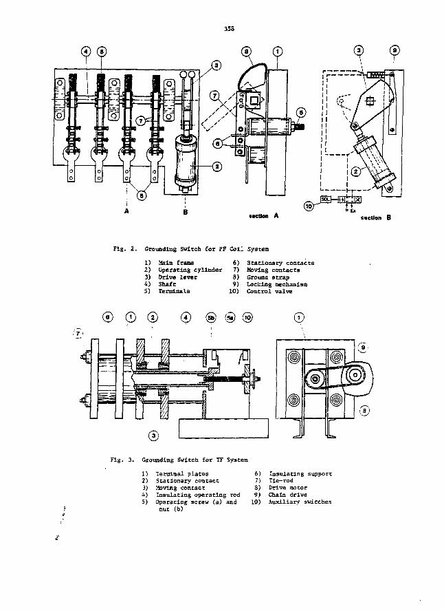
353
•action A section B
Fig. 2. Grounding Switch for FF Call System
1) Main frame 6) Stationary contacts2) Operating cylinder 7) Moving contacts3) Drive lever 8) Ground strap4) Shaft 9) Locking mechanism5) Terminals 10) Control valve
© © 0 (§) ©
Fig. 3. Grounding Switch for TF System
1)2)3)4)5)
Terminal platesStationary contactMoving contactInsulating operating rodOperating screw (a) andnut (b)
6)7)8)9)10)
Insulating supportTie-rodDrive motorChain driveAuxiliary switches
359
15.5
INDUCTANCE AND RESISTANCE CHARACTERISTICS OF SINGLE-SITE UNTRIGGEKED WATER SWITCHES INWATER TRANSFER CAPACITOR CIRCUITS
P. W. Spence, ¥. C- Chen, G. Frazier, and H. Calvin
Physics International CompanySan Leandro, California 94577
Abstract
Inductance and resistance characteristics of
single-site untriggered water switch arc-channels
have been investigated by measurement of their af-
fects on frequency and voltage gain in a water
capacitor transfer circuit* Data are presented for
two distinct switch configurations covering a
voltage range from 3 to 6 XV, gaps from 7 to 35 can,
and mean switching fields from 150 to 350 kV/cm. A
simple lumped circuit model is postulated with
switch L and R varying linearly with gap spacing
under low voltage conditions. Extrapolation of
this zero-order modal to higher voltage conditions
compares favorably with msasured circuit character-
istics. Energy loss in the water switch is ob-
served to be approximately a factor of two in
excess of maximum losses predicted from previous
estimates.1'2
Introduction
Water transfer capacitor circuits are often
applied in the design of high-powar, low-impedance*
short-pulse generators. In practice the circuit
provides an intermediate power amplification stage
in which energy from a Marx generator is Input
(over a rew microsecond tioescale) to a capacitor
and then transferred (over a few hundred nanosecond
timescale) via a switch to a second capacitor. The
principal benefits afforded by such circuits are:
! 1) the ability to operate the second capacitor at.
higher stress levels than possible through direct
charging hy the Marx; and (2) the relaxation of
switching requirements on the second capacitor
stage. Both benefits result from a reduction in
the second stage charge time. Within certain
limitations, single-site untriggered water switches
can be used to Accomplish the transfer of energy
between the two capacitors in the circuit. Two of
these limitations, inductance and effective resist-
ance of the switch arc-channel, are the subject of
this paper.
Conclusions from pioneer work by J. C. Martin
and his associates at MfRE, summarized in a set of
semi-empirical formulae meant to roughly estimate
energy loss, inductance, and the duration of the
resistive phase of such arc-channels, have remained
basically unaltered over the last decade and have
provided valuable tools in the design of switches
over a wide parameter range. As recently as 1977,
VanOevender reported current risetime and energy
loss in a < 1.8 HV water switch to be adequately
described by J. C. Martin' s semi-empirical rela-
tions; he additionally observed no evidence of a
later tine plateau resistance phase which had been
observed in previous lower-energy and lower-voltage
switch experiments.3
Accurate direct measurement of the inductance
and time-varying resistance of water sparks under
high TOltage and high energy density conditions is
a formidable task. Indirect inference of induct-
ance and resistance from transfer circuit frequency
and voltage gain presents a sore tractable measure-
ment problem but introduces considerable uncertam-
. ty accumulated from a combination monitor calibra-
tion accuracy, wave transmission effects, and ac-
curacy of estimating the various fixed L's ans C's
for realistic capacitor and electrode geometries.
In contrast to past studies, the unique features of
'Work supported by the Defense Nuclear Agency.
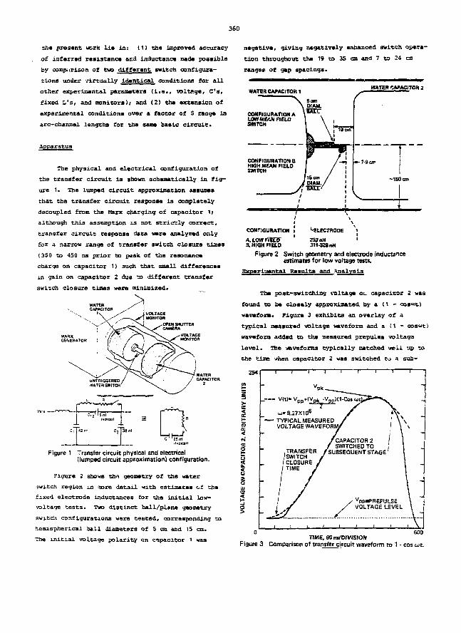
360
the present work lie In: (1) the improved accuracy
of inferred resistance ar.d inductance made possible
by comparison of two different switch configura-
tions under virtually identical conditions for all
other experimental parameters (i.e., voltage/ C's,
fixed L's, and monitors); and (2) the extension of
experimental conditions over a factor of 5 range in
arc-channel lengths for the same basic circuit.
Apparatus
The physical and electrical configuration of
the transfer circuit is shown schematically la Fig-
ure 1. The lumped circuit approximation assumes
that the transfer circuit response is completely
decoupled from the Marx charging of capacitor 11
although this assumption xs not strictly correct,
transfer circuit response data ware analyzed only
for a narrow range of transfer switch closure times
(350 to 450 ns prior to paak of the resonance
charge on capacitor 1) 3uch that small differences
in gain on capacitor 2 due to different transfer
switch closure times were minimized.
I tvDiCJll I S2 I
I
Figure 1 Transfer circuit physical and electrical{lumped circuit approximation) configuration.
Figure 2 shows thci geometry of the uaterswitch region in ioore detail with estimates of thefixed electrode inductances for the in i t ia l low-voltage tests . Two distinct ball/plane geometryswitch configurations were tested, corresponding tohemispherical ball diameters of S cm and 15 can.The init ia l voltage polarity on capacitor 1 was
negative, giving negatively enhanced switch opera-
tion throughout the 19 to 35 an and 7 to 24 cm
ranges of gap spacings>
WATER CAPACITOR 1WATER
I 19 cm
~150cm
CONFIGURATION ,
KLOWfTiLD3. HIGH FIELD
"•ELECTRODE
233 nH311-328 nH
Figure 2 Switch geometry and electrode inductanceestimate) for low voltage tens.
Sxperiaental Basulta and Analysis
The post-switching voltage or. capacitor 2 wasfound to ba closely approximated by a (1 - cosut)wavefora. Figure 3 exhibits an overlay of atypical measured voltage waveform and a (1 - cos"t)wavefora added to the measured prepulae voltagala vol. The waveforms typically matched well up tothe time when capacitor 2 was switched to a sub-
254
§ -
u
vppaPREPULSEVOLTAGE LEVEL
0 600TIME, 60 n»/DlVISION
Figure 3 Comparison of transfer circuit waveform to 1 - cos a;t.
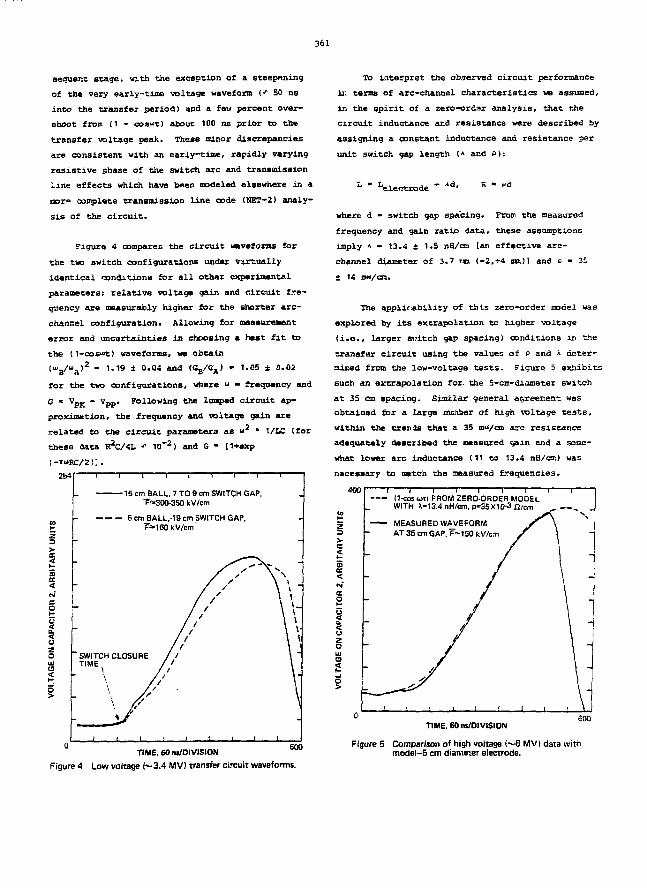
361
sequent stage, with the exception of a steepening
of the very early-time voltage waveform (' 50 ns
into the transfer period) and a few percent over-
shoot from (1 - ooa">t) about 100 ns prior to the
transfer voltage peak. These ninor discrepancies
are consistent with an early-time, rapidly varying
resistive phase of the switch arc and transmission
line effects which have twen modeled elsewhere in a
nor- complete transmission line code (NET-2) analy-
sis of the circuit.
Figure 4 compares the circuit waveforms for
the two switch configurations under virtually
identical conditions for all other experimental
parameters; relative voltage gain and circuit fre-
quency are measurably higher for the shorter arc-
channel configuration. Allowing for measurement
error and uncertainties in choosing a hast fit to
the (1-cosut) waveforms, we obtain
(U. S/«J A)2 - 1.19 ± 0.04 and <%/GA) • '•<» ± 0.0.2
for the two configurations, where " - frequency and
G « v p K - v p p. Following the lumped circuit ap-
proximation, the frequency and rootage gain are
related to the circuit parameters as <"2
these data 1^0/41, ' 10~2) and Q " [1+«xp
2S4
- IS cm BALL. 7 TO 9 cm SWITCH GAP,T="30O-35O kV/cm
- 5 cm_BALL,-19 cm SWITCH GAP,F=-160 kV/cm"
TIME, 60 ns/DIVISlON
Figure 4 Low voltage («-3.4 MV) transfer circuit waveforms.
600
To interpret the observed circuit performance
ii: terms of arc-channel characteristics we assumed,
in the spirit of a zero-ordsr analysis, that the
circuit inductance and resistance were described by
assigning a constant inductance and resistance per
unit switch gap length (* and P):
1 * Lelectrode + *«' s * " a
where d - switch gap spacing. From the measured
frequency and gain ratio data, these assumptions
imply * - 13.4 ± 1.5 nH/cn [an effective arc-
channel diameter of 3.7 nm (-2,+4 mm)] and c - 3S
i 14 nw/cm.
The applicability of this zero-order madel was
explored by its extrapolation to higher voltage
(i.e., larger switch gap spacing) conditions in the
transfer circuit using the values of P and * deter-
mined from the low-voltage tests. Figure 5 exhibits
such an extrapolation for. the 5-cm-diameter switch
at 35 cm spacing. Similar general agreement was
obtained for a large number of high voltage tests,
within the trends that a 35 mu/cn ajrc resistance
adequately described the measured gain and a some-
what lower arc inductance (11 to 13.4 nH/cm) was
necessary to match the measured frequencies.
400
ce
zoIII
s .
(1-<fflS utl FROM ZERO-ORDER MODELWITH X-13.4nWcm. P-35X10-3 fl/cm
MEASURED WAVEFORMAT 35 cm GAP, F~150 k Vtan
..: J
TIME. 60 m/DIVISION600
Figure 5 Comparison of high voltage (~6 MVI data withmodel-5 cm diameter electrode.
362
Discussion and Conclusions
It i3 not surprising that a constant induct-ance per unit gap length model appears to t i t ch«data. The values deduced for Inductance appearconsistent with observed damage pattern* (pits) onthe electrodes and previous channel expansionvelocity estimates* The observed trend towardslight reduction in inductance per unit length atlarger gap spacings may be due to the developmentof arc-channel branches near the anode side of theswitch.
The somewhat surprising applicability of aconstant resistance per unit gap length nodel hassignificant implications in extrapolation to evenhigher-voltage water capacitor transfer c ircuits .In the context of the zero-order model, this re-sistance represents a time-averaged, "effective,"resistance insofar as i t affects circuit gain dur-ing the first half-period. This resistance appearsto be distinct from the cla3slc early-time res is t -ive phase C?Q is in the few ten* of nanosecondsrange and « rL for al l configurations tested) andrepresents a longer timescala "plateau" resistancephase. Resolution of the time dependence of thisplateau phase i s beyond the scope of thisdiscussion; however, the observed voltage waveformfi t to t i-cos^t) does hint that any time dependenceis probably weak for the first half-period.
The most important implication of the results-s the increased energy loss (I R) in long waterspark channels due to tha plateau resistance-Measured losses ranged from 3'* to 26* for th*extrema in switch spacings compared with 4% to 14%expected froia J. c. Martin'31 relations for themaximum energy loss ;ondition TL •< TH:
COMPARISON CF SWITCH LOSSES ( I 2 R ) WITH
J . C. MfcBXXH'S SEMI-EMPIRICAL FORMULAE
ELOSSV
: 42 T -,1/3 ,-,4/3
in units of p.s, ohms, MV/cm.
J. e. mrctoi
M 15 ca,
M on Elaeezodt n 4%
15 <M Ktactxoda 19* n
*c 22 m
For casett where " L » T R (more characteristic of
the present testa), eveu lower switch losses are
estimated from the semi-empirical formulae.
In conclusion, we have analyzed the behavior
of a single-site, nigh-voltage, high-power, water
transfer switch in a specific transfer circuit in
terms of a zero-order model with constant induct-
ance and "plateau" resistance per unit gap length
and founds (1) inductance values consistent with
arc-channel diameters of a few millimeters;
(2) average resistance values of 35 ± 14 mU/cst; and
(3) switch energy losses in excess of previously
established estimates. Further experiments at
higher voltage and with larger gaps would be desir-
able in establishing the relevance of this model to
a wider parameter range.
Acknowledgements
The authors would like to acknowledge the par-
ticularly important contribution of the following
individuals: M. Di Capua and T. Sullivan, for
their help in digitizing the experimental data; w.
Furrow, for timely and quality hardware
construction; 0. Strachan and others, for exper-
imental assistance and facility operation; and
K. Childers, for imaginative contributions to
nomenclature •
References
1. J. C. Martin, Duration of the Resistive Phase
and Inductance of Spark Channels,
S3WA/JCV1065125, Dec. 1965 (unpublished).
2. J. ?ace WuiDevender, "The Resistive Phase of a
High Voltage Mater Spark," J. Appl. Phys. 49,
5 (1978).
3. V. H. Kuleshov, 3. L. Nedoseev, V. ?. Smirnov,
and A. M. Spektor, Sov. Phys.-Tech. Phys. 19,
1 (1974).
363
16.1
INVITED
HOLLOW-ANODE MCLTIGAP THYRATRONS
H. Menown and C. V. Neale
English Electric Valve Company LimitedChelmsford, CM1 2011United Kingdom
Abstract
Subsequent to the introduction of single-gap, hol-
low-anode cubes in 1978, a new range of multlgap
hollow-anode tubes is being intisduced. There are
many applications where high rates of rise of in-
verse voltage cause premature failure of conven-
tional aultigap thyratrons due to arc-back. One
solution has been to use double-cathode tubes,
which are capable of reverse conduction without de-
terioration of performance. The hollow-anode tubes
offer the similar advantage of tolerating reverse
conduction without requiring extra high-voltage-iso-
lated supplies. The operation of these tubes in
low-inductance circuits is compared with conven-
tional solid-anode tubes.
364
16.2
HIGH FHEQUEHCY THraATRDK EVALUATION
Abstract
Gregory A. Hill
The BDM Corporation
and
T. R. Burkes
Texas Tech University
Th« Panted* Thyratron
The high frequency characteristics of a triple grid
thryratron are investigated. The pentode thyratron
has three closely spaced grids and operates much
like a conventional tetrode thyratron. The first
grid has a dual ftmccion. It functions as a prim-
ing grid, preionlzing the grid cathode space, as
well as a shield grid, isolating the control grid
from the cathode plasma during the recovery phase.
The second grid is the control grid, with negative
control characteristics. The third grid is a shield
grid, designed to enhance the control grid aperture
deionization. This thyratron is tested in a line-
type pulser to determine its high frequency limita-
tions. Ic proves capable of operating at pulse
repetition frequencies of up to 180 kHz.
The triple grid, or pentode, thyrafron is shown
schematically in Figure 1. Its operation is like
that of a tetrode thyratron. The first grid is
the primer, or auxiliary, electrode. The second
grid is the control grid, with negative control
characteristics. The third grid Is a shield grid.
This grid, along with Grid #1, completely shields
the control grid from the rest of the tube.
This shielding has two positive effects on recovery.
Since the grids are closely spaced, the volume of
the grid aperture regions la small. Thus this space
has a small characteristic dimension, A, resulting
in very fast deionization. Therefore, the shield-
ing reduces the recovery time.
Introduction
It has become clear that advances ia switching
technology are vital to the growth and development
of pulsed power technology. A need exists for
fast rise-time, high repetition rate switches that
•jill switch high voltages and currents. One prom-
ising type of switch is the hydrogen thyratron. A
new type of thyratron, the triple-grid thyratron,
has recently been developed. This switch is rated
by its manufacturer to operate at repetition rates
of up cc 100 kHz. This paper describes a test and
>. 'aluation of :he triple-grid thyratron's high
frequency operational characteristics, with the
goal of gaining insight into the direction of future
thyratron development.
- Anode
Shield Grid (#3)Control Grid (#2)
Auxiliary Grid (#1)
Cathode
Figure 1. Triple Grid Thyratron
365
The second effect is due primarily to che shield-
ing of the control grid by the auxiliary grid.
Since the control grid is effectively isolated from
the slowly decaying cathode plasma, the density of
this plasma will not appreciably affect the control
grid current during recovery. Thus a higher-
impedance bias supply may be used to achieve
recovery with a pentode thyratron than is neces-
sary with a single grid thyrstron.
The English Electric Valve Company is now produc-
ing a triple-grid thyratron, designated Type CX
1535. This thyratron is designed to switch high-
power pulses at high repetition rates. It features
massive grids with large external cooling fins,
and is designed to be operated totally iinmersed
in coolant. Thus any beat generated in the tube
should be quickly removed. The published ma-iHrnnm
ratings for the CX1535 are given in Table 1. That
the ratings are nonsimultaneous is readily apparent
upon close examination. Although the tube is rated
to switch 12.5 HW, this may only be achieved at
pulse repetition frequencies up to 20 kHz without
exceeding the anode heating factor. At the rated
frequency of 100 kHz, the maximum output is limited
to 2.5 MW. The relationship between peak output
power and repetition frequency is shown in Figure 2.
Anode Voltage
Peak Anode Current
Rate of Anode Current
Rise
Anode Beating Factor
Peak Output Power
Pulse Repetition Fre-
quency
Envelope Temperature
Average Anode Current
25,000
1,000
5,000
500 x 109
12.5
100
150
1.25
VA
A/us
V.A.p.p
MW
KHz
°C
A
Table 1. Maximum ratings of the CX1535 thyratron.
20 40 60 SO 100
Frequency (KHz)
Figure 2. Rated Anode Heating Limitations
The reliable operation of this thyratron within its
published ratings has been established [1]. How-
ever, the true limits of its capabilities have not
previously been explored. Therefore, this test was
designed to provide an evaluation of the triple-
grid thyratron1s capabilities beyond its published
limitations.
Test Design
The triple-grid thyratron was tested in a standard
line-type pulser. The pulse-forming line (PFL)
was designed to deliver a 100 nanosecond pulse to
the 17.5 ohm load. A 0.2 microhenry inductor was
used to limit the current rise-time to 30 nano-
seconds. The shield (#3) grid was grounded to the
cathode. The auxiliary (#1) grid was biased with
a 100 milliampere current source. The control grid
was biased to a negative 200 volts. Regulated
6.3 volt direct current supplies *jere used to power
the cathode and reservoir heaters. Probes were
included, to monitor all electrode voltages and
currents. The anode temperature was monitored with
thermocouple temperature probes. The assembly was
immersed in oil, and was provided with the capa-
bility of force-cooling the anode. Inductive
charging of the PFL was employed, with a charging
rectifier being used in some portions of the test.
The test proceeded in three phases. Initially a
set of low frequency characterization tests were
performed. This involved measuring all of the
electrode voltages and currents while operating
the pulser at a low repetition frequency (3 kfiz).
The second phase was a thermal limitations test.
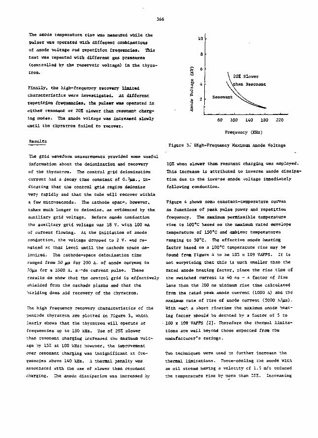
366
The anode temperature rise was measured while the
pulser was operated with different combinations
of anode voltage snd repetition frequencies. This
test was repeated with different gas pressures
(controlled by the reservoir voltage) in the thyra-
cron.
Finally, the high-frequency recovery limited
characteristics were investigated. At different
repetition frequencies, the pulsar was operated In
either resonant or 201 slower than resonant charg-
ing modes. The anode voltage was increased slowly
until the thyratron failed to recover.
Results
The grid waveform measurements provided some useful
information about the deionizacion and recovery
of the thyratron. The control grid deionization
current had a decay time constant of O.Tjis., in-
dicacing that the control grid region deionlze
very rapidly and that the tube will recover vithin
a few microseconds. The cathode space, however,
takes much longer to deionize, as evidenced by the
auxiliary grid voltage. Before anode conduction
the auxiliary grid voltage was 18 V. with 100 mA
of current flowing. At the initiation of anode
conduction, the voltage dropped to 2 V. and re-
mained at that level until the cathode space de-
ionized. The cathode-space deioi:ization time
ranged from 50 /is for 200 A. of anode current to
70^s for a 1000 A. a:'-de current pulse. These
results do show that the control grid is effectively
shielded from the cathode plasma and that the
hielding does aid recovery of the thyratron.
The high frequency recovery characteristics of the
pentode thyracron are plotted in Figure 3, which
learly shows that the thyratron will operate at
frequencies up to 180 kHz. Use of 20% slower
than resonant charging increased the maximum volt-
age by 13% at 100 kHz; however, the improvement
over resonant charging was insignificant at fre-
quencies above 140 kHz. A thermal penalty was
associated with the use of slower than resonant
charging. The anode dissipation »as increased by
10
20% Slower
\than Resonant
Resonant
60 100 140 130 220
Frequency (KHz)
Figure 3." High-Frequency Maximum Anode Voltage
10% when slower than resonant charging was employed.
This increase is attributed to inverse anode dissipa-
tion due to the inverse anode voltage immediately
following conduction.
Figure 4 shows som.s constant-temperature curves
as functions of peak pulse power and repetitiou
frequency. The "°r'»" permissible temperature
rise is 100°C based on the maximum rated envelope
temperature of 150*0 and ambient temperatures
ranging to 50°C. The effective anode heating
factor based on a 100°C temperature rise may be
found from Figure 4 to be 183 x 109 VAFPS. It is
not surprising that this is much smaller than the
rated anode heating factor, since the rise tine of
the switched current is 40 ns - a factor of five
less than the 200 ns minimum rise time calculated
from the rated peak anode current (1000 A) and the
maximum rare of rise of anode current (5000 A/us).
Hith such a short risetime the maximum anode heat-
ing factor should be derated by a factor of 5 to
• 100 x 109 VAFPS [2]. Therefore the thermal limita-
tions are well beyond those expected from Che
manufacturer's ratings.
Two techniques were used to further increase the
thermal limitations. Force-cooling the anode with
an oil stream having a velocity cf 1.5 m/s reduced
the temperature rise by more than 25%. Increasing
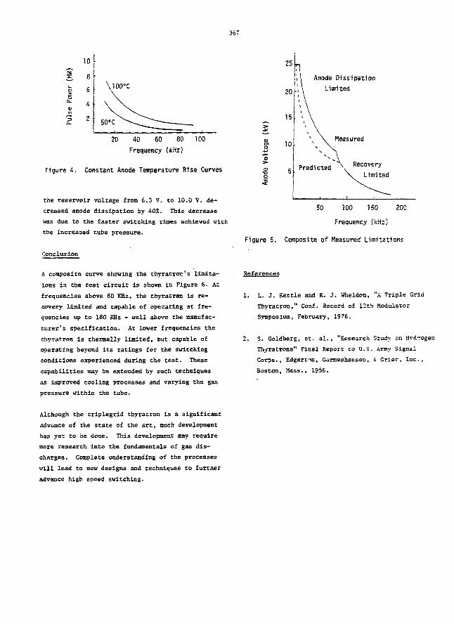
367
as
10
8
6
4
2
20 40 60 80 100
Frequency (kHz)
Figure 4. Constant Anode Temperature Rise Curves
the reservoir voltage from 6.3 V. to 10.0 V. de-
creased anode dissipation by 40%. This decrease
was due to the faster switching times achieved with
the increased tube pressure.
Conclusion
A composite curve showing the thyratron's limita-
ions in Che test circuit is shown in Figure 6. At
frequencies above 80 KHz, the thyratron is re-
covery limited and capable of operating at fre-
quencies up to 180 KHz - well above the manufac-
turer's specification. At lower frequencies the
thyratron is chermally limited, but capable of
operating beyond its ratings for the switching
conditions experienced during the test. These
capabilities may be extended by such techniques
as improved cooling processes and varying the gas
pressure within the tube.
Although the triplegrid thyratron is a significant
advance of the state of the art, much development
has yet to be done. This development may require
more research into the fundamentals of gas dis-
charges. Complete understanding of the processes
will lead to new designs and techniques to further
advance high speed switching.
25
20
10
nI Anode Dissipation.', \ Limited
• \ \
Predicted
Measured
\ Recovery\ . Limited
50 100 150 200
Frequency (kHz)
Figure 5. Composite of Measured Limitations
References
1. L. J. Kettle and R. J. Wheldon, "k Triple Grid
Thyratron," Conf. Record of 12th Modulator
Symposium, February, 1976.
2. S. Goldberg, et. al., "Research Study on Hydrogen
Thyratrons" Final Report to U.S. Army Signal
Corps., Edgartnn, Germeshausen, & Grier, Inc.,
Boston, Mass., 1956.
368
16.3
REPETITIVE ELECTRON BEAM CONTROLLED SWITCHING
R. F. FERNSLER,* D. CONTE, I. M. VITKOVITSK2
Naval Research LaboratoryWashington, D.C. Z0375
Abstract
Previous investigators have demonstrated the feasi-
bility of using an ionizing electron beam to con-
trol the conductivity of a gaseous, volume-dis-
charge switch, We have considered the possibility
of using such switches repetitively at high power
levels Cup to 10 W), with switch opening and
closing times as short as several nanoseconds. Aa
analysis of the relevent gas chemistry has indi-
cated that these requirements can best be met by
using a non-electronegative base gas diluted with
a small percentage of an electronegative gas. De-
tailed chemistry simulations, using the non-electro-
negative gas N. and the electronegative gas 0.,
have been performed and will be presented to support
this analysis. Also discussed will be the limita-
tions Imposed by switch heating and gas breakdown.
Introduction1 7 3
Hunter , 0' Loughlin", and Kovalchuk and Mesyats
have described and demonstrated a switch concept
which appears to be well suited to fast, high-
power, repetitive switching. This concept consists
(seeFig. 1) of a pair of planar electrodes sepa-
rated by a high pressure gas. The switch is made
to conduct by passing an ionizing electron beam
through the gas, such that a volume discharge can
be maintained between the switch electroues. Such
volume discharges have the property that once the
electron beam is removed, the discharge rapidly ex-
tinguishes and the gas can again hold off the high
voltage.
The use of high gas pressure allows for small elec-
trode separation, thereby minimizing switch induc-
tance. As a result, switch opening and closing are
determined primarily by the electron beam and gas
chemistry characteristics. The use of large elec-
trode surfaces, on the other hand, allows large
switch currents to be conducted before switch heat-
ing destroys proper switch behavior. The present
paper seeks to assess the overall capabilities of
these electron-bean controlled switches.
Gas ClyM stry
The svit-ii resistance is controlled by the electron
density n of the gas medium. For a volume discharge
whose dominant ionization source is an electron beam
of current density J. , n varies according toD e
dt ne Jb -£- - a - & (1)
where a is the cross-section for ionization by the
electron beam, N is the gas density, a is the
attachment rate, 3 is the two-body recombination
coefficient, and y is Che three-body recombination
coefficient. Eq. (1) mist be supplemented by the
circuit equation and by the switch current density
equation
(2)
where •/, is the electron drift velocity iue to thea
electric field E appearing across the switch.
Eqs. (i) and (2) dictate that the minimum switch
closing time is given by
. fain) J i _ _ L ^ '3>
where the bar denotes the steady-state value in the
369
closed (conducting) circuit state. Eqs. (1) and
(2) similarly determine the minimum switch opening
time, which is defined as the time for n to decay
from n to 0.1 H . For a switch dominated by
electron attachment, the minintm opening time is
* 2.3(mia),
(4a)
for a switch dominated by two-body recombination,
it is
T2-«V^; (4b)
and for a switch dominated by three-body recombin-
ation, it is
(min)50 (4c)
These latter three equations demonstrate that
attachment-dominated switches minimize the switch
opening time, without serinusly compromising the
switch closing time. (A second advantage is flex-
ibility, in that the attachment rate a can be
readily varied by using a non-attaching base gas
diluted with controlled percentages of an attaching
gas.)
To insure that che gas is everywhere ionized, the
bean electrons must have sufficient energy to tra-
verse the entire discharge. Simple analysis shows
that this energy constraint leads to
1 (TTIITI) ->, n i ,(.•.
' f Q — 15)c eE v.
o d
where che switch efficiency Q Is the ratio of the
power dissipated in the load to that consumed by
the electron beam generator, where e is the average
energy required per beam ionization in the gas, and
where E is the open-circuit field strength origi-
nally appearing across the switch. This equation
demonstrates that a trade-off exists between high
efficiency Q, and short opening and closing times
Switching characteristics of 10 atm of N2 with small
admixtures of 0 have been calculated using a de-» 4
tailed air chemistry code. These sample calcula-
tions were designed to assess the performance of a
switch soon to be constructed and tested at the
Naval Research Laboratory. The switch nominally
imposes 200 kV across a 20 JI load. The switch elec-
trodes are 1000 cm in area and are separated by
2 cm. Nominal switch efficiency is Q T. 10. The
calculations assume th<-i the electron bean current
rises instantaneously to full value (1 kA) at time
zero, and instantaneously decays to zero at 100 nsec.
The predicted behavior, shown in Fig. 2, demonstrates
that the 0 concentration significantly affects the
sv :ch opening time, without significantly affecting
the switch closing time.
Multipulse Operation and Other Considerations
Volumetric switches minimize the volumetric heating
rate such that the gas temperature and physical stare
of the gas are largely unaltered by a short, single
switching pulse. This factor accounts for the rapid
recovery and short opening times of volume discharges,
as compared with the behavior of filamentary arc
discharges.
Conversely, volumetric switches cannot be cooled
rapidly, and hence gas heating may eventually pose
problems for switches t:.at are repetitively pulsed.
These problems take three forms.
The first relates to cumulative changes in the ehem-
ical and electrical properties of the gas. Studies
of discharges in N_ suggest that such alterations
are unimportant until sufficient energy has been
deposited to raise the ,?as temperature to above
2000° K.5
The second problem is a structural one related to
excessive pressures generated by the heated gas.
This problem is severely compounded by the use of a
thin foil window (see Fig. 1) required to pass the
electron beam into the discharge volume.
The third problem concerns reductions in the gas
density N produced by the elevated gas pressure.
The main problem here stems from the constraints
imposed on the ratio E /N, where E is the open-
circuit field strength. To justify ignoring cascade
ionization of Che gas by Che gas conduction elec-
trons, E /N mast typically satisfy
E /N S Id"16 volts - cm2. (6)
Ac Che same time, Eq. (5) demonstrates that Eo
must be maximized to obtain high efficiency Q and
short closing times T . Hence, reductions in
>1, due to elevated gas pressures, reduce the
allowed field strength E , thereby degrading Q and/
The preceding discussions suggest that a conserva-
tively operated switch is one for which the total
energy deposited within Che switch from a given
pulse train is less than, say, the total kinetic
energy originally contained in the gas. This pre-
scription insures chat alterations in the gas temp-
erature, pressure, and density will be less than a
factor of 2.
The total energy deposited in the switch, from Che
electron beam and from Joule dissipation, can be
related to the total energy absorbed by the load
via a net efficiency factor Q1, where Q' £ Q. For
a pulse crain consiscing of m pulses, each of con-
duction time T , we thus require chat
note that constraint (.9), coupled to Eq. C3), limics
Che maximum practical electron beam current to a
value typically given by
CIO); 104 A;
(m Tp 0- < | Nk (7)
i.e., raising I. above this inductive limit only
degrades switch performance by reducing efficiency
Q without reducing opening or closing times T.
Sunmarv
The preceding sections have outlined the general
features of electron bean controlled switches.
These devices may be viewed as current amplifiers
in which a 3mall beam current regulates a large
discharge current. They may be operated either in
a fast, high-power mode or in a slow, high-energy
transfer mode. In the former case, the present
analysis indicuces that, at 10 atns gas pressure,
current switching rates can approach 10 A/sec;
these rates correspond to switch closing times of
several nsec and switch opening times of tens of
nsec, for switch efficiencies Q, q* s. 10. Total
energy transfer would be roughly limited, however,
to 10 Joules per cubic centimer of discharge volume.
Higher energy transfer can be obtained by degrading
switch response tima, or by raising the gas
pressure.
where '* is Boltzmann's constant and T is theo
inicial gas temperature. The breakdown con-
scraint (6) thus suggests that, for T » 300° K, gas
heating effects can generally be ignored provided3i T J « 10 Q' A - sec/cm
P s (8)
Several other limitations apply to electron beam
controlled switches. An important one is Che in-
herent switch inductance, which is minimally given
in nH by the electrode separation distance in cm.
Using constraint (6), this inductance can be shown
to limit the switch opening and closing times to
T(sec) 10'(9)
where I is the desired switch current. This result
reiterates that optimum performance is attained by
maximizing the gas density M. It is interesting to
References
1. R. 0. Hunter, "Electron Beam Controlled Switch",
Proceedings of the 1st International Pulsed
Power Conference, IEEE Cat. No. 76CH1147-B
REG 5, Lubbock, Texas (1976).
2. J. P. O'Coughlin, "PFN Design Interface with
E-Beara Sustained Gas Discharge", op. cit.
3. B. M. Kovalchuk and G. A. Mesyats, Sov. Tech.
Phys. Lett. 2., 252 (1976).
4. R. Fernsler, A. SI. All, J. R. Greig, and
I. M. Vitkovitsky, "An Air Chemistry Code",
Bull. Am. Phys. Soc. 23.. " 5 (1978).
5. T. H. Lee, Phvsics and Engineering of High
Power Devices, MIT Press, Cambridge, Mass. (1975).
6. S. C. Brown, 3asic Data of ?lasma Phvsics,
Technology Press, Cambridge, Mass. (1959).
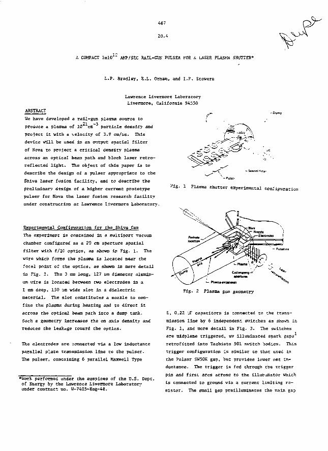
467
20.A
A COMPACT 5x10 AMP/SEC RAIL-GUN PULSER FOR A LASER PLASMA SHUTTER*
L.P. Bradley, E.L. Orham, and I.F. Stowers
Lawrence Livermore Laboratory
Llveraore, California 94550
ABSTRACT
We have developed a rail-gun plasma source to21 -3
produce a plasma of 10 cm particle density and
project it with a velocity of 3.9 cm/us. This
device will be used in an output spatial filter
of Nova to project a critical density plasma
across an optical beam path and block laser retro-
reflected light. The object of this paper is to
describe the design of a pulser appropriate to the
Shiva laser fusion facility, and to describe the
preliminary design of a higher current prototype
pulser for Nova the laser fusion research facility
under construction at Lawrence Livermore Laboratory.
Experimental Configuration for the Shiva Gun
The experiment is contained in a multipart vacuum
chamber configured as a 20 cm aperture spatial
filter with f/lC optics, as shown in Fig. 1. The
wire which forms the plasma is located near the
focal point of the optics, as shown in more detail
in Fig. 2. The 3 nm long, 127 urn diameter alumin-
um wire is located between two electrodes in a
1 mm deep, 150 urn wide slot in a dielectric
material. The slot constitutes a nozzle to con-
fine the plasma during heating and to direct it
across Che optical beam path into a dump tank.
Such a geometry increases the on axis density and
reduces the leakage toward the optics.
The electrodes are connected via a low inductance
parallel plate transmission line to the pulser.
The pulser, containing 6 parallel Maxwell Type
*Work performed under the auspices of the U.S. Dept.of Energy by the Lawrence Livensore Laboratoryunder contract no. W-7405-Eng-48.
l?ig. 1 Plasma shutter experimental configuration
Fig. 2 Plasma gun geometry
'V
S, 0.22 u? capacitors is connected to the trans-
mission line by 6 independent switches as shown in
Fig. 1, and more detail in Fig. 3. The switches
are midplane triggered, uv illuminated spark gaps
retrofitted into Tachisto 501 switch bodies. This
trigger configuration is similar to that used in
the Pulsar SW50K gap, but provides lower net in-
ductance. The trigger is fed through the trigger
pin and first arcs across to the illuirinator which
is connected to ground via a current limiting re-
sistor. The small gap preilluminates the main gap
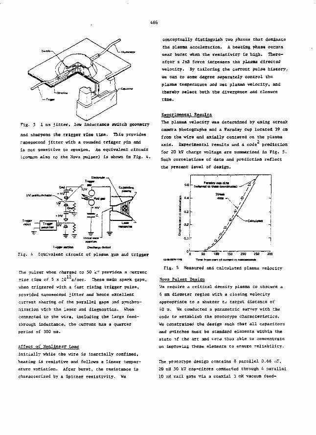
466
Fig. 3 1 ns jitter, low inductance switch geometry
and sharpens the trigger rise tine. This provides
nanosecond jitter with a rounded trigger pin and
Is not sensitive to erosion. An equivalent circuit
(common also to the Nova pulser) is shown in Fig. 4.
•Hvfyiro
"nilInitial •
Tngfm- action
Fig. i Equivalent circuit of plasma gun and trigger
The puiser when charged to 50 k'f provides a current
rise time of 5 x 10 a/sec. These main spark gaps,
when triggered with a fast rising trigger pulse,
provided nanosecond jitter and hence excellent
current sharing of the parallel gaps jnd synchro-
nization with the laser and diagnostics. When
connected to the wire, including the large feed-
through inductance, the current has a quarter
period of 300 ns.
Affect of Monlinear Load
Initially while the wire is Anerrially confined,
heating is resistive and follows a linear temper-
ature variation. After burst, the resistance is
characterized by a Spitzer resistivity. We
conceptually distinguish two phases that dominate
the plasma acceleration. A heating phase occurs
near burst when the resistivity is high. There-
after a JxB force increases the plasma directed
velocity. By tailoring the current pulse history,
we can to some degree separately control the
plasma temperature and net plasms velocity, and
thereby select both the divergence and closure
time.
Experimental Results
The plasma velocity was determined by using streak
camera photographs and a Faraday cup located 39 cm
from the wire and axially centered on the plasma
axis. Experimental results and a code prediction
for 20 kV charge voltage are summarized in Fig. 5.
Such correlations of data and prediction reflect
the present level of design.
0 50 tOO 150 200 250 300
Tiim from sort ot eunnt in runa«catids
Fig. 5 Measured and calculated plasma velocity
Nova Pulser Design
We require a critical density plasma to obscure a
6 mm diameter region with a closing velocity
appropriate to a shutter ta target distance of
40 m. We conducted a parametric survey with the
code to establish the prototype characteristics.
We constrained the design such rhat all capacitors
and srritches must be standard elements within the
state of the art and vare thus able to concentrate
on improving these elements to ensure reliability.
The prototype design contains 8 parallel 0.66 uF,
20 nH 50 k7 capacitors connected through 4 parallel
10 nH rail gaps via a coaxial 3 nH vacuum feed-
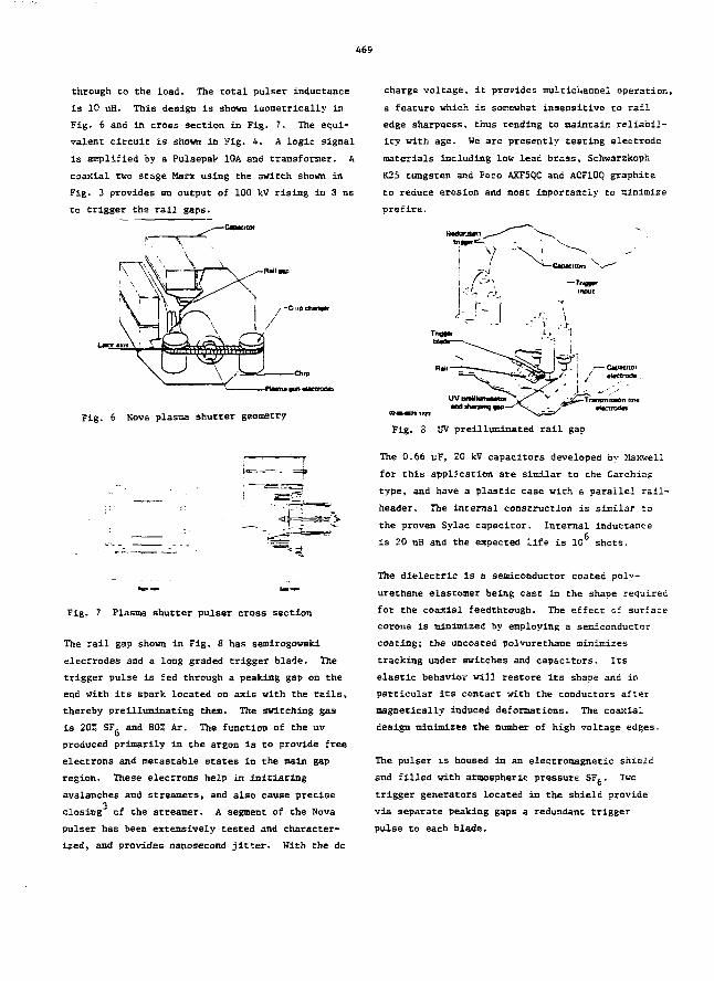
469
through to the load. The total pulser Inductance
is 10 nH. This design is shown iaometrically in
Tig. 6 and in cross section in Fig. 7. The equi-
valent circuit is shown in Fig. 4. A logic signal
is amplified by a Pulsepat 10A and transformer. A
coaxial two stage Marx using the 3Witch shown in
Fig. 3 provides an output of 100 kV rising it. 3 ns
to trigger the rail gaps.
Fig. 6 Nova plasma shutter geometry
Fig. 7 Plasma shutter pulser cross section
The rail gap shown in Fig. 8 has semirogowski
electrodes and a long graded trigger blade. The
trigger pulse is fed through a peaking gap on the
end with its spark located on axis with the rails,
thereby preilluminating them. The switching gas
is 202 SF^ and 80% Ar. The function of the uvo
produced primarily in the argon is to provide free
electrons and netastable states in the main gap
region. These electrons help in initiating
avalanches and streamers, and also cause precise
closing of the streamer. A segment of the Nova
pulser has been extensively tested and character-
ized, and provides nanosecond jitter. With the dc
charge voltage, it provides multichannel operation,
a feature which is sorewhat insensitive to rail
edge sharpness, thus tending to maintain reliabil-
ity with age. We are presently testing electrode
materials including low lead brass, Schwarzkoph
K25 tungsten and Poco AXF5QC and ACF10Q graphite
to reduce erosion and most importantly to minimize
prefire.
Tngt.
Fig. 3 UV preilluminated rail gap
The 0.66 uF, 20 kV capacitors developed by Maxwell
for this application are similar to the Garchiag
type, and have a plastic case with a parallel rail-
header. The internal construction is similar to
the proven Sylac capacitor. Internal inductance
is 20 nH and the expected life is 10 shots.
The dielectric is a semiconductor coated poly-
urethane elastomer being cast in the shape required
for the coaxial feedthrough. The effect of surface
corona is minimized by employing a semiconductor
coating; the uncoated polyurethane minimizes
tracking under switches and capacitors. Its
elastic behavior will restore its shape and ir.
particular its contact with the conductors after
magnetically induced deformations. The coaxial
design minimizes the number of high voltage edges.
The pulser is housed in an electromagnetic shield
and filled with atmospheric pressure SFg. Two
trigger generators located in the shield provide
via separate peaking gaps a redundant trigger
pulse to each blade.
470"
Conclusions
He have developed and are continuing to develop
reliable, low Inductance, high current pulsers
having nanosecond jitter. All spark gaps use uv
preillumination to pulse sharpen the trigger, to
minimize Jitter, and to minimize the effect of
electrode erosion with age. The systems are co-
axial co minimize inductance and edge effects. A
semiconductor coated elastomer dielectric minimizes
surface corc-.a and tracking. These pulsers are
utilized with a rail-gun to propel a high density
plasma to a high velocity.
Acknowledgements
We thank H. Duffus, J. Braucht, H. Rien, C. McFann
and M. Thorne for cheir contributions.
Refarences
1. H. Bacchi and J.C. Pauwek, Proc. of the 9thInt. Conf. on High Speed Photography, p. 489,Denver, Aug. 2-7, 1970.
2. Peter Koert, tJCRL 81363, 1978 (to be published).
L.P. Bradley and Peter Koert, "Plasma Shutterfor High Power Glass Lasers", 3th In'.. Symp.on Discharges and Electrical Insulation inVacuum, Albuquerque, Sept. 5-7, 1979.
3. L.?. Sradley, "Preionization Control ofScreamer Propagation", J. Appl. Phys. 3_,386, 1972.
L.?. Bradley and T.J. Davies, "Laser ControlledSwitching", IEEE J. Quantum Electronics 7_, 464,1971.
Reference to a company or productname does not imply approval orrecommendation of the product byihe University of California or theU.S. Department of Energy to the^elusion ol others that may besuitable.
NOTICE
•"This report was prepared u an account or worksponsored by th& United States' GovenuncalNeither the united S u m nor the United StalesD:pinmenl of Energy, nor iny of their employee*.nor any of their contractors, subcontractors, or[heir employees, makes any warranty, express orimplied, or assumes any legal liabifily or respon-sibility for the accuracy, completeness orusefulness of any information, appartuu. productor process disclosed, or represents U)at its usewould not infringe privately-owned ngbu."
471
20.5
FAST RISING TPJVNSIENT HEAVY CURRENT SPARK DAMAGE TO ELECTRODES
ALAN WATSON
Dept. Elect. Eng., Texas Tech Univ.
Lubbock, Texas 79409
Abstract
Crests of displaced metal have been observed in
rings beyond the crater produced on electrodes
by short duration (10-100 ns) heavy current sparks
in a variety of dielectric media. Metal is pre-
sumed to have melted and flowed radially, the
hydromagnetic forces supporting a standing canal
wave which is identified with the crest. Analysis
shows this situation to be invariant under steady
neiting and the ring diameter is proportional to
the square root of spark current, as measurement
verifies. Erosion is proposed to occur by the
breaking of this crest or by its removal under the
action of electrostatic forces, in accord with
reported experimental data.
Introduction
In the course of experience with high power flash
X-ray machines* it has been observed that elec-
trode damage from heavy current switching sparks
appear to h&ve some feat-jres in common. In a
current range up to about 250 kA lasting for 20 to
70 r9 in high pressure gas each electrode displays
a crest of frozen metal in a ring around the site
which was struck by the spark (Figure 1). There
is a small crater at this spot which corresponds
in diameter with that to be expected for a heavy
current spark channel expanding for the known
duration of the discharge. This is surrounded by
a flat undulating expanse of metal whi.ch had
obviously been molten and which extends beyond the
crest already mentioned. The radius of the ring
has been measured in three cases fov which the
current was calculable. It appears that the
Dept. Elect. Eng., Univ. of Windsor
Windsor, Ontario, Canada
radius increases as the square root of the current,
independently of the pulse duration. Significantly.
there is extremely little visible depression of
the metal level within the damage ring.
Investigations of spark damage in vacuum have
revealed that in certain cases damage of a similar
nature cakes place (Figure 2). In addition, a
region outside the damage ring was found to be
covered with molten droplets adhering to the sur-
face. Further data from pulsed discharges in
water and oil show the same characteristic damage
ring for various metals.
One feature in common with all of these discharges
is probably that the current pulse was fast rising.
In vacuum this is not always the case and the
indidence of such danage is less frequent. Replicas
were made and microphotographs prepared cf damage
sites on fls.sh X-ray machines for a wide range of
calculated currents and -ulse durations. In Fig. i
the crest radius on stainless steel appears to
vary as the square root of the spark current so
that I/r2 » 1.5 x 10¹⁰ Am'2.
A mechanism sufficient to explain these phenomena
must, therefore, be independent of the type of
discharge and more raliant upon the electrodynamics
of the current growth within the electrodes. The
purpose of the present work is to describe such a
mechanism and to throw some light upon the elec-
crode erosion process.
*Ion Physics Corporation models FX-15, FX-^5 andFX-100.

472
THEORY OF THE Mtv,HANISM
Hvdromagnatlc Flow
No initial account will be taken here of spark
channel expansion and it will be formalised simply
as a fixed conducting cylinder produced instantane-
ously between two high voltage electrodes. Cur-
renc, however, cannot be established until magne-
tic flux has penetrated into the conductors. The
channel conductivity is much less than that of the
electrode metal and diffusion into it is therefore
rapid enough tj be considered instantaneous by
comparison.
Progressive flux penetration into the electrode
surface will cause melting because of the accompa-
nying resistive power dissipation. Electromag-
necic forces also act oormally into the electrode
surface, but decrease in strength radially. Since
the liquid surface layer tends to 'freeze in' the
magnetic flux with a radial electromagnetic pres-
sure variation, a steady fluid flow will develop
in such a manner as to neutralize this.
The problem can now be formulated as that of
determining the hydromagnetic flow pattern of a
fluid with a free surface flowing radially out-
wards across an azimuchal magnetic field, as shown
in Figure 3. Hydronagnetic flow will be con-
sidered radially across an azimuthal magnetic
field distribution for a disc of conducting fluid
of non-uniform depth h, but with a free surface.
There is no indication from the conditions of the
problem chat melting occurs to a uniform depth.
Azimuthal symmetry will be assumed 30 as to reduce
the problem Co two dimensions.
"lux cransport inco the mobile pool is determined
by equating 3B/5t with che rotation of Che over-
all electric field strength given by curl(a~ ? +
u x B). Beneath Che melting floor there is no
Lorentz field and flux is transported by diffusion.
Ac this interface there must be continuity in
5B/JC and this will be achieved if Che Lorentz
field is irrotational.
A flow solution relating u and H must satisfy this
condition, and che following relationships will be
shown co be adequate for the purpose of describing
che flow over an anode surface as in Figure 3.
/au - - v'v h curl H - - /u h J (1)
/u H - /p h curl u = /p h io (2)
where h is che pool depth.
Hence the vorticity vector lies parallel to 'Lhe
magnetic field lines while the fluid velocity is
parallel to che current density. It follows
moreover that the electromagnetic body force J x
B Is equal to the inertial force • piu x u which
exists by virtue of the vorticity everywhere in
the flow and the momentum equation reduces to the
hydromagneclc form of Bernoulli's equation. It is
necessary now, however, to explain the origin o£
vartld.ty in the flowing pool of metal.
There will be a discontinuity in che fluid entropy
in crossing the liquid-solid interface due Co the
change in state. This interface is the limiting
streamline for the flow and so according to Crocco's
theorem of fluid mechanics (2) there will necessar-
ily be a corresponding jump in vorticity from zero
in che solid to a finite value within the flow.
Neglecting viscosity, Kelvin's theorem indicates
that the vorticity will be invariant within the
pool. Kelvin'3 Cheoram of conservation of vorticity
can thus be applied to che pool flow. The vorticity
'J) is given by -du/dz and since this is fixed
everywhere It can also be written as u/h. By
equating these cerms it Is seen chac che velocity
will decline exponentially from its value u at che
free surface co sero at the liquid-solid metal
Interface.
Power is dissipated at a fixed volume rate which
is absorbed in maintaining melting. The Lorentz
field given by hB is equal Co J/CT and J can be
represented by I/2irrh. = H/h. Thus it follows
chat H declines exponentially with depth and hh =
1/uo » n and che floor must cherefore recede
according Co che expression
h2 - 2 n t (3)
The exponential variation of u and H wichin the
flow follows immediately from che simultaneous
solution of (1) and (2) which are in curn unified
co one single expression ifi 2
'-SPu" = SfllB (';)
At any annulus of the pool the current density J
flowing through it is given instantaneously by

473
I /2Ttrh. (Where the subscript 'p' refers to the
pool)- A radius r may be selected for which I -
(r/h) I which clearly permits J to be represented
by I/2irr .
The pool current L, must be employed in calcula-
ting the Ohmic power dissipation in a cylindrical
annulus of the flow. This is equated with the
power absorbed in melting at the rate h which in
turn is eliminated usin<: the equation of the
streamline, h/h c u/r. Hence
[I (h/r)]2 = (4?r2pA<7h2u)r (5)
in which ur oust be constart to ensure incompress-
ible flow of the fluid. Thus, since u * dr/dt the
flow obeys the rule that r is proportional to t
just like h" and their ratio (h/r) is hence invari-
ant in time. Equation (5) readily reduces to? 9
dr/dt - 2n(uH"/pA) and by comparison with (3)
then
(h/r)2=(UH2/pA) (6)
From (1), (2), & (4) the vorticity and current
density are related, the latter being further
given by (5) so that
m = (u/pfa - (A/n) (uH2/pA) - (A*5/n)u. ... (7)and since LJ * u/h then
(8)
Within the molten pool hfeat is transferred by
conduction accoiding to
K V2 T - ps 3T/8t « J2/a - H2/h2o (9)
At the molten interface the temperature is fixed
at the melting point T . When the floor recedes
at a rate.h (4) acquires an additional driving
term 7 x(b x B) on the right hand side and the
expression reduces to
nV2^ - 3H/3t = Hh/h = nH/h2 (10)
In the mobile reference frame of the floor the
Lorentz and Ohmic fields neutralize each other as
stated, and curl E - 0 so by Faraday's law H is
constant and the last equation shows that it
decays exponentially. At the interface the
constant value of H = H is given by comparing
( 91 and (10) above which are equivalent if
(11)
The Magnetofluid Tidal Wave
The square oi the velocity of propagation, c, of a
tidal wave is given by the product of the depth h
of the fluid and the gravitational acceleration.
By analogy here the force acting down into the pool
per unit mass is J x B/p and this has been shown
to be equal to the inertial acceleration - ID x u.
Fluid velocity vectors radiate from the arc root
and terminate upon free vortex rings on the molten
interface. As melting proceeds, these rings are
stretched and give rise to the accelerating force
which replaces gravity in this analogue of tidal
wave motion. Thus
c" <= h |J x B| /p = (u/p)h(I ,'2nr2) (r/h)H . ". .(12)
Since w * u/h it follows that c * -t-u and a tidal
disturbance propagated inwards towards the arc
root along the surface of the outwardly flowing
fluid will give rise to a standing crest. It
remains to derive a relationship between the
location of this crest and the current flowing in
the arc. This is accomplished by evaluating (12),
making substitutions for each of its terms using
(6), (8) & (11). Thus
I /r2 - 2TV3/2a2tXm/pi (13)
The ring defined by the wave crest divides the
flow into two regimes. Outside of it the pool
conditions referred to in the analysis so far will
pertain. Only in that region can there exist a
flow together with a propagating wave because ur
is constant and a radius exists within which u
exceeds c. Fluid flows out from the inner regies
and accumulates in the crest so that an upwerd
velocity component is acquired in that particular
annulus. The Lorentz field due to this will crive
a current density through the annulus in opposition
to the supplementary current mentioned above and
in passing through the wave the current is restored
to the measured value I. Thus the pool current IP
should be replaced by I in (13) in order to calcu-
late the crest radius.
A calculation has been made from (13) for stainless
steel electrodes using values of resistivity o
and thermal conductivity K for stainless steel at
1000 C since these figures ware the best available
although the melting point is 1800°K. The result
gave I/r'' • 2.90 x 10 Am"2 which is in reasonable
agreement with the measured value.
Conclusions
The electrode damage mechanism is thus feasibly
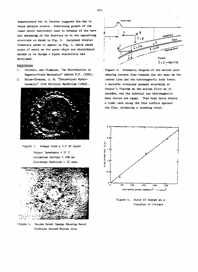
474
demonstrated buc it further suggests the way in
which erosion occurs. Continuing growth of the
crest would inevitably lead to breakup of the wave
and splashing of the droolets on to the opposlting
electrode as shown in Fig. 2. Incipient droplet
formation seems to appear in Fig. 1. which shows
cusps of metal on the crest which are distributed
around it as though a flute instability had
developed.
References
1. Ferraro, and Plumpton, "An Introduction to
Magneto-Fluid Mechanics" Oxford U.P. (1961).
2. Milne-Thomson, L. M. "Theoretical Hydro-
dynamics" (4th Edition) MacMillan (1962).
Figure 1. Damage From a 5.5 MV Spark
Output Impedance « 57 Q
Estimated Current » 100 ka
Discharge Duration = 25 nsec
•SSiFSWB^• * * • • • -.> •JK:.-®*lli»«i
Figure 2. Vacuum Spark Damage Showing Metal
Globules Around Molten Area
, wave crest
f\
-Figure 3. Schematic diagram of the molten pool
showing current flow towards the arc axis on the
center line and the hydromagnetic body force.
A specific vorticity appears according to
Crocco'3 Theorem at the molten floor as it
recedes, and the inertial ana hydromagnetic
body forces are equal. This body force drives
a tidal wave along the free surface against
the flow, producing a standing crest.
(ESTIMATED SPARK CUfiRENTl'
Figure 4. Scale of Damage as a
Function of Current
473
21.1
INFLUENCE OF NONUNIFORM EXTERNAL MAGNETIC FIELDS AND ANODE-CATHODESHAPING ON MAGNETIC INSULATION IN COAXIAL TRANSMISSION LINES
MICHAEL A. MOSTROM
Intense Particle Bean Theory GroupLos Alamos Scientific LaboratoryLos Alamos, New Mexico 87545
Abstract
Coaxial transmission lines, used to trans-fer the high voltage pulse into the dioderegion of a relativistic electron bean gener-ator, have been studied using the two-dimen-sional time-dependent fully relativistic andelectromagnetic particle simulation code CCUBE.A simple theory of magnetic insulation thatagrees well with simulation results for astraight cylindrical coax in a uniform externalmagnetic field is used to interpret the effectsof anode-cathode shaping and nonuniform exter-nal magnetic fields. Loss of magnetic insula-tion appears to be minimized by satisfying twoconditions: (1) the cathode surface shouldfollow a flux surface of the external magneticfield; (2) the anode should then be shaped toinsure that the magnetic insulation impedance,including transients, is always greater thanthe effective load impedance wherever there isan electron flow in the anode-cathode gap.
Introduction
Elsewhere in these proceedings, Mike Jones
has described both theory and simulation of
foilless diodes. The achievement of high
voltage (> 5 MeV), hign current density9
(> 500 ka/cm ), laminar electron beams by such
diodes appears at present to require external
magnetic fields on the order of 100 kg. The
fringing fields from the external magnetic
field coils will flare out to low values back
in the coaxial transmission line feeding the
diode. Also, in this same fringe field region
the transmission line anode and cathode radii
may taper dramatically in order to provide the
proper transition in impedance and size between
the diode and the insulator stack. However,1-4 5
previous theory and simulation of transmis-
sion lines has dealt only with straight coaxial
transmission lines and no external magnetic
field or with parallel plate transmission lines
with a uniform external magnetic field. We
are, therefore, in the process of addressing
the following three questions: (1) What is the
impedance of a straight coaxial transmission
line with a uniform external magnetic field;
(2) in a tapered coaxial transmission line with
a nonunifonu external magnetic field, what is
the proper cathode shape relative to the exter-
nal magnetic field lines; (3) What constraints
on the impedance profile along the transmission
line minimize the loss of magnetic insulation?
These questions are being studied using the
two-dimensional time-dependent fully relativis-
tic and electromagnetic particle simulation
code CCUBE and simple theories. Preliminary
results are given below.
Straight Coaxial Transmission Line, Uniform BQ
An analytic theory of magnetic insulation
in a straight coaxial transmission line with a
uniform p.- vernal axial magnetic field BQ = BQz
appears to require some further simplifying
assumption or approximation (e.g., ignoring the
axial self-magnetic field or imposing some
relation between radius and one or more veloc-
ity components). The choice of such a simpli-
fying approximation can perhaps be guided by
simulations, but at the time of writing this
paper, only the simplest possible theory has
been completed and compared with simulations.
This theory first involves generalizing
the critical current calculation by Creedon to
include the uniform external field B . The
result is
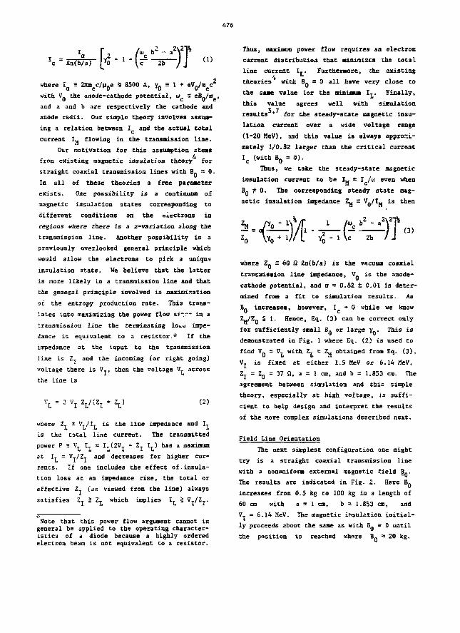
476
* \c 2b /J (1)
where S 8500 A, 1 + eV0/t»e<:
with V the anode-cathode potential, w = e^n^m
aad a and b ace respectively the cathode and
anode radii. Our simple theory involves assur-
ing a relation between I and the actual total
current Ij, flowing in the transmission line.
Our motivation for this assumption stems
from existing magnetic insulation theory for
straight coaxial transmission lines with B. ~ 0.
In all of these theories a free parameter
exists. One possibility is a continuum of
magnetic insulation states corresponding to
different conditions on the electrons in
regions where there is a z-variation along the
transmission line. Another possibility is a
previously overlooked general principle which
would allow the electrons to pick a uniqu:
insulation state. We believe that the latter
is more likely in a transmission line and that
che general principle involved is maximization
of the entropy production rate. This trans-
lates into maximizing the power flow si~r~ in a
transmission line the terminating 10**1 impe-
dance is equivalent to a resistor.* If the
impedance at the input to the transmission
Line is Z. and the incoming (or right going)
voltage there is Vj, then the voltage V. across
the Line is
\ =2 vi V (2)
I.) has a maximum
where Z = ^ T ^ L *s tile ^ n e impedance and ITis the total line current. The transmitted
power P = V I = I T U V J
at I. = V-/Z. and decreases for higher cur-
rents. If one includes the effect of insula-
tion loss at an impedance rise, the total or
effective ZT (as viewed from the line) always
satisfies Zj 2 Zj. which implies IL S VJ/ZJ-
Note that this power flow argument cannot ingeneral be applied to the operating character-istics of a diode because a highly orderedelectron beam is not equivalent to a resistor.
Thus, maximug power flow requires an electron
current distribution that minimizes the total
line current 1^. Furthermore, zhe existing
theories* with B. = 0 all have very close to
the saae value Cor the minima 1^. Finally,
this value agrees well with simulation
results ' for the steady-state magnetic insu-
lation current over a wide voltage range
(1-20 HeV), and this value is always approxi-
mately 1/0.82 larger than the critical current
Ic (with BQ = 0).
Thus, we take the steady-st.ate magnetic
insulation current to be L, = I /a even when
B- jt 0. The corresponding steady state mag-
netic insulation impedance Zj, = ?./!„ is then
(3)
where Z- = 60 Cl £n(b/a) is the vacuum coaxial
transmission line impedance, V. is the anode-
cathode potential, and a = 0.82 ± 0.01 is deter-
mined from a fit to simulation results. As
B. increases, however, I * 0 while we know
Zjj/Z0 S 1. Hence, Eq. (3) can be correct only
for sufficiently small BQ or large YQ. This is
demonstrated in Fig. 1 where Eq. (2) is used to
find VQ = V. with Z, = Z», obtained from Eq. (3),
VT is fixed at either 1.5 MeV or 6.14 MeV,
Zj = ZQ = 37 Q, a = 1 cm, and b = 1.853 cm. The
agreement between simulation and this simple
theory, especially at high voltage, is suffi-
cient to help design and interpret the results
of the more complex simulations described next.
Field Line Orientation
The next simplest configuration one might
try is a straight coaxial transmission line
with a nonunifora external magnetic field B».
The results are indicated in Fig. 2. Here B.
increases from 0.5 kg to 100 kg in a length of
60 cm with a = 1 cm, b = 1.S53 cm, and
Vj = 6.14 HeV. The magnetic insulation initial-
ly proceeds about the same as with B. = 0 until
the position is reached where B. " 2 0 kg.
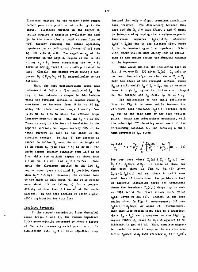
477
Electrons emitted in the weaker field region
cannot pass this petition but rather go to the
anode. Electrons emitted in the higher B.
region acquire a negative z-velocity and also
go to the anode (for a total current loss of
40%) thereby reducing the actual operating
impedance by an additional factor of 1/2 over
Eq. (3) with BQ = 0. The negative v of the
electrons in the high B_ region is due to the
strong Vg x B? force overtaking the -v x B.
force as the B. field lines converge toward the
axis. Clearly, one should avoid having a com-
ponent B^ £ BgVj /Vg of Bp perpendicular to the
cathode.
Thus, the next configurations tried have
cathodes that follow a flux surface of §_. In
Fig. 3, the cathode is shaped in this fashion
until the straight section is reached where B
continues to increase from 18 kg to SO kg.
Also, the anode radius drops linearly from
12.85 cm to 1.85 cm while the cathode drops
linearly from 4.4 cm to 1 cm, and V_ = 8.35 HeV.
There is very little loss of insulation in the
tapered section, but approximately 30% of the
total current is lost to the anode io the
straight section. In Fig. 4, the cathode is
shaped to follow B_ over the entire length of
33 cm where B. goes from 2 kg to 80 kg. The
anode tapers roughly linearly from 23.6 en to
2 cm while the cathode tapers as shown from
8.4 ca to 1.2 cm, and V = 8.35 MeV. Once
again the electrons emitted in the low B.
region cannot pass a critical B^ position (here
when B. =* 3.5 kg). However, the current loss
to the anode is only about 7%, and it is spread
over about 1.5 cm (along z) for a current2
density of less than 0.1 kA/cm at the anode
surface. In the next section we offer a pos-
sible explanation for this loss.
Impedance Revisited
In the shaped transmission lines described
above (Figs. 3 and 4), the vacuum impedance
ZQ(Z) monotonically decreased by about a factor
of two with increasing axial position z. In
simulations with B. = 0, this impedance drop
insured that only a slight transient insulation
loss occurred. The discrepancy between this
case and the B. / 0 case (Figs. 3 and 4) might
be interpreted by saying that complete magnetic
insulation requires Zj,(z) * T wherever
Zutz) < Z.(z) due to the electron flow, where
Z_ is the terminating or load impedance. Other-
wise, there will be some steady loss of insula-
tion in the region around the absolute minimum
oi the impedance.
This would explain the insulation loss in
Fig. 3 because Eq. (3) gives Zj.(z) > Z-. only up
to near the straight section where 2 = Z_.
Near the start of the straight section (where
BQ is still small) 2^ < 2Q = Z^, and os we move
into the high B. region the electrons are clamped
to the cathode and Zj, rises up to ZQ = Z_.
The explanation of the small insulation
loss in Fig. 4 is more subtle because the
effective load impedance Z^(z,t) differs from
Z_ due to the rise tine of the high voltage
pulse. Using the telegraphers equations, with
the subscript "T" denoting measurement at the
terminating position z_, and assuming a small
time derivative \' gives
(4)
For our case where ZQ(z) % ZT = Za(zT) and
VT & 0, Z£(z,t) i Zy. In spite of this, for
the case shown in Fig. 4, Eq. (3) gives
ZH(z) i Z-(z,t) and yet there is still some
snail loss of insulation. The problem is that
in magnetic insulation there are transients
where the iuoedance Zu(z,t) drops (by as much
as 30%) below the final steady state value
Zjjfz) given by Eq. (3). Indeed, in the loss
region shown io Fig. 4, measrrements indicate
Zj,(z,t) < ZE(z,t) by about 1%. Furthermore,
once this lose region forms (due to a transient
where Zu < Zp) and propagates tc the high BQ
region (where ?~, rises to Z ) it appears to be
difficult to get rid cf. Thus, complete magnet-
ic insulation seems to require the stricter con-
dition ZH(z,t) i Z£(z,t) wherever ZH(z) < Z0(z).
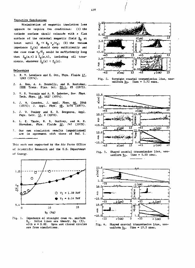
478
Tentative Conclusions
Minimization of magnetic insulation loss
appears to require two conditions: (1) the
cathode surface should coincide with a flux
surface of the external magnetic field B. at
least until Bg « B g " r/v8; (2) the vacuua
impedance 2Q(z) should drop sufficiently and
the rise time V-/V- sould be sufficiently long
that Z^Cz.t) 5 Z_(z,t), including all tran-
sients, wherever £u(z) < Z.(z).
References
1. R. V. Lovelace and E. Ott, Phys. Fluids 17,1263 (1974).
2. A. Son, A. A. Mondelli, and H. Hostoker,IEEE Trans. Plas. Sci. PS-1, 85 (1973).
3. V. S. Voronin and A. N. tebedev, Sov Phys.
Tech. Phys. 18, 1627 (1974).
4. J. a. Creedon, J. Appl. Pliys. 46, 2946(1975); J. Appl. Phys. 4J5, 1070 (1977).
5. J. W. Poukey and K. 0. Bergeron, Appl.
Phys. Lett. 32, 8 (1978).
6. L. E. Thode, B. B. Godfrey, and W. B.
Shanahan, Phys. Fluids 22, 747 (1979).
7. Our own simulation results (unpublished)are in agreement with those of Ref. 5.
This work was supported by the Air Force Office
of Scientific Research and the U.S. Department
of Energy.
1.0-
0.4
0•
10
(kg)
' I
- 1
- 6
.50
.14
MeV
MeV
20
Fig. 1. Impedance of straight coax vs. uniformBg. Solid lines are theory, Eq. (3),with a = 0.82. Open and closed circlesare from simulations.
1.85.
?0.9:
-45
-3.0
-45 z(<aa) 15 -45 z (cm) 15
Fig. 2. Straight coaxial transmission line, non-uniform JSQ. Time =" 1.72 nsec.
12.3
10.0
-10.0
10.0
-10.0
-45 z(cm) 15 -45 zfcm) 15
a
1.0-45 z(cm) 15 -45 . (cm) 15
Fig. 3. Shaped coaxial transmission lino, non-
uniform J3Q, Time » 5.33 nsec.
23.6
-10.0-33 z (cm) -33 z (cm)
Fig. 4. Shaped coaxial transmission line, non-
uniform B Q , Time "19.5 nsec.
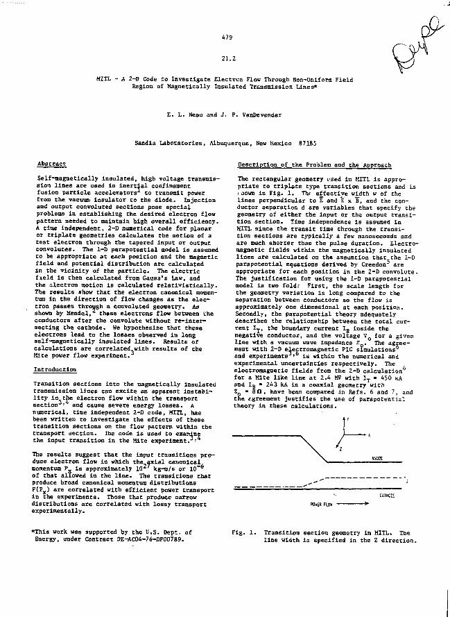
479
21.2
MITL - A 2-D Code to Investigate Electron Flow Through Non-Uniform Field
Region of Magnetically Insulated Transmission lines*
E. L. Neau and J, P. VanDevender
Sandia Labotatories, Albuquerque, New Mexico 87185
Abstract
Self-magnetically insulated, high voltage transmis-sion lines are used in inertial confinementfusion particle accelerators to transmit powerfrom the vacuum insulator to the diode. Injectionand output convoluted sections pose specialproblems in establishing the desired electron flowpattern needed to maintain high overall efficiency.A time independent, 2-D numerical code for planaror triplate geometries calculates the motion of atest electron through the tapered input or outputconvolutes. The 1-D parapotential model is assumedto be appropriate at each position and the magneticfield and potential distribution are calculatedin the vicinity of the particle- The electricfield is then calculated from Gauss's Law, andthe electron motion is calculated relativistically.The results show that the electron canonical momen-tum in the direction of flow changes as the elec-tron passes through a convoluted geometry. Asshown by Mendel, these electrons flow between theconductors after the convolute without re-inter-sectlng the cathode. We hypothesize that theseelectrons lead to the losses observed in longself-magnetically insulated lines. Results ofcalculations are correlated with results of theMite power flow experiment.
Introduction
Transition sections into the magnetically insulatedtransmission lines can excite an apparent instabi-lity in the electron flow within the transportsectionJ' and cause severe energy losses. Anumerical, time independent 2-D code, MITL, hasbeen written to investigate the effects of thesetransition sections on the flow pattern within thetransport section, the code is used to examinethe input transition in the Mite experiment. •
The results suggest that the input transitions pro-duce electron flow in which the axial canonicalmomentum P x is approximately 10
z kg-o/s or 10~°of that allowed in the line. The transitions thatproduce broad canonical momentum distributionsF(?x) are correlated with efficient power transportin the experiments. Those that produce narrowdistributions are correlated with lossy transportexperimentally.
Description of the Problem and the Approach
The rectangular geometry fsed in MITL is appro-priate to triplate type transition sections and isi nown in Fig. 1. Th: effective width w of thelines perpendicular to E and E x B, and the con-ductor separation d are variables that specify thegeometry of either the input or the output transi-tion section. Time independence is assumed inMITL since the transit time through the transi-tion sections are typically a few nanoseconds andare much shorter than the pulse duration. Electro-magnetic fields within the magnetically insulatedlines are calculated on the assumtion that the 1-Dparapotential equations derived by Creedon5 areappropriate for each position in the 2-D convolute.The justification for using the 1-D parapotentialmodel is two fold: First, the scale length forthe geometry variation Is long compared to theseparation between conductors so the flow isapproximately one dimensional at each position.Secondly, the parapotential theory adequatelydescribee the relationship between the total cur-rent lj, the boundary current 1_ inside thenegative conductor, and the voltage V for a givanline with a vacuum wave impedance Z . The agree-ment with 2-D electromagnetic PIC simulations0
and experiments ' is within the numerical andexperimental uncertainties respectively. Theelectromagnetic fields from the 2-D calculationfor a Mite like line at 2.4 MV with I T - 450 kAand Ig » 243 kA in a coaxial geometry withZ o » S n , have been compared in Refs. 6 and 7, andthe agreement justifies the use of parapotentiaitheory in these calculations.
CATHODE
PtNER FUW
*This work was supported by the U.S. Dept. of
Energy, under Contract OE-AC04-76-DP00789.Fig. 1. Transition section geometry in MITL. The
line width is specified in the Z direction.
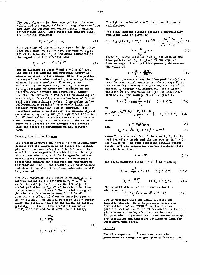
480
The test electron Is then injected into the con-volute and its notion followed through the convoluteand Into the uniform self-magnedcally insulatedtransmission line. Once inside the uniform line,the canonical momentum
K - T.mlT. - eA, <«
The initial value of Xcalculation.
X is chosen for each
The total current flowing through a magneticallyinsulated line is given by
is a constant of its motion, where m is the elec-tron rest mass, -e is the electron charge, IIX isits axial velocity, A^ is the axial component ofche magnetic vector pocential and
>yL/2y. = 1 / ( 1 - (2)
tor an electron of speed U and c « 3 x 10 m/s.The sum of ics kinetic and potential energy isalso a constant of its motion. Since Che problemis assumed to be electrostatic, the energy Is notchanged by Che convolute. However, sincedL/dx M in the convolute, then P % is changedby d ? x according to Lagrange's equation as theelectron moves through the convolute. Conse-quently, the problem is reduced to calculating A P X
accurately. Generally, the limitations of finitecell size and a finite number of particles in 2-0self-consistent simulations severely limit theaccuracy with which A P X can be computed. Thenumerical noise is avoided, at the expense of_self-consiscency, by using analytic equations for E andB~. Without self-consistency the calculations arenot, however, quantitatively exact. The value ofthese calculations is the insight they provideinto che effect of convolutes on the electronflow.
7 -m0C
(5)
where 7 m is the value of Y at ? m the edge of theflow pactern, and y is given by the appliedline voltage. The local line geometry determinesche value of
60(6)
The input parameters are the line profile w(x) andd(x) for each axial position x, the voltage VQ atthe anode for V - 0 at the cathode, and the totalcurrent Ly through the structure. For a givenposition tx,y), the value of y_(x) is calculatedfrom Eq. 4. The voltage V(x,yJ is given by
or
V ~ (
where
and
d - Y
C, -
(y 2 -
(7a)
(7b)
(8)
(9)
Description of the Program
The program Involves the choice of the initial con-ditions for the electron as it leaves the cathodeplasma in_the convolute,_the calculation of theelectric E and magnetic B fields In the vicinityof che test electron, and che integration of Cherelaclvistlc equation of motion as Che particleprogresses through che convolute and che uniformtransmission line. Each feature will be discussedand Chen che results of che Mite calculations willbe presented.
where Ym is the position of the sheath, YQ is theposition of the anode and the cathode is at Y • 0.The values of V at four positions equally spacedabout (x,y) are calculated and che electric fieldis calculated from
-W
The local magnetic field B • B z is given by
—£- CT- 1) Y <
(10)
(lla)
The cesc particles are assumed Co originate in acathode plasma at a y coordinate yc 10
c
where che voltage is <_ 0.3 eV and the magneticvector potential is AQ, which is calculated fromthe parapotential theory.3 The initial energy ofthe electron is chosen between 1 and 10 eV tosimulate che effect of electron emission from alev eV plasma. The initial particle energy deter-mines the absolute value of che electrons inicialvelocityUQ. The Initial canonical momentum~ • P x is assumed Co be zero, so inlcially,
(3)
Uy "
B2 - - "~- if Yn < Y < To (lib)
The relativistic equation of motion for cheeleccrons Is j _ _ _ _
5J- (yaMU) - -e (E + J x B) (12)
and is combined with che local electric andmagnetic fields. It is Chen solved using cheintegration routine STFODE to find Che aeaparticle poscion and velocity components, within agiven error criteria, after a time increment.The particle is progressively accelerated throughche Cransition and transport sections of line forsuccessive time steps.
Results
The Mite experiment ' used cwo transitiongeometries to change the gap spacing from 0.02 co
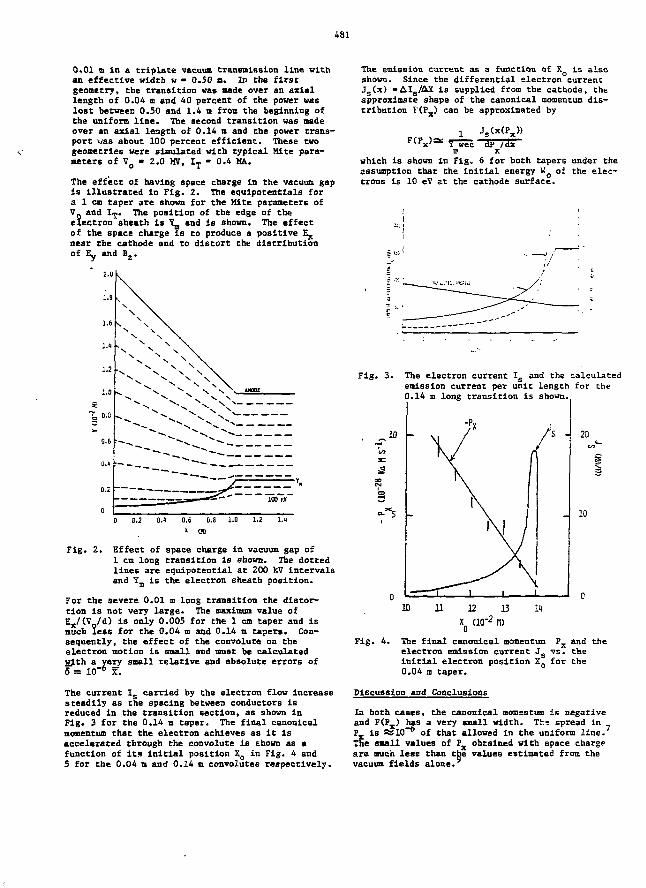
481
0.01 m in a triplate vacuum transmission line withan effective width w - 0.50 a. In the firstgeometry, the transition was made over an axiallength of 0.04 n and 40 percent of the power waslost between 0.50 and 1.4 m from the beginning ofthe uniforo line. The second transition was madeover an axial length of 0.14 m and the power trans-port was about 100 percent efficient. These twogeometries were simulated with typical Mite para-meters of Vo > 2.0 MV, IT 0.4 HA.
The effect of having space charge in the vacuum gapis illustrated in Fig. 2. The equipotentials fora 1 en taper are shown for the Mite parameters ofV. and IT. The position of the edge of theelectron sheath is \ and is shown. The effectof the space charge is to produce a positive E^near the cathode and to distort the distributionof Ey and B z.
Fig. 2. Effect of space charge in vacuum gap of1 cm long transition is shown. The dottedlines are equipotential at 200 kV intervalsand Y m is the electron sheath position.
For the severe 0.01 m long transition the distor-tion is not very large. The maximum value of^ / ( V / d ) is only 0.005 for the 1 cm taper and ismuch less for the 0.04 m and 0.14 m tapers. Con-sequently, the effect of the convolute on theelectron motion is small and must be calculatedwith a very small relative and absolute errors of6 = 10"6 X.
The current Is carried by the electron flow increasesteadily as the spacing between conductors isreduced in the transition section, as shown inFig. 3 for the 0.14 m taper. The final canonicalmomentum that the electron achieves as it isaccelerated through the convolute is shown as afunction of its initial position Xo in Fig. 4 and5 for the 0.04 m and 0.14 a convolutes respectively.
shown. Since the differential electron~currentJs(s) -AIE/AX is supplied from the cathode, theapproximate shape of the canonical momentum dis-tribution *(PX) can be approximated by
dp /dxx
which is shown in Fig. 6 for both tapers under theassumption that the initial energy VQ of the elec-trons is 10 eV at the cathode surface.
Fig. 3.
10
The electron current Is and the calculatedemission current per unit length for the0.14 m long transition is shown.
2D
-"=5 10
10 11 12
XQ CUT-
13
Fig. 4. The final canonical momentum P.electron emission current Jc vsinitial electron position X0.04 o taper.
and thethe
for the
Discussion and Conclusions
In both cases, the canonical momentum is negativeand F(PX) has a very small width. The spread inPx is sslO"
6 of that allowed in the uniform line.The small values of Px obtained with space chargeare much less than the values estimated from thevacuum fields alone.
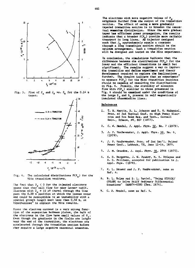
482
F i g . 5 . Plot oftaper.
X CUT2 ft)
and J= vs. X,, for the 0.14 m
_ _ _ U < TFUWSITICM .
— — — o.n n musmm
•12
V.U-a»
Fig. 6. The calculated distributions F(PX) for theMite transition sections.
The fact that ?x < 0 for the injected electronsmeans that they -Jill flow for many Larmor radii.Electron with Wo - 10 eV travel through the linepast the 0.50 m position at which the losses occurand could be susceptible to an instability with aspatial growth length much less than 0.50 m, as
The electrons with more negative values of Px
originate further from Che output of Che transitionsection. The effect of using a aore graduallytapered transition section is to broaden the canon-ical moacntua distribution. Since the aore gradualtaper has efficient power propagation, tha resultsindicate that a broader F(PX) provide more reliabletransport in long lines. An injector designedsuch that Jx approximately equals a constantthrough a Ions transition section should be theoptima arrangement. Such a transition sectionwill be designed and tested on the Mite experiment.
In conclusion, the simulations indicate that thedifference between the distributions F(?x) for thelossy and the efficient transitions is small butsignificant. The results suggest a way to improvethe transition and define experiment and theorydevelopaent required to explore the implicationsfurther. The results Indicate that an experimentto measure F(P ) for the Mite transition sectionsshould be capable of resolving the distributionsin Fig, 6. Finally, Che stability of electronflow with F(PX) slmlllar to those presented inFig. 6 should be examined under the conditions ofthe large E and B£ present in self magneticallyinsulated transmission Iine3.
References
1. T. H. Martin, D. L. Johnson and 0. H. McDaniel,Proc. of 2nd Topical Conf. on High Power Elec-tron and Ion Bean Res. and Tech., CornellUniv., Ithaca, NT, 807 (1977).
2. C. W. Mendel, J. Appl. Phys. 50, No. 7 (1979).
3. J. P. VanDevender, J. Appl. Phys. J£, Mo. 6,(1979).
4. J. P. VanDevender, Proc. of 2nd Int'l. PulsedPower Conf., Lubbock, TX, June 12-14, 1979.
5. J. M. Creedon, J. Appl. Phys. 46, 2946 (1975).
6. K. D. Bergeron, J. W. Poukey, M. S. DiCapua andD. G. Pellinen, accepted for publication in J.Appl. Phys. (1979).
7. K. L. Brower and J. P. VanDevender, same asRet. 4.
8. B. L. Huloe and S. L. Daniel, "Using STFODE/COLODE to Solve Stiff Ordinary DifferentialEquations" SAND74-0380 (Dec. 1974).
9. C. W. Mendal, same as Bef. 4.
Since the electron current is a very strong func-tion of che separacion between plates, the bulk ofthe electrons in the flow have small values of ?x.Even though the gradients in the fields are largernear the end of the transition, the electrons areaccelerated through the transition section beforethey acquire a large negative canonical momentum.
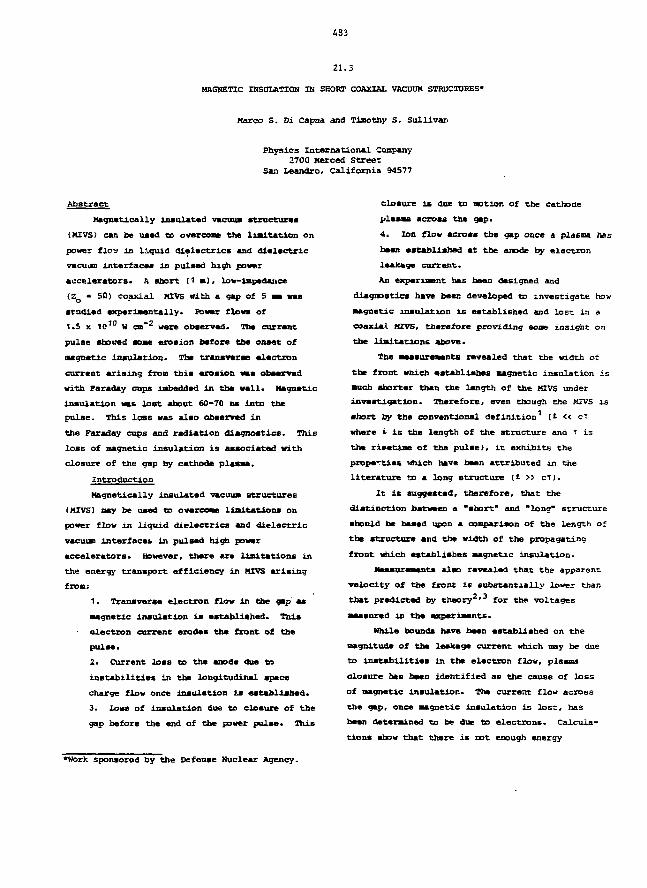
463
21.3
MAGNETIC INSULATION IN SHORT COAXIAL VACUUM STRUCTURES*
Marco S. Di Capua and Timothy S. Sullivan
Physics International Company2700 Merced Street
San Leandro, California 94577
Abstract
Magnetically insulated vacuum structures
(HIVS) can be used to overcome the limitation on
power floy in liquid dielectrics and dielectric
VSCUIIB interfaces in pulsed high power
accelerators. A abort (1 a], low-impedance
(ZQ •= SO) coaxial HIVS «fitb a gap of 5 me was
studied experimentally. Power flows of
1.5 x 10t0 w cm'2 were observed. The current
pulse shoved some eroaion before the onsat of
magnetic insulation. The transverse electron
current arising from this erosion was observed
with Faraday cups Imbedded in the wall. Magnetic
insulation was lost about 60—70 us into the
pulse. This loss was also observed in
the Faraday cups and radiation diagnostics. This
lose of magnetic insulation is associated with
closure of the gap by cathode plasma.
Introduction
Magnetically insulated vacuum structures
(HIVS) may be used to overcome limitations on
power flow in liquid dielectrics and dielectric
vacuum interfaceb in pulsed high power
accelerators. However, there are limitations in
the energy transport efficiency in MIVS arising
from:
1. Transverse electron flow in the gap as
magnetic insulation is established. This
- electron current erodes the front of the
pulse.
2. Current loss to the anode due to
instabilities in the longitudinal apace
charge flow once insulation is established.
3. Loss of insulation due to closure of the
gap before the end of the power pulse. This
closure is due to motion of the cathode
plasma across the gap.
4. Ion flow across the gap once a plaeoa has
been established at the anode by electron
leakage current.
An experiment has been designed and
diagnostics have been developed to investigate how
magnetic insulation is established and lost in a
coaxial MIVS, therefore providing some insight on
the limitations above.
The measurements revealed that the width ox
the front which establishes magnetic insulation is
much shorter than the length of the MIVS under
investigation. Therefore, even though the MIVS is
short by the conventional definition1 (* << ct
where t is the length of the structure and t is
the ri*et4me of the pulse), it exhibits the
properties uhich have been attributed in the
literature to a long structure (t >> C T ) .
It is suggested, therefore, that the
distinction between a "short" and "long* structure
should be based upon a comparison of the length of
the structure and the width of the propagating
front which establishes magnetic insulation.
Measurements also revealed that the apparent
velocity of the front is substantially lower than
that predicted by theory2'3 for the voltages
measured in the experiments.
While bounds have been established on the
magnitude of the leakage current which may be due
to instabilities in the electron flow, plasma
closure has been identified as the cause of loss
of magnetic insulation. The current flow across
the gap, once magnetic insulation is lost, has
been determined to be due to electrons. Calcula-
tions show that there is sot enough energy
•Work sponsored by the Defense Nuclear Agency.
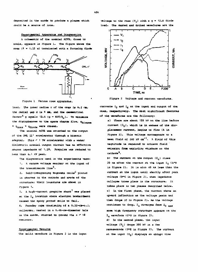
484
deposited in the anode to produce a plasma which
could be a source of ions.
Expariaantal Apparatus and Diagnostics
A schematic of the coaxial MIVS, drawn to
scale, appears in Figure 1. The figure shows the
coax <l - 1.1S m) terminated with a focusing diode
voltage to the coax (Vj) with a g • 12.6 diode
load. The dashed and dotted •eveforms are the
PIN0
FC0 >0
OWL II'
Figure 1 Vacuum coax apparatus.
load* The inner radius r oC the coax is 6*2 en,
the radial gap d is 5 mm, and the geometrical
factor4 g equals 12.6 (g - 60fl/Zo). To minimize
the disturbances to the apace charge flow, gb i c o n B.
* Scoaac " 'diode w r " <*»•«»-
The coaxial MIVS was attached to the output
of the OWL II' accelerator through a biconic
adapter. This ' t 19 accelerator with a water
dielectric coaxial output circuit has an effective
source impedance of 1.2Q. Prepulse was reduced to
less than 4. 1 kV peak.
The diagnostics used in the experiments *rei
1. A vacuum voltage monitor at the input of
Che transmission line5.
2. Self-integrating Rogowaki coilsa placad
m grooves in the cathode and apode of the
structure; theix locations are shown in
Figure 1.
3. A high-current graphite shunt wee placed
at the I4 location where electron bombardment
caused the epoxy potted coils to fail.
4. Faraday cupe consisting of a O.BZ^ca-o.s;].
collector, nested in a 0.46-cm-diaamter hole
in the anode, shunted to ground via a ^ IS
resistor.
Experimental Results
The solid waveform in Figure 2 is the input
F200'
Figure 2 Voltage and current waveforms.
currents Ig and I4 at the input and output of the
coax, respectively. The most significant features
of the waveforms are tha following:
a) There axe about 120 kV on the line before
current d 0 ) , which is in excess of the dis-
placement current, begins to flov (A in
Figure 2 ) . This voltage corresponds to a
mean field of 240 kV cm"'. A field of this
magnitude is required to achieve field
emission from exploding whiskers on the
cathode8.
b > The current at the output {Z.) rises
20 its after the current at the input I o (A*B
in Figure 2 ) . It is also 40 kA less than the
currant at the input until shortly after peek
voltage (B**C in Figure 2), when Impedance
collapse takes' place in the structure. It
takes place in two phases described below.
c) In the first phase, the current shows an
upward inflection as the voltage peaks and
then drops (C in Figure 2). As the voltage
continues to drop, I 4 diverges from Io an<j
some high frequency structure appears on the
I 4 waveform ( C D in Figure 2).
d) In the second phase, the input
voltage (VXJ drops 300 kV in a few
nanoseconds (D*£ in Figure 2). The current
at the input (Ig) displays an abrupt rise
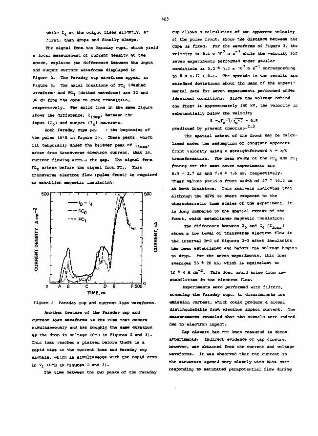
485
while I 4 at. the output rises slightly, at
first/ than drops and finally clamps.
The signal from the Faraday cups, which yield
a local measurement of current density at the
anode, explains the difference between the input
and output currant waveform displayed in
Figure 2. The Faraday cup waveforms appear in
Figure 3. The axial locations of FC0 (dashed
waveform) and FC^ (dotted waveform) are 32 and
60 en from the cone to coax transition,
respectively. The solid line in the same figure
shows the difference, IlriS8, between thR
input d 0 ) and output (I,.; currants.
Both Faraday cupe pe:. : the beginning of
the pulae (A»B in Figure 3 ) . These peaks, which
fit temporally under the broader peak of I]ABS>
arise from transverse electron current, that is,
current flowing acro^j the gap. The signal frc-m
FCg arises before the signal from sc.,. This
transverse electron flow (pulse front) lc required
to establish magnetic insulation*
500 500
ui
<
>
Uiav-Uictrs
Figure 3 Faraday cup and current loss waveforms.
Another feature of the Faraday cop and
current lose waveforms is the rise that occurs
simultaneously and has roughly the same duration
as the drop in voltage (C*D in Figures 2 and 3).
This loss Teaches a plateau belore there is a
rapid rise in the current loss and Faraday cup
signals, which is simultaneous with the rapid drop
in V: (D-E in Figures 2 and 3).
The time between the two peaks of the Faraday
cup allows a calculation of the apparent velocity
of the pulse front, since •Ae distance between the
cups is fixed. For she waveforms of Figure 3, the
velocity is 6.4 x 1C7 m s"1 while the velocity for
seven experiments performed under similar
to 8 " 0.17 * 0./.. The spreads in the results are
standard daviations about the mean of the experi-
mental data foT seven experiments performed under
identical conditions. Since the voltage behind
the front i» approximately 340 kv, the velocity is
substantially balow the velocity
predicted by praeant theories.2'
The spatial extent of the front may be calcu-
lated under the assumption of constant apparent
front Milocity using a straightforward t » x/u
transformation. The mean FHHHs of the fc0 and FC,
fronts for the same seven experiments are
6.S '- 2.7 ns and 7.4 - 1.6 ns, respectively.
These values yield a front width of 37 - 14.3 cm
at both locations. This analysis indicates that
although the HIVS is short compared to the
characteristic » 1 — scales of the experiment, it
is long compared to the spatial extent at the
front, which establishes magnetic insulation.
The difference between l0 and 14 (^ioss>
shows a low level of transverse electron flow ir.
the interval B*C of Figures 2-3 after insulation
has been established and before the voltage begins
to drop. For the seven experiments, this loss
averages 55 ± 20 kA, which is equivalent to
12 - 4 A cm" . This loss could arise from in-
stabilities in the electron flow.
Experiments were performed with filters,
covering the Faraday cups, to discriminate ion
emission current, which could produce a signal
distinguishable from electron impact current. The
measurements revealed that the signals were Indeed
due to electron impact.
Gap closure has ret been measured in these
experiments. Indirect evidence of gap closure,
however, was obtained from the current and voltage
waveforms. It was observed that the current in
the structure agreed very closely with that cor-
responding to saturated parapotential flow during
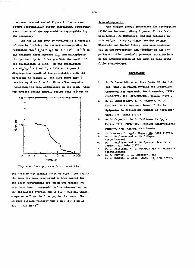
486
the time interval a*C at Figure 2 Th« currantbecaaa substantially larger thereafter, suggestingthat closure of the gap could be raaponaibla forthe Increase.
The gap in the coax i s obtained as a functionof time by dividing the currant corresponding tosaturated flow4 1,/g • ^ r «n [Y * <Y2 - 1)1/21 bythe measured input current (IQ) and multiplyingtha quotient by R. Since g - S/&, the result ofthe calculation i s d ( t ) . In the calculationY » eVj/mgC2 + 1 and Ia - 8500 h. Plgore 4displays the result of the calculation with thawaveforms of Plgure 2* OTie plot shows that dremains equal to 5 n for 40 ns after magneticinsulation has been established in the coax. Thengap closure begins shortly before peak TOltagat as
F200
Figare 4 Coax gap as a function of time-
the Faraday cup signals start to rise. The gap inthe coax has been calculated by this nethod fortha seven experiments for which the Faraday cupdata have been discussed. Before closure begins >the calculated average gap is S.3 ± 0.2 am, whichcompares well to the 5 m gap in the coax. Theaverage closure velocity for 5 n i > d > 2 a i i a
Acknowledgements
m e authors deeply appreciate the cooperation
of Halter Backmann, Jimmy Figures, Gloria Lawler,
Lila Lowell, Al McConnell, and Don Fellinen in
this effort. Special thanks are due to Hart
Klshimoto and Harlan Otting, who were instxuigen-
tal in tha preparation and fielding of the ex-
periment. John Creadon's generous contributions
to the interpretation of tha data is also grate-
fully acknowledged.
RSFKKSNCES
4 .
S.
s.
7-
3,
Z. I. Baranchikov, et a l . , Proc. of tha 6thInt. Conf. on Plasraa Riysics and ControlledTharBBnuclear Research, Barchtasgaden, IAEA-CS-3S/F7B, 185, STI/POB/439, Vienna (1977!.E. I. Baranchitov, A. V. Gordeev, V. D.Korolov, V. p. aa^rnov, Proc. of the 2ndSyaposiuai on Collectlva Methods of Accelera-tion, 271, Oubna (1977).M. 01 Capoa and 0. G. Pellinen, J. Appl.Phys., 19791 PX7R-1009, Physics InternationalCompany, S*n Leandro, California.J. Creadon, J. Appl. Phys., J8, 1070 (1977).0. G. Pellxnen and H. S. DiCapua(unpublished).0. 3. Pellinen and P. w. Spence, Rev. Sci.Instr., 42.. 1699 (1971).0. Q. Pe l l inen , M. S. OiCapua and W. Bachmann(unpublished).R. K. Parker, R. E. Anderson, andC. V. Duncan, J. Appl. Phys., «_, 2463 (1974).
4.6 - 0.3 cm Us-1
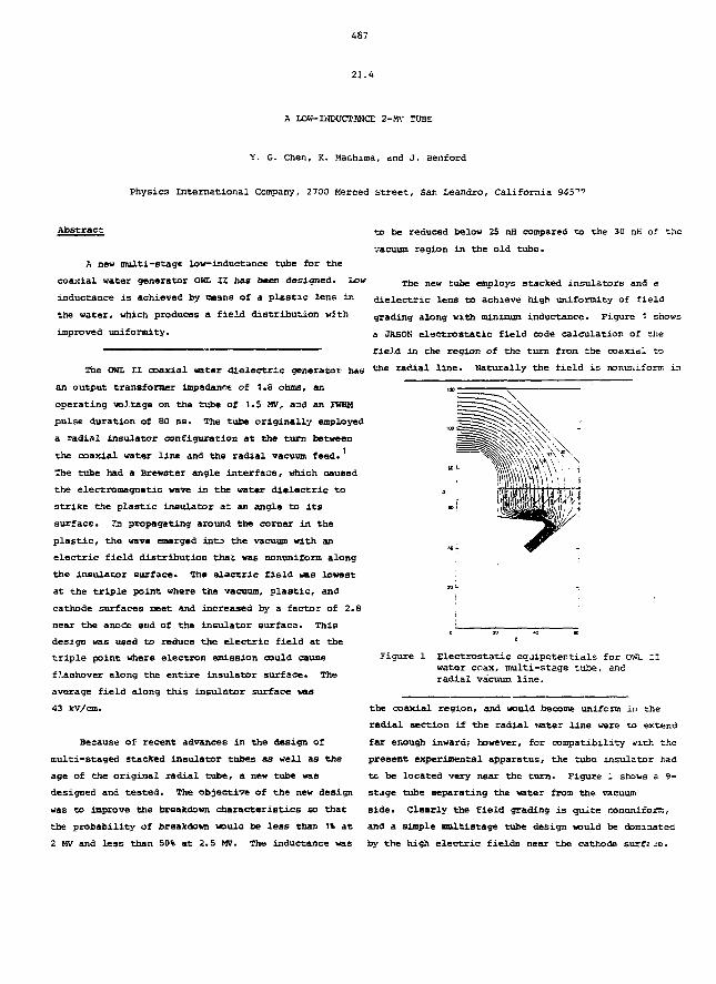
487
21.4
A LOW-IHDUCTSNCE 2-MV TUBE
Y. G. Chen, K. Mashima, and J. Benford
Physics International Company, 2700 Merced street, San Leandro, California
Abstract
A new multi-stage low-inductance tube for the
coaxial water generator OWL II has been designed. Low
inductance is achieved by means of a plastic lens in
the water, which produces a field distribution with
improved uniformity •
The OWL II coaxial water dielectric generator hau
an output transformer impedance of 1.8 ohms, an
operating voltage on the tube of 1.5 MV, and an FWHH
pulse duration of 80 ns. The tube originally employed
a radial insulator configuration at the turn between
the coaxial water line and the radial vacuum feed.
The tube had a Brewster angle interface, which caused
the electromagnetic wave in the water dielectric to
strike the plastic insulator at an angle to its
surface. In propagating around the comer in the
plastic, the wave emerged into the vacuum with an
electric field distribution that was nonuniform along
the insulator surface. The electric field was lowest
at the triple point where the vacuum, plastic, and
cathode surfaces meet and increased by a factor of 2.8
near the anode end of the insulator surface. This
design was used to reduce the electric field at the
triple point where electron emission could cause
f?.ashover along the entire insulator surface. The
average field along this insulator surface was
43 kV/cm.
Because of recent advances in the design of
multi-staged stacked insulator tubes as well as the
age of the original radial tube, a new tube was
designed and tested. The objective of the new design
was to improve the breakdown characteristics so that
the probability of breakdown would be less than 1% at
2 MV and less than 50% at 2.5 MV. The inductance was
to be reduced below 25 nH compared m the 30 nK of the
vacuum region in the old tube.
T h e nev, e u b e stacked insulators and a
dielectric lens to achieve high uniformity of field
grading along with minimum inductance. Figure 1 shows
a J R S O K electrostatic field code calculation of the
field in the region of the turn from the coaxial to
the radial line. Naturally the field is nonunifonr. in
Figure 1 Electrostatic eq-jipotentials for OWL IIwater coax, multi-stage tube, andradial vacuum line.
the coaxial region, and would become unifcna in the
radial section if the radial water line were to extend
far enough inward; however, for compatibility with the
present experimental apparatus, the tube insulator had
tc be located very near the turn. Figure 1 shows a 9-
stage tube separating the water from the vacuum
side. Clearly the field grading is quite nonunifons,
and a simple multistage tube design would be dominated
by the high electric fields near the cathode surfs-e.
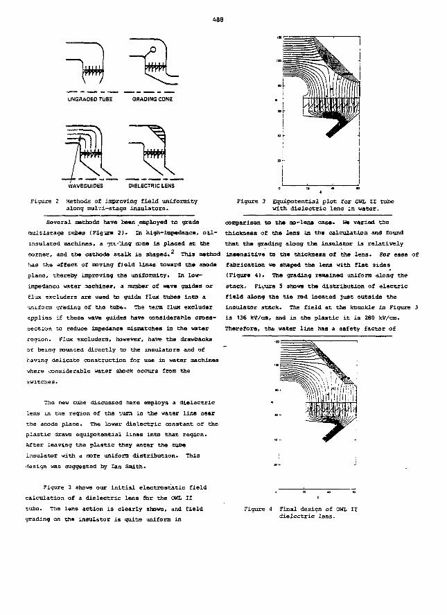
488
UNGRAOED TUBE GRADING CONE
ktw\
WAVEGUIDES DIELECTRIC LENS
Figure 2 Methods of improving field uniformityalong multi-stage insulators.
Several methods have been employed to grade
aultistage tithes (Figire 2). In high-impedance, oil-
insulated machines, a gii-'J.ng con* is placed at toe
corner, and the cathode stalk is shaped.2 This method
has the effect of moving fi eld linas toward the anode
plane, thereby improving the uniformity* In low—
impedance: water machines, a number of wave guides or
flux excluders are used to guide flux tubes into a
uniform grading of tho tube* The term flux excluder
applies if these wave guides have considerable cross-
section to reduce impedance mismatches in the water
region. Flux sxcluder3, however, have the drawbacks
of being nounced directly to the insulators and of
having delicate construction for use in water machines
vhere considerable water shock occurs from the
switches.
The new tube discussed here employs a dielectric
lens in the region of the turn in the water line near
the anode plane. The lower dielectric constant of the-
plastic draws equipotential lines into that region.
After leaving the plastic they enter the tube
insulator with a more uniform distribution. This
design was suggested by Ian Smith.
Figure 3 Equipotential plot for OWL II tubewith dielectric lens in water.
comparison to the no-lens case. He varied the
thickness of the lens in the calculation and found
that: the grading along the insulator is relatively
Insensitive to the thickness of the lens. For ease of
fabrication we shaped the lens with flat sides
(Figure 4 ) . The grading remained uniform along the
stacko Figure S shows the distribution of electric
field along the tie rod located just outside the
insulator stick. The field at the knuckle in Figure 3
is 136 kv/cm, and in the plastic it is 280 IcV/cm.
Therefora, the water line has a safety factor of
Figure 3 shows our initial electrostatic field
calculation of a dielectric lens for the OWL II
tube. The lens action is clearly shown, and field
grading on the insulator is quite uniform in
Figure 4 Final design of OWL IIdielectric Zens.
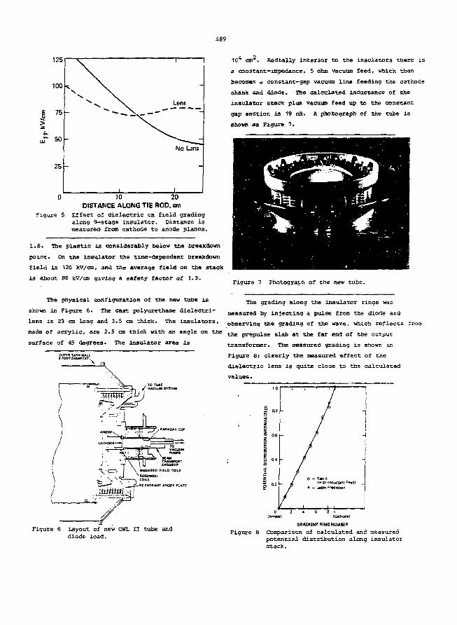
489
125 \
-
\
N . Lens
No LOTS
I i
£ 75-
50 -
25 -
10 20DISTANCE ALONG TIE ROD. cm
Figure 5 Effect of dielectric on field gradingalong 9-stage insulator. Distance ismeasured from cathode to anode planes.
1.6. The plastic is considerably below the breakdown
point. On the insulator the time-dependent breakdown
field is 120 kV/cm, and the average field on the stack
is about 80 kV/cm giving a safety factor of 1.5.
The physical configuration of the new tube is
shown ir. Figure 6. The cast polyurethane dielectric
lens is 23 cm long and 3.5 cm thick. The insulators *
made of acrylic, are 2.5 cm thick with an angle on the
surface of 45 degrees. The insulator area is
OUTER TANK MULFOOT DIAMETER.
104 cm2. Radially interior to the insulators there is
a constant-impedancet 5 ohm vacuum feed/ which then
becomes a constant-gap vacuum line feeding the cathode
shank and diode. The calculated inductance of the
insulator stack plus vacuum feed up to the constant
gap section is 19 nH. A photograph of the tube is
shown as Figure 7.
Figure 7 Photograph of the new tubs.
The grading along the insulator rings was
measured by injecting a pulse from the diode and
observing the grading of the wave, which reflects frorr.
the prepulse slab at the far end of the output
transformer. The measured grading is shown in
Figure 8; clearly the measured effect of the
dielectric lens is quite close to the calculated
values.
1,0
0.8
H6
0.4
a:
/
J/
- I_ £ (High-lnflucram Pi
J» • ~ Ufion Prediction
f 1 1 ' ! i
-
-
1J
Figure 6 Layout of new OWL II tube anddiode load•
lAfvjoe! (Cathode)
GRADIENT RING NUMBER
Figure 8 Comparison of calculated and measuredpotential distribution along insulatorstack.
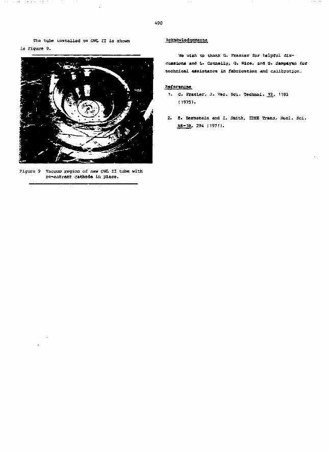
490
The tube installed on OWL XI is shown
in Figure 9.
Acknowledgements
We wish to thank S. Frazier for helpful dis-
cussions and L. Connelly, Q. Rice, and 3. Sampayan for
technical assistance in fabrication and calibration.
References
1. G. Frazier, J. Vac. Sex. Technol. _1£, 1183
(1975).
2. 3. Bernstein and I. Smith, IEEE Xrans. Hucl. Sci.
HS-18, 294 (1971).
Figure 9 Vacuum region of new OWL II tube withre-entrant cathode in place.

491
INDEX TO AUTHORS
Abramyan, E., 202
Alcock, A. J., 179
Andrews, K. R., 261
Ashby, S., 410
Barrett, D., 308
Basenkov, S. V., 25
Bayless, J. R., 372
Benford, J., 487
Berger, T. L., 237
Bickford, J., 254
Bird, W. L., 76, 325, 385, 392,398, 463
Black, S., 102
Boiler, J. R., 205
Bradley, L. P., 467
Brennan, M., 325, 392, 398
Brockhurst, F. C , 406
Brooks, W. P., 343, 381
Brower, K. L., 429
Bullion, T. M., 333, 385
Burkes, T. R. , 102, 308, 364
Burton, J. K., 205, 284
Bushnell, A. H., 161
Butcher, R. R., 273
Buttram, M. T., 61
Byszewski, P., 148
Calvin, H., 359
Canavan, G., 1
Carder, B. M., 454, 459
Caristi, R., 17
Cary, W. K., Jr., 114
Chen, Y. G., 359, 487
Chetvertkov, V. I., 25
Cnare, E. C., 343, 381
Conte, D., 83, 276, 284, 368
Cowan . M., 343
Crumley, R. J., 119
Cummings, D. B., 172, 446
D'Addario, M., 236
Davis, S. J., 246
Dalton, C., 232
Dembinski, M., 72
DiCapua, M., 483
Dobbie, C. B., 161
Driga, M. D., 76, 333, 398
Ehsani, M., 419
Fenneman, D., 122
Fernsler, R. F., 363
Fine, K. ,' 42
Fisher, R., 425
Fitch, R., 49
Vitzsimmons, W. A., 184
Forcier, M. L. , 221
Ford, R. D., 83, 276, 284
Frazier, G. B., 127, 359
Freytag, E. K., 49
Friedman, S., 17
Fuja, R. E., 419
Fujioka, T., 165
Gagnon, W. L. , 49, 246
Galbraith, J. D., 100
Gillis, P., 410
Gilmour, A. S., Jr., 250
Glancy, M. T., 295, 301
Goldhar, J., 236
Golka, R., 136
Gover, J. E. , 402
Gray, B. R., 242
Gripshover, R., 122, 221

492
Guenther, A. H., 433, 437, 442
Gully, J. H., 325, 333, 385, 392,398
Gund&rsen, M., 119
Gurbaxani, S. H.3 273
Gusev, 0. A., 25
Gvishi, M., 376
Hammon, H. G., III, 172, 446
Harjes, H. C , 442
Harris, N. W., 65
Harvey, R. J., 372
Hashimoto, T., 165
Hatfield, L. L., 442
Henderson, R. P., 287, 347
Hill, G., 364
Hoeft, L. 0., 149
Honig, E. M., 414
Howland, M. M., 246
Hutchins, R. L., 425
Istomin, J. A., 25
Jampol'skii, I. R., 25
Jansen, H., 261
Jansen, J., 31, 254
John, P. K., 72
Johnson, D. J., 191
Jones, L. A., 142
Jones, M. E., 68
Kenyon, V. L., III, 187
Kihara, R., 209
Koba, J. V., 25
Kolm, H., 42
Xrausse, G., 232
Krickhuhn, A. P., 161
Kristiansen, M., 106, 433, 437,442
Kuleshov, G. D., 202
Kulke, B., 209
Kunhardt, E. E., 433, 437
Kustom, R. L., 419
Kuswa, G. W., 153
Lalevic, B., 376
Latmanizova, G. M., 25
Lee, C. H., 165
Lehman, T. H., 425
Leopold, K. E., 179
Levinson, S-, 433
Levy, S., 376
Lin, J., 106
Lindberg, D. D., 114
Lindstrom, H. B., 83
Lippert, J. R., 132
Lupton, W. H., 83, 276, 284
Markiewicz, W. D., 381
Martin, T. H., 2, 191
Martin, V. N., 157
Mashima, K., 487
Mayhall, D. J. T., 330, 463
McDonald, K., 437
Mendel, C. W., Jr., 153
Menown, H., 363
Merritt, B. T., 454, 459
Merz, S., 17
Mesyats, G. A., 9
Mikkelson, K., 106
Miller, R. N., 250
Mongeau, P., 42
Mostrom, M. A., 475
Murray, J. R., 236
Neale, C. V., 363
Neau, E. L., 479
Newton, M., 437

493
Nielsen, K., 410
Nolting, E. E., 450
Nunnally, W. C , 142
Obara, M., 165
O'Loughlin, J. P., 96
Orham, E. L., 467
Parker, R. D., 351
Parsons, W. M., 414
Pasecbnikov, A. M., 25
Pecherskii, 0. P., 25
Pellinen, D., 410
Perlin, A. S., 25
Petr, R., 308
Pevchev, B. P., 25
Pichot, M., 398
Plante, R., 17
Ramrus, A., 320
Rapaport, W. R., 236
Reinhardc, N., 17
Reinovsky, R. E., 287, 347
Rice, J. W., 114
Riepe, K. B., 254
Rinehart, L. F., 221
Rohwein, G. J., 87
Rose, M. F., 221, 295, 301
Rosocha, L-, 184
Ross, G. F., 265
Rudakov, L. I., 25
Rylander, H. G., 76, 325, 330,
333, 385S 392, 398, 463
Sakato, Y., 165
Sarjeant, W. J., 179, 232
Sazama, F. J., 187
Scarlett, W. R., 261
Scherrer, V. E., 284
Schlitt, L., 269
Schonbach, K. H., 442
Schubert, C. W., Jr., 132
Shannon, J., 226, 320
Shipman, J. D., Jr., 205
Shoga, M., 376
Silvernail, C , 265
Simcox, G. K., 217
Singer, S., 142
Smirnov, V. P., 25
Smith, D. L., 287, 347
Sojka, R. J., 217
Spann, M. L., 392
Spence, P. W., 359, 410
Stabley, j., 242
Stine, R. D., 265
Stowers, I. F. , 4 -.7
Sullivan, T. S., 483
Thode, L. E., 68
Thompson, J. E., 106
Tolk, K. M., 76, 325, 333,392, 398
Tripoli, G. A., 214
Tucker, W. K., 381
Turner, W. C., 254
Turnquist, D., 17
VanDevender, J. P., 55, 153, 191,429, 479
Vitkovitsky, I. M., 83, 276V 284, 368
Warren, R. W., 198, 414
Watson, A., 119, 471
Watson, H., 313
Weiner, M., 91
Weldon, W. F., 76, 325, 330, 333,385, 392, 398, 463
Wilcox, R. E., 381
Wildi, P., 195, 355
Williams, P. F., 42, 119

494
Woodson, H. H.; 76, 325, 330,333, 385, 392, 398, 463
Zowarka, R. C., 325, 333

495
2nd IEEE International Pulsed Power Conference - Attendance List
Ye. A. AbramyanInstitute of High TemperaturesKorovinskoe RoadMoscow 127412 USSR
Michael AlleyDept. of Electrical EngineeringTexas Tech UniversityLubbock, TX 79409
Alex AuyeungDept. of Electrical EngineeringTexas Tech UniversityLubbock, TX 79409
William L. BakerAir Force Weapons Lab/DYPKirtland AFBNew Mexico 87117
Don G. BallLawrence Livermore LabsP.O. Box 808Livermore, CA 94550
G. W. BarrSandia LabsPulsed Power Project Div.Albuquerque, NM 87185
4251
David BarrettDept. of Electrical EngineeringTexas Tech UniversityLubbock, TX 79409
Jon E. BarthIEEE1300 Wyoming St.Boulder City, NV 89005
Steve BeckerichDept. of Electrical EngineeringTexas Tech UniversityLubbock, TX 79409
William C. BeggsAMERIEL4110 Shawnee Lane NEAtlanta, GA 30319
James BenfordPhysics International2700 Merced St.San Leandro, CA 94577
T. L. BergerNaval Surface Weapons CenterCode F-12Dahlgren, VA 22448
Ernest E. BergmannGroup L-9 MS 535Los Alamos Scientific LabsLos Alamos, NM 87544
Bernard H. BernsteinPhysics International2700 Merced St.San Leandro, CA 94577
J. BickfordLos Alamos Scientific LabsLos Alamos, NM 87545
William L. Bird, Jr.Center for ElectromagneticsUniversity of Texas/AustinTaylor Hall 167Austin, TX 78712
Susan BlackDept. of Electrical EngineeringTexas Tech UniversityLubbock, TX 79-,09
Boyd BlackwellDept. of Electrical EngineeringTexas Tech UniversityLubbock, TX 79409
Gus A. BlumeNWSC-CraneCode 7071 GCrane, Ind. 47522
John R. BoilerNaval Research LaboratoryCode 6773Washington, DC

496
R. J. BostekHarry Dalmond Labs4103 Necostin WayAnnandale, VA 22003
Laird BradleyLawrence Livermore LabsP.O. Box 808Livermore, CA 94550
Lt. Michael R. BrasherAir Force Rocket Propulsion LabAFRPL/LKDH (Stop 24)Edwards AFB, CA 92523
L. W. BravermanGTE SylvaniaBox 188Mountain View, CA 94047
Mike BrennanUniversity of Texas/AustinTaylor Hall 167Austin, TX 78712
Jerome B. BrewsterWestinghouse Electric1310 Beulah Rd.Pittsburgn, PA
Frederick C. BrockhurstAir Force Aero Propulsion LabAFAPL/POD-1Wright-Patterson AFBOhio 45433
David F. BrowerFusion Research CenterR. L. Moore Hall Rm. 202University of TexasAustin, TX 78712
Jacques BuchetCommissariat A L'Energie AtomiqueEtablissment TBoite Postate No. 793270 SEVRANFrance
Bob BurchDept. of PhysicsTexas Tech UniversityLubbock, TX 79409
T. R. BurkesDept. of Electrical EngineeringTexas Tech UniversityLubbock, TX 79409
Joseph K. BurtonNaval Research LaboratoryCode 6770Washington, DC 20375
Andrew BushnellMaxwell Laboratories8835 Balboa AvenueSan Diego, CA 92123
Bob ButcherLos Alamos Scientific LabsLos Alamos, NM 87545
Malcolm ButtramSandia LabsDiv. 4253Albuquerque, NM 87185
W. ByszewskiDept. of Electrical EngineeringTexas Tech UniversityLubbock, TX 79409
Paul A. CaldwellHarry Diamond LabsAdelphi, MD 20783
Bruce M. CarderLawrence Livermore LabsP.O. Box 5508Livermore, CA 94550
George CardwellRLM Hall 11.312University of TexasAustin, TX 78712
R. CaristiE G & G35 Congress St.Salem, Mass 01970
Bill CaryNaval Surface Weapons CenterF-12Dahlgren, VA 22448

497
Matija CenanovicOntario Hydro Research Lab800 Kipling Ave.Toronto, Canada M8Z5S4
Y. G. ChenPhysics International2700 Merced St.San Leandro, CA 94577
Edmcnd Y. ChuMaxwell Labs9244 Balboa Ave.San Diego, CA 92123
Hans-Jurgen CirkelKraftwerk Union AktiengesellschaftHammerbacher Strabe 12 + 14D 8520 Erlangen, West Germany
G. ClarkE G & G35 Congress St.Salem, Mass 019 70
Wayne ClarkMaxwell Labs8835 Balboa Ave.San Diego, CA 92123
Eugene C. CnareSandia LabsP.O. Box 5800Albuquerque, NM 87185
Dale ColemanDept. of Electrical EngineeringTexas Tech UniversityLubbock, TX 79409
Dominick ConteNaval Research LabCode 6777Washington, DC 20375
Edward G. CookLawrence Livennore LabsP.O. Box 808 L-321Livemore, CA 94550
Paul CorbiereRaytheonHartford RoadBedford, MA 01730
Jacques Cortella -Commissariat A L'Energie AtomiqueBP u 1421120-IS-SUR-TILLEFrance
Gerald W. CouttsLawrence Livermore LabsP.O. Box 808Livermore, CA 94550
M. Cowan, Jr.Sandia LabsP.O. Box 5800Albuquerque, NM 87185
James L. Cox, Jr.Old Dominion University600 Downing CrescentVirginia Beach, VA
Randy CrumleyDept. of Electrical EngineeringTexas Tech UniversityLubbock, TX 79409
D. CummingsPhysics International2700 Merced St.San Leandro, CA 94577
Charlie DaltonLos Alamos Scientific LabsP.O. Box 1663Los Alamos, NM
K. DasGuptaDept. of PhysicsTexas Tech UniversityLubbock, TX 79409
Stephen J. DavisLawrence Livermore LabsP.O. Box 808Livermore, CA 94550
Michael DembinskiUniv. of Western OntarioDept. of PhysicsLondon, OntarioNGA 3K7 Canada
A. Stuart DenholmEnergy Sciences, Inc.8 Gill St.Woburn, Mass 01801

498
Frank DeLurgioEmerson Elect. Co.8100 W. Florissant Ave.St. Louis, MO 63136
Col. Robert M. DetweilerUSAFAFOSR/NPBoiling AFBWashington, DC 20332
Dr. Peter J. DiBonaNaval Surface Weapons CenterExplosives Div. Code R-13Bldg. 315Silver Spring, MD 20910
M. DiCapuaPhysics International2700 Mercer1. St.San Leandro, CA 94577
Bob DruceDept. of Electrical EngineeringTexas Tech UniversityLubbock, TX 79409
Joe DutkowskiNWSC-CraneCode 70715Crane, Ind. 47522
John W. DzimianskiWestinghouse Elect. Corp.MS 3714P.O. Box 1521Baltimore, MD 21203
Mehrdad EhsaniArgonne National Laboratory210 S. Whitney WayMadison, WI 53705
Jan E. EningerAvco Everett Res. Lab2385 Revere Beach ParkwayEverett, MA 02149
George F. EricksonLos Alamos Scientific LabP.O. Box 1663 MS 566Los Alamos, NM 87545
M. EtzionSoreq NRCYavne, Israel
Jon FarberDefense Nuclear AgencyWashington, DC 20305
Dr. David B. FennemanNaval Surface Weapons CenterCode F-12Dahlgren, VA 22448
Richard FernslerJAYCOR5902 Euclid St.Cheverly, MD 20785
Karl FertlMIT-Natl. Magnet Lab150 Albany St. NW 14 2126Cambridge, MA
Richard FitchPrecipco, Inc.c/o Maxwell Laboratories9244 Balboa AvenueSan Diego, CA 92123
William A. FitzsimmonsNational Research Group, Inc.P.O. Box 5321Madison, Wl 53705
D. FleischerE G & G35 Congress St.Salem, MA 01970
Robert E. FontanaAir Force Institute of TechnologyAFIT/ENGWright-Patterson AFBOhio 45433
Richard FordNaval Research Lab4555 Overlook Ave.Washington, DC 20375
Col. Paul E. FortinUSAFHQ AFSC/CLWAndrews AFB, MD 20334

499
C. M. FowlerLos Alamos Scientific LabsLos Alamos, NM 87545
Bill FoxMaxwell Labs8835 Balboa Ave.San Diego, CA 92123
George Fra2ierPhysics International2700 Merced St.San Leandro, CA 94707
E. Karl FreytagLawrence Livermore LabsP.O. Box 808 L-469Livermore, CA 94550
S. FriedmanE G & G35 Congress St.Salem, MA 01970
Otto M. Freidrich, Jr.University of Texas/Austin1125 Shady LaneAustin, TX 78721
William GagnonLawrence Livermore LabsP.O. Box 808Livermore, CA 94550
J. D. GalbraithLos Alamos Scientific LabsP.O. Box 1663Los Alamos, NM 87545
Dr. Scott GilmourState University of New York4232 Ridge Lea RoadAmherst, NY 14226
Ms. Mary T. GlancyNaval Surface Weapons CenterDahlgren Laboratory, Code F 12Dahlgren, VA 22448
Terry F. GodloveDept. of EnergyMS C 404Germantown, MD 20545
Jerry GoldlustDielectric Sciences48 Cummings PkWoburn, MA 01801
Robert K. GolkaWendover ABFBox 537Wendover, UT 84083
Robert A. GoodmanLawrence Livermore LaboratoryMirror Fusion Test FacilityP.O. Box 808/L-542Livermore, CA 94550
James E. GoverSandia LabsDivision 2165Albuquerque, NM 87185
Bobby R. GrayRADC/OCTPGriffiss AFB, NY 13441
Edward E. GrazdaVan Nostrand Reinhold Co.261 Green Moore PlaceThousand Oaks, CA 91360
Ronald J. GripshoverNaval Surface Weapons CenterCode F 12Dahlgren, VA 22448
Henry C. GrunwaldITT Electron Tube DivisionP.O. Box 100Easton, PA 18042
J. H. GullyCenter for ElectromagneticsTaylor Hall 167University of Texas/AustinAustin, TX 78712
Arthur H. Guer.therAir Force Weapons Laboratory/C/Kirtland AFBAlbuquerque, NM 87117
500
Peter Haas9232 East Parkhill Dr.Bethesda, MD 20014
M. 0. HaglerDept. of Electrical EngineeringTexas Tech UniversityLubbock, TX 79409
J. R. HallRockwell Int.-Rocketdyne6633 Canoga AvenueCanoga Park, CA 91304
J. HammondPhysics International2700 Merced St.San Leandro, CA 94577
George HannaContinental ElectronicsP.O. Box 270879Dallas, TX 75227
Chuck HarjesDept. of Electrical EngineeringTexas Tech UniversityLubbock, TX 79409
Fred HarmonSouthwestern Engineering & Equipment6260 E. Mockingbird LaneDallas, TX 75214
N. W. HarrisIon Physics Co.South Bedford Rd.Burlington, MA 01803
John HarrisonMaxwell Laboratories8835 Balboa Ave.San Diego, CA 92123
Robin HarveyHughes Research Lab3011 Malibu Cyn Rd.Malibu, CA 90265
Lynn HatfieldDept. of PhysicsTexas Tech universityLubbock, TX 79409
R. E. HebnerNational Bureau of StandardsBldg. 220, B344Washington, DC 20234
Bill HeidbrinkMaxwell Laboratories8835 Balboa Ave.San Diego, CA 92123
Richard P. Henderson3225 34th St. Apt. EKirtland AFBAlbuquerque, NM 87116
Henrik HenriksenNea-LindbergIndustriparken 39-432750 BallerupDenmark
Prof. Fritz HerlachKatholieke Universiteit LeuvenCelestijnenlaan 200 DB3030 LeuvenBelgium
Stuart J. HesselsonEEV, Inc.7 Westchester PlazaElmsford, NY 10523
Gregory A. HillBDM Corp.2600 Yale Blvd. S.E.Albuquerque, NM 87106
J. A. HirschCarborundumGraphite Products Div.Globas PlantP.O. Box 339Niagara Falls, NY 14302

501
Lothar E. HoeftBDM Corp2600 Yale Blvd. S.E.Albuquerque, NM 87106
Guuter HofmannMaxwell Laboratories8835 Balboa Ave.San Diego, CA 92123
Ronald W. HollowayLawrence Livermore LaboratoryP.O. Box 5508Livennore, CA 94550
E. M. HonigCTR-9, MS 464Los Alamos Scientific LabsLos Alamos, NM 87545
Michael M. HowlandLawrence Livermore LaboratoryP.O. Box 5508Livennore, CA 94550
Robert L. HutchinsBDM Corp.2600 Yale Blvd. S.E.Albuquerque, NM 87106
Igor A. IvanovKurchatov InstituteD-98Moscow, USSR
Jorg JansenLos Alamos Scientific LabsGroup L-10 MS 532Los Alamos, NM 87544
J. S. JasperExxon Nuclear Co.P.O. Box 130Richland, WA 99352
David L. Johnson701 Guadalupe Ct. N.W.Albuquerque, NM 87114
Michael JonesLos Alamos Scientific LaboratoryGroup T-15 MS-608Los Alamos, NM 87545
J. C. JouysCommissarist a 1'Energie AtomiqueCentre d'Etudes de LimeilBolte Dostal 2794190 Villeneuve St. GeorgesFrance
E. L. KempLos Alamos Scientific LabsP.O. Box.1663Los Alamos, NM 87545
Kenneth L. KennerudThe Boeing Co.915 S. 251Kent, WA 98031
Dean 0. KippenhanLawrence Livermore LaboratoryP.O. Box 8O8-L-539Livermore, CA 94550
Hank KohnexiTransrex1160 El Watson Center Rd.Carson, CA 90745
Alan KolbMaxwell Laboratories8835 Balboa Ave.San Diego, CA 92123
Dr. Henry H. KolmMassachusetts Institute of TechnologyWeir MeadowWayland, MA 01778
M. KolpinPhysics International2700 Merced St.San Leandro, CA 945 77
Peter KornMaxwell Laboratories8835 Balboa Ave.San Diego, CA 92123

502
Irv KovalikILC Technology399 Java DriveSunnyvale, CA 94086
George KrausseLos Alamos Scientific LabsMS-846 MP-4Los Alamos, NM 87545
Dr. M. KristiansenDept. of Electrical EngineeringTexas Tech UniversityLubbock, TX 79409
Robert KuenningLawrence Livermore LaboratoryP.O. Box 5504 L-153Livermore, CA 94550
Bernhard KulkeLawrence Livermore LaboratoryP.O. Box 5504Livermore, CA 94550
E. E. KunhardtDept. of Electrical EngineeringTexas Tech UniversityLubbock, TX 79409
Boris LarionovF. Efremov Scientific Institute188631 LeningradUSSR
Robert LeBrunLeCroy Research Systems1806 Embarcadero RoadPalo Alto, CA 94303
Jacques LefebureCommissariat a L'Energie AtomiqueEstablissement TBofte Postate n 793270 SevranFrance
Gerald LevyIEEEFairchild Republic Co.Plasma LabFarmingdale, NY 11743
Stephen Levy0. S. Army Electronics Technologyand Devices Lab
Ft. Monmouth, NJ 07703
Scott LevinsonDept. of Electrical EngineeringTexas Tech UniversityLubbock, TX 79409
Jack LippertUSAF Flight Dynamics LabAFFDL/FESWright-Patterson AFB, OH 45433
Lawrence H. LuessenNaval Surface Weapons CenterCode F 12Dahlgren, VA 22448
William H. LuptonNaval Research LabWashington, DC 20375
Charles W. McCulley, Jr.Maxwell Laboratories8835 Balboa Ave.San Diego, CA 92123
Ken McDonaldDept. of Electrical EngineeringTexas Tech UniversityLubbock, TX 79409
Glen McDuffDept. of Electrical EngineeringTexas Tech UniversityLubbock, TX 79409
Sterling McNeesEIMAC Div. of Varian301 Industrial WaySan Carlos, CA 94070
Ronald H. McKnightNational Bureau of StandardsBldg. 220, Rm. B344Washington, DC 20234
Phil MaceLos Alamos Scientific LabsMS 566Los Alamos, NM 87544
503
Armen E. MardiguianUSAF European Office of AerospaceResearch and Development
Box 14FPO NY 09510
Richard A. MarshallCenter for ElectromagneticsTaylor Hall 167University of Texas/AustinAustin, TX 78712
T. H. MartinDept. 4250Sandia LaboratoriesAlbuquerque, NM 87113
V. Nicholas MartinGTE Laboratories40 Sylvan Rd.Waltham, MA 01701
Levi MartinezLos Alamos Scientific LabsP.O. Box 1663Los Alamos, NM 87544
David J. T. MayhallLawrence Livermore LaboratoryMirror Fusion Test FacilityP.O. Box 808/L 542Livermore, CA 94550
Clifford W. MendelSandia LaboratoriesAlbuquerque, NM 87113
Hugh MenownEnglish Electric Valve Co., Ltd.Waterhouse LaneChelmsford, EssexCMI-2QUEngland
Bernard T. MerrittLawrence Livermore LaboratoryP.O. Box 5508Livermore, CA 94550
G. A. MesyatsInstitute of Atmospheric OpticsSiberian Branch of AN SSSRTomsk, USSR
Richard N. MillerSCEEE7300 Lake Ellenor DriveOrlando, Fla 32809
Marshall MolenOld Dominion UniversityDept. of Electrical EngineeringNorfolk, VA 23508
Peter MongeauNational Magnet LabMassachusetts Institute of TechnologyCambridge, MA 02139
J. MoriartyRaytheon Co.Hartwell Rd.Bedford, MA 01730
Michael A. MostromLos Alamos Scientific LaboratoryGroup T-k5, MS-608P.O. Box 1663Los Alamos, NM 87545
Eugene NeauSandia LabsDiv. 4252P.O. Box 5800Albuquerque, NM 87185
W. NevinsThe Machlett Laboratories, Inc.1063 Hope St.Stamford, Conn 06807
Mark NewtonDept. of Electrica"1 EngineeringTexas Tech UniversityLubbock, TX 79409
Torben Glar Nielser.Nea-LindbergIndustreparken 39-432750 BallerupDenmark
Eugene E. NoltingNaval Surface Weapons CenterWhite Oak LabSilver Spring, MD 20910

504
W. C. NunnallyLos Alamos Scientific LabsMS 429 Div. E4Los Alamos, NM 87545
Minoru ObaraDept. of Electrical EngineeringKeio University3-14-1Hiyoshi, Kohuku-kuYokohama-shi044-63-1141Japan
Henry B. OdomNaval Surface Weapons CenterCode F-12Dahlgren, VA 22448
James O'LoughlinAir Force Weapons Lab/PGSKirtland AFBAlbuquerque, NM 87117
Edward L. OrhamLawrence Livermore LabsP.O. Box 55CSLivermore, CA 94550
Thomas J. PacalaJ.P.L.4800 Oakgrove DriveMS 183-601Pasadena, CA 91103
Robert ParkerHughes Aircraft Co.Culver City, CA 90230
W. M. ParsonsLos Alamos Scientific LabsP.O. Box 1663 MS 464Los Alamos, NM 87544
Albert PassethnikovKurchotov Institute of Atomic EnergyD-98Moscow, USSR
Todd A. PelleyLawrence Livermore LabsP.O. Box 5508Livermore, CA 94550
D. PellinenPhysics International2700 Merced St.San Leandro, CA 94577
Gerald J. PetersNaval Surface Weapons CenterWhite Oak Lab R41Silver Spring, MD 20910
Rod PetrDept. of Electrical EngineeringTexas Tech UniversityLubbock, TX 79409
Babuel PeyrissacCommissarist a 1' Energie AtomiqueCentre d1Etudes de LimeilBolte Dostal 2794190 Villeneuve St. GeorgesFrance
K. A. PichotCenter for ElectromagneticsTaylor Hall 167University of Texas/AustinAustin, TX 78712
R. PlantsE G & G35 Congress St.Salem, MA 01970
John PowerDept. of Electrical EngineeringTexas Tech UniversityLubbock, TX 79409
Kenneth R. PrestwichSandia LabsDiv. 4253P.O. Box 5800Albuquerque, NM 87185
S. PutnamPhysics International2700 Merced St.San Leandro, CA 94577
Bill H. QuonTRW System Groups1 Space Park, RI-1070Redondo Beach, CA 90250
505
Al RamrusMaxwell Laboratories8835 Balboa Ave.San Diego, CA 92123
William RapoportLawrence Livermore Labs1-470Livermore, CA 94550
N. ReinhardtE G & G35 Congress St.Salem, MA 01970
Thomas ReinhardtTufts University10 Eliot RoadLexington, MA 02173
Robert E. ReinovskyAir Force Weapons LabKirtland AFBAlbuquerque, Nil 87117
Benjamin G. RiceITT Electron Tube Division10037' Balboa Blvd.Northridge, CA 91325
K. RiepeLos Alamos Scientific LabsP.O. Box 1663Los Alamos, NM 87545
Douglas M. RischMirror Fusion Test FacilityLawrence Livermore LabP.O. Box 808/L542Livermore, CA 94550
Kenneth I. RobinsonCarborundum-Graphite Prod. Div.1999 S. Bascom Ave. Suite 935Camphill, CA 95008
Doyle RogersLawrence Livermore LabsP.O. Box 808Livermore, CA 94550
Gerald J. RohweinSandia LabsP.O. Box 5800Albuquerque, NM 87115
M. F. RoseNaval Surface Weapons CenterCode F-404Dahlgren, VA 22448
Randall I. RossLawrence Livermore LabsMS 1-540P.O. Box 808Livermore, CA 94550
W. J. SarjeantLos Alamos Scientific LabsMS 429P.O. Box 1663Los Alamos, NM 87545
Franklin J. SazamaNaval Surface Weapons CenterWhite Oak LabSilver Spring, MD 20910
R. ScarlettLos Alamos Scientific LabsP.O. Box 1663Los Alamos, NM 87545
Raymond ScarpettiLawrence Livermore LabsL-153P.O. Box 5504Livermore, CA 94550
Lt. Col. J. F. SchaeferAir Force Weapons Lab/CAKirtland AFBAlbuquerque, NM 87117
Victor E. ScherrerNaval Research LabOverlook Ave.Washington, DC 20375
Leland SchlittLawrence Livermore LabP.O. Box 808Livermore, CA 94550

506
Karl SchonbachDept. of Electrical EngineeringTexas Tech UniversityLubbock, TX 79409
Sol SchneiderU. S. Army Electronics Technologyand Devices Lab
Ft. Monmouth, NJ 07703
Charles W. Schubert, Jr.7062 Bascomb Dr.Dayton, OH 45424
Peter SeibtDept. of PhysicsTexas Tech UniversityLubbock, IX 79409
John ShannonMaxwell Laboratories8835 Balboa Ave.San Diego, CA 92123
G. SimcoxRaytheon Corp.South Bedford St.Burlington, MA 01803
David L. Smith2095-B Falcon PlaceAlbuquerque, NM 87118
F. H. SmithAR0, Inc. AEDC Div.Arnold Air Force StationTennessee 37389
Franklin R. SmithU.S. Army EngineersHND ED-FDHuntsville, AL 35802
Ian D. Smith3115 Gibbons Dr.Alameda, CA 94501
Richard A. SmithNaval Surface Weapons CenterWhite Oak LabSilver Spring, MD 20910
R. L. SnellingEnglish Electric Valve Co, Ltd.Waterhouse LaneChelmsford Essex CMI-2QUEngland
P. SpencePhysics International2700 Merced St.San Leandro, CA 94577
Thomas E. SpringerLos Alamos Scientific LaboratoryMS-429, E-4P.O. Box 1663Los Alamos, NM 87545
Jere D. StableyRCANew Holland PikeLancaster, PA 17601
Charles H. StallingsPhysics International2700 Merced St.San Leandro, CA 94577
Alex G. StewartHarry Diamond Labs2800 Powder Mill Rd.Adelphi, MD 20783
Robert StineLos Alamos Scientific LabsP.O. Box 1663 .Los Alamos, NM 87545
Regan W. StinnettSandia LaboratoriesDiv. 4252P.O. Box 5800Albuquerque, NM 87115
T. H. StorrAWRE AldermastonBLDG. H36Berks, KG 7 4 PRTadley 4111England

507
J. V. StoverHughes Aircraft CompanyBldg. 600 MS F145P. 0. Box 3310Fullerton, CA 92634
Gordon F. ThomasNaval Surface Weapons CenterCode DR-54Dahlgren, VA 22448
Don ThomasR & D Associates4667 Admirality WayMarina Del Rey, CA 92017
Jim ThompsonCollege of EngineeringUniversity of South CarolinaColumbia, SC 29208
Gary A TripoliIon PhysicsSouth Bedford St.Burlington, MA 01809
William K. TuckerSandia LabsDiv. 4253Albuquerque, NM 87115
David TurnquistE G & G35 Congress St.Salem, MA 01970
Peter J. TurchiNaval Research LabCode 6770Washington, DC 20375
V. D. ValenciaExxon Nuclear Co.P. 0. Box 130Richland, VA 99352
Fred Van HaaftenLos Alamos Scientific LaboratoryP. 0. Box 1663Los Alamos, NM 87544
Richard VergaAir Force Aero Propulsion LabPODWright-Patterson AFB, OH 45433
I. M. VitkovitskyNaval Research LabCode 6770Washington, DC 20375
G. WakalopulasHigh Energy Device Dev. SectionHughes Aircraft Co.Aerospace Groups 6/C129Culver City, CA 90230
Roger WarrenRt. 3 Box 36Santa Fe, NM 87501
Alan WatsonDept. of Electrical EngineeringTexas Tech UniversityLubbock, TX 79409
Harold WatsonAiResearch Mfg. Co.MS T-422525 W. 190thTorrance, CA 90509
Richard J. WasneskiNaval Air Systems Command350-FWashington, DC 20361
Maurice WeinerU. S. Army Elect. Technology
and Device LabFt. Monmouth, NJ 07703
William F. Weldon167 Taylor HallUniversity of Texas/AustinAustin, TX 78712
Frazer WilliamsDept. of Electrical EngineeringTexas Tech UniversityLubbock,, TX 79409
508
Charles B. WhartonOccidental Research Lab/Phillips HallCornell UniversityIthaca, NY 14853
Forest E. WhiteBDM Corp.2600 Yale Blvd. SEAlbuquerque, NM 87106
R. A. WhiteSandia LabsPulsed Power Project Div. 4251Albuquerque, NM 87185
Roger WhiteMaxwell Laboratories8835 Balboa AvenueSan Diego, CA 92123
Kenneth WhithamLawrence Livermore LabsP. 0. Box 808 L-464Livermore, CA 94550
Paul WildiFusion Research Center RLM 12.3University of Texas/AustinAustin, TX 78712
James W. WillisNaval Air Systems CommandAIR 310BWashington, DC 20361
Walter L. WillisLos Alamos Scientific LabsMS 566P. 0. Box 1663Los Alamos, NM 87545
Related Documents


