1 Diamond nanophotonic circuits functionalized by dip-pen nanolithography By Patrik Rath 1,* , Michael Hirtz 1,§,* , Georgia Lewes-Malandrakis 2 , Dietmar Brink 2 , Christoph Nebel 2 , and Wolfram H. P. Pernice 1,& [1] Patrik Rath, Michael Hirtz, Wolfram H. P. Pernice Institute of Nanotechnology (INT) & Karlsruhe Nano Micro Facility (KNMF), Karlsruhe Institute of Technology, Hermann-von-Helmholtz-Platz 1, 76344 Eggenstein-Leopoldshafen (Germany) [2] Georgia Lewes-Malandrakis, Dietmar Brink, Christoph Nebel Fraunhofer Institute for Applied Solid State Physics, Tullastr. 72, 79108 Freiburg (Germany) [*] These authors contributed equally. [§] E-mail: [email protected] [&] E-mail: [email protected] Keywords: Diamond devices; Nanophotonic circuits; Dip-pen Nanolithography. Integrated nanophotonic circuits made from wide-bandgap semiconductors offer exciting prospects for advanced sensing applications and broadband optical data processing. Among the available substrates, diamond is particularly appealing due to its long-term stability, bio- compatibility and chemical inertness. Because of strong field confinement in diamond waveguides, near-field effects can be efficiently harnessed to realize building blocks for biofunctional circuits in a scalable fashion. Here, we report on the parallel and site-specific functionalization of diamond nanophotonic devices as a promising route towards waferscale bio-photonic systems. We show that arbitrary geometric features can be surface modified using dip-pen nanolithography with a minimum linewidth of 100 nm. We simultaneously functionalize several microring and microdisc resonators with different dies and high precision, allowing us to route fluorescent emission with photonic waveguides to arbitrary locations on chip. Our approach holds promise for hybrid optical systems and nanoscale bioactive devices for robust biomedical and environmental high-throughput sensing applications.

Welcome message from author
This document is posted to help you gain knowledge. Please leave a comment to let me know what you think about it! Share it to your friends and learn new things together.
Transcript
1
Diamond nanophotonic circuits functionalized by dip-pen nanolithography
By Patrik Rath1,*, Michael Hirtz1,§,*, Georgia Lewes-Malandrakis2, Dietmar Brink2,
Christoph Nebel2, and Wolfram H. P. Pernice1,&
[1] Patrik Rath, Michael Hirtz, Wolfram H. P. Pernice
Institute of Nanotechnology (INT) & Karlsruhe Nano Micro Facility (KNMF),
Karlsruhe Institute of Technology, Hermann-von-Helmholtz-Platz 1, 76344
Eggenstein-Leopoldshafen (Germany)
[2] Georgia Lewes-Malandrakis, Dietmar Brink, Christoph Nebel
Fraunhofer Institute for Applied Solid State Physics, Tullastr. 72, 79108 Freiburg
(Germany)
[*] These authors contributed equally.
[§] E-mail: [email protected]
[&] E-mail: [email protected]
Keywords: Diamond devices; Nanophotonic circuits; Dip-pen Nanolithography.
Integrated nanophotonic circuits made from wide-bandgap semiconductors offer exciting
prospects for advanced sensing applications and broadband optical data processing. Among
the available substrates, diamond is particularly appealing due to its long-term stability, bio-
compatibility and chemical inertness. Because of strong field confinement in diamond
waveguides, near-field effects can be efficiently harnessed to realize building blocks for
biofunctional circuits in a scalable fashion. Here, we report on the parallel and site-specific
functionalization of diamond nanophotonic devices as a promising route towards waferscale
bio-photonic systems. We show that arbitrary geometric features can be surface modified
using dip-pen nanolithography with a minimum linewidth of 100 nm. We simultaneously
functionalize several microring and microdisc resonators with different dies and high
precision, allowing us to route fluorescent emission with photonic waveguides to arbitrary
locations on chip. Our approach holds promise for hybrid optical systems and nanoscale
bioactive devices for robust biomedical and environmental high-throughput sensing
applications.

2
Photonic components made from diamond have emerged as a promising platform for
applications in quantum optics [1-4], non-linear optics [5,6] and optomechanics [7,8].
Because of its remarkable material properties such as broadband optical transparency, high
mechanical stability and hardness, high thermal conductivity, and good chemical stability,
diamond is used for a wealth of applications in research and industrial environments. In
particular the combination of appealing optical properties and biocompatibility make diamond
an attractive platform for biophotonic applications [9-11]. Nowadays high quality diamond
thin films are available on large-scale substrates by relying chemical vapor deposition (CVD)
which allows for using waferscale processing techniques to realize functional devices. In this
way homogeneous large scale diamond thin films can be achieved (see Supplementary Fig.
S2). Using nanofabrication routines developed originally for the electronics industry CVD
diamond thin films can be structured into subwavelength photonic devices, which allow for
propagating light over centimeter distances, the realization of high quality optical resonators
and on-chip interferometers [8,12]. This way the powerful toolbox available to integrated
optics can be efficiently utilized to realize a sensitive readout platform for biological signals.
In order to employ integrated photonic devices for biosensing suitable links to desired
analytes have to be established. Several techniques are commonly employed to functionalize
pre-structured photonic substrates, including spincoating with suitable coatings introduced in
the liquid phase [13,14] and exposure to reactive agents in the gas phase [15]. While such
techniques are suitable to functionalize many photonic components uniformly, it is ultimately
necessary to only target specific locations on chip. Deposition of functional and bio-functional
patterns has been demonstrated using various lithography techniques [16-18]. Among the
available options, dip-pen nanolithography (DPN) has recently been established as a
promising technique for reaching spatial resolution compatible with the spatial length scales
which nanophotonic devices typically occupy. DPN [19] was first used to deposit thiols on
gold surfaces but was quickly adapted for a wide range of ink materials, including biological
inks where the mild process parameters are of special value for keeping these often delicate
compounds intact [20]. DPN employs a direct-writing method to place “inks” such as small
organic molecules [21,22], polymers [23,24], biomolecules [25,26], or nanoparticles [27,28]
onto a solid substrate using an atomic force microscopy (AFM) tip as a “pen”. The use of
phospholipids and lipid mixtures in DPN, termed Lipid-DPN (L-DPN), enables site specific
and multiplexed (i.e. different inks written at the same time and in close vicinity on the
surface) functionalization of surfaces with biomimetical membrane stacks used e.g. in
3
immunological assays [29-32]. This technique does not rely on a specific surface chemistry
and can therefore be applied to various substrates, e.g. silicon oxide, polymers [29], graphene
[33] and recently we demonstrated precise functionalization of three dimensional goblet
sensor structures by L-DPN [34]. The challenge is to combine the parallel functionalization of
devices with different inks with the functionalization of pre-structured materials with good
alignment, opposed to bare flat substrates. Furthermore the DPN functionalization of photonic
structures from a wide-gap semiconductor is a concept with interesting potential applications,
which has not been shown yet.
Here, we employ L-DPN for site-specific functionalization of waferscale diamond integrated
optical circuits using lipid mixtures, with high precision and line resolution down to 100nm.
Using waferscale, transparent diamond thin films deposited by CVD followed by chemo-
mechanical polishing we realize nanophotonic circuitry with low-surface roughness, suitable
for later surface modification. We combine planar nanofabrication techniques with DPN
functionalization in order to create biocompatible integrated optical circuits that are locally
modified for biological functionality. With L-DPN we directly write onto fabricated straight
optical waveguides and curved ring resonators. Using a multi-pen strategy, several devices are
functionalized in parallel, each with different modifiers. With fluorescence microscopy and
atomic force microscopy we verify the site-specific surface modification and demonstrate
guiding and coupling of fluorescent light in nanophotonic waveguides. Additionally, we
demonstrate the delivery of ink solutions by microchannel cantilever spotting [35, 36],
exploiting a self-alignment process for functionalization of ring resonators as an alternative
route for solvent based delivery of active material. Our approach holds promise for high
throughput and high accuracy fabrication of biophotonic devices, which will enable
applications in bio-sensing and bio-interfacing by the multiplexed introduction of active
elements in form of functional ink mixtures.
While traditional semiconductor materials are frequently employed for the fabrication of
nanophotonic components diamond devices promise several advantages over existing material
templates. The large electronic bandgap enables optical transparency above 220 nm all the
way into the long infrared spectral region and strongly suppresses two-photon absorption
commonly encountered in silicon substrates. Because diamond is carbon based, covalent
binding can be utilized to link its surface to suitable biomarkers [37]. In addition, because
diamond has been shown to provide excellent biocompatibility, devices made from diamond
4
are a promising platform for biomedical applications [38]. Here we employ CVD diamond
thin films, which can be used to tightly confine light at the nanoscale because of a large
refractive index of 2.4 (see Supplementary Fig. S3 for the waveguide geometry and guided
modes). About 900 nm of polycrystalline diamond are deposited on oxidized silicon wafers
via microwave plasma enhanced chemical vapour deposition (CVD), resulting in a diamond-
on-insulator wafer, which can be used for fabricating waveguides and routing the light
through photonic circuits [8,12]. The diamond layers are then polished via slurry based
chemical-mechanical planarization (CMP) to a thickness of 600 nm. This leads to a surface
roughness below 3 nm rms on a 25 µm2 area, which is confirmed by atomic force microscopy
(see AFM and SEM micrographs in Supplementary Fig. S1). This allows fabricating high
quality integrated photonic circuits, which are pattered into a negative tone spin-on glass
resist (HSQ 15 %) via electron beam lithography (JEOL 5300, 50kV). The patterns are
transferred into diamond via dry etching by capacitively coupled reactive ion etching (RIE),
using gas flows of 17 sccm Argon and 33 sccm Oxygen at a power of 200 W, leading to a
diamond etch rate of 22 nm/min, with a selectivity of 2:1 for etching diamond versus etching
the HSQ resist. After dry etching 300 nm into the diamond, the spin-on glass resist is removed
using buffered oxide etch (BOE), resulting in pure diamond photonic structures ready for
functionalization using DPN as illustrated in Fig.1a. This fabrication routine allows
fabricating hundreds of devices per cm2 of wafer material (see Supplementary Fig. S4 for a
representative microscope image).
We fabricated waveguides, grating coupling structures and ring resonators to provide a rich
template for later surface modification. By precisely aligning photonic components to the
separation between neighboring DPN tips several devices can be addressed in parallel,
allowing for surface-modifying each individual component with a different surfactant.
Fabricated ring resonator devices coupled to a photonic bus waveguide are shown in Fig.1b.
By choosing a particular mask layout arbitrary photonic devices can be inscribed into the
diamond surface, while we here employ waveguides coupled to ring and microdisk resonators
to realize both straight and curved optical elements. Scanning electron microscope (SEM)
images reveal low surface roughness of the diamond waveguide top surface after
nanofabrication. Small feature sizes down to 100 nm such as the gap between waveguide and
microring resonators (Fig.1c) can be achieved with this fabrication method, while the limiting
factor is only the thickness of the employed resist, which could be further reduced.
Furthermore, the high etching anisotropy reached with our procedure results in near-vertical
5
sidewalls. This is a result of the optimized RIE procedure carried out at low pressure and high
RF power. We estimate from SEM micrographs that the sidewall angle is below 2° and
therefore will enable even smaller gaps in principle. By connecting the so-fabricated
waveguide based photonic circuits to on-chip grating structures contact-free coupling to
optical fibers can be employed to realize a convenient readout platform for diamond
integrated optical devices. This way a multitude of hybrid circuit devices can be fabricated
and measured in a scalable fashion.
To surface modify pre-fabricated photonic devices, two different cantilever based approaches
for functionalization were investigated. Firstly an AFM cantilever based deposition (DPN)
which allows for drawing thin lines in arbitrary shapes (e.g. straight lines or circles). The
second approach employs a microchannel cantilever based deposition, which allows
depositing fine droplets at desired positions, for example in the inside of a microring resonator.
Both approaches provide specific advantages, which will be discussed in later sections.
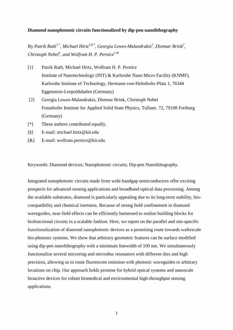
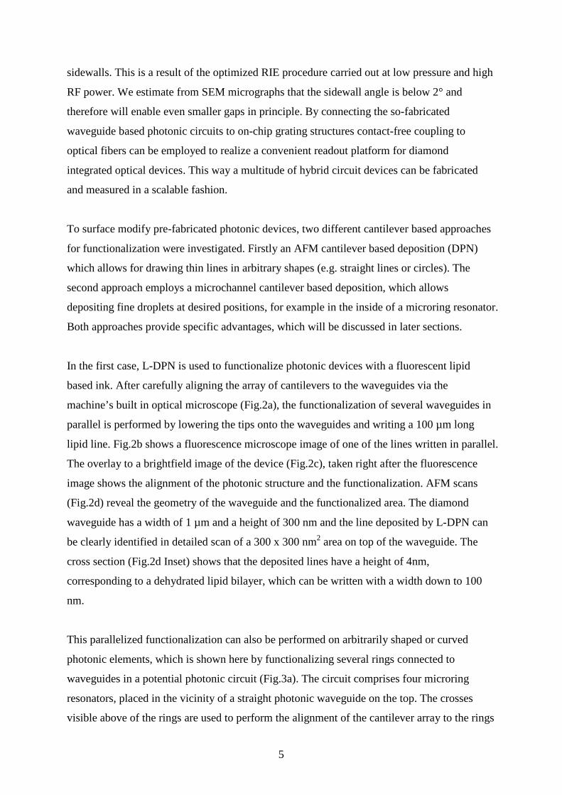
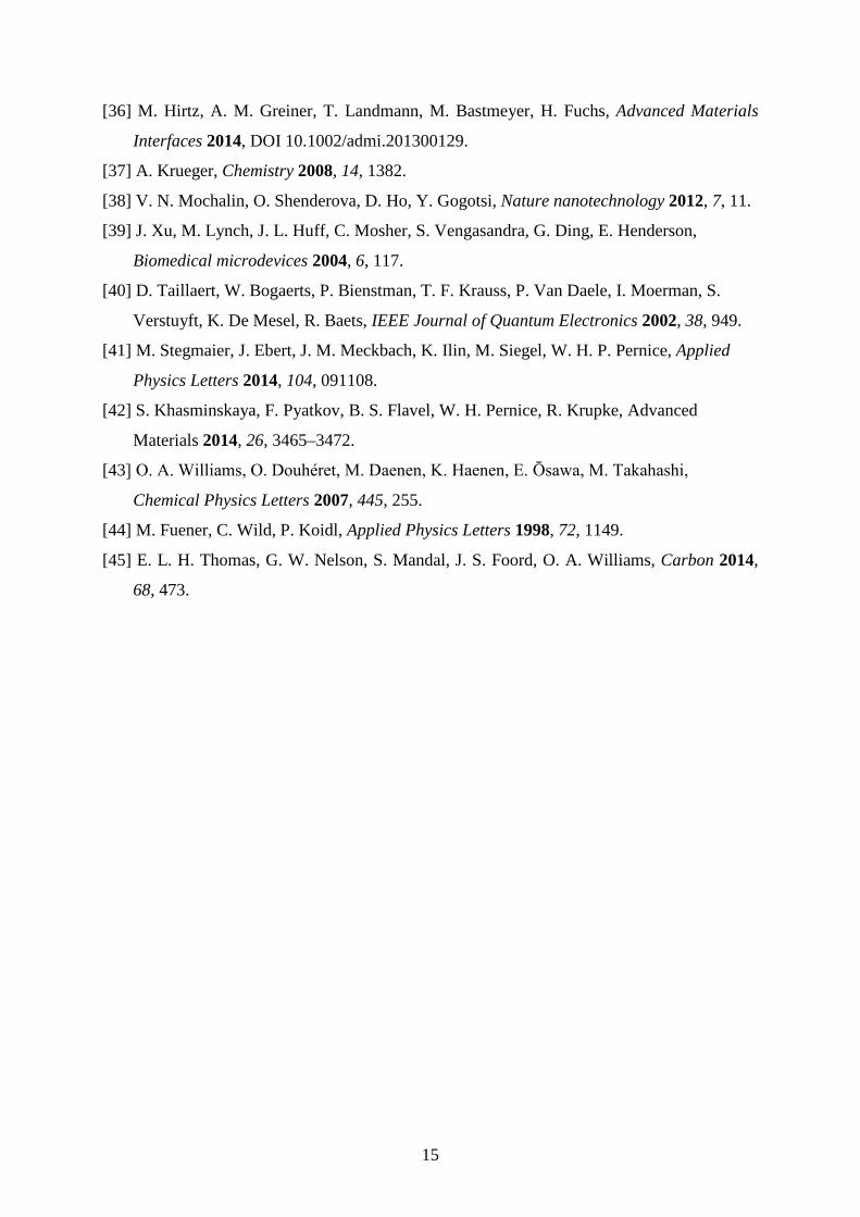
In the first case, L-DPN is used to functionalize photonic devices with a fluorescent lipid
based ink. After carefully aligning the array of cantilevers to the waveguides via the
machine’s built in optical microscope (Fig.2a), the functionalization of several waveguides in
parallel is performed by lowering the tips onto the waveguides and writing a 100 µm long
lipid line. Fig.2b shows a fluorescence microscope image of one of the lines written in parallel.
The overlay to a brightfield image of the device (Fig.2c), taken right after the fluorescence
image shows the alignment of the photonic structure and the functionalization. AFM scans
(Fig.2d) reveal the geometry of the waveguide and the functionalized area. The diamond
waveguide has a width of 1 µm and a height of 300 nm and the line deposited by L-DPN can
be clearly identified in detailed scan of a 300 x 300 nm2 area on top of the waveguide. The
cross section (Fig.2d Inset) shows that the deposited lines have a height of 4nm,
corresponding to a dehydrated lipid bilayer, which can be written with a width down to 100
nm.
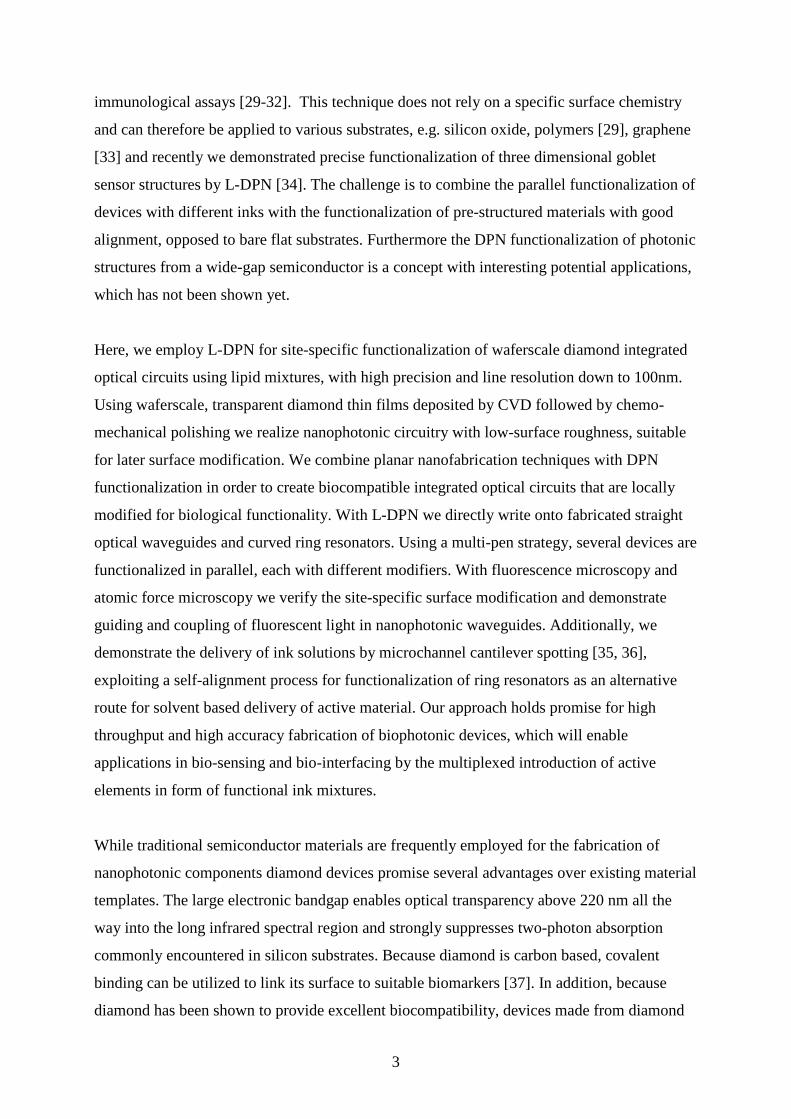
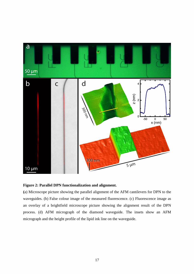
This parallelized functionalization can also be performed on arbitrarily shaped or curved
photonic elements, which is shown here by functionalizing several rings connected to
waveguides in a potential photonic circuit (Fig.3a). The circuit comprises four microring
resonators, placed in the vicinity of a straight photonic waveguide on the top. The crosses
visible above of the rings are used to perform the alignment of the cantilever array to the rings
6
(see Supplementary Fig. S11 for an in-situ view). The microrings are fabricated with a pitch
of 66 µm to match the distance between neighboring cantilevers during writing (see
Supplementary Fig. S10 for details). Here, only three of the total twelve cantilever in such an
array were coated with the fluorescent lipid ink. Thus when writing onto the microring
structures, only the first three of the four rings in the structure were decorated with the
fluorescent lipid ink in parallel, while the fourth remained as an unfunctionalized control
device. The fluorescence measurement at the same position (Fig.3b) shows that three of the
rings have been functionalized in parallel as intended, while the control device remains
unchanged (see Supplementary Fig. S15 for further microscope images). The written rings are
well aligned to the structured diamond substrate (Fig.3c) and the linewidth and height can be
easily controlled by AFM scans as shown in Fig.3d. From the image it is apparent that the
DPN written line is well guided along the radius of the rings on all three devices
simultaneously, thus showcasing the high spatial precision available to the method. Here we
only show the results for a single ring for clarity, while an overview of all three functionalized
devices can be found in the supplementary information in Fig. S15.
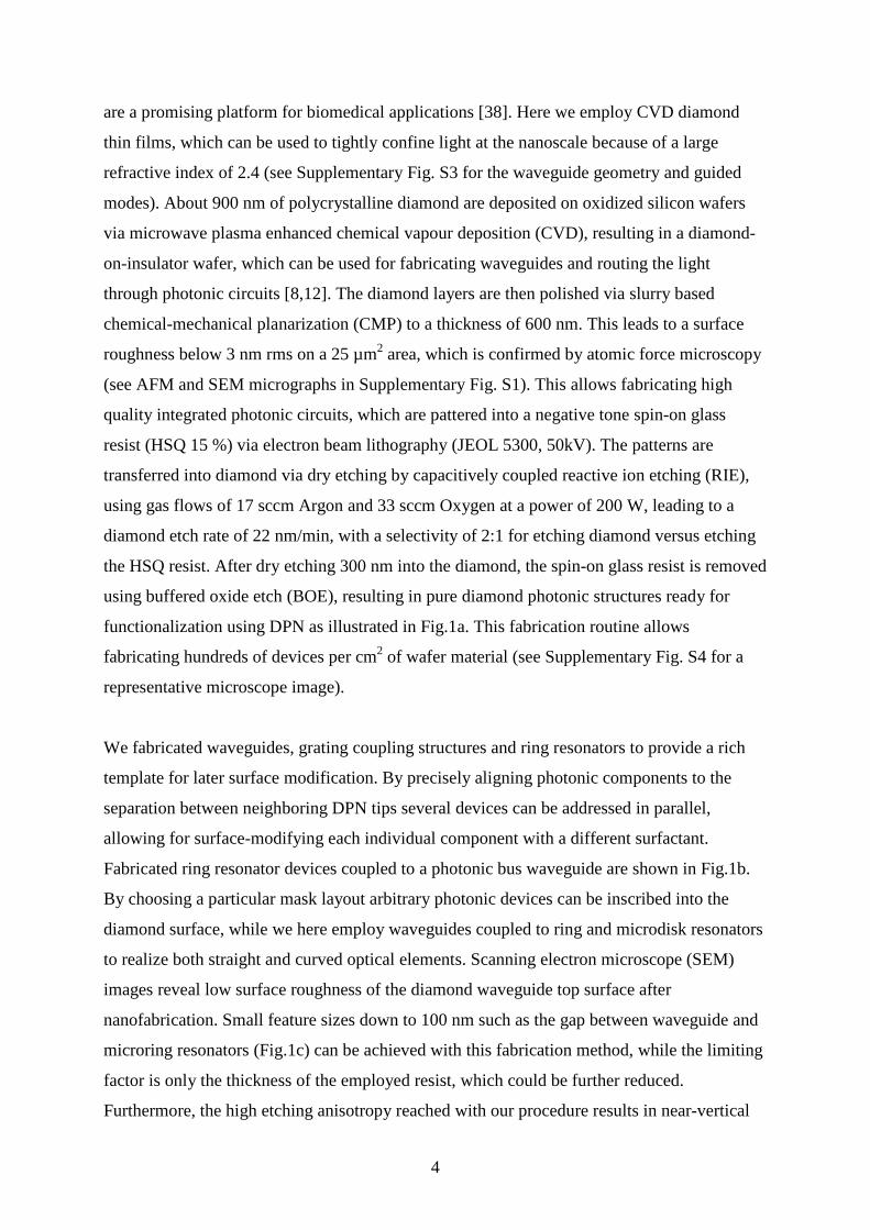
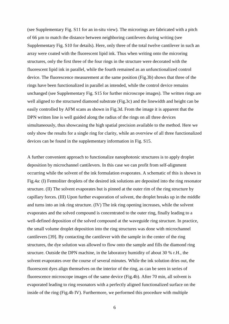
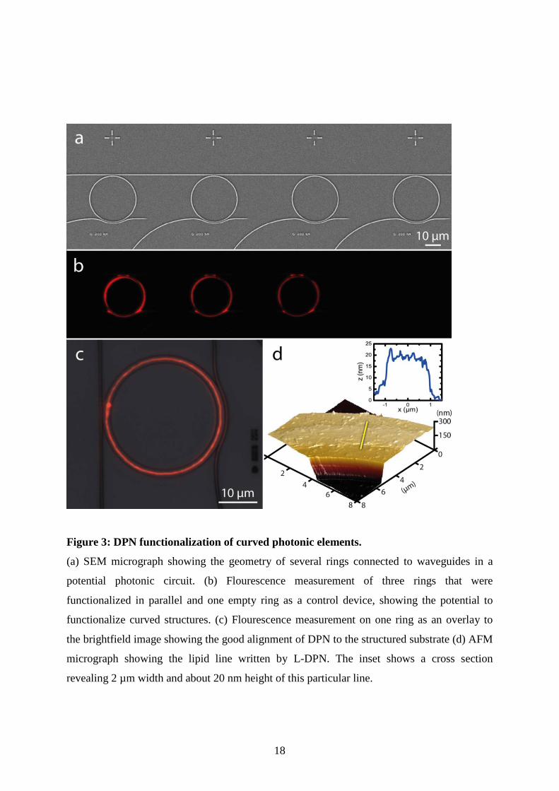
A further convenient approach to functionalize nanophotonic structures is to apply droplet
deposition by microchannel cantilevers. In this case we can profit from self-alignment
occurring while the solvent of the ink formulation evaporates. A schematic of this is shown in
Fig.4a: (I) Femtoliter droplets of the desired ink solutions are deposited into the ring resonator
structure. (II) The solvent evaporates but is pinned at the outer rim of the ring structure by
capillary forces. (III) Upon further evaporation of solvent, the droplet breaks up in the middle
and turns into an ink ring structure. (IV) The ink ring opening increases, while the solvent
evaporates and the solved compound is concentrated to the outer ring, finally leading to a
well-defined deposition of the solved compound at the waveguide ring structure. In practice,
the small volume droplet deposition into the ring structures was done with microchannel
cantilevers [39]. By contacting the cantilever with the sample in the center of the ring
structures, the dye solution was allowed to flow onto the sample and fills the diamond ring
structure. Outside the DPN machine, in the laboratory humidity of about 30 % r.H., the
solvent evaporates over the course of several minutes. While the ink solution dries out, the
fluorescent dyes align themselves on the interior of the ring, as can be seen in series of
fluorescence microscope images of the same device (Fig.4b). After 70 min, all solvent is
evaporated leading to ring resonators with a perfectly aligned functionalized surface on the
inside of the ring (Fig.4b IV). Furthermore, we performed this procedure with multiple

7
different dyes in parallel: Three different fluorescent dyes are used in the experiment emitting
in the red, green and blue wavelength range (see Supporting Information and Fig. S9 for the
chemical structure). The three different ink solutions were deposited inside three adjacent
rings by microchannel cantilevers as described above, while one empty ring acts as an
unfunctionalized control. Fig.4c shows an overlay of a grey colour brightfield image of the
diamond photonic circuit with three flourescence microscopy images in the different color
channels. The resulting image shows that an accurate site specific functionalization of devices
in close proximity is achieved by this combined top-down and self-assembly process.
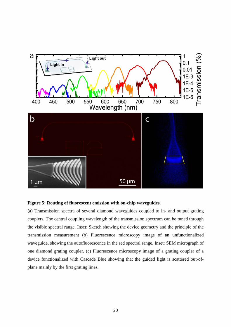
In order to evaluate the performance of the photonic circuits for on-chip routing of
fluorescence and its out-of-plane access for detection, we fabricated devices consisting of a
waveguide of 1 µm width connected to a pair of in- and output focusing grating couplers [40],
as shown in the inset of Fig.5a. We measured their transmission spectra using a broadband
supercontinuum white light source covering ultraviolet up to near-infrared wavelengths and a
spectrometer. By varying grating periods and fill factor of the Bragg grating, the coupling
efficiency can be increased and the central coupling wavelength can be adjusted to the
emission spectrum of a fluorescent dye. By changing the grating period from 250 nm to 380
nm at fill factors from 30-50% we can cover the full spectral range of visible light from 400
nm to 800 nm, as shown in Fig.5a. Each transmission peak corresponds to an individual
measurement of a different device. The transmission decreases for smaller wavelengths,
which can be mainly attributed to the increasing propagation losses at small wavelengths [41].
Due to the efficient polishing of our diamond thin films, the propagation losses are reduced
compared to previous work (see Supplementary Fig. S6 and S7), showing the potential of the
material used in this work. By employing these focusing grating couplers in photonic circuits
light, coupled into the waveguides either from external sources or on-chip fluorescent emitters,
can be guided to and extracted at arbitrary locations on chip.
In the second step the waveguide connecting the grating couplers is functionalized using DPN.
After functionalizing the circuits, the emitted fluorescence is coupled into the waveguide,
routed to a grating coupler and then scattered out-of-plane which allows it to be detected
using a wide-field fluorescent microscope equipped with a sensitive camera. To show this, we
functionalized the devices with a DPN line perpendicular across the waveguide and evaluated
the amount of fluorescence at the grating couplers. Because the DPN written line is placed in
the near-field of the photonic waveguide, light emitted by the die molecules will couple
8
preferentially into the underlying diamond waveguide because of the higher refractive index
compared to the surrounding air. Once emitted light is coupled into the diamond, it will be
propagating along the waveguide towards the grating coupler and then emitted out of plane
through Bragg scattering. To distinguish between guided light and residual false counts on the
camera, the fluorescent background due to stray light, detector dark counts and residual
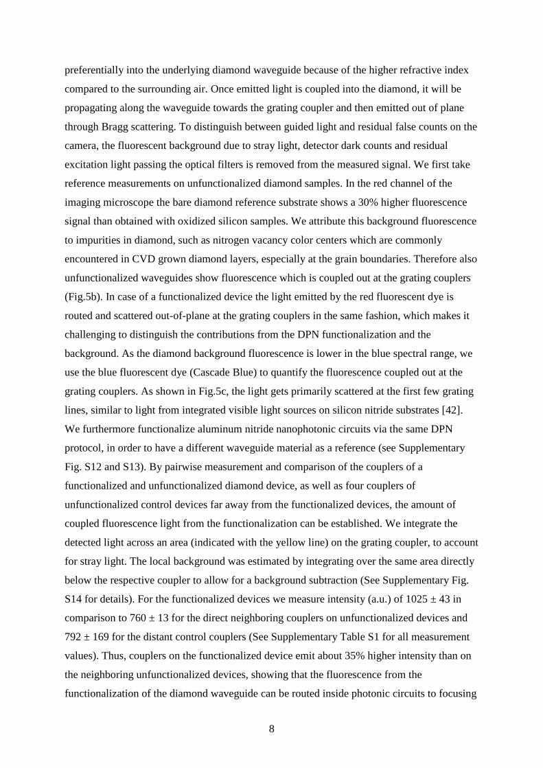
excitation light passing the optical filters is removed from the measured signal. We first take
reference measurements on unfunctionalized diamond samples. In the red channel of the
imaging microscope the bare diamond reference substrate shows a 30% higher fluorescence
signal than obtained with oxidized silicon samples. We attribute this background fluorescence
to impurities in diamond, such as nitrogen vacancy color centers which are commonly
encountered in CVD grown diamond layers, especially at the grain boundaries. Therefore also
unfunctionalized waveguides show fluorescence which is coupled out at the grating couplers
(Fig.5b). In case of a functionalized device the light emitted by the red fluorescent dye is
routed and scattered out-of-plane at the grating couplers in the same fashion, which makes it
challenging to distinguish the contributions from the DPN functionalization and the
background. As the diamond background fluorescence is lower in the blue spectral range, we
use the blue fluorescent dye (Cascade Blue) to quantify the fluorescence coupled out at the
grating couplers. As shown in Fig.5c, the light gets primarily scattered at the first few grating
lines, similar to light from integrated visible light sources on silicon nitride substrates [42].
We furthermore functionalize aluminum nitride nanophotonic circuits via the same DPN
protocol, in order to have a different waveguide material as a reference (see Supplementary
Fig. S12 and S13). By pairwise measurement and comparison of the couplers of a
functionalized and unfunctionalized diamond device, as well as four couplers of
unfunctionalized control devices far away from the functionalized devices, the amount of
coupled fluorescence light from the functionalization can be established. We integrate the
detected light across an area (indicated with the yellow line) on the grating coupler, to account
for stray light. The local background was estimated by integrating over the same area directly
below the respective coupler to allow for a background subtraction (See Supplementary Fig.
S14 for details). For the functionalized devices we measure intensity (a.u.) of 1025 ± 43 in
comparison to 760 ± 13 for the direct neighboring couplers on unfunctionalized devices and
792 ± 169 for the distant control couplers (See Supplementary Table S1 for all measurement
values). Thus, couplers on the functionalized device emit about 35% higher intensity than on
the neighboring unfunctionalized devices, showing that the fluorescence from the
functionalization of the diamond waveguide can be routed inside photonic circuits to focusing
9
grating couplers. This allows detecting the fluorescence signal at a place of choice on the chip,
enabling out-of-plane access for excitation and detection.
The nanofunctionalization approach presented here allows for labeling arbitrary photonic
components with high precision and accuracy. Employing DPN writing in conjecture with
planar nanofabrication techniques thus enables site-specific coloring of multiple nanophotonic
systems in parallel, without immersing the entire wafer in a liquid or labelactive environment.
This is of particular importance when fragile devices need to be surface modified or in the
case of several functionalization steps required in succession. Using DPN, multiple writing
sessions can be performed with varying dies, thus allowing for multiplexed functionalization
and also the creation of complex patterns on a sample surface. By combining nanophotonic
circuits with precision fluorescent labelling optical signal processing of light emitted from
precisely defined locations on chip can thus be achieved. The use of diamond as target
material in this context paves the road towards biocompatible optical devices that can be
operated in a wide wavelength range and also in a wide range of robust biomedical and
environmental high throughput sensing applications. In the nanophotonic circuits we show
that waveguiding from near-infrared wavelengths down to the ultraviolet wavelength regime
can be achieved on chip, thus covering important spectral regions for fluorescent imaging.
Exploiting the full flexibility of scalable nanofabrication routines provided by both ebeam
lithography and DPN, our approach allows for realizing a multitude of functional devices in a
controllable fashion, such as extending the functionalization to different chemistries for
sensing purposes or realizing nanoscale light emitters on chip, thus paving the way towards
high-throughput chipscale solutions for biophotonic sensing.

10
Experimental Section
Plasma enhanced CVD deposition of diamond:
To initiate the diamond growth, a diamond nano-particle seed layer is deposited onto the
substrate by ultrasonification for 30 minutes in a water based suspension of ultra-dispersed
(0.1 wt %) nano-diamond particles of typically 5-10 nm size [43]. The samples are then rinsed
with deionized water and methanol. After dry blowing, the wafer is transferred into an
ellipsoidal microwave plasma reactor [44]. The diamond films are then grown using 1 % CH4
in 99 % H2, at a pressure of 55 mbar, a microwave power of 3.5 kW and a temperature of
850 °C. In order to avoid angular non-uniformities arising from the gas flow the substrate is
continuously rotated. Growth rates are in the range of 1-2 µm/h. After growth, the samples are
cleaned in concentrated HNO3:H2SO4 to remove surface contaminants.
Chemical-mechanical planarization (CMP): For slurry based CMP of diamond thin films [45]
a contact force of 120 N is applied and about 80 ml/min polishing liquid is used at a rotational
frequency of 90 1/min. The as-deposited diamond film of 900 nm thickness shows a
roughness of 35nm rms. After removing material and reducing the film thickness by CMP to
600 nm, the surface roughness below 3 nm rms on a 25 µm2 area, which is confirmed by
atomic force microscopy.
Site-specific functionalization: The site-specific functionalization of the devices by DPN and
microchannel cantilevers was performed on a DPN5000 system (NanoInk) and a NLP2000
system (NanoInk), respectively. For DPN, cantilever arrays of M-type were used (Advanced
Creative Solutions Technology (ACST)) with a pitch of either 66 µm or 100 µm between
adjacent cantilevers were employed. Phospholipid based formulations were used as functional
inks: 1,2-dioleoyl-sn-glycero-3-phosphocholine (DOPC) was used as carrier and admixed
with 1 mol% of 1,2-dioleoyl-sn-glycero-3-phosphoethanolamine-N-(lissamine rhodamine B
sulfonyl) (ammonium salt) (Rho-PE) to render the mixture fluorescent with red emission
(both compounds from Avanti Polar Lipids). For the chemical structure of the phospholipids
see Fig. S8 in the Supporting Information. To cover the cantilever arrays with the
phospholipid mixture, Inkwells (ACST) were loaded with 1-2 µl of the lipid mixture in each
reservoir at a concentration of 20 mg/ml in chloroform. After evaporation of the chloroform in
a desiccator for 15 min, the cantilever arrays were dipped into the inkwells at a humidity of
70 % r.H. for 5 min. Excess ink on the cantilevers was removed by manually drawing line
11
patterns on a sacrificial area of the sample. After this, the cantilevers were carefully aligned
with the device structures and the desired line pattern was written. Writing took place at
controlled relative humidity ranging from 30 to 40 % r.H. and the writing speed was 5 µm/s to
10 µm/s depending on desired line thickness.
For spotting by microchannel cantilevers, cantilevers (SPT-S-C10S, Bioforce Nanosciences)
were plasma cleaned by 10 sccm oxygen plasma at 100 mTorr, 30 W for 2 min, then attached
to the DPN system’s tip holder by double sided sticky tape and filled with 1 µl of the desired
ink solution. Azide modifications of TAMRA, Alexa 488, and Cascade Blue (all from Life
Technologies) were dissolved in DI water at concentrations of 1 mg/ml and admixed with
glycerol (87% in DI water) in 7 parts dye solution to 3 parts glycerol to prevent premature
drying of the ink in the microchannel cantilevers reservoir. Spotting was performed at 60 %
r.H. and with an additional inclination of the DPN system’s sample stage by 8° to prevent
contact of the reservoir with the substrate.
Fluorescence microscopy: For quantifying the fluorescence a wide-field fluorescent
microscope (Eclipse 80i upright fluorescence microscope) is used, equipped with a sensitive
camera (CoolSNAP HQ 2 camera (Photometrics)). The broadband excitation light source
(Intensilight illumination (Nikon)) is combined with standard sets of filters (TexasRed (red),
FITC (green), DAPI (blue), Nikon) to separate excitation and emission spectra, depending on
the used dye molecule.
Atomic force microscopy: Atomic force microscopy was performed on a Dimension Icon
AFM (Bruker) in standard tapping mode in air. Cantilevers used where of type NSC15
(MikroMasch) with a nominal force constant of 46 N/m and a resonance frequency of 325
kHz.
Optical transmission measurements:
The transmission through on-chip nanophotonic circuits is measured using a custom
measurement setup for precision alignment and multi-port optical access (see Supplementary
Fig. S5 for a schematic of the setup). Light from an unpolarized supercontinuum source
(Leukos SM-30-UV) is sent through the on-chip devices via focusing grating couplers and
detected on a second coupling port with a fiber coupled spectrometer (Ocean Optics JAZ).
Both instruments are connected to an optical fiber-array. The fiber-array consists of a matrix
of optical fibers, with a fixed spacing of 250 µm between individual fibers. The distance
12
between the focusing grating couplers of the fabricated devices is therefore 250 µm as well.
The chip is mounted on an computer controlled x/y/z- piezo-stage, which allows to easily
align the fiber-to-chip coupling for many devices in a short time with precision better than
30nm.
Acknowledgements
We acknowledge support by DFG grant PE 1832/1-1 and PE 1832/2-1. P. R. acknowledges
support by the Karlsruhe School of Optics and Photonics (KSOP) and the Deutsche Telekom
Stiftung. We also appreciate support by the Deutsche Forschungsgemeinschaft (DFG) and the
State of Baden-Württemberg through the DFG-Center for Functional Nanostructures (CFN)
within subproject A6.4. This work was partly carried out with the support of the Karlsruhe
Nano Micro Facility (KNMF, http://www.knmf.kit.edu), a Helmholtz Research Infrastructure
at Karlsruhe Institute of Technology (KIT, http://www.kit.edu). The authors further wish to
thank Silvia Diewald and Stefan Kühn for assistance in device fabrication.
13
References
[1] A. Faraon, C. Santori, Z. Huang, V. Acosta, & R. Beausoleil, Phys. Rev. Lett., 2012, 109,
033604
[2] B. J. M. Hausmann, B. Shields, Q. Quan, P. Maletinsky, M. McCutcheon, J. T. Choy, T.
M. Babinec, A. Kubanek, A. Yacoby, M. D. Lukin, M. Loncar, Nano letters 2012, 12,
1578.
[3] J. Riedrich-Moeller, L. Kipfstuhl, C. Hepp, E. Neu, C. Pauly, F. Mücklich, A. Baur, M.
Wandt, S. Wolff, M. Fischer, S. Gsell, M. Schreck, C. Becher, Nature Nanotechnology
2012, 7, 69.
[4] B. J. M. Hausmann, B. J. Shields, Q. Quan, Y. Chu, N. P. de Leon, R. Evans, M. J. Burek,
A. S. Zibrov, M. Markham, D. J. Twitchen, H. Park, M. D. Lukin, M. Lonc R, Nano
letters 2013, 13, 5791.
[5] N. Vermeulen, J. E. Sipe, L. G. Helt, H. Thienpont, Laser & Photonics Reviews 2012, 6,
793.
[6] B. J. M. Hausmann, I. Bulu, V. Venkataraman, P. Deotare, M. Lončar, Nature Photonics
2014, 8, 369.
[7] P. Maletinsky, S. Hong, M. S. Grinolds, B. Hausmann, M. D. Lukin, R. L. Walsworth, M.
Loncar, A. Yacoby, Nature nanotechnology 2012, 7, 320.
[8] P. Rath, S. Khasminskaya, C. Nebel, C. Wild, W. H. P. Pernice, Nature Communications
2013, 4, 1690.
[9] B. Zhang, Y. Li, C.-Y. Fang, C.-C. Chang, C.-S. Chen, Y.-Y. Chen, H.-C. Chang, Small
2009, 5, 2716.
[10] N. Mohan, C.-S. Chen, H.-H. Hsieh, Y.-C. Wu, H.-C. Chang, Nano letters 2010, 10,
3692.
[11] T. Meinhardt, D. Lang, H. Dill, A. Krueger, Advanced Functional Materials 2011, 21,
494.
[12] P. Rath, N. Gruhler, S. Khasminskaya, C. Nebel, C. Wild, W. H. P. Pernice, Optics
Express 2013, 21, 11031.
[13] Y. Chen, W. S. Fegadolli, W. M. Jones, A. Scherer, M. Li, ACS nano 2013, 8, 522–527.
[14] M. Iqbal, M. A. Gleeson, B. Spaugh, F. Tybor, W. G. Gunn, M. Hochberg, T. Baehr-
Jones, R. C. Bailey, L. C. Gunn, IEEE Journal of Selected Topics in Quantum Electronics
2010, 16, 654.
[15] J. T. Robinson, L. Chen, M. Lipson, Optics Express 2008, 16, 4296.
14
[16] C. Subramani, Y. Ofir, D. Patra, B. J. Jordan, I. W. Moran, M.-H. Park, K. R. Carter, V.
M. Rotello, Adv. Funct. Mater. 2009, 19, 2937.
[17] C. Subramani, N. Cengiz, K. Saha, T. N. Gevrek, X. Yu, Y. Jeong, A. Bajaj, A. Sanyal,
V. M. Rotello, Adv. Mater. 2011, 23, 3165.
[18] Y. Ofir, I. W. Moran, C. Subramani, K. R. Carter, V. M. Rotello, Adv. Mater. 2010, 22,
3608.
[19] R. D Piner, J. Zhu, F. Xu, S. Hong, C. A. Mirkin, Science 1999, 283, 661.
[20] C.-C. Wu, D. N. Reinhoudt, C. Otto, V. Subramaniam, A. H. Velders, Small 2011, 7,
989.
[21] H. Zhang, S.-W. Chung, C. A. Mirkin, Nano Letters 2003, 3, 43.
[22] D. J. Pena, M. P. Raphael, J. M. Byers, Langmuir 2003, 19, 9028.
[23] A. Noy, A. E. Miller, J. E. Klare, B. L. Weeks, B. W. Woods, J. J. DeYoreo, Nano
Letters 2002, 2, 109.
[24] J.-H. Lim, C. A. Mirkin, Advanced Materials 2002, 14, 1474.
[25] L. M. Demers, D. S. Ginger, S.-J. Park, Z. Li, S.-W. Chung, C. A. Mirkin, Science 2002,
296, 1836.
[26] G. Agarwal, R. R. Naik, M. O. Stone, Journal of the American Chemical Society 2003,
125, 7408.
[27] M. Ben Ali, T. Ondarçuhu, M. Brust, C. Joachim, Langmuir 2002, 18, 872.
[28] J. C. Garno, Y. Yang, N. A. Amro, S. Cruchon-Dupeyrat, S. Chen, G.-Y. Liu, Nano
Letters 2003, 3, 389.
[29] S. Lenhert, P. Sun, Y. Wang, H. Fuchs, C. A. Mirkin, Small 2007, 3, 71.
[30] M. Hirtz, R. Corso, S. Sekula-Neuner, H. Fuchs, Langmuir 2011, 27, 11605.
[31] S. Sekula-Neuner, J. Maier, E. Oppong, A. C. B. Cato, M. Hirtz, H. Fuchs, Small 2012,
8, 585.
[32] E. Oppong, P. N. Hedde, S. Sekula-Neuner, L. Yang, F. Brinkmann, R. M. Dörlich, M.
Hirtz, H. Fuchs, G. U. Nienhaus, A. C. B. Cato, Small 2014, 10, 1991.
[33] M. Hirtz, A. Oikonomou, T. Georgiou, H. Fuchs, A. Vijayaraghavan, Nature
communications 2013, 4, 2591.
[34] U. Bog, T. Laue, T. Grossmann, T. Beck, T. Wienhold, B. Richter, M. Hirtz, H. Fuchs,
H. Kalt, T. Mappes, Lab on a chip 2013, 13, 2701.
[35] M. Hirtz, M. Lyon, W. Feng, A. E. Holmes, H. Fuchs, P. A. Levkin, Beilstein journal of
nanotechnology 2013, 4, 377.
15
[36] M. Hirtz, A. M. Greiner, T. Landmann, M. Bastmeyer, H. Fuchs, Advanced Materials
Interfaces 2014, DOI 10.1002/admi.201300129.
[37] A. Krueger, Chemistry 2008, 14, 1382.
[38] V. N. Mochalin, O. Shenderova, D. Ho, Y. Gogotsi, Nature nanotechnology 2012, 7, 11.
[39] J. Xu, M. Lynch, J. L. Huff, C. Mosher, S. Vengasandra, G. Ding, E. Henderson,
Biomedical microdevices 2004, 6, 117.
[40] D. Taillaert, W. Bogaerts, P. Bienstman, T. F. Krauss, P. Van Daele, I. Moerman, S.
Verstuyft, K. De Mesel, R. Baets, IEEE Journal of Quantum Electronics 2002, 38, 949.
[41] M. Stegmaier, J. Ebert, J. M. Meckbach, K. Ilin, M. Siegel, W. H. P. Pernice, Applied
Physics Letters 2014, 104, 091108.
[42] S. Khasminskaya, F. Pyatkov, B. S. Flavel, W. H. Pernice, R. Krupke, Advanced
Materials 2014, 26, 3465–3472.
[43] O. A. Williams, O. Douhéret, M. Daenen, K. Haenen, E. Ōsawa, M. Takahashi,
Chemical Physics Letters 2007, 445, 255.
[44] M. Fuener, C. Wild, P. Koidl, Applied Physics Letters 1998, 72, 1149.
[45] E. L. H. Thomas, G. W. Nelson, S. Mandal, J. S. Foord, O. A. Williams, Carbon 2014,
68, 473.

16
Figure 1: Surface functionalization of diamond nanophotonic components.
(a) Illustration of the surface functionalization of diamond photonic components by dip-pen
nanolithography. Multiple devices get simultaneously functionalized employing AFM-
cantilever arrays. (b) SEM micrograph of fabricated diamond photonic waveguides coupled to
a ring resonator. (c) SEM image showing the smooth top surface due to chemical-mechanical
planarization and the straight sidewalls due to reactive ion etching.
17
Figure 2: Parallel DPN functionalization and alignment.
(a) Microscope picture showing the parallel alignment of the AFM cantilevers for DPN to the
waveguides. (b) False colour image of the measured fluorescence. (c) Fluorescence image as
an overlay of a brightfield microscope picture showing the alignment result of the DPN
process. (d) AFM micrograph of the diamond waveguide. The insets show an AFM
micrograph and the height profile of the lipid ink line on the waveguide.
18
Figure 3: DPN functionalization of curved photonic elements.
(a) SEM micrograph showing the geometry of several rings connected to waveguides in a
potential photonic circuit. (b) Flourescence measurement of three rings that were
functionalized in parallel and one empty ring as a control device, showing the potential to
functionalize curved structures. (c) Flourescence measurement on one ring as an overlay to
the brightfield image showing the good alignment of DPN to the structured substrate (d) AFM
micrograph showing the lipid line written by L-DPN. The inset shows a cross section
revealing 2 µm width and about 20 nm height of this particular line.
19
Figure 4: Self-aligned functionalization of diamond ring resonators.
(a) Schematic of droplet deposition into the ring structures (b) Series of false colour
fluorescence images of the ring functionalized with Cascade Blue ink showing the drying
process which leads to a self-alignment on the inside of the ring (c) Overlay of the three
fluorescence channels on a brightfield microscope micrograph showing the result of three
rings functionalized at the same time with three different fluorescent inks (from left to right:
TAMRA, Alexa488, Cascade Blue). The right ring is a control, showing no fluorescence.
20
Figure 5: Routing of fluorescent emission with on-chip waveguides.
(a) Transmission spectra of several diamond waveguides coupled to in- and output grating
couplers. The central coupling wavelength of the transmission spectrum can be tuned through
the visible spectral range. Inset: Sketch showing the device geometry and the principle of the
transmission measurement (b) Fluorescence microscopy image of an unfunctionalized
waveguide, showing the autofluorescence in the red spectral range. Inset: SEM micrograph of
one diamond grating coupler. (c) Fluorescence microscopy image of a grating coupler of a
device functionalized with Cascade Blue showing that the guided light is scattered out-of-
plane mainly by the first grating lines.
Related Documents