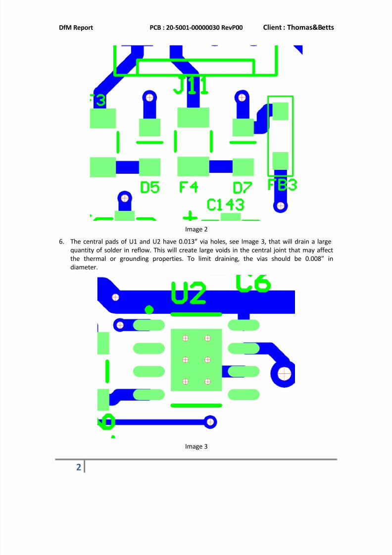
DfM Report PCB : 20-5001-00000030 RevP00 Client : Thomas&B etts 1 1. In order to properly orient the TH connectors with respect to the wave and to avoid warpage of the board during wave soldering, the PCB must be oriented in the wave soldering machine with J5 or J12 in the front. This makes that most SMT components on the bottom side need to be rotated 90 degrees, just like C12 in order to be properly oriented, to avoid skips. 2. Still in order to prevent skip solder, the SMT component pads need to be extended 0.010” each towards the exterior, in order to allow for more wetting surface. 3. To avoid solder bridges on TH components, the annular rings of the TH parts have to be adjusted so that the Cu to Cu spacing is 0.035”, in the case of RoHS products. J5, J10 -13, J16 and all the JPs, at minimum, need the annular rings to be decreased. 4. Many SMT pads need thermal relieving connections to Cu planes, in order to avoid excessive heat during soldering and even higher heat, should rework be required. See red boxes in Image 1 for examples of the mentioned situation. For calculus of thermal reliefs see IPC- 2222 paragraph 9.1.2. They are defined in IPC-2221, paragraph 9.1.3. Image 1 5. Several polarized components, e.g. D5 and D7 have the polarity mark under the body of the component, once it is installed, therefore not visible after assembly, see Image 2. Polarity marks outside of the body is advisable.

Welcome message from author
This document is posted to help you gain knowledge. Please leave a comment to let me know what you think about it! Share it to your friends and learn new things together.
Transcript
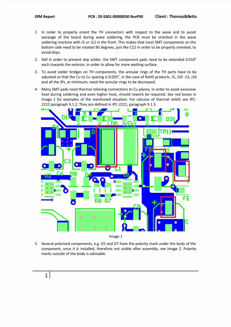
8/2/2019 DfM 20-5001-00000030
http://slidepdf.com/reader/full/dfm-20-5001-00000030 1/3
DfM Report PCB : 20-5001-00000030 RevP00 Client : Thomas&Betts
1
1. In order to properly orient the TH connectors with respect to the wave and to avoid
warpage of the board during wave soldering, the PCB must be oriented in the wave
soldering machine with J5 or J12 in the front. This makes that most SMT components on the
bottom side need to be rotated 90 degrees, just like C12 in order to be properly oriented, to
avoid skips.
2. Still in order to prevent skip solder, the SMT component pads need to be extended 0.010”
each towards the exterior, in order to allow for more wetting surface.
3. To avoid solder bridges on TH components, the annular rings of the TH parts have to be
adjusted so that the Cu to Cu spacing is 0.035”, in the case of RoHS products. J5, J10 -13, J16
and all the JPs, at minimum, need the annular rings to be decreased.
4. Many SMT pads need thermal relieving connections to Cu planes, in order to avoid excessive
heat during soldering and even higher heat, should rework be required. See red boxes in
Image 1 for examples of the mentioned situation. For calculus of thermal reliefs see IPC-
2222 paragraph 9.1.2. They are defined in IPC-2221, paragraph 9.1.3.
Image 1
5. Several polarized components, e.g. D5 and D7 have the polarity mark under the body of the
component, once it is installed, therefore not visible after assembly, see Image 2. Polarity
marks outside of the body is advisable.
8/2/2019 DfM 20-5001-00000030
http://slidepdf.com/reader/full/dfm-20-5001-00000030 2/3
DfM Report PCB : 20-5001-00000030 RevP00 Client : Thomas&Betts
2
Image 2
6. The central pads of U1 and U2 have 0.013” via holes, see Image 3, that will drain a large
quantity of solder in reflow. This will create large voids in the central joint that may affect
the thermal or grounding properties. To limit draining, the vias should be 0.008” in
diameter.
Image 3
8/2/2019 DfM 20-5001-00000030
http://slidepdf.com/reader/full/dfm-20-5001-00000030 3/3
DfM Report PCB : 20-5001-00000030 RevP00 Client : Thomas&Betts
3
7. Fab note 5 asks for 0.005” tolerance for the board thickness. As this is hard and costly to
obtain, I recommend a 10% tolerance request.
Disclaimer:
This report is the result of a visual inspection of mainly the top and bottom layers. This
inspection is not in any way exhaustive and points certain design issues that, if resolved, would
reduce the assembly costs or, in certain cases, improve the long term reliability of the product.
The component footprints are not all checked, but only a few of them, known problematic, are
verified according to the experience of the consultant or the IPC-7351B libraries.
The PCB manufacturing issues are, most likely, not all identified and a thorough computerized
analysis by a PCB manufacturer is recommended.
The interpretation and implementation of this document is at customer’s free will and Ioan
Tempea, ing., is not to be held liable to any expenses related to the said implementation.
Related Documents