HAL Id: tel-01127064 https://tel.archives-ouvertes.fr/tel-01127064 Submitted on 6 Mar 2015 HAL is a multi-disciplinary open access archive for the deposit and dissemination of sci- entific research documents, whether they are pub- lished or not. The documents may come from teaching and research institutions in France or abroad, or from public or private research centers. L’archive ouverte pluridisciplinaire HAL, est destinée au dépôt et à la diffusion de documents scientifiques de niveau recherche, publiés ou non, émanant des établissements d’enseignement et de recherche français ou étrangers, des laboratoires publics ou privés. Development of ultrafast saturable absorber mirrors for applications to ultrahigh speed optical signal processing and to ultrashort laser pulse generation at 1.55 µm Li Fang To cite this version: Li Fang. Development of ultrafast saturable absorber mirrors for applications to ultrahigh speed optical signal processing and to ultrashort laser pulse generation at 1.55 µm. Optics [physics.optics]. Université Paris Sud - Paris XI, 2014. English. NNT: 2014PA112313. tel-01127064

Welcome message from author
This document is posted to help you gain knowledge. Please leave a comment to let me know what you think about it! Share it to your friends and learn new things together.
Transcript
HAL Id: tel-01127064https://tel.archives-ouvertes.fr/tel-01127064
Submitted on 6 Mar 2015
HAL is a multi-disciplinary open accessarchive for the deposit and dissemination of sci-entific research documents, whether they are pub-lished or not. The documents may come fromteaching and research institutions in France orabroad, or from public or private research centers.
L’archive ouverte pluridisciplinaire HAL, estdestinée au dépôt et à la diffusion de documentsscientifiques de niveau recherche, publiés ou non,émanant des établissements d’enseignement et derecherche français ou étrangers, des laboratoirespublics ou privés.
Development of ultrafast saturable absorber mirrors forapplications to ultrahigh speed optical signal processing
and to ultrashort laser pulse generation at 1.55 µmLi Fang
To cite this version:Li Fang. Development of ultrafast saturable absorber mirrors for applications to ultrahigh speedoptical signal processing and to ultrashort laser pulse generation at 1.55 µm. Optics [physics.optics].Université Paris Sud - Paris XI, 2014. English. �NNT : 2014PA112313�. �tel-01127064�
UNIVERSITÉ PARIS-SUD
ÉCOLE DOCTORALE 288 : ONDES ET MATIÈRE
Laboratoire : Laboratoire de Photonique et de Nanostructures-Centre National de la
Recherche Scientifique (LPN-CNRS)
THÈSE DE DOCTORAT
PHYSIQUE
par
Li FANG
Development of ultrafast saturable absorber mirrors for
applications to ultrahigh speed optical signal processing and
to ultrashort laser pulse generation at 1.55 µm
Date de soutenance : 12/11/2014
Composition du jury: Directeur de thèse : M. Jean-Louis OUDAR Directeur de recherche émérite (LPN-CNRS)
Rapporteurs : M. Sébastien FEVRIER Maîtres de conférence (XLIM, Université de Limoges)
Mme Juliette MANGENEY Chargée de recherche (LPA, Ecole Normale Supérieure)
Examinateurs : M. Patrick GEORGES Directeur de recherche (LCF, institut d’Optique)
M. Ammar HIDEUR Maîtres de conférence (CORIA, Université de Rouen)
M. Jean-Michel LOURTIOZ Directeur de recherche émérite (IEF, Université Paris-Sud XI)

Résumé
Dans cette thèse, nous avons développé et étudié des miroirs absorbants saturables
ultra-rapides, pour des applications au traitement de signaux optiques à très haut débit
et la génération d’impulsions laser ultra-courtes à 1.55 µm.
Dans une première partie, nous avons développé un miroir absorbant saturable
ultra-rapide basé sur le semi-conducteur In0.53Ga0.47As soumis à une implantation
ionique à température élevée de 300 °C. Des ions As+ et Fe+ ont été utilisés pour
l’implantation. Nous avons étudié la durée de vie des porteurs en fonction de la dose
ionique, la température et le temps de recuit. En comparaison des échantillons
implantés As+, les temps de recouvrement des échantillons implantés Fe+ sont plus
courts. A part la durée de vie rapide, les caractéristiques de réflectivité non-linéaire,
telles que l’absorption linéaire, la profondeur de modulation, les pertes non saturables
ont été étudiées dans différentes conditions de recuit. Après un recuit à 600 °C pendant
15 s, un échantillon présentant une grande amplitude de modulation de 53.9 % et une
durée de vie de porteurs de 2 ps a été obtenu.
Dans une seconde partie, la gravure par faisceau d’ions focalisés (FIB) a été utilisée
pour fabriquer une structure en biseau ultrafin sur de l’InP cristallin, pour réaliser un
dispositif photonique multi-longueur d’onde à cavité verticale. Les procédures de
balayage FIB et les paramètres appropriés ont été utilisés pour contrôler le re-dépôt du
matériau cible et pour minimiser la rugosité de surface de la zone gravée. Le rendement
de pulvérisation de la cible en InP cristallin a été déterminé en étudiant la relation entre
la profondeur de gravure et la dose ionique. En appliquant les conditions de rendement
optimales, nous avons obtenu une structure en biseau ultrafin dont la profondeur de
gravure est précisément ajustée de 25 nm à 55 nm, avec une pente horizontale de
1:13000. La caractérisation optique de ce dispositif en biseau a confirmé le
comportement multi-longueur d’onde de notre dispositif et montré que les pertes
optiques induites par le procédé de gravure FIB sont négligeables.
Dans une troisième partie, nous avons démontré que la réponse optique non-linéaire
du graphène est augmentée de manière résonnante quand une monocouche de graphène

est incluse dans une microcavité verticale comportant un miroir supérieur. Une couche
mince de Si3N4 a été déposée selon un procédé de dépôt par PECVD spécialement
développé pour agir comme couche de protection préalable avant le dépôt du miroir
supérieur proprement dit, permettant ainsi de préserver les propriétés optiques du
graphène. En incluant une monocouche de graphène dans une microcavité appropriée,
une profondeur de modulation de 14.9 % a été obtenue pour une fluence incidente de
108 µJ / cm². Cette profondeur de modulation est beaucoup plus élevée que la valeur
maximale de 2 % obtenue dans les travaux antérieurs. De plus un temps de
recouvrement aussi bref que 1 ps a été obtenu.
Mots-clés: miroir absorbant saturable; InGaAs; implantation ionique; gravure par
faisceau d’ions focalisés; graphène
Abstract
In this thesis, we focus on the development of ultrafast saturable absorber mirrors for
applications to ultra-high speed optical signal processing and ultrashort laser pulse
generation at 1.55 μm.
In the first part, we have developed ultrafast In0.53Ga0.47As-based semiconductor
saturable absorber mirrors by heavy-ion-implantation at elevated temperature of 300
ºC. As+ and Fe+ has been employed as the implants. The carrier recovery time of the
ion-implanted SAMs as a function of the ion dose, annealing temperature, and ion
species, has been investigated. The comparison between As+- and Fe+-implanted
samples shows that Fe+-implanted sample has faster carrier lifetime. Apart from the fast
carrier lifetime, the characteristics of the nonlinear reflectivity for the Fe+-implanted
sample have also been investigated under different annealing temperature. Under the
optimal annealing conditions, an ultrafast Fe+-implanted SAM has been achieved, with
only a 3% degradation in modulation depth compared to the unimplanted sample.
In the second part, focused ion beam milling has been applied to fabricate an
ultra-thin taper structure on crystalline indium phosphide to realize a multi-wavelength
vertical cavity photonic device. The appropriate FIB scanning procedures and
operating parameters were used to control the target material re-deposition and to
minimize the surface roughness of the milled area. The sputtering yield of crystalline
indium phosphide target was determined by investigating the relationship between
milling depth and ion dose. By applying the optimal experimentally obtained yield and
related dose range, we have fabricated an ultra-thin taper structure whose etch depths
are precisely and progressively tapered from 25 nm to 55 nm, with a horizontal slope of
about 1:13000. The optical characterization of this tapered device confirms the
expected multi-wavelength behavior of our device and shows that the optical losses
induced by the FIB milling process are negligible.
In the third part, we demonstrate that the nonlinear optical response of graphene is
resonantly enhanced by incorporating monolayer graphene into a vertical microcavity
with a top mirror. A thin Si3N4 layer was deposited by a developed PECVD process to

act as a protective layer before subsequent top mirror deposition, which allowed
preserving the optical properties of graphene. Combining monolayer graphene with a
microcavity, a modulation depth of 14.9% was achieved at an input fluence of 108
µJ/cm2. This modulation depth is much higher than the value of about 2% in other
works. At the same time, an absorption recovery time of 1 ps is retained. This approach
can pave the way for applications in mode-locking, optical switching and pulse
shaping.
Keywords: Saturable absorber mirror; InGaAs; Ion implantation; FIB milling;
Graphene
Acknowledgements
It was nearly three years since I started my thesis in the Laboratoire de Photonique
et de Nanostructures (LPN-CNRS), in Marcoussis, France. At the end of this thesis, I
would like to thanks to all the people who made this thesis possible, for offering me
help and support. First and foremost, I would like to express my sincere gratitude
towards the director of the lab Domonique MAILLY and would like to acknowledge
the financial support from the China Scholarship Council (CSC).
I would like to express my deepest sense of gratitude to my supervisor Dr.
Jean-Louis OUDAR, for giving me the opportunity to work in France and leading me
into the field of saturable absorber mirror. Moreover, I would like to thank him for his
help and discussion in my scientific field.
I am warmly thankful to our collaborators. Without them, this work would not have
been possible! I would like to thank Dr. Jacque Gierak and Eric Bourhis, who helped
me to fabricate taper structure on my sample and gave me a lot of directions and
discussions in my publication; Dr. Ali Madouri and Antonella Cavanna for providing
me graphene samples, sharing with me their precious knowledge in graphene
research, the useful discussion, and their kind help in many practical experimental
aspects in the graphene transferring experiments; Dr. Isabelle SAGNES and Dr.
Gregoire BEAUDOIN for providing me the InP-based epitaxial samples and their
assistance during FTIR measurements; Dr. Cyril Bachelet in CSNSM, who helped me
to do ion implantation. I am also grateful to Ph.D. students Hakim AREZKI and Riadh
OTHMEN for sharing with me their experiences in graphene research, the discussion,
and their kind help.
I also benefited a lot of the experience of many colleagues in LPN. I am thankful
to my colleagues in group of PHODEV: Abderrahim Ramdane, Guy Aubin, Sophie
Bouchoule, and Kamel Merghem, for the discussion and their kind assistance during
this work. I also wish to thank: Noelle GOGNEAU for her assistance during AFM
measurements; Laurent COURAUD for metal deposition; Xavier LAFOSSE and
David CHOUTEAU for dielectric material deposition; Jean-Claude ESNAULT for

photolithography and for the preparation of some chemical solutions, and the LPN
clean room group for various technical supports. I also wish to thank Olivier ORIA,
Lorenzo BERNARDI, Medhi IDOUHAMD and Alain PEAN in IT support team;
Agnes ROUX, Joelle GUITTON, and Patrick HISOPE from the administrative
department.
Finally, I would like to thank the members of my jury: Dr. Sébastien FEVRIER and
Dr. Juliette MANGENEY, my reporters, who gave me kind comments on this thesis
and allowed me to defend; Prof. Patrick GEORGES, who is the president of jury; Prof.
Jean-Michel LOURTIOZ and Dr. Ammar HIDEUR, who reviewed my manuscript and
attended my defense.
I owe my thanks to my husband, my parents and my sister. Without their
encouragement and understanding, it would have been impossible for me to finish this
work. All their love keeps me moving forwards.
2015/01/05
Gif Sur Yvette

Table of content
Résumé ......................................................................................................................... II
Abstract ...................................................................................................................... IV
Acknowledgements ................................................................................................... VI
Table of content ...................................................................................................... VIII
List of figures ............................................................................................................ XII
List of tables................................................................................................................ iii
Chapter 1 Introduction................................................................................................ 1
1.1 Application of SAMs ..................................................................................... 3
1.1.1 All-optical signal processing ................................................................ 3
1.1.2 Mode-locked ultrashort pulse generation ............................................. 4
1.2 What is saturable absorber mirror (SAM)? ...................................................... 5
1.2.1 Saturable absorber material ................................................................. 6
1.2.2 SAM Design .......................................................................................... 7
1.2.2.1 SAM Design for all-optical signal processing ........................... 7
1.2.2.2 SAM Design for passive mode-locking ..................................... 9
1.3 Motivation ...................................................................................................... 10
1.4 Structure of this thesis .................................................................................... 12
1.5 Reference ....................................................................................................... 13
Chapter 2 Heavy-ion-implanted In0.53Ga0.47As-based saturable absorber mirror
...................................................................................................................................... 21
2.1 III-V compound semiconductor ..................................................................... 21
2.1.1 Saturable absorption properties ......................................................... 23
2.1.2 Carrier relaxation dynamics ............................................................... 23
2.1.3 Recombination mechanisms ................................................................ 25
2.1.4 The techniques to reduce the carrier lifetime in a semiconductor...... 26
2.2 Ion implantation technique ............................................................................ 29
2.2.1 Ion stopping theory ............................................................................. 29
2.2.2 Ion Range distribution ........................................................................ 31

2.2.3 Damage and annealing ....................................................................... 32
2.2.4 The Stopping and Range of Ions in Matter (SRIM) ............................ 33
2.3 Device fabrication .......................................................................................... 34
2.3.1 MOCVD growth .................................................................................. 34
2.3.2 Ion implantation and post-annealing .................................................. 34
2.3.3 Microcavity fabrication ...................................................................... 36
2.4 Device characterization .................................................................................. 37
2.4.1 Investigation of carrier relaxation dynamics of heavy-ion-implanted
samples ................................................................................................. 37
2.4.1.1 Characterization method and experimental setup .................... 37
2.4.1.2 Characterization of As+ implanted samples ............................. 40
2.4.1.3 Characterization of Fe+ implanted sample ............................... 43
2.4.2 Nonlinear reflectivity of Fe+ implanted samples ................................ 44
2.4.2.1 Characterization method and Experimental setup ................... 44
2.4.2.2 Characterization of Fe+ implanted sample ............................... 47
2.5 Conclusion of this chapter ............................................................................. 48
2.6 Reference ....................................................................................................... 49
Chapter 3 Multi-wavelength SAM for WDM signal regeneration .................... 54
3.1 Concept, design, and choice of fabrication method for a tapered SAM ........ 55
3.1.1 Concept ............................................................................................... 55
3.1.2 Design ................................................................................................. 56
3.1.3 Choice of fabrication method.............................................................. 60
3.2 Focused ion beam milling technology ........................................................... 61
3.2.1 Introduction to the FIB system of our lab ........................................... 61
3.2.2 Principle of FIB milling ...................................................................... 63
3.2.3 Sputtering theory ................................................................................. 66
3.3 Tapered SAM fabrication using FIB milling ................................................. 67
3.3.1 Experimental details ........................................................................... 68
3.3.1.1 FIB operating parameters ......................................................... 68
3.3.1.2 Characterization method .......................................................... 69
3.3.2 Investigation of the effect of Ga+ on InP crystal ................................ 70
3.3.3 Patterning of the taper structure on the InP phase layer of the SAM. 72
3.3.3.1 Sample preparation .................................................................. 73
3.3.3.2 Taper fabrication ...................................................................... 73
3.4 Optical characterization and evaluation of the tapered SAM ........................ 74
3.5 Conclusion of this chapter ............................................................................. 77
3.6 Reference ....................................................................................................... 79
Chapter 4 Graphene-based saturable absorber mirror (GSAM) ......................... 83
4.1 Electronic structure and optical properties of graphene ................................ 84
4.1.1 Electronic structure ............................................................................ 84
4.1.2 Optical properties ............................................................................... 86
4.1.2.1 Linear optical absorption ......................................................... 86
4.1.2.2 Ultrafast properties ................................................................... 86
4.1.2.3 Saturable absorption................................................................. 87
4.2 Synthesis and characterization of graphene ................................................... 88
4.2.1 Synthesis of graphene ......................................................................... 89
4.2.2 Raman Spectroscopy ........................................................................... 90
4.2.2.1 Raman spectrum of graphene................................................... 91
4.2.2.2 Connected to defects ................................................................ 93
4.2.2.3 Connected to number of layers ................................................ 93
4.3 Design of GSAM ........................................................................................... 95
4.3.1 Spacer layer ........................................................................................ 96
4.3.2 Top mirror ........................................................................................... 98
4.4 Fabrication and characterization of GSAM ................................................. 100
4.4.1 Fabrication of GSAM ........................................................................ 100
4.4.1.1 Bottom mirror and spacer layer ............................................. 100
4.4.1.2 Graphene growth and transfer ................................................ 101
4.4.1.3 Si3N4 protective layer ............................................................. 103
4.4.1.4 Top mirror .............................................................................. 105
4.4.2 Nonlinear optical characterization of GSAM ................................... 106

4.4.2.1 Carrier dynamics .................................................................... 106
4.4.2.2 Power-dependent nonlinear reflectivity ................................. 107
4.5 Conclusion of this chapter ........................................................................... 108
4.6 Reference ..................................................................................................... 109
Chapter 5 Conclusion .............................................................................................. 116
List of figures
Figure 1.1: Evolution in fiber-optic communication technology (commercial trend) ... 2 Figure 1.2: Generic structure of a R-FPSA. ................................................................... 8 Figure 1.3: Different SAM designs for passive mode-locking: (a) High-finesse
A-FPSA, (b) Thin AR-coated SAM, (c) Low-finesse A-FPSA, (d) D-SAM. .................................................................................................... 10
Figure 2.1: Bandgap energy as a function of lattice constant for different III-V semiconductor alloys at room temperature. The solid lines indicate a direct bandgap, whereas the dashed lines indicate an indirect bandgap (Si and Ge are also added to the figure). .................................................................... 22
Figure 2.2: Optical absorption in a direct band-gap semiconductor. ........................... 23 Figure 2.3: Schematic representation of the carrier dynamics in a 2-band bulk
semiconductor material after photoexcitation by an ultrashort laser pulse. Four time regimes can be distinguished. I Coherent regime: dephasing process, II Non-thermal regime: thermalization process, III Hot-carrier regime: cooling process, IV Isothermal regime: electron-hole pairs recombination. ......................................................................................... 24
Figure 2.4: Carrier recombination mechanisms in a direct band-gap semiconductor: (a) Band-to-band radiative recombination, (b) Auger recombination, (c) Trap-assisted recombination. ................................................................... 25
Figure 2.5: Schematic overview of an ion implanter. .................................................. 29 Figure 2.6: Electronic and nuclear stopping in a material. .......................................... 30 Figure 2.7: Gaussian distribution of the stopped atoms. .............................................. 32 Figure 2.8: (a) The implant damage and inactive dopant atoms left in the target
substrate, (b) The annealed damage and active dopant atoms. ................ 32 Figure 2.9: As-grown sample structure. ....................................................................... 34 Figure 2.10: TRIM simulation: (a) As atoms distribution in the InGaAs active region,
(b) Fe atoms distribution in the InGaAs active region. ............................ 35 Figure 2.11: Scheme of the different steps in the microcavity fabrication .................. 36 Figure 2.12: Reflection-mode degenerate pump-probe setup. PBS: polarized beam
splitter ...................................................................................................... 38 Figure 2.13: Transient reflection of the probe as a function of the pump-probe delay
for an ultrafast SAM. ............................................................................... 39 Figure 2.14: Normalized transient reflection as a function of the pump-probe delay for
the As+ implanted sample with the ion dose of 1.3×10¹² ions / cm2 without annealing. .................................................................................... 40
Figure 2.15: Variation of the carrier recovery times versus Arsenic ion dose after
rapid thermal annealing at 550 ºC, 600 ºC, and 650 ºC for 15 s. ............. 41
Figure 2.16: Normalized transient reflection as a function of the pump-probe delay for the As+ implanted samples with the ion dose of 1 × 10¹⁴ ions / cm2 after
annealing at 500 ºC, 550 ºC, 600 ºC, and 650 ºC for 15 s. The inset is the
carrier recovery time as a function of the annealing temperature. ........... 42 Figure 2.17: Normalized transient reflection as a function of the pump-probe delay for
the Fe+ implanted samples with the dose of 1×10¹⁴ ions / cm2 after
annealing at 500 ºC, 550 ºC, 600 ºC, 650 ºC, and 700 ºC for 15 s. The
inset is the carrier recovery time as a function of the annealing temperature. ............................................................................................. 43
Figure 2.18: Nonlinear reflectivity R of a SESAM as a function of the logarithmic scale of the incident pulse energy fluence Fp. Rlin: linear reflectivity; Rns: reflectivity with saturated absorption; ∆R: modulation depth; ∆Rns: nonsaturable losses in reflectivity; Fsat: saturation fluence. The red curves show the fit functions without TPA absorption (Fp→∞) while blue curves including TPA absorption. ....................................................................... 45
Figure 2.19: Reflection-mode power-dependent fiber system. .................................... 46 Figure 2.20: Reflectivity of the unimplanted sample and the Fe+-implanted samples
after annealing at 500 ºC, 550 ºC, 600 ºC, 650 ºC, 700 ºC for 15 s as a
function of the input energy fluence. ....................................................... 47 Figure 3.1: (a) Experimental setup for regeneration of an eight-channel WDM signal,
(b) Photograph of semiconductor SAM chip: Fiber array (top) and SAM module (bottom)....................................................................................... 55
Figure 3.2: Experimental setup for regeneration of a WDM signal with a tapered SAM. ........................................................................................................ 56
Figure 3.3: Resonant wavelengths as a function of change in the thickness of the top phase layer. .............................................................................................. 57
Figure 3.4: Schematic diagram of grating system. ...................................................... 57 Figure 3.5: Angular dispersion and linear dispersion as a function of wavelength. .... 59 Figure 3.6: Schematic drawing of a taper structure (cross section view). ................... 60 Figure 3.7: (a) Photo of the single beam architecture FIB machine developed at
LPN-CNRS (b) Schematic diagram of the FIB system, in which optics column is detailed. ................................................................................... 62
Figure 3.8: (a) Photo of our designed LMIS (b) Schematic LMIS setup, the inset is a
Photo of a Ga LMIS heated at T=900 ºC during emission test in a high
vacuum chamber. ..................................................................................... 62 Figure 3.9: Schematic representation of the FIB milling process. ............................... 64 Figure 3.10: TRIM simulation plots of 30 keV Ga+ into InP: depth distribution of Ga
ion. ........................................................................................................... 68 Figure 3.11: Schematic diagram of serpentine scanning used for FIB milling. The pixel
spacing (xps, yps) is the distance between the centers of two adjacent pixels................................................................................................................... 68
Figure 3.12: AFM system “Dimension 3100”. ............................................................ 69
Figure 3.13: Optical microscopy image (top view) of 3×4 FIB-patterned square array with the ion doses ranging from 1×10¹⁴ ions / cm2 (bottom left-mark#1) to 7.5×10¹⁶ ions / cm2 (top right-mark#12). The size for each square is 35×35 μm2. .......................................................................................................... 70
Figure 3.14: AFM characterizations on an irradiated zone of InP substrate. The dose is 5×10¹⁵ ions / cm2. (a) Surface roughness measurement of the milled area. The scan size is 20×20 μm2, RMS is 1.18 nm. (b) A typical cross section of the surface profile, as obtained from the AFM scan. ............................... 71
Figure 3.15: Average milling depths as a function of incident ion dose from 1×10¹⁴ to 7.5×10¹⁶ ions/cm2, in semi-logarithmic scale. The inset is the relationship between average milling depth and ion dose from 2.5×10¹⁴ to 7.5×10¹⁶ ions/cm2, in linear scale. .......................................................................... 72
Figure 3.16: (a) As-grown structure, (b) Microcavity-based structure. ....................... 73 Figure 3.17: Optical microscopy image (top view) of the taper structure fabricated with
the ion doses ranging from 1.5×10¹⁶ ions / cm2 (left-mark#1) to 2.5×10¹⁶ ions / cm2 (right-mark#40). The size for each rectangle is 35×10 μm2. .. 74
Figure 3.18: Average milling depths as a function of incident ion doses from 1.5×10¹⁶ ions / cm2 to 2.5×10¹⁶ ions / cm2, in linear scale. .................................... 74
Figure 3.19: Experimental setup for measuring linear reflection spectrum. ................ 75 Figure 3.20: Linear reflection spectra from the un-milled area (dashed curve) and from
the different parts of the taper (solid curve). The inset indicates the resonant wavelengths corresponding to the milling depths and ion doses................................................................................................................... 76
Figure 3.21: Linear reflection spectra from the FIB-milled square area on the SA (red curve) and from the chemically etched area of the SA (black curve). The resonant wavelength is at 1558 nm. ......................................................... 77
Figure 4.1: (a) Graphene’s honeycomb lattice, showing the two sublattices. Green atoms compose one sublattice; orange atoms compose the other one. (b) The Tight-banding structure of graphene π bands, considering only nearest neighbor hopping. The conduction band touches the valance band at points (K and K’) in the Brillouin zone. (c) Graphene’s band structure near the K point (Dirac point) showing the linear dispersion relationship................................................................................................................... 84
Figure 4.2: Schematic representation for the relaxation process of photoexcited carriers in graphene. .............................................................................................. 87
Figure 4.3: The saturable absorption of graphene induced by ultrashort pulse. .......... 88 Figure 4.4: A Sample Raman spectrum of a graphene edge showing all of its salient
peaks. From left to right: D peak, G peak, D’ peak, and G’ or 2D peak. It is important to note that the edge of a graphene sheet is a defect in the lattice, and thus this Raman spectrum represents low-quality graphene. Ideal undoped monolayer graphene shows no D peak and a 2D peak at least twice as intense as the G peak.................................................................. 92
Figure 4.5: Raman spectra of pristine (top) and defected (bottom) graphene. The main peaks are labelled. .................................................................................... 93
Figure 4.6: (a) Raman spectra of graphene with 1, 2, 3, and 4 layers. (b) The enlarged 2D band regions with curve fitting. ......................................................... 94
Figure 4.7: (a) Schematic drawing of a microcavity-integrated graphene SAM. Two distributed Bragg mirrors form a high-finesse optical cavity. The incident light is trapped in the cavity and passes multiple times through the graphene. The graphene sheet is shown in red, and the spacer layer is in green. (b) Electric field intensity amplitude inside the cavity. ................ 95
Figure 4.8: Spacer layer thickness (d) dependent the field intensity enhancement (β) at the graphene location (black line). Insets: Schematic view of three structures showing the bottom DBR mirror pairs with no SiO2, λ/8 SiO2 (133 nm) and λ/4 SiO2 (266 nm). The dark curve shows the normalized standing wave electric field intensity (for the design wavelength λ=1555 nm) as a function of vertical displacement from the mirror surface. SLG (red) is the top layer. ................................................................................ 97
Figure 4.9: (a) Optical field distribution of a GSAM. SiO2 is in green, Si3N4 is in orange, while the green patterned region is the SiO2 spacer and graphene is in red on top; the material refractive index profile is in color, and the normalized field intensity |E|2 is plotted (black curve). (b) Linear reflectivity (black) and field enhancement factor (blue) of the GSAM as a function of the wavelength....................................................................... 97
Figure 4.10: Calculated linear absorption (left axis) and field intensity enhancement (right axis) at the SLG location corresponding to the reflectance of the top mirror. ...................................................................................................... 98
Figure 4.11: (a), (c) and (e): Electric field amplitude in the GSAMs with 1, 2, and 3 SiO2 / Si3N4 layer pairs. SiO2 is in green, Si3N4 is in orange, the green patterned region is the SiO2 spacer, and graphene is in red. The material refractive index profile is in color, and the normalized field intensity |E|2 is plotted (black curve). (b), (d), and (f): Linear reflectivity (black) and absorption enhancement factor (blue) of the GSAMs with 1, 2, and 3 SiO2 / Si3N4 layer pairs as a function of the wavelength. ................................. 99
Figure 4.12: Fabrication process of GSAMs. ............................................................ 100 Figure.4.13: (a) Homemade (LPN-CNRS) hot filament thermal CVD set-up for
large-area graphene film deposition. Inset shows Ta filament (~1800 ºC)
wound around alumina tube. (b) Schematics of graphene growth deposition and formation of active flux of highly charged carbon and hydrogen radicals by catalytic reaction of gaseous precursors with the filament. ................................................................................................. 101
Figure 4.14: Transferring process of the SLG from cu foil onto a target substrate. .. 102 Figure 4.15: Raman spectrum of the SLG on bottom mirror with a 532 nm excitation
laser (The Raman signal of bottom mirror was subtracted). The 2D peak was fitted with a single Lorentz peak. The insets are the photo and the microscope image of the SLG on bottom mirror, respectively. ............. 102
Figure 4.16: Raman Spectra of the SLG sample before and after Si3N4 protective layer deposition. .............................................................................................. 104
Figure 4.17: Normalized differential reflection changes as a function of pump-probe delay and exponential fit curves for the SLG sample before and after Si3N4 protective layer deposition. .................................................................... 105
Figure 4.18: The linear reflectivity spectra of the GSAMs with the top mirrors of 0, 1, 2, 3 SiO2/Si3N4 layer pairs, respectively. ............................................... 106
Figure 4.19 Differential reflection changes as a function of pump-probe delay for the GSAMs with the top mirrors of 0, 1, 2, 3 SiO2/Si3N4 layer pairs, respectively. Inset is the normalized differential reflection changes as a function of pump-probe delay. ............................................................... 107
Figure 4.20: Nonlinear reflectivity as a function of input energy fluence for the GSAMs with the top mirrors of 0, 1, 2, 3 SiO2/Si3N4 layer pairs, respectively. .. 108

List of tables
Table 2.1 Detail for ion implantation. Implantation time is calculated by Equation (2.3). ......................................................................................................... 35
Table 2.2 Characteristic parameters of nonlinear reflectivity for the unimplanted
sample and the Fe+-implanted samples after annealing at 500 ºC, 550 ºC,
600 ºC, 650 ºC, and 700 ºC for 15 s. ........................................................ 47
1
Chapter 1 Introduction
Since the early 1980s, the field in fiber-optic communication has grown
tremendously and has revolutionized modern communication enabling massive
amounts of data to be rapidly transmitted around the Globe, resulting in a tremendous
impact on people’s lifestyle and modern industry. Today fiber-optic communication
technology has been successfully applied to various communication systems ranging
from very simple point-to-point transmission lines to extremely sophisticated optical
networks.
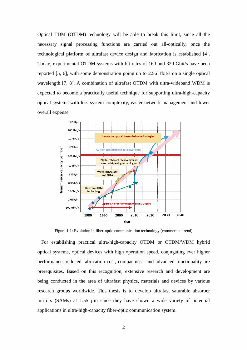
Over the past thirty years, fiber-optic communication technology has developed
rapidly through three main technological innovations, as shown in figure 1.1: time
division multiplexing (TDM) technology based on electrical multiplexing, Erbium
doped fiber amplifiers (EDFAs) combined with wavelength division multiplexing
(WDM) technology, and digital coherent technology and new multiplexing
technologies, which is currently undergoing research and development [1]. To meet
the ever-increasing worldwide demand for ultra-high-capacity systems, the progress is
still being made. On one hand, WDM technology is extensively used to further
increase the system capacity. Currently, commercial terrestrial WDM systems with
the capacity of 1.6 Tbit/s (160 WDM channels, each operating at 10 Gbit/s) per fiber
are now available [2]. However, as the channel number increases, the WDM system
would suffer from a variety of problems: the use of many lasers, each of which must
be readily tuned to a specific wavelength channel, becomes difficult or even
impractical. This limit in the wavelength management and handling may restrict the
total system capacity. On the other hand, TDM technique is being developed to
upgrade the bit-rate in single wavelength channel. However, the operating bit rate of
current electronic TDM (ETDM) systems is basically limited by the speed of
electronics components used for signal processing and driving optical devices, and its
improvement beyond a level of 100 Gbit/s seems to be rather difficult by solely
relying on existing electronic technologies [3]. In contrast with ETDM technique,
2
Optical TDM (OTDM) technology will be able to break this limit, since all the
necessary signal processing functions are carried out all-optically, once the
technological platform of ultrafast device design and fabrication is established [4].
Today, experimental OTDM systems with bit rates of 160 and 320 Gbit/s have been
reported [5, 6], with some demonstration going up to 2.56 Tbit/s on a single optical
wavelength [7, 8]. A combination of ultrafast OTDM with ultra-wideband WDM is
expected to become a practically useful technique for supporting ultra-high-capacity
optical systems with less system complexity, easier network management and lower
overall expense.
Figure 1.1: Evolution in fiber-optic communication technology (commercial trend)
For establishing practical ultra-high-capacity OTDM or OTDM/WDM hybrid
optical systems, optical devices with high operation speed, conjugating ever higher
performance, reduced fabrication cost, compactness, and advanced functionality are
prerequisites. Based on this recognition, extensive research and development are
being conducted in the area of ultrafast physics, materials and devices by various
research groups worldwide. This thesis is to develop ultrafast saturable absorber
mirrors (SAMs) at 1.55 µm since they have shown a wide variety of potential
applications in ultra-high-capacity fiber-optic communication system.
3
1.1 Application of SAMs
Compared with other optical components in fiber-optic communication system,
SAMs are more compact, cost-effective, polarization-insensitive, easy to fabricate and
operated in full simple and passive mode (no bias voltage, no Peltier cooler), which
has attracted vigorous research on exploring their applications. Their applications
mainly include various types of optical signal processing and generation of
mode-locked ultrashort pulse.
1.1.1 All-optical signal processing
The applications of SAMs to all-optical signal processing can be found both in
long-haul transmission lines and complex optical networks.
One important processing function of SAMs is all-optical regeneration which is a
key function for future optical communication system. The data signals are degraded
in the transmission system due to a combined effect of propagation loss, fiber
dispersion, fiber nonlinearity, and inter-/intra-channel interactions [9], and thus limit
the transmission length. All-optical regeneration (3R: reamplifying, reshaping,
retiming) allows for the restoration of the impaired signal and the enhancement of
transmission distance. At first, SAMs have only been used to reduce the optical noise
of the bit-0 slot mainly introduced by amplifier noise accumulation [10-12]. In 2007,
Nguyen et al. developed a new type of SAM to reduce the optical noise of the bit-1
slot, which is introduced by the dispersion effects [13]. Then the potential of SAM to
realize a complete all-optical reshaping, reducing the optical noises of both the bit-0
slot and the bit-1 slot with a single technology, has been demonstrated [14].
In addition to the function of noise suppression in simple point-to-point
transmission, SAMs can also realize various processing functions at flexible and
complicated optical node requiring all-optical packet switching. SAMs can extract the
packet header which is coded by pulse position coding technique [15], and can also
realize the all-optical seed pulse extraction from the incoming packet, which is needed
for synchronization of different inputs of a switch node in time-slotted operation
[16,17]. These two advanced functions of SAMs have been implemented by Porzi et
4
al. [18]. In all-optical packet-switched networks, logical operations in the all-optical
domain are also required to perform many functions, including header recognition
and/or modification, packet contention handling, data encoding/decoding, and
realization of half- and full-adders. SAMs have been widely exploited to realize
all-optical logic operations. Up to now, three kinds of logic gate (AND, NOR,
NAND) have already been implemented on SAMs [19, 20]. Using only NAND or
NOR operators, any logical operation can be realized. Wavelength conversion is also
important at the optical node which employs WDM. When two data channels with the
same wavelength and destination arrive in a routing node, one of them would be
blocked and lost if there is no possibility of converting one channel to another unused
wavelength. Wavelength conversion can make incoming signals to be converted to
any other wavelength to guarantee non-blocking operation. The principle of
wavelength conversion with SAMs has been previously proposed by Akiyama et al. in
1998 [21], and then developed by Porzi et al. in 2006 [22].
SAM also has the potential to realize all optical demultiplexing-sampling function.
This function can realize an all-optical format conversion to connect WDM and TDM
network in conjunction with wavelength converters. In OTDM networks, high-bit-rate
OTDM stream can be demultiplexed with SAM into its lower bit rate channels for
subsequent electrical processing. Optical sampling with SAM can allow for the
monitoring of high-capacity OTDM streams by electronic detection with the limited
bandwidth [23].
1.1.2 Mode-locked ultrashort pulse generation
The use of ultrashort pulses has a variety of potential advantages in optical
communication systems. They include the advantage of fully utilizing the material’s
nonlinearity by an extremely high peak intensity of field in ultrashort pulses. This is
essential in the development of all-optical switching and modulation devices with
high efficiency without increasing the average power consumption. An ultrashort
optical pulse occupies an extremely short distance in space and propagates at the light
velocity, and this means a possibility to precisely control the delay time in a small
5
dimension and the overall optical device and circuit can be very compact. Therefore,
in OTDM system, ultrashort pulses are also highly desirable, and can be used either as
a pulse source or in a clock circuit. Ultrashort pulse has a large spectral width due to
the pulse shape-spectrum interdependence deduced directly from Fourier transform
relationship, and this merits the used of various photonic function in wavelength
division. For example, ultrashort pulse source can be used as a multi-wavelength
source in WDM system, which can avoid the use of several laser sources. With the
same property, ultrashort pulse can also be used for wavelength conversion and pulse
waveform shaping.
SAM is an important optical component for the generation of ultrashort pulses with
passively mode-locked lasers. Today, reliable self-starting passive mode-locking for
all types of laser at 1.55 µm is obtained with semiconductor SAMs. For
semiconductor lasers, high-repetition rate of 50 GHz mode-locked
Vertical-External-Cavity Surface-Emitting laser (VECSEL) has been achieved and
then sub-picosecond pulse generation from a 1.56 µm mode-locked (VECSEL) has
been obtained [24, 25]. For solid-state lasers, 100 GHz passively mode-locked
Er:Yb:glass laser at 1.5µm with 1.6-ps pulses has been reported [26]. For fiber lasers,
a passively mode-locked fiber laser at 1.54µm with a repetition frequency of 2 GHz
and pulse duration of 900 fs has been demonstrated [27]. Mode-locked lasers by
semiconductor SAMs are expected to be promising candidates for next generation of
telecommunication sources.
1.2 What is saturable absorber mirror (SAM)?
SAM is a nonlinear mirror device, in which a saturable absorber layer (active layer)
is coupled with a mirror on one side or is integrated into a Fabry-Perot vertical
microcavity. The saturable absorber layer is a nonlinear optical material that shows
decreasing light absorption with increasing light intensity, and this light absorption
can be saturated under conditions of strong optical excitation. The key parameters for
a saturable absorber are its working wavelength (where it absorbs), response time
(how fast it recovers), saturation fluence and intensity (at what intensity or pulse
6
energy density it saturates). Such parameters can be optimized by the choice of the
saturable absorber material and the design of the mirror structure, thus allowing for
the various applications of SAMs in ultra-high-capacity fiber-optic communications.
1.2.1 Saturable absorber material
In principle, any absorbing material could be used to build a saturable absorber. In
the 1970s and 1980s, saturable absorber materials were typically organic dyes, which
suffer from short lifetimes, high toxicity, and complicated handling procedure,
limiting their application [28, 29]. Then solid-state materials, including crystals such
as Cr:YAG, were proposed as alternatives. But they typically operate for only limited
ranges of wavelengths, recovery times and saturation levels [30-32].
Now the most common saturable absorber materials are semiconductors since they
offered a wide flexibility in choosing the working wavelength (from the visible to the
mid-infrared) thanks to the advent of band-gap engineering and modern growth
technologies such as molecular beam epitaxy (MBE) [33-35] or metal organic
chemical vapor deposition (MOCVD) [36, 37], and they have large nonlinear optical
effects associated with absorption saturation [38, 39]. Moreover, being solid-state,
they don't experience the degradation typical of dyes.
Most of SAMs are based on III-V semiconductor saturable absorbers. By using
III-V compound with different compositions, the energy gap can be adjusted, enabling
SAM operating at the desired wavelength, i.e. fiber-optic communication band.
Moreover, the semiconductor layer is very easily integrated with the mirror structure,
and thus its absorption, saturation fluence and intensity can be controlled by the
structure design. As the absorption recovery time of the intrinsic compound
semiconductors in form of bulk or quantum wells (QWs) is limited to the nanosecond
region, which is not compatible with ultra-fast telecommunication systems or the
dynamics of short pulse emitting lasers, defects are created in the semiconductors
during [40, 41] or after [42] their epitaxial growth to reduce the absorption recovery
time. Indeed, defects create additional levels in the band gap which can trap electrical
non-equilibrium carriers quickly. Meanwhile, the developments of epitaxial growth
7
technologies have led to the formation of a new material-quantum dot (QD). It has a
fast absorption recovery time in the picosecond region [43] and the saturation fluence
lower than the bulk and QWs materials [44, 45]. However, the complex epitaxial
growth processes are detrimental to repeatability and reliability of high quality QDs.
Recently, single wall carbon nanotube (SWCNT) and graphene have emerged as
new types of saturable absorber materials. They have fast recovery time on the
picosecond scale [46], easy fabrication, low cost [47]. However, the spectral
applicability of SWCNT is limited by the diameter and chirality during growth. In
contrast, graphene has a broad absorption spectrum over the visible to near-infrared
region, and its optical absorption can be saturated under strong excitation. Due to its
extraordinary nonlinear properties and broad absorption spectrum, graphene has been
exploited as a “full-band” mode locker. Self-started mode locking in different types of
laser with graphene has been achieved [48, 49]. Furthermore, it has been demonstrated
that hybridization of graphene with plasmonic metamaterials could make it possible to
use graphene for ultrafast all-optical switching [50].
1.2.2 SAM Design
Beyond the saturable absorber materials properties, that govern some basic
characteristics of the SAM, such as the response time, or the wavelength window,
other important parameters of the SAM, such as the saturation fluence and intensity,
modulation depth / contrast ratio, spectral bandwidth, polarization properties, depend
strongly on the device structure design. They can be tailored by a proper device
design, with some trade-offs depending on the applications.
1.2.2.1 SAM Design for all-optical signal processing
When the SAM is used for all-optical signal processing, the saturable absorber layer
is integrated into an asymmetric Fabry-Perot microcavity, used in the reflection-mode
at normal incidence. This type of SAM is called vertical resonant Fabry-Perot
saturable absorber (R-FPSA), as shown in figure 1.2. The cavity is formed by a high
reflective back mirror with an almost 100% reflectivity and a less reflective top
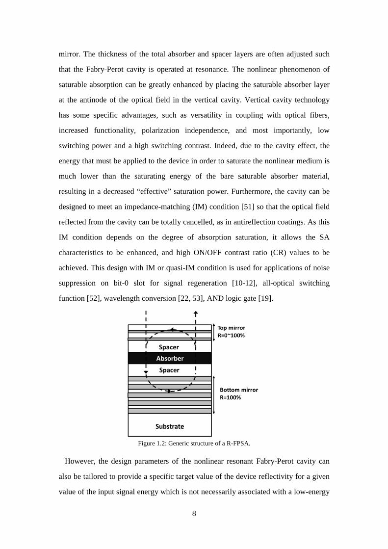
8
mirror. The thickness of the total absorber and spacer layers are often adjusted such
that the Fabry-Perot cavity is operated at resonance. The nonlinear phenomenon of
saturable absorption can be greatly enhanced by placing the saturable absorber layer
at the antinode of the optical field in the vertical cavity. Vertical cavity technology
has some specific advantages, such as versatility in coupling with optical fibers,
increased functionality, polarization independence, and most importantly, low
switching power and a high switching contrast. Indeed, due to the cavity effect, the
energy that must be applied to the device in order to saturate the nonlinear medium is
much lower than the saturating energy of the bare saturable absorber material,
resulting in a decreased “effective” saturation power. Furthermore, the cavity can be
designed to meet an impedance-matching (IM) condition [51] so that the optical field
reflected from the cavity can be totally cancelled, as in antireflection coatings. As this
IM condition depends on the degree of absorption saturation, it allows the SA
characteristics to be enhanced, and high ON/OFF contrast ratio (CR) values to be
achieved. This design with IM or quasi-IM condition is used for applications of noise
suppression on bit-0 slot for signal regeneration [10-12], all-optical switching
function [52], wavelength conversion [22, 53], AND logic gate [19].
Figure 1.2: Generic structure of a R-FPSA.
However, the design parameters of the nonlinear resonant Fabry-Perot cavity can
also be tailored to provide a specific target value of the device reflectivity for a given
value of the input signal energy which is not necessarily associated with a low-energy
9
photon flux. The incident fluence for which the IM condition is met is detuned from
low input power to relatively higher input power. These SAMs with
impedance-detuned condition have an inverse saturable absorption behavior (i.e. high
reflectivity at low input energy and low reflectivity at high input energy) for input
energy values below the IM energy, which are used for noise suppression on bit-1 slot
[13], the realization of NOR/NAND logical gate [20], all-optical header extraction
and all-optical seed pulse extraction [18].
1.2.2.2 SAM Design for passive mode-locking
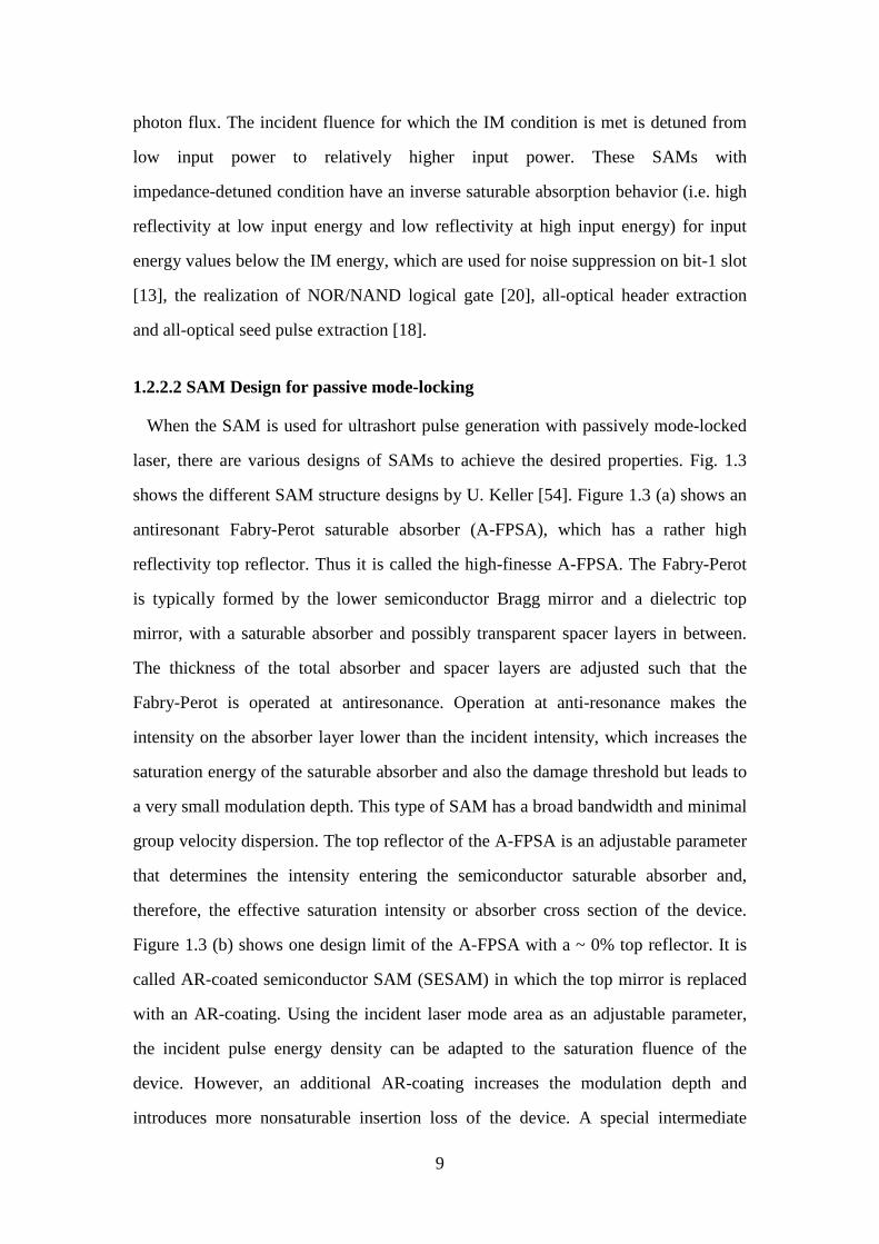
When the SAM is used for ultrashort pulse generation with passively mode-locked
laser, there are various designs of SAMs to achieve the desired properties. Fig. 1.3
shows the different SAM structure designs by U. Keller [54]. Figure 1.3 (a) shows an
antiresonant Fabry-Perot saturable absorber (A-FPSA), which has a rather high
reflectivity top reflector. Thus it is called the high-finesse A-FPSA. The Fabry-Perot
is typically formed by the lower semiconductor Bragg mirror and a dielectric top
mirror, with a saturable absorber and possibly transparent spacer layers in between.
The thickness of the total absorber and spacer layers are adjusted such that the
Fabry-Perot is operated at antiresonance. Operation at anti-resonance makes the
intensity on the absorber layer lower than the incident intensity, which increases the
saturation energy of the saturable absorber and also the damage threshold but leads to
a very small modulation depth. This type of SAM has a broad bandwidth and minimal
group velocity dispersion. The top reflector of the A-FPSA is an adjustable parameter
that determines the intensity entering the semiconductor saturable absorber and,
therefore, the effective saturation intensity or absorber cross section of the device.
Figure 1.3 (b) shows one design limit of the A-FPSA with a ~ 0% top reflector. It is
called AR-coated semiconductor SAM (SESAM) in which the top mirror is replaced
with an AR-coating. Using the incident laser mode area as an adjustable parameter,
the incident pulse energy density can be adapted to the saturation fluence of the
device. However, an additional AR-coating increases the modulation depth and
introduces more nonsaturable insertion loss of the device. A special intermediate
10
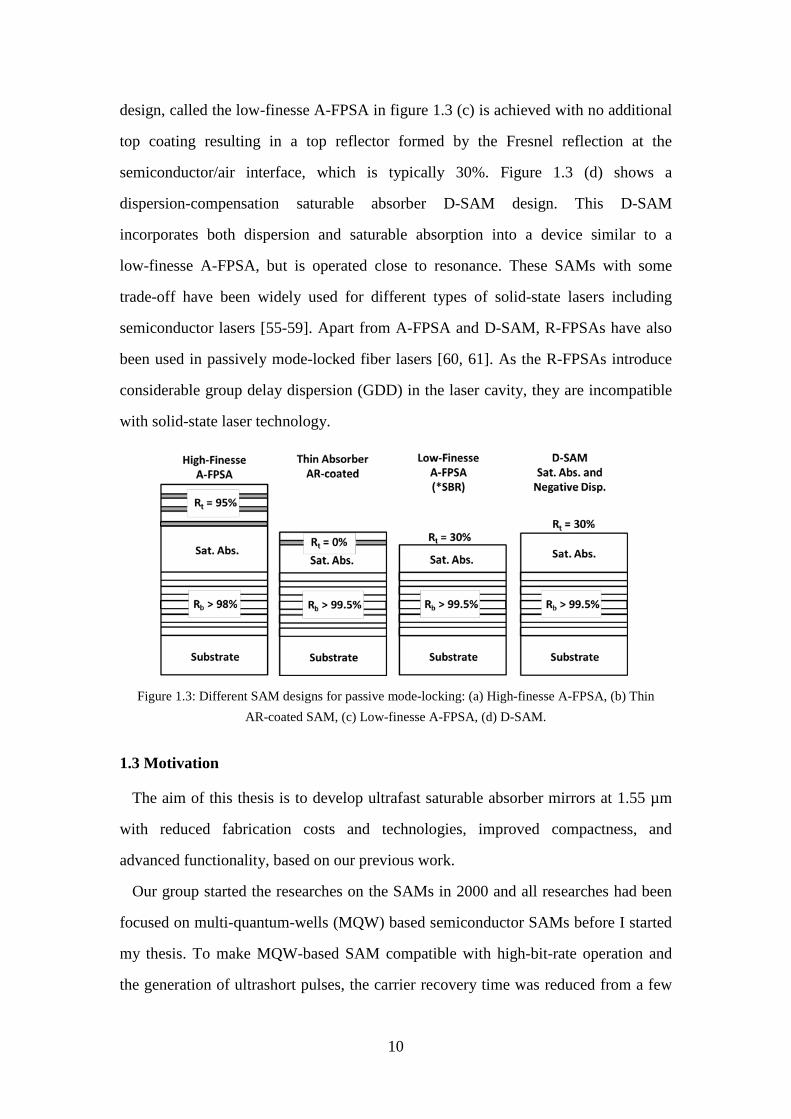
design, called the low-finesse A-FPSA in figure 1.3 (c) is achieved with no additional
top coating resulting in a top reflector formed by the Fresnel reflection at the
semiconductor/air interface, which is typically 30%. Figure 1.3 (d) shows a
dispersion-compensation saturable absorber D-SAM design. This D-SAM
incorporates both dispersion and saturable absorption into a device similar to a
low-finesse A-FPSA, but is operated close to resonance. These SAMs with some
trade-off have been widely used for different types of solid-state lasers including
semiconductor lasers [55-59]. Apart from A-FPSA and D-SAM, R-FPSAs have also
been used in passively mode-locked fiber lasers [60, 61]. As the R-FPSAs introduce
considerable group delay dispersion (GDD) in the laser cavity, they are incompatible
with solid-state laser technology.
Figure 1.3: Different SAM designs for passive mode-locking: (a) High-finesse A-FPSA, (b) Thin
AR-coated SAM, (c) Low-finesse A-FPSA, (d) D-SAM.
1.3 Motivation
The aim of this thesis is to develop ultrafast saturable absorber mirrors at 1.55 µm
with reduced fabrication costs and technologies, improved compactness, and
advanced functionality, based on our previous work.
Our group started the researches on the SAMs in 2000 and all researches had been
focused on multi-quantum-wells (MQW) based semiconductor SAMs before I started
my thesis. To make MQW-based SAM compatible with high-bit-rate operation and
the generation of ultrashort pulses, the carrier recovery time was reduced from a few
11
nanoseconds to several picoseconds by heavy-ion (Ni+) irradiation [62]. To amplify
the nonlinear response and to reduce the saturation fluence, the MQW was integrated
in a vertical resonant Fabry-Perot microcavity and located at the antinode of the
intracavity intensity. The R-FPSA device was designed to meet impedance-matching
and achieve a maximum intensity field on the MQW by the refinements in the cavity
parameters [63]. Such an optimal microcavity combined with heavy-ion irradiation
has allowed for high performance of our SAM for all-optical regeneration and optical
switching at high bit-rate of 160 Gbit/s [64-66]. The regeneration of several WDM
channels on a single SAM module has also been shown with spatial fiber
demultiplexer [67, 68]. Moreover, a special design of SAM with impedance-detuned
has realized the noise suppression on bit-0 slot [13]. In addition, the passively
mode-locked erbium-doped fiber lasers with our R-FPSA have also been reported [60,
61].
Although QWs exhibit a relatively strong nonlinear response because of quantum
confinement effects, they demand very precise control of the growth to achieve a
uniform and accurate thickness, and thus to achieve good optical properties.
Compared with the growth of QWs, semiconductor bulk structure has very simple
growth technology. In my thesis, In0.53Ga0.47As bulk material has been employed to
realize a SAM at 1.55 µm. The heavy-ion implantation is used to reduce the carrier
recovery time of In0.53Ga0.47As since it requires much lower ion energy than
heavy-ion-irradiation technique. Moreover, a taper structure is introduced on the
phase layer of In0.53Ga0.47As-based SAM to realize a multi-wavelength regenerator,
with focused ion beam (FIB) milling technology. As mentioned before, graphene, as a
new type of saturable absorber material, has been widely used for mode-locking in
different types of lasers. However, it requires high saturation energy, which limits its
potential for other applications such as optical signal processing. In this thesis, we
also integrated monolayer graphene into a vertical cavity to enhance its nonlinear
properties and reduce its saturation energy.
12
1.4 Structure of this thesis
The thesis is organized as follows: Chapter 2 focuses on the realization of ultrafast
In0.53Ga0.47As-based SAMs by heavy-ion-implantation. We introduce the carrier
dynamics of III-V compound semiconductors and give an overview of the approaches
to speed up the carrier lifetime of III-V compound semiconductor. Then we explain
why we choose heavy-ion-implantation to realize ultrafast In0.53Ga0.47As-based
SAMs, followed by an introduction to ion implantation technique. Finally, fabrication
and characterization of heavy-ion-implanted SAM are performed. Chapter 3 discusses
the realization of multi-wavelength In0.53Ga0.47As-based SAM using FIB milling. We
firstly present the concept and design of a tapered SAM, which led us to conclude that
FIB milling is an attractive technique for the taper fabrication. Then we give an
introduction to the fundamental characteristics of the FIB system and the principle of
FIB milling. Finally, the fabrication of tapered SAM and its optical characterization
are presented. Chapter 4 focuses on enhancing the nonlinear optical properties of
monolayer graphene by incorporating it into a vertical microcavity. We introduce the
optical properties of graphene and its application in optical domain. Then we present
our design concept. Finally, fabrication and characterization of the graphene-based
SAMs are performed. Chapter 5 contains a brief conclusion of our work.
13
1.5 Reference
[1] G. P. Agrawal, Fiber-optic communication systems, John Wiley & Sons, New
York, 2002.
[2] “Infinera introduces new line system,” Infinera Corp press release, Retrieved
2009-08-26.
[3] G. Raybon and P. Winzer, “100 Gb/s: ETDM generation and long haul
transmission,” in Proc. Eur. Conf. on Opt. Comm. (ECOC’07), pp. 1-2, 2007.
[4] M. Saruwatari, “All-optical signal processing for terabit/second optical
transmission,” IEEE J. Sel. Top. Quant. Electron., vol. 6, pp. 1363–1374, 2000.
[5] S. Weisser, S. Ferber, L. Raddatz, R. Ludwig, A. Benz, C. Boerner, and H. G.
Weber, “Single- and alternating polarization 170 Gb/s transmission up to 4000
km using dispersion-managed fiber and all-Raman amplification,” IEEE Photon.
Technol. Lett., vol. 18, pp. 1320-1322, 2006.
[6] B. Mikkelsen, G. Raybon, R. J. Essiambre, A. J. Stentz, T. N. Nielsen, D. W.
Peckham, L. Hsu, L. Gruner-Nielsen, K. Dreyer, and J. E. Johnson, “320-Gb/s
single-channel pseudolinear transmission over 200 km of nonzero-dispersion
fiber,” IEEE Photon. Technol. Lett., vol. 12, pp.1400-1402, 2000.
[7] M. Nakazawa, T. Yamamoto, and K. R. Tamura, “1.28 Tbit/s -70 km OTDM
transmission using third- and fourth-order simultaneous dispersion compensation
with a phase modulator,” Electron. Lett., vol. 36, pp. 2027-2029, 2000.
[8] H. G. Weber, S. Ferber, M. Kroh, C. Schmidt-Langhorst, R. Ludwig, V.
Marembert, C. Boerner, F. Futami, S. Watanabe, and C. Schubert, “Single
channel 1.28 Tb/s and 2.56 Tb/s DQPSK transmission,” Electron. Lett., vol. 42,
pp. 178-179, 2006.
[9] G. P. Agrawal, Nonlinear Fiber Optics, second edition, academic press, New
York, 1995.
[10] J. Mangeney, S. Barré, G. Aubin, J. L. Oudar, and O. Leclerc, “System application
of 1.5 mm ultrafast saturable absorber in 10Gbit/s long-haul transmission,”
Electron. Lett., vol. 36, pp. 1725-1729, 2000.
14
[11] A. Isomaki, A. M. Vainionpaa, J. Lyytikainen, and O. G. Okhotnikov,
“Semiconductor mirror for optical noise suppression and dynamic dispersion
compensation,” IEEE J. Quant. Electron., vol. 39, pp. 1481-1485, 2003.
[12] D. Massoubre, J. L. Oudar, J. Fatome, S. Pitois, G. Millot, J. Decobert, and J.
Landreau, “All-optical extinction ratio enhancement of a 160 GHz pulse train
using a saturable absorber vertical microcavity,” Opt. Lett., vol. 31, pp. 537–539,
2006.
[13] H. T. Nguyen, J. L. Oudar, S. Bouchoule, G. Aubin, and S. Sauvage, “A passive
all-optical semiconductor device for level amplitude stabilization based on fast
saturable absorber,” Appl. Phys. Lett., vol. 92, pp. 111107-1-111107-3, 2008.
[14] H. T. Nguyen, C. Fortier, J. Fatome, G. Aubin, and J. L. Oudar, “A passive
all-optical device for 2R regeneration based on the cascade of two high-speed
saturable absorbers,” J. Lightwave Technol., vol. 29, pp. 1319-1325, 2011.
[15] N. Calabretta, Y. Liu, D. H. Waardt, M. T. Hill, G. D. Khoe, and H. J. S. Dorren,
“Multiple-output all-optical header processing technique based on two-pulse
correlation principle,” Electron. Lett., vol. 37, pp. 1238–1240, 2001.
[16] X. Huang, P. Ye, M. Zhang, and L. Wang, “A novel self-synchronization scheme
for all-optical Packet Networks,” IEEE Photon. Technol. Lett., vol. 17, pp.
645-647, 2005.
[17] T. J. Xia, Y. H. Kao, Y. Liang, J. W. Lou, K. H. Ahn, O. Boyraz, G. A. Nowak, A.
A. Said, and M. N. Slam, “Novel self-synchronization scheme for high-speed
packet TDM networks,” IEEE Photon. Technol. Lett., vol. 11, pp. 269-271, 1999.
[18] C. Porzi, N. Calabretta, M. Guina, O. Okhotnikov, A. Bogoni, and L. Potì,
“All-optical processing for pulse position coded header in packet switched optical
networks using vertical cavity semiconductor gates,” IEEE J. Sel. Top. Quant.
Electron., vol. 13, pp 1579-1588, 2007.
[19] R. Takahashi, Y. Kawamura, and H. Iwamura, “Ultrafast 1.55 mm all-optical
switching using low-temperature-grown multiple quantum wells,” Appl. Phys.
Lett., vol. 68, pp. 153-155, 1996.
15
[20] C. Porzi, M. Guina, A. Bogoni, and L. Poti, “All-Optical nand/nor logic gates
based on semiconductor saturable absorber etalons,” IEEE J. Sel. Top. Quant.
Electron., vol. 14, pp. 927-937, 2008.
[21] T. Akiyama, M. Tsuchiya, and T. Kamiya, “Sub-pJ operation of broadband
asymmetric Fabry-Pérot all-optical gate with coupled cavity structure,” Appl.
Phys. Lett., vol. 72, pp. 1545-1547, 1998.
[22] C. Porzi, A. Bogoni, L. Poti, M. Guina, and O. Okhotnikov, “Characterization and
operation of vertical cavity semiconductor all-optical broadband wavelength
converter,” Proceeding SPIE Integrated Optics, Silicon Photonics, and Photonic
Integrated Circuits, pp. Z1830-Z1830, 0-8194-6239-X, Strasbourg, France.
[23] D. Reid, P. J. Maguire, L. P. Barry, Q. T. Le, S. Lobo, M. Gay, L. Bramerie, M.
Joindot, J. C. Simon, D. Massoubre, J. L Oudar and G. Aubin, “All-optical
sampling and spectrographic pulse measurement using cross-absorption
modulation in multiple-quantum-well devices,” J. Opt. Soc. Am. B, vol. 25, pp.
A133-A139, 2008.
[24] Z. Zhao, S. Bouchoule, J. Song, E. Galopin, J.-C. Harmand, J. Decobert, G. Aubin,
and J. L. Oudar, “Sub-picosecond pulse generation from a 1.56 µm mode-locked
VECSEL,” Opt. Lett., vol. 36, pp. 4377-4379, 2011.
[25] D. Lorenser, D. J. H. C. Maas, H. J. Unold, A. R. Bellancourt, B. Rudin, E. Gini,
D. Ebling, and U. Keller, “50-GHz passively mode-locked surface-emitting
semiconductor laser with 100 mW average output power,” IEEE J. Quant.
Electron., vol. 42, pp. 838-847, 2006.
[26] A. E. H. Oehler, T. Südmeyer, K. J. Weingarten, and U. Keller, “100 GHz
passively mode-locked Er:Yb:glass laser at 1.5 micrometer with 1.6-ps pulses,”
Opt. Exp., vol. 15, pp. 21930–21935, 2008.
[27] J. J. McFerran, L. Nenadovic, W. C. Swann, J. B. Schlager, and N. R. Newbury,
“A passively mode-locked fiber laser at 1.54 µm with a fundamental repetition
frequency reaching 2 GHz,” Opt. Exp., vol. 15, pp. 13155-13166, 2007.
[28] C. V. Shank and E. P. Ippen, “Subpicosecond kilowatt pulses from a mode‐
locked cw dye laser,” Appl. Phys. Lett., vol. 24, pp. 373-375, 1974.
16
[29] A. Finch, G. Chen, W. Sleat, and W. Sibett, “Pulse asymmetry in the
colliding-pulse mode-locked dye laser,” J. Mod. Opt., vol. 35, pp. 345-354, 1988.
[30] Y. X. Bai, N. L. Wu, J. Zhang, J. Q. Li, S. Q. Li, J. Xu, and P. Z. Deng, “Passively
Q-switched Nd:YVO4 laser with a Cr4+:YAG crystal saturable absorber,” Appl.
Opt., vol. 36, pp. 2468-2472, 1997.
[31] V. Yumashev, I. A. Denisov, N. N. Posnov, N. V. Kuleshov, and R. Moncorge,
“Excited state absorption and passive Q-switch performance of Co2+-doped oxide
crystals,” J. Alloys Compd., vol. 341, pp. 366-370, 2002.
[32] Y. Kalisky, “Cr4+-doped crystals: their use as lasers and passive Q-switches,”
Prog. in Quant. Electron., vol. 28, pp. 249-303, 2004.
[33] U. Keller, K. J. Weingarten, F. X. Kartner, D. Kopf, B. Braun, I. D. Jung, R. Fluck,
C. Honninger, N. Matuschek, and J. Aus der Au, “Semiconductor saturable
absorber mirrors (SESAM’s) for femtosecond to nanosecond pulse generation in
solid-state lasers,” IEEE J. Sel. Top. Quant. Electron., vol. 2, pp. 435-453, 1996.
[34] G. J. Spuhler, R. Paschotta, R. Fluck, B. Braun, M. Moser, G. Zhang, E. Gini, and
U. Keller, “Experimentally confirmed design guidelines for passively Q-switched
microchip lasers using semiconductor saturable absorbers,” J. Opt. Soc. Am. B,
vol. 16, pp. 376 -388, 1999.
[35] K. Reginski, A. Jasik, M. Kosmala, P. Karbownik, and P. Wnuk, “Semiconductor
saturable absorbers of laser radiation for the wavelength of 808 nm grown by
MBE: Choice of growth conditions,” Vacuum, vol. 82, pp. 947 -950, 2008.
[36] R. Grange, O. Ostinelli, M. Haiml, L. Krainer, G. J. Spühler, M. Ebnöther, E. Gini,
S. Schön, and U. Keller, “Antimonide semiconductor saturable absorber for 1.5
µm,” Electron. Lett., vol. 40, pp. 1414-1416, 2004.
[37] A. Aschwanden, D. Lorenser, H. J. Unold, R. Paschotta, E. Gini, and U. Keller,
“10-GHz passively mode-locked surface-emitting semiconductor laser with 1.4 W
output power”, Conf. Lasers and Electro-Optics (CLEO), (OSA), Postdeadline
CPDB8, 2004.
[38] D. A. B. Miller, “Dynamic nonlinear optics in semiconductors: physics and
applications,” Laser Focus, vol. 19, pp. 61-68, 1983.
17
[39] U. Keller, “Recent developments in compact ultrafast lasers,” Nature, vol. 424, pp.
831-838, 2003.
[40] J. S. Weiner, D. B. Pearson, D. A. B. Miller, D. S. Chemla, D. Sivco, and A. Y.
Cho, “Nonlinear spectroscopy of InGaAs/InAlAs multiple quantum well
structures,” Appl. Phys. Lett., vol. 49, pp. 531–533, 1986.
[41] S. D. Benjamin, H. S. Loka, A. Othonos, and P. W. E. Smith, “Ultrafast dynamics
of nonlinear absorption in low-temperature-grown GaAs,” Appl. Phys. Lett., vol.
68, pp. 2544–2546, 1996.
[42] D. Soderstrom, S. Marcinkevicius, S. Karlsson, and S. Lourdudoss, “Carrier
trapping due to Fe3+ / Fe2+ in epitaxial InP,” Appl. Phys. Lett., vol. 70, pp. 3374–
3376, 1997.
[43] P. Borri, S. Schneider, W. Langbein, and D. Bimberg, “Ultrafast carrier dynamics
in InGaAs quantum dot materials and devices,” J. Opt A-Pure Appl. OP., vol. 8,
pp. S33-S46, 2006.
[44] S. W. Osborne, P. Blood, P. M. Smowton, Y. C. Xin, A. Stintz, D. Huffaker, and L.
F. Lester, “Optical absorption cross section of quantum dots,” J. Phys. Condens.
Matter, vol. 16, pp. S3749-S3756, 2004.
[45] Z. Y. Zhang, A. E. H. Oehler, B. Resan, S. Kurmulis, K. J. Zhou, Q. Wang, M.
Mangold, T. Suedmeyer, U. Keller, K. J. Weingarten, and R. A. Hogg, “1.55 μm
InAs/GaAs quantum dots and high repetition rate quantum dot SESAM
mode-locked laser, ” Sci. Rep., vol. 2, Article Nr. 477, 2012.
[46] F. Bonaccorso, Z. Sun, T. Hasan, and A.C. Ferrari, “Graphene photonics and
optoelectronics,” Nature Photon., vol. 4, pp. 611-622, 2010.
[47] A. Martinez and Z. Sun, “Nanotube and graphene saturable absorbers for fiber
lasers,” Nature Photon., vol. 7, pp 842-845, 2013.
[48] W. B. Cho, J. W. Kim, H. W. Lee, S. Bae, B. H. Hong, S. Y. Choi, I. H. Baek, K.
Kim, D. I. Yeom, and F. Rotermund, “High-quality, large-area monolayer
graphene for efficient bulk laser mode-locking near 1.25 μm,” Opt. Lett., vol. 36,
pp. 4089-4091, 2011
18
[49] H. Zhang, D. Y. Tang, L. M. Zhao, Q. L. Bao, and K. P. Loh, “Large energy mode
locking of an erbium-doped fiber laser with atomic layer graphene,” Opt. Express,
vol.17, pp.17630–17635, 2009.
[50] A. E. Nikolaenko, N. Papasimakis, E. Atmatzakis, Z. Q. Luo, Z. X. Shen, F. D.
Angelis, S. A. Boden, E. D. Fabrizio, and N. I. Zheludev, “Nonlinear graphene
metamaterial,” Appl. Phys. Lett., vol. 100, pp. 181109-181109-3, 2012.
[51] R. H. Yan, R. J. Simes, and L. A. Coldren, “Surface-normal electroabsorption
reflection modulators using asymmetric Fabry-Perot structures,” IEEE J. Quant.
Electron., vol. 27, pp. 1922-1931, 1991
[52] H. S. Loka and W. E. P. Smith, “Ultrafast all-optical switching in an asymmetric
Fabry-Perot device using low-temperature-grown GaAs,” IEEE Photon. Technol.
Lett., vol. 10, pp. 269-271, 1998.
[53] E. P. Burr, M. Pantouvaki, A. J. Seeds, R. M. Gwilliam, S. M. Pinches, and C. C.
Button, “Wavelength conversion of 1.53-µm-wavelength picosecond pulses in an
ion implanted multiple-quantum-well all-optical switch,” Opt. lett., vol. 28, pp.
483-485, 2003.
[54] U. Keller, “Advances in all-solid-state ultrafast lasers,” in Ultrafast Phenomena X,
P. F. Barbara, J. G. Fujimoto, W. H. Knox, and W. Zinth, Eds. Berlin, Germany:
Springer, pp. 3-5, 1996.
[55] L. R. Brovelli, I. D. Jung, D. Kopf, M. Kamp, M. Moser, F. X. Kärtner, and U.
Keller, “Self-starting soliton mode-locked Ti:sapphire laser using a thin
semiconductor saturable absorber,” Electron. Lett., vol. 31, pp. 287-289, 1995.
[56] I. D. Jung, L. R. Brovelli, M. Kamp, U. Keller, and M. Moser, “Scaling of the
antiresonant Fabry-Perot saturable absorber design toward a thin saturable
absorber,” Opt. Lett., vol. 20, pp. 1559-1561, 1995.
[57] C. Hönninger, G. Zhang, U. Keller, and A. Giesen, “Femtosecond Yb:YAG laser
using semiconductor saturable absorbers,” Opt. Lett., vol. 20, pp. 2402-2404,
1995.
19
[58] S. Tsuda, W. H. Knox, E. A. d. Souza, W. Y. Jan, and J. E. Cunningham,
“Femtosecond self-starting passive mode-locking using an AlAs/AlGaAs
intracavity saturable Bragg reflector,” in CLEO paper CWM6, p. 254, 1995.
[59] D. Kopf, G. J. Spühler, K. J. Weingarten, and U. Keller, “Mode-locked laser
cavities with a single prism for dispersion compensation,” Appl. Opt., vol. 35,
pp. 912-915, 1996.
[60] A. Cabasse1, G. Martel, and J. L. Oudar, “High power dissipative soliton in an
Erbium-doped fiber laser mode-locked with a high modulation depth saturable
absorber mirror,” Opt. Exp., vol. 17, pp. 9537-9542, 2009.
[61] A. Cabasse, D. Gaponov, K. Ndao, A. Khadour, J. L. Oudar, and G. Martel, “130
mW average power, 4.6 nJ pulse energy, 10.2 ps pulse duration from an Er3+ fiber
oscillator passively mode locked by a resonant saturable absorber mirror,” Opt.
Lett., vol. 14, pp. 2620-2622, 2011.
[62] J. Mangeney, J. L. Oudar, J. C. Harmand, C. Mériadec1, G. Patriarche1, G.
Aubin1, N. Stelmakh, and J. M. Lourtioz, “Ultrafast saturable absorption at 1.55
μm in heavy-ion-irradiated quantum-well vertical cavity,” Appl. Phys. Lett., vol.
76, pp. 1371-1373, 2000.
[63] D. Massoubre, J. L. Oudar, J. Dion, J. C. Harmond, A. shen, J. Landreau, and J.
Decobert, “Scaling of the saturation energy in microcavity saturable absorber
devices,” Appl. Phys. Lett., vol. 88, pp. 153513-1-153513-3, 2006.
[64] J. Fatome, S. Pitois, A. Kamagate, G. Millot, D. Massoudre, and J. L. Oudar,
“All-optical reshaping based on a passive saturable absorber microcavity device
for future 160 Gb/s applications,” IEEE Photon. Technol. Lett., vol. 19, pp.
245-247, 2007.
[65] D. Massoubre, J. L. Oudar, J. Fatome, S. Pitois, G. Millot, J. Decobert, and J.
Landreau, “All-optical extinction-ratio enhancement of a 160 GHz pulse train by a
saturable-absorber vertical microcavity,” Opt. Lett., vol. 31, pp.537-539 , 2006.
[66] M. Gay, M. Costa e Silva, T. N. Nguyen, L. Bramerie, T. Chartier, M. Joindot, J.
C. Simon, J. Fatome, C. Finot, and J. L. Oudar, “Bit error rate assessment of 170
20
Gbit/s regeneration using a saturable absorber and a nonlinear-fiber-based power
limiter,” IEEE Photon. Technol. Lett., vol. 22, pp. 158-160, 2010.
[67] A. Shen, M. Goix, S. Louis, D. Delagrandiere, J. Decobert, G. Henin, D.
Rouvillain, O. Leclerc, H. Choumane, G. Aubin and J. L. Oudar, “4-channel
saturable absorber module for high bit-rate regenerated WDM transmission,”
Proc. Eur. Conf. Opt. Commun., vol. 2, Paper Tu 5.4.5, 2002.
[68] Q.T. Le, L. Bramerie, S. Lobo, M. Gay, M. Joindot, J. C. Simon, A. Poudoulec, M.
Van der Keur, C. Devemy, D. Massoubre, J. L. Oudar, G. Aubin, A. Shen and J.
Decobert, “WDM compatible 2R regeneration device based on eight-channel
saturable absorber module,” Electron. Lett., vol. 43, pp. 1305-1306, 2007.
21
Chapter 2 Heavy-ion-implanted In0.53Ga0.47As-based saturable
absorber mirror
The carrier recovery time is the most important characteristic of semiconductor
SAMs for the application to ultra-high speed optical signal processing and ultra-short
pulses generation with passively mode-locked lasers. The value of the carrier recovery
time is usually required to be on the picosecond or sub-picosecond time scale. Among
semiconductor materials in different structures, the as-grown QD structure has a
carrier recovery time in the picosecond regime. However, the epitaxial growth process
of high quality QD is very complex, which limited its application for fast SAMs. The
as-grown QW structure shows carrier recovery time values ranging from 500 ps to
several ns and the values of bulk structures are in the nanosecond level, both of which
are far too long for ultrafast operations. Defect engineering is required to speed up the
carrier relaxation dynamics in semiconductor bulk or QW structure during or after its
epitaxial growth. Compared to QW, the semiconductor bulk structure has more simple
growth technology and can be a good candidate for ultrafast SAMs with low cost.
This chapter is devoted to develop ultrafast bulk In0.53Ga0.47As-based SAMs though
reducing the carrier recovery time to picosecond levels using heavy-ion-implantation.
The first section 2.1 introduces the carrier dynamics of III-V compound
semiconductors and the techniques for accelerating the carrier relaxation in bulk and
QW semiconductors. In section 2.2, we introduce the ion implantation technique.
Then the device fabrication is given in section 2.3. In section 2.4, the
heavy-ion-implanted samples are characterized.
2.1 III-V compound semiconductor
III-V compound semiconductors are promising candidates for the SAMs because
their bandgap can be modified according to the intended wavelength by changing the
composition of the material which is lattice-matched to the substrate. These
compounds basically consist of the column III elements Al, Ga and In, and the
column V elements N, P, As and Sb. The variation of band-gap with respect to the
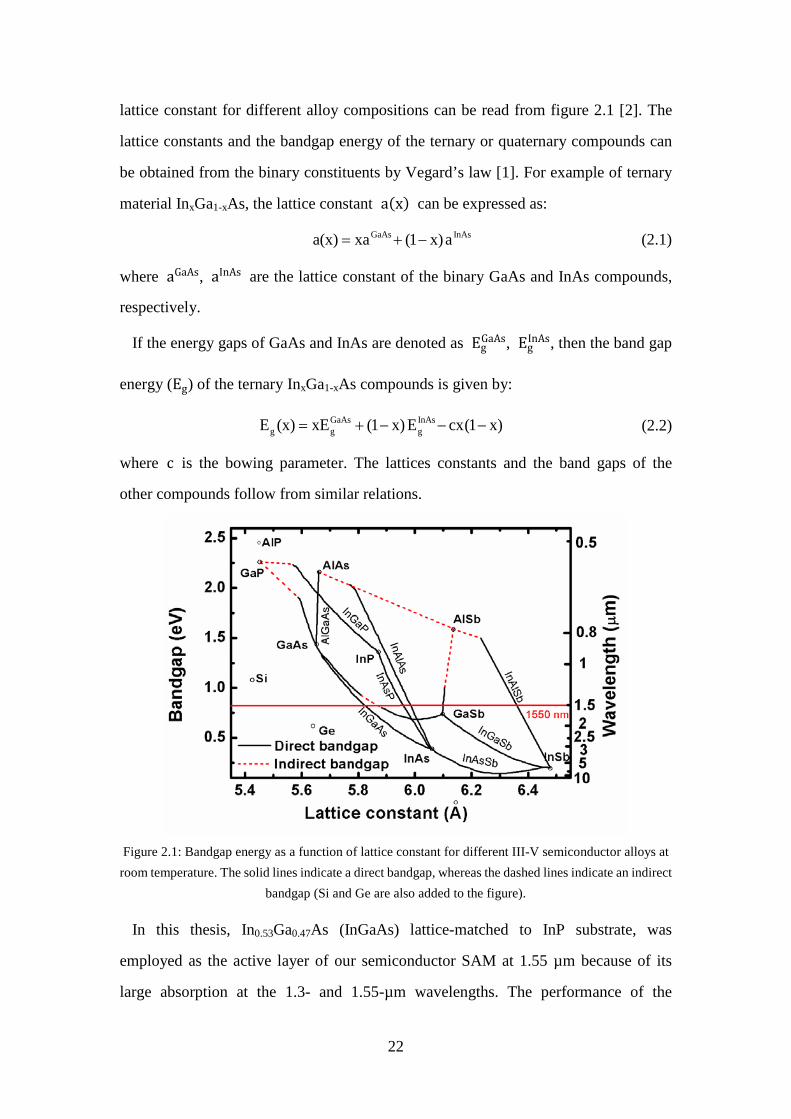
22
lattice constant for different alloy compositions can be read from figure 2.1 [2]. The
lattice constants and the bandgap energy of the ternary or quaternary compounds can
be obtained from the binary constituents by Vegard’s law [1]. For example of ternary
material InxGa1-xAs, the lattice constant a(x) can be expressed as:
GaAs InAsa(x) xa (1 x)a= + − (2.1)
where aGaAs, aInAs are the lattice constant of the binary GaAs and InAs compounds,
respectively.
If the energy gaps of GaAs and InAs are denoted as EgGaAs, Eg
InAs, then the band gap
energy (Eg) of the ternary InxGa1-xAs compounds is given by:
GaAs InAsg g gE (x) xE (1 x) E cx(1 x)= + − − − (2.2)
where c is the bowing parameter. The lattices constants and the band gaps of the
other compounds follow from similar relations.
Figure 2.1: Bandgap energy as a function of lattice constant for different III-V semiconductor alloys at
room temperature. The solid lines indicate a direct bandgap, whereas the dashed lines indicate an indirect bandgap (Si and Ge are also added to the figure).
In this thesis, In0.53Ga0.47As (InGaAs) lattice-matched to InP substrate, was
employed as the active layer of our semiconductor SAM at 1.55 µm because of its
large absorption at the 1.3- and 1.55-µm wavelengths. The performance of the
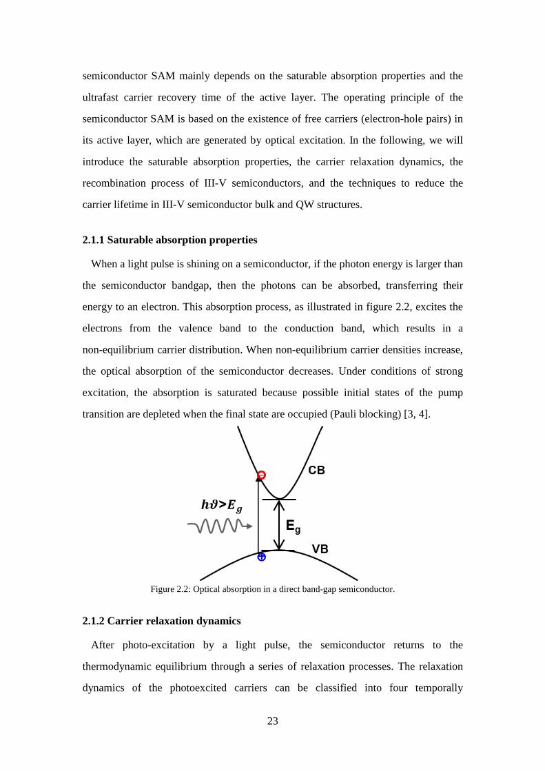
23
semiconductor SAM mainly depends on the saturable absorption properties and the
ultrafast carrier recovery time of the active layer. The operating principle of the
semiconductor SAM is based on the existence of free carriers (electron-hole pairs) in
its active layer, which are generated by optical excitation. In the following, we will
introduce the saturable absorption properties, the carrier relaxation dynamics, the
recombination process of III-V semiconductors, and the techniques to reduce the
carrier lifetime in III-V semiconductor bulk and QW structures.
2.1.1 Saturable absorption properties
When a light pulse is shining on a semiconductor, if the photon energy is larger than
the semiconductor bandgap, then the photons can be absorbed, transferring their
energy to an electron. This absorption process, as illustrated in figure 2.2, excites the
electrons from the valence band to the conduction band, which results in a
non-equilibrium carrier distribution. When non-equilibrium carrier densities increase,
the optical absorption of the semiconductor decreases. Under conditions of strong
excitation, the absorption is saturated because possible initial states of the pump
transition are depleted when the final state are occupied (Pauli blocking) [3, 4].
Figure 2.2: Optical absorption in a direct band-gap semiconductor.
2.1.2 Carrier relaxation dynamics
After photo-excitation by a light pulse, the semiconductor returns to the
thermodynamic equilibrium through a series of relaxation processes. The relaxation
dynamics of the photoexcited carriers can be classified into four temporally
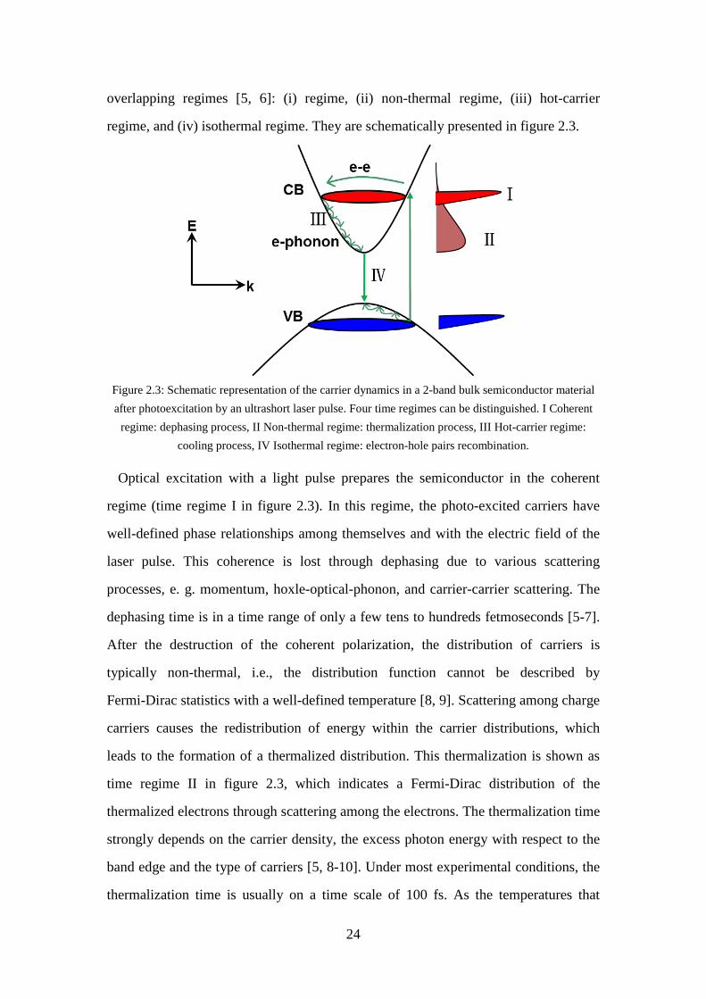
24
overlapping regimes [5, 6]: (i) regime, (ii) non-thermal regime, (iii) hot-carrier
regime, and (iv) isothermal regime. They are schematically presented in figure 2.3.
Figure 2.3: Schematic representation of the carrier dynamics in a 2-band bulk semiconductor material after photoexcitation by an ultrashort laser pulse. Four time regimes can be distinguished. I Coherent
regime: dephasing process, II Non-thermal regime: thermalization process, III Hot-carrier regime: cooling process, IV Isothermal regime: electron-hole pairs recombination.
Optical excitation with a light pulse prepares the semiconductor in the coherent
regime (time regime I in figure 2.3). In this regime, the photo-excited carriers have
well-defined phase relationships among themselves and with the electric field of the
laser pulse. This coherence is lost through dephasing due to various scattering
processes, e. g. momentum, hoxle-optical-phonon, and carrier-carrier scattering. The
dephasing time is in a time range of only a few tens to hundreds fetmoseconds [5-7].
After the destruction of the coherent polarization, the distribution of carriers is
typically non-thermal, i.e., the distribution function cannot be described by
Fermi-Dirac statistics with a well-defined temperature [8, 9]. Scattering among charge
carriers causes the redistribution of energy within the carrier distributions, which
leads to the formation of a thermalized distribution. This thermalization is shown as
time regime II in figure 2.3, which indicates a Fermi-Dirac distribution of the
thermalized electrons through scattering among the electrons. The thermalization time
strongly depends on the carrier density, the excess photon energy with respect to the
band edge and the type of carriers [5, 8-10]. Under most experimental conditions, the
thermalization time is usually on a time scale of 100 fs. As the temperatures that
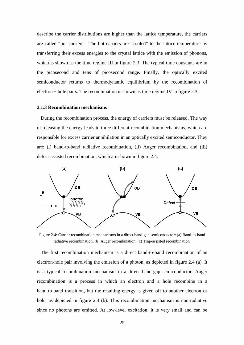
25
describe the carrier distributions are higher than the lattice temperature, the carriers
are called “hot carriers”. The hot carriers are “cooled” to the lattice temperature by
transferring their excess energies to the crystal lattice with the emission of phonons,
which is shown as the time regime III in figure 2.3. The typical time constants are in
the picosecond and tens of picosecond range. Finally, the optically excited
semiconductor returns to thermodynamic equilibrium by the recombination of
electron–hole pairs. The recombination is shown as time regime IV in figure 2.3.
2.1.3 Recombination mechanisms
During the recombination process, the energy of carriers must be released. The way
of releasing the energy leads to three different recombination mechanisms, which are
responsible for excess carrier annihilation in an optically excited semiconductor. They
are: (i) band-to-band radiative recombination, (ii) Auger recombination, and (iii)
defect-assisted recombination, which are shown in figure 2.4.
Figure 2.4: Carrier recombination mechanisms in a direct band-gap semiconductor: (a) Band-to-band
radiative recombination, (b) Auger recombination, (c) Trap-assisted recombination.
The first recombination mechanism is a direct band-to-band recombination of an
electron-hole pair involving the emission of a photon, as depicted in figure 2.4 (a). It
is a typical recombination mechanism in a direct band-gap semiconductor. Auger
recombination is a process in which an electron and a hole recombine in a
band-to-band transition, but the resulting energy is given off to another electron or
hole, as depicted in figure 2.4 (b). This recombination mechanism is non-radiative
since no photons are emitted. At low-level excitation, it is very small and can be
26
neglected, while it will be primarily important at high-level excitation [11].
Trap-assisted recombination is also known as Hall-Shockley-Read (HSR or SRH)
recombination [12], as depicted in figure 2.4 (c). It occurs when electrons (holes) fall
into a trap center, which is an energy level within the band gap caused by the presence
of impurity atoms or native defects such as vacancies and interstitials. Consequently,
electrons and holes stay at the trap centers for finite times and can return to the
conduction or valence bands through thermal excitation involving the emission of
phonons. This recombination mechanism is also non-radiative, and can speed up the
recombination rate at high-density trap centers.
2.1.4 The techniques to reduce the carrier lifetime in a semiconductor
In a semiconductor which is grown by standard epitaxial growth techniques, some
impurity atoms or native lattice defects are created unintentionally during the growth,
but their concentration are usually negligible. Therefore the recombination mainly
proceeds by the band-to-band radiative recombination or Auger recombination at
high-level excitation, which take place on time scales of hundreds of picoseconds and
longer. Consequently the long recombination time is the major obstacle to realize an
ultrafast semiconductor-based device. Large concentrations of native lattice defects or
impurity atoms are desired to create an electronic state within the band gap of the
semiconductor. They can serve as carrier trapping and recombination centers, thus
effectively reducing the carrier lifetime. Several techniques have been used to
introduce lattice defects in the semiconductor. These techniques mainly include:
(i) Low-temperature MBE growth
Low-temperature (LT) growth refers to epitaxial growth at a substrate temperature
lower than the normal growth temperature. It is usually used to reduce the carrier
lifetime in the As-based III-V crystalline semiconductors grown [13]. In order to get a
high crystalline quality, the substrate temperature during the MBE growth should be
600 °C. Growth at lower temperatures can lead to the incorporation of excess arsenic
(Group-V) atoms and the generation of native lattice defects such as As vacancies and
a group-III (In, Ga) interstitial. Both As antisites and native lattice defects can act as
27
trap centers. For example, in LT-grown GaAs the excess arsenic atoms form As
antisites (AsGa) with energy close to the center of the band gap [14]. These As
antisites act as the main trap centers and recombination centers, and their
concentration increases with decreasing growth temperature [15, 16]. Sub-picosecond
carrier lifetime in GaAs grown at 200 °C has been achieved [17]. Other LT-growth
bulk and QWs materials such as InAlAs [18], InAlAs / InP [19], GaAs / AlGaAs [20],
have also shown sub-picosecond carrier lifetime. However, LT growth of InGaAs
produces relatively long carrier lifetimes of several picoseconds since the As antisites
in LT grown InGaAs appear in lower concentration than in LT grown GaAs [21].
(ii) Impurity doping
Impurity doping is to incorporate foreign atoms into the substitutional sites in the
semiconductor crystal structure during the epitaxial growth, resulting in the formation
of a trap center within the band gap of the semiconductor. Impurity doping is divided
into shallow doping and deep doping. Shallow dopants could not result in ultrafast
carrier lifetime since their electronic states are very close to one of the bands, making
them efficient in trapping one type of carriers, but very inefficient in trapping the
other type. Therefore, the shallow doping is always associated with LT growth. For
example, Be doping seems to be used not exclusively and is always associated with a
LT growth. The combination of Be doping with LT growth can shorten the carrier
lifetime of bulk InGaAs [22] or InGaAs / InAlAs QWs [23, 24] to sub-picosecond.
Deep dopants that create electronic states near the middle of the band gap may be
efficient in trapping both carriers. It has been demonstrated that Fe doping is a deep
acceptor in InGaAs [25]. A recovery time of 290 fs in Fe-doped InGaAs / InP QWs
grown at a higher temperature of 450 °C has been achieved [26].
(iii) Ion irradiation
Ion irradiation is used to introduce native lattice defects in the semiconductor by ion
bombardment after growth. These native lattice defects can act as trap centers. The
ions for irradiation usually have very high energy so that ions can pass through the
active layer without being implanted, and thus only create native lattice defects along
their paths. Ion irradiation can be further classified into light and heavy ion
28
irradiation. The use of light ions such as protons (H+) creates a majority of isolated
point defects [27], such as interstitials and various types of vacancies, while the use of
heavy ions such as nickel (Ni+) [28], gold (Au+) or the oxygen (O+) [29] mainly
creates clusters of point defects. The different types of defect have different effects on
the carrier dynamics. It has been demonstrated that the heavy-ion irradiation gives
shorter carrier lifetimes and is more robust against thermal annealing than the
light-ion irradiation [30]. However, the heavy ion irradiation technique requires very
high ion energy on the order of MeV. This is not a common, easily available
technique.
(iv) Ion implantation
Ion implantation and ion irradiation depend on the same technology, which is using
high-energy ions to bombard the semiconductor. The difference between them is that
in the case of ion implantation, ions will not pass through the active layer but rather
stay in the active region. Post-annealing is usually required to repair lattice damages
and put the dopant on substitutional sites in the semiconductor crystal. For an
ion-implanted sample, the complexes resulting from dopant incorporation and native
lattice defects can act as trap centers. Ion implantation was shown to lead to ultrafast
carrier lifetime in many materials such as bulk InP [31], GaAs [32] and InGaAs/GaAs
QW [33]. Compared with the LT growth and impurity doping, ion implantation and
irradiation have obvious advantages. Firstly, once a wafer is grown, the properties of
the individual small sample, cleaved from it, can be tailored by the choice of the ion
species, ion energy, ion dose and annealing conditions. They also have abilities to
accurately control the number of lattice defects or impurity atoms and to place them at
the desired depth of choice.
In this thesis, heavy-ion-implantation was chosen to reduce the carrier lifetime of
InGaAs since it requires less ion energy than heavy-ion-irradiation, and is more
effective than LT-growth combined with impurity doping. In order to make full use of
ion implantation to realize ultrafast SAMs, it is necessary to understand the
fundamental features of the ion implantation technique. This is introduced in the
following section 2.2.

29
2.2 Ion implantation technique
Ion implantation works by ionizing the required atoms, selecting only the species of
interest with the ion separation magnet, accelerating them in an electric field and
directing this beam towards the target. Figure 2.5 displays a schematic overview of an
ion implanter.
Figure 2.5: Schematic overview of an ion implanter.
In order to be able to control the amount of ions (the dose) “Faraday’s cups” are used
to measure the current due to the flow of charged particles. The information from the
Faraday’s cups is then used to calculate the actual dose of ions hitting the substrate
material. This is done by utilizing the relation [34]:
1Dose IdtAq
= ∫ (2.3)
where A is the implanted area, I is the current due to the ion beam, q is the charge of
each ion and t is the integration time.
2.2.1 Ion stopping theory
The atoms enter the crystal lattice, collide with the target atoms, lose energy, and
finally come to rest at some depth within the target. The processes responsible for
slowing down (energy loss) the penetrating atoms within the target are termed
electronic and nuclear stopping [35]. Electronic stopping occurs by inelastic collisions
with bound electrons in the material. The energy loss of the penetrating ions is due to
excitation when electrons enter higher energy states, and ionization occurs when
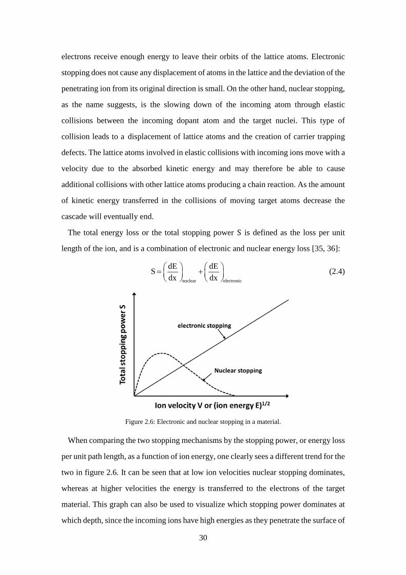
30
electrons receive enough energy to leave their orbits of the lattice atoms. Electronic
stopping does not cause any displacement of atoms in the lattice and the deviation of the
penetrating ion from its original direction is small. On the other hand, nuclear stopping,
as the name suggests, is the slowing down of the incoming atom through elastic
collisions between the incoming dopant atom and the target nuclei. This type of
collision leads to a displacement of lattice atoms and the creation of carrier trapping
defects. The lattice atoms involved in elastic collisions with incoming ions move with a
velocity due to the absorbed kinetic energy and may therefore be able to cause
additional collisions with other lattice atoms producing a chain reaction. As the amount
of kinetic energy transferred in the collisions of moving target atoms decrease the
cascade will eventually end.
The total energy loss or the total stopping power S is defined as the loss per unit
length of the ion, and is a combination of electronic and nuclear energy loss [35, 36]:
nuclear electronic
dE dESdx dx
= +
(2.4)
Figure 2.6: Electronic and nuclear stopping in a material.
When comparing the two stopping mechanisms by the stopping power, or energy loss
per unit path length, as a function of ion energy, one clearly sees a different trend for the
two in figure 2.6. It can be seen that at low ion velocities nuclear stopping dominates,
whereas at higher velocities the energy is transferred to the electrons of the target
material. This graph can also be used to visualize which stopping power dominates at
which depth, since the incoming ions have high energies as they penetrate the surface of
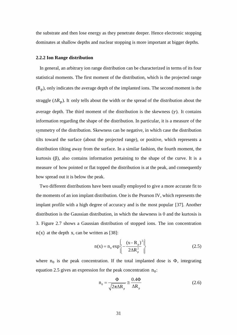
31
the substrate and then lose energy as they penetrate deeper. Hence electronic stopping
dominates at shallow depths and nuclear stopping is more important at bigger depths.
2.2.2 Ion Range distribution
In general, an arbitrary ion range distribution can be characterized in terms of its four
statistical moments. The first moment of the distribution, which is the projected range
(Rp), only indicates the average depth of the implanted ions. The second moment is the
straggle (∆Rp). It only tells about the width or the spread of the distribution about the
average depth. The third moment of the distribution is the skewness (𝛾). It contains
information regarding the shape of the distribution. In particular, it is a measure of the
symmetry of the distribution. Skewness can be negative, in which case the distribution
tilts toward the surface (about the projected range), or positive, which represents a
distribution tilting away from the surface. In a similar fashion, the fourth moment, the
kurtosis (β), also contains information pertaining to the shape of the curve. It is a
measure of how pointed or flat topped the distribution is at the peak, and consequently
how spread out it is below the peak.
Two different distributions have been usually employed to give a more accurate fit to
the moments of an ion implant distribution. One is the Pearson IV, which represents the
implant profile with a high degree of accuracy and is the most popular [37]. Another
distribution is the Gaussian distribution, in which the skewness is 0 and the kurtosis is
3. Figure 2.7 shows a Gaussian distribution of stopped ions. The ion concentration
n(x) at the depth x, can be written as [38]: 2
p0 2
p
(x R )n(x) n exp
2ΔR
− = −
(2.5)
where n0 is the peak concentration. If the total implanted dose is Φ, integrating
equation 2.5 gives an expression for the peak concentration n0:
0pp
Φ 0.4ΦnΔR2πΔR
= ≅ (2.6)
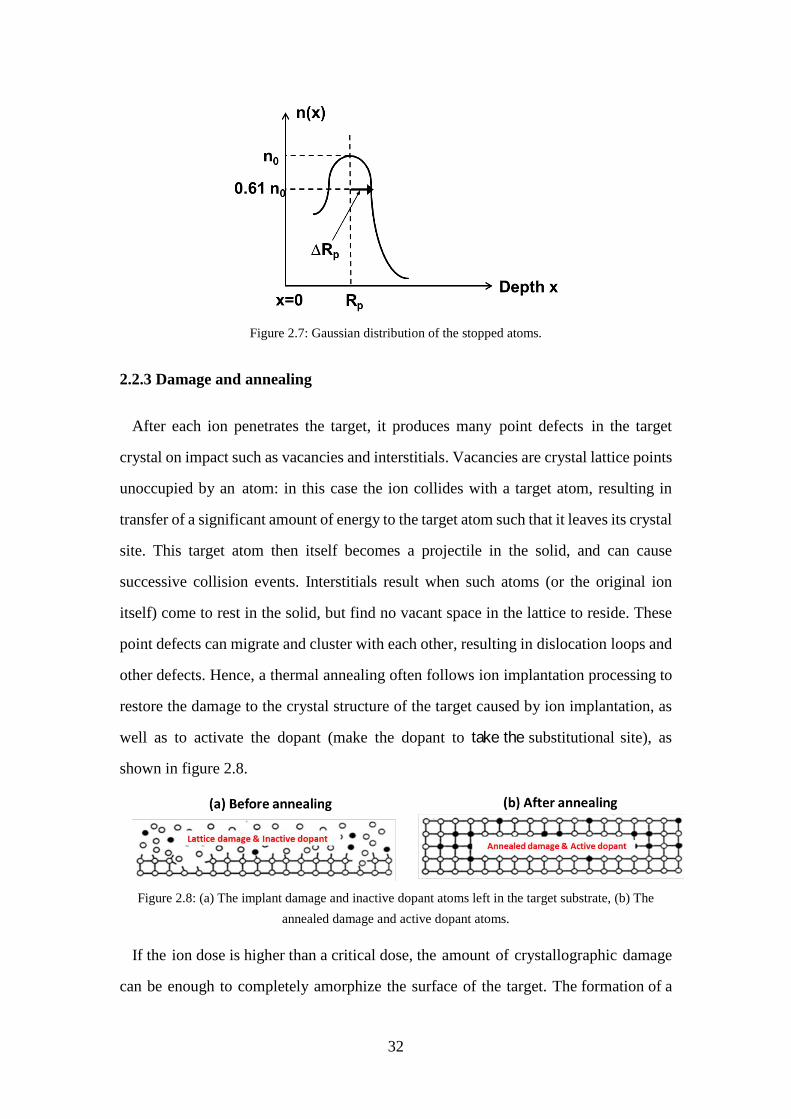
32
Figure 2.7: Gaussian distribution of the stopped atoms.
2.2.3 Damage and annealing
After each ion penetrates the target, it produces many point defects in the target
crystal on impact such as vacancies and interstitials. Vacancies are crystal lattice points
unoccupied by an atom: in this case the ion collides with a target atom, resulting in
transfer of a significant amount of energy to the target atom such that it leaves its crystal
site. This target atom then itself becomes a projectile in the solid, and can cause
successive collision events. Interstitials result when such atoms (or the original ion
itself) come to rest in the solid, but find no vacant space in the lattice to reside. These
point defects can migrate and cluster with each other, resulting in dislocation loops and
other defects. Hence, a thermal annealing often follows ion implantation processing to
restore the damage to the crystal structure of the target caused by ion implantation, as
well as to activate the dopant (make the dopant to take the substitutional site), as
shown in figure 2.8.
Figure 2.8: (a) The implant damage and inactive dopant atoms left in the target substrate, (b) The
annealed damage and active dopant atoms.
If the ion dose is higher than a critical dose, the amount of crystallographic damage
can be enough to completely amorphize the surface of the target. The formation of a
33
continuous amorphous layer will lead to a saturation of the carrier lifetime shortening
[39] and a degradation of the saturable absorption properties of the semiconductor [40].
Moreover, this continuous amorphous layer could not be restored by post-annealing.
So, in addition to the post-annealing, a dynamic annealing during the ion implantation
is also performed through implanting ions into the target under a high substrate
temperature. If the substrate temperature during ion implantation is sufficiently high,
the competing process of dynamic annealing can occur to repair some or all of the
damage as it is generated. Therefore the critical dose at which a continuous amorphous
layer forms will be increased.
2.2.4 The Stopping and Range of Ions in Matter (SRIM)
SRIM is a collection of software packages which calculate the stopping and range
of ions into matter using a quantum mechanical treatment of ion-atom collisions
(assuming a moving atom as an "ion", and all target atoms as "atoms")[35]. This
calculation is made very efficient by the use of statistical algorithms which allow the
ion to make jumps between calculated collisions and then averaging the collision
results over the intervening gap. During the collisions, the ion and atom have a
screened Coulomb collision, including exchange and correlation interactions between
the overlapping electron shells. The ion has long range interactions creating electron
excitations and plasmons within the target. These are described by including a
description of the target's collective electronic structure and interatomic bond
structure when the calculation is setup. The charge state of the ion within the target is
described using the concept of effective charge, which includes a velocity dependent
charge state and long range screening due to the collective electron sea of the target.
Its typical applications include ion stopping and range in targets, ion implantation,
sputtering, ion transmission, and ion beam therapy. Ion stopping and range in targets
are calculated in SRIM software, the Stopping and Range of Ions in Matter, while
other applications can be calculated in TRIM software, the Transport of Ions in
Matter.
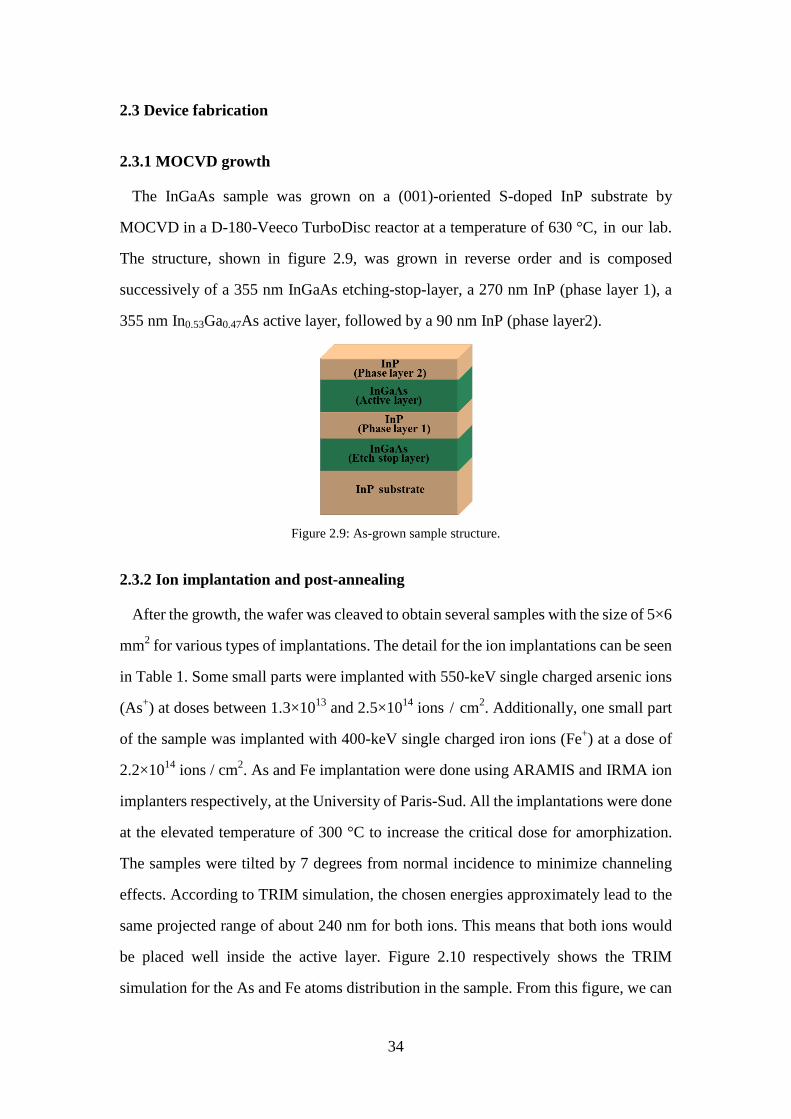
34
2.3 Device fabrication
2.3.1 MOCVD growth
The InGaAs sample was grown on a (001)-oriented S-doped InP substrate by
MOCVD in a D-180-Veeco TurboDisc reactor at a temperature of 630 °C, in our lab.
The structure, shown in figure 2.9, was grown in reverse order and is composed
successively of a 355 nm InGaAs etching-stop-layer, a 270 nm InP (phase layer 1), a
355 nm In0.53Ga0.47As active layer, followed by a 90 nm InP (phase layer2).
Figure 2.9: As-grown sample structure.
2.3.2 Ion implantation and post-annealing
After the growth, the wafer was cleaved to obtain several samples with the size of 5×6
mm2 for various types of implantations. The detail for the ion implantations can be seen
in Table 1. Some small parts were implanted with 550-keV single charged arsenic ions
(As+) at doses between 1.3×10¹³ and 2.5×10¹⁴ ions / cm2. Additionally, one small part
of the sample was implanted with 400-keV single charged iron ions (Fe+) at a dose of
2.2×10¹⁴ ions / cm2. As and Fe implantation were done using ARAMIS and IRMA ion
implanters respectively, at the University of Paris-Sud. All the implantations were done
at the elevated temperature of 300 °C to increase the critical dose for amorphization.
The samples were tilted by 7 degrees from normal incidence to minimize channeling
effects. According to TRIM simulation, the chosen energies approximately lead to the
same projected range of about 240 nm for both ions. This means that both ions would
be placed well inside the active layer. Figure 2.10 respectively shows the TRIM
simulation for the As and Fe atoms distribution in the sample. From this figure, we can
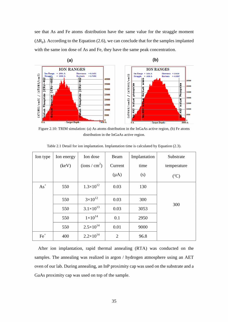
35
see that As and Fe atoms distribution have the same value for the straggle moment
(∆Rp). According to the Equation (2.6), we can conclude that for the samples implanted
with the same ion dose of As and Fe, they have the same peak concentration.
Figure 2.10: TRIM simulation: (a) As atoms distribution in the InGaAs active region, (b) Fe atoms
distribution in the InGaAs active region.
Table 2.1 Detail for ion implantation. Implantation time is calculated by Equation (2.3).
Ion type Ion energy
(keV)
Ion dose
(ions / cm2)
Beam
Current
(µA)
Implantation
time
(s)
Substrate
temperature
(ºC)
As+ 550 1.3×10¹² 0.03 130
300 550 3×10¹² 0.03 300
550 3.1×10¹³ 0.03 3053
550 1×10¹⁴ 0.1 2950
550 2.5×10¹⁴ 0.01 9000
Fe+ 400 2.2×10¹⁴ 2 96.8
After ion implantation, rapid thermal annealing (RTA) was conducted on the
samples. The annealing was realized in argon / hydrogen atmosphere using an AET
oven of our lab. During annealing, an InP proximity cap was used on the substrate and a
GaAs proximity cap was used on top of the sample.
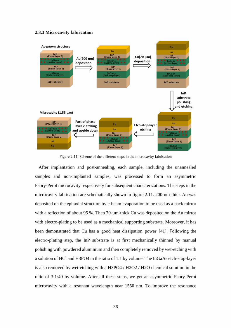
36
2.3.3 Microcavity fabrication
Figure 2.11: Scheme of the different steps in the microcavity fabrication
After implantation and post-annealing, each sample, including the unannealed
samples and non-implanted samples, was processed to form an asymmetric
Fabry-Perot microcavity respectively for subsequent characterizations. The steps in the
microcavity fabrication are schematically shown in figure 2.11. 200-nm-thick Au was
deposited on the epitaxial structure by e-beam evaporation to be used as a back mirror
with a reflection of about 95 %. Then 70-µm-thick Cu was deposited on the Au mirror
with electro-plating to be used as a mechanical supporting substrate. Moreover, it has
been demonstrated that Cu has a good heat dissipation power [41]. Following the
electro-plating step, the InP substrate is at first mechanically thinned by manual
polishing with powdered aluminium and then completely removed by wet-etching with
a solution of HCl and H3PO4 in the ratio of 1:1 by volume. The InGaAs etch-stop-layer
is also removed by wet-etching with a H3PO4 / H2O2 / H2O chemical solution in the
ratio of 3:1:40 by volume. After all these steps, we get an asymmetric Fabry-Perot
microcavity with a resonant wavelength near 1550 nm. To improve the resonance
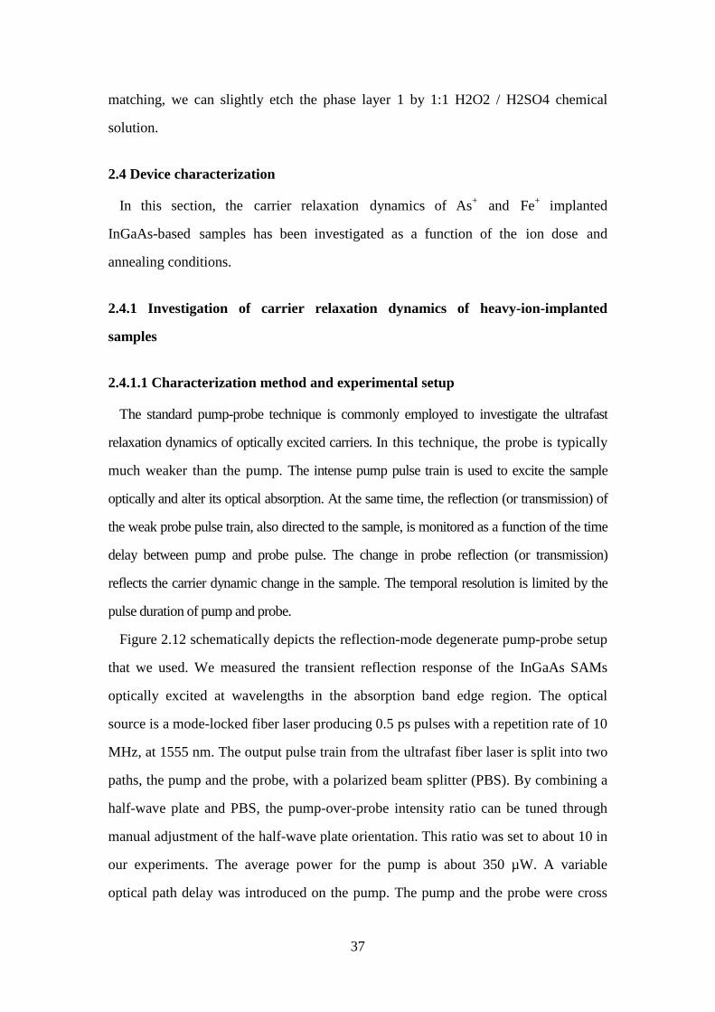
37
matching, we can slightly etch the phase layer 1 by 1:1 H2O2 / H2SO4 chemical
solution.
2.4 Device characterization
In this section, the carrier relaxation dynamics of As+ and Fe+ implanted
InGaAs-based samples has been investigated as a function of the ion dose and
annealing conditions.
2.4.1 Investigation of carrier relaxation dynamics of heavy-ion-implanted
samples
2.4.1.1 Characterization method and experimental setup
The standard pump-probe technique is commonly employed to investigate the ultrafast
relaxation dynamics of optically excited carriers. In this technique, the probe is typically
much weaker than the pump. The intense pump pulse train is used to excite the sample
optically and alter its optical absorption. At the same time, the reflection (or transmission) of
the weak probe pulse train, also directed to the sample, is monitored as a function of the time
delay between pump and probe pulse. The change in probe reflection (or transmission)
reflects the carrier dynamic change in the sample. The temporal resolution is limited by the
pulse duration of pump and probe.
Figure 2.12 schematically depicts the reflection-mode degenerate pump-probe setup
that we used. We measured the transient reflection response of the InGaAs SAMs
optically excited at wavelengths in the absorption band edge region. The optical
source is a mode-locked fiber laser producing 0.5 ps pulses with a repetition rate of 10
MHz, at 1555 nm. The output pulse train from the ultrafast fiber laser is split into two
paths, the pump and the probe, with a polarized beam splitter (PBS). By combining a
half-wave plate and PBS, the pump-over-probe intensity ratio can be tuned through
manual adjustment of the half-wave plate orientation. This ratio was set to about 10 in
our experiments. The average power for the pump is about 350 µW. A variable
optical path delay was introduced on the pump. The pump and the probe were cross
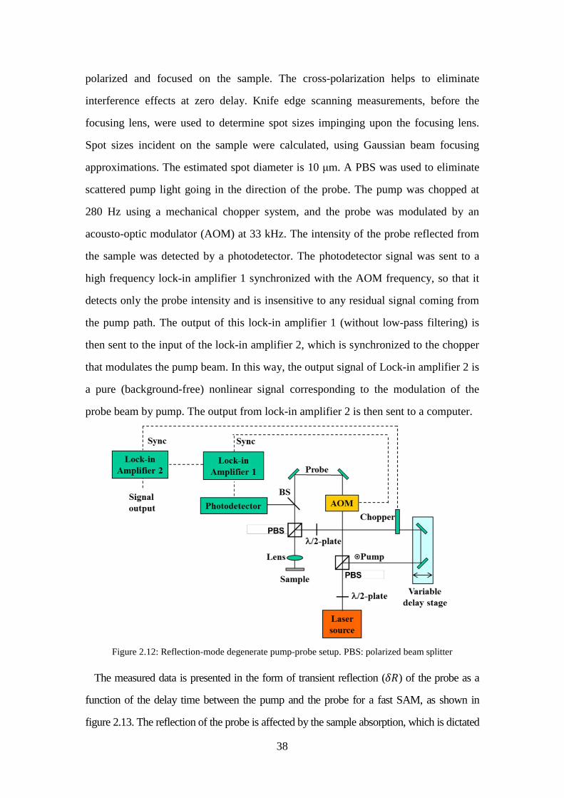
38
polarized and focused on the sample. The cross-polarization helps to eliminate
interference effects at zero delay. Knife edge scanning measurements, before the
focusing lens, were used to determine spot sizes impinging upon the focusing lens.
Spot sizes incident on the sample were calculated, using Gaussian beam focusing
approximations. The estimated spot diameter is 10 μm. A PBS was used to eliminate
scattered pump light going in the direction of the probe. The pump was chopped at
280 Hz using a mechanical chopper system, and the probe was modulated by an
acousto-optic modulator (AOM) at 33 kHz. The intensity of the probe reflected from
the sample was detected by a photodetector. The photodetector signal was sent to a
high frequency lock-in amplifier 1 synchronized with the AOM frequency, so that it
detects only the probe intensity and is insensitive to any residual signal coming from
the pump path. The output of this lock-in amplifier 1 (without low-pass filtering) is
then sent to the input of the lock-in amplifier 2, which is synchronized to the chopper
that modulates the pump beam. In this way, the output signal of Lock-in amplifier 2 is
a pure (background-free) nonlinear signal corresponding to the modulation of the
probe beam by pump. The output from lock-in amplifier 2 is then sent to a computer.
Figure 2.12: Reflection-mode degenerate pump-probe setup. PBS: polarized beam splitter
The measured data is presented in the form of transient reflection (𝛿𝛿) of the probe as a
function of the delay time between the pump and the probe for a fast SAM, as shown in
figure 2.13. The reflection of the probe is affected by the sample absorption, which is dictated
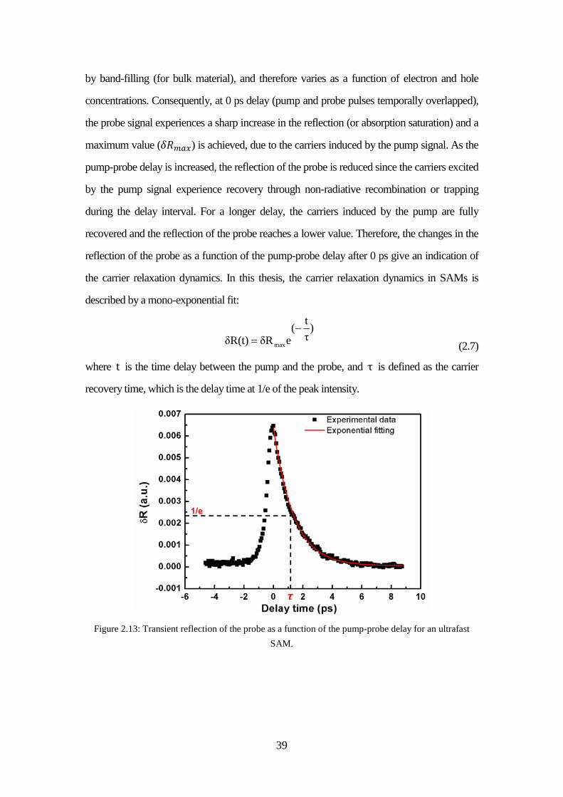
39
by band-filling (for bulk material), and therefore varies as a function of electron and hole
concentrations. Consequently, at 0 ps delay (pump and probe pulses temporally overlapped),
the probe signal experiences a sharp increase in the reflection (or absorption saturation) and a
maximum value (𝛿𝛿𝑚𝑚𝑚) is achieved, due to the carriers induced by the pump signal. As the
pump-probe delay is increased, the reflection of the probe is reduced since the carriers excited
by the pump signal experience recovery through non-radiative recombination or trapping
during the delay interval. For a longer delay, the carriers induced by the pump are fully
recovered and the reflection of the probe reaches a lower value. Therefore, the changes in the
reflection of the probe as a function of the pump-probe delay after 0 ps give an indication of
the carrier relaxation dynamics. In this thesis, the carrier relaxation dynamics in SAMs is
described by a mono-exponential fit:
max
t( )τδR(t) δR e
−= (2.7)
where t is the time delay between the pump and the probe, and τ is defined as the carrier
recovery time, which is the delay time at 1/e of the peak intensity.
Figure 2.13: Transient reflection of the probe as a function of the pump-probe delay for an ultrafast
SAM.
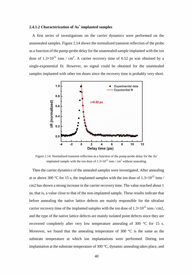
40
2.4.1.2 Characterization of As+ implanted samples
A first series of investigations on the carrier dynamics were performed on the
unannealed samples. Figure 2.14 shows the normalized transient reflection of the probe
as a function of the pump-probe delay for the unannealed sample implanted with the ion
dose of 1.3×10¹² ions / cm2. A carrier recovery time of 0.52 ps was obtained by a
single-exponential fit. However, no signal could be obtained for the unannealed
samples implanted with other ion doses since the recovery time is probably very short.
Figure 2.14: Normalized transient reflection as a function of the pump-probe delay for the As+
implanted sample with the ion dose of 1.3×10¹² ions / cm2 without annealing.
Then the carrier dynamics of the annealed samples were investigated. After annealing
at or above 300 °C for 15 s, the implanted samples with the ion dose of 1.3×10¹² ions /
cm2 has shown a strong increase in the carrier recovery time. The value reached about 1
ns, that is, a value close to that of the non-implanted sample. These results indicate that
before annealing the native lattice defects are mainly responsible for the ultrafast
carrier recovery time of the implanted samples with the ion dose of 1.3×10¹² ions / cm2,
and the type of the native lattice defects are mainly isolated point defects since they are
recovered completely after very low temperature annealing of 300 °C for 15 s.
Moreover, we found that the annealing temperature of 300 °C is the same as the
substrate temperature at which ion implantations were performed. During ion
implantation at the substrate temperature of 300 °C, dynamic annealing takes place, and
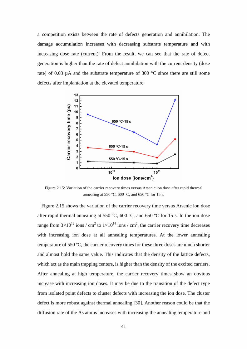
41
a competition exists between the rate of defects generation and annihilation. The
damage accumulation increases with decreasing substrate temperature and with
increasing dose rate (current). From the result, we can see that the rate of defect
generation is higher than the rate of defect annihilation with the current density (dose
rate) of 0.03 µA and the substrate temperature of 300 °C since there are still some
defects after implantation at the elevated temperature.
Figure 2.15: Variation of the carrier recovery times versus Arsenic ion dose after rapid thermal
annealing at 550 ºC, 600 ºC, and 650 ºC for 15 s.
Figure 2.15 shows the variation of the carrier recovery time versus Arsenic ion dose
after rapid thermal annealing at 550 ºC, 600 ºC, and 650 ºC for 15 s. In the ion dose
range from 3×10¹² ions / cm2 to 1×10¹⁴ ions / cm2, the carrier recovery time decreases
with increasing ion dose at all annealing temperatures. At the lower annealing
temperature of 550 ºC, the carrier recovery times for these three doses are much shorter
and almost hold the same value. This indicates that the density of the lattice defects,
which act as the main trapping centers, is higher than the density of the excited carriers.
After annealing at high temperature, the carrier recovery times show an obvious
increase with increasing ion doses. It may be due to the transition of the defect type
from isolated point defects to cluster defects with increasing the ion dose. The cluster
defect is more robust against thermal annealing [30]. Another reason could be that the
diffusion rate of the As atoms increases with increasing the annealing temperature and
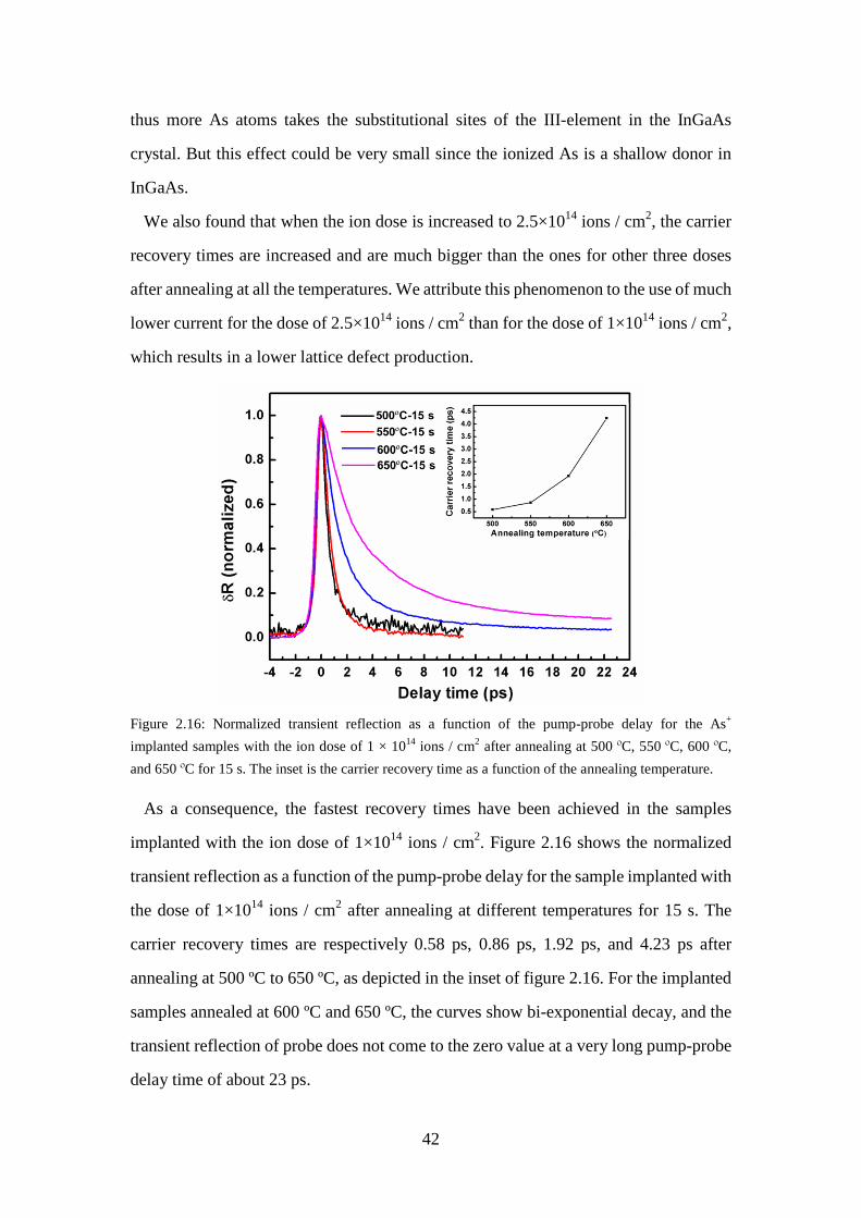
42
thus more As atoms takes the substitutional sites of the III-element in the InGaAs
crystal. But this effect could be very small since the ionized As is a shallow donor in
InGaAs.
We also found that when the ion dose is increased to 2.5×10¹⁴ ions / cm2, the carrier
recovery times are increased and are much bigger than the ones for other three doses
after annealing at all the temperatures. We attribute this phenomenon to the use of much
lower current for the dose of 2.5×10¹⁴ ions / cm2 than for the dose of 1×10¹⁴ ions / cm2,
which results in a lower lattice defect production.
Figure 2.16: Normalized transient reflection as a function of the pump-probe delay for the As+ implanted samples with the ion dose of 1 × 10¹⁴ ions / cm2 after annealing at 500 ºC, 550 ºC, 600 ºC, and 650 ºC for 15 s. The inset is the carrier recovery time as a function of the annealing temperature.
As a consequence, the fastest recovery times have been achieved in the samples
implanted with the ion dose of 1×10¹⁴ ions / cm2. Figure 2.16 shows the normalized
transient reflection as a function of the pump-probe delay for the sample implanted with
the dose of 1×10¹⁴ ions / cm2 after annealing at different temperatures for 15 s. The
carrier recovery times are respectively 0.58 ps, 0.86 ps, 1.92 ps, and 4.23 ps after
annealing at 500 ºC to 650 ºC, as depicted in the inset of figure 2.16. For the implanted
samples annealed at 600 ºC and 650 ºC, the curves show bi-exponential decay, and the
transient reflection of probe does not come to the zero value at a very long pump-probe
delay time of about 23 ps.
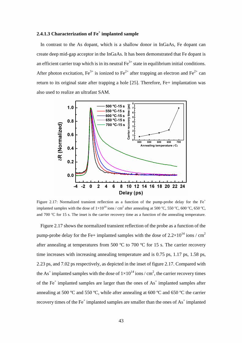
43
2.4.1.3 Characterization of Fe+ implanted sample
In contrast to the As dopant, which is a shallow donor in InGaAs, Fe dopant can
create deep mid-gap acceptor in the InGaAs. It has been demonstrated that Fe dopant is
an efficient carrier trap which is in its neutral Fe3+ state in equilibrium initial conditions.
After photon excitation, Fe3+ is ionized to Fe2+ after trapping an electron and Fe2+ can
return to its original state after trapping a hole [25]. Therefore, Fe+ implantation was
also used to realize an ultrafast SAM.
Figure 2.17: Normalized transient reflection as a function of the pump-probe delay for the Fe+ implanted samples with the dose of 1×10¹⁴ ions / cm2 after annealing at 500 ºC, 550 ºC, 600 ºC, 650 ºC, and 700 ºC for 15 s. The inset is the carrier recovery time as a function of the annealing temperature.
Figure 2.17 shows the normalized transient reflection of the probe as a function of the
pump-probe delay for the Fe+ implanted samples with the dose of 2.2×10¹⁴ ions / cm2
after annealing at temperatures from 500 ºC to 700 ºC for 15 s. The carrier recovery
time increases with increasing annealing temperature and is 0.75 ps, 1.17 ps, 1.58 ps,
2.23 ps, and 7.02 ps respectively, as depicted in the inset of figure 2.17. Compared with
the As+ implanted samples with the dose of 1×10¹⁴ ions / cm2, the carrier recovery times
of the Fe+ implanted samples are larger than the ones of As+ implanted samples after
annealing at 500 ºC and 550 ºC, while after annealing at 600 ºC and 650 ºC the carrier
recovery times of the Fe+ implanted samples are smaller than the ones of As+ implanted
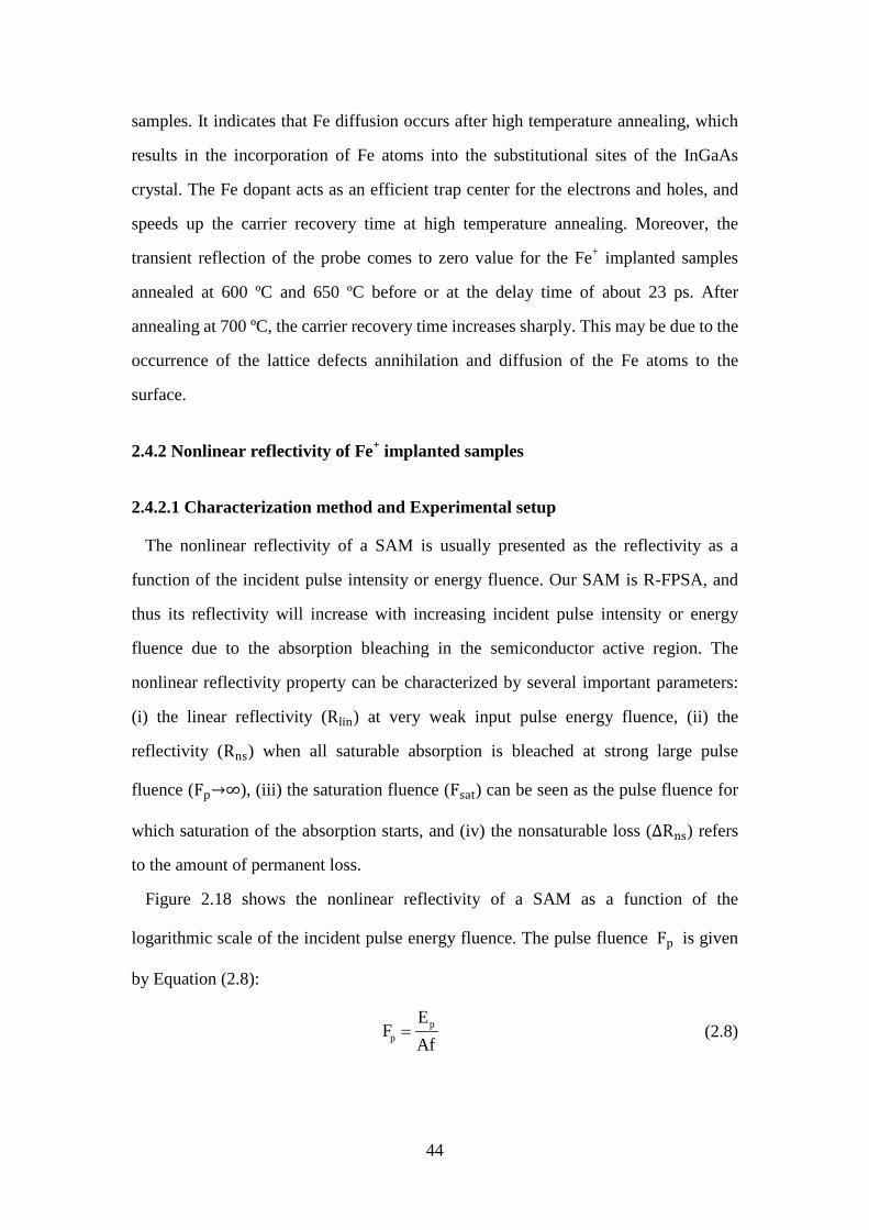
44
samples. It indicates that Fe diffusion occurs after high temperature annealing, which
results in the incorporation of Fe atoms into the substitutional sites of the InGaAs
crystal. The Fe dopant acts as an efficient trap center for the electrons and holes, and
speeds up the carrier recovery time at high temperature annealing. Moreover, the
transient reflection of the probe comes to zero value for the Fe+ implanted samples
annealed at 600 ºC and 650 ºC before or at the delay time of about 23 ps. After
annealing at 700 ºC, the carrier recovery time increases sharply. This may be due to the
occurrence of the lattice defects annihilation and diffusion of the Fe atoms to the
surface.
2.4.2 Nonlinear reflectivity of Fe+ implanted samples
2.4.2.1 Characterization method and Experimental setup
The nonlinear reflectivity of a SAM is usually presented as the reflectivity as a
function of the incident pulse intensity or energy fluence. Our SAM is R-FPSA, and
thus its reflectivity will increase with increasing incident pulse intensity or energy
fluence due to the absorption bleaching in the semiconductor active region. The
nonlinear reflectivity property can be characterized by several important parameters:
(i) the linear reflectivity (Rlin) at very weak input pulse energy fluence, (ii) the
reflectivity (Rns) when all saturable absorption is bleached at strong large pulse
fluence (Fp→∞), (iii) the saturation fluence (Fsat) can be seen as the pulse fluence for
which saturation of the absorption starts, and (iv) the nonsaturable loss (∆Rns) refers
to the amount of permanent loss.
Figure 2.18 shows the nonlinear reflectivity of a SAM as a function of the
logarithmic scale of the incident pulse energy fluence. The pulse fluence Fp is given
by Equation (2.8):
pp
EF
Af= (2.8)
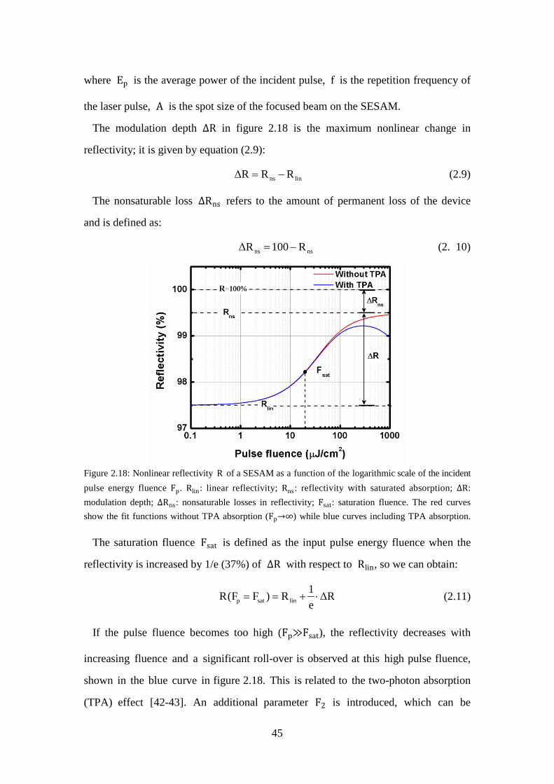
45
where Ep is the average power of the incident pulse, f is the repetition frequency of
the laser pulse, A is the spot size of the focused beam on the SESAM.
The modulation depth ∆R in figure 2.18 is the maximum nonlinear change in
reflectivity; it is given by equation (2.9):
ns linΔR R R= − (2.9)
The nonsaturable loss ∆Rns refers to the amount of permanent loss of the device
and is defined as:
ns nsΔR 100 R= − (2. 10)
Figure 2.18: Nonlinear reflectivity R of a SESAM as a function of the logarithmic scale of the incident pulse energy fluence Fp. Rlin: linear reflectivity; Rns: reflectivity with saturated absorption; ∆R: modulation depth; ∆Rns: nonsaturable losses in reflectivity; Fsat: saturation fluence. The red curves show the fit functions without TPA absorption (Fp→∞) while blue curves including TPA absorption.
The saturation fluence Fsat is defined as the input pulse energy fluence when the
reflectivity is increased by 1/e (37%) of ∆R with respect to Rlin, so we can obtain:
p sat lin1R(F F ) R ΔRe
= = + ⋅ (2.11)
If the pulse fluence becomes too high (Fp≫Fsat), the reflectivity decreases with
increasing fluence and a significant roll-over is observed at this high pulse fluence,
shown in the blue curve in figure 2.18. This is related to the two-photon absorption
(TPA) effect [42-43]. An additional parameter F2 is introduced, which can be
46
interpreted as the curvature of the rollover and is introduced as an additional
parameter in the reflectivity function, which is defined as the fluence where the
reflectivity of the SAM has dropped by 37% (1/e) compared to Rns.
These characteristic parameters are not experimentally accessible but rather
extrapolated values from the measured reflectivity using a proper model function. For
a flat-top shaped spatial beam profile, the nonlinear reflectivity can be expressed as:
2
psat
p
FF
sat
p
FF
ns
lin
nsp e
FF
1)](eRRln[1
R)R(F−
⋅−+
⋅= (2.12)
If there is no TPA, the Equation (2.12) can be expressed by
sat
p
FF
ns
lin
nsp
FF
1)](eRRln[1
R)R(F
sat
p
−+⋅= (2.13)
Figure 2.19: Reflection-mode power-dependent fiber system.
The nonlinear reflectivity of our SAM as a function of input energy fluence was
investigated by a reflection-mode power-dependent fiber system setup, using a 200
nm-thick Au coated on the silicon wafer as a reference sample. The schematic
overview of the setup is shown in figure 2.19. The optical source is a fiber laser with
1 ps pulse duration at a 10 MHz repetition rate, with 1 mW average power, and
wavelength adjustable in the range from 1546 to 1561 nm. The output pulse from the
fiber laser, after passing through a variable optical attenuator (VOA), was focused
onto the sample with a spot size of 7 μm (diameter at 1/e2 intensity). The reflected
signal from the sample was detected with a power meter.
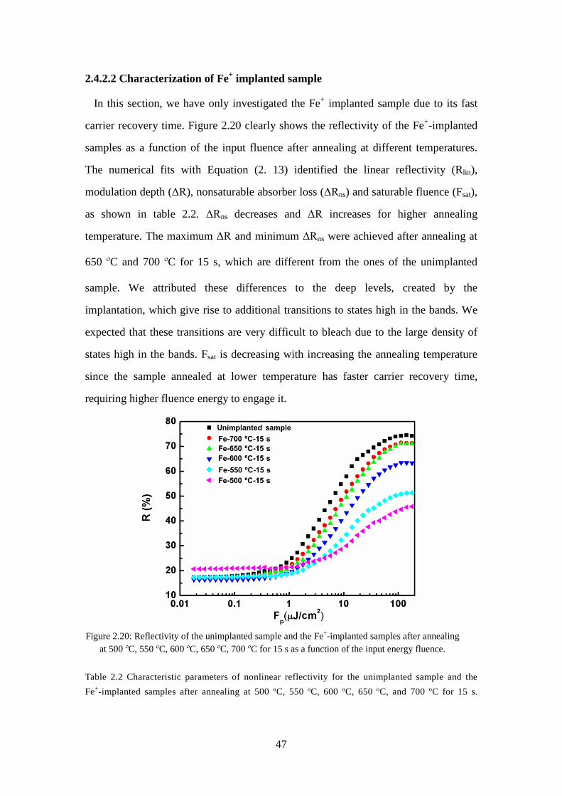
47
2.4.2.2 Characterization of Fe+ implanted sample
In this section, we have only investigated the Fe+ implanted sample due to its fast
carrier recovery time. Figure 2.20 clearly shows the reflectivity of the Fe+-implanted
samples as a function of the input fluence after annealing at different temperatures.
The numerical fits with Equation (2. 13) identified the linear reflectivity (Rlin),
modulation depth (ΔR), nonsaturable absorber loss (ΔRns) and saturable fluence (Fsat),
as shown in table 2.2. ΔRns decreases and ΔR increases for higher annealing
temperature. The maximum ΔR and minimum ΔRns were achieved after annealing at
650 ºC and 700 ºC for 15 s, which are different from the ones of the unimplanted
sample. We attributed these differences to the deep levels, created by the
implantation, which give rise to additional transitions to states high in the bands. We
expected that these transitions are very difficult to bleach due to the large density of
states high in the bands. Fsat is decreasing with increasing the annealing temperature
since the sample annealed at lower temperature has faster carrier recovery time,
requiring higher fluence energy to engage it.
Figure 2.20: Reflectivity of the unimplanted sample and the Fe+-implanted samples after annealing
at 500 ºC, 550 ºC, 600 ºC, 650 ºC, 700 ºC for 15 s as a function of the input energy fluence.
Table 2.2 Characteristic parameters of nonlinear reflectivity for the unimplanted sample and the Fe+-implanted samples after annealing at 500 ºC, 550 ºC, 600 ºC, 650 ºC, and 700 ºC for 15 s.
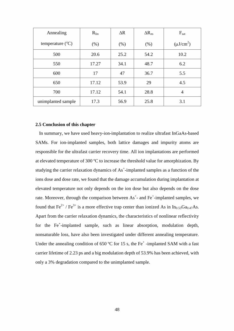
48
Annealing
temperature (ºC)
Rlin
(%)
ΔR
(%)
ΔRns
(%)
Fsat
(µJ/cm2)
500 20.6 25.2 54.2 10.2
550 17.27 34.1 48.7 6.2
600 17 47 36.7 5.5
650 17.12 53.9 29 4.5
700 17.12 54.1 28.8 4
unimplanted sample 17.3 56.9 25.8 3.1
2.5 Conclusion of this chapter
In summary, we have used heavy-ion-implantation to realize ultrafast InGaAs-based
SAMs. For ion-implanted samples, both lattice damages and impurity atoms are
responsible for the ultrafast carrier recovery time. All ion implantations are performed
at elevated temperature of 300 ºC to increase the threshold value for amorphization. By
studying the carrier relaxation dynamics of As+-implanted samples as a function of the
ions dose and dose rate, we found that the damage accumulation during implantation at
elevated temperature not only depends on the ion dose but also depends on the dose
rate. Moreover, through the comparison between As+- and Fe+-implanted samples, we
found that Fe2+ / Fe3+ is a more effective trap center than ionized As in In0.53Ga0.47As.
Apart from the carrier relaxation dynamics, the characteristics of nonlinear reflectivity
for the Fe+-implanted sample, such as linear absorption, modulation depth,
nonsaturable loss, have also been investigated under different annealing temperature.
Under the annealing condition of 650 ºC for 15 s, the Fe+ -implanted SAM with a fast
carrier lifetime of 2.23 ps and a big modulation depth of 53.9% has been achieved, with
only a 3% degradation compared to the unimplanted sample.
49
2.6 Reference
[1] R. E. Nahory, M. A. Pollack, W. D. Johnston, and R. L. Barns, “Band gap versus
composition and demonstration of Vegard’s law for In1-xGaxAsyP1-y lattice
matched to InP,” Appl. Phys. Lett., vol. 33, pp. 659-661, 1978.
[2] I. Vurgaftman, and J. R. Meyer, “Band parameters for III-V compound
semiconductors and their alloys,” J. Appl. Phys., vol. 89, pp. 5815 -5875, 2001.
[3] D. A. B. Miller, “Dynamic Nonlinear Optics in Semiconductors: Physics and
Applications,” Laser Focus, vol. 19, pp. 61-68, 1983.
[4] U. Keller, “Recent developments in compact ultrafast lasers,” Nature, vol. 424, pp.
831-838, 2003.
[5] J. Shah, Ultrafast Spectroscopy of Semiconductors and Semiconductor
Nanostructures, 3th Edition, Springer-Verlag, Berlin, 2001.
[6] E. O. Goebel, “Ultrafast Spectroscopy of Semiconductors,” in Advances in Solid
State Physics, vol. 30, pp. 269- 294, 1990.
[7] L. Allen, and J. H. Eberly, Optical Resonance and Two-Level Atoms, Dover, New
York, 1975.
[8] J. L. Oudar, D. Hulin, A. Migus, A. Antonetti, and F. Alexandre, “Subpicosecond
Spectral Hole Burning Due to Nonthermalized Photoexcited Carriers in GaAs,”
Phys. Rev. Lett., vol. 55, pp. 2074-2077, 1985.
[9] W. H. Knox, C. Hirlimann, D. A. B. Miller, J. Shah, D. S. Chemla, and C. V. Shank,
“Femtosecond Excitation of Nonthermal Carrier Populations in GaAs Quantum
Wells,” Phys. Rev. Lett., vol. 56, pp. 1191-1193, 1986.
[10] R. W. Schoenlein, W. Z. Lin, E. P. Ippen, and J. G. Fujimoto, “Femtosecond
hot-carrier energy relaxation in GaAs,” Appl. Phys. Lett., vol. 51, pp. 1442-1444,
1987.
[11] A. Hangleiter and R. Hacker, “Enhancement of Band-to-Band Auger
Recombination by Electron-Hole Correlations,” Phys. Rev. Lett., vol. 6, pp.
215-218, 1990.
[12] V. N. Abakumov, V. I. Perel, and I. N. Yassievich, Nonradiative Recombination in
Semiconductors, 3th Edition, North-Holland, Amsterdam, 1991.
50
[13] S. Gupta, J. F. Whitaker, and G. A. Mourou, “Ultrafast carrier dynamics in III-V
semiconductors grown by molecular-beam epitaxy at very low substrate
temperatures,” IEEE J. Quant. Electron., vol. 28, pp. 2464-2472, 1992.
[14] G. L. Witt, “LTMBE GaAs: present status and perspectives,” Mater. Sci. Eng. B,
vol. 22, pp. 9-15, 1993.
[15] D. C. Look, D. C. Walters, M. Mier, C. E. Stutz, and S. K. Brierley, “Native donors
and acceptors in molecular-beam epitaxial GaAs grown at 200 °C,” Appl. Phys.
Lett., vol. 60, pp. 2900-2902, 1992.
[16] X. Liu, A. Prasad, W. M. Chen, A. Kurpiewski, A. Stoschek, Z. Liliental-Weber,
and E. R. Weber, “Mechanism responsible for the semi-insulating properties of
low-temperature-grown GaAs,” Appl. Phys. Lett., vol. 65 , pp. 3002-3004, 1994.
[17] A. Krotkus, R. Viselga, K. Bertulis, V. Jasutis, S. Marcinkevicius, and U. Olin,
“Subpicosecond carrier lifetimes in GaAs grown by molecular beam epitaxy at
low substrate temperature,” Appl. Phys. Lett., vol. 66, pp. 1939-1941, 1995.
[18] S. Gupta, P. K. Bhattacharya, J. Pamulapati, and G. Mourou, “Subpicosecond
photoresponse of carriers in low-temperature molecular beam epitaxial
In0.52Al0.48As/InP,” Appl. Phys. Lett., vol 57, pp. 1543-1545, 1990.
[19] W. H. Knox, G. E. Doran, M. Asom, G. Livescu, R. Leibenguth, and S. N. G. Chu,
“Low-temperature-grown GaAs quantum wells: Femtosecond nonlinear optical
and parallel-field transport studies,” Appl. Phys. Lett., vol. 59, pp.1491-1493,
1991.
[20] S. Gupta, P. K. Bhattacharya, J. Pamulapati, and G. Mourou, “Subpicosecond
photoresponse of carriers in low-temperature molecular beam epitaxial
In0.52Al0.48As/InP,” Appl. Phys. Lett., vol. 57, pp. 1543–1545, 1990.
[21] R. Takahashi, Y. Kawamura, T. Kagawa, and H. Iwamura, “Ultrafast 1.55μm
photoresponses in low-temperature-grown InGaAs/InAlAs quantum wells,” Appl.
Phys. Lett., vol. 65, pp. 1790-1792, 1994.
[22] D. Vignaud, J. F. Lampin, E. Lefebvre, M. Zaknoune and F. Mollot, “Electron
lifetime of heavily Be-doped In0.53Ga0.47As as a function of growth temperature
and doping density,” Appl. Phys. Lett., vol. 80, pp. 4151-4153, 2002.
51
[23] R. Takahashi, Y. Kawamura, T. Kagawa, and H. Iwamura, “Ultrafast 1.55-μm
photoresponses in low-temperature-grown InGaAs/InAlAs quantum wells,” Appl.
Phys. Lett., vol. 65 , pp. 1790-1792, 1994.
[24] P. W. Juodawlkis, D. T. McInturff, and S. E. Ralph, “Ultrafast carrier dynamics
and optical nonlinearities of low-temperature-grown InGaAs/InAlAs multiple
quantum wells,” Appl. Phys. Lett., vol. 69, pp. 4062-4064, 1996.
[25] B. Srocka, H. Scheffler, and D. Bimberg, “Fe2+-Fe3+ level as a recombination
center in In0.53Ga0.47As,” Phys. Rev. B, vol. 49, pp. 10259-10268, 1994.
[26] M. Gicquel-Guezo, S. Loualiche, J. Even, C. Labbe, O. Dehaese, A. Le Corre, H.
Folliot, and Y. Pellan, “290 fs switching time of Fe-doped quantum well saturable
absorbers in a microcavity in 1.55 µm range,” Appl. Phys. Lett., vol. 85, pp.
5926-5928, 2004.
[27] K. F. Lamprecht, S. Juen, L. Palmetshofer, and R. A. Hopfel, “Ultrashort carrier
lifetimes in H+ bombarded InP,” Appl. Phys. Lett., vol. 59, pp. 926-928, 1991.
[28] J. Mangeney, H. Choumane, G. Patriarche, G. Leroux, G. Aubin, J. C. Harmand, J.
L. Oudar, and H. Bernas, “Comparison of light- and heavy-ion-irradiated
quantum-wells for use as ultrafast saturable absorbers,” Appl. Phys. Lett., vol. 79,
pp. 2722-2724, 2001.
[29] E. L. Delpon, J. L. Oudar, N. Bouche, R. Raj, A. Shen, N. Stelmakh, and J. M.
Lourtioz, “Ultrafast excitonic saturable absorption in ion-implanted
InGaAs/InAlAs multiple quantum wells,” Appl. Phys. Lett., vol. 72, pp. 759-761,
1998.
[30] L. Joulaud, J. Mangeney, J. M. Lourtioz, P. Crozat, and G. Patriarche, “Thermal
stability of ion irradiated InGaAs with (sub-) picosecond carrier lifetime,” Appl.
Phys. Lett., vol. 82, pp. 856-858, 2003.
[31] C. Carmody, H. H. Tan, C. Jagadish, A. Gaarder, and S. Marcinkevicius,
“Ultrafast carrier trapping and recombination in highly resistive ion implanted
InP,” J. Appl. Phys., vol. 94, pp. 1074-1080, 2003.
[32] A. Krotkus, S. Marcinkevicius, J. Jasinski, M. Kaminska, H. H. Tan, and C.
Jagadish, “Picosecond carrier lifetime in GaAs implanted with high doses of As
52
ions: An alternative material to low-temperature GaAs for optoelectronic
applications,” Appl. Phys. Lett., vol. 66, pp. 3304-3305, 1995.
[33] M. J. Lederer1, .Kolev1, B. Luther-Davies1, H. H. Tan, and C. Jagadish,
“Ion-implanted InGaAs single quantum well semiconductor saturable absorber
mirrors for passive mode-locking,” J. Phys. D: Appl. Phys, vol. 34, pp 2455–2464.
[34] I. P Jain and G. Agarwal, “Ion beam induced surface and interface engineering,”
Surface Science Reports, vol. 66, pp. 77–172, 2011.
[35] J. F. Ziegler, J. P. Biersack, and U. Littmark, The stopping and range of ions in
matter, New York, Pergamon press, 1985.
[36] K. Schwartz, C. Traumann, and R. Neumann, “Electronic excitations and
heavy-ion-induced processes in ionic crystals,” Nucl. Instr. Meth. Phys. Res. B,
vol. 209, pp. 73-84, 2003.
[37] S. M. Gulwadi, M. V. Rao, D. S. Simons, O. W. Holland, W. P. Hong, C. Caneau,
and H. B. Dietrich, “Range statistics and Rutherford backscattering studies on
Fe-implanted In0.53Ga0.47As,” J. Appl. Phys., vol. 69, pp. 162-167, 1991.
[38] H. Ryssel and I. Ruge, Ion implantation, John Wiley&Sons, UK, pp. 5-12, 1986.
[39] H. H. Tan, C. Jagadish, M. J. Lederer, B. Luther-Davies, J. Zou, D. J. H.
Cockayne, M. Haiml, U. Siegner, and U. Keller, “Role of implantation-induced
defects on the response time of semiconductor saturable absorbers,” Appl. Phys.
Lett., vol. 75, pp. 1437-1439, 1999.
[40] M. J. Lederer, B. Luther-Davies, H. H. Tan, C. Jagadish, M. Haiml, U. Siegner,
and U. Keller, “Nonlinear optical absorption and temporal response of arsenic-
and oxygen-implanted GaAs,” Appl. Phys. Lett., vol. 74, pp. 1993-1995, 1999.
[41] Z. Zhao, S. Bouchoule, L. Ferlazzo, A. Sirbu, A. Mereuta, E. Kapon, E. Galopin, J.
C. Harmand, J. Decobert, and J. L. Oudar, “Cost-effective thermally-managed
1.55 µm VECSEL with hybrid mirror on copper substrate,” J. Quant. Electron.,
vol. 48, pp. 643-650, 2012. [42] D. J. Maas, B. Rudin, A. R. Bellancourt, D. Iwaniuk, S. V. Marchese, T.
Südmeyer, and U. Keller, “High precision optical characterization of

53
semiconductor saturable absorber mirrors,” Opt. Exp., vol. 16, pp. 7571-7579,
2008.
[43] U. Keller, “Semiconductor nonlinearities for solid-state laser modelocking and
Q-Switching,” in Nonlinear Optics in Semiconductors II. vol. 59, E. Garmire and
A. Kost, Eds., ed Massachusetts: Academic Press, pp. 211-286, 1999.
54
Chapter 3 Multi-wavelength SAM for WDM signal regeneration
The semiconductor SAM based on an asymmetric Fabry-Pérot microcavity is of
great interest for all-optical regeneration [1-3]. Up to now, the research in our group
has been focused on the SAM based on a single resonance microcavity. Its best
performance for regeneration is currently obtained when it is operated at its resonant
wavelength or close to it, which limits its working bandwidth. To develop
high-bit-rate WDM optical communication systems, the possibility of high
performance all-optical signal regeneration with a very wide wavelength range (for
example, several tens nm) on a single SAM chip would be extremely attractive,
offering potential cost benefits. In this chapter, to extend the operational bandwidth of
the single SAM chip, we propose a multi-wavelength SAM in which the multiple
microcavity resonances are obtained by patterning an ultra-thin taper structure on the
phase layer of the SAM, using focused ion beam (FIB) milling technology. In the
following we discuss how we found that this technology was well adapted to our
purpose.
In section 3.1, we present the concept of such a tapered multi-wavelength SAM, and
the design considerations that led us to conclude that FIB milling is an attractive
technique for the taper fabrication. Then in section 3.2, we give more details on this
technology, including an introduction to the fundamental characteristics of our lab’s
FIB system, the principle of FIB milling, and some quantitative considerations based
on the sputtering theory. In section 3.3, we describe our experimental methodology,
based on the considerations on the previous section, as well as more details on the
experimental procedure, using atomic force microscopy (AFM) as the main
technological tool is described. Finally, the optical characterization of the tapered
device is presented in section 3.4, and a conclusion for this chapter is presented in
section 3.5
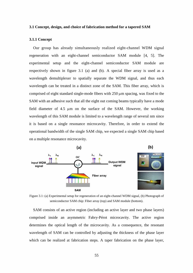
55
3.1 Concept, design, and choice of fabrication method for a tapered SAM
3.1.1 Concept
Our group has already simultaneously realized eight-channel WDM signal
regeneration with an eight-channel semiconductor SAM module [4, 5]. The
experimental setup and the eight-channel semiconductor SAM module are
respectively shown in figure 3.1 (a) and (b). A special fiber array is used as a
wavelength demultiplexer to spatially separate the WDM signal, and thus each
wavelength can be treated in a distinct zone of the SAM. This fiber array, which is
comprised of eight standard single-mode fibers with 250 µm spacing, was fixed to the
SAM with an adhesive such that all the eight out coming beams typically have a mode
field diameter of 4.5 µm on the surface of the SAM. However, the working
wavelength of this SAM module is limited to a wavelength range of several nm since
it is based on a single resonance microcavity. Therefore, in order to extend the
operational bandwidth of the single SAM chip, we expected a single SAM chip based
on a multiple resonance microcavity.
Figure 3.1: (a) Experimental setup for regeneration of an eight-channel WDM signal, (b) Photograph of
semiconductor SAM chip: Fiber array (top) and SAM module (bottom).
SAM consists of an active region (including an active layer and two phase layers)
comprised inside an asymmetric Fabry-Pérot microcavity. The active region
determines the optical length of the microcavity. As a consequence, the resonant
wavelength of SAM can be controlled by adjusting the thickness of the phase layer
which can be realized at fabrication steps. A taper fabrication on the phase layer,
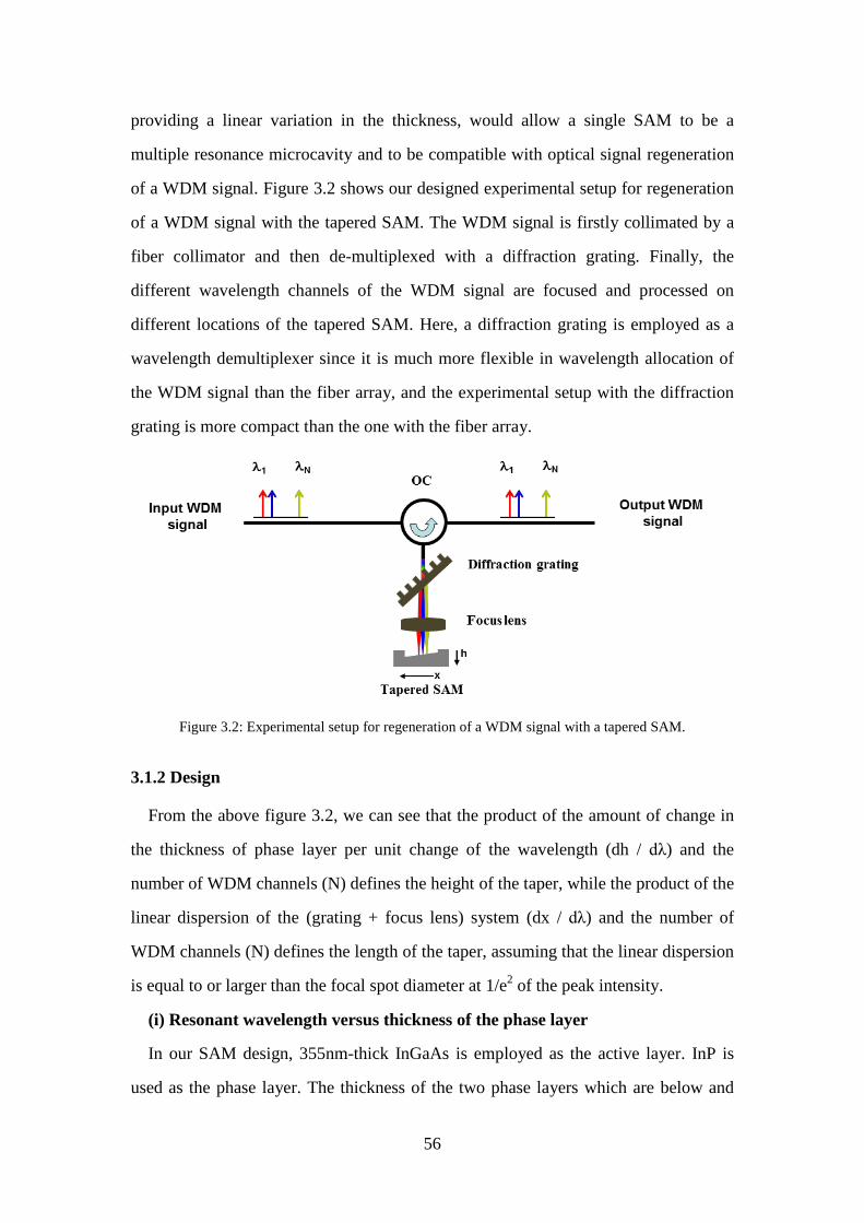
56
providing a linear variation in the thickness, would allow a single SAM to be a
multiple resonance microcavity and to be compatible with optical signal regeneration
of a WDM signal. Figure 3.2 shows our designed experimental setup for regeneration
of a WDM signal with the tapered SAM. The WDM signal is firstly collimated by a
fiber collimator and then de-multiplexed with a diffraction grating. Finally, the
different wavelength channels of the WDM signal are focused and processed on
different locations of the tapered SAM. Here, a diffraction grating is employed as a
wavelength demultiplexer since it is much more flexible in wavelength allocation of
the WDM signal than the fiber array, and the experimental setup with the diffraction
grating is more compact than the one with the fiber array.
Figure 3.2: Experimental setup for regeneration of a WDM signal with a tapered SAM.
3.1.2 Design
From the above figure 3.2, we can see that the product of the amount of change in
the thickness of phase layer per unit change of the wavelength (dh / dλ) and the
number of WDM channels (N) defines the height of the taper, while the product of the
linear dispersion of the (grating + focus lens) system (dx / dλ) and the number of
WDM channels (N) defines the length of the taper, assuming that the linear dispersion
is equal to or larger than the focal spot diameter at 1/e2 of the peak intensity.
(i) Resonant wavelength versus thickness of the phase layer
In our SAM design, 355nm-thick InGaAs is employed as the active layer. InP is
used as the phase layer. The thickness of the two phase layers which are below and
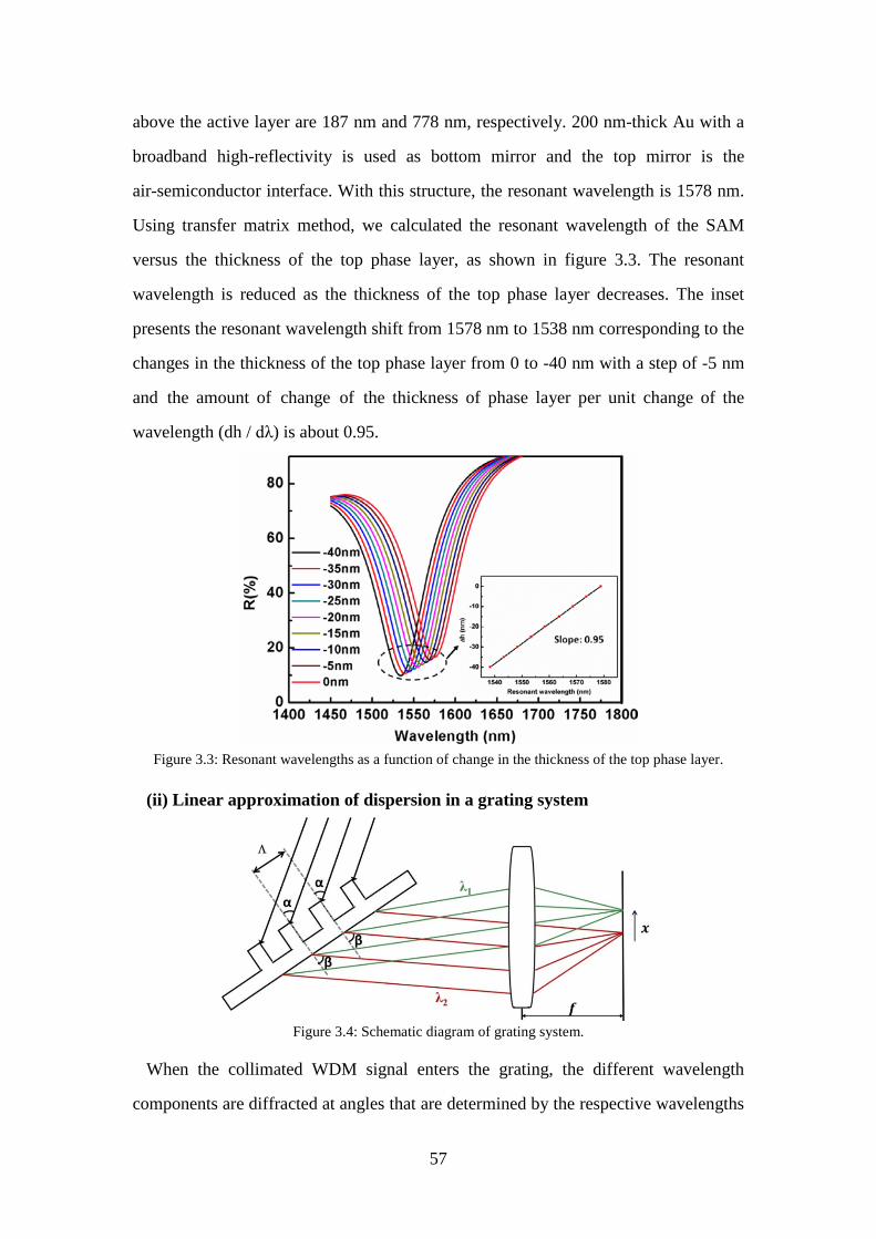
57
above the active layer are 187 nm and 778 nm, respectively. 200 nm-thick Au with a
broadband high-reflectivity is used as bottom mirror and the top mirror is the
air-semiconductor interface. With this structure, the resonant wavelength is 1578 nm.
Using transfer matrix method, we calculated the resonant wavelength of the SAM
versus the thickness of the top phase layer, as shown in figure 3.3. The resonant
wavelength is reduced as the thickness of the top phase layer decreases. The inset
presents the resonant wavelength shift from 1578 nm to 1538 nm corresponding to the
changes in the thickness of the top phase layer from 0 to -40 nm with a step of -5 nm
and the amount of change of the thickness of phase layer per unit change of the
wavelength (dh / dλ) is about 0.95.
Figure 3.3: Resonant wavelengths as a function of change in the thickness of the top phase layer.
(ii) Linear approximation of dispersion in a grating system
Figure 3.4: Schematic diagram of grating system.
When the collimated WDM signal enters the grating, the different wavelength
components are diffracted at angles that are determined by the respective wavelengths
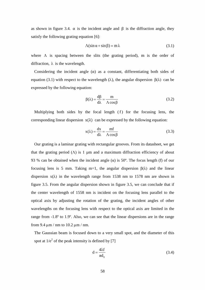
58
as shown in figure 3.4. α is the incident angle and β is the diffraction angle, they
satisfy the following grating equation [6]:
Λ(sin α sin β) m λ+ = (3.1)
where Λ is spacing between the slits (the grating period), m is the order of
diffraction, λ is the wavelength.
Considering the incident angle (α) as a constant, differentiating both sides of
equation (3.1) with respect to the wavelength (λ), the angular dispersion β(λ) can be
expressed by the following equation:
dβ mβ(λ)dλ Λ cosβ
= = (3.2)
Multiplying both sides by the focal length ( f ) for the focusing lens, the
corresponding linear dispersion x(λ) can be expressed by the following equation:
dx mfx(λ)dλ Λ cosβ
= = (3.3)
Our grating is a laminar grating with rectangular grooves. From its datasheet, we get
that the grating period (Λ) is 1 µm and a maximum diffraction efficiency of about
93 % can be obtained when the incident angle (α) is 50º. The focus length (f) of our
focusing lens is 5 mm. Taking m=1, the angular dispersion β(λ) and the linear
dispersion x(λ) in the wavelength range from 1538 nm to 1578 nm are shown in
figure 3.5. From the angular dispersion shown in figure 3.5, we can conclude that if
the center wavelength of 1558 nm is incident on the focusing lens parallel to the
optical axis by adjusting the rotation of the grating, the incident angles of other
wavelengths on the focusing lens with respect to the optical axis are limited in the
range from -1.8º to 1.9º. Also, we can see that the linear dispersions are in the range
from 9.4 µm / nm to 10.2 µm / nm.
The Gaussian beam is focused down to a very small spot, and the diameter of this
spot at 1/e2 of the peak intensity is defined by [7]
0
4λfdπd
= (3.4)
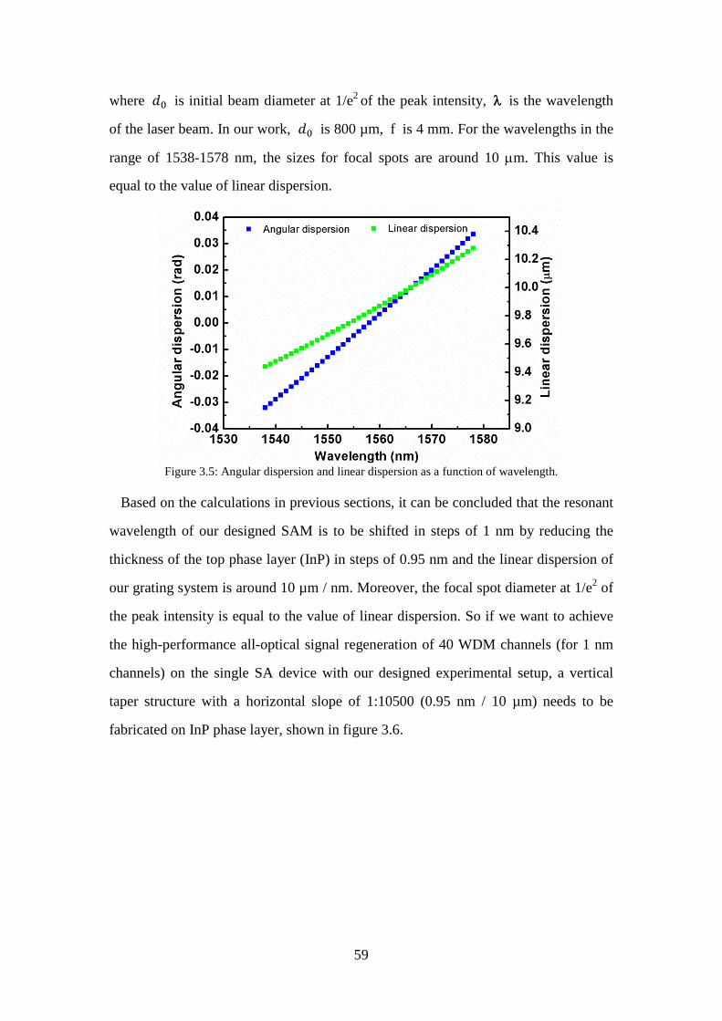
59
where 𝑑0 is initial beam diameter at 1/e2 of the peak intensity, λ is the wavelength
of the laser beam. In our work, 𝑑0 is 800 µm, f is 4 mm. For the wavelengths in the
range of 1538-1578 nm, the sizes for focal spots are around 10 µm. This value is
equal to the value of linear dispersion.
Figure 3.5: Angular dispersion and linear dispersion as a function of wavelength.
Based on the calculations in previous sections, it can be concluded that the resonant
wavelength of our designed SAM is to be shifted in steps of 1 nm by reducing the
thickness of the top phase layer (InP) in steps of 0.95 nm and the linear dispersion of
our grating system is around 10 µm / nm. Moreover, the focal spot diameter at 1/e2 of
the peak intensity is equal to the value of linear dispersion. So if we want to achieve
the high-performance all-optical signal regeneration of 40 WDM channels (for 1 nm
channels) on the single SA device with our designed experimental setup, a vertical
taper structure with a horizontal slope of 1:10500 (0.95 nm / 10 µm) needs to be
fabricated on InP phase layer, shown in figure 3.6.
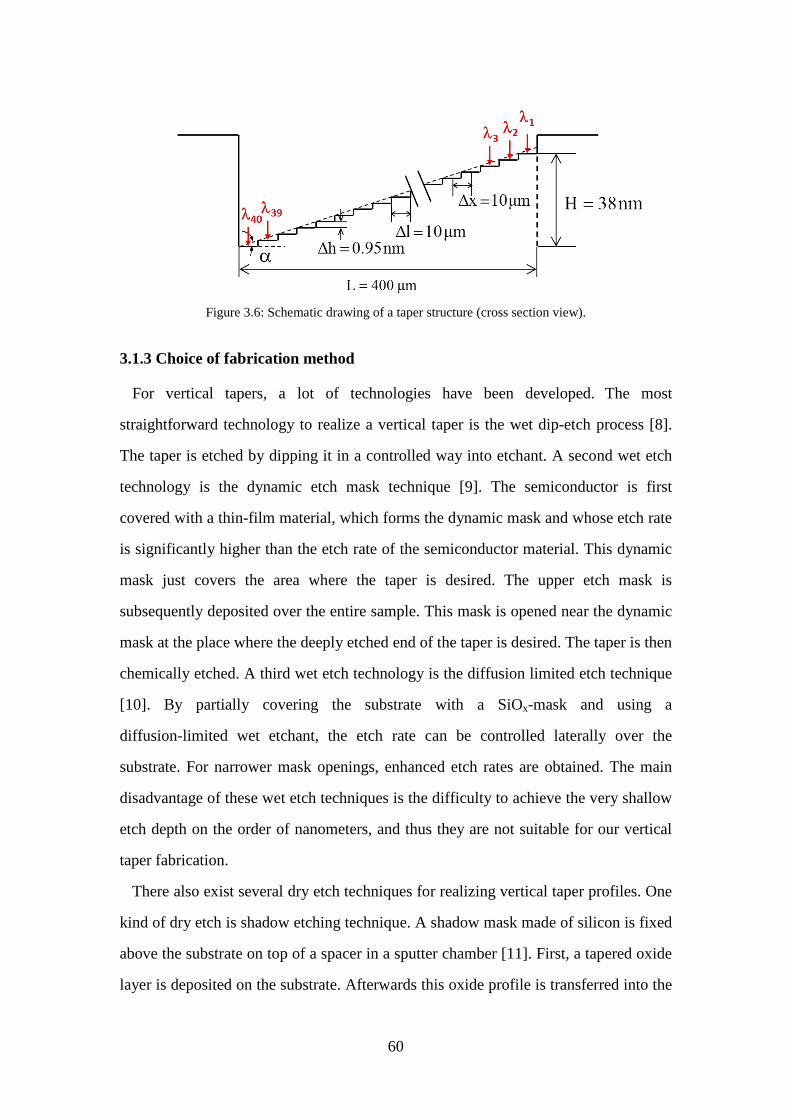
60
Figure 3.6: Schematic drawing of a taper structure (cross section view).
3.1.3 Choice of fabrication method
For vertical tapers, a lot of technologies have been developed. The most
straightforward technology to realize a vertical taper is the wet dip-etch process [8].
The taper is etched by dipping it in a controlled way into etchant. A second wet etch
technology is the dynamic etch mask technique [9]. The semiconductor is first
covered with a thin-film material, which forms the dynamic mask and whose etch rate
is significantly higher than the etch rate of the semiconductor material. This dynamic
mask just covers the area where the taper is desired. The upper etch mask is
subsequently deposited over the entire sample. This mask is opened near the dynamic
mask at the place where the deeply etched end of the taper is desired. The taper is then
chemically etched. A third wet etch technology is the diffusion limited etch technique
[10]. By partially covering the substrate with a SiOx-mask and using a
diffusion-limited wet etchant, the etch rate can be controlled laterally over the
substrate. For narrower mask openings, enhanced etch rates are obtained. The main
disadvantage of these wet etch techniques is the difficulty to achieve the very shallow
etch depth on the order of nanometers, and thus they are not suitable for our vertical
taper fabrication.
There also exist several dry etch techniques for realizing vertical taper profiles. One
kind of dry etch is shadow etching technique. A shadow mask made of silicon is fixed
above the substrate on top of a spacer in a sputter chamber [11]. First, a tapered oxide
layer is deposited on the substrate. Afterwards this oxide profile is transferred into the
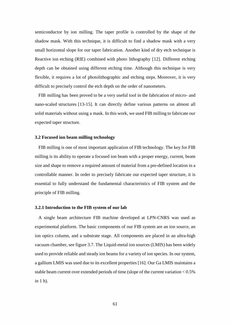
61
semiconductor by ion milling. The taper profile is controlled by the shape of the
shadow mask. With this technique, it is difficult to find a shadow mask with a very
small horizontal slope for our taper fabrication. Another kind of dry etch technique is
Reactive ion etching (RIE) combined with photo lithography [12]. Different etching
depth can be obtained using different etching time. Although this technique is very
flexible, it requires a lot of photolithographic and etching steps. Moreover, it is very
difficult to precisely control the etch depth on the order of nanometers.
FIB milling has been proved to be a very useful tool in the fabrication of micro- and
nano-scaled structures [13-15]. It can directly define various patterns on almost all
solid materials without using a mask. In this work, we used FIB milling to fabricate our
expected taper structure.
3.2 Focused ion beam milling technology
FIB milling is one of most important application of FIB technology. The key for FIB
milling is its ability to operate a focused ion beam with a proper energy, current, beam
size and shape to remove a required amount of material from a pre-defined location in a
controllable manner. In order to precisely fabricate our expected taper structure, it is
essential to fully understand the fundamental characteristics of FIB system and the
principle of FIB milling.
3.2.1 Introduction to the FIB system of our lab
A single beam architecture FIB machine developed at LPN-CNRS was used as
experimental platform. The basic components of our FIB system are an ion source, an
ion optics column, and a substrate stage. All components are placed in an ultra-high
vacuum chamber, see figure 3.7. The Liquid-metal ion sources (LMIS) has been widely
used to provide reliable and steady ion beams for a variety of ion species. In our system,
a gallium LMIS was used due to its excellent properties [16]. Our Ga LMIS maintains a
stable beam current over extended periods of time (slope of the current variation < 0.5%
in 1 h).
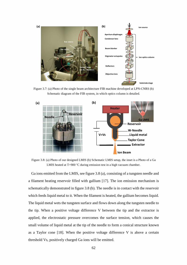
62
Figure 3.7: (a) Photo of the single beam architecture FIB machine developed at LPN-CNRS (b)
Schematic diagram of the FIB system, in which optics column is detailed.
Figure 3.8: (a) Photo of our designed LMIS (b) Schematic LMIS setup, the inset is a Photo of a Ga
LMIS heated at T=900 ºC during emission test in a high vacuum chamber.
Ga ions emitted from the LMIS, see figure 3.8 (a), consisting of a tungsten needle and
a filament heating reservoir filled with gallium [17]. The ion emission mechanism is
schematically demonstrated in figure 3.8 (b). The needle is in contact with the reservoir
which feeds liquid metal to it. When the filament is heated, the gallium becomes liquid.
The liquid metal wets the tungsten surface and flows down along the tungsten needle to
the tip. When a positive voltage difference V between the tip and the extractor is
applied, the electrostatic pressure overcomes the surface tension, which causes the
small volume of liquid metal at the tip of the needle to form a conical structure known
as a Taylor cone [18]. When the positive voltage difference V is above a certain
threshold Vs, positively charged Ga ions will be emitted.
63
After being extracted and accelerated from the LMIS using an extractor electrode, the
Ga ion beam is passed through an optics column where the beam is transported,
focused, and scanned. The designed optics column includes condenser lens, objective
lens, stigmator octupoles, beam blanker, beam deflector and aperture mechanism, as
shown in figure 3.7 (b). A beam-defining aperture is placed at the entrance of the ion
optics, which only allows the emitted ions with paraxial trajectories to enter the optics
and reach the target without loss. It also provides a range of ion currents by changing
variable apertures. The first electromagnetic lens, condenser lens, realizes the first
focusing and controls the beam diameter combined with the beam-defining aperture.
The second electromagnetic lens, objective lens placed at the end of the optics column,
is used to focus the ion beam at the sample of the surface. These two electromagnetic
lenses are identical but asymmetric, supporting low aberration coefficients [19]. After
the condenser lens, there is a beam blanker device, which can deflect the beam away
from the centre of the column onto the blanking aperture to quickly switch the beam on
and off. The stigmator is used for stigmatism correction. Following the stigmator, there
is beam deflector which controls the final trajectory or landing location of the ion beam
on the target. It can perform image scan, pattern scan, shift beam and rotate image. By
blanking and deflecting the beam, an arbitrary pattern can be fabricated.
This single beam architecture FIB system of our lab has several advantages for
nano-scale structure fabrication: the designed Ga LIMS and optics column can provide
a sub-10 nm beam spot (FWHM) on the sample [20]; In this system, the sample stage
can only move along X and Y directions, and it is controlled by a two-axis
Michelson-laser interferometer working together with a 10 MHz pattern generator.
This allows a highly accurate positioning accuracy of 2 nm [18] and a high patterning
flexibility (high patterning speed, with a pixel dwell time down to 100 ns / point and up
to 10 s / point) [21].
3.2.2 Principle of FIB milling
FIB milling is realized by scanning the energetic Ga ion beam over the target.
However, when the energetic ions irradiate the target, a variety of ion-target interaction,
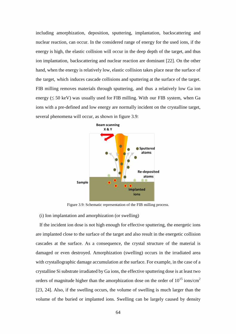
64
including amorphization, deposition, sputtering, implantation, backscattering and
nuclear reaction, can occur. In the considered range of energy for the used ions, if the
energy is high, the elastic collision will occur in the deep depth of the target, and thus
ion implantation, backscattering and nuclear reaction are dominant [22]. On the other
hand, when the energy is relatively low, elastic collision takes place near the surface of
the target, which induces cascade collisions and sputtering at the surface of the target.
FIB milling removes materials through sputtering, and thus a relatively low Ga ion
energy (≤ 50 keV) was usually used for FIB milling. With our FIB system, when Ga
ions with a pre-defined and low energy are normally incident on the crystalline target,
several phenomena will occur, as shown in figure 3.9:
Figure 3.9: Schematic representation of the FIB milling process.
(i) Ion implantation and amorphization (or swelling)
If the incident ion dose is not high enough for effective sputtering, the energetic ions
are implanted close to the surface of the target and also result in the energetic collision
cascades at the surface. As a consequence, the crystal structure of the material is
damaged or even destroyed. Amorphization (swelling) occurs in the irradiated area
with crystallographic damage accumulation at the surface. For example, in the case of a
crystalline Si substrate irradiated by Ga ions, the effective sputtering dose is at least two
orders of magnitude higher than the amorphization dose on the order of 1015 ions/cm2
[23, 24]. Also, if the swelling occurs, the volume of swelling is much larger than the
volume of the buried or implanted ions. Swelling can be largely caused by density
65
changes or amorphization, rather than exclusively by the buried or implanted ions. For
Si the magnitude of the swelling due to amorphization can be as high as tens of
nanometers [25]. Amorphization will diminish the dimensional accuracy of
nanostructures.
(ii) Material re-deposition
In our FIB system, no reactive gas is used to react with the sputtered atoms to form
volatile compounds, the sputtered target atoms are randomly ejected from the surface
and a portion of them are then re-deposited around their emitted points within a circular
disk of a few micrometers [26]. During the milling of our taper of 40 adjacent
rectangles arranged together, the milling process of one rectangle will be subject to
local re-deposition during its own FIB milling and also interfere with the milling
process of the surrounding rectangles in the taper. The accuracy of the milling depth
can be greatly degraded due to the material re-deposition. Therefore the re-deposition
effect is of the highest importance in our taper fabrication.
(iii) Ion channeling
If the ion beam is incident into the crystalline material in a precisely defined
channeling direction, the channeled ions undergo mostly electronic energy losses as
opposed to nuclear energy losses and are able to penetrate deeper into the crystal lattice.
The deeper penetration and the lower probability of nuclear collisions near the surface
extremely limit the probability that the ion will cause a collision cascade that will
contribute to the sputtering of surface atoms. So if the incident ions get channeled, the
sputtering yield will decrease [27]. In our FIB system, the Ga ion beam is normally
incident into the sample, so the ion channeling may occur during the FIB milling.
However, the occurrence of ion channeling does require a very precise angular
placement of the sample which needs to be controlled within a few degrees and the
native oxide on the surface of InP can act as a de-channeling layer, so we can
reasonably expect that the probability for Ga ions to enter a channeling direction of the
InP material is very low.
(iv) Material sputtering
66
When the energy transferred from collisions between ions and surface atoms is
sufficiently high to overcome the surface binding energy of the target, the target atom is
ejected, leading to sputtering effects. This effect will be detailed in next section 3.2.3.
3.2.3 Sputtering theory
Sputtering is the major mechanism for material removal and can be quantified by
sputtering yield which is defined as the number of sputtered atoms per incident primary
ion. Apart from the simulation of the implanted ions distribution shown in chapter 2,
the TRIM included in the software package SRIM has been widely used for predicting
the sputtering yield according to the target material, ion species, the ion energy and the
incident angle. Generally, the sputtering yield increases as the ion energy increases. But
the yield starts to decrease as the energy increased over the level where the ions can
penetrate deep into the substrate, since for high ion energy other types of ion-target
interaction are dominant as discussed in the previous section 3.2.1 [28].
In the experiments, the sputtering yield is dependent not only on the target material,
ion species, the ion energy and the incident angle, but also on the scanning procedures.
It has already been shown that the FIB sputtering yield changes as a function of the
scanning speed [29]. Furthermore, TRIM predictions of the sputtering yield did not
agree with the experimental yield under some milling conditions. For example, the
experimental yield for the GaAs target is 2.1 atoms/ion using Ga ions with energy of 30
keV at normal incidence, which is very different from the TRIM prediction of 10.05
atoms / ion [30]. In fact, in addition to TRIM prediction, the sputtering yield can also be
experimentally determined from the sputtered volume V. When a focused ion beam is
scanned over the target, the total volume removed from the target can be expressed as
[14]:
i x y
0
YN N N MV Ad
ρN= = (3.5)
where ρ and M are respectively, the target density (kg / m3) and the atomic or
molecular weight of the target (kg / mol), N0 is the Avogadro constant (6.02×10²³ /
mol), Ni is the number of ions per pixel onto the target, and (Nx, Ny) is the number of
67
pixel per line in the (x, y) direction, respectively. A is the scanning area (m2) which is
governed by Nx and Ny, and d is the milling depth of the target per scan.
So the sputtering yield Y can be expressed as:
0
i x y
AdρNYN N N M
= (3.6)
The ion dose in ions/cm2 can be calculated by [31]
ion exposure15
I tD
A 1.602 10−
×=
× × (3.7)
where Iion is the primary ion current in pA, texposure is the dwell time (the time that
the beam remains on a given target) in s, and A is the pattern area in μm2.
If the geometry is pre-defined, combining Equation (3.6) with Equation (3.7), the
sputtering yield can be expressed as:
0ρN dYM D
= × (3.8)
Equation (3.8) shows that the sputtering yield (Y) can be deduced from the ratio of the
milling depth to the ion dose (d D⁄ ) for a specific ion species and a specific target.
3.3 Tapered SAM fabrication using FIB milling
Based on the principle of FIB milling technology, several aspects have to be
considered before the taper fabrication. They are as follows: firstly, the threshold dose
for effective sputtering of InP should be determined, while amorphization should be
controlled and minimized to avoid the occurrence of swelling; secondly, the
re-deposition needs to be carefully controlled so that a precise amount of material can
be removed to realize a precisely controlled shallow-depth (nm-scale) FIB milling, and
the homogeneity of the FIB milling processing is also very important for our
application of tapered SA device; thirdly, we have to investigate experimentally the
FIB sputtering yield of the crystalline InP by investigating the milling depth as a
function of the incident Ga ion dose.
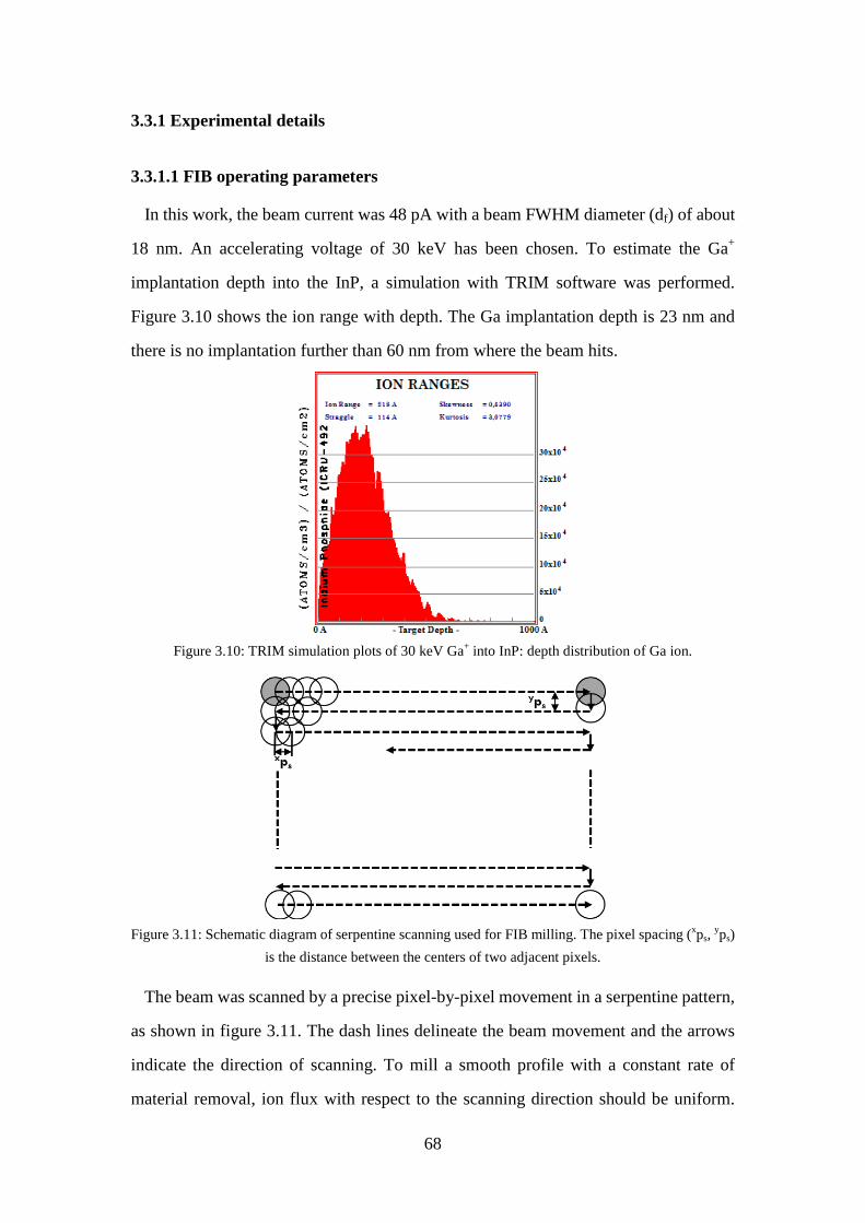
68
3.3.1 Experimental details
3.3.1.1 FIB operating parameters
In this work, the beam current was 48 pA with a beam FWHM diameter (df) of about
18 nm. An accelerating voltage of 30 keV has been chosen. To estimate the Ga+
implantation depth into the InP, a simulation with TRIM software was performed.
Figure 3.10 shows the ion range with depth. The Ga implantation depth is 23 nm and
there is no implantation further than 60 nm from where the beam hits.
Figure 3.10: TRIM simulation plots of 30 keV Ga+ into InP: depth distribution of Ga ion.
Figure 3.11: Schematic diagram of serpentine scanning used for FIB milling. The pixel spacing (xps, yps)
is the distance between the centers of two adjacent pixels.
The beam was scanned by a precise pixel-by-pixel movement in a serpentine pattern,
as shown in figure 3.11. The dash lines delineate the beam movement and the arrows
indicate the direction of scanning. To mill a smooth profile with a constant rate of
material removal, ion flux with respect to the scanning direction should be uniform.
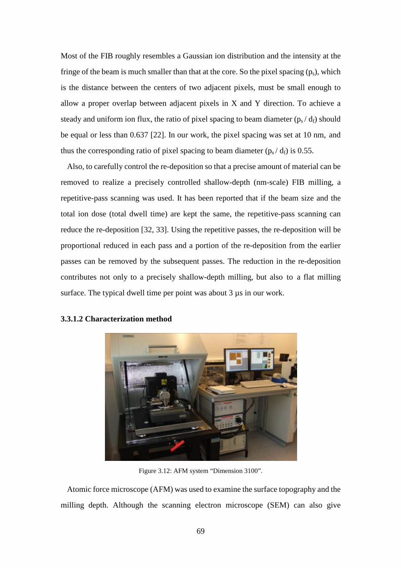
69
Most of the FIB roughly resembles a Gaussian ion distribution and the intensity at the
fringe of the beam is much smaller than that at the core. So the pixel spacing (ps), which
is the distance between the centers of two adjacent pixels, must be small enough to
allow a proper overlap between adjacent pixels in X and Y direction. To achieve a
steady and uniform ion flux, the ratio of pixel spacing to beam diameter (ps / df) should
be equal or less than 0.637 [22]. In our work, the pixel spacing was set at 10 nm, and
thus the corresponding ratio of pixel spacing to beam diameter (ps / df) is 0.55.
Also, to carefully control the re-deposition so that a precise amount of material can be
removed to realize a precisely controlled shallow-depth (nm-scale) FIB milling, a
repetitive-pass scanning was used. It has been reported that if the beam size and the
total ion dose (total dwell time) are kept the same, the repetitive-pass scanning can
reduce the re-deposition [32, 33]. Using the repetitive passes, the re-deposition will be
proportional reduced in each pass and a portion of the re-deposition from the earlier
passes can be removed by the subsequent passes. The reduction in the re-deposition
contributes not only to a precisely shallow-depth milling, but also to a flat milling
surface. The typical dwell time per point was about 3 µs in our work.
3.3.1.2 Characterization method
Figure 3.12: AFM system “Dimension 3100”.
Atomic force microscope (AFM) was used to examine the surface topography and the
milling depth. Although the scanning electron microscope (SEM) can also give
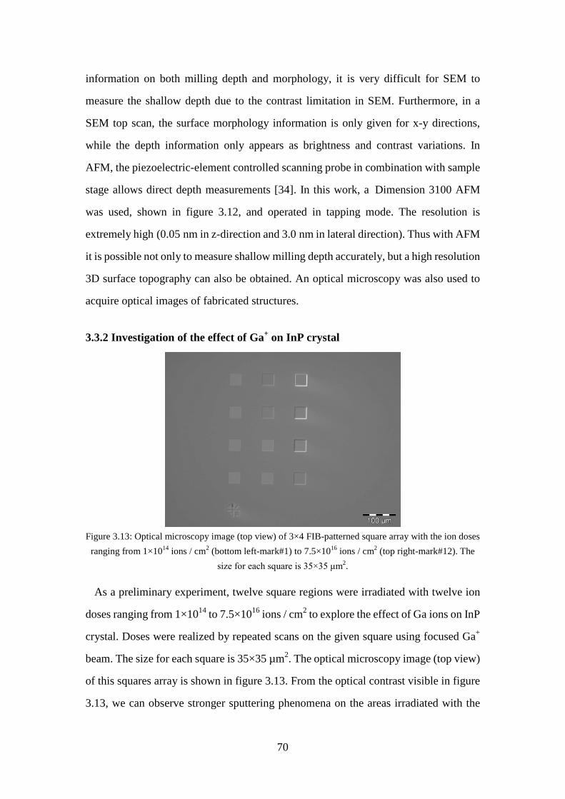
70
information on both milling depth and morphology, it is very difficult for SEM to
measure the shallow depth due to the contrast limitation in SEM. Furthermore, in a
SEM top scan, the surface morphology information is only given for x-y directions,
while the depth information only appears as brightness and contrast variations. In
AFM, the piezoelectric-element controlled scanning probe in combination with sample
stage allows direct depth measurements [34]. In this work, a Dimension 3100 AFM
was used, shown in figure 3.12, and operated in tapping mode. The resolution is
extremely high (0.05 nm in z-direction and 3.0 nm in lateral direction). Thus with AFM
it is possible not only to measure shallow milling depth accurately, but a high resolution
3D surface topography can also be obtained. An optical microscopy was also used to
acquire optical images of fabricated structures.
3.3.2 Investigation of the effect of Ga+ on InP crystal
Figure 3.13: Optical microscopy image (top view) of 3×4 FIB-patterned square array with the ion doses
ranging from 1×10¹⁴ ions / cm2 (bottom left-mark#1) to 7.5×10¹⁶ ions / cm2 (top right-mark#12). The size for each square is 35×35 μm2.
As a preliminary experiment, twelve square regions were irradiated with twelve ion
doses ranging from 1×10¹⁴ to 7.5×10¹⁶ ions / cm2 to explore the effect of Ga ions on InP
crystal. Doses were realized by repeated scans on the given square using focused Ga+
beam. The size for each square is 35×35 µm2. The optical microscopy image (top view)
of this squares array is shown in figure 3.13. From the optical contrast visible in figure
3.13, we can observe stronger sputtering phenomena on the areas irradiated with the
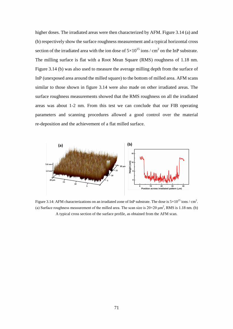
71
higher doses. The irradiated areas were then characterized by AFM. Figure 3.14 (a) and
(b) respectively show the surface roughness measurement and a typical horizontal cross
section of the irradiated area with the ion dose of 5×10¹⁵ ions / cm2 on the InP substrate.
The milling surface is flat with a Root Mean Square (RMS) roughness of 1.18 nm.
Figure 3.14 (b) was also used to measure the average milling depth from the surface of
InP (unexposed area around the milled square) to the bottom of milled area. AFM scans
similar to those shown in figure 3.14 were also made on other irradiated areas. The
surface roughness measurements showed that the RMS roughness on all the irradiated
areas was about 1-2 nm. From this test we can conclude that our FIB operating
parameters and scanning procedures allowed a good control over the material
re-deposition and the achievement of a flat milled surface.
Figure 3.14: AFM characterizations on an irradiated zone of InP substrate. The dose is 5×10¹⁵ ions / cm2. (a) Surface roughness measurement of the milled area. The scan size is 20×20 μm2, RMS is 1.18 nm. (b)
A typical cross section of the surface profile, as obtained from the AFM scan.
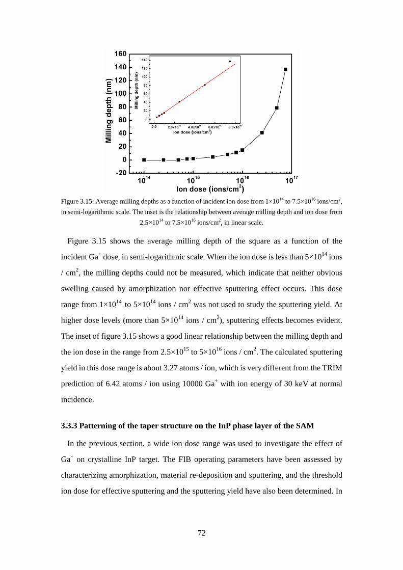
72
Figure 3.15: Average milling depths as a function of incident ion dose from 1×10¹⁴ to 7.5×10¹⁶ ions/cm2, in semi-logarithmic scale. The inset is the relationship between average milling depth and ion dose from
2.5×10¹⁴ to 7.5×10¹⁶ ions/cm2, in linear scale.
Figure 3.15 shows the average milling depth of the square as a function of the
incident Ga+ dose, in semi-logarithmic scale. When the ion dose is less than 5×10¹⁴ ions
/ cm2, the milling depths could not be measured, which indicate that neither obvious
swelling caused by amorphization nor effective sputtering effect occurs. This dose
range from 1×10¹⁴ to 5×10¹⁴ ions / cm2 was not used to study the sputtering yield. At
higher dose levels (more than 5×10¹⁴ ions / cm2), sputtering effects becomes evident.
The inset of figure 3.15 shows a good linear relationship between the milling depth and
the ion dose in the range from 2.5×10¹⁵ to 5×10¹⁶ ions / cm2. The calculated sputtering
yield in this dose range is about 3.27 atoms / ion, which is very different from the TRIM
prediction of 6.42 atoms / ion using 10000 Ga+ with ion energy of 30 keV at normal
incidence.
3.3.3 Patterning of the taper structure on the InP phase layer of the SAM
In the previous section, a wide ion dose range was used to investigate the effect of
Ga+ on crystalline InP target. The FIB operating parameters have been assessed by
characterizing amorphization, material re-deposition and sputtering, and the threshold
ion dose for effective sputtering and the sputtering yield have also been determined. In
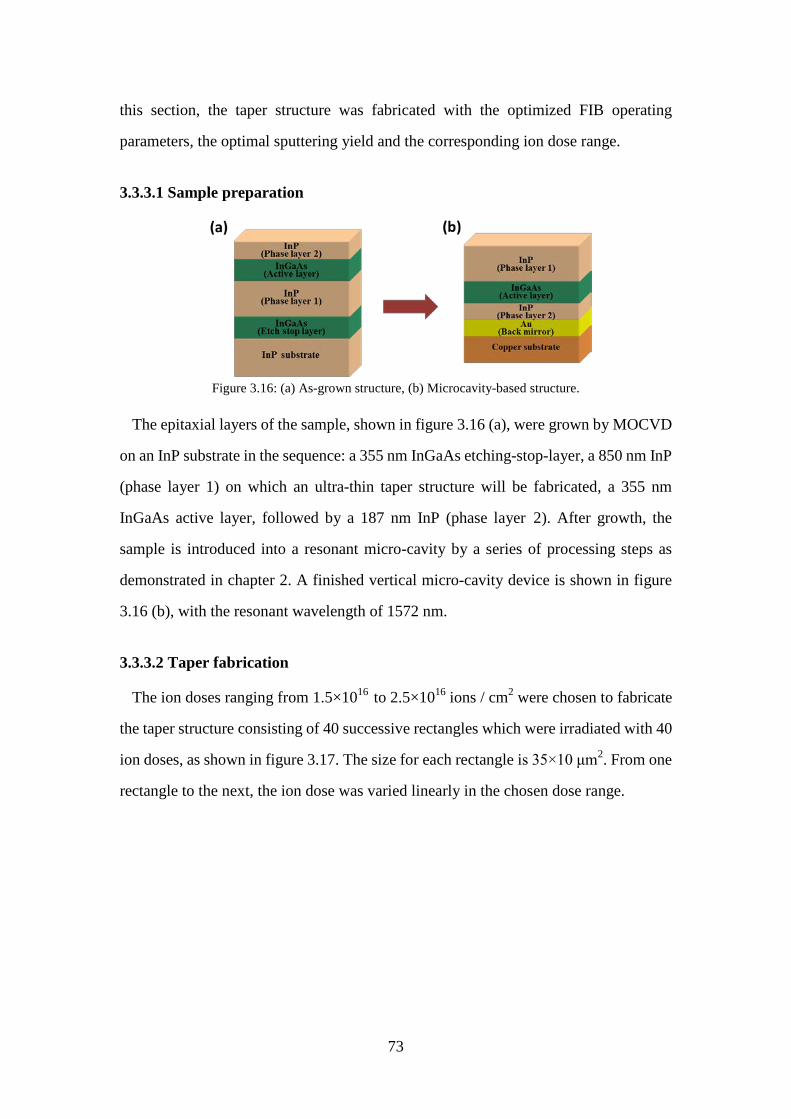
73
this section, the taper structure was fabricated with the optimized FIB operating
parameters, the optimal sputtering yield and the corresponding ion dose range.
3.3.3.1 Sample preparation
Figure 3.16: (a) As-grown structure, (b) Microcavity-based structure.
The epitaxial layers of the sample, shown in figure 3.16 (a), were grown by MOCVD
on an InP substrate in the sequence: a 355 nm InGaAs etching-stop-layer, a 850 nm InP
(phase layer 1) on which an ultra-thin taper structure will be fabricated, a 355 nm
InGaAs active layer, followed by a 187 nm InP (phase layer 2). After growth, the
sample is introduced into a resonant micro-cavity by a series of processing steps as
demonstrated in chapter 2. A finished vertical micro-cavity device is shown in figure
3.16 (b), with the resonant wavelength of 1572 nm.
3.3.3.2 Taper fabrication
The ion doses ranging from 1.5×10¹⁶ to 2.5×10¹⁶ ions / cm2 were chosen to fabricate
the taper structure consisting of 40 successive rectangles which were irradiated with 40
ion doses, as shown in figure 3.17. The size for each rectangle is 35×10 μm2. From one
rectangle to the next, the ion dose was varied linearly in the chosen dose range.
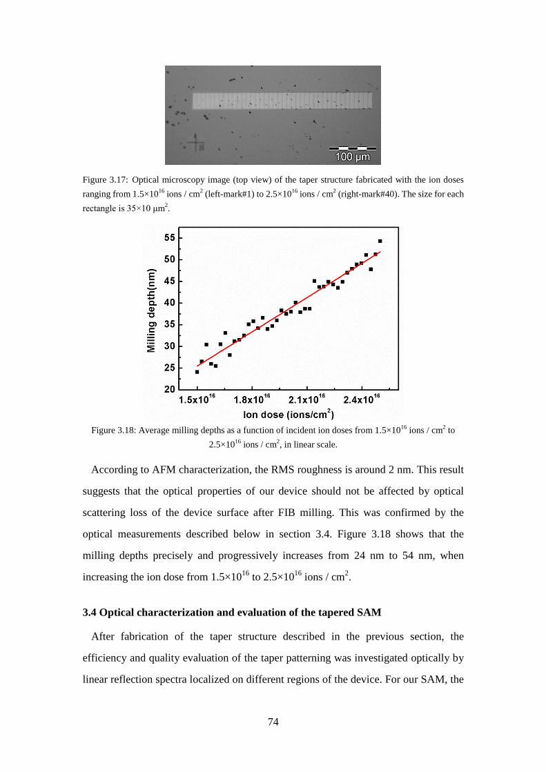
74
Figure 3.17: Optical microscopy image (top view) of the taper structure fabricated with the ion doses ranging from 1.5×10¹⁶ ions / cm2 (left-mark#1) to 2.5×10¹⁶ ions / cm2 (right-mark#40). The size for each rectangle is 35×10 μm2.
Figure 3.18: Average milling depths as a function of incident ion doses from 1.5×10¹⁶ ions / cm2 to
2.5×10¹⁶ ions / cm2, in linear scale.
According to AFM characterization, the RMS roughness is around 2 nm. This result
suggests that the optical properties of our device should not be affected by optical
scattering loss of the device surface after FIB milling. This was confirmed by the
optical measurements described below in section 3.4. Figure 3.18 shows that the
milling depths precisely and progressively increases from 24 nm to 54 nm, when
increasing the ion dose from 1.5×10¹⁶ to 2.5×10¹⁶ ions / cm2.
3.4 Optical characterization and evaluation of the tapered SAM
After fabrication of the taper structure described in the previous section, the
efficiency and quality evaluation of the taper patterning was investigated optically by
linear reflection spectra localized on different regions of the device. For our SAM, the
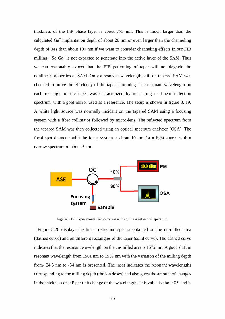
75
thickness of the InP phase layer is about 773 nm. This is much larger than the
calculated Ga+ implantation depth of about 20 nm or even larger than the channeling
depth of less than about 100 nm if we want to consider channeling effects in our FIB
milling. So Ga+ is not expected to penetrate into the active layer of the SAM. Thus
we can reasonably expect that the FIB patterning of taper will not degrade the
nonlinear properties of SAM. Only a resonant wavelength shift on tapered SAM was
checked to prove the efficiency of the taper patterning. The resonant wavelength on
each rectangle of the taper was characterized by measuring its linear reflection
spectrum, with a gold mirror used as a reference. The setup is shown in figure 3. 19.
A white light source was normally incident on the tapered SAM using a focusing
system with a fiber collimator followed by micro-lens. The reflected spectrum from
the tapered SAM was then collected using an optical spectrum analyzer (OSA). The
focal spot diameter with the focus system is about 10 μm for a light source with a
narrow spectrum of about 3 nm.
Figure 3.19: Experimental setup for measuring linear reflection spectrum.
Figure 3.20 displays the linear reflection spectra obtained on the un-milled area
(dashed curve) and on different rectangles of the taper (solid curve). The dashed curve
indicates that the resonant wavelength on the un-milled area is 1572 nm. A good shift in
resonant wavelength from 1561 nm to 1532 nm with the variation of the milling depth
from- 24.5 nm to -54 nm is presented. The inset indicates the resonant wavelengths
corresponding to the milling depth (the ion doses) and also gives the amount of changes
in the thickness of InP per unit change of the wavelength. This value is about 0.9 and is
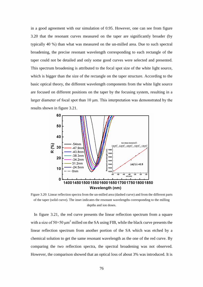
76
in a good agreement with our simulation of 0.95. However, one can see from figure
3.20 that the resonant curves measured on the taper are significantly broader (by
typically 40 %) than what was measured on the un-milled area. Due to such spectral
broadening, the precise resonant wavelength corresponding to each rectangle of the
taper could not be detailed and only some good curves were selected and presented.
This spectrum broadening is attributed to the focal spot size of the white light source,
which is bigger than the size of the rectangle on the taper structure. According to the
basic optical theory, the different wavelength components from the white light source
are focused on different positions on the taper by the focusing system, resulting in a
larger diameter of focal spot than 10 μm. This interpretation was demonstrated by the
results shown in figure 3.21.
Figure 3.20: Linear reflection spectra from the un-milled area (dashed curve) and from the different parts
of the taper (solid curve). The inset indicates the resonant wavelengths corresponding to the milling depths and ion doses.
In figure 3.21, the red curve presents the linear reflection spectrum from a square
with a size of 50×50 μm2 milled on the SA using FIB, while the black curve presents the
linear reflection spectrum from another portion of the SA which was etched by a
chemical solution to get the same resonant wavelength as the one of the red curve. By
comparing the two reflection spectra, the spectral broadening was not observed.
However, the comparison showed that an optical loss of about 3% was introduced. It is
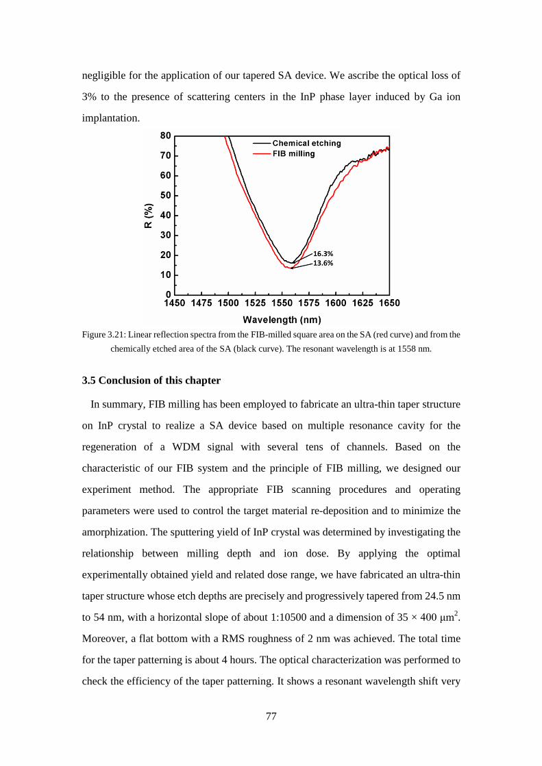
77
negligible for the application of our tapered SA device. We ascribe the optical loss of
3% to the presence of scattering centers in the InP phase layer induced by Ga ion
implantation.
Figure 3.21: Linear reflection spectra from the FIB-milled square area on the SA (red curve) and from the
chemically etched area of the SA (black curve). The resonant wavelength is at 1558 nm.
3.5 Conclusion of this chapter
In summary, FIB milling has been employed to fabricate an ultra-thin taper structure
on InP crystal to realize a SA device based on multiple resonance cavity for the
regeneration of a WDM signal with several tens of channels. Based on the
characteristic of our FIB system and the principle of FIB milling, we designed our
experiment method. The appropriate FIB scanning procedures and operating
parameters were used to control the target material re-deposition and to minimize the
amorphization. The sputtering yield of InP crystal was determined by investigating the
relationship between milling depth and ion dose. By applying the optimal
experimentally obtained yield and related dose range, we have fabricated an ultra-thin
taper structure whose etch depths are precisely and progressively tapered from 24.5 nm
to 54 nm, with a horizontal slope of about 1:10500 and a dimension of 35 × 400 μm2.
Moreover, a flat bottom with a RMS roughness of 2 nm was achieved. The total time
for the taper patterning is about 4 hours. The optical characterization was performed to
check the efficiency of the taper patterning. It shows a resonant wavelength shift very

78
similar to our design, and an optical loss of about 3%, which can be neglected for the
application of our tapered SA device. It can be concluded that FIB milling is a flexible
and reproducible technique for fabricating a tapered SA device with good optical
performance.
79
3.6 Reference [1] J. Fatome, S. Pitois, A. Kamagate, G. Millot, D. Massoubre, and J. L. Oudar
“All-optical reshaping based on a passive saturable absorber microcavity device
for future 160-Gb/s applications,” IEEE Photon. Technol. Lett., vol. 19, pp.
245-247, 2007.
[2] D. Massoubre, J. L. Oudar, J. Fatome, S. Pitois, G. Millot, J. Decobert, and J.
Landreau, “All-optical extinction-ratio enhancement of a 160 GHz pulse train by a
saturable-absorber vertical microcavity,” Opt., Lett., vol. 31, pp. 537-539, 2006.
[3] J. Fatome, S. Pitois, D. Massoubre, J. L. Oudar, and G. Millot, “Cascadability and
reshaping properties of a saturable absorber inserted inside a RZ transmission line
for future 160-Gbit/s all-optical 2R-regenerators,” Opt. Commun., vol. 279, pp.
364-369, 2007.
[4] Q. T. Le, L. Bramerie, S. Lobo, M. Gay, M. Joindot, J. C. Simon, A. Poudoulec, M.
Van der Keur, C. Deverny, D. Massoubre, J. L. Oudar, G. Aubin, A. Shen, and J.
Decobert, “WDM compatible 2R regeneration device based on eight-channel
saturable absorber module,” Electron. Lett., vol. 43, pp. 1305-1306, 2007.
[5] L. Bramerie, Q. T. Le, M. Gay, A. O’Hare, S. Lobo, M. Joindot, J. C. Simon, H. T.
Nguyen, and J. L. Oudar, “All-optical 2R regeneration with a vertical
microcavity-based saturable absorber,” IEEE J. Sel. Top. Quant. Electron., vol.
18, pp. 870-883, 2012.
[6] C. Palmer, Diffraction grating handbook, 5th edition, THERMO RGL, New York,
pp. 16-23, 2002.
[7] R. Fischer, B. Tadic-Galeb, and P. R. Yoder, Optical system Design, 2th edition,
SPIE Press, pp. 203-205, 2008.
[8] T. Brenner, W. Hunziker, M. Smit, M. Bachmann, G. Guekos, and H. Melchinor,
“Vertical InP/InGaAsP tapers for low-loss optical fiber-waveguide coupling,”
Electron. Lett., vol. 28, pp. 2040-2041, 1992.
80
[9] A. Shahar, W. J. Tomlinson, A. YiYan, M. Seto, and R. J. Deri, “Dynamic etch
mask technique for fabricating tapered semiconductor optical waveguides and
other structures,” Appl. Phys. Lett., vol. 56, pp. 1098-1100, 1990.
[10] T. Brenner and H. Melchior, “Integrated optical modeshape adapters in
InGaAsP/InP for efficiency fiber-to-waveguide coupling,” IEEE Photon.
Technol. Lett., vol. 50, pp. 1053-1056, 1993.
[11] D. E. Bossi, W. D. Goodhue, M. C. Finn, K. Rauschenbach, J. W. Bales, and R.
H. Rediker, “Reduced-confinement antennas for GaAlAs integrated optical
waveguides,” Appl. Phys. Lett., vol. 56, pp. 420-422, 1990. [12] A. Emadi, H. Wu, S. Grabarnik, G. de Graaf, and R. F. Wolffenbuttel, “Vertically
tapered layers For optical applications fabricated using resist reflow,” J.
Micromech. Microeng., vol. 19, pp. 074014 , 2009.
[13] P. M. Nellen, P. Strasser, V. Callegari, R. Wuest, D. Erni, and F. Roblin, “Focused
ion beam modification of indium phosphide photonic crystals,” Microelectron.
Eng., vol. 84, pp. 1244-1247, 2007.
[14] M. J. Cryan, M. Hill, D. Cortaberria Sanz, P. S. Ivanov, P. J. Heard, L. Tian, S. Yu,
and J. M. Rorison, “Focused ion beam-based fabrication of nanostructure photonic
devices”, IEEE J. Sel. Top. Quant. Electron., vol. 11, pp. 1266-1277, 2005.
[15] S. Matsui, T. Kaito, J. Fujita, M. Komuro, K. Kanda, and Y. Haruyama,
“Three-dimensional nanostructure fabrication by focused-ion-beam chemical
vapor deposition”, J. Vac. Sci. Technol. B, vol. 18, pp. 3181-3184, 2000.
[16] F. A. Stevie, L. A. Giannuzzi, and B. I. Prenitzer, “The Focused Ion Beam
Instrument,” in Introduction to focused ion beams: instrumentation, theory,
techniques, and practice, L. A. Giannuzzi and F. A. Stevie, Eds., New York:
Springer, pp. 1-12, 2005.
[17] J. Gierak, “Focused ion beam technology and ultimate applications,” Semicond.
Sci. Technol., vol. 24, Article ID 043001, 2009.
[18] G. Taylor, “Desintegration of water drops in an electric field,” Proc. R. Soc. A,
vol. 280, pp. 383-397, 1964.
81
[19] J. Gierak, A. Septier, and C. Vieu, “Design and realization of a very
high-resolution FIB nanofabrication instrument,” Nucl. Instrum. Methods Phys.
Res. A, vol. 427, pp. 91-98, 1999.
[20] J. Gierak, A. Madouri, A. L. Biance, E. Bourhis, G. Patriarche, C.Ulysse, D.
Lucot, X. Lafosse, L. Auvray, L. Bruchhaus, and R. Jede, “Sub-5 nm FIB direct
patterning of nanodevices,” Microelectron. Eng., vol. 84, pp. 779-783, 2007.
[21] J. Gierak, C. Vieu , M. Schneider, H. Launois, G. Ben Assayag, and A. Septier,
“Optimization of experimental operating parameters for very high resolution
focused ion beam applications,” J. Vac. Sci. Technol. B, vol. 15, pp. 2373-2378,
1997.
[22] Ampere A. Tseng, “Recent developments in micromilling using focused ion
beam technology,” J. Micromech. Microeng., vol. 14, pp. R15-R34. 2004.
[23] L. Frey, C. Lehrer, and H. Ryssel, “Nanoscale effects in focused ion beam
processing,” Appl. Phys. A, vol. 76, pp. 1017-1023, 2003.
[24] A. Lugstein, B. Basnar, J. Smoliner, and E. Bertagnolli, “FIB processing of
silicon in the nanoscale regime,” Appl. Phys. A, vol. 76, pp. 545-548, 2003.
[25] P. K. Giri, “Studies on the surface swelling of ion-irradiated silicon: Role of
defects,” Mater. Sci. Eng. B, vol. 121, pp. 238-243, 2005.
[26] J. Gierak, P. Hawkes, and R. Jede, “Nanolithography with Focused Ion Beams,”
in: S. Cabrini, S. Kawata, Eds., Nanofabrication Handbook, CRC Press, pp.
47-48, 2012.
[27] B. W. Kempshall, S. M. Schwarz, B. I. Prenitzer, L. A. Giannuzzi, R. B. Irwin,
and F. A. Stevie, “Ion channeling effects on the focused ion beam milling of
Cu,” J. Vac. Sci. Technol. B, vol. 19, pp. 749-754, 2001.
[28] A. A. Tseng, “Recent Developments in nanofabrication using focused ion beam,”
Small, vol. 10, pp. 924-939, 2005.
[29] D. Santamore, K. Edinger, J. Orloff, and J. Melngailis, “Focused ion beam sputter
yield change as a function of scan speed,” J. Vac. Sci. Technol. B, vol. 15, pp.
2346-2349, 1997.
82
[30] J. Orloff, L. W. Swanson, and M. Utlaut, “Fundamental limits to imaging
resolution for focused ion beams,” J. Vac. Sci. Technol. B, vol. 14, pp. 3759-3763,
1997.
[31] B. D. Huey, and R. M. Langford, “Low-dose focused ion beam nanofabrication
and characterization by atomic force microscopy,” Nanotechnology, vol. 14, pp.
409-412, 2003.
[32] H. Yamaguchi, A. Shimase, S. Haraichi, and T. Miyauchi, “Characteristics of
silicon removal by fine focused gallium ion beam,” J. Vac. Sci. Technol. B, vol. 3,
pp. 71-74, 1985.
[33] Y. Fu and N. K. A. Bryan, “Investigation of 3D microfabrication characteristics by
focused ion beam technology in silicon,” J. Mater. Process. Technol., vol. 104, pp.
44-47, 2000.
[34] D. Baselt, “The tip-sample interaction in atomic force microscopy and its
implications for biological applications,” Ph. D. thesis, California Institute of
Technology, 1993.
83
Chapter 4 Graphene-based saturable absorber mirror (GSAM)
Semiconductor-based resonant Fabry-Perot saturable absorber mirrors (R-FPSAs)
have been successfully used for passive mode-locking of lasers [1, 2] and various
types of optical signal processing [3-5]. The main advantage of the R-FPSA is that
important operation parameters such as the amount of light absorbed, saturation
intensity or fluence, and modulation depth (a maximum change in reflectivity) can be
easily adjusted by cavity design to adapt them to the requirements of specific
applications.
Graphene has recently been considered as an ideal saturable absorber due to its
wavelength-insensitive saturable absorption [6, 7], ultrafast recovery time in the
picosecond timescales [8], low cost, and easy fabrication. It has already been widely
used for passive mode-locking of solid-state lasers and fiber lasers at different
wavelengths [9-12]. As a mode-locker, graphene is integrated in laser cavities by
transferring graphene onto the end facet of a fiber pigtail in fiber lasers [11, 12], or on
a quartz substrate [13] or a cavity mirror [9] in free-space solid-state lasers. However,
with these integration approaches, the amount of light absorbed and the modulation
depth in reflectivity or transmissivity of the graphene saturable absorber can only be
adjusted by controlling the number of layers of graphene. Moreover, the saturation
intensity or fluence of the graphene saturable absorber increases as the number of
layers of graphene increases [14]. These will prevent the application of graphene from
some specific passive mode-locking of lasers which requires both a low saturable
intensity or fluence and a large modulation depth for the mode-locker, and even limit
its potential applications in high-speed optical signal processing. Therefore, the
concept of the resonant Fabry–Perot microcavity could also be employed to adjust the
important operation parameters of the graphene saturable absorber, and thus to
facilitate its applications in passive mode-locking of the laser and to explore its
potential applications in optical signal processing.
In this chapter, we have investigated optical properties of the graphene by
integrating it into a resonant Fabry-Perot microcavity. This device is called
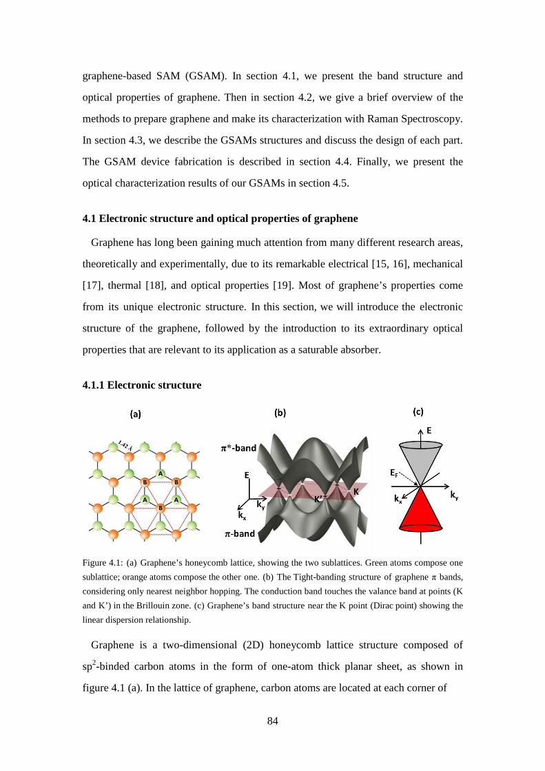
84
graphene-based SAM (GSAM). In section 4.1, we present the band structure and
optical properties of graphene. Then in section 4.2, we give a brief overview of the
methods to prepare graphene and make its characterization with Raman Spectroscopy.
In section 4.3, we describe the GSAMs structures and discuss the design of each part.
The GSAM device fabrication is described in section 4.4. Finally, we present the
optical characterization results of our GSAMs in section 4.5.
4.1 Electronic structure and optical properties of graphene
Graphene has long been gaining much attention from many different research areas,
theoretically and experimentally, due to its remarkable electrical [15, 16], mechanical
[17], thermal [18], and optical properties [19]. Most of graphene’s properties come
from its unique electronic structure. In this section, we will introduce the electronic
structure of the graphene, followed by the introduction to its extraordinary optical
properties that are relevant to its application as a saturable absorber.
4.1.1 Electronic structure
Figure 4.1: (a) Graphene’s honeycomb lattice, showing the two sublattices. Green atoms compose one sublattice; orange atoms compose the other one. (b) The Tight-banding structure of graphene π bands, considering only nearest neighbor hopping. The conduction band touches the valance band at points (K and K’) in the Brillouin zone. (c) Graphene’s band structure near the K point (Dirac point) showing the linear dispersion relationship.
Graphene is a two-dimensional (2D) honeycomb lattice structure composed of
sp2-binded carbon atoms in the form of one-atom thick planar sheet, as shown in
figure 4.1 (a). In the lattice of graphene, carbon atoms are located at each corner of
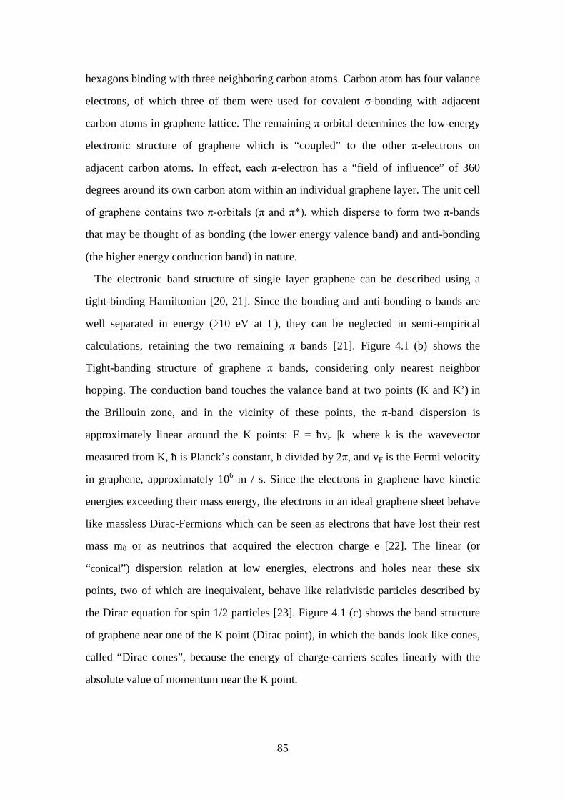
85
hexagons binding with three neighboring carbon atoms. Carbon atom has four valance
electrons, of which three of them were used for covalent σ-bonding with adjacent
carbon atoms in graphene lattice. The remaining π-orbital determines the low-energy
electronic structure of graphene which is “coupled” to the other π-electrons on
adjacent carbon atoms. In effect, each π-electron has a “field of influence” of 360
degrees around its own carbon atom within an individual graphene layer. The unit cell
of graphene contains two π-orbitals (π and π*), which disperse to form two π-bands
that may be thought of as bonding (the lower energy valence band) and anti-bonding
(the higher energy conduction band) in nature.
The electronic band structure of single layer graphene can be described using a
tight-binding Hamiltonian [20, 21]. Since the bonding and anti-bonding σ bands are
well separated in energy (>10 eV at Γ), they can be neglected in semi-empirical
calculations, retaining the two remaining π bands [21]. Figure 4.1 (b) shows the
Tight-banding structure of graphene π bands, considering only nearest neighbor
hopping. The conduction band touches the valance band at two points (K and K’) in
the Brillouin zone, and in the vicinity of these points, the π-band dispersion is
approximately linear around the K points: E = ħvF |k| where k is the wavevector
measured from K, ħ is Planck’s constant, h divided by 2π, and vF is the Fermi velocity
in graphene, approximately 106 m / s. Since the electrons in graphene have kinetic
energies exceeding their mass energy, the electrons in an ideal graphene sheet behave
like massless Dirac-Fermions which can be seen as electrons that have lost their rest
mass m0 or as neutrinos that acquired the electron charge e [22]. The linear (or
“conical”) dispersion relation at low energies, electrons and holes near these six
points, two of which are inequivalent, behave like relativistic particles described by
the Dirac equation for spin 1/2 particles [23]. Figure 4.1 (c) shows the band structure
of graphene near one of the K point (Dirac point), in which the bands look like cones,
called “Dirac cones”, because the energy of charge-carriers scales linearly with the
absolute value of momentum near the K point.
86
4.1.2 Optical properties
4.1.2.1 Linear optical absorption
Due to the unique electronic structure in which conical-shaped conduction and
valence bands meet at the Dirac point, the optical conductance of pristine monolayer
graphene is frequency-independent in a broad range of photon energies [24]:
G1(x)=G0 = 𝑒2/4ħ, where ω is the radian frequency, e is electron charge, and ħ is
reduced Planck's constant. As a direct consequence of this universal optical
conductance, the optical transmittance of pristine graphene is also
frequency-independent and solely determined by the fine structure constant
α=e2/ħc≈1/137 (c is the speed of light):
T≡�1+ 2πGc�
-2≈1-πα≈0.977 (4.1)
When scaled to its atomic thickness, graphene actually shows strong broadband
absorption per unit mass of the material (πα = 2.3%) from the visible to near-infrared
range. This absorption value of 2.3 % is ∼50 times higher than GaAs of the same
thickness [25]. The reflectance under normal light incidence is relatively weak and
written as R=0.25π2α2T=1.3×10⁻⁴, which is much smaller than the transmittance
[19]. In a few layer graphene, each sheet can be seen as a bi-dimensional electron gas,
with little perturbation from the adjacent layers, making it optically equivalent to a
superposition of almost non-interacting single layer. So the absorption of few-layer
graphene can be roughly estimated by scaling the number of layers (T=1-Nπα).
4.1.2.2 Ultrafast properties
Interband excitation by ultrafast optical pulses produces a non-equilibrium carrier
population in the valence and conduction bands. In time-resolved experiments [26],
two relaxation time scales are typically seen. A faster one, ~ 100 fs, usually associated
with carrier-carrier intraband collisions and phonon emission, and a slower one, on a
picosecond scale, corresponding to electron interband relaxation and cooling of hot
phonons [27, 28]. Figure 4.2 schematically represents this relaxation process: (I) the
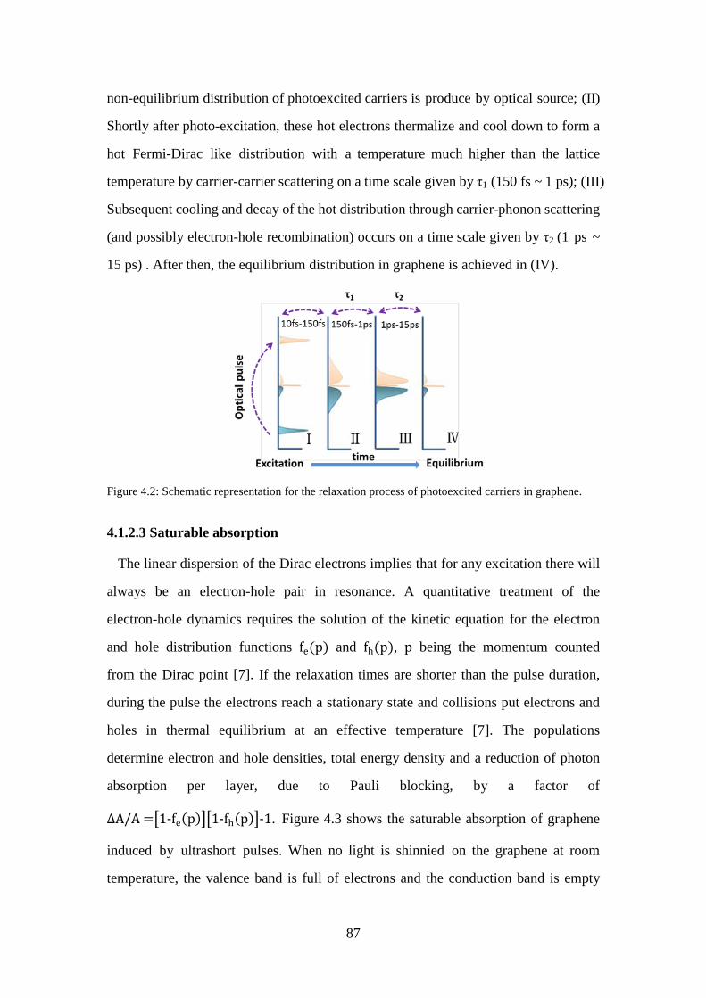
87
non-equilibrium distribution of photoexcited carriers is produce by optical source; (II)
Shortly after photo-excitation, these hot electrons thermalize and cool down to form a
hot Fermi-Dirac like distribution with a temperature much higher than the lattice
temperature by carrier-carrier scattering on a time scale given by τ1 (150 fs ~ 1 ps); (III)
Subsequent cooling and decay of the hot distribution through carrier-phonon scattering
(and possibly electron-hole recombination) occurs on a time scale given by τ2 (1 ps ~
15 ps) . After then, the equilibrium distribution in graphene is achieved in (IV).
Figure 4.2: Schematic representation for the relaxation process of photoexcited carriers in graphene.
4.1.2.3 Saturable absorption
The linear dispersion of the Dirac electrons implies that for any excitation there will
always be an electron-hole pair in resonance. A quantitative treatment of the
electron-hole dynamics requires the solution of the kinetic equation for the electron
and hole distribution functions fe(p) and fh(p), p being the momentum counted
from the Dirac point [7]. If the relaxation times are shorter than the pulse duration,
during the pulse the electrons reach a stationary state and collisions put electrons and
holes in thermal equilibrium at an effective temperature [7]. The populations
determine electron and hole densities, total energy density and a reduction of photon
absorption per layer, due to Pauli blocking, by a factor of
∆A/A =�1-fe(p)��1-fh(p)�-1. Figure 4.3 shows the saturable absorption of graphene
induced by ultrashort pulses. When no light is shinnied on the graphene at room
temperature, the valence band is full of electrons and the conduction band is empty
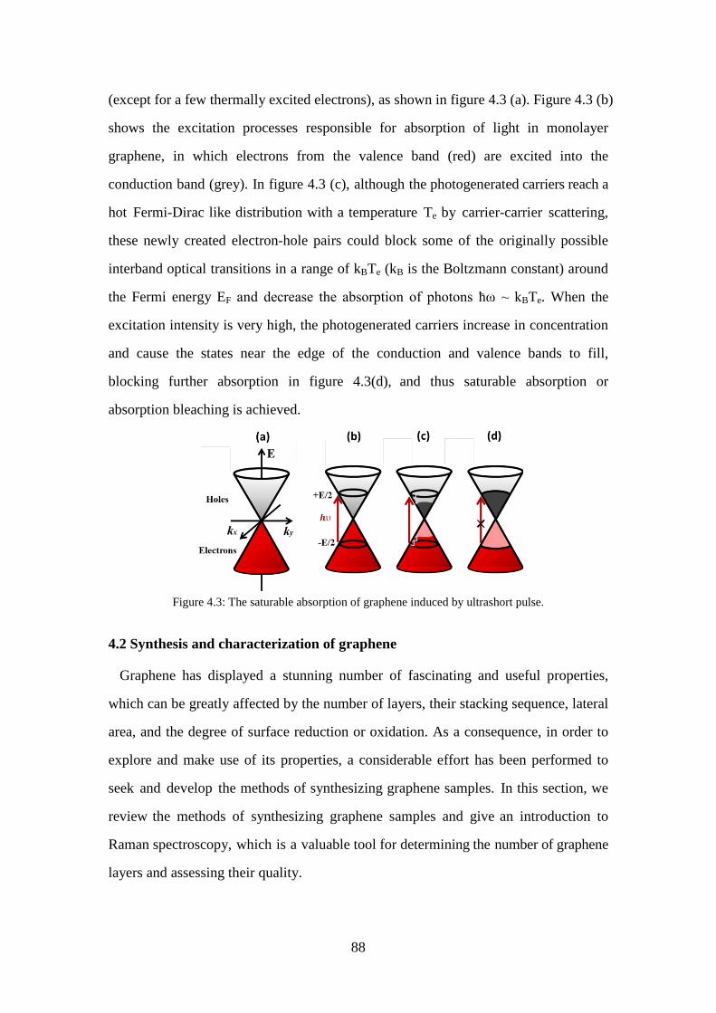
88
(except for a few thermally excited electrons), as shown in figure 4.3 (a). Figure 4.3 (b)
shows the excitation processes responsible for absorption of light in monolayer
graphene, in which electrons from the valence band (red) are excited into the
conduction band (grey). In figure 4.3 (c), although the photogenerated carriers reach a
hot Fermi-Dirac like distribution with a temperature Te by carrier-carrier scattering,
these newly created electron-hole pairs could block some of the originally possible
interband optical transitions in a range of kBTe (kB is the Boltzmann constant) around
the Fermi energy EF and decrease the absorption of photons ћω ~ kBTe. When the
excitation intensity is very high, the photogenerated carriers increase in concentration
and cause the states near the edge of the conduction and valence bands to fill,
blocking further absorption in figure 4.3(d), and thus saturable absorption or
absorption bleaching is achieved.
Figure 4.3: The saturable absorption of graphene induced by ultrashort pulse.
4.2 Synthesis and characterization of graphene
Graphene has displayed a stunning number of fascinating and useful properties,
which can be greatly affected by the number of layers, their stacking sequence, lateral
area, and the degree of surface reduction or oxidation. As a consequence, in order to
explore and make use of its properties, a considerable effort has been performed to
seek and develop the methods of synthesizing graphene samples. In this section, we
review the methods of synthesizing graphene samples and give an introduction to
Raman spectroscopy, which is a valuable tool for determining the number of graphene
layers and assessing their quality.
89
4.2.1 Synthesis of graphene
Although graphene was postulated in 1947 [21], a method to produce high-quality
graphene was only developed by Andre Geim and Konstantin Novoselov in 2004 [20],
who won the Nobel Prize as a result. This method is micromechanical exfoliation of
graphene from highly oriented pyrolytic graphite (HOPG), which can produce the
high-quality graphene sample. It involves pulling flakes off of highly-ordered graphite
with tape, and then pulling those flakes apart repeatedly until flakes consisting of
between one and ten layers of graphene sheet are achieved [29]. The tap with attached
optically transparent flakes was dissolved in acetone, and after a few further steps, the
graphene flakes including monolayers were palced on a substrate. In the process, the
atomic structure and interlayer stacking sequence were preserved. Due to the high
quality of graphene samples synthesized by this method, many important properties of
graphene have been discovered [19, 20, 30-32]. However, even though this method
produces relatively high-quality graphene, it is extremely slow, does not reproducibly
generate monolayer sheets, and is not scalable for large-area sheets production.
Following this early attempts of mechanical exfoliation, many research groups are
seeking high-throughput processing routes for producing graphene. Today, graphene
can also be produced by other methods. One of methods is the direct liquid-phase
exfoliation of graphite is a convenient method for generating ideal graphene samples in
large quantities [33, 34], which is mainly of interest for industrial applications,
especially for adding small graphene flakes to polymer materials. This method relies on
the exfoliation and stabilization of graphene using special solvents or surfactants under
sonication. After tens or hundreds hours of sonication, the number of layers of graphene
flakes can be down to less than 5. The size of graphene synthesized by this method was
around few micrometers due to long time of sonication.
Another popular method is epitaxial growth of graphene by thermal decomposition of
silicon-carbide (SiC) surface at high temperatures. The bonds between the silicon and
the carbon atoms break, which results in the formation of graphene on top of the SiC
crystal lattice [35, 36]. This technique can provide anywhere from a few monolayers of
90
graphene to several (> 50) layers on the surface of a SiC wafer. Graphene layers grown
by this technique have demonstrated low temperature carrier mobility in the tens of
thousands cm2·V-1·s-1 range and do not significantly depend on temperature [37],
which is comparable to the exfoliated graphene. Many important graphene properties
have been identified in graphene produced by this method [38-42]. Epitaxial growth is
scalable to high quantities of graphene, and, most importantly, silicon carbide wafers
are compatible with standard nanofabrication techniques used to make modern
electronics. However, epitaxially-grown graphene usually has more defects in the
lattice, resulting in lower conduction and poorer overall quality.
Chemical vapor deposition (CVD) is a very promising method for the mass
production of large area graphene films due to its capability of producing large area
deposition and the lack of intense mechanical and chemical treatment [43]. In this
technique, a metal substrate, typically nickel or copper, is heated up to approximately
1000 °C. Then, a mixture of gases, such as argon, hydrogen, and methane, is guided
over the metal substrate, where the methane is cracked and carbon diffuses into the
metal. Subsequent rapid cooling results in a graphene layer on the metal. Deposition
can be performed on substrates of a size of several 10 cm. CVD growth of graphene is
well compatible with industrial production. CVD-grown graphene can be transferred
easily to other substrates by etching away the metal film and applying a
polymer-assisted transfer process. In this thesis, the CVD method is used to fabricate
graphene for saturable absorber and more details will be presented in section 4.4.1.
4.2.2 Raman Spectroscopy
We have shown graphene can be prepared by different methods. In any production
process, it is important to control the quality of graphene in a fast and non-destructive
manner. Firstly, defects are of great importance since they modify the electronic and
optical properties of the system. Quantifying defects in graphene-based device is
crucial both to gain insight in their fundamental properties and for applications.
Secondly, it is important to be able to easily determine the number of layers and the
type of stacking of those layers of a graphene sheet. For example, using graphene as
91
saturable absorber (SA) in mode-locking vertical cavity surface emitting laser
(VECSELs) typically requires a SA with losses < 3% per cavity round-trip [44, 45].
Therefore, it is crucial to limit the layer number of graphene-based SA to monolayer
(absorption ~ 2.3%). In the field of graphene-based nanostructures, Raman
spectroscopy has been shown to be the most suitable technique to investigate the
presence of defects and the number of layers of graphene sheet [46, 47]. In this section,
we will introduce the Raman spectrum of the graphene, and its relationship with the
presence of defects and the number of layers.
4.2.2.1 Raman spectrum of graphene
As shown in section 4.1.1, graphene has two atoms in the unit cell and, therefore,
six phonon branches. Three are acoustic branches and three are optical branches.
From the three optical branches, one gives rise to an infra-red active mode at the Γ
point, while the two other branches are degenerate at the Γ point and Raman active.
Therefore, zone center (q = 0) phonons would generate a one-peak Raman spectrum.
However, the electronic structure of graphene generates special electron-phonon
induced resonance conditions with non-zone center modes (q≠0), known in the
literature as the double-resonance Raman scattering process. This double-resonance
process is responsible for the graphene related systems to have Raman spectra with
many features [48, 49]. Although the double resonance process can activate phonons
from all the six branches, the main features in the Raman spectra of graphene come
from the phonon branch related to the zone-center Raman-active mode, i.e. to the
optical phonon branch related to in-plane stretching of the C-C bonding [50].
Because graphene is a two-dimensional system, it has become convention to name
transverse phonons as either in-plane (i) or out-of-plane (o). This convention is often
extended to longitudinal phonons, though it is somewhat redundant in the case of a
two-dimensional material. All phonons that contribute to Raman scattering are
so-called “optical phonons” (O), named because they have energies and frequencies
of approximately the same order of magnitude as light. This is in contrast to “acoustic
phonons” (A), which has frequencies of the same order of magnitude as human
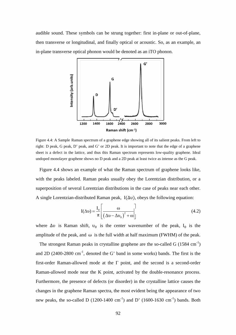
92
audible sound. These symbols can be strung together: first in-plane or out-of-plane,
then transverse or longitudinal, and finally optical or acoustic. So, as an example, an
in-plane transverse optical phonon would be denoted as an iTO phonon.
Figure 4.4: A Sample Raman spectrum of a graphene edge showing all of its salient peaks. From left to right: D peak, G peak, D’ peak, and G’ or 2D peak. It is important to note that the edge of a graphene sheet is a defect in the lattice, and thus this Raman spectrum represents low-quality graphene. Ideal undoped monolayer graphene shows no D peak and a 2D peak at least twice as intense as the G peak.
Figure 4.4 shows an example of what the Raman spectrum of graphene looks like,
with the peaks labeled. Raman peaks usually obey the Lorentzian distribution, or a
superposition of several Lorentzian distributions in the case of peaks near each other.
A single Lorentzian-distributed Raman peak, I(∆υ), obeys the following equation:
( )0
20
I ωI(Δυ)π Δυ Δυ ω
=
− + (4.2)
where ∆υ is Raman shift, υ0 is the center wavenumber of the peak, I0 is the
amplitude of the peak, and ω is the full width at half maximum (FWHM) of the peak.
The strongest Raman peaks in crystalline graphene are the so-called G (1584 cm-1)
and 2D (2400-2800 cm-1, denoted the G’ band in some works) bands. The first is the
first-order Raman-allowed mode at the Г point, and the second is a second-order
Raman-allowed mode near the K point, activated by the double-resonance process.
Furthermore, the presence of defects (or disorder) in the crystalline lattice causes the
changes in the graphene Raman spectra, the most evident being the appearance of two
new peaks, the so-called D (1200-1400 cm-1) and D’ (1600-1630 cm-1) bands. Both
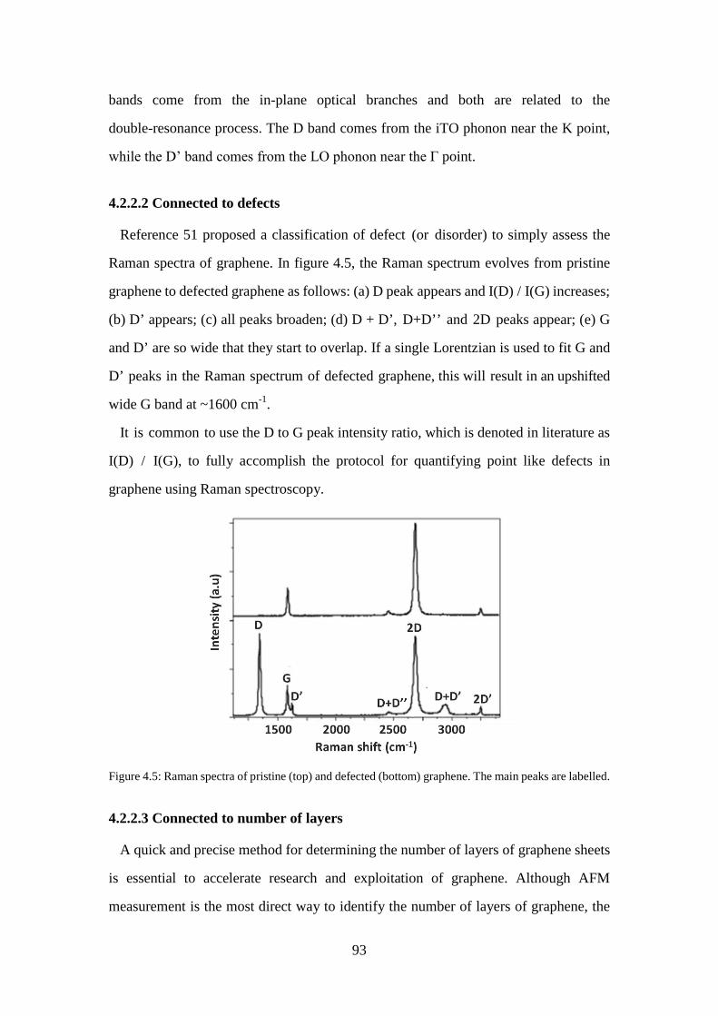
93
bands come from the in-plane optical branches and both are related to the
double-resonance process. The D band comes from the iTO phonon near the K point,
while the D’ band comes from the LO phonon near the Γ point.
4.2.2.2 Connected to defects
Reference 51 proposed a classification of defect (or disorder) to simply assess the
Raman spectra of graphene. In figure 4.5, the Raman spectrum evolves from pristine
graphene to defected graphene as follows: (a) D peak appears and I(D) / I(G) increases;
(b) D’ appears; (c) all peaks broaden; (d) D + D’, D+D’’ and 2D peaks appear; (e) G
and D’ are so wide that they start to overlap. If a single Lorentzian is used to fit G and
D’ peaks in the Raman spectrum of defected graphene, this will result in an upshifted
wide G band at ~1600 cm-1.
It is common to use the D to G peak intensity ratio, which is denoted in literature as
I(D) / I(G), to fully accomplish the protocol for quantifying point like defects in
graphene using Raman spectroscopy.
Figure 4.5: Raman spectra of pristine (top) and defected (bottom) graphene. The main peaks are labelled.
4.2.2.3 Connected to number of layers
A quick and precise method for determining the number of layers of graphene sheets
is essential to accelerate research and exploitation of graphene. Although AFM
measurement is the most direct way to identify the number of layers of graphene, the
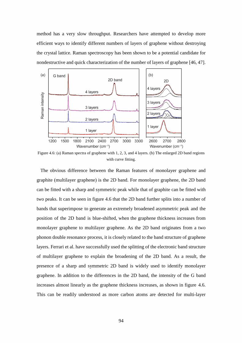
94
method has a very slow throughput. Researchers have attempted to develop more
efficient ways to identify different numbers of layers of graphene without destroying
the crystal lattice. Raman spectroscopy has been shown to be a potential candidate for
nondestructive and quick characterization of the number of layers of graphene [46, 47].
Figure 4.6: (a) Raman spectra of graphene with 1, 2, 3, and 4 layers. (b) The enlarged 2D band regions
with curve fitting.
The obvious difference between the Raman features of monolayer graphene and
graphite (multilayer graphene) is the 2D band. For monolayer graphene, the 2D band
can be fitted with a sharp and symmetric peak while that of graphite can be fitted with
two peaks. It can be seen in figure 4.6 that the 2D band further splits into a number of
bands that superimpose to generate an extremely broadened asymmetric peak and the
position of the 2D band is blue-shifted, when the graphene thickness increases from
monolayer graphene to multilayer graphene. As the 2D band originates from a two
phonon double resonance process, it is closely related to the band structure of graphene
layers. Ferrari et al. have successfully used the splitting of the electronic band structure
of multilayer graphene to explain the broadening of the 2D band. As a result, the
presence of a sharp and symmetric 2D band is widely used to identify monolayer
graphene. In addition to the differences in the 2D band, the intensity of the G band
increases almost linearly as the graphene thickness increases, as shown in figure 4.6.
This can be readily understood as more carbon atoms are detected for multi-layer
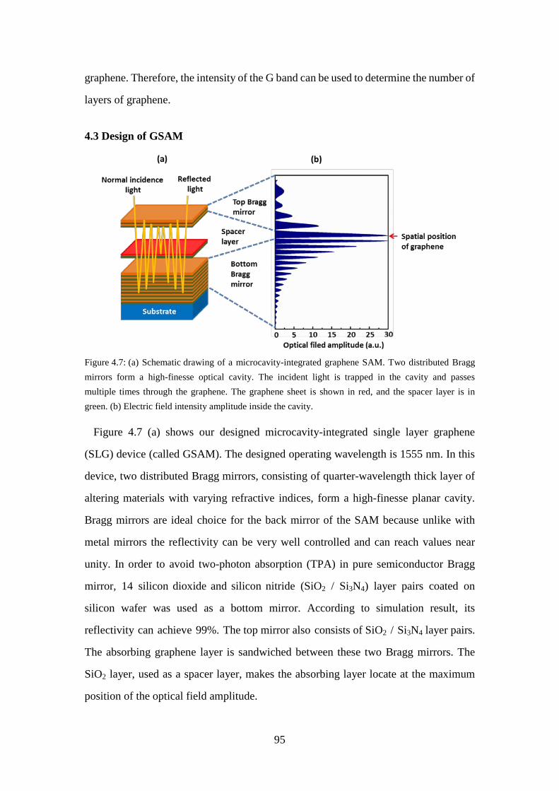
95
graphene. Therefore, the intensity of the G band can be used to determine the number of
layers of graphene.
4.3 Design of GSAM
Figure 4.7: (a) Schematic drawing of a microcavity-integrated graphene SAM. Two distributed Bragg mirrors form a high-finesse optical cavity. The incident light is trapped in the cavity and passes multiple times through the graphene. The graphene sheet is shown in red, and the spacer layer is in green. (b) Electric field intensity amplitude inside the cavity.
Figure 4.7 (a) shows our designed microcavity-integrated single layer graphene
(SLG) device (called GSAM). The designed operating wavelength is 1555 nm. In this
device, two distributed Bragg mirrors, consisting of quarter-wavelength thick layer of
altering materials with varying refractive indices, form a high-finesse planar cavity.
Bragg mirrors are ideal choice for the back mirror of the SAM because unlike with
metal mirrors the reflectivity can be very well controlled and can reach values near
unity. In order to avoid two-photon absorption (TPA) in pure semiconductor Bragg
mirror, 14 silicon dioxide and silicon nitride (SiO2 / Si3N4) layer pairs coated on
silicon wafer was used as a bottom mirror. According to simulation result, its
reflectivity can achieve 99%. The top mirror also consists of SiO2 / Si3N4 layer pairs.
The absorbing graphene layer is sandwiched between these two Bragg mirrors. The
SiO2 layer, used as a spacer layer, makes the absorbing layer locate at the maximum
position of the optical field amplitude.
96
In this section, we have discussed the cavity design of the GSAM, and have shown
how cavity design impacts on the amount of light absorbed of SLG-based SAM. We
changed the absorption by controlling the electric field intensity in SLG on a
high-reflection bottom mirror by varying the spacer layer and top mirror design. In
order to study the impact of the spacer layer and top mirror design, we used a field
intensity enhancement factor β� λ �, which controls the amount of light absorbed
A(λ) by the following equation:
A� λ �=β� λ �∙αgraphene� λ � (4.3)
where α𝑔𝑔𝑚𝑔ℎ𝑒𝑒𝑒( λ ) is the single-pass absorption of the SLG.
4.3.1 Spacer layer
The spacer layer can tune the field intensity enhancement at the top SLG layer by
changing the optical distance between SLG and the bottom mirror surface. The field
intensity enhancement for a design wavelength λ can be expressed as[]:
2 2
4β(λ)1 n cot (2π nd/ λ)
≈+
(4.4)
where n, d is the refractive index and the thickness of the spacer layer material
respectively.
In our design, SiO2 is used as the spacer layer. Figure 4.8 shows the field intensity
enhancement as a function of the thickness of SiO2 spacer layer. We can see that with
optical distances of 0, λ /8 SiO2 and λ /4 SiO2, the field intensity enhancement factors
at the location of the SLG are 0, 1.3 and 4 respectively. If the SLG is directly placed
onto the bottom mirror surface, we get β = 0, thus there is no absorption due to
destructive interference between incoming and reflected waves. If the SLG is placed
at the λ /4 distance, where there is a peak of the standing wave, we have β = 4. Thus
its absorption will increase to 400% (i.e. 4×2.3%~9.2%) due to constructive
interference. With a quarter-wavelength-thick SiO2 spacer layer, the highest field
enhancement factor can be obtained. Also from the figure 4.9 (b), which shows the
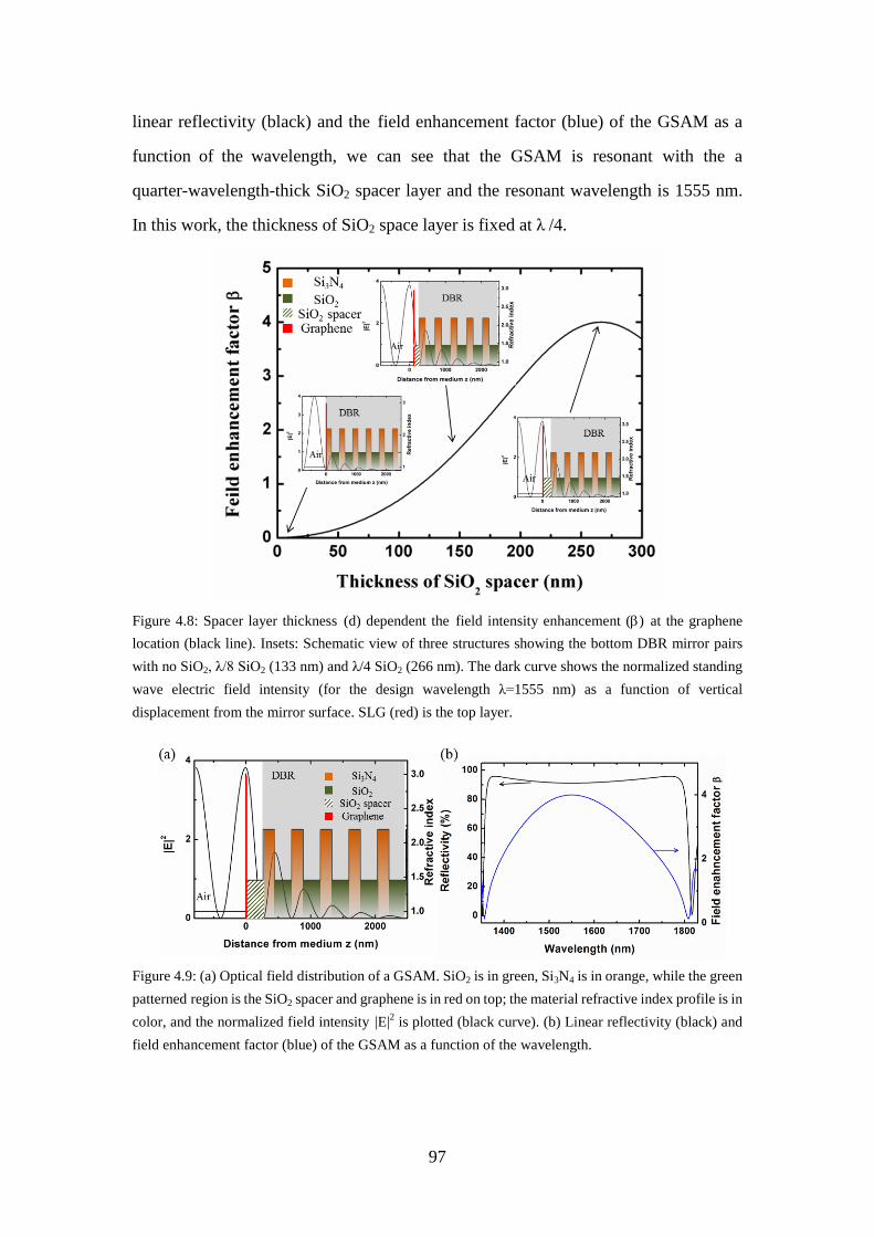
97
linear reflectivity (black) and the field enhancement factor (blue) of the GSAM as a
function of the wavelength, we can see that the GSAM is resonant with the a
quarter-wavelength-thick SiO2 spacer layer and the resonant wavelength is 1555 nm.
In this work, the thickness of SiO2 space layer is fixed at λ /4.
Figure 4.8: Spacer layer thickness (d) dependent the field intensity enhancement (β) at the graphene location (black line). Insets: Schematic view of three structures showing the bottom DBR mirror pairs with no SiO2, λ/8 SiO2 (133 nm) and λ/4 SiO2 (266 nm). The dark curve shows the normalized standing wave electric field intensity (for the design wavelength λ=1555 nm) as a function of vertical displacement from the mirror surface. SLG (red) is the top layer.
Figure 4.9: (a) Optical field distribution of a GSAM. SiO2 is in green, Si3N4 is in orange, while the green patterned region is the SiO2 spacer and graphene is in red on top; the material refractive index profile is in color, and the normalized field intensity |E|2 is plotted (black curve). (b) Linear reflectivity (black) and field enhancement factor (blue) of the GSAM as a function of the wavelength.
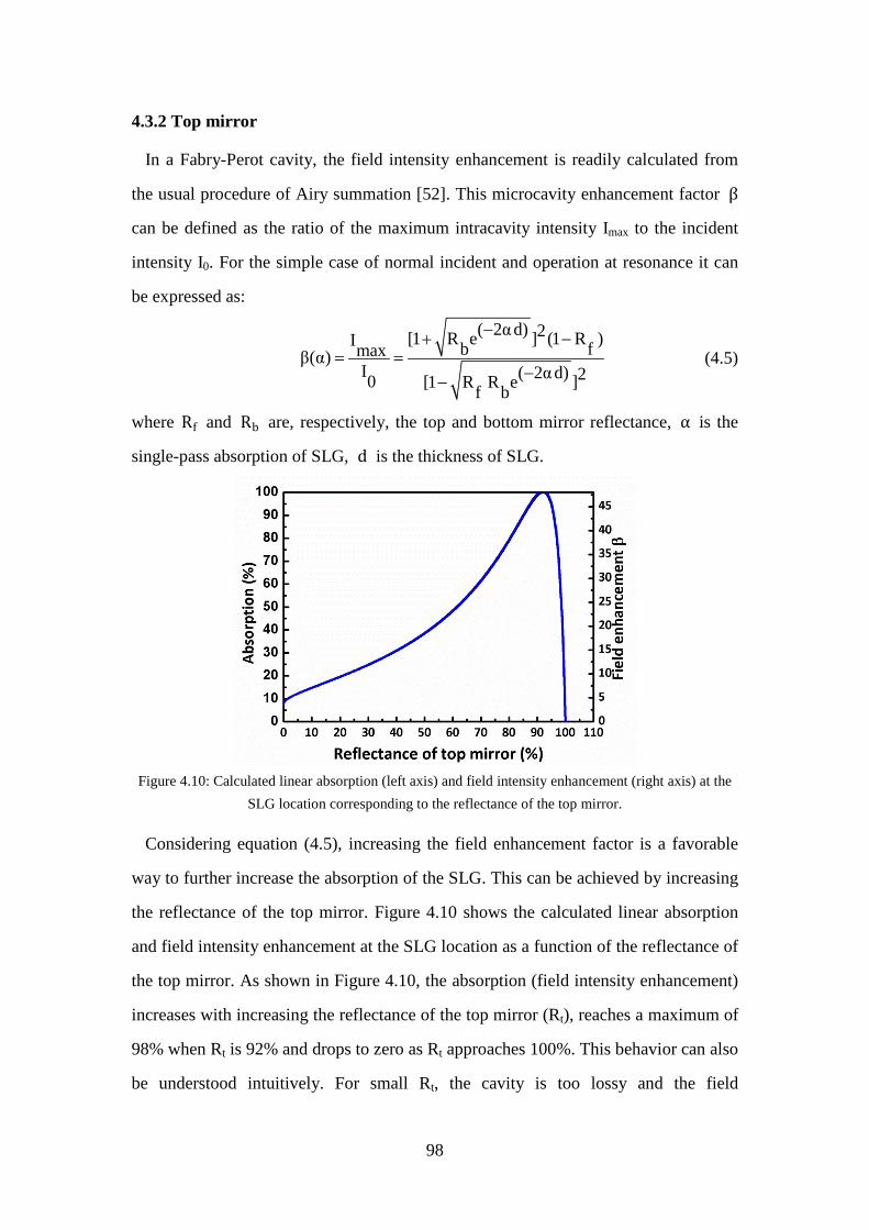
98
4.3.2 Top mirror
In a Fabry-Perot cavity, the field intensity enhancement is readily calculated from
the usual procedure of Airy summation [52]. This microcavity enhancement factor β
can be defined as the ratio of the maximum intracavity intensity Imax to the incident
intensity I0. For the simple case of normal incident and operation at resonance it can
be expressed as:
( 2α d) 2[1 R e ] (1 R )I b fmaxβ(α)I ( 2α d) 20 [1 R R e ]f b
−+ −= =
−− (4.5)
where Rf and Rb are, respectively, the top and bottom mirror reflectance, α is the
single-pass absorption of SLG, d is the thickness of SLG.
Figure 4.10: Calculated linear absorption (left axis) and field intensity enhancement (right axis) at the
SLG location corresponding to the reflectance of the top mirror.
Considering equation (4.5), increasing the field enhancement factor is a favorable
way to further increase the absorption of the SLG. This can be achieved by increasing
the reflectance of the top mirror. Figure 4.10 shows the calculated linear absorption
and field intensity enhancement at the SLG location as a function of the reflectance of
the top mirror. As shown in Figure 4.10, the absorption (field intensity enhancement)
increases with increasing the reflectance of the top mirror (Rt), reaches a maximum of
98% when Rt is 92% and drops to zero as Rt approaches 100%. This behavior can also
be understood intuitively. For small Rt, the cavity is too lossy and the field
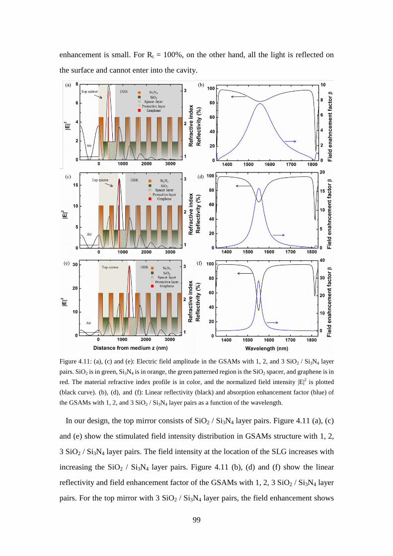
99
enhancement is small. For Rt = 100%, on the other hand, all the light is reflected on
the surface and cannot enter into the cavity.
Figure 4.11: (a), (c) and (e): Electric field amplitude in the GSAMs with 1, 2, and 3 SiO2 / Si3N4 layer pairs. SiO2 is in green, Si3N4 is in orange, the green patterned region is the SiO2 spacer, and graphene is in red. The material refractive index profile is in color, and the normalized field intensity |E|2 is plotted (black curve). (b), (d), and (f): Linear reflectivity (black) and absorption enhancement factor (blue) of the GSAMs with 1, 2, and 3 SiO2 / Si3N4 layer pairs as a function of the wavelength.
In our design, the top mirror consists of SiO2 / Si3N4 layer pairs. Figure 4.11 (a), (c)
and (e) show the stimulated field intensity distribution in GSAMs structure with 1, 2,
3 SiO2 / Si3N4 layer pairs. The field intensity at the location of the SLG increases with
increasing the SiO2 / Si3N4 layer pairs. Figure 4.11 (b), (d) and (f) show the linear
reflectivity and field enhancement factor of the GSAMs with 1, 2, 3 SiO2 / Si3N4 layer
pairs. For the top mirror with 3 SiO2 / Si3N4 layer pairs, the field enhancement shows
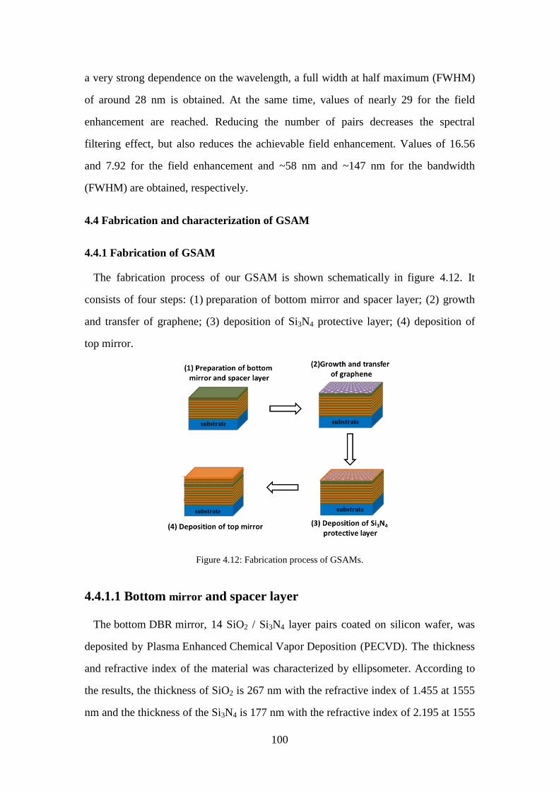
100
a very strong dependence on the wavelength, a full width at half maximum (FWHM)
of around 28 nm is obtained. At the same time, values of nearly 29 for the field
enhancement are reached. Reducing the number of pairs decreases the spectral
filtering effect, but also reduces the achievable field enhancement. Values of 16.56
and 7.92 for the field enhancement and ~58 nm and ~147 nm for the bandwidth
(FWHM) are obtained, respectively.
4.4 Fabrication and characterization of GSAM
4.4.1 Fabrication of GSAM
The fabrication process of our GSAM is shown schematically in figure 4.12. It
consists of four steps: (1) preparation of bottom mirror and spacer layer; (2) growth
and transfer of graphene; (3) deposition of Si3N4 protective layer; (4) deposition of
top mirror.
Figure 4.12: Fabrication process of GSAMs.
4.4.1.1 Bottom mirror and spacer layer
The bottom DBR mirror, 14 SiO2 / Si3N4 layer pairs coated on silicon wafer, was
deposited by Plasma Enhanced Chemical Vapor Deposition (PECVD). The thickness
and refractive index of the material was characterized by ellipsometer. According to
the results, the thickness of SiO2 is 267 nm with the refractive index of 1.455 at 1555
nm and the thickness of the Si3N4 is 177 nm with the refractive index of 2.195 at 1555
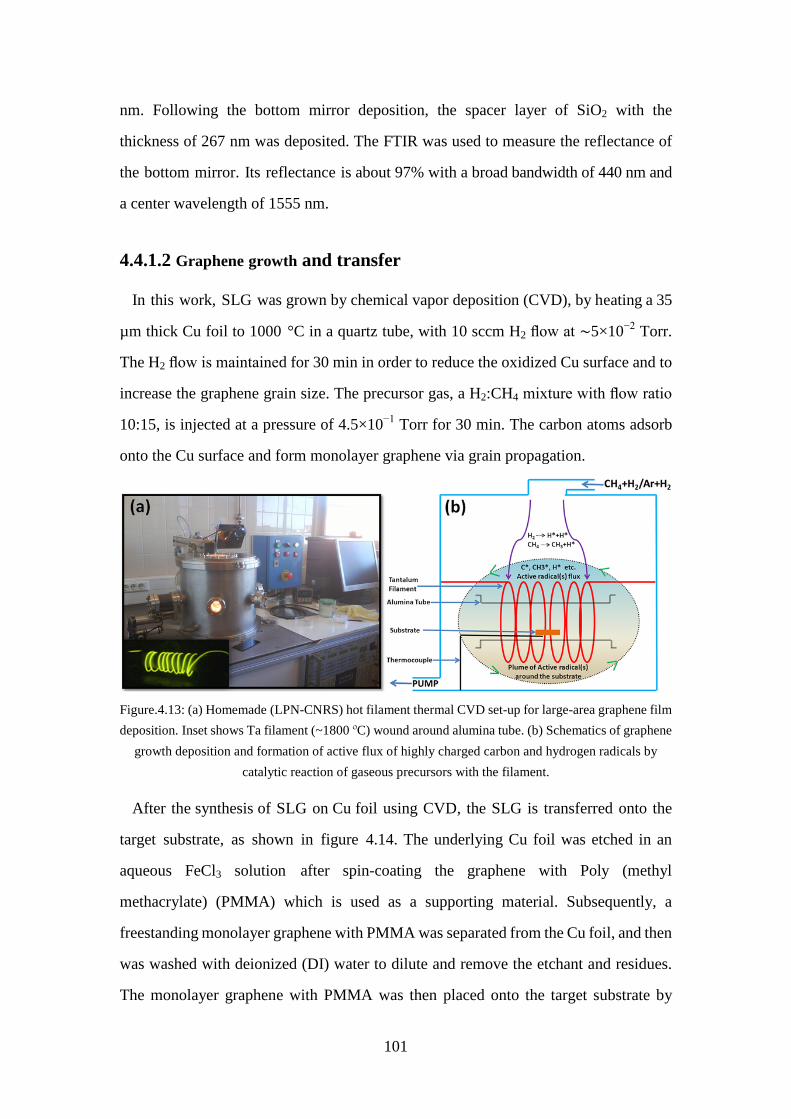
101
nm. Following the bottom mirror deposition, the spacer layer of SiO2 with the
thickness of 267 nm was deposited. The FTIR was used to measure the reflectance of
the bottom mirror. Its reflectance is about 97% with a broad bandwidth of 440 nm and
a center wavelength of 1555 nm.
4.4.1.2 Graphene growth and transfer
In this work, SLG was grown by chemical vapor deposition (CVD), by heating a 35
µm thick Cu foil to 1000 °C in a quartz tube, with 10 sccm H2 flow at ∼5×10⁻² Torr.
The H2 flow is maintained for 30 min in order to reduce the oxidized Cu surface and to
increase the graphene grain size. The precursor gas, a H2:CH4 mixture with flow ratio
10:15, is injected at a pressure of 4.5×10⁻¹ Torr for 30 min. The carbon atoms adsorb
onto the Cu surface and form monolayer graphene via grain propagation.
Figure.4.13: (a) Homemade (LPN-CNRS) hot filament thermal CVD set-up for large-area graphene film deposition. Inset shows Ta filament (~1800 ºC) wound around alumina tube. (b) Schematics of graphene
growth deposition and formation of active flux of highly charged carbon and hydrogen radicals by catalytic reaction of gaseous precursors with the filament.
After the synthesis of SLG on Cu foil using CVD, the SLG is transferred onto the
target substrate, as shown in figure 4.14. The underlying Cu foil was etched in an
aqueous FeCl3 solution after spin-coating the graphene with Poly (methyl
methacrylate) (PMMA) which is used as a supporting material. Subsequently, a
freestanding monolayer graphene with PMMA was separated from the Cu foil, and then
was washed with deionized (DI) water to dilute and remove the etchant and residues.
The monolayer graphene with PMMA was then placed onto the target substrate by
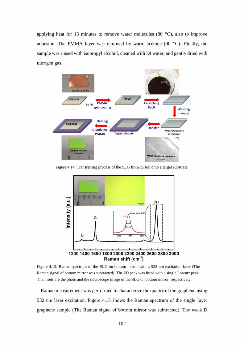
102
applying heat for 15 minutes to remove water molecules (80 °C), also to improve
adhesion. The PMMA layer was removed by warm acetone (90 °C). Finally, the
sample was rinsed with isopropyl alcohol, cleaned with DI water, and gently dried with
nitrogen gas.
Figure 4.14: Transferring process of the SLG from cu foil onto a target substrate.
Figure 4.15: Raman spectrum of the SLG on bottom mirror with a 532 nm excitation laser (The Raman signal of bottom mirror was subtracted). The 2D peak was fitted with a single Lorentz peak. The insets are the photo and the microscope image of the SLG on bottom mirror, respectively.
Raman measurement was performed to characterize the quality of the graphene using
532 nm laser excitation. Figure 4.15 shows the Raman spectrum of the single layer
graphene sample (The Raman signal of bottom mirror was subtracted). The weak D
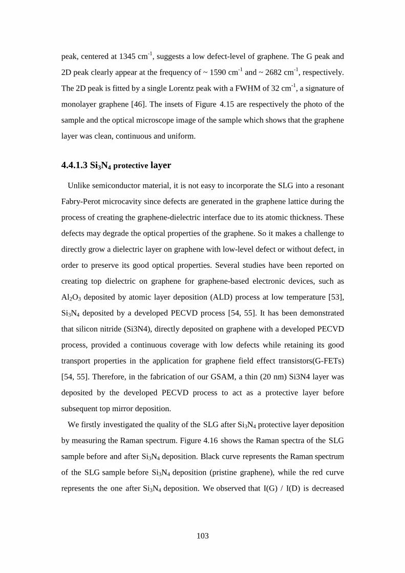
103
peak, centered at 1345 cm-1, suggests a low defect-level of graphene. The G peak and
2D peak clearly appear at the frequency of ~ 1590 cm-1 and ~ 2682 cm-1, respectively.
The 2D peak is fitted by a single Lorentz peak with a FWHM of 32 cm-1, a signature of
monolayer graphene [46]. The insets of Figure 4.15 are respectively the photo of the
sample and the optical microscope image of the sample which shows that the graphene
layer was clean, continuous and uniform.
4.4.1.3 Si3N4 protective layer
Unlike semiconductor material, it is not easy to incorporate the SLG into a resonant
Fabry-Perot microcavity since defects are generated in the graphene lattice during the
process of creating the graphene-dielectric interface due to its atomic thickness. These
defects may degrade the optical properties of the graphene. So it makes a challenge to
directly grow a dielectric layer on graphene with low-level defect or without defect, in
order to preserve its good optical properties. Several studies have been reported on
creating top dielectric on graphene for graphene-based electronic devices, such as
Al2O3 deposited by atomic layer deposition (ALD) process at low temperature [53],
Si3N4 deposited by a developed PECVD process [54, 55]. It has been demonstrated
that silicon nitride (Si3N4), directly deposited on graphene with a developed PECVD
process, provided a continuous coverage with low defects while retaining its good
transport properties in the application for graphene field effect transistors(G-FETs)
[54, 55]. Therefore, in the fabrication of our GSAM, a thin (20 nm) Si3N4 layer was
deposited by the developed PECVD process to act as a protective layer before
subsequent top mirror deposition.
We firstly investigated the quality of the SLG after Si3N4 protective layer deposition
by measuring the Raman spectrum. Figure 4.16 shows the Raman spectra of the SLG
sample before and after Si3N4 deposition. Black curve represents the Raman spectrum
of the SLG sample before Si3N4 deposition (pristine graphene), while the red curve
represents the one after Si3N4 deposition. We observed that I(G) / I(D) is decreased
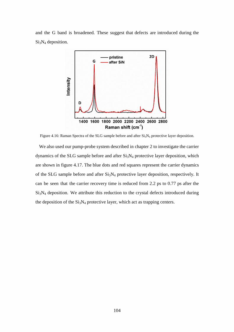
104
and the G band is broadened. These suggest that defects are introduced during the
Si3N4 deposition.
Figure 4.16: Raman Spectra of the SLG sample before and after Si3N4 protective layer deposition.
We also used our pump-probe system described in chapter 2 to investigate the carrier
dynamics of the SLG sample before and after Si3N4 protective layer deposition, which
are shown in figure 4.17. The blue dots and red squares represent the carrier dynamics
of the SLG sample before and after Si3N4 protective layer deposition, respectively. It
can be seen that the carrier recovery time is reduced from 2.2 ps to 0.77 ps after the
Si3N4 deposition. We attribute this reduction to the crystal defects introduced during
the deposition of the Si3N4 protective layer, which act as trapping centers.
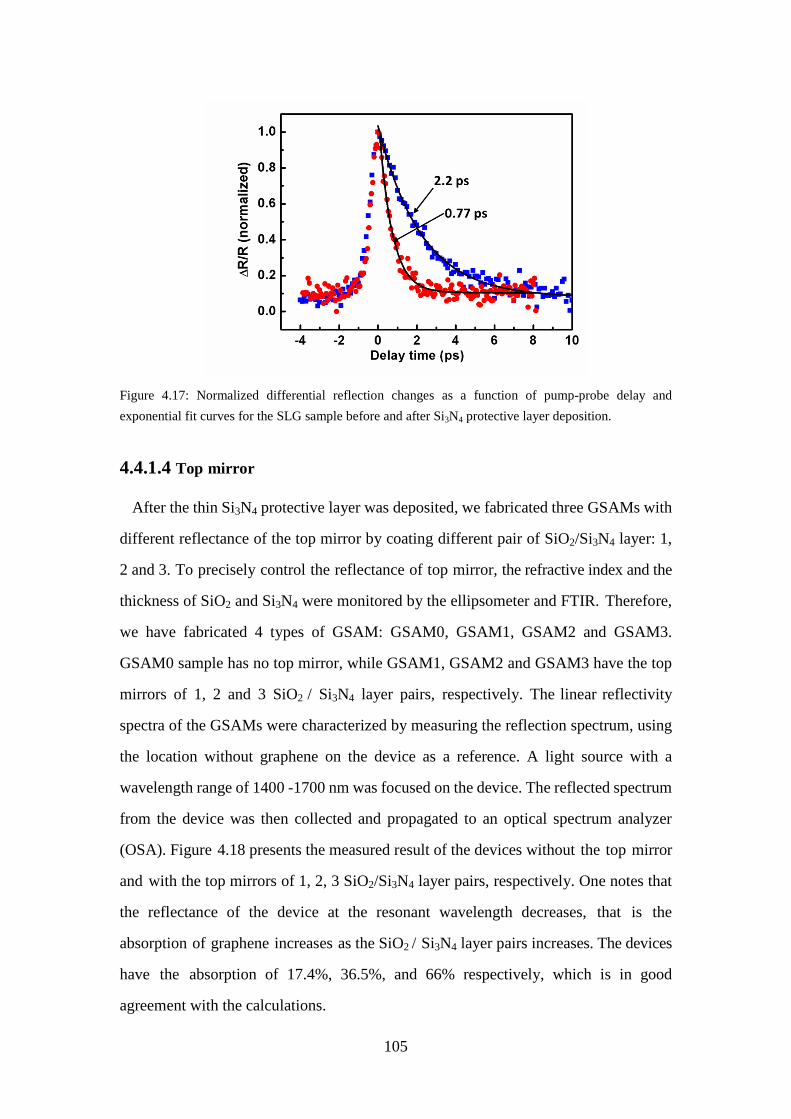
105
Figure 4.17: Normalized differential reflection changes as a function of pump-probe delay and exponential fit curves for the SLG sample before and after Si3N4 protective layer deposition.
4.4.1.4 Top mirror
After the thin Si3N4 protective layer was deposited, we fabricated three GSAMs with
different reflectance of the top mirror by coating different pair of SiO2/Si3N4 layer: 1,
2 and 3. To precisely control the reflectance of top mirror, the refractive index and the
thickness of SiO2 and Si3N4 were monitored by the ellipsometer and FTIR. Therefore,
we have fabricated 4 types of GSAM: GSAM0, GSAM1, GSAM2 and GSAM3.
GSAM0 sample has no top mirror, while GSAM1, GSAM2 and GSAM3 have the top
mirrors of 1, 2 and 3 SiO2 / Si3N4 layer pairs, respectively. The linear reflectivity
spectra of the GSAMs were characterized by measuring the reflection spectrum, using
the location without graphene on the device as a reference. A light source with a
wavelength range of 1400 -1700 nm was focused on the device. The reflected spectrum
from the device was then collected and propagated to an optical spectrum analyzer
(OSA). Figure 4.18 presents the measured result of the devices without the top mirror
and with the top mirrors of 1, 2, 3 SiO2/Si3N4 layer pairs, respectively. One notes that
the reflectance of the device at the resonant wavelength decreases, that is the
absorption of graphene increases as the SiO2 / Si3N4 layer pairs increases. The devices
have the absorption of 17.4%, 36.5%, and 66% respectively, which is in good
agreement with the calculations.
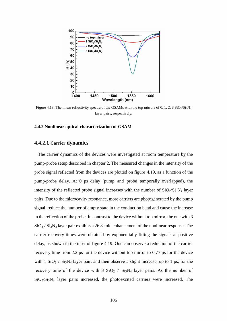
106
Figure 4.18: The linear reflectivity spectra of the GSAMs with the top mirrors of 0, 1, 2, 3 SiO2/Si3N4
layer pairs, respectively.
4.4.2 Nonlinear optical characterization of GSAM
4.4.2.1 Carrier dynamics
The carrier dynamics of the devices were investigated at room temperature by the
pump-probe setup described in chapter 2. The measured changes in the intensity of the
probe signal reflected from the devices are plotted on figure 4.19, as a function of the
pump-probe delay. At 0 ps delay (pump and probe temporally overlapped), the
intensity of the reflected probe signal increases with the number of SiO2/Si3N4 layer
pairs. Due to the microcavity resonance, more carriers are photogenerated by the pump
signal, reduce the number of empty state in the conduction band and cause the increase
in the reflection of the probe. In contrast to the device without top mirror, the one with 3
SiO2 / Si3N4 layer pair exhibits a 26.8-fold enhancement of the nonlinear response. The
carrier recovery times were obtained by exponentially fitting the signals at positive
delay, as shown in the inset of figure 4.19. One can observe a reduction of the carrier
recovery time from 2.2 ps for the device without top mirror to 0.77 ps for the device
with 1 SiO2 / Si3N4 layer pair, and then observe a slight increase, up to 1 ps, for the
recovery time of the device with 3 SiO2 / Si3N4 layer pairs. As the number of
SiO2/Si3N4 layer pairs increased, the photoexcited carriers were increased. The
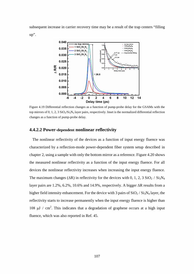
107
subsequent increase in carrier recovery time may be a result of the trap centers “filling
up”.
Figure 4.19 Differential reflection changes as a function of pump-probe delay for the GSAMs with the top mirrors of 0, 1, 2, 3 SiO2/Si3N4 layer pairs, respectively. Inset is the normalized differential reflection changes as a function of pump-probe delay.
4.4.2.2 Power-dependent nonlinear reflectivity
The nonlinear reflectivity of the devices as a function of input energy fluence was
characterized by a reflection-mode power-dependent fiber system setup described in
chapter 2, using a sample with only the bottom mirror as a reference. Figure 4.20 shows
the measured nonlinear reflectivity as a function of the input energy fluence. For all
devices the nonlinear reflectivity increases when increasing the input energy fluence.
The maximum changes (∆R) in reflectivity for the devices with 0, 1, 2, 3 SiO2 / Si3N4
layer pairs are 1.2%, 6.2%, 10.6% and 14.9%, respectively. A bigger ∆R results from a
higher field intensity enhancement. For the device with 3 pairs of SiO2 / Si3N4 layer, the
reflectivity starts to increase permanently when the input energy fluence is higher than
108 μJ / cm2. This indicates that a degradation of graphene occurs at a high input
fluence, which was also reported in Ref. 45.
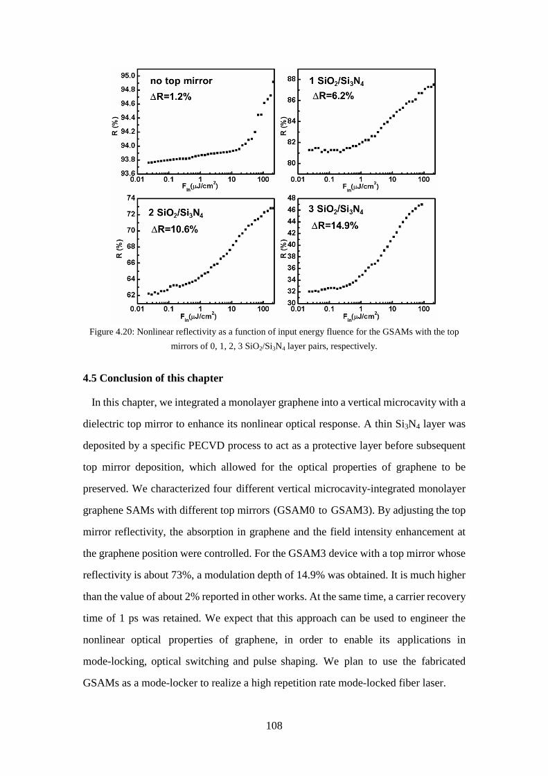
108
Figure 4.20: Nonlinear reflectivity as a function of input energy fluence for the GSAMs with the top
mirrors of 0, 1, 2, 3 SiO2/Si3N4 layer pairs, respectively.
4.5 Conclusion of this chapter
In this chapter, we integrated a monolayer graphene into a vertical microcavity with a
dielectric top mirror to enhance its nonlinear optical response. A thin Si3N4 layer was
deposited by a specific PECVD process to act as a protective layer before subsequent
top mirror deposition, which allowed for the optical properties of graphene to be
preserved. We characterized four different vertical microcavity-integrated monolayer
graphene SAMs with different top mirrors (GSAM0 to GSAM3). By adjusting the top
mirror reflectivity, the absorption in graphene and the field intensity enhancement at
the graphene position were controlled. For the GSAM3 device with a top mirror whose
reflectivity is about 73%, a modulation depth of 14.9% was obtained. It is much higher
than the value of about 2% reported in other works. At the same time, a carrier recovery
time of 1 ps was retained. We expect that this approach can be used to engineer the
nonlinear optical properties of graphene, in order to enable its applications in
mode-locking, optical switching and pulse shaping. We plan to use the fabricated
GSAMs as a mode-locker to realize a high repetition rate mode-locked fiber laser.
109
4.6 Reference
[1] A. Cabasse, G. Martel, and J. L. Oudar, “High power dissipative soliton in an
Erbium-doped fiber laser mode-locked with a high modulation depth saturable
absorber mirror,” Opt. Exp., vol. 17, pp. 9537-9542, 2009.
[2] A. Cabasse, D. Gaponov, K. Ndao, A. Khadour, J. L. Oudar, and G. Martel, “130
mW average power, 4.6 nJ pulse energy, 10.2 ps pulse duration from an Er3+ fiber
oscillator passively mode locked by a resonant saturable absorber mirror,” Opt.
Lett., vol. 14, pp. 2620-2622, 2011.
[3] J. Fatome, S. Pitois, A. Kamagate, G. Millot, D. Massoudre, and J. L. Oudar,
“All-optical reshaping based on a passive saturable absorber microcavity device
for future 160 Gb/s applications,” IEEE Photon. Technol. Lett., vol. 19, pp.
245-247, 2007.
[4] D. Massoubre, J. L. Oudar, J. Fatome, S. Pitois, G. Millot, J. Decobert, and J.
Landreau, “All-optical extinction-ratio enhancement of a 160 GHz pulse train by a
saturable-absorber vertical microcavity,” Opt. Lett., vol. 31, pp.537-539 , 2006.
[5] M. Gay, M. Costa e Silva, T. N. Nguyen, L. Bramerie, T. Chartier, M. Joindot, J. C.
Simon, J. Fatome, C. Finot, and J. L. Oudar, “Bit error rate assessment of 170
Gbit/s regeneration using a saturable absorber and a nonlinear-fiber-based power
limiter,” IEEE Photon. Technol. Lett., vol. 22, pp. 158-160, 2010
[6] T. Hasan, Z. Sun, F. Wang, F. Bonaccorso, P. H. Tan, A. G. Rozhin, and A. C.
Ferrari, “Nanotube-polymer composites for ultrafast photonics,” Adv. Mater.,
vol. 21, pp. 3874-3899, 2009.
[7] Z. Sun, T. Hasan, F. Torrisi, D. Popa, G. Privitera, F. Wang, F. Bonaccorso, D. M.
Basko, and A. C. Ferrari, “Graphene Mode-Locked Ultrafast Laser,” ACS Nano,
vol. 4, pp. 803-810, 2010.
[8] D. Sun, Z. K. Wu, C. Divin, X. B. Li, C. Berger, W. A. de Heer, P. N. First, and T.
B. Norris, “Ultrafast relaxation of excited Dirac fermions in epitaxial graphene
using optical differential transmission spectroscopy,” Phy. Rev. Lett., vol. 101,
pp. 157402-157405, 2008.
110
[9] J. Ma, G. Q. Xie, P. Lv, W. L. Gao, P. Yuan, L. J. Qian, H. H. Yu, H. J. Zhang, J.
Y. Wang, and D. Y. Tang, "Graphene mode-locked femtosecond laser at 2 μm
wavelength," Opt. Lett., vol. 37, pp. 2085-2087, 2012.
[10] W. B. Cho, J. W. Kim, H. W. Lee, S. Bae, B. H. Hong, S. Y. Choi, I. H. Baek, K.
Kim, D. I. Yeom, and F. Rotermund, “High-quality, large-area monolayer
graphene for efficient bulk laser mode-locking near 1.25 μm,” Opt. Lett., vol. 36,
pp. 4089-4091, 2011.
[11] Z. P. Sun, D. Papa, T. Hasan, F. Torrisi, F. Q. Wang, E. R. Kelleher, J. Travers,
V. Nicolosi, and A. Ferrari, “A Stable, Wideband Tunable, Near
Transform-Limited, Graphene-Mode-Locked, Ultrafast Laser,” Nano. Res., vol.
3, pp. 653-660, 2010.
[12] P. L. Huang, S. C. Lin, C. Y. Yeh, H. H. Kuo, S. H. Huang, G. R. Lin, L. J. Li,
C. Y. Su, and W. H. Cheng, “Stable mode-locked fiber laser based on CVD
fabricated graphene saturable absorber,” Opt. Exp., vol. 20, pp. 2460-2465,
2012.
[13] A. A. Lagatsky, Z. Sun, T. S. Kulmala, R. S. Sundaram, S. Milana, F. Torrisi, O.
L. Antipov, Y. Lee, J. H. Ahn, C. T. A. Brown, W. Sibbett, and A. C. Ferrari, “2
µm solid-state laser mode-locked by single-layer graphene,” Appl. Phys. Lett.,
vol. 102, pp. 013113-1-013113-4, 2013
[14] Z. P. Sun, D. Papa, T. Hasan, F. Torrisi, F. Q. Wang, E. R. Kelleher, J. Travers,
V. Nicolosi, and A. Ferrari, “A Stable, Wideband Tunable, Near
Transform-Limited, Graphene-Mode-Locked, Ultrafast Laser,” Nano. Res., vol.
3, pp. 653-660, 2010.
[15] A. H. Castro Neto, F. Guinea, N. M. R. Peres, K. S. Novoselov, and A. K. Geim,
“The electronic properties of graphene,” Rev. Mod. Phys., vol. 81, pp. 109-162,
2009.
[16] P. Avouris, Z. Chen, and V. Perebeinos, “Carbon-based electronics,” Nat.
Nanotechnol., vol. 2, pp. 605-615, 2007.
[17] C. Chen, S. Rosenblatt, K. I. Bolotin, W. Kalb, P. Kim, I. Kymissis, H. L.
Stormer,T. F. Heinz, and J. Hone, “Performance of monolayer graphene
111
nanomechanical resonators with electrical readout,” Nat. Nanotech., vol. 4, pp.
861-867, 2009.
[18] C. Lee, X. Wei, J. W. Kysar, and J. Hone, “Measurement of the elastic properties
and intrinsic strength of monolayer graphene,” Science, vol. 321, pp. 385-388,
2008.
[19] R. R. Nair, P. Blake, A. N. Grigorenko, K. S. Novoselov, T. J. Booth, T. Stauber,
N. M. R. Peres, and A. K. Geim, “Fine structure constant defines visual
transparency of graphene,” Science, vol. 320, pp. 1308-1308, 2008.
[20] K. S. Novoselov, A. K. Geim, S. V. Morozov, D. Jiang, Y. Zhang, S. V.
Dubonos, I. V. Grigorieva, and A. A. Firsov, “Electric field effect in atomically
thin carbon films,” Science, vol. 306, pp. 666-669, 2004.
[20] J. C. Charlier, P. C. Eklund, J. Zhu, and A. C. Ferrari, “Electron and Phonon
Properties of Graphene: Their Relationship with Carbon Nanotubes,” Top. Appl.
Phys. vol. 111, pp. 673-709, 2008.
[21] P. R. Wallace, “The Band Theory of Graphite,” Phys. Rev., vol. 71, pp. 622-634,
1947
[22] A. K. Geim, and K. S. Novoselov, “The rise of graphene,” Nature Materials, vol.
6, pp. 183–191, 2007.
[23] G. W. Semenoff, “Condensed-matter simulation of a three-dimensional
anomaly,” Phys. Rev. Lett., vol. 53, pp. 5449-5452, 1984.
[24] A. B. Kuzmenko, E. van Heumen, F. Carbone, and D. van der Marel, “Universal
optical conductance of graphite,” Phys. Rev. Lett., vol. 100, pp. 117401, 2008.
[25] F. Wang, Y. B. Zhang, C. S. Tian, C. Girit, A. Zettl, M. Crommie, and Y. R.
Shen, “Gate-variable optical transitions in graphene,” Science, vol. 320, pp.
206-209, 2008.
[26] M. Breusing, C. Ropers, and T. Elsaesser, “Ultrafast carrier dynamics in
graphite,” Phys. Rev. Lett., vol. 102, pp. 08680901-08680904, 2009.
[27] T. Kampfrath, L. Perfetti, F. Schapper, C. Frischkorn, and M. Wolf, “Strongly
coupled optical phonons in the ultrafast dynamics of the electronic energy and
current relaxation in graphite,” Phys. Rev. Lett., vol. 95, pp. 187403, 2005.
112
[28] M. Lazzeri, S. Piscanec, Francesco Mauri, A. C. Ferrari, and J. Robertson,
“Electron transport and hot phonons in carbon nanotubes,” Phys. Rev. Lett., vol.
95, pp. 249901, 2005.
[29] S. Berciaud, S. Ryu, L.E. Brus, and T. F. Heinz, “Probing the intrinsic properties
of exfoliated graphene: Raman spectroscopy of free-standing monolayers,” Nano
Lett., vol. 9, pp. 346-352, 2009.
[30] K. S. Novoselov, Z. Jiang, Y. Zhang, S. V. Morozov, H. L. Stormer, U. Zeitler, J.
C. Maan, G. S. Boebinger, P. Kim, and A. K. Geim, “Room-temperature
quantum Hall effect in graphene,” Science, vol. 315, pp. 1379, 2007.
[31] K. F. Mak, M. Y. Sfeir, Y. Wu, C. H. Lui, J. A. Misewich, and T. F. Heinz,
“Measurement of the optical conductivity of graphene,” Phys. Rev. Lett., vol.
101, pp. 196405, 2008.
[32] A. B. Kuzmenko, L. Benfatto, E. Cappelluti, I. Grassee, D. van der Marel, P.
Blake, K. S. Novoselov, and A. K. Geim, “Gate tunable infrared phonon
anomalies in bilayer graphene,” Phys. Rev. Lett., vol. 103, pp. 116804, 2009.
[33] V. C. Tung, M. J. Allen, Y. Yang, and R. B. Kaner, “High-throughput solution
processing of large-scale graphene,” Nat. Nanotechnol., vol. 4, pp. 25-29, 2009.
[34] M. Choucair, P. Thordarson, and J.A. Stride, “Gram-scale production of
graphene based on solvothermal synthesis and sonication,” Nat. Nanotechnol.,
vol. 4, pp. 30-33, 2008.
[35] I. Forbeaux, J. M. Themlin, and J. M. Debever, “Heteroepitaxial graphite on 6H
interfaceformation through SiC (0001): conduction-band electronic structure,”
Phys. Rev. B., vol. 58, pp. 16396-16406, 1998.
[36] Z. G. Cambaz, G. Yushin, S. Osswald, V. Mochalin, and Y. Gogotsi,
“Noncatalytic synthesis of carbon nanotubes, graphene and graphite on SiC,”
Carbon, vol. 46, pp. 841-849, 2008.
[37] C. Berger, Z. Song, X. Li, X. Wu, N. Brown, C. Naud, D. Mayou, T. Li, J. Hass,
A. M. Marchenkov, E. H. Conrad, P. N. First, and W. A. de Heer, “Electronic
confinement and coherence in patterned epitaxial graphene,” Science, vol. 312,
pp. 1191-1196, 2006.
113
[38] T. Ohta, A. Bostwick, J. L. McChesney, T. Seyller, K. Horn, and E. Rotenberg,
“Interlayer interaction and electronic screening in multilayer graphene
investigated with angle-resolved photoemission spectroscopy,” Phys. Rev. Lett.,
vol. 98, pp. 206802, 2007.
[39] S. V. Morozov, K. S. Novoselov, M. I. Katsnelson, F. Schedin, L. A.
Ponomarenko, D. Jiang, and A. K. Geim, “Strong suppression of weak
localization in graphene,” Phys. Rev. Lett., vol. 97, pp. 016801, 2006.
[40] D. Sun, C. Divin, J. Rioux, J. E. Sipe, C. Berger, W. A. de Heer, P. N. First, and
T. B. Norris, “Coherent control of ballistic photocurrents in multilayer epitaxial
graphene using quantum interference,” Nano Lett., vol. 10, pp. 1293-1296, 2010.
[41] J. M. Dawlaty, S. Shivaraman, M. Chandrashekhar, F. Rana, and M. G. Spencer,
“Measurement of ultrafast carrier dynamics in epitaxial graphene,” Appl. Phys.
Lett., vol. 92, pp. 042116-042119, 2008.
[42] P. A. George, J. Strait, J. Dawlaty, S. Shivaraman, M. Chandrashekhar, F. Rana,
and M. G. Spencer, “Ultrafast optical-pump terahertz-probe spectroscopy of the
carrier relaxation and recombination dynamics in epitaxial graphene,” Nano
Lett., vol. 8, pp. 4248-4251, 2008.
[43] X. Li, W. Cai, J. An, S. Kim, J. Nah, D. Yang, R. Piner, A. Velamakanni, I. Jung,
E. Tutuc, S. K. Banerjee, L. Colombo, and R. S. Ruoff, “Large-area synthesis of
high-quality and uniform graphene films on copper foils,” Science, vol. 324, pp.
1312–1314, 2009.
[44] M. Mangold, V. J. Wittwer, O. D. Sieber, M. Hoffmann, I. L. Krestnikov, D. A.
Livshits, M. Golling, T. Südmeyer, and U. Keller, “VECSEL gain
characterization,” Opt. Exp., vol. 20, pp. 4136-4148, 2012.
[45] C. A. Zaugg, Z. Sun, V. J. Wittwer, D. Popa, S. Milana, T. Kulmala, M.
Mangold, O. D. Sieber, M. Golling, Y. Lee, J. H. Ahn, A. C. Ferrari, and U.
Keller, “Ultrafast and widely tunable vertical-external-cavity surface-emitting
laser, mode-locked by a graphene-integrated distributed Bragg reflector,” Opt.
Exp., vol. 21, pp. 31548-31559, 2013.
114
[46] A. C. Ferrari, J. C. Meyer, V. Scardaci, C. Casiraghi, M. Lazzeri, F. Mauri, S.
Piscanec, D. Jiang, K. S. Novoselov, S. Roth, and A. K. Geim, “Raman spectrum
of graphene and graphene layers,” Phys. Rev. Lett., vol. 97, pp.
18740101-18740104, 2006.
[47] D. Graf, F. Molitor, K. Ensslin, C. Stampfer, A. Jungen, C. Hierold, and L.
Wirtz, “Spatially resolved Raman spectroscopy of single- and few-layer
graphene,” Nano Lett., vol. 7, pp. 238-242, 2007.
[48] R. Saito, A. Jorio, A. G. Souza Filho, G. Dresselhaus, M. S. Dresselhaus, and M.
A. Pimenta, “Probing phonon dispersion relations of graphite by double
resonance Raman scattering,” Phys. Rev. Lett., vol. 88, pp. 02740101-02740104,
2002.
[49] C. Thomsen, and S. Reich, “Double resonant Raman scattering in graphite,”
Phys. Rev. Lett., vol. 85, pp. 5214-5217, 2000.
[50] Sergey Mikhailov, Physics and Applications of Graphene-Experiments,
Publisher: InTech, 2011.
[51] L. G. Cancado, A. Jorio, E. H. M. Ferreira, F. Stavale, C. A. Achete, R. B.
Capaz, M. V. O. Moutinho, A. Lombardo, T. S. Kulmala, and A. C. Ferrari,
“Quantifying defects in graphene via raman spectroscopy at different excitation
energies,” Nano Lett., vol. 11, pp. 3190-3196, 2011.
[52] M. Born, and E. Wolf, Principles of Optics, 6th ed, Pergamon, New York, pp.
325-326, 1980.
[53] S. Jandhyala, G. Mordi, B. Lee, G. Lee, C. Floresca, P. R. Cha, J. Ahn, R. M.
Wallace, Y. J. Chabal, M. J. Kim, L. Colombo, K. Cho, and J. Kim, “Atomic
layer deposition of dielectrics on graphene using reversibly physisorbed ozone,”
ACS Nano, vol. 6, pp. 2722-2730, 2012. [54] W. Zhu, D. Neumayer, V. Perebeinos, and P. Avouris, “Silicon nitride gate
dielectrics and band gap engineering in graphene layers,” Nano Lett., vol. 10, pp.
3572-3576, 2010.

115
[55] O. Habibpour, S. Cherednichenko, J. Vukusic, and J. Stake, “Mobility
improvement and microwave characterization of a graphene field effect
transistor with silicon nitride gate dielectrics,” IEEE Electron Device Lett., vol.
32, pp. 871-873, 2011.
116
Chapter 5 Conclusion
In conclusion, we have developed three kinds of ultrafast SAMs at 1.55 µm with
low fabrication costs, easy fabrication technology, improved compactness, and
advanced functionality.
Firstly, we have used heavy-ion implantation to realize ultrafast InGaAs-based
SAMs. Both lattice damages and impurity atoms in bulk InGaAs material are
responsible for the ultrafast carrier recovery time. In this study, ion implantations
were performed at elevated temperature (300 ºC) to increase the threshold value for
amorphization. By studying the carrier recovery time of As+-implanted samples as a
function of the ion dose and dose rate, we found that the damage accumulation during
implantation at elevated temperature not only depends on the ion dose but also
depends on the dose rate. Moreover, through the comparison between As+- and
Fe+-implanted samples, we found that Fe2+/Fe3+ is a more effective trap center than
ionized As in In0.53Ga0.47As. Apart from the fast carrier lifetime, the characteristics of
the nonlinear reflectivity for the Fe+-implanted sample, such as linear absorption,
modulation depth, nonsaturable loss, have also been investigated under different
annealing temperature. Under the annealing condition of 650 ºC for 15 s, an Fe+
-implanted SAM with a fast carrier lifetime of 2.23 ps and a big modulation depth of
53.9% has been achieved, with only a 3% degradation compared to the unimplanted
sample.
Secondly, we have used FIB milling to fabricate an ultra-thin taper structure on
crystalline InP to realize a muti-wavelength InGaAs-based SAM, which could be used
for the regeneration of a WDM signal with several tens of channels. Based on the
characteristics of our FIB system and the principle of FIB milling, we designed our
experimental method. The appropriate FIB scanning procedures and operating
parameters were used to control the target material re-deposition and to minimize the
amorphization. The sputtering yield of InP crystal was determined by investigating the
relationship between milling depth and ion dose. By applying the optimal
experimentally obtained yield and related dose range, we have fabricated an ultra-thin
117
taper structure whose etch depths are precisely and progressively tapered from 24.5 nm
to 54 nm, with a horizontal slope of about 1:10500 and a dimension of 35 × 400 μm2.
Moreover, a flat bottom surface with a RMS roughness of 2 nm was achieved. The total
time for the taper patterning is about 4 hours. Optical characterization of the tapered
device was performed to check the efficiency of the taper patterning. It shows a
resonant wavelength shift very similar to our design, and an optical loss of about 3%,
which can be neglected for the application of our tapered SA device. It can be
concluded that FIB milling is a flexible and reproducible technique for fabricating a
tapered SA device with good optical performance.
Thirdly, in order to explore the potential of graphene for nonlinear optical
applications, we integrated a monolayer graphene into a vertical microcavity with a
dielectric top mirror to enhance its nonlinear optical response. A thin Si3N4 layer was
deposited by a developed PECVD process to act as a protective layer before subsequent
top mirror deposition, which allowed for the optical properties of graphene to be
preserved. We characterized four different vertical microcavity-integrated monolayer
graphene devices with different top mirrors (GSAM0 to GSAM3). By adjusting the
reflectivity of the top mirror, the absorption in graphene and the field intensity
enhancement at the graphene position were controlled. For the GSAM3 device, with a
top mirror whose reflectivity is about 73%, a modulation depth of 14.9% was obtained.
It is much higher than the value of about 2% reported in other works. At the same time,
an absorption recovery time of 1 ps was retained. We expect that this approach can be
used to engineer the nonlinear optical properties of graphene, in order to enable
applications in mode-locking, optical switching and pulse shaping. We plan to use the
fabricated GSAMs as a mode-locker to realize a high repetition rate mode-locked
fiber laser.
Related Documents