Development of Superconducting Tunnel Junction Photon Detector with SOI Preamplifier board to Search for Radiative decays of Cosmic Background Neutrino Tsukuba Global Science Week 2014 Takuya Okudaira 1 , Shinhong Kim 1 , Yuji Takeuchi 1 , Kota Kasahara 1 , Ren Senzaki 1 ,Koya Moriuchi 1 Kenichi Takemasa 1 , Kenji Kiuchi 1 , Tatsuya Ichimura 1 , Masahiro Kanamaru 1 , Hirokazu Ikeda 2 , Shuji Matsuura 2 , Takehiro Wada 2 , Hirokazu Ishino 3 , Atsuko Kibayashi 3 , Satoru Mima 4 , Takuo Yoshida 5 , Ryuta Hirose 5 , Yukihiro Kato 6 , Masashi Hazumi 7 , Yasuo Arai 7 ,Erik Ramberg 8 , Jonghee Yoo 8 , Mark Kozlovsky 8 , Paul Rubinov 8 , Dmitri Sergatskov 8 , and Soo-Bong Kim 9 University of Tsukuba 1 , JAXA/ISAS 2 , Okayama University 3 , RIKEN 4 University of Fukui 5 , Kinki University 6 , KEK 7 ,Fermilab 8 , Seoul National University 9 1

Welcome message from author
This document is posted to help you gain knowledge. Please leave a comment to let me know what you think about it! Share it to your friends and learn new things together.
Transcript

1
Development of Superconducting Tunnel Junction Photon Detector with SOI Preamplifier board to Search for Radiative decays of Cosmic Background Neutrino
Tsukuba Global Science Week 2014
Takuya Okudaira1, Shinhong Kim1, Yuji Takeuchi1, Kota Kasahara1, Ren Senzaki1,Koya Moriuchi1 Kenichi Takemasa1, Kenji Kiuchi1, Tatsuya Ichimura1, Masahiro Kanamaru1, Hirokazu Ikeda2, Shuji Matsuura2, Takehiro Wada2, Hirokazu Ishino3, Atsuko Kibayashi3, Satoru Mima4, Takuo Yoshida5, Ryuta Hirose5, Yukihiro Kato6, Masashi Hazumi7, Yasuo Arai7 ,Erik Ramberg8, Jonghee Yoo8, Mark Kozlovsky8, Paul Rubinov8, Dmitri Sergatskov8, and Soo-Bong Kim9
University of Tsukuba1, JAXA/ISAS2, Okayama University3, RIKEN4 University of Fukui5, Kinki University6, KEK7 ,Fermilab8, Seoul National University9

2
STJ Detector
STJ(Superconducting Tunnel Junction) detector is superconducting photoelectric detector that composed of Superconductor / Insulator /Superconductor ~400nm
Nb
Al
AlOx
Si Nb Al
Tc [K] 9.23 1.20
Δ [meV] 1100 1.550 0.172
photon quasiparticle(electron)
cooper pair insulator
Since energy gap of Nb is ~1meV (Si:~1eV), the energy resolution of STJ can be much better than semiconductor detector.
We are developing STJ photon detector for neutrino decay search (as Dr. Takeuchi slide)aiming at detecting single far infrared(50um) photon
Incident photons break up cooper pairs in STJ, the electrons from the broken cooper pairs tunnel through the insulator layer
3
Nb/Al-STJ
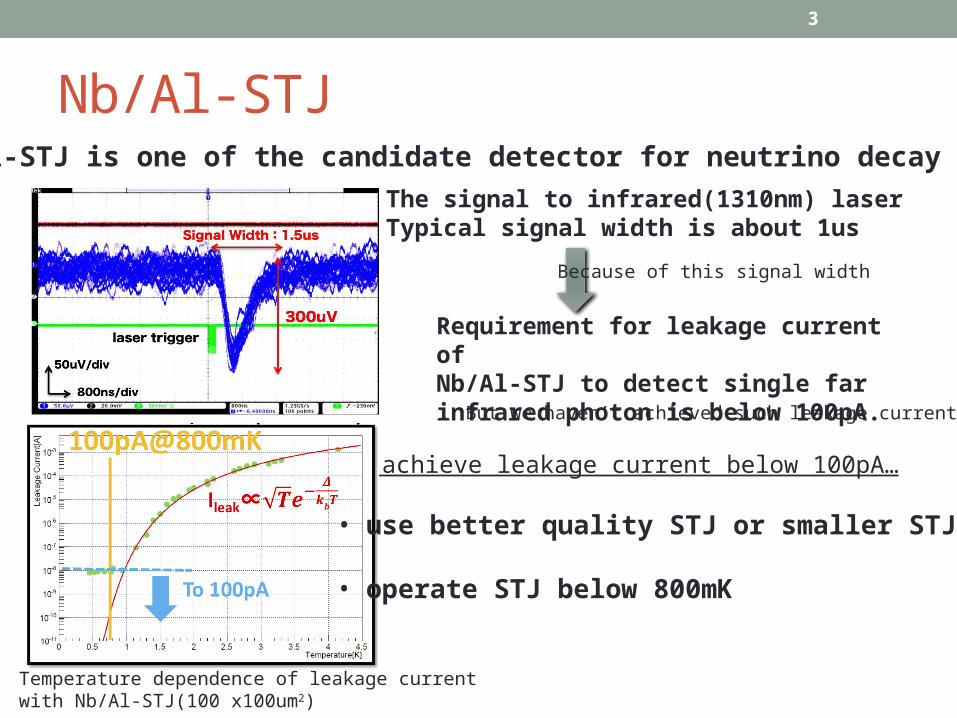
The signal to infrared(1310nm) laserTypical signal width is about 1us
To achieve leakage current below 100pA…
Nb/Al-STJ is one of the candidate detector for neutrino decay search
Requirement for leakage current of Nb/Al-STJ to detect single far infrared photon is below 100pA.
Because of this signal width
But we haven’t achieved such leakage current yet…
Temperature dependence of leakage current with Nb/Al-STJ(100 x100um2)
• use better quality STJ or smaller STJ
• operate STJ below 800mK

4
STJ array prototype for Neutrino decay searchWe processed STJ at AIST and KEK, and measured distribution of infrared(1310nm) laser with STJ array
1.4mm
2.9m
m
STJ array on the chip The number of STJs : 10The size of each STJ : 100um x100um
The distribution of infrared light with STJ array
The distribution of laser from fiber isexpected to be Gaussian
Red : Gaussian fitBlack : Output from each STJ
STJ illuminated with blue laser
STJ chip carrier
laser fiber
ST
J O
utp
ut[
AU
]

5
SOI-STJSilicon On Insulator (SOI)Processing LSI on SiO2 insulator • Low Power to be operated• high speed• can operate at a few Kelvin SOI-FET is suitable for amplifier for STJ signal
We are also developing a new detector :SOI-STJ
SOI-STJ Processing STJ directly on a SOI preamplifier board to make the detector compact ,low noise and easy to be multipixel detector.SOI-STJ can be new novel detector!
STJhas high energy resolution
STJ processed on SOI and schematic of prototype
Question• Is SOI caused any damage by processing STJ?• Can Nb/Al-STJ be processed on SOI board ?

6
STJ processed on SOI board
We confirmed STJ processed on SOI board has no problem!
apply magnetic field
150 Gauss
2mV /DIV.
1 mA /DIV.
2mV /DIV.50uA /DIV.
2mV /DIV.
1 mA /DIV.
500uV /DIV.10 nA /DIV.
Signal of Nb/Al-STJ processed on SOI board to 465nm light
Leakage current : 6nA @0.5mV
We can process good STJ on SOI board!
We observed typical STJ signal from STJ on SOI board!
IV curve of the STJ on SOI board

7
SOI-FET after processing STJ at Low Temperature
NMOS(690~750mK) PMOS(750mK)
Ids[
A]
Vgs[V]
-Id
s[A
]
Vgs[V]
Vds[V]
gm
[S]
Vds[V]gm
[S]
I-V curve of SOI-FETs after processing Nb/Al-STJ.
• Both of NMOS and PMOS can be operated below 800mK.• Trans-conductance “gm” is not varied drastically for each temperature at operation voltage(0.2V).
SOI-FET with STJ processed has excellent performance below 800mK.
SOI-FET is suitable for cold preamplifier for STJ signal !
W=1000umL=1um
W=1000umL=1um

8
Summary• We are developing STJ and SOI-STJ to detect single
far infrared photon for neutrino decay search.• We confirmed
STJ processed on SOI board has sufficient quality. SOI-FET has no damage by processing STJ SOI-FET has excellent performance below 800mK.

9
BUCK UP

10
Temperature dependence of IV curve

11
Requirement for leakage current
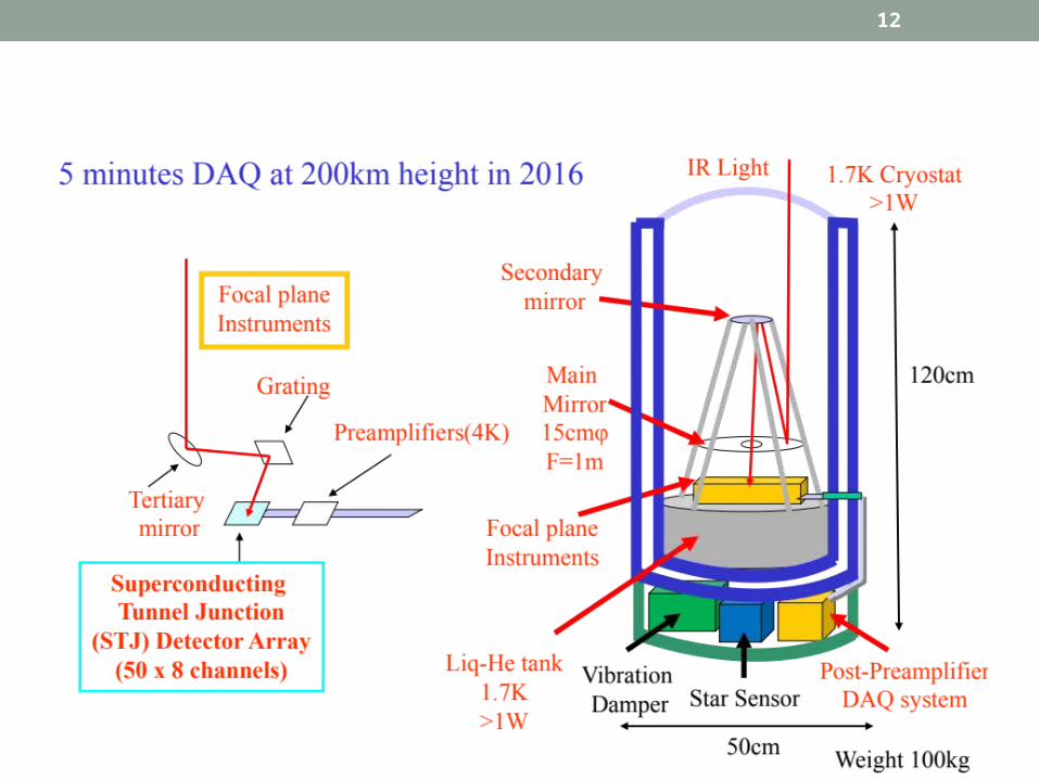
12

Division 1100um×100um STJ array
Division 2STJs with dispersed junction
Division 3STJ array with different sizes
Division 4STJs with different under layer sizes (Upper layer sizes are same )To measure dispersion of quasi particle
Division 5STJs with and without SiO2 To measure transmittanceof SiO2
Nb/Al-STJ on newly designed chip

14
Related Documents