This article appeared in a journal published by Elsevier. The attached copy is furnished to the author for internal non-commercial research and education use, including for instruction at the authors institution and sharing with colleagues. Other uses, including reproduction and distribution, or selling or licensing copies, or posting to personal, institutional or third party websites are prohibited. In most cases authors are permitted to post their version of the article (e.g. in Word or Tex form) to their personal website or institutional repository. Authors requiring further information regarding Elsevier’s archiving and manuscript policies are encouraged to visit: http://www.elsevier.com/authorsrights

Welcome message from author
This document is posted to help you gain knowledge. Please leave a comment to let me know what you think about it! Share it to your friends and learn new things together.
Transcript
This article appeared in a journal published by Elsevier. The attachedcopy is furnished to the author for internal non-commercial researchand education use, including for instruction at the authors institution
and sharing with colleagues.
Other uses, including reproduction and distribution, or selling orlicensing copies, or posting to personal, institutional or third party
websites are prohibited.
In most cases authors are permitted to post their version of thearticle (e.g. in Word or Tex form) to their personal website orinstitutional repository. Authors requiring further information
regarding Elsevier’s archiving and manuscript policies areencouraged to visit:
http://www.elsevier.com/authorsrights
Author's personal copy
Development of multilayered nanocrystalline TiO2 thin filmsfor photovoltaic application
K. Usha a, B. Mondal b,⇑, D. Sengupta b, P. Das b, K. Mukherjee b, P. Kumbhakar c
a Dept. of Engg. Physics, Bengal College of Engineering & Technology, Durgapur, Indiab Centre for Advanced Materials Processing, CSIR-Central Mechanical Engineering Research Institute, Mahatma Gandhi Avenue, Durgapur, Indiac Dept. of Physics, National Institute of Technology, Durgapur, India
a r t i c l e i n f o
Article history:Received 29 July 2013Received in revised form 23 January 2014Accepted 27 January 2014Available online 20 February 2014
Keywords:Modified precursorAcetyl acetone (Acac)Multilayer coatingsBand gapOptical constants
a b s t r a c t
Nanocrystalline multilayered thin films of TiO2 have been prepared to achieve high transparency in thewavelength range of 400–800 nm having good adhesion to the ITO substrate. TiO2 sol is synthesizedthrough wet chemical route for making thin films by dip coating process. The layer wise optical charac-terization reveals higher band gap values of 3.45 eV, 3.32 eV for 2-layered and 3-layered films respec-tively while further depositions of thin layers followed by annealing treatment shows that the value ofband gap approaches towards the bulk TiO2 considerable decrease in band gap with increase in thicknessdue to successive coatings of thin film is observed because of growth in crystal size as well as improvingthe grain contact on successive annealing treatments. Photo-conversion efficiency of the assembled solarcell is in the order of 7%.
� 2014 Elsevier B.V. All rights reserved.
1. Introduction
The crunch on the scientific world due to reducing oil reserveshas driven the researchers to wedge cheap and abundantly avail-able resources of energy. A lot of research work is currently beingpursued for the development of third generation photovoltaic solarcells. Dye-sensitized solar cells (DSSC) are a promethean categoryof economical photovoltaic cells that belong to the group of thin-film technology [1–3]. The emerging field of nanoparticles aregiven a new window that has opened prospects of research indye sensitized solar cells which work with a principle havingsimilarity with the process of photosynthesis [1]. Titanium dioxideis a wide band gap semiconductor [4] with interesting electrical [5]and optical properties [6–8]. Of all the known crystalline structuresof TiO2 at ambient conditions, i.e., anatase, rutile, brookite and sri-lankite, the anatase form of TiO2 has a large band gap of 3.18 eV,low dielectric constant, and high electron mobility and is knownto give high efficiencies when it is used in dye sensitized solar cellsas electrode. Having a wide band gap, the anatase phase of TiO2
absorbs radiation in ultraviolet region. The principle underneaththe dye sensitized solar cells lies in efficiently developing a net-work of 25–50 nm sized TiO2 particles on a glass plate coated with
transparent conducting oxide. Sensitization of nanocrystalline TiO2
network with dye, both synthetic and natural, enhances theefficiency of the cell. The electrolyte used in these cells is a redoxcouple of iodide.
The nanocrystalline TiO2 network developed on ITO plays a vitalrole in releasing electrons by light absorption. The released elec-tron can do work if its recombination rate is slower than the chargetransfer rate [9,10]. Sensitization of n-TiO2 network with dye helpsin shifting the absorption region of TiO2 to visible from ultra-violet,thus decreasing the band gap and subsequently easing the electronto the higher energy level, increasing the charge transfer rate[11–13]. Shifting the optical absorption range of electrodes depos-ited using TiO2 semiconductor from ultra violet to visible region bysensitization with dyes or using search alternative oxides shows apossibility of enhanced efficiencies. ZnO, Nb2O5 are few alternativeoxides which are under consideration for replacing TiO2 [14]. Thesensitizer dye absorbs most of the incident light resulting in accu-mulation of electrons in the working electrode and thus shiftingthe Fermi level of the TiO2 particles. The potential drop betweenthe back contact and the shifted Fermi level gives rise to thephoto-voltage in these cells. The sensitization of TiO2 layer withdye is to transport the electron to the conduction band of TiO2
through the dye upon illumination [9,10]. The anatase phase nano-particles of TiO2 provide larger surface to volume ratio for dyeabsorption resulting in enhanced efficiencies. Anatase phase TiO2
nanoparticles have large band gap in the form of thin films than
http://dx.doi.org/10.1016/j.optmat.2014.01.0370925-3467/� 2014 Elsevier B.V. All rights reserved.
⇑ Corresponding author. Tel.: +91 343 6510218; fax: +91 343 2546745.E-mail addresses: [email protected], [email protected]
(B. Mondal).
Optical Materials 36 (2014) 1070–1075
Contents lists available at ScienceDirect
Optical Materials
journal homepage: www.elsevier .com/locate /optmat
Author's personal copy
the bulk value [15]. Apart from solar cell application these thinfilms with high transparency may also find application as opticalfilters in spectrometers [7,8]. In this paper, nanocrystalline multi-layered thin films of TiO2 have been prepared through wetchemical route to achieve high transparency in the wavelengthrange of 400–800 nm. The layer wise optical characterization hasbeen carried out and it reveals that 2-layered and 3-layered filmshave higher band gap values of 3.45 eV, 3.32 eV respectively. More-over, further depositions of thin layers followed by annealing treat-ment of the as-prepared films reveals that the value of band gapapproaches towards the bulk TiO2. The considerable decrease inband gap with increase in thickness due to successive coatings ofthin film is observed may be due to the growth in crystal sizeand improves the grain contact on successive annealing treat-ments. Photo-conversion efficiency of the assembled solar cell isin the order of 7%.
2. Experimental
2.1. Synthesis of nTiO2 sol and development of thin film
TiO2 sol is synthesized from titanium isopropoxide using wetchemical route. Titanium isopropoxide is highly hygroscopic andeasily forms precipitate on exposure of moisture. In order to avoidprecipitates on exposure to moisture it is necessary to modify theprecursor with organic solvents. Lot of research on modification ofprecursor has been carried out by other authors [16,17]. In thepresent study, the modification of precursor is done with a mixtureof 1-Propanol and acetyl acetone. Initially, 1-Propanol is added toacetyl acetone in the volume ratio of 1:1. This mixture was addedto titanium isopropoxide so that the ratio of the precursor to acetylacetone is maintained in the molar ratio of 1:3. The modified pre-cursor is then added to 0.1 M nitric acid in the volume ratio of 1:6under continuous stirring. This results in a yellow transparentsolution. TritonX-100 is added as surfactant and PEG 3000 is usedto obtain porous thin films. The resultant yellow solution so ob-tained is heated in an oven at 60 �C for 40 min. The final productis in the form of sol which is stable for many days and is suitablefor coating [2,16].
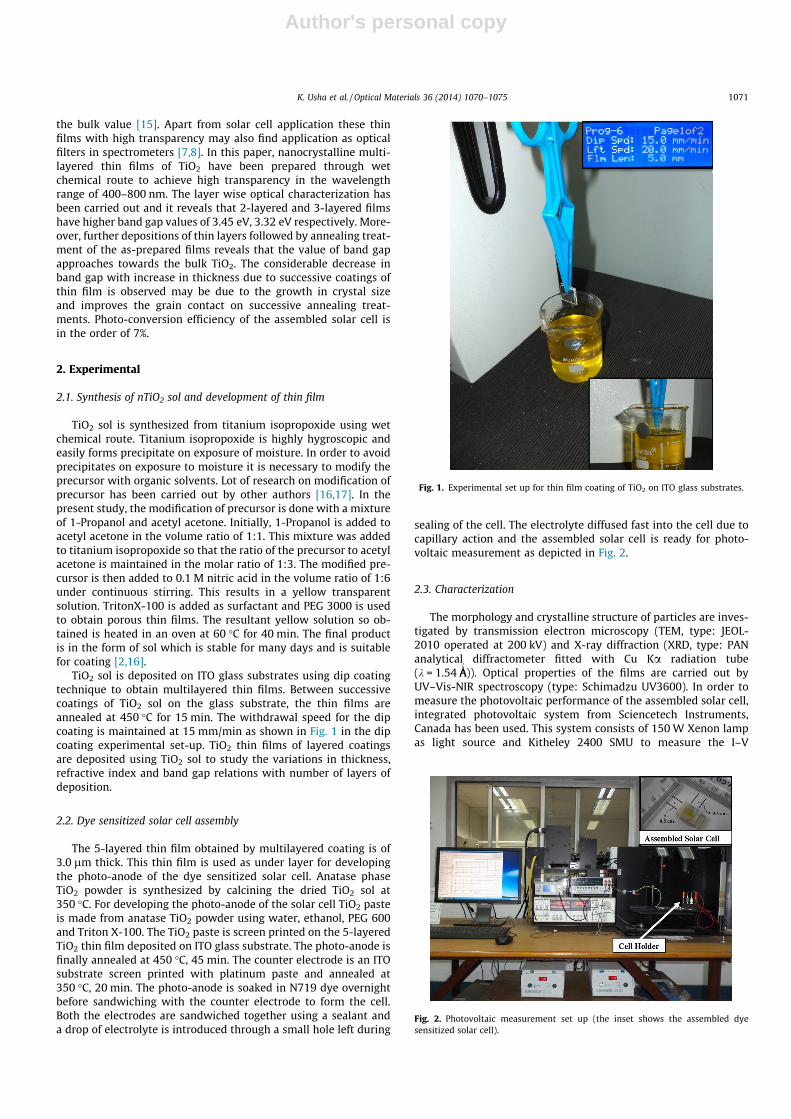
TiO2 sol is deposited on ITO glass substrates using dip coatingtechnique to obtain multilayered thin films. Between successivecoatings of TiO2 sol on the glass substrate, the thin films areannealed at 450 �C for 15 min. The withdrawal speed for the dipcoating is maintained at 15 mm/min as shown in Fig. 1 in the dipcoating experimental set-up. TiO2 thin films of layered coatingsare deposited using TiO2 sol to study the variations in thickness,refractive index and band gap relations with number of layers ofdeposition.
2.2. Dye sensitized solar cell assembly
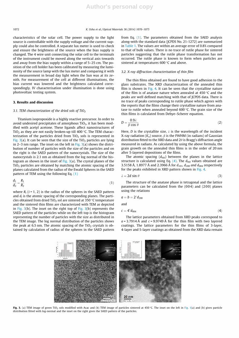
The 5-layered thin film obtained by multilayered coating is of3.0 lm thick. This thin film is used as under layer for developingthe photo-anode of the dye sensitized solar cell. Anatase phaseTiO2 powder is synthesized by calcining the dried TiO2 sol at350 �C. For developing the photo-anode of the solar cell TiO2 pasteis made from anatase TiO2 powder using water, ethanol, PEG 600and Triton X-100. The TiO2 paste is screen printed on the 5-layeredTiO2 thin film deposited on ITO glass substrate. The photo-anode isfinally annealed at 450 �C, 45 min. The counter electrode is an ITOsubstrate screen printed with platinum paste and annealed at350 �C, 20 min. The photo-anode is soaked in N719 dye overnightbefore sandwiching with the counter electrode to form the cell.Both the electrodes are sandwiched together using a sealant anda drop of electrolyte is introduced through a small hole left during
sealing of the cell. The electrolyte diffused fast into the cell due tocapillary action and the assembled solar cell is ready for photo-voltaic measurement as depicted in Fig. 2.
2.3. Characterization
The morphology and crystalline structure of particles are inves-tigated by transmission electron microscopy (TEM, type: JEOL-2010 operated at 200 kV) and X-ray diffraction (XRD, type: PANanalytical diffractometer fitted with Cu Ka radiation tube(k = 1.54 ÅA
0
)). Optical properties of the films are carried out byUV–Vis-NIR spectroscopy (type: Schimadzu UV3600). In order tomeasure the photovoltaic performance of the assembled solar cell,integrated photovoltaic system from Sciencetech Instruments,Canada has been used. This system consists of 150 W Xenon lampas light source and Kitheley 2400 SMU to measure the I–V
Fig. 1. Experimental set up for thin film coating of TiO2 on ITO glass substrates.
Fig. 2. Photovoltaic measurement set up (the inset shows the assembled dyesensitized solar cell).
K. Usha et al. / Optical Materials 36 (2014) 1070–1075 1071
Author's personal copy
characteristics of the solar cell. The power supply to the lightsource is controllable with the supply voltage and the current sup-ply could also be controlled. A separate lux meter is used to checkand ensure the brightness of the source when the bias supply ischanged. The 4 wire unit connecting the solar cell to the terminalsof the instrument could be moved along the vertical axis towardsand away from the bias supply within a range of 5–25 cm. The po-sition of the cell holder has been calibrated by measuring the lumi-nosity of the source lamp with the lux meter and comparing it withthe measurement in broad day light when the Sun was at its ze-nith. For measurement of the cell at different illuminations, thebias current was lowered and the brightness calculated corre-spondingly. IV characterisation under illumination is done usingphotovoltaic testing system.
3. Results and discussion
3.1. TEM characterization of the dried sols of TiO2
Titanium isopropoxide is a highly reactive precursor. In order toavoid undesired precipitates of amorphous TiO2, it has been mod-ified with acetyl acetone. These ligands affect nanostructures ofTiO2 as they are not easily broken-up till 400 �C. The TEM charac-terization of the particles dried from TiO2 sols is represented inFig. 3(a). It can be seen that the size of the TiO2 particles are lyingin 2–3 nm range. The inset on the left in Fig. 3(a) shows the distri-bution of number of particles with the size of the particles and onthe right is the SAED pattern of the nanocrystals. The size of thenanocrystals is 2.1 nm as obtained from the log normal of the his-togram as shown in the inset of Fig. 3(a). The crystal planes of theTiO2 particles are obtained by matching the atomic spacing of theplanes calculated from the radius of the Ewald Spheres in the SAEDpattern of TEM using the following Eq. (1)
d1
d2¼ R1
R2ð1Þ
where Ri (i = 1, 2) is the radius of the spheres in the SAED patternand di is the atomic spacing of the corresponding planes. The parti-cles obtained from dried TiO2 sol are sintered at 350 �C temperatureand the sintered thin films are characterized with TEM as depictedin Fig. 3(b). The inset on the right top of Fig. 3(b) represents theSAED pattern of the particles while on the left top is the histogramrepresenting the number of particles with the size as distributed inthe TEM image. The log normal distribution of the particles showsthe peak at 6.5 nm. The atomic spacing of the TiO2 crystals is ob-tained by calculation of radius of the spheres in the SAED pattern
from Eq. (1). The parameters obtained from the SAED analysisalong-with the standard data (JCPDS No. 21-1272) are summarizedin Table 1. The values are within an average error of 0.8% comparedto that of bulk values. There is no trace of rutile phase for sinteredparticles suggesting that the rutile phase transformation has notoccurred. The rutile phase is known to form when particles aresintered at temperatures 600 �C and above.
3.2. X-ray diffraction characterisation of thin film
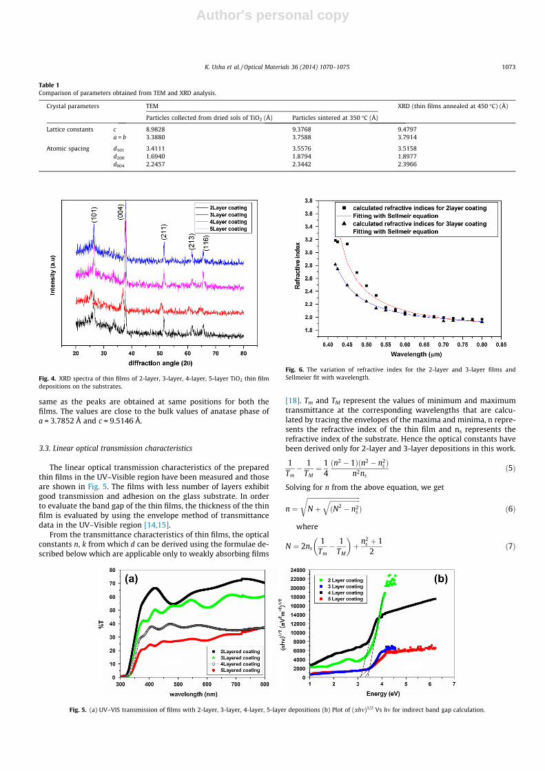
The thin films obtained are found to have good adhesion to theglass substrates. The XRD characterization of the annealed thinfilm is shown in Fig. 4. It can be seen that the crystalline natureof the film is of anatase nature when annealed at 450 �C and thepeaks are well defined matching with that of JCPDS data. There isno trace of peaks corresponding to rutile phase which agrees withthe reports that the films change their crystalline nature from ana-tase to rutile when annealed beyond 600 �C. The grain size of thethin films is calculated from Debye–Scherer equation.
D ¼ 0:9kb cos h
ð2Þ
Here, D is the crystallite size, k is the wavelength of the incidentX-ray radiation (Ka) source, b is the FWHM (in radians) of Gaussiandistribution fitted to the XRD data and 2h is Bragg’s diffraction anglemeasured in radians. As calculated by using the above formula, thegrain growth on the annealed thin films is in the order of 20 nmafter 5-layered depositions of the films.
The atomic spacing (dhkl) between the planes in the latticestructure is calculated using Eq. (4). The dhkl values obtained are3.5158 Å, 1.8977 Å and 2.3966 Å for d101, d200 and d004 respectivelyfor the peaks exhibited in XRD pattern shown in Fig. 4.
k ¼ 2d sin h ð3Þ
The structure of the anatase phase is tetragonal and the latticeparameters can be calculated from the (004) and (200) planesusing the relations
a ¼ b ¼ 2�d200
and
c ¼ 4�d004 ð4Þ
The lattice parameters obtained from XRD peaks correspond toa = 3.7914 Å and c = 9.9749 Å for the thin film with two layeredcoatings. The lattice parameters for the thin films of 3-layer,4-layer and 5-layer coatings as obtained from the XRD data remain
Fig. 3. (a) TEM image of green TiO2 sols modified with Acac and (b) TEM image of particles sintered at 450 �C. The inset on the left in Fig. 1(a) and (b) gives particledistribution fitted with log-normal and the inset on the right gives the SAED pattern of the particles.
1072 K. Usha et al. / Optical Materials 36 (2014) 1070–1075
Author's personal copy
same as the peaks are obtained at same positions for both thefilms. The values are close to the bulk values of anatase phase ofa = 3.7852 Å and c = 9.5146 Å.
3.3. Linear optical transmission characteristics
The linear optical transmission characteristics of the preparedthin films in the UV–Visible region have been measured and thoseare shown in Fig. 5. The films with less number of layers exhibitgood transmission and adhesion on the glass substrate. In orderto evaluate the band gap of the thin films, the thickness of the thinfilm is evaluated by using the envelope method of transmittancedata in the UV–Visible region [14,15].
From the transmittance characteristics of thin films, the opticalconstants n, k from which d can be derived using the formulae de-scribed below which are applicable only to weakly absorbing films
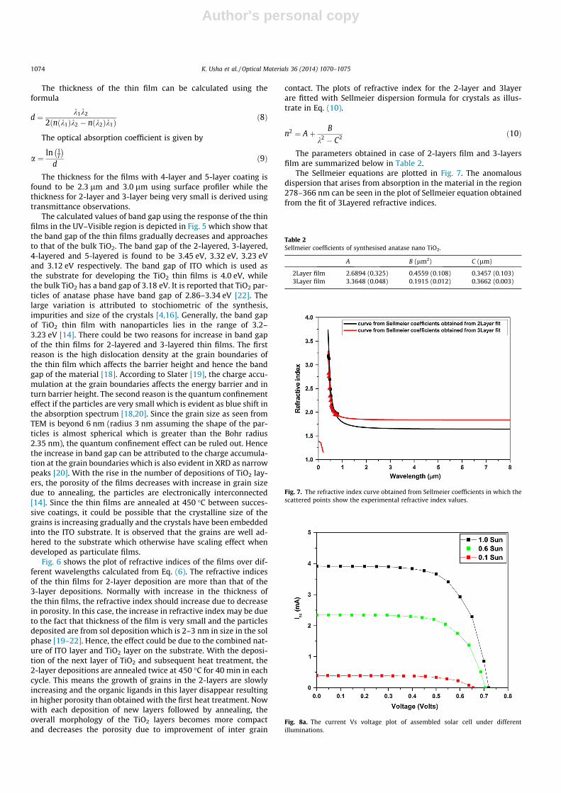
[18]. Tm and TM represent the values of minimum and maximumtransmittance at the corresponding wavelengths that are calcu-lated by tracing the envelopes of the maxima and minima, n repre-sents the refractive index of the thin film and ns represents therefractive index of the substrate. Hence the optical constants havebeen derived only for 2-layer and 3-layer depositions in this work.
1Tm� 1
TM¼ 1
4ðn2 � 1Þðn2 � n2
s Þn2ns
ð5Þ
Solving for n from the above equation, we get
n ¼ffiffiffiffiffiffiffiffiffiffiffiffiffiffiffiffiffiffiffiffiffiffiffiffiffiffiffiffiffiffiffiffiffiN þ
ffiffiffiffiffiffiffiffiffiffiffiffiffiffiffiffiffiffiffiðN2 � n2
s
qrÞ ð6Þ
where
N ¼ 2ns1
Tm� 1
TM
� �þ n2
s þ 12
ð7Þ
Table 1Comparison of parameters obtained from TEM and XRD analysis.
Crystal parameters TEM XRD (thin films annealed at 450 �C) (Å)
Particles collected from dried sols of TiO2 (Å) Particles sintered at 350 �C (Å)
Lattice constants c 8.9828 9.3768 9.4797a = b 3.3880 3.7588 3.7914
Atomic spacing d101 3.4111 3.5576 3.5158d200 1.6940 1.8794 1.8977d004 2.2457 2.3442 2.3966
Fig. 4. XRD spectra of thin films of 2-layer, 3-layer, 4-layer, 5-layer TiO2 thin filmdepositions on the substrates.
Fig. 5. (a) UV–VIS transmission of films with 2-layer, 3-layer, 4-layer, 5-layer depositions (b) Plot of (ahm)1/2 Vs hm for indirect band gap calculation.
Fig. 6. The variation of refractive index for the 2-layer and 3-layer films andSellmeier fit with wavelength.
K. Usha et al. / Optical Materials 36 (2014) 1070–1075 1073
Author's personal copy
The thickness of the thin film can be calculated using theformula
d ¼ k1k2
2ðnðk1Þk2 � nðk2Þk1Þð8Þ
The optical absorption coefficient is given by
a ¼ln 1
T
� �d
ð9Þ
The thickness for the films with 4-layer and 5-layer coating isfound to be 2.3 lm and 3.0 lm using surface profiler while thethickness for 2-layer and 3-layer being very small is derived usingtransmittance observations.
The calculated values of band gap using the response of the thinfilms in the UV–Visible region is depicted in Fig. 5 which show thatthe band gap of the thin films gradually decreases and approachesto that of the bulk TiO2. The band gap of the 2-layered, 3-layered,4-layered and 5-layered is found to be 3.45 eV, 3.32 eV, 3.23 eVand 3.12 eV respectively. The band gap of ITO which is used asthe substrate for developing the TiO2 thin films is 4.0 eV, whilethe bulk TiO2 has a band gap of 3.18 eV. It is reported that TiO2 par-ticles of anatase phase have band gap of 2.86–3.34 eV [22]. Thelarge variation is attributed to stochiometric of the synthesis,impurities and size of the crystals [4,16]. Generally, the band gapof TiO2 thin film with nanoparticles lies in the range of 3.2–3.23 eV [14]. There could be two reasons for increase in band gapof the thin films for 2-layered and 3-layered thin films. The firstreason is the high dislocation density at the grain boundaries ofthe thin film which affects the barrier height and hence the bandgap of the material [18]. According to Slater [19], the charge accu-mulation at the grain boundaries affects the energy barrier and inturn barrier height. The second reason is the quantum confinementeffect if the particles are very small which is evident as blue shift inthe absorption spectrum [18,20]. Since the grain size as seen fromTEM is beyond 6 nm (radius 3 nm assuming the shape of the par-ticles is almost spherical which is greater than the Bohr radius2.35 nm), the quantum confinement effect can be ruled out. Hencethe increase in band gap can be attributed to the charge accumula-tion at the grain boundaries which is also evident in XRD as narrowpeaks [20]. With the rise in the number of depositions of TiO2 lay-ers, the porosity of the films decreases with increase in grain sizedue to annealing, the particles are electronically interconnected[14]. Since the thin films are annealed at 450 �C between succes-sive coatings, it could be possible that the crystalline size of thegrains is increasing gradually and the crystals have been embeddedinto the ITO substrate. It is observed that the grains are well ad-hered to the substrate which otherwise have scaling effect whendeveloped as particulate films.
Fig. 6 shows the plot of refractive indices of the films over dif-ferent wavelengths calculated from Eq. (6). The refractive indicesof the thin films for 2-layer deposition are more than that of the3-layer depositions. Normally with increase in the thickness ofthe thin films, the refractive index should increase due to decreasein porosity. In this case, the increase in refractive index may be dueto the fact that thickness of the film is very small and the particlesdeposited are from sol deposition which is 2–3 nm in size in the solphase [19–22]. Hence, the effect could be due to the combined nat-ure of ITO layer and TiO2 layer on the substrate. With the deposi-tion of the next layer of TiO2 and subsequent heat treatment, the2-layer depositions are annealed twice at 450 �C for 40 min in eachcycle. This means the growth of grains in the 2-layers are slowlyincreasing and the organic ligands in this layer disappear resultingin higher porosity than obtained with the first heat treatment. Nowwith each deposition of new layers followed by annealing, theoverall morphology of the TiO2 layers becomes more compactand decreases the porosity due to improvement of inter grain
contact. The plots of refractive index for the 2-layer and 3layerare fitted with Sellmeier dispersion formula for crystals as illus-trate in Eq. (10).
n2 ¼ Aþ B
k2 � C2 ð10Þ
The parameters obtained in case of 2-layers film and 3-layersfilm are summarized below in Table 2.
The Sellmeier equations are plotted in Fig. 7. The anomalousdispersion that arises from absorption in the material in the region278–366 nm can be seen in the plot of Sellmeier equation obtainedfrom the fit of 3Layered refractive indices.
Table 2Sellmeier coefficients of synthesised anatase nano TiO2.
A B (lm2) C (lm)
2Layer film 2.6894 (0.325) 0.4559 (0.108) 0.3457 (0.103)3Layer film 3.3648 (0.048) 0.1915 (0.012) 0.3662 (0.003)
Fig. 7. The refractive index curve obtained from Sellmeier coefficients in which thescattered points show the experimental refractive index values.
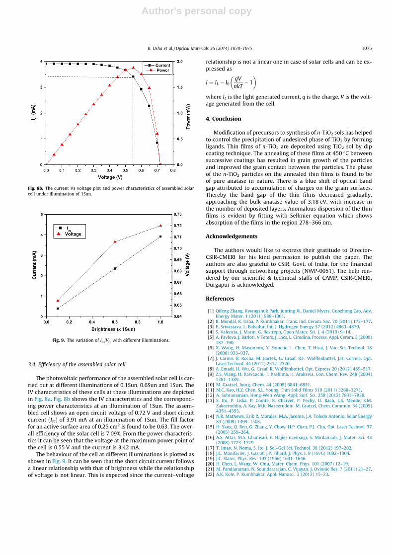
Fig. 8a. The current Vs voltage plot of assembled solar cell under differentilluminations.
1074 K. Usha et al. / Optical Materials 36 (2014) 1070–1075
Author's personal copy
3.4. Efficiency of the assembled solar cell
The photovoltaic performance of the assembled solar cell is car-ried out at different illuminations of 0.1Sun, 0.6Sun and 1Sun. TheIV characteristics of these cells at these illuminations are depictedin Fig. 8a. Fig. 8b shows the IV characteristics and the correspond-ing power characteristics at an illumination of 1Sun. The assem-bled cell shows an open circuit voltage of 0.72 V and short circuitcurrent (Isc) of 3.91 mA at an illumination of 1Sun. The fill factorfor an active surface area of 0.25 cm2 is found to be 0.63. The over-all efficiency of the solar cell is 7.09%. From the power characteris-tics it can be seen that the voltage at the maximum power point ofthe cell is 0.55 V and the current is 3.42 mA.
The behaviour of the cell at different illuminations is plotted asshown in Fig. 9. It can be seen that the short circuit current followsa linear relationship with that of brightness while the relationshipof voltage is not linear. This is expected since the current–voltage
relationship is not a linear one in case of solar cells and can be ex-pressed as
I ¼ IL � I0qVnkT� 1
� �
where IL is the light generated current, q is the charge, V is the volt-age generated from the cell.
4. Conclusion
Modification of precursors to synthesis of n-TiO2 sols has helpedto control the precipitation of undesired phase of TiO2 by formingligands. Thin films of n-TiO2 are deposited using TiO2 sol by dipcoating technique. The annealing of these films at 450 �C betweensuccessive coatings has resulted in grain growth of the particlesand improved the grain contact between the particles. The phaseof the n-TiO2 particles on the annealed thin films is found to beof pure anatase in nature. There is a blue shift of optical bandgap attributed to accumulation of charges on the grain surfaces.Thereby the band gap of the thin films decreased gradually,approaching the bulk anatase value of 3.18 eV, with increase inthe number of deposited layers. Anomalous dispersion of the thinfilms is evident by fitting with Sellmier equation which showsabsorption of the films in the region 278–366 nm.
Acknowledgements
The authors would like to express their gratitude to Director-CSIR-CMERI for his kind permission to publish the paper. Theauthors are also grateful to CSIR, Govt. of India, for the financialsupport through networking projects (NWP-0051). The help ren-dered by our scientific & technical staffs of CAMP, CSIR-CMERI,Durgapur is acknowledged.
References
[1] Qifeng Zhang, Kwangshuk Park, Junting Xi, Daniel Myers, Guozhong Cao, Adv.Energy Mater. 1 (2011) 988–1001.
[2] B. Mondal, K. Usha, P. Kumbhakar, Trans. Ind. Ceram. Soc. 70 (2011) 173–177.[3] P. Srivastava, L. Bahadur, Int. J. Hydrogen Energy 37 (2012) 4863–4870.[4] S. Valencia, J. Marin, G. Restrepo, Open Mater. Sci. J. 4 (2010) 9–14.[5] A. Pavlova, J. Barloti, V Teters, J. Locs, L. Cimdina, Process. Appl. Ceram. 3 (2009)
187–190.[6] X. Wang, H. Masumoto, Y. Someno, L. Chen, T. Hirai, J. Vac. Sci. Technol. 18
(2000) 933–937.[7] J. Carmo, R. Rocha, M. Bartek, G. Graaf, R.F. Wolffenbuttel, J.H. Correia, Opt.
Laser Technol. 44 (2012) 2312–2320.[8] A. Emadi, H. Wu, G. Graaf, R. Wolffenbuttel, Opt. Express 20 (2012) 489–517.[9] Z.S. Wang, H. Kawauchi, T. Kashima, H. Arakawa, Con. Chem. Rev. 248 (2004)
1381–1389.[10] M. Gratzel, Inorg. Chem. 44 (2005) 6841–6851.[11] M.C. Kao, H.Z. Chen, S.L. Young, Thin Solid Films 519 (2011) 3268–3271.[12] A. Subramanian, Hong-Wen Wang, Appl. Surf. Sci. 258 (2012) 7833–7838.[13] S. Ito, P. Liska, P. Comte, R. Charvet, P. Pechy, U. Bach, L.S. Mende, S.M.
Zakeeruddin, A. Kay, M.K. Nazeeruddin, M. Gratzel, Chem. Commun. 34 (2005)4351–4353.
[14] N.R. Mathews, Erik R. Morales, M.A. Jacome, J.A. Toledo Antonio, Solar Energy83 (2009) 1499–1508.
[15] H. Yang, Q. Ren, G. Zhang, Y. Chow, H.P. Chan, P.L. Chu, Opt. Laser Technol. 37(2005) 259–264.
[16] A.S. Attar, M.S. Ghamsari, F. Hajiesmaeibaigi, S. Mirdamadi, J. Mater. Sci. 43(2008) 1723–1729.
[17] T. Imao, N. Noma, S. Ito, J. Sol–Gel Sci. Technol. 38 (2012) 197–202.[18] J.C. Manifacier, J. Gasiot, J.P. Fillard, J. Phys. E 9 (1976) 1002–1004.[19] J.C. Slater, Phys. Rev. 103 (1956) 1631–1646.[20] H. Chen, L. Wang, W. Chiu, Mater. Chem. Phys. 101 (2007) 12–19.[21] M. Pandiaraman, N. Soundararajan, C. Vijayan, J. Ovionic Res. 7 (2011) 21–27.[22] A.K. Kole, P. Kumbhakar, Appl. Nanosci. 2 (2012) 15–23.
Fig. 8b. The current Vs voltage plot and power characteristics of assembled solarcell under illumination of 1Sun.
Fig. 9. The variation of Isc/Vsc with different illuminations.
K. Usha et al. / Optical Materials 36 (2014) 1070–1075 1075
Related Documents