i DEVELOPMENT OF DC-DC BUCK-BOOST CONVERTER FOR BI- DIRECTIONAL POWER FLOW INVERTER TAN CHUNG SEONG A project report submitted in partial fulfilment of the requirements for the award of Bachelor of Engineering (Hons.) Electrical and Electronic Engineering Faculty of Engineering and Science Universiti Tunku Abdul Rahman April 2015

Welcome message from author
This document is posted to help you gain knowledge. Please leave a comment to let me know what you think about it! Share it to your friends and learn new things together.
Transcript
i
DEVELOPMENT OF DC-DC BUCK-BOOST CONVERTER FOR BI-
DIRECTIONAL POWER FLOW INVERTER
TAN CHUNG SEONG
A project report submitted in partial fulfilment of the
requirements for the award of Bachelor of Engineering
(Hons.) Electrical and Electronic Engineering
Faculty of Engineering and Science
Universiti Tunku Abdul Rahman
April 2015

ii
DECLARATION
I hereby declare that this project report is based on my original work except for
citations and quotations which have been duly acknowledged. I also declare that it has
not been previously and concurrently submitted for any other degree or award at
UTAR or other institutions.
Signature :
Name : TAN CHUNG SEONG
ID No. : 10UEB04710
Date : 08/05/2015
iii
APPROVAL FOR SUBMISSION
I certify that this project report entitled “DEVELOPMENT OF DC-DC BUCK-
BOOST CONVERTER FOR BI-DIRECTIONAL POWER FLOW INVERTER”
was prepared by TAN CHUNG SEONG and has met the required standard for
submission in partial fulfilment of the requirements for the award of Bachelor of
Engineering (Hons.) Electrical and Electronic Engineering at Universiti Tunku Abdul
Rahman.
Approved by,
Signature : __________________________
Supervisor : Mr Chua Kein Huat
Date :___________________________
iv
The copyright of this report belongs to the author under the terms of the
copyright Act 1987 as qualified by Intellectual Property Policy of Universiti Tunku
Abdul Rahman. Due acknowledgement shall always be made of the use of any
material contained in, or derived from, this report.
© 2015, Tan Chung Seong. All right reserved.

v
ACKNOWLEDGEMENTS
I would like to thank everyone who had contributed to the successful completion of
this project. I would like to express my gratitude to my research supervisor, Mr. Chua
Kein Huat for his invaluable advice, guidance and his enormous patience throughout
the development of the research.
In addition, I would also like to express my gratitude to my loving parent and
friends who had helped and given me encouragement through the research. I also
would like to thank my research partner, Mr. Koh Yong Qing for his assistance and
support in this research.

vi
DEVELOPMENT OF DC-DC BUCK-BOOST CONVERTER FOR BI-
DIRECTIONAL INVERTER
ABSTRACT
Nowadays, Energy Storage System (ESS) plays a significant role in solving the
intermittency issues caused by the renewable energy sources. The interconnection
between ESS and electrical grid network is often challenging as ESS generally has low
voltage level. This project involves the development of a DC-DC buck-boost converter
that can interface between the ESS and electrical grid system for charging and
discharging purpose. An embedded device, NI sbRIO-9642XT is used to generate the
pulse-width modulation (PWM) signal to drive the power switches of the converter.
Several types of closed-loop feedback controller are also developed in this project to
regulate the output of the boost converter under various operating conditions. These
controllers are the PI controller, fuzzy logic controller and hybrid fuzzy-PI controller.
Three PI controllers with different responses, including slow, normal and fast
responses have been developed and tuned based on the Ziegler-Nichols’ tuning method.
An auto-tuning algorithm has been developed to achieve optimal gains for each PI
controller. Fuzzy logic controllers with different rule sets have been developed by
adopting the rules reduction topology to reduce the redundant rules and enhance the
computational efficiency and interpretability of the fuzzy logic controller. The hybrid
fuzzy-PI controller is developed by combining both the PI and fuzzy logic controller
to improve the transient response of the converter. The experimental results show that
the boost converter and buck converter are able to step up and step down the DC
voltage respectively. Both converters are also able to achieve high efficiency. Fuzzy
logic controller has the capability to supress the overshoot while PI controller has
advantage in lowering the steady-state error. The hybrid fuzzy-PI controller inherits
the superiority of both PI and fuzzy logic controller to achieve fast rise time, low
overshoot and low steady-state error.

vii
TABLE OF CONTENTS
DECLARATION ii
APPROVAL FOR SUBMISSION iii
ACKNOWLEDGEMENTS v
ABSTRACT vi
TABLE OF CONTENTS vii
LIST OF TABLES x
LIST OF FIGURES xii
LIST OF SYMBOLS / ABBREVIATIONS xvi
CHAPTER
1 INTRODUCTION 1
1.1 Background 1
1.2 Problem Statements 3
1.3 Aims and Objectives 3
1.4 Scopes of Project 4
2 LITERATURE REVIEW 6
2.1 DC-DC Converter 6
2.1.1 Boost Converter 6
2.1.2 Buck Converter 9
2.1.3 Application of Buck and Boost Converter in Charging
and Discharging Battery 10
2.2 PI Controller 11
2.2.1 Ziegler-Nichol’s Method 12
2.3 Fuzzy Logic Controller 14
viii
2.3.1 Fuzzification 16
2.3.2 Fuzzy Inference 16
2.3.3 Defuzzification 17
2.4 Hybrid Fuzzy-PI Controller 17
2.5 LabVIEWTM 18
3 METHODOLOGY 19
3.1 Design of DC-DC Boost and Buck Converter 19
3.1.1 Calculation of Boost Converter Circuit’s Parameters
19
3.1.2 Calculation of Buck Converter Circuit’s Parameters
21
3.1.3 Simulation of Boost and Buck Converter Circuit in
MultisimTM 23
3.1.4 Selection of Hardware Components for Boost and
Buck Converter 24
3.1.5 Generation of Pulse-Width Modulation Signal by
using NI sbRIO-9642XT Embedded Device 27
3.2 Design of Closed-Loop Feedback Controller 30
3.2.1 Design of PI controller 30
3.2.2 Design of Fuzzy Logic Controller 33
3.2.3 Design of Hybrid Fuzzy-PI Controller 41
3.3 Hardware and Software Setup 44
3.3.1 Setup of NI sbRIO-9642XT Embedded Device 45
3.3.2 Interfacing the NI sbRIO-9642XT Embedded Device
with LabVIEW 50
3.3.3 Setup of NI cDAQ-9184 Ethernet Chassis 53
4 RESULTS AND DISCUSSION 56
4.1 Boost Converter 56
4.1.1 Simulation Result 56
4.1.2 Experimental Result 57
4.2 Buck Converter 65

ix
4.2.1 Simulation Result 65
4.2.2 Experimental Result 65
4.3 Closed-Loop Feedback Controllers 73
4.3.1 PI Controller 74
4.3.2 Fuzzy Logic Controller 76
4.3.3 Hybrid Fuzzy-PI Controller 79
5 CONCLUSION AND RECOMMENDATIONS 82
5.1 Conclusion 82
5.2 Recommendations 83

x
LIST OF TABLES
TABLE TITLE PAGE
2.1 The First Method of Ziegler-Nichol’s Tuning
Method 13
2.2 The Second Method of Ziegler-Nichol’s Tuning
Method 14
3.1 The Calculated Parameter of Boost Converter 21
3.2 The calculated parameter of Buck Converter 22
3.3 The Specification of Components in the Boost
Converter 25
3.4 The Tuning Formula of Different Responses for PI
Controller 32
3.5 The Parameters of PI Controller for Different Type
of Response 33
3.6 The Control Rules of the Fuzzy Controller 37
3.7 The Type-1 Fuzzy Rules 38
3.8 The Type-2 Fuzzy Rules 39
3.9 The Type-3 Fuzzy Rules 39
4.1 The Simulated Output Voltage of Boost Converter 56
4.2 The Effect of Variation of Duty Ratio on the Output
Voltage of Boost Converter for Different Load
Resistances at Switching Frequency of 50 kHz 58
4.3 The Effect of Variation of Duty Ratio on the
Efficiency of Boost Converter for Different Load
Resistances at Switching Frequency of 50 kHz 61

xi
4.4 The Effect of Variation of Switching Frequency on
the Efficiency of Boost Converter for Different
Load Resistances at Duty Ratio of 50 %. 63
4.5 The Simulated Output Voltage of Buck Converter 65
4.6 The Effect of Variation of Duty Ratio on the Output
Voltage of Buck Converter for Different Load
Resistances at Switching Frequency of 50 kHz 66
4.7 The Effect of Variation of Duty Ratio on the
Efficiency of Buck Converter for Different Load
Resistances at Switching Frequency of 50 kHz 69
4.8 The Effect of Variation of Switching Frequency on
the Efficiency of Buck Converter for Different Load
Resistances at Duty Ratio of 50 %. 71
4.9 The Charging Efficiency of the Buck Converter at
Different Duty Ratios 73
4.10 The Rise time, Overshoot Percentage, Settling Time
and Steady-state Error of PI Controllers for Step
Response of 48 V to 100 V 75
4.11 The Rise time, Overshoot Percentage, Settling Time
and Steady-state Error of PI Controllers for Step
Response of 100 V to 80 V 76
4.12 The Rise time, Overshoot Percentage, Settling Time
and Steady-state Error of Fuzzy Logic Controllers
for Step Response of 48 V to 100 V 77
4.13 The Rise time, Overshoot Percentage, Settling Time
and Steady-state Error of Fuzzy Logic Controllers
for Step Response of 100 V to 80 V 78
4.14 The Rise time, Overshoot Percentage, Settling Time
and Steady-state Error of Hybrid Fuzzy-PI
Controllers for Step Response of 48 V to 100 V 80
4.15 The Rise time, Overshoot Percentage, Settling Time
and Steady-state Error of Hybrid Fuzzy-PI
Controllers for Step Response of 100 V to 80 V 81

xii
LIST OF FIGURES
FIGURE TITLE PAGE
1.1 The grid demand during the summer and winter
overlaid with the total wind generation for the
summer day 2
2.1 Basic circuit design of a Boost Converter 7
2.2 Equivalent circuit of the Boost Converter when the
switch is closed 7
2.3 Equivalent circuit of the Boost Converter when the
switch is opened 8
2.4 Basic circuit design of a Buck Converter 9
2.5 Schematic diagram of Bi-directional DC-DC Buck-
Boost Converter 10
2.6 The Unit Step Response of a Plant 12
2.7 Sustained Oscillation with Period Pcr 13
2.8 The General Structure of a Fuzzy Logic Controller 15
3.1 The Schematic of Boost Converter in Multisim
Simulation 23
3.2 The Schematic of Buck Converter in Multisim
Simulation 24
3.3 The Schematic of Boost Converter with Input
Capacitor 26
3.4 The Actual Circuit of the Boost Converter 26
3.5 The Schematic of Buck Converter with Input
Capacitor 27
3.6 The Actual Circuit of the Buck Converter 27

xiii
3.7 The Program to Generate PWM Signal in
LabVIEWTM 28
3.8 The schematic of the MOSFET’s Gate Driver 29
3.9 The Actual Circuit of the MOSFET’s Gate Driver 29
3.10 Different Categories of Controller Developed for
the Boost Converter 30
3.11 The Program of PI Controller in LabVIEWTM 31
3.12 The Front Panel of the PI Controller’s Program in
LabVIEWTM 32
3.13 The Different Output Gain, h for Different Zones
from the Set Point 34
3.14 The Membership Functions of Error 35
3.15 The Membership Functions of Change of Error 35
3.16 The Membership Function of Change of Duty Ratio
36
3.17 The Rules Reduction Topology Employed in
Tuning the Fuzzy Rules 38
3.18 The Program of the Fuzzy Logic Controller in
LabVIEWTM 40
3.19 The Front Panel of the Fuzzy Logic Controller’s
Program in LabVIEWTM 41
3.20 The Structure of Hybrid Fuzzy-PI Controller 42
3.21 The Program of the Hybrid Fuzzy-PI Controller in
LabVIEWTM 43
3.22 The Front Panel of Hybrid Fuzzy-PI Controller’s
Program in LabVIEWTM 44
3.23 The Overall Setup of Hardware 45
3.24 The hardware setup of SBRIO 46
3.25 The NI MAX Interface 46
3.26 Finding the IP address of NI sbRIO-9642XT
Embedded Device 47

xiv
3.27 The Network and Sharing Center 48
3.28 The “Ethernet Status” 48
3.29 The “Ethernet Properties” 49
3.30 The “Internet Protocol Version 4 (TCP/IPv4)
Properties” 49
3.31 Checking the Status of NI sbRIO-9642XT
Embedded Device in NI MAX 50
3.32 The interface of LabVIEWTM with a blank project
created 50
3.33 Adding new Targets and Devices in LabVIEWTM 51
3.34 Adding NI sbRIO-9642XT embedded device in
LabVIEWTM 52
3.35 Selecting Programming Mode 52
3.36 Upon successfully adding SBRIO device in
LabVIEWTM project 53
3.37 The NI cDAQ-9184 Ethernet Chassis with Attached
NI-9225 Voltage Measurement Module 54
3.38 Adding NI cDAQ-9184 Ethernet Chassis in NI
MAX 54
3.39 “Find Network NI-DAQmx Devices” Windows 55
3.40 After Successfully Adding NI cDAQ-9184 Ethernet
Chassis 55
4.1 The Output Voltage of the Boost Converter at
Different Duty Ratios at Switching Frequency of 50
kHz. 59
4.2 The Percentage Difference between Theoretical
Vout and Experimental Vout of the Boost Converter
for Different Duty Ratios at Switching Frequency of
50 kHz 60
4.3 The Efficiency of Boost Converter at Different Duty
Ratios at Switching Frequency of 50 kHz 62
4.4 The Efficiency of Boost Converter at Different
Switching Frequencies at Duty Ratio of 50% 64

xv
4.5 The Output Voltage of the Buck Converter at
Different Duty Ratios at Switching Frequency of 50
kHz. 68
4.6: The Percentage Difference between Theoretical
Vout and Experimental Vout of the Buck Converter
for Different Duty Ratios at Switching Frequency of
50 kHz 68
4.7 The Efficiency of Buck Converter at Different Duty
Ratios at Switching Frequency of 50 kHz 70
4.8 The Efficiency of Buck Converter at Different
Switching Frequencies at Duty Ratio of 50% 72
4.9 The Step Response of PI Controllers for 48 V to 100
V 74
4.10 The Step Response of PI Controllers for 100 V to
80 V 75
4.11 The Step Response of Fuzzy Logic Controllers for
48 V to 100 V 77
4.12 The Step Response of Fuzzy Logic Controllers for
100 V to 80 V 78
4.13 The Step Response of Hybrid Fuzzy-PI Controller
for 48 V to 100 V 79
4.14 The Step Response of Hybrid Fuzzy-PI Controllers
for 100 V to 80 V 81

xvi
LIST OF SYMBOLS / ABBREVIATIONS
AC Alternating Current
DG Distributed Generation
DC Direct Current
ESS Energy Storage System
BMS Battery Management System
SOC State of Charge
SOH State of Health
NI National Instrument
SBRIO Single Board RIO
MOSFET Metal-Oxide-Semiconductor Field Effect Transistor
PI Proportional-Integral
IP Internet Protocol
BJT Bipolar Junction Transistor
IGBT Insulated-Gate Bipolar Transistor
PID Proportional-Integral-Derivative
LabVIEW Laboratory Virtual Instrument Engineering Workbench
SPST Single Pole Single Throw
PWM Pulse Width-Modulation
FPGA Field Programmable Gate Array
MAX Measurement and Automation Explorer

1
CHAPTER 1
1 INTRODUCTION
1.1 Background
Since the invention of the alternating current (AC) generation, fossil fuels had become
the main energy source of electricity generation. The types of fossil fuel that are
typically used in the generation of electricity include coal, diesel and natural gas. Over
the past few years, the demand of electricity has been ramping up high due to the
increasing world population and development of more urban cities. The subsequent
direct effect imposed is the significant increase in the consumption of fossil fuel from
years to years and yet, the cost of fossil fuels has been fluctuated from years to years
and the overall effect is the increase in the cost of fossil fuel. This problem leads to the
fact that fossil fuel may not be the economical energy source for electricity generation
in the future. Moreover, one of the major problems faced with the extended usage of
fossil fuel is the depletion of its limited available resources on the earth. Another
downside of electricity generation using fossil fuel is the emission of greenhouse gases
which contributes to the environmental pollution issues and health related issues
(Olaofe and Folly, 2012).
Studies and developments on renewable energy have been initiated with great
effort in the past few years to address the various issues in the electricity generation
using fossil fuels. Renewable energy is defined as the energy source that exist naturally
and sustainably on the Earth and it typically includes the solar energy, wind energy,
biomass energy and geothermal energy. Nowadays, there is a positive growth in the
2
usage of renewable energy and many countries have integrated renewable energy
sources into the electrical grid network in the form of distributed generation (DG). For
instance, in California, a policy has been mandated such that the 20% of the electricity
generation is supplied by the renewable energy sources by 2010 and 33% by 2020
(Qian et al., 2011). Generally, renewable energy is supplied to the grid by interfacing
the distributed generation through power electronic converters and energy storage
system (Qian et al., 2011). The major problems brought by integration of renewable
energy sources into the electrical grid network is the intermittency issue and
fluctuating power output. The fluctuating power output is due to the fact that renewable
energy, such as wind energy exhibits a large variation in its output power with respect
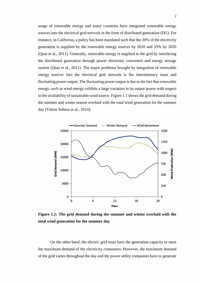
to the availability of sustainable wind source. Figure 1.1 shows the grid demand during
the summer and winter season overlaid with the total wind generation for the summer
day (Yekini Suberu et al., 2014).
Figure 1.1: The grid demand during the summer and winter overlaid with the
total wind generation for the summer day
On the other hand, the electric grid must have the generation capacity to meet
the maximum demand of the electricity consumers. However, the maximum demand
of the grid varies throughout the day and the power utility companies have to generate

3
at an extra capacity to meet the maximum demand. At certain hours of the day, the
generation capacity of the power plants exceeds much higher than the demand of the
consumers. The problem arises when the extra energy generated cannot be stored in
the grid if it is not used by the consumers and this results in the wastage of energy
(Lawder et al., 2014).
1.2 Problem Statements
Energy storage system nowadays plays a significant role in the field of renewable
energy. One of the applications of energy storage system is to solve intermittency
issues caused by the renewable energy sources by interconnecting the energy storage
system to the electrical grid. However, energy storage system which consists stack of
batteries generally has low voltage and this imposes a difficulty in connecting the
energy storage system to the electrical grid. Hence, the lower voltage at the energy
storage system side has to be stepped up to discharge the energy stored in batteries to
the grid and the higher voltage at the electrical grid side has to be stepped down to
charge the batteries.
Another problem which arises in integrating the energy storage system into the
electrical grid is that the voltage of electrical grid does not remain constant at all times
due to the fluctuation in the loads that are connected to the grid. Hence, the voltage at
the energy storage system side has to be adjusted accordingly to maintain the
interconnection between the energy storage system and the electrical grid. The feasible
solution to this problem is to implement a control system which is able to regulate the
voltage at the energy storage system side under different load conditions.
1.3 Aims and Objectives
The first objective of this project is to develop a high efficiency DC-DC buck-boost
converter for a bidirectional power flow inverter which serves as an interface between
4
the energy storage system and the electrical grid. The energy storage system developed
in this project consists of four series-connected lead-acid batteries. The DC-DC boost
converter is able to step up the voltage of the lead acid batteries to a higher DC output
voltage to discharge the energy stored in the batteries. A DC-DC buck converter is also
developed in this project which steps down a higher DC voltage to a lower DC voltage
to charge the lead-acid batteries. The second objective of this project is to develop
closed-loop feedback controller for the DC-DC boost converter so that the output
voltage of the boost converter can be maintained under different load conditions. The
performance of the feedback controller is optimized so that the boost converter has a
robust response when operating under different conditions.
1.4 Scopes of Project
This project is carried out to develop a DC-DC boost converter and a DC-DC buck
converter for a bidirectional power flow inverter. The development of the DC-DC
boost converter and buck converter mainly involves the field of power electronic,
which is a sub-branch of electronic that deals with the conversion of electrical power
by using solid-state electronic devices. Therefore, knowledge of power electronic are
important in the implementation of this project.
The implementation of this project also deals with control system when it
comes to the design of closed-loop feedback controller for the boost converter. Control
system is a sub-branch of engineering which is related to the development of system
to regulate the behaviour of a system. The knowledge of control system is typically
required in the design of the PI controller. Besides, the knowledge of fuzzy control
system is also applied in the development of the fuzzy logic controller.
National InstrumentTM (NI) LabVIEWTM is used as the programming
environment to develop the algorithm for generating the pulse-width modulation
(PWM) signal from NI sbRIO-9642XT embedded device. Furthermore, the algorithm
of the closed-loop feedback controller for the boost converter is also developed in
LabVIEWTM. Hence, extensive knowledge of LabVIEW’s graphical programming

5
language is required. Debugging, troubleshooting and problem solving skills are
required in this project. Overall, this project covers multi-disciplinary field of
electronic engineering.

6
CHAPTER 2
2 LITERATURE REVIEW
2.1 DC-DC Converter
In an AC (alternating current) system, voltage is stepped up or stepped down through
a transformer by changing the turn ratio. A transformer is totally ineffective in a DC
(direct current) system as DC does not produce changing magnetic flux for
electromagnetic induction. A DC-DC converter in a DC system is equivalent to the
transformer in the AC system, which is responsible for stepping up or stepping down
a fixed DC voltage source. There are different types of DC-DC converter and each of
them tends to be more suitable than other in some application. DC-DC converter can
be generally classified into non-isolating converter and isolated converter with
transformer. Boost converter is a type of non-isolating DC-DC converter which steps
up the DC input voltage to a higher DC output voltage.
2.1.1 Boost Converter
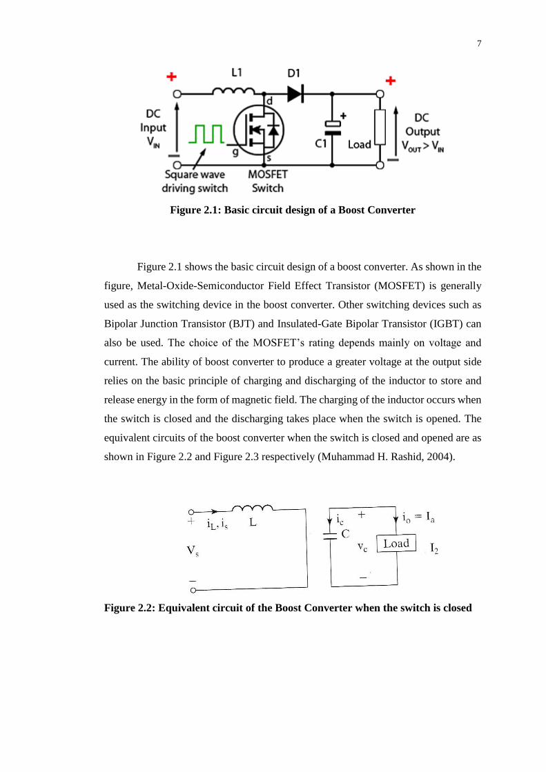
A boost converter is a DC-DC converter which steps up the input DC voltage to
produce a greater output DC voltage. The basic circuit design of boost converter
includes a switch, diode, inductor and capacitor.
7
Figure 2.1: Basic circuit design of a Boost Converter
Figure 2.1 shows the basic circuit design of a boost converter. As shown in the
figure, Metal-Oxide-Semiconductor Field Effect Transistor (MOSFET) is generally
used as the switching device in the boost converter. Other switching devices such as
Bipolar Junction Transistor (BJT) and Insulated-Gate Bipolar Transistor (IGBT) can
also be used. The choice of the MOSFET’s rating depends mainly on voltage and
current. The ability of boost converter to produce a greater voltage at the output side
relies on the basic principle of charging and discharging of the inductor to store and
release energy in the form of magnetic field. The charging of the inductor occurs when
the switch is closed and the discharging takes place when the switch is opened. The
equivalent circuits of the boost converter when the switch is closed and opened are as
shown in Figure 2.2 and Figure 2.3 respectively (Muhammad H. Rashid, 2004).
Figure 2.2: Equivalent circuit of the Boost Converter when the switch is closed

8
Figure 2.3: Equivalent circuit of the Boost Converter when the switch is opened
The ratio of the output voltage of the boost converter to its input voltage can
be adjusted by varying the duty ratio (D) of the Pulse-Width Modulation (PWM) signal,
which is the ratio of the duration of the on time to the switching period of the switch.
The equation which relates the output voltage (Vo) of the boost converter to its input
voltage (Vi) is shown in (2.1).
𝑉𝑜
𝑉𝑖=
1
1−𝐷 (2.1)
To ensure the continuous supply of current from the input to the output, the
boost converter must always be operating in continuous current mode. There is some
conditions that must be met for the boost converter to operate in the continuous current
mode, for instance the inductance and capacitance value chosen must be larger than
their respective critical value (Muhammad H. Rashid, 2004). The formulas to calculate
the critical value of inductance and capacitance are as shown in (2.2) and (2.3)
respectively.
𝑐𝑟𝑖𝑡𝑖𝑐𝑎𝑙 𝑣𝑎𝑙𝑢𝑒 𝑜𝑓 𝑖𝑛𝑑𝑢𝑐𝑡𝑎𝑛𝑐𝑒, 𝐿𝐶 =𝐷(1−𝐷)𝑅
2𝑓 (2.2)
𝑐𝑟𝑖𝑡𝑖𝑐𝑎𝑙 𝑣𝑎𝑙𝑢𝑒 𝑜𝑓 𝑐𝑎𝑝𝑎𝑐𝑖𝑡𝑎𝑛𝑐𝑒, 𝐶𝐶 =𝐷
2𝑓𝑅 (2.3)
where R is the resistance of the load and f is the switching frequency.
9
2.1.2 Buck Converter
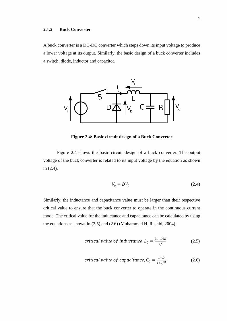
A buck converter is a DC-DC converter which steps down its input voltage to produce
a lower voltage at its output. Similarly, the basic design of a buck converter includes
a switch, diode, inductor and capacitor.
Figure 2.4: Basic circuit design of a Buck Converter
Figure 2.4 shows the basic circuit design of a buck converter. The output
voltage of the buck converter is related to its input voltage by the equation as shown
in (2.4).
𝑉𝑜 = 𝐷𝑉𝑖 (2.4)
Similarly, the inductance and capacitance value must be larger than their respective
critical value to ensure that the buck converter to operate in the continuous current
mode. The critical value for the inductance and capacitance can be calculated by using
the equations as shown in (2.5) and (2.6) (Muhammad H. Rashid, 2004).
𝑐𝑟𝑖𝑡𝑖𝑐𝑎𝑙 𝑣𝑎𝑙𝑢𝑒 𝑜𝑓 𝑖𝑛𝑑𝑢𝑐𝑡𝑎𝑛𝑐𝑒, 𝐿𝐶 =(1−𝐷)𝑅
2𝑓 (2.5)
𝑐𝑟𝑖𝑡𝑖𝑐𝑎𝑙 𝑣𝑎𝑙𝑢𝑒 𝑜𝑓 𝑐𝑎𝑝𝑎𝑐𝑖𝑡𝑎𝑛𝑐𝑒, 𝐶𝐶 =1−𝐷
16𝐿𝑓2 (2.6)
10
2.1.3 Application of Buck and Boost Converter in Charging and Discharging
Battery
A DC-DC buck boost converter has been designed by Derik Towler and Bret Whitaker
in the project “Bi-Directional Inverter and Energy Storage System”. The DC-DC boost
converter plays an important role in the project to boost the output voltage level of the
lead-acid batteries to inject the power into AC system grid in the discharging mode
(Trowler and Whitaker, 2008). Since the voltage level of the AC grid fluctuates all the
time, proportional-integral (PI) strategy was proposed by Trowler and Whitaker to
control the duty cycle of the boost converter to make necessary adjustment on the
output voltage. Besides, Trowler and Whitaker also proposed the design of a boost
converter which step up the output voltage of the batteries from 36 V to 51 V. (Trowler
and Whitaker, 2008)
In the charging mode, the DC-DC buck converter is responsible for stepping
down the voltage of AC grid to the voltage level of the batteries. According to Trowler
and Whitaker, the DC-DC buck converter can be designed in such a way that by adding
an additional switch to the DC-DC boost converter, thus forming a DC-DC buck-boost
converter with bi-directional current flow capability (Trowler and Whitaker, 2008).
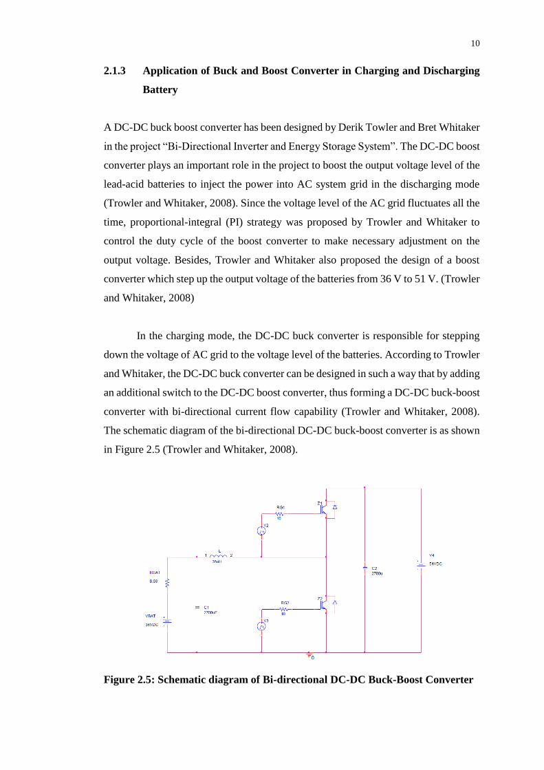
The schematic diagram of the bi-directional DC-DC buck-boost converter is as shown
in Figure 2.5 (Trowler and Whitaker, 2008).
Figure 2.5: Schematic diagram of Bi-directional DC-DC Buck-Boost Converter
11
2.2 PI Controller
PI controller, abbreviation of Proportional-Integral controller is one of the different
types of feedback controller that is widely used in the process industries. It has a simple
structure and is able to perform satisfactory in a wide range of operating condition.
Poor voltage regulation and unsatisfactory dynamic response are often the problems
faced by DC-DC boost converter when operated under open loop condition. Hence,
closed loop control is often necessary for boost converter for output voltage regulation
(Seshagiri Rao et al., 2012). DC-DC boost converter are commonly regulated with
simple linear lead-lag compensator or with linear cascaded PI controller (Krommydas
and Alexandridis, 2014). PI controller can be used to control and regulate the output
voltage of DC-DC boost converter at a certain desired set point. It works by computing
the error, which is the difference between the desired set point and the process variable
and attempts to reduce the error by making the necessary adjustment on the
manipulated variable, which is the duty ratio of boost converter.
PI controller combines both proportional effect and integral effect but eliminate
the effect of derivative in the PID controller. This is done by setting the derivative gain
in PID controller to zero. The absence of derivative effect causes the PI controller to
lose the ability to predict the future error which in turn yield a slower response time.
PI controllers are more common than PID controller since the derivative effect is
sensitive to the measurement noise. The proportional effect improves the response of
the system by generating an output which is proportional to the error magnitude. The
integral effect of PI controller reduces the steady-state oscillation caused by the
proportional effect. However, the integral effect causes a slower response speed on the
system and an overshoot due to accumulation of error from the past. The output of a
PI controller, u(t) is given by the equation as shown in (2.7).
𝑢(𝑡) = 𝐾𝑝𝑒(𝑡) + 𝐾𝑖 ∫ 𝑒(𝑡)𝑑𝑡 (2.7)
where e(t) is the difference between the set point and the process variable and Kp and
Ki are the proportional gain and integral gain respectively.
12
PI controller for DC-DC converter is usually designed based on small signal
linearization and standard frequency response technique based on the small signal
model of the converter. Ziegler-Nichol’s Method is one of the common methods
employed to design PI controller by using linear control theory.
2.2.1 Ziegler-Nichol’s Method
Ziegler-Nichol’s method is a common method of tuning the P, PI and PID controllers
by using heuristic approach. It was invented by John G. Ziegler and Nathaniel B.
Nichols in 1942. Ziegler-Nichol’s method can be considered as an experimental
approach for tuning the PID controller which is useful when the mathematic model of
the plant is not easily obtained. Ziegler-Nichol’s method generally uses the transient
response characteristic of the plant to tune the various parameters of PID controller,
including the proportional gain (KP), integral time (Ti) and derivative time (Td). There
are two methods proposed by Ziegler and Nichols to tune the parameters of P, PI and
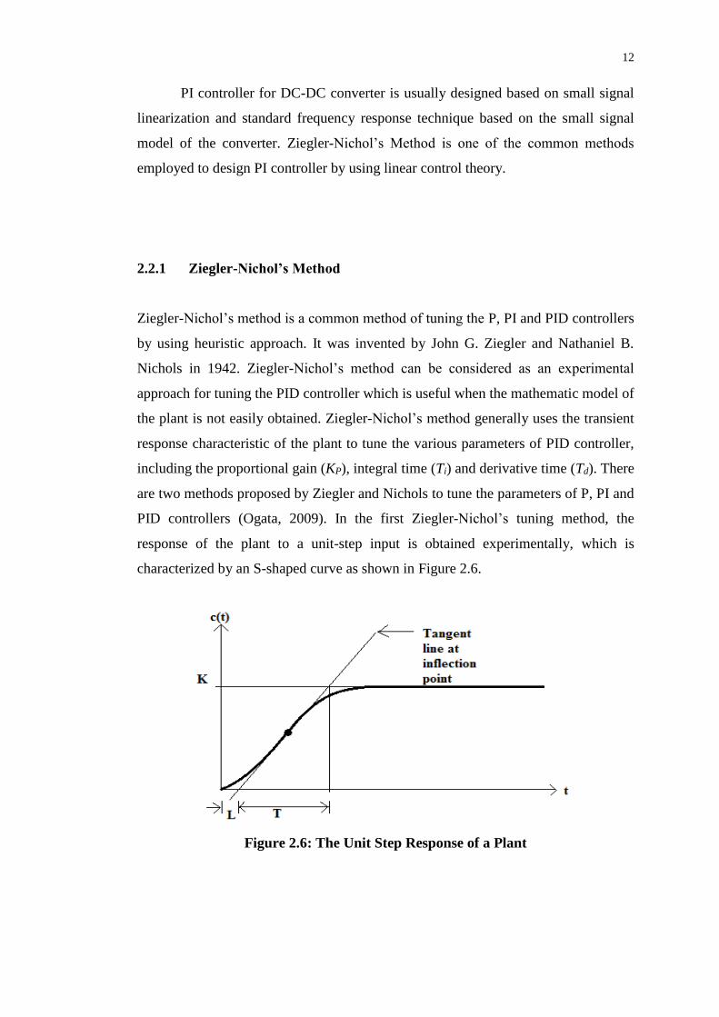
PID controllers (Ogata, 2009). In the first Ziegler-Nichol’s tuning method, the
response of the plant to a unit-step input is obtained experimentally, which is
characterized by an S-shaped curve as shown in Figure 2.6.
Figure 2.6: The Unit Step Response of a Plant

13
Figure 2.6 shows the S-shaped response curve of a plant subjected to a unit-step input.
The delay time (L) and time constant (T) of the S-shaped curve can be obtained by
sketching a tangent line at the inflection point. The intersections of the tangent line
with time axis and line c(t) = k determines the value of delay time (L) and time constant
(T). With the value of delay time (L) and time constant (T) determined, the parameters
of P, PI and PID controllers can be tuned according to the rules as shown in Table 2.1
(Ogata, 2009):
Table 2.1: The First Method of Ziegler-Nichol’s Tuning Method
Controller type Kp Ti Td
P 𝑇
𝐿
∞ 0
PI 0.9
𝑇
𝐿
𝐿
0.3
0
PID 1.2
𝑇
𝐿
2𝐿 0.5𝐿
In the second method of Ziegler-Nichol’s tuning method, the controller is first
tuned by setting Ti to a very large value and Td equal to 0. The value of KP is increased
from 0 to a critical value (Kcr) until the output of the controlled plant is oscillating
periodically. The value of critical gain (Kcr) and the corresponding critical period (Pcr)
are determined experimentally (Ogata, 2009). The value of critical period (Pcr) is
determined as shown in Figure 2.7.
Figure 2.7: Sustained Oscillation with Period Pcr
14
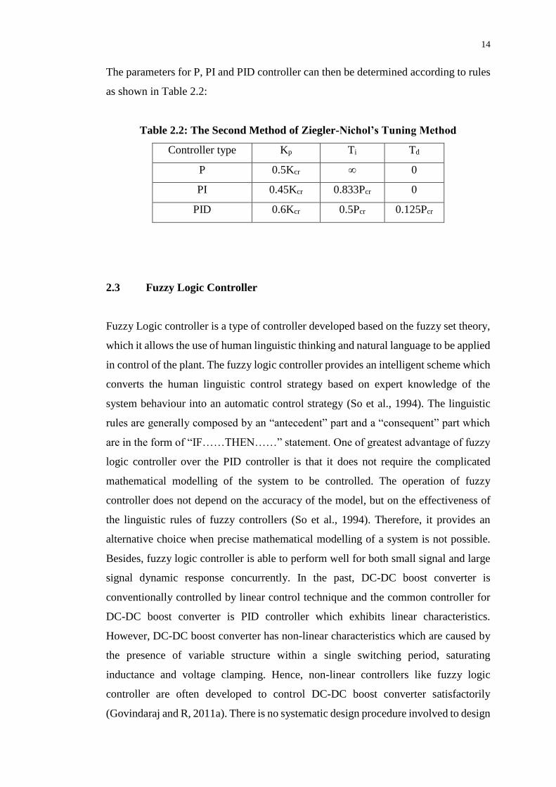
The parameters for P, PI and PID controller can then be determined according to rules
as shown in Table 2.2:
Table 2.2: The Second Method of Ziegler-Nichol’s Tuning Method
Controller type Kp Ti Td
P 0.5Kcr ∞ 0
PI 0.45Kcr 0.833Pcr 0
PID 0.6Kcr 0.5Pcr 0.125Pcr
2.3 Fuzzy Logic Controller
Fuzzy Logic controller is a type of controller developed based on the fuzzy set theory,
which it allows the use of human linguistic thinking and natural language to be applied
in control of the plant. The fuzzy logic controller provides an intelligent scheme which
converts the human linguistic control strategy based on expert knowledge of the
system behaviour into an automatic control strategy (So et al., 1994). The linguistic
rules are generally composed by an “antecedent” part and a “consequent” part which
are in the form of “IF……THEN……” statement. One of greatest advantage of fuzzy
logic controller over the PID controller is that it does not require the complicated
mathematical modelling of the system to be controlled. The operation of fuzzy
controller does not depend on the accuracy of the model, but on the effectiveness of
the linguistic rules of fuzzy controllers (So et al., 1994). Therefore, it provides an
alternative choice when precise mathematical modelling of a system is not possible.
Besides, fuzzy logic controller is able to perform well for both small signal and large
signal dynamic response concurrently. In the past, DC-DC boost converter is
conventionally controlled by linear control technique and the common controller for
DC-DC boost converter is PID controller which exhibits linear characteristics.
However, DC-DC boost converter has non-linear characteristics which are caused by
the presence of variable structure within a single switching period, saturating
inductance and voltage clamping. Hence, non-linear controllers like fuzzy logic
controller are often developed to control DC-DC boost converter satisfactorily
(Govindaraj and R, 2011a). There is no systematic design procedure involved to design
15
the fuzzy logic controller. The design of the fuzzy logic controller is purely depends
on the expert knowledge and analysis on the system behaviour of the plant to be
controlled.
Fuzzy logic controller utilizes linguistic variables instead of numerical
variables in the design of the controller. Linguistic variables are variables with values
described in the form of natural language, such as small and big which can represented
by fuzzy sets (Govindaraj and R, 2011a). Fuzzy sets allow partial membership, which
means that an element may partially belong to more than one set. This set can be
characterized by a membership function µA which applies for the set with a range
between 0 and 1 to each element in a given class (Mattavelli et al., 1997). This can be
represented by the equation shown in (2.8):
𝜇𝐴: 𝑋 → [0,1] (2.8)
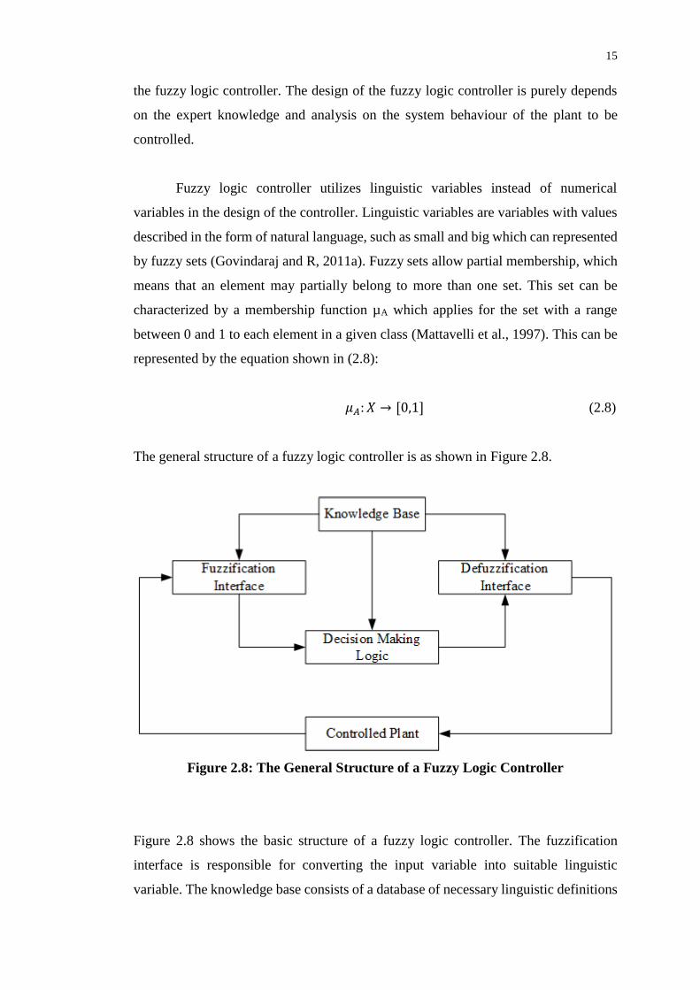
The general structure of a fuzzy logic controller is as shown in Figure 2.8.
Figure 2.8: The General Structure of a Fuzzy Logic Controller
Figure 2.8 shows the basic structure of a fuzzy logic controller. The fuzzification
interface is responsible for converting the input variable into suitable linguistic
variable. The knowledge base consists of a database of necessary linguistic definitions
16
and control rule sets. The decision making logic simulates the human decision process
and making the suitable fuzzy control action based on control rule sets and linguistic
variable definition. The defuzzification interface which produces a non-fuzzy control
action from an inferred fuzzy control action (Mattavelli et al., 1997). The design of a
fuzzy logic controller involves three steps, which are the fuzzification, fuzzy inference
and defuzzification ((Bai and Wang, n.d.).
2.3.1 Fuzzification
Fuzzification is an important step in a fuzzy control system which it converts the input
variables with numerical value into the fuzzy variables, or generally known as the
linguistic variables. The fuzzification process generally involves the derivation of
membership functions for both input and output variables. Each of the membership
function is then represented with linguistic variable. There are few types of
membership function, including triangular shape, trapezoidal shape, bell shape,
sigmoid shape, Gaussian shape and S-curve shape. Membership functions with
triangular and trapezoidal shapes are suitable for use in fuzzy system which requires
robust dynamic performance while Gaussian or S-curved shaped membership
functions are suitable for fuzzy system that requires high control accuracy (Bai and
Wang, n.d.).
2.3.2 Fuzzy Inference
The fuzzy inference involves the development of the fuzzy control rules based on the
expert knowledge of the system to be controlled. The fuzzy control rules are generally
the statements in the form of “IF…THEN…”, which the “IF” forms the antecedent
part of the statement while “THEN” forms the consequent part. The fuzzy control rules
provide the algorithms which describe the action should be taken based on the inputs
of the fuzzy controller (Bai and Wang, n.d.). There is no general guideline for
developing the fuzzy control rules for a particular system, instead in-depth knowledge
17
and experience of the system’s behaviour are often required. Sometimes, some of the
rules are also developed by “trial and error” and “intuitive” feel of the system being
controlled (Govindaraj and R, 2011a).
2.3.3 Defuzzification
Defuzzification process converts the linguistic variable, which is produced by the
fuzzy inference to the classical variable which has the numerical value. Defuzzication
process is necessary to make the output of the fuzzy inference available to the real
system to be controlled as linguistic variable does not reflect the actual action that has
to be taken by the system. The defuzzification technique that is commonly used is the
Mean Center of Gravity Method (Bai and Wang, n.d.).
2.4 Hybrid Fuzzy-PI Controller
Hybrid fuzzy-PI controller is a controller developed by combining both the PI
controller and fuzzy logic controller. Conventional PI controller provides good
performance in the transient response and steady-state of the system and hence it is
widely used in many industrial application. Generally, the parameters of PI controller
are fixed during its operation. One drawback of this fixed parameters is that the PI
controller may become inefficient in controlling the system when the system is
subjected to unknown disturbance (Pratumsuwan et al., 2010). Fuzzy logic controller,
on the other hand, has a robust performance in controlling system with great variation
in its dynamic response. It also eliminates the need to obtain the precise mathematical
modelling of the system. Another major advantage of fuzzy logic controller it has a
short rise time and small overshoot (Pratumsuwan et al., 2010). However, fuzzy logic
controller may not perform as well as PI controller at the steady state. The combination
of PI controller with fuzzy logic controller provides a compensation of the weakness
of each other, giving a good transient response and reduced overshoot while
minimizing the steady state error (Tiwary et al., 2014).

18
2.5 LabVIEWTM
LabVIEWTM (abbreviation for Laboratory Virtual Instrument Engineering Workbench)
is a proprietary software developed by National InstrumentTM which uses graphical
programming language instead of lines of text to create application. LabVIEWTM uses
a dataflow programming language known as G. In dataflow programming, the
execution order of the virtual instruments (VIs), which are the subroutine in
LabVIEWTM and functions is determined by the flow of data through the nodes on the
block diagram.
LabVIEWTM has been used extensively in the test, control and measurement
application by engineers and scientists. The main advantage of LabVIEWTM is that its
graphical programming environment offer great flexibility and reduced development
time over the traditional text-based programming environment, such as C and C++
programming. Besides, code debugging and troubleshooting are easier to be carried
out in the graphical programming environment. LabVIEWTM also features a large
library which consists of large number of function, including data acquisition, signal
generation and conditioning, mathematical and statistical function. LabVIEWTM
extensively supports for interfacing to National Instrument’s (NI) devices, such as NI
Single-Board RIO (sbRIO) embedded device, NI CompactDAQ (cDAQ) and NI
CompactRIO (cRIO) platforms. Therefore, it offers great convenience and reduced
effort in developing application for embedded control and data acquisition.
19
CHAPTER 3
3 METHODOLOGY
3.1 Design of DC-DC Boost and Buck Converter
This section focuses on the design work of the DC-DC boost and buck converter,
including the calculation of the boost and buck converter circuit’s parameter,
simulation of the boost and buck converter’s circuit in NI MultisimTM, selection of
hardware components for the converters, and development of program to generate the
pulse-width modulation (PWM) signal to drive the switching action of the converters
by using NI sbRIO-9642 embedded device in NI LabVIEWTM.
3.1.1 Calculation of Boost Converter Circuit’s Parameters
The function of boost converter in this project is to step up the voltage of the lead-acid
batteries from 48 V to a higher output DC voltage to discharge the stored energy in the
battery. The design of the boost converter adopted the basic circuit design of boost
converter which is as shown in Figure 2.1. The preliminary design steps of the boost
converter involve the calculation of various parameters of the boost converter,
including the duty ratio, ripple voltage, ripple current and critical inductance and
capacitance value required for continuous current mode. These parameters are
calculated by using the equations as shown follows:

20
𝑉𝑜
𝑉𝑖=
1
1−𝐷 (3.1)
where Vi is the input voltage of boost converter, Vo is the output voltage of boost
converter and D is the duty ratio of the PWM signal.
𝑟𝑖𝑝𝑝𝑙𝑒 𝑐𝑢𝑟𝑟𝑒𝑛𝑡, ∆𝐼 = 𝑉𝑖𝐷
𝑓𝐿 (3.2)
𝑟𝑖𝑝𝑝𝑙𝑒 𝑣𝑜𝑙𝑡𝑎𝑔𝑒, ∆𝑉 = 𝐼𝑎𝐷
𝑓𝐶 (3.3)
where Ia is the load current, f is switching frequency, L and C are the inductance and
capacitance chosen.
To ensure that the inductor current does not fall to zero, the boost converter
must be operated in the continuous current mode (CCM) by choosing the inductance
and capacitance values which are greater than their respective critical values. The
critical value of the inductance and capacitance to operate in CCM can be calculated
by using the equations as shown below:
𝑐𝑟𝑖𝑡𝑖𝑐𝑎𝑙 𝑣𝑎𝑙𝑢𝑒 𝑜𝑓 𝑖𝑛𝑑𝑢𝑐𝑡𝑎𝑛𝑐𝑒, 𝐿𝐶 =𝐷(1−𝐷)𝑅
2𝑓 (3.4)
𝑐𝑟𝑖𝑡𝑖𝑐𝑎𝑙 𝑣𝑎𝑙𝑢𝑒 𝑜𝑓 𝑐𝑎𝑝𝑎𝑐𝑖𝑡𝑎𝑛𝑐𝑒, 𝐶𝐶 =𝐷
2𝑓𝑅 (3.5)
Before calculating the various parameters, the switching frequency (f) and
resistance of the load (R) are fixed at 30 kHz and 50 Ω. The resistance of the load is
first selected based on assumption to ease the calculation since the actual load
resistance is not known at the initial stage.
The duty ratio of the boost converter is calculated by setting a range of output
voltage from 60 V to 120 V on a basis of 5 V increment. After having determined the
duty ratio, the critical value of inductance and capacitance can be calculated
subsequently. However, choosing the exact critical value to be the inductance and
capacitance value results in large output ripple voltage and ripple current. Therefore,

21
the minimum capacitance value is calculated in such a way that the output voltage
produced has less than 1 % ripple voltage. While, the inductance value chosen is 1.3
times the critical inductance value. Microsoft Excel is used to perform all the
calculations to speed up the process and present the data in a more organized manner.
The results of the calculation are as shown in Table 3.1.
Table 3.1: The Calculated Parameter of Boost Converter
Vi (V) Vo (V) D (%) Lmin
(mH)
Cmin
(µF)
L (mH) C (µF)
48 60 20.00 0.133 0.067 0.173 13.333
48 65 26.20 0.161 0.087 0.209 17.436
48 70 31.40 0.180 0.105 0.233 20.952
48 75 36.00 0.192 0.120 0.250 24.000
48 80 40.00 0.200 0.133 0.260 26.667
48 85 43.50 0.205 0.145 0.266 29.020
48 90 46.70 0.207 0.156 0.270 31.111
48 95 49.50 0.208 0.165 0.271 32.982
48 100 52.00 0.208 0.173 0.270 34.667
48 105 54.30 0.207 0.181 0.269 36.190
48 110 56.40 0.205 0.188 0.266 37.576
48 115 58.30 0.203 0.194 0.263 38.841
48 120 60.00 0.200 0.200 0.260 40.000
3.1.2 Calculation of Buck Converter Circuit’s Parameters
In this project, the buck converter is designed to serve the purpose of charging the lead
acid batteries. The circuit design of the buck converter is as shown in Figure 2.4.
Similarly, the preliminary design steps involved the calculation of duty ratio, ripple
current, ripple voltage and critical value of inductance and capacitance required and
they are calculated by using the equations as shown below.
22
𝑉𝑜 = 𝐷𝑉𝑖 (3.6)
𝑟𝑖𝑝𝑝𝑙𝑒 𝑐𝑢𝑟𝑟𝑒𝑛𝑡, ∆𝐼 = 𝑉𝑖𝐷(1−𝐷)
𝑓𝐿 (3.7)
𝑟𝑖𝑝𝑝𝑙𝑒 𝑣𝑜𝑙𝑡𝑎𝑔𝑒, ∆𝑉 = 𝑉𝑠𝐷(1−𝐷)
8𝐿𝐶𝑓2 (3.8)
𝑐𝑟𝑖𝑡𝑖𝑐𝑎𝑙 𝑣𝑎𝑙𝑢𝑒 𝑜𝑓 𝑖𝑛𝑑𝑢𝑐𝑡𝑎𝑛𝑐𝑒, 𝐿𝐶 =(1−𝐷)𝑅
2𝑓 (3.9)
𝑐𝑟𝑖𝑡𝑖𝑐𝑎𝑙 𝑣𝑎𝑙𝑢𝑒 𝑜𝑓 𝑐𝑎𝑝𝑎𝑐𝑖𝑡𝑎𝑛𝑐𝑒, 𝐶𝐶 =1−𝐷
16𝐿𝑓2 (3.10)
The buck converter in this project is designed based on input DC voltage of 48
V as higher DC voltage supply is not available at the current stage. The output voltage
of the converter is fixed in the range of 10 V to 40 V. The switching frequency (f) and
load resistance are fixed at 30 kHz and 50 Ω respectively. The capacitance (C) is
designed in such a way that the output ripple voltage of the buck converter is less than
1 % and the inductance (L) is designed with a value of 30 % higher than the critical
inductance value (Lmin). The result of the calculation is shown in Table 3.2:
Table 3.2: The calculated parameter of Buck Converter
Vi (V) Vo (V) D (%) Lmin
(mH)
Cmin
(µF) L (mH) C (µF)
48 10 20.83 0.657 0.084 0.854 115.85
48 15 31.25 0.571 0.084 0.742 115.85
48 20 41.67 0.484 0.084 0.629 115.85
48 25 52.08 0.398 0.084 0.517 115.85
48 30 62.50 0.311 0.084 0.404 115.85
48 35 72.92 0.225 0.084 0.292 115.85
48 40 83.33 0.138 0.084 0.180 115.85
23
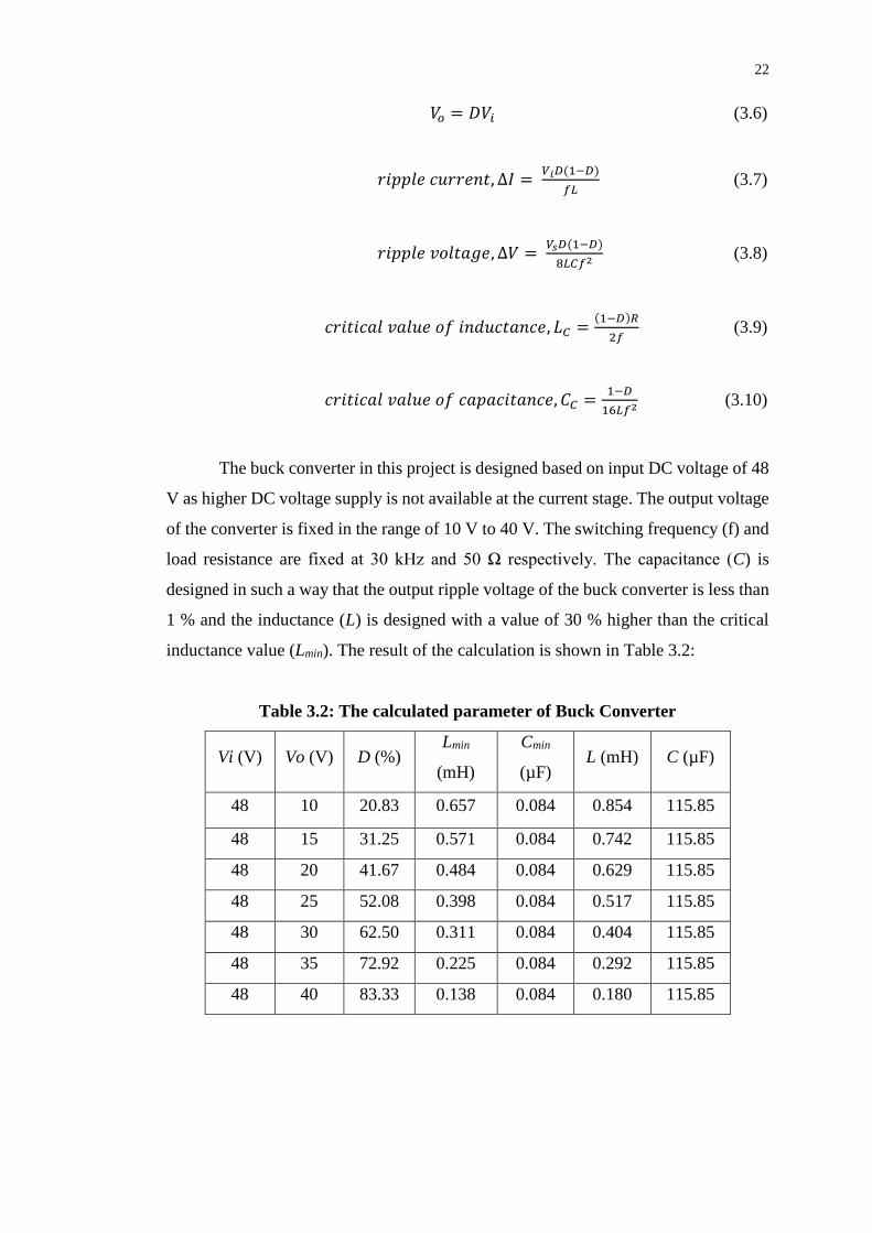
3.1.3 Simulation of Boost and Buck Converter Circuit in MultisimTM
The functionality of the boost and buck converter is verified through the simulation in
NI MultisimTM before it is tested on the real hardware. Multisim is an easy-to-use
circuit simulation software with large component library and interactive graphic user
interface. It features powerful simulation technology and is capable of analysing
analogue and digital electronics circuit and as well as power electronics circuit.
In the simulation, the boost converter circuit as shown in Figure 2.1 was
constructed in MultisimTM. Instead of using MOSFET, a voltage-controlled single
pole single throw (SPST) switch is used to represent an ideal switch for the boost
converter. The voltage-controlled SPST is driven by a function generator which
produces a PWM signal with 30 kHz switching frequency and a magnitude of 10 V.
The inductance and capacitance of the boost converter are fixed at 0.75 mH and 1500
µF respectively, which are much larger than the critical inductance and capacitance
required based on the parameters as shown in Table 3.1. The purpose of choosing larger
inductance and capacitance value is to ensure that the boost converter is operating in
the continuous current mode. The input voltage of the boost converter is fixed at 48 V
and the output is measured by using a multimeter by connecting it in parallel with the
load. The schematic of the boost converter in the simulation is as shown in Figure 3.1.
Figure 3.1: The Schematic of Boost Converter in Multisim Simulation
The simulation is carried out for different duty ratios from 10 % to 60 %. The results
of the simulation are shown in Chapter 4.
L1
0.75mH
D1
C1
1500µF
V1
48V S1
+-
R1
50Ω
XFG1
XMM1
24
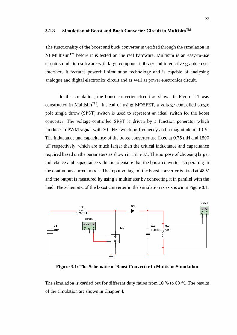
Similarly, the simulation of the buck converter is carried out in NI Multisim to
verify its functionality. In the simulation, the inductance value and capacitance value
are chosen to be 0.75 mH and 1500 µF to ensure they are larger than the critical
inductance and critical capacitance required for continuous current mode. The
simulation is carried out with an input voltage of 48 V, switching frequency of 30 kHz
and load resistance of 50 Ω. The duty ratio of the buck converter is adjusted from 10 %
to 70%. The schematic of the buck converter in the simulation is constructed as shown
in Figure 3.2.
Figure 3.2: The Schematic of Buck Converter in Multisim Simulation
3.1.4 Selection of Hardware Components for Boost and Buck Converter
The hardware components which are required to construct the circuit of the boost and
buck converter include a MOSFET (S), a diode (D), an inductor (L) and capacitors (C).
Since both the boost and buck converter are sharing the same hardware components,
the selection of rating of the hardware components is ensured to meet the parameter
requirement of the boost and buck converter. The rating of the hardware components
to construct the converter is not taken exactly as the parameters that are obtained from
the calculation. Instead, components with higher rating are chosen to prevent the
components from easily spoiled during the experiment stage. The specification of the
components used to construct the boost and buck converter are shown in Table 3.3.
V1
48V
L1
0.75mH
C1
1500µF
D1
R1
50Ω
S1
+ -
XFG1
XMM1
25
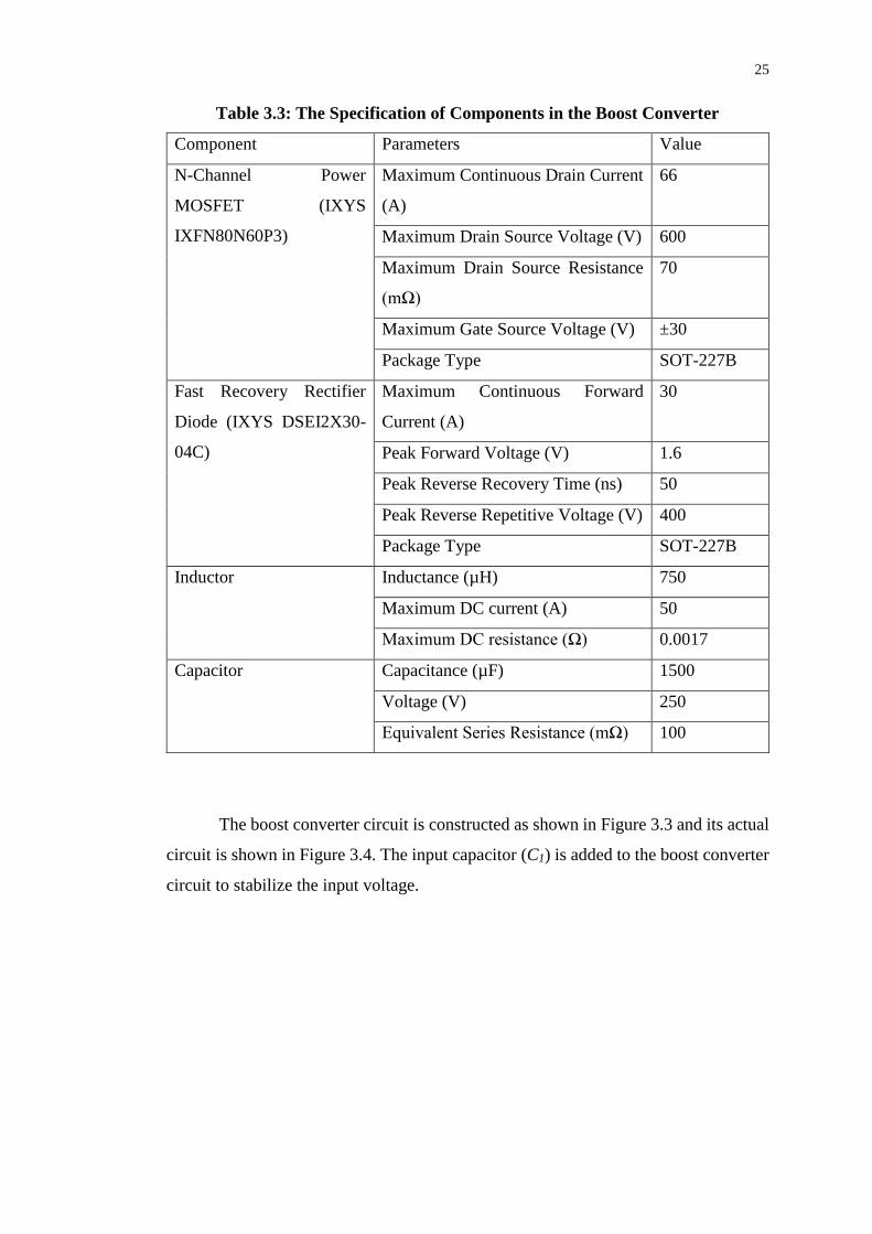
Table 3.3: The Specification of Components in the Boost Converter
Component Parameters Value
N-Channel Power
MOSFET (IXYS
IXFN80N60P3)
Maximum Continuous Drain Current
(A)
66
Maximum Drain Source Voltage (V) 600
Maximum Drain Source Resistance
(mΩ)
70
Maximum Gate Source Voltage (V) ±30
Package Type SOT-227B
Fast Recovery Rectifier
Diode (IXYS DSEI2X30-
04C)
Maximum Continuous Forward
Current (A)
30
Peak Forward Voltage (V) 1.6
Peak Reverse Recovery Time (ns) 50
Peak Reverse Repetitive Voltage (V) 400
Package Type SOT-227B
Inductor Inductance (µH) 750
Maximum DC current (A) 50
Maximum DC resistance (Ω) 0.0017
Capacitor Capacitance (µF) 1500
Voltage (V) 250
Equivalent Series Resistance (mΩ) 100
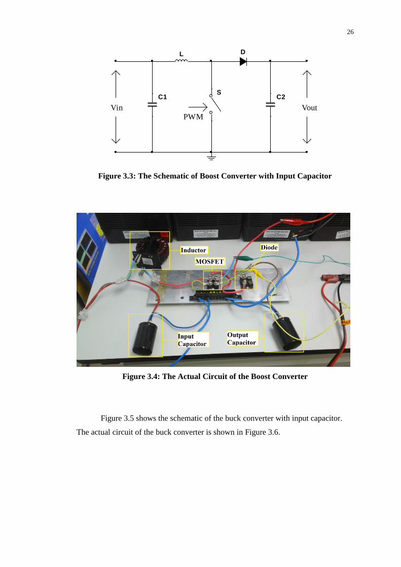
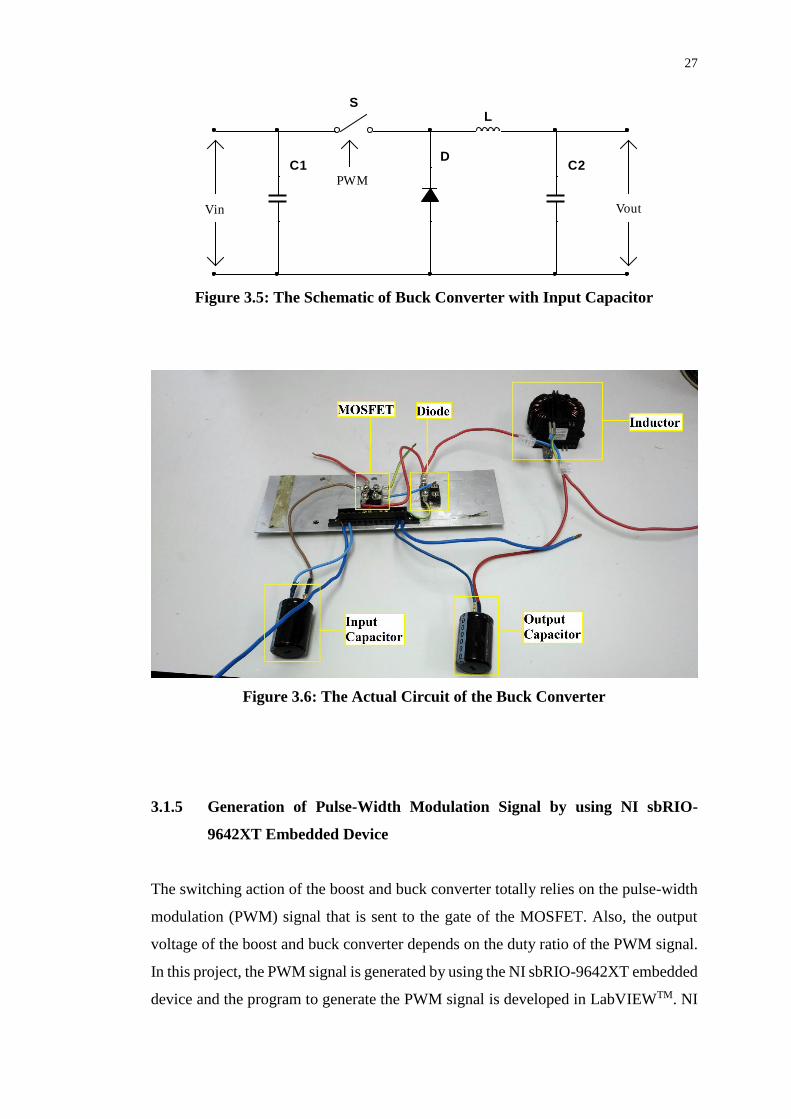
The boost converter circuit is constructed as shown in Figure 3.3 and its actual
circuit is shown in Figure 3.4. The input capacitor (C1) is added to the boost converter
circuit to stabilize the input voltage.
26
Figure 3.3: The Schematic of Boost Converter with Input Capacitor
Figure 3.4: The Actual Circuit of the Boost Converter
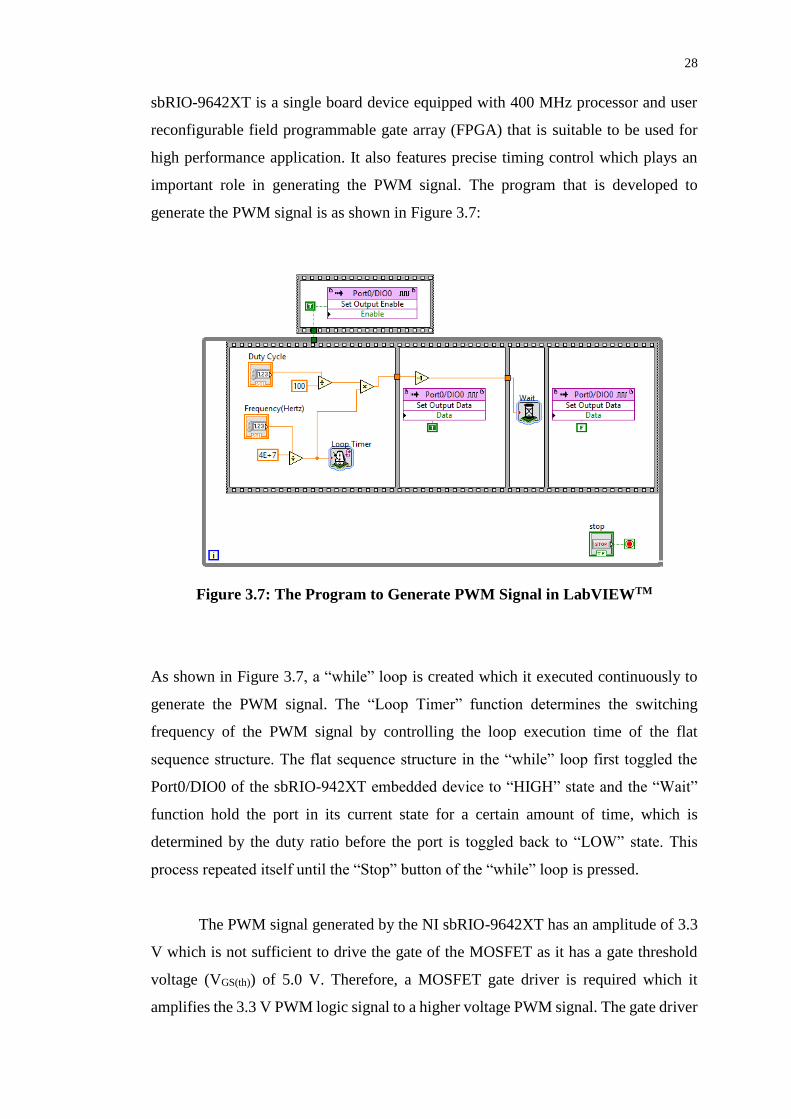
Figure 3.5 shows the schematic of the buck converter with input capacitor.
The actual circuit of the buck converter is shown in Figure 3.6.
L D
C2S
C1
Vin VoutPWM
27
Figure 3.5: The Schematic of Buck Converter with Input Capacitor
Figure 3.6: The Actual Circuit of the Buck Converter
3.1.5 Generation of Pulse-Width Modulation Signal by using NI sbRIO-
9642XT Embedded Device
The switching action of the boost and buck converter totally relies on the pulse-width
modulation (PWM) signal that is sent to the gate of the MOSFET. Also, the output
voltage of the boost and buck converter depends on the duty ratio of the PWM signal.
In this project, the PWM signal is generated by using the NI sbRIO-9642XT embedded
device and the program to generate the PWM signal is developed in LabVIEWTM. NI
C1
S
D
L
C2
Vin Vout
PWM
28
sbRIO-9642XT is a single board device equipped with 400 MHz processor and user
reconfigurable field programmable gate array (FPGA) that is suitable to be used for
high performance application. It also features precise timing control which plays an
important role in generating the PWM signal. The program that is developed to
generate the PWM signal is as shown in Figure 3.7:
Figure 3.7: The Program to Generate PWM Signal in LabVIEWTM
As shown in Figure 3.7, a “while” loop is created which it executed continuously to
generate the PWM signal. The “Loop Timer” function determines the switching
frequency of the PWM signal by controlling the loop execution time of the flat
sequence structure. The flat sequence structure in the “while” loop first toggled the
Port0/DIO0 of the sbRIO-942XT embedded device to “HIGH” state and the “Wait”
function hold the port in its current state for a certain amount of time, which is
determined by the duty ratio before the port is toggled back to “LOW” state. This
process repeated itself until the “Stop” button of the “while” loop is pressed.
The PWM signal generated by the NI sbRIO-9642XT has an amplitude of 3.3
V which is not sufficient to drive the gate of the MOSFET as it has a gate threshold
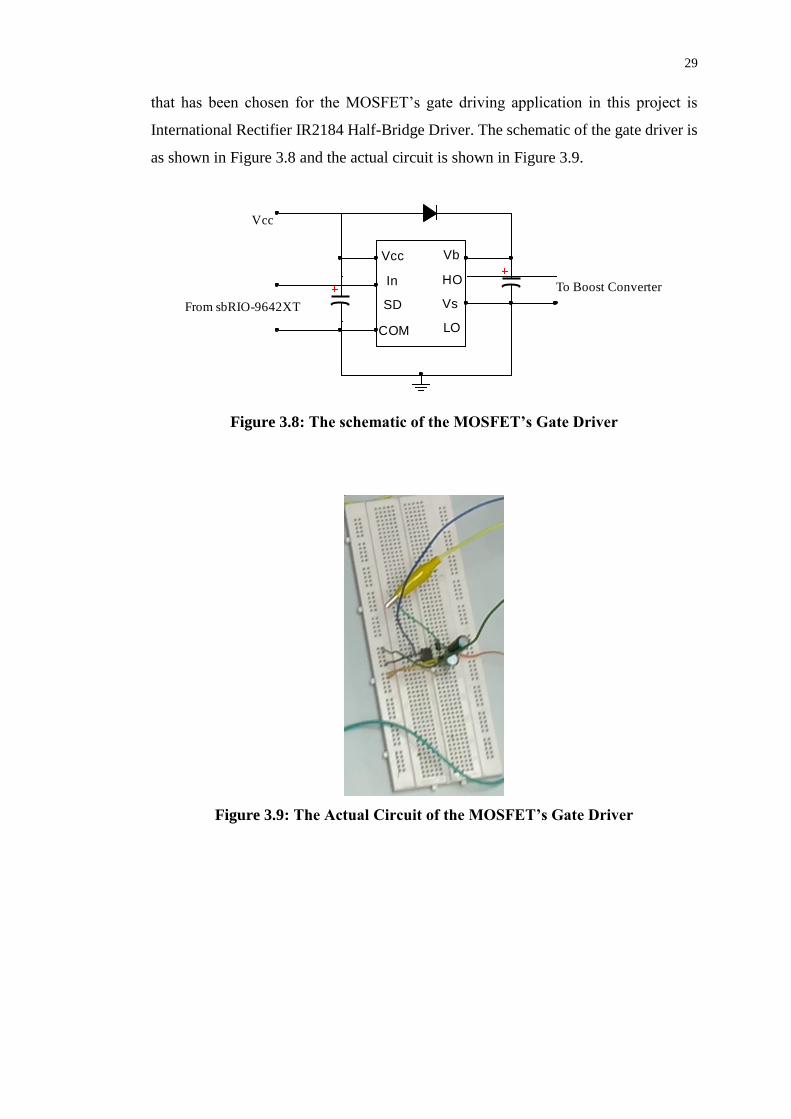
voltage (VGS(th)) of 5.0 V. Therefore, a MOSFET gate driver is required which it
amplifies the 3.3 V PWM logic signal to a higher voltage PWM signal. The gate driver
29
that has been chosen for the MOSFET’s gate driving application in this project is
International Rectifier IR2184 Half-Bridge Driver. The schematic of the gate driver is
as shown in Figure 3.8 and the actual circuit is shown in Figure 3.9.
Figure 3.8: The schematic of the MOSFET’s Gate Driver
Figure 3.9: The Actual Circuit of the MOSFET’s Gate Driver
Vcc
In
SD
COM
Vb
HO
Vs
LO
To Boost Converter
From sbRIO-9642XT
Vcc
30
3.2 Design of Closed-Loop Feedback Controller
This section focuses on the design of the closed-loop feedback controller for the boost
converter. A boost converter operated under open loop condition without any
controller exhibits poor voltage regulation and unsatisfactory dynamic response when
subjected to large load variation. Hence, a close-loop controller is often necessary for
converter operated under large load variation to achieve a good voltage regulation and
fast dynamic response. Different types of controller have been developed for the
converter in this project to achieve an optimal performance of the converter, including
PI controller, fuzzy logic controller and hybrid fuzzy-PI controller. A comparative
study is carried out to evaluate the performance of the rise time, overshoot, settling
time and steady-state error of these controllers. Figure 3.10 shows the controllers that
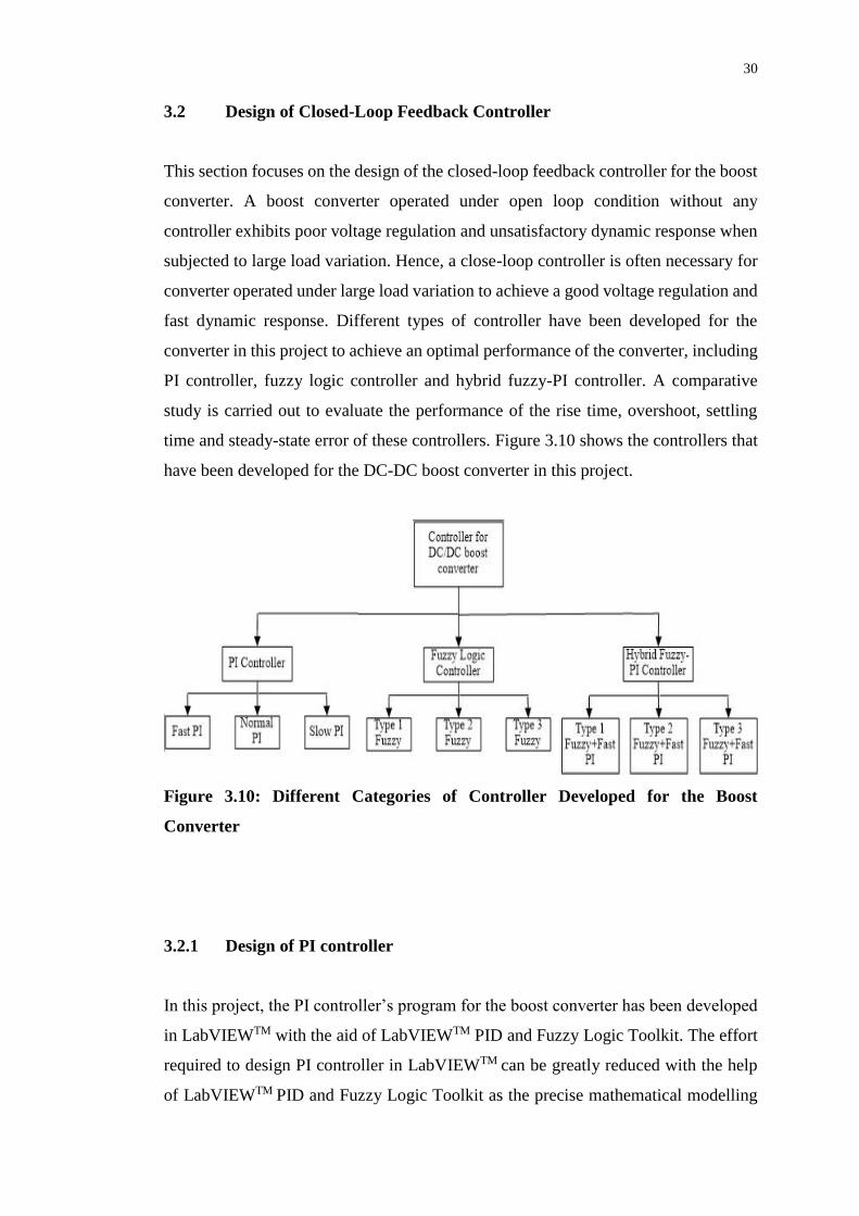
have been developed for the DC-DC boost converter in this project.
Figure 3.10: Different Categories of Controller Developed for the Boost
Converter
3.2.1 Design of PI controller
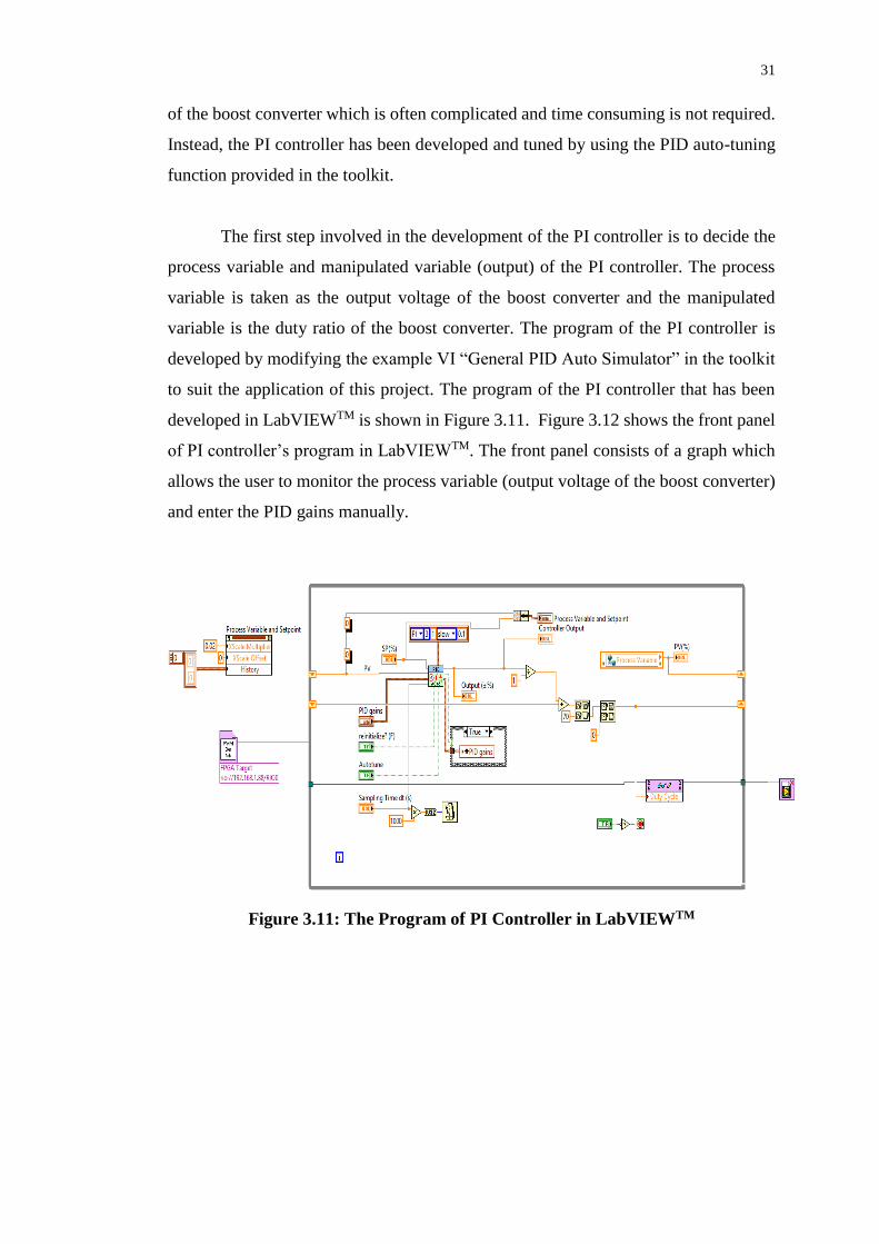
In this project, the PI controller’s program for the boost converter has been developed
in LabVIEWTM with the aid of LabVIEWTM PID and Fuzzy Logic Toolkit. The effort
required to design PI controller in LabVIEWTM can be greatly reduced with the help
of LabVIEWTM PID and Fuzzy Logic Toolkit as the precise mathematical modelling
31
of the boost converter which is often complicated and time consuming is not required.
Instead, the PI controller has been developed and tuned by using the PID auto-tuning
function provided in the toolkit.
The first step involved in the development of the PI controller is to decide the
process variable and manipulated variable (output) of the PI controller. The process
variable is taken as the output voltage of the boost converter and the manipulated
variable is the duty ratio of the boost converter. The program of the PI controller is
developed by modifying the example VI “General PID Auto Simulator” in the toolkit
to suit the application of this project. The program of the PI controller that has been
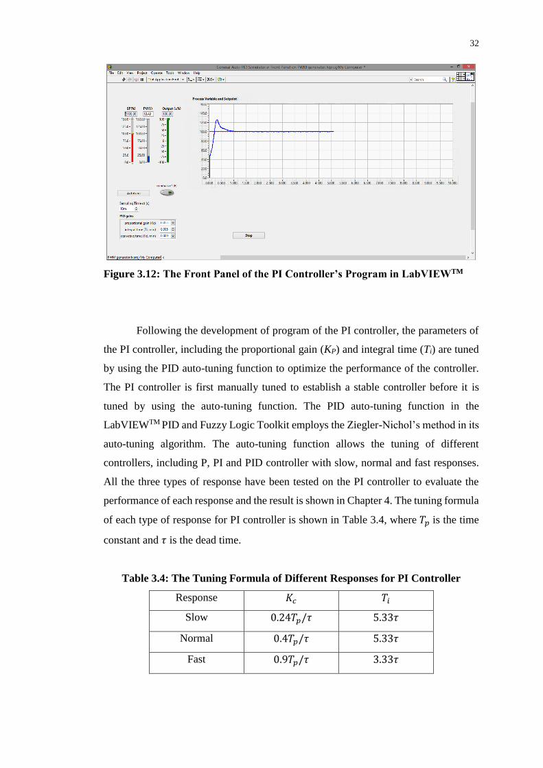
developed in LabVIEWTM is shown in Figure 3.11. Figure 3.12 shows the front panel
of PI controller’s program in LabVIEWTM. The front panel consists of a graph which
allows the user to monitor the process variable (output voltage of the boost converter)
and enter the PID gains manually.
Figure 3.11: The Program of PI Controller in LabVIEWTM
32
Figure 3.12: The Front Panel of the PI Controller’s Program in LabVIEWTM
Following the development of program of the PI controller, the parameters of
the PI controller, including the proportional gain (KP) and integral time (Ti) are tuned
by using the PID auto-tuning function to optimize the performance of the controller.
The PI controller is first manually tuned to establish a stable controller before it is
tuned by using the auto-tuning function. The PID auto-tuning function in the
LabVIEWTM PID and Fuzzy Logic Toolkit employs the Ziegler-Nichol’s method in its
auto-tuning algorithm. The auto-tuning function allows the tuning of different
controllers, including P, PI and PID controller with slow, normal and fast responses.
All the three types of response have been tested on the PI controller to evaluate the
performance of each response and the result is shown in Chapter 4. The tuning formula
of each type of response for PI controller is shown in Table 3.4, where 𝑇𝑝 is the time
constant and 𝜏 is the dead time.
Table 3.4: The Tuning Formula of Different Responses for PI Controller
Response 𝐾𝑐 𝑇𝑖
Slow 0.24𝑇𝑝/𝜏 5.33𝜏
Normal 0.4𝑇𝑝/𝜏 5.33𝜏
Fast 0.9𝑇𝑝/𝜏 3.33𝜏

33
The parameters of the PI controller for each of the response tuned by the auto-tuning
function are as shown in Table 3.5:
Table 3.5: The Parameters of PI Controller for Different Type of Response
Response KP 𝑇𝑖(min)
Slow 0.012 0.010
Normal 0.025 0.008
Fast 0.055 0.005
3.2.2 Design of Fuzzy Logic Controller
The program to implement the fuzzy logic controller for the DC boost converter is
developed in LabVIEWTM with the aid of LabVIEWTM PID and Fuzzy Logic Toolkit.
The fuzzy controller implemented in this project used multiple inputs and single output
(MISO). The two inputs are error (e) and change of error (∆e) and the single output is
the change of duty ratio (∆d). The error (e) is computed as the difference between the
desired output voltage of the boost converter (SP) and the nth sample of the actual
output voltage of the boost converter (PV), which is as shown in (3.11).
e[n] = SP – PV [n] (3.11)
The second input, change of error (∆e) is the difference between successive errors and
is shown in (3.12).
∆e[n] = e[n] – e[n-1] (3.12)
Both the error (e) and change of error (∆e) are scaled by factors k1 and k2 before
they are fed into the controller. The value of k1 and k2 are fixed at 0.02 and 0.2
respectively to scale the actual value of error (e) and change of error (∆e) into
normalized range of [-1, 1]. The output, change of duty ratio (∆d) is scaled by the
output gain (h) and then added to the duty ratio of previous sampling period and it is
as shown in (3.8).
34
d [n] = d[n-1] + h∆d[n] (3.13)
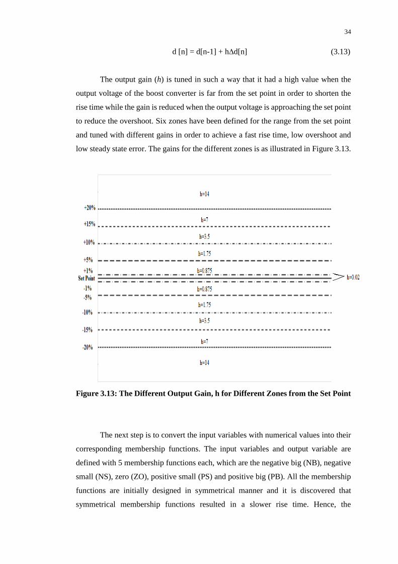
The output gain (h) is tuned in such a way that it had a high value when the
output voltage of the boost converter is far from the set point in order to shorten the
rise time while the gain is reduced when the output voltage is approaching the set point
to reduce the overshoot. Six zones have been defined for the range from the set point
and tuned with different gains in order to achieve a fast rise time, low overshoot and
low steady state error. The gains for the different zones is as illustrated in Figure 3.13.
Figure 3.13: The Different Output Gain, h for Different Zones from the Set Point
The next step is to convert the input variables with numerical values into their
corresponding membership functions. The input variables and output variable are
defined with 5 membership functions each, which are the negative big (NB), negative
small (NS), zero (ZO), positive small (PS) and positive big (PB). All the membership
functions are initially designed in symmetrical manner and it is discovered that
symmetrical membership functions resulted in a slower rise time. Hence, the
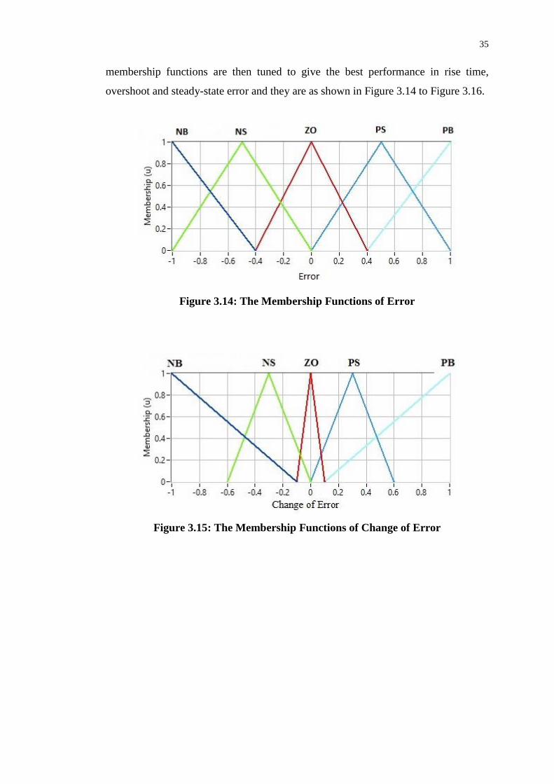
35
membership functions are then tuned to give the best performance in rise time,
overshoot and steady-state error and they are as shown in Figure 3.14 to Figure 3.16.
Figure 3.14: The Membership Functions of Error
Figure 3.15: The Membership Functions of Change of Error

36
Figure 3.16: The Membership Function of Change of Duty Ratio
As shown in Figure 3.14 to Figure 3.16, the membership functions adopted the
triangular and trapezoidal shapes and the value of the input and output variables is
normalized in the range of [-1, 1] by using suitable scale factor.
The control rules of the fuzzy logic controller are derived based on the general
knowledge of system behaviour of the boost converter. It must be considered that the
derivation of the control rules can improve the dynamic response and robustness of the
controller under various operating conditions. The fuzzy rules are derived by using
heuristic approach and based on the following criteria.
1) If the error is large in magnitude, then the change of duty ratio must be large
so as to reduce the error quickly.
2) If the error is approaching a small value in magnitude, then the change of duty
ratio must be small.
3) If the error is approaching zero value, then the duty ratio must remain the same
to prevent overshoot.
4) If the error reaches zero value and the output voltage is still changing, then the
duty ratio must be adjusted a little to prevent the output voltage from moving
away.
5) If the error reaches zero and the output voltage is steady, then the change of
duty ratio must remain zero.

37
6) If the output voltage goes beyond the set point, the change of duty ratio must
be in the opposite way and vice versa.
The fuzzy control rules which are derived based on the criteria above are as shown in
Table 3.6:
Table 3.6: The Control Rules of the Fuzzy Controller
e
de
NB NS ZO PS PB
NB NB NB NB NS ZO
NS NB NB NS ZO PS
ZO NB NS ZO PS PB
PS NS ZO PS PB PB
PB ZO PS PB PB PB
The proposed fuzzy inference rules as shown in Table 3.6 are general and
modification is necessary to obtain the desired responses. Furthermore, it is found that
some of the rules are redundant can be removed to improve the computational
efficiency and interpretability of the fuzzy logic controller. Hence, the fuzzy rules
shown above is modified by adopting the rules reduction topology as shown in Figure
3.17. The white boxes indicate the rules that are removed. At first, the rules which are
located at the extreme corners of the table are removed and some changes are made to
the remaining rules. The performance of the fuzzy controller which utilizes the 21 sets
of fuzzy rules is compared to that with the 25 set of fuzzy rules in terms of rise time,
overshoot, settling time and steady-state error. The fuzzy rules with 21 rules are further
reduced and tuned to evaluate the performance of the fuzzy controllers using different
number of fuzzy rules, including 17, 13, 11 and 9 rules. The rules are reduced in such
a way that they are removed starting from the outer region of the table to the inner
region of the table until the boost converter is totally out of stability.
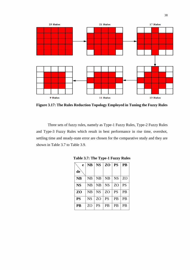
38
Figure 3.17: The Rules Reduction Topology Employed in Tuning the Fuzzy Rules
Three sets of fuzzy rules, namely as Type-1 Fuzzy Rules, Type-2 Fuzzy Rules
and Type-3 Fuzzy Rules which result in best performance in rise time, overshot,
settling time and steady-state error are chosen for the comparative study and they are
shown in Table 3.7 to Table 3.9.
Table 3.7: The Type-1 Fuzzy Rules
e
de
NB NS ZO PS PB
NB NB NB NB NS ZO
NS NB NB NS ZO PS
ZO NB NS ZO PS PB
PS NS ZO PS PB PB
PB ZO PS PB PB PB

39
Table 3.8: The Type-2 Fuzzy Rules
e
de
NB NS ZO PS PB
NB NB NB NS
NS NB NB NS PS PS
ZO NB NS ZO PS PB
PS NS NS PS PB PB
PB PS PB PB
Table 3.9: The Type-3 Fuzzy Rules
e
de
NB NS ZO PS PB
NB
NS NB NS ZO
ZO NB NS ZO PS PB
PS ZO PS PB
PB
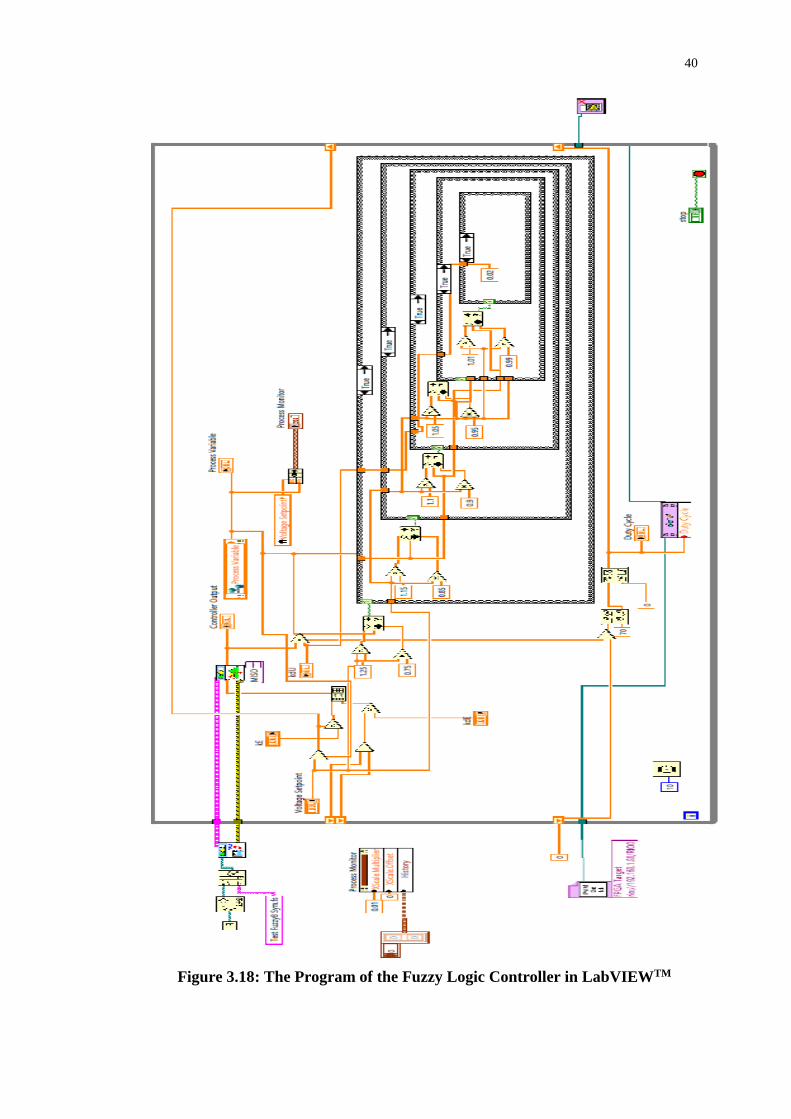
The program of the fuzzy logic controller that has been developed in
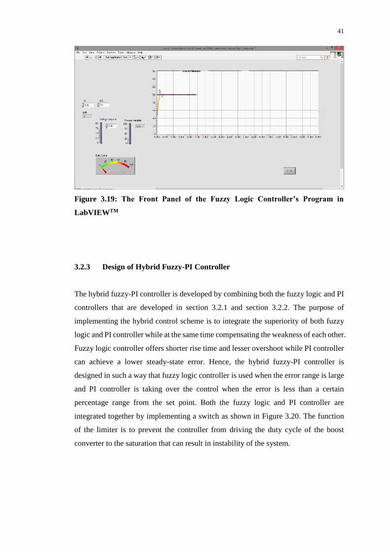
LabVIEWTM is as shown in Figure 3.18. The front panel of the fuzzy logic controller’s
program in LabVIEWTM is as shown in Figure 3.19.
40
Figure 3.18: The Program of the Fuzzy Logic Controller in LabVIEWTM
41
Figure 3.19: The Front Panel of the Fuzzy Logic Controller’s Program in
LabVIEWTM
3.2.3 Design of Hybrid Fuzzy-PI Controller
The hybrid fuzzy-PI controller is developed by combining both the fuzzy logic and PI
controllers that are developed in section 3.2.1 and section 3.2.2. The purpose of
implementing the hybrid control scheme is to integrate the superiority of both fuzzy
logic and PI controller while at the same time compensating the weakness of each other.
Fuzzy logic controller offers shorter rise time and lesser overshoot while PI controller
can achieve a lower steady-state error. Hence, the hybrid fuzzy-PI controller is
designed in such a way that fuzzy logic controller is used when the error range is large
and PI controller is taking over the control when the error is less than a certain
percentage range from the set point. Both the fuzzy logic and PI controller are
integrated together by implementing a switch as shown in Figure 3.20. The function
of the limiter is to prevent the controller from driving the duty cycle of the boost
converter to the saturation that can result in instability of the system.
42
Figure 3.20: The Structure of Hybrid Fuzzy-PI Controller
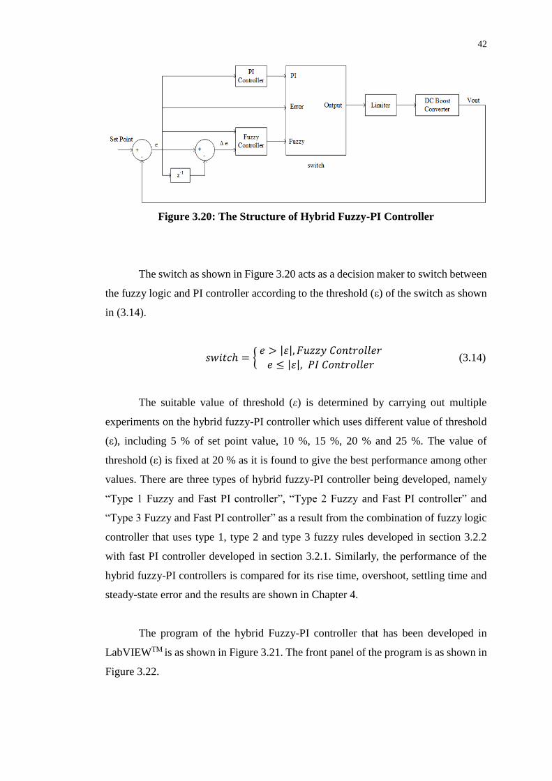
The switch as shown in Figure 3.20 acts as a decision maker to switch between
the fuzzy logic and PI controller according to the threshold (ε) of the switch as shown
in (3.14).
𝑠𝑤𝑖𝑡𝑐ℎ = 𝑒 > |𝜀|, 𝐹𝑢𝑧𝑧𝑦 𝐶𝑜𝑛𝑡𝑟𝑜𝑙𝑙𝑒𝑟
𝑒 ≤ |𝜀|, 𝑃𝐼 𝐶𝑜𝑛𝑡𝑟𝑜𝑙𝑙𝑒𝑟 (3.14)
The suitable value of threshold (ε) is determined by carrying out multiple
experiments on the hybrid fuzzy-PI controller which uses different value of threshold
(ε), including 5 % of set point value, 10 %, 15 %, 20 % and 25 %. The value of
threshold (ε) is fixed at 20 % as it is found to give the best performance among other
values. There are three types of hybrid fuzzy-PI controller being developed, namely
“Type 1 Fuzzy and Fast PI controller”, “Type 2 Fuzzy and Fast PI controller” and
“Type 3 Fuzzy and Fast PI controller” as a result from the combination of fuzzy logic
controller that uses type 1, type 2 and type 3 fuzzy rules developed in section 3.2.2
with fast PI controller developed in section 3.2.1. Similarly, the performance of the
hybrid fuzzy-PI controllers is compared for its rise time, overshoot, settling time and
steady-state error and the results are shown in Chapter 4.
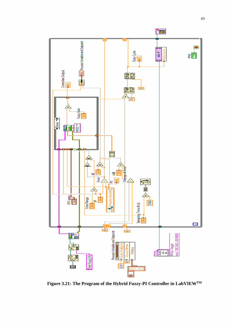
The program of the hybrid Fuzzy-PI controller that has been developed in
LabVIEWTM is as shown in Figure 3.21. The front panel of the program is as shown in
Figure 3.22.
43
Figure 3.21: The Program of the Hybrid Fuzzy-PI Controller in LabVIEWTM

44
Figure 3.22: The Front Panel of Hybrid Fuzzy-PI Controller’s Program in
LabVIEWTM
3.3 Hardware and Software Setup
The main hardware involved in this project include the lead acid batteries, DC boost
converter, NI sbRIO-9642XT embedded device, NI cDAQ-9184 Ethernet Chassis with
NI-9225 voltage measurement module and a network router. The overall setup of the
hardware is illustrated as shown in Figure 3.23.
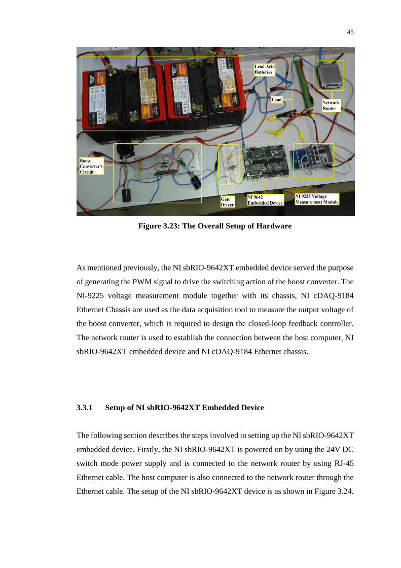
45
Figure 3.23: The Overall Setup of Hardware
As mentioned previously, the NI sbRIO-9642XT embedded device served the purpose
of generating the PWM signal to drive the switching action of the boost converter. The
NI-9225 voltage measurement module together with its chassis, NI cDAQ-9184
Ethernet Chassis are used as the data acquisition tool to measure the output voltage of
the boost converter, which is required to design the closed-loop feedback controller.
The network router is used to establish the connection between the host computer, NI
sbRIO-9642XT embedded device and NI cDAQ-9184 Ethernet chassis.
3.3.1 Setup of NI sbRIO-9642XT Embedded Device
The following section describes the steps involved in setting up the NI sbRIO-9642XT
embedded device. Firstly, the NI sbRIO-9642XT is powered on by using the 24V DC
switch mode power supply and is connected to the network router by using RJ-45
Ethernet cable. The host computer is also connected to the network router through the
Ethernet cable. The setup of the NI sbRIO-9642XT device is as shown in Figure 3.24.
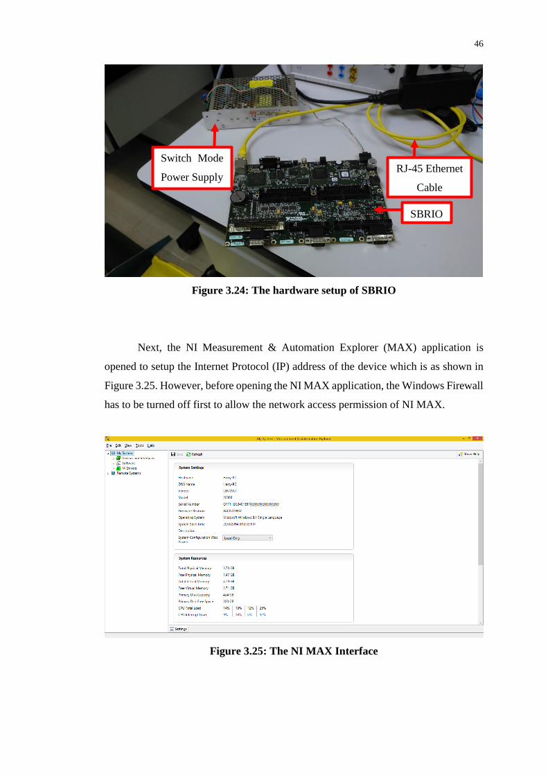
46
Figure 3.24: The hardware setup of SBRIO
Next, the NI Measurement & Automation Explorer (MAX) application is
opened to setup the Internet Protocol (IP) address of the device which is as shown in
Figure 3.25. However, before opening the NI MAX application, the Windows Firewall
has to be turned off first to allow the network access permission of NI MAX.
Figure 3.25: The NI MAX Interface
SBRIO
Switch Mode
Power Supply
RJ-45 Ethernet
Cable
47
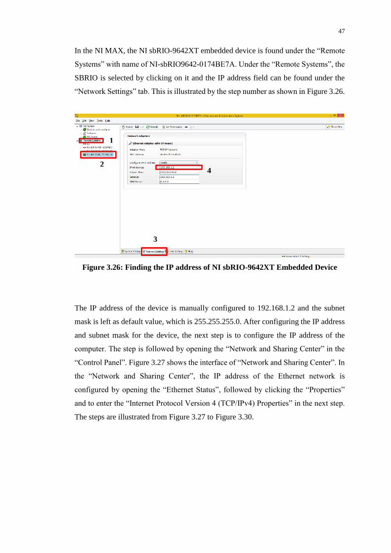
In the NI MAX, the NI sbRIO-9642XT embedded device is found under the “Remote
Systems” with name of NI-sbRIO9642-0174BE7A. Under the “Remote Systems”, the
SBRIO is selected by clicking on it and the IP address field can be found under the
“Network Settings” tab. This is illustrated by the step number as shown in Figure 3.26.
Figure 3.26: Finding the IP address of NI sbRIO-9642XT Embedded Device
The IP address of the device is manually configured to 192.168.1.2 and the subnet
mask is left as default value, which is 255.255.255.0. After configuring the IP address
and subnet mask for the device, the next step is to configure the IP address of the
computer. The step is followed by opening the “Network and Sharing Center” in the
“Control Panel”. Figure 3.27 shows the interface of “Network and Sharing Center”. In
the “Network and Sharing Center”, the IP address of the Ethernet network is
configured by opening the “Ethernet Status”, followed by clicking the “Properties”
and to enter the “Internet Protocol Version 4 (TCP/IPv4) Properties” in the next step.
The steps are illustrated from Figure 3.27 to Figure 3.30.
1
2
3
4

48
Figure 3.27: The Network and Sharing Center
Figure 3.28: The “Ethernet Status”
Click this to show
“Ethernet Status”
Click “Properties” to open “Ethernet Properties”

49
Figure 3.29: The “Ethernet Properties”
Figure 3.30: The “Internet Protocol Version 4 (TCP/IPv4) Properties”
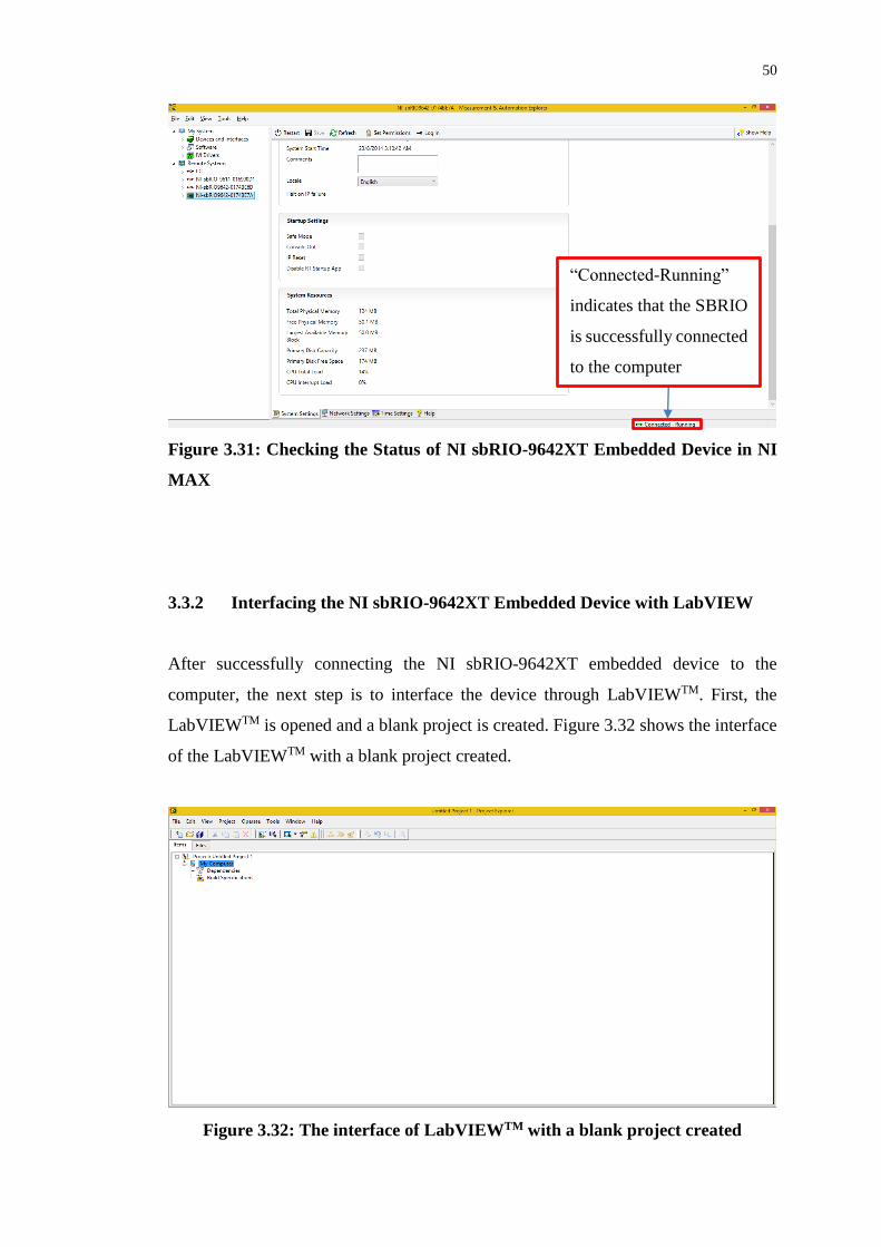
Once the correct IP address and subnet mask are filled in, the NI MAX
application is opened again to check the status of device. In the NI MAX application,
the bottom right hand corner of the window will show a message “Connected-Running”
to indicate that the device is successfully connected to the computer. This is as shown
in Figure 3.31.
Highlight the
“Internet Protocol
Version 4 (TCP/IPv4)
and click “Properties”
Choose “Use the
following IP address”
Fill in “192.168.1.1”
in the IP address field
and “255.255.255.0”
in the Subnet Mask
field
50
Figure 3.31: Checking the Status of NI sbRIO-9642XT Embedded Device in NI
MAX
3.3.2 Interfacing the NI sbRIO-9642XT Embedded Device with LabVIEW
After successfully connecting the NI sbRIO-9642XT embedded device to the
computer, the next step is to interface the device through LabVIEWTM. First, the
LabVIEWTM is opened and a blank project is created. Figure 3.32 shows the interface
of the LabVIEWTM with a blank project created.
Figure 3.32: The interface of LabVIEWTM with a blank project created
“Connected-Running”
indicates that the SBRIO
is successfully connected
to the computer

51
The next step is to add the device into the LabVIEWTM project and this is
illustrated in the following section. Firstly, right click on the “Project: Untitled Project
1” and choose “New” then followed by “Targets and Devices”. This is illustrated in
the Figure 3.33.
Figure 3.33: Adding new Targets and Devices in LabVIEWTM
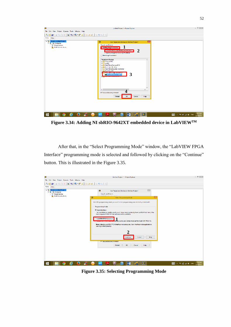
In the “Targets and Devices”, the options “Existing target or device” and
“Discover an existing target(s) and device(s)” are chosen. Next, the SBRIO device is
found under the “Real-Time Single-Board RIO” with the name of “NI-sbRIO9642-
0174BE7A”. The “NI-sbRIO9642-0174BE7A” is highlighted and the SBRIO device
is added by clicking “OK”. This is illustrated in the Figure 3.34.
1 2 3
52
Figure 3.34: Adding NI sbRIO-9642XT embedded device in LabVIEWTM
After that, in the “Select Programming Mode” window, the “LabVIEW FPGA
Interface” programming mode is selected and followed by clicking on the “Continue”
button. This is illustrated in the Figure 3.35.
Figure 3.35: Selecting Programming Mode
1 2
3
4
1
2

53
After successfully adding the device into the LabVIEWTM project, it is listed
under the project items which is as shown in the Figure 3.36.
Figure 3.36: Upon successfully adding SBRIO device in LabVIEWTM project
3.3.3 Setup of NI cDAQ-9184 Ethernet Chassis
The NI cDAQ-9184 Ethernet Chassis is a data acquisition device which can support
up to 4 measurement modules simultaneously. In this project, the NI cDAQ-9184
Ethernet Chassis is used together with the NI-9225 voltage measurement module to
measure the output voltage of the boost converter which is required to design the
closed-loop feedback controller of the boost converter. Ni-9225 voltage measurement
module is a 24-bit analogue input that has maximum sampling rate of 50,000
samples/second to provide an accurate measurement of the output voltage. The voltage
measurement module is attached to the NI cDAQ-9184 Ethernet Chassis to establish a
connection with the computer. The NI cDAQ-9184 Ethernet Chassis together with
attached NI-9225 voltage measurement module is as shown in Figure 3.37.
The SBRIO device
is listed here.
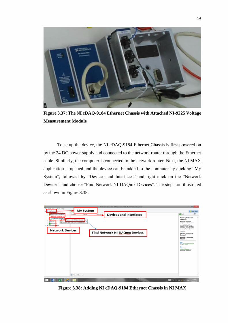
54
Figure 3.37: The NI cDAQ-9184 Ethernet Chassis with Attached NI-9225 Voltage
Measurement Module
To setup the device, the NI cDAQ-9184 Ethernet Chassis is first powered on
by the 24 DC power supply and connected to the network router through the Ethernet
cable. Similarly, the computer is connected to the network router. Next, the NI MAX
application is opened and the device can be added to the computer by clicking “My
System”, followed by “Devices and Interfaces” and right click on the “Network
Devices” and choose “Find Network NI-DAQmx Devices”. The steps are illustrated
as shown in Figure 3.38.
Figure 3.38: Adding NI cDAQ-9184 Ethernet Chassis in NI MAX

55
In the “Find Network NI-DAQmX Devices” window, the device with name
“cDAQ9184-19CE319” is selected and followed by clicking the “Add Selected
Devices”. This is illustrated as shown in Figure 3.39.
Figure 3.39: “Find Network NI-DAQmx Devices” Windows
After the device is successfully added to the computer, it will be listed in NI
MAX as shown in Figure 3.40.
Figure 3.40: After Successfully Adding NI cDAQ-9184 Ethernet Chassis

56
CHAPTER 4
4 RESULTS AND DISCUSSION
4.1 Boost Converter
4.1.1 Simulation Result
As discussed in Section 3.1.3, the simulation of the boost converter is carried out in NI
Multisim to verify the functionality of the boost converter. In the simulation, the input
voltage and switching frequency of the boost converter are fixed at 48 V and 30 kHz
respectively and the load resistance is chosen to be 50 Ω. The duty ratio of the PWM
signal is adjusted from 10 % to 60 % and the output voltage of the boost converter is
recorded. Table 4.1 shows the results obtained from the simulation.
Table 4.1: The Simulated Output Voltage of Boost Converter
D (%) Theoretical Vout (V) Simulated Vout (V)
10 53.33 52.50
20 60.00 59.15
30 68.57 67.71
40 80.00 79.12
50 96.00 95.00
60 120.00 119.00
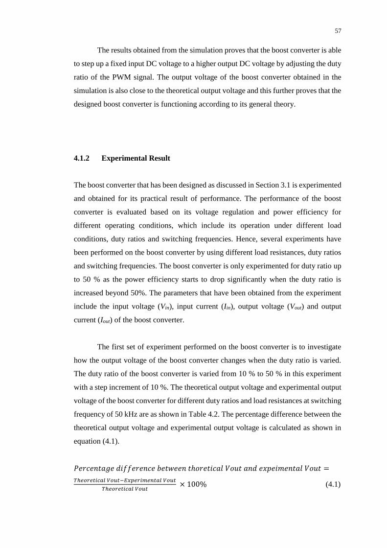
57
The results obtained from the simulation proves that the boost converter is able
to step up a fixed input DC voltage to a higher output DC voltage by adjusting the duty
ratio of the PWM signal. The output voltage of the boost converter obtained in the
simulation is also close to the theoretical output voltage and this further proves that the
designed boost converter is functioning according to its general theory.
4.1.2 Experimental Result
The boost converter that has been designed as discussed in Section 3.1 is experimented
and obtained for its practical result of performance. The performance of the boost
converter is evaluated based on its voltage regulation and power efficiency for
different operating conditions, which include its operation under different load
conditions, duty ratios and switching frequencies. Hence, several experiments have
been performed on the boost converter by using different load resistances, duty ratios
and switching frequencies. The boost converter is only experimented for duty ratio up
to 50 % as the power efficiency starts to drop significantly when the duty ratio is
increased beyond 50%. The parameters that have been obtained from the experiment
include the input voltage (Vin), input current (Iin), output voltage (Vout) and output
current (Iout) of the boost converter.
The first set of experiment performed on the boost converter is to investigate
how the output voltage of the boost converter changes when the duty ratio is varied.
The duty ratio of the boost converter is varied from 10 % to 50 % in this experiment
with a step increment of 10 %. The theoretical output voltage and experimental output
voltage of the boost converter for different duty ratios and load resistances at switching
frequency of 50 kHz are as shown in Table 4.2. The percentage difference between the
theoretical output voltage and experimental output voltage is calculated as shown in
equation (4.1).
𝑃𝑒𝑟𝑐𝑒𝑛𝑡𝑎𝑔𝑒 𝑑𝑖𝑓𝑓𝑒𝑟𝑒𝑛𝑐𝑒 𝑏𝑒𝑡𝑤𝑒𝑒𝑛 𝑡ℎ𝑜𝑟𝑒𝑡𝑖𝑐𝑎𝑙 𝑉𝑜𝑢𝑡 𝑎𝑛𝑑 𝑒𝑥𝑝𝑒𝑖𝑚𝑒𝑛𝑡𝑎𝑙 𝑉𝑜𝑢𝑡 =
𝑇ℎ𝑒𝑜𝑟𝑒𝑡𝑖𝑐𝑎𝑙 𝑉𝑜𝑢𝑡−𝐸𝑥𝑝𝑒𝑟𝑖𝑚𝑒𝑛𝑡𝑎𝑙 𝑉𝑜𝑢𝑡
𝑇ℎ𝑒𝑜𝑟𝑒𝑡𝑖𝑐𝑎𝑙 𝑉𝑜𝑢𝑡 × 100% (4.1)
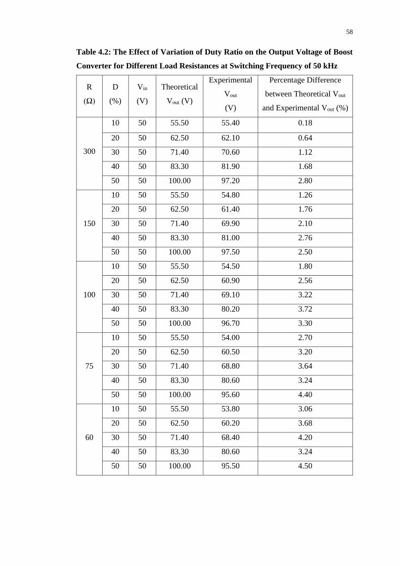
58
Table 4.2: The Effect of Variation of Duty Ratio on the Output Voltage of Boost
Converter for Different Load Resistances at Switching Frequency of 50 kHz
R
(Ω)
D
(%)
Vin
(V)
Theoretical
Vout (V)
Experimental
Vout
(V)
Percentage Difference
between Theoretical Vout
and Experimental Vout (%)
300
10 50 55.50 55.40 0.18
20 50 62.50 62.10 0.64
30 50 71.40 70.60 1.12
40 50 83.30 81.90 1.68
50 50 100.00 97.20 2.80
150
10 50 55.50 54.80 1.26
20 50 62.50 61.40 1.76
30 50 71.40 69.90 2.10
40 50 83.30 81.00 2.76
50 50 100.00 97.50 2.50
100
10 50 55.50 54.50 1.80
20 50 62.50 60.90 2.56
30 50 71.40 69.10 3.22
40 50 83.30 80.20 3.72
50 50 100.00 96.70 3.30
75
10 50 55.50 54.00 2.70
20 50 62.50 60.50 3.20
30 50 71.40 68.80 3.64
40 50 83.30 80.60 3.24
50 50 100.00 95.60 4.40
60
10 50 55.50 53.80 3.06
20 50 62.50 60.20 3.68
30 50 71.40 68.40 4.20
40 50 83.30 80.60 3.24
50 50 100.00 95.50 4.50
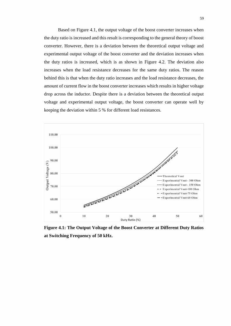
59
Based on Figure 4.1, the output voltage of the boost converter increases when
the duty ratio is increased and this result is corresponding to the general theory of boost
converter. However, there is a deviation between the theoretical output voltage and
experimental output voltage of the boost converter and the deviation increases when
the duty ratios is increased, which is as shown in Figure 4.2. The deviation also
increases when the load resistance decreases for the same duty ratios. The reason
behind this is that when the duty ratio increases and the load resistance decreases, the
amount of current flow in the boost converter increases which results in higher voltage
drop across the inductor. Despite there is a deviation between the theoretical output
voltage and experimental output voltage, the boost converter can operate well by
keeping the deviation within 5 % for different load resistances.
Figure 4.1: The Output Voltage of the Boost Converter at Different Duty Ratios
at Switching Frequency of 50 kHz.
60
Figure 4.2: The Percentage Difference between Theoretical Vout and
Experimental Vout of the Boost Converter for Different Duty Ratios at Switching
Frequency of 50 kHz
The second experiment conducted is to investigate the how the efficiency of
the boost converter changes when the duty ratio is varied. The efficiency of the boost
convert at different duty ratios and fixed switching frequency of 50 kHz for different
load resistances are as shown in Table 4.3.
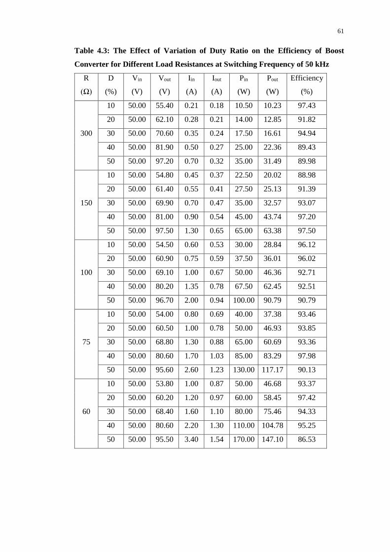
61
Table 4.3: The Effect of Variation of Duty Ratio on the Efficiency of Boost
Converter for Different Load Resistances at Switching Frequency of 50 kHz
R
(Ω)
D
(%)
Vin
(V)
Vout
(V)
Iin
(A)
Iout
(A)
Pin
(W)
Pout
(W)
Efficiency
(%)
300
10 50.00 55.40 0.21 0.18 10.50 10.23 97.43
20 50.00 62.10 0.28 0.21 14.00 12.85 91.82
30 50.00 70.60 0.35 0.24 17.50 16.61 94.94
40 50.00 81.90 0.50 0.27 25.00 22.36 89.43
50 50.00 97.20 0.70 0.32 35.00 31.49 89.98
150
10 50.00 54.80 0.45 0.37 22.50 20.02 88.98
20 50.00 61.40 0.55 0.41 27.50 25.13 91.39
30 50.00 69.90 0.70 0.47 35.00 32.57 93.07
40 50.00 81.00 0.90 0.54 45.00 43.74 97.20
50 50.00 97.50 1.30 0.65 65.00 63.38 97.50
100
10 50.00 54.50 0.60 0.53 30.00 28.84 96.12
20 50.00 60.90 0.75 0.59 37.50 36.01 96.02
30 50.00 69.10 1.00 0.67 50.00 46.36 92.71
40 50.00 80.20 1.35 0.78 67.50 62.45 92.51
50 50.00 96.70 2.00 0.94 100.00 90.79 90.79
75
10 50.00 54.00 0.80 0.69 40.00 37.38 93.46
20 50.00 60.50 1.00 0.78 50.00 46.93 93.85
30 50.00 68.80 1.30 0.88 65.00 60.69 93.36
40 50.00 80.60 1.70 1.03 85.00 83.29 97.98
50 50.00 95.60 2.60 1.23 130.00 117.17 90.13
60
10 50.00 53.80 1.00 0.87 50.00 46.68 93.37
20 50.00 60.20 1.20 0.97 60.00 58.45 97.42
30 50.00 68.40 1.60 1.10 80.00 75.46 94.33
40 50.00 80.60 2.20 1.30 110.00 104.78 95.25
50 50.00 95.50 3.40 1.54 170.00 147.10 86.53
62
The input power (Pin), output power (Pout) and efficiency of the boost converter are
calculated as shown in (4.2) to (4.4).
𝐼𝑛𝑝𝑢𝑡 𝑝𝑜𝑤𝑒𝑟, 𝑃𝑖𝑛 = 𝑉𝑖𝑛 × 𝐼𝑖𝑛 (4.2)
𝑂𝑢𝑡𝑝𝑢𝑡 𝑝𝑜𝑤𝑒𝑟, 𝑃𝑜𝑢𝑡 = 𝑉𝑜𝑢𝑡 × 𝐼𝑜𝑢𝑡 (4.3)
𝐸𝑓𝑓𝑖𝑐𝑖𝑒𝑛𝑐𝑦 (%) = 𝑃𝑖𝑛
𝑃𝑜𝑢𝑡× 100% (4.4)
Based on Figure 4.3, the efficiency of the boost converter lies in the range of
86 % to 98 % for different duty ratios and load resistances and it can be concluded that
the boost converter can achieve quite a high efficiency in the range of 10 % to 50 %
duty ratio. The boost converter can achieve the highest efficiency at around 40 %,
however there is a decreasing trend in the efficiency when the duty ratio is approaching
50 %. The drop in the efficiency is due to higher conduction loss in the boost converter.
Figure 4.3: The Efficiency of Boost Converter at Different Duty Ratios at
Switching Frequency of 50 kHz
63
The third experiment is conducted to study how the efficiency of the boost
converter varies when the switching frequency is increased. The efficiency of the boost
converter operating at different switching frequency and a fixed duty ratio of 50 % for
different load resistances are shown in Table 4.4.
Table 4.4: The Effect of Variation of Switching Frequency on the Efficiency of
Boost Converter for Different Load Resistances at Duty Ratio of 50 %.
R
(Ω)
Switching
Frequency
(kHz)
Vin
(V)
Vout
(V) Iin (A)
Iout
(A)
Pin
(W)
Pout
(W)
Efficiency
(%)
300
30 50.00 98.00 0.70 0.32 35.00 31.80 90.86
40 50.00 97.80 0.66 0.32 33.00 31.67 95.97
50 50.00 97.20 0.70 0.32 35.00 31.49 89.98
60 50.00 97.10 0.70 0.32 35.00 31.43 89.79
70 50.00 98.00 0.70 0.33 35.00 32.01 91.47
150
30 50.00 97.00 1.40 0.65 70.00 62.73 89.61
40 50.00 97.30 1.35 0.65 67.50 63.12 93.50
50 50.00 97.50 1.30 0.65 65.00 63.38 97.50
60 50.00 98.00 1.30 0.65 65.00 64.03 98.50
70 50.00 96.50 1.35 0.64 67.50 62.08 91.97
100
30 50.00 95.90 2.20 0.93 110.00 89.29 81.17
40 50.00 96.20 2.10 0.93 105.00 89.85 85.57
50 50.00 96.70 2.00 0.94 100.00 90.79 90.79
60 50.00 98.00 1.95 0.95 97.50 93.24 95.63
70 50.00 101.00 2.00 0.98 100.00 99.04 99.04
75
30 50.00 95.30 2.90 1.22 145.00 116.44 80.30
40 50.00 95.50 2.80 1.22 140.00 116.93 83.52
50 50.00 95.60 2.60 1.23 130.00 117.17 90.13
60 50.00 96.40 2.60 1.24 130.00 119.14 91.65
70 50.00 98.50 2.60 1.26 130.00 124.39 95.68
60
30 50.00 94.50 3.70 1.52 185.00 144.04 77.86
40 50.00 94.90 3.50 1.53 175.00 145.26 83.00
50 50.00 95.50 3.40 1.54 170.00 147.10 86.53
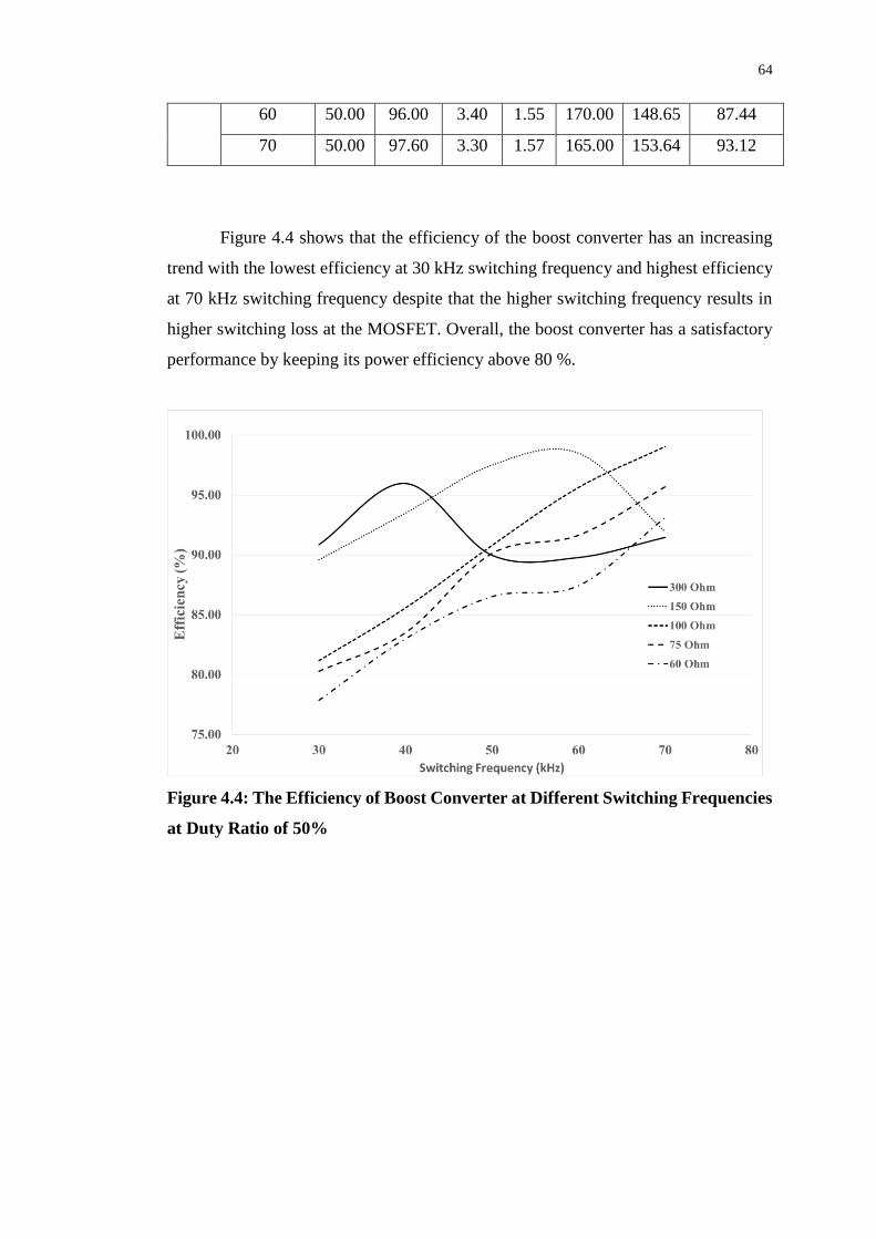
64
60 50.00 96.00 3.40 1.55 170.00 148.65 87.44
70 50.00 97.60 3.30 1.57 165.00 153.64 93.12
Figure 4.4 shows that the efficiency of the boost converter has an increasing
trend with the lowest efficiency at 30 kHz switching frequency and highest efficiency
at 70 kHz switching frequency despite that the higher switching frequency results in
higher switching loss at the MOSFET. Overall, the boost converter has a satisfactory
performance by keeping its power efficiency above 80 %.
Figure 4.4: The Efficiency of Boost Converter at Different Switching Frequencies
at Duty Ratio of 50%
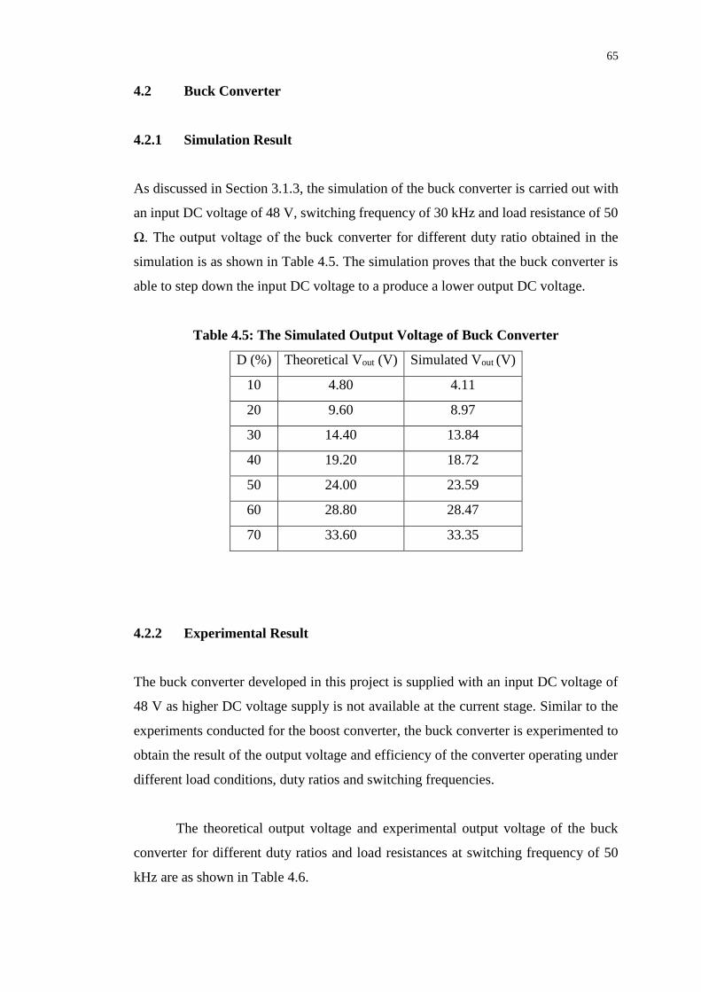
65
4.2 Buck Converter
4.2.1 Simulation Result
As discussed in Section 3.1.3, the simulation of the buck converter is carried out with
an input DC voltage of 48 V, switching frequency of 30 kHz and load resistance of 50
Ω. The output voltage of the buck converter for different duty ratio obtained in the
simulation is as shown in Table 4.5. The simulation proves that the buck converter is
able to step down the input DC voltage to a produce a lower output DC voltage.
Table 4.5: The Simulated Output Voltage of Buck Converter
D (%) Theoretical Vout (V) Simulated Vout (V)
10 4.80 4.11
20 9.60 8.97
30 14.40 13.84
40 19.20 18.72
50 24.00 23.59
60 28.80 28.47
70 33.60 33.35
4.2.2 Experimental Result
The buck converter developed in this project is supplied with an input DC voltage of
48 V as higher DC voltage supply is not available at the current stage. Similar to the
experiments conducted for the boost converter, the buck converter is experimented to
obtain the result of the output voltage and efficiency of the converter operating under
different load conditions, duty ratios and switching frequencies.
The theoretical output voltage and experimental output voltage of the buck
converter for different duty ratios and load resistances at switching frequency of 50
kHz are as shown in Table 4.6.
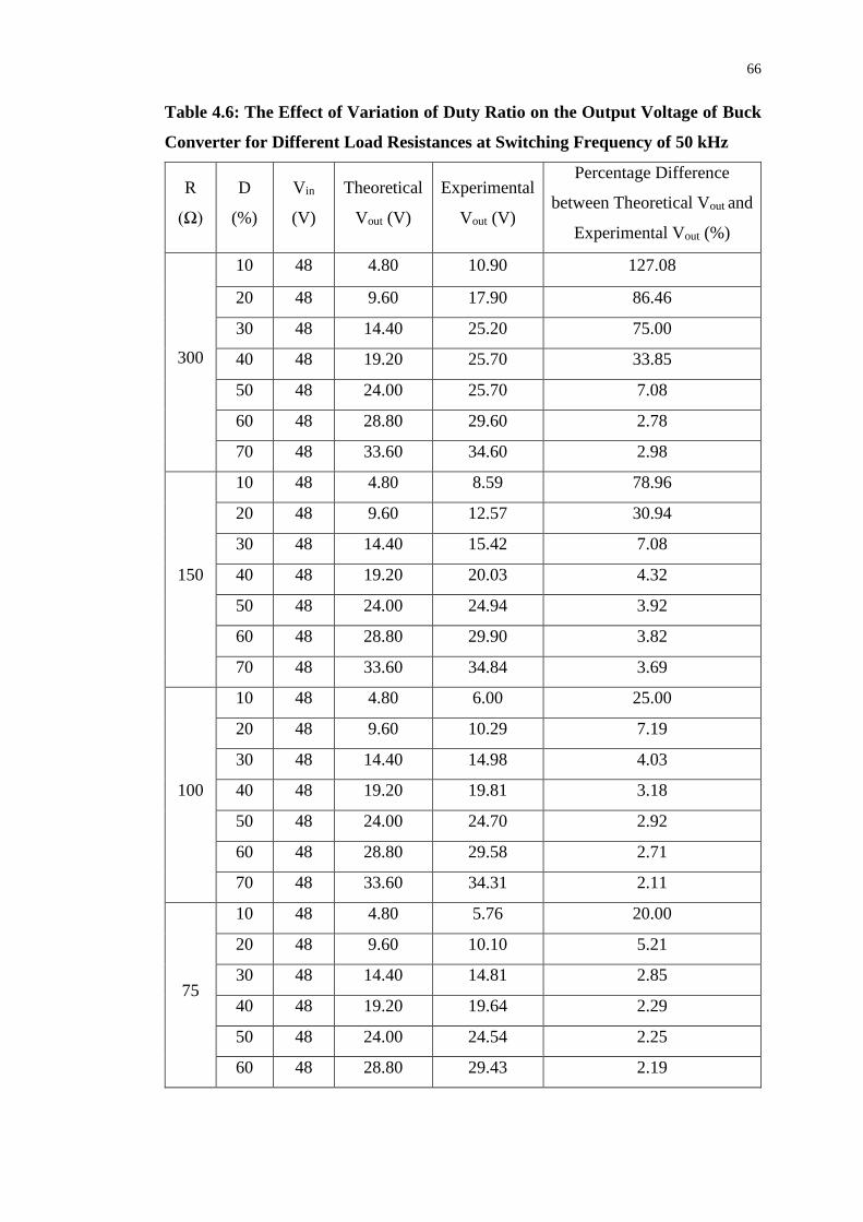
66
Table 4.6: The Effect of Variation of Duty Ratio on the Output Voltage of Buck
Converter for Different Load Resistances at Switching Frequency of 50 kHz
R
(Ω)
D
(%)
Vin
(V)
Theoretical
Vout (V)
Experimental
Vout (V)
Percentage Difference
between Theoretical Vout and
Experimental Vout (%)
300
10 48 4.80 10.90 127.08
20 48 9.60 17.90 86.46
30 48 14.40 25.20 75.00
40 48 19.20 25.70 33.85
50 48 24.00 25.70 7.08
60 48 28.80 29.60 2.78
70 48 33.60 34.60 2.98
150
10 48 4.80 8.59 78.96
20 48 9.60 12.57 30.94
30 48 14.40 15.42 7.08
40 48 19.20 20.03 4.32
50 48 24.00 24.94 3.92
60 48 28.80 29.90 3.82
70 48 33.60 34.84 3.69
100
10 48 4.80 6.00 25.00
20 48 9.60 10.29 7.19
30 48 14.40 14.98 4.03
40 48 19.20 19.81 3.18
50 48 24.00 24.70 2.92
60 48 28.80 29.58 2.71
70 48 33.60 34.31 2.11
75
10 48 4.80 5.76 20.00
20 48 9.60 10.10 5.21
30 48 14.40 14.81 2.85
40 48 19.20 19.64 2.29
50 48 24.00 24.54 2.25
60 48 28.80 29.43 2.19

67
70 48 33.60 34.10 1.49
60
10 48 4.80 5.60 16.67
20 48 9.60 9.99 4.06
30 48 14.40 14.71 2.15
40 48 19.20 19.56 1.87
50 48 24.00 24.42 1.75
60 48 28.80 29.26 1.60
70 48 33.60 34.10 1.49
Based on Figure 4.5, it can be observed that the experimental output voltage of
the buck converter is close to its theoretical output voltage for different load resistances,
except for load resistance of 300 Ω and 150 Ω as the parameters of the buck converter
are not optimized for load resistance of 300 Ω and 150 Ω. The buck converter is more
optimized for lower load resistance as load resistance of 50 Ω is chosen as the load
resistance of the buck converter in the preliminary design. When the duty ratio of the
buck converter is increased, the experimental output voltage is also increased and this
is in correspond with its theoretical output voltage. Figure 4.6 shows that load
resistance of 300 Ω and 150 Ω have higher percentage difference between theoretical
output voltage and experimental output voltage at low duty ratio and the percentage
difference decreases significantly when the duty ratio is increased.
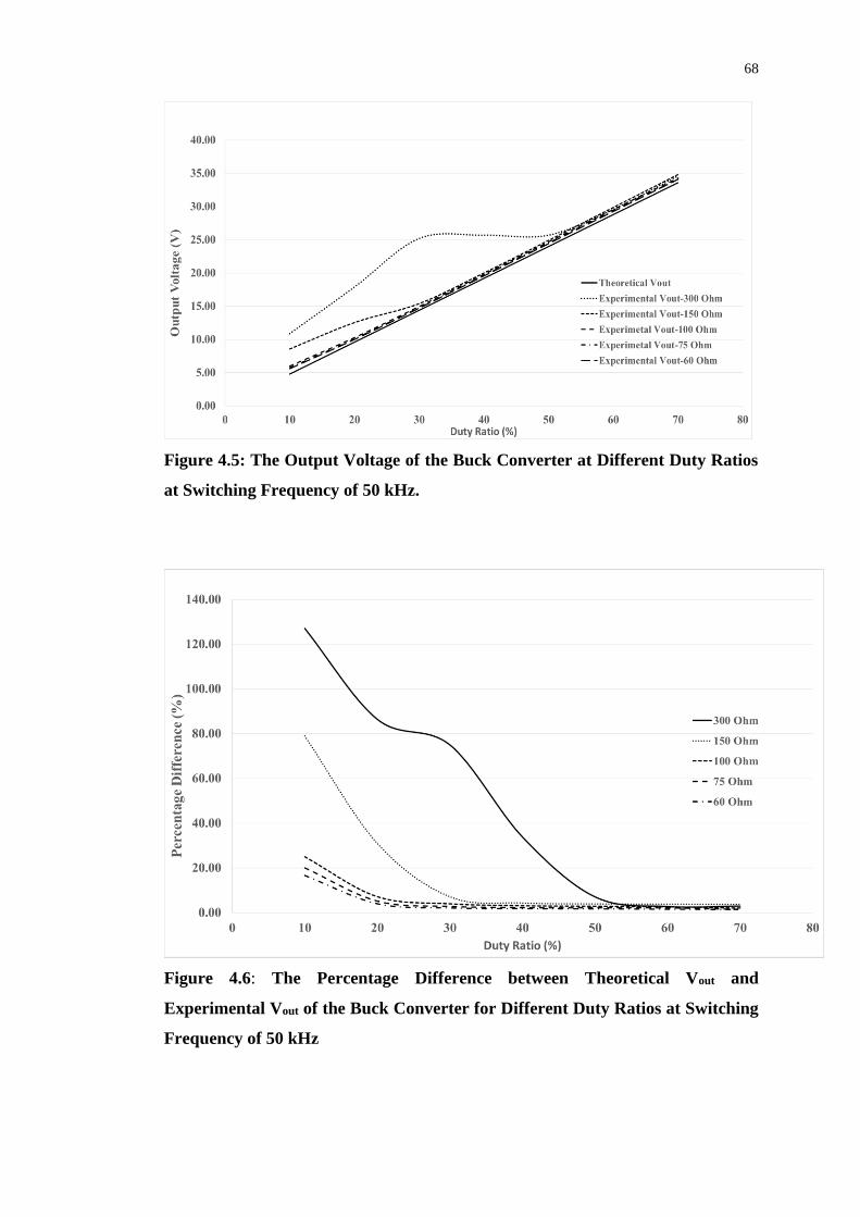
68
Figure 4.5: The Output Voltage of the Buck Converter at Different Duty Ratios
at Switching Frequency of 50 kHz.
Figure 4.6: The Percentage Difference between Theoretical Vout and
Experimental Vout of the Buck Converter for Different Duty Ratios at Switching
Frequency of 50 kHz
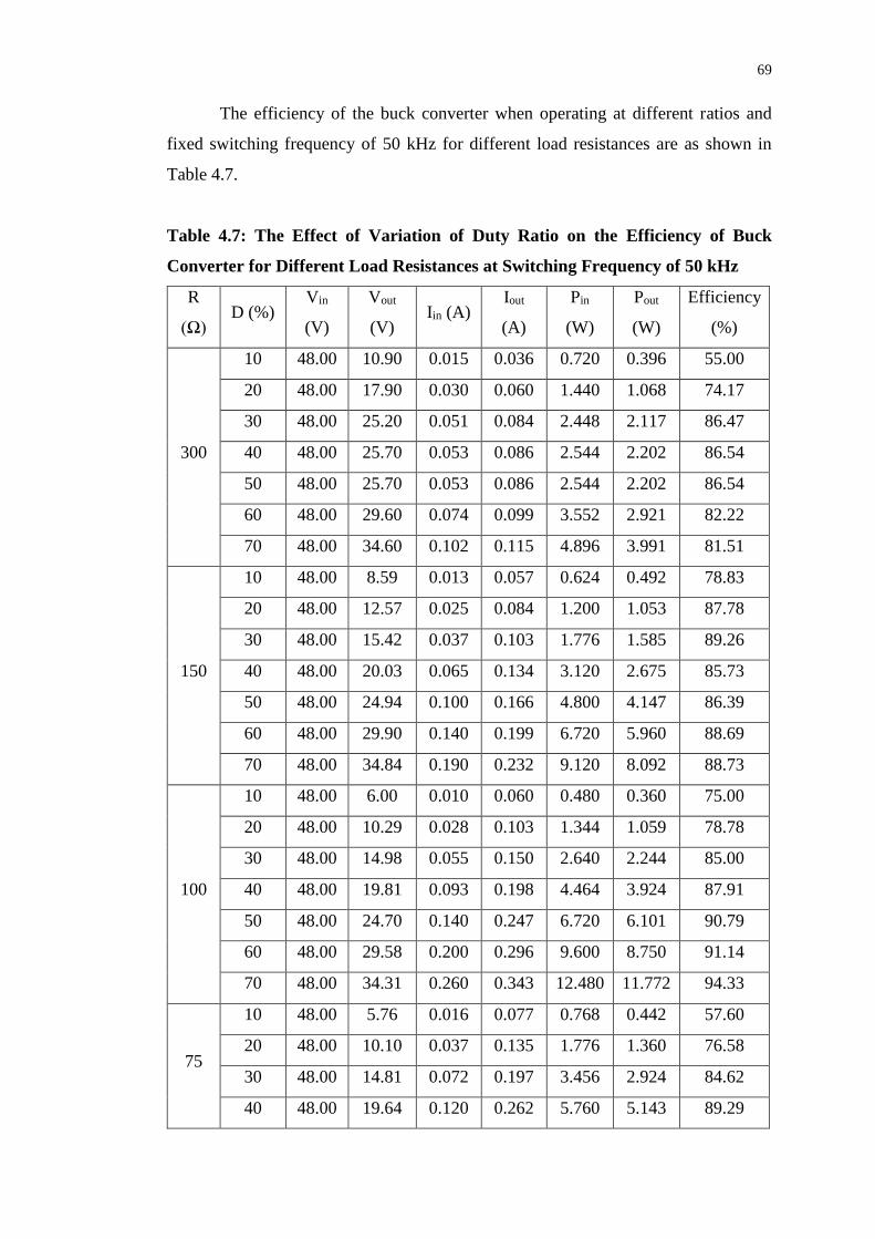
69
The efficiency of the buck converter when operating at different ratios and
fixed switching frequency of 50 kHz for different load resistances are as shown in
Table 4.7.
Table 4.7: The Effect of Variation of Duty Ratio on the Efficiency of Buck
Converter for Different Load Resistances at Switching Frequency of 50 kHz
R
(Ω) D (%)
Vin
(V)
Vout
(V) Iin (A)
Iout
(A)
Pin
(W)
Pout
(W)
Efficiency
(%)
300
10 48.00 10.90 0.015 0.036 0.720 0.396 55.00
20 48.00 17.90 0.030 0.060 1.440 1.068 74.17
30 48.00 25.20 0.051 0.084 2.448 2.117 86.47
40 48.00 25.70 0.053 0.086 2.544 2.202 86.54
50 48.00 25.70 0.053 0.086 2.544 2.202 86.54
60 48.00 29.60 0.074 0.099 3.552 2.921 82.22
70 48.00 34.60 0.102 0.115 4.896 3.991 81.51
150
10 48.00 8.59 0.013 0.057 0.624 0.492 78.83
20 48.00 12.57 0.025 0.084 1.200 1.053 87.78
30 48.00 15.42 0.037 0.103 1.776 1.585 89.26
40 48.00 20.03 0.065 0.134 3.120 2.675 85.73
50 48.00 24.94 0.100 0.166 4.800 4.147 86.39
60 48.00 29.90 0.140 0.199 6.720 5.960 88.69
70 48.00 34.84 0.190 0.232 9.120 8.092 88.73
100
10 48.00 6.00 0.010 0.060 0.480 0.360 75.00
20 48.00 10.29 0.028 0.103 1.344 1.059 78.78
30 48.00 14.98 0.055 0.150 2.640 2.244 85.00
40 48.00 19.81 0.093 0.198 4.464 3.924 87.91
50 48.00 24.70 0.140 0.247 6.720 6.101 90.79
60 48.00 29.58 0.200 0.296 9.600 8.750 91.14
70 48.00 34.31 0.260 0.343 12.480 11.772 94.33
75
10 48.00 5.76 0.016 0.077 0.768 0.442 57.60
20 48.00 10.10 0.037 0.135 1.776 1.360 76.58
30 48.00 14.81 0.072 0.197 3.456 2.924 84.62
40 48.00 19.64 0.120 0.262 5.760 5.143 89.29
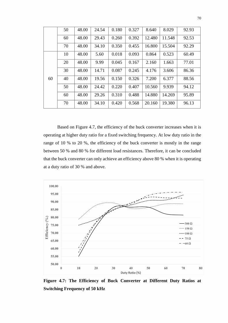
70
50 48.00 24.54 0.180 0.327 8.640 8.029 92.93
60 48.00 29.43 0.260 0.392 12.480 11.548 92.53
70 48.00 34.10 0.350 0.455 16.800 15.504 92.29
60
10 48.00 5.60 0.018 0.093 0.864 0.523 60.49
20 48.00 9.99 0.045 0.167 2.160 1.663 77.01
30 48.00 14.71 0.087 0.245 4.176 3.606 86.36
40 48.00 19.56 0.150 0.326 7.200 6.377 88.56
50 48.00 24.42 0.220 0.407 10.560 9.939 94.12
60 48.00 29.26 0.310 0.488 14.880 14.269 95.89
70 48.00 34.10 0.420 0.568 20.160 19.380 96.13
Based on Figure 4.7, the efficiency of the buck converter increases when it is
operating at higher duty ratio for a fixed switching frequency. At low duty ratio in the
range of 10 % to 20 %, the efficiency of the buck converter is mostly in the range
between 50 % and 80 % for different load resistances. Therefore, it can be concluded
that the buck converter can only achieve an efficiency above 80 % when it is operating
at a duty ratio of 30 % and above.
Figure 4.7: The Efficiency of Buck Converter at Different Duty Ratios at
Switching Frequency of 50 kHz
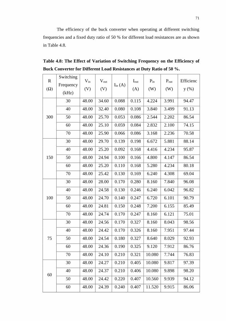
71
The efficiency of the buck converter when operating at different switching
frequencies and a fixed duty ratio of 50 % for different load resistances are as shown
in Table 4.8.
Table 4.8: The Effect of Variation of Switching Frequency on the Efficiency of
Buck Converter for Different Load Resistances at Duty Ratio of 50 %.
R
(Ω)
Switching
Frequency
(kHz)
Vin
(V)
Vout
(V) Iin (A)
Iout
(A)
Pin
(W)
Pout
(W)
Efficienc
y (%)
300
30 48.00 34.60 0.088 0.115 4.224 3.991 94.47
40 48.00 32.40 0.080 0.108 3.840 3.499 91.13
50 48.00 25.70 0.053 0.086 2.544 2.202 86.54
60 48.00 25.10 0.059 0.084 2.832 2.100 74.15
70 48.00 25.90 0.066 0.086 3.168 2.236 70.58
150
30 48.00 29.70 0.139 0.198 6.672 5.881 88.14
40 48.00 25.20 0.092 0.168 4.416 4.234 95.87
50 48.00 24.94 0.100 0.166 4.800 4.147 86.54
60 48.00 25.20 0.110 0.168 5.280 4.234 80.18
70 48.00 25.42 0.130 0.169 6.240 4.308 69.04
100
30 48.00 28.00 0.170 0.280 8.160 7.840 96.08
40 48.00 24.58 0.130 0.246 6.240 6.042 96.82
50 48.00 24.70 0.140 0.247 6.720 6.101 90.79
60 48.00 24.81 0.150 0.248 7.200 6.155 85.49
70 48.00 24.74 0.170 0.247 8.160 6.121 75.01
75
30 48.00 24.56 0.170 0.327 8.160 8.043 98.56
40 48.00 24.42 0.170 0.326 8.160 7.951 97.44
50 48.00 24.54 0.180 0.327 8.640 8.029 92.93
60 48.00 24.36 0.190 0.325 9.120 7.912 86.76
70 48.00 24.10 0.210 0.321 10.080 7.744 76.83
60
30 48.00 24.27 0.210 0.405 10.080 9.817 97.39
40 48.00 24.37 0.210 0.406 10.080 9.898 98.20
50 48.00 24.42 0.220 0.407 10.560 9.939 94.12
60 48.00 24.39 0.240 0.407 11.520 9.915 86.06
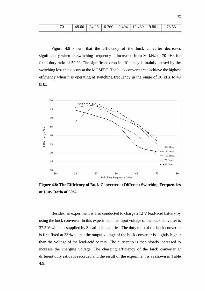
72
70 48.00 24.25 0.260 0.404 12.480 9.801 78.53
Figure 4.8 shows that the efficiency of the buck converter decreases
significantly when its switching frequency is increased from 30 kHz to 70 kHz for
fixed duty ratio of 50 %. The significant drop in efficiency is mainly caused by the
switching loss that occurs at the MOSFET. The buck converter can achieve the highest
efficiency when it is operating at switching frequency in the range of 30 kHz to 40
kHz.
Figure 4.8: The Efficiency of Buck Converter at Different Switching Frequencies
at Duty Ratio of 50%
Besides, an experiment is also conducted to charge a 12 V lead-acid battery by
using the buck converter. In this experiment, the input voltage of the buck converter is
37.5 V which is supplied by 3 lead-acid batteries. The duty ratio of the buck converter
is first fixed at 33 % so that the output voltage of the buck converter is slightly higher
than the voltage of the lead-acid battery. The duty ratio is then slowly increased to
increase the charging voltage. The charging efficiency of the buck converter at
different duty ratios is recorded and the result of the experiment is as shown in Table
4.9.
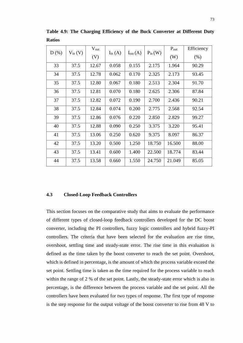
73
Table 4.9: The Charging Efficiency of the Buck Converter at Different Duty
Ratios
D (%) Vin (V) Vout
(V) Iin (A) Iout (A) Pin (W)
Pout
(W)
Efficiency
(%)
33 37.5 12.67 0.058 0.155 2.175 1.964 90.29
34 37.5 12.78 0.062 0.170 2.325 2.173 93.45
35 37.5 12.80 0.067 0.180 2.513 2.304 91.70
36 37.5 12.81 0.070 0.180 2.625 2.306 87.84
37 37.5 12.82 0.072 0.190 2.700 2.436 90.21
38 37.5 12.84 0.074 0.200 2.775 2.568 92.54
39 37.5 12.86 0.076 0.220 2.850 2.829 99.27
40 37.5 12.88 0.090 0.250 3.375 3.220 95.41
41 37.5 13.06 0.250 0.620 9.375 8.097 86.37
42 37.5 13.20 0.500 1.250 18.750 16.500 88.00
43 37.5 13.41 0.600 1.400 22.500 18.774 83.44
44 37.5 13.58 0.660 1.550 24.750 21.049 85.05
4.3 Closed-Loop Feedback Controllers
This section focuses on the comparative study that aims to evaluate the performance
of different types of closed-loop feedback controllers developed for the DC boost
converter, including the PI controllers, fuzzy logic controllers and hybrid fuzzy-PI
controllers. The criteria that have been selected for the evaluation are rise time,
overshoot, settling time and steady-state error. The rise time in this evaluation is
defined as the time taken by the boost converter to reach the set point. Overshoot,
which is defined in percentage, is the amount of which the process variable exceed the
set point. Settling time is taken as the time required for the process variable to reach
within the range of 2 % of the set point. Lastly, the steady-state error which is also in
percentage, is the difference between the process variable and the set point. All the
controllers have been evaluated for two types of response. The first type of response
is the step response for the output voltage of the boost converter to rise from 48 V to
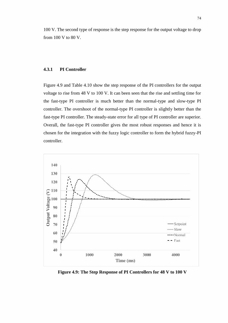
74
100 V. The second type of response is the step response for the output voltage to drop
from 100 V to 80 V.
4.3.1 PI Controller
Figure 4.9 and Table 4.10 show the step response of the PI controllers for the output
voltage to rise from 48 V to 100 V. It can been seen that the rise and settling time for
the fast-type PI controller is much better than the normal-type and slow-type PI
controller. The overshoot of the normal-type PI controller is slightly better than the
fast-type PI controller. The steady-state error for all type of PI controller are superior.
Overall, the fast-type PI controller gives the most robust responses and hence it is
chosen for the integration with the fuzzy logic controller to form the hybrid fuzzy-PI
controller.
Figure 4.9: The Step Response of PI Controllers for 48 V to 100 V
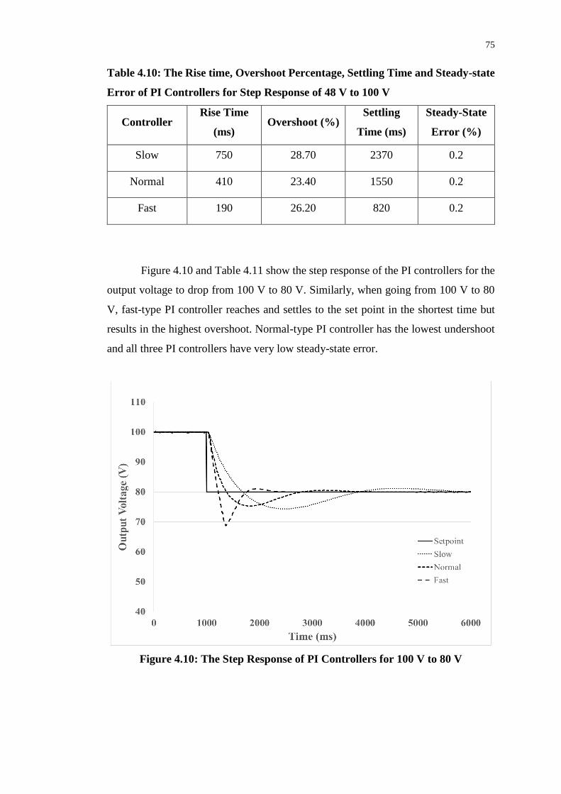
75
Table 4.10: The Rise time, Overshoot Percentage, Settling Time and Steady-state
Error of PI Controllers for Step Response of 48 V to 100 V
Controller Rise Time
(ms) Overshoot (%)
Settling
Time (ms)
Steady-State
Error (%)
Slow 750 28.70 2370 0.2
Normal 410 23.40 1550 0.2
Fast 190 26.20 820 0.2
Figure 4.10 and Table 4.11 show the step response of the PI controllers for the
output voltage to drop from 100 V to 80 V. Similarly, when going from 100 V to 80
V, fast-type PI controller reaches and settles to the set point in the shortest time but
results in the highest overshoot. Normal-type PI controller has the lowest undershoot
and all three PI controllers have very low steady-state error.
Figure 4.10: The Step Response of PI Controllers for 100 V to 80 V

76
Table 4.11: The Rise time, Overshoot Percentage, Settling Time and Steady-state
Error of PI Controllers for Step Response of 100 V to 80 V
Controller Rise Time
(ms)
Undershoot
(%)
Settling
Time (ms)
Steady-State
Error (%)
Slow 680 7.00 2510 0.125
Normal 390 5.88 1450 0.125
Fast 220 14.00 670 0.125
4.3.2 Fuzzy Logic Controller
The performance of the fuzzy logic controllers with different sets of fuzzy rules is
illustrated in Figure 4.11 and Table 4.12. It is found that all three types of fuzzy logic
controller give a faster rise time and lower overshoot as compared to all types of PI
controllers. Type-1 fuzzy logic controller has lower steady-state error while Type-2
and Type-3 fuzzy logic controllers have higher steady-state error as compared to the
PI controllers. Among the three fuzzy controllers, Type-3 fuzzy controller exhibits the
best performance in rise time, overshoot and settling time, but it has relatively higher
steady-state error.
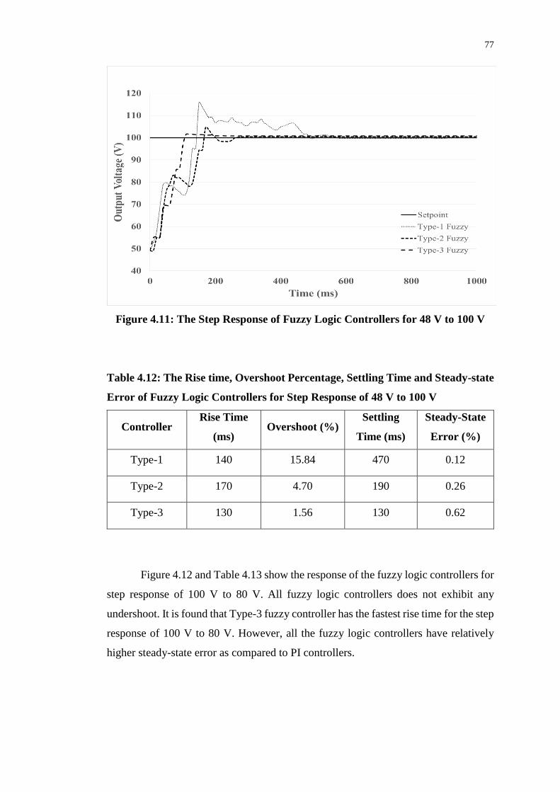
77
Figure 4.11: The Step Response of Fuzzy Logic Controllers for 48 V to 100 V
Table 4.12: The Rise time, Overshoot Percentage, Settling Time and Steady-state
Error of Fuzzy Logic Controllers for Step Response of 48 V to 100 V
Controller Rise Time
(ms) Overshoot (%)
Settling
Time (ms)
Steady-State
Error (%)
Type-1 140 15.84 470 0.12
Type-2 170 4.70 190 0.26
Type-3 130 1.56 130 0.62
Figure 4.12 and Table 4.13 show the response of the fuzzy logic controllers for
step response of 100 V to 80 V. All fuzzy logic controllers does not exhibit any
undershoot. It is found that Type-3 fuzzy controller has the fastest rise time for the step
response of 100 V to 80 V. However, all the fuzzy logic controllers have relatively
higher steady-state error as compared to PI controllers.
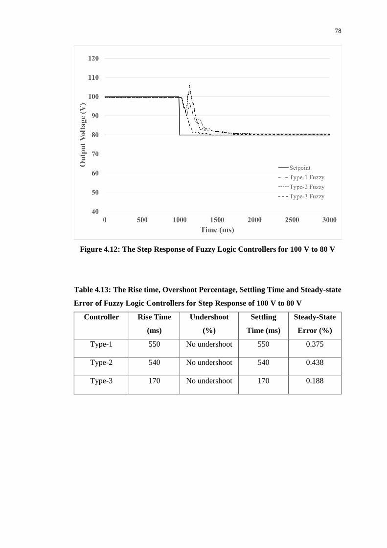
78
Figure 4.12: The Step Response of Fuzzy Logic Controllers for 100 V to 80 V
Table 4.13: The Rise time, Overshoot Percentage, Settling Time and Steady-state
Error of Fuzzy Logic Controllers for Step Response of 100 V to 80 V
Controller Rise Time
(ms)
Undershoot
(%)
Settling
Time (ms)
Steady-State
Error (%)
Type-1 550 No undershoot 550 0.375
Type-2 540 No undershoot 540 0.438
Type-3 170 No undershoot 170 0.188
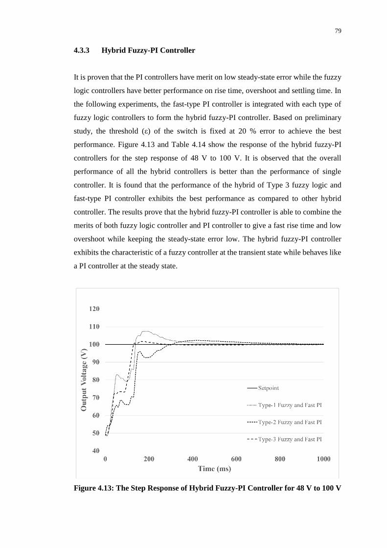
79
4.3.3 Hybrid Fuzzy-PI Controller
It is proven that the PI controllers have merit on low steady-state error while the fuzzy
logic controllers have better performance on rise time, overshoot and settling time. In
the following experiments, the fast-type PI controller is integrated with each type of
fuzzy logic controllers to form the hybrid fuzzy-PI controller. Based on preliminary
study, the threshold (ε) of the switch is fixed at 20 % error to achieve the best
performance. Figure 4.13 and Table 4.14 show the response of the hybrid fuzzy-PI
controllers for the step response of 48 V to 100 V. It is observed that the overall
performance of all the hybrid controllers is better than the performance of single
controller. It is found that the performance of the hybrid of Type 3 fuzzy logic and
fast-type PI controller exhibits the best performance as compared to other hybrid
controller. The results prove that the hybrid fuzzy-PI controller is able to combine the
merits of both fuzzy logic controller and PI controller to give a fast rise time and low
overshoot while keeping the steady-state error low. The hybrid fuzzy-PI controller
exhibits the characteristic of a fuzzy controller at the transient state while behaves like
a PI controller at the steady state.
Figure 4.13: The Step Response of Hybrid Fuzzy-PI Controller for 48 V to 100 V
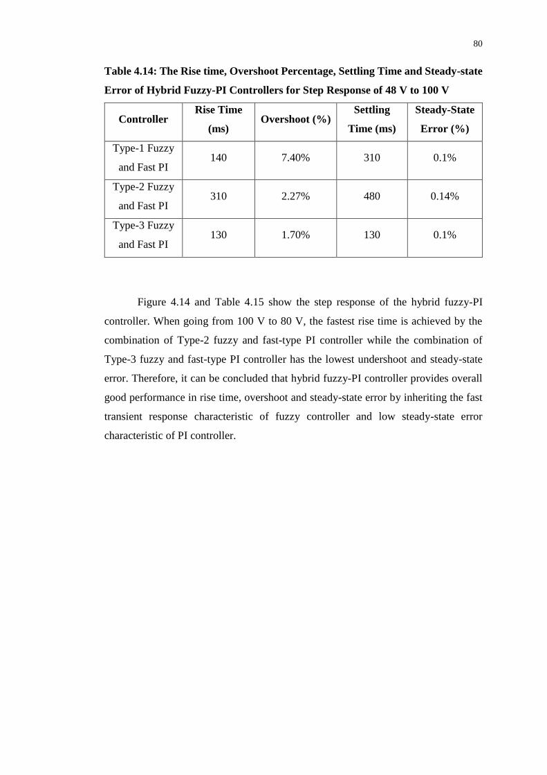
80
Table 4.14: The Rise time, Overshoot Percentage, Settling Time and Steady-state
Error of Hybrid Fuzzy-PI Controllers for Step Response of 48 V to 100 V
Controller Rise Time
(ms) Overshoot (%)
Settling
Time (ms)
Steady-State
Error (%)
Type-1 Fuzzy
and Fast PI 140 7.40% 310 0.1%
Type-2 Fuzzy
and Fast PI 310 2.27% 480 0.14%
Type-3 Fuzzy
and Fast PI 130 1.70% 130 0.1%
Figure 4.14 and Table 4.15 show the step response of the hybrid fuzzy-PI
controller. When going from 100 V to 80 V, the fastest rise time is achieved by the
combination of Type-2 fuzzy and fast-type PI controller while the combination of
Type-3 fuzzy and fast-type PI controller has the lowest undershoot and steady-state
error. Therefore, it can be concluded that hybrid fuzzy-PI controller provides overall
good performance in rise time, overshoot and steady-state error by inheriting the fast
transient response characteristic of fuzzy controller and low steady-state error
characteristic of PI controller.
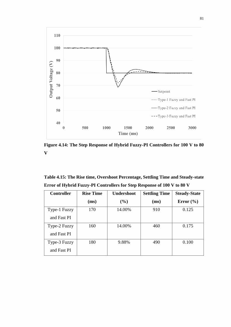
81
Figure 4.14: The Step Response of Hybrid Fuzzy-PI Controllers for 100 V to 80
V
Table 4.15: The Rise time, Overshoot Percentage, Settling Time and Steady-state
Error of Hybrid Fuzzy-PI Controllers for Step Response of 100 V to 80 V
Controller Rise Time
(ms)
Undershoot
(%)
Settling Time
(ms)
Steady-State
Error (%)
Type-1 Fuzzy
and Fast PI
170 14.00% 910 0.125
Type-2 Fuzzy
and Fast PI
160 14.00% 460 0.175
Type-3 Fuzzy
and Fast PI
180 9.88% 490 0.100

82
CHAPTER 5
5 CONCLUSION AND RECOMMENDATIONS
5.1 Conclusion
In this project, a DC-DC boost converter has been successfully developed to step up
the low voltage of the energy storage system which consists of four series-connected
lead-acid batteries to a higher DC voltage. Through multiple experiments, it is proved
that the developed boost converter can achieve an efficiency above 90 % when
operating under certain load conditions, duty ratios and switching frequencies. Besides,
a buck converter is developed in this project to charge the lead-acid battery. The buck
converter is also able to achieve a high efficiency when charging the lead acid battery.
Furthermore, three types of closed-loop feedback controller have been
successfully developed for the boost converter, including the PI controller, fuzzy logic
controller and hybrid fuzzy-PI controller. All the controllers have been optimized to
give the best performance and a comparative study is carried out to evaluate the
performance of each controller. The results of the comparative study prove that the PI
controller performs well at the steady-state and the fuzzy logic controller has good
transient response by giving a faster rise time and lesser overshoot. The hybrid of PI
and fuzzy logic controller combines the merits of both controllers, giving a fast rise
time and lesser overshoot while keeping the steady-state error low.

83
5.2 Recommendations
The present boost converter is only able to discharge a small amount of power from
the energy storage system. It is suggested that the boost converter can be improved in
its design to discharge much more power from the batteries so that there is sufficient
amount of power that can be injected into the grid. The buck converter can also be
improved so that it can charge all the lead-acid batteries at once by using a higher input
DC voltage. Also, closed-loop feedback controller can also be developed for the buck
converter to regulate its output for different operating conditions. The battery
management system (BMS) is another major feature which can be developed for this
project. The BMS provides multiple functions and schemes for the energy storage
system, including monitoring scheme and protection scheme. In the monitoring
scheme, the BMS is able to provide information on the health condition of the energy
storage system, including the state of charge (SOC) and state of health (SOH) of the
batteries. The protection scheme prevents the overcharging and over discharging of
the batteries to prolong the lifetime of the batteries.
84
REFERENCES
Bai, Y., Wang, D., n.d. Fundamentals of Fuzzy Logic Control - Fuzzy Sets, Fuzzy
Rules and Defuzzification, in: Advanced Fuzzy Logic Technologies in
Industrial Applications.
Govindaraj, T., R, R., 2011a. Development of Fuzzy Logic Controller for DC-DC
Buck Converter. Int J Engg Techsci 2, 192–198.
Govindaraj, T., R, R., 2011b. Development of Fuzzy Logic Controller for DC-DC
Buck Converter. Int J Engg Techsci 2, 192–198.
Krommydas, K.F., Alexandridis, A.T., 2014. Design and passivity-based stability
analysis of a PI current-mode controller for dc/dc boost converters, in:
American Control Conference (ACC), 2014. Presented at the American
Control Conference (ACC), 2014, pp. 5067–5072.
doi:10.1109/ACC.2014.6859156
Lawder, M.T., Suthar, B., Northrop, P.W.C., De, S., Hoff, C.M., Leitermann, O., Crow,
M.L., Santhanagopalan, S., Subramanian, V.R., 2014. Battery Energy Storage
System (BESS) and Battery Management System (BMS) for Grid-Scale
Applications. Proc. IEEE 102, 1014–1030. doi:10.1109/JPROC.2014.2317451
Mattavelli, P., Rossetto, L., Spiazzi, G., Tenti, P., 1997. General-purpose fuzzy
controller for DC-DC converters. IEEE Trans. Power Electron. 12, 79–86.
doi:10.1109/63.554172
85
Muhammad H. Rashid, 2004. Power Electronics Circuits, Devices and Applications,
Third Edition. ed. Pearson Prentice Hall.
Ogata, K., 2009. Modern Control Engineering, 5th ed. Prentice Hall.
Olaofe, Z.O., Folly, K.A., 2012. Energy storage technologies for small scale wind
conversion system, in: 2012 IEEE Power Electronics and Machines in Wind
Applications (PEMWA). Presented at the 2012 IEEE Power Electronics and
Machines in Wind Applications (PEMWA), pp. 1–5.
doi:10.1109/PEMWA.2012.6316391
Pratumsuwan, P., Thongcai, S., Tansriwong, S., 2010. A Hybrid of Fuzzy and
Propotional-Integral-Derivative Controller for Electro-Hydraulic Position
Servo System. Energy Res. J. 1, 62–67.
Qian, H., Zhang, J., Lai, J.-S., Yu, W., 2011. A high-efficiency grid-tie battery energy
storage system. IEEE Trans. Power Electron. 26, 886–896.
doi:10.1109/TPEL.2010.2096562
Seshagiri Rao, G., Raghu, S., Rajasekaran, N., 2012. Design of Feedback Controller
for Boost Converter Using Optimization Technique. Int. J. Power Electron.
Drive Syst. 3, 117–128.
So, W.C., Tse, C.K., Lee, Y.S., 1994. A fuzzy controller for DC-DC converters, in: ,
25th Annual IEEE Power Electronics Specialists Conference, PESC ’94
Record. Presented at the , 25th Annual IEEE Power Electronics Specialists
Conference, PESC ’94 Record, pp. 315–320 vol.1.
doi:10.1109/PESC.1994.349715
Tiwary, N., Rathinam, A., Ajitha, S., 2014. Design of Hybrid Fuzzy-PI controller for
speed control of Brushless DC motor, in: 2014 International Conference on
Electronics, Communication and Instrumentation (ICECI). Presented at the
2014 International Conference on Electronics, Communication and
Instrumentation (ICECI), pp. 1–4. doi:10.1109/ICECI.2014.6767360

86
Trowler, D., Whitaker, B., 2008. Bi-Directional Inverter and Energy Storage.
University of Arkansas.
Yekini Suberu, M., Wazir Mustafa, M., Bashir, N., 2014. Energy storage systems for
renewable energy power sector integration and mitigation of intermittency.
Renew. Sustain. Energy Rev. 35, 499–514. doi:10.1016/j.rser.2014.04.009
Related Documents