Developing of Low-resistance Ohmic Contact on GaN HEMTs for High Operating Frequency Applications Introduction: GaN high-electron-mobility transistors (HEMTs) technology currently offers exceptional device properties for next-generation high power and high frequency applications [1]. This is attributed to their high breakdown voltage and current capabilities. However, the formation of low source/drain contact resistance is required to lower the access resistance and thus enhance DC and RF performance [2]. Research Goal: Material and Devices: Analysis & Results: Conclusion & Future Work: • Development of low ohmic contact resistance with good surface morphology was realized on AlGaN/GaN on LR Si substrate. • Recessed ohmic contacts with lower annealing temperatures could be adopted for better contact resistance R c . Abdulaziz BinKhudhayr 2176393, e-mail:[email protected] University of Glasgow, charity number SC004401 Supervisor Name: Dr.Khaled Elgaid Figure 2: Schematic diagram of AlGaN/GaN HEMT grown on Si. Figure 4: Contact resistance for non-recessed & recessed metal stacks. Figure 4: SEM images of (a) Ti/Al/Mo/Au and (b) Ti/Al/Ni/Au. Figure 1:Energy Bandgap diagram. Fabrication Process Material Growth Two metal schemes with different interlayer metals were utilized for this project: Table 2:Summary of the development process. Table 1:Summary of the fabrication process. Y_Sample A = 4.4354x + 8.4481 Y_Sample B= 4.0199x + 9.7737 Y_Sample C = 4.5482x + 22.694 0 50 100 150 200 0 5 10 15 20 25 30 35 R T , Ω Gap spacing, µm Sample A Sample B Sample C Transfer length method (TLM) was used to characterize ohmic contacts. Figure 3: Optical microscope image of TLM test structure 150 × 150 µm pads with the spacing 2.5, 5, 10, 15, 20, 25, 30, and 35 µm. Scanned Electron Microscopy (SEM) of two metal stacks surfaces: Since non-recessed Ti/ Al/Mo/Au metal scheme resulted in the best ohmic contacts, Gate wrap-around d-mode devices were fabricated. Figure 5: devices characteristic. References: [1] Kolaklieva, L. and Kakanakov, R. (2009). Ohmic Contacts for High Power and High Temperature Microelectronics. Micro Electronic and Mechanical Systems [Accessed 5 Mar. 2015]. [2] U. K. Mishra, L. Shen, T. E. Kazior, and Y.-F. Wu. “GaN-based RF power devices and amplifiers,” Proc. IEEE, vol. 96, no. 2, pp. 287–305, Feb. 2008.

Welcome message from author
This document is posted to help you gain knowledge. Please leave a comment to let me know what you think about it! Share it to your friends and learn new things together.
Transcript
Developing of Low-resistance Ohmic Contact on GaN HEMTs for High Operating Frequency Applications
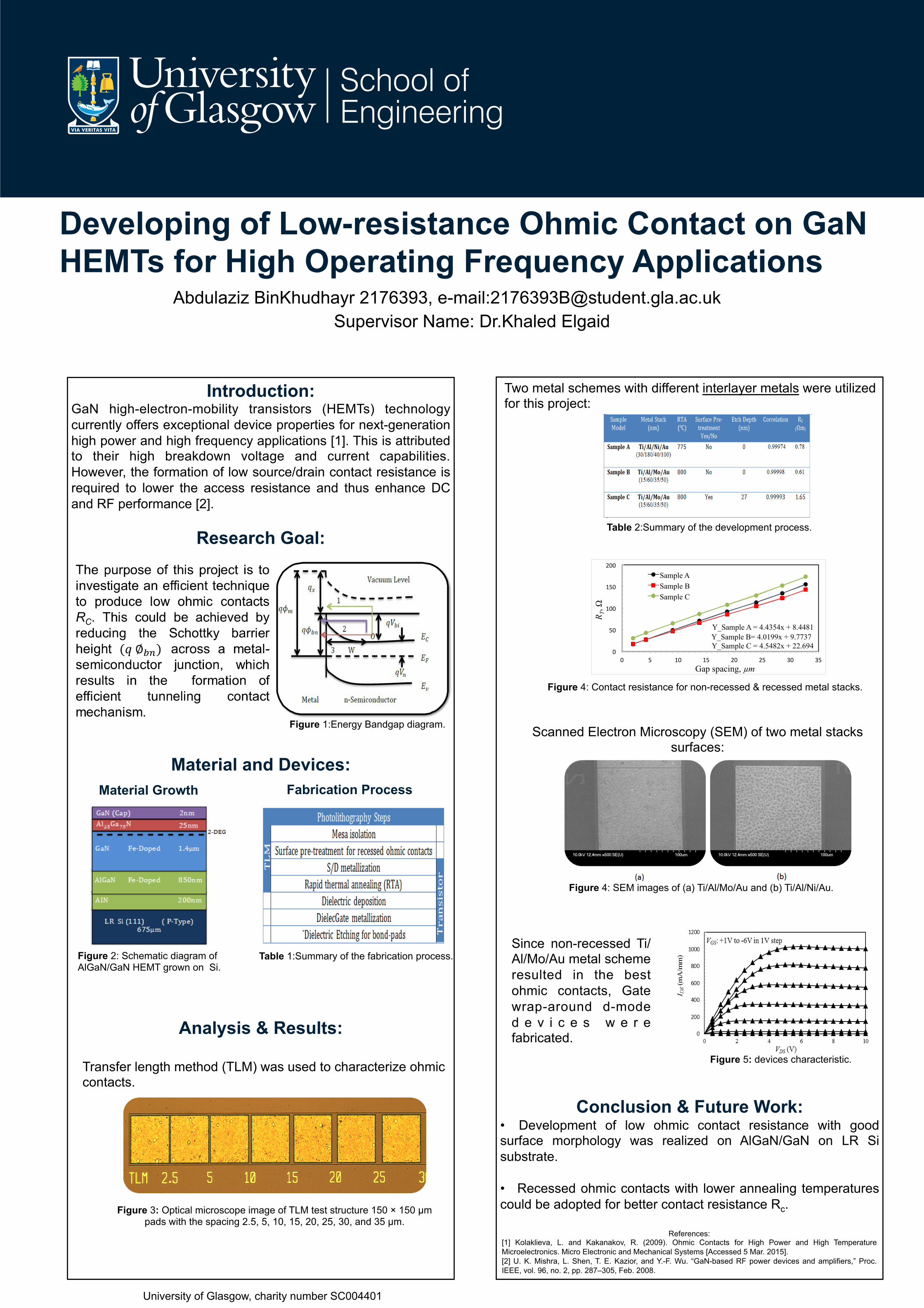
Introduction: GaN high-electron-mobility transistors (HEMTs) technology currently offers exceptional device properties for next-generation high power and high frequency applications [1]. This is attributed to their high breakdown voltage and current capabilities. However, the formation of low source/drain contact resistance is required to lower the access resistance and thus enhance DC and RF performance [2].
Research Goal:
Material and Devices:
Analysis & Results:
Conclusion & Future Work: • Development of low ohmic contact resistance with good surface morphology was realized on AlGaN/GaN on LR Si substrate. • Recessed ohmic contacts with lower annealing temperatures could be adopted for better contact resistance Rc.
Abdulaziz BinKhudhayr 2176393, e-mail:[email protected]
University of Glasgow, charity number SC004401
Supervisor Name: Dr.Khaled Elgaid
Figure 2: Schematic diagram of AlGaN/GaN HEMT grown on Si.
Figure 4: Contact resistance for non-recessed & recessed metal stacks.
Figure 4: SEM images of (a) Ti/Al/Mo/Au and (b) Ti/Al/Ni/Au.
Figure 1:Energy Bandgap diagram.
Fabrication Process Material Growth
Two metal schemes with different interlayer metals were utilized for this project:
Table 2:Summary of the development process.
Table 1:Summary of the fabrication process.
Y_Sample A = 4.4354x + 8.4481 Y_Sample B= 4.0199x + 9.7737 Y_Sample C = 4.5482x + 22.694
0
50
100
150
200
0 5 10 15 20 25 30 35
R T, Ω
Gap spacing, µm
Sample A Sample B Sample C
Transfer length method (TLM) was used to characterize ohmic contacts.
Figure 3: Optical microscope image of TLM test structure 150 × 150 µm pads with the spacing 2.5, 5, 10, 15, 20, 25, 30, and 35 µm.
Scanned Electron Microscopy (SEM) of two metal stacks surfaces:
Since non-recessed Ti/Al/Mo/Au metal scheme resulted in the best ohmic contacts, Gate wrap-around d-mode d e v i c e s w e r e fabricated.
Figure 5: devices characteristic.
References: [1] Kolaklieva, L. and Kakanakov, R. (2009). Ohmic Contacts for High Power and High Temperature Microelectronics. Micro Electronic and Mechanical Systems [Accessed 5 Mar. 2015]. [2] U. K. Mishra, L. Shen, T. E. Kazior, and Y.-F. Wu. “GaN-based RF power devices and amplifiers,” Proc. IEEE, vol. 96, no. 2, pp. 287–305, Feb. 2008.
Related Documents