Development of a multichannel integrated circuit for Silicon Photo-Multiplier arrays readout Albert Comerma i Montells ADVERTIMENT. La consulta d’aquesta tesi queda condicionada a l’acceptació de les següents condicions d'ús: La difusió d’aquesta tesi per mitjà del servei TDX (www.tdx.cat) i a través del Dipòsit Digital de la UB (diposit.ub.edu) ha estat autoritzada pels titulars dels drets de propietat intel·lectual únicament per a usos privats emmarcats en activitats d’investigació i docència. No s’autoritza la seva reproducció amb finalitats de lucre ni la seva difusió i posada a disposició des d’un lloc aliè al servei TDX ni al Dipòsit Digital de la UB. No s’autoritza la presentació del seu contingut en una finestra o marc aliè a TDX o al Dipòsit Digital de la UB (framing). Aquesta reserva de drets afecta tant al resum de presentació de la tesi com als seus continguts. En la utilització o cita de parts de la tesi és obligat indicar el nom de la persona autora. ADVERTENCIA. La consulta de esta tesis queda condicionada a la aceptación de las siguientes condiciones de uso: La difusión de esta tesis por medio del servicio TDR (www.tdx.cat) y a través del Repositorio Digital de la UB (diposit.ub.edu) ha sido autorizada por los titulares de los derechos de propiedad intelectual únicamente para usos privados enmarcados en actividades de investigación y docencia. No se autoriza su reproducción con finalidades de lucro ni su difusión y puesta a disposición desde un sitio ajeno al servicio TDR o al Repositorio Digital de la UB. No se autoriza la presentación de su contenido en una ventana o marco ajeno a TDR o al Repositorio Digital de la UB (framing). Esta reserva de derechos afecta tanto al resumen de presentación de la tesis como a sus contenidos. En la utilización o cita de partes de la tesis es obligado indicar el nombre de la persona autora. WARNING. On having consulted this thesis you’re accepting the following use conditions: Spreading this thesis by the TDX (www.tdx.cat) service and by the UB Digital Repository (diposit.ub.edu) has been authorized by the titular of the intellectual property rights only for private uses placed in investigation and teaching activities. Reproduction with lucrative aims is not authorized nor its spreading and availability from a site foreign to the TDX service or to the UB Digital Repository. Introducing its content in a window or frame foreign to the TDX service or to the UB Digital Repository is not authorized (framing). Those rights affect to the presentation summary of the thesis as well as to its contents. In the using or citation of parts of the thesis it’s obliged to indicate the name of the author.

Welcome message from author
This document is posted to help you gain knowledge. Please leave a comment to let me know what you think about it! Share it to your friends and learn new things together.
Transcript

Development of a multichannel integrated circuit for Silicon Photo-Multiplier arrays readout
Albert Comerma i Montells
ADVERTIMENT. La consulta d’aquesta tesi queda condicionada a l’acceptació de les següents condicions d'ús: La difusió d’aquesta tesi per mitjà del servei TDX (www.tdx.cat) i a través del Dipòsit Digital de la UB (diposit.ub.edu) ha estat autoritzada pels titulars dels drets de propietat intel·lectual únicament per a usos privats emmarcats en activitats d’investigació i docència. No s’autoritza la seva reproducció amb finalitats de lucre ni la seva difusió i posada a disposició des d’un lloc aliè al servei TDX ni al Dipòsit Digital de la UB. No s’autoritza la presentació del seu contingut en una finestrao marc aliè a TDX o al Dipòsit Digital de la UB (framing). Aquesta reserva de drets afecta tant al resum de presentació de la tesi com als seus continguts. En la utilització o cita de parts de la tesi és obligat indicar el nom de la persona autora.
ADVERTENCIA. La consulta de esta tesis queda condicionada a la aceptación de las siguientes condiciones de uso: La difusión de esta tesis por medio del servicio TDR (www.tdx.cat) y a través del Repositorio Digital de la UB (diposit.ub.edu) ha sido autorizada por los titulares de los derechos de propiedad intelectual únicamente para usos privados enmarcados en actividades de investigación y docencia. No se autoriza su reproducción con finalidades de lucro ni su difusión y puesta a disposición desde un sitio ajeno al servicio TDR o al Repositorio Digital de la UB. No se autoriza la presentación de su contenido en una ventana o marco ajeno a TDR o al Repositorio Digital de la UB (framing). Esta reserva de derechos afecta tanto al resumen de presentación de la tesis como a sus contenidos. En la utilización o cita de partes de la tesis es obligado indicar el nombre de la persona autora.
WARNING. On having consulted this thesis you’re accepting the following use conditions: Spreading this thesis by the TDX (www.tdx.cat) service and by the UB Digital Repository (diposit.ub.edu) has been authorized by the titular of the intellectual property rights only for private uses placed in investigation and teaching activities. Reproduction with lucrativeaims is not authorized nor its spreading and availability from a site foreign to the TDX service or to the UB Digital Repository. Introducing its content in a window or frame foreign to the TDX service or to the UB Digital Repository is not authorized (framing). Those rights affect to the presentation summary of the thesis as well as to its contents. In the using orcitation of parts of the thesis it’s obliged to indicate the name of the author.

Development of a multichannel
integrated circuit for Silicon
Photo-Multiplier arrays readout
Albert Comerma i Montells
AlbertComerma
Developmentofamultic
hannelIC
forSiP
Marraysreadout

UNIVERSITAT DE BARCELONA
INSITUT DE CIENCIES DEL COSMOS
DEPARTAMENT D’ELECTRONICA
PROGRAMA DE DOCTORAT EN ENGINYERIA I TECNOLOGIESAVANCADES
Development of a multichannel
integrated circuit for Silicon
Photo-Multiplier arrays readout
Albert Comerma i Montells
DIRECTOR
Dr. David Gascon i Fora
TUTOR
Dr. Atila Herms i Berenguer


Memoria presentada per Albert Comerma i Montellsper optar al grau de Doctor
Barcelona, 2013

Agraıments
Abans d’agrair res a ningu em voldria disculpar per a totes les personesque m’han ajudat a arribar fins aquı i que no mencionare en els agraıments.Per comencar tots els estudiants de doctorat i postdocs que he tingut lasort de coneixer durant tots aquests anys al departament i que seria llargd’enumerar i molt probablement impossible de no deixar-me algu.
Moltes gracies en primer lloc a en David Gascon, per ser el meu director,pero sobretot per la seva feina en el disseny de molts dels circuits descritsen aquesta tesi i la seva visio i experiencia per entendre com funcionen (operque no funcionen) d’una sola ullada. Sense ell hagues estat impossiblerealitzar aquesta feina (almenys en el temps que s’ha fet).
Gracies tambe a en Lluıs Freixas per totes les hores de disseny i layoutdedicades a molts blocs comentats en aquesta tesi. Sobretot per les nitssense dormir just abans d’enviar a fabricar alguns dels prototips. Sense laseva feina segur que tampoc haguessim arribat a bon port tant rapidament.
Muchısimas gracias a Jose Manuel-Perez y Jesus Marın del CIEMATpor tener una idea tan clara de como funciona un sistema PET y comodeberıa ser la electronica de lectura, y a Juan Jose Vaquero de la UC3Mpor comentar los problemas que se han encontrado y como mejorar lossistemas actuales. Muchas gracias tambien a todo el equipo del CIEMAT yen especial a Pedro Rato e Icıar Sarasola por la validacion de la electronicaen un sistema PET.
Thanks to EPFL people for their collaboration in the SciFi tracker de-sign, specially to Fred Blanch for all the meetings and Guido Haefeli forthe SiPM knowledge and testing.
Thanks also to Herve Chanal from Clermont Ferrand for all the brain-storming around PACIFIC ASIC.
Merci beaucoup Laurent Royer pour l’integration du design PACIFICr1dans TROPIC ASIC.
Moltes gracies a en Ricardo Graciani per la seva ajuda a entendre queha de sortir de la mesura d’una font radioactiva i com ha de ser l’espectreresultant d’un cristall. Tambe per proporcionar les fonts del laboratori dedocencia per a realitzar les mesures. I a en Lluıs Garrido i l’Eugeni Graugesper confiar en mi per aquesta tasca i crear i mantenir el grup durant tantde temps.

Tambe haig de donar les gracies a en Juan Trenado, pels seus processatsi grafics en python, per comentar els seus extensos coneixements sobre elcomportament de semiconductors amb mi i totes les hores de testbeam pas-sades (encara que no incloses en aquesta tesi). Moltes gracies als companysde despatx; Adria Casajus (per als vale por un Adri), Andreu Sanuy (elrei del layout) i l’Edu Picatoste sempre disposat a donar un cop de ma enqualsevol bloc.
Moltıssimes gracies als meus pares que em van fer tal com soc i semprem’han ajudat i donat suport per a dedicar-me a el que mes m’agrades.Inculcar-me la curiositat pel que ens envolta i arribar a entendre com fun-cionen les coses ha fet que hagi arribat fins aquı. Moltes gracies als meusgermans tambe, Dani i Nuria, dels quals he apres moltes mes coses de lesque es poden imaginar.
Moltes gracies a en Joan i la Merce, tu si que vales. I moltıssimes graciesa la Pat per estar al meu costat, fins i tot mentre intento escriure aquesteslınies i la resta de la tesi tancats a casa. Moltes gracies per compartir lamuntanya amb mi. Endavant!

La feina descrita en aquesta tesi ha estat realitzada entre els centres:
Universitat de Barcelona Institut de Ciencies del cosmos
Centro de Investigaciones EnergeticasMedioambientales y Tecnologicas (CIEMAT)
Amb la col.laboracio de:
CERN LHCbI financada parcialment pels projectes del Ministerio de Ciencia e Innovacion:
FPA2008-06271-c02-01PTA2009-2077-P


Abstract
The aim of this thesis is to present a solution for the readout of Sil-icon Photo-Multipliers (SiPMs) arrays improving currently implementedsystems. Using as a starting point previous designs with similar objectivesa novel current mode input stage has been designed and tested. To startwith the design a valid model has been used to generate realistic outputfrom the SiPMs depending on light input. Design has been performed infirst place focusing in general applications for medical imaging PositronEmission Tomography (PET) and then using the same topology for a moreconstrained design in particle detectors (upgrade of Tracker detector atLHCb experiment).
A 16 channel ASIC for PET applications including the novel input stagehas demonstrated an excellent timing measurement with good energy res-olution measurement and pile-up detection. This document starts with theanalysis of the requirements needed to fit such a system. Followed by a de-tailed description of the input stage and analog processing. Signal is dividedin the input stage into three different signal paths: timing, energy and pile-up. Every channel performs different signal analysis to deliver; a fast timesignal output (digital edge), energy output (a linear time over thresholddigital output) and a digital bit to signal pile-up. The time information isthen ORed between all channels to generate a single timing output. All thepile-up bits are combined in a digital word ready to be readout for the 16channels. Design has been optimized for reduced power consumption andno components needed to interface inputs and outputs. Digital slow controlto tune the circuit behaviour is also included. The prototype measurementshave proved to be a valid option for integration in a full system scanner.
An adapted prototype of the input stage using different technology andadapted to the different constraints from a particle detector is also pre-sented. Only simulation results are available since device is still underproduction. An analysis of the different requirements needed by the SciFitracker design is summarized. Current specifications are still evolving sincefinal sensor is still not defined, but other requirements and some tunableelements permits to design such prototypes.

Contents
ABSTRACT
RESUM v
SUMMARY xxxix
PATENT NOTICE lxxv
1 INTRODUCTION 11.1 Detector Systems Overview 41.2 Light sensors 6
1.2.1 Photo-Multiplier Tube, PMT 61.2.2 Avalanche Photo-Diode, APD 9
1.2.2.1 Hybrid devices 111.2.3 Silicon photo-multipliers, SiPM 12
1.2.3.1 Dynamic range 141.2.3.2 Gain Variation with Temperature 151.2.3.3 Gain Uniformity 161.2.3.4 Typical Signal 171.2.3.5 After Pulsing 181.2.3.6 Dark Count 181.2.3.7 Crosstalk 19
1.2.4 Arrays construction 191.3 Scintillators 22
1.3.1 Phoswich 241.4 SiPMs Applications 26
1.4.1 Medical Imaging 261.4.1.1 Positron Emission Tomography 261.4.1.2 Time Of Flight 291.4.1.3 Single-Photon Emission Computed Tomog-
raphy 291.4.2 Particle Detectors 31
1.4.2.1 CERN and LHC 321.4.2.2 LHCb 341.4.2.3 Scintillator Fibre Tracker 36
i

Contents
1.4.3 Other Applications 38
2 SIPM MODELLING 392.1 PSpice model 39
2.1.1 Parameters extraction 412.1.2 Measurement setup 422.1.3 Simulation results 43
2.2 VerilogA model 47
3 SIPM READOUT ASICS 493.1 FLC SiPM 503.2 MAROC 523.3 SPIROC 543.4 NINO 563.5 PETA 573.6 BASIC 593.7 VATA64 603.8 RAPSODI 623.9 TOFPET 633.10 Comparison tables 65
4 INPUT STAGE 694.1 Architecture 704.2 Circuit analysis 71
4.2.1 Low Frequency feedback loop 724.2.2 High Frequency feedback loop 73
4.2.2.1 Input impedance 764.2.2.2 Input capacitance 77
4.2.3 Input voltage variation 784.2.4 Noise 79
5 DESIGN FOR PET APPLICATIONS 815.1 Requirements 84
5.1.1 Number of channels 845.1.1.1 Packaged electronics power consumption 85
5.1.2 Rate constraints 865.1.3 Bandwidth 865.1.4 Linearity 875.1.5 Specifications summary 87
5.2 Implementation 88
ii

Contents
5.2.1 Architecture 885.2.1.1 Floorplan 90
5.2.2 Power 915.2.3 Energy measurement Blocs 91
5.2.3.1 Linear Time Over Threshold 915.2.3.2 Hysteresis comparator 95
5.2.4 Time measurement Blocs 975.2.4.1 Current discriminator 97
5.2.5 Pile-up detection blocs 985.2.6 Common Blocs and Biasing 99
5.2.6.1 Bandgap references 995.2.6.2 DACs 995.2.6.3 Single Ended CMOS Pad 1015.2.6.4 Differential Current Mode Logic Pad 1025.2.6.5 Temperature sensor 1035.2.6.6 Slow Control 1045.2.6.7 Debug signals 105
5.2.7 Layout 1065.3 Results 108
5.3.1 Test system 1085.3.2 Power consumption 1095.3.3 Input stage Bloc 110
5.3.3.1 Input Impedance 1105.3.4 Energy measurement Blocs 112
5.3.4.1 Hysteresis comparator 1125.3.4.2 Electrical signal injection measurements 113
5.3.5 Time measurement Blocs 1185.3.5.1 Jitter 118
5.3.6 Pile-up measurement Blocs 1205.3.7 Common Blocs and Biasing 120
5.3.7.1 DACs 1205.3.7.2 Single Ended CMOS Pad 1235.3.7.3 Differential Current Mode Logic Pad 1235.3.7.4 Temperature sensor 124
5.3.8 SiPM measurements 1255.3.9 Radioactive sources 1255.3.10 Coincidence Resolving Time 1285.3.11 PET system measurements 131
6 DESIGN FOR SCIFI TRACKER 135
iii

6.1 Front End Electronics 1386.1.1 Number of channels 1386.1.2 Power consumption 1396.1.3 Timing constraints 139
6.1.3.1 Double peak resolution 1396.1.3.2 Spill over 139
6.1.4 Noise 1406.1.5 Signal from SiPM 140
6.1.5.1 Dynamic range 1426.1.5.2 Propagation delay 1436.1.5.3 Mirror 144
6.1.6 Slow control 1456.1.7 Data link 1456.1.8 Specifications summary 146
6.2 Implementation 1476.2.1 Architecture 1476.2.2 Preamplifier 148
6.2.2.1 Multiple voltages operation 1496.2.3 Simulation results 149
6.2.3.1 Input impedance 1506.2.3.2 Input voltage variation 1506.2.3.3 Bandwidth 1516.2.3.4 Linearity 1526.2.3.5 Noise 153
6.2.4 Layout 153
7 CONCLUSIONS 1557.1 Achievements 1557.2 Outlook 156
REFERENCES 159
LIST OF ACRONYMS 165
LIST OF FIGURES 173
LIST OF TABLES 175
A SIPMVFER1 DATASHEET 177
B PACIFICR1 DATASHEET 191
iv

Resum
L’objectiu d’aquesta tesi es presentar una solucio per a la lectura de ma-trius de fotomultiplicadors de silici (SiPM) millorant les caracterıstiquesde sistemes actuals. Amb aquesta finalitat s’ha dissenyat i provat el circuitd’una nova etapa d’entrada. En primer lloc s’ha dissenyat pensant en apli-cacions generiques i per a imatge medica, concretament per a escaners PET(Positron Emission Tomography). Pero mes endavant s’aplica la mateixatopologia per a una aplicacio mes concreta i especıfica com es un detectorde partıcules (l’actualitzacio del Tracker a l’experiment LHCb).
Els SiPM son uns dispositius electronics relativament nous[1] amb la pos-sibilitat de comptar fotons i millorant algunes caracterıstiques dels sensorsactuals, com serien la tensio d’operacio mes baixa, mes guany o immunitata camps magnetics, mentre mante unes prestacions excel·lents respecte elguany, resolucio temporal i rang dinamic. Aquest tipus de dispositius estroben en constant evolucio encara i una gran varietat de fabricants inten-ten millorar les prestacions, sobretot respecte la eficiencia en la deteccio dellum, reduir el corrent d’obscuritat, construir matrius mes grans i augmen-tar l’espectre al qual son sensibles.
En aquest document es presenta el disseny d’un circuit integrat especıficamb les seguents caracterıstiques: gran rang dinamic, alta velocitat, multi-canal, amb entrada en corrent i baixa impedancia d’entrada, baix consum,control de la tensio de polaritzacio del SiPM i amb les sortides de; temps,carrega i apilament.
El preamplificador utilitza un circuit nou amb doble realimentacio que re-dueix la impedancia d’entrada al mateix temps que mante una polaritzaciofixa en el node d’entrada.
Fotomultiplicador de Silici (SiPM)
Els fotomultiplicadors de silici son uns dispositius formats per centenarsde micro-cel·les en paral·lel. Cada cel·la es un dıode d’allau (APD) trebal-lant en mode Geiger, amb una resistencia que evita la destruccio del dis-positiu. El comportament dels APDs es conegut i estudiat des de principisdels anys 60[7]. Totes les cel·les es combinen en una sola sortida (connec-tades en paral·lel). El resultat es una sortida molt similar a la produıda
v

RESUM
per un Tub Fotomultiplicador convencional (PMT), pero amb una senyaldiscreta (cada cel·la deixa anar una quantitat fixa de carrega).
De la mateixa manera que els APDs els primers parells de portadorsdins el silici es generen mitjancant efecte fotoelectric i es multipliquen dinsdel silici. En aquest cas, pero la multiplicacio es una allau produıda pelfet d’estar per sobre la tensio de trencament del dispositiu. Per evitar unefecte destructiu de l’allau s’incorpora una resistencia en serie al dispositiuper baixar la tensio per sota el trencament en el cas d’una allau. El guanyresultant es semblant al d’un PMT de l’ordre de 105 a 107.
La probabilitat de deteccio de llum d’un SiPM es defineix per la Eficienciade Deteccio de Fotons (PDE). Aquesta eficiencia es calcula mitjancant elsefectes produıts per la zona no utilitzada entre les micro-cel·les (FF) i laeficiencia quantica del dispositiu (QE). El PDE es calcula facilment multi-plicant els elements anteriors per la probabilitat que un parell electro-foratcomenci una allau.
Moltes mesures sobre diferents propietats de diferents fabricants es podenconsultar en la literatura[8] igual que la descripcio de diferents efectes nodesitjats dels dispositius[9].
Els SiPM ofereixen una sortida lineal respecte la il·luminacio rebudaen un cert rang. La saturacio dels SiPM es pot modelitzar mitjancant laequacio[10] 1, on m es el nombre total de cel·les del dispositiu i ε el PDE.thephoton detection efficiency.
Ncel·lesdisparades = m ∗(
1− e−Nfotons∗ ε
m
)(1)
Els fotomultiplicadors de silici tenen una important dependencia entrela variacio de la tensio de trencament i la temperatura, de manera quetambe afecten el guany. El coeficient de temperatura depen del proces defabricacio pero es habitual en aquest tipus de dispositius. En el cas quees polaritzin un conjunt de dispositius amb la mateixa tensio caldra podervariar la tensio en el node de connexio amb la electronica de lectura per apoder compensar aquestes variacions, de la mateixa manera que tambe potvariar la tensio de trencament entre diferents dispositius d’una matriu.
El fenomen anomenat com a After Pulsing es un efecte conegut que con-sisteix en la generacio de senyal de forma espontania despres d’un primerpic de senyal. Es degut a l’acumulacio de carrega en els defectes del semi-conductor. Aquesta carrega atrapada es pot alliberar mes tard. Si la carregas’allibera pot generar una nova allau. Els temps tıpics d’alliberament sondes dels pocs ns a centenars de ns. Les primeres carregues alliberades noafecten la senyal de sortida ja que les cel·les encara no s’han recarregat, pero
vi

incrementaran el temps de recuperacio del dispositiu. Treballar a baixestemperatures fan aquest alliberament mes lent, per tant l’efecte es mesevident.
Un dels principals problemes dels SiPM es l’anomenat corrent d’obscuritat.Aquesta corrent es genera de forma espontania per carregues excitadestermicament. Aquestes carregues poden generar una allau en la cel·la quesera identica a una senyal generada per un foto. El nombre d’allaus pertemps dona un resultat de comptes d’obscuritat (normalment en Hz).
Les principals avantatges i inconvenients dels Fotomultiplicadors de Silicies resumeixen en la taula seguent:
Avantatges Inconvenients
Alta eficiencia Quantica Resistencia a la radiacioPoca sensibilitat al camp magnetic Baix PDE
Compacte i resistent Comptes d’obscuritatBaixa tensio (20V - 100V)
Matrius de dispositius
Table 1: Avantatges i inconvenients dels Fotomultiplicadors de Silici
vii

RESUM
Centellejadors
Un centellejador es un material que exhibeix emissio de llum (senseescalfar-se) quan s’excita mitjancant radiacio ionitzant. Aquesta radiacioes composa per partıcules que tenen prou energia cinetica individualmentper alliberar un electro d’un atom o molecula, ionitzant. Quan el materialrep una partıcula absorbeix la energia i la re-emet en forma de llum. De-penent del material, l’estat d’excitacio pot ser meta-estable de forma quela relaxacio es pot retardar algun temps (des de microsegons a hores). Lesprimeres utilitzacions de centellejadors es daten a principis del segle 20[13]
pero fins a 1944 no es van utilitzar de forma generalitzada combinant-losamb fotomultiplicadors convencionals (PMTs). En aquests detectors mod-erns el primer element en el camı de la partıcula ionitzant es el cristallcentellejador i la converteix a una senyal lluminosa. Aquesta llum es con-verteix a una senyal electrica mitjancant un transductor (PMT, APD oSiPM) i llavors es processa. Els cristalls no son ideals i presenten variacionstemporals importants en la generacio de llum. Una vegada la llum s’ha gen-erat aquesta ha de recorrer el camı fins el transductor que pot incrementarencara mes la dispersio temporal, sobretot depenent de les dimensions delcristall[14].
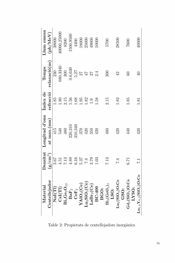
Moltes de les propietats desitjades son; gran densitat, alta velocitat, bonalinealitat, resistencia a la radiacio i baix cost. L’alta densitat redueix lanecessitat de material per a produir llum de partıcules d’alta energia il’efecte Compton es redueix per partıcules de mes baixa energia. L’altavelocitat, amb temps de recuperacio rapids, porta a una millor resolucio enles mesures i millor identificacio del tipus de partıcules mesurades, a mesde reduir el temps de recuperacio. La resistencia a la radiacio es necessariaper mantenir els cristalls en detectors amb un ambient hostil. Finalmentel cost tambe es un factor important ja que els cristalls solen necessitarprocessos de purificacio complicats i terres rares per a la seva fabricacio.
Les propietats tıpiques d’alguns centellejadors inorganics es resumeixenen la taula 2. Els centellejadors organics tenen una densitat molt menor (1g/cm3) i menys emissio de llum (al voltant del 50% del NaI(Tl)).
viii
Mate
rial
Densi
tat
Longit
ud
d’o
na
Index
de
Tem
ps
Llu
mem
esa
Cente
lleja
dor
(g/cm
3)
at
max.(nm
)re
fraccio
rela
xacio
(ns)
(ph/M
eV
)
NaI(
Tl)
3.67
415
1.85
230
3800
0C
sI(T
l)4.
5154
01.
80680,3
340
4000
0,25
000
Bi 4G
e3O
12
7.13
480
2.15
300
8200
BaF
24.
8922
0,31
01.
560.6
,630
1500
,950
0C
eF
36.
1631
0,34
01.
685,2
744
00Y
AlO
3(C
e)
5.37
370
1.95
27
1800
0Lu
2SiO
5(C
e)
7.4
420
1.82
47
2500
0LaB
r 3(C
e)
3.79
350
1.9
27
4900
0B
C-4
00
1.03
420
1.58
2.4
1000
0B
GO
:B
i 4(G
eO
4) 3
7.13
480
2.15
300
5700
LSO
:Lu
2(S
iO4)O
:Ce
7.4
420
1.82
42
2850
0G
SO
:G
d2(S
iO4)O
:Ce
6.71
440
1.85
60
7600
LY
SO
:Lu
1.8Y
0.2(S
iO4)O
:Ce
7.1
420
1.81
40
4000
0
Table 2: Propietats de centellejadors inorganics
ix
RESUM
Aplicacions dels SiPMs
Els fotomultiplicadors de silicis es poden utilitzar en qualsevol aplicacioon es necessiti la mesura de senyals febles de llum. Les aplicacions meshabituals son; l’us en la deteccio de rajos gamma emesos per un isotopintroduıt en el cos per detectar l’acumulacio en diferents arees (com perexemple en la tomografia d’emissio de positrons, PET) o els detectors departıcules d’altes energies per a usos comercials o d’investigacio en les sevesvariants ( com per exemple la construccio de calorımetres a l’LHC).
Tomografia d’Emissio de Positrons, PET
La Tomografia d’Emissio de Positrons (PET) es una tecnica d’imatgemedica que produeix imatges en tres dimensions dels processos funcionalsdel cos. Els sistemes PET es basen en la deteccio de parells de rajos gammaemesos indirectament per un isotop introduıt en el cos. Les dades produıdesper la concentracio de parells de rajos gamma i el seu temps d’arribadas’utilitzen per a construir imatges en tres dimensions de l’activitat dins delcos. Els aparells actuals utilitzen sistemes combinats de raigs X pero seriadesitjable substituir-los per ressonancia magnetica ja que no augmenten laradiacio a la que s’exposa el pacient i millora el contrast en els teixits tous.En la figura 1 es pot veure a nivell esquematic un sistema PET.
El bloc de deteccio normalment esta format per cristalls centellejadors(que converteixen el raig gamma a llum) seguits per tubs fotomultiplicadors(convertint la senyal de llum en una corrent electrica) i la electronica deprocessat (amb amplificacio i mesura del temps i de la senyal d’entrada).La resolucio espacial final depen de la mida dels cristalls i de la precisio delsistema global.
La combinacio de sistemes PET amb raigs X o MRI donant mesuresanatomiques i metaboliques en el mateix aparell es molt util ja que elpacient no es mou entre mesures. Aixo es mes important en estructuresamb variacions anatomiques o en organs que es puguin moure.
Les dades generades per l’escaner son una llista d’esdeveniments en coin-cidencia representant deteccions gairebe simultanies dels fotons aniquilats(en detectors situats a 180o). Cada coincidencia representa una lınia enl’espai connectant els dos detectors. Normalment es necessari molt proces-sat per a generar les imatges finals.
Els sistemes PET nomes accepten esdeveniments valids al voltant de lafinestra d’energia produıda per un raig gamma, 511keV. Si un esdevenimentes troba en aquesta finestra i amb coincidencia amb un detector situat a
x

Figure 1: Esquema d’un sistema PET
l’altre costat l’esdeveniment s’accepta. Tota la resta es descarta. Per evi-tar l’acumulacio de dades es important prendre aquestes decisions el mesrapidament possible en el detector.
Alguns cristalls tenen una emissio espontania de llum, emetent un espec-tre en la regio d’interes. Com a exemple Saint Gobain produeix el PRelude420[24], un centellejador basat en un isotop del Luteci generant 3 raigsgamma en cascada de 307, 202 i 88 keV, essent el mes probable una energiade 597keV.
Temps de Vol
El Temps de Vol (ToF) es un metode utilitzat per a mesurar el tempsque triga una partıcula per a recorrer una certa distancia. Aquesta mesuras’utilitza per a determinar alguna propietat del medi de propagacio o pera coneixer alguna propietat de la partıcula. La partıcula es pot detectardirecta o indirectament. En sistemes PET els esdeveniments d’interes esdetecten facilment mitjancant la coincidencia. Es una mesura indirecta jaque la partıcula genera una senyal lluminosa en el centellejador i llavorsaquesta senyal es converteix a corrent i es processada. La mesura de tempsen els dos costats dels detectors ajuda a millorar la resolucio sobre la posicioon s’ha produıt l’esdeveniment.
xi

RESUM
CERN i LHC
El Centre Europeu per la Recerca Nuclear o Conseil Europeen pour laRecherche Nucleaire (CERN) es va fundar el 1954 amb la intencio d’esdeveniruna institucio lıder en el mon en aquest camp de recerca. Es va construir enla frontera Suıssa i Francesa, a prop de Ginebra. Els seus edificis s’estenenal llarg dels dos costats de la frontera, de la mateixa manera que el tunel onhi ha l’accelerador mes potent creat fins al moment, el Gran Col·lisionadord’Hadrons (LHC). Durant la seva historia ha tingut diferents acceleradorsi experiments donant lloc a diferents descobriments i premis. Avui en dia20 paısos formen part dels membres d’aquesta col·laboracio internacional.L’LHC es un col·lisionador proto-proto situat en un anell de 27km construıtsota el terra.
LHCb
L’experiment Large Hadron Collider beauty (LHCb) es un dels exper-iments actuals al CERN (Ginebra). En la figura 2 es mostra el detector.LHCb es un espectrometre amb un angle de cobertura aproximat de 15 a300 mrad en el pla horitzontal i de 15 a 240 mrad en el pla vertical. Aquestageometria esta motivada pel fet que els parells de partıcules bb produıts aLHC es produeixen majoritariament en una direccio unica.
Figure 2: LHCb detectora
aImatge proporcionada per la col·laboracio LHCb
xii
Comencant des del punt d’interaccio, a l’esquerra de la figura, el detectorconsisteix en un sensor de tracking construıt amb tires de silici envoltant lazona d’interaccio (el detector de Vertex). Tot seguit hi ha un imant que gen-era un camp aproximat de 4Tm i que corba la trajectoria de les partıcules.Tot seguit els RICH (Ring Imaging Cherenkov) que identifiquen partıculescarregades distingint pions i kaons. Despres d’aquest punt els detectors songrans telons verticals que defineixen diferents plans paral·lels de mesura.Un detector de silici cobrint una gran area (el trigger tracker, TT ) en com-binacio amb un detector gasos (el Inner Tracker, IT, i Outer Traker, OT ).Detectors de muons i finalment calorımetres (Hadronic i Eelctromagnetic)per a mesurar l’energia de les partıcules.
SciFi Tracker
El tracker actual de LHCb esta format pel detector gasos de l’OT i eldetector de tires de silici de l’IT per cobrir la zona amb mes ocupancia alvoltant de la canonada amb el feix de partıcules. Per a l’actualitzacio deldetector s’ha escollit una nova tecnologia basada en fibres centellejadores[6],amb fibres clares generant i transportant la senyal. La zona central es reem-placara per fibres centellejadores cobrint tota l’alcada del detector. Con-tindra fibres de 2.5m separades per miralls en el punt mig i llegides perfotomultiplicadors de silici muntats als extrems.
Amb aquesta configuracio el material es redueix al mınim. Un dels prob-lemes principals es determinar les prestacions dels fotomultiplicadors desilici en radiacio. Alguns estudis s’han realitzat mitjancant una font ra-dioactiva de PuBe[6], i s’han deixat mostres en el detector d’LHCb durant2011.
Les tecniques per la produccio de les matrius de SiPM encara es trobenen desenvolupament. I s’han fabricat alguns prototips amb caracterıstiquesadequades.
Una matriu de SiPMs a mida s’esta desenvolupant per encaixar en lamida del modul evitant zona morta. Els prototips de Hamamatsu i Ketekconsisteixen en matrius de 64 canals amb el catode comu. Amb una areatotal de 0.23x1.32mm2 per canal, 96 micro-cel·les i una mida de 57.5x55μm2
per micro-cel·la. Els 128 canals es fabriquen unint dues oblees amb 64 canalsamb un costat polit de forma que es redueix al mınim la distancia entre lesoblees.
xiii

RESUM
Model dels SiPM
La utilitzacio d’un model fiable es imprescindible per produir senyalsfidels a la realitat al dissenyar la electronica. Un model simple[26] s’ha im-plementat i utilitzat mitjancant eines SPICE. L’esquema del model es potobservar en la figura 3 amb els parametres corresponents en la taula 3.
En aquest model [26] les diferents cel·les es modelitzen com elementspassius amb la diferencia que les cel·les disparades tenen alguns elementsmes que la resta, que actuen com a carrega.
Figure 3: Esquema del model
Degut a que la base d’una micro-cel·la es un dıode amb una resistencia dequenching per evitar la seva destruccio, el model incorpora una capacitatparasita en paral·lel al dıode, una font de voltatge i una resistencia en serie.
xiv
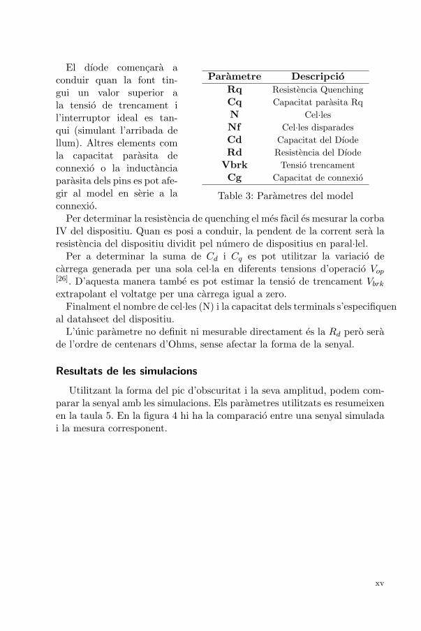
Parametre Descripcio
Rq Resistencia Quenching
Cq Capacitat parasita Rq
N Cel·lesNf Cel·les disparades
Cd Capacitat del Dıode
Rd Resistencia del Dıode
Vbrk Tensio trencament
Cg Capacitat de connexio
Table 3: Parametres del model
El dıode comencara aconduir quan la font tin-gui un valor superior ala tensio de trencament il’interruptor ideal es tan-qui (simulant l’arribada dellum). Altres elements comla capacitat parasita deconnexio o la inductanciaparasita dels pins es pot afe-gir al model en serie a laconnexio.
Per determinar la resistencia de quenching el mes facil es mesurar la corbaIV del dispositiu. Quan es posi a conduir, la pendent de la corrent sera laresistencia del dispositiu dividit pel numero de dispositius en paral·lel.
Per a determinar la suma de Cd i Cq es pot utilitzar la variacio decarrega generada per una sola cel·la en diferents tensions d’operacio Vop[26]. D’aquesta manera tambe es pot estimar la tensio de trencament Vbrk
extrapolant el voltatge per una carrega igual a zero.Finalment el nombre de cel·les (N) i la capacitat dels terminals s’especifiquen
al datahseet del dispositiu.L’unic parametre no definit ni mesurable directament es la Rd pero sera
de l’ordre de centenars d’Ohms, sense afectar la forma de la senyal.
Resultats de les simulacions
Utilitzant la forma del pic d’obscuritat i la seva amplitud, podem com-parar la senyal amb les simulacions. Els parametres utilitzats es resumeixenen la taula 5. En la figura 4 hi ha la comparacio entre una senyal simuladai la mesura corresponent.
xv

RESUM
Figure 4: Simulacio d’una cel·la i mesura
Parametre Valor
Rq 300kΩCq 5.7fFN 1600Cd 12fFRd 1kΩCg 15.8pFVbrk 69.47V
Figure 5: S10362-11-025Pparametres
ASICs de lectura de SiPMs
Un resum de diferents opcions per a la lectura de fotomultiplicadorsde silici formen aquesta seccio, amb una descripcio de les diferents ar-quitectures. Es important tenir en compte que probablement no tots elsdesenvolupaments hi estaran recollits degut a la gran quantitat d’opcions.L’objectiu es obtenir una visio global de l’estat de l’art en el desenvolupa-ment de circuits integrats per a la lectura de fotomultiplicadors de silici.
Les implementacions tıpiques de pre-amplificadors es basen en Amplifi-cadors Sensibles a la Carrega (CSA) o en etapes d’entrada en mode corrent.Cadascun d’ells te les seves avantatges i inconvenients. L’amplificador decarrega o tensio permet una connexio del sensor tant en l’anode com elcatode i normalment es troba amb un acoblament en alterna per podervariar el valor en contınua del node d’entrada. Les implementacions enmode corrent nomes permeten la connexio en un dels dos terminals (ladireccio de la corrent ha de ser la correcta) i solen oferir millors carac-terıstiques de velocitat.
Degut als diferents anys de fabricacio i en diferents tecnologies els pro-totips no es poden comparar directament pel que fa el consum i l’area. Peroper tenir una primera aproximacio de com s’han realitzat les implementa-cions pot ser un valor interessant.
xvi

Taules comparatives
Per tal de comparar algunes caracterıstiques de diferents ASICs elselements mes interessants es resumeixen en les tables seguents, 4 i 5. Enla primera hi ha un resum de les sortides, tipus de sortides, magnitudmesurada, resolucio i informacio temporal. A la segona es resumeix el tipusd’etapa d’entrada, potencia, area i tecnologia.
L’aproximacio habitual es donar carrega i informacio temporal (realitzantuna OR de diferents canals). Normalment aquesta mesura doble es realitzadividint en dos la senyal a la sortida del pre-amplificador, dividint-se en doscamins de senyal amb diferent processat. Es realitzen prototips amb moltscanals degut als sistemes en els quals han d’anar instal·lats.
A les taules es pot veure que la lectura mes popular es en carrega. Sovintaplicant algun circuit per canviar la forma en el pre-amplificador. Aque-sts tipus de circuits s’utilitzen sovint en detectors de partıcules, pero noaprofiten les possibilitats temporals del sensor. Per altra banda la lecturaen corrent s’utilitza menys i habitualment connectat al catode.
Les implementacions diferencials no s’utilitzen massa degut a que el sen-sor es unipolar i normalment el consum se’n ressenteix i complica la con-nexio.
xvii

RESUM
ASIC
Sort
ides
Measu
raR
eso
lucio
Sort
ida
Tem
pora
l
FLC
SIP
MM
ult
iple
xat
analo
gic
Car
rega
-N
oM
AR
OC
3M
ult
iple
xat
analo
gic
idig
ital
Carr
ega
Fin
s12
bit
s64
+2O
RSP
IRO
C2c
Dig
italte
mps
ica
rreg
aTem
ps
iC
arr
ega
12
bit
si150ps
Para
ula
dig
ital
NIN
OD
igit
al
Tem
ps
iam
pla
da
60ps
LV
DS
PETA
Dig
ital
Tem
ps
ien
ergia
28ps
rms
Par
aula
dig
ital
BA
SIC
Dig
italianalo
gic
mux.
Tem
ps
ien
ergia
650ps
OR
tem
ps
VA
TA
64
Mult
iple
xat
analo
gic
idig
ital
Tem
ps
ica
rreg
a-
Tem
ps
ian
alo
gic
RA
PSO
DI
Dig
ital
Tem
ps
ica
rreg
a-
Tem
ps
TO
FP
ET
Dig
ital
Tem
ps
ica
rreg
a50ps
Para
ula
dig
ital
Table 4: Sortides dels ASICs
xviii

ASIC
Tip
us
Tecnolo
gia
Impedancia
Canals
Are
aPote
ncia
Any
entr
ada
entr
ada
(mm
2/ch
)m
W/ch
FLC
SIP
MC
arr
ega
0.8
μm
AM
SA
C18
0.5
611
2004
MA
RO
C3
Cor
rent
0.35
μm
SiG
eA
MS
≈50Ω
64
0.2
52.
520
09SP
IRO
C2c
Car
rega
0.35
μm
SiG
eA
MS
AC
36
0.8
9≈2
.520
12N
INO
Dif.C
arre
ga0.
25μm
IBM
≈20Ω
81
4020
03P
ETA
Difer
enci
al
0.18μ
mU
MC
-16
0.66
862008
BA
SIC
Cor
rent
0.35
μm
SiG
eA
MS
≈17Ω
80.8
8>
2.65
2008
VA
TA
64
Cor
rent
-A
C64
115
2007
RA
PSO
DI
Cor
rent
0.35
μm
SiG
eA
MS
≈20Ω
24.5
100
2008
TO
FP
ET
Cor
rent
0.13
μm
10-6
0Ω64
0.3
97
2012
Table 5: Propietats dels ASICsxix

RESUM
Disseny per PET
Els objectius principals per a un disseny multicanal que millori els sis-temes actuals i utilitzable en sistemes PET es resumeix en els seguentspunts;
• Ample de Banda ≈ 250MHz
• Connexio directa al SiPM
• Valor de tensio DC controlable al SiPM
• Baixa impedancia d’entrada
• OR rapida entre tots els canals per a mesura temporal
• Mesura d’energia mitjancant una senyal digital del tipus Temps sobreun llindar (ToT)
• Minimitzar consum
• Bona linealitat
Arquitectura
En la figura 6 es mostra un diagrama de blocs del canal analogic imple-mentat. Despres d’analitzar els ASICs anteriors sembla que la millor solucioper la mesura es una etapa d’entrada en corrent. La etapa implementadapermet controlar el valor en contınua del node d’entrada i generar copiesde la senyal d’entrada. En aquest cas es generen tres copies que s’utilitzenper a tres mesures; temps, energia i apilament.
Per la mesura temporal l’habitual es utilitzar un dels camins de senyal icomparar directament amb un llindar per detectar un flanc. Aquest proced-iment dona prou bons resultats. Altres processats son molt mes complexos imilloren la resolucio lleugerament [40]. Per evitar la complexitat s’ha escollitun comparador rapid en corrent per aquesta aplicacio.
Per la mesura d’energia s’ha escollit una sortida digital degut a la sevaflexibilitat en la lectura i els pocs recursos necessaris en l’ASIC (no calADC). Un integrador amb una corrent de descarrega constant genera unasenyal que va a un comparador amb histeresis. Utilitzant aquest circuits’obte una sortida amb una amplada lineal respecte el pic de corrent d’entrada.D’aquesta manera s’eviten correccions a posteriori.
Per la mesura d’apilament simplement s’utilitza una altra branca ambun acoblament en alterna. La sortida de l’acoblament es passa per un com-parador en corrent rapid de manera que tenim una senyal digital curta percada variacio brusca de corrent a l’entrada. Aquesta senyal es passa llavors
xx

per dos flip-flops en cascada de forma que generen una senyal logica a nivellalt si hi ha hagut dos pics o mes. La sortida es guarda en un registre de 16bits de forma que es pot llegir el resultat de tots els canals.
Aquesta arquitectura mante una connexio molt simple tant a l’entradacom a les sortides, sense la necessitat de components afegits i amb unainterfıcie digital compatible amb una FPGA comercial.
Figure 6: Blocs del prototip
La deteccio d’apilament es una novetat respecte altres implementacionsi ajudara els algoritmes de post-processat.
Un sistema de control lent permet ajustar tots els voltatges i correntsde polaritzacio i operacio (llindars dels comparadors, tensio en el noded’entrada, etc...) i esta inclos en el prototip.
Temps sobre Llindar Linial (TOT)
El Temps sobre Llindar o Time Over Threshold (TOT) es un metodede processat en el qual una senyal analogica es compara amb un valor(llindar) fixe per obtenir una senyal digital representant l’alcada de la senyalanalogica. Mesurant l’amplada de la senyal digital de sortida haurıem depoder estimar la entrada. Els sistemes TOT son molt simples i utils per asistemes multicanal ja que redueixen recursos i consum. Pero normalmentpresenten una linealitat molt dolenta.
El comportament no lineal del TOT dependra del processat de la senyal.Per exemple si un filtre Gaussia s’aplica, l’entrada es pot aproximar a un
xxi

RESUM
Figure 7: Entrada TOTFigure 8: Sortida TOT per una en-trada triangular
triangle. Utilitzant aquesta entrada [48] la no linealitat resultant es potobservar clarament depenent del valor llindar (a les figures 7 i 8). En algunscasos s’han utilitzat llindars dinamics per evitar aquests efectes [48], pero sis’aconsegueix una senyal amb un temps de pujada molt rapid i una baixadalineal el resultat de la mesura hauria de ser molt millor.
Utilitzant les propietats de la senyal del SiPM ens podem aproximar ala senyal desitjable a l’entrada. Utilitzant un integrador amb una correntconstant de descarrega abans d’un comparador s’hauria d’obtenir un TOTlineal. L’esquema basic es pot veure en la figura 9. Una tecnica molt similars’ha utilitzat en altres circuits de lectura de sensors [49],[50].
Figure 9: Esquema TOT lineal
Idealment el resultat del TOT es pot calcular facilment mitjancant laformula 2, tenint en compte com a entrada la carrega (Q). Degut a que
xxii

el llindar (VTh), la capacitat de realimentacio (CKrum) o la corrent dedescarrega (IKrum) son constants la mesura haura de ser lineal respecteQ. Els elements que introdueixen no linealitats seran el temps del flanc depujada i la baixada de la senyal. Aquests efectes seran molt majors persenyals relativament petites en amplitud (petites per un sistema PET) oper a corrents de descarrega molt petites.
TTOT =Q
IKrum
− VThCKrum
IKrum
(2)
Una de les avantatges mes importants d’aquesta estructura es la flexibil-itat. Canviant la capacitat de realimentacio i la corrent de descarrega enspodem adaptar als requeriments de temps / resolucio i corrent d’entradade l’aplicacio desitjada.
En la seguent figura es poden observar unes simulacions de linealitatutilitzant una senyal d’entrada el mes proxima a la realitat (mesurada en unsensor amb un centellejador i una font radioactiva Na22). La primera graficamostra la corrent d’entrada, la seguent la tensio de sortida de l’integradori finalment la sortida del comparador digital abans de l’error de linealitatper a cada punt.
xxiii

RESUM
Figure 10: Simulacio de linealitat
xxiv

Resultats
El prototip del FLEXTOT es va rebre l’Octubre del 2012, amb 30mostres encapsulades en un format QFN64 i 10 mostres sense encapsu-lar. Mentre es realitzava la fabricacio es va dissenyar un sistema de test pertal de mesurar el mes rapidament el maxim de caracterıstiques possiblesdel prototip.
Sistema de test
El sistema de test (en la figura 11) es basa en l’apilament de tres cir-cuits impresos amb tots els elements necessaris; des del sensor fins a lacomunicacio de dades a un ordinador. L’unic element no inclos es la fontd’alt voltatge (< 100V)necessaria per alimentar els sensors. La seguentelectronica es troba en els diferents circuits (de dalt a baix);
• Sensor: en aquest circuit es poden soldar diferents sensors. El sensores connecta directament al seguent circuit. Una variant amb un circuitd’injeccio es pot utilitzar per la calibracio amb una corrent conegudaa l’entrada.
• Circuit Analogic: en aquest circuit basicament hi ha el prototip ambalgun regulador, capacitat de desacoblament i resistencies de pro-teccio. Tambe incorpora un parell d’amplificadors per a poder ex-treure senyals de prova directament a l’oscil·loscopi i interruptorsd’alta frequencia (SPDT) per a desconnectar les entrades dels canals.
• Circuit Digital: en aquest circuit hi ha una FPGA de baix cost (AlteraCyclone III, EP3C) i un circuit de comunicacions FT2232 que esconnecta al port USB d’un ordinador. Utilitzant aquest sistema espot controlar tots els elements del circuit i del prototip i realitzaruna adquisicio de la sortida del prototip (amb una resolucio de 5nsen la mesura de l’amplada del pols digital).
Les alimentacions VDDA i VDDD s’alimenten a 3.3V. El consum mig esde 10.7mW per canal o 7.7mW de consum analogic (excloent la potenciade l’alimentacio digital que inclou les cel.les estandard, els comparadorsrapids i alguns convertidors digitals / analogics).
Un element important per evitar canviar la forma de la senyal d’entradai maximitzar la corrent d’entrada es la impedancia d’entrada. La mesurarealitzada compleix els resultats esperats; amb el comportament inductiuesperat la impedancia es mante a valors baixos (34Ω) fins a uns 200MHz.
xxv

RESUM
Figure 11: Sistema de test
Per tal de simular la senyal generada pels SiPM s’ha dissenyat un circuitque substitueix el dels sensors. Basicament es tracta d’un amplificador se-guit d’un acoblament en alterna i una resistencia en serie per mesurar elcorrent. El pic es genera mitjancant un generador arbitrari per simular laforma de la senyal del SiPM.
Linealitat
Per tal d’obtenir una millor linealitat en l’amplitud de la senyal injectadas’ha col·locat un atenuador programable entre el generador i la entrada delcircuit. El generador es configura amb una amplitud maxima de sortida i esva atenuant mitjancant l’atenuador programable. Aquest sistema permetuna millor linealitat en la senyal d’entrada que simplement variar l’amplituden el generador.
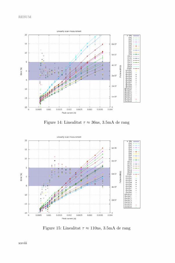
Degut als parametres de configuracio del prototip alguna calibracio esnecessaria per adaptar-se al rang de senyals d’entrada. Alguns exemples deles corbes de calibracio resultants ens poden veure en els 16 canals en lesfigures 12, 14 per una constant de temps de l’entrada de τ ≈36ns i en lesfigures 13, 15 per una constant de temps τ ≈110ns.
xxvi

Figure 12: Linealitat τ ≈ 36ns, 18mA de rang
Figure 13: Linealitat τ ≈ 110ns, 18mA de rang
xxvii
RESUM
Figure 14: Linealitat τ ≈ 36ns, 3.5mA de rang
Figure 15: Linealitat τ ≈ 110ns, 3.5mA de rang
xxviii

Mesures amb SiPM
Despres de caracteritzar electricament el prototip es col·loca un sen-sor real connectat al sistema de test. La senyal d’entrada tindra un tempsrealista i evitara qualsevol efecte del circuit d’injeccio. Amb aquesta con-figuracio es realitzen algunes mesures.
Fonts Radioactives
Per caracteritzar amb una senyal el mes propera a la realitat s’utilitzendiferents fonts radioactives. Un petit cristall LSO (de 2x2x8 mm3) es col·locasobre un canal del detector (de 3x3 mm2) i llavors una font radioactiva aprop. Primerament es mesura l’espectre del cristall sol per tal que es puguirestar a posteriori (el material del cristall te una emissio de partıcules dediferent energia que generen llum).. Les fonts utilitzades son Na22, Co60 iCs137, i els resultats es resumeixen a la figura 16.
Figure 16: Mesura de l’espectre Na22, Co60, Cs137
xxix

RESUM
Es pot observar la bona linealitat del sistema en tot el rang. Utilitzantla posicio dels dos pics mes externs s’obte una constant de calibracio. Util-itzant aquesta constant es converteixen les resolucions (σ) mesurades aenergia. La resolucio calculada es resumeix a la taula 6. Com s’esperavamillora lleugerament al augmentar l’energia.
Font keV μ (comptes) σ (comptes) Res.(%)
Na22 511 53.3 7.1 9.61275 166.3 3.51 -
Cs137 662 75.9 6.6 6.9
Co60 1173 149.1 9.5 5.61332 171.6 6.41 -
1 Caldria mes estadıstica
Table 6: Mesures de les Fonts radioactives
xxx

Mesura de coincidencia temporal
Per obtenir una primera estimacio de la resolucio temporal del sistemacomplet s’ha reproduıt un sistema de coincidencia en el laboratori. Dossistemes de test amb un sol canal es col·loquen un davant de l’altre. Sobreels dos SiPM es situen cristalls (s’han probat LSO i LYSO) i una fontradioactiva de Na22 enmig. La sortida de temps i les d’energia dels doscanals es capturen amb l’oscil·loscopi.
Utilitzant l’espectre extret dels dos canals es seleccionen els esdeveni-ments dins del rang d’energies d’interes. Aquesta finestra es corresponal voltant dels 511keV (±1σ). Una vegada seleccionats els esdevenimentsd’interes es representa el retard entre les dues sortides temporals dels dossistemes de test. El resultat final es mostra en l’histograma de la figura 17obtenint una resolucio temporal per sota dels 300ps FWHM (≈115ps rms).
Figure 17: Mesura de coincidencia
xxxi

RESUM
Mesures en un sistema complet
Algunes mesures preliminars s’han realitzat al CIEMAT amb un sistemaque emula un sistema PET complet. Es tracta de dos sensors situats ados costats d’una plataforma giratoria (d’aquesta manera no cal un anellcomplet de detectors ja que es fa girar la mosta). Al centre es situa unafont radioactiva (Na22) i una vegada adquirides les dades s’apliquen elsalgoritmes de reconstruccio d’imatge. Un resultat de la imatge generada ila mesura de posicio es pot veure en la figura 18.
En aquest cas s’han realitzat dues mesures, una primera amb una solafont radioactiva (de 0.25mm de diametre) i superposant la mesura en duesposicions, i una segona amb dues fonts radioactives (de 1mm de diametre)mesurant al mateix temps. La precisio en la mesura de posicio resultant esde pocs milımetres com s’espera.
Figure 18: Mesura en un sistema complet
xxxii

Disseny per al Tracker SciFi
En el cas del disseny per a detectors de partıcules cal que es compleixinunes restriccions temporals molt diferents (comparant amb PET). La re-utilitzacio i implementacio de la etapa d’entrada en una nova tecnologiai amb unes caracterıstiques temporals prou diferents son un repte per aldisseny. En aquest cas es tracta d’una tecnologia mes moderna amb unatensio d’alimentacio molt inferior i completament CMOS.
El tracker es un sub-detector de LHCb que indica el camı que segueixenles partıcules amb carrega electrica que passa a traves del detector i inter-acciona amb el material. Les partıcules deixen una petita senyal electricaal moure’s pel detector. Els detectors d’aquest tipus normalment utilitzentires de silici o detectors gasosos (straw tubes). Una vegada s’ha generat,s’adquireix i processa i s’envia a un ordinador que reconstrueix la trajectoriade les partıcules.
La tecnologia per a l’IT i l’OT es basara en fibres centellejadores generantuna senyal de llum i transportant-ne els fotons des d’on es generin fins al’extrem on hi haura els sensors. En el primer esborrany sobre com sera eldetector es preveu utilitzar fibres de 2.5m cobrint almenys la zona central.Tot el detector es construira mitjancant 3 panells cadascu dels quals amb 3plans inclinats entre ells (≤5o) per crear els plans X-U-V-X. Cada pla estaconstruıt amb 5 capes de fibres de 250μm de diametre i 2.5 m de llargada.
Un dels problemes mes importants per a fer realitat aquest detector es laconstruccio dels moduls de fibres. Algunes noves tecniques s’estan provanti desenvolupant per a la seva fabricacio.
Per a dissenyar la electronica de processat s’ha iniciat una col·laboracioentre Barcelona i Clermont Ferrand, oberta a qualsevol altra instituciode LHCb, per dissenyar el ”low Power Asic for the sCIntillating FIbrestraCker” PACIFIC.
S’han estudiat diferents alternatives per al processat, pero sembla quela mes senzilla sera la solucio base, incorporant un canal amb un pre-amplificador, shaper, integrador mostrejat i ADC.
xxxiii

RESUM
Resum de les especificacions
En la seguent taula es pot veure un resum de les especificacions quehaura de complir la electronica;
Parametre Valor Unitat
Canals 64 o 128 -Potencia 0.5 o 1 WEncapsulat BGA -Resolucio temporal 25 nsConstant de temps sensor de 40 a 300 nsRang dinamic 0-64 micro-cel·lesTemps d’arribada de la senyal 0-15 ns
Soroll referit a l’entrada ≤143 pA√Hz
Table 7: Especificacions del PACIFIC
Arquitectura
L’arquitectura del canal proposat per al PACIFIC es pot observar en lafigura 19. Tot i que s’estan estudiant altres alternatives, especıficament unadigitalitzacio rapida seguida per un processat digital de la senyal, la soluciomes facil sembla realitzar un shaping de la senyal i integrar durant 25ns. Alno haver-hi temps mort entre mostra i mostra caldra un doble integradorentrellacat de forma que un estigui capturant al temps que l’altre torna a lescondicions inicials. Despres de l’integrador un convertidor analogic / digitalgenerara els valors representant l’amplitud a 40MHz. Finalment un enllacserie (probablement diferencial seguint un estandard) enviara les dades aalta velocitat. Per aquest ultim pas caldra algun tipus de multiplicador defrequencia (com per exemple un PLL en la figura).
Algunes polaritzacions comunes i un control digital de les tensions, cor-rents i parametres d’operacio tambe hauran d’estar integrats. Aixı ques’hauran de dissenyar blocs com convertidors digitals analogics ( en tensioi corrent), resistencies variables i capacitats variables, connectats a algunbus de control.
xxxiv

Figure 19: Blocs del canal del PACIFIC
Pre-amplificador
La etapa d’entrada es un amplificador en mode corrent amb la connexiodirecta al SiPM. L’objectiu es aconseguir les seguents especificacions delbloc:
• Ample de banda (≈ 250MHz).
• Baix consum (< 2mW, maxim de 8mW/canal en tot l’ASIC).
• Baixa impedancia d’entrada (20Ω < Zin < 40Ω).
• Tensio controlada al node d’entrada (≈ 1V de rang).
• Soroll referit a l’entrada ≤ 143 pA√Hz
El circuit utilitzat com a referencia per aconseguir aquestes caracterıstiqueses pot veure en la figure 20. La etapa d’entrada es basa en la mateixa novaestructura amb una realimentacio doble amb alguna petita variacio peradaptar-se a una tecnologia mes moderna (IBM 0.13μ m).
Aquest circuit permet una impedancia d’entrada baixa per aconseguir lamaxima corrent d’entrada i aixı la millor resolucio temporal. HFFB es el llacde realimentacio d’alta frequencia que mante la impedancia d’entrada baixai constant (fins a certa frequencia). El segon camı LFFB es un llac de reali-mentacio a mes baixa frequencia i proporciona un valor de contınua (Voffset
in figure) al node d’entrada utilitzant el curtcircuit virtual de l’amplificadorque regula el seguidor.
El disseny s’ha realitzat tenint en compte que el node dominant ha deser el d’entrada degut a la gran capacitat parasita del detector. D’aquestamanera la estabilitat es veura encara mes reforcada al connectar un sensoramb una gran capacitat parasita a l’entrada.
xxxv

RESUM
Figure 20: Etapa d’entrada PACIFICr1
xxxvi

Conclusions
En aquesta tesi s’ha descrit de forma detallada les propietats del sensor iels requeriments necessaris per a dissenyar la electronica en dos ambits bendiferenciats; fısica medica (PET) i detectors de partıcules (SciFi Tracker).Prenent com a punt d’inici les implementacions realitzades anteriorment iproposant una nova solucio amb una etapa amb doble realimentacio peraconseguir un gran rang dinamic i la possibilitat de configurar facilmentel sistema. Un model del comportament del sensor s’ha utilitzat i ha sigutmolt util per al disseny de la electronica. Els dos circuits dissenyats s’hancomentat detalladament per a diferents tecnologies.
Els objectius principals per al sistema PET s’han complert amb el dissenyd’una arquitectura multicanal i la connexio directa als SiPM amb el pro-cessat analogic. El prototipus s’ha dissenyat i testejat. L’ajust de voltatgeal node d’entrada permet controlar el punt d’operacio del sensor, mentreque els diferents camins de senyal permeten la realitzacio de les diferentsmesures amb una mesura de temps d’una resolucio excel·lent, una mesuraadequada de la energia i la deteccio de l’apilament d’esdeveniments. Aixıdoncs la etapa d’entrada compleix amb tot el que es demanava del circuit.Despres del disseny i el test ja tan sols quedara comprovar el seu funciona-ment en un detector real.
Les restriccions en el disseny del PACIFIC encara s’estan concretant, iel primer prototipus descrit ha de servir com una primera etapa. El circuitdissenyat segueix la mateixa estructura que el de PET pero portat a unatecnologia mes moderna i simplificat per l’aplicacio. Una vegada fabricatcaldra comprovar les seves prestacions. Mentre s’avanca en el disseny de laresta d’etapes per tal de complir el calendari fixat.
xxxvii


Summary
The aim of this thesis is to present a solution for the readout of SiliconPhoto-Multipliers (SiPMs) arrays improving current implemented solu-tions. With this purpose a novel current mode input stage has been de-signed and tested. In first place focusing in general applications for medicalimaging (Positron Emission Tomography, PET) and then using the sametopology for a more constrained design in higghe energy physics (upgradeof Tracker detector at LHCb experiment).
SiPM are recently developed electronic devices[1] with photon countingcapabilities improving current state of the art detectors regarding high volt-age requirements, signal gain and magnetic field tolerance, while keepingat the same time excellent gain and timing characteristics, and a wide dy-namic range. They are semiconductor devices still under development toimprove yield, reduce dark count, provide multi-channel architectures andincrease light sensitivity spectrum.
A Front End Readout Application Specific Integrated Circuit (ASIC)for SiPMs is presented with the following features: wide dynamic range,high speed, multi channel, low input impedance current preamplifier, lowpower consumption, SiPM voltage control, and timing, charge and pileupsignal output.
The pre-amplifier input stage includes a novel circuitry with double feed-back loop to lower input impedance at the same time it keeps a constantDC value at the input node over the full range of operation and keepingthe desired bandwidth.
Silicon Photo-Multipliers
A silicon photo-multiplier is a device formed by hundreds of micro-cells inparallel. Each micro-cell is an Avalanche Photo Diode (APD) working inGeiger mode, with their own quenching resistor to avoid destruction of thedevice. APDs behaviour is well known and has been studied during manyyears from 1960 [7]. All those micro-cells are combined in one single output(connected in parallel). The result is an output similar to the one producedby a PMT, but with a somehow discrete analog output (since each cellreleases a fixed amount of charge when fired).
xxxix

SUMMARY
In the same way as the APDs the first pairs are generated by photo-electric effect and then multiplied inside the silicon. But in this case themultiplication is an avalanche, produced over breakdown voltage. In a nor-mal multiplication process electrons are drawn through the high field regionand create additional electron-hole pairs. The electrons continue in the samedirection but holes are attracted in the opposite direction. At a sufficienthigh field values (over breakdown voltage) the holes can also multiply and,since hole multiplication also produces additional free electrons, this pro-cess leads to a runaway. To avoid a destructive effect a resistor (quenchingresistor) in series is connected to each APD so the voltage it’s droppedwhen it reaches some current limit. This combination of APD and quench-ing resistor is the micro-cell. The resulting gain is similar to the PMT onthe order of 105 to 107.
SiPM detection capabilities are measured as it’s Photon DetectionEfficiency (PDE). It’s nothing more than joining the effects produced bythe area lost between micro-cells and Quantum Efficiency. Since there issome area not able to detect incoming light a Fill Factor (FF) is definedas in 3. The resulting PDE will be calculated easily using formula 3 withPstart being the probability of an electron-hole pair to start an avalanche.Some techniques used to improve crosstalk between micro-cells (such asadding trenches) can degrade this value. The reduction of micro-cell sizewill also make a worse fill factor.
FF =Total Device Area
Sensible Area→ PDE = FF x QE x Pstart (3)
Several measurements and comparisons between different production de-vices can be found in literature[8] with deep description of different effects[9].SiPM offer a linear output depending on incident light in a range of inputphotons. According to [10] the response of a SiPM can be extracted withequation 4, where m is the total number of cells of the device and ε thephoton detection efficiency.
Ncellsfired = m ∗(
1− e−Nphotons∗ ε
m
)(4)
SiPM devices have an important temperature coefficient which modifiesit’s breakdown voltage thus affecting it’s gain. The temperature coefficientis different depending on manufacturing process but existent in all devices.If an array of devices should be compensated without modifying the general
xl

polarization voltage some channel by channel polarization should be pro-vided. Non uniformities between devices in array should also compensatedusing the same mechanism; SiPMs offer a very linear gain versus voltagecharacteristic permitting to compensate non uniformities between differentsensors (those non uniform effects are much sensible at small over-voltagesoperation).
After Pulsing is a known effect which consists on the generation of aspontaneous peak output after a first peak. It is due to the trapping of somecharge in the semiconductor defects. This charge has some probability tobe released afterwards. If this charge is released will start a new avalanche.Typical release times range from few ns to several hundreds of ns. The firstreleased charges (few ns) does not affect the signal because the micro-cellsare not fully recharged, but will increase recovery time. Working at lowtemperatures will make release of this trapped charges more slow, so theafter pulses will be more noticeable.
Dark Count is one of the most important drawbacks of the SiPMs. Darkcount is generated by spontaneous thermally generated carriers. Those car-riers can then generate an avalanche in the micro-cell that will be identicalto a signal generated by a photon. The name of dark count comes from thefact that this signal will continue being generated without any illuminationat all. The average number of avalanches in some time without signal wouldgive the expected dark count rate (normally in Hz).
A summary of advantages and drawbacks of SiPMs are collected in table8.
Advantages Drawbacks
High quantum efficiency Radiation hardnessMagnetic field insensitivity Low PDE
Robust and small Dark countLow voltage operation (from 20V to less than 100V)
Arrays available
Table 8: SiPM advantages and drawbacks
xli

SUMMARY
Scintillators
A scintillator is a material that exhibits emission of light (not resultingfrom heat) when excited by ionizing radiation. This radiation is composedof particles that individually carry enough kinetic energy to liberate anelectron from an atom or molecule, ionizing it. When hit by an incom-ing particle the scintillating material absorb its energy and re-emit theabsorbed energy in the form of light. Depending on material the excitedstate could be metastable, so the relaxation back out of the excited stateis delayed some time (from a few microseconds to hours). First scintillatorusage dates at the beginning of 20th century[13] but gained attention in1944, when Curran and Baker replaced the naked eye measurement withthe newly developed PMT. This was the birth of the modern scintillationdetector.
In this modern scintillation detectors, the first part in the path of theionizing particle are the scintillating crystals used to convert it into a lightburst. Then those light burst are converted into electrical current by atransducer (PMT, APD or SiPM) and processed. This crystals are notideal and present an important timing spread in the photon emission pro-cess. Once the photons are produced they should arrive to the electronicsfollowing different paths which will also increase the time spread in thedetector itself, highly affected by the crystal dimensions[14].
Some of the desired properties of scintillators are high density, high speedresponse, good linearity, radiation hardness and low cost. High density re-duces the material size of showers for high-energy γ-rays and electrons andthe Compton scattered photons are reduced for low energy γ-rays. Highspeed response, with reduced decay times, leads to better resolution inmeasurements and also identification of the type of particle measuring de-cay time (different times are generated depending if they are γ-rays or ions)and also useful to avoid dead time. High speed in fast rise time will producebetter timing measurements. Good linearity is mandatory for the measure-ment of energy in some range. Radiation hardness is needed to allow longlife time of the detector since it could be placed in hostile environment (spe-cially in particle detectors). Finally cost is an important factor since mostcrystal scintillators require high-purity chemicals and sometimes rare-earthmetals that are expensive.
Typical properties of some inorganic scintillating materials are summa-rized in table 9. Organic ones present much lower density (around 1 g/cm3)and lower light emission (around 50% of NaI(Tl)).
xlii

Scin
tillato
rD
ensi
tyW
avele
ngth
Refr
active
Decay
Lig
ht
yeld
Mate
rial
(g/cm
3)
at
max.(
nm
)in
dex
tim
e(n
s)(p
h/M
eV
)
NaI(
Tl)
3.67
415
1.85
230
3800
0C
sI(T
l)4.
5154
01.
80
680,3
340
4000
0,25
000
Bi 4G
e3O
12
7.13
480
2.15
300
8200
BaF
24.
8922
0,31
01.
56
0.6
,630
1500
,950
0C
eF
36.
1631
0,34
01.
68
5,2
744
00Y
AlO
3(C
e)
5.37
370
1.95
27
1800
0Lu
2SiO
5(C
e)
7.4
420
1.82
47
2500
0LaB
r 3(C
e)
3.79
350
1.9
27
4900
0B
C-4
00
1.03
420
1.58
2.4
1000
0B
GO
:B
i 4(G
eO
4) 3
7.13
480
2.15
300
5700
LSO
:Lu
2(S
iO4)O
:Ce
7.4
420
1.82
42
2850
0G
SO
:G
d2(S
iO4)O
:Ce
6.71
440
1.85
60
7600
LY
SO
:Lu
1.8Y
0.2(S
iO4)O
:Ce
7.1
420
1.81
40
4000
0
Table 9: Inorganic scintillators properties summary
xliii

SUMMARY
SiPMs Applications
Silicon Photo Multipliers could be used in any application where a fastmeasurement of a small signal is needed. Today’s main applications arethe detection of the gamma rays emitted by a radionuclide in the body todetect accumulation in different areas of the body (for example in PositronEmission Tomography scanners) or particle detectors with the help of scin-tillating material to produce light from the incoming particles (for examplein Scintillating Fibre Tracker at LHCb).
Positron Emission Tomography
Positron Emission Tomography (PET) is a nuclear medical imagingtechnique to produce three-dimensional images of functional processes inthe body. PET systems are based on detection of gamma rays pairs emit-ted indirectly by a radionuclide (tracer) introduced into the body. Dataproduced with the concentration of the gamma rays pairs and their arrivaltime is used in computer analysis to produce 3D images of their activityinside the body. Modern devices complete the image performing a secondscan with CT-X-ray in the same machine although a combination withMRI (Magnetic Resonance Imaging) would be preferred due to the lackof added irradiation of the patient and better contrast in soft tissues. Akey element to the development and usage of PET systems is the parallelevolution of radiopharmaceuticals. In particular the development of severalcompounds (for example 2-fluorodeoxy-D-glucose, 2FDG) to determine it’sconcentration in different organs by the scanner. First scanners relied ontwo 2 dimensional arrays of detectors, but soon it was clear that a logicaldistribution for full readout detectors was to place it forming a ring aroundthe patient. A schematic view of the system is shown in figure 21.
The detector block is usually formed by scintillator crystals (convertinggamma ray into light bursts) followed by photomultiplier tubes (convertinglight burst into current pulses) and readout electronics (with amplificationand time tagging of the input signal). The final spatial resolution of thehardware depends on the size of the crystals and time accuracy of the wholesystem.
Combination of PET scans with CT-X-ray or MRI giving both anatomicand metabolic information in the same scanner is very useful since patientwon’t move between scans and will make easier to correlate both images.This is important in structures with anatomic variations or moving organs(outside the brain).
xliv

Figure 21: Schema of PET imaging system
The raw data generated by PET scanner are a list of coincidence eventsrepresenting near-simultaneous detections of annihilated photons (in a 180degrees placed detectors). Each coincidence represents a line in space con-necting the two detectors (line of response, LOR). Coincidence events canbe gropued into projection images, called sinograms. Those sinograms areanalogous to the ones produced by CT-X-ray scanners, but with much lessstatistics (at least three orders of magnitude less). As such PET data sufferfrom scatter and random events much more dramatically than CT-X-rayscans. In practice considerable pre-processing of the data is required.
PET systems will only accept as valid events the ones in the energywindow produced by the gamma ray. This is around 511keV. If an event isaround this energy and in coincidence with an other event at a 180 degreeblock then it will be an accepted event. All the rest is discarded. To avoidsystem bottlenecks it’s important to take the decision if an event is savedor dropped as soon of possible in the detector chain.
Some crystals have spontaneous emission of light, emitting an spectra inthe region of interest. As an example Saint Gobain’s Prelude 420[24] is alutetium based scintillator with a radioactive isotope generating 3 gammaray cascade of 307, 202 and 88 keV, being the most probable a 597keVdeposited in the scintillator. This can be useful for offline calibrations ofthe detector (for example LSO and LYSO crystals).
xlv

SUMMARY
Time Of Flight
Time of Flight (TOF) is the name given to several methods to measurethe time it takes for a particle to travel some distance. This measure shouldbe used as a way to determine some property of the medium (velocity) orto know more about the particle. The object could be detected directlyor indirectly. In PET systems the relevant events are detected easily usingcoincidence of two particles of 511keV at 180 degrees. It’s an indirect mea-surement since particles generate some light and this is what is detectedand processed. Since detectors (scintillator crystals) have a finite size (in3 axis) the line where the event has been produced has some angular un-certainty (not an ideal line). If a time stamp is added on the two sideswith time better than ns then the distance from the two detectors is alsodefined (the resolution will increase with the timing resolution). Using thistechnique the signal to noise ratio (SNR) of the events is improved, leadingto less events needed for a given image quality.
xlvi

CERN and LHC
European Organization for Nuclear Research or ”Conseil Europeen pourla Recherche Nucleaire” (CERN) was funded in 1954 with the aim to be-came a world leading institution in this research topic. It was built besidethe French and Swiss frontier, close to Geneva. It’s buildings and sites ex-tent in both sides of the frontier, and also the tunnel constructed to hold themost powerful accelerator created up to date, the Large Hadron Collider(LHC). During it’s history it has hold different accelerators and experi-ments leading to some discoveries and prizes. Today it has 20 countries asmembers of this international collaboration. The LHC is a proton-protoncollider placed in the 27km ring previously build underground for the LEPmachine.
LHCb
Large Hadron Collider beauty (LHCb) experiment is one of the ongoingexperiments at CERN (Geneva). Shown in figure 22, LHCb is a forwardspectrometer with a polar angle coverage of approximately 15 to 300 mradin the horizontal bending plane and 15 to 250 mrad in the vertical non-bending plane. This geometry choice is motivated by the fact that bb pairsproduced at the LHC are produced in a large proportion in the same di-rection, either forward or backward.
Figure 22: LHCb detectora
aImage courtesy of LHCb collaboration
xlvii

SUMMARY
Starting from the interaction point, at the left of figure 22, the LHCbtracking system consists of a silicon strip device surrounding the proton-proton interaction region (the Vertex Locator), a large area silicon stripdetector (the trigger tracker, TT) located upstream of a dipole magnetwhich has a bending power of about 4 Tm, and a combination of siliconstrip detectors and straw drift-tubes placed downstream of the magnet (theInner Tracker, IT and the Outer Tracker, OT).
Scintillator Fibre Tracker
The current LHCb Tracker stations are composed of an Outer Tracker(OT) with straw tube detectors and an Inner Tracker (IT) with silicon stripdetectors to cover the high-occupancy area near the beam pipe. A newtechnology for the IT upgrade, based on scintillating fibres, was introducedin the Upgrade Letter of Intent[6], with clear fibres carrying the photonsfrom the inner region to the sensors placed outside the LHCb acceptance.
In the mean time, a new scintillating-fibre layout has been proposed(Central Tracker, CT), with 2.5 m long fibres covering the whole centralregion of the Tracker stations, from the LHC beam plane all the way to thetop and bottom of the LHCb acceptance. In this option, the IT and severalOT modules are replaced by the new scintillating-fibre modules. Trackingdownstream of the dipole magnet with scintillating-fibre modules in thecentral region is being considered. In this new configuration, the existingoutermost straw tube modules, four on each side, are kept as in the currentLHCb detector and their electronics upgraded to allow readout at 40MHz.The central part (OT and IT) is replaced with scintillating fibre modulescovering the full height of the detector. The upper and lower halves ofthe modules contain 2.5 m long scintillating fibres, separated with mirrorsat the inner boundary and read out with Silicon Photomultipliers (SiPM)mounted outside the LHCb acceptance.
With this configuration, passive material in the detector acceptance isminimized and exposure to radiation is reduced for the SiPMs and FEelectronics. One of the key development challenges will be to determine howthe SiPM performance will evolve as a function of radiation dose and underwhat conditions these photon detectors will represent a viable solution forthe LHCb CT. The radiation fluence at the SiPM location is expected tobe of the order of 1012neqcm
−2. Besides previously described irradiationstudies with 65 MeV protons and with neutrons from a PuBe source [6],SiPM samples have been placed in the LHCb detector at the bottom of thetracking stations during the 2011 data taking period.
xlviii

The techniques for the production of fibre matrices are still under de-velopment for both methods presented in the LoI, namely winding fibreson a cylindrical surface of radius larger than 40 cm or on a long cuboid.Dummy fibre matrices have been produced with both methods. Recently,a 2.5 m long sample module has been fabricated on the cylindrical barrelwith scintillating fibres of 0.25 mm diameter. The sample contained fivelayers of about 100 fibres each.
Specially designed SiPM array is undergoing to fit the mechanical sizeof the module with the minimum dead area possible. The prototypes fromHamamatsu and Ketek consist in 64 channels arrays with a common cath-ode configuration. With a total size of 0.23x1.32mm2 per channel, 96 micro-cells and 57.5x55μm2 micro-cell size. The 128 channels are constructed join-ing to dies of 64 channels with the edge polished, dead area between pixelsis kept to the minimum with a value of 0.25mm between two arrays.
xlix

SUMMARY
SiPM modelling
A reliable SiPM model is mandatory to produce accurate input signalsfor the electronics. A simple model [26] has been implemented and simulatedusing the standard SPICE tools in conjunction with the electronics. Ageneral view of the circuit model can be seen in figure 23 with its parameterson table 10.
In this model [26] the different micro-cells in the SiPM are modelled aspassive elements with the difference that the firing cells by some light haveseveral more elements than the passive cells, acting as a load.
Figure 23: Model schematics
Since the base of a micro-cell is a diode with a quenching resistor (to avoidit’s destruction), the model comprises the union capacitance in parallel withthe diode reverse voltage power supply plus a series resistor to the diode.
The quenching resistor is simulated with an ideal resistor in parallel witha parasitic resistance.
l

Parameter Description
Rq Quenching resistor value
Cq Parasitic capacitance of Rq
N Number of cells
Nf Number of firing cells
Cd Diode capacitance
Rd Diode resistance
Vbrk Breakdown voltage
Cg Grid connect capacitance
Table 10: Model parameters
The diode will start con-ducting when the powersupply is greater than it’sbreakdown voltage and anideal switch is closed (sim-ulating the incoming light).Apart from this parametersan interconnection parasiticcapacitance is also included.
Other parameters such asparasitic inductance of thepins can also be added tothe model in series with the anode and cathode connection.
To determine the quenching resistor, the easiest way is to produce an IVcurve with the device biased in the direct region. At some point the diodewill start to conduct limiting it’s current only by the resistor in series of thediode plus the quenching resistor. Since the quenching resistor is expectedto be much greater than the device resistance the value of the slope of thecurve (in the linear region) will be approximately the quenching resistordivided by the number of cells (all in parallel).
In order to determine the Cd and Cq sum, the charge variation of the out-put single cell fired has been measured and plotted changing Vop value[26].With this procedure Vbrk can also be determined extrapolating the voltagewhen output charge should be 0.
Finally the number of cells (N) and charge seen on the device terminalsis specified on the datasheet. Assuming the terminal capacitance value isspecified in dc conditions, the Cg value can be extracted as documentedin[26].
The only non specified and non measurable directly parameter is Rd butcan be estimated in the order of hundreds of Ohms, not affecting the shapeof the signal.
Simulation results
Using the shape of the dark count peak and amplitude we can approx-imate the real values of the device with the simulations, summarized intable 25. In figure 24 there is a comparison between the simulated pulseand the measured single cell fired at Vop.
For the SciFi Tracker design a VerilogA model has been implementedusing the described model as a basis. This model permits much faster com-
li

SUMMARY
Figure 24: Single cell fired pulse and simu-lation
Parameter Value
Rq 300kΩCq 5.7fFN 1600Cd 12fFRd 1kΩCg 15.8pFVbrk 69.47V
Figure 25: S10362-11-025Pparameters
putation of the output and avoids convergence parameters problems thatoften appear in the simulation of non linear devices (such as ideal switchincluded in the PSpice model). This model is being extensively used tosimulate the different SiPMs under test for the SciFi tracker and to fit theelectronics to it’s signal shape.
SiPM readout ASICs
A brief status of different integrated options for the readout of SiPMs issummarized in this chapter with detailed description of different architec-tures. It is important to note that probably not all existing devices will belisted and commented due to the amount of existing options. At the endof this section a snapshot of the ”state of the art” in the development ofintegrated electronics specific for the readout of silicon photo-multipliersshould have been provided.
The main results on different charge or current mode input stages isstressed. Typical pre-amplifier implementations are based on Charge Sens-ing Amplifiers (CSA) or Current Mode input stages. Each of themhave some advantages and drawbacks being the speed of the current modeinput the most significant advantage. The charge (or voltage) amplifierpermits the connection of the sensor both in the anode or cathode, andnormally is AC coupled in order to tune the DC voltage applied at theconnection node. Current mode implementations only permit the currentflow in one direction (if a good ratio between biasing current and input
lii

current range is desired) thus it must be fixed by design.Due to different years of production and different technologies used in the
production of the prototypes a direct comparison on charge or area can’tbe made. But in general terms a first approach on the order of magnitudeof how this implementations deal with area and power can be obtained.
Comparison tables
To compare several characteristics of the previous ASICs the figures ofmerit are summarized in next tables, 11 and 12. In first table there is asummary of outputs, outputs type, measurement, measurement accuracyand timing information. Second table summarizes input stage type, powerconsumption, area usage and also technology.
The typical approach is to deliver charge and timing information, often asa result of the OR of different channels. Normally this double measurementis performed splitting the signal at the output of the pre-amplifier anddriving two different signal paths. A multi-channel architecture is alwaysenvisaged due to the high numbers of channels needed in current particledetectors or PET systems. Typically a power of 2 channel number is used.
On tables we can see the most popular readout is to use charge basedreadout. Sometimes applying some shaping just at the pre-amplifier. Thisis a well known circuit widely used in particle detectors, but does notexploit the speed possibilities of the sensor. On the other hand currentmode readout is less used and a connection with the sensor must be definedprior to design, in all examples cathode connection is used.
Differential implementations are not much used since it’s not a natu-ral connection of the sensor to the electronics (SiPMs are basically singleended). They offer much better performance in terms of noise but the priceto pay is a much important power consumption which does not seem tocompensate the advantages.
liii

SUMMARY
ASIC
Outp
uts
Measu
reA
ccura
cy
Tim
ing
outp
ut
FLC
SIP
MM
ult
iple
xed
analo
gC
harg
e-
No
MA
RO
C3
Mult
iple
xed
analo
gan
ddig
ital
Charg
eU
pto
12
bit
s64
+2O
RSP
IRO
C2c
Dig
italti
me
and
charg
eT
ime
and
Charg
e12
bit
san
d150ps
Dig
italw
ord
NIN
OD
igit
al
Tim
ean
dw
idth
60ps
LV
DS
PETA
Dig
ital
Tim
ean
den
ergy
28ps
rms
Dig
italw
ord
BA
SIC
Dig
italand
Analo
gm
ux.
Tri
gger
and
ener
gy
650ps
OR
trig
ger
VA
TA
64
Mult
iple
xed
analo
gan
ddig
ital
Tim
ean
dC
harg
e-
Tri
gger
and
analo
gR
AP
SO
DI
Dig
ital
Tri
gger
and
Charg
e-
Tri
gger
TO
FP
ET
Dig
ital
Tim
ean
dC
harg
e50ps
Dig
italw
ord
Table 11: Different ASICs outputs summaryliv

ASIC
Input
Tech
nolo
gy
Input
Channels
Are
aPow
er
Year
type
impedance
(mm
2/ch
)m
W/ch
FLC
SIP
MC
harg
e0.8
μm
AM
SA
Cco
uple
180.
56
112004
MA
RO
C3
Curr
ent
0.3
5μm
SiG
eA
MS
≈50Ω
640.2
52.
520
09SP
IRO
C2c
Charg
e0.3
5μm
SiG
eA
MS
AC
couple
360.8
9≈2
.520
12N
INO
Diff
.C
har
ge0.
25μm
IBM
≈20Ω
81
4020
03P
ETA
Diff
eren
tial
0.18
μm
UM
C-
160.
66
862008
BA
SIC
Curr
ent
0.3
5μm
SiG
eA
MS
≈17Ω
80.8
8>
2.65
2008
VA
TA
64
Curr
ent
-A
Cco
uple
641
15
2007
RA
PSO
DI
Curr
ent
0.3
5μm
SiG
eA
MS
≈20Ω
24.5
100
2008
TO
FP
ET
Curr
ent
0.1
3μm
10-6
0Ω64
0.3
97
2012
Table 12: Different ASICs properties summary lv

SUMMARY
Design for PET applications
The main design objectives of a multichannel prototype to improve cur-rent state of the art are:
• Pre-amplifier Bandwidth ≈ 250MHz
• Direct connection to SiPM
• Controllable DC voltage at SiPM
• Low input impedance
• Fast OR of all channels for timing measurements
• Digital Time Over Threshold output for energy measurement
• Minimize power consumption
• Good linearity
Architecture
In figure 26 a block diagram of the analog channel can be seen. Af-ter analysis of previous ASICs it seems the better solution for the read-out is current mode input to achieve good timing resolution measurementskeeping low power consumption. Current mode input stage provides a lowimpedance input with a controlled DC voltage and multiple scaled copiesof the input current. In this case three copies have been implemented fordifferent measurements; timing, energy and pile-up.
For the timing measurement the common approach is to use one of thesignal paths and compare directly with some threshold to detect the leadingedge. This process leads to reasonably good timing measurement results.Other more complex processing[40] can lead to slightly better resolution butare often much more complex. For this reason a simple fast current modecomparator has been designed for this application.
For the energy measurement a digital output is desired due to it’s flexibil-ity for the readout and low resources usage (no ADC). An integrator witha constant current discharge will provide signal to an hysteresis compara-tor. Using this circuit a linear output depending on input charge will bedelivered. This linear behaviour is desired to avoid extra offline correctionson data.
For the pile-up measurement an extra path with less gain and AC coupledhas been used. The AC coupled signal is compared to a fixed threshold usingthe same fast current comparator used in the timing stage. The output ofthe comparator is then feed into two cascaded registers to provide a logical
lvi

output. Pile-up of all channels is stored in a 16bit register with it’s owninterface to be controlled and readout.
This architecture keeps interface simplicity both at the input with noextra components needed for SiPM connections and at the output with adirect digital interface to the readout system (typically an FPGA).
Figure 26: FLEXTOT channel blocks diagram
The added pile-up detection circuitry adds a feature not present in pre-vious designs and useful to avoid extra effort in offline processing of theinteresting events.
Slow control for thresholds setup, control voltages and polarization cur-rents of the circuit is also included in the prototype.
Linear Time Over Threshold
Time Over Threshold (TOT) is a processing methodology in which ananalog signal is compared to a fixed threshold to obtain a digital pulserepresenting the height of the analog one. Measuring the width of the digitaloutput the amplitude of the input signal can be obtained. TOT offers simplecircuitry for multichannel systems with low power consumption. Howevertypical TOT implementations have poor linearity.
The non linear behaviour of the TOT will depend on signal processing.For example if a simple Gaussian shaping is used on the input signal atriangular approach can be used.Taking this triangular input signal (as
lvii
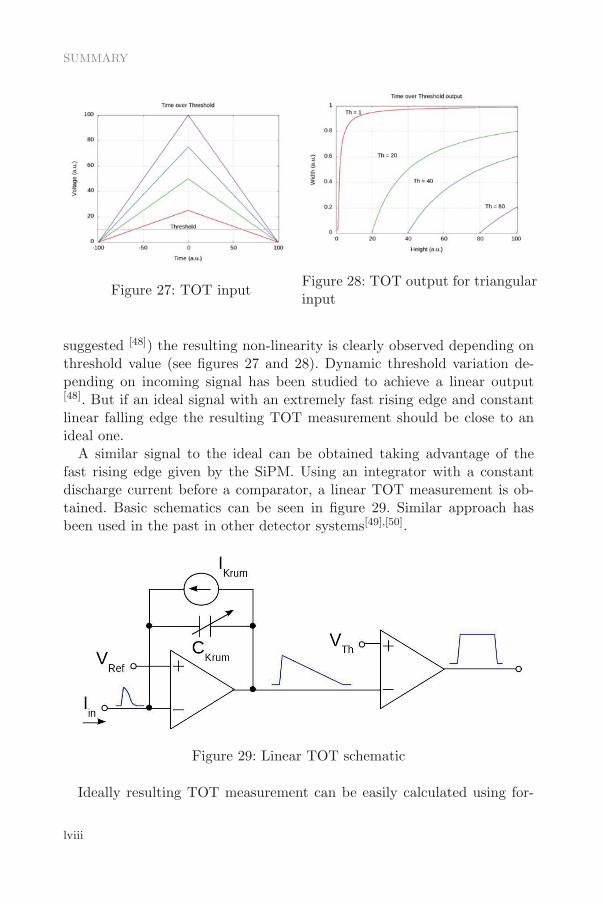
SUMMARY
Figure 27: TOT inputFigure 28: TOT output for triangularinput
suggested [48]) the resulting non-linearity is clearly observed depending onthreshold value (see figures 27 and 28). Dynamic threshold variation de-pending on incoming signal has been studied to achieve a linear output[48]. But if an ideal signal with an extremely fast rising edge and constantlinear falling edge the resulting TOT measurement should be close to anideal one.
A similar signal to the ideal can be obtained taking advantage of thefast rising edge given by the SiPM. Using an integrator with a constantdischarge current before a comparator, a linear TOT measurement is ob-tained. Basic schematics can be seen in figure 29. Similar approach hasbeen used in the past in other detector systems[49],[50].
Figure 29: Linear TOT schematic
Ideally resulting TOT measurement can be easily calculated using for-
lviii

mula 5, taking as input the injected charge signal (Q). Since thresholdvoltage (VTh), capacitance (CKrum) and discharge current (IKrum) will beconstant the measured time will have a linear behaviour with Q. The nonideal behaviour will be introduced by the slope of the rising edge of oursignal and the long decay of some SiPMs. This effect will be noticeable forvery small signals, but not for usual events from PET systems.
TTOT =Q
IKrum
− VThCKrum
IKrum
(5)
Some linearity simulations of the linear time over threshold measure-ment is summarized in figure 30 using a real measured signal as inputand including pre-amplifier. First plot represents input signal (in current),second is the voltage output of the integrator, third is the resulting timeover threshold output and last one represents the linearity error of everymeasurement.
One of the most important advantages of this structure is the flexibility.Changing the feedback capacitor and the discharge current much differentranges and time / resolution results can be obtained fitting the range ofthe desired input signal.
lix

SUMMARY
Figure 30: Linearity simulation
lx
Results
FLEXTOT prototype was received in October 2012, with 30 encapsu-lated dies on a QFN64 and 10 non encapsulated dies. During manufacturinga test system was designed thinking on testing the maximum parametersas possible. First electrical characterization was followed by more realistictests with SiPM and light sources or radioactive sources.
Test system
Test system (see figure 31) is based on a stack of three PCB with allthe needed electronics for a full system. From the sensor to the data com-munication with a host computer. The only thing not included is the highvoltage power supply for the sensors. The following electronics features arepresent in each of the different PCBs (from top to bottom):
• Sensor PCB: different manufacturers sensors can be placed over thisPCB. The sensor connects directly to next PCB, only high voltageconnector is available. A variation PCB with a charge injection circuitcan be placed in the same position to calibrate channels with a knowninput shape and peak current.
• Analog PCB: the analog PCB is basically a QFN64 test socket withlow drop-out (LDO) linear regulators and some decoupling capacitorsand resistors. It also uses a pair of amplifiers to check debug signalsdirectly to an oscilloscope and a high speed switch (SPDT) to be ableto disconnect input to channels.
• Digital PCB: EP3C low cost FPGA with FT2232 transceiver to han-dle communications with host computer. Using the FPGA the slowcontrol can be configured, pile-up interface managed, SPDT switchesconnection enabled and also a low resolution (5ns) pulse width mea-surement can be performed for all channels. It houses a basic DAQfor testing the capabilities of the ASIC.
VDDA and VDDD are powered at nominal 3.3V power supply. The av-erage power consumption is 10.7mW per channel or 7.7mW per analogchannel (excluding digital power and fast comparators with it’s thresholdDACs).
An important element to avoid changing the shape of the input signal andto maximize the input current to the input stage is the input impedance. Inthe design process this value has been kept to a reasonably low value. The
lxi

SUMMARY
Figure 31: Test system setup
measurement verify the results are as expected; with the typical inductivebehaviour at high frequencies and a value close to the typical one (around34Ω until 200MHz).
To simulate the signal generated by a SiPM a small pcb with the samesize as the one supporting the sensors have been designed. The basic circuitis an amplifier followed by an AC coupling with a resistor in series to mea-sure input current. The peak used is generated from an arbitrary waveformgenerator to mimic the signal from a SiPM.
Linearity
To obtain good linearity in the amplitude of the signal injected betweenthe AWG and the injection circuit a programmable attenuation is inserted.The generator is setup with the maximum output and is then attenuatedjust before the injection. This setup permits much better linearity in theinput signal than just modifying generator output voltage. Previous to lin-earity measurement a calibration on current input peak value is performed.Using this calibration the energy width of every channel is measured.
Since the prototype has some configurable values it will need some cal-ibration to achieve good linearity results in a defined range and times ofinput signals. Some examples of the resulting curves from a full prototype(16 channels) are plotted in 32, 34 for a τ ≈36ns and 33, 35 for a τ ≈110ns.
lxii

Figure 32: Linearity τ ≈36ns 18mA range
Figure 33: Linearity τ ≈110ns 18mA range
lxiii

SUMMARY
Figure 34: Linearity τ ≈36ns 3.5mA range
Figure 35: Linearity τ ≈110ns 3.5mA range
lxiv

SiPM measures
After electrical characterization of the prototype a real sensor is at-tached to the test system. The input signal will have a realistic timing andavoid any undesired effect introduced by the injection circuit. With thisconfiguration several measurements are performed.
Radioactive sources
To characterize with a signal close to reality several radioactive sourceshave been used. A small LSO crystal (2x2x8 mm3) has been placed overa detection channel (3x3 mm2) and then a radioactive source close to thecrystal. Previous to the measurement with sources background (LSO emis-sion spectra) is also measured and should be substracted. The sources usedhave been Na22, Co60 and Cs137, see figure 36.
Figure 36: Na22, Co60, Cs137 spectra measurement
We can observe excellent linearity in the full range. Using the positionof the two more external peaks a calibration constant is determined. The
lxv

SUMMARY
measured resolutions (σ) are then converted to energy using this constant.The resulting resolution computation is summarized in table 13. As ex-pected resolution improves for higher energies.
Source keV μ (counts) σ (counts) Res.(%)
Na22 511 53.3 7.1 9.61275 166.3 3.51 -
Cs137 662 75.9 6.6 6.9
Co60 1173 149.1 9.5 5.61332 171.6 6.41 -
1 Some more statistics or better fit should be needed
Table 13: Sources measurements for TH=40
Coincidence Resolving Time
To obtain a first estimation about the overall system timing accuracy, apreliminary measurement has been performed. The basics is to reproduce acoincidence system in the laboratory. Two test boards with single channelSiPMs are placed facing to each other. On top of the SiPM the crystal isplaced (LSO and LYSO have been tested). The Na22 radioactive source isplaced as close as possible to both crystals and just in the middle to obtaincoincident signals. The CML output is readout using differential probes. Inthe oscilloscope the timing and energy signals are acquired.
Plotting both channels energy spectra is used to select a window withthe interesting events. This window corresponds to the energies around511keV (±1σ). Previous window is used to filter relevant events from theacquisition. The resulting delay measurements of timing outputs from thoseevents are plotted in an histogram to obtain the timing accuracy of the fullsystem in figure 37 resulting in a Coincidence Resolving Time resolutionbelow 300ps FWHM (≈115ps rms).
lxvi
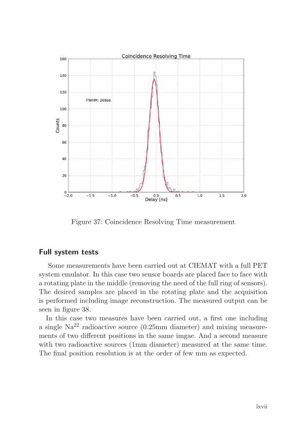
Figure 37: Coincidence Resolving Time measurement
Full system tests
Some measurements have been carried out at CIEMAT with a full PETsystem emulator. In this case two sensor boards are placed face to face witha rotating plate in the middle (removing the need of the full ring of sensors).The desired samples are placed in the rotating plate and the acquisitionis performed including image reconstruction. The measured output can beseen in figure 38.
In this case two measures have been carried out, a first one includinga single Na22 radioactive source (0.25mm diameter) and mixing measure-ments of two different positions in the same imgae. And a second measurewith two radioactive sources (1mm diameter) measured at the same time.The final position resolution is at the order of few mm as expected.
lxvii

SUMMARY
Figure 38: Full system measurements
lxviii

Design for SciFi Tracker
Design for high energy particle detectors must meet some relevant timingconstraints much more different than in other systems (such as PET).
The tracker sub-detector of the LHCb experiment reveals the paths ofelectrically charged particles as they pass through and interact with suitablesubstances. The detector records a tiny signal (light or charge) that par-ticles trigger as they move through the detector. Some built detectors usesilicon devices (strip detectors) or gaseous detectors (straw tubes). Oncethe signal is acquired and readout a computer program reconstructs therecorded patterns of tracks.
The new technology for the OT IT upgrade will be based on scintillatingfibres, with clear scintillating fibres generating and carrying the photonsfrom the inner region to the sensors placed outside the LHCb acceptance.
In the first draft of the Technical Design Report (TDR), a new scintillating-fibre layout has been proposed, with 2.5 m long fibres covering the wholecentral region of the tracker stations, from the LHC beam plane all the wayto the top and bottom of the LHCb acceptance. In this Central Tracker(CT) option, the IT and several (or all of the) OT modules are replacedby the new scintillating-fibre modules. Full detector is built by 3 stationswith three tilted (≤5o) fibre planes of X-U-V-X. Every plane is made of 5layers of fibres with 250 μm in diameter and 2.5 m long.
One of the major concerns is the production and alignment of the fibresin the modules. Some new techniques have been developed to produce suchmodules and showed promising results.
Regarding the electronics a collaboration with Clermont Ferrand andopened to any other institute from LHCb is ongoing and a common designeffort for the production of a readout ASIC will be developed, the lowPower Asic for the sCIntillating FIbres traCker, PACIFIC.
Several processing strategies are under study, but the simplest one seemsto be the baseline solution, involving pre-amplifier, shaper, gated integratorand ADC. More complex processing is also under study.
Specifications summary
A summary of the specifications for the PACIFIC readout ASIC is de-tailed in table 14.
lxix

SUMMARY
Parameter Value Unit
Channels 64 or 128 -Power 0.5 or 1 WPackage BGA -Double peak resolution 25 nsSiPM time constant 40 - 400 nsDynamic range 0-64 micro-cellsSignal time of arrival 0-15 ns
Input referred noise ≤143 pA√Hz
Table 14: PACIFIC specifications summary
Architecture
The channel architecture proposed for the PACIFIC design is depictedin figure 39. Although other alternatives are under study, specifically afastest digitization followed by digital processing, the easiest solution seemsto shape and integrate signal in the 25 ns window. Since no dead time isallowed a double and interleaved gated integrator will be needed. After theintegration a 40MHz ADC will convert the signal to digital. Afterwards aserial link will take the signal from one or several channels and serializethem into a single (probably differential) high speed link. For this last stepsome kind of multiplication frequency circuit will be needed (for examplea PLL in the figure).
Figure 39: PACIFIC channel blocks
Some common bias and digital control of configurable voltages, currentsand shaping parameters will also be needed. So current DACs, voltage
lxx

DACs and variable resistors and capacitors will also be designed, with aslow control interface built in standard cells.
Preamplifier
The input stage is current mode preamplifier with the current flowingfrom the SiPM anode to the circuit. The goal is to achieve the followingspecifications in this block;
• High bandwidth (≈ 250MHz).
• Low power (< 2mW, maximum of 8mW/channel including all ASIC).
• Low input impedance (20Ω < Zin < 40Ω).
• DC voltage controllable at input node (≈ 1V range).
• Input referred noise ≤ 143 pA√Hz
The basic circuit to achieve previous features is depicted in figure 40.The input stage is based on the same novel approach of double feedbackbut with some variations to adapt to a newer technology process (IBM0.13μm).
Figure 40: PACIFICr1 input stage
It provides a low input impedance in order to avoid affecting timing be-haviour of the SiPM and increase input current. HFFB is the high frequency
lxxi

SUMMARY
feedback path that keeps this input impedance constant (in a certain fre-quency range). The second labelled path, LFFB will provide the dc voltage(Voffset in figure) of the input node using the virtual short circuit in theamplifier that will drive a follower in a lower frequency range. The designhas been implemented taking into account that dominant pole should beset at the input node (SiPM parasitic capacitance is at the order of tenthsof pF). In this way stability is not compromised when an important capac-itance is added at the input.
lxxii

Conclusions
A detailed description on the sensor properties and requirements forboth a PET detector and SciFi tracker has been exposed. Taking as a start-ing point several implementations of readout circuits a novel input stagehas been proposed with a novel double feedback structure making possibleto achieve wide dynamic ranges and easily configurable. A behaviour modelfrom the sensor has been useful in the design stage to simulate circuit be-haviour. Two designs using this circuit intended for PET and SciFi havebeen detailed. Both of them use similar input stage but implemented ondifferent technologies. PET prototype uses SiGe technology and benefitsfrom the bipolar transistors usage (specially on input stage and referencecircuits), while SciFi prototype is a CMOS technology but benefits from asmaller feature size.
The main goals for the PET system have been fulfilled. A multi-channelarchitecture with direct connection to the SiPMs and analog processing hassuccessfully been designed and tested. The voltage adjustment on the inputwill permit to change sensor gain. Multiple signal paths proved to give thedesired results. With excellent timing measurement and also good energymeasurement and pile-up detection. The proposed input stage fits all therequirements and the rest of processing benefits from this. After design andproduction, full device testing has been performed including some tests thatexceeds the mere electronics characterization (radiation sources tests andcoincidence). The only test remaining is to integrate this electronics in areal PET system to verify it’s functionality.
The design constrainis on the PACIFIC project are still under analy-sis and this first prototype has served as a starting point. The circuitrydesigned for the SiPM readout has been ported to a new technology andsimplified for the application. Real prototype testing is still needed butmeanwhile design is ongoing adding the needed signal processing chain toachieve the goal.
lxxiii


Patent notice
As a result of the work described in this document a shared patent appli-cation was submitted in 2012:“Readout circuits for multi-channel photomultiplier arrays”, D. Gascon,A. Comerma, and Ll. Freixas (Applicants: Universitat de Barcelona andCIEMAT), European Patent Application EP12382516.8, December 20, 2012.
lxxv


1Introduction
The aim of this thesis is to present a solution for the readout of SiliconPhoto-Multipliers (SiPMs) arrays improving current implemented solu-tions. With this purpose a novel current mode input stage has been de-signed and tested. Design focuses in general applications for medical imag-ing (Positron Emission Tomography, PET). The same input stage topologyis also used for a more constrained design in particle physics (upgrade ofTracker detector at LHCb experiment).
SiPMs are recently developed electronic devices[1] with photon countingcapabilities improving current state of the art detectors regarding high volt-age requirements, signal gain and magnetic field insensitivity, while keepingat the same time excellent gain and timing characteristics and a wide dy-namic range. They are semiconductor devices still under development bysome manufacturersa in order to improve yield, to reduce dark count, toprovide multi-channel architectures and to increase light sensitivity spec-trum.
Immunity to magnetic field and compact form factor make SiPMs anideal choice for their usage in particle detectors and medical imaging sys-tems such as MR-PET scanners when used with an optically coupled scin-tillating material providing the conversion between particles to light pulses.
A Front-End Readout Application Specific Integrated Circuit (ASIC)for SiPMs is presented with the following features: wide dynamic range,
aSome manufacturers, but not all include: Hamamatsu, KETEK, SENSL, STM, Exceli-tas, AdvanSID, Photonique and Zecotek.
1
INTRODUCTION
high speed, multi channel, low input impedance, low power consumption,SiPM voltage control and timing, charge and pileup signal outputs.
Special emphasis in a detailed description on the SiPM modeling andparameter extraction to be used in the design stage is also included. Thismodel makes possible the emulation of the signal generated by differentcommercial devices in the design stage using SPICE simulations. The pa-rameters needed by the model are simple enough to be measured directlyon the devices with standard equipment.
The pre-amplifier stage includes a novel circuitry with saturation controlthat permits to be operational on the various signal paths (timing, chargeand pileup) even when the path with higher gain is completely saturated.This circuitry permits the correct operation of the measurement outputs ina wide input dynamic range. Input stage introduces a novel double feedbackloop to lower input impedance at the same time it keeps a constant DCvalue at the input node.
First prototype was submitted on June 2011 and manufactured by Aus-triaMicrosystems 0.35 μm BiCMOS technology. A second mixed mode andmore complex prototype was submitted in June 2012 with the same tech-nology for PET applications. A third prototype is envisaged for begin-ning 2014. For a high energy physics application like the Scintillating FibreTracker of LHCb, very different timing constraints should be met. A firstpre-amplifier version was submitted in May 2013 and using standard CERNtechnology IBM 130nm.
Chapter 1 with a basic detector systems overview introduces severallight sensors with their advantages and drawbacks. An important part ina detector is the scintillator, generating light bursts on particle crossing,a description of the functionality and characteristics of different types andtheir properties is also present. The chapter ends with an introductionto the two main applications developed in this work, Positron EmissionTomography (PET) and Scnitillator Fibre (SciFi) Tracker detector for theupgrade of LHCb experiment at CERN.
Chapter 2 details the model used for the simulation of signal comingfrom a SiPM with some real measurements. This Spice model is used insimulations with the schematics of the pre-amplifier block.
Chapter 3 is a summary of different developed ASICs for the readout ofSiPMs. They are intended not only for SiPMs and sometimes are compat-ible with other similar devices such as PMTs. This chapter should give anoverview of the current state in development of such electronics, with theirgood points and drawbacks. This will be the basis for defining specifications
2

for the optimal design of the electronics.Chapter 4 details the novel input stage implementation with exhaus-
tive description of it’s behaviour and advantages from the state of the artdescribed in previous chapter.
Chapter 5 focuses on the design developed for PET applications. This isa multi-channel design in AMS 0.35μm BiCMOS technology for the readoutof arrays of SiPMs, with energy, timing and pileup outputs.
Chapter 6 is a modified version of the design in previous chapter adaptedto a completely different technology (IBM 130nm) with a much lower oper-ation voltage (1.2V or 1.5V in spite of 3.3V), fully CMOS implementationand requiring much less area.
Finally in Chapter 7 the conclusions of the results achieved with currentprototypes and next steps to follow are commented.
On the Appendices several datasheets generated as documentation fordifferent prototypes are compiled including the main simulations and mea-surements.
3

INTRODUCTION
1.1 Detector Systems Overview
bMost of detector systems include the same basic functions. The signalfrom each sensor or sensor channel in a detector array must be amplified,shaped and processed for storage and analysis. Some functions are clearlyassociated with individual circuit blocks while other functions are carriedout by more than one block. In single channel systems digitization and datastorage are often combined in a single unit, but multi-channel systems nor-mally use external digitizers and data is then feed to a computer. In highlycompact detectors (such as high energy physics detectors) some channels ofanalog and digital electronics are often accommodated in specific circuits(ASICs).
Figure 1.1: Typical detector system [2]
The typical sequence of detector functions is illustrated in figure 1.1.The sensor converts the energy deposited by a particle or photon to anelectrical signal. This can be achieved in different ways (see section 1.2). Insome cases the resulting sensor pulses can be quite short (few nanosecondsor less).
The signal charge can be quite small (of the order of few fC for typicalsensors and signal) so it will need some amplification. The pre-amplifierwill perform this amplification keeping in mind that the minimal electronicnoise is required to avoid degradation of the signal. The specific factor ofamplification will depend on the original gain of the sensor, signal rangeand resolution requirement of the measure.
Normally the function of the shaper in detector systems is to improvethe signal to noise ratio (SNR). Signal and noise do not present the samefrequency spectra so one can improve the SNR by applying a filter thattailors the frequency response, attenuating the noise. This change in thefrequency response will produce a change in the signal shape, thus the nameof the stage. Simple shapers normally reduce the bandwidth. The result of
bBased on [2]
4

1.1 DETECTOR SYSTEMS OVERVIEW
this reduction is that the signal becomes slower. This can lead to overlap-ping between signals (if high rate is expected), called pile-up. Shapers canbe of high complexity with several stages, but it is common to all shapersto constrain maximum and minimum frequency bounds, determining risetime and pulse duration. When designing a system it is necessary to findthe proper balance between noise and speed. Sometimes the shaper is hid-den, an input stage integrating the input pulse should translate the chargeinto voltage that can be held for digitization. This is also a form of shaping.
Digital conversion will translate the voltage amplitude into discretesteps corresponding to a digital bit pattern. Analog to Digital Converters(ADCs), are widely used nowadays. Generally speed and resolution areopposing parameters in ADCs, as speed and power.
5

INTRODUCTION
1.2 Light sensors
Several light sensors exist and have been used in the past. The mostnotable is the classical Photo-Multiplier Tube (PMT), but some other al-ternatives are also present such as Avalanche Photo-Diode (APD) and re-cently the SiPMs. Their usage ranges from particle detectors to medicalimaging and astroparticle detectors.
1.2.1 Photo-Multiplier Tube, PMT
Figure 1.2:PMTc
This devices are a type of vacuum tubes. They are verysensitive light detectors in different spectra (typically opti-mised for visible or ultraviolet). They are so sensitive thateven single photons can be measured. This combination ofhigh gain, low noise, fast response and large area of lightcollection are often desired in high energy physics applica-tions or medical imaging. First photomultiplier producedis dated around 1935 [3].
The basic of operation combines the photoelectric ef-fect with amplification produced by secondary emission.In figure 1.3 a schematic view of its parts and opera-tion can be seen when coupled to a scintillating mate-rial. The two major components inside the tube are aphotosensitive layer, called photo-cathode, coupled to anelectron multiplier structure. Once the incoming photonshit the photo-cathode, the photoelectric effect producessome low-energy electrons (photo-electrons). If the incom-ing light consists of a pulse from a scintillation crystal, thephotoelectrons produced will also be a pulse of similar duration. Becauseonly a few hundred photoelectrons may be involved in a typical pulse, theircharge is too small at this point to serve as a convenient electrical signal.
The electron multiplier section in a PMT provides an efficient collectiongeometry for the photoelectrons as well as serving as a nearly ideal ampli-fier to greatly increase their number. Electrons from the photo-cathode areaccelerated and caused to strike the surface of an electrode, called a dyn-ode. If the dynode material is properly chosen, the energy deposited by theincident electron can result in the re-emission of more than one electron.Electrons leaving the photo-cathode have a very low kinetic energy. There-fore, if first dynode has a positive potential of several hundred volts the
cImage extracted from wikipedia
6

1.2 LIGHT SENSORS
kinetic energy of electrons at arrival is determined almost by the acceler-ating voltage. The usage of several stages produce more and more amplifi-cation on every stage. After amplification through the multiplier structure,a typical pulse will give rise to 107-1010 electrons, sufficient charge to beprocessed after being collected in the anode[4].
Figure 1.3: Photomultiplier basic operation
Photo-cathodes can be constructed as either opaque or semitransparentlayers. Several photo-cathode materials provide sensitivity to a wider ornarrower spectra adapting to the application. The variety of spectra sensi-tivity of the PMT (changing the material of the photo-cathode) makes itan ideal solution for ultra violet light measurement. An important practicalproperty of photo-cathodes is the uniformity to which their thickness can beheld over the entire area. Variations in thickness give rise to correspondingchanges in sensitivity and can be one source of resolution loss.
Spontaneous electron emission is produced by thermal emission. Normalconduction electrons within the photo-cathode material will always havesome thermal kinetic energy that, at room temperature, will average a lowvalue. There is a spread in this distribution, however, and those electrons atthe extreme upper end of the distribution can occasionally have an energythat exceeds the potential barrier. If that electron is close enough to thesurface, it may escape and give rise to a spontaneous thermally inducedsignal.
The sensitivity of photo-cathodes cathodes can be quoted in several ways.A unit with great significance is the Quantum efficiency (QE). Thequantum efficiency is as simple to describe as in formula 6[4]. The efficiencywould be 100% for an ideal photo-cathode, but practical devices show muchsmaller values.
QE =photoelectrons emitted
incident photons(6)
7

INTRODUCTION
The quantum efficiency of any photo-cathode will be a strong function ofthe wavelength (or energy of incoming photons). To estimate the effectivequantum efficiency when used with a particular light source, the curve ofQE versus wavelength must be averaged over the emission spectrum.
To define the overall detection capabilities of the sensor the most commonmeasure is the Photon Detection Efficiency (PDE). It is the result ofjoining the QE of the photo-cathode and the Collection Efficiency (CE)of the amplifications dynodes (see formula 7). The Collection Efficiency willinclude geometrical effects on the construction that lead to dead area orsignal loss before the first dynode.
PDE = QE x CE (7)
Multi-channel devices with arrays of 8x8 channels have been producedand arranged in a rectangular packaging to improve area coverage withsmall crosstalk and keeping excellent properties [5].
Most important drawbacks of using PMTs are:
• Dark current (noise) produced by photo cathode thermal emission ofelectrons.
• Low Quantum Efficiency.
• High voltage needed for it’s operation (typically between 1000 and2000 V).
• Magnetic field sensitivity.
• Mechanically fragile.
• Size.
• Ageing (photo-cathode degrades with use).
8

1.2 LIGHT SENSORS
1.2.2 Avalanche Photo-Diode, APD
Avalanche Photo-Diodes are semiconductor devices based on the pho-toelectric effect and avalanche multiplication. By applying a high inversevoltage polarization just over breakdown (from 100 to 1000 V dependingon devices), an important gain can be obtained (in the range of 100 to1000). If more gain is needed (105 or 106) this devices can be operated overthe breakdown voltage in Geiger mode, with external circuitry to providequenching of the device.
On conventional photo-diodes, when light is incident on the semiconduc-tor, electron-hole pairs are generated. Photons from a scintillator typicallycarry about double the energy of the semiconductor bandgap, thus suffi-cient to create the electron-hole pairs. Since this conversion is not limitedby the need of carriers to escape from a surface (as in a photo-cathode)the maximum quantum efficiency can be larger upto 60-80%. The sensi-ble wavelength is often also wider than from PMTs, so it results in moreprimary charge generated from the incoming light.
Figure 1.4: Typical photo-diode configuration
A typical configuration[4] can be seen in fig-ure 1.4, with a p-layer as thin as possible toenhance transmission of light, and a volumepolarized with an electric field to collect thegenerated pairs. Generally APDs are designedas fully depleted detectors, consisting of highpurity p or n silicon with highly doped p and ntype contacts at opposite surfaces. Electronicnoise in such devices is much more importantthat dark current in PMTs.
The small amount of charge that is producedby photoelectric effect in a conventional photo-diode can be increasedthrough an avalanche process that occurs in a semiconductor at high val-ues of applied voltage. The charge carriers are accelerated sufficiently be-tween collisions to create additional electron-hole pairs along the collectionpath. The internal gain helps pull the signal up from the electronic noiselevel and permits good energy resolution than conventional photo-diodes.Because gain is very sensitive to temperature and voltage, they requirewell-regulated high-voltage supplies.
9

INTRODUCTION
Figure 1.5: Typical APD configuration
A typical construction[4] knownas reach-through configurationis shown in figure 1.5. Lightenters through the thin p+
layer on the left of the dia-gram and interacts somewherewithin the π region that consti-tutes most of the diode thick-ness. The results of interactionsare electron-hole pairs, and the
electrons are drawn to the right through the drift portion and into themultiplying region, with high electric field (p-n+ union in the right). Hereadditional pairs are created increasing the signal. Gain factor of a few hun-dred are typical and quantum efficiency can be as high as 80%.
Typical applications for APDs are on telecommunications, laser rangefind-ers and in some cases have been used in medical imaging and particle de-tectors. APDs arrays are becoming commercially available.
Compared to PMTs, APDs offer some advantages;
• High Quantum Efficiency.
• Relatively low voltage needed (between 50 V and 400 V typically).
• Magnetic field insensitivity.
• Robust and small.
And also some drawbacks;
• Electronic noise is important.
• Small gain.
• Radiation hardness.
10
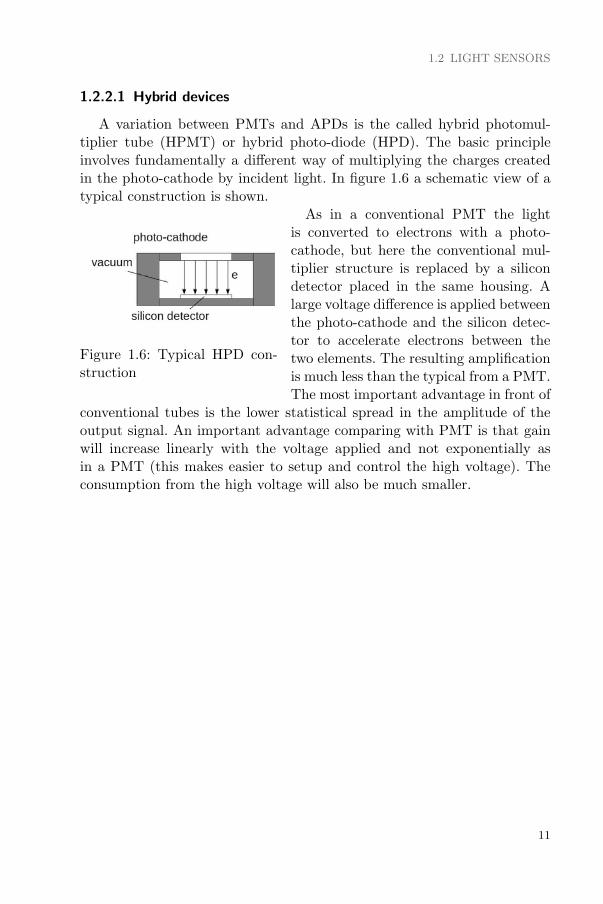
1.2 LIGHT SENSORS
1.2.2.1 Hybrid devices
A variation between PMTs and APDs is the called hybrid photomul-tiplier tube (HPMT) or hybrid photo-diode (HPD). The basic principleinvolves fundamentally a different way of multiplying the charges createdin the photo-cathode by incident light. In figure 1.6 a schematic view of atypical construction is shown.
Figure 1.6: Typical HPD con-struction
As in a conventional PMT the lightis converted to electrons with a photo-cathode, but here the conventional mul-tiplier structure is replaced by a silicondetector placed in the same housing. Alarge voltage difference is applied betweenthe photo-cathode and the silicon detec-tor to accelerate electrons between thetwo elements. The resulting amplificationis much less than the typical from a PMT.The most important advantage in front of
conventional tubes is the lower statistical spread in the amplitude of theoutput signal. An important advantage comparing with PMT is that gainwill increase linearly with the voltage applied and not exponentially asin a PMT (this makes easier to setup and control the high voltage). Theconsumption from the high voltage will also be much smaller.
11

INTRODUCTION
1.2.3 Silicon photo-multipliers, SiPM
A silicon photo-multiplier is a relatively new device formed by hundredsof micro-cells in parallel. Each micro-cell is an Avalanche Photo Diodes(APDs) working in Geiger mode, with its own quenching resistor to avoiddestruction of the device. APDs behaviour is well known and has beenstudied during many years since 1960 [7]. All those micro-cells are combinedin one single output (connected in parallel). The result is an output similarto the one produced by a PMT, but with a somehow discrete analog output(since each cell releases a fixed amount of charge when fired). In figures 1.7and 1.8 and table 1.1 some commercial devices from Hamamatsu can becompared.
Figure 1.7: S10362-11-025P
Figure 1.8: S10931-050P
Parameter 025P 050P 100C
Number of cells 1600 2600 100
Cell size (μm2) 25x25 50x50 100x100
Active area (mm2) 1x1 3x3 1x1
Voltage operation (V) ≈ 70V ≈ 70V ≈ 70V
Gain 2.75x10⁵ 7.5x10⁵ 2.4x10⁶
Fill Factor 0.31 0.62 0.79
Table 1.1: Hamamatsu SiPMs characteristics
In the same way as the APDs, the first pairs are generated by photoelec-tric effect and then multiplied inside the same silicon. But in this case the
All referred commercial devices must be taken in the context of an evolving technology.Thus real numbers may have varied with time and newer models introduced. Valuesshould be taken just as example.
12

1.2 LIGHT SENSORS
multiplication is an avalanche, produced over breakdown voltage.In a normal multiplication process electrons are drawn through the high
field region and create additional electron-hole pairs. The electrons continuein the same direction but holes are attracted in the opposite direction.At a sufficient high field values (over breakdown voltage) the holes canalso multiply and, since hole multiplication also produces additional freeelectrons, this process leads to a runaway. To avoid a destructive effect ofthe avalanche a resistor in series is connected to each APD so the voltageit’s dropped when it reaches some current limit. This combination of APDand quenching resistor is the micro-cell. The resulting gain is similar to thePMT on the order of 105 to 107.
Since SiPMs are constructed as a group of smaller micro-cells an extraconcept should be added when defining the characteristics, this conceptis called Photon Detection Efficiency (PDE). It’s nothing more thanjoining the effects produced by the area lost between micro-cells and Quan-tum Efficiency. Since there is some area not able to detect incoming light aFill Factor (FF) is defined as in 8. The resulting PDE will be calculatedeasily using formula 8 with Pstart being the probability of an electron-holeto start an avalanche. Some techniques used to improve crosstalk betweenmicro-cells (such as adding trenches) can degrade this value. The reduc-tion of micro-cell size to increase dynamic range will also make a worse fillfactor.
FF =Total Device Area
Sensible Area→ PDE = FF x QE x Pstart (8)
Most important advantages with respect to other sensors are:
• High quantum efficiency.
• Magnetic field insensitivity.
• Robust and small.
• Low voltage operation (from 20V to less than 100V).
• Arrays available.
And drawbacks or possible problems:
• Radiation hardness.
• Low PDE.
• Dark count.
13
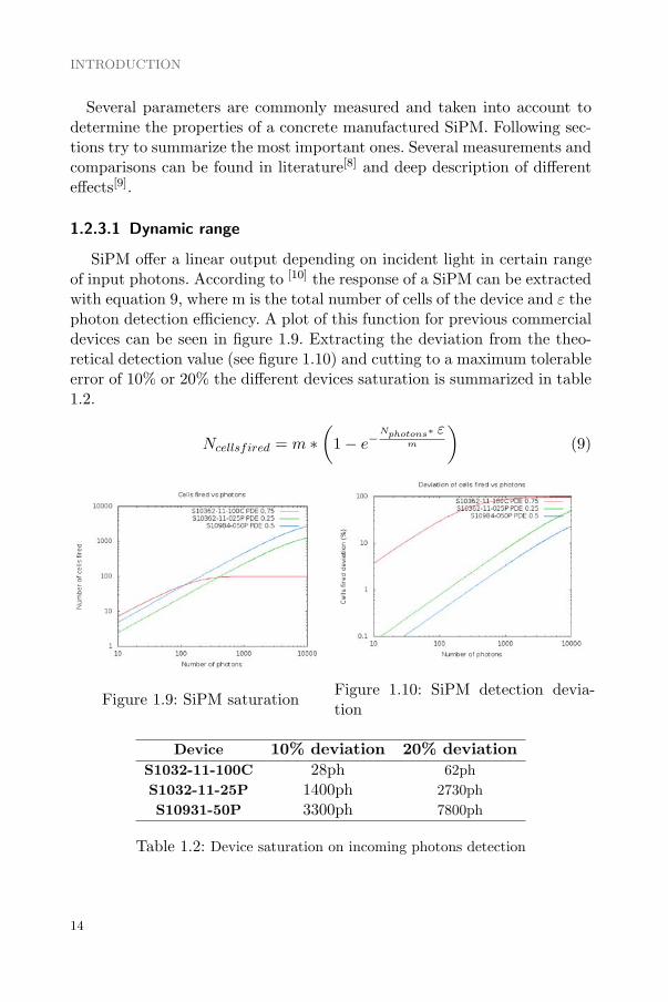
INTRODUCTION
Several parameters are commonly measured and taken into account todetermine the properties of a concrete manufactured SiPM. Following sec-tions try to summarize the most important ones. Several measurements andcomparisons can be found in literature[8] and deep description of differenteffects[9].
1.2.3.1 Dynamic range
SiPM offer a linear output depending on incident light in certain rangeof input photons. According to [10] the response of a SiPM can be extractedwith equation 9, where m is the total number of cells of the device and ε thephoton detection efficiency. A plot of this function for previous commercialdevices can be seen in figure 1.9. Extracting the deviation from the theo-retical detection value (see figure 1.10) and cutting to a maximum tolerableerror of 10% or 20% the different devices saturation is summarized in table1.2.
Ncellsfired = m ∗(
1− e−Nphotons∗ ε
m
)(9)
Figure 1.9: SiPM saturationFigure 1.10: SiPM detection devia-tion
Device 10% deviation 20% deviation
S1032-11-100C 28ph 62ph
S1032-11-25P 1400ph 2730ph
S10931-50P 3300ph 7800ph
Table 1.2: Device saturation on incoming photons detection
14

1.2 LIGHT SENSORS
1.2.3.2 Gain Variation with Temperature
SiPM devices have an important temperature coefficient which modifiestheir breakdown voltage thus affecting their gain. The temperature coeffi-cient is common to all devices and equal to 56mV/oC. In figures 1.11 and1.12 it is represented the gain variation with the temperature change [11].
The gain change extracted from previous figures is 4%/oC in 50μm de-vices and 2%/oC in 25μm devices. If an array of devices should be com-pensated without modifying the general polarization voltage in a range of10oC the voltage applied is calculated in 10.
Figure 1.11: S10362-11-025 Gainvariation with temperature
Figure 1.12: S10362-11-050 Gainvariation with temperature
ΔT = 10◦C, ΔV25 = ΔT ∗ 0.021V
0.5= 400mV
ΔT = 10◦C, ΔV50 = ΔT ∗ 0.041V
1.5= 267mV (10)
The resulting controlling DAC should provide a range to compensatethe temperature and gain uniformity variations (1.1V for the 25μm devicewhile only 500mV for the 50μm devices) with resolution (to achieve 1%gain adjustment) of around 6.66mV for the 50μm devices and 20mV forthe 25μm devices.
All referred commercial devices must be taken in the context of an evolving technology.Thus real numbers may have varied with time and newer models introduced. Valuesshould be taken just as example.
15

INTRODUCTION
1.2.3.3 Gain Uniformity
Those devices offer a very linear gain versus voltage characteristic thatpermits to compensate uniformities between different sensors. This linearcharacteristic is around 50%/V in 25μm devices and 150%/V in 50μm
devices, as seen in figures 1.13 and 1.14 extracted from [11]. If the gainshould be adjusted at a level of 1% a voltage adjust resolution of 6.66 mVin the 50μm devices while only 20mV in the 25 μm devices.
Figure 1.13: S10362-11-025 Gainvariation with Voltage
Figure 1.14: S10362-11-050 Gainvariation with Voltage
The expected dispersion between gain in devices should also be compen-sated and is expected to be as high as 35% [12]d. In the worst case a 25μm
device would need a voltage compensation calculated in 11, while a 50μm
device should need much less voltage adjust due to it’s gain variation.
ΔG = 0.35, ΔV25 =1V ΔG
0.5= 700mV
ΔG = 0.35, ΔV50 =1V ΔG
1.5= 233mV (11)
dThis gain dispersion should be verified with a significant number of devices, recenttested arrays of SiPMs does not report a dispersion bigger than 13%, but they couldhave been selected on manufacturing process
All referred commercial devices must be taken in the context of an evolving technology.Thus real numbers may have varied with time and newer models introduced. Valuesshould be taken just as example.
16

1.2 LIGHT SENSORS
1.2.3.4 Typical Signal
Typical output signal from a SiPM connected directly to a load (50Ω)resistor can be observed in figure 1.15. Measurement is performed using anoscilloscope with long retention on the screen (30s), so signals are accumu-lated on the same screen.
The trigger is connected to the same signal firing a red laser LED facingthe SiPM. Signal is adjusted to be as low as possible so different cells firingcan be observed directly and distinguished on the screen. The differentpeak amplitudes on the screen result from a different number of micro-cellstriggered by single photons.
Figure 1.15: Typical signal from SiPM
17

INTRODUCTION
1.2.3.5 After Pulsing
After Pulsing is a known effect which consists on the generation of aspontaneous peak output after a first peak. It is due to the trapping of somecharge in the semiconductor defects. This charge has some probability tobe released afterwards. If this charge is released will start a new avalanche.Typical release times range from few ns to several hundreds of ns. The firstreleased charges (few ns) do not affect the signal because the micro-cellsare not fully recharged, but will increase recovery time. Working at lowtemperatures will make release of this trapped charges slower, so the afterpulses will be more noticeable.
1.2.3.6 Dark Count
Dark Count is one of the most important drawbacks of the SiPMs. Darkcount is generated by spontaneous thermally generated carriers. Those car-riers can then generate an avalanche in the micro-cell that will be identicalto a true signal generated by a photon. The name of dark count comesfrom the fact that this signal will continue being generated without anyillumination at all. The average number of avalanches in some time wouldgive the expected count rate (normally in Hz).
The evolution of dark count rate with over-voltage applied to the de-vice typically follows an exponential increase. In figures 1.16 and 1.17 darkcount versus operation voltage is plotted by the manufacturer with twodifferent thresholds to determine if dark count exists, one set to 0.5 photoelectrons (0.5 micro-cell amplitude) and a second set to 1.5 photo electrons.For this reason over-voltage is kept to the minimum to obtain the desiredgain. Since breakdown voltage, thus gain, thus dark count will change de-pending on temperature, it’s important to keep under control the operatingtemperature of the device.
All referred commercial devices must be taken in the context of an evolving technology.Thus real numbers may have varied with time and newer models introduced. Valuesshould be taken just as example.
18

1.2 LIGHT SENSORS
Figure 1.16: S10362-11-025 DarkCount variation with Voltage
Figure 1.17: S10362-11-050 DarkCount variation with Voltage
1.2.3.7 Crosstalk
An important aspect is the crosstalk between different micro-cells.Crosstalk can be electrical or optical. Electrical crosstalk is producedwhen some carrier (electron or hole) produced by an avalanche of a microcell crosses the boundary between micro cells producing a second avalanchein the neighbouring cell. Optical crosstalk is produced by photons generatedin the avalanche going to neighbour micro-cell crossing oxide over the cells(optically transparent).
Worse crosstalk will increase statistical fluctuations in the signal gener-ated from the device. Thus it should be reduced to the maximum. Severaltechniques are applied to reduce crosstalk. Most used ones are: increasingdistance between micro cells and producing trenches between devices. In-creasing distance has the inconvenient of reducing fill factor, and PDE so itshould be avoided if possible. Trenches between devices are a much more re-liable method since a barrier is produced between micro-cells and the loss offill factor is the minimum permitted by the trenching technology. Trenchesare often filled by some opaque material to avoid optical transmission.
1.2.4 Arrays construction
SiPM can be constructed in two different configurations depending onthe substrate doping. A p-on-n device or a n-on-p device can be defined, seefigure 1.18. The operation principle in both cases is the same but the final
19

INTRODUCTION
behaviour is slightly different; in a p-on-n structure (figure 1.18, left) bluelight will be absorbed in first nm of p+ layer. In this process an electron-hole pair will be created and the electron will drift to the junction andgenerate an avalanche with high probability. Longer wavelengths will beabsorbed in deeper silicon on the n layers after the junction and holes willdrift to the junction, leading to less probability of generating avalanche.Opposite to that, in a n-on-p structure photons with shorter wavelengthwill have less probability of generating an avalanche.
Figure 1.18: SiPM construction topologies
Those differences of the carrier probabilities lead to different PDE for aspecific wavelength (see figure 1.19, p-on-n device, extracted from Hama-matsu technical information). The peak of PDE will move from around400-450nm to 550-600nm depending on construction topology.
Observing carefully table 1.3 most scintillating materials provide themaximum signal in the range of 400-450nm. Then it is more interestingin order to maximize the final PDE to use a p-on-n structure.
If it is assumed that the substrate should be common to all channelsof an array (to avoid wells and dead area between channels) the final de-vice should have a common-cathode arrangement by construction. Discretechannels packaged together to construct arrays can also be produced, butthe price to pay will be more dead area between channels. Those discretechannels could be pre-selected to achieve better overall behaviour in the ar-ray (gain uniformity between channels, dark count and operating voltage).
All referred commercial devices must be taken in the context of an evolving technology.Thus real numbers may have varied with time and newer models introduced. Valuesshould be taken just as example.
20

1.2 LIGHT SENSORS
Figure 1.19: PDE variation with Wavelength
21
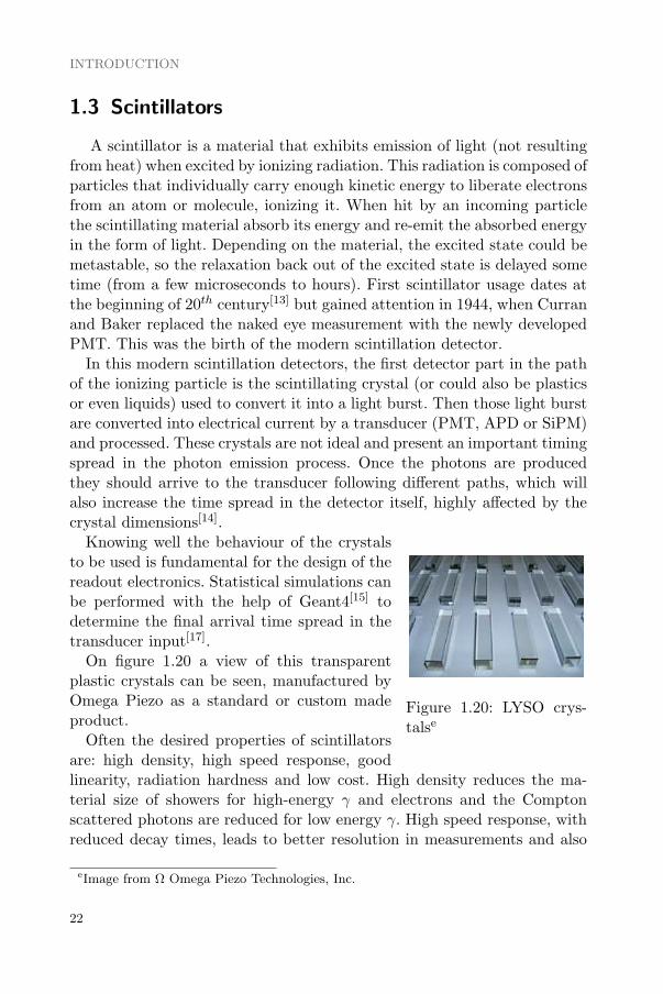
INTRODUCTION
1.3 Scintillators
A scintillator is a material that exhibits emission of light (not resultingfrom heat) when excited by ionizing radiation. This radiation is composed ofparticles that individually carry enough kinetic energy to liberate electronsfrom an atom or molecule, ionizing it. When hit by an incoming particlethe scintillating material absorb its energy and re-emit the absorbed energyin the form of light. Depending on the material, the excited state could bemetastable, so the relaxation back out of the excited state is delayed sometime (from a few microseconds to hours). First scintillator usage dates atthe beginning of 20th century[13] but gained attention in 1944, when Curranand Baker replaced the naked eye measurement with the newly developedPMT. This was the birth of the modern scintillation detector.
In this modern scintillation detectors, the first detector part in the pathof the ionizing particle is the scintillating crystal (or could also be plasticsor even liquids) used to convert it into a light burst. Then those light burstare converted into electrical current by a transducer (PMT, APD or SiPM)and processed. These crystals are not ideal and present an important timingspread in the photon emission process. Once the photons are producedthey should arrive to the transducer following different paths, which willalso increase the time spread in the detector itself, highly affected by thecrystal dimensions[14].
Figure 1.20: LYSO crys-talse
Knowing well the behaviour of the crystalsto be used is fundamental for the design of thereadout electronics. Statistical simulations canbe performed with the help of Geant4[15] todetermine the final arrival time spread in thetransducer input[17].
On figure 1.20 a view of this transparentplastic crystals can be seen, manufactured byOmega Piezo as a standard or custom madeproduct.
Often the desired properties of scintillatorsare: high density, high speed response, goodlinearity, radiation hardness and low cost. High density reduces the ma-terial size of showers for high-energy γ and electrons and the Comptonscattered photons are reduced for low energy γ. High speed response, withreduced decay times, leads to better resolution in measurements and also
eImage from Ω Omega Piezo Technologies, Inc.
22

1.3 SCINTILLATORS
identification of the type of particle measuring decay time (different timesare generated depending if they are γ and ions) and also useful to avoiddead time. High speed rise time will produce better timing measurements.Good linearity is mandatory for the measurement of energy in some range.Radiation hardness is needed to allow long life time of the detector since itwill be normally placed in a hard environment (in the case of high energyphysics or radiation measurement equipment). Finally cost is an impor-tant factor since most crystal scintillators require high-purity chemicalsand sometimes rare-earth metals that are expensive. Many crystals alsorequire expensive furnaces and long time (months) of growth.
Trying to improve the previous commented properties several types ofscintillating materials have been developed:
• Organic crystals: Organic scintillators are aromatic hydrocarboncompounds. They have a typical decay time of a few nanoseconds.Most common types are anthracene (C14H10, decay time ≈ 30ns),stilbene (C14H12, 4.5 ns decay time) and naphthalene (C10H8, fewns decay time). They are very durable but their energy resolutionis not optimal and can not be easily manufactured, so they are notoften used. Anthracene has the highest light output and is chosen asa reference in organic scintillators.
• Plastic: Plastic scintillators typically refers to a scintillating materialin which the primary fluorescent emitter (called fluor) is suspendedin the base (a solid polymer matrix). Polyethylene naphthalene ex-hibit scintillation by itself and is expected to replace existing plasticscintillators. The advantage of plastic scintillators include high lightoutput and fast signal (with decay time of 2-4 ns) and they can beshaped easily. Several combinations of bases and fluors lead to differ-ent properties.
• Inorganic crystals: Inorganic scintillators are usually crystals grownin high temperature furnaces often with a small amount of activatorimpurity. The most widely used is NaI(Tl)(sodium iodide doped withtallium). Newly developed products include LaCl3(Ce), lanthanumchloride doped with Cerium, as well as Cerium-doped lanthanum bro-mide, LaBr3(Ce). They are both very hygroscopic but offer excellentlight output and energy resolution with a fast response and excellentlinearity. LYSO has an even higher density, is non-hygroscopic, andhas a higher light output in addition to being rather fast.
• Gaseous: Gaseous scintillators consist of nitrogen and the noblegases helium, argon, krypton and xenon. The detector response is
23

INTRODUCTION
very fast (≈1 ns), they typically emit in the ultraviolet so some wave-length shifting is needed.
• Glasses: Most common glass scintillators are cerium-activated lithiumor boron silicates. Glass detectors are particularly well suited for thedetection of slow neutrons. Lithium is more used since it has greaterlight output. Their response time is ≈10 ns but their light output istypically low.
Typical properties of some inorganic scintillating materials are summarizedin table 1.3. Organic ones present much lower density (around 1 g/cm3) andlower light emission (around 50% of NaI(Tl)).
1.3.1 Phoswich
Phoswich[16] or ”phosphor sandwich” is a combination of scintillatorswith two very different pulse shape characteristics (typically very differentdecay time) optically coupled to each other and to a common light sen-sor (typically a PMT). Analysis of the output signal can distinguish thescintillator originating the signal.
Figure 1.21: Phoswich
In figure 1.21 a schematic view of the configu-ration of a typical phoswich system is presented.In this configuration a thin crystal is followed bya second more thick one and then followed by thelight sensor.
The main advantage of this technique is thatwithout incrementing the number of channels itimproves resolution of the direction of incomingparticle. This is achieved because the interactiondeep in the sensor is better constrained due to the
determination of the crystal that generated the signal.
24

1.3 SCINTILLATORS
Scin
tillato
rD
ensi
tyW
avele
ngth
Refr
active
Decay
Lig
ht
yeld
Mate
rial
(g/cm
3)
at
max.(
nm
)in
dex
tim
e(n
s)(p
h/M
eV
)
NaI(
Tl)
3.67
415
1.85
230
3800
0C
sI(T
l)4.
5154
01.
80
680,3
340
4000
0,25
000
Bi 4G
e3O
12
7.13
480
2.15
300
8200
BaF
24.
8922
0,31
01.
56
0.6
,630
1500
,950
0C
eF
36.
1631
0,34
01.
68
5,2
744
00Y
AlO
3(C
e)
5.37
370
1.95
27
1800
0Lu
2SiO
5(C
e)
7.4
420
1.82
47
2500
0LaB
r 3(C
e)
3.79
350
1.9
27
4900
0B
C-4
00
1.03
420
1.58
2.4
1000
0B
GO
:B
i 4(G
eO
4) 3
7.13
480
2.15
300
5700
LSO
:Lu
2(S
iO4)O
:Ce
7.4
420
1.82
42
2850
0G
SO
:G
d2(S
iO4)O
:Ce
6.71
440
1.85
60
7600
LY
SO
:Lu
1.8Y
0.2(S
iO4)O
:Ce
7.1
420
1.81
40
4000
0
Table 1.3: Inorganic scintillators properties summary
25

INTRODUCTION
1.4 SiPMs Applications
Silicon Photo Multipliers could be used in any application where a fastmeasurement of a small light signal is needed. Today’s main applicationsare medical imaging and particle detectors.
Applications have very different timing constraints and expected signalrequirements, but most of them include a huge number of channels andoften the design uses arrays of detectors. In this work two applicationsare explored; first would be the detection of the gamma rays emitted by aradionuclide in the body to detect accumulation in different areas of thebody (for Positron Emission Tomography scanners). And then for buildingtracking detectors with the help of scintillating material to produce lightfrom the incoming particles (Scintillating Fibre Tracker at LHCb).
1.4.1 Medical Imaging
The usage of SiPMs in medical imaging applications is basically re-duced to PET or Single-Photon Emission Computed Tomography (SPECT)systems. SiPMs offer similar or better performance than other types ofsensors[20] with the advantages of it’s low operation voltage, magnetic fieldtolerance and robustness. Permitting combined systems such as MR-PET.
1.4.1.1 Positron Emission Tomography
Positron Emission Tomography (PET) is a nuclear medical imagingtechnique to produce three-dimensional images of functional processes inthe body. PET systems are based on detection of gamma rays pairs emit-ted indirectly by a radionuclide (tracer) introduced into the body. Dataproduced with the concentration of the gamma rays pairs and their arrivaltime is used in computer analysis to produce 3D images of their activityinside the body. Modern devices complete the image performing a secondscan with CT-X-ray in the same machine although a combination with MRI(Magnetic Resonance Imaging) would be preferred due to the lack of addedirradiation of the patient and better contrast in soft tissues.
The concept and basics of emission and transmission tomography wasintroduced by David E. Kuhl, Luke Chapman and Roy Edwards in thelate 1950s. The first demonstration of this process in medical imaging wasperformed by Gordon Brownell, Charles Burnham and their associates atthe Massachussetts General Hosbital in 1953[21]. In 1961, James Robert-son and his associates at Brookhaven National Laboratory built the first
26

1.4 SIPMS APPLICATIONS
Figure 1.22: Schema of PET imaging system
single-plane PET scan, nicknamed the ”head-shrinker”. The developmentsat University of Pensilvania and Washington University School of Medicineproduce first scanners[22][23].
A key element to the development and usage of PET systems is the par-allel evolution of radiopharmaceuticals. In particular the development ofseveral compounds (for example 2-fluorodeoxy-D-glucose, 2FDG) to deter-mine its concentration in different organs by the scanner.
First scanners relied on two 2 dimensional arrays of detectors, but soon itwas clear that a logical distribution for full readout detectors was to placeit forming a ring around the patient. A schematic view of the system isshown in figure 1.22.
The detector block is usually formed by scintillator crystals (convertinggamma ray into light bursts) followed by photomultiplier tubes (convertinglight burst into current pulses) and readout electronics (with amplificationand time tagging of the input signal).
The final spatial resolution of the hardware depends on the size of thecrystals and time accuracy of the whole system. In figure 1.23 a detailedview of the detector block can be observed, note the size of the photomul-tiplier compared with the scintillating crystals.
27

INTRODUCTION
Figure 1.23: Detail of PET imagingsystem detector block and ring
Combination of PET scans withCT-X-ray or MRI giving bothanatomic and metabolic informationin the same scanner is very usefulsince patient won’t move betweenscans and will make easier to corre-late both images. This is importantin structures with anatomic varia-tions or moving organs (outside thebrain).
Radionuclides used in PET scan-ning are typically isotopes with short half-lives such as carbon-11 (20 min),nitrogen-13 (10 min), oxigen-15 (2 min), fluorine-18 (110 min) or rubidium-82 (1.27 min). These nuclides are incorporated into compounds normallyused by the body such as glucose, water or ammonia or into molecules thatshould bind to receptors. Such labelled compounds are known as radiotrac-ers. PET technology can be used to trace the biologic pathway of thosecompounds. At present, the most used radiotracer in PET is fluorodeox-uglucose (FDG), with fluorine-18, used in all scans of oncology and mostof neurology. Those radionuclides have traditionally been produced using acyclotron in close proximity to the PET scanner. The minimization of radi-ation dose to the subject is the reason to use short-lived radionuclides butthe proximity to cyclotrons (and cost) and the need of preparation of thetracer after irradiation of the isotope limit its adoption. Because of the half-life of fluorine-18 is about two hours, the prepared dose will need frequentrecalibration and careful planning with respect to patient scheduling.
The raw data generated by PET scanner are a list of coincidence eventsrepresenting near-simultaneous detections of annihilated photons (in a 180degrees placed detectors). Each coincidence represents a line in space con-necting the two detectors (line of response, LOR). Coincidence events canbe gropued into projection images, called sinograms. Those sinograms areanalogous to the ones produced by CT-X-ray scanners, but with much lessstatistics (at least three orders of magnitude less). As such PET data sufferfrom scatter and random events much more dramatically than CT-X-rayscans. In practice considerable pre-processing of the data is required.
PET systems will only accept as valid events the ones in the energywindow produced by the gamma ray. This is around 511keV. If an event isaround this energy and in coincidence with an other event at a 180 degreethen it will be an accepted event. All the rest is discarded. To avoid system
28

1.4 SIPMS APPLICATIONS
bottlenecks it is important to take the decision if an event is saved ordropped as soon of possible in the detector chain.
Some crystals have spontaneous emission of light, emitting an spectra inthe region of interest. As an example Saint Gobain’s Prelude 420[24] is alutetium based scintillator with a radioactive isotope generating 3 gammaray cascade of 307, 202 and 88 keV, being the most probable a 597keVdeposited in the scintillator. This can be useful for offline calibrations ofthe detector. This are the case of LSO and LYSO crystals, widely used inPET systems.
1.4.1.2 Time Of Flight
Time of Flight (TOF) is the name given to several methods to measurethe time it takes for a particle to travel some distance. This measure canbe used as a way to determine some property of the medium (velocity) orto know more about the particle. In PET systems the relevant events aredetected easily using coincidence of two particles of 511keV at 180 degrees.It’s an indirect measurement since particles generate some light and this iswhat is detected and processed. Since detectors (scintillator crystals) havea finite size (in 3 axis) the line where the event has been produced has someangular uncertainty (not an ideal line). If a time stamp is added on the twosides with time better than ns then the distance from the two detectors isalso defined (the resolution will improve with the timing resolution). Usingthis technique the signal to noise ratio (SNR) of the events is improved,leading to less events needed for a given image quality.
1.4.1.3 Single-Photon Emission Computed Tomography
PET and SPECT systems are similar, they are based on the detectionof the signal produced by a gamma rays. However the difference of SPECTsystem is the tracer used emits gamma radiation that is measured directly,whereas PET tracer emits positrons that annihilate with electrons a fewmillimeters away, causing two gamma photons to be emitted in oppositedirections. A PET scanner detects the coincidence arrival in time of thosegamma photons, which provides more precise localization information ofthe radiation event. Normally PET images have higher resolution thanSPECT (which has about 1 cm resolution). SPECT systems are signifi-cantly less expensive than PET because they can use more easily-obtainedradioisotopes.
To acquire SPECT images, the gamma camera is rotated around the
29

INTRODUCTION
patient. The patient lies on a table that slides through the machine. Pro-jections are acquired at defined points, typically every 3–6 degrees. A full360-degree rotation is used to obtain an optimal reconstruction with a timeneeded for every position around 15–20 seconds, thus giving a total scantime of 15–20 minutes. Multi-headed gamma cameras provide acceleratedacquisition and dual-headed with 180-degree spacing or triple-head cameraswith 120-degree spacing are also used.
30

1.4 SIPMS APPLICATIONS
1.4.2 Particle Detectors
SiPM usage in particle detectors has been explored in several studies [19].Its main usage is focused (but not reduced to) tracking systems, calorime-ters, imaging Cherenkov counters and astroparticle detectors.
Tracking devices reveal the paths of electrically charged particles as theypass through and interact with suitable substances. Most tracking devicesdo not make particle tracks directly visible, but record tiny electrical signalsthat particles trigger as they move through the device. A computer programthen reconstructs the recorded patterns of tracks.
A calorimeter measures the energy a particle loses as it passes through. Itis usually designed to stop entirely or “absorb” most of the particles comingfrom a collision, forcing them to deposit all of their energy within thedetector. Calorimeters typically consist of layers of “passive” or “absorbing”high-density material – for example, lead – interleaved with layers of an“active” medium such as solid lead-glass or liquid argon.
Electromagnetic calorimeters measure the energy of electrons and pho-tons as they interact with the electrically charged particles in matter.Calorimeters can stop most known particles except muons and neutrinos.
In both detectors a scintillating material is directly coupled to the SiPMand the light produced by the particles is directly readout by the SiPM. Theexcellent photon counting capabilities and SNR of SiPM make its usage onthese detectors a perfect option.
In calorimeters the results of reading out the light signal with SiPM havebeen proved to be similar to a classical PMT system.
In Cherenkov detectors the excellent photon counting capabilities andSNR are added to the fast response usable for sub nanosecond measure-ment. This factors make them an ideal candidate of the readout of imagingCherenkov counters.
Astroparticle detectors on earth are based on the detection of the lightburst produced by particles entering the atmosphere. SiPM characteris-tics, robustness and dynamic range make them a good candidate for theCherenkov Telescope Array, CTA, competing with PMTs.
31
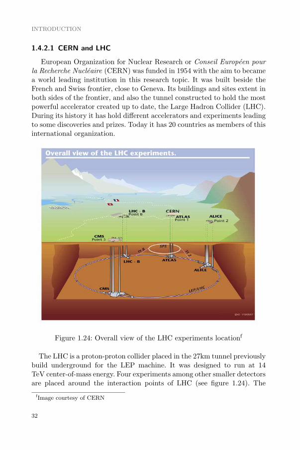
INTRODUCTION
1.4.2.1 CERN and LHC
European Organization for Nuclear Research or Conseil Europeen pourla Recherche Nucleaire (CERN) was funded in 1954 with the aim to becamea world leading institution in this research topic. It was built beside theFrench and Swiss frontier, close to Geneva. Its buildings and sites extent inboth sides of the frontier, and also the tunnel constructed to hold the mostpowerful accelerator created up to date, the Large Hadron Collider (LHC).During its history it has hold different accelerators and experiments leadingto some discoveries and prizes. Today it has 20 countries as members of thisinternational organization.
Figure 1.24: Overall view of the LHC experiments locationf
The LHC is a proton-proton collider placed in the 27km tunnel previouslybuild underground for the LEP machine. It was designed to run at 14TeV center-of-mass energy. Four experiments among other smaller detectorsare placed around the interaction points of LHC (see figure 1.24). The
fImage courtesy of CERN
32

1.4 SIPMS APPLICATIONS
experiments are placed on average at 100m below surface.These experiments are:
• ALICE, dedicated to the study of the physics of strongly interactingmatter and quark-gluon plasma in heavy nuclei (Pb-Pb) collisionswith dedicated runs in the accelerator.
• ATLAS, a general purpose experiment with the objective to test theStandard Model at the TeV scale, and to search for the Higgs bosonand physics beyond the Standard Model.
• CMS, another general purpose experiment with the aim of study-ing the mechanism of electroweak symmetry breaking, for which theHiggs mechanism is presumed to be responsible, and testing the Stan-dard Model at energies above one TeV.
• LHCb, dedicated to the study of Charge-Parity violation and raredecays in the b and c quark sector.
33

INTRODUCTION
1.4.2.2 LHCb
Large Hadron Collider beauty (LHCb) experiment is one of the ongoingexperiments at CERN (Geneva). It is located at Interaction Point 8 of theLHC accelerator, previously used by the DELPHI experiment from LEP.The LHCb experiment is dedicated to the study of heavy flavor physics atthe LHC. Its main aim is to make precise measurements of CP violationand rare decays of beauty and charm hadrons. Shown in figure 1.25, LHCbis a forward spectrometer with a polar angle coverage of approximately 15to 300 mrad in the horizontal bending plane and 15 to 250 mrad in thevertical non-bending plane. This geometry choice is motivated by the factthat bb pairs produced at the LHC are produced in a large proportion inthe same direction, either forward or backward.
Figure 1.25: LHCb detectorg
Starting from the interaction point, at the left of figure 1.25 and 1.26(cross section of the detector), the LHCb tracking system consists of asilicon strip device surrounding the proton-proton interaction region (theVertex Locator), a large area silicon strip detector (the trigger tracker, TT)located upstream of a dipole magnet which has a bending power of about4 Tm, and a combination of silicon strip detectors and straw drift-tubesplaced downstream of the magnet (the Inner Tracker, IT and the OuterTracker, OT), forming the tracking stations (T1, T2 and T3 in figure 1.26).
gImage courtesy of LHCb collaboration
34
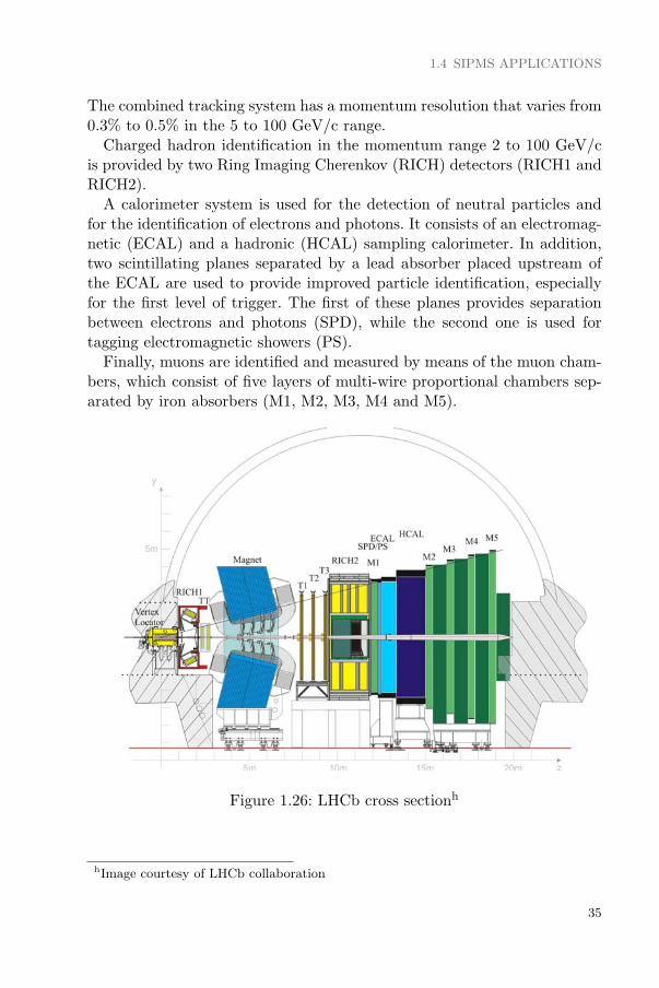
1.4 SIPMS APPLICATIONS
The combined tracking system has a momentum resolution that varies from0.3% to 0.5% in the 5 to 100 GeV/c range.
Charged hadron identification in the momentum range 2 to 100 GeV/cis provided by two Ring Imaging Cherenkov (RICH) detectors (RICH1 andRICH2).
A calorimeter system is used for the detection of neutral particles andfor the identification of electrons and photons. It consists of an electromag-netic (ECAL) and a hadronic (HCAL) sampling calorimeter. In addition,two scintillating planes separated by a lead absorber placed upstream ofthe ECAL are used to provide improved particle identification, especiallyfor the first level of trigger. The first of these planes provides separationbetween electrons and photons (SPD), while the second one is used fortagging electromagnetic showers (PS).
Finally, muons are identified and measured by means of the muon cham-bers, which consist of five layers of multi-wire proportional chambers sep-arated by iron absorbers (M1, M2, M3, M4 and M5).
Figure 1.26: LHCb cross sectionh
hImage courtesy of LHCb collaboration
35

INTRODUCTION
1.4.2.3 Scintillator Fibre Tracker
The current LHCb Tracker stations are composed of an Outer Tracker(OT) with straw tube detectors and an Inner Tracker (IT) with silicon stripdetectors to cover the high-occupancy area near the beam pipe.
Figure 1.27: LHCb tracker up-grade layout
A new technology for the IT upgrade,based on scintillating fibres, was intro-duced in the Upgrade Letter of Intent[6],with clear fibres carrying the signal pho-tons from the inner region to the detectorssituated outside the LHCb acceptance.
In the mean time, a new scintillating-fibre layout has been proposed (CentralTracker, CT), with 2.5 m long fibres cover-ing the whole central region of the Trackerstations, from the LHC beam plane all theway to the top and bottom of the LHCbacceptance. In this option, the IT and several OT modules are replacedby the new scintillating-fibre modules (see figure 1.27). The decision hasbeen taken that any change to the LHCb detector should be made suchthat the new implementation is compatible with operation at a leveled, i.e.constant, luminosity of 2x1033cm−2s−1.
In this new configuration, the existing outermost straw tube modules,four on each side, are kept as in the current LHCb detector and theirelectronics upgraded to allow readout at 40MHz. The central part (OTand IT) is replaced with scintillating fibre modules covering the full heightof the detector. The upper and lower halves of the modules contain 2.5 mlong scintillating fibres, separated with mirrors at the inner boundary andread out with Silicon Photomultipliers (SiPM) mounted outside the LHCbacceptance.
With this configuration, passive material in the detector acceptance isminimized and exposure to radiation is reduced for the SiPMs and FEelectronics. One of the key development challenges will be to determine howthe SiPM performance will evolve as a function of radiation dose and underwhat conditions these photon detectors will represent a viable solution forthe LHCb CT. The radiation fluence at the SiPM location is expected tobe of the order of 1012neqcm
−2. Besides previously described irradiationstudies with 65 MeV protons and with neutrons from a PuBe source [6],SiPM samples have been placed in the LHCb detector at the bottom of thetracking stations during the 2011 data taking period.
36

1.4 SIPMS APPLICATIONS
Adding 1 mm of Pb shielding (and then 1 mm of Cd) between the SiPMand the polyethylene had little impact on the evolution of the leakage cur-rent. The effects of radiation damage can also be reduced by operating theSiPMs at low temperature. The dark current is predicted to be reducedby a factor 2 for about every 8oC temperature step. The option to coolthe SiPM is being studied, with a temperature as low as -25oC being con-sidered. This development effort will determine whether a combination ofneutron shielding and active cooling will allow the SiPM lifetime to beextended to the required level. The signal deterioration due to radiationdamage in the fibres was already mentioned and will now be measured onirradiated 2.5 m modules.
Figure 1.28: Cross section of a fibres module prototype
The techniques for the production of fibre matrices are still under devel-opment for both methods presented in the LoI, namely winding fibres on acylindrical surface of radius larger than 40 cm or on a long cuboid. Dummyfibre matrices have been produced with both methods. Recently, a 2.5 mlong sample module has been fabricated on the cylindrical barrel with scin-tillating fibres of 0.25 mm diameter. The sample contained five layers ofabout 100 fibres each. Figure 1.28 shows a photograph of the cross sectionof this 2.5 m long module. The distance between the centres of adjacentfibres was measured with an accuracy of 6 μm rms relative to each other.
Specially designed SiPM array is undergoing to fit the mechanical sizeof the module with the minimum dead area possible. The prototypes fromHamamatsu and Ketek consist in 64 channels arrays with a common cath-ode configuration. A mechanical view can be observed in figure 1.29, witha total size of 0.23x1.32mm2 per channel, 96 micro-cells and 57.5x55μm2
micro-cell size. The 128 channels are constructed joining to dies of 64 chan-nels with the edge polished, dead area between pixels is kept to the mini-mum with a value of 0.25mm between two arrays.
37

INTRODUCTION
Figure 1.29: SiPM array prototype
1.4.3 Other Applications
As commented previously SiPM can be used in any application wheremeasurement of light is needed. Most of applications using as sensor a PINdiode, APD or PMT can be substituted by a SiPM. Different uses from thepreviously commented include Laser Range Finder and imaging LIDARsystems[25].
A Laser Range Finder is a device using a laser beam to determine dis-tance. The typical operation consists on the measurement of Time of Flightby sending a laser pulse in a narrow beam towards the object and measur-ing the time taken by the pulse to be reflected off the target and returned.Due to the speed of light and time measurement precision this techniquecan not be used for high precision sub-millimeter measurements. The pulsemay be modulated to reduce the chance that the Range Finder measure-ment could be erroneous. It is possible to use Doppler effect techniques tomeasure whether the object is moving and its speed.
A LIDAR is a remote sensing technique involving the illumination ofa surface by a laser light and studying the reflected light. Such systemsnormally use visible light or close in the spectra; ultraviolet or near infrared.A narrow light pulse can be used to scan most of surfaces and materialswith very high resolution.
Typically light is reflected via backscattering and different types of scat-tering can be the basis for the LIDAR measurement, defining different typesof LIDAR.
LIDAR is often used for the production of high resolution maps, meteo-rology or atmospheric research.
38

2SiPM modelling
Correct model of the input signal to be processed by the analog electron-ics is crucial to achieve the desired results. For this reason a PSpice modelhas been chosen. This model permits simulation of both sensing device andelectronics under design.
2.1 PSpice model
A reliable SiPM model is mandatory to produce accurate input signalsfor the electronics. A simple model [26] has been implemented and simulatedusing the standard SPICE tools in conjunction with the electronics. A gen-eral view of the circuit model can be seen in figure 2.1 with its parameterson table 2.1.
In this model [26] the different micro-cells in the SiPM are modelled aspassive elements with the difference that the fired cells by some light haveseveral more elements than the passive cells, acting as a load.
Since the base of a micro-cell is a diode with a quenching resistor (to avoidits destruction), the model comprises the union capacitance in parallel withthe diode reverse voltage power supply plus a series resistor to the diode.
The quenching resistor is simulated with an ideal resistor in parallel witha parasitic resistance. The diode will start conducting when the power sup-ply is greater than its breakdown voltage and an ideal switch is closed(simulating the incoming light). Apart from this parameters an intercon-nection parasitic capacitance is also included.
39
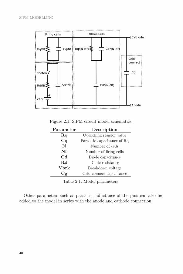
SIPM MODELLING
Figure 2.1: SiPM circuit model schematics
Parameter Description
Rq Quenching resistor value
Cq Parasitic capacitance of Rq
N Number of cells
Nf Number of firing cells
Cd Diode capacitance
Rd Diode resistance
Vbrk Breakdown voltage
Cg Grid connect capacitance
Table 2.1: Model parameters
Other parameters such as parasitic inductance of the pins can also beadded to the model in series with the anode and cathode connection.
40

2.1 PSPICE MODEL
2.1.1 Parameters extraction
To determine the quenching resistor, the easiest way is to produce an IVcurve with the device biased in the direct region. At some point the diodewill start to conduct limiting its current only by the resistor in series of thediode plus the quenching resistor. Since the quenching resistor is expectedto be much greater than the device resistance the value of the slope of thecurve (in the linear region) will be approximately the quenching resistordivided by the number of cells (all in parallel). In figure 2.2 the resultingvoltage-current graph from the direct region of different devices can beobserved.
Figure 2.2: IV characterization of different devices
In order to determine the Cd and Cq sum, the charge variation of theoutput has been measured and plotted as a function of Vop value. On for-mula 12 [26] the relation between charge and capacitance can be observed.With this procedure Vbrk can also be determined extrapolating the voltagewhen output charge should be 0. Measurements are plotted on figures 2.3and 2.4.
Q = (Cd + Cq).(Vop − Vbrk) (12)
Finally the number of cells (N) and charge seen on the device terminalsis specified on the datasheet. Assuming the terminal capacitance value is
41

SIPM MODELLING
Figure 2.3: S10362-11-025P Charge vsVop
Figure 2.4: S10931-050P Charge vsVop
specified in dc conditions, the Cg value can be extracted using formula 13as documented in[26].
Cg = Cω −NtotCd +ω2C2
dR2qNtot (Cd + Cq)
1 + ω2R2q (Cd + Cq)
2
for ω → 0, Cg = Ctot −NtotCd (13)
The only non specified and non directly measurable parameter is Rd butit can be estimated in the order of hundreds of Ω, not affecting the shapeof the signal.
2.1.2 Measurement setup
Several measurements have been performed to obtain the desired pa-rameters and cross check the model on real devices. A small test board wasdesigned to do so, using the usual AC coupled measure, only changing loadresistor from the usual 50Ω value to 1kΩ, since amplifier has a 50Ω inputimpedance. The output amplifier is a MAN-1LN, 500MHz. On figure 2.5and 2.7 there is the circuit used for testing the dark count signals shape.On figure 2.6 a typical output with some light applied to a S10362-11-025Pdevice can be observed. Measurements are done using a 300MHz bandwidthoscilloscope.
To calibrate the gain of the amplifier the SiPM signal has been measuredat the input and output of the amplifier. The results can be observed infigure 2.8 concluding a gain of 60(35.5dB). Different amplitudes have beentested until saturation has been observed (at around 20 mV peak inputsignal).
42

2.1 PSPICE MODEL
Figure 2.5: SiPM basic testcircuit
Figure 2.6: Output for illuminated S10362-11-100P
Figure 2.7: SiPM basic test board
Figure 2.8: SiPM test board gain
2.1.3 Simulation results
Using the shape and amplitude of the dark count peak one can approx-imate the real values of the device with the simulations, summarized intables 2.2 and 2.3. In figures 2.9 and 2.10 there is a comparison betweenthe simulated pulse and the measured single cell fired at Vop.
In order to be more realistic the generation of a light pulse in a scintil-lator will have some time dispersion in the generation of the photons thussome cells will fire at different times; once the photons are produced theyshould arrive to the electronics following different paths which will also in-
43
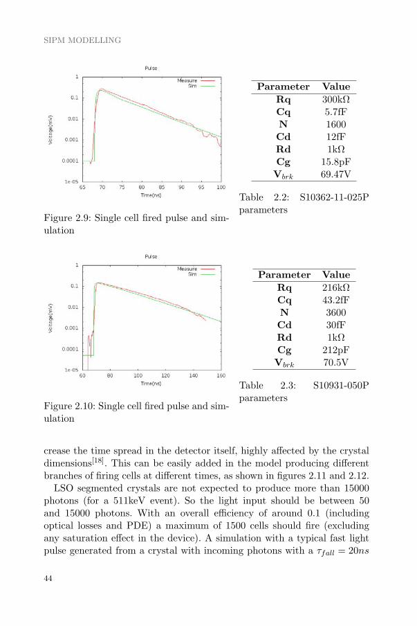
SIPM MODELLING
Figure 2.9: Single cell fired pulse and sim-ulation
Parameter Value
Rq 300kΩCq 5.7fFN 1600Cd 12fFRd 1kΩCg 15.8pFVbrk 69.47V
Table 2.2: S10362-11-025Pparameters
Figure 2.10: Single cell fired pulse and sim-ulation
Parameter Value
Rq 216kΩCq 43.2fFN 3600Cd 30fFRd 1kΩCg 212pFVbrk 70.5V
Table 2.3: S10931-050Pparameters
crease the time spread in the detector itself, highly affected by the crystaldimensions[18]. This can be easily added in the model producing differentbranches of firing cells at different times, as shown in figures 2.11 and 2.12.
LSO segmented crystals are not expected to produce more than 15000photons (for a 511keV event). So the light input should be between 50and 15000 photons. With an overall efficiency of around 0.1 (includingoptical losses and PDE) a maximum of 1500 cells should fire (excludingany saturation effect in the device). A simulation with a typical fast lightpulse generated from a crystal with incoming photons with a τfall = 20ns
44
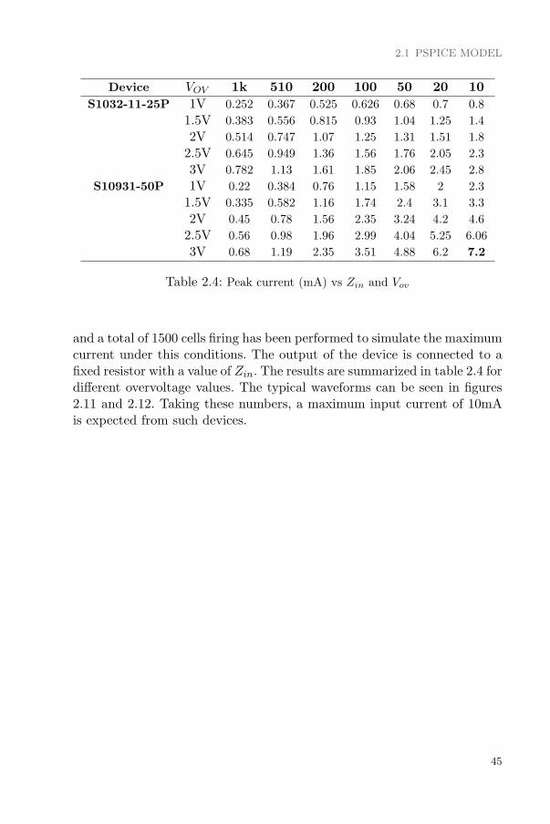
2.1 PSPICE MODEL
Device VOV 1k 510 200 100 50 20 10
S1032-11-25P 1V 0.252 0.367 0.525 0.626 0.68 0.7 0.8
1.5V 0.383 0.556 0.815 0.93 1.04 1.25 1.4
2V 0.514 0.747 1.07 1.25 1.31 1.51 1.8
2.5V 0.645 0.949 1.36 1.56 1.76 2.05 2.3
3V 0.782 1.13 1.61 1.85 2.06 2.45 2.8
S10931-50P 1V 0.22 0.384 0.76 1.15 1.58 2 2.3
1.5V 0.335 0.582 1.16 1.74 2.4 3.1 3.3
2V 0.45 0.78 1.56 2.35 3.24 4.2 4.6
2.5V 0.56 0.98 1.96 2.99 4.04 5.25 6.06
3V 0.68 1.19 2.35 3.51 4.88 6.2 7.2
Table 2.4: Peak current (mA) vs Zin and Vov
and a total of 1500 cells firing has been performed to simulate the maximumcurrent under this conditions. The output of the device is connected to afixed resistor with a value of Zin. The results are summarized in table 2.4 fordifferent overvoltage values. The typical waveforms can be seen in figures2.11 and 2.12. Taking these numbers, a maximum input current of 10mAis expected from such devices.
45

SIPM MODELLING
Figure 2.11: Crystal light simulation S10362-11-025P
Figure 2.12: Crystal light simulation S10931-050P
46

2.2 VERILOGA MODEL
2.2 VerilogA model
For the SciFi Tracker design a VerilogA model has been implementedusing the described model as a basis. This model permits much faster com-putation of the output and avoids convergence parameters problems thatoften appear in the simulation of non linear devices (such as ideal switchincluded in the PSpice model). This model is being extensively used tosimulate the different SiPMs under test for the SciFi tracker and to fit theelectronics to its signal shape.
47


3SiPM readout ASICs
The status of different integrated options for the readout of SiPMs issummarized in this chapter with detailed description of different architec-tures. It is important to note that probably not all existing devices will belisted and commented due to the amount of existing options. At the endof this section a snapshot of the ”state of the art” in the development ofintegrated electronics specific for the readout of silicon photo-multipliersshould have been provided.
The main results on different charge or current mode input stages isstressed. Typical pre-amplifier implementations are based on Charge Sens-ing Amplifiers (CSA) or Current Mode input stages. Each of themhave some advantages and drawbacks being the speed of the current modeinput the most significant advantage. The charge (or voltage) amplifierpermits the connection of the sensor both in the anode or cathode, andnormally is AC coupled in order to tune the DC voltage applied at theconnection node. Current mode implementations only permit the currentflow in one direction (if a good ratio between biasing current and inputcurrent range is desired) thus it must be fixed by design.
Due to different years of production and different technologies used inthe production of the prototypes a direct comparison on charge or areacan not be made. But in general terms a first approach on the order ofmagnitude of how this implementations deal with area and power can beobtained.
49

SIPM READOUT ASICS
3.1 FLC SiPM
FLC SiPM[27] is a current mode ASIC designed for high energy physics.It was developed in Orsay (France) by the Omega group. It aims to pro-vide readout of SiPMs for the International Linear Collider (ILC) hadroncalorimeter. It is designed using a variable gain low-noise pre-amplifier fol-lowed by a variable shaper and Track and Hold (T&H). The output mul-tiplexes the analog signal of several channels. An 8 bit DAC is added toevery input to tune the High Voltage of the SiPM.
The hadronic calorimeter prototype for ILC uses scintillator tiles readout by SiPMs. The SiPM is coupled directly to the scintillator tiles anduses some coaxial cable to the electronics box. The connection to the ASICis direct with a high voltage decoupling and cable matching componentsplaced in both conductors of the cable (shielding and signal).
Architecture
FLC SiPM provides a multiplexed analog output of the 18 channels.Each channel output is a shaped signal proportional to the input charge.A variable gain charge pre-amplifier followed by a CRRC2 shaper witha variable shaping time performs the analog processing and then feeds atrack and hold. All bias is common to all channels. Channel architecture isdepicted in figure 3.1.
Figure 3.1: FLC SiPM channel [27]
50

3.1 FLC SIPM
At the input node, an 8 bit DAC provides 5V voltage change to beable to tune the High Voltage per channel. After this node, the input isac coupled to the pre-amplifier and followed by a resistor to perform afirst derivative constant time. This resistor can be shorted. A low noisecharge pre-amplifier follows with 1300 electrons of noise (compared to 106
electrons of a photo-electron). The gain can be controlled externally with4 bits (setting the feedback capacitor value) from 0.7 to 10 V/pC. At theoutput of the pre-amplifier the signal is filtered using a CRRC2 shaper witha variable time constant selected externally with 4 bits from 12 to 180 ns.The fast shaping (called calibration mode) is used for calibration while thelong shaping (called physics mode) is necessary to be compatible with thecurrent readout.
Measurements permit to distinguish single photons (in calibration mode)and show good linearity with the different gain configurations (in physicsmode).
51

SIPM READOUT ASICS
3.2 MAROC
MAROC[28] ASIC stands for Multi Anode Read-Out Chip. In fact isa family of devices intended for the readout of Multi Anode PMTs. Itwas developed in Orsay (France) by the Omega group. The first prototypewas OPERA ROC in 2001 in AMS 0.8μm technology. The MAROC familystarted with porting this prototype to AMS 0.35μm SiGe CMOS technol-ogy. First version MAROC1 was a 64 channels prototype in 2004 with12mm2 and 5mW/ch power consumption. MAROC2 followed in 2006 andMAROC3 in 2009 with less power consumption and a Wilkinson ADC. Therequirements of MAROC were defined by the ATLAS luminometer designwith a valid trigger for signal above 1/3 photo-electron.
Architecture
MAROC3 version includes 64 low impedance pre-amplifier channels with8 bit variable gain for each channel to equalize gain dispersion in PMTs.Shown in figure 3.2 the signal is first amplified by a low impedance pream-plifier (about 50Ω). The amplified current then connects to a slow shaperand a sample and hold circuit to multiplex the analog output. A secondsample and hold measures the baseline and the maximum. This analogvoltage can also feed the Wilkinson ADC providing 8, 10 or 12 bit digitaloutput.
In parallel to those charge signals 64 trigger outputs coming from two fastchannels are provided. First channel is a fast shaper followed by low offsetdiscriminator, second comes from a bipolar fast shaper with lower gain forhigher signals followed by discriminator. The outputs of two discriminatorsare multiplexed to provide 64 outputs. The thresholds of the discriminatorscan be changed using two 10 bit DACs common for all channels. Two moreoutputs are available (OR1 and OR2) which are the OR of all channelsfrom first or second discriminators. Like in MAROC2 the sum of up toeight preamplifier outputs can be extracted from the ASIC.
52

3.2 MAROC
Figure 3.2: MAROC3 block diagram [28]
53

SIPM READOUT ASICS
3.3 SPIROC
SPIROC2[29] is a System on Chip (SOC) designed to read-out the fore-seen calorimeter from ILC equipped with SiPM. It was developed in Orsay(France) by the Omega group. The prototype is being built at DESY lab-oratory in Germany by the CALICE collaboration. They aim to design adense, high granularity calorimeter (10 million channels). The design re-lies on small detector blocks with the readout electronics attached, thuspower consumption of the electronics should be reduced to the maximumto avoid extra needs of cooling. Version 2c submitted in February 2012improves noise performance and includes a new Time to Digital Converter(TDC).
Architecture
The analog part of the design includes 36 channels, each of them cantune the SiPM voltage at the input node using a DAC with 5V full-scale.Two input pre-amplifiers (see figure 3.3) process the same signal. One hasa larger gain than the other permitting to handle smaller input signals.High gain pre-amplifier is followed by a fast shaper and a discriminator todetect a trigger condition. To measure the charge the output of the two pre-amplifiers are connected to a configurable shaper circuit and to a 16-deepswitched capacitor array (SCA), storing the value (as a T&H).
Time is measured using a coarse counter running at 5MHz and 12 bits,while a more precise measurement is performed using a TDC. The value ofthe TDC is stored at the same time as the signal in the analog memoriesformed by the array of capacitors (SCA). Finally data is converted usinga Wilkinson 12 bit ADC. Time resolution achieved by the TDC is around150ps. Digital part manages all operations and also readouts the previouslyconverted values from a memory (RAM).
54

3.3 SPIROC
Figure 3.3: SPIROC2c block diagram [29]
55
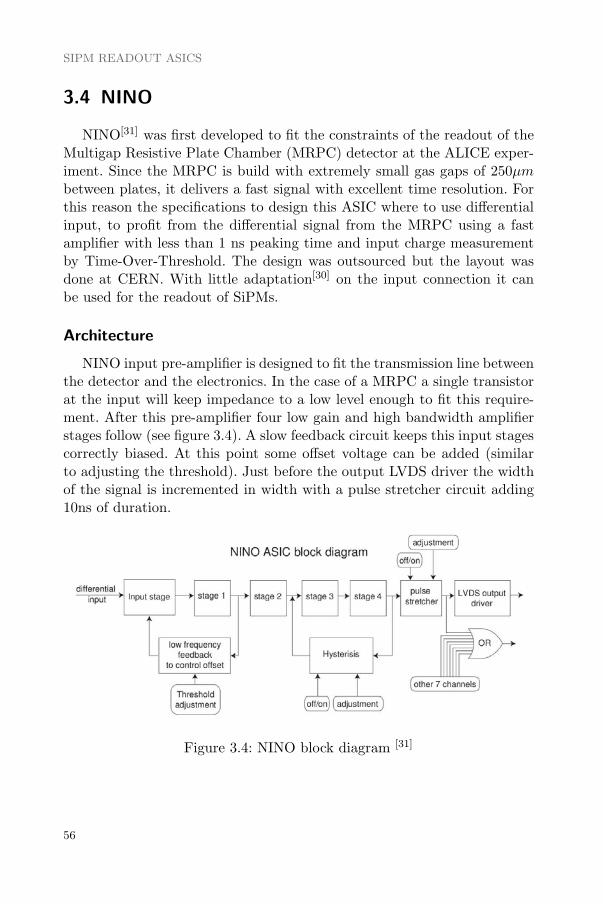
SIPM READOUT ASICS
3.4 NINO
NINO[31] was first developed to fit the constraints of the readout of theMultigap Resistive Plate Chamber (MRPC) detector at the ALICE exper-iment. Since the MRPC is build with extremely small gas gaps of 250μm
between plates, it delivers a fast signal with excellent time resolution. Forthis reason the specifications to design this ASIC where to use differentialinput, to profit from the differential signal from the MRPC using a fastamplifier with less than 1 ns peaking time and input charge measurementby Time-Over-Threshold. The design was outsourced but the layout wasdone at CERN. With little adaptation[30] on the input connection it canbe used for the readout of SiPMs.
Architecture
NINO input pre-amplifier is designed to fit the transmission line betweenthe detector and the electronics. In the case of a MRPC a single transistorat the input will keep impedance to a low level enough to fit this require-ment. After this pre-amplifier four low gain and high bandwidth amplifierstages follow (see figure 3.4). A slow feedback circuit keeps this input stagescorrectly biased. At this point some offset voltage can be added (similarto adjusting the threshold). Just before the output LVDS driver the widthof the signal is incremented in width with a pulse stretcher circuit adding10ns of duration.
Figure 3.4: NINO block diagram [31]
56

3.5 PETA
3.5 PETA
PETA[32] is a 16 channel self triggered readout chip for time and energymeasurement. It was developed for the HyperImage european project inHeidelberg. When a differential low-noise discriminator detects a hit signalit is time stamped and, in parallel, integrated. After integration it is dig-itized with 8-bit resolution. Readout is performed using a serial protocol.Several chips can be synchronized using an internal PLL that can be lockedto the same reference clock.
Architecture
Simplified block diagram of the chip is shown in figure 3.5. The low noisedifferential input discriminator will trigger a hit when the input signal isabove the programmed threshold. This hit will freeze the contents of thetime counters (common to all chip). This time counters are formed by acoarse value (15 bit counter using reference clock) and a more fine countercoming from a 16 stage ring oscillator connected to the reference clock. Thesame hit signal will start the integration of the input signal for a fixed (andprogrammable) time period. When this period has elapsed the resultingvalue is converted to digital using a DAC and a comparator (DAC valueis increased until comparator changes state). Once time stamp, integrationand conversion has been performed the data can be read out using a serialinterface based on shift registers. In addition some other common DACsare also included in the design. All analog blocks are fully differential whilefast digital blocks use differential constant current logic to reduce emittednoise.
57

SIPM READOUT ASICS
Figure 3.5: PETA block diagram [32]
58

3.6 BASIC
3.6 BASIC
BASIC[33] is an 8 channel self triggered ASIC for SiPM readout. It hasbeen designed by Universita di Pisa and Politecnico di Bari. A 32 channelversion also exists keeping the same architecture. This ASIC uses a currentmode input stage connected at the Cathode of the sensor.
Architecture
The BASIC architecture can be observed in figure 3.6. It features a dou-ble signal path, a fast one which uses a current discriminator to provide atiming signal, and a slow one which generates an analog signal proportionalto the charge delivered by the sensor, which is finally converted to digitalby an 8-bit successive approximation-register (SAR) ADC.
The first stage is a current buffer to keep input stage impedance lowand to deliver a copy of the input current to the two signal paths withhigh bandwidth and virtual connection to ground in the input node. In thetiming path a direct copy of the input current is used to generate a triggersignal in a fast current discriminator. All channels are ORed to obtain asingle timing output. At the slow signal path another replica of the currentis used, but now scaled by some factor to fit the desired dynamic range. Itis integrated by means of a CSA with variable gain. A peak detector keepsvoltage output of the CSA constant to process it easily. A baseline holderis added to control the DC value of the CSA output without affecting thefast signals in a very low feedback loop. The current buffer implementationalso permits to fine tune the voltage applied to the SiPM input node by1V.
59
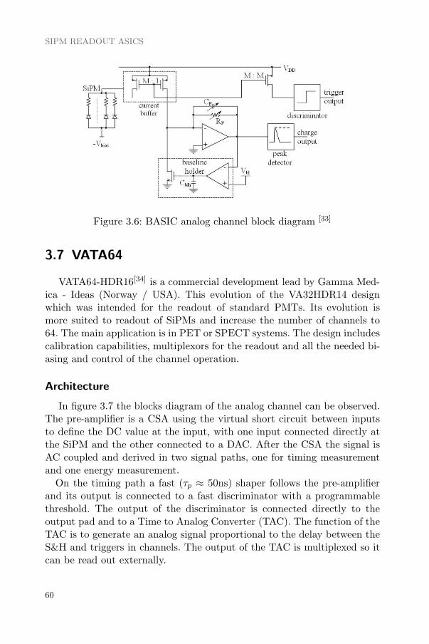
SIPM READOUT ASICS
Figure 3.6: BASIC analog channel block diagram [33]
3.7 VATA64
VATA64-HDR16[34] is a commercial development lead by Gamma Med-ica - Ideas (Norway / USA). This evolution of the VA32HDR14 designwhich was intended for the readout of standard PMTs. Its evolution ismore suited to readout of SiPMs and increase the number of channels to64. The main application is in PET or SPECT systems. The design includescalibration capabilities, multiplexors for the readout and all the needed bi-asing and control of the channel operation.
Architecture
In figure 3.7 the blocks diagram of the analog channel can be observed.The pre-amplifier is a CSA using the virtual short circuit between inputsto define the DC value at the input, with one input connected directly atthe SiPM and the other connected to a DAC. After the CSA the signal isAC coupled and derived in two signal paths, one for timing measurementand one energy measurement.
On the timing path a fast (τp ≈ 50ns) shaper follows the pre-amplifierand its output is connected to a fast discriminator with a programmablethreshold. The output of the discriminator is connected directly to theoutput pad and to a Time to Analog Converter (TAC). The function of theTAC is to generate an analog signal proportional to the delay between theS&H and triggers in channels. The output of the TAC is multiplexed so itcan be read out externally.
60

3.7 VATA64
Figure 3.7: VATA64-HDR16 analog channel block diagram, extracted fromspecifications
On the energy measurement path a programmable slower (τp = 50 -300ns) shaper is connected at the output of the pre-amplifier. This shaperis of a semi-Gaussina CR-RC type. After the shaper a peak hold circuitkeeps the voltage to the maximum to be able to sample it and multiplexat the output. The user can select between sampling the peak hold outputand the signal itself.
61

SIPM READOUT ASICS
3.8 RAPSODI
RAPSODI[35] is a SiPM readout ASIC with two channels. This twochannels can work standalone or in coincidence.
Architecture
RAPSODI (see figure 3.8) is formed by two identical channels plus somecoincidence logic. Each channel consists on a preamplifier, comparator,peak detector and ADC. Some common coincidence logic permits to mixthe output of each channel. The full system is controlled by an externalFPGA.
Figure 3.8: RAPSODI block diagram and external FPGA connection[35]
The pre-amplifier is formed by two folded cascode amplifiers with a con-figurable pole-zero cancellation circuit between them. This permits to avoidthe undershoot of the signal and adjust to different SiPM timing constants.The pre-amplifier gain is also configurable by changing the value of the feed-back elements. After the pre-amplifier the signal is split in two paths, onegoing to a peak hold circuit and a second one going to a comparator. Thepeak hold circuit has the function of keeping the maximum voltage con-stant for the ADC conversion (7 bit flash ADC). The comparator signalwill generate a trigger signal when it is above the voltage threshold and actover the coincidence logic (if enabled).
62

3.9 TOFPET
3.9 TOFPET
TOFPET[36] is a 64 channels SiPM readout ASIC designed for theEndoTOFPET-US collaboration. The input stage can be designed for nor p type inputs (changing current flow direction). After a pre-amplifier,the signal uses two signal paths in voltage to obtain the desired timing andcharge information.
Architecture
Figure 3.9: TOFPET channel block diagram [36]
The TOFPET ASIC readout channel starts with a current mode analogpre-amplifier. The signal is AC coupled and drives two mirrors to generatea voltage signal with the same characteristics as the current input from theSiPM. On the timing path the signal directly drives a voltage comparatorwith a threshold set by a 6 bit DAC. On the energy path the signal canbe shaped with different time constants before driving an other voltagecomparator generating a time-over-threshold (TOT) signal. The resultingdigital values are then used in a TDC to generate a data set containinginformation on the time of the trigger and the TOT of the processed inputsignal.
To overcome the fact that the timing signal is susceptible to variationsof the trigger time with the amplitude of the pulse, the charge informa-tion can be used to correct offline the timing degradation, due to time-
63

SIPM READOUT ASICS
walk. The output of the TOT is highly non linear and will need the usageof external calibration and offline correction also to obtain better energymeasurements.
Running at 160 MHz the chip yields a 50 ps time bin and dissipates7 mW per channel (simulated for 40 kHz event rate p/channel) for highcapacitance SiPM (320 pF).
One pad-free edge to allows to package two dies into a 128-channel BGApackage.
64
3.10 COMPARISON TABLES
3.10 Comparison tables
To compare several characteristics of the previous ASICs the figures ofmerit are summarized in next tables, 3.1 and 3.2. In first table there is asummary of outputs, outputs type, measurement, measurement accuracyand timing information. Second table a summarizes input stage, power,area usage and also technology.
The typical approach is to deliver charge and timing information, typi-cally as a result of the OR of different channels. Normally this double mea-surement is performed splitting the signal at the output of the pre-amplifierand driving two different signal paths. A multi-channel architecture is al-ways envisaged due to the high numbers of channels needed in currentparticle detectors or PET systems. The number of channels is typically apower of 2.
On tables we can see the most popular readout is to use charge basedreadout. Sometimes applying some shaping just at the pre-amplifier. Thisis a well known circuit widely used in particle detectors, but does notexploit the speed possibilities of the sensor. On the other hand currentmode readout is less used and a connection with the sensor must be definedprior to design, in all examples cathode connection is used.
Differential implementations are not much used since it is not a natu-ral connection of the sensor to the electronics (SiPMs are basically singleended). They offer much better performance in terms of noise but the priceto pay is a much important power consumption which does not seem tocompensate the advantages.
65

SIPM READOUT ASICS
ASIC
Outp
uts
Measu
reA
ccura
cy
Tim
ing
outp
ut
FLC
SIP
MM
ult
iple
xed
analo
gC
harg
e-
No
MA
RO
C3
Mult
iple
xed
analo
gan
ddig
ital
Charg
eU
pto
12
bit
s64
+2O
RSP
IRO
C2c
Dig
italti
me
and
charg
eT
ime
and
Charg
e12
bit
san
d150ps
Dig
italw
ord
NIN
OD
igit
al
Tim
ean
dw
idth
60ps
LV
DS
PETA
Dig
ital
Tim
ean
den
ergy
28ps
rms
Dig
italw
ord
BA
SIC
Dig
italand
Analo
gm
ux.
Tri
gger
and
ener
gy
650ps
OR
trig
ger
VA
TA
64
Mult
iple
xed
analo
gan
ddig
ital
Tim
ean
dC
harg
e-
Tri
gger
and
analo
gR
AP
SO
DI
Dig
ital
Tri
gger
and
Charg
e-
Tri
gger
TO
FP
ET
Dig
ital
Tim
ean
dC
harg
e50ps
Dig
italw
ord
Table 3.1: Different ASICs outputs summary66

3.10 COMPARISON TABLES
ASIC
Input
Tech
nolo
gy
Input
Channels
Are
aPow
er
Year
type
impedance
(mm
2/ch
)m
W/ch
FLC
SIP
MC
harg
e0.8
μm
AM
SA
Cco
uple
180.
56
112004
MA
RO
C3
Curr
ent
0.3
5μm
SiG
eA
MS
≈50Ω
640.2
52.
520
09SP
IRO
C2c
Charg
e0.3
5μm
SiG
eA
MS
AC
couple
360.8
9≈2
.520
12N
INO
Diff
.C
har
ge0.
25μm
IBM
≈20Ω
81
4020
03P
ETA
Diff
eren
tial
0.18
μm
UM
C-
160.
66
862008
BA
SIC
Curr
ent
0.3
5μm
SiG
eA
MS
≈17Ω
80.8
8>
2.65
2008
VA
TA
64
Curr
ent
-A
Cco
uple
641
15
2007
RA
PSO
DI
Curr
ent
0.3
5μm
SiG
eA
MS
≈20Ω
24.5
100
2008
TO
FP
ET
Curr
ent
0.1
3μm
10-6
0Ω64
0.3
97
2012
Table 3.2: Different ASICs properties summary 67


4Input Stage
The major improve presented in this thesis is a novel input stage andcurrent mode processing. The main challenge is to improve other implemen-tations performance. Previous section presented several implementations ofreadout stages for SiPMs. One of the most common approach is to includea charge amplifier at the input. This is a good approach for a charge mea-surement but degrades the timing of the signal: The processing is slow forTOF measurement and if input impedance is high the recharge time of theSiPM will be incremented. Several studied implementations use currentmode input stages which provide better time measurement results. This isthe chosen input mode to obtain excellent timing measurement.
A recurrent architecture is to use multiple path processing for the dif-ferent time and charge information. This approach seems to be the correctsince it permits independent gain of the different signal paths and differ-ent signal shape processing. In current mode this signal can be reproducedeasily using current mirrors just keeping in mind some control of the satu-ration of the mirrors; If the most gain mirror saturates it could avoid theother mirrors to work properly, so some saturation control should permitto extend the range of the other mirrors while the saturated one continuesworking.
A first prototype was submitted in July 2012 to test the most critical partin the design, the pre-amplifier. This first prototype, SiPMVFEr1 (SiPMVery Front End), uses a cathode connected device and buffers it’s currentto two different signal paths (time and energy) with a gain similar to 1 in
69

INPUT STAGE
the time path and some attenuation in the energy path. Some saturationcontrol circuitry must be added in the timing path to keep the energycurrent mirrors operating correctly after saturation of time output (seeappendix A for details).
After this first attempt and during it’s test more devices and arrays ofdevices started to show up. Most of them having the anode and cathodeavailable for readout but some using a common cathode structure betweenchannels. The decision taken with this new information was to change theinput stage to be able to read in the anode (opposite current flow). Sinceresults from first prototype where promising and reproducible by simula-tions it was decided to add more functionality to this second prototype ina multi-channel architecture (16 channels to start with). This prototype isFLEXTOT and it’s input stage is described.
4.1 Architecture
The main goals of the input stage are to keep low input impedanceand voltage controlled at the input node with a reasonable bandwidth.The input signal will be a current burst that should be replicated at theoutputs. Full circuit of input stage (with some simplified blocks) can beobserved in figure 4.1.
Requirements are achieved with two independent feedback loops, a highfrequency feedback look to keep input impedance low, and a second lowfrequency feedback to keep voltage constant at the input node.
Several parts are highlighted in the schematics;
• HFfb : High Frequency feedback loop to keep input impedance low.
• LFfb : Low Frequency feedback loop to keep input voltage controlled.
• PROT : Protection circuit to avoid voltages over 2V or below 1Vat the input (voltage outside this range would lead to over currentflowing in the input stage).
• Current mirrors : A bipolar master cascode with a number of elementsequal to n with it’s slaves (with a, b and c elements) to replicate inputcurrent with different ratios ( a
n, b
nand c
n).
Transistor Mfb is shared by both feedback paths, while the rest of MOStransistors are used for biasing (Mb, Mb2 and MB) or as an active load (D).
The design can be scaled to obtain any number of desired current replicaswith any gain.
70

4.2 CIRCUIT ANALYSIS
Figure 4.1: Input stage schematic
In following stages some protection circuitry has been added to achievea correct output in the mirrors when the one with most gain is undersaturation. The solution applied is the evolution of the one presented inCTA design[37].
4.2 Circuit analysis
Even though some other circuitry is present in the design, the mostfundamental part is described by the two related feedback loops (HFfb andLFfb). Since superposition can be applied both are analysed individually.
Simulations have been performed during design stage to fine tune thefinal values of the different elements included in the circuit to obtain betterresults. And to cross-check functionality when the parasitic elements areadded (layout and bonding inductance).
71

INPUT STAGE
4.2.1 Low Frequency feedback loop
Using the simplified circuit depicted in figure 4.2 the behaviour of thecircuit is described.
Figure 4.2: Low Frequency feedbackloop simplified circuit
Transistors Q1, Q2 with it’sCMOS load acts as a differentialamplifier with a fixed gain of A0.
The output of the amplifier isthen buffered at the input by Mfb
as in equation 14 and voltage at in-put forced to v′i.
v′i = −A0.vi.gmfb (14)
In large signal this voltage willbe equal to Voffset since differentialpair will keep vdiff = 0.
In order to avoid interferencewith high frequency feedback loopthe overall cut frequency of thisloop is kept at low values. Since thedominant pole of the circuit will bedelivered by the input capacitance
(of the SiPM) the cut frequency will be provided by equation 15.
fcut =1
2.π. 1gmfb
.CMAX
(15)
For typical values of 4 m and 300pF the cut frequency will be around 2MHz.
In figure 4.3 stability simulations are performed for a typical case (lowinput capacitance) resulting with a Unity Gain around 2.5 MHz and a PhaseMargin around 79 degrees. Montecarlo process and mismatch variations arealso plotted in the same figure.
72
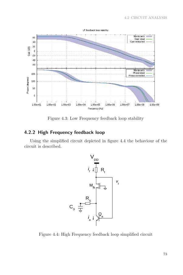
4.2 CIRCUIT ANALYSIS
Figure 4.3: Low Frequency feedback loop stability
4.2.2 High Frequency feedback loop
Using the simplified circuit depicted in figure 4.4 the behaviour of thecircuit is described.
Figure 4.4: High Frequency feedback loop simplified circuit
73

INPUT STAGE
The basic equations of the system are summarized;
if ≈ icZi
Zi + 1gmfb
(16)
ia = gma.v′t (17)
vt = −Rf .if (18)
Zi = Rs +1
s.CD
=s.Rs.CD + 1
s.CD
(19)
The transfer function can be extracted from previous equations:
T (s) = −vt
v′t= gma.Rf .
s.Rs.CD+1s.CD
s.Rs.CD+1s.CD
+ 1gmfb
(20)
Figure 4.5: High frequency feedback transfer function
P =1
2.π.(Rs + 1
gmfb
).CD
Z =1
2.π.(Rs + CD)(21)
The resulting transfer function has one pole and one zero, as depicted infigure 4.5.
With typical values of sensor capacitance around 30 pF, series resistorof 12 Ω and transconductance of 100 Ω pole is located at around 50 MHzand zero around 500 MHz. If the approximated GBW should be around500 MHz, then;
74

4.2 CIRCUIT ANALYSIS
GBW ≈ gma.Rf
2.π.(Rs + 1
gmfb
).CD
≈ 500MHz → gma.Rf ≈ 10 (22)
But in previous assumptions (equation 16) the influence of Low Fre-quency feedback loop is not taken into account. This feedback will changethe results;
if = icZi
Zi + ZiLF
(23)
ZiLF =
1gmfb
A(s) + 1=
1gmfb
GBWLF
s+wc+ 1
=
1gmfb
.(s + wc)
GBWLF + s + wc(24)
Now transfer function is:
gma.Rf .(s.Rs.CD + 1).(s + GBWLF )
s2.(Rs + 1
gmfb
).CD + s.
(Rs.CD.GBWLF + CD.wc
gmfb+ 1
)+ GBWLF
(25)
CD.wc
gmfb
=CD.GBWLF
gmfb.A0→ Rs >>
1gmfb
A0(26)
Equation 25 can be simplified to:
T (s) = gma.Rf .(s.Rs.CD + 1).(s + GBWLF )
s2.(Rs + 1
gmfb
).CD + s. (Rs.CD.GBWLF + 1) + GBWLF
(27)
Circuit is simulated with the final schematic taking into account processand mismatch variations to check it’s functionality (see figure 4.6).
75

INPUT STAGE
Figure 4.6: High Frequency feedback loop stability
4.2.2.1 Input impedance
As observed in formula 19 the input impedance has an inductive be-haviour (increases with frequency). The final schematics are simulated tak-ing into account process and mismatch variations and depicted in figure 4.7.As expected impedance is constant for low frequencies and equal to Rs, formedium resistances it raises to around 34Ω and for higher frequencies itstarts rising fast over the circuit Bandwidth.
Figure 4.7: Input impedance
76

4.2 CIRCUIT ANALYSIS
4.2.2.2 Input capacitance
In the case of a very small input capacitance:
Rs.CD.GBWLF << 1(28)
T (s) =
(Rs +
1
gmfb
).
⎡⎣s2 +
s(Rs + 1
gmfb
).CD
+GBWLF(
Rs + 1gmfb
).CD
⎤⎦ (29)
(Rs +
1
gmfb
).CD.
⎛⎝s +
1(Rs + 1
gmfb
).CD
⎞⎠ . (s + GBWLF ) (30)
To obtain a stable feedback the condition of equation 31 is fixed. In thisconditions dominant pole is 1(
Rs+1
gmfb
).CD
, thus input node. The circuit
will be more stable as much as input capacitance increases. To keep thiscondition for typical values GBWLF should be kept below 5 MHz.
GBWLF <<<1(
Rs + 1gmfb
).CD
(31)
Simulation of final circuit phase margin relation with input capacitanceshows an increase in the margin when capacitance value increases as ex-pected by design (see figure 4.8).
Figure 4.8: Effect of input capacitance to stability
77

INPUT STAGE
4.2.3 Input voltage variation
Protection circuitry has been added at the input stage to avoid extracurrent consumption in the input stage. The input node voltage has beenlimited between 1V and 2V to avoid this condition. In figure 4.9 a simulationwith schematic and extracted (post-layout) elements has been performed,including Montecarlo simulations with process and mismatch variations.
Figure 4.9: Input node voltage variation
The error on setting node voltage is plotted on y axis while desiredvoltage is on x axis. The limiting circuit keeps the input voltage on thedesired range as expected. Thus a total adjustment rage around 1V isachieved.
78
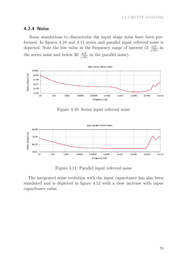
4.2 CIRCUIT ANALYSIS
4.2.4 Noise
Some simulations to characterize the input stage noise have been per-formed. In figures 4.10 and 4.11 series and parallel input referred noise isdepicted. Note the low value in the frequency range of interest (2 nA√
Hzin
the series noise and below 30 pA√Hz
in the parallel noise).
Figure 4.10: Series input referred noise
Figure 4.11: Parallel input referred noise
The integrated noise evolution with the input capacitance has also beensimulated and is depicted in figure 4.12 with a slow increase with inputcapacitance value.
79

INPUT STAGE
Figure 4.12: Integrated noise evolution with input capacitance
80

5Design for PET applications
The design of the readout of a PET scanner is probably one of the mostdirect applications for SiPM. Current PET scanners provide sufficient imag-ing capabilities to be the most sensitive molecular imaging technique. Itsfast and successful development has allowed this technique to be imple-mented in practically every large hospital and biomedical laboratory indeveloped countries.
Three are the main specifications to be improved in state-of-the-art PETsystems: First the compatibility with morphological imaging systems withless radiological risks than CT; PET provides a functional image but theintakes providing information of metabolic functions, lesions or abnormalfunctionalities can only be properly evaluated if the PET image is mergedwithin a morphological image of the body. This is usually provided by com-puted tomography (CT), with the problem that this technique provides anon-negligible radiological risk. Second the improvement of spatial resolu-tion (around 1 mm for preclinical and beyond that figure for human wholebody systems). Third the improvement of detector efficiency.
Current PET technology integrates CT or magnetic resonance imaging(MRI), providing the clinician with both anatomical and functional in-formation. Presently there are commercially available PET-CT scannerscapable of simultaneous acquisition of both imaging modalities from ma-jor vendors (Siemens, Philips and General Electric), and only one trulysimultaneous PET-MRI, the mMR scanner from Siemens. The major prob-lems for PET-MR compatibility are the need for replacement of classical
81

DESIGN FOR PET APPLICATIONS
photo detectors by high gain semiconductor photo detectors (such as SiPM)and new challenging requirements of RF and magnetic compatibility of thefront-end electronics attached close to the detector ring.
Recent technological developments have made possible the implementa-tion of time-of-flight (ToF) techniques in PET scanners. These techniquesimprove the image resolution and enhance the efficiency of the system byreducing the uncertainty of the location of the positron source along eachPET line of response (LoR). While most PET-CT systems feature ToF ca-pabilities to improve sensitivity and overall image quality, particularly inthe case of large patients, PET-MRI systems do not have this capabilitybecause of the use of silicon avalanche photodiodes (APDs) as light sensors,which are not fast enough. The use of faster SiPM in several prototype de-tector designs is pushing towards ToF, however these sensors require veryfast electronics in order to preserve their excellent timing properties. NewASIC designs with fast response for the readout of SiPMs, capable of oper-ating in strong magnetic fields, are being pursued by several groups, aimingtowards setting a new state of the art in molecular imaging: simultaneousPET-MRI hybrid systems featuring ToF PET.
A present technological limitation derived from the design of PET detec-tor elements is the parallax error, defined as the uncertainty in the locationof the photon interaction position in the detector due to the thickness of thecrystal. Conventional PET scanners are unable to provide a 3D interactionlocation in the detector, thus introducing an uncertainty in the depth ofinteraction. Since the average detector thickness is around 20 mm, this be-comes a non-negligible problem for off-centered LoRs, mainly in small ringPET detectors. Several solutions have been implemented to address thisproblem, such as double readout, phoswich and using statistical methods,but with limited success.
Regarding the improvement of the spatial resolution, trends move to-wards replacing the simple analog detector readout techniques (cost-effectivefor commercial development) with reduced number of electronics channelsby more complex electronics, coupling one electronics channel to each singlecrystal in the detector block. This will allow the use of signal processingto improve the photon position identification. But it will imply more com-plexity, which might turn out in an unacceptable increase of the price.The only way to advance in this approach is to develop custom integratedelectronics capable to provide a large amount of detector channels (>64per detector block) plus digital signal processing, providing to the nextelectronics readout modules a fully processed data array [p, t, E] (3D inter-
82

action position, time mark of the event and deposited energy). Therefore,it is most likely that the way to improve the spatial resolution will belinked to the development of more complex, cost-effective digital front endintegrated electronics.
In terms of detector efficiency, there are two direct ways to improve thecurrent figures: New scintillators, with larger density and higher atomicnumber but providing excellent specifications on light yield and fast signal,or thicker detector with current materials. On the one hand, the searchfor new scintillator materials is not evident, and has not provided in thelast years relevant results. On the other hand, the use of thicker detectorcrystals has a limit due to geometrical factors: the light output in a crystaldetector with an area in the order of 2 mm x 2 mm becomes inefficientwhen the crystal exceeds a certain thickness. One way to increase the de-tector efficiency while avoiding the intrinsic limitations described above isto use non-segmented detectors, i.e. monolithic detector blocks. Some keyresearches on new PET technologies (see references [38],[39]) foresee that thenext generation PET detectors will be monolithic-block detectors coupledto arrays of Si-PMs supported by statistical-based estimation algorithmsthat locate events in the crystal block in three dimensions.
It is clear that a path to advance towards the next generation PETscanners (MR-compatible, ToF capable, high efficiency, high resolution) isrelated to the capability of providing cost-efficient, reliable, accurate, fastfront-end electronics with digital processing capabilities. Only a reducednumber of institutions and companies in the world have resources to facesuch challenging electronics development.
Although the most usual readout technique is based on integrated chargepulses digitized by ADCs, the time-over-threshold technique (ToT) has be-come a promising alternative in the last years. The ToT technique is basedon digitizing the time a signal spends over a fixed threshold. The leadingedge provides the information on the time of arrival of the photon and thetime lapse between the leading and falling edge supplies the energy infor-mation. ToT has an advantage of a conventional pulse height system withrespect to circuit integration and power consumption since ToT can becomposed simply and without an ADC. A higher level of integration wouldallow PET scanners based on the individual readout method to achieveboth a high count rate and better spatial resolution. ToT is now very oftenapplied in High Energy Physics (HEP) for indirect amplitude measurementwith moderate resolution, for instance in tracking, or in medical applica-tions [41],[42],[43]. A survey in the 2011 IEEE NSS MIC Conference reveals
83

DESIGN FOR PET APPLICATIONS
that research institutes in Europe (Italy, Poland, Czech Republic), Japanand Canada are active in this field, providing promising results. TypicalToT method suffers from poor linearity, but the non-linear relationshipbetween energy and time, properly processed, can be useful to providecompression (higher dynamic range) or faster conversion time. Linear ToTmethods can provide better resolution and are based in constant currentdischarge of a capacitor.
5.1 Requirements
Good definition of the requirements will lead to a prototype with mini-mal or no changes to be done to fit the final application. One of the mostimportant things for defining specifications in this case is the Sensor to beused. For this reason some emphasis has been done in previous sections inthe characterization and modelling on various Hamamatsu devices with dif-ferent cell sizes. In common PET systems seems that the only usable deviceis the 3x3mm sensor. This is because with a reasonable size it can achievethe desired dynamic range and PDE needed by the incoming light froman LSO / LYSO crystal without saturation in the range of PET energies.Some other manufacturers such as SenSL or KETEK have similar productswith reasonably similar characteristics for PET systems. This wide sensoroptions leads to some adjustable parameters in the signal processing sincethey will provide different signal shape, PDE, crosstalk and dynamic range.
5.1.1 Number of channels
Common PET systems use a detector block with an array of sensors.Those arrays are typically a 6x6 or 8x8 (formed joining smaller arrays of3x3, 4x4 or 2x2). On the detector block there can be a monolithic crystalblock over the sensors covering all the area or a segmented crystal blockon every channel. If a monolithic crystal is used the light will spread overseveral channels, if few channels are used and summed the final measurecan be weighted and measure with most precision the originating point ofthe light (leading to better resolution). In a similar way if the crystal isalready segmented the resolution will be defined by this segmentation, butmore signal will be present in every channel (all light goes to the samesensor).
As PET systems become more compact, the number of channels andits density increases so some important efforts have been done to reducethe readout channel number. The most typical case is to sum the rows an
84

5.1 REQUIREMENTS
columns [46]. Thinking on a discrete implementation this solution seems agood option. But on an integrated basis it doesn’t seem to be so muchimportant. All channels would need a connection to the readout electronicsso if a single digital line is used for the output of the measured signal itwill have a symmetric input output structure. With this approach it can bedecided afterwards if the signal should be added or other processing havingall the information is needed.
To sum up a reasonable goal for the number of channels should be asclose as possible to the sensors array. If that number can not be achieveda divisor is the most desirable option.
5.1.1.1 Packaged electronics power consumption
Initially power consumption is not constrained, but a reasonable powerconsumption should be obtained to avoid cooling systems. The thermalcircuit is depicted in figure 5.1. With only the junction to case resistanceand the case to ambient resistance[45].
Figure 5.1: Thermal circuit
Assuming a typical thermal resistance (Rj−c) of a QFN package withexposed pad of 7oC/W, a typical thermal resistance from the case to theambient temperature (Rc−amb) with no air flow of 50oC/W, a maximumoperating temperature of the junction (TjMAX
) of 125oC and a maximumambient temperature (TambMAX
) of 70oC, the maximum power consump-tion (PVMAX
) can be calculated easily in 32.
PVMAX=
TjMAX− TambMAX
Rj−c + Rc−amb
=125− 70
7 + 50= 0.96W (32)
85

DESIGN FOR PET APPLICATIONS
According to previous calculation a maximum of ≈ 1W for the full pro-cessing electronics should be achieved to avoid any cooling if a 64 channelstypical system is used then the consumption of a single channel should bearound 15mW.
5.1.2 Rate constraints
An optimal design on the detector should avoid any dead time producedby the signal processing. This would reduce the acquisition time to obtainthe needed statistics to generate an image. The expected gamma ray gen-eration is in the order of kHz (below 1MHz). Thus the processing timeshould be kept at the order of 500 ns (to minimize pile-up), with no deadtime between different events introduced by the electronics. Double peakresolution should be around 500ns.
5.1.3 Bandwidth
The timing signal is usually obtained after discrimination of the inputsignal, thus it is the jitter of the discriminated signal what limits the timingresolution of the electronics. The random jitter (σt) is proportional to thenoise (σn) and inversely proportional to the signal slope (δS
δt) around the
threshold level. Then the signal BW in first order approximation is calcu-lated in equation 33.
σt =σn
δSδt|ST
≈ trSN
BW ≈ 0.35
tr(33)
For a TOF PET application a temporal resolution of around 100ps shouldbe needed. Expecting a S/N ratio around 10 a rise time of less than 1nsis needed, leading to an expected minimum analog bandwidth of around350MHz.
But in the case of a TOF PET system timing accuracy will not only beconstrained by the electronics, and in fact the S/N ratio will depend onthe threshold level, being greater than 10 in most of the cases. In fact itcan be demonstrated[44] that the coincidence resolving time of two sensorswith electronics is mainly limited by photon statistics while crosstalk, elec-tronic noise and signal bandwidth have relatively little influence. Thus abandwidth around 250MHz should be enough.
86

5.1 REQUIREMENTS
5.1.4 Linearity
PET systems use the energy measurement to cut off non coincidentevents. The system is only interested in events around 511keV that shouldproduce the LoR with some time information (if ToF is used). The restof events are usually discarded. Thus system linearity does not need to bevery accurate. Good scintillating materials used in PET provide an energyresolution around 7%[24], the goal for the electronics in order not to degrademuch the performance of the full system should be around ±5 %.
5.1.5 Specifications summary
A summary of previous section conclusions is detailed in table 5.1.
Parameter Value Unit
Channels 16, 32 or 64 -Power <15 mW/chDouble peak resolution <500 nsBandwidth timing >250 MHzPackage QFN or BGA -Linearity ±5 %
Table 5.1: PET readout ASIC specifications summary
87

DESIGN FOR PET APPLICATIONS
5.2 Implementation
Taking into account previous requirements it was decided to first designa block test prototype including the most critical part in the design: the pre-amplifier. Some basic current discriminator was also included. Afterwardsa multi-channel prototype with more functionality should be designed.
The main design objectives of the final prototype are:
• Pre-amplifier Bandwidth ≈ 250MHz
• Direct connection to SiPM
• Controllable DC voltage at SiPM
• Low input impedance
• Fast OR of all channels for timing measurements
• Digital Time Over Threshold output for energy measurement
• Minimize power consumption
• Good linearity
5.2.1 Architecture
In figure 5.2 a block diagram of the analog channel can be seen. Afteranalysis of previous ASICs it seems that the best solution for the readout iscurrent mode input. The current mode input stage is described in previoussection. It provides a low impedance input with a controlled DC voltageand multiple scaled copies of the input current. In this case three copieshave been implemented; timing, energy and pile-up.
For the timing measurement the common approach is to use one of thesignal paths and compare directly with some threshold to detect the leadingedge. This process leads to reasonably good timing measurement results.Other more complex processing can lead to better resolution in some ap-plications but are often much more complex[40]. For this reason a simplefast current mode comparator has been designed for this application. Af-terwards all timing signals for the different channels are combined in a logicOR to generate only one timing signal for the full ASIC.
For the energy measurement a digital output is desired due to the flexi-bility for the readout and low resource usage. An integrator with a constantcurrent discharge will provide signal to an hysteresis comparator. Using thiscircuit a linear output depending on input charge will be delivered. Thislinear behaviour is desired to avoid extra offline corrections on data.
For the pile-up measurement (detection when two incoming signals occurduring our measurement window, thus changing signal shape) an extra
88

5.2 IMPLEMENTATION
AC coupled path with less gain has been used. The AC coupled signal iscompared to a fixed threshold using the same fast current comparator usedin the timing stage. The output of the comparator is then feed into twocascaded registers to provide a logical output. Pile-up of all channels isstored in a register with its own interface to be controlled and readout.
This architecture keeps interface simplicity both at the input with noextra components needed for SiPM connections and at the output with adirect digital interface to the readout system (typically an FPGA).
Figure 5.2: FLEXTOT channel blocks diagram
The added pile-up detection circuitry adds a feature not present in pre-vious designs and helps offline processing.
Slow control for the setup of thresholds, control voltages and polarizationcurrents of the circuit are also included in the prototype.
89

DESIGN FOR PET APPLICATIONS
5.2.1.1 Floorplan
Since one of the main purposes of this design is to include an importantnumber of channels that should be extended in future prototypes it is im-portant to keep a regular and easy to reproduce shape. For this reason theanalog channel has been designed in a hard macro including input pad.
Common biasing block is placed in the center of the prototype to reducethe length of the connections to all channels. Common biasing parametersare copied to all channels using long vertical lines, thus voltage signals areused. In the central part also the common slow control and registers areplaced.
Figure 5.3: FLEXTOT floorplan
Since prototype was 16 channels in a 64 package, the sides of the designis already fully populated by the input and output signals of the channel.Top and bottom parts are used for power supplies, debugging signals andslow control needed pins.
All power lines go from top to bottom of the prototype with double padsin each side to reduce the parasitic inductance and length of connections.
90
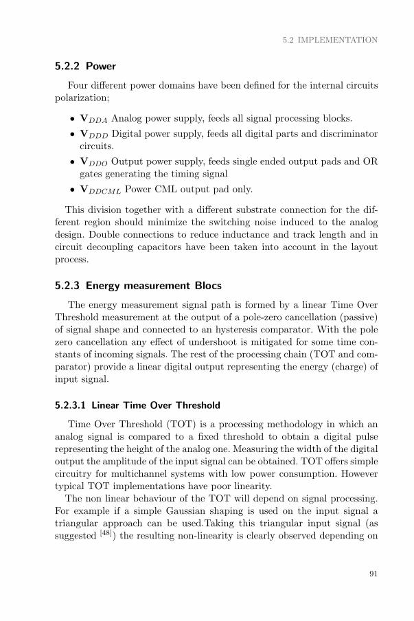
5.2 IMPLEMENTATION
5.2.2 Power
Four different power domains have been defined for the internal circuitspolarization;
• VDDA Analog power supply, feeds all signal processing blocks.
• VDDD Digital power supply, feeds all digital parts and discriminatorcircuits.
• VDDO Output power supply, feeds single ended output pads and ORgates generating the timing signal
• VDDCML Power CML output pad only.
This division together with a different substrate connection for the dif-ferent region should minimize the switching noise induced to the analogdesign. Double connections to reduce inductance and track length and incircuit decoupling capacitors have been taken into account in the layoutprocess.
5.2.3 Energy measurement Blocs
The energy measurement signal path is formed by a linear Time OverThreshold measurement at the output of a pole-zero cancellation (passive)of signal shape and connected to an hysteresis comparator. With the polezero cancellation any effect of undershoot is mitigated for some time con-stants of incoming signals. The rest of the processing chain (TOT and com-parator) provide a linear digital output representing the energy (charge) ofinput signal.
5.2.3.1 Linear Time Over Threshold
Time Over Threshold (TOT) is a processing methodology in which ananalog signal is compared to a fixed threshold to obtain a digital pulserepresenting the height of the analog one. Measuring the width of the digitaloutput the amplitude of the input signal can be obtained. TOT offers simplecircuitry for multichannel systems with low power consumption. Howevertypical TOT implementations have poor linearity.
The non linear behaviour of the TOT will depend on signal processing.For example if a simple Gaussian shaping is used on the input signal atriangular approach can be used.Taking this triangular input signal (assuggested [48]) the resulting non-linearity is clearly observed depending on
91

DESIGN FOR PET APPLICATIONS
Figure 5.4: TOT inputFigure 5.5: TOT output for triangularinput
threshold value (see figures 5.4 and 5.5). Dynamic threshold variation de-pending on incoming signal has been studied to achieve a linear output[48]. But if an ideal signal with an extremely fast rising edge and constantlinear falling edge the resulting TOT measurement should be close to anideal one (see figure 5.6 and 5.7).
Figure 5.6: TOT input Figure 5.7: TOT output
A similar signal to the ideal can be obtained taking advantage of the fastrising edge of the input signal generated by the SiPM. Using an integratorwith a constant discharge current before a comparator, a linear TOT mea-surement is obtained. Basic schematics can be seen in figure 5.8. Similarapproach has been used in the past in other detector systems[49],[50].
Ideally resulting TOT measurement can be easily calculated using for-mula 34, taking as input the injected charge signal (Q). Since thresholdvoltage (VTh), capacitance (CKrum) and discharge current (IKrum) will
92

5.2 IMPLEMENTATION
Figure 5.8: Linear TOT schematic
be constant the measured time will have a linear behaviour with Q. Thenon ideal behaviour will be introduced by the slope of the rising edge ofour signal and the long decay of some SiPMs combined with the scintil-lating material. A pole-zero passive cancellation is also included to avoidundershoot in input signal to the integrator. Those non ideal effects willbe noticeable for very small signals, but not for usual events from PETsystems.
TTOT =Q
IKrum
− VThCKrum
IKrum
(34)
Some linearity simulations of the linear time over threshold measure-ment is summarized in figure 5.9 using a real measured signal as input andincluding pre-amplifier.
One of the most important advantages of this structure is the flexibil-ity. Changing the feedback capacitor and the discharge current offers thepossibility to trade-off resolution versus output time over threshold width.
93
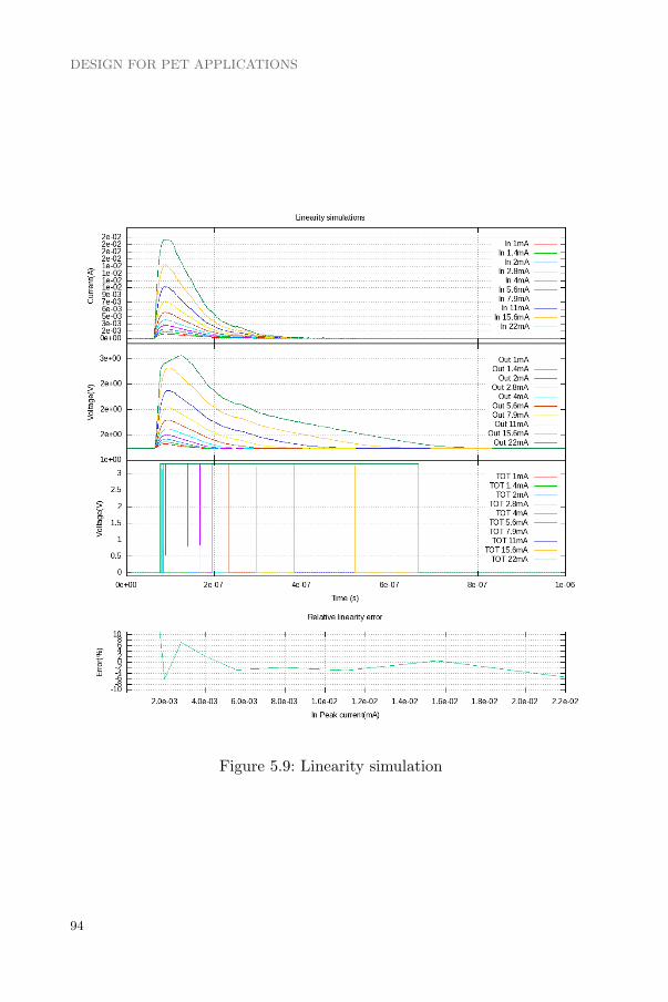
DESIGN FOR PET APPLICATIONS
Figure 5.9: Linearity simulation
94

5.2 IMPLEMENTATION
5.2.3.2 Hysteresis comparator
The hysteresis comparator is needed to avoid multiple transitions pro-duced by noise in the signal tail. The added hysteresis will provide a cleansignal at the output of the comparator. For this reason a design based on astandard CMOS comparator [52] has been used. A source coupled differen-tial pair with positive feedback and a differential to single ended converterhas been designed. For the differential pair bipolar transistors have beenused. To improve performance cascoded current mirrors have been used.The schematic can be observed in figure 5.10.
Figure 5.10: Hysteresis comparator schematic
Figure 5.11: Hysteresis compara-tor layout
By design the cascodes in the differ-ential pair will be equal in sizes andalso Q1 and Q2. If we define as α therelation in currents from cascode mas-ter and slave (related to their dimen-sions), the resulting hysteresis from thecircuit can be calculated using formula35, basically controlled by the cascodecurrent gain between M3 and M1 or thesame size M4 and M5. By design thehysteresis is set to 30mV. Layout only
95

DESIGN FOR PET APPLICATIONS
requires 73μm x 33μm and can be seen in figure 5.11.
VHisteresys = 2.
√IbiasMb2
gmQ1,Q2
.
√α− 1√1 + α
(35)
MonteCarlo simulations with a fixed input set to 1.65V and varying theother comparator input is shown in figure 5.12 including process and mis-match variations. Hysteresis width presents small variations in this circuitas desired.
Figure 5.12: Hysteresis comparator MonteCarlo simulation
96

5.2 IMPLEMENTATION
5.2.4 Time measurement Blocs
Timing signal path only includes a fast current discriminator at theoutput of the pre-amplifier to generate the timing information.
5.2.4.1 Current discriminator
Current discriminator should have an extremely fast response for lowsignal currents. This is important because the first electrons generated bythe SiPM would give the better timing for the incoming signal. Imple-mented design is based in a combination of a extremely fast low currentdiscriminator[51] with a constant current mirror. The current mirror is con-nected to a DAC used for setting the threshold (deriving some fixed amountof current at the input). The basic schematic can be observed in figure 5.13.
Figure 5.13: Current fast discrimina-tor
Initial conditions keep outputvoltage equal to input voltage andin a range keeping Mn and Mp
OFF. On the event of incoming cur-rent it will be integrated by the par-asitic input capacitance, generatingan increasing voltage at the inputnode. The voltage at the outputnode will decrease faster than theinput since the amplifier gain (-A).Vgs for Mn transistor will increaseuntil its operation point is set to theON state. Once ON a negative feed-back loop is created driving inputnode to virtual ground. If current
signal is inverted (flowing from the discriminator to the previous stage),Mp will perform the complementary operation. This structure is simpleand delivers very fast response time specially in low input currents.
The output buffer isolates output node from next stage. It will generatea voltage signal suitable for further processing or readout.
The resulting layout has a total size of 21μm x 83μm (seen in figure5.14).
MonteCarlo simulations points to very small variation (of the order ofnano amperes) on the switching point, keeping the transition around 178μAof input current with implemented dimensions.
97

DESIGN FOR PET APPLICATIONS
Figure 5.14: Fast current discriminator layout
5.2.5 Pile-up detection blocs
To avoid costly offline processing a pile-up flag is available on everychannel at every acquisition. This is achieved using an extra signal pathto detect a double peak at the input during the acquisition window. Thedifferentiated signal (using in series capacitor) at the output of the pre-amplifier will trigger a comparator and if two comparator outputs havebeen triggered before resetting pile-up logic, a logic assertion will be markedin the pile-up register. The basic schematic of the pile-up detection logic isdepicted in figure 5.15.
Figure 5.15: Pile-up detectionlogic
Figure 5.16: Pile-up reset logic
To reduce latency on the readout a dedicated readout and control for thepile-up register has been designed. To reduce input / output signals for thecontrol, some combinational logic has also been added to generate differentreset signals in the blocks. In figure 5.16 the reset logic can be observedand in figure 5.17 a full readout sequence is depicted.
Figure 5.17: Pile up register readout
98

5.2 IMPLEMENTATION
5.2.6 Common Blocs and Biasing
Several blocs have been designed to provide the needed voltages andcurrents for setting the operation point of the circuitry and also to provideall the configurable analog values.
5.2.6.1 Bandgap references
Two Bandgap references previously used in other designs has been reusedto provide a voltage and a current reference for all the biasing and DACscircuitry. The voltage reference generates 1.21V while the current referencegenerates a 100μA current. See SiPMVFEr1 appendix for further details.
5.2.6.2 DACs
Several DACs are included in the design in order to tune the circuitbehaviour. Some of them can be read directly from the input/output pins.All DACs are based on the current output DAC shown in figure 5.18. Uppertransistor acts as a slave of a current mirror, while the transistor connectedin series acts as a switch. Binary inputs enable those switches to permit afixed current to cross to the output. Multiplied circuits in parallel generatethe weighted output depending on bit pattern.
Figure 5.18: Current output DAC
For the generation of voltage DACs between a determined value the signalfrom the current DAC and the Bandgap reference voltage are combinedachieving a fixed offset and resolution with small changes with temperature.In figure 5.19 a general schematic for the voltage output DACs can be seenusing those two elements. The Bandgap voltage is used to add a fixedcurrent at the output of the current DAC. The process and temperaturevariation of the resistors value is compensated between the reference ofthe fixed current and the load of the current DAC. The sum of currents isconverted to voltage and buffered. The resulting voltage output will have
99

DESIGN FOR PET APPLICATIONS
an offset defined by 36, an LSB defined by 37 and a maximum output givenby 38.
Figure 5.19: Voltage output DAC
Voffset =VBG
R1.R2 (36)
VLSB = ILSBDAC.R2 (37)
VMAX =VBG
R1.R2 + IMAXDAC
.R2(38)
To reduce area and power consumption all DACs share common refer-ences from the common bias block. Those references are used to copy aconstant current master (for the current DACs, Vbias in schematic) or afixed current (amplifier connected to VBG and master mirror with resistorload). Due to area constraints only a pair of current DACs where designed(3 bits and 6 bits) and they are combined to generate greater resolutionDACs connecting it’s output in parallel. Such combination can lead to nonuniformities due to unmatched current copies.
A MonteCarlo simulation of a 6bit voltage DAC including mismatch andprocess variations can be observed in figure 5.20. Step size matches desiredvalue (around 10mV) and full scale is as expected.
Figure 5.20: Voltage DAC(6b) MonteCarlo
100

5.2 IMPLEMENTATION
5.2.6.3 Single Ended CMOS Pad
Standard output pads have been used when possible (input wire connec-tion, power pads, digital on top and bottom zone of pad ring). But for somereasons two pads have been designed and used as a hard macro. Lookingat section 5.2.1.1 the width of the full channel including input and outputpads is fixed. The size of a standard analog input pad (wire connection)is around 100μm height, but standard CMOS output buffers double thiswidth.
For this reason it was decided to implement a custom output pad keepingthe same height of the analog one but incrementing it’s length. It was alsodesigned to be able to tolerate short circuit at the output and with a slewrate control.
The basis to obtain this features is to control the output impedance. Inthis case an output resistance with a pass gate to connect two in seriescontrols the slew rate by a single bit (the inverter of the pass gate is alsoincluded). Schematic can be seen in next figure 5.22. The controlled outputresistance limits output current to around 5mA (with high resistor) and10mA (with small resistor).
On the layout the width is kept to the same as a standard analog pad(around 100μm) but the length is extended to fit the rest of introducedelements with a total of around 362μm. Full layout can be seen in figure5.21.
Figure 5.21: Output pad buffer layoutFigure 5.22: Output padbuffer with SR controlschematic
101
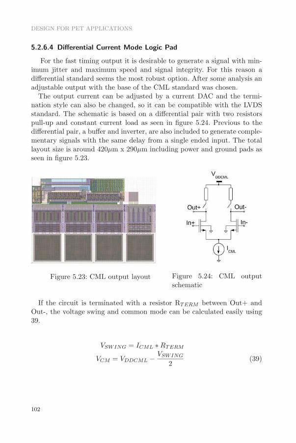
DESIGN FOR PET APPLICATIONS
5.2.6.4 Differential Current Mode Logic Pad
For the fast timing output it is desirable to generate a signal with min-imum jitter and maximum speed and signal integrity. For this reason adifferential standard seems the most robust option. After some analysis anadjustable output with the base of the CML standard was chosen.
The output current can be adjusted by a current DAC and the termi-nation style can also be changed, so it can be compatible with the LVDSstandard. The schematic is based on a differential pair with two resistorspull-up and constant current load as seen in figure 5.24. Previous to thedifferential pair, a buffer and inverter, are also included to generate comple-mentary signals with the same delay from a single ended input. The totallayout size is around 420μm x 290μm including power and ground pads asseen in figure 5.23.
Figure 5.23: CML output layout Figure 5.24: CML outputschematic
If the circuit is terminated with a resistor RTERM between Out+ andOut-, the voltage swing and common mode can be calculated easily using39.
VSWING = ICML ∗RTERM
VCM = VDDCML − VSWING
2(39)
102

5.2 IMPLEMENTATION
5.2.6.5 Temperature sensor
A small temperature sensor based on the voltage drop across a diodeconnected FET has been introduced in the circuit. To achieve more voltagevariation with temperature three diodes have been placed in series (seefigure 5.26. The output drives directly an analog (wire) pad. Total size ofthe sensor (including current mirror) is 34μm x 47μm (see figure 5.25).
Figure 5.25: Tempera-ture sensor layout
Figure 5.26:Tempera-ture sensorschematic
Figure 5.27: Temperature sensorslope montecarlo simulation
The voltage drop of a diode with a constant current will vary dependingon the temperature. Since all diodes are at the same temperature, thechange in voltage will be three times bigger with three diodes. The resultingoutput voltage is expected to have a slope of 5mV/oC (see montecarlosimulation in figure 5.27). Process variations will change the absolute valueof the temperature output at a given temperature, but not the slope thusallowing an easy single point calibration.
103

DESIGN FOR PET APPLICATIONS
5.2.6.6 Slow Control
Slow control interface is based on a standard JTAG[47] interface with userdefined data registers. Synopsys R© tools permit automatic insertion of theTest Access Port (TAP) controller and connect the registers at compilationtime, easing the introduction of this protocol in the design. Only using 5lines, TDI, TDO, TMS, TCK and TRST internal registers can be read andwritten. Using standard TAP controller FSM (see figure 5.28), any of thecontrol registers can be read or written by selecting the instruction registerthat points to the corresponding data register and then writing the data.TAP controller FSM changes it’s state depending on TMS value on everyrising edge of TCK.
Figure 5.28: TAP controller FSM
Following FSM a typical write to a register with 33 bits length shouldbe as depicted in figure 5.29.
104
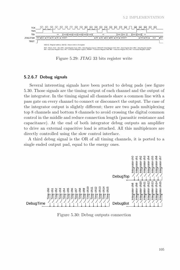
5.2 IMPLEMENTATION
Figure 5.29: JTAG 33 bits register write
5.2.6.7 Debug signals
Several interesting signals have been ported to debug pads (see figure5.30. Those signals are the timing output of each channel and the output ofthe integrator. In the timing signal all channels share a common line with apass gate on every channel to connect or disconnect the output. The case ofthe integrator output is slightly different; there are two pads multiplexingtop 8 channels and bottom 8 channels to avoid crossing the digital commoncontrol in the middle and reduce connection length (parasitic resistance andcapacitance). At the end of both integrator debug outputs an amplifierto drive an external capacitive load is attached. All this multiplexors aredirectly controlled using the slow control interface.
A third debug signal is the OR of all timing channels, it is ported to asingle ended output pad, equal to the energy ones.
Figure 5.30: Debug outputs connection
105

DESIGN FOR PET APPLICATIONS
5.2.7 Layout
Full layout of final prototype can be seen in figure 5.31. Channel pro-cessing chain is placed from left (channel input) to right (channel output),with separated power supply for digital part (right end of channel) andoutput pads. In the middle of the prototype the common bias and DACswith the common digital is placed, thus the length of connections to allchannels is minimized. Left and right pads are reserved for input / outputof the channels (with ground connection on the middle left and debug dig-ital outputs on the middle right). Top and bottom are mostly for digitalinterface and power supplies.
Figure 5.31: Final FLEXTOT layout
To avoid coupling through power supply separated supplies for analog,
106

5.2 IMPLEMENTATION
digital and output pads have been selected. Different power domains canbe observed in figure 5.32. Power supplies are connected from top to bot-tom, doubling the pads (whenever possible) in both sides of the design. Inthis way a good connection with as low as possible parasitic resistance isachieved. Few decoupling capacitors are also placed in free areas and inpower rails.
Figure 5.32: FLEXTOT power domains
107

DESIGN FOR PET APPLICATIONS
5.3 Results
FLEXTOT prototype was received in October 2012, with 30 encapsu-lated dies on a QFN64 and 10 non encapsulated dies. During manufacturinga test system was designed thinking on testing the maximum parametersas possible. First electrical characterization was followed by more realistictests with SiPM and radioactive sources.
5.3.1 Test system
Test system (see figure 5.33.) is based on a stack of three PCB with allthe needed electronics for a full system. From the sensor to the data com-munication with a host computer. The only thing not included is the highvoltage power supply for the sensors. The following electronics / featuresare present in each of the different PCBs (from top to bottom):
• Sensor PCB: different manufacturers sensors can be placed over thisPCB. The sensor connects directly to next PCB, only high voltageconnector is available. A variation PCB with a charge injection circuitcan be placed in the same position to calibrate channels with a knownsignal shape and amplitude.
• Analog PCB: the analog PCB is basically a QFN64 test socket withlow drop-out (LDO) linear regulators and some decoupling and resis-tors. It also uses a pair of amplifiers to check debug signals directlyfrom oscilloscope and a high speed switch (SPDT) to be able to dis-connect input to channels.
• Digital PCB: EP3C low cost FPGA with FT2232 transceiver to han-dle communications with host computer. Using the FPGA the slowcontrol can be configured, pile-up interface managed, SPDT switchesconnection enabled and also a low resolution (5ns) pulse width mea-surement can be performed for all channels. It houses a basic DAQfor testing the capabilities of the ASIC.
108

5.3 RESULTS
Figure 5.33: Test system setup
5.3.2 Power consumption
Using test points in the analog PCB the power consumption from dif-ferent power supplies can be measured. A summary of the tested ASICsis available in table 5.2, VDDO and VDDCML are not measured, since innormal conditions and no commutations at the outputs VDDO will drawa negligible current and VDDCML current draw will depend on configura-tion. VDDA and VDDD are powered at nominal 3.3V power supply. Theaverage power consumption is 10.7mW per channel or 7.7mW per analogchannel (excluding digital power).
109
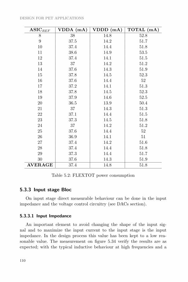
DESIGN FOR PET APPLICATIONS
ASICREF VDDA (mA) VDDD (mA) TOTAL (mA)
8 38 14.8 52.89 37.5 14.2 51.710 37.4 14.4 51.811 38.6 14.9 53.512 37.4 14.1 51.513 37 14.2 51.214 37.6 14.3 51.915 37.8 14.5 52.316 37.6 14.4 5217 37.2 14.1 51.318 37.8 14.5 52.319 37.9 14.6 52.520 36.5 13.9 50.421 37 14.3 51.322 37.1 14.4 51.523 37.3 14.5 51.824 37 14.2 51.225 37.6 14.4 5226 36.9 14.1 5127 37.4 14.2 51.628 37.4 14.4 51.829 37.3 14.4 51.730 37.6 14.3 51.9
AVERAGE 37.4 14.8 51.8
Table 5.2: FLEXTOT power consumption
5.3.3 Input stage Bloc
On input stage direct measurable behaviour can be done in the inputimpedance and the voltage control circuitry (see DACs section).
5.3.3.1 Input Impedance
An important element to avoid changing the shape of the input sig-nal and to maximize the input current to the input stage is the inputimpedance. In the design process this value has been kept to a low rea-sonable value. The measurement on figure 5.34 verify the results are asexpected; with the typical inductive behaviour at high frequencies and a
110

5.3 RESULTS
value close to the typical one (around 34Ω until 200MHz).
Figure 5.34: Input impedance
111
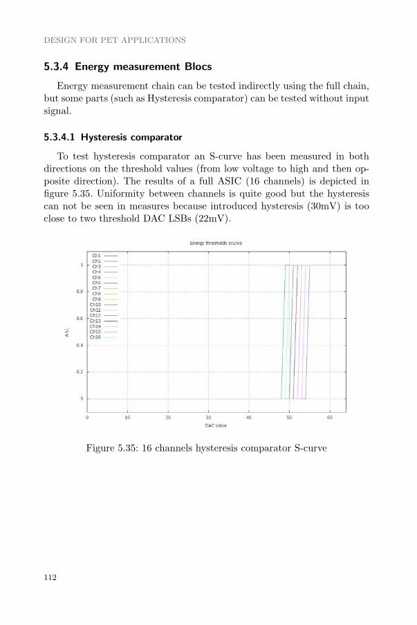
DESIGN FOR PET APPLICATIONS
5.3.4 Energy measurement Blocs
Energy measurement chain can be tested indirectly using the full chain,but some parts (such as Hysteresis comparator) can be tested without inputsignal.
5.3.4.1 Hysteresis comparator
To test hysteresis comparator an S-curve has been measured in bothdirections on the threshold values (from low voltage to high and then op-posite direction). The results of a full ASIC (16 channels) is depicted infigure 5.35. Uniformity between channels is quite good but the hysteresiscan not be seen in measures because introduced hysteresis (30mV) is tooclose to two threshold DAC LSBs (22mV).
Figure 5.35: 16 channels hysteresis comparator S-curve
112
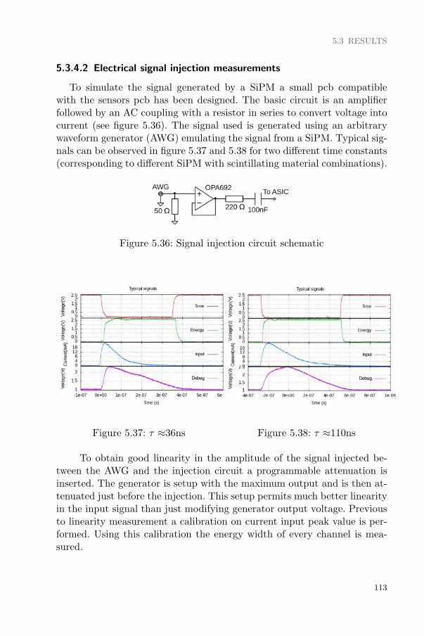
5.3 RESULTS
5.3.4.2 Electrical signal injection measurements
To simulate the signal generated by a SiPM a small pcb compatiblewith the sensors pcb has been designed. The basic circuit is an amplifierfollowed by an AC coupling with a resistor in series to convert voltage intocurrent (see figure 5.36). The signal used is generated using an arbitrarywaveform generator (AWG) emulating the signal from a SiPM. Typical sig-nals can be observed in figure 5.37 and 5.38 for two different time constants(corresponding to different SiPM with scintillating material combinations).
Figure 5.36: Signal injection circuit schematic
Figure 5.37: τ ≈36ns Figure 5.38: τ ≈110ns
To obtain good linearity in the amplitude of the signal injected be-tween the AWG and the injection circuit a programmable attenuation isinserted. The generator is setup with the maximum output and is then at-tenuated just before the injection. This setup permits much better linearityin the input signal than just modifying generator output voltage. Previousto linearity measurement a calibration on current input peak value is per-formed. Using this calibration the energy width of every channel is mea-sured.
113

DESIGN FOR PET APPLICATIONS
Since the prototype has some configurable values it will need some cal-ibration to achieve good linearity results in a defined range and shape ofinput signals. Some examples of the resulting curves from a full prototype(16 channels) are plotted in figures 5.39, 5.41, 5.43 for a τ ≈36ns and infigure 5.40, 5.42, 5.44 for a τ ≈110ns.
Figure 5.39: Linearity τ ≈36ns 18mA range
114

5.3 RESULTS
Figure 5.40: Linearity τ ≈110ns 18mA range
Figure 5.41: Linearity τ ≈36ns 5mA range
115
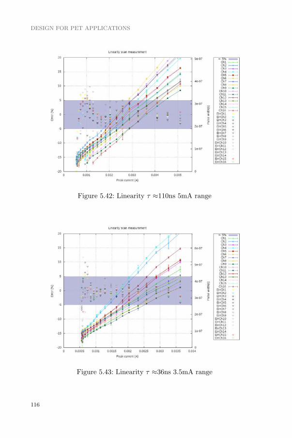
DESIGN FOR PET APPLICATIONS
Figure 5.42: Linearity τ ≈110ns 5mA range
Figure 5.43: Linearity τ ≈36ns 3.5mA range
116

5.3 RESULTS
Figure 5.44: Linearity τ ≈110ns 3.5mA range
117

DESIGN FOR PET APPLICATIONS
5.3.5 Time measurement Blocs
Timing signal path can be measured indirectly injecting signal at theinput stage and evaluating it’s response.
5.3.5.1 Jitter
Jitter is measured as the variation of the delay measurement between atrigger signal and the timing (CML) output. The signal is generated usingan arbitrary waveform generator (AWG2021) reproducing a signal similarto a 511keV signal (previously measured at section 5.3.9). Typical signalsare plotted in figure 5.45, input signal should match the rising edge of adetector (≈ 4ns) and output CML is deskewed to reduce the oscilloscopewindow for the measurement. Measurement is depicted as two vertical barsmeasuring the delay between input rising edge and output.
Figure 5.45: Jitter measurement signals
The variation of this delay measurement (sigma) will be the jitter mea-sured (rms). As an example a measurement with no capacitance at theinput is plotted in figure 5.46. The total signal measured is the generatorjitter added to the system jitter including oscilloscope. Expecting oscillo-scope jitter is much less than the rest the assumption that jitter is provided
118

5.3 RESULTS
Figure 5.46: Total jitter measurement
by generator and electronics can be done. According to technical docu-mentation jitter between signal and marker output (used for trigger) fromAWG2021 is 20ps rms, thus electronics jitter can be easily calculated using40.
σTOTAL =√
σGenerator2 + σElectronics
2
σElectronics =√
σTOTAL2 − σGenerator
2 (40)
An important feature of the input stage is the capacitance seen at theinput should not increment the noise (so jitter) at the output. To testthis feature with the test injection circuitry different capacitance is placedat the input. As expected the jitter is not incremented dramatically. The
119

DESIGN FOR PET APPLICATIONS
results are plotted in figure 5.47 (correcting the jitter introduced by thegenerator), a minimum capacitance of 5pF is added due to the parasiticson the PCB.
Figure 5.47: Jitter variation with input capacitance
5.3.6 Pile-up measurement Blocs
On pile-up some preliminary measurements have been performed usingan arbitrary waveform generated signal with two equal peaks close to eachother (separated by 10 ns). The signal chain detects always a pile-up in thiscase, while with a clean signal it is not detected. Further measurementsmust be performed to characterize fully this bloc.
5.3.7 Common Blocs and Biasing
5.3.7.1 DACs
Several DACs can be measured directly from input / output pins. Prob-ably the most representative is the 9 bit voltage DAC used to change thevoltage at the input node of the ASIC. In figure 5.48 the measurement of 16channels from the same ASIC can be observed compared with the monte-carlo simulations. To keep the input stage in the operating point the input
120

5.3 RESULTS
node voltage can not be set to any value and a protection circuit couldrequire a little bit more current from the DAC than in normal conditions,fixing the voltage in a certain range. For this reason a clear effect at low orhigh values can be observed, keeping voltage between 1 and 2 V.
Figure 5.48: Channel DAC measurement
Typical calculations of INL and DNL are represented in figure 5.49. It isimportant to note the increment in INL should be produced by the effectof the voltage limiting circuit in the input node.
The same measurement performed in the Debug outputs (with no signalshould be equal to Vref set internally by a DAC) in figure 5.50. In this casesignal is not affected by a voltage limiting circuit, but since it is read atthe output of the amplifier it will have it’s range limited. In this case INLtakes more usual values.
121

DESIGN FOR PET APPLICATIONS
Figure 5.49: Single channel Offset DAC measurement
Figure 5.50: Single channel Vref DAC measurement
122

5.3 RESULTS
5.3.7.2 Single Ended CMOS Pad
A simple measurement on the single ended output pads with a passiveprobe has been performed. As it can be seen in figure 5.51 two clearlydifferent slew rates are available depending on configuration bits.
Figure 5.51: Single ended pad slew rate
5.3.7.3 Differential Current Mode Logic Pad
On the CML output pad a pseudoLVDS configuration is tested with330Ω external pull-up resistors and 100Ω termination. Different currentconfigurations are also measured and summarized in table 5.3 with theoptional internal pull-up (switch) configuration.
Figure 5.52: CML output
123

DESIGN FOR PET APPLICATIONS
Digital configuration Internal switch Current(mA)
000X0 Off 211
000X1 On 211
001XX On or Off 181
010XX On or Off 151
011XX On or Off 121
100XX On or Off 9101XX On or Off 6110XX On or Off 3111XX On or Off 0
1 For agressive power consumption external resistors are needed to avoid voltagedrop in internal switches, limiting current.
Table 5.3: CML configuration options
5.3.7.4 Temperature sensor
Temperature sensor has been tested to verify its output behaviour. As aninitial test the transient on internal temperature raise has been measured.Since the calibration slope was constant to (≈ 5mV/oC) a simple calibrationwith just one point (ambient temperature at power up) has been used. Theresulting transient after power up permits to obtain the estimated workingtemperature of the electronics (see figure 5.53.
Figure 5.53: Temperature transient at power up
124

5.3 RESULTS
5.3.8 SiPM measurements
After electrical characterization of the prototype a real sensor is at-tached to the test system. The input signal will have a realistic timing andavoid any undesired effect introduced by the injection circuit. With thisconfiguration several measurements are performed.
5.3.9 Radioactive sources
Figure 5.54: LSO setup detail
To characterize with a signal close to re-ality several radioactive sources have beenused. A small LSO crystal (2x2x8 mm3)has been placed over a detection channel(3x3 mm2) and then a radioactive sourceclose to the crystal. The system setup(without radioactive source) is depicted infigure 5.54. Previous to the measurementwith sources background (LSO emissionspectra) is also measured and should besubstracted. The sources used have beenNa22, Co60 and Cs137, see figure 5.55.
Using the resulting fitted points a plot of the linearity achieved on thesignal with the resulting TOT value is plotted. We can observe excellentlinearity in the full range. Varying threshold of the energy comparatorthe resulting line will move over the x-axis, as seen in figure 5.56 for twodifferent thresholds in channel (40 and 50 DAC counts).
With the position of the two more external peaks a calibration constantis determined (see formula 41). The measured resolutions (σ) are then con-verted to energy using this constant. The resulting resolution computationis summarized in table 5.4 and table 5.5, for the two threshold configurationcases. As expected resolution improves for higher energies.
εs =μpeak1 − μpeak2
keVpeak1 − keVpeak2
→ PkErr =σ
εs→ Pkres =
PkErr
keVpeak
∗ 100 (41)
125
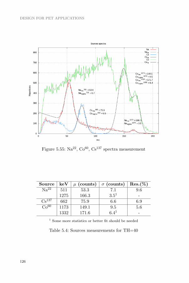
DESIGN FOR PET APPLICATIONS
Figure 5.55: Na22, Co60, Cs137 spectra measurement
Source keV μ (counts) σ (counts) Res.(%)
Na22 511 53.3 7.1 9.61275 166.3 3.51 -
Cs137 662 75.9 6.6 6.9
Co60 1173 149.1 9.5 5.61332 171.6 6.41 -
1 Some more statistics or better fit should be needed
Table 5.4: Sources measurements for TH=40
126

5.3 RESULTS
Figure 5.56: Linearity of the resulting spectra measurements
Source keV μ (counts) σ (counts) Res.(%)
Na22 511 88 5.6 8.31275 195 81 -
Cs137 662 112 6.2 7.1
Co60 1173 176 9 5.81332 197 5.71 -
1 Some more statistics or better fit should be needed
Table 5.5: Sources measurements for TH=50
127

DESIGN FOR PET APPLICATIONS
5.3.10 Coincidence Resolving Time
To obtain a first estimation about the overall system timing accuracy, apreliminary measurement has been performed. The basics is to reproducea coincidence system in the laboratory. The setup can be seen in figure5.57 Two test boards with single channel SiPMs are placed facing to eachother. On top of the SiPM the LSO crystal is placed. The Na22 radioactivesource is placed as close as possible to both crystals and just in the middleto obtain coincident signals. The CML output is readout using differentialprobes. In the oscilloscope the timing and energy signals are acquired.
Figure 5.57: Coincidence system setup
Typical signals obtained by the system can be observed in figure 5.58.Plotting both channels energy spectra results in a variation of clusters
mostly concentrated in the 511keV energy. After running a clustering algo-rithm the events around 511keV are obtained (see figures 5.59 and 5.60).
Plotting those events and fitting the result, the final relevant events forthe CRT measurement are reduced to ±σ (see figures 5.61 and 5.62 withthe ±σ zones highlighted).
The resulting delay measurements of timing outputs from those eventsare plotted in an histogram to obtain the timing accuracy of the full systemin figure 5.63.
The results show a consistent measurement of resolutions below 300psFWHM (around 115ps rms).
128
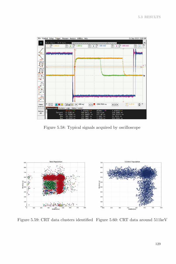
5.3 RESULTS
Figure 5.58: Typical signals acquired by oscilloscope
Figure 5.59: CRT data clusters identified Figure 5.60: CRT data around 511keV
129

DESIGN FOR PET APPLICATIONS
Figure 5.61: Channel 1 energy measure-ment
Figure 5.62: Channel 2 energy measure-ment
Figure 5.63: Coincidence Resolving Time
130

5.3 RESULTS
5.3.11 PET system measurements
Several measurements have been performed at CIEMAT to check theviability of the electronics for a full PET system. Including two sensorsplaced face to face with a mobile (rotating) platform in the middle (usedto emulate a full ring of detectors). The setup can be seen in figure 5.64.Several samples (radioactive sources) are placed in the mobile platform tocharacterize the system.
Figure 5.64: Test system at CIEMAT
Once data is acquired image reconstruction techniques are used to de-rive a 2D image representing the zone from the incoming signal. The re-construction algorithm applied in this case has been Filter Backprojection(FBP)[53], even though more complex algorithms[54] could also be usedto improve spatial resolution with the cost of incrementing reconstructiontime.
A first measurement can be observed in figure 5.65 with the measurementof a single Na22 (0.25mm diameter) radioactive source (left) placed in twodifferent positions and reconstructing the position in the same image. Onthe right two Na22 (1mm diameter) sources are placed at 4mm separation
131

DESIGN FOR PET APPLICATIONS
and data acquired and reconstructed. More systematic measurements withdifferent separation of the sources can be seen in figure 5.66 with a summaryon table 5.6. As expected final spatial resolution is around few mm.
Figure 5.65: PET initial tests at CIEMAT
Distance Center Na221 FWHM Na22
1 Center Na222 FWHM Na22
2
2 mm 0.11 mm 3.03 mm 0.11 mm 3.03 mm3 mm -1.18 mm 2.94 mm 1 mm 2.65 mm4 mm -1.77 mm 2.58 mm 1.75 mm 2.81 mm5 mm -2.26 mm 2.57 mm 2.25 mm 2.48 mm
Table 5.6: CIEMAT spatial resolution measurements
132

5.3 RESULTS
Figure 5.66: PET spatial resolution measurements
133


6Design for SciFi Tracker
High luminosity particle detectors must operate at much higher ratesthan in other systems (such as PET). The tracker sub-detector of the LHCbexperiment reveals the paths of electrically charged particles as they passthrough and interact with suitable substances[6]. Particle records a weakelectrical signal that particles trigger as they move through the device.Normal detectors use silicon devices (strip detectors) or gaseous detectors(straw tubes). Once the signal is acquired and readout a computer programreconstructs the recorded patterns of tracks.
The current LHCb Tracker stations are composed of an Outer Tracker(OT) with straw tube detectors and an Inner Tracker (IT) with siliconstrip detectors to cover the high-occupancy area near the beam pipe (seefigure 6.1). The new technology for the OT IT upgrade will be based onscintillating fibres, with clear fibres carrying the signal photons from theinner region to the detectors situated outside the LHCb acceptance.
In the first draft of the Letter of Intent for the LHCb upgrade[6], a newscintillating-fibre layout has been proposed, with 2.5 m long fibres coveringthe whole central region of the tracker stations, from the LHC beam planeall the way to the top and bottom of the LHCb acceptance (see figure 6.2).In this Central Tracker (CT) option, the IT and several (or all of the) OTmodules are replaced by the new scintillating-fibre modules. Full detectoris built by 3 stations with three tilted (≤5o) fibre planes of X-U-V-X. Everyplane is made of 5 layers of 250 μm in diameter fibres and 2.5 m long.
One of the major concerns is the production and alignment of the fibres
135
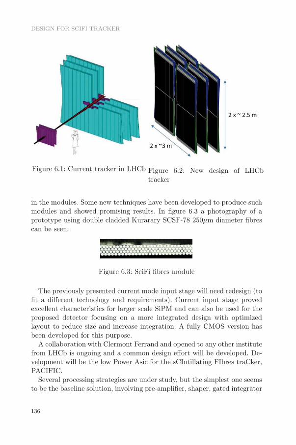
DESIGN FOR SCIFI TRACKER
Figure 6.1: Current tracker in LHCb Figure 6.2: New design of LHCbtracker
in the modules. Some new techniques have been developed to produce suchmodules and showed promising results. In figure 6.3 a photography of aprototype using double cladded Kurarary SCSF-78 250μm diameter fibrescan be seen.
Figure 6.3: SciFi fibres module
The previously presented current mode input stage will need redesign (tofit a different technology and requirements). Current input stage provedexcellent characteristics for larger scale SiPM and can also be used for theproposed detector focusing on a more integrated design with optimizedlayout to reduce size and increase integration. A fully CMOS version hasbeen developed for this purpose.
A collaboration with Clermont Ferrand and opened to any other institutefrom LHCb is ongoing and a common design effort will be developed. De-velopment will be the low Power Asic for the sCIntillating FIbres traCker,PACIFIC.
Several processing strategies are under study, but the simplest one seemsto be the baseline solution, involving pre-amplifier, shaper, gated integrator
136
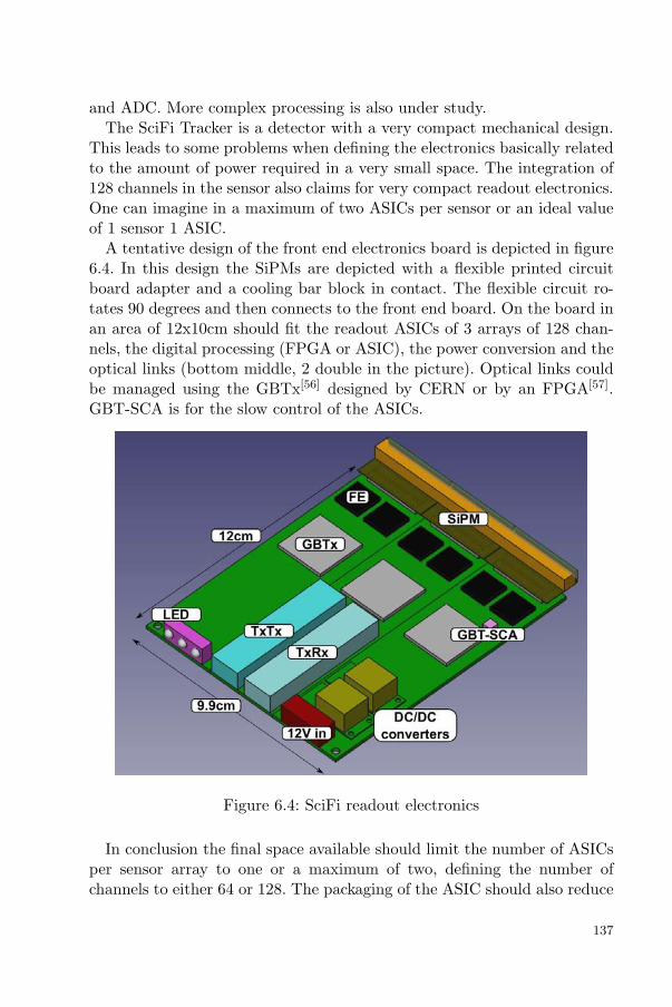
and ADC. More complex processing is also under study.The SciFi Tracker is a detector with a very compact mechanical design.
This leads to some problems when defining the electronics basically relatedto the amount of power required in a very small space. The integration of128 channels in the sensor also claims for very compact readout electronics.One can imagine in a maximum of two ASICs per sensor or an ideal valueof 1 sensor 1 ASIC.
A tentative design of the front end electronics board is depicted in figure6.4. In this design the SiPMs are depicted with a flexible printed circuitboard adapter and a cooling bar block in contact. The flexible circuit ro-tates 90 degrees and then connects to the front end board. On the board inan area of 12x10cm should fit the readout ASICs of 3 arrays of 128 chan-nels, the digital processing (FPGA or ASIC), the power conversion and theoptical links (bottom middle, 2 double in the picture). Optical links couldbe managed using the GBTx[56] designed by CERN or by an FPGA[57].GBT-SCA is for the slow control of the ASICs.
Figure 6.4: SciFi readout electronics
In conclusion the final space available should limit the number of ASICsper sensor array to one or a maximum of two, defining the number ofchannels to either 64 or 128. The packaging of the ASIC should also reduce
137

DESIGN FOR SCIFI TRACKER
to the maximum the routing space needed. The BGA package seems thebest option.
6.1 Front End Electronics
In terms of Bandwidth the requirements are the same as in previousdesign (chapter 5) since no extra constraints are added. But in this casemore constraints are applicable.
6.1.1 Number of channels
Currently prototypes being developed keep a goal of 128 channels inthe same device (normally 2 dies packaged together). This should be thegoal of the designed electronics, to have a perfect match between sensorand readout electronics. This simple approach but leads to some importantproblem, die size. In IBM 0.13μm technology (the default used by CERNand thus in this project) area costs are important and should be kept to areasonable value.
For the high number of channels it seems reasonable that the design willbe PAD limited. In this scenario we could think on two different PADsarrangements (see figures 6.6 and 6.5). The typical arrangement (6.5) isa simple row of input output PADs in a row keeping minimum distances.A more compact design alternative (6.6) is the so called staggered PADslayout, in which two columns of PADs are used for input output.
Figure 6.5: Inline PADs Figure 6.6: Staggered PADs
The staggered PADs option is the optimal one for this design but sincethe density of channels is doubled the height of the resulting channel is
138

6.1 FRONT END ELECTRONICS
reduced to half. In this technology the minimum pitch between two analogPADs is around 80μm so the maximum height of channel by design shouldbe 40μm.
Some extra space (not depicted in previous figures) will also be neededto accommodate the needed common bias and control blocks for the fullASIC. Normally this block should be placed in the middle of the channelsto reduce the routing distance between this part and the channels.
6.1.2 Power consumption
Although power consumption is not limited, a first approach suggests itshould be reduced to the minimum. The main issue is the sensors (SiPMarray) will probably be cooled to very low temperature to avoid dark countincrease with radiation damage. As the sensors will be close to the analogASIC, the heating produced by the electronics could affect the sensor cool-ing system. An other limiting factor is the power supply, DC-DC convertersradiation tolerant are being developed at CERN, but their output currentis 3A maximum. If a single converter is used for the analog electronics amaximum of 1A should be available for 128 channels. Taking into accountnominal supply is 1.2V this leads to a maximum of 1.2W per 128 channels.If some margin is added a reasonable power consumption should be 1Wfor a 128 channels ASIC or 7.5mW/channel. This calculation agrees withprevious chapter maximum power consumption without cooling of around1W (depending on package and thermal design).
6.1.3 Timing constraints
Incoming particles bunches in LHC arrive every 25ns so at this frequencycollisions are generated.
6.1.3.1 Double peak resolution
The most important constrain for the electronics is an output mustbe given every 25ns being able to process next event. This is commonlydescribed as a double peak resolution time of 25ns.
6.1.3.2 Spill over
In order to minimize spill over (two events overlapped due to slow tails)the electronics must preserve the pulse shape from the SiPM with a small
139

DESIGN FOR SCIFI TRACKER
input impedance (for a fast recovery), but keeping in mind low power con-sumption trade-off. Some signal processing should also be needed to reduceat an acceptable level the spill over.
6.1.4 Noise
As in general designs for a single fired cell resolution the S/N ratioshould be greater than 10 in the charge spectra. The input referred noisein function of the input charge and integration time is determined[55] byequation 42, being T the integration time and Qin the input charge. Fora SiPM typical gain of the order of 106 thus for a single photon a totalof 1.106 electrons will be generated (or multiplying by the electron charge,16.10−14 Coulombs).
iin ≤√
2.Qin√T . S
N
≤√
2.16.10−14
√25.10−9.10
≤ 143pA√Hz
(42)
Keeping the S/N>10 the referred noise at the input should be smallerthan 143pA√
Hz.
6.1.5 Signal from SiPM
Two manufacturers SiPM are being studied at the moment. 128 channelsprototypes are being manufactured by Ketek and Hamamatsu. They aredesigned to provide the 128 channels with the minimum dead area possibleand fitting the fibres modules size. In figure 6.7 a photograph of one of theHamamatsu prototypes can be seen with it’s mechanical drawing.
Figure 6.7: Hamamatsu SiPM array prototype
The prototype is based on two 64 channels devices in the same die gluedtogether over a substrate with align holes to minimize the dead area be-tween them. Ketek prototypes follow the same form factor.
140

6.1 FRONT END ELECTRONICS
During December 2012 several preliminary measurements on a prototypefibres module where carried out at CERN denoting the different shapeof the signal provided by two sensors. The fibres are excited by a Sr90
radioactive source with a fixed magnet to filter only signals with energyequal to a Minimum Ionizing Particle (MIP). It is the same source used forthe characterization of LHCb pre-shower and Scintillator Pad Detector (seefigure 6.8). In those tests a single fibre was replaced by a fibres module withan array of SiPMs connected at the end. Signal is read using a low gainhigh speed amplifier with the output connected directly to the oscilloscope.A small PCB was designed to fit the amplifier and a pair of connectors tothe flexible board adapter where SiPMs are placed (see figure 6.9).
Figure 6.8: Measurement system setup
The resulting measurements show very different shapes depending on thedetector used. In Hamamatsu devices the signal follows a fast rising edgeand an exponential decay. In Ketek prototype the signal follows a muchfaster rising edge with a first and fast decay followed by a second and muchslower than Hamamatsu exponential decay, see figures 6.10 and 6.11.
With previous measurements it’s clear some shaping circuitry will beneeded to compress the signal in a 25ns window.
141

DESIGN FOR SCIFI TRACKER
Figure 6.9: Adapter board for the module readout
Figure 6.10: Hamamatsu signal Figure 6.11: Ketek signal
6.1.5.1 Dynamic range
SiPM prototypes have a fixed number of 96 micro-cells. This shouldbe the absolute maximum value to be read from the devices. But in realmeasurements signal is much more limited by the photo-statistics which israther low. For this reason and also for calibration it is important to besensitive to very small signals from a single micro-cell.
142
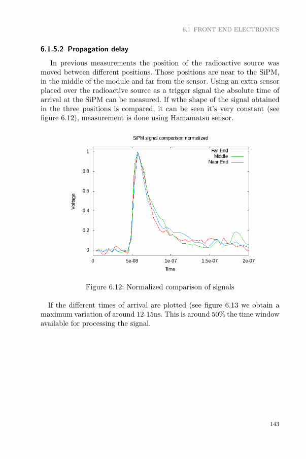
6.1 FRONT END ELECTRONICS
6.1.5.2 Propagation delay
In previous measurements the position of the radioactive source wasmoved between different positions. Those positions are near to the SiPM,in the middle of the module and far from the sensor. Using an extra sensorplaced over the radioactive source as a trigger signal the absolute time ofarrival at the SiPM can be measured. If wthe shape of the signal obtainedin the three positions is compared, it can be seen it’s very constant (seefigure 6.12), measurement is done using Hamamatsu sensor.
Figure 6.12: Normalized comparison of signals
If the different times of arrival are plotted (see figure 6.13 we obtain amaximum variation of around 12-15ns. This is around 50% the time windowavailable for processing the signal.
143

DESIGN FOR SCIFI TRACKER
Figure 6.13: Time of arrival of signals
6.1.5.3 Mirror
To improve the light yield produced by the fibres it is expected to adda mirror at the end of the detector. It will have the effect of increasing thephotons produced at the far end, since the ones generated in the oppositedirection will be reflected. In the event of a production in the middle of thedetector some signal will arrive later than the main signal. In figure 6.14a signal with a mirror placed at the end of the detector can be comparedto a signal without the mirror. The light is produced in the middle of thedetector. If the event is produced at the near end of the detector it isexpected that nearly no signal will be back from the mirror due to theattenuation. Note a second peak after the main signal generated by themirrored light around 30ns later.
144

6.1 FRONT END ELECTRONICS
Figure 6.14: Mirror effect on signal
6.1.6 Slow control
The inclusion of some controllable elements for polarization mainly andfor tuning the SiPM voltage will lead to some digital control interface. Tokeep the number of pins low a serial protocol is expected to be integratedin the forthcoming prototypes. An I2C protocol is a good candidate for thispurpose.
6.1.7 Data link
The amount of channels that should be included in the final design,the number of bits to be extracted by each of them (5 or 6) and the highrate (every 25ns) suggests that even if occupancy is low a high volume ofinformation will be produced. This information should be transmitted tonext step in the processing chain (probably an FPGA). The problems ofgoing from the ASIC to an other commercial device is mainly the numberof lines to connect both and the voltage swing (power consumption andnoise generated). For this reason a single ended LVCMOS signal shouldbe dropped and replaced by high speed serialized signals with low voltageswing interface (LVDS or CML). The final implementation will depend onthe capabilities of the FPGA.
145

DESIGN FOR SCIFI TRACKER
6.1.8 Specifications summary
A summary of previous section conclusions is detailed in table 6.1.
Parameter Value Unit
Channels 64 or 128 -Power 0.5 or 1 WPackage BGA -Double peak resolution 25 nsSiPM time constant To Be Defined -Dynamic range 0-64 micro-cellsSignal time of arrival 0-15 ns
Input referred noise ≤143 pA√Hz
Table 6.1: PACIFIC specifications summary
146
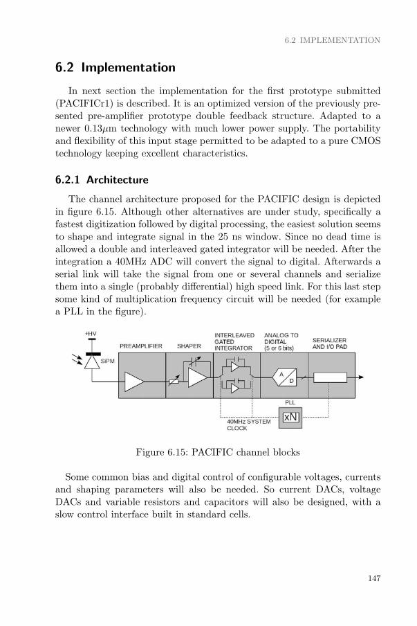
6.2 IMPLEMENTATION
6.2 Implementation
In next section the implementation for the first prototype submitted(PACIFICr1) is described. It is an optimized version of the previously pre-sented pre-amplifier prototype double feedback structure. Adapted to anewer 0.13μm technology with much lower power supply. The portabilityand flexibility of this input stage permitted to be adapted to a pure CMOStechnology keeping excellent characteristics.
6.2.1 Architecture
The channel architecture proposed for the PACIFIC design is depictedin figure 6.15. Although other alternatives are under study, specifically afastest digitization followed by digital processing, the easiest solution seemsto shape and integrate signal in the 25 ns window. Since no dead time isallowed a double and interleaved gated integrator will be needed. After theintegration a 40MHz ADC will convert the signal to digital. Afterwards aserial link will take the signal from one or several channels and serializethem into a single (probably differential) high speed link. For this last stepsome kind of multiplication frequency circuit will be needed (for examplea PLL in the figure).
Figure 6.15: PACIFIC channel blocks
Some common bias and digital control of configurable voltages, currentsand shaping parameters will also be needed. So current DACs, voltageDACs and variable resistors and capacitors will also be designed, with aslow control interface built in standard cells.
147
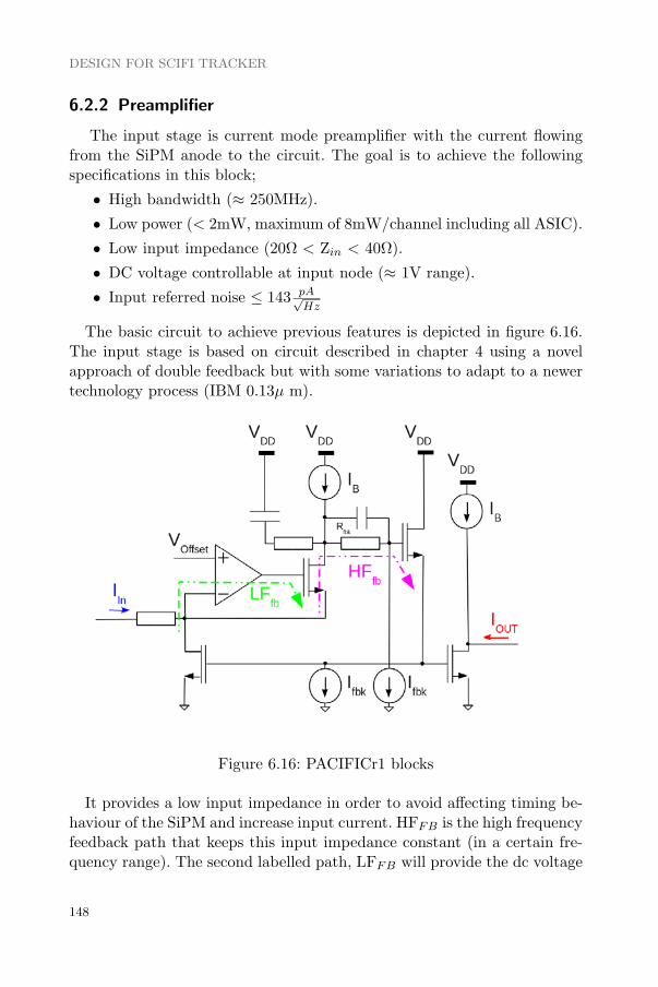
DESIGN FOR SCIFI TRACKER
6.2.2 Preamplifier
The input stage is current mode preamplifier with the current flowingfrom the SiPM anode to the circuit. The goal is to achieve the followingspecifications in this block;
• High bandwidth (≈ 250MHz).
• Low power (< 2mW, maximum of 8mW/channel including all ASIC).
• Low input impedance (20Ω < Zin < 40Ω).
• DC voltage controllable at input node (≈ 1V range).
• Input referred noise ≤ 143 pA√Hz
The basic circuit to achieve previous features is depicted in figure 6.16.The input stage is based on circuit described in chapter 4 using a novelapproach of double feedback but with some variations to adapt to a newertechnology process (IBM 0.13μ m).
Figure 6.16: PACIFICr1 blocks
It provides a low input impedance in order to avoid affecting timing be-haviour of the SiPM and increase input current. HFFB is the high frequencyfeedback path that keeps this input impedance constant (in a certain fre-quency range). The second labelled path, LFFB will provide the dc voltage
148

6.2 IMPLEMENTATION
(Voffset in figure) of the input node using the virtual short circuit in theamplifier that will drive a follower in a lower frequency range. The designhas been implemented taking into account that dominant pole should beset at the input node (SiPM parasitic capacitance is at the order of tenthsof pF). In this way stability is not compromised when an important capac-itance is added at the input.
6.2.2.1 Multiple voltages operation
As described in the requirements an important element of the circuitis the possibility to tune the voltage at the input node. Due to the factthis technology uses low voltage polarization (1.2V) an important efforthas been made to maximize the range of this voltage variation. The easiestoption is to power the circuit at a higher voltage (1.5V). For this reason aconfigurable pre-amplifier optimized for the two operating conditions hasbeen designed. The only part needing changes is the high frequency feed-back path. An adjustable pair of RC values can be switched by an externalcontrol pin. This change adapts behaviour to the desired operating voltage.In table 6.2.2.1 the selection options are described.
VSEL Switch VDD
1.2 ON 1.20 OFF 1.5
Table 6.2: VSEL operation
6.2.3 Simulation results
PACIFICr1 prototype is still under production, for this reason only sim-ulation results are presented. Some precautions on design (add parasiticelements such as wire bonding inductance) should assure a real behaviourclose to simulations.
149

DESIGN FOR SCIFI TRACKER
6.2.3.1 Input impedance
Figure 6.17: PACIFICr1 pre-amplifier inputimpedance
Input impedance is keptlow using the high fre-quency feedback loop. Thiskind of feedback loops presentan inductive behaviour athigh frequencies. The sim-ulation can be observedin figure 6.17. The inputimpedance is kept to a lowvalue corresponding to theresistance in series (16Ω) atthe pre-amplifier input un-til around 100KHz. Fromthis point increases slowlyto reach a value of around34Ω at 100MHz. Passed thisfrequency impedance increases fast reaching a value of 50Ω at around250MHz.
6.2.3.2 Input voltage variation
To determine the range of input node voltage adjustment the error onvoltage adjustment is plotted. The results can be seen in figure 6.18. Whenfeedback loop starts to became out of the operation range the voltage errorincreases faster. The obtained ranges are around 0.6V for a 1.2V powersupply and around 0.9V for a 1.5V power supply as expected. In orderto increase voltage variation triple well transistors have been used for theMOS feedback.
150

6.2 IMPLEMENTATION
Figure 6.18: PACIFICr1 Voffset error
6.2.3.3 Bandwidth
Figure 6.19: PACIFICr1 pre-amplifier Band-width
The Bandwidth ofthe pre amplifier shouldbe greater than 250MHz.The influence of inputcapacitance is to reducethe Bandwidth of thecircuit. For this reasonit is important to designit as immune as possi-ble to this effect. In fig-ure 6.19 the AC anal-ysis of the input stagewith a pair of inputcapacitances (5pF and15pF) show greater val-ues than 250MHz band-width. So it should not be a problem with those values.
151
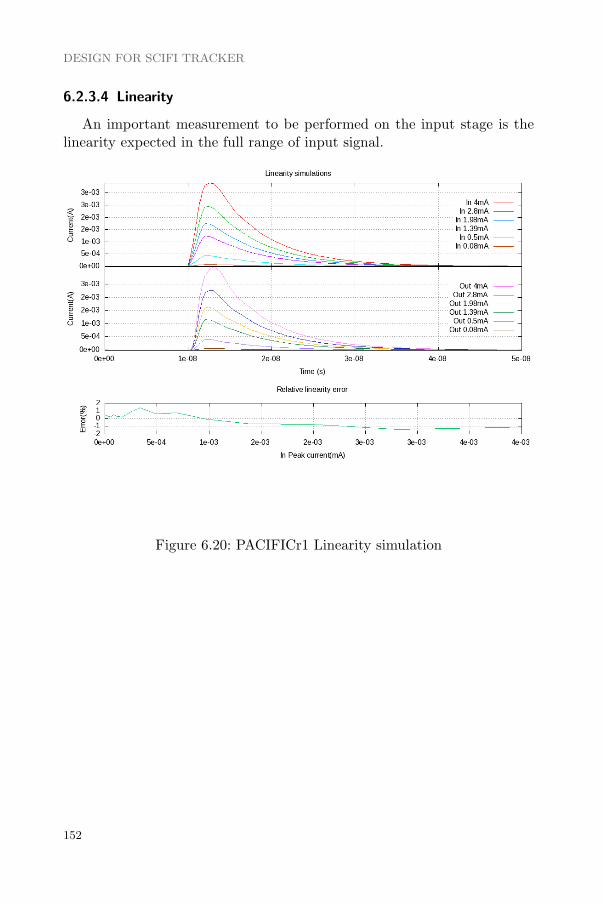
DESIGN FOR SCIFI TRACKER
6.2.3.4 Linearity
An important measurement to be performed on the input stage is thelinearity expected in the full range of input signal.
Figure 6.20: PACIFICr1 Linearity simulation
152

6.2 IMPLEMENTATION
6.2.3.5 Noise
Noise simulations show no issues with just input stage, it’s below 100pA√Hz
until 250MHz frequencies (see figure 6.21).
Figure 6.21: PACIFICr1 Noise simulation
6.2.4 Layout
Final layout of the pre-amplifier only needs an area of 335μm x 40μm.The usage of high levels capacitors (MIMCAPS) with electronics buriedbelow helped in reducing the overall area needed in the design keeping theneeded characteristics.
Figure 6.22: PACIFICr1 pre-amplifier layout
153


7Conclusions
A novel current conveyor topology with double feedback structure hasbeen presented and demonstrated it’s excellent characteristics, with lownoise, low power, wide dynamic range and low input impedance. The fullsystem tests proved to be a good option compared to previous similarASICs.
A detailed description on the sensor properties and requirements for botha PET detector and SciFi tracker has been exposed. A behaviour modelfrom the sensor has been useful in the design stage to simulate circuitbehaviour. Two designs using this circuit intended for PET and SciFi havebeen detailed. Both of them use similar input stage but implemented ondifferent technologies. PET prototype uses SiGe technology and benefitsfrom the bipolar transistors usage (specially on input stage and referencecircuits), while SciFi prototype is a CMOS technology but benefits from asmaller feature size.
7.1 Achievements
Compared to previous designs the proposed solution keeps an excel-lent balance between power consumption, dynamic range, noise and timingresolution (see table 7.1 with a qualitative representation of the achievedvalues comparing with ASICs providing timing and charge information). Itis also the only available for a direct current mode anode connection forSiPM arrays.
155

CONCLUSIONS
The main goals for the PET system have been fulfilled. A multi-channelarchitecture with direct connection to the SiPMs and analog processing hassuccessfully been designed and tested. The voltage adjustment on the inputwill permit to change sensor gain. Multiple signal paths proved to give thedesired results. With excellent timing measurement and also good energymeasurement and pile-up detection. The proposed input stage fits all therequirements and the rest of processing benefits from this. After design andproduction, full device testing has been performed including some tests thatexceeds the mere electronics characterization (radiation sources tests andcoincidence).
The design constraints on the PACIFIC project are still under study andthis first prototype has served as a starting point. The circuitry designedfor the SiPM readout (specifically the input stage) has been ported to anew technology and simplified for the application. Real prototype testingis still needed but meanwhile design is ongoing on the other blocks needed.
7.2 Outlook
In the FLEXTOT line of prototypes even if the basic functionality hasbeen tested and verified and current prototype has shown promising resultssome issues should be addressed. It has proved to be an excellent solutionfor segmented crystals readout, but probably would not be the case formonolithic crystals. First because the resulting signal from a shared crys-tal between pixels would need higher gain in the electronics and secondlybecause uniformity between channels would require an important effort inpost processing.
In the PACIFIC line of development a new prototype submission hasbeen made on November 2013. It included pre-amplifier, shaper (differentversions or tunable for the various SiPMs time constants) and gated inte-grator. This prototype should verify if the required functionality needed forthe readout electronics of the SciFi tracker is feasible, before a more am-bitious multi-channel ASIC with more functionality (and analog to digitalconversion included) to be submitted at 2014. A tight schedule is foreseenafter the verification of 2013 prototype to be ready for installation on theforeseen upgrade window in 2018.
156

7.2 OUTLOOK
Nam
eM
anufa
cture
rT
ime
Ener
gy
Pow
erA
rray
readout
Dynam
icpro
cess
reso
luti
onre
solu
tion
incu
rren
tra
nge
FLE
XT
OT
AM
S0.3
5μm
Ver
ygo
od
Ver
ygo
od
Low
Yes
Wid
e++
TO
FP
ET
0.1
3μm
Ver
ygo
od
Good
Low
No
Narr
owSP
IRO
CA
MS
0.35μ
mG
ood
Ver
ygo
od
Low
No
Wid
eN
INO
IBM
0.25
μm
Ver
yG
ood
Good
Hig
hLim
ited
Narr
owP
ETA
UM
C0.
18μ
mV
ery
Good
Good
Hig
hN
oN
arr
owB
ASIC
AM
S0.3
5μm
Poor
Ver
ygo
od
Low
No
Wid
eVA
TA
64
-Poor
Ver
ygo
od
Hig
hN
oW
ide
Table 7.1: FLEXTOT comparison with other ASICs
157

References
[1] Z.Ya. Sadygov, Russian Patent #2102820, priority of 10.10.1996
[2] H. Spieler, ”Semiconductor Detector Systems”, Oxford UniversityPress, ISBN 0-19-852784-5, 2006
[3] H. Iams, B. Salzberg, ”The Secondary Emission Phototube”, Proceed-ings of the IRE 23: 55 (1935)
[4] Glenn F. Knoll, ”Radiation Detection and Measurement”, Third Edi-tion, Jhon Wiley & Sons, Inc., ISBN 0-471-07338-5, 2000
[5] Hamamatsu web page:http://www.hamamatsu.com/jp/en/product/category/3100/3002/H7546B/index.html
[6] LHCb collaboration, ”Letter of Intent for the LHCb Upgrade”, CERN-LHCC-2011-001, LHCC-I-018, 2011
[7] R. J. McIntyre, ”Theory of Microplasma Instability in Silicon”, Journalof Applied Physics, vol. 32, n.6, pp. 983, 1961
[8] P. Eckert, HC. Schultz-Coulon, W. Shen, R. Stamen, A. Tadday, ”Char-acterization Studies of Silicon Photomultipliers”, Nuclear Instrumentsand Methods A, vol. 620, n. 2-3, pp. 217, 2010
[9] D. Renker, E. Lorenz, ”Advances in solid state photon detectors”,JINST, 4 P04004, 2009
[10] B. Dolgoshein, ”Silicon Photomultipliers in particle physics: possibil-ities and limitations” Proceedings of the 42nd Workshop of the INFNELOISATRON Project, 2003
[11] Hamamatsu Photonics, ”Multi-Pixel Photon Counter Technical Infor-mation”
159
References
[12] Satoru Uozomi, ”Study of the MPPC performance - R&D status ofthe GLD calorimeter readout”, International Linear Collider Workshop,Valencia, 2006
[13] Stephen A. Dyer, ”Survey of instrumentation and measurement”,Wiley-IEEE. p. 920. ISBN 0-471-39484-X, 2001
[14] Chang Lyong Ki1, Sergei Dolinsky, Kent C. Burr, Scott Zelakiewicz,David L. McDaniel , ”Dependence of Timing Resolution on Crystal Sizefor TOF PET”, IEEE Nuclear Science Symposium Conference Record,2007
[15] S. Agostinelli et al.,, ”Geant4 - A Simulation Toolkit”, Nuclear In-struments and Methods A 506, 250-303, 2003
[16] Saint Gobain Crystals & Detectors, ”Phoswich Detectors For HighEnergy Backgrounds”
[17] P. Jarron, E. Auffray, S.E. Brunner, M. Despeisse, E. Garutti, M.Goettlich, H. Hillemanns, P. Lecoq, T. Meyer, F. Powolny, W. Shen,H.C. Schultz-Coulon, C. Williams, ”Time based readout of a siliconphotomultiplier (SiPM) for Time Of Flight Positron Emission Tomog-raphy (TOF-PET)”, IEEE Nuclear Science Symposium/Medical Imag-ing Conference, 2009
[18] Chang Lyong Ki1, Sergei Dolinsky, Kent C. Burr, Scott Zelakiewicz,David L. McDaniel, ”Dependence of Timing Resolution on Crystal Sizefor TOF PET”, IEEE Nuclear Science Symposium Conference Record,vol. 4, pp. 2875, 2007
[19] P. Buzhan, B. Dolgoshein, L. Filatov, A. Ilyin, V. Kantzerov, V.Kaplin, A. Karakash, F. Kayumov, S. Klemin, E. Popova, S. Smirnov”Silicon photomultiplier and its possible applications”, NIMA, vol. 504,pp. 48-52, 2003
[20] N. Efthimiou, G. Argyropoulos, G. Panayiotakis, M. Georgiou, G. Lou-dos, ”Initial Results on SiPM Performance for use in Medical Imaging”IEEE International Conference on Imaging Systems and Techniques,2010
[21] W. H. Sweet, G. L. Brownell, ”Localization of brain tumors withpositron emitters”, Nucleonics, v. 11, pp. 40-45, 1953
160

References
[22] M.M. Ter-Pogossian, M.E. Phelps, E.J. Hoffman, N.A. Mullani, ”Apositron-emission transaxial tomograph for nuclear imaging (PET)”,Radiology, v. 114, no. 1, pp. 89-98, 1975
[23] M.M. Ter-Pogossian, M.E. Phelps, E.J. Hoffman, N.A. Mullani, ”Ap-plication of annihilation coincidence detection to transaxial reconstruc-tion tomography”, Journal of Nuclear Medicine, v. 16, no. 3, pp. 210-224,1975
[24] ”Saint Gobain - Prelude 420 datasheet”
[25] C. Jackson (SensL), ”Laser Range Finding and Imaging LIDAR withSilicon Photomultipliers”, IWPC, Advanced Radar, Camera, and LaserSensors for Automated Driving Workshop, 2013
[26] S. Seifert, H. T. Van Dam, J. Huizenga, R. Vinke, P. Dendooven, H.Lohner, D.R. Schaart, ”Simulation of Silicon Photomultipliers Signals”,IEEE Transactions on Nuclear Science, vol. 56, n.6, 2009
[27] C. de la Taille, G. Martin-Chassard, L. Raux, ”FLC SIPM: Front-EndChip for SIPM Readout for ILC Analog HCAL”, International LinearCollider Workshop, Standford, U.S.A, 2005
[28] S. Blin, P. Barrillon, C. de la Taille, ”MAROC, a generic Photo-multiplier Readout chip”, IEEE Nuclear Science Symposium/MedicalImaging Conference, 2010
[29] S. Conforti Di Lorenzo, S. Callier, J. Fleury, F. Dulucq, C. De la Taille,G. Martin Chassard, L. Raux and N. Seguin-Moreau, ”SPIROC: designand performances of a dedicated very front-end electronics for an ILCAnalog Hadronic CALorimeter (AHCAL) prototype with SiPM read-out”, Journal of Instrumentation, vol. 8, 2013
[30] F. Powolny, E. Auffray, S. E. Brunner, E. Garutti, M. Goettlich, H.Hillemanns, P. Jarron, P. Lecoq, T. Meyer, H. C. Schultz-Coulon, W.Shen, M. C. S. Williams, ”Time-Based Readout of a Silicon Photo-multiplier (SiPM) for Time of Flight Positron Emission Tomography(TOF-PET)” IEEE Transactions on Nuclear Science, vol. 58, n. 3,2011
[31] F. Anghinolfi, P. Jarron, A.N. Martemiyanov, E. Usenko, H. Wen-ninger, M.C.S. Williams, A. Zichichi, ”NINO: an ultra-fast and low-power front-end amplifier/discriminator ASIC designed for the multi-
161

References
gap resistive plate chamber” Nuclear Instruments and Methods A, vol.533, pp. 183-187, 2004
[32] P. Fischer, I. Peric, M. Ritzert, M. Koniczek, ”Fast Self Triggered MultiChannel Readout ASIC for Time and Energy Measurement” IEEETransactions on Nuclear Science, vol. 56, n. 3, 2009
[33] F. Corsi, M. Foresta, C. Marzocca, G. Matarrese, A. Del Guerra, ”BA-SIC: an 8-channel Front-end ASIC for Silicon Photomultiplier Detec-tors” IEEE Nuclear Science Symposium Conference Record, 2009
[34] D. Meier, S. Mikkelsen, J. Talebi, S. Azman, G. Mæhlum, B.E. Patt,”An ASIC for SiPM/MPPC Readout” IEEE Nuclear Science Sympo-sium Conference Record, 2010
[35] W. Kucewicz, J. Barszcz, J. Juraszek, R. Mos, M. Sapor, ”The TwoChannel CMOS Converter for Silicon Photomultiplier” InternationalConference on Signals and Electronic Systems ,ICES, 2008
[36] M.D. Rolo, R. Bugalho, F. Goncalves, G. Mazza, A. Rivetti, J.C. Silva,R. Silva, J. Varela ”TOFPET ASIC for PET applications” Journal ofInstrumentation, vol. 8, 2013
[37] A. Sanuy, D. Gascon, J.M. Paredes, Ll. Garrido, M. Ribo, J. Sieiro,“Wideband (500 MHz) 16 bit dynamic range current mode PreAmplifierfor the CTA cameras(PACTA)”, Journal of Instrumentation, vol. 7,2012
[38] T. K. Lewellen, “Recent developments in PET detector technology”,Phys. Med. Biol. 53 (2008) pp 287-317.
[39] S. Seifert, H. T. van Dam, R. Vinke, P. Dendooven, H. Loehner, F.J. Beekman, D. R. Schaart, ”Monolithic LaBr3:Ce Crystals on SiliconPhotomultiplier Arrays: Towards the Optimum Time-of-Flight PET De-tector”, 2011 IEEE NSS MIC Conference Record.
[40] J. F. Genat, G. Varner, F. Tang, H. Frisch ”Signal Processing forPico-second Resolution Timing Measurements” NIMA, vol. 607, pp.387-393, 2009
[41] T. Orita, H. Takahashi, K. Shimazoe, T. Fujiwara, S. Boxuan, ”A newpulse width signal processing with delay-line and non-linear circuit (forToT)”, Nucl. Instrum. Meth. A 648 ,pp. 24–27, 2011
162

References
[42] M.D. Rolo, L.N. Alves, E.V. Martins, A. Rivetti, M.B. Santos andJ. Varela, ”A low-noise CMOS front-end for TOF-PET”, JINST n.6P09003, 2011
[43] X. Llopart, R. Ballabriga, M. Campbell, L. Tlustos, and W. Wong,”Timepix, a 65k programmable pixel readout chip for arrival time, en-ergy and/or photon counting measurements”, Nucl. Instrum. Meth. A581, pp. 485-494, 2007
[44] S. Seifert, H. T. van Dam, R. Vinke, P. Dendooven, H. Lohner, F.J. Beekman, D. R. Schaart ”A Comprehensive Model to Predict theTiming Resolution of SiPM-Based Scintillation Detectors: Theory andExperimental Validation IEEE Transactions on Nuclear Science, vol.59, n. 1, pp. 190-204 , 2012
[45] Michael Lenz, Gunther Striedl, Ulrich Frohler ”Thermal Resistance,Theory and Practice” Infineon Technologies AG, Munich, Germany,2000.
[46] Y. C. Shih, F. W. Sun, L. R. MacDonald, B. P. Otis, R. S. Miyaoka, W.McDougald, T. K. Lewellen, ”An 8x8 Row-Column Summing ReadoutElectronics for Preclinical Positron Emission Tomography Scanners”,IEEE Nuclear Science Symposium Conference Record, 2009
[47] IEEE standard, http://standards.ieee.org/findstds/standard/1149.1-2013.html
[48] T. Orita, H. Takahashi, K. Shimazoe, T. Fujiwara, S. Boxuan, ”A newpulse width signal processing with delay-line and non-linear circuit (forToT)”, NIMA, A. 648, pp. 24-27, 2011
[49] X. Llopart, M.Campbell, D. San Segundo, E. Pernigotti, R. Dinapoli,”Medipix2, a 64k pixel read out chip with 55μm square elements workingin single photon counting mode”, IEEE Nuclear Science SymposiumConference Record, 2001
[50] F. Krummenacher, ”Pixel detectors with local intelligence : an ICdesigner point of view”, NIMA, A 305, pp. 527-532, 1991
[51] R. del Rıo-Fernandez, G. Linan-Cembrano, R. Domınguez-Castro,A. Rodrıguez-Vazquez, ”A Mismatch-Insensitive High-Accuracy High-Speed Continuous-Time Current Comparator in Low Voltage CMOS”,Proceedings of Design of Circuits and Integrated Systems Conference,pp. 139-144, 1997
163

References
[52] R. Gregorian, ”Introduction to CMOS Op-Amps and comparators”,John Wiley & Sons, ISBN 0-471-31778-0 ,1999
[53] M. Daube-Witherspoon, G. Muehllehner, ”Treatment of Axial Datain Three-Dimensional PET”, Journal of Nuclear Medicine, vol. 28, pp.1717-1724, 1987
[54] P. Bruyant, ”Analytic and Iterative Reconstruction Algorithms inSPECT” Journal of Nuclear Medicine, vol. 43, pp. 1343-1358, 2002
[55] D. Gascon et al., ”Noise Analysis of Time Variant Shapers in Fre-quency Domain”, IEEE, Trans. Nuclear Sci., vol. 58, pp. 177-186, 2011
[56] P. Moreira et al., ”The GBT, a Proposed Architecture for Multi-Gb/sData Transmission in High Energy Physics”, Topical Workshop onElectronics for particle Physics, 2007
[57] S. Baron, J. P. Cachemiche, F. Marin, P. Moreira, C. Soos, ”Imple-menting the GBT Data Transmission Protocol in FPGAs”, TopicalWorkshop on Electronics for particle Physics, 2009
164

List of Acronyms
2FDG 2-fluorodeoxy-D-glucose
ADC Analog to Digital Converter
ALICE A Large Ion Collider Experiment
AMS Ausria Micro-Systems
APD Avalanche Photo Diode
ASIC Application Specific Integrated Circuit
ATLAS A Toroidal LHC Apparatus
BGO Bi4(GeO4)3
BiCMOS Bipolar Complementary Metal-Oxide-Semiconductor
CALICE CAlorimeter for LInear Collider Experiment
CE Collection Efficiency
CERN Conseil Europeen pour la Recherche Nucleaire or EuropeanOrganization for Nuclear Research
CML Current Mode Logic
CMS Compact Muon Solenoid
CP Charge-Parity
CSA Charge Sensitive Amplifier
CTA Cherenkov Telescope Array
CT Central Tracker
CT-X-ray X-ray Computed Tomography
DAC Digital to Analog Converter
DAQ Data AQuisition
DELPHI DEtector with Lepton, Photon and Hadron Identification
DESY Deutsches Elektronen-SYnchrotron or German ElectronSynchrotron
165

LIST OF ACRONYMS
DNL Differential Non Linearity
ECAL Electromagnetic CALorimeter
FBP Filter Backprojection
FF Fill Factor
FPGA Field Programmable Gate Array
FSM Finite-State Machine
FWHM Full Width at Half Maximum
GSO Gd2(SiO4)O:Ce
HCAL Hadronic CALorimeter
HEP High Energy Physics
HPD Hybrid Photo-Diode
I2C Inter-Integrated Circuit
IBM International Business Machines Corporation
ILC International Linear Collider
INL Integral Non Linearity
IT Inner Tracker
JTAG Joint Test Action Group
LDO Low Drop-Out
LED Light Emitting Diode
LEP Large Electron-Positron Collider
LHCb Large Hadron Collider beauty
LHC Large Hadron Collider
LIDAR LIght raDAR
LOR Line Of Response
LSO Lu2(SiO4)O:Ce
LVDS Low Voltage Differential Signaling
LYSO Lu1.8Y0.2(SiO4)O:Ce
MIP Minimum Ionizing Particle
MRI Magnetic resonance Imaging
MRPC Multigap Resistive Plate Chamber
OT Outer Tracker
PACIFIC low Power Asic for the sCIntillating FIbres traCker
PDE Photon Detection Efficiency
166

PET Positron Emission Tomography
PLL Phase Locked Loop
PMT Photo Multiplier Tube
PS Pre-Shower detector
QE Quantum Efficientcy
RAM Random Access Memory
RICH Ring Imaging CHerenkov detector
RMS Root Mean Square
SAR Successive Approximation Register
SCA Switched Capacitors Array
SiPM Silicon Photo Multiplier
SNR Signal to Noise Ratio
SOC System On Chip
SPD Scintillator Pad Detector
SPDT Single Pole Double Throw
SPECT Single-Photon Emission Computed Tomography
SPICE Simulation Program with Integrated Circuit Emphasis
TAC Time to Analog Converter
TAP Test Acces Port
TCK Test Clock
TDC Time to Digital Converter
TDI Test Data Input
TDO Test Data Output
T&H Track And Hold
TMS Test Mode Select
TOF Time Of Flight
TRST Test Reset
TT Trigger Tracker
167


List of Figures
1.1 Typical detector system 41.2 PMT 61.3 Photomultiplier basic operation 71.4 Typical photodiode configuration 91.5 Typical APD configuration 101.6 Typical HPD construction 111.7 S10362-11-025P 121.8 S10931-050P 121.9 SiPM saturation 141.10 SiPM detection deviation 141.11 S10362-11-025 Gain variation with temperature 151.12 S10362-11-050 Gain variation with temperature 151.13 S10362-11-025 Gain variation with Voltage 161.14 S10362-11-050 Gain variation with Voltage 161.15 Typical signal from SiPM 171.16 S10362-11-025 Dark Count variation with Voltage 191.17 S10362-11-050 Dark Count variation with Voltage 191.18 SiPM construction topologies 201.19 PDE variation with Wavelength 211.20 LYSO crystals 221.21 Phoswich 241.22 Schema of PET imaging system 271.23 Detail of PET imaging system detector block and ring 281.24 Overall view of the LHC experiments location 321.25 LHCb detector 341.26 LHCb cross section 351.27 LHCb tracker upgrade layout 361.28 Cross section of a fibres module prototype 371.29 SiPM array prototype 38
169

List of Figures
2.1 SiPM circuit model schematics 402.2 IV characterization of different devices 412.3 S10362-11-025P Charge vs Vop 422.4 S10931-050P Charge vs Vop 422.5 SiPM basic test circuit 432.6 Output for illuminated S10362-11-100P 432.7 SiPM basic test board 432.8 SiPM test board gain 432.9 Single cell fired pulse and simulation 442.10 Single cell fired pulse and simulation 442.11 Crystal light simulation S10362-11-025P 462.12 Crystal light simulation S10931-050P 46
3.1 FLC SiPM channel 503.2 MAROC3 block diagram 533.3 SPIROC2c block diagram 553.4 NINO block diagram 563.5 PETA block diagram 583.6 BASIC analog channel block diagram 603.7 VATA64-HDR16 analog channel block diagram 613.8 RAPSODI block diagram and external FPGA connection 623.9 TOFPET channel block diagram 63
4.1 Input stage schematic 714.2 Low Frequency feedback loop simplified circuit 724.3 Low Frequency feedback loop stability 734.4 High Frequency feedback loop simplified circuit 734.5 High frequency feedback transfer function 744.6 High Frequency feedback loop stability 764.7 Input impedance 764.8 Effect of input capacitance to stability 774.9 Input node voltage variation 784.10 Series input referred noise 794.11 Parallel input referred noise 794.12 Integrated noise evolution with input capacitance 80
5.1 Thermal circuit 855.2 FLEXTOT channel blocks diagram 895.3 FLEXTOT floorplan 905.4 TOT input 92
170

List of Figures
5.5 TOT output for triangular input 925.6 TOT input 925.7 TOT output 925.8 Linear TOT schematic 935.9 Linearity simulation 945.10 Hysteresis comparator schematic 955.11 Hysteresis comparator layout 955.12 Hysteresis comparator MonteCarlo simulation 965.13 Current fast discriminator 975.14 Fast current discriminator layout 985.15 Pile-up detection logic 985.16 Pile-up reset logic 985.17 Pile up register readout 985.18 Current output DAC 995.19 Voltage output DAC 1005.20 Voltage DAC(6b) MonteCarlo 1005.21 Output pad buffer layout 1015.22 Output pad buffer with SR control schematic 1015.23 CML output layout 1025.24 CML output schematic 1025.25 Temperature sensor layout 1035.26 Temperature sensor schematic 1035.27 Temperature sensor slope montecarlo simulation 1035.28 TAP controller FSM 1045.29 JTAG 33 bits register write 1055.30 Debug outputs connection 1055.31 Final FLEXTOT layout 1065.32 FLEXTOT power domains 1075.33 Test system setup 1095.34 Input impedance 1115.35 16 channels hysteresis comparator S-curve 1125.36 Signal injection circuit schematic 1135.37 Typical signals with τ ≈36ns 1135.38 Typical signals with τ ≈110ns 1135.39 Linearity τ ≈36ns 18mA range 1145.40 Linearity τ ≈110ns 18mA range 1155.41 Linearity τ ≈36ns 5mA range 1155.42 Linearity τ ≈110ns 5mA range 1165.43 Linearity τ ≈36ns 3.5mA range 116
171
List of Figures
5.44 Linearity τ ≈110ns 3.5mA range 1175.45 Jitter measurement signals 1185.46 Total jitter measurement 1195.47 Jitter variation with input capacitance 1205.48 Channel DAC measurement 1215.49 Single channel Offset DAC measurement 1225.50 Single channel Vref DAC measurement 1225.51 Single ended pad slew rate 1235.52 CML output 1235.53 Temperature transient at power up 1245.54 LSO setup detail 1255.55 Na22, Co60, Cs137 spectra measurement 1265.56 Linearity of the resulting spectra measurements 1275.57 Coincidence system setup 1285.58 Typical signals acquired by oscilloscope 1295.59 CRT data clusters identified 1295.60 CRT data around 511keV 1295.61 Channel 1 energy measurement 1305.62 Channel 2 energy measurement 1305.63 Coincidence Resolving Time 1305.64 Test system at CIEMAT 1315.65 PET initial tests at CIEMAT 1325.66 PET spatial resolution measurements 133
6.1 Current tracker in LHCb 1366.2 New design of LHCb tracker 1366.3 SciFi fibres module 1366.4 SciFi readout electronics 1376.5 Inline PADs 1386.6 Staggered PADs 1386.7 Hamamatsu SiPM array prototype 1406.8 Measurement system setup 1416.9 Adapter board for the module readout 1426.10 Hamamatsu signal 1426.11 Ketek signal 1426.12 Normalized comparison of signals 1436.13 Time of arrival of signals 1446.14 Mirror effect on signal 1456.15 PACIFIC channel blocks 1476.16 PACIFICr1 blocks 148
172

6.17 PACIFICr1 pre-amplifier input impedance 1506.18 PACIFICr1 Voffset error 1516.19 PACIFICr1 pre-amplifier Bandwidth 1516.20 PACIFICr1 Linearity simulation 1526.21 PACIFICr1 Noise simulation 1536.22 PACIFICr1 pre-amplifier layout 153
173


List of Tables
1.1 Hamamatsu SiPMs characteristics 121.2 Device saturation on incoming photons detection 141.3 Inorganic scintillators properties summary 25
2.1 Model parameters 402.2 S10362-11-025P parameters 442.3 S10931-050P parameters 442.4 Peak current (mA) vs Zin and Vov 45
3.1 Different ASICs outputs summary 663.2 Different ASICs properties summary 67
5.1 PET readout ASIC specifications summary 875.2 FLEXTOT power consumption 1105.3 CML configuration options 1245.4 Sources measurements for TH=40 1265.5 Sources measurements for TH=50 1275.6 CIEMAT spatial resolution measurements 132
6.1 PACIFIC specifications summary 1466.2 VSEL operation 149
7.1 FLEXTOT comparison with other ASICs 157
175


ASiPMVFEr1 Datasheet
177

SiPM readout blocks
Data Sheet SiPMVFEr1FEATURES
Current mode input.
Low input impedance.
Zero components interface between sensor and device.
High Bandwidth preamplifier (≈350MHz).
Relative linearity error ±5%.
High Dynamic Range to operate SiPM at high over-
voltage.
Low Power consumption (≈7.3mW/channel).
TYPICAL APPLICATION CIRCUIT
Figure 1: Typical application schematic
Rev. A Information furnished by ICC-UB is believed to be accurate and reliable.
However, no responsibility is assumed by ICC-UB for its use, nor for any infringe-
ments of patents or other rights of third parties that may result from its use.
Specifications subject to change without notice. No license is granted by impli-
cation or otherwise under any patent or patent rights of ICC-UB. Trademarks and
registered trademarks are the property of their respective owners.
APPLICATION
Readout of Silicon Photo Multipliers arrays.
DESCRIPTION
SiPMVFEr1 is a prototype with some blocks for the readout
Silicon Photo Multipliers with current mode input.
SiPMVFEr1 has been developed using Austria Micro Systems
(AMS) 0.35 μm HBT BiCMOS technology and operates over
the -40◦C to +125◦C junction temperature range.
SiPMVFEr1 is available in a QFN32 package.
Av. Diagonal 645, Barcelona, ES08028, SPAIN
Tel. 934021587 http://icc.ub.edu
Fax. 934037063 c© 2013 ICC-UB / CIEMAT
All rights reserved.

SiPMVFEr1 Data SheetSiPMVFEr1 Data SheetSiPMVFEr1 Data Sheet
TABLE OF CONTENTS
FEATURES . . . . . . . . . . . . . . . . . . . . . . . . . 1
TYPICAL APPLICATION CIRCUIT . . . . . . . . . . . . 1
APPLICATION . . . . . . . . . . . . . . . . . . . . . . . 1
DESCRIPTION . . . . . . . . . . . . . . . . . . . . . . . 1
REVISION HISTORY . . . . . . . . . . . . . . . . . . . 2
FUNCTIONAL BLOCK DIAGRAM . . . . . . . . . . . . 3
SPECIFICATIONS . . . . . . . . . . . . . . . . . . . . . 4
DEFAULT PARAMETERS . . . . . . . . . . . . . . . . . 4
ABSOLUTE MAXIMUM RATINGS . . . . . . . . . . . 5
THERMAL RESISTANCE . . . . . . . . . . . . . . . . 5
Boundary Condition . . . . . . . . . . . . . . . . 5
ESD CAUTION . . . . . . . . . . . . . . . . . . . . . 5
PINS CONFIGURATION AND DESCRIPTION . . . . . . 6
BANDWIDTH . . . . . . . . . . . . . . . . . . . . . . . . 7
BANDGAP . . . . . . . . . . . . . . . . . . . . . . . . . 7
TEST SYSYTEM . . . . . . . . . . . . . . . . . . . . 8
LINEARITY . . . . . . . . . . . . . . . . . . . . . . . . . 9
JITTER . . . . . . . . . . . . . . . . . . . . . . . . . . . 9
INPUT CAPACITANCE EFFECT . . . . . . . . . . . . 9
NOISE . . . . . . . . . . . . . . . . . . . . . . . . . . . 9
INPUT CAPACITANCE EFFECT . . . . . . . . . . . . 9
HG SATURATION CONTROL . . . . . . . . . . . . . . . 10
SIPM VOLTAGE CONTROL . . . . . . . . . . . . . . . . 10
LAYOUT . . . . . . . . . . . . . . . . . . . . . . . . . . 11
BONDING DIAGRAM . . . . . . . . . . . . . . . . . . . 11
OUTLINE DIMENSIONS . . . . . . . . . . . . . . . . . 12
ORDERING IFORMATION . . . . . . . . . . . . . . . . 12
NOTES . . . . . . . . . . . . . . . . . . . . . . . . . . . 13
REVISION HISTORY
03/13 - First version
rev. A | page 2 of 13

Data Sheet SiPMVFEr1Data Sheet SiPMVFEr1Data Sheet SiPMVFEr1
FUNCTIONAL BLOCK DIAGRAM
Figure 2: Channel block diagram
Every channel contains three different paths used for time of arrival measurement and energy measurement;
The time of arrival measurement performed using a High Gain path. In channel 2 this High Gain output is connected to a
current mode discriminator to generate a digital signal.
The energy measurement uses a lower gain output, Low Gain path. In channel 1 and 2 this Low Gain output is connected to
a buffer to attack the external load, while in channel 3 it’s directly connected to the PAD.
Apart from the channel analog chain a common bias block is also present with a BandGap Voltage reference which can be
measured directly.
rev. A | page 3 of 13

SiPMVFEr1 Data SheetSiPMVFEr1 Data SheetSiPMVFEr1 Data Sheet
SPECIFICATIONS
TA=25◦C, VDD=3.3V, VDD_BUF =3.3V
Parameter Conditions Min Typ Max Unit
INPUT
Zin Default input stage polarization currents 20 22 24 ΩPOWER CONSUMPTION
VDD Default parameters 6.39 6.62 6.78 mA
VDD_BUFF Default parameters 19.6 29.41 33.38 mA
INPUT SIGNAL
HIGH GAIN LINEARITY
Input range Default parameters 0.5 - 1 mA peak
Linearity error Default parameters - ≤ ±5 - %
LOW GAIN LINEARITY
Input range Default parameters 0.5 - 8 mA peak
Linearity error Default parameters - ≤ ± 5 - %
SIPM VOLTAGE CONTROL
Voff Default parameters 0.25 - 1.25 V
Table 1: Specifications summary
DEFAULT PARAMETERS
Default polarization conditions are summarized in next table.
Parameter Value Function
VDD 3.3V Power supply
VDD_BUFF 3.3V Power supply for output buffers
Iref -7μA Reference current for bandgap
Ibias_in 12 μA Input amplifier bias current
Ibias_fb 30 μA Feedback amplifier bias current
Ibias -21 μA Input amplifier bias current for mirrors control
Iref_se -900 μA Output buffers bias current
Iref_cas 300 μA Output buffers cascode current
VCM 1.5V Common mode voltage for buffers output
Vlim 1V Voltage control of High Gain saturation
Voff 1V Common mode voltage at input node
Iref _disc 300μA Discriminator threshold
Table 2: Default parameters
rev. A | page 4 of 13

Data Sheet SiPMVFEr1Data Sheet SiPMVFEr1Data Sheet SiPMVFEr1
ABSOLUTE MAXIMUM RATINGS
Parameter Rating
VDD 3.2 to 3.4 V
VDD_BUF 3.2 to 3.4 V
Temperature Range
Operatingjunction -40◦C to 125◦C
Storage -65◦C to 150◦C
Soldering Conditions JEDEC J-STD-020
Table 3: Absoulte maximum ratings summary
Stresses above those listed under Absolute Maximum Rat-
ings may cause permanent damage to the device. This is a
stress rating only; functional operation of the device at these
or any other conditions above those indicated in the opera-
tional section of this specification is not implied. Exposure to
absolute maximum rating conditions for extended periods may
affect device reliability.
THERMAL RESISTANCE
θJA is specified for the worst-case conditions, that is, a device
soldered in a circuit board for surface-mount packages.
Boundary Condition
θJA is measured using natural convection on JEDEC 4-layer
board, and the exposed pad is soldered to the printed circuit
board (PCB) with thermal vias. Due to the exposed pad
different thermal resistance may be extracted from top or
bottom of the packaging.
Package type θJA Unit
32-Lead QFN top 7 TBC1 ◦C/W
32-Lead WFN bottom 1 TBC1 ◦C/W
1To be confirmed
Table 4: Thermal Resistance
ESD CAUTION
ESD (electrostatic discharge) sensitive
device. Charged devices and circuit
boards can discharge without detection.
Although this product features patented
or proprietary protection circuitry, damage
may occur on devices subjected to high en-
ergy ESD. Therefore, proper ESD precau-
tions should be taken to avoid performance
degradation or loss of functionality.
rev. A | page 5 of 13

SiPMVFEr1 Data SheetSiPMVFEr1 Data SheetSiPMVFEr1 Data Sheet
PINS CONFIGURATION AND DESCRIPTION
Figure 3: Pin configuration (Top view)
Pin No. Mnemonic Type Description
13,15,28 VDD Power Analog power supply
17,27 VDD_BUF Power Buffer power supply
5,9,12,20,25,29 GND Power Ground
1,4,6 IN Signal Channel Input
2 Vlim Input Control of High Gain saturation
3 Voff Input Control of DC voltage at input node
7 Iref Input Bandgap reference current
8 Ext_ref Input External voltage reference
10 Vbg Output Bangap output
11 LG3 Output Low Gain channel 3 output
14 HG3 Output High Gain channel 3 output
16 LG2 Output Low Gain channel 2 output
18 Iref_DISC Input Discriminator comparator current
19 DISC Output Discriminator digital output
21 LG1 Output Low Gain channel 1 output
22 Vcm Input Common mode control of output buffers
23 Iref_cas Input Output buffers cascode current
24 Iref_se Input Output buffers bias current
26 HG1 Output High Hain channel 1 output
30 Ibias_in Input Input amplifier bias current
31 Ibias Input Input stage bias current
32 Ibias_fb Input Feedback amplifier bias current
EP GND Power Ground
Table 5: Pin function descriptions
rev. A | page 6 of 13

Data Sheet SiPMVFEr1Data Sheet SiPMVFEr1Data Sheet SiPMVFEr1
BANDWIDTH
Bandwidth of High Gain path and Low Gain path is measured
using the setup in figure 4 with a Rhode & Schwarz spectrum
analyzer. It is compared to simulations (*_Sim) and extracted
layout simulations (*_Ext) in figures 5 and 6. As expected it’s
around 350MHz and 250MHz for HG and LG respectively.
Figure 4: Bandwidth measurement setup
Figure 5: High Gain path Bandwidth measurement
Figure 6: Low Gain path Bandwidth measurement
BANDGAP
A Bandgap reference circuit has been included in current de-
sign. It’s output is directly connected at the output pin Vbg pin
and it’s directly connected to channel 1 and 2 biasing circuits.
Channel 3 can be connected either to the output of this ref-
erence or to an external reference using the Extref pin. The
output measurement of the Bandgap reference is depicted in
figure 7, the variation with temperature agrees perfectly with
simulations although it’s absolute value is a little bit different
(probably due to some process variation).
Figure 7: Bandgap voltage variation with temperature
Power Supply Rejection Ratio (PSRR) in AC and DC is also
measured in figures 8 and 9 and results as expected.
Figure 8: Bandgap PSRR
Figure 9: Bandgap PSRR in AC
rev. A | page 7 of 13

SiPMVFEr1 Data SheetSiPMVFEr1 Data SheetSiPMVFEr1 Data Sheet
TEST SYSYTEM
The test system consists in a signal injection circuit to simulate the SiPM shape. This signal is generated using an Arbitrary
Waveform Generator (AWG). The output of the generator has a fixed amplitude and is attenuated using a programmable
attenuator, permitting a better linearity injection of signal. The output of the ASIC is readout using a standard oscilloscope.
Some programmable DACs and current sources are in the test PCB and controlled using a USB connection to an FPGA. The
whole setup can be seen in figure 10.
Figure 10: Test system
The ASIC is placed inside a QFN32 test socket to permit the exchange between different prototypes. Using this test setup
several measurements have been performed including linearity, noise and jitter.
rev. A | page 8 of 13
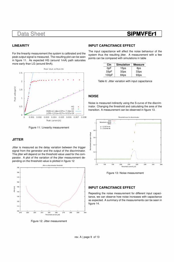
Data Sheet SiPMVFEr1Data Sheet SiPMVFEr1Data Sheet SiPMVFEr1
LINEARITY
For the linearity measurement the system is calibrated and the
peak output signal is measured. The resulting plot can be seen
in figure 11. As expected HG (around 1mA) path saturates
more early than LG (around 8mA).
Figure 11: Linearity measurement
JITTER
Jitter is measured as the delay variation between the trigger
signal from the generator and the output of the discriminator.
This jitter will depend on the threshold value used for the com-
parator. A plot of the variation of the jitter measurement de-
pending on the threshold value is plotted in figure 12
Figure 12: Jitter measurement
INPUT CAPACITANCE EFFECT
The input capacitance will affect the noise behaviour of the
system thus the resulting jitter. A measurement with a few
points can be compared with simulations in table
Cin Simulation Measure
0pF 15ps 8ps
33pF 32ps 33ps
100pF 84ps 93ps
Table 6: Jitter variation with input capacitance
NOISE
Noise is measured indirectly using the S-curve of the discrim-
inator. Changing the threshold and calculating the area of the
transition. A measurement can be observed in figure 13.
Figure 13: Noise measurement
INPUT CAPACITANCE EFFECT
Repeating the noise measurement for different input capaci-
tance, we can observe how noise increases with capacitance
as expected. A summary of the measurements can be seen in
figure 14.
rev. A | page 9 of 13

SiPMVFEr1 Data SheetSiPMVFEr1 Data SheetSiPMVFEr1 Data Sheet
Figure 14: Noise variation with input capacitance
HG SATURATION CONTROL
The saturation point of the High Gain signal path can be tuned
using the external Vlim control voltage. The resulting mea-
surement is summarized in figure 15.
Figure 15: Saturation control of High Gain
SIPM VOLTAGE CONTROL
The DC voltage of the input node can be controlled externally
using the Voff pin. A measurement of the linearity error on the
HG with the variation of this voltage is performed and summa-
rized in figure 16. The permitted variation range is around 1V
as expected.
Figure 16: Voff variation effect in High Gain
rev. A | page 10 of 13

Data Sheet SiPMVFEr1Data Sheet SiPMVFEr1Data Sheet SiPMVFEr1
LAYOUT
Figure 17: SiPMVFEr1 layout, ≈ 2x2mm , 4mm2 die
BONDING DIAGRAM
Figure 18: SiPMVFEr1 bonding diagram with downbonds to the cavity/exposed pad
rev. A | page 11 of 13

SiPMVFEr1 Data SheetSiPMVFEr1 Data SheetSiPMVFEr1 Data Sheet
OUTLINE DIMENSIONS
Figure 19: Packaging outline
Packaging provided by SEMPAC, INC.
ORDERING IFORMATION
Model Temperature Range1 Package Description2,3
SiPMVFEr1 -40◦C to 125◦C 32 Lead QFN
1 Temperature range from the ASIC technology used. To be tested.2 Package dimensions without lid 9 x 9 mm, 0.8 mm thick.3 Lid dimensions 9 x 9 mm, 0.2 mm thick.
rev. A | page 12 of 13

Data Sheet SiPMVFEr1Data Sheet SiPMVFEr1Data Sheet SiPMVFEr1
NOTES
c© 2013 ICC-UB / CIEMAT, All rights reserved.
Trademarks and registered trademarks are the property of their respective owners.
http://icc.ub.edu
rev. A | page 13 of 13

BPACIFICr1 Datasheet
191
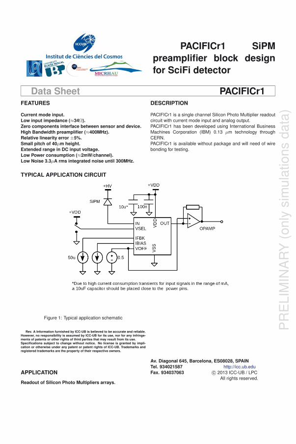
PR
ELIM
INA
RY
(only
sim
ula
tions
data
)
PACIFICr1 SiPM
preamplifier block design
for SciFi detector
Data Sheet PACIFICr1FEATURES
Current mode input.
Low input impedance (≈34Ω).
Zero components interface between sensor and device.
High Bandwidth preamplifier (≈400MHz).
Relative linearity error ±5%.
Small pitch of 40μm height.
Extended range in DC input voltage.
Low Power consumption (≈2mW/channel).
Low Noise 3.3μA rms integrated noise until 300MHz.
TYPICAL APPLICATION CIRCUIT
Figure 1: Typical application schematic
Rev. A Information furnished by ICC-UB is believed to be accurate and reliable.
However, no responsibility is assumed by ICC-UB for its use, nor for any infringe-
ments of patents or other rights of third parties that may result from its use.
Specifications subject to change without notice. No license is granted by impli-
cation or otherwise under any patent or patent rights of ICC-UB. Trademarks and
registered trademarks are the property of their respective owners.
APPLICATION
Readout of Silicon Photo Multipliers arrays.
DESCRIPTION
PACIFICr1 is a single channel Silicon Photo Multiplier readout
circuit with current mode input and analog output.
PACIFICr1 has been developed using International Business
Machines Corporation (IBM) 0.13 μm technology through
CERN.
PACIFICr1 is available without package and will need of wire
bonding for testing.
Av. Diagonal 645, Barcelona, ES08028, SPAIN
Tel. 934021587 http://icc.ub.edu
Fax. 934037063 c© 2013 ICC-UB / LPC
All rights reserved.

PR
ELIM
INA
RY
(only
sim
ula
tions
data
)
PACIFICr1 Data SheetPACIFICr1 Data SheetPACIFICr1 Data Sheet
TABLE OF CONTENTS
FEATURES . . . . . . . . . . . . . . . . . . . . . . . . . 1
TYPICAL APPLICATION CIRCUIT . . . . . . . . . . . . 1
APPLICATION . . . . . . . . . . . . . . . . . . . . . . . 1
DESCRIPTION . . . . . . . . . . . . . . . . . . . . . . . 1
REVISION HISTORY . . . . . . . . . . . . . . . . . . . 2
FUNCTIONAL BLOCK DIAGRAM . . . . . . . . . . . . 3
SPECIFICATIONS . . . . . . . . . . . . . . . . . . . . . 4
PINS CONFIGURATION AND DESCRIPTION . . . . . . 4
OPERATING VOLTAGE SELECTION (VSEL) . . . . . 5
INPUT IMPEDANCE . . . . . . . . . . . . . . . . . . 5
VOLTAGE ADJUST RANGE . . . . . . . . . . . . . . 5
CURRENT REFERENCES IFBK AND IBIAS . . . . . 5
NOISE . . . . . . . . . . . . . . . . . . . . . . . . . . 5
LINEARITY . . . . . . . . . . . . . . . . . . . . . . . 6
DC GAIN . . . . . . . . . . . . . . . . . . . . . . . . 6
BANDWIDTH . . . . . . . . . . . . . . . . . . . . . . 7
ABSOLUTE MAXIMUM RATINGS . . . . . . . . . . . 7
ESD CAUTION . . . . . . . . . . . . . . . . . . . . . 7
LAYOUT . . . . . . . . . . . . . . . . . . . . . . . . . . 8
BONDING DIAGRAM . . . . . . . . . . . . . . . . . . . 8
NOTES . . . . . . . . . . . . . . . . . . . . . . . . . . . 9
REVISION HISTORY
05/13 - First version A
rev. A | page 2 of 9

PR
ELIM
INA
RY
(only
sim
ula
tions
data
)
Data Sheet PACIFICr1Data Sheet PACIFICr1Data Sheet PACIFICr1
FUNCTIONAL BLOCK DIAGRAM
Figure 2: Channel block diagram
The input stage uses a novel approach of double feedback. Detailed schematics can be observed in figure 2. It provides
a low input impedance in order to avoid affecting timing behaviour of the SiPM and increase input current. HFFB is the high
frequency feedback path that keeps this input impedance constant (in a certain frequency range). The second labelled path,
LFFB will provide the dc voltage (Voffset in figure) of the input node using the virtual short circuit in the amplifier that will drive
a follower in a lower frequency range.
The design has been implemented taking into account that dominant pole should be set at the input node (SiPM parasitic
capacitance is at the order of tenths of pF). In this way stability is not compromised when an important capacitance is added at
the input.
In order to work at different supply voltages two resistor values of the high frequency path are available. This resistor can be
switched using an external control pin.
rev. A | page 3 of 9
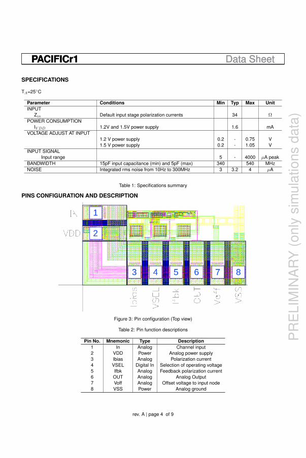
PR
ELIM
INA
RY
(only
sim
ula
tions
data
)
PACIFICr1 Data SheetPACIFICr1 Data SheetPACIFICr1 Data Sheet
SPECIFICATIONS
TA=25◦C
Parameter Conditions Min Typ Max Unit
INPUT
Zin Default input stage polarization currents 34 ΩPOWER CONSUMPTION
IV DD 1.2V and 1.5V power supply 1.6 mA
VOLTAGE ADJUST AT INPUT
1.2 V power supply 0.2 - 0.75 V
1.5 V power supply 0.2 - 1.05 V
INPUT SIGNAL
Input range 5 - 4000 μA peak
BANDWIDTH 15pF input capacitance (min) and 5pF (max) 340 540 MHz
NOISE Integrated rms noise from 10Hz to 300MHz 3 3.2 4 μA
Table 1: Specifications summary
PINS CONFIGURATION AND DESCRIPTION
Figure 3: Pin configuration (Top view)
Table 2: Pin function descriptions
Pin No. Mnemonic Type Description
1 In Analog Channel input
2 VDD Power Analog power supply
3 Ibias Analog Polarization current
4 VSEL Digital In Selection of operating voltage
5 Ifbk Analog Feedback polarization current
6 OUT Analog Analog Output
7 Voff Analog Offset voltage to input node
8 VSS Power Analog ground
rev. A | page 4 of 9

PR
ELIM
INA
RY
(only
sim
ula
tions
data
)
Data Sheet PACIFICr1Data Sheet PACIFICr1Data Sheet PACIFICr1
OPERATING VOLTAGE SELECTION (VSEL)
In order to adapt to both 1.2V and 1.5V power supply keep-
ing the desired dynamic range, an internal switch to change
the resistor in the high frequency feedback path has been im-
plemented (resistor Rfbk in figure 2). The connection is a pass
gate (switch) connected in parallel to a resistor. This pin is
called VSEL and follows next table operation;
VSEL Switch VDD
1.2 ON 1.2
0 OFF 1.5
Table 3: VSEL operation
With this configurable resistance the input stage behaves as
expected in both operating conditions.
INPUT IMPEDANCE
Input impedance is kept low using the high frequency feed-
back loop. This kind of feedback loops present an inductive be-
haviour at high frequencies. The simulation can be observed
in figure 4.
Figure 4: Input impedance for different VDD*
* Simulation does not include input inductance that will affect high
frequency (over GHz) behaviour
The input impedance is kept to a low value corresponding
to the resistance in series (16Ω) at the pre-amplifier input un-
til around 100KHz. From this point increases slowly to reach
a value of around 34Ω at 100MHz. Passed this frequency
impedance increases fast reaching a value of 50Ω at around
250MHz.
VOLTAGE ADJUST RANGE
One key parameter is the option to adjust anode voltage
of every device directly from the ASIC connection. That’s the
function of the low frequency feedback loop, but it’s limited due
to the voltage drop needed from the transistors. Special ef-
fort has been made to try to maximize this range (using LVT
transistors and minimizing the number of transistors in series
in the signal path). The final range of adjustment is around
0.55V for 1.2V power supply and around 0.85V for 1.5 power
supply.
Figure 5: Voffset adjustment error for different VDD
CURRENT REFERENCES IFBK AND IBIAS
In order to flexibly test the behaviour of the pre-amplifier
two polarization current references have been taken to exter-
nal pins. This way the modification of the parameters respect
this currents can be observed. General input stage current
reference (Ibias) and feedback current (Ifbk) are in different in-
puts to control independently the behaviour of the feedback
loop and input stage. The default value of all bias currents is
50μA to ground.
NOISE
Integrated noise from 10Hz to 300MHz (the range affecting
the shape of input signal) should be smaller than 5μA. Typi-
cal simulations in the worst case (1.5VDD) show an expected
value of around 3μA.
rev. A | page 5 of 9

PR
ELIM
INA
RY
(only
sim
ula
tions
data
)
PACIFICr1 Data SheetPACIFICr1 Data SheetPACIFICr1 Data Sheet
LINEARITY
According to simulations linearity is better than ±5% in either
configurations in full range. In figure 6 some input / output
signals can be observed with the corresponding linearity error
on the full range.
Figure 6: Linearity simulation
DC GAIN
DC gain is expected to be equal to 1 since current mirrors
have the same dimensions. When this DC gain starts to de-
crease a worse linearity is obtained. A simulation on DC gain
for the various operating voltages can be observed in figure 7.
Figure 7: DC gain simulation
rev. A | page 6 of 9

PR
ELIM
INA
RY
(only
sim
ula
tions
data
)
Data Sheet PACIFICr1Data Sheet PACIFICr1Data Sheet PACIFICr1
BANDWIDTH
Input node voltage control is slow in comparison to input
impedance control. This feedback structure transfer function
can be observed in figure 8. Comparing two cases of input
capacitance (determined by sensor), as input impedance is
increased bandwidth is reduced as expected.
Figure 8: Input stage bandwidth
ABSOLUTE MAXIMUM RATINGS
Parameter Rating
VDD 1.2 to 1.5 V
Temperature Range
Operatingjunction -40◦C to 125◦C
Storage -65◦C to 150◦C
Soldering Conditions To Be Determined
Table 4: Absoulte maximum ratings summary
Stresses above those listed under Absolute Maximum Rat-
ings may cause permanent damage to the device. This is a
stress rating only; functional operation of the device at these
or any other conditions above those indicated in the opera-
tional section of this specification is not implied. Exposure to
absolute maximum rating conditions for extended periods may
affect device reliability.
ESD CAUTION
ESD (electrostatic discharge) sensitive
device. Charged devices and circuit
boards can discharge without detection.
Although this product features patented
or proprietary protection circuitry, damage
may occur on devices subjected to high en-
ergy ESD. Therefore, proper ESD precau-
tions should be taken to avoid performance
degradation or loss of functionality.
rev. A | page 7 of 9

PR
ELIM
INA
RY
(only
sim
ula
tions
data
)
PACIFICr1 Data SheetPACIFICr1 Data SheetPACIFICr1 Data Sheet
LAYOUT
The layout of the channel have been optimized to use staggered input pad’s on the ASIC. This leads to a maximum of 40μm
pitch between channel.
Figure 9: PACIFICr1 channel layout, 335μm x 40μm
BONDING DIAGRAM
To Be Determined
rev. A | page 8 of 9

PR
ELIM
INA
RY
(only
sim
ula
tions
data
)
Data Sheet PACIFICr1Data Sheet PACIFICr1Data Sheet PACIFICr1
NOTES
c© 2013 ICC-UB / LPC, All rights reserved.
Trademarks and registered trademarks are the property of their respective owners.
http://icc.ub.edu
rev. A | page 9 of 9
Related Documents