www.acse-journal.org Advances in Ceramic Science and Engineering (ACSE) Volume 3, 2014 Detonation Nanodiamond Seeding Technique for Nucleation Enhancement of CVD Diamond – Some Experimental Insights Awadesh K. Mallik 1* , Joana C. Mendes 2 , Shlomo Z. Rotter 3 , Sandip Bysakh 4 1,4 CSIR - Central Glass & Ceramic Research Institute, Kolkata 700032, West Bengal, India 2,3 Instituto de Telecomunicações, Campus Universitário de Santiago, 3810-193 Aveiro, Portugal 1* [email protected], 2 [email protected], 3 [email protected], 4 [email protected] Received 21 February, 2014; Revised 10 April, 2014; Accepted 20 April, 2014; Published 18 May, 2014 © 2014 Science and Engineering Publishing Company Abstract Detonation nanodiamond (DND) seeding recently emerged as an effective method for enhancing nucleation of chemical vapor deposited (CVD) diamond on non-diamond substrates. This work attempts to provide insight on this effect. For this purpose, polycrystalline diamond coatings were deposited on DND-treated silicon substrates. The exposed nucleation surface side was examined with x-ray diffraction (XRD), scanning electron microscopy (SEM) and high-resolution transmission electron microscopy (HRTEM); it was found to contain micron-sized granular features, composed of 25-40 nm diamond nanocrystals, similar in size to the DND seeds. HRTEM images further confirm this similarity. A detailed analysis of the nanocarbon phase diagram suggests that nanodiamond crystals can form under CVD environments. Keywords Diamond Film; Nanocrystals; Plasma Enhanced CVD; Nucleation; Nanocarbon Phase Diagram Introduction Diamond chemical vapor deposition (CVD) on foreign substrates requires a seeding procedure that supplies the substrate with a high density of seeding particles that facilitate diamond nucleation (Rotter et al 2009). The simplest procedure is scratching or abrading the substrate with an abrasive or diamond powder (Popovici et al 1992). In spite of being a simple technique, it is highly non-reproducible and leaves scratch marks on optically smooth surfaces; in addition, it can only be used with plane substrates and may damage delicate surfaces. The ultrasonic seeding (US) is another widely used seeding method that can be used on complex shapes (Iijima et al 1990). During the seeding procedure, the substrate is submerged in a solution containing diamond particles dispersed through the whole volume; the set is then agitated in ultrasonic bath, for a determined time period; due to the cavitation effect, the diamond particles hit and get impinged on the substrate surface. This process produces uniformly distributed surface defects, with embedded diamond particles of various sizes, and leads to an enhanced uniform nucleation and growth of CVD diamond. Ultrasonically agitating the substrate in a solution of detonation nanodiamond (DND) powders (Shenderova et al 2010, Williams et al 2007, Kromka et al 2008, Williams et al 2006, Butler et al 2008, Mallik et al 2013) enables nucleation densities in excess of 10 12 cm -2 and became a standard procedure for nucleation enhancement after the first conference on DND held at St. Petersberg, Russia in 2003, 40 years after its discovery (Osawa 2008, Badziag et al 1990). Rotter proposed a new nucleation procedure, known as NNP, where the standard sonication with diamond suspension is preceded with the exposure of the substrate to diamond growth conditions for a short period of time (Rotter et al 2009, Gouzman et al 2000, Edelstein et al 1999). With this method he conformally coated complex 3D shapes and different materials. Sumant et al (2007) deposited ultra-nanocrystalline (UNCD) films using NNP followed by US with DND suspension. Bias-enhanced nucleation (BEN) (Yugo et al 1991, Stoner et al 1992, Chavanne et al 2012) is another method used to enhance diamond nucleation on non- 36

Welcome message from author
This document is posted to help you gain knowledge. Please leave a comment to let me know what you think about it! Share it to your friends and learn new things together.
Transcript

www.acse-journal.org Advances in Ceramic Science and Engineering (ACSE) Volume 3, 2014
Detonation Nanodiamond Seeding Technique for Nucleation Enhancement of CVD Diamond – Some Experimental Insights Awadesh K. Mallik1*, Joana C. Mendes2, Shlomo Z. Rotter3, Sandip Bysakh4 1,4CSIR - Central Glass & Ceramic Research Institute, Kolkata 700032, West Bengal, India 2,3Instituto de Telecomunicações, Campus Universitário de Santiago, 3810-193 Aveiro, Portugal 1*[email protected], [email protected], [email protected], [email protected] Received 21 February, 2014; Revised 10 April, 2014; Accepted 20 April, 2014; Published 18 May, 2014 © 2014 Science and Engineering Publishing Company Abstract
Detonation nanodiamond (DND) seeding recently emerged as an effective method for enhancing nucleation of chemical vapor deposited (CVD) diamond on non-diamond substrates. This work attempts to provide insight on this effect. For this purpose, polycrystalline diamond coatings were deposited on DND-treated silicon substrates. The exposed nucleation surface side was examined with x-ray diffraction (XRD), scanning electron microscopy (SEM) and high-resolution transmission electron microscopy (HRTEM); it was found to contain micron-sized granular features, composed of 25-40 nm diamond nanocrystals, similar in size to the DND seeds. HRTEM images further confirm this similarity. A detailed analysis of the nanocarbon phase diagram suggests that nanodiamond crystals can form under CVD environments.
Keywords
Diamond Film; Nanocrystals; Plasma Enhanced CVD; Nucleation; Nanocarbon Phase Diagram
Introduction
Diamond chemical vapor deposition (CVD) on foreign substrates requires a seeding procedure that supplies the substrate with a high density of seeding particles that facilitate diamond nucleation (Rotter et al 2009). The simplest procedure is scratching or abrading the substrate with an abrasive or diamond powder (Popovici et al 1992). In spite of being a simple technique, it is highly non-reproducible and leaves scratch marks on optically smooth surfaces; in addition, it can only be used with plane substrates and may damage delicate surfaces.
The ultrasonic seeding (US) is another widely used
seeding method that can be used on complex shapes (Iijima et al 1990). During the seeding procedure, the substrate is submerged in a solution containing diamond particles dispersed through the whole volume; the set is then agitated in ultrasonic bath, for a determined time period; due to the cavitation effect, the diamond particles hit and get impinged on the substrate surface. This process produces uniformly distributed surface defects, with embedded diamond particles of various sizes, and leads to an enhanced uniform nucleation and growth of CVD diamond. Ultrasonically agitating the substrate in a solution of detonation nanodiamond (DND) powders (Shenderova et al 2010, Williams et al 2007, Kromka et al 2008, Williams et al 2006, Butler et al 2008, Mallik et al 2013) enables nucleation densities in excess of 1012 cm-2 and became a standard procedure for nucleation enhancement after the first conference on DND held at St. Petersberg, Russia in 2003, 40 years after its discovery (Osawa 2008, Badziag et al 1990).
Rotter proposed a new nucleation procedure, known as NNP, where the standard sonication with diamond suspension is preceded with the exposure of the substrate to diamond growth conditions for a short period of time (Rotter et al 2009, Gouzman et al 2000, Edelstein et al 1999). With this method he conformally coated complex 3D shapes and different materials. Sumant et al (2007) deposited ultra-nanocrystalline (UNCD) films using NNP followed by US with DND suspension.
Bias-enhanced nucleation (BEN) (Yugo et al 1991, Stoner et al 1992, Chavanne et al 2012) is another method used to enhance diamond nucleation on non-
36
Advances in Ceramic Science and Engineering (ACSE) Volume 3, 2014 www.acse-journal.org
diamond substrates. However, this method may damage delicate surfaces; the work by Maillard-Schaller et al (1997) showed evidence of damage (holes as deep as 2-3 µm and as large as 200-300 nm in diameter) on the surface of a silicon substrate.
Other techniques to increase the nucleation density include the use of intermediate layers (Feng et al 1993, Naguib et al 2006), the rougher back side of the one-side polished silicon substrate (Mallik et al 2010) and ion implantation (Hirabayashi et al 1988, Lin et al 1992), but with limited success.
In this study, polycrystalline diamond (PCD) films were deposited by microwave plasma CVD (MPCVD) on silicon wafers treated with DND suspension containing 30 nm-size particles. After the deposition, the silicon substrates were chemically etched and the nucleation surface was evaluated by scanning electron microscopy (SEM), transmission electron microscopy (TEM), high resolution TEM (HRTEM), electron diffraction (EDAX) and X-ray diffraction (XRD).
Experimental
PCD films were deposited inside a 915 MHz 15 kW MPCVD system (DIAMOTEK 1800, Lambda Technologies Inc. USA) on (100) p-type mirror-polished single crystal silicon wafers. The substrates were cleaned successively in ultrasonic bath of distilled water, acetone and methanol for 15 minutes each. After the cleaning step they were seeded with DND suspension, obtained by mixing commercially available DMSO-based DND slurry and ethanol in 1:3 ratios. According to data supplied by the DND manufacturer (M/s International Technology Centre), the average size of the particles present in the suspension is 30 nm. After 15 minutes of US (Electrosonic Industry, model: EI 500HI, 40 kHz, 16 W/l), the substrates were rinsed with ethanol and dried under class 100000 clean room air conditioner. In one of the wafer sample, i.e. W2, after following the general ultrasonic cleaning, seeding and rinsing procedures, instead of drying the sample under clean
room atmosphere, W2 wafer surface was mopped/soaked with a clean tissue paper. Another set of silicon samples was also manually scratched with 1 µm-sized diamond grit for comparison purposes.
The ultrasonically seeded wafers were loaded into the MWPCVD reactor and diamond was deposited according to the conditions listed in Table 1. The temperature at the center of the substrate was monitored with a double wavelength optical pyrometer (Williamson, USA, Model: PRO 82-40-C) – Table 1. After a few hours of deposition the samples were taken out of the reactor and the silicon substrate was etched away with a solution of HF:HNO3:CH3COOH in 1:1:1 ratio. The nucleation surface of the samples was thoroughly characterized by XRD, SEM and HRTEM. The crystalline phases and orientation of the PCD films were studied by XRD (PW 1710, Philips Research Laboratory, Eindhoven, the Netherlands) with Cu–Kα radiation (45 kV, 35 mA). The surface morphology was characterized by SEM (Supra 35VP, Carl Zeiss, Germany). The grains and intergranular regions were evaluated by HRTEM (Tecnai G2 30ST, FEI Company, USA); the samples were prepared by thinning down the PCD films by ion milling, starting from the growth side, with a 5 keV argon ion beam, at 20o incidence angle. The surface of the seeded silicon substrates was also analyzed by SEM (LEO S430i, UK).
Results & Discussion
Figure 1 displays SEM images of manually scratched (Figure 1a & b) and DND-seeded (Figure 1c) silicon substrates. The manual scratching resulted in a random distribution of scratches, with diamond particles embedded inside. On the other side, DND seeding produced a uniform and dense distribution of ≈30 nm DND particles across the substrate surface. The seeding density, calculated from Figure 1c, is 3×109 cm-2. Figure 1b shows a 2 µm diamond particle that was left on the substrate surface after the manual scratching.
TABLE 1 MPCVD PROCESSING PARAMETERS for GROWING PCD FILMS on SILICON SUBSTRATES.
Sample CH4/H2 (%)
H2 flow rate (sccm)
Substrate temperature (oC)
Pressure (Torr)
Microwave power (W)
Deposition time (hr) Seeding procedure
W2 3 850 960-1050 118 9300 24 DND + US +
mopping AW1 3 500 920-1140 118 9300 34 DND + US BW1 3 500 920-1060 118 9000 66 DND + US CW1 3 500 900-1140 118 9000 96 DND + US DW1 3 500 900-1110 118 9000 140 DND + US
37
www.acse-journal.org Advances in Ceramic Science and Engineering (ACSE) Volume 3, 2014
FIG. 1 SEM IMAGES of (a) MANUALLY SCRATCHED SILICON
SUBSTRATE, (b) MICRON-SIZE ABRASIVE DIAMOND GRIT LEFTOVER and (c) DND-SEEDED SILICON SUBSTRATE.
Figure 2 displays SEM images of the nucleation surface of samples #AW1, #BW1, #CW1 and #DW1. The nucleation surface of the different samples seems to be composed of small 25-45 nm diamond clusters embedded in an amorphous matrix, as suggested by HRTEM data. Figure 2a & d show how these diamond clusters form larger 400-500 nm colonies.
FIG. 2 SEM IMAGES of the NUCLEATION SURFACE of SAMPLES
(a) #AW1, (b) #BW1, (c) #CW1 and (d) #DW1.
Butler et al (2008) published similar images of the nucleation surface of UNCD films grown under argon-rich mixtures, revealing colonies, hundreds of nm in size, composed of nanometer scale diamond grains. It is interesting to note that the same phenomenon happened in this case, even though the gas chemistry was radically different (3% CH4/H2, in contrast to argon-rich mixtures).
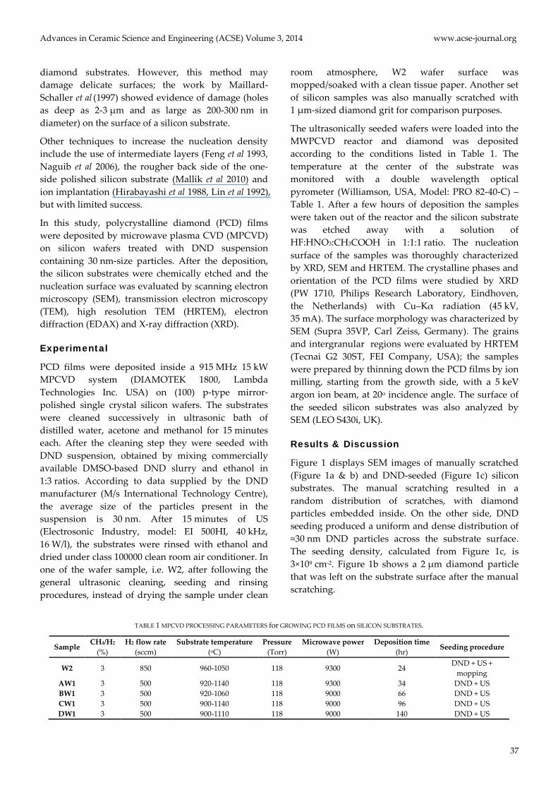
FIG. 3 SEM IMAGES and EDAX SPECTRA of (a) AS-GROWN DIAMOND COLONY of SAMPLE W2; (b) UNCOVERED SILICON SUBSTRATE of SAMPLE W2; (c) SEM IMAGE and EDAX LINE SCAN ALONG DND AGGLOMERATES LEFTOVERS ACROSS the COLONIES on the
NUCLEATION SIDE of SAMPLE W2. (d) 1-2 µm-SIZED COLONIES on the NUCLEATION SIDE of SAMPLE CW1.
38
Advances in Ceramic Science and Engineering (ACSE) Volume 3, 2014 www.acse-journal.org
To study in detail the growth of individual seed particles, silicon wafer W2 was wiped with clean tissue paper after the standard US with DND suspension, reducing the number of DND seeds on the surface. The sample was then placed inside the reactor and diamond growth proceeded over 24 hours. The resulting diamond film was not continuous; instead it was mainly composed of large (tenths of µm) isolated diamond colonies – Figure 3a & b. Figure 3a & b also display the EDAX scans taken on an individual diamond colony and on the bare silicon substrate lying beneath (area within rectangular brackets), respectively. The quantitative analysis of the bare silicon surface region yields peaks corresponding to both carbon and silicon, which can be attributed to formation of amorphous carbon or a SiC layer. On the other hand, the EDAX scan taken on the colony yields a sharp carbon peak and reveals traces of oxygen and silicon. In a particular surface region of the wafer sample W2, the manual wiping was not so effective, and diamond colonies grew large in size till they coalesced, forming a continuous film. The silicon substrate of this area was etched out and the nucleation surface was observed under SEM – Figure 3c, showing diamond colonies tenths of µm in size and DND agglomerate leftovers on the surface. An EDAX line scan taken on the DND leftovers is also presented. The carbon peak drastically falls at the region between the colonies and becomes sharper in the regions corresponding to the DND agglomerates. Similarly, figure 3d shows 1-2 µm-sized colonies on the nucleation surface of sample CW1, together with the EDAX scan revealing a large carbon peak.
The XRD plots taken on the nucleation surface of samples AW1, BW1, CW1 and DW1 (not shown) have the (111) and (220) diamond peaks. The size of the diamond crystals was calculated by Debye-Scherrer
analysis of the XRD data, (L: crystallite
size; λ: incident X-ray wavelength; β: full width at half maxima (FWHM) of the x-ray peaks; θ: diffraction angle). The values obtained are listed in Table 2.
TABLE 2 CALCULATIONS of CRYSTALLITE SIZES from DEBYE-SCHERRER ANALYSIS of XRD DATA.
Sample Thickness (µm) Crystallite size (nm) AW1 82.615 27.937 BW1 136.64 22.443 CW1 252.45 29.360 DW1 299.64 19.691
The crystal size values obtained by Debye-Scherrer analysis of XRD results match with the size of the
diamond clusters that were identified by SEM observations (Figure 2). Moreover, this value is also similar to the size of the DND seeds present in the DMSO-based DND slurry used for seeding.
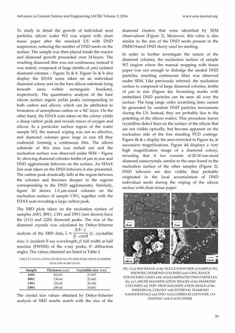
In order to further investigate the nature of the diamond colonies, the nucleation surface of sample W2 (region where the manual mopping with tissue paper was not enough to dislodge the seeded DND particles, resulting continuous film) was observed under SEM. Like previously referred, the nucleation surface is composed of large diamond colonies, tenths of µm in size (Figure 4a). Scratching marks with embedded DND particles can be seen all over the surface. The long range order scratching lines cannot be generated by random DND particles movements during the US. Instead, they are probably due to the polishing of the silicon wafers. This procedure leaves crystalline defect lines on the surface of the silicon that are not visible optically, but become apparent on the nucleation side of the free standing PCD coatings. Figure 4b & c display the area encircled in Figure 4a, at successive magnifications. Figure 4d displays a very high magnification image of a diamond colony, revealing that it too consists of 20-50 nm-sized diamond nanocrystals, similar to the ones found in the nucleation surface of the other samples (Figure 2). DND leftovers are also visible; they probably originated in the local accumulation of DND individual seeds during the wiping of the silicon surface with clean tissue paper.
FIG. 4 (a) SEM IMAGE of the NUCLEATION SIDE of SAMPLE W2,
SHOWING DIAMOND COLONIES and LONG RANGE SCRATCHING LINES with AGGLOMERATED DND PARTICLES;
(b), (c) LARGER MAGNIFICATION IMAGES of the DIAMOND COLONIES; (d) VERY HIGH MAGNIFICATION IMAGE of the
INDIVIDUAL COLONY with INTERNAL DIAMOND NANOCRYSTALS and DND AGGLOMERATE LEFTOVER, CO-
EXISTING with EACH OTHER.
39

www.acse-journal.org Advances in Ceramic Science and Engineering (ACSE) Volume 3, 2014
The nucleation side of sample W2 was further observed by TEM. A low magnification TEM image (Figure 5a) reveals large diamond colonies tenths of micron in size (region A) previously observed under SEM (Figure 4a & b) and the inter-colonial region B. HRTEM images of the colony A and the inter-colonial region B can be seen in Figure 5b& c, respectively.
Figure 5d displays a dark field TEM image of similar colonies, revealing micron size elongated features comprised of white dots of diamond nanocrystals. The EDAX spectrum taken from region A (Figure 5e) has a sharp carbon peak with low intensity signals corresponding to silicon, oxygen, fluorine and other impurities; the EDAX spectrum taken from the inter-granular region B (Figure 5f) reveals the existence of a higher amount of non-carbon phases, such as silicon, oxygen, fluorine and trace amounts of metal impurities.
FIG. 5 NUCLEATION SIDE of SAMPLE W2: (a) LOW
MAGNIFICATION BRIGHT FIELD TEM IMAGE; (b) HRTEM IMAGE of GRANULAR REGION A; (c) HRTEM IMAGE of INTER-
GRANULAR REGION B; (d) DARK FIELD TEM IMAGE from INSIDE the GRAIN; (e) EDAX of (b); (f) EDAX of (c).
Commercially-available DND slurries contain primary, secondary and larger aggregates, as reported by Osawa in his Pure and Applied Chemistry paper in 2008. The average size of the primary agglomerates (seeds) present in the DND suspension used for seeding is in the order of 30 nm. These seeds are composed of individual diamond nanocrystals, 3-4 nm in size, and are very difficult to separate by simple sonication force; in addition, they have a high tendency to agglomerate due to their high surface energy, creating micrometer-sized secondary and larger aggregates (Mochalin et al 2012). While larger and secondary agglomerates are held together by Van der Waals forces and can be separated by simple sonication, the primary agglomerates require beads-milling to be broken down into diamond nanoparticles 3-4 nm in size. Due to the difficulty in breaking the
primary agglomerates into individual nanoparticles, Osawa (2008) proposed that they are hold together by primary C-C covalent bonding and that possess a structure similar to UNCD.
A closer look at Figure 1c reveals that the surface of the silicon wafer gets fully covered by DND seeds during the US seeding. The nucleation surface of diamond films deposited on the seeded silicon wafers is also composed of 25-45 nm diamond crystals, similar in size to the individual DND seeds (Figure 2 and Table 2 for samples #AW1, #BW1, #CW1 & #DW1). In Figure 4 (for sample W2) larger agglomerates, hundreds of nanometers in size, are also visible. These agglomerates probably resulted from the exposure to growth conditions of local concentrations of DND seeds, caused by the mopping of the surface. During CVD diamond growth, these seeds seem to have fused together, forming secondary aggregates, hundreds of nm in size, spread all over the nucleation side of the free standing PCD coating, as suggested by Figure 4a.These secondary DND aggregates seem to be embedded in the surface of the individual diamond colonies, which in turn started to grow from the DND seeds left on the silicon surface after seeding (Figure 4d).
HRTEM images further confirm the strong resemblance between the structure of the DND primary aggregates of the DMSO-based DND slurry used for the substrate pre-treatment (Shenderova et al 2006) and the structure of the diamond colonies; HRTEM images of the granular region (Figure 5b) show 6-8 nm-sized diamond single crystals (marked as 1, 2 & 3 in Figure 5b) surrounded by an amorphous carbon matrix, revealing a striking resemblance with earlier reported DND agglomerate microstructures (Osawa 2008, Podesta et al 2006). It is also interesting to note that the size of such individual nanocrystals is larger than the 1-2 nm-sized amorphous carbon particles present in the inter-colonial regions (marked as 1, 2 & 3 in Figure 5c).
These results show that the ≈30 nm in size DND seeds, composed of clusters of 6-8 nm size diamond nanocrystals, survived the gas chemistry used for growing PCD films (Table 1) and even re-agglomerated during growth (Figure 4d). This suggests that nanodiamond crystals can be synthesized under conditions usually associated with polycrystalline diamond. In fact Kumar et al in their very recent October 2013 paper in Nature Communications have demonstrated synthesis of
40

Advances in Ceramic Science and Engineering (ACSE) Volume 3, 2014 www.acse-journal.org
nanodiamond at near atmospheric conditions by micro-plasma activation of ethanol vapor in the presence of hydrogen.
Podesta et al (2006) analyzed thick MPCVD PCD coatings; although they did not provide any SEM images, AFM images of the nucleation side showed similar features, with 2 µm diamond grains separated by inter-granular 50 nm-deep grooves; a closer look into the internal structures reveals that the nucleation surface of these individual grains also consists of small nanocrystalline features.
According to the prevalent theory, growth of diamond from the vapor phase begins with the formation of diamond clusters that nucleate on entrapped particles, small defects, edges or areas with high energy. These individual clusters, with size r, can grow bigger or disintegrate, depending on the Gibbs free energy difference ∆G. If ∆G is positive, the atomic cluster vanishes; if, on the other hand, ∆G is negative, more atoms add to the cluster. Once r reaches the critical value rc = 8 nm, the cluster stabilizes and becomes an effective diamond nucleus. The relevant thermodynamic analysis with associated mathematical calculations has been carried out by Zhang et al in their 2004 J. Phys. Chem. B paper. A Similar calculation in the present context is shown as follows:
Let’s consider heterogeneous nucleation of the spherical cap of diamond clusters on a Si substrate (figure 6) upon CVD. The Gibbs free energy difference, is expressed as: ΔG(r) = Vs/Vm × Δg + (Asf γsf + Asc γsc - Acf γcf); where Vs: volume of the spherical cap of diamond clusters; Vm: mole volume of diamond; Δg: the mole volume Gibbs free energy difference depending on pressure P and temperature T in the phase transition of graphite to diamond; Asf, Asc, Acf: interface area; γsf, γsc, γcf: interface energy (s: spherical cap of diamond clusters, f: gas phase and, c: substrates).
FIG. 6 SCHEMATIC of HETEROGENEOUS NUCLEATION of
DIAMOND on SILICON SUBSTRATE.
Zhang et al (2004) have shown by the nano-thermodynamic calculations that the Gibbs’ free energy difference on phase transition from graphite to diamond is: ΔG(r) = [4/3 πr3ΔV × P – 2.73 × 10⁶T – 7.23 × 10 8 + 2γ/r)Vm + 4πr2γ](2 + m)(1 - m)2/4; when (δΔG(r)/δr) = 0, the critical size of diamond nuclei becomes: r* = 2γ(2/3 + Vm/ΔV)/(2.73×106T + 7.23 × 10⁸ – P), where, m = Cosθ.
The calculated size (diameter) of the spherical cap of diamond nuclei has found to be 8 nm. This value had experimental support of the earlier works by Lee et al (2000) where they showed that the critical size of the diamond nuclei seeding on silicon substrate is in the range 2-6 nm. Such nano-thermodynamic calculations show that a very low forming energy for heterogeneous nucleation of diamond from vapor phase is required with critical energy in the tune of 10 -
16 Joule.
More details on thermodynamics of metastable phase nucleation can be found in the 2005 review article by Wang and Yang. Diamond deposition happens, thus, in two stages: the nucleation stage, where the clusters are smaller than rc, and the growth stage, where the clusters are larger than rc.
Now it can be stated that, since the critical nuclei size is 8 nm (value determined by nano-thermodynamic calculations and further supported by experimental results of Lee et al 2000 and Lifshitz et al 2002), in our case there is no nucleation phase, since the diamond seeds are 25-45 nm in size; instead of a competitive effect of formation and disintegration of carbon clusters till the critical size is reached, once the seeded wafers are exposed to the growth plasma, the DND seeds present on the surface of the substrate immediately behave as growth centers. This happens irrespective of the growth environment: in this study, the gas chemistry chosen was 3% methane diluted in hydrogen and not an argon-rich mixture, like in the case UNCD growth. So we can say that the DND particles not only survive the growth chemistry, but act as growth centers, growing in three dimensions with adatoms and coalescing with each other to form a continuous film from the beginning of the plasma exposure.
As suggested by the SEM (Figure 4) and HRTEM (Figure 5) images presented in this manuscript, irrespective of the CVD growth environment (hydrogen- or argon-rich mixtures), when the substrate is pre-treated with DND suspension, the diamond microstructures present on the nucleation
41

www.acse-journal.org Advances in Ceramic Science and Engineering (ACSE) Volume 3, 2014
side are strikingly similar to the DND agglomeration products. This means that the DND particles are stable under traditional PCD growth conditions, otherwise they would have disintegrated. Experimental data suggest the co-existence of DND particles and colonies of diamond nanograins; this implies the phase stability of nanodiamond under the present CVD growth environment. This result is further supported by the work of Danilenko (2005) on the nanocarbon phase diagram which showed that the phase diagram of the different states of nanocarbon is sub-divided into various regions with particle size reducing gradually from (1) liquid nanocarbon (nanodrops) and (2) nanodiamond to (3) amorphous nanocarbon. Danilenko developed this nanocarbon phase diagram (very similar to figure 7) with detailed thermodynamic calculations.
Nanosize induced pressure-temperature carbon-phase diagram has also been discussed by Mochalin et al (2012) in their recent Nature Nanotechnology review article where they have shown that due to nanosize considerations, the triple point of the nanocarbon-phase diagram (Danilenko et al 2005) shifts towards lower temperature and higher pressure, enabling condensation of carbon nano droplets from the supersaturated carbon vapor of the detonation product, which on further reduction of temperature and pressure from the Jouguet point along the isentropic line, condense and crystallize into nanodiamond particles of 4-5 nm size. It has been proven that tetrahedral carbon phase is more stable when the size is less than 3-6 nm (as in the present scenario). In general, carbon nano clusters stabilises in different forms, starting with tens of atoms (“endofullerenes”) to hundreds of atoms (“buckydiamond”) to 104-105 atoms (nanodiamonds) and anything beyond 105 carbon atoms stabilise the graphite phase.
Keeping in mind the apparent co-existence of DND particles and CVD grown diamond nano grains, we propose in Figure 7, a little modification in nanocarbon phase diagram where the DND agglomerates growth environments and the CVD growth conditions used in the present work overlap/interlink.
During the DND synthesis process, shock waves propagate through the material and generate high temperatures (1600-4000 K) and high pressures (3-30 GPa) that correspond to the thermodynamic stability region for diamond. These waves meet
unused carbon phases, melting them into nanodroplets which, under rapid cooling conditions (10-8 to 10-4 seconds), crystallize into cubic diamond. These individual single crystals (4-5 nm in size) may fuse/coagulate under these conditions, forming primary aggregates 20-100 nm in diameter. Depending on the synthesis time period, the formed aggregates may vary from fractals to porous polycrystals and even to polycrystals with total extinction of porosity, following the general laws of vapor phase condensation (Mochalin et al 2012, Podesta et al 2006). Figure 2c and Figure 4d show individual nanocrystals that seem to have been sintered/fused together in a process similar to the detonation steps of melting, fusing and coagulating carbon droplets, suggesting that DND particles may have formed under these particular CVD growth conditions.
FIG. 7 MODIFIED NANOCARBON PHASE DIAGRAM with
OVERLAP of NANODIAMOND and NANOSIZE-INDUCED CVD PHASE STABILITY REGIONS.
Recent thermodynamic calculations (Wang and Yang 2005, Zhang et al 2004) showed that during CVD nanodiamond growth, there is a capillary rise of pressure, given by the Laplace-Young equation
( , where γ=3.7J.m2 and r is the radius of the nanoparticles, upto several giga Pascals; it can thus be stated that the pressure under CVD growth conditions falls into the DND phase region in the modified nanocarbon phase diagram due to the capillarity rise of CVD pressure. The key question is to know whether the temperatures reached during the CVD growth of our samples match the temperatures of DND synthesis environment. The substrate temperature rose as high as 1140oC (≈ 1413 K) – Table 1, a value considerably lower than 1600 K, the lower limit for DND synthesis. However, the nanocarbon phase diagram clearly indicates that, with the decrease in size, the triple point shifts towards
42

Advances in Ceramic Science and Engineering (ACSE) Volume 3, 2014 www.acse-journal.org
lower temperatures and slightly higher pressures. So it may happen that, at extremely small carbon nanocluster sizes, a substrate temperature of 1400 K is high enough to comply with DND environment, enabling the formation of nanocarbon droplets that further condense and crystallize into nanodiamond. But it is also true that, during MPCVD of diamond, the plasma temperature at the core and periphery of the discharge can reach values in the range 1600-3500 K at 105 Torr (Grotjohn et al 2002), which are well within the DND temperature regime. In addition, the critical energy for heterogeneous nucleation of diamond is 10-
16 J (Wang et al 2005), a value low enough to assist nanodiamond formation under CVD growth environments.
Vereshchagin (2004), in his search for the genesis of carbon in the universe, said, and we quote, that “detonation nanodiamonds is a primary state of carbon in the Universe”. The co-existence of leftover/unconsumed secondary agglomerates of DND and NCD colonies (Figure 4d) (that is, clusters of nanodiamond formed initially under the present MWPCVD conditions, upon which further typical columns of diamond rose) suggests that DND particles survived and re-agglomerated under PCD growth conditions. A very recent work by Kumar and co-authors (2013) has shown that nanodiamond can be grown by dissociation of hydrocarbon precursor in the presence of hydrogen gas at atmospheric pressure and below 100oC by microplasma excitation of vapor phase. Their work further validates current propositions.
Conclusions
PCD films were deposited by MPCVD on silicon substrates pretreated with DMSO-based DND suspension. The average size of the DND seeds left on the silicon surface (30 nm) is larger than the critical radii of diamond nuclei (8 nm); this means the seeds start growing immediately and no incubation step is needed.
The nucleation surface of the free-standing films is composed of individual diamond colonies, hundreds of nanometer in size; these colonies further consist of 20-30 nm-sized diamond nanoparticles. The size of these particles is equivalent to the average size of the DND seeds present in the seeding suspension. In addition, the diamond particles touch each other and form agglomerate similar to the DND agglomerates found in the detonation product. HRTEM revealed that these 20-30 nm diamond particles are further
composed 6-8 nm sized single diamond nanocrystals that resemble HRTEM images of the individual DND spherical particles of the detonation product.
The similarity between the microstructure of the nucleation side and the hierarchical agglomerates of DNDs suggests that the growth environment inside the MPCVD system may be similar to the detonation of explosive-containing carbon. DND forms at pressures of 3-30 GPa and temperatures between 1600 and 4000ºK, on the other hand, recent thermodynamic calculations reveal that the capillary rise of pressure due to the nanosize may push the CVD growth conditions into high pressure (>2 GPa) and high temperatures (>1600 K).This implies the overlapping of the nanosize-induced CVD diamond growth and the nanodiamond phase stability regions.
ACKNOWLEDGEMENT
CSIR, India provided financial support for the network project title “Very High Power MW Tubes: Design and Development Capabilities (MTDDC)” (CSIR Grant No. PSC0101) under 12th five year plan. Dr. J.C. Mendes acknowledges the Portuguese Science and Technology Foundation for the grant SFRH/BPD/90306/2012.
REFERENCES
Butler J E and Sumant A V, “The CVD of Nanodiamond
Materials”, Chem. Vap. Deposition, 14 (2008) 145–160.
Badziag P, Verwoerd W S, Ellis W P, Greiner N R,
“Nanometre-sized diamonds are more stable than
graphite”, Nature (London) 343 (1990) 244.
Chavanne A, Barjon J, Vilquin B, Arabski J, Arnault J C,
"Surface investigations on different nucleation pathways
for diamond heteroepitaxial growth on iridium",
Diamond Relat. Mater. 22 (2012) 52.
Danilenko V V, “Phase Diagram of Nanocarbon”,
Combustion, Explosion, and Shock Waves, 41 (2005) 460–
466.
Edelstein R S, Gouzman I, Folman M, Rotter S, Hoffman A,
“Surface carbon saturation as a means of CVD diamond
nucleation enhancement“, Diamond Relat. Mater., 8
(1999) 139.
Feng Z, Komvipoulos K, Brown I G and Bogy D B, “Effect of
graphitic carbon films on diamond nucleation by
microwave-plasma-enhanced chemical-vapor deposition”,
43

www.acse-journal.org Advances in Ceramic Science and Engineering (ACSE) Volume 3, 2014
J. Appl. Phys., 74 (1993) 2841.
Gouzman I, Richter V, Rotter S, Hoffman A, “Study of
chemical vapor deposition diamond film evolution from
a nanodiamond precursor by C13 isotopic labeling and
ion implantation”, J. Vac. Sci. Technol. A 2000, 18, 2997.
Grotjohn T A and Asmussen J, “Microwave Plasma-Assisted
Diamond Film Deposition”, Chapter 7, Diamond Films
Handbook, edited by J. Asmussen and D. K. Reinhard,
published by Marcel Dekker, Inc. (2002) p.275-278.
Hirabayashi K, Taniguchi Y, Takamatsu O, Ikeda T, Ikoma
K, and Iwasaki-Kurihara N., “Selective deposition of
diamond crystals by chemical vapor deposition using a
tungsten-filament method”, Appl. Phys. Lett., 53 (1988)
1815..
Iijima S, Aikawa Y, Baba K, "Early formation of chemical
vapor deposition diamond films", Appl. Phys. Lett. 57
(1990) 2646.
Kromka A, Potocký Š, Čermák J, Rezek B, Potměšil J, Zemek
J, Vaněček M, "Early stage of diamond growth at low
temperature", Diamond Relat. Mater. 17 (2008) 1252.
Kumar Ajay, Lin Pin Ann, Xue Albert, Hao Boyi, Yap Yoke
Khin & Sankaran R. Mohan, “Formation of
nanodiamonds at near-ambient conditions via
microplasma dissociation of ethanol vapour”, Nature
Communications, 4:2618, DOI: 10.1038/ncomms3618.
Lee S T, Peng H Y, Zhou X T, Wang N, Lee C S, Bello I,
Lifshitz Y, “A Nucleation Site and Mechanism Leading to
Epitaxial Growth of Diamond Films”, Science 287 (2000)
104.
Lifshitz Y, Kohler T, Frauenheim T, Guzmann I, Hoffman A,
Zhang R Q, Zhou X T, Lee S T, “The Mechanism of
Diamond Nucleation from Energetic Species”, Science,
297 (2002) 1531.
Lin S J, Lee S L, Hwang J, Chang C S, and Wen H Y,
“Effects of local facet and lattice damage on nucleation of
diamond grown by microwave plasma chemical vapor
deposition”, Appl. Phys. Lett., 60 (1992) 1559.
Maillard-Schaller E, Küttel O M, Gröning P, Gröning O,
Agostino R G, Aebi P, Schlapbach L, Wurzinger P,
Pongratz P, " Local heteroepitaxy of diamond on silicon
(100):mA study of the interface structure", Phys. Rev. B 55
(1997) 15895.
Mallik A K, Binu S R, Satapathy L N, Narayana C, Seikh M
M, Shivashankar S A and Biswas S K, “Effect of substrate
roughness on growth of diamond by hot filament CVD”,
Bull. Mater. Sci., Vol. 33, No. 3, June 2010, pp. 251–255.
Mallik A K, Bysakh S, Pal K S, Dandapat N, Guha B K, Datta
S, Basu D, “Synthesis and Characterisation of
Freestanding Diamond Coatings”, Indian Journal of
Engineering and Materials Science, 20, 2013, pp. 522-532.
Mochalin V N, Shenderova O, Ho D and Gogotsi Y, “The
properties and applications of nanodiamonds”, Nature
Nanotechnology 7 (2012) 11–23.
Naguib N N, Elam J W, Birrell J, Wang J, Grierson D S,
Kabius B, Hiller J M, Sumant A V, Carpick R W, Auciello
O, Carlisle J A, “Enhanced nucleation, smoothness and
conformality of ultrananocrystalline diamond (UNCD)
ultrathin films via tungsten interlayers”, Chemical
Physics Letters 430 (2006) 345–350.
Osawa E, “Monodisperse single nanodiamond particulates”,
Pure Appl. Chem., Vol. 80 (2008) 1365–1379.
Podesta A, Salerno M, Ralchenko V, Bruzzi M, Sciortino S,
Khmelnitskii R, Milani P, “An atomic force microscopy
study of the effects of surface treatments of diamond
films produced by chemical vapor deposition”, Diamond
& Related Materials 15 (2006) 1292 – 1299.
Popovici G and Prelas M A, “Nucleation and Selective
Deposition of Diamond Thin Films“, Phys. Status Solidi
132 (1992) 233.
Rotter S Z, Madaleno J C, “Diamond CVD by a Combined
Plasma Pretreatment and Seeding Procedure”, Chemical
Vapor Deposition, 15 (2009) 209.
Shenderova O, Hens S, McGuire G, “Seeding slurries based
on detonation nanodiamond in DMSO”, Diamond &
Related Materials 19 (2010) 260–267.
Shenderova O, McGuire G, in Nanomaterials Handbook (Ed.
Y. Gogotsi), CRC Press, Taylor and Francis Group
Florida, 2006.
Stoner B R, Ma G H M, Wolter S D, and Glass J T ,
“Characterization of bias-enhanced nucleation of
diamond on silicon by invacuo surface analysis and
transmission electron microscopy”, Phys. Rev. B, 45
(1992) 11067.
Sumant A V, Gilbert P U P A, Grierson D S, Konicek A R,
Abrecht M, Butler J E, Feygelson T, Rotter S S, Carpick R
W, “Surface composition, bonding, and morphology in
44
Advances in Ceramic Science and Engineering (ACSE) Volume 3, 2014 www.acse-journal.org
the nucleation and growth of ultra-thin, high quality
nanocrystalline diamond films”, Diamond & Related
Materials 16 (2007) 718-724.
Vereshchagin A L, “Initial stages of carbon genesis in the
universe”, Universitas Scientiarum Vol 9 (2004) 59-64.
Wang C X, Yang G W, “Thermodynamics of metastable
phase nucleation at the nanoscale”, Materials Science and
Engineering R 49 (2005) 157–202.
Williams O A, Douhe´ret O, Daenen M, Haenen K, Osawa E,
Takahashi M, “Enhanced diamond nucleation on
monodispersed nanocrystalline diamond”, Chemical
Physics Letters 445 (2007) 255–258.
Williams O A and Nesládek M, “Growth and properties of
nanocrystalline diamond films”, phys. stat. sol. (a) 203
(2006) 3375–3386.
Yugo S, Kanai T, Kimura T, Muto T, "Generation of diamond
nuclei by electric field in plasma chemical vapor
deposition", Appl. Phys. Lett. 58 (1991) 1036.
Zhang C Y, Wang C X, Yang Y H, and Yang G W, “A
Nanoscaled Thermodynamic Approach in Nucleation of
CVD Diamond on Nondiamond Surfaces”, J. Phys. Chem.
B 108 (2004) 2589-2593.
45
Related Documents