Determining mechanical properties of thin films from the loading curve of nanoindentation testing Manhong Zhao a , Yong Xiang b , Jessica Xu c , Nagahisa Ogasawara d , Norimasa Chiba d , Xi Chen a, ⁎ a Department of Civil Engineering and Engineering Mechanics, Columbia University, New York, NY 10027-6699, USA b Intel Corporation, Materials Technology Department, 3065 Bowers Avenue, MS SC2-24, Santa Clara, CA 95054, USA c Intel Corporation, Logical Technology Development, 2501 NW 229th Avenue, MS RA3-402, Hillsboro, OR 97124, USA d Department of Mechanical Engineering, National Defense Academy, Hashirimizu, Yokosuka 239-8686, Japan Received 14 August 2007; received in revised form 11 March 2008; accepted 12 March 2008 Available online 21 March 2008 Abstract Nanoindentation has been widely used to evaluate material properties. In this study, we propose a method that utilizes only the loading curves of an indentation test to extract the elastoplastic properties of an elastic-perfectly plastic thin film as well as the plastic properties of a work hardening thin film. The use of loading curve circumvents some common difficulties encountered during the post-processing of experimental unloading curves. Measurements are taken at two different indentation depths, which have different levels of substrate effects and lead to the establishment of independent equations that correlate the material properties with indentation responses. Effective reverse analysis algorithms are proposed by following which the desired film properties can be determined from a sharp indentation test. The extracted material properties agree well with that measured from a bulge test. © 2008 Elsevier B.V. All rights reserved. Keywords: Nanoindentation; Thin film; Elastic property; Plastic property 1. Introduction 1.1. Background of indentation on thin films One of the most important material systems in microelec- tronics consists of one or more layers of thin films deposited onto a substrate of another material; the films can be metallic, ceramic, or dielectric, and the substrate is typically Si or other hard and stiff material in many cases. While the film Young's modulus often remains close to its bulk counterpart, due to the presence of the film–substrate interface and small grain size, thin metal films often support stresses that would be relaxed through plastic flow in bulk materials, leading to a higher yield stress and/or work hardening exponent (i.e. different plastic properties than bulk) [1–6]. Measuring the elastic and plastic properties of thin films is always the first critical step to analyze their mechanical integrity. This is often considered difficult since the conventional techniques, such as the micro-tensile or bulge test on freestanding thin films [5, 7–11], or the micro- beam cantilever deflection technique [12–14], require extensive micromachining efforts to remove the substrate while trying not to alter the film properties. Among alternative techniques, nanoindentation is arguably the simplest approach for measuring the mechanical properties of small material structures including thin films [15–20]. In an indentation test, a diamond indenter is pressed into materials (Fig. 1(a)) and the indentation load (P) and indentation depth (δ) are continuously measured with high accuracy (Fig. 1(b)). One of the most widely used indenter geometry is a pyramidal Berkovich tip; it has been established that for two sharp in- denters with different shapes (e.g. pyramidal Berkovich and conical indenters), as long as their ratios of cross-sectional area to depth are the same, these two indenters yield almost identical Available online at www.sciencedirect.com Thin Solid Films 516 (2008) 7571 – 7580 ⁎ Corresponding author. Tel.: +1 212 854 3787; fax: +1 212 854 6267. E-mail address: [email protected] (X. Chen). www.elsevier.com/locate/tsf 0040-6090/$ - see front matter © 2008 Elsevier B.V. All rights reserved. doi:10.1016/j.tsf.2008.03.018

Welcome message from author
This document is posted to help you gain knowledge. Please leave a comment to let me know what you think about it! Share it to your friends and learn new things together.
Transcript
Available online at www.sciencedirect.com
008) 7571–7580www.elsevier.com/locate/tsf
Thin Solid Films 516 (2
Determining mechanical properties of thin films from the loading curve ofnanoindentation testing
Manhong Zhao a, Yong Xiang b, Jessica Xu c, Nagahisa Ogasawara d, Norimasa Chiba d, Xi Chen a,⁎
a Department of Civil Engineering and Engineering Mechanics, Columbia University, New York, NY 10027-6699, USAb Intel Corporation, Materials Technology Department, 3065 Bowers Avenue, MS SC2-24, Santa Clara, CA 95054, USAc Intel Corporation, Logical Technology Development, 2501 NW 229th Avenue, MS RA3-402, Hillsboro, OR 97124, USA
d Department of Mechanical Engineering, National Defense Academy, Hashirimizu, Yokosuka 239-8686, Japan
Received 14 August 2007; received in revised form 11 March 2008; accepted 12 March 2008Available online 21 March 2008
Abstract
Nanoindentation has been widely used to evaluate material properties. In this study, we propose a method that utilizes only the loading curvesof an indentation test to extract the elastoplastic properties of an elastic-perfectly plastic thin film as well as the plastic properties of a workhardening thin film. The use of loading curve circumvents some common difficulties encountered during the post-processing of experimentalunloading curves. Measurements are taken at two different indentation depths, which have different levels of substrate effects and lead to theestablishment of independent equations that correlate the material properties with indentation responses. Effective reverse analysis algorithms areproposed by following which the desired film properties can be determined from a sharp indentation test. The extracted material properties agreewell with that measured from a bulge test.© 2008 Elsevier B.V. All rights reserved.
Keywords: Nanoindentation; Thin film; Elastic property; Plastic property
1. Introduction
1.1. Background of indentation on thin films
One of the most important material systems in microelec-tronics consists of one or more layers of thin films depositedonto a substrate of another material; the films can be metallic,ceramic, or dielectric, and the substrate is typically Si or otherhard and stiff material in many cases. While the film Young'smodulus often remains close to its bulk counterpart, due to thepresence of the film–substrate interface and small grain size,thin metal films often support stresses that would be relaxedthrough plastic flow in bulk materials, leading to a higher yieldstress and/or work hardening exponent (i.e. different plastic
⁎ Corresponding author. Tel.: +1 212 854 3787; fax: +1 212 854 6267.E-mail address: [email protected] (X. Chen).
0040-6090/$ - see front matter © 2008 Elsevier B.V. All rights reserved.doi:10.1016/j.tsf.2008.03.018
properties than bulk) [1–6]. Measuring the elastic and plasticproperties of thin films is always the first critical step to analyzetheir mechanical integrity. This is often considered difficultsince the conventional techniques, such as the micro-tensile orbulge test on freestanding thin films [5, 7–11], or the micro-beam cantilever deflection technique [12–14], require extensivemicromachining efforts to remove the substrate while trying notto alter the film properties.
Among alternative techniques, nanoindentation is arguablythe simplest approach for measuring the mechanical propertiesof small material structures including thin films [15–20]. In anindentation test, a diamond indenter is pressed into materials(Fig. 1(a)) and the indentation load (P) and indentation depth (δ)are continuously measured with high accuracy (Fig. 1(b)). Oneof the most widely used indenter geometry is a pyramidalBerkovich tip; it has been established that for two sharp in-denters with different shapes (e.g. pyramidal Berkovich andconical indenters), as long as their ratios of cross-sectional areato depth are the same, these two indenters yield almost identical
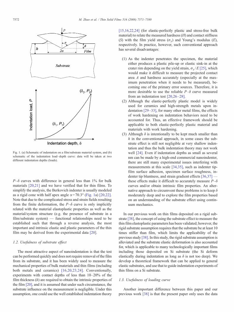
Fig. 1. (a) Schematic of indentation on a film/substrate material system, and (b)schematic of the indentation load–depth curve: data will be taken at twodifferent indentation depths (loads).
7572 M. Zhao et al. / Thin Solid Films 516 (2008) 7571–7580
P–δ curves with difference in general less than 1% for bulkmaterials [20,21] and we have verified that for thin films. Tosimplify the analysis, the Berkovich indenter is usually modeledas a rigid cone with half apex angle α=70.3° (Fig. 1a) [20,22].Note that due to the complicated stress and strain fields resultingfrom the finite deformation, the P–δ curve is only implicitlyrelated with the material elastoplastic properties as well as thematerial/system structure (e.g. the presence of substrate in afilm/substrate system) — functional relationships need to beestablished such that through a reverse analysis, the mostimportant and intrinsic elastic and plastic parameters of the thinfilm may be derived from the experimental data [20].
1.2. Usefulness of substrate effect
The most attractive aspect of nanoindentation is that the testcan be performed quickly and does not require removal of the filmfrom its substrate, and it has been widely used to measure themechanical properties of bulk materials and thin films (includingboth metals and ceramics) [16,20,23,24]. Conventionally,experiments with contact depths of less than 10–20% of thefilm thickness (h) are required to obtain the intrinsic properties ofthe film [20], and it is assumed that under such circumstance, thesubstrate influence on the measurement is negligible. Under thisassumption, one could use the well established indentation theory
[15,16,22,24] (for elastic-perfectly plastic and stress-free bulkmaterial) to relate the measured hardness (H) and contact stiffness(S) with the film yield stress (σy) and Young's modulus (E),respectively. In practice, however, such conventional approachhas several disadvantages:
(1) As the indenter penetrates the specimen, the materialeither produces a plastic pile-up or elastic sink-in at thecrater rim depending on the yield strain, σy /E [25], whichwould make it difficult to measure the projected contactarea A and hardness accurately (especially at the max-imum penetration when it needs to be measured), be-coming one of the primary error sources. Therefore, it ismore desirable to use the reliable P–δ curve measuredfrom an indentation test [20,26–28].
(2) Although the elastic-perfectly plastic model is widelyused for ceramics and high-strength metals upon in-dentation [29–33], for many other metal films, the effectsof work hardening on indentation behaviors need to beaccounted for. Thus, an effective framework should beapplicable to both elastic-perfectly plastic material andmaterials with work hardening.
(3) Although δ is intentionally to be kept much smaller thanh in the conventional approach, in some cases the sub-strate effect is still not negligible at very shallow inden-tation and thus the bulk indentation theory may not workwell [24]. Even if indentation depths as small as severalnm can be made by a high-end commercial nanoindenter,there are still many experimental issues interfering withmeasurements at this scale [34,35], such as indenter tip-film surface adhesion, specimen surface roughness, in-denter tip bluntness, and strain gradient effects [36,37]—these effects make it difficult to accurately measure P–δcurves and/or obtain intrinsic film properties. An alter-native approach to circumvent these problems is to keep δmoderately deep and to explore the film properties basedon an understanding of the substrate effect using contin-uum mechanics.
In our previous work on thin films deposited on a rigid sub-strate [38], the concept of using the substrate effect to measure thethin film elastoplastic parameters has been validated; however, therigid substrate assumption requires that the substrate be at least 10times stiffer than film, which limits the applicability of theprevious study [38]. In this study, the rigid substrate assumption isalleviated and the substrate elastic deformation is also accountedfor, which is applicable to many technologically important filmsincluding those deposited on Si substrate (the Si deformelastically during indentation as long as δ is not too deep). Wedevelop a theoretical framework that can be applied to generalelastic substrates, and use that to guide indentation experiments ofthin films on a Si substrate.
1.3. Usefulness of loading curve
Another important difference between this paper and ourprevious work [38] is that the present paper only uses the data
7573M. Zhao et al. / Thin Solid Films 516 (2008) 7571–7580
from the loading section of P–δ curves, based on the followingconsiderations:
(1) In a nanoindentation test, very often the stress relaxationis observed at the maximum load when unloading justoccurs, which is because the strain beneath indenter isquite large and the strain rate is also very large at thispoint (since the loading rate is usually finite during theexperiment), and the sudden withdraw of indenter causesoscillations in measurement whereas holding at maximumload may lead to uncertainties in the measured quantities[16]. In addition, the initial portion of unloading is moreprone to thermal drift than the loading curve. Manyexperimental schemes have been proposed to minimizethese effects, nevertheless, the possible existence of theseaspects requires that the experiment must be carried outvery carefully, otherwise the first unloading may not beentirely elastic, the unloading curve may not be veryreproducible, and the unloading curve must be used withcaution (see below for an example).
(2) In many theoretical and numerical indentation studies, arigid indenter is used [20,24,32,38,39] whereas in prac-tice, a diamond indenter tip is employed. It is well knownthat the unloading behavior is strongly affected by thecompliance of indenter tip [16]. Therefore, in order toapply the developed indentation method based on rigidindenter, a real P–δ curve measured from experimentmust be converted to that by a rigid indenter — forexample, our previous work [38] utilizes the unloadingwork in indentation analysis, which requires the fullinformation the unloading P–δ curve with a rigid in-denter, and if the diamond tip contribution is not properlyremoved from experimental data, plus any of the above-mentioned error due to the nonelastic effects in the un-loading P–δ curve, large error may occur based on ourerror sensitivity analysis [38].
For example, we have shown [40] that in a recent study byGuelorget et al. [41], because their sharp and spherical inden-tation experiments were not carefully conducted, in particularthe scatter of unloading data was not properly treated, and thecontribution of elastic deformation of the diamond tip was notremoved from the measurement of contact stiffness, the materialproperties extracted from reverse analyses had very large error.It comes to our attention that quite a few users (e.g. [41]) maynot fully aware of how to carefully handle the unloading dataobtained from an experiment; therefore, perhaps a way totemporarily circumvent such issue is to avoid the use of un-loading data, whose accurate measurement and post-processingmay require extra care.
Another benefit of avoiding the use of unloading curve isthat, as remarked above, the experimental P–δ curve measuredwith a diamond indenter (regardless of what experimentalscheme one uses) must be converted to that of a rigid indenter,so as to apply many well established theories based on rigidindenters. The conversion of the entire P–δ curve is often verydifficult due to the unknown exact indenter tip geometry (e.g.
effective “height” of the tip), which will in particular impact theunloading curve (since the variation of δ is small, which may beon the same order of diamond tip deformation). Since thediamond tip compliance has very small influence on the loadingP–δ curve (especially at moderate indentation depth adopted inthis paper, which is much larger than the diamond tipdeformation), we therefore propose to circumvent suchdifficulty by using only the perhaps more reliable loading P–δ curve measured from an experiment.
During loading as the indenter approaches the interface, thevarying degree to which the substrate affects the indentationmeasurement provides rich information for extracting the filmelastoplastic properties. The data are taken when the indentationdepth δ is 1/3 and 2/3 of film thickness h, respectively — thesetwo depths are chosen such that 1) they are not too small tointerfere with the aforementioned small scale effects; 2) they arealso not too large so as to prevent cracking in practice; 3) theyare separated sufficiently apart, where the different substrateeffects would induce different loading curvatures (see below)and provide two independent equations that can be used to solvetwo independent elastoplastic parameters — the principle issimilar to [38] but an important difference is that the substrateelastic deformation is accounted for in this paper (and thesubstrate property is not fixed during the establishment ofindentation method, although later in this paper, Si substrate ischosen in parallel experiment), and that we only use informationobtained from loading so as to avoid uncertainties at unloading.The indentation load at the two depths are denoted as P1 and P2,respectively (Fig. 1b).
1.4. Organization of paper
An effective reverse analysis algorithm is established in thispaper such that, once the substrate modulus is known, usefulelastic and/or plastic properties of the film material can bereadily obtained from the indentation P–δ loading curve via oneindentation test. Theories are developed for two categories ofthin films:
(1) Deriving Young's modulus and yield stress of elastic-perfectly plastic films. As mentioned earlier, the classicindentation theory [15,16,20,22] is focused on elastic-perfectly plastic bulk materials and such theory has beenapplied to ceramics and high-strengthmetals [16], to extracttheir effective elastic and plastic properties upon indenta-tion. Here we extend the technique to thin films, by takinginto account the substrate effect under the assumption thatthe substrate deforms elastically; in addition, the approachdoes not require the determination of projected contact area.The technique is applicable to ceramic or high-strengthmetal thin films whose indentation behaviors can be ef-fective described by the phenomenological elastic-perfectlyplastic material model [29–33] as long as significantcracking does not occur, and it will be applied to study aSiN film on Si substrate.
(2) Solving the plastic properties of thin films with workhardening. In many cases the lattice structure of the film
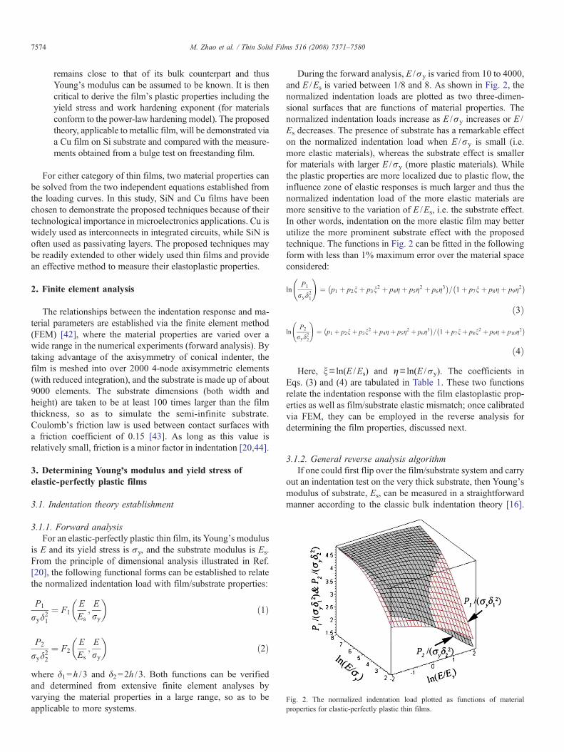
Fig. 2. The normalized indentation load plotted as functions of materialproperties for elastic-perfectly plastic thin films.
7574 M. Zhao et al. / Thin Solid Films 516 (2008) 7571–7580
remains close to that of its bulk counterpart and thusYoung's modulus can be assumed to be known. It is thencritical to derive the film's plastic properties including theyield stress and work hardening exponent (for materialsconform to the power-law hardening model). The proposedtheory, applicable to metallic film, will be demonstrated viaa Cu film on Si substrate and compared with the measure-ments obtained from a bulge test on freestanding film.
For either category of thin films, two material properties canbe solved from the two independent equations established fromthe loading curves. In this study, SiN and Cu films have beenchosen to demonstrate the proposed techniques because of theirtechnological importance in microelectronics applications. Cu iswidely used as interconnects in integrated circuits, while SiN isoften used as passivating layers. The proposed techniques maybe readily extended to other widely used thin films and providean effective method to measure their elastoplastic properties.
2. Finite element analysis
The relationships between the indentation response and ma-terial parameters are established via the finite element method(FEM) [42], where the material properties are varied over awide range in the numerical experiments (forward analysis). Bytaking advantage of the axisymmetry of conical indenter, thefilm is meshed into over 2000 4-node axisymmetric elements(with reduced integration), and the substrate is made up of about9000 elements. The substrate dimensions (both width andheight) are taken to be at least 100 times larger than the filmthickness, so as to simulate the semi-infinite substrate.Coulomb's friction law is used between contact surfaces witha friction coefficient of 0.15 [43]. As long as this value isrelatively small, friction is a minor factor in indentation [20,44].
3. Determining Young's modulus and yield stress ofelastic-perfectly plastic films
3.1. Indentation theory establishment
3.1.1. Forward analysisFor an elastic-perfectly plastic thin film, its Young's modulus
is E and its yield stress is σy, and the substrate modulus is Es.From the principle of dimensional analysis illustrated in Ref.[20], the following functional forms can be established to relatethe normalized indentation load with film/substrate properties:
P1
ryd21
¼ F1EEs
;Ery
� �ð1Þ
P2
ryd22
¼ F2EEs
;Ery
� �ð2Þ
where δ1=h / 3 and δ2=2h / 3. Both functions can be verifiedand determined from extensive finite element analyses byvarying the material properties in a large range, so as to beapplicable to more systems.
During the forward analysis, E /σy is varied from 10 to 4000,and E /Es is varied between 1/8 and 8. As shown in Fig. 2, thenormalized indentation loads are plotted as two three-dimen-sional surfaces that are functions of material properties. Thenormalized indentation loads increase as E /σy increases or E /Es decreases. The presence of substrate has a remarkable effecton the normalized indentation load when E /σy is small (i.e.more elastic materials), whereas the substrate effect is smallerfor materials with larger E /σy (more plastic materials). Whilethe plastic properties are more localized due to plastic flow, theinfluence zone of elastic responses is much larger and thus thenormalized indentation load of the more elastic materials aremore sensitive to the variation of E /Es, i.e. the substrate effect.In other words, indentation on the more elastic film may betterutilize the more prominent substrate effect with the proposedtechnique. The functions in Fig. 2 can be fitted in the followingform with less than 1% maximum error over the material spaceconsidered:
lnP1
ryd21
!¼ p1 þ p2nþ p3n
2 þ p4gþ p5g2 þ p6g
3� �
= 1þ p7nþ p8gþ p9g2
� �ð3Þ
lnP2
ryd22
!¼ p1 þ p2nþ p3n
2 þ p4gþ p5g2 þ p6g
3� �
= 1þ p7nþ p8n2 þ p9gþ p10g
2� �
ð4ÞHere, ξ≡ ln(E /Es) and η≡ ln(E /σy). The coefficients in
Eqs. (3) and (4) are tabulated in Table 1. These two functionsrelate the indentation response with the film elastoplastic prop-erties as well as film/substrate elastic mismatch; once calibratedvia FEM, they can be employed in the reverse analysis fordetermining the film properties, discussed next.
3.1.2. General reverse analysis algorithmIf one could first flip over the film/substrate system and carry
out an indentation test on the very thick substrate, then Young'smodulus of substrate, Es, can be measured in a straightforwardmanner according to the classic bulk indentation theory [16].
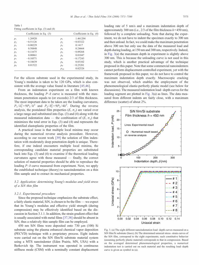
Fig. 3. (a) The eight different nanoindentation load–depth curves measured on aSiN film/Si substrate (lines); (b) The determined uniaxial stress–strain curves ofthe SiN film, correspond to the eight experiments; such constitutive behavior(assuming perfectly plastic material) corresponds to that in compression. Basedon the averaged determined phenomenological properties, a numericalindentation test is carried out on such material and the resulting load–depthcurve is given as symbol in (a).
Table 1Fitting coefficients in Eqs. (3) and (4)
Coefficients in Eq. (3) Coefficients in Eq. (4)
p1 1.26920 p1 1.461204p2 −0.51126 p2 −0.83322p3 −0.00229 p3 0.1417p4 0.50848 p4 0.24664p5 −0.11675 p5 −0.09268p6 0.00861 p6 0.01047p7 −0.10571 p7 −0.17243p8 −0.18639 p8 0.03102p9 0.01522 p9 −0.25201
p10 0.02526
7575M. Zhao et al. / Thin Solid Films 516 (2008) 7571–7580
For the silicon substrate used in the experimental study, itsYoung's modulus is taken to be 120 GPa, which is also con-sistent with the average value found in literature [45,46].
From an indentation experiment on a film with knownthickness, the loading P–δ curve is measured with the max-imum penetration equals to (or exceeds) 2/3 of film thickness.The most important data to be taken are the loading curvatures,P1 /δ1
2 =9P1 /h2 and P2 / δ2
2 =9P2 / 4h2. During the reverse
analysis, the postulated film properties (E, σy) are varied overa large range and substituted into Eqs. (3) and (4) along with themeasured indentation data — the combination of (E, σy) thatminimizes the total error in Eqs. (3) and (4) and represents theidentified elastoplastic properties of the film.
A practical issue is that multiple local minima may occurduring the numerical reverse analysis procedure. However,according to our recent work [39] the solution of film inden-tation with moderately deep penetration depth is unique. There-fore, if one indeed encounters multiple local minima, thecorresponding candidate material properties are substitutedback into Eqs. (3) and (4) to examine if the theoretical loadingcurvatures agree with those measured — finally, the correctsolution of material properties should be able to reproduce theloading P–δ curve measured from experiment. Next, we applythe established technique (theory) to nanoindentation on a thinfilm sample and to extract its mechanical properties.
3.2. Application: determining Young's modulus and yield stressof a SiN thin film
3.2.1. Experimental procedureSince the proposed technique emphasizes the substrate effect,
a fairly elastic material, SiN, is chosen to be the film—we expectthat its Young's modulus and effective yield strength (duringcompression) may be effectively identified based on the dis-cussion in Section 3.1.1. In addition, the strain gradient effect thatis usually associated with metal films [37,38] should be absent inSiN, thus a relatively thin sample film can be employed.
450 nm SiN films were deposited onto 730 μm (100) Sisubstrate using the plasma enhanced chemical vapor deposition(PECVD) technique with a proprietary process. Eight indentswere carried out on the SiN film/Si substrate material systemusing a MTS nanoindenter (Eden Prairie, MN, USA) with aBerkovich tip. The instrument was operated in continuousstiffness mode (CSM) with a nominally constant displacement
loading rate of 5 nm/s and a maximum indentation depth ofapproximately 300 nm (i.e., 2/3 of the film thickness h=450 nm),followed by a complete unloading. Note that during the exper-iment, we do not have to indent the specimen exactly to 300 nmand then unload. In fact, we couldmake themaximum penetrationabove 300 nm but only use the data of the measured load anddepth during loading, at 150 nmand 300 nm, respectively. Indeed,in Fig. 3(a) the maximum depth in experiment is slightly above300 nm. This is because the unloading curve is not used in thisstudy, which is another practical advantage of the techniqueproposed in this paper. Note that some commercial nanoindenterscannot perform displacement-controlled experiment, yet with theframework proposed in this paper, we do not have to control themaximum indentation depth exactly. Macroscopic crackingwas not observed, which enables the employment of thephenomenological elastic-perfectly plastic model (see below fordiscussions). Themeasured indentation load–depth curves for theloading segment are plotted in Fig. 3(a) as lines. The data mea-sured from different indents are fairly close, with a maximumdifference (scatter) of about 2%.
7576 M. Zhao et al. / Thin Solid Films 516 (2008) 7571–7580
3.2.2. Determination of SiN thin film properties fromindentation tests
Based on the experimental curves, the reverse analysis isapplied to extract both Young's modulus E and yield stress σy ofSiN film. For each individual test, reverse analysis based onSection 3.1.2 is carried out to extract (E, σy) of the film, and theresulting uniaxial stress–strain curve of the identified filmproperties is given in Fig. 3(b); a total of 8 results are shownwhich correspond to the 8 indentation experiments. The aver-aged measured Young's modulus is 196.2 GPa and the averagedidentified effective yield stress is 9.88 GPa — the identifiedYoung's modulus is very close to that measured by thecontinuous stiffness measurement (CSM) at shallow indentationdepth, which is about 200 GPa, as well as the reported value of aplasma-CVD SiN film, 210 GPa, measured by a deflection test[47]. It is difficult to independently verify the identified effectivecompressive yield strength of SiN, since during a parallel bulgetest of the freestanding SiN film, the film fractured at tensilestress (which was absent during the indentation experiment);moreover, to our knowledge it is impossible to carry out auniaxial compression test on a freestanding SiN film with a largestrain. Therefore, we will evaluate the plastic property deter-mination of the present indentation technique in the next section,through bulge test on a ductile Cu film specimen.
We remark that for the SiN film, we adopt the widely-usedmodel for ceramics under indentation and assume that its be-havior upon indentation is elastic-perfectly plastic [19,29–33].First, elastic-perfectly plastic is the simplest elastoplasticbehavior and thus theoretically it is important, moreover if onecould verify that a thin film specimen indeed nearly conforms tothe elastic-perfectly plastic behavior, then the formulationestablished in this section is applicable. It is noted again that itis impossible to carry out an uniaxial compression test on the SiNfilm sample we used, nevertheless in the literature, thecompression test on a silicon nitride cylinder shows a behaviorthat is not far away from the elastic-perfectly model [48], andsimilar behaviors can be found for many other ceramic-likematerials, such as GaAs, Si, etc. [49–52]. Second, the elastic-perfectly plastic model is a phenomenological model in the sensethat even if there are other mechanisms (e.g. microcracks in abrittle material), the overall compressive stress–strain behaviorupon indentation (especially that during loading) may still beroughly described by such an ideal model. Note that micro-cracking in a brittle material may lead to a different unloadingbehavior which may invalidate the elastic-perfectly plasticmodel, however, only the loading curve from indentation is usedin this paper and the unloading behavior is not concerned. Inother words, when such an ideal model is applied to the SiN filmin our experiment, and with its modulus and effective yield stressderived above, the indentation behavior of such model isconsistent with that of the real specimen regardless of thespecimen's microstructural details; that is to say, if we carry out anumerical indentation test on a virtual material that obeys theideal elastic-perfectly plastic relationship and with the derivedmaterial parameters given in Fig. 3(b), the resulting P–δ curve(open circular symbol in Fig. 3(a)) agrees well with the measuredP–δ curves (lines in Fig. 3(a)). Hence, the elastic-perfectly
plastic model could be effectively applied to describe (and toreproduce) the indentation loading behavior of SiN in this study,at least in a phenomenological way, and such model may beapplied to other similar ceramic materials [19,29–33].
3.2.3. Error sensitivity of the proposed techniqueDuring nanoindentation experiments, the noise (error) of mea-
surements of the indentation loads P1 and P2 is inevitable, andthus the error sensitivity of the film properties determined from thereverse analysis needs to be investigated. By differentiatingEqs. (3) and (4), the dependences of the variations of the identifiedYoung's modulus and yield stress with respect to the errors of P1and P2 can be explicitly derived. In the case of indentation on SiNfilm/Si substrate, with Es=120 GPa, E=196.2 GPa, and σy=9.88 GPa, the error sensitivity analysis leads to
dEE
¼ 7:34dP1
P1� 9:94
dP2
P2ð5Þ
dryry
¼ �4:83dP1
P1þ 10:66
dP2
P2ð6Þ
where the perturbations of the identified material properties (lefthand side of the equations) are related with the errors of measuredindentation loads (right hand side of equations). Note that sucherrors are that generated from possible perturbation of experi-mental data, and independent of the error of the fitting functions,Eqs. (3) and (4).
We illustrate the application of the error sensitivity equa-tions, Eqs. (5) and (6), for SiN/Si film/substrate system: theerrors of measured P1 and P2 will be magnified by 7.34 and−9.94 times, respectively, and becoming the error of thedetermined Young's modulus; the errors of measured P1 and P2
will be magnified by −4.83 and 10.66 times, respectively, andbecoming the error of the determined yield strength. Note that inboth Eqs. (5) and (6), the signs of two parameters related withdP1 and dP2 are opposite. Therefore, any systematical error ofthe measured indentation load (i.e. when the errors of P1 and P2
are of the same order of magnitude and sign, such as thosearisen from instrument calibration error or diamond compliancecontribution) will induce a partial error cancellation effect onthe identified material properties (Young's modulus and yieldstress), such that the reverse analysis results are relatively stableand insensitive to the systematic errors — which can also bedemonstrated through the small variations of the identified filmproperties for 8 different indentation tests shown in Fig. 3(b). Ofcourse, such argument does not hold for the statistical measure-ment error if the signs of the errors of P1 and P2 are different.
4. Measuring plastic properties of elastoplastic film withwork hardening
4.1. Indentation theory establishment
4.1.1. Forward analysisFor many metal films (except those high-strength films
whose strain hardening may be ignored), work hardening needsto be incorporated at finite plastic deformation. The widely used
Table 2Fitting coefficients in Eqs. (10) and (11)
Coefficients in equation Coefficients in equation
p1 1.26920 p17 −0.00687 p1 1.46120 p17 −0.01184p2 −0.51126 p18 −0.18099 p2 −0.83322 p18 7.4909E-4p3 −0.00229 p19 0.01019 p3 0.14174 p19 3.1286E-5p4 0.50848 p20 0.24978 p4 0.24664 p20 −0.31600p5 −0.11675 p21 0.01800 p5 −0.09268 p21 0.02833p6 0.00861 p22 0.06218 p6 0.01047 p22 0.65379p7 −0.10571 p23 −0.00979 p7 −0.17243 p23 0.16761p8 −0.18639 p24 −0.12963 p8 0.03102 p24 0.02865p9 0.01522 p25 0.00655 p9 −0.25201 p25 −0.00153p10 −0.57366 p26 −0.77508 p10 0.02526 p26 −0.33428p11 −0.11405 p27 0.26357 p11 −2.13940 p27 0.01972p12 −0.03021 p28 −0.03224 p12 −0.09858 p28 −0.22611p13 0.00159 p29 −0.03436 p13 −0.00672 p29 0.03513p14 0.28659 p30 0.00144 p14 1.59180 p30 −0.16255p15 −0.01072 p15 −0.36257 p31 0.01077p16 −0.02451 p16 0.02827
7577M. Zhao et al. / Thin Solid Films 516 (2008) 7571–7580
power-law hardening model is a good approximation for mostmetals and alloys including thin films [20], whose uniaxialstress–strain relationship is:
r ¼ Ee for eVry=E and r ¼ Ren for ezry=E;
ð7Þwhere n is the work hardening exponent, and R≡σy(E /σy)
n is thework hardening rate.We note that the power-law hardeningmodelis the simplest and most widely used phenomenological con-tinuum model used in indentation mechanics to describe theelastoplastic behaviors of a specimen [20,39], and the adoption ofan effective continuum model is required for extracting materialproperties from any indentation analysis. We neglect theinhomogeneity induced by filmmicrostructure and strain gradienteffect in the theoretical study, by assuming that the indentationdepth is sufficiently deep to overcome such effects.Other forms ofmaterial hardening model may be explored in future.
Within the context of power-law hardening elastoplastic thinfilm/elastic substrate system, the dimensionless functions relatingthe normalized loading curvatures andmaterial properties become
P1
ryd21
¼ G1EEs
;Ery
; n
� �ð8Þ
P2
ryd22
¼ G2EEs
;Ery
; n
� �ð9Þ
During the forward analysis of calibrating these two equations,both E /σy and E /Es are varied over a wide range (E /σy from 10to 4000, and E /Es from 1/8 to 8) so as to ensure broader potentialapplications; moreover, n is varied between 0 and 0.6 (a typicalrange for most metals and alloys [39]). Both functions can bedetermined from extensive finite element analyses:
lnP1
ryd21
!¼ p1 þ p2nþ p3n
2 þ p4gþ p5g2 þ p6g3� �� 1þ p7nþ p8gþ p9g2ð Þþ p10 þ p11nþ p12n
2 þ p13n3 þ p14gþ p15g2
� �� 1þ p16nþ p17n
2 þ p18gþ p19g2� �
n
þ p20 þ p21nþ p22n2 þ p23n
3 þ p24gþ p25g2� �
� 1þ p26nþ p27n2 þ p28n
3 þ p29gþ p30g2� �
n2
ð10Þ
lnP2
ryd22
!¼ p1 þ p2nþ p3n
2 þ p4gþ p5g2 þ p6g3� �� 1þ p7nþ p8n
2 þ p9gþ p10g2� �
þ p11 þ p12nþ p13n2 þ p14gþ p15g2 þ p16g3
� �� 1þ p17nþ p18n
2 þ p19n3 þ p20gþ p21g2
� �n
þ p22 þ p23nþ p24n2 þ p25n
3 þ p26gþ p27g2� �
� 1þ p28nþ p29n2 þ p30gþ p31g2
� �n2 ð11Þ
The maximum error of fitting is less than 1%, with ξ≡ ln(E /Es)and η≡ ln(E /σy). The coefficients in Eqs. (10) and (11) aretabulated in Table 2. When n=0, Eqs. (10) and (11) reduce toEqs. (3) and (4), respectively.
4.1.2. General reverse analysis algorithmIn the reverse analysis of the current problem, we assume
that both the film and substratemodulus are known (i.e. bothE andE /Es are known) where the film modulus can be either taken fromthat of its bulk counterpart, or measured by other developed meth-ods. Therefore, the unknown plastic parameters in this problem areσy and n, which may be solved from the two equations above.
For a film with known thickness, from the loading P–δ curve,the important shape factors, P1 /δ1
2=9P1 /h2 and P2 /δ2
2=9P2 /4h2,
are measured. Reverse analysis can be carried out by minimizingthe total error of Eqs. (10) and (11) with respect to the candidatematerial properties and experimental data. Similar to the proceduredescribed in Section 3.1.2, numerical iteration is used to filter outpseudo-localminima and obtain the best candidatematerial whoseindentation behavior could reproduce that of experimental data—such iteration can be carried out based on Eqs. (10) and (11), andwithout additional finite element simulations. Next, we apply theestablished method to nanoindentation on an elastoplastic thinfilm sample and to extract its plastic properties.
4.2. Application: determining plastic properties of a Cu thin film
4.2.1. Experimental procedureNanoindentation test is performed on a copper film/Si sub-
strate system with film thickness of 900 nm. Copper has closetensile and compressive behaviors [53] — the compressiveconstitutive behavior can be measured by the proposed inden-tation technique, and the tensile behavior of the same materialsystem is characterized using the bulge test technique.
The details of material preparation, the bulge test procedure,and the results have been published elsewhere [4,54]. Briefly, Cufilms of 0.9 μm thickness were sputtered directly onto long,rectangular, freestanding Si3N4/TaN membranes that wereprepared using micromachining. Immediately after deposition,
7578 M. Zhao et al. / Thin Solid Films 516 (2008) 7571–7580
the Cu filmwas annealed in-situ at 200 °C for 10min, resulting inan average grain size of 0.5 μm and a mixed crystallographictexture that is dominated by (111) and (100) fiber components.The Si3N4/TaN was removed with a reactive ion etch and theresulting freestanding Cu film was subsequently deformed inplane strain by applying pressure to the rectangular membrane.The applied pressure and the corresponding membrane deflection
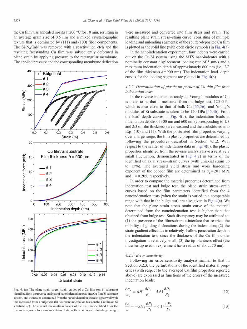
Fig. 4. (a) The plane strain stress–strain curves of a Cu film (on Si substrate)identified from the reverse analysis of nanoindentation tests on aCu film/Si substratesystem, and the results determined from the nanoindentation test also agreewellwiththat measured from a bulge test. (b) Four nanoindentation tests on the Cu film on Sisubstrate. (c) The uniaxial stress–strain curves of the Cu film identified from thereverse analysis of four nanoindentation tests, as the strain is varied in a larger range.
were measured and converted into film stress and strain. Theresulting plane strain stress–strain curve (consisting of multipleloading and unloading segments) of the sputter-deposited Cu filmis plotted as the solid line (with open circle symbols) in Fig. 4(a).
In the nanoindentation experiment, four indents were carriedout on the Cu/Si system using the MTS nanoindenter with anominally constant displacement loading rate of 5 nm/s and amaximum indentation depth of approximately 600 nm (i.e., 2/3of the film thickness h=900 nm). The indentation load–depthcurves for the loading segment are plotted in Fig. 4(b).
4.2.2. Determination of plastic properties of Cu thin film fromindentation tests
In the reverse indentation analysis, Young's modulus of Cuis taken to be that is measured from the bulge test, 125 GPa,which is also close to that of bulk Cu [55,56], and Young'smodulus of Si substrate is taken to be 120 GPa [45,46]. Fromthe load–depth curves in Fig. 4(b), the indentation loads atindentation depths of 300 nm and 600 nm (corresponding to 1/3and 2/3 of film thickness) are measured and then substituted intoEqs. (10) and (11). With the postulated film properties varyingover a large range, the film plastic properties are determined byfollowing the procedures described in Section 4.1.2. Withrespect to the scatter of indentation data in Fig. 4(b), the plasticproperties identified from the reverse analysis have a relativelysmall fluctuation, demonstrated in Fig. 4(c) in terms of theidentified uniaxial stress–strain curves (with uniaxial strain upto 15%). The averaged yield stress and work hardeningexponent of the copper film are determined as σy=201 MPaand n=0.205, respectively.
In order to compare the material properties determined fromindentation test and bulge test, the plane strain stress–straincurves based on the film parameters identified from the 4nanoindentation tests (when the strain is varied in a comparablerange with that in the bulge test) are also given in Fig. 4(a). Wenote that the plane strain stress–strain curve of the materialdetermined from the nanoindentation test is higher than thatobtained from bulge test. Such discrepancy may be attributed to:(1) the presence of the film/substrate interface that restricts themobility of gliding dislocations during the indentation; (2) thestrain gradient effect due to relatively shallow penetration depth inthe indentation test, since the thickness of the Cu film underinvestigation is relatively small; (3) the tip bluntness effect (theindenter tip used in experiment has a radius of about 70 nm).
4.2.3. Error sensitivityFollowing an error sensitivity analysis similar to that in
Section 3.2.3, the perturbations of the identified material prop-erties (with respect to the averaged Cu film properties reportedabove) are expressed as functions of the errors of the measuredindentation loads:
dryry
¼ 6:91dP1
P1� 5:61
dP2
P2ð12Þ
dnn
¼ �5:97dP1
P1þ 6:14
dP2
P2ð13Þ
7579M. Zhao et al. / Thin Solid Films 516 (2008) 7571–7580
The parameters on the right hand sides of Eqs. (12) and (13)represent the magnifying factors of the errors in reverseanalysis. The error of the identified yield stress is 6.91 timesof error of P1 and −5.61 times of the error of P2, and the error ofthe identified work hardening exponent is −5.97 times of per-turbation of P1 and 6.14 times of the perturbation of P2. Again,the signs of the magnifying factors in either Eq. (12) or Eq. (13)are opposite, and therefore the perturbations of identifiedmaterial properties from systematic perturbations of P1 and P2
will be reduced by the partial cancellation effect. In addition,since the magnifying factors of σy and n are of opposite sign,for any source of error, the resulting effect on the overall plasticproperty may be partially cancelled — that is, if the yieldstrength is overestimated by an error in measurement, then thework hardening exponent is underestimated — the overalleffect leads to a more consistent trend of the identified plasticproperty (c.f. Fig. 4(c)).
5. Conclusion
In this paper, an indentation technique is developed to extractthe mechanical properties of thin films by utilizing the substrateeffect. We start with studying the substrate effect, “amplifying”and then utilizing such effect, and finally subtracting off sucheffect to obtain the thin film mechanical properties. The pro-posed technique expands our previous work [38] andincorporates the important substrate elastic deformation; more-over, only the loading segment of an indentation test is needed,which circumvents the common sources of measurement errorsencountered during unloading and increases the potentialapplicability.
From the numerical forward analysis, the relationshipsbetween the material properties and the indentation parametersare established based on extensive finite element simulations.Based on these relationships, the film material properties can bedetermined from the reverse analysis by performing anindentation test on the sample material, and measuring data attwo different indentation depths (i.e. using two differentsubstrate effects). Two versions of this technique are presented:(a) to extract the material properties of an elastic-perfectlyplastic film (applicable to ceramic and high-strength metal/alloyfilms upon compression) and (b) with the film elastic modulusknown (or taken to be that of the bulk), to extract the yield stressand work hardening exponent of a work hardened metal/alloyfilm. These two approaches are applied to a SiN film and aCu film, respectively. In both cases plausible results and goodagreements with literature or parallel bulge test are reported. Inaddition, error sensitivity analyses of both applications arecarried out, which reveals that the present film indentationtechnique is reasonably stable.
Acknowledgments
The work of MZ and XC is supported by NSF CMS-0407743 and CMMI-0643726. The bulge test was done atHarvard University and the authors have benefited from dis-cussion with J. Vlassak (Harvard).
References
[1] W.D. Nix, Metall. Mater. Trans. A 20 (1989) 2217.[2] R. Venkatraman, J.C. Bravman, W.D. Nix, P.W. Davies, P.A. Flinn, D.B.
Fraser, J. Electron. Mater. 19 (1990) 1231.[3] R.P. Vinci, J.J. Vlassak, Annu. Rev. Mater. Sci. 26 (1996) 431.[4] L. Nicola, Y. Xiang, J.J. Vlassak, E.V.d. Giessen, A. Needleman, J. Mech.
Phys. Solids 54 (2006) 2089.[5] H.D. Espinosa, B.C. Prorok, J. Mater. Sci. 38 (2003) 4125.[6] Y. Xiang, T.Y. Tsui, J.J. Vlassak, J. Mater. Res. 21 (2006) 1607.[7] Y. Xiang, X. Chen, J.J. Vlassak, J. Mater. Res. 20 (2005) 2360.[8] J.J. Vlassak, W.D. Nix, J. Mater. Res. 7 (1992) 3242.[9] Y. Xiang, X. Chen, J.J. Vlassak, Mater. Res. Soc. Sym. Proc. 695 (2001)
491.[10] H. Huang, F. Spaepen, Acta Mater. 48 (2000) 3261.[11] M.A. Haque, T. Saif, Thin Solid Films 484 (2005) 364.[12] S.P. Baker, W.D. Nix, J. Mater. Res. 9 (1994) 3145.[13] S.P. Baker, W.D. Nix, J. Mater. Res. 9 (1994) 3131.[14] T.P. Weihs, S. Hong, J.C. Bravman, W.D. Nix, J. Mater. Res. 13 (1998)
931.[15] F. Doerner, W.D. Nix, J. Mater. Res. 1 (1986) 601.[16] W.C. Oliver, G.M. Pharr, J. Mater. Res. 7 (1992) 1564.[17] T.Y. Tsui, J.J. Vlassak, W.D. Nix, J. Mater. Res. 14 (1999) 2196.[18] T.Y. Tsui, J.J. Vlassak, W.D. Nix, J. Mater. Res. 14 (1999) 2204.[19] X. Chen, Y. Xiang, J.J. Vlassak, J. Mater. Res. 21 (2006) 715.[20] Y.T. Cheng, C.M. Cheng, Mater. Sci. Eng. R44 (2004) 91.[21] M. Li, W.M. Chen, N.G. Liang, L.D. Wang, J. Mater. Res. 18 (2004)
73.[22] G.M. Pharr, Mater. Sci. Eng. A 253 (1998) 151.[23] R. Saha, W.D. Nix, Acta Mater. 50 (2002) 23.[24] X. Chen, J.J. Vlassak, J. Mater. Res. 16 (2001) 2974.[25] M. Zhao, X. Chen, Y. Xiang, J.J. Vlassak, D. Lee, N. Ogasawara, N. Chiba,
Y.X. Gan, Acta Mater. 55 (2007) 6260.[26] N. Ogasawara, N. Chiba, X. Chen, J. Mater. Res. 20 (2005) 2225.[27] N. Ogasawara, N. Chiba, X. Chen, J. Mater. Res. 21 (2006) 947.[28] N. Ogasawara, N. Chiba, X. Chen, Scripta Mater. 54 (2006) 65.[29] X. Chen, J.W. Hutchinson, J. Mech. Phys. Solids 50 (2002) 2669.[30] X. Chen, J.W. Hutchinson, A.G. Evans, Acta Mater. 52 (2004) 565.[31] X. Chen, J.W. Hutchinson, A.G. Evans, J. Am. Ceram. Soc. 88 (2005)
1233.[32] Y. Sun, A. Bloyce, T. Bell, Thin Solid Films 271 (1995) 122.[33] G. Care, A.C. Fischer-Cripps, J. Mater. Sci. 32 (1997) 5653.[34] R. Saha, Z. Xue, Y. Huang, W.D. Nix, J. Mech. Phys. Solids 49 (2001)
1997.[35] J.G. Swadener, E.P. George, G.M. Pharr, J. Mech. Phys. Solids 50 (2002)
681.[36] N.A. Fleck, J.W. Hutchinson, Adv. Appl. Mech. 33 (1997) 295.[37] H. Gao, Y. Huang, W.D. Nix, J.W. Hutchinson, J. Mech. Phys. Solids 47
(1999) 1239.[38] M. Zhao, X. Chen, N. Ogasawara, A.C. Razvan, N. Chiba, D. Lee, Y.X.
Gan, J. Mater. Res. 21 (2006) 3134.[39] X. Chen, N. Ogasawara, M. Zhao, N. Chiba, J. Mech. Phys. Solids 55
(2007) 1618.[40] N. Ogasawara, M. Zhao, N. Chiba, X. Chen, J. Mater. Res. 23 (2008) 598.[41] B. Guelorget, M. Francois, C. Liu, J. Lu, J. Mater. Res. 22 (2007) 1512.[42] ABAQUS, ABAQUS 6.4 User's Manual, ABAQUS Inc., Pawtucket,
Rhode Island, 2004.[43] F.P. Bowden, D. Tabor, The Friction and Lubrications of Solids, Oxford
University Press, Oxford, 1950.[44] J.L. Bucaille, S. Stauss, E. Felder, J. Michler, Acta Mater. 51 (2003) 1663.[45] D.R. Lide, CRC Handbook of Chemistry and Physics, CRC Press, Boca
Raton, FL, 1998.[46] B. Bhushan, X. Li, J. Mater. Res. 12 (1997) 54.[47] O. Tabata, K. Kawahata, S. Sugiyama, I. Igarashi, Sens. Actuators, A 20
(1989) 135.[48] M. Gei, D. Bigoni, S. Guicciardi, Mech. Mater. 36 (2004) 335.[49] F.P. Francois, A. Lefebvre, G. Vanderschaeve, Phys. Status Solidi, A 109
(1988) 187.

7580 M. Zhao et al. / Thin Solid Films 516 (2008) 7571–7580
[50] W. Jiang, K. Qiu, F. Liu, H. Choo, P.K. Liaw, Adv. Eng. Mater. 9 (2006)147.
[51] K.F. Yao, F. Ruan, Y.Q. Yang, N. Chen, Appl. Phys. Lett. 88 (2006) 122106.[52] J. Rabier, J.L. Demenet, Phys. Status Solidi, B 222 (2000) 63.[53] M.S. Paterson, J. Sci. Instrum. 32 (1955) 356.
[54] Y. Xiang, J.J. Vlassak, Acta Mater. 54 (2006) 5449.[55] M.F. Ashby, D.R.H. Jones, Engineering Materials I, Butterworth
Heinemann, 1996.[56] J. Dolbow, M. Gosz, Mech. Mater. 23 (1996) 311.
Related Documents