Detection of Terahertz Radiation from Submicron Plasma Waves Transistors Y.M. Meziani 1 , E. Garcia 1 , J. Calvo 1 , E. Diez 1 , E. Velazquez 1 , K. Fobelets 2 and W. Knap 3 1 Facultad de Ciencias, Universidad de Salamanca, Salamanca 2 Department of Electrical and Electronic Engineering, Imperial College London, London 3 LC2 Laboratory, Université Montpellier 2 & CNRS, Montpellier 1 Spain 2 United Kingdom 3 France 1. Introduction Terahertz (THz) rays are located in the spectral region ∼ 0.1-10 THz (∼ 3 mm - 30 μm, 3 cm −1 - 300 cm −1 ) between the microwave and the infrared portion of the electromagnetic spectrum. Detection and emission of terahertz radiation bears great potential in medical diagnostics, product quality control and security screening. The attractive features of THz radiation for applications are: (i) They are transmitted by cloths and most packaging materials such as paper or plastics (ii) Many substances have "fingerprint" spectra in the THz range (iii) Due to its low photon energy (about one million times less than X-rays), THz radiation is non-ionizing and therefore not dangerous for human beings. These properties make THz systems a promising tool for different types of applications wherever detection and identification of hidden threats is the task and when human beings are to be scanned. When T-rays strike an object some of the rays pass through and others bounce back. A detector can measure the time it takes for rays to bounce back from different layers of an object. From that information, computers can produce a three dimensional image of the objects internal structure. The detectors can also identify the color shift of the reflecting rays. Every chemical and material has a unique color signature (fingerprint), so THz systems can determine not just what an object looks like, but what it’s made of. THz rays may have dozens of practical applications, from medical imaging to wireless communications (Tonouchi, 2007). New terahertz system for scanning mails is under trial in Japan (Hoshina et al., 2009). Kawase et al. has demonstrated non-destructive terahertz imaging of illicit drugs (Kawase et al., 2003). An excellent review highlighting the importance of terahertz range in different types of applications from astronomy to spectroscopy can be found in Siegel (Siegel, 2002) and references in. Terahertz detectors that rely on quantum transitions require cryogenic temperatures, since the thermal energy (k B T) needs to be smaller than the quantum transition energy (1 THz∼4 6

Welcome message from author
This document is posted to help you gain knowledge. Please leave a comment to let me know what you think about it! Share it to your friends and learn new things together.
Transcript
0
Detection of Terahertz Radiation fromSubmicron Plasma Waves Transistors
Y.M. Meziani1, E. Garcia1, J. Calvo1, E. Diez1, E. Velazquez1,K. Fobelets2 and W. Knap3
1Facultad de Ciencias, Universidad de Salamanca, Salamanca2Department of Electrical and Electronic Engineering, Imperial College London, London
3LC2 Laboratory, Université Montpellier 2 & CNRS, Montpellier1Spain
2United Kingdom3France
1. Introduction
Terahertz (THz) rays are located in the spectral region ∼ 0.1-10 THz (∼ 3 mm - 30 μm, 3cm−1 - 300 cm−1) between the microwave and the infrared portion of the electromagneticspectrum. Detection and emission of terahertz radiation bears great potential in medicaldiagnostics, product quality control and security screening. The attractive features of THzradiation for applications are: (i) They are transmitted by cloths and most packaging materialssuch as paper or plastics (ii) Many substances have "fingerprint" spectra in the THz range(iii) Due to its low photon energy (about one million times less than X-rays), THz radiationis non-ionizing and therefore not dangerous for human beings. These properties makeTHz systems a promising tool for different types of applications wherever detection andidentification of hidden threats is the task and when human beings are to be scanned. WhenT-rays strike an object some of the rays pass through and others bounce back. A detector canmeasure the time it takes for rays to bounce back from different layers of an object. Fromthat information, computers can produce a three dimensional image of the objects internalstructure. The detectors can also identify the color shift of the reflecting rays. Every chemicaland material has a unique color signature (fingerprint), so THz systems can determine notjust what an object looks like, but what it’s made of. THz rays may have dozens of practicalapplications, from medical imaging to wireless communications (Tonouchi, 2007). Newterahertz system for scanning mails is under trial in Japan (Hoshina et al., 2009). Kawaseet al. has demonstrated non-destructive terahertz imaging of illicit drugs (Kawase et al.,2003). An excellent review highlighting the importance of terahertz range in different typesof applications from astronomy to spectroscopy can be found in Siegel (Siegel, 2002) andreferences in.
Terahertz detectors that rely on quantum transitions require cryogenic temperatures, sincethe thermal energy (kBT) needs to be smaller than the quantum transition energy (1 THz∼4
6
2 Will-be-set-by-IN-TECH
meV∼50 K) to avoid thermal saturation. Development of new detectors that can operate atroom temperature is of big interest for terahertz technology. Dipole photoconductive antennaswere developed first and are nowadays widely used in terahertz spectroscopy system forboth detection and emission of terahertz pulses (Cheville, 2008; Hoffmann & Fülöp, 2011;Smith et al., 1988). The photoconductive antenna consists of a semiconductor material (GaAs,Low temperature-grown GaAs or silicon on saphire SOS) with a short carrier lifetime and anelectrode structure with a gap of 10 μm. The electrode are biased to a voltage of the order of10-50 V, resulting in high electric field strength (few KV cm−1) across the switch. When thelaser pulse hits the biased gap, free carriers are generated, and subsequently accelerated bythe electric field. The rapid change in polarization induced by the ultrafast accelerations ofthe carriers generates a sub-picosecond electromagnetic pulse that partially propagates alongthe electrodes and, partially, is emitted to free space. The same physical phenomena is usedto detect terahertz pulses using photoconductively gated antennas. The antenna is gated onand off by the optical pulse. Only when the laser pulse generates carriers the current flows inthe direction of the THz electric field. The electric field of the terahertz wave can be measuredas a function of time by scanning the time delay between the narrow gate laser pulse and theTHz pulse.
Oscillations of the plasma waves in the channel of sub-micron transistors is one of promisingtools for detection of terahertz radiations at room temperature. They present manyadvantages: low cost, small size, room temperature operation, and tuning of the resonantfrequency by the gate voltage. The interest in the applications of plasma wave devicesin the THz range started at the beginning of 90’s with a pioneering theoretical work ofDyakonov and Shur (Dyakonov & Shur, 1996) who predicted that nonlinear propertiesof the two-dimensional (2D) plasma in the sub-micron transistor channel can be used fordetection of THz radiation. Experimental investigations has been then conducted on differenttypes of transistors demonstrating their capabilities for detection of terahertz radiation.Resonant detection from GaAs/AlGaAs FETs1 was first reported by Knap et al. (Knap, Deng,Rumyantsev, Lü, Shur, Saylor & Brunel, 2002) at 8 K. Later, they reported on room temperaturenon-resonant detection (Knap, Kachorovskii, Deng, Rumyantsev, Lü, Gaska, Shur, Simin, Hu,Asif Khan, Saylor & C. Brunel, 2002). In 2004, it was demonstrated for the first time roomtemperature non resonant detection from silicon field-effect transistors (Knap et al., 2004)where the responsivity was estimated at around 200 V/W and the Noise Equivalent Power(NEP) at around 1 pW/
√Hz (Meziani et al., 2006; Tauk et al., 2006). THz imaging based on
CMOS technology has been reported by different groups (Öjefors et al., 2009; Schuster et al.,2011). Recently, a responsivity of 80 KV/W and a NEP of 300 pW/
√Hz were reported using
an array of Si-MOSFET processed by 0.25 μm CMOS technology as well as imaging at 0.65THz (Lisauskas et al., 2009).
Here, we report on the detection of terahertz radiation by strained Si/Si0.6Ge0.4 n-MODFETstransistors. In the second section, we introduce the plasma wave oscillation under the theoryof Dyakonov and Shur and we discuss both resonant and nonresonant detection cases. Thethird section describes the strained silicon devices and in the fourth one we present anddiscuss the observed resonant and non resonant detection from our devices and we explainthese detections as due to the oscillations of the plasma waves in the channel. The last section
1 FET: Field Effect Transistor
138 Bolometers
Detection of Terahertz Radiation from
Submicron Plasma Waves Transistors 3
shows the capabilities of those devices in real applications where terahertz imaging using thestrained Silicon devices are presented. All those results demonstrate the ability of plasmawave devices to be used in applications whenever detection of THz (0.1-10 THz) radiation isneeded.
2. Principle of detection of terahertz radiation
When the electron plasma in the channel of a field-effect transistor is excited by an externalelectromagnetic radiation the induced ac electric field can be converted into measurable dcvoltage (signal) via a nonlinear conversion mechanism. This signal has a resonant dependenceon the incoming radiation with maxima at the plasma oscillation frequency, ω0 and its oddharmonics Dyakonov & Shur (1995; 2001) ωN = (1 + 2N)ω0, where:
ω0 =πs2L
(1)
L is the gate length, and s the plasma waves velocity which depends on the carrier density inthe channel ns, and on the gate-to-channel capacitance per unit area C :
s =
√e2ns
mC(2)
where e is the absolute value of the electron charge and m is the electron effective mass. Thesurface carrier concentration (ns) in the channel is related to the gate-to-channel voltage swingor overdrive voltage (U0) by (Dyakonov & Shur, 2001):
ns =CU0e
(3)
Here U0 = Ug − Uth, Ug is the gate-to-channel voltage, and Uth is the threshold voltage atwhich the channel is completely depleted. Note that Eq. 3 is valid as long as the scale of thespacial variation of U(x) is larger than the gate-to-channel separation (the gradual channelapproximation). From Eqs. 1, 2, and 3, the fundamental plasma frequency can then be roughlyexpressed by the relation:
f0 =1
4L
√eU0m
(4)
This relation lead to two important consequences: (i) a submicron FET can operate as aterahertz detector (ii) the resonant frequency can be tuned by the gate bias.
The equations describing the 2D plasmon are the relationship between the surface carrierconcentration and the swing voltage (Eq. 3), the equation of motion (Eq. 5), and the continuityequation (Eq. 6). The equation of motion (the Euler equation) is given by (Dyakonov & Shur,2001):
∂v∂t
+em
∂U0∂x
+vτ= 0 (5)
where ∂U0/∂x is the longitudinal electric field in the channel, v(x, t) is the local electronvelocity, the last term is the viscosity and accounts for electronic collisions with phononsand/or impurities, and τ is the relaxation time. Equation 5 has to be solved together with
139Detection of Terahertz Radiation from Submicron Plasma Waves Transistors
4 Will-be-set-by-IN-TECH
the continuity equation which can be written as:
∂U0∂t
+∂(U0v)
∂x= 0 (6)
According to Dyakonov and Shur (Dyakonov & Shur, 1996; 2001), the solution of thoseequations under the boundary conditions of common-source/open-drain is given by:
ΔU =U2
a4U0
f (ω) (7)
where ΔU is the source-to-drain voltage induced by the incoming radiation which isapproximated by Ua cos(ωt)(Dyakonov & Shur, 1996) and:
f (ω) = 1 + β− 1 + β cos(2k′0L)sinh2(k′′0 L) + cos2(k′0L)
(8)
Here
β =2ωτ√
1 + (ωτ)2(9)
k′0 =ω
s
√(1 + (ωτ)−2)1/2 + 1
2(10)
k′′0 =ω
s
√(1 + (ωτ)−2)1/2 − 1
2(11)
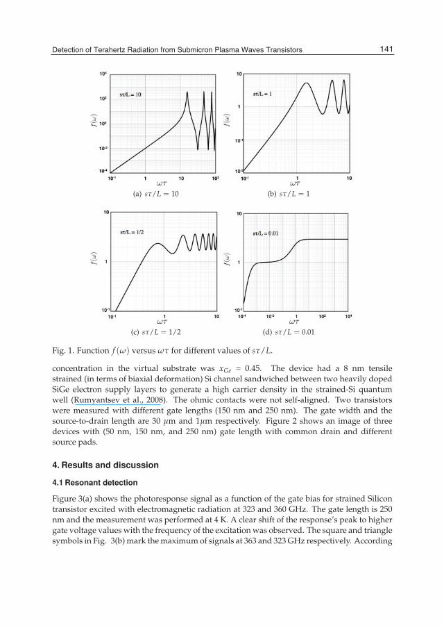
Equations 7 and 8 describe the response of the device as a THz detector for any frequencyand gate length. The function f (ω) depends on two dimensionless parameters: ωτ and sτ/L.Figure 1 shows f (ω) as a function of ωτ for different values of sτ/L. When ωτ � 1 and forsubmicron devices, such that sτ/L � 1, f (ω) exhibit sharp resonances at the fundamentalfrequency and its odd harmonics (Fig. 1(a) and (b)). In this case the damping of the plasmawaves excited by incoming radiation is small and the device exhibits a resonance detectionmode. However, when ωτ � 1, the plasma oscillations are overdamped. For a long device,the oscillations excited at the source by the incoming radiation do not reach the drain becauseof the damping. The boundary conditions at the drain are irrelevant in this case, and theresponse does not depend on L. As it can be seen in Fig. 1(c) and (d), f (ω) changes from f = 1for ωτ � 1 to f = 3 for ωτ � 1, where we also see how at very small values of ωτ thecondition of a long sample is violated and f tends to zero. In both cases, a long channel actsas a broadband detector of electromagnetic radiation. Underdamped ωτ � 1 or overdampedωτ � 1 plasma waves decay near the source end of the channel, leading to a dc voltageinduced between drain and source.
3. Devices description
The epistructure of the MODFET was grown by molecular beam epitaxy (MBE) ona thick relaxed SiGe virtual substrate grown by low-energy plasma-enhanced chemicalvapor deposition (LEPECVD) over a p-doped conventional Si wafer. The final Ge molar
140 Bolometers
Detection of Terahertz Radiation from
Submicron Plasma Waves Transistors 5
(a) sτ/L = 10 (b) sτ/L = 1
(c) sτ/L = 1/2 (d) sτ/L = 0.01
Fig. 1. Function f (ω) versus ωτ for different values of sτ/L.
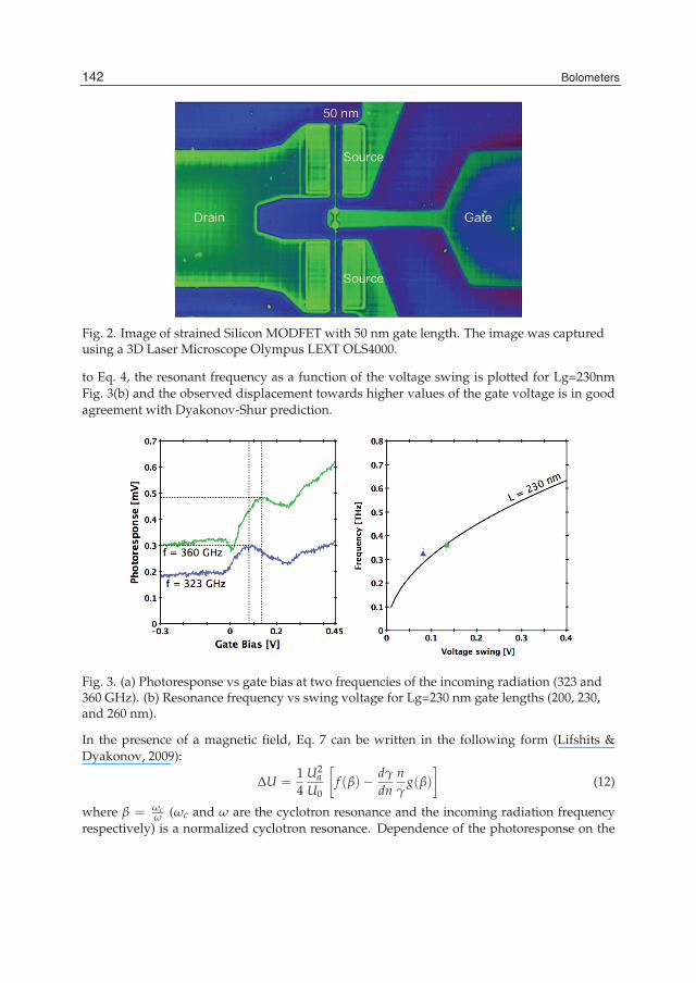
concentration in the virtual substrate was xGe = 0.45. The device had a 8 nm tensilestrained (in terms of biaxial deformation) Si channel sandwiched between two heavily dopedSiGe electron supply layers to generate a high carrier density in the strained-Si quantumwell (Rumyantsev et al., 2008). The ohmic contacts were not self-aligned. Two transistorswere measured with different gate lengths (150 nm and 250 nm). The gate width and thesource-to-drain length are 30 μm and 1μm respectively. Figure 2 shows an image of threedevices with (50 nm, 150 nm, and 250 nm) gate length with common drain and differentsource pads.
4. Results and discussion
4.1 Resonant detection
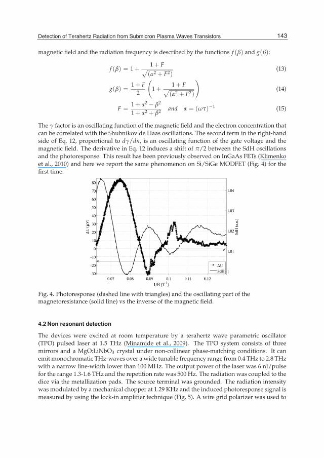
Figure 3(a) shows the photoresponse signal as a function of the gate bias for strained Silicontransistor excited with electromagnetic radiation at 323 and 360 GHz. The gate length is 250nm and the measurement was performed at 4 K. A clear shift of the response’s peak to highergate voltage values with the frequency of the excitation was observed. The square and trianglesymbols in Fig. 3(b) mark the maximum of signals at 363 and 323 GHz respectively. According
141Detection of Terahertz Radiation from Submicron Plasma Waves Transistors
6 Will-be-set-by-IN-TECH
Fig. 2. Image of strained Silicon MODFET with 50 nm gate length. The image was capturedusing a 3D Laser Microscope Olympus LEXT OLS4000.
to Eq. 4, the resonant frequency as a function of the voltage swing is plotted for Lg=230nmFig. 3(b) and the observed displacement towards higher values of the gate voltage is in goodagreement with Dyakonov-Shur prediction.
Fig. 3. (a) Photoresponse vs gate bias at two frequencies of the incoming radiation (323 and360 GHz). (b) Resonance frequency vs swing voltage for Lg=230 nm gate lengths (200, 230,and 260 nm).
In the presence of a magnetic field, Eq. 7 can be written in the following form (Lifshits &Dyakonov, 2009):
ΔU =14U2
aU0
[f (β)− dγ
dnnγ
g(β)
](12)
where β = ωcω (ωc and ω are the cyclotron resonance and the incoming radiation frequency
respectively) is a normalized cyclotron resonance. Dependence of the photoresponse on the
142 Bolometers
Detection of Terahertz Radiation from
Submicron Plasma Waves Transistors 7
magnetic field and the radiation frequency is described by the functions f (β) and g(β):
f (β) = 1 +1 + F√(α2 + F2)
(13)
g(β) =1 + F
2
(1 +
1 + F√(α2 + F2)
)(14)
F =1 + α2 − β2
1 + α2 + β2 and α = (ωτ)−1 (15)
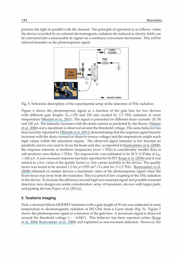
The γ factor is an oscillating function of the magnetic field and the electron concentration thatcan be correlated with the Shubnikov de Haas oscillations. The second term in the right-handside of Eq. 12, proportional to dγ/dn, is an oscillating function of the gate voltage and themagnetic field. The derivative in Eq. 12 induces a shift of π/2 between the SdH oscillationsand the photoresponse. This result has been previously observed on InGaAs FETs (Klimenkoet al., 2010) and here we report the same phenomenon on Si/SiGe MODFET (Fig. 4) for thefirst time.
Fig. 4. Photoresponse (dashed line with triangles) and the oscillating part of themagnetoresistance (solid line) vs the inverse of the magnetic field.
4.2 Non resonant detection
The devices were excited at room temperature by a terahertz wave parametric oscillator(TPO) pulsed laser at 1.5 THz (Minamide et al., 2009). The TPO system consists of threemirrors and a MgO:LiNbO3 crystal under non-collinear phase-matching conditions. It canemit monochromatic THz-waves over a wide tunable frequency range from 0.4 THz to 2.8 THzwith a narrow line-width lower than 100 MHz. The output power of the laser was 6 nJ/pulsefor the range 1.3-1.6 THz and the repetition rate was 500 Hz. The radiation was coupled to thedice via the metallization pads. The source terminal was grounded. The radiation intensitywas modulated by a mechanical chopper at 1.29 KHz and the induced photoresponse signal ismeasured by using the lock-in amplifier technique (Fig. 5). A wire grid polarizer was used to
143Detection of Terahertz Radiation from Submicron Plasma Waves Transistors
8 Will-be-set-by-IN-TECH
polarize the light in parallel with the channel. The principle of operation is as follows: whenthe device is excited by an external electromagnetic radiation the induced ac electric fields canbe converted into a measurable dc signal via a nonlinear conversion mechanism. This will bereferred hereafter as the photoresponse signal.
Fig. 5. Schematic description of the experimental setup of the detection of THz radiation.
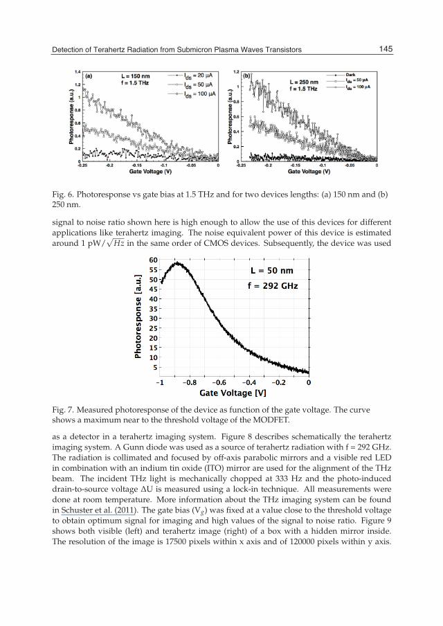
Figure 6 shows the photoresponse signal as a function of the gate bias for two deviceswith different gate lengths (LG=150 and 250 nm) excited by 1.5 THz radiation at roomtemperature (Meziani et al., 2011). The signal is presented for different drain currents: 20, 50and 100 μA. The intensity increases with the drain current as predicted by the theory (Veksleret al., 2006) and a maximum is observed around the threshold voltage. The same behavior hasbeen recently reported by Elkhatib et al. (2011) demonstrating that the response signal linearlyincreases with the drain current (or drain-to-source voltage) and the responsivity might reachhigh values within the saturation regime. The observed signal intensity is low because noparabolic mirror was used to focus the beam and also, as reported in Rumyantsev et al. (2008),the response intensity at terahertz frequencies (over 1 THz) is considerably smaller than atsub-terahertz ones (below 1 THz). The responsivity was estimated to be 20 V/J/Pulse at IDS= 100 μA. A non-resonant response has been reported for Si-FET Knap et al. (2004) and it wasrelated to a low value of the quality factor i.e. low carrier mobility in the device. The qualityfactor was found to be around 1.2 for μ=1355 cm2/V.s and for f=1.5 THz. Rumyantsev et al.(2008) obtained on similar devices a maximum value of the photoresponse signal when thebeam focus was away from the transistor. This is a proof of low coupling of the THz radiationto the device. To increase the efficiency toward high non-resonant signal and possible resonantdetection, new designs are under consideration: array of transistors, devices with larger pads,and grating devices Popov et al. (2011a).
5. Terahertz imaging
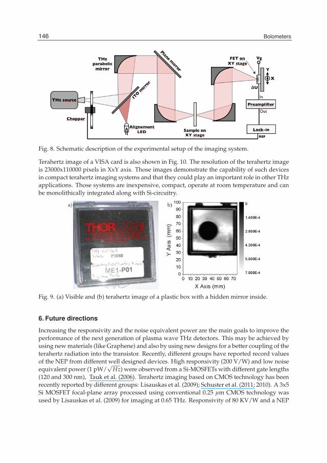
First, a strained Silicon MODFET transistor with a gate length of 50 nm was subjected at roomtemperature to electromagnetic radiation at 292 GHz from a Gunn diode (Fig. 5). Figure 7shows the photoresponse signal as a function of the gate bias. A maximum signal is observedaround the threshold voltage (∼ −0.84V). This behavior has been reported earlier (Knapet al., 2004; Rumyantsev et al., 2008) and explained as non-resonant detection. However, the
144 Bolometers
Detection of Terahertz Radiation from
Submicron Plasma Waves Transistors 9
Fig. 6. Photoresponse vs gate bias at 1.5 THz and for two devices lengths: (a) 150 nm and (b)250 nm.
signal to noise ratio shown here is high enough to allow the use of this devices for differentapplications like terahertz imaging. The noise equivalent power of this device is estimatedaround 1 pW/
√Hz in the same order of CMOS devices. Subsequently, the device was used
Fig. 7. Measured photoresponse of the device as function of the gate voltage. The curveshows a maximum near to the threshold voltage of the MODFET.
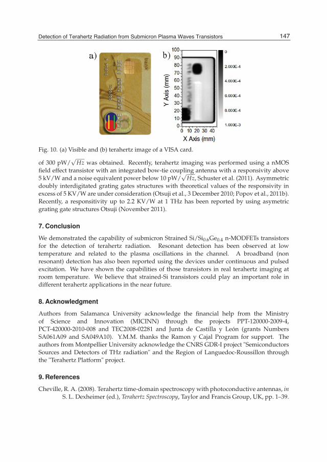
as a detector in a terahertz imaging system. Figure 8 describes schematically the terahertzimaging system. A Gunn diode was used as a source of terahertz radiation with f = 292 GHz.The radiation is collimated and focused by off-axis parabolic mirrors and a visible red LEDin combination with an indium tin oxide (ITO) mirror are used for the alignment of the THzbeam. The incident THz light is mechanically chopped at 333 Hz and the photo-induceddrain-to-source voltage ΔU is measured using a lock-in technique. All measurements weredone at room temperature. More information about the THz imaging system can be foundin Schuster et al. (2011). The gate bias (Vg) was fixed at a value close to the threshold voltageto obtain optimum signal for imaging and high values of the signal to noise ratio. Figure 9shows both visible (left) and terahertz image (right) of a box with a hidden mirror inside.The resolution of the image is 17500 pixels within x axis and of 120000 pixels within y axis.
145Detection of Terahertz Radiation from Submicron Plasma Waves Transistors
10 Will-be-set-by-IN-TECH
Fig. 8. Schematic description of the experimental setup of the imaging system.
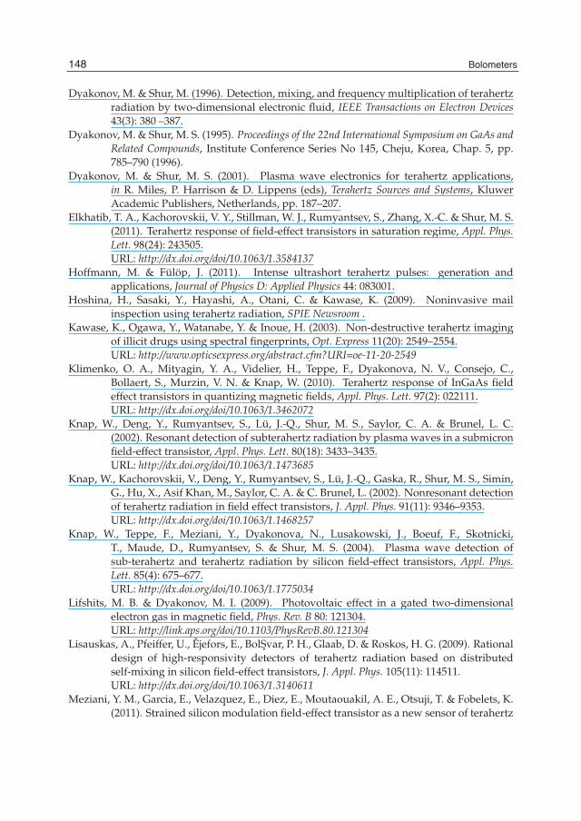
Terahertz image of a VISA card is also shown in Fig. 10. The resolution of the terahertz imageis 23000x110000 pixels in XxY axis. Those images demonstrate the capability of such devicesin compact terahertz imaging systems and that they could play an important role in other THzapplications. Those systems are inexpensive, compact, operate at room temperature and canbe monolithically integrated along with Si-circuitry.
Fig. 9. (a) Visible and (b) terahertz image of a plastic box with a hidden mirror inside.
6. Future directions
Increasing the responsivity and the noise equivalent power are the main goals to improve theperformance of the next generation of plasma wave THz detectors. This may be achieved byusing new materials (like Graphene) and also by using new designs for a better coupling of theterahertz radiation into the transistor. Recently, different groups have reported record valuesof the NEP from different well designed devices. High responsivity (200 V/W) and low noiseequivalent power (1 pW/
√Hz) were observed from a Si-MOSFETs with different gate lengths
(120 and 300 nm), Tauk et al. (2006). Terahertz imaging based on CMOS technology has beenrecently reported by different groups: Lisauskas et al. (2009); Schuster et al. (2011; 2010). A 3x5Si MOSFET focal-plane array processed using conventional 0.25 μm CMOS technology wasused by Lisauskas et al. (2009) for imaging at 0.65 THz. Responsivity of 80 KV/W and a NEP
146 Bolometers
Detection of Terahertz Radiation from
Submicron Plasma Waves Transistors 11
Fig. 10. (a) Visible and (b) terahertz image of a VISA card.
of 300 pW/√
Hz was obtained. Recently, terahertz imaging was performed using a nMOSfield effect transistor with an integrated bow-tie coupling antenna with a responsivity above5 kV/W and a noise equivalent power below 10 pW/
√Hz, Schuster et al. (2011). Asymmetric
doubly interdigitated grating gates structures with theoretical values of the responsivity inexcess of 5 KV/W are under consideration (Otsuji et al., 3 December 2010; Popov et al., 2011b).Recently, a responsitivity up to 2.2 KV/W at 1 THz has been reported by using asymetricgrating gate structures Otsuji (November 2011).
7. Conclusion
We demonstrated the capability of submicron Strained Si/Si0.6Ge0.4 n-MODFETs transistorsfor the detection of terahertz radiation. Resonant detection has been observed at lowtemperature and related to the plasma oscillations in the channel. A broadband (nonresonant) detection has also been reported using the devices under continuous and pulsedexcitation. We have shown the capabilities of those transistors in real terahertz imaging atroom temperature. We believe that strained-Si transistors could play an important role indifferent terahertz applications in the near future.
8. Acknowledgment
Authors from Salamanca University acknowledge the financial help from the Ministryof Science and Innovation (MICINN) through the projects PPT-120000-2009-4,PCT-420000-2010-008 and TEC2008-02281 and Junta de Castilla y León (grants NumbersSA061A09 and SA049A10). Y.M.M. thanks the Ramon y Cajal Program for support. Theauthors from Montpellier University acknowledge the CNRS GDR-I project "SemiconductorsSources and Detectors of THz radiation" and the Region of Languedoc-Roussillon throughthe "Terahertz Platform" project.
9. References
Cheville, R. A. (2008). Terahertz time-domain spectroscopy with photoconductive antennas, inS. L. Dexheimer (ed.), Terahertz Spectroscopy, Taylor and Francis Group, UK, pp. 1–39.
147Detection of Terahertz Radiation from Submicron Plasma Waves Transistors
12 Will-be-set-by-IN-TECH
Dyakonov, M. & Shur, M. (1996). Detection, mixing, and frequency multiplication of terahertzradiation by two-dimensional electronic fluid, IEEE Transactions on Electron Devices43(3): 380 –387.
Dyakonov, M. & Shur, M. S. (1995). Proceedings of the 22nd International Symposium on GaAs andRelated Compounds, Institute Conference Series No 145, Cheju, Korea, Chap. 5, pp.785–790 (1996).
Dyakonov, M. & Shur, M. S. (2001). Plasma wave electronics for terahertz applications,in R. Miles, P. Harrison & D. Lippens (eds), Terahertz Sources and Systems, KluwerAcademic Publishers, Netherlands, pp. 187–207.
Elkhatib, T. A., Kachorovskii, V. Y., Stillman, W. J., Rumyantsev, S., Zhang, X.-C. & Shur, M. S.(2011). Terahertz response of field-effect transistors in saturation regime, Appl. Phys.Lett. 98(24): 243505.URL: http://dx.doi.org/doi/10.1063/1.3584137
Hoffmann, M. & Fülöp, J. (2011). Intense ultrashort terahertz pulses: generation andapplications, Journal of Physics D: Applied Physics 44: 083001.
Hoshina, H., Sasaki, Y., Hayashi, A., Otani, C. & Kawase, K. (2009). Noninvasive mailinspection using terahertz radiation, SPIE Newsroom .
Kawase, K., Ogawa, Y., Watanabe, Y. & Inoue, H. (2003). Non-destructive terahertz imagingof illicit drugs using spectral fingerprints, Opt. Express 11(20): 2549–2554.URL: http://www.opticsexpress.org/abstract.cfm?URI=oe-11-20-2549
Klimenko, O. A., Mityagin, Y. A., Videlier, H., Teppe, F., Dyakonova, N. V., Consejo, C.,Bollaert, S., Murzin, V. N. & Knap, W. (2010). Terahertz response of InGaAs fieldeffect transistors in quantizing magnetic fields, Appl. Phys. Lett. 97(2): 022111.URL: http://dx.doi.org/doi/10.1063/1.3462072
Knap, W., Deng, Y., Rumyantsev, S., Lü, J.-Q., Shur, M. S., Saylor, C. A. & Brunel, L. C.(2002). Resonant detection of subterahertz radiation by plasma waves in a submicronfield-effect transistor, Appl. Phys. Lett. 80(18): 3433–3435.URL: http://dx.doi.org/doi/10.1063/1.1473685
Knap, W., Kachorovskii, V., Deng, Y., Rumyantsev, S., Lü, J.-Q., Gaska, R., Shur, M. S., Simin,G., Hu, X., Asif Khan, M., Saylor, C. A. & C. Brunel, L. (2002). Nonresonant detectionof terahertz radiation in field effect transistors, J. Appl. Phys. 91(11): 9346–9353.URL: http://dx.doi.org/doi/10.1063/1.1468257
Knap, W., Teppe, F., Meziani, Y., Dyakonova, N., Lusakowski, J., Boeuf, F., Skotnicki,T., Maude, D., Rumyantsev, S. & Shur, M. S. (2004). Plasma wave detection ofsub-terahertz and terahertz radiation by silicon field-effect transistors, Appl. Phys.Lett. 85(4): 675–677.URL: http://dx.doi.org/doi/10.1063/1.1775034
Lifshits, M. B. & Dyakonov, M. I. (2009). Photovoltaic effect in a gated two-dimensionalelectron gas in magnetic field, Phys. Rev. B 80: 121304.URL: http://link.aps.org/doi/10.1103/PhysRevB.80.121304
Lisauskas, A., Pfeiffer, U., Ejefors, E., BolSvar, P. H., Glaab, D. & Roskos, H. G. (2009). Rationaldesign of high-responsivity detectors of terahertz radiation based on distributedself-mixing in silicon field-effect transistors, J. Appl. Phys. 105(11): 114511.URL: http://dx.doi.org/doi/10.1063/1.3140611
Meziani, Y. M., Garcia, E., Velazquez, E., Diez, E., Moutaouakil, A. E., Otsuji, T. & Fobelets, K.(2011). Strained silicon modulation field-effect transistor as a new sensor of terahertz
148 Bolometers
Detection of Terahertz Radiation from
Submicron Plasma Waves Transistors 13
radiation, Semiconductor Science and Technology 26(10): 105006.URL: http://stacks.iop.org/0268-1242/26/i=10/a=105006
Meziani, Y. M., Lusakowski, J., Dyakonova, N., Knap, W., Seliuta, D., Sirmulis, E., Devenson,J., Valusis, G., Boeuf, F. & Skotnicki, T. (2006). Non resonant response to terahertzradiation by submicron CMOS transistors, IEICE TRANSACTIONS on ElectronicsE89-C: 993–998.
Minamide, H., Ikari, T. & Ito, H. (2009). Frequency-agile terahertz-wave parametric oscillatorin a ring-cavity configuration, Rev. Sci. Instrum. 80(12): 123104.URL: http://dx.doi.org/doi/10.1063/1.3271039
Öjefors, E., Lisauskas, A., Glaab, D., Roskos, H. & Pfeiffer, U. (2009). Terahertz imagingdetectors in CMOS technology, Journal of Infrared, Millimeter and Terahertz Waves30: 1269–1280. 10.1007/s10762-009-9569-4.URL: http://dx.doi.org/10.1007/s10762-009-9569-4
Otsuji, T., Popov, V., Knap, W., Meziani, Y., Dyakonova, N., D. Coquillat, F. T., Fateev,D. & Perez, J. E. V. (3 December 2010). Terahertz apparatus, Japanese PatentPCT/JP2010/007074 .
Otsuji, T. (2011). Emission and detection of terahertz radiation using two-dimensionalelectrons in III-V semiconductors and Graphene, Proceedings of the joint conferencefor International Symposium on Terahertz Nanoscience (Teranano2011) andWokshop of International Terahertz Research Network (GDR-I THz 2011), OsakaUniversity Nakanoshima Center, Osaka, Japan, pp. 133-136.
Popov, V., Fateev, D., Otsuji, T., Meziani, Y., Coquillat, D. & Knap, W. (2011a). Plasmonicdetection of terahertz radiation in a double-grating-gate transistor structure withan asymmetric unit cell, Proceedings of XV International Symposium "Nanophysicsand Nanoelectronics", Vol. 1, Institute Conference Series No 145, Nizhnii Novgorod,Russia, pp. 121–122.
Popov, V., Fateev, D., Otsuji, T., Meziani, Y., Coquillat, D. & Knap, W. (2011b). Plasmonicterahertz detection by a double-grating-gate field-effect transistor structure with anasymmetric unit cell, Submitted to Appl. Phys. Lett.URL: http://arxiv.org/abs/1111.1807
Rumyantsev, S. L., Fobelets, K., Veksler, D., Hackbarth, T. & Shur, M. S. (2008). Strained-simodulation doped field effect transistors as detectors of terahertz and sub-terahertzradiation, Semiconductor Science and Technology 23(10): 105001.URL: http://stacks.iop.org/0268-1242/23/i=10/a=105001
Schuster, F., Coquillat, D., Videlier, H., Sakowicz, M., Teppe, F., Dussopt, L., Giffard, B.,Skotnicki, T. & Knap, W. (2011). Broadband terahertz imaging with highly sensitivesilicon CMOS detectors, Opt. Express 19(8): 7827–7832.URL: http://www.opticsexpress.org/abstract.cfm?URI=oe-19-8-7827
Schuster, F., Sakowicz, M., Siligaris, A., Dussopt, L., Videlier, H., Coquillat, D., Teppe, F.,Giffard, B., Dobroiu, A., Skotnicki, T. & Knap, W. (2010). THz imaging with low-cost130 nm CMOS transistors, Proc. SPIE 7837(1): 783704.URL: http://dx.doi.org/doi/10.1117/12.864877
Siegel, P. (2002). Terahertz technology, IEEE Transactions on Microwave Theory and Techniques,50(3): 910–928.
Smith, P., Auston, D. & Nuss, M. (1988). Subpicosecond photoconducting dipole antennas,IEEE Journal of Quantum Electronics 24(2): 255–260.
149Detection of Terahertz Radiation from Submicron Plasma Waves Transistors
14 Will-be-set-by-IN-TECH
Tauk, R., Teppe, F., Boubanga, S., Coquillat, D., Knap, W., Meziani, Y. M., Gallon, C., Boeuf,F., Skotnicki, T., Fenouillet-Beranger, C., Maude, D. K., Rumyantsev, S. & Shur,M. S. (2006). Plasma wave detection of terahertz radiation by silicon field effectstransistors: Responsivity and noise equivalent power, Appl. Phys. Lett. 89(25): 253511.URL: http://dx.doi.org/doi/10.1063/1.2410215
Tonouchi, M. (2007). Cutting-edge terahertz technology, Nature Photonics 1: 97–105.Veksler, D., Teppe, F., Dmitriev, A. P., Kachorovskii, V. Y., Knap, W. & Shur, M. S. (2006).
Detection of terahertz radiation in gated two-dimensional structures governed by dccurrent, Phys. Rev. B 73: 125328.URL: http://link.aps.org/doi/10.1103/PhysRevB.73.125328
150 Bolometers
Related Documents