Desktop 4th Generation Intel ® Core ™ Processor Family, Desktop Intel ® Pentium ® Processor Family, and Desktop Intel ® Celeron ® Processor Family Datasheet – Volume 1 of 2 March 2015 Order No.: 328897-010

Welcome message from author
This document is posted to help you gain knowledge. Please leave a comment to let me know what you think about it! Share it to your friends and learn new things together.
Transcript

Desktop 4th Generation Intel® Core™
Processor Family, Desktop Intel®Pentium® Processor Family, andDesktop Intel® Celeron® ProcessorFamilyDatasheet – Volume 1 of 2
March 2015
Order No.: 328897-010

You may not use or facilitate the use of this document in connection with any infringement or other legal analysis concerning Intel products describedherein. You agree to grant Intel a non-exclusive, royalty-free license to any patent claim thereafter drafted which includes subject matter disclosedherein.
No license (express or implied, by estoppel or otherwise) to any intellectual property rights is granted by this document.
All information provided here is subject to change without notice. Contact your Intel representative to obtain the latest Intel product specifications androadmaps.
The products described may contain design defects or errors known as errata which may cause the product to deviate from published specifications.Current characterized errata are available on request.
Copies of documents which have an order number and are referenced in this document may be obtained by calling 1-800-548-4725 or visit http://www.intel.com/design/literature.htm.
Intel technologies’ features and benefits depend on system configuration and may require enabled hardware, software or service activation. Learnmore at http://www.intel.com/ or from the OEM or retailer.
No computer system can be absolutely secure.
Intel® Hyper-Threading Technology (Intel® HT Technology) is available on select Intel® Core™ processors. It requires an Intel® HT Technology enabledsystem. Consult your PC manufacturer. Performance will vary depending on the specific hardware and software used. Not available on Intel® Core™
i5-750. For more information including details on which processors support Intel® HT Technology, visit http://www.intel.com/info/hyperthreading.
Intel® High Definition Audio (Intel® HD Audio) requires an Intel® HD Audio enabled system. Consult your PC manufacturer for more information.Sound quality will depend on equipment and actual implementation. For more information about Intel® HD Audio, refer to http://www.intel.com/design/chipsets/hdaudio.htm.
Intel® 64 architecture requires a system with a 64-bit enabled processor, chipset, BIOS and software. Performance will vary depending on the specifichardware and software you use. Consult your PC manufacturer for more information. For more information, visit http://www.intel.com/content/www/us/en/architecture-and-technology/microarchitecture/intel-64-architecture-general.html.
Intel® Virtualization Technology (Intel® VT) requires a computer system with an enabled Intel® processor, BIOS, and virtual machine monitor (VMM).Functionality, performance or other benefits will vary depending on hardware and software configurations. Software applications may not becompatible with all operating systems. Consult your PC manufacturer. For more information, visit http://www.intel.com/go/virtualization.
The original equipment manufacturer must provide TPM functionality, which requires a TPM-supported BIOS. TPM functionality must be initialized andmay not be available in all countries.
For Enhanced Intel SpeedStep® Technology, see the Processor Spec Finder at http://ark.intel.com/ or contact your Intel representative for moreinformation.
Intel® AES-NI requires a computer system with an AES-NI enabled processor, as well as non-Intel software to execute the instructions in the correctsequence. AES-NI is available on select Intel® processors. For availability, consult your reseller or system manufacturer. For more information, see http://software.intel.com/en-us/articles/intel-advanced-encryption-standard-instructions-aes-ni/.
Intel® Active Management Technology (Intel® AMT) should be used by a knowledgeable IT administrator and requires enabled systems, software,activation, and connection to a corporate network. Intel AMT functionality on mobile systems may be limited in some situations. Your results willdepend on your specific implementation. Learn more by visiting Intel® Active Management Technology.
No computer system can provide absolute security under all conditions. Intel® Trusted Execution Technology (Intel® TXT) requires a computer withIntel® Virtualization Technology, an Intel TXT-enabled processor, chipset, BIOS, Authenticated Code Modules and an Intel TXT-compatible measuredlaunched environment (MLE). Intel TXT also requires the system to contain a TPM v1.s. For more information, visit http://www.intel.com/technology/security.
Requires a system with Intel® Turbo Boost Technology. Intel Turbo Boost Technology and Intel Turbo Boost Technology 2.0 are only available on selectIntel® processors. Consult your PC manufacturer. Performance varies depending on hardware, software, and system configuration. For moreinformation, visit https://www-ssl.intel.com/content/www/us/en/architecture-and-technology/turbo-boost/turbo-boost-technology.html.
Intel® Advanced Vector Extensions (Intel® AVX) are designed to achieve higher throughput to certain integer and floating point operations. Due tovarying processor power characteristics, utilizing AVX instructions may cause a) some parts to operate at less than the rated frequency and b) someparts with Intel® Turbo Boost Technology 2.0 to not achieve any or maximum turbo frequencies. Performance varies depending on hardware, software,and system configuration and you should consult your system manufacturer for more information. Intel® Advanced Vector Extensions refers to Intel®AVX, Intel® AVX2 or Intel® AVX-512. For more information on Intel® Turbo Boost Technology 2.0, visit https://www-ssl.intel.com/content/www/us/en/architecture-and-technology/turbo-boost/turbo-boost-technology.html
Intel, Intel Core, Celeron, Pentium, Intel SpeedStep, and the Intel logo are trademarks of Intel Corporation in the U.S. and/or other countries.
*Other names and brands may be claimed as the property of others.
Copyright © 2013–2015, Intel Corporation. All rights reserved.
Desktop 4th Generation Intel® Core™ Processor Family, Desktop Intel® Pentium® Processor Family, and Desktop Intel® Celeron®
Processor FamilyDatasheet – Volume 1 of 2 March 20152 Order No.: 328897-010
Contents
Revision History..................................................................................................................9
1.0 Introduction................................................................................................................101.1 Supported Technologies.........................................................................................111.2 Interfaces............................................................................................................121.3 Power Management Support...................................................................................121.4 Thermal Management Support................................................................................131.5 Package Support...................................................................................................131.6 Terminology.........................................................................................................131.7 Related Documents............................................................................................... 16
2.0 Interfaces................................................................................................................... 182.1 System Memory Interface...................................................................................... 18
2.1.1 System Memory Technology Supported.......................................................192.1.2 System Memory Timing Support................................................................. 202.1.3 System Memory Organization Modes........................................................... 21
2.2 PCI Express* Interface.......................................................................................... 232.2.1 PCI Express* Support................................................................................232.2.2 PCI Express* Architecture.......................................................................... 242.2.3 PCI Express* Configuration Mechanism........................................................24
2.3 Direct Media Interface (DMI).................................................................................. 262.4 Processor Graphics................................................................................................282.5 Processor Graphics Controller (GT)..........................................................................28
2.5.1 3D and Video Engines for Graphics Processing.............................................. 292.5.2 Multi Graphics Controllers Multi-Monitor Support........................................... 31
2.6 Digital Display Interface (DDI)................................................................................312.7 Intel® Flexible Display Interface (Intel® FDI)............................................................372.8 Platform Environmental Control Interface (PECI)....................................................... 37
2.8.1 PECI Bus Architecture................................................................................37
3.0 Technologies...............................................................................................................393.1 Intel® Virtualization Technology (Intel® VT)............................................................. 393.2 Intel® Trusted Execution Technology (Intel® TXT).....................................................433.3 Intel® Hyper-Threading Technology (Intel® HT Technology)....................................... 443.4 Intel® Turbo Boost Technology 2.0..........................................................................453.5 Intel® Advanced Vector Extensions 2.0 (Intel® AVX2)................................................453.6 Intel® Advanced Encryption Standard New Instructions (Intel® AES-NI).......................463.7 Intel® Transactional Synchronization Extensions - New Instructions (Intel® TSX-NI).....463.8 Intel® 64 Architecture x2APIC................................................................................ 473.9 Power Aware Interrupt Routing (PAIR)....................................................................483.10 Execute Disable Bit..............................................................................................483.11 Supervisor Mode Execution Protection (SMEP)........................................................48
4.0 Power Management.................................................................................................... 494.1 Advanced Configuration and Power Interface (ACPI) States Supported......................... 504.2 Processor Core Power Management......................................................................... 51
4.2.1 Enhanced Intel® SpeedStep® Technology Key Features..................................514.2.2 Low-Power Idle States...............................................................................52
Contents—Processor
Desktop 4th Generation Intel® Core™ Processor Family, Desktop Intel® Pentium® Processor Family, and Desktop Intel® Celeron®
Processor FamilyMarch 2015 Datasheet – Volume 1 of 2Order No.: 328897-010 3

4.2.3 Requesting Low-Power Idle States...............................................................534.2.4 Core C-State Rules....................................................................................544.2.5 Package C-States......................................................................................554.2.6 Package C-States and Display Resolutions....................................................59
4.3 Integrated Memory Controller (IMC) Power Management............................................604.3.1 Disabling Unused System Memory Outputs...................................................604.3.2 DRAM Power Management and Initialization..................................................614.3.3 DRAM Running Average Power Limitation (RAPL) .........................................634.3.4 DDR Electrical Power Gating (EPG).............................................................. 63
4.4 PCI Express* Power Management............................................................................634.5 Direct Media Interface (DMI) Power Management...................................................... 634.6 Graphics Power Management..................................................................................64
4.6.1 Intel® Rapid Memory Power Management (Intel® RMPM)................................644.6.2 Graphics Render C-State............................................................................644.6.3 Intel® Graphics Dynamic Frequency............................................................ 64
5.0 Thermal Management................................................................................................. 655.1 Desktop Processor Thermal Profiles......................................................................... 67
5.1.1 Processor (PCG 2013D and PCG 2014) Thermal Profile...................................685.1.2 Processor (PCG 2013C) Thermal Profile........................................................695.1.3 Processor (PCG 2013B) Thermal Profile........................................................705.1.4 Processor (PCG 2013A) Thermal Profile........................................................72
5.2 Thermal Metrology................................................................................................735.3 Fan Speed Control Scheme with Digital Thermal Sensor (DTS) 1.1.............................. 735.4 Fan Speed Control Scheme with Digital Thermal Sensor (DTS) 2.0.............................. 755.5 Thermal Specifications...........................................................................................765.6 Processor Temperature..........................................................................................785.7 Adaptive Thermal Monitor...................................................................................... 785.8 THERMTRIP# Signal.............................................................................................. 815.9 Digital Thermal Sensor.......................................................................................... 81
5.9.1 Digital Thermal Sensor Accuracy (Taccuracy)................................................825.10 Intel® Turbo Boost Technology Thermal Considerations............................................82
5.10.1 Intel® Turbo Boost Technology Power Control and Reporting.........................825.10.2 Package Power Control.............................................................................835.10.3 Turbo Time Parameter............................................................................. 84
6.0 Signal Description.......................................................................................................866.1 System Memory Interface Signals........................................................................... 866.2 Memory Reference Compensation Signals.................................................................886.3 Reset and Miscellaneous Signals............................................................................. 896.4 PCI Express* Interface Signals............................................................................... 906.5 Display Interface Signals....................................................................................... 906.6 Direct Media Interface (DMI).................................................................................. 906.7 Phase Locked Loop (PLL) Signals.............................................................................916.8 Testability Signals.................................................................................................916.9 Error and Thermal Protection Signals.......................................................................926.10 Power Sequencing Signals....................................................................................926.11 Processor Power Signals.......................................................................................936.12 Sense Signals.....................................................................................................936.13 Ground and Non-Critical to Function (NCTF) Signals.................................................936.14 Processor Internal Pull-Up / Pull-Down Terminations................................................ 93
Processor—Contents
Desktop 4th Generation Intel® Core™ Processor Family, Desktop Intel® Pentium® Processor Family, and Desktop Intel® Celeron®
Processor FamilyDatasheet – Volume 1 of 2 March 20154 Order No.: 328897-010

7.0 Electrical Specifications.............................................................................................. 947.1 Integrated Voltage Regulator..................................................................................947.2 Power and Ground Lands ...................................................................................... 947.3 VCC Voltage Identification (VID).............................................................................. 947.4 Reserved or Unused Signals................................................................................... 997.5 Signal Groups.......................................................................................................997.6 Test Access Port (TAP) Connection........................................................................ 1017.7 DC Specifications............................................................................................... 1017.8 Voltage and Current Specifications........................................................................ 102
7.8.1 Platform Environment Control Interface (PECI) DC Characteristics................. 1077.8.2 Input Device Hysteresis........................................................................... 108
8.0 Package Mechanical Specifications........................................................................... 1098.1 Processor Component Keep-Out Zone.................................................................... 1098.2 Package Loading Specifications............................................................................. 1098.3 Package Handling Guidelines................................................................................ 1108.4 Package Insertion Specifications............................................................................1108.5 Processor Mass Specification.................................................................................1108.6 Processor Materials............................................................................................. 1108.7 Processor Markings............................................................................................. 1118.8 Processor Land Coordinates..................................................................................1118.9 Processor Storage Specifications........................................................................... 113
9.0 Processor Ball and Signal Information...................................................................... 115
Contents—Processor
Desktop 4th Generation Intel® Core™ Processor Family, Desktop Intel® Pentium® Processor Family, and Desktop Intel® Celeron®
Processor FamilyMarch 2015 Datasheet – Volume 1 of 2Order No.: 328897-010 5

Figures1 Platform Block Diagram ...........................................................................................112 Intel® Flex Memory Technology Operations.................................................................213 PCI Express* Related Register Structures in the Processor............................................ 254 PCI Express* Typical Operation 16 Lanes Mapping....................................................... 265 Processor Graphics Controller Unit Block Diagram........................................................ 296 Processor Display Architecture...................................................................................327 DisplayPort* Overview............................................................................................. 338 HDMI* Overview..................................................................................................... 349 PECI Host-Clients Connection Example....................................................................... 3810 Device to Domain Mapping Structures........................................................................ 4211 Processor Power States............................................................................................ 4912 Idle Power Management Breakdown of the Processor Cores ..........................................5213 Thread and Core C-State Entry and Exit......................................................................5314 Package C-State Entry and Exit................................................................................. 5715 Thermal Test Vehicle Thermal Profile for Processor (PCG 2013D and PCG 2014)...............6816 Thermal Test Vehicle Thermal Profile for Processor (PCG 2013C)....................................6917 Thermal Test Vehicle Thermal Profile for Processor (PCG 2013B)....................................7018 Thermal Test Vehicle Thermal Profile for Processor (PCG 2013A)....................................7219 Thermal Test Vehicle (TTV) Case Temperature (TCASE) Measurement Location..................7320 Digital Thermal Sensor (DTS) 1.1 Definition Points.......................................................7421 Digital Thermal Sensor (DTS) Thermal Profile Definition................................................7622 Package Power Control.............................................................................................8423 Input Device Hysteresis.......................................................................................... 10824 Processor Package Assembly Sketch.........................................................................10925 Processor Top-Side Markings...................................................................................11126 Processor Package Land Coordinates........................................................................ 11227 2014 Processor Package Land/Pin Side Components................................................... 113
Processor—Figures
Desktop 4th Generation Intel® Core™ Processor Family, Desktop Intel® Pentium® Processor Family, and Desktop Intel® Celeron®
Processor FamilyDatasheet – Volume 1 of 2 March 20156 Order No.: 328897-010

Tables1 Terminology........................................................................................................... 132 Related Documents..................................................................................................163 Processor DIMM Support by Product...........................................................................194 Supported UDIMM Module Configurations....................................................................195 Supported SO-DIMM Module Configurations (AIO Only)................................................ 206 DDR3 / DDR3L System Memory Timing Support...........................................................207 PCI Express* Supported Configurations in Desktop Products..........................................238 Processor Supported Audio Formats over HDMI*and DisplayPort*.................................. 359 Valid Three Display Configurations through the Processor..............................................3610 DisplayPort and embedded DisplayPort* Resolutions for 1, 2, 4 Lanes – Link Data
Rate of RBR, HBR, and HBR2.....................................................................................3611 System States.........................................................................................................5012 Processor Core / Package State Support..................................................................... 5013 Integrated Memory Controller States..........................................................................5014 PCI Express* Link States.......................................................................................... 5015 Direct Media Interface (DMI) States........................................................................... 5116 G, S, and C Interface State Combinations .................................................................. 5117 D, S, and C Interface State Combination.....................................................................5118 Coordination of Thread Power States at the Core Level................................................. 5319 Coordination of Core Power States at the Package Level............................................... 5620 Deepest Package C-State Available............................................................................ 5921 Desktop Processor Thermal Specifications...................................................................6622 Thermal Test Vehicle Thermal Profile for Processor (PCG 2013D and PCG 2014) ..............6823 Thermal Test Vehicle Thermal Profile for Processor (PCG 2013C)....................................6924 Thermal Test Vehicle Thermal Profile for Processor (PCG 2013B)....................................7125 Thermal Test Vehicle Thermal Profile for Processor (PCG 2013A)....................................7226 Digital Thermal Sensor (DTS) 1.1 Thermal Solution Performance Above TCONTROL............. 7527 Thermal Margin Slope.............................................................................................. 7628 Boundary Conditions, Performance Targets, and TCASE Specifications.............................. 7729 Intel® Turbo Boost Technology 2.0 Package Power Control Settings............................... 8430 Signal Description Buffer Types................................................................................. 8631 Memory Channel A Signals........................................................................................8632 Memory Channel B Signals........................................................................................8733 Memory Reference and Compensation Signals............................................................. 8834 Reset and Miscellaneous Signals................................................................................ 8935 PCI Express* Graphics Interface Signals..................................................................... 9036 Display Interface Signals.......................................................................................... 9037 Direct Media Interface (DMI) – Processor to PCH Serial Interface................................... 9038 Phase Locked Loop (PLL) Signals............................................................................... 9139 Testability Signals....................................................................................................9140 Error and Thermal Protection Signals..........................................................................9241 Power Sequencing Signals........................................................................................ 9242 Processor Power Signals........................................................................................... 9343 Sense Signals......................................................................................................... 9344 Ground and Non-Critical to Function (NCTF) Signals..................................................... 9345 Processor Internal Pull-Up / Pull-Down Terminations.................................................... 9346 Voltage Regulator (VR) 12.5 Voltage Identification....................................................... 9547 Signal Groups......................................................................................................... 9948 Processor Core Active and Idle Mode DC Voltage and Current Specifications...................10249 Memory Controller (VDDQ) Supply DC Voltage and Current Specifications....................... 10350 VCCIO_OUT, VCOMP_OUT, and VCCIO_TERM ........................................................... 10451 DDR3 / DDR3L Signal Group DC Specifications...........................................................10452 Digital Display Interface Group DC Specifications....................................................... 10553 embedded DisplayPort* (eDP*) Group DC Specifications............................................. 106
Tables—Processor
Desktop 4th Generation Intel® Core™ Processor Family, Desktop Intel® Pentium® Processor Family, and Desktop Intel® Celeron®
Processor FamilyMarch 2015 Datasheet – Volume 1 of 2Order No.: 328897-010 7

54 CMOS Signal Group DC Specifications.......................................................................10655 GTL Signal Group and Open Drain Signal Group DC Specifications................................ 10656 PCI Express* DC Specifications................................................................................10757 Platform Environment Control Interface (PECI) DC Electrical Limits...............................10758 Processor Loading Specifications.............................................................................. 11059 Package Handling Guidelines................................................................................... 11060 Processor Materials................................................................................................ 11161 Processor Storage Specifications..............................................................................11362 Processor Ball List by Signal Name........................................................................... 115
Processor—Tables
Desktop 4th Generation Intel® Core™ Processor Family, Desktop Intel® Pentium® Processor Family, and Desktop Intel® Celeron®
Processor FamilyDatasheet – Volume 1 of 2 March 20158 Order No.: 328897-010

Revision History
Revision Description Date
001 • Initial Release June 2013
002
• Added Desktop 4th Generation Intel® Core™ i7-4771, i5-4440,i5-4440S, i3-4340, i3-4330, i3-4330T, i3-4130, and i3-4130Tprocessors
• Added Desktop Intel® Pentium® G3430, G3420, G3220,G3420T, G3220T processors
• Updated Section 4.2.4, Core C-State Rules• Updated Section 4.2.5, Package C-States• Minor edits throughout for clarity
September 2013
003 • Minor edits throughout for clarity November 2013
004
• Added Desktop Intel® Celeron® G1830, G1820, and G1820Tprocessors
• Added Section 4.2.6, "Package C-States and DisplayResolutions"
December 2013
005 • Updated Table 39, "Testability Signals" March 2014
006
• Added Desktop 4th Generation Intel® Core™ i7-4790, i7-4790S,i7-4790T, i7-4785T, i5-4690, i5-4690S, i5-4690T, i5-4590,i5-4590S, i5-4590T, i5-4460, i5-4460S, i5-4460T, i3-4360,i3-4350, i3-4350T, i3-4150, i3-4150T processors
• Added Desktop Intel® Pentium® G3450, G3440, G3440T,G3240, G3240T processors
• Added Desktop Intel® Celeron® G1850, G1840, G1840Tprocessors
• Added Section 5.5, Thermal Specifications
May 2014
007• Added Desktop 4th Generation Intel® Core™ i7-4790K, i5 4690K
processors• Added Desktop Intel® Pentium® G3258 processor
June 2014
008
• Added Desktop 4th Generation Intel® Core™ i3-4370, i5i3-4360T, i3-4160, i3-4160T processors
• Added Desktop Intel® Pentium® G3460, G3450T, G3250,G3250T processor
• Added PCG 2014• Updated Table 21, Desktop Processor Thermal Specifications• Updaed Table 26, Digital Thermal Sensor (DTS) 1.1 Thermal
Solution Performance Above TCONTROL
• Updated Table 27, Thermal Margin Slope.• Updated Table 28, Boundary Conditions, Performance Tagets,
and TCASE Specifications.• Updaed Table 48, Processor Core Active and Idle Mode DC
Voltage and Current Specifications.
July 2014
009 • Added Figure 27, 2014 Processor Package Land/Pin SideComponents. July 2014
010
• Added Desktop 4th Generation Intel® Core™ i3-4370T, i3-4170,i3-4170T processors
• Added Desktop Intel® Pentium® G3470, G3460T, G3260,G3260T processor
March 2015
Revision History—Processor
Desktop 4th Generation Intel® Core™ Processor Family, Desktop Intel® Pentium® Processor Family, and Desktop Intel® Celeron®
Processor FamilyMarch 2015 Datasheet – Volume 1 of 2Order No.: 328897-010 9
1.0 Introduction
The Desktop 4th Generation Intel® Core™ processor family , Desktop Intel® Pentium®
processor family, and Desktop Intel® Celeron® processor family are 64-bit, multi-coreprocessors built on 22-nanometer process technology.
The processors are designed for a two-chip platform consisting of a processor andPlatform Controller Hub (PCH). The processors are designed to be used with the Intel®8 Series chipset. See the following figure for an example platform block diagram.
Throughout this document, the Desktop 4th Generation Intel® Core™ processor family,Desktop Intel® Pentium® processor family, and Desktop Intel® Celeron® processorfamily may be referred to simply as "processor".
Throughout this document, the Desktop 4th Generation Intel® Core™ processor familyrefers to the Desktop 4th Generation Intel® Core™ i7-4790, i7-4790S, i7-4790T,i7-4790K, i7-4785T, i7-4771, i7-4770R, i7-4770K, i7-4770, i7-4770S, i7-4770T,i7-4765T, i5-4690, i5-4690S, i5-4690T, i5-4690K, i5-4670R, i5-4670K, i5-4670,i5-4670S, i5-4670T, i5-4670R, i5-4590, i5-4590S, i5-4590T, i5-4570R, i5-4570S,i5-4570T, i5-4570, i5-4460, i5-4460S, i5-4460T, i5-4440, i5-4440S, i5-4430,i5-4430S, i3-4370, i3-4370T, i3-4360, i3-4360T, i3-4350, i3-4350T, i3-4340, i3-4330,i3-4330T, i3-4170, i3-4170T, i3-4150, i3-4160, i3-4160T, i3-4150T, i3-4130, andi3-4130T processors.
Throughout this document, the Desktop Intel® Pentium® processor family refers tothe Intel® Pentium® G3470, G3460, G3460T, G3450, G3450T, G3440, G3440T,G3430, G3420, G3420T, G3258, G3260, G3260T, G3250, G3250T, G3240, G3240T,G3220, and G3220T processors.
Throughout this document, the Desktop Intel® Celeron® processor family refers to theIntel® Celeron® G1850, G1840, G1840T, G1830, G1820, and G1820T processors.
Note: Some processor features are not available on all platforms. Refer to the processorSpecification Update document for details.
Processor—Introduction
Desktop 4th Generation Intel® Core™ Processor Family, Desktop Intel® Pentium® Processor Family, and Desktop Intel® Celeron®
Processor FamilyDatasheet – Volume 1 of 2 March 201510 Order No.: 328897-010

Figure 1. Platform Block Diagram
Processor
PCI Express* 3.0
Digital Display
Interface (DDI)
(3 interfaces)
System Memory
2 DIMMs / CH
CH A
CH B
Intel® Flexible Display
Interface (Intel® FDI)
(x2)
Direct Media Interface 2.0
(DMI 2.0) (x4)
Platform Controller
Hub (PCH)SATA, 6 GB/s
(up to 6 Ports)
Analog Display
(VGA)
SPI Flash
Super IO / EC
Trusted Platform
Module (TPM) 1.2
LPC
Intel® High
Definition Audio
(Intel® HD Audio)
Integrated LAN
USB 3.0
(up to 6 Ports)
USB 2.0
(8 Ports)
PCI Express* 2.0
(up to 8 Ports)
SPI
SMBus 2.0
GPIOs
Supported Technologies
• Intel® Virtualization Technology (Intel® VT)
• Intel® Active Management Technology 9.5 (Intel® AMT 9.5 )
• Intel® Trusted Execution Technology (Intel® TXT)
• Intel® Streaming SIMD Extensions 4.2 (Intel® SSE4.2)
• Intel® Hyper-Threading Technology (Intel® HT Technology)
• Intel® 64 Architecture
• Execute Disable Bit
• Intel® Turbo Boost Technology 2.0
1.1
Introduction—Processor
Desktop 4th Generation Intel® Core™ Processor Family, Desktop Intel® Pentium® Processor Family, and Desktop Intel® Celeron®
Processor FamilyMarch 2015 Datasheet – Volume 1 of 2Order No.: 328897-010 11

• Intel® Advanced Vector Extensions 2.0 (Intel® AVX2)
• Intel® Advanced Encryption Standard New Instructions (Intel® AES-NI)
• PCLMULQDQ Instruction
• Intel® Secure Key
• Intel® Transactional Synchronization Extensions - New Instructions (Intel® TSX-NI)
• PAIR – Power Aware Interrupt Routing
• SMEP – Supervisor Mode Execution Protection
• Enhanced Intel® Speedstep® Technology
Note: The availability of the features may vary between processor SKUs.
Interfaces
The processor supports the following interfaces:
• DDR3/DDR3L
• Direct Media Interface (DMI)
• Digital Display Interface (DDI)
• PCI Express*
Power Management Support
Processor Core
• Full support of ACPI C-states as implemented by the following processor C-states:
— C0, C1, C1E, C3, C6, C7
• Enhanced Intel SpeedStep® Technology
System
• S0, S3, S4, S5
Memory Controller
• Conditional self-refresh
• Dynamic power-down
PCI Express*
• L0s and L1 ASPM power management capability
DMI
• L0s and L1 ASPM power management capability
Processor Graphics Controller
• Intel® Rapid Memory Power Management (Intel® RMPM)
• Intel® Smart 2D Display Technology (Intel® S2DDT)
• Graphics Render C-state (RC6)
1.2
1.3
Processor—Introduction
Desktop 4th Generation Intel® Core™ Processor Family, Desktop Intel® Pentium® Processor Family, and Desktop Intel® Celeron®
Processor FamilyDatasheet – Volume 1 of 2 March 201512 Order No.: 328897-010

• Intel® Seamless Display Refresh Rate Switching with eDP port
• Intel® Display Power Saving Technology (Intel® DPST)
Thermal Management Support
• Digital Thermal Sensor
• Adaptive Thermal Monitor
• THERMTRIP# and PROCHOT# support
• On-Demand Mode
• Memory Open and Closed Loop Throttling
• Memory Thermal Throttling
• External Thermal Sensor (TS-on-DIMM and TS-on-Board)
• Render Thermal Throttling
• Fan speed control with DTS
Package Support
The processor socket type is noted as LGA1150. The package is a 37.5 x 37.5 mm FlipChip Land Grid Array (FCLGA 1150). See the appropriate Processor ThermalMechanical Design Guidelines and LGA1150 Socket Application Guide for completedetails on the package.
Terminology
Table 1. Terminology
Term Description
APD Active Power-down
B/D/F Bus/Device/Function
BGA Ball Grid Array
BLC Backlight Compensation
BLT Block Level Transfer
BPP Bits per pixel
CKE Clock Enable
CLTM Closed Loop Thermal Management
DDI Digital Display Interface
DDR3 Third-generation Double Data Rate SDRAM memory technology
DLL Delay-Locked Loop
DMA Direct Memory Access
DMI Direct Media Interface
DP DisplayPort*
DTS Digital Thermal Sensor
continued...
1.4
1.5
1.6
Introduction—Processor
Desktop 4th Generation Intel® Core™ Processor Family, Desktop Intel® Pentium® Processor Family, and Desktop Intel® Celeron®
Processor FamilyMarch 2015 Datasheet – Volume 1 of 2Order No.: 328897-010 13

Term Description
DVI* Digital Visual Interface. DVI* is the interface specified by the DDWG (Digital DisplayWorking Group)
EC Embedded Controller
ECC Error Correction Code
eDP* embedded DisplayPort*
EPG Electrical Power Gating
EU Execution Unit
FMA Floating-point fused Multiply Add instructions
FSC Fan Speed Control
HDCP High-bandwidth Digital Content Protection
HDMI* High Definition Multimedia Interface
HFM High Frequency Mode
iDCT Inverse Discrete Cosine Transform
IHS Integrated Heat Spreader
GFX Graphics
GSA Graphics in System Agent
GUI Graphical User Interface
IMC Integrated Memory Controller
Intel® 64Technology
64-bit memory extensions to the IA-32 architecture
Intel® DPST Intel Display Power Saving Technology
Intel® FDI Intel Flexible Display Interface
Intel® TSX-NI Intel Transactional Synchronization Extensions - New Instructions
Intel® TXT Intel Trusted Execution Technology
Intel® VTIntel Virtualization Technology. Processor virtualization, when used in conjunctionwith Virtual Machine Monitor software, enables multiple, robust independent softwareenvironments inside a single platform.
Intel® VT-d
Intel Virtualization Technology (Intel VT) for Directed I/O. Intel VT-d is a hardwareassist, under system software (Virtual Machine Manager or OS) control, for enablingI/O device virtualization. Intel VT-d also brings robust security by providing protectionfrom errant DMAs by using DMA remapping, a key feature of Intel VT-d.
IOV I/O Virtualization
ISI Inter-Symbol Interference
ITPM Integrated Trusted Platform Module
LCD Liquid Crystal Display
LFM Low Frequency Mode. LFM is Pn in the P-state table. It can be read at MSR CEh[47:40].
LFP Local Flat Panel
LPDDR3 Low-Power Third-generation Double Data Rate SDRAM memory technology
MCP Multi-Chip Package
continued...
Processor—Introduction
Desktop 4th Generation Intel® Core™ Processor Family, Desktop Intel® Pentium® Processor Family, and Desktop Intel® Celeron®
Processor FamilyDatasheet – Volume 1 of 2 March 201514 Order No.: 328897-010

Term Description
MFM Minimum Frequency Mode. MFM is the minimum ratio supported by the processor andcan be read from MSR CEh [55:48].
MLE Measured Launched Environment
MLC Mid-Level Cache
MSI Message Signaled Interrupt
MSL Moisture Sensitive Labeling
MSR Model Specific Registers
NCTFNon-Critical to Function. NCTF locations are typically redundant ground or non-criticalreserved, so the loss of the solder joint continuity at end of life conditions will notaffect the overall product functionality.
ODT On-Die Termination
OLTM Open Loop Thermal Management
PCG Platform Compatibility Guide (PCG) (previously known as FMB) provides a designtarget for meeting all planned processor frequency requirements.
PCHPlatform Controller Hub. The chipset with centralized platform capabilities includingthe main I/O interfaces along with display connectivity, audio features, powermanagement, manageability, security, and storage features.
PECIThe Platform Environment Control Interface (PECI) is a one-wire interface thatprovides a communication channel between Intel processor and chipset componentsto external monitoring devices.
Ψ ca
Case-to-ambient thermal characterization parameter (psi). A measure of thermalsolution performance using total package power. Defined as (TCASE - TLA ) / TotalPackage Power.
PEGPCI Express* Graphics. External Graphics using PCI Express* Architecture. It is ahigh-speed serial interface where configuration is software compatible with theexisting PCI specifications.
PL1, PL2 Power Limit 1 and Power Limit 2
PPD Pre-charge Power-down
Processor The 64-bit multi-core component (package)
Processor CoreThe term “processor core” refers to Si die itself, which can contain multiple executioncores. Each execution core has an instruction cache, data cache, and 256-KB L2cache. All execution cores share the L3 cache.
Processor Graphics Intel Processor Graphics
Rank A unit of DRAM corresponding to four to eight devices in parallel, ignoring ECC. Thesedevices are usually, but not always, mounted on a single side of a SO-DIMM.
SCI System Control Interrupt. SCI is used in the ACPI protocol.
SF Strips and Fans
SMM System Management Mode
SMX Safer Mode Extensions
Storage Conditions
A non-operational state. The processor may be installed in a platform, in a tray, orloose. Processors may be sealed in packaging or exposed to free air. Under theseconditions, processor landings should not be connected to any supply voltages, haveany I/Os biased, or receive any clocks. Upon exposure to “free air” (that is, unsealedpackaging or a device removed from packaging material), the processor must behandled in accordance with moisture sensitivity labeling (MSL) as indicated on thepackaging material.
continued...
Introduction—Processor
Desktop 4th Generation Intel® Core™ Processor Family, Desktop Intel® Pentium® Processor Family, and Desktop Intel® Celeron®
Processor FamilyMarch 2015 Datasheet – Volume 1 of 2Order No.: 328897-010 15

Term Description
SVID Serial Voltage Identification
TAC Thermal Averaging Constant
TAP Test Access Point
TCASEThe case temperature of the processor, measured at the geometric center of the top-side of the TTV IHS.
TCC Thermal Control Circuit
TCONTROL
TCONTROL is a static value that is below the TCC activation temperature and used as atrigger point for fan speed control. When DTS > TCONTROL, the processor must complyto the TTV thermal profile.
TDP Thermal Design Power: Thermal solution should be designed to dissipate this targetpower level. TDP is not the maximum power that the processor can dissipate.
TLB Translation Look-aside Buffer
TTV Thermal Test Vehicle. A mechanically equivalent package that contains a resistiveheater in the die to evaluate thermal solutions.
TM Thermal Monitor. A power reduction feature designed to decrease temperature afterthe processor has reached its maximum operating temperature.
VCC Processor core power supply
VDDQ DDR3/DDR3L power supply.
VF Vertex Fetch
VID Voltage Identification
VS Vertex Shader
VLD Variable Length Decoding
VMM Virtual Machine Monitor
VR Voltage Regulator
VSS Processor ground
x1 Refers to a Link or Port with one Physical Lane
x2 Refers to a Link or Port with two Physical Lanes
x4 Refers to a Link or Port with four Physical Lanes
x8 Refers to a Link or Port with eight Physical Lanes
x16 Refers to a Link or Port with sixteen Physical Lanes
Related Documents
Table 2. Related Documents
Document DocumentNumber / Location
Desktop 4th Generation Intel® Core® Processor Family, Desktop Intel® Pentium®
Processor Family, and Desktop Intel® Celeron® Processor Family Datasheet, Volume2 of 2
328898
Desktop 4th Generation Intel® Core® Processor Family, Desktop Intel® Pentium®
Processor Family, and Desktop Intel® Celeron® Processor Family SpecificationUpdate
328899
continued...
1.7
Processor—Introduction
Desktop 4th Generation Intel® Core™ Processor Family, Desktop Intel® Pentium® Processor Family, and Desktop Intel® Celeron®
Processor FamilyDatasheet – Volume 1 of 2 March 201516 Order No.: 328897-010

Document DocumentNumber / Location
Desktop 4th Generation Intel® Core® Processor Family, Desktop Intel® Pentium®
Processor Family, Desktop Intel® Celeron® Processor Family, and Intel® Xeon®
Processor E3-1200 v3 Product Family Thermal Mechanical Design Guidelines328900
LGA1150 Socket Application Guide 328999
Intel® 8 Series / C220 Series Chipset Family Platform Controller Hub (PCH)Datasheet 328904
Intel® 8 Series / C220 Series Chipset Family Platform Controller Hub (PCH)Specification Update 328905
Intel® 8 Series / C220 Series Chipset Family Platform Controller Hub (PCH) ThermalMechanical Specifications and Design Guidelines 328906
Intel® 9 Series Chipset Family Platform Controller Hub (PCH) Datasheet 330550
Intel® 9 Series Chipset Family Platform Controller Hub (PCH) Specification Update 330551
Intel® 9 Series Chipset Family Platform Controller Hub (PCH) Thermal MechanicalSpecifications and Design Guidelines 330549
Advanced Configuration and Power Interface 3.0 http://www.acpi.info/
PCI Local Bus Specification 3.0http://www.pcisig.com/specifications
PCI Express Base Specification, Revision 2.0 http://www.pcisig.com
DDR3 SDRAM Specification http://www.jedec.org
DisplayPort* Specification http://www.vesa.org
Intel® 64 and IA-32 Architectures Software Developer's Manuals
http://www.intel.com/products/processor/manuals/index.htm
Introduction—Processor
Desktop 4th Generation Intel® Core™ Processor Family, Desktop Intel® Pentium® Processor Family, and Desktop Intel® Celeron®
Processor FamilyMarch 2015 Datasheet – Volume 1 of 2Order No.: 328897-010 17
2.0 Interfaces
System Memory Interface
• Two channels of DDR3/DDR3L Unbuffered Dual In-Line Memory Modules (UDIMM)or DDR3/DDR3L Unbuffered Small Outline Dual In-Line Memory Modules (SO-DIMM) with a maximum of two DIMMs per channel.
• Single-channel and dual-channel memory organization modes
• Data burst length of eight for all memory organization modes
• Memory data transfer rates of 1333 MT/s and 1600 MT/s
• 64-bit wide channels
• DDR3/DDR3L I/O Voltage of 1.5 V for Desktop
• The type of the DIMM modules supported by the processor is dependent on thePCH SKU in the target platform:
— Desktop PCH platforms support non-ECC UDIMMs only
— All In One platforms (AIO) support SO-DIMMs
• Theoretical maximum memory bandwidth of:
— 21.3 GB/s in dual-channel mode assuming 1333 MT/s
— 25.6 GB/s in dual-channel mode assuming 1600 MT/s
• 1Gb, 2Gb, and 4Gb DDR3/DDR3L DRAM device technologies are supported
— Using 4Gb DRAM device technologies, the largest system memory capacitypossible is 32 GB, assuming Dual Channel Mode with four x8 dual rankedDIMM memory configuration
• Up to 64 simultaneous open pages, 32 per channel (assuming 8 ranks of 8 bankdevices)
• Processor on-die VREF generation for DDR DQ Read and Write as well asCMD/ADD
• Command launch modes of 1n/2n
• On-Die Termination (ODT)
• Asynchronous ODT
• Intel Fast Memory Access (Intel FMA):
— Just-in-Time Command Scheduling
— Command Overlap
— Out-of-Order Scheduling
2.1
Processor—Interfaces
Desktop 4th Generation Intel® Core™ Processor Family, Desktop Intel® Pentium® Processor Family, and Desktop Intel® Celeron®
Processor FamilyDatasheet – Volume 1 of 2 March 201518 Order No.: 328897-010

System Memory Technology Supported
The Integrated Memory Controller (IMC) supports DDR3/DDR3L protocols with twoindependent, 64-bit wide channels each accessing one or two DIMMs. The type ofmemory supported by the processor is dependent on the PCH SKU in the targetplatform.
Note: The IMC supports a maximum of two DDR3/DDR3L DIMMs per channel; thus, allowingup to four device ranks per channel.
Note: The support of DDR3/DDR3L frequencies and number of DIMMs per channel is SKUdependent.
Table 3. Processor DIMM Support by Product
Processor Cores Package DIMM per Channel DDR3 / DDR3L
Dual Core uLGA1 DPC 1333/1600
2 DPC 1333/1600
Quad Core uLGA1 DPC 1333/1600
2 DPC 1333/1600
DDR3/DDR3L Data Transfer Rates:
• 1333 MT/s (PC3-10600)
• 1600 MT/s (PC3-12800)
AIO platform DDR3/DDR3L SO-DIMM Modules:
• Raw Card B – Single Ranked x8 unbuffered non-ECC
• Raw Card F – Dual Ranked x8 (planar) unbuffered non-ECC
Desktop platform UDIMM Modules:
• Raw Card A – Single Ranked x8 unbuffered non-ECC
• Raw Card B – Dual Ranked x8 unbuffered non-ECC
• Standard 1Gb, 2Gb, and 4Gb technologies and addressing are supported for x8devices. There is no support for memory modules with different technologies orcapacities on opposite sides of the same memory module. If one side of a memorymodule is populated, the other side is either identical or empty.
Table 4. Supported UDIMM Module Configurations
RawCard
Version
DIMMCapacity
DRAMDevice
Technology
DRAMOrganization
# ofDRAM
Devices
# ofPhysicalDevicesRanks
# ofRow / ColAddress
Bits
# ofBanksInsideDRAM
Page Size
Desktop Platforms
Unbuffered / Non-ECC Supported DIMM Module Configurations
A 1 GB 1 Gb 128 M X 8 8 1 14/10 8 8K
continued...
2.1.1
Interfaces—Processor
Desktop 4th Generation Intel® Core™ Processor Family, Desktop Intel® Pentium® Processor Family, and Desktop Intel® Celeron®
Processor FamilyMarch 2015 Datasheet – Volume 1 of 2Order No.: 328897-010 19
RawCard
Version
DIMMCapacity
DRAMDevice
Technology
DRAMOrganization
# ofDRAM
Devices
# ofPhysicalDevicesRanks
# ofRow / ColAddress
Bits
# ofBanksInsideDRAM
Page Size
B
2 GB 1 Gb 128 M X 8 16 2 14/10 8 8K
4 GB 2 Gb 256 M X 8 16 2 15/10 8 8K
4 GB 4 Gb 512 M X 8 8 1 15/10 8 8K
8 GB 4 Gb 512 M X 8 16 2 16/10 8 8K
Note: DIMM module support is based on availability and is subject to change.
Table 5. Supported SO-DIMM Module Configurations (AIO Only)
Raw CardVersion
DIMMCapacity
DRAMOrganization
# of DRAMDevices
# of Row/ColAddress Bits
# of BanksInside DRAM
Page Size
B
1 GB 128 M x 8 8 14/10 8 8K
2 GB 256 M x 8 8 15/10 8 8K
4 GB 512 M x 8 8 16/10 8 8K
F
2 GB 128 M x 8 16 14/10 8 8K
4 GB 256 M x 8 16 15/10 8 8K
8 GB 512 M x 8 16 16/10 8 8K
Note: System memory configurations are based on availability and are subject to change.
System Memory Timing Support
The IMC supports the following DDR3/DDR3L Speed Bin, CAS Write Latency (CWL),and command signal mode timings on the main memory interface:
• tCL = CAS Latency
• tRCD = Activate Command to READ or WRITE Command delay
• tRP = PRECHARGE Command Period
• CWL = CAS Write Latency
• Command Signal modes = 1N indicates a new command may be issued everyclock and 2N indicates a new command may be issued every 2 clocks. Commandlaunch mode programming depends on the transfer rate and memoryconfiguration.
Table 6. DDR3 / DDR3L System Memory Timing Support
Segment Transfer Rate(MT/s)
tCL (tCK) tRCD(tCK)
tRP(tCK)
CWL(tCK)
DPC CMDMode
All segments
1333 8/9 8/9 8/9 71 1N/2N
2 2N
1600 10/11 10/11 10/11 81 1N/2N
2 2N
2.1.2
Processor—Interfaces
Desktop 4th Generation Intel® Core™ Processor Family, Desktop Intel® Pentium® Processor Family, and Desktop Intel® Celeron®
Processor FamilyDatasheet – Volume 1 of 2 March 201520 Order No.: 328897-010
Note: System memory timing support is based on availability and is subject to change.
System Memory Organization Modes
The Integrated Memory Controller (IMC) supports two memory organization modes –single-channel and dual-channel. Depending upon how the DIMM Modules arepopulated in each memory channel, a number of different configurations can exist.
Single-Channel Mode
In this mode, all memory cycles are directed to a single-channel. Single-channel modeis used when either Channel A or Channel B DIMM connectors are populated in anyorder, but not both.
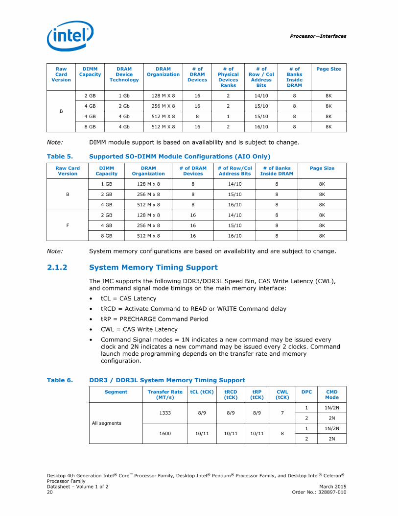
Dual-Channel Mode – Intel® Flex Memory Technology Mode
The IMC supports Intel Flex Memory Technology Mode. Memory is divided intosymmetric and asymmetric zones. The symmetric zone starts at the lowest address ineach channel and is contiguous until the asymmetric zone begins or until the topaddress of the channel with the smaller capacity is reached. In this mode, the systemruns with one zone of dual-channel mode and one zone of single-channel mode,simultaneously, across the whole memory array.
Note: Channels A and B can be mapped for physical channel 0 and 1 respectively or viceversa; however, channel A size must be greater or equal to channel B size.
Figure 2. Intel® Flex Memory Technology Operations
CH BCH A
B B
C
B
B
C Non interleaved access
Dual channel interleaved access
TOM
CH A and CH B can be configured to be physical channels 0 or 1B – The largest physical memory amount of the smaller size memory moduleC – The remaining physical memory amount of the larger size memory module
Dual-Channel Symmetric Mode
Dual-Channel Symmetric mode, also known as interleaved mode, provides maximumperformance on real world applications. Addresses are ping-ponged between thechannels after each cache line (64-byte boundary). If there are two requests, and thesecond request is to an address on the opposite channel from the first, that requestcan be sent before data from the first request has returned. If two consecutive cachelines are requested, both may be retrieved simultaneously, since they are ensured to
2.1.3
Interfaces—Processor
Desktop 4th Generation Intel® Core™ Processor Family, Desktop Intel® Pentium® Processor Family, and Desktop Intel® Celeron®
Processor FamilyMarch 2015 Datasheet – Volume 1 of 2Order No.: 328897-010 21

be on opposite channels. Use Dual-Channel Symmetric mode when both Channel Aand Channel B DIMM connectors are populated in any order, with the total amount ofmemory in each channel being the same.
When both channels are populated with the same memory capacity and the boundarybetween the dual channel zone and the single channel zone is the top of memory, theIMC operates completely in Dual-Channel Symmetric mode.
Note: The DRAM device technology and width may vary from one channel to the other.
System Memory Frequency
In all modes, the frequency of system memory is the lowest frequency of all memorymodules placed in the system, as determined through the SPD registers on thememory modules. The system memory controller supports one or two DIMMconnectors per channel. The usage of DIMM modules with different latencies isallowed, but in that case, the worst latency (among two channels) will be used. Fordual-channel modes, both channels must have a DIMM connector populated and forsingle-channel mode only a single channel may have one or both DIMM connectorspopulated.
Note: In a two-DIMM Per Channel (2DPC) layout memory configuration, the furthest DIMMfrom the processor of any given channel must always be populated first.
Intel® Fast Memory Access (Intel® FMA) Technology Enhancements
The following sections describe the Just-in-Time Scheduling, Command Overlap, andOut-of-Order Scheduling Intel FMA technology enhancements.
Just-in-Time Command Scheduling
The memory controller has an advanced command scheduler where all pendingrequests are examined simultaneously to determine the most efficient request to beissued next. The most efficient request is picked from all pending requests and issuedto system memory Just-in-Time to make optimal use of Command Overlapping. Thus,instead of having all memory access requests go individually through an arbitrationmechanism forcing requests to be executed one at a time, the requests can be startedwithout interfering with the current request allowing for concurrent issuing ofrequests. This allows for optimized bandwidth and reduced latency while maintainingappropriate command spacing to meet system memory protocol.
Command Overlap
Command Overlap allows the insertion of the DRAM commands between the Activate,Pre-charge, and Read/Write commands normally used, as long as the insertedcommands do not affect the currently executing command. Multiple commands can beissued in an overlapping manner, increasing the efficiency of system memory protocol.
Out-of-Order Scheduling
While leveraging the Just-in-Time Scheduling and Command Overlap enhancements,the IMC continuously monitors pending requests to system memory for the best use ofbandwidth and reduction of latency. If there are multiple requests to the same openpage, these requests would be launched in a back-to-back manner to make optimumuse of the open memory page. This ability to reorder requests on the fly allows theIMC to further reduce latency and increase bandwidth efficiency.
2.1.3.1
2.1.3.2
Processor—Interfaces
Desktop 4th Generation Intel® Core™ Processor Family, Desktop Intel® Pentium® Processor Family, and Desktop Intel® Celeron®
Processor FamilyDatasheet – Volume 1 of 2 March 201522 Order No.: 328897-010

Data Scrambling
The system memory controller incorporates a Data Scrambling feature to minimize theimpact of excessive di/dt on the platform system memory VRs due to successive 1sand 0s on the data bus. Past experience has demonstrated that traffic on the data busis not random and can have energy concentrated at specific spectral harmonicscreating high di/dt, which is generally limited by data patterns that excite resonancebetween the package inductance and on die capacitances. As a result, the systemmemory controller uses a data scrambling feature to create pseudo-random patternson the system memory data bus to reduce the impact of any excessive di/dt.
PCI Express* Interface
This section describes the PCI Express* interface capabilities of the processor. See thePCI Express Base* Specification 3.0 for details on PCI Express*.
PCI Express* Support
The PCI Express* lanes (PEG[15:0] TX and RX) are fully-compliant to the PCI ExpressBase Specification, Revision 3.0.
The processor with the PCH support the configurations shown in the following table(may vary depending on PCH SKUs).
Table 7. PCI Express* Supported Configurations in Desktop Products
Configuration Desktop
1x8, 2x4 GFX, I/O
2x8 GFX, I/O
1x16 GFX, I/O
• The port may negotiate down to narrower widths.
— Support for x16/x8/x4/x2/x1 widths for a single PCI Express* mode.
• 2.5 GT/s, 5.0 GT/s and 8 GT/s PCI Express* bit rates are supported.
• Gen 1 Raw bit-rate on the data pins of 2.5 GT/s, resulting in a real bandwidth perpair of 250 MB/s given the 8b/10b encoding used to transmit data across thisinterface. This also does not account for packet overhead and link maintenance.Maximum theoretical bandwidth on the interface of 4 GB/s in each directionsimultaneously, for an aggregate of 8 GB/s when x16 Gen 1.
• Gen 2 Raw bit-rate on the data pins of 5.0 GT/s, resulting in a real bandwidth perpair of 500 MB/s given the 8b/10b encoding used to transmit data across thisinterface. This also does not account for packet overhead and link maintenance.Maximum theoretical bandwidth on the interface of 8 GB/s in each directionsimultaneously, for an aggregate of 16 GB/s when x16 Gen 2.
• Gen 3 raw bit-rate on the data pins of 8.0 GT/s, resulting in a real bandwidth perpair of 984 MB/s using 128b/130b encoding to transmit data across this interface.This also does not account for packet overhead and link maintenance. Maximumtheoretical bandwidth on the interface of 16 GB/s in each direction simultaneously,for an aggregate of 32 GB/s when x16 Gen 3.
• Hierarchical PCI-compliant configuration mechanism for downstream devices.
• Traditional PCI style traffic (asynchronous snooped, PCI ordering).
2.1.3.3
2.2
2.2.1
Interfaces—Processor
Desktop 4th Generation Intel® Core™ Processor Family, Desktop Intel® Pentium® Processor Family, and Desktop Intel® Celeron®
Processor FamilyMarch 2015 Datasheet – Volume 1 of 2Order No.: 328897-010 23

• PCI Express* extended configuration space. The first 256 bytes of configurationspace aliases directly to the PCI Compatibility configuration space. The remainingportion of the fixed 4-KB block of memory-mapped space above that (starting at100h) is known as extended configuration space.
• PCI Express* Enhanced Access Mechanism. Accessing the device configurationspace in a flat memory mapped fashion.
• Automatic discovery, negotiation, and training of link out of reset.
• Traditional AGP style traffic (asynchronous non-snooped, PCI-X Relaxed ordering).
• Peer segment destination posted write traffic (no peer-to-peer read traffic) inVirtual Channel 0: DMI -> PCI Express* Port 0
• 64-bit downstream address format, but the processor never generates an addressabove 64 GB (Bits 63:36 will always be zeros).
• 64-bit upstream address format, but the processor responds to upstream readtransactions to addresses above 64 GB (addresses where any of Bits 63:36 arenonzero) with an Unsupported Request response. Upstream write transactions toaddresses above 64 GB will be dropped.
• Re-issues Configuration cycles that have been previously completed with theConfiguration Retry status.
• PCI Express* reference clock is 100-MHz differential clock.
• Power Management Event (PME) functions.
• Dynamic width capability.
• Message Signaled Interrupt (MSI and MSI-X) messages.
• Polarity inversion
Note: The processor does not support PCI Express* Hot-Plug.
PCI Express* Architecture
Compatibility with the PCI addressing model is maintained to ensure that all existingapplications and drivers operate unchanged.
The PCI Express* configuration uses standard mechanisms as defined in the PCI Plug-and-Play specification. The processor PCI Express* ports support Gen 3. At 8 GT/s,Gen 3 operation results in twice as much bandwidth per lane as compared to Gen 2operation. The 16 lanes PEG can operate at 2.5 GT/s, 5 GT/s, or 8 GT/s.
Gen 3 PCI Express* uses a 128b/130b encoding that is about 23% more efficient thanthe 8b/10b encoding used in Gen 1 and Gen 2.
The PCI Express* architecture is specified in three layers – Transaction Layer, DataLink Layer, and Physical Layer. See the PCI Express Base Specification 3.0 for detailsof PCI Express* architecture.
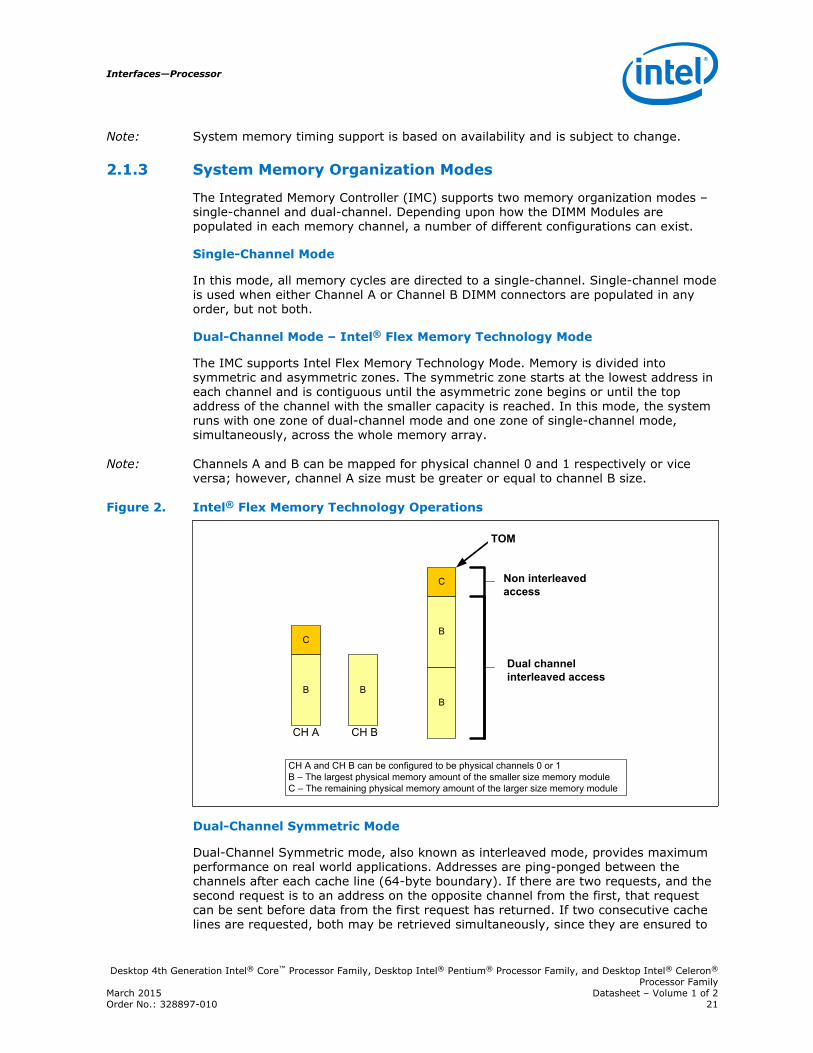
PCI Express* Configuration Mechanism
The PCI Express* (external graphics) link is mapped through a PCI-to-PCI bridgestructure.
2.2.2
2.2.3
Processor—Interfaces
Desktop 4th Generation Intel® Core™ Processor Family, Desktop Intel® Pentium® Processor Family, and Desktop Intel® Celeron®
Processor FamilyDatasheet – Volume 1 of 2 March 201524 Order No.: 328897-010
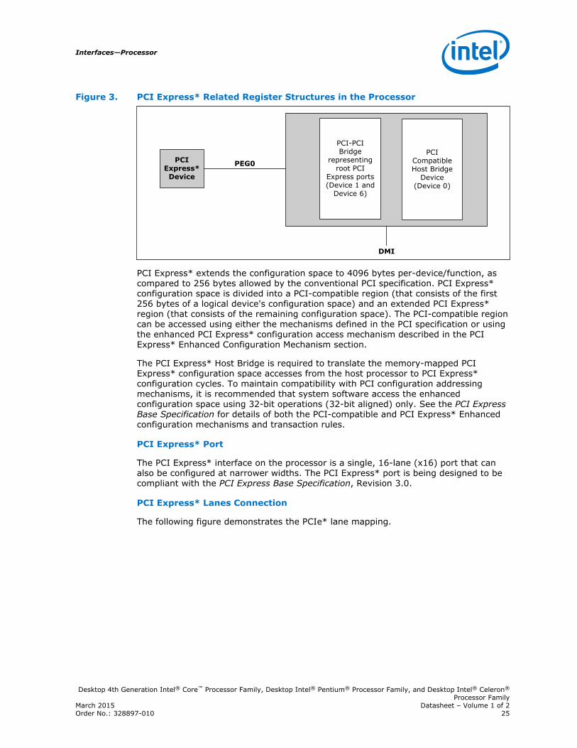
Figure 3. PCI Express* Related Register Structures in the Processor
PCI-PCI Bridge
representing root PCI
Express ports (Device 1 and
Device 6)
PCI Compatible Host Bridge
Device(Device 0)
PCI Express*
Device
PEG0
DMI
PCI Express* extends the configuration space to 4096 bytes per-device/function, ascompared to 256 bytes allowed by the conventional PCI specification. PCI Express*configuration space is divided into a PCI-compatible region (that consists of the first256 bytes of a logical device's configuration space) and an extended PCI Express*region (that consists of the remaining configuration space). The PCI-compatible regioncan be accessed using either the mechanisms defined in the PCI specification or usingthe enhanced PCI Express* configuration access mechanism described in the PCIExpress* Enhanced Configuration Mechanism section.
The PCI Express* Host Bridge is required to translate the memory-mapped PCIExpress* configuration space accesses from the host processor to PCI Express*configuration cycles. To maintain compatibility with PCI configuration addressingmechanisms, it is recommended that system software access the enhancedconfiguration space using 32-bit operations (32-bit aligned) only. See the PCI ExpressBase Specification for details of both the PCI-compatible and PCI Express* Enhancedconfiguration mechanisms and transaction rules.
PCI Express* Port
The PCI Express* interface on the processor is a single, 16-lane (x16) port that canalso be configured at narrower widths. The PCI Express* port is being designed to becompliant with the PCI Express Base Specification, Revision 3.0.
PCI Express* Lanes Connection
The following figure demonstrates the PCIe* lane mapping.
Interfaces—Processor
Desktop 4th Generation Intel® Core™ Processor Family, Desktop Intel® Pentium® Processor Family, and Desktop Intel® Celeron®
Processor FamilyMarch 2015 Datasheet – Volume 1 of 2Order No.: 328897-010 25
Figure 4. PCI Express* Typical Operation 16 Lanes Mapping
0
1
2
3
4
5
6
7
8
9
10
11
12
13
14
15
1X
16C
ontr
olle
r
Lane 00
1
2
3
4
5
6
7
8
9
10
11
12
13
14
15
Lane 1
Lane 2
Lane 3
Lane 4
Lane 5
Lane 6
Lane 7
Lane 8
Lane 9
Lane 10
Lane 11
Lane 12
Lane 13
Lane 14
Lane 15
0
1
2
3
4
5
6
7
1X
8C
ontr
olle
r
0
1
2
3
1X
4C
ontr
o lle
r
Direct Media Interface (DMI)
Direct Media Interface (DMI) connects the processor and the PCH. Next generationDMI2 is supported.
Note: Only DMI x4 configuration is supported.
• DMI 2.0 support.
• Compliant to Direct Media Interface Second Generation (DMI2).
• Four lanes in each direction.
2.3
Processor—Interfaces
Desktop 4th Generation Intel® Core™ Processor Family, Desktop Intel® Pentium® Processor Family, and Desktop Intel® Celeron®
Processor FamilyDatasheet – Volume 1 of 2 March 201526 Order No.: 328897-010
• 5 GT/s point-to-point DMI interface to PCH is supported.
• Raw bit-rate on the data pins of 5.0 GB/s, resulting in a real bandwidth per pair of500 MB/s given the 8b/10b encoding used to transmit data across this interface.Does not account for packet overhead and link maintenance.
• Maximum theoretical bandwidth on interface of 2 GB/s in each directionsimultaneously, for an aggregate of 4 GB/s when DMI x4.
• Shares 100-MHz PCI Express* reference clock.
• 64-bit downstream address format, but the processor never generates an addressabove 64 GB (Bits 63:36 will always be zeros).
• 64-bit upstream address format, but the processor responds to upstream readtransactions to addresses above 64 GB (addresses where any of Bits 63:36 arenonzero) with an Unsupported Request response. Upstream write transactions toaddresses above 64 GB will be dropped.
• Supports the following traffic types to or from the PCH:
— DMI -> DRAM
— DMI -> processor core (Virtual Legacy Wires (VLWs), Resetwarn, or MSIsonly)
— Processor core -> DMI
• APIC and MSI interrupt messaging support:
— Message Signaled Interrupt (MSI and MSI-X) messages
• Downstream SMI, SCI and SERR error indication.
• Legacy support for ISA regime protocol (PHOLD/PHOLDA) required for parallel portDMA, floppy drive, and LPC bus masters.
• DC coupling – no capacitors between the processor and the PCH.
• Polarity inversion.
• PCH end-to-end lane reversal across the link.
• Supports Half Swing “low-power/low-voltage”.
DMI Error Flow
DMI can only generate SERR in response to errors, never SCI, SMI, MSI, PCI INT, orGPE. Any DMI related SERR activity is associated with Device 0.
DMI Link Down
The DMI link going down is a fatal, unrecoverable error. If the DMI data link goes todata link down, after the link was up, then the DMI link hangs the system by notallowing the link to retrain to prevent data corruption. This link behavior is controlledby the PCH.
Downstream transactions that had been successfully transmitted across the link priorto the link going down may be processed as normal. No completions fromdownstream, non-posted transactions are returned upstream over the DMI link after alink down event.
Interfaces—Processor
Desktop 4th Generation Intel® Core™ Processor Family, Desktop Intel® Pentium® Processor Family, and Desktop Intel® Celeron®
Processor FamilyMarch 2015 Datasheet – Volume 1 of 2Order No.: 328897-010 27
Processor Graphics
The processor graphics contains a generation 7.5 graphics core architecture. Thisenables substantial gains in performance and lower power consumption over previousgenerations. Up to 20 Execution Units are supported depending on the processor SKU.
• Next Generation Intel Clear Video Technology HD Support is a collection of videoplayback and enhancement features that improve the end user’s viewingexperience
— Encode / transcode HD content
— Playback of high definition content including Blu-ray Disc*
— Superior image quality with sharper, more colorful images
— Playback of Blu-ray* disc S3D content using HDMI (1.4a specificationcompliant with 3D)
• DirectX* Video Acceleration (DXVA) support for accelerating video processing
— Full AVC/VC1/MPEG2 HW Decode
• Advanced Scheduler 2.0, 1.0, XPDM support
• Windows* 8, Windows* 7, OSX, Linux* operating system support
• DirectX* 11.1, DirectX* 11, DirectX* 10.1, DirectX* 10, DirectX* 9 support.
• OpenGL* 4.0, support
• Switchable Graphics support on AIO platforms with MxM solutions only
Processor Graphics Controller (GT)
The Graphics Engine Architecture includes 3D compute elements, Multi-format HWassisted decode/encode pipeline, and Mid-Level Cache (MLC) for superior highdefinition playback, video quality, and improved 3D performance and media.
The Display Engine handles delivering the pixels to the screen. GSA (Graphics inSystem Agent) is the primary channel interface for display memory accesses and“PCI-like” traffic in and out.
2.4
2.5
Processor—Interfaces
Desktop 4th Generation Intel® Core™ Processor Family, Desktop Intel® Pentium® Processor Family, and Desktop Intel® Celeron®
Processor FamilyDatasheet – Volume 1 of 2 March 201528 Order No.: 328897-010

Figure 5. Processor Graphics Controller Unit Block Diagram
3D and Video Engines for Graphics Processing
The Gen 7.5 3D engine provides the following performance and power-managementenhancements.
3D Pipeline
The 3D graphics pipeline architecture simultaneously operates on different primitivesor on different portions of the same primitive. All the cores are fully programmable,increasing the versatility of the 3D Engine.
3D Engine Execution Units
• Supports up to 20 EUs.The EUs perform 128-bit wide execution per clock.
• Support SIMD8 instructions for vertex processing and SIMD16 instructions forpixel processing.
Vertex Fetch (VF) Stage
The VF stage executes 3DPRIMITIVE commands. Some enhancements have beenincluded to better support legacy D3D APIs as well as SGI OpenGL*.
2.5.1
Interfaces—Processor
Desktop 4th Generation Intel® Core™ Processor Family, Desktop Intel® Pentium® Processor Family, and Desktop Intel® Celeron®
Processor FamilyMarch 2015 Datasheet – Volume 1 of 2Order No.: 328897-010 29
Vertex Shader (VS) Stage
The VS stage performs shading of vertices output by the VF function. The VS unitproduces an output vertex reference for every input vertex reference received fromthe VF unit, in the order received.
Geometry Shader (GS) Stage
The GS stage receives inputs from the VS stage. Compiled application-provided GSprograms, specifying an algorithm to convert the vertices of an input object into someoutput primitives. For example, a GS shader may convert lines of a line strip intopolygons representing a corresponding segment of a blade of grass centered on theline. Or it could use adjacency information to detect silhouette edges of triangles andoutput polygons extruding out from the edges.
Clip Stage
The Clip stage performs general processing on incoming 3D objects. However, it alsoincludes specialized logic to perform a Clip Test function on incoming objects. The ClipTest optimizes generalized 3D Clipping. The Clip unit examines the position ofincoming vertices, and accepts/rejects 3D objects based on its Clip algorithm.
Strips and Fans (SF) Stage
The SF stage performs setup operations required to rasterize 3D objects. The outputsfrom the SF stage to the Windower stage contain implementation-specific informationrequired for the rasterization of objects and also supports clipping of primitives tosome extent.
Windower / IZ (WIZ) Stage
The WIZ unit performs an early depth test, which removes failing pixels andeliminates unnecessary processing overhead.
The Windower uses the parameters provided by the SF unit in the object-specificrasterization algorithms. The WIZ unit rasterizes objects into the corresponding set ofpixels. The Windower is also capable of performing dithering, whereby the illusion of ahigher resolution when using low-bpp channels in color buffers is possible. Colordithering diffuses the sharp color bands seen on smooth-shaded objects.
Video Engine
The Video Engine handles the non-3D (media/video) applications. It includes supportfor VLD and MPEG2 decode in hardware.
2D Engine
The 2D Engine contains BLT (Block Level Transfer) functionality and an extensive setof 2D instructions. To take advantage of the 3D during engine’s functionality, someBLT functions make use of the 3D renderer.
Processor Graphics VGA Registers
The 2D registers consists of original VGA registers and others to support graphicsmodes that have color depths, resolutions, and hardware acceleration features that gobeyond the original VGA standard.
Processor—Interfaces
Desktop 4th Generation Intel® Core™ Processor Family, Desktop Intel® Pentium® Processor Family, and Desktop Intel® Celeron®
Processor FamilyDatasheet – Volume 1 of 2 March 201530 Order No.: 328897-010

Logical 128-Bit Fixed BLT and 256 Fill Engine
This BLT engine accelerates the GUI of Microsoft Windows* operating systems. The128-bit BLT engine provides hardware acceleration of block transfers of pixel data formany common Windows operations. The BLT engine can be used for the following:
• Move rectangular blocks of data between memory locations
• Data alignment
• To perform logical operations (raster ops)
The rectangular block of data does not change, as it is transferred between memorylocations. The allowable memory transfers are between: cacheable system memoryand frame buffer memory, frame buffer memory and frame buffer memory, and withinsystem memory. Data to be transferred can consist of regions of memory, patterns, orsolid color fills. A pattern is always 8 x 8 pixels wide and may be 8, 16, or 32 bits perpixel.
The BLT engine expands monochrome data into a color depth of 8, 16, or 32 bits.BLTs can be either opaque or transparent. Opaque transfers move the data specifiedto the destination. Transparent transfers compare destination color to source color andwrite according to the mode of transparency selected.
Data is horizontally and vertically aligned at the destination. If the destination for theBLT overlaps with the source memory location, the BLT engine specifies which area inmemory to begin the BLT transfer. Hardware is included for all 256 raster operations(source, pattern, and destination) defined by Microsoft*, including transparent BLT.
The BLT engine has instructions to invoke BLT and stretch BLT operations, permittingsoftware to set up instruction buffers and use batch processing. The BLT engine canperform hardware clipping during BLTs.
Multi Graphics Controllers Multi-Monitor Support
The processor supports simultaneous use of the Processor Graphics Controller (GT)and a x16 PCI Express* Graphics (PEG) device. The processor supports a maximum of2 displays connected to the PEG card in parallel with up to 2 displays connected to theprocessor and PCH.
Note: When supporting Multi Graphics Multi Monitors, "drag and drop" between monitors andthe 2x8PEG is not supported.
Digital Display Interface (DDI)
• The processor supports:
— Three Digital Display (x4 DDI) interfaces that can be configured asDisplayPort*, HDMI*, or DVI. DisplayPort* can be configured to use 1, 2, or 4lanes depending on the bandwidth requirements and link data rate of RBR(1.62 GT/s), HBR (2.7 GT/s) and HBR2 (5.4 GT/s). When configured asHDMI*, DDIx4 port can support 2.97 GT/s. In addition, Digital Port D ( x4DDI) interface can also be configured to carry embedded DisplayPort*(eDPx4). Built-in displays are only supported on Digital Port D.
— One dedicated Intel FDI Port for legacy VGA support on the PCH.
2.5.2
2.6
Interfaces—Processor
Desktop 4th Generation Intel® Core™ Processor Family, Desktop Intel® Pentium® Processor Family, and Desktop Intel® Celeron®
Processor FamilyMarch 2015 Datasheet – Volume 1 of 2Order No.: 328897-010 31

• The HDMI* interface supports HDMI with 3D, 4K, Deep Color, and x.v.Color. TheDisplayPort* interface supports the VESA DisplayPort* Standard Version 1,Revision 2.
• The processor supports High-bandwidth Digital Content Protection (HDCP) forhigh-definition content playback over digital interfaces.
• The processor also integrates dedicated a Mini HD audio controller to drive audioon integrated digital display interfaces, such as HDMI* and DisplayPort*. The HDaudio controller on the PCH would continue to support down CODECs, and so on.The processor Mini HD audio controller supports two High-Definition Audio streamssimultaneously on any of the three digital ports.
• The processor supports streaming any 3 independent and simultaneous displaycombination of DisplayPort*/HDMI*/DVI/eDP*/VGA monitors with the exception of3 simultaneous display support of HDMI*/DVI . In the case of 3 simultaneousdisplays, two High Definition Audio streams over the digital display interfaces aresupported.
• Each digital port is capable of driving resolutions up to 3840x2160 at 60 Hzthrough DisplayPort* and 4096x2304 at 24 Hz/2560x1600 at 60 Hz using HDMI*.
• DisplayPort* Aux CH, DDC channel, Panel power sequencing, and HPD aresupported through the PCH.
Figure 6. Processor Display Architecture
Me
mo
ry \ C
on
fig
In
terf
ace
Display
Pipe A
Display
Pipe B
Display
Pipe C
Pa
ne
l F
ittin
g
HD Audio
Controller
Transcoder A
DP / HDMI
Timing, VDIP
Transcoder B DP / HDMI
Timing, VDIP
Transcoder C DP / HDMI
Timing, VDIP
eDP* Mux
Transcoder eDP*
DP encoder
Timing, VDIP
DPT, SRID
Po
rt M
ux
Audio
Codec
DP
Aux
PC
H D
isp
lay
DD
I P
ort
s B
, C
, a
nd
D
DP /
HDMI /
DVI
DP /
HDMI /
DVI / eDP
FDIFDI
RX
DP /
HDMI /
DVI
D
C
B
Display is the presentation stage of graphics. This involves:
• Pulling rendered data from memory
• Converting raw data into pixels
• Blending surfaces into a frame
Processor—Interfaces
Desktop 4th Generation Intel® Core™ Processor Family, Desktop Intel® Pentium® Processor Family, and Desktop Intel® Celeron®
Processor FamilyDatasheet – Volume 1 of 2 March 201532 Order No.: 328897-010
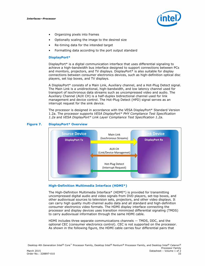
• Organizing pixels into frames
• Optionally scaling the image to the desired size
• Re-timing data for the intended target
• Formatting data according to the port output standard
DisplayPort*
DisplayPort* is a digital communication interface that uses differential signaling toachieve a high-bandwidth bus interface designed to support connections between PCsand monitors, projectors, and TV displays. DisplayPort* is also suitable for displayconnections between consumer electronics devices, such as high-definition optical discplayers, set top boxes, and TV displays.
A DisplayPort* consists of a Main Link, Auxiliary channel, and a Hot-Plug Detect signal.The Main Link is a unidirectional, high-bandwidth, and low latency channel used fortransport of isochronous data streams such as uncompressed video and audio. TheAuxiliary Channel (AUX CH) is a half-duplex bidirectional channel used for linkmanagement and device control. The Hot-Plug Detect (HPD) signal serves as aninterrupt request for the sink device.
The processor is designed in accordance with the VESA DisplayPort* Standard Version1.2a. The processor supports VESA DisplayPort* PHY Compliance Test Specification1.2a and VESA DisplayPort* Link Layer Compliance Test Specification 1.2a.
Figure 7. DisplayPort* Overview
Source Device Sink DeviceMain Link(Isochronous Streams)
AUX CH(Link/Device Managemet)
Hot-Plug Detect(Interrupt Request)
DisplayPort Tx DisplayPort Rx
High-Definition Multimedia Interface (HDMI*)
The High-Definition Multimedia Interface* (HDMI*) is provided for transmittinguncompressed digital audio and video signals from DVD players, set-top boxes, andother audiovisual sources to television sets, projectors, and other video displays. Itcan carry high quality multi-channel audio data and all standard and high-definitionconsumer electronics video formats. The HDMI display interface connecting theprocessor and display devices uses transition minimized differential signaling (TMDS)to carry audiovisual information through the same HDMI cable.
HDMI includes three separate communications channels — TMDS, DDC, and theoptional CEC (consumer electronics control). CEC is not supported on the processor.As shown in the following figure, the HDMI cable carries four differential pairs that
Interfaces—Processor
Desktop 4th Generation Intel® Core™ Processor Family, Desktop Intel® Pentium® Processor Family, and Desktop Intel® Celeron®
Processor FamilyMarch 2015 Datasheet – Volume 1 of 2Order No.: 328897-010 33

make up the TMDS data and clock channels. These channels are used to carry video,audio, and auxiliary data. In addition, HDMI carries a VESA DDC. The DDC is used byan HDMI Source to determine the capabilities and characteristics of the Sink.
Audio, video, and auxiliary (control/status) data is transmitted across the three TMDSdata channels. The video pixel clock is transmitted on the TMDS clock channel and isused by the receiver for data recovery on the three data channels. The digital displaydata signals driven natively through the PCH are AC coupled and needs level shiftingto convert the AC coupled signals to the HDMI compliant digital signals.
The processor HDMI interface is designed in accordance with the High-DefinitionMultimedia Interface with 3D, 4K, Deep Color, and x.v.Color.
Figure 8. HDMI* Overview
HDMI Source HDMI Sink
TMDS Data Channel 0
Hot-Plug Detect
HDMI Tx HDMI Rx
TMDS Data Channel 1
TMDS Data Channel 2
TMDS Clock Channel
CEC Line (optional)
Display Data Channel (DDC)
Digital Video Interface
The processor Digital Ports can be configured to drive DVI-D. DVI uses TMDS fortransmitting data from the transmitter to the receiver, which is similar to the HDMIprotocol except for the audio and CEC. Refer to the HDMI section for more informationon the signals and data transmission. To drive DVI-I through the back panel the VGADDC signals are connected along with the digital data and clock signals from one ofthe Digital Ports. When a system has support for a DVI-I port, then either VGA or theDVI-D through a single DVI-I connector can be driven, but not both simultaneously.
The digital display data signals driven natively through the processor are AC coupledand need level shifting to convert the AC coupled signals to the HDMI compliant digitalsignals.
Processor—Interfaces
Desktop 4th Generation Intel® Core™ Processor Family, Desktop Intel® Pentium® Processor Family, and Desktop Intel® Celeron®
Processor FamilyDatasheet – Volume 1 of 2 March 201534 Order No.: 328897-010

embedded DisplayPort*
embedded DisplayPort* (eDP*) is an embedded version of the DisplayPort standardoriented towards applications such as notebook and All-In-One PCs. Digital Port D canbe configured as eDP. Like DisplayPort, embedded DisplayPort also consists of a MainLink, Auxiliary channel, and an optional Hot-Plug Detect signal.
The eDP on the processor can be configured for 2 or 4 lanes.
The processor supports embedded DisplayPort* (eDP*) Standard Version 1.2 andVESA embedded DisplayPort* Standard Version 1.2.
Integrated Audio
• HDMI and display port interfaces carry audio along with video.
• Processor supports two DMA controllers to output two High Definition audiostreams on two digital ports simultaneously.
• Supports only the internal HDMI and DP CODECs.
Table 8. Processor Supported Audio Formats over HDMI*and DisplayPort*
Audio Formats HDMI* DisplayPort*
AC-3 Dolby* Digital Yes Yes
Dolby Digital Plus Yes Yes
DTS-HD* Yes Yes
LPCM, 192 kHz/24 bit, 8 Channel Yes Yes
Dolby TrueHD, DTS-HD Master Audio*(Lossless Blu-Ray Disc* Audio Format)
Yes Yes
The processor will continue to support Silent stream. Silent stream is an integratedaudio feature that enables short audio streams, such as system events to be heardover the HDMI and DisplayPort monitors. The processor supports silent streams overthe HDMI and DisplayPort interfaces at 44.1 kHz, 48 kHz, 88.2 kHz, 96 kHz,176.4 kHz, and 192 kHz sampling rates.
Multiple Display Configurations
The following multiple display configuration modes are supported (with appropriatedriver software):
• Single Display is a mode with one display port activated to display the output toone display device.
• Intel Display Clone is a mode with up to three display ports activated to drive thedisplay content of same color depth setting but potentially different refresh rateand resolution settings to all the active display devices connected.
• Extended Desktop is a mode with up to three display ports activated to drive thecontent with potentially different color depth, refresh rate, and resolution settingson each of the active display devices connected.
The digital ports on the processor can be configured to support DisplayPort*/HDMI/DVI. For Desktop designs, digital port D can be configured as eDPx4 in addition todedicated x2 port for Intel FDI for VGA. The following table shows examples of validthree display configurations through the processor.
Interfaces—Processor
Desktop 4th Generation Intel® Core™ Processor Family, Desktop Intel® Pentium® Processor Family, and Desktop Intel® Celeron®
Processor FamilyMarch 2015 Datasheet – Volume 1 of 2Order No.: 328897-010 35

Table 9. Valid Three Display Configurations through the Processor
Display 1 Display 2 Display 3 MaximumResolution Display
1
MaximumResolutionDisplay 2
MaximumResolution Display
3
HDMI HDMI DP4096x2304 @ 24 Hz2560x1600 @ 60 Hz
3840x2160 @ 60 Hz
DVI DVI DP 1920x1200 @ 60 Hz 3840x2160 @ 60 Hz
DP DP DP 3840x2160 @ 60 Hz
VGA DP HDMI 1920x1200 @ 60 Hz 3840x2160 @60 Hz
4096x2304 @ 24 Hz2560x1600 @ 60 Hz
eDP DP HDMI 3840x2160 @ 60 Hz 3840x2160 @60 Hz
4096x2304 @ 24 Hz2560x1600 @ 60 Hz
eDP DP DP 3840x2160 @ 60 Hz 3840x2160 @ 60 Hz
eDP HDMI HDMI 3840x2160 @ 60 Hz4096x2304 @ 24 Hz2560x1600 @ 60 Hz
Notes: 1. Requires support of 2 channel DDR3/DDR3L 1600 MT/s configuration for driving 3 simultaneous3840x2160 @ 60 Hz display resolutions
2. DP and eDP resolutions in the above table are supported for 4 lanes with link data rate HBR2.
The following table shows the DP/eDP resolutions supported for 1, 2, or 4 lanesdepending on link data rate of RBR, HBR, and HBR2.
Table 10. DisplayPort and embedded DisplayPort* Resolutions for 1, 2, 4 Lanes – LinkData Rate of RBR, HBR, and HBR2
Link Data Rate Lane Count
1 2 4
RBR 1064x600 1400x1050 2240x1400
HBR 1280x960 1920x1200 2880x1800
HBR2 1920x1200 2880x1800 3840x2160
Any 3 displays can be supported simultaneously using the following rules:
• Maximum of 2 HDMIs
• Maximum of 2 DVIs
• Maximum of 1 HDMI and 1 DVI
• Any 3 DisplayPort
• One VGA
• One eDP
High-bandwidth Digital Content Protection (HDCP)
HDCP is the technology for protecting high-definition content against unauthorizedcopy or unreceptive between a source (computer, digital set top boxes, and so on)and the sink (panels, monitor, and TVs). The processor supports HDCP 1.4 for contentprotection over wired displays (HDMI*, DVI, and DisplayPort*).
The HDCP 1.4 keys are integrated into the processor and customers are not requiredto physically configure or handle the keys.
Processor—Interfaces
Desktop 4th Generation Intel® Core™ Processor Family, Desktop Intel® Pentium® Processor Family, and Desktop Intel® Celeron®
Processor FamilyDatasheet – Volume 1 of 2 March 201536 Order No.: 328897-010

Intel® Flexible Display Interface (Intel® FDI)
• The Intel Flexible Display Interface (Intel FDI) passes display data from theprocessor (source) to the PCH (sink) for display through a display interface on thePCH.
• Intel FDI supports 2 lanes at 2.7 GT/s fixed frequency. This can be configured to 1or 2 lanes depending on the bandwidth requirements.
• Intel FDI supports 8 bits per color only.
• Side band sync pin (FDI_CSYNC).
• Side band interrupt pin (DISP_INT). This carries combined interrupt for HPDs of allthe ports, AUX and I2C completion events, and so on.
• Intel FDI is not encrypted as it drives only VGA and content protection is notsupported on VGA.
Platform Environmental Control Interface (PECI)
PECI is an Intel proprietary interface that provides a communication channel betweenIntel processors and external components, like Super I/O (SIO) and EmbeddedControllers (EC), to provide processor temperature, Turbo, TDP, and memorythrottling control mechanisms and many other services. PECI is used for platformthermal management and real time control and configuration of processor featuresand performance.
PECI Bus Architecture
The PECI architecture is based on a wired-OR bus that the clients (as processor PECI)can pull up high (with strong drive).
The idle state on the bus is near zero.
The following figure demonstrates PECI design and connectivity. While the host/originator can be a third party PECI host, one of the PECI clients is a processor PECIdevice.
2.7
2.8
2.8.1
Interfaces—Processor
Desktop 4th Generation Intel® Core™ Processor Family, Desktop Intel® Pentium® Processor Family, and Desktop Intel® Celeron®
Processor FamilyMarch 2015 Datasheet – Volume 1 of 2Order No.: 328897-010 37

Figure 9. PECI Host-Clients Connection Example
VTT
Host / Originator
Q1nX
Q21X
PECI
CPECI<10pF/Node
Q3nX
VTT
PECI Client
Additional PECI Clients
Processor—Interfaces
Desktop 4th Generation Intel® Core™ Processor Family, Desktop Intel® Pentium® Processor Family, and Desktop Intel® Celeron®
Processor FamilyDatasheet – Volume 1 of 2 March 201538 Order No.: 328897-010

3.0 Technologies
This chapter provides a high-level description of Intel technologies implemented in theprocessor.
The implementation of the features may vary between the processor SKUs.
Details on the different technologies of Intel processors and other relevant externalnotes are located at the Intel technology web site: http://www.intel.com/technology/
Intel® Virtualization Technology (Intel® VT)
Intel® Virtualization Technology (Intel® VT) makes a single system appear as multipleindependent systems to software. This allows multiple, independent operating systemsto run simultaneously on a single system. Intel VT comprises technology componentsto support virtualization of platforms based on Intel architecture microprocessors andchipsets.
Intel® Virtualization Technology (Intel® VT) for IA-32, Intel® 64 and Intel®Architecture (Intel® VT-x) added hardware support in the processor to improve thevirtualization performance and robustness. Intel® Virtualization Technology forDirected I/O (Intel VT-d) extends Intel® VT-x by adding hardware assisted support toimprove I/O device virtualization performance.
Intel® VT-x specifications and functional descriptions are included in the Intel® 64 andIA-32 Architectures Software Developer’s Manual, Volume 3B and is available at:
http://www.intel.com/products/processor/manuals/index.htm
The Intel VT-d specification and other Intel VT documents can be referenced at:
http://www.intel.com/technology/virtualization/index.htm
https://sharedspaces.intel.com/sites/PCDC/SitePages/Ingredients/ingredient.aspx?ing=VT
Intel® VT-x Objectives
Intel VT-x provides hardware acceleration for virtualization of IA platforms. VirtualMachine Monitor (VMM) can use Intel VT-x features to provide an improved reliablevirtualized platform. By using Intel VT-x, a VMM is:
• Robust: VMMs no longer need to use paravirtualization or binary translation. Thismeans that off-the-shelf operating systems and applications can be run withoutany special steps.
• Enhanced: Intel VT enables VMMs to run 64-bit guest operating systems on IAx86 processors.
3.1
Technologies—Processor
Desktop 4th Generation Intel® Core™ Processor Family, Desktop Intel® Pentium® Processor Family, and Desktop Intel® Celeron®
Processor FamilyMarch 2015 Datasheet – Volume 1 of 2Order No.: 328897-010 39

• More reliable: Due to the hardware support, VMMs can now be smaller, lesscomplex, and more efficient. This improves reliability and availability and reducesthe potential for software conflicts.
• More secure: The use of hardware transitions in the VMM strengthens theisolation of VMs and further prevents corruption of one VM from affecting otherson the same system.
Intel® VT-x Features
The processor supports the following Intel VT-x features:
• Extended Page Table (EPT) Accessed and Dirty Bits
— EPT A/D bits enabled VMMs to efficiently implement memory management andpage classification algorithms to optimize VM memory operations, such as de-fragmentation, paging, live migration, and check-pointing. Without hardwaresupport for EPT A/D bits, VMMs may need to emulate A/D bits by marking EPTpaging-structures as not-present or read-only, and incur the overhead of EPTpage-fault VM exits and associated software processing.
• Extended Page Table Pointer (EPTP) switching
— EPTP switching is a specific VM function. EPTP switching allows guest software(in VMX non-root operation, supported by EPT) to request a different EPTpaging-structure hierarchy. This is a feature by which software in VMX non-root operation can request a change of EPTP without a VM exit. Software canchoose among a set of potential EPTP values determined in advance bysoftware in VMX root operation.
• Pause loop exiting
— Support VMM schedulers seeking to determine when a virtual processor of amultiprocessor virtual machine is not performing useful work. This situationmay occur when not all virtual processors of the virtual machine are currentlyscheduled and when the virtual processor in question is in a loop involving thePAUSE instruction. The new feature allows detection of such loops and is thuscalled PAUSE-loop exiting.
The processor core supports the following Intel VT-x features:
• Extended Page Tables (EPT)
— EPT is hardware assisted page table virtualization.
— It eliminates VM exits from the guest operating system to the VMM for shadowpage-table maintenance.
• Virtual Processor IDs (VPID)
— Ability to assign a VM ID to tag processor core hardware structures (such asTLBs).
— This avoids flushes on VM transitions to give a lower-cost VM transition timeand an overall reduction in virtualization overhead.
• Guest Preemption Timer
— Mechanism for a VMM to preempt the execution of a guest operating systemafter an amount of time specified by the VMM. The VMM sets a timer valuebefore entering a guest.
— The feature aids VMM developers in flexibility and Quality of Service (QoS)guarantees.
Processor—Technologies
Desktop 4th Generation Intel® Core™ Processor Family, Desktop Intel® Pentium® Processor Family, and Desktop Intel® Celeron®
Processor FamilyDatasheet – Volume 1 of 2 March 201540 Order No.: 328897-010
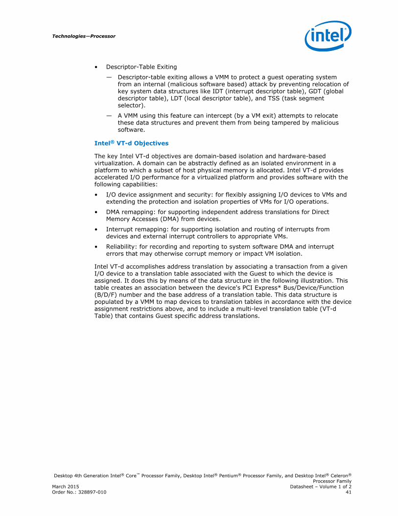
• Descriptor-Table Exiting
— Descriptor-table exiting allows a VMM to protect a guest operating systemfrom an internal (malicious software based) attack by preventing relocation ofkey system data structures like IDT (interrupt descriptor table), GDT (globaldescriptor table), LDT (local descriptor table), and TSS (task segmentselector).
— A VMM using this feature can intercept (by a VM exit) attempts to relocatethese data structures and prevent them from being tampered by malicioussoftware.
Intel® VT-d Objectives
The key Intel VT-d objectives are domain-based isolation and hardware-basedvirtualization. A domain can be abstractly defined as an isolated environment in aplatform to which a subset of host physical memory is allocated. Intel VT-d providesaccelerated I/O performance for a virtualized platform and provides software with thefollowing capabilities:
• I/O device assignment and security: for flexibly assigning I/O devices to VMs andextending the protection and isolation properties of VMs for I/O operations.
• DMA remapping: for supporting independent address translations for DirectMemory Accesses (DMA) from devices.
• Interrupt remapping: for supporting isolation and routing of interrupts fromdevices and external interrupt controllers to appropriate VMs.
• Reliability: for recording and reporting to system software DMA and interrupterrors that may otherwise corrupt memory or impact VM isolation.
Intel VT-d accomplishes address translation by associating a transaction from a givenI/O device to a translation table associated with the Guest to which the device isassigned. It does this by means of the data structure in the following illustration. Thistable creates an association between the device's PCI Express* Bus/Device/Function(B/D/F) number and the base address of a translation table. This data structure ispopulated by a VMM to map devices to translation tables in accordance with the deviceassignment restrictions above, and to include a multi-level translation table (VT-dTable) that contains Guest specific address translations.
Technologies—Processor
Desktop 4th Generation Intel® Core™ Processor Family, Desktop Intel® Pentium® Processor Family, and Desktop Intel® Celeron®
Processor FamilyMarch 2015 Datasheet – Volume 1 of 2Order No.: 328897-010 41
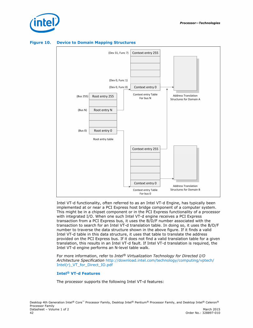
Figure 10. Device to Domain Mapping Structures
Root entry 0
Root entry N
Root entry 255
Context entry 0
Context entry 255
Context entry 0
Context entry 255
(Bus 255)
(Bus N)
(Bus 0)
Root entry table
(Dev 31, Func 7)
(Dev 0, Func 1)
(Dev 0, Func 0)
Context entry TableFor bus N
Context entry TableFor bus 0
Address TranslationStructures for Domain A
Address TranslationStructures for Domain B
Intel VT-d functionality, often referred to as an Intel VT-d Engine, has typically beenimplemented at or near a PCI Express host bridge component of a computer system.This might be in a chipset component or in the PCI Express functionality of a processorwith integrated I/O. When one such Intel VT-d engine receives a PCI Expresstransaction from a PCI Express bus, it uses the B/D/F number associated with thetransaction to search for an Intel VT-d translation table. In doing so, it uses the B/D/Fnumber to traverse the data structure shown in the above figure. If it finds a validIntel VT-d table in this data structure, it uses that table to translate the addressprovided on the PCI Express bus. If it does not find a valid translation table for a giventranslation, this results in an Intel VT-d fault. If Intel VT-d translation is required, theIntel VT-d engine performs an N-level table walk.
For more information, refer to Intel® Virtualization Technology for Directed I/OArchitecture Specification http://download.intel.com/technology/computing/vptech/Intel(r)_VT_for_Direct_IO.pdf
Intel® VT-d Features
The processor supports the following Intel VT-d features:
Processor—Technologies
Desktop 4th Generation Intel® Core™ Processor Family, Desktop Intel® Pentium® Processor Family, and Desktop Intel® Celeron®
Processor FamilyDatasheet – Volume 1 of 2 March 201542 Order No.: 328897-010

• Memory controller and processor graphics comply with the Intel VT-d 1.2Specification
• Two Intel VT-d DMA remap engines
— iGFX DMA remap engine
— Default DMA remap engine (covers all devices except iGFX)
• Support for root entry, context entry, and default context
• 39-bit guest physical address and host physical address widths
• Support for 4 KB page sizes
• Support for register-based fault recording only (for single entry only) and supportfor MSI interrupts for faults
• Support for both leaf and non-leaf caching
• Support for boot protection of default page table
• Support for non-caching of invalid page table entries
• Support for hardware-based flushing of translated but pending writes and pendingreads, on IOTLB invalidation
• Support for Global, Domain specific, and Page specific IOTLB invalidation
• MSI cycles (MemWr to address FEEx_xxxxh) not translated
— Translation faults result in cycle forwarding to VBIOS region (byte enablesmasked for writes). Returned data may be bogus for internal agents; PEG/DMIinterfaces return unsupported request status
• Interrupt remapping is supported
• Queued invalidation is supported
• Intel VT-d translation bypass address range is supported (Pass Through)
The processor supports the following added new Intel VT-d features:
• 4-level Intel VT-d Page walk: Both default Intel VT-d engine, as well as the IGDIntel VT-d engine, are upgraded to support 4-level Intel VT-d tables (adjustedguest address width 48 bits)
• Intel VT-d superpage: support of Intel VT-d superpage (2 MB, 1 GB) for thedefault Intel VT-d engine (that covers all devices except IGD)
IGD Intel VT-d engine does not support superpage and BIOS should disablesuperpage in default Intel VT-d engine when iGFX is enabled.
Note: Intel VT-d Technology may not be available on all SKUs.
Intel® Trusted Execution Technology (Intel® TXT)
Intel Trusted Execution Technology (Intel TXT) defines platform-level enhancementsthat provide the building blocks for creating trusted platforms.
The Intel TXT platform helps to provide the authenticity of the controlling environmentsuch that those wishing to rely on the platform can make an appropriate trustdecision. The Intel TXT platform determines the identity of the controlling environmentby accurately measuring and verifying the controlling software.
3.2
Technologies—Processor
Desktop 4th Generation Intel® Core™ Processor Family, Desktop Intel® Pentium® Processor Family, and Desktop Intel® Celeron®
Processor FamilyMarch 2015 Datasheet – Volume 1 of 2Order No.: 328897-010 43

Another aspect of the trust decision is the ability of the platform to resist attempts tochange the controlling environment. The Intel TXT platform will resist attempts bysoftware processes to change the controlling environment or bypass the bounds set bythe controlling environment.
Intel TXT is a set of extensions designed to provide a measured and controlled launchof system software that will then establish a protected environment for itself and anyadditional software that it may execute.
These extensions enhance two areas:
• The launching of the Measured Launched Environment (MLE).
• The protection of the MLE from potential corruption.
The enhanced platform provides these launch and control interfaces using Safer ModeExtensions (SMX).
The SMX interface includes the following functions:
• Measured/Verified launch of the MLE.
• Mechanisms to ensure the above measurement is protected and stored in a securelocation.
• Protection mechanisms that allow the MLE to control attempts to modify itself.
The processor also offers additional enhancements to System Management Mode(SMM) architecture for enhanced security and performance. The processor providesnew MSRs to:
• Enable a second SMM range
• Enable SMM code execution range checking
• Select whether SMM Save State is to be written to legacy SMRAM or to MSRs
• Determine if a thread is going to be delayed entering SMM
• Determine if a thread is blocked from entering SMM
• Targeted SMI, enable/disable threads from responding to SMIs both VLWs and IPI
For the above features, BIOS must test the associated capability bit before attemptingto access any of the above registers.
For more information, refer to the Intel® Trusted Execution Technology MeasuredLaunched Environment Programming Guide.
Intel® Hyper-Threading Technology (Intel® HTTechnology)
The processor supports Intel Hyper-Threading Technology (Intel HT Technology) thatallows an execution core to function as two logical processors. While some executionresources, such as caches, execution units, and buses are shared, each logicalprocessor has its own architectural state with its own set of general-purpose registersand control registers. This feature must be enabled using the BIOS and requiresoperating system support.
3.3
Processor—Technologies
Desktop 4th Generation Intel® Core™ Processor Family, Desktop Intel® Pentium® Processor Family, and Desktop Intel® Celeron®
Processor FamilyDatasheet – Volume 1 of 2 March 201544 Order No.: 328897-010

Intel recommends enabling Intel HT Technology with Microsoft Windows* 8 andMicrosoft Windows* 7 and disabling Intel HT Technology using the BIOS for allprevious versions of Windows* operating systems. For more information on Intel HTTechnology, see http://www.intel.com/technology/platform-technology/hyper-threading/.
Intel® Turbo Boost Technology 2.0
The Intel Turbo Boost Technology 2.0 allows the processor core to opportunisticallyand automatically run faster than its rated operating frequency/render clock, if it isoperating below power, temperature, and current limits. The Intel Turbo BoostTechnology 2.0 feature is designed to increase performance of both multi-threadedand single-threaded workloads.
Maximum frequency is dependant on the SKU and number of active cores. No specialhardware support is necessary for Intel Turbo Boost Technology 2.0. BIOS and theoperating system can enable or disable Intel Turbo Boost Technology 2.0.
Compared with previous generation products, Intel Turbo Boost Technology 2.0 willincrease the ratio of application power to TDP. Thus, thermal solutions and platformcooling that are designed to less than thermal design guidance might experiencethermal and performance issues since more applications will tend to run at themaximum power limit for significant periods of time.
Note: Intel Turbo Boost Technology 2.0 may not be available on all SKUs.
Intel® Turbo Boost Technology 2.0 Frequency
The processor rated frequency assumes that all execution cores are running anapplication at the thermal design power (TDP). However, under typical operation, notall cores are active. Therefore, most applications are consuming less than the TDP atthe rated frequency. To take advantage of the available thermal headroom, the activecores can increase their operating frequency.
To determine the highest performance frequency amongst active cores, the processortakes the following into consideration:
• The number of cores operating in the C0 state.
• The estimated core current consumption.
• The estimated package prior and present power consumption.
• The package temperature.
Any of these factors can affect the maximum frequency for a given workload. If thepower, current, or thermal limit is reached, the processor will automatically reduce thefrequency to stay within its TDP limit. Turbo processor frequencies are only active ifthe operating system is requesting the P0 state. For more information on P-states andC-states, see Power Management on page 49.
Intel® Advanced Vector Extensions 2.0 (Intel® AVX2)
Intel Advanced Vector Extensions 2.0 (Intel AVX2) is the latest expansion of the Intelinstruction set. Intel AVX2 extends the Intel Advanced Vector Extensions (Intel AVX)with 256-bit integer instructions, floating-point fused multiply add (FMA) instructions,and gather operations. The 256-bit integer vectors benefit math, codec, image, and
3.4
3.5
Technologies—Processor
Desktop 4th Generation Intel® Core™ Processor Family, Desktop Intel® Pentium® Processor Family, and Desktop Intel® Celeron®
Processor FamilyMarch 2015 Datasheet – Volume 1 of 2Order No.: 328897-010 45

digital signal processing software. FMA improves performance in face detection,professional imaging, and high performance computing. Gather operations increasevectorization opportunities for many applications. In addition to the vector extensions,this generation of Intel processors adds new bit manipulation instructions useful incompression, encryption, and general purpose software.
For more information on Intel AVX, see http://www.intel.com/software/avx
Intel® Advanced Encryption Standard New Instructions(Intel® AES-NI)
The processor supports Intel Advanced Encryption Standard New Instructions (IntelAES-NI) that are a set of Single Instruction Multiple Data (SIMD) instructions thatenable fast and secure data encryption and decryption based on the AdvancedEncryption Standard (AES). Intel AES-NI are valuable for a wide range ofcryptographic applications, such as applications that perform bulk encryption/decryption, authentication, random number generation, and authenticated encryption.AES is broadly accepted as the standard for both government and industryapplications, and is widely deployed in various protocols.
Intel AES-NI consists of six Intel SSE instructions. Four instructions, AESENC,AESENCLAST, AESDEC, and AESDELAST facilitate high performance AES encryptionand decryption. The other two, AESIMC and AESKEYGENASSIST, support the AES keyexpansion procedure. Together, these instructions provide a full hardware forsupporting AES; offering security, high performance, and a great deal of flexibility.
PCLMULQDQ Instruction
The processor supports the carry-less multiplication instruction, PCLMULQDQ.PCLMULQDQ is a Single Instruction Multiple Data (SIMD) instruction that computes the128-bit carry-less multiplication of two, 64-bit operands without generating andpropagating carries. Carry-less multiplication is an essential processing component ofseveral cryptographic systems and standards. Hence, accelerating carry-lessmultiplication can significantly contribute to achieving high speed secure computingand communication.
Intel® Secure Key
The processor supports Intel® Secure Key (formerly known as Digital Random NumberGenerator (DRNG)), a software visible random number generation mechanismsupported by a high quality entropy source. This capability is available toprogrammers through the RDRAND instruction. The resultant random numbergeneration capability is designed to comply with existing industry standards in thisregard (ANSI X9.82 and NIST SP 800-90).
Some possible usages of the RDRAND instruction include cryptographic key generationas used in a variety of applications, including communication, digital signatures,secure storage, and so on.
Intel® Transactional Synchronization Extensions - NewInstructions (Intel® TSX-NI)
Intel Transactional Synchronization Extensions - New Instructions (Intel TSX-NI). IntelTSX-NI provides a set of instruction extensions that allow programmers to specifyregions of code for transactional synchronization. Programmers can use these
3.6
3.7
Processor—Technologies
Desktop 4th Generation Intel® Core™ Processor Family, Desktop Intel® Pentium® Processor Family, and Desktop Intel® Celeron®
Processor FamilyDatasheet – Volume 1 of 2 March 201546 Order No.: 328897-010

extensions to achieve the performance of fine-grain locking while actuallyprogramming using coarse-grain locks. Details on Intel TSX-NI are in the Intel®Architecture Instruction Set Extensions Programming Reference.
Intel® 64 Architecture x2APIC
The x2APIC architecture extends the xAPIC architecture that provides keymechanisms for interrupt delivery. This extension is primarily intended to increaseprocessor addressability.
Specifically, x2APIC:
• Retains all key elements of compatibility to the xAPIC architecture:
— Delivery modes
— Interrupt and processor priorities
— Interrupt sources
— Interrupt destination types
• Provides extensions to scale processor addressability for both the logical andphysical destination modes
• Adds new features to enhance performance of interrupt delivery
• Reduces complexity of logical destination mode interrupt delivery on link basedarchitectures
The key enhancements provided by the x2APIC architecture over xAPIC are thefollowing:
• Support for two modes of operation to provide backward compatibility andextensibility for future platform innovations:
— In xAPIC compatibility mode, APIC registers are accessed through memorymapped interface to a 4K-Byte page, identical to the xAPIC architecture.
— In x2APIC mode, APIC registers are accessed through Model Specific Register(MSR) interfaces. In this mode, the x2APIC architecture provides significantlyincreased processor addressability and some enhancements on interruptdelivery.
• Increased range of processor addressability in x2APIC mode:
— Physical xAPIC ID field increases from 8 bits to 32 bits, allowing for interruptprocessor addressability up to 4G–1 processors in physical destination mode.A processor implementation of x2APIC architecture can support fewer than 32-bits in a software transparent fashion.
— Logical xAPIC ID field increases from 8 bits to 32 bits. The 32-bit logicalx2APIC ID is partitioned into two sub-fields – a 16-bit cluster ID and a 16-bitlogical ID within the cluster. Consequently, ((2^20) – 16) processors can beaddressed in logical destination mode. Processor implementations can supportfewer than 16 bits in the cluster ID sub-field and logical ID sub-field in asoftware agnostic fashion.
• More efficient MSR interface to access APIC registers:
— To enhance inter-processor and self-directed interrupt delivery as well as theability to virtualize the local APIC, the APIC register set can be accessed onlythrough MSR-based interfaces in x2APIC mode. The Memory Mapped IO(MMIO) interface used by xAPIC is not supported in x2APIC mode.
3.8
Technologies—Processor
Desktop 4th Generation Intel® Core™ Processor Family, Desktop Intel® Pentium® Processor Family, and Desktop Intel® Celeron®
Processor FamilyMarch 2015 Datasheet – Volume 1 of 2Order No.: 328897-010 47

• The semantics for accessing APIC registers have been revised to simplify theprogramming of frequently-used APIC registers by system software. Specifically,the software semantics for using the Interrupt Command Register (ICR) and EndOf Interrupt (EOI) registers have been modified to allow for more efficient deliveryand dispatching of interrupts.
• The x2APIC extensions are made available to system software by enabling thelocal x2APIC unit in the “x2APIC” mode. To benefit from x2APIC capabilities, anew operating system and a new BIOS are both needed, with special support forx2APIC mode.
• The x2APIC architecture provides backward compatibility to the xAPIC architectureand forward extendible for future Intel platform innovations.
Note: Intel x2APIC Technology may not be available on all SKUs.
For more information, see the Intel® 64 Architecture x2APIC Specification at http://www.intel.com/products/processor/manuals/.
Power Aware Interrupt Routing (PAIR)
The processor includes enhanced power-performance technology that routesinterrupts to threads or cores based on their sleep states. As an example, for energysavings, it routes the interrupt to the active cores without waking the deep idle cores.For performance, it routes the interrupt to the idle (C1) cores without interrupting thealready heavily loaded cores. This enhancement is mostly beneficial for high-interruptscenarios like Gigabit LAN, WLAN peripherals, and so on.
Execute Disable Bit
The Execute Disable Bit allows memory to be marked as executable when combinedwith a supporting operating system. If code attempts to run in non-executablememory, the processor raises an error to the operating system. This feature canprevent some classes of viruses or worms that exploit buffer overrun vulnerabilitiesand can thus help improve the overall security of the system. See the Intel® 64 andIA-32 Architectures Software Developer's Manuals for more detailed information.
Supervisor Mode Execution Protection (SMEP)
Supervisor Mode Execution Protection provides the next level of system protection byblocking malicious software attacks from user mode code when the system is runningin the highest privilege level. This technology helps to protect from virus attacks andunwanted code from harming the system. For more information, refer to Intel® 64and IA-32 Architectures Software Developer's Manual, Volume 3A at: http://www.intel.com/Assets/PDF/manual/253668.pdf
3.9
3.10
3.11
Processor—Technologies
Desktop 4th Generation Intel® Core™ Processor Family, Desktop Intel® Pentium® Processor Family, and Desktop Intel® Celeron®
Processor FamilyDatasheet – Volume 1 of 2 March 201548 Order No.: 328897-010
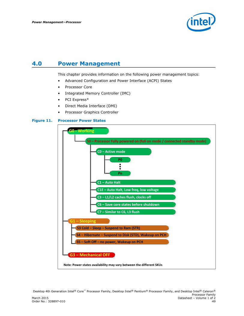
4.0 Power Management
This chapter provides information on the following power management topics:
• Advanced Configuration and Power Interface (ACPI) States
• Processor Core
• Integrated Memory Controller (IMC)
• PCI Express*
• Direct Media Interface (DMI)
• Processor Graphics Controller
Figure 11. Processor Power States
G0 - Working
S0 – Processor Fully powered on (full on mode / connected standby mode)
C0 – Active mode
P0
Pn
C1 – Auto Halt
C1E – Auto Halt, Low freq, low voltage
C3 – L1/L2 caches flush, clocks off
C6 – Save core states before shutdown
C7 – Similar to C6, L3 flush
G1 – Sleeping
Note: Power states availability may vary between the different SKUs
S3 Cold – Sleep – Suspend to Ram (STR)
S4 – Hibernate – Suspend to Disk (STD), Wakeup on PCH
S5 – Soft Off – no power, Wakeup on PCH
G3 – Mechanical OFF
Power Management—Processor
Desktop 4th Generation Intel® Core™ Processor Family, Desktop Intel® Pentium® Processor Family, and Desktop Intel® Celeron®
Processor FamilyMarch 2015 Datasheet – Volume 1 of 2Order No.: 328897-010 49

Advanced Configuration and Power Interface (ACPI)States Supported
This section describes the ACPI states supported by the processor.
Table 11. System States
State Description
G0/S0 Full On Mode.
G1/S3-Cold Suspend-to-RAM (STR). Context saved to memory (S3-Hot state is not supported by theprocessor).
G1/S4 Suspend-to-Disk (STD). All power lost (except wakeup on PCH).
G2/S5 Soft off. All power lost (except wakeup on PCH). Total reboot.
G3 Mechanical off. All power removed from system.
Table 12. Processor Core / Package State Support
State Description
C0 Active mode, processor executing code.
C1 AutoHALT state.
C1E AutoHALT state with lowest frequency and voltage operating point.
C3 Execution cores in C3 state flush their L1 instruction cache, L1 data cache, and L2 cacheto the L3 shared cache. Clocks are shut off to each core.
C6 Execution cores in this state save their architectural state before removing core voltage.
C7
Execution cores in this state behave similarly to the C6 state. If all execution coresrequest C7 state, L3 cache ways are flushed until it is cleared. If the entire L3 cache isflushed, voltage will be removed from the L3 cache. Power removal to SA, Cores and L3will reduce power consumption. C7 may not be available on all SKUs.
Table 13. Integrated Memory Controller States
State Description
Power up CKE asserted. Active mode.
Pre-chargePower-down
CKE de-asserted (not self-refresh) with all banks closed.
Active Power-down
CKE de-asserted (not self-refresh) with minimum one bank active.
Self-Refresh CKE de-asserted using device self-refresh.
Table 14. PCI Express* Link States
State Description
L0 Full on – Active transfer state.
L0s First Active Power Management low-power state – Low exit latency.
L1 Lowest Active Power Management – Longer exit latency.
L3 Lowest power state (power-off) – Longest exit latency.
4.1
Processor—Power Management
Desktop 4th Generation Intel® Core™ Processor Family, Desktop Intel® Pentium® Processor Family, and Desktop Intel® Celeron®
Processor FamilyDatasheet – Volume 1 of 2 March 201550 Order No.: 328897-010

Table 15. Direct Media Interface (DMI) States
State Description
L0 Full on – Active transfer state.
L0s First Active Power Management low-power state – Low exit latency.
L1 Lowest Active Power Management – Longer exit latency.
L3 Lowest power state (power-off) – Longest exit latency.
Table 16. G, S, and C Interface State Combinations
Global(G)
State
Sleep (S)State
ProcessorPackage (C)
State
ProcessorState
System Clocks Description
G0 S0 C0 Full On On Full On
G0 S0 C1/C1E Auto-Halt On Auto-Halt
G0 S0 C3 Deep Sleep On Deep Sleep
G0 S0 C6/C7 Deep Power-down On Deep Power-down
G1 S3 Power off Off, except RTC Suspend to RAM
G1 S4 Power off Off, except RTC Suspend to Disk
G2 S5 Power off Off, except RTC Soft Off
G3 NA Power off Power off Hard off
Table 17. D, S, and C Interface State Combination
GraphicsAdapter (D)
State
Sleep (S)State
Package (C)State
Description
D0 S0 C0 Full On, Displaying.
D0 S0 C1/C1E Auto-Halt, Displaying.
D0 S0 C3 Deep sleep, Displaying.
D0 S0 C6/C7 Deep Power-down, Displaying.
D3 S0 Any Not displaying.
D3 S3 N/A Not displaying, Graphics Core is powered off.
D3 S4 N/A Not displaying, suspend to disk.
Processor Core Power Management
While executing code, Enhanced Intel SpeedStep® Technology optimizes theprocessor’s frequency and core voltage based on workload. Each frequency andvoltage operating point is defined by ACPI as a P-state. When the processor is notexecuting code, it is idle. A low-power idle state is defined by ACPI as a C-state. Ingeneral, deeper power C-states have longer entry and exit latencies.
Enhanced Intel® SpeedStep® Technology Key Features
The following are the key features of Enhanced Intel SpeedStep Technology:
4.2
4.2.1
Power Management—Processor
Desktop 4th Generation Intel® Core™ Processor Family, Desktop Intel® Pentium® Processor Family, and Desktop Intel® Celeron®
Processor FamilyMarch 2015 Datasheet – Volume 1 of 2Order No.: 328897-010 51

• Multiple frequency and voltage points for optimal performance and powerefficiency. These operating points are known as P-states.
• Frequency selection is software controlled by writing to processor MSRs. Thevoltage is optimized based on the selected frequency and the number of activeprocessor cores.
— Once the voltage is established, the PLL locks on to the target frequency.
— All active processor cores share the same frequency and voltage. In a multi-core processor, the highest frequency P-state requested among all activecores is selected.
— Software-requested transitions are accepted at any time. If a previoustransition is in progress, the new transition is deferred until the previoustransition is completed.
• The processor controls voltage ramp rates internally to ensure glitch-freetransitions.
• Because there is low transition latency between P-states, a significant number oftransitions per-second are possible.
Low-Power Idle States
When the processor is idle, low-power idle states (C-states) are used to save power.More power savings actions are taken for numerically higher C-states. However,higher C-states have longer exit and entry latencies. Resolution of C-states occur atthe thread, processor core, and processor package level. Thread-level C-states areavailable if Intel Hyper-Threading Technology is enabled.
Caution: Long term reliability cannot be assured unless all the Low-Power Idle States areenabled.
Figure 12. Idle Power Management Breakdown of the Processor Cores
Thread 0 Thread 1
Core 0 State
Thread 0 Thread 1
Core N State
Processor Package State
Entry and exit of the C-states at the thread and core level are shown in the followingfigure.
4.2.2
Processor—Power Management
Desktop 4th Generation Intel® Core™ Processor Family, Desktop Intel® Pentium® Processor Family, and Desktop Intel® Celeron®
Processor FamilyDatasheet – Volume 1 of 2 March 201552 Order No.: 328897-010

Figure 13. Thread and Core C-State Entry and Exit
C1 C1E C7C6C3
C0MWAIT(C1), HLT
C0
MWAIT(C7),P_LVL4 I/O Read
MWAIT(C6),P_LVL3 I/O ReadMWAIT(C3),
P_LVL2 I/O Read
MWAIT(C1), HLT(C1E Enabled)
While individual threads can request low-power C-states, power saving actions onlytake place once the core C-state is resolved. Core C-states are automatically resolvedby the processor. For thread and core C-states, a transition to and from C0 is requiredbefore entering any other C-state.
Table 18. Coordination of Thread Power States at the Core Level
Processor Core C-State Thread 1
C0 C1 C3 C6 C7
Thread 0
C0 C0 C0 C0 C0 C0
C1 C0 C11 C11 C11 C11
C3 C0 C11 C3 C3 C3
C6 C0 C11 C3 C6 C6
C7 C0 C11 C3 C6 C7
Note: 1. If enabled, the core C-state will be C1E if all cores have resolved a core C1 state or higher.
Requesting Low-Power Idle States
The primary software interfaces for requesting low-power idle states are through theMWAIT instruction with sub-state hints and the HLT instruction (for C1 and C1E).However, software may make C-state requests using the legacy method of I/O readsfrom the ACPI-defined processor clock control registers, referred to as P_LVLx. Thismethod of requesting C-states provides legacy support for operating systems thatinitiate C-state transitions using I/O reads.
For legacy operating systems, P_LVLx I/O reads are converted within the processor tothe equivalent MWAIT C-state request. Therefore, P_LVLx reads do not directly resultin I/O reads to the system. The feature, known as I/O MWAIT redirection, must beenabled in the BIOS.
The BIOS can write to the C-state range field of the PMG_IO_CAPTURE MSR to restrictthe range of I/O addresses that are trapped and emulate MWAIT like functionality.Any P_LVLx reads outside of this range do not cause an I/O redirection to MWAIT(Cx)like request. The reads fall through like a normal I/O instruction.
4.2.3
Power Management—Processor
Desktop 4th Generation Intel® Core™ Processor Family, Desktop Intel® Pentium® Processor Family, and Desktop Intel® Celeron®
Processor FamilyMarch 2015 Datasheet – Volume 1 of 2Order No.: 328897-010 53
Note: When P_LVLx I/O instructions are used, MWAIT sub-states cannot be defined. TheMWAIT sub-state is always zero if I/O MWAIT redirection is used. By default, P_LVLxI/O redirections enable the MWAIT 'break on EFLAGS.IF’ feature that triggers awakeup on an interrupt, even if interrupts are masked by EFLAGS.IF.
Core C-State Rules
The following are general rules for all core C-states, unless specified otherwise:
• A core C-state is determined by the lowest numerical thread state (such as Thread0 requests C1E state while Thread 1 requests C3 state, resulting in a core C1Estate). See the G, S, and C Interface State Combinations table.
• A core transitions to C0 state when:
— An interrupt occurs
— There is an access to the monitored address if the state was entered using anMWAIT/Timed MWAIT instruction
— The deadline corresponding to the Timed MWAIT instruction expires
• An interrupt directed toward a single thread wakes only that thread.
• If any thread in a core is in active (in C0 state), the core's C-state will resolve toC0 state.
• Any interrupt coming into the processor package may wake any core.
• A system reset re-initializes all processor cores.
Core C0 State
The normal operating state of a core where code is being executed.
Core C1/C1E State
C1/C1E is a low power state entered when all threads within a core execute a HLT orMWAIT(C1/C1E) instruction.
A System Management Interrupt (SMI) handler returns execution to either Normalstate or the C1/C1E state. See the Intel® 64 and IA-32 Architectures SoftwareDeveloper’s Manual for more information.
While a core is in C1/C1E state, it processes bus snoops and snoops from otherthreads. For more information on C1E state, see Package C-States on page 55.
Core C3 State
Individual threads of a core can enter the C3 state by initiating a P_LVL2 I/O read tothe P_BLK or an MWAIT(C3) instruction. A core in C3 state flushes the contents of itsL1 instruction cache, L1 data cache, and L2 cache to the shared L3 cache, whilemaintaining its architectural state. All core clocks are stopped at this point. Becausethe core’s caches are flushed, the processor does not wake any core that is in the C3state when either a snoop is detected or when another core accesses cacheablememory.
4.2.4
Processor—Power Management
Desktop 4th Generation Intel® Core™ Processor Family, Desktop Intel® Pentium® Processor Family, and Desktop Intel® Celeron®
Processor FamilyDatasheet – Volume 1 of 2 March 201554 Order No.: 328897-010

Core C6 State
Individual threads of a core can enter the C6 state by initiating a P_LVL3 I/O read oran MWAIT(C6) instruction. Before entering core C6 state, the core will save itsarchitectural state to a dedicated SRAM. Once complete, a core will have its voltagereduced to zero volts. During exit, the core is powered on and its architectural state isrestored.
Core C7 State
Individual threads of a core can enter the C7 state by initiating a P_LVL4 I/O read tothe P_BLK or by an MWAIT(C7) instruction. The core C7 state exhibits the samebehavior as the core C6 state.
Note: C7 state may not be available on all SKUs.
C-State Auto-Demotion
In general, deeper C-states, such as C6 state, have long latencies and have higherenergy entry/exit costs. The resulting performance and energy penalties becomesignificant when the entry/exit frequency of a deeper C-state is high. Therefore,incorrect or inefficient usage of deeper C-states have a negative impact on idle power.To increase residency and improve idle power in deeper C-states, the processorsupports C-state auto-demotion.
There are two C-state auto-demotion options:
• C7/C6 to C3 state
• C7/C6/C3 To C1 state
The decision to demote a core from C6/C7 to C3 or C3/C6/C7 to C1 state is based oneach core’s immediate residency history and interrupt rate . If the interrupt rateexperienced on a core is high and the residence in a deep C-state between suchinterrupts is low, the core can be demoted to a C3 or C1 state. A higher interruptpattern is required to demote a core to C1 state as compared to C3 state.
This feature is disabled by default. BIOS must enable it in thePMG_CST_CONFIG_CONTROL register. The auto-demotion policy is also configured bythis register.
Package C-States
The processor supports C0, C1/C1E, C3, C6, and C7 (on some SKUs) power states.The following is a summary of the general rules for package C-state entry. Theseapply to all package C-states, unless specified otherwise:
• A package C-state request is determined by the lowest numerical core C-stateamongst all cores.
• A package C-state is automatically resolved by the processor depending on thecore idle power states and the status of the platform components.
— Each core can be at a lower idle power state than the package if the platformdoes not grant the processor permission to enter a requested package C-state.
— The platform may allow additional power savings to be realized in theprocessor.
4.2.5
Power Management—Processor
Desktop 4th Generation Intel® Core™ Processor Family, Desktop Intel® Pentium® Processor Family, and Desktop Intel® Celeron®
Processor FamilyMarch 2015 Datasheet – Volume 1 of 2Order No.: 328897-010 55

— For package C-states, the processor is not required to enter C0 state beforeentering any other C-state.
— Entry into a package C-state may be subject to auto-demotion – that is, theprocessor may keep the package in a deeper package C-state than requestedby the operating system if the processor determines, using heuristics, that thedeeper C-state results in better power/performance.
The processor exits a package C-state when a break event is detected. Depending onthe type of break event, the processor does the following:
• If a core break event is received, the target core is activated and the break eventmessage is forwarded to the target core.
— If the break event is not masked, the target core enters the core C0 state andthe processor enters package C0 state.
— If the break event is masked, the processor attempts to re-enter its previouspackage state.
• If the break event was due to a memory access or snoop request,
— But the platform did not request to keep the processor in a higher package C-state, the package returns to its previous C-state.
— And the platform requests a higher power C-state, the memory access orsnoop request is serviced and the package remains in the higher power C-state.
The following table shows package C-state resolution for a dual-core processor. Thefollowing figure summarizes package C-state transitions.
Table 19. Coordination of Core Power States at the Package Level
Package C-State Core 1
C0 C1 C3 C6 C7
Core 0
C0 C0 C0 C0 C0 C0
C1 C0 C11 C11 C11 C11
C3 C0 C11 C3 C3 C3
C6 C0 C11 C3 C6 C6
C7 C0 C11 C3 C6 C7
Note: 1. If enabled, the package C-state will be C1E if all cores have resolved a core C1 state or higher.
Processor—Power Management
Desktop 4th Generation Intel® Core™ Processor Family, Desktop Intel® Pentium® Processor Family, and Desktop Intel® Celeron®
Processor FamilyDatasheet – Volume 1 of 2 March 201556 Order No.: 328897-010
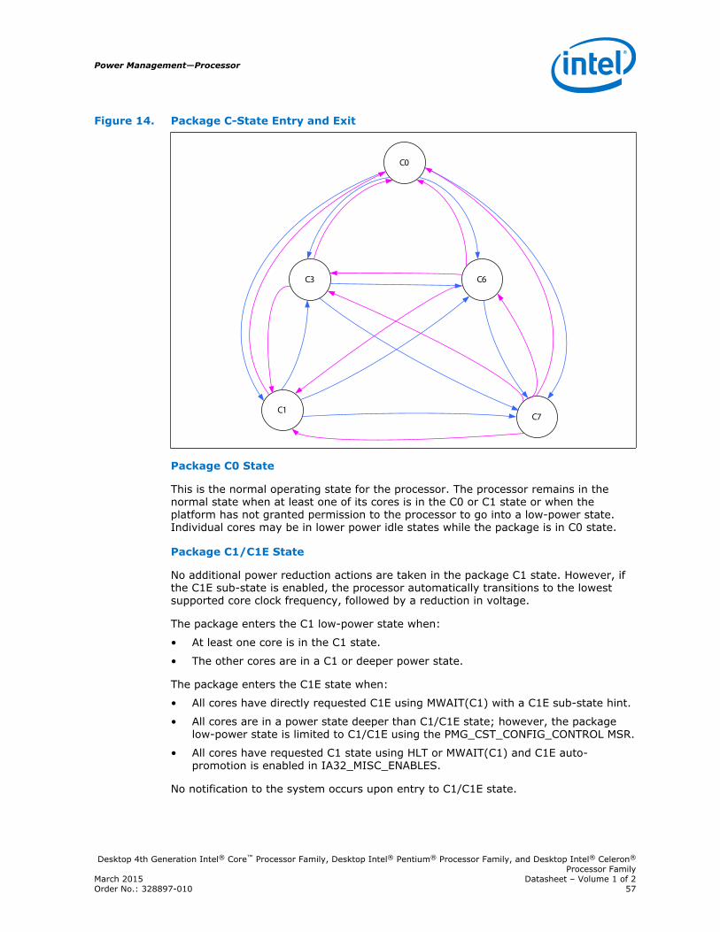
Figure 14. Package C-State Entry and Exit
C0
C1
C6
C7
C3
Package C0 State
This is the normal operating state for the processor. The processor remains in thenormal state when at least one of its cores is in the C0 or C1 state or when theplatform has not granted permission to the processor to go into a low-power state.Individual cores may be in lower power idle states while the package is in C0 state.
Package C1/C1E State
No additional power reduction actions are taken in the package C1 state. However, ifthe C1E sub-state is enabled, the processor automatically transitions to the lowestsupported core clock frequency, followed by a reduction in voltage.
The package enters the C1 low-power state when:
• At least one core is in the C1 state.
• The other cores are in a C1 or deeper power state.
The package enters the C1E state when:
• All cores have directly requested C1E using MWAIT(C1) with a C1E sub-state hint.
• All cores are in a power state deeper than C1/C1E state; however, the packagelow-power state is limited to C1/C1E using the PMG_CST_CONFIG_CONTROL MSR.
• All cores have requested C1 state using HLT or MWAIT(C1) and C1E auto-promotion is enabled in IA32_MISC_ENABLES.
No notification to the system occurs upon entry to C1/C1E state.
Power Management—Processor
Desktop 4th Generation Intel® Core™ Processor Family, Desktop Intel® Pentium® Processor Family, and Desktop Intel® Celeron®
Processor FamilyMarch 2015 Datasheet – Volume 1 of 2Order No.: 328897-010 57

Package C2 State
Package C2 state is an internal processor state that cannot be explicitly requested bysoftware. A processor enters Package C2 state when:
• All cores and graphics have requested a C3 or deeper power state; however,constraints (LTR, programmed timer events in the near future, and so on) prevententry to any state deeper than C 2 state. Or,
• All cores and graphics are in the C3 or deeper power states, and a memory accessrequest is received. Upon completion of all outstanding memory requests, theprocessor transitions back into a deeper package C-state.
Package C3 State
A processor enters the package C3 low-power state when:
• At least one core is in the C3 state.
• The other cores are in a C3 state or deeper power state and the processor hasbeen granted permission by the platform.
• The platform has not granted a request to a package C6 or deeper state, however,has allowed a package C6 state.
In package C3 state, the L3 shared cache is valid.
Package C6 State
A processor enters the package C6 low-power state when:
• At least one core is in the C6 state.
• The other cores are in a C6 or deeper power state and the processor has beengranted permission by the platform.
• If the cores are requesting C7 state, but the platform is limiting to a package C6state, the last level cache in this case can be flushed.
In package C6 state all cores have saved their architectural state and have had theircore voltages reduced to zero volts. It is possible the L3 shared cache is flushed andturned off in package C6 state. If at least one core is requesting C6 state, the L3cache will not be flushed.
Package C7 State
The processor enters the package C7 low-power state when all cores are in the C7state. In package C7, the processor will take action to remove power from portions ofthe system agent.
Core break events are handled the same way as in package C3 or C6 state.
Note: C7 state may not be available on all SKUs.
Processor—Power Management
Desktop 4th Generation Intel® Core™ Processor Family, Desktop Intel® Pentium® Processor Family, and Desktop Intel® Celeron®
Processor FamilyDatasheet – Volume 1 of 2 March 201558 Order No.: 328897-010

Note: Package C6 state is the deepest C-state supported on discrete graphics systems withPCI Express Graphics (PEG).
Package C7 state is the deepest C-state supported on integrated graphics systems (orswitchable graphics systems during integrated graphics mode). However, in mostconfigurations, package C6 will be more energy efficient than package C7 state. As aresult, package C7 state residency is expected to be very low or zero in mostscenarios where the display is enabled. Logic internal to the processor will determinewhether package C6 or package C7 state is the most efficient. There is no need tomake changes in BIOS or system software to prioritize package C6 state over packageC7 state.
Package C-States and Display Resolutions
The integrated graphics engine has the frame buffer located in system memory. Whenthe display is updated, the graphics engine fetches display data from system memory.Different screen resolutions and refresh rates have different memory latencyrequirements. These requirements may limit the deepest Package C-state theprocessor can enter. Other elements that may affect the deepest Package C-stateavailable are the following:
• Display is on or off
• Single or multiple displays
• Native or non-native resolution
• Panel Self Refresh (PSR) technology
Note: Display resolution is not the only factor influencing the deepest Package C-state theprocessor can get into. Device latencies, interrupt response latencies, and core C-states are among other factors that influence the final package C-state the processorcan enter.
The following table lists display resolutions and deepest available package C-State.The display resolutions are examples using common values for blanking and pixelrate. Actual results will vary. The table shows the deepest possible Package C-state.System workload, system idle, and AC or DC power also affect the deepest possiblePackage C-state.
Table 20. Deepest Package C-State Available
Number of Displays 1 Native Resolution Deepest Available Package C-State
Single 800x600 60 Hz PC6
Single 1024x768 60 Hz PC6
Single 1280x1024 60 Hz PC6
Single 1920x1080 60 Hz PC6
Single 1920x1200 60 Hz PC6
Single 1920x1440 60 Hz PC6
Single 2048x1536 60 Hz PC6
Single 2560x1600 60 Hz PC6
Single 2560x1920 60 Hz PC3
continued...
4.2.6
Power Management—Processor
Desktop 4th Generation Intel® Core™ Processor Family, Desktop Intel® Pentium® Processor Family, and Desktop Intel® Celeron®
Processor FamilyMarch 2015 Datasheet – Volume 1 of 2Order No.: 328897-010 59
Number of Displays 1 Native Resolution Deepest Available Package C-State
Single 2880x1620 60 Hz PC3
Single 2880x1800 60 Hz PC3
Single 3200x1800 60 Hz PC3
Single 3200x2000 60 Hz PC3
Single 3840x2160 60 Hz PC3
Single 3840x2160 30 Hz PC3
Single 4096x2160 24 Hz PC3
Multiple 800x600 60 Hz PC6
Multiple 1024x768 60 Hz PC6
Multiple 1280x1024 60 Hz PC6
Multiple 1920x1080 60 Hz PC3
Multiple 1920x1200 60 Hz PC3
Multiple 1920x1440 60 Hz PC3
Multiple 2048x1536 60 Hz PC3
Multiple 2560x1600 60 Hz PC2
Multiple 2560x1920 60 Hz PC2
Multiple 2880x1620 60 Hz PC2
Multiple 2880x1800 60 Hz PC2
Multiple 3200x1800 60 Hz PC2
Multiple 3200x2000 60 Hz PC2
Multiple 3840x2160 60 Hz PC2
Multiple 3840x2160 30 Hz PC2
Multiple 4096x2160 24 Hz PC2
Notes: 1. For multiple display cases, the resolution listed is the highest native resolution of all enableddisplays, and PSR is internally disabled; that is, dual display with one 800x600 60 Hz display andone 2560x1600 60 Hz display will result in a deepest available package C-state of PC2.
2. Microcode Update rev 00000010 or newer must be used.
Integrated Memory Controller (IMC) Power Management
The main memory is power managed during normal operation and in low-power ACPICx states.
Disabling Unused System Memory Outputs
Any system memory (SM) interface signal that goes to a memory module connector inwhich it is not connected to any actual memory devices (such as SO-DIMM connectoris unpopulated, or is single-sided) is tri-stated. The benefits of disabling unused SMsignals are:
• Reduced power consumption.
4.3
4.3.1
Processor—Power Management
Desktop 4th Generation Intel® Core™ Processor Family, Desktop Intel® Pentium® Processor Family, and Desktop Intel® Celeron®
Processor FamilyDatasheet – Volume 1 of 2 March 201560 Order No.: 328897-010

• Reduced possible overshoot/undershoot signal quality issues seen by theprocessor I/O buffer receivers caused by reflections from potentially un-terminated transmission lines.
When a given rank is not populated, the corresponding chip select and CKE signals arenot driven.
At reset, all rows must be assumed to be populated, until it can be determined thatthe rows are not populated. This is due to the fact that when CKE is tri-stated with anSO-DIMM present, the SO-DIMM is not ensured to maintain data integrity.
CKE tri-state should be enabled by BIOS where appropriate, since at reset all rowsmust be assumed to be populated.
DRAM Power Management and Initialization
The processor implements extensive support for power management on the SDRAMinterface. There are four SDRAM operations associated with the Clock Enable (CKE)signals, which the SDRAM controller supports. The processor drives four CKE pins toperform these operations.
The CKE is one of the power save means. When CKE is off, the internal DDR clock isdisabled and the DDR power is reduced. The power saving differs according to theselected mode and the DDR type used. For more information, refer to the IDD table inthe DDR specification.
The processor supports three different types of power-down modes in package C0.The different power-down modes can be enabled through configuring"PM_PDWN_config_0_0_0_MCHBAR". The type of CKE power-down can be configuredthrough PDWN_mode (bits 15:12) and the idle timer can be configured throughPDWN_idle_counter (bits 11:0). The different power-down modes supported are:
• No power-down (CKE disable)
• Active power-down (APD): This mode is entered if there are open pages whende-asserting CKE. In this mode the open pages are retained. Power-saving in thismode is the lowest. Power consumption of DDR is defined by IDD3P. Exiting thismode is defined by tXP – small number of cycles. For this mode, DRAM DLL mustbe on.
• PPD/DLL-off: In this mode the data-in DLLs on DDR are off. Power-saving in thismode is the best among all power modes. Power consumption is defined byIDD2P1. Exiting this mode is defined by tXP, but also tXPDLL (10–20 according toDDR type) cycles until first data transfer is allowed. For this mode, DRAM DLLmust be off.
The CKE is determined per rank, whenever it is inactive. Each rank has an idle-counter. The idle-counter starts counting as soon as the rank has no accesses, and ifit expires, the rank may enter power-down while no new transactions to the rankarrives to queues. The idle-counter begins counting at the last incoming transactionarrival.
It is important to understand that since the power-down decision is per rank, the IMCcan find many opportunities to power down ranks, even while running memoryintensive applications; the savings are significant (may be few Watts, according to theDDR specification). This is significant when each channel is populated with moreranks.
4.3.2
Power Management—Processor
Desktop 4th Generation Intel® Core™ Processor Family, Desktop Intel® Pentium® Processor Family, and Desktop Intel® Celeron®
Processor FamilyMarch 2015 Datasheet – Volume 1 of 2Order No.: 328897-010 61
Selection of power modes should be according to power-performance or thermaltrade-offs of a given system:
• When trying to achieve maximum performance and power or thermalconsideration is not an issue – use no power-down
• In a system which tries to minimize power-consumption, try using the deepestpower-down mode possible – PPD/DLL-off with a low idle timer value.
• In high-performance systems with dense packaging (that is, tricky thermaldesign) the power-down mode should be considered in order to reduce the heatingand avoid DDR throttling caused by the heating.
The default value that BIOS configures in "PM_PDWN_config_0_0_0_MCHBAR" is6080h; that is, PPD/DLL-off mode with idle timer of 80h, or 128 DCLKs. This is abalanced setting with deep power-down mode and moderate idle timer value.
The idle timer expiration count defines the number of DCKLs that a rank is idle thatcauses entry to the selected power mode. As this timer is set to a shorter time, theIMC will have more opportunities to put DDR in power-down. There is no BIOS hook toset this register. Customers choosing to change the value of this register can do it bychanging it in the BIOS. For experiments, this register can be modified in real time ifBIOS does not lock the IMC registers.
Initialization Role of CKE
During power-up, CKE is the only input to the SDRAM that has its level recognized(other than the DDR3/DDR3L reset pin) once power is applied. It must be driven LOWby the DDR controller to make sure the SDRAM components float DQ and DQS duringpower-up. CKE signals remain LOW (while any reset is active) until the BIOS writes toa configuration register. Using this method, CKE is ensured to remain inactive formuch longer than the specified 200 micro-seconds after power and clocks to SDRAMdevices are stable.
Conditional Self-Refresh
During S0 idle state, system memory may be conditionally placed into self-refreshstate when the processor is in package C3 or deeper power state. Refer to Intel®Rapid Memory Power Management (Intel® RMPM) for more details on conditional self-refresh with Intel HD Graphics enabled.
When entering the S3 – Suspend-to-RAM (STR) state or S0 conditional self-refresh,the processor core flushes pending cycles and then enters SDRAM ranks that are notused by Intel graphics memory into self-refresh. The CKE signals remain LOW so theSDRAM devices perform self-refresh.
The target behavior is to enter self-refresh for package C3 or deeper power states aslong as there are no memory requests to service.
Dynamic Power-Down
Dynamic power-down of memory is employed during normal operation. Based on idleconditions, a given memory rank may be powered down. The IMC implementsaggressive CKE control to dynamically put the DRAM devices in a power-down state.The processor core controller can be configured to put the devices in active power-down (CKE de-assertion with open pages) or pre-charge power-down (CKE de-
4.3.2.1
4.3.2.2
4.3.2.3
Processor—Power Management
Desktop 4th Generation Intel® Core™ Processor Family, Desktop Intel® Pentium® Processor Family, and Desktop Intel® Celeron®
Processor FamilyDatasheet – Volume 1 of 2 March 201562 Order No.: 328897-010

assertion with all pages closed). Pre-charge power-down provides greater powersavings, but has a bigger performance impact since all pages will first be closed beforeputting the devices in power-down mode.
If dynamic power-down is enabled, all ranks are powered up before doing a refreshcycle and all ranks are powered down at the end of refresh.
DRAM I/O Power Management
Unused signals should be disabled to save power and reduce electromagneticinterference. This includes all signals associated with an unused memory channel.Clocks, CKE, ODE, and CS signals are controlled per DIMM rank and will be powereddown for unused ranks.
The I/O buffer for an unused signal should be tri-stated (output driver disabled), theinput receiver (differential sense-amp) should be disabled, and any DLL circuitryrelated ONLY to unused signals should be disabled. The input path must be gated toprevent spurious results due to noise on the unused signals (typically handledautomatically when input receiver is disabled).
DRAM Running Average Power Limitation (RAPL)
RAPL is a power and time constant pair. DRAM RAPL defines an average powerconstraint for the DRAM domain. Constraint is controlled by the PCU. Platform entities(PECI or in-band power driver) can specify a power limit for the DRAM domain. PCUcontinuously monitors the extant of DRAM throttling due to the power limit andrebudgets the limit between DIMMs.
DDR Electrical Power Gating (EPG)
The DDR I/O of the processor supports Electrical Power Gating (DDR-EPG) while theprocessor is at C3 or deeper power state.
In C3 or deeper power state, the processor internally gates VDDQ for the majority ofthe logic to reduce idle power while keeping all critical DDR pins such asSM_DRAMRST#, CKE and VREF in the appropriate state.
In C7, the processor internally gates VCCIO_TERM for all non-critical state to reduce idlepower.
In S3 or C-state transitions, the DDR does not go through training mode and willrestore the previous training information.
PCI Express* Power Management
• Active power management is supported using L0s, and L1 states.
• All inputs and outputs disabled in L2/L3 Ready state.
Direct Media Interface (DMI) Power Management
Active power management is supported using L0s/L1 state.
4.3.2.4
4.3.3
4.3.4
4.4
4.5
Power Management—Processor
Desktop 4th Generation Intel® Core™ Processor Family, Desktop Intel® Pentium® Processor Family, and Desktop Intel® Celeron®
Processor FamilyMarch 2015 Datasheet – Volume 1 of 2Order No.: 328897-010 63
Graphics Power Management
Intel® Rapid Memory Power Management (Intel® RMPM)
Intel Rapid Memory Power Management (Intel RMPM) conditionally places memoryinto self-refresh when the processor is in package C3 or deeper power state to allowthe system to remain in the lower power states longer for memory not reserved forgraphics memory. Intel RMPM functionality depends on graphics/display state(relevant only when processor graphics is being used), as well as memory trafficpatterns generated by other connected I/O devices.
Graphics Render C-State
Render C-state (RC6) is a technique designed to optimize the average power to thegraphics render engine during times of idleness. RC6 is entered when the graphicsrender engine, blitter engine, and the video engine have no workload being currentlyworked on and no outstanding graphics memory transactions. When the idlenesscondition is met, the processor graphics will program the graphics render engineinternal power rail into a low voltage state.
Intel® Graphics Dynamic Frequency
Intel Graphics Dynamic Frequency Technology is the ability of the processor andgraphics cores to opportunistically increase frequency and/or voltage above theguaranteed processor and graphics frequency for the given part. Intel GraphicsDynamic Frequency Technology is a performance feature that makes use of unusedpackage power and thermals to increase application performance. The increase infrequency is determined by how much power and thermal budget is available in thepackage, and the application demand for additional processor or graphicsperformance. The processor core control is maintained by an embedded controller.The graphics driver dynamically adjusts between P-States to maintain optimalperformance, power, and thermals. The graphics driver will always try to place thegraphics engine in the most energy efficient P-state.
4.6
4.6.1
4.6.2
4.6.3
Processor—Power Management
Desktop 4th Generation Intel® Core™ Processor Family, Desktop Intel® Pentium® Processor Family, and Desktop Intel® Celeron®
Processor FamilyDatasheet – Volume 1 of 2 March 201564 Order No.: 328897-010

5.0 Thermal Management
This chapter provides both component-level and system-level thermal management.Topics covered include processor thermal specifications, thermal profiles, thermalmetrology, fan speed control, adaptive thermal monitor, THERMTRIP# signal, DigitalThermal Sensor (DTS), Intel Turbo Boost Technology, package power control, powerplane control, and turbo time parameter.
The processor requires a thermal solution to maintain temperatures within itsoperating limits. Any attempt to operate the processor outside these operating limitsmay result in permanent damage to the processor and potentially other componentswithin the system. Maintaining the proper thermal environment is key to reliable,long-term system operation.
A complete solution includes both component and system level thermal managementfeatures. Component level thermal solutions can include active or passive heatsinksattached to the processor integrated heat spreader (IHS).
To allow the optimal operation and long-term reliability of Intel processor-basedsystems, the processor must remain within the minimum and maximum casetemperature (TCASE) specifications as defined by the applicable thermal profile.Thermal solutions not designed to provide this level of thermal capability may affectthe long-term reliability of the processor and system.
The processors implement a methodology for managing processor temperatures thatis intended to support acoustic noise reduction through fan speed control and toassure processor reliability. Selection of the appropriate fan speed is based on therelative temperature data reported by the processor’s Digital Temperature Sensor(DTS). The DTS can be read using the Platform Environment Control Interface (PECI)as described in Processor Temperature on page 78. Alternatively, when PECI ismonitored by the PCH, the processor temperature can be read from the PCH using theSMBus protocol defined in Embedded Controller Support Provided by the PCH. Thetemperature reported over PECI is always a negative value and represents a deltabelow the onset of thermal control circuit (TCC) activation, as indicated by PROCHOT#(see Processor Temperature on page 78). Systems that implement fan speed controlmust be designed to use this data. Systems that do not alter the fan speed only needto ensure the case temperature meets the thermal profile specifications.
Analysis indicates that real applications are unlikely to cause the processor toconsume maximum power dissipation for sustained time periods. Intel recommendsthat complete thermal solution designs target the Thermal Design Power (TDP),instead of the maximum processor power consumption. The Adaptive Thermal Monitorfeature is intended to help protect the processor in the event that an applicationexceeds the TDP recommendation for a sustained time period. For more details on thisfeature, see Adaptive Thermal Monitor on page 78. To ensure maximum flexibilityfor future processors, systems should be designed to the Thermal Solution Capabilityguidelines, even if a processor with lower power dissipation is currently planned.
Thermal Management—Processor
Desktop 4th Generation Intel® Core™ Processor Family, Desktop Intel® Pentium® Processor Family, and Desktop Intel® Celeron®
Processor FamilyMarch 2015 Datasheet – Volume 1 of 2Order No.: 328897-010 65
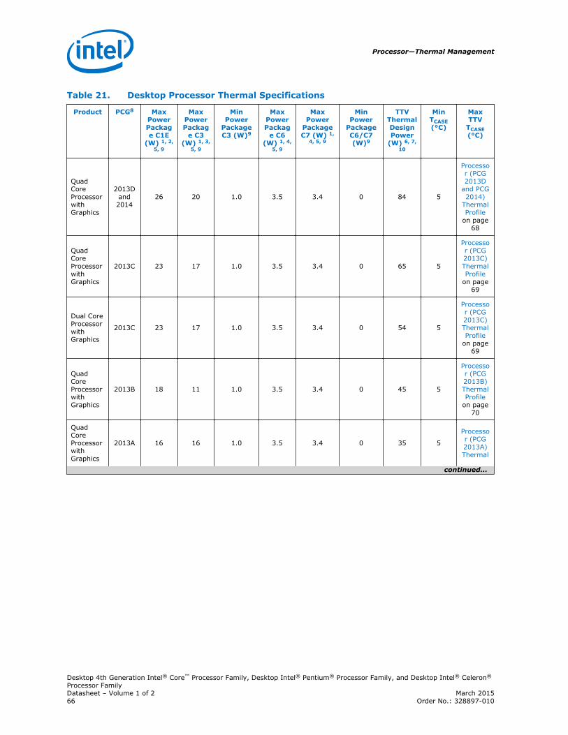
Table 21. Desktop Processor Thermal Specifications
Product PCG8 MaxPowerPackage C1E
(W) 1, 2,5, 9
MaxPowerPackag
e C3(W) 1, 3,
5, 9
MinPower
PackageC3 (W)9
MaxPowerPackag
e C6(W) 1, 4,
5, 9
MaxPower
PackageC7 (W) 1,
4, 5, 9
MinPower
PackageC6/C7(W)9
TTVThermalDesignPower
(W) 6, 7,10
MinTCASE(°C)
MaxTTV
TCASE(°C)
QuadCoreProcessorwithGraphics
2013Dand2014
26 20 1.0 3.5 3.4 0 84 5
Processor (PCG2013D
and PCG2014)
ThermalProfile
on page68
QuadCoreProcessorwithGraphics
2013C 23 17 1.0 3.5 3.4 0 65 5
Processor (PCG2013C)ThermalProfile
on page69
Dual CoreProcessorwithGraphics
2013C 23 17 1.0 3.5 3.4 0 54 5
Processor (PCG2013C)ThermalProfile
on page69
QuadCoreProcessorwithGraphics
2013B 18 11 1.0 3.5 3.4 0 45 5
Processor (PCG2013B)ThermalProfile
on page70
QuadCoreProcessorwithGraphics
2013A 16 16 1.0 3.5 3.4 0 35 5
Processor (PCG2013A)Thermal
continued...
Processor—Thermal Management
Desktop 4th Generation Intel® Core™ Processor Family, Desktop Intel® Pentium® Processor Family, and Desktop Intel® Celeron®
Processor FamilyDatasheet – Volume 1 of 2 March 201566 Order No.: 328897-010

Product PCG8 MaxPowerPackage C1E
(W) 1, 2,5, 9
MaxPowerPackag
e C3(W) 1, 3,
5, 9
MinPower
PackageC3 (W)9
MaxPowerPackag
e C6(W) 1, 4,
5, 9
MaxPower
PackageC7 (W) 1,
4, 5, 9
MinPower
PackageC6/C7(W)9
TTVThermalDesignPower
(W) 6, 7,10
MinTCASE(°C)
MaxTTV
TCASE(°C)
Profileon page
72
Dual CoreProcessorwithGraphics
16 16 1.0 3.5 3.4 0 35 5
Notes: 1. The package C-state power is the worst case power in the system configured as follows:a. Memory configured for DDR3 1333 and populated with two DIMMs per channel.b. DMI and PCIe links are at L1.
2. Specification at DTS = 50 °C and minimum voltage loadline.3. Specification at DTS = 50 °C and minimum voltage loadline.4. Specification at DTS = 35 °C and minimum voltage loadline.5. These DTS values in Notes 2 – 4 are based on the TCC Activation MSR having a value of 100, see Processor
Temperature on page 78.6. These values are specified at VCC_MAX and VNOM for all other voltage rails for all processor frequencies. Systems
must be designed to ensure the processor is not to be subjected to any static VCC and ICC combination wherein VCCPexceeds VCCP_MAX at specified ICCP. See the loadline specifications.
7. Thermal Design Power (TDP) should be used for processor thermal solution design targets. TDP is not themaximum power that the processor can dissipate. TDP is measured at DTS = -1. TDP is achieved with the Memoryconfigured for DDR3 1333 and 2 DIMMs per channel.
8. Platform Compatibility Guide (PCG) (previously known as FMB) provides a design target for meeting all plannedprocessor frequency requirements.
9. Not 100% tested. Specified by design characterization.
Desktop Processor Thermal Profiles
This section provides thermal profiles for the Desktop processor families.
5.1
Thermal Management—Processor
Desktop 4th Generation Intel® Core™ Processor Family, Desktop Intel® Pentium® Processor Family, and Desktop Intel® Celeron®
Processor FamilyMarch 2015 Datasheet – Volume 1 of 2Order No.: 328897-010 67

Processor (PCG 2013D and PCG 2014) Thermal Profile
Figure 15. Thermal Test Vehicle Thermal Profile for Processor (PCG 2013D and PCG2014)
40
45
50
55
60
65
70
75
80
0 20 40 60 80 100
TTV
Cas
e T
em
pe
ratu
re (
°C)
TTV Power (W)
TCASE = 0.33 * Power + 45.0
See the following table for discrete points that constitute the thermal profile.
Table 22. Thermal Test Vehicle Thermal Profile for Processor (PCG 2013D and PCG2014)
Power (W) TCASE_MAX(°C)
Y = 0.33 * Power + 45
0 45.00
2 45.66
4 46.32
6 46.98
8 47.64
10 48.30
12 48.96
14 49.62
16 50.28
18 50.94
20 51.60
22 52.26
24 52.92
continued...
Power (W) TCASE_MAX(°C)
26 53.58
28 54.24
30 54.90
32 55.56
34 56.22
36 56.88
38 57.54
40 58.20
42 58.86
44 59.52
46 60.18
48 60.84
50 61.50
52 62.16
continued...
Power (W) TCASE_MAX(°C)
54 62.82
56 63.48
58 64.14
60 64.80
62 65.46
64 66.12
66 66.78
68 67.44
70 68.10
72 68.76
74 69.42
76 70.08
78 70.74
continued...
5.1.1
Processor—Thermal Management
Desktop 4th Generation Intel® Core™ Processor Family, Desktop Intel® Pentium® Processor Family, and Desktop Intel® Celeron®
Processor FamilyDatasheet – Volume 1 of 2 March 201568 Order No.: 328897-010
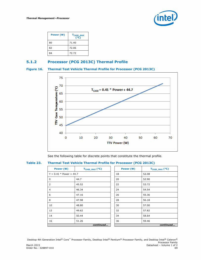
Power (W) TCASE_MAX(°C)
80 71.40
82 72.06
84 72.72
Processor (PCG 2013C) Thermal Profile
Figure 16. Thermal Test Vehicle Thermal Profile for Processor (PCG 2013C)
See the following table for discrete points that constitute the thermal profile.
Table 23. Thermal Test Vehicle Thermal Profile for Processor (PCG 2013C)
Power (W) TCASE_MAX (°C)
Y = 0.41 * Power + 44.7
0 44.7
2 45.52
4 46.34
6 47.16
8 47.98
10 48.80
12 49.62
14 50.44
16 51.26
continued...
Power (W) TCASE_MAX (°C)
18 52.08
20 52.90
22 53.72
24 54.54
26 55.36
28 56.18
30 57.00
32 57.82
34 58.64
36 59.46
continued...
5.1.2
Thermal Management—Processor
Desktop 4th Generation Intel® Core™ Processor Family, Desktop Intel® Pentium® Processor Family, and Desktop Intel® Celeron®
Processor FamilyMarch 2015 Datasheet – Volume 1 of 2Order No.: 328897-010 69

Power (W) TCASE_MAX (°C)
38 60.28
40 61.10
42 61.92
44 62.74
46 63.56
48 64.38
50 65.20
52 66.02
54 66.84
56 67.66
58 68.48
60 69.30
62 70.12
64 70.94
65 71.35
Processor (PCG 2013B) Thermal Profile
Figure 17. Thermal Test Vehicle Thermal Profile for Processor (PCG 2013B)
See the following table for discrete points that constitute the thermal profile.
5.1.3
Processor—Thermal Management
Desktop 4th Generation Intel® Core™ Processor Family, Desktop Intel® Pentium® Processor Family, and Desktop Intel® Celeron®
Processor FamilyDatasheet – Volume 1 of 2 March 201570 Order No.: 328897-010
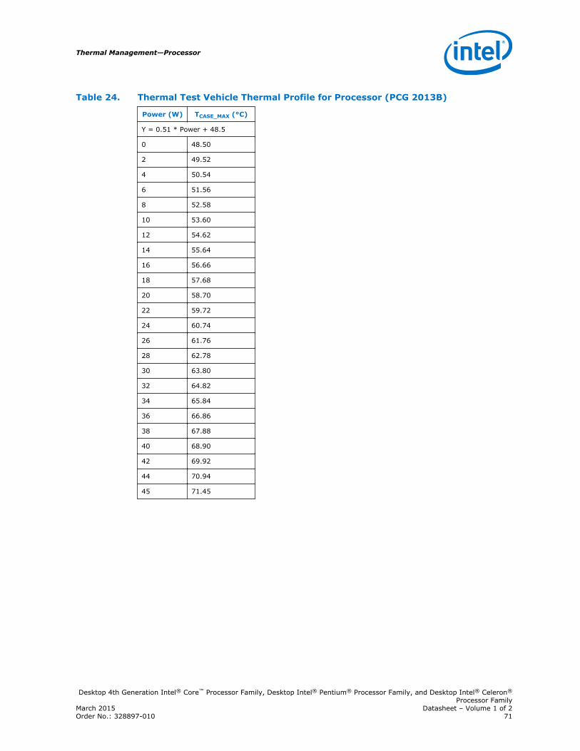
Table 24. Thermal Test Vehicle Thermal Profile for Processor (PCG 2013B)
Power (W) TCASE_MAX (°C)
Y = 0.51 * Power + 48.5
0 48.50
2 49.52
4 50.54
6 51.56
8 52.58
10 53.60
12 54.62
14 55.64
16 56.66
18 57.68
20 58.70
22 59.72
24 60.74
26 61.76
28 62.78
30 63.80
32 64.82
34 65.84
36 66.86
38 67.88
40 68.90
42 69.92
44 70.94
45 71.45
Thermal Management—Processor
Desktop 4th Generation Intel® Core™ Processor Family, Desktop Intel® Pentium® Processor Family, and Desktop Intel® Celeron®
Processor FamilyMarch 2015 Datasheet – Volume 1 of 2Order No.: 328897-010 71

Processor (PCG 2013A) Thermal Profile
Figure 18. Thermal Test Vehicle Thermal Profile for Processor (PCG 2013A)
See the following table for discrete points that constitute the thermal profile.
Table 25. Thermal Test Vehicle Thermal Profile for Processor (PCG 2013A)
Power (W) TCASE_MAX (°C)
Y = 0.51 * Power + 48.5
0 48.50
2 49.52
4 50.54
6 51.56
8 52.58
10 53.60
12 54.62
14 55.64
16 56.66
18 57.68
20 58.70
22 59.72
24 60.74
26 61.76
28 62.78
continued...
Power (W) TCASE_MAX (°C)
30 63.80
32 64.82
34 65.84
35 66.35
5.1.4
Processor—Thermal Management
Desktop 4th Generation Intel® Core™ Processor Family, Desktop Intel® Pentium® Processor Family, and Desktop Intel® Celeron®
Processor FamilyDatasheet – Volume 1 of 2 March 201572 Order No.: 328897-010

Thermal Metrology
The maximum Thermal Test Vehicle (TTV) case temperatures (TCASE-MAX) can bederived from the data in the appropriate TTV thermal profile earlier in this chapter.The TTV TCASE is measured at the geometric top center of the TTV integrated heatspreader (IHS). The following figure illustrates the location where TCASE temperaturemeasurements should be made.
Figure 19. Thermal Test Vehicle (TTV) Case Temperature (TCASE) Measurement Location
37.5
37.5
Measure TCASE atthe geometriccenter of the
package
Note: THERM-X OF CALIFORNIA can machine the groove and attach a thermocouple to theIHS. The supplier is subject to change without notice. THERM-X OF CALIFORNIA, 1837Whipple Road, Hayward, Ca 94544. Ernesto B Valencia +1-510-441-7566 Ext. [email protected]. The vendor part number is XTMS1565.
Fan Speed Control Scheme with Digital Thermal Sensor(DTS) 1.1
To correctly use DTS 1.1, the designer must first select a worst case scenario TAMBIENT,and ensure that the Fan Speed Control (FSC) can provide a ΨCA that is equivalent orgreater than the ΨCA specification.
The DTS 1.1 implementation consists of two points: a ΨCA at TCONTROL and a ΨCA atDTS = -1.
5.2
5.3
Thermal Management—Processor
Desktop 4th Generation Intel® Core™ Processor Family, Desktop Intel® Pentium® Processor Family, and Desktop Intel® Celeron®
Processor FamilyMarch 2015 Datasheet – Volume 1 of 2Order No.: 328897-010 73

The ΨCA point at DTS = -1 defines the minimum ΨCA required at TDP considering theworst case system design TAMBIENT design point:
ΨCA = (TCASE-MAX – TAMBIENT-TARGET) / TDP
For example, for a 95 W TDP part, the Tcase maximum is 72.6 °C and at a worst casedesign point of 40 °C local ambient this will result in:
ΨCA = (72.6 – 40) / 95 = 0.34 °C/W
Similarly for a system with a design target of 45 °C ambient, the ΨCA at DTS = -1needed will be 0.29 °C/W.
The second point defines the thermal solution performance (ΨCA) at TCONTROL. Thefollowing table lists the required ΨCA for the various TDP processors.
These two points define the operational limits for the processor for DTS 1.1implementation. At TCONTROL the fan speed must be programmed such that theresulting ΨCA is better than or equivalent to the required ΨCA listed in the followingtable. Similarly, the fan speed should be set at DTS = -1 such that the thermalsolution performance is better than or equivalent to the ΨCA requirements at TAMBIENT-MAX. The fan speed controller must linearly ramp the fan speed from processor DTS =TCONTROL to processor DTS = -1.
Figure 20. Digital Thermal Sensor (DTS) 1.1 Definition Points
Processor—Thermal Management
Desktop 4th Generation Intel® Core™ Processor Family, Desktop Intel® Pentium® Processor Family, and Desktop Intel® Celeron®
Processor FamilyDatasheet – Volume 1 of 2 March 201574 Order No.: 328897-010

Table 26. Digital Thermal Sensor (DTS) 1.1 Thermal Solution Performance AboveTCONTROL
ProcessorTDP
ΨCA at DTS =TCONTROL
1, 2
At System TAMBIENT-MAX = 30 °C
ΨCA at DTS = -1At System
TAMBIENT-MAX= 40 °C
ΨCA at DTS = -1At System
TAMBIENT-MAX= 45 °C
ΨCA at DTS = -1At System TAMBIENT-
MAX = 50 °C
88 W 0.619 0.387 0.330 0.273
84 W 0.627 0.390 0.330 0.270
65 W 0.793 0.482 0.405 0.328
45 W 1.207 0.699 0.588 0.477
35 W 1.406 0.753 0.610 0.467
Notes: 1. ΨCA at "DTS = TCONTROL" is applicable to systems that have an internal TRISE (TROOM temperatureto Processor cooling fan inlet) of less than 10 °C. In case the expected TRISE is greater than 10°C, a correction factor should be used as explained below. For each 1 °C TRISE above 10 °C, thecorrection factor (CF) is defined as CF = 1.7 / (processor TDP)
2. Example: A chassis TRISE assumption is 12 °C for a 95 W TDP processor:CF = 1.7 / 95 W = 0.018 /WFor TRISE > 10 °CΨCA at TCONTROL = (Value provide in Column 2) – (TRISE – 10) * CFΨCA = 0.627 – (12 – 10) * 0.018 = 0.591 °C/WIn this case, the fan speed should be set slightly higher, equivalent to ΨCA = 0.591 °C/W
Fan Speed Control Scheme with Digital Thermal Sensor(DTS) 2.0
To simplify processor thermal specification compliance, the processor calculates theDTS Thermal Profile from TCONTROL Offset, TCC Activation Temperature, TDP, and theThermal Margin Slope provided in the following table.
Note: TCC Activation Offset is 0 for the processors.
Using the DTS Thermal Profile, the processor can calculate and report the ThermalMargin, where a value less than 0 indicates that the processor needs additionalcooling, and a value greater than 0 indicates that the processor is sufficiently cooled.Refer to the processor Thermal Mechanical Design Guidelines (TMDG) for additionalinformation (see Related Documents).
5.4
Thermal Management—Processor
Desktop 4th Generation Intel® Core™ Processor Family, Desktop Intel® Pentium® Processor Family, and Desktop Intel® Celeron®
Processor FamilyMarch 2015 Datasheet – Volume 1 of 2Order No.: 328897-010 75

Figure 21. Digital Thermal Sensor (DTS) Thermal Profile Definition
Table 27. Thermal Margin Slope
PCG DieConfiguration
(Native)Core + GT
TDP (W) TCC ActivationTemperature (°C)MSR 1A2h 23:16
TemperatureControl Offset
MSR 1A2h 15:8
ThermalMarginSlope
(°C / W)
2014 4+2 (4+2) 88 100 20 0.634
2013D4+2 (4+2) 84 100 20 0.654
4+0 (4+2) 82 100 20 0.671
2013C
4+2 (4+2) 65 92 6 0.722
2+2 (2+2) 54 100 20 1.031
2+1 (2+2) 53 100 20 1.051
2013B 4+2 (4+2) 45 85 6 0.806
2013A
4+2 (4+2) 35 75 6 0.806
2+2 (4+2) 35 85 6 1.016
2+2 (2+2) 35 85 6 1.021
2+1 (2+2) 35 90 6 1.141
Thermal Specifications
This section provides thermal specifications (Thermal Profile) and design guidelines forenabled thermal solutions to cool the processor.
5.5
Processor—Thermal Management
Desktop 4th Generation Intel® Core™ Processor Family, Desktop Intel® Pentium® Processor Family, and Desktop Intel® Celeron®
Processor FamilyDatasheet – Volume 1 of 2 March 201576 Order No.: 328897-010

Performance Targets
The following table provides boundary conditions and performance targets as guidancefor thermal solution design. Thermal solutions must be able to comply with theMaximum TCASE Thermal Profile.
Table 28. Boundary Conditions, Performance Targets, and TCASE Specifications
Processor PCG2 PackageTDP
PlatformTDP Heatsink3
TLA,Airflow,
RPM,ѰCA
4
MaximumTCASE
ThermalProfile5
TCASE-MAX @Platform
TDP6
Desktop
4C/GT2 95W1 2014 88W 88W Active CuCore (DHA-A)
40 °C,3100 RPM,0.358 °C/W
y = 0.33 *Power + 45.0
74.0 °C
4C/GT2 95W1 2013D 84W 84W Active CuCore (DHA-A)
40 °C,3100 RPM,0.381 °C/W
y = 0.33 *Power + 45.0
72.7 °C
4C/GT2 65W1
2013C
65W 65W Active AlCore (DHA-B)
40 °C,3100 RPM,0.485 °C/W
y = 0.41 *Power + 44.7
71.4 °C
2C/GT2 65W1 54W 54W Active AlCore (DHA-B)
40 °C,3100 RPM,0.495 °C/W
y = 0.41 *Power + 44.7
66.8 °C
2C/GT1 65W1 53W 53W Active AlCore (DHA-B)
40 °C,3100 RPM,0.495 °C/W
y = 0.41 *Power + 44.7
66.4 °C
4C/GT2 45W1
2013B
45W 45W Active Short(DHA-D)
45 °C,3000 RPM,0.595 °C/W
y = 0.51 *Power + 48.5
71.5 °C
4C/GT2 35W1 35W 35W Active Short(DHA-D)
45 °C,3000 RPM,0.595 °C/W
y = 0.51 *Power + 48.5
66.4 °C
2C/GT2 35W1 35W 35W Active Short(DHA-D)
45 °C,3000 RPM,0.595 °C/W
y = 0.51 *Power + 48.5
66.4 °C
Notes: 1. TDP shown here, 95W for example, represents the maximum expected platform TDP in the next generationplatform for this type of SKU. This placeholder value is provided as a guideline for hardware design for the nextgeneration platform.
2. Platform Compatibility Guide (PCG) provides a design target for meeting all planned processor frequencyrequirements. For more information, refer to Voltage and Current Specifications on page 102.
3. .N/A4. These boundary conditions and performance targets are used to generate processor thermal specifications and to
provide guidance for heatsink design. Values are for the heatsink shown in the adjacent column are calculated atsea level, and are expected to meet the Thermal Profile at TDP. TLA is the local ambient temperature of theheatsink inlet air. Airflow is through the heatsink fins with zero bypass for a passive heatsink. RPM is fanrevolutions per minute for an active heatsink. ѰCA is the maximum target (mean + 3 sigma) for the thermalcharacterization parameter. For more information on the thermal characterization parameter, refer to the processorThermal Mechanical Design Guidelines (see Related Documents section).
5. Maximum TCASE Thermal Profile is the specification that must be complied to. Any Attempt to operate the processoroutside these operating limits may result in permanent damage to the processor and potentially other systemcomponents.
6. TCASE-MAX at Platform TDP is calculated using the maximum TCASE Thermal Profile and the platform TDP.7. ATCA Reference Heatsink supports Socket B and is not tooled for Socket H.
Thermal Management—Processor
Desktop 4th Generation Intel® Core™ Processor Family, Desktop Intel® Pentium® Processor Family, and Desktop Intel® Celeron®
Processor FamilyMarch 2015 Datasheet – Volume 1 of 2Order No.: 328897-010 77
Processor Temperature
A software readable field in the TEMPERATURE_TARGET register contains theminimum temperature at which the TCC will be activated and PROCHOT# will beasserted. The TCC activation temperature is calibrated on a part-by-part basis andnormal factory variation may result in the actual TCC activation temperature beinghigher than the value listed in the register. TCC activation temperatures may changebased on processor stepping, frequency or manufacturing efficiencies.
Adaptive Thermal Monitor
The Adaptive Thermal Monitor feature provides an enhanced method for controllingthe processor temperature when the processor silicon exceeds the Thermal ControlCircuit (TCC) activation temperature. Adaptive Thermal Monitor uses TCC activation toreduce processor power using a combination of methods. The first method (Frequencycontrol, similar to Thermal Monitor 2 (TM2) in previous generation processors)involves the processor reducing its operating frequency (using the core ratiomultiplier) and internal core voltage. This combination of lower frequency and corevoltage results in a reduction of the processor power consumption. The secondmethod (clock modulation, known as Thermal Monitor 1 or TM1 in previous generationprocessors) reduces power consumption by modulating (starting and stopping) theinternal processor core clocks. The processor intelligently selects the appropriate TCCmethod to use on a dynamic basis. BIOS is not required to select a specific method(as with previous-generation processors supporting TM1 or TM2). The temperature atwhich Adaptive Thermal Monitor activates the Thermal Control Circuit is factorycalibrated and is not user configurable. Snooping and interrupt processing areperformed in the normal manner while the TCC is active.
When the TCC activation temperature is reached, the processor will initiate TM2 inattempt to reduce its temperature. If TM2 is unable to reduce the processortemperature, TM1 will be also be activated. TM1 and TM2 will work together (clockswill be modulated at the lowest frequency ratio) to reduce power dissipation andtemperature.
With a properly designed and characterized thermal solution, it is anticipated that theTCC will only be activated for very short periods of time when running the most powerintensive applications. The processor performance impact due to these brief periods ofTCC activation is expected to be so minor that it would be immeasurable. An under-designed thermal solution that is not able to prevent excessive activation of the TCC inthe anticipated ambient environment may cause a noticeable performance loss, and insome cases may result in a TCASE that exceeds the specified maximum temperatureand may affect the long-term reliability of the processor. In addition, a thermalsolution that is significantly under designed may not be capable of cooling theprocessor even when the TCC is active continuously. See the appropriate processorThermal Mechanical Design Guidelines for information on designing a compliantthermal solution.
The Thermal Monitor does not require any additional hardware, software drivers, orinterrupt handling routines. The following sections provide more details on thedifferent TCC mechanisms used by the processor.
5.6
5.7
Processor—Thermal Management
Desktop 4th Generation Intel® Core™ Processor Family, Desktop Intel® Pentium® Processor Family, and Desktop Intel® Celeron®
Processor FamilyDatasheet – Volume 1 of 2 March 201578 Order No.: 328897-010
Frequency Control
When the Digital Temperature Sensor (DTS) reaches a value of 0 (DTS temperaturesreported using PECI may not equal zero when PROCHOT# is activated), the TCC willbe activated and the PROCHOT# signal will be asserted if configured as bi-directional.This indicates the processor temperature has met or exceeded the factory calibratedtrip temperature and it will take action to reduce the temperature.
Upon activation of the TCC, the processor will stop the core clocks, reduce the coreratio multiplier by 1 ratio and restart the clocks. All processor activity stops during thisfrequency transition that occurs within 2 us. Once the clocks have been restarted atthe new lower frequency, processor activity resumes while the core voltage is reducedby the internal voltage regulator. Running the processor at the lower frequency andvoltage will reduce power consumption and should allow the processor to cool off. Ifafter 1 ms the processor is still too hot (the temperature has not dropped below theTCC activation point, DTS still = 0 and PROCHOT is still active), then a secondfrequency and voltage transition will take place. This sequence of temperaturechecking and frequency and voltage reduction will continue until either the minimumfrequency has been reached or the processor temperature has dropped below the TCCactivation point.
If the processor temperature remains above the TCC activation point even after theminimum frequency has been reached, then clock modulation (described below) atthat minimum frequency will be initiated.
There is no end user software or hardware mechanism to initiate this automated TCCactivation behavior.
A small amount of hysteresis has been included to prevent rapid active/inactivetransitions of the TCC when the processor temperature is near the TCC activationtemperature. Once the temperature has dropped below the trip temperature and thehysteresis timer has expired, the operating frequency and voltage transition back tothe normal system operating point using the intermediate VID/frequency points.Transition of the VID code will occur first, to insure proper operation as the frequencyis increased.
Clock Modulation
Clock modulation is a second method of thermal control available to the processor.Clock modulation is performed by rapidly turning the clocks off and on at a duty cyclethat should reduce power dissipation by about 50% (typically a 30–50% duty cycle).Clocks often will not be off for more than 32 microseconds when the TCC is active.Cycle times are independent of processor frequency. The duty cycle for the TCC, whenactivated by the Thermal Monitor, is factory configured and cannot be modified.
It is possible for software to initiate clock modulation with configurable duty cycles.
A small amount of hysteresis has been included to prevent rapid active/inactivetransitions of the TCC when the processor temperature is near its maximum operatingtemperature. Once the temperature has dropped below the maximum operatingtemperature and the hysteresis timer has expired, the TCC goes inactive and clockmodulation ceases.
Thermal Management—Processor
Desktop 4th Generation Intel® Core™ Processor Family, Desktop Intel® Pentium® Processor Family, and Desktop Intel® Celeron®
Processor FamilyMarch 2015 Datasheet – Volume 1 of 2Order No.: 328897-010 79
Immediate Transition to Combined TM1 and TM2
When the TCC is activated, the processor will sequentially step down the ratiomultipliers and VIDs in an attempt to reduce the silicon temperature. If thetemperature continues to increase and exceeds the TCC activation temperature byapproximately 5 °C before the lowest ratio/VID combination has been reached, theprocessor will immediately transition to the combined TM1/TM2 condition. Theprocessor remains in this state until the temperature has dropped below the TCCactivation point. Once below the TCC activation temperature, TM1 will be discontinuedand TM2 will be exited by stepping up to the appropriate ratio/VID state.
Critical Temperature Flag
If TM2 is unable to reduce the processor temperature, then TM1 will be also beactivated. TM1 and TM2 will then work together to reduce power dissipation andtemperature. It is expected that only a catastrophic thermal solution failure wouldcreate a situation where both TM1 and TM2 are active.
If TM1 and TM2 have both been active for greater than 20 ms and the processortemperature has not dropped below the TCC activation point, the Critical TemperatureFlag in the IA32_THERM_STATUS MSR will be set. This flag is an indicator of acatastrophic thermal solution failure and that the processor cannot reduce itstemperature. Unless immediate action is taken to resolve the failure, the processorwill probably reach the Thermtrip temperature (see Testability Signals on page 91)within a short time. To prevent possible permanent silicon damage, Intel recommendsremoving power from the processor within ½ second of the Critical Temperature Flagbeing set.
PROCHOT# Signal
An external signal, PROCHOT# (processor hot), is asserted when the processor coretemperature has exceeded its specification. If Adaptive Thermal Monitor is enabled (itmust be enabled for the processor to be operating within specification), the TCC willbe active when PROCHOT# is asserted.
The processor can be configured to generate an interrupt upon the assertion or de-assertion of PROCHOT#.
By default, the PROCHOT# signal is set to bi-directional. However, it is recommendedto configure the signal as an input only. When configured as an input or bi-directionalsignal, PROCHOT# can be used for thermally protecting other platform componentsshould they overheat as well. When PROCHOT# is driven by an external device:
• The package will immediately transition to the minimum operation points (voltageand frequency) supported by the processor and graphics cores. This is contrary tothe internally-generated Adaptive Thermal Monitor response.
• Clock modulation is not activated.
The TCC will remain active until the system de-asserts PROCHOT#. The processor canbe configured to generate an interrupt upon assertion and de-assertion of thePROCHOT# signal. Refer to the appropriate Platform Thermal Mechanical DesignGuidelines (see Related Doucments section) for details on implementing the bi-directional PROCHOT# feature.
Note: Toggling PROCHOT# more than once in 1.5 ms period will result in constant Pn stateof the processor.
Processor—Thermal Management
Desktop 4th Generation Intel® Core™ Processor Family, Desktop Intel® Pentium® Processor Family, and Desktop Intel® Celeron®
Processor FamilyDatasheet – Volume 1 of 2 March 201580 Order No.: 328897-010

Note: A corner case exists for PROCHOT# configured as a bi-directional signal that cancause several milliseconds of delay to a system assertion of PROCHOT# when theoutput function is asserted.
As an output, PROCHOT# (Processor Hot) will go active when the processortemperature monitoring sensor detects that one or more cores has reached itsmaximum safe operating temperature. This indicates that the processor ThermalControl Circuit (TCC) has been activated, if enabled. As an input, assertion ofPROCHOT# by the system will activate the TCC for all cores. TCC activation whenPROCHOT# is asserted by the system will result in the processor immediatelytransitioning to the minimum frequency and corresponding voltage (using Frequencycontrol). Clock modulation is not activated in this case. The TCC will remain activeuntil the system de-asserts PROCHOT#.
Use of PROCHOT# in input or bi-directional mode can allow VR thermal designs totarget maximum sustained current instead of maximum current. Systems should stillprovide proper cooling for the Voltage Regulator (VR), and rely on PROCHOT# only asa backup in case of system cooling failure. The system thermal design should allowthe power delivery circuitry to operate within its temperature specification even whilethe processor is operating at its Thermal Design Power.
THERMTRIP# Signal
Regardless of whether or not Adaptive Thermal Monitor is enabled, in the event of acatastrophic cooling failure, the processor will automatically shut down when thesilicon has reached an elevated temperature (refer to the THERMTRIP# definition in Error and Thermal Protection Signals on page 92). THERMTRIP# activation isindependent of processor activity. The temperature at which THERMTRIP# asserts isnot user configurable and is not software visible.
Digital Thermal Sensor
Each processor execution core has an on-die Digital Thermal Sensor (DTS) thatdetects the core's instantaneous temperature. The DTS is the preferred method ofmonitoring processor die temperature because:
• It is located near the hottest portions of the die.
• It can accurately track the die temperature and ensure that the Adaptive ThermalMonitor is not excessively activated.
Temperature values from the DTS can be retrieved through:
• A software interface using processor Model Specific Register (MSR).
• A processor hardware interface as described in Platform Environmental ControlInterface (PECI) on page 37.
When temperature is retrieved by the processor MSR, it is the instantaneoustemperature of the given core. When temperature is retrieved using PECI, it is theaverage of the highest DTS temperature in the package over a 256 ms time window.Intel recommends using the PECI reported temperature for platform thermal controlthat benefits from averaging, such as fan speed control. The average DTStemperature may not be a good indicator of package Adaptive Thermal Monitoractivation or rapid increases in temperature that triggers the Out of Specificationstatus bit within the PACKAGE_THERM_STATUS MSR 1B1h and IA32_THERM_STATUSMSR 19Ch.
5.8
5.9
Thermal Management—Processor
Desktop 4th Generation Intel® Core™ Processor Family, Desktop Intel® Pentium® Processor Family, and Desktop Intel® Celeron®
Processor FamilyMarch 2015 Datasheet – Volume 1 of 2Order No.: 328897-010 81

Code execution is halted in C1 or deeper C-states. Package temperature can still bemonitored through PECI in lower C-states.
Unlike traditional thermal devices, the DTS outputs a temperature relative to themaximum supported operating temperature of the processor (TjMAX), regardless ofTCC activation offset. It is the responsibility of software to convert the relativetemperature to an absolute temperature. The absolute reference temperature isreadable in the TEMPERATURE_TARGET MSR 1A2h. The temperature returned by theDTS is an implied negative integer indicating the relative offset from TjMAX. The DTSdoes not report temperatures greater than TjMAX. The DTS-relative temperaturereadout directly impacts the Adaptive Thermal Monitor trigger point. When a packageDTS indicates that it has reached the TCC activation (a reading of 0h, except when theTCC activation offset is changed), the TCC will activate and indicate an AdaptiveThermal Monitor event. A TCC activation will lower both IA core and graphics corefrequency, voltage, or both. Changes to the temperature can be detected using twoprogrammable thresholds located in the processor thermal MSRs. These thresholdshave the capability of generating interrupts using the core's local APIC. Refer to theIntel® 64 and IA-32 Architectures Software Developer’s Manual for specific registerand programming details.
Digital Thermal Sensor Accuracy (Taccuracy)
The error associated with DTS measurements will not exceed ±5 °C within the entireoperating range.
Intel® Turbo Boost Technology Thermal Considerations
Intel Turbo Boost Technology allows processor cores and integrated graphics cores torun faster than the baseline frequency. During a turbo event, the processor canexceed its TDP power for brief periods. Turbo is invoked opportunistically andautomatically as long as the processor is conforming to its temperature, powerdelivery, and current specification limits. Thus, thermal solutions and platform coolingthat are designed to less than thermal design guidance may experience thermal andperformance issues since more applications will tend to run at or near the maximumpower limit for significant periods of time.
Intel® Turbo Boost Technology Power Control and Reporting
Package processor core and internal graphics core powers are self monitored andcorrespondingly reported out.
• With the processor turbo disabled, rolling average power over 5 seconds will notexceed the TDP rating of the part for typical applications.
• With turbo enabled (see Figure 22 on page 84)
— For the PL1: Package rolling average of the power set in POWER_LIMIT_1(TURBO_POWER_LIMIT MSR 0610h bits [14:0]) over time window set inPOWER_LIMIT_1_TIME (TURBO_POWER_LIMIT MSR 0610h bits [23:17]) mustbe less than or equal to the TDP package power as read from thePACKAGE_POWER_SKU MSR 0614h for typical applications. Power control isvalid only when the processor is operating in turbo. PL1 lower than thepackage TDP is not guaranteed.
— For the PL2: Package power will be controlled to a value set inPOWER_LIMIT_2 (TURBO_POWER_LIMIT MSR 0610h bits [46:32]). Occasionalbrief power excursions may occur for periods of less than 10 ms over PL2.
5.9.1
5.10
5.10.1
Processor—Thermal Management
Desktop 4th Generation Intel® Core™ Processor Family, Desktop Intel® Pentium® Processor Family, and Desktop Intel® Celeron®
Processor FamilyDatasheet – Volume 1 of 2 March 201582 Order No.: 328897-010

The processor monitors its own power consumption to control turbo behavior,assuming the following:
• The power monitor is not 100% tested across all processors.
• The Power Limit 2 (PL2) control is only valid for power levels set at or above TDPand under workloads with similar activity ratios as the product TDP workload. Thisalso assumes the processor is working within other product specifications.
• Setting power limits (PL1 or PL2) below TDP are not ensured to be followed, andare not characterized for accuracy.
• Under unknown work loads and unforeseen applications the average processorpower may exceed Power Limit 1 (PL1).
• Uncharacterized workloads may exist that could result in higher turbo frequenciesand power. If that were to happen, the processor Thermal Control Circuitry (TCC)would protect the processor. The TCC protection must be enabled by the platformfor the product to be within specification.
An illustration of Intel Turbo Boost Technology power control is shown in the followingsections and figures. Multiple controls operate simultaneously allowing forcustomization for multiple system thermal and power limitations. These controlsprovide turbo optimizations within system constraints.
Package Power Control
The package power control allows for customization to implement optimal turbo withinplatform power delivery and package thermal solution limitations.
5.10.2
Thermal Management—Processor
Desktop 4th Generation Intel® Core™ Processor Family, Desktop Intel® Pentium® Processor Family, and Desktop Intel® Celeron®
Processor FamilyMarch 2015 Datasheet – Volume 1 of 2Order No.: 328897-010 83

Table 29. Intel® Turbo Boost Technology 2.0 Package Power Control Settings
MSR:Address:
MSR_TURBO_POWER_LIMIT610h
Control Bit Default Description
POWER_LIMIT_1 (PL1) 14:0 SKU TDP
• This value sets the average power limit over a long timeperiod. This is normally aligned to the TDP of the part andsteady-state cooling capability of the thermal solution. Thedefault value is the TDP for the SKU.
• PL1 limit may be set lower than TDP in real time for specificneeds, such as responding to a thermal event. If it is setlower than TDP, the processor may require to use frequenciesbelow the guaranteed P1 frequency to control the low-powerlimits. The PL1 Clamp bit [16] should be set to enable theprocessor to use frequencies below P1 to control the set-power limit.
• PL1 limit may be set higher than TDP. If set higher than TDP,the processor could stay at that power level continuously andcooling solution improvements may be required.
POWER_LIMIT_1_TIME(Turbo Time Parameter)
23:17 1 sec
This value is a time parameter that adjusts the algorithmbehavior to maintain time averaged power at or below PL1. Thehardware default value is 1 second; however, 28 seconds isrecommended for most mobile applications.
POWER_LIMIT_2 (PL2) 46:32 1.25 x TDP
PL2 establishes the upper power limit of turbo operation aboveTDP, primarily for platform power supply considerations. Powermay exceed this limit for up to 10 ms. The default for this limit is1.25 x TDP; however, the BIOS may reprogram the default valueto maximize the performance within platform power supplyconsiderations. Setting this limit to TDP will limit the processor toonly operate up to the TDP. It does not disable turbo becauseturbo is opportunistic and power/temperature dependent. Manyworkloads will allow some turbo frequencies for powers at orbelow TDP.
Figure 22. Package Power Control
Turbo Time Parameter
Turbo Time Parameter is a mathematical parameter (units in seconds) that controlsthe Intel Turbo Boost Technology algorithm using an average of energy usage. Duringa maximum power turbo event of about 1.25 x TDP, the processor could sustainPower_Limit_2 for up to approximately 1.5 the Turbo Time Parameter. See theappropriate processor Thermal Mechanical Design Guidelines for more information(see Related Documents section). If the power value and/or Turbo Time Parameter is
5.10.3
Processor—Thermal Management
Desktop 4th Generation Intel® Core™ Processor Family, Desktop Intel® Pentium® Processor Family, and Desktop Intel® Celeron®
Processor FamilyDatasheet – Volume 1 of 2 March 201584 Order No.: 328897-010

changed during runtime, it may take a period of time (possibly up to approximately 3to 5 times the Turbo Time Parameter, depending on the magnitude of the change andother factors) for the algorithm to settle at the new control limits.
Thermal Management—Processor
Desktop 4th Generation Intel® Core™ Processor Family, Desktop Intel® Pentium® Processor Family, and Desktop Intel® Celeron®
Processor FamilyMarch 2015 Datasheet – Volume 1 of 2Order No.: 328897-010 85

6.0 Signal Description
This chapter describes the processor signals. The signals are arranged in functionalgroups according to the associated interface or category. The following notations areused to describe the signal type.
Notation Signal Type
I Input pin
O Output pin
I/O Bi-directional Input/Output pin
The signal description also includes the type of buffer used for the particular signal(see the following table).
Table 30. Signal Description Buffer Types
Signal Description
PCI Express*PCI Express* interface signals. These signals are compatible with PCI Express 3.0Signaling Environment AC Specifications and are AC coupled. The buffers are not 3.3 V-tolerant. See the PCI Express Base Specification 3.0.
DMIDirect Media Interface signals. These signals are compatible with PCI Express 2.0Signaling Environment AC Specifications, but are DC coupled. The buffers are not 3.3 V-tolerant.
CMOS CMOS buffers. 1.05V- tolerant
DDR3/DDR3L DDR3/DDR3L buffers: 1.5 V- tolerant
A Analog reference or output. May be used as a threshold voltage or for buffercompensation
GTL Gunning Transceiver Logic signaling technology
Ref Voltage reference signal
Asynchronous 1 Signal has no timing relationship with any reference clock.
1. Qualifier for a buffer type.
System Memory Interface Signals
Table 31. Memory Channel A Signals
Signal Name Description Direction / BufferType
SA_BS[2:0]Bank Select: These signals define which banks are selectedwithin each SDRAM rank.
ODDR3/DDR3L
SA_WE#Write Enable Control Signal: This signal is used withSA_RAS# and SA_CAS# (along with SA_CS#) to define theSDRAM Commands.
ODDR3/DDR3L
continued...
6.1
Processor—Signal Description
Desktop 4th Generation Intel® Core™ Processor Family, Desktop Intel® Pentium® Processor Family, and Desktop Intel® Celeron®
Processor FamilyDatasheet – Volume 1 of 2 March 201586 Order No.: 328897-010

Signal Name Description Direction / BufferType
SA_RAS#RAS Control Signal: This signal is used with SA_CAS# andSA_WE# (along with SA_CS#) to define the SRAM Commands.
ODDR3/DDR3L
SA_CAS#CAS Control Signal: This signal is used with SA_RAS# andSA_WE# (along with SA_CS#) to define the SRAM Commands.
ODDR3/DDR3L
SA_DQS[8:0]SA_DQSN[8:0]
Data Strobes: SA_DQS[8:0] and its complement signal groupmake up a differential strobe pair. The data is captured at thecrossing point of SA_DQS[8:0] and SA_DQS#[8:0] during readand write transactions.
I/ODDR3/DDR3L
SA_DQ[63:0]Data Bus: Channel A data signal interface to the SDRAM databus.
I/ODDR3/DDR3L
SA_MA[15:0]Memory Address: These signals are used to provide themultiplexed row and column address to the SDRAM.
ODDR3/DDR3L
SA_CK[3:0]
SDRAM Differential Clock: These signals are Channel ASDRAM Differential clock signal pairs. The crossing of thepositive edge of SA_CK and the negative edge of its complementSA_CK# are used to sample the command and control signals onthe SDRAM.
ODDR3/DDR3L
SA_CKE[3:0]
Clock Enable: (1 per rank). These signals are used to:• Initialize the SDRAMs during power-up• Power-down SDRAM ranks• Place all SDRAM ranks into and out of self-refresh during STR
ODDR3/DDR3L
SA_CS#[3:0]Chip Select: (1 per rank). These signals are used to selectparticular SDRAM components during the active state. There isone Chip Select for each SDRAM rank.
ODDR3/DDR3L
SA_ODT[3:0]On Die Termination: Active Termination Control. O
DDR3/DDR3L
Table 32. Memory Channel B Signals
Signal Name Description Direction / BufferType
SB_BS[2:0]Bank Select: These signals define which banks are selectedwithin each SDRAM rank.
ODDR3/DDR3L
SB_WE#Write Enable Control Signal: This signal is used withSB_RAS# and SB_CAS# (along with SB_CS#) to define theSDRAM Commands.
ODDR3/DDR3L
SB_RAS#RAS Control Signal: This signal is used with SB_CAS# andSB_WE# (along with SB_CS#) to define the SRAM Commands.
ODDR3/DDR3L
SB_CAS#CAS Control Signal: This signal is used with SB_RAS# andSB_WE# (along with SB_CS#) to define the SRAM Commands.
ODDR3/DDR3L
SB_DQS[8:0]SB_DQSN[8:0]
Data Strobes: SB_DQS[8:0] and its complement signal groupmake up a differential strobe pair. The data is captured at thecrossing point of SB_DQS[8:0] and its SB_DQS#[8:0] duringread and write transactions.
I/ODDR3/DDR3L
SB_DQ[63:0]Data Bus: Channel B data signal interface to the SDRAM databus.
I/ODDR3/DDR3L
SB_MA[15:0]Memory Address: These signals are used to provide themultiplexed row and column address to the SDRAM.
ODDR3/DDR3L
continued...
Signal Description—Processor
Desktop 4th Generation Intel® Core™ Processor Family, Desktop Intel® Pentium® Processor Family, and Desktop Intel® Celeron®
Processor FamilyMarch 2015 Datasheet – Volume 1 of 2Order No.: 328897-010 87

Signal Name Description Direction / BufferType
SB_CK[3:0]
SDRAM Differential Clock: Channel B SDRAM Differentialclock signal pair. The crossing of the positive edge of SB_CKand the negative edge of its complement SB_CK# are used tosample the command and control signals on the SDRAM.
ODDR3/DDR3L
SB_CKE[3:0]
Clock Enable: (1 per rank). These signals are used to:• Initialize the SDRAMs during power-up.• Power-down SDRAM ranks.• Place all SDRAM ranks into and out of self-refresh during
STR.
ODDR3/DDR3L
SB_CS#[3:0]Chip Select: (1 per rank). These signals are used to selectparticular SDRAM components during the active state. There isone Chip Select for each SDRAM rank.
ODDR3/DDR3L
SB_ODT[3:0]On Die Termination: Active Termination Control. O
DDR3/DDR3L
Memory Reference Compensation Signals
Table 33. Memory Reference and Compensation Signals
Signal Name Description Direction /Buffer Type
SM_RCOMP[2:0]System Memory Impedance Compensation: I
A
SM_VREFDDR3/DDR3L Reference Voltage: This signal is used asa reference voltage to the DDR3/DDR3L controller and isdefined as VDDQ/2
ODDR3/DDR3L
SA_DIMM_VREFDQSB_DIMM_VREFDQ
Memory Channel A/B DIMM DQ Voltage Reference:The output pins are connected to the DIMMs, and holdsVDDQ/2 as reference voltage.
ODDR3/DDR3L
6.2
Processor—Signal Description
Desktop 4th Generation Intel® Core™ Processor Family, Desktop Intel® Pentium® Processor Family, and Desktop Intel® Celeron®
Processor FamilyDatasheet – Volume 1 of 2 March 201588 Order No.: 328897-010

Reset and Miscellaneous Signals
Table 34. Reset and Miscellaneous Signals
Signal Name Description Direction /Buffer Type
CFG[19:0]
Configuration Signals: The CFG signals have a default value of'1' if not terminated on the board.• CFG[1:0]: Reserved configuration lane. A test point may be
placed on the board for these lanes.• CFG[2]: PCI Express* Static x16 Lane Numbering Reversal.
— 1 = Normal operation— 0 = Lane numbers reversed.
• CFG[3]: MSR Privacy Bit Feature— 1 = Debug capability is determined by
IA32_Debug_Interface_MSR (C80h) bit[0] setting— 0 = IA32_Debug_Interface_MSR (C80h) bit[0] default
setting overridden• CFG[4]: Reserved configuration lane. A test point may be
placed on the board for this lane.• CFG[6:5]: PCI Express* Bifurcation: 1
— 00 = 1 x8, 2 x4 PCI Express*— 01 = reserved— 10 = 2 x8 PCI Express*— 11 = 1 x16 PCI Express*
• CFG[19:7]: Reserved configuration lanes. A test point maybe placed on the board for these lands.
I/OGTL
CFG_RCOMP Configuration resistance compensation. Use a 49.9 Ω ±1%resistor to ground. —
FC_xFC (Future Compatibility) signals are signals that are available forcompatibility with other processors. A test point may be placedon the board for these lands.
—
PM_SYNCPower Management Sync: A sideband signal to communicatepower management status from the platform to the processor.
ICMOS
PWR_DEBUG#Signal is for debug. I
AsynchronousCMOS
IST_TRIGGERSignal is for IFDIM testing only. I
CMOS
IVR_ERROR
Signal is for debug. If both THERMTRIP# and this signal aresimultaneously asserted, the processor has encountered anunrecoverable power delivery fault and has engaged automaticshutdown as a result.
OCMOS
RESET#Platform Reset pin driven by the PCH. I
CMOS
RSVDRSVD_TPRSVD_NCTF
RESERVED: All signals that are RSVD and RSVD_NCTF must beleft unconnected on the board. Intel recommends that allRSVD_TP signals have via test points.
No ConnectTest Point
Non-Critical toFunction
SM_DRAMRST#DRAM Reset: Reset signal from processor to DRAM devices. Onesignal common to all channels.
OCMOS
TESTLO_x TESTLO should be individually connected to VSS through aresistor. —
Note: 1. PCIe bifurcation support varies with the processor and PCH SKUs used.
6.3
Signal Description—Processor
Desktop 4th Generation Intel® Core™ Processor Family, Desktop Intel® Pentium® Processor Family, and Desktop Intel® Celeron®
Processor FamilyMarch 2015 Datasheet – Volume 1 of 2Order No.: 328897-010 89
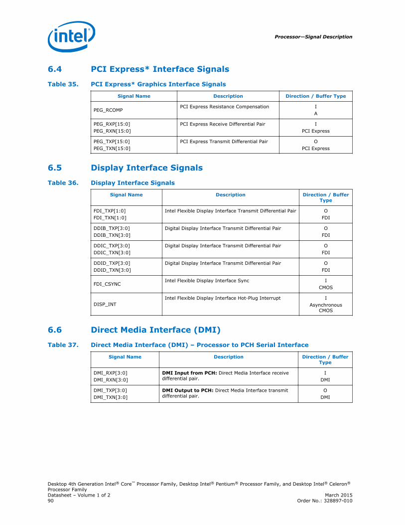
PCI Express* Interface Signals
Table 35. PCI Express* Graphics Interface Signals
Signal Name Description Direction / Buffer Type
PEG_RCOMPPCI Express Resistance Compensation I
A
PEG_RXP[15:0]PEG_RXN[15:0]
PCI Express Receive Differential Pair IPCI Express
PEG_TXP[15:0]PEG_TXN[15:0]
PCI Express Transmit Differential Pair OPCI Express
Display Interface Signals
Table 36. Display Interface Signals
Signal Name Description Direction / BufferType
FDI_TXP[1:0]FDI_TXN[1:0]
Intel Flexible Display Interface Transmit Differential Pair OFDI
DDIB_TXP[3:0]DDIB_TXN[3:0]
Digital Display Interface Transmit Differential Pair OFDI
DDIC_TXP[3:0]DDIC_TXN[3:0]
Digital Display Interface Transmit Differential Pair OFDI
DDID_TXP[3:0]DDID_TXN[3:0]
Digital Display Interface Transmit Differential Pair OFDI
FDI_CSYNCIntel Flexible Display Interface Sync I
CMOS
DISP_INTIntel Flexible Display Interface Hot-Plug Interrupt I
AsynchronousCMOS
Direct Media Interface (DMI)
Table 37. Direct Media Interface (DMI) – Processor to PCH Serial Interface
Signal Name Description Direction / BufferType
DMI_RXP[3:0]DMI_RXN[3:0]
DMI Input from PCH: Direct Media Interface receivedifferential pair.
IDMI
DMI_TXP[3:0]DMI_TXN[3:0]
DMI Output to PCH: Direct Media Interface transmitdifferential pair.
ODMI
6.4
6.5
6.6
Processor—Signal Description
Desktop 4th Generation Intel® Core™ Processor Family, Desktop Intel® Pentium® Processor Family, and Desktop Intel® Celeron®
Processor FamilyDatasheet – Volume 1 of 2 March 201590 Order No.: 328897-010

Phase Locked Loop (PLL) Signals
Table 38. Phase Locked Loop (PLL) Signals
Signal Name Description Direction / BufferType
BCLKPBCLKN
Differential bus clock input to the processor IDiff Clk
DPLL_REF_CLKPDPLL_REF_CLKN
Embedded Display Port PLL Differential Clock In:135 MHz
IDiff Clk
SSC_DPLL_REF_CLKPSSC_ DPLL_REF_CLKN
Spread Spectrum Embedded DisplayPort PLLDifferential Clock In: 135 MHz
IDiff Clk
Testability Signals
Table 39. Testability Signals
Signal Name Description Direction / BufferType
BPM#[7:0]
Breakpoint and Performance Monitor Signals:Outputs from the processor that indicate the status ofbreakpoints and programmable counters used formonitoring processor performance.
I/OGTL
DBR#
Debug Reset: This signal is used only in systems whereno debug port is implemented on the system board.DBR# is used by a debug port interposer so that an in-target probe can drive system reset.
O
PRDY#Processor Ready: This signal is a processor outputused by debug tools to determine processor debugreadiness.
OGTL
PREQ#Processor Request: This signal is used by debug toolsto request debug operation of the processor.
IGTL
TCK
Test Clock: This signal provides the clock input for theprocessor Test Bus (also known as the Test AccessPort). This signal must be driven low or allowed to floatduring power on Reset.
IGTL
TDITest Data In: This signal transfers serial test data intothe processor. This signal provides the serial inputneeded for JTAG specification support.
IGTL
TDOTest Data Out: This signal transfers serial test data outof the processor. This signal provides the serial outputneeded for JTAG specification support.
OOpen Drain
TMSTest Mode Select: This is a JTAG specificationsupported signal used by debug tools.
IGTL
TRST#Test Reset: This signal resets the Test Access Port(TAP) logic. This signal must be driven low during poweron Reset.
IGTL
6.7
6.8
Signal Description—Processor
Desktop 4th Generation Intel® Core™ Processor Family, Desktop Intel® Pentium® Processor Family, and Desktop Intel® Celeron®
Processor FamilyMarch 2015 Datasheet – Volume 1 of 2Order No.: 328897-010 91

Error and Thermal Protection Signals
Table 40. Error and Thermal Protection Signals
Signal Name Description Direction / BufferType
CATERR#
Catastrophic Error: This signal indicates that the system hasexperienced a catastrophic error and cannot continue tooperate. The processor will set this for non-recoverablemachine check errors or other unrecoverable internal errors.CATERR# is used for signaling the following types of errors:Legacy MCERRs, CATERR# is asserted for 16 BCLKs. LegacyIERRs, CATERR# remains asserted until warm or cold reset.
OGTL
PECIPlatform Environment Control Interface: A serialsideband interface to the processor, it is used primarily forthermal, power, and error management.
I/OAsynchronous
PROCHOT#
Processor Hot: PROCHOT# goes active when the processortemperature monitoring sensor(s) detects that the processorhas reached its maximum safe operating temperature. Thisindicates that the processor Thermal Control Circuit (TCC) hasbeen activated, if enabled. This signal can also be driven tothe processor to activate the TCC.
GTL InputOpen-Drain Output
THERMTRIP#
Thermal Trip: The processor protects itself from catastrophicoverheating by use of an internal thermal sensor. This sensoris set well above the normal operating temperature to ensurethat there are no false trips. The processor will stop allexecution when the junction temperature exceedsapproximately 130 °C. This is signaled to the system by theTHERMTRIP# pin.
OAsynchronous OD
Asynchronous CMOS
Power Sequencing Signals
Table 41. Power Sequencing Signals
Signal Name Description Direction / BufferType
SM_DRAMPWROKSM_DRAMPWROK Processor Input: This signalconnects to the PCH DRAMPWROK.
IAsynchronous CMOS
PWRGOOD
The processor requires this input signal to be a cleanindication that the VCC and VDDQ power supplies arestable and within specifications. This requirementapplies regardless of the S-state of the processor.'Clean' implies that the signal will remain low (capableof sinking leakage current), without glitches, from thetime that the power supplies are turned on until thesupplies come within specification. The signal mustthen transition monotonically to a high state.
IAsynchronous CMOS
SKTOCC#
SKTOCC# (Socket Occupied) / PROC_DETECT#:Processor Detect: This signal is pulled down directly(0 Ohms) on the processor package to ground. Thereis no connection to the processor silicon for this signal.System board designers may use this signal todetermine if the processor is present.
—
6.9
6.10
Processor—Signal Description
Desktop 4th Generation Intel® Core™ Processor Family, Desktop Intel® Pentium® Processor Family, and Desktop Intel® Celeron®
Processor FamilyDatasheet – Volume 1 of 2 March 201592 Order No.: 328897-010
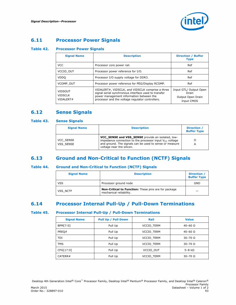
Processor Power Signals
Table 42. Processor Power Signals
Signal Name Description Direction / BufferType
VCC Processor core power rail. Ref
VCCIO_OUT Processor power reference for I/O. Ref
VDDQ Processor I/O supply voltage for DDR3. Ref
VCOMP_OUT Processor power reference for PEG/Display RCOMP. Ref
VIDSOUTVIDSCLKVIDALERT#
VIDALERT#, VIDSCLK, and VIDSCLK comprise a threesignal serial synchronous interface used to transferpower management information between theprocessor and the voltage regulator controllers.
Input GTL/ Output OpenDrain
Output Open DrainInput CMOS
Sense Signals
Table 43. Sense Signals
Signal Name Description Direction /Buffer Type
VCC_SENSEVSS_SENSE
VCC_SENSE and VSS_SENSE provide an isolated, low-impedance connection to the processor input VCC voltageand ground. The signals can be used to sense or measurevoltage near the silicon.
OA
Ground and Non-Critical to Function (NCTF) Signals
Table 44. Ground and Non-Critical to Function (NCTF) Signals
Signal Name Description Direction /Buffer Type
VSS Processor ground node GND
VSS_NCTF Non-Critical to Function: These pins are for packagemechanical reliability. —
Processor Internal Pull-Up / Pull-Down Terminations
Table 45. Processor Internal Pull-Up / Pull-Down Terminations
Signal Name Pull Up / Pull Down Rail Value
BPM[7:0] Pull Up VCCIO_TERM 40–60 Ω
PREQ# Pull Up VCCIO_TERM 40–60 Ω
TDI Pull Up VCCIO_TERM 30–70 Ω
TMS Pull Up VCCIO_TERM 30–70 Ω
CFG[17:0] Pull Up VCCIO_OUT 5–8 kΩ
CATERR# Pull Up VCCIO_TERM 30–70 Ω
6.11
6.12
6.13
6.14
Signal Description—Processor
Desktop 4th Generation Intel® Core™ Processor Family, Desktop Intel® Pentium® Processor Family, and Desktop Intel® Celeron®
Processor FamilyMarch 2015 Datasheet – Volume 1 of 2Order No.: 328897-010 93

7.0 Electrical Specifications
This chapter provides the processor electrical specifications including integratedvoltage regulator (VR), VCC Voltage Identification (VID), reserved and unused signals,signal groups, Test Access Points (TAP), and DC specifications.
Integrated Voltage Regulator
A new feature to the processor is the integration of platform voltage regulators intothe processor. Due to this integration, the processor has one main voltage rail (VCC)and a voltage rail for the memory interface (VDDQ) , compared to six voltage rails onprevious processors. The VCC voltage rail will supply the integrated voltage regulatorswhich in turn will regulate to the appropriate voltages for the cores, cache, systemagent, and graphics. This integration allows the processor to better control on-dievoltages to optimize between performance and power savings. The processor VCC railwill remain a VID-based voltage with a loadline similar to the core voltage rail (alsocalled VCC) in previous processors.
Power and Ground Lands
The processor has VCC, VDDQ, and VSS (ground) lands for on-chip power distribution.All power lands must be connected to their respective processor power planes; all VSSlands must be connected to the system ground plane. Use of multiple power andground planes is recommended to reduce I*R drop. The VCC lands must be suppliedwith the voltage determined by the processor Serial Voltage IDentification (SVID)interface. Table 46 on page 95 specifies the voltage level for the various VIDs.
VCC Voltage Identification (VID)
The processor uses three signals for the serial voltage identification interface tosupport automatic selection of voltages. The following table specifies the voltage levelcorresponding to the 8-bit VID value transmitted over serial VID. A ‘1’ in this tablerefers to a high voltage level and a ‘0’ refers to a low voltage level. If the voltageregulation circuit cannot supply the voltage that is requested, the voltage regulatormust disable itself. VID signals are CMOS push/pull drivers. See the Voltage andCurrent Specifications section for the DC specifications for these signals. The VIDcodes will change due to temperature and/or current load changes to minimize thepower of the part. A voltage range is provided in the Voltage and CurrentSpecifications section. The specifications are set so that one voltage regulator canoperate with all supported frequencies.
Individual processor VID values may be set during manufacturing so that two devicesat the same core frequency may have different default VID settings. This is shown inthe VID range values in the Voltage and Current Specifications section. The processorprovides the ability to operate while transitioning to an adjacent VID and itsassociated voltage. This will represent a DC shift in the loadline.
7.1
7.2
7.3
Processor—Electrical Specifications
Desktop 4th Generation Intel® Core™ Processor Family, Desktop Intel® Pentium® Processor Family, and Desktop Intel® Celeron®
Processor FamilyDatasheet – Volume 1 of 2 March 201594 Order No.: 328897-010
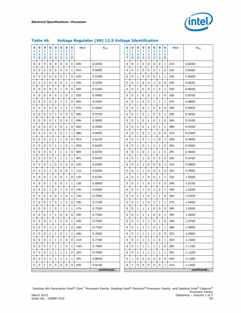
Table 46. Voltage Regulator (VR) 12.5 Voltage Identification
Bit7
Bit6
Bit5
Bit4
Bit3
Bit2
Bit1
Bit0
Hex VCC
0 0 0 0 0 0 0 0 00h 0.0000
0 0 0 0 0 0 0 1 01h 0.5000
0 0 0 0 0 0 1 0 02h 0.5100
0 0 0 0 0 0 1 1 03h 0.5200
0 0 0 0 0 1 0 0 04h 0.5300
0 0 0 0 0 1 0 1 05h 0.5400
0 0 0 0 0 1 1 0 06h 0.5500
0 0 0 0 0 1 1 1 07h 0.5600
0 0 0 0 1 0 0 0 08h 0.5700
0 0 0 0 1 0 0 1 09h 0.5800
0 0 0 0 1 0 1 0 0Ah 0.5900
0 0 0 0 1 0 1 1 0Bh 0.6000
0 0 0 0 1 1 0 0 0Ch 0.6100
0 0 0 0 1 1 0 1 0Dh 0.6200
0 0 0 0 1 1 1 0 0Eh 0.6300
0 0 0 0 1 1 1 1 0Fh 0.6400
0 0 0 1 0 0 0 0 10h 0.6500
0 0 0 1 0 0 0 1 11h 0.6600
0 0 0 1 0 0 1 0 12h 0.6700
0 0 0 1 0 0 1 1 13h 0.6800
0 0 0 1 0 1 0 0 14h 0.6900
0 0 0 1 0 1 0 1 15h 0.7000
0 0 0 1 0 1 1 0 16h 0.7100
0 0 0 1 0 1 1 1 17h 0.7200
0 0 0 1 1 0 0 0 18h 0.7300
0 0 0 1 1 0 0 1 19h 0.7400
0 0 0 1 1 0 1 0 1Ah 0.7500
0 0 0 1 1 0 1 1 1Bh 0.7600
0 0 0 1 1 1 0 0 1Ch 0.7700
0 0 0 1 1 1 0 1 1Dh 0.7800
0 0 0 1 1 1 1 0 1Eh 0.7900
0 0 0 1 1 1 1 1 1Fh 0.8000
0 0 1 0 0 0 0 0 20h 0.8100
continued...
Bit7
Bit6
Bit5
Bit4
Bit3
Bit2
Bit1
Bit0
Hex VCC
0 0 1 0 0 0 0 1 21h 0.8200
0 0 1 0 0 0 1 0 22h 0.8300
0 0 1 0 0 0 1 1 23h 0.8400
0 0 1 0 0 1 0 0 24h 0.8500
0 0 1 0 0 1 0 1 25h 0.8600
0 0 1 0 0 1 1 0 26h 0.8700
0 0 1 0 0 1 1 1 27h 0.8800
0 0 1 0 1 0 0 0 28h 0.8900
0 0 1 0 1 0 0 1 29h 0.9000
0 0 1 0 1 0 1 0 2Ah 0.9100
0 0 1 0 1 0 1 1 2Bh 0.9200
0 0 1 0 1 1 0 0 2Ch 0.9300
0 0 1 0 1 1 0 1 2Dh 0.9400
0 0 1 0 1 1 1 0 2Eh 0.9500
0 0 1 0 1 1 1 1 2Fh 0.9600
0 0 1 1 0 0 0 0 30h 0.9700
0 0 1 1 0 0 0 1 31h 0.9800
0 0 1 1 0 0 1 0 32h 0.9900
0 0 1 1 0 0 1 1 33h 1.0000
0 0 1 1 0 1 0 0 34h 1.0100
0 0 1 1 0 1 0 1 35h 1.0200
0 0 1 1 0 1 1 0 36h 1.0300
0 0 1 1 0 1 1 1 37h 1.0400
0 0 1 1 1 0 0 0 38h 1.0500
0 0 1 1 1 0 0 1 39h 1.0600
0 0 1 1 1 0 1 0 3Ah 1.0700
0 0 1 1 1 0 1 1 3Bh 1.0800
0 0 1 1 1 1 0 0 3Ch 1.0900
0 0 1 1 1 1 0 1 3Dh 1.1000
0 0 1 1 1 1 1 0 3Eh 1.1100
0 0 1 1 1 1 1 1 3Fh 1.1200
0 1 0 0 0 0 0 0 40h 1.1300
0 1 0 0 0 0 0 1 41h 1.1400
continued...
Electrical Specifications—Processor
Desktop 4th Generation Intel® Core™ Processor Family, Desktop Intel® Pentium® Processor Family, and Desktop Intel® Celeron®
Processor FamilyMarch 2015 Datasheet – Volume 1 of 2Order No.: 328897-010 95
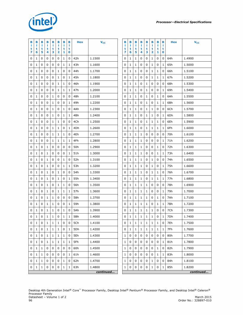
Bit7
Bit6
Bit5
Bit4
Bit3
Bit2
Bit1
Bit0
Hex VCC
0 1 0 0 0 0 1 0 42h 1.1500
0 1 0 0 0 0 1 1 43h 1.1600
0 1 0 0 0 1 0 0 44h 1.1700
0 1 0 0 0 1 0 1 45h 1.1800
0 1 0 0 0 1 1 0 46h 1.1900
0 1 0 0 0 1 1 1 47h 1.2000
0 1 0 0 1 0 0 0 48h 1.2100
0 1 0 0 1 0 0 1 49h 1.2200
0 1 0 0 1 0 1 0 4Ah 1.2300
0 1 0 0 1 0 1 1 4Bh 1.2400
0 1 0 0 1 1 0 0 4Ch 1.2500
0 1 0 0 1 1 0 1 4Dh 1.2600
0 1 0 0 1 1 1 0 4Eh 1.2700
0 1 0 0 1 1 1 1 4Fh 1.2800
0 1 0 1 0 0 0 0 50h 1.2900
0 1 0 1 0 0 0 1 51h 1.3000
0 1 0 1 0 0 1 0 52h 1.3100
0 1 0 1 0 0 1 1 53h 1.3200
0 1 0 1 0 1 0 0 54h 1.3300
0 1 0 1 0 1 0 1 55h 1.3400
0 1 0 1 0 1 1 0 56h 1.3500
0 1 0 1 0 1 1 1 57h 1.3600
0 1 0 1 1 0 0 0 58h 1.3700
0 1 0 1 1 0 0 1 59h 1.3800
0 1 0 1 1 0 1 0 5Ah 1.3900
0 1 0 1 1 0 1 1 5Bh 1.4000
0 1 0 1 1 1 0 0 5Ch 1.4100
0 1 0 1 1 1 0 1 5Dh 1.4200
0 1 0 1 1 1 1 0 5Eh 1.4300
0 1 0 1 1 1 1 1 5Fh 1.4400
0 1 1 0 0 0 0 0 60h 1.4500
0 1 1 0 0 0 0 1 61h 1.4600
0 1 1 0 0 0 1 0 62h 1.4700
0 1 1 0 0 0 1 1 63h 1.4800
continued...
Bit7
Bit6
Bit5
Bit4
Bit3
Bit2
Bit1
Bit0
Hex VCC
0 1 1 0 0 1 0 0 64h 1.4900
0 1 1 0 0 1 0 1 65h 1.5000
0 1 1 0 0 1 1 0 66h 1.5100
0 1 1 0 0 1 1 1 67h 1.5200
0 1 1 0 1 0 0 0 68h 1.5300
0 1 1 0 1 0 0 1 69h 1.5400
0 1 1 0 1 0 1 0 6Ah 1.5500
0 1 1 0 1 0 1 1 6Bh 1.5600
0 1 1 0 1 1 0 0 6Ch 1.5700
0 1 1 0 1 1 0 1 6Dh 1.5800
0 1 1 0 1 1 1 0 6Eh 1.5900
0 1 1 0 1 1 1 1 6Fh 1.6000
0 1 1 1 0 0 0 0 70h 1.6100
0 1 1 1 0 0 0 1 71h 1.6200
0 1 1 1 0 0 1 0 72h 1.6300
0 1 1 1 0 0 1 1 73h 1.6400
0 1 1 1 0 1 0 0 74h 1.6500
0 1 1 1 0 1 0 1 75h 1.6600
0 1 1 1 0 1 1 0 76h 1.6700
0 1 1 1 0 1 1 1 77h 1.6800
0 1 1 1 1 0 0 0 78h 1.6900
0 1 1 1 1 0 0 1 79h 1.7000
0 1 1 1 1 0 1 0 7Ah 1.7100
0 1 1 1 1 0 1 1 7Bh 1.7200
0 1 1 1 1 1 0 0 7Ch 1.7300
0 1 1 1 1 1 0 1 7Dh 1.7400
0 1 1 1 1 1 1 0 7Eh 1.7500
0 1 1 1 1 1 1 1 7Fh 1.7600
1 0 0 0 0 0 0 0 80h 1.7700
1 0 0 0 0 0 0 1 81h 1.7800
1 0 0 0 0 0 1 0 82h 1.7900
1 0 0 0 0 0 1 1 83h 1.8000
1 0 0 0 0 1 0 0 84h 1.8100
1 0 0 0 0 1 0 1 85h 1.8200
continued...
Processor—Electrical Specifications
Desktop 4th Generation Intel® Core™ Processor Family, Desktop Intel® Pentium® Processor Family, and Desktop Intel® Celeron®
Processor FamilyDatasheet – Volume 1 of 2 March 201596 Order No.: 328897-010

Bit7
Bit6
Bit5
Bit4
Bit3
Bit2
Bit1
Bit0
Hex VCC
1 0 0 0 0 1 1 0 86h 1.8300
1 0 0 0 0 1 1 1 87h 1.8400
1 0 0 0 1 0 0 0 88h 1.8500
1 0 0 0 1 0 0 1 89h 1.8600
1 0 0 0 1 0 1 0 8Ah 1.8700
1 0 0 0 1 0 1 1 8Bh 1.8800
1 0 0 0 1 1 0 0 8Ch 1.8900
1 0 0 0 1 1 0 1 8Dh 1.9000
1 0 0 0 1 1 1 0 8Eh 1.9100
1 0 0 0 1 1 1 1 8Fh 1.9200
1 0 0 1 0 0 0 0 90h 1.9300
1 0 0 1 0 0 0 1 91h 1.9400
1 0 0 1 0 0 1 0 92h 1.9500
1 0 0 1 0 0 1 1 93h 1.9600
1 0 0 1 0 1 0 0 94h 1.9700
1 0 0 1 0 1 0 1 95h 1.9800
1 0 0 1 0 1 1 0 96h 1.9900
1 0 0 1 0 1 1 1 97h 2.0000
1 0 0 1 1 0 0 0 98h 2.0100
1 0 0 1 1 0 0 1 99h 2.0200
1 0 0 1 1 0 1 0 9Ah 2.0300
1 0 0 1 1 0 1 1 9Bh 2.0400
1 0 0 1 1 1 0 0 9Ch 2.0500
1 0 0 1 1 1 0 1 9Dh 2.0600
1 0 0 1 1 1 1 0 9Eh 2.0700
1 0 0 1 1 1 1 1 9Fh 2.0800
1 0 1 0 0 0 0 0 A0h 2.0900
1 0 1 0 0 0 0 1 A1h 2.1000
1 0 1 0 0 0 1 0 A2h 2.1100
1 0 1 0 0 0 1 1 A3h 2.1200
1 0 1 0 0 1 0 0 A4h 2.1300
1 0 1 0 0 1 0 1 A5h 2.1400
1 0 1 0 0 1 1 0 A6h 2.1500
1 0 1 0 0 1 1 1 A7h 2.1600
continued...
Bit7
Bit6
Bit5
Bit4
Bit3
Bit2
Bit1
Bit0
Hex VCC
1 0 1 0 1 0 0 0 A8h 2.1700
1 0 1 0 1 0 0 1 A9h 2.1800
1 0 1 0 1 0 1 0 AAh 2.1900
1 0 1 0 1 0 1 1 ABh 2.2000
1 0 1 0 1 1 0 0 ACh 2.2100
1 0 1 0 1 1 0 1 ADh 2.2200
1 0 1 0 1 1 1 0 AEh 2.2300
1 0 1 0 1 1 1 1 AFh 2.2400
1 0 1 1 0 0 0 0 B0h 2.2500
1 0 1 1 0 0 0 1 B1h 2.2600
1 0 1 1 0 0 1 0 B2h 2.2700
1 0 1 1 0 0 1 1 B3h 2.2800
1 0 1 1 0 1 0 0 B4h 2.2900
1 0 1 1 0 1 0 1 B5h 2.3000
1 0 1 1 0 1 1 0 B6h 2.3100
1 0 1 1 0 1 1 1 B7h 2.3200
1 0 1 1 1 0 0 0 B8h 2.3300
1 0 1 1 1 0 0 1 B9h 2.3400
1 0 1 1 1 0 1 0 BAh 2.3500
1 0 1 1 1 0 1 1 BBh 2.3600
1 0 1 1 1 1 0 0 BCh 2.3700
1 0 1 1 1 1 0 1 BDh 2.3800
1 0 1 1 1 1 1 0 BEh 2.3900
1 0 1 1 1 1 1 1 BFh 2.4000
1 1 0 0 0 0 0 0 C0h 2.4100
1 1 0 0 0 0 0 1 C1h 2.4200
1 1 0 0 0 0 1 0 C2h 2.4300
1 1 0 0 0 0 1 1 C3h 2.4400
1 1 0 0 0 1 0 0 C4h 2.4500
1 1 0 0 0 1 0 1 C5h 2.4600
1 1 0 0 0 1 1 0 C6h 2.4700
1 1 0 0 0 1 1 1 C7h 2.4800
1 1 0 0 1 0 0 0 C8h 2.4900
1 1 0 0 1 0 0 1 C9h 2.5000
continued...
Electrical Specifications—Processor
Desktop 4th Generation Intel® Core™ Processor Family, Desktop Intel® Pentium® Processor Family, and Desktop Intel® Celeron®
Processor FamilyMarch 2015 Datasheet – Volume 1 of 2Order No.: 328897-010 97
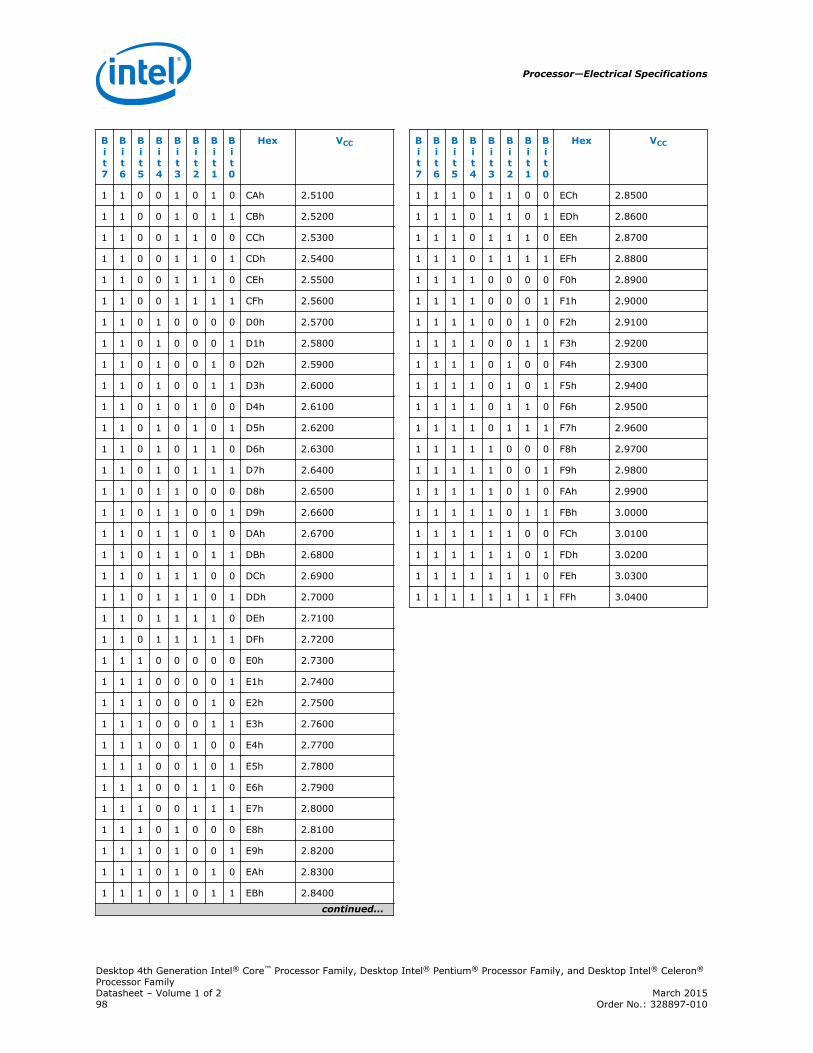
Bit7
Bit6
Bit5
Bit4
Bit3
Bit2
Bit1
Bit0
Hex VCC
1 1 0 0 1 0 1 0 CAh 2.5100
1 1 0 0 1 0 1 1 CBh 2.5200
1 1 0 0 1 1 0 0 CCh 2.5300
1 1 0 0 1 1 0 1 CDh 2.5400
1 1 0 0 1 1 1 0 CEh 2.5500
1 1 0 0 1 1 1 1 CFh 2.5600
1 1 0 1 0 0 0 0 D0h 2.5700
1 1 0 1 0 0 0 1 D1h 2.5800
1 1 0 1 0 0 1 0 D2h 2.5900
1 1 0 1 0 0 1 1 D3h 2.6000
1 1 0 1 0 1 0 0 D4h 2.6100
1 1 0 1 0 1 0 1 D5h 2.6200
1 1 0 1 0 1 1 0 D6h 2.6300
1 1 0 1 0 1 1 1 D7h 2.6400
1 1 0 1 1 0 0 0 D8h 2.6500
1 1 0 1 1 0 0 1 D9h 2.6600
1 1 0 1 1 0 1 0 DAh 2.6700
1 1 0 1 1 0 1 1 DBh 2.6800
1 1 0 1 1 1 0 0 DCh 2.6900
1 1 0 1 1 1 0 1 DDh 2.7000
1 1 0 1 1 1 1 0 DEh 2.7100
1 1 0 1 1 1 1 1 DFh 2.7200
1 1 1 0 0 0 0 0 E0h 2.7300
1 1 1 0 0 0 0 1 E1h 2.7400
1 1 1 0 0 0 1 0 E2h 2.7500
1 1 1 0 0 0 1 1 E3h 2.7600
1 1 1 0 0 1 0 0 E4h 2.7700
1 1 1 0 0 1 0 1 E5h 2.7800
1 1 1 0 0 1 1 0 E6h 2.7900
1 1 1 0 0 1 1 1 E7h 2.8000
1 1 1 0 1 0 0 0 E8h 2.8100
1 1 1 0 1 0 0 1 E9h 2.8200
1 1 1 0 1 0 1 0 EAh 2.8300
1 1 1 0 1 0 1 1 EBh 2.8400
continued...
Bit7
Bit6
Bit5
Bit4
Bit3
Bit2
Bit1
Bit0
Hex VCC
1 1 1 0 1 1 0 0 ECh 2.8500
1 1 1 0 1 1 0 1 EDh 2.8600
1 1 1 0 1 1 1 0 EEh 2.8700
1 1 1 0 1 1 1 1 EFh 2.8800
1 1 1 1 0 0 0 0 F0h 2.8900
1 1 1 1 0 0 0 1 F1h 2.9000
1 1 1 1 0 0 1 0 F2h 2.9100
1 1 1 1 0 0 1 1 F3h 2.9200
1 1 1 1 0 1 0 0 F4h 2.9300
1 1 1 1 0 1 0 1 F5h 2.9400
1 1 1 1 0 1 1 0 F6h 2.9500
1 1 1 1 0 1 1 1 F7h 2.9600
1 1 1 1 1 0 0 0 F8h 2.9700
1 1 1 1 1 0 0 1 F9h 2.9800
1 1 1 1 1 0 1 0 FAh 2.9900
1 1 1 1 1 0 1 1 FBh 3.0000
1 1 1 1 1 1 0 0 FCh 3.0100
1 1 1 1 1 1 0 1 FDh 3.0200
1 1 1 1 1 1 1 0 FEh 3.0300
1 1 1 1 1 1 1 1 FFh 3.0400
Processor—Electrical Specifications
Desktop 4th Generation Intel® Core™ Processor Family, Desktop Intel® Pentium® Processor Family, and Desktop Intel® Celeron®
Processor FamilyDatasheet – Volume 1 of 2 March 201598 Order No.: 328897-010

Reserved or Unused Signals
The following are the general types of reserved (RSVD) signals and connectionguidelines:
• RSVD – these signals should not be connected
• RSVD_TP – these signals should be routed to a test point
• RSVD_NCTF – these signals are non-critical to function and may be left un-connected
Arbitrary connection of these signals to VCC, VDDQ, VSS, or to any other signal(including each other) may result in component malfunction or incompatibility withfuture processors. See Signal Description on page 86 for a pin listing of the processorand the location of all reserved signals.
For reliable operation, always connect unused inputs or bi-directional signals to anappropriate signal level. Unused active high inputs should be connected through aresistor to ground (VSS). Unused outputs maybe left unconnected; however, this mayinterfere with some Test Access Port (TAP) functions, complicate debug probing, andprevent boundary scan testing. A resistor must be used when tying bi-directionalsignals to power or ground. When tying any signal to power or ground, a resistor willalso allow for system testability.
Signal Groups
Signals are grouped by buffer type and similar characteristics as listed in the followingtable. The buffer type indicates which signaling technology and specifications apply tothe signals. All the differential signals and selected DDR3/DDR3L and Control Sidebandsignals have On-Die Termination (ODT) resistors. Some signals do not have ODT andneed to be terminated on the board.
Note: All Control Sideband Asynchronous signals are required to be asserted/de-asserted forat least 10 BCLKs with maximum Trise/Tfall of 6 ns for the processor to recognize theproper signal state. See the DC Specifications section and AC Specifications section.
Table 47. Signal Groups
Signal Group Type Signals
System Reference Clock
Differential CMOS Input BCLKP, BCLKN, DPLL_REF_CLKP, DPLL_REF_CLKN,SSC_DPLL_REF_CLKP, SSC_DPLL_REF_CLKN
DDR3 / DDR3L Reference Clocks 2
Differential DDR3/DDR3LOutput
SA_CKP[3:0], SA_CKN[3:0], SB_CKP[3:0], SB_CKN[3:0]
DDR3 / DDR3L Command Signals 2
Single ended DDR3/DDR3LOutput
SA_BS[2:0], SB_BS[2:0], SA_WE#, SB_WE#, SA_RAS#,SB_RAS#, SA_CAS#, SB_CAS#, SA_MA[15:0], SB_MA[15:0]
DDR3 / DDR3L Control Signals 2
Single ended DDR3/DDR3LOutput
SA_CKE[3:0], SB_CKE[3:0], SA_CS#[3:0], SB_CS#[3:0],SA_ODT[3:0], SB_ODT[3:0]
Single ended CMOS Output SM_DRAMRST#
continued...
7.4
7.5
Electrical Specifications—Processor
Desktop 4th Generation Intel® Core™ Processor Family, Desktop Intel® Pentium® Processor Family, and Desktop Intel® Celeron®
Processor FamilyMarch 2015 Datasheet – Volume 1 of 2Order No.: 328897-010 99

Signal Group Type Signals
DDR3 / DDR3L Data Signals 2
Single ended DDR3/DDR3L Bi-directional
SA_DQ[63:0], SB_DQ[63:0]
Differential DDR3/DDR3L Bi-directional
SA_DQSP[7:0], SA_DQSN[7:0], SB_DQSP[7:0], SB_DQSN[7:0]
DDR3 / DDR3L Compensation
Analog Input SM_RCOMP[2:0]
DDR3 / DDR3L Reference Voltage Signals
DDR3/DDR3LOutput
SM_VREF, SA_DIMM_VREFDQ, SB_DIMM_VREFDQ
Testability (ITP/XDP)
Single ended CMOS Input TCK, TDI, TMS, TRST#
Single ended GTL TDO
Single ended Output DBR#
Single ended GTL BPM#[7:0]
Single ended GTL PREQ#
Single ended GTL PRDY#
Control Sideband
Single ended GTL Input/OpenDrain Output
PROCHOT#
Single ended AsynchronousCMOS Output
THERMTRIP#, IVR_ERROR
Single ended GTL CATERR#
Single ended AsynchronousCMOS Input
PM_SYNC,RESET#, PWRGOOD, PWR_DEBUG#
Single ended Asynchronous Bi-directional
PECI
Single ended GTL Bi-directional CFG[19:0]
Single ended Analog Input SM_RCOMP[2:0]
Voltage Regulator
Single ended CMOS Input VR_READY
Single ended CMOS Input VIDALERT#
Single ended Open Drain Output VIDSCLK
Single ended GTL Input/OpenDrain Output
VIDSOUT
Differential Analog Output VCC_SENSE, VSS_SENSE
Power / Ground / Other
Single ended Power VCC, VDDQ
Ground VSS, VSS_NCTF 3
No Connect RSVD, RSVD_NCTF
continued...
Processor—Electrical Specifications
Desktop 4th Generation Intel® Core™ Processor Family, Desktop Intel® Pentium® Processor Family, and Desktop Intel® Celeron®
Processor FamilyDatasheet – Volume 1 of 2 March 2015100 Order No.: 328897-010

Signal Group Type Signals
Test Point RSVD_TP
Other SKTOCC#,
PCI Express* Graphics
Differential PCI Express Input PEG_RXP[15:0], PEG_RXN[15:0]
Differential PCI Express Output PEG_TXP[15:0], PEG_TXN[15:0]
Single ended Analog Input PEG_RCOMP
Digital Media Interface (DMI)
Differential DMI Input DMI_RXP[3:0], DMI_RXN[3:0]
Differential DMI Output DMI_TXP[3:0], DMI_TXN[3:0]
Digital Display Interface
Differential DDI Output DDIB_TXP[3:0], DDIB_TXN[3:0], DDIC_TXP[3:0],DDIC_TXN[3:0], DDID_TXP[3:0], DDID_TXN[3:0]
Intel® FDI
Single ended CMOS Input FDI_CSYNC
Single ended AsynchronousCMOS Input
DISP_INT
Differential FDI Output FDI_TXP[1:0], FDI_TXN[1:0]
Notes: 1. See Signal Description on page 86 for signal description details.2. SA and SB refer to DDR3/DDR3L Channel A and DDR3/DDR3L Channel B.
Test Access Port (TAP) Connection
Due to the voltage levels supported by other components in the Test Access Port(TAP) logic, Intel recommends the processor be first in the TAP chain, followed by anyother components within the system. A translation buffer should be used to connect tothe rest of the chain unless one of the other components is capable of accepting aninput of the appropriate voltage. Two copies of each signal may be required with eachdriving a different voltage level.
The processor supports Boundary Scan (JTAG) IEEE 1149.1-2001 and IEEE1149.6-2003 standards. A few of the I/O pins may support only one of thosestandards.
DC Specifications
The processor DC specifications in this section are defined at the processor pins,unless noted otherwise. See Signal Description on page 86 for the processor pinlistings and signal definitions.
• The DC specifications for the DDR3 / DDR3L signals are listed in the Voltage andCurrent Specifications section.
• The Voltage and Current Specifications section lists the DC specifications for theprocessor and are valid only while meeting specifications for junction temperature,clock frequency, and input voltages. Read all notes associated with eachparameter.
7.6
7.7
Electrical Specifications—Processor
Desktop 4th Generation Intel® Core™ Processor Family, Desktop Intel® Pentium® Processor Family, and Desktop Intel® Celeron®
Processor FamilyMarch 2015 Datasheet – Volume 1 of 2Order No.: 328897-010 101

• AC tolerances for all DC rails include dynamic load currents at switchingfrequencies up to 1 MHz.
Voltage and Current Specifications
Table 48. Processor Core Active and Idle Mode DC Voltage and Current Specifications
Symbol Parameter Min Typ Max Unit Note1
OperationalVID VID Range 1.65
2013D: 1.752013C: 1.752013B: 1.752013A: 1.75
1.86 V 2
Idle VID(packageC6/C7)
VID Range 1.5 1.6 1.65 V 2
R_DC_LL
Loadlineslope withinthe VRregulationloopcapability
2014: PCG: -1.52013D PCG: -1.52013C PCG: -1.52013B PCG: -1.52013A PCG: -1.5
mΩ 3, 5, 6, 8
R_AC_LL
Loadlineslope inresponse todynamic loadincreaseevents
2014: PCG: -2.42013D PCG: -2.42013C PCG: -2.42013B PCG: -2.42013A PCG: -2.4
mΩ —
R_AC_LL_OS
Loadlineslope inresponse todynamic loadreleaseevents
2014: PCG: -3.02013D PCG: -3.02013C PCG: -3.02013B PCG: -3.02013A PCG: -3.0
mΩ —
T_OVS Overshoottime 500 uS —
V_OVS Overshoot 50 mV —
VCC TOBVCCToleranceBand
± 20 (PS0, PS1, PS2, PS3) mV 3, 5, 6, 7, 8
VCC Ripple
Ripple ± 10 (PS0)± 15 (PS1)
+50/-15 (PS2)+60/-15 (PS3)
mV 3, 5, 6, 7, 8
VCC,BOOT
Default VCCvoltage forinitial powerup
— 1.70 — V —
ICC2013D PCGICC
— — 95 A 4, 8
ICC2013C PCGICC
— — 75 A 4, 8
ICC2013B PCGICC
— — 58 A 4, 8
continued...
7.8
Processor—Electrical Specifications
Desktop 4th Generation Intel® Core™ Processor Family, Desktop Intel® Pentium® Processor Family, and Desktop Intel® Celeron®
Processor FamilyDatasheet – Volume 1 of 2 March 2015102 Order No.: 328897-010
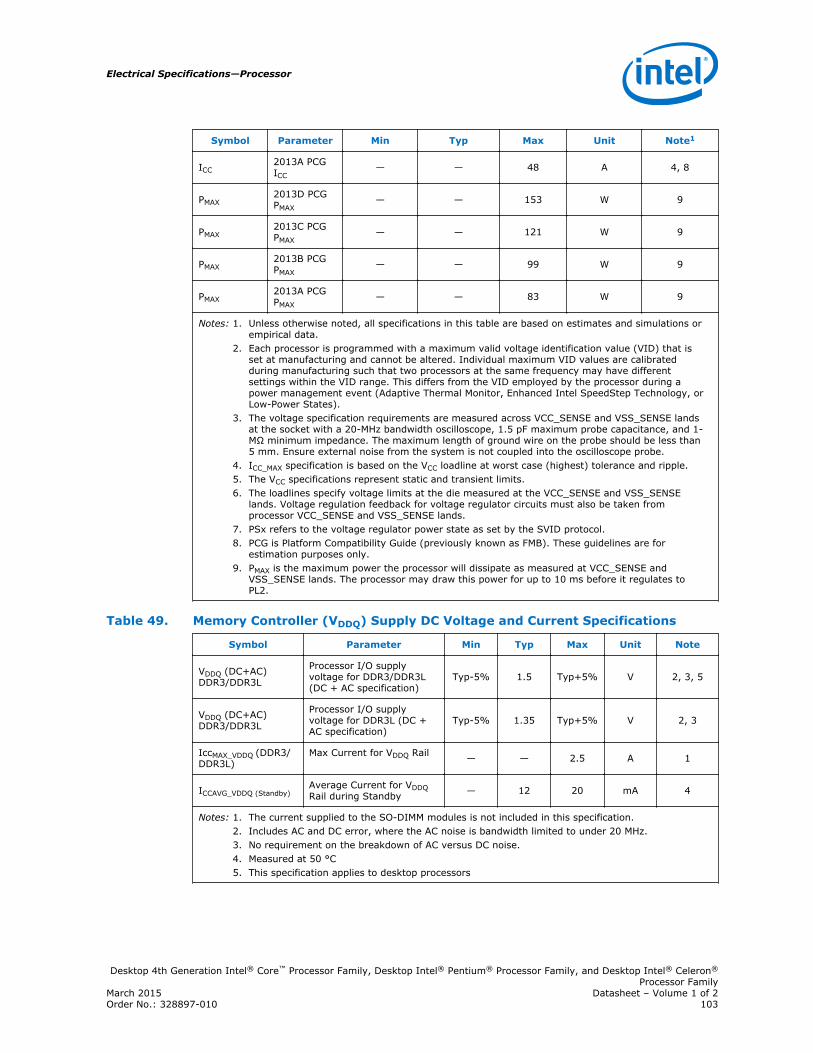
Symbol Parameter Min Typ Max Unit Note1
ICC2013A PCGICC
— — 48 A 4, 8
PMAX2013D PCGPMAX
— — 153 W 9
PMAX2013C PCGPMAX
— — 121 W 9
PMAX2013B PCGPMAX
— — 99 W 9
PMAX2013A PCGPMAX
— — 83 W 9
Notes: 1. Unless otherwise noted, all specifications in this table are based on estimates and simulations orempirical data.
2. Each processor is programmed with a maximum valid voltage identification value (VID) that isset at manufacturing and cannot be altered. Individual maximum VID values are calibratedduring manufacturing such that two processors at the same frequency may have differentsettings within the VID range. This differs from the VID employed by the processor during apower management event (Adaptive Thermal Monitor, Enhanced Intel SpeedStep Technology, orLow-Power States).
3. The voltage specification requirements are measured across VCC_SENSE and VSS_SENSE landsat the socket with a 20-MHz bandwidth oscilloscope, 1.5 pF maximum probe capacitance, and 1-MΩ minimum impedance. The maximum length of ground wire on the probe should be less than5 mm. Ensure external noise from the system is not coupled into the oscilloscope probe.
4. ICC_MAX specification is based on the VCC loadline at worst case (highest) tolerance and ripple.5. The VCC specifications represent static and transient limits.6. The loadlines specify voltage limits at the die measured at the VCC_SENSE and VSS_SENSE
lands. Voltage regulation feedback for voltage regulator circuits must also be taken fromprocessor VCC_SENSE and VSS_SENSE lands.
7. PSx refers to the voltage regulator power state as set by the SVID protocol.8. PCG is Platform Compatibility Guide (previously known as FMB). These guidelines are for
estimation purposes only.9. PMAX is the maximum power the processor will dissipate as measured at VCC_SENSE and
VSS_SENSE lands. The processor may draw this power for up to 10 ms before it regulates toPL2.
Table 49. Memory Controller (VDDQ) Supply DC Voltage and Current Specifications
Symbol Parameter Min Typ Max Unit Note
VDDQ (DC+AC)DDR3/DDR3L
Processor I/O supplyvoltage for DDR3/DDR3L(DC + AC specification)
Typ-5% 1.5 Typ+5% V 2, 3, 5
VDDQ (DC+AC)DDR3/DDR3L
Processor I/O supplyvoltage for DDR3L (DC +AC specification)
Typ-5% 1.35 Typ+5% V 2, 3
IccMAX_VDDQ (DDR3/DDR3L)
Max Current for VDDQ Rail — — 2.5 A 1
ICCAVG_VDDQ (Standby)Average Current for VDDQRail during Standby — 12 20 mA 4
Notes: 1. The current supplied to the SO-DIMM modules is not included in this specification.2. Includes AC and DC error, where the AC noise is bandwidth limited to under 20 MHz.3. No requirement on the breakdown of AC versus DC noise.4. Measured at 50 °C5. This specification applies to desktop processors
Electrical Specifications—Processor
Desktop 4th Generation Intel® Core™ Processor Family, Desktop Intel® Pentium® Processor Family, and Desktop Intel® Celeron®
Processor FamilyMarch 2015 Datasheet – Volume 1 of 2Order No.: 328897-010 103

Table 50. VCCIO_OUT, VCOMP_OUT, and VCCIO_TERM
Symbol Parameter Typ Max Units Notes
VCCIO_OUT TerminationVoltage 1.0 — V
ICCIO_OUT MaximumExternal Load — 300 mA
VCOMP_OUT TerminationVoltage 1.0 — V 1
VCCIO_TERM TerminationVoltage 1.0 — V 2
Notes: 1. VCOMP_OUT may only be used to connect to PEG_RCOMP and DP_RCOMP.2. Internal processor power for signal termination.
Table 51. DDR3 / DDR3L Signal Group DC Specifications
Symbol Parameter Min Typ Max Units Notes1
VIL Input Low Voltage — VDDQ/2 0.43*VDDQ V 2, 4, 11
VIH Input High Voltage 0.57*VDDQ VDDQ/2 — V 3, 11
VILInput Low Voltage(SM_DRAMPWROK) — — 0.15*VDDQ V —
VIHInput High Voltage(SM_DRAMPWROK) 0.45*VDDQ — 1.0 V 10, 12
RON_UP(DQ)
DDR3/DDR3L DataBuffer pull-upResistance
20 26 32 Ω 5, 11
RON_DN(DQ)
DDR3/DDR3L DataBuffer pull-downResistance
20 26 32 Ω 5, 11
RODT(DQ)
DDR3/DDR3L On-dietermination equivalentresistance for datasignals
38 50 62 Ω 11
VODT(DC)
DDR3/DDR3L On-dietermination DC workingpoint (driver set toreceive mode)
0.45*VDDQ 0.5*VDDQ 0.55*VDDQ V 11
RON_UP(CK)
DDR3/DDR3L ClockBuffer pull-upResistance
20 26 32 Ω 5, 11,13
RON_DN(CK)
DDR3/DDR3L ClockBuffer pull-downResistance
20 26 32 Ω 5, 11,13
RON_UP(CMD)
DDR3/DDR3L CommandBuffer pull-upResistance
15 20 25 Ω 5, 11,13
RON_DN(CMD)
DDR3/DDR3L CommandBuffer pull-downResistance
15 20 25 Ω 5, 11,13
RON_UP(CTL)
DDR3/DDR3L ControlBuffer pull-upResistance
19 25 31 Ω 5, 11,13
continued...
Processor—Electrical Specifications
Desktop 4th Generation Intel® Core™ Processor Family, Desktop Intel® Pentium® Processor Family, and Desktop Intel® Celeron®
Processor FamilyDatasheet – Volume 1 of 2 March 2015104 Order No.: 328897-010
Symbol Parameter Min Typ Max Units Notes1
RON_DN(CTL)
DDR3/DDR3L ControlBuffer pull-downResistance
19 25 31 Ω 5, 11,13
RON_UP(RST)
DDR3/DDR3L ResetBuffer pull-upResistance
40 80 130 Ω —
RON_DN(RST)
DDR3/DDR3L ResetBuffer pull-upResistance
40 80 130 Ω —
ILI
Input Leakage Current(DQ, CK)0V0.2*VDDQ
0.8*VDDQ
— — 0.7 mA —
ILI
Input Leakage Current(CMD, CTL)0V0.2*VDDQ
0.8*VDDQ
— — 1.0 mA —
SM_RCOMP0 Command COMPResistance 99 100 101 Ω 8
SM_RCOMP1 Data COMP Resistance 74.25 75 75.75 Ω 8
SM_RCOMP2 ODT COMP Resistance 99 100 101 Ω 8
Notes: 1. Unless otherwise noted, all specifications in this table apply to all processor frequencies.2. VIL is defined as the maximum voltage level at a receiving agent that will be interpreted as a
logical low value.3. VIH is defined as the minimum voltage level at a receiving agent that will be interpreted as a
logical high value.4. VIH and VOH may experience excursions above VDDQ. However, input signal drivers must comply
with the signal quality specifications.5. This is the pull up/down driver resistance.6. RTERM is the termination on the DIMM and in not controlled by the processor.7. The minimum and maximum values for these signals are programmable by BIOS to one of the
two sets.8. SM_RCOMPx resistance must be provided on the system board with 1% resistors. SM_RCOMPx
resistors are to VSS.9. SM_DRAMPWROK rise and fall time must be < 50 ns measured between VDDQ *0.15 and VDDQ
*0.47.10.SM_VREF is defined as VDDQ/2.11.Maximum-minimum range is correct; however, center point is subject to change during MRC
boot training.12.Processor may be damaged if VIH exceeds the maximum voltage for extended periods.13.The MRC during boot training might optimize RON outside the range specified.
Table 52. Digital Display Interface Group DC Specifications
Symbol Parameter Min Typ Max Units
VIL HPD Input Low Voltage — — 0.8 V
VIH HPD Input High Voltage 2.25 — 3.6 V
Vaux(Tx) Aux peak-to-peak voltage at transmittingdevice 0.39 — 1.38 V
Vaux(Rx) Aux peak-to-peak voltage at receivingdevice 0.32 — 1.36 V
Electrical Specifications—Processor
Desktop 4th Generation Intel® Core™ Processor Family, Desktop Intel® Pentium® Processor Family, and Desktop Intel® Celeron®
Processor FamilyMarch 2015 Datasheet – Volume 1 of 2Order No.: 328897-010 105
Table 53. embedded DisplayPort* (eDP*) Group DC Specifications
Symbol Parameter Min Typ Max Units
VIL HPD Input Low Voltage 0.02 — 0.21 V
VIH HPD Input High Voltage 0.84 — 1.05 V
VOL eDP_DISP_UTIL Output Low Voltage 0.1*VCC — — V
VOH eDP_DISP_UTIL Output High Voltage 0.9*VCC — — V
RUP eDP_DISP_UTIL Internal pull-up 100 — — Ω
RDOWN eDP_DISP_UTIL Internal pull-down 100 — — Ω
Vaux(Tx) Aux peak-to-peak voltage attransmitting device 0.39 — 1.38 V
Vaux(Rx) Aux peak-to-peak voltage at receivingdevice 0.32 — 1.36 V
eDP_RCOMPDP_RCOMP
COMP Resistance 24.75 25 25.25 Ω
Note: 1. COMP resistance is to VCOMP_OUT.
Table 54. CMOS Signal Group DC Specifications
Symbol Parameter Min Max Units Notes1
VIL Input Low Voltage — VCCIO_OUT* 0.3 V 2
VIH Input High Voltage VCCIO_OUT* 0.7 — V 2, 4
VOL Output Low Voltage — VCCIO_OUT * 0.1 V 2
VOH Output High Voltage VCCIO_OUT * 0.9 — V 2, 4
RON Buffer on Resistance 23 73 Ω —
ILIInput LeakageCurrent — ±150 μA 3
Notes: 1. Unless otherwise noted, all specifications in this table apply to all processor frequencies.2. The VCCIO_OUT referred to in these specifications refers to instantaneous VCCIO_OUT.3. For VIN between “0” V and VCCIO_OUT. Measured when the driver is tri-stated.4. VIH and VOH may experience excursions above VCCIO_OUT. However, input signal drivers must
comply with the signal quality specifications.
Table 55. GTL Signal Group and Open Drain Signal Group DC Specifications
Symbol Parameter Min Max Units Notes1
VILInput Low Voltage (TAP, exceptTCK) — VCCIO_TERM * 0.6 V 2
VIHInput High Voltage (TAP, exceptTCK) VCCIO_TERM * 0.72 — V 2, 4
VIL Input Low Voltage (TCK) — VCCIO_TERM * 0.4 V 2
VIH Input High Voltage (TCK) VCCIO_TERM * 0.8 — V 2, 4
VHYSTERESIS Hysteresis Voltage VCCIO_TERM * 0.2 — V —
RON Buffer on Resistance (TDO) 12 28 Ω —
VIL Input Low Voltage (other GTL) — VCCIO_TERM * 0.6 V 2
continued...
Processor—Electrical Specifications
Desktop 4th Generation Intel® Core™ Processor Family, Desktop Intel® Pentium® Processor Family, and Desktop Intel® Celeron®
Processor FamilyDatasheet – Volume 1 of 2 March 2015106 Order No.: 328897-010
Symbol Parameter Min Max Units Notes1
VIH Input High Voltage (other GTL) VCCIO_TERM * 0.72 — V 2, 4
RON Buffer on Resistance (CFG/BPM) 16 24 Ω —
RON Buffer on Resistance (other GTL) 12 28 Ω —
ILI Input Leakage Current — ±150 μA 3
Notes: 1. Unless otherwise noted, all specifications in this table apply to all processor frequencies.2. The VCCIO_OUT referred to in these specifications refers to instantaneous VCCIO_OUT.3. For VIN between 0 V and VCCIO_TERM. Measured when the driver is tri-stated.4. VIH and VOH may experience excursions above VCCIO_TERM. However, input signal drivers must
comply with the signal quality specifications.
Table 56. PCI Express* DC Specifications
Symbol Parameter Min Typ Max Units Notes1
ZTX-DIFF-DCDC Differential Tx Impedance (Gen 1Only) 80 — 120 Ω 1, 6
ZTX-DIFF-DCDC Differential Tx Impedance (Gen 2 andGen 3) — — 120 Ω 1, 6
ZRX-DC DC Common Mode Rx Impedance 40 — 60 Ω 1, 4, 5
ZRX-DIFF-DCDC Differential Rx Impedance (Gen1Only) 80 — 120 Ω 1
PEG_RCOMP Comp Resistance 24.75 25 25.25 Ω 2, 3
Notes: 1. See the PCI Express Base Specification for more details.2. PEG_RCOMP should be connected to VCOMP_OUT through a 25 Ω ±1% resistor.3. Intel allows using 24.9 Ω ±1% resistors.4. DC impedance limits are needed to ensure Receiver detect.5. The Rx DC Common Mode Impedance must be present when the Receiver terminations are first
enabled to ensure that the Receiver Detect occurs properly. Compensation of this impedance canstart immediately and the 15 Rx Common Mode Impedance (constrained by RLRX-CM to 50 Ω±20%) must be within the specified range by the time Detect is entered.
6. Low impedance defined during signaling. Parameter is captured for 5.0 GHz by RLTX-DIFF.
Platform Environment Control Interface (PECI) DCCharacteristics
The PECI interface operates at a nominal voltage set by VCCIO_TERM. The set of DCelectrical specifications shown in the following table is used with devices normallyoperating from a VCCIO_TERM interface supply.
VCCIO_TERM nominal levels will vary between processor families. All PECI devices willoperate at the VCCIO_TERM level determined by the processor installed in the system.
Table 57. Platform Environment Control Interface (PECI) DC Electrical Limits
Symbol Definition and Conditions Min Max Units Notes1
Rup Internal pull up resistance 15 45 Ω 3
VinInput Voltage Range -0.15 VCCIO_TERM +
0.15 V —
VhysteresisHysteresis 0.1 *
VCCIO_TERMN/A V —
continued...
7.8.1
Electrical Specifications—Processor
Desktop 4th Generation Intel® Core™ Processor Family, Desktop Intel® Pentium® Processor Family, and Desktop Intel® Celeron®
Processor FamilyMarch 2015 Datasheet – Volume 1 of 2Order No.: 328897-010 107

Symbol Definition and Conditions Min Max Units Notes1
VnNegative-Edge ThresholdVoltage
0.275 *VCCIO_TERM
0.500* VCCIO_TERM
V —
VpPositive-Edge ThresholdVoltage
0.550 *VCCIO_TERM
0.725 *VCCIO_TERM
V —
Cbus Bus Capacitance per Node N/A 10 pF —
Cpad Pad Capacitance 0.7 1.8 pF —
Ileak000 leakage current at 0 V — 0.6 mA —
Ileak025 leakage current at 0.25*VCCIO_TERM
— 0.4 mA —
Ileak050 leakage current at 0.50*VCCIO_TERM
— 0.2 mA —
Ileak075 leakage current at 0.75*VCCIO_TERM
— 0.13 mA —
Ileak100 leakage current atVCCIO_TERM
— 0.10 mA —
Notes: 1. VCCIO_TERM supplies the PECI interface. PECI behavior does not affect VCCIO_TERM minimum /maximum specifications.
2. The leakage specification applies to powered devices on the PECI bus.3. The PECI buffer internal pull-up resistance measured at 0.75* VCCIO_TERM .
Input Device Hysteresis
The input buffers in both client and host models must use a Schmitt-triggered inputdesign for improved noise immunity. Use the following figure as a guide for inputbuffer design.
Figure 23. Input Device Hysteresis
Minimum VP
Maximum VP
Minimum VN
Maximum VN
PECI High Range
PECI Low Range
Valid InputSignal Range
MinimumHysteresis
VTTD
PECI Ground
7.8.2
Processor—Electrical Specifications
Desktop 4th Generation Intel® Core™ Processor Family, Desktop Intel® Pentium® Processor Family, and Desktop Intel® Celeron®
Processor FamilyDatasheet – Volume 1 of 2 March 2015108 Order No.: 328897-010

8.0 Package Mechanical Specifications
The processor is packaged in a Flip-Chip Land Grid Array package that interfaces withthe motherboard using the LGA1150 socket. The package consists of a processormounted on a substrate land-carrier. An integrated heat spreader (IHS) is attached tothe package substrate and core and serves as the mating surface for processorthermal solutions, such as a heatsink. The following figure shows a sketch of theprocessor package components and how they are assembled together.
The package components shown in the following figure include the following:
1. Integrated Heat Spreader (IHS)
2. Thermal Interface Material (TIM)
3. Processor core (die)
4. Package substrate
5. Capacitors
Figure 24. Processor Package Assembly Sketch
Processor Component Keep-Out Zone
The processor may contain components on the substrate that define component keep-out zone requirements. A thermal and mechanical solution design must not intrudeinto the required keep-out zones. Decoupling capacitors are typically mounted to theland-side of the package substrate. Refer to the LGA1150 Socket Application Guide forkeep-out zones. The location and quantity of package capacitors may change due tomanufacturing efficiencies but will remain within the component keep-in. This keep-inzone includes solder paste and is a post reflow maximum height for the components.
Package Loading Specifications
The following table provides dynamic and static load specifications for the processorpackage. These mechanical maximum load limits should not be exceeded duringheatsink assembly, shipping conditions, or standard use condition. Also, any
8.1
8.2
Package Mechanical Specifications—Processor
Desktop 4th Generation Intel® Core™ Processor Family, Desktop Intel® Pentium® Processor Family, and Desktop Intel® Celeron®
Processor FamilyMarch 2015 Datasheet – Volume 1 of 2Order No.: 328897-010 109

mechanical system or component testing should not exceed the maximum limits. Theprocessor package substrate should not be used as a mechanical reference or load-bearing surface for thermal and mechanical solution.
Table 58. Processor Loading Specifications
Parameter Minimum Maximum Notes
Static Compressive Load — 600 N [135 lbf] 1, 2, 3
Dynamic CompressiveLoad
— 712 N [160 lbf] 1, 3, 4
Notes: 1. These specifications apply to uniform compressive loading in a direction normal to the processor,IHS.
2. This is the maximum static force that can be applied by the heatsink and retention solution tomaintain the heatsink and processor interface.
3. These specifications are based on limited testing for design characterization. Loading limits arefor the package only and do not include the limits of the processor socket.
4. Dynamic loading is defined as an 50g shock load, 2X Dynamic Acceleration Factor with a 500gmaximum thermal solution.
Package Handling Guidelines
The following table includes a list of guidelines on package handling in terms ofrecommended maximum loading on the processor IHS relative to a fixed substrate.These package handling loads may be experienced during heatsink removal.
Table 59. Package Handling Guidelines
Parameter Maximum Recommended Notes
Shear 311 N [70 lbf] 1, 4
Tensile 111 N [25 lbf] 2, 4
Torque 3.95 N-m [35 lbf-in] 3, 4
Notes: 1. A shear load is defined as a load applied to the IHS in a direction parallel to the IHS top surface.2. A tensile load is defined as a pulling load applied to the IHS in a direction normal to the IHS
surface.3. A torque load is defined as a twisting load applied to the IHS in an axis of rotation normal to the
IHS top surface.4. These guidelines are based on limited testing for design characterization.
Package Insertion Specifications
The processor can be inserted into and removed from an LGA1150 socket 15 times.The socket should meet the LGA1150 socket requirements detailed in the LGA1150Socket Application Guide.
Processor Mass Specification
The typical mass of the processor is 27.0 g (0.95 oz). This mass [weight] includes allthe components that are included in the package.
Processor Materials
The following table lists some of the package components and associated materials.
8.3
8.4
8.5
8.6
Processor—Package Mechanical Specifications
Desktop 4th Generation Intel® Core™ Processor Family, Desktop Intel® Pentium® Processor Family, and Desktop Intel® Celeron®
Processor FamilyDatasheet – Volume 1 of 2 March 2015110 Order No.: 328897-010

Table 60. Processor Materials
Component Material
Integrated Heat Spreader (IHS) Nickel Plated Copper
Substrate Fiber Reinforced Resin
Substrate Lands Gold Plated Copper
Processor Markings
The following figure shows the top-side markings on the processor. This diagram aidsin the identification of the processor.
Figure 25. Processor Top-Side Markings
Processor Land Coordinates
The following figures show the bottom view of the processor package.
8.7
8.8
Package Mechanical Specifications—Processor
Desktop 4th Generation Intel® Core™ Processor Family, Desktop Intel® Pentium® Processor Family, and Desktop Intel® Celeron®
Processor FamilyMarch 2015 Datasheet – Volume 1 of 2Order No.: 328897-010 111
Figure 26. Processor Package Land Coordinates
Processor—Package Mechanical Specifications
Desktop 4th Generation Intel® Core™ Processor Family, Desktop Intel® Pentium® Processor Family, and Desktop Intel® Celeron®
Processor FamilyDatasheet – Volume 1 of 2 March 2015112 Order No.: 328897-010

Figure 27. 2014 Processor Package Land/Pin Side Components
Processor Storage Specifications
The following table includes a list of the specifications for device storage in terms ofmaximum and minimum temperatures and relative humidity. These conditions shouldnot be exceeded in storage or transportation.
Table 61. Processor Storage Specifications
Parameter Description Minimum Maximum Notes
Tabsolute storage
The non-operating device storagetemperature. Damage (latent orotherwise) may occur when subjected tofor any length of time.
-55 °C 125 °C 1, 2, 3
Tsustained storage
The ambient storage temperature limit(in shipping media) for a sustainedperiod of time.
-5 °C 40 °C 4, 5
continued...
8.9
Package Mechanical Specifications—Processor
Desktop 4th Generation Intel® Core™ Processor Family, Desktop Intel® Pentium® Processor Family, and Desktop Intel® Celeron®
Processor FamilyMarch 2015 Datasheet – Volume 1 of 2Order No.: 328897-010 113
Parameter Description Minimum Maximum Notes
RHsustained storageThe maximum device storage relativehumidity for a sustained period of time. 60% @ 24 °C 5, 6
TIMEsustained storage
A prolonged or extended period of time;typically associated with customer shelflife.
0 Months 6 Months 6
Notes: 1. Refers to a component device that is not assembled in a board or socket that is not to beelectrically connected to a voltage reference or I/O signals.
2. Specified temperatures are based on data collected. Exceptions for surface mount reflow arespecified in by applicable JEDEC standard. Non-adherence may affect processor reliability.
3. TABSOLUTE storage applies to the unassembled component only and does not apply to the shippingmedia, moisture barrier bags, or desiccant.
4. Intel branded board products are certified to meet the following temperature and humidity limitsthat are given as an example only (Non-Operating Temperature Limit: -40 °C to 70 °C,Humidity: 50% to 90%, non-condensing with a maximum wet bulb of 28 °C). Post board attachstorage temperature limits are not specified for non-Intel branded boards.
5. The JEDEC, J-JSTD-020 moisture level rating and associated handling practices apply to allmoisture sensitive devices removed from the moisture barrier bag.
6. Nominal temperature and humidity conditions and durations are given and tested within theconstraints imposed by Tsustained storage and customer shelf life in applicable Intel box and bags.
Processor—Package Mechanical Specifications
Desktop 4th Generation Intel® Core™ Processor Family, Desktop Intel® Pentium® Processor Family, and Desktop Intel® Celeron®
Processor FamilyDatasheet – Volume 1 of 2 March 2015114 Order No.: 328897-010

9.0 Processor Ball and Signal Information
This chapter provides processor ball information. The following table provides the balllist by signal name.
Note: References to SA_ECC_CB[7:0] and SB_ECC_CB[7:0] are for processor SKUs thatsupport ECC. These signals are reserved on the Desktop 4th Generation Intel® Core™
processor family.
Table 62. Processor Ball List by Signal Name
Signal Name Ball #
BCLKN V4
BCLKP V5
BPM#0 G39
BPM#1 J39
BPM#2 G38
BPM#3 H37
BPM#4 H38
BPM#5 J38
BPM#6 K39
BPM#7 K37
CATERR# M36
CFG_RCOMP H40
CFG0 AA37
CFG1 Y38
CFG10 AA34
CFG11 V37
CFG12 Y34
CFG13 U38
CFG14 W34
CFG15 V35
CFG16 Y37
CFG17 Y36
CFG18 W36
CFG19 V36
CFG2 AA36
continued...
Signal Name Ball #
CFG3 W38
CFG4 V39
CFG5 U39
CFG6 U40
CFG7 V38
CFG8 T40
CFG9 Y35
DBR# G40
DDIB_TXBN0 F17
DDIB_TXBN1 G18
DDIB_TXBN2 H19
DDIB_TXBN3 G20
DDIB_TXBP0 E17
DDIB_TXBP1 F18
DDIB_TXBP2 G19
DDIB_TXBP3 F20
DDIC_TXCN0 E19
DDIC_TXCN1 D20
DDIC_TXCN2 E21
DDIC_TXCN3 D22
DDIC_TXCP0 D19
DDIC_TXCP1 C20
DDIC_TXCP2 D21
DDIC_TXCP3 C22
DDID_TXDN0 C15
continued...
Signal Name Ball #
DDID_TXDN1 B16
DDID_TXDN2 C17
DDID_TXDN3 B18
DDID_TXDP0 B15
DDID_TXDP1 A16
DDID_TXDP2 B17
DDID_TXDP3 A18
DISP_INT D18
DMI_RXN0 T3
DMI_RXN1 V1
DMI_RXN2 V2
DMI_RXN3 W3
DMI_RXP0 U3
DMI_RXP1 U1
DMI_RXP2 W2
DMI_RXP3 Y3
DMI_TXN0 AA5
DMI_TXN1 AB4
DMI_TXN2 AC4
DMI_TXN3 AC2
DMI_TXP0 AA4
DMI_TXP1 AB3
DMI_TXP2 AC5
DMI_TXP3 AC1
DP_RCOMP R4
continued...
Processor Ball and Signal Information—Processor
Desktop 4th Generation Intel® Core™ Processor Family, Desktop Intel® Pentium® Processor Family, and Desktop Intel® Celeron®
Processor FamilyMarch 2015 Datasheet – Volume 1 of 2Order No.: 328897-010 115

Signal Name Ball #
DPLL_REF_CLKN W6
DPLL_REF_CLKP W5
EDP_DISP_UTIL E16
FC_K9 K9
FC_Y7 Y7
FDI_CSYNC D16
FDI0_TX0N0 B14
FDI0_TX0N1 C13
FDI0_TX0P0 A14
FDI0_TX0P1 B13
IST_TRIGGER C39
IVR_ERROR R36
PECI N37
PEG_RCOMP P3
PEG_RXN0 F15
PEG_RXN1 E14
PEG_RXN10 F6
PEG_RXN11 G5
PEG_RXN12 H6
PEG_RXN13 J5
PEG_RXN14 K6
PEG_RXN15 L5
PEG_RXN2 F13
PEG_RXN3 E12
PEG_RXN4 F11
PEG_RXN5 G10
PEG_RXN6 F9
PEG_RXN7 G8
PEG_RXN8 D4
PEG_RXN9 E5
PEG_RXP0 E15
PEG_RXP1 D14
PEG_RXP10 F5
PEG_RXP11 G4
PEG_RXP12 H5
PEG_RXP13 J4
continued...
Signal Name Ball #
PEG_RXP14 K5
PEG_RXP15 L4
PEG_RXP2 E13
PEG_RXP3 D12
PEG_RXP4 E11
PEG_RXP5 F10
PEG_RXP6 E9
PEG_RXP7 F8
PEG_RXP8 D3
PEG_RXP9 E4
PEG_TXN0 B12
PEG_TXN1 C11
PEG_TXN10 G2
PEG_TXN11 H3
PEG_TXN12 J2
PEG_TXN13 K3
PEG_TXN14 M3
PEG_TXN15 L2
PEG_TXN2 D10
PEG_TXN3 C9
PEG_TXN4 D8
PEG_TXN5 C7
PEG_TXN6 B6
PEG_TXN7 C5
PEG_TXN8 E2
PEG_TXN9 F3
PEG_TXP0 A12
PEG_TXP1 B11
PEG_TXP10 G1
PEG_TXP11 H2
PEG_TXP12 J1
PEG_TXP13 K2
PEG_TXP14 M2
PEG_TXP15 L1
PEG_TXP2 C10
PEG_TXP3 B9
continued...
Signal Name Ball #
PEG_TXP4 C8
PEG_TXP5 B7
PEG_TXP6 A6
PEG_TXP7 B5
PEG_TXP8 E1
PEG_TXP9 F2
PM_SYNC P36
PRDY# L39
PREQ# L37
PROCHOT# K38
PWR_DEBUG N40
PWRGOOD AB35
RESET# M39
RSVD AB33
RSVD AB36
RSVD AB8
RSVD AC8
RSVD AK20
RSVD AL20
RSVD AT40
RSVD AU1
RSVD AU27
RSVD AU39
RSVD AV2
RSVD AV20
RSVD AV24
RSVD AV29
RSVD AW12
RSVD AW23
RSVD AW24
RSVD AW27
RSVD AY18
RSVD H12
RSVD H14
RSVD H15
RSVD J15
continued...
Processor—Processor Ball and Signal Information
Desktop 4th Generation Intel® Core™ Processor Family, Desktop Intel® Pentium® Processor Family, and Desktop Intel® Celeron®
Processor FamilyDatasheet – Volume 1 of 2 March 2015116 Order No.: 328897-010

Signal Name Ball #
RSVD J17
RSVD J40
RSVD J9
RSVD L10
RSVD L12
RSVD M10
RSVD M11
RSVD M38
RSVD N35
RSVD P33
RSVD R33
RSVD R34
RSVD T34
RSVD T35
RSVD T8
RSVD U8
RSVD W8
RSVD Y8
RSVD_TP A4
RSVD_TP AV1
RSVD_TP AW2
RSVD_TP B3
RSVD_TP C2
RSVD_TP D1
RSVD_TP H16
RSVD_TP J10
RSVD_TP J12
RSVD_TP J13
RSVD_TP J16
RSVD_TP J8
RSVD_TP K11
RSVD_TP K12
RSVD_TP K13
RSVD_TP K8
RSVD_TP N36
RSVD_TP N38
continued...
Signal Name Ball #
RSVD_TP P37
SA_BS0 AV12
SA_BS1 AY11
SA_BS2 AT21
SA_CAS# AU9
SA_CK0 AY15
SA_CK1 AW15
SA_CK2 AV14
SA_CK3 AW13
SA_CKE0 AV22
SA_CKE1 AT23
SA_CKE2 AU22
SA_CKE3 AU23
SA_CKN0 AY16
SA_CKN1 AV15
SA_CKN2 AW14
SA_CKN3 AY13
SA_CS#0 AU14
SA_CS#1 AV9
SA_CS#2 AU10
SA_CS#3 AW8
SA_DIMM_VREFDQ
AB39
SA_DQ0 AD38
SA_DQ1 AD39
SA_DQ10 AK38
SA_DQ11 AK39
SA_DQ12 AH37
SA_DQ13 AH38
SA_DQ14 AK37
SA_DQ15 AK40
SA_DQ16 AM40
SA_DQ17 AM39
SA_DQ18 AP38
SA_DQ19 AP39
SA_DQ2 AF38
continued...
Signal Name Ball #
SA_DQ20 AM37
SA_DQ21 AM38
SA_DQ22 AP37
SA_DQ23 AP40
SA_DQ24 AV37
SA_DQ25 AW37
SA_DQ26 AU35
SA_DQ27 AV35
SA_DQ28 AT37
SA_DQ29 AU37
SA_DQ3 AF39
SA_DQ30 AT35
SA_DQ31 AW35
SA_DQ32 AY6
SA_DQ33 AU6
SA_DQ34 AV4
SA_DQ35 AU4
SA_DQ36 AW6
SA_DQ37 AV6
SA_DQ38 AW4
SA_DQ39 AY4
SA_DQ4 AD37
SA_DQ40 AR1
SA_DQ41 AR4
SA_DQ42 AN3
SA_DQ43 AN4
SA_DQ44 AR2
SA_DQ45 AR3
SA_DQ46 AN2
SA_DQ47 AN1
SA_DQ48 AL1
SA_DQ49 AL4
SA_DQ5 AD40
SA_DQ50 AJ3
SA_DQ51 AJ4
SA_DQ52 AL2
continued...
Processor Ball and Signal Information—Processor
Desktop 4th Generation Intel® Core™ Processor Family, Desktop Intel® Pentium® Processor Family, and Desktop Intel® Celeron®
Processor FamilyMarch 2015 Datasheet – Volume 1 of 2Order No.: 328897-010 117
Signal Name Ball #
SA_DQ53 AL3
SA_DQ54 AJ2
SA_DQ55 AJ1
SA_DQ56 AG1
SA_DQ57 AG4
SA_DQ58 AE3
SA_DQ59 AE4
SA_DQ6 AF37
SA_DQ60 AG2
SA_DQ61 AG3
SA_DQ62 AE2
SA_DQ63 AE1
SA_DQ7 AF40
SA_DQ8 AH40
SA_DQ9 AH39
SA_DQSN0 AE38
SA_DQSN1 AJ38
SA_DQSN2 AN38
SA_DQSN3 AU36
SA_DQSN4 AW5
SA_DQSN5 AP2
SA_DQSN6 AK2
SA_DQSN7 AF2
SA_DQSN8 AU32
SA_DQSP0 AE39
SA_DQSP1 AJ39
SA_DQSP2 AN39
SA_DQSP3 AV36
SA_DQSP4 AV5
SA_DQSP5 AP3
SA_DQSP6 AK3
SA_DQSP7 AF3
SA_DQSP8 AV32
SA_ECC_CB0 AW33
SA_ECC_CB1 AV33
SA_ECC_CB2 AU31
continued...
Signal Name Ball #
SA_ECC_CB3 AV31
SA_ECC_CB4 AT33
SA_ECC_CB5 AU33
SA_ECC_CB6 AT31
SA_ECC_CB7 AW31
SA_MA0 AU13
SA_MA1 AV16
SA_MA10 AW11
SA_MA11 AV19
SA_MA12 AU19
SA_MA13 AY10
SA_MA14 AT20
SA_MA15 AU21
SA_MA2 AU16
SA_MA3 AW17
SA_MA4 AU17
SA_MA5 AW18
SA_MA6 AV17
SA_MA7 AT18
SA_MA8 AU18
SA_MA9 AT19
SA_ODT0 AW10
SA_ODT1 AY8
SA_ODT2 AW9
SA_ODT3 AU8
SA_RAS# AU12
SA_WE# AU11
SB_BS0 AK17
SB_BS1 AL18
SB_BS2 AW28
SB_CAS# AP16
SB_CK0 AM20
SB_CK1 AP22
SB_CK2 AN20
SB_CK3 AP19
SB_CKE0 AW29
continued...
Signal Name Ball #
SB_CKE1 AY29
SB_CKE2 AU28
SB_CKE3 AU29
SB_CKN0 AM21
SB_CKN1 AP21
SB_CKN2 AN21
SB_CKN3 AP20
SB_CS#0 AP17
SB_CS#1 AN15
SB_CS#2 AN17
SB_CS#3 AL15
SB_DIMM_VREFDQ
AB40
SB_DQ0 AE34
SB_DQ1 AE35
SB_DQ10 AK31
SB_DQ11 AL31
SB_DQ12 AK34
SB_DQ13 AK35
SB_DQ14 AK32
SB_DQ15 AL32
SB_DQ16 AN34
SB_DQ17 AP34
SB_DQ18 AN31
SB_DQ19 AP31
SB_DQ2 AG35
SB_DQ20 AN35
SB_DQ21 AP35
SB_DQ22 AN32
SB_DQ23 AP32
SB_DQ24 AM29
SB_DQ25 AM28
SB_DQ26 AR29
SB_DQ27 AR28
SB_DQ28 AL29
SB_DQ29 AL28
continued...
Processor—Processor Ball and Signal Information
Desktop 4th Generation Intel® Core™ Processor Family, Desktop Intel® Pentium® Processor Family, and Desktop Intel® Celeron®
Processor FamilyDatasheet – Volume 1 of 2 March 2015118 Order No.: 328897-010
Signal Name Ball #
SB_DQ3 AH35
SB_DQ30 AP29
SB_DQ31 AP28
SB_DQ32 AR12
SB_DQ33 AP12
SB_DQ34 AL13
SB_DQ35 AL12
SB_DQ36 AR13
SB_DQ37 AP13
SB_DQ38 AM13
SB_DQ39 AM12
SB_DQ4 AD34
SB_DQ40 AR9
SB_DQ41 AP9
SB_DQ42 AR6
SB_DQ43 AP6
SB_DQ44 AR10
SB_DQ45 AP10
SB_DQ46 AR7
SB_DQ47 AP7
SB_DQ48 AM9
SB_DQ49 AL9
SB_DQ5 AD35
SB_DQ50 AL6
SB_DQ51 AL7
SB_DQ52 AM10
SB_DQ53 AL10
SB_DQ54 AM6
SB_DQ55 AM7
SB_DQ56 AH6
SB_DQ57 AH7
SB_DQ58 AE6
SB_DQ59 AE7
SB_DQ6 AG34
SB_DQ60 AJ6
SB_DQ61 AJ7
continued...
Signal Name Ball #
SB_DQ62 AF6
SB_DQ63 AF7
SB_DQ7 AH34
SB_DQ8 AL34
SB_DQ9 AL35
SB_DQS0 AF35
SB_DQS1 AL33
SB_DQS2 AP33
SB_DQS3 AN28
SB_DQS4 AN12
SB_DQS5 AP8
SB_DQS6 AL8
SB_DQS7 AG7
SB_DQS8 AN25
SB_DQSN0 AF34
SB_DQSN1 AK33
SB_DQSN2 AN33
SB_DQSN3 AN29
SB_DQSN4 AN13
SB_DQSN5 AR8
SB_DQSN6 AM8
SB_DQSN7 AG6
SB_DQSN8 AN26
SB_ECC_CB0 AM26
SB_ECC_CB1 AM25
SB_ECC_CB2 AP25
SB_ECC_CB3 AP26
SB_ECC_CB4 AL26
SB_ECC_CB5 AL25
SB_ECC_CB6 AR26
SB_ECC_CB7 AR25
SB_MA0 AL19
SB_MA1 AK23
SB_MA10 AP18
SB_MA11 AY25
SB_MA12 AV26
continued...
Signal Name Ball #
SB_MA13 AR15
SB_MA14 AV27
SB_MA15 AY28
SB_MA2 AM22
SB_MA3 AM23
SB_MA4 AP23
SB_MA5 AL23
SB_MA6 AY24
SB_MA7 AV25
SB_MA8 AU26
SB_MA9 AW25
SB_ODT0 AM17
SB_ODT1 AL16
SB_ODT2 AM16
SB_ODT3 AK15
SB_RAS# AM18
SB_WE# AK16
SKTOCC# D38
SM_DRAMPWROK
AK21
SM_DRAMRST# AK22
SM_RCOMP0 R1
SM_RCOMP1 P1
SM_RCOMP2 R2
SM_VREF AB38
SSC_DPLL_REF_CLKN
U5
SSC_DPLL_REF_CLKP
U6
TCK D39
TDI F38
TDO F39
TESTLO_N5 N5
TESTLO_P6 P6
THERMTRIP# F37
TMS E39
TRST# E37
continued...
Processor Ball and Signal Information—Processor
Desktop 4th Generation Intel® Core™ Processor Family, Desktop Intel® Pentium® Processor Family, and Desktop Intel® Celeron®
Processor FamilyMarch 2015 Datasheet – Volume 1 of 2Order No.: 328897-010 119
Signal Name Ball #
VCC A24
VCC A25
VCC A26
VCC A27
VCC A28
VCC A29
VCC A30
VCC B25
VCC B27
VCC B29
VCC B31
VCC B33
VCC B35
VCC C24
VCC C25
VCC C26
VCC C27
VCC C28
VCC C29
VCC C30
VCC C31
VCC C32
VCC C33
VCC C34
VCC C35
VCC D25
VCC D27
VCC D29
VCC D31
VCC D33
VCC D35
VCC E24
VCC E25
VCC E26
VCC E27
VCC E28
continued...
Signal Name Ball #
VCC E29
VCC E30
VCC E31
VCC E32
VCC E33
VCC E34
VCC E35
VCC F23
VCC F25
VCC F27
VCC F29
VCC F31
VCC F33
VCC F35
VCC G22
VCC G23
VCC G24
VCC G25
VCC G26
VCC G27
VCC G28
VCC G29
VCC G30
VCC G31
VCC G32
VCC G33
VCC G34
VCC G35
VCC H23
VCC H25
VCC H27
VCC H29
VCC H31
VCC H33
VCC H35
VCC J21
continued...
Signal Name Ball #
VCC J22
VCC J23
VCC J24
VCC J25
VCC J26
VCC J27
VCC J28
VCC J29
VCC J30
VCC J31
VCC J32
VCC J33
VCC J34
VCC J35
VCC K19
VCC K21
VCC K23
VCC K25
VCC K27
VCC K29
VCC K31
VCC K33
VCC K35
VCC L15
VCC L16
VCC L17
VCC L18
VCC L19
VCC L20
VCC L21
VCC L22
VCC L23
VCC L24
VCC L25
VCC L26
VCC L27
continued...
Processor—Processor Ball and Signal Information
Desktop 4th Generation Intel® Core™ Processor Family, Desktop Intel® Pentium® Processor Family, and Desktop Intel® Celeron®
Processor FamilyDatasheet – Volume 1 of 2 March 2015120 Order No.: 328897-010

Signal Name Ball #
VCC L28
VCC L29
VCC L30
VCC L31
VCC L32
VCC L33
VCC L34
VCC M13
VCC M15
VCC M17
VCC M19
VCC M21
VCC M23
VCC M25
VCC M27
VCC M29
VCC M33
VCC M8
VCC P8
VCC_SENSE E40
VCCIO_OUT L40
VCOMP_OUT P4
VDDQ AJ12
VDDQ AJ13
VDDQ AJ15
VDDQ AJ17
VDDQ AJ20
VDDQ AJ21
VDDQ AJ24
VDDQ AJ25
VDDQ AJ28
VDDQ AJ29
VDDQ AJ9
VDDQ AT17
VDDQ AT22
VDDQ AU15
continued...
Signal Name Ball #
VDDQ AU20
VDDQ AU24
VDDQ AV10
VDDQ AV11
VDDQ AV13
VDDQ AV18
VDDQ AV23
VDDQ AV8
VDDQ AW16
VDDQ AY12
VDDQ AY14
VDDQ AY9
VIDALERT# B37
VIDSCLK C38
VIDSOUT C37
VSS A11
VSS A13
VSS A15
VSS A17
VSS A23
VSS A5
VSS A7
VSS AA3
VSS AA33
VSS AA35
VSS AA38
VSS AA6
VSS AA7
VSS AA8
VSS AB34
VSS AB37
VSS AB5
VSS AB6
VSS AB7
VSS AC3
VSS AC33
continued...
Signal Name Ball #
VSS AC34
VSS AC35
VSS AC36
VSS AC37
VSS AC38
VSS AC39
VSS AC40
VSS AC6
VSS AC7
VSS AD1
VSS AD2
VSS AD3
VSS AD33
VSS AD36
VSS AD4
VSS AD5
VSS AD6
VSS AD7
VSS AD8
VSS AE33
VSS AE36
VSS AE37
VSS AE40
VSS AE5
VSS AE8
VSS AF1
VSS AF33
VSS AF36
VSS AF4
VSS AF5
VSS AF8
VSS AG33
VSS AG36
VSS AG37
VSS AG38
VSS AG39
continued...
Processor Ball and Signal Information—Processor
Desktop 4th Generation Intel® Core™ Processor Family, Desktop Intel® Pentium® Processor Family, and Desktop Intel® Celeron®
Processor FamilyMarch 2015 Datasheet – Volume 1 of 2Order No.: 328897-010 121
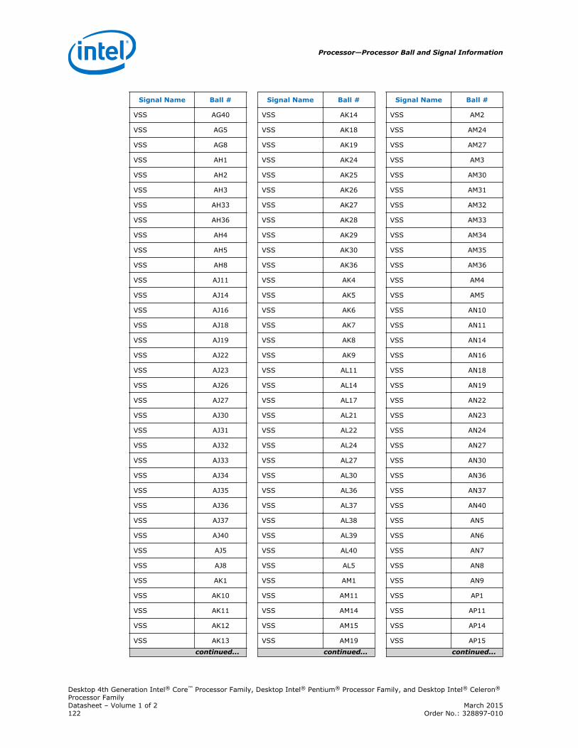
Signal Name Ball #
VSS AG40
VSS AG5
VSS AG8
VSS AH1
VSS AH2
VSS AH3
VSS AH33
VSS AH36
VSS AH4
VSS AH5
VSS AH8
VSS AJ11
VSS AJ14
VSS AJ16
VSS AJ18
VSS AJ19
VSS AJ22
VSS AJ23
VSS AJ26
VSS AJ27
VSS AJ30
VSS AJ31
VSS AJ32
VSS AJ33
VSS AJ34
VSS AJ35
VSS AJ36
VSS AJ37
VSS AJ40
VSS AJ5
VSS AJ8
VSS AK1
VSS AK10
VSS AK11
VSS AK12
VSS AK13
continued...
Signal Name Ball #
VSS AK14
VSS AK18
VSS AK19
VSS AK24
VSS AK25
VSS AK26
VSS AK27
VSS AK28
VSS AK29
VSS AK30
VSS AK36
VSS AK4
VSS AK5
VSS AK6
VSS AK7
VSS AK8
VSS AK9
VSS AL11
VSS AL14
VSS AL17
VSS AL21
VSS AL22
VSS AL24
VSS AL27
VSS AL30
VSS AL36
VSS AL37
VSS AL38
VSS AL39
VSS AL40
VSS AL5
VSS AM1
VSS AM11
VSS AM14
VSS AM15
VSS AM19
continued...
Signal Name Ball #
VSS AM2
VSS AM24
VSS AM27
VSS AM3
VSS AM30
VSS AM31
VSS AM32
VSS AM33
VSS AM34
VSS AM35
VSS AM36
VSS AM4
VSS AM5
VSS AN10
VSS AN11
VSS AN14
VSS AN16
VSS AN18
VSS AN19
VSS AN22
VSS AN23
VSS AN24
VSS AN27
VSS AN30
VSS AN36
VSS AN37
VSS AN40
VSS AN5
VSS AN6
VSS AN7
VSS AN8
VSS AN9
VSS AP1
VSS AP11
VSS AP14
VSS AP15
continued...
Processor—Processor Ball and Signal Information
Desktop 4th Generation Intel® Core™ Processor Family, Desktop Intel® Pentium® Processor Family, and Desktop Intel® Celeron®
Processor FamilyDatasheet – Volume 1 of 2 March 2015122 Order No.: 328897-010
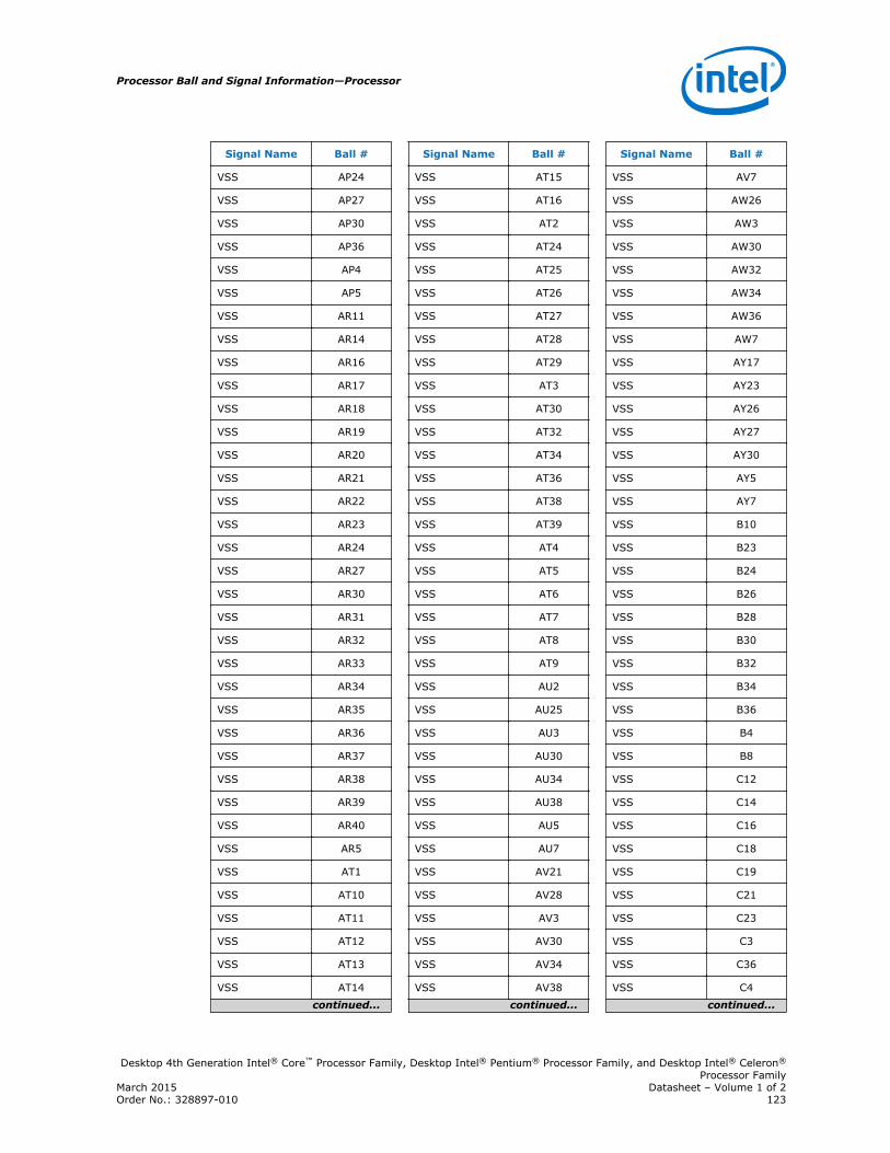
Signal Name Ball #
VSS AP24
VSS AP27
VSS AP30
VSS AP36
VSS AP4
VSS AP5
VSS AR11
VSS AR14
VSS AR16
VSS AR17
VSS AR18
VSS AR19
VSS AR20
VSS AR21
VSS AR22
VSS AR23
VSS AR24
VSS AR27
VSS AR30
VSS AR31
VSS AR32
VSS AR33
VSS AR34
VSS AR35
VSS AR36
VSS AR37
VSS AR38
VSS AR39
VSS AR40
VSS AR5
VSS AT1
VSS AT10
VSS AT11
VSS AT12
VSS AT13
VSS AT14
continued...
Signal Name Ball #
VSS AT15
VSS AT16
VSS AT2
VSS AT24
VSS AT25
VSS AT26
VSS AT27
VSS AT28
VSS AT29
VSS AT3
VSS AT30
VSS AT32
VSS AT34
VSS AT36
VSS AT38
VSS AT39
VSS AT4
VSS AT5
VSS AT6
VSS AT7
VSS AT8
VSS AT9
VSS AU2
VSS AU25
VSS AU3
VSS AU30
VSS AU34
VSS AU38
VSS AU5
VSS AU7
VSS AV21
VSS AV28
VSS AV3
VSS AV30
VSS AV34
VSS AV38
continued...
Signal Name Ball #
VSS AV7
VSS AW26
VSS AW3
VSS AW30
VSS AW32
VSS AW34
VSS AW36
VSS AW7
VSS AY17
VSS AY23
VSS AY26
VSS AY27
VSS AY30
VSS AY5
VSS AY7
VSS B10
VSS B23
VSS B24
VSS B26
VSS B28
VSS B30
VSS B32
VSS B34
VSS B36
VSS B4
VSS B8
VSS C12
VSS C14
VSS C16
VSS C18
VSS C19
VSS C21
VSS C23
VSS C3
VSS C36
VSS C4
continued...
Processor Ball and Signal Information—Processor
Desktop 4th Generation Intel® Core™ Processor Family, Desktop Intel® Pentium® Processor Family, and Desktop Intel® Celeron®
Processor FamilyMarch 2015 Datasheet – Volume 1 of 2Order No.: 328897-010 123

Signal Name Ball #
VSS C6
VSS D11
VSS D13
VSS D15
VSS D17
VSS D2
VSS D23
VSS D24
VSS D26
VSS D28
VSS D30
VSS D32
VSS D34
VSS D36
VSS D37
VSS D5
VSS D6
VSS D7
VSS D9
VSS E10
VSS E18
VSS E20
VSS E22
VSS E23
VSS E3
VSS E36
VSS E38
VSS E6
VSS E7
VSS E8
VSS F1
VSS F12
VSS F14
VSS F16
VSS F19
VSS F21
continued...
Signal Name Ball #
VSS F22
VSS F24
VSS F26
VSS F28
VSS F30
VSS F32
VSS F34
VSS F36
VSS F4
VSS F7
VSS G11
VSS G12
VSS G13
VSS G14
VSS G15
VSS G16
VSS G17
VSS G21
VSS G3
VSS G36
VSS G37
VSS G6
VSS G7
VSS G9
VSS H1
VSS H10
VSS H11
VSS H13
VSS H17
VSS H18
VSS H20
VSS H21
VSS H22
VSS H24
VSS H26
VSS H28
continued...
Signal Name Ball #
VSS H30
VSS H32
VSS H34
VSS H36
VSS H39
VSS H4
VSS H7
VSS H8
VSS H9
VSS J11
VSS J14
VSS J18
VSS J19
VSS J20
VSS J3
VSS J36
VSS J37
VSS J6
VSS J7
VSS K1
VSS K10
VSS K14
VSS K15
VSS K16
VSS K17
VSS K18
VSS K20
VSS K22
VSS K24
VSS K26
VSS K28
VSS K30
VSS K32
VSS K34
VSS K36
VSS K4
continued...
Processor—Processor Ball and Signal Information
Desktop 4th Generation Intel® Core™ Processor Family, Desktop Intel® Pentium® Processor Family, and Desktop Intel® Celeron®
Processor FamilyDatasheet – Volume 1 of 2 March 2015124 Order No.: 328897-010

Signal Name Ball #
VSS K40
VSS K7
VSS L11
VSS L13
VSS L14
VSS L3
VSS L35
VSS L36
VSS L38
VSS L6
VSS L7
VSS L8
VSS L9
VSS M1
VSS M12
VSS M14
VSS M16
VSS M18
VSS M20
VSS M22
VSS M24
VSS M26
VSS M28
VSS M30
VSS M32
VSS M34
VSS M35
VSS M37
VSS M4
VSS M40
VSS M5
VSS M6
VSS M7
VSS M9
VSS N1
VSS N2
continued...
Signal Name Ball #
VSS N3
VSS N33
VSS N34
VSS N39
VSS N4
VSS N6
VSS N7
VSS N8
VSS P2
VSS P34
VSS P35
VSS P38
VSS P39
VSS P40
VSS P5
VSS P7
VSS R3
VSS R35
VSS R37
VSS R38
VSS R39
VSS R40
VSS R5
VSS R6
VSS R7
VSS R8
VSS T1
VSS T2
VSS T33
VSS T36
VSS T37
VSS T38
VSS T39
VSS T4
VSS T5
VSS T6
continued...
Signal Name Ball #
VSS T7
VSS U2
VSS U33
VSS U34
VSS U35
VSS U36
VSS U37
VSS U4
VSS U7
VSS V3
VSS V33
VSS V34
VSS V40
VSS V6
VSS V7
VSS V8
VSS W1
VSS W33
VSS W35
VSS W37
VSS W4
VSS W7
VSS Y33
VSS Y4
VSS Y5
VSS Y6
VSS_NCTF AU40
VSS_NCTF AV39
VSS_NCTF AW38
VSS_NCTF AY3
VSS_NCTF B38
VSS_NCTF B39
VSS_NCTF C40
VSS_NCTF D40
VSS_SENSE F40
Processor Ball and Signal Information—Processor
Desktop 4th Generation Intel® Core™ Processor Family, Desktop Intel® Pentium® Processor Family, and Desktop Intel® Celeron®
Processor FamilyMarch 2015 Datasheet – Volume 1 of 2Order No.: 328897-010 125
Related Documents