28610.09, Rev. 6 SANKEN ELECTRIC CO., LTD. http://www.sanken-ele.co.jp/en/ Description The SLA6868MZ and SLA6870MZ inverter power module (IPM) ICs provide a robust, highly-integrated solution for optimally controlling 3-phase motor power inverter systems and variable speed control systems used in energy-conserving designs to drive motors of residential and commercial appliances. These ICs take 230 VAC input voltage, and up to 3 A (continuous) output current. They can withstand voltages of up to 500 V (MOSFET breakdown voltage). The SLA power package includes an IC with all of the necessary power elements (six MOSFETs), pre-driver ICs (two), and bootstrap diodes (three), needed to configure the main circuit of an inverter. This enables the main circuit of the inverter to be configured with fewer external components than traditional designs. Applications include residential white goods (home applications) and commercial appliance motor control: • Air conditioner fan • Small ventilation fan • Dishwasher pump Features and Benefits ▪ Built-in pre-drive IC ▪ MOSFET power element ▪ Alleviate noise generation by adjusting an internal resistor ▪ CMOS compatible input (5 V) ▪ High-side gate driver using bootstrap circuit or floating power supply ▪ Built-in protection circuit for controlling power supply voltage drop (UVLO on VCC) ▪ Overcurrent protection (OCP), overcurrent limiting (OCL), and thermal shutdown (TSD) ▪ Output of fault signal during operation of protection circuit ▪ Output current 1.5, 2.5, or 3 A ▪ Small SIP (SLA 24-pin) High Voltage 3-Phase Motor Drivers Figure 1. Driver block diagram. Functional Block Diagram Low-Side Driver UVLO UVLO UVLO UVLO Input Logic Input Logic (OCP Reset ) UVLO Thermal Shutdown SD1 VCC1 VB1 VB2 VB3 VBB U V W1 W2 LS 2 LS 1 SD2 COM2 LIN3 LIN2 LIN1 VCC 2 COM1 HIN3 HIN2 HIN1 High-Side Level Shift Driver OCL OCP and OCL RC OCP A. ¯ S ¯¯ D ¯ ¯ 1 ¯ , ¯ S ¯¯ D ¯ ¯ 2 ¯ terminals are used for both input and output. B. ¯ S ¯¯ D ¯ ¯ 1 ¯ , ¯ S ¯¯ D ¯ ¯ 2 ¯ , and ¯ O ¯¯ C ¯ ¯ L ¯ terminals are open-collector output. RC terminal is open-drain input. C. Blanking Time (t blank ) is used in Overcurrent Limiting (OCL) and Overcurrent Protection (OCP). If the time exceeds the limit, the signal will be output (open-collector output turns on), and protection operation will start up. Not to scale Leadform 2171 Leadform 2175 Packages: Power SIP SLA6868MZ and SLA6870MZ Not Recommended for New Designs

Welcome message from author
This document is posted to help you gain knowledge. Please leave a comment to let me know what you think about it! Share it to your friends and learn new things together.
Transcript

28610.09, Rev. 6 SANKEN ELECTRIC CO., LTD.http://www.sanken-ele.co.jp/en/
DescriptionThe SLA6868MZ and SLA6870MZ inverter power module (IPM) ICs provide a robust, highly-integrated solution for optimally controlling 3-phase motor power inverter systems and variable speed control systems used in energy-conserving designs to drive motors of residential and commercial appliances. These ICs take 230 VAC input voltage, and up to 3 A (continuous) output current. They can withstand voltages of up to 500 V (MOSFET breakdown voltage).
The SLA power package includes an IC with all of the necessary power elements (six MOSFETs), pre-driver ICs (two), and bootstrap diodes (three), needed to configure the main circuit of an inverter. This enables the main circuit of the inverter to be configured with fewer external components than traditional designs.
Applications include residential white goods (home applications) and commercial appliance motor control:• Air conditioner fan• Small ventilation fan• Dishwasher pump
Features and Benefits▪ Built-in pre-drive IC ▪ MOSFET power element▪ Alleviate noise generation by adjusting an internal resistor ▪ CMOS compatible input (5 V) ▪ High-side gate driver using bootstrap circuit or floating
power supply▪ Built-in protection circuit for controlling power supply
voltage drop (UVLO on VCC) ▪ Overcurrent protection (OCP), overcurrent limiting (OCL),
and thermal shutdown (TSD) ▪ Output of fault signal during operation of protection circuit▪ Output current 1.5, 2.5, or 3 A ▪ Small SIP (SLA 24-pin)
High Voltage 3-Phase Motor Drivers
Figure 1. Driver block diagram.
Functional Block Diagram
Low-SideDriver
UVLOUVLOUVLOUVLO
InputLogic
Input Logic(OCP Reset )
UVLO
ThermalShutdown
SD1
VCC1
VB1 VB2 VB3
VBB
UV
W1W2
LS
2LS
1SD2
COM2
LIN3LIN2LIN1
VCC2
COM1
HIN3HIN2HIN1 High-Side
Level Shift Driver
OCL
OCP and OCL
RC
OCP
A. S D 1 , S D 2 terminals are used for both input and output.B. S D 1 , S D 2 , and O C L terminals are open-collector output. RC terminal is open-drain input.C. Blanking Time (tblank) is used in Overcurrent Limiting (OCL) and Overcurrent Protection (OCP). If the time exceeds the limit, the signal will be output (open-collector output turns on), and protection operation will start up.
Not to scale
Leadform 2171 Leadform 2175
Packages: Power SIP
SLA6868MZ and SLA6870MZ
Not Reco
mmended
for N
ew D
esign
s

2SANKEN ELECTRIC CO., LTD.
High Voltage 3-Phase Motor DriversSLA6868MZ and SLA6870MZ
28610.09, Rev. 6
Selection Guide
Part NumberMOSFET Breakdown
Voltage, VDSS(min)(V)
Output CurrentContinuous, IO(max)
(A)Pulsed, IOP (max)
(A)SLA6868MZ 500 2.5 3.75
SLA6870MZ 500 3 4.5
Absolute Maximum Ratings, valid at TA = 25°CCharacteristic Symbol Remarks Rating Unit
MOSFET Breakdown Voltage VDSS VCC = 15 V, ID = 100 μA, VIN = 0 V 500 V
Logic Supply Voltage VCC Between VCC and COM 20 V
Bootstrap Voltage VBS Between VB and HS (U,V, and W phases) 20 V
Output Current, Continuous IOSLA6868MZ 2.5 A
SLA6870MZ 3 A
Output Current, Pulsed IOPSLA6868MZ
PW ≤ 100 μs, duty cycle = 1%3.75 A
SLA6870MZ 4.5 A
Input Voltage VIN HINx and LINx pins –0.5 to 7 V
Pull-up Voltage for Shutdown Pins VSDX S D x pins 7 V
Pull-up Voltage for Overcurrent Limiting Pin VOCL 7 V
Allowable Power Dissipation PD TC = 25°C 32.9 W
Thermal Resistance (Junction to Case) RθJC All elements operating 3.8 °C/W
Case Operating Temperature TCOP –20 to 100 °C
Junction Temperature (MOSFET) TJ 150 °C
Storage Temperature Tstg –40 to 150 °C
All performance characteristics given are typical values for circuit or system baseline design only and are at the nominal operating voltage and an ambient temperature, TA, of 25°C, unless oth er wise stated.
Not Reco
mmended
for N
ew D
esign
s
3SANKEN ELECTRIC CO., LTD.
High Voltage 3-Phase Motor DriversSLA6868MZ and SLA6870MZ
28610.09, Rev. 6
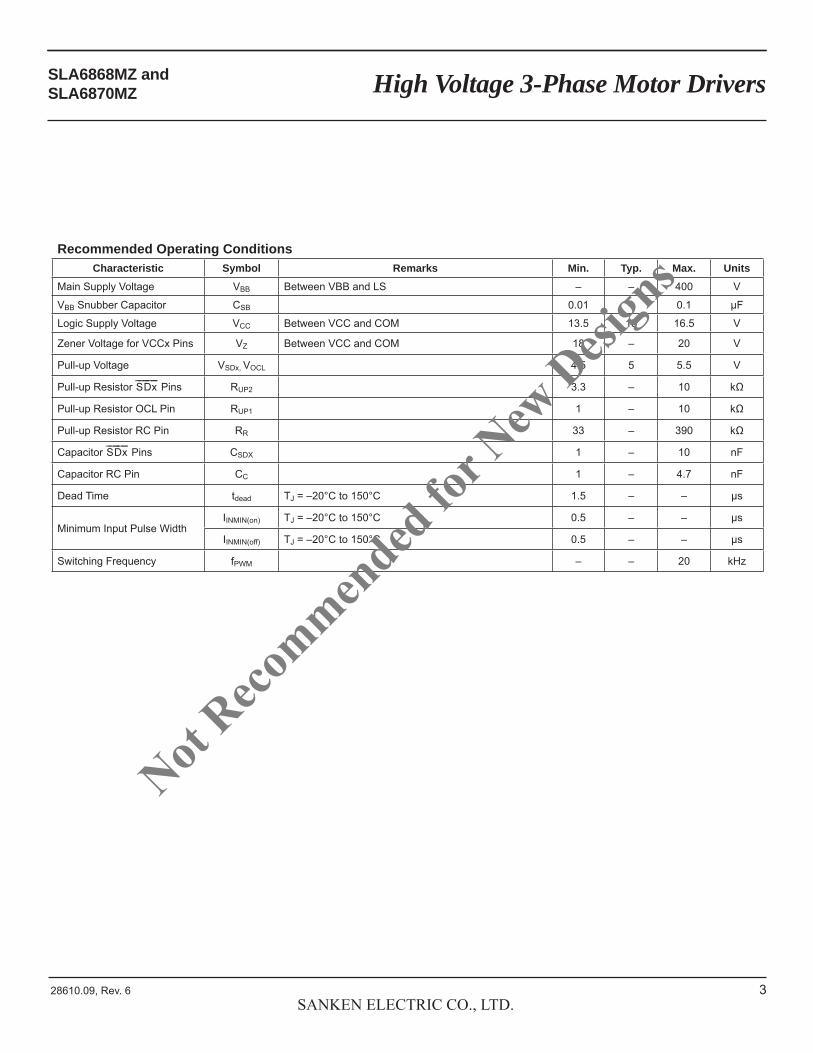
Recommended Operating ConditionsCharacteristic Symbol Remarks Min. Typ. Max. Units
Main Supply Voltage VBB Between VBB and LS – – 400 V
VBB Snubber Capacitor CSB 0.01 – 0.1 μF
Logic Supply Voltage VCC Between VCC and COM 13.5 15 16.5 V
Zener Voltage for VCCx Pins VZ Between VCC and COM 18 – 20 V
Pull-up Voltage VSDx, VOCL 4.5 5 5.5 V
Pull-up Resistor S D x Pins RUP2 3.3 – 10 kΩ
Pull-up Resistor OCL Pin RUP1 1 – 10 kΩ
Pull-up Resistor RC Pin RR 33 – 390 kΩ
Capacitor S D x Pins CSDX 1 – 10 nF
Capacitor RC Pin CC 1 – 4.7 nF
Dead Time tdead TJ = –20°C to 150°C 1.5 – – μs
Minimum Input Pulse WidthIINMIN(on) TJ = –20°C to 150°C 0.5 – – μs
IINMIN(off) TJ = –20°C to 150°C 0.5 – – μs
Switching Frequency fPWM – – 20 kHz
Not Reco
mmended
for N
ew D
esign
s

4SANKEN ELECTRIC CO., LTD.
High Voltage 3-Phase Motor DriversSLA6868MZ and SLA6870MZ
28610.09, Rev. 6
VCC2
LIN1
VCC1
HIN1
COM1
VB1
HO 3
HS3
LIN2
LIN3
SD2
COM 2
LO 1
LO 2
LO 3
M
MC U
15 V
HVIC
LVIC
HIN2HIN3
VB2 VB3
SLA6868MZSLA6870MZ
HO 2
HO 1
HS1
HS2
10
1 3
4
5
6
78
24
12
11
13
16
17
14
23
22
19
18
20
21
OCL
2
SD19
RC15
RUP1
5V
5 V
RUP2
DZ1
DZ2
RS
5V
CC
RR
CSD1
CSD2
CSB
NOTE:▪ The external electrolytic capacitors should be placed as close to the IC as possible, in order to avoid malfunctions from
external noise interference. Put a ceramic capacitor in parallel with the electrolytic capacitor if further reduction of noise susceptibility is necessary.
Typical Application DiagramShows configuration for implementing current limiter function: O C L and S D 1 pins tied together
Not Reco
mmended
for N
ew D
esign
s

5SANKEN ELECTRIC CO., LTD.
High Voltage 3-Phase Motor DriversSLA6868MZ and SLA6870MZ
28610.09, Rev. 6
VCC2
LIN1
VCC1
HIN1
COM1
VB1
HO3
HS3
LIN2
LIN3
SD2
COM2
LO1
LO2
LO3
M
15V
HVIC
LVIC
HIN2
HIN3
VB2 VB3
HO2
HO1
HS1
HS2
10
1 3
4
5
6
7
8
24
12
11
13
16
17
14
23
22
19
18
20
21
OCL
2
SD1
9
RC15
Rup1
5VZD
ZD
RS
VRC
CC
RR
CSD
Rup
SLA6868MZSLA6870MZ
Typical Application Diagram
NOTE:The external electrolytic capacitors should be placed as close to the IC as possible, in order to avoid malfunctions from external noise interference. Put a ceramic capacitor in parallel with the electrolytic capacitor if further reduction of noise susceptibility is necessary.
Shows configuration without current limiter function: S D 1 and S D 2 pins tied together
Not Reco
mmended
for N
ew D
esign
s

6SANKEN ELECTRIC CO., LTD.
High Voltage 3-Phase Motor DriversSLA6868MZ and SLA6870MZ
28610.09, Rev. 6
ELECTRICAL CHARACTERISTICS, valid at TA=25°C, unless otherwise notedCharacteristics Symbol Conditions Min Typ Max Units
Logic Supply Current ICCSLA6868MZ
VCC = 15 V, TC = –20°C to 125°C– 4.2 7 mA
SLA6870MZ – 2.7 5.0 mA
Bootstrap Supply Current IBX VBX = 15 V, VHIN = 5 V – 135 380 μA
Input VoltageVIH VCC = 15 V – 2.9 3.4 V
VIL VCC = 15 V 1.6 2.1 – V
Input Voltage Hysteresis VIhys VCC = 15 V – 0.8 – V
Input Current IIN VIN = 5 V – 230 500 μA
Undervoltage Lock Out
VUVHLHigh side, between VBx and U, V, or W
9.0 10.0 11.0 V
VUVHH 9.5 10.5 11.5 V
VUVHhys High side, hysteresis – 0.5 – V
VUVLLLow side, between VCC2 and COM2
10.0 11.0 12.0 V
VUVLH 10.5 11.5 12.5 V
VUVLhys Low side, hysteresis – 0.5 – V
SDx and OCL Output Voltage VSDX(on), VOCL
VSDX = VOCL = 5 V, RUPX = 3.3 kΩ – – 0.6 V
Overtemperature Detection Threshold Temperature (Activation and Deactivation)
TDH
VCC = 15 V, high-side and low side
120 135 150 °C
TDL 100 115 130 °C
TDhys – 20 – °C
Overcurrent Protection Trip Voltage VTRIP VCC = 15 V 0.9 1.0 1.1 V
Overcurrent Limit Reference Voltage VLIM VCC = 15 V 0.5035 0.53 0.5565 V
Overcurrent Protection Hold Time tp VRC = 5 V, RR = 360 kΩ, CC = 0.0047 μF – 2.0 – ms
Blanking Time tblank VCC = 15 V 1.4 2.0 2.6 μs
Bootstrap Diode Leakage Current ILBD VR = 250 V – – 10 μA
Bootstrap Diode Forward Voltage VFBDSLA6868MZ
IF = 0.05 A– 1.1 1.3 V
SLA6870MZ – 0.8 1.3 V
Bootstrap Diode Recovery Time trrb IF / IRP = 100 mA / 100 mA – 70 – ns
Bootstrap Diode Series Resistor RBD 168 210 252 Ω
MOSFET Breakdown Voltage VDSS VCC = 15 V, ID = 100 μA, VIN = 0 V 500 – – V
MOSFET Leakage Current IDSS VCC = 15 V, VDS = 500 V, VIN = 0 V – – 100 μA
MOSFET On State Resistance RDS(on)SLA6868MZ VCC = 15 V, ID = 1.5 A, VIN = 5 V – 2.0 2.4 Ω
SLA6870MZ VCC = 15 V, ID = 1.25 A, VIN = 5 V – 1.4 1.7 Ω
MOSFET Diode Forward Voltage VSDFSLA6868MZ VCC = 15 V, ISD = 1.5 A, VIN = 0 V – 1.1 1.5 V
SLA6870MZ VCC = 15 V, ISD = 1.25 A, VIN = 0 V – 1.0 1.5 VNot Reco
mmended
for N
ew D
esign
s
7SANKEN ELECTRIC CO., LTD.
High Voltage 3-Phase Motor DriversSLA6868MZ and SLA6870MZ
28610.09, Rev. 6
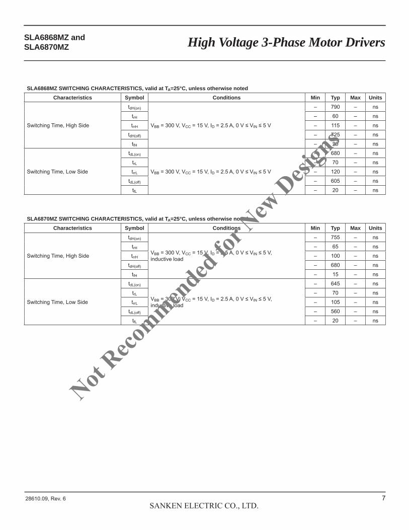
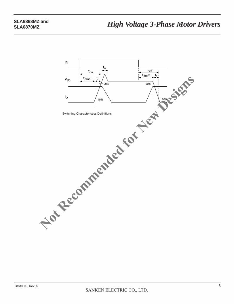
SLA6868MZ SWITCHING CHARACTERISTICS, valid at TA=25°C, unless otherwise notedCharacteristics Symbol Conditions Min Typ Max Units
Switching Time, High Side
tdH(on)
VBB = 300 V, VCC = 15 V, ID = 2.5 A, 0 V ≤ VIN ≤ 5 V
– 790 – ns
trH – 60 – ns
trrH – 115 – ns
tdH(off) – 725 – ns
tfH – 20 – ns
Switching Time, Low Side
tdL(on)
VBB = 300 V, VCC = 15 V, ID = 2.5 A, 0 V ≤ VIN ≤ 5 V
– 680 – ns
trL – 70 – ns
trrL – 120 – ns
tdL(off) – 605 – ns
tfL – 20 – ns
SLA6870MZ SWITCHING CHARACTERISTICS, valid at TA=25°C, unless otherwise notedCharacteristics Symbol Conditions Min Typ Max Units
Switching Time, High Side
tdH(on)
VBB = 300 V, VCC = 15 V, ID = 2.5 A, 0 V ≤ VIN ≤ 5 V,inductive load
– 755 – ns
trH – 65 – ns
trrH – 100 – ns
tdH(off) – 680 – ns
tfH – 15 – ns
Switching Time, Low Side
tdL(on)
VBB = 300 V, VCC = 15 V, ID = 2.5 A, 0 V ≤ VIN ≤ 5 V,inductive load
– 645 – ns
trL – 70 – ns
trrL – 105 – ns
tdL(off) – 560 – ns
tfL – 20 – ns
Not Reco
mmended
for N
ew D
esign
s
8SANKEN ELECTRIC CO., LTD.
High Voltage 3-Phase Motor DriversSLA6868MZ and SLA6870MZ
28610.09, Rev. 6
VDS
ton tofftf
tr
trr
td(on)td(off)
ID 10% 10%
90% 90%
IN
Switching Characteristics Definitions
Not Reco
mmended
for N
ew D
esign
s
9SANKEN ELECTRIC CO., LTD.
High Voltage 3-Phase Motor DriversSLA6868MZ and SLA6870MZ
28610.09, Rev. 6
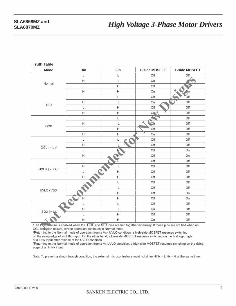
Truth Table Mode Hin Lin H-side MOSFET L-side MOSFET
Normal
L L Off Off
H L On Off
L H Off On
H H On On
TSD
L L Off Off
H L On Off
L H Off Off
H H On Off
OCP
L L Off Off
H L On Off
L H Off Off
H H On Off
O C L ( = L )1
L L Off Off
H L Off Off
L H Off On
H H Off On
UVLO ( VCC )2
L L Off Off
H L Off Off
L H Off Off
H H Off Off
UVLO ( VB )3
L L Off Off
H L Off Off
L H Off On
H H Off On
S D 2 ( = L )
L L Off Off
H L On Off
L H Off Off
H H On Off 1The OCL feature is enabled when the O C L and S D 1 pins are tied together externally. If these pins are not tied when an OCL condition occurs, device operation continues in Normal mode.2Returning to the Normal mode of operation from a VCC UVLO condition, a high-side MOSFET resumes switchingon the rising edge of an HINx input. On the other hand, a low-side MOSFET resumes switching on the first logic highof a LINx input after release of the UVLO condition.3Returning to the Normal mode of operation from a VB UVLO condition, a high-side MOSFET resumes switching on the rising edge of an HINx input.
Note: To prevent a shoot-through condition, the external microcontroller should not drive HINx = LINx = H at the same time.
Not Reco
mmended
for N
ew D
esign
s

10SANKEN ELECTRIC CO., LTD.
High Voltage 3-Phase Motor DriversSLA6868MZ and SLA6870MZ
28610.09, Rev. 6
LIN
LO
LS1
SD2
tblank
RC
Slope defined by RC, CC
O C PRelease
tp
3.5 V
VTRIP
OCP Timing Diagram
Low-Side TSD Timing Diagram
Open-collector output transistorturned on in low state
Not Reco
mmended
for N
ew D
esign
s
11SANKEN ELECTRIC CO., LTD.
High Voltage 3-Phase Motor DriversSLA6868MZ and SLA6870MZ
28610.09, Rev. 6
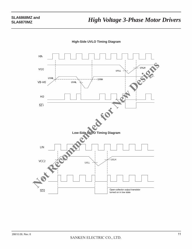
LIN
SD2
VCC2 UVLLUVLH
LO
UVLH
Open-collector output transistorturned on in low state
High-Side UVLO Timing Diagram
Low-Side UVLO Timing Diagram
Not Reco
mmended
for N
ew D
esign
s

12SANKEN ELECTRIC CO., LTD.
High Voltage 3-Phase Motor DriversSLA6868MZ and SLA6870MZ
28610.09, Rev. 6
OCL Timing Diagram
O C L and S D 1 pins connected externally
LIN
LO
LS1
SD2
RC
VTRIP (1 V)
VOCL (0.5 V)
3.5 V
OCL,SD1
2 μs
VTH (2.1 V)VTH (2.1 V)
VTH (2.9 V) VTH (2.9 V)
VTH (2.9 V)
2 μs
5 μs
2 μs
= 50 Cf
= 50 CC
= RL×Cf = RL×Cf
= RR×CC
= R2×C2
HIN
HO3.3 μs 3.3 μs
Low-side shutdown
High-side shutdown
Enable resumption of high-sideoperation at next HIN rising edge
Enable resumption of low-sideoperation at next LIN rising edge
High-side shutdown
= 50 C2
Not Reco
mmended
for N
ew D
esign
s
13SANKEN ELECTRIC CO., LTD.
High Voltage 3-Phase Motor DriversSLA6868MZ and SLA6870MZ
28610.09, Rev. 6
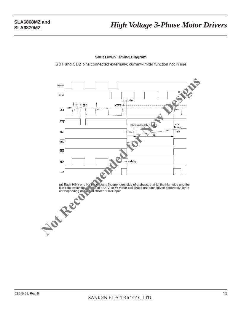
Shut Down Timing Diagram
S D 1 and S D 2 pins connected externally; current-limiter function not in use
Slope defined by RC, CC
LIN(a)
HIN(a)
(a) Each HINx or LINx pin drives a independent side of a phase, that is, the high-side and thelow-side swtiching devices of a U, V, or W motor coil phase are each driven separately, by thecorresponding dedicated HINx or LINx input
Not Reco
mmended
for N
ew D
esign
s

14SANKEN ELECTRIC CO., LTD.
High Voltage 3-Phase Motor DriversSLA6868MZ and SLA6870MZ
28610.09, Rev. 6
Leadform 2171 Leadform 2175
1 3 5 7 9 11 13 15 17 19 21 23
2 4 6 8 10 12 14 16 18 20 22 24
2 4 6 8 10 12 14 16 18 20 22 24
1 3 5 7 9 11 13 15 17 19 21 23
Pad Side
Pad Side
Terminal List TableNumber Name Function
1 VB1 High side bootstrap terminal (U phase)
2 VB2 High side bootstrap terminal (V phase)
3 VB3 High side bootstrap terminal (W phase)
4 VCC1 High side logic supply voltage
5 S D 1 High side shutdown input and UVLO fault signal output
6 COM1 High side logic GND terminal
7 HIN3 High side input terminal (W phase)
8 HIN2 High side input terminal (V phase)
9 HIN1 High side input terminal (U phase)
10 VBB Main supply voltage
11 W1 Output of W phase (connect to W2 externally)
12 V Output of V phase
13 W2 Output of W phase (connect to W1 externally)
14 LS2 Low side source terminal (connect to LS1 externally)
15 RC Overcurrent protection hold time adjustment input terminal
16 LS1 Low side source terminal (connect to LS2 externally)
17 O C L Output for overcurrent limiting
18 LIN3 Low side input terminal (W phase)
19 LIN2 Low side input terminal (V phase)
20 LIN1 Low side input terminal (U phase)
21 COM2 Low side GND terminal
22 S D 2 Low side shutdown input and overtemperature, overcurrent, and UVLO fault signals output
23 VCC2 Low side logic supply voltage
24 U Output of U phase
Pin-out Diagram
Not Reco
mmended
for N
ew D
esign
s
15SANKEN ELECTRIC CO., LTD.
High Voltage 3-Phase Motor DriversSLA6868MZ and SLA6870MZ
28610.09, Rev. 6
1.27 ±0.7
0.6
0.6 +0.15– 0.05
9.5 +0.7– 0.5 0.5 +0.15
– 0.05
16.4 ±0.2
24.4 ±0.2
Ø3.2 ±0.15
31 ±0.2
Gate protrusion
9.9 ±0.2
12.9 ±0.2
16 ±0.2
A
A
BMeasured at pin tips
To case top
1 3 5 7 9 11 13 15 17 19 21 23
2 4 6 8 10 12 14 16 18 20 22 24
1.7 ±0.1
4.8 ±0.2
R1REF
4.5REF 4.5 ±0.7
5 ±0.5
2.45 ±0.2BSCB
Ø3.2 ±0.15
31.3 ±0.2
View A
Heatsink exposedthis side
Deflection at pin bend
0.7 MAX0.7 MAX
View A
2X Gate protrusion
2X Exposed tie barBranding Area
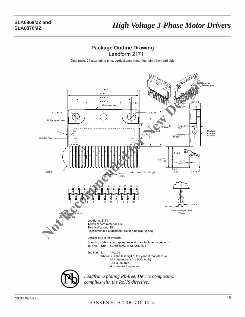
Leadform: 2171Terminal core material: CuTerminal plating: NiRecommended attachment: Solder dip (Sn-Ag-Cu)
Dimensions in millimetersBranding codes (exact appearance at manufacturer discretion):1st line, type: SLA6868MZ or SLA6870MZ 2nd line, lot: YMDD# Where: Y is the last digit of the year of manufacture M is the month (1 to 9, O, N, D) DD is the date # is the tracking letter
Exposed heatsink pad
Leadframe plating Pb-free. Device composition complies with the RoHS directive.
Package Outline DrawingLeadform 2171
Dual rows, 24 alternating pins; vertical case mounting; pin #1 on pad side
Not Reco
mmended
for N
ew D
esign
s
16SANKEN ELECTRIC CO., LTD.
High Voltage 3-Phase Motor DriversSLA6868MZ and SLA6870MZ
28610.09, Rev. 6
1.27 ±0.2
0.616.4 ±0.2
24.4 ±0.2
Ø3.2 ±0.15
31 ±0.2
Gate protrusion
9.9 ±0.1
12.9 ±0.2
16 ±0.2
A
A
B To case top
1.7 ±0.1
4.8 ±0.2
R1REF
0.5 ±0.1
2.45 ±0.1BSCB
Ø3.2 ±0.15
31.3 ±0.1
View A
2 4 6 8 10 12 14 16 18 20 22 241 3 5 7 9 11 13 15 17 19 21 23
Measured at pin exit from case
4.4REF
2.2 ±0.6BSC
2.2 ±0.6BSC
3 ±0.3BSC
0.6 +0.2– 0.1
Deflection at pin bend
0.7 MAX0.7 MAX
View A
2X Gate protrusion
2X Exposed tie bar
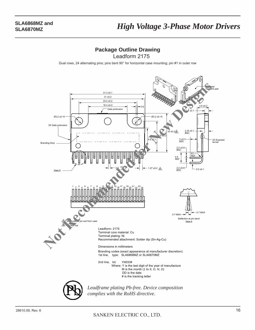
Leadform: 2175Terminal core material: CuTerminal plating: NiRecommended attachment: Solder dip (Sn-Ag-Cu)
Dimensions in millimeters
Branding Area
Branding codes (exact appearance at manufacturer discretion):1st line, type: SLA6868MZ or SLA6870MZ 2nd line, lot: YMDD# Where: Y is the last digit of the year of manufacture M is the month (1 to 9, O, N, D) DD is the date # is the tracking letter
Exposed heatsink pad
Package Outline DrawingLeadform 2175
Dual rows, 24 alternating pins; pins bent 90° for horizontal case mounting; pin #1 in outer row
Leadframe plating Pb-free. Device composition complies with the RoHS directive.
Not Reco
mmended
for N
ew D
esign
s
17SANKEN ELECTRIC CO., LTD.
High Voltage 3-Phase Motor DriversSLA6868MZ and SLA6870MZ
28610.09, Rev. 6
Because reliability can be affected adversely by improper storage environments and handling methods, please observe the following cautions.Cautions for Storage• Ensure that storage conditions comply with the standard
temperature (5°C to 35°C) and the standard relative humidity (around 40% to 75%); avoid storage locations that experience extreme changes in temperature or humidity.
• Avoid locations where dust or harmful gases are present and avoid direct sunlight.
• Reinspect for rust on leads and solderability of the products that have been stored for a long time.
Cautions for Testing and Handling When tests are carried out during inspection testing and
other standard test periods, protect the products from power surges from the testing device, shorts between the product pins, and wrong connections. Ensure all test parameters are within the ratings specified by Sanken for the products.
Remarks About Using Silicone Grease with a Heatsink• When silicone grease is used in mounting the products on
a heatsink, it shall be applied evenly and thinly. If more silicone grease than required is applied, it may produce excess stress.
• Volatile-type silicone greases may crack after long periods of time, resulting in reduced heat radiation effect. Silicone greases with low consistency (hard grease) may cause cracks in the mold resin when screwing the products to a heatsink.
Our recommended silicone greases for heat radiation purposes, which will not cause any adverse effect on the product life, are indicated below:
Type Suppliers
G746 Shin-Etsu Chemical Co., Ltd.
YG6260 Momentive Performance Materials Inc.
SC102 Dow Corning Toray Co., Ltd.
Cautions for Mounting to a Heatsink• When the flatness around the screw hole is insufficient, such
as when mounting the products to a heatsink that has an extruded (burred) screw hole, the products can be damaged, even with a lower than recommended screw torque. For mounting the products, the mounting surface flatness should be 0.05 mm or less.
• Please select suitable screws for the product shape. Do not use a flat-head machine screw because of the stress to the products. Self-tapping screws are not recommended. When using self-tapping screws, the screw may enter the hole diagonally, not vertically, depending on the conditions of hole before threading or the work situation. That may stress the products and may cause failures.
• Recommended screw torque: 0.588 to 0.785 N●m (6 to 8 kgf●cm).
• For tightening screws, if a tightening tool (such as a driver) hits the products, the package may crack, and internal stress fractures may occur, which shorten the lifetime of the electrical elements and can cause catastrophic failure. Tightening with an air driver makes a substantial impact. In addition, a screw torque higher than the set torque can be applied and the package may be damaged. Therefore, an electric driver is recommended.
When the package is tightened at two or more places, first pre-tighten with a lower torque at all places, then tighten with the specified torque. When using a power driver, torque control is mandatory.
Soldering• When soldering the products, please be sure to minimize
the working time, within the following limits: 260±5°C 10±1 s (Flow, 2 times) 380±10°C 5±0.5 s (Soldering iron, 1 time)• Soldering should be at a distance of at least 1.5 mm from
the body of the products.Electrostatic Discharge• When handling the products, the operator must be
grounded. Grounded wrist straps worn should have at least 1 MΩ of resistance from the operator to ground to prevent shock hazard, and it should be placed near the operator.
• Workbenches where the products are handled should be grounded and be provided with conductive table and floor mats.
• When using measuring equipment such as a curve tracer, the equipment should be grounded.
• When soldering the products, the head of soldering irons or the solder bath must be grounded in order to prevent leak voltages generated by them from being applied to the products.
• The products should always be stored and transported in Sanken shipping containers or conductive containers, or be wrapped in aluminum foil.
Not Reco
mmended
for N
ew D
esign
s

18SANKEN ELECTRIC CO., LTD.
High Voltage 3-Phase Motor DriversSLA6868MZ and SLA6870MZ
28610.09, Rev. 6
• The contents in this document are subject to changes, for improvement and other purposes, without notice. Make sure that this is the latest revision of the document before use.
• Application and operation examples described in this document are quoted for the sole purpose of reference for the use of the prod-ucts herein and Sanken can assume no responsibility for any infringement of industrial property rights, intellectual property rights or any other rights of Sanken or any third party which may result from its use.
• Although Sanken undertakes to enhance the quality and reliability of its products, the occurrence of failure and defect of semicon-ductor products at a certain rate is inevitable. Users of Sanken products are requested to take, at their own risk, preventative measures including safety design of the equipment or systems against any possible injury, death, fires or damages to the society due to device failure or malfunction.
• Sanken products listed in this document are designed and intended for the use as components in general purpose electronic equip-ment or apparatus (home appliances, office equipment, telecommunication equipment, measuring equipment, etc.).
When considering the use of Sanken products in the applications where higher reliability is required (transportation equipment and its control systems, traffic signal control systems or equipment, fire/crime alarm systems, various safety devices, etc.), and whenever long life expectancy is required even in general purpose electronic equipment or apparatus, please contact your nearest Sanken sales representative to discuss, prior to the use of the products herein.
The use of Sanken products without the written consent of Sanken in the applications where extremely high reliability is required (aerospace equipment, nuclear power control systems, life support systems, etc.) is strictly prohibited.
• In the case that you use Sanken products or design your products by using Sanken products, the reliability largely depends on the degree of derating to be made to the rated values. Derating may be interpreted as a case that an operation range is set by derating the load from each rated value or surge voltage or noise is considered for derating in order to assure or improve the reliability. In general, derating factors include electric stresses such as electric voltage, electric current, electric power etc., environmental stresses such as ambient temperature, humidity etc. and thermal stress caused due to self-heating of semiconductor products. For these stresses, instantaneous values, maximum values and minimum values must be taken into consideration.
In addition, it should be noted that since power devices or IC's including power devices have large self-heating value, the degree of derating of junction temperature affects the reliability significantly.
• When using the products specified herein by either (i) combining other products or materials therewith or (ii) physically, chemically or otherwise processing or treating the products, please duly consider all possible risks that may result from all such uses in advance and proceed therewith at your own responsibility.
• Anti radioactive ray design is not considered for the products listed herein.• Sanken assumes no responsibility for any troubles, such as dropping products caused during transportation out of Sanken's distribu-
tion network.• The contents in this document must not be transcribed or copied without Sanken's written consent.
Not Reco
mmended
for N
ew D
esign
s
Related Documents