Application Note Please read the Important Notice and Warnings at the end of this document V 1.1 www.infineon.com/powermosfet page 1 of 27 2022-02-10 AN_2112_PL18_2112_024619 Designing with power MOSFETs How to avoid common issues and failure modes Author: Peter B. Green About this document Scope and purpose In common with all power semiconductor devices, power MOSFETs have their own technical strengths, weaknesses and subtleties, which need to be properly understood if the designer is to avoid reliability issues. In this application note some of the most common dos and don’ts of using power MOSFETs are discussed. The objective is to help the system designer understand how to use these devices correctly and avoid common mistakes, thereby reducing design time. A list of useful references is provided at the end for more in-depth study. Intended audience Power engineers and students designing with power MOSFETs. This is intended for engineers with a basic familiarity with MOSFETs but limited experience of designing with them. Table of contents About this document ....................................................................................................................... 1 Table of contents ............................................................................................................................ 1 1 Introduction to power MOSFETs .............................................................................................. 3 2 Handling and testing power MOSFETs ...................................................................................... 5 3 Reverse blocking characteristics .............................................................................................. 6 3.1 Avalanche failure mechanisms ............................................................................................................... 6 3.1.1 Latch-up ............................................................................................................................................. 6 3.1.2 Thermal failure ................................................................................................................................... 7 3.2 Avalanche testing .................................................................................................................................... 7 3.3 Single and repetitive avalanche conditions ........................................................................................... 8 3.4 How to avoid avalanche .......................................................................................................................... 9 4 MOSFET current ratings and heatsinking ................................................................................. 10 5 Gate-to-source voltage transients ........................................................................................... 12 6 Safe operating area ............................................................................................................... 13 6.1 RDS(on) limit (blue).................................................................................................................................... 14 6.2 Maximum operating current limit (red) ................................................................................................ 14 6.3 Power limit (dark green) ....................................................................................................................... 15 6.4 Thermal stability limit (light green) ...................................................................................................... 15 6.5 Breakdown voltage (yellow) ................................................................................................................. 16 7 Induced turn-on and shoot-through ........................................................................................ 17 7.1 How to avoid induced turn-on .............................................................................................................. 18 8 Body diode ........................................................................................................................... 19 9 Package and board layout considerations ................................................................................ 21 Feeda

Welcome message from author
This document is posted to help you gain knowledge. Please leave a comment to let me know what you think about it! Share it to your friends and learn new things together.
Transcript

Application Note Please read the Important Notice and Warnings at the end of this document V 1.1
www.infineon.com/powermosfet page 1 of 27 2022-02-10
AN_2112_PL18_2112_024619
Designing with power MOSFETs
How to avoid common issues and failure modes
Author: Peter B. Green
About this document
Scope and purpose
In common with all power semiconductor devices, power MOSFETs have their own technical strengths,
weaknesses and subtleties, which need to be properly understood if the designer is to avoid reliability issues. In this application note some of the most common dos and don’ts of using power MOSFETs are discussed. The
objective is to help the system designer understand how to use these devices correctly and avoid common mistakes, thereby reducing design time. A list of useful references is provided at the end for more in-depth study.
Intended audience
Power engineers and students designing with power MOSFETs. This is intended for engineers with a basic familiarity with MOSFETs but limited experience of designing with them.
Table of contents
About this document ....................................................................................................................... 1
Table of contents ............................................................................................................................ 1
1 Introduction to power MOSFETs .............................................................................................. 3
2 Handling and testing power MOSFETs ...................................................................................... 5
3 Reverse blocking characteristics .............................................................................................. 6 3.1 Avalanche failure mechanisms ............................................................................................................... 6 3.1.1 Latch-up ............................................................................................................................................. 6
3.1.2 Thermal failure ................................................................................................................................... 7 3.2 Avalanche testing .................................................................................................................................... 7
3.3 Single and repetitive avalanche conditions ........................................................................................... 8 3.4 How to avoid avalanche .......................................................................................................................... 9
4 MOSFET current ratings and heatsinking ................................................................................. 10
5 Gate-to-source voltage transients ........................................................................................... 12
6 Safe operating area ............................................................................................................... 13
6.1 RDS(on) limit (blue) .................................................................................................................................... 14 6.2 Maximum operating current limit (red) ................................................................................................ 14
6.3 Power limit (dark green) ....................................................................................................................... 15 6.4 Thermal stability limit (light green) ...................................................................................................... 15 6.5 Breakdown voltage (yellow) ................................................................................................................. 16
7 Induced turn-on and shoot-through ........................................................................................ 17 7.1 How to avoid induced turn-on .............................................................................................................. 18
8 Body diode ........................................................................................................................... 19
9 Package and board layout considerations ................................................................................ 21
Feed a

Application Note 2 of 27 V 1.1
2022-02-10
Designing with power MOSFETs How to avoid common issues and failure modes
Table of contents
10 Paralleling of power MOSFETs ................................................................................................ 23
11 Conclusion ........................................................................................................................... 24
References .................................................................................................................................... 25
Revision history............................................................................................................................. 26

Application Note 3 of 27 V 1.1
2022-02-10
Designing with power MOSFETs How to avoid common issues and failure modes
Introduction to power MOSFETs
1 Introduction to power MOSFETs
Power MOSFETs were first introduced in the 1970s, and became the most widely used power transistors in the
world. They offer many advantages over older technologies such as bipolar power transistors in both linear and switching applications. These advantages include greatly improved switching, easy paralleling capability, the absence of the second breakdown effect, and a wider safe operating area (SOA). MOSFETs are voltage-driven transconductance devices.
The differently doped layers of silicon from which the MOSFET die is constructed fall into two broad technology categories, referred to as planar and trench, as shown in Figure 1.
Planar MOSFET Trench MOSFET
Figure 1 Planar and trench MOSFET die layers
A power MOSFET die is composed of many individual cells or planar strips connected in parallel with a meshed
gate connection.
Planar HEXFET™1 structure Trench structure
Source metal
Gate metal
Buried source poly
metal
Back
Dielectric
Gate oxide
Buried source poly field plate
N type silicon
Gate electrode
Gate poly
Drain
A A
R
Cut taken along A-A line
Top view Cross-section
Figure 2 MOSFET device structures
1 A hexagonal type of power MOSFET developed at Stanford University in 1977 by Alex Lidow and Tom Herman, and commercialized by
International Rectifier in 1978.

Application Note 4 of 27 V 1.1
2022-02-10
Designing with power MOSFETs How to avoid common issues and failure modes
Introduction to power MOSFETs
Infineon OptiMOS™ devices are based on trench technology, while CoolMOS™ devices are based on superjunction, which is an enhancement of planar technology that enables lower on-resistance and supersedes
the older HEXFET™ devices.
The topics discussed in this application note are applicable to all of these silicon power MOSFET technologies, but may not apply to other power devices and technologies such as IGBTs, silicon carbide (SiC) FETs or gallium
nitride (GaN) high-electron-mobility transistors (HEMTs). The focus will be on N-channel enhancement mode devices, which account for the majority of power MOSFETs produced.
Although power MOSFETs may initially appear to be simple three-terminal voltage-driven switches, this is a
very misleading idea. In reality, these devices are somewhat more complicated, and therefore a solid understanding of the basic characteristics and behavior is essential before embarking on any design project. This should greatly reduce frustrating failures and burned circuits! When it comes to power MOSFETs, or for
that matter any other power semiconductor devices, taking the time to gain an understanding of the aspects described in the following sections will ultimately save time.

Application Note 5 of 27 V 1.1
2022-02-10
Designing with power MOSFETs How to avoid common issues and failure modes
Handling and testing power MOSFETs
2 Handling and testing power MOSFETs
The user’s first onta t with a MOS-gated transistor could be a package of parts arriving on their desk. Even at this stage, it is important to be knowledgeable about some elementary precautions. Being MOS devices with very high gate impedance, power MOSFETs can be damaged by static discharge during handling, testing or
installation into a circuit. ESD damage of MOSFETs typically occurs when the gate-to-source voltage is high enough to arc across the gate dielectric. This burns a microscopic hole in the gate oxide, causing the part to fail immediately or later during operation.
Power MOSFET devices have high enough input capacitance to absorb some static charge without excessive build-up of voltage. However, to avoid possible problems, the following procedures should be followed as a matter of good practice, wherever possible:
• MOS-gated transistors should be left in their anti-static shipping bags, or conductive foam, or they
should be placed in metal containers or conductive bins until required for testing or connection into a circuit. The person handling the device should ideally be grounded through a suitable wrist strap, though in reality this added precaution is seldom essential.
• Devices should be handled by the package, not by the leads. When checking the electrical characteristics of the MOS-gated transistors on a curve tracer, or in a test circuit, the following precautions should be observed:
1. Test stations should use electrically conductive floor and grounded anti-static mats on the test
bench.
2. When inserting the device in a curve tracer or a test circuit, voltage should not be applied until all
terminals are solidly connected into the circuit.
3. When using a curve tracer, a resistor should be connected in series with the gate to damp spurious
oscillations that can otherwise occur on the trace. A suitable value of resistance is
100 Ω.
• The next step is to connect the device into an actual circuit. The following simple precautions should be observed:
1. Workstations should use electrically grounded table and floor mats.
2. Soldering irons should be grounded.
Now that the device has been connected into its circuit, it is ready for the power to be applied. From here on, success in applying the device becomes a matter of the integrity of the circuit design and depends on whether
the necessary circuit design precautions have been taken to guard against unintentional abuse of its ratings.
The following sections describe the interrelated device and circuit considerations that lead to reliable, trouble-free design.
Application Note 6 of 27 V 1.1
2022-02-10
Designing with power MOSFETs How to avoid common issues and failure modes
Reverse blocking characteristics
3 Reverse blocking characteristics
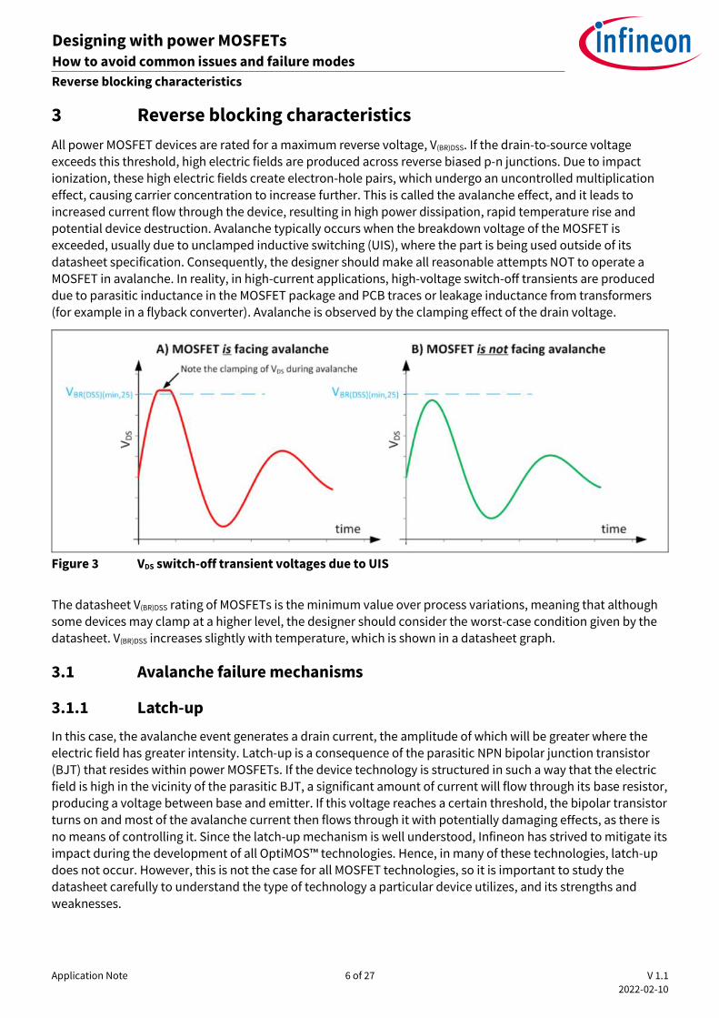
All power MOSFET devices are rated for a maximum reverse voltage, V(BR)DSS. If the drain-to-source voltage exceeds this threshold, high electric fields are produced across reverse biased p-n junctions. Due to impact ionization, these high electric fields create electron-hole pairs, which undergo an uncontrolled multiplication
effect, causing carrier concentration to increase further. This is called the avalanche effect, and it leads to increased current flow through the device, resulting in high power dissipation, rapid temperature rise and potential device destruction. Avalanche typically occurs when the breakdown voltage of the MOSFET is exceeded, usually due to unclamped inductive switching (UIS), where the part is being used outside of its
datasheet specification. Consequently, the designer should make all reasonable attempts NOT to operate a MOSFET in avalanche. In reality, in high-current applications, high-voltage switch-off transients are produced due to parasitic inductance in the MOSFET package and PCB traces or leakage inductance from transformers
(for example in a flyback converter). Avalanche is observed by the clamping effect of the drain voltage.
Figure 3 VDS switch-off transient voltages due to UIS
The datasheet V(BR)DSS rating of MOSFETs is the minimum value over process variations, meaning that although
some devices may clamp at a higher level, the designer should consider the worst-case condition given by the datasheet. V(BR)DSS increases slightly with temperature, which is shown in a datasheet graph.
3.1 Avalanche failure mechanisms
3.1.1 Latch-up
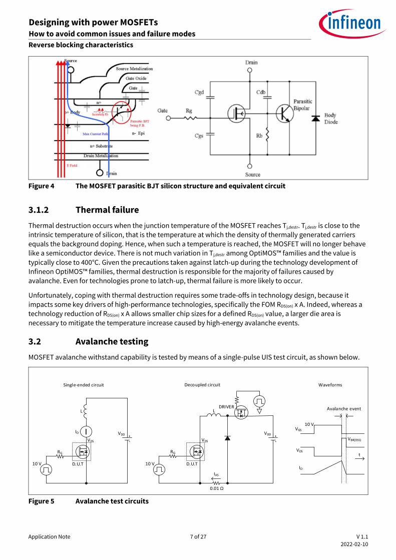
In this case, the avalanche event generates a drain current, the amplitude of which will be greater where the
electric field has greater intensity. Latch-up is a consequence of the parasitic NPN bipolar junction transistor (BJT) that resides within power MOSFETs. If the device technology is structured in such a way that the electric field is high in the vicinity of the parasitic BJT, a significant amount of current will flow through its base resistor, producing a voltage between base and emitter. If this voltage reaches a certain threshold, the bipolar transistor turns on and most of the avalanche current then flows through it with potentially damaging effects, as there is
no means of controlling it. Since the latch-up mechanism is well understood, Infineon has strived to mitigate its impact during the development of all OptiMOS™ technologies. Hence, in many of these technologies, latch-up does not occur. However, this is not the case for all MOSFET technologies, so it is important to study the datasheet carefully to understand the type of technology a particular device utilizes, and its strengths and
weaknesses.
Application Note 7 of 27 V 1.1
2022-02-10
Designing with power MOSFETs How to avoid common issues and failure modes
Reverse blocking characteristics
Figure 4 The MOSFET parasitic BJT silicon structure and equivalent circuit
3.1.2 Thermal failure
Thermal destruction occurs when the junction temperature of the MOSFET reaches Tj,destr. Tj,destr is close to the
intrinsic temperature of silicon, that is the temperature at which the density of thermally generated carriers equals the background doping. Hence, when such a temperature is reached, the MOSFET will no longer behave like a semiconductor device. There is not much variation in Tj,destr among OptiMOS™ families and the value is
typically close to 400°C. Given the precautions taken against latch-up during the technology development of Infineon OptiMOS™ families, thermal destruction is responsible for the majority of failures caused by
avalanche. Even for technologies prone to latch-up, thermal failure is more likely to occur.
Unfortunately, coping with thermal destruction requires some trade-offs in technology design, because it
impacts some key drivers of high-performance technologies, specifically the FOM RDS(on) x A. Indeed, whereas a technology reduction of RDS(on) x A allows smaller chip sizes for a defined RDS(on) value, a larger die area is
necessary to mitigate the temperature increase caused by high-energy avalanche events.
3.2 Avalanche testing
MOSFET avalanche withstand capability is tested by means of a single-pulse UIS test circuit, as shown below.
IID
L
D.U.T
VDS
VDD
Single-ended circuit
RG
IAS
L
D.U.T
VDS
VDD
Decoupled circuit
DRIVER
0.01 Ω
10 V 10 V
10 VVGS
VDS
VBR(DSS)
ID
Avalanche event
t
Waveforms
RG
Figure 5 Avalanche test circuits

Application Note 8 of 27 V 1.1
2022-02-10
Designing with power MOSFETs How to avoid common issues and failure modes
Reverse blocking characteristics
In these circuits, a pulse of defined duration is applied to the MOSFET gate to switch the device on so that the drain current rises linearly due to the series inductor. The MOSFET is then switched off, at which point a large
negative di/dt occurs that produces a voltage transient. In the decoupled circuit both MOSFETs are switched on and off at the same time, so that the inductor voltage is equal to that applied between the MOSFET drain and
source. The switch-off transient rises above V(BR)DSS so that the energy stored in the inductor (defined by the pulse length and inductance) can be transferred into the MOSFET during an avalanche condition. Infineon
performs avalanche stress testing to assure conformance with the EAS rating, validate ruggedness and screen for defective parts.
3.3 Single and repetitive avalanche conditions
There is a defined maximum amount of avalanche energy that a MOSFET is able to withstand in a single pulse, which is specified as EAS in the MOSFET datasheet under a certain set of test conditions. As its name suggests, a
single-pulse avalanche event should only be allowed to occur once, particularly if the conditions are close to the limits provided in the datasheet. This is because those limits correspond to junction temperatures above
the Tj,max of the MOSFET, therefore repeating such events would impair the operating lifetime of the MOSFET. Please remember that avalanche is not a recommended operating condition.
In the case of repetitive avalanche, the events occur continuously at a fast repetition rate, which is typically the same as the switching frequency (fSW) of an application circuit such as a switching power converter. The safe quantity of avalanche energy allowable per event is much lower than for single-pulse avalanche.
In most repetitive avalanche cases, due to the relatively low energy of each avalanche event, the silicon
temperature rise is negligible compared to the worst-case single-pulse avalanche condition. The observed VDS
spikes only slightly exceed the V(BR)DSS,(min,25) rating of the MOSFET, as opposed to the 1.2~1.3 x V(BR)DSS,(min,25)
amplitudes recorded during high-energy single-pulse avalanche testing. A relevant difference between single
and repetitive avalanche ratings relates to the permitted Tj,max caused by such events. In fact, although the junction temperature is permitted to exceed Tj,max during single-pulse avalanche, this is NOT the case for repetitive avalanche.
Exceeding Tj,max during repetitive avalanche has a cumulative effect, which risks reducing the reliability of the
device over its lifetime, leading to early failure. Tj,max can be as low as 150°C for parts in QFN 5x6 (SuperSO8) or
S3O8 packages. This is a limitation of the package rather than the silicon itself, which can usually withstand 175°C. As a result, in some cases MOSFETs with the same die, when housed within a different package (e.g., TO-220 or D2PAK) are rated at 175°C.
It is very important to distinguish between single-pulse and repetitive avalanche, because the way they can affect normal MOSFET behavior differs significantly. The two device failure modes for single-pulse avalanche
are caused either by high current (latch-up) or high energy (thermal destruction). These failure modes are
catastrophic; however, in the case of repetitive avalanche, deterioration is incremental, impacting the device very slowly through repeated micro-damage. Even a low-energy avalanche event generates some hot carriers, which are charges injected along the trench oxide of the power MOSFET. The repetition of such avalanche
events leads to an accumulation of such charges, which slowly impair reliability. This can result in field failures
occurring after a period of time.
It is worth mentioning that to significantly reduce the impact of repetitive avalanche on technology parameters, Infineon would need to compromise significantly on other figures of merit that are dominant in the
vast majority of applications. This would be too high a price to pay for an event that does not correspond to a normal usage of a MOSFET, which a designer should strive to avoid. Consequently, Infineon does not insert
repetitive avalanche ratings within the OptiMOS™ “Industrial and Standard Grades” datasheets.

Application Note 9 of 27 V 1.1
2022-02-10
Designing with power MOSFETs How to avoid common issues and failure modes
Reverse blocking characteristics
3.4 How to avoid avalanche
First and foremost, it is necessary to select a device with the right V(BR)DSS rating for the application. This means that the maximum steady-state voltage across the drain and source of the device under worst-case operating
conditions should be considered with a safety margin of at least 20 percent. In cases where large switch-off transients occur, a much higher safety margin will be required to achieve reliable operation. For example, in motor drive inverts it is not unusual to select a MOSFET with V(BR)DSS rating of twice the DC bus voltage. It is, however, a mistake to choose a part with a higher rating than needed, because this would give a higher RDS(on)
and probably cost more.
Methods that can be employed to reduce the switch-off transient include slowing down the MOSFET switch-off
by adjusting the gate drive network and adding RC snubbers between the drain and source. Naturally, both of
these create additional switching losses, which reduces system efficiency.
Rg_on
Rg_off
Rg_on
Rg_off
Switch OFF faster than switch ON Switch ON faster than switch OFF
Figure 6 Gate drive circuits
Depending on the specifics of the design, one of the above gate drive circuits can be used to control the switch-
on and switch-off speeds. Adjusting Rg_off allows the designer to reduce the switch-off transient voltage without affecting the switch-on speed. However, in hard-switching half-bridge circuits, the value of Rg_off cannot be too high, as this could result in an induced turn-on spike appearing at the low-side gate, caused by the CGD.di/dt
effect. If large enough, this spike can exceed the MOSFET VGS(th) and cause dangerous shoot-through currents
(this is discussed further in section 7). Careful consideration of the gate drive resistor values is essential to achieve the best trade-off between minimizing switch-off transient amplitude, avoiding induced turn-on (if applicable) and controlling EMI emissions.
As previously mentioned, a series RC snubber can be added across the drain and source to absorb some of the
switch-off transient, thereby reducing its peak voltage; however, this produces additional switch-on losses.
Figure 7 RC snubber connected across a MOSFET drain and source
Application Note 10 of 27 V 1.1
2022-02-10
Designing with power MOSFETs How to avoid common issues and failure modes
MOSFET current ratings and heatsinking
4 MOSFET current ratings and heatsinking
The inexperienced user may assume that the continuous drain current rating ID(MAX) that appears on a MOSFET datasheet represents the current at which the device can be operated in a practical system. However, it is important to realize that this is not the case!
Such ID(MAX) ratings are based on ideal test conditions not achievable in a practical design. Test conditions often
involve very large heatsinks or die temperatures to be maintained at a low level through artificial cooling.
It should be noted that different manufacturers use different criteria (some more conservative than others) for
determining the ID(MAX) rating claimed for their MOSFETs, and these methods have also evolved over time. It is therefore a mistake to rely on these ratings to compare the capabilities of different devices! The method now used by Infineon is described in [5].
A more realistic approach to comparing different devices would be on the basis of power loss and how it causes
the die and package temperatures to rise under a given set of conditions.
As a first criteria to look at, it is useful to compare RDS(on) at 25°C, because this provides a common basis for comparison. RDS(on) is composed of series die and package resistances1, with the former being dependent on the
gate-to-source voltage VGS.
RDS(on), taken in conjunction with the junction-case thermal resistance RTH(JC),2 gives a much better indication of a
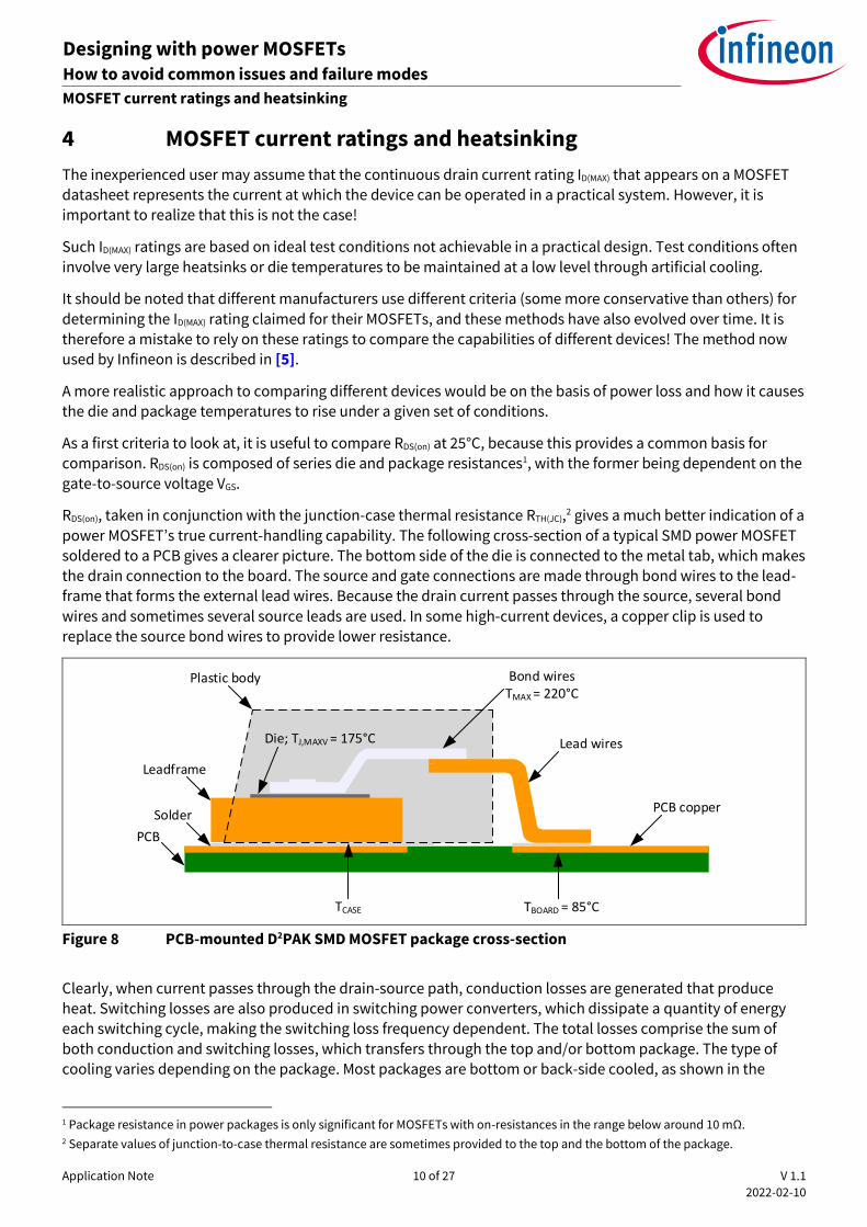
power MOSFET’s true current-handling capability. The following cross-section of a typical SMD power MOSFET soldered to a PCB gives a clearer picture. The bottom side of the die is connected to the metal tab, which makes
the drain connection to the board. The source and gate connections are made through bond wires to the lead-frame that forms the external lead wires. Because the drain current passes through the source, several bond
wires and sometimes several source leads are used. In some high-current devices, a copper clip is used to
replace the source bond wires to provide lower resistance.
Plastic body
Die; TJ,MAXV = 175°C
Bond wiresTMAX = 220°C
Leadframe
Solder
PCB
TCASE TBOARD = 85°C
Lead wires
PCB copper
Figure 8 PCB-mounted D2PAK SMD MOSFET package cross-section
Clearly, when current passes through the drain-source path, conduction losses are generated that produce
heat. Switching losses are also produced in switching power converters, which dissipate a quantity of energy each switching cycle, making the switching loss frequency dependent. The total losses comprise the sum of
both conduction and switching losses, which transfers through the top and/or bottom package. The type of
cooling varies depending on the package. Most packages are bottom or back-side cooled, as shown in the
1 Package resistance in power packages is only significant for MOSFETs with on-resistances in the range below around 10 mΩ. 2 Separate values of junction-to-case thermal resistance are sometimes provided to the top and the bottom of the package.

Application Note 11 of 27 V 1.1
2022-02-10
Designing with power MOSFETs How to avoid common issues and failure modes
MOSFET current ratings and heatsinking
above example, where most of the heat passes through the drain tab to the PCB, which needs to include a large number of thermal vias underneath the drain pad to transfer heat through to the bottom of the board. A
heatsink may then be mounted under the board. There are also top-side cooled packages, such as the TOLT package, in which the internal arrangement of the die and lead-frame within the package is different; they have
an exposed metal pad on top of the package where a heatsink may be mounted.
Figure 9 Bottom and top-side cooling
The heatsink must be sized to be able to transfer enough heat from the MOSFET die so that its junction temperature remains below the maximum rated level. The designer must first select the correct MOSFET die size and package option to limit power loss, and then they must choose a suitable heatsink to maintain a safe
junction temperature.
Apart from the heatsink size and surface area (determined by the shape and number of fins), the thermal
resistance from junction to ambient must also be considered. This depends on the heatsinking arrangement used, and can be calculated by adding all of the series thermal resistances (including PCB, thermal insulation
material/TIM, etc.) between the junction and the heatsink and that of the heatsink itself (see Figure 9). Clearly, a low junction-to-ambient thermal resistance is required to effectively transfer the heat from the MOSFET die
and allow it to safely conduct the highest possible current.
In conclusion, it makes more sense to look at the whole picture in terms of current handling than to pay too
much attention to datasheet ID(MAX) ratings.

Application Note 12 of 27 V 1.1
2022-02-10
Designing with power MOSFETs How to avoid common issues and failure modes
Gate-to-source voltage transients
5 Gate-to-source voltage transients
Excessive voltage transients can punch through the thin gate-source oxide layer and result in permanent damage. Unfortunately, such transients are produced in power switching circuits and can be coupled to the sensitive MOSFET gate input. The designer is strongly advised to look closely at the gate drive waveforms to
ensure that neither positive nor negative transients are present that exceed the device limits (typically +/-20 V for power MOSFETs, but this should be checked on the datasheet).
CGD
CGS
CDS
dVDS/dtD
S
G
i=C.dVDS/dt
RG
VGS
VGS
t
VGS (M AX)
Gate parasitic inductance
LG
LS
LDDrain parasitic
inductance
Source parasitic inductance
Figure 10 Rapidly changing drain-source voltages produce gate-source transients
During the switch-on or switch-off operations of the gate drive, a high dVDS/dt is produced as the device
transitions from the on-state to the off-state and vice-versa. Considering the presence of parasitic inductances in the gate, source and drain leads, and also the MOSFET CGD (Miller capacitance), it can be understood that transient voltages will be produced between the gate and source resulting from a combination of these
parasitic elements. Fortunately, the gate capacitance CGS acts to reduce this effect.
The ratio of CGS/CGD must be as high as possible to minimize drain-to-source voltage coupling. It is also essential
to optimize the PCB layout to reduce parasitic inductance as much as possible. In some cases, designers add small gate-source capacitors to help reduce these spikes, though this also slows down the MOSFET switching.
The values of CGS and CGD are voltage dependent and because of this, usually are not directly quoted on a
MOSFET datasheet. It is therefore more convenient instead to look at the related charge values QGD and QGS. The charge ratios are often expressed as: QGD/QGS or QGD/QGS(TH), where a lower value means the device is less susceptible to induced turn on coupled through CGD.

Application Note 13 of 27 V 1.1
2022-02-10
Designing with power MOSFETs How to avoid common issues and failure modes
Safe operating area
6 Safe operating area
The development of modern power MOSFETs has focused on fast switching with ultralow RDS(on), for which reduction of die area has been the trend. The power-handling capabilities of devices for a specific RDS(on) have therefore generally decreased, especially in linear operation mode (in the saturation region). When designing in
power MOSFETs (or any other type of power transistor), it is essential to pay close attention to the SOA diagram and ensure that the device will never be operated outside of the defined limit-lines. A reliable design is not possible if these limits are violated!
In order to accurately set these limits, Infineon carries out extensive testing on many samples, which involves testing parts to destruction. There are certain applications in which operation takes place in the saturation region for an extended period of time, such as inrush urrent limiting or “hot swap”. In these cases, particular
attention must be paid to the SOA limits for the required pulse duration to ensure these are never exceeded.
Figure 11 Ohmic (triode or linear)1 region and saturation region of a power MOSFET
SOA cannot be overlooked in typical switching applications because the device also passes through the saturation region every switching cycle unless it is a zero-voltage or current-switching transition. These
transitions happen rapidly, and therefore the MOSFET can withstand a much higher current pulse under the
defined conditions. However, it is advisable to check that it is operating within the SOA limits. It is important to keep in mind that when slowing down the switch-on or switch-off of a MOSFET (as discussed in section 3.4) to reduce EMI or switch-off transients, the period of operating time in the saturation region is increased.
1 Linear region is different from linear mode. Operating in linear mode means in the saturation region, not the ohmic region.
Application Note 14 of 27 V 1.1
2022-02-10
Designing with power MOSFETs How to avoid common issues and failure modes
Safe operating area
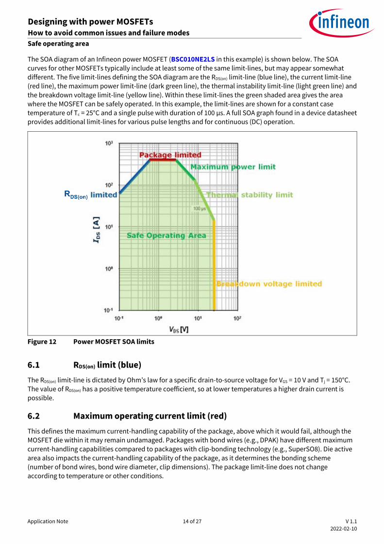
The SOA diagram of an Infineon power MOSFET (BSC010NE2LS in this example) is shown below. The SOA curves for other MOSFETs typically include at least some of the same limit-lines, but may appear somewhat
different. The five limit-lines defining the SOA diagram are the RDS(on) limit-line (blue line), the current limit-line (red line), the maximum power limit-line (dark green line), the thermal instability limit-line (light green line) and
the breakdown voltage limit-line (yellow line). Within these limit-lines the green shaded area gives the area where the MOSFET can be safely operated. In this example, the limit-lines are shown for a constant case
temperature of Tc = 25°C and a single pulse with duration of 100 µs. A full SOA graph found in a device datasheet provides additional limit-lines for various pulse lengths and for continuous (DC) operation.
Figure 12 Power MOSFET SOA limits
6.1 RDS(on) limit (blue)
The RDS(on) limit-line is dictated y Ohm’s law for a spe ifi drain-to-source voltage for VGS = 10 V and Tj = 150°C. The value of RDS(on) has a positive temperature coefficient, so at lower temperatures a higher drain current is
possible.
6.2 Maximum operating current limit (red)
This defines the maximum current-handling capability of the package, above which it would fail, although the MOSFET die within it may remain undamaged. Packages with bond wires (e.g., DPAK) have different maximum
current-handling capabilities compared to packages with clip-bonding technology (e.g., SuperSO8). Die active
area also impacts the current-handling capability of the package, as it determines the bonding scheme (number of bond wires, bond wire diameter, clip dimensions). The package limit-line does not change
according to temperature or other conditions.

Application Note 15 of 27 V 1.1
2022-02-10
Designing with power MOSFETs How to avoid common issues and failure modes
Safe operating area
6.3 Power limit (dark green)
This is calculated from the maximum power the device is permitted to dissipate that produces a stable junction temperature Tj of 150°C in thermal equilibrium, where Tc = 25°C. Considering the junction-to-case thermal
impedance of the package ZthJC, defined in °C per W, a certain power dissipation produces a ∆T of 125°C. This provides the power limit-line, where the product of VDS and ID remains constant to determine the slope.
For short pulses the value of ZthJC depends on the pulse length and its duty cycle. ZthJC can be taken from the corresponding diagram in the datasheet. The SOA diagram illustrates that an increased pulse duration shifts the maximum thermal limit-line downward, reflecting the higher thermal impedance at longer pulse lengths and/or higher duty cycle.
In a real application Tj will not remain at 25°C, so it will not be possible to operate the device within the SOA at
the power limit. Depending on the package, the heatsink and whether forced air-cooling is used, the maximum
permissible power dissipation will be that which results in a steady-state Tj of 150°C. As always it is advisable not to operate the device at its limit, so in practice some safety margin should be included.
6.4 Thermal stability limit (light green)
The thermal stability limit-line is also of critical importance to achieve reliable power MOSFET operation. In some cases, especially for older devices, the datasheet SOA graph may not include this limit-line though the
device may exhibit a thermal stability limitation. In general terms, thermal instability is the condition in which power loss rises more rapidly than power dissipation with respect to temperature so that thermal equilibrium cannot be achieved. Instead thermal runaway occurs due to current crowding in hotter cells of the device (see
section 1). This is referred to as the Spirito effect,1 where as a cell becomes hotter it draws more current,
causing its temperature to rise further until it is eventually destroyed. Under this condition, current cannot be
evenly distributed among cells.
Thermal instability can be expressed as follows:
𝜕𝑃𝑔𝑒𝑛𝑒𝑟𝑎𝑡𝑒𝑑
𝜕𝑇>
𝜕𝑃𝑑𝑖𝑠𝑠𝑖𝑝𝑎𝑡𝑒𝑑
𝜕𝑇 [1]
In such a condition the temperature of the system is not stable and is not in thermal equilibrium, unlike the case for the maximum power limit line (above).
𝑃𝑔𝑒𝑛𝑒𝑟𝑎𝑡𝑒𝑑 = 𝐼𝐷𝑆 ∙ 𝐼𝐷 [2]
and
𝑃𝑑𝑖𝑠𝑠𝑖𝑝𝑎𝑡𝑒𝑑 =𝑇𝑗−𝑇𝑎𝑚𝑏𝑖𝑒𝑛𝑡
𝑍𝑡ℎ𝐽𝐶 [3]
Assuming VDS is constant over temperature, the inequality can be rearranged to:
𝑉𝐷𝑆 ∙𝛿𝐼𝐷
𝛿𝑇>
1
𝑍𝑡ℎ𝐽𝐶(𝑡𝑝𝑢𝑙𝑠𝑒) [4]
The above equation defines the operating range where the MOSFET may encounter thermal instability. The term δID/δT is called the temperature coefficient. Since VDS > 0, thermal instability occurs is the temperature coefficient is positive.
1 Named after professor Pablo Spirito, who discovered it.

Application Note 16 of 27 V 1.1
2022-02-10
Designing with power MOSFETs How to avoid common issues and failure modes
Safe operating area
Thermal instability occurs if the drain current increases with temperature at a given value of VGS. This occurs for VGS values below the zero-temperature coefficient (ZTC) point. At higher VGS levels the drain current reduces
with temperature. This is illustrated in Figure 13.
Figure 13 Thermal stability related to ID vs. VGS
The change of temperature coefficient from positive to negative over VGS is caused by two competing effects. The resistance of a MOSFET increases with temperature due to lower electron mobility, while the threshold
voltage (VTH) decreases with temperature because more electrons have been excited into the conduction band. At low temperatures the effect of decreasing threshold voltage over increasing temperature dominates and
current increases with temperature, whereas at higher temperatures, the increase of RDS(on) dominates and ID
then decreases with temperature.
As shown above, thermal instability occurs when VGS is below the ZTC point. Thus, MOSFETs with a ZTC at high
currents and high VGS voltages will be more prone to thermal instability. The ZTC point is in direct relationship to the MOSFET transconductance (gm or gfs). With increasing transconductance the ZTC point will move toward higher VGS. Modern power MOSFETs exhibit ever-increasing transconductances and therefore also ZTC points at
higher VGS.
To avoid failures due to thermal instability, the designer needs to ensure that the SOA thermal stability limit
will not be violated.
6.5 Breakdown voltage (yellow)
This represents the device V(BR)DSS rating described in section 3.

Application Note 17 of 27 V 1.1
2022-02-10
Designing with power MOSFETs How to avoid common issues and failure modes
Induced turn-on and shoot-through
7 Induced turn-on and shoot-through
Induced turn-on is a phenomenon that occurs when MOSFETs are used in fast-switching applications where high dVDS/dt transitions appear at the drain while the device is in the off-state. This typically occurs in hard-switching1 applications such as switching power supplies and motor drive inverters, where two MOSFETs are
used in a half-bridge configuration.
HB node
VBUS
Figure 14 MOSFET half-bridge
The high- and low-side MOSFETs switch on and off alternately, with a small dead time between switch-off of
one device and switch-on of the other to prevent overlap that would result in very high current pulses. When the low-side MOSFET switches off, after the dead time has expired, the high-side switches on. When this
happens the HB node transitions rapidly from zero volts to VBUS.
CGD
CGS
CDS dVDS/dt
D
S
G
i=C.dVDS/dt
RG(EXT)
Gate drive Low
VGS
VGS
t
RG(INT)
Figure 15 Induced turn-on mechanism
Figure 15 shows how “C.dv/dt” auses a current pulse to couple through CGD to the gate, which is pulled to zero volts through RG(EXT). This current pulse can be sufficient to induce a voltage spike at the gate. It is important to
remember that the MOSFET may also have a significant internal gate resistance RG(INT), so that the induced gate
spike appearing at the silicon may be larger than that observed at the gate terminal.
If the induced turn-on spike exceeds the MOSFET VTH then the device will partially turn on for a brief time before the high-side MOSFET has fully turned off. With both devices partially on, a high current can flow through the
half-bridge, which can violate SOA limits and destroy one or both devices.
1 Hard-switching occurs when a MOSFET switches on with a non-zero VDS.

Application Note 18 of 27 V 1.1
2022-02-10
Designing with power MOSFETs How to avoid common issues and failure modes
Induced turn-on and shoot-through
7.1 How to avoid induced turn-on
As mentioned in section 5, MOSFETs with higher CGS/CGD, which means lower QGD/QGS and QGD/QGS(TH), are less susceptible drain-to-source voltage coupling. A QGD/QGS of 0.5 to 0.8 and QGD/QGS(TH) less than 1.0 is
recommended for hard switching applications. It should be notes that lower QGD/QGS devices may suffer from greater ringing in the gate voltage waveform, however this depends on the value of RG(INT) and the circuit loop inductance.
Induced turn-on may be reduced by slowing down the switching transition and therefore lowering the dv/dt. This can be done by slowing down the switch-on of the high-side device by increasing Rg_on (refer to Figure 6). Depending on the circuit switching behavior the high- and low-side gate drive network may be the same or may
be different. Slowing down the turn-on also reduces radiated EMI, but at the same time increases switching
losses, therefore it is a trade-off to be considered carefully.
Another way to reduce induced turn-on is to use a “swit h off faster than swit h on” type gate drive networ , which includes a diode and resistor to allow a strong pull-down for the gate while allowing a slower turn-on. This is good during the off-state but also leads to a fast switch-off, which tends to produce higher drain-transient voltages that may create a risk of avalanche – another trade-off to be considered during design. It is
worth mentioning that some smart gate driver ICs1 now available from Infineon include a programmable gate
drive where the gate current can be defined during different phases of operation, thereby eliminating resistor-diode gate driver networks and enabling precise tailoring of the gate drive to allow optimization during switching and in the off-state.
A third method involves adding an external gate-to-source capacitor. This can reduce the magnitude of the
induced gate transient by increasing the effective CGS/CGD, though again it slows down the switching and so
should be applied only when necessary and kept to a minimum value.
1 MOTIX™ 6EDL7141 smart gate driver IC for motor drive applications.

Application Note 19 of 27 V 1.1
2022-02-10
Designing with power MOSFETs How to avoid common issues and failure modes
Body diode
8 Body diode
The body diode is intrinsic to the MOSFET structure, formed by the p-n junction between p-body and n-epi layers shown in Figure 4. Power MOSFETs are three-terminal devices where the body and source are connected internally.1 This can be understood by looking at the circuit symbols for n- and P-channel devices.
Gate Gate
Drain
DrainSource(external pin)
Source
BodyBody
Source
Source(external pin)
Figure 16 N-channel (left) and P-channel (right) MOSFET circuit symbols, showing the body diodes
Like other p-n junction diodes, the MOSFET body diode exhibits minority carrier reverse recovery, resulting in a
finite reverse recovery time. Reverse recovery occurs when the diode is reverse biased while carrying a forward current. Reverse recovery is characterized in datasheets by time trr and the reverse recovery charge Qrr tested under a specified set of conditions.
Figure 17 Forward and reverse biasing of the body diode
At interval (1), the diode is in the off-state, and it starts to turn on in interval (2). At the end of the turn-on process, the diode becomes forward biased. The reverse recovery charge accumulates and is stored while the forward biased diode carries a positive current during interval (3). At the start of the turn-off interval (4), the current reduces to zero then flows in the opposite direction. During interval (5) reverse recovery is completed
1 This is ne essary to avoid the “ ody effe t”, whi h affe ts the value of VTH.

Application Note 20 of 27 V 1.1
2022-02-10
Designing with power MOSFETs How to avoid common issues and failure modes
Body diode
and the turn-off process is completed by interval (6), in which the diode is blocking. The shaded area in the diagram indicates Qrr, the key device parameter for hard-commutation ruggedness.
In half-bridge power-switching circuits as described in the previous section, body diode reverse recovery becomes significant when switching high current into an inductive load. Consider a synchronous buck regulator operating in continuous conduction mode (CCM) with Q1 on and Q2 off where a current IL is flowing
from the half-bridge switching node.
VIN
VOUT
IL
Q1
Q2
IL
t
Figure 18 Synchronous buck regulator
When Q1 switches off, the inductor current is commutated through the body diode of Q2, which then switches on after the dead time has ended. At the end of the Q2 conduction (synchronous rectification) period it
switches off again so that the current once again flows through its body diode. At the end of the dead time
period Q1 switches on, and this is where the body diode recovery of Q2 becomes critical. If Q1 switches on too rapidly, the peak reverse recovery current of the integral body diode Q2 will rise too rapidly, exceeding the peak
reverse recovery current rating, and the device may be destroyed!
Different MOSFET technologies have different degrees of body diode ruggedness and different reverse recovery
speeds. It is important to select devices that are suited to applications where hard commutation occurs, even if
this is only under some operating conditions. Infineon’s high-voltage CoolMOS™ family of superjunction MOSFETs includes the CFD family of parts, which have fast-recovery body diodes. In addition, there are several series of low- and mid-voltage OptiMOS™ trench devices. As a general rule, it is important to choose the right
type of power MOSFET for a particular design based on the type of switching that takes place.
The peak reverse recovery current of the body diode can be reduced by slowing down the rate of change of
current during the commutation process. The rate of change of current can be controlled by slowing down the
rate of rise of the gate driving pulse, as shown in Figure 6 and discussed in sections 3.4 and 7.1. Using this technique, the peak reverse recovery current can be reduced to an acceptable level at the expense of prolonging the high dissipation switching period, so as always there is a trade-off to consider. For operation at
frequencies up to around 20 kHz, slowing the applied gate drive signal to reduce the peak reverse recovery
current of the “opposite” devi e’s ody diode offers a good practical solution. At higher frequencies the designer must pay particular attention to the voltages and currents that the MOSFETs are required to switch and choose an appropriate device and gate drive scheme.

Application Note 21 of 27 V 1.1
2022-02-10
Designing with power MOSFETs How to avoid common issues and failure modes
Package and board layout considerations
9 Package and board layout considerations
Different power MOSFET packages have different parasitic inductances, leaded packages have higher inductances than SMD packages, and the amount of inductance present in an SMD package depends on the internal geometry of the drain and source connections. It is therefore necessary to consider which type of
package is required for any design based not only on its thermal characteristics but also on package inductance, which may not be specified in the datasheet. In short, where high currents are being switched in hard commutation, an SMD package with lowest possible inductance in conjunction with a well laid-out PCB will be required to achieve acceptable performance and avoid reliability and potential EMI issues. When laying
out a PCB for a power appli ation it is advisa le to use the manufa turer’s re ommended devi e footprint and to ensure that handling and soldering guidelines are followed [11].
Stray inductance in power switching circuits increases the amplitude and energy of overvoltage transients,
making it necessary to reduce switching speed to avoid avalanching. Transients are produced by rapid changes in current:
𝑉𝐷𝑆 = 𝐿𝑆𝑑𝑖𝑑
𝑑𝑡 [5]
where LS is determined by the current loop that starts at the closest bus decoupling capacitor, passes through the switching elements and then returns to the capacitor.
VIN
VOUT
Q1
Q2
Current loop
Decoupling capacitor
Figure 19 Loop of switching current in a half-bridge
In a physical board layout, the inductance of the current loop depends on how tightly spaced the traces are that form it, and on how far away the DC bus decoupling capacitor is located from the MOSFETs. Long traces
and larger loop areas also produce radiated EMI. The loop can be minimized by placing the MOSFETs as close to
each other and the DC bus decoupling capacitor as possible. This is accomplished by using two or more layers of copper in the PCB and placing the return current path directly underneath the current path, starting at the
decoupling capacitor and passing through the MOSFETs to provide tight coupling. The return path is often in the form of a power ground plane. It is common to reserve one or more copper layers in a multi-layer PCB to
create this. It should be mentioned here that signal/digital grounds and power grounds should be kept separated to avoid “ground oun e”, whi h an affe t sensitive ontrol circuitry. Power and signal grounds are ideally joined together at one point, preferably the decoupling capacitor ground connection.
A cross-section is shown below of a simplified layout utilizing top and bottom copper layers to create a tight current loop, indicated by the dashed red line. The two layers are connected with multiple vias, which are also used to transfer heat to the bottom side of the board.

Application Note 22 of 27 V 1.1
2022-02-10
Designing with power MOSFETs How to avoid common issues and failure modes
Package and board layout considerations
DC bus decoupling capacitor
SMD power MOSFET packages
Source pad(s)
Drain pad
Thermal vias Thermal vias
Top copper layer
Bottom copper layer
PCB material
Figure 20 PCB layout optimization example for SMD MOSFET packages

Application Note 23 of 27 V 1.1
2022-02-10
Designing with power MOSFETs How to avoid common issues and failure modes
Paralleling of power MOSFETs
10 Paralleling of power MOSFETs
Understanding and controlling the steady-state and dynamic current balance between parallel MOSFETs is important in power systems operating with high current. With regard to steady-state current balancing, this may be achieved when the device is operating in the ohmic region (see Figure 11), because RDS(on) has a positive
temperature coefficient. This allows currents to balance, because if one device were to conduct more current due to having a lower RDS(on) than its parallel device, its die temperature would rise, thereby raising its RDS(on) and thus balancing the current. To work effectively the devices should be placed close together, with similar copper trace lengths and widths connected to their drains and sources.
However, paralleling becomes more of a challenge under switching conditions, and more so as frequency increases. This is because dynamic effects now come into play during each switch-on and switch-off operation,
which may stress one device more than the other(s). Mis-matches in the following device parameters can affect
current sharing and power dissipation during switching: gate threshold (VTH), transconductance (gfs) gate-source capacitance (CGS), Miller capacitance (CGD) and body diode recovery (Qrr), as well as RDS(on). If parts are mis-matched, one device may carry most of the current during switching, which may violate SOA limits. Pay
particular attention to the power and thermal stability limits. Besides this, the thermal balancing mechanism described earlier requires some time to reach equilibrium, and this may not be possible when fast switching is taking place. In paralleling applications, the designer should look at the datasheet tolerances given for the
parameters mentioned, because tighter tolerances will yield better dynamic balancing.
In the PCB layout, gate loop and current path inductances need to be kept as similar as possible. Circuit layout should be kept as symmetrical as possible to maintain balanced currents in parallel connected MOSFETs. The
gates of parallel connected devices may be decoupled by small ferrite beads placed over the gate connections, or by individual resistors in series with each gate to prevent parasitic oscillations.
Design of the gate drive circuitry is also critical. Because parallel MOSFETs are unlikely to turn on or off
simultaneously when the first MOSFET turns on, a rapid voltage swing occurs at the source node. This may couple through the CGD of the slower parallel connected device and produce a voltage spike at the shared gate
connection. This can create oscillation as the MOSFETs rapidly turn on and off, which is likely to damage the
MOSFETs and the gate driver. To prevent this, each parallel MOSFET should have its own gate drive network
placed between the gate and the shared connection to the gate driver.
Figure 21 MOSFET paralleling with separated gate drives
A detailed discussion on paralleling is beyond the scope of this application note, but detailed literature is available online.

Application Note 24 of 27 V 1.1
2022-02-10
Designing with power MOSFETs How to avoid common issues and failure modes
Conclusion
11 Conclusion
This application note has given a short introduction to power MOSFETs and described the key attributes that must be understood when designing with them. It has explained how designing power conversion systems based on MOSFETs requires careful consideration of the trade-offs between switching speed and losses, turn-
off transients that may cause avalanching, remaining within the different SOA limits, and the reverse recovery of the body diode. The first step is to choose the best-suited device and heatsinking arrangement to meet the performance requirements of the design, which is then followed by optimization of the gate drive to balance switch-off transients and body diode stress against switching losses. Finally, the PCB layout should be
optimized to minimize parasitic inductance in the high-current switching path.
Applying these guidelines should save system development time and unnecessary component failures during
testing, which we hope will benefit our customers.

Application Note 25 of 27 V 1.1
2022-02-10
Designing with power MOSFETs How to avoid common issues and failure modes
References
References
[1] International Rectifier AN-936A (HEXFET™ power MOSFET designer’s manual, 1993), The dos and don’ts of using MOS-gated transistors, Brian R. Pelly.
[2] International Rectifier AN-1084, Power MOSFET basics, Vrej Barkhordarian.
[3] International Rectifier AN-955, Protecting IGBTs and MOSFETs from ESD, Steve Brown, Bob Ghent.
[4] International Rectifier AN-1005, Power MOSFET avalanche design guidelines, Tim McDonald, Marco Soldano, Anthony Murray, Teodor Avram.
[5] Infineon AN_201611_PL11_002, Some key facts about avalanche, Olivier Guillemant.
[6] Infineon AN_201709_PL11_006, A new approach to datasheet maximum drain current ID rating of low
voltage MOSFETs, Gerhard Noebauer, Elvir Kahrimanovic.
[7] Infineon AP99007, Linear mode operation and safe operating diagram of power MOSFETs, Johannes
Schoiswohl.
[8] Infineon AN_201403, Hard commutation of power MOSFETs, Alan Huang.
[9] International Rectifier, Paralleling of power MOSFETs for higher power output, James B. Forsythe.
[10] International Rectifier, From planar to trench – evaluation of ruggedness across various generations of power MOSFETs and implications in in-circuit performance, Hemal Shah, Steve Oknaian, Eric Persson, Rongjun Huang.
[11] Infineon, Recommendations for board assembly of Infineon discrete packages without leads.
[12] Electronic Design, MOSFET design basics you need to know, Paul Schimel.
[13] Wikipedia, Power MOSFETs, https://en.wikipedia.org/wiki/Power_MOSFET.

Application Note 26 of 27 V 1.1
2022-02-10
Designing with power MOSFETs How to avoid common issues and failure modes
Revision history
Revision history
Document
version
Date of release Description of changes
V 1.0 2022-01-10 First release
V 1.1 2022-02-10 Updated sections 5 and 7 to include references to QGD/QGS and
QGD/QGS(TH) in addition to CGS/CGD to comply with more common
terminology.

Published by
Infineon Technologies AG
81726 Munich, Germany
© 2022 Infineon Technologies AG.
All Rights Reserved.
Do you have a question about this
document?
Email: [email protected]
Document reference
IMPORTANT NOTICE The information contained in this application note is given as a hint for the implementation of the product only and shall in no event be regarded as a description or warranty of a certain functionality, condition or quality of the product. Before implementation of the product, the recipient of this application note must verify any function and other technical information given herein in the real application. Infineon Technologies hereby disclaims any and all warranties and liabilities of any kind (including without limitation warranties of non-infringement of intellectual property rights of any third party) with respect to any and all information given in this application note. The data contained in this document is exclusively intended for technically trained staff. It is the responsi ility of ustomer’s te hni al departments to evaluate the suitability of the product for the intended application and the completeness of the product information given in this document with respect to such application.
For further information on the product, technology, delivery terms and conditions and prices please contact your nearest Infineon Technologies office (www.infineon.com).
WARNINGS Due to technical requirements products may contain dangerous substances. For information on the types in question please contact your nearest Infineon Technologies office. Except as otherwise explicitly approved by Infineon Technologies in a written document signed by authorized representatives of Infineon Te hnologies, Infineon Te hnologies’ produ ts may not be used in any applications where a failure of the product or any consequences of the use thereof can reasonably be expected to result in personal injury.
Edition 2022-02-10
AN_2112_PL18_2112_024619
Trademarks All referenced product or service names and trademarks are the property of their respective owners.
Related Documents