EuCARD-BOO-2014-007 European Coordination for Accelerator Research and Development PUBLICATION Designing the Four Rod Crab Cavity for the High-Luminosity LHC upgrade (R.S.Romaniuk, M.Vretenar, Editors), EuCARD Monograph Vol.25 Hall, B (Cockcroft Institute UK) 08 July 2014 The research leading to these results has received funding from the European Commission under the FP7 Research Infrastructures project EuCARD, grant agreement no. 227579. This work is part of EuCARD Work Package 2: DCO: Dissemination, Communication & Outreach. The electronic version of this EuCARD Publication is available via the EuCARD web site <http://cern.ch/eucard> or on the CERN Document Server at the following URL : <http://cds.cern.ch/record/1741551 EuCARD-BOO-2014-007

Welcome message from author
This document is posted to help you gain knowledge. Please leave a comment to let me know what you think about it! Share it to your friends and learn new things together.
Transcript
EuCARD-BOO-2014-007
European Coordination for Accelerator Research and Development
PUBLICATION
Designing the Four Rod Crab Cavity forthe High-Luminosity LHC upgrade
(R.S.Romaniuk, M.Vretenar, Editors),EuCARD Monograph Vol.25
Hall, B (Cockcroft Institute UK)
08 July 2014
The research leading to these results has received funding from the European Commissionunder the FP7 Research Infrastructures project EuCARD, grant agreement no. 227579.
This work is part of EuCARD Work Package 2: DCO: Dissemination, Communication &Outreach.
The electronic version of this EuCARD Publication is available via the EuCARD web site<http://cern.ch/eucard> or on the CERN Document Server at the following URL :
<http://cds.cern.ch/record/1741551
EuCARD-BOO-2014-007
Designing the Four Rod Crab Cavity for the
High-Luminosity LHC upgrade.
Ben Hall
This thesis is submitted in partial fulfilment of the requirements
for the degree of Doctor of Philosophy
September 2012
Abstract
This thesis presents the design for a novel compact crab cavity for the HL-LHC
upgrade at CERN, Geneva. The LHC requires 400MHz RF cavities that can
provide up to 10MV transverse gradient across two to three cavities with suit-
ably low surface fields for continual operation. As a result, a cavity design was
required that would be optimised to these new parameters. From initial design
studies based on Jefferson Laboratory’s CEBAF deflector, extensive optimiza-
tion was carried out to design a superconducting crab cavity, dubbed the Four
Rod Crab Cavity (4RCC). The design underwent several iterations throughout
the course of the project due to changing requirements from CERN, particularly
space requirements inside the LHC. In addition, it was decided that a focus on
field flatness was required. An aluminium prototype was then constructed from
the finalised and computer-simulated design to confirm the designed field flat-
ness. Additional computer simulation studies using CST were performed to en-
sure that multipacting and higher order modes were at tolerable levels. Design
considerations were made to ensure a niobium prototype could be construc-
ted for cold testing, the results of which are presented along with discussion of
future plans for continuing to further the design of the cavity.

Acknowledgements
I would like to acknowledge the help of and thank the following for their
work, help and support throughout my PhD: my supervisor Graeme Burt,
Praveen Ambattu, Rama Calaga, Jean Delayen, Amos Dexter, Philippe
Goudket, Erk Jensen, and Chris Lingwood.
I would also like to thank my parents, Chris and Liz Hall, as well as my
girlfriend Heather Thornton, for their help and support.
ii
Contents
Contents iii
List of Figures viii
List of Tables xv
1 Introduction 1
1.1 The LHC . . . . . . . . . . . . . . . . . . . . . . . . . . . . . . . . . 1
1.2 LHC Upgrades . . . . . . . . . . . . . . . . . . . . . . . . . . . . . 3
1.3 Crab Cavity Upgrade . . . . . . . . . . . . . . . . . . . . . . . . . . 8
1.4 Summary . . . . . . . . . . . . . . . . . . . . . . . . . . . . . . . . . 12
2 Crab Cavities 13
2.1 Radio Frequency Basics . . . . . . . . . . . . . . . . . . . . . . . . . 13
2.1.1 PW Theorem . . . . . . . . . . . . . . . . . . . . . . . . . . 19
2.2 Beam Dynamics . . . . . . . . . . . . . . . . . . . . . . . . . . . . . 23
2.3 Introduction to SRF . . . . . . . . . . . . . . . . . . . . . . . . . . . 27
2.4 History of Deflecting and Crab Cavities . . . . . . . . . . . . . . . 37
2.4.1 Lengler . . . . . . . . . . . . . . . . . . . . . . . . . . . . . . 37
2.4.2 CERN - Karlsruhe . . . . . . . . . . . . . . . . . . . . . . . 40
2.4.3 NAL . . . . . . . . . . . . . . . . . . . . . . . . . . . . . . . 41
2.4.4 CEBAF . . . . . . . . . . . . . . . . . . . . . . . . . . . . . 42
2.4.5 KEKB . . . . . . . . . . . . . . . . . . . . . . . . . . . . . . . 51
2.5 Other LHC Crab cavities . . . . . . . . . . . . . . . . . . . . . . . . 54
iii

iv CONTENTS
2.6 Conclusion . . . . . . . . . . . . . . . . . . . . . . . . . . . . . . . 62
3 CST Cavity Modelling 65
3.1 Introduction . . . . . . . . . . . . . . . . . . . . . . . . . . . . . . . 65
3.2 Mesh and Convergence Study . . . . . . . . . . . . . . . . . . . . . 68
3.3 Separation . . . . . . . . . . . . . . . . . . . . . . . . . . . . . . . . 70
3.4 Outer Radius . . . . . . . . . . . . . . . . . . . . . . . . . . . . . . . 72
3.5 Rod Radius Variation . . . . . . . . . . . . . . . . . . . . . . . . . 73
3.6 Gap variation . . . . . . . . . . . . . . . . . . . . . . . . . . . . . . 75
3.7 Rounding . . . . . . . . . . . . . . . . . . . . . . . . . . . . . . . . 77
3.7.1 Rounding at rod base and beam pipe . . . . . . . . . . . . 78
3.7.2 Rounding Tip . . . . . . . . . . . . . . . . . . . . . . . . . . 79
3.8 Conical Rods . . . . . . . . . . . . . . . . . . . . . . . . . . . . . . . 80
3.9 Oval Rods . . . . . . . . . . . . . . . . . . . . . . . . . . . . . . . . 82
3.9.1 Oval Base . . . . . . . . . . . . . . . . . . . . . . . . . . . . 82
3.9.1.1 Breadth . . . . . . . . . . . . . . . . . . . . . . . . 82
3.9.1.2 Width . . . . . . . . . . . . . . . . . . . . . . . . . 84
3.9.2 Oval Mid point . . . . . . . . . . . . . . . . . . . . . . . . . 85
3.9.2.1 Breadth . . . . . . . . . . . . . . . . . . . . . . . . 85
3.9.2.2 Width . . . . . . . . . . . . . . . . . . . . . . . . . 86
3.9.3 Oval Tip . . . . . . . . . . . . . . . . . . . . . . . . . . . . . 87
3.9.3.1 Breadth . . . . . . . . . . . . . . . . . . . . . . . . 87
3.9.3.2 Width . . . . . . . . . . . . . . . . . . . . . . . . . 88
3.10 Cavity Shape . . . . . . . . . . . . . . . . . . . . . . . . . . . . . . 89
3.11 Changes due to Beam-pipe shrinkage and coupler squash . . . . . 90
3.12 Updated Cavity Design . . . . . . . . . . . . . . . . . . . . . . . . 92
3.13 Conclusion . . . . . . . . . . . . . . . . . . . . . . . . . . . . . . . . 94
4 Voltage Calculations 97
4.1 Introduction . . . . . . . . . . . . . . . . . . . . . . . . . . . . . . . 97

CONTENTS v
4.2 Complications of Voltage Variation . . . . . . . . . . . . . . . . . . 97
4.3 Multipole Components . . . . . . . . . . . . . . . . . . . . . . . . . 100
4.4 Voltage Variation in the Original Shape . . . . . . . . . . . . . . . 103
4.5 Pill Box Voltage Variation . . . . . . . . . . . . . . . . . . . . . . . 104
4.6 Voltage Variation in Cylindrically-Symmetric Cavity with Beam-
Pipes . . . . . . . . . . . . . . . . . . . . . . . . . . . . . . . . . . . 109
4.7 Voltage Variation for a Four Rod Deflecting Cavity . . . . . . . . . 111
4.8 Voltage Comparison . . . . . . . . . . . . . . . . . . . . . . . . . . 115
4.9 Parallel Plates . . . . . . . . . . . . . . . . . . . . . . . . . . . . . . 116
4.10 Focus Electrodes for removal of sextupole component . . . . . . . 118
4.11 Kidney Shape . . . . . . . . . . . . . . . . . . . . . . . . . . . . . . 120
4.12 Multipole components of new cavity . . . . . . . . . . . . . . . . . 122
4.13 Summary . . . . . . . . . . . . . . . . . . . . . . . . . . . . . . . . . 125
5 Bead Pull 127
5.1 Introduction . . . . . . . . . . . . . . . . . . . . . . . . . . . . . . . 127
5.2 Bead Pull Theory . . . . . . . . . . . . . . . . . . . . . . . . . . . . 128
5.3 Aluminum Cavity . . . . . . . . . . . . . . . . . . . . . . . . . . . . 132
5.3.1 Needle Choice . . . . . . . . . . . . . . . . . . . . . . . . . . 133
5.4 Comparison to CST . . . . . . . . . . . . . . . . . . . . . . . . . . . 136
5.4.1 Operating Mode . . . . . . . . . . . . . . . . . . . . . . . . 136
5.4.2 Lower order mode . . . . . . . . . . . . . . . . . . . . . . . 137
5.5 Bead Pull of Four Rod Cavity . . . . . . . . . . . . . . . . . . . . . 138
5.6 Summary . . . . . . . . . . . . . . . . . . . . . . . . . . . . . . . . 143
6 Multipacting 144
6.1 Introduction . . . . . . . . . . . . . . . . . . . . . . . . . . . . . . . 144
6.2 Theory of Multipacting . . . . . . . . . . . . . . . . . . . . . . . . . 145
6.3 Simulation of Multipacting . . . . . . . . . . . . . . . . . . . . . . 149
6.4 Cavity Results . . . . . . . . . . . . . . . . . . . . . . . . . . . . . . 151
vi CONTENTS
6.5 Conclusion . . . . . . . . . . . . . . . . . . . . . . . . . . . . . . . . 153
7 Design and manufacture issues. 156
7.1 Introduction . . . . . . . . . . . . . . . . . . . . . . . . . . . . . . . 156
7.2 Compound Round and Electron Beam Welding. . . . . . . . . . . 157
7.3 Deep Drawing and Compound Round . . . . . . . . . . . . . . . . 158
7.3.1 Kidney, No Compound Round . . . . . . . . . . . . . . . . 159
7.3.2 No Kidney, No Compound Round . . . . . . . . . . . . . . 160
7.3.3 Kidney, No Compound Round, Slanted Rods . . . . . . . . 161
7.4 Summary of Altered Shapes . . . . . . . . . . . . . . . . . . . . . . 161
7.5 Niobium Saving . . . . . . . . . . . . . . . . . . . . . . . . . . . . . 163
8 Wakefields 165
8.1 Proposed LOM Coupler . . . . . . . . . . . . . . . . . . . . . . . . 167
8.2 Proposed Wave-Guide Coupler . . . . . . . . . . . . . . . . . . . . 169
8.3 Conclusion . . . . . . . . . . . . . . . . . . . . . . . . . . . . . . . 170
9 Conclusion 171
9.1 Design of Compact SRC Cavity . . . . . . . . . . . . . . . . . . . . 171
9.2 Comparison to Other Cavities . . . . . . . . . . . . . . . . . . . . . 173
9.2.1 Quarter Wave Resonator . . . . . . . . . . . . . . . . . . . . 174
9.2.2 Ridged Wave-Guide . . . . . . . . . . . . . . . . . . . . . . 175
9.2.3 Four Rod Structure . . . . . . . . . . . . . . . . . . . . . . . 177
9.2.4 Summary of LHC Upgrade Options . . . . . . . . . . . . . 178
9.3 Future Work . . . . . . . . . . . . . . . . . . . . . . . . . . . . . . . 179
9.3.1 Elimination of Sextupole Components . . . . . . . . . . . 179
9.3.2 Vertical Testing of Structure . . . . . . . . . . . . . . . . . . 179
9.3.3 Couplers . . . . . . . . . . . . . . . . . . . . . . . . . . . . . 179
9.3.4 Thermal and Mechanical Considerations . . . . . . . . . . 180
9.3.5 Tuning . . . . . . . . . . . . . . . . . . . . . . . . . . . . . . 180
9.3.6 LOM and HOM Frequencies . . . . . . . . . . . . . . . . . 181

CONTENTS vii
9.3.7 Test in SPS . . . . . . . . . . . . . . . . . . . . . . . . . . . . 181
9.3.8 Cryomodule . . . . . . . . . . . . . . . . . . . . . . . . . . . 181
9.3.9 Low Level RF . . . . . . . . . . . . . . . . . . . . . . . . . . 182
9.4 Other Applications . . . . . . . . . . . . . . . . . . . . . . . . . . . 182
Bibliography 184

List of Figures
1.1 Layout of the main experiments of the LHC . . . . . . . . . . . . 3
1.2 Liouville’s theorem ellipse. . . . . . . . . . . . . . . . . . . . . . . 5
1.3 Reduction factor vs Piwinski factor. . . . . . . . . . . . . . . . . . 6
1.4 Top: Head-on collision. Middle: Normal collision at an angle.
Bottom: Collision with crab cavity at an angle. . . . . . . . . . . . 9
1.5 Profile of the snaked bunches. . . . . . . . . . . . . . . . . . . . . . 11
2.1 The first four Bessel functions. . . . . . . . . . . . . . . . . . . . . . 15
2.2 Mode position for the monopole mode . . . . . . . . . . . . . . . . 17
2.3 Mode configurations for the two polarizations of the dipole field 17
2.4 Mode polarizations for the quadrupole mode. . . . . . . . . . . . 18
2.5 Surface resistance vs temperature. . . . . . . . . . . . . . . . . . . 30
2.6 Electron energy barrier for emission. . . . . . . . . . . . . . . . . . 34
2.7 The two different states of the Type II superconductor . . . . . . 35
2.8 Non-uniformity of flux in Type II superconductor . . . . . . . . . . 36
2.9 Cross section of the Lengler structure. . . . . . . . . . . . . . . . . 38
2.10 Cross section of the Lengler structure. . . . . . . . . . . . . . . . . 39
2.11 Schematic showing the position of the coupler at the end of the
deflector. . . . . . . . . . . . . . . . . . . . . . . . . . . . . . . . . . 39
2.12 A picture of the Karlsruhe deflecting cavity. . . . . . . . . . . . . . 41
2.13 Schematic diagram of the BNL separator. . . . . . . . . . . . . . . 42
2.14 Schematic of the CEBAF deflector. . . . . . . . . . . . . . . . . . . 43
2.15 CEBAF separator on a test stand. . . . . . . . . . . . . . . . . . . . 44
viii
LIST OF FIGURES ix
2.16 Two rod transmission line, each rod has radius R and the mid
points of the rods are separated by a distance of 2A . . . . . . . . 45
2.17 Side view of a four rod cavity, with the mirror plane shown as a
dotted line. . . . . . . . . . . . . . . . . . . . . . . . . . . . . . . . . 48
2.18 Schematic of the KEK-B deflecting cavity. . . . . . . . . . . . . . . 53
2.19 Quarter wave deflector electric field. . . . . . . . . . . . . . . . . . 55
2.20 Quarter wave deflector magnetic field.Arrow size is proportional
to field strength, . . . . . . . . . . . . . . . . . . . . . . . . . . . . 55
2.21 Half wave deflector electric fields. . . . . . . . . . . . . . . . . . . 56
2.22 Half wave deflector magnetic fields. . . . . . . . . . . . . . . . . . 56
2.23 Ridged waveguide deflector electric fields. . . . . . . . . . . . . . 57
2.24 Ridged waveguide deflector magnetic fields. . . . . . . . . . . . . 57
2.25 Four quarter wave deflector electric fields. . . . . . . . . . . . . . . 58
2.26 Four quarter wave deflector magnetic fields. . . . . . . . . . . . . 58
2.27 Electric (a) and Magnetic (b) fields for the LOM in the 4RCC. . . . 59
2.28 Electric (a) and Magnetic (b) fields for the first HOM in the 4RCC 60
2.29 Electric (a) and Magnetic (b) fields for the second HOM in the 4RCC 61
2.30 Fields seen by the beam in deflecting (a) and crabbing (b) phases. 64
3.1 Space available for the LHC crab cavity. Centre to centre separa-
tion is 200mm with 50mm beam-pipes allowing 150mm for cavity
radius. . . . . . . . . . . . . . . . . . . . . . . . . . . . . . . . . . . 65
3.2 Initial shape of the cavity, length (d), can radius (R0), gap (g),
beam-pipe radius (bpr), rod radius (r) and separation (s) are shown. 68
3.3 Convergence study of 4RCC . . . . . . . . . . . . . . . . . . . . . . 69
3.4 Graphical representation of the separation . . . . . . . . . . . . . . 70
3.5 Separation between the rods vs Emax/Vt (a), and Bmax/Vt (b). . . 71
3.6 Proportional longitudinal electric field across different separations. 72
3.7 Graphical representation of the outer radius . . . . . . . . . . . . . 72
3.8 Outer Radius vs. Emax/Vt (a) and B/Vt (b) . . . . . . . . . . . . . . 73

x LIST OF FIGURES
3.9 Graphical representation of the gap and rod radius . . . . . . . . 74
3.10 Variation of rod radius vs Emax/Vt (a) and Bmax/Vt (b) . . . . . . . 74
3.11 Proportional longitudinal electric field across different rod Radii. 75
3.12 Graphical representation of the gap and rod radius . . . . . . . . 75
3.13 Gap between tips vs Bmax/Vt (a) and Emax/Vt (b) at various rod
radii. . . . . . . . . . . . . . . . . . . . . . . . . . . . . . . . . . . . 76
3.14 Proportional longitudinal electric field across different gaps. . . . 77
3.15 Peak electric (a) and magnetic (b) field over various rod radii at
different base rounding . . . . . . . . . . . . . . . . . . . . . . . . . 78
3.16 Rounding radius on the tip vs Emax/Vt (a) and Bmax/Vt (b) . . . . 79
3.17 2D contour plot of peak electric field. . . . . . . . . . . . . . . . . . 80
3.18 Tip and base of rods . . . . . . . . . . . . . . . . . . . . . . . . . . . 81
3.19 Rod base diameter vs Emax/Vt (a) and Bmax/Vt (b) . . . . . . . . . 81
3.20 Location of peak magnetic field seen at large rod radius. . . . . . 82
3.21 Areas on the oval rods. . . . . . . . . . . . . . . . . . . . . . . . . . 83
3.22 Schematic representation of BWY . . . . . . . . . . . . . . . . . . . 83
3.23 Rod base breadth vs Emax/Vt (a) and Bmax/Vt (b) . . . . . . . . . . 84
3.24 Schematic representation of BWX . . . . . . . . . . . . . . . . . . 84
3.25 Rod base width vs Emax/Vt (a) and Bmax/Vt (b) . . . . . . . . . . . 85
3.26 Schematic representation of MWY . . . . . . . . . . . . . . . . . . 85
3.27 Rod mid breadth vs Emax/Vt (a) and Bmax/Vt (b) . . . . . . . . . . 86
3.28 Schematic representation of MWX . . . . . . . . . . . . . . . . . . 86
3.29 Rod mid width vs Emax/Vt (a) and Bmax/Vt (b) . . . . . . . . . . . 87
3.30 Schematic representation of TWY . . . . . . . . . . . . . . . . . . . 88
3.31 Rod tip breadth vs Emax/Vt (a) and Bmax/Vt (b) . . . . . . . . . . 88
3.32 Schematic representation of TWX . . . . . . . . . . . . . . . . . . . 88
3.33 Rod tip width vs Emax/Vt (a) and Bmax/Vt (b) . . . . . . . . . . . . 89
3.34 Peak electric (a) and magnetic (b) fields as absolute plot . . . . . 90
3.35 Racetrack-shaped outer can . . . . . . . . . . . . . . . . . . . . . . 91

LIST OF FIGURES xi
3.36 Variation in Peak fields as the size of the rod base and outer can
was varied. . . . . . . . . . . . . . . . . . . . . . . . . . . . . . . . . 92
3.37 Rod base width vs Emax/Vt (a) and Bmax/Vt (b) . . . . . . . . . . . 93
3.38 . . . . . . . . . . . . . . . . . . . . . . . . . . . . . . . . . . . . . . 93
4.1 Geometric loss factor at varying factional change in voltage at the
two extremes of Piwinski factor. . . . . . . . . . . . . . . . . . . . 99
4.2 Fitting multipole measurements of ’Original’ cavity to CST. . . . . 102
4.3 Variation in the transverse voltage (Vx) against horizontal and
vertical offset . . . . . . . . . . . . . . . . . . . . . . . . . . . . . . 103
4.4 Proportional deflecting voltage (Vx) (a) and parasitic deflecting
voltage (Vy) (b) of a pillbox cavity at various offsets in the x and
y direction, normalization to central transverse voltage, x is the
direction of desired deflection. . . . . . . . . . . . . . . . . . . . . 108
4.5 Variation in deflecting voltage across increasing x offsets at dif-
ferent frequencies. The y offset is at 0 mm. . . . . . . . . . . . . . 109
4.6 Proportional Deflecting voltage, at various x offsets across a range
of β values . . . . . . . . . . . . . . . . . . . . . . . . . . . . . . . . 111
4.7 Representation of the equipotential lines generated by two line
charges. . . . . . . . . . . . . . . . . . . . . . . . . . . . . . . . . . . 112
4.8 Proportional deflecting (Vx) (a) and parasitic deflecting voltage
(Vy) (b) of the four rod deflecting cavity, normalised to the nor-
mal transverse voltage, with the parameters A = 92mm and R =
50mm. . . . . . . . . . . . . . . . . . . . . . . . . . . . . . . . . . . . 114
4.9 Proportional deflecting voltage (Vx) (a) and parasitic deflecting
voltage (Vy) (b) of the four rod deflecting cavity across a range R
values with A− R = 42mm. . . . . . . . . . . . . . . . . . . . . . . 114
4.10 Proportional deflecting voltage (Vx) (a) and parasitic deflecting
voltage (Vy) (b) of the four rod deflecting cavity with R = 50mm
across a range of τ where A = R + τ. . . . . . . . . . . . . . . . . 115

xii LIST OF FIGURES
4.11 The flat equipotantials of large plate like rods are shown in a.
However, there is a large variation in transverse voltage at differ-
ent plate lengths which is shown in figure b. . . . . . . . . . . . . 117
4.12 R/Q variation at various plate lengths a, Peak surface magnetic
field for plate length 200 mm b. . . . . . . . . . . . . . . . . . . . . 117
4.13 Shape of the plate-like rod with electrodes added . . . . . . . . . . 118
4.14 Strength of the sextupole term for different wing lengths across a
range of angles. . . . . . . . . . . . . . . . . . . . . . . . . . . . . . 119
4.15 Overlay of 30 deg winged rod (black) over final kidney base shape
(grey). . . . . . . . . . . . . . . . . . . . . . . . . . . . . . . . . . . 120
4.16 Equipotential lines for plate-like rods a, oval rods b, and kidney-
shaped rods c. . . . . . . . . . . . . . . . . . . . . . . . . . . . . . . 121
4.17 Comparison of deflecting field between oval and kidney shaped
rods and a pill box cavity as a function of horizontal offset. . . . 122
4.18 Fitting multipole measurements of ’Aluminium’ cavity to CST. . 123
4.19 Higher order components for the ’Niowave’ cavity . . . . . . . . . 124
5.1 A stretched spheroid is used to represent a needle. . . . . . . . . . 131
5.2 Pictures of the beadpull setup . . . . . . . . . . . . . . . . . . . . . 133
5.3 Transverse E field variation at electric field peak (a) and trans-
verse B field variation at magnetic field peak (b) over the aperture
at the longitudinal position of peak field. . . . . . . . . . . . . . . 134
5.4 The operating mode on axis for metal and dielectric spheres is
shown in a. The comparison between the on axis electric field
bead pull and CST at U = 1 J is shown in b.The comparison
between the on axis magnetic field bead pull and CST at U = 1 J
is shown in c. A comparison between CST and bead pull data for
the longitudinal electric field is shown in d U = 1 J. . . . . . . . . 137

LIST OF FIGURES xiii
5.5 The lower order mode on axis metal and dielectric sphere is shown
in a, the LOM electric field on axis compared to the calculated
value from CST U = 1 J is shown in b. . . . . . . . . . . . . . . . . 138
5.6 The raw on axis data is shown in a, the initial cleaning of the
data is shown in b and the error due to the on axis electric and
magnetic field error calculated from the measured frequency data
if the on axis measurements id not accounted for is shown in c. . 139
5.7 S21 Measurement of the Cavity . . . . . . . . . . . . . . . . . . . . 140
5.8 Noise measured by subtracting two identical measurements. . . 140
5.9 Processing the off axis data and data ad various offsets. . . . . . . 141
5.10 Comparison between simulation and bead pull measurements . . 142
6.1 Sketch of the three different modes of interaction that can cause
secondary electrons. . . . . . . . . . . . . . . . . . . . . . . . . . . 146
6.2 The probability of a secondary electron over a range of impact
energies for stainless steel. . . . . . . . . . . . . . . . . . . . . . . . 147
6.3 The variation in the number of secondary electrons emitted from
the surface of copper and stainless steel at 300 ev . . . . . . . . . . 148
6.4 Average SEY for wet treatment niobium across all phases, up to
a power level of 4.5 MV V transverse . . . . . . . . . . . . . . . . 152
6.5 Average SEY for 300 deg bake-out niobium across all phases . . . 152
6.6 Average SEY for Ar discharge cleaned niobium across all phases 153
6.7 Average SEY for all models showing peak value across all phases
at each power step. . . . . . . . . . . . . . . . . . . . . . . . . . . . 154
6.8 Initial multipacting region . . . . . . . . . . . . . . . . . . . . . . . 155
6.9 Multipacting on iris region some time later. . . . . . . . . . . . . . 155
6.10 Electric field in the region of multipacting . . . . . . . . . . . . . . 155
7.1 The shallow angle of attack that the second rod weld will experi-
ence after the first rod is welded in place. . . . . . . . . . . . . . . 158

xiv LIST OF FIGURES
7.2 Altered shape proposed at the CC workshop . . . . . . . . . . . . 159
7.3 3D picture of the altered shape a, end on schematic b and side on
schematic c. . . . . . . . . . . . . . . . . . . . . . . . . . . . . . . . 160
7.4 3D picture of the altered shape a, end on schematic b and side on
schematic c. . . . . . . . . . . . . . . . . . . . . . . . . . . . . . . . 160
7.5 3D picture of the altered shape with rods slanted towards each
other. . . . . . . . . . . . . . . . . . . . . . . . . . . . . . . . . . . . 161
7.6 Altering the rod profile to allow niobium saving. . . . . . . . . . . 164
7.7 Pictures of the niobium cavity. . . . . . . . . . . . . . . . . . . . . . 164
8.1 R/Q for modes within the cavity up to 2.5 GHz. . . . . . . . . . . 166
8.2 Q value required to sufficiently damp a mode. . . . . . . . . . . . 167
8.3 Coupler Q’s for different cavity squashing. . . . . . . . . . . . . . 168
8.4 Initial idea for loop coupler. . . . . . . . . . . . . . . . . . . . . . . 168
8.5 Magnetic surface fields with attached wave-guide, in arbitrary
units. . . . . . . . . . . . . . . . . . . . . . . . . . . . . . . . . . . . 169
8.6 Magnetic fields of the LOM coupler, in arbitrary units. . . . . . . 169
9.1 Proposed quarter wave resonator shape. . . . . . . . . . . . . . . . 174
9.2 HOM profile of the quarter wave cavity. . . . . . . . . . . . . . . . 175
9.3 Proposed wave-guide resonator shape. . . . . . . . . . . . . . . . 176
9.4 HOM profile of the ridged waveguide. . . . . . . . . . . . . . . . . 176
9.5 Proposed four rod resonator shape. . . . . . . . . . . . . . . . . . . 177
9.6 HOM profile of the 4RCC. . . . . . . . . . . . . . . . . . . . . . . . 178

List of Tables
1.1 Upgrade parameters for the LHC. . . . . . . . . . . . . . . . . . . 8
2.1 Key properties of the Lengler cavity. . . . . . . . . . . . . . . . . . 40
2.2 Key properties of the Karlsruhe cavity. . . . . . . . . . . . . . . . 41
2.3 Key properties of the NAL cavity. . . . . . . . . . . . . . . . . . . . 42
2.4 Key properties of the KEKB cavity. . . . . . . . . . . . . . . . . . . 53
3.1 Basic parameters for the cavity. . . . . . . . . . . . . . . . . . . . . 68
3.2 Optimised parameters for the cavity. . . . . . . . . . . . . . . . . . 90
3.3 Parameters for the cavity. . . . . . . . . . . . . . . . . . . . . . . . 94
4.1 Summary of pillbox voltage variation . . . . . . . . . . . . . . . . 108
4.2 Summary of cylindrically-symmetric voltage variation . . . . . . 111
4.3 Summary of four rod deflecting voltage variation . . . . . . . . . 114
4.4 Comparison in deflecting voltages at chosen points for a pillbox,
a cylindrically-symmetric cavity with beam pipes and a four rod
deflecting cavity. . . . . . . . . . . . . . . . . . . . . . . . . . . . . . 115
4.5 First three higher order components of the cavity designs . . . . . 124
4.6 Parameters for the final cavity. . . . . . . . . . . . . . . . . . . . . . 126
5.1 Comparison of errors with and without on axis correction . . . . 135
5.2 Comparison of drop in peak field due to averaging and trans-
verse susceptibility of rod length. . . . . . . . . . . . . . . . . . . . 136
6.1 Peak values for the emission models from CST Particle studio. . . 151
xv

xvi LIST OF TABLES
8.1 R/Q’s for the first 4 modes of the cavity. . . . . . . . . . . . . . . 170
9.1 Comparison of main features of proposed compact cavities. . . . 174
Nomenclature
Cavity Properties
f Frequency
ω Angular frequency
k Wave number
c Speed of light
d Cavity length
R0 Cavity radius
λ Wavelength
z Direction of the beam in Cartesian coordinates
x Direction of deflection within the cavity
y Direction normal to beam deflection
V Voltage
V⊥ General transverse voltage perpendicular to the ˆz direction
Vt Transverse voltage
Vz Longitudinal voltage in the zdirection
Vx Transverse voltage in the xdirection
Vy Transverse voltage in the ydirection
v Scalar velocity of the bunch
v Vector velocity of the bunch

LIST OF TABLES xvii
q Charge on an electron
x X coordinate
y Y coordinate
ρ Radial coordinate(√
x2 + y2)
θ Angular coordinate
Electromagnetic Properties
E Electric Field
B Magnetic Field
A Magnetic vector potential
ε0 Permittivity of free-space
Mathematical definitions
ζ11 First root of the first J Bessel function
R Geometric loss factor
Φ Piwinski factor
θc Crossing angle
σz Longitudinal bunch size
σt Transverse bunch size CST Microwave studio CST Particle studio
< SEY >average sey for multipacting
Chapter 1
Introduction
1.1 The LHC
The Large Hadron Collider (LHC) is the world’s largest circular collider, at
27 Km, located on the border of Switzerland and France. The LHC beams con-
sist of 2808 bunches of 1.15 · 1011 protons, each bunch is 7.55 cm long, circulating
at 7 TeV. This corresponds to a beam current of 0.58 A with the bunches 25 ns
apart travelling at 0.999999991 c. Each beam when fully ramped up contains
∼ 360 MJ of energy. This allows the LHC to have the highest luminosity in the
world and the largest integrated luminosity of any particle accelerator ever built
[1, 2].
The LHC generates its bunches through a complex chain that accelerates
protons from freshly-ionised hydrogen atoms to the multiple TeV of the main
LHC synchrotron. The protons begin life at the LINAC-2 proton source, where
they are accelerated to 50 MeV. They are passed to the Proton Synchrotron
Booster (PS Booster), where they are accelerated to 1.4 GeV. This then goes into
the Proton Synchrotron, where they are accelerated to 25 GeV. They are then
fed into the Super Proton Synchrotron (SPS), where it is accelerated to 450 GeV.
The bunches are then split into the two contra-rotating rings of the LHC, where
they are further accelerated to their maximum energy. This is currently 3.5 TeV,
but this number is expected to reach its design specification of 7 TeV after the
1
CHAPTER 1. INTRODUCTION
2013 shut-down [3].
The main synchrotron ring of the LHC includes 12,302 super-conducting
dipole magnets that are approximately 15 m long and nominally operate at
8.36 Tesla and at 1.9 K. These dipoles bend the beam around the 27 km ring.
Numerous quadrupole and sextupole magnets focus the beam as it circulates.
The acceleration of each beam is provided by eight 400 MHz super-conducting
cavities, each delivering 2 Mv[4].
The LHC aims to understand the fundamental physics of the universe. Its
recent discovery of a Higgs-like particle is one step in its journey [5]. The LHC is
also looking to study the following - the existence of super symmetry (a possible
extension to the Standard Model [6]), Dark Matter (which appears to account
for a large portion of the universe’s mass-energy [7]) and some aspects of String
Theory [8]. The experiments that will carry out this research are located at four
interaction points [IP’s] spread around the ring where the beams cross shown
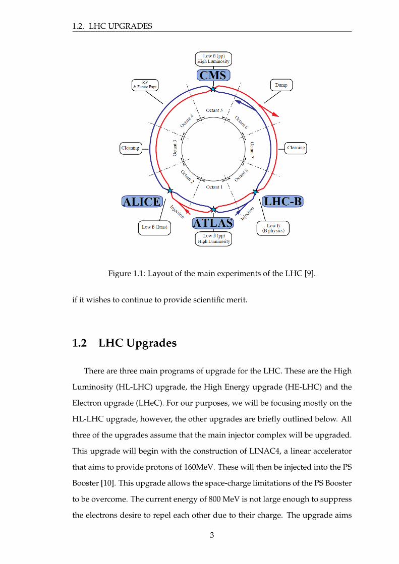
in Figure 1.1. ATLAS and CMS are two general purpose experiments. ALICE
is dedicated to the study of heavy ions, and LHC-B is dedicated to the study of
CP-violation and other rare phenomenon [9].
The number of collisions that have happened in the LHC is represented by
the integrated luminosity. As they are trying to increase the number of colli-
sions, the LHC is aiming to maximize this value. Luminosity is the number of
particles per unit area, per unit time, times the opacity of the target, in units
cm−2s−1. This is usually denoted in inverse femto barns per second, fb−1s−1,
where fb−1s−1 = 1× 1039 cm−2s−1. The integrated luminosity, with regards to
time, is thus expressed in inverse femto barns, fb−1.
The LHC is aiming to meet its design luminosity of 1 · 1034 cm−2s−1by the
end of 2014. This will provide approximately 40 fb−1of luminosity per year.
However as the experiment continues to run, the statistical significance of gain-
ing more data begins to diminish and it starts to take several years to halve any
statistical errors. Thus the LHC must be upgraded to run at a higher luminosity
2
1.2. LHC UPGRADES
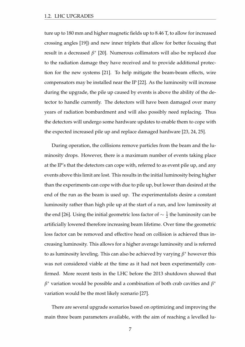
Figure 1.1: Layout of the main experiments of the LHC [9].
if it wishes to continue to provide scientific merit.
1.2 LHC Upgrades
There are three main programs of upgrade for the LHC. These are the High
Luminosity (HL-LHC) upgrade, the High Energy upgrade (HE-LHC) and the
Electron upgrade (LHeC). For our purposes, we will be focusing mostly on the
HL-LHC upgrade, however, the other upgrades are briefly outlined below. All
three of the upgrades assume that the main injector complex will be upgraded.
This upgrade will begin with the construction of LINAC4, a linear accelerator
that aims to provide protons of 160MeV. These will then be injected into the PS
Booster [10]. This upgrade allows the space-charge limitations of the PS Booster
to be overcome. The current energy of 800 MeV is not large enough to suppress
the electrons desire to repel each other due to their charge. The upgrade aims
3
CHAPTER 1. INTRODUCTION
to increase the energy to 1400 MeV. This can help improve the brightness and
luminosity of the LHC beam [11].
The LHeC proposes to use an electron beam to collide simultaneously with
the normal LHC collisions. The electron beam allows for high precision, deep
inelastic scattering measurements. These will enable investigation of strong
and electro-weak interactions. The LHeC may consist of either a specially-built
LINAC or an additional ring inside the LHC beam line [12].
The HE-LHC is dependent on the HL-LHC upgrade, which will be described
in further detail below. After the HL-LHC upgrade, the HE-LHC intends to ex-
tend the energy regime from the current 14TeV centre of mass energy to a higher
energy of 33TeV. This would extend the possibilities for further experimenta-
tion into unknown areas of physics [13].
The aim of the HL-LHC upgrade is to drastically increase the luminosity of
the LHC and thus the rate at which data can be acquired [14, 15].
The instantaneous luminosity is given as:
L =frev · nb · N1 · N2
2π
√(σ2
x,1 + σ2x,2
)·(
σ2y,1 + σ2
y,2
) (1.1)
where frev is the revolution frequency, nb the number of bunches colliding at
the Interaction Point (IP), N1 and N2 are the particles per bunch. σ2x,1 and σ2
x,2are
the horizontal beam size and σ2y,1 and σ2
y,2are the vertical beam size of the two
colliding beams.
This provides three main ways to increase the luminosity: increase the num-
ber of bunches, increase the number of particles in a bunch and decrease the
beam size at IP. The increase in luminosity is however limited by the perform-
ance of the hardware. The LHC will primarily focus on decreasing the beam
size at the IP. This will result in the β∗ being reduced from 0.55 m to 0.15 m
[16][17]. β∗ is the value of β at the point (IP).
4
1.2. LHC UPGRADES
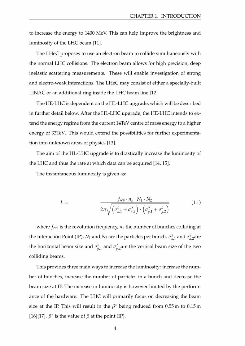
The position (x) and momentum (x′) of a particle obey Liouville’s theorem
as they circulate, allowing them to oscillate around the bunch as the bunch
moves around the accelerator. Liouville’s theorem conserves the bunch’s x and
x′ within a phase space area, usually an ellipse. The maximum position on the
x axis is given by√
εβ, the square root of the beta function (β) and the emit-
tance (ε). The emittance is the average spread of the particles in phase space
and the beta function is the amplitude function that relates the emittance to the
beam size. The maximum position on the x′ axis is given by√
εβ , as shown in
Figure1.2.
Figure 1.2: Liouville’s theorem ellipse.
By decreasing β∗ or increasing N1 and N2, instabilities within the machine
will increase. The hardware can only mitigate a fixed amount of instabilities.
Beam-beam interactions are also a major source of limiting instability. Here, as
the number of particles within each bunch increases, the interaction between
opposing beams increases. To reduce the effect of the long range beam-beam
interaction, the angle at which the beams cross can be increased.
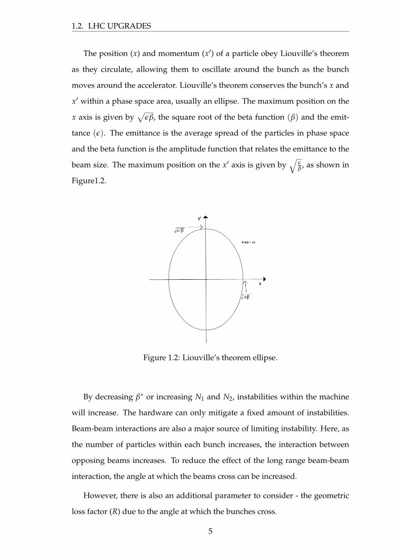
However, there is also an additional parameter to consider - the geometric
loss factor (R) due to the angle at which the bunches cross.
5
CHAPTER 1. INTRODUCTION
R =1√
1 + Φ2(1.2)
Φ is the Piwinski factor calculated as [18]:
Φ =θcσz
2σt(1.3)
Where θc is the crossing angle, σz is the longitudinal bunch size and σt is the
transverse bunch size. The variation of the geometric loss factor is shown in
Figure 1.3 as the Piwinski factor is varied.
Piwinski factor
Red
uctio
n fa
ctor
0 1 2 3 4 50.1
0.2
0.3
0.4
0.5
0.6
0.7
0.8
0.9
1
Figure 1.3: Reduction factor vs Piwinski factor.
The nominal LHC runs with a a Piwinski factor of 0.68 which corresponds
to a geometric loss factor of 0.83. However during the upgrade this factor is
likely to increase, possibly up to as high as 2.6, which would correspond to a
geometric loss factor of 0.46. This is a significant loss in luminosity that will
need to be mitigated.
To increase the beam performance, reduce the β∗, and increase the number
of particles per bunch, the LHC must undergo several updates in hardware. The
entire upgrade is referred to as the HL-LHC upgrade. The magnet systems will
be overhauled with new separation dipoles (that provide a larger beam aper-
6
1.2. LHC UPGRADES
ture up to 180 mm and higher magnetic fields up to 8.46 T, to allow for increased
crossing angles [19]) and new inner triplets that allow for better focusing that
result in a decreased β∗ [20]. Numerous collimators will also be replaced due
to the radiation damage they have received and to provide additional protec-
tion for the new systems [21]. To help mitigate the beam-beam effects, wire
compensators may be installed near the IP [22]. As the luminosity will increase
during the upgrade, the pile up caused by events is above the ability of the de-
tector to handle currently. The detectors will have been damaged over many
years of radiation bombardment and will also possibly need replacing. Thus
the detectors will undergo some hardware updates to enable them to cope with
the expected increased pile up and replace damaged hardware [23, 24, 25].
During operation, the collisions remove particles from the beam and the lu-
minosity drops. However, there is a maximum number of events taking place
at the IP’s that the detectors can cope with, referred to as event pile up, and any
events above this limit are lost. This results in the initial luminosity being higher
than the experiments can cope with due to pile up, but lower than desired at the
end of the run as the beam is used up. The experimentalists desire a constant
luminosity rather than high pile up at the start of a run, and low luminosity at
the end [26]. Using the initial geometric loss factor of ∼ 12 the luminosity can be
artificially lowered therefore increasing beam lifetime. Over time the geometric
loss factor can be removed and effective head on collision is achieved thus in-
creasing luminosity. This allows for a higher average luminosity and is referred
to as luminosity leveling. This can also be achieved by varying β∗ however this
was not considered viable at the time as it had not been experimentally con-
firmed. More recent tests in the LHC before the 2013 shutdown showed that
β∗ variation would be possible and a combination of both crab cavities and β∗
variation would be the most likely scenario [27].
There are several upgrade scenarios based on optimizing and improving the
main three beam parameters available, with the aim of reaching a levelled lu-
7
CHAPTER 1. INTRODUCTION
minosity of 5 · 1034 cm−2s−1 and the potential to reach a peak of 2.5 · 1035 cm−2s−1.
Due to the necessity for an increased crossing angle over the current 300 µrad to
420− 590 µrad, only those scenarios that include crab cavities are able to reach
this target.
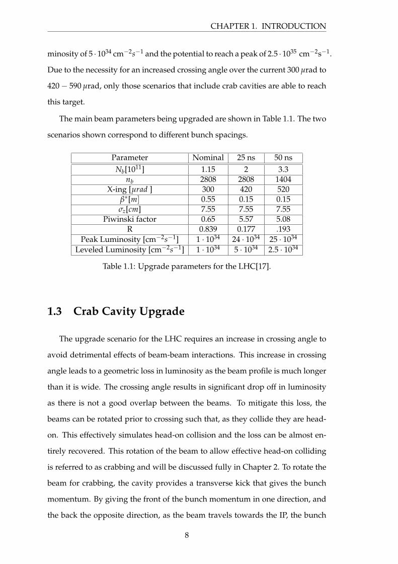
The main beam parameters being upgraded are shown in Table 1.1. The two
scenarios shown correspond to different bunch spacings.
Parameter Nominal 25 ns 50 nsNb[1011] 1.15 2 3.3
nb 2808 2808 1404X-ing [µrad ] 300 420 520
β∗[m] 0.55 0.15 0.15σz[cm] 7.55 7.55 7.55
Piwinski factor 0.65 5.57 5.08R 0.839 0.177 .193
Peak Luminosity [cm−2s−1] 1 · 1034 24 · 1034 25 · 1034
Leveled Luminosity [cm−2s−1] 1 · 1034 5 · 1034 2.5 · 1034
Table 1.1: Upgrade parameters for the LHC[17].
1.3 Crab Cavity Upgrade
The upgrade scenario for the LHC requires an increase in crossing angle to
avoid detrimental effects of beam-beam interactions. This increase in crossing
angle leads to a geometric loss in luminosity as the beam profile is much longer
than it is wide. The crossing angle results in significant drop off in luminosity
as there is not a good overlap between the beams. To mitigate this loss, the
beams can be rotated prior to crossing such that, as they collide they are head-
on. This effectively simulates head-on collision and the loss can be almost en-
tirely recovered. This rotation of the beam to allow effective head-on colliding
is referred to as crabbing and will be discussed fully in Chapter 2. To rotate the
beam for crabbing, the cavity provides a transverse kick that gives the bunch
momentum. By giving the front of the bunch momentum in one direction, and
the back the opposite direction, as the beam travels towards the IP, the bunch
8
1.3. CRAB CAVITY UPGRADE
rotates. The removal of the crabbing by additional cavities after collision, elim-
inates this transverse momentum at a time when the bunch has zero rotation
relative to the beam direction [28].
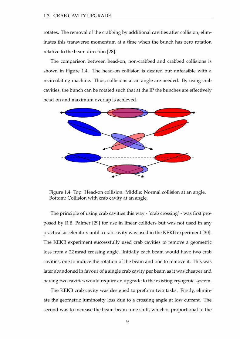
The comparison between head-on, non-crabbed and crabbed collisions is
shown in Figure 1.4. The head-on collision is desired but unfeasible with a
recirculating machine. Thus, collisions at an angle are needed. By using crab
cavities, the bunch can be rotated such that at the IP the bunches are effectively
head-on and maximum overlap is achieved.
Figure 1.4: Top: Head-on collision. Middle: Normal collision at an angle.Bottom: Collision with crab cavity at an angle.
The principle of using crab cavities this way - ’crab crossing’ - was first pro-
posed by R.B. Palmer [29] for use in linear colliders but was not used in any
practical accelerators until a crab cavity was used in the KEKB experiment [30].
The KEKB experiment successfully used crab cavities to remove a geometric
loss from a 22 mrad crossing angle. Initially each beam would have two crab
cavities, one to induce the rotation of the beam and one to remove it. This was
later abandoned in favour of a single crab cavity per beam as it was cheaper and
having two cavities would require an upgrade to the existing cryogenic system.
The KEKB crab cavity was designed to preform two tasks. Firstly, elimin-
ate the geometric luminosity loss due to a crossing angle at low current. The
second was to increase the beam-beam tune shift, which is proportional to the
9
CHAPTER 1. INTRODUCTION
luminosity of the KEKB setup at high current. The beam-beam effects are the
electromagnetic interactions between incoming and outgoing bunches in a ma-
chine. The electromagnetic forces between the separate bunches induce dipole
like and higher order perturbations. The beam beam tune shift can be used to
measure particle interaction in the bunch and hence luminosity.
These interaction can result in defocusing, transverse deflection and an in-
crease in halo size [31][32].
The KEKB experiment was able to confirm bunch rotation though the use
of streak cameras, and that the lost specific luminosity at low current was re-
gained. However, the crab cavity was unable to provide increased luminosity
at high current, due to lack of understanding of the beam-beam effects and how
they relate to luminosity [33]. Due to this, it was widely misunderstood that
crab cavities do not provide luminosity recovery. This is now known to not
be the case, the specific luminosity did reach the desired maximum due to geo-
metric recovery at low current, however at higher currents there was no gain. In
the case of the LHC, the crossing angle is the main concern and the beam-beam
effects are less of an impact, thus the geometric gains are desirable.
Two scenarios present themselves for operation of the crab cavities in the
LHC - global and local.
In the case of a global scheme, the cavities induce a rotation in the bunch at
a suitable location on the ring. The bunch rotation oscillates around the entire
ring as it is kicked by various focus magnets. The cavities can then be used to
top up or remove the rotation as needed.
In the case of a local scheme, the crabbing is induced shortly before an in-
teraction region and removed soon after. Each IP that requires crabbing would
need both crab cavities to induce the rotation and anti-crab cavities to remove
it again after.
The global scheme would call for 800 MHz cavities that would fit between
the opposing beam lines, in a region where the beam lines have enough separ-
10
1.3. CRAB CAVITY UPGRADE
ation [34] .
The local scheme calls for 400 MHz cavities. Due to the relatively close
nature of the IP’s in the local scheme, the beam pipes are very close together
- situated 194 mm centre to centre apart. Each beam pipe has an inner radius
of 42 mm. This requires the cavity to have a maximum outer radius of 152 mm,
not including the wall thickness of the opposing beam line. The outer radius of
a typical elliptical cavity is related to its frequency of operation. For a 400 MHz
elliptical cavity, an outer radius of 375 mm would not be unexpected. As this
is considerably greater than the space available, a novel design is needed that
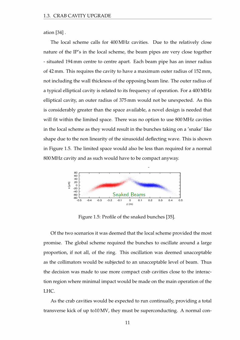
will fit within the limited space. There was no option to use 800 MHz cavities
in the local scheme as they would result in the bunches taking on a ’snake’ like
shape due to the non linearity of the sinusoidal deflecting wave. This is shown
in Figure 1.5. The limited space would also be less than required for a normal
800 MHz cavity and as such would have to be compact anyway.
Figure 1.5: Profile of the snaked bunches [35].
Of the two scenarios it was deemed that the local scheme provided the most
promise. The global scheme required the bunches to oscillate around a large
proportion, if not all, of the ring. This oscillation was deemed unacceptable
as the collimators would be subjected to an unacceptable level of beam. Thus
the decision was made to use more compact crab cavities close to the interac-
tion region where minimal impact would be made on the main operation of the
LHC.
As the crab cavities would be expected to run continually, providing a total
transverse kick of up to10 MV, they must be superconducting. A normal con-
11
CHAPTER 1. INTRODUCTION
ducting cavity providing this transverse voltage would not be able to support
this level of ohmic heating in constant wave (CW) operation.
1.4 Summary
The LHC currently provides some of the best and most interesting experi-
mental scientific output in the field of physics in the world. This can be seen in
the recent discoveries regarding the Higgs particle, its impact on the scientific
community and its understanding of fundamental forces. So that the LHC can
continue to provide world-leading physics, an upgrade to some of its major
components is required. This upgrade will enable it to effectively operate for
a further 15-20 years. Although the Higgs like particle has been discovered,
it still requires study and more data to confirm that was was recorded is the
Higgs particle. The upgrade will enable the 14Tev collision energy, which is the
highest in the world currently, to have a higher data output. The upgrade will
primarily focus on the injection setup, for example LINAC4, and the interaction
region, for example the final focus triplets. As the interaction points are up-
graded, the crossing angle of the beams will be increased to reduce beam-beam
effects. This increase in crossing angle must be mitigated as it would result in
a large loss of luminosity if not corrected for. Crab cavities provide the neces-
sary luminosity recuperation by creating effective head-on collisions. However,
the space available for the crab cavities is extremely limited. Thus a compact
superconducting crab cavity is required for the HL-LHC upgrade.
12
Chapter 2
Crab Cavities
A crab cavity is a type of radio frequency (RF) cavity used for bunch rotation
because of its transverse electric and magnetic fields[29]. This chapter will dis-
cuss the fundamental properties of cavities and how the transverse deflection is
calculated using Panofsky Wenzel theorem. It will also discuss beam dynamics
in brief, some fundamental properties of Superconducting RF (SRF), a brief his-
tory of prominent previous deflectors and the KEK-B crab cavity, and options
for the LHC compact crab cavity.
2.1 Radio Frequency Basics
Within an RF cavity there are multiple mode configurations that can exist.
For a pillbox cavity of length λ2 the fundamental mode is TM0 1 0, where the
electric field is maximum in the centre of the cavity and parallel to the beam-
pipe . The next field configuration is the TM1 1 0, where there is an azimuthal
variation in the electric field of the cavity. This second mode is often referred
to as a dipole mode. This dipole mode in an accelerating cavity can act like a
time-varying dipole magnet if it is excited. The mode can be used for one of
two main variations, depending on the phase of the cavity. In one phase, the
beam is ’deflected’ giving the whole bunch transverse momentum which can
be used to separate bunches. Ninety degrees out of phase from this, the bunch
13
CHAPTER 2. CRAB CAVITIES
is rotated or ’crabbed’. This is where the front of the bunch is given momentum
in an opposite direction to the rear of the bunch, with the centre remaining
unperturbed. This results in the bunch rotating as it travels. Both of these rely
on the potential gradient that exists between the opposing directions of electric
field to impart momentum to the bunch.
In order to rotate the bunches, a time-varying force is required. The force on
a charged particle is given by the Lorentz force:
F = q(E + v× B) (2.1)
thus a a time-varying electric or magnetic field can be used to produce a
transverse kick. For a particle travelling in the z direction, if deflection in the x
direction is desired, the electric field must also be in the x direction, and/or the
magnetic field in the y.
Fx = q(Ex + vz × By) (2.2)
As the bunch length in the LHC is only 1.06 ns, the field must vary very
quickly as the bunch passes through the cavity, so that the head and tail of
the bunch receive equal and opposite kicks. For these kicks to be of sufficient
magnitude and duration, an RF cavity must be used.
A pillbox cavity is the simplest form of a cavity consisting of a cylindrical can
with flat end plates. The solution to the wave equation can be easily calculated
for a pillbox cavity, and the mode structure that is present holds true for other
cavities.
The wave equation in cylindrical polar co-ordinates is;
[1r
δ
δr
(r
δ
δr
)+
1r2
δ
δφ2 + µεω2 − k2z
]ψ = 0 (2.3)
where r is the radius, φ is the angular position, µ is the permeability, ε is
the permittivity, ω is the angular frequency, kz is the longitudinal wave-number
14
2.1. RADIO FREQUENCY BASICS
and ψ is the solution.
The solution takes the form;
ψ = A1 Jm(ktr)e±imθ (2.4)
where Jm is the mth Bessel function and ψ is the the longitudinal componant
of the field, either Ez or Hz depending on which orientation is chosen.
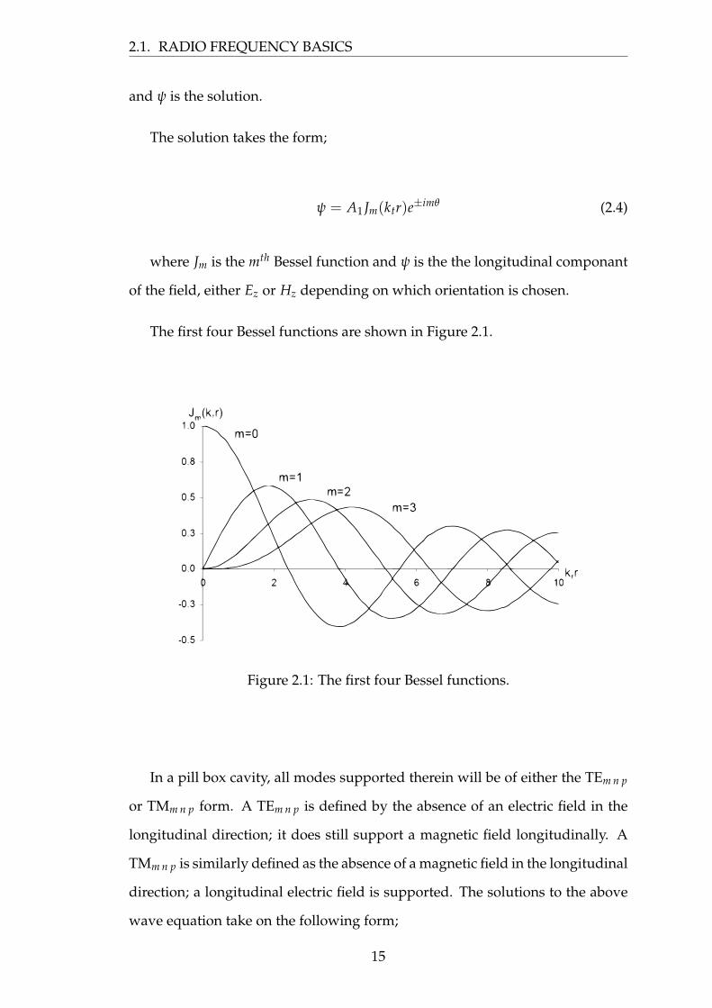
The first four Bessel functions are shown in Figure 2.1.
Figure 2.1: The first four Bessel functions.
In a pill box cavity, all modes supported therein will be of either the TEm n p
or TMm n p form. A TEm n p is defined by the absence of an electric field in the
longitudinal direction; it does still support a magnetic field longitudinally. A
TMm n p is similarly defined as the absence of a magnetic field in the longitudinal
direction; a longitudinal electric field is supported. The solutions to the above
wave equation take on the following form;
15
CHAPTER 2. CRAB CAVITIES
for TE modes;
Hz(r, φ) = A1 Jm
(ξ′m,nra
)e±imφ (2.5)
H⊥ =ikza2
ξ′2m,n∇⊥Hz (2.6)
E⊥ = − iεωa2
ξ′2m,n
(z×∇⊥Hz) (2.7)
for TM modes;
Ez(r, φ) = A1 Jm
(ξm,nr
a
)e±imφ (2.8)
E⊥ =ikza2
ξ2m,n∇⊥Ez (2.9)
H⊥ =iεωa2
ξ2m,n
(z×∇⊥Ez) (2.10)
where A1 is the normalized field, ξm.n is the Bessel function zero correspond-
ing to m and n, a is the radius φ is the radial angle, E⊥ and B⊥ correspond to the
transverse components of the electric and magnetic field and ∇⊥ = ∇− δδz .
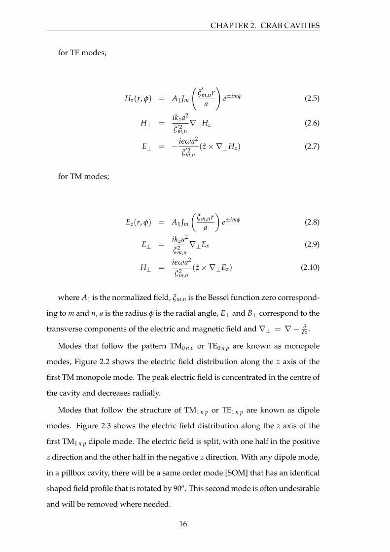
Modes that follow the pattern TM0 n p or TE0 n p are known as monopole
modes, Figure 2.2 shows the electric field distribution along the z axis of the
first TM monopole mode. The peak electric field is concentrated in the centre of
the cavity and decreases radially.
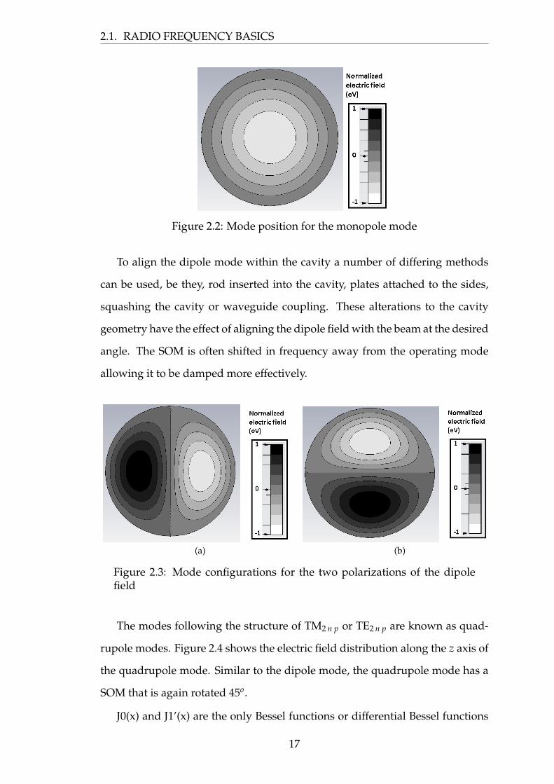
Modes that follow the structure of TM1 n p or TE1 n p are known as dipole
modes. Figure 2.3 shows the electric field distribution along the z axis of the
first TM1 n p dipole mode. The electric field is split, with one half in the positive
z direction and the other half in the negative z direction. With any dipole mode,
in a pillbox cavity, there will be a same order mode [SOM] that has an identical
shaped field profile that is rotated by 90o. This second mode is often undesirable
and will be removed where needed.
16
2.1. RADIO FREQUENCY BASICS
Figure 2.2: Mode position for the monopole mode
To align the dipole mode within the cavity a number of differing methods
can be used, be they, rod inserted into the cavity, plates attached to the sides,
squashing the cavity or waveguide coupling. These alterations to the cavity
geometry have the effect of aligning the dipole field with the beam at the desired
angle. The SOM is often shifted in frequency away from the operating mode
allowing it to be damped more effectively.
(a) (b)
Figure 2.3: Mode configurations for the two polarizations of the dipolefield
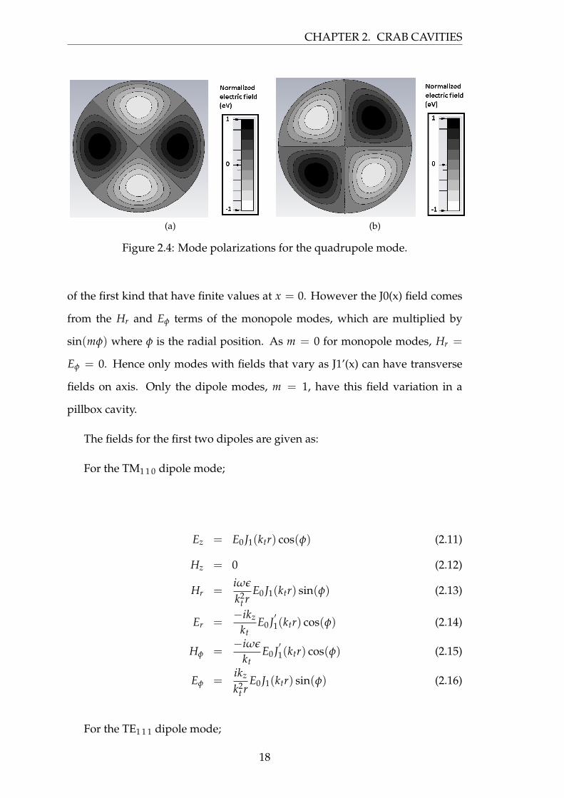
The modes following the structure of TM2 n p or TE2 n p are known as quad-
rupole modes. Figure 2.4 shows the electric field distribution along the z axis of
the quadrupole mode. Similar to the dipole mode, the quadrupole mode has a
SOM that is again rotated 45o.
J0(x) and J1’(x) are the only Bessel functions or differential Bessel functions
17
CHAPTER 2. CRAB CAVITIES
(a) (b)
Figure 2.4: Mode polarizations for the quadrupole mode.
of the first kind that have finite values at x = 0. However the J0(x) field comes
from the Hr and Eφ terms of the monopole modes, which are multiplied by
sin(mφ) where φ is the radial position. As m = 0 for monopole modes, Hr =
Eφ = 0. Hence only modes with fields that vary as J1’(x) can have transverse
fields on axis. Only the dipole modes, m = 1, have this field variation in a
pillbox cavity.
The fields for the first two dipoles are given as:
For the TM1 1 0 dipole mode;
Ez = E0 J1(ktr) cos(φ) (2.11)
Hz = 0 (2.12)
Hr =iωε
k2t r
E0 J1(ktr) sin(φ) (2.13)
Er =−ikz
ktE0 J
′1(ktr) cos(φ) (2.14)
Hφ =−iωε
ktE0 J
′1(ktr) cos(φ) (2.15)
Eφ =ikz
k2t r
E0 J1(ktr) sin(φ) (2.16)
For the TE1 1 1 dipole mode;
18
2.1. RADIO FREQUENCY BASICS
Ez = 0 (2.17)
Hz = H0 J1(ktr) sin(φ) (2.18)
Hr =ikz
ktH0 J
′1(ktr) sin(φ) (2.19)
Er =−iωµ
k2t r
H0 J1(ktr) cos(φ) (2.20)
Hφ =−ikz
k2t r
H0 J1(ktr) cos(φ) (2.21)
Eφ =iωµ
ktH0 J
′1(ktr) sin(φ) (2.22)
Both of these modes have either transverse electric or magnetic field com-
ponents that could potentially deflect a passing bunch .
2.1.1 PW Theorem
In 1956, a paper by Panofsky and Wenzel[36] demonstrated how transverse
momentum could be imparted to a fast moving particle parallel to the axis. This
theorem allows the deflection of a particle normal to the direction of travel to be
calculated from the electric field in the direction of travel, rather than needing
both the electric and magnetic fields and the phase between them as in the case
of integrating the Lorentz force. This method does not hold for all situations but
is accurate over the area of interest for crab cavities as the longitudinal electric
field on axis is usually zero.
This was discussed in a paper by Browman [37] in 1993. His derivation is
shown here.
The transverse momentum p⊥imparted to a particle with velocity v and
charge e travelling in the z direction through an radio frequency cavity of length
d is given by;
p⊥ =
ˆ t(z=d)
t(z=0)F⊥dt =
( ev
) ˆ d
0[E⊥ + (v×B)⊥]dz (2.23)
19
CHAPTER 2. CRAB CAVITIES
if v is large enough to allow the particle direction to remain essentially un-
changed by the transverse force. Equation (2.23) can be simplified by taking the
right hand side as a vector potential;
E = −δAδt−∇V (2.24)
where A is the magnetic vector potential and V is the scalar potential.
As V is constant inside the cavity;
E = −δAδt
(2.25)
and;
E⊥ = −δA⊥δt
(2.26)
(v× B)⊥ in terms of A;
(v× B)⊥ = [v× (∇×A)]⊥ = [∇(v ·A)− (v · ∇)A]⊥ (2.27)
= ∇⊥(v ·A)− (v · ∇)A⊥ (2.28)
Thus we can state;
p⊥ =ev
ˆ d
0
[(−δA⊥
δt− (v · ∇)A⊥
)+∇⊥(v ·A)
]dz (2.29)
As v is essentially constant and in the z direction;
(v · ∇)A⊥ = vδA⊥
δz(2.30)
and;
∇⊥(v ·A) = v∇⊥Az (2.31)
20

2.1. RADIO FREQUENCY BASICS
thus;
p⊥ =( e
v
) ˆ d
0
[(−δA⊥
δt− v
δA⊥δz
)+ v∇⊥Az
]dz (2.32)
= eˆ d
0
[(−1
vδA⊥
δt− δA⊥
δz
)+∇⊥Az
]dz (2.33)
however;
v =dzdt
(2.34)
allowing the simplification;
(1v
δA⊥δt
+δA⊥
δz
)dz =
δA⊥δt
dt +δA⊥
δzdz = dA⊥ (2.35)
p⊥ = eˆ A⊥(z=d)
A⊥(z=0)− (dA⊥) + e
ˆ d
0∇⊥Azdz (2.36)
For this to be useful, A needs to be expressed in terms of E, assuming e−iω0t
time dependence on E then;
A = − iω0
E (2.37)
is a valid choice for A1. The first term of Equation (2.36) vanishes as for any
cavity where the ends are perpendicular to its axis, A⊥ = E⊥ = 0 (in metal). It
can also vanish for cavities with beam pipes, as long as E⊥ = 0, as z = 0 and
z = d where d is the length of the cavity. Thus in this case;
p⊥ = eˆ d
0∇⊥Azdz (2.38)
where e is the charge on an electron. Substituting (2.37) into (2.38) we obtain;
1−i = e−1 π2 so A has a time dependence of e−i(ω0t+ π
2 ). Thus A is shifted 900in time from Eand has the same phase as the magnetic field as would be expected.
21

CHAPTER 2. CRAB CAVITIES
p⊥ =
(e
ω0
) ˆ d
0(−1)∇⊥Ezdz (2.39)
As the particles being deflected have very high longitudinal energy, the
transverse kick can be approximated to an equivalent kick from an electric field,
using E = cB where c is the speed of light. Using this approximation, we can
define the transverse voltage as;
V⊥= − cˆ d
0dzˆ z
c
t0
dt (∇⊥Ez(z, t)) (2.40)
where t0 is the initial time, zc is the time taken to reach the position z along
the z axis and Ez(z, t) is the electric field at the position z at time t.
This can be further simplified, as we know the electric field follows the time
dependence e−iω0t.
V⊥= −icω
ˆ d
0dz∇⊥Ez(z,
zc) (2.41)
For a dipole mode m = 1, this can be simplified to
V⊥(0)= −icωr
(V‖(0) −V‖(r)
)(2.42)
where V‖ is the longitudinal voltage at a radius r.
For a cylindrically symmetric cavity, where there is no longitudinal voltage
on axis, this can then be approximated to;
V⊥(0)= −icV‖(r)
ωr(2.43)
The transverse shunt impedance R⊥can be calculated;
R⊥=12
|V⊥|2Pc
(2.44)
Similarly a calculation for transverse R⊥/Q , a useful property for examin-
ing the ratio of transverse deflecting voltage to stored energy, can be made;
22
2.2. BEAM DYNAMICS
R⊥Q
=|V⊥|22ωU
=|V‖(r)|2
2ωU
( cωr
)2(2.45)
where R⊥ is the transverse shunt impedance and Q is the cavity quality
factor.
Equation 4.14 shows that the transverse kick a beam receives can be calcu-
lated from the longitudinal electric field, however equation 2.17 shows us that
a TEm n p has no longitudinal electric field. Thus it can be inferred that only
TM1 n p modes are actually able to deflect a beam.
2.2 Beam Dynamics
The deflection experienced by a bunch in a dipole cavity can be expressed
geometrically. If the assumption is made that the deflection will be significantly
small compared to the longitudinal direction, small angle approximation can
also be used. Taking the beam energy in the longitudinal direction z to be Ebeam ,
and in the transverse direction x a voltage to be V⊥, a triangle can be constructed
with the angle of the deflection φ.
x = z tan(φ) (2.46)
Thus the small angle can be assumed to be vtvz
;
x = z tan(
V⊥Ebeam
)(2.47)
which can then be further simplified via small angle approximation;
x ≈ z(
V⊥Ebeam
)(2.48)
Using the simplified transformation R12 which in this case is analogous to
length adjusted due to the focusing and defocusing elements between the two
points. R12 is part of the the transfer matrix that allows the transverse properties
23
CHAPTER 2. CRAB CAVITIES
of the bunch to be described as it travels round the accelerator.
x2
x′2
y2
y′2
=
R11 R12 R13 R14
R21 R22 ... ...
... ... R33 ...
R41 ... ... R44
·
x1
x′1
y1
y′1
(2.49)
We can make the assumption that x2 = R12x′1 as the bunch will be trav-
elling near the speed of light, resulting in no perturbation in the y direction,
and almost no shift in the position of x as it passes though the cavity, thus the
assumption R11 ≈ R13 ≈ R14 ≈ 0.
The position becomes:
x = R12
(V⊥
Ebeam
)(2.50)
However, this assumes that the collision is linear and not recirculating.
An idealised particle in a synchrotron will follow a circular path through the
centre of all magnets as it circulates the ring, ending up at the same position
that is started at. This is referred to as a closed orbit. In practice, real particles
have a spread in position and momentum, and the components of the facility
have small errors in them. This results in the particles osculating around the
closed orbit as they circulate the ring. This is referred to as betatron motion, or
betatron oscillation.
The number of oscillations per revolution a bunch experiences is referred to
as the betatron tune Q, given as;
Q =
ˆ s+C
s
dsβy(s)
(2.51)
where s is the position within the ring, C is the circumference of the ring and
βy(s) is the betatron function at s.
The betatron frequency β f is the tune multiplied by the revolution frequency
24
2.2. BEAM DYNAMICS
of the ring f0.
β f = Q · f0 (2.52)
It is important that the tune does not fall at integer values as this increases
the chance of errors in the cavities compounding which leads to the beam destabil-
ising. If the tune was an integer, then on every revolution the bunch phase dis-
tribution would be the same at a given point. This would result in any errors
compounding on each revolution. If the tune was a half integer, then the dipole
errors would cancel out on each revolution as the phase distribution would be
opposite. However, a half integer is not usually chosen as it results in reson-
ances from quadrupole terms as these similarly compound. Other fractional
values are excluded due to resonances within the machine that could build in
the same way.
If an error was introduced at a frequency (n±Q) f0 in the form of a deflecting
field, then this leads to a signal S;
S = sin (2π(n−±Q) f0t) (2.53)
This results in the bunch seeing the kick;
S = sin (2πn f0t) sin (2π(n−±Q) f0t) (2.54)
which can be simplified using;
S = sin(a) cos(b) =12(sin(a + b + sin(a− b)) (2.55)
to get a dependence on;
S ≈ sin (2πQ f0t) (2.56)
Thus an error in the side bands of the betatron tune (n± Q) f0 can result in
25
CHAPTER 2. CRAB CAVITIES
a perpetual build up of deflection, resulting in an RF knock-out as the beam is
deflected [38].
When crab cavities are added, they will inevitably disrupt the closed orbit
of the LHC. There are two options for correcting the closed orbits.
In the local scheme, the bunch is rotated between the crabbing cavities and
the anti-crab cavities, with the crab cavities disrupting the closed orbit and the
anti-crab’s returning the bunch to the expected orbit. This results in the crabs
acting like a local bump and the orbit in the rest of the ring not being effected.
In the global scheme, the initial expectation with the bunches retaining their
rotation throughout the entire ring appears to result in a larger kick on each re-
volution. However, by choosing the correct location of the cavity, it is possible to
create new closed orbits for the particles. This results in the cavity maintaining
the oscillation as it travels round the machine. Each particle within the bunch
obtains a new closed orbit. This, for example, could result in a particle getting
transverse momentum on the first pass and have it removed on the second [39].
The voltage required to deflect the beam depends on the scheme selected.
For the local scheme, the voltage required is given as;
Vcrab =c2 · ps · tan( θ
2)
q ·ω ·√
β∗ · βcrab · sin(∆φ0)(2.57)
where c is the velocity of light, psis the particle momentum, θ is the crossing
angle, q is the charge on the particle, ω is the angular frequency of the cavity,
∆φ0 is the phase advance between the cavity and the IP and β∗ and βcrab are the
beta functions at the IP and crab location respectively.
For the anti-crab cavities, the voltage required is ;
Vanti = −R22Vcrab (2.58)
where R22 is the (2, 2) element of the transfer matrix between the crab and
anti-crab cavities.
26
2.3. INTRODUCTION TO SRF
For the global scheme, the voltage is given as;
Vcrab =c2 · ps · tan( θ
2)
q ·ω ·√
β∗ · βcrab· | 2 sin(πQ)
cos(∆φ0 − πQ)| (2.59)
where Q is the betatron tune of the ring and the other parameters are the
same as for the local scheme[39] .
2.3 Introduction to SRF
RF refers to an electronic device operating at radio frequencies, therefore
SRF is an abbreviation of Superconducting Radio Frequency. A superconduct-
ing cavity is one that is constructed of a material that when cooled below a
critical temperature (Tc), its internal resistance drops to be almost zero. For an
AC current, a very small residual resistance will be present that is analogous
to inertia. This BCS resistance scales with the square of the frequency of the
applied current. Conventional normal-conducting cavities may be fed with up
to tens of mega watts of power, often for very short time periods which results
in massive power loss. This can be due to ohmic heating as the RF power is
dissipated into the walls through resistance, or removed to an external dump in
a travelling wave structure. By using superconducting cavities, power dissipa-
tion in the walls can be almost completely removed, requiring less power to be
fed into the cavity and thus making it cheaper.
However, the cost savings made by reducing the amount of wasted power
must be compared to the costs of running the cavity at the desired temperature.
The machine is limited by the Carnot cycle, this provides an efficiency decrease
of:
Carnot e f f iciency = 1− Tc
TH(2.60)
where Tc is the temperature of the cold sink and TH is the temperature of the
hot sink.
27
CHAPTER 2. CRAB CAVITIES
This provides an efficiency of ∼ 1− 2% for cavities operating at temperat-
ures ∼ 3− 6 K.
The most common material for use as a superconductor is niobium. Niobium
is used as it has one of the highest Tc’s of any of the periodic elements. It is also
able to sustain the highest critical surface fields [40]. Niobium becomes super-
conducting at 9.2 K, but usually operates at 4.2 K. This is because the niobium is
submerged in liquid helium which acts as a coolant, and 4.2 K is the temperature
of liquid helium [41]. Liquid helium baths are used due to the large enthalpy
that can be absorbed in the cold vapor [42]. Superconducting cavities are often
operated at ∼ 2 K with the liquid helium being pumped to a lower pressure.
The lower temperature improves the SRF properties of the niobium, lowering
the surface resistance of the niobium. This has the added benefit of improv-
ing the thermal conductivity of the liquid helium. The liquid helium becomes
superfluid, so there is no bubbling, and this reduces microphonics within the
cavity. By operating at a temperature well below that of the superconducting
transition, the chance of a quench can be reduced. A quench is when a super-
conducting cavity suddenly becomes normal conducting. This reduction comes
from the material resistances (Res) continued dependence on its temperature;
Res ∝ exp(−1.76Tc
T) (2.61)
where Tc is the critical temperature and T is the current temperature. This re-
duction in resistance reduces the chance of localised heating and thus a quench
[43].
By having very low losses in the cavity walls, the cavities can be run continu-
ally at high gradient, unlike normal conducting cavities that must be pulsed to
avoid destroying the cavity. This proves advantageous when high repetition
rates are required, as normal conducting cavities can only sustain a certain level
of pulsed heating [44]. This leads to high power storage rings and synchrotrons
using superconducting cavities as they are able to cope with the high repetition
28
2.3. INTRODUCTION TO SRF
rates.
A number of RF parameters are used to describe the properties and beha-
viour of an SRF cavity. The most prominent of them will be described below.
Surface Resistance
One of the primary reasons for using a superconducting cavity is that the
resistance of the cavity is several orders of magnitude smaller, ∼ nΩ, below
a certain transition temperature (Tc). Although this would imply that below
the transition temperature the resistance will be zero, it is not the case. The
superconducting state is not perfect and there is a very small resistance within
the material.
The surface resistance (Rs) can be summarized as,
Rs = RBCS + R0 (2.62)
where RBCS is the temperature and frequency dependent resistance from
BCS theory, and R0is the residual resistance. These will be expanded on below.
These parameters result in SRF cavities having very small but non zero res-
istance [43]. As the temperature decreases, the resistance becomes dominated
by the residual resistance R0 and no longer depends on the BCS resistance, this
is shown in Figure 2.5.
BCS Theory
The BCS theory is widely accepted as the best microscopic explanation for
the mechanisms of superconductivity. This theory proposed by Bardeen, Cooper
and Schrieffer [BCS] allows for electrons to interact with each other within the
ion lattice of a material. The electrons couple electromagnetically via the at-
tractive force caused by the perturbation of the lattice. This interaction leads to
the formation of Cooper pairs, where a pair of electrons of opposite spin form
a boson-like particle with zero spin that obeys Bose-Einstein statistics. This al-
29
CHAPTER 2. CRAB CAVITIES
Figure 2.5: Surface resistance vs temperature [43].
lows the pairs to be in the same quantum state and thus exist with a lower com-
bined energy than two separate electrons. The transition to Cooper pairs only
happens below a certain transition temperature, Tc, dependent on the material.
Above the transition temperature, the thermal vibrations of the lattice disrupt
the coupling.
The resistance that electrons experience can be analogous to them colliding
with other electrons and atoms on a quantum level. They are able to collide as
their coherence length - the length at which they can be said to exhibit particle-
like behavior instead of that of a wave - is comparable to the distance between
atoms. The coherence length of a Cooper pair is considerably larger than that of
an electron. Cooper pairs act more like a wave and less like individual particles
on the atomic level. Because they exist in the same quantum state where they
can’t be scattered as in normal resistance, they act collectively. The longer co-
herence length also allows for defects or impurities, smaller than the coherence
30
2.3. INTRODUCTION TO SRF
length, to be ignored.
The resistance due to BCS theory can be given as:
RBCS =2 · 10−4
T
(f
1.5
)2
exp(−17.67
T
)(2.63)
where T is the temperature in Kelvin and f is the frequency, when T < Tc2 .
The resistance increases with the square of the RF frequency. The Cooper
pairs themselves have inertial mass that must be overcome for them to move.
In the case of an alternating field, as for an RF cavity, the continual change
in direction leads to the BCS resistance. This leads to most superconducting
cavities being low frequency, usually below∼ 4 GHz, as the trade off in surface
heating and cryogenics is not viable at high frequency.
The resistance decreases exponentially with temperature. This is due to the
condensation of Cooper pairs that carry the charge rather than electrons. As
the temperature falls from the transition temperature (the temperature at which
Cooper pairs start to form), the number exponentially increases until T = 0 K
where all charge carriers are Cooper pairs.
The BCS resistance can also be partly characterized by the amount of im-
purities in the bulk of the material. This is often referred to as the RRR value,
with low RRR implying the material is of lower quality and containing more im-
purities. The residual resistance ratio (RRR) factor is usually used for thermal
conductivity but acts as a good guide for the purity of the bulk material. It
is defined as the ratio of the room temperature resistance to that of its satur-
ated resistance at low temperature, as this is dominated by impurity scattering.
This can be electrical or thermal conductivity as both are dominated by electron
transport in metals.
Residual Resistance
There is always some resistance remaining in the structure even though the
BCS resistance falls to zero, this is referred to as the residual resistance (R0). The
31
CHAPTER 2. CRAB CAVITIES
residual resistance can form from a number of characteristics of the material,
these are usually due to the manufacturing of the cavity.
Magnetic flux can become trapped in regions of impurities, either from inad-
equate shielding from the Earth’s magnetic field, or from indium joins or welds
between differing parts of the cavity. The trapped magnetic flux results in cur-
rents flowing in the surface contrary to the surface fields of the cavity.
Hydrogen gas can become deposited in the surface of the cavity during
cleaning by acid etching. Lossy hydrides then precipitate at the surface of the
cavity, this is often called ’Q disease’ as it can drastically affect the cavity Q. The
effect is most often seen when a cavity is allowed to reach temperatures above
20oC during acid treatment, though it is not the only source. The hydrogen is
trapped in the bulk of the cavity and only precipitates out to the surface during
cooling. To avoid the creation of hydrides, the cavity must be cooled quickly
in the temperature region ∼ 120− 170 K. By baking the cavity at 700− 900oC
under vacuum, most of the hydrogen trapped in the surface can be removed.
Oxides can form on the surface of the cavity if it is exposed to air, which
is likely to happen at some point in the preparation of the cavity. By baking
the cavity at higher temperatures, the oxides can be removed. However this
is sometimes not possible due to the design of the cavity, for example indium
seals could melt or the cavity could deform under its own weight.
Cavity Quality
The quality of a cavity is important as it is proportional to how much power
needs to be supplied to the cavity to maintain its operating energy. A higher
cavity quality means most of the power from the power supply is used to re-
place any energy deposited into the beam as it traverses the cavity. A low qual-
ity cavity would dissipate much of the input energy into its walls and heat up
the cavity bulk.
The cavity quality [Q0] relates the dissipation of power in the cavity to the
32
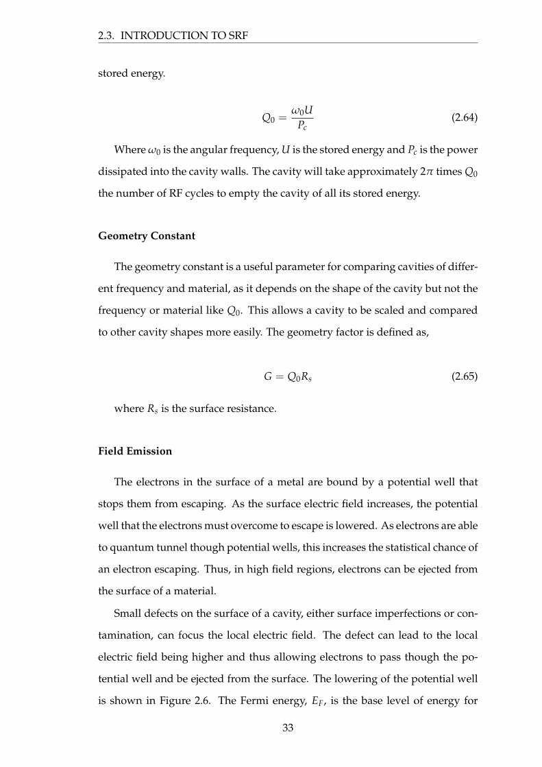
2.3. INTRODUCTION TO SRF
stored energy.
Q0 =ω0U
Pc(2.64)
Where ω0 is the angular frequency, U is the stored energy and Pc is the power
dissipated into the cavity walls. The cavity will take approximately 2π times Q0
the number of RF cycles to empty the cavity of all its stored energy.
Geometry Constant
The geometry constant is a useful parameter for comparing cavities of differ-
ent frequency and material, as it depends on the shape of the cavity but not the
frequency or material like Q0. This allows a cavity to be scaled and compared
to other cavity shapes more easily. The geometry factor is defined as,
G = Q0Rs (2.65)
where Rs is the surface resistance.
Field Emission
The electrons in the surface of a metal are bound by a potential well that
stops them from escaping. As the surface electric field increases, the potential
well that the electrons must overcome to escape is lowered. As electrons are able
to quantum tunnel though potential wells, this increases the statistical chance of
an electron escaping. Thus, in high field regions, electrons can be ejected from
the surface of a material.
Small defects on the surface of a cavity, either surface imperfections or con-
tamination, can focus the local electric field. The defect can lead to the local
electric field being higher and thus allowing electrons to pass though the po-
tential well and be ejected from the surface. The lowering of the potential well
is shown in Figure 2.6. The Fermi energy, EF, is the base level of energy for
33
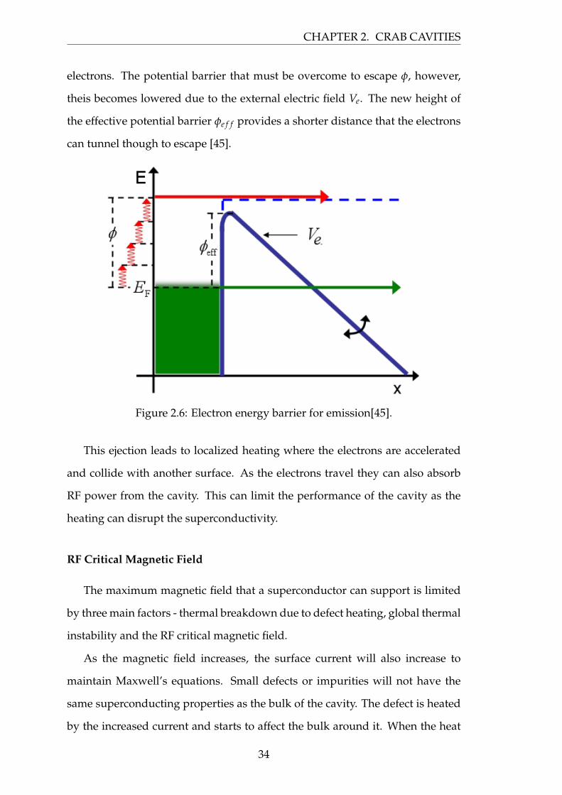
CHAPTER 2. CRAB CAVITIES
electrons. The potential barrier that must be overcome to escape φ, however,
theis becomes lowered due to the external electric field Ve. The new height of
the effective potential barrier φe f f provides a shorter distance that the electrons
can tunnel though to escape [45].
Figure 2.6: Electron energy barrier for emission[45].
This ejection leads to localized heating where the electrons are accelerated
and collide with another surface. As the electrons travel they can also absorb
RF power from the cavity. This can limit the performance of the cavity as the
heating can disrupt the superconductivity.
RF Critical Magnetic Field
The maximum magnetic field that a superconductor can support is limited
by three main factors - thermal breakdown due to defect heating, global thermal
instability and the RF critical magnetic field.
As the magnetic field increases, the surface current will also increase to
maintain Maxwell’s equations. Small defects or impurities will not have the
same superconducting properties as the bulk of the cavity. The defect is heated
by the increased current and starts to affect the bulk around it. When the heat
34
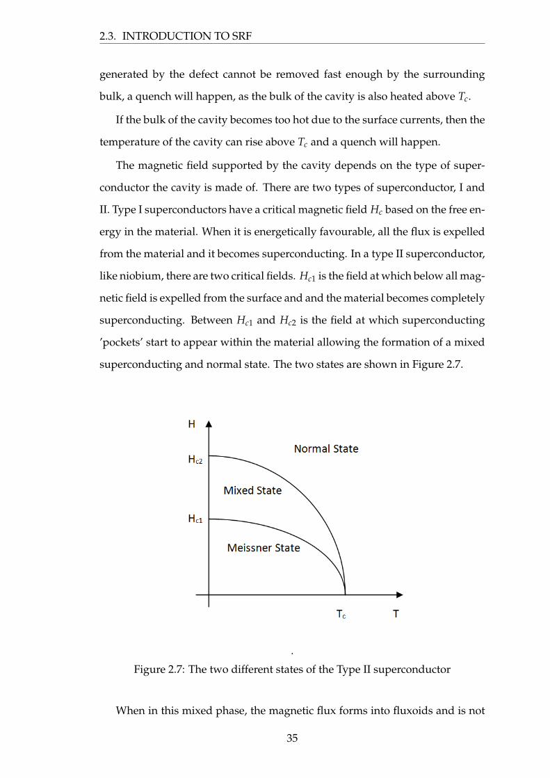
2.3. INTRODUCTION TO SRF
generated by the defect cannot be removed fast enough by the surrounding
bulk, a quench will happen, as the bulk of the cavity is also heated above Tc.
If the bulk of the cavity becomes too hot due to the surface currents, then the
temperature of the cavity can rise above Tc and a quench will happen.
The magnetic field supported by the cavity depends on the type of super-
conductor the cavity is made of. There are two types of superconductor, I and
II. Type I superconductors have a critical magnetic field Hc based on the free en-
ergy in the material. When it is energetically favourable, all the flux is expelled
from the material and it becomes superconducting. In a type II superconductor,
like niobium, there are two critical fields. Hc1 is the field at which below all mag-
netic field is expelled from the surface and and the material becomes completely
superconducting. Between Hc1 and Hc2 is the field at which superconducting
’pockets’ start to appear within the material allowing the formation of a mixed
superconducting and normal state. The two states are shown in Figure 2.7.
.
Figure 2.7: The two different states of the Type II superconductor
When in this mixed phase, the magnetic flux forms into fluxoids and is not
35
CHAPTER 2. CRAB CAVITIES
uniformly distributed across the material. A super-vortex current surrounds
each fluxoid to allow field and and current free regions. This is shown in Figure
2.8. As the magnetic field increases, these fluxoids become more dense until the
material is saturated and becomes normal conducting.
Figure 2.8: Non-uniformity of flux in Type II superconductor [46].
These parameters are for the DC case, both types have a critical RF magnetic
field dependant on the maximum RF field that the material can support.
The RF critical field Hr f can exist in a metastable state above Hc1. The nuc-
leation of fluxoids takes a comparably long period of time compared to the RF
periods. This allows the magnetic field to be higher than that of the transition
to the Meissner state.
For a typical niobium cavity, the maximum magnetic field is 0.23 Tesla, which
in a Tesla-style elliptical cavity corresponds to an electric field of 55 MV/m.
However, in mushroom-style cavities, peak fields of up to 145 MV/m have
been achieved [43].
Hc1 Lower critical magnetic field. The magnetic field below which a su-
perconductor in the Meissner phase and the magnetic field is completely
expelled. Above this value, the magnetic fields will start to enter a type II
superconductor in a mixed state. For niobium this is 130− 140 mT at 4.2 K
[47].
Hc2 Upper critical magnetic field. The magnetic field at which a super-
conductor in the mixed phase loses the last of its superconductivity and
36
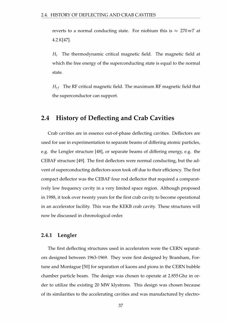
2.4. HISTORY OF DEFLECTING AND CRAB CAVITIES
reverts to a normal conducting state. For niobium this is ≈ 270 mT at
4.2 K[47].
Hc The thermodynamic critical magnetic field. The magnetic field at
which the free energy of the superconducting state is equal to the normal
state.
Hr f The RF critical magnetic field. The maximum RF magnetic field that
the superconductor can support.
2.4 History of Deflecting and Crab Cavities
Crab cavities are in essence out-of-phase deflecting cavities. Deflectors are
used for use in experimentation to separate beams of differing atomic particles,
e.g. the Lengler structure [48], or separate beams of differing energy, e.g. the
CEBAF structure [49]. The first deflectors were normal conducting, but the ad-
vent of superconducting deflectors soon took off due to their efficiency. The first
compact deflector was the CEBAF four rod deflector that required a comparat-
ively low frequency cavity in a very limited space region. Although proposed
in 1988, it took over twenty years for the first crab cavity to become operational
in an accelerator facility. This was the KEKB crab cavity. These structures will
now be discussed in chronological order.
2.4.1 Lengler
The first deflecting structures used in accelerators were the CERN separat-
ors designed between 1963-1969. They were first designed by Bramham, For-
tune and Montague [50] for separation of kaons and pions in the CERN bubble
chamber particle beam. The design was chosen to operate at 2.855 Ghz in or-
der to utilize the existing 20 MW klystrons. This design was chosen because
of its similarities to the accelerating cavities and was manufactured by electro-
37
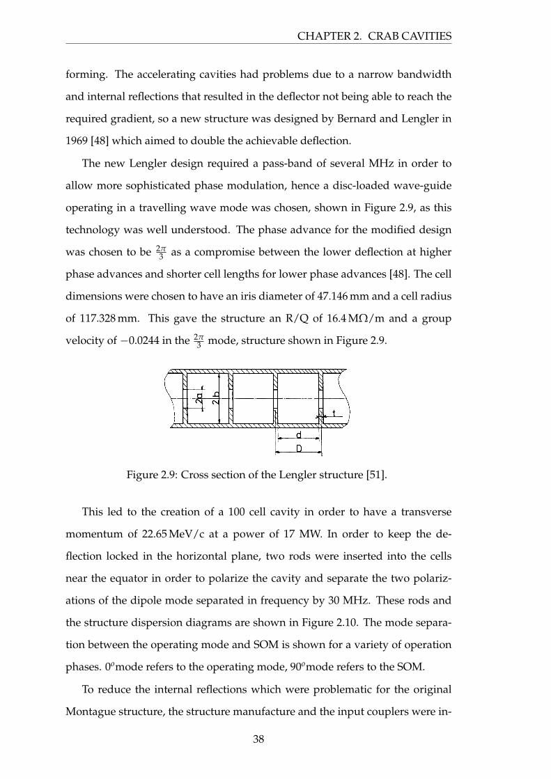
CHAPTER 2. CRAB CAVITIES
forming. The accelerating cavities had problems due to a narrow bandwidth
and internal reflections that resulted in the deflector not being able to reach the
required gradient, so a new structure was designed by Bernard and Lengler in
1969 [48] which aimed to double the achievable deflection.
The new Lengler design required a pass-band of several MHz in order to
allow more sophisticated phase modulation, hence a disc-loaded wave-guide
operating in a travelling wave mode was chosen, shown in Figure 2.9, as this
technology was well understood. The phase advance for the modified design
was chosen to be 2π3 as a compromise between the lower deflection at higher
phase advances and shorter cell lengths for lower phase advances [48]. The cell
dimensions were chosen to have an iris diameter of 47.146 mm and a cell radius
of 117.328 mm. This gave the structure an R/Q of 16.4 MΩ/m and a group
velocity of −0.0244 in the 2π3 mode, structure shown in Figure 2.9.
Figure 2.9: Cross section of the Lengler structure [51].
This led to the creation of a 100 cell cavity in order to have a transverse
momentum of 22.65 MeV/c at a power of 17 MW. In order to keep the de-
flection locked in the horizontal plane, two rods were inserted into the cells
near the equator in order to polarize the cavity and separate the two polariz-
ations of the dipole mode separated in frequency by 30 MHz. These rods and
the structure dispersion diagrams are shown in Figure 2.10. The mode separa-
tion between the operating mode and SOM is shown for a variety of operation
phases. 0omode refers to the operating mode, 90omode refers to the SOM.
To reduce the internal reflections which were problematic for the original
Montague structure, the structure manufacture and the input couplers were in-
38
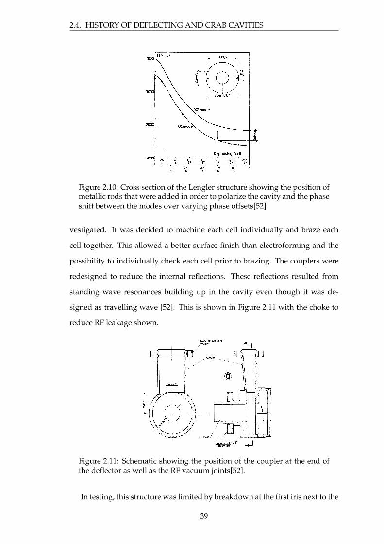
2.4. HISTORY OF DEFLECTING AND CRAB CAVITIES
Figure 2.10: Cross section of the Lengler structure showing the position ofmetallic rods that were added in order to polarize the cavity and the phaseshift between the modes over varying phase offsets[52].
vestigated. It was decided to machine each cell individually and braze each
cell together. This allowed a better surface finish than electroforming and the
possibility to individually check each cell prior to brazing. The couplers were
redesigned to reduce the internal reflections. These reflections resulted from
standing wave resonances building up in the cavity even though it was de-
signed as travelling wave [52]. This is shown in Figure 2.11 with the choke to
reduce RF leakage shown.
Figure 2.11: Schematic showing the position of the coupler at the end ofthe deflector as well as the RF vacuum joints[52].
In testing, this structure was limited by breakdown at the first iris next to the
39
CHAPTER 2. CRAB CAVITIES
input coupler to a maximum electric field of Ep = 522 kVcm [52].
Parameter Value/UnitFrequency of operational mode 2855 MHz
Operating mode 2π3
Deflecting voltage Vat 160 kV/cm
Peak electric field Eap 480 kV/cm
Rt/Q 1376 Ω
Table 2.1: Key properties of the Lengler cavity.
2.4.2 CERN - Karlsruhe
The Karlsruhe cavity was designed and built in 1970’s and was one of the
first superconducting deflecting cavities constructed [53]. The decision to make
the Karlsruhe deflectors superconducting was made due to conventional cavit-
ies being unable to produce the desired deflecting fields for the required length
of time, mainly due to losses [54].
As design improvements progressed, the limit of materials was pushed. Due
to concerns about the peak magnetic field on the previous lead surfaces the
Karlsruhe deflectors were made out of solid niobium [55]. The location of the
joints in the cavity required the cavity to operate in a π2 mode, as this allowed
for lower surface fields as every second cell has zero fields in a standing wave
π2 structure. Figure 2.12 shows one of the Karlsruhe cavities.
As the cavity operates with a standing wave unlike the travelling wave
structures previously, ensuring that a pair of cavities remain at the same fre-
quency is very important. As the RF power in travelling wave structures is
being continually replaced, any frequency variation in one pulse should be cor-
rected in the next, and provided two cavities are fed by the same source they
will always be in phase. Standing wave structures build up power at the de-
sired frequency and if one cavity shifts its fundamental frequency, via thermal
expansion of the cavity, problems can arise. To stop this from happening, the
frequency of the cavities must be carefully monitored and the status of any pair-
40
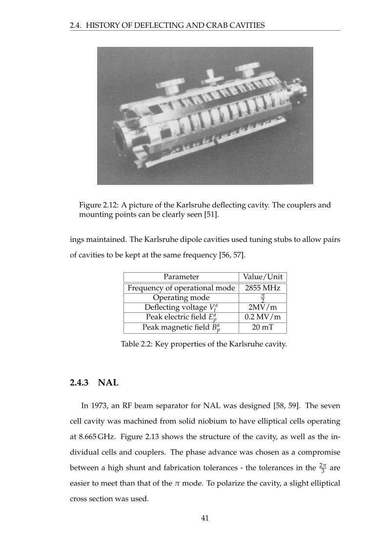
2.4. HISTORY OF DEFLECTING AND CRAB CAVITIES
Figure 2.12: A picture of the Karlsruhe deflecting cavity. The couplers andmounting points can be clearly seen [51].
ings maintained. The Karlsruhe dipole cavities used tuning stubs to allow pairs
of cavities to be kept at the same frequency [56, 57].
Parameter Value/UnitFrequency of operational mode 2855 MHz
Operating mode π2
Deflecting voltage Vat 2MV/m
Peak electric field Eap 0.2 MV/m
Peak magnetic field Bap 20 mT
Table 2.2: Key properties of the Karlsruhe cavity.
2.4.3 NAL
In 1973, an RF beam separator for NAL was designed [58, 59]. The seven
cell cavity was machined from solid niobium to have elliptical cells operating
at 8.665 GHz. Figure 2.13 shows the structure of the cavity, as well as the in-
dividual cells and couplers. The phase advance was chosen as a compromise
between a high shunt and fabrication tolerances - the tolerances in the 2π3 are
easier to meet than that of the π mode. To polarize the cavity, a slight elliptical
cross section was used.
41
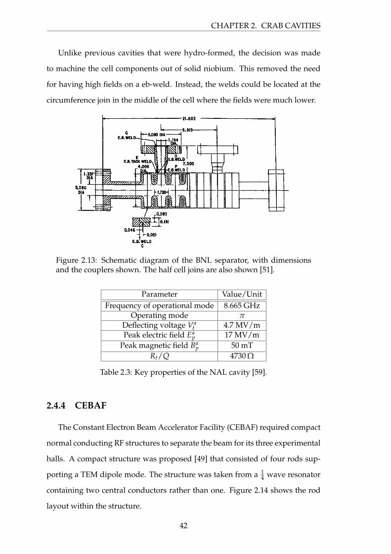
CHAPTER 2. CRAB CAVITIES
Unlike previous cavities that were hydro-formed, the decision was made
to machine the cell components out of solid niobium. This removed the need
for having high fields on a eb-weld. Instead, the welds could be located at the
circumference join in the middle of the cell where the fields were much lower.
Figure 2.13: Schematic diagram of the BNL separator, with dimensionsand the couplers shown. The half cell joins are also shown [51].
Parameter Value/UnitFrequency of operational mode 8.665 GHz
Operating mode πDeflecting voltage Va
t 4.7 MV/mPeak electric field Ea
p 17 MV/mPeak magnetic field Ba
p 50 mTRt/Q 4730 Ω
Table 2.3: Key properties of the NAL cavity [59].
2.4.4 CEBAF
The Constant Electron Beam Accelerator Facility (CEBAF) required compact
normal conducting RF structures to separate the beam for its three experimental
halls. A compact structure was proposed [49] that consisted of four rods sup-
porting a TEM dipole mode. The structure was taken from a 14 wave resonator
containing two central conductors rather than one. Figure 2.14 shows the rod
layout within the structure.
42
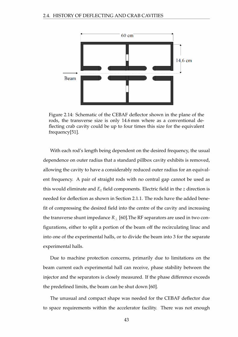
2.4. HISTORY OF DEFLECTING AND CRAB CAVITIES
Figure 2.14: Schematic of the CEBAF deflector shown in the plane of therods, the transverse size is only 14.6 mm where as a conventional de-flecting crab cavity could be up to four times this size for the equivalentfrequency[51].
With each rod’s length being dependent on the desired frequency, the usual
dependence on outer radius that a standard pillbox cavity exhibits is removed,
allowing the cavity to have a considerably reduced outer radius for an equival-
ent frequency. A pair of straight rods with no central gap cannot be used as
this would eliminate and Ez field components. Electric field in the z direction is
needed for deflection as shown in Section 2.1.1. The rods have the added bene-
fit of compressing the desired field into the centre of the cavity and increasing
the transverse shunt impedance R⊥ [60].The RF separators are used in two con-
figurations, either to split a portion of the beam off the recirculating linac and
into one of the experimental halls, or to divide the beam into 3 for the separate
experimental halls.
Due to machine protection concerns, primarily due to limitations on the
beam current each experimental hall can receive, phase stability between the
injector and the separators is closely measured. If the phase difference exceeds
the predefined limits, the beam can be shut down [60].
The unusual and compact shape was needed for the CEBAF deflector due
to space requirements within the accelerator facility. There was not enough
43
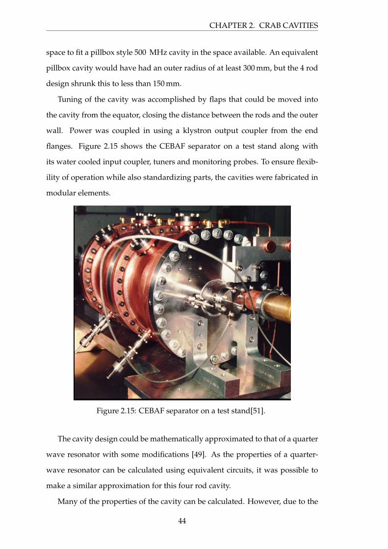
CHAPTER 2. CRAB CAVITIES
space to fit a pillbox style 500 MHz cavity in the space available. An equivalent
pillbox cavity would have had an outer radius of at least 300 mm, but the 4 rod
design shrunk this to less than 150 mm.
Tuning of the cavity was accomplished by flaps that could be moved into
the cavity from the equator, closing the distance between the rods and the outer
wall. Power was coupled in using a klystron output coupler from the end
flanges. Figure 2.15 shows the CEBAF separator on a test stand along with
its water cooled input coupler, tuners and monitoring probes. To ensure flexib-
ility of operation while also standardizing parts, the cavities were fabricated in
modular elements.
Figure 2.15: CEBAF separator on a test stand[51].
The cavity design could be mathematically approximated to that of a quarter
wave resonator with some modifications [49]. As the properties of a quarter-
wave resonator can be calculated using equivalent circuits, it was possible to
make a similar approximation for this four rod cavity.
Many of the properties of the cavity can be calculated. However, due to the
44
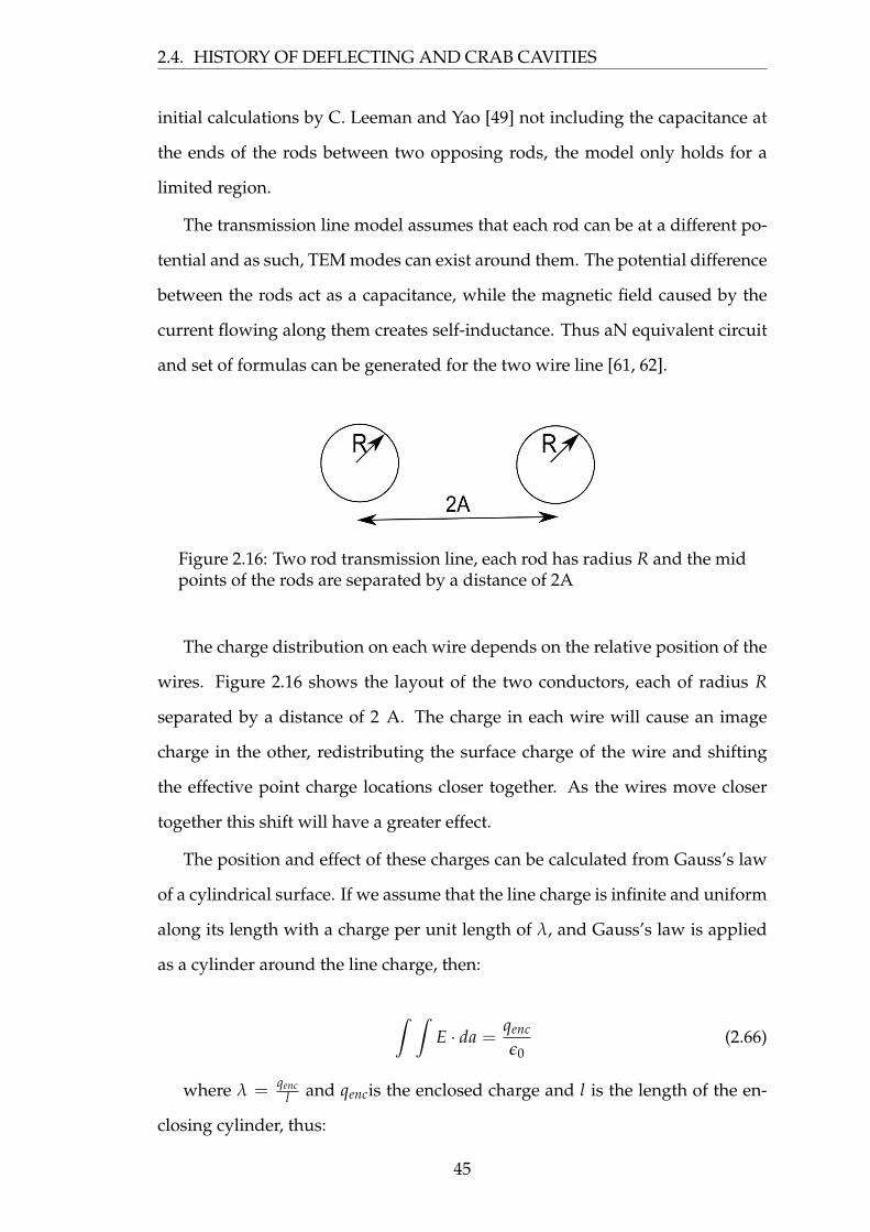
2.4. HISTORY OF DEFLECTING AND CRAB CAVITIES
initial calculations by C. Leeman and Yao [49] not including the capacitance at
the ends of the rods between two opposing rods, the model only holds for a
limited region.
The transmission line model assumes that each rod can be at a different po-
tential and as such, TEM modes can exist around them. The potential difference
between the rods act as a capacitance, while the magnetic field caused by the
current flowing along them creates self-inductance. Thus aN equivalent circuit
and set of formulas can be generated for the two wire line [61, 62].
Figure 2.16: Two rod transmission line, each rod has radius R and the midpoints of the rods are separated by a distance of 2A
The charge distribution on each wire depends on the relative position of the
wires. Figure 2.16 shows the layout of the two conductors, each of radius R
separated by a distance of 2 A. The charge in each wire will cause an image
charge in the other, redistributing the surface charge of the wire and shifting
the effective point charge locations closer together. As the wires move closer
together this shift will have a greater effect.
The position and effect of these charges can be calculated from Gauss’s law
of a cylindrical surface. If we assume that the line charge is infinite and uniform
along its length with a charge per unit length of λ, and Gauss’s law is applied
as a cylinder around the line charge, then:
ˆ ˆE · da =
qenc
ε0(2.66)
where λ = qencl and qencis the enclosed charge and l is the length of the en-
closing cylinder, thus:
45
CHAPTER 2. CRAB CAVITIES
E · 2πr =λ
ε0(2.67)
E =λ
2πrε0(2.68)
where r is the radius of the cylinder, though this only holds if r > R.
By integrating this, the potential can then be found:
φ =
ˆE · dr =
λ
2πε0ln(
br
)+ const (2.69)
where b is an arbitrary point that we can and will choose to have a potential
of zero. Again, this only holds for r > R, but this also allows the wire to be
treated as a line charge as there is no longer a dependence on R.
This can then be combined with a second oppositely-charged line, which is
placed a distance 2A away from the initial wire.
φ =λ
2πε0ln(
1r1
)− λ
2πε0ln(
1r2
)(2.70)
where r1 and r2 are the radii of the two cylinders.
φ =λ
4πεln
(r2
2r2
1
)(2.71)
This can then be simplified using:
a =√(A2 − R2) (2.72)
where a is the distance between the mid point of the wire and the effective
charge location, A is the distance between the mid point of the wires and the
centre of a wire and R is the radius of a wire. In the case where A R, we can
assume that a ≈ A. Thus the voltage between the two wires is given as:
46

2.4. HISTORY OF DEFLECTING AND CRAB CAVITIES
V =λ
2πε0ln(
A + aA− a
)(2.73)
Thus the capacitance between the two rods can be calculated as:
C =qV
=2πε0
ln(
A+aA−a
) =πε0
ln[(A2+a2)A2−a2
] =πε0
ln((A+a)
a
) (2.74)
This can then be rearranged using a =√(A2 − R2), α = A
R and the relation-
ship:
cosh−1 x = ln(
x +√
x2 − 1)
(2.75)
becomes:
ln(
A + aA− a
)= cosh−1(α) (2.76)
Thus the capacitance becomes:
C =πε0
cosh−1(α)(2.77)
Similarly, the inductance becomes[63]:
L =µ0
πcosh−1(α) (2.78)
Hence the impedance becomes:
47
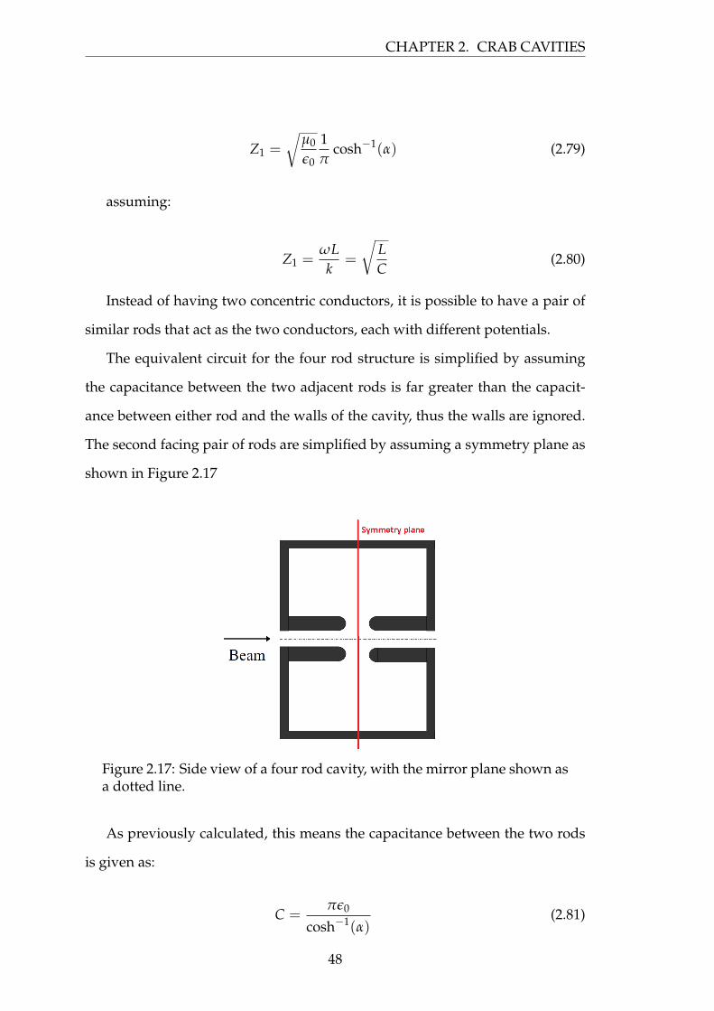
CHAPTER 2. CRAB CAVITIES
Z1 =
õ0
ε0
1π
cosh−1(α) (2.79)
assuming:
Z1 =ωLk
=
√LC
(2.80)
Instead of having two concentric conductors, it is possible to have a pair of
similar rods that act as the two conductors, each with different potentials.
The equivalent circuit for the four rod structure is simplified by assuming
the capacitance between the two adjacent rods is far greater than the capacit-
ance between either rod and the walls of the cavity, thus the walls are ignored.
The second facing pair of rods are simplified by assuming a symmetry plane as
shown in Figure 2.17
Figure 2.17: Side view of a four rod cavity, with the mirror plane shown asa dotted line.
As previously calculated, this means the capacitance between the two rods
is given as:
C =πε0
cosh−1(α)(2.81)
48
2.4. HISTORY OF DEFLECTING AND CRAB CAVITIES
The inductance given as:
L =µµ0
πcosh−1(α) (2.82)
The peak electric field will again be dependant on the maximum voltage
between two points over a given distance, however this could be between the
tips of two parallel rods, or between two facing rods, depending on the dis-
tances involved.
At the ends of the rods the maximum electric field will still be:
Emax =V0
d(2.83)
where d is the distance between the tips
However this is likely not to be the case. To calculate the electric field at the
surface of the rods between two adjacent parallel rods, the voltage between
them must be calculated. The potential difference at the end of the rods is
known to be ±V0, and as such the voltage a distance z down the rod will be
given as:
Vp = V0 sin(kz) (2.84)
where V0 is the maximum voltage through the tip, k is the wave number, z is
the distance down the rod.
From this the charge per unit length q can be calculated [63]. Equation 2.85
can then be rearranged and placed in Equation 2.87. This can then be used to
calculate the electric fields at the surface where x = A − R or the transverse
electric field where x = 0.
49
CHAPTER 2. CRAB CAVITIES
V(x,y) =q
4πε0ln
(r2−
r2+
)(2.85)
Ex(x, y) = −∂V∂x
(2.86)
= − aqπε0
[x2 − a2 − y2
r2−r2
+
](2.87)
where A is the rod separation, R is the rod radius, a =√
A2 − R2, r− =√
x2 − a2, r+ =√
x2 + a2
Using the relation H = EZc
, the magnetic field can then be calculated. Once
the transverse electric and magnetic fields are known, the transverse voltage
can be calculated from:
Vtrans =
lˆ
0
[Etrans sin(kz)eikz + cBtrans cos(kz)eikz
]dz (2.88)
Where l is the length of the rod in the z direction and Etrans and Btrans are the
transverse electric and magnetic field components calculated previously.
As there is no current flow across the gap at the end of the rod, it is easier to
work with only the energy stored magnetically, as the inductance only has one
component, rather than two in the case of the electric fields.
We know:
U =
ˆLI2dz (2.89)
I(z) = IL cos(kz) (2.90)
I1 =V1
Z1(2.91)
50
2.4. HISTORY OF DEFLECTING AND CRAB CAVITIES
We can rearrange this to get:
U =
ˆLI2dz (2.92)
= LI21
ˆcos2(kz)dz (2.93)
= LV2
12Z2
c
ˆ l
0cos2(kz) (2.94)
= LV2
12Z2
c
(l4+
14
sin(kl))
(2.95)
Where l is the actual length of the rod, which is not λ2 but is very close to and
can be calculated as shown earlier.
The integral can be simplified as the initial conditions mean x2 +
14 sin(2x) =
0 when x = 0. If the rod length was to be λ2 , then then the additional dependence
on sin(kl) would also disappear.
The R/Q of the cavity can be calculated as:
RQ
=V2
02ωU
(2.96)
2.4.5 KEKB
The KEKB dipole cavity is the first super-conducting crab cavity implemen-
ted and operated on a working facility. The crab cavities were added to the
electron-positron collider to eliminate any beam-beam instabilities caused by
synchrotron-betatron oscillating2 and reduce loss of luminosity caused by geo-
metrical effects. The cavity is of a non-axially-symmetric squashed cell shape,
often called ’racetrack’. The racetrack shape, characterized by its two linked
semi-circles provides polarization of the cavity by shifting the SOM to a differ-
ent higher frequency [64]. Figure 2.18 shows part of the structure, including
2Synchrotron oscillation are the motion of of particles longitudinally within the bunch,betatron oscillations are the harmonic motions of the particles transverse to the direction ofpropagation.
51
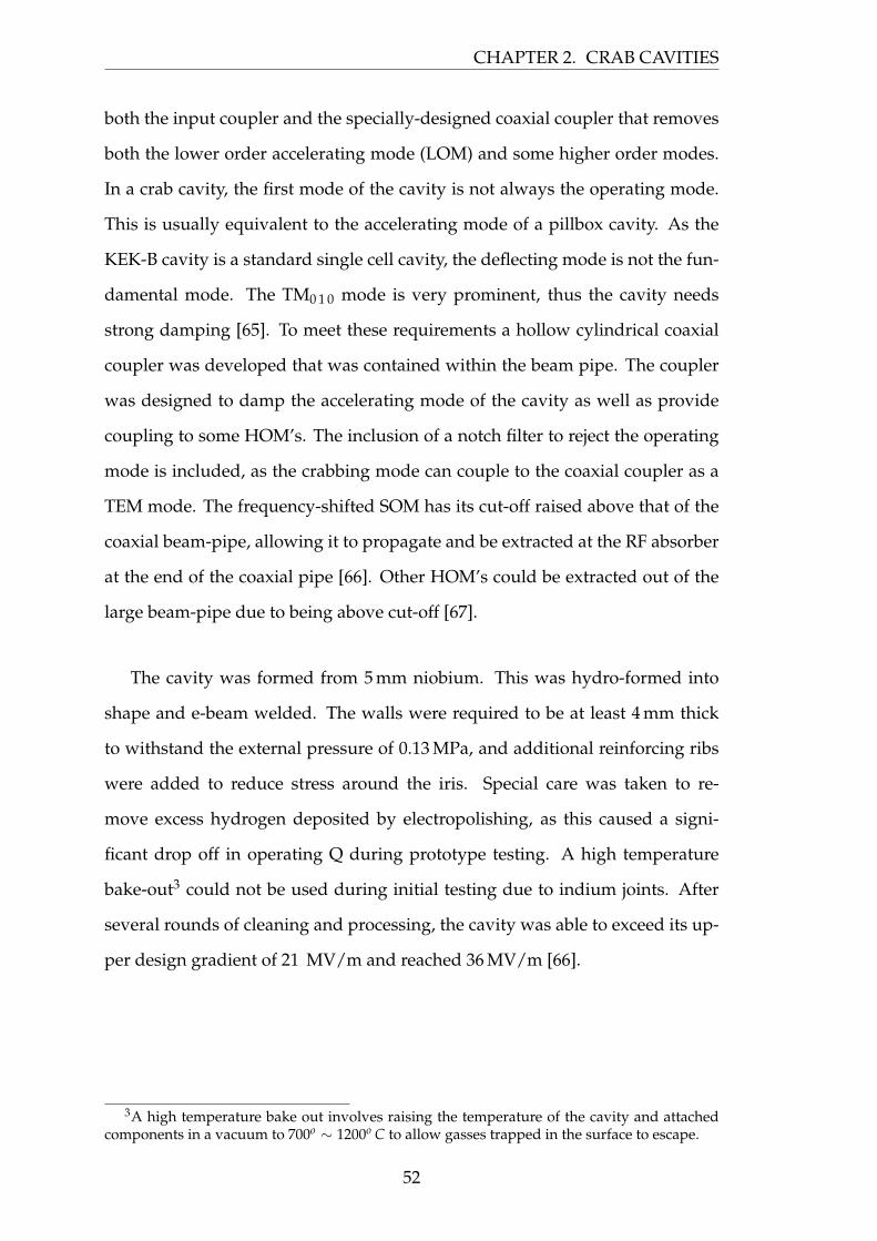
CHAPTER 2. CRAB CAVITIES
both the input coupler and the specially-designed coaxial coupler that removes
both the lower order accelerating mode (LOM) and some higher order modes.
In a crab cavity, the first mode of the cavity is not always the operating mode.
This is usually equivalent to the accelerating mode of a pillbox cavity. As the
KEK-B cavity is a standard single cell cavity, the deflecting mode is not the fun-
damental mode. The TM0 1 0 mode is very prominent, thus the cavity needs
strong damping [65]. To meet these requirements a hollow cylindrical coaxial
coupler was developed that was contained within the beam pipe. The coupler
was designed to damp the accelerating mode of the cavity as well as provide
coupling to some HOM’s. The inclusion of a notch filter to reject the operating
mode is included, as the crabbing mode can couple to the coaxial coupler as a
TEM mode. The frequency-shifted SOM has its cut-off raised above that of the
coaxial beam-pipe, allowing it to propagate and be extracted at the RF absorber
at the end of the coaxial pipe [66]. Other HOM’s could be extracted out of the
large beam-pipe due to being above cut-off [67].
The cavity was formed from 5 mm niobium. This was hydro-formed into
shape and e-beam welded. The walls were required to be at least 4 mm thick
to withstand the external pressure of 0.13 MPa, and additional reinforcing ribs
were added to reduce stress around the iris. Special care was taken to re-
move excess hydrogen deposited by electropolishing, as this caused a signi-
ficant drop off in operating Q during prototype testing. A high temperature
bake-out3 could not be used during initial testing due to indium joints. After
several rounds of cleaning and processing, the cavity was able to exceed its up-
per design gradient of 21 MV/m and reached 36 MV/m [66].
3A high temperature bake out involves raising the temperature of the cavity and attachedcomponents in a vacuum to 700o ∼ 1200o C to allow gasses trapped in the surface to escape.
52
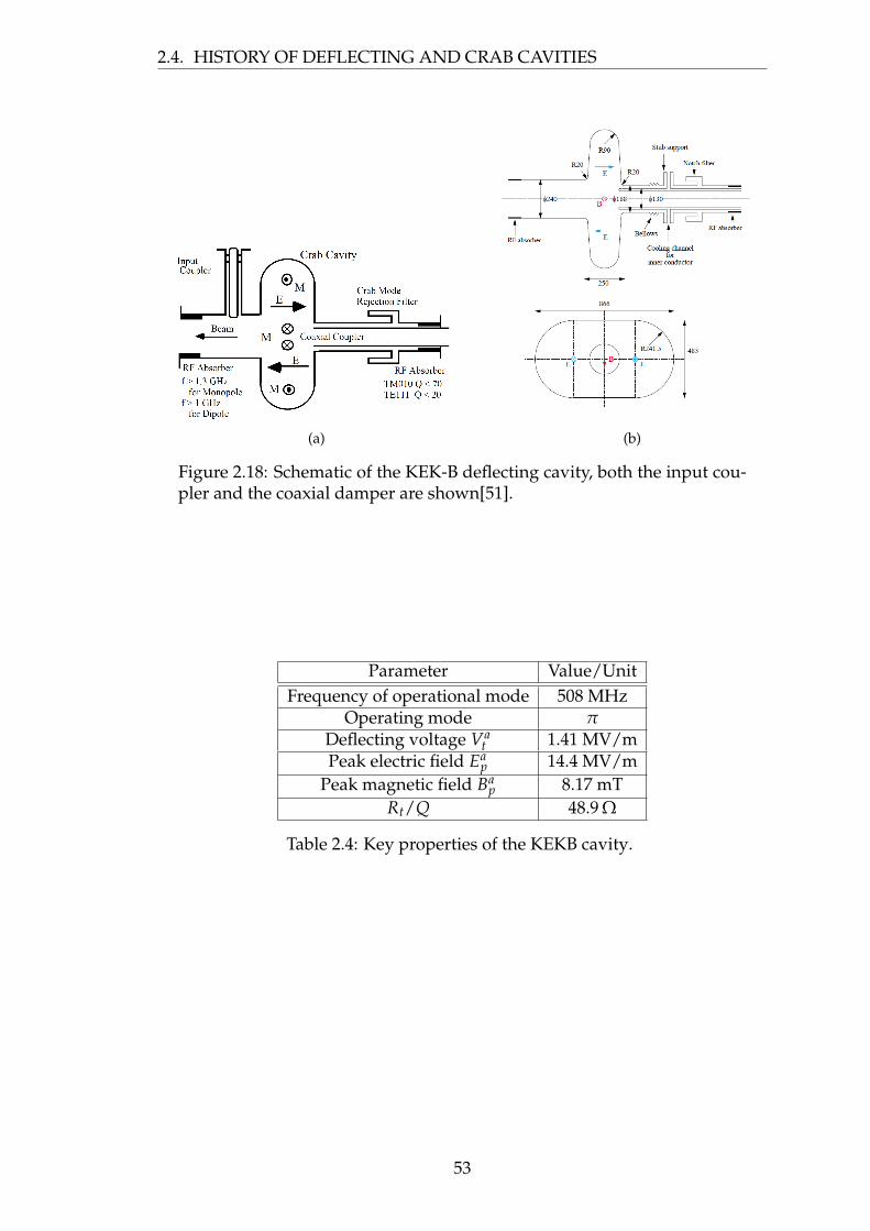
2.4. HISTORY OF DEFLECTING AND CRAB CAVITIES
(a) (b)
Figure 2.18: Schematic of the KEK-B deflecting cavity, both the input cou-pler and the coaxial damper are shown[51].
Parameter Value/UnitFrequency of operational mode 508 MHz
Operating mode πDeflecting voltage Va
t 1.41 MV/mPeak electric field Ea
p 14.4 MV/mPeak magnetic field Ba
p 8.17 mTRt/Q 48.9 Ω
Table 2.4: Key properties of the KEKB cavity.
53
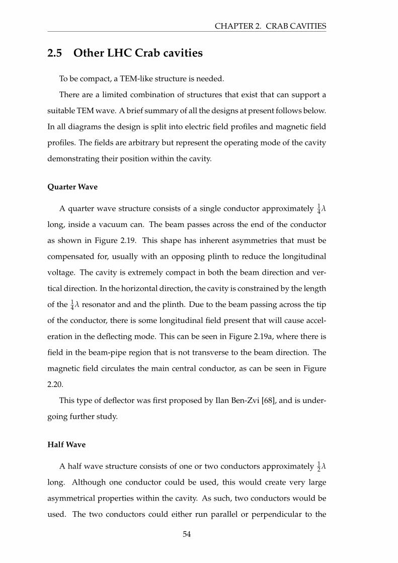
CHAPTER 2. CRAB CAVITIES
2.5 Other LHC Crab cavities
To be compact, a TEM-like structure is needed.
There are a limited combination of structures that exist that can support a
suitable TEM wave. A brief summary of all the designs at present follows below.
In all diagrams the design is split into electric field profiles and magnetic field
profiles. The fields are arbitrary but represent the operating mode of the cavity
demonstrating their position within the cavity.
Quarter Wave
A quarter wave structure consists of a single conductor approximately 14 λ
long, inside a vacuum can. The beam passes across the end of the conductor
as shown in Figure 2.19. This shape has inherent asymmetries that must be
compensated for, usually with an opposing plinth to reduce the longitudinal
voltage. The cavity is extremely compact in both the beam direction and ver-
tical direction. In the horizontal direction, the cavity is constrained by the length
of the 14 λ resonator and and the plinth. Due to the beam passing across the tip
of the conductor, there is some longitudinal field present that will cause accel-
eration in the deflecting mode. This can be seen in Figure 2.19a, where there is
field in the beam-pipe region that is not transverse to the beam direction. The
magnetic field circulates the main central conductor, as can be seen in Figure
2.20.
This type of deflector was first proposed by Ilan Ben-Zvi [68], and is under-
going further study.
Half Wave
A half wave structure consists of one or two conductors approximately 12 λ
long. Although one conductor could be used, this would create very large
asymmetrical properties within the cavity. As such, two conductors would be
used. The two conductors could either run parallel or perpendicular to the
54
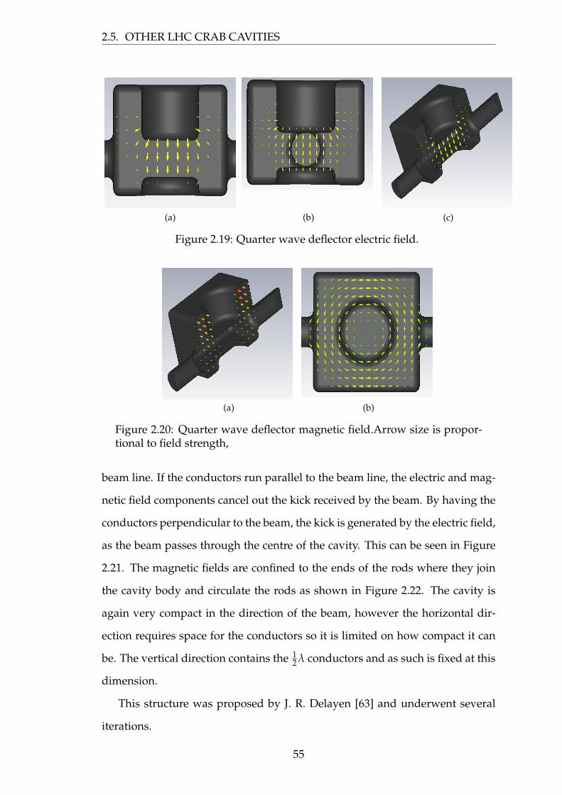
2.5. OTHER LHC CRAB CAVITIES
(a) (b) (c)
Figure 2.19: Quarter wave deflector electric field.
(a) (b)
Figure 2.20: Quarter wave deflector magnetic field.Arrow size is propor-tional to field strength,
beam line. If the conductors run parallel to the beam line, the electric and mag-
netic field components cancel out the kick received by the beam. By having the
conductors perpendicular to the beam, the kick is generated by the electric field,
as the beam passes through the centre of the cavity. This can be seen in Figure
2.21. The magnetic fields are confined to the ends of the rods where they join
the cavity body and circulate the rods as shown in Figure 2.22. The cavity is
again very compact in the direction of the beam, however the horizontal dir-
ection requires space for the conductors so it is limited on how compact it can
be. The vertical direction contains the 12 λ conductors and as such is fixed at this
dimension.
This structure was proposed by J. R. Delayen [63] and underwent several
iterations.
55
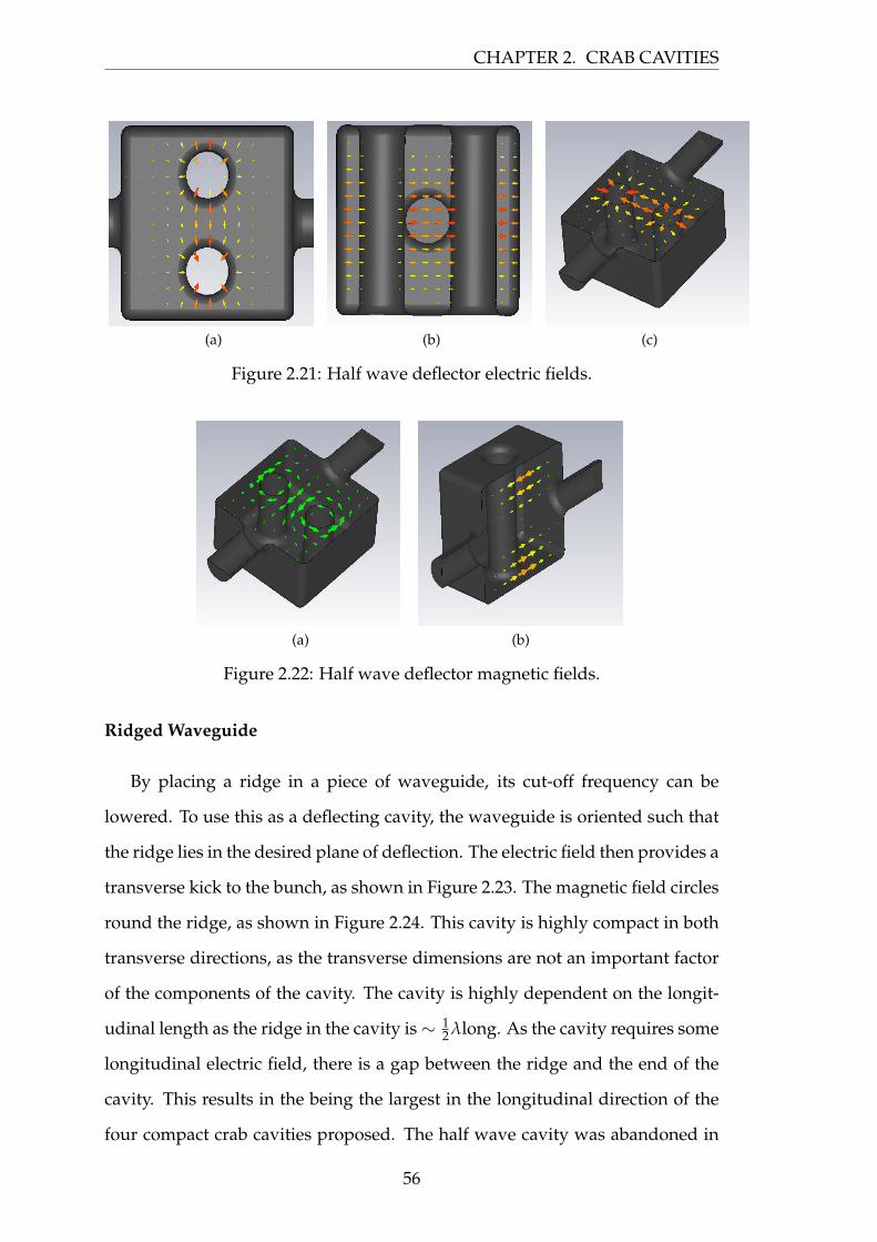
CHAPTER 2. CRAB CAVITIES
(a) (b) (c)
Figure 2.21: Half wave deflector electric fields.
(a) (b)
Figure 2.22: Half wave deflector magnetic fields.
Ridged Waveguide
By placing a ridge in a piece of waveguide, its cut-off frequency can be
lowered. To use this as a deflecting cavity, the waveguide is oriented such that
the ridge lies in the desired plane of deflection. The electric field then provides a
transverse kick to the bunch, as shown in Figure 2.23. The magnetic field circles
round the ridge, as shown in Figure 2.24. This cavity is highly compact in both
transverse directions, as the transverse dimensions are not an important factor
of the components of the cavity. The cavity is highly dependent on the longit-
udinal length as the ridge in the cavity is∼ 12 λlong. As the cavity requires some
longitudinal electric field, there is a gap between the ridge and the end of the
cavity. This results in the being the largest in the longitudinal direction of the
four compact crab cavities proposed. The half wave cavity was abandoned in
56
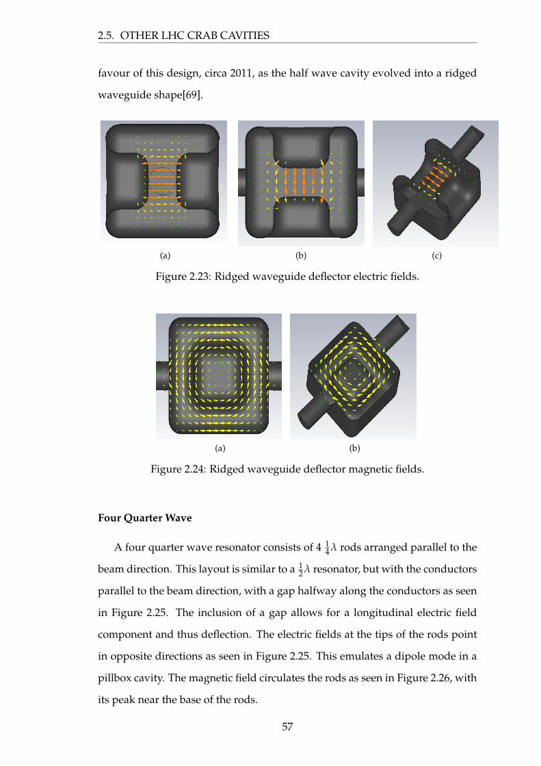
2.5. OTHER LHC CRAB CAVITIES
favour of this design, circa 2011, as the half wave cavity evolved into a ridged
waveguide shape[69].
(a) (b) (c)
Figure 2.23: Ridged waveguide deflector electric fields.
(a) (b)
Figure 2.24: Ridged waveguide deflector magnetic fields.
Four Quarter Wave
A four quarter wave resonator consists of 4 14 λ rods arranged parallel to the
beam direction. This layout is similar to a 12 λ resonator, but with the conductors
parallel to the beam direction, with a gap halfway along the conductors as seen
in Figure 2.25. The inclusion of a gap allows for a longitudinal electric field
component and thus deflection. The electric fields at the tips of the rods point
in opposite directions as seen in Figure 2.25. This emulates a dipole mode in a
pillbox cavity. The magnetic field circulates the rods as seen in Figure 2.26, with
its peak near the base of the rods.
57
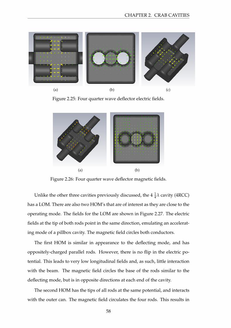
CHAPTER 2. CRAB CAVITIES
(a) (b) (c)
Figure 2.25: Four quarter wave deflector electric fields.
(a) (b)
Figure 2.26: Four quarter wave deflector magnetic fields.
Unlike the other three cavities previously discussed, the 4 14 λ cavity (4RCC)
has a LOM. There are also two HOM’s that are of interest as they are close to the
operating mode. The fields for the LOM are shown in Figure 2.27. The electric
fields at the tip of both rods point in the same direction, emulating an accelerat-
ing mode of a pillbox cavity. The magnetic field circles both conductors.
The first HOM is similar in appearance to the deflecting mode, and has
oppositely-charged parallel rods. However, there is no flip in the electric po-
tential. This leads to very low longitudinal fields and, as such, little interaction
with the beam. The magnetic field circles the base of the rods similar to the
deflecting mode, but is in opposite directions at each end of the cavity.
The second HOM has the tips of all rods at the same potential, and interacts
with the outer can. The magnetic field circulates the four rods. This results in
58
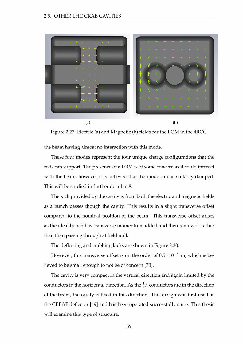
2.5. OTHER LHC CRAB CAVITIES
(a) (b)
Figure 2.27: Electric (a) and Magnetic (b) fields for the LOM in the 4RCC.
the beam having almost no interaction with this mode.
These four modes represent the four unique charge configurations that the
rods can support. The presence of a LOM is of some concern as it could interact
with the beam, however it is believed that the mode can be suitably damped.
This will be studied in further detail in 8.
The kick provided by the cavity is from both the electric and magnetic fields
as a bunch passes though the cavity. This results in a slight transverse offset
compared to the nominal position of the beam. This transverse offset arises
as the ideal bunch has transverse momentum added and then removed, rather
than than passing through at field null.
The deflecting and crabbing kicks are shown in Figure 2.30.
However, this transverse offset is on the order of 0.5 · 10−8 m, which is be-
lieved to be small enough to not be of concern [70].
The cavity is very compact in the vertical direction and again limited by the
conductors in the horizontal direction. As the 14 λ conductors are in the direction
of the beam, the cavity is fixed in this direction. This design was first used as
the CEBAF deflector [49] and has been operated successfully since. This thesis
will examine this type of structure.
59
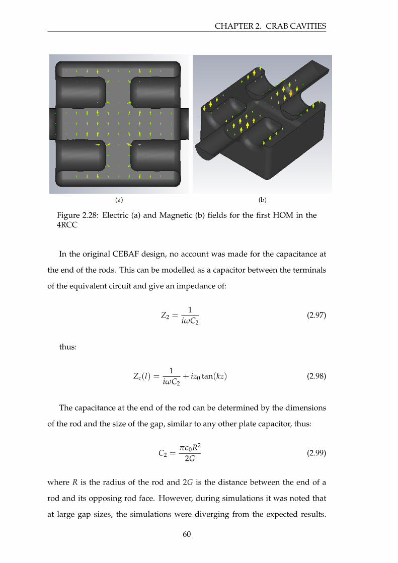
CHAPTER 2. CRAB CAVITIES
(a) (b)
Figure 2.28: Electric (a) and Magnetic (b) fields for the first HOM in the4RCC
In the original CEBAF design, no account was made for the capacitance at
the end of the rods. This can be modelled as a capacitor between the terminals
of the equivalent circuit and give an impedance of:
Z2 =1
iωC2(2.97)
thus:
Zc(l) =1
iωC2+ iz0 tan(kz) (2.98)
The capacitance at the end of the rod can be determined by the dimensions
of the rod and the size of the gap, similar to any other plate capacitor, thus:
C2 =πε0R2
2G(2.99)
where R is the radius of the rod and 2G is the distance between the end of a
rod and its opposing rod face. However, during simulations it was noted that
at large gap sizes, the simulations were diverging from the expected results.
60
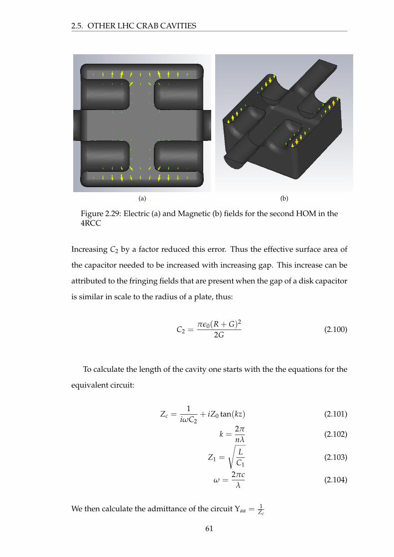
2.5. OTHER LHC CRAB CAVITIES
(a) (b)
Figure 2.29: Electric (a) and Magnetic (b) fields for the second HOM in the4RCC
Increasing C2 by a factor reduced this error. Thus the effective surface area of
the capacitor needed to be increased with increasing gap. This increase can be
attributed to the fringing fields that are present when the gap of a disk capacitor
is similar in scale to the radius of a plate, thus:
C2 =πε0(R + G)2
2G(2.100)
To calculate the length of the cavity one starts with the the equations for the
equivalent circuit:
Zc =1
iωC2+ iZ0 tan(kz) (2.101)
k =2π
nλ(2.102)
Z1 =
√L
C1(2.103)
ω =2πc
λ(2.104)
We then calculate the admittance of the circuit Υaa =1
Zc
61
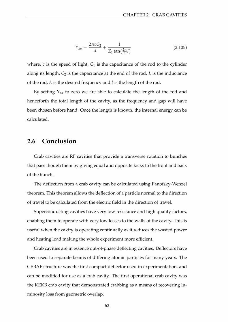
CHAPTER 2. CRAB CAVITIES
Υaa =2πcC2
λ+
1Z1 tan(2π
λ l)(2.105)
where, c is the speed of light, C1 is the capacitance of the rod to the cylinder
along its length, C2 is the capacitance at the end of the rod, L is the inductance
of the rod, λ is the desired frequency and l is the length of the rod.
By setting Υaa to zero we are able to calculate the length of the rod and
henceforth the total length of the cavity, as the frequency and gap will have
been chosen before hand. Once the length is known, the internal energy can be
calculated.
2.6 Conclusion
Crab cavities are RF cavities that provide a transverse rotation to bunches
that pass though them by giving equal and opposite kicks to the front and back
of the bunch.
The deflection from a crab cavity can be calculated using Panofsky-Wenzel
theorem. This theorem allows the deflection of a particle normal to the direction
of travel to be calculated from the electric field in the direction of travel.
Superconducting cavities have very low resistance and high quality factors,
enabling them to operate with very low losses to the walls of the cavity. This is
useful when the cavity is operating continually as it reduces the wasted power
and heating load making the whole experiment more efficient.
Crab cavities are in essence out-of-phase deflecting cavities. Deflectors have
been used to separate beams of differing atomic particles for many years. The
CEBAF structure was the first compact deflector used in experimentation, and
can be modified for use as a crab cavity. The first operational crab cavity was
the KEKB crab cavity that demonstrated crabbing as a means of recovering lu-
minosity loss from geometric overlap.
62
2.6. CONCLUSION
For the LHC, there is extremely limited space and this requires a compact
cavity design. There are four main designs that could be used to fulfil the LHC
requirements. The four quarter wave design based on the CEBAF deflector will
be the focus of this thesis.
63
CHAPTER 2. CRAB CAVITIES
position / m
Tra
nsve
rse
B f
ield
, [T
m/s
]
-0.4 -0.3 -0.2 -0.1 0 0.1 0.2 0.3 0.4
-1
0
1
2
3
× 106
Tra
nsve
rse
E f
ield
, [V
]
-0.4 -0.3 -0.2 -0.1 0 0.1 0.2 0.3 0.4
0
1
2
3
4
× 106
Magnetic
Electric
(a)
position / m
Tra
nsve
rse
B f
ield
, [T
m/s
]
-0.4 -0.3 -0.2 -0.1 0 0.1 0.2 0.3 0.4-5
0
5× 10
6
Tra
nsve
rse
E f
ield
, [V
]
-0.4 -0.3 -0.2 -0.1 0 0.1 0.2 0.3 0.4-5
0
5× 10
6
Magnetic
Electric
(b)
Figure 2.30: Fields seen by the beam in deflecting (a) and crabbing (b)phases.
64
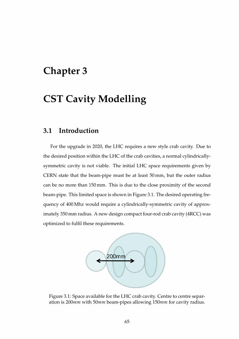
Chapter 3
CST Cavity Modelling
3.1 Introduction
For the upgrade in 2020, the LHC requires a new style crab cavity. Due to
the desired position within the LHC of the crab cavities, a normal cylindrically-
symmetric cavity is not viable. The initial LHC space requirements given by
CERN state that the beam-pipe must be at least 50 mm, but the outer radius
can be no more than 150 mm. This is due to the close proximity of the second
beam-pipe. This limited space is shown in Figure 3.1. The desired operating fre-
quency of 400 Mhz would require a cylindrically-symmetric cavity of approx-
imately 350 mm radius. A new design compact four-rod crab cavity (4RCC) was
optimized to fulfil these requirements.
Figure 3.1: Space available for the LHC crab cavity. Centre to centre separ-ation is 200mm with 50mm beam-pipes allowing 150mm for cavity radius.
65
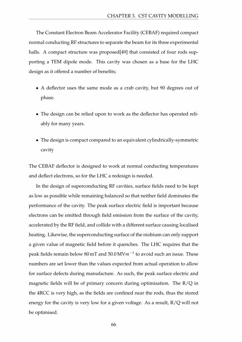
CHAPTER 3. CST CAVITY MODELLING
The Constant Electron Beam Accelerator Facility (CEBAF) required compact
normal conducting RF structures to separate the beam for its three experimental
halls. A compact structure was proposed[49] that consisted of four rods sup-
porting a TEM dipole mode. This cavity was chosen as a base for the LHC
design as it offered a number of benefits;
• A deflector uses the same mode as a crab cavity, but 90 degrees out of
phase.
• The design can be relied upon to work as the deflector has operated reli-
ably for many years.
• The design is compact compared to an equivalent cylindrically-symmetric
cavity
The CEBAF deflector is designed to work at normal conducting temperatures
and deflect electrons, so for the LHC a redesign is needed.
In the design of superconducting RF cavities, surface fields need to be kept
as low as possible while remaining balanced so that neither field dominates the
performance of the cavity. The peak surface electric field is important because
electrons can be emitted through field emission from the surface of the cavity,
accelerated by the RF field, and collide with a different surface causing localised
heating. Likewise, the superconducting surface of the niobium can only support
a given value of magnetic field before it quenches. The LHC requires that the
peak fields remain below 80 mT and 50.0 MVm−1 to avoid such an issue. These
numbers are set lower than the values expected from actual operation to allow
for surface defects during manufacture. As such, the peak surface electric and
magnetic fields will be of primary concern during optimisation. The R/Q in
the 4RCC is very high, as the fields are confined near the rods, thus the stored
energy for the cavity is very low for a given voltage. As a result, R/Q will not
be optimised.
66
3.1. INTRODUCTION
CST Microwave Studio was used to simulate and partially design the cav-
ity. CST Microwave Studio[71] is a conformal rectangular mesh, 3D FIT elec-
tromagnetic solver that is highly regarded and bench-tested as a reliable simu-
lator of RF designs. Due to some limitations in the CST MWS drawing package
SolidWorks[72] was used for some of the design as it provided a more robust
drawing platform that could cope with complex geometry. SolidWorks is a 3D
CAD drawing package that can export CST compatible SAT files. As the optim-
isation progressed, the shape of the rods became increasingly complex to the
point where the shape could no longer be assembled from primitives in CST.
SolidWorks enabled the rods to be lofted through differing shapes to provide
the desired rod shape. The rounding at the base of the rods where it joins the
beam pipe also proved particularly difficult for the CST drawing package to
generate. The advanced engine in SolidWorks was able to cope with the highly
rounded shape.
During initial testing, it was found that by varying the length of the rods,
the cavity could always be brought back onto a resonance of 400 MHz. This
was expected from the transmission line approximations that can be made from
the cavity shape. Thus throughout all simulations, the length of the rods, and as
such, cavity length, were varied to re-obtain resonance whenever a parameter is
changed. The initial parameters chosen to optimise to find the minimal surface
fields were;
• The separation between the rods, (s).
• The size of the outer can, (R0).
• The gap between the opposing rods, (g).
• The rod radius, (r).
• The rounding on the rods at the tip and base.
These parameters were varied from the initial values chosen in Table 3.1 to ob-
tain the lowest peak surface electric and magnetic fields. These parameters are
67
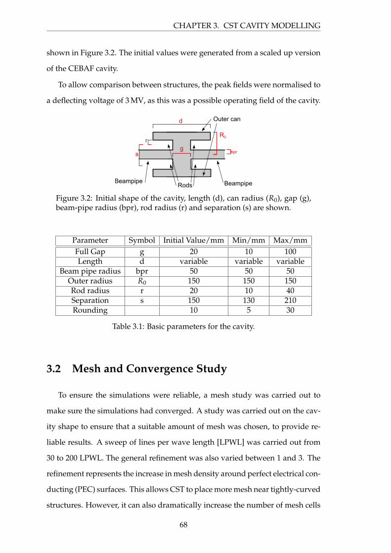
CHAPTER 3. CST CAVITY MODELLING
shown in Figure 3.2. The initial values were generated from a scaled up version
of the CEBAF cavity.
To allow comparison between structures, the peak fields were normalised to
a deflecting voltage of 3 MV, as this was a possible operating field of the cavity.
R
bpr
0
d
gr
s
Outer can
Rods BeampipeBeampipe
Figure 3.2: Initial shape of the cavity, length (d), can radius (R0), gap (g),beam-pipe radius (bpr), rod radius (r) and separation (s) are shown.
Parameter Symbol Initial Value/mm Min/mm Max/mmFull Gap g 20 10 100Length d variable variable variable
Beam pipe radius bpr 50 50 50Outer radius R0 150 150 150Rod radius r 20 10 40Separation s 150 130 210Rounding 10 5 30
Table 3.1: Basic parameters for the cavity.
3.2 Mesh and Convergence Study
To ensure the simulations were reliable, a mesh study was carried out to
make sure the simulations had converged. A study was carried out on the cav-
ity shape to ensure that a suitable amount of mesh was chosen, to provide re-
liable results. A sweep of lines per wave length [LPWL] was carried out from
30 to 200 LPWL. The general refinement was also varied between 1 and 3. The
refinement represents the increase in mesh density around perfect electrical con-
ducting (PEC) surfaces. This allows CST to place more mesh near tightly-curved
structures. However, it can also dramatically increase the number of mesh cells
68
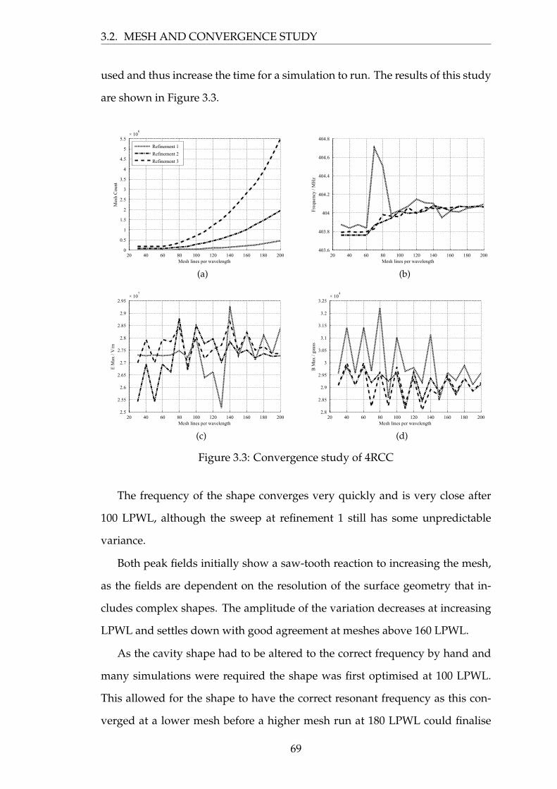
3.2. MESH AND CONVERGENCE STUDY
used and thus increase the time for a simulation to run. The results of this study
are shown in Figure 3.3.
Mesh lines per wavelength
Mes
h C
ount
20 40 60 80 100 120 140 160 180 2000
0.5
1
1.5
2
2.5
3
3.5
4
4.5
5
5.5× 10
6
Refinement 1
Refinement 2
Refinement 3
(a)Mesh lines per wavelength
Fre
quen
cy /
MH
z
20 40 60 80 100 120 140 160 180 200403.6
403.8
404
404.2
404.4
404.6
404.8
(b)
Mesh lines per wavelength
E M
ax /
V/m
20 40 60 80 100 120 140 160 180 2002.5
2.55
2.6
2.65
2.7
2.75
2.8
2.85
2.9
2.95× 10
7
(c)Mesh lines per wavelength
B M
ax /
gaus
s
20 40 60 80 100 120 140 160 180 2002.8
2.85
2.9
2.95
3
3.05
3.1
3.15
3.2
3.25× 10
4
(d)
Figure 3.3: Convergence study of 4RCC
The frequency of the shape converges very quickly and is very close after
100 LPWL, although the sweep at refinement 1 still has some unpredictable
variance.
Both peak fields initially show a saw-tooth reaction to increasing the mesh,
as the fields are dependent on the resolution of the surface geometry that in-
cludes complex shapes. The amplitude of the variation decreases at increasing
LPWL and settles down with good agreement at meshes above 160 LPWL.
As the cavity shape had to be altered to the correct frequency by hand and
many simulations were required the shape was first optimised at 100 LPWL.
This allowed for the shape to have the correct resonant frequency as this con-
verged at a lower mesh before a higher mesh run at 180 LPWL could finalise
69
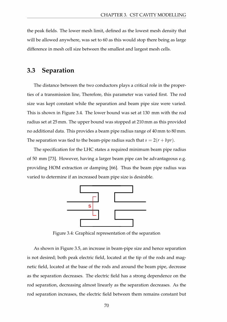
CHAPTER 3. CST CAVITY MODELLING
the peak fields. The lower mesh limit, defined as the lowest mesh density that
will be allowed anywhere, was set to 60 as this would stop there being as large
difference in mesh cell size between the smallest and largest mesh cells.
3.3 Separation
The distance between the two conductors plays a critical role in the proper-
ties of a transmission line, Therefore, this parameter was varied first. The rod
size was kept constant while the separation and beam pipe size were varied.
This is shown in Figure 3.4. The lower bound was set at 130 mm with the rod
radius set at 25 mm. The upper bound was stopped at 210 mm as this provided
no additional data. This provides a beam pipe radius range of 40 mm to 80 mm.
The separation was tied to the beam-pipe radius such that s = 2(r + bpr).
The specification for the LHC states a required minimum beam pipe radius
of 50 mm [73]. However, having a larger beam pipe can be advantageous e.g.
providing HOM extraction or damping [66]. Thus the beam pipe radius was
varied to determine if an increased beam pipe size is desirable.
s
Figure 3.4: Graphical representation of the separation
As shown in Figure 3.5, an increase in beam-pipe size and hence separation
is not desired; both peak electric field, located at the tip of the rods and mag-
netic field, located at the base of the rods and around the beam pipe, decrease
as the separation decreases. The electric field has a strong dependence on the
rod separation, decreasing almost linearly as the separation decreases. As the
rod separation increases, the electric field between them remains constant but
70
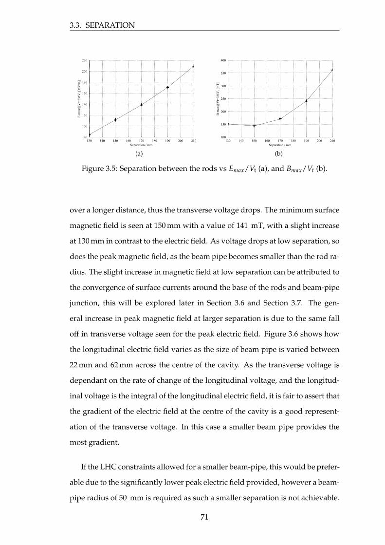
3.3. SEPARATION
Separation / mm
E m
ax@
Vt=
3MV
, [M
V/m
]
130 140 150 160 170 180 190 200 21080
100
120
140
160
180
200
220
(a)Separation / mm
B m
ax@
Vt=
3MV
, [m
T]
130 140 150 160 170 180 190 200 210100
150
200
250
300
350
400
(b)
Figure 3.5: Separation between the rods vs Emax/Vt (a), and Bmax/Vt (b).
over a longer distance, thus the transverse voltage drops. The minimum surface
magnetic field is seen at 150 mm with a value of 141 mT, with a slight increase
at 130 mm in contrast to the electric field. As voltage drops at low separation, so
does the peak magnetic field, as the beam pipe becomes smaller than the rod ra-
dius. The slight increase in magnetic field at low separation can be attributed to
the convergence of surface currents around the base of the rods and beam-pipe
junction, this will be explored later in Section 3.6 and Section 3.7. The gen-
eral increase in peak magnetic field at larger separation is due to the same fall
off in transverse voltage seen for the peak electric field. Figure 3.6 shows how
the longitudinal electric field varies as the size of beam pipe is varied between
22 mm and 62 mm across the centre of the cavity. As the transverse voltage is
dependant on the rate of change of the longitudinal voltage, and the longitud-
inal voltage is the integral of the longitudinal electric field, it is fair to assert that
the gradient of the electric field at the centre of the cavity is a good represent-
ation of the transverse voltage. In this case a smaller beam pipe provides the
most gradient.
If the LHC constraints allowed for a smaller beam-pipe, this would be prefer-
able due to the significantly lower peak electric field provided, however a beam-
pipe radius of 50 mm is required as such a smaller separation is not achievable.
71
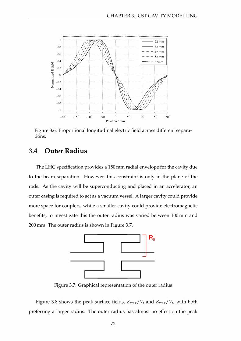
CHAPTER 3. CST CAVITY MODELLING
Position / mm
Nor
mal
ized
E f
ield
-200 -150 -100 -50 0 50 100 150 200
-1
-0.8
-0.6
-0.4
-0.2
0
0.2
0.4
0.6
0.8
1 22 mm
32 mm
42 mm
52 mm
62mm
Figure 3.6: Proportional longitudinal electric field across different separa-tions.
3.4 Outer Radius
The LHC specification provides a 150 mm radial envelope for the cavity due
to the beam separation. However, this constraint is only in the plane of the
rods. As the cavity will be superconducting and placed in an accelerator, an
outer casing is required to act as a vacuum vessel. A larger cavity could provide
more space for couplers, while a smaller cavity could provide electromagnetic
benefits, to investigate this the outer radius was varied between 100 mm and
200 mm. The outer radius is shown in Figure 3.7.
R0
Figure 3.7: Graphical representation of the outer radius
Figure 3.8 shows the peak surface fields, Emax/Vt and Bmax/Vt, with both
preferring a larger radius. The outer radius has almost no effect on the peak
72
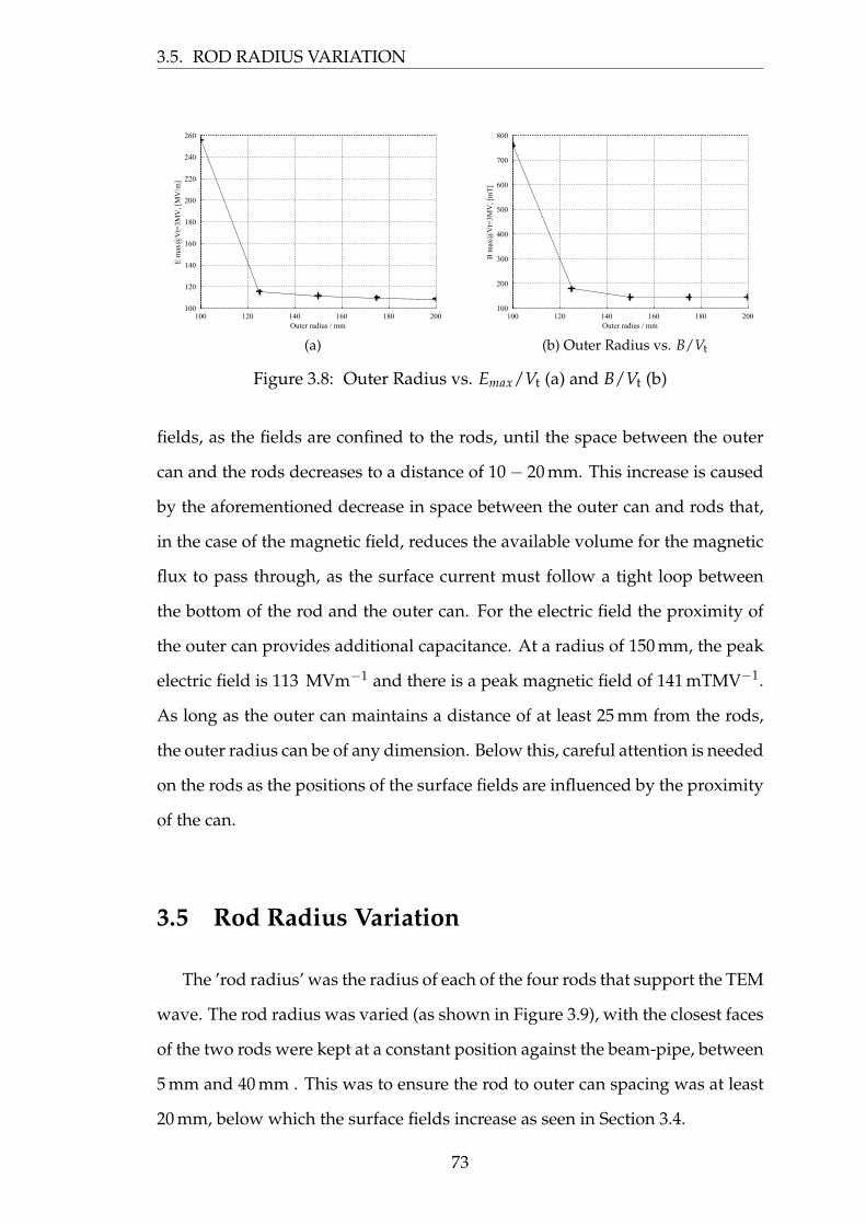
3.5. ROD RADIUS VARIATION
Outer radius / mm
E m
ax@
Vt=
3MV
, [M
V/m
]
100 120 140 160 180 200100
120
140
160
180
200
220
240
260
(a)Outer radius / mm
B m
ax@
Vt=
3MV
, [m
T]
100 120 140 160 180 200100
200
300
400
500
600
700
800
(b) Outer Radius vs. B/Vt
Figure 3.8: Outer Radius vs. Emax/Vt (a) and B/Vt (b)
fields, as the fields are confined to the rods, until the space between the outer
can and the rods decreases to a distance of 10− 20 mm. This increase is caused
by the aforementioned decrease in space between the outer can and rods that,
in the case of the magnetic field, reduces the available volume for the magnetic
flux to pass through, as the surface current must follow a tight loop between
the bottom of the rod and the outer can. For the electric field the proximity of
the outer can provides additional capacitance. At a radius of 150 mm, the peak
electric field is 113 MVm−1 and there is a peak magnetic field of 141 mTMV−1.
As long as the outer can maintains a distance of at least 25 mm from the rods,
the outer radius can be of any dimension. Below this, careful attention is needed
on the rods as the positions of the surface fields are influenced by the proximity
of the can.
3.5 Rod Radius Variation
The ’rod radius’ was the radius of each of the four rods that support the TEM
wave. The rod radius was varied (as shown in Figure 3.9), with the closest faces
of the two rods were kept at a constant position against the beam-pipe, between
5 mm and 40 mm . This was to ensure the rod to outer can spacing was at least
20 mm, below which the surface fields increase as seen in Section 3.4.
73
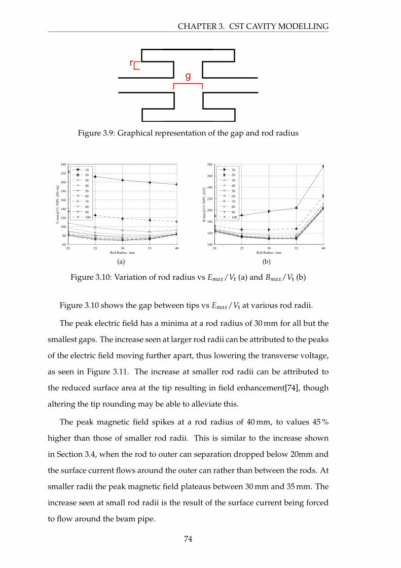
CHAPTER 3. CST CAVITY MODELLING
gr
Figure 3.9: Graphical representation of the gap and rod radius
Rod Radius / mm
E m
ax@
Vt=
3MV
, [M
v/m
]
20 25 30 35 4060
80
100
120
140
160
180
200
220
240
10
20
30
40
50
60
70
80
90
100
(a)Rod Radius / mm
B m
ax@
Vt=
3MV
, [m
T]
20 25 30 35 40140
160
180
200
220
240
260
280
10
20
30
40
50
60
70
80
90
100
(b)
Figure 3.10: Variation of rod radius vs Emax/Vt (a) and Bmax/Vt (b)
Figure 3.10 shows the gap between tips vs Emax/Vt at various rod radii.
The peak electric field has a minima at a rod radius of 30 mm for all but the
smallest gaps. The increase seen at larger rod radii can be attributed to the peaks
of the electric field moving further apart, thus lowering the transverse voltage,
as seen in Figure 3.11. The increase at smaller rod radii can be attributed to
the reduced surface area at the tip resulting in field enhancement[74], though
altering the tip rounding may be able to alleviate this.
The peak magnetic field spikes at a rod radius of 40 mm, to values 45 %
higher than those of smaller rod radii. This is similar to the increase shown
in Section 3.4, when the rod to outer can separation dropped below 20mm and
the surface current flows around the outer can rather than between the rods. At
smaller radii the peak magnetic field plateaus between 30 mm and 35 mm. The
increase seen at small rod radii is the result of the surface current being forced
to flow around the beam pipe.
74
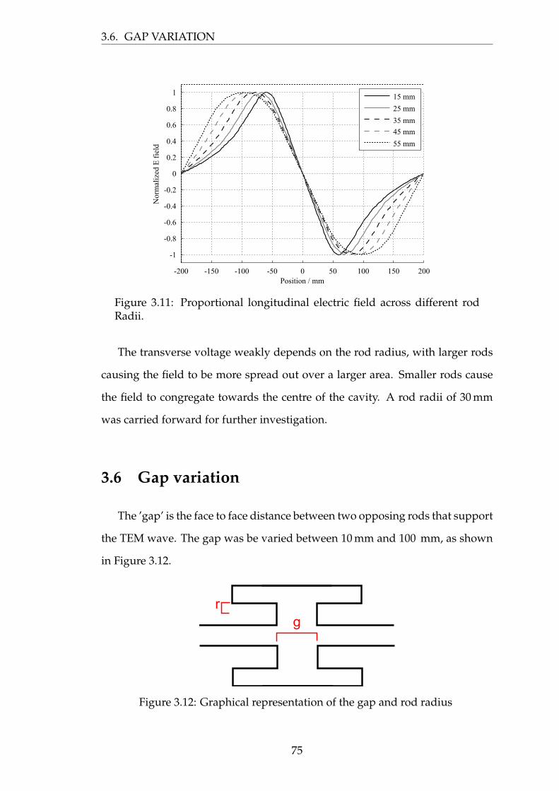
3.6. GAP VARIATION
Position / mm
Nor
mal
ized
E f
ield
-200 -150 -100 -50 0 50 100 150 200
-1
-0.8
-0.6
-0.4
-0.2
0
0.2
0.4
0.6
0.8
1 15 mm
25 mm
35 mm
45 mm
55 mm
Figure 3.11: Proportional longitudinal electric field across different rodRadii.
The transverse voltage weakly depends on the rod radius, with larger rods
causing the field to be more spread out over a larger area. Smaller rods cause
the field to congregate towards the centre of the cavity. A rod radii of 30 mm
was carried forward for further investigation.
3.6 Gap variation
The ’gap’ is the face to face distance between two opposing rods that support
the TEM wave. The gap was be varied between 10 mm and 100 mm, as shown
in Figure 3.12.
gr
Figure 3.12: Graphical representation of the gap and rod radius
75
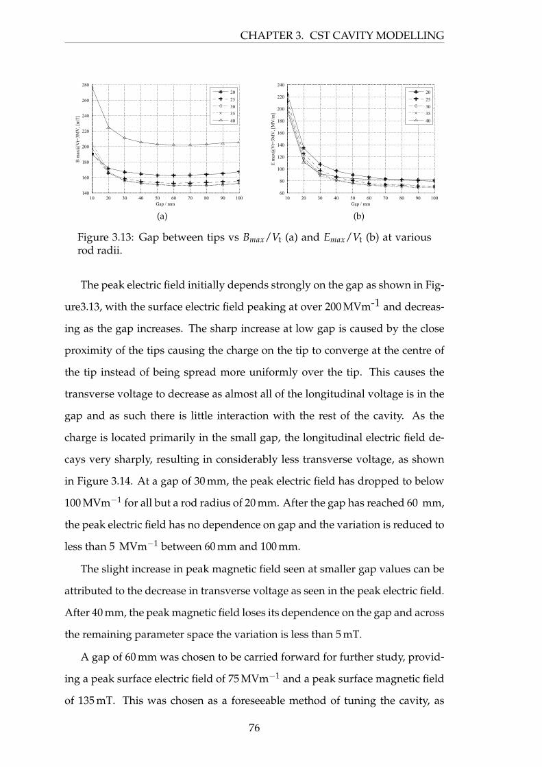
CHAPTER 3. CST CAVITY MODELLING
Gap / mm
B m
ax@
Vt=
3MV
, [m
T]
10 20 30 40 50 60 70 80 90 100140
160
180
200
220
240
260
280
20
25
30
35
40
(a)Gap / mm
E m
ax@
Vt=
3MV
, [M
V/m
]
10 20 30 40 50 60 70 80 90 10060
80
100
120
140
160
180
200
220
240
20
25
30
35
40
(b)
Figure 3.13: Gap between tips vs Bmax/Vt (a) and Emax/Vt (b) at variousrod radii.
The peak electric field initially depends strongly on the gap as shown in Fig-
ure3.13, with the surface electric field peaking at over 200 MVm-1 and decreas-
ing as the gap increases. The sharp increase at low gap is caused by the close
proximity of the tips causing the charge on the tip to converge at the centre of
the tip instead of being spread more uniformly over the tip. This causes the
transverse voltage to decrease as almost all of the longitudinal voltage is in the
gap and as such there is little interaction with the rest of the cavity. As the
charge is located primarily in the small gap, the longitudinal electric field de-
cays very sharply, resulting in considerably less transverse voltage, as shown
in Figure 3.14. At a gap of 30 mm, the peak electric field has dropped to below
100 MVm−1 for all but a rod radius of 20 mm. After the gap has reached 60 mm,
the peak electric field has no dependence on gap and the variation is reduced to
less than 5 MVm−1 between 60 mm and 100 mm.
The slight increase in peak magnetic field seen at smaller gap values can be
attributed to the decrease in transverse voltage as seen in the peak electric field.
After 40 mm, the peak magnetic field loses its dependence on the gap and across
the remaining parameter space the variation is less than 5 mT.
A gap of 60 mm was chosen to be carried forward for further study, provid-
ing a peak surface electric field of 75 MVm−1 and a peak surface magnetic field
of 135 mT. This was chosen as a foreseeable method of tuning the cavity, as
76
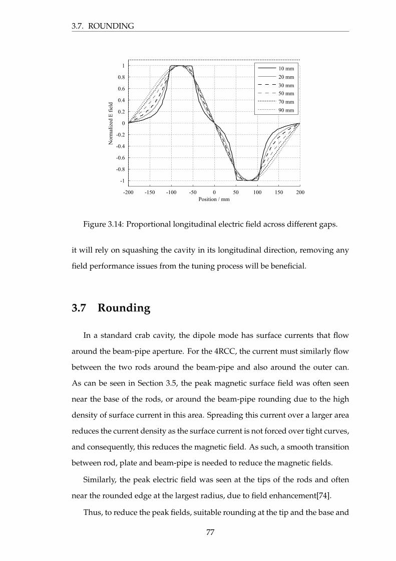
3.7. ROUNDING
Position / mm
Nor
mal
ized
E f
ield
-200 -150 -100 -50 0 50 100 150 200
-1
-0.8
-0.6
-0.4
-0.2
0
0.2
0.4
0.6
0.8
1 10 mm
20 mm
30 mm
50 mm
70 mm
90 mm
Figure 3.14: Proportional longitudinal electric field across different gaps.
it will rely on squashing the cavity in its longitudinal direction, removing any
field performance issues from the tuning process will be beneficial.
3.7 Rounding
In a standard crab cavity, the dipole mode has surface currents that flow
around the beam-pipe aperture. For the 4RCC, the current must similarly flow
between the two rods around the beam-pipe and also around the outer can.
As can be seen in Section 3.5, the peak magnetic surface field was often seen
near the base of the rods, or around the beam-pipe rounding due to the high
density of surface current in this area. Spreading this current over a larger area
reduces the current density as the surface current is not forced over tight curves,
and consequently, this reduces the magnetic field. As such, a smooth transition
between rod, plate and beam-pipe is needed to reduce the magnetic fields.
Similarly, the peak electric field was seen at the tips of the rods and often
near the rounded edge at the largest radius, due to field enhancement[74].
Thus, to reduce the peak fields, suitable rounding at the tip and the base and
77
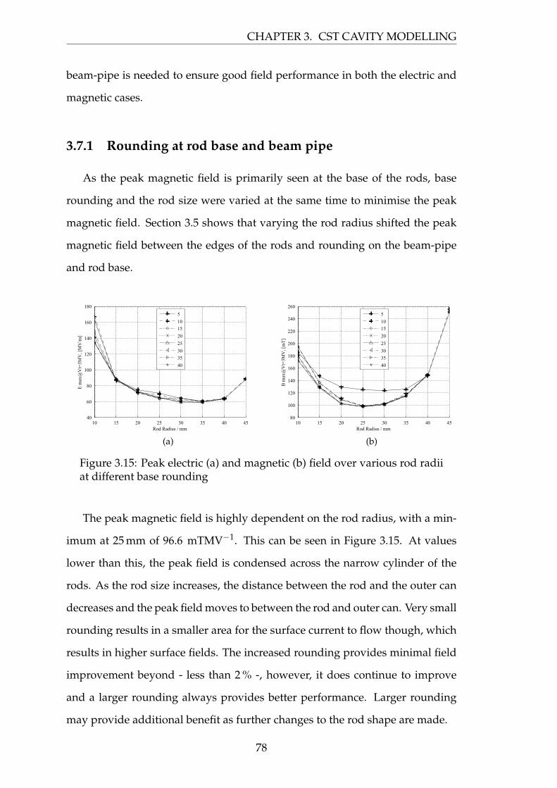
CHAPTER 3. CST CAVITY MODELLING
beam-pipe is needed to ensure good field performance in both the electric and
magnetic cases.
3.7.1 Rounding at rod base and beam pipe
As the peak magnetic field is primarily seen at the base of the rods, base
rounding and the rod size were varied at the same time to minimise the peak
magnetic field. Section 3.5 shows that varying the rod radius shifted the peak
magnetic field between the edges of the rods and rounding on the beam-pipe
and rod base.
Rod Radius / mm
E m
ax@
Vt=
3MV
, [M
V/m
]
10 15 20 25 30 35 40 4540
60
80
100
120
140
160
180
5
10
15
20
25
30
35
40
(a)Rod Radius / mm
B m
ax@
Vt=
3MV
, [m
T]
10 15 20 25 30 35 40 4580
100
120
140
160
180
200
220
240
260
5
10
15
20
25
30
35
40
(b)
Figure 3.15: Peak electric (a) and magnetic (b) field over various rod radiiat different base rounding
The peak magnetic field is highly dependent on the rod radius, with a min-
imum at 25 mm of 96.6 mTMV−1. This can be seen in Figure 3.15. At values
lower than this, the peak field is condensed across the narrow cylinder of the
rods. As the rod size increases, the distance between the rod and the outer can
decreases and the peak field moves to between the rod and outer can. Very small
rounding results in a smaller area for the surface current to flow though, which
results in higher surface fields. The increased rounding provides minimal field
improvement beyond - less than 2 % -, however, it does continue to improve
and a larger rounding always provides better performance. Larger rounding
may provide additional benefit as further changes to the rod shape are made.
78
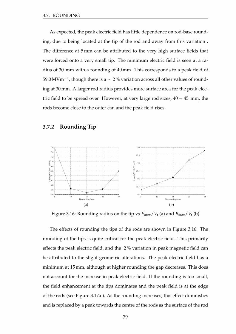
3.7. ROUNDING
As expected, the peak electric field has little dependence on rod-base round-
ing, due to being located at the tip of the rod and away from this variation .
The difference at 5 mm can be attributed to the very high surface fields that
were forced onto a very small tip. The minimum electric field is seen at a ra-
dius of 30 mm with a rounding of 40 mm. This corresponds to a peak field of
59.0 MVm−1, though there is a ∼ 2 % variation across all other values of round-
ing at 30 mm. A larger rod radius provides more surface area for the peak elec-
tric field to be spread over. However, at very large rod sizes, 40− 45 mm, the
rods become close to the outer can and the peak field rises.
3.7.2 Rounding Tip
Tip rounding / mm
E m
ax@
Vt=
3MV
, [M
v/m
]
5 10 15 20 2556
58
60
62
64
66
68
70
72
74
76
(a)Tip rounding / mm
B m
ax@
Vt=
3MV
, [m
T]
5 10 15 20 2593
93.5
94
94.5
95
95.5
96
(b)
Figure 3.16: Rounding radius on the tip vs Emax/Vt (a) and Bmax/Vt (b)
The effects of rounding the tips of the rods are shown in Figure 3.16. The
rounding of the tips is quite critical for the peak electric field. This primarily
effects the peak electric field, and the 2 % variation in peak magnetic field can
be attributed to the slight geometric alterations. The peak electric field has a
minimum at 15 mm, although at higher rounding the gap decreases. This does
not account for the increase in peak electric field. If the rounding is too small,
the field enhancement at the tips dominates and the peak field is at the edge
of the rods (see Figure 3.17a ). As the rounding increases, this effect diminishes
and is replaced by a peak towards the centre of the rods as the surface of the rod
79
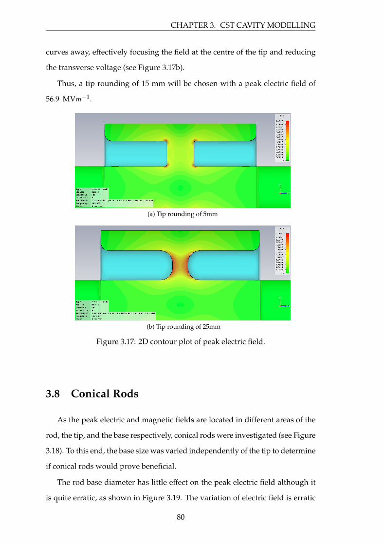
CHAPTER 3. CST CAVITY MODELLING
curves away, effectively focusing the field at the centre of the tip and reducing
the transverse voltage (see Figure 3.17b).
Thus, a tip rounding of 15 mm will be chosen with a peak electric field of
56.9 MVm−1.
(a) Tip rounding of 5mm
(b) Tip rounding of 25mm
Figure 3.17: 2D contour plot of peak electric field.
3.8 Conical Rods
As the peak electric and magnetic fields are located in different areas of the
rod, the tip, and the base respectively, conical rods were investigated (see Figure
3.18). To this end, the base size was varied independently of the tip to determine
if conical rods would prove beneficial.
The rod base diameter has little effect on the peak electric field although it
is quite erratic, as shown in Figure 3.19. The variation of electric field is erratic
80
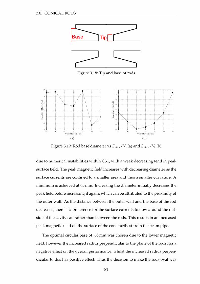
3.8. CONICAL RODS
Base Tip
Figure 3.18: Tip and base of rods
Conical base size / mm
E m
ax@
Vt=
3MV
, [M
V/m
]
55 60 65 70 75 80 8549
50
51
52
53
54
55
(a)Conical base size / mm
B m
ax@
Vt=
3MV
, [m
T]
55 60 65 70 75 80 8596
98
100
102
104
106
108
110
112
(b)
Figure 3.19: Rod base diameter vs Emax/Vt (a) and Bmax/Vt (b)
due to numerical instabilities within CST, with a weak decreasing tend in peak
surface field. The peak magnetic field increases with decreasing diameter as the
surface currents are confined to a smaller area and thus a smaller curvature. A
minimum is achieved at 65 mm. Increasing the diameter initially decreases the
peak field before increasing it again, which can be attributed to the proximity of
the outer wall. As the distance between the outer wall and the base of the rod
decreases, there is a preference for the surface currents to flow around the out-
side of the cavity can rather than between the rods. This results in an increased
peak magnetic field on the surface of the cone furthest from the beam pipe.
The optimal circular base of 65 mm was chosen due to the lower magnetic
field, however the increased radius perpendicular to the plane of the rods has a
negative effect on the overall performance, whilst the increased radius perpen-
dicular to this has positive effect. Thus the decision to make the rods oval was
81
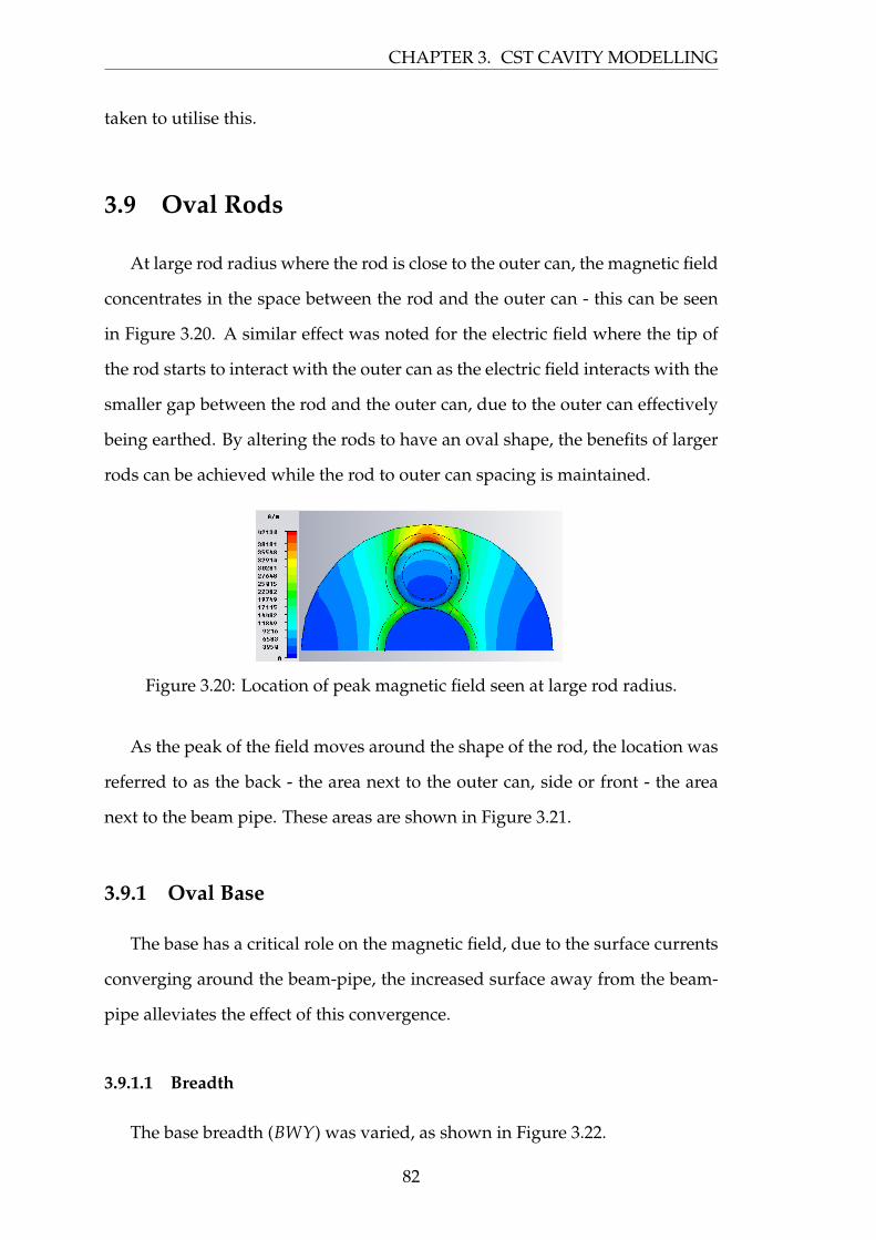
CHAPTER 3. CST CAVITY MODELLING
taken to utilise this.
3.9 Oval Rods
At large rod radius where the rod is close to the outer can, the magnetic field
concentrates in the space between the rod and the outer can - this can be seen
in Figure 3.20. A similar effect was noted for the electric field where the tip of
the rod starts to interact with the outer can as the electric field interacts with the
smaller gap between the rod and the outer can, due to the outer can effectively
being earthed. By altering the rods to have an oval shape, the benefits of larger
rods can be achieved while the rod to outer can spacing is maintained.
Figure 3.20: Location of peak magnetic field seen at large rod radius.
As the peak of the field moves around the shape of the rod, the location was
referred to as the back - the area next to the outer can, side or front - the area
next to the beam pipe. These areas are shown in Figure 3.21.
3.9.1 Oval Base
The base has a critical role on the magnetic field, due to the surface currents
converging around the beam-pipe, the increased surface away from the beam-
pipe alleviates the effect of this convergence.
3.9.1.1 Breadth
The base breadth (BWY) was varied, as shown in Figure 3.22.
82
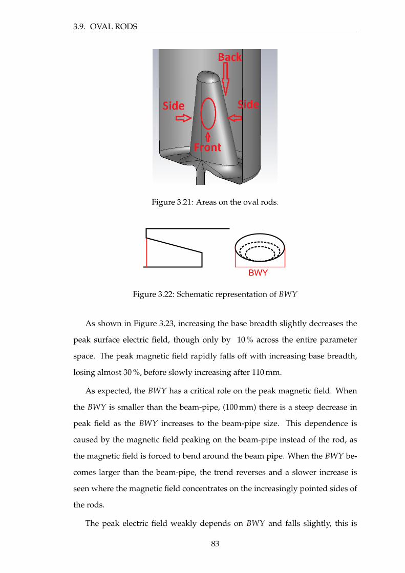
3.9. OVAL RODS
Figure 3.21: Areas on the oval rods.
BWY
Figure 3.22: Schematic representation of BWY
As shown in Figure 3.23, increasing the base breadth slightly decreases the
peak surface electric field, though only by 10 % across the entire parameter
space. The peak magnetic field rapidly falls off with increasing base breadth,
losing almost 30 %, before slowly increasing after 110 mm.
As expected, the BWY has a critical role on the peak magnetic field. When
the BWY is smaller than the beam-pipe, (100 mm) there is a steep decrease in
peak field as the BWY increases to the beam-pipe size. This dependence is
caused by the magnetic field peaking on the beam-pipe instead of the rod, as
the magnetic field is forced to bend around the beam pipe. When the BWY be-
comes larger than the beam-pipe, the trend reverses and a slower increase is
seen where the magnetic field concentrates on the increasingly pointed sides of
the rods.
The peak electric field weakly depends on BWY and falls slightly, this is
83
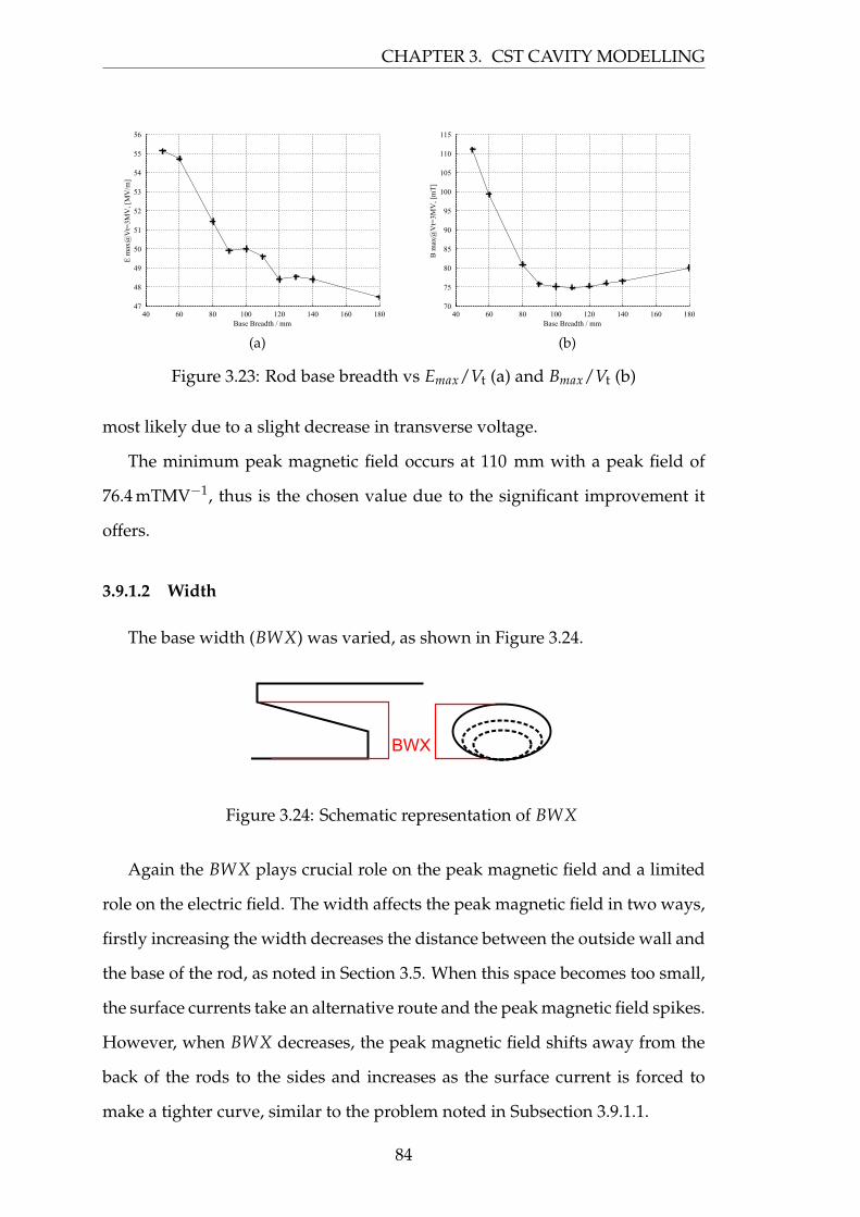
CHAPTER 3. CST CAVITY MODELLING
Base Breadth / mm
E m
ax@
Vt=
3MV
, [M
V/m
]
40 60 80 100 120 140 160 18047
48
49
50
51
52
53
54
55
56
(a)Base Breadth / mm
B m
ax@
Vt=
3MV
, [m
T]
40 60 80 100 120 140 160 18070
75
80
85
90
95
100
105
110
115
(b)
Figure 3.23: Rod base breadth vs Emax/Vt (a) and Bmax/Vt (b)
most likely due to a slight decrease in transverse voltage.
The minimum peak magnetic field occurs at 110 mm with a peak field of
76.4 mTMV−1, thus is the chosen value due to the significant improvement it
offers.
3.9.1.2 Width
The base width (BWX) was varied, as shown in Figure 3.24.
BWX
Figure 3.24: Schematic representation of BWX
Again the BWX plays crucial role on the peak magnetic field and a limited
role on the electric field. The width affects the peak magnetic field in two ways,
firstly increasing the width decreases the distance between the outside wall and
the base of the rod, as noted in Section 3.5. When this space becomes too small,
the surface currents take an alternative route and the peak magnetic field spikes.
However, when BWX decreases, the peak magnetic field shifts away from the
back of the rods to the sides and increases as the surface current is forced to
make a tighter curve, similar to the problem noted in Subsection 3.9.1.1.
84
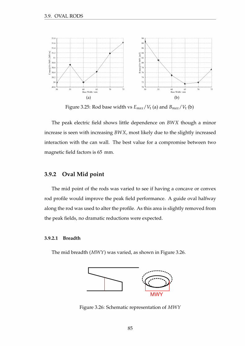
3.9. OVAL RODS
Base Width / mm
E m
ax@
Vt=
3MV
, [M
V/m
]
50 55 60 65 70 7549.8
50
50.2
50.4
50.6
50.8
51
51.2
51.4
51.6
51.8
(a)Base Width / mm
B m
ax@
Vt=
3MV
, [m
T]
50 55 60 65 70 7570
72
74
76
78
80
82
84
86
88
90
(b)
Figure 3.25: Rod base width vs Emax/Vt (a) and Bmax/Vt (b)
The peak electric field shows little dependence on BWX though a minor
increase is seen with increasing BWX, most likely due to the slightly increased
interaction with the can wall. The best value for a compromise between two
magnetic field factors is 65 mm.
3.9.2 Oval Mid point
The mid point of the rods was varied to see if having a concave or convex
rod profile would improve the peak field performance. A guide oval halfway
along the rod was used to alter the profile. As this area is slightly removed from
the peak fields, no dramatic reductions were expected.
3.9.2.1 Breadth
The mid breadth (MWY) was varied, as shown in Figure 3.26.
MWY
Figure 3.26: Schematic representation of MWY
85
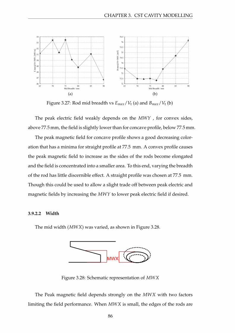
CHAPTER 3. CST CAVITY MODELLING
Mid Breadth / mm
E m
ax@
Vt=
3MV
, [M
V/m
]
65 70 75 80 85 9046
47
48
49
50
51
52
53
54
(a)Mid Breadth / mm
B m
ax@
Vt=
3MV
, [m
T]
65 70 75 80 85 9072
72.5
73
73.5
74
74.5
75
75.5
76
76.5
(b)
Figure 3.27: Rod mid breadth vs Emax/Vt (a) and Bmax/Vt (b)
The peak electric field weakly depends on the MWY , for convex sides,
above 77.5 mm, the field is slightly lower than for concave profile, below 77.5 mm.
The peak magnetic field for concave profile shows a good decreasing color-
ation that has a minima for straight profile at 77.5 mm. A convex profile causes
the peak magnetic field to increase as the sides of the rods become elongated
and the field is concentrated into a smaller area. To this end, varying the breadth
of the rod has little discernible effect. A straight profile was chosen at 77.5 mm.
Though this could be used to allow a slight trade off between peak electric and
magnetic fields by increasing the MWY to lower peak electric field if desired.
3.9.2.2 Width
The mid width (MWX) was varied, as shown in Figure 3.28.
MWX
Figure 3.28: Schematic representation of MWX
The Peak magnetic field depends strongly on the MWX with two factors
limiting the field performance. When MWX is small, the edges of the rods are
86
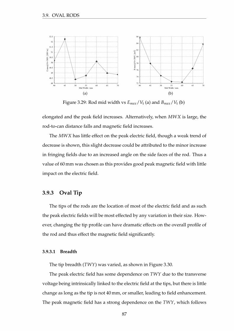
3.9. OVAL RODS
Mid Width / mm
E m
ax@
Vt=
3MV
, [M
V/m
]
40 45 50 55 60 65 7048
48.5
49
49.5
50
50.5
51
51.5
52
52.5
(a)Mid Width / mm
B m
ax@
Vt=
3MV
, [m
T]
40 45 50 55 60 65 7072
74
76
78
80
82
84
86
(b)
Figure 3.29: Rod mid width vs Emax/Vt (a) and Bmax/Vt (b)
elongated and the peak field increases. Alternatively, when MWX is large, the
rod-to-can distance falls and magnetic field increases.
The MWX has little effect on the peak electric field, though a weak trend of
decrease is shown, this slight decrease could be attributed to the minor increase
in fringing fields due to an increased angle on the side faces of the rod. Thus a
value of 60 mm was chosen as this provides good peak magnetic field with little
impact on the electric field.
3.9.3 Oval Tip
The tips of the rods are the location of most of the electric field and as such
the peak electric fields will be most effected by any variation in their size. How-
ever, changing the tip profile can have dramatic effects on the overall profile of
the rod and thus effect the magnetic field significantly.
3.9.3.1 Breadth
The tip breadth (TWY) was varied, as shown in Figure 3.30.
The peak electric field has some dependence on TWY due to the transverse
voltage being intrinsically linked to the electric field at the tips, but there is little
change as long as the tip is not 40 mm, or smaller, leading to field enhancement.
The peak magnetic field has a strong dependence on the TWY, which follows
87
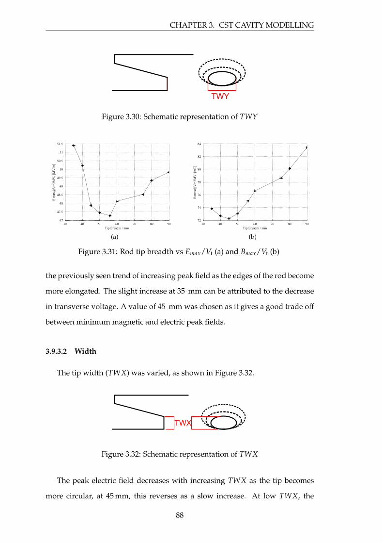
CHAPTER 3. CST CAVITY MODELLING
TWY
Figure 3.30: Schematic representation of TWY
Tip Breadth / mm
E m
ax@
Vt=
3MV
, [M
V/m
]
30 40 50 60 70 80 9047
47.5
48
48.5
49
49.5
50
50.5
51
51.5
(a)Tip Breadth / mm
B m
ax@
Vt=
3MV
, [m
T]
30 40 50 60 70 80 9072
74
76
78
80
82
84
(b)
Figure 3.31: Rod tip breadth vs Emax/Vt (a) and Bmax/Vt (b)
the previously seen trend of increasing peak field as the edges of the rod become
more elongated. The slight increase at 35 mm can be attributed to the decrease
in transverse voltage. A value of 45 mm was chosen as it gives a good trade off
between minimum magnetic and electric peak fields.
3.9.3.2 Width
The tip width (TWX) was varied, as shown in Figure 3.32.
TWX
Figure 3.32: Schematic representation of TWX
The peak electric field decreases with increasing TWX as the tip becomes
more circular, at 45 mm, this reverses as a slow increase. At low TWX, the
88
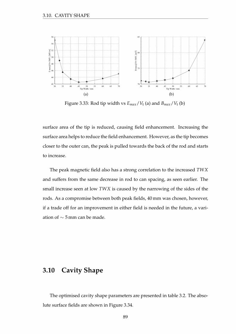
3.10. CAVITY SHAPE
Tip Width / mm
E m
ax@
Vt=
3MV
, [M
V/m
]
30 35 40 45 50 55 60 65 7042
44
46
48
50
52
54
56
(a)Tip Width / mm
B m
ax@
Vt=
3MV
, [m
T]
30 35 40 45 50 55 60 65 7070
75
80
85
(b)
Figure 3.33: Rod tip width vs Emax/Vt (a) and Bmax/Vt (b)
surface area of the tip is reduced, causing field enhancement. Increasing the
surface area helps to reduce the field enhancement. However, as the tip becomes
closer to the outer can, the peak is pulled towards the back of the rod and starts
to increase.
The peak magnetic field also has a strong correlation to the increased TWX
and suffers from the same decrease in rod to can spacing, as seen earlier. The
small increase seen at low TWX is caused by the narrowing of the sides of the
rods. As a compromise between both peak fields, 40 mm was chosen, however,
if a trade off for an improvement in either field is needed in the future, a vari-
ation of ∼ 5 mm can be made.
3.10 Cavity Shape
The optimised cavity shape parameters are presented in table 3.2. The abso-
lute surface fields are shown in Figure 3.34.
89
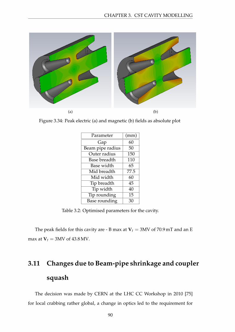
CHAPTER 3. CST CAVITY MODELLING
(a) (b)
Figure 3.34: Peak electric (a) and magnetic (b) fields as absolute plot
Parameter (mm)Gap 60
Beam pipe radius 50Outer radius 150Base breadth 110Base width 65
Mid breadth 77.5Mid width 60Tip breadth 45Tip width 40
Tip rounding 15Base rounding 30
Table 3.2: Optimised parameters for the cavity.
The peak fields for this cavity are - B max at Vt = 3MV of 70.9 mT and an E
max at Vt = 3MV of 43.8 MV.
3.11 Changes due to Beam-pipe shrinkage and coupler
squash
The decision was made by CERN at the LHC CC Workshop in 2010 [75]
for local crabbing rather global, a change in optics led to the requirement for
90
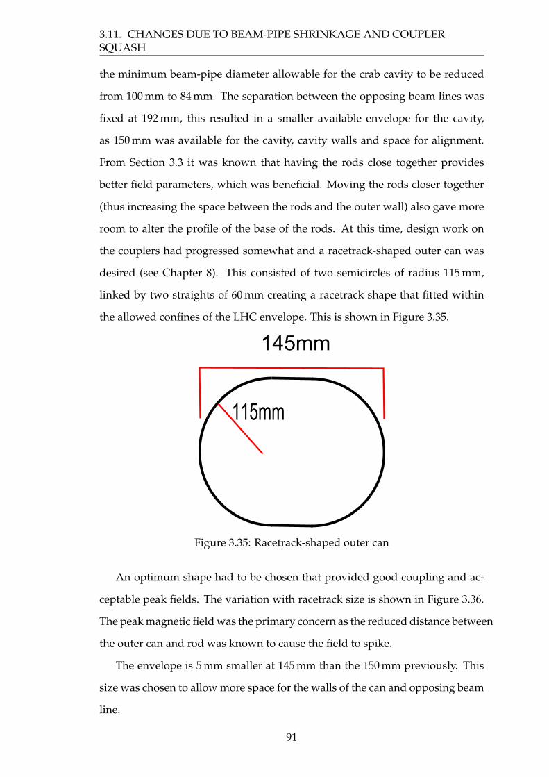
3.11. CHANGES DUE TO BEAM-PIPE SHRINKAGE AND COUPLERSQUASH
the minimum beam-pipe diameter allowable for the crab cavity to be reduced
from 100 mm to 84 mm. The separation between the opposing beam lines was
fixed at 192 mm, this resulted in a smaller available envelope for the cavity,
as 150 mm was available for the cavity, cavity walls and space for alignment.
From Section 3.3 it was known that having the rods close together provides
better field parameters, which was beneficial. Moving the rods closer together
(thus increasing the space between the rods and the outer wall) also gave more
room to alter the profile of the base of the rods. At this time, design work on
the couplers had progressed somewhat and a racetrack-shaped outer can was
desired (see Chapter 8). This consisted of two semicircles of radius 115 mm,
linked by two straights of 60 mm creating a racetrack shape that fitted within
the allowed confines of the LHC envelope. This is shown in Figure 3.35.
145mm
115mm
Figure 3.35: Racetrack-shaped outer can
An optimum shape had to be chosen that provided good coupling and ac-
ceptable peak fields. The variation with racetrack size is shown in Figure 3.36.
The peak magnetic field was the primary concern as the reduced distance between
the outer can and rod was known to cause the field to spike.
The envelope is 5 mm smaller at 145 mm than the 150 mm previously. This
size was chosen to allow more space for the walls of the can and opposing beam
line.
91
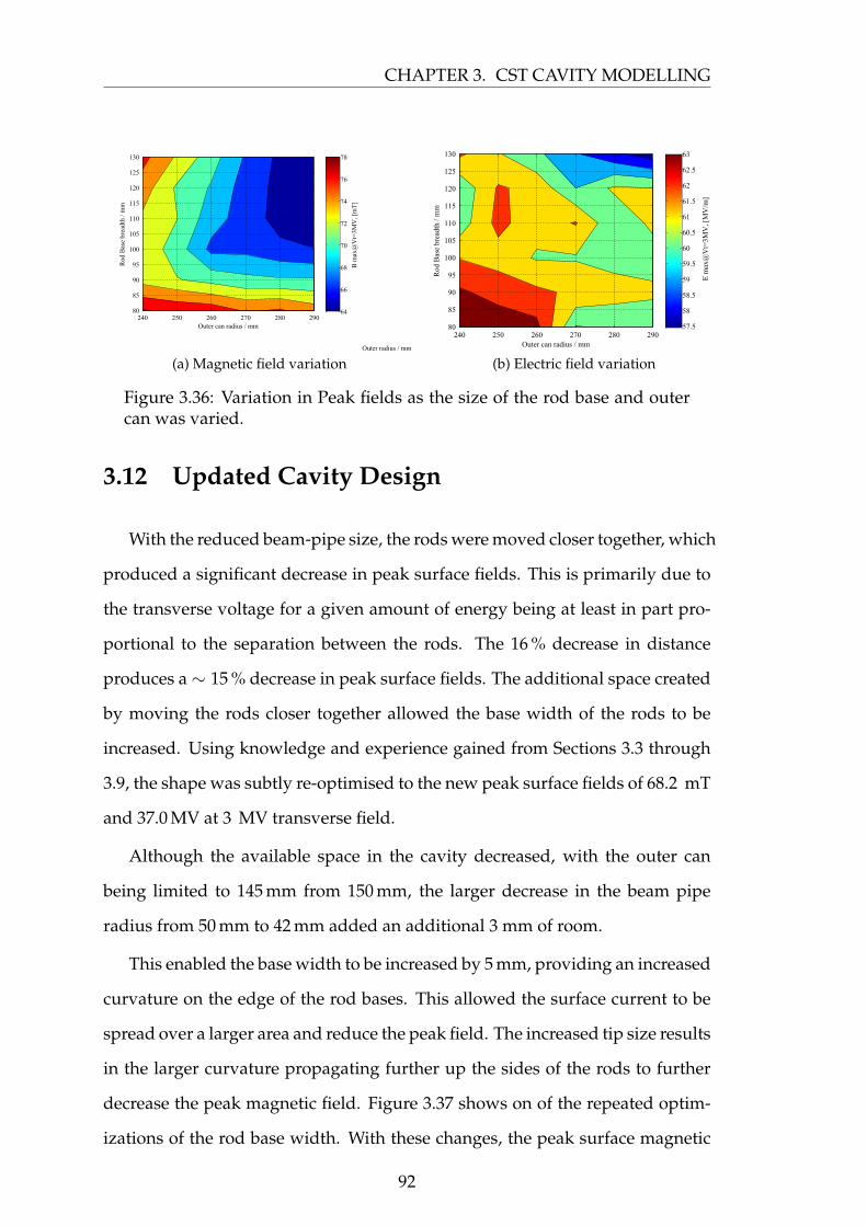
CHAPTER 3. CST CAVITY MODELLING
Outer can radius / mm
Rod
Bas
e br
eadt
h / m
m
240 250 260 270 280 29080
85
90
95
100
105
110
115
120
125
130
64
66
68
70
72
74
76
78
Outer radius / mmB
max
@V
t=3M
V, [
mT
]
(a) Magnetic field variationOuter can radius / mm
Rod
Bas
e br
eadt
h / m
m
240 250 260 270 280 29080
85
90
95
100
105
110
115
120
125
130
57.5
58
58.5
59
59.5
60
60.5
61
61.5
62
62.5
63
E m
ax@
Vt=
3MV
, [M
V/m
]
(b) Electric field variation
Figure 3.36: Variation in Peak fields as the size of the rod base and outercan was varied.
3.12 Updated Cavity Design
With the reduced beam-pipe size, the rods were moved closer together, which
produced a significant decrease in peak surface fields. This is primarily due to
the transverse voltage for a given amount of energy being at least in part pro-
portional to the separation between the rods. The 16 % decrease in distance
produces a ∼ 15 % decrease in peak surface fields. The additional space created
by moving the rods closer together allowed the base width of the rods to be
increased. Using knowledge and experience gained from Sections 3.3 through
3.9, the shape was subtly re-optimised to the new peak surface fields of 68.2 mT
and 37.0 MV at 3 MV transverse field.
Although the available space in the cavity decreased, with the outer can
being limited to 145 mm from 150 mm, the larger decrease in the beam pipe
radius from 50 mm to 42 mm added an additional 3 mm of room.
This enabled the base width to be increased by 5 mm, providing an increased
curvature on the edge of the rod bases. This allowed the surface current to be
spread over a larger area and reduce the peak field. The increased tip size results
in the larger curvature propagating further up the sides of the rods to further
decrease the peak magnetic field. Figure 3.37 shows on of the repeated optim-
izations of the rod base width. With these changes, the peak surface magnetic
92
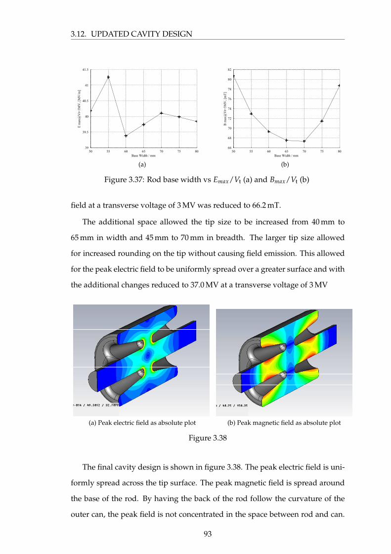
3.12. UPDATED CAVITY DESIGN
Base Width / mm
E m
ax@
Vt=
3MV
, [M
V/m
]
50 55 60 65 70 75 8039
39.5
40
40.5
41
41.5
(a)Base Width / mm
B m
ax@
Vt=
3MV
, [m
T]
50 55 60 65 70 75 8066
68
70
72
74
76
78
80
82
(b)
Figure 3.37: Rod base width vs Emax/Vt (a) and Bmax/Vt (b)
field at a transverse voltage of 3 MV was reduced to 66.2 mT.
The additional space allowed the tip size to be increased from 40 mm to
65 mm in width and 45 mm to 70 mm in breadth. The larger tip size allowed
for increased rounding on the tip without causing field emission. This allowed
for the peak electric field to be uniformly spread over a greater surface and with
the additional changes reduced to 37.0 MV at a transverse voltage of 3 MV
(a) Peak electric field as absolute plot (b) Peak magnetic field as absolute plot
Figure 3.38
The final cavity design is shown in figure 3.38. The peak electric field is uni-
formly spread across the tip surface. The peak magnetic field is spread around
the base of the rod. By having the back of the rod follow the curvature of the
outer can, the peak field is not concentrated in the space between rod and can.
93
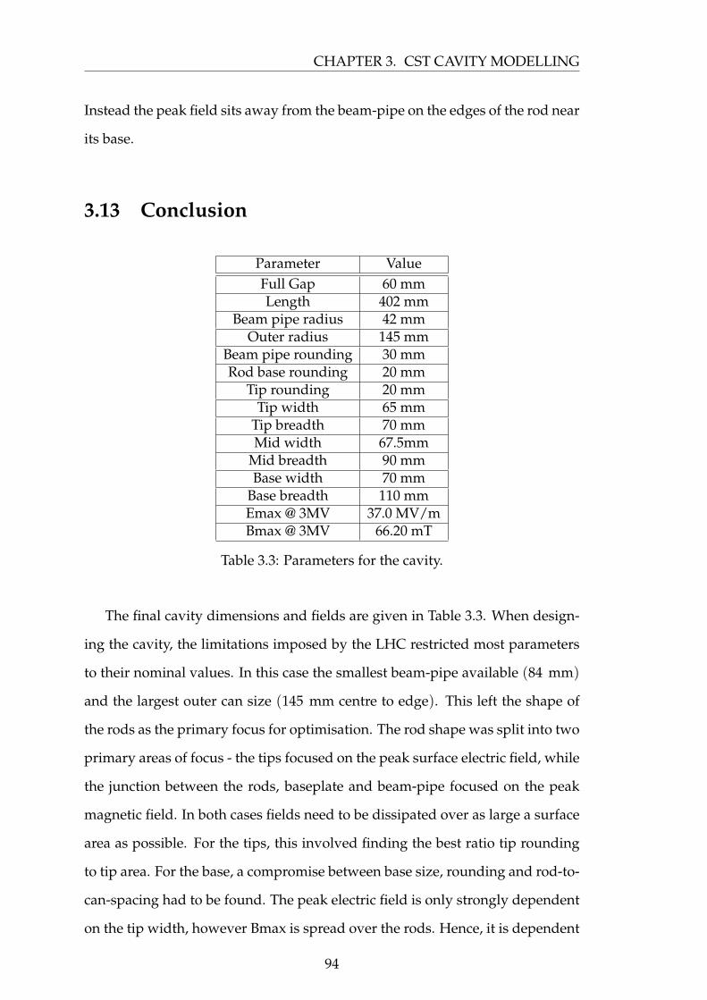
CHAPTER 3. CST CAVITY MODELLING
Instead the peak field sits away from the beam-pipe on the edges of the rod near
its base.
3.13 Conclusion
Parameter ValueFull Gap 60 mmLength 402 mm
Beam pipe radius 42 mmOuter radius 145 mm
Beam pipe rounding 30 mmRod base rounding 20 mm
Tip rounding 20 mmTip width 65 mm
Tip breadth 70 mmMid width 67.5mm
Mid breadth 90 mmBase width 70 mm
Base breadth 110 mmEmax @ 3MV 37.0 MV/mBmax @ 3MV 66.20 mT
Table 3.3: Parameters for the cavity.
The final cavity dimensions and fields are given in Table 3.3. When design-
ing the cavity, the limitations imposed by the LHC restricted most parameters
to their nominal values. In this case the smallest beam-pipe available (84 mm)
and the largest outer can size (145 mm centre to edge). This left the shape of
the rods as the primary focus for optimisation. The rod shape was split into two
primary areas of focus - the tips focused on the peak surface electric field, while
the junction between the rods, baseplate and beam-pipe focused on the peak
magnetic field. In both cases fields need to be dissipated over as large a surface
area as possible. For the tips, this involved finding the best ratio tip rounding
to tip area. For the base, a compromise between base size, rounding and rod-to-
can-spacing had to be found. The peak electric field is only strongly dependent
on the tip width, however Bmax is spread over the rods. Hence, it is dependent
94
3.13. CONCLUSION
on almost every parameter but is most sensitive to the base variation.
Electric field
The peak electric field is concentrated near the tips of the rods and as such
these should be the main focus for reducing the peak electric field. An increased
surface area at the tip is usually preferred for an increased surface area for the
electric field to be spread over, however this can cause problems for the peak
magnetic field. Rounding on the tips of the rods is critical as shown in Figure
3.17, too much and the field is forced into a smaller area, too little and the field
peaks at the edges. Thus an optimum must be found that evenly distributes the
field over the entire area.
Magnetic field
The peak magnetic field is located around the base of the rods, the beam-
pipe and the narrow sides of the rods. Rounding on the beam-pipe is critical
up to a point, then becomes insignificant once the peak is shifted away from the
beam pipe. At decreased beam-pipe radii, an increased rounding is necessary
over a larger beam-pipe radii. The size of the base of the rods greatly influences
the peak magnetic field, although the rod profile as a whole dictates the areas
where the peak field is located. A large base is optimal, though the distance
between the base of the rod and the outside wall, can be critical, if the distance
decreases the peak shifts from the narrow, sides of the rods to the face against
the outside wall often increasing in value. Similarly if the rods become too
elongated and narrow the field concentrates along these narrow edges, driving
up the peak magnetic field. The oval shape is necessary however, as the profile
of the base of the rods should extend beyond the edge of the beam pipe so
the surface currents do not converge around the beam pipe. Thus an optimum
shape must be found that allows for the greatest surface area around the base
of the rod to distribute the magnetic field. However, this increase must not
95

CHAPTER 3. CST CAVITY MODELLING
result in the base of the rod becoming too close to the outside wall, nor must the
rounded faces of the rods become too pointed, as both of these will dramatically
increase the peak magnetic field.
96
Chapter 4
Voltage Calculations
4.1 Introduction
At the LHC-CC Workshop 2010[75], the question of field flatness was raised.
The fields for the cavity at that time were deemed unsuitable and a partial re-
design was undertaken to eliminate the change in field whist still maintaining
as low surface fields as possible. In an ideal case, the transverse voltage would
be uniformly flat across the entire region where the beam would be present.
This re-design called for the field profile to be as flat as possible and no worse
than that of a pillbox cavity. Ideally, a crab cavity will have a purely dipole field
within it. However, this is not always the case, and asymmetric components or
higher order components may exist within the cavity. These will perturb the
dipole field and produce unwanted effects.
4.2 Complications of Voltage Variation
When a particle travels through a crab cavity, it is hoped there will be no
kick in the direction of travel (z). The full kick will be in the desired direction
of deflection (x) and there will be no kick perpendicular to this (y).
The two beams of colliding particles will lie on a plane, therefore the kick
imparted to the beam should also lie on this plane (usually the horizontal). In
97
CHAPTER 4. VOLTAGE CALCULATIONS
the LHC, there is the possibility of a vertical kick, and although the principles
are identical, we shall concentrate only on the horizontal here. Any kick normal
to this plane will result in misalignment of the beam, which will result in a
vertical rotation. This will lead to an unwanted vertical crossing angle at the
IP, and thus loss in luminosity. If a vertical kick is induced, and is not able
to be removed by the anti-crab cavity, the beam will start to oscillate around
the ring and could cause the collimators to interact with it, clipping the beam .
This unwanted kick will be referred to as “the parasitic deflection”, as it is an
unwanted but innate by-product of the crabbing mode.
When combined with the positional variation, the minimisation of any un-
wanted variation is essential. As such a uniform horizontal deflecting voltage
is desired, with minimal parasitic voltage. The crab that is induced in the beam
must also be removed after the interaction, if the de-crabbing cavities do not re-
move the full crab it is possible for instabilities to build up as the bunch revolves
around the beam line.
The deflecting voltage for a pillbox, a cylindrically-symmetric cavity with
beam pipes and a four rod deflecting cavity will be analytically calculated across
the region of the LHC beam-pipe (radius 42mm). The numerically-simulated
deflecting voltages for parallel plates and the four rod compact LHC crab cavity
will then be compared to these. To compare these cavities easily, the voltage will
be calculated at specific (x,y) co-ordinates, as well as being displayed graphic-
ally across a range of co-ordinates to aid in comparison.
The deflecting voltage received by a particle travelling through a crab cavity
would ideally be independent of its transverse position. However, this is not
always the case due to design constraints imposed by the cavity shape or its ad-
ditional components. If a particle travelling through off-axis receives a different
kick to a particle on axis, the resulting change in transverse momentum will be
different across the bunch. Similarly, if a bunch enters the cavity at the wrong
position due to an error in the dipole kicker magnets or beam-beam interac-
98
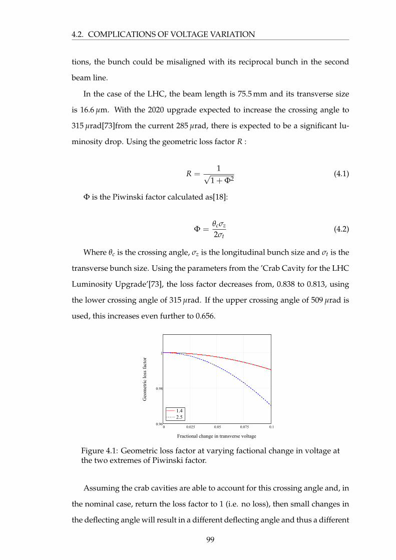
4.2. COMPLICATIONS OF VOLTAGE VARIATION
tions, the bunch could be misaligned with its reciprocal bunch in the second
beam line.
In the case of the LHC, the beam length is 75.5 mm and its transverse size
is 16.6 µm. With the 2020 upgrade expected to increase the crossing angle to
315 µrad[73]from the current 285 µrad, there is expected to be a significant lu-
minosity drop. Using the geometric loss factor R :
R =1√
1 + Φ2(4.1)
Φ is the Piwinski factor calculated as[18]:
Φ =θcσz
2σt(4.2)
Where θc is the crossing angle, σz is the longitudinal bunch size and σt is the
transverse bunch size. Using the parameters from the ’Crab Cavity for the LHC
Luminosity Upgrade’[73], the loss factor decreases from, 0.838 to 0.813, using
the lower crossing angle of 315 µrad. If the upper crossing angle of 509 µrad is
used, this increases even further to 0.656.
0 0.025 0.05 0.075 0.10.96
0.98
1
1.42.5
Fractional change in transverse voltage
Geo
met
ric
loss
fac
tor
Figure 4.1: Geometric loss factor at varying factional change in voltage atthe two extremes of Piwinski factor.
Assuming the crab cavities are able to account for this crossing angle and, in
the nominal case, return the loss factor to 1 (i.e. no loss), then small changes in
the deflecting angle will result in a different deflecting angle and thus a different
99
CHAPTER 4. VOLTAGE CALCULATIONS
Piwinski factor. If we calculate the change in angle as
∆θc(x, y) = θcVx(x, y)−Vx(0, 0)
Vx(0, 0)(4.3)
where Vx(x, y) is the deflecting voltage received at the position (x, y) in the
cavity by the particle and Vx(0, 0)0 is the nominal value of the deflecting voltage
at the centre of the cavity. Then, as the Piwinski factor is directly proportional
to the crossing angle, it will also be proportional to the change in deflecting
voltage. From Figure 4.1, the change in geometric loss factor for a 3% drop
in deflecting voltage will cause a 0.088% or a 0.280% drop in luminosity for a
Piwinski factor of 1.4 and 2.5 respectively. For a 10% drop in voltage, a 0.966%
or 2.986% drop in luminosity is seen for 1.4 and 2.5 respectively, however this
is comparatively small. These numbers are unlikely to be a limiting factor on
the LHC, however they may be indicative of multipole components interfering
with the deflection.
4.3 Multipole Components
The deflecting mode in the LHC is not a pure dipole. The mode consists of a
superposition of terms that create the defecting mode. The main component of
the operating mode is dipole however there are higher order terms that appear
at increased offset that can impact the beam [76]. As the higher order modes
are highly susceptible to offset, the decapole mode varies with r5, the terms of
most concern are those with components that are noticeable close to the beam
position.
The multipole components for the cavity were examined to ensure they were
of acceptable levels. The multipole expansion of the cavity can be expressed as
a summation of angularly dependant components at.
Vz = ∑n
xn(rn cos(θn) + rn sin(θn)) (4.4)
100
4.3. MULTIPOLE COMPONENTS
We know that there is no longitudinal voltage on axis, or in the plane per-
pendicular to the direction of deflection. Thus for θ = π2 , Vz must be zero. This
results in the elimination of the terms with a dependence on cos(2nθ)‘. Due to
symmetry the terms of sin(θ) may similarly be eliminated.
This provides the following variation in Vz for the first three terms, with
higher order terms following the same patten.
Vz = ar cos(θ) + br3 cos(3θ) + cr5 cos(5θ) (4.5)
To calculate the coefficients a b and c a full circular profile of the voltage
is taken, this consisted of 800 points taken at a radius of 5 mm. A fast Furrier
transform was then preformed. The resulting values then could be normalised
to a 5 mm offset before being used as the variables.
Vz(circle) = A[2, 800] (4.6)
FFT(A[2, 800]) ∝ M[800] (4.7)
a = M[2]/0.0051 (4.8)
b = M[4]/0.0053 (4.9)
b = M[6]/0.0055 (4.10)
where Vz(circle) is the values taken from CST, placed in the two by eight
hundred matrix A[2, 800], M[800] is the result of the Furrier transform with M[2]
corresponding to the 2nd term of the transform.
By comparing measurements of Vz at a range of offsets in an arc the from
CST to the analytical values of a, b and c calculated the calculation can be
checked for self consistency . To calculate the multipole components from CST
the longitudinal voltage was calculated at a range offset’s across a π2 segment of
101
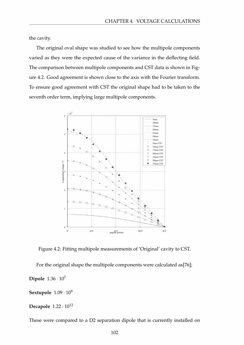
CHAPTER 4. VOLTAGE CALCULATIONS
the cavity.
The original oval shape was studied to see how the multipole components
varied as they were the expected cause of the variance in the deflecting field.
The comparison between multipole components and CST data is shown in Fig-
ure 4.2. Good agreement is shown close to the axis with the Fourier transform.
To ensure good agreement with CST the original shape had to be taken to the
seventh order term, implying large multipole components.
angular poition
Lon
gitu
dina
l vol
tage
/ V
0 pi/8 pi/4 3pi/8 pi/2
0
1
2
3
4
5
6× 10
5
5mm
10mm
15mm
20mm
25mm
30mm
35mm
5mm CST
10mm CST
15mm CST
20mm CST
25mm CST
30mm CST
35mm CST
Figure 4.2: Fitting multipole measurements of ’Original’ cavity to CST.
For the original shape the multipole components were calculated as[76];
Dipole 1.36 · 107
Sextupole 1.09 · 109
Decapole 1.22 · 1012
These were compared to a D2 separation dipole that is currently installed on
102
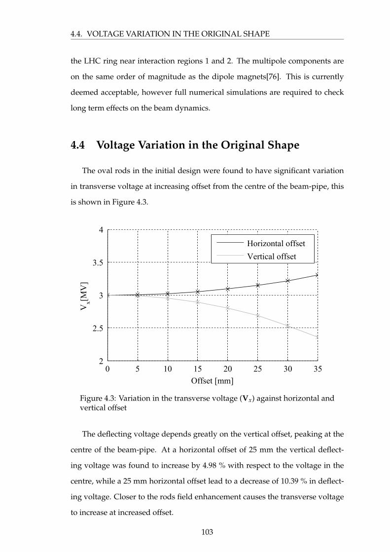
4.4. VOLTAGE VARIATION IN THE ORIGINAL SHAPE
the LHC ring near interaction regions 1 and 2. The multipole components are
on the same order of magnitude as the dipole magnets[76]. This is currently
deemed acceptable, however full numerical simulations are required to check
long term effects on the beam dynamics.
4.4 Voltage Variation in the Original Shape
The oval rods in the initial design were found to have significant variation
in transverse voltage at increasing offset from the centre of the beam-pipe, this
is shown in Figure 4.3.
Offset [mm]
Vx[M
V]
0 5 10 15 20 25 30 352
2.5
3
3.5
4
Horizontal offset
Vertical offset
Figure 4.3: Variation in the transverse voltage (Vx) against horizontal andvertical offset
The deflecting voltage depends greatly on the vertical offset, peaking at the
centre of the beam-pipe. At a horizontal offset of 25 mm the vertical deflect-
ing voltage was found to increase by 4.98 % with respect to the voltage in the
centre, while a 25 mm horizontal offset lead to a decrease of 10.39 % in deflect-
ing voltage. Closer to the rods field enhancement causes the transverse voltage
to increase at increased offset.
103
CHAPTER 4. VOLTAGE CALCULATIONS
The particularly large variation seen in the deflecting voltage can be attrib-
uted to the size of the rods, as seen in Section 4.7, where small rods produced
a larger variation in deflecting voltage. Due to the constraints imposed on the
size of the LHC crab cavity, cylindrical rods of a size large enough to eliminate
this problem are unfeasible.
It is clear that circular rods have a large variation in deflecting voltage across
the beam-pipe aperture, hence it was necessary to investigate other rod geomet-
ries to minimise the variation in transverse voltage. It is well known that the
transverse electric field in between two infinite parallel plates is constant.
4.5 Pill Box Voltage Variation
The most simple electromagnetic cavity design is that of a pill box; a cyl-
indrical cavity of length d and radius R0. By looking at this shape we can com-
pare the fields of mathematical models and real world designs to a simple crab
cavity design. The longitudinal voltage in a pill box cavity can be calculated
from the integral of the longitudinal electric field Ez at any choice of radial co-
ordinate for any TMm n pmode [43].
Here, the position within the cavity is defined as the longitudinal position z,
the radial angle θ , the radial offset as ρ and E0 is the nominal time-dependent
electric field. While applying this to the dipole mode TM1 1 0 there is no z vari-
ation and the equation simplifies to;
Vz(ρ, θ) =
ˆ d2
−d2
Ez(ρ, θ, z)dz (4.11)
which becomes:
Vz(ρ, θ) = V0 J1
(ζ11ρ
R0
)cos (θ) (4.12)
Where V0is the nominal accelerating voltage and ζ11 in the first root of the
first Bessel function J1.
104
4.5. PILL BOX VOLTAGE VARIATION
This can then be transformed into Cartesian coordinates the longitudinal
voltage can be rewritten as:
Vz(x, y) = V0 J1
(ζ11√
x2 + y2
R0
)x√
x2 + y2(4.13)
From the Panofski Wenzel theorem,
V⊥= −icω
ˆ d
0∇⊥Ez(z,
zc)dz (4.14)
the deflecting component of this can derived as:
Vx =cω
∂Vz
∂x(4.15)
With the parasitic deflection derived as:
Vy =cω
∂Vz
∂y(4.16)
By performing a Taylor expansion on J1, the behaviour of the deflecting and
parasitic voltages can be examined and generalisations made on how they will
behave close to the axis:
J1 (u) =u2− u3
16+
u5
384+(
O7...)
(4.17)
Substituting in the first 3 terms and ignoring terms of 7th order and higher:
Vz (x, y) = V0
ζ11√
x2 + y2
2R0
x√x2 + y2
−(
ζ11√
x2 + y2
R0
)3x
16√
x2 + y2
+
(ζ11√
x2 + y2
R0
)5x
384√
x2 + y2+(
O7...)
(4.18)
This was then simplified by cancelling and grouping terms together to get:
105
CHAPTER 4. VOLTAGE CALCULATIONS
Vz (x, y) = V0
(ζ11x2R0−
ζ311x(x2 + y2)
16R30
+ζ5
11x(x2 + y2)2
384R50
+(
O7...))
(4.19)
In the ideal case the dipole would vary with just x, thus being a uniform. The
higher terms are distortions that lead to the variations in the deflecting voltage.
Then while using Equations 4.15 and 4.19, the deflecting voltage can be de-
rived as:
Vx = V0cω
(ζ11
2R0−
3ζ311x2
16R30−
ζ311y2
16R30+
5ζ511x4
384R50+
6ζ511x2y2
384R50
+ζ5
11y4
384R50+(
O7...))
(4.20)
converting this back into θ and ρ with x = ρ cos θ and y = θ cos θ
Vx = V0cω
ζ11
2R0
(1−
ζ211ρ2 (2 cos2 θ + 1
)8R2
0+
ζ411ρ4 (5 cos2 θ + sin2 θ
)192R4
0
)(4.21)
Similarly, using Equation 4.16, the parasitic deflecting voltage can be derived
as:
Vy = V0cω
(2ζ3
11yx16R3
0−
4ζ511xy3
384R50− 4ζ11x3y
384R50
+(
O6...))
(4.22)
and again converted back into θand ρ.
Vy = V0cω
ζ311
8R30
(ρ2 cos θ sin θ −
ζ211ρ4 cos θ sin θ
12R20
(O6...
))(4.23)
The two voltages are normalized to the transverse voltage so the relative
magnitudes of the deflecting voltage and the parasitic deflection across each of
the differing cavities and to allow relative percentage changes to be tracked.
The variation in Vxis dominated by the ρ2term, as seen in Equation 4.21. The
ratio of the dipole amplitude to this term is ζ2
4R20, hence the higher the cavity
frequency, the larger the variation over a fixed distance. This is to be expected
106
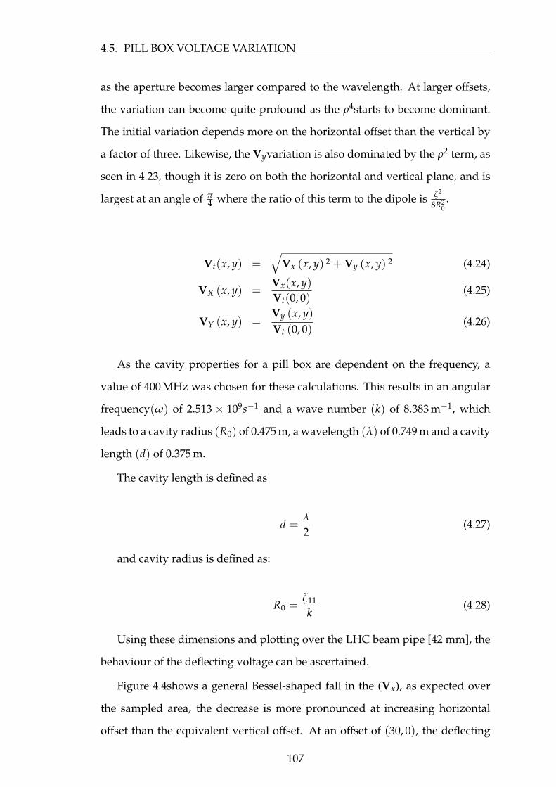
4.5. PILL BOX VOLTAGE VARIATION
as the aperture becomes larger compared to the wavelength. At larger offsets,
the variation can become quite profound as the ρ4starts to become dominant.
The initial variation depends more on the horizontal offset than the vertical by
a factor of three. Likewise, the Vyvariation is also dominated by the ρ2 term, as
seen in 4.23, though it is zero on both the horizontal and vertical plane, and is
largest at an angle of π4 where the ratio of this term to the dipole is ζ2
8R20.
Vt(x, y) =√
Vx (x, y) 2 + Vy (x, y) 2 (4.24)
VX (x, y) =Vx(x, y)Vt(0, 0)
(4.25)
VY (x, y) =Vy (x, y)Vt (0, 0)
(4.26)
As the cavity properties for a pill box are dependent on the frequency, a
value of 400 MHz was chosen for these calculations. This results in an angular
frequency(ω) of 2.513 × 10⁹s−1 and a wave number (k) of 8.383 m−1, which
leads to a cavity radius (R0) of 0.475 m, a wavelength (λ) of 0.749 m and a cavity
length (d) of 0.375 m.
The cavity length is defined as
d =λ
2(4.27)
and cavity radius is defined as:
R0 =ζ11
k(4.28)
Using these dimensions and plotting over the LHC beam pipe [42 mm], the
behaviour of the deflecting voltage can be ascertained.
Figure 4.4shows a general Bessel-shaped fall in the (Vx), as expected over
the sampled area, the decrease is more pronounced at increasing horizontal
offset than the equivalent vertical offset. At an offset of (30, 0), the deflecting
107
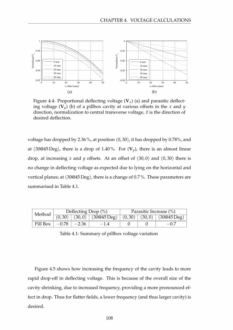
CHAPTER 4. VOLTAGE CALCULATIONS
x offset (mm)
Nor
mal
ised
Vx
0 10 20 30 40 500.92
0.94
0.96
0.98
1
0 mm
10 mm
20 mm
30 mm
40 mm
(a)
x offset (mm)
Nor
mal
ised
Vy
0 10 20 30 40 50-0.04
-0.03
-0.02
-0.01
0
0 mm
10 mm
20 mm
30 mm
40 mm
(b)
Figure 4.4: Proportional deflecting voltage (Vx) (a) and parasitic deflect-ing voltage (Vy) (b) of a pillbox cavity at various offsets in the x and ydirection, normalization to central transverse voltage, x is the direction ofdesired deflection.
voltage has dropped by 2.36 %, at position (0, 30), it has dropped by 0.78%, and
at (30@45 Deg), there is a drop of 1.40 %. For (Vy), there is an almost linear
drop, at increasing x and y offsets. At an offset of (30, 0) and (0, 30) there is
no change in deflecting voltage as expected due to lying on the horizontal and
vertical planes; at (30@45 Deg), there is a change of 0.7 %. These parameters are
summarised in Table 4.1.
Method Deflecting Drop (%) Parasitic Increase (%)(0, 30) (30, 0) (30@45 Deg) (0, 30) (30, 0) (30@45 Deg)
Pill Box −0.78 −2.36 −1.4 0 0 −0.7
Table 4.1: Summary of pillbox voltage variation
Figure 4.5 shows how increasing the frequency of the cavity leads to more
rapid drop-off in deflecting voltage. This is because of the overall size of the
cavity shrinking, due to increased frequency, providing a more pronounced ef-
fect in drop. Thus for flatter fields, a lower frequency (and thus larger cavity) is
desired.
108
4.6. VOLTAGE VARIATION IN CYLINDRICALLY-SYMMETRIC CAVITYWITH BEAM-PIPES
x offset (mm)
Nor
mal
ised
Vx
0 10 20 30 40 500.4
0.5
0.6
0.7
0.8
0.9
1
200 MHz
400 MHz
800 MHz
1200 MHz
Figure 4.5: Variation in deflecting voltage across increasing x offsets atdifferent frequencies. The y offset is at 0 mm.
4.6 Voltage Variation in Cylindrically-Symmetric Cav-
ity with Beam-Pipes
The addition of beam-pipes to the pill box cavity causes the transverse field
to flatten in the region of the beam-pipe. This flattening effect is caused by
the hybridisation of the dipole mode that causes no variation in the deflecting
voltage along the x axis. This allows deflecting cavities to have a far flatter field
profile than the theoretical pill box.
k20 = k2
⊥ + k2z (4.29)
k2⊥ =
√k2
0 − k2z (4.30)
k2⊥ =
√(ω
c
)2−(ω
v
)2(4.31)
Here k0is the wave number, k⊥is the transverse wave number and kz is the
longitudinal wave number, ωis the angle of frequency of the wave, v is the
velocity of the wave and c is the speed of light.
As the velocity of the particles will be less than c, the transverse wave num-
109
CHAPTER 4. VOLTAGE CALCULATIONS
ber will be imaginary, thus the complex Bessel function was used:
iIn(A) = Jn(iA) (4.32)
The longitudinal voltage is defined as [77]
Vz(x, y) = V0 I1
(ω
c
√1β2 − 1ρ
)xρ
(4.33)
However, as β approaches 1, the complex Bessel function becomes increas-
ingly small. Using the Taylor expansion of the complex Bessel function:
I1 (u) =u2+
u3
16+
u5
384+(
O7...)
(4.34)
all the terms greater than u2 can be ignored as they are of the order δ3and as
such, would be completely dominated by the first term. This then leaves :
Vz(x, y) = V0ωx2c
(4.35)
at very large β. This then results in zero parasitic voltage and a uniform
deflecting voltage.
For a value of β = 0.9999 , there is almost no variation in either the deflecting
or parasitic voltage, at (30@45 Deg) the parasitic voltage has a value of 1.406×
10−6 . These parameters are summarised in Table 4.2.
Depending on the β chosen for the cavity, particles travelling through at
this speed will receive a greater or lesser uniform kick. At a low β, particles
would travel through at a lower speed and thus will see more of the sinusoidal
variation of the RF field. As β increases, this results in a more uniform deflecting
voltage, as can be seen in 4.6.
110
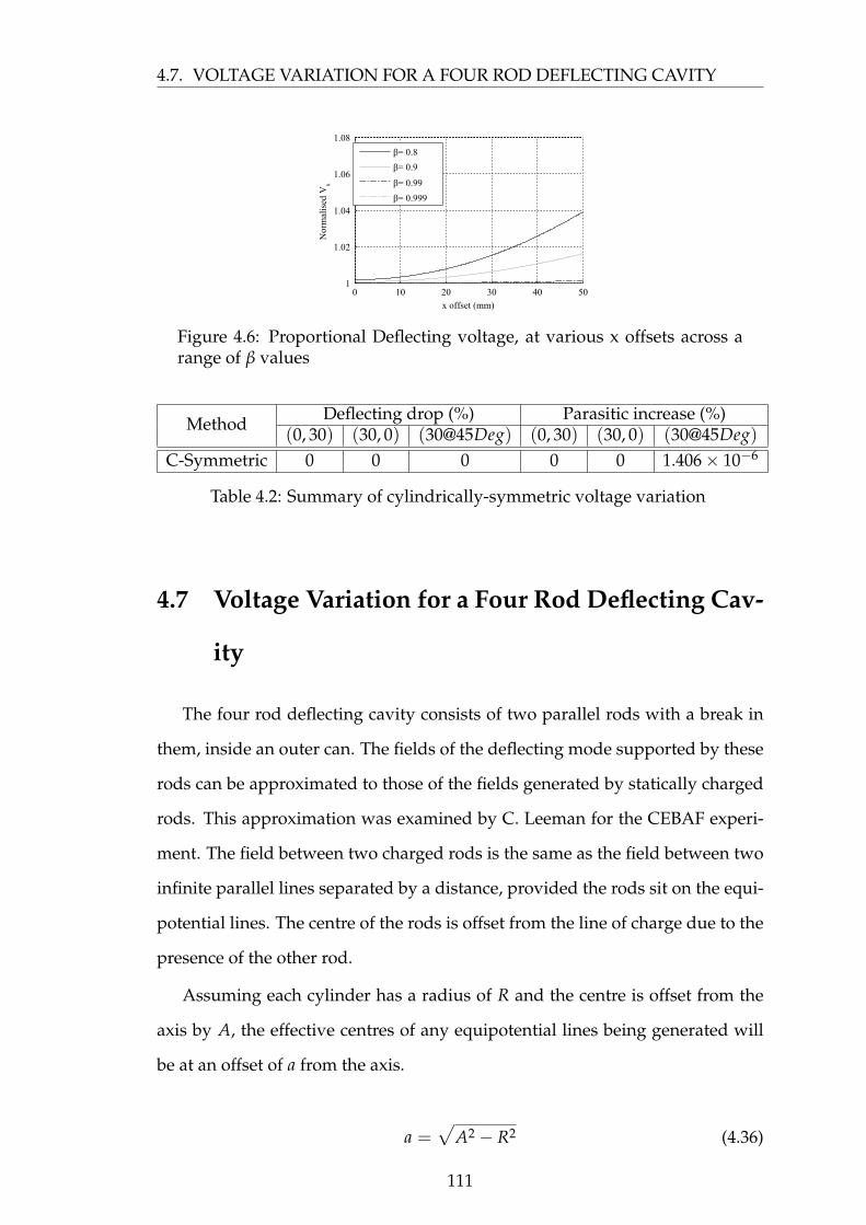
4.7. VOLTAGE VARIATION FOR A FOUR ROD DEFLECTING CAVITY
x offset (mm)
Nor
mal
ised
Vx
0 10 20 30 40 501
1.02
1.04
1.06
1.08
β= 0.8
β= 0.9
β= 0.99
β= 0.999
Figure 4.6: Proportional Deflecting voltage, at various x offsets across arange of β values
Method Deflecting drop (%) Parasitic increase (%)(0, 30) (30, 0) (30@45Deg) (0, 30) (30, 0) (30@45Deg)
C-Symmetric 0 0 0 0 0 1.406× 10⁻⁶
Table 4.2: Summary of cylindrically-symmetric voltage variation
4.7 Voltage Variation for a Four Rod Deflecting Cav-
ity
The four rod deflecting cavity consists of two parallel rods with a break in
them, inside an outer can. The fields of the deflecting mode supported by these
rods can be approximated to those of the fields generated by statically charged
rods. This approximation was examined by C. Leeman for the CEBAF experi-
ment. The field between two charged rods is the same as the field between two
infinite parallel lines separated by a distance, provided the rods sit on the equi-
potential lines. The centre of the rods is offset from the line of charge due to the
presence of the other rod.
Assuming each cylinder has a radius of R and the centre is offset from the
axis by A, the effective centres of any equipotential lines being generated will
be at an offset of a from the axis.
a =√
A2 − R2 (4.36)
111
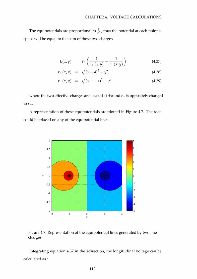
CHAPTER 4. VOLTAGE CALCULATIONS
The equipotentials are proportional to 1r2 , thus the potential at each point is
space will be equal to the sum of these two charges.
E(x, y) = V0
(1
r+ (x, y)− 1
r−(x, y)
)(4.37)
r+(x, y) =
√(x + a)2 + y2 (4.38)
r−(x, y) =
√(x +−a)2 + y2 (4.39)
where the two effective charges are located at±a and r+ is oppositely charged
to r−.
A representation of these equipotentials are plotted in Figure 4.7. The rods
could be placed on any of the equipotential lines.
X
Y
-2 -1 0 1 2-2
-1.5
-1
-0.5
0
0.5
1
1.5
2
-5
-4
-3
-2
-1
0
1
2
3
4
5
Figure 4.7: Representation of the equipotential lines generated by two linecharges.
Integrating equation 4.37 in the zdirection, the longitudinal voltage can be
calculated as :
112
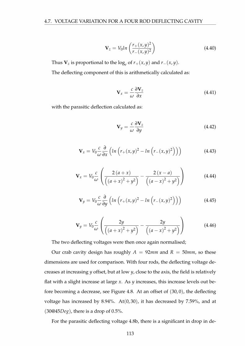
4.7. VOLTAGE VARIATION FOR A FOUR ROD DEFLECTING CAVITY
Vz = V0ln(
r+(x, y)2
r−(x, y)2
)(4.40)
Thus Vz is proportional to the loge of r+(x, y) and r−(x, y).
The deflecting component of this is arithmetically calculated as:
Vx =cω
∂Vz
∂x(4.41)
with the parasitic deflection calculated as:
Vy =cω
∂Vz
∂y(4.42)
Vx = V0cω
∂
∂x
(ln(
r+(x, y)2 − ln(
r−(x, y)2)))
(4.43)
Vx = V0cω
2 (a + x)((a + x)2 + y2
) − 2 (x− a)((a− x)2 + y2
) (4.44)
Vy = V0cω
∂
∂y
(ln(
r+(x, y)2 − ln(
r−(x, y)2)))
(4.45)
Vy = V0cω
2y((a + x)2 + y2
) − 2y((a− x)2 + y2
) (4.46)
The two deflecting voltages were then once again normalised;
Our crab cavity design has roughly A = 92mm and R = 50mm, so these
dimensions are used for comparison. With four rods, the deflecting voltage de-
creases at increasing y offset, but at low y, close to the axis, the field is relatively
flat with a slight increase at large x. As y increases, this increase levels out be-
fore becoming a decrease, see Figure 4.8. At an offset of (30, 0), the deflecting
voltage has increased by 8.94%. At(0, 30), it has decreased by 7.59%, and at
(30@45Deg), there is a drop of 0.5%.
For the parasitic deflecting voltage 4.8b, there is a significant in drop in de-
113
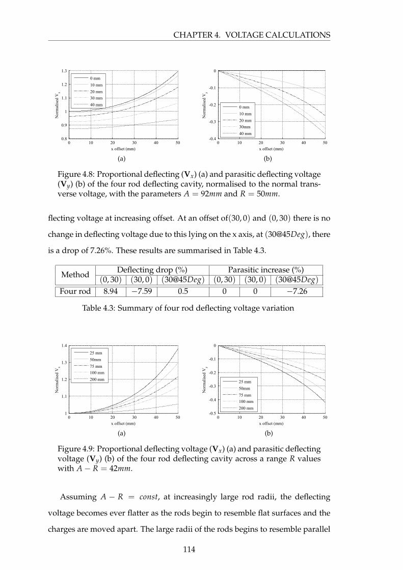
CHAPTER 4. VOLTAGE CALCULATIONS
x offset (mm)
Nor
mal
ised
Vx
0 10 20 30 40 500.8
0.9
1
1.1
1.2
1.3
0 mm
10 mm
20 mm
30 mm
40 mm
(a)
x offset (mm)
Nor
mal
ised
Vy
0 10 20 30 40 50-0.4
-0.3
-0.2
-0.1
0
0 mm
10 mm
20 mm
30mm
40 mm
(b)
Figure 4.8: Proportional deflecting (Vx) (a) and parasitic deflecting voltage(Vy) (b) of the four rod deflecting cavity, normalised to the normal trans-verse voltage, with the parameters A = 92mm and R = 50mm.
flecting voltage at increasing offset. At an offset of(30, 0) and (0, 30) there is no
change in deflecting voltage due to this lying on the x axis, at (30@45Deg), there
is a drop of 7.26%. These results are summarised in Table 4.3.
Method Deflecting drop (%) Parasitic increase (%)(0, 30) (30, 0) (30@45Deg) (0, 30) (30, 0) (30@45Deg)
Four rod 8.94 −7.59 0.5 0 0 −7.26
Table 4.3: Summary of four rod deflecting voltage variation
x offset (mm)
Nor
mal
ised
Vx
0 10 20 30 40 501
1.1
1.2
1.3
1.4
25 mm
50mm
75 mm
100 mm
200 mm
(a)
x offset (mm)
Nor
mal
ised
Vy
0 10 20 30 40 50-0.5
-0.4
-0.3
-0.2
-0.1
0
25 mm
50mm
75 mm
100 mm
200 mm
(b)
Figure 4.9: Proportional deflecting voltage (Vx) (a) and parasitic deflectingvoltage (Vy) (b) of the four rod deflecting cavity across a range R valueswith A− R = 42mm.
Assuming A − R = const, at increasingly large rod radii, the deflecting
voltage becomes ever flatter as the rods begin to resemble flat surfaces and the
charges are moved apart. The large radii of the rods begins to resemble parallel
114
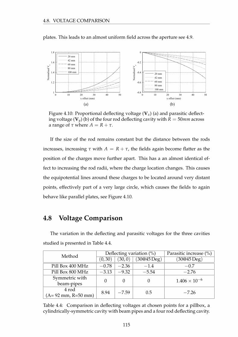
4.8. VOLTAGE COMPARISON
plates. This leads to an almost uniform field across the aperture see 4.9.
x offset (mm)
Nor
mal
ised
Vx
0 10 20 30 40 501
1.2
1.4
1.6
1.8
20 mm
42 mm
60 mm
80 mm
100 mm
(a)
x offset (mm)
Nor
mal
ised
Vy
0 10 20 30 40 50-0.8
-0.6
-0.4
-0.2
0
20 mm
42 mm
60 mm
80 mm
100 mm
(b)
Figure 4.10: Proportional deflecting voltage (Vx) (a) and parasitic deflect-ing voltage (Vy) (b) of the four rod deflecting cavity with R = 50mm acrossa range of τ where A = R + τ.
If the size of the rod remains constant but the distance between the rods
increases, increasing τ with A = R + τ, the fields again become flatter as the
position of the charges move further apart. This has a an almost identical ef-
fect to increasing the rod radii, where the charge location changes. This causes
the equipotential lines around these charges to be located around very distant
points, effectively part of a very large circle, which causes the fields to again
behave like parallel plates, see Figure 4.10.
4.8 Voltage Comparison
The variation in the deflecting and parasitic voltages for the three cavities
studied is presented in Table 4.4.
Method Deflecting variation (%) Parasitic increase (%)(0, 30) (30, 0) (30@45 Deg) (30@45 Deg)
Pill Box 400 MHz −0.78 −2.36 −1.4 −0.7Pill Box 800 MHz −3.13 −9.32 −5.54 −2.76Symmetric with 0 0 0 1.406× 10⁻⁶
beam-pipes4 rod 8.94 −7.59 0.5 −7.26(A= 92 mm, R=50 mm)
Table 4.4: Comparison in deflecting voltages at chosen points for a pillbox, acylindrically-symmetric cavity with beam pipes and a four rod deflecting cavity.
115
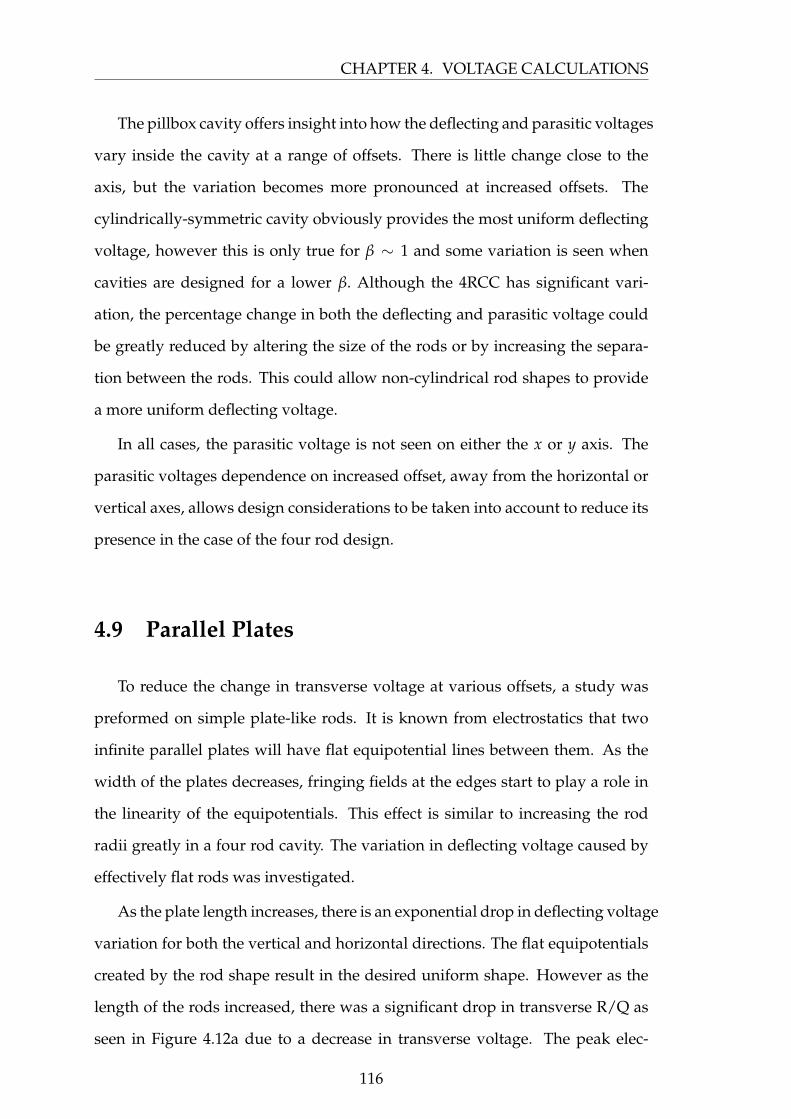
CHAPTER 4. VOLTAGE CALCULATIONS
The pillbox cavity offers insight into how the deflecting and parasitic voltages
vary inside the cavity at a range of offsets. There is little change close to the
axis, but the variation becomes more pronounced at increased offsets. The
cylindrically-symmetric cavity obviously provides the most uniform deflecting
voltage, however this is only true for β ∼ 1 and some variation is seen when
cavities are designed for a lower β. Although the 4RCC has significant vari-
ation, the percentage change in both the deflecting and parasitic voltage could
be greatly reduced by altering the size of the rods or by increasing the separa-
tion between the rods. This could allow non-cylindrical rod shapes to provide
a more uniform deflecting voltage.
In all cases, the parasitic voltage is not seen on either the x or y axis. The
parasitic voltages dependence on increased offset, away from the horizontal or
vertical axes, allows design considerations to be taken into account to reduce its
presence in the case of the four rod design.
4.9 Parallel Plates
To reduce the change in transverse voltage at various offsets, a study was
preformed on simple plate-like rods. It is known from electrostatics that two
infinite parallel plates will have flat equipotential lines between them. As the
width of the plates decreases, fringing fields at the edges start to play a role in
the linearity of the equipotentials. This effect is similar to increasing the rod
radii greatly in a four rod cavity. The variation in deflecting voltage caused by
effectively flat rods was investigated.
As the plate length increases, there is an exponential drop in deflecting voltage
variation for both the vertical and horizontal directions. The flat equipotentials
created by the rod shape result in the desired uniform shape. However as the
length of the rods increased, there was a significant drop in transverse R/Q as
seen in Figure 4.12a due to a decrease in transverse voltage. The peak elec-
116
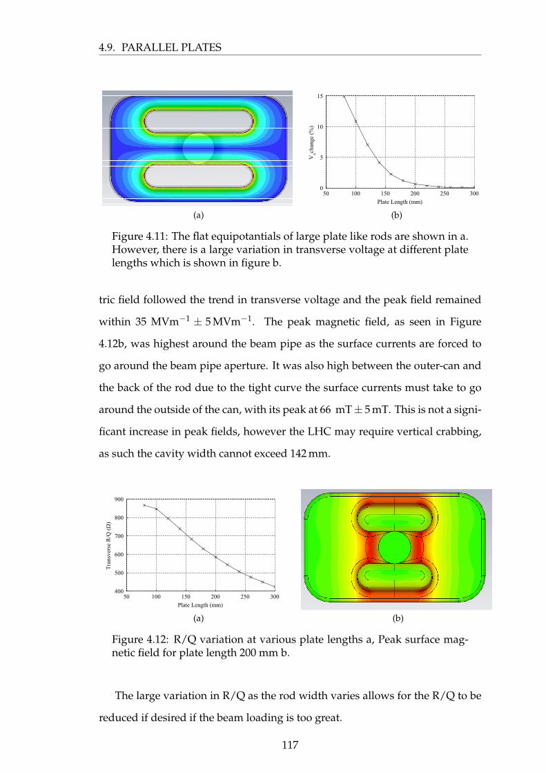
4.9. PARALLEL PLATES
(a)
Plate Length (mm)
Vxch
ange
(%
)
50 100 150 200 250 3000
5
10
15
(b)
Figure 4.11: The flat equipotantials of large plate like rods are shown in a.However, there is a large variation in transverse voltage at different platelengths which is shown in figure b.
tric field followed the trend in transverse voltage and the peak field remained
within 35 MVm−1 ± 5 MVm−1. The peak magnetic field, as seen in Figure
4.12b, was highest around the beam pipe as the surface currents are forced to
go around the beam pipe aperture. It was also high between the outer-can and
the back of the rod due to the tight curve the surface currents must take to go
around the outside of the can, with its peak at 66 mT± 5 mT. This is not a signi-
ficant increase in peak fields, however the LHC may require vertical crabbing,
as such the cavity width cannot exceed 142 mm.
Plate Length (mm)
Tra
nsve
rse
R/Q
(Ω
)
50 100 150 200 250 300400
500
600
700
800
900
(a) (b)
Figure 4.12: R/Q variation at various plate lengths a, Peak surface mag-netic field for plate length 200 mm b.
The large variation in R/Q as the rod width varies allows for the R/Q to be
reduced if desired if the beam loading is too great.
117
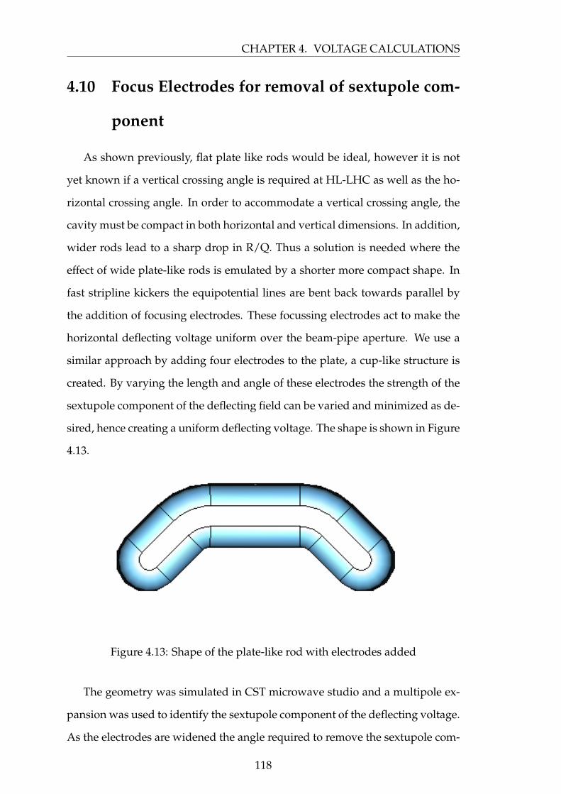
CHAPTER 4. VOLTAGE CALCULATIONS
4.10 Focus Electrodes for removal of sextupole com-
ponent
As shown previously, flat plate like rods would be ideal, however it is not
yet known if a vertical crossing angle is required at HL-LHC as well as the ho-
rizontal crossing angle. In order to accommodate a vertical crossing angle, the
cavity must be compact in both horizontal and vertical dimensions. In addition,
wider rods lead to a sharp drop in R/Q. Thus a solution is needed where the
effect of wide plate-like rods is emulated by a shorter more compact shape. In
fast stripline kickers the equipotential lines are bent back towards parallel by
the addition of focusing electrodes. These focussing electrodes act to make the
horizontal deflecting voltage uniform over the beam-pipe aperture. We use a
similar approach by adding four electrodes to the plate, a cup-like structure is
created. By varying the length and angle of these electrodes the strength of the
sextupole component of the deflecting field can be varied and minimized as de-
sired, hence creating a uniform deflecting voltage. The shape is shown in Figure
4.13.
Figure 4.13: Shape of the plate-like rod with electrodes added
The geometry was simulated in CST microwave studio and a multipole ex-
pansion was used to identify the sextupole component of the deflecting voltage.
As the electrodes are widened the angle required to remove the sextupole com-
118
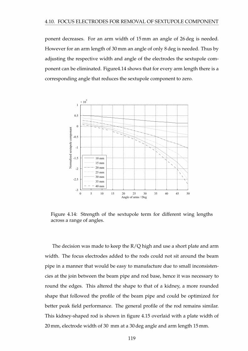
4.10. FOCUS ELECTRODES FOR REMOVAL OF SEXTUPOLE COMPONENT
ponent decreases. For an arm width of 15 mm an angle of 26 deg is needed.
However for an arm length of 30 mm an angle of only 8 deg is needed. Thus by
adjusting the respective width and angle of the electrodes the sextupole com-
ponent can be eliminated. Figure4.14 shows that for every arm length there is a
corresponding angle that reduces the sextupole component to zero.
Angle of arms / Deg
Nor
mal
ized
sex
tapo
le c
ompo
nant
0 5 10 15 20 25 30 35 40 45 50-3
-2.5
-2
-1.5
-1
-0.5
0
0.5
1× 10
9
10 mm
15 mm
20 mm
25 mm
30 mm
35 mm
40 mm
Figure 4.14: Strength of the sextupole term for different wing lengthsacross a range of angles.
The decision was made to keep the R/Q high and use a short plate and arm
width. The focus electrodes added to the rods could not sit around the beam
pipe in a manner that would be easy to manufacture due to small inconsisten-
cies at the join between the beam pipe and rod base, hence it was necessary to
round the edges. This altered the shape to that of a kidney, a more rounded
shape that followed the profile of the beam pipe and could be optimized for
better peak field performance. The general profile of the rod remains similar.
This kidney-shaped rod is shown in figure 4.15 overlaid with a plate width of
20 mm, electrode width of 30 mm at a 30 deg angle and arm length 15 mm.
119
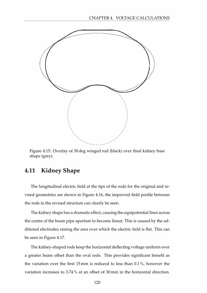
CHAPTER 4. VOLTAGE CALCULATIONS
Figure 4.15: Overlay of 30 deg winged rod (black) over final kidney baseshape (grey).
4.11 Kidney Shape
The longitudinal electric field at the tips of the rods for the original and re-
vised geometries are shown in Figure 4.16, the improved field profile between
the rods in the revised structure can clearly be seen.
The kidney shape has a dramatic effect, causing the equipotential lines across
the centre of the beam pipe aperture to become linear. This is caused by the ad-
ditional electrodes raising the area over which the electric field is flat. This can
be seen in Figure 4.17.
The kidney-shaped rods keep the horizontal deflecting voltage uniform over
a greater beam offset than the oval rods. This provides significant benefit as
the variation over the first 15 mm is reduced to less than 0.1 %, however the
variation increases to 3.74 % at an offset of 30 mm in the horizontal direction.
120
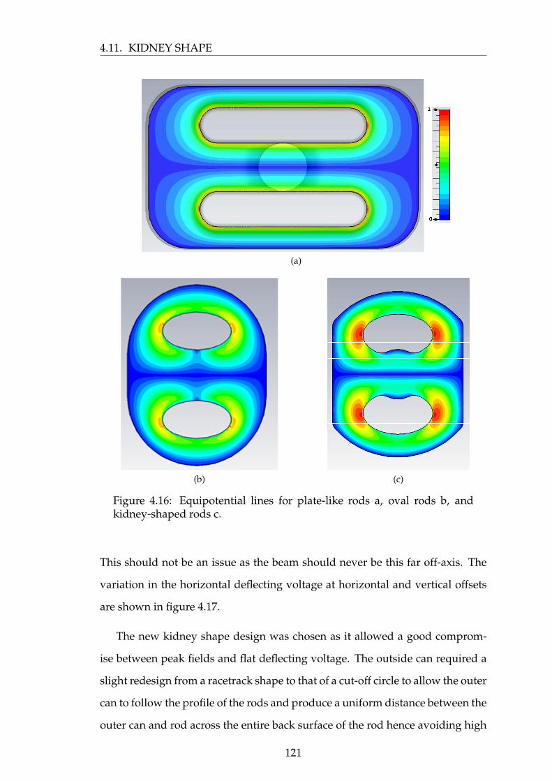
4.11. KIDNEY SHAPE
(a)
(b) (c)
Figure 4.16: Equipotential lines for plate-like rods a, oval rods b, andkidney-shaped rods c.
This should not be an issue as the beam should never be this far off-axis. The
variation in the horizontal deflecting voltage at horizontal and vertical offsets
are shown in figure 4.17.
The new kidney shape design was chosen as it allowed a good comprom-
ise between peak fields and flat deflecting voltage. The outside can required a
slight redesign from a racetrack shape to that of a cut-off circle to allow the outer
can to follow the profile of the rods and produce a uniform distance between the
outer can and rod across the entire back surface of the rod hence avoiding high
121
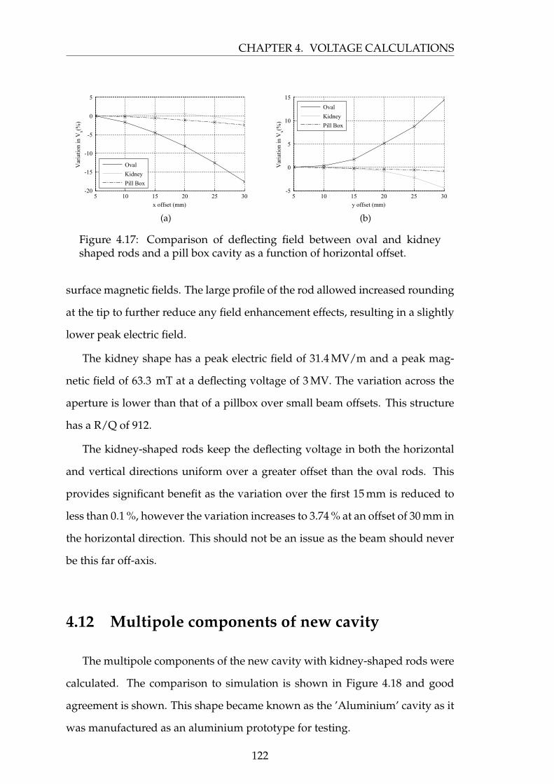
CHAPTER 4. VOLTAGE CALCULATIONS
x offset (mm)
Var
iatio
n in
Vx(%
)
5 10 15 20 25 30-20
-15
-10
-5
0
5
Oval
Kidney
Pill Box
(a)
y offset (mm)
Var
iatio
n in
Vx(%
)
5 10 15 20 25 30-5
0
5
10
15
Oval
Kidney
Pill Box
(b)
Figure 4.17: Comparison of deflecting field between oval and kidneyshaped rods and a pill box cavity as a function of horizontal offset.
surface magnetic fields. The large profile of the rod allowed increased rounding
at the tip to further reduce any field enhancement effects, resulting in a slightly
lower peak electric field.
The kidney shape has a peak electric field of 31.4 MV/m and a peak mag-
netic field of 63.3 mT at a deflecting voltage of 3 MV. The variation across the
aperture is lower than that of a pillbox over small beam offsets. This structure
has a R/Q of 912.
The kidney-shaped rods keep the deflecting voltage in both the horizontal
and vertical directions uniform over a greater offset than the oval rods. This
provides significant benefit as the variation over the first 15 mm is reduced to
less than 0.1 %, however the variation increases to 3.74 % at an offset of 30 mm in
the horizontal direction. This should not be an issue as the beam should never
be this far off-axis.
4.12 Multipole components of new cavity
The multipole components of the new cavity with kidney-shaped rods were
calculated. The comparison to simulation is shown in Figure 4.18 and good
agreement is shown. This shape became known as the ’Aluminium’ cavity as it
was manufactured as an aluminium prototype for testing.
122
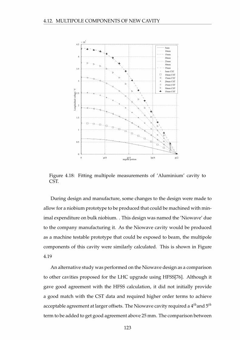
4.12. MULTIPOLE COMPONENTS OF NEW CAVITY
angular poition
Lon
gitu
dina
l vol
tage
/ V
0 pi/8 pi/4 3pi/8 pi/2
0
0.5
1
1.5
2
2.5
3
3.5
4
4.5× 10
5
5mm
10mm
15mm
20mm
25mm
30mm
35mm
5mm CST
10mm CST
15mm CST
20mm CST
25mm CST
30mm CST
35mm CST
Figure 4.18: Fitting multipole measurements of ’Aluminium’ cavity toCST.
During design and manufacture, some changes to the design were made to
allow for a niobium prototype to be produced that could be machined with min-
imal expenditure on bulk niobium. . This design was named the ’Niowave’ due
to the company manufacturing it. As the Niowave cavity would be produced
as a machine testable prototype that could be exposed to beam, the multipole
components of this cavity were similarly calculated. This is shown in Figure
4.19
An alternative study was performed on the Niowave design as a comparison
to other cavities proposed for the LHC upgrade using HFSS[76]. Although it
gave good agreement with the HFSS calculation, it did not initially provide
a good match with the CST data and required higher order terms to achieve
acceptable agreement at larger offsets. The Niowave cavity required a 4thand 5th
term to be added to get good agreement above 25 mm. The comparison between
123
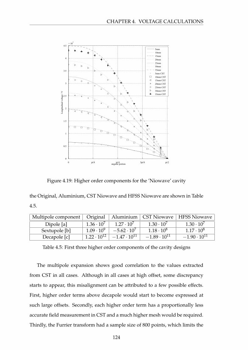
CHAPTER 4. VOLTAGE CALCULATIONS
angular poition
Lon
gitu
dina
l vol
tage
/ V
0 pi/8 pi/4 3pi/8 pi/2
0
0.5
1
1.5
2
2.5
3
3.5
4
4.5× 10
5
5mm
10mm
15mm
20mm
25mm
30mm
35mm
5mm CST
10mm CST
15mm CST
20mm CST
25mm CST
30mm CST
35mm CST
Figure 4.19: Higher order components for the ’Niowave’ cavity
the Original, Aluminium, CST Niowave and HFSS Niowave are shown in Table
4.5.
Multipole component Original Aluminium CST Niowave HFSS NiowaveDipole [a] 1.36 · 107 1.27 · 107 1.30 · 107 1.30 · 107
Sextupole [b] 1.09 · 109 −5.62 · 107 1.18 · 108 1.17 · 108
Decapole [c] 1.22 · 1012 −1.47 · 1011 −1.89 · 1011 −1.90 · 1011
Table 4.5: First three higher order components of the cavity designs
The multipole expansion shows good correlation to the values extracted
from CST in all cases. Although in all cases at high offset, some discrepancy
starts to appear, this misalignment can be attributed to a few possible effects.
First, higher order terms above decapole would start to become expressed at
such large offsets. Secondly, each higher order term has a proportionally less
accurate field measurement in CST and a much higher mesh would be required.
Thirdly, the Furrier transform had a sample size of 800 points, which limits the
124
4.13. SUMMARY
accuracy. Unfortunately the computing time to eliminate these discrepancies is
disproportionate to the benefit.
The original cavity with oval rods has significantly larger sextupole and
decapole components by an order of magnitude..
Both kidney shaped designs have very similar dipole components, however
the Niowave cavity, that has smaller tips compared to the Aluminium cav-
ity, has a positive sextupole instead of a negative one. The design difference
between the two cavities is the size and shape of the tip of the rod. Thus between
the two designs exists a shape that will have zero sextupole component.
The comparison between the Niowave cavity in CST and the HFSS model
also shows very good agreement. Both the dipole and sextupole components
are almost in perfect agreement. There is some discrepancy between the deca-
pole component but both are still relatively close and it is expected that the
inaccuracies mentioned earlier lead to this disagreement.
4.13 Summary
The uniformity of deflecting voltage required by the LHC was not initially
met by the original oval shaped rods. Alternative methods of flattening the
deflecting voltage were examined and a new shape was created. Parallel plates
would provide a uniform mode, however they resulted in an unacceptable drop
in R/Q and increased the size of the cavity beyond the limits that would allow
the cavity to be rotated to enable vertical crossing. Focus electrodes were used
to replicate the longer plate-like rods without compromising on the compact
nature of the cavity. The electrodes allowed for the minimisation of multipole
components that can adversely effect the dipole field.
The focus electrodes did not line up well with the geometry of the beam-
pipe, and a new shape was created that followed the contour of the beam-pipe.
The kidney shape provided all the advantages of the focus electrodes whilst
125
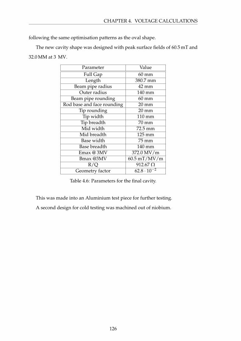
CHAPTER 4. VOLTAGE CALCULATIONS
following the same optimisation patterns as the oval shape.
The new cavity shape was designed with peak surface fields of 60.5 mT and
32.0 MM at 3 MV.
Parameter ValueFull Gap 60 mmLength 380.7 mm
Beam pipe radius 42 mmOuter radius 140 mm
Beam pipe rounding 60 mmRod base and face rounding 20 mm
Tip rounding 20 mmTip width 110 mm
Tip breadth 70 mmMid width 72.5 mm
Mid breadth 125 mmBase width 75 mm
Base breadth 140 mmEmax @ 3MV 372.0 MV/mBmax @3MV 60.5 mT/MV/m
R/Q 912.67 ΩGeometry factor 62.8 · 10−2
Table 4.6: Parameters for the final cavity.
This was made into an Aluminium test piece for further testing.
A second design for cold testing was machined out of niobium.
126
Chapter 5
Bead Pull
5.1 Introduction
To verify the simulated design of the cavity, an aluminum prototype was
manufactured. This allowed for experimental verification of the 4RCC via bead
pull.
It is possible to measure the electromagnetic properties of RF structures by
perturbing the fields within them and measuring the response. By comparing
the measured response to that of a theoretic response it is possible to character-
ise the RF structure.
A common perturbation technique that can characterise a cavity is a bead
pull. This consists of a metal or dielectric object of known shape being pulled
through the cavity by a thin wire. The wire is usually considerably smaller than
the bead and made of a material that will not perturb the cavity significantly
compared to the perturbation from the bead, in this case kevlar. The bead alters
the frequency of the cavity as the local field patterns are disrupted by the change
of local permeability and permittivity. The shift in frequency is proportional to
the strength of the electric and magnetic fields.
Typically needles, disks and spheres are used, as the perturbation from these
objects can be calculated reasonably easily. For modes with longitudinal electric
fields, a needle is typically used as this interacts significantly more with the
127
CHAPTER 5. BEAD PULL
longitudinal electric field when pulled along the longitudinal axis. Transverse
fields can be selected by using a disk. By using a dielectric object, only the
electric fields can be measured allowing for the separation of the magnetic field.
5.2 Bead Pull Theory
By inserting a small metallic or dielectric object into a cavity it is possible to
measure the perturbation in resonant frequency. The perturbation of the cavity
frequency can be calculated from the perturbing objects disruption to the local
permittivity and permeability, a new resonant frequency can then be measured
and the shift, compared to the unperturbed cavity, calculated. The perturbation
can then be used to calculate the fields of the cavity from the shift in frequency.
Assuming the perturbation is small, the effect of the perturbation has the
following form. [78]
ω−ω0
ω=
´(∆εE · E∗0 + ∆µH ·H∗0) · dV´ (
ε0E · E∗0 + µ0H ·H∗0)· dV
(5.1)
Where ω is the angular frequency, ε is the
In the case of small perturbations we can assume that : E ≈ E0, H ≈ H0 and
ω ≈ ω0.
This allows for the simplification :
ω−ω0
ω= −
´(∆εE · E∗0 + ∆µH ·H∗0) · dV
4W(5.2)
where W is the the total energy stored in the cavity.
This is then integrated to give :
128
5.2. BEAD PULL THEORY
∆ ff0
=1
W
(ε0αEE2
0 + µ0αmH20
)(5.3)
where αE is the the electric polarisability and αM the magnetic polarisability
of the object.
To profile the absolute electric and magnetic fields in the cavity, measure-
ments are made on axis with both a dielectric and a metal bead. As the dielec-
tric bead interacts with only the electric field it is possible to subtract this away
from the metal profile to extract the magnetic field.
For a sphere the polarisability is given by
α = −πa3 ξ − 1ξ + 2
(5.4)
where a is the radius of the sphere and ξ is the relative permeability µr or
permittivity εr.
For a metal sphere where εr → ∞ and µr = 0 :
αE =−πa3 (5.5)
αM =12
πa3 (5.6)
To calculate the electric field on axis the pure dielectric data can be used. As
the shift in frequency can be either positive or negative the magnitude of the
frequency shift must be used to avoid taking the root of a negative number.
|E| =√
|∆ f |f0
1W ε0αE
(5.7)
However for the magnetic field the frequency shift used must be adjusted
to account for the electric field. Thus the magnetic frequency shift ∆ fm can be
calculated as:
129
CHAPTER 5. BEAD PULL
∆ fm = (∆ fDia · κ)− |∆ fmetal| (5.8)
where the proportionality constant κ = ξ−1ξ+2 , ∆ fDia is the frequency shift due to
the dielectric bead and ∆ fmetal is the shift due to the metal bead.
This allows for the magnetic field to then be calculated.
|B| =√|∆ fm|
f01
W µ0αM(5.9)
To profile the transverse fields in the cavity, only the longitudinal electric
field is of interest. To study the longitudinal field, E0 was split into longitudinal
and horizontal components Et and Ez. [79]The assumption was made that the
transverse effect would be significantly smaller than the longitudinal effect and
could be neglected.
∆ ff0
=1
W
(ε0αEz |Ez|2 + ε0αEt |Et|2 − µ0αmz |Hz|2 − µ0αmt |Ht|2
)(5.10)
p| a
The polarisability of the needle is calculated as αE where β = ba with a being
half the length of the needle and b being the radius of the needle. An example
needle is shown in Figure 5.1.
αEz =−2
3 πa3(1− β2)32
ln 1+(1−β2)12
1−(1−β2)12− 2(1− β2)
12
(5.11)
αMz =−2
3 πa3(1− β2)32
ln 1+(1−β2)12
1−(1−β2)12− 2(1−β2)
12
β2
(5.12)
130
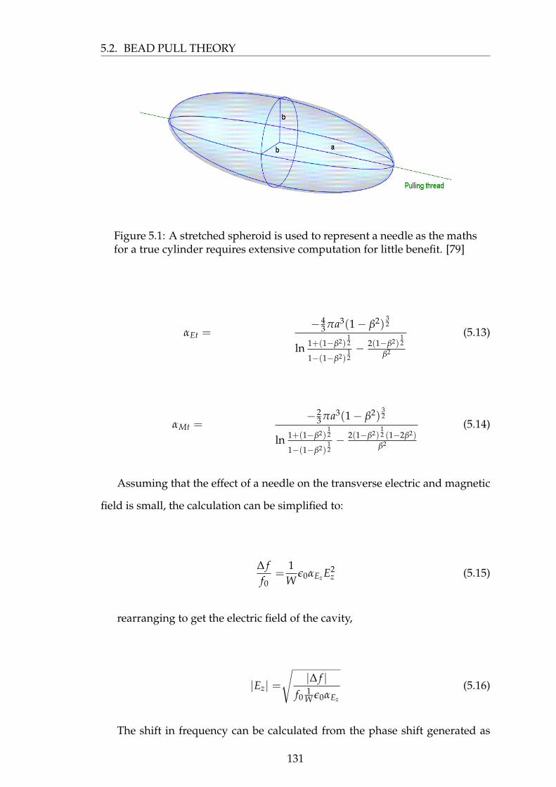
5.2. BEAD PULL THEORY
Figure 5.1: A stretched spheroid is used to represent a needle as the mathsfor a true cylinder requires extensive computation for little benefit. [79]
αEt =−4
3 πa3(1− β2)32
ln 1+(1−β2)12
1−(1−β2)12− 2(1−β2)
12
β2
(5.13)
αMt =−2
3 πa3(1− β2)32
ln 1+(1−β2)12
1−(1−β2)12− 2(1−β2)
12 (1−2β2)
β2
(5.14)
Assuming that the effect of a needle on the transverse electric and magnetic
field is small, the calculation can be simplified to:
∆ ff0
=1
Wε0αEz E2
z (5.15)
rearranging to get the electric field of the cavity,
|Ez| =√
|∆ f |f0
1W ε0αEz
(5.16)
The shift in frequency can be calculated from the phase shift generated as
131
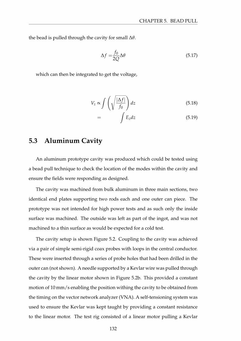
CHAPTER 5. BEAD PULL
the bead is pulled through the cavity for small ∆θ.
∆ f =f0
2Q∆θ (5.17)
which can then be integrated to get the voltage,
Vz ∝ˆ (√ |∆ f |
f0
)dz (5.18)
=
ˆEzdz (5.19)
5.3 Aluminum Cavity
An aluminum prototype cavity was produced which could be tested using
a bead pull technique to check the location of the modes within the cavity and
ensure the fields were responding as designed.
The cavity was machined from bulk aluminum in three main sections, two
identical end plates supporting two rods each and one outer can piece. The
prototype was not intended for high power tests and as such only the inside
surface was machined. The outside was left as part of the ingot, and was not
machined to a thin surface as would be expected for a cold test.
The cavity setup is shown Figure 5.2. Coupling to the cavity was achieved
via a pair of simple semi-rigid coax probes with loops in the central conductor.
These were inserted through a series of probe holes that had been drilled in the
outer can (not shown). A needle supported by a Kevlar wire was pulled through
the cavity by the linear motor shown in Figure 5.2b. This provided a constant
motion of 10 mm/s enabling the position withing the cavity to be obtained from
the timing on the vector network analyzer (VNA). A self-tensioning system was
used to ensure the Kevlar was kept taught by providing a constant resistance
to the linear motor. The test rig consisted of a linear motor pulling a Kevlar
132
5.3. ALUMINUM CAVITY
string against a tensor unit, driven at a fixed speed. At each end of the rig a
pair of stepper motors allowed the position of the Kevlar wire to be altered and
aligned with the cavity in either the horizontal or vertical directions and are
shown in Figure5.2a. The cavity is contained inside a mobile clean room to act
as a pressure baffle against entry to the lab. The motors and network analyser
are controlled through a LabView script that synchronises the linear motor and
time domain data sampling.
(a) (b)
(c)
Figure 5.2: Pictures of the beadpull setup
5.3.1 Needle Choice
By using the on axis measurement to correct transverse fields some of the
error was reduced. Ideally just the longitudinal field will be picked up but as
shown in Section 5.2 this is not the case due to the finite width of the needle
required for threading.
133
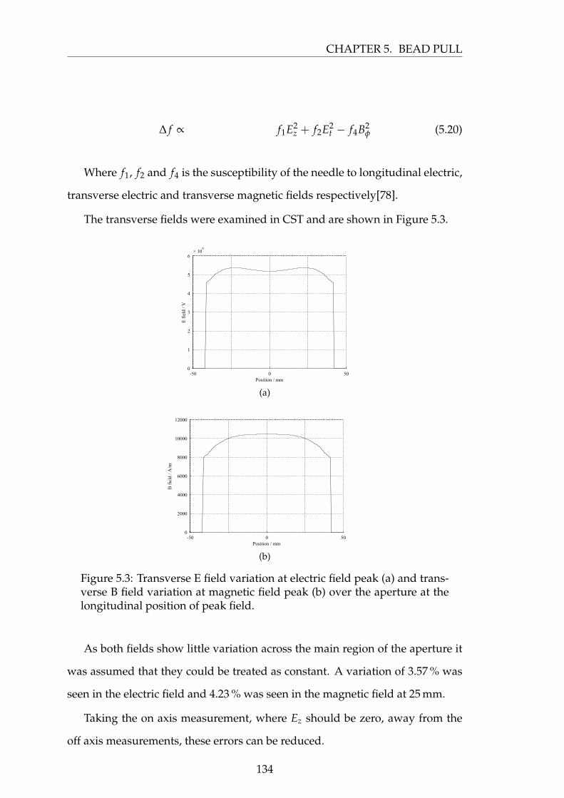
CHAPTER 5. BEAD PULL
∆ f ∝ f1E2z + f2E2
t − f4B2φ (5.20)
Where f1, f2 and f4 is the susceptibility of the needle to longitudinal electric,
transverse electric and transverse magnetic fields respectively[78].
The transverse fields were examined in CST and are shown in Figure 5.3.
Position / mm
E f
ield
/ V
-50 0 500
1
2
3
4
5
6× 10
6
(a)
Position / mm
B f
ield
/ A
/m
-50 0 500
2000
4000
6000
8000
10000
12000
(b)
Figure 5.3: Transverse E field variation at electric field peak (a) and trans-verse B field variation at magnetic field peak (b) over the aperture at thelongitudinal position of peak field.
As both fields show little variation across the main region of the aperture it
was assumed that they could be treated as constant. A variation of 3.57 % was
seen in the electric field and 4.23 % was seen in the magnetic field at 25 mm.
Taking the on axis measurement, where Ez should be zero, away from the
off axis measurements, these errors can be reduced.
134
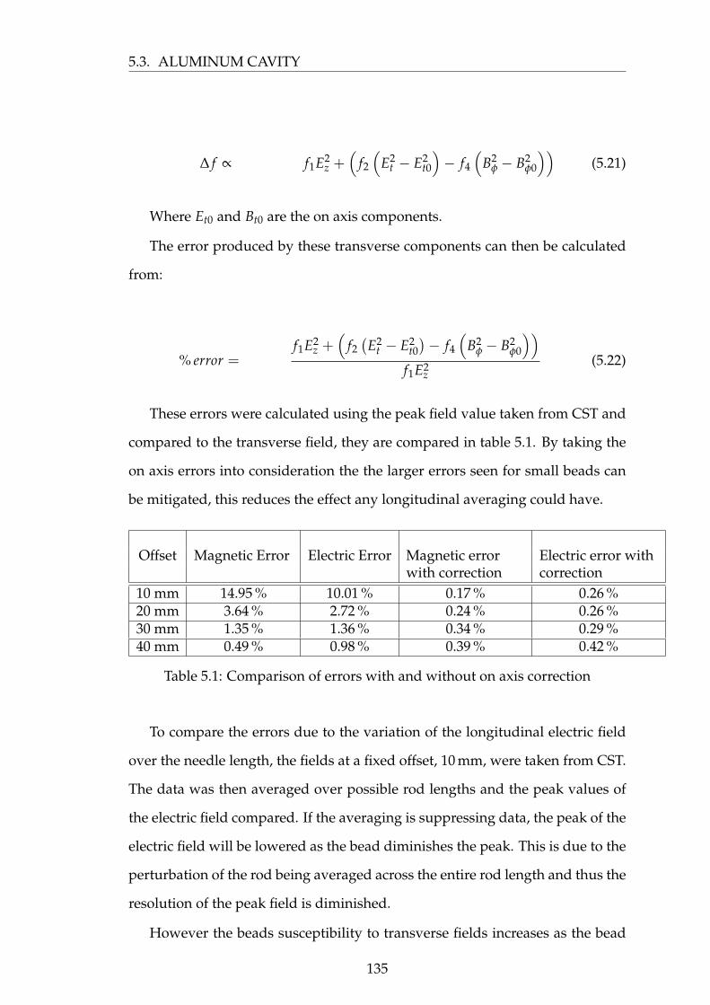
5.3. ALUMINUM CAVITY
∆ f ∝ f1E2z +
(f2
(E2
t − E2t0
)− f4
(B2
φ − B2φ0
))(5.21)
Where Et0 and Bt0 are the on axis components.
The error produced by these transverse components can then be calculated
from:
% error =f1E2
z +(
f2(E2
t − E2t0)− f4
(B2
φ − B2φ0
))f1E2
z(5.22)
These errors were calculated using the peak field value taken from CST and
compared to the transverse field, they are compared in table 5.1. By taking the
on axis errors into consideration the the larger errors seen for small beads can
be mitigated, this reduces the effect any longitudinal averaging could have.
Offset Magnetic Error Electric Error Magnetic errorwith correction
Electric error withcorrection
10 mm 14.95 % 10.01 % 0.17 % 0.26 %20 mm 3.64 % 2.72 % 0.24 % 0.26 %30 mm 1.35 % 1.36 % 0.34 % 0.29 %40 mm 0.49 % 0.98 % 0.39 % 0.42 %
Table 5.1: Comparison of errors with and without on axis correction
To compare the errors due to the variation of the longitudinal electric field
over the needle length, the fields at a fixed offset, 10 mm, were taken from CST.
The data was then averaged over possible rod lengths and the peak values of
the electric field compared. If the averaging is suppressing data, the peak of the
electric field will be lowered as the bead diminishes the peak. This is due to the
perturbation of the rod being averaged across the entire rod length and thus the
resolution of the peak field is diminished.
However the beads susceptibility to transverse fields increases as the bead
135
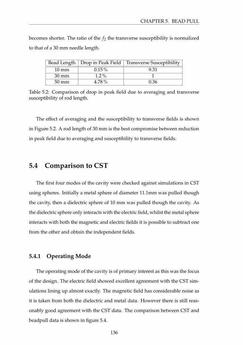
CHAPTER 5. BEAD PULL
becomes shorter. The ratio of the f2 the transverse susceptibility is normalized
to that of a 30 mm needle length.
Bead Length Drop in Peak Field Transverse Susceptibility10 mm 0.15 % 9.3130 mm 1.2 % 150 mm 4.78 % 0.36
Table 5.2: Comparison of drop in peak field due to averaging and transversesusceptibility of rod length.
The effect of averaging and the susceptibility to transverse fields is shown
in Figure 5.2. A rod length of 30 mm is the best compromise between reduction
in peak field due to averaging and susceptibility to transverse fields.
5.4 Comparison to CST
The first four modes of the cavity were checked against simulations in CST
using spheres. Initially a metal sphere of diameter 11.1mm was pulled though
the cavity, then a dielectric sphere of 10 mm was pulled though the cavity. As
the dielectric sphere only interacts with the electric field, whilst the metal sphere
interacts with both the magnetic and electric fields it is possible to subtract one
from the other and obtain the independent fields.
5.4.1 Operating Mode
The operating mode of the cavity is of primary interest as this was the focus
of the design. The electric field showed excellent agreement with the CST sim-
ulations lining up almost exactly. The magnetic field has considerable noise as
it is taken from both the dielectric and metal data. However there is still reas-
onably good agreement with the CST data. The comparison between CST and
beadpull data is shown in figure 5.4.
136
5.4. COMPARISON TO CST
Position in cavity / cm
Pha
se p
ertu
batio
n / R
ads
0 10 20 30 40 50 60 70 80-0.6
-0.5
-0.4
-0.3
-0.2
-0.1
0
0.1
0.2
Metal bead
Dielectric bead
(a)Position / cm
|Ele
ctri
c fi
eld|
/ V
0 10 20 30 40 50 60 700
1
2
3
4
5
6× 10
6
Bead pull
CST data
(b)
Position / cm
|Mag
netic
fie
ld| /
V
0 10 20 30 40 50 60 700
2000
4000
6000
8000
10000
12000
14000
16000
Bead pull
CST data
(c)Position / mm
Ele
ctri
c fi
eld
/ V
0 10 20 30 40 50 60 70 800
2
4
6
8
10
12
14× 10
5
Bead Pull Data
CST Simulated result
(d)
Figure 5.4: The operating mode on axis for metal and dielectric spheres isshown in a. The comparison between the on axis electric field bead pulland CST at U = 1 J is shown in b.The comparison between the on axismagnetic field bead pull and CST at U = 1 J is shown in c. A comparisonbetween CST and bead pull data for the longitudinal electric field is shownin d U = 1 J.
5.4.2 Lower order mode
The comparison between bead pull data and CST simulations is shown in
Figure 5.5. The results show reasonable correlation to the simulation with the
peak electric field where expected. However it is slightly lower than expected.
The magnetic field was expected to be zero but due to the non zero noise offset
seen in the longitudinal measurements a non zero value is returned. This non
zero value consists of noise and is of the same level as the noise seen in higher
order modes.
137
CHAPTER 5. BEAD PULL
Position in cavity / cm
Pha
se p
ertu
batio
n / R
ads
0 10 20 30 40 50 60 70 80-0.8
-0.7
-0.6
-0.5
-0.4
-0.3
-0.2
-0.1
0
0.1
Metal bead
Dielectric bead
(a)Position / cm
|Ele
ctri
c fi
eld|
/ V
0 10 20 30 40 50 60 70 800
1
2
3
4
5
6× 10
6
Bead pull
CST data
(b)
Figure 5.5: The lower order mode on axis metal and dielectric sphere isshown in a, the LOM electric field on axis compared to the calculated valuefrom CST U = 1 J is shown in b.
5.5 Bead Pull of Four Rod Cavity
Initial testing showed the bead pull set-up used, contained inherent errors
in measurement. The needle used picked up a trace amount of transverse field.
Assuming the transverse components to be uniform over the aperture, by
taking a measurement at the centre of the cavity where the Ez field should be
zero the perturbation due to the transverse fields can be measured. This can be
taken into consideration and accounted for in the processing of the data.
To account for this, the measured perturbation was split into ∆ frf0
, the desired
electric field, and ∆ ftf0
, the perturbation seen on axis due to the transverse fields.
Figure 5.6a shows the raw unprocessed on axis data taken from the network
analyser. This could then be cleaned up to reduce the noise via averaging over
three points and normalized to zero and converted into a frequency shift, as
seen in Figure 5.6b. The positive shift is due to the magnetic field while the
negative shift is due to the electric field, thus the transverse perturbation ∆ ftf0
is made up of both transverse electric and transverse magnetic components. If
the on axis signal is further processed to acquire the electric field as for the off
axis signals would the shift caused by the transverse fields can be clearly seen
as four peaks as shown in Figure 5.6c. There should be no on axis field, as such
138
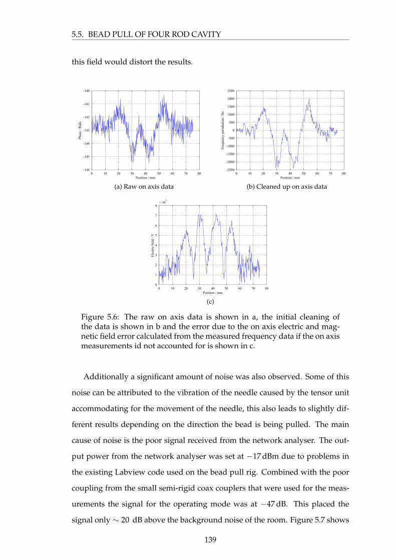
5.5. BEAD PULL OF FOUR ROD CAVITY
this field would distort the results.
Position / mm
Pha
se /
Rad
s
0 10 20 30 40 50 60 70 80-146
-145
-144
-143
-142
-141
-140
(a) Raw on axis dataPosition / mm
Fre
quen
cy p
ertu
batio
n / H
z
0 10 20 30 40 50 60 70 80-2500
-2000
-1500
-1000
-500
0
500
1000
1500
2000
2500
(b) Cleaned up on axis data
Position / mm
Ele
ctri
c fi
eld
/ V
0 10 20 30 40 50 60 70 800
1
2
3
4
5
6
7
8× 10
5
(c)
Figure 5.6: The raw on axis data is shown in a, the initial cleaning ofthe data is shown in b and the error due to the on axis electric and mag-netic field error calculated from the measured frequency data if the on axismeasurements id not accounted for is shown in c.
Additionally a significant amount of noise was also observed. Some of this
noise can be attributed to the vibration of the needle caused by the tensor unit
accommodating for the movement of the needle, this also leads to slightly dif-
ferent results depending on the direction the bead is being pulled. The main
cause of noise is the poor signal received from the network analyser. The out-
put power from the network analyser was set at −17 dBm due to problems in
the existing Labview code used on the bead pull rig. Combined with the poor
coupling from the small semi-rigid coax couplers that were used for the meas-
urements the signal for the operating mode was at −47 dB. This placed the
signal only ∼ 20 dB above the background noise of the room. Figure 5.7 shows
139
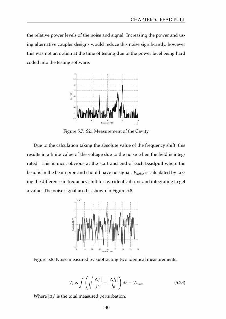
CHAPTER 5. BEAD PULL
the relative power levels of the noise and signal. Increasing the power and us-
ing alternative coupler designs would reduce this noise significantly, however
this was not an option at the time of testing due to the power level being hard
coded into the testing software.
Frequency / Hz
S21
/ dB
3 3.5 4 4.5 5-70
-65
-60
-55
-50
-45
-40
-35
-30
× 108
Figure 5.7: S21 Measurement of the Cavity
Due to the calculation taking the absolute value of the frequency shift, this
results in a finite value of the voltage due to the noise when the field is integ-
rated. This is most obvious at the start and end of each beadpull where the
bead is in the beam pipe and should have no signal. Vnoise is calculated by tak-
ing the difference in frequency shift for two identical runs and integrating to get
a value. The noise signal used is shown in Figure 5.8.
Position / mm
Ele
ctri
c fi
eld
/ V
0 10 20 30 40 50 60 70 800
1
2
3
4
5
6× 10
5
Figure 5.8: Noise measured by subtracting two identical measurements.
Vz ∝ˆ (√ |∆ f |
f0− |∆ ft|
f0
)dz−Vnoise (5.23)
Where |∆ f |is the total measured perturbation.
140
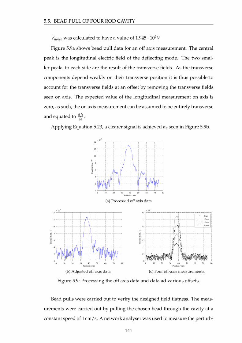
5.5. BEAD PULL OF FOUR ROD CAVITY
Vnoise was calculated to have a value of 1.945 · 105V
Figure 5.9a shows bead pull data for an off axis measurement. The central
peak is the longitudinal electric field of the deflecting mode. The two smal-
ler peaks to each side are the result of the transverse fields. As the transverse
components depend weakly on their transverse position it is thus possible to
account for the transverse fields at an offset by removing the transverse fields
seen on axis. The expected value of the longitudinal measurement on axis is
zero, as such, the on axis measurement can be assumed to be entirely transverse
and equated to ∆ ftf0
.
Applying Equation 5.23, a clearer signal is achieved as seen in Figure 5.9b.
Position / mm
Ele
ctri
c fi
eld
/ V
0 10 20 30 40 50 60 70 800
2
4
6
8
10
12
14× 10
5
(a) Processed off axis data
Position / mm
Ele
ctri
c fi
eld
/ V
0 10 20 30 40 50 60 70 800
2
4
6
8
10
12
14× 10
5
(b) Adjusted off axis dataPosition / mm
Ele
ctri
c fi
eld
/ V
0 10 20 30 40 50 60 70 800
0.5
1
1.5
2
2.5
3
3.5× 10
6
8mm
12mm
16mm
20mm
(c) Four off-axis measurements.
Figure 5.9: Processing the off axis data and data ad various offsets.
Bead pulls were carried out to verify the designed field flatness. The meas-
urements were carried out by pulling the chosen bead through the cavity at a
constant speed of 1 cm/s. A network analyser was used to measure the perturb-
141
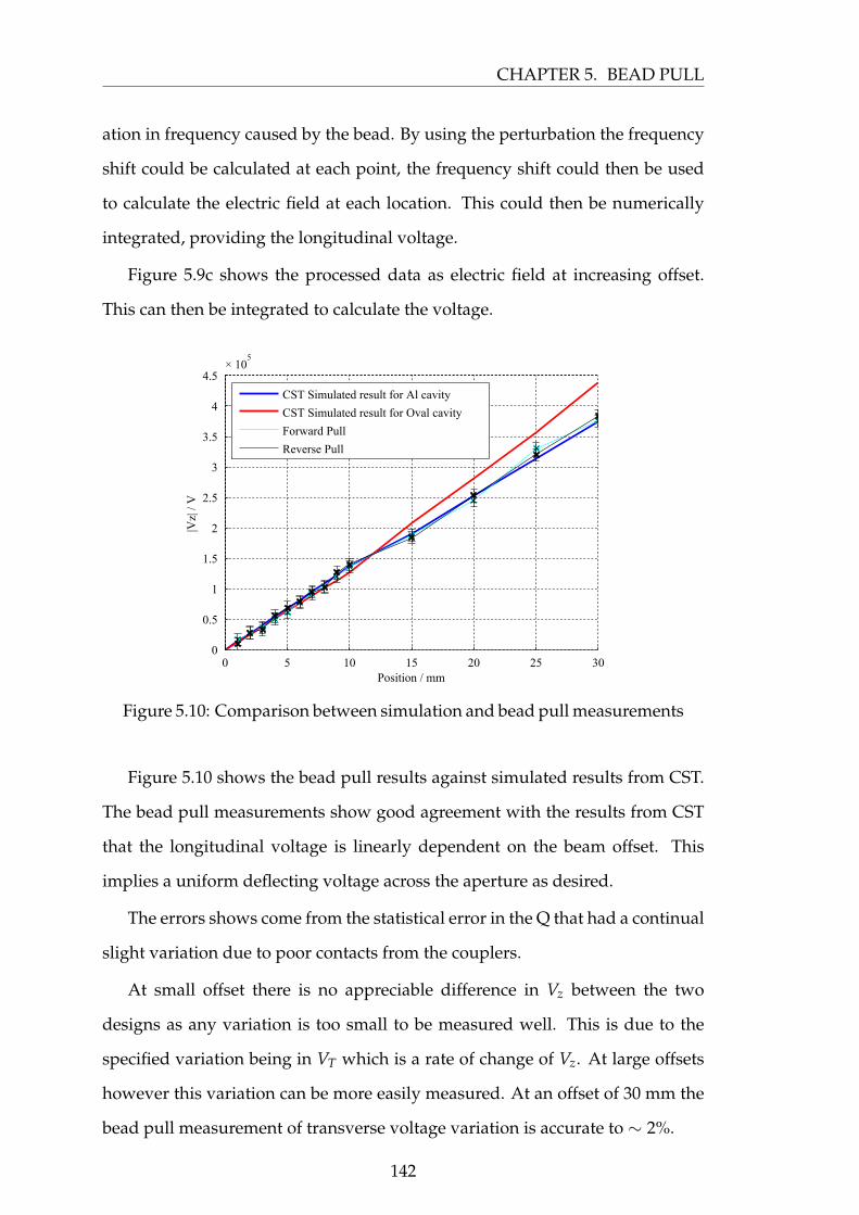
CHAPTER 5. BEAD PULL
ation in frequency caused by the bead. By using the perturbation the frequency
shift could be calculated at each point, the frequency shift could then be used
to calculate the electric field at each location. This could then be numerically
integrated, providing the longitudinal voltage.
Figure 5.9c shows the processed data as electric field at increasing offset.
This can then be integrated to calculate the voltage.
Position / mm
|Vz|
/ V
0 5 10 15 20 25 300
0.5
1
1.5
2
2.5
3
3.5
4
4.5× 10
5
CST Simulated result for Al cavity
CST Simulated result for Oval cavity
Forward Pull
Reverse Pull
Figure 5.10: Comparison between simulation and bead pull measurements
Figure 5.10 shows the bead pull results against simulated results from CST.
The bead pull measurements show good agreement with the results from CST
that the longitudinal voltage is linearly dependent on the beam offset. This
implies a uniform deflecting voltage across the aperture as desired.
The errors shows come from the statistical error in the Q that had a continual
slight variation due to poor contacts from the couplers.
At small offset there is no appreciable difference in Vz between the two
designs as any variation is too small to be measured well. This is due to the
specified variation being in VT which is a rate of change of Vz. At large offsets
however this variation can be more easily measured. At an offset of 30 mm the
bead pull measurement of transverse voltage variation is accurate to ∼ 2%.
142
5.6. SUMMARY
5.6 Summary
The Aluminium cavity that was produced for experimentation provided
measurements which confirmed the basic properties of the cavity and allowed
for the fields within the cavity to be tested via bead-pull. Although significant
noise was initially seen, through processing and adjustment taking on axis er-
rors into count, useful measurements were able to be taken and compared to
simulations from CST.
The cavity showed close agreement with the simulations despite errors cal-
culated. The field uniformity lies within the error of the measurement and as
such is assumed to be within tolerance as no major deviation was seen.
The fields of the cavity match well with the expected fields as calculated
from CST for both the operating mode and the lower order mode. The good
correlation with the expected results through bead pull implies the cavity is
operating as designed. The bead pull can clearly tell the difference between the
oval design and aluminium designs.
143
Chapter 6
Multipacting
6.1 Introduction
A major limiting factor in many RF cavities is multipacting. Multipacting is
the build-up of unwanted electrons that absorb the RF power within the cavity
system, which reduces the energy available to the beam and limits gradient[80,
81, 82]. The initial build up of electrons is caused by an exponential cascade of
secondary electrons until a steady state of saturation is reached. The electron
population is sustained by secondary emission of electrons from impacts with
the surface.
Multipacting can thus be a ’show stopper’ for a cavity design, as it can
render the entire cavity unusable if it cannot be processed through. The LHC-4R
crab cavity operates in a 400 MHz dipole like mode. Dipole cylindrical cavities
at lower frequencies, below ∼ 1.5 GHz, have been shown to exhibit multipact-
ing in the iris region[81]. The LHC-4R crab cavity was examined for multipact-
ing to ensure it did not multipact in the desired region of operation. Full 3D
simulations using CST Particle studio were undertaken following a previously
benchmarked procedure to look for multipacting in the cavity. The results of
this study follow.
144
6.2. THEORY OF MULTIPACTING
6.2 Theory of Multipacting
Multiactor was first seen between two surfaces supporting an RF field [83],
but it was first categorized and shown to be a problem some years later[82].
Multipacting consists of the buildup of electrons within a system that is self-
sustaining. The RF field provides the power that allows the osculation to per-
petuate, while the repeated impacts with the surface or surfaces provide sec-
ondary electrons to increase the electron count. Initially this is often seen as an
exponential build up. The process eventually saturates as the number of sec-
ondary electrons produced for every impact approaches unity. If the average
number of electrons emitted is below unity, the total number of electrons in the
system will decrease over time and the electron cloud will dissipate.
The secondary electrons produced from an initial incident electron can be
generated in one of three ways:
• Back scattered or elastically-scattered electrons are those that are effect-
ively reflected back off of the surface.
• Re-diffused are those that are absorbed into the surface of the material, but
contain enough energy to break free from the surface a short time later.
• True secondaries are those that are produced from within the surface of
the material by the incident electron and are usually accompanied by on
of the other events.
The Ferman-Pivi model treats the back-scattered and re-defused electrons as
single electron events, thus each incident electron can only produce a single
electron as a secondary electron. The true secondaries are generally only in-
volved in events where the number of secondary electrons is greater than one.
Although this is not a true model of the electron behavior - a secondary electron
could be generated, and escape, while the incident electron is trapped within
the surface - the model was found to fit. This is shown in Figure 6.1. The num-
ber of electrons generated is known as the secondary emission yield (SEY).
145
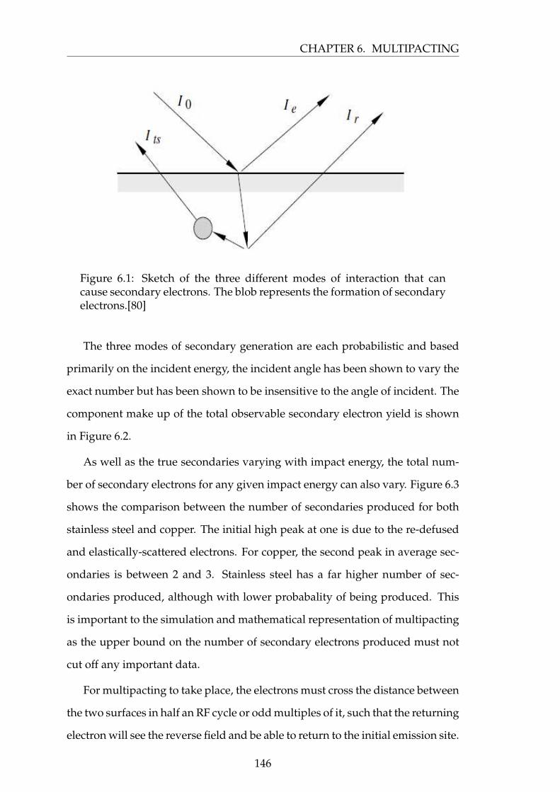
CHAPTER 6. MULTIPACTING
Figure 6.1: Sketch of the three different modes of interaction that cancause secondary electrons. The blob represents the formation of secondaryelectrons.[80]
The three modes of secondary generation are each probabilistic and based
primarily on the incident energy, the incident angle has been shown to vary the
exact number but has been shown to be insensitive to the angle of incident. The
component make up of the total observable secondary electron yield is shown
in Figure 6.2.
As well as the true secondaries varying with impact energy, the total num-
ber of secondary electrons for any given impact energy can also vary. Figure 6.3
shows the comparison between the number of secondaries produced for both
stainless steel and copper. The initial high peak at one is due to the re-defused
and elastically-scattered electrons. For copper, the second peak in average sec-
ondaries is between 2 and 3. Stainless steel has a far higher number of sec-
ondaries produced, although with lower probabality of being produced. This
is important to the simulation and mathematical representation of multipacting
as the upper bound on the number of secondary electrons produced must not
cut off any important data.
For multipacting to take place, the electrons must cross the distance between
the two surfaces in half an RF cycle or odd multiples of it, such that the returning
electron will see the reverse field and be able to return to the initial emission site.
146
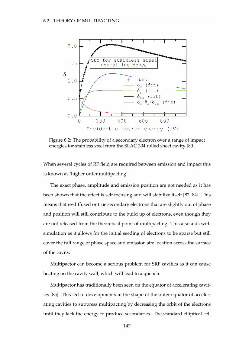
6.2. THEORY OF MULTIPACTING
Figure 6.2: The probability of a secondary electron over a range of impactenergies for stainless steel from the SLAC 304 rolled sheet cavity [80].
When several cycles of RF field are required between emission and impact this
is known as ’higher order multipacting’.
The exact phase, amplitude and emission position are not needed as it has
been shown that the effect is self focusing and will stabilize itself [82, 84]. This
means that re-diffused or true secondary electrons that are slightly out of phase
and position will still contribute to the build up of electrons, even though they
are not released from the theoretical point of multipacting. This also aids with
simulation as it allows for the initial seeding of electrons to be sparse but still
cover the full range of phase space and emission site location across the surface
of the cavity.
Multipactor can become a serious problem for SRF cavities as it can cause
heating on the cavity wall, which will lead to a quench.
Multipactor has traditionally been seen on the equator of accelerating cavit-
ies [85]. This led to developments in the shape of the outer equator of acceler-
ating cavities to suppress multipacting by decreasing the orbit of the electrons
until they lack the energy to produce secondaries. The standard elliptical cell
147
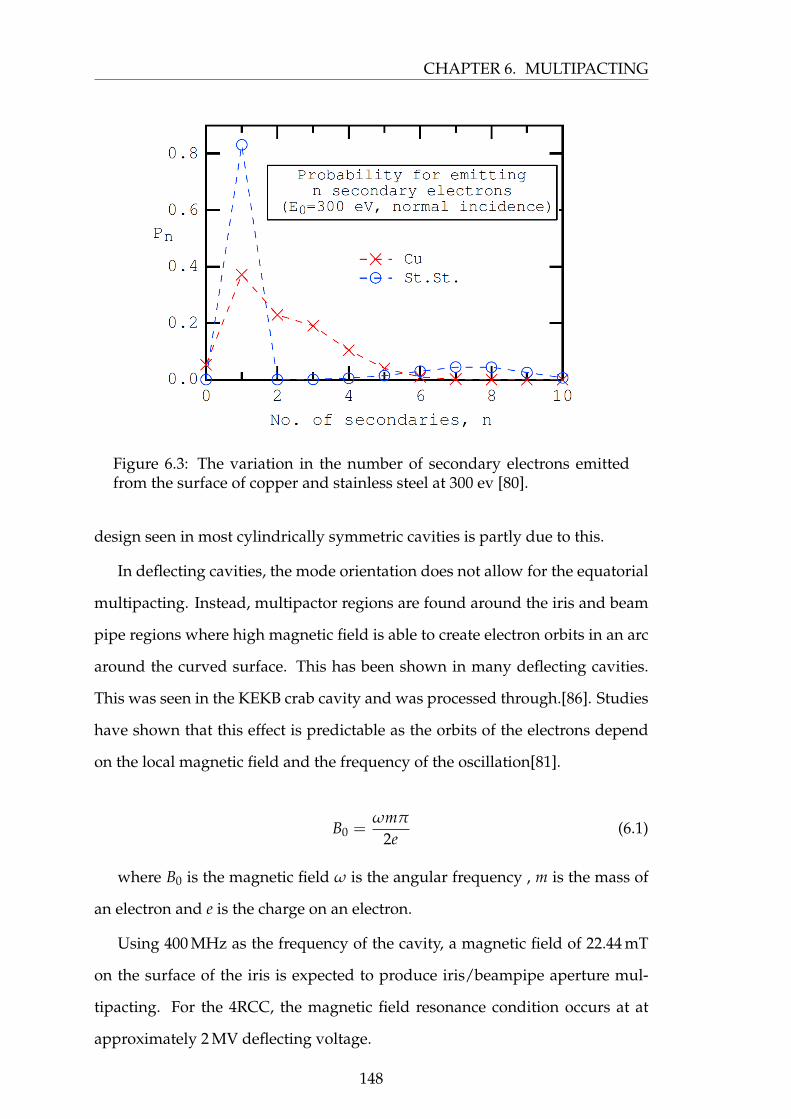
CHAPTER 6. MULTIPACTING
Figure 6.3: The variation in the number of secondary electrons emittedfrom the surface of copper and stainless steel at 300 ev [80].
design seen in most cylindrically symmetric cavities is partly due to this.
In deflecting cavities, the mode orientation does not allow for the equatorial
multipacting. Instead, multipactor regions are found around the iris and beam
pipe regions where high magnetic field is able to create electron orbits in an arc
around the curved surface. This has been shown in many deflecting cavities.
This was seen in the KEKB crab cavity and was processed through.[86]. Studies
have shown that this effect is predictable as the orbits of the electrons depend
on the local magnetic field and the frequency of the oscillation[81].
B0 =ωmπ
2e(6.1)
where B0 is the magnetic field ω is the angular frequency , m is the mass of
an electron and e is the charge on an electron.
Using 400 MHz as the frequency of the cavity, a magnetic field of 22.44 mT
on the surface of the iris is expected to produce iris/beampipe aperture mul-
tipacting. For the 4RCC, the magnetic field resonance condition occurs at at
approximately 2 MV deflecting voltage.
148
6.3. SIMULATION OF MULTIPACTING
6.3 Simulation of Multipacting
To simulate multipacting within a chosen structure CST Particle studio can
be used. It has been previously bench-marked on waveguide and cavities. CST
particle tracking is used instead of particle in cell as it allows the fields to be
calculated separately at high mesh and imported for tracking so the fields do
not need to be re-run for every simulation. The initial fields were calculated
at 200 lines per wavelength to ensure accurate fields near the surface and the
tracking solver ran at 120 lines per wavelength.
To determine if multipacting is present, the number of electrons emitted
from the surface of the cavity must be measured. Initially electrons are emitted
over a large area. Electrons not involved in multipacting are absorbed within
one or two cycles while the multipacting electrons quickly dominate. This is
then compared to the total number of impacts that generated these electrons.
By dividing the number of secondaries produced by the number of impacts, the
average secondary emission yield (< SEY >) can be calculated.
< SEY >=number o f secondaries
number o f impacts(6.2)
If the < SEY > is greater than one then the total number of electrons within
the cavity will grow and this will be an indicator of multipacting. The number of
electron in the cavity ,ne, increases as ne =< SEY >#r f , where #r f is the number
of RF cycles or impacts. If the < SEY > falls below one then the number of
electron will fall away to zero as each cycle reduces the total.
The solid object can then have SEY emission models applied to it to enable
the statistical models described in section to be implemented. The previously
calculated fields can be imported and be varied through phase and amplitude
to enable a full sweep across all phases and up to and past the desired region of
interest.
Faces within the shape can then be selected as sites for releasing electrons.
149
CHAPTER 6. MULTIPACTING
The level of seeding was adjusted so that there was approximately 1 electron per
sq. cm . If the number is too high, the solver will take an unacceptable length of
time to run. If the seeding is to low, the resonant trajectories will not be found.
The seeding does not need to be too much as the resonant trajectories can start
slightly off optimal position and will converge on to the optimal location over a
few osculations.
Three different surface conditions of niobium have been used for simulation
with different SEY:
• Wet treatment represents niobium that has been cleaned by high pressure
water, this removes most particular surface contaminants.
• 300 deg bake-out is treated niobium that may have had a bake out to re-
move hydrogen and oxygen on the surface.
• The Ar discharge cleaned surface represents a cleaned niobium surface
that has been processed. The nucleation sites for multipacting have been
bombarded by ions and less likely to emit secondary electrons as the sur-
face contaminants have been displaced. This is similar to an effect that
multipacting itself can cause, where the surface is processed by secondary
electrons, and can allow multipacting to be processed through by simply
running the machine.
Multipacting can be identified as either hard or soft, depending on how its <
SEY > changes as the material is processed. For multipacting to be hard its
< SEY > will remain above one as its processed. However if, as processing
takes place, the < SEY > decreases below one the multipacting is said to be
soft as it will die out. The initial surface of a cavity will have a high SEY. By
cleaning, heating the surface or applying acid the surface SEY can be altered as
contaminants are removed or added.
A full 3D eigen mode simulation was carried out with high mesh to estab-
lish the electromagnetic fields within the cavity using the basic vacuum cavity
150
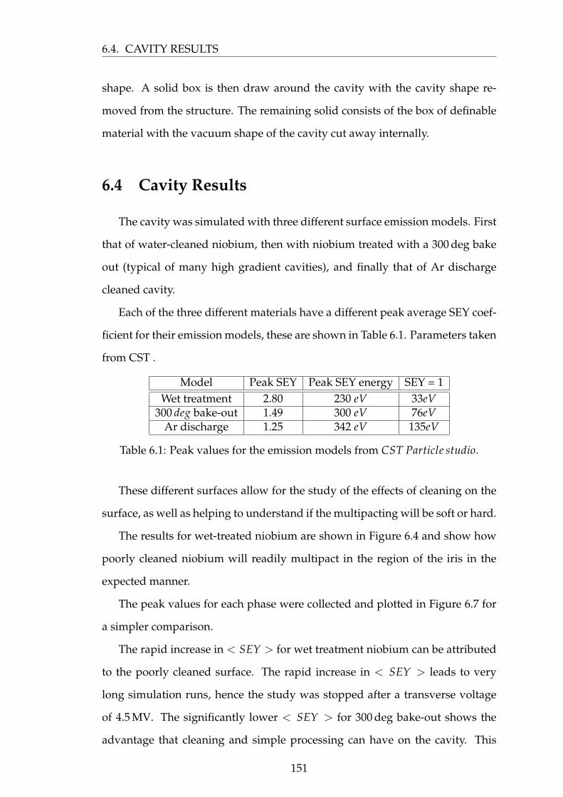
6.4. CAVITY RESULTS
shape. A solid box is then draw around the cavity with the cavity shape re-
moved from the structure. The remaining solid consists of the box of definable
material with the vacuum shape of the cavity cut away internally.
6.4 Cavity Results
The cavity was simulated with three different surface emission models. First
that of water-cleaned niobium, then with niobium treated with a 300 deg bake
out (typical of many high gradient cavities), and finally that of Ar discharge
cleaned cavity.
Each of the three different materials have a different peak average SEY coef-
ficient for their emission models, these are shown in Table 6.1. Parameters taken
from CST .
Model Peak SEY Peak SEY energy SEY = 1Wet treatment 2.80 230 eV 33eV
300 deg bake-out 1.49 300 eV 76eVAr discharge 1.25 342 eV 135eV
Table 6.1: Peak values for the emission models from CST Particle studio.
These different surfaces allow for the study of the effects of cleaning on the
surface, as well as helping to understand if the multipacting will be soft or hard.
The results for wet-treated niobium are shown in Figure 6.4 and show how
poorly cleaned niobium will readily multipact in the region of the iris in the
expected manner.
The peak values for each phase were collected and plotted in Figure 6.7 for
a simpler comparison.
The rapid increase in < SEY > for wet treatment niobium can be attributed
to the poorly cleaned surface. The rapid increase in < SEY > leads to very
long simulation runs, hence the study was stopped after a transverse voltage
of 4.5 MV. The significantly lower < SEY > for 300 deg bake-out shows the
advantage that cleaning and simple processing can have on the cavity. This
151
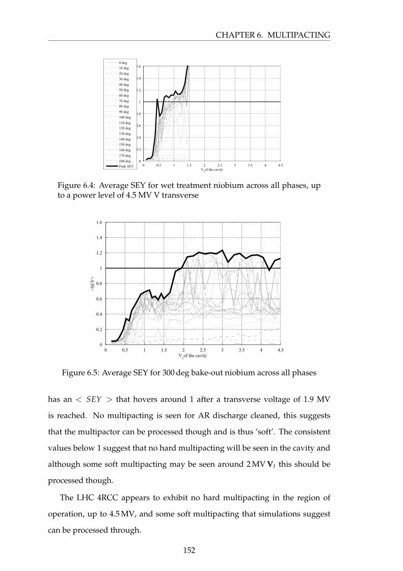
CHAPTER 6. MULTIPACTING
Vxof the cavity
<S
EY
>
0 0.5 1 1.5 2 2.5 3 3.5 4 4.50
0.2
0.4
0.6
0.8
1
1.2
1.4
1.60 deg
10 deg
20 deg
30 deg
40 deg
50 deg
60 deg
70 deg
80 deg
90 deg
100 deg
110 deg
120 deg
130 deg
140 deg
150 deg
160 deg
170 deg
180 deg
Peak SEY
Figure 6.4: Average SEY for wet treatment niobium across all phases, upto a power level of 4.5 MV V transverse
Vxof the cavity
<S
EY
>
0 0.5 1 1.5 2 2.5 3 3.5 4 4.50
0.2
0.4
0.6
0.8
1
1.2
1.4
1.6
Figure 6.5: Average SEY for 300 deg bake-out niobium across all phases
has an < SEY > that hovers around 1 after a transverse voltage of 1.9 MV
is reached. No multipacting is seen for AR discharge cleaned, this suggests
that the multipactor can be processed though and is thus ’soft’. The consistent
values below 1 suggest that no hard multipacting will be seen in the cavity and
although some soft multipacting may be seen around 2 MV Vt this should be
processed though.
The LHC 4RCC appears to exhibit no hard multipacting in the region of
operation, up to 4.5 MV, and some soft multipacting that simulations suggest
can be processed through.
152
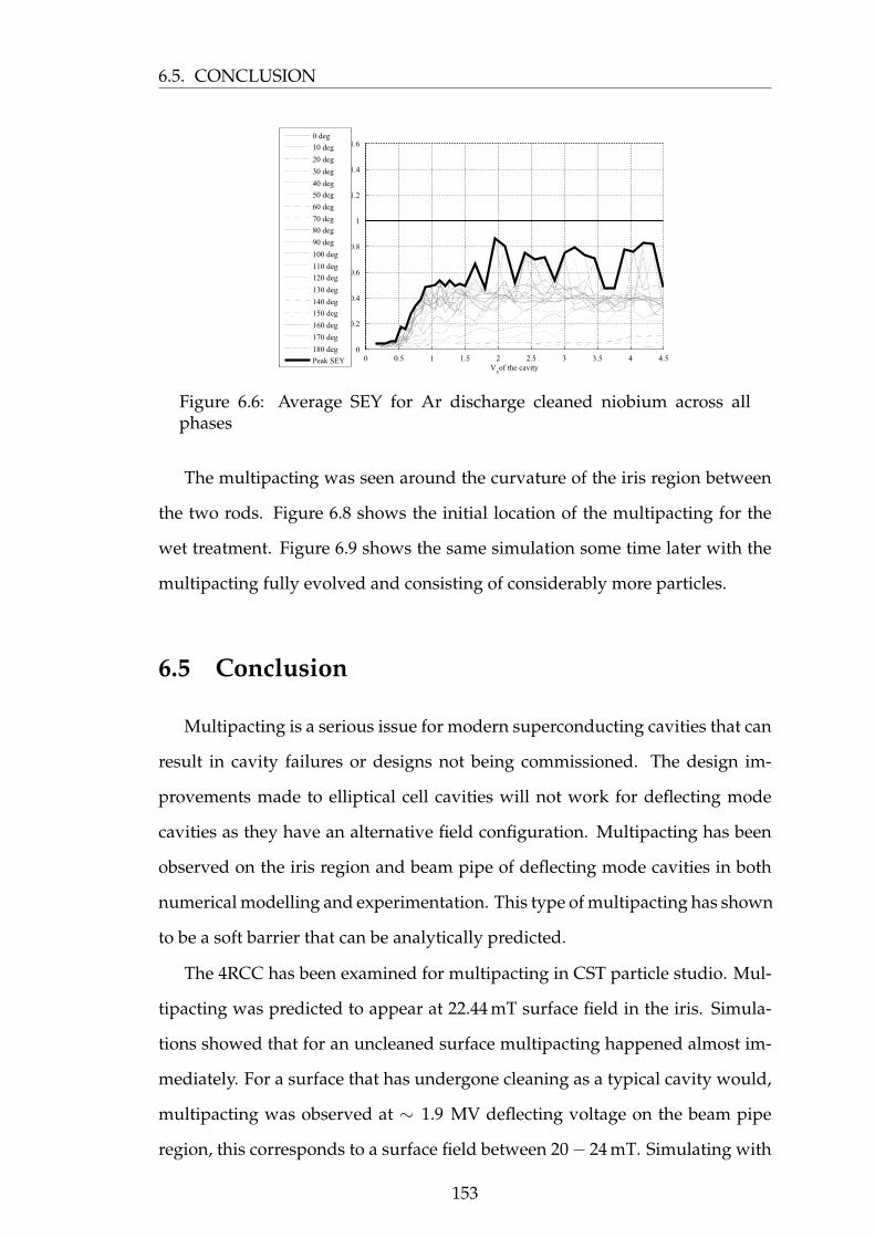
6.5. CONCLUSION
Vxof the cavity
<S
EY
>
0 0.5 1 1.5 2 2.5 3 3.5 4 4.50
0.2
0.4
0.6
0.8
1
1.2
1.4
1.60 deg
10 deg
20 deg
30 deg
40 deg
50 deg
60 deg
70 deg
80 deg
90 deg
100 deg
110 deg
120 deg
130 deg
140 deg
150 deg
160 deg
170 deg
180 deg
Peak SEY
Figure 6.6: Average SEY for Ar discharge cleaned niobium across allphases
The multipacting was seen around the curvature of the iris region between
the two rods. Figure 6.8 shows the initial location of the multipacting for the
wet treatment. Figure 6.9 shows the same simulation some time later with the
multipacting fully evolved and consisting of considerably more particles.
6.5 Conclusion
Multipacting is a serious issue for modern superconducting cavities that can
result in cavity failures or designs not being commissioned. The design im-
provements made to elliptical cell cavities will not work for deflecting mode
cavities as they have an alternative field configuration. Multipacting has been
observed on the iris region and beam pipe of deflecting mode cavities in both
numerical modelling and experimentation. This type of multipacting has shown
to be a soft barrier that can be analytically predicted.
The 4RCC has been examined for multipacting in CST particle studio. Mul-
tipacting was predicted to appear at 22.44 mT surface field in the iris. Simula-
tions showed that for an uncleaned surface multipacting happened almost im-
mediately. For a surface that has undergone cleaning as a typical cavity would,
multipacting was observed at ∼ 1.9 MV deflecting voltage on the beam pipe
region, this corresponds to a surface field between 20− 24 mT. Simulating with
153
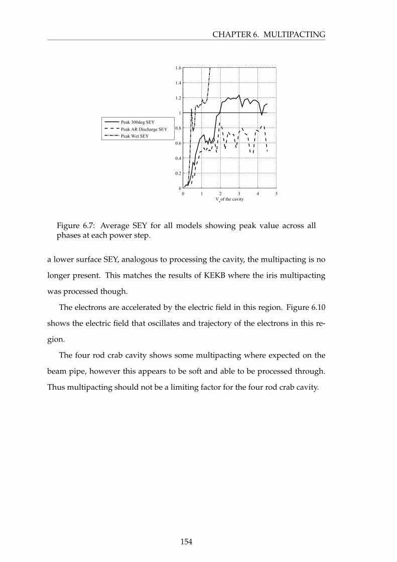
CHAPTER 6. MULTIPACTING
Vxof the cavity
<S
EY
>
0 1 2 3 4 50
0.2
0.4
0.6
0.8
1
1.2
1.4
1.6
Peak 300deg SEY
Peak AR Discharge SEY
Peak Wet SEY
Figure 6.7: Average SEY for all models showing peak value across allphases at each power step.
a lower surface SEY, analogous to processing the cavity, the multipacting is no
longer present. This matches the results of KEKB where the iris multipacting
was processed though.
The electrons are accelerated by the electric field in this region. Figure 6.10
shows the electric field that oscillates and trajectory of the electrons in this re-
gion.
The four rod crab cavity shows some multipacting where expected on the
beam pipe, however this appears to be soft and able to be processed through.
Thus multipacting should not be a limiting factor for the four rod crab cavity.
154
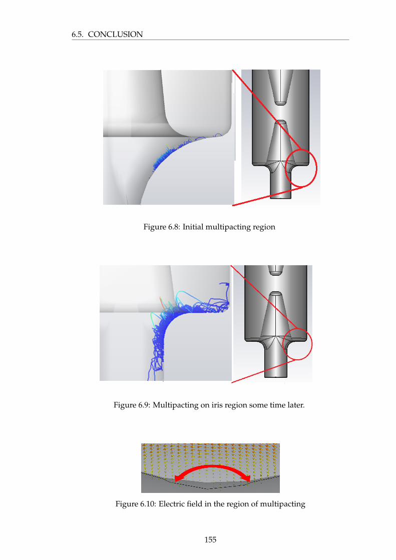
6.5. CONCLUSION
Figure 6.8: Initial multipacting region
Figure 6.9: Multipacting on iris region some time later.
Figure 6.10: Electric field in the region of multipacting
155
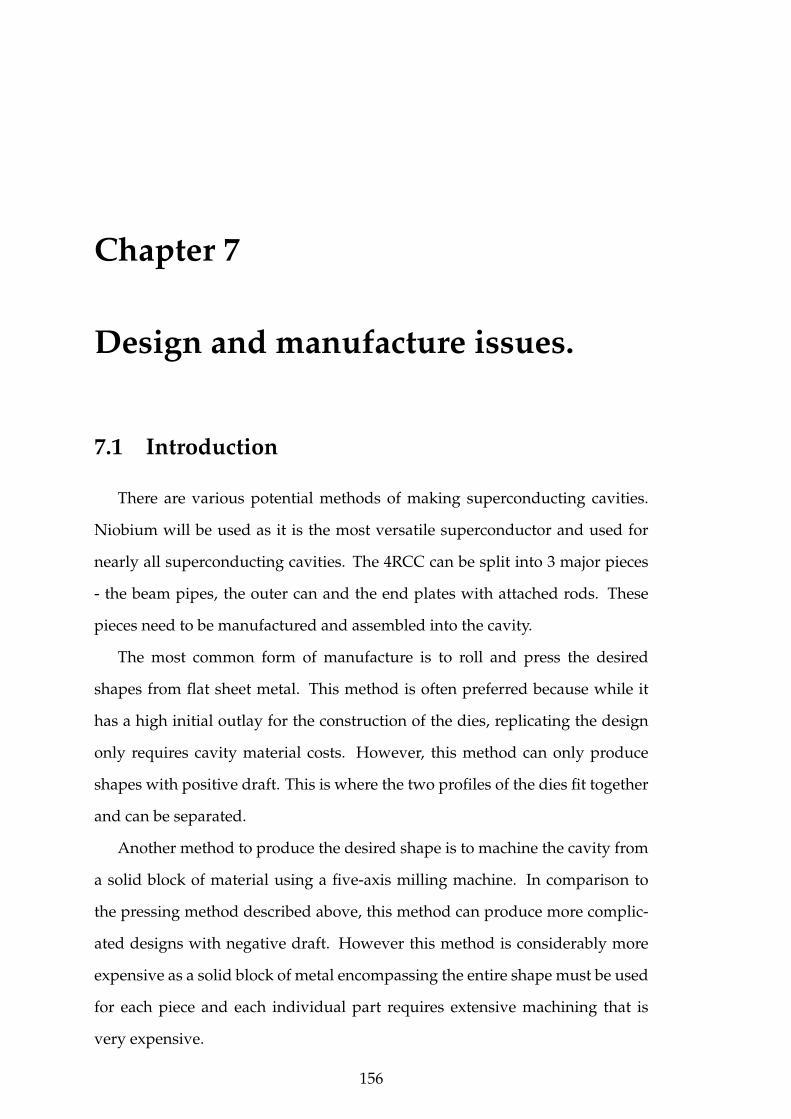
Chapter 7
Design and manufacture issues.
7.1 Introduction
There are various potential methods of making superconducting cavities.
Niobium will be used as it is the most versatile superconductor and used for
nearly all superconducting cavities. The 4RCC can be split into 3 major pieces
- the beam pipes, the outer can and the end plates with attached rods. These
pieces need to be manufactured and assembled into the cavity.
The most common form of manufacture is to roll and press the desired
shapes from flat sheet metal. This method is often preferred because while it
has a high initial outlay for the construction of the dies, replicating the design
only requires cavity material costs. However, this method can only produce
shapes with positive draft. This is where the two profiles of the dies fit together
and can be separated.
Another method to produce the desired shape is to machine the cavity from
a solid block of material using a five-axis milling machine. In comparison to
the pressing method described above, this method can produce more complic-
ated designs with negative draft. However this method is considerably more
expensive as a solid block of metal encompassing the entire shape must be used
for each piece and each individual part requires extensive machining that is
very expensive.
156
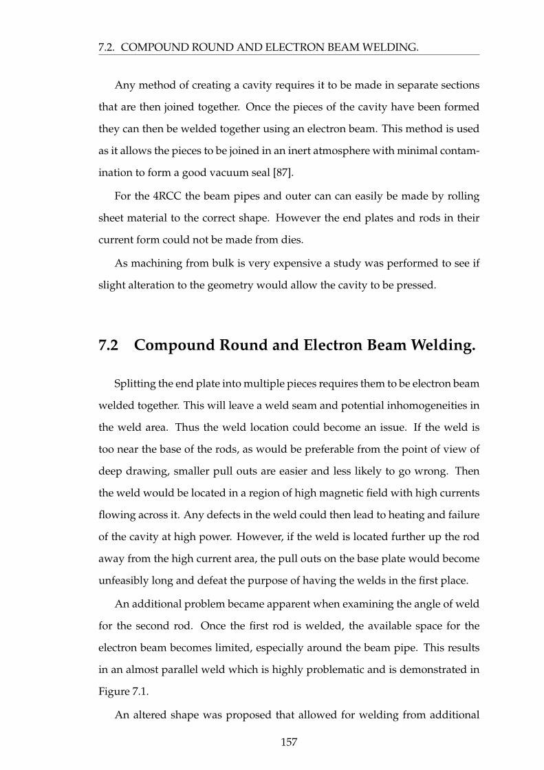
7.2. COMPOUND ROUND AND ELECTRON BEAM WELDING.
Any method of creating a cavity requires it to be made in separate sections
that are then joined together. Once the pieces of the cavity have been formed
they can then be welded together using an electron beam. This method is used
as it allows the pieces to be joined in an inert atmosphere with minimal contam-
ination to form a good vacuum seal [87].
For the 4RCC the beam pipes and outer can can easily be made by rolling
sheet material to the correct shape. However the end plates and rods in their
current form could not be made from dies.
As machining from bulk is very expensive a study was performed to see if
slight alteration to the geometry would allow the cavity to be pressed.
7.2 Compound Round and Electron Beam Welding.
Splitting the end plate into multiple pieces requires them to be electron beam
welded together. This will leave a weld seam and potential inhomogeneities in
the weld area. Thus the weld location could become an issue. If the weld is
too near the base of the rods, as would be preferable from the point of view of
deep drawing, smaller pull outs are easier and less likely to go wrong. Then
the weld would be located in a region of high magnetic field with high currents
flowing across it. Any defects in the weld could then lead to heating and failure
of the cavity at high power. However, if the weld is located further up the rod
away from the high current area, the pull outs on the base plate would become
unfeasibly long and defeat the purpose of having the welds in the first place.
An additional problem became apparent when examining the angle of weld
for the second rod. Once the first rod is welded, the available space for the
electron beam becomes limited, especially around the beam pipe. This results
in an almost parallel weld which is highly problematic and is demonstrated in
Figure 7.1.
An altered shape was proposed that allowed for welding from additional
157
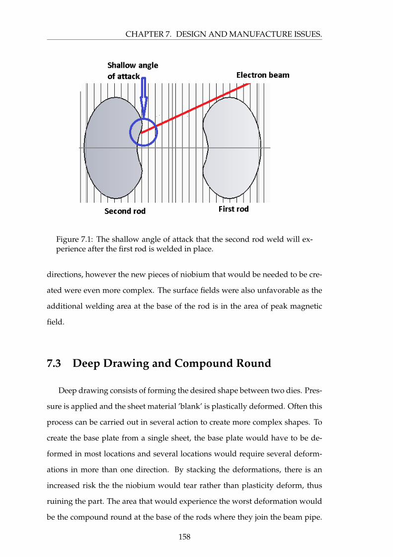
CHAPTER 7. DESIGN AND MANUFACTURE ISSUES.
Figure 7.1: The shallow angle of attack that the second rod weld will ex-perience after the first rod is welded in place.
directions, however the new pieces of niobium that would be needed to be cre-
ated were even more complex. The surface fields were also unfavorable as the
additional welding area at the base of the rod is in the area of peak magnetic
field.
7.3 Deep Drawing and Compound Round
Deep drawing consists of forming the desired shape between two dies. Pres-
sure is applied and the sheet material ’blank’ is plastically deformed. Often this
process can be carried out in several action to create more complex shapes. To
create the base plate from a single sheet, the base plate would have to be de-
formed in most locations and several locations would require several deform-
ations in more than one direction. By stacking the deformations, there is an
increased risk the the niobium would tear rather than plasticity deform, thus
ruining the part. The area that would experience the worst deformation would
be the compound round at the base of the rods where they join the beam pipe.
158
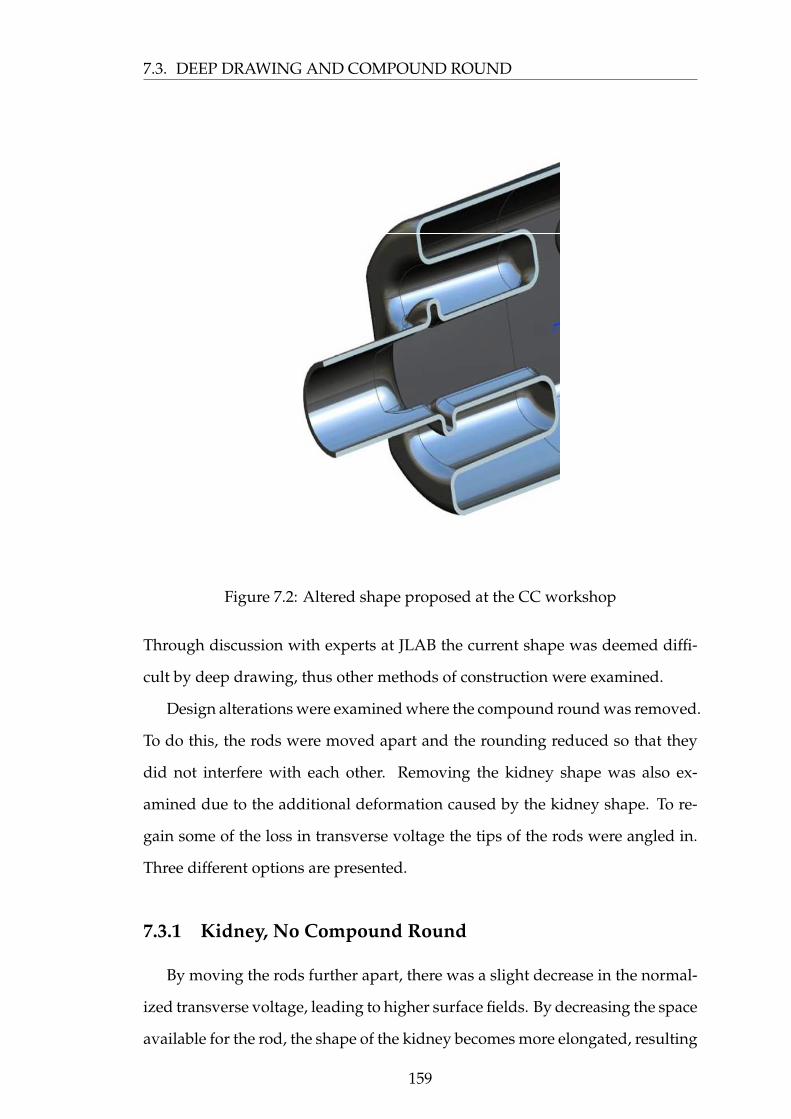
7.3. DEEP DRAWING AND COMPOUND ROUND
Figure 7.2: Altered shape proposed at the CC workshop
Through discussion with experts at JLAB the current shape was deemed diffi-
cult by deep drawing, thus other methods of construction were examined.
Design alterations were examined where the compound round was removed.
To do this, the rods were moved apart and the rounding reduced so that they
did not interfere with each other. Removing the kidney shape was also ex-
amined due to the additional deformation caused by the kidney shape. To re-
gain some of the loss in transverse voltage the tips of the rods were angled in.
Three different options are presented.
7.3.1 Kidney, No Compound Round
By moving the rods further apart, there was a slight decrease in the normal-
ized transverse voltage, leading to higher surface fields. By decreasing the space
available for the rod, the shape of the kidney becomes more elongated, resulting
159
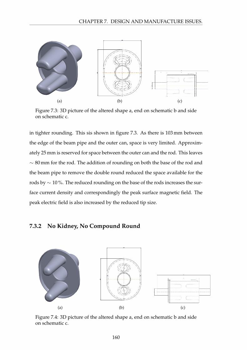
CHAPTER 7. DESIGN AND MANUFACTURE ISSUES.
(a) (b) (c)
Figure 7.3: 3D picture of the altered shape a, end on schematic b and sideon schematic c.
in tighter rounding. This sis shown in figure 7.3. As there is 103 mm between
the edge of the beam pipe and the outer can, space is very limited. Approxim-
ately 25 mm is reserved for space between the outer can and the rod. This leaves
∼ 80 mm for the rod. The addition of rounding on both the base of the rod and
the beam pipe to remove the double round reduced the space available for the
rods by∼ 10 %. The reduced rounding on the base of the rods increases the sur-
face current density and correspondingly the peak surface magnetic field. The
peak electric field is also increased by the reduced tip size.
7.3.2 No Kidney, No Compound Round
(a) (b) (c)
Figure 7.4: 3D picture of the altered shape a, end on schematic b and sideon schematic c.
160
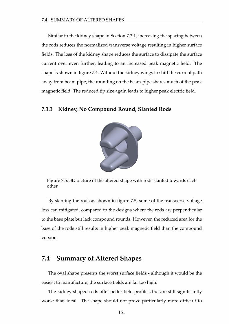
7.4. SUMMARY OF ALTERED SHAPES
Similar to the kidney shape in Section 7.3.1, increasing the spacing between
the rods reduces the normalized transverse voltage resulting in higher surface
fields. The loss of the kidney shape reduces the surface to dissipate the surface
current over even further, leading to an increased peak magnetic field. The
shape is shown in figure 7.4. Without the kidney wings to shift the current path
away from beam pipe, the rounding on the beam-pipe shares much of the peak
magnetic field. The reduced tip size again leads to higher peak electric field.
7.3.3 Kidney, No Compound Round, Slanted Rods
Figure 7.5: 3D picture of the altered shape with rods slanted towards eachother.
By slanting the rods as shown in figure 7.5, some of the transverse voltage
loss can mitigated, compared to the designs where the rods are perpendicular
to the base plate but lack compound rounds. However, the reduced area for the
base of the rods still results in higher peak magnetic field than the compound
version.
7.4 Summary of Altered Shapes
The oval shape presents the worst surface fields - although it would be the
easiest to manufacture, the surface fields are far too high.
The kidney-shaped rods offer better field profiles, but are still significantly
worse than ideal. The shape should not prove particularly more difficult to
161
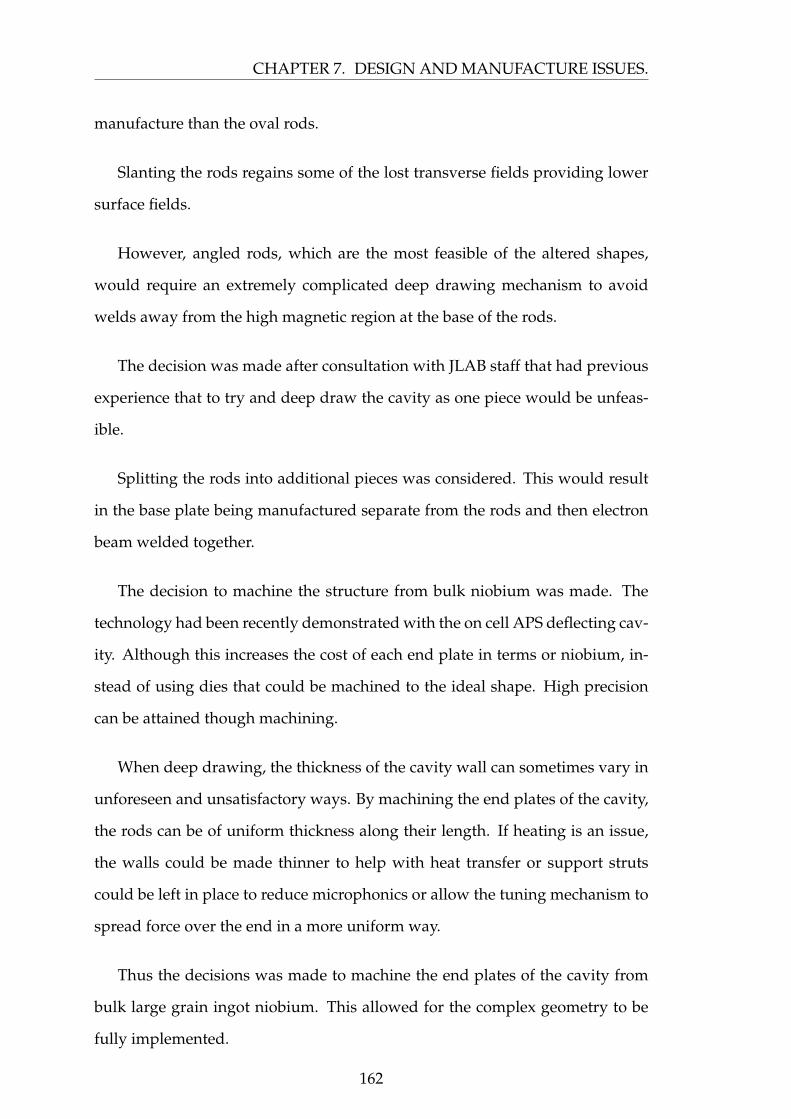
CHAPTER 7. DESIGN AND MANUFACTURE ISSUES.
manufacture than the oval rods.
Slanting the rods regains some of the lost transverse fields providing lower
surface fields.
However, angled rods, which are the most feasible of the altered shapes,
would require an extremely complicated deep drawing mechanism to avoid
welds away from the high magnetic region at the base of the rods.
The decision was made after consultation with JLAB staff that had previous
experience that to try and deep draw the cavity as one piece would be unfeas-
ible.
Splitting the rods into additional pieces was considered. This would result
in the base plate being manufactured separate from the rods and then electron
beam welded together.
The decision to machine the structure from bulk niobium was made. The
technology had been recently demonstrated with the on cell APS deflecting cav-
ity. Although this increases the cost of each end plate in terms or niobium, in-
stead of using dies that could be machined to the ideal shape. High precision
can be attained though machining.
When deep drawing, the thickness of the cavity wall can sometimes vary in
unforeseen and unsatisfactory ways. By machining the end plates of the cavity,
the rods can be of uniform thickness along their length. If heating is an issue,
the walls could be made thinner to help with heat transfer or support struts
could be left in place to reduce microphonics or allow the tuning mechanism to
spread force over the end in a more uniform way.
Thus the decisions was made to machine the end plates of the cavity from
bulk large grain ingot niobium. This allowed for the complex geometry to be
fully implemented.
162
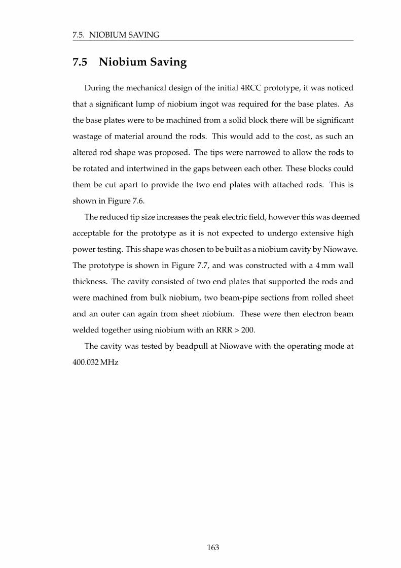
7.5. NIOBIUM SAVING
7.5 Niobium Saving
During the mechanical design of the initial 4RCC prototype, it was noticed
that a significant lump of niobium ingot was required for the base plates. As
the base plates were to be machined from a solid block there will be significant
wastage of material around the rods. This would add to the cost, as such an
altered rod shape was proposed. The tips were narrowed to allow the rods to
be rotated and intertwined in the gaps between each other. These blocks could
them be cut apart to provide the two end plates with attached rods. This is
shown in Figure 7.6.
The reduced tip size increases the peak electric field, however this was deemed
acceptable for the prototype as it is not expected to undergo extensive high
power testing. This shape was chosen to be built as a niobium cavity by Niowave.
The prototype is shown in Figure 7.7, and was constructed with a 4 mm wall
thickness. The cavity consisted of two end plates that supported the rods and
were machined from bulk niobium, two beam-pipe sections from rolled sheet
and an outer can again from sheet niobium. These were then electron beam
welded together using niobium with an RRR > 200.
The cavity was tested by beadpull at Niowave with the operating mode at
400.032 MHz
163
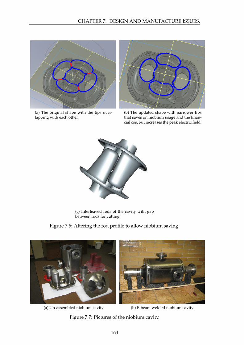
CHAPTER 7. DESIGN AND MANUFACTURE ISSUES.
(a) The original shape with the tips over-lapping with each other.
(b) The updated shape with narrower tipsthat saves on niobium usage and the finan-cial cos, but increases the peak electric field.
(c) Interleaved rods of the cavity with gapbetween rods for cutting.
Figure 7.6: Altering the rod profile to allow niobium saving.
(a) Un-assembled niobium cavity (b) E-beam welded niobium cavity
Figure 7.7: Pictures of the niobium cavity.
164
Chapter 8
Wakefields
In a traditional single cell elliptical accelerating cavity, the operating mode
is the fundamental mode of the cavity, with all other modes being higher order
modes, HOM’s, with higher frequencies. For crab cavities we have the possib-
ility of LOM’s, SOM’s and HOM’s.
Within the four rod cavity there exist both a lower order mode (LOM) loc-
ated at 375.18 MHz, and HOM’s. The LOM is a by-product in nearly all normal
deflecting cavities where the fundamental mode of the cavity is an accelerating
mode. This mode is unwanted and must be damped so as not to interact with
the beam as any beam power that is deposited in the cavity can cause beam
instabilities. The HOM’s similarly can result in unwanted disturbance to the
beam profile and must be similarly damped.
All modes interact differently with the beam, the easiest way of comparing
the interaction with the beam is to measure the R/Q of the mode. This is a direct
relation to beam cavity interaction. The R/Q’s of the modes up to 2.5 GHz are
presented in Figure 8.1. The operating mode has a very high R/Q of 912.67
however, the LOM has a comparable R/Q of 124.34, which is similar to most
accelerating cavities. This is due to the very compact nature of the cavity forcing
all the fields and thus energy into the confined space of the beam pipe and thus
beam. The first harmonics of the LOM and operating mode at 971.1 MHz and
1071.0 MHz respectively and are the 3λ4 modes, also have sizeable R/Q’s.
165
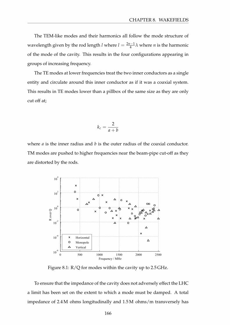
CHAPTER 8. WAKEFIELDS
The TEM-like modes and their harmonics all follow the mode structure of
wavelength given by the rod length l where l = 2n−14 λ where n is the harmonic
of the mode of the cavity. This results in the four configurations appearing in
groups of increasing frequency.
The TE modes at lower frequencies treat the two inner conductors as a single
entity and circulate around this inner conductor as if it was a coaxial system.
This results in TE modes lower than a pillbox of the same size as they are only
cut off at;
kc =2
a + b
where a is the inner radius and b is the outer radius of the coaxial conductor.
TM modes are pushed to higher frequencies near the beam-pipe cut-off as they
are distorted by the rods.
Frequency / MHz
R o
ver
Q
0 500 1000 1500 2000 250010
-6
10-4
10-2
100
102
104
Horizontal
Monopole
Vertical
Figure 8.1: R/Q for modes within the cavity up to 2.5 GHz.
To ensure that the impedance of the cavity does not adversely effect the LHC
a limit has been set on the extent to which a mode must be damped. A total
impedance of 2.4 M ohms longitudinally and 1.5 M ohms/m transversely has
166
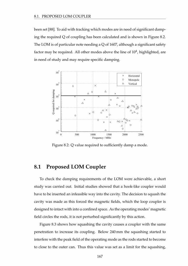
8.1. PROPOSED LOM COUPLER
been set [88]. To aid with tracking which modes are in need of significant damp-
ing the required Q of coupling has been calculated and is shown in Figure 8.2.
The LOM is of particular note needing a Q of 1607, although a significant safety
factor may be required. All other modes above the line of 104, highlighted, are
in need of study and may require specific damping.
Frequency / MHz
Q r
equi
red
for
dam
ping
0 500 1000 1500 2000 2500
102
103
104
105
106
107
Horizontal
Monopole
Vertical
Figure 8.2: Q value required to sufficiently damp a mode.
8.1 Proposed LOM Coupler
To check the damping requirements of the LOM were achievable, a short
study was carried out. Initial studies showed that a hook-like coupler would
have to be inserted an infeasible way into the cavity. The decision to squash the
cavity was made as this forced the magnetic fields, which the loop coupler is
designed to intact with into a confined space. As the operating modes’ magnetic
field circles the rods, it is not perturbed significantly by this action.
Figure 8.3 shows how squashing the cavity causes a coupler with the same
penetration to increase its coupling. Below 240 mm the squashing started to
interfere with the peak field of the operating mode as the rods started to become
to close to the outer can. Thus this value was set as a limit for the squashing,
167
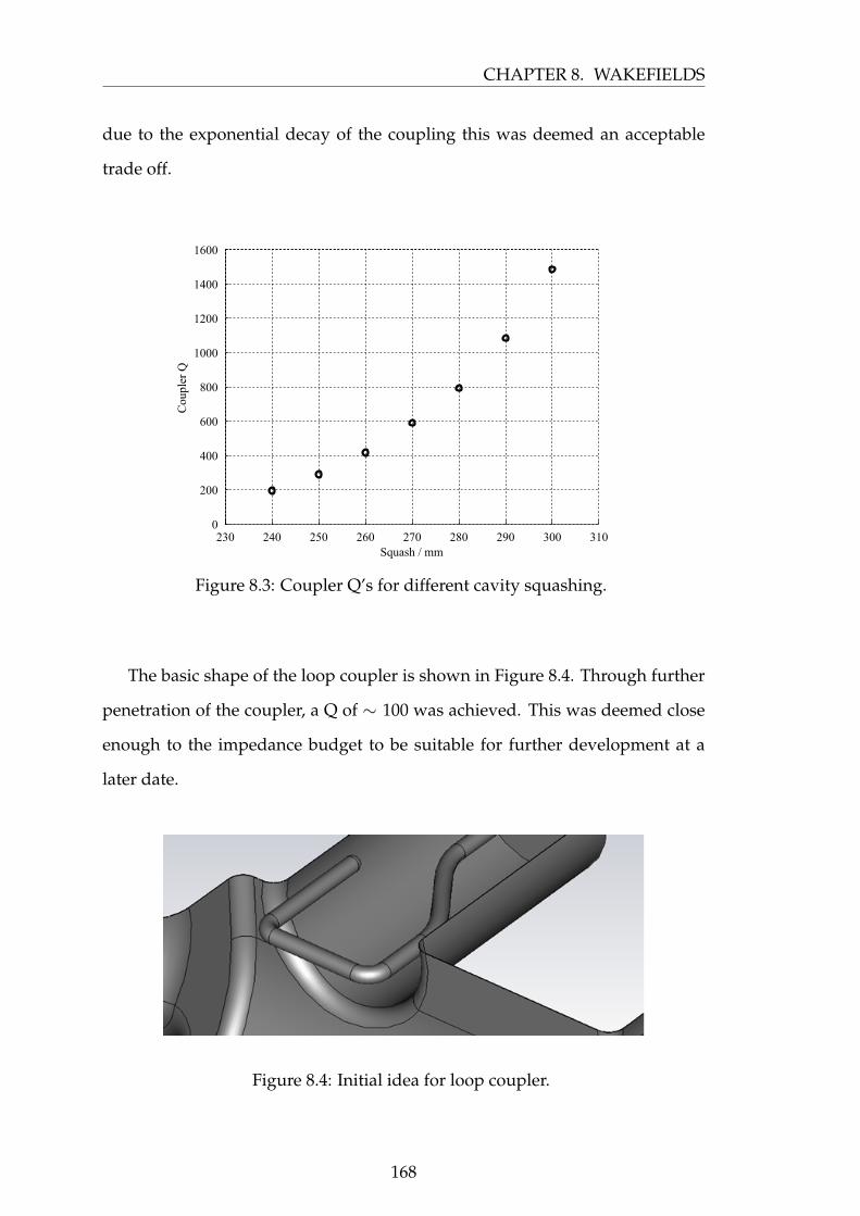
CHAPTER 8. WAKEFIELDS
due to the exponential decay of the coupling this was deemed an acceptable
trade off.
Squash / mm
Cou
pler
Q
230 240 250 260 270 280 290 300 3100
200
400
600
800
1000
1200
1400
1600
Figure 8.3: Coupler Q’s for different cavity squashing.
The basic shape of the loop coupler is shown in Figure 8.4. Through further
penetration of the coupler, a Q of ∼ 100 was achieved. This was deemed close
enough to the impedance budget to be suitable for further development at a
later date.
Figure 8.4: Initial idea for loop coupler.
168
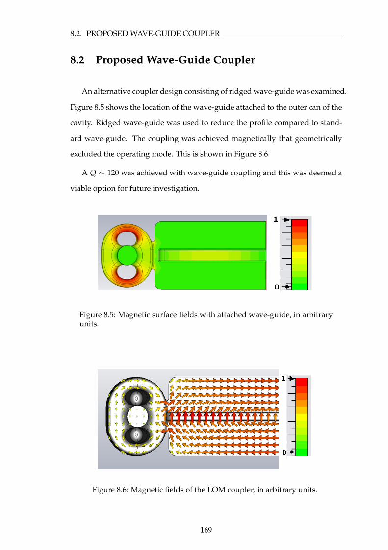
8.2. PROPOSED WAVE-GUIDE COUPLER
8.2 Proposed Wave-Guide Coupler
An alternative coupler design consisting of ridged wave-guide was examined.
Figure 8.5 shows the location of the wave-guide attached to the outer can of the
cavity. Ridged wave-guide was used to reduce the profile compared to stand-
ard wave-guide. The coupling was achieved magnetically that geometrically
excluded the operating mode. This is shown in Figure 8.6.
A Q ∼ 120 was achieved with wave-guide coupling and this was deemed a
viable option for future investigation.
Figure 8.5: Magnetic surface fields with attached wave-guide, in arbitraryunits.
Figure 8.6: Magnetic fields of the LOM coupler, in arbitrary units.
169
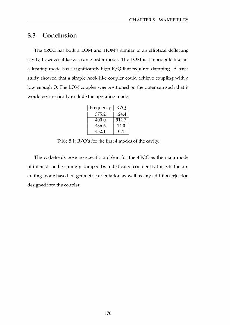
CHAPTER 8. WAKEFIELDS
8.3 Conclusion
The 4RCC has both a LOM and HOM’s similar to an elliptical deflecting
cavity, however it lacks a same order mode. The LOM is a monopole-like ac-
celerating mode has a significantly high R/Q that required damping. A basic
study showed that a simple hook-like coupler could achieve coupling with a
low enough Q. The LOM coupler was positioned on the outer can such that it
would geometrically exclude the operating mode.
Frequency R/Q375.2 124.4400.0 912.7436.6 14.0452.1 0.4
Table 8.1: R/Q’s for the first 4 modes of the cavity.
The wakefields pose no specific problem for the 4RCC as the main mode
of interest can be strongly damped by a dedicated coupler that rejects the op-
erating mode based on geometric orientation as well as any addition rejection
designed into the coupler.
170
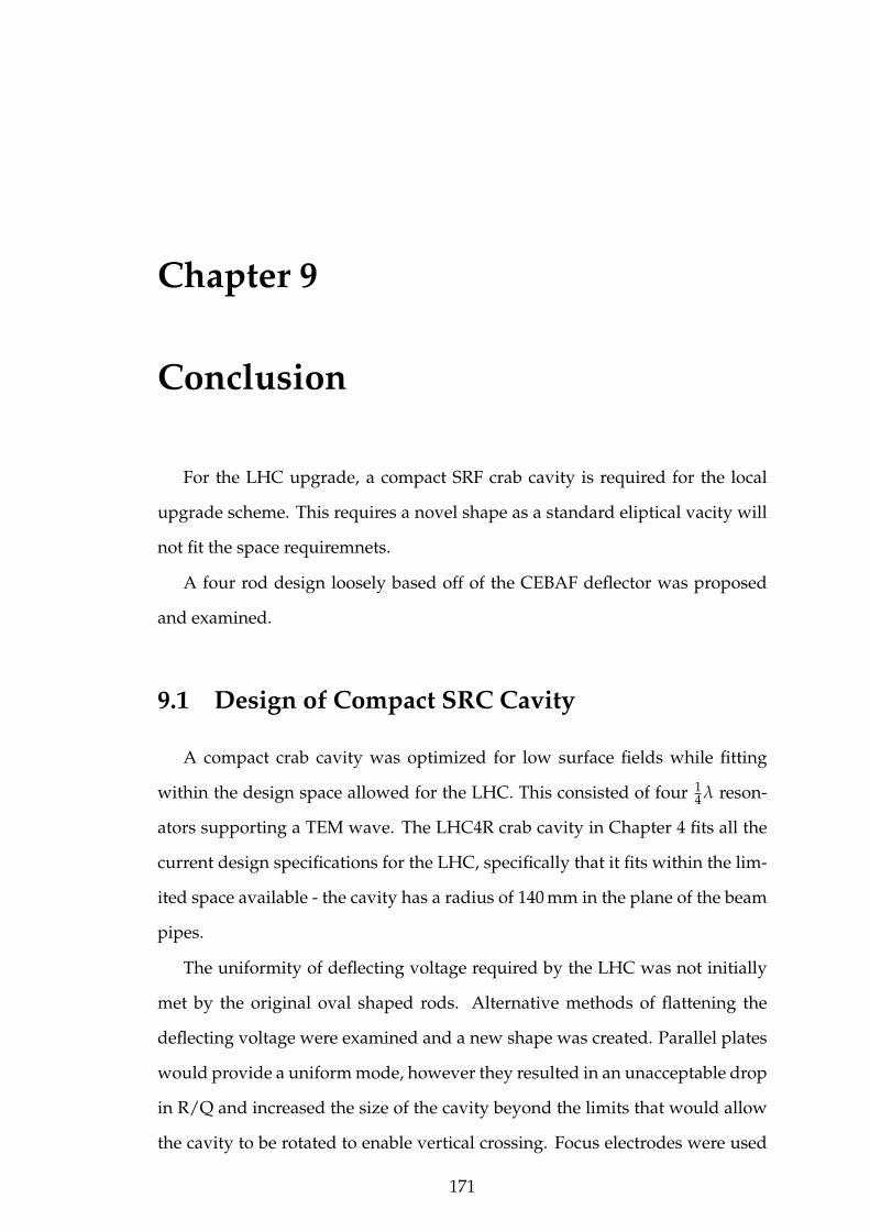
Chapter 9
Conclusion
For the LHC upgrade, a compact SRF crab cavity is required for the local
upgrade scheme. This requires a novel shape as a standard eliptical vacity will
not fit the space requiremnets.
A four rod design loosely based off of the CEBAF deflector was proposed
and examined.
9.1 Design of Compact SRC Cavity
A compact crab cavity was optimized for low surface fields while fitting
within the design space allowed for the LHC. This consisted of four 14 λ reson-
ators supporting a TEM wave. The LHC4R crab cavity in Chapter 4 fits all the
current design specifications for the LHC, specifically that it fits within the lim-
ited space available - the cavity has a radius of 140 mm in the plane of the beam
pipes.
The uniformity of deflecting voltage required by the LHC was not initially
met by the original oval shaped rods. Alternative methods of flattening the
deflecting voltage were examined and a new shape was created. Parallel plates
would provide a uniform mode, however they resulted in an unacceptable drop
in R/Q and increased the size of the cavity beyond the limits that would allow
the cavity to be rotated to enable vertical crossing. Focus electrodes were used
171
CHAPTER 9. CONCLUSION
to replicate the longer plate-like rods without compromising on the compact
nature of the cavity. The electrodes allowed for the minimisation of multipole
components that can adversely effect the dipole field. A variation in the dipole
field of less than 0.1 % at 15 mm was achieved.
The focus electrodes do not line up well with the geometry of the beam-
pipe and a new shape was created that followed the contour of the beam-pipe.
The kidney shape provided all the advantages of the focus electrodes whilst
following the same optimisation pattens as the oval shape.
The new cavity shape was designed with peak surface fields of 60.5 mT and
32.0 MV at a deflecting voltage of 3 MV. This was made into an Aluminium test
piece for further testing.
If the higher order components are non-zero, they can be offset against each
other to minimize their effects at low offset. If a flatter field is required or spe-
cific higher order components require minimization, the rod faces can be altered
to accommodate this.
The Aluminium cavity that was produced for experimentation provided
measurements which confirmed the basic properties of the cavity and allowed
for the fields within the cavity to be tested via bead-pull. Although significant
noise was initially seen, through processing and adjustment taking on axis er-
rors into count, useful measurements were able to be taken and compared to
simulations from CST.
The cavity showed close agreement with the simulations despite errors cal-
culated. The field uniformity lies within the error of the measurement and as
such is assumed to be within tolerance as no major deviation was seen.
The fields of the cavity match well with the expected fields as calculated
from CST for both the operating mode and the lower order mode. The good
correlation with the expected results through bead pull implies the cavity is
operating as designed.
Multipacting is a serious issue for modern superconducting cavities and can
172
9.2. COMPARISON TO OTHER CAVITIES
result in cavity failures or designs not being commissioned. The design im-
provements made to elliptical cell cavities will not work for deflecting mode
cavities as they have an alternative field configuration.
The four rod crab cavity has been examined for multipacting in CST particle
studio. Multipacting was predicted to appear at 22.44 mT surface field. Simula-
tions showed that for an uncleaned surface multipacting happened almost im-
mediately. For a surface that has undergone cleaning as a typical cavity would,
multipacting was observed at ∼ 1.9 MV deflecting voltage on the beampipe re-
gion, this corresponds to a surface field between 20− 24 mT. Simulating with
a lower surface SEY, analogous to processing the cavity, the multipacting is no
longer present. This matches the results of KEKB where the iris multipacting
was processed through.
The four rod crab cavity shows some multipacting where expected on the
beam pipe however this appears to be soft and able to be processed through.
Thus multipacting should not be a limiting factor for the four rod crab cavity.
Due to the high cost of niobium, a modified design was produced by Niowave
to enable high power tests in a cryostat. This design altered the tips of the rods
such that the two base plates could be made of a single piece of niobium. This
results in higher peak electric fields, but a considerable saving in costs.
9.2 Comparison to Other Cavities
Other options are currently being developed for the LHC. The two main
contenders are a quarter wave resonator design and a wave-guide like structure.
A comparison of the main features on the cavities and the design presented here
are shown in Table 9.1.
173
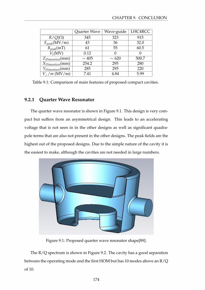
CHAPTER 9. CONCLUSION
Quarter Wave Wave-guide LHC4RCCR/Q(Ω) 345 323 915
Epeak(MV/m) 43 36 32.0Bpeak(mT) 61 55 60.5Vz(MV) 0.12 0 0
ZDimention(mm) ∼ 405 ∼ 620 500.7XDimention(mm) 254.2 295 280YDimention(mm) 285 295 220V⊥/m (MV/m) 7.41 4.84 5.99
Table 9.1: Comparison of main features of proposed compact cavities.
9.2.1 Quarter Wave Resonator
The quarter wave resonator is shown in Figure 9.1. This design is very com-
pact but suffers from an asymmetrical design. This leads to an accelerating
voltage that is not seen in in the other designs as well as significant quadra-
pole terms that are also not present in the other designs. The peak fields are the
highest out of the proposed designs. Due to the simple nature of the cavity it is
the easiest to make, although the cavities are not needed in large numbers.
Figure 9.1: Proposed quarter wave resonator shape[89].
The R/Q spectrum is shown in Figure 9.2. The cavity has a good separation
between the operating mode and the first HOM but has 10 modes above an R/Q
of 10.
174
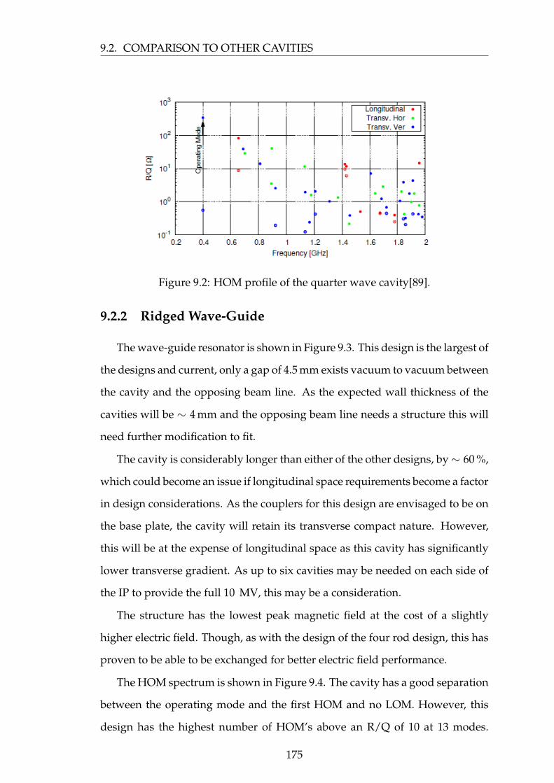
9.2. COMPARISON TO OTHER CAVITIES
Figure 9.2: HOM profile of the quarter wave cavity[89].
9.2.2 Ridged Wave-Guide
The wave-guide resonator is shown in Figure 9.3. This design is the largest of
the designs and current, only a gap of 4.5 mm exists vacuum to vacuum between
the cavity and the opposing beam line. As the expected wall thickness of the
cavities will be ∼ 4 mm and the opposing beam line needs a structure this will
need further modification to fit.
The cavity is considerably longer than either of the other designs, by∼ 60 %,
which could become an issue if longitudinal space requirements become a factor
in design considerations. As the couplers for this design are envisaged to be on
the base plate, the cavity will retain its transverse compact nature. However,
this will be at the expense of longitudinal space as this cavity has significantly
lower transverse gradient. As up to six cavities may be needed on each side of
the IP to provide the full 10 MV, this may be a consideration.
The structure has the lowest peak magnetic field at the cost of a slightly
higher electric field. Though, as with the design of the four rod design, this has
proven to be able to be exchanged for better electric field performance.
The HOM spectrum is shown in Figure 9.4. The cavity has a good separation
between the operating mode and the first HOM and no LOM. However, this
design has the highest number of HOM’s above an R/Q of 10 at 13 modes.
175
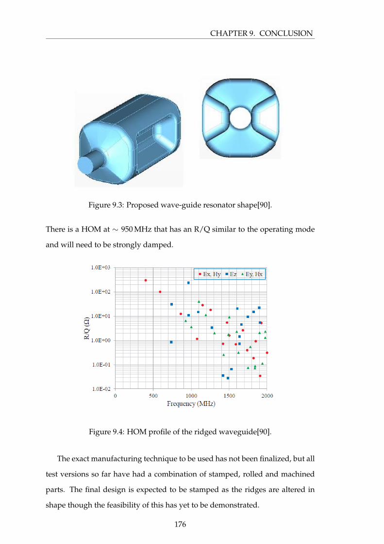
CHAPTER 9. CONCLUSION
Figure 9.3: Proposed wave-guide resonator shape[90].
There is a HOM at ∼ 950 MHz that has an R/Q similar to the operating mode
and will need to be strongly damped.
Figure 9.4: HOM profile of the ridged waveguide[90].
The exact manufacturing technique to be used has not been finalized, but all
test versions so far have had a combination of stamped, rolled and machined
parts. The final design is expected to be stamped as the ridges are altered in
shape though the feasibility of this has yet to be demonstrated.
176
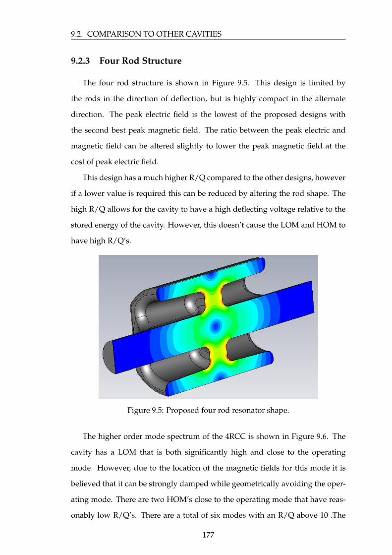
9.2. COMPARISON TO OTHER CAVITIES
9.2.3 Four Rod Structure
The four rod structure is shown in Figure 9.5. This design is limited by
the rods in the direction of deflection, but is highly compact in the alternate
direction. The peak electric field is the lowest of the proposed designs with
the second best peak magnetic field. The ratio between the peak electric and
magnetic field can be altered slightly to lower the peak magnetic field at the
cost of peak electric field.
This design has a much higher R/Q compared to the other designs, however
if a lower value is required this can be reduced by altering the rod shape. The
high R/Q allows for the cavity to have a high deflecting voltage relative to the
stored energy of the cavity. However, this doesn’t cause the LOM and HOM to
have high R/Q’s.
Figure 9.5: Proposed four rod resonator shape.
The higher order mode spectrum of the 4RCC is shown in Figure 9.6. The
cavity has a LOM that is both significantly high and close to the operating
mode. However, due to the location of the magnetic fields for this mode it is
believed that it can be strongly damped while geometrically avoiding the oper-
ating mode. There are two HOM’s close to the operating mode that have reas-
onably low R/Q’s. There are a total of six modes with an R/Q above 10 .The
177
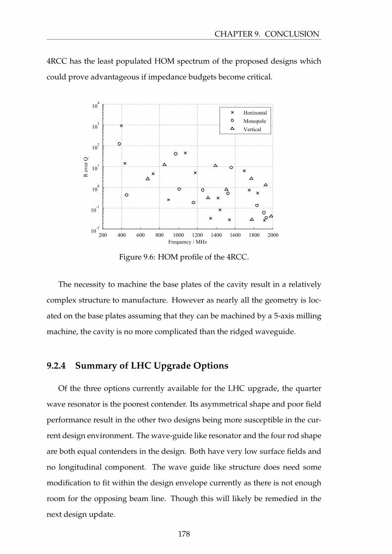
CHAPTER 9. CONCLUSION
4RCC has the least populated HOM spectrum of the proposed designs which
could prove advantageous if impedance budgets become critical.
Frequency / MHz
R o
ver
Q
200 400 600 800 1000 1200 1400 1600 1800 200010
-2
10-1
100
101
102
103
104
Horizontal
Monopole
Vertical
Figure 9.6: HOM profile of the 4RCC.
The necessity to machine the base plates of the cavity result in a relatively
complex structure to manufacture. However as nearly all the geometry is loc-
ated on the base plates assuming that they can be machined by a 5-axis milling
machine, the cavity is no more complicated than the ridged waveguide.
9.2.4 Summary of LHC Upgrade Options
Of the three options currently available for the LHC upgrade, the quarter
wave resonator is the poorest contender. Its asymmetrical shape and poor field
performance result in the other two designs being more susceptible in the cur-
rent design environment. The wave-guide like resonator and the four rod shape
are both equal contenders in the design. Both have very low surface fields and
no longitudinal component. The wave guide like structure does need some
modification to fit within the design envelope currently as there is not enough
room for the opposing beam line. Though this will likely be remedied in the
next design update.
178
9.3. FUTURE WORK
9.3 Future Work
The structure constructed throughout this thesis is only the initial RF design.
Considerable further work is needed for the structure to become a completed
unit able to be fully integrated within the LHC.
9.3.1 Elimination of Sextupole Components
The current design provides a flat deflecting voltage across the centre of the
aperture. However there are still some sextupole components that offset against
the decapole components. If the decapole components are viable at larger val-
ues then the design could be altered to completely remove the sextupole com-
ponent at the expense of slightly higher multi-pole components of higher or-
ders. This design change may be preferential, though consultation with CERN
is required.
9.3.2 Vertical Testing of Structure
The niobium prototype produced by Niowave has been designed to be cold
tested. This will allow high power tests of the cavity shape to ensure the cav-
ity can operate at the design gradient. Some soft multipacting was predicted
around the iris region, and the discovery and processing through of this would
confirm the simulations. The choice to machine the cavity from a single block
of niobium and still be able to achieve the required gradient rather than the
standard pressed shape would be good to confirm.
9.3.3 Couplers
The initial vertical tests of the cavity will require couplers to be designed and
manufactured. These must fit within the ports added to the Niowave shape.
The cavity will require at least one import coupler, one LOM coupler and one
HOM coupler. Additional couplers may be required or may be integrated with
179
CHAPTER 9. CONCLUSION
the aforementioned couplers. These need complete RF designs, thermal studies
and to be checked for multipacting.
9.3.4 Thermal and Mechanical Considerations
The cavity structure needs to be analysed for both mechanical and thermal
properties. The RF fields within the cavity will generate some heating, either
via impurities or general thermal instabilities. If the cavity cannot dissipate this
heat into the helium bath, a quench could happen. Unfortunately the thermal
conductivity of niobium is less than ideal, thus thin walls are desirable. How-
ever, the cavity will be under vacuum relative to pressures potentially up to
2 Bar at times, for example during cool down. To ensure the cavity does not
plastically deform and become buckled during these pressure changes, the me-
chanical stability must be investigated and the shape potentially altered to stop
this. As the rods are being machined out of bulk, the insides of the cones can
have material left in strategic places to act as stiffening ribs. However, the outer
can which currently contains a large flat area will not be able to do this and may
require a new shape or stiffening ribs. Any stiffening ribs added must avoid the
opposing beam line which may add further complications.
9.3.5 Tuning
The frequency of the cavities may shift during cool down as the niobium
contracts or the cavity may need to be shifted off resonance, during the ramp
for example, so that it does not interact with the beam. To enable the cavity
frequency to be altered, either to shift the cavity back onto, or away from, res-
onance, a method of tuning the cavity in situ. The current envisioned tuning
setup would consist of squashing the cavity in the longitudinal direction as this
alters the capacitance at the ends of the rods and thus the frequency of the cav-
ity.
This would require a calliper arrangement that could apply force to the end
180
9.3. FUTURE WORK
plates of the cavity and elastically squash it. As the outer can is effectively a
cylinder shape that is mechanically very strong in compression, some modifica-
tion may be required. Adding in a deformable ridge on the outer can in an area
where there are no fields would be the first area of study.
9.3.6 LOM and HOM Frequencies
The current design of the cavity has a LOM with a high R/Q and two close
by HOM’s. Ideally, there would be no LOM in the cavity and all of the HOM’s
would be at considerable higher frequencies as this would allow for simpler
coupler designs and low wakefields. During the design of the current cavity,
little attention was paid to the HOM’s and the LOM was only studied in regard
to achieving good coupling to remove it. By altering the outer can shape or the
rod profiles it may be possible to shift the frequencies of the other modes to
more desirable locations.
9.3.7 Test in SPS
The Niowave cavity could be placed in the SPS at CERN to test the cavity
with a high current beam. This would allow further conformation of the cavity’s
viability to act as the crab cavity for the HL-LHC project. A test in the SPS will
also allow the effects of emmittance growth to the studied.
The SPS will allow the crab cavity to be tested with beam as the LHC cannot
be used as a trial run and conformation of the crab cavity is essential before tests
in the LHC are carried out.
9.3.8 Cryomodule
The crab cavity will be operating at superconducting temperatures and will
need an associated cryomodule to fit it into the existing cryo system in place at
CERN. This module must contain the helium jacket to maintain the helium bath
181
CHAPTER 9. CONCLUSION
around the cavity, gas return for any boiled off helium and input for fresh he-
lium. This must all be contained within any vacuum vessels, magnetic shielding
and intermediate liquid nitrogen cooling. Input and damping couplers along
side tuners and any electronic monitors must also be included and will penet-
rate though several of these layers. As it is unknown if two or three cavities
will be used in the final design, the cryomodule design must be adaptable to
the ever-changing requirements of the LHC.
9.3.9 Low Level RF
The cavities require very strict timing between the kicks they give to a bunch
as it travels around the ring. The crabbing cavities must all have the correct
phase such that the full 10 MV of defecting voltage is delivered to the beam
as required. The anti-crab cavities must similarly have the correct phasing to
ensure all the rotation is removed. This requires a dedicated control system to
maintain the crab cavities at their correct phase and power.
9.4 Other Applications
As well as the crab cavity for the LHC upgrade, there are other projects that
require compact deflecting cavities that a modified 4RCC could be used for.
The CEBAF experiment is undergoing an upgrade to 12 GeV and is in need
of new deflectors to the current normal conducting ones. The 4RCC is based
directly off of this design and only relatively small modifications would be re-
quired to alter the design to replace its spiritual forefather[90].
In addition to the 12 GeV upgrade, an electron-light ion collider (ELIC) that
would utilise crab cavities is also being built at JLab. Although, this design calls
for a 1.5 GHz crab cavity[91].
The Project X deflector has similar requirements to the LHC crab system,
though it needs more transverse kick. The project calls for 10 MV of kick from
182

9.4. OTHER APPLICATIONS
one cavity operating at approximately 400 MHz. A similarly large aperture is
required. The 4RCC could be modified slightly to provide the requested per-
formance [92].
All three projects are close to the design requirements of the LHC that the
4RCC could be modified to fulfil the needs of each.
183
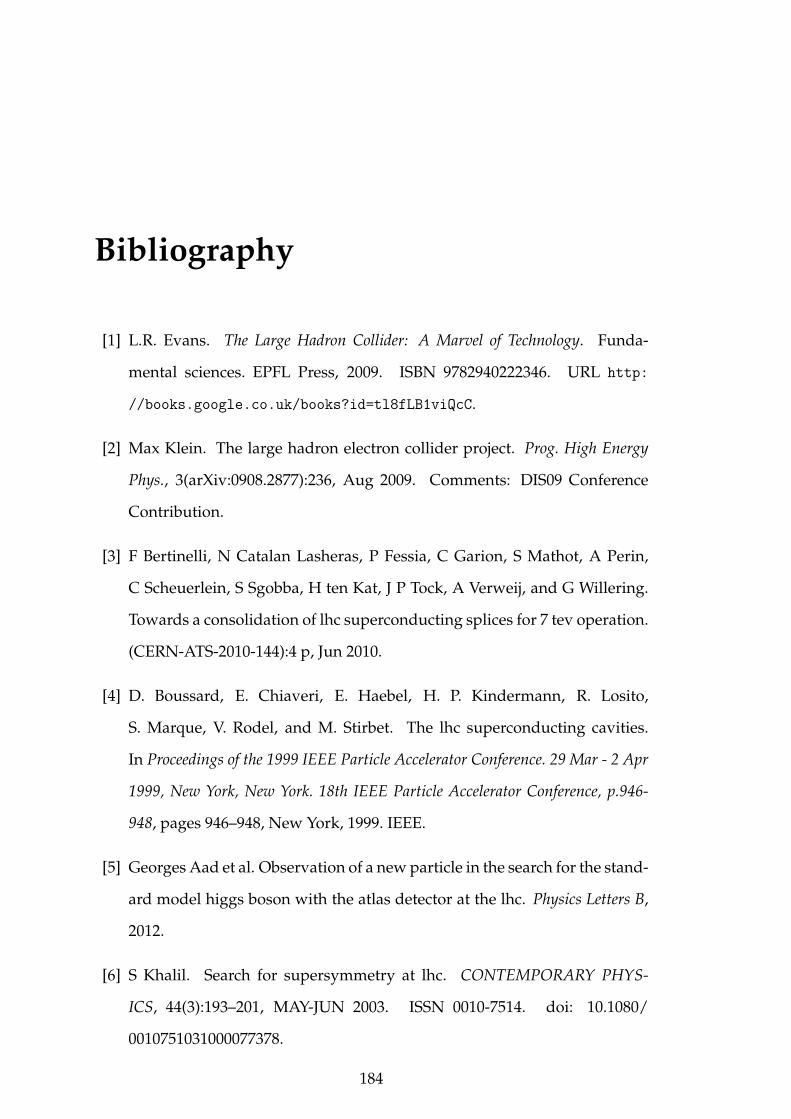
Bibliography
[1] L.R. Evans. The Large Hadron Collider: A Marvel of Technology. Funda-
mental sciences. EPFL Press, 2009. ISBN 9782940222346. URL http:
//books.google.co.uk/books?id=tl8fLB1viQcC.
[2] Max Klein. The large hadron electron collider project. Prog. High Energy
Phys., 3(arXiv:0908.2877):236, Aug 2009. Comments: DIS09 Conference
Contribution.
[3] F Bertinelli, N Catalan Lasheras, P Fessia, C Garion, S Mathot, A Perin,
C Scheuerlein, S Sgobba, H ten Kat, J P Tock, A Verweij, and G Willering.
Towards a consolidation of lhc superconducting splices for 7 tev operation.
(CERN-ATS-2010-144):4 p, Jun 2010.
[4] D. Boussard, E. Chiaveri, E. Haebel, H. P. Kindermann, R. Losito,
S. Marque, V. Rodel, and M. Stirbet. The lhc superconducting cavities.
In Proceedings of the 1999 IEEE Particle Accelerator Conference. 29 Mar - 2 Apr
1999, New York, New York. 18th IEEE Particle Accelerator Conference, p.946-
948, pages 946–948, New York, 1999. IEEE.
[5] Georges Aad et al. Observation of a new particle in the search for the stand-
ard model higgs boson with the atlas detector at the lhc. Physics Letters B,
2012.
[6] S Khalil. Search for supersymmetry at lhc. CONTEMPORARY PHYS-
ICS, 44(3):193–201, MAY-JUN 2003. ISSN 0010-7514. doi: 10.1080/
0010751031000077378.
184
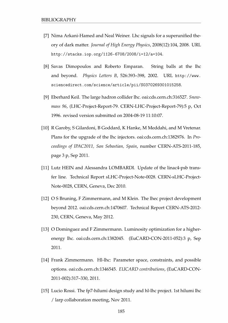
BIBLIOGRAPHY
[7] Nima Arkani-Hamed and Neal Weiner. Lhc signals for a superunified the-
ory of dark matter. Journal of High Energy Physics, 2008(12):104, 2008. URL
http://stacks.iop.org/1126-6708/2008/i=12/a=104.
[8] Savas Dimopoulos and Roberto Emparan. String balls at the lhc
and beyond. Physics Letters B, 526:393–398, 2002. URL http://www.
sciencedirect.com/science/article/pii/S0370269301015258.
[9] Eberhard Keil. The large hadron collider lhc. oai:cds.cern.ch:316527. Snow-
mass 96, (LHC-Project-Report-79. CERN-LHC-Project-Report-79):5 p, Oct
1996. revised version submitted on 2004-08-19 11:10:07.
[10] R Garoby, S Gilardoni, B Goddard, K Hanke, M Meddahi, and M Vretenar.
Plans for the upgrade of the lhc injectors. oai:cds.cern.ch:1382976. In Pro-
ceedings of IPAC2011, San Sebastian, Spain, number CERN-ATS-2011-185,
page 3 p, Sep 2011.
[11] Lutz HEIN and Alessandra LOMBARDI. Update of the linac4-psb trans-
fer line. Technical Report sLHC-Project-Note-0028. CERN-sLHC-Project-
Note-0028, CERN, Geneva, Dec 2010.
[12] O S Bruning, F Zimmermann, and M Klein. The lhec project development
beyond 2012. oai:cds.cern.ch:1470607. Technical Report CERN-ATS-2012-
230, CERN, Geneva, May 2012.
[13] O Dominguez and F Zimmermann. Luminosity optimization for a higher-
energy lhc. oai:cds.cern.ch:1382045. (EuCARD-CON-2011-052):3 p, Sep
2011.
[14] Frank Zimmermann. Hl-lhc: Parameter space, constraints, and possible
options. oai:cds.cern.ch:1346545. EUCARD contributions, (EuCARD-CON-
2011-002):317–330, 2011.
[15] Lucio Rossi. The fp7-hilumi design study and hl-lhc project. 1st hilumi lhc
/ larp collaboration meeting, Nov 2011.
185
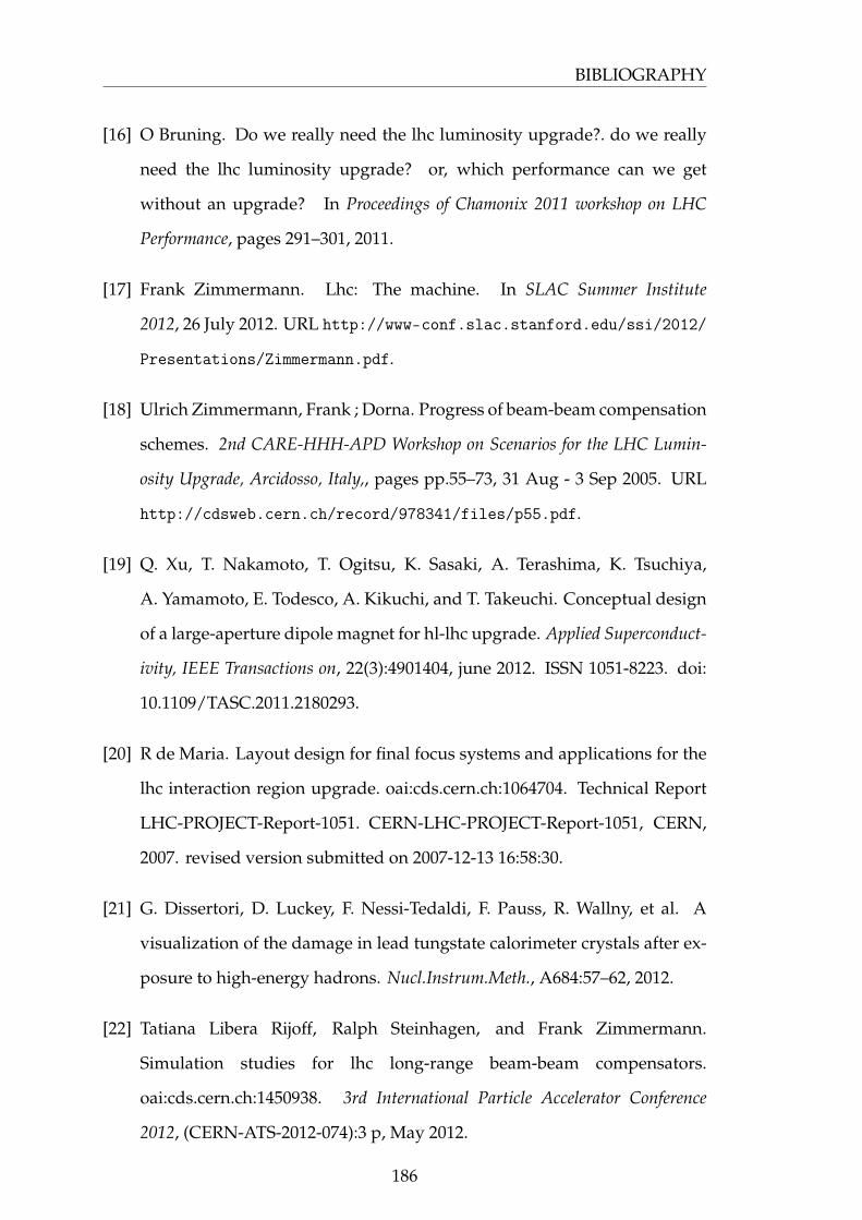
BIBLIOGRAPHY
[16] O Bruning. Do we really need the lhc luminosity upgrade?. do we really
need the lhc luminosity upgrade? or, which performance can we get
without an upgrade? In Proceedings of Chamonix 2011 workshop on LHC
Performance, pages 291–301, 2011.
[17] Frank Zimmermann. Lhc: The machine. In SLAC Summer Institute
2012, 26 July 2012. URL http://www-conf.slac.stanford.edu/ssi/2012/
Presentations/Zimmermann.pdf.
[18] Ulrich Zimmermann, Frank ; Dorna. Progress of beam-beam compensation
schemes. 2nd CARE-HHH-APD Workshop on Scenarios for the LHC Lumin-
osity Upgrade, Arcidosso, Italy,, pages pp.55–73, 31 Aug - 3 Sep 2005. URL
http://cdsweb.cern.ch/record/978341/files/p55.pdf.
[19] Q. Xu, T. Nakamoto, T. Ogitsu, K. Sasaki, A. Terashima, K. Tsuchiya,
A. Yamamoto, E. Todesco, A. Kikuchi, and T. Takeuchi. Conceptual design
of a large-aperture dipole magnet for hl-lhc upgrade. Applied Superconduct-
ivity, IEEE Transactions on, 22(3):4901404, june 2012. ISSN 1051-8223. doi:
10.1109/TASC.2011.2180293.
[20] R de Maria. Layout design for final focus systems and applications for the
lhc interaction region upgrade. oai:cds.cern.ch:1064704. Technical Report
LHC-PROJECT-Report-1051. CERN-LHC-PROJECT-Report-1051, CERN,
2007. revised version submitted on 2007-12-13 16:58:30.
[21] G. Dissertori, D. Luckey, F. Nessi-Tedaldi, F. Pauss, R. Wallny, et al. A
visualization of the damage in lead tungstate calorimeter crystals after ex-
posure to high-energy hadrons. Nucl.Instrum.Meth., A684:57–62, 2012.
[22] Tatiana Libera Rijoff, Ralph Steinhagen, and Frank Zimmermann.
Simulation studies for lhc long-range beam-beam compensators.
oai:cds.cern.ch:1450938. 3rd International Particle Accelerator Conference
2012, (CERN-ATS-2012-074):3 p, May 2012.
186
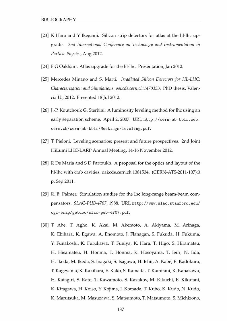
BIBLIOGRAPHY
[23] K Hara and Y Ikegami. Silicon strip detectors for atlas at the hl-lhc up-
grade. 2nd International Conference on Technology and Instrumentation in
Particle Physics, Aug 2012.
[24] F G Oakham. Atlas upgrade for the hl-lhc. Presentation, Jan 2012.
[25] Mercedes Minano and S. Marti. Irradiated Silicon Detectors for HL-LHC:
Characterization and Simulations. oai:cds.cern.ch:1470353. PhD thesis, Valen-
cia U., 2012. Presented 18 Jul 2012.
[26] J.-P. Koutchouk G. Sterbini. A luminosity leveling method for lhc using an
early separation scheme. April 2, 2007. URL http://cern-ab-bblr.web.
cern.ch/cern-ab-bblr/Meetings/leveling.pdf.
[27] T. Pieloni. Leveling scenarios: present and future prospectives. 2nd Joint
HiLumi LHC-LARP Annual Meeting, 14-16 November 2012.
[28] R De Maria and S D Fartoukh. A proposal for the optics and layout of the
hl-lhc with crab cavities. oai:cds.cern.ch:1381534. (CERN-ATS-2011-107):3
p, Sep 2011.
[29] R. B. Palmer. Simulation studies for the lhc long-range beam-beam com-
pensators. SLAC-PUB-4707, 1988. URL http://www.slac.stanford.edu/
cgi-wrap/getdoc/slac-pub-4707.pdf.
[30] T. Abe, T. Agho, K. Akai, M. Akemoto, A. Akiyama, M. Arinaga,
K. Ebihara, K. Egawa, A. Enomoto, J. Flanagan, S. Fukuda, H. Fukuma,
Y. Funakoshi, K. Furukawa, T. Funiya, K. Hara, T. Higo, S. Hiramatsu,
H. Hisamatsu, H. Honma, T. Honma, K. Hosoyama, T. Ieiri, N. Iida,
H. Ikeda, M. Ikeda, S. Inagaki, S. Isagawa, H. Ishii, A. Kabe, E. Kadokura,
T. Kageyama, K. Kakihara, E. Kako, S. Kamada, T. Kamitani, K. Kanazawa,
H. Katagiri, S. Kato, T. Kawamoto, S. Kazakov, M. Kikuchi, E. Kikutani,
K. Kitagawa, H. Koiso, Y. Kojima, I. Komada, T. Kubo, K. Kudo, N. Kudo,
K. Marutsuka, M. Masuzawa, S. Matsumoto, T. Matsumoto, S. Michizono,
187
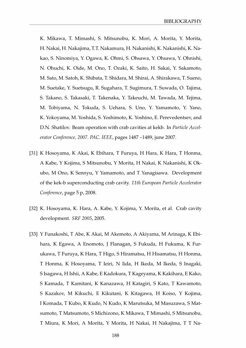
BIBLIOGRAPHY
K. Mikawa, T. Mimashi, S. Mitsunobu, K. Mori, A. Morita, Y. Morita,
H. Nakai, H. Nakajima, T.T. Nakamura, H. Nakanishi, K. Nakanishi, K. Na-
kao, S. Ninomiya, Y. Ogawa, K. Ohmi, S. Ohsawa, Y. Ohsawa, Y. Ohnishi,
N. Ohuchi, K. Oide, M. Ono, T. Ozaki, K. Saito, H. Sakai, Y. Sakamoto,
M. Sato, M. Satoh, K. Shibata, T. Shidara, M. Shirai, A. Shirakawa, T. Sueno,
M. Suetake, Y. Suetsugu, R. Sugahara, T. Sugimura, T. Suwada, O. Tajima,
S. Takano, S. Takasaki, T. Takenaka, Y. Takeuchi, M. Tawada, M. Tejima,
M. Tobiyama, N. Tokuda, S. Uehara, S. Uno, Y. Yamamoto, Y. Yano,
K. Yokoyama, M. Yoshida, S. Yoshimoto, K. Yoshino, E. Perevedentsev, and
D.N. Shatilov. Beam operation with crab cavities at kekb. In Particle Accel-
erator Conference, 2007. PAC. IEEE, pages 1487 –1489, june 2007.
[31] K Hosoyama, K Akai, K Ebihara, T Furuya, H Hara, K Hara, T Honma,
A Kabe, Y Kojima, S Mitsunobu, Y Morita, H Nakai, K Nakanishi, K Ok-
ubo, M Ono, K Sennyu, Y Yamamoto, and T Yanagisawa. Development
of the kek-b superconducting crab cavity. 11th European Particle Accelerator
Conference, page 5 p, 2008.
[32] K. Hosoyama, K. Hara, A. Kabe, Y. Kojima, Y. Morita, et al. Crab cavity
development. SRF 2005, 2005.
[33] Y Funakoshi, T Abe, K Akai, M Akemoto, A Akiyama, M Arinaga, K Ebi-
hara, K Egawa, A Enomoto, J Flanagan, S Fukuda, H Fukuma, K Fur-
ukawa, T Furuya, K Hara, T Higo, S Hiramatsu, H Hisamatsu, H Honma,
T Honma, K Hosoyama, T Ieiri, N Iida, H Ikeda, M Ikeda, S Inagaki,
S Isagawa, H Ishii, A Kabe, E Kadokura, T Kageyama, K Kakihara, E Kako,
S Kamada, T Kamitani, K Kanazawa, H Katagiri, S Kato, T Kawamoto,
S Kazakov, M Kikuchi, E Kikutani, K Kitagawa, H Koiso, Y Kojima,
I Komada, T Kubo, K Kudo, N Kudo, K Marutsuka, M Masuzawa, S Mat-
sumoto, T Matsumoto, S Michizono, K Mikawa, T Mimashi, S Mitsunobu,
T Miura, K Mori, A Morita, Y Morita, H Nakai, H Nakajima, T T Na-
188
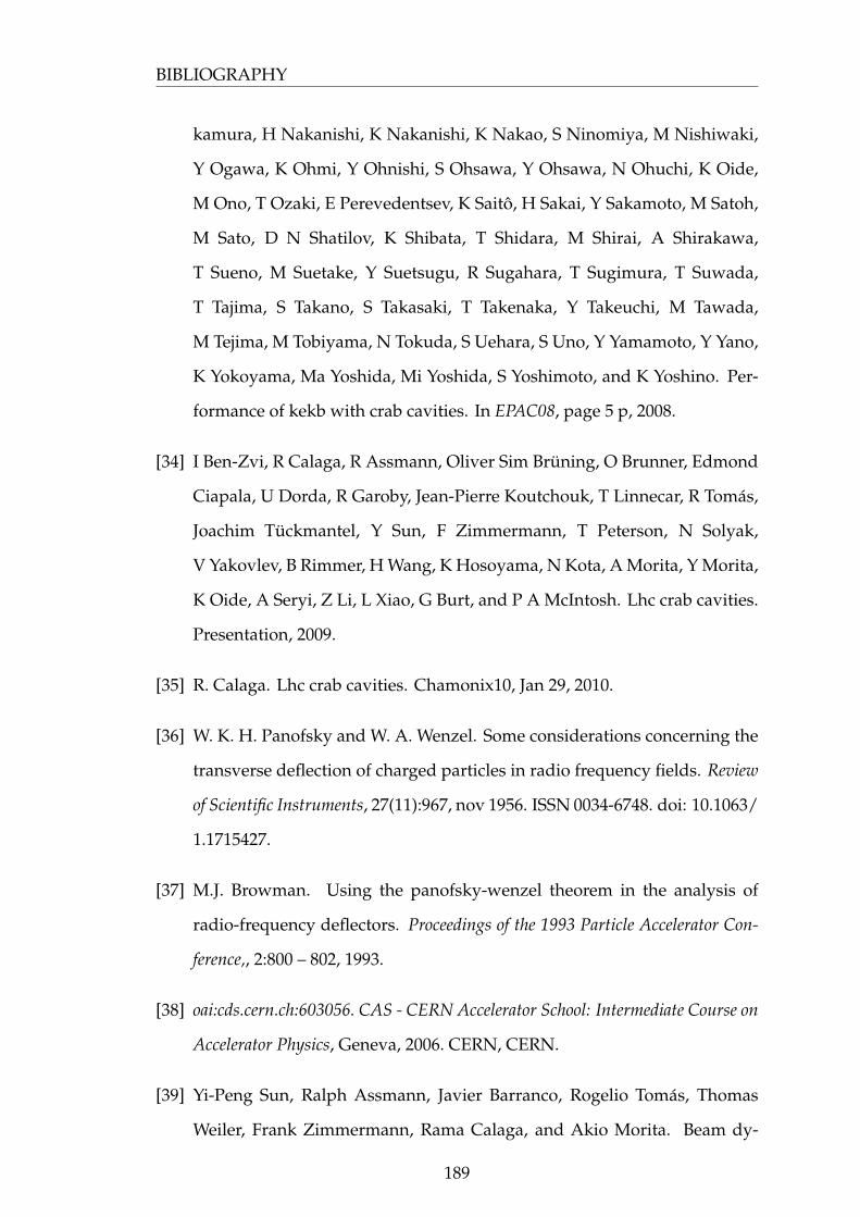
BIBLIOGRAPHY
kamura, H Nakanishi, K Nakanishi, K Nakao, S Ninomiya, M Nishiwaki,
Y Ogawa, K Ohmi, Y Ohnishi, S Ohsawa, Y Ohsawa, N Ohuchi, K Oide,
M Ono, T Ozaki, E Perevedentsev, K Saitô, H Sakai, Y Sakamoto, M Satoh,
M Sato, D N Shatilov, K Shibata, T Shidara, M Shirai, A Shirakawa,
T Sueno, M Suetake, Y Suetsugu, R Sugahara, T Sugimura, T Suwada,
T Tajima, S Takano, S Takasaki, T Takenaka, Y Takeuchi, M Tawada,
M Tejima, M Tobiyama, N Tokuda, S Uehara, S Uno, Y Yamamoto, Y Yano,
K Yokoyama, Ma Yoshida, Mi Yoshida, S Yoshimoto, and K Yoshino. Per-
formance of kekb with crab cavities. In EPAC08, page 5 p, 2008.
[34] I Ben-Zvi, R Calaga, R Assmann, Oliver Sim Brüning, O Brunner, Edmond
Ciapala, U Dorda, R Garoby, Jean-Pierre Koutchouk, T Linnecar, R Tomás,
Joachim Tückmantel, Y Sun, F Zimmermann, T Peterson, N Solyak,
V Yakovlev, B Rimmer, H Wang, K Hosoyama, N Kota, A Morita, Y Morita,
K Oide, A Seryi, Z Li, L Xiao, G Burt, and P A McIntosh. Lhc crab cavities.
Presentation, 2009.
[35] R. Calaga. Lhc crab cavities. Chamonix10, Jan 29, 2010.
[36] W. K. H. Panofsky and W. A. Wenzel. Some considerations concerning the
transverse deflection of charged particles in radio frequency fields. Review
of Scientific Instruments, 27(11):967, nov 1956. ISSN 0034-6748. doi: 10.1063/
1.1715427.
[37] M.J. Browman. Using the panofsky-wenzel theorem in the analysis of
radio-frequency deflectors. Proceedings of the 1993 Particle Accelerator Con-
ference,, 2:800 – 802, 1993.
[38] oai:cds.cern.ch:603056. CAS - CERN Accelerator School: Intermediate Course on
Accelerator Physics, Geneva, 2006. CERN, CERN.
[39] Yi-Peng Sun, Ralph Assmann, Javier Barranco, Rogelio Tomás, Thomas
Weiler, Frank Zimmermann, Rama Calaga, and Akio Morita. Beam dy-
189
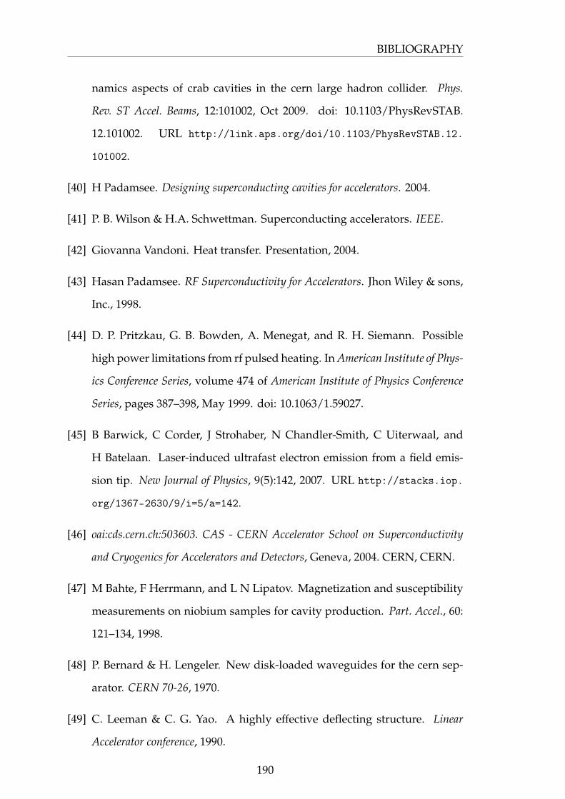
BIBLIOGRAPHY
namics aspects of crab cavities in the cern large hadron collider. Phys.
Rev. ST Accel. Beams, 12:101002, Oct 2009. doi: 10.1103/PhysRevSTAB.
12.101002. URL http://link.aps.org/doi/10.1103/PhysRevSTAB.12.
101002.
[40] H Padamsee. Designing superconducting cavities for accelerators. 2004.
[41] P. B. Wilson & H.A. Schwettman. Superconducting accelerators. IEEE.
[42] Giovanna Vandoni. Heat transfer. Presentation, 2004.
[43] Hasan Padamsee. RF Superconductivity for Accelerators. Jhon Wiley & sons,
Inc., 1998.
[44] D. P. Pritzkau, G. B. Bowden, A. Menegat, and R. H. Siemann. Possible
high power limitations from rf pulsed heating. In American Institute of Phys-
ics Conference Series, volume 474 of American Institute of Physics Conference
Series, pages 387–398, May 1999. doi: 10.1063/1.59027.
[45] B Barwick, C Corder, J Strohaber, N Chandler-Smith, C Uiterwaal, and
H Batelaan. Laser-induced ultrafast electron emission from a field emis-
sion tip. New Journal of Physics, 9(5):142, 2007. URL http://stacks.iop.
org/1367-2630/9/i=5/a=142.
[46] oai:cds.cern.ch:503603. CAS - CERN Accelerator School on Superconductivity
and Cryogenics for Accelerators and Detectors, Geneva, 2004. CERN, CERN.
[47] M Bahte, F Herrmann, and L N Lipatov. Magnetization and susceptibility
measurements on niobium samples for cavity production. Part. Accel., 60:
121–134, 1998.
[48] P. Bernard & H. Lengeler. New disk-loaded waveguides for the cern sep-
arator. CERN 70-26, 1970.
[49] C. Leeman & C. G. Yao. A highly effective deflecting structure. Linear
Accelerator conference, 1990.
190
BIBLIOGRAPHY
[50] E. Keil H. Lengler B.W. Montague & W.W. Neale P. Bramham, R.D. Fortune.
Deflecting cavity design. Phys. Letters, 15:290, 1965.
[51] G.Burt. Rf deflecting mode cavities lecture ii issues and cavity designs. RF
for Accelerators CAS 2010, 2010.
[52] H. Lengeler & V. Vaghin P. Bernard, P. Lazeyras. Particle separation with
two and three cavity rf separators at cern. CERN 68-29, 1968.
[53] J. R. Aggus, W. Bauer, S. Giordano, H. Hahn, and H. J. Halama. Super-
conducting niobium deflectors. Nuclear Science, IEEE Transactions on, 20(3):
95 –97, june 1973. ISSN 0018-9499. doi: 10.1109/TNS.1973.4327051. URL
http://ieeexplore.ieee.org/stamp/stamp.jsp?tp=&arnumber=4327051.
[54] A. Citron H. Schopper. Superconducting particle separator,. Letter of intent
to the Electronics experimental committee, CERN, 1968. URL http://cdsweb.
cern.ch/record/1046302/files/CM-P00066155.pdf.
[55] W. Bauer. Design study of a superconducting deflecting cavity. IEEE Xplore,
18:181–185, 1971.
[56] W. Bauer, A. Citron, G. Dammertz, H. C. Eschelbacherx, H. Lengeler,
H. Miller, E. Rathgeber, and H. Diepers. Rf-tests on deflecting cavities
for a superconductinig particle separator. Nuclear Science, IEEE Transac-
tions on, 20(3):59 –62, june 1973. ISSN 0018-9499. doi: 10.1109/TNS.
1973.4327043. URL http://ieeexplore.ieee.org/stamp/stamp.jsp?tp=
&arnumber=4327043.
[57] W. Bauer, A. Citron, G. Dammertz, M. Grundner, L. Husson, H. Lengeler,
and E. Rathgeber. Status of the cern-karlsruhe superconducting rf particle
separator. Nuclear Science, IEEE Transactions on, 22(3):1144 –1147, june
1975. ISSN 0018-9499. doi: 10.1109/TNS.1975.4327831. URL http:
//ieeexplore.ieee.org/stamp/stamp.jsp?tp=&arnumber=4327831.
191
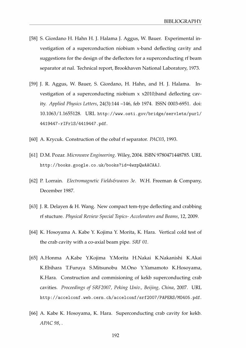
BIBLIOGRAPHY
[58] S. Giordano H. Hahn H. J. Halama J. Aggus, W. Bauer. Experimental in-
vestigation of a superconduction niobium x-band deflecting cavity and
suggestions for the design of the deflectors for a superconducting rf beam
separator at nal. Technical report, Brookhaven National Laboratory, 1973.
[59] J. R. Aggus, W. Bauer, S. Giordano, H. Hahn, and H. J. Halama. In-
vestigation of a superconducting niobium x x2010;band deflecting cav-
ity. Applied Physics Letters, 24(3):144 –146, feb 1974. ISSN 0003-6951. doi:
10.1063/1.1655128. URL http://www.osti.gov/bridge/servlets/purl/
4419447-rIFrlS/4419447.pdf.
[60] A. Krycuk. Construction of the cebaf rf separator. PAC03, 1993.
[61] D.M. Pozar. Microwave Engineering. Wiley, 2004. ISBN 9780471448785. URL
http://books.google.co.uk/books?id=4wzpQwAACAAJ.
[62] P. Lorrain. Electromagnetic Fields&waves 3e. W.H. Freeman & Company,
December 1987.
[63] J. R. Delayen & H. Wang. New compact tem-type deflecting and crabbing
rf stucture. Physical Review Special Topics- Accelorators and Beams, 12, 2009.
[64] K. Hosoyama A. Kabe Y. Kojima Y. Morita, K. Hara. Vertical cold test of
the crab cavity with a co-axial beam pipe. SRF 01.
[65] A.Honma A.Kabe Y.Kojima Y.Morita H.Nakai K.Nakanishi K.Akai
K.Ebihara T.Furuya S.Mitsunobu M.Ono Y.Yamamoto K.Hosoyama,
K.Hara. Construction and commisioning of kekb superconducting crab
cavities. Proceedings of SRF2007, Peking Univ., Beijing, China, 2007. URL
http://accelconf.web.cern.ch/accelconf/srf2007/PAPERS/MO405.pdf.
[66] A. Kabe K. Hosoyama, K. Hara. Superconducting crab cavity for kekb.
APAC 98, .
192
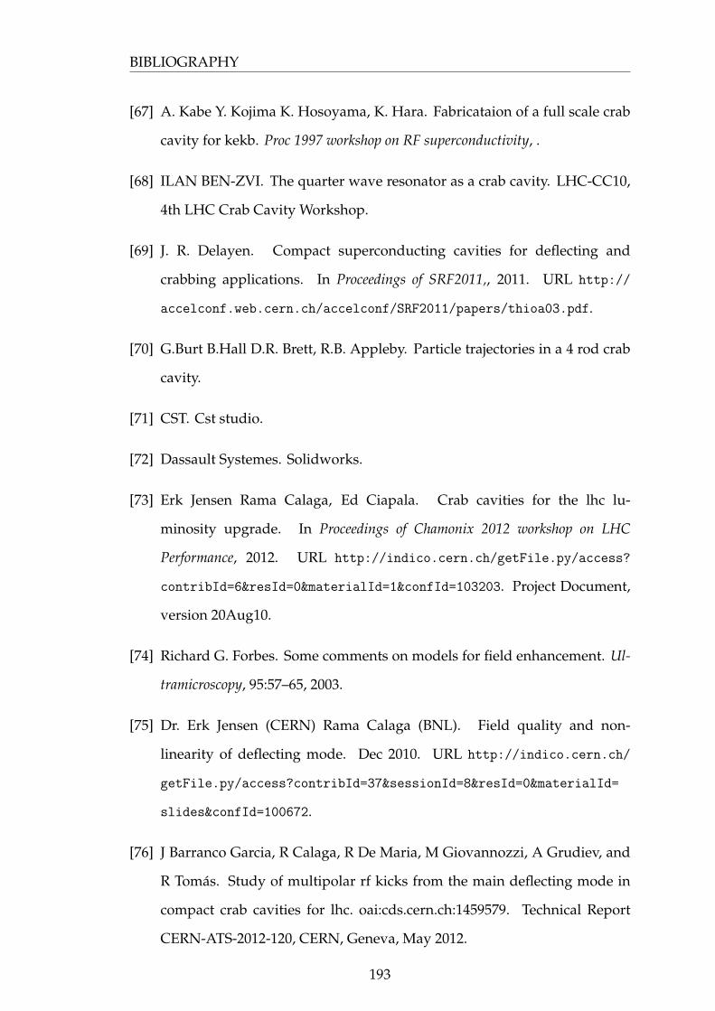
BIBLIOGRAPHY
[67] A. Kabe Y. Kojima K. Hosoyama, K. Hara. Fabricataion of a full scale crab
cavity for kekb. Proc 1997 workshop on RF superconductivity, .
[68] ILAN BEN-ZVI. The quarter wave resonator as a crab cavity. LHC-CC10,
4th LHC Crab Cavity Workshop.
[69] J. R. Delayen. Compact superconducting cavities for deflecting and
crabbing applications. In Proceedings of SRF2011,, 2011. URL http://
accelconf.web.cern.ch/accelconf/SRF2011/papers/thioa03.pdf.
[70] G.Burt B.Hall D.R. Brett, R.B. Appleby. Particle trajectories in a 4 rod crab
cavity.
[71] CST. Cst studio.
[72] Dassault Systemes. Solidworks.
[73] Erk Jensen Rama Calaga, Ed Ciapala. Crab cavities for the lhc lu-
minosity upgrade. In Proceedings of Chamonix 2012 workshop on LHC
Performance, 2012. URL http://indico.cern.ch/getFile.py/access?
contribId=6&resId=0&materialId=1&confId=103203. Project Document,
version 20Aug10.
[74] Richard G. Forbes. Some comments on models for field enhancement. Ul-
tramicroscopy, 95:57–65, 2003.
[75] Dr. Erk Jensen (CERN) Rama Calaga (BNL). Field quality and non-
linearity of deflecting mode. Dec 2010. URL http://indico.cern.ch/
getFile.py/access?contribId=37&sessionId=8&resId=0&materialId=
slides&confId=100672.
[76] J Barranco Garcia, R Calaga, R De Maria, M Giovannozzi, A Grudiev, and
R Tomás. Study of multipolar rf kicks from the main deflecting mode in
compact crab cavities for lhc. oai:cds.cern.ch:1459579. Technical Report
CERN-ATS-2012-120, CERN, Geneva, May 2012.
193
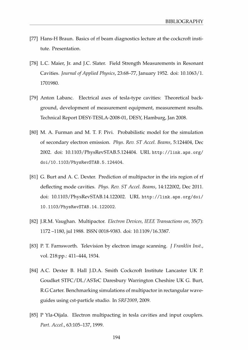
BIBLIOGRAPHY
[77] Hans-H Braun. Basics of rf beam diagnostics lecture at the cockcroft insti-
tute. Presentation.
[78] L.C. Maier, Jr. and J.C. Slater. Field Strength Measurements in Resonant
Cavities. Journal of Applied Physics, 23:68–77, January 1952. doi: 10.1063/1.
1701980.
[79] Anton Labanc. Electrical axes of tesla-type cavities: Theoretical back-
ground, development of measurement equipment, measurement results.
Technical Report DESY-TESLA-2008-01, DESY, Hamburg, Jan 2008.
[80] M. A. Furman and M. T. F. Pivi. Probabilistic model for the simulation
of secondary electron emission. Phys. Rev. ST Accel. Beams, 5:124404, Dec
2002. doi: 10.1103/PhysRevSTAB.5.124404. URL http://link.aps.org/
doi/10.1103/PhysRevSTAB.5.124404.
[81] G. Burt and A. C. Dexter. Prediction of multipactor in the iris region of rf
deflecting mode cavities. Phys. Rev. ST Accel. Beams, 14:122002, Dec 2011.
doi: 10.1103/PhysRevSTAB.14.122002. URL http://link.aps.org/doi/
10.1103/PhysRevSTAB.14.122002.
[82] J.R.M. Vaughan. Multipactor. Electron Devices, IEEE Transactions on, 35(7):
1172 –1180, jul 1988. ISSN 0018-9383. doi: 10.1109/16.3387.
[83] P. T. Farnsworth. Television by electron image scanning. J Franklin Inst.,
vol. 218:pp.: 411–444, 1934.
[84] A.C. Dexter B. Hall J.D.A. Smith Cockcroft Institute Lancaster UK P.
Goudket STFC/DL/ASTeC Daresbury Warrington Cheshire UK G. Burt,
R.G Carter. Benchmarking simulations of multipactor in rectangular wave-
guides using cst-particle studio. In SRF2009, 2009.
[85] P Yla-Oijala. Electron multipacting in tesla cavities and input couplers.
Part. Accel., 63:105–137, 1999.
194
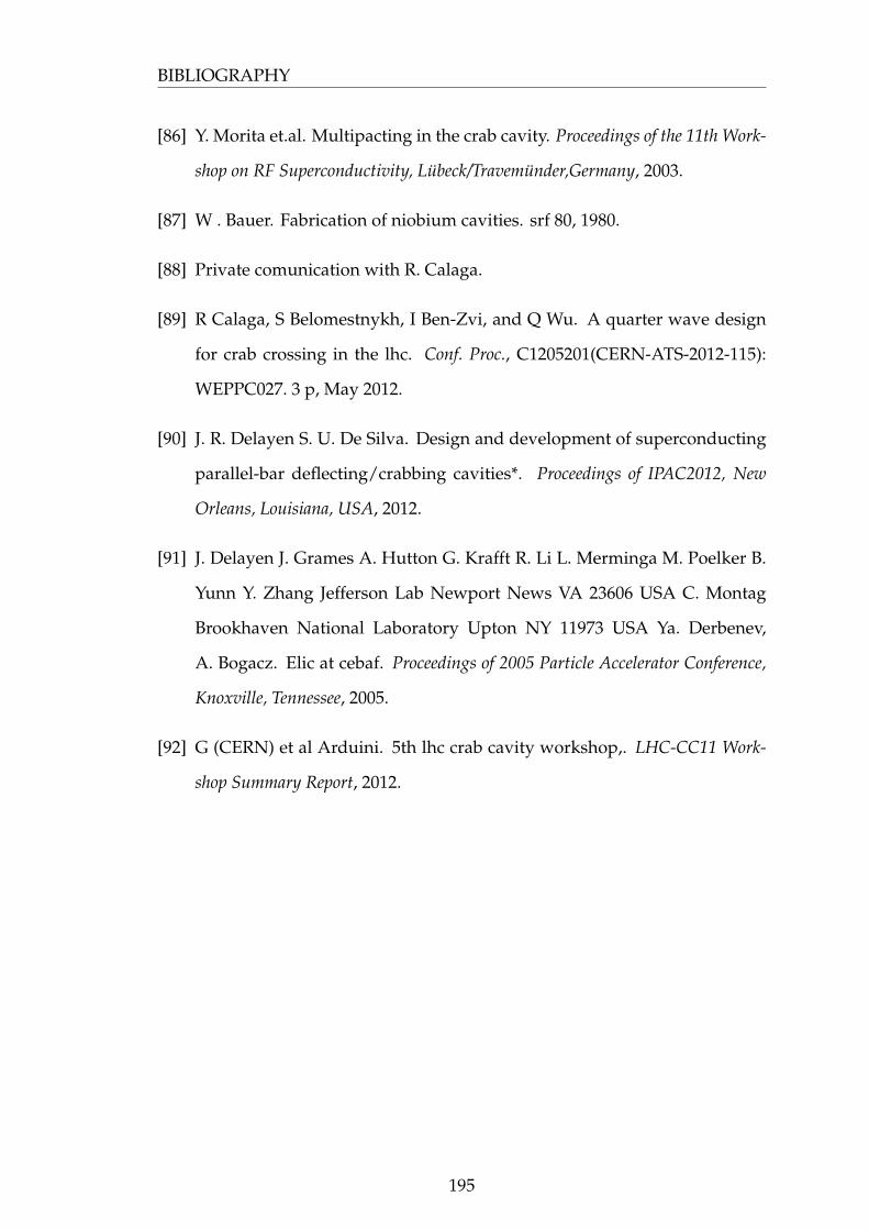
BIBLIOGRAPHY
[86] Y. Morita et.al. Multipacting in the crab cavity. Proceedings of the 11th Work-
shop on RF Superconductivity, Lübeck/Travemünder,Germany, 2003.
[87] W . Bauer. Fabrication of niobium cavities. srf 80, 1980.
[88] Private comunication with R. Calaga.
[89] R Calaga, S Belomestnykh, I Ben-Zvi, and Q Wu. A quarter wave design
for crab crossing in the lhc. Conf. Proc., C1205201(CERN-ATS-2012-115):
WEPPC027. 3 p, May 2012.
[90] J. R. Delayen S. U. De Silva. Design and development of superconducting
parallel-bar deflecting/crabbing cavities*. Proceedings of IPAC2012, New
Orleans, Louisiana, USA, 2012.
[91] J. Delayen J. Grames A. Hutton G. Krafft R. Li L. Merminga M. Poelker B.
Yunn Y. Zhang Jefferson Lab Newport News VA 23606 USA C. Montag
Brookhaven National Laboratory Upton NY 11973 USA Ya. Derbenev,
A. Bogacz. Elic at cebaf. Proceedings of 2005 Particle Accelerator Conference,
Knoxville, Tennessee, 2005.
[92] G (CERN) et al Arduini. 5th lhc crab cavity workshop,. LHC-CC11 Work-
shop Summary Report, 2012.
195
Related Documents