Designing Future VLSI Systems with Monolithically Integrated Silicon-Photonics Vladimir Stojanović University of California, Berkeley SSCS DL Lecture University of Texas, Austin November, 2013

Welcome message from author
This document is posted to help you gain knowledge. Please leave a comment to let me know what you think about it! Share it to your friends and learn new things together.
Transcript

Designing Future VLSI Systems
with Monolithically Integrated
Silicon-Photonics
Vladimir Stojanović
University of California, Berkeley
SSCS DL Lecture
University of Texas, Austin
November, 2013

Acknowledgments
• Milos Popović (Boulder), Rajeev Ram, Michael Watts, Hanqing Li (MIT),
Krste Asanović (UC Berkeley)
• Jason Orcutt, Jeffrey Shainline, Christopher Batten, Ajay Joshi, Anatoly
Khilo
• Mark Wade, Karan Mehta, Erman Timurdogan, Jie Sun, Cheryl Sorace,
Josh Wang
• Michael Georgas, Jonathan Leu, Benjamin Moss, Chen Sun, Yu-Hsin Chen
• Yong-Jin Kwon, Scott Beamer, Yunsup Lee, Andrew Waterman, Miquel
Planas
• Roy Meade, Gurtej Sandhu and Fab12 team (Zvi, Ofer, Daniel, Efi, Elad, …)
• DARPA, Micron, NSF and FCRP IFC
• IBM Trusted Foundry, CNSE Albany, Solid-State Circuits Society
2

Chip design is going through a change
• Already have more devices than can use at once
• Limited by power density and bandwidth
“The Processor is the new Transistor” [Rowen]
Intel 4004 (1971):
4-bit processor,
2312 transistors,
~100 KIPS,
10 micron PMOS,
11 mm2 chip
1000s of processor cores and
accelerators per die
Intel Knights Corner
50 cores, 200 Threads
Oracle T5
16 cores, 128 Threads
Nvidia Fermi
540 CUDA cores IBM Power 7
8 cores, 32 threads
3

Bandwidth, pin count and power scaling
Need 16k pins in 2017 for HPC*
1 Byte/Flop
256 cores
2 TFlop/s signal pins @ 20 Gb/s/link
2,4 cores
Pack
age p
in c
ount
*> half pins for power supply
4
T5
T5

0
2
4
6
8
10
12
14
16
18
20
1 10 100 1000
Mobile LPDDR2-1066
Mobile LPDDRX-1666
Mobile LPDDRX 2017
DDR3-1333 4GB
DDR4-2667 8GB
GDDR5
HMC-Gen1
HMC-Gen2
Memory interface scaling problems:
Energy-cost and bandwidth density
HMC
LPDDR
En
erg
y c
ost
[pJ/b
it]
Bandwidth density [Gb/s/pin]
DDR4
GDDR5
5

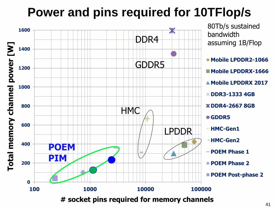
Power and pins required for 10TFlop/s
0
200
400
600
800
1000
1200
1400
1600
100 1000 10000 100000
Mobile LPDDR2-1066
Mobile LPDDRX-1666
Mobile LPDDRX 2017
DDR3-1333 4GB
DDR4-2667 8GB
GDDR5
HMC-Gen1
HMC-Gen2 To
tal
me
mo
ry c
ha
nn
el p
ow
er
[W]
# socket pins required for memory channels
80Tb/s sustained bandwidth assuming 1B/Flop
HMC
LPDDR
DDR4
GDDR5
6

Monolithic Si-Photonics for core-to-core and
core-to-DRAM networks
7 7
Supercomputers
Embedded apps
Si-photonics in advanced CMOS and DRAM process NO costly process changes
Bandwidth density – need dense WDM Energy-efficiency – need monolithic integration
7

Thin BOX SOI CMOS Electronics
Bulk CMOS Electronics
<150 nm SiO2
Monolithic CMOS photonic integration
8

9
Si and polySi waveguide formation
9

Integrated photonic interconnects
• Each λ carries one bit of data
Bandwidth Density achieved
through DWDM
Energy-efficiency achieved
through low-loss optical
components and
tight integration
10

Single channel link tradeoffs
10-dB
15-dB
Loss
5-fF 25-fF Rx Cap 11
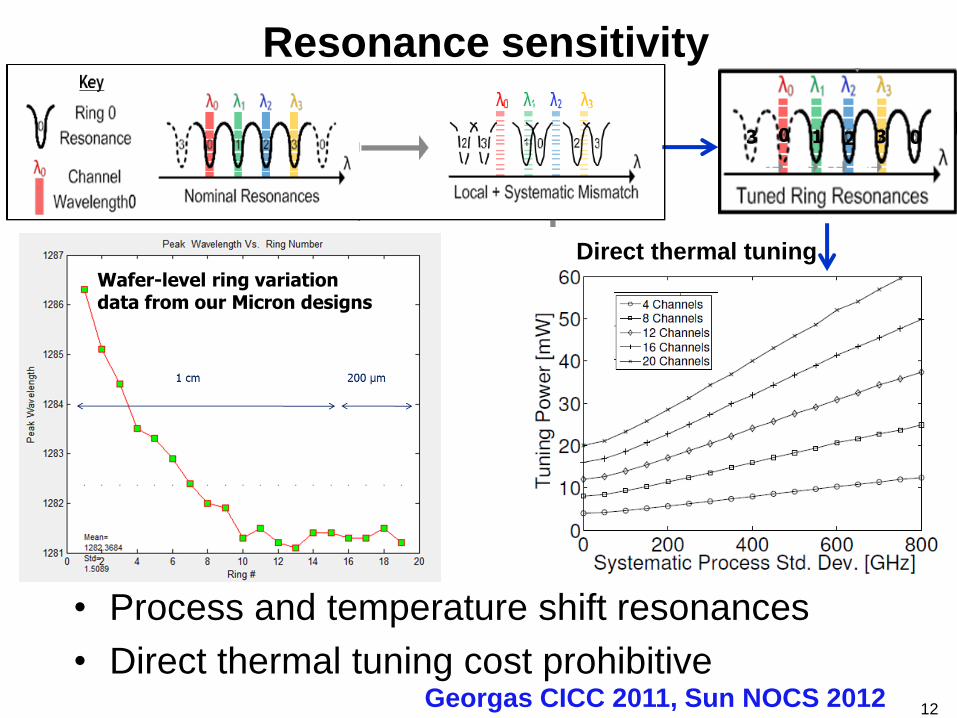
Resonance sensitivity
• Process and temperature shift resonances
• Direct thermal tuning cost prohibitive
Direct thermal tuning
Georgas CICC 2011, Sun NOCS 2012
Wafer-level ring variation data from our Micron designs
0 1 2 33 0
12
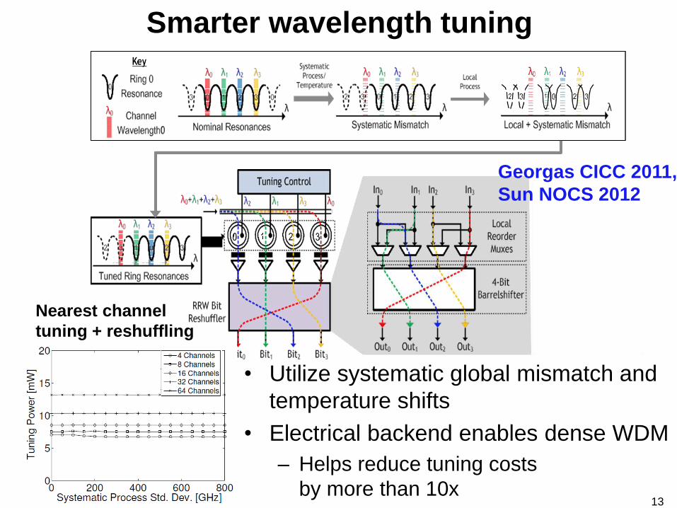
Smarter wavelength tuning
• Utilize systematic global mismatch and
temperature shifts
• Electrical backend enables dense WDM
– Helps reduce tuning costs
by more than 10x
Nearest channel
tuning + reshuffling
Georgas CICC 2011,
Sun NOCS 2012
13

14
• Laser energy increases with data-rate
—Limited Rx sensitivity
—Modulation more expensive -> lower extinction ratio
• Tuning costs decrease with data-rate
• Moderate data rates most energy-efficient
512 Gb/s aggregate throughput
assuming 32nm CMOS
Georgas CICC 2011
Need to optimize carefully
15
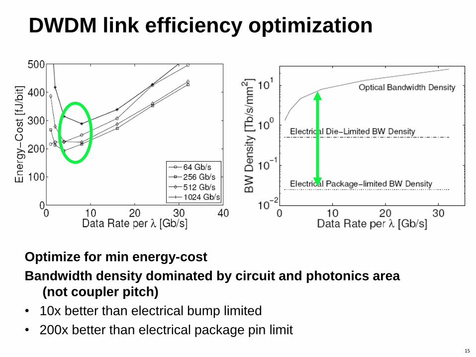
DWDM link efficiency optimization
Optimize for min energy-cost
Bandwidth density dominated by circuit and photonics area
(not coupler pitch)
• 10x better than electrical bump limited
• 200x better than electrical package pin limit

Many architectural studies show promise
[Shacham’07]
[Petracca’08]
[Vantrease’08]
[Psota’07]
[Kirman’06]
[Joshi’09]
[Pan’09]
[Batten’08] [Beamer’10] [Koka’08-10]
16
17
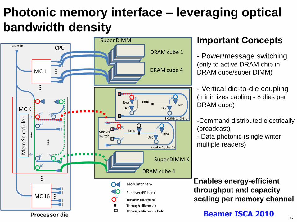
Photonic memory interface – leveraging optical
bandwidth density Important Concepts
- Power/message switching (only to active DRAM chip in
DRAM cube/super DIMM)
- Vertical die-to-die coupling (minimizes cabling - 8 dies per
DRAM cube)
-Command distributed electrically
(broadcast)
- Data photonic (single writer
multiple readers)
MC 1
MC 16
Mem
Sch
edu
ler
MC K
CPUDRAM cube 1
DRAM cube 4
Super DIMM
cmdDwr
Drd
( cube 1, die 1)
cmdDwr
Drd
( cube 1, die 8)
Dwr
Drd
DRAM cube 4
Super DIMM K
die-die switch
Laser in
Modulator bank
Receiver/PD bank
Tunable filterbank
Through silicon via
Through silicon via holeBeamer ISCA 2010 Processor die
Enables energy-efficient
throughput and capacity
scaling per memory channel

18
Enables capacity scaling per channel and significant savings in laser
energy
Laser Power Guiding Effectiveness
Beamer ISCA 2010
19
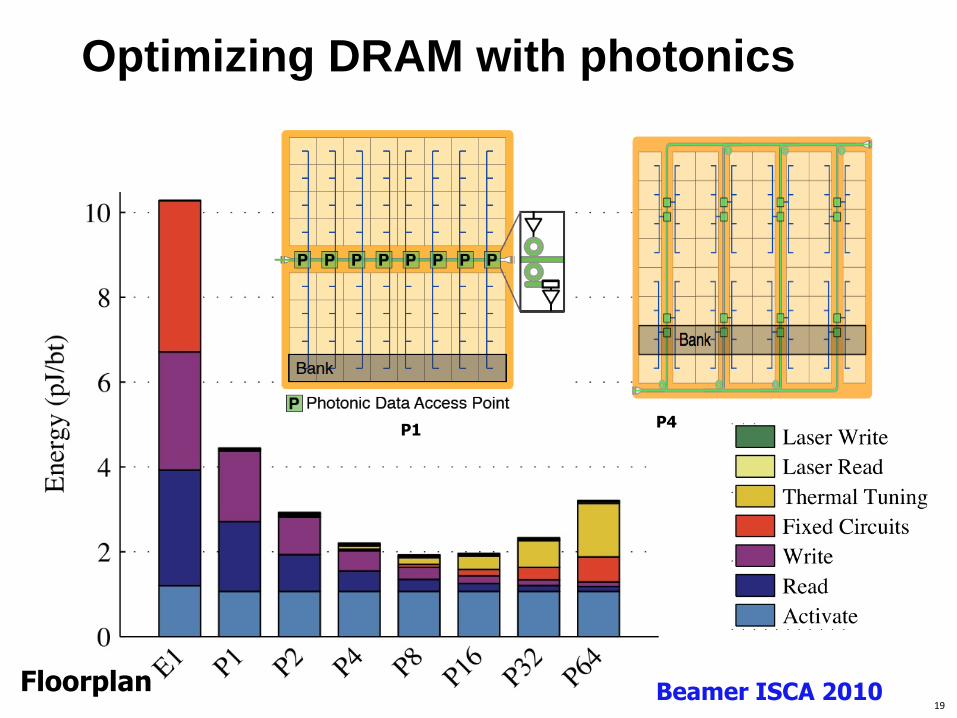
Optimizing DRAM with photonics
Floorplan
P1 P4
Beamer ISCA 2010

20
Design Space Exploration of Networks Tool
DSENT
User-Defined Models
Support Models Tools
Arbiter Router
Decoder Buffers
Technology Characterization
Area
Mesh Network
Electrical ClosRepeated Link
Optical Link Photonic Clos
CrossbarMultiplexer
Delay
Technology
Parameters
Model
Parameters
Standard Cells Timing Optimization
Expected
Transitions
Optical Link
Components
Optical Link
Optimization
Non-Data-
Dependent Power
Data-Dependent
Energy
Nin
Nout
fclock
...
Process
VDD
Wmin
T
...
20
DSENT – A Tool Connecting Emerging Photonics with Electronics for Opto-Electronic
Networks Modeling Chen NOCS 2012
Kurian IPDPS 2012
Available for download at:
https://sites.google.com/site/mitdsent/
21
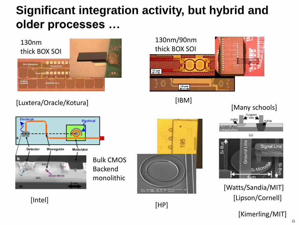
Significant integration activity, but hybrid and
older processes …
[Luxtera/Oracle/Kotura] [IBM]
[HP]
[Watts/Sandia/MIT]
[Intel]
130nm thick BOX SOI
130nm/90nm thick BOX SOI
Bulk CMOS Backend monolithic
[Lipson/Cornell]
[Kimerling/MIT]
[Many schools]

Our work: Si Electronic-Photonic Integration Timeline
IBM 9sf TI 28nm TI 65nm
EOS1 EOS2 EOS3 EOS4 EOS6+8+10
2007 2008 2009 2010 2011 2012
IBM 12SOI
EOS12
MIT-Micron Poly-Si Loss Study (D-1)
MIT-Micron Actives
Test (D0)
DARPA POEM D1S
Memory
Logic

EOS Platform: EOS8 fabricated in IBM12SOI
3 x 3 mm die
45nm Thin Box SOI
Technology
(used for Power 7 and
Cell processors)
3M Transistors
400 Pads
ARM Standard Cells
and
custom link circuits
Orcutt et al,
Optics Express, 2012
23

EOS8 performance summary
Fiber-to-chip grating
couplers with 3.5 dB
insertion loss
Waveguides under
4dB/cm propagation
loss
10 dB extinction
optical modulators
8 channel wavelength
division multiplexing
filter bank with
<-20 dB cross talk
All integrated with
electronic circuits
24

Integration of photonics into VLSI tools
VERSION 5.6 ;
BUSBITCHARS "[]" ;
DIVIDERCHAR "/" ;
MACRO block_electronic_etch_row_1
CLASS BLOCK ;
ORIGIN -208 -1794 ;
FOREIGN block_electronic_etch_row_1 208 1794 ;
SIZE 2488 BY 165 ;
SYMMETRY X Y R90 ;
PIN heater_a_1
DIRECTION INOUT ;
USE SIGNAL ;
PORT
LAYER ua ;
RECT 431 1870.5 436.5 1882 ;
END
END heater_a_1
...
OBS
LAYER m1 ;
RECT 208 1794 2696 1959 ;
...
END
END block_electronic_etch_row_1
END LIBRARY
modulator.LEF
Layout of
photonics
Layout of
Circuit blocks
abstract
abstract
LEF
LEF
LEF of standard cells, I/O pads
(provided by ARM)
Chip-level verilog
(instantiation of.LEF macros and
connectivity)
Technology files
SOC Encounter
Place and route
Floorplan
(macro placement,power grid, routing
Constraints)
Place&routed
layout
Photonic device
p-cell abstract
custom photonics-friendly auto-fill
layout
25

Circuit/Device Co-Simulation: VerilogA
Layout size: 120um x 50um
Optical Eye Diagram
Verilog A Model
Cadence Testbench View Modulator Instantiation
Driver Circuit
26
Laser input
Inside ring
Ring output
Output power (log scale) CW laser frequency increase

Platform Organization
27
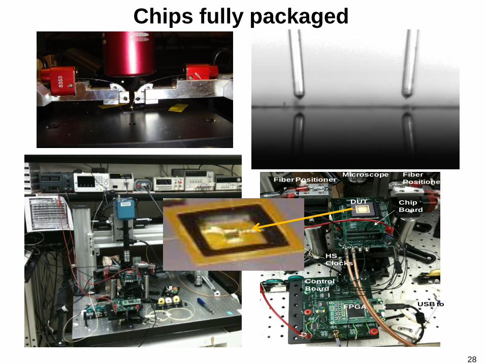
Chips fully packaged
DUT Chip
Board
HS
Clocks
FPGA
Control
Board
Fiber PositionerFiber
Positioner
USB to laptop
Microscope
28

Best waveguide losses ever reported in a
sub-100nm production CMOS line
• Body-Si waveguides
– 3-4dB/cm loss
• Poly waveguides
– 50dB/cm loss
• Body-Si ring Q
factor
– 227k @ 1280nm
– 112k @ 1550nm
700nm width
470nm width
700nm width
29
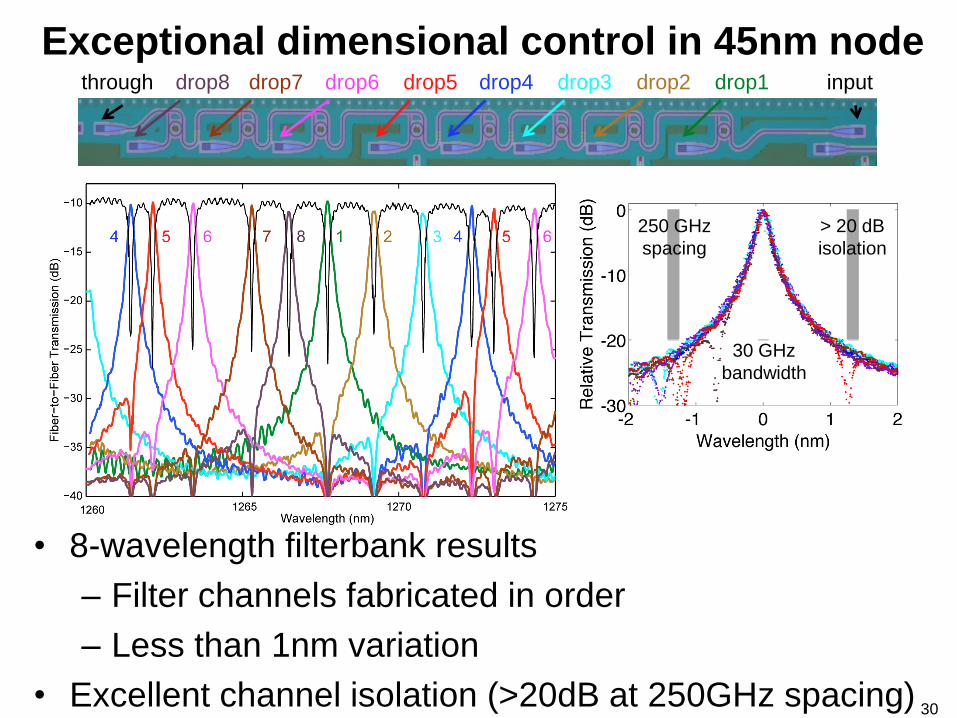
• 8-wavelength filterbank results
– Filter channels fabricated in order
– Less than 1nm variation
• Excellent channel isolation (>20dB at 250GHz spacing)
> 20 dB
isolation
30 GHz
bandwidth
250 GHz
spacing
through input drop8 drop7 drop6 drop5 drop4 drop3 drop2 drop1
Exceptional dimensional control in 45nm node
30
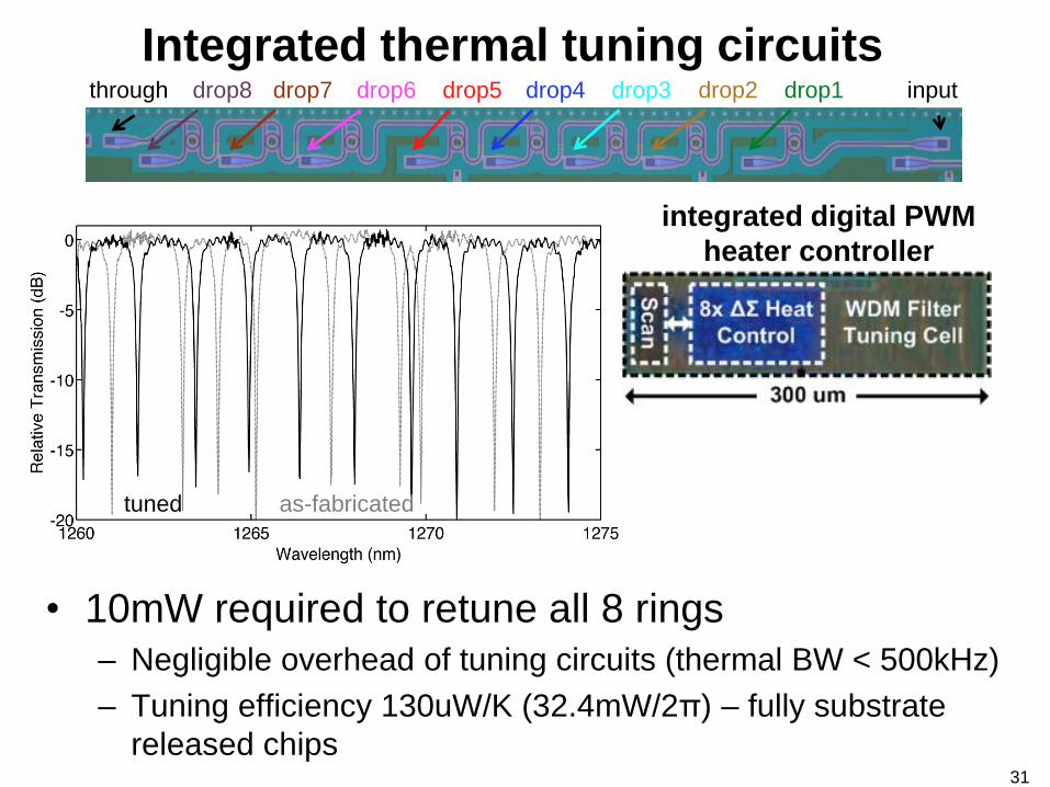
• 10mW required to retune all 8 rings
– Negligible overhead of tuning circuits (thermal BW < 500kHz)
– Tuning efficiency 130uW/K (32.4mW/2π) – fully substrate
released chips
tuned as-fabricated
integrated digital PWM
heater controller
through input drop8 drop7 drop6 drop5 drop4 drop3 drop2 drop1
Integrated thermal tuning circuits
31
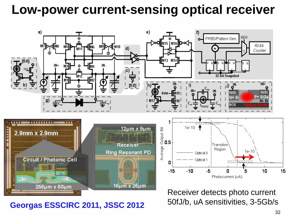
Low-power current-sensing optical receiver
Georgas ESSCIRC 2011, JSSC 2012
Receiver detects photo current
50fJ/b, uA sensitivities, 3-5Gb/s
32

Optical modulator design
Carrier-injection device
at 1550nm
• Extinction ratio 19dB
• 45GHz 3dB optical bw
at 1280nm
• Extinction ratio 9dB
• 60GHz 3dB optical bw
Shainline, Popovic
33
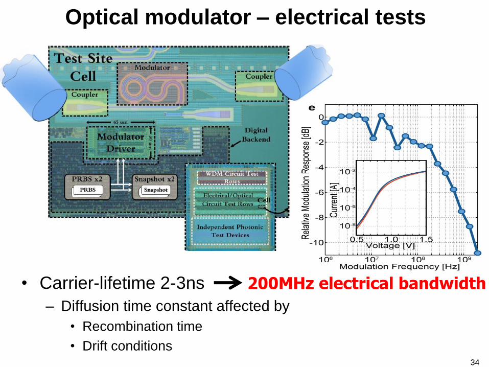
Optical modulator – electrical tests
• Carrier-lifetime 2-3ns
– Diffusion time constant affected by
• Recombination time
• Drift conditions
200MHz electrical bandwidth
34

Modulator driver sub-bit pre-emphasis
• Partial forward bias at 0-bit key to fast operation
35

Modulator driver heads
• Split-supply used for sub-bit pre-emphasis
– Use core and I/O voltage – no regulators 36

First modulation in 45nm process
• 2.5Gb/s modulation
• 1.2pJ/bit
• 3dB insertion loss
• 3dB extinction ratio
Moss ISSCC 2013 37
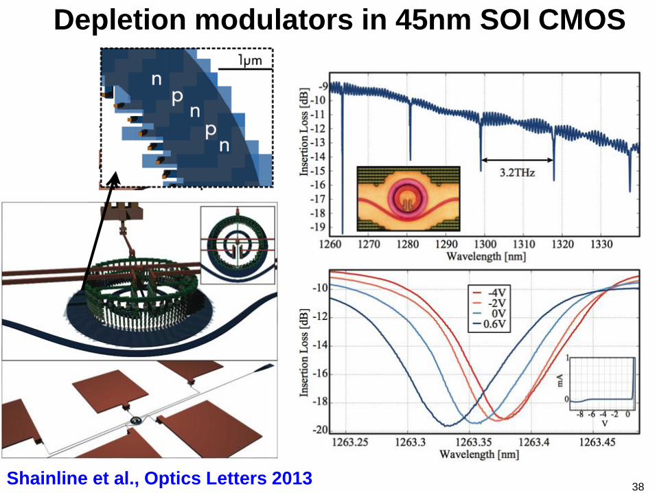
Depletion modulators in 45nm SOI CMOS
Shainline et al., Optics Letters 2013 38

Depletion modulators in 45nm SOI CMOS
• Modulation: 5 Gbps
5.2dB extinction ratio
• Energy:
55 fJ/bit
Tunable across FSR with
400GHz/mW (~2nm/mW)
39

0
2
4
6
8
10
12
14
16
18
20
1 10 100 1000
Mobile LPDDR2-1066
Mobile LPDDRX-1666
Mobile LPDDRX 2017
DDR3-1333 4GB
DDR4-2667 8GB
GDDR5
HMC-Gen1
HMC-Gen2
POEM Phase 1
POEM Phase 2
POEM Post-phase 2
Memory interface scaling problems:
Energy-cost and bandwidth density
HMC
LPDDR
En
erg
y c
ost
[pJ/b
it]
Bandwidth density [Gb/s/pin]
DDR4
GDDR5
POEM PIM
40
Power and pins required for 10TFlop/s
0
200
400
600
800
1000
1200
1400
1600
100 1000 10000 100000
Mobile LPDDR2-1066
Mobile LPDDRX-1666
Mobile LPDDRX 2017
DDR3-1333 4GB
DDR4-2667 8GB
GDDR5
HMC-Gen1
HMC-Gen2
POEM Phase 1
POEM Phase 2
POEM Post-phase 2
To
tal
me
mo
ry c
ha
nn
el p
ow
er
[W]
# socket pins required for memory channels
80Tb/s sustained bandwidth assuming 1B/Flop
HMC
LPDDR
POEM PIM
DDR4
GDDR5
41
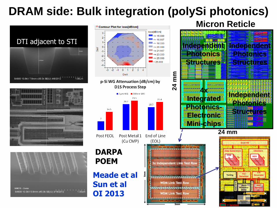
DRAM side: Bulk integration (polySi photonics)
Data Generators
PRB
S
PRB
S
PRB
S
PRB
S
PRB
S
PRB
S
PRB
S
PRB
S
Checkers
PRB
S
PRB
S
PRB
S
PRB
S
PRB
S
PRB
S
PRB
SBER
Scan I/O
Tuning8:2
Serializer
2:8
Deserializ
er
DDR
Modulator
Driver
Modulator
Device
He
ater D
river
He
ater D
river
= tested
DDR
Receive
r
DTI adjacent to STI
DARPA POEM
Micron Reticle
Independent
Photonics
Structures
Independent
Photonics
Structures
Independent
Photonics
Structures
4x
Integrated
Photonics-
Electronic
Mini-chips
24
mm
24 mm
Meade et al Sun et al OI 2013

Summary
• Silicon-photonics can push both critical dimensions – Energy-efficiency – monolithic integration
– Bandwidth Density - dense WDM
• Need to optimize across layers – Connect devices to circuits, and links to networks
• Building early technology development platforms – Feedback to device and circuit designers
– Accelerated adoption
• EOS Platform designed for multi-project wafer runs – Best end-of-line passives in sub-100nm process (3-4dB/cm loss)
– sub-100fJ/b transmitters/receivers
– Record-high tuning efficiency with undercut ~ 25uW/K
44
Conclusions
• Silicon-photonics – enabler of new capabilities – Think “new on-chip inductor” or “new on-chip t-line”
• Potentially revolutionize many applications despite slowdown in CMOS scaling – VLSI compute and network infrastructure
– Wireless comm
– Imaging and Sensing
• Need process, device, circuit and system-level understanding
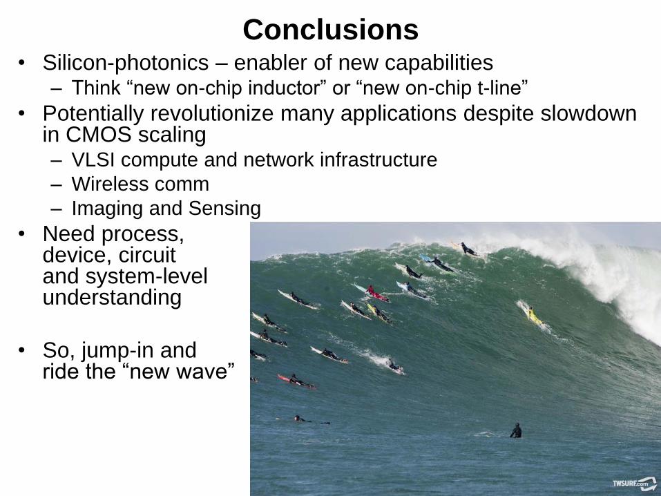
• So, jump-in and ride the “new wave”
45
Related Documents