Design Tradeoffs of Single Chip Multi-computer Networks A Thesis Presented to the Faculty of the Department of Computer Engineering University of Houston In Partial Fulfillment of the Requirements for the Degree Master of Science in Computer Engineering by Kurt Olin December 1999

Welcome message from author
This document is posted to help you gain knowledge. Please leave a comment to let me know what you think about it! Share it to your friends and learn new things together.
Transcript

Design Tradeoffs of Single Chip Multi-computer Networks
A Thesis
Presented to the Faculty of the Department of Computer Engineering
University of Houston
In Partial Fulfillment
of the Requirements for the Degree
Master of Science
in Computer Engineering
by
Kurt Olin
December 1999

ii
Design Tradeoffs of Low-cost Multi-computer Networks
Kurt Olin
Approved:
Committee Members:
Chairman of the Committee Martin Herbordt, Professor, Electrical and Computer Engineering
Pauline Markenscoff, Professor, Computer and Systems Engineering
Lennart Johnsson, Professor, Electrical and Computer Engineering
C. Dalton, Associate Dean, Cullen College of Engineering
L. S. Shieh, Professor and Chairman, Computer and Systems Engineering

iii
Acknowlegements
Special thanks and gratitude to Dr. Martin Herbordt for his guidance, encouragement, and insight.
Special thanks to Dr. Markenscoff and Dr. Johnsson for taking time from their schedules to be on
my committee.

iv
Design Tradeoffs of Single Chip Multi-computer Networks
An Abstract of a
A Thesis
Presented to the Faculty of the Department of Computer Engineering
University of Houston
In Partial Fulfillment
of the Requirements for the Degree
Master of Science
in Computer Engineering
by
Kurt Olin
December 1999

v
Abstract
A comparison is made among a number of embedded network designs for the purpose of
specifying low-cost yet cost-effective multi-computer networks. Among the parameters varied are
switching mode, number of lanes, buffer size, wraparound, and channel selection. We obtain
results using two methods: 1) RTL cycle-driven simulations to determine latency and capacity
with respect to load, communication pattern, and packet size and 2) hardware synthesis to a
current technology to find the operating frequency and chip area. These results are also
combined to yield performance/area measures for all of the designs.
We find that lanes are just as likely to improve performance of virtual cut-through as wormhole
networks, and that virtual cut-through routing is preferable to wormhole routing in more domains
than may have been previously realized. Other results are deeper understanding of virtual cut-
through in terms of deadlock properties and the capability of dynamic load balancing among
buffers.

vi
Table of Contents
Acknowlegements ............................................................................................................................iii
Abstract ............................................................................................................................................ v
List of Figures..................................................................................................................................vii
List of Tables.................................................................................................................................. viii
1 Introduction ................................................................................................................................... 1 1.1 Problem/motivation................................................................................................................. 1
1.2 Methods.................................................................................................................................. 6
1.3 Results.................................................................................................................................... 7
1.4 Impact.....................................................................................Error! Bookmark not defined. 2 Design Space.............................................................................................................................. 10
2.1 Basic Network Assumptions and Parameters ...................................................................... 10
2.1.1 Immediate Constraints and Assumptions ...................................................................... 10
2.1.2 Derived Issues ............................................................................................................... 12
2.1.3 Measured issues............................................................................................................ 14
2.2 Deadlock Prevention ............................................................................................................ 21
2.3 Differences between Wormhole and Virtual Cut-Through ................................................... 23
3 Hardware Issues ......................................................................................................................... 26 3.1 Node Architecture................................................................................................................. 26
3.2 Input Buffer Implementation ................................................................................................. 28
3.3 Output Implementation ......................................................................................................... 35
3.4 Buffer Sharing Options ......................................................................................................... 37
4 Simulation ................................................................................................................................... 39 5 Results ........................................................................................................................................ 42
5.1 Simulated Performance........................................................................................................ 42
5.2 Latency ................................................................................................................................. 46
5.3 Area ...................................................................................................................................... 48
5.4 Timing................................................................................................................................... 53
5.5 Cost-Effective Designs ......................................................................................................... 56
5.6 Buffer Sharing....................................................................................................................... 61
5.7 Comparison to an Output Queue Design ............................................................................. 63
5.8 Experiments and Observations ............................................................................................ 63
6 Conclusions................................................................................................................................. 69 7 References.................................................................................................................................. 70

vii
List of Figures
Figure 1 Sample Chip Organization.................................................................................................3
Figure 2 Packet Structure ................................................................Error! Bookmark not defined. Figure 3 Portion of a sample network, bidirectional virtual cut-through.........................................13
Figure 4 Crossbar comparison for WH (top) and VCT (bottom) ....................................................18
Figure 5 Packets A, dark shade, and B, light shade, are traveling in the X dimension, but are
blocked because packet A can’t turn into a busy Y dimension, black shade. ........................19
Figure 6 With an extra lane in the X dimension, packet B is not blocked by packet A because it
can us the extra lane...............................................................................................................20
Figure 7 Difference between WH and VCT, bidirectional and unidirectional nodes. In the WH
nodes the double arrows represent the two virtual channels. These two virtual channels
share a single physical channel. WH and VCT have the same size physical channel. ........24
Figure 8 Organization of 4-lane bidirectional virtual cut-through cascaded crossbar node...........26
Figure 9 Register implementation of FIFO.....................................................................................29
Figure 10 RAM implementation of FIFO. .......................................................................................31
Figure 11 Filling and emptying the FIFO........................................................................................32
Figure 12 Path selection logic........................................................................................................35
Figure 13 Sample arbitration logic for a 4 lane design ..................................................................36
Figure 14 Shown is a graph of latency versus applied load for a number of switching designs with
the random communication pattern and a packet size of 5 flits. Measurements were taken
using the RTL simulator. The three ‘bundles’ of series correspond to the unidirectional torus
wormhole, the mesh wormhole, and the bidirectional wormhole configurations respectively.41
Figure 15 Packet latency through node. .......................................................................................46
Figure 16 Visual Basic code for bidirectional VCT area. ...............................................................50
Figure 17 Legend for capacity versus area graphs. .....................................................................56
Figure 18 Capacity versus area graph for a random pattern with a packet size of 6, top, and 24,
bottom. ....................................................................................................................................57
Figure 19 Capacity versus area graph for a hot-spot pattern with a packet size of 6, top, and 24,
bottom. ....................................................................................................................................58
Figure 20 Capacity versus area graph for a near pattern with a packet size of 6, top, and 24,
bottom. ....................................................................................................................................59
Figure 21 Buffer sharing capacity versus area graphs for random and hot-spot patterns with a
packet size of 6. ......................................................................................................................62

viii
List of Tables
Table 1 Load imbalance in the standard virtual channel selection algorithm for the unidirectional
wormhole torus. Virtual channel 0 is the wrap-around channel and virtual channel 1 is the
direct channel. The counts indicate the number of source-destination paths that go through
the particular channel in each node........................................................................................16
Table 2 Load imbalance in the T3D-inspired virtual channel selection algorithm for the
unidirectional wormhole torus. Virtual channel 0 has node 0 as a dateline and virtual channel
1 has node 4. ..........................................................................................................................17
Table 3 FIFO valid bit control.........................................................................................................29
Table 4 Performance with random communication pattern and a packet size of 6. .....................43
Table 5 Performance with random communication pattern and a packet size of 24. ....................43
Table 6 Performance with hot-spot communication pattern and a packet size of 6. .....................44
Table 7 Performance with hot-spot communication pattern and a packet size of 24. ..................44
Table 8 Performance with near communication pattern and a packet size of 6. ..........................45
Table 9 Performance with near communication pattern and a packet size of 24. .........................45
Table 10 Area of designs with no input buffer sharing...................................................................51
Table 11 Area of designs with input buffer sharing between lanes. ..............................................51
Table 12 Area of designs with input buffer sharing within a physical channel...............................52
Table 13 Area of designs with input buffer sharing within the entire node. ...................................52
Table 14 Cycle time summary. ......................................................................................................54
Table 15 Cost-effective designs.....................................................................................................60
Table 16 Cost-effective designs with sharing. ...............................................................................61
Table 17 Output Queue Design Characteristics. ...........................................................................63

1
1 Introduction
1.1 Problem and Motivation
As advances in process technology continue with only modest slowdowns expected in the next
decade, one of the fundamental questions in computer architecture remains how best to use
newly available resources. Several possible approaches have been proposed, although they
mostly fall into one of two categories: i) enhancing microprocessors with increased speculative
capability, instruction-level parallelism and/or multi-threading and ii) multiprocessing on a chip,
that is, integrating multiple discrete microprocessors or digital signal processors (DSPs) on a
chip. The latter approach is likely to be preferable for computationally intensive tasks and is our
primary interest here.
Currently, the focus in building multiprocessor systems on a chip (SOCs) is, understandably, on
taking advantage of existing processor and memory designs and the electronic design
automation (EDA) technology which makes them easy to replicate and integrate. SOCs based on
replicating microprocessors have included studies of symmetric multiprocessors (SMPs) on a
chip. Others multiprocessor SOCs have taken a completely different approach, being based on
enhancing memory by integrating a large number of simple processing elements (PEs).
A critical issue for multiprocessor SOCs that has received very little attention is the question of
how the removal of chip boundaries might change the design of the multiprocessor system,
including both the design of the components as well as how they are integrated. Since it was the
fact that an entire processor could be placed on a single chip--thereby removing long
intraprocessor signaling delays--that spurred the microprocessor revolution, it seems possible
that removal of packaging boundaries might cause a similar paradigm shift with multiprocessors.
At the very least, there is likely to be a major shift in the design space as the distribution of
propagation delays and the ratio of propagation delay to switching time is fundamentally altered.

2
The problem we address in this thesis is the design of a network appropriate for a single chip
multiprocessor. This problem is important because the changing ratio of switching to propagation
time is likely to have a significant effect on the relative benefits of various design choices. The
single-chip assumption is also interesting from a methodological standpoint as it allows us to use
standard workstation EDA tools for accurate circuit-level simulations. When these are combined
with cycle-level simulations as we do in this thesis, it becomes possible to examine a large
number of design alternatives without compromising accuracy.
In this thesis, a large number of parallel processor network router designs are made and
compared in terms of cycle-by-cycle performance, cell area, and cycle time. Although these
designs are directed to parallel processor networks for use on a single substrate, they are also
applicable to other design situations. The designs are based on a single basic design framework
with a large number of different options. By comparing the designs that result from these options,
a designer can make deductions about the relative cost and performance benefits of particular
options and make decisions about which design to use for his particular situation.
1.2 The Basic Model
We envision these multiprocessors on a chip as having dozens of nodes on a silicon substrate,
increasing to hundreds as technology allows. Such a chip would have an array of processor
node pairs, each with a connection to near neighbors. All processor-to-processor data transfers
take place in the network nodes using the following scenario: i) the source processor transfers
the data packet to its associated network node, ii) the packet is transferred from network node to
network node until it reaches the destination network node, and iii) the packet is then transferred
from the destination network node to its associated processor. All processor instruction and
control transfers are outside the network and we do not consider them here. The design of the
off-chip connections depends on the details of the design external to the chip and the particular

3
pin constraints of the chip’s package. Since this is very design specific we do not consider the
details here, except to note that the off-chip connections are allowed for in our designs.
While designs with (2N)2 nodes, and array of 2N on a side, may be easier to program than other
sizes, our designs do not depend on any particular size. But, our simulated performance is only
applicable for designs with the same number of nodes on each side. The following figure shows
at a high level how such a chip might be organized.
Processor
Network Node
Processor
Network Node
Processor
Network Node
Processor
Network Node
Processor
Network Node
Processor
Network Node
Processor
Network Node
Processor
Network Node
Figure 1 Sample Chip Organization

4
Because the processors and network nodes are on a single chip and arranged in a 2 dimensional
array with short interconnections, the data transfer between one node to another is very fast.
This, combined with the network nodes’ simple and efficient design, presents the opportunity for a
design with a short cycle time, and therefore, high performance. The regular organization of the
chip simplifies the design and testing of the actual implementation.
We assume small fixed size packets and deterministic routing. The routers’ designs are allowed
to take advantage of this particular environment whenever possible. The resulting routers are
simple, low-cost, and suitable for parallel processor systems on a single substrate.
We generally assume input buffering, but to be sure that we are not going down the wrong path,
we also study a design that has output buffering. Output buffering has higher performance when
considering network throughput per cycle, but the design is more complex and managing the
buffer at the output results in a much longer critical path. To see whether the increase in
throughput per cycle compensates for the increase in cycle time we evaluate a network with
nodes with output queuing, similar to the IBM SP2 design [21], but which still taking advantage of
our particular environment.
1.3 Previous Work
Although there has been extensive work in the area of switch design and multiprocessor
networks, relatively few studies include hardware costs, either in their effect on chip area or on
operating frequency. Of the studies that do pay attention to cost, even fewer do so quantitatively,
or for more than one particular implementation of a design.
An exception is Chien [1, 6], who has performed a detailed hardware cost and operating
frequency analysis for a particular class of routers in terms of the number of inputs or outputs,

5
number of virtual channels and routing freedom. But, this analysis does not account for some of
the options we would like to consider such as virtual cut-through routing, unidirectional vs.
bidirectional switches, the varying buffer sizes, dynamic buffer sharing between lanes and does
not address the network performance achieved by varying these parameters.
Another gap is that virtual cut-through switching has not been explored to nearly the extent of
wormhole switching. This is especially important since even a preliminary glance at the problem
of low-cost networks, points to virtual cut-through as a way of cutting down on the number of
virtual channels and thereby getting more switch for your silicon. Some that do, Duato et al [x],
do not perform a hardware cost analysis or have a design that is not suited for our particular
environment.
We are designing for an environment where the node to node delay is very small because the
nodes are on the same chip and are placed adjacent or very near their communication neighbors.
Little work has been done for this environment. (Even Dally’s Torus Routing Chip [10] had off-
chip delays between nodes and couldn’t operate faster than the off-chip and wire delays.) The
Abacus SIMD Array [4] is one that uses network nodes on the same chip, but this network is
much too simple for our purposes.
Much work is done for nodes that are more featured and complex than we use. The SP2 is an
example. Its design is more complex than we use and that makes the operating frequency lower
than we are able to achieve. The SP2 design uses this complexity to increase its performance for
its particular environment and this is good. The reason is that the SP2 has very long node to
node delays and even with extensive pipelining one could not possibly achieve the small cycle
times we do for our design. So the additional complexity probably does not affect the operating
frequency.

6
And finally, there are just too many parameters. Even if you could try everything, the analysis
would be prohibitive. In other words, the questions we need answers for had not been answered.
1.4 Methods
Because our focus is how to build an embedded network for single chip coprocessors, we
concentrate on low-cost, cost-effective mechanisms: The routing is deterministic dimension
order. The topology is either a 2D mesh or torus. A single physical channel exists between
nodes per direction per dimension. The packets are small and have fixed size, 6 and 24 flits in
our experiments. These sizes approximate transfers of single words or cache lines.
Even so, there are still a large number of router design options to consider: These include:
• Whether the switching mode is wormhole (WH) or virtual cut-through (VCT)
• Whether the connections are unidirectional or bidirectional
• Whether the crossbars are full or cascaded
• The optimal number of virtual lanes per channel.
• The optimal FIFO buffer size.
• Whether to share FIFO buffer space for more than 1 lane in the same RAM.
We evaluate the design alternatives in terms of both the cost in chip area and the performance in
terms of effect on network capacity and operating frequency. This requires using three different
methods, which are now described.
To determine network capacity, we use a cycle-driven simulator and simulate a network of
reasonable size, 8 by 8. We determine network capacity by assigning injectors a fixed capacity
(load) and run enough cycles to determine if the network saturates with this load. We believe our
method is more representative of real systems, even if it requires more computer time per design.
A simulation run consists of a single network type / load / routing pattern / packet size

7
combination. After performing multiple runs with different loads, we determine the network
capacity in terms of flits/node/cycle. The routing patterns we use for performance evaluation are
standard synthetic patterns: random, hot-spot, and near-random.
To determine cell area we represent the designs in Verilog High-level Design Language, HDL,
then perform logic synthesis targeting LSI Logic’s G10-p 0.18 micron technology. The logic
synthesis package we use, from Synopsys, is very good at deriving a design with optimum cell
area. Not all designs are evaluated completely; we take advantage of the hardware design’s
modularity to evaluate some of the modules separately. For example, the number of ports in the
output queue can be evaluated for many design points and a formula for cell area based on the
number of ports generated. These formulas are used in the designs instead of generating a
complete Verilog HDL for each design option. Combining these formulas yields a cell area for
each design option.
To determine cycle time, the designs are evaluated and critical paths determined manually. The
logic design involving these critical paths is done by hand and timed using gate delay for the
target technology. We do this manually because the logic synthesis package we use, from
Synopsys, is not very good at deriving a design with optimum timing.
1.5 Results
The results we present in this thesis include some key observations about virtual cut-through
routing, performance of the designs with a cycle-driven simulator, router cell area, and router
cycle time analysis. The results presented show the effect of these options on the routers’ cell
area and cycle timing when mapped into a current generation 0.18 micron technology, LSI Logic’s
G10-p Cell-Based ASIC technology.
This work adds to previous studies in that it accounts for:

8
• Variations in the number of lanes in the VCT configurations.
• Not only bidirectional tori, but meshes and unidirectional tori are considered.
• Deadlock and timing considerations unique to VCT.
• Static virtual channel selection versus dynamic lane selection methods.
• Both physical properties, such as critical path timing and layout area, and latency/bandwidth
results from register transfer level simulations.
Some of the key results we present are:
• Lanes are as useful to VCT networks as they are to wormhole networks.
• When operating frequency is factored in, increasing the number of lanes beyond 2 per
physical channel is not likely to be cost effective.
• For equal numbers of buffers and space per buffer, VCT switching is likely to have better
performance than WH switching. The reason is that the space guarantee associated with
VCT switching is easy to implement for small packets and has powerful consequences in
load balancing among lanes and, to a lesser extent, flow control latency.
• All the designs described are evaluated with respect to area/performance for each workload
and the cost-effective ones enumerated.
While investigating the design framework, it was necessary to work out some issues that are
themselves contributions. These are:
• Observations about VCT deadlock and how to prevent it.
• The application of virtual channel load balancing to unidirectional WH torus networks.
1.6 Significance
Our designs take advantage of many of the characteristics of single chip parallel systems and our
results are directly applicable to the environment of our primary interest, single chip parallel
systems. We believe our results also provide useful insight into other, more general, design

9
areas including SIMD and distributed shared memory. While our designs are mapped to a
current technology for evaluation in this paper, we believe the results will be applicable to future
ASIC technologies.
Although we show the results in tabular form, the equations we have generated for cell area allow
network designers to determine some characteristics for designs that have slightly different
options than the particular ones we have chosen. For example, it is a simple matter to determine
the cell area of a router with a different buffer size, flit size, or crossbar matrix than what we
present here.
1.7 Outline
The rest of the thesis is organized as follows:

10
2 Design Space
We now present the details of our network design space. Since some of the configurations are
new and others have non-trivial motivation, we also discuss deadlock in wormhole, WH, and
virtual cut-through, VCT, networks and virtual channel selection in WH networks. We end this
section with an analysis of the design consequences of the choice between WH and VCT
switching.
2.1 Basic Network Assumptions and Parameters
Any parameter study, especially one on such a well-studied area as switch design has to be
constrained. These constraints are critical since you will never solve everybody's problem! Of
course, the constraints also have to be credible since all aspects of the design need to be
reasonable if you are going to analyze any particular feature. We divide the parameter space into
three categories:
1. The immediate constraints and assumptions following immediately from our domain.
2. The derived decisions which followed from a small amount of analysis or experimentation.
3. The parameters we measured.
2.1.1 Immediate Constraints and Assumptions
1. We have constrained our designs to only have two dimensions. The nodes we are
connecting are not boxes or boards to be wired together with copper, but rather, on-chip
modules. A two dimensional topology is significantly less expensive, in terms of chip area,
because a chip is built in two dimensions.
2. The area used by our network node matters. Although we have much more chip area than,
say, Dally did when designing the Torus Routing Chip, we do have a constraint: the more
space we spend on the routers, the fewer the processors we can fit on the chip.

11
3. The communication modes we will support are fine-grained message passing and
dataparallel communication operations.
4. Our packets are small and fixed size. A packet is made up of N data plus 2 address 8-bit
flits. A packet’s route is determined at the source processor before the packet is inserted into
the network. Two address flits are pre-pended to the packet. These address flits contain the
X and Y destination nodes and the direction the packet is to take to get to these nodes.
7 6 5 4 3 2 1 0 + - Next X Node Destination + - Next Y Node Destination
Data flit 0 Data flit 1
• • •
Data flit N-1
Where + and - indicate which direction to go when entering the X dimension or the Y dimension. And Next indicates that the address will match at the next node and a turn should take place.
Figure 2 Packet Structure
5. When a packet travelling in the X dimension reaches its X node destination, the X node
destination flit is removed from the packet and the Y node destination flit becomes the
packet’s first flit. When the Y destination node is reached, the Y node destination flit is
removed and only the data flits are forwarded to the destination processor.
6. Our analysis strives for reasonable technology independence. Since we do not know what
the technology will be when these results are used, nor what our timing and area constraints
will be, we want to make our study at least moderately technology independent. We have
mapped our designs into a standard CMOS 0.18 micron technology. This should be
representative, with scaling, of ASIC technologies for some time.

12
7. The entire network operates on a single clock. Single chip clock distribution is very well
understood and clocked systems are simpler than unclocked systems. Bolotski, et. al.
present several novel techniques for dealing with this [4].
8. The inter-switch transfer time is on the order of the switch time or smaller. Because our
switching nodes are on the same chip and our routing is mesh or torus, the distance, and
therefore the transfer time, between nodes is very small.
9. The header flit takes two cycles while the other flits take one cycle to traverse the switch. This
constraint turns out to be a good balance between minimizing slack and keeping the number
of cycles to a minimum. Although this constraint is not “immediate” and will be discussed
further below, we introduce it here since it has fundamental design implications.
2.1.2 Derived Issues
Topology
Our prime directive of working in two dimensions eliminates all topologies but one-dimensional
and two-dimensional meshes as the longer wire lengths for the other choices cannot be justified,
especially if there is any locality at all in the communication. This decision will only be truer with
advancing process technology causing wires to cause an increasing fraction of the delay.
Because the design is intended for parallel processors on a single chip substrate, the designs are
simple and low-cost. The network structure is either two dimensional mesh or torus. Each node
has one physical channel connection to each neighboring node for each direction. The physical
channel is 1 flit, 8 bits, wide with extra handshaking signals. A router node is associated with
each processor, and that processor has separate input and output channels to the node. All
nodes are considered identical, except for the nodes’ particular address. There is no attempt to
simplify any particular node, e.g. edge or corner nodes. The following figure shows a portion of a
sample network.

13
X- inX+ in
X+ outX- out
Y- in Y- out
Y+ out Y+ in
X- inX+ in
X+ outX- out
Y- in Y- out
Y+ out Y+ in
X- inX+ in
X+ outX- out
Y- in Y- out
Y+ out Y+ in
X- inX+ in
X+ outX- out
Y- in Y- out
Y+ out Y+ in
X- inX+ in
X+ outX- out
Y- in Y- out
Y+ out Y+ in
X- inX+ in
X+ outX- out
Y- in Y- out
Y+ out Y+ in
X- inX+ in
X+ outX- out
Y- in Y- out
Y+ out Y+ in
X- inX+ in
X+ outX- out
Y- in Y- out
Y+ out Y+ in
X- inX+ in
X+ outX- out
Y- in Y- out
Y+ out Y+ in
P PP
P P
P
P
P P
Figure 3 Portion of a sample network, bidirectional virtual cut-through
Routing Algorithm
The constraints applicable here are:
• a two dimensional mesh,
• minimize area cost, and
• small fixed sized packets.
The standard choices in routing are between dimension order, random, and adaptive, and all their
combinations. The problem with all methods other than dimension order routing is that they
cause some additional complexity and so may slow down the clock, cause an increase in area, or
both. Although for the simplest random algorithm this is perhaps not true since all the
computation can be overlapped.
But a more important reason is that dimension order routing causes packets to make the fewest
possible turns and turns in two dimensions can cause more congestion than they alleviate. We
still have a bit to learn about adaptive algorithms, but Leighton's classic result for store-and-

14
forward is persuasive [17]. While single shot dimension order routing causes virtually no
congestion with very high probability, random shortest path causes O(log N) slowdown with very
high probability. Because the places where blocking is initiated tend to be where packets try to
turn but can't. For small packets and non-trivial buffers, this result applies here as well.
We therefore use dimension order routing.
Buffering Mechanism
We use input buffering and its multi-lane variations exclusively. This is not because output
buffering is not effective; it is just not optimal for everything. Output buffering carries more
inherent overhead than does input buffering which you can hide completely with long packets and
long inter-switch transfer times, but not with short packets and short inter-switch transfer times.
We therefore use input buffering with space sharing.
Crossbar
There is a choice between single and cascaded crossbars. To make the decision, we performed
timing and simulation studies which can be summarized as follows: for two dimensional meshes
with small numbers of lanes per channel, it does not make much difference. We use cascaded
crossbars because they have a faster operating frequency.
2.1.3 Measured Issues
Switching mode
We consider two switching modes, wormhole, WH, and virtual cut-through, VCT, in our designs.
A few points however:
1. The only real difference between wormhole and virtual cut-through, is that in virtual cut-
through, the receiving node provides a guarantee that, if it receives the packet header, it can
receive the rest of the packet.

15
2. As a consequence, deadlock prevention is significantly easier in virtual cut-through since
preventing deadlock in wormhole routing likely to require using virtual channels.
However, beyond these basic differences, they have much in common:
3. For a given buffer size, as long as there is enough space to provide the space guarantee,
the buffer size choice in virtual cut-through is not constrained.
4. A similar point for can be made for virtual channels (or lanes) in wormhole routing: once
you have enough to prevent deadlock, there are no more constraints. Nor are there ever
constraints on lanes in virtual cut-through, again, as long as the space guarantee can be
provided.
5. For our domain with small fixed sized packets, the basic hardware support between
wormhole and virtual cut-through is nearly identical.
6. VCT has fewer constraints on virtual channel selection. We discuss this in section 2.3.
Virtual Channel Selection in Wormhole Switching
A very important issue in getting decent performance out of an input buffered wormhole routing
network is virtual channel selection. In an early work on virtual channels, Dally proposed the
following selection algorithm, all packets that can proceed to their destination (in the dimension)
without wraparound use virtual channel 0 while the others use virtual channel 1 until the
wraparound point at which time they transfer to channel 0 to complete the route [11]. Bolding
noticed that this algorithm leads to an extreme imbalance in buffer usage [2]. It turns out that
distributing the load between virtual channels is very important and Scott and Thorson have a
very effective way of addressing this problem for bidirectional torus networks with the introduction

16
of datelines and off-line channel selection [20]. We have extended this idea to unidirectional
torus networks.
The method is a straightforward extension of the bidirectional technique with the exception that
no pair of datelines exists such that all packets cross at most one dateline. We address this
problem by requiring packets that cross both datelines to switch channels once. This is not as
elegant a solution as is available in the bidirectional case, but provides for a substantial
improvement in load balance between channels. The initial load imbalance is shown in Table 1
and the load imbalance after the application of the T3D technique is shown in Table 2.
We have also made one change to the basic T3D technique. We perform inter-dimension
channel selection dynamically and based on availability. Since the inter-dimensional channels do
not form a ring, this does not alter the deadlock properties of the network. It does, however,
improve network capacity by 3 to 5%.
Another critical point is that this load balancing assumes a uniform communication pattern. It is
not necessarily optimal for other patterns. The reason why this is so important here, and this is
one of the key results of this work, is that virtual cut-through does not have this problem since
deadlock considerations do not play a role in lane selection.
Table 1 Load imbalance in the standard virtual channel selection algorithm for the unidirectional wormhole torus. Virtual channel 0 is the wrap-around channel and virtual channel 1 is the direct channel. The counts indicate the number of source-destination paths that go through the particular channel in each node.
Node Virtual channel 0 1 2 3 4 5 6 7
Average Imbalance
Max Imbalance
0 0 0 1 3 6 10 15 21 1 28 28 27 25 22 18 13 7
Imbalance 1.0 1.0 .93 .79 .57 .28 .07 .5 .64 1.0

17
Table 2 Load imbalance in the T3D-inspired virtual channel selection algorithm for the unidirectional wormhole torus. Virtual channel 0 has node 0 as a dateline and virtual channel 1 has node 4.
Node Virtual channel 0 1 2 3 4 5 6 7
Average Imbalance
Max Imbalance
0 7 9 13 16 21 19 15 12 1 21 19 15 12 7 9 13 16
Imbalance .50 .26 .07 .14 .50 .26 .07 .14 .24 .50
Crossbar Switches
The choice of switching mode also affects the crossbar. Here is an example of the crossbar
matrices for two lane wormhole node and a four lane virtual cut-through node. Since there are
fewer constraints on virtual channel selection in virtual cut-through, there are more possible lane
choices and therefore more crosspoints.
It turns out that this is not a bad thing. In comparison to the space we are going to spend on
buffering and because of the regular shape, the difference between being 5/9ths and 7/9ths full is
less than 1% of the total switch area.

18
X0+a X1+a X0-a X1-a C0a C1a X0+b X1+b X0-b X1-b C0b C1b
Y0+aY0+bY1-aY1-b
Y0+aY0+bY1-aY1-b
X0-aX0-bX1-aX1-b
X0+aX0+bX1+aX1+b
P1aP1b
Y0+a Y1+a Y0-a Y1-a P0a P1a Y0+b Y1+b Y0-b Y1-b P0b P1b
P0aP0a
X+a X+c X-a X-c Ca Cc X+b X+d X-b X-d Cb Cd
Y-aY-bY-cY-d
Y+aY+bY+cY+d
X-aX-bX-cX-d
X+aX+bX+cX+d
PcPd
Y+a Y+c Y-a Y-c Pa Pc Y+b Y+d Y-b Y-d Pb Pd
PbPa
Figure 4 Crossbar comparison for WH (top) and VCT (bottom)
Which 2D Topology?
The choices are between unidirectional and bidirectional mesh and between mesh and torus.
The advantage of the mesh is that it by itself prevents deadlock and so allows you to do

19
wormhole routing without virtual channels. Tori can be constructed without long wires by using
the standard interleaving trick. In other words, whatever virtual channels you do have, the
selection can be completely dynamic depending only on which one is free. The idea of the
unidirectional mesh makes sense in this context since even if it does lead to a great deal of
congestion, it can have double the internode bandwidth and much smaller internal buffering.
Lanes for Performance
There have already been many studies that point to the benefits of having multiple lanes per
channel. The reason is because, as is shown below, they allow packets to avoid being blocked.
We investigate one, two, and four lanes per virtual channel.
Figure 5 Packets A, dark shade, and B, light shade, are traveling in the X dimension, but are blocked because packet A can’t turn into
a busy Y dimension, black shade.

20
Figure 6 With an extra lane in the X dimension, packet B is not blocked by packet A because it can us the extra lane.
Buffer Size
Increasing buffer size improves performance because it gets blocked packets out of the way.
This is a cruder use of chip area than increasing the number of lanes, but does not require adding
ports in the crossbar. For maximum speed, we want register-based FIFOs. For maximum area
use we want to use RAM. For our reference process, and LSI Logic 0.18 micron standard cell,
small fast register files in RAM are 6 to 8 times smaller, but a factor of 2 slower than the register
equivalent. We use hybrid buffers. This is a technique allows hiding with a wide bus. Five flit
slots are registers while all the rest are RAM. See section 3.4.
Dynamic Space Sharing
We investigate space sharing among buffers. Again, this is all done on the input side. The
rationale here is that if larger buffers are good, we should use that space as efficiently as
possible. We should not have extra flit slots that are unused.
We look at four scenarios for wormhole routing, the virtual cut-through circuits are slightly less
complex in that there is only one virtual channel, so option 3, below, is the same as option 2:
1. No sharing,

21
2. Sharing space among buffers in a channel,
3. Sharing space among buffers in a dimension, and
4. Sharing space among buffers in the whole switch.
All of these schemes can be implemented with no slowdown as long as the buffer is at least a
certain minimum size. For 2), sharing is simple because we can get at most one flit per cycle
input on a physical channel. The other sharing options are more complex.
2.2 Deadlock Prevention
We begin by defining the switching modes:
Wormhole Routing - Packets are divided into flits which are transmitted contiguously. When
the head of the packet is blocked, the flits remain in place. In practice, space for more than
one flit per node is required. Two is usually the minimum needed to handle handshaking and
communication of `blocked-ness' back through the worm so as to prevent flits from being
overwritten.
Virtual Cut Through Routing - Packets are divided into flits and travel through the network
as in WH routing. When blocked, however, the entire packet is queued as in packet-switched
routing.
In practice WH routing networks usually have larger buffers than two. The term buffered
wormhole routing was used to describe the IBM SP2 network in which a node can buffer several
good-sized packets, but which provides no guarantee that an entire packet will be able to reside
there [21].
In the simplest case, VCT implies that any packet arriving at a node can be queued there in its
entirety. In parallel computers it is much more likely that the queue will be bounded to a fixed
number of packets. We propose the term virtual cut-through with limited buffers to refer to
networks with the following property, a blocked packet is guaranteed to be buffered in a single

22
node in its entirety, but a packet is not guaranteed to be blocked only because a channel is
unavailable.
Deadlock can occur when there is the possibility of a circular request for resources. For WH
routing on torus networks, deadlock as a result of circular path requests is a well-known problem.
With dimension order routing, DOR, the simplest method of preventing deadlock is to use virtual
channels. For mesh WH networks using DOR, there is no circular dependency and deadlock is
not a problem. Virtual channels are therefore not required for mesh WH networks.
It has been stated numerous times that VCT is inherently deadlock free and this is true for the
infinite buffer case. It is not true, however, for VCT with limited buffers. The problem is that
although no circular request can occur for channels, it can occur for buffers. See, e.g. [12]. We
know of two solutions. But. first a definition, we refer to the combined output/input FIFOs in a
lane/direction/dimension as a buffer and assume that each buffer has a capacity of n packets.
Strict/Local Solution - If there are n-1 headers in a buffer, the nth header can only come
from the current dimension.
The second solution to the VCT deadlock prevention problem is based on the observation that we
only really need one packet slot per direction per dimension to guarantee freedom from deadlock.
Relaxed/Distributed Solution - If there are n-1 headers in a buffer, and all other buffers
have n headers, then the nth header can only come from the current dimension.
In the above scenario progress is still made as the `hole' travels backwards and packets inch
their way forwards. The advantage of the first solution is its simple hardware requirement,
the advantage of the latter its performance.
23
2.3 Differences between Wormhole and Virtual Cut-Through
Since we assume small fixed length packets and dimension order routing, the differences
between WH and VCT networks are small but very significant. In particular, in a VCT network:
• the buffer size should be a multiple of the packet size,
• a mechanism must exist to prevent entering packets from filling up all the buffers and causing
deadlock, and
• in a synchronous switch, once a header has been permitted to transmit to the next input FIFO
there is a guarantee that there will always be a flit buffer free for all succeeding flits in the
packet.
In a WH torus network:
• deadlock must be prevented through the use of virtual channels and
• a channel selection strategy should be used to balance buffer usage.
It is important to note that just about everything else can remain identical. In particular, nothing
prevents the use of lanes in VCT networks to improve performance, although this is one of the
issues not discussed in previous comparisons between WH and VCT switching [19][12].
The basic switch variations are shown in Figure 6. If we assume similar buffer requirements for
networks of either switching mode, an assumption we will show is very reasonable, and a simple
packet header counting mechanism for VCT, then there are two principal differences. These are:
i) the virtual channel requirement of WH tori and the concomitant increase in switching
complexity, and ii) the guarantee of flit space in VCT that allows us to group the physical channel
arbitration with the lane arbitration.

24
X- in
X+ in
X+ out
X- out
Y- in Y- out
Y+ out Y+ in
P
Bidirectional WH Node
Xin X out
Y in
Y out
Unidirectional WH Node
P
X- in
X+ in
X+ out
X- out
Y- in Y- out
Y+ out Y+ in
P
Bidirectional VCT Node
Xin X out
Y in
Y out
Unidirectional VCT Node
P
Figure 7 Difference between WH and VCT, bidirectional and unidirectional nodes. In the WH nodes the double arrows represent the two virtual channels. These two virtual channels share a single physical channel. WH and VCT have the same size physical channel.
Channel Selection
Since the physical channel bandwidth is not affected by the switching mode, the question arises
whether the freedom from virtual channels is actually an advantage, after all, virtual channels
have been found to be effective for flow control [8], especially when used with an optimized load
balancing strategy [20]. We show that the answer is often yes, and for two reasons:
• Not requiring virtual channels means that particularly low cost switches can be built for VCT
networks for which there is no WH equivalent.
25
• For the same total number of buffers, VCT switching allows for more dynamic load balancing
among buffers. For example, assume a pair VCT and WH switches with an equal number of
lanes per dimension per direction. One such pair would be i) a bidirectional WH torus with
two virtual channels per direction per dimension and one lane per virtual channel and ii) a
bidirectional VCT torus with no virtual channels but with two lanes per direction per
dimension. In the first case, static selection is effected between buffers (virtual channels). In
the second case, the dynamic selection is effected between buffers (lanes). Although static
load balancing for virtual channels is effective, it is not as effective as dynamic load balancing
among lanes.
Combined Arbitration
Since, in VCT, a packet transfer can only be initiated if there is a guarantee of space for the entire
packet in the next node, and because we assume synchronous switches, there is no need for
internode flow checking beyond that for the header flit.

26
3 Hardware Issues
In this chapter we discuss the hardware design issues. We start with an overview of the
components that comprise a switch and then describe the issues in their design and how we
addressed them.
3.1 Node Architecture
A diagram of a sample follows that shows the major node components and how they are
connected.
Pin
Input BuffersX+in
X-in Input Buffers
Input Buffers
Output X+out
Output X-out
Output
Y-in
Input Buffers
Y+in Input Buffers
Input Buffers
Output Pout
Output Y+out
Output Y-out
Figure 8 Organization of 4-lane bidirectional virtual cut-through cascaded crossbar node.
In the basic node design, packet flits come into the node and are latched in the input buffer. They
then get transferred to the appropriate output buffer. If for some reason they cannot transfer
immediately, or if sometime during the packets transfer its output path becomes blocked, flits are

27
buffered in a FIFO located on the input side of the node. The collection of the input latches and
the FIFO buffer is called the input buffer. Each lane of each virtual channel has an input buffer.
While latched in the input buffer, the contents of the first flit of a packet are compared to the
node’s address. Based on the results of this comparison, an output for the packet is selected.
This is called path select.
When a path has been selected, a request is made to the selected output. Based on the
requests made to it, the output port will select a requestor. This process is called arbitration.
Each output lane has a separate arbitration.
When an input buffer wins arbitration for an output, it begins transferring flits through the
crossbar. The crossbar is distributed among the output ports. Being implemented as a set of
large multiplexors, and not as a single large block of logic. Transfers will occur until the end of
the packet.
Because the node knows what the packet size is, it can determine which flits are the first and last
flits of a packet. The first flit gets a head indicator that trails along with it, and the last flit gets a
tail indicator that trails along with it. Actually, the tail indicator appears before the last flit so the
hardware can prepare for it a cycle ahead of time.
Wormhole/Virtual Cut-Through
Flow control for wormhole routing is on a flit basis. The sending and receiving node exchange
flow control signals for each flit transferred. On each cycle the node’s control logic determines if
its input buffers can accept another flit.

28
Flow control for virtual cut-through is on a packet basis. The sending and receiving node
exchange flow control signals only for the first flit in a packet. While flow control is conceptually
simpler for VCT, the amount of hardware required by VCT and WH is similar.
Unidirectional/Bidirectional
Both unidirectional router nodes and bidirectional router nodes are investigated. A unidirectional
node has half the number of inputs and outputs as the bidirectional node. To make the
comparison between the two fair, the physical channel size is doubled, from 1 flit wide in the
bidirectional case, to 2 flits wide for the unidirectional case.
3.2 Input Buffer Implementation
Register FIFO
We are not proposing that the FIFO elements be completely implemented as registers, but if we
consider this for a moment, it makes it easier to understand the RAM implementation.
The FIFO elements can be implemented as registers. These registers are strung together in a
line with Buffer0 at the bottom and BufferN-1 at the top. The FIFO registers are always filled from
the bottom to the top with no gaps between filled positions. With each buffer register is an
associated Valid bit. To determine which buffer register gets loaded with the next input data, the
Valid bits are examined. The buffer register with the lowest not valid bit is loaded next. The FIFO
is always emptied from the bottom, Buffer0.

29
Buffer 1
Buffer 0
Buffer N-1
Buffer N-2
Buffer N-3
ToOutput Queue
FromPrevious Node
Figure 9 Register implementation of FIFO.
Each buffer register was a width of flit size+3. The three bits are for Valid, Head indicator, and
Tail indicator.
The decision each buffer register makes is simple and is based on 5 inputs as shown in the
following table. The Valid bits are for this register and the one above and below it. In is if a flit
enters the FIFO, Out is if a flit exits the FIFO. The buffer registers on the ends are simplifications
of this table.
Table 3 FIFO valid bit control.
Assume Buffer Number J Valid Bits
J+1 J J-1 In Out Action - - - 0 0 Same

30
- - - 0 1 Shift down from J+1 - 0 0 1 0 Invalid - 0 1 1 0 Load from Input - 1 1 1 0 Same - 0 0 1 1 Invalid - 0 1 1 1 Invalid 0 1 1 1 1 Load from Input 1 1 1 1 1 Shift down from J+1
RAM FIFO
The technology we use and our design is such that the RAM read and write time are two cycles.
To slow down the cycle time to accommodate a one cycle read and write would reduce
performance too much to make up for any complexity or cell savings. This means that the RAM
is two flits wide and read and written two flits at a time. The RAM used has two ports, read and
write, that operate independently and simultaneously.
The FIFO RAM has registers for write and read staging. The design also has a flit buffer for the
case when a flit comes into the node while a write is taking place. These registers are fashioned
into the model of the Register FIFO as shown. Because the RAM is read while write, there is no
bypass of the RAM.

31
Buffer 1
Buffer 0
Buffer 4
RAM
Buffer 3
Buffer 2
ToOutput Queue
FromPrevious Node
Figure 10 RAM implementation of FIFO.
The operation is similar to the Register FIFO with the exception that whenever Buffer3 is valid a
write occurs. The register read address increments at the end of a read operation and doesn’t
change until the end on the next read operation. So the RAM output is valid for the second cycle
after the previous read. Since the read address doesn’t change this output remains valid until it’s
needed.
The following two timing diagrams illustrate the operation of the FIFO RAM in the filling and the
emptying operations. The first timing diagram assumes that a new flit is entering the node on
each cycle. The second timing diagram assumes there is a flit exiting the FIFO on each cycle.
The FIFO will operate with a mixture of these. They are shown separately for viewing clarity.
Additionally, the timing diagrams show consecutive cycles.

32
Buf 4
Buf 3
Buf 2
Buf 1
Buf 0
RAM
Rd Adr
Wt Adr
-
-
-
-
Flit0
-
0
0
-
-
-
Flit1
Flit0
-
0
0
-
-
Flit2
Flit1
Flit0
-
0
0
-
Flit3
Flit2
Flit1
Flit0
0
0
Flit4
Flit3
Flit2
Flit1
Flit0
0
0
-
Flit5
Flit4
Flit1
Flit0
0
1
Flit6
Flit5
Flit4
Flit1
Flit0
0
1
-
Flit7
Flit6
Flit1
Flit0
0
2
Flit8
Flit7
Flit6
Flit1
Flit0
0
2
---Write--- ---Write--- ---Write---
RAM FIFO Filling
Buf 4
Buf 3
Buf 2
Buf 1
Buf 0
RAM
Rd Adr
Wt Adr
-
-
Flit8
Flit1
Flit0
0
3
-
-
Flit8
-
Flit1
0
3
-
-
Flit8
Flit3
Flit2
1
3
-
-
Flit8
-
Flit3
1
3
-
-
Flit8
Flit5
Flit4
2
3
-
-
Flit8
-
Flit5
2
3
-
-
Flit8
Flit7
Flit6
3
3
-
-
-
Flit8
Flit7
3
3
-
-
-
-
Flit8
3
3
----Read---
RAM FIFO Emptying
----Read--- ----Read---
Figure 11 Filling and emptying the FIFO.
The read address register and the write address register increment and wrap around. But, the
increment isn’t arithmetic, it uses a linear feedback shift register to avoid critical timing paths.
FIFO Size Options
We have examined 4 different buffer size options, 6 flits, 12 flits, 24 flits, and 48 flits. For the
RAM FIFO implementation a change in FIFO size is a simple matter of adding RAM words. This
slows the RAM’s operation time, but this isn’t the critical path. As the number of words increases
beyond each 2k, another bit is required in the RAM’s read and write address registers.

33
Incrementing the address register length doesn’t affect the timing because of its linear feedback
shift register incrementer.
For those buffer sizes where the size of the RAM would be less than or equal to 2 words, a
Register FIFO implementation is used. As the overhead for managing the buffer is larger than
two flit registers.
Path Select Operation
While latched in the input buffer, the contents of the first flit of a packet are compared to the
node’s address. Based on the results of this comparison, the Next bit is set in this address flit.
This is performed in each node for the address of the next node. Then when the next node is
reached the Next bit can be used directly, instead of waiting for the address compare to take
place.
Based on the Next bit, a destination output for the packet is selected. If the Next bit is off; i.e.
this dimension’s destination address does not match this node’s address, the selection is simple.
The packet requests an output in the same direction. If the Next bit is set, this flit is discarded by
the select logic and on the following cycle the path selected is determined by the +/- bits. For the
cascaded crossbar implementations, the cascade stage is inserted between the X and Y
dimension. This has the effect of simplifying the logic.
Figure 11 is representative of the logic used. It shows the address match and path select logic
for the P input of a bidirectional VCT cascaded crossbar node. Other node types and other input
buffers have similar implementations. Varying in number of request destinations, lower NAND
fan-in, and misc. fan-outs. The signals used for control are described below.

34
Go for Cascade
Eat Flit
Won Arbitration
X Adr in BufferAddress Match
V H T Data
Request X+ Request X- Request Cascade
THV
Next Control
Block for Previous X+ Request
Requests From Other Lanes
Block for Previous X- Request
Block for Previous C Request
Set Next
Signal Meaning Request_X+ Signals that this flit wants to go in the X+ direction. This signal goes
to arbitration logic in the X+ output queues. Request_X- Signals that this flit wants to go in the X- direction. This signal goes
to arbitration logic in the X- output queues. Request_Cascade Signals that this flit wants to go to the Cascade output queue. This
signal goes to arbitration logic in the Cascade output queues. Eat_Flit Signals to advance the buffer but keep head bit. It’s used when
turning form X to Y or Y to P and we need to get rid of the address flit. It is essentially Address_Match on the cycles when we have a head and haven’t “eaten” all the address flits.
Set _Next Signals that the Next bit should be set. Address_Match Signals that the address matches the next node’s address. X_Adr_in_Buffer Signals that we haven’t “eaten” the X address flit yet. Block_for_Previous_X+ Request
Signals that a lane in this channel already has a request for the X+ channel active. It blocks any requests by this lane.
Block_for_Previous_X- Request
Signals that a lane in this channel already has a request for the X- channel active. It blocks any requests by this lane.
Block_for_Previous_C Request
Signals that a lane in this channel already has a request for the Cascade channel active. It blocks any requests by this lane.
Requests from other Requests from other lanes of this channel. These signals are used

35
lanes to determine Block_for_previous_Request. Go_for_Cascade Signals that we have matched and “eaten” the X address flit and this
packet is destined for the Cascade output queue. Won_Arbitration Signals that this request, whichever one is active, has won
arbitration at an output queue. This is the OR of all the appropriate output queues’ arbitration won for this input buffer.
Figure 12 Path selection logic.
3.3 Output Implementation
Arbitration
Based on the requests made to it, the output port will select a requestor. This process is called
arbitration. Each output lane has a separate arbitration. If multiple lanes are sharing a physical
channel, only one can send a flit on any one cycle. The design of the arbitration logic takes
advantage of this. An arbitration is only allowed to take place on the cycles prior to the cycle
when the lane is able to send a flit on the physical channel. This allows only one of the lanes to
perform an arbitration at any one time.
The crossbar connections for an output, see Figure 4, determine which requests participate in the
arbitration. First, if there are multiple lanes per channel, all the requests from lanes of each
channel are ORed. Recall from the previous section that only one of these will be active. Then
one of the ORed requests creates a winner, see Figure 12. The results of the arbitration, the
winner signals, are distributed to three places:
• back to the path select logic, so a path can know if it won the arbitration,
• to the crossbar gating controls, so the flit can be gated to the output, and
• to the output queue control logic, to update the state machine control.

36
X+ Wins X- Wins P Wins
Only 2 and 4 lanedesigns have
these OR gates.
X+ Request (Lane D)
X+ Request (Lane C)
X+ Request (Lane B)
X+ Request (Lane A)
X- Request (Lane D)
X- Request (Lane C)
X- Request (Lane B)
X- Request (Lane A)
P Request (Lane D)
P Request (Lane C)
P Request (Lane B)
P Request (Lane A)
Allow Arbitration
Figure 13 Sample arbitration logic for a 4 lane design
Crossbar Structure and Connections
Two crossbar types are investigated, full-crossbar and cascaded-crossbar. In a cascaded-
crossbar design there are two crossbars. The first has P and X inputs and X and Cascade
outputs. There can be many P and X inputs and outputs depending on VCT/WH,
Bidirectional/Unidirectional, and the number of lanes. The second has Cascade and Y inputs and
Y and P outputs. The crossbar structure and connections have a great affect on the area and
timing of a router node.

37
3.4 Buffer Sharing Options
No sharing
The first sharing option is no sharing. In this case each lane of each virtual channel has its own
dedicated RAM. In this implementation, the FIFO design uses an efficient design that uses 5 flit
registers and a RAM, and can operate without any wait cycles, even into and out of the RAM.
The RAM size needed is the size of the desired FIFO minus 4. The extra flit register is used only
while writing the RAM. The 5 flit registers are arranged like a hardware FIFO and are numbered
0, 1, 2, 3, and 4, with 0 being closest to the FIFO output and 4 closest to the FIFO input. The
RAM input and output is positioned between registers 2 and 1. Anytime flit registers 2 and 3 are
full, the RAM is written. It is continually read. The read address is changed when only register 0
is valid and it’s being read this cycle. Once flits go into the RAM, following flits must go into the
RAM to preserve the FIFO order, until the RAM runs dry. Because RAM cells take smaller area
than register bits in random logic, this implementation reduces the FIFO area by 1/6th on sizes
greater than 4.
Sharing within lanes of a channel
The second sharing option is sharing is within lanes of a virtual channel. If there is one lane per
virtual channel there is no sharing. If there are 2 or 4 lanes per virtual channel, these 2 or 4 lanes
share a single RAM and the RAM positions are shared between the lanes. The size of the RAM
is, (lanes sharing) * ((buffers per lane) – 4).
This implementation breaks the RAM into 8 or 16 partitions, depending on if 2 or 4 lanes are
sharing. A real design will use a RAM whose size is a power of 2, our area estimations don’t do
this. If we did, we would be forcing a particular characteristic of the ASIC technology on the
results, making them less general. The partitions are assigned to a lane on an ‘as needed’ basis.
A small linked list is used to keep track of which lane is assigned to each RAM partition and which
partitions are free. This linked list it implemented with register bits because it needs to operate in
a single cycle, and the RAM elements require 2 cycles to operate. The RAM partitioning allows

38
plenty of assignment freedom and keeps the cost down. The design takes advantage of the fact
that only one flit is transferred per cycle to any of the lanes. So the RAM width can remain 2 flits.
Each lane now requires more than 5 flit registers though, depending on a worst case analysis of
flit arrival patterns. These extra flit registers and the RAM assignment linked list logic constitute
the overhead of sharing the RAM. As more lanes are shared, both components of the overhead
get larger.
Sharing within lanes and virtual channels of a physical channel
The third sharing option is sharing within lanes of a virtual channel and virtual channels within a
channel. This affects the wormhole router only. Because the virtual channels share a physical
channel, there is still only 1 flit per cycle transferred. This sharing case is similar to the one
above, except that now up to 8 lanes can share a RAM buffer and in the 8 lane case, the RAM is
partitioned into 32 partitions.
Sharing within all lanes and channels
The fourth sharing option is within the entire node, excluding the processor inputs. In the
bidirectional wormhole case, there are 4 physical channels into the node that the shared RAM
must serve. This means that 4 flits can enter the node and all may need to go into the RAM. So
the RAM datapath must be 8 flits wide. This makes the design very expensive. Now instead of 5
flit registers per lane, there must be 16 plus whatever number is needed to hold flits that a lane
can receive while other lanes are writing the RAM. A worst case analysis shows that in the 1 lane
per virtual channel case, 14 extra flit registers are needed. This is the big area adder. In
addition, the RAM needs additional output ports, 4 total, if we are to keep the same performance.

39
4 Cycle-Level Network Simulation
We use a register transfer level simulator to measure capacity and latency. Since our designs are
synchronous, the simulator can be cycle-driven and validation with the hardware model is simple.
We assume an internode routing time of one cycle, based on our assumption from section 2.1.1.
We use three communication patterns: random, hot-spot, and random-near. For the random
load, all destinations are equally probable. For the hot-spot load, we use a similar scheme as
described in [3], four destinations are four times as likely as the others. For the near-random
load, the coordinates of the destination are chosen independently for each dimension, likelihood
of a destination is inversely proportional to its distance from the source.
We use two packet sizes, 6 flits and 24 flits. These sizes were chosen to represent the transfer of
a word and a small cache line transfer, respectively. Also, the smaller packets typically span a
small number of nodes in transit while the larger packets span the entire path through the
network. Together they offer two qualitatively different workloads.
The load is presented in terms of the expected number of flits injected per node per cycle. We
prefer this measure to that of fraction of overall capacity in that it forces separate evaluation for
each communication pattern.
Our primary choice of performance measure is network load capacity. One reason for this is its
intrinsic importance. The other is the observation, repeated numerous times, that the switching
mode, buffer size, number of lanes, and other parameters which are the objects of this study all
have only a small effect on latency until saturation is approached and then the effect is quite
predictable [12]. The latency/load graph in Figure 13 depicts this effect. There are three
`bundles' of series: one each for unidirectional WH, bidirectional mesh WH, and bidirectional
torus WH. The bundles are formed around configurations with matching internode bandwidth.

40
The bidirectional and unidirectional VCT series, if shown, would be superimposed on their WH
counterparts. Within each bundle, the capacity measure, which indicates where the series
becomes vertical, is therefore sufficient to characterize the particular series.
A run consists of a single combination of network, load, communication pattern, and packet size.
A run terminates either after 80,000 cycles or when the network goes into saturation. The first
50,000 cycles are used for transient removal; thereafter latencies are recorded. Generally,
steady-state is reached after only a few thousand cycles: the extra cycles are used to increase
the sensitivity of the saturation point measurement by making it more likely that a network running
even slightly above capacity will saturate.
Saturation is determined to have taken place if the injector queue of any node overflows its
capacity of 200 flits. This criterion is justified because it can only be caused by prolonged back
pressure that is very unlikely to be caused by a local hotspot created in a load significantly less
than the saturation point.
Each combination of network, communication pattern, and packet size was simulated with
respect to a number of loads (typically 12-15) which converged about the saturation point. Thus
most of the latency/load points recorded are at and beyond the knees of the latency/load graphs
where maximum sensitivity is required. The maximum load that does not cause saturation is
determined to be the capacity of the network. The standard deviation on the capacity measure
was found to be .011 flits per node per cycle.

41
Figure 14 Shown is a graph of latency versus applied load for a number of switching designs with the random communication pattern and a packet size of 5 flits. Measurements were taken using the RTL simulator. The three ‘bundles’ of series correspond to the unidirectional torus wormhole, the mesh wormhole, and the bidirectional wormhole configurations respectively.

42
5 Results
We present results for simulated performance, latency, area, timing, and some cost-effective
designs. Then we present some results on buffer sharing, a comparison to an output buffered
design, and finally some observations on our experiments.
5.1 Simulated Performance
Results are presented in several tables each having a similar but slightly obscure format. To
save space in the captions we describe that format here and thereby also summarize the switch
configurations we have tested. Each cell contains a measured attribute, e.g. capacity or
frequency, for a particular switch design.
The columns are differentiated by switching mode (VCT or WH), wiring (unidirectional or
bidirectional), wraparound or not (mesh/torus), and other attributes particular to a switching mode.
For WH, we measured both standard and T3D-style virtual channel selection (marked whSt and
whT3D). For VCT we measured both deadlock prevention strategies, strict and relaxed (marked
vctStr and vctRel). There is only a single column for the mesh topology: it is much more likely to
be advantageous for wormhole networks and it does not require virtual channel selection.
The rows are differentiated by total lanes per dimension and by buffer size. Each design is
duplicated for 1, 2, and 4 lanes per (virtual) channel. The offsets are because i) bidirectional
networks have double the channels as unidirectional networks and because ii) WH torus
networks have two virtual channels per direction per dimension while VCT networks only have
one.
The following tables 4 to 9 show the performance, in flits / cycle, for the design options
investigated.
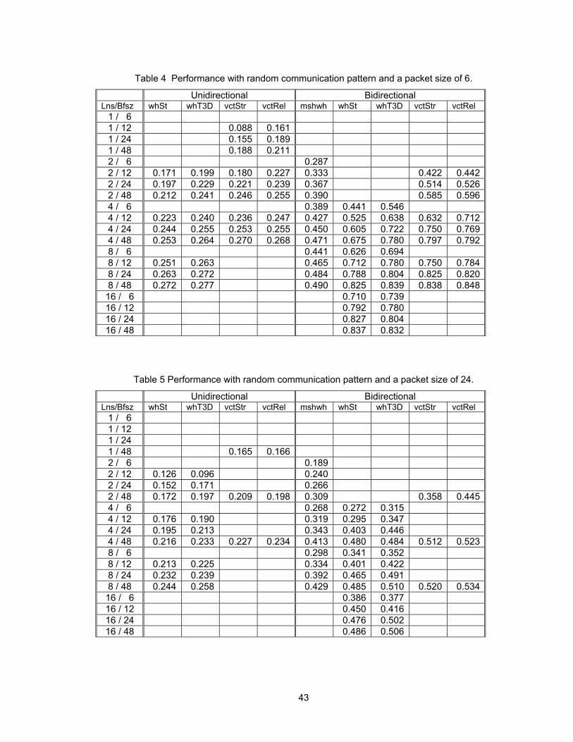
43
Table 4 Performance with random communication pattern and a packet size of 6.
Unidirectional Bidirectional Lns/Bfsz whSt whT3D vctStr vctRel mshwh whSt whT3D vctStr vctRel
1 / 6 1 / 12 0.088 0.161 1 / 24 0.155 0.189 1 / 48 0.188 0.211 2 / 6 0.287 2 / 12 0.171 0.199 0.180 0.227 0.333 0.422 0.4422 / 24 0.197 0.229 0.221 0.239 0.367 0.514 0.5262 / 48 0.212 0.241 0.246 0.255 0.390 0.585 0.5964 / 6 0.389 0.441 0.546 4 / 12 0.223 0.240 0.236 0.247 0.427 0.525 0.638 0.632 0.7124 / 24 0.244 0.255 0.253 0.255 0.450 0.605 0.722 0.750 0.7694 / 48 0.253 0.264 0.270 0.268 0.471 0.675 0.780 0.797 0.7928 / 6 0.441 0.626 0.694 8 / 12 0.251 0.263 0.465 0.712 0.780 0.750 0.7848 / 24 0.263 0.272 0.484 0.788 0.804 0.825 0.8208 / 48 0.272 0.277 0.490 0.825 0.839 0.838 0.84816 / 6 0.710 0.739 16 / 12 0.792 0.780 16 / 24 0.827 0.804 16 / 48 0.837 0.832
Table 5 Performance with random communication pattern and a packet size of 24.
Unidirectional Bidirectional Lns/Bfsz whSt whT3D vctStr vctRel mshwh whSt whT3D vctStr vctRel
1 / 6 1 / 12 1 / 24 1 / 48 0.165 0.166 2 / 6 0.189 2 / 12 0.126 0.096 0.240 2 / 24 0.152 0.171 0.266 2 / 48 0.172 0.197 0.209 0.198 0.309 0.358 0.4454 / 6 0.268 0.272 0.315 4 / 12 0.176 0.190 0.319 0.295 0.347 4 / 24 0.195 0.213 0.343 0.403 0.446 4 / 48 0.216 0.233 0.227 0.234 0.413 0.480 0.484 0.512 0.5238 / 6 0.298 0.341 0.352 8 / 12 0.213 0.225 0.334 0.401 0.422 8 / 24 0.232 0.239 0.392 0.465 0.491 8 / 48 0.244 0.258 0.429 0.485 0.510 0.520 0.53416 / 6 0.386 0.377 16 / 12 0.450 0.416 16 / 24 0.476 0.502 16 / 48 0.486 0.506

44
Table 6 Performance with hot-spot communication pattern and a packet size of 6.
Unidirectional Bidirectional Lns/Bfsz whSt whT3D vctStr vctRel mshwh whSt whT3D vctStr vctRel
1 / 6 1 / 12 0.141 0.094 1 / 24 0.157 0.134 1 / 48 0.163 0.157 2 / 6 0.206 2 / 12 0.144 0.161 0.172 0.154 0.225 0.234 0.2442 / 24 0.159 0.176 0.178 0.172 0.237 0.246 0.2702 / 48 0.169 0.183 0.246 0.255 0.242 0.270 0.2974 / 6 0.266 0.326 0.363 4 / 12 0.176 0.176 0.176 0.174 0.284 0.361 0.388 0.390 0.4394 / 24 0.184 0.183 0.182 0.188 0.298 0.384 0.418 0.422 0.4634 / 48 0.186 0.190 0.187 0.188 0.309 0.405 0.441 0.458 0.4748 / 6 0.289 0.401 0.417 8 / 12 0.187 0.186 0.302 0.435 0.433 0.427 0.4658 / 24 0.188 0.192 0.312 0.450 0.450 0.454 0.4648 / 48 0.191 0.195 0.319 0.463 0.469 0.463 0.47816 / 6 0.429 0.450 16 / 12 0.448 0.448 16 / 24 0.469 0.469 16 / 48 0.474 0.474
Table 7 Performance with hot-spot communication pattern and a packet size of 24.
Unidirectional Bidirectional Lns/Bfsz whSt whT3D vctStr vctRel mshwh whSt whT3D vctStr vctRel
1 / 6 1 / 12 1 / 24 1 / 48 0.188 0.211 2 / 6 0.162 2 / 12 0.117 0.096 0.182 2 / 24 0.134 0.148 0.203 2 / 48 0.154 0.165 0.169 0.159 0.227 0.225 0.2734 / 6 0.225 0.230 0.253 4 / 12 0.152 0.162 0.239 0.268 0.279 4 / 24 0.166 0.169 0.258 0.322 0.359 4 / 48 0.176 0.178 0.176 0.178 0.286 0.375 0.390 0.380 0.4328 / 6 0.242 0.309 0.315 8 / 12 0.169 0.176 0.277 0.360 0.364 8 / 24 0.186 0.180 0.293 0.389 0.398 8 / 48 0.188 0.188 0.307 0.420 0.435 0.450 0.47216 / 6 0.322 0.330 16 / 12 0.373 0.384 16 / 24 0.427 0.416 16 / 48 0.455 0.461

45
Table 8 Performance with near communication pattern and a packet size of 6.
Unidirectional Bidirectional Lns/Bfsz whSt whT3D vctStr vctRel mshwh whSt whT3D vctStr vctRel
1 / 6 1 / 12 0.107 0.173 1 / 24 0.169 0.206 1 / 48 0.206 0.225 2 / 6 0.317 2 / 12 0.189 0.214 0.186 0.246 0.380 0.462 0.4902 / 24 0.218 0.246 0.238 0.263 0.429 0.553 0.6052 / 48 0.234 0.262 0.270 0.274 0.465 0.645 0.6844 / 6 0.458 0.530 0.666 4 / 12 0.244 0.261 0.258 0.270 0.506 0.619 0.772 0.761 0.8294 / 24 0.265 0.277 0.277 0.281 0.558 0.724 0.834 0.885 0.8604 / 48 0.281 0.287 0.292 0.291 0.591 0.788 0.868 0.881 0.8798 / 6 0.527 0.745 0.788 8 / 12 0.277 0.285 0.570 0.848 0.853 0.855 0.8858 / 24 0.292 0.295 0.579 0.887 0.876 0.877 0.8938 / 48 0.298 0.302 0.615 0.893 0.889 0.895 0.89116 / 6 0.806 0.825 16 / 12 0.887 0.900 16 / 24 0.893 0.888 16 / 48 0.888 0.902
Table 9 Performance with near communication pattern and a packet size of 24.
Unidirectional Bidirectional Lns/Bfsz whSt whT3D vctStr vctRel mshwh whSt whT3D vctStr vctRel
1 / 6 1 / 12 1 / 24 1 / 48 0.133 0.173 2 / 6 0.212 2 / 12 0.141 0.120 0.263 2 / 24 0.169 0.185 0.312 2 / 48 0.190 0.214 0.216 0.223 0.362 0.394 0.4584 / 6 0.300 0.311 0.328 4 / 12 0.191 0.209 0.349 0.390 0.450 4 / 24 0.212 0.232 0.417 0.463 0.448 4 / 48 0.244 0.251 0.262 0.246 0.459 0.503 0.499 0.504 0.5358 / 6 0.319 0.371 0.401 8 / 12 0.234 0.246 0.380 0.448 0.488 8 / 24 0.253 0.259 0.436 0.540 0.506 8 / 48 0.272 0.277 0.499 0.510 0.546 0.530 0.55616 / 6 0.411 0.414 16 / 12 0.459 0.488 16 / 24 0.553 0.499 16 / 48 0.539 0.540

46
5.2 Latency
In order for a packet to come into the node there must be room in the node for the packet. There
is some handshaking that goes on between the transmitter node and the receiver node. For VCT
this handshaking is simple and can be easily spread over multiple cycles. Because the nature of
VCT guarantees that packets can’t be halted mid-packet. For WH this handshaking is more
complex and can be spread across two or more cycles by careful management of buffer space.
The requirements of the handshaking time are less stringent than the other times, so this really
doesn’t play into the latency.
Flit 3Flit 4
-
Flit 2
Flit 2Flit 3
-
Flit 1
Flit 1Flit 2
-
Flit 0
Flit 0Flit 1
-
-
Flit 0--
-
---
-
InBuf 0InBuf 1InBuf 2
•••
OutBuf
Select PathArbitrate
Crossbar
1 2 3 4 5 6
Figure 15 Packet latency through node.
When a packet comes into the node we first must decide which input buffer to place it in. We
start filling buffers from Buffer 0. Buffers are filled in order, that is, if Buffer 2 has valid data, then
Buffer 1 and Buffer 0 must also have valid data. In order to decide which buffer to place an
incoming flit in we do three two things. Firstly, we determine if a flit is being transferred from
Buffer 0 to a node output. This determination is simple for all but the first flit of a packet. In the
case of the first flit, this is the end of the arbitration path. Second, we determine which is the
lowest numbered empty buffer. This is equivalent to a priority encode of the number of buffers.
The logic design is optimized for the path that results when the first flit wins its output arbitration
and starts transmitting data.
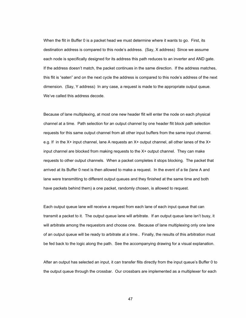
47
When the flit in Buffer 0 is a packet head we must determine where it wants to go. First, its
destination address is compared to this node’s address. (Say, X address) Since we assume
each node is specifically designed for its address this path reduces to an inverter and AND gate.
If the address doesn’t match, the packet continues in the same direction. If the address matches,
this flit is “eaten” and on the next cycle the address is compared to this node’s address of the next
dimension. (Say, Y address) In any case, a request is made to the appropriate output queue.
We’ve called this address decode.
Because of lane multiplexing, at most one new header flit will enter the node on each physical
channel at a time. Path selection for an output channel by one header flit block path selection
requests for this same output channel from all other input buffers from the same input channel.
e.g. If in the X+ input channel, lane A requests an X+ output channel, all other lanes of the X+
input channel are blocked from making requests to the X+ output channel. They can make
requests to other output channels. When a packet completes it stops blocking. The packet that
arrived at its Buffer 0 next is then allowed to make a request. In the event of a tie (lane A and
lane were transmitting to different output queues and they finished at the same time and both
have packets behind them) a one packet, randomly chosen, is allowed to request.
Each output queue lane will receive a request from each lane of each input queue that can
transmit a packet to it. The output queue lane will arbitrate. If an output queue lane isn’t busy, it
will arbitrate among the requestors and choose one. Because of lane multiplexing only one lane
of an output queue will be ready to arbitrate at a time.. Finally, the results of this arbitration must
be fed back to the logic along the path. See the accompanying drawing for a visual explanation.
After an output has selected an input, it can transfer flits directly from the input queue’s Buffer 0 to
the output queue through the crossbar. Our crossbars are implemented as a multiplexer for each

48
output with an input for each possible source. The path through the crossbar is directly related to
the number of inputs and how fact the logic reduce these inputs to one output.
We’ve divided this up into cycles that are practical. The latency through our nodes is three
cycles. The first cycle has the flit going into the input buffer. The second cycle had the address
decode and the arbitration. The third cycle is through the crossbar. Each cycle had the delay
time for the appropriate path plus the FlipFlop setup and output delay time plus the delay for clock
skew and jitter. By using a logic design trick, we’ve cut out a little time from the second and third
cycles by not actually latching between these cycles, but by making this delay part of a two-cycle
path. This saves us some setup, output delay, and clock skew time. Because we only arbitrate
when Buffer 0 has a head flit, this isn’t too hard to do. Our control state machines control when
we use this two-cycle path or not. Our cycle time ends up being defined by the greater of:
crossbar cycle path delay
or
address decode>arbitration->crossbar path delay
2
Note that in a cascaded crossbar node, the latency is 3 cycles for X to X, Y to Y, or Y to P. But is
6 cycles for X to Y, or X to P. Also note that for nodes that have multiple lanes per channel, the
latency can be higher because each lane has to share a physical channel.
5.3 Area
The cell area we determine is the area in mm2 that a router node would occupy in LSI Logic’s
G10-p Cell Based 0.18 micron technology. The base design was coded in Verilog HDL. The
Synopsys logic synthesis tools were run on this design using LSI Logic’s G10-p as the target
technology. This yielded area estimates for the base design. The router node design is very

49
modular. There are input buffers, output queues, and a very small amount of logic in-between.
This makes evaluating the options easier because they are a change to one of the modules.
The design options were evaluated in either of two ways. Some options were coded into Verilog
and the cell area was determined with the Synopsys logic synthesis tools. The FIFO size,
crossbar, and lane multiplexing options were determined this way. The input buffer sharing
options were determined by investigating the logic of the base design and shared FIFO designs
and scaling.
The G10-p RAM cell characteristics were examined and a two port, 1read 1write, asynchronous
RAM was chosen as the one used for these designs. (M10P211LA) Using the data points for
RAM size in words and bit width and cell area, a formula was developed that would provide cell
areas for data points not listed in the databook. The RAM area is determined for all RAM options
without forcing the number of words to a power of 2. This would unnecessarily distort the area
results to an implementation in a particular technology and make the results less general.
Then formulas were created for the various design options. These formulas are in the form of
Visual Basic programs used in a Microsoft Excel spreadsheet. A sample program follows. This is
for a bidirectional virtual cut-through node with cascaded crossbar. The main function calculates
two major parts, fifoarea and crossbararea. fifoarea is basically a count of the number of input
queues from the Crossbar times the area for an input queue with the particular FIFO size ,
number of lanes, and sharing option. crossbararea is a count of the output queues times their
size. The functions IQ_bivct and OQ determine the size of a single input and output queue.
'bidirectional virtual cut-through, cascaded crossbar Function bivct(lanes, fifo, share) Dim l, fifoarea, crossbararea If (s = 2) Then s = 1 'for bivct share 1 and 2 are the same End If l = lanes fifoarea = (6 * l) * IQ_bivct(fifo, l, share) crossbararea = 2 * ((l * OQ(3 * l)) + ((2 * l) * OQ(2 * l))) bivct = fifoarea + crossbararea

50
End Function Function IQ_bivct(fifo_int, lanes, share) Dim Base, rm Dim fifo fifo = fifo_int * 1# Base = cells2mm(7032#) If (fifo <= 4) Then share = 0 'no sharing for fifos <= 4 End If If (share = 0) Then rm = 1# End If If (share = 1) Then rm = Switch(lanes = 1, 1#, lanes = 2, 1.53, lanes = 4, 2.25) 'reg multiplier End If If (share = 2) Then rm = Switch(lanes = 1, 1#, lanes = 2, 1.53, lanes = 4, 2.25) 'reg multiplier End If IQ_bivct = (rm * Base) + (ramarea(lanes * (fifo - 4#) / 2, 20, lanes) / lanes) If (share = 3) Then 'vct node sharing uses this rm = Switch(lanes = 1, 4.92, lanes = 2, 5.42, lanes = 4, 6.75) IQ_bivct = (rm * Base) + (1.75 * ramarea(lanes * (fifo - 4#) / 2, 20, lanes) / lanes) End If End Function ' ram area with no increments on #words or #bits ' good for up to 512 words, 72 bits ' w - words in RAM ' b - bit width of RAM ' rd - number of read ports Function ramarea(w, b, rd) Dim Area If (w <= 0) Then ramarea = 0 End If Area = (180.6 + (6.839 * w)) + (42.29 + (1.217 * w)) * b ramarea = (Area * 0.0001) * ((1 + rd) / 2) End Function Function OQ(ports) OQ = cells2mm(374.3 + (225.7 * ports)) End Function Function cells2mm(cells) cells2mm = (cells / 3.2) / 13082 End Function
Figure 16 Visual Basic code for bidirectional VCT area.
The following two pages show the cell areas, in mm2 for the design options investigated. They
are extracted from a Microsoft Excel spreadsheet.

51
Table 10 Area of designs with no input buffer sharing.
Bidirectional –Cascaded Crossbar Bidirectional – Full Crossbar Lns/Bfsz mshwh whSt whT3D vctStr VctRel mshwh whSt whT3D vctStr vctRel
1 / 6 1.75 1.35 1 / 12 1.81 1.81 1.81 1.40 1.40 1.401 / 24 1.92 1.92 1.92 1.49 1.49 1.491 / 48 2.15 2.15 2.15 1.68 1.68 1.682 / 6 3.35 3.61 3.61 2.20 2.57 2.57 2 / 12 3.52 3.73 3.73 3.52 3.52 2.33 2.66 2.66 2.33 2.332 / 24 3.85 3.95 3.95 3.85 3.85 2.58 2.82 2.82 2.58 2.582 / 48 4.53 4.40 4.40 4.53 4.53 3.09 3.16 3.16 3.09 3.094 / 6 6.99 7.04 7.04 3.95 4.51 4.51 4 / 12 7.55 7.38 7.38 7.55 7.55 4.34 4.75 4.75 4.34 4.344 / 24 8.68 8.05 8.05 8.68 8.68 5.14 5.22 5.22 5.14 5.144 / 48 10.92 9.40 9.40 10.92 10.92 6.73 6.18 6.18 6.73 6.738 / 6 13.34 13.34 8.68 8.68 8 / 12 14.27 14.27 9.45 9.45 8 / 24 16.14 16.14 11.00 11.00 8 / 48 19.88 19.88 14.08 14.08
Table 11 Area of designs with input buffer sharing between lanes.
Bidirectional –Cascaded Crossbar Bidirectional – Full Crossbar Lns/Bfsz mshwh whSt whT3D vctStr vctRel mshwh whSt whT3D vctStr vctRel
1 / 6 1.75 1.35 1 / 12 1.81 1.81 1.81 1.40 1.40 1.401 / 24 1.92 1.92 1.92 1.49 1.49 1.491 / 48 2.15 2.15 2.15 1.68 1.68 1.682 / 6 3.35 3.61 3.61 2.20 2.57 2.57 2 / 12 4.59 3.73 3.73 4.59 4.59 2.33 2.66 2.66 2.33 2.332 / 24 4.92 3.95 3.95 4.92 4.92 2.58 2.82 2.82 2.58 2.582 / 48 5.60 4.40 4.40 5.60 5.60 3.09 3.16 3.16 3.09 3.094 / 6 6.99 7.04 7.04 3.95 4.51 4.51 4 / 12 12.59 9.52 9.52 12.59 12.59 4.34 6.26 6.26 4.34 4.344 / 24 13.72 10.19 10.19 13.72 13.72 5.14 6.74 6.74 5.14 5.144 / 48 15.96 11.54 11.54 15.96 15.96 6.73 7.69 7.69 6.73 6.738 / 6 13.34 13.34 8.68 8.68 8 / 12 22.67 22.67 16.38 16.38 8 / 24 24.54 24.54 17.92 17.92 8 / 48 28.28 28.28 21.01 21.01

52
Table 12 Area of designs with input buffer sharing within a physical channel.
Bidirectional –Cascaded Crossbar Bidirectional – Full Crossbar Lns/Bfsz mshwh whSt whT3D vctStr vctRel mshwh whSt whT3D vctStr vctRel
1 / 6 1.75 1.35 1 / 12 1.81 1.81 1.81 1.40 1.40 1.401 / 24 1.92 1.92 1.92 1.49 1.49 1.491 / 48 2.15 2.15 2.15 1.68 1.68 1.682 / 6 3.35 3.61 3.61 2.20 2.57 2.57 2 / 12 4.59 4.18 4.18 4.59 4.59 3.13 2.66 2.66 3.13 3.132 / 24 4.92 4.40 4.40 4.92 4.92 3.38 2.82 2.82 3.38 3.382 / 48 5.60 4.85 4.85 5.60 5.60 3.89 3.16 3.16 3.89 3.894 / 6 6.99 7.04 7.04 3.95 4.51 4.51 4 / 12 12.59 11.49 11.49 12.59 12.59 7.91 4.75 4.75 7.91 7.914 / 24 13.72 12.17 12.17 13.72 13.72 8.71 5.22 5.22 8.71 8.714 / 48 15.96 13.52 13.52 15.96 15.96 10.30 6.18 6.18 10.30 10.308 / 6 13.34 13.34 8.68 8.68 8 / 12 40.27 40.27 9.45 9.45 8 / 24 42.14 42.14 11.00 11.00 8 / 48 45.88 45.88 14.08 14.08
Table 13 Area of designs with input buffer sharing within the entire node.
Bidirectional –Cascaded Crossbar Bidirectional – Full Crossbar Lns/Bfsz mshwh whSt whT3D vctStr vctRel mshwh whSt whT3D vctStr vctRel
1 / 6 1.75 1.35 1 / 12 6.26 6.26 6.26 5.11 5.11 5.111 / 24 6.46 6.46 6.46 5.28 5.28 5.281 / 48 6.85 6.85 6.85 5.60 5.60 5.602 / 6 3.35 3.61 3.61 2.20 2.57 2.57 2 / 12 13.25 13.64 13.64 13.25 13.25 9.63 10.09 10.09 9.63 9.632 / 24 13.84 14.04 14.04 13.84 13.84 10.07 10.39 10.39 10.07 10.072 / 48 15.01 14.82 14.82 15.01 15.01 10.95 10.98 10.98 10.95 10.954 / 6 6.99 7.04 7.04 3.95 4.51 4.51 4 / 12 32.31 32.20 32.20 32.31 32.31 21.88 22.33 22.33 21.88 21.884 / 24 34.28 33.38 33.38 34.28 34.28 23.27 23.16 23.16 23.27 23.274 / 48 38.20 35.73 35.73 38.20 38.20 26.05 24.83 24.83 26.05 26.058 / 6 13.34 13.34 8.68 8.68 8 / 12 71.19 71.19 56.41 56.41 8 / 24 74.46 74.46 59.11 59.11 8 / 48 81.01 81.01 64.51 64.51

53
5.4 Timing
Timing is determined based on the designs being implemented in LSI Logic’s G10-p Cell Based
0.18 micron technology. Using the LSI Logic G10-p databook and Microsoft Excel, the delay for
NAND gates with various fan-in and fan-out are determined and put into a function. See
Appendix B. The paths were determined by inspection of the design. The logic is designed using
almost exclusively NAND gates. This simplifies the analysis and while it may alter the absolute
numbers to a small degree, it preserves the relative delays. Fan-in and fan-out are used as
parameters to the NAND delay function generated for Microsoft Excel. The paths are entered
into a Microsoft Excel spreadsheet and tabulated. See Appendix B.
The following table shows the resultant cycle times for some of the design options investigated.
The bidirectional nodes are cascaded crossbar, and the unidirectional nodes are full crossbar.
Refer to Appendix B for details on the components of the path delays and the determination of
the gate delays themselves.
As a general observation, the path delays are very small. This is because the router designs are
relatively simple compared to other kinds of logic, say like you’d find in a processor. The other
important observation is that the delay is roughly proportional to a constant, plus the log of the
number of ports in the crossbar,
k + .65 * log10(# crossbar ports).
Where k = .83 for the bidirectional case and k = .86 for the unidirectional case.
The constant is due to the path constants, flip-flop clock to output delay, setup time, clock skew
and jitter allotments, and the path delays that are independent of the number of ports (i.e.
address matching). The constant is slightly bigger for the unidirectional cases because these are

54
implemented as full crossbars and the path selection logic has slightly more delay due to the
more turning options. The remainder of the path’s delay is in the arbitration and crossbar logic.
This logic has a delay proportional to the log of the number of ports in the crossbar.
Table 14 Cycle time summary.
1 lane 2 lane 4 laneBidirectional VCT 1.18 1.39 1.50Bidirectional Wormhole 1.39 1.49 1.70Unidirectional VCT 1.18 1.39 1.53Unidirectional Wormhole 1.42 1.53 1.73
Bidirectional Virtual Cut-Through
1 lane 2 lane 4 laneFIFO reg > CB > LM > Output reg FIFO reg clk to output .41 .41 .41Crossbar,lane multiplex .42 .63 .71Output reg setup .10 .10 .10clock skew, jitter .25 .25 .25
Total 1.18 1.39 1.47 FIFO > AD > PA > CB > LM > Output reg FIFO reg clk to output .41 .41 .41Addr match/path select .62 .58 .66Path arbitrate .49 .73 .88Crossbar,lane multiplex .42 .63 .71Output reg setup .10 .10 .10clock skew, jitter .25 .25 .25
Total 2.28 2.69 3.00Total / 2 1.14 1.35 1.50
Cycle time (max of both) 1.18 1.39 1.50
Bidirectional Wormhole
1 lane 2 lane 4 laneFIFO reg > CB > LM > Output reg FIFO reg clk to output .41 .41 .41Crossbar,lane multiplex .63 .71 .92Output reg setup .10 .10 .10clock skew, jitter .25 .25 .25
Total 1.39 1.47 1.68 FIFO > AD > PA > CB > LM > Output reg FIFO reg clk to output .41 .41 .41Addr match/path select .70 .58 .66Path arbitrate .67 .93 1.05Crossbar,lane multiplex .63 .71 .92

55
Output reg setup .10 .10 .10clock skew, jitter .25 .25 .25
Total 2.76 2.98 3.39Total / 2 1.38 1.49 1.70
Cycle time (max of both) 1.39 1.49 1.70
Unidirectional Virtual Cut-Through
1 lane 2 lane 4 laneFIFO reg > CB > LM > Output reg FIFO reg clk to output .41 .41 .41Crossbar,lane multiplex .42 .63 .71Output reg setup .10 .10 .10clock skew, jitter .25 .25 .25
Total 1.18 1.39 1.47 FIFO > AD > PA > CB > LM > Output reg FIFO reg clk to output .41 .41 .41Addr match/path select .63 .59 .67Path arbitrate .53 .77 .92Crossbar,lane multiplex .42 .63 .71Output reg setup .10 .10 .10clock skew, jitter .25 .25 .25
Total 2.33 2.74 3.05Total / 2 1.17 1.37 1.53
Cycle time (max of both) 1.18 1.39 1.53
Unidirectional Wormhole
1 lane 2 lane 4 laneFIFO reg > CB > LM > Output reg FIFO reg clk to output .41 .41 .41Crossbar,lane multiplex .63 .71 .92Output reg setup .10 .10 .10clock skew, jitter .25 .25 .25
Total 1.39 1.47 1.68 FIFO > AD > PA > CB > LM > Output reg FIFO reg clk to output .41 .41 .41Addr match/path select .75 .63 .71Path arbitrate .69 .96 1.08Crossbar,lane multiplex .63 .71 .92Output reg setup .10 .10 .10clock skew, jitter .25 .25 .25
Total 2.84 3.05 3.47Total / 2 1.42 1.53 1.73
Cycle time (max of both) 1.42 1.58 1.73

56
5.5 Cost-Effective Designs
The following graphs show cost-effectiveness of each design option in terms of performance vs.
cell area for each combination of traffic pattern and packet size. The cost-effective designs,
those that have higher performance for a given cell area, are easy to spot because they are on
the top left frontier.
Figure 17 Legend for capacity versus area graphs.

57
Figure 18 Capacity versus area graph for a random pattern with a packet size of 6, top, and 24, bottom.

58
Figure 19 Capacity versus area graph for a hot-spot pattern with a packet size of 6, top, and 24, bottom.

59
Figure 20 Capacity versus area graph for a near pattern with a packet size of 6, top, and 24, bottom.

60
Table 15 Cost-effective designs.
Random, packet size of 6 Unidirectional VCT – Relaxed, 1 lane, buffer size = 12 Unidirectional VCT – Relaxed, 1 lane, buffer size = 24 Unidirectional VCT – Relaxed, 1 lane, buffer size = 48 Bidirectional VCT – Relaxed, 1 lane, buffer size = 12 Bidirectional VCT – Relaxed, 1 lane, buffer size = 24 Bidirectional VCT – Relaxed, 1 lane, buffer size = 48 Bidirectional VCT – Relaxed, 2 lane, buffer size = 12 Bidirectional VCT – Relaxed, 2 lane, buffer size = 24 Bidirectional VCT – Relaxed, 2 lane, buffer size = 48 Random, packet size of 24 Unidirectional VCT – Relaxed, 1 lane, buffer size = 48 Bidirectional VCT – Relaxed, 1 lane, buffer size = 48 Hot-spot, packet size of 6 Unidirectional VCT – Strict, 1 lane, buffer size = 12 Unidirectional VCT – Strict, 1 lane, buffer size = 24 Unidirectional VCT – Strict, 1 lane, buffer size = 48 Bidirectional VCT – Relaxed, 1 lane, buffer size = 12 Bidirectional VCT – Relaxed, 1 lane, buffer size = 24 Bidirectional VCT – Relaxed, 1 lane, buffer size = 48 Bidirectional VCT – Relaxed, 2 lane, buffer size = 12 Bidirectional VCT – Relaxed, 2 lane, buffer size = 24 Bidirectional VCT – Relaxed, 2 lane, buffer size = 48 Hot-spot, packet size of 24 Unidirectional VCT – Relaxed, 1 lane, buffer size = 48 Bidirectional WH T3D, 1 lane, buffer size = 24 Bidirectional WH T3D, 1 lane, buffer size = 48 Bidirectional VCT – Relaxed, 2 lane, buffer size = 48 Near, packet size of 6 Unidirectional VCT – Relaxed, 1 lane, buffer size = 12 Unidirectional VCT – Relaxed, 1 lane, buffer size = 24 Unidirectional VCT – Relaxed, 1 lane, buffer size = 48 Bidirectional VCT – Relaxed, 1 lane, buffer size = 12 Bidirectional VCT – Relaxed, 1 lane, buffer size = 24 Bidirectional VCT – Relaxed, 1 lane, buffer size = 48 Bidirectional VCT – Relaxed, 2 lane, buffer size = 12 Bidirectional VCT – Relaxed, 2 lane, buffer size = 24 Near, packet size of 24 Unidirectional VCT – Relaxed, 1 lane, buffer size = 48 Bidirectional VCT – Relaxed, 1 lane, buffer size = 48

61
5.6 Buffer Sharing
Figure 20 shows the cost/benefit of buffer sharing for bidirectional WH networks. Table 16
identifies the cost-effective alternatives. Sharing has virtually no benefit for random loads but
some benefit for hot spot loads. This observation is similar to that of [3] although our sharing
schemes retain the deterministic routing algorithm. The sharing designs that prove cost-effective
under hot spot loads are those with a single lane per virtual channel and sharing between the pair
of lanes in a virtual channel pair. These have relatively low area overhead and no added latency.
Table 16 Cost-effective designs with sharing.
Random No sharing, 1 lane, 6 flit buffer No sharing, 1 lane, 12 flit buffer No sharing, 1 lane, 24 flit buffer No sharing, 1 lane, 48 flit buffer Hot-spot No sharing, 1 lane, 6 flit buffer No sharing, 1 lane, 12 flit buffer No sharing, 1 lane, 24 flit buffer No sharing, 1 lane, 48 flit buffer Sharing among lanes in a virtual channel pair, 1 lane, 48 flit buffer Sharing among all lanes in a node, 1 lane, 24 flit buffer Sharing among all lanes in a node, 1 lane, 48 flit buffer

62
Figure 21 Buffer sharing capacity versus area graphs for random and hot-spot patterns with a packet size of 6.

63
5.7 Comparison to an Output Queue Design
We investigate an output queue design, after the SP2 implementation [21], to verify that we aren’t
missing something fundamental. We try to keep the design optimized for our choice of
technology and application in the same manner as for our other designs. We discover that we
are not able to make some of the optimizations we had made for the input queue designs.
Particularly bothersome is the requirement that the pointer array be written or read in one cycle.
(Our input queue designs are able to spread an array read or write over two cycles.)
The cell area and timing characteristics of this design follow. When we use the upper bound on
performance of 1 flit per node per cycle to get an upper bound for the performance of the output
queue design, we see that it is not cost-effective for the Random or Near traffic patterns. For the
Hot Spot traffic pattern we believe that the performance of the output queue design will be
reduced by the same factors that reduced the performance of the other designs and that the
output queue design will not be cost-effective for the Hot Spot traffic pattern either.
Table 17 Output Queue Design Characteristics.
Buffer Size Area (mm2) Cycle Time Performance Upper Bound 6 Not practical because register portion exceeds buffer size. 12 2.38 3.05 ns .328 flit/node/ns 24 2.82 3.11 ns .322 flit/node/ns 48 3.69 3.19 ns .313 flit/node/ns
5.8 Experiments and Observations
Topology, latency, and capacity
For reasons discussed above, the only latency results presented are those shown in Figure 13.
With no congestion, latencies of the three topologies are related to the average path length: k for
the unidirectional torus, about 2/3 k for the mesh, and 1/2 k for the bidirectional torus. However,
since the injection time is a significant part of the latency, 2 times the packet size or 10 in Figure

64
13, and identical for all three topologies, the average path length may not be the most critical
aspect of changing topology for small networks. Rather, it is the effect on capacity.
There are three related reasons why topology affects capacity: i) differences in total internode
bandwidth , ii) the shorter path length gets packets out more quickly and so they interfere less
with each other, and iii) the intrinsic variation in quality among the buffer load balancing
opportunities. These latency/bandwidth effects can be seen in Figure 13 as follows. The level of
the `flat parts' of each bundle are due to differences in average path length while the locations of
the knees are given by differences in the capacity-related properties.
WH virtual channel selection
This and the next several sets of observations are based on Tables 4 through 9.
For bidirectional torus WH networks, T3D virtual channel selection was found to extremely
effective with increases in capacity of up to 30% over the standard method. The advantage is
diminished with the number of channels, however. This is because lanes within virtual channels
are selected dynamically. Therefore, in a configuration with, say, four total lanes per direction,
the two pairs of lanes are selected statically while the lanes within the virtual channels are
selected dynamically. As the number of lanes increases, the quality of the initial selection
becomes less important.
The impact of optimized channel selection is much less pronounced for the unidirectional torus.
This is somewhat surprising because of the dramatic reduction in channel imbalance due to T3D-
style optimization.
The impact of optimized virtual channel selection method is also less for non-random
communication patterns. This may be because both unidirectional and bidirectional selection
tables were optimized for a random load. Performance versus the near-random load can

65
certainly be improved by recomputing the lane selections, but the hot-spot load, which is
inherently unpredictable, is more problematic.
VCT buffer control
Relaxing the VCT buffer control policy increases the usable buffer space for packets entering X
from the input and Y from X. As expected, the improvement is most pronounced the smaller
buffer sizes and is particularly important when routing the 24 flit packets with 48 flit buffers.
Size of buffers
Increasing the buffer size has the predictably positive effect on capacity. The improvement starts
to tail off only for the designs with the largest total buffer capacity. For packets larger than 24
flits, larger buffers may be called for.
Number of buffers
Dally, in his study of virtual channel flow control, keeps the total buffer size constant while dividing
that space among from 1 to 16 lanes [8]. Although not tabulated separately, we have done this
for a buffer size of 48 per direction. In most cases, the improvement in network capacity when
the number of lanes per (virtual) channel is increased from 1 to 2 was significant while the
improvement from 2 to 4 was slight, and, in some cases, negative. For the bidirectional WH torus
networks, the improvement was much greater with standard virtual channel selection than with
the optimized version. Clearly this is another manifestation of the diminishing return of increasing
the number of lanes.
When area and cycle time are accounted for, the 4 lane per (virtual) channel designs are clearly
poor. For VCT designs, 2 lanes per channel is often cost-effective. For WH designs, 2 lanes per
virtual channel (4 lanes per direction per dimension) is almost never cost-effective.

66
Effect of Topology
The unidirectional networks were found to be cost-effective only for the very simplest designs
which have no bidirectional equivalent, VCT with one lane per channel which equates to one lane
per dimension. In the case of two lanes per dimension, mesh WH with one lane per direction per
dimension was found to be better than either unidirectional VCT or WH with two lanes per
direction per dimension. In general, however, mesh networks were also found to be cost-
effective only were there was no bidirectional equivalent, that is, in the case with one lane per
direction per dimension with small buffer size.
Wormhole versus virtual cut-through switching
One difference is that VCT networks can be created with a single buffer per node per ring. Such
a WH network can only be constructed by either removing the wrap-around connections or
adding buffers. Therefore cost-effective VCT networks exist in niches where WH networks do
not.
For the two buffer per ring case, VCT retains a distinct advantage in capacity, up to 10% greater
for random loads, 8-14% for hot-spot loads, and up to 8% for near-random loads. As discussed
earlier, this disparity in differences is due to the different ways buffers are selected, static for WH
and dynamic for VCT. For reasons stated above, the near-random comparison is probably not
valid and the performances are probably closer than shown. However, the hot-spot load, which is
much more likely to occur in practice than a purely random load, accentuates the VCT advantage.
As the number of buffers increases and the initial static selection becomes less important, WH
and VCT performance converges.
Certain mesh and bidirectional torus WH configurations also have niches where they are the most
cost-effective. These are the lowest cost mesh WH networks and the bidirectional torus WH
networks with buffer sizes smaller than twice the packet size.

67
Accounting for area and operating frequency
Figures 16 to 18 contain the plots of network capacity in flits per node per nanosecond versus
switch area in cells. The cost-effective designs are those toward the left and top of each graph.
The four or five best designs for each combination of communication pattern and packet size are
identified.
Figures 16 to 18 combine three sets of results: i) the operating frequencies, ii) that the cell area,
and iii) the capacity measures. Putting these together it is clear that an architect working on an
application where area is important will be tempted to only select candidate switches from the left
edges of the graphs. Specifically:
• If increasing the number of lanes per direction to four or beyond was questionable from the
cycle-based capacity results alone, accounting for the slower clock shows that it is clearly not
cost-effective.
• The decision on larger buffers is less clear-cut, but the capacity/area graphs are again
illuminating. The designs with larger buffers cannot be eliminated out-right for the reason that
another design has both lower cost and better performance. Yet, a doubling of area appears
to yield only a few percent increase in capacity.
Buffer Sharing
Figure 20 shows the cost/benefit of buffer sharing for bidirectional WH networks. Table 17
identifies the cost-effective alternatives. Sharing has virtually no benefit for random loads but
some benefit for hot spot loads. This observation is similar to that of [3] although our sharing
schemes retain the deterministic routing algorithm. The sharing designs that prove cost-effective
under hot spot loads are those with a single lane per virtual channel and sharing between the pair
of lanes in a virtual channel pair. These have relatively low area overhead and no added latency.

68
In the hot-spot graph, one of the central queue designs appears cost-effective, in reality it is not.
In Figure 20 we do not penalize the central queue designs for output contention overhead which
would certainly eliminate the 8% advantage which had been achieved at a cost of a factor of 2.5
increase in area.

69
6 Conclusions
In this work we have endeavored to exhaustively explore the design space of low-cost
multicomputer networks including issues in switching, lane selection, buffer size, topology, routing
algorithm, and packet size.
Virtual Cut-Through is examined and found to be both more and less like Wormhole switching
than previously described. More in that virtually all of the critical hardware including multi-lane
channels can be identical to that of WH switches. Less in that VCT has its own deadlock issues
and is open to a different lane selection paradigm. It has been stated elsewhere that VCT versus
WH routing is a tradeoff between buffering and congestion. We suggest that for small packets
and equal buffering, it is really mostly the difference between static and dynamic lane selection.
Each design was characterized in two ways: with and RTL simulator that measured its capacity
with respect to several workloads, and by synthesizing it to obtain its cell area and operating
frequency. These results are analyzed with respect to the various parameters. Finally, the most
promising designs are determined.

70
References
[1] Aoyama, K., and Chien, A. A. The Cost of adaptivity and virtual lanes in a wormhole router.
Journal of VLSI Design (1994).
[2] Bolding, K. Non-uniformities introduced by virtual channel deadlock prevention. Tech. Rep.
UW-CSE-92-07-07, Dept. of Comp. Sci. and Eng., U. of Washington, Seattle, WA 98195,
1992.
[3] Bolding, K., Fulgham, M., and Snyder, L. The case for adaptive routing. IEEE Trans. on
Computers C-46, 12 (1997), 1281-1292.
[4] Bolotski, M, et.al. Abacus: A 1024 Processor 8ns SIMD Array. ???.
[5] Carbonaro, J., and Verhoorn, F. Cacallino: The teraflops router and NIC. In Proc. of Hot
interconnects Symposium IV (1996).
[6] Chien, A. A. A cost and speed model for k-ary n-cube wormhole routers. In Proc. of Hot
Interconnects ’93 (1993).
[7] Dally, W. J. Performance analysis of k-ary n-cube interconnection networks. IEEE Trans. on
Computers C-39, 6 (1990), 775-785.
[8] Dally, W. J. Virtual channel flow control. IEEE Trans. on parallel and Distributed Systems 3,
2 (1992), 194-205.
[9] Dally, W. J., and et al. The message processor: A multicomputer processing node with
efficient mechanisms. IEEE Micro 12, 2 (1994), 194-205
[10] Dally, W. J., and Seitz, C. L. The torus routing chip. Distributed Computing 1 (1986), 187-
196.
[11] Dally, W. J., and Seitz, C. L. Deadlock free routing in multiprocessor interconnection
networks. IEEE Trans. on Computers C-36, 5 (1987).
[12] Duato, J., Yalamanchili, S., and Ni, L. Interconnection Networks: An Engineering Approach.
IEEE Comuter Socieity Press, Los Alamitos, CA, 1997.
[13] Frazier, G. L. Buffering and Flow Control in Communication Switches. PhD thesis, Los
Angeles, CA, 1995.

71
[14] Galles, M. Scalable pipelined interconnect for distributed endpoint routing: The SPIDER
chip. In Proc. of Hot Interconnects Symposium IV (1996).
[15] Herbordt, M. C., and Weems, C. C. An emperical study of datapath, memory hierarchy, and
network in massively parallel array architectures. In Proc of the 1995 Int. Conf. on
Computer Design (1995), 546-551.
[16] Kermani, P., and Kleinrock, L. Virtual cut-through: A new computer communication
switching technique. Computer Networks 3 (1979), 267-286.
[17] Leighton, F. T. Average case analysis of greedy routing algorithms on arrays. In Proc. 2nd
Symposium on Parallel algorithms and Architectures (1990), pp. 2-11.
[18] LSI Logic Corp. G10-p cell Based ASIC Products. Milpitas, CA, 1997.
[19] Rexford, J. Tailoring Router Architectures to Performance Requirements in Cut-Through
Networks. PhD thesis, Dept. of Computer Science and Engineering, U of Michigan, 1996.
[20] Scott, S., and Thorson, G. Optimized routing in the Cray T3D. In Proc. of the Workshop on
Parallel Computer Routing and Communication (1994), pp. 281-294.
[21] Stunkel, C. B., and et al. The SP2 high-performance switch. IBM Systems Journal 34, 2
(1995), 185-204.
Related Documents